1
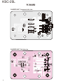
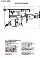
RAPID CHARGER
KSC-25L
SERVICE MANUAL
© 2011-10 PRINTED IN JAPAN
B51-8996-00 (Y) PDF
Relay terminal
(E23-1372-08) x 4
Cabinet (Upper)
(A02-4150-08)
KS
CH C
CO AR -25
MP GIN L (Fo
LE G(R Ba r LiTE
tt io
(G ED) ery) n
RN
)
Cabinet (Bottom)
(A02-4151-08)
Document Copyrights
Disclaimer
Copyright 2011 by JVC KENWOOD Corporation. All
rights reserved.
No part of this manual may be reproduced, translated,
distributed, or transmitted in any form or by any means,
electronic, mechanical, photocopying, recording, or otherwise, for any purpose without the prior written permission of
JVC KENWOOD Corporation.
While every precaution has been taken in the preparation
of this manual, JVC KENWOOD Corporation assumes no
responsibility for errors or omissions. Neither is any liability
assumed for damages resulting from the use of the information contained herein. JVC KENWOOD Corporation reserves
the right to make changes to any products herein at any time
for improvement purposes.
SPECIFICATIONS
PARTS LIST
Input Voltage .................................... AC 120~240V 50/60Hz
(Use the supplied AC adapter)
Charging Current ............................................... 945mA±5%
Charging Time ........................... KNB-55L: Approx. 150 min.
KNB-57L: Approx. 170 min.
Usable Temperature Range ..... 0°C to 40°C (32°F to 104°F)
Dimensions (W x H x D, charger only)
.................. 105 (4.13) x 54.6 (2.15) x 135 (5.32) mm (in)
Weight (charger only) ...................... Approx. 170g / 0.37 lbs
KSC-25L
Ref. New
No. parts
Parts No.
Description
✽ : New Parts
Destination
KSC-25L
✽
✽
A02-4150-08
A02-4151-08
CABINET(UPPER)
CABINET(BOTTOM)
✽
B62-2334-00
INSTRUCTION MANUAL
✽
✽
E03-0466-08
E23-1372-08
DC JACK
RELAY TERMINAL
✽
✽
✽
✽
✽
W08-1264-08
W08-1267-08
W08-1268-08
W08-1269-08
W08-1270-08
CHARGER
AC ADAPTER
AC ADAPTER
AC ADAPTER
AC ADAPTER
K
T
E
X
Note: The AC adapter and AC cord are arranged as a pair.
This product complies with the RoHS directive for the European market.
This PCB does not have theThis
LF silk
product
screen,
usesbut
Lead
it isFree
a lead-free
solder.
solder corresponding product.
KSC-25L
PC BOARD
CHARGER UNIT Component side view
L1
EC2
(JP3)
EC1
D2
Q1
(JP1)
XT1
(JP4)
R2
F1
L2
LED1
(JP5)
R3
(JP6)
D1
(JP2)
VR1
R1
U2
C5
R18
C6
R11
C26
EC3
D3
CHARGER UNIT Foil side view
C4
C3
C25
C24
C11
8
R10
C21
R5
C2
Q2
C20
R4
R9
C14
R8
R17
C22
R7
7
C15
C16
C12
C13
U1
R15
R16
R12
14
C18
C19
C17
1
C8
C7
R13
C10
C9
R19
R14
C23
R6
C1
2
KSC-25L
FLOW CHART
Li-ion : Vs = VB , when Battery is not in charger set.
Vs = 1/3 VB, when Battery is in charger set.
Therefore Ni-Cd/Ni-MH voltage must consider Vf
of protected reverse connection diode.
START
Does T, S
contact?
No
charge condition and on temperature stand-by condition.
Yes
open/short
check
Error battery
LED: Red Flash
Go to START
when T contact is off
Yes
No
Temperature
check
T 0°C or T 40°C
0°C T 40°C
Stand-by
temperature
LED: Red
Give +B terminal power
8.65V, 60mA, 5 second
Yes
A1
VB >8.85V
No
Are output
terminal shorted?
Yes
No
Battery distinguish
Voltage and
open/short
check
Above 5.8V
Above 8.55V or Below 0.5V
Below 5.8V
About 5.8V
180min. timer stop
Low voltage battery
charge: 150mA
180min. timer start
LED: Red
A2
Rapid charge
Constant current
945mA
Constant voltage
8.4V
180min. timer start
LED: Red
No
A3
VB >8.85V
5.5V >VB
Error battery
timer stop
LED: Red Flash
Yes
Go to START
when T contact is off
A2
100mA
Detected full charge
Finish charge
timer stop
Below 7.6V
LED: Green
Above 8.85V
A2
A1
A3
A1
Error battery
Timer STOP
LED: Red Flash
No
Does T, S
contact?
Yes
GO to START
Stand-by temperature
timer hold
LED: Red
A2
T 57°C or
T 0°C
timer recount
0°C T 45°C
Stand-by temperature
timer hold
LED: Red or Green
0°C T 45°C
timer recount
T
A3
Times 2
0°C
T 57°C
Count times
T 45°C
Times 2
Stand-by temperature
timer recount
Total 120min.
3
KSC-25L
SCHEMATIC DIAGRAM
Q1
(JP2)
Vcc
C1
R5
3
R6
R18
R10
R2
D3
C21
C10
(JP5)
S
T
R11
-
6
R16
OSCI
RESET
OSCO
11
7
VCC
C9
C15
P60
P68
P61
P67
C16
GND
10
C11
9
R17
8
TEST
(JP6)
C24
C20
C12
C7
P54
R19
13
12
C13
5
LED1 (RED)
R15
ADC0
C14
C17
C18
4
ADC3
4MHz
R14
3
14
Y1
2
C19
ADC1
C8
U1
ADC2
R13
R1
R12
R3
C26
1
(GRN)
VR1
(JP4)
Q2
R7
(JP3)
(JP1)
R8
C23
C6
C25
C
+
C5
OUT
GND
2
C4
IN
EC3
C3
R9
1
L1
D2
C2
U2
DC
7-15V
EC1
1.85A
EC2
D1
C22
F1
R4
JACK