1
UNION SWITCH & SIGNAL
SERVICE MANUAL 6700B
645 Russell Street
Batesburg, SC 29006
GENISYS SERIES 2000
Multi-Purpose Communication Products
Installation
Operation
Field Programming
Field Maintenance
June 1996
COPYRIGHT 1995, UNION SWITCH & SIGNAL, INC.
PRINTED IN USA
An ANSALDO Affiliated Company
TABLE OF CONTENTS
I
GENERAL INFORMATION .....................................................................................................1-1
1.1
RELATED MANUALS ..................................................................................................1-1
1.2
FORMAT OF MANUAL ................................................................................................1-1
1.3
INTRODUCTION..........................................................................................................1-2
1.3.1
General.........................................................................................................................1-2
1.3.2
Components .................................................................................................................1-7
1.3.2.1
Enhanced Controller Board N451441-9101 .................................................................1-7
and Software
1.3.2.2
32-Bit Output Boards N451441-9601, -9801................................................................1-7
1.3.2.3
32-Bit Input Board N451441-9701................................................................................1-8
1.3.2.4
Code Line Interface/Power Supply Board N451441-9402 ...........................................1-8
1.3.2.5
Code Line Interface Board N451441-9401...................................................................1-8
1.3.2.6
Power Supply Board N451441-9403 ............................................................................1-8
1.3.2.7
Card Enclosure N451891-0102....................................................................................1-8
1.3.2.8
Surge Suppressor/Serial Interface PCBs and Panels..................................................1-9
1.3.2.9
Summary ......................................................................................................................1-9
1.4
SYSTEM SPECIFICATIONS...................................................................................... 1-11
II
ENHANCED CONTROLLER PCB N451441-9101 .................................................................2-1
2.1
DESCRIPTION.............................................................................................................2-1
2.1.1
General Application ......................................................................................................2-1
2.1.2
Hardware ......................................................................................................................2-1
2.1.3
Communications Interfaces..........................................................................................2-5
2.1.3.1
Serial ............................................................................................................................2-5
2.1.3.2
Parallel..........................................................................................................................2-5
2.1.4
Software .......................................................................................................................2-5
2.1.4.1
Executive ......................................................................................................................2-5
2.1.4.2
Application ....................................................................................................................2-6
2.1.4.3
Field Configuration .......................................................................................................2-6
2.2
SPECIFICATIONS .......................................................................................................2-7
2.3
INSTALLATION............................................................................................................2-9
2.3.1
Shipment Inspection .....................................................................................................2-9
2.3.2
Pre-Installation Preparation..........................................................................................2-9
2.3.2.1
EPROMs.......................................................................................................................2-9
2.3.2.2
Jumpers........................................................................................................................2-9
2.3.3
Installation in Cardfile or Enclosure............................................................................ 2-11
2.3.4
Serial and Parallel Communications Interfaces ......................................................... 2-13
2.3.4.1
General....................................................................................................................... 2-13
SM 6700B 6/96
i
TABLE OF CONTENTS
2.3.4.2
PCB Connector “A” Pinout Listing (Serial and Parallel Ports) ................................... 2-17
2.3.4.3
PCB Connector “A” Signal Line Descriptions ............................................................ 2-18
2.3.4.4
Detailed Serial Link Diagrams.................................................................................... 2-20
2.3.4.5
Serial Interface to Portable PC................................................................................... 2-31
2.4
FIELD CONFIGURATION PROGRAMMING ............................................................ 2-32
2.4.1
Introduction................................................................................................................. 2-32
2.4.2
Procedure Using Board Switches and Alpha-Numeric LEDs..................................... 2-34
2.4.2.1
Introduction................................................................................................................. 2-34
2.4.2.2
Procedure for ATCS MCP Application ....................................................................... 2-37
Procedure for US&S GENISYS®/500 Series Code Line Applications....................... 2-44
2.4.2.3
2.4.2.4
Procedure for US&S GENISYS®/GRS K Series Code Line Applications ................. 2-55
2.4.2.5
Procedure for Harmon MCS-1, MCS-2 Code Line Applications ................................ 2-56
2.4.2.6
Procedure for WB&S S2 Code Line Application ........................................................ 2-57
2.4.3
Procedure Using Portable PC .................................................................................... 2-58
2.4.3.1
Introduction................................................................................................................. 2-58
2.4.3.2
Program Rules and Notes .......................................................................................... 2-58
2.4.3.3
Initial Set-Up and Program Close-Out........................................................................ 2-61
2.4.3.4
CONFIGURE Miscellaneous Address/Time Out Parameters - ATCS ....................... 2-63
2.4.3.5
CONFIGURE Slave Serial Port Parameters - ATCS ................................................. 2-64
2.4.3.6
CONFIGURE Slave Serial Station Parameters - ATCS............................................. 2-65
CONFIGURE Slave Serial Port Parameters - GENISYS® ........................................ 2-66
2.4.3.7
2.4.3.8
CONFIGURE Slave Serial Station Parameters -GENISYS® .................................... 2-67
2.4.3.9
CONFIGURE - Harmon MCS-1, MCS-2 Applications................................................ 2-69
2.4.3.10
CONFIGURE - Harmon MCS-1, MCS-2 Applications................................................ 2-70
2.4.3.11
CONFIGURE Misc. Recall/Time Out Parameters -US&S 500 Series
DC Code Lines ........................................................................................................... 2-71
2.4.3.12
CONFIGURE Slave Station Parameters - US&S 500 Series
DC Code Lines ........................................................................................................... 2-72
2.4.3.13
CONFIGURE Timing Parameters - US&S 500 Series DC Code Lines ..................... 2-73
2.4.3.14
CONFIGURE - GRS K, K1 Applications .................................................................... 2-75
2.4.3.15
CONFIGURE - GRS K, K1 Applications .................................................................... 2-76
2.4.3.16
CONFIGURE - GRS K, K1 Applications .................................................................... 2-77
2.4.3.17
CONFIGURE Slave Serial Port Parameters - WB&S S2........................................... 2-78
2.4.3.18
2.4.3.19
CONFIGURE Slave Serial Station Parameters - WB&S S2 ...................................... 2-79
CONFIGURE Master Serial Port Parameters - ATCS, GENISYS®,
US&S 500 Series, WB&S S2 ..................................................................................... 2-80
CONFIGURE Code Unit Local I/O Parameters - ATCS, GENISYS®,
US&S 500 Series, WB&S S2 .................................................................................... 2-83
2.4.3.20
ii
SM 6700B 6/96
TABLE OF CONTENTS
2.4.3.21
WRITE Parameter Values/Options Into Enhanced Controller
EEPROM .................................................................................................................... 2-84
2.5
LED INDICATIONS .................................................................................................... 2-85
2.5.1
Power-Up/Reset Displays........................................................................................... 2-85
2.5.2
Operational Displays .................................................................................................. 2-87
2.6
FIELD MAINTENANCE .............................................................................................. 2-88
2.6.1
Introduction................................................................................................................. 2-88
2.6.2
Inspection and Field Repairs...................................................................................... 2-89
2.6.3
Initial Troubleshooting ................................................................................................ 2-89
2.6.3.1
Preliminary Checks .................................................................................................... 2-89
2.6.3.2
LED Fault Indications ................................................................................................. 2-90
2.6.4
Troubleshooting with Portable PC.............................................................................. 2-93
2.6.4.1
Introduction................................................................................................................. 2-93
2.6.4.2
Misc. Communications and Program Entry/Termination
Commands - All Applications ..................................................................................... 2-97
2.6.4.3
GET Misc. Data from Connected Unit - ATCS........................................................... 2-98
2.6.4.4
2.6.4.5
GET Message and Error Counts - US&S 500 SeriesCode Lines .............................. 2-99
GET Message and Error Counts - GENISYS® ......................................................... 2-101
2.6.4.6
GET Message and Error Counts - WB&S S2 ...........................................................2-102
2.6.4.7
GET Misc. Information - All Applications...................................................................2-103
2.6.4.8
SHOW Misc. Internal Message and Error Counts, and DTOOL
Version No. - All Applications ....................................................................................2-104
2.6.4.9
Misc. Test Operation Commands..............................................................................2-105
2.6.4.10
Misc. Programming Commands - All Applications ....................................................2-106
III
32-BIT INPUT PCB N451441-9701 .........................................................................................3-1
32-BIT OUTPUT PCB N451441-9601
32-BIT OUTPUT PCB N451441-9801
3.1
DESCRIPTION.............................................................................................................3-1
3.1.1
General Applications ....................................................................................................3-1
3.1.2
Components and Basic Operation ...............................................................................3-1
3.1.2.1
32-Bit Input Board N451441-9701................................................................................3-1
3.1.2.2
32-Bit Output Boards N451441-9601, -9801................................................................3-3
3.2
SPECIFICATIONS .......................................................................................................3-5
3.3
INSTALLATION............................................................................................................3-6
3.3.1
Shipment Inspection .....................................................................................................3-6
3.3.2
Pre-Installation Adjustments.........................................................................................3-6
3.3.3
Installation In Cardfiles .................................................................................................3-6
3.3.4
Connector/Cable Assemblies .......................................................................................3-9
3.3.5
Basic Application Circuits ........................................................................................... 3-12
SM 6700B 6/96
iii
TABLE OF CONTENTS
3.4
LED INDICATIONS .................................................................................................... 3-12
3.5
FIELD MAINTENANCE .............................................................................................. 3-17
3.5.1
Inspection ................................................................................................................... 3-17
3.5.2
Troubleshooting.......................................................................................................... 3-18
IV
CODE LINE INTERFACE PCB N451441-9401 ......................................................................4-1
CODE LINE INTERFACE/POWER SUPPLY PCB -9042
POWER SUPPLY PCB N451441-9403
4.1
DESCRIPTION.............................................................................................................4-1
4.1.1
General Applications ....................................................................................................4-1
4.1.2
Components .................................................................................................................4-1
4.2
SPECIFICATIONS .......................................................................................................4-3
4.3
INSTALLATION AND POWER-UP ..............................................................................4-5
4.3.1
Shipment Inspection .....................................................................................................4-5
4.3.2
Pre-Installation Preparation..........................................................................................4-5
4.3.3
Installation in Card Enclosure.......................................................................................4-5
4.3.4
Board Power-Up and LED Displays .............................................................................4-6
4.4
FIELD MAINTENANCE ................................................................................................4-8
4.4.1
Inspection .....................................................................................................................4-8
4.4.2
Troubleshooting............................................................................................................4-9
V
SURGE SUPPRESSOR/SERIAL INTERFACE PCBS N451807-8901, -9802 .......................5-1
VI
INTERFACE MODULE CARD ENCLOSURE N451891-0103................................................6-1
ILLUSTRATIONS
1-1
1-2
1-3
2-1
2-2
2-3
2-4
2-5
2-6
2-7
2-8
2-9
iv
ATCS Communications Interface.................................................................................1-4
Serial Code Line Interface............................................................................................1-5
DC Code Line Interface................................................................................................1-6
Enhanced Controller PCB Block Diagram....................................................................2-2
Enhanced Controller PCB: EPROM and Jumper Locations ..................................... 2-10
Enhanced Controller PCB Installation ........................................................................ 2-12
Basic Serial Communications Links with ATCS MCP Interface................................. 2-14
Basic Serial Communications Links with Serial Code Line Interface......................... 2-15
Basic Serial Communications Links with DC Code Line............................................ 2-16
Interface
Serial Port Wiring with ATCS MCP Interface - GENISYS® Cardfile ......................... 2-22
Serial Port Wiring with ATCS MCP Interface -MICROLOK-PLUS™
Cardfile ....................................................................................................................... 2-23
Serial Port Wiring with ATCS MCP Interface - GENISYS®
Series 2000 Card Enclosure ...................................................................................... 2-24
SM 6700B 6/96
TABLE OF CONTENTS
2-10
2-11
2-12
2-13
2-14
2-15
2-16
2-17
2-18
2-19
2-20
2-21
3-1
3-2
3-3
3-4
3-5
3-6
3-7
3-8
3-9
4-1
4-2
5-1
6-1
Serial Port Wiring with Serial Code Line Interface -GENISYS®
Cardfile ....................................................................................................................... 2-25
Serial Port Wiring with Serial Code Line Interface MICROLOK-PLUS™ Cardfile .................................................................................... 2-26
Serial Port Wiring with Serial Code Line Interface -GENISYS®
Series 2000 Card Enclosure ...................................................................................... 2-27
Parallel and Serial Port Wiring with DC Code Line Interface
- GENISYS® Cardfile ................................................................................................ 2-28
Parallel and Serial Port Wiring with DC Code Line Interface
- MICROLOK-PLUS™ Cardfile .................................................................................. 2-29
Parallel and Serial Port Wiring with DC Code Line
Interface - GENISYS® Series 2000 Card Enclosure ................................................. 2-30
Enhanced Controller Interface to Portable PC ........................................................... 2-31
Enhanced Controller Field Configuring Using Switches and LEDs............................ 2-35
Basic Switch/LED Field Configuration Procedure (Flow Chart) ................................. 2-36
DTOOL Commands Typically Used for Field Configuration
Programming.............................................................................................................. 2-59
Enhanced Controller PCB LED Displays (Except Alpha-Numeric) ........................... 2-86
DTOOL Commands Typically Used for Diagnostics .................................................. 2-96
32-Bit Input PCB Basic Block Diagram ........................................................................3-2
32-Bit Output PCBs Basic Block Diagram....................................................................3-4
32-Bit Output PCB - Output Mode Select Jumper........................................................3-7
Sample Cardfile Installations of 32-Bit Input and Output PCBs ...................................3-8
Typical 32-Bit I/O Connector/Cable Mechanical Assembly........................................ 3-11
Basic Wiring of 32-Bit Input PCB N451441-9701 ...................................................... 3-13
Basic Wiring of 32-Bit Output PCB N451441-9601.................................................... 3-14
Basic Wiring of 32-Bit Output PCB N451441-9801.................................................... 3-15
32-Bit I/O Boards LEDs .............................................................................................. 3-16
-940X Series PCBs - Basic Block Diagram..................................................................4-2
-940X Series PCBs - Installation and LED Displays ....................................................4-7
Surge Suppressor/Serial Interface PCBs.....................................................................5-2
Card Enclosure Back Panel Connector Arrangement..................................................6-4
TABLES
1-1
2-1
2-2
2-3
2-4
2-5
2-8
2-9
2-10
4-1
6-1
6-2
GENISYS® Series 2000 Component Applications ................................................... 1-10
Enhanced Controller PCB Connector “A” Pinout Listing ............................................ 2-17
Enhanced Controller PCB Signal Line Descriptions .................................................. 2-18
Enhanced Controller PCB 9-Pin Port Pinout Listing .................................................. 2-31
Quick Reference Guide - On-Board Switch Configuration
Procedure for ATCS MCP Software........................................................................... 2-38
Quick Reference Guide - On-Board Switch Configuration
Procedure for GENISYS® and 500 Series DC Code Line Software.......................... 2-45
Enhanced Controller PCB LED Indications (Except
Alpha-Numeric) .......................................................................................................... 2-87
Critical Error Codes on Alpha-Numberic Display ....................................................... 2-91
DTOOL Commands.................................................................................................... 2-94
-940X Series PCBs - LED Displays..............................................................................4-6
GENISYS Series 2000 Card Enclosure Serial Port Pin-Outs....................................6-2
GENISYS Series 2000 Card Enclosure Parallel Port Pin-Outs .................................6-3
SM 6700B 6/96
v
This page is intentionally blank.
Section I GENERAL INFORMATION
I.
GENERAL INFORMATION
1.1
RELATED MANUALS
This manual describes field installation, programming, operation and maintenance procedures for
selected applications of the GENISYS® Series 2000 product family, including:
A.
ATCS-compliant mobile communications processor interface
B.
US&S GENISYS®, Harmon MCS-1 or WB&S S2 serial code line interfaces
C.
US&S 500-series or GRS-K series dc code line interfaces
Another manual covering GENISYS® Series 2000 components is:
SM-6700A
GENISYS® Series 2000 Application Logic Programming*
*SM-6700A covers all GENISYS® Series 2000 applications except Protocol Converter.
Any manuals covering special applications of the GENISYS® Series 2000 components fall within the
6700 series (e.g. SM-6700E, SM-6700F).
Because the Enhanced Controller PCB may be used in GENISYS® and MICROLOK-PLUS™ systems,
field and shop information on this PCB is also appended to:
SM-6300B
GENISYS® Non-Vital Logic Emulator/MICROLOK-PLUS™ Vital + Non-Vital
Control Package - Field Installation and Maintenance
Contact US&S at 1-800-652-7276 for these other manuals. (Manuals may also be obtained through
any US&S Field Sales Office.)
NOTE
Selected GENISYS® Series 2000 components are integral to the operation
of the GENISYS® Non-Vital Logic Emulator and MICROLOK-PLUS™ Vital
+ Non-Vital Control Package. The manuals for these products must be
used in conjunction with this manual for proper installation, operation and
maintenance of these systems.
1.2
FORMAT OF MANUAL
Each GENISYS® Series 2000 component is covered in a separate section of the manual:
Section II
Enhanced Controller PCB
Section III
32-Bit Output PCBs
32-Bit Input PCB
SM 6700B 6/96
1-1
Section I GENERAL INFORMATION
Section IV
Power Supply PCB
DC Code Line PCB
DC Code Line/Power Supply PCB
Section V
Surge Suppressor/Serial Interface Panel
Section VI
Card Enclosure
In addition, specific applications of this equipment are contained in specific sets of pages with the
application denoted at the top corner of the page, including:
ATCS MCP
GENISYS®
MCS-1
WB&S S2
US&S 500 DC
GRS K DC
Pages covering subjects applicable to all of the above are denoted with “ALL APPLICATIONS” at the
top.
1.3
INTRODUCTION
1.3.1
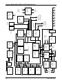
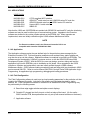
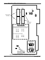
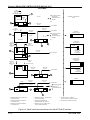
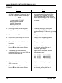
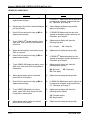
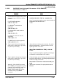
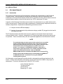
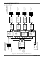
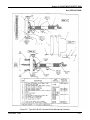
General (Ref. Figures 1-1, 1-2, 1-3)
GENISYS® Series 2000 product line is used for a variety of communication interfacing and non-vital
logic functions. Basic applications include:
Application
Description
CTC/ATCS BCP Interface
Direct interface between a CTC communications circuit
employing a US&S PRCCI™ protocol and an ATCScompliant radio Base Communications Processor (BCP).
ATCS MCP Interface
Direct interface between an ATCS-compliant radio Mobile
Communications Processor (MCP) and US&S vital
interlocking controllers*:
Serial Code Line Interface
Direct interface between US&S GENISYS, Harmon MCS1 and WB&S S2 serial code lines and US&S vital
interlocking controllers*
DC Code Line Interface
Direct interface between selected DC code lines and
US&S vital interlocking controllers:
In applications where the GENISYS® Series 2000 Controller board is part of a field code unit, the
system also performs non-vital logic functions (e.g. local I/O control, Local Control Panel interface), in
addition to the above communications interfacing functions.
1-2
SM 6700B 6/96
Section I GENERAL INFORMATION
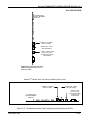
As shown in the right-hand part of Figure 1-1, GENISYS® Series 2000 components enable a direct
interface between an ATCS-compliant Mobile Communications Processor (MCP) and US&S vital
interlocking controllers*. If a new field installation requires local non-vital I/O (e.g. to a local control
panel), the Enhanced Controller is housed in a GENISYS® or MICROLOK-PLUS™ cardfile. Existing
GENISYS® or MICROLOK-PLUS™ installations can be retrofit with the Enhanced Controller to create
the interface to the MCP. If there is no requirement for non-vital local I/O, the Enhanced Controller can
be housed in the GENISYS Series 2000® Card Enclosure. Regardless of the installation, the
Enhanced Controller contains the same interfacing/conversion software for the communications link
with the MCP.
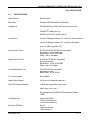
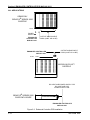
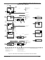
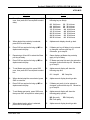
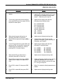
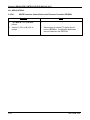
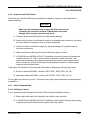
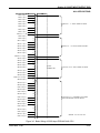
As shown in Figure 1-2, GENISYS® Series 2000 components also enable a direct interface between
selected serial code line carriers and US&S vital interlocking controllers*. Installation options for the
Enhanced Controller are the same as those for the MCP application (refer to above paragraph).
Different communications handling software is provided for each serial code line application.
In both the ATCS MCP and serial code line applications, an optional Surge Suppression/Serial
Interface Panel is available to protect Enhanced Controller PCB circuits from potentially damaging
transient voltages.
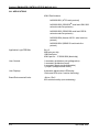
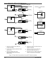
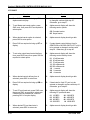
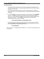
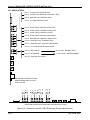
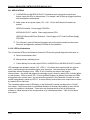
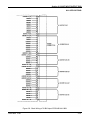
As shown in Figure 1-3, GENISYS® Series 2000 components also enable a direct interface between
selected DC code lines and US&S vital interlocking controllers*. As with the ATCS MCP and serial
code line applications, the Enhanced Controller can be installed in GENISYS® or MICROLOK-PLUS™
cardfiles to manage non-vital local I/O, or in the GENISYS® Series 2000 Card Enclosure when the
local I/O is not present. The GENISYS® Series 2000 DC Code Line PCB provides the electrical
interface between the Enhanced Controller and the DC Code Line. Different communications handling
software is provided for each DC code line application.
* MICROLOK® Vital Interlocking Control System
MICROLOK-PLUS™ Vital + Non-Vital Control Package
MICROTRAX® Coded Track Circuit/End-of-Siding Controller
SM 6700B 6/96
1-3
9 10 1
N 45 14 41 -
CO N T RO L L ER
EN H AN C ED
T O C L US T ER
M ICR O T RA X ®
CO N T RO L L ER
CO M P UT E R
PRO T C O L T O C T C
A S YCH RO N O US
O
R
A T CS PRO T O CO L
AAAA
AAAA
AAAA
AAAAAAAA
AAAA
AAAAAAAA
AAAA
AAAAAAAA
AAAA
AAAA
AAAA
AAAA
AAAA
AAAAAAAA
S ERIA L " PRC CI™"
CO N T RO L P A CK A G E
V IT A L + N O N -V IT A L
E OS CO N T RO L L E R
GE N ISY S ® SERIE S 2 0 0 0 CO M P O N EN T S
91 01
C O NT RO L SY ST E M
M ICRO L O K ® V I T A L
INT ERL O CK ING
3 2 - B IT
N 45 14 41 -
I/ O PCB S
C O NT RO L L E R
3 2 - B IT
I/ O PC B S
B
M IC RO L O K - P L US™
P O W ER S UP PL Y
I/ O
L O G.
I/ O
L O G.
N- V
C O N VE RT ER
( RE F E R T O S M -6 7 0 0 D )
EN H . C O NT . N 4 5 1 4 4 1 -9 1 0 1
AAAAAAAAAAAAAA
AAAA
AAAAAAAA
A
AAAA
AAAAAAAA
AAAAAAAA
AAAAAA
AAAA
AAAA
AAAA
A
AAAA
AAAA
AAAA
A
AAAA
AAAA
AAAA
AAAAAAAA
AAAAAAAA
AAAAAA
AAAA
A
AAAA
AAAA
AAAA
AAAAAAAAAAAAAA
AAAA
AAAA
AAAA
AAAAAAAAAAAAAA
AAAAAAAA
AAAAAAAA
AAAAA
AAAA
AA
AAAA
AAAAAAAA
AAAA
AAAAAAAA
AAAAAAAA
AAAAAA
AAAA
AAAA
AAAA
A
AAAA
AAAA
AAAA
AAAAAAAA
AAAAAAAA
AAAAAA
AAAA
A
AAAA
AAAA
AAAA
A
AAAA
AAAA
AAAA
AAAAAAAA
AAAAAAAA
AAAAAA
AAAA
A
AAAA
AAAA
AAAA
AAAAAAAAAAAAAA
AAAA
AAAA
AAAA
AAAAAAAAAAAAAA
AAAA
AAAA
AAAA
AAAAAAAA
AAAAAAAA
AAAAAA
AAAA
A
AAAA
AAAAAAAA
AAAAAAAA
AAAAAA
AAAA
AAAA
AAAAAAAAAAAA
AAAAA
PRO T O CO L
V IT .
V IT .
N- V
AAAAAAAAAAAAAAAAAAAAAAAAAAAA
AAAA
AAAAAAAA
AAAAAAAAAAAA
AAAAAAAAAAAA
AAAAAAAA
AAAA
AAAAAAAAAAAA
AAAAAAAAAAAA
AAAAAAAAAAAA
AAAA
AAAA
AAAA
AAAAAAAA
AAAAAAAA
AAAAAAAA
AAAAAAAA
AAAAAAAA
AAAAAAAA
AAAA
AAAA
AAAA
AAAA
AAAA
AAAA
AAAA
AAAA
AAAAAAAA
AAAAAAAA
AAAAAAAA
AAAAAAAA
AAAAAAAA
AAAAAAAA
AAAAAAAAAAAAAAAAAAAAAAAAAAAA
AAAA
AAAA
AAAA
AAAA
AAAA
AAAA
AAAA
AAAA
AAAAAAAAAAAAAAAAAAAAAAAAAAAA
AAAA
AAAA
AAAA
AAAA
AAAA
AAAA
AAAA
AAAA
AAAA
AAAA
AAAA
AAAA
AAAA
AAAA
AAAA
AAAA
AAAA
AAAA
AAAA
AAAA
AAAA
AAAAAAAA
AAAAAAAA
AAAAAAAA
AAAAAAAA
AAAAAAAA
AAAAAAAA
AAAA
AAAAAAAAAAAAAAAAAAAAAAAAAAAA
PO W ER SU P P. N 4 5 1 4 4 1 -9 4 0 3
CIRCU IT S
L IN K ( RS -4 2 2 )
L IN K ( R S-2 3 2 )
L O CA L
H DL C S ERIA L
V DC
AAAAAAAAAAA
AAAAAAAAAAA
AAAAAAAAAAA
AAAAAAAAAAA
AAAAAAAA
AAA
AAAAAAAAAAA
AAAA
AAA
AAAAAAAA
AAAAAAA
AAAAAAAA
AAA
AAAAAAAAAAA
AAAAAAAAAAA
AAAAAAAA
AAA
AAAAAAAAAAA
AAAAAAAAAAA
AAAA
AAAA
AAAAAA
AAAA
AAAA
AAAA
AAA
AAA
AAAA
AAAA
AAAA
AAAAAA
AAAA
AAAA
AAAA
AAAAAA
AAAA
AAAA
AAAA
AAAAAA
AAAA
AAAA
AAAA
AAAAAA
AAAA
AAAA
AAAA
AAAAAA
AAAA
AAAA
AAAA
AAAAAA
AAAA
AAAA
AAAAAA
AAAA
AAAA
AAA
AAAA
AAAA
AAA
AAAAAAAA
AAA
AAAAAAA
AAAAAAAA
AAAAAAAAAAA
AAAAAAAAAAA
AAAAAAAA
AAA
AAAAAAAAAAA
AAAAAAAAAAA
AAAAAAAAAAA
AAAAAAAA
AAA
AAAAAAAAAAA
AAAAAAAAAAA
AAAAAAAA
AAA
AAAAAAAAAAA
HD L C S E RIA L
AAAAAAAAAAA
AAAAAAAAAAA
AAAAAAAA
AAA
AAAAAAAAAAA
AAAAAAAAAAA
AAAAAAAAAAA
AAAAAAAA
AAA
AAAAAAAAAAA
AAAAAAAAAAA
AAAAAAAA
AAA
AAAAAAAAAAA
AAAA
AAA
AAAAAAAA
AAAAAAA
AAAAAAAA
AAA
AAAA
AAAA
AAAAAA
AAAA
AAAA
AAAA
AAA
AAA
AAAA
AAAA
AAAA
AAAAAA
AAAA
AAAA
AAAA
AAAAAA
AAAA
AAAA
AAAA
AAAAAA
AAAA
AAAA
AAAA
AAAAAA
AAAA
AAAA
AAAA
AAAAAA
AAAA
AAAA
AAAA
AAAAAA
AAAA
AAAA
AAAA
AAAAAA
AAAA
AAAAAAAA
AAA
AAAAAAAAAAA
AAAAAAAAAAA
AAAAAAAA
AAA
AAAAAAAAAAA
AAAAAAAAAAA
AAAAAAAAAAA
AAAAAAAA
AAA
AAAAAAAAAAA
AAAAAAAAAAA
AAAAAAAA
AAA
AAAAAAAAAAA
AAAAAAA
AAAA
AAAAAAAAAAA
9 .5 - 3 5 .0
O R O N C A R DF IL E)
N 4 5 1 8 9 2 -1 4 0 1
B
R
E N HA N CED
L O GI C E M UL A T O R
G E N ISY S ® N O N- V IT A L
L O G.
E
W
N- V
O
P
I/ O
AAAA
AAAAAAAA
AAAAAAAA
AAAAAAAA
AAAAAAAA
AAAAAAAA
AAAAAAAA
AAAA
AAAA
AAAA
AAAA
AAAAAAAA
AAAAAAAA
AAAAAAAA
AAAAAAAA
AAAAAAAA
AAAAAAAA
AAAA
AAAA
AAAA
AAAA
AAAA
AAAA
AAAA
AAAA
AAAA
AAAA
AAAA
AAAA
AAAA
AAAA
AAAAAAAA
AAAAAAAA
AAAAAAAA
AAAAAAAA
AAAAAAAA
AAAAAAAA
AAAA
AAAA
AAAA
AAAA
AAAA
AAAA
AAAA
AAAA
AAAA
AAAA
AAAA
AAAA
AAAA
AAAA
AAAA
AAAA
AAAAAAAA
AAAAAAAA
AAAAAAAA
AAAAAAAA
AAAAAAAA
AAAAAAAA
AAAA
AAAAAAAAAAAAAAAAAAAAAAAAAAAA
AAAA
AAAAAAAA
AAAAAAAA
AAAAAAAA
AAAAAAAA
AAAAAAAA
AAAAAAAA
AAAA
AAAA
AAAA
AAAA
AAAA
AAAA
AAAA
AAAA
AAAAAAAAAAAAAAAAAAAAAAAAAAAA
AAAA
AAAAAAAA
AAAAAAAA
AAAAAAAA
AAAAAAAA
AAAAAAAA
AAAAAAAA
AAAA
AAAA
AAAA
AAAA
AAAA
AAAA
AAAA
AAAA
AAAA
AAAAAAAA
AAAAAAAA
AAAAAAAA
AAAAAAAA
AAAAAAAA
AAAAAAAA
AAAA
AAAA
AAAA
AAAA
AAAA
AAAA
AAAA
AAAA
AAAA
AAAA
AAAA
AAAA
AAAA
AAAA
AAAA
AAAA
AAAAAAAAAAAAAAAAAAAAAAAAAAAA
AAAA
AAAA
AAAA
AAAA
AAAA
AAAA
AAAA
AAAA
AAAA
AAAA
AAAA
AAAA
AAAA
AAAA
AAAAAAAA
AAAAAAAA
AAAAAAAA
AAAAAAAA
AAAAAAAA
AAAAAAAA
AAAA
AAAAAAAA
AAAAAAAA
AAAAAAAA
AAAAAAAA
AAAAAAAA
AAAAAAAA
AAAA
AAAA
N -V
CIRCU IT S
L O CA L
P C B P O RT
C O DE SY S T E M
B
VDC
S ERIA L L I NK
RS- 2 3 2 / 4 2 3
N45 189 1-0 10 2
9 .5 - 3 5 .0
C A RD E NC L O S URE
IN T E RF A CE M O D U L E
E N H. CO N T . N4 5 1 4 4 1 - 9 1 0 1
P OW ER SU P P. N 4 5 1 4 4 1 -9 4 0 3
O R O N CA RD FIL E )
HD L C SE RIA L
L I N K ( R S -4 2 2 )
L IN K ( RS - 4 2 2 )
AAAAAAAAAAA
AAAAAAAAAAA
AAAA
AAAA
AAAAAA
AAAA
AAAA
AAAA
AAA
AAA
AAAA
AAAA
AAAA
AAAAAA
AAAA
AAAA
AAAA
AAAAAA
AAAA
AAAA
AAAA
AAAAAA
AAAA
AAAA
AAAA
AAAAAA
AAAA
AAAA
AAAA
AAA
AAA
AAAA
AAAA
AAAA
AAAAAA
AAAA
AAAA
AAAA
AAAAAA
AAAAAAAA
AAA
AAAAAAA
AAAAAAAA
AAAAAAAAAAA
AAAAAAAAAAA
AAAAAAAA
AAA
AAAAAAAAAAA
AAAAAAAAAAA
AAAAAAAAAAA
AAAAAAAA
AAA
AAAAAAAAAAA
AAAAAAAAAAA
AAAAAAAA
AAA
AAAAAAAAAAA
AAAAAAAAAAA
AAAAAAAAAAA
AAAAAAAA
AAA
AAAA
AAAA
AAAAAA
AAAA
AAAA
AAAA
AAAAAA
AAAA
AAAA
AAAA
AAAAAA
AAAA
AAAA
AAAA
AAAAAA
AAAA
AAAA
AAAA
AAAAAA
AAAA
AAAA
AAAA
AAAAAA
AAAA
AAAA
AAAA
AAAAAA
AAAA
AAAA
AAAAAA
AAAA
AAAA
AAAA
AAAA
AAA
AAA
AAAA
AAAA
AAA
AAAA
H D L C S ERIA L
O R O N CA RD F IL E)
8 90 2
IN T ERF A CE PA N E L
8 90 1
N 45 18 07 -
S. S. / S .I PCB
H D L C SE RI A L
L IN K ( RS - 2 3 2 )
AAAAAAAAAAAAAA
AAAAAAAAAAAAAA
AAAAAAAA
AA
AAAAAAAAAAAA
AA
AAAAAAAAAAAA
AA
AAAAAA
AAAAAAAA
AAAAAAAAAAAA
AA
AAAA
AAAAAAAAAAAAAA
AAAAAAAAAAAAAA
AAAAAAAA
AA
AAAA
AAAAAAAAAAAAAA
AAAAAAAAAAAAAA
AAAAAAAA
AA
AAAAAAAAAAAA
AA
AAAA
AAAAAAAAAAAAAA
AAAAAAAAAAAAAA
AAAAAAAA
AA
AAAA
AAAAAAAAAAAAAA
AAAAAAAAAAAAAA
AAAAAAAA
AA
AAAAAAAAAAAA
AA
AAAA
AAAAAAAAAAAAAA
AAAAAAAAAAAAAA
AAAAAAAA
AA
AAAA
AAAAAAAAAAAAAA
AAAAAAAAAAAAAA
AAAAAAAA
AA
AAAAAAAAAAAA
AA
AAAA
AAAAAAAAAAAAAA
AAAAAAAA
AA
AAAAAAAAAAAA
AA
AAAA
AAAAAAAAAAAAAA
AAAAAAAAAAAAAA
AAAAAAAA
AA
AAAA
AAAAAAAAAAAAAA
AAAAAAAA
AAAAAA
AA
AAAAAAAA
AAAA
89 02
PA N EL
( ST A N D -A L O N E
N 45 18 07 P A N EL
( S T A ND - A LO N E
S UP P RE SS ./ SE RIA L
A
M O UN T I N G
S URG E
PR OC E S SO R ( B AS E)
A T C S - CO M P L I A NT
B CP
M O BI LE CO M M UN ICA T IO N S
PA N EL
8 90 1
N45 18 07 -
M O UN T IN G
8 90 2
S .S. / S .I PCB
N 4 51 80 7-
M O U NT IN G
89 01
S.S ./ S. I P CB
N 4 51 80 7-
L I N K ( RS -4 2 2 )
S . S ./ S .I PC B
PRO C ES S O R ( F IEL D )
A T CS - CO M P L I A NT
A T CS RF L IN K
M O BI L E CO M M UN ICA T IO N S
HD L C SE RIA L
A
M CP
A
S. S . / S. I P C B
N 45 18 07 -
S .S. / S .I PCB
A
AAAAAAAAAAA
AAAAAAAAAAA
AAAA
AAAA
AAAAAA
AAAA
AAAA
AAAA
AAA
AAA
AAAA
AAAA
AAAA
AAAAAA
AAAA
AAAA
AAAA
AAAAAA
AAAA
AAAA
AAAA
AAAAAA
AAAA
AAAA
AAAA
AAAAAA
AAAA
AAAA
AAAA
AAAAAA
AAAA
AAAA
AAAA
AAAAAA
AAAA
AAAA
AAAA
AAAAAA
AAAAAAAA
AAA
AAAAAAA
AAAAAAAA
AAAAAAAAAAA
AAAAAAAAAAA
AAAAAAAAAAA
AAAAAAAA
AAA
AAAAAAAAAAA
AAAAAAAAAAA
AAAAAAAA
AAA
AAAAAAAAAAA
AAAAAAAAAAA
AAAAAAAAAAA
AAAAAAAA
AAA
AAAAAAAAAAA
AAAAAAAAAAA
AAAAAAAA
AAA
AAAA
AAAA
AAAAAA
AAAA
AAAA
AAAA
AAAAAA
AAAA
AAAA
AAAA
AAAAAA
AAAA
AAAA
AAAA
AAAAAA
AAAA
AAAA
AAAA
AAAAAA
AAAA
AAAA
AAAA
AAAAAA
AAAA
AAAA
AAAA
AAAAAA
AAAA
AAAA
AAAAAA
AAAA
AAAA
AAAA
AAAA
AAA
AAA
AAAA
AAAA
AAA
AAAA
( ST A N D- A L O N E
Section I GENERAL INFORMATION
Figure 1-1. ATCS Communications Interface
1-4
SM 6700B 6/96
PO W E R SUP PL Y
ENHANCED
CONTROLLER
N451441-9101
N -V
I/ O
N -V
LO G.
V IT .
I/ O
VIT .
LO G.
MICROT RA X ®
EO S CO NT RO LL E R
AAAAAAAAA
AAAAAAAA
AAAAAA
AAAA
AAAA
AAAAAAAA
AAAAAA
AAAA
AAAA
AAAA
AAAAAAA
AAAA
AAAAAAAA
AAAAAA
AAAA
AAAA
MI CROL OK - PL US ™
V IT A L + NO N-V IT A L
CO NT ROL PA CK A GE
3 2 -B IT
I/ O PCBS
B
P
O
W
E
R
AAAAAAAAAAAAAAAAAAAAAAAAAAAA
AAAAAAAAAAAAAAAAAAAAAAAAAAAA
AAAAAAAAAAAAAAAAAAAAAAAAAAAA
AAAAAAAAAAAAAAAAAAAAAAAAAAAA
AAAAAAAAAAAAAAAAAAAAAAAAAAAA
AAAAAAAA
AAAAAAAA
AAAAAAAA
AAAAAAAAAAAA
AAAAAAAAAAAA
AAAAAAAA
AAAAAAAA
AAAAAAAA
AAAAAAAA
AAAA
AAAAAAAA
AAAA
AAAA
AAAA
AAAA
AAAA
AAAAAAAAAAAAAAAAAAAAAAAAAAAA
AAAAAAAAAAAAAAAAAAAAAAAAAAAA
AAAAAAAAAAAAAAAAAAAAAAAAAAAA
AAAAAAAA
AAAA
AAAA
AAAA
AAAA
AAAAAAAAAAAAAAAAAAAAAAAAAAAA
AAAAAAAAAAAAAAAAAAAAAAAAAAAA
AAAA
AAAAAAAA
AAAAAAAAAAAA
AAAAAAAA
AAAAAAAA
AAAAAAAA
AAAAAAAA
AAAA
AAAAAAAAAAAAAAAAAAAAAAAA
AAAA
AAAAAAAAAAAAAAAAAAAAAAAAAAAA
GENIS YS ® SERIES 2 0 0 0 CO M PO NE NT S
MI CRO LOK ® V IT A L
I NT ERL OCK IN G
CON TROL SY ST EM
B
GEN ISY S® N ON - V IT A L 3 2 - BIT
LO GIC EM ULA T OR I/ O PCBS
EN HA NCED
CON TROL L ER
N4 5 1 4 4 1 - 9 1 0 1
N-V
I/ O
AAAAAAAAAAAAAAAAAAAAAAAAAAAA
AAAAAAAAAAAAAAAAAAAAAAAAAAAA
AAAAAAAAAAAAAAAAAAAAAAAAAAAA
AAAAAAAAAAAAAAAAAAAAAAAAAAAA
AAAAAAAA
AAAA
AAAAAAAAAAAA
AAAAAAAA
AAAAAAAA
AAAAAAAA
AAAA
AAAAAAAAAAAA
AAAAAAAAAAAA
AAAAAAAA
AAAAAAAA
AAAAAAAA
AAAAAAAA
AAAA
AAAAAAAA
AAAA
AAAA
AAAA
AAAA
AAAAAAAAAAAAAAAAAAAAAAAA
AAAA
AAAAAAAAAAAAAAAAAAAAAAAAAAAA
AAAA
AAAAAAAA
AAAA
AAAA
AAAA
AAAA
AAAAAAAAAAAA
AAAA
AAAA
AAAA
AAAA
AAAAAAAAAAAAAAAAAAAAAAAAAAAA
AAAAAAAAAAAAAAAAAAAAAAAAAAAA
AAAA
AAAAAAAA
AAAA
AAAA
AAAA
AAAA
AAAAAAAAAAAAAAAAAAAAAAAAAAAA
AAAAAAAAAAAAAAAAAAAAAAAAAAAA
AAAA
AAAAAAAA
AAAAAAAAAAAAAAAA
AAAAAAAAAAAA
AAAA
AAAA
AAAA
AAAA
AAAAAAAAAAAAAAAAAAAAAAAAAAAA
AAAA
AAAAAAAA
AAAA
AAAA
AAAA
AAAA
AAAAAAAAAAAA
AAAA
AAAA
AAAA
AAAA
AAAAAAAAAAAAAAAAAAAAAAAA
AAAA
AAAA
AAAAAAAAAAAAAAAAAAAAAAAAAAAA
AAAAAAAAAAAAAAAAAAAAAAAAAAAA
AAAAAAAAAAAAAAAAAAAAAAAAAAAA
AAAAAAAAAAAAAAAAAAAAAAAAAAAA
AAAAAAAA
AAAA
AAAA
AAAA
AAAA
AAAAAAAAAAAAAAAAAAAAAAAAAAAA
AAAAAAAAAAAAAAAAAAAAAAAAAAAA
AAAAAAAAAAAAAAAAAAAAAAAAAAAA
AAAA
AAAAAAAAAAAAAAAAAAAAAAAA
AAAA
AAAAAAAAAAAAAAAAAAAAAAAAAAAA
N -V
LO G.
L OCA L
CIRCUI TS
SE RIA L
LIN K ( RS- 2 3 2 )
S ERI A L
L INK ( RS-2 3 2 )
AAAAAAAAAAA
AAAAAAAA
AAAAAAA
AAA
AAAA
AAAA
AAAAAAAA
AAAAAAA
AAA
AAAA
AAAA
AAA
AAAA
AAAA
AAA
AAAA
AAAAAAAA
AAAAAAA
AAA
AAAA
AAAA
AAA
AAAA
AAAA
AAAAAAAA
AAAAAAA
AAA
AAAA
AAA
AAAA
AAAA
AAA
AAAA
AAAA
AAA
AAAA
AAA
AAAA
AAAA
AAA
AAA
AAAA
AAAA
AAAA
AAA
AAA
AAAA
AAAA
AAAA
AAA
AAA
AAAA
AAAA
AAAA
AAA
AAA
AAAA
AAAA
AAAA
AAA
AAA
AAAA
AAAA
AAAA
AAA
AAA
AAAA
AAAA
AAAA
AAA
AAA
AAAA
AAAA
AAAA
AAA
AAAA
AAA
AAAA
AAAA
AAA
AAA
AAAA
AAAA
AAAA
AAAAAAAA
AAAAAAA
AAA
AAAA
AAA
AAAA
AAAA
AAAAAAAA
AAAAAAA
AAA
AAAA
AAA
AAAA
AAAA
AAAAAAAA
AAAAAAA
AAA
AAAA
AAA
AAAA
AAAA
AAAAAAAAAAA
AAA
AAAAAAAA
AAAAAAA
AAA
AAAA
AAAA
AAAAAAAA
AAAAAAA
AAA
AAAA
AAAA
AAA
LO CA L
CI RCUIT S
MOUN T ING P A NE L
( STA ND A LO NE OR
O N CA RDFIL E)
AAAAAAAAAAA
AAAAAAAAAAA
AAAA
AAAAAA
AAAA
AAAA
AAAA
AAAAAA
AAAA
AAAA
AAAA
AAAAAA
AAAA
AAAA
AAAA
AAAAAA
AAAA
AAAA
AAAA
AAAAAA
AAAA
AAAA
AAAA
AAAAAA
AAAA
AAAA
AAAA
AAAAAA
AAAA
AAAA
AAAA
AAAAAA
AAAA
AAAA
AAAA
AAAA
AAAAAA
AAAA
AAAA
AAAA
AAAAAA
AAAA
AAAAAAAAAAA
AAAAAAAAAAA
AAAAAAAAAAA
AAAAAAAA
AAA
AAAAAAAAAAA
AAAAAAAAAAA
AAAAAAAA
AAA
AAAAAAAAAAA
AAAA
AAA
AAAAAAAA
AAAAAAA
AAAAAAAA
AAA
AAAAAAAAAAA
AAAAAAAAAAA
AAAAAAAA
AAA
AAAAAAAAAAA
AAAAAAAAAAA
AAAAAAAA
AAA
AAAA
AAAAAA
AAAA
AAAA
AAAA
AAAAAA
AAAA
AAAA
AAAA
AAAAAA
AAAA
AAAA
AAAA
AAAAAA
AAAA
AAAA
AAAA
AAAAAA
AAAA
AAAA
AAAA
AAAAAA
AAAA
AAAA
AAAA
AAAAAA
AAAA
AAAA
AAAA
AAAAAA
AAAA
AAAA
AAAA
AAAA
AAAAAA
AAAA
AAAA
AAAA
AAA
AAA
AAAA
AAAA
AAA
AAAA
CO DE S YSTEM
PCB PO RT
B
SERIA L LIN K
RS- 2 3 2 / 4 2 3
9.5 - 3 5.0
VD C
INT ERFA CE MO DUL E
CA RD EN CLO SURE
N4 5 1 8 9 1 - 0 1 0 2
-
.
.
ENH CONT
N451441-9101
POWER SUPP N451441-9403
S. S. / S. I PCB
S. S./ S .I P CB
N4 5 1 8 0 7 -8 9 0 1 N4 5 1 8 0 7 - 8 9 0 1
A
S. S. / S. I PCB
N4 5 1 8 0 7 - 8 9 0 1
MOUN T ING P A NE L
( S TA ND A LO NE OR
O N CA RDFIL E)
S. S ./ S.I P CB
N4 5 1 8 0 7 - 8 9 0 A
1
A
S ERI A L
L INK ( RS-2 3 2)
LINE CA RRIER
SERIA L COD E LIN E ( GENI SY S® , HA RMO N M CS- 1 / 2 , W B & S S2 )
AAAAAAAAAAAAAA
AAAAAAAAAAAAA
AAAAAAAA
AA
AAAAAAAAAAAA
AAAAAAAAAAAA
AAAAAAAAAAAA
AAAAAA
AAAAAAAA
A
AAAAAAAAAAAA
AAAA
AAAAAAAAAAAAAA
AAAAAAAA
AA
AAAAAAAAAAAA
AAAA
AAAA
AAAA
AAAAAAAA
AAAAAAAAAA
AAAAAAAA
A
AAAAAAAAAAAA
AAAA
AAAAAAAAAAAAAA
AAAAAAAA
A
AAAAAAAAAAAA
AAAAAAAAAAAA
AAAAAA
AAAAAAAA
AAAA
AAAAAAAAAAAAAA
AAAAAAAAAAAAA
AAAAAAAAAAAAA
AAAAAAAA
A
AAAAAAAAAAAA
AAAAAAAAAAAA
AAAAAA
AAAAAAAA
AA
AAAAAAAAAAAA
AAAAAAAAAAAA
AAAA
AAAAAAAAAAAAAA
AAAAAAAA
A
AAAAAAAAAAAA
AAAA
AAAAAAAAAAAAAA
AAAAAAAA
AA
AAAAAAAAAAAA
AAAAAAAAAAAA
AAAA
AAAAAAAAAAAAAA
AAAAAAAA
A
AAAAAAAAAAAA
AAAA
AAAAAAAA
AAAAAA
AAAAAAAA
AAAA
MOUNTING PANEL
(STAND ALONE
OR CARDFILE
A
AAAAAAAAAAA
AAAAAAAAAAA
AAAA
AAAA
AAAAAA
AAAA
AAAA
AAA
AAA
AAAA
AAAA
AAAA
AAAAAA
AAAA
AAAA
AAAA
AAAAAA
AAAA
AAAA
AAAA
AAAAAA
AAAA
AAAA
AAAA
AAAAAA
AAAA
AAAA
AAAA
AAAAAA
AAAA
AAAA
AAAA
AAAAAA
AAAA
AAAA
AAAA
AAAA
AAAAAA
AAAA
AAA
AAAA
AAAA
AAA
AAAAAAAA
AAAAAAA
AAAAAAAA
AAA
AAAAAAAAAAA
AAAAAAAAAAA
AAAAAAAA
AAA
AAAAAAAAAAA
AAAAAAAAAAA
AAAAAAAA
AAA
AAAAAAAAAAA
AAAAAAAAAAA
AAAAAAAAAAA
AAAAAAAA
AAA
AAAAAAAAAAA
AAAAAAAAAAA
AAAAAAAA
AAA
AAAAAAAAAAA
AAAAAAAAAAA
AAAA
AAAA
AAA
AAAAAA
AAAA
AAAA
AAA
AAAA
AAAA
AAAA
AAAAAA
AAAA
AAAA
AAAA
AAAAAA
AAAA
AAAA
AAAA
AAAAAA
AAAA
AAAA
AAAA
AAAAAA
AAAA
AAAA
AAAA
AAAAAA
AAAA
AAAA
AAAA
AAAAAA
AAAA
AAAA
AAAA
AAAA
AAAAAA
AAAA
AAA
AAAA
AAAA
AAA
AAAA
AAAAAAA
AAA
AAAAAAAA
AAAA
SE RIA L
LIN K ( RS -2 3 2 )
S. S ./ S .I P CB
N4 5 1 8 0 7 -8 9 0 1
Section I GENERAL INFORMATION
Figure 1-2. Serial Code Line Interface
SM 6700B 6/96
1-5
MICROT RA X ®
EO S CO NT RO L L E R
B
MOUNTING PANEL
( ST A ND- A LO NE
OR ON CA RDFILE)
S.S./ S. I PCB
N4 5 1 8 0 7 - 8 9 0 1
MICRO LO K ® VIT A L
INT ERLOCKIN G
CON T RO L SY ST EM
CO DE S YST EM
P CB PO RT
GENI SY S® SE RIES 2 0 0 0 COM PON ENT S
MICROLO K-P L US™
V IT A L + N ON -V IT A L
CO NT RO L P A CK AG E
PO W ER SUPP L Y
N- V
L OG.
V IT.
I/ O
V IT .
L OG.
A
N- V
I/ O
AAAAAAAAAAAAAAAAAAAAAAAAAAAAA
AAAAAAAAAAAAAAAAAAAAAAAAAAAAAA
AAAAAAAAAAAAAAAAAAAAAAAAAAAAA
AAAAAAAAAAAAAAAAAAAAAAAAAAAAA
AAAAAAAAAAAAAAAAAAAAAAAAAAAAA
AAAAAAAA
AAAAAAAA
AAAAAAAA
A
AAAAAAAAAAAA
AAAAAAAAAAAA
AAAAAAAA
AAAAAAAA
AAAAAAAA
AAAAAAAA
AAAAAA
AAAAAAAA
AAAA
AAAA
AAAA
AAAA
AAAA
AAAAAAAAAAAAAAAAAAAAAAAAAAAAAA
AAAA
AAAA
AAAA
AAAA
AAAA
AAAA
AAAAAAAA
AAAAAAAAAAAAAAAAAAAAAAAAAA
AAAAAAAA
AAAAAAAA
AAAAAAAA
A
AAAAAAAAAAAA
AAAAAAAAAAAA
AAAAAAAA
AAAAAAAA
AAAAAAAA
AAAAAAAA
AAAAAA
AAAAAAAA
AAAA
AAAA
AAAA
AAAA
A
AAAAAAAAAAAA
AAAA
AAAA
AAAA
AAAAAAAAAAAAAAAAAAAAAAAA
AAAAAAAA
AAAAAA
AAAAAAAA
AAAAAAAAAAAAAAAA
AAAA
AAAAAAAAAA
AAAAAAAAAA
AAAA
AAAAAA
AA
AAAA
AA
AAAAAAAA
AAAAAA
AAAA
AAAA
AA
AAAA
AAAA
AA
AAAA
AAAA
AAAAAAAAAA
AA
AAAA
AAAA
AA
AAAA
AAAA
AA
AAAAAAAA
AAAAAA
AAAA
AA
AAAA
AAAA
AA
AAAA
AAAA
AAAAAAAA
AA
AAAA
AAAA
AAAAAAAA
AAAAAA
AAAA
AAAAAAAA
AAAAAA
AAAA
AAAAAAAA
AAAAAA
AAAA
AAAAAAAA
AAAAAA
AAAA
AAAAAAAA
AAAAAA
AAAA
AAAAAAAA
AAAAAA
AAAA
AAAAAAAA
AAAAAA
AAAA
AAAAAAAA
AAAAAA
AAAA
AAAAAA
AAAA
AAAA
AAAA
AAAA
AAAAAAAA
AA
AAAA
AA
AAAA
AAAA
AA
AAAA
AAAA
AA
AAAAAAAA
AAAAAA
AAAA
AA
AAAA
AAAA
AA
AAAAAAAA
AAAAAA
AAAA
AA
AAAA
AAAA
AAAAAAAAAA
AA
AAAAAAAA
AAAAAA
AAAA
AA
AAAA
AAAA
AA
AAAAAAAA
AAAAAA
AAAA
AAAAAAAAAA
ENHA NCED
CO NT RO L L ER
N4 5 1 4 4 1 - 9 1 0 1
GE NIS YS ® NON - V IT A L 3 2 - BIT I/ O
LO GIC EM UL AT O R
PCB S
S ERI A L L INK
RS- 2 3 2 / 4 23
3 2 -BIT I/ O
PCB S
A
PA RA L L EL
I NT ERFA CE
LO CA L
CIRCUIT S
INTERFACE MODULE
CARD ENCLOSURE
N451891-0102
( N O PCB)
DC CODE LINE N451441-9401
PA RA L L E L
INT ERFA CE
9 .5 - 3 5 .0
V DC
CO DE LINE FILT ER
AAAA
AAAAAAAA
AAAAAAAA
AAAAAAA
AAAA
AAAA
AAAA
AAAA
AAAAAAAA
AAAAAAAA
AAAAAAA
AAAA
AAAA
AAAAAAAAAAAA
AAAAA
AAAAAAAA
AAAAAAAA
AAAAAA
AAAA
AAAA
AAAAAAAA
AAAAAAAA
AAAAAA
AAAAAAAA
AAAAAAAA
AAAAAA
AAAA
AAAA
AAAA
AAAAAAAA
AAAAAAAA
AAAAAAA
AAAA
AAAA
AAAA
AAAA
AAAAAA
AAAA
AAAA
AAAAAAAA
AAAAAAAA
AAAAAA
AAAA
AAAA
AAAA
AAAA
AAAAAAAA
AAAAAAAA
AAAAAAA
AAAA
AAAAAAAAAAAA
AAAAA
AAAA
AAAA
AAAAAAAAAAAA
AAAAAA
AAAA
AAAAAAAA
AAAAAAAA
AAAAAA
AAAAAAAA
AAAAAAAA
AAAAAA
AAAA
AAAA
AAAA
AAAAAAAA
AAAAAAAA
AAAAAAA
AAAA
AAAA
AAAA
AAAA
AAAAAA
AAAA
AAAA
AAAAAAAA
AAAAAAAA
AAAAAA
AAAA
AAAA
AAAA
AAAA
AAAAAAAA
AAAAAAAA
AAAAAAA
AAAA
AAAA
B
B
N -V
LO G.
N- V
I/ O
AAAA
AAAA
AAAAAAAA
AAAAAAAA
AAAAAAAA
AAAAAAAA
AAAAAAAA
AAAAAAAA
AAAA
AAAA
AAAA
AAAA
AAAA
AAAA
AAAA
AAAA
AAAA
AAAA
AAAAAAAA
AAAAAAAA
AAAAAAAA
AAAAAAAA
AAAAAAAA
AAAAAAAA
AAAA
AAAA
AAAA
AAAA
AAAA
AAAA
AAAA
AAAA
AAAA
AAAA
AAAA
AAAA
AAAA
AAAA
AAAAAAAA
AAAAAAAA
AAAAAAAA
AAAAAAAA
AAAAAAAA
AAAAAAAA
AAAA
AAAAAAAAAAAAAAAAAAAAAAAAAAAA
AAAA
AAAA
AAAA
AAAA
AAAA
AAAA
AAAA
AAAA
AAAAAAAA
AAAAAAAA
AAAAAAAA
AAAAAAAA
AAAAAAAA
AAAAAAAA
AAAA
AAAA
AAAA
AAAA
AAAAAAAA
AAAAAAAA
AAAAAAAA
AAAAAAAA
AAAAAAAA
AAAAAAAA
AAAA
AAAA
AAAA
AAAA
AAAA
AAAA
AAAA
AAAA
AAAA
AAAA
AAAA
AAAA
AAAA
AAAA
AAAA
AAAA
AAAA
AAAA
AAAA
AAAA
AAAA
AAAAAAAAAAAAAAAAAAAAAAAAAAAA
AAAA
AAAA
AAAA
AAAA
AAAA
AAAA
AAAA
AAAA
AAAA
AAAA
AAAA
AAAA
AAAA
AAAA
AAAAAAAA
AAAAAAAA
AAAAAAAA
AAAAAAAA
AAAAAAAA
AAAAAAAA
AAAA
AAAAAAAAAAAAAAAAAAAAAAAAAAAA
AAAAAAAAAAAAAAAAAAAAAAAAAAAA
AAAA
AAAAAAAA
AAAAAAAA
AAAAAAAA
AAAAAAAA
AAAAAAAA
AAAAAAAA
AAAA
AAAAAAAAAAAAAAAAAAAAAAAAAAAA
AAAA
AAAAAAAA
AAAAAAAA
AAAAAAAA
AAAAAAAA
AAAAAAAA
AAAAAAAA
AAAA
AAAA
AAAA
AAAA
AAAA
AAAA
AAAA
AAAA
AAAA
AAAAAAAA
AAAAAAAA
AAAAAAAA
AAAAAAAA
AAAAAAAA
AAAAAAAA
AAAA
AAAAAAAAAAAAAAAAAAAAAAAAAAAA
P
O
W
E
R
A
EN HA N CED
CO NT ROL L ER
N 4 5 1 4 4 1 -9 1 0 1
L OCA L
CIRCUIT S
MO UNT IN G PA NEL
( ST A ND- A L ON E
O R O N CA RDFIL E)
SERIA L LIN K
RS- 2 3 2 / 4 2 3
ENH. CONT. N451441-9101
IN T E RF A CE MOD UL E
CA RD E NCLO SURE
N 4 5 1 8 9 1 -0 1 0 2
N 4 5 1 4 4 1 -9 4 0 2
AAAA
AAAAAAAA
AAAAAAAA
AAAAAAA
AAAA
AAAA
AAAA
AAAA
AAAAAAAA
AAAAAAAA
AAAAAAA
AAAA
AAAA
AAAA
AAAA
AAAA
AAAAAA
AAAA
AAAA
AAAAAAAA
AAAAAAAA
AAAAAA
AAAA
AAAA
AAAA
AAAA
AAAAAAAA
AAAAAAAA
AAAAAAA
AAAA
AAAA
AAAA
AAAA
AAAAAAAAAAAA
AAAAAA
AAAAAAAA
AAAAAAAA
AAAAAA
AAAA
AAAA
AAAA
AAAAAAAA
AAAAAAAA
AAAAAAA
AAAA
AAAA
AAAA
AAAA
AAAAAAAA
AAAAAAAA
AAAAAAA
AAAA
AAAA
AAAA
AAAA
AAAAAA
AAAA
AAAA
AAAAAAAA
AAAAAAAA
AAAAAA
AAAA
AAAAAAAAAAAA
AAAAA
AAAAAAAA
AAAAAAAA
AAAAAA
AAAA
AAAA
AAAA
AAAAAA
AAAA
AAAA
AAAAAAAA
AAAAAAAA
AAAAAA
AAAA
AAAAAAAAAAAA
AAAAA
AAAAAAAA
AAAAAAAA
AAAAAA
AAAA
AAAA
AAAA
AAAAAA
AAAA
AAAA
AAAAAAAAAAAA
AAAAA
S. S. / S. I PCB
N 4 5 1 8 0 7 -8 9 0 1
DC CO DE LI NE/
PO W ER SUPP L Y
PA RA L L EL
I NT ERF A CE
9 .5 - 3 5 .0
V DC
CO DE LI NE FILT ER
DC CO DE L INE ( US & S 5 0 0 SERIES, GRS K S ERI ES)
AAAAAAAA
AAA
AAAAAAAA
AAA
AAAAAAAAAAA
AAAAAAAA
AAA
AAAAAAAA
AAA
AAAAAAAAAAA
AAAAAAAA
AAA
AAAAAAAA
AAA
AAAAAAAA
AAA
AAAAAAAAAAA
AAAAAAAA
AAA
AAAAAAAA
AAA
AAAAAAAAAAA
AAAAAAAA
AAA
AAAAAAAA
AAA
AAAA
AAAA
AAAA
AAA
AAAA
AAAA
AAAA
AAAA
AAAA
AAA
AAAA
AAAA
AAAA
AAAA
AAA
AAAA
AAAA
AAAA
AAAA
AAA
AAAA
AAAA
AAAA
AAAA
AAA
AAAA
AAAA
AAAA
AAAA
AAA
AAAA
AAAA
AAAA
AAAA
AAA
AAAA
AAAA
AAAA
AAAA
AAA
AAAA
AAAA
AAAA
AAAA
AAA
AAAA
AAAA
AAAA
AAAA
AAA
AAAAAAAA
AAA
AAAAAAAAAAA
AAAAAAAA
AAA
AAAAAAAA
AAA
AAAAAAAAAAA
AAAAAAAA
AAA
AAAAAAAA
AAA
AAAAAAAA
AAA
AAAAAAAAAAA
AAAAAAAA
AAA
AAAAAAAA
AAA
AAAAAAAAAAA
AAAAAAAA
AAA
AAAAAAAA
AAA
AAAAAAAAAAA
SE RIA L LIN K
RS- 2 3 2 / 4 2 3
Section I GENERAL INFORMATION
AAAAAAAAAA
AAAA
AAAAAAAA
AAAAAA
AAAA
AAAA
A
AAAA
AAAAAAAA
AAAAAA
AAAA
AAAA
A
AAAA
AAAAAAAA
AAAAAA
AAAA
AAAA
AAAAAAAAA
Figure 1-3. DC Code Line Interface
1-6
SM 6700B 6/96
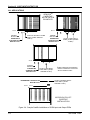
Section I GENERAL INFORMATION
1.3.2
Components
GENISYS® Series 2000 component part numbers include:
Component
US&S Part No.
Enhanced Controller PCB
32-Bit Output PCBs
32-Bit Input PCB
Code Line Interface PCB
Code Line Interface/Power Supply PCB
Power Supply PCB
Card Enclosure
Surge Suppressor/Serial Interface Panel
Surge Suppressor/Serial Interface PCBs
GENISYS® Series 2000 Development System (G2DS)
Executive PROM Sets
N451441-9101
N451441-9601, -9801
N451441-9701
N451441-9401
N451441-9402
N451441-9403
N451891-0102
N451892-1401
N451807-8901, -8902
N451232-0120, -0121
N451800-0201 to -020X
1.3.2.1 Enhanced Controller Board (N451441-9101) and Software
The Enhanced Controller PCB is used in all GENISYS® Series 2000 applications. It contains circuitry
and software for performing non-vital logic functions in GENISYS® and MICROLOK-PLUS™ units, as
well as the various communications interfacing functions in ATCS, serial code line and DC code line
applications. When used in GENISYS® and MICROLOK-PLUS™ units, this board performs the same
logic and local I/O interfacing functions as the N451441-5602 Controller. (The -5602 board does not
have the signal interfacing/protocol conversion capabilities of the -9101 board). When used in the
stand-alone field interface to a MICROLOK® or MICROTRAX End-of-Siding system (Reference
Figures 1-1 through 1-3), the Enhanced Controller Board is housed in the GENISYS® Series 2000
Card Enclosure.
The Enhanced Controller PCB operates with both Executive and Application software. Executive
PROM sets accommodate the different communications protocols (e.g. ATCS, MCS), while Application
EPROMs contain the operating logic designed via the GENISYS® Series 2000 Development System
(G2DS). The G2DS is not compatible with the GENISYS® Development System (GDS). Refer to
Section II, Enhanced Controller PCB N451441-9101, for a detailed description of the Enhanced
Controller Board.
1.3.2.2 32-Bit Output Boards (N451441-9601, -9801)
The 32-Bit Output boards are used in GENISYS® Series 2000 field code unit applications that drive
local relays. These boards are installed in the 18-PCB GENISYS® cardfile or in the non-vital section
of the MICROLOK-PLUS™ cardfile. They can only be used with the Enhanced Controller PCB; output
type is selected by jumpers. The 32-bit boards differ only in direction of relay drive voltage (source or
sink). Refer to Section III, 32-Bit Input PCB N451441-9701, 32-Bit Input PCB N451441-9601, 32-Bit
Output PCB N451441-9801, for detailed descriptions of the 32-Bit Output boards.
SM 6700B 6/96
1-7
Section I GENERAL INFORMATION
1.3.2.3 32-Bit Input Board (N451441-9701)
The 32-Bit Input board is used in GENISYS® Series 2000 field code unit applications that take inputs
from local relay contacts. This board is installed in the 18-PCB GENISYS® cardfile or in the non-vital
section of the MICROLOK-PLUS™ cardfile. It is only compatible with the Enhanced Controller PCB,
and provides the same type of relay contact inputs as the earlier 16-bit input boards. Refer to Section
III, 32-Bit Input PCB N451441-9701, 32-Bit Output PCB N451441-9601, 32-Bit Output PCB N4514419801, for a detailed description of the 32-Bit Input board.
1.3.2.4 Code Line Interface/Power Supply Board (N451441-9402)
This board is used in DC code line applications and is housed in the Card Enclosure with the
Enhanced Controller (Ref. Figure 1-3). The -9402 board contains power supply components to convert
external input voltage to levels compatible with the Enhanced Controller. It also contains components
for conversion of DC code signal voltages to signal levels compatible with the Enhanced Controller’s
logic, and vice-versa. Refer to Section IV, Code Line Interface PCB N451441-9401, Code Line
Interface/Power Supply PCB -9042, Power Supply PCB N451441-9403, for a detailed description of
this board.
1.3.2.5 Code Line Interface Board (N451441-9401)
This board is used exclusively in DC code line applications where the Enhanced Controller Board is
installed in GENISYS® or MICROLOK-PLUS™ units (Ref. Figure 1-3). The -9401 board only contains
components for converting DC code line voltages to levels compatible with the Enhanced Controller,
and vice-versa. Power supply components are absent. The -9401 board is used in applications where
logic power is available from another source such as a GENISYS®, MICROLOK® or MICROTRAX®
cardfile. Refer to section IV, Code Line Interface PCB N451441-9401, Code Line Interface/Power
Supply PCB -9042, Power Supply PCB N451441-9403, for a detailed description of this board.
1.3.2.6 Power Supply Board (N451441-9403)
This board is used in ATCS and serial code line applications, and is housed in the Card Enclosure
along with the Enhanced Controller to provide regulated operating power to the Controller (Ref. Figures
1-1 and 1-2). The application of -9403 board covered in this manual consists of the field stand-alone
interface to a MICROLOK® or MICROTRAX® End-of-Siding system. Refer to section IV, Code Line
Interface PCB N451441-9401, Code Line Interface/Power Supply PCB -9042, Power Supply PCB
N451441-9403, for a detailed description of this board.
1.3.2.7 Card Enclosure (N451891-0102)
The GENISYS® Series 2000 Card Enclosure is provided to house the DC Code Line Interface PCB
(-9401) and, for certain applications, the Enhanced Controller PCB. The most common application of
the enclosure is connection of a GENISYS® or MICROLOK-PLUS™ unit to a DC code line. In this
application, the enclosure houses only the DC Code Line Interface PCB, while the Enhanced Controller
PCB is housed in the GENISYS® or MICROLOK-PLUS™ cardfile.
When the application requires an interface between a MICROLOK® or MICROTRAX® End-of-Siding
System, the card enclosure also contains the Enhanced Controller PCB. In this configuration, the
enclosure also contains the alternate Code Line Interface/Power Supply PCB, which includes a logic-
1-8
SM 6700B 6/96
Section I GENERAL INFORMATION
level power supply for the Enhanced Controller. This configuration is used when the external unit (to
which the Enhanced Controller is connected) is not capable of powering the controller.
Because of the many possible system configurations, the enclosure and appropriate PCBs must be
ordered separately. Refer to section VI, Code Line Interface PCB N451441-9401, Code Line
Interface/Power Supply PCB -9042, Power Supply PCB N451441-9403, for a detailed description
of the Card Enclosure.
1.3.2.8 Surge Suppressor/Serial Interface PCBs and Panels
GENISYS® Series 2000 Surge Suppressor/Serial Interface PCBs are used in ATCS (office and field)
and serial code line applications to protect the Enhanced Controller from transient voltages (e.g.
lightning-induced) on the serial communications interfaces (Ref. Figures 1-1 and 1-2). In addition, the
PCBs interface RS-232 and RS-422 signal levels to the Enhanced Controller PCB. PCB part numbers
are N451807-8901 and N451807-8902.
PCB -8901 is used for all RS-232 serial interfaces, but not the RS-422 interface used in the MCP end
of the ATCS communications link. PCB -8902 is used only for the RS-422 interface to the MCP.
Mounting Panel N451892-1401 allows 19” rack mounting of the above PCBs adjacent to an existing
GENISYS® or MICROLOK-PLUS™ cardfile, or the GENISYS® Series 2000 card enclosure.
GENISYS® and MICROLOK-PLUS cardfiles are also available with built-in mounting panel for the
PCBs. Contact US&S for ordering information.
1.3.2.9 Summary
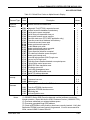
Table 1-1 summaries the application of the various GENISYS® Series 2000 components to new and
existing communications systems. Office protocol converter applications are included for reference
(refer to SM-6700D for details).
SM 6700B 6/96
1-9
1-10
In Stand-Alone
Interface Assy.
In GENISYS® or
MICROLOKPLUS™ unit
In Stand-Alone
Interface Assy.
In GENISYS® or
MICROLOKPLUS™ unit
In Code Line
Interface Assy.
ATCS-compliant MCP to
MICRO LOK® unit. See Figure
1-1.
® or
Serial code line to GENISYS
MICROLOK-PLUS™ unit.
See Fig. 1-2.
®
Serial code line to MICROLOK
unit. See Figure 1-2.
® or
DC code line to GENISYS
MICRO LOK-PLUS™ unit. See
Fig. 1-3.
DC code line to MICROLOK®
unit. See Figure 1-3.
GRS K Series:
N451800-0203
GRS K Series:
N451800-0203
US&S 500 Series:
N451800-0202
WB&S S2: N451800-020X
US&S 500 Series:
N451800-0202
Harmon MCS-1:
N451800-0204
WB&S S2: N451800-020X
GENISYS®:
N451800-0202, -0203
Harmon MCS-1:
N451800-0204
GENISYS®: N451800-0202,
-0203
ATCS: N451800-0201
ATCS: N451800-0201
EXECUTIVE
SOFTWARE
(PRO M SETS)*
(None)
CARD ENCLOSURE
N451891-0102
MCP Interface:
N451807-8902
SURGE SUPPRESS./
SERIAL INTERFACE
PCB(S)
(None)
GENISYS®/MICROLOKPLUS™ Interface:
N451807-8901
Code Line Interface/
Power Supply:
N451441-9402
Code Line Interface:
N451441-9401
PROM set N451800-0203 US&S GENISYS ® and GRS K-Series conversion software.
(None)
In GENISYS® or
MICROLOK-PLUS™ unit, if
req’d by appli-cation.
(None)
32-BIT INPUT PCB
N451441-9701
®
In GENISYS or
MICROLOK-PLUS™ unit, if
req’d by appli-cation.
32-BIT OUTPUT PCBS
N451441-9601, -9801
(None)
In GENISYS® or
GENISYS®/MICROLOKPLUS™ Interface: N451807
- MICROLOK-PLUS™ unit, if
8901
req’d by appli-cation.
(Optional)
Function: Stand-Alone GENISYS®/MICROLOKPLUS™ Interface: N451807
Interface
8901
(Optional)
Function: Code Line
Interface
MICROLOK® Interface:
N451807-8901
Power Supply: N451441
- Function: Stand-Alone Carrier Modem Interface:
N451807-8901
9403
Interface
(None)
®
MICROLOK Interface:
N451807-8901
Carrier Modem Interface:
N451807-8901
GENISYS®/MICROLOKPLUS™ Interface: N451807
8901
Power Supply: N451441
- Function: Stand-Alone MCP Interface: N451807
8902
9403
Interface
(None)
CODE LINE INTF.
PCB/POWER
SUPPLY PCBS
* PROM set N451800-0202 contains both US&S GENISYS ® and 500-Series conversion software.
In GENISYS® or
MICROLOKPLUS™ unit
ENHANCED
CONTROLLER
PCB
N451441-9101
ATCS-compliant MCP to
GENISYS® or MICROLOKPLUS™ unit. See Fig. 1-1.
APPLICATION
Table 1-1 . GENISYS ® Series 2000 Component Applications (Except Protocol Converter)
Section I GENERAL INFORMATION
SM 6700B 6/96
Section I GENERAL INFORMATION
1.4
SYSTEM SPECIFICATIONS
ATCS Radio Interface:
ATCS-compliant mobile communications processor
(Motorola MCP or equivalent) over HDLC serial link
Communications Interfaces:
ATCS-compliant BCP:
ATCS-compliant MCP: EIA RS-422
GENISYS® Master and Slave: EIA RS-423 (RS232C/422 compatible)
No TTL capability
GENISYS® Master/Slave System:
Up to 64 Slave units (typical maximum)
Serial Code Line Protocols:
US&S GENISYS®
Harmon MCS-1
WB&S S2
DC Code Line Protocols:
US&S 504B, 504C, 506, 506A, 506C, 514
GRS K, K1, K2
Field Code Unit Non-Vital I/O:
32 bits per output PCB
32 bits per input PCB
GENISYS® cardfile: Up to 16 output and/or input PCBs
MICROLOK-PLUS™ cardfile: One or two output and/or
input PCBs
SM 6700B 6/96
1-11
This page is intentionally blank.
Section II ENHANCED CONTROLLER PCB N451441-9101
2.1
DESCRIPTION (Refer to Figure 2-1)
2.1.1
General Application
ALL APPLICATIONS
The GENISYS® Series 2000 Enhanced Controller PCB manages logic and communications
interfacing functions in a variety of non-vital control system applications. Basic applications covered in
this manual include:
A. Interfacing of a US&S vital interlocking system* to an ATCS-compliant mobile
communications processor (MCP).
B. Interfacing of a US&S vital interlocking system* to GENISYS®, Harmon MCS-1 or WB&S
S2 protocol serial code lines.
C. Interfacing of a US&S vital interlocking system* to US&S 500 series or GRS K series DC
code lines.
These applications are accomplished with installation of the Enhanced Controller in a GENISYS® or
MICROLOK-PLUS™ cardfile, or the GENISYS® Series 2000 Card Enclosure. When used in a
GENISYS® or MICROLOK-PLUS™ cardfile, the Enhanced Controller PCB also manages local nonvital inputs and outputs in the same manner as the N451441-5602 Controller board. Refer to Section I,
General Information, for a more detailed description of Enhanced Controller Board applications.
2.1.2
Hardware
Enhanced Controller Board N451441-9101 is a standard GENISYS®/MICROLOK® size PCB. Two
44-way PCB connectors interface all power and data lines to the board. In a GENISYS® or
MICROLOK-PLUS™ unit, the “A” (top) connector interfaces external signals via 44-way cable plug. In
the GENISYS® Series 2000 Card Enclosure, the “A” connector passes signals through a motherboard
to selected 25-pin “D” connectors on the rear of the enclosure. The “B” (bottom) connector passes
internal signals via the cardfile or enclosure motherboard bus.
No modifications are required on the GENISYS® or MICROLOK-PLUS™ motherboard “B” connector
(at Controller PCB slot) to accommodate the Enhanced Controller. However, the external cable wiring
to the “A” connector differs between the -5602 and -9101 boards. When retrofitting an existing
GENISYS® or MICROLOK-PLUS™ unit with the -9101 Controller, the external cable connection must
be rewired (Refer to section 2.3.4).
* MICROLOK® Vital Interlocking Control System
MICROLOK-PLUS™ Vital + Non-Vital Control Package
MICROTRAX® Coded Track Circuit/End-of-Siding Controller
SM 6700B 6/96
2-1
2-2
TO "A"
C ON NEC TOR
A PP L I.
E PR O M
AP PL I.
E PR OM
EX EC U TIV E
EP R OM
EX EC U TIV E
EP R OM
10 M HZ
C LOCK
RAM
RAM
LE D
A D D R . B US
SE R IAL
IN TER FACE
RE CEIV ERS
S ER IAL
IN TER FA CE
D R IVE RS
RES ET
B U TTON
SLAV E &
SPA RE
SE R IAL
P OR TS
9 .8 304 M HZ
C L OCK
RECE IVE
SE R IA L
DATA
LEDS
D IA G. &
MA STE R
SE R IA L
P OR TS
V IA
DATA
BUS
RECE IVE
SE R IAL
D ATA
LEDS
D ATA B US
LATC HE S
PU S HB U TTON
9- PIN
P OR T
VE RS ATIL E
IN TER FAC E
AD A PTE R
VE RS ATIL E
IN TER FAC E
AD A PTE R
DATA B US
D IAG .
P OR T
INTE R FA CE
TIM ER
6 80 1 0
M ICR OPR OCE SS OR
A LP HANUM ER IC
D IS PLAY
TO P ER IP HE RALS
2 M HZ
C L OCK
A D D RES S BUS
WATC H D OG
C IRC U IT
TO "B "
C O NN E C TOR :
GE N IS YS ® S ER IES
200 0 EN C LOSU R E
(D C C OD E I/O)
+ 12V
TO
IN TER NAL
& A PP LI.
CIR C U ITS
POW ER
C ON V ER TE R
C IR C U IT
+5V
F RO M U N IT
P OW ER
SUP PL IES
SE RIA L M ES SA GE S TATU S LEDS
TO " B"
C ON NEC TOR :
GE N ISY S ® ,
M IC RO LO K-P LU S™
I/O PCB S
DATA
AD D RES S/
BU S C ON TR O L
DATA
TO M IS C .
C H IP S
PR OG RAM MA BLE
LO GIC
D E VICES
F IE L D C O NF IG .
E EP R OM
AD D R .
TOG GLE
SW ITC H
Section II ENHANCED CONTROLLER PCB N451441-9101
Figure 2-1. Controller PCB Block Diagram
SM 6700B 6/96
Section II ENHANCED CONTROLLER PCB N451441-9101
ALL APPLICATIONS
The Enhanced Controller PCB operates from regulated +5, +12 and -12V dc sources supplied through
the “B” connector. Input power is obtained from these sources:
GENISYS® cardfile:
MICROLOK-PLUS™ cardfile:
GENISYS® Series 2000 Card Enclosure:
Power Supply Converter PCB
Power supply drawer
Power Supply PCB or Code Line Interface/Power
Supply PCB
Principal components of the Enhanced Controller PCB include:
Microprocessor
The Enhanced Controller PCB is managed by a 16-bit Motorola microprocessor (MC68010). This chip
is used to provide enhanced performance and extended, directly accessible memory address space
not available with the -5602 board. The MC68010 is driven by a 10 MHz clock signal.
EPROMs and EEPROM
Two erasable programmable read-only memory (EPROM) ICs contain the system Executive software,
while two additional EPROMs contain the user-defined application software. Each of these EPROM
sets has a capacity of 128K bytes. Field-configurable data is stored in a separate, electrically-erasable
serial PROM (EEPROM).
RAMs
Two 32K random access memory (RAM) ICs are installed on the Enhanced Controller for storage of
variable data. These ICs have a capacity of 64KB x 8 bit bytes.
Parallel I/O VIAs
Two 6522 Versatile Interface Adapter (VIA) ICs on this board interface parallel data lines to the
microprocessor. One VIA handles these functions:
4 inputs:
4 outputs:
1 output:
3 inputs:
2 inputs/outputs:
DC code system*
DC code system*
Watchdog strobe
Manual switches**
EEPROM address and data lines
* When required by application
**Refer to “Manual Switches and Jumpers” below
The other VIA interfaces to the system Control/Indication bus, for example, to pass data between the
microprocessor and the I/O boards in a GENISYS® cardfile. Lines include:
8 data bits (input/output)
8 address/bus control bits (output)
SM 6700B 6/96
2-3
Section II ENHANCED CONTROLLER PCB N451441-9101
ALL APPLICATIONS
Serial Communications Controllers
The Enhanced Controller is equipped with two 85C30 Serial Communications Controllers, each with
two serial data ports, that interface serial communications with the microprocessor. These ports serve
but are not limited to the following uses:
Universal serial port (ATCS, GENISYS®, MCS-1, S2, Slave port)
Asynchronous serial port (GENISYS® Master port)
Asynchronous serial port (field set-up and diagnostics)*
Asynchronous serial port (spare)
*Refer to following listing.
Set-Up/Diagnostic Serial Port
A 9-pin “D” type male plug on the front edge of the Enhanced Controller permits connection of a
portable PC for field set-up and diagnostics of the associated system. Refer to sections 2.3.4.8, 2.4.3
and 2.6.4 for use of this port.
Manual Switches and Jumpers
The Enhanced Controller PCB is equipped with the following user-accessible switches and jumpers:
One momentary-action pushbutton (set-up/diagnostics)*
One momentary-action pushbutton (reset)
One momentary-action, center-off toggle switch (set-up/diagnostics)*
Seven jumpers (configure serial communications lines)
*Used in conjunction with alphanumeric displays; refer to following listing.
Refer to section 2.4.2 for switch operation/settings, and section 2.3.2.2 for jumper positions.
LED Displays
Alphanumeric and individual LEDs are provided on the board for various monitoring purposes. One 4character alphanumeric display provides encoded messages during system set-up and diagnostics,
and is used in conjunction with two of the three manual switches. Seven of fifteen individual LEDs
show the status of these lines:
4 LEDs (serial communications receive lines)
1 LED (control deliver output line)*
1 LED (reset line)
1 LED (watchdog strobe line)
*When used in a GENISYS® or MICROLOK-PLUS™ cardfile equipped with output PCBs.
The remaining eight LEDs are software controlled and indicate logical status of serial ports. Refer to
Section 2.5 for interpretation of LED displays.
2-4
SM 6700B 6/96
Section II ENHANCED CONTROLLER PCB N451441-9101
ALL APPLICATIONS
2.1.3
Communications Interfaces
2.1.3.1 Serial
The Enhanced Controller PCB is equipped with independent serial data ports for communications with:
A.
B.
C.
D.
E.
F.
PRCCI™ CTC communications circuits
ATCS-compliant base* and mobile communications processors
Serial code lines (US&S GENISYS®, Harmon MCS-1, WB&S S2)
Master and Slave GENISYS® and MICROLOK-PLUS™ units
MICROLOK® or MICROTRAX (End-of-Siding) units (via code line interface)
Portable PC
Except for the portable PC, these remote systems/devices are interfaced on the board’s “A” connector
edge. EIA RS-232, RS-422 or RS-423 signal levels are employed according to the application,
however a 5V TTL interface is not available.
Serial communications parameters such as key delays and baud rates may be defined during field
configuration via the front edge toggle switches and alpha-numeric display, the front edge PC port or in
the application logic. Set-up of a given parameter is not limited to any one of these options; most are
accessible via all three paths.
When the Enhanced Controller is used to manage other GENISYS® or MICROLOK-PLUS™ units in a
Master/Slave configuration, the maximum practical limit is 64 Slaves. Refer to Section 2.3.4 for
application of the serial data ports.
2.1.3.2 Parallel
The Enhanced Controller PCB is equipped with a set of signal lines for parallel communication with a
DC code line. These lines reside on the board’s “A” connector. Communications with the DC code
line are interfaced through the GENISYS® Series 2000 Code Line Interface or Code Line
Interface/Power Supply board. The code line protocol (e.g. 504, 514, K1) is selected via the Executive
EPROM set and the application logic.
2.1.4
Software
The Enhanced Controller PCB operates under the control of its Executive and Application software as
modified by its field configuration.
2.1.4.1 Executive
The Executive software performs certain routine operations and automatic diagnostics common to all
Enhanced Controller PCBs, and is contained in two 64K byte EPROM chips. Different
communications protocols are accommodated in different part numbers for these chips (two EPROMs
per set). Executive software covered by this manual include:
SM 6700B 6/96
2-5
Section II ENHANCED CONTROLLER PCB N451441-9101
ALL APPLICATIONS
US&S Part No.
N451800-0201
N451800-0202
N451800-0203
N451800-0204
N451800-020?
Application
ATCS-compliant MCP interface
GENISYS® serial code line and US&S 500 series DC code line
GENISYS® serial code line and GRS K series DC code line
Harmon MCS-1 serial code line
WB&S S2
Note that the -0202 and -203 EPROM sets contain both GENISYS® serial and DC code line interfacing
software and may be used for either type of communications system. Upgrades to the Executive
software are denoted in the revision number printed on the EPROM chip. When upgrades are
implemented, users are initially notified through a US&S software Maintenance Notice.
NOTE
The Executive software used in the Enhanced Controller PCB is not
compatible with Controller PCB N451441-5602.
2.1.4.2 Application
The Application software carries the user-defined logic for the particular system managed by the
Enhanced Controller PCB. Field configuration parameters such as baud rates, station address etc.
may also be set up via this software. Application software is contained in two 64K byte EPROMs. The
software may be developed by US&S as a customer service, or with the GENISYS® Series 2000
Development System (G2DS). With the G2DS, the user may design, exercise, debug and load the
application logic into the EPROMs, prior to installation on the board. When upgrades to the G2DS
compiler or simulator are implemented, users are initially notified through a US&S software
Maintenance Notice. G2DS software loading procedures (hard and floppy disk) are described in US&S
service manual SM-6701. Refer to service manual SM-6700A, Genisys Series 2000 Application Logic
Programming, for application logic programming, debugging and loading procedures.
2.1.4.3 Field Configuration
The Field Configuration software is used to set up local operating parameters for the particular unit that
contains the Enhanced Controller. Included in this software are baud rates, key delays, station
address, etc. Field Configuration software is contained in an erasable EEPROM. Programming may
be performed by the following means:
A. Board front edge toggle switches and alpha-numeric displays
B. Portable PC plugged into the 9-pin port on the front edge of the board. (On the earlier 5602 Controller PCB, these parameters are only set up with manual switches on the board.)
C. Application software.
2-6
SM 6700B 6/96
Section II ENHANCED CONTROLLER PCB N451441-9101
ALL APPLICATIONS
2.2
SPECIFICATIONS
US&S Part No.:
N451441-9101
Board Size:
Standard GENISYS®/MICROLOK® size
Installations:
GENISYS® Series 2000 Card Enclosure (lower slot)
GENISYS® cardfile (slot J2)
MICROLOK-PLUS™ cardfile (slot O)
Connections:
44-way PCB edge connector “A”: External communications
44-way PCB edge connector “B”: System motherboard
9-pin “D” (IBM compatible PC)
Slave Serial I/O Port:
EIA RS-423 (RS-232C/RS-422 compatible)
Synchronous or asynchronous
Baud Rates: 150 to 19,200 BPS
Mode: Half or full duplex
Master Serial I/O Port:
EIA RS-423 (RS-232C compatible)
Asynchronous only
Baud Rates: 150 to 19,200 BPS
Mode: Half or full duplex
Set-Up/Diagnostics Port:
RS-423 (RS-232C compatible)
Asynchronous only
Baud Rates: 150 to 19,200
TTL Serial Interface:
Not available
Master/Slave System:
64 Slave units (practical maximum)
G2DS Development System:
128K bytes in application logic (max.)
4000 “relay coils” (max.)
Not compatible with GENISYS® Development System
(GDS)
Controlling Chip:
Motorola MC68010:
32-bit internal data bus
16-bit external data bus
Executive EPROMs:
Qty = 2
64K bytes per chip
128K total bytes
SM 6700B 6/96
2-7
Section II ENHANCED CONTROLLER PCB N451441-9101
ALL APPLICATIONS
US&S Part Numbers:
N451800-0201 (ATCS radio protocol)
N451800-0202 (GENISYS® serial and US&S 500series dc code line protocols)
N451800-0203 (GENISYS® serial and GRS Kseries dc code line protocols)
N451800-0204 (Harmon MCS-1 serial code line
protocol)
N451800-020X (WB&S S2 serial code line
protocol)
Application Logic EPROMs:
Qty = 2
64K bytes per chip
128K total bytes
US&S part no.: J715029-0596 (blank chip)
User Controls:
1 momentary pushbutton (set-up/diagnostics)
1 momentary pushbutton (reset)
1 momentary toggle (set-up/diagnostics)
7 jumpers (configure serial comm.)
User Displays:
4-character alphanumeric LED display
15 discrete LEDs (misc. function monitoring)
Board Environmental Limits:
-40o to +70oC
95% relative humidity (non-condensing)
2-8
SM 6700B 6/96
Section II ENHANCED CONTROLLER PCB N451441-9101
ALL APPLICATIONS
2.3
INSTALLATION
2.3.1
Shipment Inspection
Prior to installation, the Enhanced Controller PCB should be inspected for possible damage during
shipping. Check for loose or missing components, broken solder leads, breaks in tracks, fractures in
the board material etc. Damaged boards should be returned to US&S for repair or replacement. For
service information call 1-800-652-7276 or write:
Union Switch & Signal Inc.
The Service Shop
645 Russell St.
Batesburg, SC 29006
2.3.2
Pre-Installation Preparation (Ref. Figure 2-2)
2.3.2.1 EPROMs
The Enhanced Controller PCB is shipped without Executive or Application software or EPROMs. Four
EPROMs are required for normal operation, including two Executive and two Application. The sockets
for these EPROMs are marked “EXEC EVEN”, “EXEC ODD” and “APPL EVEN”, “APPL ODD”. These
sockets are also marked U4, U5, U6 and U7. Install the Executive and Application software EPROMs
according to their labels, with the “EVEN” EPROMs going in the “EVEN” sockets and the “ODD”
EPROMs going in the “ODD” sockets. When installing an EPROM, make certain the chip has the
proper pin orientation and is fully inserted.
2.3.2.2 Jumpers
The Enhanced Controller PCB is equipped with seven jumpers for configuration of various
communications lines and watchdog functions. Settings are as follows:
Jumper settings for GENISYS®,
US&S 500-Series, GRS “K” Series,
Harmon MCS-1 slave Applications
JP1
JP2
JP3
JP4
BC
BC
BC
BC
JP5
JP6*
JP7**
BC
BC
AB
Jumper settings for ATCS MCP
communications:
JP1
JP2
JP3
JP4
BC
BC
AB
AB
JP5
JP6*
JP7**
BC
BC
AB
* Keep jumper in BC position for all applications (watchdog enable)
**Keep jumper in AB position for all applications (watchdog time out of 1200 mS)
SM 6700B 6/96
2-9
Section II ENHANCED CONTROLLER PCB N451441-9101
EXEC
JP2
A
A
C
C
C
JP1
APPLICATION
EPROMS
JP4
A
JP3
U4
A C
ODD
C
A
U6
JP5
APPL
EVEN
U7
U5
EXECUTIVE
EPROMS
JUMPER POSITIONS
GENISYS ®, US&S 500 SERIES CODE LINE,
HARMON MCS-1/2 SLAVE APPLICATIONS:
JP1
JP2
JP3
JP4
- BC
- BC
- BC
- BC
JP5 - BC
JP6 - BC
JP7 - AB
ATCS MCP APPLICATIONS:
JP1
JP2
JP3
JP4
- BC
- BC
- AB
- AB
JP5 - BC
JP6 - BC
JP7 - AB
JUMPER IN A-B
POSITION
A
A
JP7
JP6
C
C
NOTE:
KEEP T HESE JUMPER
POSITIONS FOR ALL
APPLICATIONS.
A
C
JUMPER IN B-C
POSITION
A
C
Figure 2-2. Enhanced Controller PCB: EPROM and Jumper Locations
2-10
SM 6700B 6/96
Section II ENHANCED CONTROLLER PCB N451441-9101
ALL APPLICATIONS
2.3.3
Installation in Cardfile or Enclosure (Ref. Figure 2-3)
The Enhanced Controller PCB is installed in slot J2 of the GENISYS® cardfile, slot O of the
MICROLOK-PLUS™ cardfile, or the lower slot of the GENISYS® Series 2000 Card Enclosure, as
required by the application.
CAUTION
Make certain unit operating power is turned off while installing
the enhanced controller PCB, otherwise component damage and
or unreliable operation may result.
SM 6700B 6/96
2-11
Section II ENHANCED CONTROLLER PCB N451441-9101
ALL APPLICATIONS
GENISYS® /
GENISYS® SERIES 2000
CARDFILE
SLOT
J1
J2 J3
J18
POWER
SUPPLY
ENHANCED
CONTROLLER
N451441-9101
OUTPUT AND/OR INPUT
PCBS (32-BIT OR 16-BIT)
OUTPUT AND/OR INPUT
PCBS (32-BIT OR 16-BIT)
ENHANCED CONTROLLER
N451441-9101
SLOT
ABC
OPQ
MICROLOK-PLUS™
CARDFILE
DC CODE LINE/POWER SUPPLY PCB
DC CODE LINE PCB
POWER SUPPLY PCB
GENISYS® SERIES 2000
CARD ENCLOSURE
ENHANCED CONTROLLER
N451441-9101
Figure 2-3. Enhanced Controller PCB Installation
2-12
SM 6700B 6/96
Section II ENHANCED CONTROLLER PCB N451441-9101
ALL APPLICATIONS
2.3.4
Serial and Parallel Communications Interfaces
2.3.4.1 General
Figure 2-4 summarizes the serial and parallel communications interfaces to the Enhanced Controller
board for the system applications covered in this manual. Three serial communications ports on the
Enhanced Controller reside on the “A” connector. These ports include:
A. Universal synchronous/asynchronous Slave port for communications with a remote Master
unit
B. Asynchronous-only Master port for communications with a remote Slave Unit
C. Universal spare port (not used)
The asynchronous 9-pin port on the PCB front edge is only used for on-site set-up and diagnostics.
Refer to Section 2.3.4.8 for wiring of this port.
The Universal Slave serial interface port supports both synchronous and asynchronous interfaces and
is an RS-422 compatible implementation of RS-423. All inputs are balanced differential inputs, while
all outputs are unbalanced and referenced to signal common. This allows connection to external
devices implementing standard RS-232, RS-422 or RS-423 interfaces. The Master serial interface and
set-up/diagnostics ports only support asynchronous serial interfaces and RS-232/423 electrical
compatibility.
Physically, the serial ports on the Enhanced Controller are connected with a 44-way cable connector
when the board is installed in a GENISYS® or MICROLOK-PLUS™ cardfile. When the board is
installed in the GENISYS® Series 2000 Card Enclosure, the serial ports are externally connected
through plugs J3, J4 and J5 (25-pin “D” type) on the rear of the Card Enclosure, which shares a
motherboard bus with the Enhanced Controller. Shielded cable is used in all interfaces to minimize
induced noise. Twisted pair wiring is also employed in the ATCS MCP interface to take full advantage
of the additional noise immunity inherent in RS-422 balanced signal circuits.
NOTE
The Enhanced Controller PCB is not equipped with a TTL-compatible
serial communications port, as is provided on the on -5602 Controller
PCB.
NOTE
Use of the GENISYS® Series 2000 Surge Suppressor/Serial Interface
Panel is optional, but strongly recommended for any installation where
transient voltages (e.g. lightning induced) could damage circuits in the
Enhanced Controller PCB.
SM 6700B 6/96
2-13
Section II ENHANCED CONTROLLER PCB N451441-9101
ATCS MCP
4 4 -W A Y
P CB CO N N.
S LOT J 2
CO NT RO LL ER PC B
1
SL AVE
TO C OD E L IN E PORT:
• MICR OL OK®
• MICR OTRAX ® EOS
RS-4 23
MASTER
G ENISYS ®
2
• MODEM
F
M
M
3
F
4 4 -W A Y
P C B CO N N .
S LO T J 2
CONT ROL LE R
PC B
H DLC L IN K
RS-4 22
TO ATCS MCP
H DLC L IN K
RS-4 22
HD LC LINK
R S-422
TO ATCS MCP
SL AVE
4
EXTERNAL LY INTERFAC ED
UN ITS
MASTER
ATCS MCP
MS3116 F1 4-15 SZ
TO CODE LINE PORT:
• MICR OL OK®
• MICR OTRAX ® EOS
R S-423
• MODEM
2
GENISYS®
4 4 -W A Y
PC B CON N .
S LOT O
CO NT ROL LER
PCB
M
M
F
2 5 -P IN ( M )
C O NN .
CO D E S Y S. P ORT
F
MICROLOK ®
CPU C ARDFILE
3
5
SLAVE
SL AVE
6
37-PIN (F)
C ON NECTO R
AT C OD E
SYSTEM PCB
HDL C LINK
RS-4 22
MASTER
TO ATCS MCP
M
2
F
MIC ROLOK-PLUS™
4 4 -W A Y
P C B CO NN .
S LO T O
CONT ROL LE R
PCB
MICROTRAX ®
EN D-OF-SIDING
C ARDFILE
2 5 - PI N (M )
C ON N .
COD E S YS . PO RT
SLAVE
HD LC LINK
R S-422
MASTER
7
HDL C LINK
RS-4 22
2
MIC ROLOK-PLUS™
M
2 5-PIN (F)
C ON NECTOR:
CODE
SYSTEM PORT
TO ATCS MCP
5
F
MODEM
HD LC LINK
R S-422
SL AVE
MASTER
8
J3
J4
J5
HD LC LINK
R S-422
TO ATC S MC P
RS-42 3
2
TO CODE LINE POR T:
• MIC RO LO K®
• MIC RO TR AX ® EOS
M
F
M
F
3
5
1 GENISYS® CAR DFIL E WITH BUILT-IN
SU RGE PC B PANEL
4 GENISYS ® CARD FILE WITHOUT BU ILTIN SURG E PCB PANEL
7 MIC ROLOK-PLUS™ CARD FILE
WITHOUT BUILT-IN SUR GE PCB PANEL
2 SU RGE SU PPR./SER IAL INTERFAC E
PC B N 451 807 -890 2
5 GENISYS ® 200 0 SURGE PCB
MOUNTING PANEL N4 518 92-1 401
8 GEN ISYS ® 2 000 C ARD ENC LOSURE
3 SU RGE SU PPR./SER IAL INTERFAC E
PC B N 451 807 -890 1
6 MICROLOK-PLU S™ C ARDFILE WITH
BUILT-IN SURGE PCB PAN EL
Figure 2-4. Basic Serial Communications Links with ATCS MCP Interface
2-14
SM 6700B 6/96
Section II ENHANCED CONTROLLER PCB N451441-9101
GENISYS®, MCS-1, WB&S S2
4 4 -W A Y
PC B C O N N .
S LOT J2
C O N T RO L L ER PC B
1
S LAV E
TO C O DE LI NE P OR T:
• M I CR OL OK ®
• M I CR OT R A X ® E OS
R S -4 23
M A S TE R
G E N IS Y S ®
2
• M OD EM
F
M
M
F
2
R S -2 32
4 4 -W A Y
PC B C O N N .
S LOT J2
C O N T RO L L E R PC B
T O S ER IA L LIN E
C A RR IE R
R S -232
R S -23 2
T O S ER IA L LIN E
C A RR IE R
R S -423
T O C O DE LINE P OR T:
• M I CR O LOK ®
• M I CR O TR A X ® EOS
S LA VE
3
E XT E RN A LLY I NT ER FA C E D
UN I TS
MA S T ER
S E R I AL LI NE
C AR R IE R
• M O DE M
2
G EN IS Y S ®
4 4 -W A Y
PC B C O N N .
SL O T O
C O N TR O L L ER
PC B
M
F
M
2 5 - PIN ( M )
C ON N .
C O D E SY S. PO RT
F
M IC R OLO K ®
C P U C A RD F IL E
2
4
S LA VE
S LAV E
5
R S - 23 2
M A S TE R
M
F
37-P IN (F)
C ONN E C T OR
A T C OD E
S Y S TE M P C B
T O S ER IA L LIN E
C A RR IE R
2
M IC ROLO K - PL U S ™
4 4 -W A Y
P CB C O N N .
S LOT O
C O N T RO L L ER
PC B
M I CR OT RA X ®
EN D- OF -S I D I N G
C A R D F I LE
2 5 - PI N ( M )
CONN .
C O D E SY S. PO R T
S L AV E
R S - 232
M A ST E R
6
R S -232
2
M I C ROL OK - P LU S ™
M
25 - PI N (F)
C ONN E C T OR :
C ODE
S Y S TE M P O R T
T O S ER IA L LIN E
C A RR IE R
4
F
M OD EM
R S -23 2
S LAV E
M A S TE R
7
J3
J4
J5
R S -232
TO S E R I A L LI N E
C A R RI ER
R S -42 3
T O C OD E LIN E P ORT:
• MI C RO LOK ®
• MI C RO TRA X ® EO S
2
M
F
M
F
2
4
1
GE N IS Y S® C A R D FILE WI TH BUI LT- IN
S UR G E P CB PA NE L
4
GE NI S YS ® 2000 S U RGE P CB
M OUN T IN G PA NE L N 45189 2-1401
2
S UR GE S U PP R ./ S ER I A L INT ERFA CE
P CB N 45180 7-8901
5
MI CR OLOK -PLUS ™ C A R D FI LE WI TH
B UILT-I N SU R GE PC B PA N E L
3
GE N IS Y S® C A R D FILE WI TH O UT B U ILTI N S U R GE PC B PA N E L
6
MI CR OLOK -PLUS ™ CAR DF ILE
WI TH O U T B UI LT - IN S UR G E P CB P A NE L
7 GE NIS YS ® 2000 C A R D ENC LO SUR E
Figure 2-5. Basic Serial Communications Links with Serial Code Line Interface
SM 6700B 6/96
2-15
Section II ENHANCED CONTROLLER PCB N451441-9101
US&S 500 DC, GRS K DC
44-WAY
PCB CO NN.
SLO T J2
PAR ALLEL INTERFACE
SLAVE
TO
MIC ROLOK®
MIC ROTRAX®
RS-423
MASTER
1
TO J1, J2, J 6
GENISYS ®
M
2
F
J2
J1
PA RA L L EL
J7 IN TERF A C E
J9
J 11
J6
J8
J10
3
EXTERNALLY INTERFACED
UNITS
TO CODE
LINE F ILTER
MICROLOK ®
CPU CARDFILE
2
5
44- WAY
PC B CO NN.
SLO T J2
4
M F
MICROLOK®
MICROTR AX®
37- PIN ( F)
CONNECTOR
AT CO DE
SYST EM PCB
PARALLEL INTERFACE
MASTER
RS-423
J1
GENISYS ®
J6
J8
J1 0
J2
3
6
TO
SLAVE
TO J1, J2, J6
44-WAY
PCB CO NN.
SLO T O
RS- 423
PA RA L L EL
J7 IN TER F A CE
J9
J1 1
MICROTRAX®
END-O F-SIDING
CARDFILE
TO CODE
LINE FILTER
25-PIN (F )
CO NNECT OR:
CODE
SYSTEM PORT
PARALLEL INT ERFACE
SLAVE
TO J 1, J2, J6
J1
MICRO LOK-PLUS™
J2
3
J6
J8
J1 0
5
M F
PA RA L L EL
J7 IN TERF A C E
J9
J1 1
RS- 423
TO CODE
LINE FILT ER
DC CODE LINE
FILTER
TO
MICROLO K®
MICROT RAX®
SLAVE RS-423
J1
3
J2
J4
J6
J8
J10
PA RA L L EL
J7 IN TERF A C E
J9
J1 1
TO CODE
LINE FILT ER
1 GENISYS® CARDFILE WITH BUILT-IN
4
GENISYS ® CARDFILE WITHOUT BUILT-IN
SURGE PCB PANEL
2 SURGE SUPPR./SERIAL INTERFACE PCB
5
GENISYS ® SERIES 2000 SURGE PCB
MOUNTING PANEL N451892-1401
3 GENISYS® SERIES 2000 C ARD
6
MICROLOK-PLUS™ CARDF ILE (BUILT-IN
SURGE PCB PANEL NOT REQUIRED)
SURGE PCB PANEL
N451807-8901
ENCLOSURE (INTERFACE MOD ULE)
N451891-0102
Figure 2-6. Basic Serial Communications Links with DC Code Line Interface
2-16
SM 6700B 6/96
Section II ENHANCED CONTROLLER PCB N451441-9101
ALL APPLICATIONS
Refer to Section 2.4.2, Procedure Using Board Switches and Alpha-Numeric LEDs, for serial
communications set up instructions using the switches and alpha-numeric display, and Section 2.4.3,
Procedure Using Portable PC, for set-up via a PC. Refer to SM-6700A, Genisys Series 2000
Application Logic Programming, for serial communications programming in the Application software.
Parallel interface lines to the Enhanced Controller also reside on the “A” connector and are used
strictly for DC code line applications. These include four output lines, four input line and dc voltage
lines of +5V, +12V, -12V and 0V. Refer to following section for parallel line pinout locations.
2.3.4.2 PCB Connector “A” Pinout Listing (Serial and Parallel Ports)
Table 2-1. Enhanced Controller PCB Connector “A” Pinout Listing
Pin
No.
1
2
3
4
5
6
Description
S2RXD- (Spare Receive Data “-”)
S2DCD- (Spare Data Carrier Detect “-”)
S1TXC- (Slave Transmit Clock “-” )
S1RTS (Slave Request to Send)
S1TXD (Slave Transmit Data)
S1COM (Slave Common: 0 volts)
Pin
No.
A
B
C
D
E
F
7
8
9
10
11
12
13
14
15
16
17
18
19
20
21
22
S2DTR (Spare Data Terminal Ready)
S2TXD (Spare Transmit Data)
S1DCD- (Slave Data Carrier Detect “-”)
S1RXC- (Slave Receive Clock “-”)
S1CTS- (Slave Clear to Send “-”)
S1RXD- (Slave Receive Data “-”)
POUT1 (Parallel Out 1)*
POUT2 (Parallel Out 2)*
PIN1 (Parallel In 1)*
PIN3 (Parallel In 3)*
+12V (+12 Volts dc)*
MTXD (Master Transmit Data)
0V (0 volts dc)*
-12V (-12 volts dc)*
MRXD (Master Receive Data)
+5V (+5 volts dc)*
H
J
K
L
M
N
P
R
S
T
U
V
W
X
Y
Z
Description
S2COM (Spare Common: 0 volts)
S2RXC- (Spare Receive Clock “-”)
S1TXC+ (Slave Transmit Clock “+”)
S1DTR (Slave Data Terminal Ready)
S1TXC (Slave Transmit Clock: Output)
S2TXC (Spare Xmit Clock: Output)**
S2TXC- (Spare Xmit Clock “-”: Input)**
MDTR (Master Data Terminal Ready)
S2RTS (Spare Request to Send)
S1DCD+ (Slave Data Carrier Detect “+”)
S1RXC+ (Slave Receive Clock “+”)
S1CTS+ (Slave Clear to Send “+”)
S1RXD+ (Slave Receive Data “+”)
POUT2 (Parallel Out 2)*
POUT4 (Parallel Out 4)*
PIN2 (Parallel In 2)*
PIN4 (Parallel In 4)*
+12V (+12 volts dc)
MRTS (Master Request to Send)
MCOM (Master Common: 0 volts)
-12V (-12 volts dc)
MDCD (Master Data Carrier Detect)
+5V (+5 volts dc)
Notes: * Connections to Code Line Interface board
**Output or input selected with jumper JP5 on controller board
S1 = Slave Port: RS-423 (RS-422 compatible)
S2 = Spare Port: RS-232D compatible
M = Master Port: RS-232D compatible
SM 6700B 6/96
2-17
Section II ENHANCED CONTROLLER PCB N451441-9101
ALL APPLICATIONS
2.3.4.3 PCB Connector “A” Signal Line Descriptions
Table 2-2.
Describes all individual serial and parallel signal lines on all “A” connector edge ports.
Table 2-2.
Enhanced Controller PCB Signal Line Descriptions (Serial and Parallel)
- Connector “A”
Signal Name
Signal
Direction
Port(s)
Description
TXD (Transmit Data)
Output
Slave
Master
Spare
Passes serial data to connected device.
RXD (Receive Data)
Input
Slave
Master
Spare
Accepts serial data from connected device.
RTS (Request to Send) Output
Slave
Master
Spare
Frames transmitted message. Typically used
to turn on data carrier at start of transmitted message, turn off carrier and end of
this message.
CTS (Clear to Send)
Input
Slave
Indicates the serial link is stable and ready
to accept transmitted data. Typically
asserted in response to RTS by the serial
link after fixed delay.
DCD (Data carrier
detect)
Input
Slave
Master
Spare
Indicates serial link (carrying incoming
data) is active and stable. Connected unit
is about to send or is sending data.
TXC (Transmit Clock)
Input or
Output
Slave
Spare
Clock signal to which transmitted data is
synchronized. Transmitted data is valid on
negative-going transition of clock signal.
Transmitted data also in transition on positive-going transition of clock signal. Slave port
may accept or generate TXC based on position of
jumpers JP2 and JP4. TXC only
used when transmitting serial data in synchronous
mode.
2-18
SM 6700B 6/96
Section II ENHANCED CONTROLLER PCB N451441-9101
RXC (Receive Clock)
Input
Slave
Spare
Clock signal, provided by source of received data,
to which received data is synchronized. Received
data expected to be valid on negative-going transition of received clock. Received
data also expected to be in transition on positive-going transition of received clock. RXC only used when receiving
serial data in synchronous mode.
DTR (Data Terminal
Ready)
Output
Slave
Master
Spare
Slave: Asserted to enable the connected data
modem. When not asserted, modem transmit
oscillator is disabled. DTR only used by
WB&S S2 Executive software.
Master, Spare: Not used.
SM 6700B 6/96
2-19
Section II ENHANCED CONTROLLER PCB N451441-9101
ALL APPLICATIONS
2.3.4.4 Detailed Serial Link Diagrams
The following tabulation summarizes detailed serial link diagrams in this section:
Fig. No.
2-7
Page
No.
2-20
2-8
2-21
Serial Port Wiring with ATCS MCP Interface - MICROLOK-PLUS™ Cardfile
• Enhanced Controller Slave port interface to MCP
• Master port interfaces to modem or to MICROLOK-PLUS™ code system
port on same cardfile. (Vital section of MICROLOK-PLUS™ cardfile
functions as interlocking controller.)
2-9
2-22
Serial Port Wiring with ATCS MCP Interface - GENISYS® Series 2000
Card Enclosure
• Covers Enhanced Controller Slave port interface to MCP
• Master port interface to external US&S interlocking controller.
2-10
2-23
Serial Port Wiring with Serial Code Line Interface - GENISYS®
Cardfile
• Enhanced Controller Slave port interface to serial code line
carrier
• Master port interfaces to modem or external US&S interlocking
controller.
2-11
2-24
Serial Port Wiring with Serial Code Line Interface - MICROLOK-PLUS™
Cardfile
• Enhanced Controller Slave port interface to serial code line
carrier
• Master port interfaces to modem or to MICROLOK-PLUS™ code system
port on same cardfile. (Vital section of MICROLOK-PLUS™ cardfile
functions as interlocking controller.)
2-12
2-25
Serial Port Wiring with Serial Code Line Interface - GENISYS® Series
2000 Card Enclosure
• Enhanced Controller Slave port interface to serial code line
carrier
• Master port interface to external US&S interlocking controller.
2-20
Description/Comments
Serial Port Wiring with ATCS MCP Interface - GENISYS® Cardfile
• Enhanced Controller Slave port interface to MCP
• Master port interfaces to modem or external US&S interlocking
controller.
SM 6700B 6/96
Section II ENHANCED CONTROLLER PCB N451441-9101
2-13
2-26
Parallel and Serial Port Wiring with DC Code Line Interface GENISYS® Cardfile
• Enhanced Controller parallel data port interface to DC code line
filter
• Master port serial interfaces to modem or external US&S
interlocking controller.
2-14
2-27
Parallel and Serial Port Wiring with DC Code Line Interface MICROLOK-PLUS™ Cardfile
• Enhanced Controller parallel data port interface to DC code
line filter
• Master port interfaces to modem or to MICROLOK-PLUS™ code system
port on same cardfile. (Vital section of MICROLOK-PLUS™ cardfile
functions as interlocking controller.)
2-15
2-28
Parallel and Serial Port Wiring with DC Code Line Interface GENISYS® Series 2000 Card Enclosure
• Enhanced Controller parallel data port interface to DC code line
filter
• Master port interface to external US&S interlocking controller.
SM 6700B 6/96
2-21
Section II ENHANCED CONTROLLER PCB N451441-9101
ATCS MCP
E NHA NCED
CO NT RO L L E R PCB
SURGE SUPPR./
SERIAL INTERFACE
PCB N451807-8902
INTERFACE CABLE
GENISYS ® CA RDFILE
SL O T J2
S1RXDS1RXD+
S1RXCS1RXC+
S1TXD
S1COM
S1 TXC
+12V
-12V
INTERFACE CABLE
D B25S
DB25P
MCP
MS3116F14-15SZ
12
3
GND
1
N
16
TXD-
2
H
10
17
TXD+
19
J
L
18
RXD-
3
D
5
2
RXD+
16
E
6
7
RXC-
17
B
RXC+
18
C
E
24
TXC+
23
G
U
9
TXC-
24
F
X
10
COM
7
R
1
DB25S
MTXD
MRXD
MCOM
MRTS
RXD B
TXD A
TXD B
TXC A
TXC B
RXC B
RXC A
COM
DB25P
9
9
10
10
18
2
2
21
3
3
W
7
7
Y
4
4
1
1
TY PICA L MA ST ER
P ORT CO NN ECTI ON
( GEN ISY S®
CA RDFILE ON LY)
RXD A
POWER
FOR
MODEM
(IF REQ’D)
MODEM
TWISTED-PAIR
WIRES
SURGE SUPPR./
SERIAL INTERFACE
PCB N451807-8901
INTERFACE CABLE
Figure 2-7. Serial Port Wiring with ATCS MCP Interface - GENISYS® Cardfile
2-22
SM 6700B 6/96
Section II ENHANCED CONTROLLER PCB N451441-9101
ATCS MCP
SURGE SUPPR./
SERIAL INTERFACE
PCB N451807-8902
ENH A NC ED
CO NT R OL L ER P C B
M ICR OL OK - PL US ™
C A RD FIL E
S L O T " O"
S1RXD-
INTERFACE CABLE
DB25S
DB25P
12
3
GND
1
MCP
MS3116F14-15SZ
N
16
TXD-
2
H
10
17
TXD+
19
J
L
18
RXD-
3
D
5
2
RXD+
16
E
6
7
RXC-
17
B
RXC+
18
C
S1RXD+
S1RXC-
INTERFACE CABLE
S1RXC+
S1TXD
S1COM
S1TXC
+12V
-12V
E
24
TXC+
23
G
U
9
TXC-
24
F
X
10
COM
7
R
1
SLAVE PORT
RXD A
RXD B
TXD A
TXD B
TXC A
TXC B
RXC B
RXC A
COM
MASTER PORT
MTXD
MRXD
MCOM
MRTS
MDCD
18
21
W
V
Y
MICROLOK-PLUS™
INTRA-CARDFILE
CABLE
RTS
DCD
SIG COM
TXD
RXD
TWISTED-PAIR
WIRES
13
5
20
16
14
DB25M
M ICRO LO K- PL U S™
C A RD FIL E
COD E SYSTEM
PORT
Figure 2-8. Serial Port Wiring with ATCS MCP Interface - MICROLOK-PLUS™ Cardfile
SM 6700B 6/96
2-23
Section II ENHANCED CONTROLLER PCB N451441-9101
ATCS MCP
GENI SY S® SE RIES 2 0 0 0
CA RD E NCL O SURE
PO RT J 4 ( TO
EN HA N CED
CON TROL L ER P CB)
S1RXDS1RXD+
S1RXCS1RXC+
S1TXD
S1COM
S1TXC
+12V
-12V
INTERFACE CABLE
DB25F
MCOM
MRTS
MDCD
DB25M
MCP
MS3116F14-15SZ
3
GND
1
16
16
TXD-
2
H
17
17
TXD+
19
J
RXD B
18
18
RXD-
3
D
TXD A
2
2
RXD+
16
E
7
7
RXC-
17
B
RXC+
18
C
24
24
TXC+
23
G
9
9
TXC-
24
F
10
10
COM
7
R
MASTER PORT
MRXD
INTERFACE CABLE
3
1
SLAVE PORT
MTXD
SURGE SUPPR./
SERIAL INTERFACE
PCB N451807-8902
DB25F
DB25M
DB2 5F
14
3
16
7
2
4
5
8
13
18
GEN ISY S® S ERI ES 2 0 0 0
CA RD ENCL OS URE
30
7
SURGE SUPPR./
SERIAL INTERFACE
PCB N451807-8901
TWISTED-PAIR
WIRES
(OPTIONAL)
TXD B
TXC A
TXC B
RXC B
RXC A
COM
DB3 7M
2
PORT J3 ( T O
E NHA NCED
CO NT RO LL ER PCB )
RXD A
INTERFACE CABLE
RX D
TXD
SIG COM
DCD
RTS
RX COM
CTS
DS R
M ICRO LO K ®
CO DE S YS TE M
PO RT
Figure 2-9. Serial Port Wiring with ATCS MCP Interface - GENISYS® Series 2000 Card Enclosure
2-24
SM 6700B 6/96
Section II ENHANCED CONTROLLER PCB N451441-9101
GENISYS®, MCS-1, WB&S S2
Figure 2-10. Serial Port Wiring with Serial Code Line Interface - GENISYS® Cardfile
SM 6700B 6/96
2-25
Section II ENHANCED CONTROLLER PCB N451441-9101
GENISYS®, MCS-1, WB&S S2
SURGE SUPPR./
SERIAL INTE RFACE
PCB N451807-8901
EN HA N CED
CON TRO L L ER PCB
M ICRO L OK - PL US ™
CA RD FILE
SL O T " O "
DB25M
5
2
12
3
S1TXDS1RXD-
INTERFACE CABLE
INTERFACE CABLE
N
S1RXD+
6
S1COM
7
K
S1DCD+
1
TXD
2
RXD
3
RTS
4
COM
7
8
DCD
8
4
4
+12V
9
D
20
-12V
10
U
9
DTR
20
X
10
S1RTS
S 1DTR
-12V
SHIE LD
9
S1DCD-
+12V
DB25F
1
SLAVE PORT
SERIA L L INE CA RRIER
( MO DEM )
DATA TO MODEM
DATA FROM MODEM
KEY ON
S IGNAL COMMON
MODEM CARR. DET. (1)
POWER TO MODEM (2)
POWER TO MODEM (2)
MODEM DISABLE (3)
(1) HARMON MCS-1 AND WB&S S2 ONLY
(2) REQUIRED ONLY IF MODE M IS POWERED BY
GENIS YS® SERIES 2000
(3) WB&S S2 O NLY
MASTER PORT
MTXD
MRX D
MCOM
MRTS
18
21
W
V
DB25M
RTS
DCD
SIG COM
TXD
RXD
MICROLOK -P LUS™
INTRA-CARDFIL E
CABLE
13
5
20
16
14
MI CROL OK - PL US ™
CA RDFI L E
CO DE S YS TE M PO RT
Figure 2-11. Serial Port Wiring with Serial Code Line Interface - MICROLOK-PLUS™ Cardfile
2-26
SM 6700B 6/96
Section II ENHANCED CONTROLLER PCB N451441-9101
GENISYS®, MCS-1, WB&S S2
SURGE SUPPR./
SERIAL INTERFACE
PCB N451807-8901
GENIS YS ® 2 0 0 0
CA RD ENCL O SURE
PO RT J4
( T O EN HA NCED
CON TRO L L ER PCB )
S1TXDS1RXDS1RXD+
S1COM
S1DCD+
DB25M
2
2
3
3
7
7
12
DB25F
SHIELD
1
TXD
2
RXD
3
RTS
4
COM
7
8
8
DCD
8
4
4
+12V
9
20
20
-12V
10
9
9
DTR
20
10
10
S1RTS
+12V
-12V
INTERFACE CABLE
16
S1DCD-
S1DTR
INTERFACE CA BLE
INTERFACE CABLE
MASTER PORT
MTXD
MRXD
MCOM
MRTS
MDCD
DATA TO MODEM
DATA FROM MODEM
KEY ON
SIGNAL COMMON
MODEM CARR. DET. (1)
POWER TO MODEM (2)
POWER TO MODEM (2)
MODEM DISABL E (3)
(1) HARMON MCS-1 AND WB&S S2 ONLY
(2) REQUIRED ONLY IF MODEM IS POWERED BY
G ENISYS® SERIES 2000
(3) WB&S S2 ONLY
1
SLAVE PORT
SE RIA L LI NE CA RRI ER
( M ODE M)
INTERFACE CABLE
DB25M
DB25F
2
2
2
14
3
3
3
16
7
7
7
2
4
4
4
5
8
8
8
13
1
1
18
30
GE NIS YS ® 2 0 0 0
CA RD E NCL O SURE
PORT J3
( TO EN HA N CED
CON TROL L ER PCB)
7
SURGE SUPPR./
SERIAL INTERFACE
PCB N451807-8901
DB37M
RX D
TXD
SIG COM
DCD
RTS
RX COM
CTS
DSR
M ICRO L O K ®
COD E SY ST EM PO RT
Figure 2-12. Serial Port Wiring with Serial Code Line Interface - GENISYS® Series 2000 Card
Enclosure
SM 6700B 6/96
2-27
Section II ENHANCED CONTROLLER PCB N451441-9101
US&S 500 DC, GRS K DC
GENISYS®
SERIES 2000
CARD ENCLOSURE
(CODE LINE
INTERFACE MODULE)
J8-8
FSR
J8-1
ENHA NCED
CO NT RO LLE R PCB
GENISYS ® CA RDFILE
SLO T J2
-12V
0V
+12V
P OUT1
P OUT2
P IN1
P IN2
MTXD
MRXD
MCOM
MRTS
J9-7
20
J1-4
17
LA
L1
L2
LB
J11-3
J1-1
13
LB-1
LB-3 LB-2
J1-8
19
R
600R
J2-8
P
J2-7
15
J2-4
S
2MF-1
4MF-1
J11-2
J2-3
2MF
J6-8
J6-1
4MF
CODE LINE FILTER
DB25P
U
9
9
X
10
10
18
2
2
21
3
3
W
7
7
Y
4
4
1
1
TY PICA L MA ST ER
P ORT CO NN ECTION
( GEN ISY S®
CA RDFILE ON LY)
LA-1
CODE
LINE
DB25S
-12V
LA-2
INTERFACE CABLE
HOUSE
BATTERY
9.5 - 36.0
VOLTS
+12V
LA-3
J9-8
POWER
FOR
MODEM
(IF REQ'D)
MODEM
INTERFACE CABLE
SURGE SUPPR./
SERIAL INTERFACE
PCB N451807-8901
INTERFACE CABLE
Figure 2-13. Parallel and Serial Port Wiring with DC Code Line Interface GENISYS ® Cardfile
2-28
SM 6700B 6/96
Section II ENHANCED CONTROLLER PCB N451441-9101
US&S 500 DC, GRS K DC
GENISYS®
SERIES 2000
CARD ENCLOSURE
(CODE LINE
INTERFACE MODULE)
EN HA N CED
CON T RO L L ER PCB
M ICRO L O K -PL US ™
CA RD FIL E
SL O T " O "
-12V
0V
+12V
P OUT1
P OUT2
P IN1
P IN2
J8-8
FSR
J8-1
J9-8
LA-3
LA-2
LA-1
LA
INTERFACE CABLE
CODE
LINE
J9-7
20
J1-8
19
J1-4
17
LB-3
LB-1
LB-2
LB
L2
J11-3
J1-1
13
L1
R
600R
J2-8
P
J2-7
15
J2-4
S
2MF-1
4MF-1
J11-2
J2-3
HOUSE
BATTERY
9.5 - 36.0
VOLTS
J6-8
J6-1
2MF
4MF
CODE LINE FILTER
MASTER PORT
MTXD
MRXD
MCOM
MRTS
MDCD
18
21
W
V
Y
MICROLOK-PLUS™
INTRA-CARDFILE
CABLE
RTS
DCD
SIG COM
TXD
RXD
13
5
20
16
14
DB25M
M IC ROL OK - PL US™
CA RDF IL E
C OD E SYST EM
PO RT
Figure 2-14. Parallel and Serial Port Wiring with DC Code Line Interface MICROLOK-PLUS™ Cardfile
SM 6700B 6/96
2-29
Section II ENHANCED CONTROLLER PCB N451441-9101
US&S 500 DC, GRS K DC
GENISYS® SERIES 2000
CARD ENCLOSURE
(INTERFACE MODULE)
J8-8
FSR
J8-1
LA-3
J9-8
LA-2
LA-1
LA
L1
CODE
LINE
LB-1
J9-7
LB-3
LB-2
L2
LB
J11-3
R
600R
2MF-1
4MF-1
J11-2
2MF
4MF
CODE LINE FILTER
INTERFACE CABLE
MASTER PORT
MTXD
MRXD
MCOM
MRTS
MDCD
INTERFACE CABLE
DB25M
DB25F
2
2
2
14
3
3
3
16
7
7
7
2
4
4
4
5
8
8
8
13
1
1
18
30
SERIAL PORT J3
7
SURGE SUPPR./
SERIAL INTERFACE
P CB N451807-8901
DB37M
RXD
TXD
SIG COM
DCD
RTS
RX COM
CTS
DSR
MI CRO L OK ®
CODE SY ST EM PO RT
Figure 2-15. Parallel and Serial Port Wiring with DC Code Line Interface GENISYS ® Series 2000
Card Enclosure
2-30
SM 6700B 6/96
Section II ENHANCED CONTROLLER PCB N451441-9101
ALL APPLICATIONS
2.3.4.5 Serial Interface to Portable PC
The PC serial port is a standard 9-pin, IBM compatible interface that uses RS-423 (RS-232C) signals.
Operating mode is asynchronous only. Baud rates range from 150 BPS to 19,200 BPS (default: 2400
BPS). To select the baud rate on the Enhanced Controller PCB, use the switch/LED field configuration
procedure for the type of Executive software installed on the board (refer to section 2.5.2). Table 2-3
lists pinouts. Figure 2-16 shows wiring options.
Table 2-3. Enhanced Controller PCB 9-Pin Port Pinout Listing
Pin No.
1
2
3
4
5
6
7
8
9
Description
DCD: Data Carrier Detect
RXD: Received Data
TXD: Transmitted Data
DTR: Data Terminal Ready
COM: Signal Common
NC: (No connection)
RTS: Request to Send
NC: (No connection)
NC: (No connection)
ENHANCED
CONTROLLER PCB
9-PIN PC PORT
LAPTOP PC
9-PIN CONNECTOR
TXD
RXD
COM
3
2
5
GND
AAAAAAAAAAAAAA
AAAAAAAAAAAAAA
AAAAAAAAAAAAAA
AAAAAAAAAAAAAA
AAAAAAAA
AA
AAAAAAAAAAAA
AA
AAAAAAAAAAAA
AA
AAAAAA
AAAAAAAA
AAAAAAAAAAAA
AA
AAAA
AAAAAAAAAAAAAA
AAAAAAAAAAAAAA
AAAAAAAA
AA
AAAA
AAAAAAAAAAAAAA
AAAAAAAAAAAAAA
AAAAAAAA
AA
AAAAAAAAAAAA
AA
AAAA
AAAAAAAAAAAAAA
AAAAAAAAAAAAAA
AAAAAAAA
AA
AAAA
AAAAAAAAAAAAAA
AAAAAAAAAAAAAA
AAAAAAAA
AA
AAAAAAAAAAAA
AA
AAAA
AAAAAAAAAAAAAA
AAAAAAAAAAAAAA
AAAAAAAA
AA
AAAA
AAAAAAAAAAAAAA
AAAAAAAAAAAAAA
AAAAAAAA
AA
AAAAAAAAAAAA
AA
AAAA
AAAAAAAAAAAAAA
AAAAAAAA
AA
AAAAAAAAAAAA
AA
AAAA
AAAAAAAAAAAAAA
AAAAAAAAAAAAAA
AAAAAAAA
AA
AAAA
AAAAAAAAAAAAAA
AAAAAAAAAAAAAA
AAAAAAAA
AA
AAAAAAAAAAAA
AAAAAA
AAAAAAAAAA
AAAA
AAAAAAAAAAAAAA
AAAAAAAA
AAAA
AAAA
AAAAAAAA
AA
AAAA
AAAAAAAA
AAAAAA
AAAAAAAAAAAA
AAAAAAAA
A
AAAA
AAAAAAAA
AAAAAA
AAAAAAAAAAAA
AAAAAAAA
AA
AAAA
AAAAAAAA
AAAA
AAAAAAAA
AAAAAA
AAAAAAAAAAAA
AAAAAAAA
A
AAAA
AAAAAAAA
AAAAAA
AAAAAAAAAAAA
AAAAAAAA
AA
AAAA
AAAAAAAA
AAAA
AAAAAAAA
AAAAAA
AAAAAAAAAAAA
AAAAAAAA
A
AAAA
AAAAAAAA
AAAAAA
AAAAAAAAAAAA
AAAAAAAA
A
AAAA
AAAAAAAA
AAAAAAAA
AAAAAA
AAAAAAAA
AAAA
AAAA
AAAAAAAA
AA
AAAA
AAAAAAAA
AAAAAA
AAAAAAAAAAAA
AAAAAAAA
A
AAAA
AAAAAAAA
AAAAAAAAAAAAA
AAAAAAAAAAAAAA
RXD
COM
GND
2
3
7
1
3
5
RXD
TXD
COM
ENHANCED
CONTROLLER PCB
9-PIN PC PORT
LAPTOP PC
25-PIN CONNECTOR
TXD
2
AAAAAAAAAAAAAA
AAAAAAAAAAAAAA
AAAA
AA
AAAAAAAA
AAAAAAAA
AAAAAA
AAAAAAAA
AA
AAAAAAAAAAAA
AA
AAAAAAAAAAAA
AA
AAAAAA
AAAAAAAA
AAAA
AAAAAAAAAAAAAA
AAAAAAAAAAAAAA
AAAAAAAA
AA
AAAA
AAAAAAAAAAAAAA
AAAAAAAAAAAAAA
AAAAAAAAAAAAAA
AAAAAAAA
AA
AAAA
AAAAAAAAAAAAAA
AAAAAAAAAAAAAA
AAAAAAAA
AA
AAAAAAAAAAAA
AA
AAAA
AAAAAAAAAAAAAA
AAAAAAAAAAAAAA
AAAAAAAA
AA
AAAA
AAAAAAAAAAAAAA
AAAAAAAAAAAAAA
AAAAAAAA
AA
AAAAAAAAAAAA
AA
AAAA
AAAA
AA
AAAAAAAA
AAAAAAAA
AAAAAA
AAAAAAAA
AA
AAAA
AAAAAAAAAAAAAA
AAAAAAAAAAAAAA
AAAAAAAA
AA
AAAA
AAAAAAAAAAAAAA
AAAAAAAAAAAAAA
AAAAAAAA
AA
AAAAAAAAAAAA
AA
AAAA
AAAAAAAAAAAAAA
AAAAAAAAAAAAAA
AAAAAAAA
AA
AAAA
AAAAAAAAAAAAAA
AAAAAAAAAAAAAA
AAAAAAAA
AAAAAA
AAAAAAAAAAAAAA
AAAAAAAAAAAAA
AAAA
AAAA
AAAAAAAA
AAAAAAAAAA
AAAAAAAA
A
AAAAAAAAAAAA
AAAAAAAAAAAA
AAAAAA
AAAAAAAA
A
AAAAAAAAAAAA
AAAAAAAAAAAA
AAAAAA
AAAAAAAA
AAAA
AAAAAAAAAAAAAA
AAAAAAAAAAAAA
AAAAAAAAAAAAA
AAAAAAAA
A
AAAAAAAAAAAA
AAAAAAAAAAAA
AAAAAA
AAAAAAAA
A
AAAAAAAAAAAA
A
AAAAAAAAAAAA
AAAA
AAAAAAAAAAAAAA
AAAAAAAA
A
AAAAAAAAAAAA
AAAA
AAAAAAAAAAAAAA
AAAAAAAA
AAAA
AAAAAAAAAAAAAA
AAAAAAAAAAAAA
AAAAAAAA
AAAA
AAAAAAAAAAAAAA
AAAAAAAAAAAAA
AAAAAAAAAAAAA
AAAAAAAA
AAAA
AAAAAAAAAAAAA
2
3
5
RXD
TXD
COM
Figure 2-16. Enhanced Controller Interface to Portable PC
SM 6700B 6/96
2-31
Section II ENHANCED CONTROLLER PCB N451441-9101
ALL APPLICATIONS
2.4
FIELD CONFIGURATION PROGRAMMING
2.4.1
Introduction
This section describes how to select various field configuration values unique to each Enhanced
Controller installation, using the board’s front edge switches and alpha-numeric display, or a PC
plugged into the front edge 9-pin port. Field configuration values may also be defined in the
Application software (refer to SM-6700A, Genisys Series 2000 Application Logic Programming for
procedures). Field configuration values are entered according to the type Executive software installed
on the Enhanced Controller (e.g. ATCS MCP, GENISYS®). These values are stored in field
configuration software EEPROM U15.
Most (but not all) configuration operations can be performed using the on-board configuration process.
The process allows most parameters to be viewed or changed, however it is somewhat more
cumbersome than the DTOOL utility, and is intended for emergency field use.
Refer to section 2.4.2, Procedure Using Board Switches and Alpha-Numeric LEDS’s, for the
switch/LED field configuration procedure.
The PC-based field configuration procedure is part of the “DTOOL” program utility, which performs
diagnostic as well as set-up operations. This procedure controls a greater range of field configuration
parameters than the on-board switch procedure. (These additional parameters are also controllable in
the Application software.) Refer to section 2.4.3, Procedure Using Portable PC, for the PC-based setup procedures.
CAUTION
Before setting any field configuration value in the Genisys
Series
2000 Enhanced controller board, consult Service Manual 6300B,
Genisys/Microlok Plus Installation/Field Maintenance, for
recommendations on optimum settings. If these recommendations
are not followed the system could operate unreliably.
The latest revision of the original GENISYS® controller Executive program obtains its configuration
from parameters programmed in the application EPROM, and from discrete configuration switches on
the Enhanced Controller board. Configuration parameters not set in the application program (which
are alternately assigned to switches) may be set by changing the on-board configuration switches.
Configuration parameters explicitly set in the Application program may only be changed by changing
the Application program.
The resulting composite of configuration parameters (Application program, on-board switch, and
DTOOL-defined) is stored in non-volatile memory (serial EEPROM), from which it is reloaded each
time the controller PCB is reset.
When Executive and Application PROMs are first installed on a new Enhanced Controller board and
the board is powered up:
A. Checksums of the Application and Executive PROM sets are compared to checksums
stored in the Enhanced Controller’s non-volatile configuration memory.
2-32
SM 6700B 6/96
Section II ENHANCED CONTROLLER PCB N451441-9101
ALL APPLICATIONS
B. If the checksums do not match those in configuration memory, or if the memory is invalid,
the unit configuration is rebuilt.
C. Values to be stored in the rebuilt configuration memory are obtained as follows:
1. First from values placed in the Application program by the user.
2. Second from Application program standard default values (placed by GENISYS® Series
2000 compiler) where user values are not specified.
3. Last from Executive program standard default values where Application program values
(user or default) are not specified.
D. These default values, along with Executive and Application program checksums, are
automatically written to the non-volatile configuration memory when the new Enhanced
Controller/program is first initialized.
E. This valid product configuration will be loaded in any time the Enhanced Controller is
powered up or reset.
F. Once valid, the configuration memory can be changed either using the on-board switches or
DTOOL utility.
G. The modified configuration can be stored, if desired, in the non-volatile configuration
memory, where it becomes the permament configuration of the Enhanced Controller. (Data
stored in the serial EPROM is highly secure.)
The permanent configuration is a composite of values selected by the application programmer, the
GENISYS® Series 2000 compiler, the Executive program and the field user (via the on-board
switches). This arrangement is designed to simplify Enhanced Controller installation by reducing the
need to re-program Application PROMs when unexpected changes to the site application are
encountered. After successful completion of an installation, configuration data in the Application
EPROMs may be updated to reflect the final, permanent configuration. Or, the permanent
configuration in the EPROM can be used indefinitely.
The permanent configuration for an Enhanced Controller is destroyed and replaced with default
configuration when:
A. Executive or Application program PROM sets are replaced with PROM sets having different
checksums.
B. The “Load Default” (LD) command is issued, followed by the “Write” (WR) command (from
the on-board switches or DTOOL utility).
C. The permament configuration is determined to be invalid.
SM 6700B 6/96
2-33
Section II ENHANCED CONTROLLER PCB N451441-9101
ALL APPLICATIONS
2.4.2
On-Board Configuration Procedure
2.4.2.1 Introduction
The on-board field configuration procedure uses toggle switch SW1 (“Select”), pushbutton switch SW2
(“Execute”) and the 4-character alpha-numeric display.
1. A given parameter is selected by pressing switch SW1 downward when the Enhanced
Controller is installed in a GENISYS® or MICROLOK-PLUS™ cardfile, and to the right
when the board is installed in the GENISYS® Series 2000 Card Enclosure.
2. Each time this switch is pressed, a 2-character code or “mnemonic” appears in the alphanumeric display. This represents a specific parameter such as Slave port baud rate or
Master port key-on delay.
3. Once a parameter is selected, it is entered by pressing switch SW2 (execute). At this point,
the current value for that parameter is displayed in the remaining part of the alpha-numeric
display.
4. Pressing toggle switch SW1 advances the display through all possible values in a
continuous loop.
5. When the desired parameter value is reached, the SW2 is pushed. This action stores the
value in the active configuration in volatile memory.
6. If a given parameter is not entered within 30 seconds of call-up, the alpha-numeric display
goes dark. To restore the display, press toggle switch SW1 downward to recycle the
display.
7. After all desired parameters are entered, the user may write the current configuration into
the field configuration EEPROM.
8. If the new configuration is not written into the EEPROM and the unit is reset, the
configuration will be lost and replaced with the values currently stored in the EEPROM.
9. At any time the user can restore the last values, stored in the EEPROM, to the active
configuration memory by resetting the unit, or restore Application PROM defaults by
executing the “Load Default” (LD) command.
10. If any parameter values must be changed, SW1 is pressed again to cycle the alphanumeric display back to the first parameter in the menu. Remaining parameters are then
run through until the desired parameter and values are reached.
2-34
SM 6700B 6/96
Section II ENHANCED CONTROLLER PCB N451441-9101
ALL APPLICATIONS
4-CHARACTER
ALPHA-NUMERIC
DISPLAY
"SELECT" TOGGLE
SWITCH (SW1)
"EXECUTE" PUSHBUTTON (SW2)
"RESET" P US HBUTTO N
(SW3) (NOT US ED
DURI NG SWITCH/ LED
PROCEDURE)
ENHANCED CONTROLLER PCB
GENISYS®/MICROLOK-PLUS™
INSTALLATION
GENISYS ® SER IES 2000 CARD ENCLOSURE INSTALLATION
" SELECT" TOGGLE
SWITCH (SW1)
"EX ECUTE" PUSHBUTTON (SW2)
"RESE T" PUSHBUTTON (SW3)
(NO T US ED DURI NG
SWITCH/LE D
PROCEDURE)
4-CHARACTER
ALPHA-NUMERIC
DISPLAY
ENHANCED CONTROLLER PCB
Figure 2-17. Enhanced Controller Field Configuring Using Switches and LEDs
SM 6700B 6/96
2-35
Section II ENHANCED CONTROLLER PCB N451441-9101
THIS PAGE INTENTIONALLY BLANK.
2-36
SM 6700B 6/96
Section II ENHANCED CONTROLLER PCB N451441-9101
ATCS MCP
2.4.2.2 Procedure for ATCS MCP Application (Ref. Table 2-4)
List of Procedure Steps
Function
Master port carrier test
Select “logical” Slave
Selected ATCS MCP address
Wayside Interlocking Unit (WIU) Link Address
Master Port Baud Rate
Master port key-on delay
Master port key-off delay
Master port stop bits
Master port parity
Master carrier option
Relay output PCB control delivery time
9-pin PC port baud rate
Load Application software default values?
Write switch-set or default values to memory?
SM 6700B 6/96
DisplayProcedure Steps
MT
SL
AT
AD
MB
MN
MF
MS
MP
MX
DT
DB
LD
WR
1-4
6-8
9 - 15
16 - 19
20 - 22
23 - 25
26, 27
28 - 30
31 - 33
34 - 36
37 - 39
40 - 42
43 - 45
46 - 48
2-37
Section II ENHANCED CONTROLLER PCB N451441-9101
ATCS MCP
Table 2-4. Quick-Reference Guide - On-Board Switch Configuration Procedure for
ATCS MCP Software
MT (Master Carrier Test):
NO (normal operation), MK (mark), SP (space),
CY (50% duty cycle)
SL (Slave Select):
1, 2, 3, 4, 5, 6
AT (ATCS MCP Address):
First two digits: 00, 01, 02, 03, 04, 05, 06,
07, 08, 09, 0A
Second two digits: Determined by first digits
Third two digits: Determined by second digits
Etc.
AD (WIU Link Address):
00 ---> all hexidecimal numbers ---> FF.
MB (Master Baud Rate):
01 (150), 03 (300), 06 (600), 12 (1200 BPS),
24 (2400), 48 (4800), 96 (9600), 19 (19,200) BPS
MN (Master Key-On Delay): 00, 04, 08, 12, 16, 20, 24, 28, 32, 36,
40, 44, 48, 52, 52, 56, 60
MF (Master Key-Off Delay): 00, 04, 08, 12, 16, 20, 24, 28, 32, 36,
40, 44, 48, 52, 52, 56, 60
MS (Master Stop Bits):
01 (1 stop bit), 02 (2 stop bits)
MP (Master Parity):
NO (none), EV (even), OD (odd)
MX (Master Carrier
Option):
CO (constant), KY (keyed)
DT (Relay Output PCB
01 (10 mS), 03 (30 mS), 07 (70 mS), 13 (130 mS),
Control Delivery Time): 25 (250 mS), 1S (1 sec.), 2S (2 sec.), 4S (4 sec.)
DB (PC Port Baud Rate);
2-38
01 (150), 03 (300), 06 (600), 12 (1200 BPS),
24 (2400), 48 (4800), 96 (9600), 19 (19,200) BPS
LD (Load Appli. Software
Defaults?):
N (No), Y (Yes)
WR (Write Set-Up Data to
EEPROM?):
N (No), Y (Yes)
SM 6700B 6/96
Section II ENHANCED CONTROLLER PCB N451441-9101
Operation
Result
ATCS MCP
1.
Press toggle switch SW1 as required to
bring up MT on alpha-numeric display.
1.
If the serial carrier on the Master port is to
be tested, continue with step 2. Otherwise,
go to step 5.
2.
Press pushbutton SW2.
2.
Alphanumeric display should show current
Master port state.
3.
Press toggle SW1 to cycle through carrier
test modes.
3.
Display should repeat cycle as follows:
4.
Press SW2 when desired carrier test mode
is selected.
4.
Display should go dark.
5.
Press toggle switch SW1 as required to
bring up SL on alpha-numeric display.
5.
If selecting “logical” Slaves, continue with
step 6. Otherwise, go to step 9.
6.
Press pushbutton SW2.
6.
Display should show 1.
7.
Press toggle SW1 to cycle through logical
Slaves 1 through 6.
7.
Display should repeat 1 2 3 4 5 6.
8.
Press SW2 when desired Slave number is
selected.
8.
Display should go dark. All further Slavedependent changes will be made to the
selected Slave.
9.
Press toggle switch SW1 as required to
bring up AT on alpha-numeric display.
9.
10.
Press pushbutton SW2.
10.
If selecting or changing the ATCS MCP
address, continue with step 10. Otherwise,
go to step 16.
Display should show 00.
11.
Press toggle SW1 to cycle through the first
two hexidecimal digits of the ATCS MCP
address.
11.
Display should repeat 00 01 02
04 05 06 07 08 09 0A.
12.
Press SW2 when desired first two digits of
ATCS MCP address appear on display.
12.
Display should show another pair of
hexidecimal digits.
13.
Press toggle SW1 to cycle through the next
two hexidecimal digits of the ATCS MCP
address.
13.
Display should repeat a sequence of 11 new
hexidecimal digits, related to the previous
digits selected.
14.
Press SW2 when desired next two digits of
the ATCS MCP address appear on the
display.
14.
Display should show another pair of
hexidecimal digits.
SM 6700B 6/96
NO
MK
SP
CY
Normal operation
Mark
Space
50% duty cycle
03
2-39
Section II ENHANCED CONTROLLER PCB N451441-9101
ATCS MCP
Operation
15.
Result
15.
Repeat steps 13 and 14 to build complete
ATCS MCP address. Continue with step 13
when the complete address is developed.
NOTE
If a wrong pair of ATCS MCP
address digits are selected
with SW2, the complete
address must be rebuilt,
starting with step 9.
Each time SW2 is pressed, display should
show another pair of hexidecimal digits.
Each time SW1 is toggled, the display
should repeat another 11-digit sequence.
When the last two digits of the address are
selected, the display will go dark when SW2
is pressed.
16.
Press toggle switch SW1 as required to
bring up AD on alpha-numeric display.
16.
If selecting or changing the wayside
interlocking unit (WIU) link address,
continue with step 17. Otherwise, go to step
20.
17.
Press pushbutton SW2.
17.
Display should show 00.
18.
Press SW1 to cycle through the WIU link
address numbers.
18.
Display should repeat all hexidecimal
numbers between 00 and FF.
19.
Press SW2 when desired WIU link address
is selected.
19.
Display should go dark.
20.
Press toggle switch SW1 as required to
bring up MB on alpha-numeric display.
20.
If baud rate on Master port is to be entered
or changed, continue with step 21.
Otherwise, go to step 23.
21.
To set Master port baud rate, press
pushbutton SW2 once, then press SW1 as
required to select baud rate.
21.
Alpha-numeric display will show the
following baud rates:
22.
When desired baud rate is selected, press
SW2 to enter rate.
22.
Alphanumeric display should go dark.
23.
Press toggle switch SW1 as required to
bring up MN on alpha-numeric display.
23.
If Master port key-on delay is to be entered
or changed, continue with step 24.
Otherwise, go to step 26.
2-40
01
03
06
12
150 BPS
300 BPS
600 BPS
1200 BPS
24
48
96
19
2400 BPS
4800 BPS
9600 BPS
19200 BPS
SM 6700B 6/96
Section II ENHANCED CONTROLLER PCB N451441-9101
ATCS MCP
Operation
24.
Result
To set Master port key-on delay, press SW2 24.
once, then press SW1 as required to select
delay.
Alpha-numeric display will show the
following key-on delays:
25.
When desired key-on delay is selected,
press SW2 to enter delay.
25.
Alphanumeric display should go dark.
26.
Press SW1 as required to bring up MF on
alpha-numeric display.
26.
If Master port key-off delay is to be entered
or changed, continue with step 27.
Otherwise, go to step 28.
27.
Repeat steps 24 and 25 to select the Slave
port key-off delay.
27.
Same displays as Master key-on delay
apply to key-off delay.
28.
Press SW1 as required to bring up MS on
alpha-numeric display.
28.
IF Master port stop bits are to be entered or
changed, continue with step 29. Otherwise,
go to step 31.
29.
To set Master port stop bits, press SW2
once, then press SW1 as required to select
bits.
29.
Alpha-numeric display will show the
following stop bits:
30.
When desired stop bits are selected, press
SW2 to enter bits.
30.
Alpha-numeric display should go dark.
31.
Press SW1 as required to bring up MP on
alpha-numeric display.
31.
If Master port parity is to be entered or
changed, continue with step 32. Otherwise,
go to step 34.
32.
To set Master port parity, press SW2 once, 32.
then press SW1 as required to select parity.
00
04
08
12
16
20
24
28
0 bit times
4 bit times
8 bit times
12 bit times
16 bit times
20 bit times
24 bit times
28 bit times
01 1 stop bit
When desired parity option is selected,
press SW2 to enter option.
SM 6700B 6/96
33.
32 bit times
36 bit times
40 bit times
44 bit times
48 bit times
52 bit times
56 bit times
60 bit times
02 2 stop bits
Alpha-numeric display will show the
following parity options:
NO No parity
EV Even parity
33.
32
36
40
44
48
52
56
60
OD Odd parity
Alpha-numeric display should go dark.
2-41
Section II ENHANCED CONTROLLER PCB N451441-9101
ATCS MCP
Operation
Result
34.
Press SW1 as required to bring up MX on
alpha-numeric display.
34.
If Master port carrier option is to be entered
or changed, continue with step 35.
Otherwise, go to step 37.
35.
To set Master port carrier option, press
SW2 once, then press SW1 as required to
select option.
35.
Alpha-numeric display will show the
following carrier options:
36.
When desired carrier option is selected,
press SW2 to enter option.
36.
Alpha-numeric display should go dark.
37.
Press SW1 as required to bring up DT on
display.
37.
If output board control delivery time (in
GENISYS® or MICROLOK-PLUS™ unit) is
to be entered or changed, continue with
step 38. Otherwise, go to step 40.
38.
To set relay output board control delivery
time, press SW2 once, then press SW1 as
required to select option.
38.
Alpha-numeric display will show the
following control delivery times:
39.
When desired control delivery time is
selected, press SW2 to enter time.
39.
Alpha-numeric display should go dark.
40.
Press SW1 as required to bring up DB on
display.
40.
If baud rate for 9-pin PC port is to be
entered or changed, continue with step 41.
Otherwise, go to step 43.
41.
To set PC port baud rate, press SW2 once,
then press SW1 as required to select rate.
If desired rate is passed over, continue
pressing SW1 to recycle display.
41.
Alpha-numeric display will show the
following PC port baud rates:
When desired PC port baud rate is
selected, press SW2 to enter rate.
42.
42.
2-42
CO Constant carrier
KY Keyed carrier
01
03
07
13
25
1S
2S
4S
01
03
06
12
10 milliseconds
30 milliseconds
70 milliseconds
130 milliseconds
250 milliseconds
1 second
2 seconds
4 seconds
150 BPS
300 BPS
600 BPS
1200 BPS
24
48
96
19
2400 BPS
4800 BPS
9600 BPS
19200 BPS
Alpha-numeric display should go dark.
SM 6700B 6/96
Section II ENHANCED CONTROLLER PCB N451441-9101
ATCS MCP
Operation
Result
43.
Press SW1 as required to bring up LD on
alpha-numeric display, then press SW2
once.
43.
If field configuration default values (stored in
Application software) are to be used in
place of switch settings, continue with step
44. If not, go to step 46.
44.
Press SW1 to select Y, then press SW2
once.
44.
When Y is selected, default parameters are
loaded.
45.
Press SW1 to select N, then press SW2
once.
45.
Alpha-numeric display should go dark.
46.
Press SW1 as required to bring up WR on
alpha-numeric display, then press SW2
once.
46.
If current active configuration values are to
be written in to the EEPROM, continue with
step 47. If not, go to step 48.
47.
Press SW1 to select Y, then press SW2
once.
47.
Alpha-numeric display should go dark.
48.
Press SW1 to select N, then press SW2
once.
48.
Alpha-numeric display goes dark. Return to
step 1 to make any additional configuration
adjustments required.
SM 6700B 6/96
2-43
Section II ENHANCED CONTROLLER PCB N451441-9101
GENISYS®, US&S 500 DC
2.4.2.3 Procedure for US&S GENISYS®/500 Series Code Line Applications (Ref. Table 2-5)
List of Procedure Steps
Function
GENISYS® Slave port carrier test
GENISYS® Master port carrier test
Select “logical” Slave (DC or serial code)
500 series DC code address
500 series DC code control stop
500 series DC code indication stop
GENISYS® Slave unit address
GENISYS® Slave port baud rate
GENISYS® Slave port key-on delay
GENISYS® Slave port key-off delay
GENISYS® Slave port stop bits
GENISYS® Slave port parity
GENISYS® Slave carrier option
GENISYS® Master port baud rate
GENISYS® Master port key-on delay
GENISYS® Master port key-off delay
GENISYS® Master port stop bits
GENISYS® Master port parity
GENISYS® Master carrier option
Relay output PCB control delivery time
9-pin PC port baud rate
Load Application software default values?
Write switch-set or default values to memory?
2-44
DisplayProcedure Steps
ST
MT
SL
AX
CS
IS
AD
SB
SN
SF
SS
SP
SX
MB
MN
MF
MS
MP
MX
DT
DB
LD
WR
1-4
5, 6
7 - 10
11 - 13
14 - 16
17, 18
19 - 21
22 - 24
25 - 27
28 - 29
30 - 32
33 - 35
36 - 38
39 - 41
42 - 44
45 - 46
47 - 49
50 - 52
53 - 55
56 - 58
59 - 61
62 - 64
65 - 67
SM 6700B 6/96
Section II ENHANCED CONTROLLER PCB N451441-9101
GENISYS®, US&S 500 DC
Table 2-5.
Quick-Reference Guide - On-Board Switch Configuration Procedure for
GENISYS® and 500 Series DC Code Line Software
ST (Slave Carrier Test): NO (normal operation), MK (mark), SP (space),
CY (50% duty cycle)
MT (Master Carrier Test):
NO (normal operation), MK (mark), SP (space),
CY (50% duty cycle)
SL (Slave Select):
1, 2, 3, 4, 5, 6
AX (500 series DC Code
Addresses):
357,
578,
235,
268,
358,
567,
237,
245,
356,
568,
238,
248,
378,
678,
236,
248,
367, 368, 345, 347, 348, 346,
457, 458, 456, 478, 467, 468,
234, 257, 258, 256, 278, 267,
246
CS (500 series DC code
Control Stop):
10 --> (even numbers) --> 64
IS (500 series DC code
Indication Stop):
10 --> (even numbers) --> 64
AD (GENISYS® Slave Addr.):
001 --> (all numbers) --> 255
SB (GENISYS® Slave Baud
Rate):
01 (150), 03 (300), 06 (600), 12 (1200 BPS),
24 (2400), 48 (4800), 96 (9600), 19 (19,200) BPS
SN (GENISYS® Slave KeyOn Delay):
00, 04, 08, 12, 16, 20, 24, 28, 32, 36,
40, 44, 48, 52, 52, 56, 60
SF (GENISYS® Slave KeyOff Delay):
00, 04, 08, 12, 16, 20, 24, 28, 32, 36,
40, 44, 48, 52, 52, 56, 60
SS (GENISYS® Slave Stop
Bits):
01 (1 stop bit), 02 (2 stop bits)
SP (GENISYS® Slave Parity):
NO (none), EV (even), OD (odd)
SX (GENISYS® Slave
Carrier Option):
CO (constant), KY (keyed)
MN (GENISYS® Master KeyOn Delay):
00, 04, 08, 12, 16, 20, 24, 28, 32, 36,
40, 44, 48, 52, 52, 56, 60
MF (GENISYS® Master KeyOff Delay):
00, 04, 08, 12, 16, 20, 24, 28, 32, 36,
40, 44, 48, 52, 52, 56, 60
SM 6700B 6/96
2-45
Section II ENHANCED CONTROLLER PCB N451441-9101
2-46
MS (GENISYS® Master Stop
Bits):
01 (1 stop bit), 02 (2 stop bits)
MP (GENISYS® Master Parity):
NO (none), EV (even), OD (odd)
MX (GENISYS® Master
Carrier Option):
CO (constant), KY (keyed)
DT (Relay Output PCB
Control Delivery Time):
01 (10 mS), 03 (30 mS), 07 (70 mS), 13 (130 mS),
25 (250 mS), 1S (1 sec.), 2S (2 sec.), 4S (4 sec.)
DB (PC Port Baud Rate);
01 (150), 03 (300), 06 (600), 12 (1200 BPS),
24 (2400), 48 (4800), 96 (9600), 19 (19,200) BPS
LD (Load Appli. Software
Defaults?):
N (No), Y (Yes)
WR (Write Set-Up Data to
EEPROM?):
N (No), Y (Yes)
SM 6700B 6/96
Section II ENHANCED CONTROLLER PCB N451441-9101
GENISYS®, US&S 500 DC
Operation
Result
1.
Press toggle switch SW1 as required to
bring up ST on alpha-numeric display.
1.
If the serial carrier on the GENISYS® Slave
port is to be tested, continue with step 2.
Otherwise, go to step 5.
2.
Press pushbutton SW2.
2.
Display should also show the current Slave
port state.
3.
Press toggle SW1 to cycle through carrier
test modes.
3.
Display should repeat cycle as follows:
Press SW2 when desired carrier test mode
is selected.
Press toggle switch SW1 as required to
bring up MT on alpha-numeric display.
4.
Alphanumeric display should go dark.
5.
If the serial carrier on the GENISYS®
Master port is to be tested, continue with
step 6. Otherwise, go to step 7.
4.
5.
NO
MK
SP
CY
Normal operation
Mark
Space
50% duty cycle
6.
Repeat steps 2 through 4 for the Master
port test.
6.
Display shows same test modes as step 3.
7.
Press toggle switch SW1 as required to
bring up SL on alpha-numeric display.
7.
If selecting “logical” Slaves (dc code or
serial code), continue with step 8.
Otherwise, go to step 10.
8.
Press pushbutton SW2.
8.
Display should also show 1.
9.
Press toggle SW1 to cycle through logical
Slaves 1 through 6.
9.
Display should repeat 1 2 3 4 5 6.
10.
Press SW2 when desired Slave number is
selected.
10.
Alphanumeric display should go dark. All
further Slave-dependent changes will be
made to the selected Slave.
11.
Press toggle switch SW1 as required to
bring up AX on alpha-numeric display.
11.
If 500 Series DC code address for the
selected Slave is to be entered or changed,
continue with step 12. Otherwise, go to step
14.
SM 6700B 6/96
2-47
Section II ENHANCED CONTROLLER PCB N451441-9101
GENISYS®, US&S 500 DC
Operation
12.
To set 500 series dc code address, press
pushbutton SW2 once, then press SW1 as
required to select address.
Result
12.
Alpha-numeric display will show the following
code addresses (based on Slave unit
configuration):
357
358
356
378
367
368
345
347
348
346
578
567
568
678
457
458
456
246
Address 478
Address 467
Address 468
Address 235
Address 237
Address 238
Address 236
Address 234
Address 257
Address 258
Address 256
Address 278
Address 267
Address 268
Address 245
Address 247
Address 248
13.
Press SW2 when desired dc code address is
selected.
14.
Press toggle switch SW1 as required to bring up 14.
CS on alpha-numeric display.
If 500 series DC code control stop is to be
entered or changed, continue with step 15.
Otherwise, go to step 17.
15.
To set 500 series control stop, press pushbutton 15.
SW2 once, then press SW1 as required to
select CS.
Alpha-numeric display will show the following:
Press SW2 when desired DC code control stop
is selected.
Alphanumeric display should go dark.
16.
2-48
13.
478
467
468
235
237
238
236
234
257
258
256
278
267
268
245
247
248
Address 357
Address 358
Address 356
Address 378
Address 367
Address 368
Address 345
Address 347
Address 348
Address 346
Address 578
Address 567
Address 568
Address 678
Address 457
Address 458
Address 456
Address 246
16.
Alphanumeric display should go dark.
10
12
14
16
18
20
22
24
26
28
30
32
34
36
10 steps
12 steps
14 steps
16 steps
18 steps
20 steps
22 steps
24 steps
26 steps
28 steps
30 steps
32 steps
34 steps
36 steps
38
40
42
44
46
48
50
52
54
56
58
60
62
64
38 steps
40 steps
42 steps
44 steps
46 steps
48 steps
50 steps
52 steps
54 steps
56 steps
58 steps
60 steps
62 steps
64 steps
SM 6700B 6/96
Section II ENHANCED CONTROLLER PCB N451441-9101
GENISYS®, US&S 500 DC
Operation
Result
17.
Press toggle switch SW1 as required to
bring up IS on alpha-numeric display.
17.
18.
Repeat steps 15 and 16 to select indication
stop.
18.
19.
Press toggle switch SW1 as required to
bring up AD on alpha-numeric display.
19.
20.
To set GENISYS® address for Slave port 1, 20.
press SW2 once, then press SW1 as
required to select address.
Alpha-numeric display will advance in 1step increments, starting with 001 (Address
1) and stopping at 255 (Address 127),
depending on the actual Slave unit
configuration.
21.
When desired Slave address is selected,
press SW2 to enter address.
21.
Alphanumeric display should go dark.
22.
Press toggle switch SW1 as required to
bring up SB on alpha-numeric display.
22.
If baud rate on Slave port 1 is to be entered
or changed, continue with step 23.
Otherwise, go to step 25.
23.
To set Slave port baud rate, press
pushbutton SW2 once, then press SW1 as
required to select baud rate.
23.
Alpha-numeric display will show the
following baud rates:
24.
When desired baud rate is selected, press
SW2 to enter rate.
24.
Alphanumeric display should go dark.
25.
Press toggle switch SW1 as required to
bring up SN on alpha-numeric display.
25.
If GENISYS® Slave port key-on delay is to
be entered or changed, continue with step
26. Otherwise, go to step 28.
SM 6700B 6/96
If 500 series dc indication stop is to be
entered or changed, continue with step 18.
Otherwise, go to step 19.
.
Same displays as control stop (see above)
apply to indication stop.
IF GENISYS® Slave unit address is to be
entered or changed, continue with step 20.
Otherwise, go to step 22.
01
03
06
12
150 BPS
300 BPS
600 BPS
1200 BPS
24
48
96
19
2400 BPS
4800 BPS
9600 BPS
19200 BPS
2-49
Section II ENHANCED CONTROLLER PCB N451441-9101
GENISYS®, US&S 500 DC
Operation
26.
Result
To set Slave port key-on delay, press SW2
once, then press SW1 as required to select
delay.
26.
27.
When desired key-on delay is selected,
press SW2 to enter delay.
27.
Alphanumeric display should go dark.
28.
Press SW1 as required to bring up SF on
alpha-numeric display.
28.
If GENISYS® Slave port key-off delay is to
be entered or changed, continue with step
29. Otherwise, go to step 30.
29.
Repeat steps 26 and 27 to select the Slave
port key-off delay.
29.
Same displays as Slave key-on delay apply
to key-off delay.
30.
Press SW1 as required to bring up SS on
alpha-numeric display.
30.
IF GENISYS® Slave port stop bits are to be
entered or changed, continue with step 31.
Otherwise, go to step 33.
31.
To set GENISYS® Slave port stop bits,
press SW2 once, then press SW1 as
required to select bits.
31.
Alpha-numeric display will show the
following stop bits:
32.
When desired stop bits are selected, press
SW2 to enter bits.
32.
Alpha-numeric display should go dark.
33.
Press SW1 as required to bring up SP on
alpha-numeric display.
33.
If GENISYS® Slave port parity is to be
entered or changed, continue with step 34.
Otherwise, go to step 36.
34.
To set GENISYS® Slave port parity, press
SW2 once, then press SW1 as required to
select parity.
34.
Alpha-numeric display will show the
following parity options:
When desired parity option is selected,
press SW2 to enter option.
35.
35.
2-50
Alpha-numeric display will show the
following key-on delays:
00
04
08
12
16
20
24
28
0 bit times
4 bit times
8 bit times
12 bit times
16 bit times
20 bit times
24 bit times
28 bit times
01 1 stop bit
NO No parity
EV Even parity
32
36
40
44
48
52
56
60
32 bit times
36 bit times
40 bit times
44 bit times
48 bit times
52 bit times
56 bit times
60 bit times
02 2 stop bits
OD Odd parity
Alpha-numeric display should go dark.
SM 6700B 6/96
Section II ENHANCED CONTROLLER PCB N451441-9101
GENISYS®, US&S 500 DC
Operation
Result
36.
If GENISYS® Slave port carrier option is to
be entered or changed, continue with step
37. Otherwise, go to step 39.
36.
Press SW1 as required to bring up SX on
alpha-numeric display.
37.
To set GENISYS® Slave port carrier option, 37.
press SW2 once, then press SW1 as
required to select option.
Alpha-numeric display will show the
following carrier options:
38.
When desired carrier option is selected,
press SW2 to enter option.
38.
Alpha-numeric display should go dark.
39.
Press toggle switch SW1 as required to
bring up MB on alpha-numeric display.
39.
If baud rate on Master port is to be entered
or changed, continue with step 40.
Otherwise, go to step 42.
40.
To set Master port baud rate, press
pushbutton SW2 once, then press SW1 as
required to select baud rate.
40.
Alpha-numeric display will show the
following baud rates:
41.
When desired baud rate is selected, press
SW2 to enter rate.
41.
Alphanumeric display should go dark.
42.
Press toggle switch SW1 as required to
bring up MN on alpha-numeric display.
42.
If GENISYS® Master port key-on delay is to
be entered or changed, continue with step
43. Otherwise, go to step 45.
43.
To set Master port key-on delay, press SW2 43.
once, then press SW1 as required to select
delay..
Alpha-numeric display will show the
following key-on delays:
When desired key-on delay is selected,
press SW2 to enter delay.
Alphanumeric display should go dark.
44.
SM 6700B 6/96
CO Constant carrier
KY Keyed carrier
01
03
06
12
44.
00
04
08
12
16
20
24
28
150 BPS
300 BPS
600 BPS
1200 BPS
0 bit times
4 bit times
8 bit times
12 bit times
16 bit times
20 bit times
24 bit times
28 bit times
24
48
96
19
32
36
40
44
48
52
56
60
2400 BPS
4800 BPS
9600 BPS
19200 BPS
32 bit times
36 bit times
40 bit times
44 bit times
48 bit times
52 bit times
56 bit times
60 bit times
2-51
Section II ENHANCED CONTROLLER PCB N451441-9101
GENISYS®, US&S 500 DC
Operation
Result
45.
If GENISYS® Master port key-off delay is to
be entered or changed, continue with step
46. Otherwise, go to step 48.
45.
Press SW1 as required to bring up MF on
alpha-numeric display.
46.
Repeat steps 43 and 44 to select the Master 46.
port key-off delay.
47.
Press SW1 as required to bring up MS on
alpha-numeric display.
47.
If GENISYS® Master stop bits are to be
entered or changed, continue with step 48.
Otherwise, go to step 50.
48.
To set GENISYS® Master stop bits, press
SW2 once, then press SW1 as required to
select bits.
48.
Alpha-numeric display will show the
following stop bits:
49.
When desired stop bits are selected, press
SW2 to enter bits.
49.
Alpha-numeric display should go dark.
50.
Press SW1 as required to bring up MP on
alpha-numeric display.
50.
If GENISYS® Master port parity is to be
entered or changed, continue with step 51.
Otherwise, go to step 53.
51.
To set GENISYS® Master port parity, press
SW2 once, then press SW1 as required to
select parity.
51.
Alpha-numeric display will show the
following parity options:
52.
When desired parity option is selected,
press SW2 to enter option.
52.
Alpha-numeric display should go dark.
53.
Press SW1 as required to bring up MX on
alpha-numeric display.
53.
If GENISYS® Master port carrier option is to
be entered or changed, continue with step
54. Otherwise, go to step ??.
54.
To set GENISYS® Master port carrier
option, press SW2 once, then press SW1
as required to select option.
54.
Alpha-numeric display will show the
following carrier options:
When desired carrier option is selected,
press SW2 to enter option.
55.
55.
2-52
Same displays as Master key-on delay
apply to key-off delay.
01 1 stop bit
NO No parity
EV Even parity
02 2 stop bits
OD Odd parity
CO Constant carrier
KY Keyed carrier
Alpha-numeric display should go dark.
SM 6700B 6/96
Section II ENHANCED CONTROLLER PCB N451441-9101
GENISYS®, US&S 500 DC
Operation
Result
56.
Press SW1 as required to bring up DT on
display.
56.
If output board control delivery time (in
GENISYS® or MICROLOK-PLUS™ unit) is
to be entered or changed, continue with
step 57. Otherwise, go to step 59.
57.
To set relay output board control delivery
time, press SW2 once, then press SW1 as
required to select option.
57.
Alpha-numeric display will show the
following control delivery times:
When desired control delivery time is
selected, press SW2 to enter time.
Press SW1 as required to bring up DB on
display.
58.
Alpha-numeric display should go dark.
59.
If baud rate for 9-pin PC port is to be
entered or changed, continue with step 60.
Otherwise, go to step 62.
To set PC port baud rate, press SW2 once,
then press SW1 as required to select rate.
If desired rate is passed over, continue
pressing SW1 to recycle display.
60.
Alpha-numeric display will show the
following PC port baud rates:
61.
When desired PC port baud rate is
selected, press SW2 to enter rate.
61.
Alpha-numeric display should go dark.
62.
Press SW1 as required to bring up LD on
alpha-numeric display, then press SW2
once.
62.
If field configuration default values (stored in
Application software) are to be used in
place of switch settings, continue with step
63. If not, go to step 64.
63.
Press SW1 to select Y, then press SW2
once.
63.
When Y is selected, default parameters are
loaded.
64.
Press SW1 to select N, then press SW2
once.
64.
Alpha-numeric display should go dark.
58.
59.
60.
SM 6700B 6/96
01
03
07
13
25
1S
2S
4S
01
03
06
12
10 milliseconds
30 milliseconds
70 milliseconds
130 milliseconds
250 milliseconds
1 second
2 seconds
4 seconds
150 BPS
300 BPS
600 BPS
1200 BPS
24
48
96
19
2400 BPS
4800 BPS
9600 BPS
19200 BPS
2-53
Section II ENHANCED CONTROLLER PCB N451441-9101
GENISYS®, US&S 500 DC
Operation
Result
65.
Press SW1 as required to bring up WR on
alpha-numeric display, then press SW2
once.
65.
If current active configuration values are to
be written in to the EEPROM, continue with
step 66. If not, go to step 67.
66.
Press SW1 to select Y, then press SW2
once.
66.
Alpha-numeric display should go dark.
67.
Press SW1 to select N, then press SW2
once.
67.
Alpha-numeric display goes dark. Return to
step 1 to make any additional configuration
adjustments required.
2-54
SM 6700B 6/96
Section II ENHANCED CONTROLLER PCB N451441-9101
GENISYS®, GRS K DC
2.4.2.4 Procedure for US&S GENISYS®/GRS K Series Code Line Applications
(under development)
SM 6700B 6/96
2-55
Section II ENHANCED CONTROLLER PCB N451441-9101
MCS-1
2.4.2.5 Procedure for Harmon MCS-1 Code Line Application
(under development)
2-56
SM 6700B 6/96
Section II ENHANCED CONTROLLER PCB N451441-9101
WB&S S2
2.4.2.6 Procedure for WB&S S2 Code Line Application
(Under Development)
SM 6700B 6/96
2-57
Section II ENHANCED CONTROLLER PCB N451441-9101
ALL APPLICATIONS
2.4.3
Procedure Using Portable PC
2.4.3.1 Introduction
The PC-based field configuration procedure uses serial port on the front edge of the Enhanced
Controller PCB. This is a standard 9-pin, IBM PC-compatible port that uses RS-423 (RS-232C)
signals. Operating mode is asynchronous only. Baud rates range from 150 BPS to 19,200 BPS. To
select the baud rate on the Enhanced Controller PCB, use the switch/LED field configuration
procedure for the type of Executive software installed on the board (refer to Section 2.5.2, Operational
Displays).
The Enhanced Controller board software contains a program called “DTOOL”, which is used for
diagnostics as well as field configuration. Two of 20 total DTOOL commands are used to select and
execute field configuration data: CONFIGURE and WRITE. Some commands have subroutine levels.
The first level of the CONFIGURE command is used to select the basic application (e.g. ATCS, DC
code line). The second level under each application is used to set up specific configuration values
such as baud rates, key delays etc. When all field configuration data has been selected, the WRITE
command is used to load the data into the EEPROM on the Enhanced Controller. If the WRITE
command is not issued, the system will revert to the previous field configuration with the next reset.
2.4.3.2 Program Rules and Notes
The PC-based field configuration is governed by the following program rules:
A. When a given command is entered, the user is automatically prompted for new field
configuration data.
B. Where applicable, limits for a given parameter are displayed. When a new value is
entered, it is checked against these limits.
C. Each parameter description includes the default value or setting (the default is always the
current value). This is indicated by the letter D in [brackets] at the end of the parameter
line. Example:
MASTER PORT PARITY [NONE = 0, EVEN = 1, ODD = 3 D:0]:
“D:0” indicates the default is 0 or no parity.
D. If the new value is in the proper range, a prompt for the next parameter is displayed.
E. If an invalid value is entered, the same prompt is repeated.
F. If a value is entered that does not apply to the installed Executive software, the system
generates a COMMAND COULD NOT BE EXECUTED message.
G. If no value is entered (carriage return <CR> response only), the current parameter value
remains unchanged.
H. If no value or carriage return is entered, the program automatically times out after 60
seconds and leaves all parameters in the selected configuration group unchanged.
2-58
SM 6700B 6/96
Section II ENHANCED CONTROLLER PCB N451441-9101
TI MING
ALL APPLICATIONS
S2_SLAVE
SUB-COMMANDS
CO MMANDS
REFER TO SM-6700D
STATIO N
NVLE
MASTER_PO RT
MASTER_PORT
SERIAL_SLAVE
CH A R A CT ERIST I CS
AAAAAAAAAA
AAAAAAAAAA
AAAAAAAA
AA
AAAAAAAAAA
AAAAAAAAAA
AAAAAAAA
AA
AAAAAAAAAA
AAAAAAAAAA
AAAAAAAAAA
AAAAAAAA
AA
AAAAAAAAAA
AAAAAAAAAA
AAAAAAAA
AA
AAAAAAAAAA
AAAAAAAAAA
AAAAAAAAAA
AAAAAAAA
AA
AAAAAAAAAA
AAAAAAAAAA
AAAAAAAA
AA
AAAAAAAAAA
AAAAAAAAAA
AAAAAAAA
AA
AAAAAAAAAA
AAAAAA
AAAA
AAAAAAAAAA
PROTO COL_
CONVERTER
STATION
N VLE
PO RT
PORT
STATIO N
NVLE
MASTER_PO RT
STATI ON
DC_SLAVE
ATCS_SLAVE
C H A RA C T ERIS T IC S
MASTER_PORT
H ELP
COMMAND
AAAAAAAAAAA
AAAAAAAAAAA
AAAAAAAAAAA
AAAAAAAAAAA
AAAAAAAA
AAA
AAAAAAAAAAA
AAAAAAAAAAA
AAAAAAAA
AAA
AAAAAAAAAAA
AAAAAAAAAAA
AAAAAAAAAAA
AAAAAAAA
AAA
AAAAAAAAAAA
AAAAAAAAAAA
AAAAAAAA
AAA
AAAAAAAAAAA
AAAAAAAAAAA
AAAAAAAA
AAA
AAAAAAAAAAA
AAAAAAAAAAA
AAAAAAAAAAA
AAAAAAAA
AAA
AAAAAAAAAAA
AAAAAAAAAAA
AAAAAAAA
AAA
AAAAAAAAAAA
N VLE
PORT
WRITE
CO MMAND
AAAAAAAAAAA
AAAAAAAAAAA
AAAAAAAAAAA
AAAAAAAA
AAA
AAAAAAAAAAA
AAAAAAAAAAA
AAAAAAAAAAA
AAAAAAAA
AAA
AAAAAAAAAAA
AAAAAAAAAAA
AAAAAAAA
AAA
AAAAAAAAAAA
AAAAAAAAAAA
AAAAAAAAAAA
AAAAAAAA
AAA
AAAAAAAAAAA
AAAAAAAAAAA
AAAAAAAA
AAA
AAAAAAAAAAA
AAAAAAAAAAA
AAAAAAAA
AAA
AAAAAAAAAAA
AAAAAAAAAAA
AAAAAAAAAAA
AAAAAAAA
AAA
AAAAAAA
AAAA
AAAAAAAAAAA
C O N F IG UR A T I O N
C OM M A ND
AAAAAAAA
AAAAAAAA
AAAAAA
AA
AAAA
AAAA
AAAAAAAA
AAAAAAAA
AAAAAA
AA
AAAA
AAAA
AAAA
AA
AAAA
AAAA
AAAA
AA
AAAA
AAAAAAAA
AAAAAAAA
AAAAAA
AA
AAAA
AAAA
AAAA
AA
AAAA
AAAA
AAAA
AAAAAAAA
AAAAAAAA
AAAAAA
AA
AAAA
AA
AAAA
AAAA
AAAA
AA
AAAA
AAAAAAAA
AAAAAAAA
AAAAAA
AA
AAAA
AAAA
AAAA
AAAAAAAAAAAAAA
AA
AAAAAAAA
AAAAAAAA
AAAAAA
AA
AAAA
AAAA
AAAA
AAAA
AAAAAAAA
AAAAAAAA
AAAAAA
AA
AAAA
AA
AAAA
AAAA
AAAA
AA
AAAA
AAAAAAAA
AAAAAAAA
AAAAAA
AA
AAAA
AAAA
AAAA
AA
AAAA
AAAA
AAAA
AAAAAAAA
AAAAAAAA
AAAAAA
AA
AAAA
AA
Figure 2-19. DTOOL Commands Typically Used for Field Configuration Programming
SM 6700B 6/96
2-59
Section II ENHANCED CONTROLLER PCB N451441-9101
ALL APPLICATIONS
I.
The program does not allow the user to skip over a given parameter; all parameters in a
given set must be run through. To bypass a parameter that is not to be changed, press the
carriage return (<CR>) key.
J. After all prompts have been answered, the current product configuration is updated by
answering yes (Y) to a final configuration prompt. A no (N) answer leaves the configuration
unchanged.
K. The DTOOL HELP command describes actions and options available in the CONFIGURE
command. The HELP command can be consulted at any time during the configuration
process. It is not an isolated command that must be entered and exited separate from the
operational commands. To use the HELP command, type in this word before the
command/subcommand in question. Example:
HELP CONFIGURE SERIAL_SLAVE MASTER_PORT
L. The DTOOL program accepts shortened command terms in lower or upper case letters.
Such a command term must be distinguishable from other commands and must not have
out-of-sequence letters. Example from item K above:
HE CON SER MAS
Refer to section 2.6.4, Troubleshooting with Portable PC, for DTOOL commands typically used
for diagnostics.
2-60
SM 6700B 6/96
Section II ENHANCED CONTROLLER PCB N451441-9101
ALL APPLICATIONS
2.4.3.3 Initial Set-Up and Program Close-Out
Operation
Result
1.
With PC turned off, plug cable into 9-pin
port on front edge of Enhanced Controller
Board.
1.
--
2.
On the board, set the baud rate for the PC
link using the front switches and LEDs.
Refer to section 2.4.2 for procedure.
(Default is 2400 BPS and normally need not
be changed.)
2.
--
3.
Set PC to matching baud rate if a rate other
than 2400 BPS has been selected.
3.
--
4.
Press carriage return (<CR>) on PC.
4.
The PC should display the current DOS
prompt string.
5.
Type DTOOL at DOS prompt.
5.
The PC should show the version number of
the DTOOL software, a HELP instruction
and the status of the communication link
with the board.
6.
Enter ENAB <CR> at DTOOL> prompt.
6.
The PC should show:
REMOTE COMMUNICATIONS STATUS:
NORMAL
7.
If the REMOTE COMMUNICATION
STATUS message on the PC indicates a
failed link, check the plug connection to the
board and repeat steps 4 and 5. If the
communi-cations problem does not clear, a
fault is indicated.
7.
--
8.
Using the DTOOL HELP command, enter
the required CONFIGURE command for the
applicable Executive software.
8.
--
9.
9.
After all values and options are selected
using the CONFIGURE command and
subcommands, go to section 2.3.4.21
(WRITE command) to load values/options
into EEPROM on Enhanced Controller PCB.
--
SM 6700B 6/96
2-61
Section II ENHANCED CONTROLLER PCB N451441-9101
ALL APPLICATIONS
Specific CONFIGURE command and subcommand procedures are covered in the following sections
of the manual:
Section
Application
Parameter(s)
2.4.3.4
ATCS MCP
Code unit addresses: Health monitor, ground host, HDLC
link etc. Comm. failure time out.
2.4.3.5
ATCS MCP
Slave serial port: Baud rate, key delays etc.
2.4.3.6
ATCS MCP
Slave station address
2.4.3.7
GENISYS® serial line
Slave serial port: Baud rate, key delays etc.
2.4.3.8
GENISYS® serial line
Slave station address
2.4.3.9
Harmon MCS-1
(under development)
2.4.3.10
Harmon MCS-1
(under development)
2.4.3.11
US&S 500 Series DC line Misc. characteristics: Auto recall option, cutout time,
communication failure time out, etc.
2.4.3.12
US&S 500 Series DC line Slave station: Address, control stop, indication stop, etc.
2.4.3.13
US&S 500 Series DC line Timing: Indication odd short, maximum control start etc.
2.4.3.14
GRS K, K1 DC line
(under development)
2.4.3.15
GRS K, K1 DC line
(under development)
2.4.3.16
GRS K, K1 DC line
(under development)
2.4.3.17
WB&S S2 serial line
Slave serial port: Baud rate, key delays etc.
2.4.3.18
WB&S S2 serial code
line
Slave station address
2.4.3.19
All
Master serial port: Baud rate, key delays etc.
2.4.3.20
All
Non-Vital Logic Emulator: Control delivery time, indication
change delay time
2-62
SM 6700B 6/96
Section II ENHANCED CONTROLLER PCB N451441-9101
ATCS MCP
2.4.3.4 CONFIGURE Miscellaneous Address/Time Out Parameters - ATCS
1.
Operation
Enter CON ATC CHA <CR> on PC.
1.
PC should show:
Result
ATCS ADDRESS FOR MCP
[D:XXXXXXXXXXXXXXXX]:
where “XXXXX.....” is application-defined default
ATCS MCP address, if the address was not defined in
the application program. This address is all zeros.
2.
Type in ATCS MCP address and
press <CR> to enter address. Type
<CR> only to keep current address.
Repeat this procedure for all
remaining parameters displayed on
PC.
2.
When valid ATCS MCP address is entered, PC
should display next parameter. The same occurs
if <CR> is typed only without a new value. Remaining
parameters displayed on the PC
include:
ATCS ADDRESS FOR HEALTH MONITOR [D:XXXXXXXXXXXXXXX]:
ATCS ADDRESS FOR GROUND HOST [D:XXXXXXXXXXXXXXXX]:
CODE UNIT HDLC LINK ADDRESS [ODD NUMBERS BETWEEN $1 AND $FD D:$S3]:
GROUND HDLC LINK ADDRESS [ODD NUMBERS BETWEEN $1 AND $FD D:$23]:
MCP SOFTWARE HDLC LINK ADDRESS [ODD NUMBERS BETWEEN $1 AND $FD D:$1]:
COMMUNICATION FAILURE TIME OUT [10 - 600 SEC. D:300 SEC.]:
where “XXXXX.....” is application-defined value.
When last parameter value in sequence (communi-cation
failure time out) is entered, PC should display option of
writing values (entered to
this point) into configuration file, or entering displayed default values. PC display:
3.
Answer Y <CR> or N <CR> to
prompt. When DTOOL prompt
appears, any other parameter can be
accessed at this time (refer to section
2.4.3.3, step 7 for listing).
Refer to section 2.4.3.21 for
EEPROM loading with WRITE
command.
SM 6700B 6/96
3.
WRITE NEW ACTIVE ATCS SLAVE
CONFIGURATION? [Y/N D:N]:
When answer is entered, PC display should
return to DTOOL>.
2-63
Section II ENHANCED CONTROLLER PCB N451441-9101
ATCS MCP
2.4.3.5 CONFIGURE Slave Serial Port Parameters - ATCS
Operation
1.
Answer Y <CR> or N <CR> to
prompt. When DTOOL prompt
appears, any other parameter can be
accessed at this time (refer to section
2.4.3.3, step 7 for listing).
Refer to section 2.4.3.21 for
EEPROM loading using WRITE
command.
Result
1.
When answer is entered, PC display should
return to DTOOL>.
(No other steps.)
2-64
SM 6700B 6/96
Section II ENHANCED CONTROLLER PCB N451441-9101
ATCS MCP
2.4.3.6 CONFIGURE Slave Serial Station Parameters - ATCS
Operation
1.
Enter CON ATC STA <CR> on PC.
Result
1.
PC should show:
SLAVE 1 ATCS ADDRESS [D:XXXXXXXXXXXXXXXX]:
Where “XXXX...” is application-defined default
ATCS Slave station address.
2.
Type in station address for Slave port 1
and press <CR> to enter address. Type
<CR> only to keep current address.
Repeat this procedure for all remaining
ATCS Slave station addresses (as
applicable) displayed on PC.
2.
When valid Slave station address 1 is entered,
PC should display station 2 address request.
The same occurs if <CR> is typed only without
a new value. Same displays should be repeated
for up to 6 stations:
SLAVE 2 ATCS ADDRESS [D:XXXXXXXXXXXXXXXX]:
SLAVE 3 ATCS ADDRESS [D:XXXXXXXXXXXXXXXX]:
SLAVE 4 ATCS ADDRESS [D:XXXXXXXXXXXXXXXX]:
SLAVE 5 ATCS ADDRESS [D:XXXXXXXXXXXXXXXX]:
SLAVE 6 ATCS ADDRESS [D:XXXXXXXXXXXXXXXX]:
“XXXX...” is application-defined default
ATCS Slave station address.
When last address in sequence is entered, PC
should display option of writing values
(entered to this point) into configuration
file, or entering displayed default values.
PC display is as follows:
WRITE NEW ACTIVE ATCS SLAVE STATION
CONFIGURATION? [Y/N D:N]:
3.
Answer Y <CR> or N <CR> to prompt.
When DTOOL prompt appears, any
other parameter can be accessed
at this time (refer to section 2.4.3.3, step
7 for listing). Refer to section 2.4.3.21 for
EEPROM loading using WRITE
command.
SM 6700B 6/96
3.
When answer is entered, PC display should
return to DTOOL>.
2-65
Section II ENHANCED CONTROLLER PCB N451441-9101
GENISYS®
2.4.3.7 CONFIGURE Slave Serial Port Parameters - GENISYS®
1.
Operation
Enter CON SER POR <CR> on PC.
1.
PC should show:
Result
SLAVE PORT BAUD [150 - 19200 BPS. D:9600
BPS.]:
2.
Type in Slave port baud rate and
press <CR> to enter rate. Type
<CR> only to keep current rate.
Repeat this procedure for all
remaining Slave port parameters
and Y/N options displayed on PC.
2.
When valid Slave port baud rate is entered, PC
should display next parameter. The same occurs
if <CR> is typed only without a new value.
Remaining parameters and Y/N options displayed
on the PC include:
SLAVE PORT STOP BITS [1 - 2 BITS D:1 BIT(S)]:
SLAVE PORT PARITY [NONE = 0, EVEN = 1, ODD = 3 D:0]:
SLAVE PORT KEY-ON DELAY [0 - 63 BITS D:12 BIT(S)]:
SLAVE PORT KEY-OFF DELAY [0 - 63 BITS D:12(S)]:
SLAVE PORT DATA ACCEPT DELAY [0 - 16 BITS D::0 BIT(S)]
SLAVE PORT WORD RECEIVE DELAY [25 - 100 MS D:25 MS.]
SLAVE PORT COMMUNICATION FAILURE TIMEOUT [10 - 600 SEC. D:300 SEC.]:
CONSTANT CARRIER ON SLAVE PORT? [Y/N D:N]:
When last value in sequence is entered, PC
should display option of writing values
(entered to this point) into configuration
file, or entering displayed default values.
PC display is as follows:
WRITE NEW ACTIVE SERIAL SLAVE
CONFIGURATION? [Y/N D:N]:
3.
2-66
Answer Y <CR> or N <CR> to
prompt. When DTOOL prompt
appears, any other parameter can be
accessed at this time (refer to section
2.4.3.3, step 7 for listing). Refer to
section 2.4.3.21 for EEPROM loading
using WRITE command.
3.
When answer is entered, PC display should
return to DTOOL>.
SM 6700B 6/96
Section II ENHANCED CONTROLLER PCB N451441-9101
2.4.3.8 CONFIGURE Slave Serial Station Parameters - GENISYS®
Operation
Result
1. Enter CON SER STA <CR> on PC.
1. PC should show:
GENISYS®
SERIAL SLAVE 1 ADDRESS [1 - 255 D:1]:
2.
Type in station address for Slave port
1 and press <CR> to enter address.
Type <CR> only to keep current
address. Repeat this procedure for
all remaining Slave station addresses
(as applicable) displayed on PC.
2.
When valid Slave station address 1 is entered,
PC should display station 2 address request.
The same occurs if <CR> is typed only without
a new value. Same displays should be repeated
for up to 6 stations:
SERIAL SLAVE 2 ADDRESS [1 - 255 D:0]:
MCS SLAVE 2 CONTROL BYTES [0 - 9 D:3.]:
MCS SLAVE 2 INDICATION BYTES [1 - 12 D:3.]:
SERIAL SLAVE 3 ADDRESS [1 - 255 D:0]:
MCS SLAVE 3 CONTROL BYTES [0 - 9 D:3.]:
MCS SLAVE 3 INDICATION BYTES [1 - 12 D:3.]:
SERIAL SLAVE 4 ADDRESS [1 - 255 D:0]:
MCS SLAVE 4 CONTROL BYTES [0 - 9 D:3.]:
MCS SLAVE 4 INDICATION BYTES [1 - 12 D:3.]:
SERIAL SLAVE 5 ADDRESS [1 - 255 D:0]:
MCS SLAVE 5 CONTROL BYTES [0 - 9 D:3.]:
MCS SLAVE 5 INDICATION BYTES [1 - 12 D:3.]:
SERIAL SLAVE 6 ADDRESS [1 - 255 D:0]:
MCS SLAVE 6 CONTROL BYTES [0 - 9 D:3.]:
MCS SLAVE 6 INDICATION BYTES [1 - 12 D:3.]:
When last address in sequence is entered, PC
should display option of writing values
(entered to this point) into configuration
file, or entering displayed default values.
PC display is as follows:
WRITE NEW ACTIVE SERIAL SLAVE STATION
CONFIGURATION? [Y/N D:N]:
SM 6700B 6/96
2-67
Section II ENHANCED CONTROLLER PCB N451441-9101
GENISYS®
Operation
3.
2-68
Answer Y <CR> or N <CR> to
prompt. When DTOOL prompt
appears, any other parameter can be
accessed at this time (refer to section
2.4.3.3, step 7 for listing). Refer to
section 2.4.3.21 for EEPROM loading
using WRITE command.
Result
3.
When answer is entered, PC display should
return to DTOOL>.
SM 6700B 6/96
Section II ENHANCED CONTROLLER PCB N451441-9101
MCS-1
2.4.3.9 CONFIGURE - Harmon MCS-1 Application
(under development)
SM 6700B 6/96
2-69
Section II ENHANCED CONTROLLER PCB N451441-9101
MCS-1
2.4.3.10
CONFIGURE - Harmon MCS-1 Application
(under development)
2-70
SM 6700B 6/96
Section II ENHANCED CONTROLLER PCB N451441-9101
US&S 500 DC
2.4.3.11
CONFIGURE Misc. Recall/Time Out Parameters - US&S 500 Series DC Code
Lines
Operation
1.
Enter CON DC CHAR <CR> on PC.
Result
1.
PC should show:
AUTO RECALL OPTION? [Y/N D:N]:
2.
Answer Y or N to auto recall
option and press <CR> to enter
answer. Type <CR> only to keep
current option. Repeat this procedure
for all remaining parameters.
2.
When valid auto recall option is entered, PC
should display next parameter. The same occurs
if <CR> is typed only without a new option
answer. Remaining parameters displayed on PC
include:
CUTOUT TIME [0 = DISABLED, 30 - 300 SEC. D:0
SEC.]:
COMMUNICATION FAILURE TIMEOUT [10 - 600
SEC. D:300 SEC.]:
When last value is entered, PC should display option
of writing values (entered to this
point) into configuration file, or entering displayed
default values. PC display is as follows:
WRITE NEW ACTIVE DC LINE CONFIGURATION?
[Y/N D:N]:
3.
Answer Y <CR> or N <CR> to
prompt. When DTOOL prompt
appears, any other parameter can be
accessed at this time (refer to section
2.4.3.3, step 7 for listing). Refer to
section 2.4.3.21 for EEPROM loading
using WRITE command.
SM 6700B 6/96
3.
When answer is entered, PC display should
return to DTOOL>.
2-71
Section II ENHANCED CONTROLLER PCB N451441-9101
US&S 500 DC
2.4.3.12
CONFIGURE Slave Station Parameters - US&S 500 Series DC Code Lines
Operation
1.
Enter CON DC STAT <CR> on PC.
Result
1.
PC should show:
DC SLAVE 1 ADDRESS [D:357]:
2.
Type in station address for Slave 1 and press
<CR> to enter address. Type <CR> only to
keep current address. Repeat this procedure
for all remaining Slaves (as applicable)
displayed on PC.
2.
When valid Slave address 1 is entered, PC should display next
parameter. The same occurs if <CR> is typed only without a
new option answer. Remaining parameters displayed onPC
include:
DC SLAVE 1 CONTROL STOP [10 - 64 STEPS D:16 STEPS]:
DC SLAVE 1 INDICATION STOP [10 - 64 STEPS D:16
STEPS]:
DC SLAVE 2 ADDRESS [D:000]:
DC SLAVE 2 CONTROL STOP [10 - 64 STEPS D:0 STEPS]:
DC SLAVE 2 INDICATION STOP [10 - 64 STEPS D:0 STEPS]:
|
(continues up to:)
|
V
DC SLAVE 6 ADDRESS [D:000]:
DC SLAVE 6 CONTROL STOP [10 - 64 STEPS D:0 STEPS]:
DC SLAVE 6 INDICATION STOP [10 - 64 STEPS D:0 STEPS]:
When last value in sequence is entered, PC should display
option of writing values (entered to this point) into configuration
file, or entering displayed default values. PC display is as
follows:
WRITE NEW ACTIVE DC SLAVE CONFIGURATION? [Y/N
D:N]:
3.
2-72
Answer Y <CR> or N <CR> to prompt. When
DTOOL prompt appears, any other parameter
can be accessed at this time (refer to section
2.4.3.3, step 7 for listing). Refer to section
2.4.3.21 for EEPROM loading using WRITE
command.
3.
When answer is entered, PC display should return to DTOOL>.
SM 6700B 6/96
Section II ENHANCED CONTROLLER PCB N451441-9101
US&S 500 DC
2.4.3.13
1.
2.
CONFIGURE Timing Parameters - US&S 500 Series DC Code Lines
Operation
Enter CON DC TIM <CR> on PC.
Type in indication start pulse
value and press <CR> to enter
value. Type <CR> only to keep
current value. Repeat this procedure
for all remaining timing functions
displayed on PC.
1.
2.
PC should show:
Result
INDICATION START PULSE [130 - 230 MS. D:180
MS.]:
When valid indication start pulse value is
entered, PC should display next parameter.
The same occurs if <CR> is typed only without
a new option answer. Remaining parameters
displayed the PC include:
INDICATION ODD SHORT [60 - 130 MS. D:84 MS.]:
INDICATION EVEN SHORT [60 - 130 MS. D:103 MS.]:
INDICATION ODD LONG [300 - 450 MS. D:345 MS.]:
INDICATION EVEN LONG [300 - 450 MS. D:410 MS.]:
TRANSMIT MODE TIME OUT [30 - 70 MS. D:50 MS.]:
LINE QUIET BEFORE INDICATION START [1000 - 1200 MS. D:1026 MS.]:
LINE QUIET BEFORE INDICATION START (W/SS) [1200 - 1500 MS. D:1358 MS.]:
INDICATION DISABLE DELAY AFTER LINE BUSY {20 - 50 MS. D:30 MS.]:
INDICATION ABORT DELAY [230 - 350 MS. D:300 MS.]:
MINIMUM CONTROL START [230 - 350 MS. D:280 MS.]:
MINIMUM CONTROL SHORT [40 - 70 MS. D:50 MS.]:
MINIMUM CONTROL LONG [180 - 300 MS. D:250 MS.]:
MAXIMUM CONTROL LONG [475 - 590 MS. D:550 MS.]:
MINIMUM RECALL STEP 9 [500 - 800 MS. D:600 MS.]:
MINIMUM RECEIVED INDICATION START [110 - 220 MS. D:160 MS.]:
MAXIMUM RECEIVED INDICATION START [150 - 250 MS. D:250 MS.]:
MINIMUM RECEIVED INDICATION SHORT [40 - 70 MS. D:65 MS.]:
MINIMUM RECEIVED INDICATION LONG [280 - 430 MS. D:330 MS.]:
MAXIMUM RECEIVED INDICATION LONG [450 - 600 MS. D:550 MS.]:
MAXIMUM RECEIVE MODE LINE SHUNT [1500 - 3000 MS. D:2000 MS.]:
MAXIMUM NOISE IN RECEIVED SHORT [10 - 50 MS. D:40 MS.]:
MAXIMUM NOISE IN RECEIVED LONG [10 - 300 MS. D:200 MS.]:
MAXIMUM NOISE IN RECEIVED CONTROL START [10 - 350 MS. D:150 MS.]:
MAXIMUM NOISE IN RECEIVED INDICATION START [10 - 200 MS. D:40 MS.]:
LINE REVERSE THRESHOLD [100 - 200 MS. D:150 MS.]:
MINIMUM LINE QUIET TIME [500 - 600 MS. D:550 MS.]:
SM 6700B 6/96
2-73
Section II ENHANCED CONTROLLER PCB N451441-9101
US&S 500 DC
Operation
Result
When last value in sequence is entered, PC
should display option of writing values
(entered to this point) into configuration
file, or entering displayed default values.
PC display is as follows:
WRITE NEW ACTIVE DC LINE CONFIGURATION?
[Y/N D:N]:
3.
2-74
Answer Y <CR> or N <CR> to
prompt. When DTOOL prompt
appears, any other parameter can be
accessed at this time (refer to section
2.4.3.3, step 7 for listing). Refer to
section 2.4.3.21 for EEPROM loading
using WRITE command.
3.
When answer is entered, PC display should
return to DTOOL>.
SM 6700B 6/96
Section II ENHANCED CONTROLLER PCB N451441-9101
GRS K DC
2.4.3.14
CONFIGURE - GRS K, K1 Applications
(under development)
SM 6700B 6/96
2-75
Section II ENHANCED CONTROLLER PCB N451441-9101
GRS K DC
2.4.3.15
CONFIGURE - GRS K, K1 Applications
(under development)
2-76
SM 6700B 6/96
Section II ENHANCED CONTROLLER PCB N451441-9101
GRS K DC
2.4.3.16
CONFIGURE - GRS K, K1 Applications
(under development)
SM 6700B 6/96
2-77
Section II ENHANCED CONTROLLER PCB N451441-9101
WB&S S2
2.4.3.17
CONFIGURE Slave Serial Port Parameters - WB&S S2
Operation
1.
2.
Result
Enter CON S2_SL POR <CR> on
PC.
1.
Type in Slave port baud rate and
press <CR> to enter rate. Type
<CR> only to keep current rate.
Repeat this procedure for all
remaining Slave port parameters
and Y/N options displayed on PC.
2.
PC should show:
SLAVE PORT BAUD [150 - 19200 BPS. D:300
BPS.]:
When valid Slave port baud rate is entered, PC
should display next parameter. The same occurs
if <CR> is typed only without a new value.
Remaining parameters and Y/N options
displayed on the PC include:
SLAVE PORT KEY-ON DELAY [5 - 63 BITS D:0 BIT(S)]:
SLAVE PORT KEY-OFF DELAY [0 - 63 BITS D:0 BIT(S)]:
SLAVE FRAME LENGTH [32 - 128 BITS D: 32 BITS.]:
SLAVE PORT COMMUNICATION FAILURE TIMEOUT [30 - 600 SEC. D:300 SEC.]:
CONSTANT CARRIER ON SLAVE PORT? [Y/N D:Y]:
When last value in sequence is entered, PC
should display option of writing values
(entered to this point) into configuration
file, or entering displayed default values.
PC display is as follows:
WRITE NEW ACTIVE S2 SERIAL SLAVE
CONFIG? [Y/N D:N]:
3.
2-78
Answer Y <CR> or N <CR> to
prompt. When DTOOL prompt
appears, any other parameter can be
accessed at this time (refer to section
2.4.3.3, step 7 for listing). Refer to
section 2.4.3.21 for EEPROM loading
using WRITE command.
3.
When answer is entered, PC display should
return to DTOOL>.
SM 6700B 6/96
Section II ENHANCED CONTROLLER PCB N451441-9101
WB&S S2
2.4.3.18
CONFIGURE Slave Serial Station Parameters - WB&S S2
Operation
1.
Enter CON S2_SL STA <CR> on PC.
Result
1.
PC should show:
SERIAL SLAVE 1 ADDRESS [1 - 255 D:0]:
2.
Type in station address for Slave port
1 and press <CR> to enter address.
Type <CR> only to keep current
address. Repeat this procedure for
all remaining Slave station addresses
(as applicable) displayed on PC.
2.
When valid Slave station address 1 is entered,
PC should display station 2 address request.
The same occurs if <CR> is typed only without
a new value. Same displays should be
repeated for up to 6 stations:
SERIAL SLAVE 2 ADDRESS [1 - 255 D:0]:
SERIAL SLAVE 3 ADDRESS [1 - 255 D:0]:
SERIAL SLAVE 4 ADDRESS [1 - 255 D:0]:
SERIAL SLAVE 5 ADDRESS [1 - 255 D:0]:
SERIAL SLAVE 6 ADDRESS [1 - 255 D:0]:
When last address in sequence is entered, PC
should display option of writing values
(entered to this point) into configuration
file, or entering displayed default values.
PC display is as follows:
WRITE NEW ACTIVE SERIAL SLAVE STATION
CONFIGURATION? [Y/N D:N]:
3.
Answer Y <CR> or N <CR> to
prompt. When DTOOL prompt
appears, any other parameter can be
accessed at this time (refer to section
2.4.3.3, step 7 for listing). Refer to
section 2.4.3.21 for EEPROM loading
using WRITE command.
SM 6700B 6/96
3.
When answer is entered, PC display should
return to DTOOL>.
2-79
Section II ENHANCED CONTROLLER PCB N451441-9101
ALL APPLICATIONS
2.4.3.19
CONFIGURE Master Serial Port Parameters - ATCS, GENISYS ®,
US&S 500 Series, WB&S S2
Operation
1.
Enter configuration command/
subcommand and carriage return
(<CR>) according to type of
Executive software installed:
Result
1.
PC should show:
MASTER PORT BAUD [150 - 19200 BPS. D:300
BPS.]:
For ATCS MCP application:
CON ATC MAS <CR>
For GENISYS® serial code line
application:
CON SER MAS <CR>
For US&S 500 series dc code line
application:
CON DC MAS <CR>
2-80
SM 6700B 6/96
Section II ENHANCED CONTROLLER PCB N451441-9101
2.
Type in Master port baud rate and
press <CR> to enter rate. Type
<CR> only to keep current rate.
Repeat this procedure for all
remaining Master port parameters
and Y/N options displayed on PC.
2.
When valid Master port baud rate is entered,
PC should display next parameter. The same
occurs if <CR> is typed only without a new
value. Remaining parameters and Y/N options
displayed on the PC after Master port baud
rate include:
MASTER PORT STOP BITS [1 - 2 BITS D:1
BIT(S)]:
MASTER PORT PARITY [NONE = 0, EVEN = 1,
ODD = 3 D:0]:
MASTER PORT KEY-ON DELAY [0 - 63 BITS D:0
BIT(S)]:
MASTER PORT KEY-OFF DELAY [0 - 63 BITS
D:0(S)]:
MASTER PORT NO RESP. TIME OUT [30 - 8000
MS. D:1000 MS.]:
CONSTANT CARRIER ON MASTER PORT? [Y/N
D:Y]:
USE SECURE POLL ON MASTER PORT? [Y/N
D:N]:
USE CHECKBACK CONTROLS ON MASTER
PORT? [Y/N D:N]:
ENABLE COMMON MODE ON MASTER PORT?
[Y/N D:N]:
When last parameter value in sequence (communication failure time out) is entered, PC
should display option of writing values
(entered to this point) into configuration
file, or entering displayed default values.
PC display is as follows:
WRITE NEW ACTIVE MASTER PORT
CONFIGURATION? [Y/N D:N]:
(Continued)
SM 6700B 6/96
2-81
Section II ENHANCED CONTROLLER PCB N451441-9101
ALL APPLICATIONS
Operation
3.
2-82
Answer Y <CR> or N <CR> to
prompt. When DTOOL prompt
appears, any other parameter can be
accessed at this time (refer to section
2.4.3.3, step 7 for listing). Refer to
section 2.4.3.21 for EEPROM loading
using WRITE command.
Result
3.
When answer is entered, PC display should
return to DTOOL>.
SM 6700B 6/96
Section II ENHANCED CONTROLLER PCB N451441-9101
2.4.3.20
ALL APPLICATIONS
CONFIGURE Code Unit Local I/O Parameters - ATCS, GENISYS ®,
US&S 500 Series, WB&S S2
Operation
1.
Enter configuration command/
subcommand and carriage return (<CR>)
according to type of Executive software
installed:
Result
1.
PC should show:
CONTROL DELIVERY TIME [30 - 8000 MS D:50]:
Note: This parameter applies to relay output board(s) in a
GENISYS® or MICROLOK-PLUS™
cardfile.
For ATCS MCP application:
CON ATC NVL <CR>
For GENISYS® serial code line
application:
CON SER NVL <CR>
For Harmon MCS-1 serial code line
application:
CON SER NVL <CR>
For US&S 500 series DC code line
application:
CON DC NVL <CR>
For WB&S serial code line application:
CON S2_SL NVL <CR>
2.
Type in control delivery time delay and
press <CR> to enter delay. Type <CR>
only to keep current delay.
2.
When valid control delivery time is entered, PC should
display next parameter. The same occurs if <CR> is
typed only without a new value:
INDICATION CHANGE DELAY TIME [0 - 2000 MS.
d:1000]:
Note: This parameter applies to optical input board(s) in
a GENISYS® or MICROLOK-PLUS™cardfile.
3.
4.
Type in indication change time delay and
press <CR> to enter delay. Type <CR>
only to keep current delay.
Answer Y <CR> or N <CR> to prompt.
When DTOOL prompt appears, any other
parameter can be accessed at this time
(refer to section 2.4.3.3, step 7 for
listing). Refer to section 2.4.3.21 for
EEPROM loading using WRITE
command.
SM 6700B 6/96
3.
4.
PC should display option of writing values (entered to this
point) into configuration file, or entering displayed default
values. PC display is as follows:
WRITE NEW ACTIVE NVLE CONFIGURATION? [Y/N
D:N]:
When answer is entered, PC display should return to
DTOOL>.
2-83
Section II ENHANCED CONTROLLER PCB N451441-9101
ALL APPLICATIONS
2.4.3.21
WRITE Parameter Values/Options Into Enhanced Controller EEPROM
Operation
Result
1.
Type WRITE <CR> at DTOOL
prompt.
1.
2.
Answer Y <CR> or N <CR> to
prompt.
2.
2-84
-When answer is entered, PC display should
return to DTOOL>. Configuration parameters
are now loaded into the EEPROM.
SM 6700B 6/96
Section II ENHANCED CONTROLLER PCB N451441-9101
ALL APPLICATIONS
2.5
LED INDICATIONS (Ref. Figure 2-20)
2.5.1
Power-Up/Reset Displays
When the Enhanced Controller PCB is powered up or reset with pushbutton switch SW3, the following
normal indications should occur:
1. LED 13 should light for about 1 second, then go dark. If LED 13 flashes continuously at
about once per second, a problem on the board is indicated. Refer to Section 2.6, Field
Maintenance, for troubleshooting instructions.
2. LED 14 should flash rapidly for about 3 seconds, then should flash continuously. This
indicates the board has passed power-up/reset diagnostics.
3. Depending on the system configuration, selected LEDs among LEDs 1 through 12 should
flash rapidly, reporting the state of serial communications links, etc. Refer to Section 2.5.2,
Operational Displays, for a detailed description of LED displays when the Enhanced
Controller board has passed power-up/reset diagnostics.
NOTE
Refer to section 2.6.3.2 for error code indications on the 4-character
alpha-numeric display.
SM 6700B 6/96
2-85
Section II ENHANCED CONTROLLER PCB N451441-9101
ALL APPLICATIONS
LED 1: SLAVE PORT REC EIVE DATA
LED 2: SPAR E PORT RECEIVE DATA (NOT U SED)
LED 3: M ASTER PORT RECEIVE DATA
LED 4: PC PORT RECEIVE DATA
LED 5: SLAVE PORT REC EIVE GOOD DATA
LED 6: SLAVE PORT TRANSMIT GOOD DATA
LED 7: SLAVE PORT ADD RESS ACCEPT
LED 8: SLAVE PORT RECEIVE DATA ERROR
LED 9: M ASTER PORT RECEIVE GOOD DATA
LED 10: MASTER PORT T RAN SM IT DATA
LED 11: M ASTER PORT RECEIVE DATA ERROR
LED 12: PC PORT RECEIVE DATA ERROR
LED 13: WATCH DOG
2H Z FLASH: BOARD FAILED
LED 14: HEARTBEAT
2 - 3HZ FLASH: BOARD NORMAL
LED 15: CONTR OL D ELIVERY
LED 13
LED 14
LED 15
LED 5
LED 6
LED 7
LED 8
LED 9
LED 10
LED 11
LED 12
LED 1
LED 2
LED 3
LED 4
ENH AN CED C ON TROLLER PCB
GENISYS ®/MIC ROLOK-PLUS™
IN STALLATION
GEN ISYS® SERIES 2000 CARD ENCLOSUR E INSTALLATION
Figure 2-20. Enhanced Controller PCB LED Displays (Except Alpha-Numeric)
2-86
SM 6700B 6/96
Section II ENHANCED CONTROLLER PCB N451441-9101
ALL APPLICATIONS
2.5.2
Operational Displays
Table 2-8 summaries LED displays when the Enhanced Controller PCB has passed power-up/reset
diagnostics and is operational.
Table 2-8. Enhanced Controller PCB LED Indications (Except Alpha-Numeric)
LED
Description
Display
1
Slave Port Receive Data
Flashes with receipt of data from remote Master unit,
otherwise dark
2
Spare Port Receive Data
None (port not used)
3
Master Port Receive Data
Flashes with receipt of data from remote Slave unit,
otherwise dark
4
PC Port Receive Data
Flashes with receipt of data from portable PC, otherwise
dark
5
Slave Port Receive Good Data
50 mS flash with receipt of good data on Slave port,
otherwise dark
6
Slave Port Transmit Good Data
50 mS flash with transmit of good data from Slave port,
otherwise dark
7
Slave Port Address Accept
50 mS flash when unit is correctly addressed by Master
unit, otherwise dark
8
Slave Port Receive Data Error
On steady with receipt of bad data on Slave port. Goes
dark when a good message is received.
9
Master Port Receive Good Data
50 mS flash with receipt of good data on Master port,
otherwise dark
10
Master Port Transmit Data
Flashes during data transmit from Master port, otherwise
dark
11
Master Port Receive Data Error
12
PC Port Receive Data Error
13
14
Watchdog
Heartbeat
50 mS flash with receipt of bad data on Master port,
otherwise dark
On steady with receipt of bad data on PC port. Goes dark
when a good message is received.
2 Hz flash when board has failed (refer to section 2.5.1)
2 - 3 Hz flash when board is operating normally (refer to
section 2.5.1)
15
Control Delivery
SM 6700B 6/96
Flashes when delivering outputs to
GENISYS®/MICROLOK-PLUS™ output boards
2-87
Section II ENHANCED CONTROLLER PCB N451441-9101
ALL APPLICATIONS
2.6
FIELD MAINTENANCE
2.6.1
Introduction
This section gives procedures for field inspection, repairing and troubleshooting of the Enhanced
Controller board. These procedures are intended for technicians trained in the operation and
maintenance of microprocessor-based, software-driven controllers and the various classes of remote
communications systems covered in this manual (e.g. ATCS, serial code, DC code).
Inspection of the Enhanced Controller board consists of an examination for any visible defects which
may be causing a fault. Repairs are limited to replacement of selected plug-in chips and correction of
interface wiring defects. Systematic troubleshooting procedures include:
A. Analysis of board LED fault displays
B. Analysis of communication link performance using a portable PC plugged into the board’s
front edge 9-pin port.
The PC-based procedure describes how to access, examine and exercise internal and remote
communications circuits. However, interpretation of PC-derived test data and corrective actions are
not provided. These are determined by the user’s particular application of the Enhanced Controller.
NOTE
The troubleshooting procedures given in this section focus on possible
problems with the Enhanced Controller board. Because this board is
extensively linked with other boards and other systems, attention must
also be paid to these boards/systems as a possible source of a
problem. For example, in a GENISYS® installation, faults with an
output board, optical-input board or the cardfile motherboard could
appear on the Enhanced Controller. Refer to SM-6300B,
GENISYS®/Microlok Plus Installation/Field Maintenance, Section VII for
detailed system-wide troubleshooting recommendations for GENISYS®
and MICROLOK-PLUS™ installations running the GENISYS®
communications protocol.
No field repairs on the Enhanced Controller should be attempted beyond those described in this
section. A faulty board should be removed from service and returned to US&S for shop repair or
replacement. For service information call 1-800-652-7276 or write:
Union Switch & Signal Inc.
The Service Shop
645 Russell St.
Batesburg, SC 29006
2-88
SM 6700B 6/96
Section II ENHANCED CONTROLLER PCB N451441-9101
ALL APPLICATIONS
2.6.2
Inspection and Field Repairs
The Enhanced Controller PCB should be periodically inspected in conjunction with inspections of
related equipment.
CAUTION
Make sure unit operating power is turned off while removing and
reinstalling the enhanced controller PCB,otherwise compenent
damage and/or improper operation may result.
A. Check the board material for fractures or other physical damage.
B. Examine circuit traces on both sides for breaks or unintended cross connections, and check
for broken leads on components such as resistors and diodes.
C. Check for evidence of transient voltage (e.g. lightning) damage, for example burned or
discolored components.
D. Make sure all plug-in chips are fully inserted with pins properly oriented.
E. In GENISYS® and MICROLOK-PLUS™ installations, check the 44-way plug that attaches
to board connector “A”. Make certain all wires are properly inserted in the plug. Also
confirm that all contact pins are present and properly connected to their respective wires.
Refer to section 2.3.4, Serial and Parallel Communications Interfaces, to confirm proper
location of serial interface wires.
Field repairs to the Enhanced Controller board are limited to replacement of these plug-in chips:
A. Executive software EPROMs - sockets “EXEC EVEN”, “EXEC ODD” (U4, U5)
B. Application software EPROMs - sockets “APPL EVEN”, “APPL ODD” (U6, U7)
Do not replace any other plug-in chips. These chips may require special calibration procedures during
reinstallation.
2.6.3
Initial Troubleshooting
2.6.3.1 Preliminary Checks
Prior to troubleshooting the Enhanced Controller PCB, make these installation checks:
A. Make certain the board is fully inserted in the cardfile or card enclosure.
B. In GENISYS® and MICROLOK-PLUS™ installations, check that the 44-way serial port plug
is properly connected to the board, through the rear of the cardfile.
SM 6700B 6/96
2-89
Section II ENHANCED CONTROLLER PCB N451441-9101
ALL APPLICATIONS
C. In GENISYS® and MICROLOK-PLUS™ installations with output and/or optical input
boards, check the LEDs on these boards. For example, dark LEDs may suggest a problem
with the backplane motherboard.
D. Make certain all unit power inputs (+5V, +12V, -12V) to the Enhanced Controller are
present.
GENISYS® cardfile: Power supply PCB LEDs
MICROLOK-PLUS™ cardfile: Power supply drawer LEDs
GENISYS® Series 2000 Card Enclosure: Power Supply or DC Code Line/Power Supply
PCB LEDs
E. Turn off power, remove Enhanced Controller and confirm that the board has the correct
Executive and Application software EPROMs for the installation.
2.6.3.2 LED Fault Indications
The 15 individual LEDs on the Enhanced Controller PCB provide general diagnostic information on:
A. Serial communications links
B. Microprocessor watchdog circuit
C. Control delivery line to relay output PCB’s in a GENISYS® or MICROLOK-PLUS™ cardfile
LED messages are detailed in section 2.5.2. LEDs 1 - 12 indicate when a given serial line is active
and if a valid message has passed through a given serial port. Note that several of these LEDs
specifically indicate message errors. LEDs 13 and 14 monitor the status of the board’s
microprocessor. Any failure that triggers the watchdog circuit is shown by these LEDs, including failure
to reset properly. Refer to section 2.5.1, Power-Up/Reset Displays, for displays from these two LEDs
during power-up or manual reset. Any control delivery problem in the Enhanced Controller or on the
cardfile motherboard is shown by LED 15. A control delivery receive failure on a output board is shown
by related LED on that board.
The 4-character alpha-numeric LED display on the Enhanced Controller provides various “Critical”
error codes. Critical errors result in a sustained shutdown of the board and inability to reset until the
source of the problem is eliminated. These errors can be generated by a fault in the Executive
software, a critical interrupt of the microprocessor or by a hardware problem. Table 2-9 lists these
error codes.
2-90
SM 6700B 6/96
Section II ENHANCED CONTROLLER PCB N451441-9101
ALL APPLICATIONS
Table 2-9 Critical Error Codes on Alpha-Numeric Display
General Type
Executive
Software
Processor
Interrupt
System
Hardware
Notes:
SM 6700B 6/96
Error
Code
Description
Notes
E 00
General Executive software fault
1
E 01
E 02
E 03
E 04
E 05
E 06
E 07
E 08
E 0A
E 0B
E 0C
E 0D
E 0E
E 0F
E 10
E 11
E 12
E 13
E 14
E 15
E 16
E 17
E 18
E 19
I 100
Diagnostic Tool (DTOOL) requested a reset
General executive database inconsistency
Serial receive queue corrupted
Serial Slave port transmitter time out
Slave serial transmit queue overflow
Send link state error (ATCS MCP application only)
Executive event timer database inconsistency
All executive event timers used
Master port transmit queue full
Invalid Master port mode
Master port transmit queue corrupted
Master port transmitter time out
Timer executive linked list corrupted
DC code line indication queue corrupted
Master port interrupt error
Non-vital logic emulator (NVLE) logic error
Key-on, key-off logic error
Executive queue handler detected a corrupted queue
Critical Slave control queue error
WB&S S2 Slave transmitter error
Bit change queue full
Pool buffer management error
Invalid LAPB send handler mode
Bad ATCS address detected
General interrupt fault
1
1
1
1
1
1
1
1
1
1
1
1
1
1
1
1
1
1
1
1
1
1
1
1
I 102
I 103
S 00
Processor bus error
Address error
General Enhanced Controller PCB fault
S 01
S 02
S 03
C 01
Executive EPROM checksum error
Application EPROM checksum error
Watchdog late
Unit configuration error
2, 4
3, 4
1
5
6
1
7
(1) GENISYS Series 2000 Executive detected a critical software error during
normal operation. Report this fault to US&S Customer Service (1-800-652-7276).
(2) Processor addressed non-existent address space
(3) Processor generated illegal ODD address
(4) Check all EPROMs to verify that they have been correctly inserted. Verify that
Application PROMs have been properly programmed. If error’s cause cannot be
found, contact US&S Customer Service.
2-91
Section II ENHANCED CONTROLLER PCB N451441-9101
(5) Check Executive PROMs for proper insertion. Replace these PROMs with a known
good set, if necessary.
(6) Check Application PROMs for proper insertion. Replace these PROMs as
necessary.
(7) Where applicable, check all input and output boards to insure they are inserted in
the cardfile in accordance with the application program.
2-92
SM 6700B 6/96
Section II ENHANCED CONTROLLER PCB N451441-9101
ALL APPLICATIONS
2.6.4
Troubleshooting with Portable PC
2.6.4.1 Introduction
The US&S “DTOOL” PC program provides means of examining various Enhanced Controller PCB
stored data and setting up field configuration parameters such as baud rates and key delays. Refer to
the following sections for background information on the PC link and the DTOOL program:
Section
Topic
2.3.4.8
2.4.2
2.4.3.1
2.4.3.2
2.4.3.3
9-pin port pinouts, wiring
9-pin port baud rate
General introduction to program
Program rules and notes
Initial set-up of PC link and close-out
Table 2-10 on next page summarizes all DTOOL commands. Figure 2-21 shows DTOOL commands
and subcommands typically used for diagnostics. Note those commands and subcommands intended
for US&S factory use only.
SM 6700B 6/96
2-93
Section II ENHANCED CONTROLLER PCB N451441-9101
ALL APPLICATIONS
Command Name
CLEAR
Table 2-10. DTOOL Commands
Purpose/Comments
Resets DTOOL statistics accumulators.
COMMAND_SYN Instructional command only: Describes acceptable usage of command and
subcommand terms.
TAX
CONFIGURE
Selects field configuration values/options (baud rates, key delays etc.).
CONVERT
Converts numbers from one radix to another. (Typically used for program
analysis.)
DEPOSIT
Places data directly in PCB memory (1)
DISABLE
Suspends diagnostic communications protocol.
ENABLE
Reestablishes diagnostic communications protocol.
EXAMINE
Views contents of software memory (2).
EXIT
Terminates DTOOL and returns PC to DOS.
GET
Obtain miscellaneous data (controls, indications, error messages etc.).
HANGUP
Breaks phone line connection to remote unit when diagnostic connection
is made by modem.
HELP
Describes purpose, use of selected command and subcommand.
LOAD_DEFAULT Sets all field configuration values/options to factory or application
EPROM defaults. Does not affect values/options stored in Field
Configuration EEPROM (see WRITE).
MODEM
Enables user to pass (AT) commands directly to a modem (i.e. GENISYS®
serial link not used).
QUIT
Terminates DTOOL and returns program to DOS.
RESET
Executes a hardware reset on the connected GENSYS® Series 2000 unit.
SET
Sets the address of the connected unit for PC/DTOOL communications.
Used when multiple remote units are accessed via modem (3)
2-94
SM 6700B 6/96
Section II ENHANCED CONTROLLER PCB N451441-9101
SHOW
Displays accumulated transmit/receive messages, errors, DTOOL version
number for the diagnostic tool protocol.
START
Causes GENISYS® Series 2000 unit to transmit a test indication message
(e.g. to central
office)
WRITE
Loads current active configuration values/options to EEPROM.
(1) CAUTION: FOR FACTORY TEST ONLY. USE OF THIS COMMAND COULD RESULT IN
UNRELIABLE OPERATION OR FAILURE OF THE ENHANCED CONTROLLER BOARD.
(2) Command intended for factory test only.
(3) RDB subcommand of this command intended for factory test only.
SM 6700B 6/96
2-95
Section II ENHANCED CONTROLLER PCB N451441-9101
*FAC TORY USE
ONLY
EXAMINE*
DC-SLAVE
RESET
*FAC TORY USE
ONLY
R DB *
START
LOA D
D EF A U L T
AAAAAAAA
AAAAAAAA
AAAAAAAA
AAAAAAAA
AAAAAAAA
AAAAAAAA
AAAAAAAA
AAAAAAAA
AAAAAAAA
AAAAAAAA
AAAAAAAA
AAAAAAAA
AAAAAAAA
AAAAAAAA
AAAAAAAA
AAAAAAAA
AAAAAAAA
AAAAAAAA
AAAAAAAA
AAAAAAAA
AAAA
AAAAAAAA
AAAA
AAAA
AAA
AAAA
AAA
AAAA
AAAAAAA
AAA
AAAA
AAA
AAAA
AAAAAAA
AAA
AAAA
AAAAAAA
AAA
AAAA
AAAAAAA
AAA
AAAA
AAA
AAAA
AAAAAAA
AAA
AAAA
AAA
AAAA
AAAAAAA
AAA
AAAA
AAA
AAAA
AAA
AAAA
AAAAAAA
AAA
AAAA
AAA
SET
ERROR
COUNTS
SHOW
M IS C. TES T OP ER ATION C OMMA ND S
VERSION
STATUS
INDICATIONS
CONTROLS
BIT
R DB *
*FACTOR Y USE
ONLY
STATION
AAAA
AAAA
AAAA
AAAA
AAAA
AAAAAAAA
AAAA
AAAA
AAAA
AAAA
AAAAAAAA
AAAA
AAAA
AAAAAAAA
AAAA
AAAA
AAAAAAAA
AAAA
AAAA
AAAA
AAAA
AAAAAAAA
AAAA
AAAA
AAAA
AAAA
AAAAAAAA
AAAA
AAAA
AAAA
AAAA
AAAA
AAAA
AAAAAAAA
AAAA
AAAA
AAAA
AAAAAAA
AAAA
AAA
AAAA
AAA
AAAA
AAAAAAA
AAA
AAAA
AAA
AAAA
AAAAAAA
AAA
AAAA
AAA
AAAA
AAA
AAAA
AAAAAAA
AAA
AAAA
AAA
AAAA
AAAAAAA
AAA
AAAA
AAAAAAA
AAA
AAAA
AAAAAAA
AAA
AAAA
AAA
AAAA
AAAAAAA
AAA
ADDRESS
UPTIME
AAAAAAA
AAAAAAA
AAAAAAA
AAAAAAA
AAAAAAA
AAAAAAA
AAAAAAA
AAAAAAA
AAAAAAA
AAAAAAA
AAAAAAA
AAAAAAA
AAAAAAA
AAAAAAA
AAAAAAA
AAAAAAA
AAAAAAA
AAAAAAA
AAAAAAA
AAAAAAA
AAA
AAAA
AAAAAAA
AAAA
AAAAAAAA
AAAA
AAAA
AAAA
AAAA
AAAA
AAAA
AAAAAAAA
AAAA
AAAA
AAAA
AAAA
AAAAAAAA
AAAA
AAAA
AAAA
AAAA
AAAA
AAAA
AAAAAAAA
AAAA
AAAA
AAAA
AAAA
AAAAAAAA
AAAA
AAAA
AAAA
AAAA
AAAA
AAAA
AAAAAAAA
AAAA
AAAA
AAAAAAAA
AAAA
ATCS_SLAVE
DEPOSIT*
CONVERT
AAAA
AAAA
AAAA
AAAA
AAAA
AAAA
AAAA
AAAAAAAA
AAAA
AAAA
AAAA
AAAA
AAAAAAAA
AAAA
AAAA
AAAA
AAAA
AAAAAAAA
AAAA
AAAAAAAA
AAAA
AAAA
AAAA
AAAAAAAA
AAAA
AAAA
AAAA
AAAA
AAAAAAAA
AAAA
AAAA
AAAA
AAAA
AAAA
AAAAAAAA
AAAAAAAA
CLEAR
IDENTIFICATION
LOCAL
MIS C. PR OGR AM MING C OMM AN D S
REFER TO
SM- 67 00 D
P RO T O .
C O NV .
STATUS
SERIAL_SLAVE
ATCS_SLAVE
AAAA
AAA
AAAA
AAA
AAAA
AAAAAAA
AAA
AAAA
AAA
AAAA
AAAAAAA
AAA
AAAA
AAAAAAA
AAA
AAAA
AAAAAAA
AAA
AAAA
AAA
AAAA
AAAAAAA
AAA
AAAA
AAA
AAAA
AAAAAAA
AAA
AAAA
AAA
AAAA
AAA
AAAA
AAAAAAA
AAA
AAAA
AAA
GET
DISABLE
AAAA
AAA
AAAA
AAA
AAAA
AAAAAAA
AAA
AAAA
AAA
AAAA
AAAAAAA
AAA
AAAA
AAAAAAA
AAA
AAAA
AAAAAAA
AAA
AAAA
AAA
AAAA
AAAAAAA
AAA
AAAA
AAA
AAAA
AAAAAAA
AAA
AAAA
AAA
AAAA
AAA
AAAA
AAAAAAA
AAA
AAAA
AAA
AAA
AAAAAAA
AAAA
AAA
AAAA
AAA
AAAA
AAA
AAAAAAA
AAAA
AAA
AAAA
AAA
AAAAAAA
AAAA
AAA
AAAA
AAA
AAAAAAA
AAAA
AAA
AAAA
AAA
AAAA
AAA
AAAAAAA
AAAA
AAA
AAAA
AAA
AAAAAAA
AAAA
AAA
AAAA
AAAAAAA
AAAAAAA
AAAAAAAA
AAAAAAAA
AAAAAAAA
AAAAAAAA
AAAAAAAA
AAAAAAAA
AAAAAAAA
AAAAAAAA
AAAAAAAA
AAAAAAAA
AAAAAAAA
AAAAAAAA
AAAAAAAA
AAAAAAAA
AAAAAAAA
AAAAAAAA
AAAAAAAA
AAAAAAAA
AAAAAAAA
AAAAAAAA
AAAA
AAAAAAAA
AAAA
ENABLE
AAAAAAA
AAAAAAA
AAAAAAA
AAAAAAA
AAAAAAA
AAAAAAA
AAAAAAA
AAAAAAA
AAAAAAA
AAAAAAA
AAAAAAA
AAAAAAA
AAAAAAA
AAAAAAA
AAAAAAA
AAAAAAA
AAAAAAA
AAAAAAA
AAAAAAA
AAAAAAA
AAA
AAAA
H DL C
S TAT.
AAAAAAAA
AAAA
AAAAAAAA
AAAA
AAAA
AAAA
AAAA
AAAA
AAAA
AAAAAAAA
AAAA
AAAA
AAAA
AAAA
AAAAAAAA
AAAA
AAAA
AAAA
AAAA
AAAA
AAAA
AAAAAAAA
AAAA
AAAA
AAAA
AAAA
AAAAAAAA
AAAA
AAAA
AAAA
AAAA
AAAAAAAA
AAAA
AAAA
AAAAAAAA
AAAA
ATC S
S TAT.
COMMANDS
DC_SLAVE
SERIAL_SLAVE
HANG-UP
AAAAAAAA
AAAAAAAA
AAAAAAAA
AAAAAAAA
AAAAAAAA
AAAAAAAA
AAAAAAAA
AAAAAAAA
AAAAAAAA
AAAAAAAA
AAAAAAAA
AAAAAAAA
AAAAAAAA
AAAAAAAA
AAAAAAAA
AAAAAAAA
AAAAAAAA
AAAAAAAA
AAAAAAAA
AAAAAAAA
AAAAAAAA
AAAAAAAA
AAAAAAA
AAAAAAA
AAAAAAA
AAAAAAA
AAAAAAA
AAAAAAA
AAAAAAA
AAAAAAA
AAAAAAA
AAAAAAA
AAAAAAA
AAAAAAA
AAAAAAA
AAAAAAA
AAAAAAA
AAAAAAA
AAAAAAA
AAAAAAA
AAAAAAA
AAAAAAA
AAA
AAAA
AAAAAAA
EXIT
MISC. COMMUNICATIONS AND PROGRAM ENTRY/TERMINATION COMMANDS
MODEM
AAAAAAAA
AAAAAAAA
AAAAAAAA
AAAAAAAA
AAAAAAAA
AAAAAAAA
AAAAAAAA
AAAAAAAA
AAAAAAAA
AAAAAAAA
AAAAAAAA
AAAAAAAA
AAAAAAAA
AAAAAAAA
AAAAAAAA
AAAAAAAA
AAAAAAAA
AAAAAAAA
AAAAAAAA
AAAAAAAA
AAAA
AAAA
AAAAAAAA
ERRO RS
QUIT
AAAAAAAA
AAAAAAAA
AAAAAAAA
AAAAAAAA
AAAAAAAA
AAAAAAAA
AAAAAAAA
AAAAAAAA
AAAAAAAA
AAAAAAAA
AAAAAAAA
AAAAAAAA
AAAAAAAA
AAAAAAAA
AAAAAAAA
AAAAAAAA
AAAAAAAA
AAAAAAAA
AAAAAAAA
AAAAAAAA
AAAAAAAA
AAAAAAAA
SUB-CO MMANDS
REMOTE
ALL APPLICATIONS
Figure 2-21. DTOOL Commands Typically Used for Diagnostics
2-96
SM 6700B 6/96
Section II ENHANCED CONTROLLER PCB N451441-9101
ALL APPLICATIONS
2.6.4.2 Misc. Communications and Program Entry/Termination Commands All Applications:
A.
B.
C.
D.
E.
F.
DISABLE PC/unit serial communications
ENABLE PC/unit serial communications
EXIT DTOOL program, return to DOS (same as QUIT)
HANGUP phone connection (via modem) with remote unit
Establish MODEM connection with remote unit
QUIT DTOOL program, return to DOS (same as EXIT)
Operation
Result
A. Enter DISA <CR> to break PC
communications with the unit
under test.
A. PC will show DTOOL> prompt and:
B. Enter ENAB <CR> to reestablish
PC communications with the unit
under test.
B. PC will show DTOOL> prompt and:
C. Enter EXIT <CR> to leave DTOOL
program.
C. PC should show the DOS prompt.
D. Enter HANG <CR> to terminate
phone connection with remote
unit.
D. PC will show DTOOL> prompt and:
E. Enter MOD <CR> to dial up modem
for remote unit. When PC screen
clears, enter required phone
number.
E. PC screen clears when modem is ready to dial
up remote modem. Modem response depends on
type and configuration of modem used.
F.
F.
Enter EXIT <CR> to leave DTOOL
program.
SM 6700B 6/96
REMOTE COMMUNICATIONS: DISABLED
REMOTE COMMUNICATIONS: NORMAL
REMOTE COMMUNICATIONS: DISABLED
PC should show the DOS prompt.
2-97
Section II ENHANCED CONTROLLER PCB N451441-9101
ATCS MCP
2.6.4.3 GET Misc. Data from Connected Unit - ATCS
(under development)
2-98
SM 6700B 6/96
Section II ENHANCED CONTROLLER PCB N451441-9101
US&S 500 DC
2.6.4.4 GET Message and Error Counts - US&S 500 Series Code Lines
NOTE
Use CLEAR REMOTE command/subcommand to reset message and error counts to
zero (refer to section 2.6.4.10).
Operation
Result
A. Enter GET DC_S ERR <CR> on PC.
A. PC should show:
X
X
X
X
X
X
X
X
X
X
X
X
SHORT CONTROL START
LONG CONTROL START
NOISY CONTROL START
SHORT CONTROL STEP
NOISY SHORT CONTROL
STEP
LONG CONTROL STEP
NOISY LONG CONTROL
STEP
LONG LINE SHUNT
(CONTROL)
TOO FEW CONTROL
STEPS
TOO MANY CONTROL
STEPS
NO CONTROL ADDRESS
INVALID CONTROL
ADDRESS
X
X
X
SHORT INDICATION
START
LONG INDICATION START
NOISY INDICATION START
SHORT INDICATION STEP
NOISY SHORT INDICATION
STEP
LONG INDICATION STEP
NOISY LONG INDICATION
STEP
LONG LINE SHUNT (IND.)
X
X
X
X
X
X
X
X
X
X
LONG LINE RECEIVE
TOO MANY INDICATION
STEPS
TOO MANY TRANSITIONS
TRANSMIT LOGIC
FAILURE
TOTAL ERRORS
where “X” is the total number of errors for
that parameter.
B. Enter GET DC_S STAT <CR> on PC.
SLAVE
SM 6700B 6/96
GOOD
CONTRO
L
B. PC should show:
GOOD
RECALL
GOOD
INDICATI
ON
I
CONTRO INDICATI
ON
L
ERRORS ABORTS
2-99
Section II ENHANCED CONTROLLER PCB N451441-9101
1
2
3
4
5
6
X
X
X
X
X
X
X
X
X
X
X
X
X
X
X
X
X
X
X
X
X
X
X
X
X
X
X
X
X
X
TOTAL
X
X
X
X
X
TOTAL GOOD CONTROL CYCLES X
where “X” is the total number of events for
that station.
2-100
SM 6700B 6/96
Section II ENHANCED CONTROLLER PCB N451441-9101
GENISYS®
2.6.4.5 GET Message and Error Counts - GENISYS®
NOTE
Use CLEAR REMOTE command/subcommand to reset message and
error counts to zero (refer to section 2.6.4.10).
Operation
A. Enter GET SER <CR> on PC.
GOOD MESSAGES
RECEIVED
GOOD CONTROLS
RECEIVED
GOOD COMMON CTL’S
RECEIVED
GOOD ACK MESSAGES
RECEIVED
GOOD INDICATIONS
SENT
HARDWARE RECEIVE
ERRORS
MESSAGE LENGTH
ERRORS
Result
A. PC should show:
XXX
XX
XXX
XX
XXX
XX
XXX
XX
XXX
XX
XXX
XX
XXX
XX
GOOD MESSAGES FOR
THIS UNIT
FAILED CONTROL
CHECKBACKS
GOOD RECALLS
RECEIVED
XXX
XX
XXX
XX
XXX
XX
MESSAGE CRC ERRORS
XXX
XX
ILLEGAL MESSAGE
HEADERS
XXX
XX
where “X” is the total number of events for
that parameter.
SM 6700B 6/96
2-101
Section II ENHANCED CONTROLLER PCB N451441-9101
WB&S S2
2.6.4.6 GET Message and Error Counts - WB&S S2
NOTE
Use CLEAR REMOTE command/subcommand to reset message and
error counts to zero (refer to section 2.6.4.10).
Operation
A. Enter GET S2_SL STAT <CR> on
PC.
GOOD MESSAGES
RECEIVED
GOOD CONTROLS
RECEIVED
GOOD INDICATIONS
SENT
MESSAGE LENGTH
ERRORS
CONTROL BYTE
ERRORS
OVERRUN ERRORS
2-102
Result
A. PC should show:
XXX
XX
XXX
XX
XXX
XX
XXX
XX
XXX
XX
XXX
XX
GOOD MESSAGES FOR
THIS UNIT
GOOD RECALLS
RECEIVED
XXX
XX
XXX
XX
MESSAGE CRC ERRORS
XXX
XX
XXX
XX
DIRECTION BIT ERRORS
where “X” is the total number of events for
that parameter.
SM 6700B 6/96
Section II ENHANCED CONTROLLER PCB N451441-9101
ALL APPLICATIONS
2.6.4.7 GET Misc. Information - All Applications
NOTES
The RDB subcommand is intended for factory test only.
Operation
A. To get the value of GENISYS®
user-defined bits, enter on PC:
Result
A.
--
GET BIT <DECIMAL Starting Bit
Number> [DECIMAL number of bits>]
<CR>
B. To get misc. ID and time-stamped
data, enter GET IDENT <CR> on
PC.
B. Using GENISYS®/500 series Executive software
application as example, PC would show:
US&S GENISYS/5XX FIELD CODE UNIT
EXECUTIVE REVISION
- 00 10/15/1993
EXECUTIVE CHECKSUM
APPLICATION
CHECKSUM
- 00704B7A
- 01D68913
TOTAL UNIT UPTIME
LAST UNIT RESET
- 000 22:59:38
- Thu Jun 14:11:30
1994
LAST STATISTICS RESET - Fri Jun 03 12:47:43
1994
C. To get total time unit under
test has run since the last
reset, enter GET UPT <CR> on PC.
SM 6700B 6/96
C. PC should show (example):
TOTAL UNIT UPTIME - 000 22:59:38
2-103
Section II ENHANCED CONTROLLER PCB N451441-9101
ALL APPLICATIONS
2.6.4.8 SHOW Misc. Internal Message and Error Counts, and DTOOL Version No. All Applications
NOTE
Use CLEAR LOCAL command/subcommand to reset message
and error counts to zero (refer to section 2.6.4.10).
Operation
A.
Enter SHOW COUNT <CR> to
display total numbers of
messages transmitted and
received by the DTOOL
program.
Result
A.
PC show:
Diagnostic Tool Message Counts
Transmitted Messages
Received Messages
XXXXX
XXXXX
where “XXXXX” is the total number of messages.
B.
Enter SHOW ERR <CR> to display
various types of errors and
counts.
B.
PC should show:
Invalid Errors
Hardware Errors
Buffer Overflow
Transmitter Time
Out
Receiver Time Out
Handler Error
Receive CRC
Error
No Message
Header
Protocol Errors
Request Errors
Remote Unit Fault
Print Data Lost
Invalid Error
Header
Total Line Errors
Multiple Line
Errors
X
X
X
X
X
X
X
X
X
X
X
X
X
X
X
where “X” is the total number of events for
that parameter.
C.
Enter SHOW VERS <CR> to display
current version number of DTOOL
software.
2-104
C.
PC should show (example):
Union Switch & Signal Inc. Diagnostic Tool Version
1.0
SM 6700B 6/96
Section II ENHANCED CONTROLLER PCB N451441-9101
ALL APPLICATIONS
2.6.4.9 Misc. Test Operation Commands
A.
B.
C.
D.
E.
LOAD DEFAULT Configuration Values into Unit Under Test
SET Address of Unit Under Test for DTOOL
START Transmission of Test Indication Bit - ATCS Application
START Transmission of Test Indication Bit - DC Code Line Application
RESET Unit Under Test
NOTE
The RDB subcommand of the SET command is intended for
factory test only.
Operation
Result
A. Enter LOAD DEF <CR> to enter
default configuration values.
A. PC should return to DTOOL> prompt after
command is entered.
B. To set DTOOL address of unit
under test, enter:
B. PC should return to DTOOL> prompt after
command is entered.
SET ADDR <address> <CR>
where “address” is 1 - 255.
C. Enter RESET <CR> to reset unit
under test.
SM 6700B 6/96
C. PC should return to DTOOL> prompt after
command is entered. Also, Enhanced
Controller PCB LEDs should show reset
condition.
2-105
Section II ENHANCED CONTROLLER PCB N451441-9101
ALL APPLICATIONS
2.6.4.10
A.
B.
C.
D.
E.
Misc. Programming Commands - All Applications
CLEAR statistics accumulators in DTOOL memory.
CLEAR Statistics accumulators in memory of unit under test
CONVERT one radix to another
DEPOSIT data in memory
EXAMINE memory contents of
Operation
Result
A. Enter CLEAR LOCAL <CR> on PC
to reset DTOOL statistics accumulators.
A. PC should show DTOOL> prompt (PC clearing
operation complete).
B. Enter CLEAR REMOTE <CR> on PC
to reset statistics accumulators
in the connected unit (e.g.
Enhanced Controller PCB in
GENISYS® unit).
B. PC should show DTOOL> prompt (unit clearing
operation complete).
C. Enter CONV <current radix>
<desired radix> <CR> on PC.
1.
Example:
DTOOL>CONV. 10 16-25
25(10) = 19(16)
CAUTION
The DEPOSIT COMMAND is intended for factory test only. Improper
use of this command could result in unreliable or failed operation of
the enhanced controller board.
NOTE
The EXAMINE command is intended for factory use only.
2-106
SM 6700B 6/96
Section II ENHANCED CONTROLLER PCB N451441-9101
OLD S2 ON-BOARD SWITCH PROCEDURE
Function
DisplayProcedure Steps
Address for Slave port 1
Slave port baud rate
Slave port key-on delay
Slave port key-off delay
Master port baud rate
Master port key-on delay
Master port key-off delay
Master port stop bits
Master port parity
Master port carrier option
Relay output PCB control delivery time
9-pin PC port baud rate
Load/no-load default parameters from Application
software
Write/no-write parameter values to EEPROM
A1
SB
SN
SF
MB
MN
MF
ST
PA
CX
DT
DB
1-3
4-6
7-9
10, 11
12, 13
14, 15
16, 17
18 - 20
21 - 23
24 - 26
27 - 29
30 - 32
LD
WR
33, 34
35, 36
Operation
Result
1.
Press toggle switch SW1 as required to
bring up A1 on alpha-numeric display.
1.
If S2 address for Slave port 1 is to be
entered or changed, continue with step 2,
otherwise go to step 4.
2.
To set S2 address for Slave port 1, press
SW2 once, then press SW1 as required to
select address. If desired address is
passed, continue pressing SW1 to recycle
display.
2.
Alpha-numeric display will advance in 1step increments, starting with 001 (Address
1) and stopping at 127 (Address 127). No
other addresses are available.
3.
When desired Slave address is selected,
press SW2 to enter address.
3.
After Slave address is entered, display
should return to A1.
4.
Press toggle switch SW1 as required to
bring up SB on alpha-numeric display.
4.
If S2 Slave port baud rate is to be entered
or changed, continue with step 5, otherwise
go to step 7.
5.
To set Slave port baud rate, press
pushbutton SW2 once, then press SW1 as
required to select baud rate. If desired baud
rate is passed, continue pressing SW1 to
recycle display.
5.
Alpha-numeric display will show the
following baud rates:
When desired Slave port baud rate is
selected, press SW2 to enter rate.
6.
6.
SM 6700B 6/96
01
03
06
12
150 BPS
300 BPS
600 BPS
1200 BPS
24
48
96
19
2400 BPS
4800 BPS
9600 BPS
19200 BPS
No other baud rates are available.
After PC port baud rate is entered, display
should return to SB.
2-107
Section II ENHANCED CONTROLLER PCB N451441-9101
WB&S S2
Operation
Result
7.
Press SW1 as required to bring up SN on
display.
7.
If S2 Slave port key-on delay is to be
entered or changed, continue with step 8.
Otherwise, go to step 10.
8.
To set Slave port key-on delay, press SW2
once, then press SW1 as required to select
delay. If desired delay is passed, continue
pressing SW1 to recycle display.
8.
Alpha-numeric display will show the
following key-on delays:
00
04
08
12
16
20
24
28
0 bit times
4 bit times
8 bit times
12 bit times
16 bit times
20 bit times
24 bit times
28 bit times
32
36
40
44
48
52
56
60
32 bit times
36 bit times
40 bit times
44 bit times
48 bit times
52 bit times
56 bit times
60 bit times
No other key-on delays are available.
9.
When desired key-on delay is selected,
press SW2 to enter delay.
9.
After key-on delay is entered, display should
return to SN.
10.
Press SW1 as required to bring up SF on
display.
10.
If S2 Slave port key-off delay is to be
entered or changed, continue with step 11.
Otherwise, go to step 12.
11.
Repeat steps 8 and 9 to select the Slave
port key-off delay.
11.
Same displays as Slave key-on delay apply
to Slave key-off delay.
12.
Press SW1 as required to bring up MB on
display.
12.
If S2 Master port baud rate is to be entered
or changed, continue with step 13.
Otherwise, go to step 14.
13.
Repeat steps 5 and 6 to select the Master
port baud rate.
13.
Same displays as Slave port baud rate
apply to Master port baud rate.
14.
Press SW1 as required to bring up MN on
display.
14.
If S2 Master port key-on delay is to be
entered or changed, continue with step 15.
Otherwise, go to step 16.
15.
Repeat steps 8 and 9 to select the Master
port key-on delay.
15.
Same displays as Slave key-on delay apply
to Master key-on delay.
16.
Press SW1 as required to bring up MF on
display.
16.
If S2 Master port key-off delay is to be
entered or changed, continue with step 17.
Otherwise, go to step 18.
WB&S S2
2-108
SM 6700B 6/96
Section II ENHANCED CONTROLLER PCB N451441-9101
Operation
Result
17.
Repeat steps 8 and 9 to select the Master
port key-off delay.
17.
Same displays as Slave key-on delay apply
to Master key-off delay.
18.
Press SW1 as required to bring up ST on
display.
18.
IF S2 stop bits are to be entered or
changed, continue with step 19. Otherwise,
go to step 21.
19.
To set S2 stop bits, press SW2 once, then
press SW1 as required to select bits. If
desired stop bits are passed, continue
pressing SW1 to recycle display.
19.
Alpha-numeric display will show the
following stop bits:
20.
When desired stop bits are selected, press
SW2 to enter bits.
20.
After stop bits are entered, display should
return to ST.
21.
Press SW1 as required to bring up PA on
display.
21.
If S2 Master port parity is to be entered or
changed, continue with step 22. Otherwise,
go to step 24.
22.
To set S2 Master port parity, press SW2
once, then press SW1 as required to select
parity. If desired parity is passed, continue
pressing SW1 to recycle display.
22.
Alpha-numeric display will show the
following parity options:
23.
When desired parity option is selected,
press SW2 to enter option.
23.
After parity option is entered, display should
return to PA.
24.
Press SW1 as required to bring up CX on
display.
24.
If S2 Master port carrier option is to be
entered or changed, continue with step 25.
Otherwise, go to step 27.
25.
To set S2 Master port carrier option, press
SW2 once, then press SW1 as required to
select option. If desired option is passed,
continue pressing SW1 to recycle display.
25.
Alpha-numeric display will show the
following carrier options:
26.
When desired carrier option is selected,
press SW2 to enter option.
26.
After carrier option is entered, display
should return to CX.
27.
Press SW1 as required to bring up DT on
display.
27.
If relay output board control delivery time (in
GENISYS® or MICROLOK-PLUS™ unit) is
to be entered or changed, continue with
step 28. Otherwise, go to step 30.
SM 6700B 6/96
01 1 stop bit
NO No parity
EV Even parity
02 2 stop bits
OD Odd parity
CO Constant carrier
KY Keyed carrier
2-109
Section II ENHANCED CONTROLLER PCB N451441-9101
WB&S S2
Operation
28.
To set relay output board control delivery time,
press SW2 once, then press SW1 as required
to select option. If desired option is passed,
continue pressing SW1 to recycle display.
Result
28.
Alpha-numeric display will show the following
control delivery times:
01
03
07
13
25
1S
2S
4S
10 milliseconds
30 milliseconds
70 milliseconds
130 milliseconds
250 milliseconds
1 second
2 seconds
4 seconds
No other times are available.
29.
When desired control delivery time is selected,
press SW2 to enter time.
29.
After control delivery time is entered, the display
should return to DT.
30.
Press SW1 as required to bring up DB on
display.
30.
If baud rate for 9-pin PC port is to be entered or
changed, continue with step 31. Otherwise, go
to step 33.
31.
To set PC port baud rate, press SW2 once, then 31.
press SW1 as required to select rate. If desired
rate is passed over, continue pressing SW1 to
recycle display.
Alpha-numeric display will show the following PC
port baud rates:
01
03
06
12
150 BPS
300 BPS
600 BPS
1200 BPS
24
48
96
19
2400 BPS
4800 BPS
9600 BPS
19200 BPS
No other baud rates are available.
32.
When desired PC port baud rate is selected,
press SW2 to enter rate.
32.
After PC port baud rate is entered, display
should return to DB.
33.
Press SW1 as required to bring up LD on
display, then press SW2 once.
33.
This function allows loads (or does not load)
field configuration default parameters stored in
the Application software.
34.
Press SW1 as required to select Y or N, then
press SW2 once to answer.
34.
When Y is selected, default parameters are
loaded. When N is selected, default parameters
are not loaded. When either option is selected,
the display should return to LD.
35.
Press SW1 as required to bring up WR on
display, then press SW2 once.
35.
This function allows writes (or does not write)
field configuration values into the EEPROM.
2-110
SM 6700B 6/96
Section II ENHANCED CONTROLLER PCB N451441-9101
WB&S S2
Operation
Result
36.
Press SW1 as required to select Y or N,
then press SW2 once to answer.
36.
When Y is selected, field configuration
values are written. When N is selected,
parameters are not written. When either
option is selected, the display should return
to WR.
37.
Press SW1.
37.
No display (end of procedure).
SM 6700B 6/96
2-111
This page is intentionally blank.
Section III 32-BIT INPUT/OUTPUT PCB
ALL APPLICATIONS
SECTION III
32-BIT INPUT PCB N451441-9701
32-BIT OUTPUT PCB N451441-9601/ 32-BIT OUTPUT PCB N451441-9801
3.1
DESCRIPTION
3.1.1
General Applications
The GENISYS® Series 2000 32-Bit Input and Output PCBs are used in applications where local
parallel data lines are interfaced to the system. These boards serve the same purpose as the original
GENISYS® 16-bit relay-output and opto-input boards, but have twice the parallel data capacity as the
earlier boards to reduce system hardware requirements.
The 32-bit boards are designed for installation in the standard GENISYS®/GENISYS® Series 2000
cardfile or the MICROLOK-PLUS™ cardfile, and may be mixed with the 16-bit boards. However, the
32-bit boards are only compatible with the GENISYS® Series 2000 Enhanced Controller PCB
N451441-9101. They are not compatible with the earlier N451441-5602 Controller PCB. All boards
are compatible with the standard GENISYS® DC/DC and AC/DC Power Supply Converter boards.
External connections to the 32-bit boards are made on a 44-way PCB edge connector that projects
through backplane slots in the cardfile. Cardfile internal bus signals are interfaced on the “B”
connector of these boards.
The output mode (constant or pulsed) of the 32-Bit Output boards is defined with jumpers. Discrete
LEDs on all boards allow monitoring of individual input or output lines, and addressing of a board by
the Enhanced Controller.
The -9601 “Sinking” Output PCB and -9801 “Sourcing” Output PCBs differ only in the common power
configuration. The -9601 board provides a negative sink path for external devices with a “+” common,
while the -9801 board provides “+” voltage to external devices with a negative common.
3.1.2
Components and Basic Operation
3.1.2.1 32-Bit Input Board N451441-9701 (Ref. Figure 3-1)
Each input (B+, N-) to the -9701 board passes through a level detection circuit that only accepts
signals of 6.5V dc or greater. The usable input voltage range is 8.0 to 32.0V dc, and is received on the
board’s “A” connector edge. An input of the proper voltage actives an opto isolator (32 total), which
serves to electrically isolate any external voltage transients from PCB or system internal circuits. At
the same time, the corresponding LED is lit (32 total), displaying the presence of the input. The first
three groups of eight inputs requires the same common voltage on all inputs, while different commons
may be applied to each of the last group of eight inputs (Ref. Figure 3-6).
Four, 8-bit control gates enable the 32 total inputs on the board to be passed onto the cardfile data bus
in 8-bit groups (under the control of the Enhanced Controller PCB). A bus address decoding circuit on
the board receives two groups of external inputs: Program bit and address bit. The 4-bit program
input is read on the cardfile slot “B” connector, and defines the cardfile location of the particular input
board. The 4-bit address input is generated by the Enhanced Controller to enable reading of inputs of
a specific input board.
SM 6700B 11/95
3-1
3-2
24- 31
INPUT BITS
16- 23
INPUT BITS
8- 15
INPUT BITS
0-7
INPUT BITS
PROG. BIT SLOT
ASSIGNMENT
FROM MOTHER
BOARD
BINARY
ADDRESS
BUS
U5
U4
U2
DECODER
ADDRESS
LEVEL
DETECTORS
LEVEL
DETECTORS
LEVEL
DETECTORS
LEVEL
DETECTORS
FROM MICRO CONTROLLER
FROM EXTERNAL CIRCUITS
U8
A1
ISOLATORS
A3
A2
A1
A0
ISOLATORS
OPTO
A2
ISOLATORS
A3
U11
ADDRESS
8 BIT GATE
U10
ADDRESS
OPTO
8 BIT GATE
U9
ADDRESS
8 BIT GATE
A0
ADDRESS
8 BIT GATE
OPTO
ISOLATORS
OPTO
8 BIT
DATA
BUS
TO MICRO CONTROLLER
Section III 32-BIT INPUT/OUTPUT PCB
ALL APPLICATIONS
Figure 3-1. 32-Bit Input PCB Basic Block Diagram
SM 6700B 11/95
Section III 32-BIT INPUT/OUTPUT PCB
ALL APPLICATIONS
When the Program bit and address bit agree, groups of inputs at the 8-bit control gates are released to
the cardfile system bus. When these bits are not in agreement, input data is not released. Four
additional LEDs report when individual 8-bit groups of input data are addressed by the Enhanced
Controller board
3.1.2.2 32-Bit Output Boards N451441-9601, -9801 (Ref. Figure 3-2)
Data outputs from the Enhanced Controller PCB (via 8-bit cardfile bus) are locked in four 8-bit storage
buffers, each in sequence. When each 8-bit byte is placed on the bus, the Enhanced Controller sends
the address bit for the respective 8-bit storage buffer, followed by a data strobe pulse which triggers
the respective buffer. Two methods of data output to external circuits are available on the 32-Bit output
boards: Constant and pulsed.
In the constant mode, data stored in the four 8-bit buffers is immediately output to external circuits as
soon as each buffer receives data. Each data output in this mode remains “on” until turned off by the
Enhanced Controller. In the Strobe mode, data in the 8-bit storage buffers is held until the Enhanced
Controller sends a “Deliver” pulse. The Deliver pulse sets off a 0.5 second output pulse during which
time the selected external circuits are energized. A single jumper (JP1) on the 32-Bit Output board is
installed to select Constant or Strobe delivery. This jumper configures a single mode select circuit that
controls the delivery mode of all 32 outputs.
Each output is protected with an opto isolator that electrically isolates PCB and system internal circuits
from possible transient voltages induced on the output circuits. These opto-isolators are also used to
execute the output mode selected with the mode-select circuit. In the constant mode, all isolators are
set high to pass data as soon as it appears on the 8-bit storage buffers. In the strobe mode, the
isolators are set high only during the 0.5 second output pulse.
The 32-Bit Output boards use 32 solid-state, field effect transistors (FETs) to pass output energy to
external circuits; relay contacts are not used. On the -9801 “Sourcing” board, B+ and N- lines are
configured so that the board routes battery positive to external device with a negative common. On the
-9601 “Sinking” board, B+ and N- lines are configured to provide a negative path for external devices
with a positive common. Individual LEDs are provided to display the “on” state of each output.
A bus address decoding circuit on the -9601 and -9801 boards receives two external inputs: Program
bits and address bits. The 4-bit program input is read on the cardfile slot “B” connector, and defines
the cardfile location of the particular output board. The 4-bit address input is generated by the
Enhanced Controller prior to generating outputs from a specific board. When the Program bit and
address bit agree, output bits on the cardfile data bus are accepted for temporary storage and delivery.
When these bits are not in agreement, output bits are not accepted for delivery to external circuits.
Four additional LEDs report when individual 8-bit groups of output data are supplied by the Enhanced
Controller board.
SM 6700B 11/95
3-3
3-4
PROG. BIT
SLOT
ASSIGNMENT
FROM MOTHER
BOARD
BINARY
ADDRESS
BUS
PULSED
U4
U3
U2
DECODER
ADDRESS
CONSTANT
DATA STROBE
8 BIT
DATA BUS
JP1
FROM MICRO CONTROLLER
A3
A2
A1
A0
U14
ADDRESS
A3
8 BIT
STORAGE
U15
8 BIT
STORAGE
ADDRESS
A2
U16
8 BIT
STORAGE
ADDRESS
A1
U17
8 BIT
STORAGE
ADDRESS
AO
ISOLATORS
OPTO
ISOLATORS
OPTO
ISOLATORS
DRIVERS
SOLID STATE
DRIVERS
SOLID STATE
DRIVERS
SOLID STATE
DRIVERS
ISOLATORS
OPTO
SOLID STATE
OPTO
24 - 31
OUTPUT BITS
16 - 23
OUTPUT BITS
8 - 15
OUTPUT BITS
0-7
OUTPUT BITS
TO EXTERNAL CIRCUITS
Section III 32-BIT INPUT/OUTPUT PCB
ALL APPLICATIONS
Figure 3-2. 32-Bit Output PCBs - Basic Block Diagram
SM 6700B 11/95
Section III 32-BIT INPUT/OUTPUT PCB
3.2
SPECIFICATIONS
US&S Part Nos.:
N451441-9601 (32-Bit Sinking Output PCB)
N451441-9701 (32-Bit Input PCB)
N451441-9801 (32-Bit Sourcing Output PCB)
Board Size:
Standard GENISYS®/MICROLOK® size
Installation:
GENISYS®/GENISYS® Series cardfile, slots J3 through
J18
MICROLOK-PLUS™ cardfile (non-vital section), slots
Connections:
44-way PCB edge connector “A” through cardfile
backplane slots
44-way PCB edge connector “B” to cardfile backplane
plug on motherboard
Input Board Voltage:
Detection threshold: 6.5V dc (min.),
+0.3V dc
Range: 8.0 to 32.0V dc
Input Board Current:
4 mA @ 32.0V dc
Output Boards Voltage:
Range: 8.0 to 32.0V dc
Output Boards Current:
750 mA (resistive)
Output Boards Strobe Time:
0.5 second
Output Boards Configuration:
N451441-9601: N- for external device B+
N451441-9801: B+ for external device N-
User Controls:
Output boards: Mode-select jumper
Input board: None
User Displays:
32 discrete LEDs: Monitor individual I/O lines (all boards)
4 discrete LEDs: Monitor 8-bit byte addressing from
Enhanced Controller
Board Environmental Limits:
SM 6700B 11/95
-40oC to +70oC
95% relative humidity (non-condensing)
3-5
Section III 32-BIT INPUT/OUTPUT PCB
ALL APPLICATIONS
3.3
INSTALLATION
3.3.1
Shipment Inspection
Prior to installation, the 32-Bit Input or Output board should be inspected for possible damage during
shipping. Check for loose or missing components, broken solder leads, breaks in tracks, fractures in
the board material etc. Damaged boards should be returned to US&S for repair or replacement. For
service information call 1-800-652-7276 or write:
Union Switch & Signal Inc.
The Service Shop
645 Russell St.
Batesburg, SC 29006
3.3.2
Pre-Installation Adjustments (Ref. Figure 3-3)
The 32-Bit Output boards incorporate a jumper for selecting constant or pulsed delivery of outputs. Set
jumper JP1 as follows:
“CON” position for constant delivery
“PUL” position for pulsed delivery
No other adjustments are required on the output boards before installation.
No adjustments are required on the 32-Bit Input board before installation.
3.3.3
Installation In Cardfiles (Ref. Figure 3-4)
The 32-Bit Input and 32-Bit Output boards are installed in the non-vital I/O section of the
GENISYS®/GENISYS® Series 2000 18-slot cardfile, or the MICROLOK-PLUS™ cardfile.
CAUTION
Make sure unit operating power is off when installing the 32-bit
boards, otherwise component damage and/or unreliable operation
may result.
Cardfile installation rules are as follows:
A. The cardfile must be equipped with Enhanced Controller PCB N451441-9101.
B. In systems with both input and output boards, the 32-Bit Output boards are always installed
to the left of the input boards.
C. Input and Output boards may be installed in clusters or with empty cardfile spaces between
boards. (If empty spaces are present, these must be specified as dummy locations in the
application logic.)
D. The 32-bit boards may be mixed with 16-bit boards; rule “B” above is still applicable. (16-bit
boards are compatible with the Enhanced Controller PCB.)
3-6
SM 6700B 11/95
Section III 32-BIT INPUT/OUTPUT PCB
ALL APPLICATIONS
JUMPER IN "PULSED"
OUTPUT POSIT ION
PUL
PUL
AAAAAAAAAA
AA
AAAA
AA
AAAAAAAA
AAAAAA
AAAA
AAAA
AA
AAAA
AAAAAAAA
AAAAAA
AAAAAAAAAAA
AAAAAAAAAAA
AAAAAAAA
AAA
AAAAAAAAAAA
AAAAAAA
AAA
AAAAAAAA
AAAA
CON
CON
PUL
JP1
CON
JU MPER IN "CONSTANT"
OU TPU T POSITION
32-OUTPUT PCBS N451441-9601, -9801
Figure 3-3. 32-Bit Output PCB - Output Mode Select Jumper
SM 6700B 11/95
3-7
Section III 32-BIT INPUT/OUTPUT PCB
ALL APPLICATIONS
GEN ISYS ®
C ARD FILE
INSTALLATIO N
EXAMPLES
SLOT
J1
P OWER
SU PP LY
ENHAN CE D
C ON TRO LLE R
N451441-9101
J2 J3
J18
OUTPUT OR INPUT P CBS
ONLY (32-BIT A ND/OR
16-B IT)
SLOT
J1
POWE R
SU PPLY
ENHANC ED
CONTR OL LER
N 451441-9101
POW ER
S UPP LY
ENH ANCED
CONTROLLER
N451441-9101
J2 J3
ABC
J2 J3
J18
O UTPUT AND INPUT
PCBS ( 32-BIT AN D/OR
16-BIT )*
J18
OUTPUT O R INPU T
PC BS ONLY (32- BIT
A ND/OR 16-BIT)*
*M AK E C ERTAIN TO D EN OTE
EMP TY CARD FILE S LOT S IN
AP PLICATIO N LOGIC
OUTPUT AND/OR IN PU T
PC BS ONLY (32- BIT
AN D/OR 16-B IT )
E NHAN CED C ON TROLLER
N451441- 9101
SLOT
J1
SLOT
OPQ
MIC RO LO K-PLU S™
CARD FILE
INSTALLAT ION
Figure 3-4. Sample Cardfile Installations of 32-Bit Input and Output PCBs
3-8
SM 6700B 11/95
Section III 32-BIT INPUT/OUTPUT PCB
ALL APPLICATIONS
3.3.4
Connector/Cable Assemblies
Connector/cable assemblies for the 32-Bit Input and Output boards are not available from US&S as
standard products. However, connector kits are available in US&S kit part no. N451170-1001. The
construction and test procedure is as follows:
NOTE
The following information is intended as a general guide for the design
and assembly of the 32-bit I/O interfac-ing cables. The rules set down
should be followed in accordance with the overall project requirements,
proper engineering practices and common sense. Contact US&S for
any interfacing details not covered in this manual.
A. General Rules
Each external interface is connected to the unit using a printed circuit board edge connector
housing and contacts mounted on a strain-relief bracket. Generic rules for constructing the
assembly are as follows:
1. In general, shielded cabling is not required for the non-vital 32-bit I/O interfaces. However,
if the application does require shielded cable for noise protection, connect only one end of
the shield to ground, not both. When shielded cable is used, check all active wires in the
cable for possible shorts to the shield.
2. When twisted-pair wiring is required by the application, twists should be made at a
minimum of two twists per foot.
3. The contact used to terminate the cardfile end of the cable can accept one #18 to #22 AWG
wire with a nominal outside diameter of .055 to .080 inches. Or, it can accept two #22 wires
with a maximum outside diameter of .120 inches. If a configuration with a wire larger than
one #18 wire or more than two #22 wires is required, contact US&S for additional
information.
4. To avoid strain on the cable connection, each cable should be connected to the cardfile
mounting bar or an external mounting bar. Also, add a service loop to the cable at the
mounting bar so that the connector can be easily accessed during maintenance.
B. Typical Construction Procedure (Ref. Figure 3-5)
1. Cut cable (Item 1) and common wire (Item 4) to required length.
2. On 44-pin connector end of cable, strip and discard 3-1/4 inches of outer jacket. On open
end of cable, strip and discard 19 inches of outer jacket.
3. On both ends of cable, identify spare wires using the applicable wiring diagram. Fold back
the spare wires, bundle and tape to the body of the cable.
4. Assemble cable connector using Item 6 and Items 8 through 13 (Ref. view C).
SM 6700B 11/95
3-9
Section III 32-BIT INPUT/OUTPUT PCB
ALL APPLICATIONS
5. Line up end of cable jacket with end of tie wrap hole (Ref. view B). Using the wiring
diagram, place color-coded active wires through proper holes in connector. Bend wire
along bracket for neat, even spacing (Ref. view B). This will leave approximately one inch
protruding from the block for the end wires, with longer lengths protruding from the center.
6. Make sure all wires lay flat against the bracket with no tangles. Place cable tie (Item 14)
through holes in bracket and tighten cable tie (Ref. view A) just enough to hold cable.
7. Cut all wires flush with the front of the block.
8. Pull wires out of the block and strip 1/8 inch of insulation. Then crimp the wire in contact
(Item 7) with crimping tool (Item 15).
9. Insert contacts (Item 7) in proper position in block, referring to the applicable wiring
diagram. Pull-test each wire.
10. Insert dummy contacts (Item 7) in all unused positions on block.
11. Roll up the #22 red common wire (Item 4).
12. Insert keying plug (Item 5) between applicable pins.
13. Apply label (Item 3) to housing per view A.
14. Inspect assembly as follows:
Mechanical
a.
b.
c.
d.
Check that color-coded wires agree with wiring diagram.
Check that all assembly notes were followed.
Make sure the cable is free of nicks, cracks and burns.
Make sure the connector hardware is fastened securely.
Electrical
a. Check for shorts (individual signal wires to all other signal wires).
b. Check continuity of all signal wires.
3-10
SM 6700B 11/95
Section III 32-BIT INPUT/OUTPUT PCB
ALL APPLICATIONS
Figure 3-5. Typical 32-Bit I/O Connector/Cable Mechanical Assembly
SM 6700B 11/95
3-11
Section III 32-BIT INPUT/OUTPUT PCB
ALL APPLICATIONS
3.3.5
Basic Application Circuits
Figures 3-6, 3-7 and 3-8 show basic applications of the 32-Bit Input and Output boards to external
circuits. Key on-board interfacing/driving components are included for reference. Note the
battery/common differences between the -9601 “Sinking” and -9801 “Sourcing” output PCBs.
Consult detailed application circuit diagrams for variations and additional details in these circuits.
3.4
LED INDICATIONS
The 32-Bit Input and Output PCBs are each equipped with 32 discrete LEDs for monitoring individual
input or output lines. When a given line is energized, the corresponding LED lights for the duration of
the data bit “on” time.
All 32-bit boards are also equipped with 4 discrete LEDs for monitoring 8-bit data byte addressing by
the Enhanced Controller PCB. When a given line is energized, the corresponding LED lights for the
duration of the addressing bit “on” time. As this time is very short, these LEDs light very dimly.
Figure 3-9 shows the board edge arrangement of the LEDs for both types of boards.
3-12
SM 6700B 11/95
Section III 32-BIT INPUT/OUTPUT PCB
ALL APPLICATIONS
INPUT 0 (B +)
INPUT 1 (B +)
INPUT 2 (B +)
INPUT 3 (B +)
INPUT 4 (B +)
INPUT 5 (B +)
INPUT 6 (B +)
INPUT 7 (B +)
INPUTS 1 - 7 (N-)
INPUT 8 (B +)
INPUT 9 (B +)
I NP UT 10 (B +)
1
A
2
B
3
4
D
5
9
K
8
J
INP UT 11 (B +)
INP UT 1 2 (B+)
7
INP UT 1 3 (B+)
H
INP UT 1 4 (B+)
INP UT 1 5 (B+)
INPUTS 8 - 15 : APP LY SA ME VO LTAGE *
6
F
E
I NP UTS 8 - 1 5 (N-)
INP UT 1 6 (B+)
INP UT 1 7 (B+)
INP UT 1 8 (B+)
INP UT 1 9 (B+)
INP UT 2 0 (B+)
INP UT 2 1 (B+)
INP UT 2 2 (B+)
INP UT 2 3 (B+)
P
13
N
12
M
44-WAY
CO NNECTOR
INPUTS 1 6 - 2 3: A PPLY SAME VOLTA GE*
11
L
10
14
INPUTS 1 8 - 2 3 (N-)
INP UT 2 4 (B+)
21
S
INP UT 2 4 (N-)
INP UT 2 5 (B+)
20
T
INPUT 2 5 (N-)
INP UT 2 6 (B+)
19
U
INPUT 2 6 (N-)
INP UT 2 7 (B+)
18
INPUT 2 7 (N-)
V
INP UT 2 8 (B+)
17
INPUTS 2 4 - 3 1: DIFFERENT VOLTAGES
MAY BE AP PL IED TO EA CH INPUT*
W
INPUT 2 8 (N-)
INP UT 2 9 (B+)
16
X
INPUT 2 9 (N-)
INP UT 3 0 (B+)
15
Y
INPUT 3 0 (N-)
INP UT 3 1 (B+)
INPUT 3 1 (N-)
INPUTS 0 - 7 : AP PLY S AM E V OLTAG E*
C
22
R
*RANGE: 8. 0 TO 32 .0V DC
Figure 3-6. Basic Wiring of 32-Bit Input PCB N451441-9701
SM 6700B 11/95
3-13
Section III 32-BIT INPUT/OUTPUT PCB
ALL APPLICATIONS
OU TPU TS 0 - 7 (B+)
OUT PUT 0
OU TPU T 1
OU TPU T 2
OU TPU T 3
OU TPU T 4
OU TPU T 5
OU TPU T 6
OU TPU T 7
OU TPU TS 0 - 7 (N -)
OU TPU TS 8 - 15 (B+ )
OU TPU T 8
OU TPU T 9
OUT PUT 10
OU TPU T 11
OU TPU T 12
OU TPU T 13
OU TPU T 14
OU TPU T 15
OUT PUTS 8 - 15 (N-)
OU TPU TS 16 - 19 (B+ )
OU TPU T 16
OU TPU T 17
OU TPU T 18
OU TPU T 19
OUT PUT S 16 - 19 (N-)
OU TPU TS 20 - 23 (B+)
OU TPU T 20
OU TPU T 21
OU TPU T 22
OU TPU T 23
OU TPU TS 20 - 23 (N -)
OU TPU TS 24 - 27 (B+)
OU TPU T 24
OU TPU T 25
OU TPU T 26
OU TPU T 27
OU TPU TS 24 - 27 (N -)
OU TPU TS 28 - 31 (B+)
OU TPU T 28
OU TPU T 29
OU TPU T 30
OU TPU T 31
OU TPU TS 28 - 31 (N -)
1
B
C
D
E
OUTP UTS 0 - 7
F
H
J
K
A
10
2
3
4
5
6
7
44- WAY
CONN ECTOR
OU TPU TS 8 - 15
8
9
L
T
N
P
R
OUTPUTS 16 - 19
S
M
18
12
13
14
OUTPUTS 20 - 23
15
11
U
V
W
X
OUTP UTS 24 - 27
Y
Z
17
18
19
20
OUTP UTS 28 - 31
21
22
Figure 3-7. Basic Wiring of 32-Bit Output PCB N451441-9601
3-14
SM 6700B 11/95
Section III 32-BIT INPUT/OUTPUT PCB
ALL APPLICATIONS
Figure 3-8. Basic Wiring of 32-Bit Output PCB N451441-9801
SM 6700B 11/95
3-15
Section III 32-BIT INPUT/OUTPUT PCB
ALL APPLICATIONS
DATA BIT 0
DATA BIT 7
DATA BIT 8
DATA BIT 15
DATA BIT 16
SAME LED
ARRANGEMENT
FO R:
32-BIT INPUT PCB
32-BIT OUTPUT PCBS
DATA BIT 23
DATA BIT 24
DATA BIT 31
BITS 0 - 7 ADDRESSED (FR OM CONTROLLER)
BITS 8 - 15 ADDR ESSED ( FROM CONTROLLER)
BIT S 16 - 23 ADDR ESSED ( FROM CONTROLLER)
BIT S 24 - 31 ADDR ESSED ( FROM CONTROLLER)
Figure 3-9. 32-Bit I/O Boards LEDs
3-16
SM 6700B 11/95
Section III 32-BIT INPUT/OUTPUT PCB
ALL APPLICATIONS
3.5
FIELD MAINTENANCE
Field maintenance of the 32-Bit Input and Output boards is limited to visual inspection of the boards for
defects, checking of LEDs and complete replacement of faulty boards.
No field repairs these should be attempted. A faulty board should be removed from service and
returned to US&S for shop repair or replacement. For service information call 1-800-652-7276 or
write:
Union Switch & Signal Inc.
The Service Shop
645 Russell St.
Batesburg, SC 29006
3.5.1
Inspection
The 32-Bit Input and Output boards should be periodically inspected in conjunction with inspections of
related equipment.
CAUTION
Make certain unit operating power is turned off while removing and
reinstalling a 32 Bit I/O PCB, otherwise component damage and/or
unreliable operation may result.
In the inspection:
A. Check the board material for fractures or other physical damage.
B. Examine circuit traces on both sides for breaks or unintended cross connections, and check
for broken leads on components such as resistors and diodes.
C. Check for evidence of transient voltage (e.g. lightning) damage, for example burned or
discolored components.
D. Make sure all plug-in chips are fully inserted with pins properly oriented.
E. Also check the condition of the backplane connectors in the GENISYS® or MICROLOKPLUS™ cardfile.
SM 6700B 11/95
3-17
Section III 32-BIT INPUT/OUTPUT PCB
ALL APPLICATIONS
3.5.2
Troubleshooting
In the event of an apparent problem with the 32-Bit Input or Output board, perform the following
checks:
A. Make certain the board is fully inserted in the GENISYS® or MICROLOK-PLUS™ cardfile.
B. Make certain cardfile power connections are secure.
C. Check board LEDs (Ref. Figure 3-9).
-
If one data input or output LED does not light, a problem with the associated input or
output circuit is indicated. Group failures of LEDs suggest a problem with the LEDs.
-
If a board addressing LED does not light, a problem with the cardfile bus or Enhanced
Controller PCB is suggested.
D. Problems with input and output boards can also result from improper application logic
programming. Check the application logic for proper assignments of boards to cardfile
slots.
E. If the above checks are OK, make certain problems in related circuits and equipment are
not causing apparent problems with the 32-Bit Input or Output boards. For example, if the
Enhanced Controller PCB is failing to send controls to local circuits, this will appear on the
addressed Output board.
3-18
SM 6700B 11/95
Section IV DC CODE LINE INTERFACE
SECTION IV
CODE LINE INTERFACE PCB N451441-9401
CODE LINE INTERFACE/POWER SUPPLY PCB N451441-9402
POWER SUPPLY PCB N451441-9403
4.1
DESCRIPTION
4.1.1
General Applications
The “-940X” series of PCBs serve several purposes in GENISYS® Series 2000 applications, including:
A. Code Line Interface PCB -9401: Code line interface for Enhanced Controller board
installed in GENISYS® or MICROLOK PLUS™ unit. PCB -9401 is installed in GENISYS®
Series 2000 Interface Module. Reference Figure 1-3.
B. Code Line Interface/Power Supply PCB -9402: Operating power and code line interface for
Enhanced Controller board installed in GENISYS® Series 2000 Interface Module. Module
interfaces US&S 500 series or GRS K series DC code line with MICROLOK® system.
Reference Figure 1-3.
C. Power Supply PCB -9403: Operating power for Enhanced Controller board installed in
GENISYS® Series 2000 Interface Module. Reference Figures 1-1 and 1-2.
D. Power Supply PCB -9403: Operating power for GENISYS® Series 2000 Protocol
Converter.
4.1.2
Components (see Figure 4-1)
The -940X series of PCBs are standard GENISYS®/MICROLOK® size PCBs developed from a
common circuit board. These PCBs are only designed for installation in the upper slot of the
GENISYS® Series 2000 Card Enclosure. They are not compatible with a GENISYS®, MICROLOKPLUS™ or MICROLOK® cardfile.
PCB -9402 contains two basic circuits: Code line interface and power supply. PCB -9403 contains
only the power supply circuitry; code line interface components are absent. PCB -9401 contains only
the code line interface circuitry; power supply components are absent. All three boards incorporate the
same copper traces on both sides.
The power supply circuitry on the -9402 and -9403 boards is electrically independent from the code line
interface circuitry (where present) and only provides regulated voltages for the Enhanced Controller
PCB. A separate power supply converter within the code line interface circuitry provides regulated
power to the interfacing components. Both power supply circuits accept 9.5 to 35.0V dc external
voltage. This voltage enters the board through a filering/clamping circuit with a toggle switch. The
toggle switch controls voltage to both the independent power supply circuitry and/or the power
converter within the code line interface circuitry.
SM 6700B 11/95
4-1
4-2
INP UTS FRO M
ENHA NCE D
CO NTROL LE R
( IND . TO COD E
LINE)
A
TO G GL E
SWITCH
O P TO IS OL ATO RS
LE D: O NB OA RD
5V S TATUS
P O WER
SU PP LY
CO NV ERTER
REL AY
OUTP UT L EDS
(IND. TO CO DE
L INE )
+5 V TO
INTERFACE
CO MP ONE NTS
EX TERNA L
9.5 - 35.0 BATT.
(V IA CA RD
ENCL OS URE)
B
LO GIC
GATES ,
RE LAY
DRIV ERS
S HUNT/
CO NTRO LS
FRO M
CO DE LINE
FILTER/
CLA MPING
B
L ED: 5 V TO
E NHAN CED
CO NTRO LL ER
5V
CO NVE RTER
FORM " C"
REL AY S
(DATA )
FORM " A"
RE LAY
(S HUNT)
FILTER/
CLA MPING
A
9. 5 - 35 .0 V DC
TO:
-9402,, -9403 PCBS: FRO M
PO WER S UPP LY CIRCUIT
(THIS CIRCUIT
AB SE NT FRO M
- 940 1 PC B)
+12 & -12 V
CONVERTERS
+1 2V L ED
-1 2V L ED
+/-1 2V
TO LINE
DRIVE R
C
+5 V TO
CO NTROL LER
C
-9401 PCB: FRO M ENHA NCED
CONTRO LLER (V IA CA RD
ENCL OS URE)
+/-12 V DC
L INE
DRIVE R
TO
ENHA NCE D
CO NTROL LE R
(V IA CA RD
E NCLO SURE )
(CIRCUITS O UTSIDE THES E B OX ES
A BS ENT FROM - 904 3 PC B)
TO CODE
LINE ( VIA
CARD
ENCL OS URE)
OP TOISO LATORS
O PTO -IN PUT
L EDS ( CONTRO LS
FROM CO DE
LINE)
Section IV DC CODE LINE INTERFACE
Figure 4-1. -940X Series PCBs - Basic Block Diagram
SM 6700B 11/95
Section IV DC CODE LINE INTERFACE
In the code line interface circuitry, three dual form “C”, mercury-wetted relays generate control outputs
for the dc code line, while one dual form “A” relay shunts the code line. These relays are driven by a
line driver IC via inputs from the Enhanced Controller PCB. Four opto-isolators interface relay driver
inputs to the code line interface from the Enhanced Controller PCB. Inputs from the DC code line are
interfaced through four additional opto-isolators. In turn, these inputs are delivered to the Enhanced
Controller via a line driver IC operating from +/-12V power.
Both sets of opto-isolators electrically isolate input and output lines from internal circuits to prevent
transient voltage damage. LEDs tied to each input and output line (four input, 4 output LEDs) report
status of code line controls and indications. Regulated 5V power for the code line circuitry is obtained
from a power converter/regulator chip; this converter is not field adjustable. The state of the on-board
5V power is reported with a separate LED.
The independent power supply circuit on the -9402 and -9403 boards includes three power
converter/regulator chips providing these outputs (as applicable):
A. +5V for all Enhanced Controller PCB components except serial line drivers and receivers.
B. +12V and -12V for serial line drivers and receivers on the Enhanced Controller, and the onboard line driver for code line inputs to the Enhanced Controller. (On the -9401 board, this
line driver receives +/-12V power externally from the Enhanced Controller.)
None of the power converter/regulator chips in the power supply circuitry are field adjustable. An LED
is provided for each +5V, +12V and -12V line. Reference Figure 4-2 for LED displays.
4.2
SPECIFICATIONS
US&S Part Nos.:
N451441-9401 (Code Line Interface PCB)
N451441-9402 (Code Line Interface/Power Supply PCB)
N451441-9403 (Power Supply PCB)
Board Size:
Standard GENISYS®/MICROLOK® size
Installation:
GENISYS® Series 2000 Card Enclosure - upper slot
Connections:
44-way PCB edge connectors “A” and “B” (to card
enclosure backplane plugs)
Power Input:
9.5 to 35.0V dc, 5% ripple (max.)
Power Outputs:
+5V for Enhanced Controller misc. components
+12V/-12V for Enhanced Controller serial line drivers and
receivers, on-board line driver
User Controls:
SM 6700B 11/95
SPST toggle switch (input power control)
4-3
Section IV DC CODE LINE INTERFACE
4-4
User Displays:
11 or 12 discrete LEDs (per board part no.), I/O and
power monitoring
Board Environmental Limits:
-40oC to +70oC
95% relative humidity (non-condensing)
SM 6700B 11/95
Section IV DC CODE LINE INTERFACE
4.3
INSTALLATION AND POWER-UP
4.3.1
Shipment Inspection
Prior to installation, the -940X series PCB should be inspected for possible damage during shipping.
Check for loose or missing components, broken solder leads, breaks in tracks, fractures in the board
material etc. Damaged boards should be returned to US&S for repair or replacement. For service
information call 1-800-652-7276 or write:
Union Switch & Signal Inc.
The Service Shop
645 Russell St.
Batesburg, SC 29006
4.3.2
Pre-Installation Adjustments
Prior to installing the -940X PCB, make certain toggle switch SW1 is in the OFF position (to right as
viewed in the GENISYS® Series 2000 Card Enclosure). No other adjustments are required prior to
installation.
4.3.3
Installation In Card Enclosure (Ref. Figure 4-2)
The -940X series PCB is installed in the upper slot of the GENISYS® Series 2000 Card Enclosure with
the component side facing up.
CAUTION
Make certain unit operating power is tuned off while installing
the 940X Series PCB, otherwise component damage and/or
unreliable operation may result.
SM 6700B 11/95
4-5
Section IV DC CODE LINE INTERFACE
4.3.4
Board Power-Up and LED Displays (see Figure 4-2)
With power to the GENISYS® Series 2000 Card Enclosure turned on, flip toggle switch SW1 to the
right. Table 4-1 below lists complete LED displays. Refer to section 2.5.2 for LED power-up and
running displays on the Enhanced Controller.
Table 4-1. -940X Series PCBs - LED Displays
LED
No.
Used on PCB
N451441-
Description
Display
1
-9401, -9402
Output #1 from Enhanced Controller Lights momentarily when line shunt
to code line (line shunt)
relay is engerized.
2
-9041, -9402
Output #2 from Enhanced Controller Lights momentarily when line control
to code line (indication)
relay is engerized.
3
-9041, -9402
Output #3 from Enhanced Controller Lights momentarily when line control
to code line (indication)
relay is engerized.
4
-9041, -9402
Output #3 from Enhanced Controller Lights momentarily when line control
to code line (indication)
relay is engerized.
5
-9041, -9402
Input #1 from code line to Enhanced Lights when normal line polarity is
Controller (line shunted)
received.
6
-9041, -9402
Input #2 from code line to Enhanced Lights when reverse line polarity is
Controller (control)
received.
7
-9041, -9402
Input #3 from code line to Enhanced Not used in US&S 500 series and
Controller (control)
GRS K series applications
8
-9041, -9402
Input #4 from code line to Enhanced Not used in US&S 500 series and
Controller (control)
GRS K series applications
On-board +5V power.
Lights steadily when power switch is
turned on.
-12V line driver power
-9401 PCB: -12V line on from
Enhanced Controller
9
-9401, -9402
10
All
11
12
-9402, -9403
All
+5V power to Enhanced Controller
components
+12V line driver power
-9402, -9403 PCBs: -12V line on
from on-board supply
Lights steadily when power switch is
turned on.
-9401 PCB: +12V line on from
Enhanced Controller
-9402, -9403 PCBs: +12V line on
from on-board supply
4-6
SM 6700B 11/95
ENHANCED CONTROLLER PCB
N451441-9101 (NOT INSTALLED
HERE WITH -9401 CODE LINE
INTERFACE PCB)
LED 8
LED 7
LED 6
LED 5
LED 2
LED 1
LED 9:
ON-BOARD
5V POWER
GENISYS® SERIES 2000 CARD ENCLOSURE
LED 3
LED 4
SM 6700B 11/95
-940X SERIES PCB
INPUTS FROM CODE
LINE TO ENHANCED
CONTROLLER
CONTROL OUTPUTS
FROM ENHANCED
CONTROLLER TO
CODE LINE
OFF
BOARD
POWER
SWITCH
ON
LED 12: +12V
LED 11: +5V TO
ENHANCED
CONTROLLER
(ABSENT FROM
-9401 PCB)
LED 10: -12V
Section IV DC CODE LINE INTERFACE
Figure 4-2. -904X Series PCBs - Installation and LED Displays
4-7
Section IV DC CODE LINE INTERFACE
4.4
FIELD MAINTENANCE
Field maintenance of the GENISYS® Series 2000 -940X boards is limited to visual inspection of the
boards for defects, checking of LEDs and complete replacement of faulty boards.
No field repairs on a -940X series PCB should be attempted. A faulty board should be removed from
service and returned to US&S for shop repair or replacement. For service information call 1-800-6527276 or write:
Union Switch & Signal Inc.
The Service Shop
645 Russell St.
Batesburg, SC 29006
4.4.1
Inspection
The -940X series boards should be periodically inspected in conjunction with inspections of related
equipment.
Prior to removing the board for inspection, move the board’s toggle switch to the right (power off).
CAUTION
Make certain unit operating power is turned off while removing
and reinstalling a 940X Series PCB, otherwise component
damage and/or unreliable operation may result.
In the inspection:
A. Check the board material for fractures or other physical damage.
B. Examine circuit traces on both sides for breaks or unintended cross connections, and check
for broken leads on components such as resistors and diodes.
C. Check for evidence of transient voltage (e.g. lightning) damage, for example burned or
discolored components.
D. Make sure all plug-in chips are fully inserted with pins properly oriented.
E. Also check the condition of the backplane connectors in the GENISYS® Series 2000 Card
Enclosure.
4-8
SM 6700B 11/95
Section IV DC CODE LINE INTERFACE
4.4.2
Troubleshooting
In the event of an apparent problem with the -940X series board, perform the following checks:
A. Make certain the board is fully inserted in the GENISYS® Series 2000 Card Enclosure.
B. Make certain Card Enclosure power and code line connections are secure (refer to section
6.X).
C. Check the board LEDs (Ref. Figure 4-3).
1. If the 5V on-board power LED does not light, the board may not be receiving external
power. Power supply problems with the -9402 and -9403 boards will be shown on the
Enhanced Controller PCB, which will be off.
2. If the 5V on-board power LED is lit, but remaining LEDs are dark or not showing proper
displays (per section 3.3.4), the board should be replaced.
D. If the above checks are OK, make certain problems in related circuits and equipment are
not causing apparent problems with the -940X board. For example, if the Enhanced
Controller PCB is failing to send indications to the code line, the four indication LEDs on the
-940X board will be dark.
SM 6700B 11/95
4-9
This page is intentionally blank.
Section V SURGE SUPPRESSOR/SERIAL INTERFACE
ALL APPLICATIONS
GENISYS Series 2000 Surge Suppressor/Serial Interface PCBs are used in ATCS MCP (office and
field) and serial code line applications to protect the Enhanced Controller from transient voltages (e.g.
lightning-induced) on the serial communciations interfaces. In addition, the PCBs interface RS-232
and RS-422 signal levels to the Enhanced Controller PCB.
PCB -8901 is used for all RS-232 serial interfaces, but not the RS-422 interface used in the MCP end
of the ATCS communications link. PCB -8902 is used only for the RS-422 interface to the MCP.
Stand along mounting panel N451892-1401 allows 19” rack mounting of the -8901 and -8902 PCBs
adjacent to an existing GENISYS or MICROLOK-PLUS cardfile, or the GENISYS Series 2000 card
enclosure. GENISYS and MICROLOK-PLUS cardfiles are also available with built-in mounting
panel for the PCBs (contact US&S for ordering information.) Up to three PCBs may be mounted on
the stand alone or cardfile-mounted panels using stand-off posts and screws.
Key components of the -8901 and -8902 PCBs include one 25-pin “D” male connector for the cable
connection to the Enhanced Controller PCB, and one 25-pin “D” female connector for the cable
connection to the external device (e.g. modem or serial line carrier). Transient voltage protection for
data lines is provided by 14 bi-directional Tranzorbs. Two single direction Transzorbs provide transient
voltage protection for +12 and -12V lines.
A level converter circuit on the -8902 board changes RS-232 data transmit and transmit clock signals
to differential RS-422 levels. This circuit is absent form the -8901 PCB (not required).
The GENISYS Series 2000 Surge Suppressor/Serial Interface PCBs are not field repairable. If faulty,
they should be returned to US&S for repair or replacement. For service information, contact:
Union Switch & Signal Inc.
645 Russell Street
Batesburg, South Carolina 29006
Figure 5-1 shows the general arrangement and application of the Surge Suppressor/Serial Interface
PCBs.
SM 6700B 11/95
5-1
Section V SURGE SUPPRESSOR/SERIAL INTERFACE PCBS
ALL APPLICATIONS
MOUNTING PANEL
STAND-ALONE: N451892-1401
ON-GENISYS® CARDFILE: CONTACT US&S
SURGE SUPPRESOR/
SERIAL INTERFACE PCB
N451807-8901 OR -8902
SURGE SUPPRESOR/
SERIAL INTERFACE PCB
N451807-8901 OR -8902
SURGE SUPPRESOR/
SERIAL INTERFACE PCB
N451807-8901 OR -8902
J2
SERIAL CABLE
TO ENHANCED
CONTROLLER
PCB
PIN
25
PIN 13
PIN
14
PIN 1
PIN 13
PIN 1
PIN
25
PIN
14
SERIAL CABLE
TO EXTERNAL
DEVICE (E.G.
MODEM)
J1
DB25M CONNECTOR
DB25F CONNECTOR
Figure 5-1. Surge Suppressor/Serial Interface PCBs
5-2
SM 6700B 11/95
Section VI INTERFACE MODULE CARD ENCLOSURE
ALL APPLICATIONS
SECTION VI INTERFACE MODULE CARD ENCLOSURE (N451891-0102)
The GENISYS® Series 2000 Card Enclosure is provided to house the DC Code Line Interface PCB
(-9401) and, for certain applications, the Enhanced Controller PCB. The most common application of
the enclosure is connection of a GENISYS® or MICROLOK-PLUS™ unit to a DC code line. In this
application, the enclosure houses only the DC Code Line Interface PCB, while the Enhanced Controller
PCB is housed in the GENISYS® or MICROLOK-PLUS™ cardfile.
When the application requires an interface between a MICROLOK® or MICROTRAX® End-of-Siding
System, the card enclosure also contains the Enhanced Controller PCB. In this configuration, the
enclosure also contains the alternate Code Line Interface/Power Supply PCB, which includes a logiclevel power supply for the Enhanced Controller. This configuration is used when the external unit (to
which the Enhanced Controller is connected) is not capable of powering the controller. Because of the
many possible system configurations, the enclosure and appropriate PCBs must be ordered
separately.
The GENISYS® Series 2000 Card Enclosure is designed for installation in a standard 19” equipment
rack. Boards are inserted horizontally in two slots with two internal backplane connectors each.
Installed boards may be accessed through a hinged front cover. The cover includes a transparent
window for viewing LEDs, and a cut-out for connecting a diagnostic PC 9-pin plug to the Enhanced
Controller PCB (when installed). To open the front cover, press the two side latches downward.
All power and data line connections to the card enclosure are made on the back panel of the unit.
Connectors include three 25-pin “D” plugs for serial communications with GENISYS®, MICROLOKPLUS™, MICROLOK®, MICROTRAX® EOS, modems and other devices per the application. Eight 8way terminal strips accommodate power input and dc code line parallel I/O discrete wiring. Silkscreen
labeling on the enclosure back panel identifies parallel wiring terminals. See Figure 6-1 for the card
enclosure back panel layout. Tables 6-1 and 6-2 list all back panel connector pin-outs.
In addition to power and data connections, the card enclosure back panel includes two screws for card
enclosure grounding. US&S recommends that the enclosure be grounded to rack prime ground to
minimize the effects of possible voltage transients.
The GENISYS® Series 2000 Card Enclosure is not repairable in the field. If determined to be faulty, it
should be returned to US&S for repair or replacement. For service information, call 1-800-652-7276 or
write:
Union Switch & Signal Inc.
The Service Shop
645 Russell St.
Batesburg, SC
SM 6700B 11/95
6-1
Section VI INTERFACE MODULE CARD ENCLOSURE
ALL APPLICATIONS
Table 6-1. GENISYS® Series 2000 Card Enclosure Serial Port Pin-Outs
Conn.
No.
Pin
No.
J3
1
2
3
4
5, 6
6
7
8
9-25
Not Used*
MTXD (Master Transmit Data)
MRXD (Master Receive Data)
MRTS (Master Request to Send)
Not Used*
1
2
3
4
5, 6
7
8
9
10
11
12
13-15
16
17
18
19
20
21-23
24
25
Not Used*
S1TXD (Slave Port Transmit Data)
S1RXD- (Slave Port Receive Data “-”)
S1RTS (Slave Port Request to Send)
Not Used*
S1COM (Slave Port Common)
Not Used*
+12V
-12V
Not Used*
S1DCD+ (Slave Port Data Carrier Detect “+”)
Not Used*
S1RXD+ (Slave Port Receive Data “+”)
S1RXC- (Slave Port Receive Clock “-”)
S1RXC+ (Slave Port Receive Clock “+”)
Not Used*
S1DTR (Slave Port Data Terminal Ready)
Not Used*
S1TXC (Slave Port Transmit Clock)
Not Used*
1-25
Not Used*
J4
J5
Description
MCOM (Master Common)
MDCD (Master Data Carrier Detect)
Not Used*
Applications
GENISYS®
GENISYS®
GENISYS®
GENISYS®
GENISYS®
GENISYS®, ATCS MCP
GENISYS®, ATCS MCP
GENISYS®
GENISYS®, ATCS MCP
GENISYS®, ATCS MCP
GENISYS®, ATCS MCP
GENISYS®
GENISYS®, ATCS MCP
ATCS MCP
ATCS MCP
GENISYS®
ATCS MCP
*Not used for the specific system applications in this manual. Other applications may utilize these
pinouts.
6-2
SM 6700B 11/95
Section VI INTERFACE MODULE CARD ENCLOSURE
US&S 500, GRS K
Table 6-2. GENISYS® Series 2000 Card Enclosure Parallel Port Pin-Outs
Conn.
No.
Pin
No.
J1
1
2, 3
4
5-7
8
+12V
Not used*
0 volts
Not used*
-12V
1, 2
3
4
5, 6
7
8
Not Used*
Code Line Input 2
Code Line Input 1
Not used*
Code Line Output 2
Code Line Output 1
1
2-7
8
External Battery “-”
Not used*
External Battery “+”
J7
1-8
Not used*
J8
1
2-7
8
Code Line FSR (see Figures 2-13, 2-14, 2-15)
Not used*
Code Line FSR (see Figures 2-13, 2-14, 2-15)
1-6
7
Not used*
Code Line Filter L2 Output (see Figures 2-13,
2-14, 2-15)
Code Line Filter L1 Output (see Figures 2-13,
2-14, 2-15)
J2
J6
J9
8
J10
1-8
J11
1
2
3
4-8
Description
Applications
US&S 500, GRS K
US&S 500, GRS K
US&S 500, GRS K
US&S 500, GRS K
US&S 500, GRS K
US&S 500, GRS K
US&S 500, GRS K
US&S 500, GRS K
US&S 500, GRS K
US&S 500, GRS K
US&S 500, GRS K
US&S 500, GRS K
US&S 500, GRS K
Not used*
Not used*
Code Line Filter L2 Input (see Figures 2-13, 214, 2-15)
Code Line Filter L1 Input (see Figures 2-13, 214, 2-15)
Not used*
US&S 500, GRS K
*Not used for the specific system applications in this manual. Other applications may utilize these
pinouts.
SM 6700B 11/95
6-3
J1
G ND
1
+1 2V
14
1
J3
25
13
RUN TO RACK
GROUND
1
CDO UT 1
CDO UT 2
CDOUT 3
CDOUT 4
C D IN 1
CDIN2
CDIN3
CD IN 4
8
14
1
J4
25
13
14
1
J5
25
13
J1 0
J8
J6
1 8
L1
L2
RELA Y
3
REL A Y
2
1
APPLIES TO J6 THROUGH J11
8
B A TT +
REL A Y
4
FSR
B A TT -
IN 3 +
IN 3 IN4 +
IN 4 -
6-4
-12 V
8
J2
NOT TO SCALE
J1 1
J9
J7
Section VI INTERFACE MODULE CARD ENCLOSURE
ALL APPLICATIONS
Figure 6-1. Card Enclosure Back Panel Connector Arrangement
SM 6700B 11/95