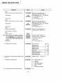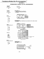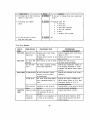
1
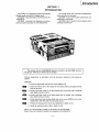
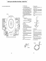
MICRO FLOPPYDISK DRIVE
OA-D32W
OA-D32V
SONY
SERVICE MANUAL
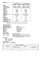
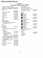
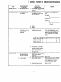
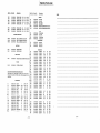
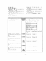
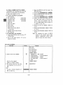
Specifications
OA·D32W
SI NG LE
DENSITY
J
OA·D32V
DOUBLE
DENSITY
SINGLE
DENSITY
I
DOUBLE
DENSITY
Capacity
Unformatted Per Disk
Unformatted Per Track
RATE
500 Kbytes /1.0 Mbytes
3.125 Kbytes
6.25 Kbytes
250 Kbits/sec 500 Kbits/sec
Bu~tTRANSFER
AcctItITlme
Track to Track
AverageSettling Time
Head Load Time
Average Latency
250 Kbytes /500 Kbytes
3.125 Kbytes
6.25 Kbytes
250 Kbiu/sec 500 Kbits/sec
12 msec.
350 msec.
30 msec.
SO msec.
50 msec.
Functiona'
Rotational Speed
Recording Density (inside track)
Track density
Cylinders
Tracks
R/W Heads
Encoding Method
SOO RPM
4359 bpi
I 8717 bpi
approx. 135 TPI
80
160
2
FM, MFM
Heat Dissipation
Operating Mode (Head Load)
Standby mode (Head Unload)
Media Requirements
3.5" x 3.7" (90 mm x 94 mm)
- Average access time
12 msec.
350 msec.
30msec.
SOmsec.
50 msec.
a
1/3
X
SOO RPM
4094 bpi
I 8187 bpi
approx.135 TPI
80
80
1
FM, MFM
6.0W
3.9W
S.OW
3.9W
SONY OM·D4440
SONY OM·D3440
{Track Nos.l x (Track to track time) + (Settling Time)
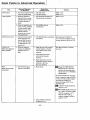
Environmental Consideration.
ReliabilitY and Maintainability
Preventive Maintenance (PM)
Meantime Between Failures (MTBF)
Meantime to Repair (MTTR)
Component Life
Media Life
Disk Interchange
Soft Read Error
Hard Read Error
Seek Error
Envlronmenta' Limits
Temperature (Operating)
Humidity
(Operating)
Vibration
40· F to 115°F (5°C to 45°C)
20 % to 80 % relative humidity, with a wet bulb temperature of85°F
(29°C) and no condensation.
The unit shall perform all read/write operations (no seek) according
to specifications, with continuous vibration of less than 0.5 G (±10 %)
from 5 Hz to 100 Hz (along the x, y, z plane).
(Opel'8ting)
Dimensional Data
Height
Width
Depth
Weight
2.0 In.
4.0 in.
5.1 in.
1.51bs
Not required
8000 POH (Power On Hourtime)
30 min.
5 years or 15,000 POH
3.0 x 10" passes/traek
20,000 times
1 per 10' bits read
1 per 10" bits read
1 per 10" seeks
(51 mm)
(102 mm)
(130 mm)
(S50 g)
DC Power Requirements
Reading
+12.0 V
±5 %
(Operating) +5.0 V
±5 %
0.30 A (typical)
0.48 A (typical)
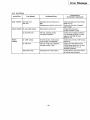
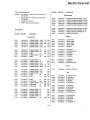
RECORD OF REVISIONS
NOTES
REVISION
1
ORIGINAL ISSUE
November, 1983
-2-
TABLE
OF
CONTENTS
Description
SECTION 1.
INTRODUCTION .••••.••..• \' ..........•..•..•..•..••..•.
SECTION 2.
TOOLS AND MEASURING INSTRUMENT.S . . • . • • • . • . . • • . • . . . •.
2-1.
2-2.
8
a.
General Tools ..••.•..........••..•...•.•.••..•.
8
b.
Special Tools. . • • . • • . • . . • . . • • . • . . • . • . • . • . . • . . • ..
8
c.
Measuririg Equipment •. ' ..•..• " . . . • • • • • . . • . . . . . • . .•
8
d.
Disks.•.••.•.•••.•..•....•.....•............•.
e.
Expendable and Chemical Supplies ..•...••.••..••....•
9
MFD Checker II . . . . . . . . . . . . . . . . . . . . . . . . . . . . ..
9
2-2-2.
Configuration of SMC-70 Drive Test System." . • . . . • • . . .. 13
2-2-3.
Disks •.••..•................•••.......•..• 14
TROUBLESHOOTING ..•....•.........••.•..•..•...•.•... IS
3-1.
BEFORE TROUBLESHOOTING •.....••...•...•..•..... IS
3-2.
TYPES OF ERROR ON A SYSTEM LEVEL ....•.•.••.... IS
3-3.
3-4.
SECTION 4.
8
SPECIAL TOOLS ..•..•.............••.....•.. '.....
2-2-1.
SECTION 3.
8
GENERAL AND SPECIAL TOOL UST • . • . • • • . . . . . . . • . ..
3-2-1.
Soft Error ...•.....•.........•.•............ IS
3-2-2.
Write Error •................•. : •...•..••• : .. IS
3-2-3.
Seek Error. • . . . . . . . . . . . • . . • . . • . . .. . • . . . . . • •. IS
3-2-4.
Interchange Error •.............•••.•..••.•.... IS
FAULT DIAGNOSIS BY MFD CHECKER II ............... IS
3-3-1.
Normal Operation. . . . • . . • • . . . . . • • . . . . . . . . • • . .. IS
3-3-2.
Check Points to Abnormal Operation •••.•..•..•..•.. 20
FINAL CHECK . ~ . • . . . . . . • . . . . • . . . • . • • . . . . . . . • . . . •. 23
3-4-1.
Setting ofSMC-70 ..•.......•.•.•..•.....
3-4-2.
Set the Check Area. . • . . • . . • . . • . • • . . • . . • . . • . . •. 23
3-4-3.
Check the Drive Unit. . • • . • . . . . . . . . • . . • . . • . • . • .. 25
3-4-4.
Error Message ...•...•.........•....•....... ;. 27
. ... 23
PART REPLACEMENT ., . . . • . . . . . • . . . . . . . . • • . • . . • . . • . . . .. 29
4-1.
4-2.
4-3.
FC-9/FC-14 MOUNTED BOARD REPLACEMENT .......•..•. 29
4-1-1.
Removal .................•..•.•..•........• 29
4-1-2.
Installation and Adjustment ..•.•..•.............• 29
FRONT PANEL ASS'Y REPLACEMENT ....•..•........•. 29
4-2-1.
Removal .•..•...•.•..........•......•...... 29
4-2-2.
Installation................................. 29
BLIND PANEL REPLACEMENT .....•.•......••....•.. 30
4-3-1.
Removal •..•..•.............••..•....•••.•. 30
4-3-2.
Installation................................. 30
-3-
Description
4-4.
4-5.
_
em
4-6.
4-7.
4-8.
4-9.
LED MOUNTED BOARD ASS'Y REPLACEMENT. • • . . • . • . .• 30
4-4-1.
Removal................................... 30
4-4-2.
Installation................................. 30
MAIN COVER REPLACEMENT ••••.••.•.•••••••••.•••• 31
3-5·1.
Removal ........•.....•.••.•.••••.••.••.•.• 31
3-5·2.
Installation................................. 31
PAD ASS'Y REPLACEMENT •.•••.•.•...•••••.•..••.•• 31
4-6-1.
Removal................................... 31
4-6-2.
Installation and Adjustment .•.••.••••..••.•..•.•• 31
D.AMPER REPLACEMENT. . • . . • . • • • . • . . • . . • . . • . • • . . .• 31
4-7·1.
Removal •.• ; .••.•..•.••.•••.••....••.•....• 31
4-7·2.
Installation ..••.•..•..•.. '••.••••..•..•..•... 32
HEAD LOAD ASS'Y REPLACEMENT •.•..••.••.•..••.•. 32
4-8·1.
Removal •••...•••.•..•••••••..•..•....•••.. 32
4-8·2.
Installation and Adjustment . . • . • . . . • . . . • • . . • . • • •. 32
CASSETTE·UP ASS'Y REPLACEMENT. • • • . • . . . • . • . . . • . • . 33
4-9·1.
Removal •••••••••••.•••.•..•..•.•••.•..•.•• 33
4-9·2.
Installation and Adjustment . . • • • . . • . . • . . • . . • . • • •• 33
4-10. WP ARM I D-DETECTION ARM I COMPRESSION SPRING
(3-659·609·00) REPLACEMENT •.•...•......•.•.•... 34
4-1 ()'1. Removal................................... 34
4-1()'2. Installation and Adjustment .•••.•.•••...••.••.••. 34
4-11.
DC DISK DRIVE MOTOR (BHC·2101A) REPLACEMENT ...•• 34
4-11·1. Removal •...•.•.•••.••.•••••...•••.•..••.•. 34
4-11·2. Installation and Adjustment ....•...•.••.••.••.•.. 35
4-12.
SENSOR MOUNTED BOARD REPLACEMENT' .•••••.••.... 35
4-12·1. Removal................................... 35
4-12·2. Installation and Adjustment •.•.••..•.•••.••••..•• 35
4-13.
LEAD SCREW ASS'Y (STEPPING MOTOR I LEAD SCREW I
COUPUNG ASS'Y I COMPRESSION SPRING
(4-601·083-00»
REPLACEMENT •••....••..••••.•••. 36
4-13-1. Removal .•••.•••.•••.••.••.•..•..••••.••••. 36
4-13-2. Installation and Adjustment .••.• : •.••.•..••..•••• 36
4-14. (32V) HEAD ARM ASS'Y REPLACEMENT,
(32W) HEAD CARRIAGE ASS'Y REPLACEMENT. . • • • • . • • •. 37
4-14-1. Removal................................... 37
4-14-2. Installation and Adjustment .•.••.•.....•••.•.•••• 38
-4-
Description
SECTION 5.
CHECK AND ADJUSTMENT. . . . . . . . . . . . . . . . . . . . . . . . . . . . . .. 39
5-1.
_
5-2.
LEAD SCREW ECCENTRICITY ••..•••••••..••...•••••• 39
5-1-1.
Tools and Measuring Equipment ••••••••••..••.•• "
5-1-2.
Measurement ••••..••• ' •..•..•••••••..•..•.••• 39
5-1-3.
Adjustment ••••••.•••••.•..••••••••.••.••••• 39
PAD PRESSURE. • . • • . . • . • • • • • • • • . . • • . • • . • . . • • • • • •• 39
5-2-1.
5-3.
Measurement. . . • . . • • . • . . . . • • • • • . . • • . • • . • . . •• 39
5-2-3.
Adjustment •...•••••••.•.•...•••.•.•..••..•• 40
HEAD COMPUANCE •••••••••.•••.•..•...•....•.••. 40
5-5.
Measurement .•••.••••..•....•.• ~ • . • • • . • • • • •• 40
5-3-3.
Adjustment............. • . • • . . • • • . • • . . • . . • .. 41
RADIAL AUGNMENT AND TRK 00 SENSOR .••.. ,. . • . . •. 42
Measurement. • • . . • • . • • • • . . . • . • • . • . . . . . . . . • •• 42
5-4-3.
Adjustment .•.••.•••••.•..•.••.••••••....••• 42
5-4-4.
Set Up Command , • • • • . . • • • • . • . • • • . . • • . . . • • . .• 42
5-4-5.
Measurement Command. • • • • • • . • . . • . . • . . . . . . • . .• 43
5-4-6.
Adjustment Command ••.•.•••.•..•...•....... "
5-4-7.
Error Message
44
.•••.•.•••.••.•••.•......•••.. 46
STEPPING MOTOR LOAD TORQUE . • . . . • • . • • . . . . . • . • .. 46
Tools and Measurement Equipment . . • • . . . • • • . . • • . •• 46
5-5-2.
Measurement...... • • . • • • • • . . . . . • . . • . . . • . • • .• 46
5-5-3.
Adjustment .•..••.•.••.•••••. : • • . • • . . . . • . . •. 46
INDEX PHASE • • • • • • . • • • • • • . • • • • . . • • • • • • • . . • • • . . .• 47
5-6-1.
5-7.
Tools and Measuring Equipment •••.••••..•....•••. 42
5-4-2.
5-5-1.
5-6.
Tools and Measuring Equipment _ .•..••.••.• : •••.•• 40
5-3-2.
5-4-1.
_
Tools and Measuring Equipment .••.••.•.•••••.•••• 39
5-2-2.
5-3-1.
5-4.
39
Tools and Measuring Equipment •..•.•••••..•....•• 47
5-6-2.
Measurement •..••.•••••••..•.....••.•...•.•. 47
5-6-3.
Adjustment ..•...••.•..•..•..•..•.••...• ',' .. 47
READ AMPUFIER GAIN AND READ AMPUFIER
OFF SET ..••••..•.••.••.••..•.••..•.••.....•. 47
5-7-1.
5-8.
Tools and Measuring Equipment •....••.••.•..•..•. 47
5-7-2.
Measurement •..••••.••.••.•..••.••••........ 47
5-7-3.
Adjustment •..•••••.•..•..•..••.•••••.••.•.. 48
DISK DRIVE DC' MOTOR SPEED . • . • . . • • . . • • • • • • • • • • •• 48
5-8-1.
Tools and Measuring Equipment . . . . . . . . . . . . . . . . . .. 48
5-8-2.
Measurement........... • • • . • . • . . . • • . • • . . • • •. 48
5-8-3.
Adjustment •...•.•••••.••.•..•• '. • • • • • . • . . . •. 49
-5-
Description
ED
5·9.
HL ARM HEIGHT •.••••.•••.•..••.••••.•••.••••..• 53
5.9.1.
5·10.
Tools and Measuring Equipment •..••.•..••.••.••.• 53
5.9·2.
Measurement... • . • . . . . . • . • • • • • . • . . . • • . • • • • •• 53
5·9·3.
Adjustment......................... • . • • • • •• 53
HEAD CLEARANCE •.•.•.•..•.••••••.•..•• " .•••.• , 53
5·10-1. Tools and Measuring Equipment ...••••.••.••.•••.• 53
5·10-2. Measurement................................ 53
5·10-3. Adjustment................................. 53
5·11.
HEAD CLEANING .................................. 54
5·11·1. Tools and Measuring Equipment .................. "
ED
5·11·3. Cleaning with Cleaning Disk
SECTION 6.
PARTS ASS'Y LOCATION •.•.•..•••..••..••.••.••••• 55
6·2.
MECHANICAL PARTS LIST .••..•.•••.•.•••.•..•..•• , 57
6·3.
OVER ALL DIAGRAM .....•.••...•.•••••••••••••. "
6-3·1.
6-4.
6·5.
59
Interconnection Diagram •.....••••..••.••..••••. 59
CIRCUIT DIAGRAM . • • • • . . • . . • . . • • • • • • • . . • • . • . • • • .• 61
6-4·1.
Circuit Diagram on FC·9 Mounted Board •..•••••.•.•• 61
6-4-2.
Parts Layout on FC·9 Mounted Board •••..•..••••.•• 65
6-4-3.
Disk: Motor Circuit Diagram. . • • . • • • • • . • • . • • • • • . •• 67
6-4-4.
Parts Layout on Disk Motor Circuit Board. . . • • • • • • • • .• 69
ELECTRIC PARTS ...•..•..• ; . . . . • • • • • . • . • • • • • • . • •. 70
6-5·1.
ChipParts Replacement Procedure. • • • • • . • • • • . • • . • •• 70
6-5·2.
Electric Parts List •.•.....•..••••...•.••••..•.. 71
PARTS LOCATION AND LIST (OA·D32V) ••••••••.••••••••..• 75
7·1.
PARTS ASS'Y LOCATION ......•..••••.....••.•..•.. 75
7·2.
MECHANICAL PARTS LIST .• , .••.••.•••••.••••••••.• 77
7·3.
OVER ALL DIAGRAM ................... ; . • • • • • • . . •. 79
7·3·1.
7·4.
7·S.
Interconnection Diagram ...•..•..•..••.••••..•... 79
CIRCUIT DIAGRAM • . • . . • . . • . . • . . • . . • . . • • . • • . • • . • •. 81
7-4-1.
SECTION 8.
..•••••.•.••.•..••..• 54
PARTS LOCATION AND LIST (OA·D32W) .••.••.•..•••••.•..• 55
6·1.
SECTION 7.
54
5·11·2. Cleaning with Applicator • • . . . • . . . . • • . • . . • . • • • • .. 54
Circuit Diagram on FC·14 Mounted Board .•••••••.•..• 81
7·4-2.
Parts Layout on FC·14 Mounted Board •••..•.••.••.•• 85
7·4-3.
Disk: Motor Circuit Diagram .••.••..•• . • • • • • • . • . •. 87
7-4-4.
Parts Layout on Disk Motor Circuit Board. • . • • • • • . • . .• 89
ELECTRIC PARTS •.•.••.•...•.•.•.••••.•.••••••.•• 90
7·5·1.
Chip Parts Replacement Procedure •••• ; • . . • . • • • • • • .• 90
7·5·2.
Electric Parts List • • . • . . • . . . . • • • . • • . • . • • • • • . • •. 91
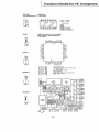
TRANSISTORS I DIODES IICS PIN ARRANGEMENT •• . • • . • • • . • .• 94
-6-
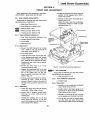
Introduction
SECTION 1
INTRODUCTION
The overall check after removals and adjustments
will be included in this section.
SECTION 4 and 5 cover parts replacements and
adjustments, respectively.
SECTION 6 and 7 consist of circuit diagrams, ass'y
drawin~s, and parts lists.
This manual is a maintenance guide forOA·D32W
(Double sided) and OA·D32V (Single sided).
SECTION 2 describes disks and tools necessary for
maintenance.
SECTION 3 provides fault diagnostic procedures
that may require spare parts or some adjustments.
The cassette dummy (4-603-929-00) should be inserted in the OA·D32W when it is
transported. Otherwise, its heads may be damaged.
Perform maintenance in accordance with the procedure specified in this manual as
follows:
(Example)
e. Fasten the guide shaft with the two screws (PSW2.6 x 6).
Em
Em
f. Fasten the head board to the chassis on the bottom surface, and apply nut lock
paint to the screw.
g. Connect the head board to the head harness (by four points) with a soldering
iron. (Refer to Fig. 4-14 (c) )
_
h. Connect the head board to the head harness (by six points) with a soldering
iron. (Refer to Fig. 4-14 (d»
_
i. Fasten head board and terminal shield plate with a screw (PSW2.6 x 8) on the
chassis bottm, and then apply nut lock paint onto it.
E!D
j. Perform the stepping motor load torque adjustment. (Refer to 5-5)
k. Install the cassette·up ass'y in place. (Refer to 4-9)
Steps e, h, i, and k should be carried out in sequence for the OA·D32W.
Steps e, f, g, j and k should be carried out in sequence for the OA·D32V.
-7-
General and Special Tool List
SECTION 2
TOOLS AND MEASURING INSTRUMENTS
2-1. GENERAL AND SPECIAL TOOL LIST
c. Measuring Equipment
The tools, and measuring instruments for performing
maintenance on the OA-D32W/OA-D32V are listed below.
Oscilloscope Dual Trace 20 MHz
a. General Tools
Tension Gauge
(Max. 200 g)
(J-604-163-OA)
Tension Gauge
(Max. 20 g)
(7-732-050-fO)
SONY Parts No.
TOTSU Screw Driver (M2.6)
(7-721 :-050-62)
@ Driver 2 mm
(7-700-749-01)
e Driver 2 mm
e Driver 4 mm
Tweezers
Universal Counter Resolution 0.1 msec.
d. Disks·
Level Disk
(7-700-750-01)
lSI
(7-700-750-04)
_
(7-700-753-02)
(7-700-757-01)
lSI
Adj Rod
(7-700-733-01)
_
Cutter
(7-700-75S-02)
lSI
Desoldering Metal Braid
_
lSI
_
(J-609-IS2-0A)
lSI
_
SMI-70lll SMI-70llA I SMI-70121 SMI-70l2A
SMC-70
KX-13Gl
'AID Converter
(J-623-002-OA)
25P/26P Conversion Cable
(J-623-90l-0A)
(8-960-009-41)
OR-DSIVA
OR-DSIWA
(8-960-009-35)
(8-960-009-44)
OR-D52VA
OR-DS2WA
(8-960-009-36)
(8-960-009-45)
OR-D29VA
OR-D29WA
(8-960-009-15)
(8-960-009-39)
e. Expendable and Chemical Supplies
Nut Lock Paint
Alcohol
Radial Alignment System Disk
(8-960-009-74)
(J-609-01l-0A)
(J-609-l20-0A)
Geared Driver
(J-609-0 l7-0A)
Pad Weight
(J-609-124-0A)
Hexagon Wrench Torque Driver
(J-609-125-0A)
Power Cable
(J-609-l30-0A)
Interface Cable
(J-609-200-0A)
(7-611-0.18-01)
Sony Grease
(7-622-001-52)
Applicator
Lead Screw Eccentricity Inspection Tool (J-609-l36-OA)
Standard Disk Dummy
(for Cassette-Up Ass'y Installation)
SonyOU
Bamboo Stick
Error Check.system Disk (OR-D87VA)(8-960-009-75)
Rotatory Knob (fOt Stepping Motor)
(8-960-009-32)
Cleaning Disk
SMC-70 System
(OR-DS6VA)
OR-D47VA
OR-D47WA
Dynamic Inspection Disk - 30
b. Special Tools
MFD Checker D
(8-960-009-40)
Dynamic Inspection Disk +30
Soldering Iron (20W)
Tester
(8-960-009-31)
Alignment Disk
Round Nose Plier
DC Power Supplier (+5 V DC i5 %, O.S A max.,
+12 V DC i5 %, 1.5 A max.)
OR-D46VA
OR-D46WA
-8-
Special Tools
2-2. SPECIAL TOOLS
WCP W1M ..•....• Selects upper and lower
patterns when the OSC SEL switch is set to
WCP. (Refer to Fig. 3-3 (c), (d»
HD LOAD •...... This is used to set the
plunger solenoid active.
M,OTOR ON ...•.. This is used to operate the
Disk Motor.
DRIVE SELECf ... Selects the disk drive.
The DRIVE SELECf switch on the disk drive
relates to the DRIVE SELECf switch on the
checker as follows:
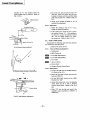
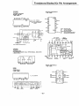
2-2-1. MFD Checker D
(1) MFD Checker D configuration
Main Checker Board
(26pin and 34pin)
Power Cable
(2 pieces)
Conversion Board (26pins-to-34pins)
I/F Cable
NOTE: The Conversion Board and 34pin IIF Cable are
required for the OA-D33W/OA-D33V.
(2) Micro Floppydisk Drive Connection (Refer to
Fig. 2-,1)
(3) MFD Checker n function switches
STEP IN •....... Steps the head inwards.
STEP OUT ....... Steps the head outwards.
The head continously moves if the switch is
kept pressed.
SIDE SELECT •... Selects one of two heads
(side 0 or side 1) for a double sided. (This
switch is invalid for single sided versions.)
WRITE ...•....•. Records, data specified by
the OSC SEL switch, onto one track.
OSC SEL . . . . . . . . Selects such write data as
"2F", "IF", "WCP" (worst case pattern), or
EXT.
Checker
Drive
IS101)
1
2
1
2
3
4
OFF
ON
OFF
ON
OFF
OFF
ON
ON
CHGRST . . . . . . . . Resets the DSKCHG
signal.
600/300 SELECf (Located in the middle of the
board) . . . . . . . . . . Set the 600/300 SELECf
switch at "600" for the OA-D32W IOA-D32V.
SO/70 SELECf (Located in the middle of the
board) ..•.....•• Set the SO/70 SELECf
switch to "SO" for the OA-D32W/OA-D32V.
Power Cable
Fig. 2-1 Drawing of Connection Between Disk Drive
and MFD Checker II
-9-
Special Tools
(4) INDICATOR
OSC SEL (Four LEDs in the left of the board)
. . . . . . . . . . • . . . '. They indicate the selected
position on the OSC SEL switch.
IfF signals (Five LEDs in the middle of the
board) . . . . . . . . . . They indicate at the states
of TRK 00, WRTPRT, RDY, DSKCHG, and
INDEX, respectively.
The TRK 00, WRTPRT, ROY, and DSKCHG
indicators are lit when the respective IfF signals are low (true). The INDEX indicator
blinks when the INDEX signal is applied to
the board.
TRACK POSITION (Seven segment LED indicator in the right of the board) •.. ~ ....•.••
Indicates the current track position.
(5) Test Points
TP-I; "M;:::O';;:T:AO-;:::R-'O""N~
TP-2; WRT GATE
TP-3; RD DATA
TP-5; INDEX
TP-6; STEP
TP-7; ;';H-;:::D:-L~O="A-:-D;::'
The GND terminal: is marked by "GND".
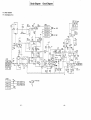
MFD Checker II Block Diagram
-10-"
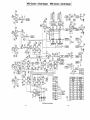
MFD Checker II Circuit Diagram
MFD Checker II Circuit Diagram
R3B
4.7K
R33IK
~
SELECT!
(SELECT)
R3
IIC
l
DIP
I
lC4
06
DKC
1:
4
(sIDE SE/.)
...- - - (SIDE SEL
T"9~/c
!esidt9)
'FJeSide/)
J
(CHORST) { RZB
d/gdast
(--c:----H-GR-ST--.,~
(
R3S
II<
RDDATA~:jl
II<
OFF TP9
TPB
TP3
R31
10K
T.P.G
I
+5 V
I--
2
GND
r- -
3
GND
t-- - I -
4
+IZV
EXT
WCP
IF
I
Z
+SV
3
aND
4
+lZV
OND
f---
2
SELECT &
DKCHG
SELECT I
GND
4
6
8
9
GND
10
/I
GND
12
WRTGATE
13
GND
14
HD LOAD
CHGRST
DIRTN
STEP
WRTDATA
IS
GND
16
17
GND
18
INDEX
~~
19
GND
10
TRK (HI
21
"23
GND
22
WRTPRT
GND
24
RD DATA
"2S
GND
26
READY
CZ
TP4
GND
ZF
MFD Checker II Circuit Diagram
-11-
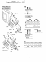
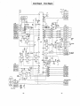
MOTOR ON
'~ 0.021
CI
RlWEROIJT
I
3
S
7
-12-
SIDE SEL
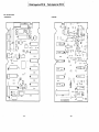
Configuration of SMC-70 Drive Test System
Disks
2·2·2. Configuration of SMC·70 Drive Test System
2·2·3. Disks
System configuration for Radial Alignment and
TRK 00 Sencer measurement, adjustment, and error
check with SMC·70 System is shown in Fig. 2·2 (a),
(a) Level disk
_
OR·D46VA
ED
OR-D46WA
These disks are used to check and adjust the read
amplifier gain and off set, The self-read/write
operation can be checked with both of these
disks and the SMC-70 System.
(b).
(b) Alignment disk _
ED
OR-D47VA
OR-D47WA
These disks have prerecorded data such as Cat's
eye pattern and INDEX signal to check and
adjust the off-tracking and index position.
OR·D47WA
OR·D47VA
SIDE
0
SIGNAL
TRACK
SIGNAL
TRACK
CAT'S EYE
PATTERN
00, 20, 25, 30, 35,
40,45,50,55,79
CAT'S EYE
PATTERN
00,20,25,30,35,
40,45,50,55,79
INDEX
SIDE
40
not applicable
I
fa} Error Check
INDEX
40
CAT'S EYE
PATTERN
40
INDEX
40
(d) CLEANING DISK
(c) DYNAMIC INSPECTION D'ISK +30
1m OR-D5IVA
OR-D5IWA
DYNAMIC INSPECTION DISK -30
_
OR-D52VA
1m
OR-D29VA
OR-D29WA
This type of disk can be used for cleaning the
head.
ED
Dynamic Inspection Disk/Level Disk
To Monitor
ED
ED
OR-D52WA
These disks can be used in the final check for a
drive with the SMC-70 System.
NOTE: (+) indicates that data has been recorded in the
inner side oftracks.
(-) indicates that data has been recorded in the
outer side of tracks.
Contents
OR·D51VA
SIDE
0
SIDE
I
Offset of +30 tJ.m for
all formatted tracks
not applicable
OR·D52VA
Offset of -30 tJ.m for
all formatted tracks
not applicable
fb} Radial AlignmentlTRK 00 Senser
Fig. 2·2
-13-
-14-
OR·D51WA
OR-D52WA
Offset of +30 tJ.m for
all formatted tracks
Offset of -30 tJ.m for
all formatted tracks
Offset of +30 tJ.m for
all formatted tracks
Offset of -30 tJ.m for
all formatted tracks
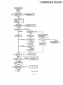
Before Troubleshooting
SECTION 3
TROUBLESHOOTING
SECTION 3 describes the methods of troubleshooting. 3-2 refers to several errors specfied in a
system level. 3-3 describes normal operations and
the check points for abnormal operations. These descriptions define the Error Spot under operating
conditions.
3-1. BEFORE TROUBLE SHOOTING
The following procedures are recommended to see
if the drive is really faulty or not:
1)
Incorrect operational procedure
2)
program error of host system
3)
Poor connection with host system (esp. GNDrelated connection, frame GND, etc.)
4)
Defective disk. Check that same trouble occurs
with other disks.
5)
Environmental conditions (where electrical noise
easily jumps into signal)
6)
Influence of strong magnetic field
7)
Wrong supply voltage
3·2. TYPES OF ERROR ON A SYSTEM LEVEL
3·2·1. Soft Error
Soft error are caused by;
1)
Dirty head
2)
Electrical noise
Poor connection with system
(GND-related connection)
5)
Incorrect motor speed
6)
Incorrect head compliance
To determine whether the disk or the drive is
failing. the disk should be replaced by other disks and
check that there still exists write error. If write error
does not exist any more, remove the old one. If write
error exists with use of any rlisk, drive might cause
write error.
3·2·3. Seek Error
Seek error comes from:
1)
Head movement is incorrect because ellectrical
noise jumps into signal.
2)
Head driving system might be at fault. If it is not
re-readable after re-calibration, drive might be at
fault.
3·2-4. Interchange Error
If data written on one drive is readable correctly
on another drive, but not by other drives, interchange
error exists.
Interchange errors are caused by;
I)
Head is not properly positioned.
2)
Motor speed is not correct.
3)
Optimum head output level and offset and head
compliance are not obtained.
4)
Chucking mechanism does not work.
3·3. FAULT DIAGNOSIS BY MFD CHECKER II
3-3-1 describes check method for normal
operations in accordance with the predetermined
procedUres.
3-3-2 describes check points for abnormal operations which come out in accordance with the above
procedures.
3) Tracking error
4)
3·2·2. Write Error
Clean the head first. Check for index pulse interval
and head compliance and then read error spot more
than several times. If not readable, move the head to
the adjacent track in the same direction as before,
then return to the desired track, and read. If readable
this time, check radial alignment. (Refer to 5-4)
If not readable yet, the error is not recoverable.
-15-
3·3·1. Normal Operation
1)
Pre-setting:
Refering to Fig. 2-1 (Micro Floppydisk Drive
Connection), connect the drive to MFD Checker
II.
2)
Set the slide switch (SI01) on the disk drive to
"}".
3)
Set all switches in the MFD Checker II to "OFF".
Normal· Operation
Step
Procedure
1
Power On
2
Drive Select Check after checked,
the disk drive is to be kept
selected.
Operation
1. The head automatically returns to TRK 00 and stops
there.
2. The disk motor remains stopped.
1. The TRK 00, WP, and DSKCHG indicators light only
when the DRIVE SELECT switch on the MFD Checker
D and the slide switch (S 10 1) on the disk drive are set as
follows:
MFD Checker n
1
2
OFF
ON
OFF
ON
OFF
OFF
ON
ON
Disk drive
IS101)
1
2
3
4
C?therwise, these indicators go out.
3
Operation during CASSETTE IN
(Alignment disk is to be inserted.)
1. When the cassette is inserted, the motor is rotating and
the plunger is pulled out. The head is loaded and unloaded in sequence. The motor then stops operation.
4
MOTOR ON switch on
1. The motor rotates. (The INDEX indicator on the MFD
Checker II blinks.)
2. The TRK 00, WRTPRT, RDY, and DSKCHG indicators
light. (The RDY indicator, however, lights in about 1.5
seconds after the disk is inserted.)
5
CHGRST switch on
6
HD LOAD switch on
1. The DSK CHG. indicator goes out at the moment when
the CHG RST switch is pressed.
mJ
IE
1. The plunger Solenoid is set on, and the pad lifts down.
2. The plunger Solenoid is set active and the head lifts
down.
3. The clearance between the HL arm and pad arm is set as
shown in Fig. 5-9.
7
Stepping
1. When the STEP IN switch is pressed, the head is continuously stepped in until it arrives at TRK 79.
When the STEP OUT switch is pressed, the head is
continuously stepped out until it arrives at TRK 00.
2. When the head is set to any track other than TRK 00,
the TRK 00 indicator does not ligh(
8
Track positioning
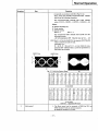
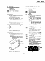
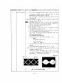
1. Such a Cat's eye pattern signal as slivwn in Fig. 3-1 (a)
can be obtained at CNI07-1 on the disk drive when the
head accesses TRK 20, TRK 30 or TRK 50. The oscilloscope is triggered by the signal at TP-5 of the MFD
Checker II.
Note: Such a signal as shown in Fig. 3-1 (b) can be obtained when the
head accesses TRK 40.
Em
2. SIDE SELECT switch to side 1. such a Cat's eye pattern
signal as shown Fig. 3-1 (b) can be obtained at CN 107-1
on the disk drive. When the head accesses TRK 40.
3. Set amplitude L in Fig. 3-1 (a) to 5 divisions, and then
read amplitude R in Fig. 3-1 (a).
Calculate the OFF TRACK value, refering to Table 3-1
-16-
Normal Operation
Operation
Step
Procedure
(c) and (d), in accordance with R in Fig. 3·1 (a).
Then, obtain the humidity-compensated OFF TRACK
value from the following expression:
The compensated OFF TRACK value = OFF TRACK
value + 0.2 (50 - H)(39.5 - 0.1875N - 1.5S)/33.5 ... (1)
Where;
H: Relative humidity (%)
N: Track number
S: Side ID number
Side 1: 1
Side 0: 0
The compensated OFF TRACK value should meet the
following formula.
.
'
-20 ~ Compensated OFF TRACK value ~ +20 ... (2)
[EX] For R = 4.5 in the OA-D32V, the apparent OFF TRACK
value is as shown in table 3·1 (d).
Assuming = 4.5,
H = 60 %, N = 40, 'al1d S = I, we can obtain the compensated OFF TRACK value as 2.6 from expression (1).
This satisfy the formula.
(a)
Fig. 3·1 Cat's Eye Pattern Signal
2:
3:
4:
5:
6:
7:
S:
9:
(b)
0.0
0.1
0.2
0.3
0.4
0.5
0.6
0.7
0.8
0.9
34.5
20.1
S.9
0.0
-7.3
-13.4
-IS.6
-23.0
32.9
IS.9
8.0
-O.S
-S.O
-14.0
-19.0
-23.4
31.3
17.7
7.0
-1.6
-S.6
-14.5
-19.5
-23.8
29.S
16.5
6.1
-2.3
-9.3
-15.1
-20.0
-24.2
28.3
15.3
S.I
-3.1
-9.9
-15.6
-20.4
-24.6
26.S
14.2
4.2
-3.S
-10.5
-16.1
-20.9
-25.0
25.4
13.1
3.4
-4.6
-11.1
-16.6
-21.3
-25.4
24.0
12.0
2.5
-5.3
-11.7
-17.1
-21.7
-25.7
22.7
11.0
1.6
-6.0
-12.3
-17.6
-22.2
-26.1
21.4
9.9
0.8
-6.6
-12.9
-IS.I
-22.6
-26.5
0.0
0.1
0.2
0.3
0.4
Q,1
0.6
0.7
0.8
0.9
36.9
21.5
9.6
0.0
-7.8
-14.3
-19.8
-24.6
35.1
20.2
S.S
-0.9
-S.S
-14.9
-20.4
-25.0
33.4
18.9
7.5
-1.7
-9.2
-15.5
-20.8
-25.4
31.S
17.6
6.5
-2.5
-9.9
-16.1
-21.3
-25.9
30.2
16.4
5.5
-3.3
-10.6
-16.6
-21.S
-26.3
2S.7
15.2
27.2
14.0
3.6
-4.9
-11.9
-17.7
-22.S
-27.1
25.7
12.9
2.7
-5.6
-12.5
-18.3
-23.2
-27.5
24.3
11.7
1.8
-6.4
-13.1
-IS.8
-23.7
-27.9
22.9
10.6
0.9
-7.1
-13.7
-19.3
-24.1
-2S.3
(e) OA·D32W
2:
3:
~:
5:
6:
7:
S:
9:
~
-4.1
-11.2
-17.2
-22.3
-26.7
(d) OA·D32V
Table 3·1. Apparent off Track
9
Motor speed
1. The Motor speed can be measured at TRK35, in TP·5 on
MFD Checker II with an universal counter.
It should be 100 msec ± 1.5 msec.
-17-
NormalOperation
Procedure
10
Operation
Step
Index position
1. The following waveform can be obtained on TRK 40.
Index
signal
(TP-5)
I
il
Output
signal
(CNt07-1)
-100 J,lsec_::::; T::::; +100 J,lsec.
Fig_ 3-2 Index Phase Specification
11
1. Move the head until it arrives at TRK 01. (Do not move
the head passing TRK 01. If the head arrives at TRK 00,
through the Cat's eye pattern signal is to be rechecked
and then the head is to be set on the TRK 01.)
The output signal level of CN I 07-5 is 3 V or more.
TRK 00 sensor level
2. Move the head until it arrives at TRK 00.
The output signal level of CNI07-5 is 0.7 V or less.
12
Cassette out (When the alignment
disk is ejected.)
1. The DSKCHG indicator lights.
13
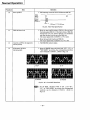
Write (When the level
disk is inserted)
1. When the WRITE switch is pressed and "2F", "IF", or
"WCP (MfW)" are written, the corresponding waveform
can be obtained at CN 107-1. (Refer to Fig. 3-3)
I
(b) 1F
(a)2F
(c)WCP(M)
(d) WCP(W)
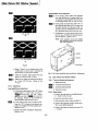
Fig_ 3-3 2F, IF and WCP Waveforms
Em 2. Set
the SIDE SELECT switch to side 1, and "2F",
"IF", or "WCP (M/W)" are written, the corresponding
waveform can be obtained at CNI07-1. (Refer to
Fig. 3-3)
-18-
Normal Operation'
Procedure
14
Step
Operation
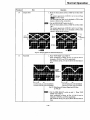
1. Move the head until it arrives at TRK 79, and then write
"2F".
The output signal level of CNl07-l is 0.4 to 0.8 Vp·p
0.2 to 0.5 Vp·p).
The following read data can be obtained at TP-3 on the
checker. (Refer to Fig. 3-4 (a) (b) )
Output level
(e
Em 2.
Set the SIDE SELECT switch to side 1.
Move the head until it arrives at TRK 79, and then write
"2F".
The output signal level of CNl07-l is 0.2 to 0.5 Vp-p.
The following read data can be obtained at TP-3 on the
checker. (Refer to Fig. 3-4 (a) )
0.2V
-0.5 V
Output
Signal
RDData
(a)e
(b)
EE1!I
Fig. 3·4 Output Signal and RD Data Waveforms
15
Peak Shift
1. Write "WCP(W/M)" ontoTRK 79.
Such waveforms as shown in Fig. 3-5 (a) (b) can be
obtained at eNl07-l and TP-3, respectively.
The waveform in Fig. 3-5 (a) (b) shows the read data at
.
~1
Output
Signal
(CNtOl·t)
RDData
(Tp·3)
(a)
L-J
Less than 2.43 Ilsec. (with OA·046VA)
(b)
Less than 2.43 IlSec. (with OA·D46VA)
Less than 2.43 jlSec. (with OA·D46WA)
Less than 2.43 jlSec. (with OA·D46WA)
Fig. 3·5 Waveforms of Output Signal and RD Data
at TRK 79
Em
2. Set the SIDE SELECT switch to side 1. Write "WCP
(W/M)" onto TRK 79.
Such waveforms as shown in Fig. 3-5 (a) (b) can be
obtained at CN 107-1 and TP-3, respectively.
The waveform in Fig. 3-5 (a) (b) shows the read data at
TP-3.
-19-
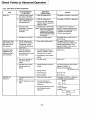
Check Points to Abnormal Operation
3-3-2. Check Points to Abnormal Operation
Step
Power On
Abnormal Operation
for Each Step
I. The head ~oves tow!ll'd
the center of the Drive.
2. The head is stepped out,
but it is idling around
the outmost track.
3. The head moves
uncertainly. (The head
movement is not
constant.)
CheckPoint
(defective place)
Remarks
I. TRK 00 sensing circuit.
Thcl signal of CN 103-2 is Low level
1. TRK 00 sensing circuit.
The signal of CN 103-2 is High level
2. Check if the TRK 00 Sensor
Mounted Board is installed a
little bit outside.
1. Stepping motor drive system.
NOTE: If no TRK 00 is detected in
several seconds after power
is turned on, the CPU automatically stops the stepping
motor and thereafter accepts
no instructioh.
A voltage of+12 V appears at
CN I 05-2 during normal operation.
Voltages at 3 pin through 6 pin of
of CNI05 are switched in
10 ± 0.1 msec intervals.
4. The disk motor rotates.
1. Disk motor drive system.
The signal CNIOI-5 and CNIOI-?
are Low level
Drive Select Check
after checked, the
disk drive is to be
kept selected.
1. The I/F indicators are
put out for the selected
combination, or they
are lit for the unselected
combination.
1. Drive select circuit system.
The signal ofICIOS-3 for the
selected combination is High level
during normal operation. The
signal ofICIOS-3 is Low level for
unselected combipation.
Operation during
CASSETTE IN
(Alignment disk is
to be inserted.)
1. After the cassette is
inserted, the head is
not loaded and the motor
does not rotate.
1. The CSTIN signal does not
appear at CNIOI-5, and it is
not sent from the motor.
Refer to 5-S.
2. The cassette is not properly
placed.
2. The head is loaded, but
the motor does not
rotate.
1. The disk motor.
Refer to 5-S.
3. The disk motor rotates,
but the head is not
loaded.
1. Plunger solenoid ·or its drive
system.
The signal waveforms shown below
appear of CNI04-2, 3.
During normal operation.
(Refer to Fig. 3~6)
2. Plunger stroke.
3. Head Clearance.
MOTOR ON
switch on
Refer to 5-10.
4. HL arm height.
Refer to 5-9.
I. The disk motor does not
rotate.
1. Disk motor drive system.
2. The IJF indicators do not
light.
1. If no I/F indicato!S is
lit, the drive select is not
conducted.
The signal of CNIOI-? is High level,
or the disk motor is defective.
c
2. If some IfF indicators are lit,
the IfF signal circuit is
defective.
+12V_a ,
+5~-----'\L.-.._ _ _ _ _ _ _ 1
CN104.3f OISK IN
r--
CN104·2 """5 V
It----15-m-s-ec-.- - - f
l
Fig. 3·6
-20-
Check Points to Abnormal Operation
Step
CHGRST switch on
Abnormal Operation
for Each Step
Check Point
(defective place)
1. The DSKCHG indicator
I. The CHGRST signal (CN I 09-3)
is not sent to the CPU
(lCI01-9).
does not go out.
HD LOAD switch on
1. The plunger solenoid is
not energized.
1. The HD LOAD signal
(at CNI09-14) is not sent to
the CPU (ICIOl-6).
Remark.
Waveforms of normal operation
are;
HD LOAD
IC101-33
I
IC101-34
Fig. 3-7
2. IC III
3. IC 101
Stepping
1. The step operation does
not function at all, or it
is not smoothly
functioned.
1. Stepping motor drive system
or stepping motor itself.
In normal condition, the signal of
ICIOI-40 is High level for about
I msec after the STEP signal enters.
During this time, a DC voltage of
+12 V is applied to the stepping
motor.
TRACK,.
Po(ICI06-5) PI (ICI06-9) P2(1CI06-11) P3(1CI06-13)
L
H
L
H
0,4,8, ••• 72,76.
L
H
L
H
1,5,9, ••• 73,77.
H
H
L
L
2,6,10, ••. 74, 78.
'H
L
H
L
3,7,11, •.• 75,79.
2. The harness (~ e, the TRK 00
sensor) is internally attached
to other mounting parts.
3. Obstacles are attached to the
slide guide shaft.
Track positioning
1. The ratio of the left to
right signals does not
meet the specification.
2. No signal appears.
1. A voltage of +5 V is not applied
to the stepping motor.
(CNI05-I,2)
2. Radial alignment is incomplete.
Refer to 5-4.
I. Read amplifier circuit.
Signal appeance must be confirmed
with the sequence ofCNI07-1,
ICI03-16, ICI03-17, ICI03-I,
ICI03-2, ICI04-7, ICI04-8.
2; A seek error has occurred_
Refer to 3-2-3.
-21 -
::heck Points to Abnormal Operation
Step
Abnormal Operation
for Each Step
Check Point
(defective place)
Remarks
Motor speed
I. The motor speed does not
meet the specification.
1. The disk motor
2. The pad pressure
Refer to 5-8.
Refer to 5-2.
Index position
I. When the cassette is
inserted twice or more,
positions on each track
is varied ±40 p.sec or
more.
1. The chucking mechanism of
the disk moter is defective.
Refer to 4-11.
2. When the cassette is set
twice or more, positions
on each track is varied
±40 Ilsec or less. The
shifted positions,
however, do not meet·
the specification.
1. The INDEX phase is
mis-adjusted.
Refer to 5-6.
TRK 00 sensor level
I. The head returned from
inside track does not
stop at TRK 0 I and it
goes to TRK 00 where
re-calibration is to be
carried out.
1. The TRK 00 sensor positioning
is improper.
The signal level of CNI07-5
is 3 V or more at TRK 01 during
normal operation. (Refer to 5-4.)
Cassette out
(When the alignment
disk is ej ected.)
1. When the casette is
ejected, the DSKCHG
indicator does not
light.
1. Signal has not been detecte'd
cassette ejection. Check if
the D-detected arm moves
properly.
The signal of CNIOI-S remains
Low level.
2. Check if the disk motor
I circuit board operates
properly.
3. Signal appearance must be
confirmed with the sequence
ofICI01-3,IC112-I,
IC112-3, CNI09-3.
Write
(When the level disk
is inserted.)
I. The waveform signal
cannot be re-written.
1. Write circuit
iEEChange the SIDE SELECT
SWITCH to side I and then
conduct the operation specified in item 13-1 of NORMAL
OPERATION.
In normal condition of write gate
circuit, terminal voltage of CN I 09
-12 is Low level, terminal voltage
of ICIOI-46 is High level,
terminal voltage oflC 11 5-4 is
High level and
Em Collector voltage ofQI06 is
e
2. Check whether write data
is applied or not.
-22-
approx. +12·V.
When SIDE SELECT switch is
set to side 0, collector voltage
of Q 107 is approx. +12 V.
When it is set to side I,
collector voltage of Q 106 is
approx.+12 V.
Final Check
Abnormal Operation
for Each Step
Step
Output level
Check Point
(defective place)
1. The output signallevel
does not meet the
specification.
1. Read amplifier gain adjustment
is incomplete.
2. Read data does not
appear.
1. ICI03 (MC3470AP)
I. The shifted peak value
does not meet the
specification.
I. When the value in both "WCP
W" and "WCP M" do not
meet the specification, the
head is defective.
Peak Shift
Remarks
Refer to 5-7.
Refer to 4-14.
2. When difference in value
Refer to 5-7.
between "WCP W" and
"WCP M" is remarkably Big,
off set adjustment is incomplete.
3-4. FINAL CHECK
Co
3-4-1. Setting of SMC·70
a. Place auto start switch located on the left
side panel to "DISK".
Connect. the drive under test to the conversion
cable and set the DRIVE SELECT switch(SIOI)
of the unit to "2".
d. Error check system disk is inserted into drive A
of SMI-7012A and power is turned on.
b. A conversion cable for IfF (25 pin to 26 pin) is
connected to rear panel of SMI-7012A(Drive"
Unit).
e. After word "I\>" appears on CRT display,
drive check program will start.
3-4-2. Set The Check Area
Description
To display original test condition of the disk.
Keying
Display
~lliJllil!ID ITl[Q
..... Floppy Disk Analysis v3.0 .....
IRETURN!
..... Copyright (C) 1981. Sep. .. ...
[Test condition)
drive C
Minimum track
Maximum track
0
79
Minimum Sector
Maximum sector
1
16
Sector size
256
Single or Double side?
S
Read & Write retry
Seek & Home retry
1
0
#Do you want to change these test
conditions? (Y, N) =
To change any of test conditions.
[XJ IRETURN!
+Minimum track
@) IRETURN!
+Maximum track
o
[track)='*
Type the minimum track to be tested.
[EX)
In case it is TRK 00.
-23-
79 [track)=q
Final Check
Description
Keying
Display
Type the maximum track to be tested.
[EX]
In case it is TRK 79.
IlIl2l
IRETURNI
+Minimum sector
1 [sector]==>
+Maxirnum sector
16 [sector]==>
Type the minimum sector to be tested.
[EX]
In case it is 1 sector.
ill IRETURN I
Type the maximum sector to be tested.
[EX]
In case it is 16 sector.
ill!§] IRETURNI
+Sector size
256 [bytes]:=>
Type the number of byte size per a sector, to be
tested.
[EX]
In case it is 256 bytes.
~~ IRETURNI +Single side or Double side?
<S, D>==>
Type the initial name letter (S-single sided, Ddouble sided) of disk surface to be tested.
[EX]
In case it is double side.
[Q] IRETURNI
+Read & Write retry
1 [times]==>
ill IRETURN I
+Seek + Home retry
o [times]==>
Type the number of how many retry must be
conducted when read error or write error occurs.
[EX]
In case it is once.
Type the number of how many seek retry must be
conducted when the error occurs.
[EX]
••• Command table •••..
In case no retry is desired.
r : =read test
w : = write test
: = show disk condition
s : =set test condition
h : = help
e : = finish & exit to CP 1M
-24-
Check the Drive Unit
3-4-3. Check the Drive Unit
The test item from command table must be chosen.
Description
1. To read dynamic inspection disk or pre-recorded data disk.
Keying
00 \RETURN \
Display
••• Read Test •••
#Enter pass-count = i
Type the number of pass-count for reading
tracks and sectors pre-set in item 3-4-2.
[EX]
In case it is once.
#Test disk ready? yes - ... hit [Return]
Insert the disk to be tested.
<<Pass-count =
I»
In-ward (trkmin- -+ trkmax)
+Track =
Out-ward (trkmax--+trkmin)
+Track =
Read test starts under the test condition pre-set
in item 3-4-2.
The te~t ends.
••• Read Test End •••
[I] Total of Seek error:
o times during 00160 times seek.
+Seek eRe
error: 0 times
+Seek
error: 0 times
[2] Total of Read error:
o times during 02560 times read.
+10, DATA ADM missing: 0 times
error: 0 times
+10 eRe
+DATA eRe error: 0 times
+Lost data
error: 0 times
+Byte data verify Err: 0 times
[3] Total of Write error:
o times during 00000 times write.
+10, ADM missing: 0 times
error: 0 times
+10 eRe
+Lost data
error: 0 times
+Write Protect error: 0 times
+Write Fault error: 0 times
2. To write the data on a level disk.
5YI\RETURNI
NOTE: Before writing data pattern on a level disk,
formatting (initialization) can be mode
automaticaly. If the some error occurs during
the processing, the error will be displayed
under title of "Initialize Test End".
... Write Test ...
• •• Write data pattern •••
Pattern No. I ... Random data (all data random)
Pattern No.2 ... Random data (1st byte-OAAh)
Pattern No.3 ... Worst pattern (DBh, 6Dh, B6h)
Pattern No.4 ... User definable
#Select pattern number: [I, 2, 3, 4]
=
To select the data pattern.
[EX]
In case it is worst pattern.
~ \RETURN \
\ RETURN I
The test ends.
-25-
#Now, You select pattern No: 3
#Test disk ready? yes - - hit [Return]
••• Write Test Start •••
+Track = End
• •• Write Test End ...
Check the Drive Unit
Description
Keying
In case it is random data. (all data random.)
ill/RETURNl
Display
[EX)
Type any key.
~
/RETURNI
The test ends.
#Now, You select pattern No: 1
#Hit any key after few seconds = =>
#Test disk ready? yes -0+ hit [Return)
... Write Test Start ...
+ Track = End
... Write Test End •••
[EX)
In case it is random data. (1st byte =OAAh)
Type any key.
illlRETURNl
[A]
/RETURN/
The test ends.
#Now, You select pattern No: 2
#Hit any key after few seconds ==>
#Test disk ready? yes -0+ hit [Return)
... Write Test Start ...
+Track = End
... Write Test End ...
[EX)
In case it is user definable.
[1] IRETURNI
#Now, You select pattern NO: 4
+Enter hex data [1st Bytes) ==>
Type the data to be written it.
[EX)
In case it is "DA".
NOTE: Only 2 characters can be assigned for each byte;
the character of more than two is disregarded.
The Key IRETURNI must be depressed at the
end of each byte. Maximum twenty (20) characters (ten kind of byte -10th bytes) can be
assigned.
[QJOO
\RETURNI
+Enter hex data [2nd Bytes) ==>
IRETURNI
IRETURNI
#Test disk ready?--hit [Return)
••• Write Test Start ...
+Track = End
... Write Test End
The test ends.
3. To display the test condition.
[Test condition)
drive C
Minimum track
Maximum track
0
79
Minimum sector
Maximum sector
1
16
Sector size
256
Single or Double side?
Read & Write retry
Seek & Home retry
-4. To change any of test condition. (Refer to item
llillRETURNI
+Minimum track
0 [track) ==>
5. To display the command table.
ill] \RETURNl
... Command table ...
r : = read test
w : = write test
1 : = show disk condition
s : = set test condition
h : =help
e : = finish & exit to CP/M
6. To end. the test or retest from the first step.
lID IRETURNl
A>
3-4-2)
-26-
S
1
0
Error Message
3-4-4. Error Message
I
Kind of Error
Error Message
Considerable Cause
Countermeasure
(Confirmation I Adjustment).
SEEK ERROR
Seek CRC error
Seek error
Stepping motor load torque is too
high.
Stepping motor circuit is out of order.
Confirm stepping motor load torque.
(Refer to 5·5.)
Confirm the function of stepping
motor circuit.
READ ERROR
10, data, ADM missing.
Read circuit is out of order.
Confirm the read circuit.
(at first check RF out put)
lD, data CRC error
Off track, 'chucking trouble,
wrong head compliance.
Confirm head compliance, (Refer to
5-3.) chucking mechanism or radial
alignment and TRK 00 sensor
(Refer to 5-4).
10 ADM missing
No write function. (write circuit
is out of order, no formatting)
Confirm the waveform of RF output.
(CNl07-l)
lD CRC error
Off track wrong head compliance,
chucking trouble, or disk.
Confirm the radial alignment and
TRK 00 sensor (Refer to 5-4.), head
compliance (Refer to 5-3.), or
chucking mechanism.
Write protect error
Condition is set to write protect.
Confirm Media, write protect circuit
or write protect mechanism.
WRITE
ERROR
-27-
MEMO
-28-
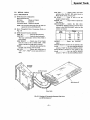
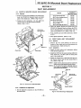
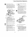
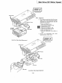
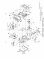
FC-9/FC-14 Mounted Board Replacemen1
SECTION 4
PART REPLACEMENT
4·1. FC·9/FC·14 MOUNTED BOARD REPLACEMENT
Harness
FC·9/FC·14
Mounted Board
7p (To the disk motor)
6p (To the stepping motor)
(V) 5p (To the head)
(W) 6p (To the head)
3p (To the plunger)
3p (To LED)
3p (To tp.e TRK 00 sensor)
CNIOI
CN105
CNI06
. CNI06
CNI04
CNI02
CNI03
4-1·1. Removal
a. Remove the three screws (PSW2.6 x 6) which fasten
both the FC-9/FC-14 Mounted Board and shield
plate to the chassis ass'y. (Refer to Fig. 4·1 (a) )
b. Remove all the connectors. Do not apply any
excessive force to the head harness (CNI06).
.
(Refer to Fig~ 4·1 (b»
b. Insert the harness between the chassis ass'y and
FC·9/FC·14 Mounted Board and fasten the FC·9j
FC·14 Mounted Board and shield plate with the
three screws (PSW2.6 x 6). (Refer to Fig. 4-1)
c. Read amplifier gain and offset adjustment. (Refer
to 5·7)
d. Index phase adjustment. (Refer to 5-6)
4·2. FRONT PANEL ASS'Y REPLACEMENT
4·2·1. Removal
a. Remove the two screws (PS2.6 x 10) from the
bottom of the chassis ass'y and then remove the
front panel ass'y. (Refer to Fig. 4-2)
4-2-2. Installation
a. Install the eject button and compression spring
onto the front panel ass'y.
b. Install the LED into the square opening within the
front panel ass'y, and then press the front panel
ass'y to the chassis ass'y.
fa}
c. Fasten the chassis ass'y to the front panel ass'y on
the bottom surface with the two screws (PS2.6 x
10). (Refer to Fig. 4·2)
NOTE 1: Install both the chassis ass'y and front panel ass'y
in place so that these assemblies closely contact.
NOTE 2: Do not pintch the harness, (especially head har·
ness), during the installation le, the head harness
gap between these assemblies.
Bosl-t-+_".q,.:::),.
PS2.6x10
.
CDmp,"",~ r-l~.;:
;~r
Spring
E"'Butt. .
~ ~
FC.9/FC'14
Mountlld Board
i~
~~~~II
~
.
fb}
~
Fig. 4-1 FC·9 / FC·14 Mounted Board
4-1·2. Installation and Adjustment
a. Set the respective connectors to the FC·9/FC·14
Mounted Board.
-29-
Front pa!,AIS'Y
~
D'_ GLSPR20
.
Fig. 4-2 Front Panel Ass'y Replacement
Blind Panel Replacement
4-3.
BLIND PANEL REPLACEMENT
4-3·1. Removal
a. Remove the front panel ass'y. (Refer to 4-2)
b. Remove the blind panel by twisting it into the
arrow while pressing its both edges. (Refer to Fig.
4-3)
4-4·2. Installation
a. Peel off remover from the cushion and set the
LED Mounted Board as shown in Fig. 4-4 (b).
b. Install both the FC-9/FC-14 Mounted Board and
shield plate. (Refer to 4-1)
c. Install the front panel ass'y. (Refer to 4·2)
4-3·2. Installation
a. Press the blind panel toward the cassette-up ass'y
and latch the two tabs onto the disk holder.
(Refer to Fig. 4-3)
PS2.6x 10
b. Install the front panel ass'y. (Refer-to 4-2)
LEO Mounted Board Ass'y
(aJ
Fig. 4·3 Blind Panel Replacement
REO
4-4. LED MOUNTED BOARD ASS'V
REPLACEMENT
4-4·1. Removal
a. Remove both the FC-9/FC-14 Mounted Board and
shield plate. Disconnect CN 102 connector.
(Refer to Fig. 4-4 (a) )
BLK
(bJ
b. Remove the front panel ass'y. (Refer to 4-2)
c. Remove the LED Mounted Board ass'y from the
chassis ass'y.
Fig. 4·4 LED Mounted Board Ass'y Replacement
-30-
Main Cover Replacement
4-5. MAIN COVER REPLACEMENT
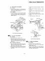
c. Perform the pad pressure adjustment.
5-2)
4-5·1. Removal
d. Perform the head clearance adjustment.
to 5-10)
a. Remove the screw (82.6 x 5) which fastens the
main cover from the chassis ass'y, and then remove
the main cover. (Refer to Fig. 4-5 )
(Refer
e. Perform the HL arm height adjustment. (Refer to
.
5~)
4-5·2. Installation
a. Install
is set
install
(Refer
(Refer to
f. Make the head clean. (Refer to 5-11)
the main cover so that the position marked
in accordance with the arrow, and then
the main cover with the screw (82.6 x 5).
to Fig. 4-5)
g. Perform the head compliance adjustment. (Refer
to 5-3)
h. Install the main cover. (Refer to 4-5)
Pad Arm Ass'y
Pad Holder
P~~~
Pad Ass'y
ra)
Fig. 4-5 Main Cover Replacement
ED 4-6.
PAD ASS'V REPLACEMENT
4.0-1. Removal
a. Remove the main cover. (Refer to 4-5)
b. Lifting the pad arm tip so that any excessive force
may not be applied to the pad arm ass'y. remove
the pad ass'y by pressing its rear part. (Refer to
Fig. 4-6 (a»
Fig. 4-6 Pad Ass'y Replacement
E12I
4-7. DAMPER REPLACEMENT
4.0-2. Installation and Adjustment
4·7-1. Removal
a. Pick up pad holder (not pad itselO of pad ass'y
lightly and insert pad ass'y into the location on
pad arm ass'y. (Refer to Fig. 4-6 (a) )
a. Remove the main cover. (Refer to 4-5)
b. Pull down the pad arm ass'y, and check if the pad
is arranged in parallel with the head as shown in
Fig. 4-6 (b).
c. Remove the screw (PS2.6 x 6) which fastens the
damper to the head load ass'y. and then remove
the damper. (Refer to Fig. 4-7)
-31-
b. Manually set the machine into the Disk-In mode.
(Refer to Fig. 4-9 (a) )
tlead Load Ass'y Replacement
4·7·2. Installation
f. Install both the FC-9/FC-14 Mounted Board
and shield plate in place. (Refer to 4-1)
a. Insert the damper arm tip into between the cassette holder and HL arm, and set the damper to
the head load ass'y. (Refer to Fig. 4·7)
g. Perform the head clearance adjustment.
(Refer to 5-10)
h. Perform the HL arm height adjustment. (Refer
to 5-9)
b. Install the main cover. (Refer to 4·5)
c. Make.the head clean. (Refer to 5·11)
i. Install the main cover in place. (Refer to 4·5)
j. Make the head clean. (Refer to 5·11)
Fig. 4·7 Damper Replacement
4-8. HEAD LOAD ASS'V REPLACEMENT
4-8·1. Removal
a. Remove both the FC-9/FC·14 Mounted Baord
and shield plate: (Refer to 4-1)
. b. Remove the main cover. (Refer to 4·5)
c. Manually set the machine into the Disk·In
mode. (Refer to Fig. 4·9 (a) )
Em d.
Remove the damper. (Refer to 4·7)
e. Remove the two screws (PS2.6 x 6) which
fasten the head load ass'y to the chassis so
that an excessive force is not applied to the
head arm, and then remove the head load
ass'y, (Refer to Fig. 4·8 (a) (b»
4-8·2. Installation and Adjustment
a. Manually set the machine into the Disk·In
mode. (Refer to Fig. 4·9 (a) )
b. Pass the harness of the head load ass'y through
the opening of the chassis. (Refer to Fig. 4·8
(a) (b) )
c. Fasten both the head load ass'y and lug terminal to the chassis with the two screws (PS2.6
it 6). (Refer to Fig. 4-8 (a) (b) )
0
d. Bend one tip of the lug terminal by 90
±l~o. (Refer to Fig. 4-8 (c»
Em e.
Fig. 4-8 Head Load Ass'y Replacement
Install the damper in place. (Refer to 4-7)
-32-
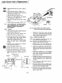
Cassette-Up AsS'y Replacement
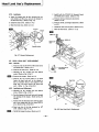
4-9. CASSETTE·UP ASS'Y REPLACEMENT
4~·1.
_
Removal
CillIJranCtl
a. Remove both the FC·9 Mounted Board and
shield plate. (Refer to 4-1)
ClllaranCtl
Sidll Platll (LBftJ-mf--....l...+---I'
Sidll Platll (RightJ
b. Remove the front panel ass'y. (Refer to 4-2)
c. Remove the blind panel. (Refer to 4-3)
d. Remove the main cover. (Refer to 4-5)
(c)
e. Manually set the machine into the Disk-In
mode. (Refer to Fig. 4-9 (a) )
_
f. Remove the damper. (Refer to 4-7)
_
g. Remove the head load ass'y. (Refer to 4-8)
h. Remove the four screws (PSW2.6 x 8) from
the bottom of the chassis, and then remove
the cassette-up ass'y. (Refer to Fig. 4-9 (b»
(dJ TDP VIEW of Cassstte-UpAss'y
(aJ Stllllling to Disk-In Modll
Positioning Pin
(eJ
Fig_ 4-9 Cassette-Up Ass'y Replacement
~-2.
Installation and Adjustment
a. Place the cassette-up ass'y onto the chassis
ass'y and fasten the bottom of the chassis
ass'y 'lightly with the four screws (PSW2.6 x
8). (Refer to Fig. 4-9 (b) )
(bJ
-33-
WPArm/D-Detection Arm/Compression
Spring (3-659-609-00) Replacement
~E2.3
b. Insert the standard disk dummy (OA-120)
into the cassette-up ass'y. Check if the standard disk dummy positioning hole aligns with
the positioning pin on the chassis, and if the
clearance shown in Fig. 4-9 (c) (d) are kept
assured, and then fasten the four screws
firmly.
c. Install the head load ass'y. (Refer to 4-8)
Em
Em d.
D-Detection Arm
Install the damper in place. (Refer to 4-7)
e. Insert the level disk into the cassette-up ·ass'y.
Check if disk positioning is properly located
while touching the forefmge.r at the positioning holes in the left and right of the disk.
(Refer to Fig. 4-9 (e» Check if disk positioning is properly located even while placing each
side of the disk drive downwards.
Fig. 4·10 WP Arm/D·Detection Arm/Compression
Spring Replacement
f. If any displacement is found during positioning test .in item (e), repeat the operations
defined in 4-9-2.
4·10·2. Installation and Adjustment
a. Pass the compression spring (3-659-609-00)
and WP arm or the compression spring (3~59·
609·00) and D·Detection arm through the
shaft in sequence. Then, clamp them with the
E ring (E2.3). (Refer to Fig. 4·10)
g. Press the eject lever and check if the level disk
can smoothly be mifted up and down.
Em
h. Install the both FC-9 Mounted Board and
shield plate in place. (Refer to 4·1)
b. Pressing with the fmgers the portion indicated
by arrow on the WP' or D-Detection arm,
check if the WP or D-Detection arm smoothly
returns to home position by spring force.
i. Make the head clean. (Refer to 5-11)
j. Install the main cover in place. (Refer to 4-5)
k. Install blind panel in place. (Refer to 4-3)
IE
1. Install the front panel ass'y in place. (Refer
to 4-2)
_
f. Install the damper in place. (Refer to 4-7)
h. Install the main cover in place. (Refer to 4-5)
i. Install the front panel ass'y in place. (Refer
to 4-2)
a. Remove both the FC-9 Mounted Board and
shield plate. (Refer to 4-1)
b. Remove the front panel ass'y. (Refer to 4-2)
4·11.
c. Remove the main cover. (Refer to 4-5)
DC DISK DRIVE MOTOR (BHC·2101A)
REPLACEMENT
4·11-1. Removal
d. Manually set the machine into the Disk-In
mode. (Refer to Fig. 4-9 (a) )
_
e. Install the head load ass'y in place. (Refer to
4-8)
g. Make the head clean. (Refer to 5-11)
4-10-1. Removal
IE e.
c. Install both the FC·9 Mounted Board and
shield plate in place. (Refer to 4·1)
d. Install the cassette·up ass'y in place. (Refer to
4-9)
IE
4-10. WP ARMlD"[)ETECTION ARMICOMPRE.S·
SION SPRING (3-65~09~0) REPLACEMENT
_
WPArm
~E2.3
a. Connect the MFD Checker II, and then turn
off the power switch. (Refer to Fig. 2-1)
Remove the damper. (Refer to 4-7)
b. Remove both the FC-9/FC-14 Mounted Board
and shield plate. (Refer to 4-1)
f. Remove the head load ass'y. (Refer to 4-8)
g. Remove the cassette-up ass'y. (Refer to 4-9)
c. Remove the front panel ass'y. (Refer to 4-2)
h. Remove the E ring (E2.3), pull out both the
WP and D-Detection arms, and remove the
compression spring (3~59~09~0) from the
chassis ass'y. (Refer to Fig. 4-10)
d. Remove the main cover. (Refer to 4-5)
e. Manually set the machine into the Disk-In
mode. (Refer to Fig. 4-9 (a) )
-34-
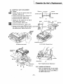
Sensor Mounted Board Replacement
m
m
e. Remove the damper. (Refer to 4-7)
f. Remove the head load ass'y. (Refer to 4-8)
4-12. SENSOR
MENT
g. Remove the cassette-up ass'y. (Refer to 4-9)
4-12·1. Removal
MOUNTED BOARD REPLACE·
a. Connect the MFD Checker II, move the head
until it arrives at TRK 79, and then tum off
the power switch. (Refer to Fig. 2-1)
h. Remove the WP arm, D-Detection arm and
these compression springs. (Refer to 4-10)
i. Remove the two screws (PS2.6 x 8) which
fasten the disk motor, and then remove the
disk motor. (Refer to Fig. 4-11)
b. Remove both the FC-9/FCI4 Mounted Board
and shield plate. (Refer to 4-1)
c. Remove the front panel ass'y. (Refer to 4-2)
d. Manually set the machine into the Disk-In
mode. (Refer to Fig. 4-9 (a) )
Em
Em
e. Remove the damper (Refer to 4-7)
f. Remove the head load ass'y. (Refer to 4-8)
g. Remove the cassette-up ass'y. (Refer to 4-9)
h. Remove the screw (PSW2.6 x 6) which fastens
the Sensor Mounted Board and remove the
Sensor Mounted Board. (Refer to Fig. 4-12)
Fig.4-11 Disk Drive DC Motor (BHC-2101A)
Replacement
4-11-2. Installation and Adjustment
a. Pass the DC Disk motor harness through the
opening in front of the chassis ass'y, and then
fasten the DC Disk motor with the two screws
(PS2.6 x '8). (Refer to Fig. 4-11)
b. Install the WP arm, D-Detection arm, and
these compression springs in place_ (Refer to
4-10)
c. Install the cassette-up ass'y in place. (Refer to
4-9)
d. Install the head load ass'y in place. (Refer to
4-8)
Fig. 4-12 Sensor Mounted Board Replacement
e. Install the damper in place. (Refer to 4-7)
f. Install both the FC-9/FC-14 Mounted Board
and shield plate. (Refer to 4-1)
h. Perform the radial alignment and TRK 00
sensor adjustment. (Refer to 5-4)
i
Perform the index phase adjustment. (Refer
to 5-6)
j. Install the
4·12-2. Installation and Adjustment
a. Feed the harness of Sensor Mounted Board
'g. Make the head clean. (Refer to 5-11)
m~in cover in place. (Refer to 4-5)
k. Install the front panel ass'y in place. (Refer
to 4-2)
-35-
as shown by the arrow, set the Sensor Mounted Board onto the chassis along the positioning pin, and fasten lightly it with the
screw (PSW2.6 x 6). (Refer to Fig. 4-12)
NOTE: The sensor board should be placed near the
disk motor as far as possible.
b. Install the cassette-up ass'y in place. (Refer to
4-9)
,
Lead Screw Ass'y Replacement
ED
ED
c. Install the head load ass'y in place. (Refer to
4-8)
<I. Install the damper in place. (Refer to 4-7)
e. Install both the FC-9/FC-14 Mounted Board
and shield plate. (Refer to 4-1)'
f. Make the head clean. (Refer to 5-11)
g. Perform the radial alignment and TRK 00
sensor adjustment. (Refer to 5-4)
h. Install the front panel ass'y in place. (Refer
to 4-2)
i. Install the main cover in place. (Refer to 4-5)
4-13_
LEAD SCREW ASS'V (STEPPING MOTOR/
LEAD SCREW/COUPLING ASS'V/CaMPRESSION SPRING (4-601-083-GO) )
REPLACEMENT
Fig. 4-13 Stepping Motor (SNS·1100A), Coupling
Ass'y and Compression Spring Replacement'
4-13.1. Removal
a. Remove both the FC-9/FC-14 Mounted Board
and shield plate. (Refer to 4-1)
j. Turning the rotary knob, remove the lead
b. Remove the front panel ass'y. (Refer to 4-2)
screw ass'y.. DUring removal, hold with the
tweezers the ball bearing which hold the lead
screw, as shown in Fig. 4-13 (b)-I.
c. Remove the main cover. (Refer to 4-5)
d. Attach the rotary knob to the rear shaft of
the stepping motor with hexagon wrench
torque driver. (Refer to Fig. 4-13 (a»
Check if the gap between the motor bearing
metal and rotary knob is approximately
0.5mm.
NOTE: If the replacement can be made with lead screw
ass'y, steps 8 up to II should be skipped.
e. Manually set the machine into the Disk-In
mode. (Refer to Fig. 4-9 (a»
a. Stepping motor, lead screw, coupling ass'y
and thrust bearing must be roughly assembled'.
ED f.
ED g.
4-13-2. Installation and Adjustment
NOTE: Apply Sony grease (same quantity of watch tip) on
whole area of lead screw before replacing it.
Remove the damper. (Refer to 4-7)
b. Pressing the coupling ass'y to the lead screw,
fasten the setscrew near the lead screw with a
hexagon wrench torque driver. (Refer to Fig.
4-13 (a»
Remove the head load ass'y. (Refer to 4-8)
h. Remove the cassette-up ass'y. (Refer to 4-9)
i. Remove die two screws (PSW2.6 x 6) which
fasten the stepping motor. (Refer to Fig. 4-13
(b»
c. Pressing the coupling ass'y to th~ stepping
motor, fasten the setscrew near the stepping
motor with a hexagon wrench torque dirver.
(Refer to Fig. 4-13 (a) )
Compression Spring
-
Rotary Knob
I
Stt:pping Motor
-
@
d. Turning the rotary knob, pass the lead screw
through the opening of the ball bearing along
the path indicated by arrow. (Refer to Fig.
4-13 (b) )
e. Fasten loosely the stepping motor with the
two screws (PSW2.6 x 6).
~
f. Loosen the setscrew ne!U" the stepping motor
so that the lead screw touches the ball bearing
by the force of the compression spring.
g. Pulling the rotary knob lightly, fasten the setscrew near the stepping motor with a hexagon
wrench torque driver.
Coupling Ass'y
(a)
-36-
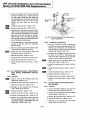
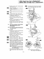
(32V) Head Arm Ass'y Replacement
(32W) Head Carriage Ass'y Replacement
h. Perform the lead screw eccentricity adjust-
ment. (Refer to 5-1)
E!D
.
D
k. Smoothly pull out the head arm ass'y together
with the guide shaft. (Refer to Fig. 4-14 (a) )
i Perform the stepping motor load torque ad-
justment. (Refer to 5-5)
j. Install the cassette-up ass'y in place. (Refer to
4-9)
EEm
k. Install the head load ass'y in place. (Refer to
4-8)
EEm
I. In$tall the damper in place. (Refer to 4-7)
m.Install both the FC-9/FCI4 Mounted Board
and shield plate. (Refer to 4-1)
n. Make the head clean. (Refer to 5-11)
o. Remove the rotary knob from the stepping
motor shaft.
p. Perform the radial alignment and TRK 00
sensor adjustment. (Refer to 5-4)
q. Instiill the main cover in place. (Refer to 4-5)
r. Install the front panel ass'y in place. (Refer
to 4-2)
4-14.
(32V) HEAD ARM ASS'Y REPLACEMENT
(32W) HEAD CARRIAGE ASS'Y
REPLACEMENT
NOTE: Do not disassemble or adjust the head arm ass'y or
head carriage ass'y because these ass'y have precisely
been adjusted in factory.
Guide Shaft
4·14-1. Removal
a. Remove both the FC-9/FCI4 Mounted Board
and shield plate. (Refer to 4-1)
b. Remove the front panel ass·y. (Refer to 4-2),
c. Remove the main cover. (Refer to 4-5)
d. Manually set the machine into the Disk-In
mode. (Refer to Fig. 4-9 (a) )
PSW2.6X9~
EEm
e. Remove the damper. (Refer to 4-7)
Em
f. Remove the helJ.d load ass·y. (Refer to 4-8)
g. Remove the cassette-up ass·y. (Refer to
_
Em
(b)
~-9)
h. Remove the screw (PSW2.6 x 6) which
fastens the head harness to the chassis on the
bottom surface. (Refer to Fig. 4-14 (a) )
i. Remove the screw (PSW2.6 x 8) which fastens
the head harness to the shield plate on the
bottom surface of- the chassis. and remove the
head harness that is adhesive to the chassis.
(Refer to Fig. 4-14 (b) )
NOTE: The head harness is contacted to the chassis
via the adhesive tape with its both surface
coated with adhesive agent.
j. Remove the two screws (PSW2.6 x 6) which
fasten the guide shaft. (Refer to Fig. 4-14 (a)
(b»
-37-
(e)
(d)
Fig. 4-14 Head Arm Ass'y Replacement
Head Carriage Ass'y Replacement
(32V) Head Arm Ass'y Replacement
(32W) Head Carriage Ass'y Replacement
Em
1. Smoothly pull out the head carriage ass'y
together with the guide shaft. (Refer to Fig.
4-14 (b»
Em
m. Disconnect the head board from the head
harness (by four points) with a soldering iron.
(Refer to Fig. 4-14 (c) )
Em
n. Disconnec~ the head board from the head
harness (b'y six points) with a soldering iron.
(Refer to ,Fig. 4-14 (d) )
4-14-2. Installation and Adjustment
NOTE: Apply Sony oil to the guide shaft before installing.
Apply Sony oil to the openings of both the head ann
ass'y and head carriage au'y using the bamboo stick.
Em
Em
Em
Em
ED
i. Fasten head board and terminal shield plate
with a screw (PSW2.6 x 8) on the chassis
bottom, and then apply nut lock paint onto it.
NOTE: The screw must not be tighten too hard. It
may produce electrical short or' crack of
head board. ,
Em
j. Perform the stepping motor load torque adjustment. (Refer to 5-5)
k. Install the cassette-up ass'y in place. (Refer to
4-9)
Em
1. Install the head load ass'y in place. (Refer to
Em
m. Install the damper in place. (Refer to 4-7)
4-8)
a. PaSs the guide shaft through the openmg of
the head arm ass'y.
n. Install both the FC-9/FC-14 Mounted Board
and shield plate. (Refer to 4-1)
b. Pass the guide shaft through the opening of
the head carriage ass'y.
o. Perform the HL arm height adjustment.
(Refer to 5-9)
c. Carefully install the head arm ass'y in place.
(Refer to Fig. 4-14 (a) )
p. Perform the head clearance adjustment.
(Refer to 5-10)
d. Carefully install the head carriage ass'y in
place. (Refer to Fig. 4-14 (b»
q'. Make the head clean. (Refer to 5-11)
r. Perform the radial alignment and TRK 00
sensor adjustment. (Refer to 54)
e. Fasten the guide shaft with the two screws
(PSW2.6 x 6).
Em -f.
s. Perform the read amplifier gain and offset
adjustment. (Refer to 5-7)
Fasten the head board to the chassis on the
bottom surface, and apply nut lock paint to
the screw.
t. 'Perform the index phase adjustment. (Refer
to 5-6)
g. Connect the head board to the head harness
(by four points) with a soldering iron. (Refer
to Fig.'4-14 (c»
u. Install the main cover in place. (Refer to 4-5)
v. .Install the front panel ass'y in place. (Refer
to 4-1)
h. Connect the head board to the head harness
(by six points) with a soldering iron. (Refer
to Fig. 4-14 (d»
-38-
Lead Screw Eccentricity
SECTION 5
CHECK' AN,D ADJUSTMENT
After measurement and adjustment in accordance
with SECTION 5, please surely clean the head.
d. Pulling the stepping motor shaft, fasten the
setscrew for the stepping motor. (With a
torque orO.7 kg-cm)
5-1.
e. Measure the lead screw eccentrifity in accordance with 5-1-2.
Unless the result meets the specification,
measurement should be carried out' again
starting with item "a".
LEAD SCREW ECCENTRICITY
Disassemble the following parts and then perform
the measurement and adjustment.
a. Main Cover (Refer to 4-5)
b. Front Panel Ass'y (Refer to 4-2)
Em
Em
c. Q_amper (Refer to 4-7)
d. Head Load Ass'y (Refer to 4-8)
e. Cassette-up Ass'y (Refer to 4-9)
5-1·1. Tools and Measuring Equipment
a. Lead Screw Eccentricity Inspection Tool
b. Hexagon Wrench Torque Driver
c. Rotary Knob
d. MFD Checker II
5-1-2. Measurement
a. Connect the MFD Checker n to the disk
drive. (Refer to Fig. 2-.1) and step in the
head until it arrives at TRK 79.
b. Tum off the power.
c. Attach the rotary knob onto the rear shaft
of the stepping motor shaft with hexagon
wrench torque driver. (Refer to Fig. 4-13
(a» Check if the gap between the motor
bearing metal and rotary knob is approximately 0.5 mm.
d. Revolve the rotary knob 3 to 4 turns
counterclockwise by hand.
e. Aligning the positioning hole of the lead
screw eccentricity tool to the positioning
pin on the chassis ass'y, set the lead
screw eccentricity inspection tool in place.
(Refer to Fig. 5-1)
Fig.5-' Lead Screw Eccentricity Adiustment
Em 5-2.
f. - Tum the rot:lry knob clockwise or counterclockwise by hand.
Check if the gap
measures 50 p.m (5 scales on the meter of
the lead screw eccentricity inspection tool)
or less.
5-1-3. Adjustment
a. Attach the rotary knob onto the stepping
motor shaft. (Reifer to Fig. 4-13 (a»
b. Loosen with a hexagon wrench torque
driver the two screws which- fasten the
coupling ass'y.
c. Pressing the coupling ass'y to the lead
screw, fasten the setscrew for the lead
screw with a hex~on wrench torque driver.
(with a torque of 0.7 kg-cm)
-39-
PAD PRESSURE
Disassemble the following parts and then perform
the measurment and adjustment.
a. Main Cover (Refer to 4-5)
5-2-1. Tools and Measuring Equipment
a. Tension Gauge
5-2-2. Measurement
a. Manually set the machine into the Disk-ln
mode. (Refer to Fig. 4-9 (a) )
b. Install a string to the tension gauge at one
end and tie the other end to the measuring
point. (Refer to Fig. 5-2 (a) )
c. Manually put down the HL arm, and then
set the machine into the Head Load mode.
d. Lift the pad arm with the tension gauge,
and then slowly put down the pad arm
until the gauge reading becomes unchanged.
Head Compliance
Identify as "A" the position where the
stable reading can be obtained. (Refer to
Fig. 5-2 (b) )
'-........~
\
M~8SUring
~
e. Put down the pad arm below point "A"
until the point just before the pad arm
touches the head, and then read the rising
peak value at point "B". (Refer to Fig. 5-2
(b»
Point
f. Check if the reading is within 11 ±1.S g
specified for adjustment.
5-2-3. Adjustment
Fan·Shaped Gauge
a. Unless the reading is out of 11 ± 1.5 g,
change the spring set-position.
b. If the reading is in excess of 12.5 g, move
the position toward "A". If the reading is
less than 9.5 g, move the position toward
"B". Do not change position "C" where
the string is set. (Refer to Fig. 5-2 (c) )
5-3. HEAD COMPLIANCE
Disassemble the following parts and then perform
the measurment and adjustment.
a. Main Cover (Refer to 4-5)
(a) Pad Pressure Measuring Method
5-3-1. Tools and Measuring Equipment
a. Oscilloscope
b. MFD Checker II
ED
c. Level Disk (OR-D46VA)
_
d. Level Disk (OR-D46WA)
e. Pad weight
ED
f.
e 2 mm Driver
g. Rotary Knob
h. Hexagon Wrench Torque Driver
5-3-2. Measurement
a. Connect the disk drive to the MFD Checker
II. (Refer to Fig. 2-1)"
(x) Distance between surfaces of head and pad.
(b)
b. Insert the level disk in place, and move the
head onto TRK 79.
c. Set the HD LOAD swhch on the MFD
Checker II to "ON".
d. Attach the rotary knob onto the stepping
motor shaft and fix it with a hexagon
wrench torque driver. (Refer to Fig. 4-13
(a) )
e. Write "2F" into the disk and check if the
amplifier output waveform at CNIO?-I is
satisfactory.
(e)
Fig. 5·2 Pad Pressure Adjustment
-40-
Head Compliance
f. When a pad weight is loaded as shown in
Fig. 5-3 (a), (b);
g. Take the pad weight, and move the head to
TRK 03.
1) The output signal level at that time should
not be greater than that obtained when no
pad weight is loaded.
h. Write "IF" into the disk.
i. Turn the rotary knob clockw\se until it
arrives at the clicking point, move the head
to TRK 04, and write "EXT" in to the disk.
2) The output sigriallevel at that time should
not be 95 % or less of that obtained when
no pad weight is loaded.
Em
j. Fully turn the rotary knob counterclockwise, move the head back to TRK 03, and
check if the output signal level at that time
is 5 % or less of that obtained by item "h".
Em.I
k. Fully turn the rotary knob counterclockwise, move the head back to TRK 03, and
check if the output signal level at that time
is 10 % or less of that 0 btained by item "e".
l. Write "IF" into the disk.
m. Turn the rotary knob counterclockwise
until it arrives at the clicking point, move
the head to TRK 02, and write "EXT" into
the disk.
(a) Weight Positioning
Em
n. Turn the rotary knob clockwise until it
arrives at the clicking point, move the head
back to TRK 03, and check if the output
signal level at that time is 5 % or less of
that obtained by item "I".
_
o. Turn the rotary knob clockwise until it
arrives at the clicking point, move the head
back to TRK 03, and check if the output
signal level at that time is 10 % or less of
that obtained by item "1"_
_
5-3-3. Adjustment
ED
a. If the output signal level does not meet
item 5-3-2 "f", perform adjustment by
turning the pad ass'y as shown in Fig. 5-3
(c).
(b) Weight Positioning
Em.I
b. If the output signal level does not meet.
item 5-3-2 "f", replace the head carriage
ass'y. (Refer to 4-14)
Em
c. If the output signal level doesnot meet
item 5-3-2 "n", perform adjustment by
turning the pad ass'y as shown in Fig. 5-3
(c).
NOTE: Check if the head compliance is satisfactory after this adjustment
Em.I
(e) Pad ASoS'y Rotation
Fig. 5-3 Head Complience
-41-
d. If the output signal level doesnot meet
item 5-3-2 "0", replace the head carriage
ass'y. (Refer to 4-14)
Radial Alignment and Trk 00 Sensor
5-4.
RADIAL ALIGNMENT AN> TRK 00 SENSOR
insert the alignment disk, and set the DRIVE
SELECT switch (Sl 01) to 4. (Refer to Fig.
2-2)
Dissassemble the following parts and then perform
the measurement and adjustment.
a. Main Cover (Refer to 4-5)
d. Execute the Set Up command. (Refer to
5-4-4)
5-4-1. Tools and Measuring Equipment
a. SMC-70 System
e. Execute the Measurement command.
(Refer to 5-4-5)
b. Radial Alignment System Disk
Em
c. Alignment Disk (OR·D47VA)
Em!l
d. Alignment Disk (OR·D47WA)
e. Rotary Knob
i.
f. If adjustment is necessary, the Adjustment
command is to be executed. (Refer to
5-4-6)
5-4-3. Adjustment
Geared Driver
a. Perform adjustment in accordance with
5-4-2 (a) up to (d).
g. TOTSU Screw Driver (M2.6)
h.
e 4 mm Driver
b. Attach the rotary knob to the stepping
motor shaft and fix it with a hexagon
wrench torque driver. (Refer to Fig. 4~13
i. Hexagon Wrench Torque Driver
5-4·2. Measurement
(a»
a. Insert the Radial Alignment system disk
into the SMI-7012A drive A.
c. Execute the Adjustment command. (Refer
to 5-4-6)
b. Tum on the power switch. After approximately 15 seconds, "off set measurement!
adjustment ver 1.0" is displayed.
NOTE: For resuming the state of SMC-70
System to the Initial state (that apprears
Immediately after power goes on), press
the reset button.
'
c. Connect the disk drive (under test) to the
cable which leads to the AID converter,
5-4-4. Set Up Command
Keying
Function
[]
1. Select the Set Up command.
[EX]
In case a relative humidity of 60 % is keyed in,
4. The initial value for the
set at 26 ",m.'
sp~cified
[]
~IQ]IRETURNI
HUMIDITY [%]?
COMMAND NUMBER?
SPECIFICATION?
off track is to be
[EX]
In case an off track of 30 pm is keyed in,
COMMAND NUMBER?
1. HUMIDITY 20 - 80 %:
2. SPECIFICATION
:
3. TIME/4DIVISIONS
4. R/W CORE WIDTH :
5. QUIT
COMMAND NUMBER?
2. Asks for the cOll1mand number at display center.
3. The initial value for the relative humidity is to be
set at 50 %.
Display
@I@JIRETURNI
-42-
COMMAND NUMBER?
50.0
26.0
100
120
[%]
[micrometer]
[ns]
[micrometer]
Measurement Command
Display
Keying
Function
5. The initial value for the INDEX signal period is to
be set at 100 msec.
TIME/4 DIVISIONS?
[EX)
In case an INDEX signal period of lOa msec is
keyed in,
I!]~~IRETURNI COMMAND NUMBER?
I
6. The initial value for the RfW core width is to be
set at 120 "m.
RfW CORE WIDTH?
[EX)
In case a RfW core width of 131/.1m for the
OA-32V is keyed in. (Specify a R/W core width
of 120 /.1m for the OA-32W.)
1!]@]l!lIRETURNI COMMAND NUMBER?
1!J§IQ]lRETU~NI
7. When the Set Up command execution ends,
(control to the main menu.)
MAIN MENU
[I) SET UP
(2) MEASUREMENT
(3) ADJUSTMENT
5-4-5. Measurement Command
Keying
FUnction
1. Select the Measurement command.
Display
SET DRIVE SELECT 4
INSERT AUGNMENT DISK
HIT [RETURN) KEY
Insert the Alignment disk.
ADJUST CAT'S EYE SIGNAL LEVEL
[MIN (L, R) > 2 div) AND
[MAX(L, R) < 4 div) AND
[MAX(L/R, R/L) < 1.5)
HIT [RETURN) KEY
2. Set the AID converter gain by adjustment so that
the peak values at both edges of the Cat's eye pattern signal may range from 2 to 4 divisions. (Refer
to Fig. 5-4 (a) )
:t
NOTE: If gain adjustment cannot be done, key in [Q) to
execute step 9. Thereafter, perform the radial
alignment adjustment. (Refer to 54-6.)
;-.,
"',.L
/
"-\
(aJ
3. Measure the off track._
MEASURING
4. Calculate the off track.
CALCULATING
ADJUST 00 SENSOR
HIT [RETURN) KEY
NOTE: When "NO GOOD" is indicated on the CRT,
key [Q] to execute step 9. Thereafter, perform
adjustment in accordance with 54-6.
-43-
I
II
\
/'
""
Measurement Command
Function
Keying
5. Check if the TRK 00 sensor output is set at a value
between broken lines 3.5 V and 4.5 V.
(Refer to Fig. 5-4 (e) )
IRETURN I
NOTE: If not, key in
rID
to execute step 9. Thereafter,
perform adjustment· in accOIdance with 54-6.
Display
TRACK 3
XXX VOLT
TRACK 00>01
(Spec: 3.5-4.5)
XXX VOLT
OK
TRACK 02>01
(Spec : 3.5~4.5)
·XXX VOLT
OK
TRACK 01>00
(Spec: MAX 0.5):
XXX VOLT
6. Check if the TRK 00 sensor output is satisfactory.
(When "NO GOOD" is displayed on the CRT,
repeat step 5.)
7. Measure the off track
MEASURING
8. Calculate and check the off track.
CALCULATING
GOOD!
HIT [RETURN] KEY
NOTE: When "NO GOOD" is displayed on the CRT, key
in (QJ to execute step 9. Thereafter, perform
adjustment in accordance with 54-6.
9. End the execution in the Measurement mode.
IRETURNI
I§IRIIm IRETURNI
SET DRIVE SELECT 4
INSERT ALIGNMENT DISK
IDT [RETURN] KEY
5-4-j). Adjustment Command
Function
Keying
Display
COMMAND NUMBER?
SET DRIVE SELECT 4
INSERT ALIGNMENT DISK
HIT [RETURN) KEY
1. Select the Adjustment command.
Insert the Alignment disk.
ADJUST eAT'S EYE
[MIN(L, R) > 3 divl AND
[MAX(L, R < 4 div) AND
[MAX(L/R, R/L) < 1.2]
HIT [ RETURN] KEY
2. Tum the rotary knob clockwise untn the head
arrives at the outmost position. Thereafter, tum
the rotary knob counter clockwise while stopping
and starting at each clicking point until the Cat's
eye pattern signal appears. Turning the stepping
motor with the geared driver within the range that
the screw fastening the stepping motor is not
dropped from the stepping moter flange, set the
amplitude ratio of the peak signals on the Cat's
eye pattern signal at 1 : 1.2 or less.
I
/'
II
"'""-
"'\1
\
/'
1\/
(b)
"-
NOTE: A ratio of 1 : 1.2 is defmed by identifying the
smaller one as unity.
NOTE:.1f adjustment of the stepping motor cannot be
conducted by using the geared driver, fust fmd
the appropriate position in accordance with the
/~
\
\
I
.I
/'
1\1
"
'\I
(e)
Fig. 54
-44-
""""
"
Adjustment Command
Function
Keying
Display
following procedure, and perform adjustment
again.
(1) When the waveform is as shown in Fig. 5-4
(b), tum the rotary knob clockwise.
(2) When the waveform is as shown in Fig. 5-4
(c), tum the rotary knob counterclockwise.
)
3. Set the AID converter gain by adjustment so that
the peak values of the Cat's eye pattern signal may
range from 3 to 4 divisions. (Refer Fig. 5-4 (d) )
NOTE: If the amplitude ratio is set at any value other
than utmost 1: 1.2 during initializing, control
does not advance the step to the next even if the
IRETURNI key is pressed.
4. Measure the off track.
MEASURING
5. Calculate the off track.
CALCULATING
ADJUST RADIAL A~IGNMENT
[MAX (L/R, R/L)
1.05)
TIGHT FIRMLY
ruT [RETURN) KEY
<
6. Turning the stepping motor with the geared driver,
set the amplitude ratio of the peak signals on the
Cat's eye pattern signal utmost at I : LOS, fasten
the setscrew and then apply nut lock paint to it.
IRETURN I
MOVE 00 SENSOR BOARD TO OUT
SIDE
ruT [RETURN) KEY
NOTE: A ratio of 1 : 1.05 is dermed by identifying the
smaller one as unity.
NOTE: Unless the amplitude ratio is utmost 1 : 1.05,
/
control does not advance the next step.
L
~
-'"\ IIL
'\ II
/" ~
"'"
Fig. 5-4
(d)
7. Move the TRK 00 sensor board outside (toward
the stepping motor).
ADJUST Oo. SENSOR
HIT [RETURN) KEY
8. Check if the TRK 00 sensor output level is within
the range of broken Jines 3.5 V to 4.5 V.
If not, set the level nearlest to the center between
these broken Jines by adjustment, and fasten the
setscrew with nut lock paint.
(Refer to Fig. 5-4 (e»
TRACK 3
XXX VOLT
TRACK 00>01
(Spec: 3.5-4.5)
XXX VOLT
o'K
TRACK 02>01
(Spec: 3.5-4.5)
XXX VOLT
OK
TRACK 01>00
(Spec: MAX 0.5):
XXX VOLT
NOTE: When "NO GOOD" is displayed on the CRT,
repeat step 8.
.
I
4.5 Vf ---- ----3.5 V-t ---- --
(e)
Fig. 5-4 Radial Alignment, TRK 00
Ad·ustment
-45-
Stepping Motor Load Torque
Display
Keying
Function
9;" Measure the offtraclc.
MEASURING
10. Calculate and check the off traclc.
CALCURATING
GOOD!
HIT [RETURN) KEY
SET DRIVE SELECT 4
INSERT AUGNMENT DISK
HIT [RETURN) KEY
5-4·7. Error Message
5-5-1. Tools and Measurement Equipment
One of the following errors can occur during
measurement: adjustment, or setting of the machine
for radial alignment:
a. Oscilloscope
b. MFD Checker II
_
a) Not Ready ... Indicates that READY signal is not
issued. Check for disk drive connection or check
for the DRIVE SELECT switch position.
c. Alignment Disk (OR-D47VA)
d. Tention Gauge
e.. ®Driver 2 mm
b) Not Index Pulse ... Indicates that INDEX signal is
not issued. Check for disk drive connection.
5-5-2.
Measureme~t
a. Push up the steel plate near the lead screw
with a spring balance. (Refer to Fig. 5-5)
c) Cat's Eye Error ... Indicates that the Cat's eye pattern signal is abnonnal. Check for the alignment
d~.
"
b. Checlc if the spring balance indicates a
value in the range of 50 g to 80 g at the
point where the head arm is just separated
from the lead screw.
In addition to these messages in above, one of the
following statements is also displayed.
Statement I:
[0) CONTINUE / [1) RETRY
Statement 2:
[RETURN) FIRST STEP / [1) RETRY
m
Key in [Q] when statement
is displayed, and
then control advances the step to the next,disregarding the error which has occurred.
Thereafter, key in. [I] and then the same measurement item is executed again.
Key in IRETURNI when statement 2 is displayed,
and then control performs the radial alignment
measurement and returns to the initial step in the Adjustment mode. Thereafter," key in ill and th~n the
same measurement item is executed again.
Fig. 5-5 Stepping Motor Load Torque
5-5-3. Adjustment
NOTE: Check for the disk drive in accordance with COrullmatlon items to the message displayed before retrying the key-in
operation.
a. If the spring balance indicates a force of 50
g or less, fasten the setscrew (+P2x3). If
it indicates 80 g or more, loosen the setscrew. (Refer to Fig. 5-5)
ill
_
5-5. STEPPING MOTOR LOAD TORQUE
Disassemble the following parts and then perform
the measurement and adjustment.
b. Fix the setscrew (+P2x3) for the steel plate
with nut lock paint.
a. FC-9/FC-14 Mounted Board. (Refer to 4-1)
c. Perform the radial alignment and TRK 00
sensor adjustment. (Refer to 5-4)
-46-
Index Phase
5-6.
5-7.
INDEX PHASE
5-6-1. Tools and Measurement Equipment
READ AMPLIFIER GAIN AND READ
AMPLIFIER OFF SET
5-7-1. Tools and Measuring Equipment
a. Oscilloscope
a. Oscilloscope
b. MFD Checker II
ED
c. Alignment Disk (OR·D47VA)
Em
d. Alignment Disk (OR-D47WA)
b. MFD Checker II
e. Adj rod.
Em
c. Level Disk (OR·D46VA)
Em
d. Level Disk (OR·D46WA)
e. Adj rod
5-6-2. Measurement
5-7-2. Measurement
a. Connect the disk drive to the MFD Checker
ll. (Refer to Fig. 2-1)
a. Connect the disk drive to the MFD Checker
II. (Refer to Fig. 2-1)
b. Insert the alignment disk in place.
b. Connect the os~illoscope probe tip (CH-l)
to CNI07-1 built in the disk drive and
other tip (CH-2) to TP-5 of the MFD
Checker II.
NOTE: The vertical sensitivities are set at 0.2
V/dlv on Cn·l and at 2 V/dlv on Cn-2
with a timing range of 10 ms/dlv. The
oscilloscope is triggered by the signal on
Cn-2.
c. Connect the oscilloscope probe tip to
CN 107-1 and trigger the oscilloscope at TP5 of the MFD Checker II.
d. Move the head to TRK 40.
e. Check if the phase relation between the
INDEX signal and output signal meets the
specification shown in Fig. 5-6 (a).
c. Select display only for CH-l.
d. Insert the level disk in place and move the
head to TRK 79.
I
j
j~
_
0 tl00jlsec.·
e. Set the SIDE SELEer switch on the MFD
Checker n to side O.
f. Press the WRITE switch, and then "2F" is
written into the disk.
Fig. 5-6 (a) Index Phase Specification
g. Check if the peak.ta-peak value of the output waveform for "2F" is 0.6 ± 0.2 V
0.35 ± 0.15 V). (Refer to Fig. 5-7 (a) )
5-6-3. Adjustment
(Em
a. If the phase relation described above does
not meet the specification, adjust RVIOI
on the FC-9/FC-14 Mounted Board with an
adj rod tool.
NOTE: If adjustment of RVIOI does not satisfy
the specification, the disk drive motor
may be damaged. For the replacement,
please refer to S·S.
Em
h. Set the SIDE SELEer switch on the MFD
Checker n to side 1.
Em
i. Press the WRITE switch, and then "2F" is
written into the disk.
Em j.
Check if the peak·ta-peak value of the output waveform for "2F" is I O. 3S±O .1SV
(Refer to Fig. 5-7 (a»
k. Connect the oscilloscope probe tip (CH-2)
to TP-3 on the MFD Checker II.
RV101
Shield Plate
L Operate the oscilloscope in the chop mode
with a timing range of 0.5 J.l.sec/div.
Em
to.15 V
Fig. 5-6 (b) Index Phase Adjustment
(aJ
-47-
Disk Drive DC Motor Speed
Read amplifier off set adjustment
lED
a. If any jittery pulses follow the triggered
one, stop jittering at the pulse edge as far
as possible by adjusting RV103 on the FC14 Mounted Board with an adj rod tool
_
b. If the pulses are issued from side 0 or 1 at
any interval other than 2.0 ± 0.2 Jlsec, set
the pulse interval on both sides 0 and 1 at
2.0 ± 0.2 Jlsec by adjusting RVI03 on the
FC·9 Mounted Board with an adj rod tool
c. If adjstment of a and b above does not satisfy the spec, FC-9/FC-14 Mounted Baord
must be replaced. (Refer to 4-1)
(b)
NOTE: After completion of the read amplifier
gain adjustment, perform the read amplifier offset adjustment.
RV103
RV102
(e)
Shield Plate
Fig.5-7
m.Select "Uncal" on the timing axi~ of the
oscilloscope and then such a waveform as
shown in Fig. 5-7 (b) can be obtaind.
lED
n. Check if no jittery pulse follows the triggered one. (Refer to Fig. 5-7 (b»
_
o. Check if the pulses are issued from side 0
or 1 every 2.0 ± 0.2IJsec. (Refer to Fig.
5-7 (c»
Fig. 5-7 (d) Read Amplifier Gain and Off set Adjustment
5-8. DISK DRIVE DC MOTOR SPEED
5-8-1. Tools and Measuring Equipment
a. MFD Checker II
5-7-3. Adjustment
Read amplifier gain adjustment
b. Level Disk (OR-D46VAJ
_
c. Level Disk (OR-D46WA)
d. Universal Counter
a. If the peak-to-peak value of the "2F" Read
signal output is other than 0.6 ± 0.2 V
(_0.35 ± 0.15 V), set the output
signal at 0.6±0.05 V ( _ 0.35± 0.15 V)
by adjusting RV}02 on the FC-9/FC-14
Mounted Board with an adj rod tool.
_
lED
5-8-2. Measurement
a. Connect the disk drive to the MFD Checker
II. (Refer to Fig. 5-8 (a) )
b. Insert the level disk in place.
c. Move the head until it arrives at TRK 35.
b. If the peak-to-peak value of output waveform for "2F" in item j of the above is not
o•35:!:O .15V~ replace the head carriage ass'y.
(Refer to 4-14)
d. Connect the universal counter probe tip to
TP-5 on the MFD Checker II.
e, Check if the pulses are generated every·} 00
± 1.5 msec.
c. Perform the Head compliance adjustment.
(Refer to 5-3)
-48-
Disk Drive DC Motor Speed
5-8-3
Adjustment
a. If the pulses are generated other than every
100±1.5 msec in the measurement (5-8-2),
disassemble the following parts and then
perform the adjustment.
Em
Em
I.
2.
3.
4.
5.
6.
7.
Main cover (Refer to 4-5)
Front panel ass'y (Refer to 4-2)
Damper (Refer to 4-7)
Head load ass'y (Refer to 4-8)
Cassette-up ass'y (Refer to 4-9)
Disk motor (Refer to 4~11)
WP arm, D-Detection arm (Refer to
4-10)
b. Connect the disassembled disk motor
board as shown in Fig. 5-8 (b).
Fig. 5-8 (a) Motor Speed Measurement
Fig. 58 (b) Motor Speed Adjustment
I
-49-
Adjustment
c. Set disk motor control switch (Sl02)
located on FC-9/FC-14 Mounted Board, to
side "A".
d. Tum on the unit. Read the value of the
universal counter.
e. The value may be failed in one of the
followillgs.
1. 0 (Not rotate)
2. 100±10 msec
3. 90 'msec or less
Replace the parts in accordance with the
flowchart or expression below:
'i) When the disk motor does not rptate:
(Refer to flowchart 5-8 (a»
ii) When the pulses are generated every 100
,±lO msec:
Change the value of R9 and R8 in the following manner:
o PULSE INTERVAL-lOO<O
R9 (Ul) = 1.5 x [100 - PULSEINTERVAL (msec»)
R8
= 150 kn
'
o PULSE INTERVAL - 100 > 0
R8(kn)= 150-1.5 x [PULSEINTERVAL(msec) -100)
R9=On
NOTE: Figures marked with # are for a dlsk
motor having the lot number of XXXX2.
For detail, refer to the circuit diagram
and electrical parts llst.
o PULSE INTERVAL-lOO<O
R9 (kn) = 1.5 x [100 - PULSEINTERVAL (msec»)
4!R8 =160 kn
.
o PULSE INTERVAL- 100>0
#R8 (kn) = 160 -1.5 [PULSEINTERVAL (msec) - 100)
R9=On
iii)
When the motor speed is abnormally
high: (Refer to flowchart 5-8 (b»
f. Install all the assembled parts.
g. Remeasure the motor speed interval and
confirm that it is 1OO± l.5 msec.
h. If it is not 1OO± 1.5 msec, repeat the steps
from the beginning of 5-8-3. Adjustment.
NOTE: Don't forget to put disk motor control
switch (SI02) located on FC-9/FC-14
Mounted Board, back to original position.
-50-
Troubleshooting Flowchart
FC·9/FC·14 Mounted Board
II defective.
YES
more than 2 V
mora than 2 V
NO
Dilk motor i. defect;"".
Repeat the 6-8-3
Flowchart 5·8 (a)
-51-
Troubleshooting· Flowchart
FC·9/FC·14 Mounted
Board i. defective.
Power off and check the resistanca
~,_'"
less than 50 mVp-p
",......
'~lli
.....,.
~
'---r-.~
Disk Motor circuit i. defective.
Replace the R9.
(Refer to 6-8-3 d·1i)
Repeat the 6-8-3.
Flowchart 5-8 (b)
-52-
HL Arm Height
Em 5-9_
Head Cleaning
e
HL ARM HEIGHT
b. Insert a
driver beneath the plunger
solenoid and slowly push up the plunger
solenoid until clearance B becomes the
specified value. (Refer to Fig. 5-9)
Disassemble the following parts and then perfonn
the adjustment_
a_ Main Cover (Refer to 4-5)
5-11. HEAD CLEANING
Disassemble the following parts and then make the
head clean.
a. Main Cover (Refer to 4-5)
c. Fasten the screw and check again if clearance B meets the specification.
5-9-1_ Tools and Measuring Equipment
5-11-1. Tools and Measuring Equipment
EE11 a. Applicator
a. MFD Checker II
b. G:>2 mm Driver
c.
e 2 mm Driver
5-9-2. Measurement
5-10. HEAD CLEARANCE
Em
Disassemble the following parts and then perfonn
the adjustment.
EE11 c. Cleaning Disk (OR-D29VA)
5-1~1.
b. Move the head until it arrives at TRK 79.
c. Manually set the machine into the Disk-In
mode. (Refer to Fig. 4-9 (a) )
b. Round Nose Plier
a. Manually lifting the pad arm, scrub the
head surface lightly with an applicator
containing alcohol
b. Scrub the head surface with a dry applicator. Do not leave fine cotton fibers on
the head surface.
5-10-2. Measurement
a. Connect the disk drive to the MFD Checker
II. (Refer to Fig. 2-1)
Pad Arm
B-a3-a9mm
5-11-3. Cleaning with Cleaning Disk
b. Move the head until it arrives at TRK 79.
a. Connect the disk drive to MFD Checker II.
(Refer to Fig. 2-1)
c. Manually set the machine into the Disk-In
mode. (Refer to Fig. 4-9 (a) )
HLArm
==
Em d. After pressing the HL Arm twice or more,
visually check if the clearance between the
head and pad is within 0.1 to 0.4 mm.
(Refer to Fig. 5-10 (a»
Em
5-1~3.
Fig. 5-9 HL Arm Height Adjustment
e. Check if clearance B between the HL Ann
and pad ann is set at a value within the
range of 0.3 to 0.9 mm. (Refer to Fig. 5-9)
c. Set the cleaning disk in place, and hold it
for about 10 seconds. Thereafter, eject the
cleaning disk.
Hexagon Wrench
Torque Driver
not use any scratched cleaning disk.
Do not reuse any used track because
reuse of the track weakens the cleaning
effect on the head.
NOTE: Cross out numbers of the used tracks on
a cleaning disk label, shown in the
example, for avoiding reusage.
NOTE: Do
Adjustment
a. If the clearance is greater than 0.4 mm,
bend the HL Arm mounting plate downwards. (Refer to 5-10 (a»
_
b. If the clearance is less than 0.1 mm, bend,
the HL Arm mounting plate upwards.
(~efer to FiE:: 5-10 (a»
Em
c. If the clearance is out of the specified
range, turn the HL Arm adjusting screw
until the clearance is in the specification.
(Refer to Fig. 5-10 (b»
Em
d: After completion of the adjustment, fix
the adjusting screw with nut lock paint.
(Refer to Fig. 5-10(b»
-53-
b. Move the head until it arrives at an unused
track of the cleaning disk.
ta) OA·D32V
e. After pressing the HL Arm twice or more,
visually check if the clearance between
both heads is within 0.1 to 0.4 mm. (Refer
to Fig. 5-10 (b»
Em
5-9-3. Adjustment
a. If the gap is not within 0.3 to 0.9 mm,
loosen the screw which fastens the plunger
solenoid and once push down the plunger
solenoid.
EE115-11-2. 'Cleaning with Applicator
c. Hexagon Wrench Torque Driver
d. Push down the plunger core of the head.
load ass'y at point A. (Refer to Fig. 5-9)
d. Cleaning Disk (OR-D29WA)
e. MFD Checker II
Tools and Measuring Equipment
a. MFD Checker II
~
EmJ
a. Main Cover (Refer to 4-5)
a. Connect the disk drive to the MFD' Checker
II. (Refer to Fig. 2-1)
b. Alcohol
Cleaning Disk
Check Column
w j:ji( s><. 03
10 11 12 13
20 21 22 23
30 31 32 33
40 41 42 43
50 51 52 53
60 61 62 63
70 71 72 73
(b) OA-D32W
Fig. 5-10 HL Arm Height Adjustment
04
14
24
34
44
54
64
74
05
15
25
35
45
55
65
75
06
16
26
36
46
56
66
76
OR-029VA
-54-
07
17
27
37
47
57
67
77
08
18
28
38
48
58
68
78
09
19
29
39
49
59
69
79
~
"U
»
::IJ
~
l>
en
en
.(
r0
0
»
-f
(5
z
"tJ
»
:tJ
....
en
r0
0
»
12
-I
0
Z
I
en
m
0
»
Z 0
C Z
-I
(J1
(J1
I
r- en
en
-I
(5
»
C
w
~
."
...
en
»en
Q)
r+
en
<-~
0
n
Q)
r+
0"
11
:l
."
...
Q)
r+
en
»
en
en
<-~-
0
n
Q)
r+
0"
:l
9
PSW2.6X6
~
I
I
(J1
c»
I
i
PSW2.6 x 6"'"'=-_ _ _~
Mechanical Parts LiS1
6-2.
MECHANICAL PARTS LIST
NOTE: 1. Parts printed in Bold·Face type are normally
stocked fOI replacement purposes. The lemaining parts shown in this list are not normally
required for routine service wOlk. Orders for
parts not shown in Bold·Face type will be Pl()'
cessed, but allow for additional delivery time.
No.
3
4
7
8
10
11
12
13
14
15
16
17
18
19
20
21
22
23
24
2S
26
27
28
29
30
31
32
33
34
35
36
37
38
39
40
41
Parts No.
Description
Parts No.
Description
A·8010·049·A
A·8010-014·B
4-601-076-00
4-601-083-00
4-601-097-00
8·838·025·11
8·838·061-01
A-8010-024-A
A·80 10·025·A
4-603·921·00
4-603·922·00
4-603·923-00
A·801 O-026·A
4-601-096-00
4-603·901·00
4-604-062·00
4-847·057-00
A·8050-001-A
3·659·609·00
4-601·003-00
4-601·008-03
4-603-926-00
4-601-009-03
4-601-050-04
4-601-098·00
4-603-916-00
4-603-924-00
4-603·925-02
4-603-927-00
7-623·520-01
8·838·050·01
A·8050-002-B
1·605-400-00
4-601·027-00
8·719·900-92
A·8051-042-A
4-601-026-11
4-603-928·00
4-603-929-00
X-4601-029-1
X·4601·043-1
4-601-052·12
4-601·060-00
Lead Screw Ass'y
Coupling Ass'y
Lead Serew
Compression Spring
Thrust Bearing
Stepping Motor (SNS·II OOA)
Stepping Motor (SNS.1500A)
Head Carriage Ass'y
Head Load Ass'y
HLArm
HL Arm Shaft
Torsion Spring
Cassette-up Ass'y
Tention Spring
Tension Spring
Eject Arm
Tension Spring
Sensor Mounted Board
Compression Spring
Slide Guide Shaft
Guide Retainer (A)
Guide Retainer (C)
WPArm
Blind Panel
Ball Bearing (No Flange)
HC-Harness Holder
Damper
Terminal Shield Plate
D-Deteetion Arm
Lug, 3
Disk Drive Motor (BHC·210IA)
LED Mounted Board Ass'y
LED Mounted Board
Cushion
GL·9PR20
FC·9 Complete PCB
Main Cover
Shield Plate
Transport Cassette Dummy
Front Panel Ass'y (OA-D32W)
Front Panel Ass'y (OA·D32W·1O)
Eject Button
Compression Spring
7-621·972·25
SCREW, TOTSU PS2.6 x 6
SCREW, TOTSU PS2.6 x 10
SCREW, TOTSU PSW2.6 x 6
SCREW, TOTSU PSW2.6 x 8
SCREW, TOTSU B2.6 x 5
SET-SCT, HEX. 2 x 2.5,
FLAT POINT
SET·SCT, HEX. 2 x 4
FLAT POINT
STOP RING 1.5, TYPE-E
STOP RING 2.3, TYPE ·E
-57-
7.621-972-4~, ..
7·621-981·15
7-621·981·25
7-621·912-20
7·621·731·08
7-621·733-08
7·624-102-04
7·624-105·04
MEMO
•••••••••••••••••••••••••••••• 0 •••••••••
~
••••••••••••••••••••••••••••••••••••• 0 ••••••••••••••••••••••••••••••••••••••••••••••••••••••••••• 0 ••• 0 ••••••••••••••••••••••••••••••••• , ••••••••••••••••• 0 ••••••••••
...... _......................................................................................................................................................................:...............................
...................................:.....................................................................................................................................................................;... .
..........................................................: .................................................................................................................................................. .
............................................................................................ :................................................................................................................ .
-58-
Over All Diagram
Over All Diagram
6-3. OVER ALL DIAGRAM
6-3-1. Interconnection Diagram
-------------1
r----I
I
I
I
I
I
DC MotorIBHC-210IA)
8-838-050-01
I
r -
-
CNIOI
+12V
+5V
Complete PCB. FC-9
A-8051-042-A
GNO
MOTON
MINOEX
WRT PRT
CSTIN
IMlor Servo
a
Senser
I
I
r---------~-------------
I
I
DC MotortSNS-11 OOA)
8-838- 025-11
I
-
-
-
-
-
-
CNI09
I
260
I
IL
7- 25?
HEAD Carriage Assy
. A-8010-024-A
.s;...
:.
~l
r
1
I
HCOM ¢
I
I
I
I
I
GND
R/W FINISH
R/W START
ERASE
- H :.. I I
'-"'_-----',
X a;::
X
I
L ___ _
-"
3
5
6
~
1
®
I
:
I
IL
I
LED PC BOARD Assy
A- 8050- 002- B
I
I
L __ _
Plungu I
FRAME GND
2 0
-
~
.. _ _
3 0
4 0
2
+12V
I
I---
1
------------,
CNI07
~C!)~~-------~;-~~:~:-:-------------~~[}[I]
I 0
2 0
3 0
4 0
5 0
6 0
7 0
_______________ -1
CNI03
Mounted PCB Sensor
A-8050-001-A
+SV
CTR ¢
TR ¢ LCD
I
I
I
I
I ______________________
I
2
L
JI
-59-
+SV
GND
GND
-4~---------'
r------I
I
I
[ill
C~I:
~
I
__ '- _ _ _ _ _ _ _ _ _ _ _ _ _
r---------I
I
r--_ _ _ _ _ _ _ _-:I_~PI~un!.!J!.!ger~¢:..___ _ _+_-------_;_-_r~<> 3
I
HEAD LOAD Assy
A-8010-032-A
Signal GND
~ 4
r - - - - - - - - - - - - - - - - - - - - -.,
I
I
WRT GATE
H.D LOAD
HD SELECT
INDEX
TRK-¢¢
WRT PRT
RD DATA
READY
2
I
_________________ -..l
;'
I
MOTOR ON
SELECT ¢
DSK CHG
SELECT 4
CHG RST
DIRTN
STEP
WRT DATA
....f..t!!QL
-+________-;---f-o
L-!.I_~HC~O~M.!.I_ _ _ _
...
I
(Odd Nol'
0
r - - - -. - - - - - - - - - - - - - - - - - - - I
I
1
I
~
_ _ _ _ _ _ _ _ _ _ _ _ _ _ _ _ _ _ _ _ _ _ _ _ ......_ _ _ _ _ _ _
"I
0
0
0
0
5 0
6 0
B0
100
120
140
160
180
200
22 0
240
I
2
3
4
I
L ____________________________ ---J
-60-
AMP OUT
NC
CSTIN
NC
TRK¢SNS
NC
GND
Circuit Diagram
Circuit Diagram
6-4. CIRCUIT DIAGRAM
6-4·1. Circuit Diagram on FC·9
!lye
BIOS
CNI09
lIl?I
UK
IX
CNI07 (FOI'ChecklngJ .
4.
ANPOUT
NC
7
&ND
~----------------11
8.1/(1
II(
till'
CNI06
btl.se
HEAD
tSY
CPUEIU,_ _......-ti
TO OIU ~Sl'
£.117
l.ZK
COtLECTOR
8107
II<
B174
J.JX
till'
RIIS
lSI<
RII4
ISK
CNI08
+5V
1~~~~--~~-4--~~~
GND
GND
2
3
+/2V
4
f---+---+----+----4~+--+-~~
t!1S9
100X
-61-
[f.
,,In
0.1
-62-
FI?AHE (iND
Circuit Diagram
Circuit Diagram
i'SV
+IZV
lJ/-IJ
IX
LlOI
0"
'}
CNI09
f'5r
~lIq
~
:
:
1!iJ8
11117
F\
r--~Z'XtD/
+SV
~
XJOI
I
tSV
EXt41
8
(101
P,,~~
Pz4tr1~
~~
Pe .rv,;
~~
P/ 'fV
fA
m-
,P0S
L
1C109
IOO! .
lOOp T
Q
100/
fir
'---~'-------'
5r
II{
I*'
41
fr J/J
'7!
fJ%:i~fj
!
~14
lSI(
l£ 8
/A
QI-"/J<----+-_-,
0 1 ~A
+-____,,6RID
t!r
T()1CI114PIN
ICIIO
lellO
+SY 1/
L..u:
tJY
11/6l
,Q
t4- +s'-,---+--+---'-''''"lC1(
atL
~
'-----'-\R.:r
4.7K
rtfl~
~r
TRA(J(
DW,'14EK
CNI03
CPUEIU
tr.CJ-'~~
r----r' ,
i----~~I_!_:<w.--.--I. . . . . :
1
-,
D!
I
J
i l__ ~
J L__ ~J
!
iiiS lzz
..
~u
4
J
SMA 2 -ro l'-- ~
SMA I ~IO~r-
I
DI07
1Sl~8H
6
511B I
-zzo
1 LED
+
IV C
~'!s.!~J7
:
Z
r--<~
ff:Z~ L~_'
CN 102
J fff!s96
r-
3 LED CHI04
L-.._ _
RI6J
II( Z
+
~_ _-I
/
2
3
NC
0108
-ZSS6Z4
11VC
CNI09
~1liiil'-p'·11"--------------_126 READV
.-J-r=:?
A
WRT PRT
'C1l:n;::>"·lI<-----------------lZO TRX ¢¢
~ 7ii~.1
3 D5J( CHG
-q,::?
"
10
1t3 INDEX
IJ;=:'
R7
13
~
+~y--- ~ f;/~~Kj; ~______________~~--I__------------~
CN/07 (For CheckIng)
CST IN
L - - + - - - - - - - - - - - - - - - - - - - - - - - - tJ 3
eTR¢
2~--------~--------------------~----------------------------------------~S
HJi'13 ?1
4
8.1
I.JK
1}o
-63-
IN USE WIP
PLUNGER/~ HEAD La4/)
Pf.(J/{GER~ ~ SOLENOID
;D'l.IH81
• RD4.JH8Z
Ro44
I1OTOR
~
DI;;
3
~ SENSER
3>,
~J
_H
+SV
TRd eLf) 1
-roT'o-. STEPPING
.--l~~~---------_iZZ
lL
r----'-" KJ
....I.S. Hz
.~
L_____ J
mv
,_
liT
5MB 2 ~
• RI6Z
1
Cl16'1' r," DIll
Rl
f JI(
~/40
[C1I4 >'l-·J-e_~
.."\--'~W60
_
/0,/16
<;>
I-
3
Dill ISlJ48H
tSf
1-------,
1--4------1
Dill IS2J48H
~ ~4
r ~ ~:J~ ~1~":
DIIJ
ERA81-(J()4,:!
I
QIIl
I
SV ?
1C/II
j
~~~~
ri
Q.LA:! RI4
D
DlIO IS1J48H
SI1C'
1
J:
O"W
Vss
CNIOI
MINDEX I ~
~------~4_----~~~6·~m
CST IN .J t--_ _ _ _~=-----T()-Ii-'CIO-'-.J7_t_Fll/_t_--._--...LI""iXD.~
WRT PRT 6
:
2
Dlaf IS1J44H
S6
: 1.~Z
Q 4...
~
isv {>!:.~ozz
~
+Ilr
Q~ ~ 1'6
flLf--4: A
I~
SELI-
eNIOJ
QIOJ
JJX
~ 1,..
~ I"
1
~ ',/0
h!
lC/09
0,
/lISO
t;"'i :
21
51
Ws
/!104
+sr
RVIOI
.
1
R4
rJ'Z
"
4Q
0'1
~-~~~--·~~~~:-J_=~~r_~--_+-----~41~
(rl~
8 1-----~"""'BI08'V1.--o+SV ~¥o:
l'l rc
II(
~IJI
J JK
8179
I?IZ~ ~1~~~ 1t:1-----~!l ,'f.!J. 8UI ~Z_SB_1J_I_~>-----I1 $!1C U
1~' 1
tJf.:~
t - - - -........-"""7n:;-Ltn~----_t_--+_----____!.jIl'lI"1I
HD LOA£) 14 r-
,.0106
'~RDJJE4J
Vee p.7-.---.-..-.--,
D1RTIV 6
Sflj5
GND
MOT ON
j+/ZV
~IC
,
L _ .....
B/fl
l
OK
4.7K
l.ZI(
-4~~+_-~l~~~~~~ll~.n
I
,1
SELECT$ 2 1- ~
l~P"-<
rr--'
SELECT 1 4 i~_.r:;;:=~=::;:;;~~r:lJlflaJ I(!OJ +--_-+-_
_ _ _~sI?,
mTORON I
A
:l,4~~78!1t ~
8
~4
'----------------1 7
CPIOI
CHGRST S -
5102
3l.
9 RIJ
~5V CNIOf
2 +J V
• 3
+/c v
-64-
mXU5NS
Parts Layout on FC-9
.Parts Layout on FC-9
6-4-2. Parts Layout on FC-9
- Pattern Side -
- Component Side -
I
CNIOI
...
t::::==:C=NI07==::::Ic:;;;J.
~;
3 ------I1~~~0D'~'
]
L . . - I
......
w
J...----------.lg"V~ A."\
TL.._ _ _ _ _ _ _ _- '
~.& ~G~
:il
~
CI20 elll
~
ICIIO"
IC I 03
ICI14
c=J
RI12
Jy\,
XIOI
Jy\,
-f 0 ..
R'IO
~
IC 107
CPIOI
CD
~[]r------J+ ~
ICIOI
(9) ."
ICI15
'[J" ----1+, 8u
~
ICI02
el21
L . . - I
=== ~::~ ~D
~121
0109 S101
ICIII
+
CI29
+
ICI II
IC 108
, R111
IC 108
ICI05
RI17
+
eln
.
~
,
,
+
+
RI3e
----J
...
rlC1D7
.. Q1D6
QID7
~
R177-" -
CIDS
126
n
z
~
;,40 t
Stt L L :
~
-r1 -
<>
RI69
+
R174
()
+
R~~i !!~
RI70
ICI15
i
n
z
~
§
+
n
CNloe
L - I_ _ _ _ _ _ _ _
R113
CI31
26
ICI12
CNI09
z
~ t,......."..,..,....-~_
-
CNI09
2S
t
t
t-t
t
t
t
t
t
t
+~
CII2
I
-65-
1181
RI82
a
ICI12
CI28
-
1~9 l - J
'E
T :.
ICI05
~0
CNloe
r ...
Ie 109
ClOI
(")
n
g
r
r
0102
0109
0101
ICI09
..
t
}
+
+
+
t
0103
L - -_ _ _----J
D
...en
-..-
J.
~.-- t~
}
CL..12-S-·-I(---·-I(-C...J123
~ ~CJ
IC 106
~
n
+
-66-
z
~
Disk Motor Circuit Diagram
Disk Motor Circuit Diagram
#
lC3 TA72S9P
6-4-3. Disk Motor Circuit Diagram
Remark:
1. Numbers between FC-14/FC·9 and Disk Motor
Circuit Board indicate the color of the cable.
3. Part name or part's value of part reference no
marked with # may be differed from this diagram for a disk motor having the lot number of
XXXX2, that is rubber-stampped on the metal
cover. As to the actual part name and part's value
for these parts, please refer to electrical parts list.
2. A part marked with ~ in the diagram is factory
selected. For the replacement, ple~e refer to 5-8.
r---------------------------------------------------------------------------------------~--,
#RJ
1001(
R5
#R8
150K
1001(
RI
100
r<Z>
ex - 069A
L(~
F~
P;NTCOIL
~
+
cs _;~
Ie 2 ~J~9 ~I
#
R4
*1O(W/16Y
+#
7S0
_1>-
~r
C4
O.OW
ti-;:'
#
A4p
.--
.&
z
,~.g.
Z H
# DJ pr, fJ
RD-J.IEBZO ~
0.
fJRIYE
>-
HJ
c~/i
1
+ + +
C14, +
1O.6F/16~ r-
I Z
1
~ ~ z:kA~
TA-7Z4SBP
2SA9j111
QT ClI
T-'- CJ
o.~T
O.047.J
RIJ
I I(
RI6
7"
ZX
rcNlo,-----l
I
4 GND I
'--2
~'H-'
r---l SPI-lOI"'ZO·
r-----14
I
I
I
I
I
I_I
I
I
I-I
t:K
ZI
~I(
"I
I:
I-I
ii-I
1
1
I
"'---~'\
"
HI9'~'H-:Z
r---l SP/-201-10
r-----'4
1
1
..-.....
1.1
.... ___________ .J
4
Ie3
/.Jfl
~--~--~----~-+~--~~~~----+---~--+I--~R=17~mK~~-+------~--~+-----------------~r-J
HI8
j
lOJIfjl6Y X J
#UK
Ia~l
MOT(WCOIl
v.
c~
7'}--..-t-lro-t-:B.J'T""'OIOu~
'-- .4 ~
CI/~
1
1f10
10K RI!
60 PIECES ~
,---
6
~Hz'Lt=h>-~·
I
LOGIC
~C7DOIAd
HTS - 10].4
CN Z
US IOJ
r---
IJ--+-+--+--,
R7
4.71(
1001(
HOLL SENS
H4
Ifl]
C6
.1f,: Hall Element
.~is~~.
HI
#RIl
20
H2O
5.6J<
t:K
Z
I
\
\ ~-
i1
'
Z IL __________
I...-J
-.llJ
~,
\
, .... ___ /
IfZI
:S.6X
IfZl
#HZJ
ZJf
J()(JI(
1
~~-4J58S
~i..
8
-
PH-)
+
Ii N7l-.f141f-AB 6
4.
D";I
I
IfZ4
/001(
:iJn~!~_-+-..,
liZ!
r JJK
RZt.
.-I
""'·rl--__
-JJ"""'K--t......Lt---.-£?'+l
CIO
DI.!..fms
...-,
l
-4
6 WRTPRT
I
I
II
I
L£C.:~LFi:.~_J
~ OJ
IJillJ
I
I
J +/ZV
Z +5 V
ZSCZ021
'----
IcNIo'----l
I I1INf)EX I
I
5 CST IN I
7 MOTON I
I FC-14 /FC-9 I
I
__________J
-67-
-68-
Parts Layout on Disk Motor Circuit
6-4-4. Parts Layout on Disk Motor Circuit Board
Electrical Parts
6-5. ELECTRIC PARTS
(2) Transistor and Diode
6-6·1. Chip Parts Replacement Procedure
1) Cut the leads of the semiconductor part to be
removed with a cutter.
This unit uses chip components such as carbon
resistor, ceramic capacitor, transistor and diode in
some circuits. It also uses IC's of flat-pack type.
As the appearance of carbon resistor and ceramic
capacitor are identical, destinguishment of each can
be possible by visual check of reference address of
silk-screen print on the printed circuit board.
As the shape' of transistor and diode are same, they
also are, distinguished by the reference address of silkscreen print.
LOT. NO
2) Remove the leads cut as the above, and confirm
visually that there is no pattern peeling, any
damage and/or bridge where the part was removed
or its surrounding.
3) Presolder the pattern into thin where the part was
removed.
4) Place a new chip-part onto the pattern and solder
the leads.
'
Tools:
@
• Soldering iron; 20 W
(If possible, use soldering tip with heat-controller 0(270 ± 10°C)
• Desoldering metal braid ("SOLDER TAUL" or
,
equivalent)
• Solder (of 0.6 mm dia. is recommended.)
• Tweezers
Soldering Conditions:
J;;
T'ip temperature; 270±IOoC
Solder within 2sec. per an electrode
Higher temperature or longer tip application than
specified may be damaged to the chip component.
.....",
I,.
.'f\
~
(I) Resistor and Capacitor
(3) IC (Flat-pack type)
I) Add heat onto the chip-part by the top of soldering iron tip and slide the chip-part aside when the
solder is melted.
1) Cut the lea4s of the IC to be removed with a
cutter.
2) Remove the each pin of IC from the pattern by
tweezers while heating the pin by soldering iron.
2) Confum visually with care that there is no pattern
peeling, damage, and/or bridge where the part was
removed or its surrounding.
3) Confum visually with care that there is no pattern
peeling, damage, and/or bridge where the part was
removed or its surrounding.
3) Presolder the pattern into thin where the part was
removed.
4) Place a new IC onto the pattern and solder it.
4) ~lace a new chip-part onto the pattern and solder
5) Confum by tester that each conduction between
IC's terminal and upper port is surely made.
both sides.
CAUTION:
Do not use the chip-part again once used.
6) If not, resolder the portion.
Cutter
-69-
-70-
Electric Parts Lis1
Ref. No. Parts No.
1Kj.2. Electric Parts List
NOTE: I. All capacitors are in micro farads unless otherwise specified.
CONNECTORS
2. All inductors are in micro henries unless otherwise specified.
3. All resistors are in ohms.
4. "CHIP" stands for chip component.
FC·9BOARD
Description
Ref.No. Parts No.
Description
CNI0l
CNI02
CNI03
CNI04
CNI05
1·S6G-618-{)0
1·S60·3S7-{)0
1·S6Q.3S7-{)0
1·560·357·00
1·S6Q.36Q-{)0
CONNECTOR POST HEADER. ILG 7P
CONNECTOR POST HEADER. ILG (3P)
CONNECTOR POST HEADER. ILG (3P)
CONNECTOR POST HEADER. ILG (3P)
CONNECTOR POST HEADER. ILG (6P)
CNI06
CNI07
CN108
CNI09
1·S60·36Q-{)0
1·S6G-619-{)0
I·S60·S42-{)0
1·S64·244-{)0
CONNECTOR POST HEADER. ILG (6P)
CONNECTOR POST HEADER. ILG 7P
POST HEADER. EI CONNECTOR 4P
CONNECTOR (M) 26P
DIODES
CAPACITORS
CIOI
CI02
CI03
CI04
CIOS
1-163·2SHlO
1-163·2S9-{)0
1·163-{)IHlO
1-163-o3S-{)0
1·163-o11-{)0
CERAMIC (CHIP)
CERAMIC (CHIP)
CERAMIC (CHIP)
CERAMIC (CHIP)
CERAMIC (CHIP)
100PF 5%
220PF 5%
0.0047 10%
0.047
0.0015 10%
SOY
SOY
SOY
SOY
SOY
DIOI
DI02
DI03
DI04
DIOS
8·719·10Q-{)5
8·719·101·23
8·719·101·23
8·719·10Q-{)S
8·719·10Q-{)5
IS2837
ISS123
ISS123
IS2837
IS2837
CI06
CI07
CI08
CI09
ClIO
1-163-o2HlO
CERAMIC (CHIP)
CERAMIC (CHIP)
CERAMIC (CHIP)
ELECT
CERAMIC (CHIP)
0.01
0.01
0.1
47
0.047
SOY
50V
2SV
16V
50V
DI06
DI07
0108
0109
0110
8-719·101-07
8-719·912·25
8·719·106-43
8·719·912·25
8·719·912·25
R033EB3
IS2348HTD
R09.1M·BI (CHIP)
lS2348HTD
lS2348HTD
Clli
C1l2
C1l3
C1l4
CllS
1-123-621-41
1-163·038'()0
1-l63-{)38'()0
1-l63-{)3S'()0
ELECT
CERAMIC (CHIP)
CERAMIC (CHIP)
CERAMIC (CHIP)
CERAMIC (CHIP)
10
20%
0.1
0.1
0.047
220PF 5%
2SV
25V
2SV
SOY
SOY
Dill
0112
8·719·912·25
8·719·912·25
8·719·981-01
8-719·105-64
'IS2348HTD
lS2348HTD
ERA81·004
RD4.3M·B2 (CHIP)
C1l6
C1l7
C1l8
Cll9
C120
1-l63·259'()0
1-163-{)3S'()0
l·l63-{)3S'()0
CERAMIC (CHIP) 220PF 5%
CERAMIC (CHIP) 0.047
CERAMIC (CHIP) 0.047
CERAMIC (CHIP) 0.047
ELECT
10
20%
SOY
50V
SOY
SOV
2SV
47
47
0.47
0.022
4.7
20%
20%
10%
10%
10%
16V
l6V
3SV
2SV
2SV
10
0.1
0.1
0.1
0.1
10%
16V
2SV
2SV
2SV
2SV
1·163-021-{)0
1·163-{)38-{)0
1·123·821-{)0
1-163·03S'()0
1·163·2S9'()0
10%
10%
20%
Din
0114
(CHIP)
(CHIP)
(CHIP)
(CHIP)
(CHIP)"
ICS
1·163·03S-{)0
1-123-621-41
C121
C122
C123
C124
C12S
1-123·821'()0
1-l23·82l'()0
1·131·34S.()0
1-l63-{)37'()0
1-131·357'()0
ELECT
ELECT
TANTALUM
CERAMIC (CHIP)
TANTALUM
C126
C127
C128
C129
C130
1·131·371-{)0
1-l63-{)38'()0
1-163'()38-oo
1-l63-{)38'()0
1-163-{)38-{)0
TANTALUM
CERAMIC (CHIP)
CERAMIC (CHIP)
CERAMIC (CHIP)
CERAMIC (CHIP)
C131
C132
1-16W38-o0
1-163-247-00
CERAMIC (CHIP) 0.1
CERAMIC (CHIP) 68PF
5%
2SV
SOV
-71-
IC MB8847-1199M
ICIOI
ICI02
IC103
ICI04
ICI0S
8·759·908·30
8·759·12Q-{)3
8·7S9-OOQ-{)7
8·759-005·92
8·7S9·90().14
IC"PA2003C
ICMC3470AP
ICNES92N
IC SN74LS14N
ICI06
ICI07
ICI08
ICI09
ICllO
8·7 5 9·974-{)6
8·7S9·90().26
8-759·974·38
8·759·902·74
8·759·902·21
IC SN7406N
IC SN74LS26N
IC SN7438N
IC SN74LS423N
IC SN74LS22lN
ICl11
ICll2
IC1l3
ICll4
ICllS
8-7S9·90()'74
8·759·974-38
8·7S9·178-{)S
8-7S9-612-(l4
8-759·902-66
IC SN74LS74AN
ICSN7438N
IC"PC78LOS
IC M51204L
IC SN74LS266N
:Iectric Parts List
Ref. No. Parts No.
Description
Description
COILS
L101
1-408-442-21
MICRO INDUCTOR 10l'H
TRANSISTORS
R127
R128
R129
R130
R131
1-216-065-00
1-216-049-00
1-216-041-00
1-216-041-00
1-216-049-00
METAL (CHIP)
METAL (CHIP)
METAL (CHIP)
METAL (CHIP)
METAL (CHIP)
4.7K
1K
470
470
1K
5%
5%
5%
5%
5%
1/10W
1/l0W
1/10W
1/10W
1/10W
Q101
Q102
Q103
Q104
Q105
8-729-900-53
8-729-900-53
8-729-271-23
8-729-16245
8-729-103-43
DTC1l4EK (CHIP)
DTCIl4EK (CHIP)
2SC2712G (CHIP)
2SB624-BV5 (CHIP)
2SB734-2
R134
R135
R136
R137
R138
1-216-067-00
1-216'()61-00
1-216-033-00
1-216-073-00
1-216-057-00
METAL (CHIP)
METAL (CHIP)
METAL (CHIP)
METAL (CHIP)
METAL (CHIP)
5.6K
3.3K
220
10K
2.2K
5%
5%
5%
5%
5%
1/10W
1/l0W
1/10W
1/10W
1/10W
Q106
Ql07
Q108
Q109
QUO
8-729-16245
8-729-16245
8-729-16245
8-729-271-23
8-729-900-53
2SB624-BV5 (CHIP)
2SB624-BV5 (CHIP)
2SB624-BV5 (CHIP)
2SC2712G (CHIP)
DTCIl4EK (CHIP)
R140R141
R142
R143
R144
1-216-081-00
1-216-065-00
1-2'16-065-00
1-216-065-00
1-216-065-00
METAL (CHIP)
METAL (CHIP)
METAL (CHIP)
METAL (CHIP)
METAL (CHIP)
22K
4.7K
4.7K
4.7K
4.7K
5%
5%
5%
5%
5%
1/10W
1/10W
1/10W
1/10W
1/10W
Qlll
Q1l2
Q1l3
Q1l4
8-729-159-64
8-729-900-53
8-729-900-53
8-729-900-53
2SD596-DV5 (CHIP)
DTCIl4EK (CHIP)
DTC1l4EK (CHIP)
DTC1l4EK (CHIP)
R145
R146
R147
R148
R149
1-216-049-00
1-216-049-00
1-2l6'()83-O0
1-216-081-00
1-216-077-00
METAL (CHIP)
METAL (CHIP)
METAL (CHIP)
METAL (CHIP)
METAL (CHIP)
1K
1K
27K
22K
15K
5%
5%
5%
5%
5%
1/10W
1/10W
1/10W
1/10W
1/10W
R150
R15l
R152
R153
R154
1-216-077-00
1-216-061-00
1-216'()81-00
l-216'()73-00
1-2l6-06l'()0
METAL (CHIP)
METAL (CHIP)
METAL (CHIP)
METAL (CHIP)
METAL (CHIP)
15K
5%
3.3K 5%
22K
5%
10K
5%
3.3K' 5%
l/l0W
1/10W
1/10W
l/IOW
1/10W
R155
R156
R157
R158
R159
1-216-O83'()0
1-216-061-00
1-216-061-00
1-212-515'()0
1-216-097-00
METAL (CHIP)
METAL (CHIP)
METAL (CHIP)
METAL
METAL (CHIP)
27K
3.3K
3.3K
180
lOOK
5%
5%
5%
1%
5%
1/10W
1/10W
1/10W
1/2W
1/l0W
R160
R161
R162
R163
R164
1-216-085-00
1-216-053'()0
1-216-033-00
1-216-043'()0
1-216'()73-O0
METAL (CHIP)
METAL (CHIP)
METAL (CHIP)
METAL (CHIP)
METAL (CHIP)
33K
1.5K
220
560
10K
5%
5%
5%
5%
5%
1/10W
1/10W
1/10W
1/10W
1/10W
R165
R166
R167
R168
R169
1-216-077-00
1-216-O77'()0
1-216-073-00
1-216-009-00
1-216-037-00
METAL (CHIP)
METAL (CHIP)
METAL (CHIP)
~ETAL (CHIP)
METAL (CHIP)
15K
15K
10K
22
330
5%
5%
5%
5%
5%
1/10W
1/l0W
1/10W
1/10W
1/10W
R170
Rl71
Rl72
R173
R174
1-216-037-00
1-216-081-00
1-2l6-061'()0
1-216-08.1-00
1-216-061-00
METAL (CHIP)
METAL (CHIP)
METAL (CHIP)
METAL (CHIP)
METAL (CHIP)
330
22K
3.3K
22K
3.3K
5%
5%
5%
5%
5%
1/10W
1/10W
1/l0W
1/l0W
1/10W
RESITORS
R101
R102
R103
R104
R105
1-216-049'()0
1-216-049-00
1-216-049-00
1-216-049-00
1-216-049'()0
METAL (CHIP)
METAL (CHIP)
METAL (CHIP)
METAL (CHIP)
METAL (CHIP)
1K
1K
1K
1K
1K
5%
5%
5%
5%
5%
1/10W
1/10W
1/10W
1/10W
1/10W
Rl06
R107
R108
R109
RllO
1-216.()49-00
1-216.()49'()0
1-216.()49-00
1-216-073'()0
1-214-140-00
METAL (CHIP)
METAL (CHIP)
METAL (CHIP)
METAL (CHIP)
METAL
1K
1K
lK
10K
2.2K
5%
5%
5%
5%
1%
1/10W
1/10W
1/10W
1/10W
1/4W
RIll
RIl2
R1l3
R1l4
R1l5
1-216-057-00
1-214-140-00
1-216-057'()0
1-216-077-00
1-216-077-00
METAL (CHIP)
METAL
METAL (CHIP)
METAL (CHIP)
METAL (CHIP)
2.2K
2.2K
2.2K
15K
15K
5%
1%
5%
5%
5%
1/l0W
1/4W
1/10W
1/10W
1/10W
RU7
RU8
Rl19
R120
R12l
1-216'()57'()0
1-216-021-00
1-216'()73'()0
1-216-073'()0
1-216.()49-00
METAL (CHIP)
METAL (CHIP)
METAL (CHIP)
METAL (CHIP)
METAL (CHIP)
2.2K
68
10K
10K
1K
5%
5%
5%
5%
5%
1/10W
1/10W
l/lOW
1/10W
1/10W
R122
R123
R124
R125
R126
1-216-089'()0
1-216'()89'()0
1-216-057'()0
1-216'()57-O0
1-216-057-00
METAL (CHIP)
METAL (CHIP)
METAL (CHIP)
METAL (CHIP)
METAL (CHIP)
47K
47K
2.2K
2.2K
2.2K
5%
5%
5%
5%
5%
1/10W
1/10W
1/10W
1/l0W
1/10W
-72-
Electric Parts List
Ref. No. Parts No.
Description
R17S
R176
RI77
R178
R179
1-216-061.Q0
1-216-061.Q0
1-216.061.Q0
1-216.061.Q0
1-216.Q01.Q0
METAL (CHIP)
METAL (CHIP)
METAL (CHIP)
METAL (CHIP)
METAL (CHIP)
3.3K
3.3K
3.3K
3.3K
10
R180
R181
R182
1-216-049.Q0
1-216-06S.Q0
1-216.06S.Q0
METAL (CHIP)
METAL (CHIP)
METAL (CHIP)
1K
4.7K
4.7K
Description
5%
5%
5%
5%
5%
1/l0W
1/10W
l/10W
1/10W
l/10W
5% 1/10W
5% 1/l0W
.5% 1/10W
VARIABLE RESISTORS
RV101
RV102
RV103
1-226-703.Q0
1-226-772{)0
1-226-774.Q0
RES, ADJ, METAL GLAZE 10K
RES, ADJ, METAL GLAZE 4.7K
RES, ADJ, METAL GLAZE 47K
D1
D2
D3
#D3
PHI
PH2
8-719-815-55
8-719-815-55
8-719-150-23
8-719-150-21
8-719-902-90
8-719-902-90
lSlSSSTP
lSlSS5TP
RDS.1EB2T
RD4.7EB3T
PHOTO INTERRUPTOR SP1201-20
PHOTO INTERRUPTOR SP1201-20
ICI
IC2
IC3
#IC3
8-7S9-700.Q8
8-7S0-690.Q0
8-759-201-54
8-759-202.Q2
ICS
IC NJM4SS8S
IC CX-069
IC TA 724SBP
IC TA7259P
Q1
Q2
Q3
8-729-993-72
8-729-902-11
8-729-902-11
1-SS4-644{)0
1-SS3-S1O.Q0
. R1
R2
#R2
R3
#R3
1-247-807.Q0
1-247-801-00
1-247-890-00
1-247-879-00
1-247-849.Q0
1-247-879.Q0
1-247-849.Q0
1-247-879-00
1-247-848-00
1-247-847.Q0
1-241-883.Q0
1-247-884.Q0
SWITCH, SLIDE
SWITCH, SLIDE
1-S27-838.Q0
OSCILLATOR, CERAMIC (WITH CAP)
100
100
300K
lOOK
5.6K
lOOK
5.6K
lOOK
5%
5%
5%
5%
5%
5%
5%
5%
1/6W
1/6W
1/6W
1/6W
1/6W
1/6W
1/6W
1/6W
1-247-864.Q0
1-247-879.Q0
CARBON
CARBON
CARBON
CARBON
CARBON
CARBON
CARBON
CARBON
CARBON
CARBON
CARBON
CARBON
CARBON
CARBON
CARBON
S.lK
4.7K
l50K
160K
10K
24K
lOOK
5%
5%
5%
5%
5%
5%
5%
1/6W
1/6W
1/6W
1/6W
1/6W
1/6W
1/6W
R12
#R12
R13
R14
R1S
R16
1-241-79O.Q0
CARBON
20
5%
1/6W
1-247-828.Q0
1-247-828.Q0
1-247-831-00
1-246-405.Q0
CARBON
CARBON
CARBON
CARBON
750
750
1K
1.5
5%
5%
5%
1/6W
1/6W
1/6W
1/4W
R11
R18
R19
R20
R21
1-241-855.Q0
1-247-838.Q0
1-247-838.Q0
1-247-849.Q0
1-241-849.Q0
CARBON
CARBON
CARBON
CARBON
CARBON
10K
2K
2K
S.6K
5.6K
5%
5%
5%
5%
5%
1/6W
1/6W
1/6W
1/6W
1/6W
R22
R23
#R23
1-247-838-00
1-241-819-00
1-241-873.Q0
1-247-879.Q0
1-247-867.Q0
1-247-867.Q0
1-247-847.Q0
CARBON
CARBON
CARBON
CARBON
CARBON
CARBON
CARBON
2K
lOOK
56K
lOOK
33K
33K
4.7K
5%
5%
5%
5%
1/6W
1/6W
R4
#R4
FILTER
RS
FLlOl
1-235-269-00
FILTER, LOW PASS
DISK DRIVE DC MOTOR BOARD (BHC-2101A)
The reference no. marked with # is used only for a disk motor
having the lot number of XXXX2, that is rubber-stampped on the
metal cover.
CAPACITORS
C1
C2
C3
C4
C5
C6
#C6
C7
C8
C10
Cll
C12
C13
C14
CIS
#C1S
1-123-611-00
l-161.QS4.Q0
1-130491-00
1-136-213.Q0
1-123-617'()o
1-123-617.Q0
ELECT
CERAMIC
MYLAR
FILM
ELECT
ELECT
1-161.Q39.QO
1-130-487-00
1-161.QS1{)0
1-123-617.Q0
1-123-611-00
1-123-617.Q0
1-123-617.Q0
1-131-371.Q0
CERAMIC
MYLAR
CERAMIC
ELECT
ELECT
ELECT
ELECT
TANTALUM
0.018
. 0.047
O.ol
10
10
0.001
0.022
0.01
10
10
10
10
10
2SA937-R
2SC2021-R
2SC2021-R
RESISTORS
OSCILLATOR
X101
.................. : ....................................................................................................................................................................:........................
TRANSISTORS
SWITCHES
S101
S102
MEMO
DIODES
20%
10%
5%
20%
20%
SOV
SOV
SOV
100V
16V
16V
10%
SOY
5%
R6
R7
R8
#R8
RIO
R11
#R11
5% SOY
10%
20%
20%
20%
20%
10%
SOY
16V
16V
16V
16V
16V
R24
R2S
R26
R27
-73-
1~47-855.Q0
5%
5%
5%
5%
1/6W
1/6W
1/6W
1/6W
1/6W
\
••• : .•••••••••••••••••••••••••••• : •••••••••••••••••••••••••••••••••••• ! ......................................................................................................................................
-74-
~
:JJ
~
~
.(
bo
."
»
o~z -t
:JJ
.
en
ro
n
~
o
I
.....
UI
I
en
Z
~
z
c
Z
» ::!
0
r- ......
~
o
»
C
w
N
5
I
.....
Ol
I
Mechanical Parts Lis1
7·2. MECHANICAL PARTS LIST
NOTE: 1. Parts printed in Bold·Face type are nonnally
stocked for replacement purposes. The remaining parts shown in this list are not nonnally
required for routine service work. Orders for
parts not shown in Bold·Face type will be processed, but allow for additional delivery time.
~o.~_
1
2
4
7
8
9
10
II
12
13
14
15
16
17
18
19
20
21
22
23
24
25
26
27
28
29
30
31
32
33
34
35
36
37
38
Parts No.
Description
Parts No.
Description
A·8010-049·A
A·8010-014·B
4-601·076-00
4-601·0B3-00
4-601·097·00
8·838·025·11
8·838·061·01
A·8010-028·A
A·80 10-020·A
4-603-936-00
A·BOI0-030·A
4-601·096-00
4-603-901·00
4-604-062-00
4-847·057·00
A·B050-00 I·A
A·8010·032·A
1-454-2B9-21
4-601·017·00
4-601·060·00
3-659·609·00
4-601·003-00
4-6-1·00B-03
4-603·926-00
4-601·009·03
4-601·050-04
4-601·098·00
4-603-927·00
7·623·507·01
8·838·050-01
A-B05(}.002·B
1·605·40(}'00
4-601·027·00
8· 719·900·92
A·B051·044-A
4-601·026-11
4-603-92B·00
X·4601·029·0
4·601·052·12
Lead Screw Ass'y
Coupling Ass'y
Lead Screw
Compression Spring
Thrust Bearing
Stepping Motor (SNS·I100A)
Stepping Motor (SNS·1500A)
Head Arm Ass'y
Pad Ass'y
Tension Spring
Cassette·up Ass'y
Tension Spring
Tension Spring
Eject Arm
Tension Spring
Sensor Mounted Board
Head Load Ass'y
Plunger Solenoid
HLArm
Compression Spring
Compression Spring
Slide Guide Shaft
Guide Retainer (A)
Guide Retainer (C)
WPArm
Blind PanelBall Bearing (No Flange)
D·Detection Arm
Lug, 2.6
Disk Drive Motor, (BHC·210IA)
LED Mounted Board Ass'y
LED Mounted Board
Cushion
GL-9PR20
FC·14 Complete PCB
Main Cover
Shield Plate
Front Panel Ass'y
Eject Button
-
7·621-972·25
7·621·972·45
7·621·981·15
7·621-981-25
7·621·912·20
7·62B-253·05
7·621-731-0B
SCREW, TOTSU PS2.6 x 6
PS2.6 x 10
SCREW, TOTSU
SCREW, TOTSU PSW2.6 x 6
SCREW, TOTSU PSW2.6 x 8
SCREW, TOTSU B2.6 x 5
SCREW +PS2 x 4
SET-SCT. HEX. 2 x 2.5,
FLAT POINT
STOP RING 2.3, TYPE-E
W2, SMALL
-77-
7·624-105·04
7·688·001-01
MEMO
......................................................................................................................................................................................................: ..... .
.............. :..............................................................................................................................................................................................
..........................................., ..................... ...................................................................................': ........................................................
~
...............................................................................................................................................................................................................
-78-
Over All Diagram
Over All Diagram
7-3. OVER ALL DIAGRAM
7-3-1. Interconnection Diagram
- - - - - - - - - -.- - -1
DC Motor(BHC-210IA)
8-838-050-01
I
r-~~---------------~
+12V
+5V
GND
MOTON
MINDEX
WRT PRT
CSTIN
3
2
'" 4
7
",I
6
5
Complete PCB, FC-14
A-8051-044-A
r------~----------------~
I
II
I
IL
...QllQl..
.--_ _ _ _ _ _ _ _~I--S~M:.=C¢:e.....----+-------~:___t_<>
DC MotorISNS-IIOOA)
8-838-025-11
I
2
5
L---------~II~~~------~------------~--;_O 6
SMA2
4
3
I
'
_ _ _ _ _ _ _ _ _ _ _ _ _ _ _ _ _ _ _ _ _ _ _ _ 41____________~
~------_--------~I--~S~M~CI--------_+--------------~_t-o
.
I
2
3·
4
5
0
0
0
0
0
I
I
I
I
6 0
8 0
100
12 0
140
160
180
200
22 0
240
i...---
I
- - - - - --cNI091
~'
~\..------------~1--2~~:~~:~--------4_--------------~--_r~
260
?
~~--------~I--~S~M~82~------_+--------------~_+-o
7-25
(Odd No)'
0
MOTOR ON
SELECT ¢
DSK CHG
SELECT I
CHG RST
DIRTN
STEP
WRT DATA
WRT GATE
HD LOAD
NC
INDEX
TRK ¢¢
WRT PRT
RD DATA
READY
Signal GND
r-----------------------i
1
I
I
,..Q!lQ.§...
.-.-_ _ _ _ _ _ _ _~G.!!!ND~_ _ _ _+-------.;__t-o
HEAD ARM Assy
A-8010-028-A
.!..I
~~(~\~------------~I--~R~/W~S~IO~rI------_+--------------~--~<>
~~.~~_~I+\--------------~I--~R~/w~Fi~ni~sh~------~--------------~--r_o
I I
I
Erase Siorl
I
X
:x a-
I
Erose Finish
~
V
L _______________________
JI
-
3
4
5
I
2
CNI08
r - - - - - - - - - - - - - - - - - - - --,
I
I
HEAD LOAD Assy
A- 8010-032-A
®
I
I
I
Plunger¢
I
I
I
I
Plunger I
FRAME GND
I
I
LEO PC BOARD Assy
A-8050-002-B
3
I
I
L____
I
I
.[ill
10
2 0
3 0
4 0
5 0
6 0
7 0
~~~--------------------~LE~D--------------------------------_ ______________ ..J
r-------I
CNI07
CNI02
LED+
CNI03
Mounted PCB ,Sensor
A-8050-001-A
+5V
CTR ¢
TR ¢ LCD
I
I
)
I
~1¢--2~'~~
I
L ____ - - - - - ___ - - - - - - - ___ J
-79-
+5V
GND
GND
+12V
L.....-
--------,
Iii\.
2 0
3 0
4 0
2
I
L -- __________________ _14 - - - - - - - - - - - - '
r-----·-----
OJ
~
----------------------~
-80-
AMP OUT
NC
CSTIN
NC
TRK¢SNS
NC
,GND
Circuit Diagram
Circuit Diagram
7-4. CIRCUIT DIAGRAM
7-4·1. Circuit Diagram on FC·14
+J'V
lC101
~J'V
11107
II(
KIJ4
ZZOWzwJ
IU74
J.JK
0107
lS86Z4
46
ro (JIIZ
CN/06
I
ESTT
X Erase
2 EFIN
HEAD
J
&ND
HFIN
S HSTT
CPU!!?!
RZ
CN/07 (For Check/~)
, ANP OUT
COi/.ECTOH
4
-
H/w HEAD
+llV
RIl9
-47()
817.$
UII
R176
loll(
tlU
I?I48
Ina
CN/or;
6-ND
J'lRTGATE /2
Ne
/6
CN/08
+5V
GNIJ
GND
+/ZV
2
3
4
ICIOS
8124
Z.ZK
' ' qr
/
1001{
-81-
0.1
FRA'" ....
-82-
Circuit Diagram
Circuit Diagram
tSI'
11/4.S
/X
SI02
9 IlIJ
A
CPIOI
+S.I'
f - ~'fl
~
'I
1111'1
lIIZ7
70K
4.7K
B.1J8
l.U
l~~I/l.J.w-....l;>
1
5ELECTY-' 2
~
~IY.
L"~ L.-..--<.:\''-riif::"::'')OLlL-_·1fl
Icm
SELECT I 4 1--..8=/2=1-----",tSg,r.~~-::::r.
I1OTOR ON I
L
_-'
.1
I R,
::f1
~ 810J
l5lRTlV 6
8
HD LOAD /4
:
~
N'I
1
7K
. i ~A7~
'f--~xtW
:~EXtal
i
~tSY
eN 109
CHGRST S
IX
'1
~/OJ 0.0047
+Sy
~/J(
jSI' ~
S'fn5
oIL
8
f-
(101
lOOp
r
/elos
II
~Or
r
1(/09
~A
O'Z
,},-T
R4
/C/OI
tSI'
~/04
II<
RI'IOI
10)
. ~ +SY
SEL/TV lCIlZ 4PIN
....--------'6"-1100
t$Y
Vss
ii
ne- 1'2
1
n,
eN/OI
MINDEX I
CST IN
~
RN -+ __..-__ 13
.s r-_____=:-____.TO_Ii_CIO_'_,j7-t
"-\x.o
-L
~~~~
fsr
B.18Z
:: :L____
:
I
L ___ _
...J
L _____ .J
f:
I
I
I
::
-.J .... -----
II
I
:
J
~'QlAA
D/~
"'"
ls8624
RD'I./N81
IZYC
CN/09
RI 45
~
XJ
r-llxz
R16!J
,_
~/40
lCI/4 >,-.J-4--jo.lH--,\J:M60,--ff
Ro44
R7
1J
"
~b'·"0<....---------------iZ6 READV
~6
22 WRTPRT
~~,
1'Cj'p. ..J
20 TRX ~¢
3 DSI< (HG-
'-;S2'"
"
10
18 INDEX
)).IIJ
Drc/UEI(
t.Jr
eN/03
CNE/U
t!..c!..~~ -,
.r-11f-.-4-1'I/Yor..-t
I I
D~/!~E/f
QIIl
I
r----t'
4.711
TRACK
till'
r 1!J~ ~~:f:
L.-.,-------+-~----~U~ffi
i --- - , I
-
I
ERA81-(J()4 +
II{ Z +
026 ,... t; ~ /2114
1a.t16
RD4..JH82
WRT PRT 6
-
IY ~
DIU
oJ
I
NC
2 PLUNGER I'r----rb.
' - - - - 4 - - - - / 3 Pf(JNGER(J ~
J
CiI/07 (For Checking)
3
L - - - f - - - - - - - - - - - - - - - - - - - - - - - i J CST II(
eTR ¢ 2 1------/l-.'4-ri...-------------4--------------------------I-l~ TRXgStYS
TRfJ CLD I ~
/ix
-t-SV
~ SENSEI?
I
~
-83-
-84-
HEAD Law
SOLENOID
Parts Layout on FC-14
'Parts Layout on FC-14
7-4-2. Parts Layout on FC·14
- Components Side -
- Pattern Side -
I
~D
C.~N:::;IO:::::7=~======::::lOB"'"
G) Q:
I ·I~·~OD~
Oil
n
O
CNIOI
0-;:
+
~~
-
+
~D
.
•
XIOI
~
R:
ICI07
RIIO
RI12
IC I 06
JVvo
~
)(
~
ICIIO
CNI07
I
RI6S
i:i
RI2S
RI23 ",'
•
NO
~
+..
+
~+
In'"
"'J:-:.!illi~i'" ~+
J ... I ;:jP10
C'l'16.
•
CIIS
_
....
E
L
ICI09
~
en
+
+
..
R~9
IC I 09
ICIII
f=
LIJ
•
.. S+
RI52:+
CI29
g
'"n-
"'1
+S
D
:l1:li
0
CD
;;:
-.
£)
g
L-j
RIBI
'f~ ET :
RIB2
~
:0
N
en
ICIII
+
ICI08
R111
..
1
J :;\
en on
z++
'-r'a -"T'i -
C
C5i:in
tD
.."CDr'\)
++
+
1+
~ ~ n!:!
ICI14
~CJ"''''
+
+- + c
~~
~ + ::}
0
,
CI14 CIl2 "ORI47--+
CD
CID3 RID9
.: _ .:
10 0
::!! :!:!
en -..I
1+11 +!}l iiii~1+ +
Rt31
~/'
'-L--.:--=C""13""'0-""".-,"".--'. '
R146 CI24 R,ISO
+-
D
_
•
L
n
+~.D
TPI04
RI37
W -
"'
ICIIO"
0 J. ~"'1(
+r--------,
rlOI
CNIDI
<,.
z
'"
<
1 D ~ :;: ... t~
~
L ----1
7
·rD' .~ ~8. "!~ICIO: :;:: ,;,:o~~o~ I"_:-"_:~"~~.
W
CI20 CIII
"D"'O~ '"''
g
•
I~®® ~O~
t ~
"0~_C )_ ~tD:D;"
.-
1 1 "'~
S102
RI55
n
0
20
~ §
z
::!
0
-
o
en
:0
t=
.....
en }
+ "-'....
" V RI6S
++ f
11clo7
nl07 Rl7l
f
RI6S
-1----'"
wn
3
}
DI03
1
;
1nlos
1
RII4 -
-
RII5
CI31
R\69
,
1
_RI_4_1._C_!_?_:2_ _R_;;_31
R174
~ 1~
R170
i
IC 108
~Df-----:--'+
IC I 01
~(9)
IC 115
n
0
~
g
ICI02
~-.r-
0
1
CI21
+
ICIOS
~
(")
CI22
+~8t0
U1
"'1
1-
I
CNloe
-85-
IC 112
+
CIOI
=====
=:;=....:.-_D_10_9~SI;,,;.;DI
~;;~ ~DDI
~2 I
+~
IC 105
CI2e
RI3e
+
+
()
+
IC 115
n
z
o
§
IC 112
CNI09
26
n
z
CNloe
2S
CNI09
++++++++1 + ~
CI12
-86-
~
Disk Motor Circuit Diagram
Disk Motor Circuit Diagram
7-4-3. Disk Motor Circuit Diagram
Ie3 TA 7259 p
#
Remark:
1. Numbers between FC-14/FC-9 and Disk Motor
Circuit Board indicate the color of the cable.
2. A part marked with [jjJ in the diagram is factory
selected. For the replacement, please refer to 5-8.
3. Part name or part's value of part reference no
marked with # may be differed from this diagram for a disk motor having the lot number of
XXXX2, that is rubber-stampped on the metal
cover. As to the actual part name and part's value
for these parts, please refer to electrical parts list.
r------------------------------------------------------------------------------------------,I
1
I
.'%,: Hall Element
I
1
#RIZ
+ + +
#DJ
FG
R7
I()()K
4.7X
CI4
10.llF/16V
(1110[03]'
RD-.I.1E82T
R4
1
1
1
1
1
1
1
1
1
1
CN Z MOTOR COiL
RI]
750
#
+
1 Z j 4
IO.IIF/16V.tJ
lC3
TA-724SBP
PRINTeO!L
60 PIECES
rCNIO'-----l
4 GND
RIS
II(
I
1m 101(
RI8
ZX
HTS -lOlA
I
20
PH-/
r---,I
SP]-20/-20
Rlq
ZX
I
I
I
I
I
1_1
~
I
:
I
CJ
'
z I ___________
1.1
~
,r---l r------ 4
I'
I
I
I-I
i_i
,
\
J PH-J
I
.1 '--_/
\
4
I;
.5:6
~,
:J.6X
2 +5 V
I
Jjl(
I
:
J
4
R26
I
1
21
~_l
L ___________ J
R~
lc/
NJH-4,J58S
~ ... ---....,
PH-Z SPI-20/-20
Z
J
RU
#/?lJ
ZI(
I()()}f
/?l41(X)1(
'6 WRTPRT
LE!~-'i(Ji:.~_
+
N7L-SI41E-A8 6
+/ZV
icNio,----l
/
I1INfJEX I
I
DI l'tfIJ
I
CST IN
Z
5
J
7, MOTON
I
I FC-/4/FC-Q
I
I
I
I
I
, __________J
I ____________________________ _________________________________________________________________
L
~
-87-
-88-
~
Parts Layout on Disk Motor Circuit Board
7-4-4. Parts Layout on Disk Motor Circuit Board
Electric Parts
7·5. ELECTRIC PARTS
(2) Transistor and Diode
7-5·1. Chip Parts Replacement Procedure
1) Cut the leads of the semiconductor part to be
This unit uses chip compone.lts such as carbon
resistor, ceramic capacitor, transistor and diode in
some circuits. It also uses IC's of flat-pack type.
As the appearance of carbon resistor and ceramic
capacitor are identical, destinguishment of each can
be possible by visual check of reference address of
silk-screen print on the printed circuit board.
As the shape of transistor and diode are same, they
also are distinguished by the reference address of silkscreen print.
LOT. NO
removed with a cutter.
2) Remove the leads cut as the above, and confirm
visually that there is no pattern peeling, any
damage and/or bridge where the part was removed
or its surrounding.
3) Presolder the pattern into thin where the part was
removed.
4) Place a new chip-part onto the pattern and solder
the leads.
Tools:
• Soldering iron; 20 W
(If possible, use soldering tip with heat-controller of 270 ± 10°C)
• Desoldering metal braid ("SOLDER TAUL" or
equivalent)
• Solder (of 0.6 mm dia. is recommended.)
• Tweezers
Soldering Conditions:
Tip temperature; 270± 10°C
Solder within 2sec. per an electrode
Higher temperature or longer tip application than
specified may be damaged to the chip Gomponent.
(I) Resistor and Capacitor
(3) IC (Flat-pack type)
1) Add heat onto the chip-part by the top of solder-
1) Cut the leads of the IC to be removed with a
ing iron tip and slide the chip-part aside when the
solder is melted.
2) Confirm visually with care that there is no pattern
peeling, damage, and/or bridge where the part was
removed or its surrounding.
3) Presolder the pattern into thin where the part was
removed.
4) Place a new chip-part onto the pattern and solder
both sides.
CAUTION:
Do not use the chip-part again once used.
cutter.
2) Remove the each pin of IC from the pattern by
tweezers while heating the pin by soldering iron.
3) Confirm visually with care that there is no pattern
peeling, damage, and/or bridge where the part was
removed or its surrounding.
4) Place a new IC onto the pattern and solder it.
5) Confirm by tester that each conduction between
IC's terminal and upper port is surely made.
6) If not, resolder the portion.
Cutter
-89-
-90-
Electric Parts list
Ref. No. Parts No.
7-5-2. Electric Parts List
NOTE: 1. AIl capacitors are in micro farads unless other-
wise specified.
CONNECTORS
.
2. AIl inductors are in micro henries unless otherwise specified.
3. AIl resistors are in ohms.
4. "CHIP" stands for chip component.
FC·14 BOARD
Ref. No. Parts No.
Description
Description
CNIOl
CNI02
CNI03
CNI04
CNl05
1-560-618'()0
1-560·357'()0
1-560-357'()0
1-560-357'()0
1-560·360'()0
CONNECTOR POST HEADER, ILG 7P
CONNECTOR POST HEADER, ILG (3P)
CONNECTOR POST HEADER, ILG (3P)
CONNECTOR POST HEADER, ILG (3P)
CONNECTOR POST HEADER, ILG (6P)
CNI06
CNI07
CN108
CNI09
1-560·359'()0
1-560-619'()0
1-560-542'()0
1-564·244'()0
CONNECTOR POST HEADER, ILG (5P)
CONNECTOR POST HEADER, ILG 7P
POSTHEADER,EICONNECTOR 4P
CONNECTOR (M) 26P
DIODES
CAPACITORS
CI01
CI02
CI03
C104
C105
1-163-251-00
1-163-259-00
1-163-017-00
1-163-035-00
1-163-011-00
CERAMIC (CHIP)
CERAMIC (CHIP)
CERAMIC (CHIP)
CERAMIC (CHIP)
CERAMIC (CHIP)
100PF 5%
220PF 5%
0.0047 10%
0.047
0.0015 10%
50Y
50Y
50Y
50Y
50Y
0101
0102
0103
0105
0106
8-719-100-05
8-719·101-23
8-719·101·23
8-719-100-05
8-719-101'()7
IS2837 (CHIP)
ISS123 (CHIP)
lSS123 (CHIP)
lS2837 (CHIP)
R033EB3
C106
C107
C109
C110
C111
1-163-021-00
1-163-021-00
1·123-821-Q0
1-163-035-00
1-123-621-41
CERAMIC (CHIP)
CERAMIC (CHIP)
ELECT
CERAMIC (CHIP)
ELECT
0.01
0.01
47
0.047
10
20%
50Y
50Y
16Y
50Y
25Y
0107
0108
0109
0110
0111
8-719-912-25
8-719·10643
8-719-912-25
8-719·912-25
8-719-912-25
lS2348HTD
R09.1M·B1 (CHIP)
lS2348HTD
lS2348HTD
lS2348HTD
C112
C113
C114
C115
C1l6
1-163-038-00
1-163-038-00
1-163-035-00
1-163-259-00
1-163-259-00
CERAMIC (CHIP)
CERAMIC (CHIP)
CERAMIC (CHIP)
CERAMIC (CHIP)
CERAMIC (CHIP)
0.1
0.1
0.047
220PF
220PF
0112
0113
0114
8-719-912-25
8-719-981-01
8-719-10H4
IS2348HTD
ERA81-004
RD4.3M·B2 (CHIP)
5%
5%
25Y
25Y
50Y
50Y
50Y
C117
C1l8
C119
C120
C121
1-163-035-00
1-163-035.()0
1-163-035-00
1-123-621-41
1-123-821-Q0
CERAMIC (CHIP)
CERAMIC (CHIP)
CERAMIC (CHIP)
ELECT
ELECT
0.047
0.047
0.047
10
47
20%
20%
50Y
50Y
50Y
25Y
16Y
C122
C123
C124
C125
C126
1-123-821-00
1-131-345.()0
1-163-o37.()0
1-131-357'()0
1-131-371.()0
ELECT
TANTALUM
CERAMIC (CHIP)
TANTALUM
TANTALUM
47
. 0.47
20%
10%
10%
10%
10%
16Y
35Y
25Y
25Y
16Y
C127
C12S
C129
C130
C131
C134
1-163'()38.()0
1-163-038-00
1-163-o38'()0
1-163-o38.()0
1-163·038-00
1-131·356-:00
CERAMIC (CHIP)
CERAMIC (CHIP)
CERAMIC (CHIP)
CERAMIC (CHIP)
CERAMIC (CHIP)
TANTALUM
0.1
0.1
0.1
0.1
0.1
3.3
10%
25Y
25Y
25Y
25Y
25Y
25Y
0.022
4.7
10
10%
10%
20%
-91-
FILTER
FLI0l
1-235-269.()0
FILTER, LOW PASS
ICS
ICI01
ICI02
ICI03
ICI04
ICI05
8-759-908-30
8-759-120-03
. 8-759-000-07
8-759-005-92
8-759-900-14
IC MB8847-1199M
IC id'A2003C
ICMC3470AP
ICNE592N
IC SN74LS14N
ICI06
IC107
ICI08
IC109
IC110
8-759-974-06
8·759-954-52
8-759-974-38
8·759-902-74
8-759-902-21
IC SN7406N
IC SN75452BP
IC SN7438N
IC SN74LS423N
IC SN74LS221N
IC111
IC112
IC1l3
IC114
IC115
8·759-900-74
8-759-974-38
8·759-178-05
8·759-612-04
8-759-902-66
IC SN74LS74AN
ICSN7438N
IC 1'l'C78L05
ICM51204L
IC SN74LS266N
Electric Parts List
Ref. No. Parts No.
Description
Ref. No. Parts No.
COIL
LIOI
1-408442-21
MICRO INDUCTOR 10llH
TRANSISTORS
Description
R127
R128
R129
Rl30
Rl31
1-216-065"{)O
1-216-049-00
1-216-041"{)O
1-216-041"{)O
1-216-049"{)O
METAL (CHIP)
METAL (CHIP)
METAL (CHIP)
METAL (CHIP)
METAL (CHIP)
4.7K
1K
470
470
1K
S% i/10W
5% 1/10W
5% 1/10W
S% l/lOW
5% 1/10W
Q101
QI02
Q103
Q104
Q105
8-761-621-00
8-729-900-53
8-761-621"{)O
8-729-16245
8-729-10343
2SC1636-21
DTC1l4EK (CHIP)
2SC1636-21
2SB624-BV5 (CHIP)
2SB734-2
Rl34
R13S
R136
R137
R138
1-216"{)67"{)O
1-216-061"{)O
1-216"{)33"{)O
1-216"{)73"{)O
1-216-057-00
METAL (CHIP)
METAL (CHIP)
METAL (CHIP)
METAL (CHIP)
METAL (CHIP)
5.6K
3.3K
220
10K
2.2K
5% l/lOW
5% 1/10W
S% 1/10W
5% 1/10W
5% 1/10W
Q106
QI07
QI08
Q109
Qll1
8-729-16245
8-729-16245
8-729-16245
8-729-900-53
8-729-159-64
2SB624-BV5 (CHIP)
2SB624-BV5 (CHIP)
2SB624-BV5 (CHIP)
DTC114EK (CHIP)
2SD596-DV5 (CHIP)
R140
R141
R142
R143
R144
1-216-041"{)O
1-216-065"{)O
1-216"{)65"{)O
1-216-065"{)O
1-216-065-00
METAL (CHIP)
METAL (CHIP)
METAL (CHIP)
METAL (CHIP)
METAL (CHIP)
470
4.7K
4.7K
4.7K
4.7K
5%
5%
5%
5%
5%
Qll2
Qll3
Qll4
8-729-900-53
8-729-900-53
8-729-900-53
DTCll4EK (CHIP)
DTC1l4EK (CHIP)
DTC1l4EK (CHIP)
R145
R146
R147
R148
R149
1-216-049"{)O
1-216-049"{)O
1-216-065"{)O
1-216-041"{)O
1-216"{)77..{)O
METAL (CHIP)
METAL (CHIP)
METAL (CHIP)
METAL (CHIP)
METAL (CHIP)
1K
1K
4.7K
470
5% 1/10W
5% l/lOW
5% l/lOW
S% 1/10W
5% 1/10W
1-216"{)77"{)O
1-216-061"{)O
1-216"{)81"{)O
1-216-061"{)O
1-216-065-{)0
1-216-061"{)O
1-216-061"{)O
1-212·517"{)O
1-216"{)97"{)O
1-216"{)85-00
1-216"{)S3"{)O
METAL (CHIP)
METAL (CHIP)
METAL (CHIP)
METAL (CHIP)
METAL (CHIP)
METAL (CHIP)
METAL (CHIP)
METAL (CHIP)
METAL (CHIP)
METAL (CHIP)
METAL (CHIP)
lSK
5% 1/10W
3.3K 5% 1/10W
.22K
5% l/lOW
3.3K
5% 1/l0W
4.7K 5% 1/10W
3.3K 5% 1/10W
3.3K 5% l/lOW·
220
10% 1/2W
lOOK 5% 1/10W
33K
5% l/lOW
1.5K
5% 1/10W
RESISTORS
lSK
1/10W
l/lOW
l/lOW
1/10W
1/10W
RI01
R102
RI03
RI04
R105
1-216-049-00
l-216-049"{)O
1-216-049.QO
1-216-049"{)O
1-216-065"{)O
METAL (CHIP)
METAL (CHIP)
METAL (CHIP)
METAL (CHIP)
METAL (CHIP)
JK
1K
1K
lK
4.7K
5%
5%
5%
5%
5%
1/10W
1/10W
1/l0W
1/10W
1/10W
R106
R107
RI08
R109
RllO
1-216-049"{)O
1-216-049..{)O
1-216-049"{)O
1-216"{)73"{)O
1-214-122..{)O
METAL (CHIP)
METAL (CHIP)
METAL (CHIP)
METAL (CHIP)
METAL (CHIP)
1K
1K
1K
10K
390
5%
5%
5%
5%
1%
1/10W
1/10W
1/10W
1/10W
1/4W
R1S0
R151
R1S2
R154
R15S
R156
R157
R158
R159
R160
R161
Rll1
RIl2
R1l3
RIl4
Rll5
1-216"{)57"{)O
1-214-122"{)O
1-216"{)53"{)O
1-216-06l-00
1-216''{)6l-00
METAL (CHIP)
METAL (CHIP)
METAL (CHIP)
METAL (CHIP)
METAL (CHIP)
2.2K
390
1.5K
3.3K
3.3K
5%
1%
5%
5%
5%
1/10W
1/4W
1/l0W
1/10W
1/10W
R162
R163
R164
R165
R166
1-216"{)33"{)O
1-216-043"{)O
1-216"{)73-{)0
1-216-053-{)0
1-216"{)53-{)0
METAL (CHIP)
METAL (CHIP)
METAL (CHIP)
METAL (CHIP)
METAL (CHIP)
220
560
10K
1.SK
1.5K
5% 1/10W
5% 1/l0W
S% 1/10W
S% l/lOW
5% 1/l0W
RIl7
RU8
RIl9
R120
R121
1-216"{)53"{)O
1-216"{)21"{)O
1-216"{)73"{)O
1-216"{)73.QO
1-216-049..{)O
METAL (CHIP)
METAL (CHIP)
METAL (CHIP)
METAL (CHIP)
METAL (CHIP)
1.5K
68
10K
10K
1K
5%
5%
5%
5%
5%
1/l0W
1/10W
1/10W
1/10W
l/lOW
R167
R168
R169
R170
R171
1-216-0S9"{)O
1-216-009-{)0
1-216-03HO
1-216"{)37"{)O
1-216"{)73"{)O
METAL (CHIP)
METAL (CHIP)
METAL (CHIP)
METAL (CHIP)
METAL (CHIP)
2.7K
22
330
330
10K
5% 1/10W
5% 1/10W
5% 1/l0W
S% 1/10W
5% 1/10W
R122
R123
R124
R125
R126
1-216"{)89"{)O
1-216"{)89.:o0
1-216..{)S7..{)O
1-216"{)S7..{)O
1-216-065..{)O
METAL (CHIP)
METAL (CHIP)
METAL (CHIP)
METAL (CHIP)
METAL (CHIP)
47K
47K
2.2K
2.2K
4.7K
5%
5%
5%
5%
5%
1/l0W
1/10W
1/10W
1/l0W
l'/lOW
Rl72
R173
R174
R175
R176
1-216-061"{)O
1-216"{)73"{)O
1-216"{)61-{)0
1-216"{)57"{)O
1-216"{)57"{)O
METAL (CHIP)
METAL (CHIP)
METAL (CHIP)
METAL (CHIP)
METAL (CHIP)
3.3K
10K
3.3K
S% 1/l0W
-92-
2.iK
2.2K
5%
5%
5%
5%
1/10W
1/10W
1/10W
1/l0W
Electric Parts List
DIODES
R177
R178
R179
R180
R181
1-216-057-00
1-216-057-00
1-216-001-00
1-216-049-00
1-216-065-00
METAL (CHIP)
METAL (CHIP)
METAL (CHIP)
METAL (CHIP)
METAL (CHIP)
2.2K
2.2K
10
1K
4.7K
5%
5%
5%
5%
5%
R182
R183
1-216-06S-00
1-216-29S-00
METAL (CHIP)
METAL (CHIP)
4.7K
0
5% 1/10W
5% 1/l0W
1/10W
1/10W
1/10W
1/10W
. 'lOW
VARIABLE RESITORS
RV101
RV102
RV103
1-226-703-00
1-226-772-00
1-226-774-00
RE:", ADJ, METAL GLAZE 10K
RES, ADJ, METAL GLAZE 4.7K
RES,ADJ,METALGLAZE47K
D1
D2
D3
#D3
PHI
PH2
1-SS4-644-00
1-SS3-S10-00
1-426-073-00
8-7S9-700-08
8-7S0-690-00
Ql
8-729-993-72
8-729-902-11
8-729-902-11
Q2
Q3
SWITCH, SLIDE
SWITCH, SLIDE
TRANSFORMER, RF
OSCILLATOR, CERAMIC (WITH CAP)
DISK DRIVE DC MOTOR BOARD (BHC-2101AI
The reference no. marked with # is used only for a disk motor
having the lot number of XXXX2, that is rubber-stampped on the
metal cover.
CAPACITORS
C1
C2
C3
C4
C5
C6
ELECT
0.018
0.047
0.01
10
10
20% 50V
10% SOV
5% SOV
5% 100V
20% 16V
20% 16V
CERAMIC
MYLAR
CERAMIC
ELECT
ELECT
ELECT
ELECT
TANTALUM
0.001
0.022
0.01
10
10
10
10
10
10% 50V
5% 50V
10% SOV
20% 16V
20% 16V
20% 16V
20% 16V
10% 16V
1-123-611-00
1-161-054-00
1-130-491-00
1-136-213-00
1-123-617-00
1-123-617-00
ELECT
CERAMIC
MYLAR
FILM
ELECT
CARBON
CARBON
CARBON
CARBON
5%
5%
5%
5%
5%
5%
5%
5%
1-247-864-00
1-247-879-00
CARBON
CARBON
CARBON
CARBON
CARBON
CARBON
CARBON
S.lK
4.7K
lS0K
160K
10K
24K
lOOK
5%
S%
5%
5%
5%
5%
5%
R12
#R12
R13
R14
R1S
R16
1-247-790-00
CARBON
20
S%
1/6W
1-247-828-00
1-247-828-00
1-247-831-00
1-246-405-00
CARBON
CARBON
CARBON
CARBON
7S0
7S0
1K
I.S
5%
5%
S%
S%
1/6W
1/6W
1/6W
1/4W
1-161-039-00
1-130-487-00
1-161-051-00
1-123-617-00
1-123-617-00
1-123-617-00
1-123-617-00
1-131-371-00
R17
R18
R19
R20
R21
1-247-8SS-00
1-247-838-00
1-247-838-00
1-247-849-00
1-247-849-00
CARBON
CARBON
CARBON
CARBON
CARBON
10K
2K
2K
S.6K
S.6K
5%
5%
S%
1/6W
1/6W
1/6W
1/6W
1/6W
R22
1-247-838-00
1-247-879-00
1-247-873-00
1-247-879-00
1-247-867-00
1-247-867-00
1-247-847-00
CARBON
CARBON
CARBON
CARBON
CARBON
CARBON
CARBON
2K
lOOK
S6K
lOOK
33K
33K
4.7K
5%
5%
5%
5%
5%
5%
R6
R7
R8
#R8
RIO
Rll
#Rll
#C6
C7
C8
C10
C11
C12
C13
C14
CIS
#C1S
2SA937-R
2SC2021-R
2SC2021-R
100
100
300K
lOOK
S.6K
lOOK
lOOK
lOOK
RS
1-527-838-00
8-7S9-201-S4
8-7S9-202-02
ICS
IC NJM4SS8S
IC CX-069
IC TA 724SBP
ICTA72S9P
RESISTORS
R1
R2
#R2
R3
#R3
R4
#R4
OSCILLATOR
X101
8-719-1S0-23
8-719-1S0-21
8-719-902-90
8-719-902-90
lSlSSSTP
lSlSS5TP
RDS.1EB2T
RD4.7EB3T
PHOTO INTERRUPTOR SPI201-20
PHOTO INTERRUPTOR SPI201-20
TRANSISTORS
TRANSFORMER
TlOl
8-719-81S-SS
8-719-81S-SS
IC1
IC2
IC3
#IC3
SWITCHES
SlQ1
S102
Des.:ription
Ref. No. Parts No.
Description
Ref. No. Parts No.
R23
#R23
R24
R2S
R26
R27
-93-
1-247-807-00
1-247-807-00
1-247-890-00
1-247-879-00
1-247-849-00
1-247-879-00
1-247-879-00
1-247-879-00
CARBON
CARBON
CARBON
1-247-848-00
1-247-847-00
1-247-883-00
1-247-884-00
1~47-8SS-00
CARBC'~I
5%
5%
5%
1/6W
1/6W
1/6W
1/6W
1/6W
1/6W
1/6W
1/6W
1/6W
1/6W
1/6W
1/6W
1/6W
1}6W
1/6W
1/6W
1/6W
1/6W
1/6W
1/6W
1/6W
1/6W
Transistors/Diodes/I Cs Pin Arrangement
SECTION 8
TRANSISTORS I DIODES IICS PIN ARRANGEMENT
RD5.1EB2T
RD33EB3
1S1555TP
1S2348HTD
ERAB1·Q04
SN74LS266N (Til
TTL 2·INPUT EXCLUSIVE - NOR GATE
WITH OPEN - COLLECTOR OUTPUT
- TOP VJEW-
155123
fOI#VIEWtsCALE"'J
SN74LS423N (Til
TTL RETRIGGERABLE MONOSTABLE MULTIVIBRATOR WITH DIRECT RESET
-TOP VIEW-
INPUTS OUTPUTS
RoA8 0 ~
o x x 0
I
X I X 0
I
1S2B37
TOP VIEW (SCALE 4/11
X X 0
I 0 I
I
I I
0
.n.
.n.
I
O:LOW LEVEL
:HIGH LEVEL
,
l..I X:OON'T CARE
SP1201·20
FOR
C-UU"NAL
~: ~ :::~.. OR
CA~.CITANCI!-"
RD77M
TOP VIEW (SCALE 4/11
@.
PPA2003C (NEC)
HIGH GAIN AMPLIFIER
-TOP VIEW-
SK
..
tSt
.
-94-
SK
ouT
C I 1000".
Transistors/Diodes/I Cs Pin Arrangement
.........
TA7245BP
MC3470AP (MOTOROLA)
-TOP VIEW-
TA7245BP (TOSHIBA)
MOTOR DRIVER
-TOP VIEW-
Lo,Lb .Le ; COIL TERMINAL
Ho,Hb,HC ; HALL ELEMENT INPUT
FRS; FORWARD REVERSE
SELECT
AMP IN ;AMPUFIER INPUTS
OFO
;OFFSET OECOOPUNG
OC
;ONE-SHOT COMPONENTS
AMP OUT;AMPUFIER .OUTPVTS
AOI
; ACTIVE OIFFERENTIATOR INPUTS
OF
'OIFFERENTIATOR COMPONENTS
FRS; FORWARD REVERSE SELECT
.........
NJM455BS
NJM4558S (JRC)
HIGH PERFORMANCE DUAL OPERATIONAL AMPLIFIER
-SIDE VIEW-
AOUT A-IN A+IN
8+1111 8-IN SOUT
NE592N (MOTOROLA)
-TOP VIEW-
......
CX069
CX069 (SONY)
, :""SIDE VIEW-
INPUT 2
TC; TIME CONSTANT
.-- -------------------
I
I
I
I
I
I
I
I
TIMI:
CO,!ST","
TI.
CONSTANT
our""
TIM[
CONSTANT
~!~N SELECT
3
12
~~N
~l~N SELECT
4
II
~~N SEUECT
SEUECT
- --,
-
I
IN"""
I
Tn. GIG ""
CONSTANT
-95-
OUTPUT 2 7
OUTPUT I
Transistors/Diodes/I Cs Pin Arrangement
SN74LS14N (Til
-TOP VIEW-
SN74LS74AN (Til
-TOP VIEW-
INPUTS
Y-A
V IN
o
[ffi]v
O;L~:
OUTPUTS
D On+t 00+1
1 X X
0
1 0 X X
1
o 0 x X , . , ..
~VOJT
11
1 I
1
0
1
0
LEVELtIlOUT
I ;HIGH LEVEL
SN7414N----O.9 1.7V
SN1I4LSI4N---o.S 1.6V
O;LOW LEVEL
1 ; HIGH LEVEL
X;DON'r CARE
1*; NONSTABLE
VI'
IIPC78L05A (NEC)
POSITIVE VOLTAGE REGULATOR (lOOmA)
SN7406N (Til
-TOP VIEW-
pPCTSL
y·l
I
O;LOWLEVEL·
\" HIGH LEVEL
y
o 1
* ~ OPEN COLLECTOR
1 0
5V
IlI'C78L05 (A)
SN74LS26N (Til
-TOP VIEWM5l204L (MITSUBISHII
VOLTAGE COMPARATOR
-SIDE VIEW-
~D-Y':V-Y·
y·Fe-i+i
I
1 0
0: LOW LEVEL
I : HIGH LEVEL
2SC2712
2S0596
TOP VI EW (SCALE 4/1)
SN74LS221N (Til
-TOP VIEW-
~
~'
INPUTS
OUTPUTS
ABO
0
x x 0
1
Ro
o
X
0
1
o
0
1
lOt
L..J O;LOW LEVEL
1 .JL L..J 1; HIGH LEVEL
o 1.fL.
X;DONT CARE
2SB624
TOP VIEW (SCALE 4/1)
~.
~'
-96-
I
Transistors/Diodes/I Cs Pin Arrangement
DTC114EK
SN7438N (Til
TOP VI EW (SCALE 4/1) - TOP VI EW-
2SB734
MBB847 (FUJITSU) (FLAT PACKAGE)
4-BIT ONE-CHIP MICROCOMPUTER
-TOP VIEW-
2SA937·R
sp~p
2SC2021·R
RO-R3: RO
R4-R7 :RI
R8-RII:R2
R12- RI~: R3
KO- K3 : K
00- 03: OL
04- 07: OH
PO- P3 : P
PORT
PORT
PORT
PORT
PORT
PORT
PORT
PORT
n: TIMER
COUNTER
SERIAL SHIFT CLOCKITIMING OUTPUT
S I : SERIAL BUFF
SO: SERIAL BUFFER OUTPUT
iRa : INTERRUPT
EXTAL/XTAL: FOR X'TAL OR CLOCK INPUT
RESET: RESET INPUT
SC/TO:
2SC1636-21
-97-
MEMO
••••••••••••••••••••••••••••••••••••• ' : . . . . . . . . . . . . . . . . . . . . . . . . . . . . . . . . . . . . . . . . . ~ •••••••••••••••••••••••••••••••• o ••••••••••••••
-98-
00................................................................ ..........,.
-99-
Sony Corporation
~975-131'()1
©
1983
-100-
83K051G-1
MICRO FLOPPYDISK DRIVE
SUPPLEMENT 1
This supple.ant covers
so.a change of reference disks fer servicing of .odels OA-D32W/OA-D32Y.
We have changed signal compo. it method and phase relationship for alignment disk, in order to increaae
the accuracy of. the adjultmentl to be required in the field 'CIvice.
In addition to the above, .ystem disks to be employed for both radial alignment adjustment/ meuurement
and final error check are modified in each content, to utilize the field available .oft-wares CP 1M (SONY
model name SMW-7002) and SONY BASIC (SONY model name SMW-7011). The new .ystem disk, we prepare,
is named as R/E .ystm disk (OR-D1l4VA, PIN 8-960-010-18).
In the actual procedure, the following disks must be ~repared for necessary adjustment and final check.
1. A. for radial alignment adjustment/measurement, a SONY BASIC and our new .ystem disk OR-Dl14VA
are required.
2. A. for final check, a CP 1M disk, a CP 1M disk and our new system disk OR-D1l4VA are required.
The change of PIN for apDlicable disks are .. folln.a.
I taD
PIN of orlalnal disk
PIN of new disk
a) Aliganent disk
m-D47VA
m-0123VA
8-960-009-32
8-960-010-26
b) Radial aligauent
m-086VA
.ystem di.k
c) Error check
.yltem di.k
. 8-960-009-74
none
m-087VA
8-960-009-75
none
d) aIM dilk
none
e) s::NY BASIC
none
~701l
f) RIE Iyltem disk
none
m-01l4VA
~-7002
8-960-010-18
The following section. (pages on original lervice manual) .hould be replaced with attached revised pages.
Section 2-1
General and special tool
(page 8)
Section 3-3-1 Procudure Tuck po.itioning (pages 16 - 17)
Sect ion 3-4 Pinal check
(pages 23 - Z7)
Section 5-4 Radial aligrment
(pages 42 - 46)
SONY.
SERVICE MANUAL
c. Heasuring Equipment
2-1 GENERAL AND SPECIAL TOOl LIST
The
tools
and measuring
instruments
for
Oscilloscope Dual. Trace 20MHz
perform maintenance on the OA-D32W/OA-D32V
Universal Counter Resolution O.lmsec.
are listed below.
Tension Gauge (Max. 200g)
(J-604-163-0A)
Tension Gauge (Max.
(7-732-050-10)
20g)
a. General Toola
SONY parts No.
TOTSU screw driver(H2.6)
( 7-721-050-62)
+ driver 2mm
0-700-749-01)
- driver 2mm
0-700-750-01)
- driver 4mm
0-700-750-04)
Tweezers
(7-700-753-02)
Round nose plier
0-700-757-01)
Adj. rod
(7-700-733-01)
Cutter
0-700-75S-02)
d. Dislta
Level Disk
m
ED
SONY DISK BASIC (SHW-7011)
(8-960-009-31)
OR-D46WA
(8-960-009-40)
Alignment Disk
m
ED
OR-D123VA
(8-960-010-26)
OR-D47WA
(8-960-009-40
Dynamic Inspection Disk +30
m
ED
CP/H (SHW-7002)
OR-D46VA
OR-D?lVA
(8-960-009-35)
0~-D51WA
(8-960-009-44)
Dynamic Inspection Disk -30
m
Soldering iron (2011)
ED
Desoldering Hetal Braid
DC power supplier
OR-D52VA
(8-960-009-36)
OR-D52WA
(8-960-009-45)
Cleaning Disk
m
+SVDC!S%, O.SA min ••
ED
+12VDC!5%. 1.SA min.
OR-D29VA
(S-960-o09-15)
OR-D29WA
(8-960-009-39)
Tester
e. Expendable and Chemical Supplies
b. Special Toola
HFD Checker II
Nut Lock
(J-609-1S2-0A)
Alcohol
Sony Oil
0-611-018-00
SHI-7011/ SHI-7011A/ SKI7012/ SKI7012A
Sony Grease
(7-622-001-52)
SKC-70
Bamboo stick
SHC-70 System
iOt-13HGl
Applicator
AID Converter
(J-623-o02-QA)
25P/26P Conversion Cable
(J-623-001-0A)
R/E System Disk (OR-D1l4VA)
(S-960-010-18)
Rotatory Knob (for stepping motor)
(J-609-011-0A)
Lesd Screw Eccentricity Inspection Tool
(J-609-136-0A)
Standard Disk Dummy (for Cassette-Up Ass ' y
Installation)
(J-609-120-0A)
Geared Driver
(J-609-o17-0A)
Pad Weight
(J-609-124-0A)
Hexagon Wrench Torque Driver
(J-609-125-0A)
Power Cable
(J-609-130-0A)
Interface Cable
(J-609-200-0A)
-2-
Procedure
eratton
Ste
1. Such a Cat's eye pattern signal as shown in Fig. 3-1 (a) can
Track positioning
be obtained at CN-l07-1
on the disk drive when
the head
accesses TRK 20, TRK 30, TRK 40 or TRK 50.
The oscilloscope is triggered by the signal at TP-5 of the
MFD checker II.
Hote: Such a signal as shown in Fig. 3-1 (b) can be obtained when
the head accesses TRK 40.
Em 2.
SIDE SELECT
switch
to
side
1.
such
a
Cat' s eye pattern
signal as shown Fig. 3-1 (b) can be obtained at CNI07.,.1 on
the disk drive. When the. head accesses TRK 40.
3. Move the head onto TRK 40.
4. Set amplitude L in Fig. 3-1 (b) to 4 divisions, and then
read amplitude R in Fig. 3-1 (b).
Calculate the OFF TRACK value, refering to Table 3-1 (c) and
(d), in accordance with R in Fig. 3-1 (b).
Then, obtain the humidity-compensated OFF TRACK value from
the following expression:
The compensated OFF TRACK value
- OFF TRACK value + O.2(50-H)(32-1.5s)f33.5 ..... (0
Where;
H: Relative humidity (%)
S: Side ID number
Side 0 : 0
Side 1 : 1
The compensated OFF TRACK value should meet the following
formula.
-26
S Compensated
OFF TRACK value
$
+26 ......... (2)
[EX] For R - 3.6 in the OA-D32V, the apparent OFF TUCK value is
as shown in table 3-l.(c).
Assuming the apparent OFF TRACK - 4.5, H - 60%, and S .. 0, we
can obtain the compensated OFF TRACK value as 2.589 from
expression (1). This satisfy the formula.
INDEX Pulse
INDEX Pulse
INDEX Pulse
I
I
_eJ
(a)
(b)
Fig. 3·1 Cat's Eye Pattern Signal
-3-
Procedure
sten
OperatIon
0.0
0.1
0.2
0.3
0.4
0.5
0.6
0.7
0.8
0.9
2:
28.7
26.8
25.0
23.2
21.5
19.8
18.2
16.7
15.2
13.7
3:
12.3
10.9
9.6
8.2
7.0
5.7
[i]
4:
0.0
-1.1
-2.1
-3.1
-4.1
-5.1
-6.0
5:
3.4
2.2
1.1
-6.9
-7.8
-8.7
-9.6 -10.4 -11.2 -12.0 -12.8 -13.6 -14.3 -15.1 -15.8 -16.5
6: -17.2
~17.9
-18.5 -19.2 -19.8 -20.5 -21.1 -21.7 -22.3 -22.9
7 : -23.5 -24.0 -24.6 -25.1 -25.6 -26.2 -26.7 -27.2 -27.7 -28.2
8: -28.7 -29.1 -29.6 -30.1 -30.5 -31.0 -31.4 -31.8 -32.2 -32.7
9: -33.1.-33.5 -33.9 -34.3 -34.7 -35.0 -35.4 -35.8 -36.1 -36.5
(e) OA-D32V
0.0
0.1
0.2
0.3
0.4
0.5
0.6
0.7
0.8
0.9
2:
26.8
25.1
23.4
21.7
20.1
18.6
17.1
15.6
14.2
12.8
3:
11.5
10.2
' 8.9
7.7
6.5
5.4
4.2
3.1
2.1
1.0
4:
0.0
-1.0
-2.0
-2.9
-3.8
-4.7
-5.6
-6.5
-7.3
-8.1
5:
-8.9
-9.7 -10.5 -11.3
-~2.0
-12.7 -13.4 -14.1 -14.8 -15.4
6: -16.1 -16.7 -17.4 -18.0 -18.6 -19.2 -19.7 -20.3 -20.9 -21.4
7 : -22.0 -22.5 -23.0 -23.5 -24.0 -24.5 -25.0 -25.5 -25.9 -26.4
8: -26.8 -21.3 -27.7 -28.1 -28.6 -29.0 -29.4 -29.8-30.2 -30.6
9: -31.0 -31.3 -31.7 -32.1 -32.4 -32.8 -33.1 -33.5 -33.8 -34.2
(d) OA-D32W
-4-
3-4 F I HAl 0iE0<
3-4-1 Setting of gc-70
a. Refering to Fig. 2-2 (a) I
d. Insert
the CP/M Disk into drive A of
SMI-7012A.
connect the
e.• Turn on the power switch. "A" is displayed
b. Place auto start swi'tch located on the
f. Eject the CP/M Disk and then insert the
on 8creen.
drive to SMC-70 system.
R/E system disk.
left side panel to "DISK".
g. Perform keying ~.~.~.~.I!l.E:I and !RETURN~
c. Set the DRIVE SELECT switch (5101) of the
unit to "2".
3-4-2 Set the Check Area
Description
KevlnQ
Display
*****
*****
To displ&y original test condition of the disk.
Floppy Disk Analysis v3.0
Copyright (e) 1981.Sep.
( Test condition]
drive e
Minimum track
0
Maximum track
79
Minimum sector
1
Maximum sector
16
Sector size
*****
*****
256
Single or Double side?
S
Read & Write retry
1
Seek & Home
0
retry
IDo you want to change these test conditions?
(Y,N) •
To change any of test conditions
I!] IRETURN I
+Minimum track
0 (track] .,.
@]
+Maximum track
79 (track] .,.
Type the minimum track to be tested.
[EX)
In case it is TRK 00.
IUTURNI
Type the maximum track to be tested.
[EX)
In case it is TRK 79.
.~
+Minimum sector
1 (sector]
+Maximum sector
16 (sector] .,.
Type tbe minimum sector to be tested.
[EX)
In case it is 1 sector.
[I] IRETURN I
Type the maximum sector to be tested.
[EX)
In case it is 16 sector.
+Sector size
-5-'
256 (bytes ]
.~
Oeser I Dt I on
KeyIng
Dlspley
Type the number of byte size per a
sector, to be tested.
[EX1
In case it is 256 bytes.
. +8ingle side or Double side?
(8 ,D ) -~
Type the initial name letter (8single I!.ided, D-double sided) of
disk surface to be tested.
[EX1
In case it is double side.
~ IRETURN I +Read
I [times1 -~
& Write retry
Type the number of how many retry
must be conducted when read error
or write error occurs.
[EX1
In case it is once.
[!]
IRETURNI
+8eek + Home retry
@]
IRETURN I
***
Command table
r
:- read test
w
:- write test
I
:- show disk condition
s
:- set test condition
h
:- help
e
:- finish & exit to CP/M
0 [times1
Type the number of how many seek
retry must be conducted when the
errer occurs.
[EX1
In case no retry is desired.
-6-
***
-~
3-4-3 Check the Drive Unit
The test item from command table must be chosen.
Oeser I pt I on
Display
Keylnq
1. To read dynamic inspection disk or [!]IRE'IURNI
pre-recorded data disk.
***
***
Read Test
# Enter pass-count -
Type the number of pass count for
reading tracks and sectors pre-set
in item 3-4-2.
[EX)
# Test disk ready? yes
In case it is once.
Insert the disk to be tested.
Pass-count -
,-~
hit [Return)
1
-->
In-ward (trkmin
trkmax)
+TrackRead test starts under the test
Out-ward (trkmax-';:' trkmin)
condition pre-set in item 3-4-2.
+Track-
The test ends.
***
Read Test End ***
[1] Total of Seek error:
o
times during 00160 times seek.
+ Seek eRe error : 0 times
+ Seek
error : 0 times
[2) Total of Read error :
0 times during 02560 times read.
+ ID,DATA ADM missing : 0 times
+ ID
eRe
en;or : 0 times
+ DATA eRe
error : 0 times
+ Lost data
error : 0 times
+ Byte data verify Err: 0 times
[3) Total of Write error:
o
+ ID, ADM
times during 00000 times write.
missing : 0 times
+ ID eRe
error : 0 times
+ Lost data
error : 0 times
+ Write Protect error : 0 times
error : 0 times
+ Write Fault
2. To write the data on a level disk ~ IRE'IURNI
***
***
Write Test
***
a level disk, formatting (initi-
Write data pattern ***
Pattern No.1 --- Random data (all data random)
alization) can be mode automatical-
Pattern No.2 --- Random data Ost byte-OAAh)
ly. If the some error occurs during
Pattern No.3 --- Worst pattern (DBh, 6Dh, B6h)
the processing, the error will be
Pattern No.4 --- User definable
displayed under title of "InitializE
# Select pattern number: [1,2,3,4)-
Rote: Before writing data pattern on
Test End".
-7-
Description
Keying
Displey
To select the data pattern.
[EX)
In case it is worst pattern.
~!RETURN!
1 Now, You select pattern No: 3
1 Teat disk ready? yea--:> hit [Return)
*** Write
Teat Start
+Track-End
*** Write
The test ends.
Teat End
***
***
[EX)
1 Now, You select pattern No: 1
I. Hit any key after few seconds -~
1 Teat disk ready? yes-~ hit [Return)
In case it is random data.
(all data random.)
Type any key.
*** Write
Teat Start
+Track-End
*** Write
The test ends.
Teat End
***
***
[EX)
1 Now, You select pattern No: 2
1 Hit any key after few seconds
In case it is random data.
Ost byte - OAAh)
-~
1 Teat disk ready? yea-?> hit [Return)
Type, any key.
*** Write Teat Start
+Track-End
***
The test ends.
*** Write
In case it is user definable.
1 Now, You select pattern No: 4
Teat End
***
+Enter hex data Ust Bytel)-~
Type the data of written it.
[EX)
I~ case it- is "DA".
Bote: Only :i characters can be assigned for each byte; the character
IRETURN
I
+Enter hex data [2nd
Bytes)-~
of more than two is disregarded.
The key IRETURN ! must be depre88ed at
!RETURN!
1 Teat disk ready?
IRETURN!
*** Write
->
hit [Return]
the end of each byte. MaxilllUlll
twenty(20) characters (ten kind of
byte-10th bytes) can be assigned.
*** Write
The test ends.
3. To display the tes t condition.
Teat Start
+Track-End
mIRETURNI
Telt End
***
***
[ Teat condition ]
drive C
HinilllUlll track
0
MaxilllUlll track
79
HinilllUlll sector
1
Maximum sector
16
Sector aize
256
Single or Double side?
Ii
Read & Write retry
1
retry
0
Seek & Heime
-8-
Keying
Oeser I pt I on
4. To change any of test condition.
DlsplOY
~ IRETURNI
I Do you want to change these test conditions?
(Refer to item 3-4-2)
(Y,N) -
I!J IRETURN I
5. To display the command
**-
table.
Command table ***
:- read test
r
w
:- write test
1
:- .how disk condition
s
:- set test condition
h
:- help
e
:- finish & exit to CP/M
~ IRETURN I A>
6. To end the test or retest
from the first step.
3-4-4 Error Message
KIM) Of
ERROO MESSAGE
SEEK ERROR
READ ERROR
COONTERMEASURE
CONS I DERABlE CAUSE
(CONFIRMATIOO/ADJUS1JoE1NT)
ERROO
Confirm stepping motor load torque.
Seek CRC error
Stepping motor load torque
Seek error
is too high.
(Refer to 5-5)
Stepping motor circuit is out
Confirm the function of stepping
of order.
motor circuit.
Read circuit is out of order.
Conf irm the read circuit.
ID, data CRC
Off track, chucking trouble,
Confirm head compliance, (Refer to
error
vrong head compliance.
5-3) chucking mechanism or radial
ID, data, ADM
(at first check RF output)
missing
alignment and TRK 00 sensor (Refer
to 5-4).
WRITE ERROR
ID ADM missing
No write function. (vrite
Conf irm the waveform of RF output.
circuit is out of order,
(CNl07-l)
no formatting)
ID
cac
error
Off track wrong head compli-
Confirm the radial alignment and
ance, chucking trouble, or
TRK 00 sensor (Refer to 5-4), bead
disk.
compliance (Refer to 5-3), or
Condition is set to write
Confirm Media, write protect circuit
error
protect.
or write protect mechanism.
Disk not ready
Disk is not inserted, or
Confirm disk detect circuit.
chucking mechanism.
Write protect
CONNECTION
the insertion is not de-
ERROR
tected.
Drive not
DC power is not supplied, or
Confirm DC power supplier, drive
connect;ed
a drive is not selected.
select switch position and drive
select circuit.
-9-
5-4 RAD I At At I GtI4EKT AND TRK 00 SENSM
Disassemble the following parts and then
c. Eject the CP/M Disk and then insert the
perform the measurement and adjustment.
d. Perform keyingl!l.~.~. [!I.
a. Main Cover (Refer to 4-5)
e. Eject the SONY Disk Basic and then insert
SONY Disk Basic.
TSE R/Esystem disk.
5-4-1 Tools and Measuring Equlpll8rrt
a. SMC-70 System
b. R/E System Disk
@I and IRETURN~
f.
(OR-D1l4VA)
PerformkeYing~.@l.~.B.[!I.B. andIRETURN~
g. Connect the disk drive (under test) to
m c . AliglllDent Disk
(OR-D123VA)
the cable which leads to the AID con-
_ d . AliglllDent Disk
(OR-D47WA)
verter. insert the alignment disk. and
e. CP/M Diik
set the DRIVE SELECT switch (5101) to
f. SONY Disk Basic
4. (Refer to Fig. 2-2)
h. Execute the Set Up command". (Refer to
g. Rotary Knob
5-4-3)
h. Geared Driver
i. TOTSU Screw Driver (K2.6)
i. Execute the Measurement command. (Refer
to 5-4-4)
j. - Driver 4mm
k. Hexagon Wrench Torque Driver
j. Execute the Adjustment command. (Refer to
5-4-5)
1. A/D Converter
Bote: For resuming
5-4-2 Measurement and adjustment
a. Insert the CP/M Disk into the drive "A"
tbe
state of SMC-70
system to the initial state (that
of SMI-7012A.
appears"
immediately
after
played on screen.
5-4-3 Set Up CaIIIand
Function
Keying
Display
I
Main Menu
(1) Set Up
(2) Measurement
(3) Adjustment
COMMAND NUMBER?
1. Select the Set Up command.
ill
1. HUMIDITY 20 - 80%: 50.0[%)
2. SPECIFICATION
: 26.0 [micrometer]
3. TIME/4DIVISIONS
: 100[ms)
4. R/W CORE WIDTH
: 120 [micrometer 1
5. QUIT
Asks for the command
COMMAND NUMBER?
number at display center.
2. The initial value for the rela-
[!]
HUMIDITY[%) ?
tive humidity is to be set at
50%.
[EX)
In case a relative humidity of
power
goes on) press the reset button.
b. Turn on the power switch. "A" is dis-
~@IIRETURNI
COMMAND NUMBER?
60% is keyed in.
-10-
Function
3. The initial value for the speci-
Kevlno
DlsD11!Y
SPECIFICATION?
fied off track is to be Bet at
26II1II.
(EX]
In cue an off track of 30II1II i.
COMMAND N1J!!JIER?
keyed in,
4. The initial value for the INDEX
Tnm/4 DIVISIONS?
signal period is to be set at
100maec.
(EX]
In case an INDEX signal period
COMMAND NlJMBEIl?
of 100maec is keyed in,
5. The initial value for the
R/v
Il/v CORE WIDTH?
core vidth is to be set at 120II1II.
(EX]
In case a
R/v core width of 131II1II
COHHAND NlJMBEIl?
for the OA-D32V is keyed in.
(Specify a R/V core width of
120II1II for the OA-D32V.)
6. 'When the Set Up command execution
HAIN MENU
ends. (This control returns to
(1] SET UP
the main menu.)
(2] MEASUREMENT
(3] ADJUSTMENT
5-4-4 Measurllll8nt Cc:lamInd
Function
1. Select the Keasurement command.
Keying
Displey
~
SET DRIVE SELECT 4
INSEilT ALIGNMENT DISK
HIT (RETURN]-KEY
Insert the AligDlllent disk.
~
ADJUST CAT'S EYE. SIGNAL LEVEL
(KIN (L,R) 2div] AND
(MAX (L,ll) 4div] AND
(MAX (L/ll. R/L) 1.51
HIT (RETURN] KEY
2. Set the AID cOlIYerter gain by ad-
!RETURN I
jU8tlllent so that the peak values
at both edges of the Cat' s eye
41
pattern signal may range frOlll 2
to 4 divisions. (Refer to Fig.
/
21
5-4 (a»
/
/
IIote: If gain adjustment cannot be
/" \.
/.
\
\
/
raj
done, key in ~ to execute
.tep 9.
'lbereafter, perf o rill the
radial aligDlllent adjultment.
(Refer to 5-4-5)
-11-
I
'"
\
\
Display
Keyl~
Function
3. Healure the off track.
~SUIUNG
4. Calculate the off track.
CALCULATING
Ilote: When "NO GOOD" il indicated
ADJUST 00 SENSOR
on the CRT,key ~ to execute
HIT [RETURN] KEY
Itep 9. Thereafter, perform
adjustment in accordance wi"th
5-4-5 •.
5. Check if the TRK 00 senIor output
!RETURN!
TRACK 3
: XXX VOLT
is set at a value between broken
TRACK 00>01 (Spec:3.5-4.5) : XXX VOLT
OK
lines 3.5V and 4. SV. (Refer to
TRACK 02>01 (Spec:3.5-4.S) : XXX VOLT
OK
(Refer to Fig. 5-4 (e»
TRACK 01>00 (Spec:MAX 0.5) : XXX VOLT
Bote: If not, key in @] to execute
Itep 9. Thereafter, perform
adjustment in accordance with
5-4-5.
6. Check if the TRK 00 sensor output
is satilfactory. When "NO GOOD"
is displayed on the CRT, repeat
step 5.
7. Healure the off track.
MEASURING
8. Calculate and check the off
CALCULATING
GOOD I
track.
Bote: When "NO GOOD" is displayed
on the CRT, key in
EI to
execute
HIT [RETURN] .KEY
~
step 9. Thereafter, perform ad-
SET DRIVE SELECT 4
justment in accordance with
INSERT ALIGNMENT DISK
5-4-5.
HIT [RETURN] KEY
~®~
9. End the execution in the Measure-
!RETURN!
ment mode.
5-4-5 AdJusUent ec-and
Function
1- Select the Adjultment command.
Display
Keyln!!
~
COMMAND NOMBER?
SET DRIVE SELECT 4
INSERT ALIGNMENT DISK
HIT [RETURN] KEY
Insert the Alignment disk.
IRETURNI
ADJUST CAT'S EYE SIGNAL LEVEL
[MIN (L,R) 3div] AND
[MAX (L,R) 4div] AND
[MAX (L/R, aiL) 1.2]
HIT [RETURN] KEY
-12-
Function
Key_lng
Display
2. Turn the rotary knob clockwise
until the head arrives at the
outmost position. Thereafter, turn
the rotary knob counterclockwise
/"
while stopping and starting at
~
/
\.
\
/
each clicking point until the
/
Cat's eye pattern signal sppears.
~ ~
\
Turning the stepping motor with
/
\.
(bl-I
the geared driver within the range
that the screw fastening the
stepping motor is not dropped from
the stepping motor flange, set the
£').
"\
amplitude ratio of the peak
\.
signals on the Cat' s eye pattern
/
"'-
./
\
\
signal at 1:1.2 or less.
/
"'(bl-2
Rote: A ratio of 1: 1.2 is defined by
identifyin!r, the smaller one as
/
~nity.
Hote: If adjustment of the stepping
motor cannot be conducted by
using the geared driver ,first
/:
~
\
/
find the appropriate position
/
in accordance with the follow/'
ing procedure, and perform ad-
/
justment again.
'\
/
'""\.
(cl-I
(1) When the waveform is as shown in
Fig. 5-4 (b)-l and (b)-2, turn
the geared driver clockwise.
(2) When the waveform is as shown in
1/\
/
\
Fig. 5-4 (c)-l and (c)-2, turn
"'-
/
1\
\
the geared driver counterclockwise.
/
\.
/'
/
/
J. Set the AID converter gain by ad-
(e
1-2
justment so that the peak values
of the Cat's eye pattern signal
may range from J to 4 divisions.
(Refer to Fig. 5-4 (d»
41
Rote: If the amplitude ratio is set
Jt
/
at any value other than utmost
/
1:1.2 during initializing,
/
control does not advance the
I key is pressed.
\
/
/
\
'\
-""-\
Cdl
step to the next even if the
I RETURN
/
"\.
Fig. 5·4
IRETURNI
-13-
FunctIon
Dlsplzsy
KeyIng
4. Measure the off'track.
MEASURING
5. Calculate the off track.
CALCULATING
ADJUST RADIAL ALIGNMENT
[MAX (L/R,R/L)<1.05)
TIGHT FIRMLY
HIT [RETURN) KEY
6. Turning the stepping motor with
IRETURN I
the geared driver, set the ampli-
MOVE 00 SENSOR BOARD TO OUTSIDE
HIT [RETURN) KEY
tude ratio of the peak signals on
the Cat's eye pattern signal
utmost at 1: 1.05, fasten the
setscrew and then apply nut lock
paint to it.
Hote: A ratio of 1 :1.05 is defined
by identifying the smaller one
as unity.
Hote: Unless the amplitude ratio is
utmost 1: 1.05, control does
not advance the next step.
7. Move the TRK 00 1ensor board
IRETURN I
outside (toirard the stepping
ADJUST 00 SENSOR
HI T [RETURN) KEY
moto·r) •
8. Check if the TRK 00 sensor output
IRETURNI
: XXX VOLT
TRACK 3
level is within the range of
TRACK 00>01 (Spec:3.5-4.5) : XXX VOLT
OK
broken lines 3.5V to 4 .5V. If not,
TRACK 02>01 (Spec:3.5-4.5) : XXX VOLT
OK
set the level nearlest to the cen-
TRACK ODOO (Spec:MAX 0.5) : XXX VOLT
ter between these broken lines by
%-_-_-_-__-+_-_-__-_-+-__-_-_,
4.5 LI-_-_-_-_-_
adjustment, and fasten the
setscrew with nut lock paint.
J.S
(Refer to Fig. 5-4 (e»
'1----------%----------+---------.--%-------,
Hate: When "NO GOOD" is displayed on
the CRT, repeat step 8.
9. Measure the off track.
10. Ca'Iculate and check the off track.
(e)
MEASURING
CALCULATING
Fig. 5-4 Radial Alignment, TR K 00
Adjustment
GOOD!
HIT [RETURN) KEY
SET DRIVE SELECT 4
INSERT .ALIGNMENT DISK
HIT [RETURN) KEY
11. End the execution in the adjus tment mode. (This contro 1
returns to the main menu.)
-14-
5-4-6 Error
One
of
Statement 1: (0) CONTINUE/ (1) RETRY
Mess~e
the
following
during measurement,
errors
can
Statement 2: [RETURN) FIRST STEP/[l) RETRY
occur
adjustment, or setting
Key in
a) Not Ready ••• Indicates
is
not
issued.
that
Check
disk
Thereafter,
drive
Key
switch position.
signal
is
not
issued.
that
Check
for
signal
is
that
ill
measurement
after, key in
the
and
then
the
same
statement 2
is
dis-
and
returns
to
the
statements
is
ill and
then the same measure-
ment item is executed again.
abnormal.
Bote: Check for the disk drive in accordance
Check for the alignment disk.
following
in
in IRETURNI when
alignment
disk
with confirmation items to the message
In addition to these messages in above, one
the
key
initial step in the Adjustment mode. There-
c) Cat's Eye Error ••••• lndicates
of
displayed, and
played, and then control performs the radial
INDEX
drive connection.
Cat I s eye pattern
ill is
measurement item is executed again.
connection or check for the DRIVE SELECT
b) No Index Pulse ••••• Indicates
statement
disregarding the error, which has occurred:
READY signal
for
IQI when
then control advances the step to the next,
of the machine for radial alignment:
displayed before retrying the key-in
also, dis-
ill operation.
played.
-15-
Sony Corporation
9-975-131-51
@1984
-16-
84F0510-1