1
Data
Systems
Field Support Manual
P859 Rack(M4R) & Power Supply
PHILIPS
A PUBLICATION OF
PHILIPS DATA SYSTEMS
APELDOORN, THE NETHERLANDS
PUB. NO.
5122 991 30781
DATE
January 1981
Great care has been taken to ensure that the information
contained in this handbook is accurate and complete.
Should any errors or omissions be discovered, however,
or should any user wish to make a suggestion for improving
this handbook, he is invited to send the relevant details to:
PHILIPS DATA SYSTEMS
SERVo DOC. AND TR.L\INING DEPT.
P.O. Box 245, APELDOORN,
THE NETHERLANDS.
Copyright © by PHILIPS DATA SYSTEMS.
All rights strictly reserved. Reproduction or Issue to third
parties in any form whatever is not permitted without
written autholity from the publisher.
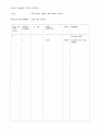
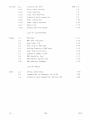
SERVICE MANUAL STATUS RECORD
TITLE
P859 RACK (M4R) AND POWER SUPPLY
PUBLICATION NUMBER
5122 991 30781
I I I I I I I I I I I I I I I I I I I I I I I I I I I I I I I I I I I I I I I I I I I I I I I I I I I I I I I I I I I I I I I I I I I I I I I I I I I I I I I I
I
PUB. NO.
12th
di git
I
I
UPDATE
PACKAGE
S1. NO.
PAGES
AFFECTED
I I I I I I I I I I I I I I I I I I I I I I I I I I I I I I I I I I I I
I
DATE
I
REMARKS
I I I I I I I I I I I I I I I I I I I I I I I I I I I I I I I I I
I I I I I I I I I I I
Issued 8101
1
1
I I I I I I I I I I I I I I I
6-20
8204
I
Conversion list
added
t I I I I I I I I I I I I I I I I I I I I I I I I I I I I I I I I I I I I I I I I I I I I I I I I I I I I I I 1 I I I I I I I I I
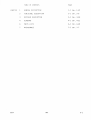
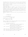
CHAPTER
8204
TABLE OF CONTENTS
PAGE
1
GENERAL DESCRIPTION
1-1 thr. 1-22
2
FUNCTIONAL DESCRIPTION
2-1 thr. 2-6
3
DETAr LED DESCRIPTION
3-1 thr. 3-18
4
DIAGRAMS
4-1 thr. 4-11
6
PARTS LISTS
6-1 thr. 6-24
7
MA.INTENANCE
7-1 thr. 7-7
M4R
0-1
GnlEPAL DESC:; I PTIOfl
1
SECTIOfj
INTPODUCT roil
1.2
PHYSICAL DESCRIPTION
1-3
1.3
TECHNICAL DATA
POltier Input
Power Supply Outputs
Power Supply Protection
Power Failure Signal
Peset Line
Real Time Clock Pulse
Battery Back-Up Suppl ies
Battery Back-Up Supply Protection
Battery Back-Up Time
Battery Charge Time
Environmental Conditions
Physical Characteristics
1-4
1. 3.1
1. 3.2
1. 3. 3
1. 3.4
1. 3. 5
1. 3.6
1. 3.7
1. 3. 8
1. 3.9
1. 3 .10
1.3.11
1. 3.12
1. 4.7
INTERFACES
Power Supply to System
~1ains Supply
Operator's Panel
Key Switch
Extension Packs
CPU Interfaces
Connector J1
Connector J3
Connector J 5
Battery Back-Up System
1.5
APPLICATION NOTES
1.4
1. 4.1
1. 4.2
1. 4.3
1. 4.4
1. 4.5
1. 4.6
1.4.6.1
1.4.6.2
1.4.6.3
8101
PAGE 1-3
1.1
1-4
1-4
1-5
1-5
1-5
1-5
1-5
1-5
1-6
1-6
1-6
1-6
1-6
1-6
1-6
1-6
1-7
1-7
1-7
1-7
1-7
1-8
1-8
1-8
~14R
1-1
SECTIOIj
1.6
1. 6.1
1. 6.2
1. 6.3
1. 6.4
1. 6. 5
1.6.6
1. 6.7
1. 6.8
H1ST/\LUnWrl DAT;\
Mains Input Voltage
Strap Settings
Logic Card Mounting
Extension Rack Connection
Ma ins Connect i on
Power Supply Accuracy
Mains Fuse
Battery Back-Up System
PAGE 1-8
1-8
1-9
1-9
1-9
1-10
1-10
1-10
1-10
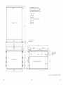
LIST OF ILLUSTRATIONS
Figure
1.1
1.2
1.3
1.4
1.5
1.6
1.7
1.8
1.9
1.10
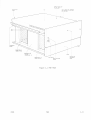
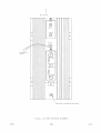
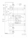
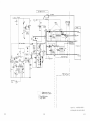
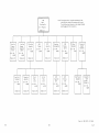
M4R Rack
M4R Rack Functions
Back Panel PCB
Rear View of M4R Rack
Outline Drawing of M4R Rack
Real Time Clock Pulse
Connector CONN1 of CPU
M4R Regulator Card
M4R Battery Option Card
M4R Heatsink Assembly
1-11
1-12
1-13
1-14
1-15
1-16
1-16
1-17
1-18
1-19
LIST OF TABLES
Table
1-2
1.1
1.2
1.3
GP Bus Connections
Connections to Connector J5 of CPU
Extension Rack Connections 10M and lOB
~14R
1-20
1-21
1-22
8101
1.1
The
~14R
I1ITRODUCTIO'!
Rack is the main framework for P859 systems. Ur to ten
logic cards
(including a CPU card) can be mounted in the rack. The rack includes an M4R
Power Supply and an optional Battery Back-Up system for memory. The power supply
provides the following supplies and signals to cards mounted in the rack:
• +5V logic s~pply (+5VL)
+16, -5V memory supplies (+16VM, -5VM)
+lSV, -lSV (nominally +16V, -16V) data communication
supplies (+lSV, -lSV)
• Power failure signals PWFN, RSLN
Additionally the power supply provides the CPU with a real time clock pulse
RTCN.
The battery back-up system, if fitted:
Maintains the +16W1 supply in the event of a mains power failure
• Generates a +5V memory supply
of a mains failure.
(+5V~1)
and maintains it in the event
If the battery back-up system is not fitted,
this supply is taken from the +5VL supply.
Generates "Battery was off" signal BA\rIOFN to the CPU.
A key switch mounted on the front of the rack permits the power supply to be
switched on and off and controls the operation of the battery back-up system, if
fi tted.
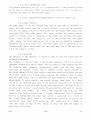
An operators control panel may be mounted on the front of the rack, see fi gure
1.1, which provides direct access to the CPU.
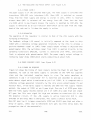
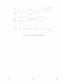
Figure 1.2 shows the basic electrical functions of the rack components.
1.2
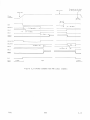
PHYSICAL DESCRIPTION
The rack comprises an aluminium "basic mounting box" in which are mounted a
power supply unit, 10 card slots for logic cards of the "Belier" format, a key
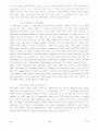
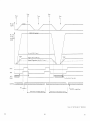
switch and the back panel pcb, see fi gure 1.1.
The back panel
pcb provides bussed interconnections between the 109ic cards,
this is the General Purpose Bus (GP Bus). Connector J3 of each logic card mates
with a connector on the reverse of the back panel, the connector (and mounting
slot) at the top of the rack being reserved for the CPU, see figure 1.3. The
back panel is mounted on the side of the rack and protudes into the power supply
unit
where
connections
are made
for
the
power surplies and
power failure
signals.
S101
i14R
1-3
The operators panel is bol ted on the front of the rack. A pl ug on the back of
the panel mates wi th a 9 pi n connector on a fl yi ng 1ead mounted on the front of
the rack. A cut-out is provided in the panel for the key s~"itch which is also
mounted on the front of the rack.
Racks are mounted in a standard 19 inch cabinet and are fitted with telescopic
slides for easy access.
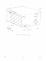
The M4R Power Supply Unit is mounted in a box at the top of the rack. The
battery back-up system (if fitted) is mounted in this same box. The ten
horizontal card slots are mounted underneath the power supply. The rack is
ventilated by two fans mounted at the back which draw air horizontally across
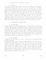
the logic cards and the heatsink assembly of the power supply, see figure 1.4.
The rack operates on a single phase mains supply which is supplied via a socket
mounted on the side of the rack.
The physical dimensions of the rack are given in the outline drawing at figure
1. 5.
1.3 TECHNICAL DATA
1.3.1 POWER INPUT
Single phase mains supply at 50Hz. ± 2Hz.
or 60Hz. ± 3Hz.
Voltage 110/115V ± 10% at 8 amps.
or
220/240V ± 10% at 4 amps.
The rack is adapted to mains voltage with soldered U-links on the regulator pcb
in the power supply unit, see paragraph 1.6.1.
1.3.2 POWER SUPPLY OUTPUTS (DC)
• +5VL; +5V, 60A max. ± 3% stability due to 10% mains and dynamic load
variation, 20-100% static load variation.
Ripple and noise' 1% (0 - 30MHz.).
• -5VM; -5V, 0.8A max. ± 5% stability due to 10% mains and dynamic load
variation, 10-100% static load variation.
Rip P1e and no i se' 1% (0 - 3m1 Hz. ) .
· +16VM; +16V, 3A max.}± 15% stability due to 10% mains and dynamic load
+18V
-16V, 2A max. variation, 10-100% static load variation.
-18V
-16V, 2A max. Ripple and noise, 1% (0
30~1Hz.).
1-4
~14R
8101
1.3.3 POVIEl< SUPPLY PROTECTIOn
~'1ains supply - Protected v/ith a sloVJ blol/ fuse
+5VL supply - Overcurrent 1i mit between 60 and 70 amps.
- Overvoltage 1 imit bet \\fee n +5.5 and + 7.5V
- 5V~1 sup ply - Overcurrent 1i mi t betvJeen 0.8 and 3 amps.
Overvoltage 1 i mi t bet \vee n -5.5 and -7.5V
+16Vf'1 SUPP11- No over voltage protection
+18V supply - No over current protection but a short circuit will not
damage these supplies.
. -18V supply
1.3.4 POWER FAILURE SIGNAL PllFN
Signal active 101'1 - logical 0
o to +O.5V, sink current 48mA
1.3.5 RESET LINE RSLN
Signal active low - logical 0
o to +0.5V, sink current 150mA
When the mains supply is not present this signal is a true 0 volts via a relay
contact to logical ground.
1.3.6 REAL TIME CLOCK PULSE RTCN
This signal is a train of l~s logical 0 pulses, see figure 1.6.
Logical 0 - low
o to +0.5V, sink current 48mA
1.3.7 BATTERY BACK-UP SUPPLIES - if fitted
.+5VM; +5V, 8A max. -3% stability due to 10% mains and dynamic load
variation and 10-100% static load variation.
Ripple and noise < 1% (0 - 30MHz.).
This supply is generated under normal operating conditions with mains supply on
and during mains failure, see paragraph 1.3.9 .
. +16VM; as for +16VM supply from power supply unit, see paragraph 1.3.2.
This supply is generated only during mains failure.
1.3.8 BATTERY BACK-UP SUPPLY PROTECTION - if fitted
.+5VM; - Overcurrent limit between 8 and lOA.
Overvoltage 1 imit between +5.5 and +7.5V .
. +16VM; - As for +16VM supply from power supply unit, see paragraph 1.3.3.
8101
~14R
1-5
1.3.9 BATTERY BACK-UP TIME
A rechargeable battery maintains the +5VM and +16VM suppl ies during mains
failures for the following times:
~10S memory of 128K words - 60 minutes
256K words - 30 minutes
512K words - 10 minutes
1.3.10 BATTERY CHARGE TIME
A completely discharged battery can be fully charged in 48 hours.
1.3.11 ENVIRONMENTAL CONDITIONS
Max. ambient temperature range
0 - 50°C.
Max. relative humidity
90%
height
width
depth
wei ght
1.3.12 PHYSICAL CHARACTERISTICS (refer to figure 1.5)
266 mm
483 mm
563 mm
< 20 kg when fully equipped (front panels" logic cards, etc.).
1.4 INTERFACES
1.4.1 POWER SUPPLY TO SYSTEM
The power supply interfaces to the rest of the system via the GP Bus on the back
panel pcb (see table 1.1) and via discrete connections to connector J5 of the
CPU (see table 1.2). Logic signals PI~FN, RSLN and RTCN are taken from the power
supply (each v~ith an individual ground lead) as twisted pairs.
1.4.2 MAINS SUPPLY
The s i ngl e phase mains supply is fed vi a a socket mounted on the 1eft hand side
of the rack, see figure 1.4.
1.4.3 OPERATORS PANEL
The operators control panel interfaces via a 9 pin connector on a flying lead
mounted on the front of the rack, (this is normally inaccessible, being covered
by the operators pane 1). The other end of the flyi ng 1ead is connected to a 9
pin socket which is discrete It/ired to connector J5 of the CPU except the +5V
supply which is obtained from the bus at connector J3 of the CPU, see figure
4.1.
1-6
81 01
1.4.4 KEY SIIITCH
Signal
BATOFH~
is generated by the key sltJitch, this is discrete wired to the
battery back-up system (if fitted)
via a twisted rair. The key switch also
operates a microsv'litch via a cam ItJhich generates the remote start signal to the
power supply and is wired via a screened cable, see figure 4.1.
1.4.5 EXTENSION RACKS
~Jhen
used these are interfaced via ti'lO connectors lOB and 10M mounted on the
bottom of the back panel (figure 1.3). The extension racks are connected via GP
Bus cables (see table1.3). Refer also to paragraph 1.6.4.
1.4.6 CPU INTERFACES
The CPU interfaces to the rest of the system via connectors J1, J3 and J5 (see
tables 1.1 and 1.2). The following interfaces are wired as standard on the basic
~14R
rack:
• V24 serial
CU break requests
} - connector Jl
OKO/OKI bus control
GP Bus
connector J3
• Ope ra tor s Panel
• "Battery was off" indication }
Floating Point Processor
connector J 5
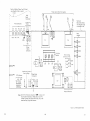
1.4.6.1 CONNECTOR Jl
Connector J1 of the CPU is mounted on a small printed circuit card, CONN1, which
is mounted to the 1eft of the back panel pcb, see fi gure 1.7. On thi s card are
also mounted connector pins for the V24 interface, break request inruts either
from CU cards mounted in the main rack (CPU rack) or from CU cards mounted in
extension racks, and for the bus control chain OKO/OKI. These interfaces are
described in detail in the CPU manual.
1.4.6.2 CONNECTOR J3
The CPU interfaces to the GP Bus at connector J3. Those signals which concern
the power supply are listed in table 1.1. For further details refer to the CPU
man ua 1 •
8101
~14R
1-7
1.4.6.3 COWIECTOR J5
Connect ions at connector J 5 of the CPU to the bJttery back-up (BAf,IOFN), the
pOvJer supply (PTCN) and the operators panel
are shown in table 1.2. vlhen a
floating point processor is used in a system it must be mounted at slot 2. The
FPP interfaces with the GP Bus at connector J3 and in addition some discrete
wi red connect ions are made to the CPU at connector J 5. These connect ions are
also shown in table l.2. Note: \tJhen a floating point processor is not used any
logic card can be mounted at slot 2.
1.4.7 BATTEPY BACK-UP SYSTEM (if fitted)
The battery back-up system interfaces to the rest of the system vi a di screte
wiring. "Battery was off" indication, BAVIOFN, is wired as a twisted
pair to
connector J5 of the CPU, see table 1.2. Battery back-up control signal, BATOFFN,
is
wired
from
the
key
switch
as
a
twisted
pair,
see
figure
4.1.
Other
connections to the power supply unit and the +5VM and +16VM supplies to the bus
are made inside the power supply box.
1.5 APPLICATION NOTES
Figure 1.2 shows the basic functions of the rack. The rack has been designed for
PS59 systems. These systems use the CP7R type CPU, MOS memory (up to 512K words
- four cards) and FRCP type operators panel. The first slot (at the top) is
reserved for the CPU. Slot 2
is reserved for the float i ng poi nt proces sor (if
used). Logic cards used with the rack must be of the "Bel ier" format. Pack
capacity may be extended with the E2 extension rack. This provides +5V, -5V and
+16V supplies (from a single phase as mains input) and mounting slots for up to
six control units.
1.6 INSTALLATION DATA
1.6.1 MAINS INPUT VOLTAGE
The power supply is adapted to the mains voltage with four soldered U-links on
the Regulator card, see figure 1.S. The following connections should be made:
220/240V: a-b, d-e, g-h, j-k
llO-120V: b-c, e-f, h-i, k-l
The mains
fuse,
figure
1.4 is
rated
at
4A for 220V or SA for llOV.
The
ventilator fan assembly mounted on the rear of the rack is chosen for the mains
voltage with vlhich
it
will
be
used.
For a 220V supply two 115V fans are
connected in series. For a llOV supply tv/O 115V fans are connected in parallel.
l-S
~14R
8101
1.6.2 STRAP SETTINGS
TVI0 soldered U-links are fitted to the regulato'," card, figure 1.8,
for test
purposes, TLl and TL2. These shoul d both be fi tted for normal operat ion.
1.6.3 LOGIC CARD MOUNTING
All
logic cards used with the rack must be securely mounted in the correct
slots. Slot positions are given in the system configuration sheets. The cards
are held in position vvith plastic release catches. All discrete lA/iring specific
to a system must be made. For information on these refer to the Installation
section of the individual manuals for each card and the system configuration
sheets.
1.6.4 EXTENSION RACK CONNECTION
Extension racks are connected via two GP Bus cables connected at connectors lOB
and 10M at the bottom of the back panel
pcb. The GP Bus cabl es are of tvvo
standard lengths, 3 metres and 15 metres. The following rules must be observed
when connecting extension racks:
1) Bus cables are connected between the connectors at the bottom of
the back panel pcb of the CPU rack to the connectors at the bottom
of the back panel of the extension rack.
For subsequent extension racks connected in a chain, the bus cables
are connected between the connectors at the top of the back panel
of the previous rack to those at the bottom of the following rack.
2) The cable must be connected so that pi n 50 of each connector is
connected to the same wire of the cable. A red line printed on the
cable may be used as a reference.
3) The 1ast exten si on rack ina chain must have a termi nator netv'Iork
pl ugged into the connectors at the top of the back panel pcb.
4) I~aximum cable length (between CPU rack and the last extension rack
in a chain) = 15 metres.
5)
~1aximum
number of extension racks
used = 7;
hO\tJever,
this
is
limited to 5 because of the standard cable length of 3 metres.
6) Extension racks must be equally spaced along the bus cable.
7)
Maximum number of logic cards used in each extension rack
6.
These must all be control unit card s.
8) The extension racks may only be used with slave control units.
Cards which are system masters must be mounted in the CPU rack.
8101
~14R
1-9
l. 6.5 W\ rr~s COIHIECTI 011
The single phase mains supply is connected via a socket mounted on the right
hand side of the rack.
The mains supply must comply with the rating plate
mounted near the mains socket. Before connecting the mains surply set the key
s~vitc
h on the front of the rack to rosit i on "OFF".
1.6.5 POWER SUPPLY ACCURACY
The power supplies are set up to the specified tolerances (para. l.3) in the
factory before dispatch. Any discrepancy may be due to an inaccurate mains
supply, this should be checked before any adjustment is made.
Information on
power supply adjustment is given in chapter 7 of this manual.
1.6.7 MAINS FUSE
The single mains fuse is mounted on the right hand side of the rack near the
mains socket, see figure 1.4. This is a slow blow fuse rated at 4 amps for 220V
supply or 8 amps for a 110V supply.
1.6.8 BATTERY BACK-UP SYSTEM (if fitted)
No installation procedures are necessary for this system. Connections to the
Battery card
are
made
at
system
installation
time.
Figure
1.9
connector position on this card. Information on adjustment of the
shows
+5V~1
the
surply
(if necessary) is given in chapter 7 of this manual.
1-10
~14R
8101
POWER SUPPl'i AhD
Bt..TTERY BACK.
(IF FITTED)
VENTILATOR
FANS
LOGIC CARCS ARE INSERTED
AND REMOYED AT THIS SIDE
TOP
OF THE RACK
JJ~JJJJJJ . "
. . . . J]JDJU]JJ
' .. JJJJ
TELESCOPIC
SLIDES
02540
i
CONNECTORS J 1
(WHEN FITTED)
BACK PANEL PCB
GP BUS
CONNECTORS 13
I
FRONT
C ONNEC TORS J 5
(WHEN FlTTED)
KE Y SWiTCH
RACK'RETAINING
POSITION OF
OPERATOWS
PANEL
SCREW
Figure 1.1 M4R RACK
8101
~14R
1-11
Single phase
mains supply
M4R Power Supply
.....
.....0
0..
:::J
Powee Suppl;e,
}
+ 5 V L/ + 1 6 V M / -5 V M
+18V / -18V
Signals
PWFN/RSLN
I
...:::t.
u
Z
0
o:l
LL
0
'-
"-
c
0
>.. 0
5;
Q)
'- U
«
~
c
0
'Q)
~
0
CL
0
o:l
o:l
/
GP
connector
J1
Bus
III
C
o
connector
J3
Q)
c
o
CL
....U
\
connector
J5
:::J
'"-
III
C
Key switch
Operator's
Panel
Figure 1.2 M4R RACK FUNCTIONS
1-12
~14R
mOl
+18V
-18V
(ON OTHER
PWFN
+16vM
SIDE)
r
~
-5VM
*5'/M
SENSE
+ 16\1
t5VlOV
RSlN
<
,.
_ _ _ _--t""''--_ _ _ _ _ _
'n
MECHANICAL
GROUNDS
(NOT USED)
,I
........ '
I::F
I
I
I JAOI
LOGICAL GROUNDS
(NOT USED)
!
•
i.i 'I
3801
..
"0'
-i<111~111~1' ~1f-:
II
I
O_R_'G_.I_NA_,L_C~.O-',-NE..,CTOR5
____________
OPERATOR'S PANEL (NOT USED)
TO
I
I
~
I ;I
I
I
'I
I
LJ
3B.::.3
/
,"til::::
..
;
;
I 'I
•
I
,I
-.q
,I·
CONNECTOR
FOR CPU
+5VM
J3
BUS BARS MOUNTED
ABovE THE PCB
•
.. I
I
USED
108
10M
I: ::: :::: ::: : : :: :: : : :::: :; I
::: : : : : : :: I
/
CONNECTORS TO
EXTENSION RACKS
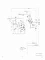
Figure 1.3 BACK PANEL PCB (GP BUS)
8101
~14R
1-13
FRONT
O}646
I
FOUR LED
INDICATORS
??QQI
,
MAINS FUSE
'--' ---- RSLN
L~------=
+ 5 Vl
MAIN~
SOCKET
RATIN~
YENTILATOR
FANS
PLATE
FILTER UNlT
- 5YL
+ 16VL
Fi gure 1. 4 REAR VrEVr OF t14R RACK
1-14
1'14R
8101
~
Rear
All dimensions in mm ± 0.5 mm.
Maximum dimensions with front panels
in place and allowing for screws and
vent fan grills protuding at rear of rack:
T
He ight : 266
Width : 483
Depth : 563
Dimensions of Basic Mounting Box
Height : 263
Width :440
Depth : 537
Viewed from top
r.....
M
If)
=
[2
tOt
477
472
460
440
537
~
5_
I
.
-
~
I-
Mounting holes for
front pane Is
l
Front
-
I--
-- ~
0-
...
00
Ir-
I-n
-
I~
II+I--
"f
-
--
h.
I
I
r
-
r-- -
-
-
-t-
-
-I
I
I
+-
-
.
+~~
0
If)
V-
Mounting holes
for telescopic
slides.
l.
M
-0
N
,.
~
-0
"'<t
-
"'I
~.~
Viewed from right hand side
-
ll)
- -I
If)
I
-
N
-
W'
+-
I
101 ,6
:c
"'<t
-0
I
~
-
-
,-L--
~
Viewed from front
I
in
_
...
14
101,6
,
t--
I
1
203 2
-
r
N.
t
465
1
Figure 1.5 OUTLINE DRAWING OF M4R RACK
8101
~14R
1-15
HIGH
LOW
e
= LjJs
T
~
+20 %
-30%
MAINS PERIOD (20mS FOR
50Hz, 16,6mS FOR 60Hz)
Figure 1.6 REAL TIME CLOCK PULSE
BREAK SELECT LINKS
USED WHEN EXTENSlQN
RACK IS CONNECTED
IBOl
o
o
lAOl
r-------------BO
-_.+--<1
I
0
AD
0
010
o
0
0
._--
0
1637
- - - - - - - - - - - CONNECTOR )1
lA37
(OF CPU) (ON REVERSE)
0
r------
:~oooo
oooooo~:
10:0000
0000000:1
10000000
ooooooo:!
r
I
I
--l
0
0
!
0 t - - j - - - - - - - OKO I OKl CONNECTIONS
L __ , ,J
0
II~::_-_~~~~ =~ ____ ~ -:_-_O-~~ -~-~-~----r~~~ ~~-~(=-o__~_-_ ~ ~ J
O}61.7
I
00
V24 SERIAL
INTERFACE
01
A8 B8
BROO
07
06
BR15
09
15
BREAK CONNECTIONS FROM
CPU RACK (MAIN RACK) OR
EXTENSION RACK
Figure 1.7 CONNECTOR CONN 1 (Jl) FOR CPU
1-16
~14R
8101
".. .
I
Position of Battery Option Card (if fitted),
when Regulator Card is mounted
__ -- - - - _ ,
in rack
-I
'---
J
-_.-"--
-- -- - ---
F Iyi ng Leads to Heat
Sink Assemb Iy
______________________________
r - - - - -__________________________
~A'_
~,
,
(
Logic
Signal
Connectors
Power Connectors
r~----------~A~----------~
~~
Positi on of
Mains Safety Shield
when Regulator Card
is mounted in rack.
_ 5 __ _ _ _ __ _ _\
o o o
+16VL
_ _ _ _ _I
Large
Heatsink
-5VL +5VL
TR 1
TR4
l - -____.....y.-______..J
CR300
Batte ry
Opti on
Connectors
CR303
Aluminium
Heatsink
Mains Voltage
selection U-links
CR302
~
jc
CR3
k
CR4
~-L-_....JI P402
I
el
o
g® "
h eo
"f
i
0
~}220V
~
c} 11 OV
0
0
I
EI"-_....JI
Mechanical ground fgr
Sense Voltages
IVoltage Sense
LED Indicators
I Connectors
_____
...
P40 1
r--_~Io.,_
(
.
Q313
,----------j
I
P5
I~
I6VM
o 001
5v
TR7
00
;101 [§JP
S
I
==~__________~=:
OV
N
:
V
I
10 1 @J:
Mains Connections
Note: Each of the three strip connectors ( ITIIJ ) is shown with
one pin position blacked out. These pins are cut off to
provide a locator which mates with the key way on the
associated Berg flying lead connector.
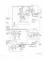
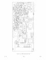
Figure 1.8 M4R REGULATOR CARD
8101
~14R
1-17
L4
Heatsink----n-
+5VM~
o
ov
P7
Power
Connectors
P!lL--ov
[j.-RSLN
@]+24V
o
Regulator
Card
Connectors
OV
Note: Each of the two strip connectors
(I·W·I·I·l)is shown wit h one pin
blacked out. These pins are cut off
to provide a locator which mates with
the key way on the assoc iated Berg
flyi ng lead connector.
BATOFF
BAWOFN
''----......v------''
Logic Signal
Connector
+BAT
Figure 1.9 M4R BATTERY CARD (OPTIONAL)
1-18
M4R
8101
Reor of Rack
rtt.
UU
0
CR] 00
---
f-
CR] 0]
0
0
0
I
I--
r--
CR]]O
~
r--
~
k0
eft
W:J
Conn ector to
+]6VM
CR]
-u
R2
R3
I
-
N
u
CR2
r--
r--
0
0
-
1
® r
f-
~
\
\
Connector to mechanical ground (E)
Figure 1.10 M4R HEATSINK ASSEMBLY
8101
~14R
1-19
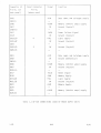
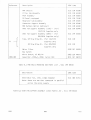
Connector J3
Pi n No. (on
back panel)
3AOl
3A02-5
3A06
3A07
3A08-16
3A17
3A18
3A19,20
3A21,22
3A23
3A24,25
Panel Connector
Pin ~~o.
(vJhere used)
Signa 1
Function
+18V
Data comm. and teletype supply
+16V~1
Memory (inhibit amps) supply
Ground (logical)
OV
PWFN
OV
Power Failure Signal
Ground (logical)
Logic Supply
Ground (logical)
OV
Ground (logical)
OV
4
3
+5VL
3A26-43
3801
3802
3803-5
3806
3807
3808-16
3817
3818
3819,20
3821,22
3823
3824
3825
-18V
OV
+16VM
OV
RSLN
-5VM
+5VL
Data comm. and teletype supply
Ground (mechanical)
Memory (inhibit amps) supply
Ground (logical)
+5VM
Reset Si gna 1
Memory Supply
Logic Supply
Ground (logical)
Memory Supply
+16V~1
Memory (inhibit amps) supply
OV
3826-43
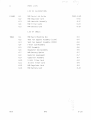
Table 1.1 GP 8US CONNECTIONS (USED 8Y POWER SUPPLY UNIT)
1-20
~14R
8101
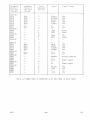
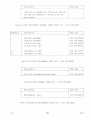
Connector
J5-Slot 1
(for CPU)
Pin No.
Connector
J5-Slot 2
(for FPP)
Pin No.
5AOI-I0
5All
5A12
5A13
5A14
5A15
5A16
5A17
5A18-29
5A30
5A31
5A32,33
5A34
5A35
5A36,37
--
5801-ll
5812
5813
5814
5815
5816-19
5820
5821,22
5823
5824
5825
5826-30
5831
5832,33
5834
5835
5836
5837
5All
5A12
5A13
5A14
5A15
--
5A17
---
Pane 1
Connector
Pi n rio.
---
-----
----
Signal
Signal Source
-FLOACT
8SYCPUN
GFECHT
DONEF
FLOCR1
--
--
OSC
--
CPU
CPU
CPU
FPP
FPP
-CPU
--
I
LOCK
SDP~1
Panel
Pane 1
--
--
---
6
-2
7
--
SDMP
RTCE
--
CPU
Panel
--
--
--
5812
5813
5814
5815
--
P~1FN
----
--
5820
--
---
---
---
-----
--
--
-----------
f30FFN
FLOCRO
FPPAf3S
CPU
CPU
FPP
FPP
--
--
PAFN
CPU
-8attery f3ack-Up
--
--
--
8AVlOFN
--
RTCN
--
3
OV
8
5
RESETN
+12V
--
--
9
-12V
--
Power Supply
--
Power Supply
-CPU
CPU
--
CPU
Table 1.2 CONNECTIONS TO CONNECTOR J5 OF CPU (MADE IN f3ASIC RACK)
8101
~14R
1-21
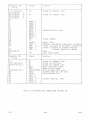
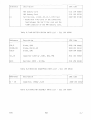
Connector Im1
Pi n tJo.
f
1-21 (odd nos.)
23,25,26,28,
29,31,32,34,
35,37,38,40,
41,43,45,47,
49
Signal
Function
~1A
Ground for Address Lines
t1C
Ground for Command Lines
2
MAD04 -
4
~~AD03
~1AD08
~1AD09
6
8
10
12
14
16
18
20
22
24
27
30
33
39
42,44,46,48
50
Connecto r 108
Pin tJo.
~1AD 10
~1A D11
I----
Address/Function Lines
~1AD12
t'1AD13
14
~1AD
~1AD15
_
AOJ
Accept Command
CLEAR~J
+5V
s ter Cl ea r
Exchan g
Peripheral Controller to Master
Timing
Master to Peripheral Controller
Signals
Master to External Register
External Register to Master
Spare
Logic Power Supply
Signal
Function
Ground for Command Lines
Ground for BIO Lines
Ground for Command Lines
Reset from Power Supply
Power Failure Signal
Bi-directional Data Lines
Encoded Interrupt Line (lsb)
Scan Interrupt Line
TPMN
TMPN
H1EN
~1a
}-
TR~1N
1 ,3
MC
5-37 (odd nos.)
39-49 (odd nos.)
~18
2
RSLN
~1C
4
P~/FN
6-36 (even nos.)
38
40
42
44
46
48
50
8 I 015N-B roON
8IEC5
SCEIN
8IEC3
81EC4 } BIEC1
B1EC2
B1ECO
1
Encoded Interrupt Lines
Table 1.3 EXTENSION RACK CONNECTIONS 10M AND lOB
1-22
~14R
8101
FUNCTIOiIAL DESCPIPTIOtI
?
1-
SECTIOfi
2.1
GENERAL
2.2
pm~ER
2.3
POWER FAILURE AND RESET SIGNALS
2-2
2.4
REAL TIME CLOCK SIGNAL
2-3
2.5
BATTERY BACK-UP SYSTEM
2-3
2.6
OPERATORS KEYSWITCH
2-4
2.7
LED HJDICATORS
2-4
PAGE 2-2
SUPPLI ES
2-2
LIST OF ILLUSTRATIONS
FIGURE
8101
2.1
BLOCK DIAGRAM OF M4R POWER SUPPLY AND
BATTERY BACK-UP
2-5
2.2
TIMING OF POWER SUPPLY LOGIC SIGNALS
2-6
M4R
2-1
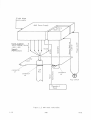
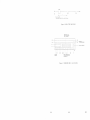
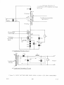
Figure 2.1 shmls til", main functions of t12 pm'ler surrly and hattery hack-ur (if
fitted), The power sU[Jply is sifitched on vfit:' the Remote Start signal frol71 the
microSvlitch Vlhich
rack.
The
is operated by the keyslfitch mounted on the front
Battery
Back-Up system is controlled by signal
of thF'
RATOFFf\! vfhich
is
generated by the keysl/itch.
The pOlver supply [Jrovides the follmJing out[Juts:
-------~-.-~
Signal function
Signal flame at
Signal flame at
PO\Jer SU[J[Jly
GP bus
---~-----
+5V at 60A, logic supply
+5Vl
+5Vl
-5V at O.8A, memory supply
-5Vl
- 5V~1
+lGV at 3A, memory sU[Jply
+16Vn
+ 16V~1
+18V (nominally +16V) at 2A, data comm. SU[J[Jlyl
-18V (nominally -16V) at 2A, data comm. sur[JlYI
+16Vl
+18V
-16Vl
pI-In!
-18V
Reset Signal
RSU!
RSUI
Real Time Clock Signal
RHJ!
RTUI
Power Failure Signal
I
Plln!
The battery back-u[J system provi des the fon mling outputs:
Function
Signal flame
+lGV at 3A (during mains [J0vler fa ilure only)
+1 oV~1
+5V at 8A (duri ng normal o[Jeration Vii t h [Jower
+5V~1
on or during pm'fer failure)
"Battery "Ia s off" indication
BAHOFr!
2.2 POUER SUPPLIES
Specifications for the [JoVier supplies are given in raragra[Jh 1.3 of chapter 1 of
this manual.
2.3 POlIER FAILURE AND RESET SIGriAlS
Signals
Pl·IFfJ
and
RSU!
are
generated
during
thf'>
[J0\tfPr
on/off
seqllences.
Specifications for the signals are given in paragraph 1.3. Roth signals ilre
distributed to the rest of the system via the GP Gus. The timing of the si<]nills
is
shovm
in
figure
2.2.
Roth signals are set
suppl i es have stabil i sed after
2-2
s~Jitch
inactive high vlhen the [Joller
on.
r'14R
8101
The po\ler off sequence is for normal switch off or for a mai ns power fai 1 ure for
longer than 10ms. Shorter mains failures will not cause the povier off sequence.
Once Pv/FN goes low the sequence will continue to set RSUllovi. A failure in any
of the +5VL, +16VL or +24V Aux suppl i es Vii 11 also cause PHFN and RSLN to go low
though the other power supplies will continue to flmction normally.
~Iote:
If the
+16VL supply fails then the +5VL supply It/ill also fail since this is generated
from the -16VL supply. A failure in the -5VL supply (the rest of the power
supply operating normally) will cause signal RSUl only to go low.
A complete description of the sequencing logic is given in chapter 3.
2.4
REAL TIME CLOCK SIGNAL
Signal RTCN is generated all the time that the mains supply is active.
The
signal is a train of negative pulses of hs duration, see paragraph 1.3.6. The
signal is sent to the CPU where it is enabled by signal RTCE from the operators
control panel.
2.5
BATTERY BACK-UP SYSTEM
This is an optional system which when fitted maintains the
+16V~1
memory supply
in the event of a mains power failure and generates the +5VH memory supply
during normal
operation or during a power failure.
Note:
v,/hen
the
battery
back-up system is not fitted, the +5VM supply is derived from the +5VL surply
via a wired connection.
The system comprises a battery which provides the +16VM supply during a rower
failure and a pcb which provides the control functions of the battery back-up
system
during
normal
operation,
including
the
recharging
of
a discharged
battery.
Under normal operating conditions the +16W1 supply is available from the pmver
supply. This provides the input to the +5VM power supply (see figure 2.1). The
battery charger charges the battery from the +24V Aux supply. Signal RSLN is
then high
(inactive)
and the relay operated by battery
back-up control
is
de-energised - ie. its contact is open and the battery is isolated from the rest
of the system.
vlhen the system was initially switched on, BAVJOFN was set lovv. v/hen a povler
failure occurs RSLN goes low which resets BAWOFN high.
At the same time the
battery back-up control energises the relay and the battery provides the
supply to the bus and to the
+5V~1
supply.
The battery back-up control
+16V~1
then
monitors the battery voltage during the power fail ure. If the mains supply is
switched
back
on
before
the
battery
is
discharged,
BAWOFN
remains
high
indicating to the CPU that no loss of power was experienced by the memory.
8101
~14R
?'-3
If the battery voltage drops belm! a critical level during the rOltler failure the
relay is de-energised (to avoid damage to the
bat~ery)
and the suppl ies to the
battery card are lost. vlhen the mains is switched back on
again, It/hich indicates to the CPU that the battery supply
8A\JOF~1
~vas
is set 10ltj
not maintained
during the power failure.
2.6
OPERATOR'S KEYSWITCH
This is a four position
keys~vitch
on the front of the rack. The switch itself
generates signal BATOFFN. \t,lhen the switch is in the "OFF" position BATOFFN is
low which indicates to the battery back-up control that the battery is to be
isolated from the system. v.Jhen the keyswitch is in either of the "ON" positions
or "r1AINT", BATOFFN is hi gh and the battery back-up operates as descri bed in
paragraph 2.5. The keyswitch also operates a microswitch which generates the
remote control start signal to the power supply. When the keyswitch is in either
of the
"ON"
positions the
polt/er supply is sit/itched on.
The keyswitch thus
performs the following functions:
Keysv/itch
Functions
position
OFF
-
Power Supply off, Battery Back-Up off, key can be removed from
keyswitch
ON
I
ON
]
Power Supply on, Battery Back-Up on, key cannot be removed from
keyswitch
Power Supply on, Battery Back-Up on, key can be removed from
keyswitch
~1AINT
-
Power Supply off, Battery Back -Up on, key cannot be removed from
(memory is maintained)
keyswitch
ON
ON~
"'=
e
,:JMA'NT
0)60
KEYSWITCH POSITIONS
2.7 LED INDICATORS
flhen the rack is moved forward on its telescopic sl ides out of the cabinet, four
LED indicators can be seen (see figure 1.4). These monitor (from left to right)
+16VL, -16VL, -5VL, +5VL supplies and RSLN rest signal. All four LED's should be
lit for normal operation (ie. supplies active).
2-4
~14R
8101
+ VL
~~
~e>'
Ventilator Fan
Supply
Mains
Filter
Remote
Control
Start
-- - - - -
1
Mains Detector
and
Sequence Logic
Mains
Supply
GP Bus
RSLN4
PWFN
RTCN
RSLN
I
I
I PWFN
-
to CPU
--
+24 Volt
+24V Aux
Auxiliary
__S_ ~pP 11 ____
Fuse
~
H.T.
A uxi I iary
Supply
HT
+5VL
->
0-0
C ~
u
OV
OV
+5V Power
Supply
Mains Socket
~ OJ
-- .- 0
I +5VL-......
I
I
Q~ \~~~cata, I I
Batte ry
Charger
I
'7/'T7;
"1
-11t---+-+-----.
Remote Start _ _ _'---'
from Microswitch
r
I
,
S uppl ies
Battery
Back-Up
Control
-----I
r
Relay
+5VM
Power
Supply
+5VM)
+5VM
•
3atterv oack-U p System I
+16VM
+16VM
16 Volt Power
jlBAWOFN
-J
Batte r~ L
........-
~
:
.. /'Battery
wa s off'
I-~::":"':":"':""'::::":""':~----t.....
Indication
to CPU
-
,r 1-----
VlVl4-
BATOFFN
from Keyswitch
•
-5VL
+5(L
I
•
)LED
Indicator
This connection is
made if the battery
back-up system is
not fitted
+16VL
+24V Aux
.c
,- - - - - - -,
-16VL
+16VL
I
I
-18V -'"
+18V
•
Q~ "
) LED
) Indicator
7177;
~
-5 Volt Power
Supply
-5VM
-"iVI
Q~
.4 ';" )LED
Indicator
Power Supply Unit
8101
f
71",
I
•
,
Fl gure 2.1 BLOCK DIAGRAM OF ~14R
POWER SUPPLY AND BATTERY BACK-UP
M4R
2-5
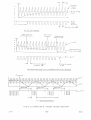
POWER ON
POWER
SUPP LI E 5
RSLN
POWER OFF
f------L-'
f------;-~,-------'/ I~-+--'I~-T------
PWFN
t3
tl ::.
>
t4
50mS
t2 = > O,1mS
13 ::. > lOmS
t4 = > 2 mS
t5 ::. > lOjJS
Figure 2.2 TIMING OF POWER SUPPLY LOGIC SIGNALS
2-6
8101
DETAILED DEscrIPTION
3
SECTION
8101
PAGE 3-3
3-3
3-3
3-3
3-3
3.1
3.1.1
3.1. 2
3.1. 3
3.1.4
POWER SUPPLY INPUT CIRCUITS
Mains Supply
Remote Start
HT Auxiliary Supply
+24V Auxiliary Supply
3.2
PRINCIPLES OF OPERATION OF SWITCHED
MODE POWER SUPPLY
3-4
3.3
3.3.1
3.3.2
3.3.3
3.3.4
3.3.5
3.3.6
3.3.7
3.3.8
3.3.9
3.3.10
+5VL REGULATOR AND POWER SUPPLY
Power Supply
Regulator
Feedback Loop
Soft Start Sequence
Short Circuit Protection
Feedback Loop Open Circuit Protection
Overcurrent Protection
Supply Failure Protection
Overvoltage Protection
16V Synchronising Signal
3-4
3-4
3-4
3-5
3-5
3-5
3-6
3-6
3-6
3-6
3-7
3.4
3.4.1
3.4.2
16 VOLT REGULATOR AND POWER SUPPLIES
Pmver Supp 1 i es
Regulator
3-7
3-7
3.5
3.5.1
3.5.2
-5VM REGULATOR AND POWER SUPPLY
Power Supply
Regulator
3-8
3-8
3-8
3.6
3.6.1
3.6.2
3.6.3
POWER SEQUENCE LOGIC
Power On Sequence
Power Off Sequence
Real Time Clock Pulse
3-8
3-8
3-9
3-9
~14R
3-7
3-1
SECTION
3.7
3.7.1
3.7.2
3.7.2.1
3.7.2.2
3.7.3
3.7.4
3.7.5
B/\TTERY 8l\CK -UP SYSTEtl
Gene,al
+5V~1 Regul ato, and POIf/e, SU[Jply
Powe, Supply
Regulato,
Batte,y Back -Up Cont,ol
Batte,y Cha,ge, and Cont,ol
Batte,y lvas Off Indication
P/\GE 3-10
3-10
3-10
3-10
3-10
3-11
3-11
3-12
LI ST OF I LLUSTRA TIONS
FIGURE
3.1
3.2
( a)
(b)
(c)
3.3
3.4
3.5
Basic Switched Mode Power Supply
Ope,ation of TDA1060 Voltage Regulato,
Soft Sta,t Sequence
Sho,t Ci,cuit/Open Ci,cuit P,otection
Ove,cu"ent P,otection
Timing Diag,am fo, M4R Logic Signals
Batte,y Cha,ge Cont,ol
Battery Was Off Indication
3-13
3-14
3-14
3-14
3-14
3-15
3-16
3-17
LIST OF TABLES
TABLE
3-2
3.1
List of Integrated Ci,cuits Used
~14R
3-18
8101
3.1 POtiER SUPPL Y INPUT CIRCUITS
3.1.1
~1AINS
SUPPLY (Figure 4.1)
The single phase mains supply is input to the unit via a mains
socket.
The
supply is fused and filtered and input to the M4R Regulator Card at connectors P
and N.
3.1.2 REMOTE CONTROL START (Figure 4.2)
The mains supply is switched on with the key switch. Hith this switch set to
either of the liON" positions a cam closes the contacts of a microswitch which
puts a short circuit across connectors P and S of the regulator card. This gates
on triac Q313 which energises the regulator card and provides the ventilator
fans supply at connector V. The mains is supplied initially via surge limit
resistor R300 to the HT Auxiliary supply circuit and to transformer TR7.
3.1.3 HT AUXILIARY SUPPLY (Figure 4.2)
vJhen the unit is used with a mains supply of 220/240V the soldered U-links in
this circuit are as shown in the diagram. Diodes CR300-303 operate as a diode
bridge which rectify the mains supply. The output is smoothed by C300-303 to
provide an HT supply of approximately 300V dc which is used by the +5V and +16V
po we r
sup p1 i e s . When the unit
i sus e d with a ma ins sup ply
U-links are soldered between points b - c and e - f.
0f
11 0 /l15 V the
In this case diodes
CR300-303 and capacitors C300-303 operate as a voltage-doubler circuit. In this
case the neutral of the mains supply is connected to the centre point of the
network C301-303/R305,306.
~Jhen
the Line (P)
is positive with respect to the
Neutral (N) in the mains supply capacitors C300,301 are charged positively wrt
the centre point via CR300,301. When P is negative wrt N capacitors C302,303 are
charged negatively wrt the centre point. The total voltage developped between
+HT and
-HT
is
again
approximately 300Vdc.
Resistors
R305,306
balance the
leakage resistance of the capacitors in the network.
3.1.4 +24V AUXILIARY SUPPLY (Figure 4.2)
The primary of transformer TR7 comprises two windings. l4hen the unit is used
with 220/240V the windings are connected in series across the mains via the two
soldered U-links as shown in the diagram. VJhen used with 110/l15V the U-links
are soldered between points h - i and k - 1 in which case the two windings are
connected in parallel across the mains. The secondary of TR7 at connections 8,9
is rectified and smoothed to provide the +24Vdc auxiliary supply used internally
by the
regul ator card and by the battery card, if fitted. Thi s supply then
energises relay Kl which short circuits surge limit resistor R300.
8101
~14R
3-3
3.2 PRIrlCIPLES OF OPEIVHIOf! OF S\JITCHED
1,10DE POtiER SUPPLY
Figure 3.1. shows the basic operation of a switched mode power supply. This type
of circuit is used in the +5VL,
+16V~1,
+16VL and -16VL surplies. A transistor
sVJitching signal generated in the regulator circuit alternately sVJitches Ql on
and off. When Ql is switched on current flows from the HT through winding 1 of
TRI primary, inducing a magnetic field in TRI (figure 3.1(a). This induces an
emf in TRI secondary (figure 3.1(b). CR6 is foflt/ard biased and current flows
through Ll to the load increasing linearly. Capacitor C3 is charged and energy
is stored in Ll.
~Jhen
Ql is switched off current stops flowing from the HT and the polarity of
the voltage across vJinding 1 of TRI is reversed. Thus the emf at TRI secondary
is reversed and CR6 is reversed biased. The polarity of the voltage across Ll is
al so reversed and the stored energy from Ll is passed to the load via forward
biased CR7. At the same time C3 discharges through the load. The total
current which
is
the
sum of the caracitor and
load
inductor currents decreases
linearly.
The collapsing magnetic field in TRI generates a reverse emf in winding 1 which
could easily destroy Ql so winding 2 is used as a demagnetisation vlinding. This
has the same number of turns as winding 1. When the reverse emf acros windings 1
and 2 (and hence across Ql) increases above tv/ice the HT voltage CR4 becomes
forward biased and winding 2 discharges into the caracitors of the HT supply.
The slope of the increasing reverse emf is controlled by charging Cl via forward
biased CR5. When Ql is switched on again Cl discharges via Rl through Ql. Diodes
CRl-3 with R4 and C3 ensure that the base of Ql is negative with respect to the
emitter when it is switched off.
3.3 +5VL REGULATOR MID POVJER SUPPLY (refer to fi gure 4.3)
3.3.1 POWER SUPPLY
The power supply is of the switched mode type as described at paragraph 3.2
above. The output is smoothed by Cl - C6 and fed to the bus components Cll /R2
across CRI and C12/R3 across CR2 limit switching srikes in these diodes.
The
supply is monitored by an LED indicator CR212 which can be seen from the right
hand side of the rack. The LED is lit when the supply is active.
3.3.2 REGULATOR
The power supply switching transistor Ql is controlled by a variable duty cycle,
constant frequency sVJitching signal generated in the voltage regulator chip TDA
1060 (rCI).
3-4
~14R
8101
The
output
pulses
from
the
chip
are
produced
by
comparing
an
internally
generated savJ tooth waveform with a duty cycle vo;tage at the input to a pulse
width modulator (PvJM). The duty cycle of the output pulses increases with this
voltage and the mean output voltage of the power supply increases with the duty
cycle. The maximum level of duty cycle (5 max) is set by the voltage at pin 6
which is derived from an internal stabil"ised power supply Vz (S.SV) at pin 2
across R19/R20. During normal operation this voltage is constant and 5 max is
4S%. The frequency of the saw tooth generator, and hence of the output pul ses,
is fixed by timing components R21/C21 at 40KHz. The saw tooth waveform can be
monitored at pin S of the chip. The pulses from the PWM are passed via an output
stage to pin IS of the chip. Pulses switch transistor Q4 which passes a constant
current through the primary of TR2. f'lhen the signal at pin IS is high (inactive)
Q4 is switched on and energy is stored in TR2. vJhen Q4 is switched off energy
flows from the secondary of TR2 vi a RS/C16 to swi tch on Ql. vJhen Q4 is swi tched
on agai n the base of Ql goes negat i ve and swi tc hes off. The con stant current
source is provided by Q2,3 and 13. Transistor Q13 develops a constant voltage
across RIO which passes a constant current of 200mA through Q2 to TR2 primary
when switched by Q4.
3.3.3 FEEDBACK LOOP
The chip monitors,
developped across
at
pin
3,
the output
potentiometer PI,
of the
compares
power supply
it with
an
(+SV sense)
internally derived
reference voltage (3.72V) at the input to an error amplifier and adjusts the
duty cycle voltage accordingly.
Thus PI is used to adjust the power supply
output voltage since it forms part of the feedback loop. The gain of this loop
is determined by R22/R23 which are connected around the error amplifier at pin
4.
3.3.4 SOFT START SEQUENCE
Before the
supply to
the chip
is
switched
on
C20 connected
at
pin
6 is
discharged. During a start up sequence after the +24V Aux supply becomes active
capacitor C20 slowly charges from Vz at pin 2.
Thus the duty cycle slowly
increases from 0% to provide a soft start, see figure 3.2(a).
3.3.S SHORT CIRCUIT PROTECTION
If the voltage at pin 3 becomes less than 600mV (eg. a short circuit on the
power supply output) the chip internally reduces the duty cycle voltage at the
Pv/~1
to a value corresponding to =10%, see figure 3.2(b). The duty cycle remains
at 10% until the short circuit is removed.
S101
f~4R
3-S
3.3.6 FEEDBACK LOOP OPEN CIRCUIT PROTECTION
If the feedback loop is open circuited (ie. loss of +5V sense) the voltage at
pin 3 is left floating. The chip internally simulates a high feedback voltage
which
reduces
the duty cycle
to
zero
(ie.
no
pulses).
This
condition
is
maintained until the open circuit fault is corrected, see figure 3.2(b).
3.3.7 OVERCURRENT PROTECTION
Current flovJ in the povJer supply is moni tored by transformer TR3. The secondary
of
TR3
is
half wave
potentiometer
P2.
If
rectified
the
by CRS and applied
voltage
at
pin
11
rises
to
pin
above
11
of
4S0mV
IC1
the
via
chip
immediately limits current flow by cutting short the output pulse. This cycle by
cycle current 1 imit continues until the overcurrent is reduced or until
the
voltage at pin 11 goes higher than 600mV. At this point the chip immediately
inhibits the output stage (which inhibits all pul ses) and discharges capacitor
C20 at pin 6. When the voltage on pin 6 is reduced to 600mV the output stage is
enabled and C6 is allowed to recharge from Vz at pin 2 and the chip attempts a
soft
start
sequence.
The chi p cont i nues
in
thi s
"hi ck-up"
mode
unti 1 the
overcurrent condition is removed, see figure 3.2(c).
Due to its storage effect, transistor Q1 is switched on for a period of time
slightly longer than the switching pulse. This means that under normal operating
condi t ions vJhen the voltage at pi n 11 increases above4S0mV and the output pul se
is switched off, the transistor continues to conduct and the 600mV level will be
reached at pin 11. Thus any overcurrent condition will result in the "hick-up"
mode. The overcurrent limit is adjusted with potentiometer P2.
3.3.S SUPPLY FAILURE PROTECTION
If the chip input supply at pin 1 reduces below 10.5V the output stage is
inhibited and capacitor C20 is discharged. The chip remains in this state until
the input voltage increases above 10.5V at which time the chip commences a soft
start sequence.
3.3.9 OVER VOLTAGE PROTECTION
The power supply output voltage is monitored by a Crowbar circuit mounted on the
+5 Volt Filter Card.
If the supply voltage increases above the specification
transistor Q502 sVJitches on and fires Thyristor Q501 which short circuits the
power supply.
3-6
~14R
S101
3.3.10 16V SYNCHRONISING SIGNAL
The sawtooth vvavefonn at pi n 8 of ICI is comrared v.ith a fi xed reference vol tage
at the input to comparator IC208. The square wave output at rin 1 is used as a
synchronising signal for the 16V pmyer supply.
3.4 16 VOLT REGULATOR AND POWER SUPPLIES (refer to figure 4.4)
3.4.1 POWER SUPPLIES
The power supply is of the switched mode type as described at paragrarh 3.2
above. The power supply comprises a single primary circuit and two secondary
circuits. The output at NSI/0 of TR4 provides the +18V (named +16VL) surply and,
via diode CR110, the +16VM supply.
This diode
isolates the battery back-ur
system (if fitted), which is connected to the +16VM line, from the +18V supply
during a mains failure.
The output at 11/12 of TR4 provides the -18V (named
-16VL) supply. The three supp 1 i es are fed to the bus vi a smoothi ng components
mounted on the 16 Volt Filter Card. The +16VL supply only is monitored by LED
indicator CR213 which can be seen from the right hand side of the rack and is
lit if the supply is active.
3.4.2 REGULATOR
The operation of the regulator is similar to that for the +5VL supply with the
following differences.
The frequency of the osci 11 ator in the voltage regul at or chi p IC2 is set with
components R124/Cl16 at approx. 50KHz. This oscillator is then synchronised with
the
slightly
lower
frequency
Transi stor Q8 switches current
synchronising
from
signal
from
a constant current
the
source
+5VL
supply.
provided
by
Q6,7,CRI08 (200mA) via TR5. This controls switching transistor Q5 which provides
the primary current for all three power suppl ies. The feedback signal is taken
from the
+16V~1
supply, this is therefore the best regulated of the three, via
potentiometer P4 which controls the output voltage.
When there
is
a short
circuit on the +16VM the duty cycle of the switching transistor will be reduced
to 10%. A short circuit on either of the other suprl ies will be seen by IC2 as
an overcurrent. Current is monitored by TR6 which monitors the total of currents
in the
+16V~1,
+18V (+16VL), -18V (-16VL), -5VM (suppl ied from +16VL) and
+5V~~
(supplied from +16VM on battery card if fitted). Overcurrent limit is adjusted,
with P3, to operate when the total load current is equivalent to a current of
14A in the +16VM supply.
There is no overvoltage rrotection on any of the
suppl ies but Zener diode CR114 across the -16VL supply acts as a bleeder to
limit the output voltage of this
operating at low current.
8101
suprly to
~14R
about 20V when the
supply is
3-7
3.5
-5V~1
REGULATOR MlO POliER SUPPLY (see fi9ure 4.5)
3.5.1 pmlER SUPPLY
The power supply is of the switched mode type. The +16VL supply is switched with
transistors Q401,402 into inductance L401.
~Ihen
Q401 is sVJitched on current
flows from the +16VL supply and energy is stored in L401. CR401 is reversed
biased.
~Jhen
Q401 is switched off the energy from L401 flovls into the load
via CR401 which is now forward biased. The supply is smoothed by C407-409. The
supply is monitored by an LED indicator CR214 which can be seen from the right
hand of the rack and is lit when the supply is active.
3.5.2 REGULATOR
The operation of the regulator is similar to that of the +5VL supply VJith the
following differences:
The feedback voltage (-5V sense) is initially compared at the input to chip
IC402 with a reference voltage generated internally by the chip to produce a
positive feedback signal to IC401. Power supply output voltage is adjusted with
potentiometer P401. The switching signal from IC401 is applied directly to the
sVJitching transistors Q402,401.
Current is monitored with TR401.
1 imit is adjusted with potentiometer P402.
Overcurrent
The power supply output voltage is
limited by Zener diode CR403 which starts conducting at about 6.8V.
3.6 POWER SEQUENCE LOGIC (see figure 4.2)
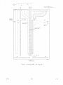
3.6.1 POWER ON SEQUENCE
Figure 3.3 shows the timing of logic signals during the Power On and Power Off
sequences. As soon as the mains supply is switched on the +24V Aux supplies
rises
and
the
individual
supplies
begin
to
rise.
The
mains
waveform
at
connectors 6 and 7 of transformer TR7 is rectified and smoothed to provide a
mains detect signal which is monitored at pin 5 of IC201. It is compared with a
reference voltage generated internally by the chip across potentiometer P5 and
resistor R211. If the mains supply is healthy and when the +5VL supply reaches
nominal, the output of 1C201 at pin 9 goes high. Thus pin 4 of 1C205 goes high.
When the +16VL supply reaches nominal pin 5 of 1C205 also goes high and signal
DET goes low. This sets signal RLY high and switches on transistor Qll in the
±5V detector circuit.
If the -5VL supply is active transistor QI0 is
also
switched on and relay K201 is energised. This opens a contact across RSLN.
When DET goes low it triggers monostable 1C202 and DELAYI goes high and after a
delay of approx.
lOOns (due to R210/C216) DLYl goes low (this delay masks the
propogation time of the monostable).
3-8
~14R
8101
At
the
same time DELAYlN goes
low to
reset
signal
DELAY2.
The monostable
produces a pulse of 1,5 seconds duration, at the end of vvhich time DELAYl is
reset low and DELI goes high. After a delay of approx.lOOns (due to R2l6/C2l5)
DLY2 goes high, DEL2 goes low and transistor Q12 is switched off to set RSLN
high. 6ms after DELI (due to R209/C205), PWFN also goes high.
3.6.2 POWER OFF SEQUENCE
If the mains supply is switched off the mains detect signal at pin 5 of IC201
starts
to
fall.
After
10ms
it
fall s
sufficiently
amplifier switches state and pin 9 of IC201 goes
so
low.
that
the
This time
comparator
period
is
adjusted with potentiometer P5 which controls the comparator voltage at pin 4 of
IC201. Also a failure in the +24V Aux or +5VL supply will cause the output of
IC201 to go 10\,J. A failure in the +16VL supply will result in pin 5 of IC205
going low. Thus any of these supply failures will
be detected by signal DET
going high. After a delay of approx. lOOns DLYl goes high, DEll goes 101'1 and
PWFN goes low. DELI going low triggers monostable IC202 setting DELAY2 high and
after a delay of approx. lOOns DLY2 goes low (this delay masks the propogation
time of the monostable). The monostable produces a pulse of 3ms duration, at the
end of which time DELAY2 is reset 10vJ, DEL2 goes high and transistor Q12 is
switched on to set RSLN low. When DEL2 goes high, signal RLY goes low to switch
off transistor Qll. Relay K20l then de-energises and its contact grounds RSLN.
Note: Since transistor Q12 operates after relay K201 for power on and before
K20l for power off, contact bounce is masked from the RSLN line. A failure in
the -5VL supply causes transistor Q10 to switch off. K201 de-energises and RSLN
is grounded. PWFN remains high under these conditions. RSLN is monitored with an
LEO indicator visible from the right hand side of the rack. This LEO, CR211, is
lit when RSLN is high (during power on).
3.6.3 REAL TIME CLOCK PULSE
The
Real
Time
Clock
Pulse
RTCN
is
generated
by
pul se
shaping
the
mains
waveform. The waveform at tap 6 of transformer TR7 is a hal fwave rectified
signal with a frequency equal to that of the mains. It is applied via a filter
network to the input of a comparator amplifier IC207 which provides a square
wave output with the same frequency. Each low to high transition of the square
wave tri ggers
the
monostabl e
IC203 whi ch
produces
an
output
pul se of 111s
duration. This time is determined by timing components R202/C211,
see figure
1.6. The output from the monostable is then inverted and output to the CPU as a
twisted pair w{th an associated ground lead, see figure 4.1.
8101
~14R
3-9
3.7 BATTERY BACK-UP SYSTEM (see figure 4.6)
3.7.1 GENERAL
This system provides a battery supply to maintain the
+16V~1
supply to the memory
in the event of mains power failures. The system also generates a +5VH memory
supply from the +16VM supply (with mains power on or off) and provides a battery
charger which charges the battery during normal operation with mains power on.
vJhen a rack is provided without this battery back-up option the +5VM supply is
taken via a link from the +5VL supply, hOvJever in this case the
the +16VM supply) will
back-up
system will
not be maintained during
maintain the
two
power
+5V~1
power failure.
supplies
until
supply (nor
The battery
the
battery is
discharged at which time the batttery will be isolated from the system. If this
happens signal BAWOFN indicates to the CPU, when the mains supply is switched on
again, that the power suppl ies were not maintained during the power failure.
3.7.2 +5VM REGULATOR AND POWER SUPPLY
3.7.2.1 POWER SUPPLY
The power supply is of the switched mode type. The +16VM supply is switched with
transistor Q518. When Q518 is switched on CR509 is reversed biased and current
flows from the +16VM supply through L4 to the load. Capacitors C501, 503-505 are
charged and energy is stored in L4. When Q518 is switched off energy flows from
L4 into the load via CR509 now forward biased. At the same time C50l, 503-505
discharge into the load, the total load current being the sum of the capacitor
and inductor currents. The current drawn from the +16VM supply is smoothed by a
filter comprising C500 and inductance L5 to limit noise.
3.7.2.2 REGULATOR
The operation of the regulator is similar to that of the +5VL supply with the
following differences:
The switching signal
output from the voltage regulator chip
IC512 switches
transi stor Q519 which passes current from the +16VM supply through the primary
of TR9
via
resistors
transistor Q518.
R533/541.
The
The feedback signal
secondary of TR9 drives
the
switching
is taken from the output of the power
supply (+5VM sense) via P5 controls the output voltage. TR8 monitors the total
current passes by the power supply and regulator circuits. Overcurrent limit is
adjusted with P6. The po\tJer supply output voltage is limited by Zener diode
CR511 which starts conducting at about 6.8V.
3-10
M4R
8101
3.7.3 BATTERY BACK-UP COflTIWL
It·Jith mains power switched on the +16VM supply is available at the battery card.
The voltage developped across
R500/501
is monitored by comparator amplifier
IC511 at pin 3 and compared I'Jith a stabilised voltage (6,2V) across P7 at pin
2. Under normal operating conditions the level at the base of 0515 is high due
to the output of IC511 but this point is held low by signal RSLN, RATOFFN from
the key switch is open circuit. Transistors 0515/516 are then switched off and
K502 is de-energised. If a power failure occurs RSLN goes low, the base of Q515
+16V~1
goes high and relay K502 is energised which connects the battery to the
line. Thus the
+16V~1
supply is maintained during the power failure.
As the
battery discharges its voltage falls. When the critical value is reached the
output
from
the
comparator
IC511
goes
low,
0515/516
switch
off,
K502
is
de-energi sed and the battery is di sconnected from the + 16V~1 1 i ne. The cri ti ca 1
value (between +12V and +13V) is adjusted with P7. Hhen the operators key switch
is in the OFF position, only, signal
~round.
BATOFFN is short circuited to logical
The base of 0515 is then held low and relay K502 de-energised.
3.7.4 BATTERY CHARGER AND CONTROL
The battery is charged from the +24V Aux supply (while mains power is switched
on).
The battery voltage is monitored
(Battery Voltage Sense)
at
pin 6 of
comparator IC511 and is compared \vith a reference voltage (6,2V) stabilised by
CR508. The comparator operates on a hysteresis loop, provided by R509, so that
its output goes hi gh or low for di fferent battery vol tages.
supply
is
available
transistors
0521/522
are
switched
~Jhen
on,
the +24V Aux
these
pass
the
charging current to the battery via CR510. Initially with a battery voltage of,
say, 13V, the output from IC511 at pi n 7 is hi gh and transi stors 0514/520 are
switched on. 0520 passes a charging current of 25mA via R537-539, see figure
3.4.
As
the
battery charges
its
voltage
rises,
when
this
reaches
17,15V
(typical) IC511 switched and transistors 0514/520 are switched off. A charging
current of 5mA is then
passed by R518.
Under these conditions the battery
voltage decreases until 16,10V (typical) at which point IC511 switches back and
0514/520 are switched on again. This cycle repeats itself but slows down as full
charge is reached, and eventually stabilises with 0514/520 switched off and the
battery supply is maintained with the trickle charge of 5mA.
Note:
Figure 3.4 is not drawn to scale. The initial
switching time of the
transistor is several minutes while the total charging time may be as long as 48
hours.
8101
M4R
3-11
3.7.5 BATTERY viAS OFF 1N01CATIml
Timer chip type NE555 (1C509) is used as a flip-f;op to generate signal RAI'IOFN.
The flip-flop has two states:
Set (pin 3 high, BAHOFN lm'l) \-'Jhen the voltage on the trigger inrut,
pin 2, goes lower than one third of the supply voltage Vcc, pin 8.
Note: when 1C509 is switched on it is always switched on in this
triggered state.
Reset (pin 3 low, BAWOFN high) when pin 4 (Reset) goes low, ie. when
signal RSLN goes low.
Note: BA\lJOFN is considered as significant from the time RSLN goes
high (after power on) to 5ws after PWFN goes high- this is the time
when the CPU monitors BAHOFN.
l1hen the machine is initially switched on (battery was previously off), IC509
is switched on with pin 3 high and BAvlOFN low, see figure 3.5. BAvlOFN remains
low until
the first
power failure, at this time RSLN goes high providing a
negative going edge which is differentiated by capacitor C510 to
produce a
negative pulse at the reset input, pin 4 of IC509. The output at pin 3 goes low
and BAWOFN goes high. If the battery back-up is active during the power failure,
ie. the supply to IC509 is maintained, BAl10FN remains high. Hhen the power is
next switched on the CPU will recognise BAHOFN high indicating that the memory
supply was maintained during the power failure. If during the rower failure the
battery supply was switched off IC509 was also switched off and when the mains
supply is next switched on IC509 will be switched on in the triggered state and
the CPU will
recognise BAWOFN low indicating that the memory supply was not
maintained during the power failure. The chip is triggered when it is switched
on because the voltage at pin 2, derived from the +16VM supply via resistor
bridge R528/529 is initially less than one third of Vcc at pin 8 and which is
derived from the +16VM supply via Zener di ode CR500. fl/hen the
+16V~1
supply ri ses
to about 9V the voltage at pin 2 rises above one third of Vcc and the trigger
circuit relaxes. When the chip is switched off there is also a trigger point as
shown in figure 3.5, but this is masked by the trigger that follows the next
switch on.
3-12
M4R
8101
--_~ indicates direction of
current flow with transistor switched
on or off.
(R4
~
Transformer secondary
(see below)
+----------~--+_------------------__1
HT
Supply
(2
Winding 1
Overcurrent
D e te c ti.;:::o.:.;.n_____----4I--________---.J
R1
Transistor
~----------~-.------~-
switching
signa I
(R5
Off! +--_ _
-..l
~
(3
(1
a) Transformer Primary (ircuit
L1
~-.--------~--------o
R2
+
Output
b) Transformer Secondary (ircuit
Figure 3.1 BASIC SltJITCHED MODE POVIER SUPPLY USING A STEP DOtm TRANSFOR~1ER
8101
~14R
3-13
1
Volts
6
5
Oscillotor
Signa I
at pin 8
4
[; max voltage
at pin 6
3
2
o
5 1_ ------..,r-..,
1"-~I
I--
Output
Pulses
at pin 15
Max duty cycle 45%
(a) : Sori S~art Sequence
Short circuit on
power supply output
Short circuit
removed
Feedback loop
Volts
6
~Pin8
5
4
3
2
1
o
~--------------------
effecti ve(inte rna I)
.
.
.
duty
cycle voltage
____________- L_______
r---\-r------'~
JI L
(b)
~ dead-time
pi n 15
I
De'y eyd. "decod
Duty cycle reduced
to 0%
toapprox.10%
Power Supply Short Circuit and Feedback Open Circuit Protection
1
.1
I
dead-time
: dead -time
I~
""'"
I
f---
1m
.. ,
1
I m-~'L---Pin
15
Successive Soft Start attempts
(c) : Overcurrent Protecti on
Figure 3.2 OPERATION OF TDA1060 VOLTAGE REGULATOR
3-14
~14R
8101
Depends on the load
on the power supply.
Mains Off
!
(\
Power
Supplies
:~U;
,>lOms'
~
DET
:"'-'-1\) lOOns
DE LAY]
I
I ...
] ,5 seconds
DLY]
-.....:
~!"\J]OOns
DEll
6ms
DELAY] N
:( ..
DELAY2
1i.J]
OOns----':
3ms
D LY2
Ii.J lOOns---";
_
DE L2
1
RLY
closed
open
I closed
Figure 3.3 TIMING DIAGRAM FOR M4R LOGIC SIGNALS
8101
~14R
3-15
BATTERY FULLY CHARGED
17)5V
i6,lOV
BAT T ERY
VOLTAGE
ON
OFF
TRANSISTORS
Q514 / S20
2S0mA
SmA -
--~-
--
'--
'--CHARGE RATE
u}61.7
Figure 3.4 BATTERY CHARGE CONTROL
3-16
~14R
8101
Power
Off
Power
On
DC Logie
S uppl ies
nominal
Power
Off
!
Power
! -'~
:/
~
On
1
Power
On
+16VM +16V nominal
DC Levels
at ti mer
eh ip N E555
(IC509)
Vee -
in 8 +5.1V nom.
I
PWFN
o-----------~~--~II
RSLN
o
pin 3 ,NE555
_---.;-------..J!
~~
I
I
I cL
J
r
II~--~----------r_--~-------------------
I
~LI____________________________________~______~
level at pin 3 not valid
l
powe, F Q;I u,e without Botte,y 30c k -U p
J
Figure 3.5 "BATTERY l:iAS OFF" INDICATION
8101
~14R
3-17
Type No.
Function
I-------+---~--.-~-----~-------------------------_l
TDA 1060
l1A 723DC
9602
74121
74S38
74132
74S02
U"1393 AN
NE 555
Power Supply Switching Controller
Voltage Regulator
Dual Retriggerable Monostable Multivibrator
Single Monostable Multivibrator
Quadruple 2-input Positive NAND Buffers (open coll. alp)
Quadruple 2-input Positive NAND Schmitt Triggers
Quadruple 2-input Positive NOR Gates
DualL i near Am p1if i e r
Timer
Table 3.1 LIST OF INTEGRATED CIRCUITS USED
3-18
M4R
8101
4
DI AGRAf'1S
LI ST OF ILLUSTRrUIONS
FIGURE
8101
RACK
Power Supply
4.1
~'14R
4.2
~14R
4.3
H4R Power Supply
4.4
H4R PovJer Supp 1y
4.5
H4R Power Supply
4.6
~,14R
Internal l:Jiring
Hains Input and Sequence
Logic
+5V Regul ator and Power
Supply
16V Regulator and Power
Supplies
-5V Regulator and PovJer
Supply
Battery- Back -Up
PAGE 4-2
4-3/4
4-5/6
4-7/8
4-9/10
4-11
~14R
4-1
Mf.R POWER SUPPLY
BACK - UP
M
AND
BATTERY
(IF FITTED)
VENTILATOR FANS
(SHOWN FOR 220VAC
SUPPLY)
RTCN
~-~-~-~-~-~-~----------(}-----<V
I I
--
1
FIG.4 6ilBWW-;~----o---___
rSl
I
BAWOFN
*
P
__ ~)---{D
r
FIG 4 3
FIG.A.1
"'5Vl
·5L>------+----~'-,
~
I
+5VM*
FIG.A.6 ~~S:i'Mi>----1{}--~=---'
r--__ --_--~_'~.I---+-+--~;~--~S
-!O___-~5~V~M,-,
FIG.4 5
1~M>_____
FIG A.A
'iic'~1i66>-____-+____-1:.:6-'.V:..:M~
-
-18V
FIG.44 "IB >------+-C-(."'"16"'V-:-C:
:::M
c:-,),
NO
(SEE TABLE 11)
8~r-----i-~~-~IB~VOM~----~~~::==~:=~~
(-16V NOM)
MAINS FILTER
FIG.AA-lS
.1
FIG A.1 ~>----<)'"
r-Y
1
RSL~
;CX=)J-..J
(
FIG A1
~Fl
z
'"
"
15
'"iL
lAOl
PINS
lA 37
id
'CD
I
II
IBOI
J
I
PINS
,\3BOI PINS 3B43/
! 3AOI
3M3
IB 37
CD
'"
SB2S
>
o
SB31
I
i i
SA37..J
I
SB37---...J
i
CONNECTOR 11
OF CPU (CONN 1)
CONNECTOR 13 OF CPU
CONNECTOR )S OF CPU
*"-z
SEE FIG 1.3
"-
KEYSWITCH
0
"
CD
ON
oVa
MAINT
/
o
BACKPANEl
r
~R~E~M~O~TE~S~T~AR~T~S~I~G~N~A~L__________:.:-~-:..:-~-~,~----~~9
I
*
;:
:\-------X I :---: -~i :- -/-
-
MAINS SOCKET
(MOUNTED ON REAR
OF RACK)
L-____
5B23"
GP BUS
z
~
NOTE. SIGNAL BAWOFN AND POWER
SUPPLY 'SVM ARE PRODUCED BY THE
MAR BATTERY CARD (IF FITTED)
IF THE MAR BATTERY CARD IS NOT
FITTED THE ,SVM SUPPLY IS TAKEN
PCB
CONNECTIONS BE TWEEN CPU AND PANEl
PANNEL
CONN
i
I
)S
SA30
SA3A
PIN NO
I
MICROSWITCH
( CLOSED WHEN KEYSWITCH IS EITHER OF
THE "ON" POSITIONS)
CPU CONN
PIN NO.
SB31
4
S
(SEE FIG.43)
IF THE M4R BATTERY CARD IS NOT
FITTED SIGNAL BATDFFN IS NOT
USED
o
0
0
0
3A14
3A19
LOC K
SDMP
OV
, SV
5A3S
SB34
SB37
RESETN
-11V
0
161738495
000
-
·12V
SDPM
RTCE
5B3S
SA31
FROM THE .5Vl SUPPLY VIA A LINK
I SIGNAL
) 3
OPERATOR'S PANEL CONNECTOR
(SEE TABLE ABOVE)
0
02553
Figure 4.1 M4R RACK
4-2
~14R
HlTER~IAL
HIRING
8101
I
I MI;.R Rt'J,d¢tor C... rd
__
-------
I
f'g.4.3 +5~>,-T..:::.5..:..:VL=--_...,
R300
1.3
f'~·"'·
+SVL
t.L~:"':::"::'::""r-----l---1
Clo1
+24VAlJX
C~21"
I
[Bl>
I
CP Bus
u. f,"g.
4-.1
~FN
~----------------~~~~~~
.n;;;
I"Pe-cecior
Mo.WlS I
f"· ..... 3
1
51.
.j.
5V/..
I
I
I
I
-f6VL
SL>-.::..r-=-------,
U-Link cOlmul:iMs 'a." - "t" Me s/tbIvn
for .. 220 V de /MillS SlL~~l!f.
f·,·4-3
rl'L
I
I
I
+fiVL
I
,- - - ~ C""'p"" .......t S IllAr Iced..
J
I
tJ...1l.S
1lI0We4 0" the
La.rSe.. l\ul";l\k /ocMe.J.
Ott I:. he Mt.."R regu LAbr
,--
K.'l.29
ca.rd. .
o
IJBer~"
DH2
'RSLN
M4-~ R~rSu.f>I3t·
,_
K20{
I
I
I
C<!MJ2.Ctors
J
I
----
Figure 4.2
~1AH!S
8101
I~~
I
(lrt
o Scre~ /Bolted COMt.ecl:O.s
o "'Fa.su,It" CMnedors
ov
~14R
~14R
POHER SUPPLY:
InpUT MIO SH)lJU1CE LOGIC
4-3/4
1
Jtf.
-1
sv l
.,
qp Bus
Su },', ..re
4-. J
Over
I
I
r----_~cw.-t
n
s""",-
1
I
I
I
I
I
I
I
I
r- 5~~[~
- - Fil.l#r_C
- - .. rd- _
L..
ss
} . ,.4-.4-
SJrhr""is;~
for
+I{, V
Si1 ft a.L
su.PPllj)
I
I
_I
J
I
I
I
I
tlft,V
s'd"cJ,.r-ol\i~il\~
Uro.<i!:.
Figure 4.3 : M4R POIJER SUPPLY .
+5V REGULATOR ANf) POt-fER SUPPLY'
8101
t14R
4-5/fi
I
-;
('
+211. V Av~
E
C\I~!
flul6"~k
----/'~~
: C~IOO
1
1
ClP Bus
r- - - -
L2
-;m
--l.~"""-"""",,,,,,,,,,-,""',\----+-,,,,,,,,,,,-,,,,,-,,,,-,*,~---c~/gV
(+lGV
~1I3
1~.....,_.....j.
..
I~~~---e~-------Over Current D
~
t
_____"""';"";i()·HbVM
'
ffiJ
,
~~--~--------~--~-+--~--------~~
Socke/:!;'
C/lIO?
ROlli)
,..----.".,{ } - -
o
0 0
mo<u<
J
ov
1/.(1. Of\
rea.r cf ro.cl<
CIII
I
1·
$jnch.ron ising
Si~n4.l
SS >-------'
1'3.4. 3
------1
CO"tp..ats
IIftJluttei M
o
o
¢
"Iadd 1:.A.u.s au
'",dL (ce4L /tm"itks
Sc'n~J /Bollei COtl.ecii....
IIFllcto,," C4u~or6
"f;ul
COII/fUU,.
Fi gure 4.4 :
~14R
PO\IER SUPPLY:
HiV REGULATOR Min pOl-rER SUPPLIES
8101
~14R
4-7/8
j;,./Y.2
-SL
12
ov
~
-5VL
Vr.)
rCI,.01.
/3
fREf(.i!6Mf.
1/_
r
_ _ _ _ ___ ---.J M4.t '§.utat.r Card-=-.=-I
__ _ __ _
_ ___ fMlt~
"P!.wer S:/>/>l!f _
j
1
- -
- --I
:
L ____
1
J
C-,b""e...t.s .......r ki!.cL Uu.s
.....,1L"~~cI..
0,,"
~"", ...ll
0. r~
lo~.l h.e..
t,;.. ks.
Fi gure 4.5 :
~14R
pmlER SUP PL Y :
-5V REGULATOR MID Po\:lER SUPPLY
8101
~14R
4-9/10
.I
.I
I
I
I
I
I
I
I
Fr.... Mt.R
r~u.l ..t.r
C4r4
~..r.:
Jig. ~2
fig./.r.~
f,.tII KtJ S... ;fdt
"0---,
I
!- --- -:
Cfffl~ ....ts
- - - - - J
/ffOI/,.f/t..e.i
o
tlF«~t.,:
<>
v.Ber~ •
OA
1
m<1rkeJ.
HIlS
S,.... /I
foe .. t
COA~tc-t.otS.
IJ.re
~eJ,'iltks,
I_I
I
~n~ ector:..
+ ___________-,
,,¢-.I2.C!..T~O..!:..FF!..!N.!.-_ _ _ _ _
~./'J;>"V'.r}.
----'
...,-++-___..,..__________--,
}'5·4-·f., _i'fiL5"''Y''i'\..,O~L....._ _ _~..,.._ _ _-,._ _
~_ _ _~~~_ _ _ _ _ _ _ _ _- ,
tl
h" /1. v.li I
C500
fil~!:e.r
urd I
h. 4 .3
K51J2
I
o
[rom. Iiw.Si~k:
I
'
a.sse-fIIbIJ
I
C£5'oo
I
I
I
I
+BAT
-
I ({5'tX.
BAT
111--- 111:JI~____________~
0I
I
I
I
IUio
I
Figure 4.fi M4R RATTERY RACK-UP
8101
~14R
4-11
PARTS LISTS
6
LIST OF ILLUSTRATIONS
FIGURE
6.1
6.2
6.3
6.4
6.5
M4R Parts List Guide
M4R Regulator Card
~14R Heatsink Assembly
~14R Filter Cards
~14R Battery Card
PAGE 6-3/4
6-16
6-17
6-18
6-19
LI ST OF TABLES
TABLE
6.1
6.2
6.3
6.4
6.5
6.6
6.7
6.8
6.9
6.10
6.11
6.12
6.13
M4R Basic Mounting Box
Vent Fan Support Assembly (l15V)
Vent Fan Support Assembly (220V)
Filter Sub-Assembly
FRCP Assembly
Regulator Sub-Assembly
M4R Battery Option
Heatsink (equipped)
Capacitor Assembly
5 Volt Filter Card
16 Volt Filter Card
~14R Regul ator Card
~14R Battery Ca rd
6-5
6-5
6-6
6-6
6-6
6-6
6-7
6-7
6-7
6-8
6-8
6-9
6-13
'I
8101
f'14R
6-1/2
Note: This diagram shows a complete breakdown of both
electrical and mechanical components for the rack.
The individual parts lists given in the tables indicated
specify only" electrical components.
M4R
Basic
Mounting Box
511119966010
(Table6.1)
Vent Fan
Support
Assembly
(115V)
Vent Fan
Support
Assembly
(220V)
5111 199
65440
M4R
Chassis
Filter SubAssembly
5111 199
65590
5111 199
65530
FRC P
Assembly
5111 199
66300
Regulator
Sub-Assembly
5111 199
65520
5111 199
65450
(T able 6.2)
(Table 6.3)
Heat Sink
Equi pped
Capacitor
Assembly
5111 199
65510
5111 199
65500
(T ab Ie 6.8)
(T able 6.5)
(Table 6.4)
(Table 6.9)
5 Volt
Filter
Card
16 Volt
F i Iter
Card
5111 199
66120
5111 199
66130
(T a b I e 6. 10)
(Table 6.6)
M4R
Regulator
Card
5111 199
66070
(T a b Ie 6. 12 )
(T a b I e 6. 1 1 )
M4R
Battery
Option
5111 199
65430
2U Pane I
Equi pped
5111 199
75160
Connector
Support
Assembly
5111 199
65490
(Table 6.7)
M4R
Battery
Card
5111 199
66000
Back Pane I
Equipped
5111 199
75350
Connector
Card
for CPU
(CONN 1)
5111 199
66270
(Table 6.13)
Figure 6.1 M4R PARTS LIST GUIDE
8101
~14R
6-3/4
, - - - - - - - - --c---
Reference
--------------------------------------------------- ---- - - -------- - ---------- ------------- - - , - - - - - - - - - - - - - - - ,
Description
12NC Code
-- - - - - - - - - 1
~14 R
F1
-
C300-303
Chas sis
Filter Sub-Assembly
FRCP Assembly
2U Panel, equipped
Regulator Sub-Assembly
Connector Support Assembly
M4R Battery Option (optional)
Vent Fan Support Assembly (115V) - (for)
110/115V Supplies only
Vent Fan Support Assembly (220V) - (for
220/240V Supplies only)
Fuse, D8 Slow Blow 8A - (for 110/115V
Supplies only
08 Slow Blow 4A - (for 220/240V
Supplies only
Ma ins Fil ter
Key Switch
Micro Switch, V3 9019 M
Capacitor, 1500wF, 200V, Felsic 018
5111
5111
5111
5111
5111
5111
5111
5111
199
199
199
199
199
199
199
199
65590
65530
66300
75160
65520
65490
65430
65440
5111 199 65450
5111 199
5111 199
2432 527 00039
2422 120 00073
2011 017 00072
Table 6.1 M4R BASIC MOUNTING BOX PARTS LIST - 5111 199 66010
Description
12NC Code
Ventilator Fan, 115V, 1141lTTl diameter
Note: there are two fans connected in parallel
across the mains supply
5111 000 01751
..
-
~
Table 6.2 VENT FAN SUPPORT ASSEMBLY (115V) PARTS LIST - 5111 199 65440
8101
~14R
6-5
Code
Description
- , '
Identical to assembly for 115V except that the
two fans are connected in series across the
mains supply
Table 6.3 VENT FAN SUPPORT ASSEMBLY (220V) PARTS LIST - 5111 199 65450
Reference
Ll
L2
Description
12NC Code
Heatsink, equipped
Capacitor Assembly
5 Volt Filter Card
16 Volt Fil ter Card
5111
5111
5111
5111
Inductance SLF 5521
Inductance SLF 5541
5111 010 05521
5111 010 05541
199
199
199
199
65510
65500
66120
66130
Table 6.4 FILTER SUB-ASSEMBLY PARTS LIST - 5111 199 65530
Description
12NC Code
FRCP (Full Refreshed Control Panel)
5111 199 66310
Table 6.5 FRCP ASSEMBLY PARTS LIST - 5111 199 66300
12NC Code
Description
~14R
Regul ator Card
5111 199 66070
Table 6.6 REGULATOR SUB-ASSEMBLY PARTS LIST - 5111 199 65520
6-6
~~4R
8101
Reference
Description
12NC
Battery Card
M4R Battery Pack
Ferrite Core, violet, 23.14.7, (Philips)
- wound with fife turns of the connecting
lead between the 16V Filter card and the
+16V~1 connector of the ~14R Battery Ca rd.
5111 199 06000
5111 010 05761
4322 020 97190
~14R
L5
Table 6.7 M4R BATTERY OPTION PARTS LIST - 5111 199 65430
,-----
i
Reference
Description
12NC Code
CR1,2
CR 100,101
CR110
Di ode, SD51
Diode, BYVI 31-50
Diode, SD41
9332 700 60682
9333 873 20112
9334 004 80682
C11 ,12
Capaci tor 0.047-w F, 400v, 20%, PMA
2011 301 55652
R2,3
Resistor, RB59 - 10 Ohm.
2111 250 00138
Table 6.8 HEATSINK (EQUIPPED) PARTS LIST - 5111 199 65510
Reference
Description
Cl - C6
Capacitor, 1500wF, 6.3V
12NC Code
2222 108 33152
' - - -_ _ _ _' - - -___________ . _ _ _ _ _ _ _ _ _ _ _ . ________________________________-----1._ _ _ _ _ _---'
Table 6.9 CAPACITOR ASSEMBLY PARTS LIST - 5111 199 65500
8101
~'14R
6-7
--~----~
Reference
1-------- ----
Description
-----
PNC Code
--.--.~.--
Q501
Q502
CR505
.... -.---.-----.-.-----~-
I
..
~--.-~-~.-~-".--
---~~.-
..
Printed Circuit Card
5111 100 07521
Thyristor, BHJ92/600Rr1
Transistor, 2N2906
9331 678 80112
9330 618 00112
Diode, BZX79 C5V6
9331 177 30112
I
C501
Capacitor, O.ljJF, 100V, 10%,
R501
R502
R503
R504
R505
Resistor,
Resistor,
Resistor,
Resistor,
Resistor,
Table 6.10
Reference
CRl14
100 Ohm. 0.2514, 5%
300 Ohm. O. 5lv, 5%
46.4 Ohm. 0.25H, 1%
10 Ohm. O. 5vl, 5%
47 Ohm. RB59, 5%
~1PR
2222 344 90002
2322
2322
2322
2322
2111
211
212
152
212
250
13101
13301
54649
13109
00229
5 VOLT FILTER CARD PARTS LIST - 5111 199 66120
Description
12NC Code
Printed Circuit Card
5111 100 07511
Diode, PFZ20
9335 376 60682
R100
R101,104
I Resistor, 470 Ohm., RB59, 5%
Resistor, 1. 5K, RB59, 5%
2111 250 00152
2111 250 00159
CI00-105
Capacitor, 47jJF, 25V, ALSIC
2011 031 00319
Table 6.11
6-8
16 VOLT FILTER CARD PARTS LIST - 5111 199 66130
~14R
8101
- -
nce
nescription
--
IC13 , 107 ,305
IC14
..
_----
~
.----- -_._--- .- ----
---
-._.-----
_.. __.-
12t,rc Corle
Printed Circuit Card
5111 100 07532
Capacitor, O.1)JF, 630V, Pt1/\
Capacitor, 4.7 nF , 2000V,
2011 301 f)o403
2222 357 92472
Capacitor, 47jJF, 10V, Fitco
2222 015 1147q
Capaci tor,
Capac itor,
Capacitor,
Capacitor,
3.3jJF, 100V, t1PR
O.ljJF, 100V, r1PR
0.33jJF, 100V, ~1PR
33jJF,40V, Fitco
Caracitor, 3.3nf, CPM, Sr,
2222 344 ?5335
2222 344 901 n1
?2?? 344 1'1334
2222 015 173::\Cl
2011 307 48n01
Capacitor, 10nF
2222 629 01103
Capacitor,
Capacitor,
Capacitor,
Ca pac i tor,
Capacitor,
Capacitor,
Ca pac ito r,
Capacitor,
Capacitor,
Capac itor,
Capacitor,
2222
2222
2222
2222
2222
2222
2222
2222
2011
2222
2222
C15, 20, 113}
115,202,
205,403
C16
C17,208,218
C18,111
C19,114
C21 , 116 ,404
C22,23,117,}
212,214,250,
405
C108
C109
ClIO
C112,217
C200,201
C203,204
C206
C209
C210
C211
C215,216,}
406,411
C306
IC307,412
C308,311
C401
C402
C407,409
C410
2.2nF, 2000V
1 jJF , 100V, t1PR
0.022jJF, 250V, ['1PR
560pF, Cerplat
470jJF, 40V, ALSIC
22jJF, 25V, Fitco
100jJF, 10V, Fitco
1.5jJF, 100V, t1PR
0.47jJF,40V, a, CKR68
150pF, 2r,
1nF
Capacitor, 47000rF, 400V, pr1.A,
Capacitor, 22000pF, 400V, P~1A
Capacitor, RIFA, pr1E, 271Y422
Caracitor, 470jJF, 25V, ALSIC
Caracitor, 10jJF, 25V, Fitco
Ca pac i tor, 1000jJF, 10V, ALSIC
Capacitor, SR 155 C 153 K/\A
357 92222
344 21105
344 41223
630015fi1
031 00334
015 11)229
015 14101
::\44 21155
308 00554
fi31 58151
fi::\O 01102
2011
2011
2011
2011
2222
2011
301 55852
::\01 55851
220 0::\003
031 n031 C)
015 1fi1Wl
031 00330
2022 552 01753
Table 6.12 M4P REGULATOR C/\RD PARTS LIST - 5111 199 66070
8101
t14R
0-9
scription
Pl-5,401}
12NC Code
Potentiometer, lK, 2600 P 102
2122 011 00019
Resistor, 1.8K, 5%, RB57
2111 250 30437
R8
Resistor, 2.2 Ohm. RB59
2111 250 00168
R9,1l0
Resistor, 47 Ohm. 0.5W, 5%
2322 212 13479
RIO
Resistor, 3.3 Ohm. 0.25W, 5%
2322 211 13338
Rll,12
Resistor, 2.2 K, 0.5ll, 5%
2322 212 13222
R13,14,211
Resistor, 1.5K, 0.5\1, 5%
2322 212 13152
R15,26,1l6
Resistor, lK, 0.5H, 5%
2322 212 13102
R16,17,1l5
Resistor, 390 Ohm. 0.5W, 5%
2322 212 13391
R18,121
Resistor, 6.19K, 0.125vl, 5%
2322 151 56192
R19,122
Resistor, Select on test (between 5.36K
2322 151 XXXXX
402
}
R4-7,
107,108
and 6.98K), 0.125v!, 1%
R20,123
Resistor, 3.48K, 0.125\-1, 1%
R21
Resistor, 8.25K,
R22
Resistor, 47K, 0.25H, 5%
2322 211 13473
R23, 120, 206}
230,231
Resistor, 4.7K, 0.25W, 5%
2322 211 13472
R24,25,1l2,}
212,218,227
Resistor, 1.2K, 0.25W, 5%
2322 211 13122
R109
Resistor, 4.7 Ohm. RB59, 5%
2111 250 0065
RIll
Resistor, 22 Ohm. 0.5VI, 5%
2322 212 13229
R1l3,1l4
Resistor, 3.9K, 0.5vJ, 5%
2322 211 11392
R1l7
Resistor, 510 Ohm. 0.25W, 5%
2322 211 13511
R1l8,208,220
Resistor, 2K, 0.25W, 5%
2322 151 13202
R124
Resistor, 7.5 K, 0.125W, 1%
2322 211 57501
R125,221
Resistor, 240 Ohm. 0.25W, 5%
2322 211 13241
R126,402
Resistor, 5.1K, 0.25W, 5%
2322 211 13512
R127
Resistor, 15K, 0.25\11, 5%
2322 211 13153
R200
Resistor, 12K, 0.25l'l, 5%
2322 151 13123
R201
Resistor, 4.22K, 0.125W, 1%
2322 151 54222
R202,404
Resistor, 9.09K, 0.125W, 1%
R203
Resistor, 31.6K, 0.125H, 1%
2322 151 590921
2322 151 53163
'--_ _ _ ~_"~_~"~L~"""_" " """"" "-""""" " """"
Table 6.12
6-10
~14R
0.125~1,
2322 151 53482
1%
____"""___ """_"""_"" ""
"~"""""""" """" ""-" "
REGULATOR CARD PARTS LIST - 5111 19966070 (CmlT.)
8101
I
--------------_._-
I
(Reference
12NC Code
Descri pt i on
,
,~~~-~
...
-
----~~-"
--.
-~------.-
----
I
Resistor, 19.6K, 0.125~/, 1%
Resistor, 1K, 0.25 \'/, 5%
Resistor, 2.4K,0.25vl, 5%
R209,210,216,:t Resistor, 100 Ohm. O. 25\~, 5%
301,302,418,
R213,214,
Resistor, 330 Ohm. 0.25W, 5%
224 -226
R215
Resistor, 300 Ohm. 0.25W, 5%
R217,222
Resistor, 5.11K, 0.125W, 1%
R223
Resistor, 270 Ohm. 25v!, 5%
R228
Resistor, 12.1K, 0.125W, 1%
R232,233
Resistor, 24K, 0.125(,1, 5%
R300
Resistor, 10 Ohm. 10%, RWM 8x45
R303
Resistor, 51 Ohm. 0.25W, 5%
R304,417
Resistor, 470 Ohm. 0.25W, 5%
R305,306
Resistor, 47K, CR68
R401
Resistor, 6.2K, 0,25\>./, 5%
R403
Resistor, 6.8K, 0.25W, 5%
R405
Resistor, lOOK, 0.25V1, 5%
R406,409
Resistor, 10K, 0.25\1/, 5%
R407,408,414, Resistor, 3.16K, 0.125vJ, 1%
R411
Resistor, 4.64K, 0.125\·/ , 1%
R412
Resistor, 2.15K, 0.125~1, 1%
R413
Resistor, 3.83K, 0.125(;1, 1%
R415,416
Resistor, 47 Ohm. 0.25(;1, 5%
R419
Resistor, 68 Ohm. 0.5\4, 5%
2322
2322
2322
2322
2322
2322
2322
2322
2322
2322
2322
2322
2322
2322
2322
2322
2322
2322
2322
2322
2322
2322
2322
211
151
211
151
211
250
211
211
214
211
211
211
211
151
151
151
151
211
212
13301
55112
13271
51213
13243
40501
13519
13471
13473
13622
13682
13104
13103
53162
54642
52152
53832
13479
13689
TRI
TR2, 5
TR3,6
TR4
TR7
TR401
5111
3122
3122
5111
5111
3122
010
138
138
010
010
138
05551
90291
90301
05561
05571
93391
iR204
jR205,219,229,
R207
Tra ns former,
Transformer,
Trans former,
Transformer,
Transformer,
Transformer,
TR5551
AT4043.45
AT4043.46
TR 5561
TR5571
AT4043.47
151
211
211
211
51963
13102
13242
13101
2322 211 13331
Table 6.12 M4R REGULATOR CARD PARTS LIST - 5111 199 66070 (CONT.)
8101
~~4R
6-11
Reference
Description
12NC Code
L3
L401
Inductance, SLF2731
Inductance, SLF4231
5111 010 02731
5111 010 04231
K1
K201
Relay, Seimens, V23027, B006, AI02
Relay, CUPP 001BI05
2422 132 05573
2422 132 05508
CR3,5
CR4
Diode, BYX 42.300R
Diode, BYX 42.300
Diode, BYV96D
9330 150 51112
9330 150 31112
9335 001 00112
Diode, BAX12A
9333 341 80112
CR6, 7,104 }
105
CR8,9,106, }
107,200-205,
402
CRll,109
CR102,103
I
CR108,207-1209,114,215)
CRl11-113
CR208
CR210
CR211-214
CR216
CR300,301
CR302,303
CR401
CR403
Diode, BZX79 C5Vl
Diode, Bn129.50
Diode, BZX 75 C3V6
9331 177 20112
9333 912 70112
9331 321 40112
Diode,
Diode,
Diode,
Diode,
Di ode,
Diode,
Di ode,
Diode,
Diode,
9331
9331
9330
9332
9331
9332
Q1,5
Q2,6
Q3,7,402
Q4
Q8
Q10
Qll,13
Q12
Transistor,
Tran si stor,
Transistor,
Transistor,
Transistor,
Transistor,
Transistor,
Tran si stor,
BYX49/300
BZX79 C4V7
Bri dge, BY164
CQY24
BZX 79 Cl2
BYX99/600
BYX99/600R
BY~131. 50
PFZ 6.8
BUX81
RDX78
2N2 90 5A
BUY47
BOX 77
2N4400
2N4402
BSX60
..
513
177
873
788
178
619
9332 619
9333 873
9334 640
40112
10112
30112
80112
10112
40112
9332
9332
9330
9331
9332
9334
30112
10112
60112
10112
00112
90112
715
306
359
737
306
639
50112
20112
10112
9334 640 00112
9330 283 50112
_-
1
Table 6.12 M4R REGULATOR CARD PARTS LIST - 5111 199 66070 (CONT.)
6-12
M4R
8101
Reference
Descri pt ion
NC
~-----------------------------------
Q313
Q401
I
IC2,401
IC201,402
IC202
IC203
IC204
IC205
IC206
IC207,208
Triac, BTX94H.800
Transistor, BDX35
9334 227 90112
9331 849 30112
I Integrated Circuit, TDA 1060
I
Integrated
I Integrated
I
Integrated
Integrated
I Integrated
II Integrated
Integrated
I
I
II
I
I
Circuit,
Circuit,
Circuit,
Circuit,
Circuit,
Circuit,
Circuit,
)JA 723DC
9602
74121
74S38
74132
74S02 .
U1393 N
--
9333
9331
5111
5111
5111
5111
5111
347
713
000
000
60112
51112
00571
00291
000 04291
000 00741
i
,
000 02241
I
~111 000 05461
Table 6.12 M4R REGULATOR CARD PARTS LIST - 5111 199 66070 (CONT.)
Reference
Description
12NC Code
-
IC512
Pri nted Ci rc uit Card
Integrated Circuit, NE555
Integrated Circuit, 74S38
Integrated Circuit, LM393 N
Integrated Circuit, TDA1060
5111
5111
5111
5111
9333
100
000
000
000
347
07542
02471
04291
05461
60112
Q514-517
Q518
Q519
Q520,521
Q522
Transistor,
Transistor,
Transi stor.
Transistor,
Transistor,
9334
9331
9331
9330
9332
639
119
849
226
90112/
90682·
30112
40112
I C509
IC510
IC511
I
2N4400, Style 1
2N5302
BDX35
2N2905
BDX78
306 10112
I
CR500,502
CR501
CR503-507
CR508
CR509
Ic
i
Diode, BZX79 C5V1
Diode, BZX75 C3V6
Diode, BAX12A
Diode, 1N823
Di ode, BYl4 30/50
Diode, 1N4005
Diode, PFZ 6.8
9331 177 20112
I 9331 321 40112
II 9333 341 80112
i 9331 119 40112
I
II
t
9333 872 90112
9331 190 60112
9334 640 10112
Table 6.13 M4R BATTERY CARD PARTS LIST - 5111 199 66000
8101
~14R
6-13
--~~
..
~
~,,-'".~.-
.
---.....
-.~-
..
...
-.-~.-------
12NC Code
Deseri pt i on
renee
------------.-..
.
-_.
Relay, KSNV23016 80005 A101
K502
Resistor,
Resistor,
Resistor,
Resistor,
Resistor,
Resistor,
Resistor,
Resistor,
R510
Resistor,
R511
R512.525,526
Resistor,
Resistor,
R513
514
Resistor,
R515-517 ,52t Resistor,
531,532
I
Resistor,
R518
Resistor,
R519
R520
Resistor,
R521,536
Resistor,
R522 ,543
Resistor,
Resistor,
R523
R524
Resistor,
R527
Resistor,
R528
Resistor,
R530
Resistor,
Resistor,
IR533, 541
R534
Resistor,
Resistor,
IR535
IR537-539
Resistor,
iR540
Resistor,
I
Resistor,
i R542
Resistor,
IR544
R500
R501
R502
R505
R507
R506
R508,9
_----
-----
--------.--.-
I
2422 132 01442
383 Ohm. 0.125VJ, 1%
1.21K, 0.12 5W, 1%
8.25K, 0.125\1J, 1%
1. 62K, 0.1251'1, 1%
19.6K, 0.125\'1, 1%
lOOK, 0.125v/, 1%
5 .11K, 0.125v/, 1%
42.2K, 0.125W, 1~
9.09K, 0.125v'J, 1%
1.2K, 0.25\>/, 5%
10K, O. 251'/, 5%
7.5K, 0.25\J, 5%
1K, 0.251 5%
151
151
151
151
151
151
151
1
/,
2322
2322
2322
2322
2322
2322
2322
2322
2322
2322
2322
2322
2322
680 Ohm. O. 25\1J, 5%
1.8K, 0.2514, 5%
6.2K, 0.25V/, 5%
5.1K, 0.2 5\1J , 5%
6.8K, 0.25vJ, 5%
47K, 0.25v\/, 5%
330 Ohm. 0.25W, 5%
620 Ohm. 0.5W, 5%
4.3K, 0.25W, 5%
20K, 0.25\1/, 5%
100 Ohm. RB59
2.2 Ohm. B59R
68 Ohm. 0.2 51v , 5%
43 Ohm. 0.5H, 5%
100 Ohm. 0.25W, 5%
330 Ohm. 0.5\'/, 5%
2K, 0.25l:J, 5%
2322
2322
2322
2322
2322
2322
2322
2322
2322
2322
2111
2111
2322
2322
2322
2322
2322
211
211
211
211
211
211
151
151
211
211
211
211
53831
51212
58252
51622
51963
51004
55112
54223
59092
13122
13103
13752
13102
,/
I
13681
13182
13622
13512
13682
13473
211 13331
212 13621
211 13432
211 132031
250 00136 !
I
250 00168
211
212
211
212
211
13689
13439
13101
13331
13202
1
i
~'6
P7
I
Potentiometer, 1k, 2600P. 102
Potentiometer,
50K, type 64W
--_._-------- _--- -----
Table 6.13
6-14
2122 Oll 00019 ,
2122 362 00436
..
r'14F~
BATTERY CARD PARTS LIST - 5111 199 66000
M4R
8101
e
i pt ion
12~lC
Code
TR9
Transformer, AT4043.47
Transformer, AT4043.48
3122 138 93391
3122 138 90581
L4
Inductor, SLF 5531
5111 010 05531
C500
C501 ,503-505
C502
C506
C507,510}
Capacitor,
Capacitor,
Capacitor,
Capacitor,
Capaci tor,
513,515
C508
C509
C511
C512
C514
Capacitor, O.ljJF, 100V, ~1PR
Capacitor, 1jJF, ~1PR
Capacitor, 47jJF, 10V, Fitco
Capacitor, 0.22jJF, tWR
Capacitor, 3.9nF, Cerplat
1000jJF, 25V, Alsic
1000jJF, 10V, Alsic
10- F, 25V, Fitco
3.3nF, 5%, CRAA
10nF, Cerplat
2011
2011
2222
2011
2222
031
031
015
307
629
00336
00309
16109
48001
01103
2222
2222
2222
2222
2222
344
344
015
344
90101
21105
14479
21224
630 01392
Table 6.13 M4R BATTERY CARD PARTS LIST - 5111 199 66000 (CONT.)
8101
M4R
6-15
[J
--j
C13
f-
[J
015710U?}
F"19ure 6.2
6-16
M4R REGULATOR CARD
~14R
8101
rill
UU
0
CRIOO
-
CRIOI
0
0
!--
0
I--
f---
CRIIO
~
~
r-
~
eft
W:J
Conn ector to
+16VM
CR I
--
u
R2
R3
'"uCR2
I--
f---
0
-
n r
®
0
-
~
Figure 6.3 1'14R HEATSHIK ASSE~1RLY
8101
6-17
r, I
~' 1-------.
,5Y
~C2)
o;~~01~~~1
~!~¢ 'f"~JT
0}58r
I
OlS8a
5 VOLT FILTER CARD
(a)
,-----il-OY---~
"6YL ~\ V/\ r:::\
~21~~0)\:J)8G
~
~'6VL
C103
fT@l1,6YM
~
'
-i=fB~R114~ =8lf8=G
t'""
R100
C104
G
II@IIOY
-1
•
~
R101
R103
R102
R104
~O,:. ,~'~
(b) 16 VOLT FILTER CARD
6-18
~14R
8101
l8
18
18
'----- G
I
l'
I
I
~~
~I
1(511
II
q
iI
~~
02681
Figure
8101
6.5
02580
M4R BATTERY CARD
~14R
6-19
CONVERSION LIST
6-20
IDENTIFICATION
CODE NUMBER
SERVICE
CODE NUMBER
DESCRIPTION
2011
2011
2011
2011
2011
017
031
031
031
031
00072
00309
00319
00334
00336
5322
4822
5322
4822
5322
124
124
124
124
124
74179
40184
40382
40228
40383
CAP.1500UF 200V
CAP.I000UF 10V
CAP.470UF 25V
CAP.470UF 40V
CAP.1000UF 50V
2011
2011
2011
2011
2011
220
301
301
301
307
03003
55851
55852
66403
48001
5322
4822
4822
5322
4822
121
121
121
121
121
41454
40278
40023
44033
40519
CAP.
CAP.22000PF 400V
CAP.0,047UF 400V 20Y.
CAP.O,lUF 630V
CAP.3,3NF 250V lOX
2011
2022
2022
2111
2111
308
552
552
250
250
00554
00602
01753
00065
00136
5322
5322
5322
5322
5322
121
122
122
113
113
40175
34108
31586
44245
44247
CAP.0,47UF 40V IX
CAP.O,lUF CER.
CAP.SR155C153KAA
RES.4,7E 5Y.
RES.I00E RB59
WW
2111
2111
2111
2111
2111
250
250
250
250
250
00138
00152
00159
00168
30437
5322
5322
5322
5322
4822
113
113
113
113
112
44248
41005
41006
41007
41114
RES.I0E
RES.470E
RES.l,5K
RES.2,2E
RES.t,8K
2111
2122
2122
2222
2222
250
011
362
015
015
40501
00019
00436
14101
14479
5322
5322
5322
4822
4822
113
103
101
124
124
41008
10023
10295
20679
20678
RES.I0E lOY.
POTH.IK
POTH.50K
CAP.I00UF 10V
CAP.47UF 10V
2222
2222
2222
2222
2222
015
015
015
015
015
15478
16109
16229
17339
18109
4822
4822
4822
4822
4822
124
124
124
124
124
20686
20697
20698
20712
20728
CAP.4,7UF 16V
CAP.I0UF
25V
CAP.22UF 25V
CAP.33UF 40V
CAP.10UF 63V
2222
2222
2222
2222
2222
016
108
344
344
344
16479
33152
21105
21155
21224
5322
5322
5322
5322
4822
124
124
121
121
121
20371
24122
40197
40227
40232
CAP. 047UF 25V
CAP.1500UF SOX 6,JV
CAP.IUF
100V
CAP.l,5UF 100V
CAP.0,22UF 100V lOY.
2222
2222
2222
2222
2222
344
344
344
344
357
21334
25335
41223
90002
92222
4822
5322
5322
5322
4922
121
121
121
121
121
40257
40283
40308
40323
41339
CAP.0,33UF 100V
CAP.3,3UF 100V
CAP.0,022UF 250V
CAP.O,lUF 100V lOY.
CAP.2,2NF 2000V
2222
2222
2222
2222
2222
357
629
630
630
630
92472
03103
01102
01221
01391
5322
4822
4822
4822
4822
121
122
122
122
122
44356
30043
30027
30094
30091
CAP.4,7NF 2000V
CAP.I0NF
CAP.1N lOY.
CAP. 220PF lOX CER
CAP.390PF lOX
2222
2222
2222
2222
2222
630
630
630
630
631
01392
01471
01561
01681
58151
4822
4822
4822
4822
4822
122
122
122
122
122
30098
30034
30126
30053
31085
CAP.3,9NF 100V lOX
CAP.470PF lOX
CAP.560PF
CAP.6BOPF lOX
CAP.150PF
2222
2222
2222
2322
2322
631
632
632
151
151
5B181
10339
58479
51004
51009
5322
4822
4822
5322
5322
122
122
122
116
116
34144
31067
31236
54696
50452
CAP.1BOPF lOX
CAP.33PF 2Y.
CAP.47PF 2Y.
RES. lOOK IX 1/8W
RES. 10E 0,125W lX
2322
2322
2322
2322
2322
151
151
151
151
151
51101
51212
51213
51472
51622
5322
5322
5322
5322
5322
116
116
116
116
116
54474 RES.I10E
54557 RES.l,21K
50572 RES.12,IK
50635 RES.I,47K
55359 RES.l,62K
M4R
RB59
RBS9
RB59
RBS9
5X
SX
SX
WW
0,12SW IX
IX I/BW
I/8W 1X
0,125W lX
IX I/SW
8204
----------------------------~-----------------~--
IDENTIFICATION SERVICE
CODE NUMBER
CODE NUMBER
DESCRIPTION
-------------------------------~-----------------
8204
2322
2322
2322
2322
2322
151 51963
151 52152
151 53162
151 53163
151 53482
5322
5322
5322
5322
5322
116
116
116
116
116
54641
50767
50579
54657
54585
RES.19,61<
11£5.2,151<
RES.3,161<
RE5.31,61<
RES.3.48K
2322
2322
2322
2322
2322
151
151
151
151
151
53831
53832
53B33
54222
54223
5322
5322
5322
5322
5322
116
116
116
116
116
54518
54589
50483
50729
50474
RES.3B3E lX 1/SW
RES.3,B3K l/BW lX
RES.3B,31< 0,125W IX
IIES.4,221< 1/SW IX
11£8.42,21< lX 1/SW
2322
2322
2322
2322
2322
151
151
151
151
151
54641
54642
55112
55113
56192
5322
5322
5322
5322
5322
H6
116
116
116
116
50536
50484
54595
50672
50609
RES.464E 0,125W 1>:
RES 41<64 0,25W IX
II£S.5,11K 1/8W IX
RES.51,ll< 11. 1/SW
I1ES.6,191( 1/SW 1;(
2322
2322
2322
2322
2322
151
151
151
151
151
56811
57501
5B252
58253
59092
5322
5322
5322
5322
4822
116
116
116
116
116
54534
54536
54559
54689
51284
RES.6BlE
RES.7,5K
RES.B,251<
RES.B2,51<
RES.9,091(
2322
2322
2322
2322
2322
211
211
211
211
211
13101
13102
13102
13103
13104
4922
4822
4822
4822
4822
:1.10
110
110
110
110
63091
63107
73107
73134
63161
RES.100E 5X 1/4W
RES. 11( 0,25 W 5;(
5;( 1/4W
RES.ll(
5X 1/4W
RES.I01<
RES.1001< 1/4W 5X
2322
2322
2322
2322
2322
211
211
211
211
211
13121
13122
13123
13123
13153
4822
4822
4B22
4822
4822
110
110
110
110
110
63083
63109
63136
73136
6313B
RES.120E
RES.1,21<
RES. 12K
RES.12K
RES. 15K
2322
2322
2322
2322
2322
211
211
211
211
211
13153
13182
13202
13203
13221
4822
4822
4822
4822
4922
110
110
110
110
73139
63114
60115
60142
HO 63089
RES.15K 1/414 51.
RES.l,SK 5;( 1/414
RES.21<
51. 1I4W
RES.20K
51. 11414
RES.220E 0,25 14 5':<
2322
2322
2322
2322
2322
211
211
211
211
211
13241
13242
13243
13271
13271
4822
4822
4822
4822
4822
110
110
110
110
110
60091
60U7
60144
63092
73092
RE9.240£ 11414 5':<
11£8.2,41< 1/4W 5X
IIES.24K 1I4W :5;(
RE8. 270E 0,2:5 W 5>:
RES.270E 1/4W :51.
2322
2322
2322
2322
2322
211
211
211
211
211
13301
13331
13338
13391
13432
4822
4822
4822
4822
110
110
110
110
4822 110
60093
73094
63041
63096
60124
RES.300E 1I4W 5X
RES.330E 5X 1/4W
IIES.3,3E 1/4W 5X
RES.390E 0,25 W 5':<
RES.4,31< :5X 1/4W
2322
2322
2322
2322
2322
211
211
211
211
211
13471
13472
13472
13473
13479
4822
4822
4822
4822
4822
110
110
110
HO
110
6309B
63125
73125
63152
63072
RES.470E
IIES.4,71<
RES.4,71<
RES.471<
RES.47E
2322
2322
2322
2322
2322
211
211
211
211
211
13512
13519
13622
13681
13682
4822
4822
4822
4822
4822
110
110
110
110
110
60126
70073
60128
63103
73129
IIE8.5,11< '5;( 1/414
RES.5IE 1/4W 5X
RES.6,2K 51. 1/4W
RES.6BOE 5':< 1/4W
RES.6,BI< 5':< 1/41<
2322
2322
2322
2322
2322
211
211
212
212
212
13689
13752
13102
13109
13152
4822
4822
4822
4822
4822
110
110
110
110
110
63076
60131
53107
53054
53112
RES.6aE
:5':< 1/4W
RES.7,51< 5>: 1/414
RES.II<
112W 5X
112W 5;1,
RES.I0E
RES.l,51< 112W 5X
M4R
1I8W 1X
l/BW IX
1/8101
1/9101
1l(
1l(
l/BW 1X
0,125W 1X
l/BW 1X
l/BW 1X
0,125W 1>:
1X 1/914
0,25W 5X
51. 1/4W
0,2514 5X
11414 5X
0.25W 5X
1I4W 5;(
0,2:514 5;(
1/4W 5;(
5X 1/414
11414 5;(
6-21
6-22
IDENTIFICATION
CODE NUMBER
SERVICE
CODE NUMBER
DESCRIPTION
2322
2322
2322
2322
2322
212
212
212
212
212
13222
13229
13301
13331
13391
4822
4822
5322
4822
4822
110
110
111
110
110
53116
53063
44006
53094
53096
RES.2,2K 1/2W 5X
RES.22E 1/2W 5X
RES.300E 1/2W 5Y.
RES.330E 5X 1/2W
RES.390E 1/2W 5X
2322
2322
2322
2322
2322
212
212
212
212
212
13392
13439
13479
13621
13689
4822
5322
4822
4822
4822
110
111
110
116
110
53123
41003
53072
51232
53076
RES.3,9K 1/2W 5X
RES.43E
5X 1/2W
RES.47E 112W 5X
RES.620E 5Y. 1/2W
RES.68E 1/2W 5X
2322
2411
2411
2411
2411
214
011
024
029
120
13473
07257
13001
11202
04435
4822
5322
5322
5322
5322
110
269
269
267
273
23152
14116
94029
74056
34147
RES. 47K
PIN OW796
JUMPER DCW06
CONNECTOR E74Y HE901
MAINS SW. WIKEY LOCK
2411
2411
2411
2411
2422
124
128
535
535
062
14045
02024
01332
01471
02512
5322
5322
5322
5322
5322
276
277
242
242
267
14412
24091
74147
74295
74062
SWITCH PUSH HDP
SLIDER 8WITCH 51H~
CRYSTAL 5,.688H
CRYSTAL 22,22M
CONNECTOR F095
2422
2422
2422
2422
2422
086
086
120
132
132
01423
01428
00073
01442
05508
5322
5322
5322
5322
5322
253
253
271
280
280
54036
54022
34129
74111
70186
FUSE 8A DELAYED
FUSE 4A DELAYED
HICROSWITCH
RELAY KSNV23016
RELAY CUPP 0018105
2422
2432
3122
3122
3122
132
527
138
138
138
05573
00039
90291
90301
90581
5322
5322
5322
4822
5322
280
121
146
142
142
70187
44293
20644
70056
64084
RELAY V23027
HAINS FILTER
TRANSFORH.AT4043-45
TRANSFORM.AT4043-46
TRANSFORM.AT4043-48
3122
5111
5111
5111
5111
138 93391
000.00141
000 00291
000 00481
000 00491
5322
5322
5322
5322
5322
158
209
209
209
209
14294
84285
84017
84167
84475
TRANSFORH.AT4043-47
IC N7438N.
IC N74121N
IC SN74S00N-OO
IC N74S04A
5111
5111
5111
5111
5111
000
000
000
000
000
00571
00601
00621
00741
00791
5322
5322
5322
5322
5322
209
209
209
209
209
84671
84237
94073
84341
84183
IC
IC
IC
IC
IC
FJB9602
8N74S112N
N7406N
N74132N
8N74874N-00
3111
5111
5111
5111
5111
000
000
000
000
000
00801
00921
00941
01751
01791
5322
5322
5322
5322
5322
209
209
209
361
209
85604
84954
54058
14075
85195
IC
IC
ROH
FAN
IC
N74lS11A
SN74S10N
3101A
115V
SN74S20N
5111
5111
5111
5111
5111
000
000
000
000
000
01871
01881
02071
02131
02151
5322
5322
5322
5322
5322
209
209
209
209
209
85621
85619
86391
85672
85683
IC COH1488
IC 1489A
IC.75451B
IC N74S138B
IC N74S174B
5111
5111
5111
5111
5111
000
000
000
000
000
02241
02251
02301
02321
02331
5322
5322
5322
5322
5322
209
209
209
209
209
85407
85812
85688
86392
84454
IC N74S02A
XC N74S158F
IC N74S153B
IC.74LS257
IC HC7805CP
5111
5111
5111
5111
5111
000
000
000
000
000
02341
02391
02451
02471
02491
5322
5322
5322
5322
5322
130
130
209
209
209
44715
44716
85669
85824
95199
IC 7812
IC 7912
IC SN74S157H
IC SE555N
IC SN74lS14N
M4R
8204
IDENTIFICATION
CODE NW1BEIl
5Ul 000
5111 000
5111 000
5111 000
5111 000
SERVICE
COllE NUMBEli
02511
IC
IC
N14UH33B
02541
02651
02661
IC
IC
IC
I04S182F
N74lS00A
N74lS04A
5322 209 85489
5322 209 84995
5322 209 85312
209 85311
20if 85561
IC
IC
IC
N14UH57B
SN74LSOBN-OO
N74lS02A
N14LS32A
N74LS21A
5322 209 84986
5322 20if 94991
~322 209 9499if
IC
IC
IC
IC
IC
!:}N74Ul74N-OO
SN74LS86N-OO
SN74LS175N-OO
14LS283
N74lS298N
85615
84996
85619
85346
85004
IC
IC
IC
N74LS85N
N74LS10A
N74S32A
SN14LS279N-OO
SN74UH2N-OO
5111 000 026'11
5111 000 02101
5111 (JO(J 02111
5111 000
5111 000 02821
5111 000 02831
000 02851
5111 000 02891
51H 000 02911
5111
51H 000 02921
5322 209 86052
5322 20'1 85931
5322
5322
5322
5322
5322
209
20if
209
209
209
03801
03841
03871
03891
03911
5322
5322
4822
5322
5322
209
209
209
209
85266
85936
80447
85681
209 85792
IC
IC
IC
IC
IC
5111 000 03931
5111 000 03941
5111 000 04011
5111 000 04021
Sill 000 04091
5322
5322
5322
5322
5322
111
209
209
209
209
R.NETW.l0215(15X1K)
IC SN74LS37AN
IC 14LS377
IC.74LS348
IC SN14LS240H
5111 000 04121
5111 000 04131
5U1 000 04231
5322 209 86162
5322 209 85961
5322
85837
5322
B6017
5322 130 44433
5iU 000 035ifl
5U1 000 03M1
5111 000 03671
5111 000 03681
5Ul 000 03191
5111
5111
5111
5111
000
000
000
000
5111 000
5111 000
S1H 000
94237
85869
86258
86259
8SB62
IC
IC
SN74LS123N
AM2907DC
N74LS393N
N74S08A
N74L9273N
IC.74SJ74
IC N74LS173N
IC N74LS51N
IC N74LS244N
IC.9251A
5322
5322
5322
5322
209
209
255
255
255
85677
86393
44171
44112
44211
IC N14S38A
IC.14LS169
IC MOUNTING DIL 16
IC MOUNTING DIL 18
IC.HOUNTING 40PINS
209
209
209
209
130
~6416
96394
B6395
5111 000 05461
5111 000 05621
5322
5322
5322
4822
5322
IC.UDN 6118A
IC.74lS39B
IC.2910
IC LM393N
5111 010
5111010
5111 010
5111 010
5111 010
5322
5322
5322
5322
5322
5111
51U
511 i
5111
000 04291
000 04iflH
000 05211
000 05221
51u 000 05261
5111 000 O~2S1
51U 000 05371
5111 000 05401
B0797
44511
TRANS.2N3725
'HI
Ol@
o.s4}'1
5111
5111
5111
5111
010
010
010
010
05521
05531
05541
05551
5322
5322
5322
5322
209 ~5624 IC 00613
209 95083 RESISTOR 22013900HH
209 85084 IC 1801 (SELECT)
157 54097 ,COIL 2731
157 54084 CHOKE SLF 3761
\l)!t:it{ ?IWM S41-l..
541~ COIL 4231
lS8 14295 CHOKE COIL
151 51234 COIL 5531
158 14296 CHOKE COIL
151 51242 TRANSFORMER TR5551
5111 010 05561
5111 010 05511
5111 100 18262
5111 100 18272
5111 100 182'2
5322
5322
5322
5322
5322
157
157
492
492
405
00613
01101
01801
02131
03761
5111 010 0423\
8204
IC
IC
NHS151B
51243
51244
34481
34439
4608'
TRANSFORMER TR5561
TRANSFORMER TR5571
SPRING LEFT
SPRING RIGHT
EXTRACTOR
M4R
6-23
IDENTIFICATION
CODE NUMBER
SERVICE
CODE NUMBER
DESCRIPTION
5111
5111
5111
5111
5111
100
199
199
199
199
18303
65530
66000
66070
66120
5322
5322
5322
5322
5322
466
2U!
216
216
216
85732
74572
21026
25736
21027
PR INT RI1HDIZING
POWERING ASSY
PCB BATTERY 114R
PCB REG.114R
PCB FILTER 5V
5111
5111
5111
8211
9300
199
199
199
220
873
66130
66310
67580
04273
20682
5322
5322
5322
5322
5322
216
216
216
209
131
21028
25626
25516
86543
94061
PCB FILTER 16V
FRCP ASSY
PCB.CP7R IP857-R
IC 74LS245 (SELECT)
DISPLAY F0610 Al
9330
9330
9330
9330
9330
042
150
150
219
226
10112
31112
51112
20112
40112
4822
5322
5322
5322
5322
130
130
130
130
130
30084 DIODE MZl8
30554 DOIDE BYX421300
30597 DOIDE BYX42/300R
40417 TRANSISTOR BSX20
40021 TRANSISTOR 2N2905
9330
9330
9330
9330
9331
283
359
618
873
119
50112
60112
00112
30112
40112
5322
5322
5322
4822
5322
130
130
130
130
130
44019
40468
44502
30414
34405
TRANSISTOR BSX60
TRANS.2N2905A
TRANSISTOR 2N2906
DIODE BY164
DIODE IN823
9331
9331
9331
9331
9331
119
177
177
177
178
90682
10112
20112
30112
10112
5322
4822
4822
4822
4822
130
130
130
130
130
44004
34174
34233
34173
34197
TRANS.2N5302
ZENER DIODE BZX79
DIODE BZX79C5Vl
ZENER DIODE BZX79
DIODE BZX79 C12
9331
9331
9331
9331
9331
190
321
513
67B
737
60112
40112
40112
80112
10112
5322
4822
5322
5322
5322
130
130
130
130
130
34323
30765
34304
24054
44084
DIODE 1N4005
Z-DIODE BZX75/C3V6
DOIDE BYX49/300
THYRISTOR BTW92/600
TRANS.BUY47
9331
9332
9332
9332
9332
849
306
306
619
619
30112
00112
10112
40112
50112
5322
5322
5322
5322
5322
130
130
130
130
130
44417
44553
44278
44734
34646
TRANS.BDX35
TRANS.BDX77
TRAN8.BDX78
DIODE BYX99/600
DIODE BYX99/600R
9332
9332
9332
9333
9333
700
715
788
341
347
60112
30112
80112
80112
60112
5322
5322
4822
5322
5322
130
130
130
130
209
34523
44729
31314
34605
85662
DIODE 8D51
TRAHS.BUX81
DOIDE CQY24
DOIDE BAX12A
IC TDA1060
9333
9333
9333
9333
9334
377
872
873
912
004
40112
90112
20112
70112
80112
5322
5322
5322
4822
5322
209
130
130
130
130
14248
31489
31491
31195
44B17
IC COH 6016
DIODE BYW30/50
DIODE BYW31-50
DOIDE BYW29-50
DIODE SD41
9334 227 90112
9334 639 90112
5322
5322
5322
5322
5322
130
130
130
130
209
20106
44832
44835
34894
86396
TRIAC BTX94H-800
TRANS.2N4400
TRANS.2N4402
DOIDE PFZ6,8
IC.AH2932DC
9334 640 00112
9334 640 10112
9334 941 60682
9335 001 00112
9335 376 60112
END OF REPORT
6-24
4822 130 31348
5322 130 31493
DOIDE BYV96D
DIODE PFZ20
M4R
8204
I
7
SECTION
~'1A r~T
ENANCE
PAGE 7-2
7-2
7-2
7-2
7-2
7-2
7-3
7-3
7-3
7-3
7-4
7.1.10
DI SAS SEi'1B LY
Removing the Rack from the Cab i net
Rack Cover
Mains Safety Shield
Battery Card
Regul ator Card
Capacitor Assembly
Heatsink Assembly
16 Volt Filter Card
5 Volt Fi lter Card
Battery
7.2
ADJUSTMENTS
7-4
7.3
POWER SUPPLY WAVEFORMS
7-4
7.1
7.1.1
7.1. 2
7.1. 3
7.1. 4
7.1. 5
7.1. 6
7.1. 7
7.1.8
7.1. 9
LIST OF DIAGRAMS
FIGURE
7.1
7.2
8101
Main Assemblies of M4R Power Supply
Waveforms for M4R Power Supply
~14R
7-5/6
7-7
7-1
7.1 DIS/\SSE~1GL Y
\JARNII~G: Before attempting any disassembly procedures, sit/itch off the mains
supply to the rack.
The components of the power supply and battery back-up system (if fitted) are
mounted in the box at the top of the rack. Figure 7.1 is a top view of the rack
showing the main components of the power supply.
7.1.1 REMOVING THE RACK FROM THE CABINET
The rack is mounted on telescopic slides in the cabinet.
· Unscrew the two rack retaining screws. These are located through the operators
panel at the front of the rack, see figure 1.1.
· Sl i de the rack forward out of the cabi net as far as it wi 11 go.
7.1.2 RACK COVER
Perform the instructions at para. 7.1.
· Unscrew and remove the four screw in the cover.
Lift off the cover.
7.1.3 MAINS SAFETY SHIELD
The safety shield is mounted on four pillars above the regulator card.
· Perform the instructions at paras. 7.1 - 7.2.
Unscrew and remove the four nuts which hold the shield in place.
Lift off the shield.
7.1.4 BATTERY CARD (if fitted)
The battery card is mounted on four pi 11 ars towards the front of the rack,
slightly overlapping the regulator card.
· Perform the instructions at paras. 7.1 - 7.2.
· Disconnect the Power, Logic Signal and Regulator Card connectors, see figure
1. 9.
Unscrew and remove the four nuts which hold the card in place.
· Lift off the card.
7.1.5 REGULATOR CARD
Perform the instructions at paras. 7.1 - 7.4.
· Disconnect the PoitJer, Logic Signal, Voltage Sense and Mains connectors, see
figure 1.8.
7-2
~14R
8101
Unscrew and remove the flying lead connections at the heatsink assembly. These
are terminal s NS1 and 0 to transformers TRI and TR4 and the mechanical ground
connector E.
· Unscrew and remove the mechanical ground connection for the Voltage Sense
s i g na 1 s.
· Unscrew and remove the four support pillars for the safety shield, one support
pillar for the battery card (which also holds the regulator card in place) and
one nut at the corner of the regulator card nearest the front of the rack.
· Lift off the regulator card with capacitors C300-303 attached.
7.1.6 CAPACITOR ASSEMBLY
• Perform the instructions at paras. 7.1 - 7.2
Unscrew and remove the four nuts and bolts (one at each end of each arm of the
assembly) which attach the assembly to the back panel pcb at one end and to
the heatsink assembly at the other.
• Lift off the assembly.
7.1.7 HEATSINK ASSEMBLY
· Perform the instructions at para. 7.6.
• Unsolder and remove the lead at the cathode of diode CRII0, see figure 1.10.
· UnscrevJ and remove the other connections to the assembly. The "Faston"
connector to mechanical ground (E) may be left attached.
Unscrew and remove the four screws which hold the assembly in place, one of
VJhich is the mechanical ground connection (E).
Lift off the assembly.
7.1.8 16 VOLT FILTER CARD
· Perform the instructions at paras. 7.1 - 7.2.
• Unsolder and remove the lead at the cathode of CRI10 of the heatsink assembly,
see figure 1.10.
Disconnect all other connections to the card, either at the card or at the
other end of the lead (ie. for leads which are soldered to the card).
Unscrew and remove the three nuts which hold the card in place.
Lift off the card.
7.1.9 5 VOLT FILTER CARD
Perform the instructions at paras. 7.1 - 7.2.
· Unscrew and remove the two connections to the card.
Unscrew and remove the two nuts which hold the card in place.
Lift off the card.
81()l
f'14R
7-3
7.1.10 BATTERY (if fitted)
Perform the instructions at paras. 7.1 - 7.2.
• Disconnect the two connections to the battery card.
Unscrew and remove the
t~vo
1ong
scre~vs
whi ch pass through the battery pack.
• Lift off the battery pack.
7.2 ADJUSH1ENTS
Trimpots mounted on the regulator card provide the following adjustments, (see
fig ure 1. S) ;
+5VL supply output voltage is adjusted with PI,
~lJith
supply under full
load,
ie. 60A.
• +5VL supply overcurrent limit is adjusted with P2 (to trip as P2 is turned
anti-clockwise) for a current of 65A.
• +16VM supply output voltage is adjusted with P4, with supply loaded to llA
(this load simulates nominal
full
load simultaneously on the +16VM, +16VL,
-16VL, -5VM and +5VM supplies).
16 Volt supplies overcurrent limit is adjusted with P3 (to trip as P3 is
turned
anti-clockwise)
with
the
+16V~1
supply
loaded
to
l4A,
(this
load
simulates a simultaneous overcurrent on the +16VM, +16VL, -16VL, -5VM and +5VM
supplies).
• Power off detection time is adjusted to lOms with P5.
• -5VM supply output voltage is adjusted with P401, with supply under full load,
i e. O. SA.
-5VM supply overcurrent 1 imit is adjusted with P402 (to trip as P402 is turned
anti-clockwise) for a current of 1.5A.
Trimpots mounted on the Battery Card provide the follo\tJing adjustments
(see
figure 1.9);
+5VM supply output voltage is adjusted with P5, with supply under full load,
i e. SA.
+5VM supply overcurrent 1 imit is adjusted with P6 (to trip as P6 is turned
anti-clockwise) for a current of IDA.
Battery cut-off voltage (battery back-up control ) is adjusted with P7 between
+12V and +13V.
7.3 POWER SUPPLY WAVEFORMS
Fi gure 7.2 shows the wave forms that can be moni tored at key poi nts in the
electronics with an osciloscope. These waveforms are all cyclic so they can be
continuously monitored. Note: The shapes of the waveforms sholtJn are typical, the
actual waveforms monitored for a given rack may differ sl ightly.
7-4
~14R
8101
FRONT
M 4R Battery
Card
(see figure J. 9)
Battery
__
~~~~~w~.~
~
~~.-------.
M4R Regulator
Card
(see figure J .8)
+5V
Filter
Card
GJ
Heat sink
Assembly
(se e fig. J • J ))
I
J6V
F i Iter
Card
0
C300-303
(underneath)
{~________~A~________~\
r,.,.-- ......
/ - - , /.,,--,
'i
(
'I
\
./\
I,
1
/.,- . . .
"
Bar Panel Pcb
~
\
Vent Fans
/'
i-l-
r
REAR
Fi gure 7.1 fl1AHJ ASSU1BLI ES OF MR pallER SUPPL Y - SHaWl lHTH
RACK COVER AIlD f1AINS SAFETY SHIELD Rn10VED
8101
i14R
7-5/6
OV
0:L -5V
1
I
~-15V
t2 <0.45T
I
,
Ybe for transistor 05
should be synchronised
with Vbe/O 1 though
not in phase. Other
spec. as for Vbe/O 1.
V be for transistor 0 1
'
--(--------- - -, I
t,
'4
<0. 45T
,
; I
r--
.,~
T= 25/J s +3/J s
IV
+ 1 .5A
--I
Ib for trgnsistor 05
Specifications as for
Ib/O 1
Ib for transistor 01
OA
I
t:::!.. 750V
_J _________ -11
I
1
I
600V - -
-I- -
V ce for transistor 01
- - - -
V ce for transistor 05
c:::I. 400V
-
-
-- -
-
-
-
-
-
-:::.-'-""""-<:::",,::-
- --I
300V
OV
I
,
N
5A -- -I - -
-
-
-
:;:..:::- -,,",,",-I
~~
____________- J
I
I
.~
,
I
Ie for transistor 01
N
1.8A
-;----- -
Ic for transistor 05
-~
--- -
OA
,'--
1
I
I
(b): for 16V supplies on full load
(a) : for +5VL supply on full load
Fi gure 7. 2 \'IAVEFOR~1S FOR ~14R POIriER SUPPLY
8101
M4R
7-7