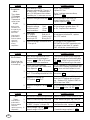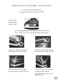
1
Safety Isolating
Transformer Models:
ISO XFR-75W
ISO XFR-100W
SERVICE MANUAL
Monitor Models:
1493
1793
1993
2093
2793
3693
2 YEAR LIMITED WARRANTY
This product is warranted by CERONIX to be free of defects in material
and workmanship for a period of two years from the date of purchase.
All parts and labor are free of charge during the warranty period.
This warranty does not cover mechanical breakage due to physical abuse.
It is the customer's responsibility for shipping the defective unit to and from
CERONIX or one of the authorized service centers for repair.
Please attach a note describing the problem.
CERONIX Inc.
13350 New Airport Road
Auburn, CA. 95602-7419
Phone: (530) 886-6400
FAX: (530) 888-1065
WEB: www.ceronix.com
CERONIX shall not be liable for any consequential damages, including
without limitation damages resulting from loss of use.
Ceronix will repair XX93 monitors after the 2 year warranty,
for a minimal charge, plus shipping to and from Ceronix.
®
Recognized under the Component Program of Underwriters Laboratories Inc., the
Canadian Standards Association, and TÜV Product Service.
Compliance to the following Standards:
IEC 60950, CAN/CSA-C22.2 No. 60950-00, ANSI/UL 60950, CAN/CSA-C22.2 No.
1-98, IEC 65:85 + A1:87 + A2:89 + A3:92.
ISO 9001:1994 Certified through TÜV Management Service.
COPYRIGHT © 2002
CERONIX
All rights reserved.
The information contained in this manual
is subject to change without prior notice.
ABOUT THIS MANUAL
This manual is specifically written to aid the service technician, repairing
CERONIX Models 1493, 1793, 1993, 2093, 2793, and 3693 color monitors.
There are three main sections:
1. General Description.
2. Circuit Description.
3. Repair Setup and Appendix.
Introduction
Installation
Instructions
Block
Diagram
Description
BLOCK
Diagram
Schematics Circuit
&
Description
Assembly
Drawings
Trouble
shooting
Handbook
Appendix
Convergence
Degaussing
P/O Form
PRAs
To understand how the Monitor works, it is best to know what each circuit
does and how each circuit relates to the other circuits. The Block Diagram is
presented in a simplified view and a comprehensive view to accomplish the goal of
understanding the whole unit. Once the general picture is clear, the complexity of
each circuit will be easier to understand.
The Circuit Description is also written in two views, a simplified view and a
detailed view to help give the reader a clear understanding of what each
component does. This understanding is most helpful for the more complex
problems or multiple problems that sometimes occur.
The power supply trouble shooting section describes methods used to power up
various monitor circuits, when there is a fault in the monitor, which disables the
power supply.
The appendix includes; filament voltage test, convergence procedure,
replacement parts purchase order form, degaussing coil attachment specification,
high pot test, wire routing drawing, production assembly drawings (PADs), C, I, J,
& K film resistor arrays and a parts list addendum. The parts list addendum is
used to add new information describing part changes. Tables, suitable for pasting
on these pages, will be published as new variations of the XX93 monitors are
produced.
i
TABLE OF CONTENTS
About This Manual............................................................................................................. i
Table of Contents................................................................................................................ii-iii
CERONIX Monitor Simplified Block Diagram................................................................. 1
Installation Instructions; English, French, and German................................................ 2-4
CERONIX Monitor Electrical Specification...................................................................... 5-8
1493, 1793, 1993, 2093, 2793, and 3693 General Operation Description.
Video Interface, Amps & Beam Current Sense........ Blocks A-D............................... 9
Auto Bias, Bias Sync Delay, & Auto Bright............. Blocks E-G............................... 10
CRT, Blanking, Sync, & Vertical deflection............. Blocks H-L............................... 11
Horizontal Deflection & Remote............................... Blocks M-P.............................. 12
Horizontal Size & Power Supply............................... Blocks Q-T............................... 13
P/S, Safety Shutdown Circuits, Degaussing............. Blocks U-Z............................... 14
Monitor BLOCK DIAGRAM.............................................................................................. 15
Monitor Schematics and Assembly Drawings
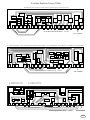
1493-CGA Main Board Schematic..(4233/4235)............................................................... 16
1493-CGA Main Board Technician Assembly Drawing................................................... 17
1493-VGA/SVGA Main Board Schematic..(4200/4252).................................................... 18
1493-VGA/SVGA Main Board Technician Assembly Drawing........................................ 19
1793-VGA Main Board Schematic..(4243/4244).............................................................. 20
1793-VGA Main Board Technician Assembly Drawing................................................... 21
1793-SVGA Main Board Schematic ..(4247/4250)............................................................ 22
1793-SVGA Main Board Technician Assembly Drawing................................................. 23
1993-VGA Main Board Schematic..(4221/4255)............................................................... 24
1993-VGA Main Board Technician Assembly Drawing................................................... 25
1993-SVGA Main Board Schematic..(4249/4256)............................................................. 26
1993-SVGA Main Board Technician Assembly Drawing................................................. 27
2093-CGA Main Board Schematic..(4112/4166)............................................................... 28
2093-CGA Main Board Technician Assembly Drawing................................................... 29
2093-VGA Main Board Schematic..(4224/4227/4108)...................................................... 30
2093-VGA Main Board Technician Assembly Drawing................................................... 31
2793-CGA Main Board Schematic..(4104)........................................................................ 32
2793-CGA Main Board Technician Assembly Drawing................................................... 33
2793-VGA Main Board Schematic..(4231)........................................................................ 34
2793-VGA Main Board Technician Assembly Drawing................................................... 35
2793-VGA Main Board Schematic..(4254)........................................................................ 36
2793-VGA Main Board Technician Assembly Drawing................................................... 37
3693-CGA Main Board Schematic..(4172)........................................................................ 38
3693-CGA Main Board Technician Assembly Drawing................................................... 39
Video Board Schematic...................................................................................................... 40
Video Board Technician Assembly Drawing..(Component Side)..................................... 41
Video Board Technician Assembly Drawing..(Conductor Side)....................................... 42
Safety Critical Components for XX93 Monitors..(English).............................................. 43
Safety Critical Components for XX93 Monitors..(German)..............................................44
Replacement Part List....................................................................................................... 45-63
Detailed Circuit Description
Video Interface Circuit, Function, Description (+ & - Analog)........................................ 64
5.6V to 1.1V, -Analog, DC, Video Interface Circuit Description...................................... 65
0V to .7V, +Analog, DC Video Interface Circuit Description........................................... 66
1Vp-p, +Analog, AC Video Interface Circuit Description................................................. 67
ii
TABLE OF CONTENTS
Video Amplifier Circuit, Function, Description.................................................................68
Video Amplifier Circuit Description and Schematic......................................................... 68-69
Video Board Power Supply and Arc Protect Schematic.................................................... 70
CRT Auto Bias and Auto Bright Circuit, Function, Description......................................71
CRT Auto Bias, Auto Bright, and Vertical Sync Delay Circuit Description....................72
CRT Auto Bias and Auto Bright Schematic...................................................................... 73
Monitor, Block Diagram Review........................................................................................ 74
Blanking, Master Gain, and Fault Circuit, Function, Description.................................. 75
Blanking, Master Gain, and Fault Circuit Description.................................................... 76
Blanking, Master Gain, Beam Limiter, and Fault Schematic......................................... 77
Vertical and Horizontal Sync Circuit Description.............................................................78
Vertical Deflection Circuit Description and Schematic.................................................... 79-81
Horizontal Deflection Circuit Description and Schematic................................................82-83
Horizontal Raster Width Control Circuit Description...................................................... 84
Horizontal Raster Width and Position Control Schematic............................................... 85
Dynamic Focus Circuit Function and Description............................................................ 86
Vertical Booster Amplifier Circuit and Description..........................................................87
Simplified Power Supply Circuit, Function, Description..................................................88-89
Switch Mode Power Supply Circuit Description and Schematic...................................... 90-91
Trouble Shooting and Repair
Equipment Setup for repairing the Model XX93 Monitor..(English)............................... 92
Equipment Setup for repairing the Model XX93 Monitor..(German).............................. 93
Power Supply Trouble Shooting Tips.................................................................................94
Trouble Shooting Handbook............................................................................................... 95-97
Filament Voltage Test..(English)....................................................................................... 98
Filament Voltage Test..(German)...................................................................................... 99
Setup and Convergence Procedure..(English)................................................................... 100
Setup and Convergence Procedure..(German)...................................................................101
Replacement Parts, Purchase Order Form........................................................................102
1493 Degaussing Coil Attachment Specification...............................................................103
1793, 1993, 2093 Degaussing Coil Attachment Specification...........................................104
2793, 3693 Degaussing Coil Attachment Specification.....................................................105
HighPot, for Shock Hazards, Circuit Description..(English)............................................ 106
HighPot, for Shock Hazards, Circuit Description..(German)........................................... 107
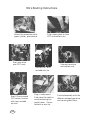
Wire Routing Instructions.................................................................................................. 108
Precision Resistor Arrays..(C, I, J).....................................................................................109
Precision Resistor Array..(K)..............................................................................................110
Precision Resistor Array..(Blue).........................................................................................111
Vertical Deflection Amplifier-Booster Technician Assembly Drawing............................ 112
Monitor Input Drive Signal Worksheet............................................................................. 113
Declaration of Conformity.................................................................................................. 114
ISO XFR-75W and ISO XFR-100W Safety Isolating Transformer.................................. 115
Circuit Description..(English).............................................................................................116
Auto Voltage Select Schematic and Assembly Drawing................................................... 117
Circuit Description..(German)............................................................................................118
Installation Instructions.....................................................................................................119-121
Specifications.......................................................................................................................122-123
Isolation Transformer Trouble shooting..(English)...........................................................124
Isolation Transformer Troubleshooting..(German)........................................................... 125
Manual Voltage Select Schematic and Assembly Drawing.............................................. 126
Part List Addendum........................................................................................................... 127-130
iii
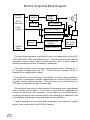
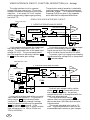
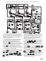
Monitor Simplified Block Diagram.
VIDEO
Output
VIDEO
Interface
Drive
Electronics
Blanking
SYNC
Output
VIDEO
Amps.
CRT
AUTO BIAS
Vertical Deflection
FBT
IB
Horizontal Deflection
Remote
Controls
Isolated
Power
Horizontal Size
Control
Fault &
High Temp.
Detection
POWER SUPPLY
This block diagram gives a broad view of the circuit organization of the 1493,
1793, 1993, 2093, 2793, and 3693 monitors. The blocks with the bold outline
represent circuits which provide these monitors with a wide range of
operating conditions without the need for adjustment.
The video interface circuit can be programmed to accept; +Analog AC or
DC coupled, -Analog, and 4 line TTL. The M. GAIN or contrast control is
located on the remote control board.
The auto bias circuit eliminates the need for the color setup procedure.
This circuit is designed to actively compensate for picture tube drift which
normally causes unbalanced color. The auto bias circuit also adjusts the
CRT gain to compensate for gain loss with age.
The horizontal size control circuit permits the horizontal size to be adjusted
from a remote control board. This circuit is also used to compensate for
pincushion distortion and blooming. Anti-blooming is accomplished by
correcting horizontal size variations which are caused by the additional load
on the flyback transformer under high beam current conditions.
Careful reading of all the information presented in this manual is a good
way to learn how to repair the CERONIX monitor.
1
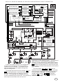
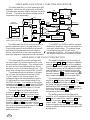
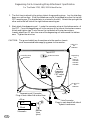
Installation Instructions For The XX93 Monitors.
1. A 3 amp slow blow fuse (for the degaussing current) and a 75 VA isolation
transformer are the minimum requirements for using our monitor in a product.
2. Unpack the monitor.
3. Install the monitor in the enclosure.
Refer to the installation instructions supplied
by the system manufacturer for details of
mounting the monitor in the enclosure.
4. Connect the green/yellow ground wire to the earth ground connection on the enclosure.
This wire is connected to the ground screw, located on the monitor chassis behind the
serial number label.
!
WARNING!
Failure to connect this ground wire before applying power is not
allowed, since this condition can produce a shock hazard. The
chassis to mains connector resistance shall not exceed 100mΩ.
5. Check that the following wires are properly connected;
Note;
A.
Green wire from the CRT aquadag braid to the video board.
B.
C.
12 conductor flat cable from the video board to the main board.
Red high voltage wire from the flyback transformer
to the picture tube anode cap.
D.
Yoke cable from the yoke to the main board.
E.
Remote cable from the remote control board to the main board.
Be sure these wires are secured such that they do not touch any metal parts.
6. Plug in the
seven conductor
video connector.
Pin
0
1
2
Signal
Color
+12V from monitor. White
Horizontal sync.
Yellow
Purple
Vertical sync.
3
4
5
6
Signal ground.
Red video.
Green video.
Blue video.
Gray
Red
Green
Blue
ISOLATION TRANSFORMER
7. Plug in the power connector
from the isolation transformer.
Mains
Power
3A-T
FUSE
75VA
GREEN / YELLOW WIRE
Attached to the
monitor chassis.
8. Apply power to the monitor and the drive electronics.
9. Check the focus and, if necessary, adjust the top control on the flyback transformer.
10.
Adjust the controls on the remote control board for proper;
Horizontal Raster Size.
Vertical Raster Size.
Vertical Raster Position.
Horizontal Picture Position.
Video Gain.
11.
For convergence instructions, see page 100 & 101.
2
Instructions d´installation des écrans XX93.
1. Un fusible á fusion lente de 3 amp (pour le courant du champ magnétique d´adjustement) et un
transformateur d´isolation de 75 VA sont le minimum requis pour utiliser nos écrans dans un produit.
2. Déballer l´écran.
3. Installer l´écran dans son carter. Se référer aux instructions d´installation foumies par le fabriquant
du systéme pour les détails de montage de l´écran dans le carter.
4. Relier le fil de terre vert/jaune á la prise de terre sur le carter. Ce cable est relié á la vis
de terre située sur le chassis de l´écran derriére l´étiquette portant le numéro de série.
!
ATTENTION!
Il n´est pas permis de ne pas relier ce fil de terre avant de mettre le courant, car
cette situation pourrait provoquer un choc électrique dangereux.
La résistance du chassis aux pricipales connections ne doit pas depasser 100mΩ.
5. Vérifier que les fils suivants sont correctement reliés:
A. Le fil vert de la tresse du tube cathodique aquadag á la carte video.
B. Le cable plat á 12 conducteurs de la carte vidéo á la carte principale.
C. Le cable rouge haut voltage du retout du transformateur au capuchon de
l´anode du tube cathodique.
D. Le fit de bobinage du bobinage á la carte principale.
E. Le fil de télécommande de la carte de la télécommande á la carte principale.
Note:
6.
Soyez sur que ces fils sont connectés en toute sécurité de sorte qu´ils ne
touchent aucune partie métallique.
Brancher les
sept fils de la
connection vidéo:
Broche
0
1
2
Signal
Couleur
+ 12V de l´écran
Synchro Horizontale
Synchro Verticale
Blanc
Jaune
Violet
3
4
5
6
Signal de terre
Rouge vidéo
Vert vidéo
Bleu vidéo
Gris
Rouge
Vert
Bleu
TRANSFORMATEUR D'ISOLATION
7.
Brancher les fils de courant
depuis le transformateur d'isolation:
Courant
Principaux
3A-T
FUSE
75VA
FIL VERT / JAUNE
Attasché au chassis
du moniteur.
8.
Amener le courant á l´écran et au disque électronique.
9.
Vérifier le foyer, et si nécessaire, régler le contróle sur le retour du transformateur.
10. Effectuer les réglages sur la carte de la commande á distance pour:
La taille du balayage horizontal.
La taille du balayage vertical.
La position du balayage fertical.
La position horizontale de l´image.
L´acquisition vidéo.
11. Pour les instructions de convergence, voir page 100 & 101.
3
Installationsanweisungen für die XX93 Monitore.
1. Ein 3 Ampère-T sicherung (für die degaussing-Strömung) und ein 75 VA Isoliertransformator
ist die Minimum-Forderung für benutzen unseren Monitoren in einem Produkt.
2. Packen Sie den Monitor aus.
3. Schließen Sie den Monitor
im Gehause an.
Für Details, Folgen Sie den Installation-Anweisungen,
Vom Lieferanten der Antriebelektronik.
4. Verbinden Sie den Grüne/Gelben Schutzleiter zum Erdung anschluß auf dem Gehause.
Dieser Draht ist verbunden zur der Erdung-Schraube auf dem Monitor-Chassis, und wird
hinter der Serien-Nummer-Aufschrift gefunden.
!
5.
WARNUNG!
Unterlassen dieser Verbindung dieses Erdung-Drahts ist
gesetze widrig. Der Widerßtand von diesem anschluß biz
zum netzstecker darf 100mΩ nicht überschreiten.
Prüfe daß die folgenden Drähte ordentlich verbunden sind;
A.
Grüne Draht vom CRT aquadag zum Video Schaltpult.
B.
12 Leiter-Flachkabel vom Videoschaltpult zum Hauptschaltpult.
C.
Rote hochspannungs Draht vom Flybacktransformator zur der Bildröhrenanode.
D.
Jochkabel vom Joch zum Hauptschaltpult.
E.
Fernsteuerung Kabel vom Fernsteuerungschaltpult zum Hauptschaltpult.
Notiz;
Seien Sie sicher diese Drähte sind so befestigt daß sie kein Metallteil berühren.
6. Stecken Sie den
7 Leiter-VideoVerbindungsstecker ein.
Leiter
0
1
2
Signal
Farbe
+12V Von Monitor.
Horizontal sync.
Vertical sync.
Weiß
Gelb
Purpur
3
4
5
6
Signal-Erdung.
Rotes Video.
Grünes Video.
Blaues Video.
Grau
Rot
Grün
Blau
ISOLIERTRANSFORMATOR
7.
Stecken Sie den Stecker vom
Isoliertransformator ein.
Netzstrom
3A-T
SICHERUNG
75VA
Grüne/Gelben Schutzleiter
Verbindung ist auf dam
Monitore chassis.
8. Schalten Sie den Monitor und die Steuerung an.
9. Prüfe Sie den Fokus und, wenn notwend, stell en Sie die obere Kontrolle ein auf dem
Flybacktransformator.
10. Stellen Sie die Kontrollen des Fernsteuerungsschaltung ein für richtige
- Horizontal Raster Größe.
- Vertical Raster Größe.
- Vertical Raster Position.
- Horizontal Bild Position.
- Video Kontrast.
11. Für Konvergenz-Anweisungen, auf seite 100 & 101.
4
CERONIX
XX93 Monitor Electrical Specification.
INPUTS
1. Standard Video Configurations, available, are:
Min.
Typ.
Max
.75V Black level
Video Saturated color
0.00V
0.75V
0.02V
0.77V
0.04V
0.79V
Black level
Saturated color
0.00V
1.00V
0.02V
1.02V
0.04V
1.04V
.75V Black level
Video Saturated color
Blk-.02V
Blank
Blk+.02V
A. Positive Analog, DC Coupled.
Video
Source
D-A
.6mA To Amp.
Video
75Ω
75Ω
Gnd
Monitor
B. Positive Analog, AC Coupled.
Video
Source
D-A
Zo=75Ω
75Ω
Video
10uA To Amp.
Amp.
Clamp
Gnd
Monitor
1.0V
Video
Blk+.73V Blk+.75V Blk+.77V
Blk-.02V Blk+0.00V Blk+.02V
1.0V Black level
Video Saturated color Blk+.98V Blk+1.00VBlk+1.02V
AC voltages are referenced to the R, G, & B
video input voltage during horizontal sync (Hs).
Blank is the black level voltage during Hs.
C. Negative Analog.
Video
Source
D-A
To Amp.
V Blk.+.7 V
Video
Gnd
R IN
Monitor
Red & Green Black level
Blue Black level
Saturated color
5.4V
5.6V
4.85V 5.05V
.7V
.9V
5.8V
5.25V
1.1V
D. 4 Line TTL also available.
R,G,B
Video
Video
Source
*
Intensity
To Amp.
BIAS
Gnd
+12V
VB
Monitor
Black level
Color on
Low intensity
Full intensity
0V
2.7V
0V
4.5V
* No pullup resistor on intensity line.
Note: RS170 and other voltage combinations optional for analog video.
5
.2V
3.5V
.2V
4.6V
.5V
6.0V
.4V
4.8V
CERONIX
XX93 Monitor Electrical Specification.
2. The Sync signals may be of either polarity and separate or composite.
Hs
1.8K
Model
Min.
Sync
Source
.15V
High input voltage 2.2V
Vs
1.8K
Low input voltage -2.7V
220 Ω, 2 PL
Gnd
Monitor
Horizontal sync pulse 1.5uS
For composite sync, vertical and horizontal
Vertical sync pulse 65uS
sync lines are connected together.
Horizontal frequencies: 15.5KHz
Custom horizontal frequencies from 15KHz
to 39KHz are available upon request.
Typ.
Max
3.5V
.30V
4.0uS
20V
.80V
12uS
.5mS
1.5mS
15.7KHz 15.9KHz
29.3KHz 29.6KHz 29.9KHz
31.2KHz 31.5KHz 31.8KHz
34.9KHz 35.2KHz 35.6KHz
37.5KHz 37.9KHz 38.3KHz
Vertical frequencies:
45Hz
51Hz
55Hz
65Hz
50Hz
56Hz
60Hz
70Hz
55Hz
61Hz
65Hz
75Hz
3. The Power to the monitor is to be supplied by a secondary winding of an
isolation transformer.
Model 1493
Model 1793
Model 1993
Min.
Min.
Min.
Max.
120VAC 50Hz or 60Hz 90VAC 145VAC
Max.
90VAC 145VAC
90VAC
Max.
145VAC
230VAC 50HZ or 60Hz 180VAC 290VAC 180VAC 290VAC 180VAC 290VAC
60W
45W
75W
35W
40W
70W
Power
Model 2093
Min.
Max.
120VAC 50Hz or 60Hz 90VAC 145VAC
Model 2793
Min.
Max.
90VAC 145VAC
Model 3693
Min.
Max.
90VAC
145VAC
230VAC 50HZ or 60Hz 180VAC 290VAC 180VAC 290VAC 180VAC 290VAC
100W
50W
100W
45W
75W
50W
Power
6
CERONIX
XX93 Monitor Electrical Specification.
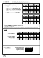
4. Five Controls are located on
a separate PCB for easy access.
H SIZE--------------Horizontal raster size
V SIZE---------------Vertical raster size
V RAS. POS.-----Vertical raster position
H POS-------Horizontal picture position
M GAIN---------------------Master gain
Model 1493
Min. Max.
Model 1793
Min. Max.
Model 1993
Min. Max.
10.1" 11.1"
7.3" 8.3"
.50"
0"
11.9" 12.9"
8.6" 9.6"
.50"
0"
13.4" 14.4"
9.8" 10.8"
.50"
0"
1" Right
1" Left
1" Right 1" Left
1" Right 1" Left
0mA
.75mA
0mA
.75mA
0mA
.75mA
Model 2093
Min. Max.
Model 2793
Min. Max.
Model 3693
Min. Max.
14.9" 15.9"
10.9" 11.9"
.60"
0"
20.4" 21.4"
15.1" 16.1"
1.0"
0"
27.4" 28.4"
20.3" 21.3"
1" Right
1" Left
1" Right
1" Left
1" Right 1" Left
0mA
.75mA
0mA
1.5mA
0"
0mA
1.0"
1.5mA
The board Controls are located on the main PCB:
Focus and G2 on the FBT.
Optional board Controls are: pincushion, video black level, and horizontal hold control.
5.
6.
Image
Color Temperature
1493
9300°K
17/19/2093
9300°K
2793
9300°K
3693
9300°K
Horizontal linearity
Vertical linearity
Pincushion
Min. Max.
-2% +2%
-2% +2%
-2% +2%
Min. Max.
-5% +5%
-5% +5%
-3% +3%
Min. Max.
-8% +8%
-8% +8%
-5% +5%
Min. Max.
-10% +10%
-10% +10%
-8% +8%
Environmental
7
Operating temperature
Storage temperature
Operating humidity
Storage humidity
0° C
-20° C
20%
10%
70° C
85° C
80%
95%
CERONIX
7.
Picture tube
Useful diagonal
XX93 Monitor Electrical Specification.
1493-CGA/VGA/SVGA
Inch
13.2
11.1
8.3
mm
335
281
211
1793-VGA/SVGA
Inch
16
12.9
9.7
mm
407
328
246
1793-SVGA
Inch
16.1
12.9
9.6
mm
409
328
245
1993-VGA/SVGA
Inch
18
14.4
10.8
mm
457
366
274
Useful horizontal
Useful vertical
Useful area 92.1 in2 593 cm2 125 in2 807 cm 2 124 in2 804 cm 2
Spacing of dot/line trios .0110" .28mm .0106" .27mm .0098" .25mm
Phosphor Trio Type
Dot
Dot
Dot
Deflection angle
90°
90°
90°
165 in2 1,003 cm2
.0102" .26mm
Light transmission
Approximately
CRT surface
Phosphor
Useful diagonal
57% Approximately 53%
Polished/Curved Polished/Curved
Approximately
Approximately
50%
AR / Flat
45%
AR / Curved
P22
P22
P22
P22
2093-CGA
Inch
mm
18.9
480
15.9
404
11.9
303
2093-VGA
Inch
mm
18.9
480
15.9
404
11.9
303
2793-CGA
Inch
mm
26.8
679
21.4
544
16.1
408
2793-VGA
Useful horizontal
Useful vertical
Useful area 189 in2 1,224 cm2 189 in2 1,224 cm2 345 in2 2,220 cm2
Spacing of dot/line trios .0331" .84mm .0307" .78mm .0326" .83mm
Phosphor Trio Type
Line
Line
Line
Deflection angle
90°
90°
110°
Light transmission Approximately 40% Approximately 40% Approximately 38%
CRT surface Polished/Curved Polished/Curved Polished/Curved
Phosphor
P22
P22
P22
2793-VGA
Inch
mm
Useful diagonal
Dot
100°
26.6
21.3
16.0
676
541
406
Inch
26.8
21.4
16.1
mm
679
544
408
2
345 in
.0326"
2,220 cm
.83mm
Line
110°
38%
Polished/Curved
P22
Approximately
3693-CGA
Inch
mm
35.5
28.4
21.3
902
721
541
Useful horizontal
Useful vertical
Useful area 341 in2 2,196 cm2 605 in2 3,901 cm2
Spacing of dot/line trios .0299" .76mm .0394"
1mm
Phosphor Trio Type Line / Variable
Line
Deflection angle
110°
111°
Light transmission
CRT surface
Phosphor
81% Approximately 32%
Polished/Flat
Polished/Curved
P22
P22
Approximately
8
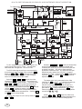
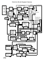
Refer to the block diagram on page 15 (foldout) when reading this description.
A
The Video Interface is designed around a custom IC and will accept DC or AC
coupled positive analog video signals. It can also be used with negative analog
and 4 line TTL. This IC has a built in multiplier circuit for the master gain
control and blanking functions. Resistors are used to protect the IC and to set
the gain. The programmed gain is dependent on the input signal amplitude
except with the TTL mode. Solder jumpers and component substations are used
to program the Video Interface for the type of input signal to be received. The
output of the IC drives the video amplifiers. This drive is a current where 0 mA
is black and 10 mA is a saturated color.
B
The Video Amplifiers are of the push pull type. They are built partly on thick
films and partly on the video PCB. Spreading out the amplifier reduces the
component heat and improves the life of the unit. The bandwidth is 25 MHz with
40Vp-p output. The rise and fall times are 20nS.
C
The Beam Current Feedback circuit directs most of the beam current of each
amplifier to the beam current buffer. The only time this current is measured, by
the auto bias circuit, is during the time of the three faint lines at the top of the
screen and three lines thereafter. The CRT auto bias circuit is designed to adjust
the video amplifier bias voltage such that the beam current of each of the three
guns is set to a specific programmed value.
D
The Beam Current Buffer converts the, high impedance low current, beam
current signal into a low impedance voltage. This voltage is applied to the auto
bias IC through a 200 ohm resistor. After the three lines of beam current are
measured, the program pulse from the auto bias IC, produces a voltage drop
across this 200 ohm resistor that equals the amplitude of the beam current
voltage.
9
E
The CRT Auto Bias IC is a combination of digital and analog circuitry. The
digital part is a counter and control logic which steps the analog circuits through a
sequence of sample and hold conditions. The analog part uses a transconductance
amplifier to control the voltage on a 10uF capacitor (one per gun). This voltage is
buffered and sent to the video amplifiers as the bias voltage. In monitors without
CRT auto bias, this voltage is adjusted manually using a setup procedure to set
the color balance. With CRT auto bias, the color balance is set during the end of
each vertical blanking time.
The control sequence is:
1.
The cycle starts with a sync pulse from the vertical oscillator (15KHz)
or from the vertical sync delay. 15H later the grid pulse starts.
2.
The grid pulse on G1 causes cathode current which can be seen as the
three faint white lines at the top of the screen. This cathode current is
transmitted by the beam current feedback to the beam current buffer
where it is converted to a voltage and applied to the CRT auto bias
input pin. At this time the CRT auto bias IC outputs a reference
voltage at its input pin which sets the voltage across the coupling
capacitor. This coupling capacitor voltage is directly dependent on
beam current.
3.
After the grid pulse is over, the program pulse matches the voltage
from the beam current buffer. If the voltage from the beam current
buffer, during the grid pulse, is the same as the voltage from the
program pulse, the bias is correct and no bias adjustment is made for
that vertical cycle.
F
The timing of the auto bias IC is synchronized to the vertical oscillator and the
flyback pulses. For horizontal frequencies higher than 15.7KHz a Vertical Sync
Delay may be needed to position the grid pulse, generated 3 gray lines, at the top
of the screen. The need for the delay circuit is dependent on the particular CRT
vertical retrace time.
G
The aging of the picture tube (CRT) not only affects the balance of the cathode
cutoff voltage, which is corrected by the auto bias circuit, but it also affects the
gain of the CRT. The Auto Bright circuit actively corrects for CRT gain changes
by sensing any common bias voltage change, from the auto bias circuit, and
adjusts the screen voltage to hold the average bias voltage constant. The lower
adjustment on the flyback transformer which is the screen voltage, is used to set
the auto bright voltage to the center of its range. Therefore, the auto bright
circuits sets up a second control feedback loop to reduce picture variation due to
CRT aging. The auto bright circuit is also used to turn off the beam current when
the monitor power is turned off.
10
H
The CRT for the 1493, 1793 and 2093 monitors have a 90° deflection angle. The
1993 incorporates 100° while the 2793 CRT has 110° and the 3693 has 111°
deflection angles. These picture tubes have integral implosion protection and a
EHT of 25KV.
H1
The Vertical Dynamic Focus amplifies the parabolic waveform across the
vertical coupling capacitor from about 3Vp-p to about 200Vp-p, depending on CRT
requirements. This waveform sharpens the top and bottom portion of the raster
on dual focus CRT's.
H2
The Horizontal Dynamic Focus amplifies the parabolic waveform across the
horizontal coupling capacitor, using a transformer to produce 300Vp-p output from
an input that is about 33Vp-p. This waveform is added to the vertical dynamic
waveform and sharpens the right and left sides of the raster.
I
Blanking is accomplished by setting the gain of the interface IC to zero during
blank time. The Horizontal Blanking pulse is generated by amplifying the flyback
pulse. The Vertical Blanking pulse is started by the vertical oscillator one shot
and ended by the counter in the auto bias IC via the "bias out" pulse. The Master
Gain control, located on the remote PCB, sets the gain of the video signal when
blanking is not active. The Beam Current Limiter circuit, which is designed to
keep the FBT from overloading, will reduce the video gain if the maximum
average beam current is exceeded. Also, the beam current is reduced if the FBT
approaches maximum operating temperature.
J
The Sync Interface can accept separate or composite sync. Two comparators are
used to receive sync, one for vertical sync and the other for horizontal sync.
Resistor dividers are used to protect the comparator IC from over voltage damage.
For customers who do not require interlace, an additional vertical sync
stabilization circuit is included. This circuit synchronizes the vertical sync to the
horizontal cycle.
K
The Vertical Oscillator generates the vertical free running frequency when no
vertical sync is present. When sync is applied, the vertical oscillator synchronizes
to the leading edge of the sync pulse.
L
The Vertical Control & Output circuit consists of:
1.
2.
3.
4.
11
One shot.
Ramp generator.
Vertical drive.
Vertical output.
The sync pulse from the LA7851 triggers a one shot in the LA7838 which clamps
the vertical ramp generation capacitor to 5V during the first half of vertical
retrace. The ramp generation capacitor then charges via a constant current set by
an external resistor. This resistor is connected to the V SIZE pot, located on the
remote control board, for the vertical size adjustment. The vertical drive is a
differential amplifier which compares the ramp voltage to the yoke return
feedback current. The yoke feedback current and voltage circuits are used to set
the vertical linearity. The vertical Output is a power driver, with thermal
protection, which drives the vertical deflection yoke. It also has a special pump up
circuit which doubles the output voltage during vertical retrace. This voltage
doubler also increases the efficiency of the circuit since the high retrace voltage is
not present across the power driver during the trace time.
M
The Horizontal Control incorporates a variable sync delay and a phase locked
loop to generate the horizontal timing. The H POS. adjustment, on the remote
control board, sets the sync delay time which controls the picture position. The
phase locked loop uses the flyback pulse to generate a sawtooth wave which is
gated with the delayed sync pulse to control the horizontal oscillator.
N
The Horizontal Driver supplies the high base current necessary to drive the
horizontal output transistor which has a beta as low as three. A transformer is
used to step up the current from the driver circuit and also protects the horizontal
output transistor from a continuous turned on state. A special clamp circuit is
connected to the transformer which reduces the turnoff time of the horizontal
output transistor for reduced power dissipation.
O
The Horizontal Output transistor is mounted to the rear frame which acts as a
heat sink. The collector conducts the 900 volt primary flyback pulses which should
not be measured unless the equipment is specifically designed to withstand this
type of stress. A linear ramp current is produced in the horizontal yoke by the
conduction of the horizontal output transistor (trace time). A fast current reversal
(retrace time) is achieved by the high voltage pulse that follows the turn off of the
horizontal output transistor. This pulse is due to the inductive action of the yoke
and flyback transformer.
P
The main function of the Flyback Transformer (FBT) is to generate a 25,000 volt
(EHT) potential for the anode of the picture tube. This voltage times the beam
current is the power that lights up the phosphor on the face of the picture tube.
At 1.5mA beam current, for the 2793 monitor, the FBT is producing almost 38
watts of high voltage power. The FBT also sources the focus voltage, screen grid
voltage, filament power, and has two more secondaries which are used for control
functions. The FBT has a built in high voltage load resistor which stabilizes the
EHT, for the low beam current condition. This resistor also discharges the EHT,
when the monitor is turned off, which improves the safety of handling the
monitor.
12
Q
The Remote Control PCB houses the:
CONTROL
1.
2.
3.
4.
5.
DESCRIPTION
CIRCUIT
H SIZE ----------- Horizontal raster size --------- Diode modulator
V SIZE ----------- Vertical raster size ------------- Vertical control
V RAS. POS. --- Vertical raster position ------- DC current to V. yoke
H POS ------------ Horizontal picture position -- H. sync delay
M GAIN ---------- Master gain ---------------------- Video interface
R
The Horizontal Size Control circuit has four inputs:
#
1.
2.
3.
4.
SIGNAL
FUNCTION
Horizontal size ------------------------------ Horizontal size control
Beam current -------------------------------- Blooming control
Vertical linear ramp ----------------------(#4)-(#3)=Vertical parabolic
Vertical parabolic + V. linear ramp --(Pincushion)
}
The horizontal size control circuit sums the four signals at one node plus the
feedback from the diode modulator to drive a switching mode power driver. The
output of the power driver is then connected to the diode modulator through an
inductor to complete the control loop.
S
The Diode Modulator is a series element of the horizontal tuned circuit. It forms
a node between GND and the normal yoke return circuit. If this node is shorted to
GND, the result is maximum horizontal size. Forward current in the diode
modulator, at the start of retrace, keeps the node voltage clamped to ground until
enough current flows from the horizontal tuned circuit to exceed this forward
current. The horizontal size, therefore, is controlled by controlling the current to
this diode via the horizontal size control circuit.
T
A Voltage Doubler is used in the power supply for two reasons:
1. To improve the efficiency of the power supply.
2. To permit 120 volt and 230 volt operation. For the 230 volt
operation the voltage doubler is replaced with a bridge rectifier.
13
XX93 Monitor Block Diagram.
U
The Switching Regulator is synchronized to the horizontal pulse and drives a power
MOSFET. Unlike most regulators that have a common GND, this power supply has a common
V+ and current is supplied from V- to GND. The MOSFET is connected to V– and signal
ground (GND) through a transformer which is used as an inductor for series switch mode
regulation. An operational amplifier, voltage reference, comparator, and oscillator in the power
supply controller IC are used to accomplished regulation by means of pulse width modulation.
The transformer has two taps on the main winding which are used to generate the +16 volt
and +24 volt supplies. It also has a secondary which is referenced to V- and supplies the power
supply. Since the power supply is generating its own power, a special start up circuit is built
into the power supply controller IC that delays start up until the capacitor which supplies the
IC is charged up enough to furnish the current to start the power supply. This capacitor is
charged with current through a high value resistor from the raw dc supply. This self sustaining
action is why the power supply chirps when an overload or underload occurs. Additional
secondaries to drive the horizontal raster shift circuit and the video amplifiers are also included
in the power transformer.
GAME
VIDEO
3
VIDEO
AMPS.
3
Interface
F.B.P.
V retrace
Beam limit
M. gain
High temp. limit
I
SYNC
Interface
J
G
H DY
3
D
Beam current
buffer
CRT AUTO
BIAS IC
Program pulse
Grid pulse
Dynamic Focus
used only on Dual
Focus CRTs
E
Horizontal
Dynamic
Focus
H2
VERTICAL
CONTROL &
OUTPUT
VERTICAL
OSCILLATOR
LA7851
LA7838
I. V. Feedback
K
L
+
W
G2
A +12V regulator is used to supply current, to all the control circuits in the monitor, with the
exception of the power supply. Many of the control circuits are decoupled from the +12 volt line
with a resistor or diode to minimize noise from common current loops.
LA7851
HORIZONTAL
CONTROL
Hs
Sync delay
H.
Output
N
FBT
2
O
P
PINCUSHION
V. Size &
V. Ras. Pos.
The Over Voltage Protect circuit is built into the power supply and monitors the flyback
transformer peak pulse voltage. This circuit will turn off the power supply and hold it off if the
EHT exceeds its maximum rated value. Since excessive X-ray output occurs with excessive
EHT, this circuit provides X-ray protection.
H.
Driver
V+
Vertical
Dynamic
EHT Focus
H1
M
H. Pos.
X
EHT≈25KV
F
2
Vs
H
VDY
Auto
Bright
H. sync (FBP)
V. sync
CA3224E
CRT
Feedback
C
3
VERTICAL
SYNC
DELAY
3
Current
B
3
3
BLANKING
Beam
3
Bias
A
SYNC
V. & H.
The Load consists primarily of the horizontal flyback circuit. The power supply will not
operate without the load since the voltage that sustains the power supply comes from a
secondary in the power transformer and depends on some primary current to generate
secondary current.
2 For Dual Focus
G1≈–20V
VIDEO
RGB
V
G2≈290V
On Video Board.
REMOTE
CONTROLS
(PCB)
DIODE
HORIZONTAL
Size Control
Q
Modulator
R
S
Beam Current
Y
+52V to +129V
The Fault Detector senses beam current and temperature. This circuit will activate the
power supply shutdown circuit if either the maximum temperature is sensed or if the beam
current becomes large enough to threaten the FBT.
ISOLATION
Transformer
Z
(IN GAME)
The Degaussing circuit is connected across the isolated AC line. A posistor is used to allow a
large current to flow, in the degaussing coil, on power up. This current is then gradually
reduced by the increased temperature of the positive temperature coefficient thermistor in the
posistor. A relay is used to short the degaussing coil after the degaussing operation. This
greatly reduces posistor residual current in the degaussing coil. When repairing a monitor, the
degaussing coil should be unplugged, to avoid possible damage to the degaussing coil shorting
relay.
VOLTAGE
DOUBLER
Raw DC
320V
T
V-
LOAD
-200V
(VIDEO & DEFLECTION)
+12V
+12V
SWITCHING +16V
Regulator
REGULATOR +24-27V
Shutdown
DEGAUSSING
CIRCUIT
Z
14
+24V
FAULT
DETECTOR
Y
V
Sync U
OVER
VOLTAGE
PROTECT
X
W
Vertical Deflection
Supply
FBP
15
Product safety note:
RCA
A48AAB37X01
Components marked by the
When replacing any of
CRT
HEAT
SINK
378
Vertical
Deflection
HORIZONTAL
BLANKING
4
4.5-5.3V Vs
5Vpp 16,E5
.047uF
077
OUT
.047uF
078
295
0Ω
220uF
0VDC Hs
56Vpp 63,D6
8
I4
S
1.62KΩ
U
220uF
244
361
1.21KΩ
086
5
258
+12V
FDH400
213
17
DELAYED
SYNC O/S
064
1K
3
7.3-8.7V Hs
4Vpp 02,D6
7.3-8.7V Vs
-.2VDC Hs
4Vpp 03,D6 1.5Vpp 04,E6
4
228
6
R IN
2
Controls
RR
1
3
- A BL
5
TTL
8.8K
I3
I12
9
1nF
351
25K
330pF
I5
6,10
350
GND
12V
M GAIN
VC
75Ω
267
066
0
D
1N4148
BIN
7
15
065
B5
233
264
NC
112
353
358
360
0Ω
114A
0Ω
GND
Synchronized
Vertical sync
disabled.
150
356
6
JD
+2.9V 3
J16
277
270
1N4148
M & N reverse Hs.
0Ω
0Ω
0Ω
281
280
283
M
325
270Ω
0Ω
286
288
328
284
1.8K
N
326
M
270Ω
330
331
5
N
88K
5 +
6
AA
GND
VC
3
CPS G
1781 VC
GREEN
292 5
INPUT
BB
B
BLUE VC
INPUT 6
Vs
VERTICAL VC
SYNC 2
CC
1/4
LM339
7 +
.14-.16V
1
355
254
2.2nF
+24V
470Ω, 1/2W
470 CC
155
Inrush Current Limit
3.3nF
56pF
108
107
17
2.15K
I15
I16
6.8nF I10 + 1600Hz +800Hz
ID
250V
175
GND
IC
100uF
+
118
1N4937
1N4937
121
122
0Ω
0Ω
167A
198A
220uF
250V
163
156
5
1
INPUT
14.8-18VDC
+15V 16
1N4007 30Ω
+17V 15
INPUT
4
INPUT
Over
COMP. Voltage 14
Protect }
INPUT
62K
143A
CONTROL &
FAULT SENSE
9
5.7-6.3VDC
33.2K
J7
36K
3-4VDC
3Vpp 47,D2
143B
0Ω
114
6.8nF
4uS
DELAY
6 Rx
Osc.
7 Cx
102
7 8,14
3A Fuse
220uF
146
128
COMP.
+
3-5VDC
5Vpp 52,F1
12
13
0.1VDC
1Vpp 51,F1
OUTPUT
Current
SENSE
DRIVE
3-6VDC
115
1.00M
J10
134
17
15.8K
J11
11
J12
J8
1-4VDC
12Vpp 50,E2
135
136
10
.093" pin
162A
18Ω
133
137
D
131
FF
GG
II
JJ
KK
S1
447
3
24.3K
044
20K
043
+ 100uF
0Ω
12.1K
061
136A
5
041
12.1K
2.15K
3.3K
042
052
6
8
058
7
10K
049
055
4
.01uF
10.0K
047
095
3
056
2-2.5VDC Hs
4.4Vpp 39,B3
HER205 HER205
458
0Ω
477
478
.022uF
630V
.10Ω
.10Ω
437
1W
475
1W
476
7
.022uF
630V
439
IRF520
057
442
250V
443
454
0Ω
510Ω
094
461
6.8nF
1.6KV
441
0.33uF
457
060
6.8K
6
.001uF
432
50uH
2.7K
049
438
200pF
CPT1504
4-19VDC Hs
27Vpp 36,J7
462
1
1/2
LM392
440
FR205
1/2W
428
.012uF
1.6KV
030
2
FR205
1KΩ
4VDC 20VDC Hs
30Vpp 200Vpp 35,H7
Max. Min. H Size
1N4937
1/2
LM392
045
CPT
1506
431
5.6-6.2VDC Vs
1-1.7V 34,B2
096
5
445
H. Linearity
coil
15.8K
Blooming
correction.
44.2K
1nF
500V
463
470 Ω
460
0.8-7VDC Hs
12Vpp 38,J7
4VDC 20VDC Vs
11Vpp 15Vpp 37,I6
Max. Min. H Size
GND
1/2W
464
8
2.7uF 100V
456
GND
GND
HORIZONTAL WIDTH DRIVE
LEGEND
0Ω
0Ω
177
176
No
.
LTR.No
.X
V-
CAUTION! POWER SUPPLY VOLTAGES REFERENCED FROM V-.
SCOPE GND MUST NOT BE CONNECTED TO GND AND V- AT THE SAME TIME.
HH
053
Correction
054
430
-Linear
Pincushion
Correction
GND
28V
HS +12V
V-
129
423
446
H. Linearity
coil
CPT
1506
3.3K
GND
140
100pF
SL
107V or 127VDC Hs
120Vpp 250Vpp 32,F6
Max. Min. H Size
033
28.0K
47Ω
1/2W, CC
0VDC Hs
27Vpp 57,F1
PC 120VAC PC
2 INPUT 1
10
050
.01uF
YC3
8
1/4
LM324
5.6-6.2VDC Vs
2-3.6Vpp 33,B2
033
010
TP49, G1
127
145
161
33K
138
1N4007
116
MPSA64
111
13
CPT1538
12mH
YC4
051
9
097
200pF
1KV
0.33Ω
2W
7
1/4
LM324
6
.1uF
H SIZE
12 510Ω
J PRA PINS: 3,10,15, & 19
009
18
14.7K
S2
HORIZONTAL YOKE
10.0K
3.3K
No DVM
300Vpp 40,G1
HEAT
SINK
188
424
510Ω
GND
6V
+28V
CPQ1304
195
008
031
5
038
125
1.00M
029
Parabolic
Pincushion
130
J9
20
2,200pF
V-
3,300pF
0Ω
4
10.0K
040
142
38.3K
V-
10.0K
200K
1N4148
126
005
0Ω
10K
I BEAM
16
200K
109
2.15K
191K
.1uF
123
-200V
.33uF
FR205
533
4.7Ω
100uF
25V
6V
166
5.5-6.8VDC
8 +7.5V REF. V- 9
XRC5184 J PRA
J6
12
124
.1-.5VDC
5
141
18Vz
149
S4
100uF
200K
194
1N4937
10 0Ω
1N4746
2
+
168
1N4937 9
139
132
2
3
3
H. S. +12V
082
6
3
4
SR
HORIZONTAL WIDTH CONTROL
450
8
425
270Ω
011
1 CPT1536
+127V
150Ω 1/2W
Excessive Beam
+ 035
Current, Monitor Shut
Down Circuit.
0Ω
019
1/4
1 22K
2SA
LM324
017
1371
033
1,000uF
GND
Horizontal Raster Adj.
026
+6V 12.1K
170
171
427
GND
037
+121V
+1,000uF 1,000uF 169
+
15.8K High Temperature Or
1N4937
+18V
VERTICAL
DEFLECTION
YOKE
YC2
1/2W
394
021
033
11
023
IB
1N4937
100Ω
14 510Ω
1/4
LM324
10.0K
+400Hz
16
158
.093" pins
Degaussing
Connector
162
12
+128V
+112V
GND
200pF
Black Wire.
022
2
426
0Ω
185
+112V
4
034
+128V
Output
90K
CPR0434
10.0K
I BEAM 62K
+112V
3.4-4.2VDC
FR205
159
25Ω@25˚C, 2A
Relay
200V.5A
468
EE
250V
144
152
12
Hs
VC HORIZONTAL
1 SYNC
DD
318
2
355
.5-.8VDC
J4
8.06K
105
3.92K
106
0Ω
1/4
LM339
327
GND
47nF
322
CC3
GND
0Ω
6.8K
3
120
ERROR
6.5-7.5VDC
104
220uF
323
4
345
I PRA
+ 100uF
56pF
22K
270Ω
R
346
9.31K
+127V
AMP.
J3
273
+12V
VC RED
4 INPUT
.01uF
344
23.2K
257
1.8K
13
H.Fo ADJ. 170Ω
680Ω 340Ω I14
2
J2
1.8K
274
8
H. V+
10
+6V
I BEAM
JE
BZT03-D160
181 160Vz
4
268
276
J18
110
+1.4V
J15
2
REV.
301Ω
GND
9
1uF
I9
191
524
&
525
GND
YC1
4.7Ω
+128V
0Ω
419E
189
+6V
FBP
GND
20
6.5-7.5VDC
41,D1
JC
130Ω
148
CC1
1N4148
Posistor
REV.
I8
15
420
0 TO 7 VDC
1
FIL.
453
Open
419B
22K
RAS. POS.
H. S. +12V
5-6VDC Hs
7Vpp 09,E6
1K
V
415
416
1,000pF
J5
FR205
INTERLACE
272
CC2
235
1N4148
13
I7
14
2SC3467
192
0Ω
9
220uF
10.6K
2.2nF
3.92K
+ 259
PN2222
REV.
271
+
33K
16.3-19VDC 55, E1
260Ω
3.3nF
10
355
10uF
275
28
357
11
+12V
266
8
113
0Ω
1/4
LM339
13
246
221
232
0Ω
278
348
101.6K
4.67K
11K
236
18
6.8nF
J14
15.8K
8
355
1K
231
242
218
10K
347
I6
2SA1371E
1
1/4
LM339
14
0Ω
7
301Ω
+ 1uF
FBP
+
L
243
223
226
3-7VDC Hs 5.5-6.3V Hs
.2Vpp 07,E6 3.6Vpp 08,E6
419F
comp.
HORIZONTAL
OSCILLATOR DISCHARGE
7
J1
GND
+ 9
BR
8
3
2
1
Open
3-5Vpp 31,F5
0Ω
193
-
2.4-3.4VDC
0Vpp 06,E6
45K
1
JB -2.8V
-1.4V
91.4K J13
100kΩ@25˚C
T 180
A5
K
225
JA
2.33K
1.5-2VDC 60,D6
J
7-10VDC
61, C2
+12V
364
A5
+
6
V+
018
Beam Current
Limiter Circuit.
1K
4
419A
0Ω
11
X-RAY
PROTECT
3-4VDC Hs
1.4Vpp 05,E6
I13
100K
GND 4
GR
12
+6V
I BEAM
CPR0432
+ 100uF
417
173
241
XRC5346A
GIN
14
12
13
5
6.8K
15.8K
020
071
10
+12V
14
GND
LA7851
MULTIPLIER
BIAS
3.92K
Video V+
014
036
239
+A EN
15
10uF
MPSA64
CPQ1322
293
7
5
0Ω
421
449
336
11
H. S. +12V
PN2222A
0Ω
418
5.4-6VDC
11, E5
V Ref.
SAW TOOTH
TR . GENERATOR
+6V
I BEAM
+
012
SCREEN
CPT1544
390Ω, 2W 12-18VDC Vs
1,000uF
35V
+
10.8-12V
10, E6
3.92K
FBP
GND
+12V
GND
11.5-12.5V
261
11
16
VERTICAL
OSC. O/S
VERTICAL
OSCILLATOR
.4VDC Hs
.7Vpp 12,E5
15.8K
408
FBP
GND
+18V
G
16 13 9 6
Ro Go Bo
BBL
4.5-5.3V Vs
5Vpp 16,E5
ADJ.
063
+127V
0Ω
P
370
414
.1-.3VCD Vs
3.8Vpp 17,E5
100K
4-7VDC Vs
5-9Vpp 62,B4
245
V-
466
VRP
363
2
GND
18Ω
076
604Ω 1.21KΩ
260
404
22K
.01uF
18
Hs
IA
22K
334
1.62KΩ
084
FDH400
OPEN
405
12-18VDC Vs
50Vpp 29,F6
4-6VDC Vs
V
V. osc. 2.8Vpp 18,D5
VIDEO GAIN LINE
FDH400
407
8
GND
1N4148
44.2K
406
.1uF
H. +12V
T
1N4148
396
330pF
7
I2
080
GND
1
2.7K
2
1.8K
Vs
362
VERT.
OSC.
PICTURE
Horizontal
POSITION
O/S
SYNC INPUT
202
17 5
7.3VDC Hs
5.5Vpp 01,D6
365K
127K
410
VERTICAL
± SYNC INPUT
V+
333
I1
391
19
VERTICAL
367
12K
352
5.5-6.5V Vs
1.2Vpp 19,D5
or
11-12.4V
20, D5
GND
3
1uF
388
2.2M
.1uF
18Ω
298
329
093
081
1N4937
072
RC1
IN
56pF
127K
385
20
252
270Ω
4.7Ω
FOCUS
452
434
+12V
GND
100uF
+
RC4
GND 296 +
Hs 12.1K
390
GND
7812
100uF
100K
392
+12V
GND
376
304
207
GND
+
1.8K
4.42K
9
0Ω
1N4007
+12V
368
1.2Ω, 1W
Vs
0Ω
067
1.8K
3
208
248
PN2222A (CPQ1322)
2.15K
4
1K
1.8K
OPEN
+
0Ω
+18V
2.32.7V
393
401
VFB
1/2
LM393
1
210
4-7VDC Hs
4-9Vpp 61,B4
2
1uF
435
1.2Ω
GND
VFB
210
8
374
465
0Ω
1N4007
343
340
V HYP
253
+5
211
402
3
4
2,200pF 1
200Ω 2W
+28V
373
1/2W
NC 6
433
I11
20
RC7
PCB 490
2-3VDC Vs
4Vpp 64,C4
PN2222
332
EHT
470Ω
2SC5690
100Ω
337
+6V
212
0Ω
PN2222
2
19
338
INCREASES
TOP AND
BOTTOM
VERT. SIZE.
FLYBACK
TRANSFORMER
10
397
1K
062
372
+6V
3
251
1N4148
1/2
LM393
7
250
382
200K
371
CPT1505
2SC
4159
+ 100uF
H
200K
NO DVM Hs
.9KVpp 27,G6
12-18VDC Hs Horizontal Drive
33Vpp 26,E7 Transformer
342
H SIZE
6
PN2907A
6.8K
395
380
1.5-2.7V Vs
24Vpp 24,E4
68.1KΩ
GND
Remote Control
1K
6.8K
44.2K
369
485 GND
VERTICAL BLANKING
0Ω
1N4007
341
D5
411
.01uF
+12V
Retrace Boost
+12V
100pF
470uF
127K
Master
Gain
RC2
D5
398
422
1N4007
409
I
13
2.2K.5W
I BEAM
+6V
GND
12
0Ω
I BEAM
209
11
0
0Ω
196
413
PS FBP
V-
10
384
100uF
100A
10
092
EHT
092A
H SIZE
V HYP
0Ω
GND
9
.68Ω,
FOCUS
800
0Ω
200K
PN2907A
412
Boost
483
5
389
22K
GND
CS=.45"
383
375
484
+127V
2
486
Horizontal 20K
Position
087
0Ω
CS=.74
203
8
5.5-6.5V Vs
1.4Vpp 23,F4
5-6VDC Vs
1.4Vpp 22,E5
403
127K
100B
379
127K
1,000pF
1K
RC
002
089
0Ω
7
200K
Video
Board
V. +12V
PP
0VDC Hs
56V 28,D3
Current
006
3
5.5-6.4V Vs
3Vpp 21,D5
6
OO
Fil. TC11
Fil. Rtn. TC12
Screen
PS FBP
V-
2
RC3
5
DECREASES
TOP AND
BOTTOM
VERT. SIZE.
Retrace
Booster
Drive
NN
Beam
PN2222
100uF
+
510Ω
750Ω
Vertical
Raster
Position
085
099
RC6
V. size
Control
50/60Hz
4
004
482
68.1K
088
PN2222 1
500Ω
090
6.8K
098
200K
Vertical
Size
1N4007
62K
3
510Ω
RC8
206
0Ω
+12
V
2
Vertical Linearity Circuit
Vert.
Out
Vert.
Drive
MM
H SIZE
SOCKET BOARD CONNECTOR (TC)
1
481 GND
RC5
+12V
1
Auto
Bright
ABA
TC2 GND
TC4 12V
TC1 18V
Beam
Current
Buffer
+12V
Horizontal
10K
Size
127V TC8
TC 10 TC 6
TC7 Red
TC5 Green
TC 3 Blue
LL
22-28V Vs
.8Vpp 25,F7
Thermal Protection
out
Ramp
Gen.
Reset
Ramp
Slope
Ramp
Reset
One Shot
out
Tr.
R/C
377
TC9 iB OFF
V Sync
KK
symbol on this schematic have special characteristics important to safety.
these components, be sure to use the parts specified in the parts list.
LA7838
+12V
Auto Bias
JJ
PS FBP
V-
800
ARC PROTECT
B+G+R=∑
II
VIDEO BOARD
Beam current
Feedback
Blue Video Amp.
HH
FBP
GND
H. S.+12V
Beam current
Feedback
GG
FBP
GND
+12V
Green Video Amp.
FF
FBP
GND
+12V
Beam current
Feedback
EE
+28V
+128V
+121V
+112V
Red Video Amp.
DD
+28V
0
CC
+
BB
AA
Measurements
are taken with
a white screen.
Hs - 5uS/div.
Vs - 2mS/div.
LL
XYV
X
X-Y VDC
X-Y VDC Sync.
Vp-p TP-REF.
WAVEFORM
BOARD PART No.
PART No. ON PRA.
PRA PIN No.
DC VOLTAGE RANGE,
{ USING
A DMM.
USE V. or H. SYNC.
AC VOLTS TEST POINT
Peak to Peak ASS. REF.
Measured with scope
MM
CERONIX
SCALE NONE
:
DRAWN BY: F. H.
DATE & REV.
2/18/92
13350 New Airport Road
Auburn, California 95602
4/10/96-E1
9/30/96-E4
CERONIX Model 2093-CGA
CERONIX
PART NO.
3/24/99-E5
03/06/02-E8
9
Monitor Circuit.
CPA4112, CPA4166
NN
OO
PP
28
C
D
E
F
G
H
I
J
NOTES
NOTES
305
0Ω, 295
4007,333
345
335
2.15K, 336
315
316
349
C4159
337
+
100uF
338
150
FR205, 148
147
Wired for;
120VAC, 50-60Hz
FR205, 156
154
153
0Ω, 524
472
0Ω, 523
4
522
507
448
521
509
29
D
E
SCH
BB5
BB5
BB7
BB7
DD7
BB7
AA7
AA7
DD7
CC7
CC7
AA7
AA7
AA5
CC7
BB7
BB5
BB5
BB7
CC7
CC7
CC7
CC7
BB7
BB7
AA7
AA7
DD7
DD7
DD8
DD8
DD8
DD8
BB7
BB7
CC9
BB9
AA9
CPA4263
0.00-3.40V
1.10-5.60V
M
N
N
M
N
N
N
N
N
N
N
N
M
M
N
N
M
N
N
N
M
N
M
N
M
M
N
N
M
N
M
M
N
N
M
M
M
M
M
M
M
N
N
N
N
N
N
N
N
N
520
512
511
BD
A3
A3
B4
B4
A4
A4
A5
A5
A5
A5
A5
A5
A6
B5
B4
B5
B5
B5
B5
B6
B5
B6
B6
B6
B6
B6
B6
C5
C5
C6
C6
C6
C6
B6
B6
B6
B6
A6
445
468
515
RELAY
Yoke Connector .062" Pins
0Ω, 466
444
1K,
.5W
428
.33uF, 250V 443
Label; W - F 334 J
H. Lin. Coil
430
CPT
1506
473
516
.012uF, 1.6KV
Label; W - H 123 H 442
517
CPT1506
H. Lin. Coil
431
.001uF, 1.6KV
441
Label; W - H 102 H
FR205, 440
0Ω, 480
2.2K, .5W
341
200Ω, 2W
1.2Ω, 434
340
4007, 435
FR205, 438
.022uF, 630V
437
.10Ω,1W
HER205
475
477
436
.10Ω,1W
HER205
476
478
.022uF, 630V
439
2.7uF, 100V
456
DEGAUSSING
446
Residual Current
426 427
6
470Ω
.5W
IRF520 464
460
50uH
CPT1511
750uH,
CPT1504
457
7
458
Vf = 60Hz
C
PART No.
CPR0012
CPR0024
CPR0050
CPR0129
CPR0050
CPR0144
CPR0129
CPR0127
CPR0144
CPR0127
CPR0129
CPR0050
CPR0129
CPR0010
CPR0144
CPR0129
CPR0050
CPR0145
CPR0127
CPR0050
CPR0128
CPD1251
CPD1251
CPD1251
CPD1251
CPD1251
CPD1251
CPR0138
CPR0140
CPR0136
CPR0147
CPR0009
CPR0033
CPR0128
CPR0129
CPR0128
CPR0128
CPR0128
CPP1703
127V DC.
Meritron, CT-8227, CPT1544
CPA4112
B
VALUE
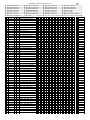
064 2.7K 5%,1/4W
064 3.3K 5%,1/4W
218 0Ω JUMPER
218 340Ω 1%,1/4W
221 0Ω JUMPER
223 12.1K 1%,1/4W
225 340Ω 1%,1/4W
226 205Ω 1%,1/4W
231 12.1K 1%,1/4W
232 205Ω 1%,1/4W
233 340Ω 1%,1/4W
236 0Ω JUMPER
236 340Ω 1%,1/4W
239 4.7K 5%,1/4W
242 12.1K 1%,1/4W
243 340Ω 1%,1/4W
261 0Ω JUMPER
261 15.8K 1%,1/4W
264 205Ω 1%,1/4W
266 0Ω JUMPER
266 301Ω 1%,1/4W
268 1N4148
268 1N4148 REV.
270 1N4148
270 1N4148 REV.
271 1N4148 REV.
271 1N4148
272 2.15K 1%,1/4W
272 3.92K 1%,1/4W
273 1.62K 1%,1/4W
273 1.00M 1%,1/4W
275 1K 5%,1/4W
275 30Ω 5%,1/4W
277 301Ω 1%,1/4W
277 340Ω 1%,1/4W
284 301Ω 1%,1/4W
286 301Ω 1%,1/4W
288 301Ω 1%,1/4W
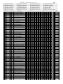
CRT A48AAB37X01
V+
126-128V DC.
Hf
15.75kHz
Video Board
Video Positive Analog
Video Negative Analog
Power: 120VAC
5
FBT: 453
514
.5W, CC
470Ω, 470
390Ω, 2W, 421
416
I PRA
510
.5W
150Ω, 425
12mH
CPT1538
447
CPA4166
Hf = 15.75kHz Hf = 15.75kHz
A
3
Blue
Wires
0Ω, 525
0Ω, 526
452
505
506
2.2nF 155
2.2nF
151
0Ω, 152
0Ω, 165
0Ω, 165A
0Ω, 176
0Ω, 177
0Ω,
0Ω, 178
183
BZT03, 181
100K, 173
0Ω, 184
4.7Ω, 185
503
0Ω,504
451
502
270Ω, 424
510Ω, 423
1uF
391
0Ω, 419B
0Ω, 419A
501
2SC5690, 433
306
H. Drive,
CPT1505
332
339
36K, 143B
100pF
129
171A
0Ω, 172
450
POSISTOR
CPR0434
120-230V, 14Ω
158
465
470Ω, .5W, CC
+
1uF
344
180
CL200, 159
0Ω, 190
0Ω, 188
0Ω, 186
1,000uF
+ 35V
+
162A
.093"
PIN 3
2
510Ω, 461
4937, 462
1nF
463
+
220uF
334
+
1,000uF
35V
449
.093" PINS
1
CPR
0432
2
157
Degaussing Conn.
162
161
0Ω, 454
12.1K, 329
1uF
347
+
200pF,
432
346
387
146
0Ω, 508
4007, 342
+
ID
6.8nF
IC
+
3A-T
FUSE
Black Wire
220uF, 250V
175
0Ω, 422
68.1K, 393
4.42K 392
0Ω, 395
100Ω,.5W,394
.01uF
414
IA Horizontal Control IB
167
182
127K, 388
100K,390
3467
420
3.92K, 417
3.92K, 418
415
220uF, 250V
163
+
4937, 168
171
0Ω, 187
379 2222
22K, 384
384A
1.2Ω,1W, 385
200K,383
4.7Ω, 396
2222
LA7851
0Ω, 164
529A
0Ω, 191
22K, 189
4.7Ω, 195
0Ω, 194
0Ω, 193
0Ω, 192
198
381A
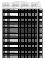
399
409 2907
352
56pF
4148, 130
A64
4007, 116
0Ω, 117
0Ω, 195A
381
250V
397
.01uF
0Ω, 318
LM339
355
H
411
.1uF
44.2K, 402
127K, 403
404
4148, 405
4148, 406
44.2K 407
15.8K, 408
.1uF, 410
CPC1058
2222 373
200K, 372
200K, 371
401
CPS1753
145
144
4937, 169
+
1,000uF
35V
378
100pF,398
1uF
220uF, 250V
0Ω, 167A
4937, 170
500
0Ω
400
1nF, 369
.01uF,374
330pF
350
6.8nF
348
.68Ω, 092
3.92K, 356
319
309
100uF
+
376
127K, 375
under
heat sink.
1
Wire Tie, 145A
CPM2123, 135
CPM
2028
0Ω, 389
377 LA7838
1nF,
351
275
2222 274
273
0Ω, 357
0Ω. 324
307
308
310
303
360
380
POWER
+
136A Jumper
313
0Ω, 314
+
100uF
304
312
4148,253
1K, 246
247
1.8K, 248
47nF,254
6.8K, 250
0Ω, 365
6.8K, 251
1.8K, 252
+
10uF
259
0Ω, 198A
201
205
088
0Ω,
4007, 090
0Ω, 083
H400,084
68.1K, 085
400, 086
127K, 087
1.21K, 245
1.21K, 258
272
1.8K, 257
256
255
+
+
166
Retighten nut after
wave soldering.
0Ω,196
470uF
50V
22K, 370
1.8K, 368
18Ω, 367
366
0Ω, 364
2.2M, 363
365K, 362
127K, 361
317
320
321
6.8k, 322
22K, 323
7812, 296
301
311
0Ω, 297
7
261
1.62K, 260
264
237
291
+
220uF
298
210
212
2907
268
270
271
REVERSE POLARITY SHOWN
283
0Ω, 358
0Ω,
290
288
287
286
285
284
6
5
4
292 3
2
1
0
300
0Ω, 293
294
6
CPS1781
236
6 Pin
Video
Input
Conn.
+
100uF
267
266
238
0Ω, 235
240
P
302
5
C5346A
241
239
230
0Ω, 228
231
232
233
234
LM393
242
220
223
224
225
226
227
119
12 pin video board connector.
CPS1757
0Ω, 136A
4937, 122
4937, 121
+
4007, 382
200K, 413
200K, 412
H400, 213
218
221
2222
CPT1536
CPQ1304
136
200pF
123
100uF
120
100uF
118
.33Ω, 2W, 137
3.3nF
125
+
+
100B
0Ω, 094
270Ω,093
+
100uF
089
191K, 126
5
1.0K, 208
47nF,207
219
33K, 097
28.0K,096
10.0K, 095
+
100uF
209
243
263
262
604Ω, 244
0Ω, 222
4
10.0K, 029
0Ω, 211
075
074
0Ω, 217
070
282
0Ω, 281
0Ω, 280
301Ω, 278
277
301Ω 276
3
0Ω, 215
0Ω, 216
0Ω, 214
10.0K, 051
3.3K, 052
2.15K, 042
3.3K, 050
3.3K, 053
20.0K, 043
24.3K, 044
.01uF, 054
LM392
12.1K, 045
10K, 055
049
.01uF, 047
6.8K, 056
046
6.8nF,057
44.2K, 058
0Ω, 048
100uF
2.7K, 060
+
1K, 062
061
.33uF
.047uF,
18Ω, 063
081
082
064
4937,
080
2222-Mot.
071
2.15K 078
1K, 065
072
75Ω, 066
077
2222-Mot.
1.62K, 076
0Ω,067
0Ω, 068
206
10
199
12.1K, 030
127
2.2nF,343
15.8K, 041
039
C5184
101
220uF
128
200K, 109
.1uF
124
027
028
10.0K, 031
115
0Ω, 100A
+
100uF
026
0Ω, 032
103
6.8nF,
102
47Ω, CC,140
0Ω, 531
+
56pF
107
56pF
104
354
15.8K, 353
12.1K, 034
033
025
62K, 143A
4007 132
30Ω,139
4937, 141
4746, 149
FR205, 142
200pF, 138
0Ω, 533
Power Supply Control
1.00M, 134
2.2nF
131
1nF
110
3.3nF
108
8.06K, 105
3.92K,106
+ 100uF
035
15.8K, 020
510Ω, 021
10.0K, 022
10.0K, 023
4148, 018
LM324
15.8K, 037
10K, 038
200K, 040
2
0Ω
019
JA JB JC & JD J PRA, 111
6.8K, 099
10uF
+
014
200K, 005
510Ω,006
527
024
007
62K, 098
0Ω, 015
1K, 012
1371
008
0Ω, 204
0Ω, 203
0Ω, 202
016
0Ω, 114A
0Ω, 092A
.1uF
010
62K, 011
A64
036
003
+
18Ω, 133
0Ω, 114
115A
0Ω, 200
CPS1804
529
100K, 113
1371
112
510Ω, 004
22K, 017
2.15K 009
1
002
1.8K, 325
270Ω, 326
270Ω, 327
0Ω, 328
270Ω, 330
1.8K, 331
0Ω, 001
Remote Connector
CPA4166
B
CPA4112
A
9
F
G
H
I
Model 2093-CGA
Vf = 60Hz
J
29
Product safety note:
Components marked by the
When replacing any of
CRT
Vertical
Deflection
6
PN2907A
3
212
253
+5
210
0Ω
1N4148
1/2
LM393
7
251
211
8
1/2
LM393
1
210
4-7VDC Hs
4-9Vpp 61,B4
+
1K
1.8K
2
484
4
077
4
078
081
093
1N4937
072
0Ω
RC1
18Ω
IN
0Ω
298
329
0VDC Hs
56Vpp 63,D6
220uF
Vs
2.2M
127K
363
361
S
17
DELAYED
SYNC O/S
U
244
086
5
FDH400
213
064
258
+12V
4-7VDC Vs
5-9Vpp 62,B4
245
3
7.3-8.7V Hs
4Vpp 02,D6
7.3-8.7V Vs
-.2VDC Hs
4Vpp 03,D6 1.5Vpp 04,E6
4
228
261
6
R IN
2
11
+A EN
Controls
RR
1
D
CPQ1322
293
5
TTL
8.8K
I3
I12
9
330pF
351
25K
330pF
I5
6,10
350
GND
12V
M GAIN
VC
75Ω
267
1N4148
065
GND 4
GR
BIN
7
15
B5
225
15.8K
75.0Ω
223
243
233
242
0Ω
218
226
366
236
75Ω
1N4148
64.9Ω
353
8
355
1K
271
278
0Ω
235
266
277
0Ω
231
221
1N4148
1N4148
246
268
30Ω
412Ω
275
273
283
270Ω
75Ω
75Ω
75Ω
288
286
284
0Ω
328
1.8K
30
N
326
M
270Ω
330
331
N
321
22K
AA
3
INPUT
BB
346
5 +
6
355
1/4
LM339
7 +
.14-.16V
B
BLUE VC
INPUT 6
Vs
VERTICAL VC
SYNC 2
CC
1
355
200K
318
256
H. V+
10
13
17
I15
I16
3.3nF I10 + 1600Hz +800Hz
ID
I PRA
151
+24V
470Ω, 1/2W
470 CC
OPEN
0Ω
468
152
247
2.2nF
155
250V
175
+
6.5-7.5VDC
+127V
1N4937
1N4937
1N4937
121
122
167
+1,000uF 1,000uF 169
171
.5-.8VDC
J4
3.3nF
56pF
108
107
3A Fuse
Black Wire.
153
146
INPUT
132
4
220uF
250V
163
0Ω
114
CONTROL &
FAULT SENSE
J7
3-4VDC
3Vpp 47,D2
3.3nF
4uS
DELAY
6 Rx
Osc.
7 Cx
102
7 8,14
J6
128
COMP.
+
3-5VDC
5Vpp 52,F1
12
13
0.1VDC
1Vpp 51,F1
OUTPUT
Current
SENSE
DRIVE
3-6VDC
.093" pin
162A
J10
134
17
FF
PC 120VAC
230VACPC
2 INPUT 1
GG
15.8K
J11
J12
135
136
12 510Ω
J8
1-4VDC
12Vpp 50,E2
033
10
18Ω
133
137
1N4007
116
MPSA64
D
111
10
II
JJ
3
054
440
053
Correction
3.3K
042
052
5
043
+ 100uF
0Ω
12.1K
061
136A
6
8
1/2
LM392
058
7
10K
049
055
4
045
2
.01uF
10.0K
047
095
3
4VDC 20VDC Hs
30Vpp 200Vpp 35,H7
Max. Min. H Size
056
2-2.5VDC Hs
4.4Vpp 39,B3
IRF520
0Ω
510Ω
094
461
3.3nF
057
477
.10Ω
.10Ω
0Ω
1W
475
1W
476
1nF
500V
463
470 Ω
460
0.8-7VDC Hs
12Vpp 38,J7
7
478
458
454
060
6.8K
HER205 HER205
457
50uH
2.7K
049
250V
443
CPT1528
4-19VDC Hs
27Vpp 36,J7
462
1
1/2
LM392
6
1.6KV
441
432
431
1N4937
096
438
200pF
030
3.3K
FR205
1/2W
428
H. Linearity
coil
041
044
5
445
446
430
5.6-6.2VDC Vs
1-1.7V 34,B2
44.2K
4VDC 20VDC Vs
11Vpp 15Vpp 37,I6
Max. Min. H Size
437
GND
1/2W
464
8
2.7uF 100V
456
GND
GND
HORIZONTAL WIDTH DRIVE
LEGEND
0Ω
0Ω
177
176
No
.
LTR.No
.X
V-
KK
447
FR205
-Linear
Pincushion
Correction
GND
25V
HS +12V
V-
CAUTION! POWER SUPPLY VOLTAGES REFERENCED FROM V-.
SCOPE GND MUST NOT BE CONNECTED TO GND AND V- AT THE SAME TIME.
S1
107V or 127VDC Hs
120Vpp 250Vpp 32,F6
Max. Min. H Size
3.3K
GND
140
129
423
033
28.0K
47Ω
1/2W, CC
100pF
SL
8
1/4
LM324
050
.01uF
010
TP49, G1
127
2,200pF
131
.1uF
138
0.33Ω
2W
YC3
5.6-6.2VDC Vs
2-3.6Vpp 33,B2
097
200pF
1KV
13
0VDC Hs
27Vpp 57,F1
HH
7
1/4
LM324
6
Blooming
correction.
009
H SIZE
14.7K
CPT1538
12mH
YC4
051
9
6V
18
HEAT
SINK
S2
HORIZONTAL YOKE
10.0K
3.3K
No DVM
300Vpp 40,G1
CPQ1304
424
510Ω
GND
031
5
038
125
1.00M
154
145
161
10K
+25V
158
.093" pins
Degaussing
Connector
162
029
Parabolic
Pincushion
130
J9
1.00M
11
J PRA PINS: 3,10,15, & 19
3,300pF
20
188
008
10.0K
040
1N4148
126
195
2.7K
38.3K
V-
115
V-
005
10.0K
200K
142
127K
16
.1uF
123
-214V
.33uF
FR205
533
5.5-6.8VDC
8 +7.5V REF. V- 9
XRC5184 J PRA
220uF
12
124
.1-.5VDC
9
5.7-6.3VDC
143B
141
0Ω
4
I BEAM
Over
COMP. Voltage 14
Protect }
INPUT
Output
5
36K
139
200K
109
0Ω
1N4937
10 0Ω
4.7Ω
100uF
25V
6V
168
1N4937 9
S4
100uF
200K
194
166
105
143A
30Ω
2
+
14.8-18VDC
2
200pF
CPR0434
+15V 16
+17V 15
3.4-4.2VDC
90K
156
INPUT
3
3
H. S. +12V
082
6
3
4
8
SR
HORIZONTAL WIDTH CONTROL
450
V+
425
270Ω
Excessive Beam
+ 035
Current, Monitor Shut
Down Circuit.
0Ω
019
1/4
1 22K
2SA
LM324
017
1371
033
1,000uF
GND
5
1
56pF
250V
144
V+
1N4937
+16V
+112V
150Ω 1/2W
011
INPUT
88K
33.2K
+6V 12.1K
1 CPT1536
AMP.
5
037
170
198A
+102V
Horizontal Raster Adj.
026
0Ω
182
GND
ERROR
FR205
159
25Ω@25˚C, 2A
GND
EE
33K
Inrush Current Limit
Relay
200V.5A
118
+
15.8K High Temperature Or
034
100uF
+
427
GND
I BEAM 62K
220uF
50V
VERTICAL
DEFLECTION
YOKE
YC2
1/2W
394
021
033
11
023
IB
1N4937
100Ω
14 510Ω
1/4
LM324
2
426
0Ω
185
+102V
4
10.0K
+400Hz
16
IC
V+
120
110
J3
62K
12
+6V
I BEAM
23.2K
106
022
+112V
+102V
+ 100uF
6.5-7.5VDC
41,D1
3
10.0K
H.Fo ADJ. 170Ω
680Ω 340Ω I14
2
J2
220uF
GND
12
Hs
VC HORIZONTAL
1 SYNC
DD
345
9.31K
191
524
&
525
GND
YC1
4.7Ω
+112V
0Ω
419E
189
+6V
FBP
GND
+16V
JE
BZT03-D160
181 160Vz
4
152
PN2222
322
2
CC3
CPS G
1752 VC
GREEN
292 5
J15
257
.047uF
6.8K
1/4
LM339
327
GND
6
JC
+1.5V
130Ω
148
254
323
4
6.8K
270Ω
GND
J18
7.15K
M
325
JD
+3V
2
100K
Posistor
280
GND
.01uF
344
I9
420
0 TO 7 VDC
1
FIL.
453
Open
419B
22K
RAS. POS.
H. S. +12V
416
20
104
CC2
281
VC
3
1uF
15
V
415
5-6VDC Hs
7Vpp 09,E6
1K
220uF
11K
PN2222
M & N reverse Hs.
0Ω
150
255
1.8K
R
-3V
1,000pF
J16
FR205
7V pp 58,C5
274
8
0Ω
167A
101.6K
4.67K
10.6K
2.2nF
200K .05VDC Vs,Hs
3.92K
0Ω
114A
260Ω
3.92K
272
276
0Ω
62K
173
J14
J5
356
PN2222
75Ω
270
100K
14
I8
16.3-19VDC 55, E1
360
2.1-2.4VDC Hs
4.6Vpp 59,D6
358
10
355
354
3.3nF
+12V
+12V
VC RED
4 INPUT
11
1/4
LM339
13
GND
9
+
13
I7
112
68.1K 15.8K
357
232
264
0Ω
75Ω
3.3nF
33K
2SC3467
192
0Ω
9
113
15.8K
1/4
LM339
14
7.15K
+
15.8K
7
0Ω
18
348
I6
FBP
0Ω
L
15.8K
10K
347
45K
1
2SA1371E
1
+ 9
A5
0Ω
K
8
419F
comp.
HORIZONTAL
OSCILLATOR DISCHARGE
3-7VDC Hs 5.5-6.3V Hs
.2Vpp 07,E6 3.6Vpp 08,E6
J1
GND
CC1
0Ω
JB
-1.5V
91.4K J13
100kΩ@25˚C
T 180
1.5-2VDC 60,D6
J
JA
2.33K
+12V
7.15K
BR
8
3
2
1
Open
3-5Vpp 31,F5
0Ω
193
-
7
I13
100K
364
A5
7-10VDC
61, C2
018
Beam Current
Limiter Circuit.
1K
066
0
+
X-RAY
PROTECT
2.4-3.4VDC
0Vpp 06,E6
V+
CPR0432
+ 100uF
4
419A
0Ω
11
+6V
I BEAM
241
XRC5346A
GIN
14
12
417
12
6
+ 1uF
15.8K
020
071
3
- A BL
3.92K
Video V+
014
036
10
+12V
LA7851
13
3-4VDC Hs
1.4Vpp 05,E6
6.8K
H. S. +12V
PN2222A
G
14
GND
5
10uF
MPSA64
012
7
5
0Ω
421
449
336
11
+6V
I BEAM
+
1K
0Ω
418
FBP
GND
+12V
GND
0Ω
15.8K
16 13 9 6
Ro Go Bo
BBL
15
MULTIPLIER
BIAS
SAW TOOTH
TR . GENERATOR
FBP
GND
+16V
11.5-12.5V
SCREEN
CPT1516
390Ω, 2W 12-18VDC Vs
1,000uF
35V
+
10.8-12V
10, E6
3.92K
5.4-6VDC
11, E5
V Ref.
063
+127V
084
260
16
VERTICAL
OSC. O/S
VERTICAL
OSCILLATOR
.4VDC Hs
.7Vpp 12,E5
15.8K
408
2
GND
18Ω
076
FDH400
4.5-5.3V Vs
5Vpp 16,E5
ADJ.
VIDEO GAIN LINE
FDH400
V-
466
448
370
414
.1-.3VCD Vs
3.8Vpp 17,E5
H. +12V
T
1,000uF
+
22K
.01uF
18
Hs
IA
22K
334
080
GND
12-18VDC Vs
50Vpp 29,F6
330pF
7
I2
7.3VDC Hs
5.5Vpp 01,D6
8
I4
1.8K
I1
352
1
2.7K
2
202
17 5
12K
3
VERT.
OSC.
PICTURE
Horizontal
POSITION
O/S
SYNC INPUT
GND
56pF
404
391
4-6VDC Vs
V
V. osc. 2.8Vpp 18,D5
VERTICAL
± SYNC INPUT
V+
333
220uF
410
19
VERTICAL
367
295
GND 296 +
Hs 12.1K
270Ω
RC4
20
252
PN2222A (CPQ1322)
.01uF
11-12.4V
20, D5
376
7812
100uF
405
8
GND
1N4148
407
406
.1uF
FOCUS
452
434
1uF
362
.1uF
5.5-6.5V Vs
1.2Vpp 19,D5
or
100uF
+
1N4007
OUT
1N4148
396
+12V
GND
Vs
304
207
GND
+
1.8K
.047uF
HORIZONTAL
BLANKING
4.5-5.3V Vs
5Vpp 16,E5
368
208
248
4.7Ω
GND
1K
067
+12V
390
388
385
+12V
0Ω
+16V
2-3VDC Vs
4Vpp 64,C4
1.8K
3
100K
392
+12V
GND
062
2.32.7V
2.7K
435
1.2Ω
GND
9
0Ω
PCB 490
250
393
401
340
465
451
1N4007
343
200Ω 2W
+25V
373
3
4
2,200pF 1
1/2W
6
433
I11
20
RC7
Remote Control
6.8K
1uF
380
1.5-2.7V Vs
24Vpp 24,E4
332
EHT
470Ω
2SC5690
397
Horizontal 20K
Position
+12V
6.8K
374
GND
485 GND
VERTICAL BLANKING
402
369
1.2Ω, 1W
FIL.
Retrace Boost
44.2K
.01uF
483
Master
Gain
RC2
PN2222
0Ω
FLYBACK
TRANSFORMER
10
100Ω
337
VFB
GND
209
PN2222
2
19
338
INCREASES
TOP AND
BOTTOM
VERT. SIZE.
VFB
101
372
VRP
201
382
200K
371
CPT1505
2SC
4159
+ 100uF
+16V
H
200K
V HYP
384
395
D5
411
375
403
100uF
CRT Autobias
Delay
0Ω
1N4007
342
+6V
.1uF
100pF
341
NO DVM Hs
.9KVpp 27,G6
12-18VDC Hs Horizontal Drive
33Vpp 26,E7 Transformer
+6V
200K
D5
398
422
1N4007
409
I
13
H SIZE
087
12
2.2K.5W
I BEAM
+6V
027
486
11
0Ω
I BEAM
127K
203
413
PS FBP
V-
510Ω
10
5.5-6.5V Vs
1.4Vpp 23,F4
5-6VDC Vs
1.4Vpp 22,E5
GND
9
470uF
1,000pF
1K
RC
002
089
8H Dly.
CD4024 100
389
22K
RC3
8
EHT
092A
196B
196
200K
PN2907A
412
0
092
FOCUS
800
H SIZE
V HYP
CS=.45"
383
12
11
9
6
5
4
7
200K
Video
Board
V. +12V
Boost
PP
0VDC Hs
56V 28,D3
Current
0Ω
CS=.74
Q1
Q2
Q3
Q4
Q5
Q6
CL
KL
NC
Vdd
Vss
Q7
1
2
8,10,13
14
7
3
100uF
+
5.5-6.4V Vs
3Vpp 21,D5
6
OO
Beam
099
PN2222
379
085
006
5
0Ω
RC6
750Ω
Vertical
Raster
Position
68.1K
1N4148
4
004
482
GND
088
500Ω
090
62K
3
DECREASES
TOP AND
BOTTOM
VERT. SIZE.
Retrace
Booster
Drive
NN
Fil. TC11
Fil. Rtn. TC12
Screen
PS FBP
V-
1N4007
098
2
Vertical
Size
206
2.2K
+12
V
62K
200K
SOCKET BOARD CONNECTOR (TC)
2
510Ω
RC8
V. size
Control
50/60Hz
+16V
1
481 GND
RC5
+12V
1
Auto
Bright
ABA
Horizontal
10K
Size
TC2 GND
TC4 12V
TC1 16V
Beam
Current
Buffer
+12V
Vertical Linearity Circuit
Vert.
Out
Vert.
Drive
MM
H SIZE
127V TC8
TC 10 TC 6
TC7 Red
TC5 Green
TC 3 Blue
LL
22-28V Vs
.8Vpp 25,F7
Thermal Protection
out
Ramp
Gen.
Reset
Ramp
Slope
Ramp
Reset
One Shot
out
Tr.
R/C
377
TC9 iB OFF
V Sync
KK
symbol on this schematic have special characteristics important to safety.
these components, be sure to use the parts specified in the parts list.
LA7838
HEAT
SINK
378
+12V
Auto Bias
JJ
PS FBP
V-
800
ARC PROTECT
B+G+R=∑
II
VIDEO BOARD
Beam current
Feedback
Blue Video Amp.
HH
FBP
GND
H. S.+12V
Beam current
Feedback
GG
FBP
GND
+12V
Green Video Amp.
FF
FBP
GND
+12V
Beam current
Feedback
EE
+24V
+112V
V+
+102V
Red Video Amp.
DD
+25V
0
CC
+
BB
AA
Measurements
are taken with
a white screen.
Hs - 5uS/div.
Vs - 2mS/div.
LL
XYV
X
X-Y VDC
X-Y VDC Sync.
Vp-p TP-REF.
WAVEFORM
BOARD PART No.
PART No. ON PRA.
PRA PIN No.
DC VOLTAGE RANGE,
{ USING
A DMM.
USE V. or H. SYNC.
AC VOLTS TEST POINT
Peak to Peak ASS. REF.
Measured with scope
MM
CERONIX
SCALE NONE
:
DRAWN BY: F. H.
DATE & REV.
2/18/92
13350 New Airport Road
Auburn, California 95602
4/10/96-E1
9/30/96-E4
3/24/99-E5
03/06/02-E8
9
CERONIX Model 2093-VGA Monitor Circuit.
CERONIX
PART NO.
CPA4224, CPA4227, CPA4108
NN
OO
PP
30
B
C
D
E
F
G
H
I
62K, 143A
+
J
NOTES
NOTES
A
31
B
4007,333
+
220uF
334
+
1uF
344
335
336
315
316
0Ω. 324
349
C
D
E
+
100uF
338
150
FR205, 148
FR205, 156
147
Wired for;
120VAC, 50-60Hz
151
154
2.2nF 155
2.2nF
152
0Ω, 165
0Ω, 165A
153
3
158
Blue Wires
0Ω, 524
472
0Ω, 525
0Ω, 526
CL200, 159
2
POSISTOR
CPR0434
120-230V, 14Ω
0Ω, 523
4
507
522
521
512
520
12mH
CPT1538
447
511
509
5
FBT: 453
514
FBT: Hitachi BW00272, CPT1516
445
446
468
515
RELAY
443
428
516
430
442
473
517
441
H. Lin. Coil
431
FR205, 440
0Ω, 480
2.2K, .5W
341
200Ω, 2W
1.2Ω, 434
340
4007, 435
F
G
FR205, 438
.5W, CC
470Ω, 470
0Ω, 466
444
518
2.7uF,
456
436
.10Ω,1W
476
HER205
477
6
470Ω
.5W
IRF520 464
460
437
.10Ω,1W
475
DEGAUSSING
426 427
Yoke Connector .062" Pins
2SC5690, 433
C4159
337
0Ω, 176
0Ω, 177
0Ω,
452
505
506
503
504
451
510
.5W
0Ω, 178
183
BZT03, 181
100K, 173
0Ω, 184
4.7Ω, 185
450
150Ω, 425
270Ω, 424
510Ω, 423
180
+
502
1,000uF, 35V
448
0Ω, 508
313
306
H. Drive,
CPT1505
332
339
36K, 143B
100pF
129
171A
0Ω, 172
0Ω, 186
0Ω, 190
0Ω, 188
0Ω, 187
390Ω, 2W, 421
0Ω, 419A
416
I PRA
.093" PINS
Residual Current
.01uF
12.1K, 329
3.3nF
345
1,000uF
+ 35V
2
157
510Ω, 461
4937, 462
1nF
463
1uF
347
ID
220uF, 250V
175
465
470Ω, .5W, CC
346
1,000uF
35V
449
146
Degaussing Conn.
162
161
162A
.093"
PIN 3
CPR
0432
3A-T
FUSE
Black Wire
0Ω, 454
+
+
200pF
432
IC
4007, 342
IA Horizontal Control IB
1uF
391
0Ω, 419B
415
387
+
CPC1103
220uF, 35V
182
1
0Ω, 422
393
2.7K, 392
0Ω, 395
4.7Ω, 396
LA7851
+
4937, 167
501
3467
420
3.92K, 417
3.92K, 418
I
100Ω,.5W,394
250V
397
0Ω, 164
529A
0Ω, 191
22K, 189
0Ω, 193
0Ω, 192
4.7Ω, 195
0Ω, 194
379 2222
22K, 384
384A
1.2Ω,1W, 385
200K,383
.1uF
+
4937, 168
171
388
100K, 390
.01uF
414
352
56pF
4148, 130
A64
4007, 116
200K, 109
.1uF
124
198
199
381A
399
2222
409 2907
V
4937, 169
378
2.2nF,343
LM339
355
0Ω, 117
0Ω, 195A
0Ω, 198A
381
200K, 201
205
0Ω, 204
0Ω, 203
0Ω, 202
092
1.0K, 208
47nF,207
3.3nF, 358
1K, 357
3.92K, 356
47nF,318
309
200K, 372
200K, 371
411
401
220uF, 250V
163
62K, 167A
4937, 170
1
CPS1753
145
144
CPM2038, 135
0Ω
400
44.2K, 402
403
404
4148, 405
4148, 406
407
15.8K, 408
.1uF, 410
CPC1058
2222 373
220uF, 250V
+
under
heat sync.
500
100pF,398
POWER
Wire Tie, 145A
166
Retighten nut after
wave soldering.
CPM
2028
0Ω, 389
1uF
CPT1536
136A Jumper
+
1,000uF
35V
196
1nF, 369
.01uF,374
FR205, 142
0Ω, 533
0Ω, 136A
4937, 122
4937, 121
119
380
4937, 141
CPQ1304
136
200pF
123
+
+
.33Ω, 2W, 137
3.3nF
125
377 LA7838
100uF
+
376
375
22K, 370
1.8K, 368
18Ω, 367
7.15K, 366
7.15K, 364
2.2M, 363
362
127K, 361
15.8K, 360
100uF
120
470uF
35V
4148,253
200K, 246
33K, 247
1.8K, 248
2222
2222
6.8K, 250
0Ω, 365
6.8K, 251
1.8K, 252
245
3.92K, 272
100K, 257
200K, 256
260
258
30Ω, 275
2222 274
412Ω, 273
319
259
100uF
118
4007, 382
1.8K, 325
270Ω, 326
270Ω, 327
0Ω, 328
270Ω, 330
1.8K, 331
307
310
305
0Ω, 295
255
317
320
6.8K, 321
6.8k, 322
22K, 323
7
303
312
0Ω, 314
0Ω, 297
7812, 296
+
100uF
304
308
311
302
+
220uF
298
0Ω, 283
301
6
5
4
292 3
2
1
0
4148, 268
4148, 270
4148, 271
300
0Ω, 293
294
6
CPS1752
0Ω, 236
7 Pin
Video
Input
Conn.
0Ω, 211
0Ω, 215
0Ω, 216
0Ω, 214
0Ω, 243
263
262
244
291
290
75.0Ω, 288
237
287
239
75.0Ω, 286
238
285
240
75.0Ω, 284
282
0Ω, 266
0Ω, 281
0Ω, 280
264
75.0Ω, 278
75.0Ω, 277
75.0Ω, 276
15.8K, 261
+
100uF
267
0Ω, 235
4
5
241
0Ω, 228
15.8K 231
64.9Ω, 232
0Ω, 233
234
25
230
220
0Ω, 222
4
0Ω, 092A
2.2K, 088
4007, 090
0Ω, 083
100B
127K, 126
+
CD4024B, 100
7 Stage Counter
127
200pF, 138
0Ω, 531
220uF
128
+
B
H400,084
68.1K, 085
400, 086
127K, 087
3
C5184
196
030
10.0K, 051
10.0K, 029
3.3K, 052
3.3K, 042
043
3.3K, 050
3.3K, 053
097
044
.01uF, 054
28.0K,096
LM392
12.1K, 045
10K, 055
10.0K, 095
049
.01uF, 047
6.8K, 056
0Ω, 094
046
3.3nF,057
270Ω, 093
44.2K, 058
+
0Ω, 048
100uF
100uF
2.7K, 060
+
062
061
.33uF
089
.01uF,
18Ω, 063
081
082
064
4937, 080
2222-Mot.
071
078
1K, 065
072
75Ω, 066
077
2222-Mot.
076
0Ω,067
0Ω, 068
206 12 pin video board connector.
075
CPS1757
070
074
+
0Ω, 217
100uF
219
209
LM393
H400, 213
0Ω,
210
221
212
0Ω, 218
2907
15.8K 223
15.8K 242
224
0Ω, 225
75.0Ω, 226
227
C5346A
039
115
.1uF, 101
330pF
351
041
56pF
107
56pF
104
30Ω,139
47Ω, CC,140
+
103
3.3nF
102
132
149
Power Supply Control
1.00M, 134
2.2nF
131
1nF
110
3.3nF
108
330pF
350
3.3nF
348
+ 100uF
4148, 018
035
025
15.8K, 020
510Ω, 021
10.0K, 022
LM324
10.0K, 023
+
033
0Ω, 032
100uF
026
510Ω, 027
10.0K, 031
028
0Ω, 200
0Ω
019
200K, 413
200K, 412
2
12.1K, 034
15.8K, 037
10K, 038
200K, 040
007
JA JB JC & JD J PRA, 111
105
7.15K, 106
0Ω, 015
10uF
+
014
1371
008
18Ω, 133
0Ω, 114
115A
0Ω, 114A
200K, 005
4148, 006
527
024
62K, 099
016
1K, 012
A64
036
003
+
.1uF
010
62K, 011
68.1K, 354
15.8K, 353
CPS1804
529
100K, 113
1371
112
510Ω, 004
22K, 017
2.7K, 009
1
002
62K, 098
0Ω, 001
Remote Connector
50uH
CPT1511
150uH,
HER205
478
439
H
CPT1528
457
I
7
458
CPA4108
CPA4224
Hf = 31.5kHz
Hf = 29.6kHz
Hf = 31.5kHz
Vf = 60Hz
Vf = 62.9Hz
Vf = 60-70Hz
VALUE
030 15.8K 1%,1/4W
030 28.0K 1%,1/4W
041 20.0K 1%,1/4W
041 44.2K 1%,1/4W
043 22K 5%,1/4W
043 15.8K 1%,1/4W
043 20.0K 1%,1/4W
044 33K 5%,1/4W
044 36K 5%,1/4W
044 28.0K 1%,1/4W
062 1K 5%,1/4W
062 2.15K 1%,1/4W
064 2.7K 5%,1/4W
064 909Ω 1%,1/4W
076 604Ω 1%,1/4W
076 1.62K 1%,1/4W
077 33K 5%,1/4W
078 1.62K 1%,1/4W
078 2.15K 1%,1/4W
092 0Ω JUMPER
092 .68Ω 5%,1/4W
097 68.1K 1%,1/4W
097 28.0K 1%,1/4W
105 62K 5%,1/4W
105 140K 1%,1/4W
132 1N4007
132 0Ω JUMPER
151 FR205
152 2.2nF, 1KV
152 0Ω JUMPER
153 2.2nF, 1KV
154 FR205
196 0Ω JUMPER
196B 0Ω JUMPER
244 105Ω 1%,1/4W
244 604Ω 1%,1/4W
245 604Ω 1%,1/4W
245 1.21K 1%,1/4W
258 464Ω 1%,1/4W
258 1.21K 1%,1/4W
260 412Ω 1%,1/4W
260 1.62K 1%,1/4W
264 75.0Ω 1%,1/4W
264 84.5Ω 1%,1/4W
336 2.7K 5%,1/4W
336 3.3K 5%,1/4W
362 365K 1%,1/4W
362 309K 1%,1/4W
375 62K 1%,1/4W
375 127K 1%,1/4W
388 200K 1%,1/4W
388 127K 1%,1/4W
393 0Ω JUMPER
393 68.1K 1%,1/4W
403 68.1K 1%,1/4W
403 127K 1%,1/4W
407 100K 1%,1/4W
407 169K 1%,1/4W
428 470Ω 5%,1/2W
428 150Ω 5%,1/2W
430 0Ω JUMPER
430 LIN. INDUCTOR
431 LIN. INDUCTOR
431 LIN. INDUCTOR
437 .022uF, 630V
437 .027uF, 800V
441 8.2nF, 1.6KV
441 7.5nF, 1.6KV
441 6.8nF, 1.6KV
443 .47uF, 250V
443 .56uF, 250V
451 0Ω JUMPER
452 0Ω JUMPER
CRT A48AAB37X03
CRT A48AGY13X87
106-108V DC.
V+
110-112V DC.
V+
PART No.
CPR0145
CPR0163
CPR0153
CPR0154
CPR0015
CPR0145
CPR0153
CPR0016
CPR0017
CPR0163
CPR0009
CPR0138
CPR0012
CPR0126
CPR0132
CPR0136
CPR0016
CPR0136
CPR0138
CPR0050
CPR0375
CPR0155
CPR0163
CPR0018
CPR0172
CPD1252
CPR0050
CPD1264
CPC1003
CPR0050
CPC1003
CPD1264
CPR0050
CPR0050
CPR0122
CPR0132
CPR0132
CPR0134
CPR0131
CPR0134
CPR0130
CPR0136
CPR0124
CPR0152
CPR0012
CPR0024
CPR0171
CPR0180
CPR0018
CPR0157
CPR0029
CPR0157
CPR0050
CPR0155
CPR0155
CPR0157
CPR0019
CPR0146
CPR0365
CPR0367
CPR0050
CPT1557
CPT1539
CPT1557
CPC1034
CPC1047
CPC1055
CPC1061
CPC1065
CPC1050
CPC1062
CPR0050
CPR0050
CPP1717
CPP1724
107V DC.
111V DC.
BD
C2
C2
A2
A2
A3
A3
A3
A3
A3
A3
A3
A3
A3
A3
B4
B4
B3
B3
B3
C3
C3
C3
C3
D2
D1
F1
F1
J2
I2
I2
I2
J2
E3
E3
B5
B5
C5
C5
C5
C5
C5
C5
B5
B5
E6
E6
D6
D6
D5
D5
F4
F4
E5
E5
E5
E5
E5
E5
F6
F6
F6
F6
F6
F6
H7
H7
H6
H6
H6
H6
H6
G4
G4
SCH
NN7
NN7
NN7
NN7
LL8
LL8
LL8
MM7
MM7
MM7
EE3
EE3
BB5
BB5
CC5
CC5
BB4
BB4
BB4
PP0
PP0
MM7
MM7
GG8
GG8
JJ6
JJ6
GG7
GG7
GG8
GG7
GG7
LL0
LL0
BB5
BB5
BB5
BB5
BB5
BB5
BB5
BB5
BB7
BB7
KK4
KK4
HH2
HH2
GG1
GG1
HH2
HH2
HH1
HH1
GG2
GG2
JJ1
JJ1
OO6
OO6
OO6
OO6
OO6
OO6
PP7
PP7
PP6
PP6
PP6
PP7
PP7
NN1
NN1
CPA4224
CPA4227
CPA4108
A
9
Q
O P
O P
Q
Q
P
O
Q
O
P
Q
O P
Q
O P
O P
Q
O P
Q
O P
Q
O P
Q
O P
P
Q
P
O
Q
Q
Q
O P
Q
Q
Q
O P
O P
Q
O P
Q
O P
Q
O P
Q
Q
O P
P Q
O
Q
O
P
O P
Q
O P
Q
O P
Q
O P
Q
O P
Q
O P
Q
Q
O P
Q
O P
P Q
O
O
Q
P
P
O
Q
O
Q
P
Q
O P
Q
O
P
CPA4227
Model 2093-VGA
J
31
QQ
RR
Red Video Amplifier
2
0
+12V
811
1
3
140Ω
K19
K16
K8
Jumper
9
1N4148
K36
3pF
A
681Ω
K1
1N4148
K35
820Ω
K22
K10
5 9
812
FDH
400
FDH
400
835
899
845
849
886
959
834
840
2SA
1370
15Ω
6
K4
9
K12
GND
836
853
1/2W
856
DAG GND
1N4007
848
30Ω
+127fV
+126V
Green Video Amplifier
2
+12V
K15
K9
40.2K
K2
3
18 Ω
MMBT
3904
16
1
3
606Ω
1.2K
K7
Jumper
K8
10
100Ω
GREEN
TC5
3pF
K6
1.50K
K1
1N4148
K35
K11
21KΩ
820Ω
K22
K10
2SA
1370
14
844
GND
+12V
15
Blue Video Amplifier
2
+12V
937
K9
K34
K8
12
14
K32
1N4148
681Ω
K1
40
934
A
QQ
2SC
3467
1N4148
K35
945
21K
820Ω
K22
K10
K11
5 9
RR
12
2.2K
K5
6
9
953
15Ω
K4
11
3.32K
GND
+12V
205Ω
943
PN2907A
33 Ω 8
5.62K
K6
K6
1.50K
.5W
K3
K3
4
K20
K21
K18
K12
SS
2SA
1370
925
1
GND
7.8 to 8.8Vdc Vs
8.4Vp-p 95uS
2.7K
1N4148
884
888
6
926
8
1.8K
955
938
933
MPS A64
D
1.8K
948
954
BIAS CONTROL LINE
1.8K
942
931
4
914
Adjust FBT bottom pot
for 4.0V to 4.4 at pin 8.
910
894
33K
2.16.3V
911
5
Red
hold
cap.
17 +10uF
892
16
2.16.3V
BIAS
15
CL Start
COUNTER
FF Q
GND
GRID
PULSE
6
2.2 to 2.7Vdc Vs
4.2Vp-p 360uS
5V REF
EN
21 H. LINE
COUNTER
CL
4.6-5.2VDC
14
AUTO
BIAS
ACTIVE
13
PROGRAM
12
CERONIX
13350 New Airport Road
Auburn, California 95602
PULSE
Scale:
NONE DATE & REV. 10/3/96-E4 03/06/02-E7
F. H. 4/16/96-E1 2/2/98-E5
Drawn By:
.1uF
940
UU
928
9 to 10Vdc Vs
9.6Vp-p 95uS
15.8K
33K
DECODER
sw control
PN2907A
11
3.92K
GND
TT
10
1.8K
1.8K
920
912
6V REF.
1K
Hs
8
comp.
9
890
Red input
7
1.22.5V
2.2nF
33K
19 +10uF
sw
.1.5V
+9.3V
Green
hold
cap.
18
5.76.3V
.047uF
62K
1/4
LM324
852
comp.
1.22.5V
Vs
+12V
Green input
5
.1uF
2.16.3V
908
5.76.3V
889
FDH400
7
C1
956
958
4
68.1K
C15
891
Dark screen
80-110VDC
1000pF
300Ω
.1uF
3pF
9.3V
200Ω
C16
5K
20
sw in grid pls. pos.
4
Auto Bright
4 Circuit
909
895
comp.
1.22.5V
62K
11 3.3K
21 +10uF
sw
924
22K
7
3
8
5
5
K33
1
885
19
Blue
hold
cap.
sw
normal
3
.047uF
14
20
Blue input
5.76.3V
.1uF
923
C2
13
8
250V
887
180Ω
20
NE592
1.2K
Jumper
K36
.015uF
10
7
12
.1uF
15
951
19
SOT
K7
7
2SA
1370
B14
K16
10
1
3
606Ω
TC3
140Ω
5
68.1K
C12
4K
200 Ω
5K
2,200pF
815
14
922
C13
2
.047uF
1
17
1/4
LM324
.1uF
921
C3
16
10
1 GND 927 Vcc 22
CA3224E
9
7
68.1K
C9
2
4K
C14
K14
16
6
BLUE
18 Ω
K19
MMBT
3904
100Ω
17
18
K13
950
C8
1/4
LM324
AUTO BIAS IC
907
850
858
200 Ω
5K
3
2,200pF
818
75 Ω 13 126V
K17
40.2K
K2
1
560 Ω PN2907A
K15
1.49K
301Ω
4K
.1uF
7
12
13
16V
120V
12.1K
10
1/4
LM324
3
TC 10
2SC3675
906
C PRA-B
917
920
6
C11
3
18
5
11
C10
957
5
TC 6
CABLE
ASS.
863
2.74K
2,200pF
941
830
842
BIAS CONTROL LINE
K12
GND
1.8K
905
866
+4.0V
1.82K
1.8K
11
3.32K
K5
TC 2
Auto Bias Vs
1N4007
C17
841
7
K4
9
2.2K
5 9 12
FDH400
903
900Ω
C7
15 Ω
6
822
5.62K
C
For
XX92
Dark screen
80-110VDC
843
825
805
K20
A
681Ω
GND
1N4007 1N4007
C4
PN2907A
33 Ω 8
816
TC 4
GND
10
9.3V
205 Ω
2SC
3467
.5W
K3
4
.1uF
9
K21
1
300Ω
5
1N4148
K36
3
8
875
1K
250V
823
7
1000pF
K32
816
.1uF
15
K18
20
SOT
12
14
801
ABA
180 Ω
824
NE592
879
2
TC 1
+12V
14
828
19
.015uF
10
7
K33
4
2SA
1370
K16
K34
.1uF
K14
140 Ω
K19
.1uF
K13
827
17
860
+12V
GND
75 Ω 13 126V
PN2907A
K17
12.1K
10
1.49K
301Ω
560Ω
+120V Source
+120V
150 Ω
1/2W cc
TC 12
TC 8
+16V
+16V
18Ω
TC 9
TC 11
+127V
859
847
+16V
803 18
FIL.
Fil. GND
1N4937
16V
120V
BEAM OFF ON POWER DOWN.
DAG GND
1uF
50V
846
857
1
EHT
Red #1 FOCUS
White #2 FOCUS
SCREEN
961
FIL.
870
+126fV
3
EHT
100K
878
FDH400
FIL.
+12V
854
2.2nF
GND
2
Green
Wire
2.2K
871
872
1/2W
880
0
Degaussing
Coil
970
1/2W
881
0VDC Hs
56V 31uS
817
7 150Ω 2 1
1/2W
855
869
873
874
868
1K
0Ω
330pF
-30V
831
837
BIAS CONTROL LINE
3.32K
K5
876
5
9
1/2W
882
10K 1/2W
1.8K
100K
.1uF
Focus
11
12
150Ω
883
GRID PULSE
-23 to -27Vdc Vs
12Vp-p 95uS
G2
! UNPLUG !
DEGAUSSING
COIL BEFORE
WORKING ON
CHASSIS.
8
10
1.8K
Pin By Fuse
CC2
Pin By FBT
GREEN 6
BLUE
1.8K
11
971 From Main PCB
CC1
CC3
G1
851
FDH400
7
ZZ
YY
SOCKET
877
900
838
810
2.2K
12
FDH
400
Dark screen
80-110VDC
K18
2SC
3467
PN2907A
33 Ω 8
K11
21K
FDH
400
9.3V
205 Ω
.5W
K3
4
5.62K
K6
1.50K
FDH
400
RED
180Ω
K20
K21
FDH
400
1000pF
300 Ω
816
XX
Socket Board
PCB 800
250V
913
7
3
.1uF
WW
.1uF
15
833
19
901
8
5
K33
1
2SA
1370
20
K32
12
14
VV
14
K14
.015uF
10
7
NE592
1.2K
K7
TC7
18Ω
40.2K
10
K13
832
SOT
606 Ω
100Ω
K17
16
K34
75 Ω 13
126V
PN2907A
17
1.49K
MMBT
3904
RED
560Ω
K15
K2
UU
16V
120V
12.1K
K9
TT
3
18
10
301Ω
1
SS
VV
VIDEO BOARD CIRCUIT
930
WW
XX
YY
ZZ
40
7
XX93 Video Board, Technician's Assembly Drawing.
View is from component side.
872
∆
M
12
1370
842
1K, 866
809
801
6
7
.1uF
8
250V
9
10 823
11
2
.015uF
250V
13
14
15 824
16
17
18
19
20
849
H400
1.0uF
846
4937
∆
1
.1uF
5
Glue
2907
827
1370
828
∆
857
30Ω, 859
1
2
3
GREEN
2907
822
0Ω,826
205Ω, 825
1.8K,831
1.8K,830
816
0Ω, 804
0Ω, 806
2.2nF,818
.1uF
0Ω, 820
0Ω, 821
2.2nF,815 0Ω,807
817
3467
805
H400
845
H400
205Ω, 834
0Ω, 813
0Ω, 814
819
∆
868
+
.1uF
2SC3675
850
100K, .5W, CF
856
870
0Ω, 802
1.8K,836
1nF, 838
840
H400
841 H400
1nF, 843
1.8K, 844
0Ω, 869
10K, CF
.5W 873
1.8K, 874
GREEN
803
0Ω, 808
848
4007
∆ 853
∆
854
H400
100K, 876
L
G1
FOCUS
RED WIRE
∆ 851
62K, 852
1K
.5W
CF
855
FOCUS
WHITE WIRE
PCB, 800
18
19
20
881
330pF,871
G2
WIRE
150Ω, CC
.5W 875
1
∆
P
RED
811
1
2
3
3467
4
810
5
6
7 2907
8 812
9
10
11
Glue
2907
13
832
14
1370
833
15
16
1370
837
17
.015uF
900
899 RED 0Ω, 902
15.8K,914
5
2.2K
.5W
CF
H400
62K, 912
1N4007 903
ED
R
877
6
CRT
SOCKET
877
∆
CERONIX
Model XX93-E7
Video Board
964
K
47nF
2.2nF, 889
47nF
0Ω
893
22K,891
961
GR
150Ω, CC
.5W 882
18Ω, 879
150Ω, CC
.5W 880
2.2nF,878
888
.093"
Pin
963
3
847
858
+
∆ 860
0Ω, 861
0Ω, 862
863∆
7 6 5 4 3 2 1
0Ω, 864
0Ω, 865
0Ω, 867
N
P
+12V
Blue Input
Signal Ground
+16V
+127V
Red Input
Auto Bias Active
Green Input
Note: Common part values marked on drawing.
The values for components marked with
the ∆ (delta) can be found in the master
part list starting on page 45.
Filament
Auto Bias Vs
0=Ib,Power Down
12 11 10 9 8 7 6 5 4 3 2 1
Fil. Rtn.
4
1K, 890
0.1uF
1N4148
.015uF
886
H400
885
2.7K,884
0Ω, 944
964
1.8K, 955
0Ω, 952
1nF, 956
205Ω,953
16
17
18
19
20
959
H400
∆
47nF
940
0Ω, 947
0Ω, 946
958
H400
957
1370
954
3
N
G2
1.8K,948
2
M
"C" PRA 917
BLUE 0Ω, 936
1 2 3 4 5 6 7 8 9 10 11 12 13 14 15 16 17 18 19 20
∆
.1uF,934
937 0Ω,
922
0Ω, 915
0Ω, 918
924
935 926
1
1.8K 933 0Ω
.1uF
.1uF
7 6 5 4 3 2 1
2
932
925
.1uF
923
LM324
1.8K,931
3
920
921
4
A64
.1uF 2907 11 10 9 8 7 6 5 4 3 2 1
10
11
12 13 14
9
8
5
942
930 928
3.3K, 909
6
CA3224E, 927
3467
33K, 911
.1uF
.1uF
7
943
250V
33K, 910
907
8
913
12 13 14 15 16 17 18 19 20 21 22
2907
33K,
908
9 250V
945
0Ω, 904
906
+
+
1N4007
10
+
250V
10uF
10uF
10uF
1N4007 905
11
.
892
894
L
I
Glue
895
F
887
FIL
E
.
2907
LU
901
13
10
9
950
B
250V
8
11
14
1370
∆ 883
N
12
BLUE
EE
951
7
15
3.92K
1.8K, 938
939
2.2nF, 941
1
L
835
K
41
4
XX93 Video Board, Technician's Assembly Drawing.
View is from conductor side.
N
941 2.2nF,
939
0Ω, 947
0Ω, 946
0.1uF
1N4148
1370
954
958
H400
957
955 1.8K,
1nF, 956
886
∆
959
963
CERONIX
Model XX93-E7
Video
964Board
100K, 876
L
K
1 2 3 4 5 6 7 8 9 10 11 12
Fil. Rtn.
Filament
Auto Bias Vs
0=Ib,Power Down
+127V
Red Input
Auto Bias Active
Green Input
+12V
Blue Input
Signal Ground
+16V
42
3
H400
964
961
2
1.8K,948
0Ω, 952
H400
16
17
18
19
20
953205Ω,
2.7K,884
.015uF
G2 PCB, 800
WIRE
150Ω, CC
875 .5W
885
.093"
Pin
1
0Ω, 944
888
22K,891
M
1K, 890
10K, CF
873 .5W
1.8K, 874
150Ω, CC
880 .5W
2.2nF,878
∆
0Ω
893
CRT
SOCKET
877
∆
FOCUS
RED WIRE
3.92K
9381.8K,
47nF
2.2nF, 889
877
1
FOCUS
RED WIRE
872
870
47nF
47nF
ED
5
0Ω, 869
N
H400
0Ω, 867
330pF,871
∆
868
+
12
150Ω, CC
882 .5W
18Ω, 879
6
G1
835
1K
.5W
CF
855
100K, .5W, CF
856
P
R
62K, 912
903 1N4007
H400
853 ∆
∆
1K, 866
2.2K
.5W
CF
881
851 ∆
62K, 852
∆ 863
4
∆
854
857 ∆
30Ω, 859
1 2 3 4 5 6 7
0Ω, 864
0Ω, 865
.015uF
900
H400
0Ω, 902 RED 899
834 205Ω,
+
2SC3675
850
K
"C" PRA 917
0Ω, 936 BLUE
20 19 18 17 16 15 14 13 12 11 10 9 8 7 6 5 4 3 2 1
∆
.1uF,
934
922
0Ω, 937
0Ω, 915
0Ω, 918
924
926 935
1
.1uF
.1uF
1 2 3 4 5 6 7
0Ω 933 1.8K
2
932
925
.1uF
923
LM324
931 1.8K,
3
920
921
4
1 2 3 4 5 6 7 8 9 10 11
A64
.1uF
2907
14 13 12 11 10 9 8
5
942
928 930
3.3K, 909
6
CA3224E, 927
3467
33K, 911
.1uF
.1uF
7
943
250V
33K, 910
907
8
913
22
21
20
19
18
17
16
15
14
13
12
2907
33K, 908
250V 9
945
0Ω, 904 906
+
+
1N4007
10
+
250V
10uF
10uF
905 1N4007
10uF
11
FIL.
892
894
Glue
887
BL 895
.
FIL
UE
2907
901
13
9 10
950
250V
8
11
14
1370
GR
∆
883
EE
12
BLUE
951
7
N
15
15.8K,914
0Ω, 813
0Ω, 814
1370
842
0Ω,807 2.2nF,815
4937
860 ∆
816
848
4007
858 ∆
0Ω, 861
0Ω, 862
.1uF
1.8K,836
1nF, 838
840
H400
H400 841
1nF, 843
847
817
1.8K,831
1.8K,830
H400
1.0uF
846
3
844 1.8K,
GREEN
18
19
20
2907
827
1370
828
H400
0Ω,826
845
825 205Ω,
.015uF
13
14
824 15
16
17
.1uF
2.2nF,818
Glue
250V
849
2907
822
0Ω, 806
6
7
.1uF
8
250V
9
823 10
11
3467
805
0Ω, 820
0Ω, 821
2
5
0Ω, 804
.1uF
801
0Ω, 802
RED
811
1
2
3
3467
4
810
5
6
2907 7
812 8
9
10
11
Glue
2907
13
832
14
1370
833
15
16
1370
837
17
18
19
20
819
809
1
1
2
3
0Ω, 808
L
940
GREEN
803
M
G2
P
Note: Common part values marked on drawing.
The values for components marked with
the ∆ (delta) can be found in the master
part list starting on page 45.
4
Safety Critical Components for XX93 Monitors.
PRODUCT SAFETY NOTE:
Components marked by the symbol ! have special characteristics important to safety.
When replacing any of these components, be sure to use the parts specified in the parts
list.
An example of how the critical components are marked in the Master Part List is shown
below. See the Master Part List for specifying critical components.
∆ Bd.# Part No. Bd. Sch. Ref.
! 102 CPC1027 D2
HH8
Description
6,800pF ±5%, 100V, Film
CAUTION:
CERONIX XX93 Monitors MUST USE AN APPROVED ISOLATION
TRANSFORMER.
The monitor chassis must be connected to earth ground via a common connection
in the system which contains the monitor.
X-RAY NOTE:
X-radiation is produced by electrons colliding with the phosphor and shadow mask at the
front of the picture tube. The X-radiation emanating from the front of the picture tube is
highly reduced due to the shielding affect of the leaded glass face.
It is also produced at the anode bulb contact. The X-radiation emanating from the anode bulb
contact is much higher than from the face due to less shielding.
X-radiation is directly proportional to beam current. It doubles for each 1.3KV increase of
the EHT voltage at the face and also doubles for each 3KV increase of the EHT at the anode
bulb contact.
From this information, it should be noted that when servicing monitor electronics, where the
back of the picture tube is facing the service person, that the beam current should be turned
down to avoid excessive exposure.
Due to the increase in X-Radiation emission with increase of EHT voltage, it is important that
the EHT voltage is checked.
To measure the EHT voltage: Connect the (-) lead of a volt meter to the monitor chassis so
that a reliable connection is made. Connect a high voltage probe to the (+) input of the meter
and at the anode contact of the picture tube.
The EHT should not exceed 26KV at 0 beam current.
43
Sicherheit Kritische Bestandteile für Monitoren XX93.
PRODUKTSICHERHEIT ANMERKUNG:
Bestandteile gekennzeichnet durch das Symbol ! haben Sie die speziellen Eigenschaften,
die zur Sicherheit wichtig sind. Wenn Sie irgendwelche dieser Bestandteile ersetzen, seien
Sie sicher, die Teile zu benutzen, die in der Stückliste spezifiziert werden. Ein Beispiel von,
wie die kritischen Bestandteile in der Vorlagenstückliste gekennzeichnet werden, wird
unten gezeigt. Sehen Sie die Vorlagenstückliste für das Spezifizieren der kritischen
Bestandteile.
∆ Bd. # TeilNr.
Bd. Sch. Ref.
! 102 CPC1027 D2
HH8
Beschreibung
6,800pF ±5%, 100V, Film
VORSICHT:
MONITOREN CERONIX XX93 MÜSSEN EINEN ANERKANNTEN
LOKALISIERUNG TRANSFORMATOR BENUTZEN.
Das Monitorchassis muß an die Masse angeschlossen werden, die über einen
allgemeinen Anschluß im System gerieben wird, das den Monitor enthält.
RöNTGENSTRAHLANMERKUNG:
X-Strahlung wird durch die Elektronen produziert, die mit der Phosphor- und
Schattenschablone an der Frontseite des Abbildung Gefäßes zusammenstoßen. Die
X-Strahlung, die von der Frontseite des Abbildung Gefäßes ausströmt, liegt in hohem Grade
an der Abschirmung beeinflussen vom verbleiten Glasgesicht verringertes. Sie wird auch am
Anode Birne Kontakt produziert. Die X-Strahlung, die vom Anode Birne Kontakt ausströmt,
ist viel höher als vom Gesicht, das zu weniger abschirmen passend ist. X-Strahlung ist direkt
zum Lichtstrahlstrom proportional. Sie verdoppelt für jede Zunahme 1.3KV der
EHT-Spannung am Gesicht und verdoppelt auch für jede Zunahme 3KV des EHT am Anode
Birne Kontakt.
Von diesen Informationen sollte es beachtet werden daß, wenn man Monitorelektronik
instandhält, in der die Rückseite des Abbildung Gefäßes die Service-Person gegenüberstellt, daß
der Lichtstrahlstrom unten gedreht werden sollte, um übermäßige Berührung zu vermeiden.
Wegen der Zunahme der X-Radiationemission mit Zunahme der EHT-Spannung, ist es wichtig,
daß die EHT-Spannung überprüft wird.
Die EHT-Spannung messen: Schließen Sie die (-) Leitung eines Voltmeßinstruments an das
Monitorchassis an, damit eine zuverlässige Beziehung hergestellt wird. Schließen Sie eine
Hochspannungsprüfspitze an den (+) Input des Meßinstruments und am Anode Kontakt des
Abbildung Gefäßes an.
Das EHT sollte nicht 26KV bei 0 Lichtstrahlstrom übersteigen.
44
CERONIX XX93 Monitor Part List
A
B
C
D
E
F
CPA4233, 1493-CGA
CPA4235, 1493-CGA
CPA4200, 1493-VGA
CPA4252, 1493-SVGA
CPA4243, 1793-VGA
CPA4244, 1793-VGA
M
N
O
P
Q
R
G CPA4247, 1793-SVGA
H CPA4250, 1793-SVGA
I CPA4221, 1993-VGA
J CPA4255, 1993-VGA
K CPA4249, 1993-SVGA
L CPA4256, 1993-SVGA
∆ Bd.# Part No. Bd. Sch. Ref.
Description
CPB1614
Main PCB “93” REV. E8
001 CPR0050 A1 J
0Ω, Jumper Wire
002 CPS1804 B1 EE2 8 Cond. Straight Header
004 CPR0006 C1 FF1 510Ω ±5%, 1/4W, CF
005 CPR0029 C1 NN5 200KΩ ±5%, 1/4W, CF
006 CPD1251 C1 CC1 10mA, 75V Diode, 1N4148
006 CPR0006 C1 CC2 510Ω ±5%, 1/4W, CF
008 CPQ1310 B1 NN5 .1A, 300V, PNP, 2SA1371AE
009 CPR0012 B1 LL7 2.7KΩ ±5%, 1/4W, CF
009 CPR0134 B1 LL7 1.21KΩ ±1%, 1/4W, MF
009 CPR0136 B1 LL7 1.62KΩ ±1%, 1/4W, MF
009 CPR0138 B1 LL7 2.15KΩ ±1%, 1/4W, MF
009 CPR0140 B1 LL7 3.92KΩ ±1%, 1/4W, MF
010 CPC1058 A1 LL7 .1uF ±5%, 50V, Film
011 CPR0018 A1 MM4 62KΩ ±5%, 1/4W, CF
012 CPR0009 A1 EE5 1KΩ ±5%, 1/4W, CF
014 CPC1101 A2 FF5 10uF, 50V, Electrolytic
015 CPR0050 B2 J
0Ω, Jumper Wire
017 CPR0015 B1 NN4 22KΩ ±5%, 1/4W, CF
018 CPD1251 B1 FF5 10mA, 75V Diode, 1N4148
019 CPR0050 C1 NN4 0Ω, Jumper Wire
020 CPR0145 C2 FF5 15.8KΩ ±1%, 1/4W, MF
021 CPR0006 C2 MM3 510Ω ±5%, 1/4W, CF
022 CPR0143 C2 MM3 10.0KΩ ±1%, 1/4W, MF
023 CPR0143 C2 MM4 10.0KΩ ±1%, 1/4W, MF
026 CPC1102 C2 NN4 100uF, 25V, Electrolytic
027 CPR0006 C2 CC2 510Ω ±5%, 1/4W, CF
029 CPR0143 C2 MM5 10.0KΩ ±1%, 1/4W, MF
030 CPR0142 C2 NN7 7.15KΩ ±1%, 1/4W, MF
030 CPR0144 C2 NN7 12.1KΩ ±1%, 1/4W, MF
030 CPR0145 C2 NN7 15.8KΩ ±1%, 1/4W, MF
030 CPR0153 C2 NN7 20.0KΩ ±1%, 1/4W, MF
030 CPR0163 C2 NN7 28.0KΩ ±1%, 1/4W, MF
030 CPR0411 C2 NN7 10K ±20%, 1/5W, White Pot
031 CPR0143 C2 NN5 10.0KΩ ±1%, 1/4W, MF
032 CPR0050 C2 J
0Ω, Jumper Wire
033 CPI1405 B2 MM6 Quad OP Amp IC, LM324
034 CPR0144 B2 MM4 12.1KΩ ±1%, 1/4W, MF
035 CPC1102 C1 NN4 100uF, 25V, Electrolytic
036 CPQ1302 A2 FF5 30V, .3A, PNP, D, MPSA64
037 CPR0145 A2 MM4 15.8KΩ ±1%, 1/4W, MF
038 CPR0143 A2 MM6 10.0KΩ ±1%, 1/4W, MF
040 CPR0029 A2 MM6 200KΩ ±5%, 1/4W, CF
041 CPR0141 A2 NN7 4.42KΩ ±1%, 1/4W, MF
041 CPR0144 A2 NN7 12.1KΩ ±1%, 1/4W, MF
041 CPR0145 A2 NN7 15.8KΩ ±1%, 1/4W, MF
041 CPR0153 A2 NN7 20.0KΩ ±1%, 1/4W, MF
041 CPR0154 A2 NN7 44.2KΩ ±1%, 1/4W, MF
041 CPR0163 A2 NN7 28.0KΩ ±1%, 1/4W, MF
041 CPR0411 A2 NN7 10K ±20%, 1/5W, White Pot
042 CPR0013 B2 NN7 6.8KΩ ±5%, 1/4W, CF
042 CPR0024 B2 NN7 3.3KΩ ±5%, 1/4W, CF
042 CPR0138 B2 NN7 2.15KΩ ±1%, 1/4W, MF
042 CPR0140 B2 NN7 3.92KΩ ±1%, 1/4W, MF
042 CPR0148 B2 NN7 24.3KΩ ±1%, 1/4W, MF
042 CPR0163 B2 NN7 28.0KΩ ±1%, 1/4W, MF
043 CPR0015 A3 LL8 22KΩ ±5%, 1/4W, CF
A
A
A
A
A
A
B C
B C
B C
B C
B C
B C
D
D
D
D
D
D
E
E
E
E
E
E
45
S
T
U
V
W
X
CPA4112, 2093-CGA
CPA4166, 2093-CGA
CPA4224, 2093-VGA
CPA4227, 2093-VGA
CPA4108, 2093-VGA
CPA4104, 2793-CGA
F
F
F
F
F
F
G
G
G
G
G
G
H
H
H
H
H
H
I
I
I
I
I
I J
J
J
J
J
J
K
K
K
K
K
K
L
L
L
L
L
L
MN
M N
M N
M N
M N
M N
O
O
O
O
O
O
O
P
P
P
P
P
P
P
Q
Q
Q
Q
Q
Q
Q
CPA4231, 2793-VGA
CPA4254, 2793-VGA
CPA4172, 3693-CGA
ISO XFR-75W
ISO XFR-100W
Vertical Deflection Booster
R S
R S
R S
R S
R S
R S
T
T
T
T
T
T
T
A B C D E F G H I J K L M N
R S
A B C D E F G H I J K L M N O P Q R S T
I J K L
O P Q
R S
T
M N
A B C D E F G H
A B C D E F G H I J K L M N O P Q R S T
A B C D E F G H I J K L M N O P Q R S T
A B C D E F G H I J K L M N O P Q R S T
A B C D E F G H I J K L M N O P Q R S T
A B C D E F G H I J K L M N O P Q R S T
A B C D E F G H I J K L M N O P Q R S T
A B C D E F G H I J K L M N O P Q R S T
A B C D E F G H I J K L M N O P Q R S T
A B C D E F G H I J K L M N O P Q R S T
A B C D E F G H I J K L M N O P Q R S T
A B C D E F G H I J K L M N O P Q R S T
A B C D E F G H I J K L M N O P Q R S T
A B C D E F G H I J K L M N O P Q R S T
O P Q
T
A B C D E F G H I J K L M N O P Q R S T
S
E F
H
M N
A B C D
Q
G
O P
I J K L
R
T
A B C D E F G H I J K L M N O P Q R S T
A B C D E F G H I J K L M N O P Q R S T
A B C D E F G H I J K L M N O P Q R S T
A B C D E F G H I J K L M N O P Q R S T
A B C D E F G H I J K L M N O P Q R S T
A B C D E F G H I J K L M N O P Q R S T
A B C D E F G H I J K L M N O P Q R S T
A B C D E F G H I J K L M N O P Q R S T
A B C D E F G H I J K L M N O P Q R S T
S
D
C
E F
H
M N
G
O P
Q
A B
R
I J K L
T
G
A B C D E F
H
O P Q
U V WX
U
U
U
U
U
U
U
U
U
U
U
U
U
U
U
U
U
U
U
U
U
U
U
U
U
U
U
U
U
U
U
U
U
T
M N
R S
L
I J K
Q
U
Com. PRICE
c
3.15
c
0.01
c
0.19
c
0.01
c
0.01
c
0.01
c
0.01
c
0.23
c
0.01
c
0.01
c
0.01
c
0.01
c
0.01
c
0.05
c
0.01
c
0.01
c
0.03
c
0.01
c
0.01
c
0.01
c
0.01
c
0.01
c
0.01
c
0.01
c
0.01
c
0.04
c
0.01
c
0.01
c
0.01
c
0.01
c
0.01
c
0.01
c
0.01
c
0.33
c
0.01
c
0.01
c
0.24
c
0.01
c
0.04
c
0.06
c
0.01
c
0.01
c
0.01
c
0.01
c
0.01
c
0.01
c
0.01
c
0.01
c
0.01
c
0.33
c
0.01
c
0.01
c
0.01
c
0.01
c
0.01
c
0.01
c
0.01
CERONIX XX93 Monitor Part List
A
B
C
D
E
F
CPA4233, 1493-CGA
CPA4235, 1493-CGA
CPA4200, 1493-VGA
CPA4252, 1493-SVGA
CPA4243, 1793-VGA
CPA4244, 1793-VGA
G CPA4247, 1793-SVGA
H CPA4250, 1793-SVGA
I CPA4221, 1993-VGA
J CPA4255, 1993-VGA
K CPA4249, 1993-SVGA
L CPA4256, 1993-SVGA
∆ Bd.# Part No. Bd. Sch. Ref.
Description
043 CPR0016 A3 LL8 33KΩ ±5%, 1/4W, CF
043 CPR0017 A3 LL8 36KΩ ±5%, 1/4W, CF
043 CPR0018 A3 LL8 62KΩ ±5%, 1/4W, CF
043 CPR0145 A3 LL8 15.8KΩ ±1%, 1/4W, MF
043 CPR0153 A3 LL8 20.0KΩ ±1%, 1/4W, MF
043 CPR0154 A3 LL8 44.2KΩ ±1%, 1/4W, MF
043 CPR0163 A3 LL8 28.0KΩ ±1%, 1/4W, MF
044 CPR0015 A3 MM7 22KΩ ±5%, 1/4W, CF
044 CPR0016 A3 MM7 33KΩ ±5%, 1/4W, CF
044 CPR0017 A3 MM7 36KΩ ±5%, 1/4W, CF
044 CPR0018 A3 MM7 62KΩ ±5%, 1/4W, CF
044 CPR0029 A3 MM7 200KΩ ±5%, 1/4W, CF
044 CPR0148 A3 MM7 24.3KΩ ±1%, 1/4W, MF
044 CPR0154 A3 MM7 44.2KΩ ±1%, 1/4W, MF
044 CPR0163 A3 MM7 28.0K ±1%, 1/4W, MF
045 CPR0144 A3 LL8 12.1KΩ ±1%, 1/4W, MF
047 CPC1032 B3 MM8 .01uF ±5%, 50V, Film
048 CPR0050 A3 J
0Ω, Jumper Wire
049 CPI1414 B3 MM8 OP Amp / Comp. IC, LM392
050 CPR0024 B3 NN6 3.3KΩ ±5%, 1/4W, CF
051 CPR0143 B2 NN5 10.0KΩ ±1%, 1/4W, MF
052 CPR0024 B2 NN7 3.3KΩ ±5%, 1/4W, CF
052 CPR0138 B2 NN7 2.15KΩ ±1%, 1/4W, MF
052 CPR0140 B2 NN7 3.92KΩ ±1%, 1/4W, MF
052 CPR0148 B2 NN7 24.3KΩ ±1%, 1/4W, MF
052 CPR0153 B2 NN7 20.0KΩ ±1%, 1/4W, MF
053 CPR0024 B3 NN6 3.3KΩ ±5%, 1/4W, CF
054 CPC1032 B3 MM7 .01uF ±5%, 50V, Film
055 CPR0143 B3 MM8 10.0KΩ ±1%, 1/4W, MF
056 CPR0013 B3 NN8 6.8KΩ ±5%, 1/4W, CF
057 CPC1027 B3 NN8 6,800pF ±5%, 100V, Film
057 CPC1035 B3 NN8 3,300pF ±5%, 100V, Film
058 CPR0154 B3 MM8 44.2KΩ ±1%, 1/4W, MF
060 CPR0012 B3 NN8 2.7KΩ ±5%, 1/4W, CF
061 CPC1102 B3 LL8 100uF, 25V, Electrolytic
062 CPR0009 A3 EE3 1KΩ ±5%, 1/4W, CF
062 CPR0138 A3 EE3 2.15KΩ ±1%, 1/4W, MF
063 CPR0002 A3 FF5 18Ω ±5%, 1/4W, CF
064 CPR0012 A3 BB5 2.7KΩ ±5%, 1/4W, CF
064 CPR0024 A3 BB5 3.3KΩ ±5%, 1/4W, CF
064 CPR0126 A3 BB5 909Ω ±1%, 1/4W, MF
065 CPR0009 A3 EE6 1KΩ ±5%, 1/4W, CF
066 CPR0124 A3 EE6 75.0Ω ±1%, 1/4W, MF
067 CPR0050 A4 EE3 0Ω, Jumper Wire
068 CPR0050 A4 J
0Ω, Jumper Wire
071 CPQ1322 B3 EE5 30V, .6A, NPN, PN2222A, Motorola.
072 CPQ1322 B3 AA4 30V, .6A, NPN, PN2222A, Motorola.
076 CPR0132 B4 CC5 604Ω ±1%, 1/4W, MF
076 CPR0136 B4 CC5 1.62KΩ ±1%, 1/4W, MF
077 CPR0163 B3 BB4 28.0KΩ ±1%, 1/4W, MF
077 CPR0016 B3 BB4 33KΩ ±5%, 1/4W, CF
078 CPR0011 B3 BB4 1.8KΩ ±5%, 1/4W, CF
078 CPR0012 B3 BB4 2.7KΩ ±5%, 1/4W, CF
078 CPR0136 B3 BB4 1.62KΩ ±1%, 1/4W, MF
078 CPR0138 B3 BB4 2.15KΩ ±1%, 1/4W, MF
080 CPD1253 B3 BB4 1A, 600V, Fast D., 1N4937
081 CPC1027 B3 BB4 6800pf ±5%, 100V, Film
M
N
O
P
Q
R
CPA4112, 2093-CGA
CPA4166, 2093-CGA
CPA4224, 2093-VGA
CPA4227, 2093-VGA
CPA4108, 2093-VGA
CPA4104, 2793-CGA
46
S
T
U
V
W
X
CPA4231, 2793-VGA
CPA4254, 2793-VGA
CPA4172, 3693-CGA
ISO XFR-75W
ISO XFR-100W
Vertical Deflection Booster
A B C D E F G H I J K L MN O P Q R S T
R S
E F G H
C
T
P
M N O
K
A B
D
I J
L
C
R
Q
O
S
T
E F G H I J
A B
M N
D
L
P
A B C D E F G H I J K L M N O P Q R S T
A B C D E F G H I J K L M N O P Q R S T
A B C D E F G H I J K L M N O P Q R S T
A B C D E F G H I J K L M N O P Q R S T
A B C D E F G H I J K L M N O P Q R S T
A B C D E F G H I J K L M N O P Q R S T
A B C D E F G H
M N O P Q
T
S
R
K
I
J
L
A B C D E F G H I J K L M N O P Q R S T
A B C D E F G H I J K L M N O P Q R S T
A B C D E F G H I J K L M N O P Q R S T
A B C D E F G H I J K L M N O P Q R S T
A B
M N
R
C D E F G H I J K L
O P Q
S T
A B C D E F G H I J K L M N O P Q R S T
A B C D E F G H I J K L M N O P Q R S T
A B C D E F G H I J K L M N O P Q R S T
C D
M N
Q R
A B
O P
S T
E F G H I J K L
A B C D E F G H I J K L M N O P Q R S T
C D
Q R
M
N
A B
O P
S T
E F G H I J K L
A B C D E F G H I J K L M N O P Q R S T
A B C D E F G H I J K L M N O P Q R S T
A B C D E F G H I J K L M N O P Q R S T
A B C D E F G H I J K L M N O P Q R S T
A B C D E F G H I J K L M N O P Q R S T
A B C D E F G H I J K L M N O P Q R S T
A B
O P
S T
E F G H I J K L
C D
Q R
M N
C D
O P
S
C D
R
Q
A B
S T
E F G H I J K L M N O P
A B C D E F G H I J K L M N O P Q R S T
G
U V WX
U
U
U
U
U
U
U
U
U
U
U
U
U
U
U
U
U
U
U
U
U
U
U
U
U
U
U
U
U
Com. PRICE
c
0.01
c
0.01
c
0.01
c
0.01
c
0.01
c
0.01
c
0.01
c
0.01
c
0.01
c
0.01
c
0.01
c
0.01
c
0.01
c
0.01
c
0.01
c
0.01
c
0.03
c
0.01
c
0.57
c
0.01
c
0.01
c
0.01
c
0.01
c
0.01
c
0.01
c
0.01
c
0.01
c
0.03
c
0.01
c
0.01
c
0.07
c
0.08
c
0.01
c
0.01
c
0.04
c
0.01
c
0.01
c
0.01
c
0.01
c
0.01
c
0.01
c
0.01
c
0.01
c
0.01
c
0.01
c
0.05
c
0.05
c
0.01
c
0.01
c
0.01
c
0.01
c
0.01
c
0.01
c
0.01
c
0.01
c
0.02
c
0.07
CERONIX XX93 Monitor Part List
A
B
C
D
E
F
CPA4233, 1493-CGA
CPA4235, 1493-CGA
CPA4200, 1493-VGA
CPA4252, 1493-SVGA
CPA4243, 1793-VGA
CPA4244, 1793-VGA
M
N
O
P
Q
R
G CPA4247, 1793-SVGA
H CPA4250, 1793-SVGA
I CPA4221, 1993-VGA
J CPA4255, 1993-VGA
K CPA4249, 1993-SVGA
L CPA4256, 1993-SVGA
∆ Bd.# Part No. Bd. Sch. Ref.
Description
081 CPC1032 B3 BB4 .01uF ±5%, 50V, Film
081 CPC1036 B3 BB4 .047uF ±5%, 50V, Film
081 CPC1040 B3 BB4 .015uF ±10%, 250V, Film
081 CPC1054 B3 BB4 .039uF ±5%, 100V, Film
082 CPC1041 B3 LL6 .33uF ±5%, 50V, Film
083 CPR0050 C3 J
0Ω, Jumper Wire
084 CPD1250 C3 AA5 100mA, 200V Diode, FDH400
085 CPR0155 C3 DD1 68.1KΩ ±1%, 1/4W, MF
086 CPD1250 C3 AA5 100mA, 200V Diode, FDH400
087 CPR0157 C3 DD2 127KΩ ±1%, 1/4W, MF
088 CPR0050 C3 BB1 0Ω, Jumper Wire
088 CPR0100 C3 BB1 2.2KΩ ±5%, 1/4W, CC
089 CPC1102 C3 DD2 100uF, 25V, Electrolytic
090 CPD1252 C3 DD1 1A, 1KV Diode, 1N4007
092 CPR0050 C3 PP0 0Ω Jumper Wire
092 CPR0375 C3 PP0 .68Ω ±5%, 1W, MO
092A CPR0050 C3 PP0 0Ω Jumper Wire
093 CPR0004 C3 CC4 270Ω ±5%, 1/4W, CF
094 CPR0050 C3 NN8 0Ω, Jumper Wire
095 CPR0143 C3 MM8 10.0KΩ ±1%, 1/4W, MF
096 CPR0163 C3 NN7 28.0KΩ ±1%, 1/4W, MF
097 CPR0016 C3 MM7 33KΩ ±5%, 1/4W, CF
097 CPR0018 C3 MM7 62KΩ ±5%, 1/4W, CF
097 CPR0146 C3 MM7 169KΩ ±1%, 1/4W, MF
097 CPR0155 C3 MM7 68.1KΩ ±1%, 1/4W, MF
097 CPR0158 C3 MM7 84.5KΩ ±1%, 1/4W, MF
097 CPR0163 C3 MM7 28.0KΩ ±1%, 1/4W, MF
098 CPR0018 D2 BB1 62KΩ ±5%, 1/4W, CF
099 CPR0013 D2 BB1 6.8KΩ ±5%, 1/4W, CF
099 CPR0018 D2 BB1 62KΩ ±5%, 1/4W, CF
100 CPI1416 D2 CC2 7 Bit Counter, CD4024B
100A CPR0050 D2 BB2 0Ω Jumper, pins 5 to 10.
100B CPQ1303 D3 BB2 30V, .6A, NPN, PN2222A
101 CPC1058 D2 BB2 .1uF ±5%, 50V, Film
! 102 CPC1027 D2 HH8 6,800pF ±5%, 100V, Film
! 102 CPC1035 D2 HH8 3,300pF ±5%, 100V, Film
104 CPC1000 D2 HH7 56pF ±5%, 100V, Ceramic
105 CPR0017 D2 HH8 36KΩ ±5%, 1/4W, CF
105 CPR0018 D2 GG8 62KΩ ±5%, 1/4W, CF
105 CPR0029 D2 HH8 200KΩ ±5%, 1/4W, CF
105 CPR0142 D1 GG8 7.15KΩ ±1%, 1/4W, MF
105 CPR0143 D2 HH8 10.0KΩ ±1%, 1/4W, MF
105 CPR0153 D2 HH8 20.0KΩ ±1%, 1/4W, MF
105 CPR0155 D1 GG8 68.1KΩ ±1%, 1/4W, MF
105 CPR0163 D2 HH8 28.0KΩ ±1%, 1/4W, MF
105 CPR0168 D1 GG8 8.06KΩ ±1%, 1/4W, MF
105 CPR0172 D1 GG8 140KΩ ±1%, 1/4W, MF
106 CPR0138 D2 GG8 2.15KΩ ±1%, 1/4W, MF
106 CPR0140 D2 GG8 3.92KΩ ±1%, 1/4W, MF
106 CPR0142 D2 GG8 7.15KΩ ±1%, 1/4W, MF
106 CPR0168 D2 GG8 8.06KΩ ±1%, 1/4W, MF
107 CPC1000 D2 HH7 56pF ±5%, 100V, Ceramic
108 CPC1035 D2 HH7 3,300pF ±5%, 100V, Film
109 CPR0029 E2 MM5 200KΩ ±5%, 1/4W, CF
110 CPC1005 D1 HH6 1,000pF ±10%, 500V, Ceramic
! 111 CPR0501 E1 JJ9 “J” PRA Power Supply
112 CPQ1310 D1 HH6 .1A, 300V, PNP, 2SA1371AE
47
S
T
U
V
W
X
CPA4112, 2093-CGA
CPA4166, 2093-CGA
CPA4224, 2093-VGA
CPA4227, 2093-VGA
CPA4108, 2093-VGA
CPA4104, 2793-CGA
A B C D E F G H I J K L MN
C D
L
M N
H I J K
E F
A B
A B C D E F G H I J K L M N
A B C D E F G H I J K L M N
A B C D E F G H I J K L M N
A B C D E F G H I J K L M N
A B C D E F G H I J K L M N
A B C D E F G H I J K L M N
A B C D E F G H I J K L M N
A B C D E F G H I J K L M N
A B C D E F G H I J K L M N
A B C D E F G H I J K L
M N
A B C D E F G H I J K L M N
A B C D E F G H I J K L M N
A B C D E F G H I J K L M N
A B C D E F G H I J K L M N
A B C D E F G H I J K L M N
M N
D
C
A B
E F G H
I J K L
CPA4231, 2793-VGA
CPA4254, 2793-VGA
CPA4172, 3693-CGA
ISO XFR-75W
ISO XFR-100W
Vertical Deflection Booster
O P Q R S T U V WX
O P Q
S T
R
U
O
O
O
O
O
O
P
P
P
P
P
P
Q
Q
Q
Q
Q
Q
R
R
R
R
R
R
R
O P Q
O P Q R
O P Q R
Q
O P
R
O P Q R
O P Q R
O P Q R
O P Q R
O P Q R
S
S
S
S
S
S
S
T
T
T
T
T
T
U
U
U
U
U
U
U
T
S T U
S T U
U
S T
S T U
S T U
S T U
S T U
S T U
Q
O
A B C D E F G H I J K L M N O
A B C D E F G H I J K L M N
O
O
A B C D E F G H I J K L M N
A B C D E F G H I J K L M N
O
A B
M N
C D E F G H I J K L
O
A B C D E F G H I J K L M N O
P
R S
P Q R S
R S
P Q
P Q
R S
R S
P Q
R
P Q
S
P Q R S
S
P
T U
T U
U
T
T
U
U
T
U
T
T U
K
R
T
H
U
I J
M N
C
Q
L
G
A
A
A
A
A
A
A
C
B
B
B
B
B
B
B
C
C
C
C
C
C
K
H
D
D
D
D
D
D
D
E
E
E
E
E
E
E
F
F
F
F
F
F
F
G
G
G
G
G
G
T
M N
H
H
H
H
H
H
I
I
I
I
I
I
I
J
J
J
J
J
J
J
K
K
K
K
K
K
R
O P Q
L
L
L
L
L
L
M
M
M
M
M
M
N
N
N
N
N
N
O
O
O
O
O
O
P
P
P
P
P
P
Q
Q
Q
Q
Q
Q
U
S
R
R
R
R
R
R
S
S
S
S
S
S
T
T
T
T
T
T
U
U
U
U
U
U
Com. PRICE
c
0.03
c
0.04
c
0.06
c
0.06
c
0.08
c
0.01
c
0.02
c
0.01
c
0.02
c
0.01
c
0.01
c
0.04
c
0.04
c
0.01
c
0.01
c
0.02
c
0.01
c
0.01
c
0.01
c
0.01
c
0.01
c
0.01
c
0.01
c
0.01
c
0.01
c
0.01
c
0.01
c
0.01
c
0.01
c
0.01
c
0.32
c
0.01
c
0.04
c
0.05
c
0.07
c
0.08
c
0.01
c
0.01
c
0.01
c
0.01
c
0.01
c
0.01
c
0.01
c
0.01
c
0.01
c
0.01
c
0.01
c
0.01
c
0.01
c
0.01
c
0.01
c
0.01
c
0.08
c
0.01
c
0.01
c
0.79
c
0.23
CERONIX XX93 Monitor Part List
A
B
C
D
E
F
CPA4233, 1493-CGA
CPA4235, 1493-CGA
CPA4200, 1493-VGA
CPA4252, 1493-SVGA
CPA4243, 1793-VGA
CPA4244, 1793-VGA
M
N
O
P
Q
R
G CPA4247, 1793-SVGA
H CPA4250, 1793-SVGA
I CPA4221, 1993-VGA
J CPA4255, 1993-VGA
K CPA4249, 1993-SVGA
L CPA4256, 1993-SVGA
∆ Bd.# Part No. Bd. Sch. Ref.
Description
113 CPR0019 D1 HH6 100KΩ ±5%, 1/4W, CF
114 CPR0050 E1 HH8 0Ω, Jumper Wire
114A CPR0050 D1 HH6 0Ω, Jumper Wire
! 115 CPI1403 E2 II7 PS Control IC, XRC5184
116 CPD1252 E2 JJ9 1A, 1N4007
117 CPR0050 E3 J
0Ω, Jumper Wire
118 CPC1102 E2 II5 100uF, 25V, Electrolytic
119 CPC1104 E3 MM0 1,000uF, 35V, Electrolytic
120 CPC1102 E2 II5 100uF, 25V, Electrolytic
121 CPD1253 F2 II6 1A, 600V, Fast D., 1N4937
122 CPD1253 F2 II6 1A, 600V, Fast D., 1N4937
123 CPC1002 F2 HH9 330pF ±10%, 500V, Ceramic
123 CPC1006 F2 HH9 200pF ±10%, 1KV, Ceramic
124 CPC1058 E2 JJ7 .1uF ±5%, 50V, Film
! 125 CPC1035 F2 KK7 3,300pF ±5%, 100V, Film
! 126 CPR0156 E2 KK7 93.1KΩ ±1%, 1/4W, MF
! 126 CPR0157 E2 KK7 127KΩ ±1%, 1/4W, MF
! 126 CPR0171 E2 KK7 365KΩ ±1%, 1/4W, MF
! 126 CPR0172 E2 KK7 140KΩ ±1%, 1/4W, MF
! 126 CPR0174 E2 KK7 210KΩ ±1%, 1/4W, MF
! 126 CPR0176 E2 KK7 226K ±1%, 1/4W, MF
! 126.5 CPR0146 E2 KK7 169KΩ ±1%, 1/4W, MF
! 126.5 CPR0169 E2 KK7 191KΩ ±1%, 1/4W, MF
127 CPQ1302 E2 JJ9 30V, .3A, PNP, D, MPSA64
128 CPC1103 E2 HH9 220uF, 50V, Electrolytic
129 CPC1009 G1 KK9 100pF ±10%, 500V, Ceramic
130 CPD1251 F2 KK7 10mA, 75V Diode, 1N4148
130 CPD1253 F2 KK7 1A, 600V, Fast D., 1N4937
131 CPC1003 E1 JJ9 2,200pF ±20%, 1KV, Ceramic
132 CPD1252 F1 JJ6 1A, 1KV Diode, 1N4007
132 CPR0050 F1 JJ6 0Ω, Jumper Wire
133 CPR0002 E1 JJ8 18Ω ±5%, 1/4W, CF
134 CPR0147 F1 JJ7 1.00MΩ ±1%, 1/4W, MF
135 CPM2037 F2 KK8 Heat Sink For P.S. FET.
135 CPM2123 F2 KK8 Heat Sink For P.S. FET.
! 136 CPQ1304 F2 KK8 4.5A, 450V, Mos Fet, 2SK1446LS
136A CPR0050 F2 KK8 22 Gage Buss Wire under P/S
heatsink.
137 CPR0389 F1 KK8 .33Ω
±5%, 2W, MO
138 CPC1006 G1 KK8 200pF ±10%, 1KV, Ceramic
139 CPR0033 G1 JJ6 30Ω ±5%, 1/4W, CF
140 CPR0350 F1 KK8 47Ω ±10%, 1/2W, CC
141 CPD1253 G1 JJ6 1A, 600V, Fast D., 1N4937
! 142 CPD1264 H1 KK6 2A, 600V Fast D., FR205-F
143A CPR0018 H1 HH8 62KΩ ±5%, 1/4W, CF
143B CPR0017 H1 HH8 36KΩ ±5%, 1/4W, CF
! 144 CPC1107 I1 GG8 330uF, 250V, Electrolytic
! 144 CPC1111 I1 GG8 220uF, 2=0V, Electrolytic
145 CPS1753 J1 GG9 2 Cond. Right Angle Header
145A CPM2003 J1
Cable Tie, 4”
! 146 CPR0425 J2 GG9 3 Amp Slow Blo
! 148 CPD1264 J2 GG7 2A, 600V Fast D., FR205-F
149 CPD1255 F1 JJ7 18V, 1W Zener D., 1N4746A
150 CPC1003 J2 GG7 2,200pF ±20%, 1KV, Ceramic
! 151 CPD1264 J2 GG7 2A, 600V Fast D., FR205-F
152 CPC1003 I2 GG7 2,200pF ±20%, 1KV, Ceramic
152 CPR0050 I2 GG8 0Ω Jumper, CS=.40”
153 CPC1003 I2 GG7 2,200pF ±20%, 1KV, Ceramic
A
A
A
A
A
A
A
A
B C
B C
B C
B C
B C
B C
B C
C
D
D
D
D
D
D
D
D
E F
F
F
F
F
F
F
F
E
E
E
E
E
E
E
A
C D E
A
C D E
A
C D E
A B
E
C D
A B C D E
A B C D E
E
C D
48
S
T
U
V
W
X
CPA4112, 2093-CGA
CPA4166, 2093-CGA
CPA4224, 2093-VGA
CPA4227, 2093-VGA
CPA4108, 2093-VGA
CPA4104, 2793-CGA
G
G
G
G
G
G
G
G
H
H
H
H
H
H
H
H
R S
R S
R S
R S
R S
R S
R S
R S
R
F G H I J K L M N O P Q R S
F G H I J K L M N O P Q R S
F G H I J K L M N O P Q R S
F G H
I J K L M N O P Q R S
F G H I J K L M N O P Q R S
F G H I J K L M N O P Q R S
F G H
O P Q
I
I
I
I
I
I
I
I J
J
J
J
J
J
J
J
K
K
K
K
K
K
K
K
L
L
L
L
L
L
L
L
MN
M N
M N
M N
M N
M N
M N
M N
O
O
O
O
O
O
O
O
P
P
P
P
P
P
P
P
CPA4231, 2793-VGA
CPA4254, 2793-VGA
CPA4172, 3693-CGA
ISO XFR-75W
ISO XFR-100W
Vertical Deflection Booster
Q
Q
Q
Q
Q
Q
Q
Q
T
T
T
T
T
T
T
T
U V WX
U
U
U
U
U
U
U
U
T U
T U
T U
T U
T U
T U
T
S
I J
U
R
A
A
A
A
A
B
B
B
B
B
C
C
C
C
D
D
D
D
E
E
E
E
F
F
F
F
G
G
G
G
H
H
H
H
I
I
I
I
J
J
J
J
K
K
K
K
K
L
L
L
L
L
M
M
M
M
M
A B C D E F G H I J K L M
M
A B C D E F G H I J K L
A B C D E F G H I J K L M
A B C D E F G H I J K L M
A
A
A
A
A
A
A
A
A
A
A
B
B
B
B
B
B
B
B
B
B
B
C
C
C
C
C
C
C
C
C
C
C
D
D
D
D
D
D
D
D
D
D
D
E
E
E
E
E
E
E
E
E
E
E
F
F
F
F
F
F
F
F
F
F
F
G
G
G
G
G
G
G
G
G
G
G
H
H
H
H
H
H
H
H
H
H
H
I
I
I
I
I
I
I
I
I
I
I
J
J
J
J
J
J
J
J
J
J
J
K
K
K
K
K
K
K
K
K
K
K
L
L
L
L
L
L
L
L
L
L
L
A
A
A
A
A
B
B
B
B
B
C
C
C
C
C
D
D
D
D
D
E
E
E
E
E
F
F
F
F
F
G
G
G
G
G
H
H
H
H
H
I
I
I
I
I
J
J
J
J
J
K
K
K
K
K
L
L
L
L
L
A B C
C
C
A B
C
D E F G H I J K
D
I J K
D
I J K
E F G H
D
I J K
N
N
N
N
N
O
O
O
O
P
P
P
P
N O P
N
P
O
N O P
N O P
Q
Q
Q
Q
R
R
R
R
S
S
S
S
Q R
R
Q
Q R
Q R
Q R
S
M
M
M
M
M
M
M
M
M
M
M
N
N
N
N
N
N
N
N
N
N
N
O
O
O
O
O
O
O
O
O
O
O
P
P
P
P
P
P
P
P
P
P
P
Q
Q
Q
Q
Q
Q
Q
Q
Q
Q
M
M
M
M
M
M
L M
L
L
M
L
N
N
N
N
N
N
N
O
O
O
O
O
P
P
P
P
P
Q
Q
Q
Q
Q
R
R
R
R
R
R
R
R
R
R
R
R
R
R
R
R
O P Q R
Q
Q
N O P
R
Q
S
S
S
S
S
S
S
S
S
S
S
S
T U
T U
T U
T
U
T U
U
T
T U
T U
U
T
T U
T U
T U
T U
T U
T U
T U
T U
T U
T U
T U
S
S
S
S
T
T
T
T
S
S
S
S
S
S
S
U
U
U
U
U
T U
T
T
U
T
Com. PRICE
c
0.01
c
0.01
c
0.01
c
3.33
c
0.01
c
0.01
c
0.04
c
0.22
c
0.04
c
0.02
c
0.02
c
0.01
c
0.01
c
0.05
c
0.08
c
0.01
c
0.01
c
0.01
c
0.01
c
0.04
c
0.01
c
0.01
c
0.01
c
0.06
c
0.14
c
0.01
c
0.01
c
0.02
c
0.02
c
0.01
c
0.01
c
0.01
c
0.01
c
0.12
c
0.16
c
1.19
c
0.01
c
0.03
c
0.01
c
0.01
c
0.06
c
0.02
c
0.03
c
0.01
c
0.01
c
1.35
c
0.97
c
0.13
c
0.01
c
0.32
c
0.03
c
0.05
c
0.02
c
0.03
c
0.02
c
0.01
c
0.02
CERONIX XX93 Monitor Part List
A
B
C
D
E
F
CPA4233, 1493-CGA
CPA4235, 1493-CGA
CPA4200, 1493-VGA
CPA4252, 1493-SVGA
CPA4243, 1793-VGA
CPA4244, 1793-VGA
M
N
O
P
Q
R
G CPA4247, 1793-SVGA
H CPA4250, 1793-SVGA
I CPA4221, 1993-VGA
J CPA4255, 1993-VGA
K CPA4249, 1993-SVGA
L CPA4256, 1993-SVGA
∆ Bd.# Part No. Bd. Sch. Ref.
Description
! 154 CPD1264 J2 GG7 2A, 600V Fast D., FR205-F
155 CPC1003 J2 GG8 2,200pF ±20%, 1KV, Ceramic
! 156 CPD1264 J2 GG9 2A, 600V Fast D., FR205-F
157 CPR0434 J3 FF9 Posistor 230V, 14Ω
158 CPR0434 J3 FF9 Posistor 230V, 14Ω
! 159 CPR0426 J3 FF9 Inrush Current Limit
161 CPS1758 I3 FF9 .093” Dia. Bead Pin, CC1
162 CPS1758 I3 FF9 .093” Dia. Bead Pin, CC2
162A CPS1758 I3 EE9 .093” Dia. Bead Pin, CC3
! 163 CPC1107 I2 GG8 330uF, 250V, Electrolytic
! 163 CPC1111 I2 GG8 220uF, 250V, Electrolytic
164 CPR0050 H2 J
0Ω, Jumper Wire
165 CPR0050 H2 J
0Ω, Jumper Wire
165A CPR0050 H2 J
0Ω, Jumper Wire
! 166 CPT1536 H2 KK7 XX93 S. M. Power Inductor
! 166 CPT1552 H2 KK6 XX93 S. M. Power Inductor
! 166 CPT1559 H2 KK6 1793 S. M. Power Inductor
! 166 CPT1562 H2 KK6 14/1993 S. M. Power Inductor
! 166 CPT1563 H2 KK6 XX93 S. M. Power Inductor
! 166 CPT1567 H2 KK6 XX93 S. M. Power Inductor
167 CPD1253 G3 JJ6 1A, 600V, Fast D., 1N4937
167A CPR0018 H2 II4 62KΩ ±5%, 1/4W, CF
167A CPR0050 H2 II4 0Ω, Jumper Wire
168 CPD1253 G3 KK6 1A, 600V, Fast D., 1N4937
169 CPD1253 G2 KK5 1A, 600V, Fast D., 1N4937
170 CPD1253 G2 KK5 1A, 600V, Fast D., 1N4937
171 CPC1104 F3 JJ6 1,000uF, 35V, Electrolytic
171A CPR0050 F3 J
0Ω, Jumper Wire
172 CPR0050 G3 J
0Ω, Jumper Wire
173 CPR0019 G3 HH4 100KΩ ±5%, 1/4W, CF
! 175 CPC1107 H3 II6 330uF, 250V, Electrolytic
! 175 CPC1111 H3 II6 220uF, 250V, Electrolytic
176 CPR0050 H4 LL9 0Ω, Jumper Wire
177 CPR0050 H4 LL9 0Ω, Jumper Wire
178 CPR0050 H4 J
0Ω, Jumper Wire
180 CPR0432 G4 GG6 100KΩ @25°C Thermistor
181 CPD1256 G3 HH6 3W, 160V Zener, BZT03-D160
182 CPC1103 G3 JJ5 220uF, 50V, Electrolytic
182 CPC1112 G3 JJ5 220uF, 100V, Electrolytic
183 CPR0050 G3 J
0Ω, Jumper Wire
184 CPR0050 G3 J
0Ω, Jumper Wire
185 CPR0003 G3 NN3 4.7Ω ±5%, 1/4W, CF
186 CPR0050 G3 J
0Ω, Jumper Wire
187 CPR0050 F4 J
0Ω, Jumper Wire
188 CPR0050 F3 OO3 0Ω, Jumper Wire
189 CPR0015 F3 NN3 22KΩ ±5%, 1/4W, CF
190 CPR0050 F3 J
0Ω, Jumper Wire
191 CPR0050 F3 NN3 0Ω, Jumper Wire
192 CPR0050 F3 MM3 0Ω, Jumper Wire
193 CPR0050 E3 MM3 0Ω, Jumper Wire
194 CPR0050 E3 MM5 0Ω, Jumper Wire
195 CPR0003 E3 NN3 4.7Ω ±5%, 1/4W, CF
195A CPR0050 E3 J
0Ω, Jumper Wire
196 CPD1252 E3 II1 1A, 1KV Diode, 1N4007
196 CPR0004 E3 MM0 270Ω ±5%, 1/4W, CS=0.40”
196 CPR0050 E3 LL0 0Ω, Jumper Wire, CS=0.78”
196B CPR0050 E3 LL0 0Ω, Jumper Wire
49
S
T
U
V
W
X
CPA4112, 2093-CGA
CPA4166, 2093-CGA
CPA4224, 2093-VGA
CPA4227, 2093-VGA
CPA4108, 2093-VGA
CPA4104, 2793-CGA
A B C
C
A B C
A B C
D E F G H I J K
D
I J K
D E F G H I J K
D E F G H I J K
A
A
A
A
A
B
B
B
B
B
C
C
C
C
C
D
D
D
D
D
E
E
E
E
E
F
F
F
F
F
G
G
G
G
G
H
H
H
H
H
I
I
I
I
I
J
J
J
J
J
K
K
K
K
K
A
A
A
A
B
B
B
B
C
C
C
C
C
D
D
D
D
D
E
E
E
E
F
F
F
F
G
G
G
G
H
H
H
H
I
I
I
I
J
J
J
J
K
K
K
K
CPA4231, 2793-VGA
CPA4254, 2793-VGA
CPA4172, 3693-CGA
ISO XFR-75W
ISO XFR-100W
Vertical Deflection Booster
L MN O P Q R S
L
Q
S
L M N O P Q R S
L M N O P Q R S
R
L M N O P Q R S
L M N O P Q R S
L M N O P Q R S
L M N O P Q R S
L M N O P Q R S
R S
L M N O P Q
L M N O P Q R S
L M N O P Q R S
L M N O P Q R S
M N O P Q R S
T U V WX
T
T U
T U
T
T
T
T
T
T
U
U
U
U
T
T
T
T
U
U
U
U
U
B
E F G
I J K
A
L
H
A B C D E F G H I J K L
A B C D E F G H I J K L
O P Q
O P Q
A
A
A
A
A
A
B
B
B
B
B
B
D
D
D
D
D
D
D
E
E
E
E
E
E
F
F
F
F
F
F
G
G
G
G
G
G
H
H
H
H
H
H
I
I
I
I
I
I
J
J
J
J
J
J
K
K
K
K
K
K
L
L
L
L
L
L
M
M
M
M
M
M
N
N
N
N
N
N
O
O
O
O
O
O
O
R
R
R
R
R
R
P Q R
P Q R
R
P Q
P Q R
P Q R
P Q R
P Q R
P Q R
P Q
A
A
A
A
A
A
A
A
A
A
A
A
A
A
A
B
B C D
B C D
C D
B C D
B C D
C D
C D
B C D
C D
B C D
B C D
B C D
C D
B C D
E
E
E
E
E
E
E
E
E
E
E
E
E
E
E
E
F
F
F
F
F
F
F
F
F
F
F
F
F
F
F
F
G
G
G
G
G
G
G
G
G
G
G
G
G
G
G
G
H
H
H
H
H
H
H
H
H
H
H
H
H
H
H
H
I
I
I
I
I
I
I
I
I
I
I
I
I
I
I
I
J
J
J
J
J
J
J
J
J
J
J
J
J
J
J
J
K
K
K
K
K
K
K
K
K
K
K
K
K
K
K
K
L
L
L
L
L
L
L
L
L
L
L
L
L
L
L
L
M
M
M
M
M
M
M
M
M
M
M
M
M
M
N
N
N
N
N
N
N
N
N
N
N
N
N
N
O
O
O
O
O
O
O
O
O
O
O
O
O
O
P
P
P
P
P
P
P
P
P
P
P
P
P
P
A
A
A
A
B
B
B
B
C
C
C
C
D
D
D
D
E
E
E
E
F
F
F
F
G
G
G
G
H
H
H
H
I
I
I
I
J
J
J
J
K
K
K
K
L
L
L
L
M
M
M
M
M
N
N
N
N
N
S
S
O
O
O
O
A B C D E F G H I J K L M N O
A B C D E F G H I J K L M N O
C
C
C
C
C
C
C
P
P
P
P
Q
Q
Q
Q
Q
Q
Q
Q
Q
Q
Q
Q
Q
Q
Q
Q
Q
Q
R
R
R
R
R
R
R
R
R
R
R
R
R
R
S
S
S
S
U
U
T
T
T
T
T
U
U
U
U
U
S T U
S T U
S T U
S
S
S
S
S
S
T
T
T
T
T
U
U
U
U
U
U
S
S
S
S
S
S
S
S
S
S
S
S
S
S
S
T
T
T
T
T
T
T
T
T
T
T
T
T
T
U
U
U
U
U
U
U
U
U
U
U
U
U
U
R
A B C D
M N
Q
O P
U
T
Com. PRICE
c
0.03
c
0.02
c
0.03
c
0.51
c
0.51
c
0.20
c
0.02
c
0.02
c
0.02
c
1.35
c
0.97
c
0.01
c
0.01
c
0.01
c
3.66
c
3.99
c
3.15
c
2.89
c
c
2.89
c
0.02
c
0.01
c
0.01
c
0.02
c
0.02
c
0.02
c
0.22
c
0.01
c
0.01
c
0.01
c
1.35
c
0.97
c
0.01
c
0.01
c
0.01
c
0.18
c
0.22
c
0.14
c
0.33
c
0.01
c
0.01
c
0.01
c
0.01
c
0.01
c
0.01
c
0.01
c
0.01
c
0.01
c
0.01
c
0.01
c
0.01
c
0.01
c
0.01
c
0.01
c
0.01
c
0.01
c
0.01
CERONIX XX93 Monitor Part List
A
B
C
D
E
F
CPA4233, 1493-CGA
CPA4235, 1493-CGA
CPA4200, 1493-VGA
CPA4252, 1493-SVGA
CPA4243, 1793-VGA
CPA4244, 1793-VGA
M
N
O
P
Q
R
G CPA4247, 1793-SVGA
H CPA4250, 1793-SVGA
I CPA4221, 1993-VGA
J CPA4255, 1993-VGA
K CPA4249, 1993-SVGA
L CPA4256, 1993-SVGA
∆ Bd.# Part No. Bd. Sch. Ref.
Description
197 CPQ1307 E3 LL0 1.5A, 180V, NPN, 2SC4159E
197 CPR0050 E3 LL0 0Ω Jumper, 0.600” Long.
198 CPR0033 D3 MM0 30Ω ±5%, 1/4W, CF
198A CPD1264 D3 JJ5 2A, 600V Fast D., FR205-F
198A CPR0050 D3 JJ5 0Ω, Jumper Wire
199 CPD1252 D3 LL0 1A, 1KV Diode, 1N4007
200 CPR0050 D3 J
0Ω, Jumper Wire
201 CPR0029 D3 BB2 200KΩ ±5%, 1/4W, CF
202 CPR0050 D3 FF3 0Ω, Jumper Wire
203 CPR0050 D3 FF1 0Ω, Jumper Wire
204 CPR0050 D3 J
0Ω, Jumper Wire
206 CPS1757 C4 CC1 12 Cond. Straight Header
207 CPC1036 D4 CC4 .047uF ±5%, 50V, Film
208 CPR0009 D4 CC3 1KΩ ±5%, 1/4W, CF
209 CPC1102 C4 DD2 100uF, 25V, Electrolytic
210 CPI1410 C4 CC3 Dual Comp. IC, LM393N
211 CPR0050 C4 CC3 0Ω, Jumper Wire
212 CPQ1301 C4 AA3 60V, .6A, PNP, PN2907A
213 CPD1250 B4 AA5 100mA, 200V Diode, FDH400
214 CPR0050 C4 J
0Ω, Jumper Wire
215 CPR0050 B4 J
0Ω, Jumper Wire
216 CPR0050 B4 J
0Ω, Jumper Wire
217 CPR0050 B4 J
0Ω, Jumper Wire
218 CPR0050 B4 BB7 0Ω, Jumper Wire
218 CPR0129 B4 BB7 340Ω ±1%, 1/4W, MF
221 CPR0050 A4 DD7 0Ω, Jumper Wire
222 CPR0050 A4 J
0Ω, Jumper Wire
223 CPR0140 A4 BB7 3.92KΩ ±1%, 1/4W, MF
223 CPR0144 A4 BB7 12.1KΩ ±1%, 1/4W, MF
223 CPR0145 A4 BB7 15.8KΩ ±1%, 1/4W, MF
223 CPR0153 A4 BB7 20.0KΩ ±1%, 1/4W, MF
225 CPD1252 A5 AA7 1A, 1KV Diode, 1N4007
225 CPR0000 A5 AA7 2.2Ω ±5%, 1/4W, CF
225 CPR0003 A5 AA7 4.7Ω ±5%, 1/4W, CF
225 CPR0050 A5 AA7 0Ω, Jumper Wire
225 CPR0129 A5 AA7 340Ω ±1%, 1/4W, MF
226 CPR0124 A5 AA7 75.0Ω ±1%, 1/4W, MF
226 CPR0125 A5 AA7 88.7Ω ±1%, 1/4W, MF
226 CPR0127 A5 AA7 205Ω ±1%, 1/4W, MF
226 CPR0173 A5 AA7 64.9Ω ±1%, 1/4W, MF
227 CPR0018 A5 BB5 62KΩ ±5%, 1/4W, CF
228 CPR0050 A5 CC5 0Ω, Jumper Wire, CS=.30”
231 CPR0141 A5 DD7 4.42KΩ ±1%, 1/4W, MF
231 CPR0144 A5 DD7 12.1KΩ ±1%, 1/4W, MF
231 CPR0145 A5 DD7 15.8KΩ ±1%, 1/4W, MF
231 CPR0153 A5 DD7 20.0KΩ ±1%, 1/4W, MF
232 CPR0121 A5 CC7 57.6Ω ±1%, 1/4W, MF
232 CPR0122 A5 CC7 105Ω ±1%, 1/4W, MF
232 CPR0124 A5 CC7 75.0Ω ±1%, 1/4W, MF
232 CPR0125 A5 CC7 88.7Ω ±1%, 1/4W, MF
232 CPR0127 A5 CC7 205Ω ±1%, 1/4W, MF
232 CPR0173 A5 CC7 64.9Ω ±1%, 1/4W, MF
232 CPR0175 A5 CC7 69.8Ω ±1%, 1/4W, MF
232 CPR0182 A5 CC7 54.9Ω ±1%, 1/4W, MF
233 CPD1252 A5 CC7 1A, 1KV Diode, 1N4007
233 CPR0000 A5 CC7 2.2Ω ±5%, 1/4W, CF
233 CPR0003 A5 CC7 4.7Ω ±5%, 1/4W, CF
CPA4112, 2093-CGA
CPA4166, 2093-CGA
CPA4224, 2093-VGA
CPA4227, 2093-VGA
CPA4108, 2093-VGA
CPA4104, 2793-CGA
50
S
T
U
V
W
X
CPA4231, 2793-VGA
CPA4254, 2793-VGA
CPA4172, 3693-CGA
ISO XFR-75W
ISO XFR-100W
Vertical Deflection Booster
A B C D E F G H I J K L MN O P Q R S
R
S
E F G H I J K L
R
R
A B C D E F G H I J K L M N O P Q
S
R
A B C D E F G H I J K L M N O P Q R S
O P Q
A B C D E F G H I J K L M N O P Q R S
A B C D E F G H I J K L M N O P Q R S
A B C D E F G H I J K L M N O P Q R S
A B C D E F G H I J K L M N O P Q R S
A B C D E F G H I J K L M N O P Q R S
A B C D E F G H I J K L M N O P Q R S
A B C D E F G H I J K L M N O P Q R S
A B C D E F G H I J K L M N O P Q R S
A B C D E F G H I J K L M N O P Q R S
A B C D E F G H I J K L M N O P Q R S
A B C D E F G H I J K L M N O P Q R S
A B C D E F G H I J K L M N O P Q R S
A B C D E F G H I J K L M N O P Q R S
A B C D E F G H I J K L M N O P Q R S
A B C D E F G H I J K L M N O P Q R S
A
C D E F G H I J K L
N O P Q R S
B
M
A
C D E F G H
N O P Q R S
A B C D E F G H I J K L M N O P Q R S
R
N
C D
O P Q
S
A
E F G H
R
H I J K L
E F
G
A
C D
O P Q
S
N
C D E F G H
O P Q
A
R
N
I J K L
S
B
A B C D E F G H I J K L M N O P Q R S
R
N
C D
O P Q
S
A
E F G H
I J K L
R
A
D
C
N
O P Q
E F G H
T U V WX
U
T
U
U
T
U
T U
T
T U
T U
T U
T U
T U
T U
T U
T U
T U
T U
T U
T U
T U
T U
T U
T U
T U
T U
U
T
U
T
U
T
T U
U
T
T
U
S
R
E F G H I J K L
A
D
U
Com. PRICE
c
0.46
c
0.01
c
0.01
c
0.03
c
0.01
c
0.01
c
0.01
c
0.01
c
0.01
c
0.01
c
0.01
c
0.25
c
0.04
c
0.01
c
0.04
c
0.17
c
0.01
c
0.04
c
0.02
c
0.01
c
0.01
c
0.01
c
0.01
c
0.01
c
0.01
c
0.01
c
0.01
c
0.01
c
0.01
c
0.01
c
0.01
c
0.01
c
0.01
c
0.01
c
0.01
c
0.01
c
0.01
c
0.01
c
0.01
c
0.01
c
0.01
c
0.01
c
0.01
c
0.01
c
0.01
c
0.01
c
0.01
c
0.01
c
0.01
c
0.01
c
0.01
c
0.01
c
0.01
c
0.01
c
0.01
c
0.01
c
0.01
CERONIX XX93 Monitor Part List
A
B
C
D
E
F
CPA4233, 1493-CGA
CPA4235, 1493-CGA
CPA4200, 1493-VGA
CPA4252, 1493-SVGA
CPA4243, 1793-VGA
CPA4244, 1793-VGA
G CPA4247, 1793-SVGA
H CPA4250, 1793-SVGA
I CPA4221, 1993-VGA
J CPA4255, 1993-VGA
K CPA4249, 1993-SVGA
L CPA4256, 1993-SVGA
∆ Bd.# Part No. Bd. Sch. Ref.
Description
233 CPR0050 A5 CC7 0Ω, Jumper Wire
233 CPR0129 A5 CC7 340Ω ±1%, 1/4W, MF
235 CPR0050 A5 BB7 0Ω, Jumper Wire
236 CPR0050 A5 AA7 0Ω, Jumper Wire
236 CPR0129 A6 AA7 340Ω ±1%, 1/4W, MF
237 CPQ1301 A6 BB7 60V, .6A, PNP, PN2907A
238 CPQ1301 B5 CC7 60V, .6A, PNP, PN2907A
239 CPR0010 B5 AA5 4.7KΩ ±5%, 1/4W, CF
239 CPR0013 B5 AA5 6.8KΩ ±5%, 1/4W, CF
240 CPR0050 B5 J
0Ω, Jumper Wire
241 CPI1409 B5 BB6 Video Input IC, XRC5346A
242 CPR0141 B4 CC6 4.42KΩ ±1%, 1/4W, MF
242 CPR0144 B4 CC7 12.1KΩ ±1%, 1/4W, MF
242 CPR0145 B4 CC7 15.8KΩ ±1%, 1/4W, MF
242 CPR0153 B4 CC7 20.0KΩ ±1%, 1/4W, MF
243 CPD1252 B5 BB7 1A, 1KV Diode, 1N4007
243 CPR0000 B5 BB7 2.2Ω ±5%, 1/4W, MF
243 CPR0003 B5 BB7 4.7Ω ±5%, 1/4W, CF
243 CPR0050 B5 BB7 0Ω, Jumper Wire
243 CPR0129 B5 BB7 340Ω ±1%, 1/4W, MF
244 CPR0122 B5 BB5 105Ω ±1%, 1/4W, MF
244 CPR0132 B5 BB5 604Ω ±1%, 1/4W, MF
245 CPR0132 C5 BB5 604Ω ±1%, 1/4W, MF
245 CPR0134 C5 BB5 1.21KΩ ±1%, 1/4W, MF
246 CPR0009 C5 EE7 1KΩ ±5%, 1/4W, CF
246 CPR0029 C5 FF7 200KΩ ±5%, 1/4W, CF
247 CPR0016 C5 FF8 33KΩ ±5%, 1/4W, CF
248 CPR0011 C5 CC3 1.8KΩ ±5%, 1/4W, CF
250 CPR0013 C5 CC3 6.8KΩ ±5%, 1/4W, CF
251 CPR0013 C5 CC3 6.8KΩ ±5%, 1/4W, CF
252 CPR0011 C5 CC4 1.8KΩ ±5%, 1/4W, CF
253 CPD1251 D5 CC3 10mA, 75V Diode, 1N4148
254 CPC1036 C5 FF8 .047uF ±5%, 50V, Film
254 CPQ1303 C5 FF8 30V, .6A, NPN, PN2222A
255 CPQ1303 C5 FF7 30V, .6A, NPN, PN2222A
256 CPR0029 C5 FF8 200KΩ ±5%, 1/4W, CF
257 CPR0019 C5 FF8 100KΩ ±5%, 1/4W, CF
257 CPR0011 C5 FF7 1.8KΩ ±5%, 1/4W, CF
258 CPR0131 C5 BB5 464Ω ±1%, 1/4W, MF
258 CPR0134 C5 BB5 1.21KΩ ±1%, 1/4W, MF
259 CPC1101 C6 FF7 10uF, 50V, Electrolytic
260 CPR0130 C5 BB5 412Ω ±1%, 1/4W, MF
260 CPR0136 C5 BB5 1.62KΩ ±1%, 1/4W, MF
261 CPR0050 B5 BB5 0Ω, Jumper Wire, 0.30” long.
261 CPR0145 B5 BB5 15.8KΩ ±1%, 1/4W, MF
264 CPR0120 B5 BB7 100 Ω ±1%, 1/4W, MF
264 CPR0124 B5 BB7 75.0Ω ±1%, 1/4W, MF
264 CPR0127 B5 BB7 205Ω ±1%, 1/4W, MF
264 CPR0152 B5 BB7 84.5Ω ±1%, 1/4W, MF
264 CPR0175 B5 BB7 69.8Ω ±1%, 1/4W, MF
266 CPQ1301 B5 CC7 60V, .6A, PNP, PN2907A
266 CPR0050 B6 CC7 0Ω, Jumper Wire
266 CPR0128 B5 CC7 301Ω ±1%, 1/4W, MF
267 CPC1102 B5 DD6 100uF, 25V, Electrolytic
268 CPD1251 B6 CC7 10mA, 75V Diode, 1N4148
268 CPD1251 B6 CC7 1N4148 Diode, Reverse Polarity.
270 CPD1251 B6 BB7 10mA, 75V Diode, 1N4148
M
N
O
P
Q
R
51
CPA4112, 2093-CGA
CPA4166, 2093-CGA
CPA4224, 2093-VGA
CPA4227, 2093-VGA
CPA4108, 2093-VGA
CPA4104, 2793-CGA
A B C D E F G H I J K L MN
C
N
A B C D E F G H I J K L M N
A
C D E F G H I J K L
N
B
M
S
T
U
V
W
X
CPA4231, 2793-VGA
CPA4254, 2793-VGA
CPA4172, 3693-CGA
ISO XFR-75W
ISO XFR-100W
Vertical Deflection Booster
O P Q R S T U V WX
O P Q
S T
O P Q
O P Q
S T
S T
R
R
U
U
R
A B C D E F G H I J K L M N O P Q R
R
N
C D
O P Q
A
E F G H
R
G
H I J K L
E F
A
C D
O P Q
N
A B
O P
E F G H I J K L
C D
M N
Q R
A B
O P
E F G H I J K L
C D
M N
Q R
M N
R
A B C D E F G H I J K L
O P Q
A B C D E F G H I J K L
O P Q
A B C D E F G H I J K L M N O P Q R
A B C D E F G H I J K L M N O P Q R
A B C D E F G H I J K L M N O P Q R
A B C D E F G H I J K L M N O P Q R
A B C D E F G H I J K L M N O P Q R
M N
R
A B C D E F G H I J K L
O P Q
A B C D E F G H I J K L
O P Q
A B C D E F G H I J K L
O P Q
A B C D E F G H I J K L
O P Q
M N
R
A B
O P
E F G H I J K L
C D
Q R
M N
R
M N
A B
O P
E F G H I J K L
C D
Q R
M N
B
M
A
C D E F G H I J K L
N O P Q R
A
R
Q
N
C D E F G H
O P
I J K L
R
A
C D E F G H I J K L
N O P Q
B
M
A B C D E F G H I J K L M N O P Q R
A
C D E F G H I J K L
N O P Q R
B
M
A
C D E F G H I J K L
N O P Q R
U
S T U
U
M
B
S T
U
T
S
S T
U
S T
U
U
S
S
S
S
S
S
S
T
T
T
T
T
T
T
S
S
S
S
T
T
T
T
U
U
U
U
U
U
U
S T
U
U
S T
U
S T U
S
U
T
U
S T
S T U
S T U
S T U
Com. PRICE
c
0.01
c
0.01
c
0.01
c
0.01
c
0.01
c
0.04
c
0.04
c
0.01
c
0.01
c
0.01
c
2.47
c
0.01
c
0.01
c
0.01
c
0.01
c
0.01
c
0.01
c
0.01
c
0.01
c
0.01
c
0.01
c
0.01
c
0.01
c
0.01
c
0.01
c
0.01
c
0.01
c
0.01
c
0.01
c
0.01
c
0.01
c
0.01
c
0.04
c
0.04
c
0.04
c
0.01
c
0.01
c
0.01
c
0.01
c
0.01
c
0.03
c
0.01
c
0.01
c
0.01
c
0.01
c
0.01
c
0.01
c
0.01
c
0.01
c
0.01
c
0.04
c
0.01
c
0.01
c
0.04
c
0.01
c
0.01
c
0.01
CERONIX XX93 Monitor Part List
A
B
C
D
E
F
CPA4233, 1493-CGA
CPA4235, 1493-CGA
CPA4200, 1493-VGA
CPA4252, 1493-SVGA
CPA4243, 1793-VGA
CPA4244, 1793-VGA
G CPA4247, 1793-SVGA
H CPA4250, 1793-SVGA
I CPA4221, 1993-VGA
J CPA4255, 1993-VGA
K CPA4249, 1993-SVGA
L CPA4256, 1993-SVGA
∆ Bd.# Part No. Bd. Sch. Ref.
Description
270 CPD1251 B6 BB7 1N4148 Diode, Reverse Polarity.
271 CPD1251 B6 AA7 1N4148 Diode, Reverse Polarity.
271 CPD1251 B6 AA7 10mA, 75V Diode, 1N4148
272 CPC1026 C6 DD7 1,000pF ±5%, 100V, Film
272 CPR0138 C5 DD7 2.15KΩ ±1%, 1/4W, MF
272 CPR0140 C5 DD7 3.92KΩ ±1%, 1/4W, MF
273 CPR0130 C6 DD8 412Ω ±1%, 1/4W, MF
273 CPR0136 C6 DD8 1.62KΩ ±1%, 1/4W, MF
273 CPR0147 C6 DD8 1.00MΩ ±1%, 1/4W, MF
273 CPR0138 C6 DD8 2.15KΩ ±1%, 1/4W, MF
274 CPQ1303 C6 DD7 30V, .6A, NPN, PN2222A
275 CPR0009 C6 DD8 1KΩ ±5%, 1/4W, CF
275 CPR0033 C6 DD8 30Ω ±5%, 1/4W, CF
275 CPR0122 C6 DD8 105Ω ±1%, 1/4W, MF
275 CPR0143 C6 DD8 10.0KΩ ±1%, 1/4W, MF
276 CPR0004 B6 CC7 270Ω ±5%, 1/4W, CF
276 CPR0124 B6 CC7 75.0Ω ±1%, 1/4W, MF
276 CPR0128 B6 CC7 301Ω ±1%, 1/4W, MF
277 CPR0004 B6 BB7 270Ω ±5%, 1/4W, CF
277 CPR0124 B6 BB7 75.0Ω ±1%, 1/4W, MF
277 CPR0128 B6 BB7 301Ω ±1%, 1/4W, MF
277 CPR0129 B6 BB7 340Ω ±1%, 1/4W, MF
278 CPR0004 B6 AA7 270Ω ±5%, 1/4W, CF
278 CPR0124 B6 AA7 75.0Ω ±1%, 1/4W, MF
278 CPR0128 B6 AA7 301Ω ±1%, 1/4W, MF
280 CPC1041 B6 BB8 .33uF ±5%, 50V, Film
280 CPR0050 B6 BB8 0Ω, Jumper Wire
281 CPC1041 B6 AA8 .33uF ±5%, 50V, Film
281 CPR0050 B6 AA8 0Ω, Jumper Wire
283 CPC1041 B6 CC8 .33uF ±5%, 50V, Film
283 CPR0050 B6 CC8 0Ω, Jumper Wire
284 CPR0124 B6 CC9 75.0Ω ±1%, 1/4W, MF
284 CPR0128 B6 CC9 301Ω ±1%, 1/4W, MF
286 CPR0124 B6 BB9 75.0Ω ±1%, 1/4W, MF
286 CPR0128 B6 BB9 301Ω ±1%, 1/4W, MF
288 CPR0124 A6 AA9 75.0Ω ±1%, 1/4W, MF
288 CPR0128 A6 AA9 301Ω ±1%, 1/4W, MF
292 CPS1752 A6 BB9 7 Cond. Straight Header
292 CPS1781 A6 BB9 6 Cond. Straight Header
293 CPR0050 A6 DD5 0Ω, Jumper Wire
295 CPR0050 A7 EE3 0Ω, Jumper Wire
296 CPI1407 A7 EE3 12V, 1A, Regulator, 7812
297 CPR0050 A7 J
0Ω, Jumper Wire
298 CPC1103 A7 FF3 220uF, 50V, Electrolytic
303 CPQ1301 B7 EE7 60V, .6A, PNP, PN2907A
304 CPC1102 B7 EE3 100uF, 25V, Electrolytic
305 CPR0012 B7 EE7 2.7KΩ ±5%, 1/4W, CF
307 CPR0004 B7 CC8 270Ω ±5%, 1/4W, CF
308 CPR0004 B7 BB8 270Ω ±5%, 1/4W, CF
309 CPC1036 C6 EE8 .047uF ±5%, 50V, Film
310 CPR0004 B7 BB8 270Ω ±5%, 1/4W, CF
311 CPQ1303 B6 AA8 30V, .6A, NPN, PN2222A
312 CPQ1303 B6 BB8 30V, .6A, NPN, PN2222A
313 CPQ1303 C6 CC8 30V, .6A, NPN, PN2222A
314 CPR0050 C7 J
0Ω, Jumper Wire
315 CPR0004 C7 DD8 270Ω ±5%, 1/4W, CF
316 CPC1009 C7 EE7 100pF ±10%, 500V, Ceramic
M
N
O
P
Q
R
CPA4112, 2093-CGA
CPA4166, 2093-CGA
CPA4224, 2093-VGA
CPA4227, 2093-VGA
CPA4108, 2093-VGA
CPA4104, 2793-CGA
52
S
T
U
V
W
X
CPA4231, 2793-VGA
CPA4254, 2793-VGA
CPA4172, 3693-CGA
ISO XFR-75W
ISO XFR-100W
Vertical Deflection Booster
A B C D E F G H I J K L MN O P Q R S
B
M
B
M
A
C D E F G H I J K L
N O P Q R S
R
N
A B C D E F G H I J K L M
O P Q
S
A
C D E F G H I J K L
O P Q
S
N
R
B
M
A B C D E F G H I J K L M N O P Q R S
B
M
A
C D E F G H I J K L
O P Q
S
N
R
R
A
C D E F G H I J K L
O P Q
S
B
M N
R
A
C D E F G H I J K L
O P Q
S
N
B
M
R
A
C D E F G H I J K L
O P Q
S
B
M N
R
A B C D E F G H I J K L M N O P Q
S
R
A B C D E F G H I J K L M N O P Q
S
R
A B C D E F G H I J K L M N O P Q
S
A
C D E F G H I J K L
O P Q R S
N
A
C D E F G H I J K L
O P Q R S
N
A
C D E F G H I J K L
O P Q R S
N
A
C D E F G H I J K L
O P Q R S
B
M N
A B C D E F G H I J K L M N O P Q R S
A B C D E F G H I J K L M N O P Q R S
A B C D E F G H I J K L M N O P Q R S
A B C D E F G H I J K L M N O P Q R S
A B C D E F G H I J K L M N O P Q R S
R
A B C D E F G H I J K L M N O P Q R S
R
R
R
R
R
R
R
R
A B C D E F G H I J K L M N O P Q R S
R
R
T U V WX
T U
U
T
T
U
T U
T
U
U
T
U
T
U
T
U
T
U
T
U
T
T U
T U
T U
T U
T
T
T
T
T
U
U
U
U
U
U
T U
U
U
U
U
U
U
U
U
T U
U
U
Com. PRICE
c
0.01
c
0.01
c
0.01
c
0.07
c
0.01
c
0.01
c
0.01
c
0.01
c
0.01
c
0.01
c
0.04
c
0.01
c
0.01
c
0.01
c
0.01
c
0.01
c
0.01
c
0.01
c
0.01
c
0.01
c
0.01
c
0.01
c
0.01
c
0.01
c
0.01
c
0.08
c
0.01
c
0.08
c
0.01
c
0.08
c
0.01
c
0.01
c
0.01
c
0.01
c
0.01
c
0.01
c
0.01
c
0.18
c
0.16
c
0.01
c
0.01
c
0.25
c
0.01
c
0.14
c
0.04
c
0.04
c
0.01
c
0.01
c
0.01
c
0.04
c
0.01
c
0.04
c
0.04
c
0.04
c
0.01
c
0.01
c
0.01
CERONIX XX93 Monitor Part List
A
B
C
D
E
F
CPA4233, 1493-CGA
CPA4235, 1493-CGA
CPA4200, 1493-VGA
CPA4252, 1493-SVGA
CPA4243, 1793-VGA
CPA4244, 1793-VGA
G CPA4247, 1793-SVGA
H CPA4250, 1793-SVGA
I CPA4221, 1993-VGA
J CPA4255, 1993-VGA
K CPA4249, 1993-SVGA
L CPA4256, 1993-SVGA
∆ Bd.# Part No. Bd. Sch. Ref.
Description
317 CPD1251 C7 EE7 10mA, 75V Diode, 1N4148
318 CPC1036 C6 FF8 .047uF ±5%, 50V, Film
318 CPR0050 C6 FF8 0Ω, Jumper Wire
319 CPD1251 C6 EE7 10mA, 75V Diode, 1N4148
320 CPR0012 C7 FF7 2.7KΩ ±5%, 1/4W, CF
321 CPR0013 C7 EE8 6.8KΩ ±5%, 1/4W, CF
322 CPR0013 C7 EE8 6.8KΩ ±5%, 1/4W, CF
323 CPR0015 C7 EE8 22KΩ ±5%, 1/4W, CF
324 CPR0050 C7 J
0Ω, Jumper Wire
325 CPR0011 C7 DD8 1.8KΩ ±5%, 1/4W, CF
326 CPR0004 D7 DD8 270Ω ±5%, 1/4W, CF
327 CPR0004 D7 EE9 270Ω ±5%, 1/4W, CF
328 CPR0050 D7 DD9 0Ω, Jumper Wire
329 CPR0144 D6 EE4 12.1KΩ ±1%, 1/4W, MF
330 CPR0004 D7 DD9 270Ω ±5%, 1/4W, CF
331 CPR0011 D7 DD9 1.8KΩ ±5%, 1/4W, CF
! 332 CPT1505 E7 NN1 Horizontal Drive Transformer
333 CPD1252 D6 FF3 1A, 1KV Diode, 1N4007
334 CPC1103 E6 FF4 220uF, 50V, Electrolytic
336 CPR0012 E6 KK4 2.7KΩ ±5%, 1/4W, CF
336 CPR0024 E6 KK4 3.3KΩ ±5%, 1/4W, CF
336 CPR0050 E6 KK4 0Ω Jumper Wire
336 CPR0134 E6 KK4 1.21KΩ ±1%, 1/4W, MF
336 CPR0138 E6 KK4 2.15KΩ ±1%, 1/4W, MF
337 CPQ1307 E7 MM1 1.5A, 180V, NPN, 2SC4159E
338 CPC1102 E7 LL1 100uF, 25V, Electrolytic
338 CPC1103 E7 LL1 220uF, 50V, Electrolytic
340 CPR0390 F7 LL1 47Ω ±5%, 2W, MO
340 CPR0391 F7 LL1 200Ω ±5%, 2W, MO
340 CPR0398 F7 LL1 100Ω ±5%, 2W, MO
341 CPR0365 F7 LL0 470Ω ±5%, 1/2W, CF
341 CPR0368 F7 LL1 2.2KΩ ±5%, 1/2W, CF
341 CPR0371 F7 LL0 1KΩ ±5%, 1/2W, CF
342 CPD1252 F6 LL1 1A, 1KV Diode, 1N4007
343 CPC1003 F6 MM1 2,200pF ±20%, 1KV, Ceramic
344 CPC1100 E6 II4 1uF , 50V, Electrolytic
! 345 CPC1027 E6 JJ4 6,800pF ±5%, 100V, Film
! 345 CPC1035 E6 JJ4 3,300pF ±5%, 100V, Film
346 CPC1032 E6 JJ4 .01uF ±5%, 50V, Film
347 CPC1100 E6 II4 1uF , 50V, Electrolytic
348 CPC1035 E6 II4 3,300pF ±5%, 100V, Film
348 CPC1027 E6 II4 6,800pF ±5%, 100V, Film
350 CPC1025 D6 HH4 330pF ±5%, 50V, Film
351 CPC1025 D6 GG4 330pF ±5%, 50V, Film
351 CPC1026 D6 GG4 1,000pF ±5%, 100V, Film
352 CPC1000 D6 EE4 56pF ±5%, 100V, Ceramic
353 CPR0145 D6 FF6 15.8KΩ ±1%, 1/4W, MF
354 CPR0155 D6 GG6 68.1KΩ ±1%, 1/4W, MF
355 CPI1406 C6 FF7 Quad Comparator IC, LM339
356 CPR0012 C6 FF7 2.7KΩ ±5%, 1/4W, CF
356 CPR0140 C6 FF7 3.92KΩ ±1%, 1/4W, MF
357 CPR0009 C6 GG6 1KΩ ±5%, 1/4W, CF
357 CPR0050 C6 FF6 0Ω, Jumper Wire, CS=.30”
358 CPC1035 C6 GG7 3,300pF ±5%, 100V, Film
358 CPR0050 C6 GG6 0Ω, Jumper Wire, CS=.40”
360 CPR0144 C6 GG6 12.1KΩ ±1%, 1/4W, MF
360 CPR0145 C6 GG6 15.8KΩ ±1%, 1/4W, MF
M
N
O
P
Q
R
CPA4112, 2093-CGA
CPA4166, 2093-CGA
CPA4224, 2093-VGA
CPA4227, 2093-VGA
CPA4108, 2093-VGA
CPA4104, 2793-CGA
53
S
T
U
V
W
X
CPA4231, 2793-VGA
CPA4254, 2793-VGA
CPA4172, 3693-CGA
ISO XFR-75W
ISO XFR-100W
Vertical Deflection Booster
A B C D E F G H I J K L MN O P Q R S
R
A B C D E F G H I J K L
O P Q
S
M N
R
R
R
A B C D E F G H I J K L
O P Q
S
A B C D E F G H I J K L M N O P Q R S
A B C D E F G H I J K L M N O P Q R S
A B C D E F G H I J K L M N O P Q R S
A B C D E F G H I J K L M N O P Q R S
A B C D E F G H I J K L M N O P Q R S
A B C D E F G H I J K L M N O P Q R S
A B C D E F G H I J K L M N O P Q R S
A B C D E F G H I J K L M N O P Q R S
A B C D E F G H I J K L M N O P Q R S
A B C D E F G H I J K L M N O P Q R S
A B C D E F G H I J K L M N O P Q R S
A B C D E F G H I J K L M N O P Q R S
A B C D E F G H I J K L M N O P Q R S
C
E F
I J
P Q
S
O
G
K L
D
H
A B
M N
R
A B C D E F G H I J K L M N O P Q R S
A B C D E F G H
M N O P Q R
I J K L
S
I J K L
A B C D E F G H
M N O P Q R
S
I J K L
A B C D
M N O P Q R
S
E F G H
A B C D E F G H I J K L M N O P Q R S
A B C D E F G H I J K L M N O P Q R S
A B C D E F G H I J K L M N O P Q R S
A B
M N
R
C D E F G H I J K L
O P Q
S
A B C D E F G H I J K L M N O P Q R S
A B C D E F G H I J K L M N O P Q R S
C D E F G H I J K L
O P Q
S
A B
R
M N
A B C D E F G H I J K L M N O P Q R S
C D E F G H I J K L
O P Q
S
A B
R
M N
A B C D E F G H I J K L M N O P Q R S
A B C D E F G H I J K L M N O P Q R S
A B C D E F G H I J K L
O P Q
S
A B C D E F G H I J K L M N O P Q R S
D E F G H I J
K L M N O P Q R S
A B C
A B C D E F G H I J K L
O P Q
S
M N
R
A B C D E F G H I J K L
O P Q
S
M N
R
S
A B C D E F G H I J
O P Q
T U V WX
U
T
U
U
U
T
T U
T U
T U
T U
T U
T U
T U
T U
T U
T U
T U
T U
T U
T
U
T U
U
T
U
T
U
T
T U
T U
T U
U
T
T U
T U
T
U
T U
T
U
T U
T U
T
T U
T U
T
U
T
U
T
Com. PRICE
c
0.01
c
0.04
c
0.01
c
0.01
c
0.01
c
0.01
c
0.01
c
0.01
c
0.01
c
0.01
c
0.01
c
0.01
c
0.01
c
0.01
c
0.01
c
0.01
c
0.72
c
0.01
c
0.14
c
0.01
c
0.01
c
0.01
c
0.01
c
0.01
c
0.46
c
0.04
c
0.14
c
0.04
c
0.03
c
0.04
c
0.01
c
0.01
c
0.01
c
0.01
c
0.02
c
0.04
c
0.07
c
0.08
c
0.03
c
0.04
c
0.08
c
0.07
c
0.06
c
0.06
c
0.07
c
0.01
c
0.01
c
0.01
c
0.18
c
0.01
c
0.01
c
0.01
c
0.01
c
0.08
c
0.01
c
0.01
c
0.01
CERONIX XX93 Monitor Part List
A
B
C
D
E
F
CPA4233, 1493-CGA
CPA4235, 1493-CGA
CPA4200, 1493-VGA
CPA4252, 1493-SVGA
CPA4243, 1793-VGA
CPA4244, 1793-VGA
M
N
O
P
Q
R
G CPA4247, 1793-SVGA
H CPA4250, 1793-SVGA
I CPA4221, 1993-VGA
J CPA4255, 1993-VGA
K CPA4249, 1993-SVGA
L CPA4256, 1993-SVGA
∆ Bd.# Part No. Bd. Sch. Ref.
Description
360 CPR0153 C6 GG6 20.0KΩ ±1%, 1/4W, MF
361 CPR0157 D6 HH2 127KΩ ±1%, 1/4W, MF
362 CPR0171 D6 HH2 365KΩ ±1%, 1/4W, MF
362 CPR0180 D6 HH2 309KΩ ±1%, 1/4W, MF
363 CPR0034 D5 HH2 2.2MΩ ±5%, 1/4W, CF
364 CPR0050 D5 EE6 0Ω, Jumper Wire
364 CPR0142 D5 EE6 7.15KΩ ±1%, 1/4W, MF
365 CPR0050 C5 J
0Ω, Jumper Wire
366 CPR0142 D5 EE6 7.15KΩ ±1%, 1/4W, MF
367 CPR0002 D5 FF3 18Ω ±5%, 1/4W, CF
368 CPR0011 D5 CC3 1.8KΩ ±5%, 1/4W, CF
369 CPC1005 E4 FF1 1,000pF ±10%, 500V, Ceramic
370 CPR0015 D5 JJ2 22KΩ ±5%, 1/4W, CF
371 CPR0029 D5 JJ1 200KΩ ±5%, 1/4W, CF
372 CPR0029 D5 KK1 200KΩ ±5%, 1/4W, CF
373 CPQ1303 D5 KK1 30V, .6A, NPN, PN2222A
374 CPC1032 D5 GG1 .01uF ±5%, 50V, Film
375 CPR0018 D5 GG1 62KΩ ±5%, 1/4W, CF
375 CPR0019 D5 GG1 100KΩ ±5%, 1/4W, CF
375 CPR0157 D5 GG1 127KΩ ±1%, 1/4W, MF
3755 CPR0156 D5 GG1 93.1KΩ ±1%, 1/4W, MF
376 CPC1102 D4 FF3 100uF, 25V, Electrolytic
! 377 CPA4265 E4 GG0 V. Deflection Boost
! 377 CPI1415 E4 GG0 V. Deflection IC, LA7838
378 CPM2028 F4 FF0 LA7838 Heat Sink.
378 CPM2028 F4 FF0 LA7838 Heat Sink.
378 CPM2037 F4 FF0 LA7838 Heat Sink.
378 CPM2121 F4 FF0 LA7838 Heat Sink.
378 CPM2122 F4 FF0 LA7838 Heat Sink.
378 CPM2141 F4 FF0 LA7838 Heat Sink.
379 CPQ1303 E4 BB2 30V, .6A, NPN, PN2222A
380 CPC1109 E4 II1 470uF, 50V, Electrolytic
381A CPC1035 D4 HH1 3,300pF ±5%, 100V, Film
382 CPD1252 E4 II1 1A, 1KV Diode, 1N4007
382 CPR0019 E4 HH1 100KΩ ±5%, 1/4W, CF
382 CPR0158 E4 HH1 84.5KΩ ±1%, 1/4W, MF
383 CPR0029 E4 AA2 200KΩ ±5%, 1/4W, CF (CS=.45)
384 CPR0015 E4 AA2 22KΩ ±5%, 1/4W, CF
385 CPR0375 E4 HH2 .68Ω ±5%, 1W, MO
385 CPR0376 E4 HH2 1.2Ω ±5%, 1W, MO
387 CPC1104 F3 KK6 1,000uF, 35V, Electrolytic
388 CPR0019 F4 HH2 100KΩ ±5%, 1/4W, CF
388 CPR0029 F4 HH2 200KΩ ±1%, 1/4W, CF
388 CPR0157 F4 HH2 127KΩ ±1%, 1/4W, MF
389 CPR0050 E4 BB2 0Ω, Jumper Wire, CS=.74”
390 CPR0019 F4 II1 100KΩ ±5%, 1/4W, CF
390 CPR0157 F4 II1 127KΩ ±1%, 1/4W, MF
391 CPC1043 F5 HH2 1uF ±5%, 50V, Film
391 CPC1101 F5 HH2 10uF, 50V, Electrolytic
392 CPR0011 F5 HH1 1.8KΩ ±5%, 1/4W, CF
392 CPR0012 F5 HH1 2.7KΩ ±5%, 1/4W, CF
392 CPR0138 F5 II1 2.15KΩ ±1%, 1/4W, MF
392 CPR0141 F5 HH1 4.42KΩ ±1%, 1/4W, MF
393 CPR0050 E5 HH1 0Ω, Jumper Wire
393 CPR0155 E5 HH1 68.1KΩ ±1%, 1/4W, MF
393 CPR0158 E5 HH1 84.5KΩ ±1%, 1/4W, MF
394 CPR0364 E5 NN3 100Ω ±5%, 1/2W, CF
54
CPA4112, 2093-CGA
CPA4166, 2093-CGA
CPA4224, 2093-VGA
CPA4227, 2093-VGA
CPA4108, 2093-VGA
CPA4104, 2793-CGA
A B C D E F G H I J K
K
A B C D E F G H I J K
J K
A B C D E F G H
I
A B C D E F G H
A
A
A
A
A
A
A
A
A
A
A
B
B
B
B
B
B
B
B
B
B
B
C
C
C
C
C
C
C
C
C
C
C
D
D
D
D
D
D
D
D
D
D
D
E
E
E
E
E
E
E
E
E
E
E
F
F
F
F
F
F
F
F
F
F
F
G
G
G
G
G
G
G
G
G
G
G
H
H
H
H
H
H
H
H
H
H
H
I
I
I
I
I
I
I
I
I
I
I
I
J
J
J
J
J
J
J
J
J
J
J
J
K
K
K
K
K
K
K
K
K
K
K
K
A B C D E F G H
A B C D E F G H I J K
A B C D E F G H I J K
A B C D
S
T
U
V
W
X
CPA4231, 2793-VGA
CPA4254, 2793-VGA
CPA4172, 3693-CGA
ISO XFR-75W
ISO XFR-100W
Vertical Deflection Booster
L MN O P Q R S
L
L M N O P Q R S
L M N O
Q R S
P
M N O P Q R S
M N
R
L
O P Q
S
L M N O P Q R S
L
O P Q
S
L M N O P Q R S
L M N O P Q R S
L M N O P Q R S
L M N O P Q R S
L M N O P Q R S
L M N O P Q R S
L M N O P Q R S
L M N O P Q R S
L
O P
R
M N
Q
S
L M N O P Q R S
S
L M N O P Q R
M N O P Q
R
R
T U V WX
T U
T U
T U
U
T
T U
T
T U
T U
T U
T U
T U
T U
T U
T U
U
T
T U
T
U
U
U
E F G H
E F G H
A B C D E
A B C D E
E
A B C D
E
I
F G H I
F G H I
F G H I
F G H I
A B C D E F G H I
A B C D E F G H I
A B C D E F G H I
A B C D E F G H I
A B C D E F G H I
A B C D E F G H I
A B C D E F G H I
E F G H I
A B
C D
A B C D E F G H
A B C D
I
F G H I
J
J
J
J
K
K
K
K
L
S T
L M N O P Q R S T
L M N O P Q R S T
L
S
M N O P Q R
T
J K L
S
J K L M N O P Q R S T
J K L M N O P Q R S T
S T
J K L M N O P Q R
R
R
O P
J K L M N
Q
S T
J K L M N O P Q R S T
J K L M N O P Q
S T
R
J K L M N O P Q
S T
R
R
J K L
O P Q
S T
M N
O P
S T
M N
Q R
J K L
K L M N O P Q R S T
U
U
U
U
U
U
U
U
U
U
U
U
U
U
Com. PRICE
c
0.01
c
0.01
c
0.01
c
0.01
c
0.01
c
0.01
c
0.01
c
0.01
c
0.01
c
0.01
c
0.01
c
0.01
c
0.01
c
0.01
c
0.01
c
0.04
c
0.03
c
0.01
c
0.01
c
0.01
c
0.01
c
0.04
c
c
1.31
c
0.28
c
0.28
c
0.12
c
0.28
c
0.30
c
0.68
c
0.04
c
0.34
c
0.08
c
0.01
c
0.01
c
0.01
c
0.01
c
0.01
c
0.02
c
0.02
c
0.22
c
0.01
c
0.01
c
0.01
c
0.01
c
0.01
c
0.01
c
0.16
c
0.03
c
0.01
c
0.01
c
0.01
c
0.01
c
0.01
c
0.01
c
0.01
c
0.01
CERONIX XX93 Monitor Part List
A
B
C
D
E
F
CPA4233, 1493-CGA
CPA4235, 1493-CGA
CPA4200, 1493-VGA
CPA4252, 1493-SVGA
CPA4243, 1793-VGA
CPA4244, 1793-VGA
M
N
O
P
Q
R
G CPA4247, 1793-SVGA
H CPA4250, 1793-SVGA
I CPA4221, 1993-VGA
J CPA4255, 1993-VGA
K CPA4249, 1993-SVGA
L CPA4256, 1993-SVGA
∆ Bd.# Part No. Bd. Sch. Ref.
Description
394 CPR0390 E5 NN3 47Ω ±5%, 2W, MO
394 CPR0397 E5 NN3 33Ω ±5%, 2W, MO
395 CPR0050 E5 II1 0Ω, Jumper Wire
396 CPR0003 E5 JJ1 4.7Ω ±5%, 1/4W, CF
397 CPC1037 E5 JJ1 .1uF ±5%, 250V, Film
398 CPC1009 E4 II1 100pF ±10%, 500V, Ceramic
399 CPC1058 D4 LL0 .1uF ±5%, 50V, Film
400 CPR0050 E4 J
0Ω, Jumper Wire
401 CPC1043 E5 HH1 1uF ±5%, 50V, Film
402 CPR0017 E5 GG1 36K ±5%, 1/4W, MF
402 CPR0163 E5 GG1 28.0KΩ ±1%, 1/4W, MF
402.5 CPR0154 E5 GG1 44.2KΩ ±1%, 1/4W, MF
403 CPR0019 E5 GG2 100KΩ ±5%, 1/4W, CF
403 CPR0155 E5 GG2 68.1KΩ ±1%, 1/4W, MF
403 CPR0156 E5 GG2 93.1KΩ ±1%, 1/4W, MF
403 CPR0157 E5 GG2 127KΩ ±1%, 1/4W, MF
404 CPR0019 E5 KK1 100KΩ ±5%, 1/4W, CF
404 CPR0146 E5 KK1 169KΩ ±1%, 1/4W, MF
404 CPR0158 E5 KK1 36KΩ ±5%, 1/4W, CF
404.5 CPR0156 E5 KK1 93.1KΩ ±1%, 1/4W, MF
404.5 CPR0157 E5 KK1 127KΩ ±1%, 1/4W, MF
405 CPD1251 E5 KK1 10mA, 75V Diode, 1N4148
406 CPD1251 E5 JJ1 10mA, 75V Diode, 1N4148
407 CPR0019 E5 JJ1 100KΩ ±5%, 1/4W, CF
407 CPR0146 E5 JJ1 169KΩ ±1%, 1/4W, MF
407 CPR0157 E5 JJ1 127KΩ ±1%, 1/4W, MF
407 CPR0158 E5 JJ1 84.5K ±1%, 1/4W, MF
407 CPR0017 E5 JJ1 36KΩ ±5%, 1/4W, CF
407 CPR0155 E5 JJ1 68.1KΩ ±1%, 1/4W, MF
407.5 CPR0018 E5 JJ1 62KΩ ±5%, 1/4W, CF
407.5 CPR0154 E5 JJ1 44.2KΩ ±1%, 1/4W, MF
408 CPR0145 E5 JJ3 15.8KΩ ±1%, 1/4W, MF
409 CPQ1301 D5 KK0 60V, .6A, PNP, PN2907A
410 CPC1058 E5 GG2 .1uF ±5%, 50V, Film
411 CPQ1303 D5 JJ1 30V, .6A, NPN, PN2222A
412 CPR0029 D5 JJ0 200KΩ ±5%, 1/4W, CF
413 CPR0029 D5 KK0 200KΩ ±5%, 1/4W, CF
414 CPC1032 D6 II2 .01uF ±5%, 50V, Film
414 CPC1035 D6 II2 3,300pF ±5%, 100V, Film
! 415 CPI1400 E6 KK3 H. Control IC, LA7851
! 416 CPR0502 E6 II4 “I” PRA Horizontal Control
417 CPR0140 E5 KK3 3.92KΩ ±1%, 1/4W, MF
418 CPR0140 E5 KK2 3.92KΩ ±1%, 1/4W, MF
419A CPR0050 F5 OO2 0Ω, Jumper, Normal Vertical.
419B CPR0050 F6 OO2 0Ω, Jumper, Normal Vertical.
419E CPR0050 F5 OO2 0Ω, Jumper, Reverse Vertical.
419F CPR0050 F5 NN2 0Ω, Jumper, Reverse Vertical.
420 CPQ1307 E5 NN3 1.5A, 180V, NPN, 2SC4159E
420 CPQ1308 E5 NN3 .1A, 200V, NPN, 2SC3467AE
421 CPR0393 F6 MM2 390Ω ±5%, 2W, MO
422 CPR0050 F5 KK1 0Ω, Jumper Wire
423 CPR0006 F5 OO3 510Ω ±5%, 1/4W, CF
424 CPR0004 F5 OO3 270Ω ±5%, 1/4W, CF
425 CPR0367 F5 OO3 150Ω ±5%, 1/2W, CF
425 CPR0379 F5 OO3 68Ω ±5%, 1W, MO
426 CPS1758 F5 OO2 .093” Dia. Bead Pin, YC1
426 CPS1759 F5 OO2 .062” Dia. Bead Pin, YC1
55
S
T
U
V
W
X
CPA4112, 2093-CGA
CPA4166, 2093-CGA
CPA4224, 2093-VGA
CPA4227, 2093-VGA
CPA4108, 2093-VGA
CPA4104, 2793-CGA
CPA4231, 2793-VGA
CPA4254, 2793-VGA
CPA4172, 3693-CGA
ISO XFR-75W
ISO XFR-100W
Vertical Deflection Booster
A B C D E F G H I J K L MN O P Q R S T U V WX
E
A
A
A
A
B
B
B
B
C
C
C
C
D
D
D
D
F
F
F
F
G
G
G
G
H
H
H
H
I
I
I
I
J
J
J
J
J
K
K
K
K
R
R
R
R
R
A B C D E F G H I J K L M N O P Q R
A B C D E F G H I J K L M N O P Q R
E
E
E
E
A B C D E F G H I
A B
I
C D E F G H
C D
I
A B
H
A B C D E F G H I
A B C D E F G H I
H
L
L
L
L
M
M
M
M
N
N
N
N
O
O
O
O
P
P
P
P
Q
Q
Q
Q
S
S
S
S
T
T
T
T
U
U
U
U
U
S T U
S T U
T
J K L
S
M N O P Q R
U
L
J K
O P
T
R S
U
M N
Q
J
K
T
L
S
R
U
J K L M N O P Q R S T U
J K L M N O P Q R S T U
K L
O P
Q
C D
A B
R
T U
I J
S
A
A
A
A
A
A
A
B
B
B
B
B
B
B
A
A
A
A
A
A
B
B
B
B
B
B
C
C
C
C
C
C
D
D
D
D
D
D
E
E
E
E
E
E
F
F
F
F
F
F
G
G
G
G
G
G
H
H
H
H
H
H
I
I
I
I
I
I
J
J
J
J
J
J
K
K
K
K
K
K
L
L
L
L
L
L
C
C
C
C
C
C
C
D
D
D
D
D
D
D
E
E
E
E
E
F
F
F
F
F
F
F
G
G
G
G
G
H
H
H
H
H
I
I
I
I
I
J
J
J
J
J
J
J
K
K
K
K
K
L
L
L
L
L
E
E
E
G H I
G H I
A B C D
F G H
A B C D E F G H
A B C D E F G H
A
C D E F G H
A
C D E F G H
A
C D E F G H
M
M
M
M
M
M
M
M
N
N
N
N
N
N
N
N
O
O
O
O
O
O
O
P
P
P
P
P
P
P
Q
Q
Q
Q
Q
Q
Q
R
R
R
R
R
R
R
M
M
M
M
M
M
N
N
N
N
N
N
O
O
O
O
O
O
P
P
P
P
P
P
Q
Q
Q
Q
Q
Q
R
R
R
R
R
R
M
M
M
M
M
M
N
N
N
N
N
N
O
O
O
O
O
O
P
P
P
P
P
P
Q
Q
Q
Q
Q
Q
R
R
R
R
R
R
T
T
T
T
T
T
T
U
U
U
U
U
U
U
S
S
S
S
S
S
S
T
T
T
T
T
T
U
U
U
U
U
U
S
S
S
S
S
S
T
T
T
T
T
T
U
U
U
U
U
U
K L
K L
J
I
I
I
I
I
I
J
J
J
J
J
K
K
K
K
K
K
L
L
L
L
L
L
E F G H I J K L
A B C D
S
S
S
S
S
S
S T
M N O P Q R
U
Com. PRICE
c
0.04
c
0.03
c
0.01
c
0.01
c
0.07
c
0.01
c
0.05
c
0.01
c
0.16
c
0.01
c
0.01
c
0.01
c
0.01
c
0.01
c
0.01
c
0.01
c
0.01
c
0.01
c
0.01
c
0.01
c
0.01
c
0.01
c
0.01
c
0.01
c
0.01
c
0.01
c
0.01
c
0.01
c
0.01
c
0.01
c
0.01
c
0.01
c
0.04
c
0.05
c
0.04
c
0.01
c
0.01
c
0.03
c
0.08
c
1.59
c
0.79
c
0.01
c
0.01
c
0.01
c
0.01
c
0.01
c
0.01
c
0.46
c
0.18
c
0.03
c
0.01
c
0.01
c
0.01
c
0.01
c
0.03
c
0.02
c
0.01
CERONIX XX93 Monitor Part List
A
B
C
D
E
F
CPA4233, 1493-CGA
CPA4235, 1493-CGA
CPA4200, 1493-VGA
CPA4252, 1493-SVGA
CPA4243, 1793-VGA
CPA4244, 1793-VGA
M
N
O
P
Q
R
G CPA4247, 1793-SVGA
H CPA4250, 1793-SVGA
I CPA4221, 1993-VGA
J CPA4255, 1993-VGA
K CPA4249, 1993-SVGA
L CPA4256, 1993-SVGA
∆ Bd.# Part No. Bd. Sch. Ref.
Description
427 CPS1758 F5 OO2 .093” Dia. Bead Pin, YC2
427 CPS1759 F5 OO2 .062” Dia. Bead Pin, YC2
428 CPR0365 F6 OO6 470Ω ±5%, 1/2W, CF
428 CPR0367 F6 OO6 150Ω ±5%, 1/2W, CF
428 CPR0371 F6 OO6 1KΩ ±5%, 1/2W, CF
430 CPR0050 F6 OO6 0Ω, Jumper Wire
430 CPT1506 F6 OO5 H. Linearity Inductor
430 CPT1539 F6 OO6 H. Linearity Inductor
430 CPT1546 F6 OO5 27uH Inductor
430 CPT1557 F6 OO6 H. Linearity Inductor
430 CPT1557 F6 OO5 H. Linearity Inductor (-3T)
430 CPT1566 F6 OO6 H. Linearity Inductor
430 CPT1569 F6 OO5 H. Linearity Inductor
431 CPT1506 F6 OO6 H. Linearity Inductor
431 CPT1517 F6 OO6 H. Linearity Inductor
431 CPT1539 F6 OO6 H. Linearity Inductor
431 CPT1557 F6 OO6 H. Linearity Inductor
431 CPT1557 F6 OO6 H. Linearity Inductor
431 CPT1565 F6 OO6 H. Linearity Inductor
431 CPT1566 F6 OO6 H. Linearity Inductor
431 CPT1569 F6 OO6 H. Linearity Inductor
432 CPC1002 G6 OO6 330pF ±10%, 500V, Ceramic
432 CPC1006 F6 OO6 200pF ±10%, 1KV, Ceramic
432 CPC1026 G6 OO6 1,000pF ±5%, 100V, Film
! 433 CPQ1305 G7 NN1 5A,1.5KV, NPN, 2SD1651
! 433 CPQ1318 G7 NN1 12A,1.5KV, NPN, 2SC5690
434 CPR0376 G7 NN1 1.2Ω ±5%, 1W, MO
435 CPD1252 G7 NN1 1A, 1KV Diode, 1N4007
436 CPD1272 H7 PP7 6A, 1KV, Fast D., HER605
! 437 CPC1034 H7 PP7 .022uF ±3%, 630V, Film
! 437 CPC1047 H7 PP7 .027uF ±3%, 800V, Film
! 437 CPC1076 H7 PP7 0.1uF ±5%, 200V, Film
438 CPD1264 H6 PP6 2A, 600V Fast D., FR205-F
! 439 CPC1034 H7 PP7 .022uF ±5%, 630V, Film
! 439 CPC1047 H7 PP7 .027uF ±3%, 800V, Film
440 CPD1259 H6 PP6 3A, 1KV Fast Diode, TF307
440 CPD1264 G6 PP6 2A, 600V Fast D., FR205-F
440 CPD1270 H6 PP6 6A, 800V Fast Diode, TF606
440 CPD1270 H6 PP6 6A, 800V Fast Diode, TF606
440 CPD1271 H6 PP6 6A, 1KV Fast Diode, TF607
440 CPD1271 H6 PP6 6A, 1KV Fast Diode, TF607
! 441 CPC1030 H6 PP6 .01uF ±3%, 1.6KV, Film
! 441 CPC1051 H6 PP6 .012uF ±3%, 1.6KV, Film
! 441 CPC1055 H6 PP6 8,200pF ±3%, 1.6KV, Film
441 CPC1057 H6 PP6 1,000pF ±3%, 1.6KV, Film
! 441 CPC1061 H6 PP6 7,500pF ±3%, 1.6KV, Film
! 441 CPC1063 H6 PP6 5,600pF ±3%, 1.6KV, Film
! 441 CPC1065 H6 PP6 6,800pF ±5%, 1.6KV, Film
! 441 CPC1075 H6 PP6 .033uF ±3%, 800V, Film
! 441 CPC1077 H6 PP6 1,500pF ±3%, 1.6KV, Film
! 442 CPC1030 H6 PP6 .01uF ±3%, 1.6KV, Film
! 442 CPC1047 H6 PP6 .027uF ±3%, 800V, Film
! 442 CPC1051 H6 PP6 12,000pF ±3%, 1.6KV, Film
! 442 CPC1055 H6 PP6 8,200pF ±3%, 1.6KV, Film
! 442 CPC1057 H6 PP6 1,000pF ±3%, 1.6KV, Film
! 442 CPC1061 H6 PP6 7,500pF ±3%, 1.6KV, Film
! 443 CPC1042 H6 PP7 .68uF ±5%, 250V, Film
56
S
T
U
V
W
X
CPA4112, 2093-CGA
CPA4166, 2093-CGA
CPA4224, 2093-VGA
CPA4227, 2093-VGA
CPA4108, 2093-VGA
CPA4104, 2793-CGA
A B C D E F G H I J K L MN O
E F G H I J K L
A B C D
M N O
G
A B C D
L
O
H I J K
E F
M N
K
B
D E F G H
M N
A
C
O
CPA4231, 2793-VGA
CPA4254, 2793-VGA
CPA4172, 3693-CGA
ISO XFR-75W
ISO XFR-100W
Vertical Deflection Booster
P Q R S T U V WX
S T
P Q R
U
P
Q R S T U
Q R S
U
P
T
I J
L
M N
B
A
D
R
C
U
Q
T
E F
H
O P
S
G
I J K
L
S
C D E F G H I J K L M N O P Q R
T U
A B
A B
C D E F G H I
A B C D E F G H I
A B C D E F G H I
I
C D E F
H I
J
J
J
J
J
A B
A B C D
K
K
K
K
K
L
L
L
L
L
M N O P Q R S
M N O P Q R S
M N O P Q R S
S
M N
P Q R
O
M N O P Q R
K L M N
R
G
I J
E F
T U
T U
T U
T
U
U
T U
S
H
A B C D
M N O P Q R
U
I J K L
T
T
G
S
S
E F
U
K
R
H
O
G
M N
C
Q
D
P
A B
I J
T
R
I J
U
L
K
M N
S
G
H
T
C
K
Com. PRICE
c
0.02
c
0.01
c
0.01
c
0.01
c
0.01
c
0.01
c
0.74
c
0.61
c
0.76
c
0.77
c
0.77
c
0.63
c
c
0.74
c
0.77
c
0.61
c
0.77
c
0.77
c
0.60
c
0.63
c
c
0.01
c
0.01
c
0.07
c
1.40
c
3.45
c
0.02
c
0.01
c
c
0.08
c
0.46
c
0.28
c
0.03
c
0.08
c
0.46
c
0.12
c
0.03
c
0.39
c
0.39
c
0.39
c
0.39
c
0.24
c
0.32
c
0.39
c
0.24
c
0.31
c
0.35
c
0.33
c
0.46
c
0.30
c
0.24
c
0.46
c
0.32
c
0.39
c
0.24
c
0.31
c
0.55
CERONIX XX93 Monitor Part List
A
B
C
D
E
F
CPA4233, 1493-CGA
CPA4235, 1493-CGA
CPA4200, 1493-VGA
CPA4252, 1493-SVGA
CPA4243, 1793-VGA
CPA4244, 1793-VGA
G CPA4247, 1793-SVGA
H CPA4250, 1793-SVGA
I CPA4221, 1993-VGA
J CPA4255, 1993-VGA
K CPA4249, 1993-SVGA
L CPA4256, 1993-SVGA
∆ Bd.# Part No. Bd. Sch. Ref.
Description
! 443 CPC1050 H6 PP7 .47uF ±5%, 250V, Film
! 443 CPC1056 H6 PP7 .39uF ±5%, 250V, Film
! 443 CPC1059 H6 PP7 .33uF ±5%, 250V, Film
! 443 CPC1062 H6 PP7 .56uF ±5%, 250V, Film
! 443 CPC1069 H6 PP7 1.5uF ±5%, 400V, Film
! 443 CPC1078 H6 PP7 1.6uF ±5%, 250V, Film
! 444 CPC1042 H6 OO7 .68uF ±5%, 250V, Film
! 444 CPC1050 H6 PP7 .47uF ±5%, 250V, Film
! 444 CPC1050 H6 OO7 .47uF ±5%, 250V, Film
! 444 CPC1059 H6 PP7 .33uF ±5%, 250V, Film
! 444 CPC1062 H6 PP7 .56uF ±5%, 250V, Film
! 444 CPC1069 H6 OO7 1.5uF ±5%, 400V, Film
445 CPS1758 G5 PP5 .093” Dia. Bead Pin, YC4
445 CPS1759 G5 PP5 .062” Dia. Bead Pin, YC4
446 CPS1758 G5 OO5 .093” Dia. Bead Pin, YC3
446 CPS1759 G5 OO5 .062” Dia. Bead Pin, YC3
447 CPT1538 G5 PP3 12 mH, H. Raster Shift Inductor
448 CPC1104 F4 MM2 1,000uF, 35V, Electrolytic
449 CPC1104 F4 MM2 1,000uF, 35V, Electrolytic
449 CPC1113 F4 MM2 2,200uF, 25V, Electrolytic
450 CPC1104 G4 KK6 1,000uF, 35V, Electrolytic
451 CPR0050 G4 NN1 0Ω, Jumper Wire
452 CPR0050 G4 NN1 0Ω, Jumper Wire
! 453 CPT1516 H5 OO2 31KHz, .75mA, FBT Meritron T-8090B
! 453 CPT1544 H5 OO2 15KHz, 1.5mA, FBT Meritron CT-8227
! 453 CPT1555 H5 OO2 31KHz, .45mA, FBT Meritron CT-8819
! 453 CPT1558 H5 OO2 15KHz, FBT Hitachi BW02651
! 453 CPT1561 H5 OO2 31KHz, FBT Meritron CT-8943
! 453 CPT1568 H5 OO2 31KHz, FBT Meritron
454 CPR0050 I6 OO7 0Ω, Jumper Wire
456 CPC1044 I6 OO8 2.7uF ±10%, 100V, Film
456 CPC1064 I6 OO8 6.8uF ±5%, 100V, Film
457 CPT1504 I7 OO7 750uH Horz. Width Inductor
457 CPT1528 I7 OO7 150uH Horz. Width Inductor
457 CPT1560 I7 OO7 100uH Horz. Width Inductor
457 CPT1564 I7 OO7 70uH Horz. Width Inductor
458 CPT1511 J7 OO7 50uH Control Inductor
460 CPQ1315 J6 OO8 8A, 100V, Mos Fet, IRF520
461 CPR0006 J6 NN8 510Ω ±5%, 1/4W, CF
462 CPD1253 J6 NN7 1A, 600V, Fast D., 1N4937
463 CPC1005 J6 OO8 1,000pF ±10%, 500V, Ceramic
464 CPR0365 J6 OO8 470Ω ±5%, 1/2W, CF
465 CPR0050 I6 PP1 0Ω Jumper Wire
465 CPR0352 I6 PP1 470Ω ±10%, 1/2W, CC
466 CPR0050 I6 MM2 0Ω, Jumper Wire
468 CPR0433 J5 EE9 24V coil, 200V @ .5A Relay
470 CPR0352 J6 EE9 470Ω ±10%, 1/2W, CC
473 CPR0050 G6 J
0Ω, Jumper Wire
475 CPR0374 H7 PP7 .10Ω ±5%, 1W, MO
476 CPR0374 H7 PP7 .10Ω ±5%, 1W, MO
477 CPD1266 H7 PP7 2A, 400V, Fast D., HER205
478 CPD1266 H7 PP7 2A, 400V, Fast D., HER205
480 CPR0050 G7 J
0Ω, Jumper Wire
500 CPC1041 F4 NN4 .33uF ±5%, 50V, Film
501 CPR0009 G4 NN4 1KΩ ±5%, 1/4W, CF
502 CPR0050 G4 NN5 0Ω, Jumper Wire
503 CPR0017 G4 OO4 36K ±5%, 1/4W, MF
M
N
O
P
Q
R
CPA4112, 2093-CGA
CPA4166, 2093-CGA
CPA4224, 2093-VGA
CPA4227, 2093-VGA
CPA4108, 2093-VGA
CPA4104, 2793-CGA
57
S
T
U
V
W
X
CPA4231, 2793-VGA
CPA4254, 2793-VGA
CPA4172, 3693-CGA
ISO XFR-75W
ISO XFR-100W
Vertical Deflection Booster
A B C D E F G H I J K L MN O P Q R S T
D E F
H
L
P
G
M N
O
Q
A B
I J
K L
A
R
E F G H
T
S
B
S T
E F G H I J K L
A B C D
M N O P Q R
S T
E F G H I J K L
A B C D
M N O P Q R
A
C D E F G H I J K L M N O P Q R S T
O P
S
A B C D E F G H I J K L M N O P Q R S
T
A B C D E F G H I J K L M N O P Q R S T
C D
O
Q
S
A B
P
R
T
E F G H I J K L M N
C D
O P Q
S
M N
R
E F G H
A B
I J K L
T
A B C D E F G H I J K L M N O P Q R S T
C D E F G H I J K L M N O P Q
S T
A B
R
M N
R
A B C D
O P Q
H
S T
E F
G
I J K L
A B C D E F G H I J K L M N O P Q R S T
A B C D E F G H I J K L M N O P Q R S T
A B C D E F G H I J K L M N O P Q R S T
A B C D E F G H I J K L M N O P Q R S T
A B C D E F G H I J K L M N O P Q R S T
A B C D E F G H I J K L M N O P Q R S T
E F G H I J K L
A B C D
M N O P Q R S T
A B C D E F G H I J K L M N O P Q R S T
A B C D E F G H I J K L M N O P Q R S T
A B C D E F G H I J K L M N O P Q R S T
T
E F G H I J K L
A B C D E F G H
M N O P Q R
A B C D E F G H
M N O P Q R
A B C D E F G H
M N O P Q R
A B C D E F G H
M N O P Q R
A B C D E F G H I J K L M N O P Q R S T
T
E F G H I J K L
T
E F G H I J K L
T
E F G H I J K L
T
U V WX
U
U
U
U
U
U
U
U
U
U
U
U
U
U
U
U
U
U
U
U
U
U
U
U
Com. PRICE
c
0.31
c
0.45
c
0.37
c
0.50
c
0.79
c
0.68
c
0.55
c
0.31
c
0.31
c
0.37
c
0.50
c
0.79
c
0.02
c
0.01
c
0.02
c
0.01
c
0.74
c
0.22
c
0.22
c
c
0.22
c
0.01
c
0.01
c
12.78
c
14.18
c
13.13
c
12.78
c
13.13
c
13.13
c
0.01
c
0.37
c
1.16
c
0.76
c
0.74
c
0.75
c
0.58
c
0.70
c
0.41
c
0.01
c
0.02
c
0.01
c
0.01
c
0.01
c
0.06
c
0.01
c
0.83
c
0.06
c
0.01
c
c
c
0.07
c
0.07
c
0.01
c
0.08
c
0.01
c
0.01
c
0.01
CERONIX XX93 Monitor Part List
A
B
C
D
E
F
CPA4233, 1493-CGA
CPA4235, 1493-CGA
CPA4200, 1493-VGA
CPA4252, 1493-SVGA
CPA4243, 1793-VGA
CPA4244, 1793-VGA
M
N
O
P
Q
R
G CPA4247, 1793-SVGA
H CPA4250, 1793-SVGA
I CPA4221, 1993-VGA
J CPA4255, 1993-VGA
K CPA4249, 1993-SVGA
L CPA4256, 1993-SVGA
∆ Bd.# Part No. Bd. Sch. Ref.
Description
503.5 CPR0151 G4 OO4 73.2KΩ ±1%, 1/4W, MF
503.5 CPR0158 G4 OO4 84.5KΩ ±1%, 1/4W, MF
504 CPR0147 G4 OO4 1.00MΩ ±1%, 1/4W, MF
505 CPR0017 G4 OO4 36KΩ ±5%, 1/4W, MF
505 CPR0018 G4 OO4 62KΩ ±5%, 1/4W, CF
505 CPR0145 G4 OO4 15.8KΩ ±1%, 1/4W, MF
507 CPC1003 G4 PP3 2,200pF ±20%, 1KV, Ceramic
507 CPC1057 G4 PP3 1,000pF ±3%, 1.6KV, Film
508 CPR0050 G5 J
0Ω, Jumper Wire
509 CPQ1308 G4 OO4 .1A, 200V, NPN, 2SC3467AE
510 CPR0034 G5 OO4 2.2MΩ ±5%, 1/4W, CF
511 CPR0034 G5 OO4 2.2MΩ ±5%, 1/4W, CF
512 CPD1252 G5 PP4 1A, 1KV Diode, 1N4007
512 CPD12XX G5 PP4 6A, 1,200V, BYD33U Diode
514 CPR0029 G5 OO4 200KΩ ±5%, 1/4W, CF
515 CPC1002 H5 PP4 330pF ±10%, 500V, Ceramic
515 CPC1005 H5 PP4 1,000pF ±10%, 500V, Ceramic
516 CPR0004 H6 OO6 270Ω ±5%, 1/4W, CF
517 CPC1037 H6 OO5 .1uF ±5%, 250V, Film
517 CPC1068 H6 OO5 .01uF ±5%, 400V, Film
518 CPT1556 I6 PP4 Dynamic Focus Transformer
520 CPR0352 J5 PP1 470Ω ±10%, 1/2W, CC
521 CPR0050 J4
J
0Ω, Jumper Wire
522 CPR0050 J4
J
0Ω, Jumper Wire
523 CPR0050 J4
J
0Ω, Jumper Wire
524 CPR0050 H4 PP2 0Ω, Jumper Wire
525 CPR0050 H4 PP2 0Ω, Jumper Wire
526 CPR0050 H4 J
0Ω, Jumper Wire
529 CPR0169 E1 GG6 191KΩ ±1%, 1/4W, MF
529 CPR0170 E1 GG6 294KΩ ±1%, 1/4W, MF
529 CPR0179 E1 GG6 392K ±1%, 1/4W, MF.
529A CPR0050 F1 J
0Ω, Jumper Wire
531 CPR0050 F1 J
0Ω, Jumper Wire
532 CPR0050 G1 KK7 0Ω, Jumper Wire
533 CPR0050 G1 KK7 0Ω, Jumper Wire, CS=.450”
600 CPB1615
Vertical Amplifier PCB
601 CPQ1314 W2
TIP32A Transistor
602 CPQ1313 W1
TIP31A Transistor
603 CPQ1313 W1
TIP31A Transistor
604 CPD1264 W1
2A, 600V Fast D., FR205-F
605 CPR0376 W1
1.2Ω ±5%, 1W, MO
607 CPR0003 V1
4.7Ω ±5%, 1/4W, CF
608 CPR0003 V1
4.7Ω ±5%, 1/4W, CF
610 CPR0377 V1
3.3Ω ±5%, 1W, MO
611 CPD1264 V1
2A, 600V Fast D., FR205-F
612 CPI1415 V2
V. Deflection IC, LA7838
613 CPS1858 V2
Vertical Amp Wiring Cable
800 CPB1613 L4 YY0 Video Board PCB E7
801 CPC1058 P1 YY2 .1uF ±5%, 50V, Film
802 CPR0050 P1 J
0Ω, Jumper Wire
803 CPR0510 P1 RR2 “K” PRA Video Amplifier
804 CPR0050 P1 J
0Ω, Jumper Wire
805 CPQ1308 P1 SS4 .1A, 200V, NPN, 2SC3467AE
806 CPR0050 P1 J
0Ω, Jumper Wire
807 CPR0050 N1 J
0Ω, Jumper Wire
808 CPR0050 P1 J
0Ω, Jumper Wire
810 CPQ1308 N1 SS1 .1A, 200V, NPN, 2SC3467AE
58
S
T
U
V
W
X
CPA4112, 2093-CGA
CPA4166, 2093-CGA
CPA4224, 2093-VGA
CPA4227, 2093-VGA
CPA4108, 2093-VGA
CPA4104, 2793-CGA
A B C D E F G H I J K
H
I J K
E F G
E F G H I J K
E F G H
I J K
CPA4231, 2793-VGA
CPA4254, 2793-VGA
CPA4172, 3693-CGA
ISO XFR-75W
ISO XFR-100W
Vertical Deflection Booster
L MN O P Q R S T U V WX
L
L
T
L
T
T
T
J K L M N O P Q R S T U
J K L
T
J K L
T
J K L
T
J K L
T
J K L
T
J K L
T
T
J K L
T
J K L
T
J K L
T
J K L
T
J K L
T
J K L
T
J K L M N O P Q R S T U
J K L M N O P Q R S T U
J K L M N O P Q R S T U
J K L M N O P Q R S T U
J K L
E F G H I J K L
A B C D E
E
E
E
E
F
F
F
F
F
G
G
G
G
G
H
H
H
H
H
I
I
I
I
I
E F G H I
E F G H I
E F G H I
E F G H I
A
A
A
A
A
B
B
B
B
C
C
C
C
D
D
D
D
E
E
E
E
E
E
E
E
F
F
F
F
F
F
F
F
G
G
G
G
G
G
G
G
H
H
H
H
H
H
H
H
I
I
I
I
I
I
I
I
I
G
H
E F
A
E F G H I J K L
A B C D E F G H I J K L M N O P Q R S T U
A
H I J K
B C D E F G
L M N O P Q R S T U
X
X
X
X
X
X
X
X
X
X
X
X
A
A
A
A
A
A
A
A
A
A
B
B
B
B
B
B
B
B
B
B
C
C
C
C
C
C
C
C
C
C
D
D
D
D
D
D
D
D
D
D
E
E
E
E
E
E
E
E
E
E
F
F
F
F
F
F
F
F
F
F
G
G
G
G
G
G
G
G
G
G
H
H
H
H
H
H
H
H
H
H
I
I
I
I
I
I
I
I
I
I
J
J
J
J
J
J
J
J
J
J
K
K
K
K
K
K
K
K
K
K
L
L
L
L
L
L
L
L
L
L
M
M
M
M
M
M
M
M
M
M
N
N
N
N
N
N
N
N
N
N
O
O
O
O
O
O
O
O
O
O
P
P
P
P
P
P
P
P
P
P
Q
Q
Q
Q
Q
Q
Q
Q
Q
Q
R
R
R
R
R
R
R
R
R
R
S
S
S
S
S
S
S
S
S
S
T
T
T
T
T
T
T
T
T
T
U
U
U
U
U
U
U
U
U
U
Com. PRICE
c
0.01
c
0.01
c
0.01
c
0.01
c
0.01
c
0.01
c
0.02
c
0.24
c
0.01
c
0.18
c
0.01
c
0.01
c
0.01
c
c
0.01
c
0.01
c
0.01
c
0.01
c
0.07
c
0.07
c
0.86
c
0.06
c
0.01
c
0.01
c
0.01
c
0.01
c
0.01
c
0.01
c
0.01
c
0.01
c
0.01
c
0.01
c
0.01
c
0.01
c
0.01
x
x
0.14
x
0.14
x
0.14
x
0.03
x
0.02
x
0.01
x
0.01
x
0.02
x
0.03
x
1.31
x
v
0.89
v
0.05
v
0.01
v
1.02
v
0.01
v
0.18
v
0.01
v
0.01
v
0.01
v
0.18
CERONIX XX93 Monitor Part List
A
B
C
D
E
F
CPA4233, 1493-CGA
CPA4235, 1493-CGA
CPA4200, 1493-VGA
CPA4252, 1493-SVGA
CPA4243, 1793-VGA
CPA4244, 1793-VGA
M
N
O
P
Q
R
G CPA4247, 1793-SVGA
H CPA4250, 1793-SVGA
I CPA4221, 1993-VGA
J CPA4255, 1993-VGA
K CPA4249, 1993-SVGA
L CPA4256, 1993-SVGA
∆ Bd.# Part No. Bd. Sch. Ref.
Description
811 CPR0510 N1 RR0 “K” PRA Video Amplifier
812 CPQ1301 N2 SS2 60V, .6A, PNP, PN2907A
813 CPR0050 N2 J
0Ω, Jumper Wire
814 CPR0050 N2 J
0Ω, Jumper Wire
815 CPC1003 N2 VV5 2,200pF ±20%, 1KV, Ceramic
816 CPC1058 N2 YY2 .1uF ±5%, 50V, Film
817 CPC1058 N1 UU2 .1uF ±5%, 50V, Film
818 CPC1003 P2 VV5 2,200pF ±20%, 1KV, Ceramic
820 CPR0050 P2 J
0Ω, Jumper Wire
821 CPR0050 P2 J
0Ω, Jumper Wire
822 CPQ1301 P2 SS4 60V, .6A, PNP, PN2907A
823 CPC1037 P2 TT3 .1uF ±5%, 250V, Film
824 CPC1040 P2 SS3 .015uF ±10%, 250V, Film
825 CPR0127 P2 SS4 205Ω ±1%, 1/4W, MF
826 CPR0050 P2 J
0Ω, Jumper Wire
827 CPQ1301 P2 SS3 60V, .6A, PNP, PN2907A
828 CPQ1309 P2 SS3 .1A, 200V, PNP, 2SA1370AE
830 CPR0011 P2 TT4 1.8KΩ ±5%, 1/4W, CF
831 CPR0011 N2 TT2 1.8KΩ ±5%, 1/4W, CF
832 CPQ1301 N2 SS0 60V, .6A, PNP, PN2907A
833 CPQ1309 N2 SS0 .1A, 200V, PNP, 2SA1370AE
834 CPR0127 N2 SS1 205Ω ±1%, 1/4W, MF
835 CPD1250 N3 UU0 100mA, 200V Diode, FDH400
836 CPR0011 N3 TT1 1.8KΩ ±5%, 1/4W, CF
837 CPQ1309 N2 TT2 .1A, 200V, PNP, 2SA1370AE
838 CPC1005 N3 TT1 1,000pF ±10%, 500V, Ceramic
840 CPD1250 N3 TT1 100mA, 200V Diode, FDH400
841 CPD1250 P3 TT4 100mA, 200V Diode, FDH400
842 CPQ1309 P2 TT4 .1A, 200V, PNP, 2SA1370AE
843 CPC1005 P3 TT4 1,000pF ±10%, 500V, Ceramic
844 CPR0011 P3 TT4 1.8KΩ ±5%, 1/4W, CF
845 CPD1250 P3 VV0 100mA, 200V Diode, FDH400
846 CPC1043 P3 XX2 1uF ±5%, 50V, Film
847 CPD1253 P3 WW2 1A, 600V, Fast D., 1N4937
848 CPD1252 P3 WW2 1A, 1KV Diode, 1N4007
849 CPD1250 P3 VV0 100mA, 200V Diode, FDH400
850 CPQ1306 P3 ZZ3 .1A, 1.5KV, NPN, 2SC3675
851 CPR0365 N3 WW0 470Ω ±5%, 1/2W, CF
851 CPR0371 N3 WW0 1KΩ ±5%, 1/2W, CF
852 CPR0018 N3 ZZ3 62KΩ ±5%, 1/4W, CF
853 CPC1034 N3 XX1 .022uF ±3%, 630V, Film
853 CPC1035 N3 XX1 3,300pF ±5%, 100V, Film
853 CPC1038 N3 XX1 .068uF ±5%, 100V, Film
853 CPC1040 N3 XX1 .015uF ±10%, 250V, Film
853 CPC1047 N3 XX1 .027uF ±3%, 800V, Film
853 CPC1058 N3 XX1 .1uF ±5%, 50V, Film
853 CPC1068 N3 XX1 .01uF ±5%, 400V, Film
! 854 CPC1026 N3 XX1 1,000pF ±5%, 100V, Film
! 854 CPC1027 N3 XX1 6,800pF ±5%, 100V, Film
! 854 CPC1035 N3 XX1 3,300pF ±5%, 100V, Film
! 854 CPC1038 N3 XX1 .068uF ±5%, 100V, Film
! 854 CPC1041 N3 XX1 0.33uF ±5%, 50V, Film
! 854 CPC1046 N3 XX1 .047uF ±5%, 200V, Film
! 854 CPC1052 N3 XX1 .018uF ±5%, 200V, Film
! 854 CPC1054 N3 XX1 .039uF ±5%, 100V, Film
! 854 CPC1067 N3 XX1 .56uF ±5%, 100V, Film
! 854 CPC1073 N3 XX1 0.033uF ±5%, 200V, Film
A
A
A
A
A
A
A
A
A
A
A
A
A
A
A
A
A
A
A
A
A
A
A
A
A
A
A
A
A
A
A
A
A
A
A
A
A
A
A
B C
B C
B C
B C
B C
B C
B C
B C
B C
B C
B C
B C
B C
B C
B C
B C
B C
B C
B C
B C
B C
B C
B C
B C
B C
B C
B C
B C
B C
B C
B C
B C
B C
B C
B C
B C
B C
B C
B C
D
D
D
D
D
D
D
D
D
D
D
D
D
D
D
D
D
D
D
D
D
D
D
D
D
D
D
D
D
D
D
D
D
D
D
D
D
D
D
E
E
E
E
E
E
E
E
E
E
E
E
E
E
E
E
E
E
E
E
E
E
E
E
E
E
E
E
E
E
E
E
E
E
E
E
E
E
E
59
S
T
U
V
W
X
CPA4112, 2093-CGA
CPA4166, 2093-CGA
CPA4224, 2093-VGA
CPA4227, 2093-VGA
CPA4108, 2093-VGA
CPA4104, 2793-CGA
F
F
F
F
F
F
F
F
F
F
F
F
F
F
F
F
F
F
F
F
F
F
F
F
F
F
F
F
F
F
F
F
F
F
F
F
F
F
F
G
G
G
G
G
G
G
G
G
G
G
G
G
G
G
G
G
G
G
G
G
G
G
G
G
G
G
G
G
G
G
G
G
G
G
G
G
G
G
H
H
H
H
H
H
H
H
H
H
H
H
H
H
H
H
H
H
H
H
H
H
H
H
H
H
H
H
H
H
H
H
H
H
H
H
H
H
H
R S
R S
R S
R S
R S
R S
R S
R S
R S
R S
R S
R S
R S
R S
R S
R S
R S
R S
R S
R S
R S
R S
R S
R S
R S
R S
R S
R S
R S
R S
R S
R S
R S
R S
R S
R S
R S
R S
S
R
M N
A B C D E F G H I J K L M N O P Q R S
I J
G H
O P Q
L
A B
I
I
I
I
I
I
I
I
I
I
I
I
I
I
I
I
I
I
I
I
I
I
I
I
I
I
I
I
I
I
I
I
I
I
I
I
I
I
I J
J
J
J
J
J
J
J
J
J
J
J
J
J
J
J
J
J
J
J
J
J
J
J
J
J
J
J
J
J
J
J
J
J
J
J
J
J
J
K
K
K
K
K
K
K
K
K
K
K
K
K
K
K
K
K
K
K
K
K
K
K
K
K
K
K
K
K
K
K
K
K
K
K
K
K
K
K
L
L
L
L
L
L
L
L
L
L
L
L
L
L
L
L
L
L
L
L
L
L
L
L
L
L
L
L
L
L
L
L
L
L
L
L
L
L
L
MN
M N
M N
M N
M N
M N
M N
M N
M N
M N
M N
M N
M N
M N
M N
M N
M N
M N
M N
M N
M N
M N
M N
M N
M N
M N
M N
M N
M N
M N
M N
M N
M N
M N
M N
M N
M N
M N
O
O
O
O
O
O
O
O
O
O
O
O
O
O
O
O
O
O
O
O
O
O
O
O
O
O
O
O
O
O
O
O
O
O
O
O
O
O
O
P
P
P
P
P
P
P
P
P
P
P
P
P
P
P
P
P
P
P
P
P
P
P
P
P
P
P
P
P
P
P
P
P
P
P
P
P
P
P
CPA4231, 2793-VGA
CPA4254, 2793-VGA
CPA4172, 3693-CGA
ISO XFR-75W
ISO XFR-100W
Vertical Deflection Booster
Q
Q
Q
Q
Q
Q
Q
Q
Q
Q
Q
Q
Q
Q
Q
Q
Q
Q
Q
Q
Q
Q
Q
Q
Q
Q
Q
Q
Q
Q
Q
Q
Q
Q
Q
Q
Q
Q
Q
T
T
T
T
T
T
T
T
T
T
T
T
T
T
T
T
T
T
T
T
T
T
T
T
T
T
T
T
T
T
T
T
T
T
T
T
T
T
T
U V WX
U
U
U
U
U
U
U
U
U
U
U
U
U
U
U
U
U
U
U
U
U
U
U
U
U
U
U
U
U
U
U
U
U
U
U
U
U
U
T U
T
U
K
D
O
Q
P
S T
U
K
E F
D
H I J
L
M N
C
G
R
Com. PRICE
v
1.02
v
0.04
v
0.01
v
0.01
v
0.02
v
0.05
v
0.05
v
0.02
v
0.01
v
0.01
v
0.04
v
0.07
v
0.06
v
0.01
v
0.01
v
0.04
v
0.23
v
0.01
v
0.01
v
0.04
v
0.23
v
0.01
v
0.02
v
0.01
v
0.23
v
0.01
v
0.02
v
0.02
v
0.23
v
0.01
v
0.01
v
0.02
v
0.16
v
0.02
v
0.01
v
0.02
v
0.88
v.
0.01
v.
0.01
v
0.01
v
0.08
v
0.08
v.
0.08
v
0.06
v
0.46
v
0.05
v.
0.07
v.
0.07
v.
0.07
v.
0.08
v.
0.08
v.
0.08
v.
0.32
v.
0.07
v.
0.06
v.
0.18
v.
0.21
CERONIX XX93 Monitor Part List
A
B
C
D
E
F
CPA4233, 1493-CGA
CPA4235, 1493-CGA
CPA4200, 1493-VGA
CPA4252, 1493-SVGA
CPA4243, 1793-VGA
CPA4244, 1793-VGA
M
N
O
P
Q
R
G CPA4247, 1793-SVGA
H CPA4250, 1793-SVGA
I CPA4221, 1993-VGA
J CPA4255, 1993-VGA
K CPA4249, 1993-SVGA
L CPA4256, 1993-SVGA
∆ Bd.# Part No. Bd. Sch. Ref.
Description
! 854 CPC1076 N3 XX1 0.1uF ±5%, 200V, Film
855 CPR0371 N4 XX1 1KΩ ±5%, 1/2W, CF
856 CPR0366 N4 YY1 100KΩ ±5%, 1/2W, CF
! 857 CPC1034 N3 WW2 .022uF ±3%, 630V, Film
! 857 CPC1037 N3 WW2 .1uF ±5%, 250V, Film
! 857 CPC1040 N3 WW2 .015uF ±10%, 250V, Film
! 857 CPC1046 N3 WW2 .047uF ±5%, 200V, Film
! 857 CPC1052 N3 WW2 .018uF ±5%, 200V, Film
! 857 CPC1074 N3 WW2 .068uF ±5%, 200V, Film
858 CPR0019 P3 YY3 100KΩ ±5%, 1/4W, CF
858 CPR0146 P3 YY3 169KΩ ±1%, 1/4W, MF
858 CPR0170 P3 YY3 294KΩ ±1%, 1/4W, MF
859 CPR0032 P4 YY2 30Ω ±5%, 1/4W, CF, Hairpin.
860 CPC1106 P3 XX2 10uF, 200V, Electrolytic
861 CPR0050 P3 J
0Ω, Jumper Wire
862 CPR0050 P4 J
0Ω, Jumper Wire
863 CPS1772 P4 ZZ3 12 Cond. Video Cable, 12”
863 CPS1849 P4 ZZ3 12 Cond. Video Cable, 17”
864 CPR0050 P4 J
0Ω, Jumper Wire
865 CPR0050 P4 J
0Ω, Jumper Wire
866 CPR0009 N4 YY3 1KΩ ±5%, 1/4W, CF
867 CPR0050 N4 J
0Ω, Jumper Wire
868 CPC1101 N4 VV2 10uF, 50V, Electrolytic
868 CPC1110 N4 VV2 100uF, 50V, Electrolytic
869 CPR0050 M3 XX1 0Ω, Jumper Wire
870 CPD1250 N4 VV2 100mA, 200V Diode, FDH400
871 CPC1002 N4 WW1 330pF ±10%, 500V, Ceramic
872 CPR0004 M4 VV2 270Ω ±5%, 1/4W, CF
872 CPR0011 M4 VV2 1.8KΩ ±5%, 1/4W, CF
872 CPR0024 M4 VV2 3.3KΩ ±5%, 1/4W, CF
872 CPR0141 M4 VV2 4.42KΩ ±1%, 1/4W, MF
872 CPR0143 M4 VV2 10.0KΩ ±1%, 1/4W, MF
873 CPR0370 M4 WW1 10KΩ ±5%, 1/2W, CF
874 CPR0011 M4 VV1 1.8KΩ ±5%, 1/4W, CF
875 CPR0351 L4 YY2 150Ω ±10%, 1/2W, CC
876 CPR0019 L4 VV1 100KΩ ±5%, 1/4W, CF
! 877 CPS1850 L3 XX0 Dual Focus CRT Socket
! 877 CPS1852 L3 XX0 Single Focus CRT Socket
878 CPC1003 L3 XX1 2,200pF ±20%, 1KV, Ceramic
879 CPR0002 L3 XX2 18Ω ±5%, 1/4W, CF
880 CPR0351 L3 YY1 150Ω ±10%, 1/2W, CC
881 CPR0368 M3 YY1 2.2KΩ ±5%, 1/2W, CF
882 CPR0351 L3 XX1 150Ω ±10%, 1/2W, CC
883 CPR0365 L2 WW1 470Ω ±5%, 1/2W, CF
883 CPR0371 L2 WW1 1KΩ ±5%, 1/2W, CF
884 CPR0012 K2 VV6 2.7KΩ ±5%, 1/4W, CF
885 CPC1040 K3 SS6 .015uF ±10%, 250V, Film
886 CPD1250 K3 VV0 100mA, 200V Diode, FDH400
887 CPC1037 K2 TT6 .1uF ±5%, 250V, Film
888 CPD1251 K2 VV6 10mA, 75V Diode, 1N4148
889 CPC1003 L2 WW6 2,200pF ±20%, 1KV, Ceramic
890 CPR0009 K2 WW7 1KΩ ±5%, 1/4W, CF
891 CPR0015 K2 VV6 22KΩ ±5%, 1/4W, CF
892 CPC1101 L2 YY5 10uF, 50V, Electrolytic
893 CPR0050 L2 J
0Ω, Jumper Wire
894 CPC1101 L2 YY5 10uF, 50V, Electrolytic
895 CPC1101 L2 YY4 10uF, 50V, Electrolytic
A
A
A
A
60
S
T
U
V
W
X
CPA4112, 2093-CGA
CPA4166, 2093-CGA
CPA4224, 2093-VGA
CPA4227, 2093-VGA
CPA4108, 2093-VGA
CPA4104, 2793-CGA
B C D E F G H I
B
B C D E F G H I
B C D E F G H I
I
CPA4231, 2793-VGA
CPA4254, 2793-VGA
CPA4172, 3693-CGA
ISO XFR-75W
ISO XFR-100W
Vertical Deflection Booster
J K L MN O P Q R S T U V WX
J K L M N O P Q R S T U
J K L M N O P Q R S T U
J K L
R
S T
A B
C D E F G H
O P Q
M N
A B C D
M
E F G H I J K L
A B C D E F G H I J K L M
M
A B C D E F G H I J K L M
A B C D E F G H I J K L M
A B C D E F G H
M
I J K L
A B C D E F G H I J K L M
A B C D E F G H I J K L M
A B C D E F G H I J K L M
A B C D E F G H I J K L M
A B C D E F G H I J K L
M
A B C D E F G H I J K L M
A B C D E F G H I J K L M
A B C D E F G H I J K L M
M
E F G H I J K L
A B
U
U
N O P Q R S T
N
N
N
N
N
O P Q R
R
O P Q R
O P Q R
O P Q R
N
N
N
N
O
O
O
O
P
P
P
P
N
N
N
N
N
O
O
O
O
P
R S
P Q R S
P Q R S
P Q R S
R
Q
Q
Q
Q
Q
R
R
R
R
O P
A
A
A
A
B
B
B
B
C
C
C
C
C
A
A
A
A
A
A
A
B
B
B
B
B
B
B
C
C
C
C
C
C
C
A
A
A
A
A
A
A
A
A
A
A
A
B
B
B
B
B
B
B
B
B
B
B
B
C
C
C
C
C
C
C
C
C
C
C
C
D
D
D
D
D
E
E
E
E
E
F
F
F
F
F
G
G
G
G
G
H
H
H
H
H
I
I
I
I
I
J
J
J
J
J
K
K
K
K
K
L
L
L
L
L
D
D
D
D
D
D
D
E
E
E
E
E
E
F
F
F
F
F
F
G
G
G
G
G
G
H
H
H
H
H
H
I
I
I
I
I
I
J
J
J
J
J
J
K
K
K
K
K
K
L
L
L
L
L
L
D
D
D
D
D
D
D
D
D
D
D
D
E
E
E
E
E
E
E
E
E
E
E
E
F
F
F
F
F
F
F
F
F
F
F
F
G
G
G
G
G
G
G
G
G
G
G
G
H
H
H
H
H
H
H
H
H
H
H
H
I
I
I
I
I
I
I
I
I
I
I
I
J
J
J
J
J
J
J
J
J
J
J
J
K
K
K
K
K
K
K
K
K
K
K
K
L
L
L
L
L
L
L
L
L
L
L
L
S T U
U
S T U
S T U
S T
U
S T U
S T U
S T U
S T U
T
T
T
T
U
U
U
U
U
S T
M
M
M
M
N
N
N
N
O
O
O
O
P
P
P
P
Q
Q
Q
Q
Q
M
M
M
M
M
M
N
N
N
N
N
N
O
O
O
O
O
O
O
P
P
P
P
P
P
P
Q
Q
Q
Q
Q
Q
Q
M
M
M
M
M
M
M
M
M
M
M
M
M
N
N
N
N
N
N
N
N
N
N
N
N
N
O
O
O
O
O
O
O
O
O
O
O
O
P
P
P
P
P
P
P
P
P
P
P
P
Q
Q
Q
Q
Q
Q
Q
Q
Q
Q
Q
Q
R
R
R
R
S
S
S
S
T
T
T
T
U
U
U
U
R
R
R
R
R
R
S
S
S
S
S
S
S
T
T
T
T
T
T
T
U
U
U
U
U
U
S
S
S
S
S
S
S
S
S
S
S
S
T
T
T
T
T
T
T
T
T
T
T
T
R
R
R
R
R
R
R
R
R
R
R
R
R
U
U
U
U
U
U
U
U
U
U
U
U
U
Com. PRICE
v.
0.28
v
0.01
v
0.01
v.
0.08
v.
0.07
v.
0.06
v.
0.32
v.
0.07
v.
0.14
v.
0.01
v.
0.01
v.
0.01
v
0.01
v.
0.24
v
0.01
v
0.01
v.
1.24
v.
1.40
v
0.01
v
0.01
v
0.01
v
0.01
v.
0.03
v.
0.14
v
0.01
v
0.02
v
0.01
v.
0.01
v.
0.01
v.
0.01
v.
0.01
v.
0.01
v
0.01
v
0.01
v
0.06
v
0.01
v.
1.31
v.
0.95
v
0.02
v
0.01
v
0.06
v
0.01
v
0.06
v.
0.01
v.
0.01
v
0.01
v
0.06
v
0.02
v
0.07
v
0.01
v
0.02
v
0.01
v
0.01
v
0.03
v
0.01
v
0.03
v
0.03
CERONIX XX93 Monitor Part List
A
B
C
D
E
F
CPA4233, 1493-CGA
CPA4235, 1493-CGA
CPA4200, 1493-VGA
CPA4252, 1493-SVGA
CPA4243, 1793-VGA
CPA4244, 1793-VGA
G CPA4247, 1793-SVGA
H CPA4250, 1793-SVGA
I CPA4221, 1993-VGA
J CPA4255, 1993-VGA
K CPA4249, 1993-SVGA
L CPA4256, 1993-SVGA
∆ Bd.# Part No. Bd. Sch. Ref.
Description
899 CPD1250 N3 UU0 100mA, 200V Diode, FDH400
900 CPR0365 N3 WW0 470Ω ±5%, 1/2W, CF
900 CPR0371 N3 WW0 1KΩ ±5%, 1/2W, CF
901 CPC1040 N2 SS1 .015uF ±10%, 250V, Film
902 CPR0050 N2 J
0Ω, Jumper Wire
903 CPD1252 N2 VV3 1A, 1KV Diode, 1N4007
904 CPR0050 M2 J
0Ω, Jumper Wire
905 CPD1252 M2 WW3 1A, 1KV Diode, 1N4007
906 CPD1252 M2 WW3 1A, 1KV Diode, 1N4007
907 CPC1058 M2 WW4 .1uF ±5%, 50V, Film
908 CPR0016 M2 YY4 33KΩ ±5%, 1/4W, CF
909 CPR0024 M1 ZZ4 3.3KΩ ±5%, 1/4W, CF
910 CPR0016 M2 YY5 33KΩ ±5%, 1/4W, CF
911 CPR0016 M2 YY5 33KΩ ±5%, 1/4W, CF
912 CPR0018 M2 ZZ4 62KΩ ±5%, 1/4W, CF
913 CPC1037 N2 TT0 .1uF ±5%, 250V, Film
914 CPR0145 N1 ZZ4 15.8KΩ ±1%, 1/4W, MF
915 CPR0050 N1 J
0Ω, Jumper Wire
917 CPR0506 M1 WW4 “C” PRA, CRT Auto Bias
918 CPR0050 M1 J
0Ω, Jumper Wire
920 CPI1405 M1 WW4 Quad OP Amp IC, LM324
921 CPC1058 M1 WW4 .1uF ±5%, 50V, Film
922 CPC1036 M1 WW4 .047uF ±5%, 50V, Film
923 CPC1058 L1 WW5 .1uF ±5%, 50V, Film
924 CPC1036 L1 WW5 .047uF ±5%, 50V, Film
925 CPC1058 L1 WW5 .1uF ±5%, 50V, Film
926 CPC1036 L1 WW6 .047uF ±5%, 50V, Film
927 CPI1402 L2 XX4 CRT Bias IC, CA3224E
928 CPQ1301 K1 WW7 60V, .6A, PNP, PN2907A
930 CPC1058 K1 VV7 .1uF ±5%, 50V, Film
931 CPR0011 K1 WW7 1.8KΩ ±5%, 1/4W, CF
932 CPR0050 L1 J
0Ω, Jumper Wire
933 CPR0011 K1 WW7 1.8KΩ ±5%, 1/4W, CF
934 CPC1058 K1 RR7 .1uF ±5%, 50V, Film
935 CPR0050 L1 J
0Ω, Jumper Wire
936 CPR0050 K1 J
0Ω, Jumper Wire
937 CPR0510 K1 RR5 “K” PRA Video Amplifier
937 CPR0511 K1 RR5 “Blue” PRA Video Amplifier
938 CPR0011 K1 VV7 1.8KΩ ±5%, 1/4W, CF
940 CPR0140 K1 VV7 3.92KΩ ±1%, 1/4W, MF
941 CPC1003 K1 VV4 2,200pF ±20%, 1KV, Ceramic
942 CPQ1302 K1 VV7 30V, .3A, PNP, D, MPSA64
943 CPQ1308 K2 SS7 .1A, 200V, NPN, 2SC3467AE
944 CPR0050 K2 J
0Ω, Jumper Wire
945 CPQ1301 K2 SS7 60V, .6A, PNP, PN2907A
946 CPR0050 K2 J
0Ω, Jumper Wire
947 CPR0050 K2 J
0Ω, Jumper Wire
948 CPR0011 K2 TT7 1.8KΩ ±5%, 1/4W, CF
950 CPQ1301 K2 SS5 60V, .6A, PNP, PN2907A
951 CPQ1309 K2 SS6 .1A, 200V, PNP, 2SA1370AE
952 CPR0050 K2 J
0Ω, Jumper Wire
953 CPR0127 K2 SS6 205Ω ±1%, 1/4W, MF
954 CPQ1309 K3 TT7 .1A, 200V, PNP, 2SA1370AE
955 CPR0011 K3 TT7 1.8KΩ ±5%, 1/4W, CF
956 CPC1005 K3 TT6 1,000pF ±10%, 500V, Ceramic
957 CPC1043 K3 TT5 1uF ±5%, 50V, Film
957 CPC1058 K3 TT5 .1uF ±5%, 50V, Film
M
N
O
P
Q
R
CPA4112, 2093-CGA
CPA4166, 2093-CGA
CPA4224, 2093-VGA
CPA4227, 2093-VGA
CPA4108, 2093-VGA
CPA4104, 2793-CGA
A B C D E F G H I J K L MN
A B C D E F G H I J K L M N
A B C D E F G H I J K L
M N
A B C D E F G H I J K L M N
A B C D E F G H I J K L M N
A B C D E F G H I J K L M N
A B C D E F G H I J K L M N
A B C D E F G H I J K L M N
A B C D E F G H I J K L M N
A B C D E F G H I J K L M N
A B C D E F G H I J K L M N
A B C D E F G H I J K L M N
A B C D E F G H I J K L M N
A B C D E F G H I J K L M N
A B C D E F G H I J K L M N
A B C D E F G H I J K L M N
A B C D E F G H I J K L M N
A B C D E F G H I J K L M N
A B C D E F G H I J K L M N
A B C D E F G H I J K L M N
A B C D E F G H I J K L M N
A B C D E F G H I J K L M N
A B C D E F G H I J K L M N
A B C D E F G H I J K L M N
A B C D E F G H I J K L M N
A B C D E F G H I J K L M N
A B C D E F G H I J K L M N
A B C D E F G H I J K L M N
A B C D E F G H I J K L M N
A B C D E F G H I J K L M N
A B C D E F G H I J K L M N
A B C D E F G H I J K L M N
A B C D E F G H I J K L M N
A B C D E F G H I J K L M N
A B C D E F G H I J K L M N
A B C D E F G H I J K L M N
B C D
M N
A
E F G H I J K L
A B C D E F G H I J K L M N
A B C D E F G H I J K L M N
A B C D E F G H I J K L M N
A B C D E F G H I J K L M N
A B C D E F G H I J K L M N
A B C D E F G H I J K L M N
A B C D E F G H I J K L M N
A B C D E F G H I J K L M N
A B C D E F G H I J K L M N
A B C D E F G H I J K L M N
A B C D E F G H I J K L M N
A B C D E F G H I J K L M N
A B C D E F G H I J K L M N
A B C D E F G H I J K L M N
A B C D E F G H I J K L M N
A B C D E F G H I J K L M N
A B C D E F G H I J K L M N
M N
A B C D E F G H I J K L
61
S
T
U
V
W
X
CPA4231, 2793-VGA
CPA4254, 2793-VGA
CPA4172, 3693-CGA
ISO XFR-75W
ISO XFR-100W
Vertical Deflection Booster
O P Q R S T
O P Q R S T
O P Q
S T
R
O P Q R S T
O P Q R S T
O P Q R S T
O P Q R S T
O P Q R S T
O P Q R S T
O P Q R S T
O P Q R S T
O P Q R S T
O P Q R S T
O P Q R S T
O P Q R S T
O P Q R S T
O P Q R S T
O P Q R S T
O P Q R S T
O P Q R S T
O P Q R S T
O P Q R S T
O P Q R S T
O P Q R S T
O P Q R S T
O P Q R S T
O P Q R S T
O P Q R S T
O P Q R S T
O P Q R S T
O P Q R S T
O P Q R S T
O P Q R S T
O P Q R S T
O P Q R S T
O P Q R S T
R
O P Q
S T
O P Q R S T
O P Q R S T
O P Q R S T
O P Q R S T
O P Q R S T
O P Q R S T
O P Q R S T
O P Q R S T
O P Q R S T
O P Q R S T
O P Q R S T
O P Q R S T
O P Q R S T
O P Q R S T
O P Q R S T
O P Q R S T
O P Q R S T
R
O P Q
S T
U V WX
U
U
U
U
U
U
U
U
U
U
U
U
U
U
U
U
U
U
U
U
U
U
U
U
U
U
U
U
U
U
U
U
U
U
U
U
U
U
U
U
U
U
U
U
U
U
U
U
U
U
U
U
U
U
Com. PRICE
v
0.02
v.
0.01
v.
0.01
v
0.06
v
0.01
v
0.01
v
0.01
v
0.01
v
0.01
v
0.05
v
0.01
v
0.01
v
0.01
v
0.01
v
0.01
v
0.07
v
0.01
v
0.01
v
0.79
v
0.01
v
0.24
v
0.05
v
0.04
v
0.05
v
0.04
v
0.05
v
0.04
v
3.47
v
0.04
v
0.05
v
0.01
v
0.01
v
0.01
v
0.05
v
0.01
v
0.01
v.
1.02
v.
1.02
v
0.01
v
0.01
v
0.02
v
0.06
v
0.18
v
0.01
v
0.04
v
0.01
v
0.01
v
0.01
v
0.04
v
0.23
v
0.01
v
0.01
v
0.23
v
0.01
v
0.01
v.
0.16
v.
0.05
CERONIX XX93 Monitor Part List
A
B
C
D
E
F
CPA4233, 1493-CGA
CPA4235, 1493-CGA
CPA4200, 1493-VGA
CPA4252, 1493-SVGA
CPA4243, 1793-VGA
CPA4244, 1793-VGA
M
N
O
P
Q
R
G CPA4247, 1793-SVGA
H CPA4250, 1793-SVGA
I CPA4221, 1993-VGA
J CPA4255, 1993-VGA
K CPA4249, 1993-SVGA
L CPA4256, 1993-SVGA
∆ Bd.# Part No. Bd. Sch. Ref.
Description
958 CPD1250 K3 TT7 100mA, 200V Diode, FDH400
959 CPD1250 K4 WW0 100mA, 200V Diode, FDH400
961 CPS1758 K4 YY1 .093” Bead Pin, Dag. GND
963 CPM2003 K4
Cable Tie, 4”
964 CPM2043
Video Board Cover
965 CPM2051
Video Board Insulating Sheet
! 971 CPS1766
ZZ0 1493, Degaussing Coil
! 971 CPS1771
ZZ0 2093, Degaussing Coil
! 971 CPS1786
ZZ0 2793, Degaussing Coil
! 971 CPS1828
ZZ0 1793, Degaussing Coil
! 971 CPS1856
ZZ0 3693, Degaussing Coil
! 971 CPS1860
ZZ0 1993, Degaussing Coil
998 CPS1775
14” Grounding Strap
998 CPS1791
20” Grounding Strap
998 CPS1792
27” Grounding Strap
Solder Conn. A6 AA9 Red Video, Input Line Filter.
A
Solder Conn. B6 BB9 Green Video, Input Line Filter.
B
Solder Conn. B6 BB9 Blue Video, Input Line Filter.
C
! CRT
17” Chunghwa M41AJR53X46
! CRT
17” Orion M41KXU100XX01
! CRT CPP1703
20” RCA A48AAB37X01 CRT. c
! CRT CPP1707
27” RCA A68AEG25X07 CRT.
! CRT CPP1708
27” RCA A68AEG25X05 CRT. c
! CRT CPP1711
14” Chunghwa M34AFA13X07 CRT.cv
! CRT CPP1717
20” RCA A48AAB37X03 CRT.
! CRT CPP1721
36” RCA A90AEJ15X02 CRT. c
! CRT CPP1724
20” Chunghwa A48AGY13X87 CRT. v
! CRT CPP1725
19” Samsung M46QCY261X112 CRT.
! CRT CPP1726
17” Chunghwa M41AGE13X47R CRT.
! CRT CPP1727
17” Samsung M41QCJ761X172 CRT.
! CRT CPP1728
27” Samsung M68QCP891X002 CRT.
CRT CPS1831
17” Grounding Strap
CRT CPS1846
36” Grounding Strap
CS Solder Conn. A6 DD9 CSync Pin 1&2 of Conn.292
Solder Conn. B5 BB5 Video, -Analog, Selection.
G
Solder Conn. D5 KK1 Vertical linearity Adjustment.
H
Solder Conn. D5 JJ1 Vertical linearity Adjustment.
I
IA Solder Conn. D6 GG4 Reverse Horizontal Sync.
IC Solder Conn. E6 KK4 Horizontal Frequency Adj.
ID Solder Conn. E6 KK4 Horizontal Frequency Adj.
Solder Conn. A5 AA7 Video, +Analog, Red Gain.
J
JC Solder conn D1 GG5 Power Supply V+ Adj.
JD Solder Conn. D1 HH7 Power Supply V+ Adj.
JE Solder Conn. E1 HH5 Power Supply V+ Adj.
Solder Conn. B5 BB7 Video, +Analog, Green Gain.
K
Solder Conn. A5 CC7 Video, +Analog, Blue Gain.
L
M CPM2024
Front Support Bracket
M CPM2025
Rear Support Bracket
M CPM2026
Right Support Bracket
M CPM2029
Left Support Bracket
M CPM2060
Rear Support Bracket
M CPM2113 G6
H. Transistor Support
M CPM2550 G6
H. Transistor Support Screw
M CPM2551 G6
H. Transistor Support Screw
M Solder Conn. C6 DD9 Reverse Hs, AC Video Clamp.
Solder Conn. C7 DD8 Reverse Hs, AC Video Clamp.
N
Solder Conn. A5 AA5 Video, -Analog, Blue Offset.
P
A
A
A
A
A
A
B C
B C
B C
B C
B C
B C
D
D
D
D
D
D
E
E
E
E
62
S
T
U
V
W
X
CPA4112, 2093-CGA
CPA4166, 2093-CGA
CPA4224, 2093-VGA
CPA4227, 2093-VGA
CPA4108, 2093-VGA
CPA4104, 2793-CGA
F
F
F
F
G
G
G
G
H
H
H
H
F G
E
I
I
I
I
I
I J
J
J
J
J
J
K
K
K
K
L
L
L
L
L
K L
MN
M N
M N
M N
M N
M N
O
O
O
O
O
O
P
P
P
P
P
P
Q
Q
Q
Q
Q
Q
CPA4231, 2793-VGA
CPA4254, 2793-VGA
CPA4172, 3693-CGA
ISO XFR-75W
ISO XFR-100W
Vertical Deflection Booster
R S
R S
R S
R S
R S
R S
T
T
T
T
U V WX
U
U
U
U
T U
H
A B C D
M N O P Q
R S T
E
G H
U
I J K L
A B C
I J K L M N O P Q
R S T
M N
S
R
A B C D
Q
U
O P
I J K L
E F
H
G
T
E F G H
U
U
R
A B C D
H
M N
Q
S
I J K L
O P
R
T U
A B C D E
H I J K
M
O P Q
S T
G
R
A B C D E F
H I J K L M N O P Q
S T U
P
P
R
U
G
A
E
U
B
D E F G
D
D E F G
D E F G
E F G
A B C D E F G
A B C D E F G
A B C D E F G
H I J K L M
M
H I J K L M
H I J K L M
H I J K L
H I J K L M
H I J K L M
H I J K L M
A
A
A
A
B
B
B
B
B
C
C
C
C
M
N O P Q R
R
N O P Q R
N O P Q R
N O P Q
N O P Q R
N O P Q R
N O P Q R
S T
T
S T
S T
S
S T
S T
S T
U
U
U
U
U
U
U
Com. PRICE
v
0.02
v
0.02
v
0.02
v.
0.01
v.
0.61
v.
0.18
c
1.70
c
3.15
c
14.82
c
2.42
c
15.14
c
9.80
c
0.33
c
0.33
c
0.77
s
s
s
c
c
c
122.50
c
300.30
c
288.75
c
87.50
c
105.00
c
918.75
c
101.50
c
245.00
c
140.00
c
218.75
c
c
0.33
c
0.79
s
s
s
s
s
s
s
s
s
s
s
s
s
c
1.87
c
0.18
c
0.42
c
0.42
c
0.26
c
c
c
0.03
s
s
s
CERONIX XX93 Monitor Part List
A
B
C
D
E
F
CPA4233, 1493-CGA
CPA4235, 1493-CGA
CPA4200, 1493-VGA
CPA4252, 1493-SVGA
CPA4243, 1793-VGA
CPA4244, 1793-VGA
M
N
O
P
Q
R
G CPA4247, 1793-SVGA
H CPA4250, 1793-SVGA
I CPA4221, 1993-VGA
J CPA4255, 1993-VGA
K CPA4249, 1993-SVGA
L CPA4256, 1993-SVGA
∆ Bd.# Part No. Bd. Sch. Ref.
Description
Solder Conn. A2 NN7 Verrable Parabolic Pincushion Range.
Q
Solder Conn. C2 NN7 Verrable -Linear Pincushion Range.
R
S1 Solder Conn. F5 PP3 Raster Shift, One Unit.
S2 Solder Conn. F5 PP3 Raster Shift, Two Units.
S4 Solder Conn. F5 PP3 Raster Shift, Four Units.
SL Solder Conn. G5 OO3 Raster Shift Left.
SR Solder Conn. G5 OO3 Raster Shift Right.
ST Solder Conn. C5 BB4 M. Gain Limit Adjustment.
Solder Conn. C5 BB4 M. Gain Limit Adjustment.
T
TR Solder Conn. G2 JJ6 Cut pin1 of 166, solder pad 1&2.
Solder Conn. C5 BB4 M. Gain Limit Adjustment.
U
Solder Conn. D6 HH2 Vertical Frequency Adj.
V
W Solder Conn. C3
Touch Screen -V Set.
V+ 107
106V to 108V
V+ 111
110V to 112V
V+ 114
113V to 115V
V+ 124
123V to 125V
V+ 127
126V to 128V
V+ 52.0
51.3V to 52.7V
V+ 54.0
53.3V to 54.7V
V+ 54.5
54V to 55V
V+ 55.5
55V to 56V
V+ 64.5
64V to 65V
V+ 70.0
69.5V to 70.5V
V+ 72.5
72V to 73V
V+ 77.5
77V to 78V
T500 CPB1606
ISO XFR PCB. .062", CEM-1.
T501 CPR0050
0Ω, Jumper Wire
T502 CPD1252
1A, 1KV Diode, 1N4007
T503 CPD1267
TZL200B 200V ±5% .5W, Z.D.
T504 CPR0016
33KΩ ±5%, 1/4W, CF
T505 CPR0171
365K ±1%, 1/4W, MF
! T506 CPR0425
3 Amp Slow Blow Fuse.
T507 CPR0431
250VAC, 6Ω, 0.145A R. Fuse.
T508 CPC1037
.1uF ±10%, 250V, Film
T509 CPR0157
127K ±1%, 1/4W, MF
T510 CPD1252
1A, 1KV Diode, 1N4007
T511 CPD1252
1A, 1KV Diode, 1N4007
T512 CPC1069
1.5uF ±5%, 400V, Film
Capacitor.
T513 CPC1110
100uF ±20%, 50V Electrolytic
Capacitor.
T514 CPQ1315
IRF520 100V, 8A Mos Fet.
(0.30Ω,
TO-220)
T515 CPD1257
1N4742A
12V ±5%, 1W,
Zener
Diode.
T516 CPD1269
P6KE27A 27V 600W, TVS
! T517 CPC1011
2,200pF ±20%, 250VAC
! T518 CPR0436
Relay; 8A, 250VAC, Coil; 24VDC
! T518 CPR0437
10A, DPDT Voltage Select
Switch.
T519 CPR0050
0Ω, Jumper Wire
T519 CPR0360
2.7Ω ±10%, 1W, CC Resistor.
! T520 CPC1011
2,200pF ±20%, 250VAC
TX CPM2047
ISO XFR 75W Housing
TX CPM2146
ISO XFR 100W Housing
! TX CPT1507
75W Isolation Transformer.
! TX CPT1553
100W Isolation Transformer
! TX CPS1830
Input Power Cable
! TX CPS1762
Output Power Cable
TX CPM2517
Vinyl Grommet
63
S
T
U
V
W
X
CPA4112, 2093-CGA
CPA4166, 2093-CGA
CPA4224, 2093-VGA
CPA4227, 2093-VGA
CPA4108, 2093-VGA
CPA4104, 2793-CGA
CPA4231, 2793-VGA
CPA4254, 2793-VGA
CPA4172, 3693-CGA
ISO XFR-75W
ISO XFR-100W
Vertical Deflection Booster
A B C D E F G H I J K L MN O P Q R S T U V WX
K
H I J
L
G
I J
L
G
I J K L
D E F
H
C D
A
Q
D E F
A
P
R S T U
P
R S T U
Q
U
G
B
N
Q
O
C D
O
Q
P
S
U
M N
R
T
B
A
K
I J
L
E F
G
H
V
V
V
V
V
V
V
V
V
V
V
V
V
V
V
V
V
V
V
V
V
V
V
V
W
W
W
W
W
W
W
W
W
W
W
W
W
W
W
W
W
W
W
W
W
W
W
W
V
W
V W
V W
V W
Com. PRICE
s
s
s
s
s
s
s
s
s
s
s
s
s
c
c
c
c
c
c
c
c
c
c
c
c
c
t
0.40
t
0.01
t
0.01
t
0.12
t
0.01
t
0.01
t
0.32
t
0.55
t
0.07
t
0.01
t
0.01
t
0.01
t
0.79
t
0.14
t
0.41
t
0.04
t
0.23
t
0.09
t
1.30
t
2.68
t
0.01
t
0.61
t
0.09
t
3.47
t
t
14.88
t
28.44
t
0.60
t
0.51
t
0.08
VIDEO INTERFACE CIRCUIT, FUNCTION, DESCRIPTION (+ & - Analog).
The particular mode of operation is selected by
The video interface circuit is a general
inserting jumpers, different value components,
purpose RGB type input circuit. This circuit
and solder bridges. The Production Assembly
connects the external video signal to the video
Drawings (PADs) are given in the appendix
amplifiers. It can accept, DC or AC coupled
which describe the component differences.
positive going analog, negative going analog,
and 4 line TTL.
SIMPLIFIED VIDEO INTERFACE CIRCUIT:
Black Level (5.6V)
1. NEGATIVE GOING ANALOG MODE.
+12V
Saturated Color (1V)
RED channel shown
16
7.5V BIAS LINE
3.5V
RED
VIDEO
INPUT
Blue channel only
200Ω
271
301Ω
340Ω
2
278
236
3
6.3V
3.6K
VIDEO
AMPS
6
MG 12
C5346
MASTER
GAIN&
BLANKING
241
4.7K
-Analog Black Level
+12V
(-A BL)
239
In the negative analog mode, the video signal
has a black level (5.6V) which is the -A BL
voltage. The saturated color is the lowest input
voltage (.9V-1.1V). The current amplitude to
the video amplifiers is defined by resistors 278
& 236 and the master gain voltage.
G
For the blue channel only, 15% of the output
239 .
current is subtracted by resistor 265
Signal sources with 8 bit drivers, that use 2
bits for the blue channel use this 15% offset.
To prevent input line ringing from exceeding
the saturated color voltage limit, a clamp diode
271
271 has been added.
Saturated Color (.70V)
2. POSITIVE GOING ANALOG MODE.
+12V
Black Level (0V)
15.8K
RED channel shown
7.5V BIAS LINE
11
16
VIDEO
AMPS
+ANALOG ENABLE
261
RED
VIDEO
INPUT
200Ω
270Ω 15KHz
75Ω 31KHz .44V
278
2
C5346
0-11V or 12V
75.0Ω
226
MASTER
GAIN &
BLANKING
1
J
0Ω
In the positive analog mode, a bias current of
.6mA flows to the input pin 2. This current is
set by resistor 261 at the +Analog Enable
input pin 11. The .6mA produces a voltage,
across the parallel resistance of the game and
288 plus resistor 278
278 , at pin 2. If the
288
external source resistance is 75 ohms, the black
level voltage at pin 2 is .18V for 15KHz and
.07V for the 31KHz.
64
MG 12
241
15.8K
223
75Ω
288
3.6K
The black level voltage is set by resistor
divider 223 & 226 to compensate for the
bias current voltage drop. An optional,
variable black level, is accomplished with the
black level adjustment pot.
The input termination resistor 288
288
reduces video line ringing and produces a
dark screen when the video input connector
is disconnected.
The normal saturated color is set at .70
volts. Higher saturated color levels can be
accommodated with resistor or gain changes.
5.6V to 1.1V, NEGATIVE ANALOG, DC COUPLED, VIDEO INTERFACE CIRCUIT DESCRIPTION.
Red Video Amp.
Beam current
Feedback
Green Video Amp.
Beam current
Feedback
Blue Video Amp.
Beam current
Feedback
0VDC Hs
56V 28,D3
SOCKET BOARD
800
TC11
CRT
Focus
EHT
ARC PROTECT
CRT Auto Bias
V Sync
Auto
Bright
ABA
TC 10 TC 6 SOCKET BOARD CONNECTOR (TC)
End Vertical Blanking
Vertical O/S or Delayed Vertical O/S.
TC7 Red
TC5 Green
TC 3 Blue
Blanking & Beam Current Limit
S
FDH400
1.62K
604Ω
1.21K
260
244
245
084
+16V
+12V
206
+
086
062
RC2
064
P
213
16 13 9 6
Ro G o Bo
BBL
239
11
+ A EN
RR
1
+12V
GND
0Ω, CS=.30"
G
4.7K
485
2.7K
258
+12V
FDH400
0Ω
228
10
+12V
Controls
3
- A BL
5
TTL
293
12
+
267
VC
0
B IN
7
Note:
The clamp 271
diodes are 270
268
installed
backwards with
respect to the
PCB legend.
100uF
GND 4
GIN
GR
14
15
GND
11.5V-12.5V
12V
M GAIN
241
XRC5346A
GND
Remote
Control PCB
+12V
M. GAIN
1K
1K
FDH400
1.21K
100uF
209
VIDEO GAIN
LINE
4-7VDC Vs
1.62K 5-9Vpp 61,B4
076
U
T
+127V
127V TC8
Beam
Current
Buffer
TC2 GND
TC4 +12V
TC1 +16V
B+G+R=∑
H Sync
Filament
Fil. Ret.
Screen
FIL.
R IN
2
TC12
+12V
BR
8
PN2222
3.92K
272
3.5V
340Ω
236
1N4148
271
340Ω
218
301Ω
340Ω
278
277
R
VC RED
4 INPUT
Video
G
Connecter
VC GREEN
VC
292
5
3
GND
INPUT
1N4148
301Ω
270
266
268
274
1K
2.15K
275
273
301Ω
276
GND
B
BLUE VC
INPUT 6
In each of the video interface circuit configurations,
current from the interface circuit is converted to a
voltage at the CRT cathodes. The simplest current
path is accomplished by the negative analog video
interface configuration.
The voltage drop across the input resistors 278
278 and
, for the red channel, is the current which drives
the video amplifiers when the video gain line is at
8.2 volts. For a lower gain line voltage, part of the
current is directed to the +12 volt line. During blanking
all the input current flows to the +12 volt line.
236
236
1N4148
and there is no video amplifier output. For the red and
green channels, a 1 volt change at the video input
produces a 15 volt change at the video amplifier output.
For the blue channel this change is 18 volts but resistor
265
265 subtracts the equivalence of .6 volts from the input
which results in the same saturated color as the red and
green channels.
271 , 270
The clamp diodes 271
270 , & 268
268 limit the
maximum current to the video amplifiers. This avoids
over driving the video amplifiers when undershoots at
the input cables are present. The clamp reference
273 , and buffer
voltage is set by resistors 272 , 273
274 . Load resistor 275 stabilizes this
transistor 274
buffered clamp voltage.
65
0V to .7V, POSITIVE ANALOG, DC COUPLED, VIDEO INTERFACE CIRCUIT DESCRIPTION.
To Video Board
Blanking & Beam Current Limit
S
FDH400
TC7 Red
TC5 Green
TC 3 Blue
T
1.62K
604Ω
1.21K
260
244
245
084
FDH400
VIDEO GAIN
LINE
U
1.62K
076
4-7VDC Vs
5-9Vpp 62,B4
Remote
Control PCB
+12V
M. GAIN
1K
1K
062
RC2
485
2.7K
086
213
064
258
11.5-12.5V +12V
GND
FDH400
16 13 9 6
Ro Go Bo
BBL
11
+A EN
10
+12V
5
TTL
3
- A BL
0Ω
15.8K*
1.87K
225
GR
15
0Ω
243
15.8K*
2.15K
L
265
0Ω
233
242
84.5Ω
88.7Ω
226
218
264
232
271
75Ω
1N4148
75Ω
GND
75Ω
270
277
276
GND
286
288
221 with a
R
GND
VC
3
234
219
10K GND
070
PN2222
1N4148
+12V
3.92K
272
268
75Ω
274
30Ω
412Ω
275
273
BLUE
B INPUT
VC
6
For DC coupled positive analog video signals, the
signal source black level is 0 volts. The standard
saturated color voltages are .7 volt and 1 volt.
231 produce a voltage drop
Resistors 223 , 242 , & 231
across the gain resistors to offset the voltage drop
caused by the .6mA bias current across the input and
protection resistors. +12 volts to these resistors
produces a fixed black level. An optional black level
adjustment may replace the +12V with a range of
0 volts to 11.3 volts. Potentiometer 070
070 is buffered by
transistor 221
221 and resistor 219
219 which provide the
adjustment voltage.
The RGB video signals and sync are connected to
the monitor through the video input connector 292
292 .
Resistors 288 , 286 , & 284
284 terminate the video
lines and load the input such that, when no signal
source is connected, the screen is dark.
278 , 277
277 , & 276
Resistors 278
276 protect the video
interface IC 241
241 from transients. They also act as
load resistors for the clamp diodes. The clamp diodes
271
270 , & 268
271 , 270
268 limit the peak amplitude of the
video, to prevent overdrive of the video amplifiers.
These diodes are connected to transistor 274
274 and load
275 . The base to emitter voltage of the
resistor 275
transistor 274
274 balances the clamp diode’s forward
voltage for temperature compensation. Resistors 272
272
and 273
273 set the clamp voltage.
66
221
15.8K*
2.15K
284
G
VC GREEN
292 5
INPUT
The gain of the input circuit is set by resistors
264
264 , & 232
232 .
0Ω jumper
for fixed
black level.
0Ω
205Ω
GND
VC RED
4 INPUT
*Replace
PN2222
231
0Ω
75Ω
GND
BR
8 56pF
75.0Ω
1N4148
278
VC
0
A5
K
267
12V
M GAIN
BIN
7
223
75Ω
12
+ 100uF
GND 4
B5
J
293
241
XRC5346A
GIN
14
A5
0Ω
228
Controls
RR
1
+12V
GND
0Ω
15.8K
261
R IN
2
GND
1.21K
226
226
The master gain line is connected to the video
241 at pin 12. It multiplies the gain set
interface IC 241
225 , 226 , etc. by 0 to 1.
by the gain resistors 225
Vertical and horizontal blanking set the gain to 0
during retrace. The gain is adjusted by the master
062 . The
485 through load resistor 062
gain control 485
maximum gain may also be limited by making solder
connections S , TT , & U
U .
,
Diodes 084 , 086 , & 213
067 clamp the video lines
connected to the video board to prevent damage to the
video interface IC from arc related voltage spikes.
1Vp-p, POSITIVE ANALOG, AC COUPLED, VIDEO INTERFACE CIRCUIT DESCRIPTION.
16 13 9 6
R o G o Bo
BBL
11
+A EN
10
+12V
Controls
3
- A BL
5
TTL
12
M GAIN
+12V
241
XRC5346A
4
GND
R IN
2
RR
1
GIN
14
GR
BIN
7
15
GND
PN2222
BR
8
221
A5
B5
1N4937
J
225
K
1.87K
88.7Ω
223
226
A5
1N4937
233
2.15K
0Ω
100Ω
218
264
0Ω
219
1N4937
L
243
Black Level
Adjustment
is optional.
242
2.15K
10K
070
231
105Ω
232
2.7K
+12V
305
PN2222
MPS2907
MPS2907
270Ω
1N4148
271
278
270Ω
237
277
1N4148
270
238
MPS2907
268
276
MPS2907
272
1N4148
270Ω
1nF
274
266
303
10K
275
PN2222
GND
1N4148
PN2222
PN2222
270Ω
270Ω
270Ω
310
308
307
270Ω
311
.33uF
.33uF
281
75Ω
280
288
GND
315
313
312
.33uF
283
75Ω
286
317
1N4148
1.0M
75Ω
273
319
For separate -H sync
see schematic at DD8. 47nF
GND
284
For composite sync.
R
VC RED
4 INPUT
VC
3
292
VC GREEN
5 INPUT
309
B
+ H. Sync.
2
320=.30”
BLUE VC
INPUT 6
H. Sync.
1
320+.45”
G
GND
In the + analog AC coupled mode, the video black
level is set by a clamp circuit which is active during the
first part of horizontal sync. For this circuit to work
properly, the incoming video must be at the black level
voltage when horizontal sync starts and remain
blanked for at least 4.5uS.
The clamp circuit is dependent on the polarity of
incoming horizontal sync. For separate horizontal
sync, the sync polarity should be positive. For
composite sync, and positive going horizontal sync
pulses, resistor 320
320 (.30” long) is connected to the
inverting horizontal sync comparator which is the same
as separate, positive, horizontal sync. For composite
sync, with negative going horizontal sync pulses,
320 (.45” long) makes the connection to the
resistor 320
noninverting vertical sync comparator. This connection
is valid since the horizontal and vertical sync lines are
connected together for composite sync.
The clamping function is accomplished by turning on
transistor 303
303 at the start of horizontal sync through
the differentiating action of capacitor 316 and resistors
305 & 320 . The collector of this transistor is
305
connected to clamp transistors 311 , 312 , & 313
313
310 , 308
through resistors 310
308 , & 307
307 with pull down
resistor 315 . The coupling capacitors 281 , 280
280 , &
283 at the video input are set to the black level voltage
by the video source.
355
2.7K
100pF
320
316
If the coupling capacitor voltage, on the clamped side,
is high at clamp time, the clamp transistor shorts the
capacitor to GND by normal transistor action. If the
coupling capacitor voltage is low at clamp time the
clamp transistors act as dual diodes to raise the
capacitor voltage to GND, which is the black level
reference for the video input circuit.
The ground referenced video signal is then buffered
237 , 238
238 , & 266
266 through protection
by transistors 237
resistors 278
278 , 277
277 , & 276
276 . The buffer transistors
are needed to reduce the .6mA bias current, from the
video interface IC, to under 10uA which limits the
coupling capacitor voltage buildup to 2mV during one
horizontal cycle.
Resistor 275
275 and clamp diodes 271
271 , 270
270 , & 268
268
are connected to the coupling capacitors to limit the
voltage buildup when no sync is present. If this limit
did not exist, the monitor would show excessive
brightness without sync. When sync pulses are
present, capacitor 309
309 with rectifier diodes 317
317 &
319
319 and filter capacitor 272
272 apply a voltage to the
base of transistor 274
274 which raises the voltage on the
clamp diodes to avoid interference with the video signal.
Diodes 225
226 , 243
243 , & 233
232 balance the base to
emitter voltage of the buffer transistors. The rest of
the video interface functions the same as the DC
coupled video interface circuit.
67
VIDEO AMPLIFIER CIRCUIT, FUNCTION, DESCRIPTION.
The video amplifier, is a high speed push pull
amplifier, which can swing as much as 90 volts.
The maximum dynamic output swing is limited to
60 volts. The rest of the output voltage range is
reserved for bias adjustment.
127V
120V
VIDEO
INTERFACE
K2
K9
K34
K15
606Ω
K19
B14
K16
885
16V
2SC3467
7
14
5.62K
C5346
SIMPLIFIED VIDEO
AMPLIFIER CIRCUIT:
1.50K
681Ω
K1
K6
K6
836Ω
OUTPUT
MPS2907
NE592
K7
2SA1370
.015uF
40.2K
1 +
K14
140Ω
12.1K
1.49K
2N
3904
18
K17
+12V
301Ω
560Ω
K11
945
Bias Control Line
from Auto Bias IC
15Ω
K4
+9.25V line
K10
The video amplifier drive circuit is built on a
ceramic substrate which is a good heat sink.
The printed resistors and conductors are small
and have precise geometries which output a
faithful reproduction of the input signal with
good high frequency response and low overshoot.
The NE592 is a 120MHz emitter coupled
differential amplifier which is connected to a
push pull output stage. This output stage
has a low bias current of 3mA and a
bandwidth of 25MHz. Although at 25MHz,
the output stage current increases to 15mA.
VIDEO AMPLIFIER CIRCUIT DESCRIPTION
The video amplifier's output voltage, with
no input signal, is the black level which is the
picture tube cut off voltage. This voltage is set,
for each of the three video amplifiers, by the
auto bias circuit via the bias control line. This
black level voltage has a range of 80V to 110V.
The voltage swing at the output is 60 volts
for a 10 mA current signal from the C5346.
For this same 10 mA current signal, the
voltage swing at the video amplifier input is
1.5 volts and the input voltage swing at the
NE592 is .80 volts. The reason for using the
voltage divider K6
K6 and K7 is that the C5346
minimum output voltage is 7.7 volts, and the
bias voltage at the NE592 input is 5.3 volts.
The input signal is buffered by a NPN
K34 for low input capacitance.
transistor K34
Resistors K1
K1 and K2
K2 set the black level
K21 (see
input voltage at 10 volts. Resistor K21
K36 protect
schematic next page) and diode K36
the input against arc related transients.
Resistors K6
K6 and K7 are used to set the
K35
input bias voltage for the NE592. Diode K35
acts as a temperature compensator to match
the emitter to base diode in the
buffer transistor.
68
The negative feedback circuit consists of
K9 , K10
K10 and output feedback
bias resistors K9
resistor K19 . The geometry of the feedback
circuit defines the AC negative feedback path.
The autobias output, which adjusts the black
level voltage, is also connected to this node
K11 . Solder connection A
through resistor K11
K22 , which raises the video
connects resistor K22
amp. output voltage by 10V, for some CRTs.
The voltage gain of the differential
amplifier K32 is set by resistor K8 . The
output of the amplifier has a load resistor K5
for faster low going transitions and is
buffered by a PNP transistor 945
945 with base
K20 . The load resistor for
matching resistor K20
this buffer amplifier is K3 which is
connected to the 16 volt line.
The buffered output of the differential
amplifier is DC coupled to the NPN transistor
943
943 and AC coupled, by capacitor 885 , to
the PNP transistor 951
951 of the push-pull
output stage. Resistors K18
K18 and 953
953
protect the push-pull transistors from current
spikes caused by voltage transients when CRT
arcing occurs.
127V
VIDEO AMPLIFIER SCHEMATIC.
.1uF
957
Blue Video Amplifier
2
+12V
K9
2SA
1370
B14
K16
K8
12
14
K36
150Ω
8
934
3pF
943
33 Ω 8
15Ω
6
K20
K21
A
681Ω
945
5.62K
K6
K6
1N4148
21K
836Ω
K35
K22
K10
K11
5 9
2.2K
12
K5
9
7
958
2SA
1370
K4
1.8K
955
1.8K
11
948
954
BIAS CONTROL LINE
3.32K
GND
956
953
MPS2907
Dark screen
80-110VDC
K12
FROM
CA3224
+12V
1.8K
VIDEO INTERFACE
MG
G
Beam
Current
Feedback
GND
+12V
R
BLUE
VIDEO
TO
CRT.
PART
OF
FDH400 AUTO
BIAS
205Ω
2SC
3467
.5W
K3
K3
4
.1uF
1N4148
1nF
3
5
K33
K18
20
K32
250V
887
7
9.25V
180Ω
885
NE592
1.0K
Jumper
100Ω
.015uF
10
7
.1uF
15
951
19
SOT
K7
K1
140Ω
10
1
3
14
K14
16
606Ω
1.62K
18 Ω
K19
K34
K13
950
17
40.2K
MMBT
3904
75 Ω 13
K17
K15
1.49K
K2
1
560 Ω MPS2907
12.1K
10
301Ω
16V
120V
3
18
937
VERTICAL and
HORIZONTAL
BLANKING,
Master Gain, &
Beam limiter
B
VIDEO SOURCE (external)
The bias current of the push-pull output
stage is set by resistors K14
K14 , K15
K15 , K16
K16 ,
K17
K17 , and diode connected transistor 950
950 .
Transistor 950 is thermally connected to
transistor 951
951 to maintain the same base to
K17
emitter voltage drop. Note that resistor K17
adds 11mA to the diode connected transistor
950
950 . This current is available to drive the
951 during periods of high
base of transistor 951
frequency amplification. This high base
current is needed because, the beta of
951 is low for high current pulses
transistor 951
and when high frequency is amplified many
high current pulses occur. The mechanism
for transferring the current from
938
9.25V
MPS A64
D 942
.1uF
3.92K
940
GND
930
transistor 950
950 to the base of transistor 951
951
is the coupling capacitor 885 which charges
through resistor K16
K16 on the positive part of
the signal and discharges through the base of
transistor 951 on the negative part of the
drive signal. Therefore the output stage,
bias current, is frequency dependent and has
a range of 3mA to 15mA.
887 , which are
Resistor K13 and capacitor 887
connected to the 9.25 volt line, decouples the
video amplifier current pulses from the 127V
line. The 9.25 volt line is connected to the
emitter of the NPN push-pull transistor by
resistor K4 . This voltage establishes the
output voltage of the NE592 in the middle of
it's ±2 volt drive range. The 9.25 volt line is
regulated by darlington transistor 942
942 with
938 & 940
940 .
voltage divider resistors 938
69
VIDEO BOARD POWER SUPPLY AND ARC PROTECT SCHEMATIC.
+127fV
+120V
FDH
400
FDH
400
FDH
400
835
899
845
849
FDH
400
FDH
400
959
CC2
971
886
CC3
1/2W
RED
GREEN
From Video Amp.
From MAIN PCB
G1
900
8
1/2W
6
851
11
12
1/2W
BLUE
10
883
5
9
150Ω
SOCKET
877
1/2W
880
1/2W
855
896
Focus
7 150Ω 1
1K
0Ω
1/2W
882
G2
10K 1/2W
GND
100K
1.87K
876
874
-23 to -27Vdc Vs
10Vp-p 95uS
100uF
50V
868
+16V
+120V
854
853
1/2W
856
DAG GND
DAG GND
FDH400
872
1N4005
848
+
Power supply voltages shown, are
for the 2793-CGA monitor.
Fil. GND
1uF
50V
0Ω
846
857
30Ω
1N4937
+120V Source
962
+127V
859
847
+12V
GND
Socket Board
PCB 800
FIL.
FIL.
870
EHT
FOCUS
SCREEN
961
100K
878
0VDC Hs
56V 31uS
FIL.
+127fV
871
2.2nF
-16V to-25V
EHT
1/2W
881
330pF
873
970
Green
Wire
2.2K
Grid Pulse
Degaussing Coil
FDH
400
CC1
Caution! 2 pin degaussing coil plug (CC1 &
CC2) must be plugged in such that the pin
with the extra wire is closest to the fuse.
UNPLUG WHEN REPAIRING MONITOR.
+16V
+
200V
18Ω
.1uF
.1uF
860
879
801
816
150 Ω
1/2W cc
875
+12V
GND
Auto Bright Control Output.
TC 11
TC 12
TC 8
TC 1
TC 4
TC 2
The high voltage in the CRT, through an arc, can
be conducted to any tube socket connection on the
video board. To reduce the danger of these arcs
causing component failure, a number of arc current
paths are provided. The tube socket has integral
spark gaps which conduct arc current to the tube
ground (aquadag). through dissipation resistor 882
882 .
The clamping voltage of the spark gaps to the
cathodes and G1 is about 1.5KV.
G1 is connected to a negative voltage to increase the
cutoff voltage which reduces the dot size and produces a
sharper picture. This negative voltage is generated by
rectifying the negative peaks of the filament flyback
pulse with diode 870 , filter capacitor 868
868 , and resistor
872 . Resistor 872
872 is used to adjust the negative G1
872
voltage for different FBTs. Resistor 876 provides a
fixed load to stabilize the -G1 voltage. The grid pulse is
developed across load resistor 874
874 by a PNP transistor.
The peak arc current to the video amplifier
900 , 851 , & 883 .
outputs is limited by resistors 900
Each amplifier output is connected to two clamp
835 , 899 , 845
845 , 849 , 886 , & 859 to
diodes 835
provide a current return to ground via the power
175 & 860
860 . The grid pulse
supply filter capacitors 175
drive to G1 is protected by a low pass filter made up
of elements 855 , 871 , & 873
873 . Resistors 881 ,
856
856 and capacitor 878
878 also form a low pass filter for
the G2 to auto bright control output connection.
The 120 volt line, which is also generated by the
filament voltage, is used to supply the video amplifier
output bias current. Capacitor 857 translates the GND
referenced filament flyback pulse to the 127 volt line.
847 & 848
848 and filter capacitor 846
846
Rectifier diodes 847
generate the V+ minus 7 volt supply. Capacitor 857
857 is
also used to adjust this voltage for different FBTs.
A dissipation resistor 880 is connected to the
focus spark gap to match the impedance of the
aquadag connection. This reduces reflections and
helps dissipate the arc energy. Resistor 879
supplies an additional ground path for arc energy.
860 decouples the video
Resistor 859
859 and capacitor 860
amplifiers from the 127 volt line. This filter is needed,
in some models, to eliminate video amplifier distortion
caused by ripple current on the V+ line. This ripple
current is caused by the, V+ minus 7 volt line, power
supply.
70
The filament voltage is adjusted by capacitor
and diode (or resistor) 853
853 .
854
CRT AUTO BIAS AND AUTO BRIGHT CIRCUIT, FUNCTION, DESCRIPTION.
The auto bias circuit is a control system that
forms a closed loop for controlling the CRT bias
voltage. It generates a set of conditions where
the current near the cutoff voltage of each gun is
measured, and then adjusts the bias voltage of
the video amplifiers, to set the correct black level
voltage for each gun. This color balance
adjustment is necessary, since each gun in the
color picture tube can have a different cutoff
voltage, which also, will change as the CRT ages.
If the picture tube gain changes, the auto
bias circuit would adjust all three guns in the
same direction to maintain constant black
level. This effect reduces the auto bias
voltage range which is needed for the cathode
differential voltage adjustment. To prevent
this occurrence a second control loop is added
to the system. This second control loop is
called the auto bright circuit and corrects for
CRT gain changes. The auto bright circuit
senses any common bias voltage change and
controls the screen grid (G2) to hold the
common bias voltage constant.
SIMPLIFIED PICTURE TUBE VIDEO BIAS CONTROL CIRCUIT: (One channel shown)
R
G
B
+
VIDEO
INTERFACE
Video
Amp.
CA3224E
G1
927
Beam
Current
Buffer
.1uF
5K
LM324
4.0V
+
921
comp.
200 Ω
C8
.047uF
Blue input
A
B
SW C
normal
Blue
hold
cap.
RED CHANNEL
V sync
H sync
10uF
+
895
B
V ref.
GREEN CHANNEL
68.1K
CRT
Counter, Decoder
Control Logic
Auto Bright
Amplifier
4.0V
+
33K
G
33K
R
33K
LM324
920
15.8K
8*
G2
FBT
+4.2V
Screen
adj.
TC 9
169K
900Ω +6V
Grid pulse
Program Pulse
1.8K -21V
*
Adjust FBT bottom pot for 4.0V to 4.4 at pin 8.
Note: Chassis before rev. E4, set to 4.6V.
The auto bias circuit performs all of its
sensing and bias corrections during the
sixteenth to the twenty first horizontal cycle,
after the vertical sync pulse. Before the
sixteenth cycle, the SW in the auto bias IC is
open ( SW in "C" position).
During the 16,17, and 18 horizontal cycle,
the CRT is brought out of cutoff by the grid
pulse. The resulting beam current produces
a voltage at the beam current buffer output.
This voltage is applied to the coupling
capacitor 921 . At the other side of the
coupling capacitor is the channel input, which
is clamped to V ref. (SW in "A" position). The
voltage amplitude of the amplifier output with
the cathode current information is then stored
in the coupling capacitor 921 during this
time.
During the next three horizontal cycles (19,
20, and 21), the SW is switched to pass current
to capacitor 895 which is the bias voltage
storage capacitor. At the same time a
program pulse is applied to resistor C8
C8
which, if the bias was correct during the
previous cycle, exactly balances the voltage
stored in the coupling capacitor and no
difference is sensed at the channel input. The
channel amplifier, in this case, does not
output current and the voltage of capacitor
895 stays unchanged.
895
If the CRT cathode is too far into cutoff, less
beam current flows at the grid pulse time.
This causes the beam current buffer to output
a smaller negative pulse and less voltage is
stored in the coupling capacitor. The program
pulse amplitude (which is constant) is now
larger than the stored (beam current) voltage
and the channel amplifier will add current to
95 thus
the, bias voltage, storage capacitor 8895
correcting the low bias voltage which caused
the cathode to be too far into cutoff. After the
program pulse is over, the SW is switched to
the open position again and the next time the
bias voltage can be adjusted is during the
next vertical blank time.
71
CRT AUTO BIAS AND AUTO BRIGHT CIRCUIT DESCRIPTION.
The beam current feedback circuit uses a PNP video
transistor 954
954 to direct most of the beam current to the
auto bias circuit while passing the voltage waveform,
from the video amplifiers to the CRT cathodes. Diode
956 insure that no video waveform
958
and capacitor 956
distortion occurs. An additional benefit of this circuit is
that it protects the video amplifiers from the destructive
955 divide energy due
arc energy. Resistors 948 and 955
to CRT arcing, between the video amplifier transistors
954 . The
and the beam current feedback transistor 954
beam current is filtered by capacitor 941 and resistor
C10 and is buffered by an operational amplifier, which
translates the beam current into a low impedance
voltage. This voltage is applied to a coupling capacitor
921
through a 200 ohm resistor C8
C8 .
The 200 ohm and the 68.1K resistor C3 forms the
program value which sets the black level voltage via the
action of the program pulse.
Capacitor 922
922 is used to stabilize the
transconductance amplifier which is used at the channel
input of the auto bias IC 927 . The auto bias IC stores
the bias voltage of this channel in capacitor 895
895 at pin
21. This voltage is buffered by an internal amplifier,
with output at pin 20, which is connected to the Blue
video amplifier bias control input.
Resistor 908
908 , 910
910 , and 911
911 are part of the auto
bright circuit. They are used to sum the bias voltage of
each of the three channels via a voltage node at the auto
bright amplifier, 920 pin 9. The resulting output
voltage then controls the screen grid via transistor 850 .
Resistor 881 protects the CRT grid from excessive
current during arcing. Capacitor 878 supplies a low
AC impedance to GND to insure that the CRT gain is
constant during each horizontal line. Resistor 858
858 and
914 defines the current gain of, and stabilizes, the auto
bright control loop.
909 eliminates crossover distortion from
Load resistor 909
920 . Resistor 852 and 856
the OP Amp. 920
856 protects the
transistor and OP Amp. from damage due to CRT
arcing.
PNP transistor 928
928 is used as a voltage translator to
direct the grid pulse from the auto bias IC to G1. The
voltage on G1 is normally -15 to -27 volts depending on
which CRT is used. When the grid pulse at pin 11 is
933 is conducted to
low, the current from resistor 933
resistor 874 and produces a 10 volt pulse on the minus
G1 line. Capacitor 871
871 and resistors 855 & 873
protect transistor 928 from CRT arcing.
The auto bias IC (CA3224E) is designed for a supply
voltage of +10V and since the video amplifier requires
+12V, three diodes 903 , 905 , and 906 are used to
C7 form a voltage
supply this IC. Resistors C4 and C7
divider which supplies the, auto bright, bias voltage to
920 . The green and blue channel circuits
the LM324 920
are identical to the red channel and are controlled by
the timing logic in the same way.
Refer to the waveforms at the bottom left of page 34
for the timing relationship. The vertical retrace boost
pulse, from the LA7838, (15KHz models) or the delayed
vertical sync pulse from the sync delay circuit (25 &
31KHz models) starts the 21 count auto bias state
counter. This pulse is applied to the auto bias IC
through resistor 891 . The negative going flyback
pulse which is used to heat the filament also supplies
the horizontal sync to the auto bias IC via diode 884
and resistor 888 . The grid pulse becomes active
between the 15 and 18 horizontal cycle and the program
pulse is active between the 18 and 21 horizontal cycle.
These two pulses in conjunction with the internal
control of the transconductance amplifier output switch
are what establish the timing for the measurement and
setting of the video bias.
CRT AUTO BIAS, VERTICAL SYNC CIRCUIT DESCRIPTION.
The auto bias vertical sync comes from from a buffer circuit
for 15KHz operation. For 31KHz operation this signal is
generated by a delay counter. For both cases, the vertical
boost pulse is "and" connected with the Vertical Osc. O/S to
provide flicker free operation and laser beam protection. In
the case of vertical deflection failure, the loss of the boost signal
causes the auto bias vertical sync to stop, which stops the auto
bias function, and blanks the screen via the vertical blanking
circuit, thus providing for laser beam protection.
+12
CRT AUTO BIAS
VERTICAL SYNC
6.8K Hfo=15KHz
099
PN2222
1
2
006
3
100
510Ω
P
62K
098
4
0Ω
For Hfo=25-31KHz
+12
V
1N4148
62K
1
2
8,10,13
14
7
3
100A
7
200K
379
CS=.45"
383
006
099
PN2222
0Ω
CS=.74
384
Retrace Boost
GND
CL
KL
NC
Vdd
Vss
Q7
Q1
Q2
Q3
Q4
Q5
Q6
200K
.1uF
201
101
Autobias
Delay
GND
Filament
Vertical Osc. O/S, LA7851 pin 16
72
12
11
9
6
5
4
CD4024 100
389
22K
1N4148
2H Dly.
024
1N4148
4H Dly.
025
1N4148
8H Dly.
027
1N4148
028
220pF
091
16H Dly.
15.8K
381
+24V
The vertical oscillator one shot (LA7851 pin 16)
supplies the start timing for the auto bias vertical
sync. This signal is conducted to the emitter of
379
379 by jumper 089
389 . The base of 379 is connected
383
to the retrace boost pulse by resistor divider 383
and 384 . Combining these signals in this way
produces a collector waveform which has the vertical
oscillator one shot timing and is dependent on the
retrace boost pulse.
For the 15KHz case, transistor 100
100 inverts the
vertical oscillator one shot signal to produce the
CRT auto bias vertical sync signal. Resistor 099
is the pullup and resistor 006 reduces the
chance of arc damage to the transistor.
For the 31KHz case, the vertical oscillator one
shot signal is directed to the clear of the 7 bit
counter 100 . This O/S time out must occur after
the autobias delay time out and come before the
bias active pulse from the CA3224E. When the
clear is low, the counter counts horizontal pulses,
by the clock connected voltage divider 099 and
201
201 . When the counter outputs ones at each diode
connected output, further counts are inhibited by
381 . This diode "or" signal
diode 006
006 and pullup 381
is also used for the CRT auto bias vertical sync.
The delay is set to locate the grid pulse generated
3 faint lines at the top of the screen with full
vertical deflection. Capacitor 091 produces a
delay to avoid a race condition between the counter
clock and the auto bias horizontal sync.
CRT AUTO BIAS AND AUTO BRIGHT SCHEMATIC.
100K, 1/2W
856
FBT
2.2nF, 1KV
878
10K
1/2W
881
1K
873
855
330pF
1,000pF
AUTO BRIGHT CIRCUIT
871
956
10
FDH400
VIDEO
INTERFACE
1.8K
958
2SA1370
+
9
955
+
C
5
6
4K
2,200pF
941
15
3
C11
4K
C14
2,200pF
815
7
V. Osc. O/S
.1uF
3
922
1.22.5V
.1uF
4
923
5.76.3V
200Ω
.047uF
1.22.5V
200Ω
C16
5K
4
.1uF
6
C1
1
V. osc o/s or Delayed V. osc o/s
V. Blanking
926
22K
Filament Pls.
1
Bias active
891
18
8
.2.6V
23V
Program pulse
+12V
7.8 to 8.8Vdc Vs
8.4Vp-p 95uS
Grid pulse
1.8K
933
To CRT Grid #1
9 to 10Vdc Vs
MPS2907 9.6Vp-p 95uS
928
1.8K
1.8K
874
931
Green
hold
cap.
10uF
19 +
894
18
2.7K
884
1N4148
10
Green
Video Amp.
BIAS.
2.56.7V
33K
comp.
910
10uF
Red input
Red
hold
cap.
17 +
892
16
Red
Video Amp.
BIAS.
2.56.7V
comp.
33K
911
6V REF.
CL
START
COUNTER
FF Q
9 GND
Grid pulse
-15V to -27V
Green input
7
1.22.5V
33K
908
sw.
.047uF
2.56.7V
comp.
5.76.3V
925
68.1K
C15
895
20
5
924
20
sw.
normal
21 10uF
+
sw.
14
1/4
LM324
Blue
hold
cap.
sw. in grid pls. pos.
5
C2
+
Blue input
921
68.1K
C12
2
.047uF
C13
5K
AUTO BIAS IC
1 GND
Vcc 22
CA3224E
927
GND
TC 10
089
On main
087
board at DD1.
127K
AUTO BIAS CIRCUIT
200Ω
1
17
19
907
C3
1/4
LM324
13
858
090
+ +16V
906
68.1K
+
12
909
.1uF
5K
16
2,200pF
818
905
C8
C9
2
4K
18
12
13
C10
169K
7
1/4
LM324
C4
3.3K
+10V
3.84.2V
920
+
1.82K
14
903
C17
11
1N4005 X3
10
900Ω
C7
085
Blue video BIAS control line.
+12V Line
For XX92
2.74K
68.1K 100uF
TC9
850
914
948
1N4005
852
920
1.8K
Beam current off on
power down circuit.
+12V
100K
15.8K
Blue BEAM CURRENT
Green &
Red BEAM
CURRENT
8
1/4
LM324
G2
CRT
Adjust the bottom pot
on the FBT for +4.2V 2SC3675
Video
Amp.
954
G1
R
G
B
2.2K
BIAS
4.6-5.2VDC
5V REF
EN
21 H. LINE AUTO
COUNTER BIAS
CL
ACTIVE
DECODER
sw. control
888
2,200pF
889
11 GRID
PULSE
15
PROGRAM
14
To
Vertical
13 Blanking
ABA
TC 6
2.2 to 2.7Vdc Vs
4.2Vp-p 360uS
12
PULSE
GND
73
Monitor, Block Diagram Review.
G2≈290V
On Video Board.
GAME
2 For Dual Focus
G1≈–20V
VIDEO
3
VIDEO
RGB
VIDEO
AMPS.
3
Interface
SYNC
V. & H.
F.B.P.
V retrace
Beam limit
M. gain
High temp. limit
I
Interface
J
H
VDY
G
H DY
3
EHT≈25KV
D
Beam current
buffer
CRT AUTO
BIAS IC
Program pulse
Grid pulse
Dynamic Focus
used only on Dual
Focus CRTs
E
F
2
Vs
3
VERTICAL
SYNC
DELAY
CRT
Feedback
C
Auto
Bright
H. sync (FBP)
V. sync
CA3224E
3
Current
B
3
3
BLANKING
SYNC
3
Bias
A
Beam
Horizontal
Dynamic
Focus
H2
VERTICAL
CONTROL &
OUTPUT
VERTICAL
OSCILLATOR
LA7851
LA7838
I. V. Feedback
K
L
+
G2
LA7851
HORIZONTAL
CONTROL
Hs
Sync delay
H.
H.
Driver
Output
N
V+
Vertical
Dynamic
EHT Focus
H1
FBT
2
O
P
M
H. Pos.
PINCUSHION
V. Size &
V. Ras. Pos.
REMOTE
CONTROLS
(PCB)
DIODE
HORIZONTAL
Size Control
Q
Modulator
R
S
Beam Current
+52V to +129V
ISOLATION
Transformer
(IN GAME)
VOLTAGE
DOUBLER
Raw DC
320V
T
V-
LOAD
-200V
(VIDEO & DEFLECTION)
+12V
+12V
SWITCHING +16V
Regulator
REGULATOR +24-27V
Shutdown
DEGAUSSING
CIRCUIT
Z
74
+24V
FAULT
DETECTOR
Y
V
Sync U
OVER
VOLTAGE
PROTECT
X
W
Vertical Deflection
Supply
FBP
BLANKING, MASTER GAIN, AND FAULT CIRCUIT, FUNCTION, DESCRIPTION.
SIMPLIFIED GAIN CONTROL CIRCUIT:
VIDEO INTERFACE
C5346
GAIN SELECT
RESISTORS
+12V
1K
MASTER GAIN
1K
062
485
FLYBACK PULSE
0VDC Hs
56Vpp 62,D6
LM393
2
210
072
To P/S OVP
1
1N4148
253
1/4
LM324
033
BEAM CURRENT LIMITER
+6V
6
3 +
Vertical Bias O/S 1/2
3
FAULT CIRCUIT
VERTICAL BLANKING
+2.5V
HIGH Z
To
CRT
200Ω +7.5V
PN2222
SIGNAL
CONDITIONING
CIRCUIT
BIAS ACTIVE
3.6K
Video
Amp.
One of three input circuits.
HORIZONTAL BLANKING
+2.5V
241
VIDEO GAIN LINE
+
+12V
MPSA64
1/2
LM393
5 +
7
Total
beam current
From FBT
High Temp. +12V
Beam Limit 28.0K
1N4148
PN2222
020
D
036
210
.047uF
2
+3.4V
071
+
10uF
014
018
100K
T @ 25°C
180
207
Blanking in this monitor is accomplished by
reducing the video gain to zero during the
vertical and horizontal blank time. During
video time, the gain is set by the master gain
control which is located on the remote control
PCB. If the overall beam current exceeds
.75mA or 1.5mA (depending on model) for
more then ten frames, the beam current
limiter circuit will reduce the video gain to
protect the FBT. A high temperature sensor,
close to the FBT, will also reduce the beam
current if the high temperature limit (70°C) is
exceeded.
The fault circuit senses the temperature
or beam current line and will turn off the
monitor if either of these signals exceeds the
beam current shut off value. If an abnormal
condition exists in the monitor or the cooling
system of the enclosure fails, the high
temperature sensor will activate the fault
circuit at 80°C. The fault circuit is also
turned on when the beam current becomes
large enough to damage the FBT. This
condition will happen if the video bias supply
(V+ –9V) on the video board fails. An OP
Amp. is used to sense the fault condition and
a transistor is used to transmit the fault
signal down to the power supply.
The video P-P voltage amplitude at the
cathodes, is the video input signal
amplitude times the master gain control
setting times the video amplifier gain.
The gain select resistors set the maximum
video gain via the master gain line. For a
greater range of brightness, (highlighting)
the video system is allowed to supply high
peak video currents which could damage
the FBT if sustained. The beam current
limiter circuit insures that the long term
maximum beam current is not exceeded.
Horizontal blanking is achieved by
amplifying the flyback pulse (FBP) with
072 . Vertical blanking starts
transistor 072
as soon as the LA7851 starts the vertical
retrace sequence and is terminated by the
auto bias, bias active signal. A comparator
is used to sense the vertical bias O/S, at pin
16 of the LA7851, which goes low when
207
vertical retrace starts. Capacitor 207
holds the vertical blanking active, between
the vertical bias O/S pulse, and the bias
active pulse. When the bias active line
207 is reset and
goes high, the capacitor 207
vertical blanking ends, after the bias active
line returns to it's high impedance state.
75
BLANKING, MASTER GAIN, AND FAULT CIRCUIT DESCRIPTION.
The master gain control 485 is connected
to the video gain line through a 1K resistor
062 . The voltage range of the video gain
062
064 , 076
076
line is programmable via resistors 064
and solder bridges at S , T , & U
U.
The solder bridges may connect resistors
244 , 245
244
245 , 258 , and 260 to the video gain
line. This arrangement permits a variety of
input signals and picture tubes to be used
with the same monitor PCB.
Horizontal blanking ( H B ) is added
to the gain line by transistors 072 . This
transistor pulls down on the gain line when
the flyback pulse is high. Capacitor 081
081 is
080 and resistor 093
093 such
charged by diode 080
that, as soon as the flyback pulse starts going
positive the NPN transistor 072 turns on
and horizontal blanking starts. The time
constant of capacitor 081 and resistors 078
and 093 is chosen such that the capacitor
will lead the FBP on the downward slope and
turn the horizontal blanking transistor off
just at the end of the FBP. This advanced
timing compensates for the turn off delay of
transistor 072
072 .
Vertical blank time is started when a low
going pulse from the LA7851 pin 16 causes
the output, pin 1, of the dual comparator
210 to go low. Capacitor 207 is discharged
210
208 at this time. After the
through resistor 208
end of the LA7851 pulse, the capacitor
207 holds the output, pin 7 of the
comparator, low until the bias active pulse
recharges the capacitor 207
207 through diode
253
253 . During the high time of the bias
active pulse, the comparator output pin 7 is
still low, because of the voltage drop across
253 . The end of vertical blank
the diode 253
time occurs when the bias active line
returns to it's high impedance state. The
capacitor 207
207 holds the charge from the
bias active pulse until the next vertical
blank time. The advantage of this type of
vertical blanking circuit is that, if the CRT
auto bias IC fails to produce a bias active
pulse, the screen stays blanked. This action
protects the CRT when the vertical
deflection system fails since the output of the
LA7838 boost pulse is needed for the CRT
auto bias vertical sync (CA3224E pin 8).
76
The video gain line will source up to 32mA
during blank time, which is the reason for
buffering the vertical blank comparator with
a PNP transistor 212 .
Resistors 251 and 252 supply a voltage
that is midrange relative to the LA7851 pulse
for maximum noise immunity.
248 and 250 also supply another
Resistors 248
midrange voltage for the bias active pulse
and the, vertical blanking, hold capacitor
207 to work against. Resistors 211
211 and
368
368 are used as jumpers.
The beam current limiter circuit uses the
base to emitter voltage of a darlington
transistor 036 to set the maximum beam
current. To sense the beam current,
capacitor 010
010 integrates the current pulses
produced by rectifying the high voltage
flyback pulses. The beam current is
converted to a voltage across resistor 009 .
This voltage is applied to a long time
011 and
constant RC circuit, resistor 011
014 , before it is sensed by the
capacitor 014
darlington transistor. The sharpness of the
012 ,
limiting response is set by resistors 012
065 and 066
066 . Transistor 071 then,
065
reduces the video gain by pulling down on
the master gain line upon excessive beam
current. The beam current is also reduced if
the FBT temperature sensor exceeds 74°C.
Resistor 020 sets the temperature at which
this circuit becomes active. The resistance
of thermistor 180 decreases with increasing
temperature until the voltage at the cathode
of diode 018
018 is low enough to turn on
transistor 036
036 which turns on transistor
071
071 and darkens the screen.
The fault circuit senses the temperature
or beam current line with a, comparator
connected, OP Amp. 033
033 at pin 2 (– input).
The + input of the OP Amp. is biased to
3 volts by a voltage divider, resistors 034
034
037
and 037 . The output of the, OP Amp. is
connected to a low pass filter, resistor 017
035 to insure that the fault
and capacitor 035
circuit does not become active on power up.
008 conducts the fault signal to
Transistor 008
the over voltage protect input of the power
supply IC. Resistor 005
005 protects the voltage
translator transistor 008
008 and the power
supply controller IC.
BLANKING, MASTER GAIN, BEAM LIMITER, AND FAULT CIRCUITS SCHEMATIC.
Remote control PCB
VIDEO GAIN LINE
1K
4-7VDC Vs
4-9Vpp 61,B4
062
+12V
MASTER
GAIN
RC2
1K
485
GND
+12V
VERTICAL
BLANKING
6
MPS2907
1/2
LM393
7
212
+
210
6.8K
6.8K
0Ω
1N4148
211
253
5
4-7VDC Hs
4-9Vpp 61,B4
8
1/2
LM393
1
+
1K
1.8K
2
2.32.7V
3
1.8K
4
208
248
2-3VDC Vs
4Vpp 63,C4
(VERTICAL BIAS O/S)
From LA7851 pin 16
368
4.5-5.3V Vs
5Vpp 16,E5
1.8K
.047uF
GND
(BIAS ACTIVE)
From auto bias IC pin 13
251
250
252
207
HORIZONTAL BLANKING
PN2222
078
(FLYBACK PULSE)
From FBT pin 8
093
0VDC Hs
56Vpp 62,D6
081
072
0Ω
270Ω
1N4937
077
GND
080
GAIN SELECT RESISTORS
S
T
244
260
241
VIDEO INTERFACE IC
U
604Ω 1.21K
1.62K
+12V
C5346
M GAIN
12
1.62K
2.7K
076
064
245
FBT
1.21K
258
8
GND
BEAM CURRENT
LIMITER CIRCUIT.
012
MPSA64
+6V
10uF
28.0K
12.1K
014
020
034
D
036
071
066
1K
065
011 +3.4V
1N4148
7-10VDC
61, C2
GND
.1uF
15.8K
018
T CPR0432
180
115
Temperature
Sensor
2
OVP 14
Shutdown
010
037
3
Power supply
controller IC
C5184
009
LIMIT
BEAM CURRENT
62K
PN2222
75Ω
EHT 4
Return
+12V
+
1K
453
Excessive beam current or
high temperature comparator.
GND
FAULT
CIRCUIT
+
100uF
035
0Ω
1/4
LM324
033
1
22K
017
019
2SA1371
GND
0Ω
200K
109
005
008
77
VERTICAL AND HORIZONTAL SYNC CIRCUIT DESCRIPTION.
For Interlaced Vertical Sync.
Composite
Sync
Vertical Sync
{ Horizontal Sync
Sync Interface
2 Comparators
+
To LA7851 pin 19
Vertical Sync To Horizontal Cycle Synchronization
and Composite Sync Decoder
To LA7851 pin 1
Composite sync or separate vertical and horizontal sync
are buffered by two comparators in the sync interface
circuit. A vertical sync synchronization circuit is used to
insure a stable raster and functions as a sync separator.
The synchronization circuit is bypassed, for interlaced
vertical sync, because this circuit rejects the half
horizontal line time variation used to generate the
interlaced vertical raster.
Vertical Sync
Horizontal Sync
FBP
+12V
7.15K
366
+
7.15K
14
364
0Ω
364
1K
+
246
259
1.8K
0Ω
47nF
257
318
13
254
323
270Ω
GND 0Ω
326
328
270Ω
1.8K
331
Hs
Horizontal
Sync
VC
1
330
1/4
LM339
5 +
6
.14-.16V
Vs
357
11
10
200K
322
246
2
358
.05VDC Vs,Hs
7V pp 60,C5
PN2222
255
1
100K
355
12
327
GND
The sync interface comparators are biased to .15 volts,
by resistors 323 & 327 , to permit receiving low level
sync signals such as RS170. For low level composite
sync, the vertical and horizontal lines are tied together
and jumper 328
328 is left off. For normal amplitude sync,
(greater than 2.3 volts) resistors 325 & 326
326 form an
attenuator to protect the sync interface comparators and
normalize the sync amplitude. This combination also
reduces noise sensitivity since the sync voltage amplitude
is low at the comparator input which slows the
comparator response and acts as a low pass filter.
For the interlaced sync case, the pullup resistor 321 is
left off and the voltage divider resistors 246
246 and 257 act
as the pullup. Also the vertical sync synchronization
comparators are disabled by changing the input resistors
to bias the comparators in the high output state and
366 is left off. Capacitor 254
254 acts as a sync
resistor 366
separator for composite interlaced sync. Capacitor 259
and jumper 364
364 are used to couple the composite sync to
the LA7851 vertical sync input pin 19.
The vertical sync synchronization window comparator
generates a pulse, a little after the midpoint of each
horizontal cycle. This pulse is shorted to GND by
transistors 255
255 except when vertical sync is active. The
two transistor circuit permits using either positive or
negative pulses for vertical sync.
78
1K
356
PN2222
257
.047uF
200K
318
256
254
270Ω
VC Vertical
2 Sync
360
2.1-2.4VDC Hs
4.6Vpp 58,D6
355
1/4
LM339
7 +
354
3.92K
6.8K
3
68.1K 15.8K
1/4
LM339
321
22K
4
+
355
6.8K
+12V
325
353
1.5-2VDC 59,D6
10uF
1.8K
15.8K
8
355
Interlace (15KHz)
9
1/4
LM339
GND
33K
247
318 couples the vertical sync pulses to
Capacitor 318
255 . When no sync pulse is present,
transistors 254
254 & 255
transistor 255
255 is turned on by resistor 246 . For a
255 is turned off
negative vertical sync pulse, transistor 255
by the negative pulse applied to resistor 257
257 and the
window comparator pulse is allowed to be the vertical sync
pulse. For positive vertical sync pulse, transistor 254 is
turned on by resistor 247 & 256 , which shorts the base
of transistor 255
255 to GND also allowing the window
comparator pulse to act as the sync pulse.
A sawtooth waveform is produced on integrating
capacitor 358
358 by applying the flyback pulse to resistors
360 & 357
357 . This sawtooth waveform is connected to two
353 ,
comparators which are biased by resistors 353
356 , 354 , & 360
360 such that both comparator outputs are
high between 1.8 volts to 2.3 volts. This circuit would
produce a pulse on both the positive and negative slope
parts of the sawtooth waveform. Resistor 357 eliminates
the output pulse on the negative slope by introducing part
of the flyback pulse to pin 8 which keeps the comparator
from going high at this time. Resistors 364
364 & 366
366 act as
a pullup for the window comparator and apply a 6 volt bias
to the vertical sync input, LA7851 pin 19. At 6 volts, the
vertical sync input is inactive. It becomes active only
when the window comparator output and the ± sync
transistors are all high.
VERTICAL DEFLECTION CIRCUIT, FUNCTION, DESCRIPTION.
The LA7851 IC is used for the vertical oscillator. The LA7838 is a vertical deflection control
and high efficiency vertical yoke driver IC. Together they form a compact and efficient
vertical deflection system.
SIMPLIFIED VERTICAL DEFLECTION CIRCUIT
Vertical Sync
Vertical Oscillator
2
LA7851
One
Shot
5V
Vertical
Linearity
Fine Tuning
6V
Retrace
Booster
Current
Source
*
Drive
Clamp
Output
+6V
9
13
12
Vertical
Yolk
LA7838
4
6
7
Ramp Control Circuit
Vertical
Size
Voltage Feedback
393
1uF
375
+23V to +27V
390
449
392
401
+
388
403
391
Current Feedback
385
Clamp Enable Pulse *
Voltage on 401
Yoke Current
Yoke Drive
The vertical oscillator in the LA7851
supplies timing to the vertical deflection IC
to maintain a raster with no sync present.
Vertical sync supplies the timing when sync
is present.
The one shot in the LA7838 clamps the
ramp forming capacitor 401 to 5V during the
first half of vertical retrace.
The ramp forming capacitor is supplied with
current by a current source at pin 6. The
current source has a fixed 6 volt input voltage
at pin 4. A linear ramp is generated if a fixed
resistor is connected from pin 4 to GND.
Feedback from the yoke current, via resistor
403 , is used to modify the linear ramp which
helps correct for nonlinearity introduced by
the voltage feedback circuit connected to
pin 7. The vertical size control is connected to
the current source input since adjusting the
slope of the ramp adjusts the vertical size.
This ramp with the clamp, as the discharge,
produces a sawtooth waveform which is
connected to the + input of the vertical control
differential amplifier at pin 6.
The combination, voltage and current,
feedback circuit senses the parabolic
waveform on the yoke coupling capacitor
449 and is connected to the yoke current
sense resistor 385
193 . This circuit is then
connected to the other input of the differential
amplifier at pin 7. A capacitor
391
391 smoothes the parabolic waveform and a
voltage divider is used to set the output bias
voltage. The time constant, of the capacitor
391
391 and resistor 392
392 , is set to produce good
vertical linearity. An additional linearity
correction circuit is added to fine tune vertical
linearity. This circuit can be set to add or
subtract deflection from the upper and lower
portions of the raster.
The differential amplifier controls the
power output stage which drives the vertical
deflection yoke. The retrace booster is
turned on when the ramp voltage is set to
the clamp voltage and is reset when the yoke
feedback voltage balances the ramp voltage.
79
VERTICAL DEFLECTION CIRCUIT DESCRIPTION.
LA7838
HEAT
SINK
378
Vertical
Deflection
377
Ramp
Reset
One Shot
out
Tr.
R/C
out
Ramp
Gen.
Reset
Ramp
Slope
Vert.
Drive
V. size
Control
50/60Hz
Retrace
Booster
+12V
+27V
1
Remote Control Board
RC8
510Ω
RC6
0Ω
2
3
4
5.5-6.4V Vs
3Vpp 21,D5
004
Vertical
Size
500Ω
203
482
RC3
486
1,000pF
1K
483
8
5.5-6.5V Vs
1.4Vpp 23,F4
9
10
470uF
44.2K
.01uF
402
374
380
393
1uF
401
392
GND
369
RC4
5-6VDC Vs
1.4Vpp 22,E5
7
68.1K
See
Table
403
+12V SUPPLY
6
375
750Ω
Vertical
Raster
Position
5
Drive
390
+
1.2Ω, 1W
385
391
388
18Ω
V.+12V
GND
367
VERTICAL SYNC Vs
100uF
365K
2.2M
127K
.01uF
The vertical sync comes from the
+
CPC1058
362
363
361
414
.1uF
synchronized vertical sync interface
376
5.5-6.5V Vs
410
circuit for monitors without interlace.
.1-.3VCD Vs
4-6VDC Vs
V
3.8Vpp 17,E5
For monitors with interlace the vertical 1N4005 1.2Vpp 19,D5 VERT. V. osc. 2.8Vpp 18,D5
or
OSC.
sync comes from the sync comparator
ADJ.
382
via a coupling capacitor and bypasses
20
19
18
17
H.+12V
the synchronizing circuit. Pin 19 of the
VERTICAL
VERTICAL
VERTICAL
VERTICAL
LA7851 is the vertical sync input and will
V+
OSCILLATOR
OSC. O/S
± SYNC INPUT
start the next oscillator cycle on either the
positive or negative sync pulse. The vertical
The one shot in the LA7838 clamps the ramp
410 discharges to 4 volts
oscillator capacitor 410
forming
capacitor 401
401 to 5 volts for about half of
on the leading edge of the vertical sync by the
374 and
the
vertical
retrace
time. Capacitor 384
action of an internal transistor and resistor.
402
resistor
402 form the RC circuit for the ramp
Capacitor 410
410 is then charged by resistor
reset one shot.
362
362 until the next sync pulse or to
8 volts, which ever comes first. The V. osc.
The ramp capacitor 401
401 is charged by current
frequency is set low such that the adjustment
from a current generator with a 6 volt input node
resistor 363 can be used to act as a vertical
at pin 4. The vertical size is adjusted by the
hold adjustment. Solder connection VV is
482 which is connected to pin
vertical size control 482
used to make this adjustment.
4 via resistors 003 & 375 . The adjustment
The vertical oscillator triggers the vertical
oscillator one shot, which outputs a pulse to
trigger the vertical sync input, pin 2, of the
LA7838. This one shot is also used to
synchronize the CRT auto bias IC.
Resistor 361
361 & capacitor 414
414 set the
timeout which must be longer than the CRT
auto bias Vs delay and shorter than the
vertical blanking. Resistors 370 & 408
supply the pullup for this one shot.
80
range is set by resistor 375 and the maximum
deflection is set by resistor 403
403 .
A third input
to pin 4 comes from the vertical linearity circuit.
This circuit uses the above and below GND parts of
the vertical current waveform separately.
Transistor 411
411 conducts when the vertical current
waveform is below GND. This transistor’s emitter
406 and resistor
is referenced to GND by diode 406
371 . The emitter is connected to the vertical
407 which is
current waveform through resistor 407
adjusted for each tube and yoke combination.
22-28V Vs
.8Vpp 24,F7
VERTICAL DEFLECTION SCHEMATIC.
Thermal Protection
V.+12V
Vert.
Out
Vertical Linearity Circuit
DECREASES
TOP AND
BOTTOM
VERT. SIZE.
196
Capacitor multiplier for the 2793.
200K
412
200K
MPS2907
270Ω
2SC4159E
413
196
Boost
GND
11
12
1N4005
I
13
0Ω
395
382
409
197
D5
D5
200K
200K
H
371
372
PN2222
PN2222
.1uF
198
+
399
INCREASES
TOP AND
BOTTOM
VERT. SIZE.
411
1.5-2.7V Vs
24Vpp 24,E4
30Ω
1N4005
199
373
1,000uF
119
GND
2SC3467
4.7Ω
396
1N4148
See
Table
1N4148
See
Table
.1uF
406
407
405
404
V RAS. POS.
0 TO 7 VDC
420
397
100Ω
1/2W
394
YC1 VERTICAL
426
YOKE
12-16VDC Vs
GND
1,000uF
35V+
449
22K
370
4.5-5.3V Vs
5Vpp 16,E5
15.8K
408
16
V. Ref.
15
14
GND
LA7851
In similar manner, the positive half of the
vertical current waveform is conducted by
transistor 373
373 diode 405 , and resistors 372
and 404
404 . Both transistors 373
373 and 411
411 may
be connected to pin 4 via solder connection H
H or
they may be connected to inverting transistor
409
409 and resistors 412
412 and 413
413 .
The inverting transistor is connected with
solder connection II and decreases the vertical
size at the top and bottom of the screen.
The ramp capacitor 401
401 is connected to a
differential amplifier at pin 6 and the negative
feedback from the yoke return line is connected
to pin 7. This negative feedback, which senses
the DC component of the vertical output voltage,
is also the current feedback for the LA7838. It is
388 and
made up of voltage divider resistors 388
390
390 + 393
393 and a wave shaping integrator.
391 and
The wave shaping integrator, capacitor 391
resistor 392 , is used as the primary vertical
linearity adjustment.
390Ω, 2W 50Vpp 28,F6
421
YC2
427
The output of the vertical drive, differential
amplifier, is connected to the power amplifier
which drives the yoke. A booster circuit is
connected to the the power amplifier supply via
380 and clamp diode 382
382 such that
capacitor 380
when the booster is active, during vertical
retrace, the power supply to the vertical output
amplifier is doubled. Resistor
396 and capacitor 397
397 make up a high
frequency vertical output stabilization circuit.
The vertical output at pin 12 is connected to
421 is a load resistor
the vertical yoke. Resistor 421
across the yoke which stabilizes the vertical
deflection feedback loop. The yoke return is
decoupled by capacitor 449 and the vertical
current is sensed by resistor 385 . The vertical
raster position is adjusted by injecting current in
the vertical yoke return. This is accomplished
by transistor 420 , with emitter resistor 394
394 ,
and the V. RAS. POS. control 483 .
A capacitive multiplier circuit is connected in
series with the 27 volt line, in the 27” monitor, to
reduce the ripple voltage due to beam current
variations. Transistor 197
197 conducts current
from the 27 volt line to the LA7838 deflection
supply input pin 8. Capacitor 119
119 and resistors
196
196 and 198
198 form a low pass filter which is
connected to the base of this transistor. Diode
199 conducts the inductive current from the
199
vertical yoke during the first part of retrace.
A jumper at 196
196 replaces the capacitive
multiplier circuit in the chassis with smaller
CRTs.
81
HORIZONTAL DEFLECTION CIRCUIT DESCRIPTION.
+12V Supply
5.4-6VDC
11, E5
3.92K
12
Remote
Control
PCB
484
1N4007
Horizontal
SYNC INPUT
333
0Ω
RC7
202
RC4
56pF
3 1.8K
7.3VDC Hs
5.5Vpp 01,D6
I1
17
2 2.7K
I4
8
7
1
DELAYED
SYNC O/S
2
NEG.
8.8K
I3
I12
220uF
9
351
2. To be able to adjust the picture position,
horizontally, with respect to the raster.
3. To operate stability through periods of
missing horizontal sync pulses.
4. To keep the picture from drifting within
the operating temperature range.
All of these functions except for the picture
position adjustment are accomplished by the
phase locked loop. Delaying the horizontal
sync with an adjustable timer produces the
picture position adjustment.
The horizontal sync input circuit (pin 1) will
trigger the picture position one-shot (O/S) on
either the rising edge, or the falling edge, of the
horizontal sync pulse. To accomplish the edge
triggering, the sync pulse is differentiated by
capacitor 352
352 into two short pulses, one for the
rising edge and one for the falling edge of the
sync pulse. Which edge is the trigger depends
on the bias voltage at pin 1. For positive edge
triggering, the bias voltage is set to 7.8 volts by
resistors I2I2 and I3I3 . For negative edge
triggering, the bias voltage is set to 4.1V by
connecting II12
12 via the solder connection IA
IA .
25K
330pF
I5
6,10
350
1,000pF-15KHz
330pF-31KHz
330pF-38KHz
The functions of the horizontal control circuits are:
1. To provide the horizontal output circuit
with a stable frequency with or without
incoming horizontal sync.
4
7.3-8.7V Vs
-.2VDC Hs
4Vpp 03,D6 1.5Vpp 04,E6
11
IA
22K
SAW TOOTH
TR . GENERATOR
3
7.3-8.7V Hs
4Vpp 02,D6
Hs
I2
334
82
GND
comp.
PICTURE
POSITION
O/S
GND
Horizontal
Sync
337
340
-
12K
352
2SC4159E
12-18VDC Hs
33Vpp 27,E7
200Ω 2W
+24V
417
11
+
Horizontal
Position
20K
341 + 100uF
342
338
3.92K
418
1N4007
2.2K.5W
+24V to 27V Supply
GND
5
6
3-4VDC Hs
1.4Vpp 05,E6
2.4-3.4VDC
0Vpp 06,E6
+ 1uF
6.8K
347
I13
45K
1
0VDC Hs
56Vpp 62,D6
I6
I PRA
416
MULTIPLIER
BIAS
10K
18
348
+
1uF
344
6,800pF-15KHz
3,300pF-31KHz
3,300pF-38KHz
The picture position O/S clamps timing capacitor
to 8.2 volts until horizontal sync triggers this O/S.
The voltage on the timing capacitor drops at a rate set
by the horizontal position control 484
484 and resistor
II44 . When the voltage, at pin 2, drops below 4 volts
the delayed sync O/S is triggered and capacitor 351
351 is
reset to its clamped voltage. The delayed sync O/S
functions the same as the picture position O/S with the
exception that it is not adjustable.
351
351
The flyback pulse, connected to pin 4 through
I6 , starts the negative slope of the saw
resistor I6
tooth generator. When the sawtooth wave, which is
produced by a current to capacitor 348 , drops to 3
volts, the sawtooth generator switches back to the
positive slope part of the wave till the next FBP.
During the active part of the delayed sync pulse,
346 which
the multiplier gates current to capacitor 346
is dependent on the sawtooth voltage at the
delayed sync pulse time. Capacitor 347 sets the
"0" voltage for the multiplier which is the average
value of the sawtooth waveform.
If the delayed sync pulse occurs when the
sawtooth is at a low voltage part of its cycle,
capacitor 346 discharges and the oscillator
frequency lowers. If the delayed sync pulse occurs
at the top part of the sawtooth wave no current
346 . This action, phase locks
flows to capacitor 346
the horizontal oscillator to the incoming sync
pulses.
I7
HORIZONTAL DEFLECTION SCHEMATIC.
19
100Ω
20
I11
2.2nF
2SC5690
Horizontal 2
Drive
Transformer
3
4
1
343
NO DVM Hs
.9KVpp 27,G6
1N4007
1.2Ω
Video
Board
434
800
433
435
332
GND
Fil. TC11
Fil. Rtn. TC12
Screen
FOCUS
EHT
To Yoke
107V-127V
LA7851
HORIZONTAL
OSCILLATOR DISCHARGE
7
8
FLYBACK
TRANSFORMER
092
EHT
415
H. V+
9
3-7VDC Hs 5.5-6.3V Hs
.2Vpp 07,E6 3.6Vpp 08,E6
10
10
092A
1K
10.8-12V
10, E6
451
5-6VDC Hs
7Vpp 09,E6
6
465
FOCUS
9
33K
13
14
I8
.01uF
346
345
1K
15
I9
9.31K
I10
6,800pF-15KHz
3,300pF-31KHz
3,300pF-38KHz
H.Fo ADJ. 170Ω
680Ω 340Ω I14
I16
I15
+800Hz +400Hz
G
F
+200Hz
16
336
452
SCREEN
Beam
4 Current
8
17
7
5
To P/S
E
346 controls the
The voltage on capacitor 346
horizontal oscillator frequency via I8I8 . In the case
of missing horizontal sync pulses, the multiplier does
not sink current and flywheel capacitor 344
344 holds
I7
the horizontal frequency constant. Resistor I7
permits small rapid changes of the control voltage at
pin 7 for locking of the oscillator to horizontal sync.
The horizontal oscillator capacitor 345
345
charges to its upper voltage limit through resistors
I10 , I16 , I15 , II14
14 , and 336
336 . This capacitor is
then discharged to the lower voltage limit through the
action of discharge pin 9 and resistor I I9
9 . The free
running frequency (Hfo) may be adjusted by making
solder connections on the I PRA. (see page 65 for the I
PRA layout). In some cases where there are many
missing horizontal sync pulses, it is necessary to
adjust the Hfo closer than ±200 Hz. For fine tuning
the Hfo, resistor 336 is replaced with a pot.
The horizontal phase locked loop then consists
of an oscillator which sets the flyback timing.
The flyback pulse is then compared to the incoming
sync pulse and the difference voltage holds the
oscillator at the sync frequency.
The duty cycle of the horizontal drive transistor
is generated by comparing the oscillator waveform
against a fixed voltage. This fixed voltage is set by
resistors 417
417 and 418 .
3
2
V- 1
453
FIL.
0Ω
467
GND
The horizontal output transistor 433
433 conducts
about three amps of horizontal flyback
transformer primary current and deflection
yoke current. This transistor has a beta as low
as three. To supply the high base current, a
horizontal output transistor drive transformer is
332 builds up
used. The drive transformer 332
energy during the on time of the drive
transistor, 337 which is the off time of the
horizontal output transistor 433
433 . Capacitor
343 and resistor II11
11 damps the drive
343
transformer primary waveform. To reduce
power dissipated by the horizontal output
transistor during turnoff, a clamp circuit is
connected to the drive transformer primary.
This clamp consists of resistor 341 , capacitor
338
338 , and diode 342 .
The flyback transformer's main function is to
supply EHT to the CRT. It also supplies the
focus and screen grid voltages which are taps on
the EHT supply. There are three low voltage
secondaries. One supplies the filament
current, negative G1 voltage, and timing on the
video board. Another supplies sync and EHT
information to the power supply. The third
secondary drives the horizontal blanking circuit
and supplies sync for the horizontal PLL, the
horizontal width control, & the vertical sync
synchronizing circuits.
83
HORIZONTAL RASTER WIDTH CONTROL CIRCUIT DESCRIPTION.
The purpose of the horizontal width control is to:
1. Provide a convenient means for adjusting
the horizontal raster size.
2. Correct pincushion distortion in the vertical axis.
3. Correct horizontal raster distortion caused by
periods of high beam current.
The horizontal width control circuit is comprised of
two main parts; The control circuit and the diode
modulator (DM). The control circuit combines four
signals in the monitor to produce the width control
circuit. These signals are:
1.
2.
3.
4.
Horizontal size - - - - - - H. Size Pot.
Vertical current (Iv) - - V. current feedback resistor
Vertical parabolic + Iv Vertical yoke return.
Beam current - - - - - - - EHT return on the FBT
The diode modulator controls the horizontal yoke
current which affects the horizontal size. This is
accomplished by the diode forward current. In effect,
the diode shorts out the horizontal width coil to the
extent of the diode forward current during the previous
horizontal trace time. The current used to control the
diode forward current comes from the diode modulator
and is controlled by the control circuit and the
switching mode driver.
The horizontal size voltage from the remote control
490
is applied directly to the current node
PCB 490
(LM392 Pin 5) of the control amplifier by resistor 043
043 .
For pincushion correction, two separate signals are
used. The inverted vertical current waveform
(TP 34) and the yoke return waveform (TP 33). The
yoke return waveform includes a parabolic and linear
component. The inverse of the linear component is
added to the yoke return waveform to correct the
pincushion. The vertical current waveform (Iv) is
029 and 051 .
inverted by an Op Amp and resistors 029
Resistor 031 level shifts the inverted Iv to + 6V.
The (vertical parabolic + Iv) is AC coupled by capacitor
082
082 and resistor 038
038 and 040
040 . It is then
amplified by an Op Amp connected as a voltage
038 protects the Op Amp against
follower. Resistor 038
050
arc related voltage spikes. Load resistors 050
and
053
053 prevent cross over distortion of the Op Amps by
using only the current source transistors.
The inverted Iv and (parabolic voltage +Iv) are added
to the current node of the control amplifier by resistors
041
041 , 042 , 030
030 , & 052
052 which then makes up the
pincushion correction signal.
The beam current from the FBT is converted to a
009 and is filtered by capacitor
voltage by resistors 009
010
010 . Resistor 097
097 then connects the signal to the
current node of the control amplifier, which
accomplishes the blooming correction function.
These circuits are designed around a virtual ground,
the +6 volt line. This line is generated by buffering a
voltage divider 022 and 023 with an OP Amp.
Resistor 021 and capacitor 026 form the output filter.
84
The power output stage of the horizontal width
control circuit is a high efficiency switching mode
057
driver. The FBT pulse is integrated by capacitor 057
through resistor 095 and level shifted by resistor 058
058
to produce a saw tooth waveform. See waveform block
TP 39. By connecting one input of the comparator, in
049 , to this sawtooth signal and the other
the LM392 049
input to the control amplifier a switched signal with a
duty cycle dependent on the control voltage is
056 form
055 and 056
produced at the output. Resistors 055
a voltage divider which limits the control voltage
amplitude to be within the sawtooth waveform.
Resistor 060 acts as a pullup for the comparator
460
output. Resistor 461
461 couples the power MOSFET 460
to the comparator. Capacitor 463
463 and resistor 464
464
are connected as a snubber circuit to reduces noise due
to rapid drain transitions.
When the MOSFET is on (gate voltage high)
458 and when the
current increases in inductor 458
MOSFET is turned off the current is dumped in to the
462 . The magnitude of
24-27V line through diode 462
this current, from the diode modulator, is determined
by the duty cycle of the MOSFET which is a function
of the control voltage.
477 and 478
Diodes 477
478 with current equalizing
resistors 475
475 and 476
476 rectify the flyback waveform
present on the GND referenced node of the
horizontal tuned circuit. This current is conducted
through inductor 457 and integrated by capacitor
456
456 and then is controlled by the driver circuit.
477 and 478 are the diode modulator
Diodes 477
diodes and the forward current which the drive
circuit controls is the current which determines the
turn on delay of the GND referenced node of the
horizontal tuned circuit. An increase in the current
of diodes 477 and 478 produces a greater delay in
the GND referenced node, and reduces the amplitude
of the flyback pulse at this node, which results in an
increased horizontal size.
441 and 442
Capacitors 441
442 are the primary
horizontal tuning capacitors and must be the specified
value for a given chassis horizontal frequency and
yoke combination for proper operation of the monitor.
Capacitors 437 and
439 are the diode modulator horizontal tuning
439
440 and 438 clamp the GND
capacitors. Diodes 440
referenced node voltage to GND. Horizontal linearity
coil 431
431 stores energy from the flyback pulse and
injects it into the horizontal yoke in the reverse
direction of the yoke current to decrease deflection at
the start of trace to balance the decreased deflection at
the end of the horizontal trace due to I 2 R losses in the
yoke during trace time. Capacitor 432 and resistor
428 keeps the linearity coil from ringing after retrace.
428
The raster may be shifted by making solder
connections: left SL
SL or right SR
SR . The amount of the
shift is set by solder connections S1
S1 , S2
S4 .
S2 , & S4
Inductor 447
447 permits only the DC current to pass to
423 , 424
424 , & 425
425 define
the yoke return. Resistors 423
the size of the shift together with the V+ plus 5V and
V+ minus 5V supplies. Resistor 189
189 supplies a load
on the V+ ±5V lines to avoid over-voltage of the filter
195 act as fuses to protect
capacitors. Resistors 185 , 195
the PCB in the case where both SL
SL and SR
SR
connections are made.
HORIZONTAL RASTER WIDTH AND POSITION CONTROL SCHEMATIC.
Horizontal Raster Position Adjustment
22K
68Ω 1W
189
V+(+5V)
425
0Ω
4.7Ω
191
185
V+(-5V)
S4
150Ω 1/2W
SR
4.7Ω
0Ω
195
188
424
423
SL
+6V
13
10.0K
Vertical
Yoke
022
12
023
1.2Ω
021
033
+
+
100uF
+6 Volt
Source
100uF
026
026
GND
HORIZONTAL YOKE
0Ω
10.0K
194
029
10.0K
10.0K
031
Horizontal
Output
FBT Pin 10
10
6V
.33uF 10K
5
038
200K
6
3.3K
7
1/4
LM324
033
040
107V or 127VDC Hs
120Vpp 250Vpp 32,F6
Max. Min. H Size
8
1/4
LM324
YC3
3.3K
GND
446
053
5.6-6.2VDC Vs
2-3.6Vpp 33,B2
-Linear
Pincushion
Correction
Correction
5.6-6.2VDC Vs
1-1.7V 34,B2
FR205
0Ω
430
440
428
FR205
438
Horizontal
Linearity
coil
1.5KV
442
432
041
6V
Blooming
Correction.
I BEAM
445
YOKE
Matching
Beam Current
Load Resistor.
009
YC4
033
050
Parabolic
Pincushion
FBT Pin 4
972
051
9
+
HS +12V
6V
+12V
Line
063
HORIZONTAL WIDTH CONTROL
385
082
447
14 510Ω
10.0K
449
S1
4
1/4
LM324
11
1,000uF
12mH
18Ω
H. S. +12V
Vert. Output
S2
270Ω
6V
Q
See
Table
431
030
R
042
See
Table
052
4VDC 20VDC Hs
30Vpp 200Vpp 35,H7
Max. Min. H Size
200V
444
1.5KV
441
200V
443
097
.1uF
.01uF
+6V
010
054
GND
4-19VDC Hs
27Vpp 36,J7
044
1N4937
+24-27V Line
HS +12V
44.2K
5
8
6
1/2
7
LM392
Amp. 049
043
12.1K
4
045
H. Size
Control
058
10K
055
.01uF
10.0K
047
095
096
2
3
1/2
LM392
Comp.
0Ω
454
2.7K
MTP
8N08
060
1
049
6.8K
0Ω
510Ω
094
461
470 Ω
057
0.8-7VDC Hs
12Vpp 38,J7
477
478
.68Ω
.68Ω
1W
475
1W
476
.022uF
630V
437
439
4VDC 20VDC Vs
11Vpp 15Vpp 37,I6
Max. Min. H Size
1/2W
464
GND
FBP, FBT Pin 8
HER105 HER105
1nF
100V
463
460
056
2-2.5VDC Hs
4.4Vpp 39,B3
458
462
28.0K
H. Width Adjustment
Range.
457
50uH
456 100V
GND
HORIZONTAL WIDTH DRIVE
85
DYNAMIC FOCUS CIRCUIT FUNCTION AND CIRCUIT DESCRIPTION.
Model 1793-31.5DF
332
1
3
4
FLYBACK
TRANSFORMER
1/2W, CC
13 470Ω
433
1N4007
520
VERTICAL
DEFLECTION
YOKE
YC2
#2 FOCUS
452
434
426
FOCUS
9
SCREEN
H PLL 8
DM Drive
GND
7
5
OVP
P/S Sync
YC1
1,000uF
35V
+
0Ω
V+
435
1.2Ω
12-18VDC Vs
50Vpp 29,F6
12 Dynamic Focus
0Ω
11
4
3
2
1
V-
CPT1555
V+
Vs
2.2MΩ 2.2MΩ
510
1.00MΩ
Vs
1.2Ω, 1W
385
Filament
453
2,200pF
1KV
13-15VDC Vs
3-5Vpp 31,F5
0VDC
1.6Vpp
465
Beam Current
504
.33uF
1KΩ
500
501
1N4007
507
HORIZONTAL YOKE
512
511
1 CPT1556 2
200KΩ
2SC3467
514
509
4
3
0.1uF
250V
270Ω
517
516
518
0Ω
191K
36K
502
503
505
Vs
GND
427
449
CRT
EHT
Red Wire.
2
10
Screen Grid.
White Wire.
Horizontal Drive
Transformer
CPT1505
G1
NO DVM Hs
.8KVp-p 27,G6
330pF
500V
Hs
Horizontal
Linearity &
Width coils.
.47uF
443
.47uF
200V
444
.01uF
1.6KV
441
515
GND
Horizontal Width Control.
(Diode Modulator)
The dual focus CRTs require a waveform on the #2 focus grid. This voltage waveform is dependent on the
position of the beam on the CRT. The lowest voltage part of the waveform is in the center of the screen and the
highest voltage part of the waveform is at the corners of the screen.
The dynamic focus circuit produces a composite waveform which consists of the horizontal parabolic waveform
and the vertical parabolic waveform. This composite waveform is applied to the dynamic focus input, of the
flyback transformer, and produces a sharp picture on the dual focus picture tubes. Typically dual focus picture
tubes produces a sharper picture than the single focus picture tubes.
Dynamic Focus Circuit Operation: The vertical component of the dynamic focus circuit is derived by
amplifying the voltage waveform across the vertical yoke coupling capacitor. The horizontal component of the
dynamic to focus circuit is produced by applying the voltage waveform across the horizontal yoke coupling
capacitor to the dynamic focus transformer primary. This transformer steps up the horizontal parabolic
voltage from about 33V to about 300V to produce the horizontal component of the dynamic focus circuit.
509 amplifies the vertical parabolic waveform which exists across capacitor
Circuit Description: Transistor 509
449 . This waveform is coupled to the transistor base via capacitor 500
501 . The bias for this
500 and resister 501
449
504 . The gain of this amplifier is defined by resister and 505
505 .
503 and 504
transistor is generated by resistors 503
Note; Resister 505
505 is connected to the vertical feed back line and not to ground. The supply voltage for the
512 which rectifiers the primary flyback pulse and is integrated by capacitor 507
507 .
collector is produced by diode 512
510 and 511
511 . The waveform on the collector, which is the
The load resisters for this transistor are resistors 510
514 and through transformer 518
518 to the dynamic
vertical parabolic waveform, is conducted through resister 514
514 and 501
509 . The
focus input of the flyback transformer. Resisters 514
501 provides arc protection for transistor 509
horizontal component of the dynamic focus waveform is produced by coupling the primary of the dynamic focus
transformer at 518 to the horizontal yoke coupling capacitors at 443
443 and 444
444 . Capacitor 515
515 provides a low
impedance pass to ground for the horizontal parabolic waveform which is developed across the dynamic focus
518 . Capacitor 517 insures that there is no D. C. component across the
transformer secondary at 518
transformer primary. Resister 516
516 protects the dynamic focus transformer primary from overload.
The flyback transformer 453
453 couples the dynamic focus waveform to the #2 focus grid via an internal capacitor.
86
Vertical Booster Amplifier Circuit, Circuit And Function Description.
Monitors with vertical deflection current which exceeds
2.2 Ap-p cannot be driven directly by the LA7838 vertical
deflection IC. The vertical booster amplifier circuit
reduces the output current of the LA7838 by amplifying
the vertical deflection current. The LA7838 is mounted
on the vertical booster amplifier circuit board to allow the
boosters circuit to be inserted at the output of the LA7838.
LA7838
Thermal Protection
Vertical
Deflection Vert.
Out
12
13
+24V
TIP31A
602
1.2Ω
FR205
604
605
E
C
B
NPN
602
E
C
B
PNP
E
C
B
PCB View;
Foil Side.
Vertical Amp. PCB
CPB1615
44Vp-p
1N4007
470uF
+
NPN
603
611
11
610
10
608
609
9
606
607
8
Boost
GND
604
+24V
377
Drive
605
Retrace
Booster
380
601
612, LA7838
382
1
3
5
7
9
11 13
Vertical yoke drive, voltage waveform.
TIP31A
609
FR205
603
4.7Ω
611
608
#3
3.3Ω
#2
610
4.7Ω
TIP32A
607
601
#1
606
YC1
.68Ω
385
2,200uF
+
449
Vertical
Deflection
Yoke
YC2
Vertical Booster Circuit,
Operation. The following
waveforms are taken from
the 2793-VGA monitor.
See waveform #1 for the
vertical deflection current.
Waveform #2 shows the
LA7838 output current.
Waveform #3 shows the
current supplied by the
vertical booster amplifier
circuit. These current
waveforms describe how the
vertical booster circuit
reduces the LA7838 output
current to a current which is
well within the specification
of the IC.
3.0Ap-p
#1
Vertical yoke drive, current waveform.
#2
0.6Ap-p
LA7838 output, current waveform.
#3
2.4Ap-p
Vertical booster, current waveform.
610 . It also drives the
The output of the LA7838 is connected to the yoke by a 3.3Ω resister at 610
601 and 603
603 through 4.7Ω stabilization resistors. When the voltage drop
bases of transistors 601
across resistor 610
610 reaches ±.7V the respective transistor (601 for -.7V & 603 for +.7V) takes
over most of the additional vertical yoke drive current.
The retrace booster pulse, from the LA7838 pin 9, is connected to the retrace booster capacitor at
380 and is also buffered by an NPN transistor at 602
602. The output of the retrace boost is
380
603 .
connected to the LA7838 at pin 13 and to the vertical booster NPN transistor at 603
611 conduct current, right at the start of retrace. This current is produced by
Diodes 604 and 611
the energy in the yoke, from the end of the last trace. Diode 382 supplies the deflection current
to both the LA7838 and the booster amplifier circuits during trace time.
Stabilization capacitors
output transistors.
606
606
and
609
are not used at present, but may be needed with other
87
SIMPLIFIED POWER SUPPLY CIRCUIT, FUNCTION, DESCRIPTION.
V+
+52V to +127V
FLYBACK
DIODE
+
AC
line
Res.
GND
LOAD
H Dy & EHT
VIDEO
+
142
GND
C5184
Error Amp.
User supplied
Isolation
Transformer
FET
SECONDARIES
Comp.
+
DRIVER
V REF.
V-
166
136
OSC.
ENABLE
115
(-200V)
The switching regulator includes the
power FET 136 which passes current from
V- to GND through the inductor 166 .
During the time the FET is on, the current
in the inductor is increasing and the
inductor is storing energy.
V-
137
When the FET is turned off, the stored
energy in the inductor continues supplying
current to GND. But in this case, the
current path is from V+ to GND, instead of
V-to GND. During this part of the cycle,
the current in the inductor is decreasing.
Under normal conditions, the current will decrease to zero and the voltage will ring.
FET drain voltage
Current in inductor
Current supplying GND
Voltage across
137
Current from V-
Current in diode
142
Current added to the +127V line
Flyback pulse
As can be seen from the waveforms, the
largest number of changes occur when the FET is
turned off. Also, the FET drain voltage switches
fast due to the high inductor current. To
minimize video interference from the power
supply, the power supply is synchronized to the
horizontal oscillator such that horizontal
blanking is coincident with the FET turn off time.
The C5184 115
115 is the series regulator
IC. All of the control circuits that are
built into this IC work together to produce
one output signal, which is the FET drive
signal. This signal can take on many
shapes depending on the load conditions of
the power supply. The waveforms for
normal operation are shown above.
For the shorted +127V to GND condition, which also occur right on power up,
the waveforms are:
FET Gate Drive
FET Drain Voltage
Inductor Current
The first FET pulse is a full on pulse
which causes current to flow in the inductor.
After the FET is turned off the current in
the inductor drops much more slowly than
normal since the inductor is discharging
into a much lower than normal voltage. If
the FET were turned on for full power in the
88
next cycle with current still flowing in the
flyback diode, a current spike of 6A would
occur, which is a power spike of 2,000W.
The reason for this is that the diode stores
charge when current flows which turns into
reverse current for a short time when the
voltage is reversed across the diode.
SIMPLIFIED POWER SUPPLY CIRCUIT DESCRIPTION.
The FET drive circuit avoids this problem
by sensing flyback diode conduction. If the
flyback diode conduction is sensed, the low
current start mode is selected. This mode
turns the FET on, to a current of .1A, for not
more than 4uS. If before or during the low
current FET on time, the flyback diode breaks
free, and the FET drain voltage goes down,
the flyback diode voltage comparator will
signal the regulator to permit the FET to be
turned on for a full power cycle. The cycle
after the last low power cycle in the waveform,
on the previous page, is an example of this
condition. The flyback diode voltage
comparator inputs are located at pins 12 & 13
of the C5184. The two resistor dividers ( see
next page ) J10
J10 , J11
J11 and J12 , 134
134 connect
the comparator across the flyback diode 142 .
The comparator enables the FET drive only
after a 10% voltage drop is measured across
this diode.
Another fault condition exists when the
FET exceeds 5A drain current. This
condition can occur if the oscillator frequency
is too low, the FET drain is shorted to GND or
V+, the transformer has a shorted secondary,
or the core is broken. In these cases the
voltage across the FET source resistor 137
exceeds 1.6V which is sensed by the over
current comparator at pin 11. If pin 11
exceeds 1.6V, the FET drive is set to 0V for
the rest of the cycle. In some cases, this
condition can produce an output waveform
which looks normal, but the voltage across the
load (+127V to GND) would be low or
unstable. A quick check for this condition is
to check the peak voltage across the FET
source resistor. CAUTION; Whenever
connecting a scope ground to V-, be sure that
the other scope probe or common grounded
devices are not connected to the monitor GND.
Most of the power supply fault conditions
cause the power supply to chirp because the
source of +17V for the C5184 is generated by
the power supply. A special circuit is built
into the C5184, which permits charging the
+17V line filter capacitor with only a very low
load from the C5184. This circuit turns the
rest of the C5184 on only after the voltage at
pin 15 reaches 17V. If the transformer does
not supply at least 12V to this line before the
filter capacitor discharges to 12V, the C5184
turns off. The reason for the audible chirp, is
that, the power supply is not full on for each
cycle which produces a frequency low enough
to hear. See the bottom waveform on the
previous page.
A 0-30 volt @ 1A, DC, isolated power supply
is a tool necessary for trouble shooting
CERONIX monitors. When trouble shooting
the power supply, it can be connected to Vand the +17V line to keep the power supply
running while checking the voltages and
waveforms to find the fault. Caution, do not
exceed 20 volts on the 17 volt line. It can also
be used to supply the GND to +16V line for
checking the horizontal circuit. If the
horizontal circuit does not work, the power
supply will chirp. Without the horizontal
circuit working, there is not enough load on
the power supply for transformer action to
keep the regulator IC +17V line up to the
minimum of +12V. A quick check for this
condition is to clip a 2-4K @ 10W power
resistor from GND to V+. If the chirping
stops, the horizontal is probably not working.
The heart of the power supply is the
oscillator which supplies the basic timing.
The FET drive is always low during the
negative slope of the oscillator or, when
synchronized, after the start of the sync pulse.
The low to high transition of the FET drive,
pin 10, is determined by the voltage at the
output of the error amplifier. If V+ goes up in
voltage, the error amplifier voltage goes up,
which then intersects the oscillator waveform
at a higher voltage and causes the FET on
time to start later and be shorter. This
negative feedback accomplishes the control
loop of the power supply.
The regulator IC has a built in reference
voltage which is used by the error amplifier
to set and hold the V+ constant. Solder
connections on the J PRA are used to adjust
V+ in steps of ±1.5V.
The over voltage protect ( OVP ) circuit,
when activated, turns off the regulator IC
until power is disconnected. This circuit is
connected to the rectified flyback pulse, which
outputs a voltage that is proportional to the
EHT. The circuit's main purpose is to protect
the user against excessive x-ray which is
caused by excessive EHT. The OVP circuit is
also activated if the monitor temperature goes
too high or if too much beam current is
demanded from the FBT. The purpose of the
last two functions is to protect the FBT and
the CRT from component failure on the main
or video boards.
89
SWITCH MODE POWER SUPPLY CIRCUIT DESCRIPTION.
Oscillator waveform without sync:
Oscillator waveform with sync:
FET drive,
C5184 pin 10:
115 , controls
The series regulator IC 115
current to the monitor GND by pulse width
112 , has an
modulation. A PNP transistor 112
emitter current, that is directly proportional to
J1 and
the 127V line voltage due to resistor J1
J14 . This
J13 & J14
adjustment resistors J13
current is transmitted to the power supply VJ5 , J15
J15 , &
line, and is applied to a resistor J5
J16 . The voltage across these resistors is
J16
compared to a reference voltage by the error
amplifier. If the +127V line goes up the output
of the error amplifier voltage goes up.
The pulse width modulation, which controls the
+ 127V line voltage, is accomplished by turning
the FET drive on at some particular voltage
along the rising slope of the oscillator waveform.
This particular voltage is the error amplifier
output voltage. See waveforms above.
The FET drive is always off during the
negative slope of the oscillator, or just after the
sync pulse. Since the FET drive pulse is started
by the error amplifier voltage and terminated by
the end of the oscillator cycle, a control system
via pulse width modulation has been established.
The oscillator waveform is produced by charging
capacitor 102 with a constant current set by
J7 to a voltage of 5V and then
resistor J7
discharging the capacitor with double the
charging current to 2.5V. Adding the flyback
pulse, via capacitor 123 to this waveform
synchronizes the oscillator, since the oscillator
frequency is set below the horizontal frequency.
J2 , J4
J4 and capacitor 108
108 limit the
Resistors J2
error amplifier's AC gain, to hold the control loop
stable. Capacitor 107 holds the error amplifier
stable. Capacitor 110 reduces power supply
noise, but, if too large, will cause the power
supply to be unstable. The 127V line is adjusted
by making solder connections on the J PRA (refer
to page 65 for the layout). Solder connections JC
and JD are used to raise the 127V line up to 4.5
volts in steps of 1.5 volts. Connections JA and JB
JB
lower the 127V line as much as 4.5V.
The FET 136 works together with the
transformer 166 to provide a low resistance
current path from V- to GND. This low
resistance coupled with no large voltage times
current products is what makes the power
supply efficient. Resistor 137 provides a
means for sensing the FET current. In the low
current mode, it is used to set the 300mA current
and in the full on mode it is used to
90
Error Amp. V.
Fet Drive
With Sync
140 , 133
133
sense the max. current. Resistors 140
and capacitor 138
138 reduce power supply
electrical noise. Transistor 127
127 and diode
116 short the FET drive to V- when the
116
monitor is turned off to protect the FET from
conducting current with a still large drain
voltage. Resistors J10
J10 , J11
J11 , J12
J12 and 134
provide a means for checking flyback diode
142 conduction via a comparator. If the
comparator measures low flyback diode voltage
the FET is turned on to the .3A low current
mode. This mode is necessary for power up,
since initially the +127V line is 0V and no
reverse diode voltage exists. The over voltage
protect circuit, at pin 14, has a trip voltage of
8V and when it is activated, it shuts down the
power supply. The EHT is measured by
rectifying the flyback pulse, with diode 130
130 ,
from a secondary winding of the FBT.
Capacitors 125
126 , J9
J9
125 , 124
124 and resistors 126
are connected as a low pass filter to smooth out
the simulated EHT voltage which is then
applied to the C5184 at pin 14. Resistor J8
J8
protects the IC current sense input from
voltage spikes and resistor 113 protects the
PNP transistor from momentary overvoltage
damage due to line spikes. Zener diode 181
protects the horizontal and video circuits from
overvoltage due to power supply failure. If the
+127V line exceeds 160V, the zener diode 181
shorts to GND the +127V line.
At the input to the power supply is a
voltage doubler which outputs between 240 to
425VDC depending on the AC line voltage. It
has a three amp fuse 146 to protect the PCB
159 to
traces, an inrush current limiter 159
protect the rectifier diodes 148
148 & 156 .
Capacitors 150
150 and 155
155 are used to reduce
diode noise from the monitor to the AC input.
For 220VAC operation the voltage doubler is
replaced by a full wave rectifier by adding
diodes 151
151 , 154 , capacitors 152 , 153
153 and
removing the jumper at 152
144 & 163
152 .
are the raw DC filter capacitors. Resistor J6
J6
supplies the power supply start current and
resistors 143A
143A and 143B balances the series
connected filter capacitors for 220VAC
operation.
Caution! When working on a monitor with a
degaussing relay, 468
468 unplug the degaussing coil
to avoid causing the residual current relay to
close on a cold posistor. This can happen if the
24V line is energized by a external power supply.
SWITCH MODE POWER SUPPLY SCHEMATIC.
V+ plus 20V ---Video Supply
+24, 28V to Vertical Deflection.
+16V, 18V to 12V Regulator.
V+ plus 5V---H. Raster Shift
V+ minus 5V---H. Raster Shift
+ 100uF
JB -3V
120
193K J13
118
1N5954B
160V Zener
181
2SA1371E
100K
+
GND
1N4937
1N4937
121
122
171
6.5-7.5VDC
41,D1
3
167
2.2nF
JC
+1.5V
130Ω
150
J15
FR205
V+
J4
56pF
108
107
3
4
3.4-4.2VDC
104
See
Table
105
106
REMOVE
FOR
230V
103
33.2K
62K
143A
144
152
250V
163
5.7-6.3VDC
143B
7 Cx
102
7 8,14
16
.1uF
COMP.
+
3-5VDC
5Vpp 52,F1
12
13
0.1VDC
1Vpp 51,F1
OUTPUT
Current
SENSE
DRIVE
3-6VDC
130
125
1.00M
J10
134
17
No DVM
300Vpp 40,G1
18
2SK1446LS
14.7K
15.8K
J11
J12
J8
1-4VDC
12Vpp 50,E2
10
D
111
123
131
220pF
1KV GND
13
138
18Ω
0.33Ω
2W
133
137
1N4005
116
MPSA64
HEAT
SINK
135
136
12 510Ω
11
J PRA PINS: 3,10,15, & 19
3,300pF
J9
1.00M
128
V-
126
38.3K
20
2,200pF
47Ω
1/2W
CC
140
VTP49, G1
127
100pF
129
V-
NOTES: POWER SUPPLY VOLTAGES REFERENCED FROM V-.
SCOPE GND MUST NOT BE CONNECTED TO GND AND V- AT THE SAME TIME.
VOLTAGE CURRENT
CIRCUIT SUPPLIED
DIODE FILTER CAP.
POWER
SUPPLY
17VDC
7mA
POWER SUPPLY CONTROL 141
100uF 128
LOW VOLTAGE 16VDC
500mA
170
1,000uF 171
VIDEO AND INPUT
SECONDARIES 24-27VDC
350mA
V. & H. DEFLECTION
168
1,000uF 173
(V+) -5VDC 150mA
121
100uF 118
H. RASTER SHIFT - LEFT
V+ MODIFIER
(V+)+5VDC 150mA
H. RASTER SHIFT - RIGHT 122
100uF 120
SECONDARIES (V+)+20VDC 60mA
167
220uF 174
1VIDEO BOOSTER
C-200-7
25-.5Ω
158 Posistor
CPR0430
CPR0434
3A Fuse
146
TR250-145U
145
CC1
CC2
CC3
1N4148
220pF
160
Degaussing
Connector
162
Degaussing Coil
142
From Fault Crcuit
100uF
Inrush Current Limit
471
168 FR205
12
V-
115
0VDC Hs
27Vpp 57,F1
0Ω
9
10
141
124
8 +7.5V REF. V- 9
XRC5184 J PRA
3-4VDC
3Vpp 47,D2
154
468
6 Rx
Osc.
J6
159
4uS
DELAY
9
FR205
+24V
.5A,240V
Relay
GND
132
1N4937
Output
J7
90K
30Ω
139
149
18Vz
Over
COMP. Voltage 14 5.5-6.8VDC
Protect }
INPUT
CONTROL &
FAULT SENSE
5
36K
114
1N4937
14.8-18VDC
166
.1-.5VDC
0Ω
2.2nF
153
FR205
230V
INPUT
23.2K
J3
156
2.2nF-230V
16
+15V
+17V 15
2
56pF
151
155
3.3nF
J2
6
3
4
8
INPUT
.5-.8VDC
4
2
152
FR205
230V
0Ω
ERROR
88K
11K
148
2.2nF-230V
INPUT
6.5-7.5VDC
+
450
5
AMP.
5
1,000uF
1 SMXFR
1
27
110
5
J16
1mF 169
387 GND
2
1,000pF
JD
260Ω
+3V
+
1,000uF
16.3-19VDC 55, E1
J5
1N4937
+16V
113
10.6K
170
198A
182
112
6
1N4937
0Ω
+
250V
175
J14
J1
1
+
20
4.67K
2.33K
V+
100uF
+28V
JA -1.5V
167A
161
PC 230VAC PC
2 120VAC 1
INPUT
The degaussing coil drive
circuit may use a dual posistor
158
158 or a single posistor with a
468 . The off
shorting relay 468
current of the single posistor is
large enough to cause raster
movement when there is a
differance between the line
frequency and the vertical
sync frequency.
91
Equipment Setup For Repairing The Model XX93 Monitor.
+17.1
DVM
ISOLATION
115
VAC
OSCILLOSCOPE
TRANSFORMER
No DVM
320Vpp 40,G1
ISOLATED
DUAL 1A DC
POWER
SUPPLY
1-4VDC
12Vpp 50,E2
0 to 30V 0 to 30V
VARIABLE
TRANSFORMER
Test
Generator
or
Signal
Source
No.
LTR.No.
X
X
XYV
X-Y VDC
CERONIX Model XX93
Legend Description
the XX93 board part number. The parts list gives the
{ Represents
CERONIX PART NUMBER which is indexed to the board part number.
Part numbers of the resistors on the PRA indicated by LTR.
PRA pin number. To determine which PRA the pin number
{ belongs to, look for the nearest PRA part number on that line.
DC voltages are measured to GND except in the power supply
where V- is the reference. Use a DVM for DC measurements.
X-Y VDC Sync.
Vp-p TP-REF.
WAVEFORM
Test Point, board cross REFerence location.
waveform is normally checked with a oscilloscope.
{ The
It has a P-P voltage amplitude of Vp-p .
CAUTION: When making measurements
on the power supply be sure that the other
scope probe is not connected to GND.
92
When all else fails,
connect 20 volts to the
power supply 17 volt
line and slowly
increase the AC
voltage up to just
before the the power
supply chirps. This is
called the smoke test.
Measurements
are taken with
a white screen.
Hs - 5uS/div.
Vs - 2mS/div.
LEGEND
No
.
LTR.No
.X
X
XY
X-Y VDC
X-Y VDC Sync.
Vp-p TP-REF.
WAVEFORM
BOARD PART No.
PART No. ON PRA.
PRA PIN No.
DC VOLTAGE RANGE,
{ USING
A DMM.
USE V. or H. SYNC.
AC VOLTS TEST POINT
Peak to Peak ASS. REF.
Measured with scope
Ausrüstung Gegründet Für Die Reparatur Des Monitors Des Modells XX93.
+17.1
DVM
LOKALISIERUNG
115
VAC
OSZILLOGRAPH
TRANSFORMATOR
No DVM
320Vpp 40,G1
LOKALISIERTE
DOPPEL 1A
GLEICHSTROM
VERSORGUNGSTEIL
1-4VDC
12Vpp 50,E2
0 to 30V 0 to 30V
VARIABLER
TRANSFORMATOR
Prüfen Sie
Generator
oder
Signalquelle
No.
LTR.No.
X
X
XYV
X-Y VDC
Wenn ganz sonst
ausfällt, schließen Sie
20 Volt an das
Versorgungsteil eine
17-Volt-Zeile an und
erhöhen Sie langsam die
AC Spannung bis, kurz
bevor das
Versorgungsteil
zwitschert. Dieses wird
die Feuerprobe genannt.
CERONIX Modell XX93
Legende Beschreibung
stellt die Teilnummer des Brettes XX93 dar. Die Stückliste gibt die
{ Dieses
CERONIX-Teilnummer, die zur Brettteilnummer registriert wird.
Teilnummern der Widerstände auf dem PRA angezeigt von LTR.
Anschlußstiftzahl. Gehört, um festzustellen welchem PRA die
{ PRA
Anschlußstiftzahl, suchen Sie nach der nächsten PRA Teilnummer auf dieser Zeile.
Gleichstromspannungen werden gemessen, um ausgenommen in das Versorgungsteil
zu reiben, in dem V- die Referenz ist. Verwenden Sie ein DVM für Gleichstrommessen.
X-Y VDC Sync.
Vp-p TP-REF.
WAVEFORM
Prüfpunkt, Brettquerverweisstandort.
Die Wellenform wird normalerweise mit einem
{ Oszillograph überprüft. Sie hat einen P-P
Spannung Umfang Vp-p .
Messen werden
mit einem
VORSICHT: Wenn Sie Messen auf
weiflen
dem Versorgungsteil bilden, seien Sie Bildschirm
genommen.
sicher, daß die andere
Bereichprüfspitze nicht an Erden
angeschlossen wird.
Hs - 5uS/div.
Vs - 2mS/div.
LEGENDE
No
LTR.No
.X
X
XY
V
X-Y VDC
X-Y VDC Sync.
Vp-p TP-REF.
Wellenform
BRETTTEIL-Nr.
TEIL-Nr. AUF PRA.
PRA Anschlußstift-Nr.
{GLEICHSTROM
Spannung
STRECKE MIT A DMM
VERWENDEN Sie V.- oder
H.-Synchronisierung.
Volt
PRüFPUNKT
Wechselstrompaek ASS. REF.
zur Spitze.
Gemessen mit oszillograph.
93
POWER SUPPLY, TROUBLE SHOOTING TIPS.
SAFETY FIRST; Use only one hand when working on a powered up monitor to avoid electrical shock.
Always wear safety glasses.
Many of the failures that cause burnt
components and boards are eliminated by the
load sensitive switching mode power supply in
the CERONIX monitor. This feature can cause
problems with servicing the monitor if the proper
trouble shooting approach is not used. The
equipment setup, shown here, is necessary for
efficient trouble shooting of the CERONIX
monitors.
Problems that cause the power supply to chirp are:
1.
2.
3.
4.
5.
Insufficient V+ line load.
Overloaded V+, +24V, or +16V lines.
Shorted V+, +24V, or +16V lines.
Power supply component failure.
Raw DC (V+ to V-) voltage too low.
1. A quick check for the insufficient V+ load is to
connect a 2K to 4K ohm 10 watt power resistor
from GND to the V+ (cathode of diode 181 ). If the
chirping stops, proceed to check the horizontal
deflection circuit. First disconnect the board from
the AC supply. Then connect 16 volts to the 16V
169 . Also connect 24 volts
line at the cathode of 169
to the 24V line at the cathode of diode 168 and to
181 on the monitor.
V+ at the cathode of diode 181
Now the complete horizontal and vertical circuits
can be checked with the oscilloscope and DVM.
The flyback waveform will be about 170Vp-p
instead of 900Vp-p which permits checking even
the H. output transistor, collector, waveform.
2. For the overloaded supply line problems, the
monitor power supply can be made to run
continuously by connecting the external power
supply to the 17V line. To accomplish this,
connect the external supply 0V clip lead to V(resistor 137
137 lead by the power transformer) and
+20V clip lead to the monitor power supply +17V
141 ). Sometimes the
line (cathode of diode 141
monitor will operate normally in this mode, in
which case, watch for smoke and after a few
minutes of operation disconnect the power
connections and carefully feel around the
conductor side of the board for hot spots. Overload
conditions will not harm the power supply unless
there is a problem in the power supply. If the
power supply is suspect, read the POWER SUPPLY
TEST section on this page. Next check the DC
voltage of each of the power supply outputs. The
overloaded line will have a lower than normal
voltage reading. The defective component can be
located by measuring the voltage drop along the
trace of this line.
94
3. If the V+ crowbar zener 181 is shorted, a fault
exists in the power supply which permitted the V+
line to exceed +160V. First replace the zener.
Never operate the monitor without the crowbar
zener installed. Then read the POWER SUPPLY
TEST section on this page. Shorts on the V+, 24V,
and 16V lines other than the crowbar zener are not
likely to be connected to the power supply even
though the power supply chirps. By operating the
power supply with the +20V external power supply
many of these problems can be found using the
same procedure as are used in trouble shooting
monitors with linear power supplies.
4.
The power supply may chirp if:
The transformer core is broken or a
winding is shorted.
The .33 ohm current sensing
resistor value is too high.
The +17V line is open. (goes away
when external. PS is used)
5. There is a line voltage range of about 60% to
70% AC line voltage where a correctly
operating monitor will chirp.
POWER SUPPLY TEST
To verify that the power supply is working
correctly, connect the 17V line, as indicated in
section 2 on this page. Also connect the
oscilloscope GND to V- and the oscilloscope probe to
116 ). There should
the FET drive (anode of diode 116
be a waveform at this point. If there is no FET
drive waveform, check the voltages and waveforms
on the C5184 pins and compare them to the
voltages and waveforms on the schematic.
Connect the AC power cord with the AC voltage,
from the variable transformer turned down to 0
volts. TAKE CARE NOT TO TOUCH THE
OSCILLOSCOPE AND MONITOR CHASSIS
DURING THIS TEST, SINCE THE VOLTAGE
DIFFERENCE CAN BE AS HIGH AS 400 VOLTS.
Connect the DVM to GND and V+. Slowly
increase the AC line voltage and observe the power
supply response. Do not exceed +145V on V+. If
the monitor runs normally, a fault may still exist
in the power supply +17V line circuit. Note; if
the crowbar zener is shorted and the FET is
internally shorted, the C5184 IC 115 should also
be replaced.
Trouble Shooting Handbook
The information that is written in this handbook is to help repair XX93 Monitors.
Here is a guideline in which this handbook will follow:
1.
2.
Color problems.
No video with power.
3.
No V-H sync.
4.
5.
Retrace lines.
No power.
Always wear safety glasses.
Caution; Use only one hand
when working on a powered up
monitor to avoid electrical
shock.
Color Problems.
A helpful hint when working with color problems is by identifying the
color of the three grid lines at the top of the screen.
When there is a missing color and the lines are white the problem lies in the video
interface section. This means it can be found between the customers game and pin 8 of
the Video Amplifier (K-Film). If the lines are not white it would be a output problem,
which is anything after pin 8 to the picture tube.
If the problem is excessive blue, green, or red background color,
tap on related K-film to see if it is defective.
If blue is the problem, check for damaged traces around the outside of
the video board, since most of these traces go to the blue K-film.
If monitor shuts down due to excessive color, disconnect the filament for
voltage tests. (Desolder CRT socket pin 9.)
Note: All voltage measurements are: DC with -lead to GND unless other wise noted.
Problem
Missing
Color.
Refer to the
schematic for
the specific pin
numbers of
each color.
Pins, listed in
table, are in
order of Red,
Green,
and Blue.
Tests
Probable Solution
1. Check voltage on 75Ω input
resistors 288 , 286 , & 284 .
If 0V to .05V, check video
connector and drive electronics.
241 pins 16, 13, or 9
2. If voltage, IC 241
less than 7V & K-Films pin 1>8V.
Check for open between IC and
associated K-Film.
3. If voltage, K-Film pin 1 is 10V and
IC 241 Pins 1,15, & 8 are .3 to.7V.
Ohm gain resistors at pins, if OK
replace video interface IC 241 .
4. If voltage, K-Film pin 1 over 10.6V If pin 1 over 10.6V, replace K-Film.
Desolder pin 1. Make open to trace.
If pin 1 is 10V, replace the diode of
213 , 086 , & 084 .
Color may be tested by connecting a clip missing color
lead to GND and a 1.62KΩ resistor.
Contact the resistor to K-Film pin 1.
If still missing color, replace IC
5. If voltage, K-Film pin 20, different
than voltage at CRT socket pin.
6.
Tests should
preformed in order
to reduce chance of
replacing wrong
component.
If voltage, K-Film pin 20 is
over 115V.
835
Red
Arc
Green 845
suppression
diodes:
886
Blue
899
849
959
241
241
.
Resistance between these two
points should not exceed 1.1KΩ.
First replace, for shorted arc
suppression, diodes of affected color.
Then try replacing the K-Film.
If not solution, change the
transistors in the amplifier.
95
Problem
Excessive
color.
Turn down
G2 (bottom
pot of FBT)
if excessive
color is too
bright.
Refer to the
schematic for
the specific pin
numbers of
each color.
Tests should
preformed in
order to reduce
chance of
replacing
wrong
component.
Problem
Tests
Probable Solution
1. Turn down M. Gain.
Measure voltage of K-Film pin 1
for each color. If affected color
has a .3V difference then others
Desolder pin 1. Make open to trace.
If pin 1 still different
replace K-Film.
846 .
2. Measure voltage across cap. 846
If this voltage is less than 5V,
check filament pulse. If OK
857 .
replace capacitor 857
3. Turn up M. Gain.
Measure voltage,
of affected color,
base to emitter:
4. Ohm check,
CRT socket.
pin of effected
color to pin 12.
Red
Green
Blue
837
842
If pin 1 voltage same as others,
replace IC 241 .
If the voltage is greater than .7V
or 0V , Replace the transistor.
954
Red, pin 8
Green, pin 6
Blue, pin 11
5. Measure voltage, of affected color,
K-Film pin 4.
Tests
If resistance is below 2K, replace
the CRT socket.
If voltage is 3-8V replace the
2SC3467 & the PNP transistor pair.
If voltage is less than 2V replace
PNP transistor connected to pin.
Probable Solution
1. Note; Blanking should be > 5V.
Measure blanking voltage on
215 . If .6V to 1V check
jumper 215
Check that the
vertical output for waveform.
master gain pot
is turned up.
2. Check light from filament.
If no light check FBP before and
854 .
after capacitor 854
No Picture.
The vertical booster pulse supplies
part of vertical sync to the auto bias
927 . With no sync to pin 8 of
IC 927
927
927 , vertical blanking is not reset.
If FBT waveform is the same on both
sides of the filament adjustment cap.
854
854 , ohm out the filament circuit.
If this voltage is over 10V, replace
3. Measure voltage on Blue K-Film
942 .
pin 7. This voltage should be 9.3V. transistor 942
If this voltage is under 100V, check
that the FBT bottom pot is turned
up. Replace CRT Socket if GND to
G2 is less than 100KΩ.
4. Measure G2 voltage on
877 pin 7.
CRT socket 877
5. Measure voltage on LM324
pin 8.
Problem
No
Sync.
Tests should
preformed in
order to reduce
chance of
replacing wrong
component.
96
920
920
Tests
If this voltage is 9-11V, replace the
917 and or LM324 920
C-Film 917
920 .
Probable Solution
1. Vertical osc. frequency adjustment;
Add or remove V solder connection. p30
2. Check H. free running freq. (Hfo)
If out ±500Hz of sync, adj. Hfo. p75
3. Check sync waveforms at input of
LA7851. Hs=pin 1, Vs=pin 19.
If input sync to the LA7851 is OK
and picture roles replace IC 415 .
355 pin 14. Also should check other voltages in this circuit.
4. Check voltage, LM339, 355
355 .
If outside range replace IC 355
Normal range is 5V to 7V.
Problem
Retrace
Lines .
Problem
Monitor
Shuts
Down.
Tests
Probable Solution
1. Turn down M. Gain to minimum.
927
Measure voltage, auto bias IC 927
pins 2, 4, & 6 for 5.5V to 6.5V.
Also measure voltage, pins 3, 5,
& 7 for 1.1V to 2.7V
2. Measure voltage, LM324 920
pin 5. Should be less than 4.5V.
If old style C-Film (no solder
connection) & pin 5 voltage is 4.8V
add a 7.15K resistor pins 8 to 11.
Otherwise replace C-Film.
215 )
3. Check video gain line (J 215
215 , .2mS/cm,
scope sync on Vs 331
and verify V. & H. blanking.
If either V. or H. blanking is
missing, go to that circuit for
further tests.
Tests
Probable Solution
1. If screen turns bright & shutdown. Check voltage across cap.
No
Power.
846
5-10V
2. If shutdown right after power up.
Check V+, Hfo, & EHT at power up.
3. Disable fault; clip
If solution, check fault circuit.
019
019
to GND.
4. Disable shutdown; clip V- to
Problem
If any of the voltages are
not in the listed voltage
range, replace IC 927 .
109
109
.
Tests
Measure EHT, should be less than 27KV.
Probable Solution
1. With power applied, check voltage
ground to (V-) anode of diode 156 .
146 &
If 0V to 100V, ohm out fuse 146
inrush current limiter 159 25Ω to .5Ω.
2. Measure voltage, V+ line is 0V &
PS chirps
181 .
Ohm out crowbar zener diode 181
433
Also ohm out H. output Xsr 433 .
3. If fuse is blown.
Ohm out 160V crowbar zener
181
181
4. If the power supply chirps and
high voltage can be heard.
5. If the power supply chirps, check
for shorted secondary voltages by;
Disconnect power to chassis.
If the zener is shorted and the fuse
146 ,
is blown, replace fuse 146
. zener 181 , power FET 136
136 ,
115 .
and the C5184 IC 115
Ohm out the 17V line; V- to anode
139 , 132
132 ,
of 141 , 141 , 149 , 139
115 pin 15.
J-Film pins 8-14 & IC 115
First, ohm out diodes;
142
142
169
,
,
168
168
181
,
.
Apply external DC PS to 16V
169 .
line at cathode of diode 169
If PS current less than .5A and 12V
line=11.5V to 12.5V, go to next test.
Apply second DC voltage to 24V
168 .
line at cathode of 168
If PS current less than .3A, line OK.
433 for
Check base of H. output 433
drive waveform. If OK connect 24V
line to V+ line and check flyback
waveform at collector of 433
433 .
(Without H. deflection load, PS
chirps) If large and small pulses
observed, replace the FBT.
FBT Check at low voltage;
97
Filament Voltage Test.
When replacing either the flyback transformer or the video
board, the filament voltage may not be correct.
Measuring the filament voltage is not accurate using a true
RMS voltage meter, because of the high frequency components,
which make up the filament voltage. An oscilloscope, with RMS
capability, may be used to measure the filament voltage.
Although a visual check of the filament color is a indicator of the
filament voltage, it is a good practice to check the filament voltage if
there is any doubt about this important monitor parameter.
The following filament voltage test is an accurate method of
finding the true RMS voltage to the filament. This is accomplished
by comparing the light output of the filament when it is driven by
the monitor to the light output of the filament with an applied DC
voltage using a loaded photocell.
62K,912
1N4005
0Ω, 904
1N4005
+
906 10uF+
1N4005
10uF
895
905
18Ω, 879
9
FIL. FIL.
2.2nF,889
10
8
0Ω, 896
11
BLUE
901
F
,C
0Ω
47
H400
899
470Ω, CF
+
0 to 30V 0 to 30V
RED
0Ω, 897
7
12
0Ω, 898
G2
900
ISOLATED
DUAL 1A DC
POWER
SUPPLY
8
9
10
6
+6.30V
DVM
12
7
GREEN
GAPS
GND
11
+
CELL
6
.150V
5
1
5
G1
62K,852
FR205
853
.033uF, 854
1K
CF
100K, CF
855
877
SO
CK
ET
.015uF
16
17
18
19
20
250V
RED
205Ω
13
14
15
0Ω, 902
10
11
903
SETUP:
DVM
T
CR
XX93
Video Board
24.3K
To find the filament voltage;
1.
Solder two short buss wires to the filament pins to clip on.
2.
Use black tape to secure the photocell over the hole in
the plastic CRT socket connector. Caution: Be sure
not to move the photocell between the two tests.
3.
Record the DC voltage output from the photocell with the monitor running normally.
The monitor should be powered up for 10 minutes before making this measurement.
4. Turn off the monitor.
5. Connect the variable voltage, 1 amp, DC power supply to the filament.
The negative lead to the filament ground at the CRT socket pin 10.
6. Adjust the power supply voltage for the photocell reading, recorded in step 3.
7. The equivalent filament RMS voltage is now recorded by measuring the DC voltage
at the CRT socket pins 9 and 10.
98
+
HeizfadenSpannung Test.
Wenn der EHT-Transformator oder die Videokarte geändert wird, kann
die Heizfadenspannung falsch sein.
Die Heizfadenspannung besteht aus Hochfrequenzbestandteilen. Genaues Messen
der Heizfadenspannung kann nicht mit einem Effektivwertmeßinstrument erhalten
werden. Ein Oszillograph mit Effektivwertmessen-Fähigkeit kann benutzt werden,
um die Heizfadenspannung zu messen.
Obgleich ein Sichtprüfen der Heizfadenfarbe eine Anzeige der
Heizfadenspannung ist, ist es gutes üblich, die Heizfadenspannung zu
überprüfen, wenn es irgendeinen Zweifel ¸ber diesen wichtigen
Monitorparameter gibt.
Der folgende Heizfadenspannung Test ist eine genaue Methode des
Findens der zutreffenden Effektivwertspannung zum Heizfaden. Dieses
wird vollendet, indem man die helle Ausgabe des Heizfadens vergleicht,
wenn es durch den Monitor zur hellen Ausgabe des Heizfadens mit einer
angewandten Gleichstromspannung mit einer einprogrammiert Fotozelle
angetrieben wird.
1N4005
+
906 10uF+
1N4005
10uF
895
905
18Ω, 879
9
FIL. FIL.
2.2nF,889
10
8
0Ω, 896
11
BLUE
F
,C
0Ω
47
H400
899
470Ω, CF
+
RED
0Ω, 897
7
12
0Ω, 898
G2
900
+
0 to 30V 0 to 30V
8
9
10
6
+6.30V
DVM
12
7
GREEN
GAPS
GND
11
+
CELL
6
.150V
5
1
5
G1
62K,852
FR205
853
.033uF, 854
1K
CF
100K, CF
855
877
SO
CK
ET
.015uF
901
LOKALISIERTE
DOPPEL 1A
GLEICHSTROM
VERSORGUNGSTEIL
0Ω, 904
250V
RED
205Ω
13
14
15
16
17
18
19
20
0Ω, 902
10
11
62K,912
903 1N4005
KONFIGURATION:
DVM
T
CR
XX93
Videokarte
24.3K
Die Heizfadenspannung finden;
1. Löten Sie zwei kurze bussleitungen zu den Heizfadenanschlußstiften weich.
2. Benutzen Sie schwarzes Band, um die Fotozelle über der Bohrung im
Plastik-CRT-Einfaßung Stecker zu sichern.
Vorsicht: Seien Sie sicher, die Fotozelle nicht zwischen die zwei Tests zu
verschieben.
3. Speichern Sie die Gleichstromspannung, die von der Fotozelle mit dem
Monitor ausgegeben wird, der normalerweise läuft. Der Monitor Muß
laufen damit 10 Minuten die Heizfadenspannung messen.
4.
Drehen Sie weg den Monitor Ab.
5. Schließen Sie die variable Spannung, 1 Ampere, Gleichstrom-Versorgung zum
Heizfaden an. Das Negativ führen zu den Heizfaden, der am CRT-Einfaßung
Anschlußstift 10 gerieben wird.
6.
Stellen Sie die Versorgungsteilspannung auf das Fotozelle Messen ein, gespeichert
in Jobstep 3.
7. Die gleichwertige Heizfadeneffektivwertspannung wird jetzt gespeichert, indem man die
Gleichstromspannung an den CRT-Einfaßung Anschlußstiften 9 und 10 mißt.
99
SETUP AND CONVERGENCE PROCEDURE
1. Use a knife to brake free the magnetic rings
on the yoke, which are usually locked with
red varnish. Bring the adjustment tabs on
each pair of magnetic rings in line for the
starting point.
2. Loosen the yoke clamp. Remove the yoke
wedges and the tape from the CRT.
7. Adjust the yoke position, on the CRT neck,
to the center of purity. One way to locate
this yoke position is to make a felt pen mark
on the CRT neck at the rear extreme of
purity and another mark at the front extreme
of purity. Make a third mark between the
two marks and set the yoke to this position.
Rotate the yoke to line up, the raster top line,
with the top of the picture tube. Tighten the
yoke clamp. Tilt the yoke side to side and up
and down while watching the red field to
verify that purity is good.
3. Connect a test generator to the video input.
4.
Turn the monitor on.
Switch the test
generator to red field. Adjust the horizontal
and vertical raster size, on the remote control
board, for under scan. Let the monitor run
for at least half an hour.
8. If the yoke position adjustment does not
produce good purity, adjust the purity
magnets. Tabs closest to the yoke winding.
9. Switch the generator to the red/blue grid.
Adjust the 4 pole magnets (center pair)
for convergence of the red and blue guns in
the center of the screen.
5. Check the auto bright control voltage with a
DVM. Connect the DMM to GND and pin 8
of the LM324 920
920 on the video board. The
voltage range is 4.0V to 4.4V.
If out of
10. Tilt the yoke up and down for the best
range, adjust this voltage to 4.2V by using
convergence around the edge of the grid.
pliers to rotate the bottom knob on the FBT.
Insert the top yoke wedge. Tilt the yoke side
to side for the best convergence around the
edge of the grid and insert the rest of the
yoke wedges. Secure the wedges with tape.
6. Degauss the picture tube and front part of
the frame.
11. Switch the generator to the white grid.
Adjust the 6 pole magnets (Pair closest to the
CAUTION: To avoid electrical shock,
video board) for convergence of the green
take care not to touch the yoke conductors or
gun. Step #10 and this step may have to be
push against the anode cap.
repeated for optimum convergence.
Always keep one hand free to avoid making a
complete electrical circuit.
12. If the corner convergence is still not
acceptable, shunts may be used to correct
this problem.
Shunts are available from CERONIX.
Shunt order number is CPM2011.
100
SETUP UND KONVERGENZ PROZEDUR
1. Benutzen Sie eine scharfes Messer, um die
magnetischen Ringe auf dem Joch frei zu
bremsen, die normalerweise mit rotem Lack
gesperrt
werden.
Holen
Sie
die
Justagetabulatoren auf jedem Paar
magnetischen Ringen in der Zeile für den
Ausgangspunkt.
2. Lösen Sie den Klemmring des Jochs.
Löschen Sie die Jochkeile von der CRT.
Löschen Sie das Band von der CRT.
3. Schließen Sie einen Testgenerator an den
videoinput an.
4. Schalten Sie den Monitor ein. Schalten Sie
den Testgenerator zum roten Feld. Justieren
Sie die horizontale und vertikale
Rastergröße, mit dem Fernbedienungbrett,
für Unterscan. Lassen Sie den Monitorlauf
für mindestens halbe Stunde.
7. Justieren Sie das Joch auf die CRT, um
Mitte der Reinheit zu erreichen.
Ein Weg, diese Joch Position zu finden, soll
eine Kugelschreiber Markierung auf dem
DATENSICHTGERäT Hals an der
Hinterseite und den vorderen Extremen der
Reinheit machen.
Machen Sie eine dritte Markierung
zwischen den zwei Markierungen und Satz
das Joch zu dieser Position.
Drehen Sie das Joch auszurichten, die
raster oberste Linie, mit dem Oberteil Rohr
des Bilds.
Ziehen Sie die Joch Klammer fest. Kippen
Sie die Joch Seite zu Seite und auf und ab
während Zuschauen des roten Felds zu
beglaubigen, daß jene Reinheit gut ist.
8.
Wenn die Joch Position Regelung gute
Reinheit nicht herstellt, stellen Sie den
Reinheit Magneten ein. Diese sind die
magnetischen Ringe der nächst Joch
Winden.
9. Schalten Sie den Generator zum rot/blauem
Raster. Stellen Sie den 4 Stange Magneten
(Mitte Paar) für Zusammenlaufen vom roten
und blauen in der Mitte des Schirms ein.
Überprüfen
Sie
die
helle
5.
Steuerselbstspannung mit einem DVM.
Schließen Sie das DMM an erden und
920 auf der
Anschlußstift 8 des LM324 920
Videokarte an. Die Spannung Strecke ist
4.0V zu 4.4V. Wenn aus Strecke heraus,
justieren Sie diese Spannung auf 4.2V, indem 10. Kippen Sie das Joch auf und ab für das
beste Zusammenlaufen um die Kante des
Sie Zangen verwenden, um den unteren
Rasters. Fügen Sie den obersten Joch Keil
Drehknopf auf dem FBT zu drehen.
ein. Kippen Sie die Joch Seite zu Seite für
das beste Zusammenlaufen um die Kante des
6. Degauss die CRT und das Vorderteil des
Rasters und fügen Sie den restlichen Joch
Monitorchassis.
Keile ein. Befestigen Sie die Keile.
Schalten Sie den Generator zum weißen
VORSICHT: Um elektrischen Schlag zu 11.
Raster. Stellen den 6 Stange Magneten
vermeiden, berühren Sie nicht sich zu den
(Paaren nahst zum Videoausschuß) für
Jochleitern oder -presse gegen die Anode
Zusammenlaufen vom grünen. Schritt #10
Schutzkappe.
und dieser Schritt können für das günstigste
Zusammenlaufen wiederholt werden müssen.
Halten Sie immer eine Hand frei beim
Arbeiten auf Elektronik.
12. Wenn die Eckkonvergenz noch nicht
annehmbar ist, können Shunts benutzt
werden, um dieses Problem zu beheben.
Shunts sind von CERONIX vorhanden.
Shuntauftragsnummer ist CPM2011.
101
CERONIX, INC.
13350 New Airport Road
Auburn, California 95602-7419
Tel. (530) 886 - 6400
Fax. (530) 888 - 1065
WEB. www.ceronix.com
REPLACEMENT PARTS PURCHASE ORDER FORM
Date
Requisition No.
Purchase Order No.
Name
BILL TO
SHIP TO
STREET & N0.
STREET & N0.
CITY
STATE
ZIP
CITY
STATE
ZIP
Fax No.
Phone No.
Shipping Information
Comments
CERONIX
Part No.
Description
1
2
3
4
5
6
7
8
9
10
11
12
Please copy form and fill in, parts order, on copy.
102
Quantity Price
DEGAUSSING COIL ATTACHMENT SPECIFICATION.
For The Model 1493 Video Monitor.
Use degaussing coil part number CPS1766.
ATTACH THE
GROUNDING
STRAP FIRST.
With the degaussing coil leads centered on the bottom of the
CRT, FORM THE COIL to avoid the remote control board.
INSTALL A WIRE TIE through
the top hole in the left CRT ear.
INSTALL A WIRE TIE through
the top hole in the right CRT ear.
INSTALL WIRE TIES through
the bottom hole in the left CRT ear.
INSTALL WIRE TIES through
the bottom hole, with the
grounding strap spring, in the
right CRT ear.
103
Degaussing Coil & Grounding Strap Attachment Specification.
For The Model 1793, 1993, 2093 Video Monitor.
1. The first item to attach to the picture tube is the grounding strap. Lay the tube face
down on a soft surface. Slide the folded over end of the braided wire over the top left
CRT mounting ear (The braided wire is oriented to the left). Attach the spring at the
other end to the left hole of the right bottom mounting ear.
2. Next attach the degaussing coil. Locate the connector wires at the bottom center of
the CRT. Form the degaussing coil to the contour of the tube at the top two corners.
Attach and tighten two 3" wire ties on the inside hole of the top two corners.
Loosely attach two 15" wire ties around the degaussing coil and around the bottom
ears. Tighten the wire ties.
CAUTION: The ground cable from the enclosure to the monitor chassis
must be connected before applying power to the monitor.
3" Wire Tie
2PL
CPM2003
Top of CRT
Grounding Strap
CPS1791
Degaussing
coil
CPS1771
CPS1828
CPS1847
CPS1860
Anode Connection
Ground
Connector.
Attach to
CRT socket
board.
15" Wire Tie
2PL
CPM2013
Degaussing coil Connector
Plugs in main board left side of fuse.
3
Blue
2
Blue
1
1
Black
2
Schematic:
104
3
Bottom
View
(pins)
Spring
Yoke Connector.
Plugs in main board left side of
flyback transformer.
Degaussing Coil & Grounding Strap Attachment Specification.
For The Model 2793 and 3693 Video Monitor.
1. The first item to attach to the picture tube is the grounding strap. Lay the tube face
down on a soft surface. Slide the folded over end of the braid over the left top CRT
mounting ear. Attach the spring at the other end to the, right side top, slot in the
rimband. Pull the bare wire through the bottom slot in the rimband (tension the
spring) and back around the braid. The coils of the spring should measure about 1.25".
2. Next attach the degaussing coil. Locate the connector wires at the bottom center of
the CRT. Loosely attach the degaussing coil with 5" wire ties as shown below.
Adjust the coil for an equal size top and bottom coil half. Tighten the wire ties.
3. Plug the yoke connectors on the yoke as shown below.
CAUTION:
The ground cable from the enclosure to the monitor chassis
must be connected before applying power to the monitor.
Top of CRT
Grounding Strap
Ye
B llow
r
B ow
lu n
R e
ed
Anode Connection
Degaussing
coil
CPS1786
CPS1856
Ground
Connector.
Attach to
CRT socket
board.
Degaussing coil Connector
Plugs in main board left side of fuse.
3
Blue
3
2
Blue
1
1
Black
2
Schematic:
Yoke Connector.
Plugs in main board left side of
flyback transformer.
Bottom
View
(pins)
105
Highpot, For Shock Hazards, Circuit Description.
For the models 1493,1793, 1993, 2093, 2793, and 3693 video monitors.
It is the responsibility of the company which uses the Ceronix
monitor in there system to make sure that no shock hazards
exist. Below is a description of the highpot test to verify that
the monitor is properly connected to an isolation transformer.
Once the monitor is installed in the enclosure, the protective
earth ground connection must be connected. The connection
point is located on the inside of the main board metal frame
behind the serial number label.
Machine in which the monitor is used.
The MONITOR is connected to
the enclosure ground via the
signal cable, monitor support
hardware, and the protective
earth ground wire.
The chassis ground must be
connected to earth ground.
Primary Line
Building wiring
AC line
All the large accessible metal
parts are connected to ground.
FUSE
Isolation
Transformer
GROUND
HIGH
POT
TESTER
106
Highpot, Für Schock Gefahren, StromkreisBeschreibung.
Für die Modelle 1493,1793,1993,2093,2793, und 3693 videomonitoren.
Es ist die Verantwortung der Firma, die den Ceronix Monitor in dort
system benutzt, sich zu vergewissern, daß kein Schock Gefahren
existieren. Unten ist eine Beschreibung Prüfung des highpot zu
beglaubigen, daß der Monitor ordentlich an einen Isolierung Umformer
angeschlossen wird.
Nachdem der Monitor in der Einschlieflung installiert wird, muß der
schützende Erde Erdanschluß verbunden werden. Der Anschluß Punkt
wird sich auf dem innerhalb des Hauptausschusses Metalls Rahmens
hinter dem Seriennummer Etikett befunden.
Maschine, in der der Monitor benutzt wird.
Der MONITOR wird an den
Einschließung Erden über das
Signalkabel, Monitor Stütze
Hardware und den schützende
Erde Erdungsdraht
angeschlossen.
Der Chassiserden muß an die
Masse Erdletung angeschlossen
werden.
PrimärZeile
Gebäudeverdrahtung
Wechselstromezeile
SICHERUNG
Lokalisierung
Transformator
Alle großen zugänglichen
Metallteile werden an erden
angeschlossen.
ERDEN
HIGHPOT
Prüfvorrichtung
107
Wire Routing Instructions.
Attach the protective earth,
green / yellow, ground wire.
Fold remote cable to clear
CRT and add wire tie.
Rout yoke wires
over CRT neck.
Shorten EHT wire
and add wire tie.
Rout G2 wire around
CRT socket, shorten
with loop, and add
wire tie.
108
Plug in video board.
Fold video flat cable to
avoid contacting the
metal frame. Secure
fold with a wire tie.
Shorten focus wire
and add wire tie.
Finished assembly with the
different voltage type wires
not touching each other.
Precision Resistor Arrays (PRAs).
Make solder connection CA when using these C PRAs for replacement parts on the XX92 product line.
Ω
200Ω
C13
Ω
200Ω
C8
Ω
200Ω
C16
2
1
Program
PULSE
H.
Blank
68.1K
68.1K
68.1K
C1
C2
C3
1.82
K
C5
C6
CA
2.74K 1.82
K
C7
Ω
900Ω
C17
3
4
5
6
7
Program
RED
i Beam
GREEN
i Beam
Program
PULSE
BLUE
i Beam
PULSE
20K
8
GND
5.00K
4K
4K
4K
C10
C11
C4
C14
5.00K
C9
5.00K
C12
C15
9
10
11
12
13
14
15
16
17
18
19
20
NC
12V
LINE
4.8V
LINE
BLUE
Amp out
BLUE
Amp FB
BLUE
i sense
GREEN
i sense
GREEN
Amp FB
GREEN
Amp out
RED
i sense
RED
Amp FB
RED
Amp out
4
5
7
6
2
1
13
14
LM324 Pin No.
C
AUTO BIAS RESISTOR ARRAY "C Film"
P/N CPR0506
IA - Inverts Horizontal Sync.
IB, IC, & ID Adjust the Horizontal Oscillator Frequency.
For 31.5KHz Operation; IB=Hfo +400 Hz, IC=Hfo +800Hz, & ID=Hfo +1,600Hz.
2.78K
200
I13
IB
2.7K
I1
I12
I4
22K
3
5
HORZ.
+12V
6
GND
7
H. Sync
Output
1
8
H. Pos.
O/S
2
33K
10K
1K
I7
9
10
GND
PLL
O/S
3
11
PLL
SYNC
4
I8
13
PLL
output
Cap.
LA7851 Pin No.
7
Horizontal Control Resistor Array
JA - Decreases V+ line by 1.5V
JC - Increases V+ line by 1.5V
JB - Decreases V+ line by 3V
JD - Increases V+ line by 3V
2.33K
91.4K
14
OSC.
8
Ω
130Ω
Ω
260Ω
J16
45K
1
V+
2
V+
Adj.
3
V-
19
20
H. Drive
Damper
Damper
Cap.
P/N CPR0502
10.6K
127K
J7
5
6
7
E. Amp
Output
2
E. Amp
+Input
1
1/2 Raw
DC
15.8K
14.7K
8
17V
9
Osc.
Rx
V-, 100V to 300V below GND.
38.8K
Ω
510Ω
33.2K
J4
4
J10
JE
J17
JD
E. AMP.
-FB CAP.
1M
45K
J8
J5
SENSE
18
Flywheel
Cap.
I
J18
J6
J3
17
H. +12V
Line
"J"
P/N CPR0501
JC
JB
23.2K
16
Hfo
SET
"I Film"
J15
11K
J2
15
Osc.Discharge
9
101.6K
POWER SUPPLY RESISTOR ARRAY.
J14
J1
JA
I11
I9
4.67K
J13
1/2
I11
1/2
I3
H. Sync
Cap.
9.31K
I10
I5
2
Ω
680Ω
I16
20K
I6
H. Pos.
POT
200
I14
I2
1
Ω
340Ω
I15
Ω
170Ω
IA
12K
FBP
ID
8.8K
1.8K
45K
IC
10
VC5184 Pin No.
J11
J12
J9
12
13
FET
i Sense
11
FET
Source
14
+17V
15
15
V-
16
17
18
19
20
O.V.P.
LOAD
14
D 142
+ Comp.
13
D 142
- Comp.
12
V-
V+
J
Normally GND -200V.
Power Supply Resistor Array
"J Film"
P/N CPR0501
109
Precision Resistor Arrays (PRAs).
1
2
3
5
4
6
7
8
9
10
11
12
13
14
15
16
17
18
19
20
K
A - Increases Output Voltage by 10V
1.62K
0Ω
21K
K22
K33
606Ω
820Ω
K1
A
K7
7
6
5
4
2
3
1
C
5.62K
K11
K9
689Ω
K34
1N4148
K35
E
B
1.2K
NE592
3904
K10
1.49
K
K6
40.2K
9
8
1N4148
K36
K8 K32
10
11
12
14
13
K19
150Ω
100Ω
2.2K
K3A
K21
K5
15Ω
301Ω
3.32K
150Ω
33Ω
K2
VIDEO
INPUT
K4
K3B
+12V
LINE
+16V
LINE
NPN
B
GND
NPN
E
9.25V
LINE
75Ω
180Ω
140Ω
K16
K13 K14
GND
+12V
LINE
AUTO
BIAS
GND
127V
LINE
PNP E
CAP.
PNP
E
Video Amplifier Resistor Array
110
560Ω
K12
K20
NE592
Output
12.1K
K15
18Ω
PNP
B
PNP B
DIODE
"K Film"
K18
K17
120V
LINE
PNP
C
AMP
Output
K
P/N CPR0510
Precision Resistor Arrays (PRAs).
1
2
3
5
4
6
7
8
9
10
11
12
13
14
15
16
17
18
19
20
BLUE
A - Increases Output Voltage by 10V
1.29K
0Ω
21K
K22
K33
606Ω
820Ω
K1
A
K7
7
6
5
4
2
3
1
C
5.62K
K11
K9
689Ω
K34
1N4148
K35
E
B
1.2K
NE592
3904
K10
1.49
K
K6
40.2K
9
8
1N4148
K36
K8 K32
10
11
12
14
13
K19
150Ω
100Ω
2.2K
K3A
K21
K5
15Ω
240Ω
3.32K
150Ω
33Ω
K2
VIDEO
INPUT
K4
K3B
+12V
LINE
+16V
LINE
NPN
B
GND
NPN
E
9.25V
LINE
75Ω
560Ω
180Ω
K12
K20
NE592
Output
12.1K
K15
18Ω
140Ω
K16
K13 K14
GND
+12V
LINE
AUTO
BIAS
GND
127V
LINE
PNP E
CAP.
PNP
E
PNP
B
K18
K17
PNP B
DIODE
120V
LINE
PNP
C
AMP
Output
BLUE
Video Amplifier Resistor Array
"BLUE Film"
P/N CPR0511
111
3
2
1
4.7Ω,
607607
606
606
4.7Ω,
608608
3.3Ω,
610
1W 610
1.2Ω,605
1W 605
611
611
FR205
NPN
602
PNP
601
E
C
B
E
C
B
V
W
X
X
Y
CPM2501
Y
Z
Z
CPM2002
x3
CPM2005
x3
CPM2501
x3
VERTICAL DEFLECTION
BOOSTER ASSEMBLY
CERONIX CPA4267
Complete Assembly View (Top view)
HEATSINK
CPM2141
CABLE:
CABLE:CPS1858
CPS1858
NPN
603
E
C
B
Board Assembly View (Component side)
13 12 11 10 9 8 7 6 5 4 3 2 1
612, LA7838
LA3838
Vertical Amp. PCB
CPB1615
604
W
604
FR205
V
TIP31A
TIP31A
112
TIP32A
9
609
3
2
1
The "Drive Signals To The Monitor Input" form is included here for those people who have
problems interfacing their drive electronics with the Ceronix Monitor.
DRIVE SIGNALS to the MONITOR INPUT
voltage and waveforms, work sheet.
CERONIX
13350 New Airport Road
Auburn, CA, USA 95602-7419
Fax (530) 888-1065
VIDEO:
Company name:
Date:
For CERONIX Monitor
Model number:
For the following measurements use an oscilloscope.
RED GREEN BLUE
With no load, the black level voltage of the video drive signal is:
With no load, the saturated color voltage is:
To simulate the monitor input resistance.
With 75Ω load on the video drive signal
or other
Ω load.
the black level voltage is:
RED GREEN BLUE
the saturated color voltage is:
If available, sketch the video drive circuit on the back of a copy of this form.
Horizontal or composite sync:
Horizontal frequency:
Horizontal sync pulse time:
KHz
uS
"High" voltage:
"Low" voltage:
V
V
Hz
uS
"High" voltage:
"Low" voltage:
V
V
Compare your sync to
this table and check
the best fit.
For composite sync.
Sketch if different.
Vertical sync:
Vertical frequency:
Vertical sync pulse time:
Check correct polarity.
If there are any questions,
call (530) 886-6400.
Complete form and send to:
or FAX us (530) 888-1065
CERONIX, INC.
13350 New Airport Road
Auburn, CA. 95602-7419
113
DECLARATION OF CONFORMITY
Manufacturer: C. CERONIX
13350 New Airport Road
Auburn, California 95602
USA
Equipment:
Component Color Monitor.
Models: 1493-CGA, 1493-VGA, 1493-SVGA.
1793-VGA, 1793-SVGA.
1993-VGA, 1993-SVGA.
2093-CGA, 2093-VGA.
2793-CGA, 2793-VGA.
3693-CGA.
Component Isolation Transformer Assembly.
Models: ISOXFR-75W, ISOXFR-100W.
Standards:
IEC 60950, 3rd Edition
'National Differences: AT, AU, CA, DE, ES, FR, GB, HU, RU, US, ZA.'
CAS/CAN 60950-00
UL 60950, 3rd Edition
IEC 65:85 + A1:87 + A2:89 + A3:92, 5th Edition
'National Differences: KR.'
I hereby declare that the equipment named above has been tested and
found to comply with the relevant sections of the above referenced
specifications. The unit complies with all essential requirements of
the standards. The declaration is issued under the sole responsibility
of the manufacturer.
Authorized
Signatory:
Don Whitaker
Title:
President
Date:
February 26, 2002
114
02
Models: ISO XFR-75W
ISO XFR-100W
SAFETY ISOLATING TRANSFORMER
115
Circuit Function Description.
The basic function of the ISO XFR-75W and ISO XFR-100W is to
isolate the line power for monitors requiring an isolation transformer.
The transformer is designed to have a low leakage flux value which
allows it to be mounted close to the CRT. To accomplish the low
leakage flux, the transformer has two sets of primary and secondary
coils mounted on a modified toroid type core. The ideal transformer
would be a toroid but this type transformer is expensive because it is
difficult to wind.
A relay is used to connect the two primary coils in series or parallel to
accommodate 240VAC or 120VAC line voltages. Before power is
applied, the relay connects the transformer primary windings in series to
avoid excessive primary current for the 240VAC case. The control
circuit energizes the relay when the line voltage is 120VAC.
240VAC
or
120VAC
50 or 60 Hz
Input
240VAC
or
120VAC
Relay Control
Output
Circuit Description.
The fuse T506
506 protects the mains wires and the control PCB.
The power transformer has two internal 2 amp temperature sensitive fuses.
Each primary half has one, built in, series connected fuse.
507 is connected to the relay driver power supply.
A resettable fuse T507
This fuse protects the relay control circuit from square wave input which would
occur if an inverter is used as the power source. Capacitor T512
512 supplies
current from the line to capacitor T513
513 through diode T510
510 which forms the, relay
control, power supply. Diode T511
511 charges capacitor T512
512 during the negative
going part of the line wave. Transient Voltage Suppressor T516
516 regulates the
24V power supply and protects the relay coil from over heating.
T514 shorts out the 24 volt power supply when the input line
The Mos Fet 514
voltage is 240VAC.
The input line voltage, at which the Mos Fet turns on, is set by the Mos Fet turn
on voltage (about 4V), the voltage drops across resistors T509
509 , T505
505 , T504
504 , and
the zener diode T503
503 . 154VAC is the approximate line voltage at which the
relay T518
518 switches. Capacitor T508
508 and diode T502
502 keep the Mos Fet turned
on for the complete AC cycle to eliminate ripple current in the capacitor T513
513 .
504 limits the peak current to capacitor T508
508 to avoid relay switching
Resistor T504
due to line transients. The zener diode T515
515 which is connected from the Mos
Fet source to gate protects the Mos Fet gate against over voltage. Resistor
T519
519 is needed to limit the mains current when the relay arcs across both sets of
contacts. Capacitors T517
517 and T520
520 reduce the relay T518 contact noise which
may be generated when switching.
116
Brown
L PC1
T506
7
PTC
1N4007
T502
TZL200B
200Vz
T512
2.7Ω ±10%, 1W, CC
2
1N4007
T508
T511
T509
1N4742A T514
12Vz
T515
Blue
L PC3
T501
RED
WHT
BLU
WHITE
PC1
120VAC
output to
monitor.
BLACK
PC2
GRY
T520
!
1
127K, ±1%
1/4W, MF
ORG
2.2nF
1KV
IRF520
T505
!
Isolation
Transformer
3
4
1N4007
T510
365K, ±1%
1/4W, MF
YEL
T517
T519
T504
0Ω
Screw
BRN
2.2nF
1KV
!
33K, ±5%
1/4W, CF
0.1uF
250V
6
5
T507
1.5uF, 400V
T503
120 or 240VAC,
50-60Hz input
power.
6Ω, .45A, 250V
YEL / GRN
Screw
BLK
!
+
Shield
ISO XFR-75W, ISO XFR-100W Schematic.
3A Fuse
CPR0425
+
P6KE27A
27V TVS
100uF
50V
T513
24VDC
8
T516
OPTIONAL WIRING.
RTE24024
DPDT Relay
YEL
WHITE
PC1
T518
240VAC
output to
monitor.
ORG
RED
BLU
BLACK
PC2
ISO XFR-75W, ISO XFR-100W PCB.
YEL
Output
ORG
PCB 500
CAUTION:
501
REPLACE WITH SAME TYPE FUSE AND
RATING. ATTENTION: UTILIZER UN FUSIBLE
DE RECHANGE DE MEME TYPE ET CALIBRE.
GRY
517
517
515
7
510
510
511
1
513
2
519 519
3
511
6
5
3
4
518
51
512
Blue
BRN
508
512
507
514
506
515
Black BLU
516
516
Connect ORG to RED for
502
230VAC output.
502
Brown
8
503
3A SLOW BLOW FUSE
Input
503
CPR0425 504 504
G
506 505
505
3A, 250V
+ D
509
507
S
+
508
509
514
520
520
WHT
Input
518
RED
White
518
YEL / GRN
GRN - Ground
BLK
Note: The "T" in front of the board numbers refers to this PCB.
White
YEL
YEL / GRN
GRN - Ground
Output
PCB 500
0Ω, 501
ORG
BLU
Black
Connect ORG to RED for
230VAC output.
4007, 502
Brown
3A SLOW BLOW FUSE TZL200B 503
Input
!
33K, 504
G
CPR0425
506
365K, 505
D
CPR0431
.1uF, 250V 127K, 509
S
+
Fuse, 507
508
514
100uF
510
4007,
1.5uF, 400V
50V
4007,511
512
513
506
512
516
P6KE27A
IRF520
515
4742A
RED
GRY
517
2.2nF
BRN
8
7
Blue
6
Input
5
24V DPDT Relay, 518
1
CPR0436
!
2.7Ω ±10%,
1W. 519
2
!
3
WHT
4
2.2nF
520 BLK
ISO XFR-75W, ISO XFR-100W Assembly Drawing.
117
Stromkreisfunktion Beschreibung
Die grundlegende Funktion des XFR75W und des XFR100W ist, die Zeile
Energie für die benötigenden Monitoren und Lokalisierung Transformator zu
lokalisieren. Der Transformator wird entworfen, um einen niedrigen
Durchsickernflusswert zu haben, der erlaubt, daß er nah an der CRT
eingehangen wird. T vollenden den niedrigen Durchsickernfluß, hat der
Transformator zwei Sets der Primär- und Sekundärspulen, die an einem
geänderten Ringkörperartkern eingehangen werden. Der ideale
Transformator würde ein Ringkörper sein, aber diese Art des
Transformators ist kostspieliges becuase zu wickeln, das ist schwierig.
Ein Relais wird benutzt, um die zwei Primärspulen in den Serien oder in der
ähnlichkeit anzuschließen, um Spannungen der Zeile anzupassen 240VAC
oder 120VAC. Bevor Energie angewendet wird, schließt das Relais die
Transformatorprimärwicklungen in den Serien an, um übermäßigen
Primärstrom für den Fall 240VAC zu vermeiden. Der Steuerstromkreis
versorgt das Relais mit Energie, wenn die Zeile Spannung 120VAC ist.
240VAC
or
120VAC
50 or 60 Hz
Input
240VAC
or
120VAC
Relay Control
Output
Stromkreis Beschreibung
5 0 6 schützt die Hauptleitungen Leitungen und das
Die Sicherung TT506
Steuer-cPwb. Der Leistungstranformator hat zwei interne
2-Ampere-temperaturempfindliche Sicherungen. Jede Primärhälfte hat ein,
das in der angeschlossenen Serie aufgebaut wird, fixieren. Eine
T507 wird an das Relaistreiber. Versorgungsteil
rückstellbare Sicherung T507
angeschlossen. Diese Sicherung schützt den Relaissteuerstromkreis vor
quadratischem Welle Input, der auftreten würde, wenn ein Inverter als
Energiequelle benutzt wird. Kondensator T512
T512 gibt Strom von der Zeile an
T513
Kondensator
T513
durch Diode T510 an, die das Relaissteuer.
Versorgungsteil bildet. Kondensator T512 Ladungen der Diode T511 während
des negativen gehenden Teils der Zeile Welle. Vorübergehender Spannung
Entstörer T516 regelt das 24V Versorgungsteil und schützt die Relaisspule
vor der überhitzung. Das MosFet T514 schließt aus dem 24 Volts.
Versorgungsteil kurz, wenn die Inputzeile Spannung 240VAC ist.
Die Inputzeile Spannung, an der das MosFet einschält, wird durch das
MosFet einschalten Spannung eingestellt (über 4v). Die Spannung fällt über
T504 und die zenerdiode T503 . 154 VAC ist die
Widerstände T509 , T505 , T504
T518 schält. Kondensator T508
ungefähre Zeile Spannung, an der das Relais T518
und Diode T502 halten das MosFet eingeschalten, damit die komplette
Wechselstromschleife den Kräuselungstrom in den Begrenzungen
Kondensatort T513
513 . Resistor T504 der Spitzenstrom zum Kondensator T508
beseitigt, um das Relaisschalten wegen der Zeile Ausgleichströme zu
vermeiden. Die zenerdiode T515
T515 , die von der MosFet-Quelle an Gatter
angeschlossen wird, schützt das MosFet-Gatter gegen überspannung.
T519 ist erforderlich, den Hauptleitungen Strom zu begrenzen,
Widerstand T519
wenn das Relais über beiden Sets Kontakten einen Bogen bildet.
Kondensatoren T517 und T520 verringern die Kontaktgeräusche des Relais
T518
T518 , die beim Schalten festgelegt werden kann.
118
WARNING! Grounding of the monitor is to be evaluated in the end user application.
Installation Instructions.
1.
Mount the unit on a, grounded, flat metal surface using at least two screws.
Note; The mounting surface should not have holes larger than
0.2" diameter under the enclosure.
2.
Connect the mains cable to the Molex plug
mounted on the enclosure.
3.
Connect the output cable from the unit to the
monitor power input connecter.
AVERTISSEMENT. La mise á la terre de l’écran doit être évaluée dans le produit fini.
Instructions d’installation
1.
Fixer l’appareil á une surface métallique plane et mise á la terre par au moins
deux vis. Note. La surface de montage ne doit pas présenter de
trous de plus de 5.1mm (0.2 po) sous le boîtier.
2.
Raccorder le câble du secteur á la prise molex sur le boîtier.
3.
Raccorder le câble de sortie de l’appareil au connecteur d’entrée de l’écran.
WARNING! Die Erdung des Monitors soll in die Endbenutzeranwendung ausgewertet werden.
Installationsanweisungen
1. Stellen Sie die Einheit auf einer geerdeten, flachen Metalloberfläche Gebrauch
wenigstens zwei Schrauben auf.
Anmerkung: Die Oberfläche soll Löcher größer als 0.2" in Durchmesser nicht haben.
2. Verbinden Sie das haupt ac Spannung Kabel zum Molex Verbinder auf der
Transformator.
3. Verbinden Sie das Ausgangskabel vom Transformator zur Kraft Verbinder des
Monitors.
119
INSTALLATION of the
ISO XFR-75W, ISO XFR-100W
ISOLATION TRANSFORMERS.
Connector:
AC Line or
neutral
AC Line
Mains power.
Preferred
orientation for
optimum cooling.
CERONIX CHASSIS.
The ISO XFR-75W/-100W MUST be grounded by mounting
on a grounded, conductive surface via at least two screws.
WARNING:
Mains power and ground connections must be made before
power is applied to the ISO XFR-75W or the ISO XFR-100W
Isolation Transformers.
WARNING: FOR CONTINUED SAFETY, REPLACE SAFETY CRITICAL
COMPONENTS ONLY WITH MANUFACTURER'S RECOMMENDED PARTS (REFER
TO SERVICE LITERATURE).
AVIS: POUR MAINTENIR LE DEGRE DE SECURITE DE L'APPAREIL NE
REMPLACER LES COMPOSANTS DONT LE FONCTIONNEMENT EST CRITIQUE
POUR LA SECURITE QUE PAR DES PIECES RECOMMANDEES PAR LA
FABRICANT (CONSULTER LE GUIDE DE DEPANNAGE).
120
INSTALLATION Isolierung Transformator
des XFR75W und des XFR100W.
Stecker:
Wechselstromzeile
oder -neutrales.
WechselstromZeile.
Hauptlinie Spannung
Lagebestimmung
Prefered für das
optimale Abkühlen.
CERONIX CHASSIS.
Das XFR75W und das XFR100W müssen geerdet werden,
indem man an einer geerdeten, leitenden Oberfläche mit
mindestens zwei Schrauben einhängt.
WARNING: Haupt ac Kraft und Erdanschlüsse müssen gemacht
werden, bevor Spannung für DEN XFR75W oder Den
XFR100W Isolierung †ransformator gegolten wird
WARNING: Zu anhaltender Sicherheit ersetzen Sie Sicherheit
kritische Bestandteile nur durch empfohlene Teile des
Herstellers (Siehe Service-Literatur).
121
Model ISO XFR-75W Specifications.
Electrical:
Rating;
Input
Notes:
Output
Volts; 120VAC
108VAC to 132VAC
108VAC to 146VAC
Volts; 240VAC
216VAC to 264VAC
108VAC to 146VAC
Volts; 120VAC
108VAC to 132VAC
216VAC to 292VAC
Volts; 240VAC
216VAC to 264VAC
216VAC to 292VAC
50Hz to 60Hz
50Hz to 60Hz
Frequency
Power
100VA
Capacitance
}
Output wired
for 240VAC.
Input = output.
No Load.
75VA
Full Load.
250pF input to output.
Highpot Voltage
Environmental:
Output wired
for 120VAC.
0VA
.84 Watts Maximum
Power
}
3,000VAC input to output.
Operating temperature range is -20°C to +60°C.
Storage temperature range is -25°C to +70°C.
Operating humidity; 20% to 80% (Noncondensing).
Mechanical:
Unit weight:
4.2Lb
1.91Kg
Enclosure dimensions:
0.20" DIA. holes
on a 0.40"grid.
2.10"
.190" DIA. X .375" DIA.
4 PL.
1.83"
2.10"
0.25"
2.94"
5.26"
6.38"
2.94"
0.933"
0.92"
0.092"
0.45"
0.328"
.50"
0.25"
0.25"
MATERIAL: .052" THICK 18AWG MILD STEEL.
FINISH: CLEAR ZINC COATING
TOLERANCE: ±0.015" Except where noted.
DIMENSIONS IN INCHES.
122
0.56" 4 PL.
3.66"
4.25"
4.75"
0.56" 4 PL.
0.32"
0.375"
Model ISO XFR-100W Specifications.
Electrical:
Rating;
Input
Volts; 120VAC
108VAC to 132VAC
108VAC to 146VAC
Volts; 240VAC
216VAC to 264VAC
108VAC to 146VAC
Volts; 120VAC
108VAC to 132VAC
216VAC to 292VAC
Volts; 240VAC
216VAC to 264VAC
216VAC to 292VAC
50Hz to 60Hz
50Hz to 60Hz
Frequency
Power
1.24 Watts Maximum
Environmental:
Output wired
for 120VAC.
}
Output wired
for 240VAC.
Input = output.
No Load.
100VA
Full Load.
275pF input to output.
Capacitance
Highpot Voltage
}
0VA
125VA
Power
Notes:
Output
3,000VAC input to output.
Operating temperature range is -20°C to +60°C.
Storage temperature range is -25°C to +70°C.
Operating humidity; 20% to 80% (Noncondensing).
0.325"
Mechanical:
Unit weight:
0.45"
5.9Lb
2.68Kg
0.200"DIA. Holes on a 0.375" grid.
Enclosure dimensions:
0.200"DIA. Holes on a 0.375" grid.
2.40"
2.40"
2.575" ±0.020"
0.190" X 0.375" DIA. HOLES
4 PL.
0.45"
0.45"
0.250"
0.55"
0.45"
0.45"
3.375"
6.000"
6.75"
6.15"
7.25"
0.933"
1.00"
1"
0.50"
0.43"
0.328" Dia. ±0.003"
0.250"
0.30"
0.325"
0.35"
5.150"
5.15"
0.50"
0.250"
0.375"
0.250"
5.75"
6.25"
MATERIAL: .052" THICK 18AWG MILD STEEL.
FINISH: CLEAR ZINC COATING
TOLERANCE: ±0.015" Except where noted.
DIMENSIONS IN INCHES.
0.200"DIA. Holes on a 0.375" grid.
20PL.
NOTE:
When box is placed on
a flat, the highest point
shall not xceed 0.015".
0.45"
0.325"
123
Equipment setup for trouble shooting the
ISO XFR-75W, ISO XFR-100W Isolation
Transformers.
Use only one hand when working on a
powered up ISO XFR-75W, ISO XFR-100W
to avoid electrical shock.
SAFETY FIRST;
Always wear safety glasses when working
on powered up electronic equipment.
Mains Power
VARIABLE
2A Fuse
Ground
TRANSFORMER
100W
120V
100W
120V
ISOLATION
Isolation
transformer, wired
for 240VAC output.
Note; ISO XFR-75W, ISO
XFR_100W output wired
for 120VAC.
TRANSFORMER
Ground
Note: When using this isolation supply for working on monitors, it is important to have some resistance
(10MΩ or less) to ground. An insulated monitor connected to a insulated power supply may attain a high
static voltage. When this voltage discharges through the ISO XFR-75W, ISO XFR-100W control circuit,
the FET in the control circuit may be damaged.
124
Vorrichtungen haben zum Lösen von Problemen mit
dem 75W und dem 100W Isolierung Transformatoren
benutzt.
SICHERHEIT ZUERST:
Um elektrischen Shock zu vermeiden, benutzen Sie nur
eine Hand beim Arbeiten auf einem angeschaltenen
Transformator 75W oder 100W.
Tragen Sie immer Sicherheitsgläser beim Arbeiten auf
angeschaltener elektronischer Ausrüstung.
Hauptlinie
Spannung
VARIABLER
2A Fuse
Erden
TRANSFORMATOR
100W
120V
100W
120V
ISOLIERENDEN
Anmerkung: XFR75W- oder XFR100W
Ausgabe hat für 120VAC
verdrahtet
TRANSFORMATOR
Isolierenden
Transformator
verdrahtet für
Ausgabe
240VAC.
Erden
Anmerkung: Beim Benutzen dieser Isolierung Versorgung von Monitoren dem Bearbeiten zu, ist es
wichtig, irgendeinen Widerstand zu haben, (10 Meg.Ω oder kleiner) zu erden. Ein Isoliermonitor, der
an eine Isolierenergie kann angleschlossen wird eine hohe statische Spannung supply, erreichen.
Wenn diese Spannung Entladungen durch das XFR75W oder den XFR100W Steuerstromkreis, der
FET im Steuerstromkreis beschädigt werden können.
125
ISO XFR-75W, ISO XFR-100W Schematic (Manual Voltage Select).
Shield
3A Fuse
CPR0425
Brown
L PC1
Screw
BLK
T506
!
YEL / GRN
7
6
5
BRN
!
Switch
0Ω
Shown In 240VAC
Input Mode
T518
T519
2
!
ORG
Isolation
Transformer
RED
3
4
T501
Screw
WHITE
YEL
120 or 240VAC,
50-60Hz input
power.
0Ω
WHT
Blue
L PC3
PC1
120VAC
output to
monitor.
BLACK
BLU
PC2
GRY
OPTIONAL WIRING.
WHITE
YEL
PC1
240VAC
output to
monitor.
ORG
RED
BLACK
BLU
PC2
ISO XFR-75W, ISO XFR-100W Assembly Drawing.
RED
YEL / GRN
GRN - Ground
Ω , 501
0Ω
Output
PCB 500
CAUTION:
REPLACE WITH SAME TYPE FUSE AND
RATING. ATTENTION: UTILIZER UN FUSIBLE
DE RECHANGE DE MEME TYPE ET CALIBRE.
ORG
!
CPR0425
512
503
504
509
511
Brown
Input
506
510
512
GRY
BRN
505
508
507
516
+
513
G
517
514
7
8
DPDT
Switch,
518
D
S
Blue
1
Ω , 519
0Ω
6
2
3
!
4
520
WHT
Note: The "T" in front of the board numbers refers to this PCB.
126
Input
5
230V
506
BLU
Black
Connect ORG to RED for
230VAC output.
502
3A SLOW BLOW FUSE
515
YEL
White
BLK
Parts List Addendum.
127
Parts List Addendum.
128
Parts List Addendum.
129
Parts List Addendum.
130