1
,
SERVICE MANUAL
SHARP
CODE: OOZMZ1U06//-E
Expa nsion Box
MODEL MZ-l U06
F OR MODEL MZ-700
, . - - - - - - -I N D E X -----------..
1 . Specification
2. Block diagram
"
,
3. Connector pin configuration
4 . System sc hematics
5. Power supply
6. Troubleshooting
7. Ci r cuit diagram and parts layout
8. Ac tual wiring diagram
9. Parts guide & list
SHARP
,
1. MZ-1U06 specifications
1-1. General specification
Connector signal
configuration
See the wlrlng diagram for detail of the bus line connection cable and the interfaing connector signal line
connections.
Signal level
TTL compatible
I/O specification
The specification of IC used shall be the input and output electrical characteristics.
The following ICs are used:
SN74LSOO, SN74LS04, SN74LS10, SN74LS14, SN74LS22,
SN74LS30, SN74LS42, SN74LS244, SN74LS245
Automatic reset
circuit
A reset pulse of more than 3 ms is issued at power on.
Operating
temperature
o
Storage
temperature
-15 to +70oC
Supply voltage
230 VAC +34 V, 50/60 Hz
-32
Physical di
dimensions
224.4 mm(W) x 264 mm(D) x 68 mm(H)
to +50 oC
1-2. Mother board specification
Buffer circuit
Data bus (SN74LS245 x 1)
bus (SN74LS244 x 2)
Control bus (SN74LS244)
~Address
1-3. Power supply specification
+34
~32
Input voltage:
230 VAC
Output voltage:
5 VDC, 2.0 A
V, 50/60 Hz
-1-
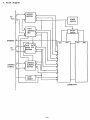
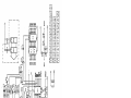
2. Block diagram
A
AO
-A15
V
, BUFFER
~ ADRESS
~r-n'
'\
~
PORT
A
ADDRESS 11
SET
Y
EXRESET
J
./
POWER
SUPPLY
-L
DAISY
CHAIN
~
•
IEI
f
DO
-D7
DIR
GATE
I
-\ DATA BUS
\.
,j
BUFFER
IEO
A
i\
L\
--V
I
1
CONTROL
SIGNAL
/
\
~
J
-y
,
~
CONTROL A..
SINGNAL
.I BUFFER 'r
\.
\
\
.;
..
r
y
AUTO
RESET
CONNECTOR
-2-
IEI
IEO
t,
3. Connector pin configuration
CNl
Parts
side
{)
Pin
No.
g
9
0
'1
2
{)
3
D
4
{)
Q
5
6
9 7
BUSst>
A 0
A
A
Back
side
1 GN
2 GN
3 GN
4 GN
5 GN
6 GN
7 GN
D
D
8
D
f)
D
D
8 GN-Q
9 GN 9
10 RESET
1
11 I~XRESO
2
12
13
14
15
16
17
18
19
A
3
A
4
A
A
A
A
A
5
6
7
8
9
A 10
A 11
A 12
A 13
A 14
A
CN2
15
HALT
GN D
;
M
FXWAIT
W
R
G N {)
{)
R
G N {)
20 10RQ
21 G N B
22 MREQ
23 G N 8
24 I N T
25
Pin
No.
1
2
3
4
5
6
7
8
Back
side
vcc
Vcc
o2 B
o3 B
o1 B
D4 8
Pin
No.
1
pin
A 9 B
Parts
side
VCC
~tRC"QB
1
{) 2 8
Vcc
A 8 B
B
2
3
f)
4
A.15 8
5
6
f)
f)
f)
f)
Back
side
2
3
4
5
6
GN"f)
~_
7
A6 8
D ~_._B_
GN D
068
A 158
o7 B
A 148
8
9
o0
CN4 AND 5
CN3
9
10
11
12
13
8US-~B
14
15 A 138
.16 Iv! 1 ~_
17 A12B
18 'W R EL
19 A 11 8
20 R f) B
21
A 108 22 IORQ8
-~
A 7..EL
HALT.IL
-----
I E I
10 A 5 8
11 ~
12 A 4 8
13 RSIB
14 A 3 8
15 EXRSTB
16 A 2 B
17
INTB
18 A 1 B
1 9 EXWAITB
20_ A 0 B
21 GN-D
22 GNf)
1 8
0 B
G N D
back
side
No.
3 8
4 B
5 [3
6 B
{) 7 [3
A 14 [3 7 Bus-iiB
A 13 [3 8
1--11 f3
f-'-'----rAJ28 9 WR [3
A 11 8 10 R {) G
A 10 B 1 1 IORQ8
A 9 8 12 MREQ8
A 8 g 13 G N f)
A 7 8 14 HALT 8
A 6 B 15
I E I
A 5 [3 16
I E
A 4 8 17 RSTB
A 3 B 18 "EX RST[3
A 2 [3 19
INTB
~---.lJl 20 EXWAITB
~
r-A-~ 21
G N 0 22 GND
a
-----
-
-3-
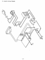
BUS BOARD
Fi?1J~.'
I
J:>.
I
to'i-iO:
,
1
1
1
liNe
.G-NQ
GNf)
GNO
GN
GN
.JiN
GN
GN£)
!-tAlT
'X1fF!:;ET
RESET
tiN£)
VI
WR
~
~
$ ill
~. ______ • _ _ _ • i
~O
~1
02
~.
£4
v5
-{)6
f)7
8tis~
A12
All
A1(1
A9
A8
A7
A6
A5
A4
AJ
A2
A1
AO
A1~
A15
A14
'--
;--
AC
~~
I
lAC
+sv
l
GN£)
BUS BOARD
1
+sv
GND
'--
POWER
SUPPLY
H
PL~o-JFILTE{]TRANS
I
···-~Ir-
t-
N
CN4.CN5
t
....Co
o
o
o....
0"
51
(1)
('t
rn
CJl
Co(
J:>.
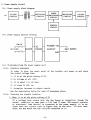
5. Power supply circuit
5-1. Power supply block diagram
AC
FILTER
CIRCUIT
-
RECTIFIER
CIRCUIT
-
POWER
RECTIFIER
FILTER
SWITCHING I-CIRCUIT I-- CIRCUIT
CIRCUIT
~
1
CONTROL
CIRCUIT
5-2. Power supply section wireing
SWICH
FILTER
o---<:r"<0--
~0 AC PLUG
POWER +5V
AC
TRANS
SUPPLY
-
...,
~
(8U S BOARD)
r".
GNO
~
5-3. Troubleshooting the power supply unit
5-3-1. Possible phenomena
In order to know the exact point of the trouble, put power on and check
the output voltage that;
1. it is at the given rating of 5V,
2. no voltage at all (OV),
3. it is about 1 to 4V only,
4. it rises to 15V, or,
5. irregular increase in output ripple.
See the description below for each of phenomena above.
5-3-2. Tracking the trouble location
1. When it is at the given rating of 5V
If a vol tage drop occurs wi th the Bus Board in connection, though the
normal condition is seen when a 2.5A load (2 ohms, 20W ceramic resistor
or electronic load device) is connected to the power supply, it is because that the circuit load is higher than 3A and more.
In this case,
check the Bus Board and the circuits connected to it.
-5-
2. When no output voltage is seen (OV)
1) Open fuse Fl
2) Defective Ql
3) Defective Rl6
4) Defective IC 24
5) Defective thermal fuse T1
Replace the above components in
reference with the figure to check
the defective component.
Check thermal fuse Tl
3. When the output is 1 to 4.5V
Replace component in reference with
the figure to check the defective
item.
4. It rises to l5V
Replace Ql with the new one when this conditions is encountered because
Ql is shorted in this case. If it remains the same after the replacement,
remove the cause that makes Ql destructed and replace the following
component in the given order to check the item causing the trouble.
Rll and Rl2 •••.. if still stays the same ••.•• D3, Cl7, and Rl3 •.•.• if
still stays the same •.••• then IC 24.
5. Irregular increase seen in the output ripple
Replace Cl7 as it might have been fatigued.
5-4. Tools required for the tests
1) Oscilloscope
2) Voltmeter or multimeter (digital multimeter is preferable)
3) A 5V, 2.5A load like the electronic load device or 2 ohms resistor of more
than 20W.
-6-
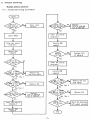
6. Trouble shooting
Mother Board section
6-1. Troubleshooting procedure
Replace
IC14 of AOB-A4B
IC3 of DOB-D7B
Check reset
circuit
Load S-BASIC
Enter the search
program-3
Enter the search
program-l
Execute RUN
command
Execute RUN
command
NO
Replace IC14
of A5B-A7B
RUN
Replace the
bus line cable
_Check if
~O
~d ~ go low a
Replace IC6
the same time
L...-_ _ _ _ _ _ _- - '
Check if ~
and 1m" to low at
the same time
~
~.
Replace the bus
line cable
Fig. 3
Fig. 2
Re(llace
IC14 of AOB-A7B
IC3 of DOB-D7B
..........Check if IQRSB~O
Replace IC6
<"and 1mB to low at
....... the same time
L...-______________
Fig. 4
~
Check the data bus
ijO select circuit
-7-
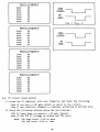
Search program-1
COOO
COOl
C002
C003
C004
C005
C006
3E
00
D3
00
C3
02
CO
IORQ
(lORQB)
im
(WRB)
Fig. 1 (Fig. 2)
Search program-2
coca
COOl
C002
C003
C004
C005
C006
3E
FF
D3
31
C3
02
CO
lORQ
(lORQB)
RD
(RDB)
I
I
Search program-3
coca
COOl
C002
C003
C004
C005
C006
3E
;FF
D3
FE
C3
02
CO
Search program-4
coca
COOl
C002
C003
C004
C005
C006
3E
00
DB
00
C3
02
CO
6-2. lC circuit check method
1) Press the lC insulator with your fingertip and check the following:
*see if too hot-----lC gate defect or short in the circuit.
*see if any condition changes-----improper soldering or printed wire.
2) Check the following defects using the oscilloscope;
*TTL lC logic" does not match-----lC gate failure
*see if the TTL lC voltage is within the TTL level.
NOTE: TTL high level: 2.5V or more
TTL low level: O.SV or less
-8-
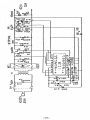
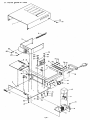
7. Circuit diagram ans parts layout
r
SEC
IN
~
C16
TK 580919
0 0
0
+ 0 RECI
I
o
o
~% ~
o-o~
,~
-'~ ;of
uOT
I
•~
~, i~
a:: 6
L1
~,
___ !!,
~
6«~!
~
o!!!!o
_ ~6
~
O~--.JI
OUT
Il.
a::
c
~
1
A ....
a::
0+
:J
0K
LOUT 5v.!I-
C17
%
lit
+
'-
...w-
OO
02
1 A
250 V
SHARP
A
SHARP
I
o
o
v--v
0
FUSE T
IN
_
C18
-RI7_
Q
BCE
IC24,~
~()+
'"
,_Q1
~
R22
A
OUT
~~O
~~
E44187
-9-
«
>"1
lI')N
.~
N
10
lI)
[t=~~=~~==~L-
________________________~
~
~d
crdJ...:~~Wr""'"
+ Lt:>.
+
91)
,
L-I~'_:!-l
+
+
61:>
61 M )1001
>
0,..,
N:J:
NO
':;ill')
-10-
I
I-'
I-'
I
CN1
A •
o
+
25
20
1C21
15
10
5
3IC14
C 10
-u-
IC2 IC3
rT
IC 1
-C~
05
J.
I
Ic5
CN 2-
~
IC15
(I
...C 13
IC
IC7
IC16
IC8
IC9
Icn
C 11
--c ~
CN3
D1
,..,.,
C1
+
R5
C2
f *~R4
+l~
I
IC 12
C9
--C~
22
J
~
~IC20
JR6
""'" Wv -u- C 3
R 1 R2
R3 1C19
~1~ C4~~
IC18
C8
--C~
IC10
~~
1 - . .
II
L---H22
1
IC22
IC4
C6
-C~
R'
t/')
0::
4.
:t:
('l..
4.
I
I\)
I-'
I
::
~""
All
412'
AIJ AI4
.lIS
:~O
I
IZI
"'
4
.
7
IC21
4
7
AI48
.lIS a
.
n
-
..
A9B
Aloa
AI18
.
IC2l!
I
A~B
A611
A71
~'
'~
mB
le: 14
Ala
A2B
A3B
A48
JIl.-_8 A08
.!iI
./8.sI
..A. IC 16
:>
>:=====+=:JJ
3, 3. ~
.z.
IC16
ICI6 13 1.2.
.1L ]0 -"=
"i
AO
AI
A2
A3
A4
A!I
A6
A1
1078
ioU
A~"
.leg •
1031 ~
~
•
Emfi
~~BAnb
ilt.b!
Jrij
141
F
RESn
GHQ
IC20
::!~J.,. ...iiJf ~T§'
:;'10
I
~l..~I
_4,r'~l
IC20
13 12
1,IC1I 1111
GHIl
GNO
\la:
~
WwIolT
~
HAl a
!!Ill.
~Q8
VCc
RSTI
I
I
7
\lice
028
C 4a
068
013
038
. OS8
• D711
.
~~
4
IC 3
.. ...
I
1
2
1
J
• I
5
I
6
GI;O
~BUS"'IJ
lIt 101
aus</l
DO
02
0 ..
D6
01
03
DS
07
L _ _ _ _ _ _ _ _ _ _ _ ..J
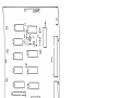
8. Actual wiring diagram
-13-
9. Parts guide
· t
& 1 1S
"
....... ~
30
~
-14-
25
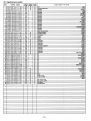
rn Electronics parts
NO.
I
2
3
4
5
6
7
8
9
10
11
12
13
14
15
16
17
18
19
20
21
22
23
24
25
26
27
28
29
30
31
32
33
34
35
36
37
38
39
40
41
42
43
44
45
46
47
48
49
50
51
52
53
54
55
56
PARTS CODE
oC F 9 5
I 3 5 I A/
OCF95-0401-A/
OCF95-2202 C/
VRD ST2EY221J
VRD-ST2EYI02J
VRD ST2EY332J
VRD ST2EY682J
VRD-ST2EY223J
VRD ST2EY330J
VRD ST2EYI03J
VRD ST2EY221J
VRD ST2EY561J
VRD ST2EY681J
VRD ST2EY182J
VRD-ST2EY202J
VRD ST2EY472J
VRD ST2EY333J
VRD-ST2EYI04J
VRS PT3ABI0lJ
OCF95-31 0 I-A/
OCF95 3 2 5 I A/
OCF95-2001 A/
o C F 9 5 2 3 0 I A/
VHDDSI588L2 1
o C F 9 5 2 3 0 2 A/
o C F 9 5 2 6 I 9 ·0/
o C F 9 5 260 9 M/
OCF95-2808 T/
o C F 9 5 2 6 0 9 A/
o C F 9 5 2 7 0 I A/
o C F 9 5 2807 C/
o C F 9 5 2 8 0 9 M/
OCF95-2615-G/
o C F 9 5 2 8 I 0 U/
o C F 9 5 2 8 1 I 0/
OAE30276973//
VHiSN74LSOO I
VHiSN74LS02 I
VHiSN74LS04 I
VHiSN74LSIO I
VHiSN74LSI4 I
VHiSN74LS22 I
VHiSN74LS30-1
VHiSN74LS244N
VHiSN74LS245N
VHiSN74LS42 I
OCF95 I 902 A/
o C F 9 5 I 9 0 2 B/
o C F 9 5 I 9 0 2 C/
OCF95-1902-D/
o C F 9 5 2 4 0 I A/
o C F 9 5 4502 A/
o C F 9 5 4 5 0 2 B/
o C F 9 5 4 506 A/
o C F 9 5 3 903 A/
o C F 9 5 4 504 A/
o C F 9 5 4 505 A/
o C F 9 5 4 I 0 5 A/
PRICE NEW
RANK MARK
AN
N
N
BC
AP
N
AA
AA
AA
AA
AA
AA
AA
AA
AA
AA
AA
AA
AA
AA
AA
AB
AE
N
N
AC
N
AL
AP
N
AB
AC
N
AU
N
AQ
N
N
AC
AC
N
AB
N
AD
N
AB
N
AA
N
AB
N
N
AC
AN
N
AE
AE
AE
AE
AM
AG
AE
AS
AR
AM
AT
N
AR
N
AP
N
AE
N
AE
N
AG
N
AF
N
AR
N
AP
N
AQ
N
BS
N
AV
N
PART
RANK
C
B
B
C
C
C
C
C
C
C
C
C
C
C
C
C
C
C
C
C
C
B
B
B
B
C
C
C
C
C
C
C
C
C
C
B
B
B
B
B
B
B
B
B
B
B
B
B
B
B
B
A
A
B
C
C
C
C
DESCRIPTION
[Ll
[T!
Coil
Power transformer
Rectifire
Resistor
Resistor
Resistor
Resistor
Resistor
Resistor
Resistor
Resistor
Resistor
Resistor
Resistor
Resistor
Resistor
Resistor
Resistor
Metal oxide resistor
Cement resisto r
Variable resistor
Transistor
Diode
Diode
Diode
Capacitor
Capacitor
Caoacitor
Capacitor
Polvester caoacitor
Capacitor
Capacitor
Capacitor
Capacitor
Capacitor
IC
IC
IC
IC
IC
IC
IC
IC
IC
IC
IC
IC
IC
IC
IC
LED
Fuse for UK
Fuse for 220V
[RECI
[R3
[R8
[R2 R6
[RI RS
[R4
[Rill
[RI4
R2S
[R7 R22
[RIS
[RIB
[R17
[R20 R21 R23
R24
RI9
RI2
RI6
VRI
[01
03
01
04
[C16
[C17
[Cl
[C19
C2l
[CIS
[C2
[C3
[C4
CS-C13C20
[lC24
ICI71Cl8
[ICll
IC161C20
[lClO
ICl9
[ICI2
[lC9ICIS
[lC61C141C22
[lC3
[IC8
[lC131C2l
IC41CS
[IClIC2
[lC7
[02
[FURS]
FURS]
SW]
AC cord for UK
AC cord for 220V
I/O Cable
Flexible board
-
,
!
•
-15-
[2J Mecha nica I pa rts
NO.
1
2
3
4
5
6
7
8
9
10
11
12
13
14
15
16
17
18
19
20
21
22
23
24
25
26
27
28
29
30
31
PARTS CODE
oC F 9 5
4 025 A/
OCF95-4024 A/
OCF95 4 0 2 6 A/
o C F 9 5 3 5 0 2 A/
OCF95 4 0 1 8 A/
OCF95-3501-A/
o C F 9 5 4 0 1 0 A/
o C F 9 5 4 034 A/
OCF95 4 0 2 1 A/
OCF95 4 0 2 7 A/
OCF95 4 5 0 7 A/
OCF95 4 03 7 A/
OCF95 4 004 A/
o C F 9 5 4 0 0 3 A/
o C F 9 5 4 0 2 3 A/
o C F 9 5 40 1 9 A/
OCF95 4 006 A/
OCF95 4 03 0 A/
OCF95 4 0 3 1 B/
XBPSD30P10000
o C F 9 5 4 0 1 2 A/
XBPSD40P08000
XBPSD26P06000
o C F 9 5 4 0 1 1 A/
XWSSD30 o 7 0 0 0
XWSSD40 o 7 0 0 0
XWHSD40 08000
XWHSD26 05000
OCF95 40 1 3 A/
OCF95-4016 AL
XBPSD30P10000
PRICE NEW
RANK MARK
BC
N
N
BB
N
AP
N
AU
AH
N
N
AQ
N
AB
AC
N
N
AK
N
AE
AA
N
AE
N
N
AE
AC
N
AG
N
AF
N
N
AC
N
AK
N
AC
AA
N
AA
AA
AA
AA
N
AA
AA
AA
AA
AA
N
AA
N
AA
PART
RANK
PRICE NEW
RANK MARK
AR
N
N
AC
AC
N
PART
RANK
0
0
0
C
0
C
C
0
0
0
C
C
0
C
0
0
0
0
0
C
C
C
C
C
C
C
C
C
C
C
C
DESCRIPTION
Cabinet Top
Chassis
PWB Guide angle
Connector for I/F slot
Guide rail for PWB
Connector for flexible cable
Pin
Soacer for PWB
Heat sink
Shield box for Power sup PRI.PWB
Fuse holder
I/O Cable Tie wrap
Badge (SHARP)
Leg
Maskinll frame for I/O slot
Masking cover for I/O slot
Bushing for I/O cable
Bushing for AC cord
Soacer for AC SW
Screw (M3X10
Screw (M3X5)
Screw (M4X8)
Screw (M26 x 6)
Screw (M3X5)
SDring washer(M31
Spring washer (M4)
WasherlM4)
Washer
Nut (M4)
Nvlon washer M3
Screw (M3XI0)
~ Other
NO.
PARTS CODE
1 o C F 9 5 900 1
2 OCF95 5 003
3 OCF95-5004
i/
A/
A/
0
0
0
DESCRIPTION
Instruction manual
Caution label ClnslBook)
Caution label (AC cord)
;
-16-