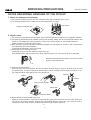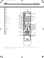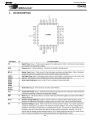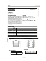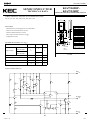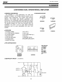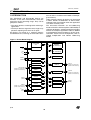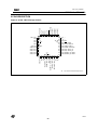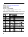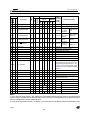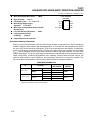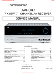
1
harman kardon Model DVD 47 DVD/CD/CD-R/CD-RW/VCD MP3 Player Service Manual - Contents SERVICE PRECAUTIONS………….……….……2 BASIC TROUBLESHOOTING GUIDE…………18 BASIC SPECIFICATIONS………………………...5 EXPLODED VIEW (120v)….……………………19 PACKAGE (120V)..………………....…….……….6 DISASSEMBLY PROCEDURE (120/230v).…...20 FRONT PANEL CONTROLS……………………..7 BLOCK DIAGRAM.……………..………………..22 INFORMATION DISPLAY…………….…………..8 ELECTRICAL PARTS LIST (120v)……… …….23 REMOTE CONTROL………………………….…..9 PCB DRAWINGS……………………..................40 REAR PANEL CONNECTIONS……………..….12 SEMICONDUCTOR PINOUTS…………………43 CONNECTIONS/SETUP……….………….........13 SCHEMATICS…………………………..…..……97 TEST SCREEEN.………………….…….............15 WIRING DIAGRAM……………………………..102 PLAYBACK BASICS……………………………..16 harman/kardon, Inc. 250 Crossways Park Dr. Woodbury, New York 11797 Rev1 8/2006 SERVICING PRECAUTIONS DVD47 harman/kardon NOTES REGARDING HANDLING OF THE PICK-UP 1. Notes for transport and storage 1) The pick-up should always be left in its conductive bag until immediately prior to use. 2) The pick-up should never be subjected to external pressure or impact. Drop impact Storage in conductive bag 2. Repair notes 1) The pick-up incorporates a strong magnet, and so should never be brought close to magnetic materials. 2) The pick-up should always be handled correctly and carefully, taking care to avoid external pressure and impact. If it is subjected to strong pressure or impact, the result may be an operational malfunction and/or damage to the printed-circuit board. 3) Each and every pick-up is already individually adjusted to a high degree of precision, and for that reason the adjustment point and installation screws should absolutely never be touched. 4) Laser beams may damage the eyes! Absolutely never permit laser beams to enter the eyes! Also NEVER switch ON the power to the laser output part (lens, etc.) of the pick-up if it is damaged. NEVER look directly at the laser beam, and don’t let contact fingers or other exposed skin. 5) Cleaning the lens surface If there is dust on the lens surface, the dust should be cleaned away by using an air bush (such as used for camera lens). The lens is held by a delicate spring. When cleaning the lens surface, therefore, a cotton swab should be used, taking care not to distort this. Pressure Magnet Pressure How to hold the pick-up Cotton swab Conductive Sheet 6) Never attempt to disassemble the pick-up. Spring by excess pressure. If the lens is extremely dirty, apply isopropyl alcohol to the cotton swab. (Do not use any other liquid cleaners, because they will damage the lens.) Take care not to use too much of this alcohol on the swab, and do not allow the alcohol to get inside the pick-up. 2 1 DVD47 harman/kardon NOTES REGARDING COMPACT DISC PLAYER REPAIRS 1. Preparations 1) Compact disc players incorporate a great many ICs as well as the pick-up (laser diode). These components are sensitive to, and easily affected by, static electricity. If such static electricity is high voltage, components can be damaged, and for that reason components should be handled with care. 2) The pick-up is composed of many optical components and other high-precision components. Care must be taken, therefore, to avoid repair or storage where the temperature of humidity is high, where strong magnetism is present, or where there is excessive dust. 2. Notes for repair 1) Before replacing a component part, first disconnect the power supply lead wire from the unit 2) All equipment, measuring instruments and tools must be grounded. 3) The workbench should be covered with a conductive sheet and grounded. When removing the laser pick-up from its conductive bag, do not place the pick-up on the bag. (This is because there is the possibility of damage by static electricity.) 4) To prevent AC leakage, the metal part of the soldering iron should be grounded. 5) Workers should be grounded by an armband (1MΩ) 6) Care should be taken not to permit the laser pick-up to come in contact with clothing, in order to prevent static electricity changes in the clothing to escape from the armband. 7) The laser beam from the pick-up should NEVER be directly facing the eyes or bare skin. Armband Resistor (1 Mohm) Resistor (1 Mohm) Conductive Sheet 3 2 DVD47 harman/kardon ESD PRECAUTIONS Electrostatically Sensitive Devices (ESD) Some semiconductor (solid state) devices can be damaged easily by static electricity. Such components commonly are called Electrostatically Sensitive Devices (ESD). Examples of typical ESD devices are integrated circuits and some field-effect transistors and semiconductor chip components. The following techniques should be used to help reduce the incidence of component damage caused by static electricity. 1. Immediately before handling any semiconductor component or semiconductor-equipped assembly, drain off any electrostatic charge on your body by touching a known earth ground. Alternatively, obtain and wear a commercially available discharging wrist strap device, which should be removed for potential shock reasons prior to applying power to the unit under test. 2. After removing an electrical assembly equipped with ESD devices, place the assembly on a conductive surface such as aluminum foil, to prevent electrostatic charge buildup or exposure of the assembly. 3. Use only a grounded-tip soldering iron to solder or unsolder ESD devices. 4. Use only an anti-static solder removal device. Some solder removal devices not classified as "anti-static" can generate electrical charges sufficient to damage ESD devices. 5. Do not use freon-propelled chemicals. These can generate electrical charges sufficient to damage ESD devices. 6. Do not remove a replacement ESD device from its protective package until immediately before you are ready to install it. (Most replacement ESD devices are packaged with leads electrically shorted together by conductive foam, aluminum foil or comparable conductive materials). 7. Immediately before removing the protective material from the leads of a replacement ESD device, touch the protective material to the chassis or circuit assembly into which the device will by installed. CAUTION : BE SURE NO POWER IS APPLIED TO THE CHASSIS OR CIRCUIT, AND OBSERVE ALL OTHER SAFETY PRECAUTIONS. 8. Minimize bodily motions when handing unpackaged replacement ESD devices. (Otherwise harmless motion such as the brushing together of your clothes fabric or the lifting of your foot from a carpeted floor can generate static electricity sufficient to damage an ESD device). 4 3 DVD 47 (120V) OM 3/30/06 10:41 AM Page 38 DVD47 harman/kardon DVD 47 TECHNICAL SPECIFICATIONS Applicable Disc: Disc formats: 5-inch (12cm) or 3-inch (8cm) DVD-Video, DVD-Audio, standard-conforming DVD-R, DVD+R, DVD-RW, DVD+RW, SACD™, VCD, CD, CD-R, CD-RW or MP3 discs Region code: DVD Video disc with Code 1 or 0 only DVD-Layers: Single side/single layer, single side/dual layer, dual side/dual layer Audio formats: DVD-Audio MLP lossless, SACD 2-channel or multichannel, Linear PCM, MPEG, Windows Media® 9, Dolby Digital or DTS Audio discs Still-image format: JPEG Video Signal System: NTSC ™ HDMI Output: Video: 480p, 720p, 1080i HDMI Version 1.0-compliant HDCP Version 1.1-compliant Composite Video Output: 1V p-p/75 ohms, sync negative polarity S-Video Output: Y/Luminance: 1V p-p/75 ohms, sync negative polarity C/Chrominance: 0.286V p-p Component Video Output: Y: 1V p-p/75 ohms, sync negative polarity Pr: 0.7V p-p/75 ohms Pb: 0.7V p-p/75 ohms Analog Audio Output: 2V rms (1kHz, 0dB) Frequency Response: DVD (Linear PCM): 2Hz – 22kHz +0/–0.5dB (48kHz sampling) 2Hz – 44kHz +0/–1.5dB (96kHz sampling) 2Hz – 88kHz +0/–0.5dB (192kHz sampling) CD: 2Hz – 20kHz +0/–0.5dB SACD: 2Hz – 100kHz +0/–0.5dB Signal/Noise Ratio (SNR): 105dB (A-weighted) Dynamic Range: DVD: 100dB (18-bit)/105dB (20-bit) CD/DVD: 96dB (16-bit) THD/1kHz: DVD/CD: 0.0025% Wow & Flutter: Below Measurable Limits AC Power: 110–240VAC/50–60Hz Power Consumption: 1 Watt (On/Standby)/13 Watts (Max) Dimensions (H x W x D): 2" x 17-3/10" x 11-1/4" (50mm x 440mm x 285mm) Weight: 6 lb (2.7kg) Shipping Dimensions (H x W x D): 5" x 14-3/8" x 20" (127mm x 365mmx 508mm) Shipping Weight: 8.8 lb (4kg) Depth measurement includes knobs and connectors. Height measurement includes feet and chassis. All specifications subject to change without notice. Harman Kardon, Harman International and Power for the Digital Revolution are registered trademarks of Harman International Industries, Incorporated. Dolby, Pro Logic and the double-D symbol are registered trademarks of Dolby Laboratories. Confidential Unpublished Works. 1992-1997 Dolby Laboratories, Inc. All rights reserved. Manufactured under license from Dolby Laboratories. DTS and DTS-ES are registered trademarks of DTS, Inc. Kodak and Photo CD are trademarks of Eastman Kodak Company. Microsoft, Windows Media, HDCD and High Definition Compatible Digital are registered trademarks of Microsoft Corporation in the United States and/or other countries. SACD is a trademark of Sony Electronics Inc. HDMI, the HDMI logo and High-Definition Multimedia Interface are trademarks or registered trademarks of HDMI Licensing LLC. This product incorporates copyright protection technology that is protected by method claims of certain U.S. patents and other intellectual property rights owned by Macrovision Corporation and other rights owners. Use of this copyright protection technology must be authorized by Macrovision Corporation and is intended for home and other limited viewing uses only unless otherwise authorized by Macrovision Corporation. Reverse engineering or disassembly is prohibited. 38 TECHNICAL SPECIFICATIONS 5 D1. V DInstruction 47 harman/kardon manual ass'y - Accessories 2 1 DVD47 2. Package Drawing DVD 47 PACKAGING & ACCESSORIES 3 1 MANUAL ASS'Y 6 CARD WARRANTY POLY BAG 4 5 6 3 SNOW PAD 3 MANUAL MANUAL INSTRUCTION OWNER'S SHEET, IMPORTANT 8 7 BATTERY ASS'Y 4 SNOW PAD 2 DVD47 SET 10 CABLE,S-VHS(1.5M) 11 CORD PIN(3P, W/R/Y) OUTER BOX ,OUT CARTON CARTON CORF ,JACK(MONO)1200MM 12 CABLE, HDMI(2M) NO DESCRIPTION STAPLE PARTS NO. Q,ty POLY BAG CPB1061Y 1 CARD WARRANTY CQE1A172X 1 HARMAN IMAGE BROCHURES HQE1A273Z 1 SHEET, IMPORTANT CQE1A169Z 1 OWNER'S MANUAL INSTRUCTION MANUAL CQX1A1050Z BATTERY CABR03P 2 CORD,PIN(3P,W/R/Y) CJS4S004Z 8 CABLE,S-VHS(1.5M) 9 CORD,JACK(MONO)1200MM 1 2 3 NO DESCRIPTION PARTS NO. Q,ty 4 5 1 MANUAL ASS'Y C 1 2 DVD47 SET DVD 47 DVD27SET 1 1 3 SNOW,PAD CPS1A714 2 CJS0I006Z 1 4 SNOW,PAD CPS1A715 1 CJS9D002Z 1 CPG1A798X 1 CARTDVD47 1 1 6 7 5 10 AC CORD CJA2A085Z 1 11 CABLE,HDMI(2M) CJS8T001Z 1 STAPLE KPL0905 3 12 SNOW PAD 9 5 CORD PIN(3P, W/R/Y) REMOCON ASS'Y HARMAN IMAGE BROCHURES 6 6 7 DVD 47 OUTER CARTON BOX,OUT CARTON REMOCON ASS'Y DVD 47 (120V) OM 3/30/06 10:41 AM Page 9 DVD 47 JPEG DVD47 VCD MP3 PROG RANDOM A – B TITLE TRACK DVD WMA AUDIO/VIDEO Open/Close REPEAT CHAP 1 ALL PBC V. OFF TEST harman/kardon HOUR MIN FRONT-PANEL CONTROLS P. SCAN SEC DVD 47 12 3 4 5 6 7 89 AUDIO/VIDEO Open/Close ) ! @ NOTE: To make it easier to follow the instructions that refer to the controls and connectors in this illustration, a larger copy may be downloaded from the Product Support section for this product at www.harmankardon.com. 0 Power Indicator 1 Power On/Off (Standby) 2 Play 3 Pause 4 Stop 5 Skip/Search Reverse 6 Skip/Search Forward 7 Remote Sensor 8 Display Dimmer 9 Disc Drawer ! Open/Close @ Information Display 1 Power Indicator: This indicator lights amber when the unit is connected to an AC power source, but is not turned on. When the unit is on, the indicator lights blue. 6 Skip/Search Reverse: Press this button once to return to the start of the current chapter for a DVD or track for a CD. Subsequent individual presses will skip backwards through the available chapters or tracks. Press and hold the button to play the disc in the fast reverse mode at the speed indicated in the on-screen display and by the Playback Mode Indicators O. 8 Display Dimmer: Press this button to reduce the brightness of the Information Display @ by 50% or to turn the display off completely in the following order: FULL BRIGHTNESS ➔ HALF BRIGHTNESS ➔ OFF ➔ FULL BRIGHTNESS. 1 Power On/Off (Standby): Press the button once to turn the DVD 47 on. Press it again to put the unit in the Standby mode. 2 Play: Press to initiate playback or to resume playback after the Pause Button 3K has been pressed. 3 Pause: Press this button to momentarily pause playback. To resume playback, press the button again. If a DVD is playing, action will freeze and a still picture will be displayed when the button is pressed. 4 Stop: Press this button once to place the disc in the Resume mode, which means that playback will stop, but as long as the tray is not opened or the disc changed, playback will continue from the same point on the disc when the Play Button 2M is pressed again. Resume will also work if the unit was turned off. Resume will not operate for WMA files or VCDs that do not have playback control. To stop a disc and have play start from the beginning, press the button twice. 7 Skip/Search Forward: Press this button once to move to the start of the next chapter for a DVD or track for a CD. Subsequent presses will skip forward through the available chapters or tracks. Press and hold the button to play the disc in the Fast Play mode at the speed indicated in the on-screen display and by the Playback Mode Indicators O. 8 Remote Sensor: The sensor that receives commands from the remote control is behind the front panel in this area. To ensure proper operation of the player with the remote, it is important that this area not be covered. In the event that the player is enclosed in a cabinet or if the remote sensor is covered, you may extend the remote sensor by connecting an optional, external remote sensor to the Remote Control Input ™ on the rear panel (see page 14). When optional, external IR “blasters” are used for system control, they should be positioned so that they point at this area. 7 ) Disc Drawer: This drawer is used to hold the discs played in the unit. Be certain to seat all discs carefully within the recess in the drawer. Do not press down on the drawer when it is open, to avoid damage to the player. When the drawer is left open with no activity for 5 minutes, it will automatically close to prevent dust or dirt from entering the component, and to prevent accidental damage. If a disc is present, the DVD 47 will immediately begin playback. ! Open/Close: Press this button to open or close the disc tray. @ Information Display: The Information Display provides status information on the player and the disc being played through a series of specific indicators and messages that appear in the display. See page 10 for more information on the display. FRONT-PANEL CONTROLS 9 DVD 47 (120V) OM 3/30/06 10:41 AM Page 10 DVD47 harman/kardon FRONT-PANEL INFORMATION DISPLAY DE F GH I C B J K A O N L M NOTE: To make it easier to follow the instructions that refer to the controls and connectors in this illustration, a larger copy may be downloaded from the Product Support section for this product at www.harmankardon.com. A Disc-Type Indicators B Audio Bitstream Indicators C Parental Lock Indicator D Program Indicator E Angle Indicator F Random Indicator G A-B Repeat Indicator H VCD Playback Control Indicator I Repeat Indicators J V-OFF Indicator K Video Indicators L Time Indicators M Chapter/Track Number Indicators N Group/Title Indicators O Playback-Mode Indicator A Disc Type Indicators: The DVD, DVD-Audio, SACD, CD, VCD, MP3, WMA or JPEG indicator will light to show the type of disc currently being played. F Random Indicator: This indicator lights when the unit is in the Random Play mode. M Chapter/Track Number Indicators: When a DVD disc is playing, these two positions in the display will show the current chapter. When a DVD-Audio, SACD or CD disc is playing they will show the current track number. NOTE: The DVD 47 does not have an HDCD® (High Definition Compact Digital®) decoder. Therefore, to benefit from HDCD encoding, make sure to connect one of the DVD 47’s Digital Audio Outputs 34 to your receiver or processor with HDCD encoding. If your receiver or processor does not have HDCD decoding, you may still enjoy conventional CD playback of the disc. B Audio Bitstream Indicators: When a Dolby® Digital, DTS® or linear PCM digital audio signal is present on the disc, one of these indicators will light. DVD-Audio, MP3 and WMA bitstreams will be indicated by the Disc Type Indicator A. C Parental Lock Indicator: This indicator lights in red when the parental-lock system is engaged in order to prevent anyone from changing the rating level without a code. D Program Indicator: This indicator lights when a playlist has been programmed using the menu system (available for CDs only). See page 36 for more information on programming playlists. E Angle Indicator: This indicator blinks when alternative viewing angles are available on the DVD currently playing. 10 G A-B Repeat Indicator: This indicator lights when a specific passage for repeat playback has been selected. H VCD Playback Control Indicator: This indicator lights when the playback control function is turned on for VCDs. I Repeat Indicators: These indicators light when any of the Repeat functions are in use. J V-OFF Indicator: This indicator lights in red when the unit's video output has been turned off by pressing the V-OFF Button F on the remote control. K Video Output Indicators: When the DVD 47 is connected to a video display using the HDMI Output 2, the display sends information to the DVD 47 indicating the highest video resolution it is capable of handling, and the DVD 47 automatically sets the video output to match it. That resolution is displayed here. You may use the HD Mode Selector G to manually select a lower video output resolution. L Time Indicators: These positions in the display will show the running time of a disc in play. NOTE: The indicators LMN will also display text messages about the DVD’s status, including LOADING when a disc is loading, POWER OFF when the unit is turned off, and DISC ERROR when a disc not compatible with the DVD is put into the play position. FRONT-PANEL INFORMATION DISPLAY 8 N Group/Title Indicators: These two positions in the display will show the current title number when a DVD disc is playing, or the current group for a DVD-Audio disc. O Playback-Mode Indicators: These indicators light to show the current playback mode: › Lights when a disc is playing in the normal mode. This indicator will flash when the disc is in Forward Slow Play mode. The on-screen banner display indicates the selected speed (1/2, 1/4, 1/8 or 1/16). ›› When the DVD 47 is in the Fast Search play mode, two of these indicators will light to show that the unit is in a Fast Play mode. The on-screen banner display indicates the selected speed (x2, x4, x8, x20 or x100). Fast Play mode is not available for WMA files. ± Lights when the disc is paused. ‹‹ Lights when the disc is in the Fast Search Reverse mode. The on-screen banner display indicates the selected speed (x2, x4, x8, x20 or x100). Fast Search Reverse mode is not available for WMA files. ‹ Flashes when the disc is in Reverse Slow Play mode. The on-screen banner display indicates the selected speed (1/2 or 1/4). DVD 47 (120V) OM 3/30/06 10:41 AM Page 11 DVD47 harman/kardon REMOTE CONTROL FUNCTIONS 0 Power On 1 Open/Close 2 Audio Select 3 Clear 4 Playlist 5 Repeat 6 A-B Repeat 7 Random 8 Info 9 Setup A Previous Step/Skip B Search/Slow Reverse C Angle D ⁄/¤/‹ / › Navigation Buttons E Light F Video Off G HD Mode Selector H Dimmer I Progressive Scan/Interlaced J Enter K Pause L Zoom M Play N Search/Slow Forward O Stop P Next Step/Skip Q Disc Menu R Status S Numeric Keys T Title U Subtitle V Power Off W IR Emitter W 0 V 1 3 2 U T 4 S 5 6 7 9 8 Q A R P O B M C N L K D J F E I HD MODE G H ® 47 NOTE: To make it easier to follow the instructions that refer to the controls and connectors in this illustration, a larger copy may be downloaded from the Product Support section for this product at www.harmankardon.com. 9 REMOTE CONTROL FUNCTIONS 11 DVD 47 (120V) OM 3/30/06 10:41 AM Page 12 DVD47 harman/kardon REMOTE CONTROL FUNCTIONS 0 Power On: Turns on the player when it is in Standby mode (Harman Kardon logo appears onscreen). 1 Open/Close: Press to open or close the disc tray. 2 Audio Select: Press to access various audio languages on a DVD (if the DVD contains multiple audio streams). This button may also allow you to access other audio formats on DVD discs, such as linear PCM or Dolby Digital 5.1 tracks (or other formats), if they’ve been recorded on the disc. 3 Clear: Press this button to remove on-screen menus or banners from the display screen. Press this button to clear the current play order displayed next to a track while programming a playlist. In Stop mode and with all menus and banners removed from the display, press and hold this button for five seconds to reset all settings to their factory defaults. 4 Playlist: Press this button to access the Playlist on-screen menu, which enables you to change the order in which tracks are played on a CD or DVDAudio disc. (See page 36 for more information on creating and playing playlists.) 5 Repeat: Each press of this button changes the playback mode to repeat a chapter or track or the entire disc. A repeat icon will appear in the upper right corner of the screen indicating the current repeat mode. If the Player Information Screen is active, the changes will be displayed on screen. 6 A-B Repeat: Press this button to enter the starting point of a section on a disc you wish to repeat. The second press enters the end of the selection to be repeated. Once the “A” (start) and “B” (end) points have been entered the player will repeat the selection until the Play Button M3 is pressed or the disc is stopped. If the Player Information Screen is active, the changes will be displayed on screen. 7 Random: Each press of this button starts or stops playback in random order. The Random function is only available when playing CDs, but not when a Playlist is active (the Player Information screen indicates Programmed Order on the Playlist line). 8 Info: Press once to access the Player Information menu for information on the current disc and the playback mode settings. Press again to remove information from screen. See page 28 for more information on the Player Information menu. 9 Setup: Press this button to use the DVD 47’s on-screen menu system to adjust the player’s configuration settings. Note that the Info Button 8 must be pressed to access the DVD 47’s Player Information menu to obtain detailed disc information, and to configure the playback mode of the disc. A Previous Step/Skip: Press this button once to skip back to the beginning of the current chapter on a DVD or track on a CD or DVD-Audio disc. Press it again to continue to skip back through the previous 12 chapters or tracks. After first pressing the Pause Button K, press this button to step backwards through a DVD or VCD as a series of still image frames. B Search/Slow Reverse: This button initiates fast or slow play in the reverse mode. For fast reverse play, each press of the button when playing DVD or VCD discs changes the speed as indicated by the number appearing in the upper right corner of the screen. For slow reverse play, first press the Pause Button K and each subsequent press of this button will change the slow play speed as indicated by the number appearing in the upper right corner of the screen. C Angle: Press this button to change the camera angle on discs programmed for multiple-angle views. When a JPEG is being displayed, pressing the Angle Button C repeatedly causes the on-screen image to rotate clockwise by 90 degrees each press. The current orientation in degrees will be displayed in the upper right corner of the screen. D M NKLNavigation Buttons: Use to move the cursor in the on-screen menu system. E Light: Press to illuminate the buttons on the remote controller. F Video Off: Press this button to turn off the video output for improved audio performance when playing discs. Press it again to view the on-screen menus. It is highly recommended that you use this function to prevent “burn-in” of your plasma video display. G HD Mode Selector: When the DVD 47 is connected to a video display using the HDMI Output 2, the display sends information to the DVD 47 indicating the highest video resolution it is capable of handling, and the DVD 47 automatically sets the video output to match it. Pressing this button allows you to manually change the output resolution, with your selection indicated by the Video Output Indicators K. The DVD 47 will not allow you to select a resolution beyond the capabilities of your display, and if you try to do so, an on-screen error message will appear to alert you to the selection of an incompatible video format. Changes made with this button remain active until the DVD 47 or the display is turned off. When either is turned off, and then on again, the DVD 47 will revert to the default setting transmitted by the display. H Dimmer: Press to change the brightness of the front panel display or to turn the display off completely in the following order: FULL BRIGHTNESS ➜ HALF BRIGHTNESS ➜ OFF ➜ FULL BRIGHTNESS I Progressive Scan/Interlaced Button: Each press of this button selects between the progressive scan and interlaced modes for the Component Video Outputs ∞. This button will not have any effect while the Setup menu system is active, indicated by ÐSETUP- appearing in the Information Display B. Press the Setup Button 9 to clear the Setup menu, and then press this button to toggle between REMOTE CONTROL FUNCTIONS 10 the progressive scan and interlaced component video settings. J Enter: Press this button to enter a setting in the DVD 47 menu system or to confirm a menu selection choice in a disc’s on-screen menu. K Pause: Press this button to pause the disc and freeze the picture during DVD or VCD playback, or to pause the playback of a CD or DVD-Audio disc. To play a DVD or VCD in the slow-forward or -reverse mode, first press this button and then press either the Search/Slow Forward N or Reverse Button B. L Zoom: Press this button to zoom in on the image from a DVD, VCD or JPEG image. The image may be expanded by a factor of x2, x3, x4 or x5. Once the on-screen indication of the zoom ratio disappears from the screen you may use the Navigation Buttons D to explore the picture. M Play: Press this button to begin the playback of a disc, or to resume normal playback when a disc has been paused or scanned. N Search/Slow Forward: This button initiates fast or slow play in the forward mode. For fast forward play, each press of the button when playing DVD or VCD discs changes the speed as indicated by the number appearing in the upper right corner of the screen. For slow forward play, first press the Pause Button K and each subsequent press of this button will change the slow play speed as indicated by the number appearing in the upper right corner of the screen. O Stop: When a DVD is playing, press this button once to place the disc in the Resume mode, which means that playback will stop. However, as long as the disc drawer is not opened, playback will continue from the point where the disc was stopped when the Play Button M3 is pressed again, as indicated by the LAST SCENE message (for DVDs) or the RESUME message (for CDs, MP3 files, JPEG files and VCDs with PBC) in the Information Display B. Resume will not operate for WMA files or VCDs that do not have playback control. Pressing the button twice will stop the disc and play will start from the beginning of the disc when the Play Button M3 is pressed again. P Next Step/Skip: Press this button once to advance to the beginning of the next chapter on a DVD or track on a CD. Press it again to continue to advance through the remaining chapters or tracks. After first pressing the Pause Button K, press this button to step through a DVD-Video disc as a series of still-image frames. Q Disc Menu: While a DVD is playing, press this button to view the disc’s main menu. R Status: Press while a disc is playing to view the on-screen status banner display. The first press will display the current title and chapter, the play mode icon and the elapsed time, along with a “temperature DVD 47 (120V) OM 3/30/06 10:41 AM Page 13 DVD47 harman/kardon REMOTE CONTROL FUNCTIONS bar” display of the time elapsed. You may use the M NKLNavigation Buttons D and the Enter Button J to select and change the current title or chapter, or the time display. The Status Banner is only available for DVDs and VCDs when PBC is turned off. Press the button one more time to remove the status displays from the screen. More detailed information about the disc is available by pressing the Info Button 8. S Numeric Keys: Press these buttons to enter a number. T Title: When a DVD is playing, press this button to go back to the main title menu for the disc being played. If you are playing a DVD-Audio disc that contains other formats the DVD 47 is capable of playing, such as linear PCM or Dolby Digital 5.1, pressing this button may enable you to switch playback from one audio format to another. U Subtitle: When a DVD is playing, press to select a subtitle language or to turn subtitles off. NOTE: Due to the variations in how DVD discs are authored, the subtitle languages displayed by the DVD 47 may not accurately reflect the actual languages available on the disc. It is recommended that subtitles be selected using the disc’s menu. V Power Off: Puts the player in Standby mode. W IR Emitter: This small, clear button-like device sends the IR commands from the remote control to the DVD 47. To ensure proper performance of the remote control, be sure to point it toward the unit and do not cover it with your fingers when sending remote commands. 11 REMOTE CONTROL FUNCTIONS 13 DVD 47 (120V) OM 3/30/06 10:41 AM Page 14 DVD47 harman/kardon REAR-PANEL CONNECTIONS AC INPUT 120V~, 60Hz 13W 0 2 1 6 4 3 5 A 8 9 7 NOTE: To make it easier to follow the instructions that refer to the controls and connectors in this illustration, a larger copy may be downloaded from the Product Support section for this product at www.harmankardon.com. ¡ Remote Control Output ™ Remote Control Input £ HDMI Output ¢ Optical Digital Audio Output ∞ Coaxial Digital Audio Output § Component Video Outputs ¶ Composite Video Output • S-Video Output ª Analog Audio Outputs ‚ 6-Channel Audio Outputs ⁄ AC Power Cord ¡ Remote Control Output: Connect this jack to the infrared (IR) input jack of another compatible remotecontrolled product to have the built-in Remote Sensor on the DVD 47 provide IR signals to other compatible products. ¢ Optical Digital Audio Output: Connect this jack to the optical digital input of an A/V receiver or surround processor for Dolby Digital, DTS or PCM audio playback. ¶ Composite Video Output: Connect this jack to the video input on a television or video projector, or to a video input on an A/V receiver or processor if you are using that type of device for video input switching. ∞ Coaxial Digital Audio Output: Connect this jack to the coaxial digital input of an A/V receiver or surround processor for Dolby Digital, DTS or PCM audio playback. • S-Video Output: Connect this jack to the S-video input on a television or video projector, or to an S-video input on an A/V receiver or processor if you are using that type of device for S-video input switching. NOTES: • Connect either the Optical Digital Audio Output ¢ or the Coaxial Digital Audio Output ∞ to a corresponding digital audio input on your receiver or processor, but not both. ª Analog Audio Outputs: Connect these jacks to an audio input on an A/V receiver, surround processor or your television for analog audio playback. ™ Remote Control Input: Connect the output of a remote infrared sensor, or the remote control output of another compatible product, to this jack. This will enable the remote control to operate even when the front-panel Remote Sensor on the DVD 47 is blocked. This jack may also be used with compatible IR remote control-based automation systems. £ HDMI Output: If you have an HDMI-compatible receiver or video display device, connect this output to an HDMI input on the receiver or video display for the highest-quality uncompressed digital audio and video available. Even if your receiver is not capable of processing audio in the HDMI format, you may still experience the superb reproduction of HDMI video. If your video display has a DVI input, you may use an optional HDMI-to-DVI cable or adapter for the connection to the display. In all cases, the video display must be HDCP-compliant in order to use the HDMI output. For best results, we do not recommend HDMI connections in excess of ten feet. The following audio formats may be output via the HDMI connection: Audio CD – 2-Channel PCM or 5.1-channel DTS DVD-Audio and SACD – 2-Channel PCM DVD-Video – Up to 5.1-channel Dolby Digital or DTS NOTE: To hear the high-resolution surround sound recorded on DVD-Audio and SACD discs, you need to connect the 6-Channel Audio Outputs 9 to the corresponding input jacks on your receiver or processor. These formats are not output digitally. 14 REAR-PANEL CONNECTIONS • The coaxial digital output should only be connected to a digital input. Even though it is the same RCAtype connector as standard analog audio connections, DO NOT connect it to a conventional analog input jack. § Component Video Outputs: These outputs carry the component video signals for connection to display monitors with component video inputs. For standard analog TVs or projectors with inputs marked Y/Pr/Pb or Y/Cr/Cb, connect these outputs to the corresponding inputs. If you have a high-definition television or projector that is compatible with high-scan-rate progressive video (480p or better), connect these jacks to the HD component inputs. If you are using a progressive scan display device, PROGRESSIVE must be selected in the Video menu in order to take advantage of the progressive scan circuitry. See the “Scan Type” section on page 23 for more information on progressive scan video. IMPORTANT: These jacks should NOT be connected to standard composite video inputs. 12 ‚ 6-Channel Audio Outputs: Connect these outputs to the matching 6-channel analog audio inputs on your receiver or surround sound processor. This connection is required to listen to the multichannel tracks on SACD and DVD-Audio discs. If the disc also contains a linear PCM, Dolby Digital or DTS track, you may listen to it using the HDMI 2, Optical ¢ or Coaxial Dgital Audio Output £ or the Analog Audio Outputs ª. ⁄ AC Power Input: Plug the female end of the AC power cord included with the DVD 47 into this input, and then connect the other end of the cord to an AC outlet. If the outlet is controlled by a switch, make certain that it is in the ON position. Do not substitute another power cord for the one provided with the DVD 47. If the cord becomes damaged, contact your authorized Harman Kardon dealer for a replacement. NOTE: You’ll find more details about all audio/video connections under Setup and Connections on the following pages. DVD 47 (120V) OM 3/30/06 10:41 AM Page 15 DVD47 harman/kardon SETUP AND CONNECTIONS • Ensure that the power switch of this unit (and of other equipment to be connected) is set to “Off” before commencing connection. We also strongly recommend that you leave all system components unplugged from AC power until after you have completed the interconnections described in this section. • Do not block the ventilation holes of any of the equipment and arrange them so that air can circulate freely. • Read through the instructions before connecting other equipment. • Ensure that you observe the color-coding when connecting audio and video cables. VIDEO NOTES: • For the best quality, if your receiver or processor and/or video display are HDMI-capable, we recommend using the HDMI output. With a single cable connection between components, HDMI is able to deliver uncompressed high-definition digital video and digital audio programming. Even without audio processing capability, your HDMI-ready receiver will be able to pass the uncompressed digital video signal to your video display. NOTE: If your video display has a DVI input, you may use an optional HDMI-to-DVI cable or adapter for the connection to the display. In all cases, the video display must be HDCP-compliant in order to use the HDMI output. • If your equipment is not HDMI-ready, we recommend the use of component video for higher quality pictures. You may also use the standard S-video or composite video connection if your TV does not have component video inputs. The component and S-video outputs are not available simultaneously. • The composite video output (yellow) sends the complete video signal to the TV (or to the A/V receiver) by one cable only. Use this video output when your TV set is equipped with a video input jack only. • The S (separate) video output connector separates the color (C) and luminance (Y) signals before transmitting them to the TV set in order to achieve a sharper picture. Use the S-video cable when connecting the player to a TV equipped with an S-video input for improved picture clarity. • The component video outputs further separate the color components of the video signal, optimizing the DVD 47’s video performance. Component video connections are preferred, when available on your TV or receiver. If you are using a television or video display that is compatible with high-resolution 480P video signals, make sure to use the input jacks on the video display marked “HD Component,” if available. Also, make sure to configure the display’s input settings for use with “480P” video signals. You will also need to change the scan type in the DVD 47’s Video Setup menu from “Interlaced” to “Progressive.” See page 23. • Modern audio/video receivers are capable of connection to several video source devices, such as the DVD 47 and a VCR, cable television set-top box, HDTV tuner or other device. The receiver is equipped with video monitor outputs for connection to your television, projector or plasma display. As you select any input source device, the receiver selects the correct video input and routes it to the correct video monitor output to your television. It is recommended that you connect one of the video outputs from the DVD 47 to the corresponding input on your receiver to simplify operation of your home entertainment system. Refer to the owner’s guide for your receiver for more information. • If your receiver is capable of multiroom operation, it is recommended that you connect both the component (or HDMI) and composite video outputs of the DVD 47 to the receiver. This enables the highestquality picture (component video) for viewing in the main listening room, while enabling the multiroom system, if it is video-capable, to distribute the composite video signal to the remote zone. Consult the owner’s guide for your receiver to determine whether it has video multiroom capability. Connecting to a TV Only When using the DVD 47 with a television but no audio receiver or processor, connect it as follows. Make the Analog Audio Connection å and one of the Video Connections (Composite Video ∫, S-Video ç, Component Video ∂). If your television or video display is HDMI-capable, you only need to make the HDMI é connection, as it handles both audio and video. Remember to plug in the power cord. TV To HDMI or DVI port on TV é To Y (green)/ Pb (blue)/ Pr (red) component video connectors ∂ To S-video input connectors on the TV To video input connectors (yellow) on the TV To analog audio input connectors (red/white) on the TV ç ∫ å To power outlet (AC 120V/60Hz) AC INPUT 120V~, 60Hz 13W 13 SETUP AND CONNECTIONS 15 DVD 47 (120V) OM 3/30/06 10:41 AM Page 16 DVD47 harman/kardon SETUP AND CONNECTIONS Connecting to a Receiver/Amplifier With a Dolby Digital or DTS Decoder One of the major advantages of the DVD format is its ability to use a variety of digital audio formats for the ultimate in sonic performance. However, in order to enjoy the benefits of digital audio, you must use a receiver or processor that has digital audio decoding capabilities and make an optical or coaxial digital audio connection between the DVD 47 and your home theater system. This simple connection is made as shown below with an optional coax or optical cable. Only one of these connections is required, and both should not be made at the same time. In order to take advantage of the high-resolution SACD and DVD-Audio output of the DVD 47, you must connect the 6-Channel Audio Outputs 9 to the matching 6-channel inputs on your receiver or processor. Only compressed PCM, Dolby Digital or DTS tracks that may be present on the disc may be listened to using the digital audio outputs. Thus, the DVD 47 decodes the digital signal and outputs separate signals for each channel: front left, center, front right, surround right, surround left and lowfrequency effects (LFE). • When the audio signal is to be fed to an analog receiver rather than to the TV, connect the Analog Audio Outputs ª to any analog audio inputs on your receiver or processor. The DVD 47 will “downmix” multichannel recordings to two channels. • The analog audio connection should also be made if you wish to play high-resolution 96kHz PCM audio discs where your receiver does not support 96kHz processing. NOTES ON VIDEO: • With multiple video sources, your audio/video receiver can be used for selecting the video signal and routing it to the TV. Connect the HDMI 2, Component ∞, Composite § or S-Video ¶ output of the DVD 47 to the correct video input on your receiver, and the video outputs of the receiver to your TV. For more details, see the manual for your audio/video receiver. • If your receiver has only DVI inputs, you may use an optional HDMI-to-DVI cable or adapter for the connection to the receiver. In addition, the video display used with your system must be HDCP-compatible in order to take advantage of the HDMI output, whether it is used with HDMI or DVI connections. NOTES FOR ANALOG AUDIO: • If you wish to use the DVD 47 as the input for a multiroom system, the Analog Audio Outputs ª should be connected to the standard analog left/ right DVD or CD inputs on your digital receiver or processor. Connecting to a Receiver • The connection from the Analog Audio Outputs ª to the TV is optional. If you plan on occasionally Front Speakers (Left/Right) using your DVD 47 alone, without turning on your complete system, this connection must be made. Center Speaker When using the DVD 47 with an audio/video receiver or processor, connect it as follows. First, make one Surround Speakers (Left/Right) Subwoofer Dolby Digital/DTS A/V Receiver or Processor To HDMI or DVI port To optical digital audio input connectors ˙ © To coaxial digital audio input connectors ƒ é To Y (green)/ Pb (blue)/ Pr (red) component video connectors ∂ To S-video input connectors To video input connectors (yellow) ç ∫ of the video connections (Composite Video ç, S-Video ∂, Component Video é or HDMI ˙) to the video input jacks on the A/V receiver, and then connect the receiver’s video monitor output to the TV. If you will sometimes use the TV without the audio component, you may optionally make the Analog Audio Connection ∫ to the TV. In addition, to benefit from the high-resolution surround sound formats recorded on SACD and DVD-Audio discs, which are not output via the HDMI connection, you will need to make the 6-Channel Audio Connection å to your receiver or processor. Second, if your receiver or processor is not HDMIcapable, make either the Optical Digital Audio Connection © or the Coaxial Digital Audio Connection ƒ, to the receiver or processor. Remember that when the HDMI connection is used with a receiver or processor that is compliant with the HDMI format, a single connection suffices for both audio and video, except for SACD and DVD-Audio discs, as noted. If your receiver or processor is not capable of processing the HDMI audio signal, then a separate audio connection is required. If your receiver/ processor has multiroom capability, you may also connect the DVD 47’s analog audio outputs to the DVD analog audio inputs on the receiver. IMPORTANT NOTE: Make certain that any device being connected, including the DVD 47, your receiver or processor and your TV or video display, is turned off whenever you make connections between products. HDMI, DVI, Component, S-video and/or Composite video monitor outputs To analog audio input connectors (red/white) on the TV or receiver (see above) TV To 6-channel analog audio inputs on receiver To power outlet (AC 120V/60Hz) å AC INPUT 120V~, 60Hz 13W 16 SETUP AND CONNECTIONS 14 DVD 47 (120V) OM 3/30/06 10:41 AM Page 25 DVD47 harman/kardon TEST SCREEN DVD is one of the highest quality sources ever made available for in-home playback of prerecorded pictures and sound. In order to make certain that your home theater system is fully optimized to take advantage of DVD’s superb picture quality, the DVD 47 offers a built-in video test signal that makes it easy to calibrate your TV or video display for proper playback. Test Screen With the test screen showing on your video display, the following adjustments may be made: • The proper color intensity setting on your TV. • Proper color adjustments using the color bars, which should be (left to right) black, white, yellow, cyan (turquoise), green, magenta, red, blue, black. • The proper color transition, seen as sharp separation of the bars. • The performance of the color circuits in your TV (with “Video” signals); bar edges should show no vertical crawling dots. With the gray scale and the black/white fields below the color bars, the brightness and contrast of your screen can be adjusted. NOTE: Most of the video adjustments using the DVD 47’s test screen should be made using the controls on your video display, with the DVD 47’s controls set at their factory default position in the center. If necessary, you may tweak the brightness and sharpness using the controls found in the DVD 47’s video adjustments menu. Color Bars Gray Scale 100% Black/White Fields Figure 10 TV Picture Adjustment With Test Screen Brightness Adjustment: 1. Turn down the color control on your TV until the color bars are visible in black and white. 2. Adjust the contrast on your TV to the lowest level where you still can see all bars within the gray scale in the test picture separately and clearly. 3. Adjust the brightness using the DVD 47 video adjustments control so that the bars in the gray scale are all visible. The bar furthest to the left has to be as black as possible rather than gray, but the next gradation must clearly be distinct from it. All the bars in the gray scale should be gradually and evenly changing from black to white, going from left to right. Contrast Adjustment: 1. Adjust the contrast on your TV until you see a bright white bar in the lower right corner of the screen and a deep-dark-black bar to the left. The optimal contrast setting will depend on your preference and the surrounding light in the TV room. 2. If the brightness of the white bar no longer increases when the contrast is turned up or the borders of the white “harman/kardon” letters on top bloom (overlight) into the black areas (drastically decreasing the sharpness of the type), the contrast has been turned up too much. Reduce the contrast until these effects disappear and the video still looks realistic. 3. If you are watching TV with customary surrounding daylight, adjust the contrast so that a normal video picture has about the same look as the surroundings in your room. That way the eye is relaxed when watching the TV picture. This contrast setting may be reduced when the surrounding light is dimmed, thereby usually improving the sharpness of a video significantly. 4. The gray scale in the middle line needs to have the same clear difference between each bar as before the contrast adjustment. If not, go back to “Brightness Adjustment” and repeat Step 3 and then “Contrast Adjustment,” making only minor adjustments each time for optimization. Sharpness Adjustment Contrary to intuition, the picture will appear sharper and clearer with the sharpness, or Edges, setting backed off from the maximum setting. Reduce the sharpness setting on your television, and the Edges setting on the DVD 47 video adjustments menu if necessary, to minimize the appearance of any white lines between the bars in the gray scale portion of the test screen. Convergence and Edge Focus The crosshatch pattern that surrounds the test screen may be used to evaluate edge focus and convergence in front- or rear-projection video displays. However, the controls used to adjust these parameters are often not user-accessible. In any event, these adjustments are extremely complex, and require proper training and experience to avoid worsening the situation. Therefore, it is recommended that if you are unable to improve the picture using the available controls, contact the video display manufacturer’s authorized service representative for assistance. When all desired setup and configuration entries have been made, use the ⁄¤ Navigation Buttons n until “Done” is highlighted at the bottom of the Video Adjustments submenu. Press the Enter Button t to select it to return to the on-screen menu system. Then, press the Setup Button j to remove the menu displays from the screen. The unit will return to normal operation and you are ready to enjoy the finest in DVD or CD playback! Color Adjustment 1. When the brightness and contrast are set optimally, turn up the color control to the level of your preference. Adjust to the level where the colors look strong but still natural, not overdone. If the color level is too high, depending on the TV, some of the bars will seem wider or the color intensity will not increase while the control is turned up. Then the color control must be reduced again. Ultimately, you also should test the color intensity with a video – e.g., pictures of natural faces, flowers, fruit and vegetables, and other common natural articles for an optimal setting of the color intensity. 2. Use the large white bar below the gray scale to tweak the warmth of the picture. Every viewer has a preference as to how the glow of the picture should be. Some prefer a little colder picture, some a warmer glow. The Tint function on your TV and the white bar can be used to control this. Adjust the Tint to the level where you feel the white color has the tone you prefer. 15 TEST SCREEN 25 DVD 47 (120V) OM 3/30/06 10:41 AM Page 26 DVD47 harman/kardon PLAYBACK BASICS Loading Discs To load discs in the DVD 47, first turn the DVD 47 on by pressing in the Power On/Off Switch 1 or Power On Button 0. Note that the Power Indicator 0 will turn amber when the unit is connected to an AC power source. It will turn blue when 37 25 is pressed. the Power On Button 2 0 27 36 Next, press the Open/Close 24 Button 1A until the 28 23 35 disc tray opens. 29 22 34 Hold the disc by the edge, and gently place it into the 30 21 33 disc drawer, making certain that the disc is properly 31 20 32 seated in the tray’s insert. If the disc is not correctly centered, you may damage both the disc and the player when the drawer closes. When loading discs, please note the following: AUDIO/VIDEO • The DVD 47 will play discs with the following logos as well as most DVD-RW or DVD+RW discs and most WMA and JPEG discs, including Kodak Picture CDs, but not Kodak Photo CDs. DO NOT attempt to AUDIO/VIDEO play another type of disc. • The DVD 47 will only display video in the NTSC format. Although the PAL format is generally used in Europe and other regions of the world outside North America, some music or other DVDs are available in PAL with a Region Code of “0,” which means they may be played on any DVD player around the world. The DVD 47 will automatically detect the PAL format, and make the necessary conversions so that the video may be displayed on an NTSC TV. PAL discs bearing a Region Code other than “0” or “1” may not be played on the DVD 47. • Playback capability for CD-RW, DVD-RW, DVD-R, DVD+RW or DVD+R discs will vary according to the quality of the disc. On some occasions it is possible that these discs may not play on the DVD 47. This does not indicate any problem with the DVD 47. • The DVD 47 will only play discs that are coded for Region 1 or discs that are open to being played in all regions (Region Code “0”). Discs that contain a Region Code of 2, 3, 4, 5 or 6 (as noted by a number inside a world map logo on the disc’s cover jacket or case) will not play. • When loading CDs, SACDs or DVD-Audio discs, load the discs with the label side up. • When loading DVD-Video discs with printed labels, load them label side up. • Some DVD-Video discs are double-sided. The title information for these will be printed on the inner ring of the disc, very close to the center hole. The title for the side you wish to play should be facing up. After a disc is properly loaded, press the Open/Close Button 1A to close the disc drawer. After the drawer closes, you will see a brief indication of LOADING in both the Main Information Display B and in the on-screen display to alert you to the fact that the unit is determining the type of disc (DVD-Video, DVD-Audio, SACD, CD, VCD, JPEG, WMA or MP3) and is reading the data for track, chapter, title and other information about the disc. Once the disc’s data has been read, the type of disc will be displayed by the Disc-Type Indicator A and its type will be identified in the upper right corner of the screen. If the disc is a DVD, SACD, CD or VCD2.0 disc, it will automatically begin playing. The disc’s track timing information and other relevant data will appear in the Main Information Display B. Any time a control button is pressed, an icon will appear in the upper right corner of the screen to indicate the player’s action. These icons include the standard transport modes (play, stop, pause, forward and reverse fast and slow search, track skip), the open/close disc drawer symbol, the repeat and random modes, and the prohibit icon (Ø) if the command action is not available at that time or for that disc. As explained in more detail in other sections of this manual, pressing the Status Button R displays the Status Banner for DVDs, and pressing the Info Button i displays the Player Information menu. • When a DVD is detected, playback will automatically begin and the screen will show the program or the disc’s menu, depending on how the disc was created. • If a CD is detected, playback will begin automatically. • If the disc contains MP3, WMA or JPEG files, or if it is a VCD without playback control, the Player Information display will appear (see Figure 11). To play one of these files, you may need to use the ⁄¤‹› Navigation Buttons n to select a folder and press the Enter Button t to open it. Use the ⁄¤ Navigation Buttons n to select a file for playback, and press the Enter Button t to begin play. • VCD2.0 discs will begin play automatically, similar to a conventional audio CD. PLAYBACK BASICS If a disc is already in the drawer when the unit is turned on, it will begin playing. If the disc was stopped using the Resume function, playback will begin from the point where it was stopped. If the disc was stopped by pressing the Stop Button 4O twice, the disc will begin playing from its beginning. Playback Features for DVD and CD Discs: • To momentarily pause playback and freeze the current picture frame on a DVD, press the Pause Button 3K. To resume playback after pressing the Pause button, press the Play Button 2M. • To move forward or backward through the tracks on a DVD-Audio disc or CD, or the chapters on a DVD, press the Skip Forward/Reverse Buttons 56 on the front panel or the Previous/Next Buttons AP on the remote. • To move forward or backward through the DVD or CD disc being played at fast speed, press the Search Forward/Reverse Buttons BN, or press and hold the front-panel Skip/Search Buttons 56 briefly until fast play begins, and then release them. Once one of these buttons is pressed, the fast search will continue until the Play Button 2M is pressed. Each press of the Search Forward/Reverse Buttons 56B N will cycle to the next speed in the following order: 2x, 4x, 8x, 20x, 100x. NOTE: Fast search is available when DVD-Audio, SACD and MP3 discs are playing, but not for WMA files. • When a DVD is playing, you may move forward or backward through the disc in slow motion by first pressing the Pause Button 4u and then pressing the Search/Slow Forward or Search/ Slow Reverse Buttons 67lx. Each press of the buttons will cycle the player through one of the four forward slow-play speeds: 1/2x, 1/4x, 1/8x or 1/16x or one of the two reverse slow-play speeds: 1/2x or 1/4x. Press the Play Button 2w to resume normal playback. Note that there is no audio playback during fast or slow-forward or -reverse play. This is normal for DVD, as A/V receivers and surround processors cannot • Both 5-inch (12cm) and 3-inch (8cm) discs may be used. 26 Figure 11 16 DVD 47 (120V) OM 3/30/06 10:41 AM Page 27 DVD47 harman/kardon PLAYBACK BASICS process the digital audio streams during slow modes. Slow-play is not available for CD discs. • To advance frame by frame while a DVD is playing, first press the Pause Button 4u, then press the Skip/Step (Previous) 6k or Skip/Step (Next) 7z buttons repeatedly. Press the Pause 4u or Play Button 3w to resume normal play. Frame-by-frame movement in reverse is not available. • When a camera icon shows on the screen, or the Angle Indicator E appears, this is your indication that there is multiple-angle information on the disc being played. To change the angle, press the Angle Button C repeatedly until the desired angle view appears. An on-screen banner message will appear to indicate the angle view in use. To illuminate the buttons on the remote control so that they may be seen in low-light conditions, press the Light Button E. 17 PLAYBACK BASICS 27 DVD 47 (120V) OM 3/30/06 10:41 AM Page 37 DVD47 harman/kardon TROUBLESHOOTING GUIDE TROUBLESHOOTING GUIDE SYMPTOM POSSIBLE CAUSE SOLUTION Unit does not turn on • No AC power • Check AC power plug and make certain any switched outlet is turned on. Disc does not play • Disc loaded improperly • Load disc label-side up; align the disc with the guides and place it in its proper position. • Check to see that disc is SACD, CD, CD-R, CD-RW, VCD, MP3, WMA, JPEG, DVD-R, DVD-RW, DVD+R, DVD+RW (standard-conforming), DVD-Audio or DVD-Video; other types will not play. • Use Region 1 or Open Region (0) disc only. • Enter password to override or change rating settings (see page 20). • Incorrect disc type • Invalid Region Code • Rating is above parental preset No picture • Intermittent connections • Wrong input • Progressive Scan output selected • Video Off feature active • HDMI Output 2 is connected to a video display that is not HDCP-compliant. No sound • Check all video connections. • Check input selection of TV or receiver. • Use Progressive Scan mode only with compatible TV. Press Progressive Scan/ Interlaced Button I to toggle to the correct mode (see page 23). • Press Video Off Button F to reactivate video circuitry. • The HDMI Output 2 may not be used with video displays that are not HDCP-compliant. Unplug the cable and select another audio and video connection (see pages 14 through 16). • Intermittent connections • Incorrect digital audio selection • DVD disc is in fast or slow mode • Surround receiver not compatible with 96kHz PCM audio • DVD Audio or SACD disc is loaded without using analog audio connection • Check all audio connections. • Check digital audio settings on DVD 47 and on receiver. • There is no audio playback on DVD discs during fast or slow modes. • Use analog audio outputs. Picture is distorted or jumps during fast forward or reverse play • MPEG-2 decoding • It is a normal artifact of DVD playback for pictures to jump or show some distortion during rapid play. Some remote buttons do not operate during DVD play; prohibited symbol appears (see below) • Function not permitted at this time • With most discs, some functions are not permitted at certain times (e.g., Track Skip) or at all (e.g., direct audio track selection). The OSD menu is in a foreign language • Incorrect OSD language • Change the display language selection (see page 23). The • Requested function not available at this time • Certain functions may be disabled by the DVD itself during passages of a disc. Picture is displayed in the wrong aspect ratio • Incorrect match of aspect ratio settings to disc • Change aspect ratio settings (see page 23). Remote control inoperative • Weak batteries • Sensor is blocked • Change both batteries. • Clear path to sensor or use optional outboard remote sensor. Disc will not copy to VCR • Copy protection • Many DVDs are encoded with copy protection to prevent copying to VCR. Password not accepted. • Incorrect password being used or password has been forgotten. • Stop play of disc. Press and hold Clear Button 3 until the display blinks. This resets the password and all settings to their defaults. symbol appears 18 • Use 6-Channel Audio Outputs 9 or Analog Audio Outputs 8. TROUBLESHOOTING GUIDE 37 DVD47 harman/kardon CJDDVD27YA COP11840C 19 DVD47 harman/kardon DISASSEMBLY PROCEDURES (DVD27) <1> TOP-COVER (21) REMOVAL 1. Remove 4 screws and then remove the Top-cover. <2> FRONT PANEL ASS’Y REMOVAL 1. Remove the Top-cover, referring to the previous step<1>. 2. Disconnect the lead wire (BN72-32p) on the Fip PCB (37-1) from connector (CN72) on the Input PCB (39-1) 3. Disconnect the lead wire (BN80-11P) on the Fip PCB (37-1) from connector (CN80) on the Main PCB (38-1). 4.Disconnect the lead wire (BN16-6P) on the Tone PCB (37-3) from connector (CN16) on the Connect PCB (37-7). 5. Disconnect the lead wire (BN41-6P) on the Tone PCB (37-3) from connector (CN41) on the Video PCB (40-1). 6. Disconnect the lead wire (BN18-5P) on the Digital input PCB (37-8) from connector (CN18) on the Input PCB (39-1). 7. Disconnect the lead wire (BN81-8P) on the Fip PCB (37-1) from connector (CN81) on the Trans PCB (40-5). 8. Disconnect the lead wire (BN15-8P) on the Fip PCB (37-1) from connector (CN15) on the Download PCB (37-9). 9. Remove 1 screw(S10) and then lead wire (JW82-2P) on the Phone PCB (37-4). 10.Remove 1screw(S10) and then lead wire (JW84-1P) on the Tone PCB (37-3) 10. Remove 10 screws (S1) and then remove the Front Panel ASS’Y. <3> TONE PCB (37-3) REMOVAL 1. Remove the Top-cover, referring to the previous step<1>. 2. Remove the Front Panel ASS’Y, referring to the previous step<2>. 3. Pull out the Volume Knob ASS’Y & 3 Rotary Knobs (5). 4. Remove 10 screws (S2,S14), and then remove the Tone PCB (37-3). 5. Disconnect the lead wire (BN84-5P) One the Tone PCB (37-3) from connector (CN84) on the Fip PCB (37-1) <4>PHONE PCB (37-4) REMOVAL 1. Remove the Top-cover, referring to the previous step<1>. 2. Remove the Front Panel ASS’Y, referring to the previous step<2>. 3. Disconnect the lead wire (BN85-2P) on the Fip PCB (37-1) from connector (CN85) on the Phone PCB (37-4) 4. Remove 2 screws (S2,S3) and then remove the Phone PCB (37-4) . <5>POWER LED PCB (37-6) REMOVAL 1. Remove the Top-cover, referring to the previous step<1>. 2. Remove the Front Panel ASS’Y, referring to the previous step<2>. 3. Remove 2 screws (S2) and then remove the Power led PCB (37-6). 4. Disconnect the lead wire (CN88) from connector (BN88-4P) on the Fip PCB (37-1). <6>FIP PCB (37-1) REMOVAL 1. Remove the Top-cover, referring to the previous step<1>. 2. Remove the Front Panel ASS’Y, referring to the previous step<2>. 3. Remove the Tone PCB (37-3), referring to the previous step<3>. 4. Remove the Phone PCB (37-4), referring to the previous step<4>. 5. Remove the Power led PCB (37-6), referring to the previous step<5>. 6. Remove 6 screws (S2) and then remove the Fip PCB (37-1) <7>TUNER MODULE (42) REMOVAL 1. Remove the Top-cover, referring to the previous step<1>. 2. Disconnect the connector (CON1-Card cable) from connector (CN13) on the Input PCB ASS’Y(39-1). 3. Remove 2 screws (S8) and then remove the Tuner Module (42). 20 DVD47 harman/kardon <8>VIDEO PCB (40-1) REMOVAL 1. Remove the Top-cover, referring to the previous step<1>. 2. Disconnect the lead wire (BN41-6P) on the Tone PCB (37-3) from connector (CN41) on the Video PCB (40-1 3.Disconnect the connector (CN15-Card cable) on the Input PCB (39-1) from connector (CN43) on the Video PCB (401). 4. Remove 6 screws (S8) and then remove the Video PCB (40-1). <9>I-POD PCB (41) REMOVAL 1. Remove the Top-cover, referring to the previous step<1>. 2. Disconnect the lead wire (BN42-5P) on the INPUT PCB (39-1) from connector (CN42) on the I-POD PCB (41). 3. Disconnect the lead wire (BN45-4P) on the INPUT PCB (39-1) from connector (CN45) on the I-POD PCB (41). 4. Disconnect the lead wire (BN44-4P) on the Download PCB (37-9) from connector (CN42) on the I-POD PCB (41). 5. Remove 2 screws (S13) and then remove the I-POD PCB (41). <10>INPUT PCB (39-1) REMOVAL 1. Remove the Top-cover, referring to the previous step<1>. 2. Remove the Connect PCB (37-7). 3. Disconnect the lead wire (BN18-5P) on the Digital input PCB (37-8) from connector (CN18) on the Input PCB (39-1). 4. Disconnect the connect (BN72-Card canle)) on the Fip PCB (37-1) from connector (CN72) on the Input PCB (39-1) 5. Remove 11 screws (S8,S11) and then remove the Input PCB (39-1). <11>Download PCB (37-9) REMOVAL 1.Remove the Top-cover, referring to the previous step<1>. 2.Disconnect the connector (CN15) from lead wire (BN15-8P) on the Fip PCB (37-2) 3.Remove 2 screws (S4) and then remove the Download PCB (37-9). <12>POWER TRANS (36) REMOVAL 1. Remove the Top-cover, referring to the previous step<1>. 2. Disconnect the connector (BN20,BN96) on the Trans PCB (40-4) from lead wire (CN20-3P,CN96-6P) on the Main PCB (38-1). 3. Remove 4 Trans screws (S9) and then remove the Power Trans (36). <13>MAIN PCB ASS’Y (38-1) REMOVAL 1. Remove the Top-cover, referring to the previous step<1>. 2. Remove the Tuner module, referring to the previous step<7>. 3. Remove the Video PCB, referring to the previous step<8>. 4. Remove the Input PCB, referring to the previous step<9>. 5. Disconnect the connector (CN80) from lead wire (BN80-11P) on the Fip PCB (37-1). 6. Disconnect the connector (CN91) from lead wire (BN91-3P) on the Moms PCB (37-5). 7. Disconnect the connector (CN20,BN96) from lead wire (CN20-3P,BN96-8P) on the Trans PCB (40-4,40-5) 8. Remove 11screws (S1-1EA, S4-2EA, S6-2EA, S8-6EA) and then remove the Main PCB ASS’Y(38-1). 21 DVD47 harman/kardon DVD Player Block Diagram (DVD47) S C A MUTE Control R OPEN/CLOSE & VIDEO SPINDLE MOTOR & SLED CONTROL AM5888S FILTER 3CH VIDEO DRV. BA7660FS T EUR ONLY Y Pb 27MHz OSC EEPROM Pr 24C08 VIDEO FILTER 6CH. VIDEO DRV. Comp. BH7862FS RF SERVO S-Video ZR36707 MPEG ZR36778 HDMI TRAVERSE UNIT HDMI OUT TRANSM. (SANYO PICK-UP HD62) DV-342FV 16M Bit FLASH u-COM SPDIF OUT SDRAM 64M Optical M29W160ET70N AUDIO PCM OUT DSD DECODER Remote Sensor 8MHz OSC SMPS Ass'y COP11840C BUFFER DSD OUT LT/RT SAA7893 SYSTEM u-COM ST72F324K2 Key Pad Coax. SDRAM 64M M29W160ET70N DATA SELECT MUX. 74LVC157 FL/FR AUDIO DAC RL/RR CS4392 SW/C BUFFER 74HCT700 7 PHOTO COUPLER VFD (CIG Type) 13BT229GINK IN Out KP1010B SYSTEM 22 DVD47 harman/kardon DVD47 Electrical Parts List Ref. Designator Part Number Description Qty SMPS PCB ASS'Y Capacitors C905 C906 C907 C908 C910 C921 C922 C923 C924 C925 C926 C927 C928 C929 C931 C935 C901 C902 C903 C904 C920 C930 C932 C933 CCFT1H104ZF CCKT1H331KB CCEA1HH100T CCEA1HH470T CCEA1HH1R0T CCEA1EH331T CCEA1HH0R1T CCEA1EH331T CCEA1VH101T CCEA1EH331T HCQI1H102JZT CCEA1HH470T CCEA1HH470T CCFT1H104ZF CCFT1H104ZF CCFT1H104ZF HCQF2E104KZE HCQF2E104KZE CCET400VKRH470K CCKT3A222KBL CCEA1EH102T CCKDHS222ME CCKDHS102ME CCKDHS102ME CAP , SEMICONDUCTOR CAP , CERAMIC CAP , ELECT CAP , ELECT CAP , ELECT CAP , ELECT CAP , ELECT CAP , ELECT CAP , ELECT CAP , ELECT CAP , MYLAR CAP , ELECT CAP , ELECT CAP , SEMICONDUCTOR CAP , SEMICONDUCTOR CAP , SEMICONDUCTOR CAP , POLYPROPYLENE FILM CAP , POLYPROPYLENE FILM CAP , ELECT(400V/47uF) CAP , CERAMIC CAP , ELECT CAP , CERAMIC (400V Y-CAP) CAP , CERAMIC (400V Y-CAP) CAP , CERAMIC (400V Y-CAP) 0.1UF 50V ZF 330PF 50V KB 10UF 50V 47UF 50V 1UF 50V 33OUF 25V 0.1UF 50V 33OUF 25V 100UF 35V 33OUF 25V 1000PF 50V J 47UF 50V 47UF 50V 0.1UF 50V ZF 0.1UF 50V ZF 0.1UF 50V ZF 0.1UF 0.1UF KOSHIN KRH SERI EKR3A222K05FK5 1000UF 25V SDE2G222M10FF7 SDE2G102M10FF7 SDE2G102M10FF7 1 1 1 1 1 1 1 1 1 1 1 1 1 1 1 1 1 1 1 1 1 1 1 1 HVDMTZJ12BT HVD1N4148T HVDMTZJ24BT HVD1N4148T HVD1N4148T HVDMTZJ5.1BT HVD1N4148T HVDMTZJ12BT HVDMTZJ2.7BT HVIKIA431BAT HVTKTC3198YT HVTKTA1273YT HVTKSC1008YT HVTKRC102MT HVTKRA102MT HVTKSC1008YT HVTKSA708YT HVDMCR100-6ZL1G HVD1N4007T HVD1N4007T HVD1N4007T HVD1N4007T HVDUF4007T HVD1N4007T HVD1N4148T HVD31DQ06H DIODE , ZENER 12V DIODE DIODE , ZENER 24V DIODE DIODE DIODE , ZENER 5.1V DIODE DIODE , ZENER 12V DIODE , ZENER 2.7V I.C , REGULATOR TRANSISTOR NPN TR NORMAL KTA1273/PNP/TO-92L TRANSISTOR NPN TRANSISTOR PNP TRANSISTOR PNP TRANSISTOR NPN TRANSISTOR PNP SCR (ON SEMI) DIODE DIODE DIODE DIODE DIODE , SCHOTTKY DIODE DIODE DIODE MTZJ12B 1/2W 1N4148 MTZJ24BT 1/2W 1N4148 1N4148 MTZJ5.1B 1/2W 1N4148 MTZJ12B 1/2W MTZJ2.7B 1/2W KIA431B KTC3198Y KTA1273Y KSC1008Y KRC102M KRA102M KSC1008Y KSA708Y DMCR100-6ZL1G 1N4007 (1000V/1A) 1N4007 (1000V/1A) 1N4007 (1000V/1A) 1N4007 (1000V/1A) UF4007 1N4007 (1000V/1A) 1N4148 31DQ06-FC5 1 1 1 1 1 1 1 1 1 1 1 1 1 1 1 1 1 1 1 1 1 1 1 1 1 1 Semiconductors D906 D907 D909 D910 D911 D912 D925 D926 D928 IC92 Q904 Q905 Q906 Q907 Q908 Q910 Q911 Q912 D901 D902 D903 D904 D905 D908 D913 D920 23 DVD47 Ref. Designator harman/kardon Part Number Description Qty SMPS PCB ASS'Y D921 D922 D923 D924 IC91 PC91 Q901 Q903 HVDUF4007T HVD1N4937T HVD1N4937T HVDSF26T BVISG6848DZ HVIPC17L1CB BVICEF04N6 HVTKSB1151Y DIODE , SCHOTTKY DIODE , RECTIFIERS DIODE , RECTIFIERS DIODE , SUPER FAST IC,PWM I.C , PHOTO COUPLER FET , CEF04N6 TRANSISTOR PNP UF4007 1N4937(600V/1A) 1N4937(600V/1A) SF26 (400V/2A) SG6848DZ PC17L1C KSB1151Y 1 1 1 1 1 1 1 1 KROS1TJ105V CRD25TJ754T CRD25TJ754T CRD20TJ222T CRD20TJ101T CRD20TJ103T CRD20TJ100T CRD20TJ103T CRD20TJ104T CRD20TJ102T CRD20TJ102T CRD20TJ333T CRD20TJ101T CRD20TJ222T CRD20TF3481T CRD20TF3001T CRD20TJ101T CRD25TJ101T CRD20TJ101T CRD20TJ102T CRD20TJ102T CRD20TJ101T CRD20TJ102T CRD20TJ153T CRD20TJ472T KRG1SANJ104H KRW1PJ1R5V KRDS1TJ681V RES , METAL FILM (1/2W , 1M OHM) RES RES RES , CARBON RES , CARBON RES , CARBON RES , CARBON RES , CARBON RES , CARBON RES , CARBON RES , CARBON RES , CARBON RES , CARBON RES , CARBON RES , CARBON RES , CARBON RES , CARBON RES , CARBON RES , CARBON RES , CARBON RES , CARBON RES , CARBON RES , CARBON RES , CARBON RES , CARBON RES,METAL OXIDE FILM RES, WIRE WOUND RES , CARBON (1/2W , 1M OHM) 750K OHM 1/4W J 750K OHM 1/4W J 2.2K OHM 1/5W J 100 OHM 1/5W J 10K OHM 1/5W J 10 OHM 1/5W J 10K OHM 1/5W J 100K OHM 1/5W J 1K OHM 1/5W J 1K OHM 1/5W J 33K OHM 1/5W J 100 OHM 1/5W J 2.2K OHM 1/5W J 3.48K OHM 1/5W J 3K 1/5W F 100 OHM 1/5W J 100 OHM 1/4W J 100 OHM 1/5W J 1K OHM 1/5W J 1K OHM 1/5W J 100 OHM 1/5W J 1K OHM 1/5W J 15K OHM 1/5W J 4.7K OHM 1/5W J 100K OHM 1W 1.5(J) NON-I 680OHM 1/2W J 1 1 1 1 1 1 1 1 1 1 1 1 1 1 1 1 1 1 1 1 1 1 1 1 1 1 1 1 CVICEF04N6YA KJP02KA060ZY CJP12GA19ZY CMX1A176 KJCFC5S KJCFC5S CLZ9Z040Z CLZ9Z040Z KRT10D9MSFT CMY2A223 CTB3+8J CLT9Z018ZE CLZ9Z060Y KBA2C2000TLEY FET. HEAT SINK ASS`Y WAFER WAFER INSULATOR, SMPS HOLDER , FUSE HOLDER , FUSE COIL , CHOKE(6.8UH) COIL , CHOKE(6.8UH) THERMISTER HEAT SINK SCREW TRANSFORMER LINE FILTER FUSE for Q901 7.92MM(YUNHO) 12Pin connector 1 1 1 1 1 1 1 1 1 1 1 1 1 1 Resistors R901 R903 R904 R905 R906 R907 R909 R910 R911 R912 R913 R914 R920 R921 R922 R923 R924 R925 R926 R928 R929 R930 R934 R935 R940 R902 R908 R927 Miscellaneous CN91 CN92 FH91 FH92 L903 L905 NT91 T901 LF91 F901 24 DR 6.5*7.5 DR 6.5*7.5 10D9M EER2828H CLZ9Z060Y EUR (2A/250V) DVD47 Ref. Designator harman/kardon Part Number Description Qty MAIN/FRONT PCB ASS'YS Capacitors C100 C101 C102 C103 C104 C106 C107 C110 C112 C113 C115 C117 C120 C122 C124 C126 C127 C129 C131 C132 C133 C138 C140 C141 C143 C144 C146 C148 C149 C151 C152 C153 C154 C156 C157 C158 C159 C160 C161 C163 C164 C165 C166 C167 C168 C169 C170 C172 C173 C174 C175 C176 C178 C179 C180 HCUS1E104ZF HCUS1E104ZF HCUS1E104ZF HCUS1E104ZF HCUS1E104ZF HCUS1E104ZF HCUS1E104ZF HCUS1E104ZF HCUS1E104ZF HCUS1E104ZF HCUS1E104ZF HCUS1E104ZF HCUS1E104ZF HCUS1E104ZF HCUS1E104ZF HCUS1E104ZF HCUS1E104ZF HCUS1E104ZF HCUS1E104ZF HCUS1E104ZF HCUS1E104ZF HCUS1E104ZF HCUS1E104ZF HCUS1E104ZF HCUS1E104ZF HCUS1H103KC HCUS1E104ZF HCUS1E104ZF HCUS1E104ZF HCUS1E104ZF HCUS1E104ZF HCUS1E104ZF HCUS1E104ZF HCUS1H180JA HCUS1H330JA HCUS1H330JA HCUS1H562KC HCUS1H562KC HCUS1H562KC HCUS1H471JA HCUS1E104ZF HCUS1E104ZF HCUS1H102KC HCUS1H102KC HCUS1H102KC HCUS1H102KC HCUS1H102KC HCUS1H102KC HCUS1H102KC HCUS1E333KC HCUS1E104ZF HCUS1H102KC HCUS1E104ZF HCUS1E104ZF HCUS1E104ZF CAP , CHIP CAP , CHIP CAP , CHIP CAP , CHIP CAP , CHIP CAP , CHIP CAP , CHIP CAP , CHIP CAP , CHIP CAP , CHIP CAP , CHIP CAP , CHIP CAP , CHIP CAP , CHIP CAP , CHIP CAP , CHIP CAP , CHIP CAP , CHIP CAP , CHIP CAP , CHIP CAP , CHIP CAP , CHIP CAP , CHIP CAP , CHIP CAP , CHIP CAP , CHIP CAP , CHIP CAP , CHIP CAP , CHIP CAP , CHIP CAP , CHIP CAP , CHIP CAP , CHIP CAP , CHIP CAP , CHIP CAP , CHIP CAP , CHIP CAP , CHIP CAP , CHIP CAP , CHIP CAP , CHIP CAP , CHIP CAP , CHIP CAP , CHIP CAP , CHIP CAP , CHIP CAP , CHIP CAP , CHIP CAP , CHIP CAP , CHIP CAP , CHIP CAP , CHIP CAP , CHIP CAP , CHIP CAP , CHIP 0.1UF ZF 1608 0.1UF ZF 1608 0.1UF ZF 1608 0.1UF ZF 1608 0.1UF ZF 1608 0.1UF ZF 1608 0.1UF ZF 1608 0.1UF ZF 1608 0.1UF ZF 1608 0.1UF ZF 1608 0.1UF ZF 1608 0.1UF ZF 1608 0.1UF ZF 1608 0.1UF ZF 1608 0.1UF ZF 1608 0.1UF ZF 1608 0.1UF ZF 1608 0.1UF ZF 1608 0.1UF ZF 1608 0.1UF ZF 1608 0.1UF ZF 1608 0.1UF ZF 1608 0.1UF ZF 1608 0.1UF ZF 1608 0.1UF ZF 1608 0.01UF KC 1608 0.1UF ZF 1608 0.1UF ZF 1608 0.1UF ZF 1608 0.1UF ZF 1608 0.1UF ZF 1608 0.1UF ZF 1608 0.1UF ZF 1608 18PF JA 1608 33PF JA 1608 33PF JA 1608 5600PF KC 1608 5600PF KC 1608 5600PF KC 1608 470PF JA 1608 0.1UF ZF 1608 0.1UF ZF 1608 1000PF KC 1608 1000PF KC 1608 1000PF KC 1608 1000PF KC 1608 1000PF KC 1608 1000PF KC 1608 1000PF KC 1608 0.033PF KC 1608 0.1UF ZF 1608 1000PF KC 1608 0.1UF ZF 1608 0.1UF ZF 1608 0.1UF ZF 1608 25 1 1 1 1 1 1 1 1 1 1 1 1 1 1 1 1 1 1 1 1 1 1 1 1 1 1 1 1 1 1 1 1 1 1 1 1 1 1 1 1 1 1 1 1 1 1 1 1 1 1 1 1 1 1 1 DVD47 Ref. Designator harman/kardon Part Number Description Qty MAIN/FRONT PCB ASS'YS C181 C183 C185 C186 C187 C188 C189 C190 C191 C192 C193 C194 C195 C196 C197 C199 C200 C201 C204 C205 C207 C208 C209 C210 C214 C215 C217 C218 C220 C222 C225 C227 C228 C229 C230 C231 C232 C234 C235 C237 C240 C242 C244 C245 C247 C249 C250 C252 C253 C254 C255 C256 C257 C260 C261 C262 C263 HCUS1E104ZF HCUS1E104ZF HCUS1E104ZF HCUS1E104ZF HCUS1E104ZF HCUS1E104ZF HCUS1E104ZF HCUS1E104ZF HCUS1E104ZF HCUS1E104ZF HCUS1E104ZF HCUS1E104ZF HCUS1E104ZF HCUS1E104ZF HCUS1E104ZF HCUS1E104ZF HCUS1E104ZF HCUS1E104ZF HCUS1E104ZF HCUS1E104ZF HCUS1H272KC HCUS1H102KC HCUS1H273KC HCUS1H102KC HCUS1E104ZF HCUS1H561JA HCUS1H273KC HCUS1E104ZF HCUS1E104ZF HCUS1E104ZF HCUS1E104ZF HCUS1E104ZF HCUS1H222KC HCUS1H222KC HCUS1H222KC HCUS1H222KC HCUS1H330JA HCUS1E104ZF HCUS1E104ZF HCUS1E104ZF HCUS1E104ZF HCUS1E104ZF HCUS1E104ZF HCUS1E104ZF HCUS1E104ZF HCUS1H150JA HCUS1H150JA HCUS1E104ZF HCUS1E104ZF HCUS1H272KC HCUS1E104ZF HCUS1E104ZF HCUS1E104ZF HCUS1E104ZF HCUS1E104ZF HCUS1E104ZF HCUS1E104ZF CAP , CHIP CAP , CHIP CAP , CHIP CAP , CHIP CAP , CHIP CAP , CHIP CAP , CHIP CAP , CHIP CAP , CHIP CAP , CHIP CAP , CHIP CAP , CHIP CAP , CHIP CAP , CHIP CAP , CHIP CAP , CHIP CAP , CHIP CAP , CHIP CAP , CHIP CAP , CHIP CAP , CHIP CAP , CHIP CAP , CHIP CAP , CHIP CAP , CHIP CAP , CHIP CAP , CHIP CAP , CHIP CAP , CHIP CAP , CHIP CAP , CHIP CAP , CHIP CAP , CHIP CAP , CHIP CAP , CHIP CAP , CHIP CAP , CHIP CAP , CHIP CAP , CHIP CAP , CHIP CAP , CHIP CAP , CHIP CAP , CHIP CAP , CHIP CAP , CHIP CAP , CHIP CAP , CHIP CAP , CHIP CAP , CHIP CAP , CHIP CAP , CHIP CAP , CHIP CAP , CHIP CAP , CHIP CAP , CHIP CAP , CHIP CAP , CHIP 0.1UF ZF 1608 0.1UF ZF 1608 0.1UF ZF 1608 0.1UF ZF 1608 0.1UF ZF 1608 0.1UF ZF 1608 0.1UF ZF 1608 0.1UF ZF 1608 0.1UF ZF 1608 0.1UF ZF 1608 0.1UF ZF 1608 0.1UF ZF 1608 0.1UF ZF 1608 0.1UF ZF 1608 0.1UF ZF 1608 0.1UF ZF 1608 0.1UF ZF 1608 0.1UF ZF 1608 0.1UF ZF 1608 0.1UF ZF 1608 2700PF KC 1608 1000PF KC 1608 0.027UF KC 1608 1000PF KC 1608 0.1UF ZF 1608 560PF JA 1608 0.027UF KC 1608 0.1UF ZF 1608 0.1UF ZF 1608 0.1UF ZF 1608 0.1UF ZF 1608 0.1UF ZF 1608 2200PF KC 1608 2200PF KC 1608 2200PF KC 1608 2200PF KC 1608 33PF JA 1608 0.1UF ZF 1608 0.1UF ZF 1608 0.1UF ZF 1608 0.1UF ZF 1608 0.1UF ZF 1608 0.1UF ZF 1608 0.1UF ZF 1608 0.1UF ZF 1608 15PF JA 1608 15PF JA 1608 0.1UF ZF 1608 0.1UF ZF 1608 2700PF KC 1608 0.1UF ZF 1608 0.1UF ZF 1608 0.1UF ZF 1608 0.1UF ZF 1608 0.1UF ZF 1608 0.1UF ZF 1608 0.1UF ZF 1608 26 1 1 1 1 1 1 1 1 1 1 1 1 1 1 1 1 1 1 1 1 1 1 1 1 1 1 1 1 1 1 1 1 1 1 1 1 1 1 1 1 1 1 1 1 1 1 1 1 1 1 1 1 1 1 1 1 1 DVD47 Ref. Designator harman/kardon Part Number Description Qty MAIN/FRONT PCB ASS'YS C266 C267 C276 C277 C279 C280 C281 C282 C283 C284 C285 C286 C287 C295 C304 C306 C307 C308 C310 C311 C312 C313 C336 C337 C338 C339 C346 C380 C401 C402 C403 C405 C406 C408 C429 C430 C431 C432 C511 C531 C533 C552 C553 C555 C556 C578 C580 C581 C584 C585 C593 C594 C615 C617 C620 C630 C631 HCUS1E104ZF HCUS1E104ZF HCUS1E104ZF HCUS1E104ZF HCUS1E104ZF HCUS1E104ZF HCUS1E104ZF HCUS1E104ZF HCUS1E104ZF HCUS1E104ZF HCUS1E104ZF HCUS1E104ZF HCUS1E104ZF HCUS1E104ZF HCSHB21A220B HCSHB21A220B HCSHB21A220B HCSHB21A220B HCUS1H102KC HCUS1H560JA HCUS1H102KC HCUS1H102KC HCUS1H682KB HCUS1H223KC HCUS1H221JA HCUS1E104ZF HCUS1H7R0DT HCUS1H150JA HCUS1E104ZF HCUS1E104ZF HCUS1H102KC HCUS1E104ZF HCUS1E104ZF HCUS1E104ZF HCUS1E104ZF CRJ10DJ0R0T HCUS1H221JA HCUS1E104ZF HCUS1H151JA HCUS1E104ZF HCUS1E104ZF HCUS1E104ZF HCUS1E104ZF HCUS1H150JA HCUS1H150JA HCUS1E104ZF HCUS1E104ZF HCUS1E104ZF HCUS1E104ZF HCUS1E104ZF HCUS1E104ZF HCUS1E104ZF HCUS1H391JA HCUS1E104ZF HCUS1E104ZF HCUS1E104ZF HCUS1H104ZF CAP , CHIP CAP , CHIP CAP , CHIP CAP , CHIP CAP , CHIP CAP , CHIP CAP , CHIP CAP , CHIP CAP , CHIP CAP , CHIP CAP , CHIP CAP , CHIP CAP , CHIP CAP , CHIP CAP , TANTAL B2 SIZE CAP , TANTAL B2 SIZE CAP , TANTAL B2 SIZE CAP , TANTAL B2 SIZE CAP , CHIP CAP , CHIP CAP , CHIP CAP , CHIP CAP , CHIP CAP , CHIP CAP , CHIP CAP , CHIP CAP , CHIP CAP , CHIP CAP , CHIP CAP , CHIP CAP , CHIP CAP , CHIP CAP , CHIP CAP , CHIP CAP , CHIP RES , CHIP CAP , CHIP CAP , CHIP CAP , CHIP CAP , CHIP CAP , CHIP CAP , CHIP CAP , CHIP CAP , CHIP CAP , CHIP CAP , CHIP CAP , CHIP CAP , CHIP CAP , CHIP CAP , CHIP CAP , CHIP CAP , CHIP CAP , CHIP CAP , CHIP CAP , CHIP CAP , CHIP CAP , CHIP 27 0.1UF ZF 1608 0.1UF ZF 1608 0.1UF ZF 1608 0.1UF ZF 1608 0.1UF ZF 1608 0.1UF ZF 1608 0.1UF ZF 1608 0.1UF ZF 1608 0.1UF ZF 1608 0.1UF ZF 1608 0.1UF ZF 1608 0.1UF ZF 1608 0.1UF ZF 1608 0.1UF ZF 1608 22UF/50V 22UF/50V 22UF/50V 22UF/50V 1000PF KC 1608 56PF JA 1608 1000PF KC 1608 1000PF KC 1608 6800PF KB 1608 0.022UF KC 1608 220PF JA 1608 0.1UF ZF 1608 7PF D 1608 15PF JA 1608 0.1UF ZF 1608 0.1UF ZF 1608 1000PF KC 1608 0.1UF ZF 1608 0.1UF ZF 1608 0.1UF ZF 1608 0.1UF ZF 1608 1608 220PF JA 1608 0.1UF ZF 1608 150PF JA 1608 0.1UF ZF 1608 0.1UF ZF 1608 0.1UF ZF 1608 0.1UF ZF 1608 15PF JA 1608 15PF JA 1608 0.1UF ZF 1608 0.1UF ZF 1608 0.1UF ZF 1608 0.1UF ZF 1608 0.1UF ZF 1608 0.1UF ZF 1608 0.1UF ZF 1608 390PF JA 1608 0.1UF ZF 1608 0.1UF ZF 1608 0.1UF ZF 1608 0.1UF ZF 1608 1 1 1 1 1 1 1 1 1 1 1 1 1 1 1 1 1 1 1 1 1 1 1 1 1 1 1 1 1 1 1 1 1 1 1 1 1 1 1 1 1 1 1 1 1 1 1 1 1 1 1 1 1 1 1 1 1 DVD47 Ref. Designator harman/kardon Part Number Description Qty MAIN/FRONT PCB ASS'YS C636 C638 C639 C641 C644 C646 C650 C657 C659 C660 C662 C664 C665 C668 C671 C672 C674 C677 C678 C679 C809 C810 C822 C823 C828 C830 C831 C834 C105 C108 C109 C111 C114 C116 C118 C119 C121 C123 C125 C128 C130 C137 C139 C142 C150 C155 C177 C182 C184 C198 C202 C203 C206 C213 C219 C221 C223 HCUS1H391JA HCUS1H391JA HCUS1H391JA HCUS1H391JA HCUS1H391JA HCUS1H391JA HCUS1H391JA HCUS1H391JA HCUS1H391JA HCUS1H391JA HCUS1H391JA HCUS1E104ZF HCUS1E104ZF HCUS1E104ZF HCUS1E104ZF HCUS1E104ZF HCUS1E104ZF HCUS1E104ZF HCUS1E104ZF HCUS1E104ZF HCUS1E104ZF HCUS1H560JA HCUS1H560JA HCUS1E104ZF HCUS1H220JA HCUS1H150JA HCUS1H150JA HCUS1E104ZF CCEA1CH470T CCEA1CH101T CCEA1CH101T CCEA1CH101T CCEA1CH101T CCEA1CH101T CCEA1CH101T CCEA1CH101T CCEA1CH101T CCEA1CH101T CCEA1CH101T CCEA1CH101T CCEA1CH101T CCEA1CH470T CCEA1CH470T CCEA1CH470T CCEA1CH101T CCEA1CH470T CCEA1CH101T CCEA1CH470T CCEA1CH470T CCEA1CH101T CCEA1CH470T CCEA1CH470T CCEA1CH470T CCEA1CH221T CCEA1CH470T CCEA1CH101T CCEA1CH101T CAP , CHIP CAP , CHIP CAP , CHIP CAP , CHIP CAP , CHIP CAP , CHIP CAP , CHIP CAP , CHIP CAP , CHIP CAP , CHIP CAP , CHIP CAP , CHIP CAP , CHIP CAP , CHIP CAP , CHIP CAP , CHIP CAP , CHIP CAP , CHIP CAP , CHIP CAP , CHIP CAP , CHIP CAP , CHIP CAP , CHIP CAP , CHIP CAP , CHIP CAP , CHIP CAP , CHIP CAP , CHIP CAP , ELECT CAP , ELECT CAP , ELECT CAP , ELECT CAP , ELECT CAP , ELECT CAP , ELECT CAP , ELECT CAP , ELECT CAP , ELECT CAP , ELECT CAP , ELECT CAP , ELECT CAP , ELECT CAP , ELECT CAP , ELECT CAP , ELECT CAP , ELECT CAP , ELECT CAP , ELECT CAP , ELECT CAP , ELECT CAP , ELECT CAP , ELECT CAP , ELECT CAP , ELECT CAP , ELECT CAP , ELECT CAP , ELECT 390PF JA 1608 390PF JA 1608 390PF JA 1608 390PF JA 1608 390PF JA 1608 390PF JA 1608 390PF JA 1608 390PF JA 1608 390PF JA 1608 390PF JA 1608 390PF JA 1608 0.1UF ZF 1608 0.1UF ZF 1608 0.1UF ZF 1608 0.1UF ZF 1608 0.1UF ZF 1608 0.1UF ZF 1608 0.1UF ZF 1608 0.1UF ZF 1608 0.1UF ZF 1608 0.1UF ZF 1608 56PF JA 1608 56PF JA 1608 0.1UF ZF 1608 22PF JA 1608 15PF JA 1608 15PF JA 1608 0.1UF ZF 1608 47UF 16V 100UF 16V 100UF 16V 100UF 16V 100UF 16V 100UF 16V 100UF 16V 100UF 16V 100UF 16V 100UF 16V 100UF 16V 100UF 16V 100UF 16V 47UF 16V 47UF 16V 47UF 16V 100UF 16V 47UF 16V 100UF 16V 47UF 16V 47UF 16V 100UF 16V 47UF 16V 47UF 16V 47UF 16V 220UF 16V 47UF 16V 100UF 16V 100UF 16V 28 1 1 1 1 1 1 1 1 1 1 1 1 1 1 1 1 1 1 1 1 1 1 1 1 1 1 1 1 1 1 1 1 1 1 1 1 1 1 1 1 1 1 1 1 1 1 1 1 1 1 1 1 1 1 1 1 1 DVD47 Ref. Designator harman/kardon Part Number Description Qty MAIN/FRONT PCB ASS'YS C224 C226 C233 C236 C241 C243 C251 C258 C301 C404 C504 C508 C510 C530 C532 C548 C549 C561 C562 C574 C579 C582 C583 C586 C616 C618 C628 C629 C637 C640 C642 C643 C645 C648 C653 C658 C661 C666 C667 C669 C670 C673 C675 C676 C680 C681 C685 C687 C688 C689 C690 C692 C733 C751 C752 C795 C801 CCEA1CH101T CCEA1CH101T CCEA1CH101T CCEA1CH470T CCEA1CH470T CCEA1CH470T CCEA1CH470T CCEA1HH4R7T CCEA1CH101T CCEA1CKS470T CCEA1CH221T CCEA1CH221T CCEA1HH4R7T CCEA1CH221T CCEA1CH221T CCEA1CH221T CCEA1CH221T CCEA1CH100T CCEA1HH1R0T CCEA1CH221T CCEA1CH221T CCEA1CH470T CCEA1CH221T CCEA1CH221T CCEA1CH220T CCEA1CH101T CCEA1CH101T CCEA1CH101T HCQI1H222JZT HCQI1H222JZT CCEA1CH220T CCEA1CH220T HCQI1H222JZT HCQI1H222JZT CCEA1CH220T HCQI1H222JZT HCQI1H222JZT CCEA1CH101T CCEA1CH101T CCEA1CH101T CCEA1CH101T CCEA1CH101T CCEA1CH470T CCEA1HH1R0T CCEA1CH221T CCEA1CH101T HCQI1H222JZT HCQI1H222JZT HCQI1H222JZT HCQI1H222JZT HCQI1H222JZT HCQI1H222JZT CCEA1HH3R3T CCEA1CH220T CCEA1CH220T CCEA1CH221T CCEA1AH331T CAP , ELECT CAP , ELECT CAP , ELECT CAP , ELECT CAP , ELECT CAP , ELECT CAP , ELECT CAP , ELECT CAP , ELECT CAP , ELECT CAP , ELECT CAP , ELECT CAP , ELECT CAP , ELECT CAP , ELECT CAP , ELECT CAP , ELECT CAP , ELECT CAP , ELECT CAP , ELECT CAP , ELECT CAP , ELECT CAP , ELECT CAP , ELECT CAP , ELECT CAP , ELECT CAP , ELECT CAP , ELECT CAP , MYLAR CAP , MYLAR CAP , ELECT CAP , ELECT CAP , MYLAR CAP , MYLAR CAP , ELECT CAP , MYLAR CAP , MYLAR CAP , ELECT CAP , ELECT CAP , ELECT CAP , ELECT CAP , ELECT CAP , ELECT CAP , ELECT CAP , ELECT CAP , ELECT CAP , MYLAR CAP , MYLAR CAP , MYLAR CAP , MYLAR CAP , MYLAR CAP , MYLAR CAP , ELECT CAP , ELECT CAP , ELECT CAP , ELECT CAP , ELECT 100UF 16V 100UF 16V 100UF 16V 47UF 16V 47UF 16V 47UF 16V 47UF 16V 4.7UF 50V 100UF 16V 47UF 16V 220UF 16V 220UF 16V 4.7UF 50V 220UF 16V 220UF 16V 220UF 16V 220UF 16V 10UF 16V 1UF 50V 220UF 16V 220UF 16V 47UF 16V 220UF 16V 220UF 16V 22UF 16V 100UF 16V 100UF 16V 100UF 16V 2200PF 50V J 2200PF 50V J 22UF 16V 22UF 16V 2200PF 50V J 2200PF 50V J 22UF 16V 2200PF 50V J 2200PF 50V J 100UF 16V 100UF 16V 100UF 16V 100UF 16V 100UF 16V 47UF 16V 1UF 50V 220UF 16V 100UF 16V 2200PF 50V J 2200PF 50V J 2200PF 50V J 2200PF 50V J 2200PF 50V J 2200PF 50V J 3.3UF 50V 22UF 16V 22UF 16V 220UF 16V 330UF 10V 29 1 1 1 1 1 1 1 1 1 1 1 1 1 1 1 1 1 1 1 1 1 1 1 1 1 1 1 1 1 1 1 1 1 1 1 1 1 1 1 1 1 1 1 1 1 1 1 1 1 1 1 1 1 1 1 1 1 DVD47 Ref. Designator harman/kardon Part Number Description Qty MAIN/FRONT PCB ASS'YS C802 C803 C804 C824 C825 C826 C827 C829 C835 C891 CCEA1AH331T CCEA1CH220T CCEA1CH101T CCEA1HH1R0T CCEA1HH1R0T CCEA1CH470T CCEA1CH470T CCEA1AH471T CCEA1CH221T CCEA1AH471T CAP , ELECT CAP , ELECT CAP , ELECT CAP , ELECT CAP , ELECT CAP , ELECT CAP , ELECT CAP , ELECT CAP , ELECT CAP , ELECT 330UF 10V 22UF 16V 100UF 16V 1UF 50V 1UF 50V 47UF 16V 47UF 16V 470UF 10V 220UF 16V 470UF 10V 1 1 1 1 1 1 1 1 1 1 HVDRLS4148SR HVDRLS4148SR HVDRLS4148SR HVDRLS4148SR HVDRLS4148SR HVDRLS4148SR HVDRLS4148SR HVDRLS4148SR HVIZR36778 HVILM1117S-3V3 HVILM1117S-1V8 HVILM1117S-3V3 HVILM1117S-1V8 HVIAT24C08N10SC HVISAA7893HLC2 HVI74VHC04MX HVIM12L64164A7T HVIZR36721 HVITL3472IDR HVIM29W160ET70N HVIM12L64164A7T HVIAM5888SLF HVIZR36707 HVICS4382-KQ BVIBH7862FS HVI74LVC157ADBR HVI74LVC157ADBR HVIST72F324K2 HVITC74HCT7007F HVILM1117S-5.0 HVINJM2068MDTE1 HVILM1117S-3V3 HVINJM2068MDTE1 HVINJM2068MDTE1 HVILM1117S-5.0 HVTHN1K05FU HVTKTA1664YP HVTKTA1664YP HVT2N3904SP HVT2N3904SP HVT2N3904SP HVT2SA1955B HVT2N3904SP HVTKRC107S DIODE, SWITCHING, SMD TYPE DIODE, SWITCHING, SMD TYPE DIODE, SWITCHING, SMD TYPE DIODE, SWITCHING, SMD TYPE DIODE, SWITCHING, SMD TYPE DIODE, SWITCHING, SMD TYPE DIODE, SWITCHING, SMD TYPE DIODE, SWITCHING, SMD TYPE IC,MPEG (ZORAN) I.C , REGULATOR (3.3V) I.C , REGULATOR (1.8V) I.C , REGULATOR (3.3V) I.C , REGULATOR (1.8V) I.C (EEPROM) IC,DSD DECODER (Philips) I.C , INVERTER IC, 64M SDRAM (4X16) IC,HDMI TRANSMITTER(ZORAN) IC,OP AMP 8-SOIC (TI) IC,16M FLASH (ST) IC, 64M SDRAM (4X16) I. C , Motor Driver(AMtek,Pb free) IC,RF (ZORAN) I.C , DAC IC , 6CH VIDEO DRIVER I.C , MULTIPLEXER I.C , MULTIPLEXER IC,FLASH (ST) I.C IC REGULATOR/SOT-223 I.C , OP AMP I.C , REGULATOR (3.3V) I.C , DUAL OP AMP I.C , DUAL OP AMP IC REGULATOR/SOT-223 MOS FET TRANSISTOR PNP TRANSISTOR PNP TRANSISTOR, CHIP (KEC) TRANSISTOR, CHIP (KEC) TRANSISTOR, CHIP (KEC) TRANSISTOR, TE85L,F, SSM Type TRANSISTOR, CHIP (KEC) TRANSISTOR , CHIP RLS4148 TE-11 RLS4148 TE-11 RLS4148 TE-11 RLS4148 TE-11 RLS4148 TE-11 RLS4148 TE-11 RLS4148 TE-11 RLS4148 TE-11 ZR36778 1117S-3.3V LM1117-1V8 1117S-3.3V LM1117-1V8 AT24C08N10SC2.7 SAA7893HL/C2 (P 74VHC04M M12L64164A7T ZR36721 TL3472 M29W160ET-70N6 M12L64164A7T AM5888S L/F ZR36707 CS4382-KQ ROHM (BH7862FS) SN74LVC157A SN74LVC157A ST72F324K2 TC74HC7007AFEL LM1117-1V8 (1.8V) NJM2068MD-TE1 1117S-3.3V NJM2068MD-TE1 NJM2068MD-TE1 LM1117-5V0 (5V) HN1K05FU KTA1664 KTA1664 2N3904S-RTK/PS 2N3904S-RTK/PS 2N3904S-RTK/PS TE85L,F SSM TYP 2N3904S-RTK/PS KRC107S 1 1 1 1 1 1 1 1 1 1 1 1 1 1 1 1 1 1 1 1 1 1 1 1 1 1 1 1 1 1 1 1 1 1 1 1 1 1 1 1 1 1 1 1 Semiconductors D101 D102 D501 D502 D511 D601 D602 D603 IC10 IC11 IC12 IC13 IC14 IC15 IC16 IC17 IC18 IC19 IC20 IC21 IC22 IC23 IC24 IC40 IC41 IC43 IC44 IC45 IC47 IC51 IC52 IC53 IC54 IC55 IC56 IC57 Q105 Q106 Q108 Q109 Q110 Q307 Q308 Q315 30 DVD47 Ref. Designator harman/kardon Part Number Description Qty MAIN/FRONT PCB ASS'YS Q404 Q407 Q408 Q501 Q502 Q604 Q606 Q607 Q608 Q609 Q610 Q611 Q612 Q613 Q614 Q615 Q616 Q617 Q618 Q619 Q620 Q621 Q622 Q804 Q805 Q806 Q821 IC50 Q605 D103 D104 D105 D107 D109 D110 D401 IC46 IC49 IC61 HVT2N3904SP HVTKRC107S HVTKRA107ST HVTKTA1504SYRTK HVTKTC3875SYRTK HVTKRA107ST HVTKRA107ST HVTKRA107ST HVTKRC107S HVTKTD1304T HVTKTD1304T HVTKTD1304T HVTKTD1304T HVTKTD1304T HVTKTD1304T HVTKRA107ST HVTKRC107S HVTKTD1304T HVTKTD1304T HVTKTD1304T HVTKTD1304T HVTKTD1304T HVTKTD1304T HVTKTA1504SYRTK HVTKTD1304T HVTKRA107ST HVTKTA1504SYRTK HVIKA79L08AZT HVTKSA916YT KVD1N4003ST KVD1N4003ST KVD1N4003ST KVD1N4003ST KVD1N4003ST KVD1N4003ST CVD50BOBBWGA BVIKP1010B HVIKIA7808API HRVKSM603TH2 TRANSISTOR, CHIP (KEC) TRANSISTOR , CHIP TRANSISTOR , CHIP TRANSISTOR , CHIP TRANSISTOR , CHIP TRANSISTOR , CHIP TRANSISTOR , CHIP TRANSISTOR , CHIP TRANSISTOR , CHIP TRANSISTOR , CHIP (MUTE) TRANSISTOR , CHIP (MUTE) TRANSISTOR , CHIP (MUTE) TRANSISTOR , CHIP (MUTE) TRANSISTOR , CHIP (MUTE) TRANSISTOR , CHIP (MUTE) TRANSISTOR , CHIP TRANSISTOR , CHIP TRANSISTOR , CHIP (MUTE) TRANSISTOR , CHIP (MUTE) TRANSISTOR , CHIP (MUTE) TRANSISTOR , CHIP (MUTE) TRANSISTOR , CHIP (MUTE) TRANSISTOR , CHIP (MUTE) TRANSISTOR , CHIP TRANSISTOR , CHIP (MUTE) TRANSISTOR , CHIP TRANSISTOR , CHIP REGULATOR, -8V TRANSISTOR PNP DIODE DIODE DIODE DIODE DIODE DIODE L.E.D , 2 COLOR (ORG , BLUE) IC, PHOTO COUPLER REGULATOR, +8V SENSOR IR 2N3904S-RTK/PS KRC107S KRA107S KTA1504S Y RTK KTC3875S Y RTK KRA107S KRA107S KRA107S KRC107S KTD1304 KTD1304 KTD1304 KTD1304 KTD1304 KTD1304 KRA107S KRC107S KTD1304 KTD1304 KTD1304 KTD1304 KTD1304 KTD1304 KTA1504S Y RTK KTD1304 KRA107S KTA1504S Y RTK KA79L08 KSA916Y 1N4003 1N4003 1N4003 1N4003 1N4003 1N4003 TOL-50BOBBWGA KP1010 KIA7808 (KEC) KSM-603TH2 1 1 1 1 1 1 1 1 1 1 1 1 1 1 1 1 1 1 1 1 1 1 1 1 1 1 1 1 1 1 1 1 1 1 1 1 1 1 1 CRJ10DJ472T CRJ10DF4700T CRJ10DJ0R0T CRJ10DF4300T CRJ10DF3920T CRJ10DJ0R0T CRJ104DJ101T CRJ10DJ330T CRJ10DJ101T CRJ10DJ472T CRJ10DJ332T CRJ104DJ330T CRJ10DJ202T CRJ10DJ202T CRJ10DJ121T RES , CHIP RES, CHIP 470 OHM/1608/1% RES , CHIP RES RES. CHIP (392R 1%) RES , CHIP RES, ARRAY, 100R (1608) RES , CHIP RES , CHIP RES , CHIP RES , CHIP RES , 4ARRAY (1608*4) RES , CHIP RES , CHIP RES , CHIP 4.7K OHM 1608 470 OHM(1%) 1608 0 OHM 1608 430 OHM(1%) 1608 392 OHM(1%)1608 0 OHM 1608 100R (1608) 33 OHM 1608 100 OHM 1608 100 OHM 1608 3.3K OHM 1608 33 OHM/1608*4 2K OHM 1608 2K OHM 1608 120 OHM 1608 1 1 1 1 1 1 1 1 1 1 1 1 1 1 1 Resistors R100 R101 R102 R103 R104 R105 R106 R107 R108 R109 R110 R111 R112 R113 R114 31 DVD47 Ref. Designator harman/kardon Part Number Description Qty MAIN/FRONT PCB ASS'YS R115 R116 R117 R118 R119 R120 R121 R122 R123 R124 R125 R126 R127 R128 R129 R130 R131 R132 R133 R134 R135 R136 R137 R138 R139 R140 R141 R142 R143 R144 R145 R146 R147 R148 R149 R150 R151 R152 R153 R154 R155 R156 R157 R158 R159 R160 R161 R162 R163 R164 R165 R166 R167 R168 R169 R170 R171 CRJ10DJ0R0T CRJ10DJ121T CRJ10DJ121T CRJ10DJ103T CRJ10DJ330T CRJ10DJ123T CRJ10DJ221T CRJ10DJ221T CRJ10DJ0R0T CRJ10DJ0R0T CRJ10DJ113T CRJ10DJ0R0T CRJ10DJ0R0T CRJ10DJ121T CRJ104DJ330T CRJ104DJ330T CRJ10DJ330T CRJ10DJ0R0T CRJ10DF3920T CRJ10DJ103T CRJ10DJ100T CRJ10DJ221T CRJ10DJ221T CRJ10DJ100T CRJ10DJ472T CRJ10DJ133T CRJ10DJ474T CRJ10DJ474T CRJ10DJ330T CRJ10DJ330T CRJ10DJ750T CRJ10DJ0R0T CRJ10DJ104T CRJ10DJ750T CRJ104DJ470T CRJ104DJ470T CRJ10DJ0R0T CRJ10DJ0R0T CRJ10DJ0R0T CRJ10DJ0R0T CRJ10DJ101T CRJ10DJ101T CRJ10DJ0R0T CRJ104DJ101T CRJ10DJ472T CRJ10DJ330T CRJ10DJ0R0T CRJ104DJ330T CRJ104DJ330T CRJ104DJ330T CRJ10DJ330T CRJ10DJ330T CRJ10DJ330T CRJ104DJ330T CRJ10DJ750T CRJ104DJ330T CRJ104DJ330T RES , CHIP RES , CHIP RES , CHIP RES , CHIP RES , CHIP RES , CHIP RES , CHIP RES , CHIP RES , CHIP RES , CHIP RES , CHIP RES , CHIP RES , CHIP RES , CHIP RES , 4ARRAY (1608*4) RES , 4ARRAY (1608*4) RES , CHIP RES , CHIP RES. CHIP (392R 1%) RES , CHIP RES , CHIP RES , CHIP RES , CHIP RES , CHIP RES , CHIP RES , CHIP RES , CHIP RES , CHIP RES , CHIP RES , CHIP RES , CHIP RES , CHIP RES , CHIP RES , CHIP RES , 4ARRAY (1608*4) RES , 4ARRAY (1608*4) RES , CHIP RES , CHIP RES , CHIP RES , CHIP RES , CHIP RES , CHIP RES , CHIP RES, ARRAY, 100R (1608) RES , CHIP RES , CHIP RES , CHIP RES , 4ARRAY (1608*4) RES , 4ARRAY (1608*4) RES , 4ARRAY (1608*4) RES , CHIP RES , CHIP RES , CHIP RES , 4ARRAY (1608*4) RES , CHIP RES , 4ARRAY (1608*4) RES , 4ARRAY (1608*4) 32 0 OHM 1608 120 OHM 1608 120 OHM 1608 10K OHM 1608 33 OHM 1608 12K OHM 1608 220 OHM 1608 220 OHM 1608 0 OHM 1608 0 OHM 1608 11K OHM 1608 0 OHM 1608 0 OHM 1608 120 OHM 1608 33 OHM/1608*4 33 OHM/1608*4 33 OHM 1608 0 OHM 1608 392 OHM(1%) 1608 10K OHM 1608 10 OHM 1608 220 OHM 1608 220 OHM 1608 10 OHM 1608 4.7K OHM 1608 13K OHM 1608 470K OHM 1608 470K OHM 1608 33 OHM 1608 33 OHM 1608 75 OHM 1608 0 OHM 1608 100K OHM 1608 75 OHM 1608 47 OHM/1608X4 47 OHM/1608X4 0 OHM 1608 0 OHM 1608 0 OHM 1608 0 OHM 1608 100 OHM 1608 100 OHM 1608 0 OHM 1608 100 OHM/1608X4 4.7K OHM 1608 33 OHM 1608 0 OHM 1608 33 OHM/1608*4 33 OHM/1608*4 33 OHM/1608*4 33 OHM 1608 33 OHM 1608 33 OHM 1608 33 OHM/1608*4 75 OHM 1608 33 OHM/1608*4 33 OHM/1608*4 1 1 1 1 1 1 1 1 1 1 1 1 1 1 1 1 1 1 1 1 1 1 1 1 1 1 1 1 1 1 1 1 1 1 1 1 1 1 1 1 1 1 1 1 1 1 1 1 1 1 1 1 1 1 1 1 1 DVD47 Ref. Designator harman/kardon Part Number Description Qty MAIN/FRONT PCB ASS'YS R172 R173 R174 R175 R176 R177 R178 R180 R181 R182 R183 R184 R185 R186 R187 R188 R189 R190 R191 R192 R193 R194 R195 R196 R197 R198 R199 R200 R201 R202 R203 R204 R205 R206 R207 R209 R210 R211 R212 R213 R214 R215 R216 R217 R218 R219 R220 R221 R222 R223 R224 R225 R226 R227 R228 R230 R241 CRJ104DJ330T CRJ104DJ330T CRJ10DJ472T CRJ10DJ912T CRJ10DJ132T CRJ10DJ132T CRJ10DJ272T CRJ10DJ0R0T CRJ10DJ0R0T CRJ10DJ0R0T CRJ10DF1202T CRJ10DJ471T CRJ10DJ332T CRJ10DJ332T CRJ10DJ332T CRJ10DJ113T CRJ10DJ105T CRJ10DJ223T CRJ10DJ223T CRJ10DJ103T CRJ10DJ332T CRJ10DJ330T CRJ10DJ101T CRJ10DJ472T CRJ10DJ753T CRJ10DJ0R0T CRJ10DJ330T CRJ10DJ330T CRJ10DJ472T CRJ10DJ622T CRJ10DJ562T CRJ10DJ562T CRJ10DJ562T CRJ10DJ103T CRJ10DF4700T CRJ10DF1002T CRJ10DF1002T CRJ10DF1002T CRJ104DJ330T CRJ104DJ330T CRJ104DJ330T CRJ104DJ330T CRJ104DJ330T CRJ10DJ330T CRJ104DJ330T CRJ10DJ273T CRJ10DJ562T CRJ10DJ562T CRJ10DJ562T CRJ10DJ103T CRJ10DJ472T CRJ10DJ330T CRJ10DJ330T CRJ10DJ330T CRJ10DJ330T CRJ10DJ472T CRJ10DF75R0T RES , 4ARRAY (1608*4) RES , 4ARRAY (1608*4) RES , CHIP RES , CHIP RES , CHIP RES , CHIP RES , CHIP RES , CHIP RES , CHIP RES , CHIP RES , CHIP 1% RES , CHIP RES , CHIP RES , CHIP RES , CHIP RES , CHIP RES , CHIP RES , CHIP RES , CHIP RES , CHIP RES , CHIP RES , CHIP RES , CHIP RES , CHIP RES , CHIP RES , CHIP RES , CHIP RES , CHIP RES , CHIP RES , CHIP RES , CHIP RES , CHIP RES , CHIP RES , CHIP RES, CHIP 470 OHM/1608/1% RES , CHIP 1% RES , CHIP 1% RES , CHIP 1% RES , 4ARRAY (1608*4) RES , 4ARRAY (1608*4) RES , 4ARRAY (1608*4) RES , 4ARRAY (1608*4) RES , 4ARRAY (1608*4) RES , CHIP RES , 4ARRAY (1608*4) RES , CHIP RES , CHIP RES , CHIP RES , CHIP RES , CHIP RES , CHIP RES , CHIP RES , CHIP RES , CHIP RES , CHIP RES , CHIP RES, CHIP 1% 75 OHM 33 33 OHM/1608*4 33 OHM/1608*4 4.7K OHM 1608 9.1K OHM/1608 1.3K OHM 1608 1.3K OHM 1608 2.7K OHM 1608 0 OHM 1608 0 OHM 1608 0 OHM 1608 1.2K OHM(1%) 1608 470 OHM 1608 3.3K OHM 1608 3.3K OHM 1608 3.3K OHM 1608 11K OHM 1608 1M OHM 1608 22K OHM 1608 22K OHM 1608 10K OHM 1608 3.3K OHM 1608 33 OHM 1608 100 OHM 1608 4.7K OHM 1608 75K OHM 1608 0 OHM 1608 33 OHM 1608 33 OHM 1608 4.7K OHM 1608 6.2K OHM 1608 5.6K OHM 1608 5.6K OHM 1608 5.6K OHM 1608 10K OHM 1608 470 OHM(1%) 1608 10K OHM(1%) 1608 10K OHM(1%) 1608 10K OHM(1%) 1608 33 OHM/1608*4 33 OHM/1608*4 33 OHM/1608*4 33 OHM/1608*4 33 OHM/1608*4 33 OHM 1608 33 OHM/1608*4 27K OHM 1608 5.6K OHM 1608 5.6K OHM 1608 5.6K OHM 1608 10K OHM 1608 4.7K OHM 1608 33 OHM 1608 33 OHM 1608 33 OHM 1608 33 OHM 1608 4.7K OHM 1608 75 OHM(1%) 1608 1 1 1 1 1 1 1 1 1 1 1 1 1 1 1 1 1 1 1 1 1 1 1 1 1 1 1 1 1 1 1 1 1 1 1 1 1 1 1 1 1 1 1 1 1 1 1 1 1 1 1 1 1 1 1 1 1 DVD47 Ref. Designator harman/kardon Part Number Description Qty MAIN/FRONT PCB ASS'YS R243 R244 R265 R284 R285 R287 R297 R298 R299 R301 R302 R303 R305 R306 R307 R308 R309 R377 R404 R409 R410 R412 R413 R414 R415 R416 R417 R418 R419 R420 R421 R422 R423 R424 R425 R501 R502 R503 R504 R505 R506 R511 R512 R513 R514 R515 R516 R517 R518 R519 R522 R533 R544 R549 R552 R553 R564 CRJ10DF75R0T CRJ10DF75R0T CRJ10DJ472T CRJ10DJ472T CRJ10DJ472T CRJ10DJ113T CRJ10DJ0R0T CRJ10DJ103T CRJ10DJ0R0T CRJ10DJ0R0T CRJ10DJ0R0T CRJ10DJ0R0T CRJ10DJ472T CRJ10DJ0R0T CRJ10DJ272T CRJ10DJ102T CRJ10DJ102T CRJ10DJ221T CRJ10DJ333T CRJ10DJ100T CRJ10DJ103T CRJ10DJ681T CRJ10DJ821T CRJ10DJ122T CRJ10DJ152T CRJ10DJ222T CRJ10DJ332T CRJ10DJ472T CRJ10DJ221T CRJ10DJ750T CRJ10DJ680T CRJ10DJ121T CRJ10DJ820T CRJ10DJ4R7T CRJ10DJ332T CRJ10DJ182T CRJ10DJ182T CRJ10DJ103T CRJ10DJ473T CRJ10DJ470T CRJ10DJ271T CRJ10DJ0R0T CRJ10DJ0R0T CRJ10DJ103T CRJ10DJ100T CRJ10DJ103T CRJ10DJ103T CRJ10DJ103T CRJ10DJ103T CRJ10DJ473T CRJ10DJ0R0T CRJ10DJ0R0T CRJ10DJ0R0T CRJ10DJ105T CRJ10DJ0R0T CRJ10DJ0R0T CRJ10DJ472T RES, CHIP 1% 75 OHM RES, CHIP 1% 75 OHM RES , CHIP RES , CHIP RES , CHIP RES , CHIP RES , CHIP RES , CHIP RES , CHIP RES , CHIP RES , CHIP RES , CHIP RES , CHIP RES , CHIP RES , CHIP RES , CHIP RES , CHIP RES , CHIP RES , CHIP RES , CHIP RES , CHIP RES , CHIP RES , CHIP RES , CHIP RES , CHIP RES , CHIP RES , CHIP RES , CHIP RES , CHIP RES , CHIP RES , CHIP RES , CHIP RES , CHIP RES , CHIP RES , CHIP RES , CHIP RES , CHIP RES , CHIP RES , CHIP RES , CHIP RES , CHIP RES , CHIP RES , CHIP RES , CHIP RES , CHIP RES , CHIP RES , CHIP RES , CHIP RES , CHIP RES , CHIP RES , CHIP RES , CHIP RES , CHIP RES , CHIP RES , CHIP RES , CHIP RES , CHIP 34 75 OHM(1%) 1608 75 OHM, 1% 1608 4.7K OHM 1608 4.7K OHM 1608 4.7K OHM 1608 11K OHM 1608 0 OHM 1608 10K OHM 1608 0 OHM 1608 0 OHM 1608 0 OHM 1608 0 OHM 1608 4.7K OHM 1608 0 OHM 1608 2.7K OHM 1608 1K OHM 1608 1K OHM 1608 220 OHM 1608 33K OHM 1608 10 OHM 1608 10K OHM 1608 680 OHM 1608 820 OHM 1608 1.2K OHM 1608 1.5K OHM 1608 2.2K OHM 1608 3.3K OHM 1608 4.7K OHM 1608 220 OHM 1608 75 OHM 1608 68 OHM 1608 120 OHM 1608 82 OHM 1608 4.7 OHM 1608 3.3K OHM 1608 1.8K OHM 1608 1.8K OHM 1608 10K OHM 1608 47K OHM 1608 47 OHM 1608 270 OHM 1608 0 OHM 1608 0 OHM 1608 10K OHM 1608 10 OHM 1608 10K OHM 1608 10K OHM 1608 10K OHM 1608 10K OHM 1608 47K OHM 1608 0 OHM 1608 0 OHM 1608 0 OHM 1608 1M OHM 1608 0 OHM 1608 0 OHM 1608 4.7K OHM 1608 1 1 1 1 1 1 1 1 1 1 1 1 1 1 1 1 1 1 1 1 1 1 1 1 1 1 1 1 1 1 1 1 1 1 1 1 1 1 1 1 1 1 1 1 1 1 1 1 1 1 1 1 1 1 1 1 1 DVD47 Ref. Designator harman/kardon Part Number Description Qty MAIN/FRONT PCB ASS'YS R593 R600 R601 R602 R603 R604 R605 R606 R607 R608 R609 R611 R612 R618 R619 R620 R621 R622 R623 R624 R625 R626 R627 R628 R629 R630 R631 R632 R633 R641 R642 R650 R651 R652 R653 R654 R655 R656 R657 R658 R659 R660 R661 R662 R663 R664 R665 R666 R667 R668 R669 R670 R671 R672 R673 R674 R675 CRJ10DJ0R0T CRJ10DJ132T CRJ10DJ132T CRJ10DJ132T CRJ10DJ132T CRJ10DJ132T CRJ10DJ132T CRJ10DJ132T CRJ10DJ132T CRJ10DJ132T CRJ10DJ132T CRJ10DJ0R0T CRJ10DJ332T CRJ10DJ332T CRJ10DJ101T CRJ10DJ132T CRJ10DJ132T CRJ10DJ132T CRJ10DJ132T CRJ10DJ102T CRJ10DJ332T CRJ10DJ332T CRJ10DJ332T CRJ10DJ102T CRJ10DJ332T CRJ10DJ221T CRJ10DJ221T CRJ10DJ104T CRJ10DJ104T CRJ10DJ224T CRJ10DJ224T CRJ10DJ132T CRJ10DJ132T CRJ10DJ132T CRJ10DJ132T CRJ10DJ102T CRJ10DJ332T CRJ10DJ332T CRJ10DJ332T CRJ10DJ102T CRJ10DJ332T CRJ10DJ102T CRJ10DJ102T CRJ10DJ104T CRJ10DJ104T CRJ10DJ102T CRJ10DJ102T CRJ10DJ102T CRJ10DJ102T CRJ10DJ104T CRJ10DJ104T CRJ10DJ102T CRJ10DJ102T CRJ10DJ332T CRJ10DJ102T CRJ10DJ332T CRJ10DJ102T RES , CHIP RES , CHIP RES , CHIP RES , CHIP RES , CHIP RES , CHIP RES , CHIP RES , CHIP RES , CHIP RES , CHIP RES , CHIP RES , CHIP RES , CHIP RES , CHIP RES , CHIP RES , CHIP RES , CHIP RES , CHIP RES , CHIP RES , CHIP RES , CHIP RES , CHIP RES , CHIP RES , CHIP RES , CHIP RES , CHIP RES , CHIP RES , CHIP RES , CHIP RES , CHIP RES , CHIP RES , CHIP RES , CHIP RES , CHIP RES , CHIP RES , CHIP RES , CHIP RES , CHIP RES , CHIP RES , CHIP RES , CHIP RES , CHIP RES , CHIP RES , CHIP RES , CHIP RES , CHIP RES , CHIP RES , CHIP RES , CHIP RES , CHIP RES , CHIP RES , CHIP RES , CHIP RES , CHIP RES , CHIP RES , CHIP RES , CHIP 0 OHM 1608 1.3K OHM 1608 1.3K OHM 1608 1.3K OHM 1608 1.3K OHM 1608 1.3K OHM 1608 1.3K OHM 1608 1.3K OHM 1608 1.3K OHM 1608 1.3K OHM 1608 1.3K OHM 1608 0 OHM 1608 3.3K OHM 1608 3.3K OHM 1608 100 OHM 1608 1.3K OHM 1608 1.3K OHM 1608 1.3K OHM 1608 1.3K OHM 1608 1K OHM 1608 3.3K OHM 1608 3.3K OHM 1608 3.3K OHM 1608 1K OHM 1608 3.3K OHM 1608 220 OHM 1608 220 OHM 1608 1M OHM 1608 1M OHM 1608 220K OHM 1608 220K OHM 1608 1.3K OHM 1608 1.3K OHM 1608 1.3K OHM 1608 1.3K OHM 1608 1K OHM 1608 3.3K OHM 1608 3.3K OHM 1608 3.3K OHM 1608 1K OHM 1608 3.3K OHM 1608 1K OHM 1608 1K OHM 1608 100K OHM 1608 100K OHM 1608 1K OHM 1608 1K OHM 1608 1K OHM 1608 1K OHM 1608 100K OHM 1608 100K OHM 1608 1K OHM 1608 1K OHM 1608 3.3K OHM 1608 1K OHM 1608 3.3K OHM 1608 1K OHM 1608 35 1 1 1 1 1 1 1 1 1 1 1 1 1 1 1 1 1 1 1 1 1 1 1 1 1 1 1 1 1 1 1 1 1 1 1 1 1 1 1 1 1 1 1 1 1 1 1 1 1 1 1 1 1 1 1 1 1 DVD47 Ref. Designator harman/kardon Part Number Description Qty MAIN/FRONT PCB ASS'YS R676 R677 R678 R679 R680 R681 R682 R683 R684 R685 R686 R687 R688 R689 R690 R691 R692 R694 R695 R698 R699 R726 R727 R728 R729 R730 R731 R732 R733 R734 R735 R736 R737 R738 R739 R744 R745 R746 R747 R748 R749 R801 R802 R803 R806 R816 R817 R818 R821 R823 R824 R825 R826 R827 R828 R829 R830 CRJ10DJ102T CRJ10DJ102T CRJ10DJ132T CRJ10DJ132T CRJ10DJ132T CRJ10DJ132T CRJ10DJ0R0T CRJ10DJ0R0T CRJ10DJ0R0T CRJ10DJ101T CRJ10DJ0R0T CRJ10DJ0R0T CRJ10DJ0R0T CRJ10DJ0R0T CRJ10DJ0R0T CRJ10DJ0R0T CRJ10DJ0R0T CRJ10DJ0R0T CRJ10DJ0R0T CRJ10DJ132T CRJ10DJ132T CRJ10DJ474T CRJ10DJ221T CRJ10DJ223T CRJ10DJ221T CRJ10DJ221T CRJ10DJ221T CRJ10DJ221T CRJ10DJ222T CRJ10DJ222T CRJ10DJ222T CRJ10DJ222T CRJ10DJ222T CRJ10DJ222T CRJ10DJ224T CRJ10DJ222T CRJ10DJ222T CRJ10DJ222T CRJ10DJ222T CRJ10DJ222T CRJ10DJ222T CRJ10DJ0R0T CRJ10DJ820T CRJ10DJ0R0T CRJ10DJ820T CRJ10DJ390T CRJ10DJ750T CRJ10DJ750T CRJ10DJ0R0T CRJ10DJ0R0T CRJ10DJ750T CRJ10DJ101T CRJ10DJ222T CRJ10DJ221T CRJ18AJ221T CRJ10DJ104T CRJ10DJ390T RES , CHIP RES , CHIP RES , CHIP RES , CHIP RES , CHIP RES , CHIP RES , CHIP RES , CHIP RES , CHIP RES , CHIP RES , CHIP RES , CHIP RES , CHIP RES , CHIP RES , CHIP RES , CHIP RES , CHIP RES , CHIP RES , CHIP RES , CHIP RES , CHIP RES , CHIP RES , CHIP RES , CHIP RES , CHIP RES , CHIP RES , CHIP RES , CHIP RES , CHIP RES , CHIP RES , CHIP RES , CHIP RES , CHIP RES , CHIP RES , CHIP RES , CHIP RES , CHIP RES , CHIP RES , CHIP RES , CHIP RES , CHIP RES , CHIP RES , CHIP RES , CHIP RES , CHIP RES , CHIP RES , CHIP RES , CHIP RES , CHIP RES , CHIP RES , CHIP RES , CHIP RES , CHIP RES , CHIP RES , CHIP RES , CHIP RES , CHIP 1K OHM 1608 1K OHM 1608 1.3K OHM 1608 1.3K OHM 1608 1.3K OHM 1608 1.3K OHM 1608 0 OHM 1608 0 OHM 1608 0 OHM 1608 100 OHM 1608 0 OHM 1608 0 OHM 1608 0 OHM 1608 0 OHM 1608 0 OHM 1608 0 OHM 1608 0 OHM 1608 0 OHM 1608 0 OHM 1608 1.3K OHM 1608 1.3K OHM 1608 470K OHM 1608 220 OHM 1608 22K OHM 1608 220 OHM 1608 220 OHM 1608 220 OHM 1608 220 OHM 1608 2.2K OHM 1608 2.2K OHM 1608 2.2K OHM 1608 2.2K OHM 1608 2.2K OHM 1608 2.2K OHM 1608 220K OHM 1608 2.2K OHM 1608 2.2K OHM 1608 2.2K OHM 1608 2.2K OHM 1608 2.2K OHM 1608 2.2K OHM 1608 0 OHM 1608 82 OHM 1608 0 OHM 1608 82 OHM 1608 39 OHM 1608 75 OHM 1608 75 OHM 1608 0 OHM 1608 0 OHM 1608 75 OHM 1608 100 OHM 1608 2.2K OHM 1608 220 OHM 1608 220 OHM 1608 100K OHM 1608 39 OHM 1608 36 1 1 1 1 1 1 1 1 1 1 1 1 1 1 1 1 1 1 1 1 1 1 1 1 1 1 1 1 1 1 1 1 1 1 1 1 1 1 1 1 1 1 1 1 1 1 1 1 1 1 1 1 1 1 1 1 1 DVD47 Ref. Designator harman/kardon Part Number Description Qty MAIN/FRONT PCB ASS'YS R832 R833 R834 R878 R879 R895 R896 CRJ10DJ102T CRJ10DJ750T CRJ10DJ820T CRJ10DJ104T CRJ10DJ101T CRJ10DJ221T CRJ10DJ680T RES , CHIP RES , CHIP RES , CHIP RES , CHIP RES , CHIP RES , CHIP RES , CHIP 1K OHM 1608 75 OHM 1608 82 OHM 1608 100K OHM 1608 100 OHM 1608 220 OHM 1608 68 OHM 1608 1 1 1 1 1 1 1 KJP24GA195ZM HOX27000E180S HJJ9H003Z HLZ9R001Z HLZ9R001Z HLZ9R001Z HLZ9R001Z HLQ06E100KRZ HLQ06E100KRZ HLQ06E100KRZ HLZ9R001Z HLZ9R001Z HLZ9R001Z HLZ9R001Z HLZ9R001Z HLZ9R001Z HLZ9R001Z HLZ9R001Z HLZ9R001Z HLZ9R001Z HLZ9R001Z HLZ9R001Z HLZ9R001Z HLZ9R001Z HLZ9R001Z HLZ9R001Z HLZ9R006Z HLZ9R001Z HLZ9R001Z HLZ9R001Z HLZ9R001Z HLZ9R001Z HLZ9R001Z HLZ9R001Z HLZ9R001Z HLZ9R001Z BLZ9R004Z BLZ9R004Z BLZ9R004Z BLZ9R004Z HLZ9R001Z HLZ9R001Z HLZ9R001Z HLZ9R001Z HLZ9R001Z HLZ9R001Z HLZ9R001Z SMT FFC/FPC WAFER(0.5MM PITCH) CRYSTAL , CHIP(27MHZ,SMD) JACK,HDMI (JALCO) FB, 2012(0805)600E, 1.5A,POWER FB, 2012(0805)600E, 1.5A,POWER FB, 2012(0805)600E, 1.5A,POWER FB, 2012(0805)600E, 1.5A,POWER INDUCTOR , CHIP INDUCTOR , CHIP INDUCTOR , CHIP FB, 2012(0805)600E, 1.5A,POWER FB, 2012(0805)600E, 1.5A,POWER FB, 2012(0805)600E, 1.5A,POWER FB, 2012(0805)600E, 1.5A,POWER FB, 2012(0805)600E, 1.5A,POWER FB, 2012(0805)600E, 1.5A,POWER FB, 2012(0805)600E, 1.5A,POWER FB, 2012(0805)600E, 1.5A,POWER FB, 2012(0805)600E, 1.5A,POWER FB, 2012(0805)600E, 1.5A,POWER FB, 2012(0805)600E, 1.5A,POWER FB, 2012(0805)600E, 1.5A,POWER FB, 2012(0805)600E, 1.5A,POWER FB, 2012(0805)600E, 1.5A,POWER FB, 2012(0805)600E, 1.5A,POWER FB, 2012(0805)600E, 1.5A,POWER BEAD , CHIP FB, 2012(0805)600E, 1.5A,POWER FB, 2012(0805)600E, 1.5A,POWER FB, 2012(0805)600E, 1.5A,POWER FB, 2012(0805)600E, 1.5A,POWER FB, 2012(0805)600E, 1.5A,POWER FB, 2012(0805)600E, 1.5A,POWER FB, 2012(0805)600E, 1.5A,POWER FB, 2012(0805)600E, 1.5A,POWER FB, 2012(0805)600E, 1.5A,POWER BEAD CHIP 90 OHM (2012 SIZE) BEAD CHIP 90 OHM (2012 SIZE) BEAD CHIP 90 OHM (2012 SIZE) BEAD CHIP 90 OHM (2012 SIZE) FB, 2012(0805)600E, 1.5A,POWER FB, 2012(0805)600E, 1.5A,POWER FB, 2012(0805)600E, 1.5A,POWER FB, 2012(0805)600E, 1.5A,POWER FB, 2012(0805)600E, 1.5A,POWER FB, 2012(0805)600E, 1.5A,POWER FB, 2012(0805)600E, 1.5A,POWER 52559-2472 (PB 27MHz, HC-49/US YKF45-7009 600E, 1.5A 600E, 1.5A 600E, 1.5A 600E, 1.5A 3225 3225 3225 600E, 1.5A 600E, 1.5A 600E, 1.5A 600E, 1.5A 600E, 1.5A 600E, 1.5A 600E, 1.5A 600E, 1.5A 600E, 1.5A 600E, 1.5A 600E, 1.5A 600E, 1.5A 600E, 1.5A 600E, 1.5A 600E, 1.5A 600E, 1.5A 221E, 1.5A 600E, 1.5A 600E, 1.5A 600E, 1.5A 600E, 1.5A 600E, 1.5A 600E, 1.5A 600E, 1.5A 600E, 1.5A 600E, 1.5A ACM2012H-900 ACM2012H-900 ACM2012H-900 ACM2012H-900 600E, 1.5A 600E, 1.5A 600E, 1.5A 600E, 1.5A 600E, 1.5A 600E, 1.5A 600E, 1.5A 1 1 1 1 1 1 1 1 1 1 1 1 1 1 1 1 1 1 1 1 1 1 1 1 1 1 1 1 1 1 1 1 1 1 1 1 1 1 1 1 1 1 1 1 1 1 1 Miscellaneous CN11 X101 JK07 L101 L102 L103 L104 L105 L106 L107 L109 L110 L111 L112 L113 L114 L115 L116 L117 L118 L119 L120 L121 L122 L123 L124 L125 L126 L127 L128 L217 L518 L519 L520 L521 L522 L601 L602 L603 L604 L610 L611 L612 L613 L614 L615 L616 37 DVD47 Ref. Designator harman/kardon Part Number Description Qty MAIN/FRONT PCB ASS'YS L617 L696 L801 L804 L805 L806 L808 L809 S401 S402 S403 S404 S405 S406 S407 S408 BN01 BN07 CN01 CN03 CN05 CN07 CN12 CN13 ET01 ET02 F401 JK01 JK02 JK03 JK04 JK06 JK08 X501 HLZ9R001Z HLZ9R001Z HLQ08ER68KRZ HLQ09E8R2KRZ HLQ08ER68KRZ HLQ08ER39KRZ HLZ9R001Z HLQ09E8R2KRZ HST1A020ZT HST1A020ZT HST1A020ZT HST1A020ZT HST1A020ZT HST1A020ZT HST1A020ZT HST1A020ZT CMD1A504 CWB1C912060EN CWB1A906190EN CJP15GA117ZY CJP07GA01ZY CJP15GB113ZY CJP06GA19ZY CJP05GA19ZY CJP06GA19ZY CMC1A111 CMC1A111 HFL13BT229GINK CJJ4R041Z CJJ4N067Z CJJ4S043Z CJJ9N003Z HJS9U008Z HJJ1D002Z HOX08000E160C CTB3+10G CTB3+6FFZ CTB3+8G CTW3+8J CUA2A259 CWZDVD37BN91A CJJ8A004Z CWZDVD37BN91 KHG1A050 KHG1A326Z KMC1A264 FB, 2012(0805)600E, 1.5A,POWER FB, 2012(0805)600E, 1.5A,POWER CHIP FERRITE INDUCTOR CHIP , COIL CHIP FERRITE INDUCTOR CHIP FERRITE INDUCTOR FB, 2012(0805)600E, 1.5A,POWER CHIP , COIL SW , TACT SW , TACT SW , TACT SW , TACT SW , TACT SW , TACT SW , TACT SW , TACT BRACKET , FIP WIRE ASS'Y WIRE ASS'Y WAFER , CARD CABLE WAFER, STRAIGHT, 7PIN WAFER WAFER, STRAIGHT, 6PIN WAFER, STRAIGHT, 5PIN WAFER, STRAIGHT, 6PIN PLATE , EARTH PLATE , EARTH F.I.P (Fluorescent Indicator Panel) 6P JACK, BOARD 2P, JACK JACK , BOARD JACK , (S-VIDEO+VHS) Optical+Coaxial Jack (Gold Plate) JACK, HOSIDEN CRYSTAL 8MHz SCREW SCREW SCREW SCREW CHASSIS, BOTTOM IN-LET WIRE ASS'Y RECEPTACLE,(2.5A 250V AC) UL WIRE ASS'Y RUBBER , CUSHION LUG CUSHION cushion,shield 600E, 1.5A 600E, 1.5A 2012-R68UH 8.2UH 2012 2012-R68UH 2012-R39UH 600E, 1.5A 8.2UH switch, Front panel switch, Front panel switch, Front panel switch, Front panel switch, Front panel switch, Front panel switch, Front panel switch, Front panel 12Pin, 60mm 6Pin, 190mm 15Pin connector 7Pin connector 15Pin connector 6Pin connector 5Pin connector 6Pin connector 13-BT-229GINK ( RCA-601DAG-11 RCA-201DAG-01 YKC22-0732N SR7400 DVD37/47 UL1617 AWG#18 1 1 1 1 1 1 1 1 1 1 1 1 1 1 1 1 2 1 1 1 1 1 1 1 1 1 1 1 1 1 1 1 1 1 1 2 1 3 7 1 1 1 1 4 2 1 Miscellaneous/Mechanical CARTDVD47 CHE154 CGWDVD47 CBT1A997 CGL1A240 CGR1A387K128 CGUDVD47ZA REMOCON ASS'Y CLAMPER , ARM FRONT PANEL ASS'Y KNOB, FUNCTION INDICATOR, POWER DOOR, DVD WINDOW ASS'Y 38 1 0.12 1 1 1 1 1 DVD47 Ref. Designator harman/kardon Part Number Description Qty Miscellaneous/Mechanical CGU1A383Z KGB1A164Z CGW2A413RDH43 CGX1A374YC23 CMZ1A105Z CTB3+10G CTB3+6J CWC1B2A15A120B KGB1A158Z CGX1A375ZA CGX1A375M7G32 KGB1A159Z CKC2B166S46 CTBD3+10GFZ CTBD3+8JFC CUADVD47 CHR301 CJDDVD27YA CADSDL003YA CMH1A250 CWB1B905150EE CWB5A906150SE CWC1G2A24G250B CKF3A303Z CKL2A186H43 WINDOW, FIP BADGE, DVD47 PANEL,FRONT ORNAMENT, DOOR FILTER, FIP SCREW SCREW CABLE , CARD BADGE , HARMAN/KARDON(FRONT) BADGE ASS'Y ORNAMENT , BADGE BADGE , HARMAN/KARDON(TOP) CABINET, TOP SCREW , DOT SCREW , DOT BOTTOM CHASSIS ASS'Y CLAMPER MECHANISM ASS'Y LOADER ASS'Y GUIDE, CABLE WIRE ASS'Y WIRE ASS'Y CABLE , CARD PANEL, REAR FOOT 39 1 1 1 1 1 5 2 1 1 1 1 1 1 6 4 1 2 1 1 1 1 1 1 1 4 DVD47 40 harman/kardon DVD47 harman/kardon 41 DVD47 harman/kardon 42 DVD47 harman/kardon 43 DVD47 harman/kardon 44 DVD47 harman/kardon 45 DVD47 harman/kardon ESMT M12L64164A SDRAM 1M x 16 Bit x 4 Banks Synchronous DRAM FEATURES ORDERING INFORMATION 54 Pin TSOP (Type II) (400mil x 875mil ) JEDEC standard 3.3V power supply LVTTL compatible with multiplexed address Four banks operation MRS cycle with address key programs - CAS Latency (2 & 3) - Burst Length (1, 2, 4, 8 & full page) - Burst Type (Sequential & Interleave) All inputs are sampled at the positive going edge of the system clock DQM for masking Auto & self refresh 64ms refresh period (4K cycle) PRODUCT NO. MAX FREQ. PACKAGE M12L64164A-6T 166MHz TSOP II M12L64164A-7T 143MHz GENERAL DESCRIPTION The M12L64164A is 67,108,864 bits synchronous high data rate Dynamic RAM organized as 4 x 1,048,576 words by 16 bits. Synchronous design allows precise cycle controls with the use of system clock I/O transactions are possible on every clock cycle. Range of operating frequencies, programmable burst length and programmable latencies allow the same device to be useful for a variety of high bandwidth, high performance memory system applications. PIN ASSIGNMENT Top View V DD DQ 0 VDD Q DQ 1 DQ 2 VSSQ DQ 3 DQ 4 VDD Q DQ 5 DQ 6 VSSQ DQ 7 V DD L DQ M WE C AS R AS CS A 13 A 12 A 10 /AP A0 A1 A2 A3 V DD 54 53 52 51 50 49 48 47 46 45 44 43 42 41 40 39 38 37 36 35 34 33 32 31 30 29 28 1 2 3 4 5 6 7 8 9 10 11 12 13 14 15 16 17 18 19 20 21 22 23 24 25 26 27 V SS DQ15 VSSQ DQ14 DQ13 VDD Q DQ12 DQ11 VSSQ DQ10 DQ 9 VDD Q DQ 8 VSS NC UDQM CLK CKE NC A 11 A9 A8 A7 A6 A5 A4 VSS Publication Date: Mar. 2003 Revision: 1.7 1/44 Elite Semiconductor Memory Technology Inc. 46 DVD47 harman/kardon ESMT M12L64164A FUNCTIONAL BLOCK DIAGRAM Bank D Bank C Bank B Address Mode Register Row Address Buffer & Refresh Counter Bank A CAS WE L(U)DQM Column Decoder Latch Circuit RAS Control Logic CS Command Decoder Sense Amplifier Column Address Buffer & Refresh Counter Data Control Circuit Input & Output Buffer CKE Clock Generator Row Decoder CLK DQ PIN FUNCTION DESCRIPTION PIN NAME INPUT FUNCTION CLK System Clock Active on the positive going edge to sample all inputs CS Chip Select Disables or enables device operation by masking or enabling all inputs except CLK , CKE and L(U)DQM CKE Clock Enable Masks system clock to freeze operation from the next clock cycle. CKE should be enabled at least one cycle prior new command. Disable input buffers for power down in standby. A0 ~ A11 Address Row / column address are multiplexed on the same pins. Row address : RA0~RA11, column address : CA0~CA7 A12 , A13 Bank Select Address Selects bank to be activated during row address latch time. Selects bank for read / write during column address latch time. Latches row addresses on the positive going edge of the CLK with RAS Row Address Strobe CAS Column Address Strobe WE Write Enable L(U)DQM Data Input / Output Mask Makes data output Hi-Z, tSHZ after the clock and masks the output. Blocks data input when L(U)DQM active. DQ0 ~ DQ15 Data Input / Output Data inputs / outputs are multiplexed on the same pins. VDD / VSS Power Supply / Ground Power and ground for the input buffers and the core logic. VDDQ / VSSQ Data Output Power / Ground Isolated power supply and ground for the output buffers to provide improved noise immunity. NC No Connection This pin is recommended to be left No Connection on the device. RAS low. Enables row access & precharge. Latches column address on the positive going edge of the CLK with CAS low. Enables column access. Enables write operation and row precharge. Latches data in starting from CAS , WE active. Publication Date: Mar. 2003 Revision: 1.7 2/44 Elite Semiconductor Memory Technology Inc. 47 DVD47 harman/kardon ESMT M12L64164A DEVICE OPERATIONS CLOCK (CLK) POWER-UP The clock input is used as the reference for all SDRAM operations. All operations are synchronized to the positive going edge of the clock. The clock transitions must be monotonic between VIL and VIH. During operation with CKE high all inputs are assumed to be in valid state (low or high) for the duration of setup and hold time around positive edge of the clock for proper functionality and Icc specifications. 1.Apply power and start clock, Attempt to maintain CKE = “H”, DQM = “H” and the other pins are NOP condition at the inputs. 2.Maintain stable power, stable clock and NOP input condition for minimum of 200us. 3.Issue precharge commands for both banks of the devices. 4.Issue 2 or more auto-refresh commands. 5.Issue a mode register set command to initialize the mode register. cf.) Sequence of 4 & 5 is regardless of the order. CLOCK ENABLE(CKE) The clock enable (CKE) gates the clock onto SDRAM. If CKE goes low synchronously with clock (set-up and hold time same as other inputs), the internal clock suspended from the next clock cycle and the state of output and burst address is frozen as long as the CKE remains low. All other inputs are ignored from the next clock cycle after CKE goes low. When all banks are in the idle state and CKE goes low synchronously with clock, the SDRAM enters the power down mode from the next clock cycle. The SDRAM remains in the power down mode ignoring the other inputs as long as CKE remains low. The power down exit is synchronous as the internal clock is suspended. When CKE goes high at least “1CLK + tSS” before the high going edge of the clock, then the SDRAM becomes active from the same clock edge accepting all the input commands. The device is now ready for normal operation. MODE REGISTER SET (MRS) The mode register stores the data for controlling the various operating modes of SDRAM. It programs the CAS latency, burst type, burst length, test mode and various vendor specific options to make SDRAM useful for variety of different applications. The default value of the mode register is not defined, therefore the mode register must be written after power up to operate the SDRAM. The mode register is written by asserting low on CS , RAS , CAS and WE (The SDRAM should be in active mode with CKE already high prior to writing the mode register). The state of address pins A0~A11 BANK ADDRESSES (A13~A12) and A13~A12 in the same cycle as CS , RAS , CAS This SDRAM is organized as four independent banks of 1,048,576 words x 16 bits memory arrays. The A13~A12 and WE going low is the data written in the mode register. Two clock cycles is required to complete the write in the mode register. The mode register contents can be changed using the same command and clock cycle requirements during operation as long as all banks are in the idle state. The mode register is divided into various fields into depending on functionality. The burst length field uses A0~A2, burst type uses A3, CAS latency (read latency from column address) use A4~A6, vendor specific options or test mode use A7~A8, A10/AP~A11 and A13~A12. The write burst length is programmed using A9. A7~A8, A10/AP~A11 and A13~A12 must be set to low for normal SDRAM operation. Refer to the table for specific codes for various burst length, burst type and CAS latencies. inputs are latched at the time of assertion of RAS and CAS to select the bank to be used for the operation. The banks addressed A13~A12 are latched at bank active, read, write, mode register set and precharge operations. ADDRESS INPUTS (A0~A11) The 20 address bits are required to decode the 1,048,576 word locations are multiplexed into 12 address input pins (A0~A11). The 12 row addresses are latched along with RAS and A13~A12 during bank active command. The 8 bit column addresses are latched along with CAS , WE and A13~A12 during read or with command. NOP and DEVICE DESELECT When RAS , CAS and WE are high, The SDRAM performs no operation (NOP). NOP does not initiate any new operation, but is needed to complete operations which require more than single clock cycle like bank activate, burst read, auto refresh, etc. The device deselect is also a NOP and is entered by asserting CS high. CS high disables the command decoder so that RAS , CAS , WE and all the address inputs are ignored. Publication Date: Mar. 2003 Revision: 1.7 11/44 Elite Semiconductor Memory Technology Inc. 48 DVD47 harman/kardon ESMT M12L64164A DEVICE OPERATIONS (Continued) BANK ACTIVATE and burst sequence. By asserting low on CS , CAS The bank activate command is used to select a random row and WE with valid column address, a write burst is initiated. The data inputs are provided for the initial address in the same clock cycle as the burst write command. The input buffer is deselected at the end of the burst length, even though the internal writing can be completed yet. The writing can be complete by issuing a burst read and DQM for blocking data inputs or burst write in the same or another active bank. The burst stop command is valid at every burst length. The write burst can also be terminated by using DQM for blocking data and procreating the bank tRDL after the last data input to be written into the active row. See DQM OPERATION also. in an idle bank. By asserting low on RAS and CS with desired row and bank address, a row access is initiated. The read or write operation can occur after a time delay of tRCD (min) from the time of bank activation. tRCD is the internal timing parameter of SDRAM, therefore it is dependent on operating clock frequency. The minimum number of clock cycles required between bank activate and read or write command should be calculated by dividing tRCD (min) with cycle time of the clock and then rounding of the result to the next higher integer. The SDRAM has four internal banks in the same chip and shares part of the internal circuitry to reduce chip area, therefore it restricts the activation of four banks simultaneously. Also the noise generated during sensing of each bank of SDRAM is high requiring some time for power supplies to recover before another bank can be sensed reliably. tRRD (min) specifies the minimum time required between activating different bank. The number of clock cycles required between different bank activation must be calculated similar to tRCD specification. The minimum time required for the bank to be active to initiate sensing and restoring the complete row of dynamic cells is determined by tRAS (min). Every SDRAM bank activate command must satisfy tRAS (min) specification before a precharge command to that active bank can be asserted. The maximum time any bank can be in the active state is determined by tRAS (max) and tRAS (max) can be calculated similar to tRCD specification. DQM OPERATION The DQM is used mask input and output operations. It works similar to OE during operation and inhibits writing during write operation. The read latency is two cycles from DQM and zero cycle for write, which means DQM masking occurs two cycles later in read cycle and occurs in the same cycle during write cycle. DQM operation is synchronous with the clock. The DQM signal is important during burst interrupts of write with read or precharge in the SDRAM. Due to asynchronous nature of the internal write, the DQM operation is critical to avoid unwanted or incomplete writes when the complete burst write is required. Please refer to DQM timing diagram also. BURST READ The burst read command is used to access burst of data on consecutive clock cycles from an active row in an active bank. The burst read command is issued by asserting low on PRECHARGE The precharge is performed on an active bank by asserting low on clock cycles required between bank activate and clock cycles required between bank CS and RAS with WE being high on the positive edge of the clock. The bank must be active for at least tRCD (min) before the burst read command is issued. The first output appears in CAS latency number of clock cycles after the issue of burst read command. The burst length, burst sequence and latency from the burst read command is determined by the mode register which is already programmed. The burst read can be initiated on any column address of the active row. The address wraps around if the initial address does not start from a boundary such that number of outputs from each I/O are equal to the burst length programmed in the mode register. The output goes into high-impedance at the end of burst, unless a new burst read was initiated to keep the data output gapless. The burst read can be terminated by issuing another burst read or burst write in the same bank or the other active bank or a precharge command to the same bank. The burst stop command is valid at every page burst length. activate and CS , RAS , WE and A10/AP with valid A13~A12 of the bank to be procharged. The precharge command can be asserted anytime after tRAS (min) is satisfy from the bank active command in the desired bank. tRP is defined as the minimum number of clock cycles required to complete row precharge is calculated by dividing tRP with clock cycle time and rounding up to the next higher integer. Care should be taken to make sure that burst write is completed or DQM is used to inhibit writing before precharge command is asserted. The maximum time any bank can be active is specified by tRAS (max). Therefore, each bank activate command. At the end of precharge, the bank enters the idle state and is ready to be activated again. Entry to power-down, Auto refresh, Self refresh and Mode register set etc. is possible only when all banks are in idle state. BURST WRITE The burst write command is similar to burst read command and is used to write data into the SDRAM on consecutive clock cycles in adjacent addresses depending on burst length Publication Date: Mar. 2003 Revision: 1.7 12/44 Elite Semiconductor Memory Technology Inc. 49 DVD47 harman/kardon ESMT M12L64164A DEVICE OPERATIONS (Continued) AUTO PRECHARGE SELF REFRESH The precharge operation can also be performed by using auto precharge. The SDRAM internally generates the timing to satisfy tRAS (min) and “tRP” for the programmed burst length and CAS latency. The auto precharge command is issued at the same time as burst write by asserting high on A10/AP, the bank is precharge command is asserted. Once auto precharge command is given, no new commands are possible to that particular bank until the bank achieves idle state. The self refresh is another refresh mode available in the SDRAM. The self refresh is the preferred refresh mode for data retention and low power operation of SDRAM. In self refresh mode, the SDRAM disables the internal clock and all the input buffers except CKE. The refresh addressing and timing is internally generated to reduce power consumption. The self refresh mode is entered from all banks idle state by asserting low on CS , RAS , CAS and CKE with high on WE . Once the self refresh mode is entered, only CKE state being low matters, all the other inputs including clock are ignored to remain in the refresh. The self refresh is exited by restarting the external clock and then asserting high on CKE. This must be followed by NOP’s for a minimum time of tRFC before the SDRAM reaches idle state to begin normal operation. If the system uses burst auto refresh during normal operation, it is recommended to use burst 4096 auto refresh cycles immediately after exiting self refresh. BOTH BANKS PRECHARGE Both banks can be precharged at the same time by using Precharge all command. Asserting low on CS , RAS , and WE with high on A10/AP after all banks have satisfied tRAS requirement, performs precharge on all banks. At the end of tRP after performing precharge all, all banks are in idle state. (min) AUTO REFRESH The storage cells of SDRAM need to be refreshed every 64ms to maintain data. An auto refresh cycle accomplishes refresh of a single row of storage cells. The internal counter increments automatically on every auto refresh cycle to refresh all the rows. An auto refresh command is issued by asserting low on CS , RAS and CAS with high on CKE and WE . The auto refresh command can only be asserted with both banks being in idle state and the device is not in power down mode (CKE is high in the previous cycle). The time required to complete the auto refresh operation is specified by tRFC (min). The minimum number of clock cycles required can be calculated by driving tRFC with clock cycle time and them rounding up to the next higher integer. The auto refresh command must be followed by NOP’s until the auto refresh operation is completed. The auto refresh is the preferred refresh mode when the SDRAM is being used for normal data transactions. The auto refresh cycle can be performed once in 15.6us or the burst of 4096 auto refresh cycles in 64ms. Publication Date: Mar. 2003 Revision: 1.7 13/44 Elite Semiconductor Memory Technology Inc. 50 DVD47 harman/kardon 51 DVD47 harman/kardon SN74LVC157A QUADRUPLE 2-LINE TO 1-LINE DATA SELECTOR/MULTIPLEXER SCAS292G – JANUARY 1993 – REVISED OCTOBER 1998 D D D D D D D EPIC (Enhanced-Performance Implanted CMOS) Submicron Process Typical VOLP (Output Ground Bounce) < 0.8 V at VCC = 3.3 V, TA = 25°C Typical VOHV (Output VOH Undershoot) > 2 V at VCC = 3.3 V, TA = 25°C Inputs Accept Voltages to 5.5 V ESD Protection Exceeds 2000 V Per MIL-STD-883, Method 3015; Exceeds 200 V Using Machine Model (C = 200 pF, R = 0) Latch-Up Performance Exceeds 250 mA Per JESD 17 Package Options Include Plastic Small-Outline (D), Shrink Small-Outline (DB), and Thin Shrink Small-Outline (PW) Packages D, DB, OR PW PACKAGE (TOP VIEW) A/B 1A 1B 1Y 2A 2B 2Y GND 1 16 2 15 3 14 4 13 5 12 6 11 7 10 8 9 VCC G 4A 4B 4Y 3A 3B 3Y description This quadruple 2-line to 1-line data selector/multiplexer is designed for 1.65-V to 3.6-V VCC operation. The SN74LVC157A features a common strobe (G) input. When the strobe is high, all outputs are low. When the strobe is low, a 4-bit word is selected from one of two sources and is routed to the four outputs. The device provides true data. Inputs can be driven from either 3.3-V or 5-V devices. This feature allows the use of these devices as translators in a mixed 3.3-V/5-V system environment. The SN74LVC157A is characterized for operation from –40°C to 85°C. FUNCTION TABLE INPUTS G A/B A B OUTPUT Y H X X X L L L L X L L L H X H L H X L L L H X H H Please be aware that an important notice concerning availability, standard warranty, and use in critical applications of Texas Instruments semiconductor products and disclaimers thereto appears at the end of this data sheet. EPIC is a trademark of Texas Instruments Incorporated. Copyright 1998, Texas Instruments Incorporated PRODUCTION DATA information is current as of publication date. Products conform to specifications per the terms of Texas Instruments standard warranty. Production processing does not necessarily include testing of all parameters. 52 DVD47 harman/kardon SN74LVC157A QUADRUPLE 2-LINE TO 1-LINE DATA SELECTOR/MULTIPLEXER SCAS292G – JANUARY 1993 – REVISED OCTOBER 1998 logic symbol† G A/B 1A 1B 2A 2B 3A 3B 4A 4B 15 1 2 3 EN G1 1 MUX 4 1Y 1 5 7 6 11 9 10 14 12 13 2Y 3Y 4Y † This symbol is in accordance with ANSI/IEEE Std 91-1984 and IEC Publication 617-12. logic diagram (positive logic) 1A 2 4 1B 2A 3 5 7 2B 3A 6 4A 10 G A/B 3Y 14 12 4B 2Y 11 9 3B 1Y 13 15 1 53 4Y DVD47 harman/kardon Revised February 2005 74VHC04 Hex Inverter General Description Features The VHC04 is an advanced high speed CMOS Inverter fabricated with silicon gate CMOS technology. It achieves the high speed operation similar to equivalent Bipolar Schottky TTL while maintaining the CMOS low power dissipation. ■ High Speed: tPD The internal circuit is composed of 3 stages including buffer output, which provide high noise immunity and stable output. An input protection circuit ensures that 0V to 7V can be applied to the input pins without regard to the supply voltage. This device can be used to interface 5V to 3V systems and two supply systems such as battery back up. This circuit prevents device destruction due to mismatched supply and input voltages. ■ Low power dissipation: ICC 3.8 ns (typ) at VCC ■ High noise immunity: VNIH VNIL 5V 28% VCC (Min) ■ Power down protection is provided on all inputs ■ Low Noise: VOLP 0.4V (typ) 2 PA (Max) @ TA 25qC ■ Pin and function compatible with 74HC04 Ordering Code: Order Number Package Package Description Number 74VHC04M M14A 14-Lead Small Outline Integrated Circuit (SOIC), JEDEC MS-012, 0.150" Narrow 74VHC04MX_NL (Note 1) M14A Pb-Free 14-Lead Small Outline Integrated Circuit (SOIC), JEDEC MS-012, 0.150" Narrow 74VHC04SJ M14D Pb-Free 14-Lead Small Outline Package (SOP), EIAJ TYPE II, 5.3mm Wide 74VHC04MTC MTC14 14-Lead Thin Shrink Small Outline Package (TSSOP), JEDEC MO-153, 4.4mm Wide 74VHC04MTCX_NL (Note 1) MTC14 Pb-Free 14-Lead Thin Shrink Small Outline Package (TSSOP), JEDEC MO-153, 4.4mm Wide 74VHC04N N14A 14-Lead Plastic Dual-In-Line Package (PDIP), JEDEC MS-001, 0.300" Wide Surface mount packages are also available on Tape and Reel. Specify by appending the suffix letter “X” to the ordering code. Pb-Free package per JEDEC J-STD-020B. 74VHC04 Note 1: “_NL” indicates Pb-Free package (per JEDEC J-STD-020B). Device available in Tape and Reel only. Logic Symbol Connection Diagram IEEE/IEC Truth Table Pin Descriptions Pin Names Description An Inputs On Outputs 54 A O L H H L 74VHC04 Hex Inverter November 1992 DVD47 harman/kardon AM5888S Motor Driver ICs 5-channel BTL Driver for DVD player AM5888S The AM5888S is a five-channel BTL driver IC for driving the motors and actuators such as used in DVD player and consists of two independent precision voltage regulators with adjustable range from 1.5V to 4 V. It supports a variety of applications. Also, Pb free package is selectable (Please refer to Marking Identification). Applications BTL driver for CD, CD-ROM and DVD. Features 1) Two channels are voltage-type BTL drivers for actuators of tracking and focus. Two channels are voltage-type BTL driver for sled and spindle motors. It is also built-in one channel bi-direction DC motor driver for tray. 2) Wide dynamic range [9.0V (typ.) when Vcc1= Vcc2= 12V, at RL= 20Ω load]. 8) Sled motor driver: A general purpose input OP provides differential input for signal addition. The output structure is one power OPAMP in bridge configuration. 9) Spindle driver: Single input linear BTL driver. The output structure are two power OPAMPS in bridge configuration. 3) Separating power of Vcc1 and Vcc2 is to improve power efficiency by a low supply voltage for tracking, focus, and spindle. 4) Level shift circuit built-in. 5) Thermal shut down circuit built-in. 6) Mute mode built-in. 7) Dual actuator drivers: A general purpose input OP provides differential input for signal addition. The output structure is two power OPAMPS in bridge configuration. AMtek SEMICONDUCTORS 10) Tray in-out driver: The DC motor driver supports forward/reverse control for tray motor. 11) 2 Built-in regulator controllers Adjustable range 1.5V ~ 4V -155 Feb 2005 V1.2 DVD47 harman/kardon AM5888S Motor Driver ICs Absolute maximum ratings (Ta=25°C) Parameter Symbol Vcc1 Vcc2 Pd Topr Tstg Supply voltage Limits Unit 13.5 V Power dissipation *1.7 -35 ~ +85 Operate Temp range **-55 ~ +150 Storage Temp range *When mounted on a 70mm×70mm×1.6mm glass epoxy board. *Reduced by 13.6mW for each increase in Ta of 1℃ over 25℃. **Should not exceed Pd or ASO and Tj=150°C values W ℃ ℃ Guaranteed operating conditions (Ta=25°C) Parameter Symbol Limits Unit Power supply voltage Vcc1 Vcc2 4.3 ~ 13.2 4.3 ~ Vcc1 V V Block diagram MUTE BIAS VINTK TRB_2 NC VINLD 28 27 26 25 24 23 GND VCTL NC VCC2 VOLD- VOLD+ VOTK- VOTK+ 22 21 20 19 18 17 16 15 PGND GND Vcc2 10K 15K MUTE 10K - Spindle Driver(4X) - - + + 25K Actuator Driver(6x) + Thermal Shut down Vcc2 Vcc2 Vcc1 25K + 10K - - - + Sled Driver(4X) 25K + Pre-DRV PGND Vcc1 Actuator Driver(6x) TRAY DRIVER 10K 1 VINFC 2 3 4 5 6 TRB_1 REGO2 VINSL+ REGO1 FWD 7 REV 8 9 VCC1 VOTR- 10 VOTR+ 11 12 13 14 VOSL+ VOSL- VOFC- VOFC+ -2- AMtek SEMICONDUCTORS 56 Feb 2005 V1.2 DVD47 harman/kardon AM5888S Motor Driver ICs Pin description PIN No Pin Name Function 1 VINFC Input for focus driver 2 TRB_1 Connect to external transistor base 3 REGO2 Regulator voltage output, connect to external transistor collector 4 VINSL+ Input for the sled driver 5 REGO1 Regulator voltage output, connect to external transistor collector 6 FWD Tray driver forward input 7 REV Tray driver reverse input 8 Vcc1 Vcc for pre-drive block and power block of sled and tray 9 VOTR- Tray driver output (-) 10 VOTR+ Tray driver output (+) 11 VOSL+ Sled driver output (+) 12 VOSL- Sled driver output (-) 13 VOFC- Focus driver output (-) 14 VOFC+ Focus driver output (+) 15 VOTK+ Tracking driver output (+) 16 VOTK- Tracking driver output (-) 17 VOLD+ Spindle driver output (+) 18 VOLD- Spindle driver output (-) 19 Vcc2 20 NC 21 VCTL Speed control input of tray driver 22 GND Ground 23 VINLD 24 NC 25 TRB_2 Connect to external transistor base 26 VINTK Input for tracking driver 27 BIAS Input for reference voltage 28 MUTE Input for mute control Vcc for power block of spindle, tracking and focus No Connection Input for spindle driver No Connection Notes) Symbol of + and – (output of drivers) means polarity to input pin. (For example, if voltage of pin1 is high, pin14 is high.) AMtek SEMICONDUCTORS -557 Feb 2005 V1.2 DVD47 harman/kardon Features • Medium-voltage and Standard-voltage Operation • • • • • • • • • • • • – 5.0 (VCC = 4.5V to 5.5V) – 2.7 (VCC = 2.7V to 5.5V) Automotive Temperature Range –40°C to 125°C Internally Organized 128 x 8 (1K), 256 x 8 (2K), 512 x 8 (4K), 1024 x 8 (8K) or 2048 x 8 (16K) Two-wire Serial Interface Schmitt Trigger, Filtered Inputs for Noise Suppression Bidirectional Data Transfer Protocol 400 kHz (2.7V) Compatibility Write Protect Pin for Hardware Data Protection 8-byte Page (1K, 2K), 16-byte Page (4K, 8K, 16K) Write Modes Partial Page Writes are Allowed Self-timed Write Cycle (5 ms max) High-reliability – Endurance: 1 Million Write Cycles – Data Retention: 100 Years 8-lead PDIP, 8-lead JEDEC SOIC, and 8-lead TSSOP Packages Two-wire Automotive Temperature Serial EEPROM 1K (128 x 8) Description 2K (256 x 8) The AT24C01A/02/04/08A/16A provides 1024/2048/4096/8192/16384 bits of serial electrically erasable and programmable read-only memory (EEPROM) organized as 128/256/512/1024/2048 words of 8 bits each. The device is optimized for use in many automotive applications where low-power and low-voltage operation are essential. The AT24C01A/02/04/08A/16A is available in space-saving 8-lead PDIP, 8-lead JEDEC SOIC, and 8-lead TSSOP packages and is accessed via a two-wire serial interface. In addition, the entire family is available in 2.7V (2.7V to 5.5V) versions. 8-lead PDIP Table 1. Pin Configurations Pin Name Function A0 − A2 Address Inputs SDA Serial Data SCL Serial Clock Input WP Write Protect NC No Connect A0 A1 A2 GND 1 2 3 4 8 7 6 5 VCC WP SCL SDA 8-lead SOIC A0 A1 A2 GND 1 2 3 4 8 7 6 5 4K (512 x 8) 8K (1024 x 8) 16K (2048 x 8) AT24C01A AT24C02 AT24C04 AT24C08A AT24C16A VCC WP SCL SDA 8-lead TSSOP A0 A1 A2 GND 1 2 3 4 8 7 6 5 VCC WP SCL SDA 5092B–SEEPR–9/05 1 58 DVD47 harman/kardon Absolute Maximum Ratings *NOTICE: Operating Temperature......................................−55°C to +125°C Storage Temperature .........................................−65°C to +150°C Voltage on Any Pin with Respect to Ground ........................................ −1.0V to +7.0V Maximum Operating Voltage .......................................... 6.25V Stresses beyond those listed under “Absolute Maximum Ratings” may cause permanent damage to the device. This is a stress rating only and functional operation of the device at these or any other conditions beyond those indicated in the operational sections of this specification is not implied. Exposure to absolute maximum rating conditions for extended periods may affect device reliability. DC Output Current........................................................ 5.0 mA Figure 1. Block Diagram Pin Description SERIAL CLOCK (SCL): The SCL input is used to positive edge clock data into each EEPROM device and negative edge clock data out of each device. SERIAL DATA (SDA): The SDA pin is bi-directional for serial data transfer. This pin is open-drain driven and may be wire-ORed with any number of other open-drain or opencollector devices. DEVICE/PAGE ADDRESSES (A2, A1, A0): The A2, A1 and A0 pins are device address inputs that are hard wired for the AT24C01A and the AT24C02. As many as eight 1K/2K devices may be addressed on a single bus system (device addressing is discussed in detail under the Device Addressing section). The AT24C04 uses the A2 and A1 inputs for hard wire addressing and a total of four 4K devices may be addressed on a single bus system. The A0 pin is a no connect. 2 AT24C01A/02/04/08A/16A 59 5092B–SEEPR–9/05 DVD47 harman/kardon AT24C01A/02/04/08A/16A The AT24C08A only uses the A2 input for hardwire addressing and a total of two 8K devices may be addressed on a single bus system. The A0 and A1 pins are no connects. The AT24C16A does not use the device address pins, which limits the number of devices on a single bus to one. The A0, A1 and A2 pins are no connects. WRITE PROTECT (WP): The AT24C01A/02/04/08A/16A has a Write Protect pin that provides hardware data protection. The Write Protect pin allows normal read/write operations when connected to ground (GND). When the Write Protect pin is connected to VCC, the write protection feature is enabled and operates as shown in the following table. Table 2. Write Protect Memory Organization Part of the Array Protected WP Pin Status 24C01A 24C02 24C04 24C08A 24C16A At VCC Full (1K) Array Full (2K) Array Full (4K) Array Full (8K) Array Full (16K) Array At GND Normal Read/Write Operations AT24C01A, 1K SERIAL EEPROM: Internally organized with 16 pages of 8 bytes each, the 1K requires a 7-bit data word address for random word addressing. AT24C02, 2K SERIAL EEPROM: Internally organized with 32 pages of 8 bytes each, the 2K requires an 8-bit data word address for random word addressing. AT24C04, 4K SERIAL EEPROM: Internally organized with 32 pages of 16 bytes each, the 4K requires a 9-bit data word address for random word addressing. AT24C08A, 8K SERIAL EEPROM: Internally organized with 64 pages of 16 bytes each, the 8K requires a 10-bit data word address for random word addressing. AT24C16A, 16K SERIAL EEPROM: Internally organized with 128 pages of 16 bytes each, the 16K requires an 11-bit data word address for random word addressing. 60 DVD47 harman/kardon AT24C01A/02/04/08A/16A Table 5. AC Characteristics Applicable over recommended operating range from TA = −40°C to +125°C, VCC = +2.7V to +5.5V, CL = 1 TTL Gate and 100 pF (unless otherwise noted) AT24C01A/02/04/08A/16A Symbol Parameter Min fSCL Clock Frequency, SCL tLOW Clock Pulse Width Low 1.2 µs tHIGH Clock Pulse Width High 0.6 µs tI Noise Suppression Time(1) tAA Clock Low to Data Out Valid 0.1 tBUF Time the bus must be free before a new transmission can start(2) 1.2 µs tHD.STA Start Hold Time 0.6 µs tSU.STA Start Set-up Time 0.6 µs tHD.DAT Data In Hold Time 0 µs tSU.DAT Data In Set-up Time 100 ns (2) tR Inputs Rise Time (2) Max Units 400 kHz 50 ns 0.9 µs 300 ns 300 ns tF Inputs Fall Time tSU.STO Stop Set-up Time 0.6 µs tDH Data Out Hold Time 50 ns Write Cycle Time tWR (2) Endurance Note: 5 5.0V, 25°C, Page Mode 1M ms Write Cycles 1. This parameter is characterized and is not 100% tested (TA = 25°C). 2. This parameter is characterized. Device Operation CLOCK and DATA TRANSITIONS: The SDA pin is normally pulled high with an external device. Data on the SDA pin may change only during SCL low time periods (see to Figure 4 on page 7). Data changes during SCL high periods will indicate a start or stop condition as defined below. START CONDITION: A high-to-low transition of SDA with SCL high is a start condition which must precede any other command (see to Figure 5 on page 7). STOP CONDITION: A low-to-high transition of SDA with SCL high is a stop condition. After a read sequence, the stop command will place the EEPROM in a standby power mode (see Figure 5 on page 7). ACKNOWLEDGE: All addresses and data words are serially transmitted to and from the EEPROM in 8-bit words. The EEPROM sends a “0” to acknowledge that it has received each word. This happens during the ninth clock cycle. STANDBY MODE: The AT24C01A/02/04/08A/16A features a low-power standby mode which is enabled: (a) upon power-up and (b) after the receipt of the STOP bit and the completion of any internal operations. 61 DVD47 harman/kardon 3-channel 75Ω driver BA7660FS Multimedia ICs The BA7660FS is a 75Ω driver with a 6dB amplifier and three internal circuits, and provides 75Ω drive of composite Y signals and C signals, as well as RGB signals. Each load is capable of driving two circuits, and a sag correction function reduces the capacitance of the output coupling capacitor. The input voltage is within a range of 0V to 1.5V, enabling direct connection of ordinary D / A converter output. An internal power-saving circuit is also included which provides simultaneous muting on all three channels, and output pin shorting protection. • Applications DVDs, set top boxes and other digital video devices • Features 1) Can be coupled directly to D / A converter output. 2) Operates at a low power consumption (115mW typ.). 3) Internal output muting circuit. 4) Internal power-saving circuit. 5) Internal output protection circuit. 6) An internal sag correction function makes it possible to reduce the capacitance of the output coupling capacitor. 7) Each load is capable of driving two circuits. 8) The compact 16-pin SSOP-A package is used. •Absolute maximum ratings (Ta = 25°C) Parameter Symbol Limits Unit Power supply voltage Vcc 8 V Power dissipation Pd 650 mW Operating temperature Topr – 25 ~ + 75 °C Storage temperature Tstg – 55 ~ + 125 °C •Recommended operating conditions (Ta = 25°C) Parameter Operating power supply voltage Symbol Min. Typ. Max. Unit Vcc 4.5 5.0 5.5 V 62 DVD47 harman/kardon Multimedia ICs BA7660FS •Block diagram MUTE 1 16 VCC 15 OUTA1 INA 2 GND 3 INB 4 GND 5 12 OUTB2 N.C. 6 11 N.C. INC 7 GND 8 6dB 75Ω 14 OUTA2 6dB 6dB 75Ω 75Ω 13 OUTB1 10 OUTC1 9 OUTC2 63 MUTE (1pin) H 3ch MUTE L NORMAL DVD47 harman/kardon BH7862FS Multimedia ICs High-performance 6-channel video driver IC for progressive DVD BH7862FS BH7862FS is a 6-channel video driver IC developed for progressive DVD player/recorder. Special filters adjusted to each band of various video signals are incorporated into a single chip. Extended definition, size reduction, and high cost performance can be achieved in DVD players. !Application DVD players, DVD recorders !Features 1) Each high-performance filter, 6dB amplifier, and 75Ω driver for DVD are incorporated into a single chip. 2) Driver 6ch (Y, C, MIX, and PY, Pb, Pr for progressive) 3) Group delay difference between chroma signal and luminance signal is a small number of nsec. 4) Drive 2 lines of each signal 5) Operating by 5V single power supply 6) Built-in mute circuit !Absolute maximum ratings (Ta = 25°C) Parameter Impressed voltage Power dissipation Symbol Limits Unit VCC max 6.0 V Pd 0.95∗ W Operating temperature range Topr −10~+70 °C Storage temperature range Tstg −55~+150 °C ∗ Reduced by −7.6mW for each increase in Ta of 1°C over 25°C. PCB (70mm×70mm, t=1.6mm) glass epoxy mounting. !Recommended operating conditions (Ta = 25°C) Parameter Power supply voltage Symbol Min. Typ. Max. Unit VCC 4.5 − 5.5 V Radiation resistance is not included in the design. 1/9 64 DVD47 harman/kardon BH7862FS Multimedia ICs !Block diagram CTRAP 1 32 COUT 6dB MUTE1 2 CIN 3 75Ω MUTE1 TEST 1.5-6M BPF 6dB 75Ω 31 TEST 30 MIXOUT 20k GND 4 YIN 5 VCC 6 29 MIXFB 6M LPF 28 GND 27 YTRAP CLAMP GND 7 PYIN 8 GND 9 26 GND CLAMP 12M LPF 6dB 75Ω 25 YOUT 24 YFB 23 GND PYTRAP 10 VCC 11 6dB 75Ω 6M LPF PbIN 12 22 PYOUT 21 PYFB 20k 20 GND GND 13 6M LPF PrIN 14 6dB 75Ω 19 PbOUT 20k MUTE2 15 PrTRAP 16 18 N.C. MUTE2 6dB 75Ω 17 PrOUT 65 2/9 DVD47 harman/kardon KIA7805API~ KIA7824API SEMICONDUCTOR TECHNICAL DATA BIPOLAR LINEAR INTEGRATED CIRCUIT THREE TERMINAL POSITIVE VOLTAGE REGULATORS 5V, 6V, 8V, 9V, 10V, 12V, 15V, 18V, 20V, 24V. A F C P U B E S G FEATURES Suitable for C-MOS, TTL, the Other Digital IC's Power Supply. Internal Thermal Overload Protection. T L L K Internal Short Circuit Current Limiting. Output Current in Excess of 1A. J M D D N N T O T MAXIMUM RATINGS (Ta=25 ) 1 2 3 Q Satisfies IEC-65 Specification. (International Electronical Commission) DIM A B C D E F G R H J K L M V N O P Q R H S T U V 1. INPUT 2. COMMON CHARACTERISTIC Input Voltage KIA7805API KIA7815API KIA7818API KIA7824API Power Dissipation (Tc=25 Power Dissipation (Without Heatsink) ) KIA7805API KIA7824API Operating Junction Temperature Storage Temperature SYMBOL RATING UNIT 35 VIN V 40 PD 20.8 W PD 2.0 W Tj -30 150 Tstg -55 150 66 3. OUTPUT TO-220IS MILLIMETERS 10.30 MAX 15.30 MAX 2.70Ź0.30 0.85 MAX Φ3.20Ź0.20 3.00Ź0.30 12.30 MAX 0.75 MAX 13.60Ź0.50 3.90 MAX 1.20 1.30 2.54 4.50Ź0.20 6.80 2.60Ź0.20 10Ɓ 25Ş 5Ş 0.5 2.60Ź0.15 DVD47 harman/kardon KIA79L05BP~ KIA79L24BP SEMICONDUCTOR TECHNICAL DATA BIPOLAR LINEAR INTEGRATED CIRCUIT THREE TERMINAL POSITIVE VOLTAGE REGULATORS 5V, 6V, 8V, 9V, 10V, 12V, 15V, 18V, 20V, 24V. B A D FEATURES P DEPTH:0.2 Best Suited to a Power Supply for TTL and CMOS. G C Built-in Overcurrent Protective Circuit. S Q Built-in Thermal Protective Circuit. R J K Max. Output Current 150mA (Tj=25 ). F F H H E M CHARACTERISTIC 1 SYMBOL RATING UNIT N -35 KIA79L15BP 3 H L MILLIMETERS 7.20 MAX 5.20 MAX 0.60 MAX 2.50 MAX 1.15 MAX 1.27 1.70 MAX 0.55 MAX _ 0.50 14.00 + 0.35 MIN _ 0.10 0.75 + 4 N O 25 1.25 Φ1.50 0.10 MAX _ 0.50 12.50 + P Q R S N 1.00 2. INPUT VIN KIA79L18BP V 3. OUTPUT -40 KIA79L24BP PD 800 Tj -30 150 Operating Temperature Topr -30 75 Storage temperature Tstg -55 150 Power Dissipation (Tc=25 2 1. COMMON KIA79L05BP Input Voltage M ) O MAXIMUM RATINGS (Ta=25 H D Packaged in TO-92L. DIM A B C D E F G H J K L M ) Operating Junction Temperature TO-92L mW EQUIVALENT CIRCUIT GND (1) R5 R11 R9 Q2 R1 Q6 Q9 R6 R10 Q3 Q19 R 4 R17 R12 Q4 Q8 Q5 R7 R10 Q7 R8 Q11 Q10 Q 12 R18 Q1 R 20 Q17 R2 Z1 Q18 C1 Q16 Q13 R3 OUTPUT (3) Q14 R13 R14 Q 15 R15 R16 INPUT (2) 67 1997. 3. 21 1/13 DVD47 harman/kardon Optic receiver modules KODENSHI KSM-60 TH2・KSM-70 TH2 DIMENSIONS (Unit : mm) The KSM-60 TH2 consist of a PIN Photodiode of high speed and a preamplifier IC in the package as an receiver for Infrared remote control systems NOTE PIN configuration ① ② ③ FEATURES 60 TH2 70 TH2 Vout Vout GND Vcc Vcc GND •One mold small package •5 Volt supply voltage, low power consumption •Shielded against electrical field disturbance •High immunity against ambient light •Easy interface with the main board •TTL and CMOS compatibility APPLICATIONS •TV, VTR, Acoustic Devices, Air Conditioners, Car Stereo Units, Computers, Interior controlling appliances, and all appliances that require remote controlling MAXIMUM RATINGS Parameter Supply Voltage Operating Temperature Storage Temperature Soldering Temperature (Ta=25℃ Unless otherwise noted) Symbol Rating Unit VCC Topr. Tstg. Tsol. 5.5 -10~+60 -20~+75 260(Max 5 sec) V ℃ ℃ ℃ B.P.F CENTER FREQUENCY Model NO. KSM-◯◯1 TH2 KSM-◯◯2 TH2 KSM-◯◯3 TH2 KSM-◯◯4 TH2 KSM-◯◯5 TH2 B.P.F Center Frequency(kHz) 40.0 36.7 37.9 32.7 56.9 ELECTRO-OPTICAL CHARACTERISTICS Parameter Supply Voltage Current Consumption Peak Wavelength *1 B.P.F Center Frequency Transmission Distance *1 H Level Output Voltage *1 L Level Output Voltage *1 H Level Output Pulse Width *1 L Level Output Pulse Width *1 Output Form Symbol VCC ICC λp fo L VOH VOL TWH TWL (Ta=25℃), Vcc=5.0V Conditions Input Signal=0 0° ±30° 30cm over the ray axis Burst Wave=600μs Period=1.2㎳ 200±50lx Min. Typ. 4.5 5.0 1.2 940 37.9 10 7 4.5 5.0 0.1 500 600 500 600 Active Low Output Max. Unit. 5.5 2.5 0.5 700 700 V mA nm kHz m m V V μs μs Note : *1. It specifies the maximum distance between emitter and detector that the output waveform satisfies the standard under the conditions below against the standard transmitter 1) Measuring place : Indoor without extreme reflection of light 2) Ambient light source : Detecting surface illumination shall be irradiate 200±50lx under ordinary white fluorescence lamp without high frequency lightning 3) Standard transmitter : Burst wave of standard transmitter shall be arranged to 50mVp-p under the measuring circuit 68 DVD47 harman/kardon 69 DVD47 harman/kardon LM1117/LM1117I 800mA Low-Dropout Linear Regulator General Description Features The LM1117 is a series of low dropout voltage regulators with a dropout of 1.2V at 800mA of load current. It has the same pin-out as National Semiconductor’s industry standard LM317. The LM1117 is available in an adjustable version, which can set the output voltage from 1.25V to 13.8V with only two external resistors. In addition, it is also available in five fixed voltages, 1.8V, 2.5V, 2.85V, 3.3V, and 5V. The LM1117 offers current limiting and thermal shutdown. Its circuit includes a zener trimmed bandgap reference to assure output voltage accuracy to within ± 1%. The LM1117 series is available in LLP, TO-263, SOT-223, TO-220, and TO-252 D-PAK packages. A minimum of 10µF tantalum capacitor is required at the output to improve the transient response and stability. n Available in 1.8V, 2.5V, 2.85V, 3.3V, 5V, and Adjustable Versions n Space Saving SOT-223 and LLP Packages n Current Limiting and Thermal Protection n Output Current 800mA n Line Regulation 0.2% (Max) n Load Regulation 0.4% (Max) n Temperature Range — LM1117 0˚C to 125˚C — LM1117I −40˚C to 125˚C Applications n n n n n 2.85V Model for SCSI-2 Active Termination Post Regulator for Switching DC/DC Converter High Efficiency Linear Regulators Battery Charger Battery Powered Instrumentation Typical Application Active Terminator for SCSI-2 Bus 10091905 Fixed Output Regulator 10091928 70 LM1117/LM1117I 800mA Low-Dropout Linear Regulator October 2002 DVD47 harman/kardon LM1117/LM1117I Block Diagram 10091901 Connection Diagrams TO-263 SOT-223 10091944 Top View 10091904 Top View 10091945 TO-220 Side View LLP 10091902 Top View TO-252 10091946 When using the LLP package Pins 2, 3 & 4 must be connected together and Pins 5, 6 & 7 must be connected together Top View 10091938 Top View 71 DVD47 harman/kardon M29W160ET M29W160EB 16 Mbit (2Mb x8 or 1Mb x16, Boot Block) 3V Supply Flash Memory FEATURES SUMMARY ■ SUPPLY VOLTAGE – VCC = 2.7V to 3.6V for Program, Erase and Read ■ ACCESS TIMES: 70, 90ns ■ PROGRAMMING TIME – 10µs per Byte/Word typical ■ 35 MEMORY BLOCKS – 1 Boot Block (Top or Bottom Location) – 2 Parameter and 32 Main Blocks ■ PROGRAM/ERASE CONTROLLER – Embedded Byte/Word Program algorithms ■ ERASE SUSPEND and RESUME MODES – Read and Program another Block during Erase Suspend ■ UNLOCK BYPASS PROGRAM COMMAND – Faster Production/Batch Programming ■ TEMPORARY BLOCK UNPROTECTION MODE ■ COMMON FLASH INTERFACE – 64 bit Security Code ■ LOW POWER CONSUMPTION – Standby and Automatic Standby ■ 100,000 PROGRAM/ERASE CYCLES per BLOCK ■ ELECTRONIC SIGNATURE – Manufacturer Code: 0020h – Top Device Code M29W160ET: 22C4h – Bottom Device Code M29W160EB: 2249h Figure 1. Packages TSOP48 (N) 12 x 20mm FBGA TFBGA48 (ZA) 6 x 8mm January 2004 1/40 72 DVD47 harman/kardon M29W160ET, M29W160EB SUMMARY DESCRIPTION The M29W160E is a 16 Mbit (2Mb x8 or 1Mb x16) non-volatile memory that can be read, erased and reprogrammed. These operations can be performed using a single low voltage (2.7 to 3.6V) supply. On power-up the memory defaults to its Read mode where it can be read in the same way as a ROM or EPROM. The memory is divided into blocks that can be erased independently so it is possible to preserve valid data while old data is erased. Each block can be protected independently to prevent accidental Program or Erase commands from modifying the memory. Program and Erase commands are written to the Command Interface of the memory. An on-chip Program/Erase Controller simplifies the process of programming or erasing the memory by taking care of all of the special operations that are required to update the memory contents. The end of a program or erase operation can be detected and any error conditions identified. The command set required to control the memory is consistent with JEDEC standards. The blocks in the memory are asymmetrically arranged, see Figures 5 and 6, Block Addresses. The first or last 64 KBytes have been divided into four additional blocks. The 16 KByte Boot Block can be used for small initialization code to start the microprocessor, the two 8 KByte Parameter Blocks can be used for parameter storage and the remaining 32K is a small Main Block where the application may be stored. Chip Enable, Output Enable and Write Enable signals control the bus operation of the memory. They allow simple connection to most microprocessors, often without additional logic. The memory is offered TSOP48 (12 x 20mm) and TFBGA48 (0.8mm pitch) packages. The memory is supplied with all the bits erased (set to ’1’). Figure 2. Logic Diagram Table 1. Signal Names VCC 20 15 A0-A19 DQ0-DQ14 W E DQ15A–1 M29W160ET M29W160EB G RB RP BYTE VSS AI06849B A0-A19 Address Inputs DQ0-DQ7 Data Inputs/Outputs DQ8-DQ14 Data Inputs/Outputs DQ15A–1 Data Input/Output or Address Input E Chip Enable G Output Enable W Write Enable RP Reset/Block Temporary Unprotect RB Ready/Busy Output BYTE Byte/Word Organization Select VCC Supply Voltage VSS Ground NC Not Connected Internally 5/40 73 DVD47 harman/kardon M29W160ET, M29W160EB Figure 3. TSOP Connections A15 A14 A13 A12 A11 A10 A9 A8 A19 NC W RP NC NC RB A18 A17 A7 A6 A5 A4 A3 A2 A1 1 48 12 M29W160ET 37 13 M29W160EB 36 24 25 AI06850 6/40 74 A16 BYTE VSS DQ15A–1 DQ7 DQ14 DQ6 DQ13 DQ5 DQ12 DQ4 VCC DQ11 DQ3 DQ10 DQ2 DQ9 DQ1 DQ8 DQ0 G VSS E A0 DVD47 harman/kardon SAA7893HL Super audio media player Rev. 02 — 26 February 2003 Product data 1. General description Thanks to the superior sound quality and multichannel capability of Super Audio CD (SACD) technology, multimedia devices such as DVD players and home cinema systems are incorporating SACD functionality. Philips' Super Audio Media Player (SA-MP) provides a flexible, state-of-the-art solution for SACD playback on DVD architectures. Built around the SAA7893HL SACD processor, SA-MP system solution delivers complete SACD functionality, avoiding the need for continual redesign and re-integration of SACD into various applications. The system is completed with a single 64 Mbit SDRAM and has extensive software processing options, resulting in low total system cost (see Figure 1). With integrated support for multiple loaders, the SAA7893 supports a variety of DVD platforms. High level and standard software interfaces – optimized for easy design-in – further enhance adaptability, enabling designers to build SACD players on many different hardware and software platforms. This ensures that the SA-MP can be left unchanged even if the SACD playback hardware is altered, again minimizing development effort. DVD HOST IC DVD SW STACK ANNEX J+ PLAYBACK API SACD TEXT AND DATA API SPEAKER SETUP API SW PSP DECODER SACD DEMUX DST DECODER BE SWITCH DSD POSTPROCESSOR PCM CONVERTER DSD CONVERTER DAC SWITCH HW HW D/A SAA7893HL SA-MP DVD host 64 Mbit SDRAM MGU724 DVD host DAC out Fig 1. General block diagram. 75 DVD47 harman/kardon SAA7893HL Philips Semiconductors Super audio media player 1.1 Hardware The SA-MP hardware consists of the SAA7893HL device. A typical HW block diagram of a DVD system incorporating the SAA7893HL is shown in Figure 2. The SAA7893HL takes sector data from the front-end. The front-end is controlled by the DVD host via the SA-MP software stack. The SAA7893HL uses one 64 Mbit SDRAM for audio data buffering and storage of SACD TOCs. The front-end timing can be fully asynchronous from all clocks. The 6-channel DAC outputs of the DVD host are routed via the SAA7893HL which provides a DAC switch function between SACD mode and DVD mode. The audio outputs of the SAA7893HL operate on the system audio clock. The DVD back-end communicates with the SAA7893HL via a host bus. The system clock and the system audio clock are allowed to be asynchronous. NVRAM SDRAM control video DVD BACK-END FRONTdata END host bus 27 MHz audio clock ROM PLL audio EFM SAA7893HL audio SDRAM MGU726 Fig 2. Hardware block diagram. 1.2 Software The SA-MP software is delivered in the form of a library in the development environment of the DVD host. The SA-MP software has been developed in ANSI-C using conventional software technology to allow easy integration into any development environment. A typical software block diagram of a DVD system incorporating SA-MP is shown in Figure 3. At the device driver and HW-level, SA-MP interfaces with the SAA7893HL and a front-end driver. At the infrastructure level, SA-MP interfaces with an Operating System Abstraction layer (OSA). At the application level, SA-MP provides a high-level playback and post-processing interface which is easy to integrate into typical applications. © Koninklijke Philips Electronics N.V. 2003. All rights reserved. 9397 750 10925 76 DVD47 harman/kardon SAA7893HL Philips Semiconductors Super audio media player APPLICATION LAYER - "SACD PLAYER BEHAVIOUR" Annex J+ MEDIA PLAYERS SA-MP POSTPROCESSING LOADER etc. UI SUBSYSTEM "LOOK-AND-FEEL" DEVICE DRIVERS UI DEVICE DRIVERS HW I/O PERIPHERALS DEVICE DRIVERS INFRASTRUCTURE (OSA) MGU725 SAA7893HL HW Fig 3. Software block diagram. 2. Features 2.1 Components ■ SAA7893HL second generation SACD processor IC ■ SA-MP Annex J+ level software stack. 2.2 HW interfaces ■ Front-end, supports 3 types: ◆ UDE ◆ FEC ◆ I2S-bus ■ Flexible PSP detection from EFM signal with AGC, without EFM clock (digital PLL) ■ (DVD-)host bus, supports 3 types: ◆ Separate address/data bus (SAD16) with 16-bit data bus (3 different modes) ◆ Multiplexed address/data bus (MAD16) with 16-bit data bus (2 different modes) ◆ Separate address/data bus (SAD08) with 8-bit data bus (1 mode) ■ 16-bit 100 MHz SDRAM interface supports one 64 Mbit device ■ 6-channel I2S-PCM audio input 44.1, 48, 88.2, 96, 176.4 or 192 kHz at 16-bit or 24-bit ■ 6-channel DSD or I2S-PCM (2fs or 4fs) output with programmable pinning configuration ■ 2-channel DSD or I2S-PCM (2fs or 4fs) output with programmable pinning configuration ■ Audio clock reference 256fs, 384fs, 512fs or 768fs ■ System clock 27 to 35 MHz. 2.3 SW interfaces ■ Annex J+ level playback interface © Koninklijke Philips Electronics N.V. 2003. All rights reserved. 9397 750 10925 77 DVD47 harman/kardon SAA7893HL Philips Semiconductors Super audio media player ■ High-level audio post-processing control ■ SACD data interface ■ System configuration 2.4 System ■ Full SACD Menu TOC and Area TOC storage in VBR ■ Front-end clock asynchronous to other clocks 2.5 System configuration ■ D/A converters: ◆ DSD and PCM selectable pin sharing configuration ◆ DSD clock polarity ■ Audio and system clock asynchronous ■ Front-end type 2.6 SACD playback ■ SACD playback: ◆ Multi-channel ◆ 2-channel ■ PSP processing ■ Decrypting and demultiplexing ■ VBR management ■ DST decoding ■ Fade processing ■ Annex J+ level software interface: ◆ Stop ◆ Pause ◆ Play ◆ Fast forward ◆ Fast reverse ◆ Next/previous track ◆ Program and play playlist ◆ Repeat (Track, All or AB) ◆ Shuffle ◆ Introscan ◆ Time search 2.7 Audio postprocessing ■ DSD Bass Management with support of: ◆ Dolby® configuration 0 (LLL1) ◆ Dolby® configuration 1 (SSS1) ◆ Dolby® configuration 2 (LSS0) ■ Programmable bass filter frequency and slope: © Koninklijke Philips Electronics N.V. 2003. All rights reserved. 9397 750 10925 78 DVD47 harman/kardon SAA7893HL Philips Semiconductors Super audio media player ■ ■ ■ ■ ■ ◆ 60, 80, 100, 120 Hz ◆ 12, 18, 24 dB/Oct (other frequencies or slopes are possible on customer request) DSD down mixing: ◆ 2/2 ◆ 3/0 ◆ 2/0 ◆ separate 2/0 DSD attenuation function 0 to −90 dB, programmable per channel DSD delay function total 65 ms (approximately 20 meters), programmable per channel 6-channel PCM input: ◆ 44.1, 88.2, 176.4, 48, 96 or 192 kHz at 16-bit or 24-bit ◆ PCM to DSD upsampling with 3 programmable Sigma-Delta and anti-aliasing filter modes ◆ Attenuation and delay as with DSD DSD to PCM conversion 88.2, 176.4 kHz at 24-bit. 2.8 SACD data and text ■ ■ ■ ■ ■ ■ Album info Disc info Album or disc text Area text Track data Track text. 2.9 General ■ ■ ■ ■ ■ ■ E-JTAG for board test and debug 3.3 V pad supply voltage 1.8 V core supply voltage 1.8 V analog supply voltage LQFP128 package 0.18 µm CMOS process. 3. Applications ■ Consumer DVD players ■ Home cinema ■ Car audio systems. © Koninklijke Philips Electronics N.V. 2003. All rights reserved. 9397 750 10925 79 DVD47 harman/kardon SAA7893HL Philips Semiconductors Super audio media player 4. Ordering information Table 1: Ordering information Type number Package SAA7893HL Name Description Version LQFP128 plastic low profile quad flat package; 128 leads; body 14 × 20 × 1.4 mm2 SOT425-1 5. Block diagram Figure 4 shows the block diagram of the SAA7893HL with all defined functions. to host host_sel HF AGC FRONTEND INTERFACE ADC HOST INTERFACE MEMORY MANAGER PSP-KEY DECODER key data-bus control REGISTER HOST INTERFACE SAA7893HL PI-bus DECRYPTION/ SECTOR PROCESSOR 8-CHANNEL DSD2PCM CONVERSION DEMUX SACD AUDIO INTERFACE PI-BUS CONTROL 2, 5 or 6-channel LOSSLESS DECODER SPEAKER SETUP VOLUME CONTROL DELAY SWITCH MATRIX to DSD/PCM DAC SDRAM INTERFACE MBL615 to 64 Mbit SDRAM aud_clk 256/384/512/768*fs sys_clk 27-35 MHz external PCM Fig 4. Block diagram. © Koninklijke Philips Electronics N.V. 2003. All rights reserved. 9397 750 10925 80 DVD47 harman/kardon SAA7893HL Philips Semiconductors Super audio media player 6. Pinning information 103 D_DQ[1] 104 D_DQ[14] 105 D_DQ[0] 106 VCC_IO5 107 D_DQ[15] 108 DSD_PCM_0 109 DSD_PCM_1 110 DSD_PCM_2 111 DSD_PCM_3 112 GND_IO6 113 DSD_PCM_4 114 DSD_PCM_5 115 DSD_PCM_6 116 DSD_PCM_7 117 DSD_PCM_8 118 VCC_IO6 119 DSD_PCM_10 120 DSD_PCM_9 121 DSD_PCM_11 122 RESETn 123 H_A_sel 124 H_A[6] 125 H_A[5] 126 H_A[4] 127 H_A[3] 128 H_A[2] 6.1 Pinning H_A[1] 1 102 D_DQ[13] H_DQ[15] 2 101 D_DQ[2] H_DQ[14] 3 100 D_DQ[12] GND_IO1 4 99 GND_IO5 H_DQ[13] 5 98 D_DQ[3] H_DQ[12] 6 97 D_DQ[11] H_DQ[11] 7 96 D_DQ[4] H_DQ[10] 8 95 D_DQ[10] H_DQ[9] 9 94 D_DQ[9] VCC_IO1 10 93 D_DQ[6] H_DQ[8] 11 92 VCC_IO4 H_DQ[7] 12 91 D_DQ[8] H_DQ[6] 13 90 D_DQ[7] H_DQ[5] 14 89 D_LDQM H_DQ[4] 15 88 D_UDQM H_DQ[3] 16 87 D_DQ[5] 86 D_clk GND_IO2 17 85 VCC_Core2 H_procclock 18 VCC_Core1 19 84 GND_Core2 SAA7893HL GND_Core1 20 83 GND_IO4 sys_clk 21 82 D_CASn H_DQ[2] 22 81 D_RASn H_DQ[1] 23 80 D_Wen H_CSn 24 79 D_ADDR[11] H_DQ[0] 25 78 D_ADDR[12] H_RWn 26 77 D_ADDR[9] H_WAIT 27 76 VCC_IO3 H_IRQn 28 75 D_ADDR[13] aud_clk 29 74 D_ADDR[8] PCM_dclk_in 30 73 D_ADDR[10] PCM_wclk_in 31 VDDA 32 72 D_ADDR[7] VSSA 33 70 D_ADDR[6] biasin 34 69 GND_IO3 71 D_ADDR[0] D_ADDR[3] 64 H_sel[1] 63 H_sel[0] 62 TCK 61 TDI 60 TDO 59 VCC_IO2 58 TMS 57 TRST 56 Be_dat(7) 55 Be_dat(6) 54 Be_dat(5) 53 Be_dat(4) 52 Be_dat(3) 51 Be_dat(2) 50 Be_dat(1) 49 Data_req 48 UDE_req 47 B_BCLK/SDCLK 46 B_DATA/Be_dat(0) 45 B_WCLK/SENB 44 B_SYNC/Sync 43 65 D_ADDR[4] B_FLAG/SERR 42 66 D_ADDR[2] GND_IO7 38 PCM_LsRs_in 41 67 D_ADDR[5] VCC_IO7 37 PCM_LeRi_in 40 68 D_ADDR[1] Adcrefl 36 PCM_CeLf_in 39 Agcinp 35 MCE016 Fig 5. Pin configuration. © Koninklijke Philips Electronics N.V. 2003. All rights reserved. 9397 750 10925 81 DVD47 harman/kardon SAA7893HL Philips Semiconductors Super audio media player 6.2 Pin description Table 2: Pin description Symbol Pin Type[1] Description H_A[1] 1 IN address bus H_DQ[15] 2 I/O10 data bus H_DQ[14] 3 I/O10 data bus GND_IO1 4 GND_IO GND I/O pads H_DQ[13] 5 I/O10 data bus H_DQ[12] 6 I/O10 data bus H_DQ[11] 7 I/O10 data bus H_DQ[10] 8 I/O10 data bus H_DQ[9] 9 I/O10 data bus VCC_IO1 10 VCC_IO VCC I/O pads H_DQ[8] 11 I/O10 data bus H_DQ[7] 12 I/O10 data bus H_DQ[6] 13 I/O10 data bus H_DQ[5] 14 I/O10 data bus H_DQ[4] 15 I/O10 data bus H_DQ[3] 16 I/O10 data bus GND_IO2 17 GND_IO GND I/O pads H_procclock 18 IN host processor EMI interface clock VCC_Core1 19 VCC_core core supply voltage GND_Core1 20 GND_core core ground sys_clk 21 IN system clock H_DQ[2] 22 I/O10 data bus H_DQ[1] 23 I/O10 data bus H_CSn 24 IN host chip select; active LOW H_DQ[0] 25 I/O10 data bus H_RWn 26 IN read = 1; write = 0 H_WAIT 27 O10 wait signal H_IRQn 28 O10 interrupt request; active LOW aud_clk 29 IN DSD audio clock PCM_dclk_in 30 IN PCM data clock PCM_wclk_in 31 IN PCM word clock VDDA 32 VDDCO VDD of ADC VSSA 33 VSSCO VSS of AGC and ADC; connected to substrate biasin 34 APIO bias current input Agcinp 35 APIO AGC positive input signal; HF in Adcrefl 36 APIO ADC decoupling VCC_IO7 37 VCC_IO VCC I/O pads GND_IO7 38 GND_IO GND I/O pads PCM_CeLf_in 39 IN PCM data center or LFE © Koninklijke Philips Electronics N.V. 2003. All rights reserved. 9397 750 10925 82 DVD47 harman/kardon SAA7893HL Philips Semiconductors Super audio media player Table 2: Pin description…continued Symbol Pin Type[1] Description PCM_LeRi_in 40 IN PCM data left or right PCM_LsRs_in 41 IN PCM data left or right surround B_FLAG/SERR 42 IN I2S-bus flag (EDC flag) B_SYNC/Sync 43 IN sector sync or absolute time sync B_WCLK/SENB 44 IN I2S-bus word clock or UDE data sense from host B_DATA/Be_dat(0) 45 IN I2S-bus data or LSB data of parallel interface B_BCLK/SDCLK 46 IN I2S-bus bit clock UDE_req 47 IN host request data from front-end; routed via the SAA7893HL Data_req 48 O10 data request for UDE Be_dat(1) 49 IN front-end parallel data interface Be_dat(2) 50 IN front-end parallel data interface Be_dat(3) 51 IN front-end parallel data interface Be_dat(4) 52 IN front-end parallel data interface Be_dat(5) 53 IN front-end parallel data interface Be_dat(6) 54 IN front-end parallel data interface Be_dat(7) 55 IN front-end parallel data interface TRST 56 IN1 boundary scan reset TMS 57 IN1 boundary scan mode select VCC_IO2 58 VCC_IO VCC I/O pads TDO 59 O10 output TDI 60 IN1 boundary scan data input TCK 61 IN boundary scan clock H_sel[0] 62 IN host select signals: SAD16, MAD16 and SAD08 H_sel[1] 63 IN host select signals: SAD16, MAD16 and SAD08 D_ADDR[3] 64 O10 SDRAM address bus D_ADDR[4] 65 O10 SDRAM address bus D_ADDR[2] 66 O10 SDRAM address bus D_ADDR[5] 67 O10 SDRAM address bus D_ADDR[1] 68 O10 SDRAM address bus GND_IO3 69 GND_IO GND I/O pads D_ADDR[6] 70 O10 SDRAM address bus D_ADDR[0] 71 O10 SDRAM address bus D_ADDR[7] 72 O10 SDRAM address bus D_ADDR[10] 73 O10 SDRAM address bus D_ADDR[8] 74 O10 SDRAM address bus D_ADDR[13] 75 O10 SDRAM address bus VCC_IO3 76 VCC_IO VCC I/O pads D_ADDR[9] 77 O10 SDRAM address bus © Koninklijke Philips Electronics N.V. 2003. All rights reserved. 9397 750 10925 83 DVD47 harman/kardon SAA7893HL Philips Semiconductors Super audio media player Table 2: Pin description…continued Symbol Pin Type[1] Description D_ADDR[12] 78 O10 SDRAM address bus D_ADDR[11] 79 O10 SDRAM address bus D_Wen 80 O10 read or write D_RASn 81 O10 row address select; active LOW D_CASn 82 O10 column address select; active LOW GND_IO4 83 GND_IO GND I/O pads GND_Core2 84 GND_core core ground VCC_Core2 85 VCC_core core supply voltage D_clk 86 O10 clock signal needed for SDRAM D_DQ[5] 87 I/O10 data bus D_UDQM 88 O10 DQ mask enable (upper) D_LDQM 89 O10 DQ mask enable (lower) D_DQ[7] 90 I/O10 data bus D_DQ[8] 91 I/O10 data bus VCC_IO4 92 VCC_IO VCC I/O pads D_DQ[6] 93 I/O10 data bus D_DQ[9] 94 I/O10 data bus D_DQ[10] 95 I/O10 data bus D_DQ[4] 96 I/O10 data bus D_DQ[11] 97 I/O10 data bus D_DQ[3] 98 I/O10 data bus GND_IO5 99 GND_IO GND I/O pads D_DQ[12] 100 I/O10 data bus D_DQ[2] 101 I/O10 data bus D_DQ[13] 102 I/O10 data bus D_DQ[1] 103 I/O10 data bus D_DQ[14] 104 I/O10 data bus D_DQ[0] 105 I/O10 data bus VCC_IO5 106 VCC_IO VCC I/O pads D_DQ[15] 107 I/O10 data bus DSD_PCM_0 108 O10 6-channel data output DSD_PCM_1 109 O10 6-channel data output DSD_PCM_2 110 O10 6-channel data output DSD_PCM_3 111 O10 6-channel data output GND_IO6 112 GND_IO GND I/O pads DSD_PCM_4 113 O10 6-channel data output DSD_PCM_5 114 O10 6-channel data output DSD_PCM_6 115 O10 6-channel clock/control DSD_PCM_7 116 O10 6-channel clock/control DSD_PCM_8 117 O10 2-channel clock/control VCC_IO6 118 VCC_IO VCC I/O pads © Koninklijke Philips Electronics N.V. 2003. All rights reserved. 9397 750 10925 84 DVD47 harman/kardon SAA7893HL Philips Semiconductors Super audio media player Table 2: Pin description…continued Symbol Pin Type[1] Description DSD_PCM_10 119 O10 2-channel data output DSD_PCM_9 120 O10 2-channel clock or control DSD_PCM_11 121 O10 2-channel data output RESETn 122 IN asynchronous reset; active LOW H_A_sel 123 IN address select H_A[6] 124 IN address bus H_A[5] 125 IN address bus H_A[4] 126 IN address bus H_A[3] 127 IN address bus H_A[2] 128 IN address bus [1] Explanation of input and output ports: IN: digital input port; all dedicated inputs are TTL tolerant. IN1: digital input port with internal pull-up resistor. I/O10: bidirectional port with 10 ns slew rate. O10: 3-state (in test mode) output port with 10 ns slew rate. APIO: analog input port. VDDCO: analog VDD port (1.8 V). VSSCO: analog VSS port. GND_IO: ground for I/O pads. VCC_IO: VCC for I/O pads (3.3 V). GND_core: ground for core. VCC_core: VCC for core (1.8 V). 7. Interfaces 7.1 Host interface Different types of host busses are supported: • Separate address/data bus with 16-bit data bus (3 different modes) • Multiplexed address/data bus with 16-bit data bus (2 different modes) • Separate address/data bus with 8-bit data bus (1 mode). The host interface type is set via the dedicated pins H_sel and sys_clk. The SAA7893HL has a dedicated interrupt output pin. 7.2 Front-end interface 7.2.1 Data input interface The SAA7893HL supports three different front-end interfaces which are selectable via the host interface: • I2S-bus interface: the front-end interface is in essence an I2S-bus interface and therefore, it has to conform to the I2S-bus specification. • FEC interface © Koninklijke Philips Electronics N.V. 2003. All rights reserved. 9397 750 10925 85 DVD47 harman/kardon SAA7893HL Philips Semiconductors Super audio media player • Parallel interface (UDE data interface part): a parallel front-end interface with a handshake protocol. 7.2.2 Analog HF input The analog HF input, coming from the optical pickup unit, is also fed to the SAA7893HL to extract the copy protection information PSP. 7.3 Audio interface 7.3.1 Audio input The audio input is a 6-channel PCM-I2S input. 7.3.2 DAC interface The audio output is a 6-channel output and a separate stereo output. Both outputs can be set in DSD and in PCM-I2S mode. 7.4 SDRAM interface The SDRAM interface forms a glueless interface to one 64 Mbit SDRAM device. Supported devices are only PC100 compliant or faster SDRAM devices: • • • • • Organization: 64 Mbit (1M × 16 × 4 banks) Refresh period: 4096 cycles per 64 ms Clock frequency: fclk ≥ 100 MHz Refresh cycle: trcar ≤ 70 ns Command period: trc ≤ 70 ns. 7.5 Clock and reset input Different processing clocks are needed in the SAA7893HL: • sys_clk: system clock for data processing part; frequency can be between 27 and 35 MHz; see Figure 6 and Table 3 • aud_clk: audio clock reference; can be 256/384/512/768 × fs (fs = 44.1 to 48 kHz); see Figure 7 and Table 4 • proc_clk: host processor clock (only used in SAD16_01/02 mode) • B_BCLK: front-end bit/byte clock. It is not required that these clocks are locked. RESETn is an asynchronous reset and should be kept LOW for at least 10 periods of sys_clk. © Koninklijke Philips Electronics N.V. 2003. All rights reserved. 9397 750 10925 86 DVD47 harman/kardon ST72F324L, ST72324BL 3V RANGE 8-BIT MCU WITH 8 TO 32K FLASH/ROM, 10-BIT ADC, 4 TIMERS, SPI, SCI INTERFACE ■ ■ ■ ■ ■ Memories – 8 to 32K dual voltage High Density Flash (HDFlash) or ROM with read-out protection capability. In-Application Programming and InCircuit Programming for HDFlash devices – 384 to 1K bytes RAM – HDFlash endurance: 100 cycles, data retention: 20 years at 55°C Clock, Reset And Supply Management – Clock sources: crystal/ceramic resonator oscillators, internal RC oscillator, and bypass for external clock – PLL for 2x frequency multiplication – Four Power Saving Modes: Halt, Active-Halt, Wait and Slow Interrupt Management – Nested interrupt controller – 10 interrupt vectors plus TRAP and RESET – 9/6 external interrupt lines (on 4 vectors) Up to 32 I/O Ports – 32/24 multifunctional bidirectional I/O lines – 22/17 alternate function lines – 12/10 high sink outputs 4 Timers – Main Clock Controller with: Real time base, Beep and Clock-out capabilities – Configurable watchdog timer – 16-bit Timer A with: 1 input capture, 1 output compare, external clock input, PWM and pulse generator modes – 16-bit Timer B with: 2 input captures, 2 output compares, PWM and pulse generator modes TQFP32 7x7 TQFP44 10 x 10 SDIP32 400 mil ■ ■ 2 Communication Interfaces – SPI synchronous serial interface – SCI asynchronous serial interface 1 Analog Peripheral – 10-bit ADC with up to 12 input ports ■ Instruction Set – 8-bit Data Manipulation – 63 Basic Instructions – 17 main Addressing Modes – 8 x 8 Unsigned Multiply Instruction ■ Development Tools – Full hardware/software development package – In-Circuit Testing capability Device Summary Features Program memory bytes RAM (stack) - bytes Voltage Range Temp. Range Packages ST72F324L(J/K)6 ST72F324L(J/K)4 ST72F324L(J/K)2 ST72324BL(J/K)4 ST72324BL(J/K)2 Flash 32K Flash 16K Flash 8K ROM 16K ROM 8K 1024 (256) 512 (256) 384 (256) 512 (256) 2.85 to 3.6V up to -40°C to +85°C TQFP44 10x10, SDIP32, TQFP32 7x7 384 (256) Rev. 3 87 1 DVD47 harman/kardon ST72F324L, ST72324BL 1 INTRODUCTION tion set and are available with FLASH or ROM program memory. Under software control, all devices can be placed in WAIT, SLOW, ACTIVE-HALT or HALT mode, reducing power consumption when the application is in idle or stand-by state. The enhanced instruction set and addressing modes of the ST7 offer both power and flexibility to software developers, enabling the design of highly efficient and compact application code. In addition to standard 8-bit data management, all ST7 microcontrollers feature true bit manipulation, 8x8 unsigned multiplication and indirect addressing modes. The ST72F324L and ST72324BL devices are members of the ST7 microcontroller family designed for the 3V operating range. They can be grouped as follows: – The 32-pin devices are designed for mid-range applications – The 44-pin devices target the same range of applications requiring more than 24 I/O ports. All devices are based on a common industrystandard 8-bit core, featuring an enhanced instruc- Figure 1. Device Block Diagram 8-BIT CORE ALU RESET VPP PROGRAM MEMORY (8K - 60K Bytes) CONTROL RAM (384 - 2048 Bytes) VSS VDD WATCHDOG OSC1 OSC2 OSC ADDRESS AND DATA BUS MCC/RTC/BEEP PORT F PF7:6,4,2:0 (6 bits on J devices) (5 bits on K devices) TIMER A BEEP PORT A PA7:3 (5 bits on J devices) (4 bits on K devices) PORT B PB4:0 (5 bits on J devices) (3 bits on K devices) PORT E PE1:0 (2 bits) PORT C SCI TIMER B PC7:0 (8 bits) PORT D PD5:0 (6 bits on J devices) (2 bits on K devices) SPI 10-BIT ADC VAREF VSSA 6/151 88 3 DVD47 harman/kardon ST72F324L, ST72324BL 2 PIN DESCRIPTION PE0 / TDO VDD_2 OSC1 OSC2 VSS_2 RESET VPP / ICCSEL PA7 (HS) PA6 (HS) PA5 (HS) PA4 (HS) Figure 2. 44-Pin TQFP Package Pinouts 44 43 42 41 40 39 38 37 36 35 34 1 33 2 32 3 31 ei0 ei2 4 30 5 29 ei3 6 28 7 27 8 26 9 25 ei1 10 24 11 23 12 13 14 15 16 17 18 19 20 21 22 VSS_1 VDD_1 PA3 (HS) PC7 / SS / AIN15 PC6 / SCK / ICCCLK PC5 / MOSI / AIN14 PC4 / MISO / ICCDATA PC3 (HS) / ICAP1_B PC2 (HS) / ICAP2_B PC1 / OCMP1_B / AIN13 PC0 / OCMP2_B / AIN12 AIN5 / PD5 VAREF VSSA MCO / AIN8 / PF0 BEEP / (HS) PF1 (HS) PF2 OCMP1_A / AIN10 / PF4 ICAP1_A / (HS) PF6 EXTCLK_A / (HS) PF7 VDD_0 VSS_0 RDI / PE1 PB0 PB1 PB2 PB3 (HS) PB4 AIN0 / PD0 AIN1 / PD1 AIN2 / PD2 AIN3 / PD3 AIN4 / PD4 eix associated external interrupt vector 7/151 89 DVD47 harman/kardon ST72F324L, ST72324BL PIN DESCRIPTION (Cont’d) Figure 3. 32-Pin SDIP Package Pinout (HS) PB4 1 ei3 32 ei2 PB3 AIN0 / PD0 2 31 PB0 AIN1 / PD1 3 30 PE1 / RDI VAREF 4 29 PE0 / TDO VSSA 5 28 VDD_2 MCO / AIN8 / PF0 6 27 OSC1 BEEP / (HS) PF1 7 26 OSC2 OCMP1_A / AIN10 / PF4 8 25 VSS_2 ICAP1_A / (HS) PF6 9 24 RESET ei1 EXTCLK_A / (HS) PF7 10 23 VPP / ICCSEL AIN12 / OCMP2_B / PC0 11 22 PA7 (HS) AIN13 / OCMP1_B / PC1 12 21 PA6 (HS) ICAP2_B / (HS) PC2 13 20 PA4 (HS) ICAP1_B / (HS) PC3 14 ICCDATA/ MISO / PC4 AIN14 / MOSI / PC5 19 PA3 (HS) 15 18 PC7 / SS / AIN15 16 17 PC6 / SCK / ICCCLK ei0 (HS) 8mA high sink capability eix associated external interrupt vector PD1 / AIN1 PD0 / AIN0 PB4 (HS) PB3 PB0 PE1 / RDI PE0 / TDO VDD_2 Figure 4. 32-Pin TQFP 7x7 Package Pinout 32 31 30 29 28 27 26 25 24 1 ei3 ei2 23 2 22 3 ei1 21 4 20 5 19 6 18 7 ei0 17 8 9 10 11 12 13 14 15 16 AIN13 / OCMP1_B / PC1 ICAP2_B / (HS) PC2 ICAP1_B / (HS) PC3 ICCDATA / MISO / PC4 AIN14 / MOSI / PC5 ICCCLK / SCK / PC6 AIN15 / SS / PC7 (HS) PA3 VAREF VSSA MCO / AIN8 / PF0 BEEP / (HS) PF1 OCMP1_A / AIN10 / PF4 ICAP1_A / (HS) PF6 EXTCLK_A / (HS) PF7 AIN12 / OCMP2_B / PC0 8/151 1 90 OSC1 OSC2 VSS_2 RESET VPP / ICCSEL PA7 (HS) PA6 (HS) PA4 (HS) (HS) 8mA high sink capability eix associated external interrupt vector DVD47 harman/kardon ST72F324L, ST72324BL PIN DESCRIPTION (Cont’d) For more details, refer to “ELECTRICAL CHARACTERISTICS” on page 110 Legend / Abbreviations for Table 1: Type: I = input, O = output, S = supply In/Output level: C = CMOS CT= CMOS with input trigger Output level: HS = high sink (on N-buffer only) Port and control configuration: – Input: float = floating, wpu = weak pull-up, int = interrupt 1), ana = analog ports – Output: OD = open drain 2), PP = push-pull Refer to “I/O PORTS” on page 39 for more details on the software configuration of the I/O ports. The RESET configuration of each pin is shown in bold. This configuration is valid as long as the device is in reset state. Table 1. Device Pin Description Port PP HS X X Port B4 X X X X X Port D0 ADC Analog Input 0 8 32 3 PD1/AIN1 I/O CT I/O CT X X X X X Port D1 ADC Analog Input 1 9 PD2/AIN2 X X X X X Port D2 ADC Analog Input 2 10 PD3/AIN3 I/O CT I/O CT X X X X X Port D3 ADC Analog Input 3 11 PD4/AIN4 I/O CT I/O CT X X X X X Port D4 ADC Analog Input 4 X X X X X Port D5 ADC Analog Input 5 12 PD5/AIN5 X ana I/O CT PD0/AIN0 int PB4 (HS) 7 31 2 wpu 6 30 1 Pin Name float OD Main Output function (after reset) Output Input Input Type Level SDIP32 TQFP32 TQFP44 Pin n° ei3 Alternate Function 13 1 4 VAREF S Analog Reference Voltage for ADC 14 2 5 VSSA S Analog Ground Voltage 15 3 6 PF0/MCO/AIN8 I/O CT 16 4 7 PF1 (HS)/BEEP PF2 (HS) I/O CT I/O CT 17 18 5 8 PF4/OCMP1_A/ AIN10 I/O CT 19 6 9 PF6 (HS)/ICAP1_A I/O CT I/O CT PF7 (HS)/ 20 7 10 EXTCLK_A X ei1 HS X ei1 HS X X ei1 X ADC Analog Input 8 X X Port F0 Main clock out (fOSC/2) X X Port F1 Beep signal output X X Port F2 X X Port F4 Timer A OutADC Analog put ComInput 10 pare 1 X X HS X X X X Port F6 Timer A Input Capture 1 HS X X X X Port F7 Timer A External Clock Source 21 VDD_0 S Digital Main Supply Voltage 22 VSS_0 S Digital Ground Voltage 23 8 11 PC0/OCMP2_B/ AIN12 I/O CT X X X X X Port C0 Timer B OutADC Analog put ComInput 12 pare 2 24 9 12 PC1/OCMP1_B/ AIN13 I/O CT X X X X X Port C1 Timer B OutADC Analog put ComInput 13 pare 1 9/151 91 1 DVD47 harman/kardon ST72F324L, ST72324BL Level PP HS X X X X Port C2 HS X X X X Port C3 Timer B Input Capture 1 ICC Data Input I/O CT X X 28 13 16 PC5/MOSI/AIN14 I/O CT X X 29 14 17 PC6/SCK/ICCCLK I/O CT X X 30 15 18 PC7/SS/AIN15 I/O CT X X 31 16 19 PA3 (HS) I/O CT HS X ana I/O CT I/O CT int OD PC4/MISO/ICCDATA wpu 27 12 15 float 26 11 14 PC3 (HS)/ICAP1_B Input Main function Output (after reset) Output 25 10 13 PC2 (HS)/ICAP2_B Port Input Pin Name Type SDIP32 TQFP32 TQFP44 Pin n° X X ei0 Alternate Function Timer B Input Capture 2 X X Port C4 SPI Master In / Slave Out Data X X Port C5 SPI Master Out / Slave In Data ADC Analog Input 14 X X Port C6 SPI Serial Clock ICC Clock Output X X Port C7 SPI Slave Select (active low) ADC Analog Input 15 X X Port A3 32 VDD_1 S Digital Main Supply Voltage 33 VSS_1 S Digital Ground Voltage 34 17 20 PA4 (HS) I/O CT HS X X X X Port A4 35 PA5 (HS) I/O CT HS X X X X Port A5 36 18 21 PA6 (HS) I/O CT HS X T Port A6 1) 37 19 22 PA7 (HS) I/O CT HS X T Port A7 1) 38 20 23 VPP /ICCSEL Must be tied low. In the flash programming mode, this pin acts as the programming voltage input VPP. See Section 12.9.2 for more details. High voltage must not be applied to ROM devices. I 40 22 25 VSS_2 I/O CT S Digital Ground Voltage 41 23 26 OSC2 O Resonator oscillator inverter output 42 24 27 OSC1 I External clock input or Resonator oscillator inverter input 39 21 24 RESET 43 25 28 VDD_2 44 26 29 PE0/TDO Top priority non maskable interrupt. S Digital Main Supply Voltage X X 1 27 30 PE1/RDI I/O CT I/O CT X X X 2 28 31 PB0 I/O CT X ei2 X 3 PB1 X ei2 X X Port B1 4 PB2 I/O CT I/O CT X ei2 X X Port B2 5 29 32 PB3 I/O CT X X X Port B3 X ei2 X Port E0 SCI Transmit Data Out X Port E1 SCI Receive Data In X Port B0 Notes: 1. In the interrupt input column, “eiX” defines the associated external interrupt vector. If the weak pull-up column (wpu) is merged with the interrupt column (int), then the I/O configuration is pull-up interrupt input, else the configuration is floating interrupt input. 2. In the open drain output column, “T” defines a true open drain I/O (P-Buffer and protection diode to VDD 10/151 1 92 DVD47 harman/kardon ST72F324L, ST72324BL are not implemented). See See “I/O PORTS” on page 39. and Section 12.8 I/O PORT PIN CHARACTERISTICS for more details. 3. OSC1 and OSC2 pins connect a crystal/ceramic resonator, or an external source to the on-chip oscillator; see Section 1 INTRODUCTION and Section 12.5 CLOCK AND TIMING CHARACTERISTICS for more details. 4. On the chip, each I/O port has 8 pads. Pads that are not bonded to external pins are in input pull-up configuration after reset. The configuration of these pads must be kept at reset state to avoid added current consumption. 11/151 93 1 TL3472 HIGH-SLEW-RATE, SINGLE-SUPPLY OPERATIONAL AMPLIFIER SLOS200G – OCTOBER 1997 – REVISED JULY 2003 D D D D D D D D D OR P PACKAGE (TOP VIEW) Wide Gain-Bandwidth Product . . . 4 MHz High Slew Rate . . . 13 V/µs Fast Settling Time . . . 1.1 µs to 0.1% Wide-Range Single-Supply Operation . . . 4 V to 36 V Wide Input Common-Mode Range Includes Ground (VCC–) Low Total Harmonic Distortion . . . 0.02% Large-Capacitance Drive Capability . . . 10,000 pF Output Short-Circuit Protection 1OUT 1IN– 1IN+ VCC–/GND 1 8 2 7 3 6 4 5 VCC+ 2OUT 2IN– 2IN+ description/ordering information Quality, low-cost, bipolar fabrication with innovative design concepts is employed for the TL3472 operational amplifier. This device offers 4 MHz of gain-bandwidth product, 13-V/µs slew rate, and fast settling time, without the use of JFET device technology. Although the TL3472 can be operated from split supplies, it is particularly suited for single-supply operation because the common-mode input voltage range includes ground potential (VCC–). With a Darlington transistor input stage, this device exhibits high input resistance, low input offset voltage, and high gain. The all-npn output stage, characterized by no dead-band crossover distortion and large output voltage swing, provides high-capacitance drive capability, excellent phase and gain margins, low open-loop high-frequency output impedance, and symmetrical source/sink ac frequency response. This low-cost amplifier is an alternative to the MC33072 and the MC34072 operational amplifiers. ORDERING INFORMATION PDIP (P) 0°C to 70°C SOIC (D) PDIP (P) –40°C to 105°C ORDERABLE PART NUMBER PACKAGE† TA SOIC (D) Tube of 25 TL3472CP Tube of 50 TL3472CD Reel of 2500 TL3472CDR Tube of 25 TL3472IP Tube of 50 TL3472ID Reel of 2500 TL3472IDR TOP-SIDE MARKING TL3472CP 3472C TL3472IP Z3472 † Package drawings, standard packing quantities, thermal data, symbolization, and PCB design guidelines are available at www.ti.com/sc/package. 94 DVD47 harman/kardon 95 DVD47 harman/kardon 96 DVD SMPS_MP.sch-1 - Tue May 16 13:38:58 2006 DVD47 harman/kardon 97 DVD47 harman/kardon 98 DVD47 harman/kardon 99 DVD47 harman/kardon 100 DVD47 harman/kardon 101 DVD47 harman/kardon 102