1
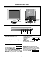
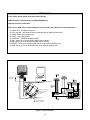
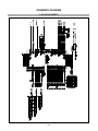
Website:http://biz.LGservice.com
E-mail:http://www.LGEservice.com/techsup.html
COLOR MONITOR
SERVICE MANUAL
CHASSIS NO. : CL-61
MODEL:
CAUTION
L1530S (L1530SM-AL**R)
L1530S (L1530SSNTM-AL**R)
(
) **Same model for Service
BEFORE SERVICING THE UNIT,
READ THE SAFETY PRECAUTIONS IN THIS MANUAL.
MENU
-
LightView
+
SET/AUTO
-1-
CONTENTS
SPECIFICATIONS ................................................... 2
PRECAUTIONS ....................................................... 3
TIMING CHART ....................................................... 4
OPERATING INSTRUCTIONS ................................ 5
WIRING DIAGRAM ................................................. 6
BLOCK DIAGRAM ................................................... 7
DESCRIPTION OF BLOCK DIAGRAM ................... 8
ADJUSTMENT ........................................................ 9
TROUBLESHOOTING GUIDE .............................. 10
PRINTED CIRCUIT BOARD................................... 14
EXPLODED VIEW...................................................16
REPLACEMENT PARTS LIST ...............................18
SCHEMATIC DIAGRAM ......................................... 20
SPECIFICATIONS
1. LCD CHARACTERISTICS
Type
: TFT XGA LCD Module
Size
: 326.5(H) x 253.5(V) x 11.2(D)
Pixel Pitch
: 0.297mm x 0.297mm
Color Depth
: 6bits(with FRC)/ 16M colors
Active Video Area : 15.0inch
(304.128 x 228.096)
Surface Treatment : Anti-Glare, Hard Coating (3H)
Backlight Unit
: 2CCFL
Opraating Mode
: Transmissive mode, Normally white
Electrical Interface : LVDS interface
2. OPTICAL CHARACTERISTICS
2-1. Viewing Angle by Contrast Ratio ≥ 10
(L1530SM / L1530SSNTM)
LPL Module
Left : 55° min. 55° typ. Right: 55° min. 65° typ.
Top : 40° min. 45° typ. Bottom: 50° min. 55° typ.
(L1530SM)
HannStar Module
Left : 50° min. 65° typ.
Top : 30° min. 45° typ.
3-2. Video Input Signal
1) Type
2) Voltage Level
a) Color 0, 0
b) Color 7, 0
c) Color 15, 0
3) Input Impedance
3-3. Operating Frequency
Horizontal
Vertical
4-1. Power
100-240V~, 50/60Hz 0.6A
4-2. Power Consumption
MODE
3. SIGNAL (Refer to the Timing Chart)
3-1. Sync Signal
1) Type
: Separate Sync. (Horizontal & Vertical)
2) Input Voltage Level : Low=0~0.8V, High=2.1~5.5V
3) Sync Polarity
: Positive or Negative
H/V SYNC VIDEO POWER CONSUMPTION LED COLOR
POWER ON (NORMAL)
ON/ON
ACTIVE
less than 25 W
GREEN
STAND-BY
OFF/ON
OFF
less than 1 W
AMBER
SUSPEND
ON/OFF
OFF
less than 1 W
AMBER
DPM OFF
OFF
OFF
less than 1 W
AMBER
POWER S/W OFF
-
-
less than 1 W
OFF
5. ENVIRONMENT
5-1. Operating Temperature: 10°C~35°C (50°F~95°F)
5-2. Operating Humidity
: 10%~80%
5-3. MTBF
: 50,000 HRS (Min.)
Lamp Life
: 40,000 Hours (Min.)
2-2. Luminance
: 200(min.), 250(typ.) at Center point
2-3. Contrast Ratio :
(L1530SM)
300(min.), 400(typ.) -LPL, AUO Module
400(min.), 500(typ.) -Hann Star Module
(L1530SSNTM) 300(min.), 400(typ.)
: 30 ~ 63kHz
: 56 ~ 75Hz
4. POWER SUPPLY
Right: 50° min. 60° typ.
Bottom: 40° min. 55° typ.
AUO Module
Left : -50° min. -60° typ. Right: +50° min. +60° typ.
Top : +30° min. +40° typ. Bottom: -50° min. -60° typ
: R, G, B Analog
: 0~0.7 V
: 0 Vp-p
: 0.35 Vp-p
: 0.7 Vp-p
: 75 Ω
6. DIMENSIONS (with TILT / with Base)
Width
Depth
Height
: 368mm (14.48'') / 368mm
: 355mm (13.97'') / 190mm
: 105mm (4.13'') / 367mm
7. WEIGHT (with TILT)
Net. Weight
Gross Weight
-2-
: 3.6kg (7.93 lbs)
: 5.0kg (11.02 lbs)
PRECAUTION
WARNING FOR THE SAFETY-RELATED COMPONENT.
WARNING
• There are some special components used in LCD
monitor that are important for safety. These parts are
marked on the schematic diagram and the
replacement parts list. It is essential that these critical
parts should be replaced with the manufacturer’s
specified parts to prevent electric shock, fire or other
hazard.
• Do not modify original design without obtaining written
permission from manufacturer or you will void the
original parts and labor guarantee.
BE CAREFUL ELECTRIC SHOCK !
• If you want to replace with the new backlight (CCFL) or
inverter circuit, must disconnect the AC adapter
because high voltage appears at inverter circuit about
650Vrms.
• Handle with care wires or connectors of the inverter
circuit. If the wires are pressed cause short and may
burn or take fire.
TAKE CARE DURING HANDLING THE LCD MODULE
WITH BACKLIGHT UNIT.
• Must mount the module using mounting holes arranged
in four corners.
• Do not press on the panel, edge of the frame strongly
or electric shock as this will result in damage to the
screen.
• Do not scratch or press on the panel with any sharp
objects, such as pencil or pen as this may result in
damage to the panel.
• Protect the module from the ESD as it may damage the
electronic circuit (C-MOS).
• Make certain that treatment person’s body are
grounded through wrist band.
• Do not leave the module in high temperature and in
areas of high humidity for a long time.
• The module not be exposed to the direct sunlight.
• Avoid contact with water as it may a short circuit within
the module.
• If the surface of panel become dirty, please wipe it off
with a softmaterial. (Cleaning with a dirty or rough cloth
may damage the panel.)
CAUTION
Please use only a plastic screwdriver to protect yourself
from shock hazard during service operation.
-3-
TIMING CHART
VIDEO
B
A
E
C
D
SYNC
MODE
1
2
3
4
5
6
7
8
9
10
11
12
13
14
H/V
Sync
Dot
31.468 KHz
Total
Period
(E)
800
70.0 Hz
449
350
99
2
60
37
31.468 KHz
900
720
180
108
55
17
70.0 Hz
449
400
49
2
34
13
31.469 KHz
800
640
160
96
48
16
60.0 Hz
525
480
45
2
33
10
35.00 KHz
864
640
224
64
96
64
66.67 Hz
525
480
45
3
39
3
37.861 KHz
832
640
192
40
128
24
72.8 Hz
520
480
40
3
28
9
37.50 KHz
840
640
200
64
120
16
75.0 Hz
500
480
20
3
16
1
35.156KHz
1024
800
224
72
128
24
56.25 Hz
625
600
25
2
22
1
37.879 KHz
1056
800
256
128
88
40
60.3 Hz
628
600
28
4
23
1
48.077 KHz
1040
800
240
120
64
56
72.188 Hz
666
600
66
6
23
37
46.875 KHz
1056
800
256
80
160
16
75.0 Hz
625
600
25
3
21
1
49.725 KHz
1152
832
320
64
224
32
74.55 Hz
667
624
43
3
39
1
48.363 KHz
1344
1024
320
136
160
24
60.0 Hz
806
768
38
6
29
3
56.476 KHz
1328
1024
304
136
144
24
70.0 Hz
806
768
38
6
29
3
60.023 KHz
1312
1024
288
96
176
16
75.0 Hz
800
768
32
3
28
1
Frequency
Polarity Clock
H (Pixels)
+
V (Lines)
–
H (Pixels)
–
V (Lines)
+
H (Pixels)
–
V (Lines)
–
H (Pixels)
–
V (Lines)
–
H (Pixels)
–
V (Lines)
–
H (Pixels)
–
V (Lines)
–
H (Pixels)
+
V (Lines)
+
H (Pixels)
+
V (Lines)
+
H (Pixels)
+
V (Lines)
+
H (Pixels)
+
V (Lines)
+
H (Pixels)
–
V (Lines)
–
H (Pixels)
–
V (Lines)
–
H (Pixels)
–
V (Lines)
–
H (Pixels)
+
V (Lines)
+
25.175
28.322
25.175
30.24
31.5
31.5
36.0
40.0
50.0
49.5
57.2832
65
75
78.75
F
Video
Blanking
Sync
Active
Time
Duration
Time ( A )
(B)
(D)
640
160
96
-4-
Back
Porch
(F)
48
Front
Porch
(C)
16
Resolution
640 x 350
720 x 400
(TEXT)
640 x 480
640 x 480
640 x 480
640 x 480
800 x 600
800 x 600
800 x 600
800 x 600
832 x 624
(MAC)
1024 x 768
1024 x 768
1024 x 768
OPERATING INSTRUCTIONS
REAR VIEW
FRONT VIEW
Power Connector
MENU
-
LightView
+
SET/AUTO
D-Sub Signal
Connector
See front control panel
Front Control Panel
3
4
1. Power Button
Use this button to turn the display on or off.
2. Power Indicator
This Indicator lights up green when the display operates
normally. If the display is in DPM (Energy Saving) mode, this
indicator color changes to amber.
5
1 2
4. -, + Buttons
Use these buttons to select or
adjust functions in the On
Screen Display.
-, + Button
LightView hot key
LIGHT VIEW
1
DAY
MENU
-
2
TEXT
+
SET
For more information, refer to page A13
3. MENU Button
Use this button to enter or exit the On Screen Display.
OSD LOCKED/UNLOCKED
This function allows you to lock the
OSD LOCKED
current control settings, so that they
cannot be inadvertently changed.
OSD UNLOCKED
Press and hold the MENU button for 5
seconds. The message "OSD LOCKED" should appear.
You can unlock the OSD controls at any time by pushing the
MENU button for 5 seconds. The message "OSD
UNLOCKED" should appear.
-5-
5. SET/AUTO Button
Use this button to enter a selection in the On Screen Display.
AUTO IMAGE ADJUSTMENT
When adjusting your display settings, always press the
SET/AUTO button before entering the On Screen
Display(OSD). This will automatically adjust your display
image to the ideal settings for the current screen resolution
size (display mode).The best display mode is
15 inch monitor : 1024x768
PROCESSING AUTO
IMAGE ADJUSTMENT
17 inch monitor : 1280x1024
WIRING DIAGRAM
Power Board
15
1
J706
MS
T9
J702
Main Board
M
J707
J1
Control Board
-6-
AC Input
12V
-7-
LIPS
5V
2.5V
Diode
KDS184
3.3V
Reg.
3.3V
3.3V
5V
3.3V
2.5V
5V
LVDS
(Low Voltage
Differential Signaling)
D-SUB
R,G,B, H/V Sync
(ADC/LVDS/SCALER )
MST9011B
including
R,G,B
differential
LCD Module
MTV312
Micom
BLOCK DIAGRAM
DESCRIPTION OF BLOCK DIAGRAM
1. Video Controller Part.
This part amplifies the level of video signal for the digital conversion and converts from the analog video signal to the
digital video signal using a pixel clock.
The pixel clock for each mode is generated by the PLL.
The range of the pixel clock is from 25MHz to 135MHz.
This part consists of the Scaler, ADC, LVDS transmitter.
The Scaler gets the video signal converted analog to digital, interpolates input to 1280 X 768 resolution signal and
outputs 8-bit R, G, B signal to transmitter.
2. Power Part.
This part consists of the one 3.3V regulator, and two 2.5V drop diodes to convert power which is provided 12V, 5V in
Power board.
5V is provided for LCD panel and Micom.
Also, 5V is converted 3.3V by regulator and 3.3V is converted 2.5V by drop diode.
Converted power is provided for IC in the main board.
3. MICOM Part.
This part consists of EEPROM IC which stores control data, Reset IC and the Micom.
The Micom distinguishes polarity and frequency of the H/V sync are supplied from signal cable.
The controlled data of each modes is stored in EEPROM.
-8-
LIPS Board Block Diagram
12V
50 ~ 60Hz
EMI
COMPONENTS
INPUT RECTIFIER
AND FILTER
HVDC
ENERGY
TRANSFER
100KHz
OUTPUT RECTIFIER
AND FILTER
5V
GND
LINE
100 ~ 240V
PWM
CONTROL
CIRCUIT
PHOTOCOUPLER
ISOLATION
PRIMARY
SIGNAL
COLLECTI
ON
SECONDARY
Operation description_LIPS
1. EMI components.
This part contains of EMI components to comply with global marketing EMI standards like FCC,VCCI CISPR,
the circuit included a line-filter, across line capacitor and of course the primary protection fuse.
2. Input rectifier and filter.
This part function is for transfer the input AC voltage to a DC voltage through a bridge rectifier and a bulk capacitor.
3. Energy Transfer.
This part function is for transfer the primary energy to secondary through a power transformer.
4. Output rectifier and filter.
This part function is to make a pulse width modulation control and to provide the driver signal to power switch,to
adjust the duty cycle during different AC input and output loading condition to achieve the dc output stabilized, and
also the over power protection is also monitor by this part.
5. Photo-Coupler isolation.
This part function is to feed back the dc output changing status through a photo transistor to primary controller to
achieve the stabilized dc output voltage.
6. Signal collection.
This part function is to collect the any change from the dc output and feed back to the primary through photo
transistor
-9-
ADJUSTMENT
Windows EDID V1.0 User Manual
2. EDID Read & Write
1) Run WinEDID.exe
Operating System: MS Windows 98, 2000, XP
Port Setup: Windows 98 => Don’t need setup
Windows 2000, XP => Need to Port Setup.
This program is available to LCD Monitor only.
1. Port Setup
a) Copy “UserPort.sys” file to
“c:\WINNT\system32\drivers” folder
b) Run Userport.exe
2) Edit Week of Manufacture, Year of Manufacture,
Serial Number
a) Input User Info Data
b) Click “Update” button
c) Click “ Write” button
c) Remove all default number
d) Add 300-3FF
e) Click Start button.
f) Click Exit button.
- 10 -
SERVICE OSD
1)Turn off the power switch at the front side of display.
2)Wait for about 5 seconds and press MENU,POWER key.
3)Shows the service OSD menu.
4)The service OSD menu contains additional menus that the User OSD menu as described below.
a) CLEAR ETI : To initialize using time.
b) AUTO COLOR : W/B balance and Automatically sets the gain and offset value.
c) AGING :Select Aging mode(on/off).
d) PANEL : Select using panel.
e) NVRAM INIT : EEPROM initialize(24C08).
f) 9300 : Allows you to set the R/G/B.-9300K value manually.
g) 6500 :Allows you to set the R/G/B.-6500K value manually.
h) OFFSET : Allows you to set the R/G/B.-Offset value manually.(Analog Only)
i) GAIN : Allows you to set the R/G/B.-Gain value manually.(Analog Only)
A
9
IBM
Compatible PC
Video Signal
Generator
15
10
5
11
6
1
6
1
5
C
d
PARALLEL PORT
2C
EL
OFF
14
ON
AL
L
F
PA
R
Power inlet (required)
5V
R
220
WE
VG
CS
T
MO
NI
ON
TO
R
E
4.7K
74LS06
B
E ST Switch
B
F V-Sync On/Off Switch
(Switch must be ON.)
Figure 1. Cable Connection
- 11 -
4.7K
4.7K
5V
OFF
YN
A
PO
S
Power Select Switch
(110V/220V)
Power LED
V-S
Control Line
5V
C
1
25
RS
23
No
tu
se
13
74LS06
TROUBLESHOOTING GUIDE
1. NO POWER
NO POWER
(POWER INDICATOR OFF)
CHECK J705
VOLTAGE
PIN5, PIN6 (5V)?
NO
CHECK POWER
BOARD, AND FIND
OUT A SHORT POINT
AS OPENING
EACH POWER LINE
YES
CHECK
U501 PIN 8 Voltage
(5V) ?
NO
CHECK 5VS LINE
(OPEN CHECK)
NO PROBLEM
YES
CHECK KEY CONTROL
CONNECTOR ROUTINE
IS U201
PIN114 (3.3V)
VOLTAGE ?
NO
CHECK 3.3V LINE
YES
CHECK U201 PIN 122
PULSE
NO
YES
CHECK U201
- 12 -
CHECK X-TAL
2. NO RASTER (OSD IS NOT DISPLAYED) – LIPS
NO RASTER
(OSD IS NOT DISPLAYED)
J705
PIN5, PIN6
5V?
NO
CHECK LIPS
YES
J705 PIN2
5V?
NO
CHECK MICOM INV
ON/OFF PORT.
YES
J705 PIN1
5V?
NO
1. CONFIRM BRIGHTNESS
OSD CONTRL STATE.
2. CHECK MICOM DIM-ADJ
PORT
YES
CHECK
PULSE AS
CONTACTING SCOPE
PROBE TO CAUTION LABEL.
(CONTACT PROBE TO
CAUTION LABEL.
CAN YOU SEE PULSE
AT YOUR
SCOPE?
NO
YES
REPLACE CCFL LAMP
IN THE LCD MODULE
- 13 -
LIPS
3. NO RASTER (OSD IS NOT DISPLAYED) – MST9011B
NO RASTER
(OSD IS NOT DISPLAYED)
U201
POWER PIN8, 114
3.3V?
NO
CHECK U801
YES
U201
PIN122, 123
OSCILLATE AS
12MHZ?
NO
1. CHECK PIN122, 123
SOLDERING CONDITION
2. CHECK X501
3. TROUBLE IN U201
YES
U501
PIN43 IS 48KHz H-SYNC?
PIN44 IS 60Hz V-SYNC?
IS PULSE APPEARED
AT SIGNAL PINS?
AT MODE 12?
NO
YES
TROUBLE IN CABLE
OR LCD MODULE
- 14 -
CHECK CONNECTION LINE
FROM D-SUB TO U501
4. TROUBLE IN DPM
TROUBLE IN DPM
CHECK
R773, R775
(SYNC) ?
NO
CHECK PC
PC IS NOT GOING
INTO DPM OFF MODE
NO
CHECK H/V SYNC
LINE
YES
CHECK
U501 PIN 43.44
SYNC PULSE ?
YES
TROUBLE IN U501
- 15 -
- 16 -
1
2
9
7
8
5
12
6
6
10
3
EXPLODED VIEW
13
4-1
11-1
4-2
11-2
EXPLODED VIEW PARTS LIST
Ref. No.
Part No.
Description
3091TKL097B
CABINET ASSEMBLY, L1530 BRAND 3090TKL088 "S" TYPE_SLIVER - L1530S
3091TKL097K
CABINET ASSEMBLY, L1530 BRAND 3090TKL088 "B"-CKD - L1530S(SNT)
6304FLP113A
LCD(LIQUID CRYSTAL DISPLAY), LM150X08-A4K3 LG PHILPS TFT COLOR PSWG,LVDS,16MS,HYNIX/HITACHI
6304FHS006B
LCD(LIQUID CRYSTAL DISPLAY), HSD150MX15 HANNSTAR TN COLOR DELL LVDS 250 NITS
6304FAU007B
LCD(LIQUID CRYSTAL DISPLAY), M150XN07 AU TFT COLOR LVDS,TN,250NITS,16MS,PSWG
3809TKL067A
BACK COVER ASSEMBLY, L1530 3808TKL072 (D/GRAY)_"S"TYPE - L1530S
3809TKL067C
BACK COVER ASSEMBLY, L1530 3808TKL072 "A"-CKD - L1530S(SNT)
3043TKK146A
TILT SWIVEL ASSEMBLY, L1530 .. STAND BASE_"S"TYPE - L1530S
3043TKK146B
TILT SWIVEL ASSEMBLY, L1530 .. "A"-CKD - L1530S(SNT)
3043TKK145D
TILT SWIVEL ASSEMBLY, L1530 .. "S"TYPE_SPRAY - L1530S
3043TKK145K
TILT SWIVEL ASSEMBLY, L1530 .. "D"-CKD - L1530S(SNT)
4951TKS136A
METAL ASSEMBLY, FRAME (L1530)_LPL_ANALOG -AUO, L1530S
4951TKS136B
METAL ASSEMBLY, FRAME L1530_HANSTAR_ANALOG - L1530S
4951TKS136J
METAL ASSEMBLY, FRAME "A"-CKD - L1530S(SNT)
4814TKK263A
SHIELD, INVERTER CAP(L1530)
6871TPT271N
PWB(PCB) ASSEMBLY,POWER, M-CHASSIS 15INCH POWER TOTAL LIEN CHANG C306 68PF - LPL, HannStar
6871TPT271A
PWB(PCB) ASSEMBLY,POWER, 15" M-CHASSIS POWER TOTAL LIEN CHANG "A INTEGRATED LIPS"- AUO
3313TL5090A
MAIN TOTAL ASSEMBLY, L1530SM BRAND CL-61 - L1530S
3313TL5090C
MAIN TOTAL ASSEMBLY, L1530SM WA CKD BRAND CL-61 - L1530S(SNT)
6631T11012R
CONNECTOR ASSEMBLY, 20P H-H 140MM UL20276 PANEL LINK CABLE LM567D
6871TST541A
PWB(PCB) ASSEMBLY,SUB, L1730BM CONTROL TOTAL BRAND CONTROL - L1530S
6871TST541B
PWB(PCB) ASSEMBLY,SUB, L1730BM CONTROL TOTAL BRAND CL-62 - L1530S(SNT)
11-1
3550TKK446B
COVER, L1530 BACK DOOR_"S"TYPE_SILVER
11-2
3550TKK452B
COVER, LXX30 STAND REAR (350U)_SILVER
6850TD9004G
CABLE,D-SUB, UL20276-9C(5.8MM) DT 1800MM BLACK(9930) SONY DM
6850TD9004H
CABLE,D-SUB, UL2990-9C(5.8MM) DT 1500MM GLAY 20 MODEL DM - AUO
6410TEW003C
POWER CORD, SP023+IS14 I-SHENG VDE/SEMKO 1870MM WALL 85964 GRA
1
2
3
4-1
4-2
5
6
7
8
9
10
12
13
- 17 -
REPLACEMENT PARTS LIST
CAUTION: BEFORE REPLACING ANY OF THESE COMPONENTS,
READ CAREFULLY THE SAFETY PRECAUTIONS IN THIS MANUAL.
* NOTE : S SAFETY Mark
AL ALTERNATIVE PARTS
*S *AL LOC. NO.
PART NO.
DATE: 2004. 3. 23.
DESCRIPTION / SPECIFICATION
*S *AL LOC. NO.
MAIN BOARD
CAPACITORS
C204
C205
C206
C207
C208
C209
C210
C211
C214
C215
C216
C217
C218
C219
C220
C221
C222
C223
C225
C226
C227
C230
C231
C232
C233
C251
C501
C502
C503
C504
C506
C507
C508
C701
C703
C708
C709
C710
C711
C717
C718
C719
C720
C721
C727
C732
C733
C734
C735
C760
C801
C803
0CK104CK56A
0CK104CK56A
0CK104CK56A
0CK104CK56A
0CK104CK56A
0CK104CK56A
0CK104CK56A
0CK104CK56A
0CK104CK56A
0CK104CK56A
0CK104CK56A
0CK104CK56A
0CK104CK56A
0CK104CK56A
0CK104CK56A
0CK104CK56A
0CK104CK56A
0CK104CK56A
0CK104CK56A
0CK104CK56A
0CK104CK56A
0CK104CK56A
0CK104CK56A
0CK104CK56A
0CK104CK56A
0CK104CK56A
0CC101CK41A
0CC101CK41A
0CK104CK56A
0CH8106F611
0CC030CK01A
0CC180CK41A
0CK104CK56A
0CK105CD56A
0CK104CK56A
0CK103CK51A
0CK103CK51A
0CK103CK51A
0CK103CK51A
0CC101CK41A
0CC101CK41A
0CC680CK41A
0CC101CK41A
0CC680CK41A
0CK105CD56A
0CK103CK51A
0CK104CK56A
0CK104CK56A
0CK104CK56A
0CE107EF610
0CK103CK51A
0CE107EF610
C804
C805
C806
C807
C808
C809
C810
C812
C814
C815
C816
0.1UF 1608 50V 10% R/TP X7R
0.1UF 1608 50V 10% R/TP X7R
0.1UF 1608 50V 10% R/TP X7R
0.1UF 1608 50V 10% R/TP X7R
0.1UF 1608 50V 10% R/TP X7R
0.1UF 1608 50V 10% R/TP X7R
0.1UF 1608 50V 10% R/TP X7R
0.1UF 1608 50V 10% R/TP X7R
0.1UF 1608 50V 10% R/TP X7R
0.1UF 1608 50V 10% R/TP X7R
0.1UF 1608 50V 10% R/TP X7R
0.1UF 1608 50V 10% R/TP X7R
0.1UF 1608 50V 10% R/TP X7R
0.1UF 1608 50V 10% R/TP X7R
0.1UF 1608 50V 10% R/TP X7R
0.1UF 1608 50V 10% R/TP X7R
0.1UF 1608 50V 10% R/TP X7R
0.1UF 1608 50V 10% R/TP X7R
0.1UF 1608 50V 10% R/TP X7R
0.1UF 1608 50V 10% R/TP X7R
0.1UF 1608 50V 10% R/TP X7R
0.1UF 1608 50V 10% R/TP X7R
0.1UF 1608 50V 10% R/TP X7R
0.1UF 1608 50V 10% R/TP X7R
0.1UF 1608 50V 10% R/TP X7R
0.1UF 1608 50V 10% R/TP X7R
100PF 1608 50V 5% R/TP NP0
100PF 1608 50V 5% R/TP NP0
0.1UF 1608 50V 10% R/TP X7R
10UF 16V M 85STD(CYL) R/TP
3PF 1608 50V 0.25 PF R/TP NP0
18PF 1608 50V 5% R/TP NP0
0.1UF 1608 50V 10% R/TP X7R
1UF 1608 10V 10% R/TP X7R
0.1UF 1608 50V 10% R/TP X7R
0.01UF 1608 50V 10% R/TP B(Y5
0.01UF 1608 50V 10% R/TP B(Y5
0.01UF 1608 50V 10% R/TP B(Y5
0.01UF 1608 50V 10% R/TP B(Y5
100PF 1608 50V 5% R/TP NP0
100PF 1608 50V 5% R/TP NP0
68PF 1608 50V 5% R/TP NP0
100PF 1608 50V 5% R/TP NP0
68PF 1608 50V 5% R/TP NP0
1UF 1608 10V 10% R/TP X7R
0.01UF 1608 50V 10% R/TP B(Y5
0.1UF 1608 50V 10% R/TP X7R
0.1UF 1608 50V 10% R/TP X7R
0.1UF 1608 50V 10% R/TP X7R
"100UF KMG,RD 16V 20% FL BULK"
0.01UF 1608 50V 10% R/TP B(Y5
"100UF KMG,RD 16V 20% FL BULK"
PART NO.
DATE: 2004. 3. 23.
DESCRIPTION / SPECIFICATION
0CK104CK56A
0CK104CK56A
0CK103CK51A
0CE107EF610
0CK104CK56A
0CK103CK51A
0CK104CK56A
0CE107EF610
0CE107EF610
0CK104CK56A
0CK103CK51A
0.1UF 1608 50V 10% R/TP X7R
0.1UF 1608 50V 10% R/TP X7R
0.01UF 1608 50V 10% R/TP B(Y5
"100UF KMG,RD 16V 20% FL BULK"
0.1UF 1608 50V 10% R/TP X7R
0.01UF 1608 50V 10% R/TP B(Y5
0.1UF 1608 50V 10% R/TP X7R
"100UF KMG,RD 16V 20% FL BULK"
"100UF KMG,RD 16V 20% FL BULK"
0.1UF 1608 50V 10% R/TP X7R
0.01UF 1608 50V 10% R/TP B(Y5
0DS226009AA
0DS226009AA
0DS226009AA
0DD184009AA
0DD184009AA
0DZ560009GB
0DZ560009GB
0DZ560009GB
0DZ560009GB
0DZ560009GB
0DZ560009GB
KDS226 TP KEC SOT-23 80V 300
KDS226 TP KEC SOT-23 80V 300
KDS226 TP KEC SOT-23 80V 300
KDS184 TP KEC - 85V - - - 300
KDS184 TP KEC - 85V - - - 300
BZT52C5V6S DIODES R/TP SOD323
BZT52C5V6S DIODES R/TP SOD323
BZT52C5V6S DIODES R/TP SOD323
BZT52C5V6S DIODES R/TP SOD323
BZT52C5V6S DIODES R/TP SOD323
BZT52C5V6S DIODES R/TP SOD323
0IPRPM3007B
0IZZTSZ347A
0ISG240860B
0IPMGKE011A
0IPMGK2001B
"MST9011B(ANALOG) MSTAR 128P,L"
MYSON MTV312 L1530SM - E
M24C08W6 SGS-THOMSON 8SOP R/T
KIA78D33F KEC DPAK R/TP 3.3V
AIC1117A-33CYTR(BS33) AIC SOT
DIODEs
D701
D702
D706
D804
D805
ZD701
ZD702
ZD703
ZD704
ZD705
ZD711
ICs
U201
U501
U502
U801
U803
TRANSISTOR
Q502
Q503
Q504
Q505
Q703
Q704
Q706
Q707
Q801
Q802
0IKE704200H
0TR390409AE
0TR390409AE
0TR390409AE
0TR390609FA
0TR390609FA
0TR390409AE
0TR390409AE
0TR127309AA
0TR390409AE
KIA7042AP TO-92 TP 4.2 VOLT.
FAIRCHILD KST3904(LGEMTF) TP
FAIRCHILD KST3904(LGEMTF) TP
FAIRCHILD KST3904(LGEMTF) TP
KST3906-MTF TP SAMSUNG SOT23
KST3906-MTF TP SAMSUNG SOT23
FAIRCHILD KST3904(LGEMTF) TP
FAIRCHILD KST3904(LGEMTF) TP
KTA1273-Y(KTA966A) TP KEC TO9
FAIRCHILD KST3904(LGEMTF) TP
RESISTORs
R201
R202
R203
R207
R208
- 18 -
0RJ1500D677
0RJ1500D677
0RJ1500D677
0RJ3900D677
0RJ1500D677
150 OHM 1/10 W 5% 1608 R/TP
150 OHM 1/10 W 5% 1608 R/TP
150 OHM 1/10 W 5% 1608 R/TP
390 OHM 1/10 W 5% 1608 R/TP
150 OHM 1/10 W 5% 1608 R/TP
*S *AL LOC. NO.
R209
R210
R213
R214
R220
R506
R508
R512
R513
R514
R515
R516
R518
R519
R520
R521
R522
R523
R524
R525
R526
R527
R528
R529
R531
R532
R534
R535
R537
R541
R542
R543
R544
R545
R546
R547
R548
R549
R555
R556
R557
R560
R561
R563
R564
R565
R701
R703
R706
R708
R709
R716
R717
R722
R723
R724
R726
R727
R728
R735
R737
R744
PART NO.
0RJ1500D677
0RJ1500D677
0RJ0000D677
0RJ0000D677
0RJ4701D677
0RJ4701D677
0RJ4701D677
0RJ0332D677
0RJ0332D677
0RJ4701D677
0RJ4701D677
0RJ4701D677
0RJ4701D677
0RJ1000D677
0RJ4701D677
0RJ4701D677
0RJ4701D677
0RJ4701D677
0RJ1000D677
0RJ1000D677
0RJ1000D677
0RJ1000D677
0RJ1000D677
0RJ1000D677
0RJ1000D677
0RJ1000D677
0RJ0000D677
0RJ3301D677
0RJ3301D677
0RJ1000D677
0RJ1000D677
0RJ4701D677
0RJ4701D677
0RJ4700D677
0RJ4701D677
0RJ4700D677
0RJ0332D677
0RJ0332D677
0RJ1000D677
0RJ4700D677
0RJ1000D677
0RJ1501D677
0RJ4701D677
0RJ1000D677
0RJ1000D677
0RJ1000D677
0RJ0752D677
0RJ0752D677
0RJ0752D677
0RJ4700D677
0RJ1001D677
0RJ4701D677
0RJ4701D677
0RJ1000D677
0RJ0332D677
0RJ0332D677
0RJ1002D677
0RJ1002D677
0RJ1502D677
0RJ0000D677
0RJ0000D677
0RJ4701D677
DATE: 2004. 3. 23.
DESCRIPTION / SPECIFICATION
*S *AL LOC. NO.
150 OHM 1/10 W 5% 1608 R/TP
150 OHM 1/10 W 5% 1608 R/TP
0 OHM 1/10 W 5% 1608 R/TP
0 OHM 1/10 W 5% 1608 R/TP
4.7K OHM 1/10 W 5% 1608 R/TP
4.7K OHM 1/10 W 5% 1608 R/TP
4.7K OHM 1/10 W 5% 1608 R/TP
33 OHM 1/10 W 5% 1608 R/TP
33 OHM 1/10 W 5% 1608 R/TP
4.7K OHM 1/10 W 5% 1608 R/TP
4.7K OHM 1/10 W 5% 1608 R/TP
4.7K OHM 1/10 W 5% 1608 R/TP
4.7K OHM 1/10 W 5% 1608 R/TP
100 OHM 1/10 W 5% 1608 R/TP
4.7K OHM 1/10 W 5% 1608 R/TP
4.7K OHM 1/10 W 5% 1608 R/TP
4.7K OHM 1/10 W 5% 1608 R/TP
4.7K OHM 1/10 W 5% 1608 R/TP
100 OHM 1/10 W 5% 1608 R/TP
100 OHM 1/10 W 5% 1608 R/TP
100 OHM 1/10 W 5% 1608 R/TP
100 OHM 1/10 W 5% 1608 R/TP
100 OHM 1/10 W 5% 1608 R/TP
100 OHM 1/10 W 5% 1608 R/TP
100 OHM 1/10 W 5% 1608 R/TP
100 OHM 1/10 W 5% 1608 R/TP
0 OHM 1/10 W 5% 1608 R/TP
3.3K OHM 1/10 W 5% 1608 R/TP
3.3K OHM 1/10 W 5% 1608 R/TP
100 OHM 1/10 W 5% 1608 R/TP
100 OHM 1/10 W 5% 1608 R/TP
4.7K OHM 1/10 W 5% 1608 R/TP
4.7K OHM 1/10 W 5% 1608 R/TP
470 OHM 1/10 W 5% 1608 R/TP
4.7K OHM 1/10 W 5% 1608 R/TP
470 OHM 1/10 W 5% 1608 R/TP
33 OHM 1/10 W 5% 1608 R/TP
33 OHM 1/10 W 5% 1608 R/TP
100 OHM 1/10 W 5% 1608 R/TP
470 OHM 1/10 W 5% 1608 R/TP
100 OHM 1/10 W 5% 1608 R/TP
1.5K OHM 1/10 W 5% 1608 R/TP
4.7K OHM 1/10 W 5% 1608 R/TP
100 OHM 1/10 W 5% 1608 R/TP
100 OHM 1/10 W 5% 1608 R/TP
100 OHM 1/10 W 5% 1608 R/TP
75 OHM 1/10 W 5% 1608 R/TP
75 OHM 1/10 W 5% 1608 R/TP
75 OHM 1/10 W 5% 1608 R/TP
470 OHM 1/10 W 5% 1608 R/TP
1K OHM 1/10 W 5% 1608 R/TP
4.7K OHM 1/10 W 5% 1608 R/TP
4.7K OHM 1/10 W 5% 1608 R/TP
100 OHM 1/10 W 5% 1608 R/TP
33 OHM 1/10 W 5% 1608 R/TP
33 OHM 1/10 W 5% 1608 R/TP
10K OHM 1/10 W 5% 1608 R/TP
10K OHM 1/10 W 5% 1608 R/TP
15K OHM 1/10 W 5% 1608 R/TP
0 OHM 1/10 W 5% 1608 R/TP
0 OHM 1/10 W 5% 1608 R/TP
4.7K OHM 1/10 W 5% 1608 R/TP
R745
R747
R748
R749
R770
R771
R772
R773
R774
R775
R779
R780
R781
R782
R783
R802
R804
R805
R806
R807
R808
R825
PART NO.
DATE: 2004. 3. 23.
DESCRIPTION / SPECIFICATION
0RJ4701D677
0RJ4701D677
0RJ4701D677
0RJ0000D677
0RJ0000D677
0RJ0000D677
0RJ1001D677
0RJ4701D677
0RJ1001D677
0RJ4701D677
0RJ0682D677
0RJ2001D677
0RJ2001D677
0RJ0102D677
0RJ0102D677
0RJ0000D677
0RJ1002D677
0RJ2000D677
0RJ2000D677
0RJ1000D677
0RJ0000D677
0RX0470J609
4.7K OHM 1/10 W 5% 1608 R/TP
4.7K OHM 1/10 W 5% 1608 R/TP
4.7K OHM 1/10 W 5% 1608 R/TP
0 OHM 1/10 W 5% 1608 R/TP
0 OHM 1/10 W 5% 1608 R/TP
0 OHM 1/10 W 5% 1608 R/TP
1K OHM 1/10 W 5% 1608 R/TP
4.7K OHM 1/10 W 5% 1608 R/TP
1K OHM 1/10 W 5% 1608 R/TP
4.7K OHM 1/10 W 5% 1608 R/TP
68 OHM 1/10 W 5% 1608 R/TP
2K OHM 1/10 W 5% 1608 R/TP
2K OHM 1/10 W 5% 1608 R/TP
10 OHM 1/10 W 5% 1608 R/TP
10 OHM 1/10 W 5% 1608 R/TP
0 OHM 1/10 W 5% 1608 R/TP
10K OHM 1/10 W 5% 1608 R/TP
200 OHM 1/10 W 5% 1608 R/TP
200 OHM 1/10 W 5% 1608 R/TP
100 OHM 1/10 W 5% 1608 R/TP
0 OHM 1/10 W 5% 1608 R/TP
0.47 OHM 1 W 5% TA52
6212AA2004A
HC-49U TXC 12.0MHZ +/- 30 PPM
OTHERs
X501
CONTROL BOARD
C1
C2
LED1
Q1
Q2
R1
R2
R3
R4
R5
R7
R8
SW2
SW3
SW6
SW7
SW8
- 19 -
0CK104CK56A
0CK104CK56A
0DLLT0340AA
0TR390409AE
0TR390409AE
0RJ4701D677
0RJ4701D677
0RJ2001D677
0RJ2001D677
0RJ5101D677
0RJ4700D677
0RJ4700D677
140-058E
140-058E
140-058E
140-058E
140-058E
0.1UF 1608 50V 10% R/TP X7R
0.1UF 1608 50V 10% R/TP X7R
LITEON LTL-14CDJNHBP1 BK GREE
FAIRCHILD KST3904(LGEMTF) TP
FAIRCHILD KST3904(LGEMTF) TP
4.7K OHM 1/10 W 5% 1608 R/TP
4.7K OHM 1/10 W 5% 1608 R/TP
2K OHM 1/10 W 5% 1608 R/TP
2K OHM 1/10 W 5% 1608 R/TP
5.1K OHM 1/10 W 5% 1608 R/TP
470 OHM 1/10 W 5% 1608 R/TP
470 OHM 1/10 W 5% 1608 R/TP
SKHV10910B LGEC NON 12V 20A H
SKHV10910B LGEC NON 12V 20A H
SKHV10910B LGEC NON 12V 20A H
SKHV10910B LGEC NON 12V 20A H
SKHV10910B LGEC NON 12V 20A H
SCHEMATIC DIAGRAM
1. H/V SYNC DETECT
1
- 20 -
2. AMP/TMDS
2
- 21 -
3. VIDEO PROCESSOR
3
- 22 -
4. OUT/PUT
4
- 23 -
P/NO : 3828TSL084K
Mar. 2004
Printed in Korea