1
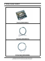
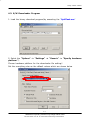
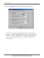
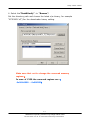
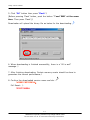
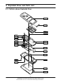
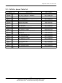
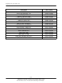
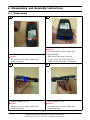
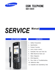
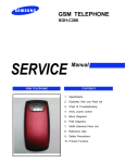
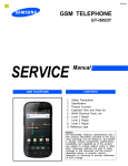
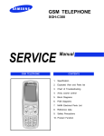
GSM TELEPHONE
SGH-C130
GSM TELEPHONE
CONTENTS
1.
Safety Precautions
2.
Specification
3.
Product Function
4.
Array course control
5.
Exploded View and Parts List
6.
Disassembly and Assembly
instructions
7.
MAIN Electrical Parts List
8.
Block Diagrams
9.
PCB Diagrams
10.
Flow Chart of Troubleshooting
11.
Reference data
Contents
1. Safety Precautions
1-1. Repair Precaution ...........................................................................1-1
1-2. ESD(Electrostatically Sensitive Devices) Precaution ...........................1-2
2. Specification
2-1. GSM General Specification ..............................................................2-1
2-2. GSM Tx Power Class ......................................................................2-2
3. Product Function
3-1. Main Function ................................................................................3-1
4. Array course control
Software Downloading
4-1. Downloading Binary Files ................................................................4-2
4-2. Pre-requsite for Downloading ..........................................................4-2
4-3. S/W Downloader Program ...............................................................4-3
5. Exploded View and Parts List
5-1. Cellular phone Exploded View .........................................................5-1
5-2. Cellular phone Part list ...................................................................5-2
6. Disassembly and Assembly instructions
6-1. Disassembly ..................................................................................6-1
6-2. Assembly ......................................................................................6-3
7. MAIN Electrical Parts List
8. Block Diagrams
9. PCB Diagrams
10. Flow Chart of Troubleshooting
10-1. Baseband
10-1-1. Power ON ..............................................................................10-1
Contents
10-1-2.
10-1-3.
10-1-4.
10-1-5.
10-1-6.
10-2. RF
10-2-1.
10-2-2.
10-2-3.
10-2-4.
Initial ....................................................................................10-5
Sim Part ...............................................................................10-8
Microphone Part ...................................................................10-10
Receiver Part .......................................................................10-12
Speaker Part ........................................................................10-12
EGSM RX .............................................................................10-16
DCS RX ...............................................................................10-18
EGSM TX .............................................................................10-20
DCS TX ...............................................................................10-22
11. Reference data
1. Safety Precautions
1-1. Repair Precaution
● Repair in Shield Box, during detailed tuning.
Take specially care of tuning or test,
because specipicty of cellular phone is sensitive for surrounding interference(RF noise).
● Be careful to use a kind of magnetic object or tool,
because performance of parts is damaged by the influence of manetic force.
● Surely use a standard screwdriver when you disassemble this product,
otherwise screw will be worn away.
● Use a thicken twisted wire when you measure level.
A thicken twisted wire has low resistance, therefore error of measurement is few.
● Repair after separate Test Pack and Set because for short danger (for example an
overcurrent and furious flames of parts etc) when you repair board in condition of
connecting Test Pack and tuning on.
● Take specially care of soldering, because Land of PCB is small and weak in heat.
● Surely tune on/off while using AC power plug, because a repair of battery charger is
dangerous when tuning ON/OFF PBA and Connector after disassembing charger.
● Don't use as you pleases after change other material than replacement registered on SEC
System. Otherwise engineer in charge isn't charged with problem that you don't keep this
rules.
1-1
SAMSUNG Proprietary-Contents may change without notice
This Document can not be used without Samsung's authorization
Safety Precautions
1-2. ESD(Electrostatically Sensitive Devices) Precaution
Several semiconductor may be damaged easilly by static electricity. Such parts are called by
ESD(Electrostatically Sensitive Devices), for example IC,BGA chip etc. Read Precaution below.
You can prevent from ESD damage by static electricity.
● Remove static electricity remained your body before you touch semiconductor or parts with
semiconductor. There are ways that you touch an earthed place or wear static electricity
prevention string on wrist.
● Use earthed soldering steel when you connect or disconnect ESD.
● Use soldering removing tool to break static electricity. , otherwise ESD will be damaged by
static electricity.
● Don't unpack until you set up ESD on product. Because most of ESD are packed by box
and aluminum plate to have conductive power,they are prevented from static electricity.
● You must maintain electric contact between ESD and place due to be set up until ESD is
connected completely to the proper place or a circuit board.
1-2
SAMSUNG Proprietary-Contents may change without notice
This Document can not be used without Samsung's authorization
2. Specification
2-1. GSM General Specification
GSM900
P has e 1
EGSM 900
P has e 2
DCS1800
Pha s e 1
Freq. Band[MHz]
U p li nk/ D own li nk
8 90 ~ 9 15
9 35 ~ 9 60
8 80 ~ 9 15
9 25 ~ 9 60
17 10 ~17 85
18 05 ~18 80
A R FC N r an g e
1~ 12 4
0~ 12 4 &
9 75 ~ 1 02 3
5 12 ~ 88 5
T x / R x sp ac i n g
4 5 M Hz
4 5 M Hz
9 5 M Hz
Mod . Bi t ra t e/
Bit Period
27 0. 83 3 kb p s
3. 69 2 u s
27 0. 83 3 kb p s
3. 69 2 u s
2 70 . 8 33 kb p s
3. 69 2 u s
Ti me Slot
Period/Frame Peri od
57 6. 9 u s
4.615 ms
57 6. 9 u s
4.615 ms
57 6. 9 u s
4.615 ms
Mod u l a t i on
0 . 3 GM S K
0 .3 G M S K
0 .3 GM SK
MS Power
33 d Bm~13 d Bm
33 dBm~5 d Bm
30 dBm~0 d Bm
P ower Cl as s
5 p cl ~ 1 5 p cl
5 pcl ~ 19 pcl
0 pcl ~ 15 pcl
Sensitivity
- 10 2 d B m
- 10 2 d B m
- 10 0 d B m
TDMA M ux
8
8
8
C el l R a di u s
35 Km
35 Km
2 Km
2-1
SAMSUNG Proprietary-Contents may change without notice
This Document can not be used without Samsung's authorization
Specification
2-2. GSM TX power class
TX Power
control level
GSM900
TX Power
control level
DCS1800
5
33±2 dBm
0
30±3 dBm
6
31±2 dBm
1
28±3 dBm
7
29±2 dBm
2
26±3 dBm
8
27±2 dBm
3
24±3 dBm
9
25±2 dBm
4
22±3 dBm
10
23±2 dBm
5
20±3 dBm
11
21±2 dBm
6
18±3 dBm
12
19±2 dBm
7
16±3 dBm
13
17±2 dBm
8
14±3 dBm
14
15±2 dBm
9
12±4 dBm
15
13±2 dBm
10
10±4 dBm
16
11±3 dBm
11
8±4 dBm
17
9± 3dBm
12
6±4 dBm
18
7±3 dBm
13
4±4 dBm
19
5±3 dBm
14
2±5 dBm
15
0±5 dBm
2-2
SAMSUNG Proprietary-Contents may change without notice
This Document can not be used without Samsung's authorization
3. Product Function
3-1. Main Function
-Camera and camcorder
-Music player
-Bluetooth
-Web browser
-Get personal with photo caller ID
-Name card
-Multimedia Message Service (MMS)
-Java
-Calendar
-Voice recorder
-Alarm
3-1
SAMSUNG Proprietary-Contents may change without notice
This Document can not be used without Samsung's authorization
4. Array course control
Test Jig (GH80-03307A)
Test Cable (GH39-00127A)
RF Test Cable (GH39-00283A)
4-1
SAMSUNG Proprietary-Contents may change without notice
This Document can not be used without Samsung's authorization
Array course control
Software Downloading
4-1. Downloading Binary Files
• Three binary files for downloading C130.
– C130XXYY.s3 : Main source code binary.
4-2. Pre-requsite for Downloading
• Downloader Program(OptiFlash.exe)
• C130 Mobile Phone
• Data Cable
• Binary files
4-2
SAMSUNG Proprietary-Contents may change without notice
This Document can not be used without Samsung's authorization
1.
Array course control
4-3. S/W Downloader Program
1. Load the binary download programby executing the “OptiFlash.exe”
2. Select the “Options” -> “Settings” -> “Generic” -> “Specify hardware
platform”.
Choose hardware platform for the downloader file setting.
Set the everything else as the default values which are shown below
4-3
SAMSUNG Proprietary-Contents may change without notice
This Document can not be used without Samsung's authorization
Array course control
3. Select the COM port when the download cable is connected
Up to twelve ports are supported. Additionally you can select the
maximum
transfer speed OptiFlash will use to communicate with
the phone. However, OptiFlash will use a slower speed if either the
PC’s or the phone’s serial hardware is incapable of handling the
selected speed
4-4
SAMSUNG Proprietary-Contents may change without notice
This Document can not be used without Samsung's authorization
Array course control
4. Select the“Flash&Verify” -> “Browse”
Set the directory path and choose the latest s/w binary, for example
“XC30XXYY.s3”,for the downloader binary setting.
Make sure that not to change the reserved memory
regions.
In case of C130 the reserved regions are :
-0x00fc0000 – 0x00ffffff
4-5
SAMSUNG Proprietary-Contents may change without notice
This Document can not be used without Samsung's authorization
Array course control
5. Click “OK” button then press “Flash”.
(Before pressing ‘Flash’ button, push the button ‘*’and ‘END’ at the same
time. Then press ‘Flash’.)
Downloader will upload the binary file as below for the downloading.
6. When downloading is finished successfully, there is a “All is well”
message. 7. After finishing downloading, Certain memory resets should be done to
guarantee the normal performance.
8. Confirm the downloaded version name and etc. :
*#5002*8376263#
Full Reset : *2767*3855#
4-6
SAMSUNG Proprietary-Contents may change without notice
This Document can not be used without Samsung's authorization
5. Exploded View and Parts List
5-1. Cellular phone Exploded View
QFR01
QIF01
QKP01
QCR17
QAR01
QLC01
QMP01
QAN06
QME01
QMI01
QAN02
QSP01
QRE02
QMO01
QRF03
QCR06
QRE01
QRF01
QBA01
QBA00
5-1
SAMSUNG Proprietary-Contents may change without notice
This Document can not be used without Samsung's authorization
Exploded View and Parts List
5-2. Cellular phone Parts list
Design LOC
Discription
SEC CODE
QAN02
INTENNA-SGHC130
GH42-00826A
QAN06
MEC-ANT CONTACT RUBBER
GH75-09635A
QAR01
AUDIO-RECEIVER
3009-001201
QBA00
MEC-COVER BATT
GH75-09643A
QBA01
INNER BATTERY PACK-750MAH,BLK,
GH43-02483A
QCR06
SCREW-MACHINE
6001-001155
QCR17
SCREW-MACHINE
6001-001460
QKP01
MEC-KEYPAD
GH75-09645A
QLC01
LCD-SGHC130 MODULE
GH07-00915A
QME01
UNIT-METAL DOME
GH59-03151A
QMI01
MICROPHONE-ASSY-SGHC130
GH30-00276A
QMO01
MOTOR-DC
3101-001324
QMP01
PBA MAIN-SGHC130
GH92-02745A
QRE01
MEC-COVER REAR
GH75-09642A
QRE02
MEC-BRACKET REAR
GH75-09644A
QRF01
RMO-COVER RF
GH73-06809A
QRF03
PMO-COVER EAR
GH72-30146A
QSP01
SPEAKER
3001-001966
QFR01
MEC-COVER FRONT
GH75-09641A
PMO-COVER IF
GH72-30148A
QIF01
5-2
SAMSUNG Proprietary-Contents may change without notice
This Document can not be used without Samsung's authorization
Exploded View and Parts List
Discription
SEC CODE
BAG PE
6902-000297
ADAPTOR-SGHN288 TAD
GH44-00184A
LABEL(P)-IMEI
GH68-01335D
LABEL(P)-WATER SOAK
GH68-02026A
MANUAL USERS-EU RUSSIAN
GH68-10872A
LABEL(R)-MAIN SEK
GH68-11303B
CUSHION-CASE TA2 MA2
GH69-03897A
BOX(P)-UNIT MAIN(EU)
GH69-04012A
RMO-CUSHION RUBBER TR
GH73-07077A
MPR-SPONGE VIBRATOR
GH74-14818A
MPR-CUSHION INTENNA
GH74-22230A
MPR-CUSHION RCV
GH74-23341A
MPR-TAPE GND
GH74-23342A
MPR-TAPE IF CON
GH74-23343A
MPR-TAPE BACKUP BATTERY
GH74-23544A
MPR-VINYL BOHO MAIN
GH74-24760A
5-3
SAMSUNG Proprietary-Contents may change without notice
This Document can not be used without Samsung's authorization
6. Disassembly and Assembly instructions
6-1. Disassembly
1
2
1) Raise up the upper part of SET.
※ caution
1) Be careful not to make scratch and
1) Unlock 4 screws.
molding damage!
※ caution
2) Must unlock the upper side first.
-If you unlock the lower part first,
1) Be careful not to make scratch and
molding damage!
locker of the lower part is damaged.
3
4
1) Unlock rightside of SET
1) Unlock leftside of SET
※ caution
※ caution
1) Be careful not to make scratch and
1) Be careful not to make scratch and
molding damage!
molding damage!
6-1
SAMSUNG Proprietary-Contents may change without notice
This Document can not be used without Samsung's authorization
Disassembly and Assembly instructions
5
6
1) Holding FRONT and pushing KEA PAD,
disassamble the MIC FPCB.
1) Holding and pulling the upper part of REAR 2) Pushing KEY PAD under the earjack,
disassamble the lower part of REAR.
disassable the lower part of PBA
※ caution
※ caution
1) Be careful not to make scratch and
1) Be careful not to make scratch and
molding damage!
molding damage!
2) Be careful not to make damage of the
2) When you disassamble PBA, be careful not
lower locker!
to make MIC FPCB damage!
7
8
1) Rising up PBA LCD PART slowly and
disassamble RECEIVER.
※ caution
1) Be careful not to make scratch and
molding damage!
2) Be careful not to make RECEIVER WIRE
damage!
3) Be careful not to make LCD damage!
6-2
SAMSUNG Proprietary-Contents may change without notice
This Document can not be used without Samsung's authorization
Disassembly and Assembly instructions
6-2. Assembly
1
2
SILK GUIDE LINE
SILK GUIDE LINE
1)fix into silk guide line,Attach the CUSION
INTENNA PORON
2)fix into undet intenna contact shape,attach
1) Fix into SILK GUIDE LINE, attach the
ROBBER.
RECEIVER PORON.
3
4
PCB GND
CORNER
COVER TOP OF BACK UP BATT
PCB OUTLINE
AND DOME
SHEET
OUTLINE
ATTACH THE PART
1) Fix into PCB GND corner, Attach the
OF CENTER
SHIELD GARSKET.
2) Fix into outline of DOME SHEET and PCB
GRD corner, Attach the ELECTRIC TAPE
1)Attach the CUSION ROBBER on ceter of
AGERE TC CHIP.
and cover the reverse side of PCB
※ caution
2)Attach the ELECTRIC TAPE for covering top
1) After attaching the ELECTRIC TAPE, rup up
of BACK UP BATT.
it not to take off.
6-3
SAMSUNG Proprietary-Contents may change without notice
This Document can not be used without Samsung's authorization
Disassembly and Assembly instructions
5
6
Check
the
polarity.
CHECK the
soldering guide
hole
1) Fix into MIC soldering guide hole,
1) Check the polarity and and solder the
solder MIC FPCB.
※ caution
RECEIVER
※ caution
1) Be careful circuit short and soldering error. 1) Be careful circuit short and soldering error.
8
7
Check the
soldering
guide hole
Locking point check
1) Fix into LCD FPCB soldering guide
hole,
solder LCD FPCB.
※ caution
1) Assemble the LCD ON the PCB.
1) Be careful not to make LCD FPCB damage. ※ caution
2) Be careful circuit short and soldering error. 1) Be careful not to make LCD FPCB damage.
6-4
SAMSUNG Proprietary-Contents may change without notice
This Document can not be used without Samsung's authorization
Disassembly and Assembly instructions
9
10
Check the
polarity
Check the point
1) Check the polarity and and solder the
RECEIVER
1) Screw up the SHEILD CAN at 4 Points.
2) Attach the MOTER on the SHIELD CAN
※ caution
[M1.4 x L2.3]
1) Attaching moter, check the direction.
※ caution
(same as picture)
1) Torque 0.8 ± 0.1 Kgf/㎠
2) Be careful not to damage LCD !
2) Be careful circuit short and soldering error.
11
12
납땜 기준홀 확인
Check the polarity
Check the locking point
1)Check the polarity of SPEAKER, solder it
1)Assemble intenna on PBA
※ caution
※ caution
1) Be careful circuit short and soldering error. 1) Be careful not to damage LCD !
6-5
SAMSUNG Proprietary-Contents may change without notice
This Document can not be used without Samsung's authorization
Disassembly and Assembly instructions
13
14
After inserting PBA, check the
locking point
After inserting
reciver, insert LCD
1) Insert PBA in the FRONT.
1) Insert RECEIVER in the FRONT
※ caution
※ caution
1) Inserting PBA, be caful not to make MIC
1) Torque 0.8 ± 0.1 Kgf/㎠
2) Be careful not to make scratch and
FPCB damage!
2) Be careful not to make scratch and
molding damage!
molding damage!
16
15
Check the
Bottom side
LOCKING
Folding MIC FPCB, insert
it in FRONT
1) Insert MIC in the FRONT MIC HOLE.
※ caution
1) Assemble FRONT and ROAR Locker..
1) Be careful not to make the MIC FPCB
※ caution
1) Be careful not to make locker damage
damage!
2) Be careful not to make scratch and
2) Be careful not to make scratch and
molding damage!
molding damage!
6-6
SAMSUNG Proprietary-Contents may change without notice
This Document can not be used without Samsung's authorization
Disassembly and Assembly instructions
17
18
After assembling the
lower side,
Check SCREW 4
assemble upper side
points
1) Screw up the REAR at 4 Points.
1) After assambling the bottom side, push
and assamble the upper side
[M1.4* L3.5]
※ caution
※ caution
1) Torque 0.8 ± 0.1 Kgf/㎠
1) Be careful not to make scratch and
2) Be careful not to make scratch and
molding damage!
molding damage!
6-7
SAMSUNG Proprietary-Contents may change without notice
This Document can not be used without Samsung's authorization
7. MAIN Electrical Parts List
SEC CODE
Design LOC
0403-001427
ANT100
Discription
DIODE-ZENER
STATUS
SA
0403-001547
BAT300
DIODE-ZENER
SA
0404-001172
BTC104
DIODE-SCHOTTKY
SA
0406-001083
C100
DIODE-TVS
SA
0406-001083
C101
DIODE-TVS
SA
0406-001083
C102
DIODE-TVS
SA
0406-001210
C105
DIODE-TVS
SA
0406-001210
C106
DIODE-TVS
SA
0406-001210
C107
DIODE-TVS
SA
0406-001210
C108
DIODE-TVS
SA
0406-001210
C109
DIODE-TVS
SA
0406-001210
C110
DIODE-TVS
SA
0406-001254
C112
DIODE-TVS
SA
0406-001254
C113
DIODE-TVS
SA
0406-001254
C115
DIODE-TVS
SA
0406-001254
C116
DIODE-TVS
SA
0406-001254
C117
DIODE-TVS
SA
0406-001254
C118
DIODE-TVS
SA
0406-001254
C119
DIODE-TVS
SA
0406-001254
C120
DIODE-TVS
SA
0407-001002
C121
DIODE-ARRAY
SA
0501-000225
C126
TR-SMALL SIGNAL
SA
0504-000168
C127
TR-DIGITAL
SA
0601-001979
C129
LED
SA
0601-001979
C130
LED
SA
0801-002529
C132
IC-CMOS LOGIC
SA
1108-000070
C133
IC-MCP
SA
1201-002364
C134
IC-POWER AMP
SA
1203-003304
C135
IC-POWER SUPERVISOR
SA
1203-003663
C136
IC-BATTERY
SA
1203-003737
C137
IC-POSI.FIXED REG.
SA
1203-004337
C138
IC-DC/DC CONVERTER
SA
1204-001811
C139
IC-MELODY
SA
1205-002683
C140
IC-TRANSCEIVER
SA
1209-001219
C141
IC-SENSOR
SA
1405-001082
C142
VARISTOR
SA
1405-001082
C143
VARISTOR
SA
1405-001082
C146
VARISTOR
SA
1405-001082
C147
VARISTOR
SA
1405-001082
C149
VARISTOR
SA
1405-001082
C150
VARISTOR
SA
1405-001082
C151
VARISTOR
SA
1405-001082
C152
VARISTOR
7-1
SA
SAMSUNG Proprietary-Contents may change without notice
This Document can not be used without Samsung's authorization
Main Electrical Parts List
SEC CODE
Design LOC
Discription
STATUS
1405-001082
C153
VARISTOR
SA
1405-001082
C155
VARISTOR
SA
1405-001082
C156
VARISTOR
SA
1405-001093
C158
VARISTOR
SA
2007-000140
C160
R-CHIP
SA
2007-000140
C161
R-CHIP
SA
2007-000142
C162
R-CHIP
SNA
2007-000148
C164
R-CHIP
SA
2007-000148
C165
R-CHIP
SA
2007-000148
C166
R-CHIP
SA
2007-000148
C167
R-CHIP
SA
2007-000157
C168
R-CHIP
SA
2007-000157
C170
R-CHIP
SA
2007-000157
C171
R-CHIP
SA
2007-000157
C172
R-CHIP
SA
2007-000160
C173
R-CHIP
SA
2007-000161
C174
R-CHIP
SA
2007-000161
C175
R-CHIP
SA
2007-000161
C176
R-CHIP
SA
2007-000161
C178
R-CHIP
SA
2007-000162
C179
R-CHIP
SA
2007-000162
C180
R-CHIP
SA
2007-000162
C181
R-CHIP
SA
2007-000162
C182
R-CHIP
SA
2007-000162
C183
R-CHIP
SA
2007-000162
C188
R-CHIP
SA
2007-000164
C198
R-CHIP
SA
2007-000170
C199
R-CHIP
SA
2007-000171
C200
R-CHIP
SA
2007-000171
C201
R-CHIP
SA
2007-000171
C202
R-CHIP
SA
2007-000171
C203
R-CHIP
SA
2007-000171
C204
R-CHIP
SA
2007-000171
C205
R-CHIP
SA
2007-000172
C206
R-CHIP
SA
2007-000172
C207
R-CHIP
SA
2007-000172
C208
R-CHIP
SA
2007-000566
C209
R-CHIP
SA
2007-000566
C210
R-CHIP
SA
2007-000566
C211
R-CHIP
SA
2007-000566
C212
R-CHIP
SA
2007-000775
C213
R-CHIP
SA
2007-000775
C214
R-CHIP
SA
7-2
SAMSUNG Proprietary-Contents may change without notice
This Document can not be used without Samsung's authorization
Main Electrical Parts List
SEC CODE
Design LOC
Discription
STATUS
2007-000775
C215
R-CHIP
SA
2007-000831
C216
R-CHIP
SA
2007-000831
C217
R-CHIP
SA
2007-001119
C220
R-CHIP
SA
2007-001308
C222
R-CHIP
SA
2007-001320
C223
R-CHIP
SA
2007-001320
C225
R-CHIP
SA
2007-001323
C226
R-CHIP
SA
2007-001325
C227
R-CHIP
SA
2007-002797
C228
R-CHIP
SA
2007-002965
C229
R-CHIP
SA
2007-002965
C230
R-CHIP
SA
2007-002965
C233
R-CHIP
SA
2007-002965
D200
R-CHIP
SA
2007-002965
D201
R-CHIP
SA
2007-007197
EAR102
R-CHIP
SA
2007-007197
F101
R-CHIP
SA
2007-007573
F102
R-CHIP
SA
2007-007573
GND101
R-CHIP
SA
2007-008137
IFC101
R-CHIP
SA
2007-008419
L100
R-CHIP
SA
2007-008419
L101
R-CHIP
SA
2007-008419
L102
R-CHIP
SA
2007-008419
L104
R-CHIP
SA
2007-008419
L105
R-CHIP
SA
2007-008419
L110
R-CHIP
SA
2007-008419
L111
R-CHIP
SA
2007-008419
L200
R-CHIP
SA
2007-008419
LED200
R-CHIP
SA
2007-008419
LED201
R-CHIP
SA
2007-008419
OSC100
R-CHIP
SA
2007-008419
OSC200
R-CHIP
SA
2007-008486
PAM100
R-CHIP
SA
2007-008516
R104
R-CHIP
SA
2007-008516
R105
R-CHIP
SA
2007-008590
R107
R-CHIP
SNA
2007-009160
R108
R-CHIP
SA
2007-009171
R111
R-CHIP
SA
2203-000233
R112
C-CER,CHIP
SA
2203-000233
R113
C-CER,CHIP
SA
2203-000233
R114
C-CER,CHIP
SA
2203-000233
R115
C-CER,CHIP
SA
2203-000233
R116
C-CER,CHIP
7-3
SA
SAMSUNG Proprietary-Contents may change without notice
This Document can not be used without Samsung's authorization
Main Electrical Parts List
SEC CODE
Design LOC
Discription
2203-000254
R117
C-CER,CHIP
SA
2203-000254
R118
C-CER,CHIP
SA
2203-000254
R120
C-CER,CHIP
SA
2203-000254
R121
C-CER,CHIP
SA
2203-000254
R122
C-CER,CHIP
SA
2203-000254
R123
C-CER,CHIP
SA
2203-000254
R128
C-CER,CHIP
SA
2203-000254
R131
C-CER,CHIP
SA
2203-000254
R133
C-CER,CHIP
SA
2203-000254
R135
C-CER,CHIP
SA
2203-000254
R137
C-CER,CHIP
SA
2203-000359
R138
C-CER,CHIP
SA
2203-000359
R139
C-CER,CHIP
SA
2203-000386
R140
C-CER,CHIP
SA
2203-000386
R142
C-CER,CHIP
SA
2203-000386
R143
C-CER,CHIP
SA
2203-000438
R144
C-CER,CHIP
SA
2203-000654
R145
C-CER,CHIP
SA
2203-000679
R146
C-CER,CHIP
SA
2203-000812
R147
C-CER,CHIP
SA
2203-000812
R150
C-CER,CHIP
SA
2203-000812
R151
C-CER,CHIP
SA
2203-000940
R152
C-CER,CHIP
SA
2203-000995
R153
C-CER,CHIP
SA
2203-000995
R155
C-CER,CHIP
SA
2203-000995
R156
C-CER,CHIP
SA
2203-001072
R157
C-CER,CHIP
SA
2203-001405
R158
C-CER,CHIP
SA
2203-001412
R159
C-CER,CHIP
SA
2203-005344
R168
C-CER,CHIP
SA
2203-005344
R170
C-CER,CHIP
SA
2203-005344
R171
C-CER,CHIP
SA
2203-005682
R172
C-CER,CHIP
SA
2203-005682
R179
C-CER,CHIP
SA
2203-005682
R180
C-CER,CHIP
SA
2203-005682
R181
C-CER,CHIP
SA
2203-005736
R182
C-CER,CHIP
SA
2203-005736
R183
C-CER,CHIP
SA
2203-005736
R184
C-CER,CHIP
SA
2203-005792
R185
C-CER,CHIP
SA
2203-005792
R186
C-CER,CHIP
SA
2203-005819
R190
C-CER,CHIP
SA
2203-005819
R191
C-CER,CHIP
7-4
SA
SAMSUNG Proprietary-Contents may change without notice
This Document can not be used without Samsung's authorization
STATUS
Main Electrical Parts List
SEC CODE
Design LOC
Discription
2203-005819
R192
C-CER,CHIP
SA
2203-005819
R193
C-CER,CHIP
SA
2203-005819
R194
C-CER,CHIP
SA
2203-005993
R195
C-CER,CHIP
SNA
2203-005993
R196
C-CER,CHIP
SNA
2203-006048
R197
C-CER,CHIP
SA
2203-006048
R198
C-CER,CHIP
SA
2203-006048
R199
C-CER,CHIP
SA
2203-006048
R200
C-CER,CHIP
SA
2203-006048
R201
C-CER,CHIP
SA
2203-006048
R204
C-CER,CHIP
SA
2203-006048
R206
C-CER,CHIP
SA
2203-006048
R207
C-CER,CHIP
SA
2203-006048
R209
C-CER,CHIP
SA
2203-006048
R214
C-CER,CHIP
SA
2203-006048
R216
C-CER,CHIP
SA
2203-006048
R243
C-CER,CHIP
SA
2203-006194
R244
C-CER,CHIP
SA
2203-006194
R245
C-CER,CHIP
SA
2203-006257
R247
C-CER,CHIP
SA
2203-006260
R249
C-CER,CHIP
SA
2203-006260
R250
C-CER,CHIP
SA
2203-006260
R251
C-CER,CHIP
SA
2203-006260
RFS100
C-CER,CHIP
SA
2203-006318
SIM103
C-CER,CHIP
SA
2203-006318
TA101
C-CER,CHIP
SA
2203-006318
TA102
C-CER,CHIP
SA
2203-006324
TA103
C-CER,CHIP
SA
2203-006348
TA104
C-CER,CHIP
SA
2203-006423
TA105
C-CER,CHIP
SA
2203-006423
TA106
C-CER,CHIP
SA
2203-006423
TA107
C-CER,CHIP
SA
2203-006423
TA108
C-CER,CHIP
SA
2203-006423
TA109
C-CER,CHIP
SA
2203-006556
TR103
C-CER,CHIP
SA
2203-006556
TR104
C-CER,CHIP
SA
2203-006562
U102
C-CER,CHIP
SA
2203-006562
U105
C-CER,CHIP
SA
2203-006562
U106
C-CER,CHIP
SA
2203-006562
U109
C-CER,CHIP
SA
2203-006562
U202
C-CER,CHIP
SA
2203-006626
U203
C-CER,CHIP
SA
2203-006626
U204
C-CER,CHIP
7-5
SA
SAMSUNG Proprietary-Contents may change without notice
This Document can not be used without Samsung's authorization
STATUS
Main Electrical Parts List
SEC CODE
Design LOC
2203-006648
UCP101
Discription
STATUS
C-CER,CHIP
SA
2203-006824
UCP201
C-CER,CHIP
SA
2404-001225
UME200
C-TA,CHIP
SA
2404-001225
VR112
C-TA,CHIP
SA
2404-001339
VR118
C-TA,CHIP
SA
2404-001343
VR119
C-TA,CHIP
SA
2404-001374
VR203
C-TA,CHIP
SA
2404-001381
VR204
C-TA,CHIP
SA
2404-001381
VR205
C-TA,CHIP
SA
2404-001406
VR206
C-TA,CHIP
SA
2404-001414
VR207
C-TA,CHIP
SA
2503-001053
VR208
C-NETWORK
SA
2503-001053
VR209
C-NETWORK
SA
2503-001053
VR210
C-NETWORK
SA
2703-002313
VR212
INDUCTOR-SMD
SA
2703-002346
ZD112
INDUCTOR-SMD
SA
2703-002485
ZD114
INDUCTOR-SMD
SA
2703-002558
ZD115
INDUCTOR-SMD
SA
2703-002603
ZD116
INDUCTOR-SMD
SA
2703-002842
ZD117
INDUCTOR-SMD
SA
2703-002842
ZD118
INDUCTOR-SMD
SA
2801-004426
ZD119
CRYSTAL-SMD
SA
2801-004466
ZD121
CRYSTAL-SMD
SA
2904-001592
ZD122
FILTER-SAW
SA
2904-001599
ZD123
FILTER-SAW
SA
3705-001358
ZD124
CONNECTOR-COAXIAL
SA
3709-001384
ZD125
CONNECTOR-CARD EDGE
SA
3710-001611
ZD126
CONNECTOR-INTERFACE
SA
3711-006228
ZD127
HEADER-BATTERY
SA
3722-002067
ZD214
JACK-EAR PHONE
SA
4302-001130
ZD215
BATTERY-LI(2ND)
SA
GH09-00036A
ZD216
IC MICOM-SGHX480
SA
GH71-05646A
ZD217
NPR-ANTENNA CONTACT
SA
GH71-05646A
ZD218
NPR-ANTENNA CONTACT
SA
7-6
SAMSUNG Proprietary-Contents may change without notice
This Document can not be used without Samsung's authorization
8. Block Diagrams
8-1
SAMSUNG Proprietary-Contents may change without notice
This Document can not be used without Samsung's authorization
Block Diagrams
8-2
SAMSUNG Proprietary-Contents may change without notice
This Document can not be used without Samsung's authorization
9. PCB Diagrams
SPK102
G1
G2
MOD500
G3
UP
ZD214LED200
ZD215
LED201
VR207
RIGHT
LEFT
MENU
I
VR201
VR208 VR206
DOWN
VR202
SEND
STO
PWR
VR212
CLEAR
G5
G6
VR211
VR205
1
2
3
G4
8
VR204
VR209
7
5
VR203
VR210
4
6
9
VR119
*
SHARP
0
VR108
VR105
VR107
VR106
R1 0 4
VR104
R1 7 9
9-1
SAMSUNG Proprietary-Contents may change without notice
This Document can not be used without Samsung's authorization
PCB Diagrams
ZD124
ZD123
GND100 ANT100 GND101
RFS100
BTC104
TA105
PAM100
U106
U202
TA106
TA101
TA102
ZD122
ZD121
ZD114
VR112
SPK101
F101F102
U107
BAT300
TR103
U102
D200
U203
OSC100
OSC200
UCP201
RSTCP_TDI CP_TMS GND1
U109
UME200
TP100 CP_TCK CP_TDO
D 201
U204
SIM103
VR113
TR104
TA108
VR117
VR115
VR116
ZD100
ZD112
VR102
IFC101
VR101
VR109
VR111
U105
TA103TA104
VR118
MIC100
VR110
VR103
VR114
TA107
EAR102
TA109
MOTOR
9-2
SAMSUNG Proprietary-Contents may change without notice
This Document can not be used without Samsung's authorization
10. Flow Chart of Troubleshooting
10-1.Baseband
10-1-1. Power ON
'Power On' does not work
Check the current consumption
Yes
Current consumption
>= 100mA
No
Download again
Yes
Check the Vbat Voltage
Voltage >=3.3V
No
Charge the Battery
Yes
Check the pin of U107
Pin#J12 >= 2.8V
No
Check U107 and C173
①
Yes
Pin#A13 and
pin#A14 =2.8V
No
Freq = 13MHz
Vrms >=300mV
Vpp≒ 900mV
No
Check U107 and C174
Yes
Yes
Check the clock signal at pin#8 of U102
pin#G11 =
1.8V
③
No
Check the clock generation circuit
(related to OSC100)
Yes
Check the initial operation
END
10-1
SAMSUNG Proprietary-Contents may change without notice
This Document can not be used without Samsung's authorization
④
②
Flow Chart of Troubleshooting
②
①②
③
①
④
10-2
SAMSUNG Proprietary-Contents may change without notice
This Document can not be used without Samsung's authorization
SERLE
SERDAT
SERCLK
XOENA
VMOD_EN
RF_EN
TX_EN
DSP_IO
DSP_RWN
FLASH_RESET
DSP_AB(0:8)
DSP_DB(15)
DSP_DB(14)
DSP_DB(13)
DSP_DB(12)
DSP_DB(11)
DSP_DB(10)
DSP_DB(9)
DSP_DB(8)
DSP_DB(7)
DSP_DB(6)
DSP_DB(5)
DSP_DB(4)
DSP_DB(3)
DSP_DB(2)
DSP_DB(1)
DSP_DB(0)
DSP_AB(8)
DSP_AB(7)
DSP_AB(6)
DSP_AB(5)
DSP_AB(4)
DSP_AB(3)
DSP_AB(2)
DSP_AB(1)
DSP_AB(0)
OCTL0
OCTL1
OCTL2
OCTL3
OCTL4
OCTL5
OCTL6
OCTL7
SERLE1
SERLE2
SERDA
SERCK
E6
C5
F5
E5
A4
G6
B3
A3
B1
A2
C1
C2
C180
100NF
10V
DB15
DB14
DB13
DB12
DB11
DB10
DB9
DB8
DB7
DB6
DB5
DB4
DB3
DB2
DB1
DB0
AB8
AB7
AB6
AB5
AB4
AB3
AB2
AB1
AB0
I|O
RWN
RESETN_CSP
D2
D3
E3
E2
F3
F2
F1
F4
G4
G3
H5
J6
J5
K3
K2
K1
K5
K7
M1
M2
N2
N1
L5
P1
K6
L3
L2
R3
A FC
TXP
D9
E7
A FC
VA PC
DSP_DB(0:15)
RTXIP
RTXIN
RTXQP
RTXQN
B5
B6
D7
D6
C7
C6
RA REF2
RA REF1
RXTXIP
RXTXIN
RXTXQP
RXTXQN
C152
C153
VCCA_2.9V
C155
VCCD_2.9V
U107
C182
ADC_AUX2
ADC_AUX1
VREF
CREF
RTC_ALMN
VEXT
VBAT
CH_BDRV
CH_ISEN
CH_RES
CSN_PSC
SCLK_PSC
SDO_PSC
SDI_PSC
VSIM
VRTC
LED2_DRV
LED1_DRV
RING_DRV
VIB_DRV
VLDO_7
VLDO_6
VL5S_B
VL5S_A
VLDO_5
VL4S_B
VL4S_A
VLDO_4
VLDO_3
VLDO_2
VLDO_1
VACC
1
C179
VBAT
2
3
TR103
TP100
D15
E10
A10
E9
H10
E14
E13
E11
F12
D14
K8
L8
N7
M7
K12
H11
G12
G13
F13
F15
C12
A14
C9
D10
B10
B11
A12
B12
A13
J12
G11
F14
N9
R10
P10
J11
K11
K14
VDD34 C11
VDD12 J13
UP_CLK
UP_RST
UP_IO
SIM_IO
SIM_RST
SIM_CLK
2
1
K 10
J 10
J9
J8
J7
H9
H8
H7
H6
G10
G9
G8
G7
F1 0
F9
F8
F7
D13
NC6
NC5
GNDS17
GNDS16
GNDS15
GNDS14
GNDS13
GNDS12
GNDS11
GNDS10
GNDS9
GNDS8
GNDS7
GNDS6
GNDS5
GNDS4
GNDS3
GNDS2
GNDS1
A UX _A DC3
A OUTA P
A OUTA N
A OUTB P
A OUTB N
MICINP
MICINN
MICOUTP
MICOUTN
A UXINP
A UXINN
A UXOUTP
A UXOUTN
VXVCM
VREGP
VREGN
DA ICK
DA IRN
DA IDI
DA IDO
P11
N12
R12
P12
N14
M14
N15
P15
M15
L 14
K 13
L 13
R13
M13
R14
R4
P4
L6
M6
A OUTA P
A OUTA N
A OUTB P
A OUTB N
MICINP
MICINN
MICOUTP
MICOUTN
A UXINP
A UXINN
A UXOUTP
A UXOUTN
N4
D1
R6
P5
P3
CL K 32K
SAMSUNG Proprietary-Contents may change without notice
DSP_INT
This Document can not be used without Samsung's authorization
CL K 13M_MC
10-3
J IG_ON
PWR_ON
RTC_CL K
XOENA Q
MC
NC7
DINTR
B4
C4
P 13
L 11
F6
A6
M10
N11
P6
R2
K4
G5
J4
N5
N6
M3
J3
F1 1
K 15
B 15
E8
B 13
C10
GND_OCTL
VDD_OCTL
GNDV
VDDV
G NDB
VDDB
G NDD
VDDD
VSS4
VSS3
VSS2
VSS1
VDD_IO2
VDD_IO1
VDD3
VDD2
VDD1
GND_HCUR
GND_PSC2
GND_PSC1
G NDQ
VDD67
VDD5
PWR_SW2
PWR_SW1N
PSW1_B UF
RESET_O
MODE
PWR_K EEP
INTRQ
VIB _RNG_EN
C14
C15
L7
K9
N10
M9
L 10
L9
VREF
RTCALARM
VCCB_2.9V
KEY_ROW(0)
KEY_COL(2)
INTRQ
PWR_KEEP
RST
VBAT
UP_CS
UP_SCLK
UP_SDO
UP_SDI
BAND_SEL1
KEY_BL1
VSIM
SIMCLK
SIMRST
SIMDATA
SIM_IO
SIM_RST
SIM_CLK
C162
C168
VCCD_2.9V
VRF_2.9V
VCCD_1.8V
C170 C171 C172 C173 C174 C175
VCCA_2.9V
BAT300
RB414_IV02N
R157
VRTC_3V
1
2
VCCD_2.9V
Flow Chart of Troubleshooting
Flow Chart of Troubleshooting
C119
VCCD_2.9V VRF_2.9V
GSM_PAM_IN
DPCS_PAM_IN
RFOH
RFOL
GND
VDD
8 XOUT
VDD
10 11 12 13 14 15 16
VIO
13M_OUT
9
_RESET
RF_EN
_PDN
C120
RFIPP
RTXIP
7 BIP
RTXIN
6 BIN
RTXQP
RFIDP
5 BQP
RFIDN
4 BQN
SERLE
RFIEP
U102
3 SDIO
RFIEN
2 _SEN
A FC
VDD
RFIAN
VDD
NC
NC
GND
XEN
1 SCLK
XTA L 2
RFIAP
XTA L 1
SERCLK
XMODE
SERDAT
XDIV
RTXQN
RFIPN
17
18
DCS_LNA_IN_P
19
DCS_LNA_IN_N
20
GSM_LNA_IN_P
21
GSM_LNA_IN_N
22
23
24
353433 32 31 30 29 28 27 26 25
R143
AFC
XOENA
C146
OSC100
3
4
2
1
C150
C147
C151
10-4
SAMSUNG Proprietary-Contents may change without notice
This Document can not be used without Samsung's authorization
Flow Chart of Troubleshooting
10-1-2. Initial
Initial Failure
Yes
The pin #G11 of U107 =
No
1.8V and
the pin #J12 of U107 =
Check the U107
(if it has some problem, it is to be replaced.)
①
Check the U107
(if it has some problem, it is to be replaced.)
①
2.8V ?
Yes
Is the pin #K9 of U107
No
"Low → High" ?
Yes
There is 32.768kHz wave
No
forms at the C216 and
Check the UCP201
②
Check the UCP201
③
Check the U107
④
C217
Yes
Is the pin #A4 of U107
No
is "High"
Yes
The voltage is "High" at
No
the C170,C172,C173
Yes
No
LCD display is O.K
Check the LCD part
Yes
No
Sound is O.K
Check the Audio part
Yes
END
10-5
SAMSUNG Proprietary-Contents may change without notice
This Document can not be used without Samsung's authorization
Flow Chart of Troubleshooting
④
①④
④
④
③②
③
10-6
SAMSUNG Proprietary-Contents may change without notice
This Document can not be used without Samsung's authorization
Flow Chart of Troubleshooting
VCCD_1.8V
VCCD_2.9VVRTC_3V
VCCD_1.8V VCCD_2.9V
C200
VCCD_1.8V
C201
C202
C203
A(22)
E15
G16
F10
E10
C11
D8
F17
C12
VSS_DPL L
VDD_DPL L
XVREF
VSSA
VDDA
VRTC
CK I
RSTB
G15
L12
K11
N4
R12
U5
T17
T14
R14
P12
P11
N11
R13
M10
U13
DSP_AB(8)
DSP_AB(7)
DSP_AB(6)
DSP_AB(5)
DSP_AB(4)
DSP_AB(3)
DSP_AB(2)
DSP_AB(1)
DSP_AB(0)
P10
R11
T11
U11
M8
N8
N7
P7
M6
R7
T7
U7
P6
R6
U6
P5
DSP_DB(15)
DSP_DB(14)
DSP_DB(13)
DSP_DB(12)
DSP_DB(11)
DSP_DB(10)
DSP_DB(9)
DSP_DB(8)
DSP_DB(7)
DSP_DB(6)
DSP_DB(5)
DSP_DB(4)
DSP_DB(3)
DSP_DB(2)
DSP_DB(1)
DSP_DB(0)
DSP_DB(15:0)
VBAT
R207
VCCB_2.9V
R209
XCP_TCK
XCP_TMS
XCP_TDI
XCP_TRSTN
XCP_TDO
B7
XBSWN
A7
X1RTC D10
X2RTC
E8
XRTCALARM_N
C6
XOSC32OUT
ICHRG
OSC200
R216
C216
KEY_COL(0:4)
KEY_ROW(0:4)
DSP_INT
DSP_IO
DSP_RWN
DSP_AB(8:0)
D12
M12
C217
D7
G8
C7
F9
D13
E4
PN17/DRQ
P13
PA 18/T_A CK
N17
PA 33/T_REQA
M17
PA 34/T_REQB
M3
PA 25/OM0
G2
PA 26/OM1
G4
PA 27/SM1_CLK
L4
L5
M4
T1
R2
T3
U3
P3
T4
N3
C220
TR_RST
D11
XAG3
E11
XAG2
A11
XAG1
B11
XAG0
G6
PA 13/TX1
G3
PA 14/RX1
M9
T5 XPA7/IRQ1
XPA8/IRQ2
P2
XPA9/IRQ3
N2
XPA10/IRQ4
YMU_IRQ
B 14
E17
E16
N16
U16
U15
P8
U2
M1
B1
XTIC_MODE
XCPTSTSTOP_CKO
G5
PA 28/IOM0
F1
PA 29/IOM1
CP_WEN
CP_OEN
DEBUG_DCD
UPPER_BYTE
VDDE
VDDE
VDDE
VDDE
VDDE
VDDE
VDDE
VDDE
VDDE
VDDE
C16
A5
R17
R16
T13
R4
R1
G1
E2
VDD
VDD
VDD
VDD
VDD
VDD
VDD
VDD
VDD
L9
J 11
L8
M7
L 10
L6
K7
K6
J7
H11
H7
G10
G9
F6
A3
A2
XCP_CSROMEN
XCP_CSRAMEN
XPA0/CS1N
XPA1/CS2N
XPA2/CS3N
XPA3/CS4N
C13
XCP_WEN
P16
XPA4/OEN
P15
XPA5/WAITN
T15
XPA6/BE1N
INTRQ
BP_CF
DB#15
DB#14
DB#13
DB#12
DB#11
DB#10
DB#9
DB#8
DB#7
DB#6
DB#5
DB#4
DB#3
DB#2
DB#1
DB#0
F3
PA 30/IM0
E1
PA 31/IM1
R243
UCP201
H4
XPA 15/TX0
L3
XPA 16/RX0
R206
A12
A13
M15
M14
M11
N14
CP_CSROMEN1
CP_CSRAMEN
CP_CSROMEN2
LCD_CS
DLC_DETECT
YMU_EN
XCP_A0_BEON
XCP_A1
XCP_A2
XCP_A3
XCP_A4
XCP_A5
XCP_A6
XCP_A7
XCP_A8
XCP_A9
XCP_A10
XCP_A11
XCP_A12
XCP_A13
XCP_A14
XCP_A15
XCP_A16
XCP_A17
XCP_A18
XCP_A19
XCP_A20
XCP_A21
AB#8
AB#7
AB#6
AB#5
AB#4
AB#3
AB#2
AB#1
AB#0
R5
XPWM1
H6
XPA 23/PWM2
H5
XPA 24/PWM3
F4
FL A SH_RESET
A(21)
CKO/IACK/ERAMHI
IOBIT[2]/VEC[3]/EROMHI
IOBIT[1]/VEC[4]/PLLTOA
INT#0
IO7
RWN
L2
PA 19/CP_MO
L1
PA 20/CP_MI
K4
XPA 21/CP_SCK
J6
PA 22/SM1_DA TA
B13
F11
E14
D15
B15
C14
A16
A15
B17
C17
D16
F14
G14
G13
G17
J12
K12
K13
K14
L14
L15
L16
F12
TDO
F15
TRST
H12
TDI
TMS G12
H13
TCK
U12
SIM_DA TA /SM0_DA TA
N10
SIM_CL K /SM0_CLK
A(0)
A(1)
A(2)
A(3)
A(4)
A(5)
A(6)
A(7)
A(8)
A(9)
A(10)
A(11)
A(12)
A(13)
A(14)
A(15)
A(16)
A(17)
A(18)
A(19)
A(20)
XCP_D0
XCP_D1
XCP_D2
XCP_D3
XCP_D4
XCP_D5
XCP_D6
XCP_D7
XCP_D8
XCP_D9
XCP_D10
XCP_D11
XCP_D12
XCP_D13
XCP_D14
XCP_D15
K5
XPA 11/IRDA RX
N1
XPA 12/IRDA TX
R204
A6
B5
F8
F7
C5
D6
E7
D5
C4
B4
B3
C1
C2
D2
D3
E3
CP_K B [ 0] /TR_CS_IRA M
CP_K B [ 1] /TR_CS_IROM
CP_K B [ 2] /TR_CS_PERF
CP_K B [ 3] /TR_CS_IPCP
CP_K B [ 4] /TR_SIZE0
CP_K B [ 5] /TR_CL K
CP_K B [ 6] /TR_PROT0
CP_K B [ 7] /TR_SIZE1
CP_K B [ 8] /TR_NEXEC
CP_K B [ 9] /TR_GNT_DMA
A(0:20)
D(0)
D(1)
D(2)
D(3)
D(4)
D(5)
D(6)
D(7)
D(8)
D(9)
D(10)
D(11)
D(12)
D(13)
D(14)
D(15)
VSS
VSS
VSS
VSS
VSS
VSS
VSS
VSS
VSS
VSS
VSS
VSS
VSS
VSS
VSS
VSS
1
NC
2
NC
D(0:15)
VCCD_2.9V
N15
XPA 36_A 23_CS5N
L 13
XPA 35_A 22
L 17
VDD
H14
XPA 32_CS0N
VREF
CLK13M_TR
TR_RST
TR_RST
RTCALARM
CLK32K
CP_TDO
TR_RST
CP_TDI
CP_TMS
CP_TCK
DEBUG_DSR
EAR_SWITCH
KEY_COL(0)
KEY_COL(1)
KEY_COL(2)
KEY_COL(3)
KEY_COL(4)
KEY_ROW(0)
KEY_ROW(1)
KEY_ROW(2)
KEY_ROW(3)
KEY_ROW(4)
JACK_IN
PWR_KEEP
SIMRST
DEBUG_RI
FLASH_RESET
LED_EN
CHG_OFF
DEBUG_DTR
DEBUG_RTS
DEBUG_TXD
DEBUG_RXD
DEBUG_CTS
CHG_DET
SDS_TXD
SDS_RXD
SIMDATA
SIMCLK
UP_CS
UP_SCLK
UP_SDO
UP_SDI
10-7
SAMSUNG Proprietary-Contents may change without notice
This Document can not be used without Samsung's authorization
C215
U202
2 VO
VS 1
GND
R214
3
Flow Chart of Troubleshooting
10-1-3. Sim Part
"Insert SIM is displayed on the LCD
Yes
Check the SIM
connector's (SIM103)
connection to SIM card
No
Resolder or change SIM103
①
Yes
Check the voltage at
pin#1 of SIM103 >=
2.8V ?
No
Check the U107
②
Check the U107
③
Yes
Is there any signals
pin#2,#3,#4 of SIM103 ?
No
Yes
Check the SIM Card
END
10-8
SAMSUNG Proprietary-Contents may change without notice
This Document can not be used without Samsung's authorization
Flow Chart of Troubleshooting
②③
①
10-9
SAMSUNG Proprietary-Contents may change without notice
This Document can not be used without Samsung's authorization
Flow Chart of Troubleshooting
10-1-4. Microphone Part
Microphone does not work
Yes
Is the assembled status
of microphone O.K?
No
Reassembled the microphone
Yes
Check the reference voltage on mic path
Yes
VR118 ≒ 2.0V ?
No
Resolder or change
R150,R151,C156,R153,R152,C158
R147,TA109,C149,R194,C161,C160
Yes
No
Check U107
Is microphone ok?
Yes
END
10-10
SAMSUNG Proprietary-Contents may change without notice
This Document can not be used without Samsung's authorization
②
①
Flow Chart of Troubleshooting
①
10-11
SAMSUNG Proprietary-Contents may change without notice
This Document can not be used without Samsung's authorization
Flow Chart of Troubleshooting
10-1-5. Receiver Part
There is no sound from the Receiver
Yes
Is the terminal of Receiver
O.K ?
No
Replace the Receiver
Yes
Is there any signals at
the pin#A11 and
pin#N12 of U107 ?
No
Check U107,R192,193
①
Yes
END
10-1-6. Speaker Part
There is no sound from the Buzzer
Yes
Is the terminal of Speaker
O.K ?
No
Replace the Speaker
Yes
Is there any signals at
the pin#A13 and
pin#N12 of U107 ?
No
Check U107,R198,R199
Yes
END
10-12
SAMSUNG Proprietary-Contents may change without notice
This Document can not be used without Samsung's authorization
②
Flow Chart of Troubleshooting
①
①
②
②
10-13
SAMSUNG Proprietary-Contents may change without notice
This Document can not be used without Samsung's authorization
Flow Chart of Troubleshooting
VCCD_2.9V
VBAT
SIM_IO
R172
C142
33PF
50V
U105
TA_VEXT
1 VIN
BAT 8
CHG_DET
2 _PPR
IREF 7
3 _CHG
IMIN 6
CHG_OFF
TA104
C188
ICHRG
4 _EN
GND 5
GND
9
R171
R170
TA103
R128
EAR102
TA107
AOUTBP
JACK_IN
R135
TA108
AOUTBN
R139
R137
C130
C136
VR113 VR114 VR115 VR116 VR117
C132 C133 C135 C134
AUXINP
R140
AUXOUTP
C137
R142
AUXINN
AUXOUTN
R145
VCCA_2.9V
C198
R147
TA109
R146
C149
R194
EAR_SWITCH
R150
C156
MIC100
3
2
1
TR104
MICINP
R151
R185
R184
R167
R168
MICOUTP
VCCA_2.9V
VCCD_2.9V
R144
R152
C183
MICINN
R153
MICOUTN
VR118
C158
R195
VR119
C161
C160
10-14
SAMSUNG Proprietary-Contents may change without notice
This Document can not be used without Samsung's authorization
R186
Flow Chart of Troubleshooting
VCCD_2.9V
VBAT
R179
R180
R181
R104
R105
IFC101
R107
R108
R111
R112
DLC_DETECT
SDS_TXD
SDS_RXD
DEBUG_TXD
DEBUG_RXD
R120
R121
DLC_DETECT 1
SDS_TXD
2
SDS_RXD
3
DEBUG_TXD 4
DEBUG_RXD 5
6
DEBUG_DTR 7
8
DEBUG_CTS 9
DEBUG_RTS 10
11
DEBUG_DCD 12
JIG_ON
13
R122
R123
14
DEBUG_DSR 15
DEBUG_RI
16
R113
R114
DEBUG_DTR
R115
R116
DEBUG_CTS
DEBUG_RTS
DEBUG_DCD
JIG_ON_IF
DEBUG_DSR
DEBUG_RI
TA_VEXT
ZD100
VR102 VR103 VR104
VR101
VR105 VR106
VR107 VR108
17
18
VR109 VR110 VR111
1
2
3
4
5
6
GND 22
7
21
8 GND
20 20
9
19
19
10
11
12
13
14
15
16
17
18
BTC104
BP_CF
BP_CF
C121
TA102
ZD112
VR112
SPK101
R198
SPK_N
ZD114
TDZ5.6
R199
SPK_P
C125
C131
ZD121
ZD122
SPK102
R192
AOUTAP
R193
AOUTAN
C122
C114
ZD123
ZD124
10-15
SAMSUNG Proprietary-Contents may change without notice
This Document can not be used without Samsung's authorization
1 1
2
2
3 3
4 NC
5 NC
6 NC
7 NC
Flow Chart of Troubleshooting
10-2.RF
CONTINUOUS RX ON
10-2-1. EGSM RX
RF INPUT : 62CH
AMP : -50dBm
NO
NORMAL CONDITION
catch the channel?
CHECK
ANT contact ?
①
YES
②
NO
PAM100 CHECK
pin12 ≥ -65dBm ?
PAM100,RFS100
resolder or change
③
YES
NO
PAM100 CHECK
pin16 ≥ -65dBm ?
PAM100
resolder or change
YES
NO
F101 CHECK
pin3,4 ≥ -65dBm ?
F101
resolder or change
YES
④
NO
U102 CHECK
pin21,22 ≥ -65dBm ?
C105,C109,L104
resolder or change
⑤
YES
NO
U102
pin 12,13,25,26,27:
2.8V ?
U107 pinA13, C172
change or resolder
⑥
YES
NO
U102 CHECK
pin 30,31 :
26MHz ?
Vp-p : 950mV?
OSC100
change or resolder
⑦
YES
NO
U102
pin 4,5,6,7 Vp-p
: 120mV ?
U102
resolder or change
YES
U107 CHECK!!
⑧
10-16
SAMSUNG Proprietary-Contents may change without notice
This Document can not be used without Samsung's authorization
Flow Chart of Troubleshooting
①③
②③
⑤
④
⑦
10-17
SAMSUNG Proprietary-Contents may change without notice
This Document can not be used without Samsung's authorization
Flow Chart of Troubleshooting
10-2-2. DCS RX
CONTINUOUS RX ON
RF INPUT : 698CH
AMP : -50dBm
NO
NORMAL CONDITION
catch the channel?
CHECK
ANT contact ?
①
YES
②
NO
PAM100 CHECK
pin12 ≥ -65dBm ?
PAM100,RFS100
resolder or change
③
YES
NO
PAM100 CHECK
pin20 ≥ -65dBm ?
PAM100
resolder or change
YES
NO
F102 CHECK
pin3,4 ≥ -65dBm ?
F101
resolder or change
YES
④
NO
U102 CHECK
pin21,22 ≥ -65dBm ?
C117,C118,L105
resolder or change
⑤
YES
NO
U102
pin 12,13,25,26,27:
2.8V ?
U107 pinA13, C172
change or resolder
⑥
YES
U102 CHECK
pin 30,31 :
26MHz ?
Vp-p : 950mV?
OSC100
change or resolder
⑦
YES
NO
U102
pin 4,5,6,7 Vp-p
: 120mV ?
U102
resolder or change
YES
U107 CHECK!!
⑧
10-18
SAMSUNG Proprietary-Contents may change without notice
This Document can not be used without Samsung's authorization
Flow Chart of Troubleshooting
①③
②③
⑤
④
⑦
10-19
SAMSUNG Proprietary-Contents may change without notice
This Document can not be used without Samsung's authorization
Flow Chart of Troubleshooting
10-2-3. EGSM TX
PAM100 pin12
: about 2~3
dBm?
①
NO
NO
PAM100
pin6 : 2.8 V?
U107
check & change
CONTINOUS TX ON CONDITION
TX POWER DAC: 600 CODE APPLIED
CH : 62
RBW : 100KHz
VBW : 100KHz
SPAN : 10MHz
REF LEV. : 10dBm
ATT. : 20dB
②
YES
YES
③
C199,RFS100
check&change
PAM100
pin7 : 3.7 V?
NO
BATTERY
check & change
YES
PAM100
pin 8 : 1.6V ?
NO
R118
Check
YES
NO
PAM100 pin11
about : -5dBm
?
YES
PAM100
pin 4 : 2.9V?
NO
YES
PAM100
change or resolder
NO
U107
check
U102
pin12,13,25,26,
28 : 2.8V ?
⑤
YES
⑥
U102
pin30,31 :
26MHz ?
Vp-p : 950mV?
U107
pinA13,C172
change or resolder
NO
OSC100
change or resolder
⑦
YES
NO
U102
pin4,5,6,7:100m
V?
YES
U107
change or resolder
U102
change or resolder
10-20
SAMSUNG Proprietary-Contents may change without notice
This Document can not be used without Samsung's authorization
Flow Chart of Troubleshooting
③
③
①
⑤
⑦
10-21
SAMSUNG Proprietary-Contents may change without notice
This Document can not be used without Samsung's authorization
Flow Chart of Troubleshooting
10-2-4. DCS TX
PAM100 pin12
: about 2~3
dBm?
①
NO
NO
PAM100
pin6 : 2.8 V?
U107
check & change
CONTINUOUS TX ON CONDITION
CH : 698CH(DCS)
TX POWER CODE: 520 CODE Aplied
RBW : 100KHz
VBW : 100KHz
SPAN : 10MHz
REF LEV. : 10dBm
ATT. : 20dB
②
YES
YES
③
C199,RFS100
check&change
PAM100
pin7 : 3.7 V?
NO
BATTERY
check & change
YES
PAM100
pin 8 : 1.6V ?
NO
R118
Check
YES
NO
PAM100 pin1
about : -5dBm
?
YES
PAM100
pin 4 : 0V?
NO
YES
PAM100
change or resolder
NO
U107
check
U102
pin12,13,25,26,
28 : 2.8V ?
⑤
YES
⑥
U102
pin30,31 :
26MHz ?
Vp-p : 950mV?
U107
pinA13,C172
change or resolder
NO
OSC100
change or resolder
⑦
YES
NO
U102
pin4,5,6,7:100m
V?
YES
U107
change or resolder
10-22
SAMSUNG Proprietary-Contents may change without notice
This Document can not be used without Samsung's authorization
Flow Chart of Troubleshooting
③
③
①
⑤
⑦
10-23
SAMSUNG Proprietary-Contents may change without notice
This Document can not be used without Samsung's authorization
DPCS_PAM_IN
GSM_PAM_IN
DCS_LNA_IN_P
DCS_LNA_IN_N
RF_EN
9
1 SCLK
2 _SEN
3 SDIO
4 BQN
5 BQP
6 BIN
7 BIP
8 XOUT
C109
U102
3
4
3
4
1
2
SERLE
SERDAT
SERCLK
XOENA
VMOD_EN
RF_EN
TX_EN
DSP_DB(15)
DSP_DB(14)
DSP_DB(13)
DSP_DB(12)
DSP_DB(11)
DSP_DB(10)
DSP_DB(9)
DSP_DB(8)
DSP_DB(7)
DSP_DB(6)
DSP_DB(5)
DSP_DB(4)
DSP_DB(3)
DSP_DB(2)
DSP_DB(1)
DSP_DB(0)
DSP_AB(8)
DSP_AB(7)
DSP_AB(6)
DSP_AB(5)
DSP_AB(4)
DSP_AB(3)
DSP_AB(2)
DSP_AB(1)
DSP_AB(0)
4
3
OSC100
RFIDP
C147
24
23
22
21
20
19
18
C151
RFIAN
RFIAP
RFIEN
RFIEP
G
C115
C106
VCCD_2.9V
AFC
GSM_LNA_IN_N
GSM_LNA_IN_P
DCS_LNA_IN_N
1
6
4
16
20
11
C116
C102
L100
C152
DPCS_PAM_IN
GSM_PAM_IN
C107
L101
L111
DCS_LNA_IN_P
4
R143
1
1
C146
2
5
17
G
G
OUT
IN
2
5
F101
G
IN
G
OUT
RFIDN
OCTL0
OCTL1
OCTL2
OCTL3
OCTL4
OCTL5
OCTL6
OCTL7
SERLE1
SERLE2
SERDA
SERCK
E6
C5
F5
E5
A4
G6
B3
A3
B1
A2
C1
C2
C180
DB15
DB14
DB13
DB12
DB11
DB10
DB9
DB8
DB7
DB6
DB5
DB4
DB3
DB2
DB1
DB0
AB8
AB7
AB6
AB5
AB4
AB3
AB2
AB1
AB0
I|O
RWN
RESETN_CSP
D2
D3
E3
E2
F3
F2
F1
F4
G4
G3
H5
J6
J5
K3
K2
K1
K5
K7
M1
M2
N2
N1
L5
P1
K6
L3
L2
R3
C150
OUT
OUT
RFIPN
2 A
F102
1 G
RFIPP
C120
C119
C105
C118
C117
10 11 12 13 14 15 16
VCCD_2.9V VRF_2.9V
L104
L105
C104
L102
353433 32 31 30 29 28 27 26 25
DSP_IO
DSP_RWN
FLASH_RESET
DSP_AB(0:8)
DSP_DB(0:15)
XOENA
SERCLK
SERLE
SERDAT
RTXQN
RTXQP
RTXIN
RTXIP
13M_OUT
TX_EN
BAND_SEL1
GSM_LNA_IN_P
GSM_LNA_IN_N
GND100
L113
VDD
ANT100
_RESET
XEN
11
22
VIO
XTAL 1
GND101
RFOL
C126
A FC
TXP
D9
E7
A FC
VA PC
11
22
VDD
VDD
_PDN
NC
NC
GND
GND
VDD
3 C
RA REF2
RA REF1
RXTXIP
RXTXIN
RXTXQP
RXTXQN
B5
B6
D7
D6
C7
C6
A FC
C153
VCCA_2.9V
VTX
VBS
RX2
RX1
GSM900_IN
DCSIN
C199
12
A NT
U107
C182
C100
27nH
L110
C101
K12
H11
G12
G13
F13
F15
C12
A14
C9
D10
B10
B11
A12
B12
A13
J12
G11
F14
1
TR103
C179
2
3
TP100
ADC_AUX2 D15
ADC_AUX1 E10
VREF A10
CREF E9
RTC_ALMN H10
VEXT E14
VBAT E13
CH_BDRV E11
CH_ISEN F12
CH_RES D14
CSN_PSC K8
SCLK_PSC L8
SDO_PSC N7
SDI_PSC M7
VSIM
VRTC
LED2_DRV
LED1_DRV
RING_DRV
VIB_DRV
VLDO_7
VLDO_6
VL5S_B
VL5S_A
VLDO_5
VL4S_B
VL4S_A
VLDO_4
VLDO_3
VLDO_2
VLDO_1
VACC
N9
R10
P10
J11
K11
K14
VDD34 C11
VDD12 J13
UP_CLK
UP_RST
UP_IO
SIM_IO
SIM_RST
SIM_CLK
VBAT
C138 C139 C140 C141
C155
VCCD_2.9V
18
14
9
8
13M_OUT
NC
NC
VMOD_EN
VRAMP
VSIM
SIM_RST
SIM_CLK
3
10
7
V1 2
VCC2
VCC1
VBATT
PAM100
2
1
K 10
J 10
J9
J8
J7
H9
H8
H7
H6
G10
G9
G8
G7
F10
F9
F8
F7
D13
RTXIP
RTXIN
RTXQP
RTXQN
XTA L 2
RFOH
XDIV
21 GND
11
22
XMODE
GND
19
NC6
NC5
GNDS17
GNDS16
GNDS15
GNDS14
GNDS13
GNDS12
GNDS11
GNDS10
GNDS9
GNDS8
GNDS7
GNDS6
GNDS5
GNDS4
GNDS3
GNDS2
GNDS1
A UX_ADC3
A OUTAP
AOUTA N
A OUTB P
AOUTB N
MICINP
MICINN
MICOUTP
MICOUTN
A UXINP
A UXINN
AUXOUTP
A UXOUTN
C181
C113
C112
C129
RTCALARM
VREF
KEY_COL(2)
KEY_ROW(0)
C168
VCCB_2.9V
INTRQ
PWR_KEEP
RST
VBAT
UP_CS
UP_SCLK
UP_SDO
UP_SDI
BAND_SEL1
KEY_BL1
VSIM
SIMCLK
SIMRST
SIMDATA
SIM_IO
SIM_RST
SIM_CLK
C162
C122
VCCD_2.9V
VRF_2.9V
VCCD_1.8V
TA104
R172
VCCD_2.9V
AOUTAN
C131
IREF 7
IMIN 6
BAT300
R157
VRTC_3V
4 _EN
GND 5
GND
9
3 _CHG
BAT 8
R182
ZD123
R193
R192
ZD121
2 _PPR
U105
C114
R199
TA_VEXT
JIG_ON_IF
R198
1 VIN
C125
C170 C171 C172 C173 C174 C175
VCCA_2.9V
CHG_OFF
CHG_DET
C188
SIM_IO
CLK13M_YMU
CLK13M_MC
AOUTAP
SPK_P
SPK_N
CLK13M_TR
VMOD_EN
VAPC
TA_VEXT
C142
C127
R118
C110
SIM103
R133
R131
TA101
VBAT
1
2
3
4
5
6
7
8
GND
5
A OUTA P
A OUTA N
A OUTB P
A OUTB N
MICINP
MICINN
MICOUTP
MICOUTN
A UXINP
A UXINN
A UXOUTP
A UXOUTN
VXVCM
VREGP
VREGN
DA ICK
DA IRN
DA IDI
DA IDO
P11
N12
R12
P12
N14
M14
N15
P15
M15
L 14
K 13
L 13
R13
M13
R14
R4
P4
L6
M6
VCC
VCC
CL K
GND
VPP
I/O
NC
NC
NC
NC
9
10
GND
13
C L K 32K
R171
VBAT
ZD122
2
A
B
ZD124
SPK102
SPK101
TA103
R183
R117
1
Y
4
U109
R170
3
GND
VCC
5
VBAT
MICINN
MICOUTP
MICINP
YMU_IRQ
MEM_RST
CLK13M_YMU
MICOUTN
ICHRG
R144
R140
ZD112
ZD100
CP_OEN
A(0)
YMU_EN
CP_WEN
D(0)
D(1)
R153
R151
R179
R142
R137
G
D0
D1
25
34
G
1
24
3
23
C156
R194
R195
C158
28 /WR
27
26
33
R152
R150
C137
R146
VCCD_2.9V
R104
4
22
21
U106
C176
R196
6
20
C161
R145
18
17
MIC100
G
16
EQ1
HPOUT-R
12
11
8
9
35
C178
VCCD_2.9V
C167
G
C165
14 R155
15
EQ2 13
EQ3
36
VR119
SPVDD
VR112
BP_CF
R122
R123
R120
R121
R115
R116
R114
R113
R107
R108
R111
R112
R158
C166
C108
AOUTBP
TA105 C164
VBAT
C183
1
3
2
TR104
BP_CF
17
18
14
DEBUG_DSR 15
DEBUG_RI
16
DLC_DETECT 1
SDS_TXD
2
SDS_RXD
3
DEBUG_TXD 4
DEBUG_RXD 5
6
DEBUG_DTR 7
8
DEBUG_CTS 9
DEBUG_RTS 10
11
DEBUG_DCD 12
JIG_ON
13
R184
VCCD_2.9V
R156
R197
C121
TA102
VBAT
C136
ZD114
EAR_SWITCH
C132 C133 C135 C134
HPOUT-L/MONO 10
TA106
R159
7
C160
VR118
R167
C198
R105
VR109 VR110 VR111
R139
R135
R128
VR105 VR106 VR107 VR108
R181
C130
TA108
TA107
VR102 VR103 VR104
R180
TA109 C149
VR101
R168
VCCA_2.9V
R147
AUXOUTN
AUXINN
AUXOUTP
AUXINP
AOUTBN
JACK_IN
AOUTBP
DEBUG_DSR
DEBUG_RI
TA_VEXT
DEBUG_DCD
JIG_ON_IF
DEBUG_CTS
DEBUG_RTS
DEBUG_DTR
DLC_DETECT
SDS_TXD
SDS_RXD
DEBUG_TXD
DEBUG_RXD
JIG_ON
D(5)
GND
15
CL K13M_MC
SPK _P
GND
17
N4
D1
R6
P5
P3
RTC_CL K
XOENA Q
MC
NC7
DINTR
B4
C4
P13
L 11
F6
A6
M10
N11
P6
R2
K4
G5
J4
N5
N6
M3
J3
F11
K 15
B 15
E8
B 13
C10
DSP_INT
D(3)
D3
D(2)
D2
CL K I
D(4)
D4
/IRQ
D(6)
D6
GND_OCTL
VDD_OCTL
GNDV
VDDV
GNDB
VDDB
GNDD
VDDD
VSS4
VSS3
VSS2
VSS1
VDD_IO2
VDD_IO1
VDD3
VDD2
VDD1
GND_HCUR
GND_PSC2
GND_PSC1
GNDQ
VDD67
VDD5
PWR_SW2
PWR_SW1N
PSW1_B UF
RESET_ O
MODE
PWR_K EEP
INTRQ
VIB _RNG_EN
SAMSUNG Proprietary-Contents may change without notice
C14
C15
L7
This Document can not be used without Samsung's authorization
K9
N10
M9
L 10
L9
10-24
J IG_ON
PWR_ON
1
2
VIB _EN
VDD
D5
/RST
SPVSS
RFS100
VREF
D(7)
D7
PL L C
SPK _N
R190
SPOUT1
R191
SPOUT2
VSS
ANT
IFC101
EAR102
R186
R185
VCCA_2.9V
VR113 VR114 VR115 VR116 VR117
BTC104
1 1
2
2
3 3
4 NC
5 NC
6 NC
7 NC
1
2
3
4
5
6
GND 22
7
21
8 GND
20 20
9
19 19
10
11
12
13
14
15
16
17
18
Flow Chart of Troubleshooting
11. Reference data
11-1. Reference Abbreviate
AAC: Advanced Audio Coding.
AVC : Advanced Video Coding.
BER : Bit Error Rate
BPSK: Binary Phase Shift Keying
CA : Conditional Access
CDM : Code Division Multiplexing
C/I : Carrier to Interference
DMB : Digital Multimedia Broadcasting
EN : European Standard
ES : Elementary Stream
ETSI: European Telecommunications Standards Institute
MPEG: Moving Picture Experts Group
PN : Pseudo-random Noise
PS : Pilot Symbol
QPSK: Quadrature Phase Shift Keying
RS : Reed-Solomon
SI : Service Information
TDM : Time Division Multiplexing
TS : Transport Stream
11-1
SAMSUNG Proprietary-Contents may change without notice
This Document can not be used without Samsung's authorization
This Service Manual is a property of Samsung Electronics Co.,Ltd.
Any unauthorized use of Manual can be punished under applicable
International and/or domestic law.
ⓒ Samsung Electronics Co.,Ltd.
Code No.: GH68-10807A
2006. 06. Rev.1.0