1
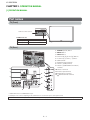
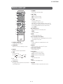
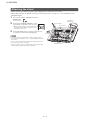
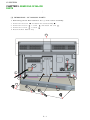
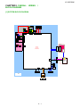
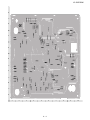
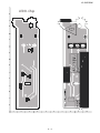
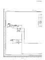
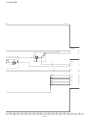
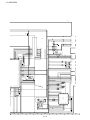
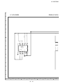
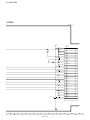
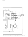
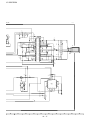
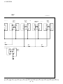
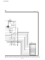
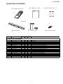
TopPage
1st Addition
SERVICE MANUAL
No.SZ12M1032LE250M
LCD COLOUR TELEVISION
MODEL : LC-32LE250M
In the interests of user-safety (Required by safety regulations in some countries) the set should be restored to its original condition and only parts identical to those specified should be used.
CONTENTS
SAFETY PRECAUTION
IMPORTANT SERVICE SAFETY
PRECAUTION................................................i
PRECAUTION FOR USING LEAD-FREE
SOLDER.........................................................ii
CHAPTER 1. OUTLINE
[1] OUTLINE...........................................1-1
CHAPTER 2. SPECIFICATIONS
[1] SPECIFICATION.................................2-1
CHAPTER 3.OPERATION MANUAL
[1] OPERATION MANUAL........................3-1
CHAPTER 4. DIMENSIONS
[1] DIMENSIONS......................................4-1
CHAPTER 6. ADJUSTMENT
[1] ADJUSTMENT....................................6-1
CHAPTER 7. TROUBLESHOOTING TABLE
[1] TROUBLESHOOTING TABLE .........................7-1
CHAPTER 8. OVERALL WIRING/BLOCK DIAGRAM
[1] SYSTEM BLOCK DIAGRAM............................8-1
CHAPTER 9. PRINTED WIRING BOARD ASSEMBLIES
[1] Main Unit .............................................9-1
CHAPTER 10. SCHEMATIC DIAGRAM
[1] DESCRIPTION OF SCHEMATIC
DIAGRAM ...........................................10-1
CHAPTER 5. REMOVING OF MAJOR PARTS
[1] REMOVING OF MAJOR PARTS...........5-1
Parts marked with "
" are important for maintaining the safety of the set. Be sure to replace these parts with specified ones for maintaining the
safety and performance of the set.
This document has been published to be used for
after sales service only.
The contents are subject to change without notice.
LC-32LE250M
SAFETY PRECAUTION
SAFETY PRECAUTIONSAFETY PRECAUTIONSAFETY PRECAUTION
LC32LE240M
5GTXKEG/CPWCN
IMPORTANT SERVICE SAFETY PRECAUTION
Service work should be performed only by qualified service technicians who are thoroughly familiar with all safety checks and the
servicing guidelines which follow:
WARNING
All checks must be repeated with the AC cord plug connection
reversed. (If necessary, a nonpolarized adaptor plug must be used
only for the purpose of completing these checks.)
1. For continued safety, no modification of any circuit should be
attempted.
Any reading of 0.74 Vrms (this corresponds to 0.5 mA rms AC.) or
more is excessive and indicates a potential shock hazard which
must be corrected before returning the monitor to the owner.
2. Disconnect AC power before servicing.
BEFORE RETURNING THE RECEIVER (Fire &
Shock Hazard)
Before returning the receiver to the user, perform the following
safety checks:
DVM
AC SCALE
3. Inspect all lead dress to make certain that leads are not pinched,
and check that hardware is not lodged between the chassis and
other metal parts in the receiver.
1.5k ohm
10W
4. Inspect all protective devices such as non-metallic control knobs,
insulation materials, cabinet backs, adjustment and compartment
covers or shields, isolation resistor-capacitor networks, mechanical
insulators, etc.
5. To be sure that no shock hazard exists, check for leakage current in
the following manner.
•
Plug the AC cord directly into a 110-240 volt AC outlet.
•
Using two clip leads, connect a 1.5k ohm, 10 watt resistor paralleled by a 0.15 F capacitor in series with all exposed metal cabinet
parts and a known earth ground, such as electrical conduit or electrical ground connected to an earth ground.
•
Use an AC voltmeter having with 5000 ohm per volt, or higher, sensitivity or measure the AC voltage drop across the resistor.
•
Connect the resistor connection to all exposed metal parts having a
return to the chassis (antenna, metal cabinet, screw heads, knobs
and control shafts, escutcheon, etc.) and measure the AC voltage
drop across the resistor.
0.15 µF
TEST PROBE
TO EXPOSED
METAL PARTS
CONNECT TO
KNOWN EARTH
GROUND
///////////////////////////////////////////////////////////////////////////////////////////////////////////////////////////////////////////////////////////////////////////////////////////////////////////////////////////////////////////
SAFETY NOTICE
Many electrical and mechanical parts in LCD colour television have
special safety-related characteristics.
For continued protection, replacement parts must be identical to those
used in the original circuit.
These characteristics are often not evident from visual inspection, nor
can protection afforded by them be necessarily increased by using
replacement components rated for higher voltage, wattage, etc.
The use of a substitute replacement parts which do not have the same
safety characteristics as the factory recommended replacement parts
shown in this service manual, may create shock, fire or other hazards.
Replacement parts which have these special safety characteristics are
identified in this manual; electrical components having such features
are identified by " " and shaded areas in the Replacement Parts List
and Schematic Diagrams.
///////////////////////////////////////////////////////////////////////////////////////////////////////////////////////////////////////////////////////////////////////////////////////////////////////////////////////////////////////////
i
LC-32LE250M
PRECAUTIONS FOR USING LEAD-FREE SOLDER
Employing lead-free solder
• “PWBs” of this model employs lead-free solder. The LF symbol indicates lead-free solder, and is attached on the PWBs and service manuals. The
alphabetical character following LF shows the type of lead-free solder.
Example:
Indicates lead-free solder of tin, silver and copper.
Indicates lead-free solder of tin, silver and copper.
Using lead-free wire solder
• When fixing the PWB soldered with the lead-free solder, apply lead-free wire solder. Repairing with conventional lead wire solder may cause damage or accident due to cracks.
As the melting point of lead-free solder (Sn-Ag-Cu) is higher than the lead wire solder by 40 C, we recommend you to use a dedicated soldering
bit, if you are not familiar with how to obtain lead-free wire solder or soldering bit, contact our service station or service branch in your area.
Soldering
• As the melting point of lead-free solder (Sn-Ag-Cu) is about 220 C which is higher than the conventional lead solder by 40 C, and as it has poor
solder wettability, you may be apt to keep the soldering bit in contact with the PWB for extended period of time. However, Since the land may be
peeled off or the maximum heat-resistance temperature of parts may be exceeded, remove the bit from the PWB as soon as you confirm the
steady soldering condition.
Lead-free solder contains more tin, and the end of the soldering bit may be easily corroded. Make sure to turn on and off the power of the bit as
required.
If a different type of solder stays on the tip of the soldering bit, it is alloyed with lead-free solder. Clean the bit after every use of it.
When the tip of the soldering bit is blackened during use, file it with steel wool or fine sandpaper.
• Be careful when replacing parts with polarity indication on the PWB silk.
Lead-free wire solder for servicing
PARTS CODE
ZHNDAi123250E
ZHNDAi126500E
ZHNDAi12801KE
PRICE
RANK
BL
BK
BM
PART
DELIVERY
J
J
J
DESCRIPTION
0.3mm 250g (1roll)
0.6mm 500g (1roll)
1.0mm 1kg (1roll)
ii
LC-32LE250M
CHAPTER 1. OUTLINE
[1] OUTLINE
MAJOR SERVICE PARTS
PWB UNIT
Ref No.
N
N
N
N
N
Part No.
DKEYMG247FM01
DKEYMG247FM02
RDENCA462WJPZ
DUNTKG238FM01
RUNTKB129WJZZ
Description
MAIN Unit ( ASIA )
MAIN Unit ( SPC )
POWER Unit
LED IR Unit
LED PWB A
N
RUNTKB130WJZZ
LED PWB B
OTHER UNIT
Ref No.
N
Part No.
R1LK315T3HB60W
Description
32-INCH Panel Hiraki
IC FOR EXCLUSIVE USE OF THE SERVICE
Ref No.
IC3104
IC3104
Part No.
RH-iXD606WJQZQ
RH-iXD614WJQZQ
Description
Q'ty
1
1
Description
Q’ty
1
1
1
1
Flash IC ( ASIA )
Flash IC ( SPC )
SERVICE JIGS
Ref No.
N
N
N
N
Part No.
QCNW-N120WJQZ
QCNW-N177WJPZ
QCNW-N179WJQZ
QCNW-N180WJQZ
RA WIRE ( Main -IR board )
Extension Cable, LVDS FFC (Main-Panel Controller)
PD WIRE ( Main -Power Unit )
LED BL wire ( Main-Panel BL )
1–1
LC-32LE250M
CHAPTER 2. SPECIFICATIONS
[1] SPECIFICATIONS
Specifications
Model
Item
LC-32LE250M
LCD panel
80 cm
Resolution
1,049,088 pixels (1366 g 768)
Video Colour System
PAL/SECAM/NTSC 3.58/NTSC 4.43/PAL 60
TV
TV-Standard
Function
Receiving VHF/UHF
Channel
CATV
PAL: B/G, D/K, I SECAM: B/G, D/K, K/K1 NTSC: M
43.25—863.25 MHz
S1—S41ch (including Hyperband)
TV-Tuning System
Auto Preset 99 ch
STEREO/BILINGUAL
NICAM: B/G, I, D/K A2 stereo: B/G
Viewing angles
H : 176º V : 176º
Audio amplifier/Speakers
10 Wg 2 / 4 g 10 cm 2pcs
Terminals
Antenna input
UHF/VHF 75 q DIN type
INPUT 1
HDMI (HDMI input), AUDIO in (
INPUT 2
VIDEO in, AUDIO in, COMPONENT in
INPUT 3
VIDEO in, AUDIO in
OUTPUT
AUDIO out, Headphone (
3.5 mm jack), PC input
3.5 mm stereo)
USB device/File system
USB Memory / FAT/FAT32
Photo file format
JPEG (.jpg) (DCF2.0 compliant). Progressive format jpeg files are not supported.
Music file format
(Files may not be playable
depending on the bitrate)
MP3 (.mp3) Bitrate: 32 k, 40 k, 48 k, 56 k, 64 k, 80 k, 96 k, 112 k, 128 k, 160 k,
192 k, 224 k, 256 k, 320 kbps
Sampling frequency: 32 k, 44.1 k, 48 kHz
OSD language
English/Simplified Chinese/Arabic/French/Portuguese/Russian/Persian/Thai/
Vietnamese/Indonesian
Power Requirement
AC 110—240 V, 50/60 Hz
Power Consumption
53 W (0.8 W Stand by)
Dimensions
without stand
735 (W) g 471 (H) g 113 (D) mm
with stand
735 (W) g 463 (H) g 167 (D) mm
Weight
7.8 kg (without stand) / 8.3 kg (with stand)
Operating Temperature
0°C — 40°C
s As a part of policy of continuous improvement, SHARP reserves the right to make design and specification changes for
product improvement without prior notice. The performance specification figures indicated are nominal values of production
units. There may be some deviations from these values in individual units.
2–1
LC-32LE250M
CHAPTER 3. OPERATION MANUAL
[1] OPERATION MANUAL
Part names
TV (Front)
Remote control sensor
POWER indicator
Light off
Lighted (Red)
Lighted (Green)
Power off.
The TV is in standby mode.
The TV is on.
TV (Rear)
SERVICE
ONLY
INPUT 1
VIDEO/Y
VIDEO
COMPONENT/AV
R-AUDIO-L
USB
ANT
AUDIO
IN
(R/L)
INPUT
R-AUDIO-L
/
AUDIO (R/L)
6
1
SERVICE
ONLY
7
1
2
3
4
5
6
7
8
9
2
11
3
8
10
11
12
13
POWER (On/Off) button
MENU button
INPUT button
Channel up (r)/down (s) buttons
Volume up (e)/down (f) buttons
USB terminal*
SERVICE ONLY terminal**
INPUT 1 (HDMI) terminal
INPUT 2 (COMPONENT/AV INPUT)
terminals
INPUT 3 terminals
Antenna input terminal
AUDIO IN (R/L) terminal
/AUDIO OUTPUT terminal
12
4
COMPONENT/AV INPUT
VIDEO
R-AUDIO-L
/
AUDIO (R/L)
13
OUTPUT
5
9
10
* USB terminal use for USB Media Player.
** Usually do not connect anything to this terminal as it is reserved only for service personnel.
s The illustrations in this operation manual are for explanation purposes and may vary slightly from the actual operations.
3–1
LC-32LE250M
Remote control unit
1
2
3
4
13
14
5
6
15
7
16
8
17
9
18
10
11
19
7 AV MODE
Select an audio and video setting.
8 VOLk/VOLl
Set the volume.
(VOLk) Increase the volume.
(VOLl) Decrease the volume.
9 e (Mute)
Press e s Mutes sound.
Press e again s Restores sound.
Mute will be cancelled after 30 minutes. However, the TV
will not suddenly output loud sound as the volume level will
be set to 0 automatically. Increase the volume level by
pressing VOL k.
10 a/b/c/d (Cursor)
Select a desired item on the setting screen.
ENTER
Execute a command.
11 WIDE
Change the wide image mode.
12
12 Colour (Red/Green/Yellow/Blue)
The coloured buttons are correspondingly used to select the
coloured items on the screen.
1 POWER (STANDBY/ON)
To switch the power on and off.
13 ECO
Reduce overall power consumption based on user
preferences.
2 COLOUR ADJ.
Adjust the colour tone of the image on screen.
14 PHOTO
Display your pictures directly on the TV screen.
3 DISPLAY
Display the channel or input information.
4 SLEEP
Set the Sleep Timer.
0 hr. 30 min.
Off
1 hr. 0 min.
2 hr. 30 min.
1 hr. 30 min.
2 hr. 0 min.
5 0–9
Set the channel.
6 A (Flashback)
Press A to return to the previous selected channel
or external input mode.
15 INPUT (INPUT SOURCE)
Select an input source.
16 CHr/CHs
TV input mode: Select the channel.
(CHr) Increase the channel number.
(CHs) Decrease the channel number.
17 MENU
Display the menu screen.
18 MPX
Select the sound multiplex mode.
19 RETURN
MENU mode: Return to the previous menu screen.
3–2
LC-32LE250M
Attaching the stand
• Before attaching (or detaching) the stand, unplug the AC cord from the AC outlet.
• Before performing work spread cushioning over the base area to lay the TV on. This will prevent it from
being damaged.
1
Con-rm the screws supplied with the TV.
Screws (m4)
(used in step 3)
2
Stand base
guide pins
Insert the stand base guide pins to the
stand holes on the rear of the TV. (1)
Screw driver
Soft cushion
• Make sure the symbol on the stand base
is parallel with the triangle symbol located
at the back of the TV.
3
Insert and tighten the 4 screws into the 4 holes
on the rear of the stand assembly.(2)
Screw
NOTE
SERVICE
ONLY
• To detach the stand, perform the steps in reverse order.
• The TV position setting is set to 7 backward after attaching
the stand.
• Do not remove the plastic wrap before attaching the stand
base to protect it from scratches.
• The bottom area of the set (curvy area) must be beyond the
table’s edge to prevent the TV from damage.
3–3
INPUT 1
VIDEO/Y
VIDEO
Guide pin holes
COMPONENT/AV INPUT
R-AUDIO-L
R-AUDIO-L
/
AUDIO (R/L)
USB
ANT
AUDIO
IN
(R/L)
LC-32LE250M
CHAPTER 4. DIMENSIONS
Unit mm
[1] DIMENSIONS
4–1
LC-32LE250M
CHAPTER 5. REMOVING OF MAJOR
PARTS
R
E
M
O
V
I
N
G
O
F
M
A
[1] REMOVING OF MAJOR PARTS
J
O
R
P
A
R
1. Remo ving of the Rear Cab in et Ass ’y a nd S tand assembly.
T
R
E
M
O
1.
R emove the 4 scr ews
and detach the S ta nd assembly
V
I
N
.
G
2 . R emove the 2 scr ew
, 1 screws
and detech AC cord
.
O
F
M
3.
R emove the 1 scr ew
, 6 screws
A
J
O
R
4. Deta ch the Rear Cabinet Ass’y .
P
A
R
T
R
E
M
O
V
I
N
G
O
7
F
M
A
J
O
R
P
A
R
T
R
E
M
O
V
I
N
G
O
F
M
A
J
O
R
P
A
R
T
R
E
M
O
V
I
N
G
O
F
M
A
J
O
R
6
P
A
R
T
4
5
3
3
1
2
5–1
LC-32LE250M
2. Removing of the Bottom Bracket and speaker L/R
1. Remove 4 screw bottom bracket 1
2, Disconnect SP wayer & remove speaker from L / R panel bosses
3. Remove 1 screw from front angle L/R & remove front angle
2
3
4. Disconnect PD,LW,RA & remove 3 screw main unit 4
5. Disconnect LED wayer & remove 4 screw sub main unit 5
5
4
PD
LED WAYER
PD
LW
SP
RA
1
3
3
2
5–2
LC-32LE250M
3. Removing of the LCD Panel Module
1
1. Detech the 10 lock hook
2, and detech the LCD Module
refer figure 1.
2
Rear Cabinet Ass'y
1 Hook
1 Hook
1 Hook
1 Hook
1 Hook
1
Hook
1 Hook
1 Hook
1 Hook
1 Hook
2
Figure 1
KS-Bezel
Cab-A
Lock
Note:
Make sure perfectly detech lock
5–3
LC-32LE250M
CHAPTER 6. ADJUSTMENT
[1] ADJUSTMENT
[1] ADJUSTMENT PROCEDURE
1. Entering and cancel the adjustment process mode
1) While holding down the TV/VIDEO and Volume DOWN keys at the same time, plug in the AC cord to turn on the power. (“K” standing for inspection process mode is displayed on the upper left position of the screen.)
2) Press the Channel DOWN and Volume DOWN keys at the same time. (The adjustment process mode screen appears.)
3) To cancel it, turn off the power using the Power switch or remote control.
2. Remote controller key operation and description of display in adjustment process mode.
1. key operation
Remote controller key
CH (
/
)
VOL (+ / –)
Cursor ( / )
Cursor ( / )
INPUT button on remote
controller
ENTER
*
Main unit key
CH (
/
)
VOL (+ / –)
——————
——————
Function
Changing channel (UP/DOWN)
Changing volume (UP/DOWN)
Turning a page (PREVIOUS/NEXT)
Changing a selected line setting (+10/-10)
INPUT button
Input source switching (toggle switching)
(TV
INPUT1 INPUT2 INPUT3 USB )
——————
——————
Input mode is switched automatically when relevant adjustment is started so far as the necessary input signal is available.
3. Software upgrading.
1) Plug off the LCD TV.
2) Insert the USB device to the USB terminal at the LCD TV.
(Make sure that the latest software is installed in the USB device).
3) Hold the LCD TV power key and plug on the LCD TV.
4) LCD TV is on and detecting the USB device.
Binary file detecting
5) A few seconds later, the software upgrading will start automatically.
Do not power off
Chip erasing
.......................
Do not power off
Chip programming
.......................
6–1
LC-32LE250M
6) Let the process running & entering verification.
Do not power off
Verifying
.........................
Verify Pass
7) Software is successfully installed when the following appears at the end of the process.
Please re-boot the system
Update Finished
8) Plug off the LCD TV and plug ON again as usual.
9) LCD TV is running with the latest software.
LCD TV ADJUSTMENT ITEM
1. EDID DATA INPUT
No need to input EDID
2. SIGNAL ADJUSTMENT
A. PICTURE ADJUSTMENT
Confirmation of signal from generator (setting to spec level)
+
• 0.7Vp-p –
0.02Vp-p (pedestal to white level)
PAL Composite signal
15K Component signal (50Hz)
• Y level
Pb, Pr level
33K Component signal
• Y level
Pb, Pr level
+
• 0.7Vp-p –
0.02Vp-p (pedestal to white level)
+
• 0.7Vp-p : 0.7Vp-p –
0.02Vp-p
+ 0.02Vp-p (pedestal to white level)
• 0.7Vp-p –
• 0.7Vp-p
•
+
0.7Vp-p –
0.02Vp-Com
a) Adjustment Mode
ITEM
1
Adjustment Mode
CONDITION
PROCEDURE
Press the test key at the test remote control
6–2
LC-32LE250M
b) Component 15K 50Hz Signal Adjustment (COMP-SD)
ITEM
1
Setting
CONDITION
PROCEDURE
•
[Signal]
COMP 15K 50Hz
(576i)
100% Full-field Colour
Bar
[Terminal]
COMPONENT
INPUT 3
2
Auto Adjustment
Feed the COMPONENT 15K 50Hz (576i) 100% Full-field
Colour Bar signal(100% colour saturation) to
COMPONENT INPUT 3
100% White•
•
Black
At the related page, move cursor to [COMP SD ADJ], press
ENTER.
Test Mode page4
(COMP SD)
[OK] appears when finished.
c)
Component 33K 60Hz Signal Adjustment (COMP-HD)
ITEM
1
Setting
CONDI TION
[Signal]
COMP 33K 60Hz
(1080i)
100% Full-field Colour
Bar
[Terminal]
COMPONENT
INPUT 3
2
Auto Adjustment
Test Mode page 5
(COMP HD)
PROCEDURE
•
Feed the COMPONENT 33K 60Hz (1080i) 100% Full-field
Colour Bar signal(100% colour saturation) to
COMPONENT INPUT 3
100% White•
•
Black
At the related page, move cursor to [COMP HD ADJ], press
ENTER.
[OK] appears when finished.
6–3
LC-32LE250M
B. WHITE BALANCE ADJUSTMENT
a) White Balance Adjustment
ITEM
1
2
Setting
Auto
Adjustment
CONDITION
PROCEDURE
Backlight : MAX
AV Mode : DYNAMIC
Active Backlight : OFF
Set
the luminance
meter on the centre of
the screen
For the details of white balance adjustment procedure, please refer to white
balance adjustment spec for Kameyama model.
[command]
Adjustment Mode
KRSW0001
KKT10037
[Adjustment Procedure]
1. Using the R/C, set the LCD TV to adjustment mode.
2.
Measure Max brightness (Lmax).
FACT0001
Setting
KYOF0001
OSDS0001
SBSL16_ _
3.
Calculate min. brightness (Lmin) = Lmax/3000.
4.
Measure Point 2 brightness (Lhigh ).
5.
Set the reference value R,G,B of Point 2 (Ref.2) = 3664 x (229 / P2)
where P2 = 255 x [(Lhigh – Lmin) / (Lmax – Lmin)] 1/2.2
6.
Set the specified gradation for point 2, fix the most faint colour to get
reference value, adjust others 2 colour to minus adjustment for
reference value of point 2.
7.
Measure Point 1 brightness (Llow).
8.
Set the reference value R,G,B of Point 1 (Ref.1) = 816 x (51 / P1)
1/2.2
where P1 = 255 x [(Llow – Lmin) / (Lmax – Lmin)]
9.
Set the specified gradation for point 1. Set G of point 1 to the
default
value [(Ref.1 x G value of point 2 / Ref.2), with fractions rounded] and
adjust RB to the reference value of point 1.
Multi point adj. Mode
MSET0000
WBI20255
Point 2
WBI20229
MG2G****
MG2B****
MG2R****
Point 1
WBI10051
MG1G****
MG1B****
MG1R****
Set Max.Level
MGMG****
MGMR****
MGMB****
Write
1. Confirm the set condition.
2. Connect the white balance jig.
3. Through RS-232C command, adjustment mode screen is displayed.
10. Set the G of point Max. to the default value (4080 x G value of point 2 /
Ref.2). Set the R,B Max. value [Gmax – G value of point 2 + (R,B value
of point 2)].
11. Adjusted value is writing at [command] MSET0003.
12. Shut down the AC power.
• Initial value at RGB 2 point : 3664
• Initial value at RGB 1 point : 816
MSET0003
6–4
LC-32LE250M
[Adjustment value]
• Teaching set send by engineering dept is set as reference.
[Reference values for adjustment reference]
Equipment
Point 2
ref.
values
Point 1
ref.
values
Ref.
:
:
Luminance meter [Minolta CA-210]
Level
Spec
Data
Adjustment
Spec.
Inspection
Spec.
229
x=0.272
y=0.277
• 0.0010
• 0.0020
51
x=0.272
y=0.277
• 0.0045
• 0.0090
For inspection, set the LCD TV as below.
AV MODE
: [DYNAMIC] (Reset)
Aging Time
: Minimum 60 minutes
3. FACTORY SETTING
AC power is plug off after shipment setting is done.
Caution: Do not plug on again after shipment setting is done. If do, please re-do the shipment setting. Do not off
with remote control.
ITEM
CONDITION
PROCEDURE
Factory setting
AC power off to exit the
factory setting.
1. Setting is done with test remote control.
2. Press the ‘Factory Setting’ key on the remote control continuously.
3. When Green background appears on screen and ‘K’ mark
disappears, setting is completed.
The followings are initialised to factory setting
1) User setting
2) Channel data (e.g. broadcast frequencies)
3) Manufacturer’s option settings
4) Password data
5) Setting values are set based on model destination
Model Name
Asia ,Near and Middle
East
PHILIPPINES
Factory Setting Key
Name
Remote Control
Code
S-System Setting
OSD Language
Setting
M-Setting
100000001010110
B/G
ENGLISH
P-Setting
100000001011110
M
ENGLISH
**Please do inspection for A3KLED3P
(PHILIPPINES) using
6–5
NTSC signal.
LC-32LE250M
CHAPTER 7. TROUBLESHOOTING
TABLE
[1] TROUBLESHOOTING TABLE
[1] TROUBLESHOOTING TABLE
No power (front LED failure to light up) or no startup (front LED failure to turn from red to green)
Is the AC cord connector tightly connected to the set?
NO
Reconnect the AC cord tightly and turn on the power again.
YES
Are the wire harnesses and other cables properly connected in
the set?
NO
Reconnect the wire harnesses and other cables properly in the
set.
YES
Is there the AC_CTRL and POWER_LED signal input at pins
(70 ) and (44) of IC3301
NO
Check the AC_CTRL signal line POWER_LED signal line.
YES
Are the DC/DC converter outputs and the output voltages along
the control lines as specified?
NO
Check the DC/DC converters and the control lines. Replace
defective parts as required.
1)
2)
3)
4)
5)
6)
M+5.6V (IC9601)
D+1.26V (IC9602)
D+5V (IC9601)
D+3.3V (IC9603)
D+1.8V (IC9606)
D+2.5V (IC9608)
7–1
LC-32LE250M
With [RF] signal input
No video onscreen (1)
No video in the UHF/VHF reception
Is there IF output from the tuner pin( 8 ) of TU1101 as specified?
NO
Check TU1101 and its peripheral circuits.
YES
Is there VIF input at pin 38 & 39 of IC3301?
NO
Check the circuit between TU1101 & IC3301.
YES
Are there the signal outputs of IC3301?
NO
Check IC3301 and its peripheral circuit.
YES
Check LVDS cable, LCD controller (incl. panel) and their peripheral circuits.
With <Video> signal input
No video onscreen (3)
No external input video onscreen <INPUT 3>
Is INPUT 3 selected on the input select menu screen?
NO
Select INPUT 3 on the input select menu screen to pick up the
right input signal.
YES
Is there the video signal input at pin (19 ) of IC3301?
NO
Check the line between pin (9) of TL539 and pin (19) of IC3301.
YES
Are there signal outputs of IC3301?
NO
Check IC3301 and its peripheral circuits.
YES
Check LVDS cable, LCD controller (incl. panel) and their peripheral circuits.
7–2
LC-32LE250M
With <Component> signal input
No video onscreen (2)
No external input video onscreen <INPUT 2>
Is INPUT 2 selected on the input select menu screen?
NO
Select INPUT 2 on the input select menu screen to pick up the
right input signal.
YES
Are there the Y, Pb and Pr signal inputs at pins (13), (11) and
(15 ) of IC 3301 respectively?
NO
Check the line between pins (6) /(14)/(18) of TL563 and pins
(13)/(11) /(15 )of IC3301.
YES
Is input waveform of IC3301 normal?
Y=(13) pin, Pb=(11) pin, Pr=(15) pin
NO
Check IC3301 and its peripheral circuits.
YES
Check LVDS cable, LCD controller (incl. panel) and their peripheral circuits.
With <HDMI> signal input
No video onscreen (4)
No external input video onscreen <INPUT 1>.
Is INPUT 1 selected on the menu screen?
NO
Select INPUT 1 on the input select menu screen to pick up the
right signal input.
YES
Are there signal outputs from SC1501 to IC3301?
NO
Check peripheral circuits between SC1501 and IC3301.
YES
Are there signal outputs of IC3301?
NO
Check IC3301 and its peripheral circuits.
YES
Check LVDS cable, LCD controller (incl. panel) and their peripheral circuits.
7–3
LC-32LE250M
No audio heard (1)
No sound in the UHF/VHF reception.
Is the IF output from the tuner pin (8) of TU1101 as specified?
NO
Check TU1101 and its peripheral circuits.
YES
Is there the I2C signal input at pins (42), (43) of IC3301?
NO
Check IC3301 and its peripheral circuits.
YES
Is thereaudio signal intput at pin(22),(32) of IC1702?
NO
Check connection between IC3301 and IC1702 and its
peripheral circuits.
NO
Check IC1702 and its peripheral circuits.
NO
Check circuit between IC 1702 & P1702.
YES
Is the L-ch audio signal output at pin(10),(11),(16),(17) of IC1702
normal ?
Is the R-ch audio signal output at pin(2),(3),(8),(9) of IC1702 normal ?
YES
Are the audio signal L-ch and R-ch output at (3)/(4) and (1)/(2) of
P1702 normal?
YES
Check speakers and their peripheral circuits.
7–4
LC-32LE250M
No audio heard (2)
No external audio heard
<INPUT 2>
Is there the L-ch audio signal input from pin (30) of input terminal
TL563 to pin (26) of IC 3301?
Is there the R-ch audio signal input from pin (26) of input terminal
TL563 to pin(27) of 3301?
<INPUT 3>
Is there the L-ch audio signal input from pin (20) of input terminal
TL539 to pin (23) of 3301?
Is there the R-ch audio signal input from pin (15) of input terminal
TL539 to pin (24) of IC3301?
YES
Is there the I2C signal input at pin (42), (43) of IC3301?
NO
Check IC3301 and its peripheral circuits.
YES
Is there audio signal input at pin(22),(32) of IC1702?
NO
Check connection between IC3301 and IC1702 and its peripheral circuits.
NO
Check IC1702 and its peripheral circuits.
NO
Check circuit between IC1702 & P1702 .
YES
Is the L-ch audio signal output at pin(10),(11),(16),(17) of
IC1702
Is the R- ch audio signal output at pin(2),(3),(8),(9) of IC1702
normal ?
YES
Are the audio signal L-ch and R-ch output at (3)/(4) and (1)/(2) of
P1702 normal?
YES
Check speakers and their peripheral circuits.
7–5
LC-32LE250M
No audio heard (3)
No HDMI sound heard. <INPUT 1>
(*INPUT 1 is digital audio.)
Does the HDMI image appear onscreen?
NO
Refer to “<INPUT 1> in No external input video onscreen
(HDMI)”.
No audio output from <INPUT 1>
NO
Check the EDID.
YES
Are waveforms input in to the pins of IC3301 normally?
NO
Check peripheral circuits IC3301.
YES
Is there audio signal input at pin(22),(32) of IC1702
NO
Check connection between IC3301 and IC1702 and its peripheral circuits.
NO
Check IC1702 and its peripheral circuits.
NO
Check circuit between IC1702 & P1702.
YES
YES
Is the L-ch audio signal output at pin(10) ,(11),(16),(17) of IC1702
normal ?
Is the R-ch audio signal output at pin (2),(3),(8),(9) of IC1702
normal ?
YES
Are the audio signal L-ch and R-ch output at (3)/(4) and (1)/(2) of
P1702 normal?
YES
Check speakers and their peripheral circuits.
7–6
LC-32LE250M
No audio heard (4)
No sound from the HDMI sound input terminal.
(INPUT 1 analog audio)
YES
Is there the L-ch audio signal input from pin (2) of external input
terminal J501 (HDMI AUDIO IN) to pin (28) of IC3301?
Is there the R-ch audio signal input from pin (3) of external input
terminal J501 (HDMI AUDIO IN) to pin (29) of IC3301?
YES
Are I2S signal output from the pins (42), (43) of IC3301 normally?
NO
Check peripheral circuits of IC3301.
YES
Is there audio signal input at pin(22),(32) of IC1702
NO
Check connection between IC3301 and IC1702 and its peripheral circuits.
NO
Check IC1702 and its peripheral circuits.
NO
Check circuit between IC1702 & P1702.
YES
Is the L- ch audio signal output at pin ( 10 ),(11),(16),(17) of
IC1702 normal ?
Is the R- ch audio signal output at pin(2),(3),(8),(9) of IC1702
normal?
YES
Are the audio signal L-ch and R-ch output at (3)/(4) and (1)/(2) of
P1702 normal?
YES
Check speakers and their peripheral circuits.
7–7
LC-32LE250M
CHAPTER 8. OVERALL
WIRING
/
BLOCK DIAGRAM
[1] SYSTEM BLOCK DIAGRAM
㪟㪛㪤㪠
㪫㪬㪥㪜㪩
㪫㪬㪈㪈㪇㪈
㪩㪫㪬㪥㪨㪘㪇㪍㪎㪮㪡㪨㪱
㪠㪝
㪚㪜㪚㩷㪠㪥
㪠㪩㩷㪩㪼㪺㫀㪼㫍㪼㫉
㪣㪜㪛
㪪㪘㪩㩿㪇㪀㩷
㪪㪘㪩㩿㪈㪀
㪪㪘㪩㩿㪉㪀
㪣㪜㪛㪶㪞
㪪㪠㪝㩷㪠㪥
㵘㵘㵘㵘
㪣㪜㪛㪶㪩
㪭㪠㪝㩷㪠㪥
㪫㪜㪤㪧㩷㪪㪜㪥㪪㪦㪩
㪫㪟㪊㪊㪇㪈
㪠㪩㪜㪤
㪪㪠㪝㩷㪪㪘㪮
㪝㫀㫃㫋㪼㫉㩷
㪪㪠㪝㪂
㪪㪠㪝㪄
㪭㪠㪝㩷㪪㪘㪮
㪝㫀㫃㫋㪼㫉㩷㪝㪣㪈㪈㪇㪉
㪢㪜㪰㪈㪆㪉㪆㪧㪦㪮㪜㪩㩷㪪㪮
㪜㪛㪠㪛
㪠㪚㪈㪌㪇㪈
㪭㪠㪝㪂
㪭㪠㪝㪄
㪟㪛㪤㪠㩷㪠㪥㪈
㪟㪛㪤㪠㩷㪛㪛㪚㪈
㪮㪧㪶㪚㪫㪩㪣
㪢㪜㪰㪆㪪㪮
㪠㪉㪚
㪠㪝㩷㪘㪤㪧㩷
㪺㫃㫂㩿㪉㪀
㪠㪉㪚㩿㪟㪛㪤㪠
㪟㪧㪛㪇㪶㪠㪥㪆㪛㪌㪭
㪻㪸㫋㪸㩿㪋㪀
㪟㪛㪤㪠㩷㪈㩷㪪㪚㪈㪌㪇㪈
㪨㪪㪦㪚㪱㪘㪈㪎㪌㪮㪡
㪫㪜㪩㪤㪠㪥㪘㪣
㪢㪜㪰㪆㪩㪚㪆㪣㪜㪛
㪫㪬㪥㪜㪩
㪠㪥㪧㪬㪫㪈
㪞㪧㪠㪦㪍
㪞㪧㪠㪦㪊㪎
㪠㪩㩷㪠㪥
㩷
㪜㪜㪧㪩㪦㪤㩷㪠㪚㪌㪇㪏
㪭㪟㪠㪙㪩㪉㪋㪫㪇㪉㪡
㪧㪚㩷㩷㪛㪪㪬㪙㩷㪈㪌㫇㫀㫅
㪪㪚㪌㪇㪉
㪚㫆㫄㫇㩷㪘㫌㪻㫀㫆㩷㪠㪥㩷㪡㪌㪇㪊
㪧㪚㩷㪛㪛㪚
㪰㪆㪧㪹㪆㪧㫉
㪚㪭㪙㪪㩷㪸㫅㪻㩷㪘㫌㪻㫀㫆㩷㪣㪆㪩
㪚㪭㪙㪪
㪚㪦㪤㪧
㪘㪬㪛㪠㪦
㪣㪆㪩
㪛㪧㪆㪛㪥
㪤㫆㫅㩷㪣㪆㪩㩷㪦㪬㪫㩷㪡㪌㪇㪌
㪤㫆㫅㩷㪘㫄㫇㩷㪺㫀㫉㪺㫌㫀㫋
㪟㪧㩷㪡㪌㪇㪋
㪟㪧㩷㪘㫄㫇㩷㪺㫀㫉㪺㫌㫀㫋㩷
㪬㪪㪙㩷㪠㪝
POWER UNIT
㪤㫆㫅㫀㫋㫆㫉㩷㪘㫌㪻㫀㫆㩷
㪟㪧㩷㪘㫌㪻㫀㫆㩷㫆㫌㫋
㪧㪛
㪟㪧㩷㪛㪼㫋
㪤㪪㪫㪍㪈㪇㪇㪭㪪
㪩㪼㪽㩷㪥㫆㪅㪠㪚㪊㪊㪇㪈
㪩㪟㪄㪠㪯㪛㪇㪊㪌㪊㪮㪡㪱㪱㪨
㵘
㪬㪩㪂㪈㪉㪅㪉㪭
㪞㪥㪛
㪧㪪㪶㪦㪥
㪜㪩㪩㪦㪩
㪦㪝㪣
㪪㪫㪙
㪜㪩㪩㪦㪩
㪦㪝㪣
㪧㪥㪣㩷㪪㪫㪙
㪧㪛
FFC
㪬㪩㪂㪈㪉㪅㪉㪭
㪞㪥㪛
㪧㪪㪶㪦㪥
㪜㪩㪩㪦㪩
㪦㪝㪣
㪪㪫㪙
CN1
2pin
LED1_A
LED1_K
LED BAR
CN1 (2pin)
LED1_A
LED1_K
䊌䊈䊦㔚Ḯ
㪉㪐㪑㩷㪈㪉㪭
㪣㪭㪛㪪㩿㪏㪹㫀㫋㪀
㪻㪸㫋㪸 㪘㩿㪏㪀
㪺㫃㫂 㪘㩿㪉㪀
㪧㪉㪍㪇㪈
㪊㪇㩷㫇㫀㫅
㪻㪸㫋㪸 㪘㩿㪏㪀
㪺㫃㫂 㪘㩿㪉㪀
䊝䉳䊠䊷䊦
㪉㪐㩷㪑㩷㪮㪯㪞㪘
㪯㪠㪥㪆㪯㪦㪬㪫
㪯㪫㪘㪣㩿㪉㪋㪅㪇㪤㪟㫑㪀
㪯㪊㪊㪇㪈
㪠㪉㪚㩷㪘㪛㪛㪩㪜㪪㪪䋺㪘㪏
㪠㪉㪚
㪜㪜㪧㪩㪦㪤㩿㪟㪛㪚㪧㪀
㪠㪚㪏㪋㪇㪊
㪩㪟㪄
㪠㪉㪚㩷㪘㪛㪛㪩㪜㪪㪪䋺㪘㪋
㪘㪬㪛㪠㪦㪶㪦㪬㪫
㪪㪧㪠㩷㪠㪆㪝
㪟㪆㪮㩷㪩㪜㪪㪜㪫
㪛㪩㪘㪤㩷㪠㪝
㪛㪛㪩㪉㩿㪈㪉㪏㪤㪹㪀
㪠㪚㪊㪌㪇㪈
㪩㪟㪄㪠㪯㪛㪊㪍㪈㪮㪡㪨㪱
㪪㪧㪠㩷㪝㪣㪘㪪㪟
㪠㪚㪏㪋㪇㪋
㪩㪟㪄
㪪㪧㪶㪣
㪪㪧㪶㪩
㪘㪬㪛㪠㪦㩷㪘㪤㪧
㪠㪚㪉㪎㪇㪋
㪭㪟㪠㪰㪛㪘㪈㪍㪋㪛㪱㪄㪈㪰
㪤㪘㪠㪥
㪪㪧㪶㪩
㪪㪧㪧㪉㪎㪇㪈
㪨㪧㪣㪞㪥㪙㪇㪐㪉㪮㪡㪱㪱㪰
㵘㵘㵘㵘㵘㵘㵘
㪪㪧㪠
㪪㪧㩷㪤㪬㪫㪜
㪠㪉㪪
㪠㪉㪪
㪩㪜㪪㪜㪫
㪠㪚㪊㪊㪇㪉
㵘㵘㵘
㪠㪉㪚
㪜㪜㪧㪩㪦㪤㩿㪛㪘㪫㪘㪀
㪠㪚㪏㪋㪇㪉
㪭㪟㪠㪩㪉㪋㪈㪉㪏㪘㪪㪄㪈㪰
㩷
㪪㪧㪶㪣
㪬㪪㪙㩷㪠㪥㩷㪡㪌㪇㪈
㪟㪛
㪭㪛
㪣㪆㪩
㪧㪚㩷㪘㫌㪻㫀㫆㩷㪡㪌㪇㪍
㪚㪭㪙㪪㪆㪚㪦㪤㪧㩷㪠㪥㩷㪡㪌㪇㪉
㪧㪚㩿㪩㪞㪙㪀
㪪㪧 㪣
㪪㪧 㪩
㪋㪆㪏㱅㪌
㪋㪆㪏㱅㪌
8–1
㪪㪧㪠㩷㪝㪣㪘㪪㪟㩷㪮㪩㪠㪫㪜
㪚㪟㪜㪢㪜㪩㩷㪣㪘㪥㪛
LC-32LE250M
CHAPTER 9. PRINTED
WIRING
BOARD ASSEMBLIES
[1] MAIN Unit / LED PWB
Main Unit ( Side-A )
H
G
F
E
D
C
B
A
1
2
3
4
6
5
9–1
7
8
9
10
LC-32LE250M
H
G
F
E
D
C
B
A
1
2
3
4
6
5
9–2
7
8
9
10
LC-32LE250M
LED A -Chip
H
LED A -Symbol
G
F
E
D
C
B
A
1
2
3
4
6
5
9–3
7
8
9
10
LC-32LE250M
LED B -Chip
H
G
F
E
D
C
B
A
1
2
3
4
6
5
9–4
7
8
9
10
LC-32LE250M
CHAPTER 10. SCHEMATIC
DIA-
GRAM
[1] DESCRIPTION OF SCHEMATIC DIAGRAM
1. VOLTAGE MEASUREMENT CONDITION:
1) The voltages at test points are measured on exclusive AC adaptor and the stable supply voltage of AC 110-240V. Signals are fed by a colour bar signal
generator for servicing purpose and the above voltages are measured with a 20k ohm/V tester.
2. INDICATION OF RESISTOR & CAPACITOR:
RESISTOR
1) The unit of resistance " " is omitted.
(K=k =1000 , M=M ).
2) All resistors are ± 5%, unless otherwise noted.
(K= ± 10%, F= ± 1%, D= ± 0.5%)
3) All resistors are 1/16W, unless otherwise noted.
CAPACITOR
1) All capacitors are F, unless otherwise noted.
(P=pF=
F).
2) All capacitors are 50V, unless otherwise noted.
CAUTION:
This circuit diagram is original one, therefore there may be a slight
difference from yours.
SAFETY NOTES:
1) DISCONNECT THE AC PLUG FROM THE AC OUTLET
BEFORE REPLACING PARTS.
2) SEMICONDUCTOR HEAT SINKS SHOULD BE REGARDED AS
POTENTIAL SHOCK HAZARDS WHEN THE CHASSIS IS
OPERATING.
IMPORTANT SAFETY NOTICE:
PARTS MARKED WITH " " (
) ARE IMPORTANT
FOR MAINTAINING THE SAFETY OF THE SET. BE SURE TO
REPLACE THESE PARTS WITH SPECIFIED ONES FOR MAINTAINING THE SAFETY AND PERFORMANCE OF THE SET.
10 – 1
LC-32LE250M
MAIN1 (TUNE R )
LC -32LE 250M
H
T L1114
T U1101
QA068WJ QZ
11
T L1110
T L1111
T L1112
S DA
10
R 1106
0
T L1106
C 1105
10u
16V
I2C _DAT
R 1108
100
I2C _C LK
RESET
R 1116
10K
IF _IN-
R 1107
100
IF _IN+
C 1128
1000P
50V
SCL
9
R 1105
0
F B 1101
0253T A
F
AIF -
T L1107
8
7
6
5
AIF +
DIF +
DIF -
IF _AG C
T L1104
4
T L1102
1.8V
3
T L1109
T L1101
C 1103
0.1u
25V
3.3V
T L1108
2
1
T L1103
RESET
5V
G
C 1112
0.01u
E
C 1116
0.1u
25V
F B 1102
0253T A
D
C 1117
10u
16V
C 1114
1000P
50V
C
RESET
C 1122
0.1u
IF _IN-
IF _IN+
B
I2C _DAT
I2C _C LK
T AG C
A
1
2
3
4
6
5
10 – 2
7
8
9
10
LC-32LE250M
NER)
PP (2012.06.14)
TO MAIN10(POWER)
010
010
D+1.8V
D+3.3V
D+1.8V
TO MAIN4(CPU)
RESET
004
C1122
0.1u
TUNER_RESET
R1115
0
C1131
0.1u
CZ
R1101
33
IF_IN-
R1102
33
IF_IN+
R1104
51
C1120
0.1u
004
VIFM
CIL
C1102
180P
L1103
100nH
CZ
R1103
51
C1121
0.1u
004
VIFP
C1132
0.1u
I2C_DAT
004
I2C_CLK
004
TAGC
004
10
11
12
13
14
15
10 – 3
16
17
I2C_DAT
I2C_CLK
TAGC
18
19
LC-32LE250M
MAIN2(T E R MINAL)
LC -32LE 250M
H
T L564
G
T L565
R 547
75
1/4W
F
T L566
R 549
75
1/4W
R 548
75
1/4W
US B :500mA max
L9501
F A154WJ
3
US B _D0P
US B _D0N
V A9503
V XA074WJ
39V
1.1pF
V A9502
V XA074WJ
39V
1.1pF
T L9505
5
E
4
V out
C 9501
10u
16V
V in
IC 9501
K ZA510WJ P Z
ON
G ND
1
C 9502
10u
16V
K ZA510WJ P Z
3479A50P
CS
2
3
C 9503
0.1u
R 9501
1K
D
2
T L505
3
T L506
1
T L504
R 503
10K
J
C 501
56P
CH
J 501
J A027WJ
P C _AUD_L
R 505
12K
C 503
1000P
CH
R 506
12K
C 504
1000P
CH
HDMI AUDIO IN
C
R 504
10K
J
C 502
56P
CH
P C _AUD_R
B
A
1
2
3
4
6
5
10 – 4
7
8
9
10
C OMP 1_P r
4
1
T L9502
T L9501
C OMP 1_P b
+5V
2
C OMP 1_Y
3
US B _DN
2
T L9503
1
J 9501
ZA330WJ QZ
4
T L9504
G ND
US B _DP
LC-32LE250M
PP (2012.07.11)
HP
J503
J502
JA030WJQZ
25
4
ZA107WJ
30
26
18
14
5
6
RD
WH
RD
BL
GN
TL563
5
4
2
37
6
1
20
15
9
TL543
TL540
TL542
TL516
TL514
TL515
TL513
7
8
RD
WH
YL
TL539
C520
0.01u
TL524
TL545
TL527
TL568
TL529
TL562
TL559
R520
1K
R522
TL538
R523
100K
100K
C521
10P
C514
56P
COMP1_Y
004
COMP1_Pb
004
COMP1_Pr
004
CVBS1
004
COMP_AUD_L
R515
12K
R524
10K
R525
33
R526
33
004
COMP_AUD_R
004
CVBS_AUD_L
004
CVBS_AUD_R
004
COMP1_Y
COMP1_Pb
COMP1_Pr
CVBS1
COMP_AUD_L
COMP_AUD_R
CVBS_AUD_L
CVBS_AUD_R
HP_R_OUT
R511
12K
R532
12K
CVBS_AUD_R
CVBS1
COMP1_Pr
R535
12K
HP_L_OUT
R534
10K
HP_IN
R536
10K
CVBS_AUD_L
75
1/4W
TO MAIN4(CPU)
C517
56P
R516
10K
R513
10K
COMP_AUD_L
C530
56P
COMP_AUD_R
C532
56P
R533
C522
10P
HP_IN
004
RC
004
IR_PASS
004
UART_DEBUG_TX
004
UART_DEBUG_RX
004
PC_AUD_L
004
PC_AUD_R
004
USB_D0P
004
USB_D0N
004
HP_IN
RC
IR_PASS
UART_DEBUG_TX
UART_DEBUG_RX
PC_AUD_L
PC_AUD_R
USB_D0P
USB_D0N
TO MAIN9(AUDIO_AMP)
HP_L_OUT
009
HP_R_OUT
009
HP_L_OUT
HP_R_OUT
TO MAIN10(POWER)
010
010
M+5.6V
D+3.3V
SERVICE
UART_DEBUG_TX
UART_DEBUG_RX
TL517
2
TL518
3
TL519
1
J504
JA027WJ
11
12
13
14
15
10 – 5
16
17
18
19
LC-32LE250M
LC -32LE 250M
MAIN3 (HDMI-TE R M)
H
G
F
TOP
INP UT1
S C 1501
ZA271WJ QZ
D1510
DB 2S 310L
24
E
20
22
2
1
4
3
D1516
DB 2S 310L
25
6
5
8
7
10
9
12
11
14
13
16
15
21
18
17
19
R 1511
47K
CZ
23
R 1505
1K
1
Q1501
LTC 044E E B
3
LTC 044E E B
R 1516
2
4
T L1504
47K
T L1501
D
HDMI0_C LK N
HDMI0_C LK P
HDMI0_D0N
HDMI0_D0P
HDMI0_D1N
HDMI0_D1P
HDMI0_D2N
HDMI0_D2P
C
B
A
1
2
3
4
6
5
10 – 6
7
8
9
10
LC-32LE250M
M)
PP (2012.06.14)
TO MAIN10(POWER)
D+5V
D+5V
D+3.3V
D+3.3V
R1510
10K
CZ
Q1503
TL1506
RT1N441U
TO MAIN4(CPU)
HPD0_IN
LTC044EEB
HPD0_IN
Q1502
HPD_CTRL
HPD_CTRL
HDMI_DAT
HDMI_DAT
HDMI_CLK
HDMI_CLK
HDMI0_CLKN
HDMI0_CLKN
HDMI0_CLKP
HDMI0_CLKP
HDMI0_D0N
HDMI0_D0N
HDMI0_D0P
HDMI0_D0P
HDMI0_D1N
HDMI0_D1N
HDMI0_D1P
HDMI0_D1P
HDMI0_D2N
HDMI0_D2N
HDMI0_D2P
10
11
12
13
14
15
10 – 7
HDMI0_D2P
16
17
18
19
LC-32LE250M
LC -32LE 250M
MAIN4 (C PU)
H
TO MAIN10(POWE R )
010
D+2.5V
010
VIF M
VIF M
I2C _DAT
I2C _DAT
AC _DE T
C 3318
10u
10V
K ZA176WJ
I2C _C LK
I2C _C LK
F B 3307
0254TA
C 3306
1u
TUNE R _R E S E T
TUNE R _R E S E T
S P I_S C LK
S P I_C S 0N
F B 3303
0254TA
VIF P
VIF P
S P I_S DI_DAT
TO MAIN1(TUNE R )
S P I_S DO_DAT
G
F B 3301
0254T A
010
D+1.26V
AC _C T R L
D+3.3V
R 3301
0
F
TO MAIN2(TE R MINAL)
C VBS input
R C A_C VB S 1_IN
C 3366
0.047u
VC OM0
C OMP 1_P rINP
R 3371
68
C 3374
0.047u
S DI
SCK
G P IO[65]
S DO
64
62
61
DDC A_DA
LV B 2P
C 3360
2.2u
10V
K ZA691WJ
AUD_L0
C VB S _AUD_R
C 3363
2.2u
10V
K ZA691WJ
AUD_R 0
002
C OMP _AUD_L
C 3315
2.2u
10V
K ZA691WJ
AUD_L1
002
C OMP _AUD_R
C 3316
2.2u
10V
K ZA691WJ
AUD_R 1
P S W_IN
002
P C _AUD_L
C 3301
2.2u
10V
K ZA691WJ
AUD_L2
HW_R E S E T
P C _AUD_R
C 3303
2.2u
10V
K ZA691WJ
AUD_R 2
IR _P AS S
002
002
UAR T_DE B UG _TX
002
UAR T_DE B UG _R X
VS
R 3344
10K
C 3311
0.1u
10V
VC C
R 3343
2.7K
G ND
CEC
88
RESET
89
G ND
90
HOTP LUG
91
R XDC K N
92
R XDC K P
93
R XD0N
94
R XD0P
95
DDC DD_DA
12
13
14
15
IC 3301
IXD465WJQZ
96
R XD1N
97
R XD1P
98
DDC DD_C K
99
R XD2N
100
R XD2P
TE MP
6
3
4
8
7
2
IR IN
87
C 3344
0.01u
5
TH3301
HXA057WJ QZ
G ND
IC 3304
1
HC 2G66DP
I2C B us S W
2
3
4
5
6
7
8
9
10
11
K E Y 2_TE MP
0.1u
C 3380
C 3334
2.2u
C 3328
1u
F B 3306
A367WJ QZ
S AR _S W2
TO MAIN3(HDMI-TE R M)
R 3332
0
R 3333
0
R 3331
0
R 3335
0
HDMI_C LK
R 3334
0
R 3330
0
HDMI_DAT
HDMI0_D1P
R 3327
0
R 3328
0
HW_R E S E T
R 3325
1K
HDMI0_D0P
4
R 3324
22K
PS T8429U
R E S E T IC
HDMI0_D2P
HDMI0_D2P
Q3302
R T1N141U
VS
C 3330
0.01u
C ZB
IC 3302
HDMI0_D2N
HDMI0_D2N
R 3323
4.7K
HDMI0_D0N
HDMI0_D1P
HDMI0_D1P
OUT
HDMI0_D1N
HDMI0_D1N
3
HDMI0_D0P
HDMI0_D0P
CD
1
G ND
TL3301
2
C 3329
0.1u
10V
HDMI0_D0N
HDMI0_D0N
V DD
HDMI0_C LK P
HDMI0_C LK P
HDMI0_C LK P
HDMI0_C LK N
HDMI0_C LK N
HDMI_DAT
HDMI_DAT
HDMI_C LK
HDMI_C LK
HP D0_IN
HP D0_IN
HP D_C TR L
HP D_C TR L
2
3
4
6
5
10 – 8
7
8
C OMP 1_P bINP
HDMI0_D2P
HDMI0_D2N
HDMI0_D1N
HDMI0_C LK N
HP D_C T R L
A
9
10
AV DD ADC 33
Q3303
R T1N141C
S AR 1
86
TL3302
KE Y2
RC
002
S AR 0
85
S OG IN1
US B _D0N
VDDIO_DATA
84
AV DD_ADC 25
US B _D0P
RC
83
B IN1P
002
002
K ZA513WJ
C 3317
2.2u
6.3V
K E Y 2_TE MP
C
1
60
LV B C K P
DDC A_C K
82
LV B 2M
P WM1
81
LV B C K M
P WM0
80
R IN1P
G ND
79
C OMP 1_P rINP
C VB S _AUD_L
002
1
B
65
G IN0M
UAR T_DE B UG _R X
66
R IN0P
UAR T_DE B UG _TX
DP _P 0
78
G IN0P
IR _P AS S
77
B IN0P
RC
DM_P 0
S OG IN0
US B _D0N
76
HS Y NC 0
US B _D0P
K E Y 1/DC _DE T
002
002
67
G IN1P
AUDIO input
P C _AUD_R
63
68
G IN1M
C 3379
0.1u
DDC A_DAT
P C _AUD_L
0.1u
69
C OMP 1_Y INM
R 3305
4.7K
DDC A_C LK
C OMP _AUD_R
70
C OMP 1_Y INP
S P I_WP
C OMP _AUD_L
71
C OMP 1_S OG IN
P WM0_OF L
C VB S _AUD_R
72
G P IO[0]
US B _D0P
D
73
HP _IN
002
C VB S _AUD_L
74
C OMP 1_Y INM
US B _D0N
HP _IN
75
CSZ
E
C 3335
C 3331
1u
AV DD_MOD
C OMP 1_P bINP
C 3359
0.047u
LV B 1M
C OMP 1_S OG IN
C 3356
0.047u
R 3356
33
LV B 1P
C 3376
1000P
R 3355
33
002
V DDC
R 3367
0
002
C OMP 1_Y INP
AV DD_12
C OMP 1_P r
C 3355
0.047u
AV DD_MOD
C OMP 1_Y
C OMP 1_P b
R 3354
33
T P 3301
C omponent input
002
LV B 0P
C 3308
0.047u
R 3357
68
LV B 0M
R 3304
33
002
V S Y NC 0
C VB S 1
16
LC-32LE250M
PP (2012.07.13)
FB3313
0254TA
C3341
10u
16V
KZA510WJPZ
TO MAIN12(R/C,LED)
TL3303
R3339
100
RC
TO MAIN8(PANEL)
TL3306
R3353
10K
R3336
10K
RXO_D0N
RXO_D0P
008
RXO_D0N
008
RXO_D1P
008
RXO_D1N
008
RXO_D1N
RXO_D1P
RXO_D2N
RXO_D2P
RXO_CLKN
RXO_CLKP
RXO_D3N
RXO_D3P
RXO_D2P
008
RXO_D2N
008
RXO_CLKP
008
RXO_CLKN
008
RXO_D3P
008
RXO_D3N
008
3
2
1
FB3317
0254TA
60
59
58
57
56
55
54
53
TO_KEY1
TO_KEY2
STBY_POW
R3345
1K
C3349
0.1u
10V
RXO_D2P
TL3315
RXO_D2N
KEY_GND
C3351
100P
CCZ
C3352
100P
CCZ
C3353
100P
CCZ
TL3337
SPI_CS0N
RXO_D3P
RXO_D3N
I2C_DAT
D3301
SPI_CZ
006
SPI_CLK
006
R3365
100
SPI_DI_DAT
006
R3366
100
SPI_DO_DAT
006
SPI_SCLK
R3363
100
SPI_SDI_DAT
SPI_SDO_DAT
I2C_CLK
TO MAIN6(FLASH)
R3430
10K
RXO_CLKN
TCON_WP
011
1
2
RXO_CLKP
VHD DB2S310L
SPI_WP
SPI_CZ
SPI_CLK
SPI_DI_DAT
SPI_DO_DAT
006
SPI_WP
TCON_WP
51
52
011
3
4
RXO_D1N
I2C_DAT
011
TO_KEY2
STBY_POW
PSW_IN
RXO_D1P
I2C_CLK
C3345
0.1u
TO_KEY1
1K
KEY2
RXO_D0N
TO MAIN11(KEY)
TL3313
R3338
KEY1
RXO_D0P
POWR_LED
TL3314
4
R3321
2.7K
POWG_LED
012
TL3312
TL3305
R3337
33K
R/C
012
TL3308
POWR_LED
D+3.3V
012
TL3307
POWG_LED
RXO_D0P
012
D+3.3V
TO MAIN9(AMP)
LVA2P
LVA1M
LVA1P
LVA2M
LVA0P
LVA0M
LVB3P
LVB3M
LVBCKP
AVDD_MOD
LVACKM
50
LVACKP
49
LVA3M
48
009
LINE_OUT_L
LVA3P
VDDC
46
45
GPIO[57]
C3343
0.1u
43
GPIO[55]
42
VDDIO_CMD
40
IM
39
IP
38
AVDD_REF
35
XOUT
34
LINEOUT_R1
33
LINEOUT_L1
FB3315
0254TA
KZA510WJPZ
C3314
31
LINEOUT_L0
30
LINEIN_R5
29
LINEIN_L5
28
C3307
220P
CVBS1
CVBS0
VCOM
CVBSOUT1
AVDD_AU33
LINEIN_L0
LINEIN_R0
26
CVBS2
AUVAG
17
18
19
20
21
22
23
24
25
009
HP_MUTE
009
SP_STBY
SP_MUTE
HP_MUTE
TO MAIN13(LED B/L)
VIFM
013
013
VIFP
013
FB3314
0254TA
C3342
0.1u
SCA239WJQZ
24MHz
X3301
1
4
2
C3357
10P
PANEL_EN
010
LAMP_ERR
010
INV_POW
010
AC_CTRL
010
PWM0_OFL
010
3
C3358
12P
R3347
470
LINE_OUT_R
AC_DET
010
LINE_OUT_L
DC_DET
010
SP_OUT_R
SP_OUT_L
010
I2C_DAT
AUD_R2
3
4
010
I2C_CLK
1
SDA
AUD_L2
3
4
1
2
3
4
1
2
2
LAMP_ERR
INV_POW
PWM0_OFL
TO MAIN10(POWER)
PANEL_EN
LAMP_ERR
INV_POW
AC_CTRL
PWM0_OFL
AC_DET
DC_DET
PANEL_POW
D+1.8V
R3368
4.7K
R3364
10
PWM0_OFL
R3315
4.7K
UART_DEBUG_RX
3
UART_DEBUG_TX
4
1
DDCA_CLK
FB3316
0110TA
DDCA_DAT
2
R3351
4.7K
R3329
10
C3378
0.1u
C3338
0.1u
13
15
14
12
16
GPIO01
GPIO39
17
GPIO02
GPIO23
GPIO24
GPIO25
GPIO26
GPIO27
GPIO28
GPIO29
GPIO30
GPIO31
40
41
42
43
44
45
46
47
48
7
6
5
4
3
2
1
GPIO33
C3313
0.1u
8
9
11
18
GPIO03
10
19
GPIO04
GPIO00
21
20
GPIO18
VDDP
GND
GPIO22
KEY1
GPIO05
GPIO34
GPIO21
6
22
GPIO17
39
7
3
GPIO06
GPIO35
36
2
GPIO07
GPIO16
35
8
GPIO08
I2C_SDA
I2C_SCL
GPIO32
30
0
31
R3303
GND
MSG1040L
32
2
VDDC
IC3305
XIN
33
4
1
HPD0_IN
VCC
1
3
24
HWRESET
34
I2C_CLK
C3312
0.1u
10V
23
GPIO36
HW_RESET
I2C_DAT
GPIO09
27
GPIO15
VS
R3322
10K
GPIO10
25
GPIO38
GPIO37
28
DC_DET
Q3304
RT1N141C
GPIO12
26
GPIO13
GPIO14
29
POWG_LED
LAMP_ERR
GPIO19
FB3310
0254TA
DC_DET
TP3304
GPIO20
SP_MUTE
38
SP_STBY
FB3309
0254TA
37
C3364
10u
C3370
0.1u
GPIO11
TUNER_RESET
HP_MUTE
4
GND
INV_POW
5
PANEL_EN
IC3307
IR_PASS
HC2G66DP
D+3.3V_IC5
I2C Bus SW
KEY1/DC_DET
R3361
SAR_SW2
0
SAR_SW1
C3302
0.1u
11
AUD_L1
AUD_R1
AUD_R0
AUD_L0
SAR_SW1
VCOM0
RCA_CVBS1_IN
AVDD_ADC33
16
27
LINEIN_L4
SP_RP
009
SP_MUTE
SCL
LINEIN_R4
C3309
220P
R3340
220K
T_AGC
16V
10u
C3348
0.1u
32
LINEOUT_R0
SP_LP
009
R3341
220K
SCL
36
XIN
R3309
1K
SP_STBY
SDA
37
AVDD_DMPLL
009
R3310
1K
41
TAGC
C3305
220P
R3311
220K
POWR_LED
44
GPIO[56]
C3304
220P
SP_OUT_R
LINEOUT_RP
R3312
220K
SP_OUT_L
C3377
0.1u
LINEOUT_LP
009
R3308
1K
47
AVDD_PLL
R3307
1K
LINE_OUT_R
HP_IN
12
13
14
15
10 – 9
16
17
18
19
LC-32LE250M
LC -32LE 250M
MAIN6 (F LAS H)
H
G
S P I_WP
F
S P I_DO_DAT
S P I_C Z
PP (2012.05.21)
E
T L3101
3
2
WP
IC 3104
S O/
S IO1
TL3106
TL3105
TL3103
4
G ND
TO MAIN10(POWER)
010
1
TO MAIN4(CPU)
CS
004
004
V HIW25Q64C V -1Y
004
S P I F LAS H
004
32Mbit
D
S I/
S IO0
5
D+3.3V
004
S C LK
HOLD
VC C
6
7
8
SPI_WP
SPI_CLK
SPI_CZ
SPI_DI_DAT
SPI_DO_DAT
C
TL3104
10V
C ZB
T L3116
S P I_C LK
S P I_DI_DAT
TL3102
C 3104
0.1u
B
A
1
2
3
4
6
5
10 – 10
7
8
9
10
LC-32LE250M
(FLASH)
D+3.3V
PP (2012.05.21)
SPI_WP
SPI_CLK
SPI_CZ
SPI_DI_DAT
SPI_DO_DAT
TO MAIN10(POWER)
010
D+3.3V
TO MAIN4(CPU)
004
004
004
004
004
SPI_WP
SPI_CLK
SPI_CZ
SPI_DI_DAT
SPI_DO_DAT
10
11
12
13
14
15
10 – 11
16
17
18
19
LC-32LE250M
MAIN8 (P ANE L)
LC -32LE 250M
H
G
T O_MAIN10(P OWE R )
F
P NL+13V
010
E
T O_MAIN4(C P U)
R XO_D0N
R XO_D0P
D
R XO_D1N
R XO_D1P
R XO_D2N
R XO_D2P
R XO_C LK N
C
R XO_C LK P
R XO_D3N
R XO_D3P
004
004
004
004
004
004
004
004
004
004
B
A
1
2
3
4
6
5
10 – 12
7
8
9
10
LC-32LE250M
8 (PANEL)
PP (2012.07.11)
TL3801
SC3801
NB080WJQZ
TL3802
C3801
0.1u
CZB
TL3803
TL3804
TL3805
TL3806
*R3802
TL3807
0
TL3808
TL3809
TL3810
TL3811
TL3812
TL3813
TL3814
TL3815
TL3816
TL3817
TL3818
TL3819
10
11
12
13
14
15
10 – 13
16
1
VCC
2
VCC
3
vCC
4
VCC
5
GND
6
GND
7
GND
8
NC/GND
9
SELLVDS
10
NC/ODSEL
11
GND
12
RX0-
13
RX0+
14
GND
15
RX1-
16
RX1+
17
GND
18
RX2-
19
RX2+
20
GND
21
RXCLK-
22
RXCLK+
23
GND
24
RX3-
25
RX3+
26
GND
27
NC/SDA
28
NC/SCL
29
NC/GND
30
GND
17
18
19
LC-32LE250M
LC -32LE 250M
MAIN9(AUDIO
H
TO MAIN10(P OWE R )
DC _DE T
T L1708
010
T L1709
UR +13V
010
010
D+5V
R 1736
100
010
D+3.3V
G
4
3
OUT
CD
IC 1704
P S T8429U
G ND
V DD
1
2
R 1735
39K
F
TO MAIN4(C P U)
T L1714
S P _S T B Y
S P _MUT E
004
T L1715
004
T L1716
S P _LP
S P _R P
004
T L1718
004
E
D
C
TO MAIN4(C P U)
HP _MUT E
LINE OUT _R P
B
LINE OUT _LP
HP _MUT E
004
004
004
TO MAIN2(TE R MINAL)
HP _R _OUT
HP _L_OUT
002
002
A
1
2
3
4
5
10 – 14
6
7
8
9
LC-32LE250M
PP (2012.07.13)
R1733
33K
CZ
R1732
33K
CZ
R1706
10K
F
R1705
10K
F
SP_MUTE
C1726
0.1u
25V
C1755
0.1u
C1745
0.1u
CZF
CZF
IC1702
29
30
GAIN0
31
GAIN1
32
1u
25V
R1731
SVR
INPB
0
18
17
OUTNB
14
15
16
OUTNB
PGNDB
PGNDB
VSS
R1701
22
SUB_GND
C1754
1u
25V
C1707
2200P
CZB
C1705
330P
CZB
4
TL1703
3
Lch+
Lch-
2
Rch-
1
Rch+
SP
C1706
0.22u
CKZ
L1701
22uH
3
OUTPB
TL1704
TL1701
L1702
22uH
1/4W
PVCCB
PVCCB
OUTPB
TL1705
C1704
2200P
CZB
2
SVCC
P1702
NA961WJ
C1711
2200P
CZB
22uH
C1701
10u
25V
KZA805WJQZ
1
VREF
36
C1735
0.1u
25V
33
CZB
INNB
34
C1734
1u
25V
C1736
1000P
35
0.22u
25V
C1738
1000P
CZB
CKZ
L1703
R1702
22
1/4W
C1737
C1739
0.22u
25V
C1710
0.22u
12
13
C1708
1u
25V
11
DIAG
C1733
TL1719
OUTNA
TL1702
10
SGND
C1712
2200P
CZB
C1709
330P
CZB
9
VDDS
TL1711
OUTNA
7
F
SYNCLK
6
25
C1732
0.1u
25V
R1709
100K
R1728
22K
F
PGNDA
PVCCA
PVCCA
26
CZB
OUTPA
PGNDA
22uH
8
19
20
21
INNA
ROSC
TL1707
L1704
5
R1708
39K
PGND
OUTPA
4
25V
23
C1731
0.1u
C1730
1000P
CZB
INPA
27
C1727
0.22u
25V
C1729
1000P
MUTE
28
C1728
0.22u
25V
VDDPW
STBY
24
R1707
22
22
TDA7491P
C1702
10u
25V
KZA805WJQZ
C1703
10u
25V
KZA805WJQZ
C1722
10u
R1711
100K
CZ
R1717
7.5K
VS
Q1701
LTC044EEB
12
OUT_R
4
3
OUT
CD
IC1703
C1713
1000P
50V
CZB
PST8429U
GND
VDD
1
2
11
GAIN
10
GND
9
VDD
13
-IN_R
CP
8
14
NC
NC
7
15
NC
16
-IN_L
IC1701
DRV612
TPA6139
CN
6
VSS
5
C1720
1u
10V
GND
OUT_L
1
R1712
3.9K
C1721
0.1u
25V
16V
KZA837WJQZ
TL1712
R1713
2.2K
C1714
1u
10V
R1715
1u
10V
1K
C1716
820P
2
GND
3
/MUTE
4
C1719
1u
CYB
R1716
12K
R1714
1K
C1715
GND
C1717
820P
TL1713
11
12
13
14
15
10 – 15
16
17
18
19
LC-32LE250M
LC -32LE 250M
H
MAIN9(AUDIO_AMP )
TO MAIN10(P OWE R )
DC _DE T
T L1708
010
T L1709
UR +13V
010
010
D+5V
R 1736
100
010
D+3.3V
G
4
3
OUT
CD
IC 1704
C 1756
1000P
50V
C ZB
P S T8429U
G ND
V DD
1
2
R 1735
39K
R 1734
120K
F
TO MAIN4(C P U)
T L1714
S P _S T B Y
S P _MUT E
004
T L1715
004
T L1716
S P _LP
S P _R P
004
T L1718
004
E
D
C
TO MAIN4(C P U)
HP _MUT E
LINE OUT _R P
LINE OUT _LP
HP _MUT E
004
004
004
B
TO MAIN2(TE R MINAL)
HP _R _OUT
HP _L_OUT
002
002
A
1
2
3
4
6
5
10 – 16
7
8
9
10
LC-32LE250M
DIO_AMP)
PP (2012.07.13)
R1733
33K
CZ
R1732
33K
CZ
R1706
10K
F
3
R1705
10K
F
0.1u
CZF
CD
C1756
1000P
50V
CZB
C1726
0.1u
25V
CZF
IC1702
C1733
29
TL1719
30
GAIN0
31
GAIN1
32
1u
25V
R1731
SVR
INPB
0
18
17
OUTNB
OUTNB
14
15
16
OUTNA
11
PGNDB
PGNDB
OUTPB
VSS
SUB_GND
TL1705
L1702
22uH
R1701
22
C1754
1u
25V
1/4W
PVCCB
PVCCB
OUTPB
P1702
NA961WJ
C1711
2200P
CZB
22uH
C1707
2200P
CZB
C1705
330P
CZB
TL1704
4
TL1703
3
TL1701
2
Rch-
1
Rch+
Lch+
Lch-
SP
C1706
0.22u
CKZ
L1701
22uH
C1704
2200P
CZB
2
SVCC
36
C1735
0.1u
25V
INNB
VREF
CKZ
L1703
R1702
22
1/4W
C1701
10u
25V
KZA805WJQZ
1
CZB
33
C1734
1u
25V
C1736
1000P
34
0.22u
25V
C1738
1000P
CZB
C1710
0.22u
12
13
C1708
1u
25V
C1737
C1739
0.22u
25V
TL1702
10
SGND
DIAG
TL1711
C1712
2200P
CZB
C1709
330P
CZB
9
F
VDDS
OUTNA
7
R1709
100K
R1728
22K
F
SYNCLK
6
C1732
0.1u
25V
PVCCA
5
26
CZB
PGNDA
PVCCA
L1704
22uH
8
19
20
21
INNA
ROSC
TL1707
OUTPA
PGNDA
4
R1708
39K
25
C1729
1000P
25V
PGND
OUTPA
3
C1731
0.1u
C1730
1000P
CZB
INPA
23
C1727
0.22u
25V
R1734
120K
MUTE
27
C1728
0.22u
25V
VDDPW
STBY
24
R1707
22
28
2
22
TDA7491P
VDD
35
U
SP_MUTE
C1755
0.1u
C1745
C1702
10u
25V
KZA805WJQZ
C1703
10u
25V
KZA805WJQZ
C1722
10u
R1711
100K
CZ
R1717
7.5K
VS
Q1701
LTC044EEB
12
OUT_R
4
3
OUT
CD
IC1703
C1713
1000P
50V
CZB
PST8429U
GND
VDD
1
2
13
-IN_R
14
NC
15
NC
16
-IN_L
11
GAIN
10
GND
9
VDD
IC1701
DRV612
TPA6139
CP
8
NC
7
CN
6
VSS
5
C1720
1u
10V
GND
OUT_L
1
R1712
3.9K
C1721
0.1u
25V
16V
KZA837WJQZ
TL1712
R1713
2.2K
C1714
1u
10V
R1715
1u
10V
1K
C1716
820P
2
GND
3
/MUTE
4
C1719
1u
CYB
R1716
12K
R1714
1K
C1715
GND
C1717
820P
TL1713
10
11
12
13
14
15
10 – 17
16
17
18
19
LC-32LE250M
LC -32LE 250M
H
C H-UP
"%
C H-DOWN
*S 201
K A037WJ
G
! ! "’
*S 202
K A037WJ
3
1
4
2
3
1
4
2
F
E
T O_K E Y 1
T O_K E Y 2
S T B Y _P OW
*R 201
8.2K
*T L201
004
004
*T L202
004
*T L203
*R 202
12K
3
D
D203
R HE X
E XA741WJ QZ
5.6V
D201
E XA741WJ QZ
R HE X
5.6V
4
D202
E XA741WJ QZ
R HE X
5.6V
C
B
A
1
2
3
4
6
5
10 – 18
7
8
9
10
LC-32LE250M
KEY
!!"’
PP (2012.07.13)
INPUT
VOL-UP
*S203
KA037WJ
"%
*S204
KA037WJ
3
1
4
2
VOL-DOWN
MENU
!!"’
*S205
KA037WJ
*S206
KA037WJ
3
1
3
1
3
1
4
2
4
2
4
2
*R202
12K
3
1
*R203
*R204
8.2K
12K
POWER
*S207
KA037WJ
4
10
2
11
12
13
14
15
10 – 19
16
17
18
19
LC-32LE250M
MAIN12 R C -LE D
LC -32LE 250M
H
R C .LE D UNIT
G
*D106
P XA218WJ QZ
G reen
F
T O MAIN4(C P U)
D+3.3V
004
*T L101
*R 104
10K
R /C
P OWG _LE D
P OWR _LE D
004
004
004
Q102
2S C 3928AR
LE D C ONT
*T L104
0.7
*T L105
*R 108
300
*T L106
0.1
0
E
0
2.0
RED
*R 109
620
RED
Q103
2S C 3928AR
LE D C ONT
0.0
*D107
P XA216WJ QZ
*R 102
10K
*LUG 102
*LUG 101
D
C
B
A
1
2
3
4
6
5
10 – 20
7
8
9
10
LC-32LE250M
C-LED
*R104
10K
PP (2012.05.21)
Q102
2SC3928AR
LED CONT
*R101
100
*D101
EXA092WJ
12V
0.7
*C102
2.2u
16V
TVF
*R108
300
0.1
0.0
0.0
2.0
*R109
620
Q103
2SC3928AR
LED CONT
0.0
10
11
12
13
14
15
10 – 21
16
17
18
19
LC-32LE250M
MAIN13(LE D B
LC -32LE 250M
H
G
C IL
*L7801
47uH
TO MAIN10(P OWE R )
UR 13V
D+3.3V
TW
INV_P OW
*T L7811
*R 7814
3
TW
004
*T L7812
004
*R 7815
*R 7801
10K
CZ
1
2
3
4
5
6
40
39
38
37
36
35
7
8
LE D5
S6
LE D6
S7
LE D7
S8
LE D8
BD8779E F
TW
3
*C 7802
0.1u
C ZF
LE D4
S5
LE D3
T WF
*R 7825
15
*R 7816
3
TW
*R 7817
3
TW
C
*R 7820
0
*R 7821
0
14
P WM0_OF L
004
*IC 7801
S3
S4
P WM8
P WM1
P WM7
P WM2
18
LAMP _E R R
LE D2
P WM6
P WM3
19
TO MAIN4(C P U)
9
3
S2
10
*R 7813
LE D1
P WM5
P WM4
20
D
CZ
*R 7804
100
*C 7808
4.7u
CKZ
11
TW
CKZ
*C 7807
4.7u
*C 7810
0.1u
C ZF
12
3
*C 7809
10u
CKZ
13
*R 7812
CYB
S1
15
TW
16
3
17
*R 7811
34
TW
33
3
OVP
S TB
24
1u
*R 7810
CP
VR E F
23
*R 7806
2.2K
CZ
*C 7803
CS
32
*R 7805
4.7K
CZ
*R 7835
0
CZ
SS
31
0.47u
30
*C 7806
P G ND
29
0.033u
FB
N
28
*C 7805
RT
VR E G
27
*R 7819
510
*C 7804
0.47u
LS P
F AIL
26
*R 7808
120K
UVLO
VC C
22
F
AG ND
25
*R 7809
CZ
18K
21
*R 7833
10K
CZ
E
TW
*R 7824
4.7
*R 7818
47K
CZ
*R 7822
0
*R 7823
0
B
A
1
2
3
4
6
5
10 – 22
7
8
9
10
LC-32LE250M
B/L)
PP (2012.07.13)
*D7802
RB095B60
3
2
1
*R7830
240K
CZ
*C7815
VCEASY1HN226MY
ASY
*R7831
20K
CZ
D
G
TWF
*R7826
15
S
*Q7801
RSD050N06
*R7827
0.2
TQE
*R7828
0.2
TQE
*R7829
0.2
TQE
*C7811
1000P
CCZ
*C7813
1000P
CCZ
*C7816
1000P
CCZ
*C7818
1000P
CCZ
*SC7801
NA961WJQZ
*C7812
1000P
CCZ
11
*C7814
1000P
CCZ
12
*C7817
1000P
CCZ
*C7819
1000P
CCZ
13
14
15
10 – 23
16
1
LED1K
2
LED2K
3
LED3K
4
LED4K
5
NC
6
VLED
7
VLED
8
NC
9
LED5K
10
LED6K
11
LED7K
12
LED8K
17
18
19
1st Addition
PartsGuide
PARTS GUIDE
No. SZ12M1032LE250M
LCD COLOUR TELEVISION
MODEL
LC-32LE250M
CONTENTS
[1]
PRINTED WIRING BOARD
ASSEMBLIES
[4]
CABINET AND MECHNICAL
PARTS
[2]
LCD PANEL
[5]
LCD PANEL
[3]
MAIN UNIT ( DKEYMG247FM01/
02)
[6]
SUPPLIED ACCESSORIES
[7]
PACKING PARTS ( NOT REPLACEMENT ITEM )
Parts marked with " " are important for maintaining the safety of the set. Be sure to replace these
parts with specified ones for maintaining the safety and performance of the set.
This document has been published to be used
for after sales service only.
The contents are subject to change without notice.
LC-32LE250M
NO.
PARTS CODE
PRICE NEW PART
RANK MARK RANK
DESCRIPTION
[1] PRINTED WIRING BOARD ASSEMBLIES
DKEYMG247FM01
DKEYMG247FM02
BM
BM
V
V
MAIN UNIT (ASIA)
MAIN UNIT (SPC)
CK
V
LCD PANEL 32"
[2] LCD PANEL
R1LK315T3HB60W
[3] MAIN UNIT ( DKEYMG247FM01/ 02)
P1702
P9601
P101
SC3801
SC1501
S201
S202
S203
S204
S205
S206
S207
FB3316
FB1101
FB3301
FB3303
FB3307
FB3309
FB3310
FB3313
FB3314
FB3315
FB3317
FB3306
C1708
C1733
C1734
C1754
C3318
C3364
C9628
C1105
C1722
C3314
C3341
C9501
C9502
C9606
C9616
C9617
C9632
C9633
C3317
C9618
C9629
C3301
C3303
C3315
C3316
C3334
C3360
C3363
C1706
C1710
C1701
C1702
C1703
C9608
C9609
C9610
C9627
C9603
C9604
C9622
C9625
C9626
L9602
L9603
L1701
L1702
L1703
L1704
L1103
X3301
D201
D202
D203
TH3301
QPLGNA961WJZZY
QPLGNB098WJZZY
QPLGNB150WJZZY
QSOCNB080WJQZY
QSOCZA347WJQZY
QSW-KA037WJZZY
QSW-KA037WJZZY
QSW-KA037WJZZY
QSW-KA037WJZZY
QSW-KA037WJZZY
QSW-KA037WJZZY
QSW-KA037WJZZY
RBLN-0110TAZZY
RBLN-0253TAZZY
RBLN-0254TAZZY
RBLN-0254TAZZY
RBLN-0254TAZZY
RBLN-0254TAZZY
RBLN-0254TAZZY
RBLN-0254TAZZY
RBLN-0254TAZZY
RBLN-0254TAZZY
RBLN-0254TAZZY
RBLN-A367WJQZY
RC-KZA114WJZZY
RC-KZA114WJZZY
RC-KZA114WJZZY
RC-KZA114WJZZY
RC-KZA176WJZZY
RC-KZA176WJZZY
RC-KZA176WJZZY
RC-KZA510WJPZY
RC-KZA510WJPZY
RC-KZA510WJPZY
RC-KZA510WJPZY
RC-KZA510WJPZY
RC-KZA510WJPZY
RC-KZA510WJPZY
RC-KZA510WJPZY
RC-KZA510WJPZY
RC-KZA510WJPZY
RC-KZA510WJPZY
RC-KZA513WJZZY
RC-KZA620WJZZY
RC-KZA620WJZZY
RC-KZA691WJZZY
RC-KZA691WJZZY
RC-KZA691WJZZY
RC-KZA691WJZZY
RC-KZA691WJZZY
RC-KZA691WJZZY
RC-KZA691WJZZY
RC-KZA709WJQZY
RC-KZA709WJQZY
RC-KZA805WJQZY
RC-KZA805WJQZY
RC-KZA805WJQZY
RC-KZA805WJQZY
RC-KZA805WJQZY
RC-KZA805WJQZY
RC-KZA805WJQZY
RC-KZA931WJQZY
RC-KZA931WJQZY
RC-KZA931WJQZY
RC-KZA931WJQZY
RC-KZA931WJQZY
RCILPB014WJQZY
RCILPB014WJQZY
RCILPB337WJQZY
RCILPB337WJQZY
RCILPB337WJQZY
RCILPB337WJQZY
RCILQA007WJQZY
RCRSCA239WJQZY
RH-EXA741WJQZY
RH-EXA741WJQZY
RH-EXA741WJQZY
RH-HXA057WJQZY
AD
AD
AC
AE
AE
AC
AC
AC
AC
AC
AC
AC
AB
AA
AB
AB
AB
AB
AB
AB
AB
AB
AB
AB
AB
AB
AB
AB
AC
AC
AC
AB
AB
AB
AB
AB
AB
AB
AB
AB
AB
AB
AB
AA
AA
AB
AB
AB
AB
AB
AB
AB
AA
AA
AB
AB
AB
AB
AB
AB
AB
AB
AB
AB
AB
AB
AC
AC
AD
AD
AD
AD
AB
AD
AB
AB
AB
AA
V
V
V
V
V
V
V
V
V
V
V
V
V
V
V
V
V
V
V
V
V
V
V
V
V
V
V
V
V
V
V
V
V
V
V
V
V
V
V
V
V
V
V
V
V
V
V
V
V
V
V
V
V
V
V
V
V
V
V
V
V
V
V
V
V
V
V
V
V
V
V
V
V
V
LVDS HEADER
Switch
Switch
Switch
Switch
Switch
Switch
Switch
Ferrite Bead
Ferrite Bead
Ferrite Bead
Ferrite Bead
Ferrite Bead
Ferrite Bead
Ferrite Bead
Ferrite Bead
Ferrite Bead
Ferrite Bead
Ferrite Bead
Ferrite Bead
Capacitor
Capacitor
Capacitor
Capacitor
Capacitor
Capacitor
Capacitor
Capacitor
Capacitor
Capacitor
Capacitor
Capacitor
Capacitor
Capacitor
Capacitor
Capacitor
Capacitor
Capacitor
Capacitor
Capacitor
Capacitor
Capacitor
Capacitor
Capacitor
Capacitor
Capacitor
Capacitor
Capacitor
Capacitor 0.22 25V Ceramic
Capacitor 0.22 25V Ceramic
Capacitor
Capacitor
Capacitor
Capacitor
Capacitor
Capacitor
Capacitor
Capacitor
Capacitor
Capacitor
Capacitor
Capacitor
Coil
Coil
Coil
Coil
Coil
Coil
Coil
Crystal
Diode
Diode
Diode
Thermistor
2
LC-32LE250M
NO.
PARTS CODE
PRICE NEW PART
RANK MARK RANK
DESCRIPTION
[3] MAIN UNIT ( DKEYMG247FM01/ 02)
IC3301
C1104
C1108
C3357
C3351
C3352
C3353
C3389
C3358
C1102
C1714
C1715
C1719
C1720
C3306
C3328
C3331
C1120
C1121
C1122
C1131
C1132
C3104
C3302
C3311
C3313
C3329
C3335
C3338
C3342
C3343
C3345
C3348
C3370
C3377
C3378
C3379
C3380
C3801
C9503
C9642
C3308
C3355
C3356
C3359
C3366
C3374
C9612
C9613
C520
C1112
C3330
C3344
C1103
C1721
C1726
C1731
C1732
C1735
C1745
C1755
C1128
C1713
C1716
C1717
C1729
C1730
C1736
C1738
C1756
C3376
C3304
C3305
C1704
C1707
C1711
C1712
C9602
C9614
C1705
C1709
C1727
C1728
C1737
C1739
RH-IXD465WJQZQ
VCCCCY1HH220JY
VCCCCY1HH220JY
VCCCCZ1HH100DY
VCCCCZ1HH101JY
VCCCCZ1HH101JY
VCCCCZ1HH101JY
VCCCCZ1HH101JY
VCCCCZ1HH120JY
VCCCCZ1HH181JY
VCKYCY1AB105KY
VCKYCY1AB105KY
VCKYCY1AB105KY
VCKYCY1AB105KY
VCKYCY1AB105KY
VCKYCY1AB105KY
VCKYCY1AB105KY
VCKYCY1CB104KY
VCKYCY1CB104KY
VCKYCY1CB104KY
VCKYCY1CB104KY
VCKYCY1CB104KY
VCKYCZ1AB104KY
VCKYCZ1AB104KY
VCKYCZ1AB104KY
VCKYCZ1AB104KY
VCKYCZ1AB104KY
VCKYCZ1AB104KY
VCKYCZ1AB104KY
VCKYCZ1AB104KY
VCKYCZ1AB104KY
VCKYCZ1AB104KY
VCKYCZ1AB104KY
VCKYCZ1AB104KY
VCKYCZ1AB104KY
VCKYCZ1AB104KY
VCKYCZ1AB104KY
VCKYCZ1AB104KY
VCKYCZ1AB104KY
VCKYCZ1AB104KY
VCKYCZ1AB104KY
VCKYCZ1AB473KY
VCKYCZ1AB473KY
VCKYCZ1AB473KY
VCKYCZ1AB473KY
VCKYCZ1AB473KY
VCKYCZ1AB473KY
VCKYCZ1CB333KY
VCKYCZ1CB333KY
VCKYCZ1EB103KY
VCKYCZ1EB103KY
VCKYCZ1EB103KY
VCKYCZ1EB103KY
VCKYCZ1EF104ZY
VCKYCZ1EF104ZY
VCKYCZ1EF104ZY
VCKYCZ1EF104ZY
VCKYCZ1EF104ZY
VCKYCZ1EF104ZY
VCKYCZ1EF104ZY
VCKYCZ1EF104ZY
VCKYCZ1HB102KY
VCKYCZ1HB102KY
VCKYCZ1HB102KY
VCKYCZ1HB102KY
VCKYCZ1HB102KY
VCKYCZ1HB102KY
VCKYCZ1HB102KY
VCKYCZ1HB102KY
VCKYCZ1HB102KY
VCKYCZ1HB102KY
VCKYCZ1HB221KY
VCKYCZ1HB221KY
VCKYCZ1HB222KY
VCKYCZ1HB222KY
VCKYCZ1HB222KY
VCKYCZ1HB222KY
VCKYCZ1HB222KY
VCKYCZ1HB222KY
VCKYCZ1HB331KY
VCKYCZ1HB331KY
VCKYTV1EB224KY
VCKYTV1EB224KY
VCKYTV1EB224KY
VCKYTV1EB224KY
AY
AA
AA
AB
AB
AB
AB
AB
AB
AB
AB
AB
AB
AB
AB
AB
AB
AB
AB
AB
AB
AB
AB
AB
AB
AB
AB
AB
AB
AB
AB
AB
AB
AB
AB
AB
AB
AB
AB
AB
AB
AB
AB
AB
AB
AB
AB
AA
AA
AA
AA
AA
AA
AA
AA
AA
AA
AA
AA
AA
AA
AB
AB
AB
AB
AB
AB
AB
AB
AB
AB
AA
AA
AA
AA
AA
AA
AA
AA
AA
AA
AA
AA
AA
AA
V
V
V
V
V
V
V
V
V
V
V
V
V
V
V
V
V
V
V
V
V
V
V
V
V
V
V
V
V
V
V
V
V
V
V
V
V
V
V
V
V
V
V
V
V
V
V
V
V
V
V
V
V
V
V
V
V
V
V
V
V
V
V
V
V
V
V
V
V
V
V
V
V
V
V
V
V
V
V
V
V
V
V
V
V
IC
Capacitor 22p 50V Ceramic
Capacitor 22p 50V Ceramic
Capacitor
Capacitor 100p 50V Ceramic
Capacitor 100p 50V Ceramic
Capacitor 100p 50V Ceramic
Capacitor 100p 50V Ceramic
Capacitor 12p 50V Ceramic
Capacitor 180p 50V Ceramic
Capacitor 1 10V Ceramic
Capacitor 1 10V Ceramic
Capacitor 1 10V Ceramic
Capacitor 1 10V Ceramic
Capacitor 1 10V Ceramic
Capacitor 1 10V Ceramic
Capacitor 1 10V Ceramic
Capacitor 0.1 16V Ceramic
Capacitor 0.1 16V Ceramic
Capacitor 0.1 16V Ceramic
Capacitor 0.1 16V Ceramic
Capacitor 0.1 16V Ceramic
Capacitor 0.1 16V Ceramic
Capacitor 0.1 16V Ceramic
Capacitor 0.1 16V Ceramic
Capacitor 0.1 16V Ceramic
Capacitor 0.1 16V Ceramic
Capacitor 0.1 16V Ceramic
Capacitor 0.1 16V Ceramic
Capacitor 0.1 16V Ceramic
Capacitor 0.1 16V Ceramic
Capacitor 0.1 16V Ceramic
Capacitor 0.1 16V Ceramic
Capacitor 0.1 16V Ceramic
Capacitor 0.1 16V Ceramic
Capacitor 0.1 16V Ceramic
Capacitor 0.1 16V Ceramic
Capacitor 0.1 16V Ceramic
Capacitor 0.1 16V Ceramic
Capacitor 0.1 16V Ceramic
Capacitor 0.1 16V Ceramic
Capacitor 0.047 10V Ceramic
Capacitor 0.047 10V Ceramic
Capacitor 0.047 10V Ceramic
Capacitor 0.047 10V Ceramic
Capacitor 0.047 10V Ceramic
Capacitor 0.047 10V Ceramic
Capacitor 0.033 16V Ceramic
Capacitor 0.033 16V Ceramic
Capacitor 0.01 25V Ceramic
Capacitor 0.01 25V Ceramic
Capacitor 0.01 25V Ceramic
Capacitor 0.01 25V Ceramic
Capacitor 0.1 25V Ceramic
Capacitor 0.1 25V Ceramic
Capacitor 0.1 25V Ceramic
Capacitor 0.1 25V Ceramic
Capacitor 0.1 25V Ceramic
Capacitor 0.1 25V Ceramic
Capacitor 0.1 25V Ceramic
Capacitor 0.1 25V Ceramic
Capacitor 1000p 50V Ceramic
Capacitor 1000p 50V Ceramic
Capacitor 1000p 50V Ceramic
Capacitor 1000p 50V Ceramic
Capacitor 1000p 50V Ceramic
Capacitor 1000p 50V Ceramic
Capacitor 1000p 50V Ceramic
Capacitor 1000p 50V Ceramic
Capacitor 1000p 50V Ceramic
Capacitor 1000p 50V Ceramic
Capacitor 220p 50V Ceramic
Capacitor 220p 50V Ceramic
Capacitor 2200p 50V Ceramic
Capacitor 2200p 50V Ceramic
Capacitor 2200p 50V Ceramic
Capacitor 2200p 50V Ceramic
Capacitor 2200p 50V Ceramic
Capacitor 2200p 50V Ceramic
Capacitor 330p 50V Ceramic
Capacitor 330p 50V Ceramic
Capacitor
Capacitor
Capacitor
Capacitor
3
LC-32LE250M
NO.
PARTS CODE
PRICE NEW PART
RANK MARK RANK
DESCRIPTION
[3] MAIN UNIT ( DKEYMG247FM01/ 02)
D9601
D9602
D1510
D1516
D3301
IC9608
IC9606
IC9501
IC9601
IC9603
IC9602
IC3304
IC3305
IC1703
IC1704
IC3302
IC1702
IC1701
IC3104
R3329
R3338
R3337
R3351
R3368
R1516
R1731
R3326
R3327
R3328
R3330
R3331
R3332
R3333
R3334
R3335
R3801
R9601
R1107
R1108
R3339
R520
R1505
R1714
R1715
R3307
R3308
R3309
R3310
R3325
R3345
R9618
R9620
R9631
R503
R504
R513
R516
R524
R534
R536
R1116
R1510
R1705
R1706
R3324
R3336
R3344
R3353
R3430
R9639
R9642
R522
R523
R1709
R1711
R9609
R9612
R202
R204
R505
R506
R511
R515
R532
R535
VHDCRS10I30-1Y
VHDCRS10I30-1Y
VHDDB2S310L-1Y
VHDDB2S310L-1Y
VHDDB2S310L-1Y
VHI3464A25N-1Y
VHI3479A18P-1Y
VHI3479A50P-1Y
VHIAP3502MP-1Y
VHIAP3503MP-1Y
VHIBD00IC0E-1Y
VHIHC2G66DP-1Y
VHIMSG1040L-1Q
VHIPST8429U-1Y
VHIPST8429U-1Y
VHIPST8429U-1Y
VHITDA7491P-1Y
VHITPA6139A-1Y
VHIW25Q32BV-1Y
VRK-SA1JF100JY
VRK-SA1JF102JY
VRK-SA1JF333JY
VRK-SA1JF472JY
VRK-SA1JF472JY
VRK-SA1JF473JY
VRS-CZ1JF000JY
VRS-CZ1JF000JY
VRS-CZ1JF000JY
VRS-CZ1JF000JY
VRS-CZ1JF000JY
VRS-CZ1JF000JY
VRS-CZ1JF000JY
VRS-CZ1JF000JY
VRS-CZ1JF000JY
VRS-CZ1JF000JY
VRS-CZ1JF000JY
VRS-CZ1JF000JY
VRS-CZ1JF101JY
VRS-CZ1JF101JY
VRS-CZ1JF101JY
VRS-CZ1JF102JY
VRS-CZ1JF102JY
VRS-CZ1JF102JY
VRS-CZ1JF102JY
VRS-CZ1JF102JY
VRS-CZ1JF102JY
VRS-CZ1JF102JY
VRS-CZ1JF102JY
VRS-CZ1JF102JY
VRS-CZ1JF102JY
VRS-CZ1JF102JY
VRS-CZ1JF103FY
VRS-CZ1JF103FY
VRS-CZ1JF103JY
VRS-CZ1JF103JY
VRS-CZ1JF103JY
VRS-CZ1JF103JY
VRS-CZ1JF103JY
VRS-CZ1JF103JY
VRS-CZ1JF103JY
VRS-CZ1JF103JY
VRS-CZ1JF103JY
VRS-CZ1JF103JY
VRS-CZ1JF103JY
VRS-CZ1JF103JY
VRS-CZ1JF103JY
VRS-CZ1JF103JY
VRS-CZ1JF103JY
VRS-CZ1JF103JY
VRS-CZ1JF103JY
VRS-CZ1JF103JY
VRS-CZ1JF104JY
VRS-CZ1JF104JY
VRS-CZ1JF104JY
VRS-CZ1JF104JY
VRS-CZ1JF104JY
VRS-CZ1JF123FY
VRS-CZ1JF123JY
VRS-CZ1JF123JY
VRS-CZ1JF123JY
VRS-CZ1JF123JY
VRS-CZ1JF123JY
VRS-CZ1JF123JY
VRS-CZ1JF123JY
VRS-CZ1JF123JY
AC
AC
AB
AB
AB
AN
AD
AD
AD
AE
AD
AD
AH
AC
AC
AC
AH
AF
AG
AB
AB
AB
AA
AA
AC
AA
AA
AA
AA
AA
AA
AA
AA
AA
AA
AA
AA
AA
AA
AA
AA
AA
AA
AA
AA
AA
AA
AA
AA
AA
AA
AB
AB
AA
AA
AA
AA
AA
AA
AA
AA
AA
AA
AA
AA
AA
AA
AA
AA
AA
AA
AA
AA
AA
AA
AA
AA
AA
AA
AA
AA
AA
AA
AA
AA
V
V
V
V
V
V
V
V
V
V
V
V
V
V
V
V
V
V
V
V
V
V
V
V
V
V
V
V
V
V
V
V
V
V
V
V
V
V
V
V
V
V
V
V
V
V
V
V
V
V
V
V
V
V
V
V
V
V
V
V
V
V
V
V
V
V
V
V
V
V
V
V
V
V
V
V
V
V
V
V
V
V
V
V
V
Diode
Diode
Diode
Diode
Diode
IC MM3464A25NRE
IC MM3479A18PRE
IC MM3479A50PRE
IC AP3502EMTR-G1
IC AP3503EMPTR-G1
IC BD00IC0WEFJ-BZE2
IC 74HC2G66DP,125
IC MSG1040RC-LF
IC IC-PST8429UR
IC IC-PST8429UR
IC-PST8429UR
IC-TDA7491P
IC-TPA6139A2RGTR
iC-W25Q32BVSSIG
Resistor 10 1/16w Metal Composition
Resistor 1k 1/16w Metal Composition
Resistor 33k 1/16w Metal Composition
Resistor 4.7k 1/16w Metal Composition
Resistor 4.7k 1/16w Metal Composition
Resistor 47k 1/16w Metal Composition
Resistor 0 1/16w Metal Oxide
Resistor 0 1/16w Metal Oxide
Resistor 0 1/16w Metal Oxide
Resistor 0 1/16w Metal Oxide
Resistor 0 1/16w Metal Oxide
Resistor 0 1/16w Metal Oxide
Resistor 0 1/16w Metal Oxide
Resistor 0 1/16w Metal Oxide
Resistor 0 1/16w Metal Oxide
Resistor 0 1/16w Metal Oxide
Resistor 0 1/16w Metal Oxide
Resistor 0 1/16w Metal Oxide
Resistor 100 1/16w Metal Oxide
Resistor 100 1/16w Metal Oxide
Resistor 100 1/16w Metal Oxide
Resistor 1k 1/16w Metal Oxide
Resistor 1k 1/16w Metal Oxide
Resistor 1k 1/16w Metal Oxide
Resistor 1k 1/16w Metal Oxide
Resistor 1k 1/16w Metal Oxide
Resistor 1k 1/16w Metal Oxide
Resistor 1k 1/16w Metal Oxide
Resistor 1k 1/16w Metal Oxide
Resistor 1k 1/16w Metal Oxide
Resistor 1k 1/16w Metal Oxide
Resistor 1k 1/16w Metal Oxide
Resistor 10k 1/16w Metal Oxide
Resistor 10k 1/16w Metal Oxide
Resistor 10k 1/16w Metal Oxide
Resistor 10k 1/16w Metal Oxide
Resistor 10k 1/16w Metal Oxide
Resistor 10k 1/16w Metal Oxide
Resistor 10k 1/16w Metal Oxide
Resistor 10k 1/16w Metal Oxide
Resistor 10k 1/16w Metal Oxide
Resistor 10k 1/16w Metal Oxide
Resistor 10k 1/16w Metal Oxide
Resistor 10k 1/16w Metal Oxide
Resistor 10k 1/16w Metal Oxide
Resistor 10k 1/16w Metal Oxide
Resistor 10k 1/16w Metal Oxide
Resistor 10k 1/16w Metal Oxide
Resistor 10k 1/16w Metal Oxide
Resistor 10k 1/16w Metal Oxide
Resistor 10k 1/16w Metal Oxide
Resistor 10k 1/16w Metal Oxide
Resistor 100k 1/16w Metal Oxide
Resistor 100k 1/16w Metal Oxide
Resistor 100k 1/16w Metal Oxide
Resistor 100k 1/16w Metal Oxide
Resistor 100k 1/16w Metal Oxide
Resistor 12k 1/16w Metal Oxide
Resistor 12k 1/16w Metal Oxide
Resistor 12k 1/16w Metal Oxide
Resistor 12k 1/16w Metal Oxide
Resistor 12k 1/16w Metal Oxide
Resistor 12k 1/16w Metal Oxide
Resistor 12k 1/16w Metal Oxide
Resistor 12k 1/16w Metal Oxide
Resistor 12k 1/16w Metal Oxide
4
LC-32LE250M
NO.
PARTS CODE
PRICE NEW PART
RANK MARK RANK
DESCRIPTION
[3] MAIN UNIT ( DKEYMG247FM01/ 02)
R9615
R9623
R1734
R9616
R1103
R1104
R9630
R1707
R1713
R1728
R9619
R9627
R3311
R3312
R3340
R3341
R9607
R9622
R3343
R3321
R525
R526
R1101
R1102
R3304
R3354
R3355
R3356
R1732
R1733
R1712
R9617
R9628
R1708
R3347
R3101
R3305
R3315
R3323
R9602
R9610
R1511
R9629
R1735
R3357
R3371
R1717
R201
R203
R1701
R1702
R533
R547
R548
R549
R9608
R9611
R9624
R9625
Q9601
Q1501
Q1502
Q1701
Q3303
Q9605
Q3302
Q1503
J501
J504
J503
J502
J9501
TU1101
VRS-CZ1JF123JY
VRS-CZ1JF123JY
VRS-CZ1JF124JY
VRS-CZ1JF152FY
VRS-CZ1JF181JY
VRS-CZ1JF181JY
VRS-CZ1JF183JY
VRS-CZ1JF220JY
VRS-CZ1JF222FY
VRS-CZ1JF223FY
VRS-CZ1JF223FY
VRS-CZ1JF223FY
VRS-CZ1JF224JY
VRS-CZ1JF224JY
VRS-CZ1JF224JY
VRS-CZ1JF224JY
VRS-CZ1JF270JY
VRS-CZ1JF270JY
VRS-CZ1JF272FY
VRS-CZ1JF272JY
VRS-CZ1JF330JY
VRS-CZ1JF330JY
VRS-CZ1JF330JY
VRS-CZ1JF330JY
VRS-CZ1JF330JY
VRS-CZ1JF330JY
VRS-CZ1JF330JY
VRS-CZ1JF330JY
VRS-CZ1JF333JY
VRS-CZ1JF333JY
VRS-CZ1JF392FY
VRS-CZ1JF392FY
VRS-CZ1JF392FY
VRS-CZ1JF393JY
VRS-CZ1JF471JY
VRS-CZ1JF472JY
VRS-CZ1JF472JY
VRS-CZ1JF472JY
VRS-CZ1JF472JY
VRS-CZ1JF472JY
VRS-CZ1JF473FY
VRS-CZ1JF473JY
VRS-CZ1JF473JY
VRS-CZ1JF563JY
VRS-CZ1JF680JY
VRS-CZ1JF680JY
VRS-CZ1JF752JY
VRS-CZ1JF822JY
VRS-CZ1JF822JY
VRS-TQ2EF220JY
VRS-TQ2EF220JY
VRS-TQ2EF750JY
VRS-TQ2EF750JY
VRS-TQ2EF750JY
VRS-TQ2EF750JY
VRS-TW2HF1R0JY
VRS-TW2HF1R0JY
VRS-TW2HF1R0JY
VRS-TW2HF1R0JY
VSKTA1535T+-1Y
VSLTC044EEB-1Y
VSLTC044EEB-1Y
VSLTC044EEB-1Y
VSRT1N141C/-1Y
VSRT1N141C/-1Y
VSRT1N141U/-1Y
VSRT1N441U/-1Y
QJAKJA027WJZZ
QJAKJA027WJZZ
QJAKJA030WJQZ
QJAKZA133WJZZ
QSOCZA330WJQZ
RTUNQA073WJQZ
AA
AA
AA
AA
AA
AA
AA
AA
AA
AA
AA
AA
AA
AA
AA
AA
AA
AA
AA
AA
AA
AA
AA
AA
AA
AA
AA
AA
AA
AA
AA
AA
AA
AA
AA
AA
AA
AA
AA
AA
AA
AA
AA
AA
AB
AB
AB
AB
AB
AA
AA
AA
AA
AA
AA
AA
AA
AA
AA
AC
AB
AB
AB
AB
AB
AB
AB
AC
AC
AD
AG
AD
AR
V
V
V
V
V
V
V
V
V
V
V
V
V
V
V
V
V
V
V
V
V
V
V
V
V
V
V
V
V
V
V
V
V
V
V
V
V
V
V
V
V
V
V
V
V
V
V
V
V
V
V
V
V
V
V
V
V
V
V
V
V
V
V
V
V
V
V
V
V
V
V
V
V
Resistor 12k 1/16w Metal Oxide
Resistor 12k 1/16w Metal Oxide
Resistor 120k 1/16w Metal Oxide
Resistor 1.5k 1/16w Metal Oxide
Resistor 180 1/16W Metal Oxide
Resistor 180 1/16W Metal Oxide
Resistor 18k 1/16W Metal Oxide
Resistor 20k 1/16W Metal Oxide
Resistor 2.2k 1/16W Metal Oxide
Resistor 22k 1/16W Metal Oxide
Resistor 22k 1/16W Metal Oxide
Resistor 22k 1/16W Metal Oxide
Resistor 220k 1/16W Metal Oxide
Resistor 220k 1/16W Metal Oxide
Resistor 220k 1/16W Metal Oxide
Resistor 220k 1/16W Metal Oxide
Resistor 27 1/16W Metal Oxide
Resistor 27 1/16W Metal Oxide
Resistor 2.7k 1/16W Metal Oxide
Resistor 2.7k 1/16W Metal Oxide
Resistor 33 1/16w Metal Oxide
Resistor 33 1/16w Metal Oxide
Resistor 33 1/16w Metal Oxide
Resistor 33 1/16w Metal Oxide
Resistor 33 1/16w Metal Oxide
Resistor 33 1/16w Metal Oxide
Resistor 33 1/16w Metal Oxide
Resistor 33 1/16w Metal Oxide
Resistor 33 1/16w Metal Oxide
Resistor 33 1/16w Metal Oxide
Resistor 3.9k 1/16w Metal Oxide
Resistor 3.9k 1/16w Metal Oxide
Resistor 3.9k 1/16w Metal Oxide
Resistor 39k 1/16w Metal Oxide
Resistor 470 1/16w Metal Oxide
Resistor 4.7k 1/16w Metal Oxide
Resistor 4.7k 1/16w Metal Oxide
Resistor 4.7k 1/16w Metal Oxide
Resistor 4.7k 1/16w Metal Oxide
Resistor 4.7k 1/16w Metal Oxide
Resistor 47k 1/16W Metal Oxide
Resistor 47k 1/16W Metal Oxide
Resistor 47k 1/16W Metal Oxide
Resistor 56k 1/16W Metal Oxide
Resistor 68 1/16w Metal Oxide
Resistor 68 1/16w Metal Oxide
Resistor 7.5k 1/16w Metal Oxide
Resistor 8.2k 1/16w Metal Oxide
Resistor 8.2k 1/16w Metal Oxide
Resistor 22 1/4w Metal Oxide
Resistor 22 1/4w Metal Oxide
Resistor 75 1/4w Metal Oxide
Resistor 75 1/4w Metal Oxide
Resistor 75 1/4w Metal Oxide
Resistor 75 1/4w Metal Oxide
Resistor 1 1/2w Metal Oxide
Resistor 1 1/2w Metal Oxide
Resistor 1 1/2w Metal Oxide
Resistor 1 1/2w Metal Oxide
Transistor
Transistor
Transistor
Transistor
Transistor RT1N141U-T112-1
Transistor RT1N141U-T112-2
Transistor RT1N141U-T112-3
Transistor
Jack
Jack
Jack
Jack
Jack
Tuner
V
V
V
V
V
V
V
V
V
V
REAR CABINET ASSEMBLY (LC-32LE250M)
REAR CABINET (LC-32LE250M)
CONTROL BUTTON
VESA ANGLE (X2)
FOR VESA ANGLE (X2)
SPACER (x15)
SPACER (x5)
SPACER (x10)
FRONT ANGLE LEFT ASSEMBLY
FRONT ANGLE LEFT
[4] CABINET AND MECHNICAL PARTS
1
1-1
1-2
1-3
1-4
1-5
1-6
1-7
2
2-1
CCABBC185WJ01
GCABBC185WJ4A
JBTN-A960WJ4B
LANGKD438WJ4W
XEBS930P08000
PSPAHC407WJ00
PSPAHC676WJ00
PSPAHC677WJ00
CANGKD856WJ01
LANGKD856WJ4W
AD
AA
AH
5
LC-32LE250M
NO.
PARTS CODE
PRICE NEW PART
RANK MARK RANK
DESCRIPTION
[4] CABINET AND MECHNICAL PARTS
2-2
3
3-1
3-2
4
5
6
7
8
8
8
8
9
10
11
12
13
14
15
16
17
18
19
20
21
22
23
PSPAZC522WJ4Z
CANGKD857WJ01
LANGKD857WJ4W
PSPAZC522WJ4Z
GCOVAE341WJ4D
LANGKD855WJ4W
LHLDWA101WJKZ
PSPAZB202WJKZ
QACCBA119WJPZ
QACCZA213WJPZ
QACCZA214WJPZ
QACCZA215WJPZ
QCNW-N120WJQZ
QCNW-N177WJPZ
QCNW-N179WJQZ
QCNW-N180WJQZ
RSP-ZA633WJPZ
XBPS730P06WS0
XBPS730P06WS0
CCABAC983WJ01
GCABAC983WJ4A
HDECQB802WJ4A
HPNLSA443WJ4A
ZSFIM-60T550E
ZSFIM-60T800E
PSPAHC675WJ00
XEBS830P12000
AB
AH
AB
AD
AN
AD
AB
AN
AA
AA
AZ
V
V
V
V
V
V
V
V
V
V
V
V
V
V
V
V
V
V
V
V
V
AC
AH
AB
AB
AA
V
CL
AY
V
V
V
V
V
V
V
V
V
V
LEG CUSHION
FRONT ANGLE RIGHT ASSEMBLY
FRONT ANGLE RIGHT
LEG CUSHION
AC CORD COVER
BOTTOM ANGLE
AC CORD HOOK
PWB SPACER (FOR LC-32LE250M ONLY)
AC CORD (FOR MIDDLE EAST)
AC CORD (EXCEPT FOR PHILIPINES/THAILAND)
AC CORD (FOR PHILIPINES)
AC CORD (FOR THAILAND)
RA WIRE
LVDS WIRE (FOR LC-32LE250M ONLY)
PD WIRE
L1 WIRE
SPEAKER (L/R)
SCREW FOR ANGLE (X13) (FOR LC-32LE250M ONLY)
SCREW FOR ANGLE (X14) (FOR LC-32LE250M ONLY)
FRONT CABINET ASSEMBLY (LC-32LE250M)
FRONT CABINET (LC-32LE250M)
LED COVER
SPEAKER SHEET (LC-32LE250M)
PROTECT SHEET (X2)
PROTECT SHEET (X2)
SPACER
SCREW FOR CAB-B (X4)
[5] LCD PANEL
1
2
2-1
2-2
2-3
2-4
2-5
2-6
2-7
2-8
3
3-1
3-2
3-3
3-4
4
4-1
4-2
5
5-1
5-2
6
6-1
6-2
7
8
9
10
11
12
13
14
15
16
17
18
19
CLCDTA290WE01
CANGKD892WJ01
LANGKD892WJ4W
LHLDZC006WJ4Z
LHLDZC007WJ4Z
LHLDZC008WJ4Z
LHLDZC009WJ4Z
LHLDZC010WJ4Z
PSPAGC820WJZZ
PSPAGB109WJZZ
CCHSMA680WJ01
LCHSMA680WJ4W
LHLDWA360WJUZ
LHLDWA361WJUZ
LHLDWA363WJUZ
CHLDZC012WJ01
LHLDZC012WJ4Z
PSHEPB282WJZZ
CHLDZC014WJ01
LHLDZC014WJ4Z
PSHEPB280WJZZ
CHLDZC015WJ01
LHLDZC015WJ4A
PSHEPB281WJZZ
LHLDZC011WJ4Z
LHLDZC013WJ4Z
LX-BZ2312TPZZ
PGIDMA074WJZZ
PMIR-A335WJ4A
PRDARB097WJ4W
PSHEPB274WJ4A
PSHEPB275WJ4A
R1LK315T3HB60W
RUNTKB129WJZZ
RUNTKB130WJZZ
XBPS730P06WS0
XEBS830P12000
AD
AD
AD
AD
AD
AD
AC
BA
AD
AD
AD
AF
AE
AF
AF
AF
AG
AE
AB
BD
AQ
AH
AR
CK
AZ
AZ
AA
AA
LCD PANEL UNIT
BEZEL ANGLE ASSEMBLY
BEZEL ANGLE
G8 HOLDER L (X2)
G8 HOLDER T (X2)
G8 HOLDER R (X2)
G8 HOLDER BL
G8 HOLDER BR
SPACER (X2)
SPACER (X2)
PWB CHASSIS ASSEMBLY
PWB CHASSIS
S-PWB HOLDER A (X2)
S-PWB HOLDER B (X2)
LED WIRE HOLDER
SHADING FRAME TL ASSEMBLY
SHADING FRAME TL
TOP TAPE
SHADING FRAME LEFT ASSEMBLY
SHADING FRAME LEFT
LEFT TAPE
SHADING FRAME RIGHT ASSEMBLY
SHADING FRAME RIGHT
RIGHT TAPE
SHADING FRAME BOTTOM
SHADING FRAME TR
SCREW FOR CHASSIS (X6)
LGP
REFLECTION
HEAT SPREADER
DIFFUSION (X2) (FOR LC-32LE250/350M)
PRISM
PANEL HIRAKI
LED PWB A
LED PWB B
ANGLE SCREW (X2)
SCREW M3X12
6
LC-32LE250M
[6] SUPPLIED ACCESSORIES
X2 Operation manual
X1 Remote control unit
X3 AAA size battery ( g2)
Stand unit
X4 Stand base
NO.
PARTS CODE
X5 Screws (g 4)
PRICE NEW PART
RANK MARK RANK
X6 Antenna adapter
DESCRIPTION
[6] SUPPLIED ACCESSORIES
X1
X3
X2
X2
X2
X2
X2
X2
X2
X2
X2
X2
X4
X5
X5
X6
X7
X7
X7
X7
RRMCGB071WJSA
NOT AVAILABLE
TINS-F746WJZZ
TINS-F747WJZZ
TINS-F748WJZZ
TINS-F749WJZZ
TINS-F751WJZZ
TINS-F752WJZZ
TINS-F753WJZZ
TINS-F754WJZZ
TINS-F755WJZZ
TINS-F756WJZZ
CCOVAE604WJ02
LX-BZA385WJF8
LX-BZA520WJF8
QCNCWA969WJZZ
TGAN-B249WJZZ
TGAN-B383WJN1
TGAN-B636WJZZ
TGAN-B728WJZZ
AP
V
AC
AC
AD
AC
AC
AC
AC
AD
AD
AC
AU
AB
V
V
V
V
V
V
V
V
V
V
V
V
V
V
V
V
V
V
AF
AC
AD
AD
AG
R/C GUN ( LC-32LE250M )
BATTERY (X2)
OPERATION MANUAL (250M FOR INDONESIA/VIETNAM/THAIL
OPERATION MANUAL (250M FOR ASIA )
OPERATION MANUAL (250M FOR ASIA/MIDDLE EAST)
OPERATION MANUAL (250M FOR THAILAND)
OPERATION MANUAL (250M FOR INDONESIA)
OPERATION MANUAL (250M FOR VIETNAM)
OPERATION MANUAL (250M FOR MIDDLE EAST)
OPERATION MANUAL (250M FOR ASIA/MIDDLE EAST)
OPERATION MANUAL (250M FOR MIDDLE EAST )
OPERATION MANUAL (250M FOR PHILIPPINES)
KS-STAND
STAND SCREW (X2)
STAND SCREW (X2)
ANTENNA ADAPTOR (FOR PHILIPPINES)
WARRANTY CARD (FOR PHILIPPINES)
WARRANTY CARD (FOR VIETNAM)
WARRANTY CARD (FOR ASIA/MALAYSIA)
WARRANTY CARD (FOR INDONESIA)
7
LC-32LE250M
[7] PACKING PARTS ( NOT REPLACEMENT ITEM )
NO.
PARTS CODE
PRICE NEW PART
RANK MARK RANK
DESCRIPTION
[7] PACKING PARTS ( NOT REPLACEMENT ITEM )
S1
S1
S2
S3
S4
S5
S6
S7
S7
S8
S9
SPAKCH070WJZZ
SPAKCH083WJZZ
SPAKPB924WJZZ
SPAKXD903WJZZ
SPAKXD904WJZZ
SPAKPB925WJZZ
SSAKA0001PEZZ
CBATUA024WJ06
CBATUA024WJ07
TLABV0182AJZZ
TLABZD534WJZZ
AQ
AQ
AE
AN
AC
AA
AG
AK
AB
AB
V
V
V
V
V
V
V
V
V
V
V
PACKING CASE (LC-32LE250M)except INDONESIA
PACKING CASE (LC-LE250M) INDONESIA
HOSO-PP
P-AD TOP
P-AD BOTTOM
STAND HOSO SACK
POLYETHYLENE BAG
SCREW & BATTERY PACK (except PHILIPPINES)
SCREW & BATTERY PACK (PHILIPPINES)
NO. CARD
CARTON LABEL (LE250M VIETNAM)
8
LC-32LE250M
9
LC-32LE250M
10
LC-32LE250M
11
EndPage
COPYRIGHT
SHARP CORPORATION
COPYRIGHT © 2012
XXXXBY
BYSHARP
CORPORATION
ALL RIGHTS RESERVED.
No part of this publication may be reproduced,
stored in a retrieval system, or transmitted in
any form
or by any
means, electronic,
mechanical,
COPYRIGHT
© XXXX
BYSHARP
CORPORATION
photocopying, recording, or otherwise, without
priorALL
written
permission
of the publisher.
RIGHTS
RESERVED.
No part of this publication may be reproduced,
stored in a retrieval system, or transmitted in
any form or by any means, electronic, mechanical,
photocopying, recording, or otherwise, without
prior written permission of the publisher.
RQ0199
DEC2012 Printed in Malaysia
Design and Production Information
Design
:SEM
Production :SMM
SELVA SMM
SHARP MANUFACTURING
CORPORATION (M) SDN. BHD
PQA DEPARTMENT
Batu Pahat, Johor,
Malaysia
–1