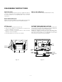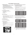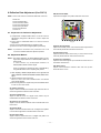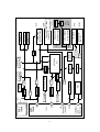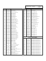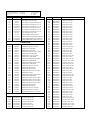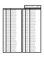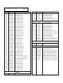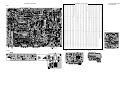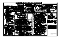
1
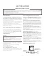
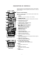
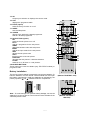
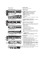
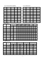
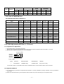
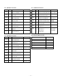
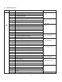
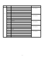
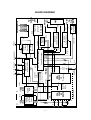
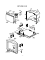
website:http://biz.LGservice.com
e-mail:http://www.LGEservice.com/techsup.html
COLOR TV
SERVICE MANUAL
CHASSIS : MC-022A
MODEL:RE-29FB50RB
CAUTION
BEFORE SERVICING THE CHASSIS,
READ THE SAFETY PRECAUTIONS IN THIS MANUAL.
P/NO : 3828VD0128B
April,2003
Printed in Korea
CONTENTS
Contents ................................................................................................................. 2
Safety Precautions ............................................................................................3
Specifications ..................................................................................................... 4
Control Descriptions ........................................................................................ 5
Disassembly Instructions ............................................................................. 8
Adjustment Instructions ............................................................................... 9
Block Diagram .................................................................................................... 16
Trouble Shooting .............................................................................................. 18
Exploded View .................................................................................................. 22
Exploded View Parts List .............................................................................23
Replacement Parts List ............................................................................... 24
SVC. Sheet ................................................................................................................
- 2 -
SAFETY PRECAUTIONS
IMPORTANT SAFETY NOTICE
Many electrical and mechanical parts in this chassis have special safety-related characteristics. These parts are identified by
in
the Schematic Diagram and Replacement Parts List.
It is essential that these special safety parts should be replaced with the same components as recommended in this manual to
prevent X-RADIATION, Shock, Fire, or other Hazards.
Do not modify the original design without permission of manufacturer.
General Guidance
Before returning the receiver to the customer,
An lsolation Transformer should always be used during
the servicing of a receiver whose chassis is not isolated from
the AC power line. Use a transformer of adequate power rating
as this protects the technician from accidents resulting in
personal injury from electrical shocks.
always perform an AC leakage current check on the exposed
metallic parts of the cabinet, such as antennas, terminals, etc.,
to be sure the set is safe to operate without damage of
electrical shock.
Leakage Current Cold Check(Antenna Cold Check)
It will also protect the receiver and it's components from being
damaged by accidental shorts of the circuitary that may be
inadvertently introduced during the service operation.
If any fuse (or Fusible Resistor) in this TV receiver is blown,
replace it with the specified.
When replacing a high wattage resistor (Oxide Metal Film
Resistor, over 1W), keep the resistor 10mm away from PCB.
Keep wires away from high voltage or high temperature parts.
Due to high vacuum and large surface area of picture tube,
extreme care should be used in handling the Picture Tube.
Do not lift the Picture tube by it's Neck.
X-RAY Radiation
Warning:
The source of X-RAY RADIATION in this TV receiver is the
High Voltage Section and the Picture Tube.
For continued X-RAY RADIATION protection, the
replacement tube must be the same type tube as specified in
the Replacement Parts List.
To determine the presence of high voltage, use an accurate
high impedance HV meter.
With the instrument AC plug removed from AC source,
connect an electrical jumper across the two AC plug prongs.
Place the AC switch in the on positioin, connect one lead of
ohm-meter to the AC plug prongs tied together and touch other
ohm-meter lead in turn to each exposed metallic parts such as
antenna terminals, phone jacks, etc.
If the exposed metallic part has a return path to the chassis, the
measured resistance should be between 1MΩ and 5.2MΩ.
When the exposed metal has no return path to the chassis the
reading must be infinite.
An other abnormality exists that must be corrected before the
receiver is returned to the customer.
Leakage Current Hot Check (See below Figure)
Plug the AC cord directly into the AC outlet.
Do not use a line Isolation Transformer during this check.
Connect 1.5K/10watt resistor in parallel with a 0.15uF capacitor
between a known good earth ground (Water Pipe, Conduit, etc.)
and the exposed metallic parts.
Measure the AC voltage across the resistor using AC
voltmeter with 1000 ohms/volt or more sensitivity.
Reverse plug the AC cord into the AC outlet and repeat AC
voltage measurements for each esposed metallic part. Any
voltage measured must not exceed 0.75 volt RMS which is
corresponds to 0.5mA.
In case any measurement is out of the limits sepcified, there is
possibility of shock hazard and the set must be checked and
repaired before it is returned to the customer.
Leakage Current Hot Check circuit
Adjust brightness, color, contrast controls to minimum.
Measure the high voltage.
The meter reading should indicate
23.5 ¡ 1.5KV: 14-19 inch, 26 ¡ 1.5KV: 19-21 inch,
29.0 ¡ 1.5KV: 25-29 inch, 30.0 ¡ 1.5KV: 32 inch
If the meter indication is out of tolerance, immediate service
and correction is required to prevent the possibility of
premature component failure.
AC Volt-meter
To Instrument's
exposed
METALLIC PARTS
Good Earth Ground
such as WATER PIPE,
CONDUIT etc.
0.15uF
1.5 Kohm/10W
- 3 -
SPECIFICATIONS
Note : Specification and others are subject to change without notice for improvement.
O
O
O
Video input system:
PAL-B/G, D/K, I/I
SECAM-B/G, D/K/L/L’
NTSC M
NTSC 4.43(AV)
NTSC- M/PAL M-N
SOUND IF :
Intermediate Frequency (Unit : MHz)
VISION IF : 38.9MHz,33.9MHz(SECAM-L’)
COLOR IF : 34.47MHz(4.43)
35.32MHz(3.58)
: NTSC-M
VIF-4.25000MHz
(
): SECAM
VIF-4.40625MHz
33.4MHz (B/G)
32.9MHz (I/I)
32.4MHz (D/K,L)
34.4MHz (M)
40.4MHz (L’)
O
Power requirement : 110~240V, 50/60Hz(NON-EU)
230V, 50Hz(EU)
O
Power consumption : 25”:125W
29”:135W
Tuning range
Band
For TV
B/G
D/K
VHF-Low
Ch2-4
Ch1-5
VHF-High
Ch5-12
Ch6-12
For CATV
I/I
NTSC
S1'-S3', S1
Ch2-13
Ch4-13
S11-S20
Hyper
UHF
S2-S10,
S21-S41
Ch21-69
Ch14-69
O
Tuning system :
FVS
100 Programme memory
200 Programme memory(W/O TXT Model)
O
Antenna input impedance : VHF/UHF 75 ohm, unbalanced
O
Voice coil impedance : 8 ohm
O
External In/Output
Audio-In:0.5Vrms ± 3db,over 10Kohm
Audio-Out:0.5Vrms ± 3db,below 1Kohm
Video-In/Out:1Vp-p ± 3db,75ohm
R,G,B In:0.7Vp-p ± 3db
O
- 4 -
Feature & Funtion
Teletext(TOP/FLOF/LIST)
AV Input : Side or Front(1),Rear(2)
Component Input : Rear(Opt.)
PERI TV Connector(AV Input,SCART Opt.)
RGB INput
2 Carrier Stereo : BG/DK
NICAM Stereo : BG/I/L
2 Carrier Dual : BG/DK
NICAM Dual : BG/I/L
SSC(Split Screen) Mode
Multi Picture Display Mode(1:4:9 PIP)
DBS
DESCRIPTION OF CONTROLS
All the functions can be controlled with the remote control handset.
Some functions can also be adjusted with the buttons on the front
panel of the set.
POWER
MUTE
11
1
1
2
3
4
5
6
7
8
9
ARC
0
TV/AV
PICTURE
MENU
Before you use the remote control handset, please install the batteries. See the next page.
2
1. POWER
switches the set on from standby or off to standby.
12
3
SOUND
4
13
14 3. ARC (Aspect Ratio Control)
changes the picture format.
( )
PR
VOL
VOL
PR
4. TURBO PICTURE / SOUND BUTTON
selects Turbo picture / sound.
( )
6
REW
PLAY
FF
P/STILL
STOP
REC
7
8
9
2. NUMBER BUTTONS
switches the set on from standby or directly select a number.
OK
T U R B O
5
Remote control handset
I/II
SSM
PSM
SLEEP
TEXT
PIP
5.
LIST
15
16
17
18
EYE/
Q.VIEW
10
MIX
TIME
REVEAL ? MODE M
SIZE
STILL
POSITION
PR
PR
INPUT
(With TELETEXT / PIP)
/ E( EE ) (Programme Up/Down)
selects a programme or a menu item.
switches the set on from standby.
scans programmes automatically.
F / G (Volume Up/Down)
adjusts the volume.
adjusts menu settings.
6. VCR BUTTONS (option)
control a LG video cassette recorder.
9/4 PIP i
SWAP
D( D
D )
19
7. SSM (Sound Status Memory)
recalls your preferred sound setting.
8. I/II (option)
selects the language during dual language broadcast (option).
selects the sound output.
9. PSM (Picture Status Memory)
recalls your preferred picture setting.
Q.VIEW
TEXT
10
MIX
TIME
REVEAL ? MODE M
SIZE
HOLD
UPDATE
INDEX
i
(With TELETEXT /
Without PIP)
10. TELETEXT BUTTONS (option)
These buttons are used for teletext.
For further details, see the ‘Teletext’ section.
11. MUTE
switches the sound on or off.
12. TV/AV
selects TV or AV mode.
switches the set on from standby.
13. MENU
selects a menu.
- 5 -
14. OK
accepts your selection or displays the current mode.
15. LIST
displays the programme table.
POWER
MUTE
11
1
16. EYE/ (option)
switches the eye function on or off.
*
17. SLEEP
sets the sleep timer.
2
18. Q.VIEW
returns to the previously viewed programme.
selects a favorite programme.
3
1
2
3
4
5
6
7
8
9
ARC
0
TV/AV
PICTURE
MENU
12
SOUND
19. PIP BUTTONS (option)
PIP
switches the sub picture on or off.
PR +/selects a programme for the sub picture.
SWAP
alternates between main and sub picture.
INPUT
selects the input mode for the sub picture.
SIZE
adjusts the sub picture size.
STILL
freezes motion of the sub picture.
POSITION
relocates the sub picture in clockwise direction.
9/4 PIP
switches on or off the 9 or 4 sub pictures.
4
13
OK
T U R B O
14
( )
PR
5
VOL
VOL
PR
( )
6
REW
PLAY
FF
P/STILL
STOP
REC
7
8
I/II
SSM
PSM
SLEEP
LIST
EYE/
9
Q.VIEW
15
16
17
18
COLOURED BUTTONS
These buttons are used for teletext (only TELETEXT models) or
programme edit.
Battery installation
The remote control handset is powered by two AA type batteries. To
load the batteries, turn the remote control handset over and open
the battery compartment. Install two batteries as indicated by the
polarity symbols ( + and - ) marked inside the compartment.
(Without TELETEXT / PIP)
/
PIP
Note : To avoid damage from possible battery leakage, remove the
batteries if you do not plan to use the remote control handset for an
extended period of time.
- 6 -
Q.VIEW
SIZE
STILL
POSITION
9/4 PIP
PR
PR
SWAP
INPUT
(Without TELETEXT /
With PIP)
19
Front panel
1. MAIN POWER
switches the set on or off.
CE/CL-29Q40 series
2. MENU (option)
selects a menu.
11
MENU
S-VIDEO
ON/OFF
VOL
PR
OK
3.
VIDEO L/MONO AUDIO R
12
VOL
2
1
3
456
10
AV3
RE/RL-29FA33 series
MENU
OK
VOL
4. OK (option)
accepts your selection or displays the current
mode.
PR
ON/OFF
1
5 24 3 6
11 12
10
5. POWER/STANDBY INDICATOR
illuminates brightly when the set is in standby
mode.
dims when the set is switched on.
CE/CL-25/29Q20 series
11
ON/OFF
S-VIDEO
MENU OK
VOL
PR
6. REMOTE CONTROL SENSOR
VIDEO
L/MONO AUDIO R
12
1
2 4 3
56
10
Note : Only use the supplied remote control
handset. (When you use others, they’ll be not
able to function.)
RE/RL-28FZ10 series
AV3
MENU
OK
VOL
PR
7. TV/AV (option)
selects TV or AV mode.
clears the menu from the screen.
switches the set on from standby.
ON/OFF
1 56
3
24
8.
CE/CL-29K30 series
VIDEO L/MONO AUDIO R
TV/AV
ON/OFF
VOL
PR
12 11
9. +/- (D/E) (option)
adjusts the function or selects a programme.
switches the set on from standby.
10
CE/CL-25/29H40 series
10. EYE (option)
adjusts picture according to the surrounding
conditions.
S-VIDEO
VIDEO
ON/OFF
MENU OK
L
AV3
PR
VOL
(L/MONO)
R
11
(Function) (option)
selects volume, EYE (option), picture items or
brief auto programme while the menus not display.
AV3
1 5 6 78 9
12
/ E (Programme Up/Down) (option)
selects a programme or a menu item.
switches the set on from standby.
F / G (Volume Down/Up) (option)
adjusts the volume.
adjusts menu settings.
D
AUDIO
1
5 6 24 3
CE/CL-28H80 series
10
AV3
VIDEO L/MONO AUDIO R
ON/OFF
TV/AV
VOL
PR
Side
panel
1
5
6
78 9
12
RE/RL-28CB80 series
MENU OK
VOL
PR
VIDEO L/MONO AUDIO
R
ON/OFF
A/V3
1
5 6
24
3
11
11. HEADPHONE SOCKET (option)
Connect the headphone plug to this socket.
12. AUDIO/VIDEO IN SOCKETS (AV3)
Connect the audio/video out sockets of external
equipment to these sockets.
S-VIDEO/AUDIO IN SOCKETS (S-AV) (option)
Connect the video out socket of an S-VIDEO
VCR to the S-VIDEO socket.
Connect the audio out sockets of the S-VIDEO
VCR to the audio sockets as in AV3.
Note : Do not place any heavy objects (over 4Kg)
on the RE/RL-29FA33 series models.
12 11
- 7 -
DISASSEMBLY INSTRUCTIONS
Important note
Chassis Assy Removal
This set is disconnected from the power supply through the
converter transformer. An isolating transformer is necessary
for service operations on the primary side of the converter
transformer.
Grasp both side of Frame and pull it backward smoothly.
Back Cabinet Removal
Remove the screws residing on the back cabinet and carefully
separate the back cabinet from the front cabinet. (Fig. 2-1).
CPT Removal
PICTURE TUBE HANDLING CAUTION
1. Pull out the CPT board from the CPT neck.
2. Place the front cabinet on soft material not to mar the front
surface or damage control knobs.
3. Remove 4 screws securing the picture tube mounting
brackets to the front cabinet.
4. Carefully separate CPT from the front cabinet.
Due to high vacuum and large surface area of picture tube, great
care must be exercised when handling picture tube. Always lift
picture tube by grasping it firmly around faceplate.
NEVER LIFT TUBE BY ITS NECK! The picture tube must not be
scratched or subjected to excessive pressure as fracture of
glass may result in an implosion of considerable violence which
can cause personal injury or property damage.
CPT
PCB
Remove
Screws
Control
PCB
MAIN
PCB
Fig. 2-1
Current
Harmonics
PCB
Fig. 2-2
- 8 -
ADJUSTMENT INSTRUCTIONS
1. Safety Precautions
5. Screen Voltage & White Balance Adjustment
1. It is safe to adjust after using insulating transformer between
the power supply line and chassis input to prevent the risk of
electric shock and protect the instrument.
2. Never disconnect leads while the TV receiver is on.
3. Don't short any portion of circuits while power is on.
4. The adjustment must be done by the correct appliances.
5. Unless otherwise noted, set the line voltage to 230Vac!10%,
50Hz.
6. The adjustment of TVshould be performed after warming up
for 15 minutes.
5-1. Adjustment of screen manually
(Using ADJ.Remote Control)
1) Receive the PAL or SECAM(NTSC) signal into RF mode
regardless of channel.
2) If you press the “ADJ”button in LINE SVC mode(IN-START
button),the LINE SVC mode changes to screen adjustment
mode.
3) Turn the Sreen Volume of FBT to change luminance of
White signal center as shown below.(Deviation ! 1FL)
4) Press the EXIT button (Like TV/AV) to exit SVC mode.
2. Test Equipment required
1.
2.
3.
4.
5.
RF signal generator (with pattern generator)
DC Power Supply
Multimeter (volt meter)
Oscilloscope
Color analyzer
3.DVCO Adjustment
1) This is for adjustment of VCT38XX,crystal oscillator
frequency after receiving a company Digital
pattern.(PAL:EU05CH,NTSC:13CH)
2) When entering adjustment mode by pressing IN-START
button,DVCO adjustment is operating automatically.
(T/X doesn’t operating occassionally during DVCO
adjustment.)
CPT & INCH
Luminance(Manual)
Note
29” FLAT
6!1FL
Single Focus
25” FLAT
8!1FL
29” NORMAL
5!1FL
25” NORMAL
6!1FL
28” NORMAL
8!1FL
5-2. Adjustment of white balance manually(LIne-SVC 1)
1)
2)
3)
4)
Tune the TV set to receive an 100% white pattern.
Adjust LOW LIght status of CUT R,CUT B at CUT G:50.
Adjust HIGH LIght status of WDR R,WDR B at WDR G:380.
Repeat above step 2) and 3) for the best condition each
status of High Light and Low Light.
White Balance Color analyzer
4. Focus Adjustment
4-1. Preparation for Adjustment
Tune the TV set to receive a digital pattern.
4-2. Adjustment Method
1) Single Focus CPT
Adjust the upper Focus volume of FBT for the best focus of
horizontal line A,vertical line B.
2) Double Focus CPT
1) Adjust the lower Focus volume of FBT for the best focus of
vertical line B.
2) Adjust the upper Focus volume of FBT for the best focus of
area A.
3) Repeat above step 1) and 2) for the best overall focus.
Menu
EU
N-EU
X
288
268
Y
295
273
Color Temperature
9000oK
13000oK
White Balance Initial Data
Menu
Range
DATA
CUR R
0 ~ 511
50
CUR G
0 ~ 511
50
CUR B
0 ~ 511
50
WDR R
0 ~ 511
380
WDR G
0 ~ 511
380
WDR B
0 ~ 511
380
NOTE : When adjusting white balance automatically,connect the
adjustment JIG in SVC mode.(When pressing INSTART,MUTE button on remote control for adjustment
orderly,it changes to SVC mode and screen displays
SVC.)
100%,80% GRAY PATTERN
Fig. 1
- 9 -
6. Deflection Data Adjustment (Line SVC-2)
NOTE : How to enter into the Line Service Mode with a remocon.
EW (Horizontal Width)
Adjust to that a digital circle pattern looks like exact circle.
1.Power off.
2.Press the Red button.
3.Press the Green button.
4.Press the Yellow button.
5.Press the Cyan button.
6.Press the OK button.
7.Power On.
6-1. Preparation for Deflection Adjustment
1) At adjustment mode(IN-START button on remote control of
adjustment),changed to LINE SVC 2 mode to adjust the
deflection.
2) Press Channel UP/DOWN button for desirous function
Adjustment.
3) Press Volume UP/DOWN button to adjust the data.
4) Tune the TV set to receive a Digital pattern.(PAL:05CH)
NOTE : If production line doesn’t the production line of LG
TV,receive available deflection adjustment pattern.
Fig. 2
EP (East-west Parabolar)
Adjust so that middle portion of the outermost left and right vertical
line looks like parallel with vertical lines of the CPT.
6-2. Adjustment Method
EC (East-west Coner)
Adjust so that the vertical line at every 4 corners of the screen
looks like parallel with the vertical lines of the CPT.
NOTE : First,adjust deflection at N50Hz,W50Hz,Z50Hz of PAL
signal.Then adjust deflection at N60Hz,W60Hz,Z60Hz of
NTSC signal.
In case of NTSC only model,adjust deflection of
N60Hz,W60Hz,Z60Hz of NTSC signal.
ET (East-west Trapezium)
Adjust to make the length of top horizontal line same with it of
the bottom horizontal line.
Store the deflection adjustment data in EEPROM by
using ENTER button before adjusting PIP position.
1) When adjusting a deflection,adjust N50Hz of PAL signal first and
adjust a deflection at W50Hz,Z50Hz,N60Hz,W60Hz,Z60Hz of PAL
signal.
2) Adjust a deflection as shown below
PAL 4:3=> PAL 16:9=>PAL ZOOM=>NTSC 4:3=>NTSC
16:9=>NTSC ZOOM.
3) After finishing deflection adjustment,press the ENTER button
to enter or exit in SVC mode.
VL (Vertical Linearity)
Adjust so that the boundary line between upper and lower half is in
accord with geometric horizontal center of the CPT.
VA (Vertical Amplitude)
Adjust so that the circle of a digital circle pattern may be
located within the effective screen of the CPT.
SC (Vertical “S” Correction)
Adjust so that all distance between each horizontal lines are to
be the same.
VS (Vertical Shift)
Adjust so that the horizontal center line of a digital circle pattern
is in accord with geometric horizontal center of the CPT.
HS (Horizontal Shift)
Adjust so that the vertical center line of a digital circle pattern is in
accord with geometric vertical center of the CPT.
- 10 -
PIP (PIP Position)
Adjust until the distance between PIP and main picture
becomes about 1~2mm.
25/29” LG FLAT CPT(CT-25Q20RB)
29” S/S SEB FLAT CPT
ITEM
RANGE
N50Hz
W50Hz
Z50Hz
ITEM
RANGE
N50Hz
W50Hz
Z50Hz
VA
0050~00CF
009A
22
11
VA
0050~00CF
00A3
-22
11
VL
0025~00BF
00F3
3
0
VL
0025~00BF
00F5
0
0
SC
0000~009F
00D0
0
0
SC
0000~009F
00D0
0
0
VS
0600~0900
0774
0
0
VS
0600~0900
0744
0
0
HS
0000~003F
0019
0
0
HS
0000~003F
0016
0
0
EW
0400~0EFF
0B96
22
0
EW
0400~0EFF
0E40
0
0
ET
0700~08FF
07DE
0
0
ET
0700~08FF
07E9
0
0
EP
06E0~0840
07BF
19
-14
EP
06E0~0840
07B4
22
-14
ES
06A0~0AFF
085C
0
0
ES
06A0~0AFF
0840
0
0
EC
0790~08E0
082B
0
0
EC
0790~08E0
0840
0
0
PIP P
0790~08E0
0007
0
0
PIP P
0790~08E0
0000B
0
0
25/29” FST CPT
N50Hz
ITEM
W50Hz
Z50Hz
N60Hz
W60Hz
Z60Hz
RANGE
25”
29”
25”
29”
25”
29”
25”
29”
25”
29”
25”
29”
VA
0050~00CF
0092
008A
-22
-22
14
14
0
0
-22
-22
-5
-5
VL
0025~00BF
00FF
00F8
0
0
0
0
-5
-5
-5
-5
0
0
SC
0000~009F
00E1
00E1
0
0
0
0
0
0
0
0
0
0
VS
0600~0900
07FF
0733
0
0
0
0
43
43
43
43
43
43
HS
0000~003F
0016
001C
0
0
0
0
4
4
4
4
4
4
EW
0400~0EFF
0C36
0C59
0
0
0
0
15
15
15
15
15
15
ET
0700~08FF
07FC
07F3
0
0
0
0
-6
-6
-6
-6
-16
-16
EP
06E0~0840
07B3
07BF
25
25
-16
-16
-2
-2
15
15
-16
-16
ES
06A0~0AFF
0864
085F
29
29
29
29
0
0
44
44
44
44
EC
0790~08E0
083F
073E
0
0
0
0
12
12
12
12
12
12
PIP P
0790~08E0
0009
0009
0
0
0
0
0
0
0
0
0
0
28” LGPD FLAT CPT
16: 9
ITEM
14: 9
ZOOM
STANDARD
RANGE
50Hz
60Hz
50Hz
60Hz
50Hz
60Hz
50Hz
60Hz
VA
0050~00CF
0083
0083
008F
008E
00A7
00A7
0083
0084
VL
0025~00BF
00FD
00FA
00FD
00A
00FD
00F8
00FD
00F9
SC
0000~009F
00F0
00F0
00F0
00F0
00F0
00F0
00F0
00F0
VS
0600~0900
0729
0753
0732
0756
073B
075D
0741
0753
HS
0000~003F
0016
0014
0016
0014
0016
0014
0016
0014
EW
0400~0EFF
0A6E
0A62
0A6E
0A68
0A6E
0A68
0A6E
0A68
ET
0700~08FF
07FF
07FD
07FF
07E8
07FF
07EA
07FD
07EA
EP
06E0~0840
07B7
07B6
07A9
07AB
078E
078B
07B3
07B6
- 11 -
16: 9
ITEM
14: 9
ZOOM
STANDARD
RANGE
50Hz
60Hz
50Hz
60Hz
50Hz
60Hz
50Hz
60Hz
VA
0050~00CF
0083
0083
008F
008E
00A7
00A7
0083
0084
VL
0025~00BF
00FD
00FA
00FD
00A
00FD
00F8
00FD
00F9
7. SVC Data & PSM,SSM Data.
PICTURE SETTING DATA (LINE SVC-3)
Menu
Range
25/29” LG Flat 29” S/S-Flat
25” FST
28” FST
29” FST
28” FLAT
DVCO(Digital VCO)
IBRM(BLACK CURRENT)
0~1FFH
00C8
00C8
00C8
00C8
00C8
00C8
WDRM(WHITE CURRENT)
0~3FFH
0190
0190
0190
0190
0190
0190
BCLT(BCL THERSHOLD
0~7FFH
0055
0055
0050
0050
0050
0050
BCLTM(BCL TIME)
0~1FFH
0007
0007
0007
0007
0007
0007
BCLGA(BCL GAIN)
0~1FFH
0007
0007
0007
0007
0007
0007
SVGA(SVM GAIN)
000D
000D
000D
000D
000D
000D
SVDEL(SVM DELAY)
0007
0007
0007
0007
0007
0007
SVD1(SVM DELAY1)
0003
0003
0003
0003
0003
0003
LDLY(L DELAY)
FFFC
FFFE
FFFE
FFFE
FFFE
DSCC(Discharge Sample)
0~01FF
000D
000D
0009
0007
0008
DSCV(Vertical Discharge)
0~01FF
FB80
FB80
FDC0
FD80
FB80
8. OPTION Adjustment (OPTION-1,2, 3,Teletext)
8-1. Preparation for Adjustment
1) This decides funtion in accordance with model.
Press the SVC TX adjustment button(IN-START button) at SVC mode,then adjust the option at OPTION 1,2,3,4 mode.
2) Mark the option adjustment data like [111,11,111,11] in BOM.
[113,63,112,128]
D
OPTION 1
OPTION 2
OPTION 3
OPTION 4
O
D
D
D
Mark of BOM
LEVEL
PART NO.
SPECIFICATION
DESCRIPTION
JOB EXP.
1.
3141VMN382A
MAIN[MC-022A]
CHASSIS ASSY
OP[113,63,112,128]
The OPTION 1 data is 113,OPTION 2 data is 63,the oOPTION 3 data is 112,the OPTION 4 data is 128 in this model.
8-2. Adjustment Method
1) Input data directly by the buttons corresponded with OPTION1 ??(0~255), OPTION2 ??(0~255), OPTION3 ???(0~127),OPTION 4
???(0 ~255).
2) Select each OPTION function by the CH Up/Down button and then set up each OPTION by the VOL Up/Down button.
- 12 -
8-3. OPTION 1 Function
Option
WIDE
TOP
ACMS
CH+AU
EYE
DEG
TILT
KEY
Code
8-5. OPTION 3 Function
Function
0
4:3 NORMAL MODEL
1
WIDE FLAT MODEL
0
W/O TOP(FLOP BASIC)
1
WITH TOP
0
Without ACMS funtion
1
With ACMS funtion
0
ALL NATION
1
Frequency Table
0
WITHOUT EYE
1
WITH EYE
0
Without DEGAUSSING
1
With DEGAUSSING
0
WITHOUT TILT
1
WITH TILT
0
1
Remark
Option
1
GAME PACK GAME(HINDI MICOM) W/O TXT Model
0
FORCED MONO NOT SETTING
1
FORCED MONO SETTING
0
WITH 1 AV JACK(BACK)
1
WITH 2 AV JACK(BACK)
PAL model ALL
0
BOOSTER CONTROL disable
1 TUNER Model
1
BOOSTER CONTROL enable
2 PIP only
0
W/O WOOFER
1
WITH WOOFER
0
1 TUNER PIP or W/O PIP
1 PIP or W/O PIP
1
2 TUNER PIP
2 PIP
0
B/G,I,D/K
CE/RE-MODEL
1
B/G,I,D/K,L/L’
CL/RL-MODEL
6 KEY
2
B/G,I,D/K,M
CT/RT-MODEL
4KEY(H80,K90,K30)
3
RESERVED
MONO
Only Austrailia
AV2
TBS
WOOF
PIP
SYS
8-6. SOUND PRE-SCALER
Code
TURBO
0
Without TURBO search
1
With TURBO search
0
Not CARRIER MUTE
MONO MODEL
1
CARRIER MUTE
DEFAULT
0
NICAM
1
NICAM & FM STEREO
0
NO SAVE DUAL/SOUND Condition
EU(CE,CL Model)
1
SAVE DUAL SOUND Condition
NON EU(CT Model)
0
PHONE JACK
1
SCART JACK
0
NORMAL VOLUME CURVE
1
RUSHED VOLUME CURVE
0
Without DVD INPUT
1
With DVD INPUT
0
Without HOTEL OPTION
1
With HOTEL OPTION
DUAL
SCART
V-CUR
DVD
HOTEL
M-VOL
0~100
TXT Model
W/O GAME
Option
A2 ST
Remark
0
GAME
8-4. OPTION 2 Function
C MUTE
Function
Code
Function
MAX VOLUME
Remark
Menu
EU
DATA
FP(FM PRE-SCALER)
0016
NP(NICAM PRE-SCALER)
0056
SP(SCART PRE-SCALER)
0013
S1 VOL(SCART1 PRE-SCALER)
0064
S2 VOL(SCART2 PRE-SCALER)
0064
AGC-L(AUTO GAIN CONT.LIMIT)
00C5
With HOTEL mode
- 13 -
8-7. OPTION 4 Function
OPTION
FUNTION
CODE
0
English Only(Eng.)
Arab.Asia
1
Arab(Eng/Fr/Arab)
3834
2
Urdu(Eng/Fr/Arab/Urdu)
3
Asia(Eng/Fr/Indonesia)
0
English Only(Eng.)
Farsi
1
Arab(Eng/Fr/Arab)
3834
2
Farsi(Eng/Fr/Arab/Farsi)
OSD
0
English Only(Eng.)
Arab-Asia
LANG.
1
Arab(Eng/Fr/Arab)
3804
2
Urdu(Eng/Fr/Arab/Urdu)
3
Arab all(Eng/Fr/Arab/Urdu/Farsi)
4
Farsi ONly(Eng/Farsi)
5
Asia(Eng/Fr/Indonesia/Malay)
0
English Only(Eng.)
WEST-EU
1
EU-7(E.Ger/Fr/Ita/Spain/Holand/Port)
3834 Only(W/TXT)
2
EU-NORTH(E-Ger/Fr/Holand/Swe/Nor/Den/Fin)
0
English Only(Eng.)
EAST-EU
1
Cyrilic(E.Russia)
3834 Only(W/TXT)
2
EU-EAST(E.Ger/Rum/Pin/Hung/Chez)
3
EU-EAST All(E-Ger/Rum/Pol/Hung/Chez/Russia)
0
English Only(Eng.)
EU-ALL
1
EU-7(E.Ger/Fr/Ita/Spain/Holand/Port)
3804 Only(W/O TXT)
2
EU-NORTH(E-Ger/Fr/Holand/Swe/Nor/Den/Fin)
3
Cyrilic(E.Russia)
4
EU-EAST(E.Ger/Rum/Pin/Hung/Chez)
5
EU-EAST All(E-Ger/Rum/Pol/Hung/Chez/Russia)
0
English Only(Eng.)
28” Wide Flat
1
EU-5(E.Ger/Fr/Ita/Spain)
3834 Only(W/TXT)
0
English Only(Eng.)
Hindi-China-Viet.
1
Vietnam(E.Vietnam)
3804 Only(W/O TXT)
2
Hindi(E.Hindi)
3
China(E.China)
0
Eng/Spain/Port
1
Spain/Port/Eng
2
Port/Spain/Eng
3
Eng/Fr
0
KOrean Only
Korea Version
- 14 -
OPTION
TXT-L
FUNTION
CODE
0
WEST-EU
Farsi only
1
EAST-EU
3834 only(W/TXT)
2
Turkey
3
Cyrillic3
5
Arab/English
8
Farsi/English
0
WEST-EU
Arab-Asia
1
EAST-EU
3834 only(W/TXT)
2
Turkey
3
Cyrillic3
5
Arab/English
0
WEST-EU
WEST EU
1
EAST-EU
3834 only(W/TXT)
2
Turkey
6
Cyrillic3
0
WEST-EU
EAST EU
1
EAST-EU
3834 only(W/TXT)
2
Turkey
6
Cyrillic3
0
WEST-EU
28” WIDE FLAT
1
EAST-EU
3834 only(W/TXT)
2
Turkey
4
Cyrillic3
5
Arab/English
6
Farsi/English
- 15 -
- 16 -
ICP101
Y&C
AV -3
AV -2
AV -1
PIP &A/V SW
ICP01
IC661
MSP-34xxG
L/R
RGB
& FB
SCART-1
RGB & FB
SDASDA9489X
PIP
Processor
V- SYNC
H- SYNC
I 2C Bus
Ik
DVD
Y, Pb,Pr
8
H-Sinc
H-Out
ST-2310
IC03
AT24C16
EEPROM
LA-7845
Tilt Control
Vetical Deflection
IC301
Tilt
Controller
VA
V-Out
T402
H-Out
R G B AMP
(6107)JF
TDA 6109
TO
TILT
COIL
V-DY
FBT
VMVM-COIL
H -DY
TO
Cathode
0f
CPT
MAIN SPEAKER
L
R
IC901
Horizontal Deflection
IC401
EW
VM
R/G/B
TDA-2066
(Mono Opt.)
V-Sinc
(Protect)
Control Processor
H/P OUT
TDA 7297
(7266)
Sound Amp.
IC602
MONITOR OUT
VCT 3801/3804/3834
Main
IC01
Sound Processor
W/O PIP AV1,2,3, Y,C
W/O PIP CVBS
SELECTED
CVBS
FOR MAIN
AF(SECAM L)
PIP-CVBS
SIF
TU101
SELECTED
CVBS
FOR PIP
TV-CVBS
MAIN
TUNER-1
CXACXA2040
AV
SWITCH
FOR PIP
(W/O PIP
Option)
TUNER-2
TU102
L/R
AV -1 AV -2 RF OUT
BLOCK DIAGRAM
- 17 -
12
110V(Flat)
120V
(Normal)
18
33V 16
17V
14
Sound Vcc
(35V OPT.)
8V
T802
12V 11
SMPS
TRANS
ST-BY
TRANS
28V(FBT)
Relay
9V
ST 5V
Tilt(Opt.)
5V
FBT
H-DRIVE
5V
EW AMP
278R05
LD3.3V
LA 7845(V-AMP)
KA78A09
12V
78L05
¡ 14V(FBT)
T803
VM
Tuner
(Main)
IC01
VCT3834
LD3.3V
7805
12V
200V(FBT)
Tuner
(Sub)
EYE(Opt.)
ICP101
ICP01
STK396-110
(VM IC)
TDA6109
(Video Switch)
CXA-2040AQ
(PIP Processor)
SDA-9489X
TDA -7297
Sound AMP
IC602
IC661
HIC920
IC901
PIP &
AV SW
(OPT.)
7805
LD3.3V
(Mono Opt.)
TDA - 2006
MSP-34XX
(Sound Processor)
LED
EEPROM
PRE-AMP
TROUBLE SHOOTING
RF- STEREO
Selected correct system
In menu
OK
NO
Check the waveform
At pin 17 of TU101
Check / Replace
TU 101
OK
NO
Check the waveform
At pin 24,25 of IC661
Check The Voltage
At pin 16,33,46, of IC661
NO
Check The voltage
At pin of IC610, IC853
OK
NO
Check the waveform
At pin 4,12 of IC602
NO
Check / Replace
Q671, 672
NO
Check / Replace
Q621, IC603
NO
Check / Replace
F851, D862
Check / Replace
IC610, IC853
OK
Check the Voltage
At pin 6, 7 of IC602
OK
Check the waveform
At pin 1, 2, 14, 15 of IC602
OK
Check the Voltage
At pin 3,13 of IC602
No Raster / Sound OK
Check the
Heater voltage of CPT
(6 ~ 6.5Vrms)
OK
Check
HV, Screen Voltage of
CPT
NO
NO
OK
NO
Check / Replace
CPT Board
Components
Check
FBT T402
Check the
Heater pulse of FBT
T402
Check
IK Current of
IC01, pin37,39,40
OK
Check
FR901, P402A
P402B, P302
Check
IC01, Q901, IC901
P03A, P03B, P541
- 18 -
NO
Check
FBT T402
NO RASTER
CHECK B+
At D807 cathode
Normal
Abnormal
Is the voltage at
Pin 25, 54 of IC01 3.3V?
Check
Fuse of AC line
No
Yes
Check &
Replace
IC01
Ok
Check the
In/out of
IC06, IC07
Check pin 24
Of IC01(H - Out)
No
Check the Voltage
Of C804
254~380 V
Yes
Check Q402
Collector waveform
Check the Voltage
Pin 3 of IC801
No
Check &
Replace
Q402
Yes
Check / Replace
IC801, IC803, IC802
Check T401
& each pin voltage
No
Check &
Replace
T401
No
Yes
Check IC01
Pin1 high?
Check & Replace
T402
Yes
Check / Replace
IC01
No
Yes
Is the voltage at pin3,15,45
IC02 5V?
No
Check &
Replace
IC01, IC03
Check the
In/out of
IC855,IC851
Open
No
Check the
Voltage at
D860 or D858
cathode
- 19 -
No
Check &
Replace
F853 ,F855
Check / Replace
Fuse , DB801
0V
Check / Replace
Fuse DB801
No Picture / No Sound
Is any OSD displayed?
OK
No
OK
Check receiving system in MENU
& execute Auto - Program.
Check IC01 pin37,42,43,44
(IK, R,G,B)
No
OK
Does the auto - Program
Operate properly.
OK
Check / Replace
IC01
Store on manual - program MENU
Check
5V, 33V &
IIC Bus Line
No
Check 5V, 33V & IIC Bus Line
Of Tuner.
OK
Check / Replace
IC01, Tuner
No
Is the CVBS signal OK.
(IC01 pin10 or 22)
OK
OK
Check
CVBS signal Line
& IC01
Check IK
Signal at
IC01 pin37
(similar to CBVS)
No
Check R,G,B signal
At IC01, pin42,43,44
OK
Check / Replace
CPT Board component
- 20 -
Go to
No Sound /
Picture OK
AV Stereo
Select correct system
In menu
OK
OK
Check the connection
Of AV equipment
AV
NO
Check the the waveform
At pin47 of IC661
OK
Check TU101 Tuner
OK
NO
Check the waveform
At pin 24, 25, of IC661
Check the voltage
Of pin16,20
OK
NO
Check waveform
At pin 4, 12 of IC602
Check / Replace
IC602
OK
NO
Check the voltage
At pin6,7 of IC602
Check / Replace
Q621, IC603
OK
Check the waveform
At pin 1,2,14,15 of IC602
NO
Check the vpltage
At pin3, 13 of IC602
OK
Replace IC 602
- 21 -
NO
Check /Replace
F851, D862
EXPLODED VIEW
943
400
913
150
510
170
112
P801
503
560
121
120
520
550
501
300
310
700
330
320
- 22 -
The components identified by mark
critical for safety.
Replace only with part number specified.
EXPLODED VIEW PARTS LIST
LOCA. NO
PART NO
DESCRIPTIONS
112
6335V29016A
120
120-C77G
CPT ASSEMBLY A68QCP893X702 0.4G 0G SDIG .
121
4810V00088B
BRACKET,SPEAKER
150
6140VC2005F
COIL,DEGAUSSING 29 FLAT ASSY (W) SELLA TECH 2001R+D07L
SPEAKER,C122P02K1459 MOTOR JOY 8 OHM 10/15W 130 57*117
170
170-844K
300
3091V00523A
CABINET ASSEMBLY
310
5020V00765A
BUTTON,CONTROL RE-29FB50 ABS, HF-380 6KEY MA LOCAL
320
320-075B
330
5020V00766A
BUTTON,POWER RE-29FB50 ABS, HF-380 1KEY MA LOCAL
400
3809V00366A
BACK COVER ASSEMBLY LGEMA EXPORT
501
4810V00297E
BRACKET,MAIN
503
3500V00022C
BOARD,A/V 2SCART
510
6871VSMN25A
PWB ASSY,CPT MC022A 29SS FLAT-MA(CKD)
520
6871VMMD20D
PWB ASSY,MAIN MC022A RE-29FB50RX LUSLMP8
550
6871VSMN26C
PWB ASSY,CONT MC022A FB50-MA(CKD)
560
6871VSM842B
PWB ASSY,SUB 022A CURRENT HARMONICS(7A)
913
332-229H
943
1PTF0403116
P801
174-009V
CPT EARTH,29 98T 4LUG LEAD SET SPRING(50MM)
SPRING,COIL NON DIA:7.5MM, H:15.5MM NON NON
SCREW,DRAWING HEXAGON HEAD
SCREW,TAP TITE(P) D4.0 L16.0
POWER,CORD
- 23 -
is
REPLACEMENT PARTS LIST
LOCA. NO
PART NO
DESCRIPTION
LOCA. NO
PART NO
D902
0DR210009AC
DIODE,RECTIFIERS BAV21 TP PHILIPS DO35
D903
0DR210009AC
DIODE,RECTIFIERS BAV21 TP PHILIPS DO35
IC
DESCRIPTION
HIC920
0IZZVF0018A
IC,STK396-110 11P ST SCAN VELOCITY MODU. SINGLE SCAN (BW 6M)
D904
0DR140049AC
DIODE,RECTIFIERS 1N4004A T-81 TP ROHM-
IC01
0ICTMMN005B
IC,VCT3834B LG23 E/EU MICRONAS 64P ST
D920
0DD060009AC
DIODE,RECTIFIERS TVR06J 600V 250NSEC
IC03
0IAL241610B
IC,AT24C16A-10PI-2.7 8PIN DIP ST EEPROM
DB801
0DD560000AA
DIODE,RECTIFIERS D5SB60 BRIDGE (5A/600V)
IC06
0ISG111733B
IC,LD1117V33C 3SIP ST REGULATOR -
LD01
162-002B
IC07
0ISG111733B
IC,LD1117V33C 3SIP ST REGULATOR -
ZD101
0DZ330009DG
DIODE,ZENERS GDZJ33B TP GRANDE DO34
IC09
0IFA752700A
IC,KA75270Z 3 TP RE-SET IC MC-007
ZD302
0DZ510009BF
DIODE,ZENERS GDZ5.1B TP GRANDE DO34
IC301
0ISA784500A
IC,LA7845 7SIP V/OUT(1.5A) - - - -
ZD303
0DZ180009BE
DIODE,ZENERS GDZJ18B TP GRANDE DO34
IC302
0IKE455800E
IC,KIA4558 8DIP DUAL OP AMP
ZD401
0DZ510009BF
DIODE,ZENERS GDZ5.1B TP GRANDE DO34
IC602
0ISG729700A
IC,TDA7297 15P,SIP BK 2CH 15W DUAL AMP
ZD402
0DZ110009AD
DIODE,ZENERS MTZJ11B TP ROHM-K DO34 -
IC603
0IFA754207A
IC,KA75420ZTA(KA7542ZTA) 3P,TO-92 TP 4.2V
ZD501
0DZ510009BF
DIODE,ZENERS GDZ5.1B TP GRANDE DO34
IC610
0IKE780500Q
IC,KIA7805API 3P TO-220 ST REGULATOR 5V
ZD601
0DZ510009BF
DIODE,ZENERS GDZ5.1B TP GRANDE DO34
IC661
0IMCRMN011C
IC,MSP3410G PO B8 V3 MICRONAS 52P DIP ST
ZD610
0DZ910009BD
DIODE,ZENERS GDZJ9.1B TP GRANDE DO34
IC662
0IFA753307A
IC,KA75330ZTA(KA7533ZTA) 3P,TO-92 TP 3.3V
ZD910
0DZ470009EF
DIODE,ZENERS GDZJ4.7B GRANDE TP DO34
IC801
0IMCRSK001A
IC,STR-F6456R SANKEN 5PIN(LF1352) BK STR
ZD911
0DZ470009EF
DIODE,ZENERS GDZJ4.7B GRANDE TP DO34
IC802
0ILI817000G
IC,LTV817M-VB 4P,DIP BK PHOTO COUPLER
ZD912
0DZ470009EF
DIODE,ZENERS GDZJ4.7B GRANDE TP DO34
IC803
0ILI817000G
IC,LTV817M-VB 4P,DIP BK PHOTO COUPLER
IC851
0IKE780500P
IC,KIA78L05BP(AT) 3P 5V,150MA - - - -
IC853
0IMCRKE002A
IC,KIA78R09PI KEC 4PIN,TO220IS-4 ST 1A LOW
IC855
0IMCRKE006A
IC,KIA278R05PI KEC TO220IS,4P ST 2A LOW
IC856
0ISK120000A
IC,SE120N 3P 120V ERROR AMP - - - -
IC901
0IMCRPH009A
IC,TDA6109JF PHILIPS 9SIP ST RGB
LED ASSY
TRANSISTOR
Q108
0TR534309AA
TR,2SC5343Y TP AUK - -
Q1106
0TR733009AA
TR,KSA733C-Y TP SAMSUNG TO-92
Q112
0TR534309AA
TR,2SC5343Y TP AUK - -
Q180
0TR534309AA
TR,2SC5343Y TP AUK - -
Q181
0TR198009BA
TR,2SA1980Y TP AUK - -
Q182
0TR198009BA
TR,2SA1980Y TP AUK - -
DIODE
D110
0DD414809ED
DIODE,SWITCHING 1N4148 TP GRANDE
Q183
0TR534309AA
TR,2SC5343Y TP AUK - -
D180
0DD414809ED
DIODE,SWITCHING 1N4148 TP GRANDE
Q184
0TR534309AA
TR,2SC5343Y TP AUK - -
D181
0DD414809ED
DIODE,SWITCHING 1N4148 TP GRANDE
Q185
0TR198009BA
TR,2SA1980Y TP AUK - -
D301
0DD150009CA
DIODE,RECTIFIERS RGP15J TP
Q186
0TR198009BA
TR,2SA1980Y TP AUK - -
D302
0DS113379BA
DIODE,SWITCHING 1SS133 T-72 TP ROHM
Q187
0TR534309AA
TR,2SC5343Y TP AUK - -
D401
0DD410000AG
DIODE,RECTIFIERS RS4FS SANKEN BK R4
Q201
0TR198009BA
TR,2SA1980Y TP AUK - -
D402
0DD410000AD
DIODE,RECTIFIERS RU4AM,LF-L1
Q202
0TR198009BA
TR,2SA1980Y TP AUK - -
D403
0DD150009CA
DIODE,RECTIFIERS RGP15J TP
Q301
0TR534309AA
TR,2SC5343Y TP AUK - -
D404
0DD150009CA
DIODE,RECTIFIERS RGP15J TP
Q302
0TR205900AB
TR,KTD2059-Y TO-220IS KEC
D405
0DR150009AB
DIODE,RECTIFIERS RGP15G TP
Q303
0TR127409AB
TR,KTA1274-Y TO-92L TP KEC
D406
0DR150009AB
DIODE,RECTIFIERS RGP15G TP
Q401
0TRSG10001A
TR,SGS-T(STM) ST2310HI ST TO220 1500V 1MA
D408
0DD060009AC
DIODE,RECTIFIERS TVR06J 600V 250NSEC
Q402
0TR223800AA
TR,KTC2238A-Y BK KEC - -
D505
0DD414809ED
DIODE,SWITCHING 1N4148 TP GRANDE
Q505
0TR534309AA
TR,2SC5343Y TP AUK - -
D506
0DD414809ED
DIODE,SWITCHING 1N4148 TP GRANDE
Q506
0TR198009BA
TR,2SA1980Y TP AUK - -
D802
0DD100009AM
DIODE,RECTIFIERS EU1ZV(1) TP SANKEN
Q507
0TR198009BA
TR,2SA1980Y TP AUK - -
D803
0DD100009AM
DIODE,RECTIFIERS EU1ZV(1) TP SANKEN
Q508
0TR198009BA
TR,2SA1980Y TP AUK - -
D804
0DD414809ED
DIODE,SWITCHING 1N4148 TP GRANDE
Q509
0TR534309AA
TR,2SC5343Y TP AUK - -
D815
0DD060009AC
DIODE,RECTIFIERS TVR06J 600V 250NSEC
Q621
0TR534309AA
TR,2SC5343Y TP AUK - -
D857
0DD414809ED
DIODE,SWITCHING 1N4148 TP GRANDE
Q671
0TR198009BA
TR,2SA1980Y TP AUK - -
D858
0DD200009AH
DIODE,RECTIFIERS RU2AMV(1) TP SANKEN
Q672
0TR198009BA
TR,2SA1980Y TP AUK - -
D860
0DD420000BB
DIODE,RECTIFIERS D4L20U SHINDENGEN
Q806
0TR102009AB
TR,KRC102M(KRC1202) KEC TP NA NA NA
D861
0DD060009AC
DIODE,RECTIFIERS TVR06J 600V 250NSEC
Q807
0TR102009AB
TR,KRC102M(KRC1202) KEC TP NA NA NA
D862
0DD420000BB
DIODE,RECTIFIERS D4L20U SHINDENGEN
Q853
0TR127009AA
TR,KTA1270-Y(KTA562TM) KEC TP TO92 50V
D863
0DD414809ED
DIODE,SWITCHING 1N4148 TP GRANDE
Q901
0TR198009BA
TR,2SA1980Y TP AUK - -
D864
0DD414809ED
DIODE,SWITCHING 1N4148 TP GRANDE
D866
0DD410000AD
DIODE,RECTIFIERS RU4AM,LF-L1
D867
0DD414809ED
DIODE,SWITCHING 1N4148 TP GRANDE
D901
0DR210009AC
DIODE,RECTIFIERS BAV21 TP PHILIPS 200V
CAPACITOR
- 24 -
C01
0CC0500K115
5P
50V
D NP0 TS
C02
0CC0500K115
5P
50V
D NP0 TS
For Capacitor & Resistors,
the charactors at 2nd and 3rd
digit in the P/No. means as
follows;
CC, CX, CK, CN : Ceramic
CQ : Polyestor
CE : Electrolytic
LOCA. NO
PART NO
C03
0CE335DK618
C04
0CN1020K519
C07
RD : Carbon Film
RS : Metal Oxide Film
RN : Metal Film
RF : Fusible
DESCRIPTION
LOCA. NO
PART NO
DESCRIPTION
3.3UF STD 50V 20% FL TP 5
C24
0CE475DK618
4.7UF STD 50V 20% FL TP 5
1000P 50V K B TA52
C245
0CN4710K519
470P 50V K B TA52
0CN1030F679
10000P 16V M Y TA52
C246
0CN4710K519
470P 50V K B TA52
C08
0CN1030F679
10000P 16V M Y TA52
C248
0CN4710K519
470P 50V K B TA52
C10
0CN8200K519
82P 50V K B TA52
C249
0CN4710K519
470P 50V K B TA52
C102
0CX4700K409
47P 50V J SL TA52
C25
0CN1040K949
0.1M 50V Z F TA52
C103
0CX4700K409
47P 50V J SL TA52
C27
0CE476DF618
47UF STD 16V M FL TP5
C104
0CN1030F679
10000P 16V M Y TA52
C28
0CN1030F679
10000P 16V M Y TA52
C107
0CN1030F679
10000P 16V M Y TA52
C29
0CE107DD618
100UF STD 10V M FL TP5
C108
0CE476DD618
47UF STD 10V 20% FL TP 5
C30
0CE226DF618
22UF STD 16V M FL TP5
C11
0CE107DD618
100UF STD 10V M FL TP5
C301
0CQ1031N509
0.01U 100V K POLY
TP
C110
0CE476DK618
47UF STD 50V M FL TP5
C302
0CQ3341N401
0.33U 100V J POLY
F5
C1101
0CE107DD618
100UF STD 10V M FL TP5
C303
0CE107BK618
100UF KME 50V M FL TP5
C111
0CN1030F679
10000P 16V M Y TA52
C304
0CQ6821N509
0.0068U 100V K POLY
C1112
0CQZVBK002C
A.C 275V 0.22UF K (S=22.5)
C305
0CQ1021N509
0.001U 100V K POLY
TP
C113
0CN1030F679
10000P 16V M Y TA52
C306
0CQ3331N509
0.033U 100V K POLY
TP
C114
0CE476DD618
47UF STD 10V 20% FL TP 5
C308
0CE476DK618
47UF STD 50V M FL TP5
TP
C120
0CN1030F679
10000P 16V M Y TA52
C309
0CN4710K519
470P 50V K B TA52
C1205
0CE106DF618
10UF STD 16V M FL TP5
C310
0CQ1031N509
0.01U 100V K POLY
TP
C121
0CE474DK618
0.4700UF STD 50V M FL TP5
C311
0CQ1031N509
0.01U 100V K POLY
TP
C125
0CN1040K949
0.1M 50V Z F TA52
C401
0CE105DK618
1UF STD 50V M FL TP5
C130
0CN1030F679
10000P 16V M Y TA52
C402
0CE475DK618
4.7UF STD 50V 20% FL TP 5
C14
0CE476DF618
47UF STD 16V M FL TP5
C403
0CQ1521N509
0.0015U 100V K POLY
C16
0CN4720F569
4700P 16V K X TA52
C405
181-015N
MPP 1600V 0.015UF H
TP
C17
0CE106DK618
10UF STD 50V M FL TP5
C406
181-091J
DEHR33D821KN3A 820PF 2KV 10%,-10%
C180
0CN1020K519
1000P 50V K B TA52
C407
181-038F
MPP 630V 0.027UF J
C181
0CN2210K519
220P 50V K B TA52
C408
0CE6851K652
6.8UF SM,SA 50V 20% FM7.5 BP(S)
C183
0CN1040K949
0.1M 50V Z F TA52
C409
0CK2220W515
2200P 500V K B
C184
0CE105DK618
1UF STD 50V M FL TP5
C410
0CE105CR636
1UF SHL,SD 250V 20% BP(D) TP FM5
C200
0CN1010K519
100P 50V K B TA52
C411
181-013Q
C201
0CE227DF618
220UF STD 16V M FL TP5
C413
0CE107DJ618
100UF STD 35V M FL TP5
C202
0CN1010K519
100P 50V K B TA52
C415
0CE108DH618
1000UF STD 25V M FL TP5
C205
0CN1010K519
100P 50V K B TA52
C416
181-009R
C207
0CX5600K409
56P 50V J SL TA52
C419
0CE108DH618
C209
0CN1050K949
1UF D 50V 80%,-20% F(Y5V) TA52
C420
181-010B
C210
0CE227DF618
220UF STD 16V M FL TP5
C422
0CE475DR618
4.7UF STD 250V 20% FL TP 5
C211
0CN4710K519
470P 50V K B TA52
C501
0CE107DD618
100UF STD 10V M FL TP5
C213
0CN4710K519
470P 50V K B TA52
C502
0CN1040K949
0.1M 50V Z F TA52
C215
0CN4710K519
470P 50V K B TA52
C503
0CN1050K949
1UF D 50V 80%,-20% F(Y5V) TA52
C216
0CN4710K519
470P 50V K B TA52
C504
0CN1050K949
1UF D 50V 80%,-20% F(Y5V) TA52
C22
0CE107DD618
100UF STD 10V M FL TP5
C505
0CN1040K949
0.1M 50V Z F TA52
C220
0CN4710K519
470P 50V K B TA52
C506
0CN1040K949
0.1M 50V Z F TA52
C221
0CN4710K519
470P 50V K B TA52
C509
0CN1050K949
1UF D 50V 80%,-20% F(Y5V) TA52
C222
0CN4710K519
470P 50V K B TA52
C511
0CN1050K949
1UF D 50V 80%,-20% F(Y5V) TA52
C225
0CN4710K519
470P 50V K B TA52
C512
0CN1010K519
100P 50V K B TA52
C227
0CE226DF618
22UF STD 16V M FL TP5
C515
0CN1050K949
1UF D 50V 80%,-20% F(Y5V) TA52
C228
0CE226DF618
22UF STD 16V M FL TP5
C516
0CN1030F679
10000P 16V M Y TA52
C229
0CE226DF618
22UF STD 16V M FL TP5
C517
0CQ6831N509
0.068U 100V K POLY TP
C23
0CE107DD618
100UF STD 10V M FL TP5
C518
0CQ6831N509
0.068U 100V K POLY TP
C230
0CE226DF618
22UF STD 16V M FL TP5
C520
0CN1020K519
1000P 50V K B TA52
C231
0CN1010K519
100P 50V K B TA52
C521
0CN1010K519
100P 50V K B TA52
C232
0CX5600K409
56P 50V J SL TA52
C522
0CN1010K519
100P 50V K B TA52
- 25 -
TS
MPP 400V 0.36UF J
PP 200V 0.022UF K
1000UF STD 25V M FL TP5
PP 400V 0.056UF J
For Capacitor & Resistors,
the charactors at 2nd and 3rd
digit in the P/No. means as
follows;
DESCRIPTION
LOCA. NO
CC, CX, CK, CN : Ceramic
CQ : Polyestor
CE : Electrolytic
LOCA. NO
PART NO
C523
0CN1010K519
100P 50V K B TA52
C825
0CK47201510
4700P 1KV K B S
C524
0CN1010K519
100P 50V K B TA52
C840
0CN1010K519
100P 50V K B TA52
C559
0CQ6831N509
0.068U 100V K POLY TP
C854
0CE107DF618
100UF STD 16V M FL TP5
C561
0CQ2242K439
0.22UF S 50V 5% M/PE NI TP5
C855
0CE107DD618
100UF STD 10V M FL TP5
C562
0CN2210K519
220P 50V K B TA52
C857
0CE108BF618
1000UF KME 16V M FL TP5
C563
0CN2210K519
220P 50V K B TA52
C858
0CE108BF618
1000UF KME 16V M FL TP5
C564
0CN2210K519
220P 50V K B TA52
C860
0CE108BF618
1000UF KME 16V M FL TP5
C565
0CN2210K519
220P 50V K B TA52
C861
0CE108DF618
1000UF STD 16V M FL TP5
C568
0CE107DF618
100UF STD 16V M FL TP5
C862
0CE335CK636
3.3UF SHL,SD 50V 20% FM5 BP(D) TP
C570
0CN1010K519
100P 50V K B TA52
C864
0CE108BJ618
1000UF KME 35V M FL TP5
C601
0CE226DF618
22UF STD 16V M FL TP5
C865
181-091Q
C604
0CE475DK618
4.7UF STD 50V 20% FL TP 5
C867
0CE227DK618
220UF STD 50V M FL TP5
C605
0CQ3321N509
0.0033U 100V K POLY
C871
0CE227DP61A
220UF STD 160V 20% FL TP 7.5
C606
0CF2241L438
0.22UF D 63V 5% TP 5 M/PE NI
C872
0CE107CP618
100U SHL 160V M FL TP5
C612
0CE477DH618
470UF STD 25V M FL TP5
C873
0CQ1041N509
0.1U 100V
C621
0CQ3321N509
0.0033U 100V K POLY
C874
181-091Y
C622
0CF2241L438
0.22UF D 63V 5% TP 5 M/PE NI
C901
0CE475DR618
4.7UF STD 250V 20% FL TP 5
C650
0CN1030F679
10000P 16V M Y TA52
C902
0CQ1044R539
0.1UF TE 250V K M/PE NI TP5
C651
0CN1030F679
10000P 16V M Y TA52
C903
181-033S
C663
0CE107DD618
100UF STD 10V M FL TP5
C904
0CE475DR618
4.7UF STD 250V 20% FL TP 5
C666
0CE335DK618
3.3UF STD 50V 20% FL TP 5
C920
0CN1030F679
10000P 16V M Y TA52
C667
0CN3320F569
3300P 16V K X TA52
C921
0CE107DF618
100UF STD 16V M FL TP5
C668
0CN3320F569
3300P 16V K X TA52
C922
0CN1510K519
150P 50V K B TA52
C670
0CE105DK618
1UF STD 50V M FL TP5
C923
0CE107DJ618
100UF STD 35V M FL TP5
C671
0CE107DD618
100UF STD 10V M FL TP5
C924
0CE107DF618
100UF STD 16V M FL TP5
C672
0CE105DK618
1UF STD 50V M FL TP5
C925
0CK1030W510
0.01U 500V K B
C673
0CF3341L438
0.33UF D 63V 5% TP 5 M/PE NI
C926
0CE106DP618
10UF STD 160V M FL TP5
C674
0CF3341L438
0.33UF D 63V 5% TP 5 M/PE NI
C927
0CK1010W515
100P
C675
0CE106DF618
10UF STD 16V M FL TP5
C928
0CE107DF618
100UF STD 16V M FL TP5
C676
0CF3341L438
0.33UF D 63V 5% TP 5 M/PE NI
C929
0CK1030W510
0.01U 500V K B
C677
0CF3341L438
0.33UF D 63V 5% TP 5 M/PE NI
C930
0CE106DP618
10UF STD 160V M FL TP5
C678
0CF3341L438
0.33UF D 63V 5% TP 5 M/PE NI
C679
0CF3341L438
0.33UF D 63V 5% TP 5 M/PE NI
C681
0CE106DF618
10UF STD 16V M FL TP5
J134
0LA0102K139
INDUCTOR,AXIAL LEAD 10UH K 4*10.5 TP
C685
0CE106DF618
10UF STD 16V M FL TP5
L01
0LA0102K119
INDUCTOR,AXIAL LEAD 10UH K 2.3*3.4 TP
C686
0CX5600K409
56P 50V J SL TA52
L04
0LA0102K119
INDUCTOR,AXIAL LEAD 10UH K 2.3*3.4 TP
C687
0CX5600K409
56P 50V J SL TA52
L05
0LA0102K139
INDUCTOR,AXIAL LEAD 10UH K 4*10.5 TP
C688
0CX5600K409
56P 50V J SL TA52
L08
0LA0102K119
INDUCTOR,AXIAL LEAD 10UH K 2.3*3.4 TP
C689
0CC0200K115
2P
50V
D NP0 TS
L103
0LA0102K139
INDUCTOR,AXIAL LEAD 10UH K 4*10.5 TP
C690
0CC0200K115
2P
50V
D NP0 TS
L121
0LA0102K139
INDUCTOR,AXIAL LEAD 10UH K 4*10.5 TP
C803
181-091U
R 220PF 2KV 10%,-10% R/TP TP7.5
L210
0LA0102K119
INDUCTOR,AXIAL LEAD 10UH K 2.3*3.4 TP
C804
0CE337KV6A0
330UF SLT 450V M VNSN BULK
L211
0LA0102K119
INDUCTOR,AXIAL LEAD 10UH K 2.3*3.4 TP
C806
181-014Y
MPP 1.6KV 0.0015UF J
L212
0LA0102K049
INDUCTOR,AXIAL LEAD 10UH 10% TP 5.0X14
C807
0CK4710K515
470PF 50V K B TR
L213
0LA0102K119
INDUCTOR,AXIAL LEAD 10UH K 2.3*3.4 TP
C808
0CE107BJ618
100UF KME 35V M FL TP5
L214
0LA0102K119
INDUCTOR,AXIAL LEAD 10UH K 2.3*3.4 TP
C809
181-091D
DEHR33A102KN2A 1000PF 1KV 10%,-10%
L215
0LA0102K119
INDUCTOR,AXIAL LEAD 10UH K 2.3*3.4 TP
C813
0CK10201515
1000P 1KV K B TS
L216
0LA0102K119
INDUCTOR,AXIAL LEAD 10UH K 2.3*3.4 TP
C814
0CQZVBK002A
A.C 275V 0.1UF M (S=15)
L218
0LA0102K119
INDUCTOR,AXIAL LEAD 10UH K 2.3*3.4 TP
C815
181-091C
DEHR33A471KN2A 470PF 1KV 10%,-10%
L219
0LA0102K119
INDUCTOR,AXIAL LEAD 10UH K 2.3*3.4 TP
C816
0CK10201515
1000P 1KV K B TS
L241
0LA0102K119
INDUCTOR,AXIAL LEAD 10UH K 2.3*3.4 TP
C818
181-120K
2200PF 4KV M E FMTW LEAD 4.5
L242
0LA0102K119
INDUCTOR,AXIAL LEAD 10UH K 2.3*3.4 TP
C822
0CE226DD618
22UF STD 10V 20% FL TP 5
L245
0LA0102K139
INDUCTOR,AXIAL LEAD 10UH K 4*10.5 TP
TP
TP
PART NO
RD : Carbon Film
RS : Metal Oxide Film
RN : Metal Film
RF : Fusible
DESCRIPTION
R 470PF 1KV 10%,-10% R/TP TP5
K POLY
TP
R 680PF 2KV 10%,-10% R/TP TP7.5
2KV B 122K TP7.5
500V K B
S
TS
S
COIL & TRANSFORMER
- 26 -
For Capacitor & Resistors,
the charactors at 2nd and 3rd
digit in the P/No. means as
follows;
CC, CX, CK, CN : Ceramic
CQ : Polyestor
CE : Electrolytic
LOCA. NO
PART NO
L246
0LA0102K119
L401
150-717K
L402
150-L01F
L509
RD : Carbon Film
RS : Metal Oxide Film
RN : Metal Film
RF : Fusible
DESCRIPTION
LOCA. NO
PART NO
INDUCTOR,AXIAL LEAD 10UH K 2.3*3.4 TP
FR413
0RP0050H709
0.05 OHM 1/2 W 10% TA52
COIL,CHOKE 1.1UH PHY TURN
FR901
0RF0161K607
1.6 OHM 2 W 5.00% TA62
COIL,LINEARITY 22.8UH 0.12*30PHY 40.5T
J128
0RD1002F609
10K OHM 1/6 W 5% TA52
0LA0102K119
INDUCTOR,AXIAL LEAD 10UH K 2.3*3.4 TP
J137
0RD1000F609
100 OHM 1/6 W 5% TA52
L510
0LA0102K119
INDUCTOR,AXIAL LEAD 10UH K 2.3*3.4 TP
J149
0RD1000F609
100 OHM 1/6 W 5% TA52
L512
0LA0102K139
INDUCTOR,AXIAL LEAD 10UH K 4*10.5 TP
J163
0RD1000F609
100 OHM 1/6 W 5% TA52
L663
0LA0102K119
INDUCTOR,AXIAL LEAD 10UH K 2.3*3.4 TP
J167
0RD1000F609
100 OHM 1/6 W 5% TA52
L810
0LA0102K119
INDUCTOR,AXIAL LEAD 10UH K 2.3*3.4 TP
J170
0RD1000F609
100 OHM 1/6 W 5% TA52
L853
150-C02F
COIL,CHOKE 82UH PHY TURN
J175
0RD1000F609
100 OHM 1/6 W 5% TA52
T401
151-C02F
TRANSFORMER,H-DRIVE,EI-19,BULK
J207
0RD1000F609
100 OHM 1/6 W 5% TA52
T402
6174V-5003G
FBT,BSC28-N2326 29 YINYANG 6003L B+120V
J210
0RD4702F609
47K OHM 1/6 W 5% TA52
T801
6170VZ0007A
TRANSFORMER,H-DRIVER TS4134 38500UH
J222
0RD4702F609
47K OHM 1/6 W 5% TA52
T802
6170VMCB01S
TRANSFORMER,SMPS EER5345 340UH 130V
J316
0RD1000F609
100 OHM 1/6 W 5% TA52
L1102
0RD0472F609
47 OHM 1/6 W 5% TA52
R01
0RD1000F609
100 OHM 1/6 W 5% TA52
CONNECTOR
DESCRIPTION
JP801B
366-009D
CONNECTOR,2.36PAI 1P . K/M AUTO
R02
0RD1000F609
100 OHM 1/6 W 5% TA52
JP802B
366-009D
CONNECTOR,2.36PAI 1P . K/M AUTO
R06
0RD3001F609
3K OHM 1/6 W 5.00% TA52
JW8A
387-907C
CONNECTOR,1P NON 200MM
R07
0RD1002F609
10K OHM 1/6 W 5% TA52
JW8B
387-907C
CONNECTOR,1P NON 200MM
R08
0RD2001F609
2K OHM 1/6 W 5% TA52
P03A
366-921J
CONNECTOR,2.5MM 10P GIL-G LG CABLE .
R09
0RD2001F609
2K OHM 1/6 W 5% TA52
P03B
387-A10J
CONNECTOR,10P 2.5MM 500MM
R10
0RD1000F609
100 OHM 1/6 W 5% TA52
P06A
366-932F
CONNECTOR,IL-G LGC 7 2.5S STICK
R102
0RD5100F609
510 OHM 1/6 W 5.00% TA52
P06B
387-A07E
CONNECTOR,7P 2.5MM 300MM
R11
0RD1000F609
100 OHM 1/6 W 5% TA52
P07A
366-932D
CONNECTOR,2.5MM 5P GIL-G LG CABLE
R1101
0RD3300F609
330 OHM 1/6 W 5.00% TA52
P07B
387-A05C
CONNECTOR,5P 2.5MM 200MM
R1103
0RD1301F609
1.3K OHM 1/6 W 5.00% TA52
P08A
366-932E
CONNECTOR,2.5MM 6P GIL-G LG CABLE
R1104
0RD4701F609
4.7K OHM 1/6 W 5% TA52
P08B
387-B06C
CONNECTOR,6P 2.5MM 200MM
R1107
0RD3600F609
360 OHM 1/6 W 5.00% TA52
P102
366-009D
CONNECTOR,2.36PAI 1P . K/M AUTO
R1108
0RD4300F609
430 OHM 1/6 W 5.00% TA52
P1112
366-043B
CONNECTOR ASSY,PLUG(2P)
R1109
0RD5600F609
560 OHM 1/6 W 5% TA52
P1113
366-043B
CONNECTOR ASSY,PLUG(2P)
R1110
0RD8200F609
820 OHM 1/6 W 5.00% TA52
P180
366-932B
CONNECTOR,2.5MM 3P GIL-G LG CABLE
R1111
0RD1001F609
1K OHM 1/6 W 5% TA52
P401
366-043K
CONNECTOR,PLUG(4P)
R119
0RD0102F609
10 OHM 1/6 W 5% TA52
P402A
366-921G
CONNECTOR,2.5MM 8P GIL-G LG CABLE .
R1207
0RD1200H609
120 OHM 1/2 W 5.00% TA52
P402B
387-A08H
CONNECTOR,8P 2.5MM 450MM
R1208
0RD1200H609
120 OHM 1/2 W 5.00% TA52
P501
366-932B
CONNECTOR,2.5MM 3P GIL-G LG CABLE
R126
0RD1001F609
1K OHM 1/6 W 5% TA52
P502
366-932B
CONNECTOR,2.5MM 3P GIL-G LG CABLE
R127
0RD1001F609
1K OHM 1/6 W 5% TA52
P601
366-932B
CONNECTOR,2.5MM 3P GIL-G LG CABLE
R129
0RD1000F609
100 OHM 1/6 W 5% TA52
P602
366-932C
CONNECTOR,2.5MM 4P GIL-G LG CABLE
R130
0RD1000F609
100 OHM 1/6 W 5% TA52
P801
366-043B
CONNECTOR ASSY,PLUG(2P)
R131
0RD1000F609
100 OHM 1/6 W 5% TA52
P802
366-043B
CONNECTOR ASSY,PLUG(2P)
R132
0RD4700F609
470 OHM 1/6 W 0.05 TA52
P901
366-009D
CONNECTOR,2.36PAI 1P . K/M AUTO
R133
0RD4700F609
470 OHM 1/6 W 0.05 TA52
P903
366-009D
CONNECTOR,2.36PAI 1P . K/M AUTO
R135
0RD5600H609
560 OHM 1/2 W 5.00% TA52
P920
366-932B
CONNECTOR,2.5MM 3P GIL-G LG CABLE
R136
0RD1002F609
10K OHM 1/6 W 5% TA52
R137
0RD1002F609
10K OHM 1/6 W 5% TA52
R18
0RD1000F609
100 OHM 1/6 W 5% TA52
RESISTOR
F851
0RP0020J809
0.02 OHM 1 W 20% TA52
R180
0RD1001F609
1K OHM 1/6 W 5% TA52
F853
0RP0050H709
0.05 OHM 1/2 W 10% TA52
R181
0RD3002F609
30K OHM 1/6 W 5.00% TA52
F854
0RP0050H709
0.05 OHM 1/2 W 10% TA52
R182
0RD6801F609
6.8K OHM 1/6 W 5.00% TA52
F855
0RP0050H709
0.05 OHM 1/2 W 10% TA52
R183
0RD1003F609
100K OHM 1/6 W 5% TA52
FR402
0RF0101K607
1 OHM 2 W 5.00% TA62
R184
0RD1801F609
1.8K OHM 1/6 W 5.00% TA52
FR403
0RP0050H709
0.05 OHM 1/2 W 10% TA52
R185
0RD1801F609
1.8K OHM 1/6 W 5.00% TA52
FR406
0RF0121K607
1.2 OHM 2 W 5.00% TA62
R186
0RD4701F609
4.7K OHM 1/6 W 5% TA52
- 27 -
For Capacitor & Resistors,
the charactors at 2nd and 3rd
digit in the P/No. means as
follows;
LOCA. NO
PART NO
R187
0RD1801F609
R188
0RD2202F609
R189
DESCRIPTION
CC, CX, CK, CN : Ceramic
CQ : Polyestor
CE : Electrolytic
LOCA. NO
PART NO
1.8K OHM 1/6 W 5.00% TA52
R410
0RMZVBK002D
22K OHM 1/6 W 5% TA52
R411
0RS7502H609
75K OHM 1/2 W 5.00% TA52
0RD5602F609
56K OHM 1/6 W 5% TA52
R413
0RS2202H609
22K OHM 1/2 W 5.00% TA52
R190
0RD5103F609
510K OHM 1/6 W 5.00% TA52
R414
0RS1001H609
1K OHM 1/2 W 5.00% TA52
R191
0RD1000F609
100 OHM 1/6 W 5% TA52
R415
0RD1002F609
10K OHM 1/6 W 5% TA52
R192
0RD4701F609
4.7K OHM 1/6 W 5% TA52
R416
0RD1001F609
1K OHM 1/6 W 5% TA52
R193
0RD4701F609
4.7K OHM 1/6 W 5% TA52
R417
0RD5603F609
560K OHM 1/6 W 5.00% TA52
R201
0RD0562F609
56 OHM 1/6 W 5.00% TA52
R419
0RD7501H609
7.5K OHM 1/2 W 5.00% TA52
R202
0RD4700H609
470 OHM 1/2 W 5.00% TA52
R420
0RS0472K607
47 OHM 2 W 5.00% TA62
R205
0RD3302F609
33K OHM 1/6 W 5% TA52
R509
0RD0752F609
75 OHM 1/6 W 5.00% TA52
R206
0RD0752F609
75 OHM 1/6 W 5.00% TA52
R51
0RD3301F609
3.3K OHM 1/6 W 5.00% TA52
R207
0RD0752F609
75 OHM 1/6 W 5.00% TA52
R517
0RD3000F609
300 OHM 1/6 W 5.00% TA52
R208
0RD0752F609
75 OHM 1/6 W 5.00% TA52
R519
0RD1001F609
1K OHM 1/6 W 5% TA52
R209
0RD0752F609
75 OHM 1/6 W 5.00% TA52
R523
0RD1002F609
10K OHM 1/6 W 5% TA52
R210
0RD0682F609
68 OHM 1/6 W 5.00% TA52
R525
0RD6801F609
6.8K OHM 1/6 W 5.00% TA52
R211
0RD1000F609
100 OHM 1/6 W 5% TA52
R526
0RD2702F609
27K OHM 1/6 W 5.00% TA52
R212
0RD3901F609
3.9K OHM 1/6 W 5% TA52
R528
0RD6801F609
6.8K OHM 1/6 W 5.00% TA52
R214
0RD0752F609
75 OHM 1/6 W 5.00% TA52
R531
0RD1201F609
1.2K OHM 1/6 W 5% TA52
R215
0RD2200F609
220 OHM 1/6 W 5.00% TA52
R532
0RD1200F609
120 OHM 1/6 W 5.00% TA52
R217
0RD3302F609
33K OHM 1/6 W 5% TA52
R533
0RD2201F609
2.2K OHM 1/6 W 5.00% TA52
R24
0RD1002F609
10K OHM 1/6 W 5% TA52
R534
0RD1000F609
100 OHM 1/6 W 5% TA52
R301
0RD2201F609
2.2K OHM 1/6 W 5.00% TA52
R537
0RD2202F609
22K OHM 1/6 W 5% TA52
R302
0RD0101H609
1 OHM 1/2 W 5.00% TA52
R541
0RD2700F609
270 OHM 1/6 W 5% TA52
R305
0RN4700F409
470 OHM 1/6 W 1.00% TA52
R542
0RD2200F609
220 OHM 1/6 W 5.00% TA52
R306
0RD1002F609
10K OHM 1/6 W 5% TA52
R543
0RD2202F609
22K OHM 1/6 W 5% TA52
R307
0RD2202F609
22K OHM 1/6 W 5% TA52
R544
0RD0822F609
82 OHM 1/6 W 5.00% TA52
R309
0RD4701F609
4.7K OHM 1/6 W 5% TA52
R545
0RD1800F609
180 OHM 1/6 W 5.00% TA52
R310
0RD0392F609
39 OHM 1/6 W 5.00% TA52
R546
0RD0472F609
47 OHM 1/6 W 5% TA52
R311
0RN0151H609
1.5 OHM 1/2 W 5.00% TA52
R548
0RD4300F609
430 OHM 1/6 W 5.00% TA52
R312
0RN0471H609
4.7 OHM 1/2 W 5.00% TA52
R549
0RD1800F609
180 OHM 1/6 W 5.00% TA52
R313
0RS3900J607
390 OHM 1 W 5.00% TA62
R550
0RD0472F609
47 OHM 1/6 W 5% TA52
R315
0RD1000F609
100 OHM 1/6 W 5% TA52
R552
0RD4300F609
430 OHM 1/6 W 5.00% TA52
R316
0RD2702F609
27K OHM 1/6 W 5.00% TA52
R553
0RD1800F609
180 OHM 1/6 W 5.00% TA52
R317
0RD2001F609
2K OHM 1/6 W 5% TA52
R554
0RD0472F609
47 OHM 1/6 W 5% TA52
R319
0RN8202F409
82K OHM 1/6 W 1.00% TA52
R556
0RD4300F609
430 OHM 1/6 W 5.00% TA52
R320
0RD1001F609
1K OHM 1/6 W 5% TA52
R557
0RD2701F609
2.7K OHM 1/6 W 5% TA52
R321
0RS0561K619
5.6 OHM 2 W 5% TR
R558
0RD0222F609
22 OHM 1/6 W 5.00% TA52
R322
0RD1501F609
1.5K OHM 1/6 W 5% TA52
R559
0RD1001F609
1K OHM 1/6 W 5% TA52
R323
0RD2702F609
27K OHM 1/6 W 5.00% TA52
R560
0RD4301F609
4.3K OHM 1/6 W 5.00% TA52
R324
0RD4700F609
470 OHM 1/6 W 0.05 TA52
R570
0RD1800F609
180 OHM 1/6 W 5.00% TA52
R325
0RS2701H609
2.7K OHM 1/2 W 5.00% TA52
R571
0RD3901F609
3.9K OHM 1/6 W 5% TA52
R326
0RS1501H609
1.5K OHM 1/2 W 5.00% TA52
R590
0RD0822F609
82 OHM 1/6 W 5.00% TA52
R327
0RS1501H609
1.5K OHM 1/2 W 5.00% TA52
R601
0RD1001F609
1K OHM 1/6 W 5% TA52
R328
0RN8201F609
8.2K OHM 1/6 W 5.00% TA52
R602
0RD1002F609
10K OHM 1/6 W 5% TA52
R330
0RD3001F609
3K OHM 1/6 W 5.00% TA52
R603
0RD1001F609
1K OHM 1/6 W 5% TA52
R331
0RD2401F609
2.4K OHM 1/6 W 5.00% TA52
R604
0RD3301F609
3.3K OHM 1/6 W 5.00% TA52
R402
0RD1001F609
1K OHM 1/6 W 5% TA52
R607
0RS0681H609
6.8 OHM 1/2 W 5.00% TA52
R403
0RD5600H609
560 OHM 1/2 W 5.00% TA52
R608
0RD3301F609
3.3K OHM 1/6 W 5.00% TA52
R404
0RD0332H609
33 OHM 1/2 W 5.00% TA52
R609
0RD6201F609
6.2K OHM 1/6 W 5.00% TA52
R405
0RS1000K619
100 OHM 2 W 5% TR
R610
0RD4702F609
47K OHM 1/6 W 5% TA52
R408
0RS0221K607
2.2 OHM 2 W 5.00% TA62
R611
0RD4702F609
47K OHM 1/6 W 5% TA52
R409
0RS1801H609
1.8K OHM 1/2 W 5.00% TA52
R624
0RD6201F609
6.2K OHM 1/6 W 5.00% TA52
- 28 -
RD : Carbon Film
RS : Metal Oxide Film
RN : Metal Film
RF : Fusible
DESCRIPTION
15K OHM 5W +/-5% RSR V-TYPE
For Capacitor & Resistors,
the charactors at 2nd and 3rd
digit in the P/No. means as
follows;
CC, CX, CK, CN : Ceramic
CQ : Polyestor
CE : Electrolytic
LOCA. NO
PART NO
R629
0RD0912F609
R662
0RD1000F609
R663
RD : Carbon Film
RS : Metal Oxide Film
RN : Metal Film
RF : Fusible
DESCRIPTION
LOCA. NO
PART NO
91 OHM 1/6 W 5.00% TA52
SW02
140-315A
SWITCH,TACT SKHV17910B 12V
100 OHM 1/6 W 5% TA52
SW03
140-315A
SWITCH,TACT SKHV17910B 12V
0RD1000F609
100 OHM 1/6 W 5% TA52
SW04
140-315A
SWITCH,TACT SKHV17910B 12V
R664
0RD1002F609
10K OHM 1/6 W 5% TA52
SW05
140-315A
SWITCH,TACT SKHV17910B 12V
R681
0RD1000F609
100 OHM 1/6 W 5% TA52
SW06
140-315A
SWITCH,TACT SKHV17910B 12V
R801
0RKZVTA001K
0.47M OHM 1/2 W 5% TA52
SWP801
6600VM2002A
R802
180-822M
R803
0RD0102H609
10 OHM 1/2 W 5.00% TA52
R804
0RD4701F609
4.7K OHM 1/6 W 5% TA52
FB1201
125-123A
FILTER,FERRITE BFD3565R2F
R805
0RD1001F609
1K OHM 1/6 W 5% TA52
FB220
125-123A
FILTER,FERRITE BFD3565R2F
R806
180-A01C
2 W RWR G 2W 0.12 J TA31(63)
FB401
125-022K
FILTER,FERRITE 1UH TAPING
R807
0RKZVTA001C
8.2M OHM 1/2 W 5% TA52
FB402
125-123A
FILTER,FERRITE BFD3565R2F
R808
0RD3301F609
3.3K OHM 1/6 W 5.00% TA52
FB801
125-022K
FILTER,FERRITE 1UH TAPING
R809
0RS2702K619
27K OHM 2 W 5.00% TR
FB802
125-022K
FILTER,FERRITE 1UH TAPING
R811
0RS2702K619
27K OHM 2 W 5.00% TR
FB803
125-022K
FILTER,FERRITE 1UH TAPING
R813
0RD1002F609
10K OHM 1/6 W 5% TA52
FL201
166-F02A
FILTER,NFV6T2A106W55 EMI,NFV610-655 T2A
R821
0RD3601F609
3.6K OHM 1/6 W 5.00% TA52
FL202
166-F02A
FILTER,NFV6T2A106W55 EMI,NFV610-655 T2A
R822
0RD3301F609
3.3K OHM 1/6 W 5.00% TA52
FL203
166-F02A
FILTER,NFV6T2A106W55 EMI,NFV610-655 T2A
R830
0RP0050H709
0.05 OHM 1/2 W 10% TA52
L920
125-022K
FILTER,FERRITE 1UH TAPING
R831
0RP0050H709
0.05 OHM 1/2 W 10% TA52
T1111
150-F06P
FILTER,LINE FILTER SQE2930 10MH
R832
0RP0020J809
0.02 OHM 1 W 20% TA52
T810
150-F06P
FILTER,LINE FILTER SQE2930 10MH
R833
0RP0050H709
0.05 OHM 1/2 W 10% TA52
X01
6202VDB007B
RESONATOR,CRYSTAL HC49U 20.250MHZ 30PPM 13PF
R850
0RD0471F609
4.7 OHM 1/6 W 5% TA52
X661
156-A02M
RESONATOR,CRYSTAL HC49U 18.432MHZ 30PPM 10PF
R852
0RS0102K619
10 OHM 2 W 5% TR
R858
0RD0471F609
4.7 OHM 1/6 W 5% TA52
R862
0RD5601F609
5.6K OHM 1/6 W 5% TA52
A1
3828VA0333M
MANUAL,OWNERS,PL/SPEC LG PL 077V/Z/088A/B TX 017B
R863
0RD2001F609
2K OHM 1/6 W 5% TA52
A2
6710V00088B
REMOTE CONTROLLERW/O PIP W/TXT 48 NON
R869
0RD4701F609
4.7K OHM 1/6 W 5% TA52
R901
0RD2200F609
220 OHM 1/6 W 5.00% TA52
R902
0RD2200F609
220 OHM 1/6 W 5.00% TA52
FP801
0FS4001B53C
FUSE,4000MA 250 V 5.2X20 CY/CE SEMKO /
R903
0RD2200F609
220 OHM 1/6 W 5.00% TA52
JA1201
6613V00006A
JACK ASSY 3P+EAR(PJ6062A)
R904
0RD4700F609
470 OHM 1/6 W 0.05 TA52
JK201
6612VMH001A
JACK,SCART UPJ-R1-018 RGB 21 PIN H=12.7,
R905
0RD7501F609
7.5K OHM 1/6 W 5.00% TA52
JK202
6613V00011A
JACK ASSY ,PMJ018A 21P SCART+A/V 2P(MONO)
R906
0RD1000F609
100 OHM 1/6 W 5% TA52
PA1101
6726VV0006J
REMOTE CONTROLLER RECEIVER,TSOP2238MQ1
R907
0RD1000F609
100 OHM 1/6 W 5% TA52
RL801
6920VB1001E
RELAY,SDT-S-105LMR OEG 5V 0.05A 250V 5A
R908
0RD1000F609
100 OHM 1/6 W 5% TA52
SK901
6620VBC003A
SOCKET,CPT PCS030A 8PIN 14/360 STRAIGHT
R909
0RCZVTA002D
1/2 W 1.5K,10%,PLIKOR(HIGH SURGE)
TH801
163-058D
R910
0RCZVTA002D
1/2 W 1.5K,10%,PLIKOR(HIGH SURGE)
TU101
6700MF0001H
TUNER,TAFD-M232D LG MULTI FS 3SYS,2IN1,DIN
R911
0RCZVTA002D
1/2 W 1.5K,10%,PLIKOR(HIGH SURGE)
VD1111
164-003K
VARISTOR,SVC621D-14A 620V 0% UL/CSA/VDE
R912
0RD2204H609
2.2M OHM 1/2 W 5.00% TA52
VD802
164-003K
VARISTOR,SVC621D-14A 620V 0% UL/CSA/VDE
R913
0RD4701F609
4.7K OHM 1/6 W 5% TA52
R921
0RD1000F609
100 OHM 1/6 W 5% TA52
R922
0RD0622F609
62 OHM 1/6 W 5.00% TA52
R923
0RS0102J607
10 OHM 1 W 5.00% TA62
R924
0RS3300J607
330 OHM 1 W 5.00% TA62
R925
0RS4300J607
430 OHM 1 W 5.00% TA62
R926
0RS3900K607
390 OHM 2 W 5.00% TA62
R94
0RD1000F609
100 OHM 1/6 W 5% TA52
R95
0RD1001F609
1K OHM 1/6 W 5% TA52
RWR 15W 1.0 OHM J PD
140-315A
SWITCH,
SWITCH,PUSH SDKEA3250V 8A HORIZONTAL 480G
FILTER & CRYSTAL
ACCESSORIES
MISCELLANEOUS
SWITCH
SW01
DESCRIPTION
TACT SKHV17910B 12V
- 29 -
THERMISTOR,PTC 03-07MX JA HWA 7 OHM
SVC. SHEET : 3854VA0098A-S
SVC. SHEET :
PRINTED CIRCUIT BOARD
MAIN
CONTROL
P/N: 3854VA0098A-S(2/2)
DATE: 2002.03.25
COMPONENT LOCATION GUIDE
C01 ..........B4
C02 ..........B4
C03 ..........B4
C04 ..........B4
C06 ..........E1
C07 ..........B4
C08 ..........B4
C10 ..........B3
C11 ..........B3
C14 ..........B4
C16 ..........B4
C17 ..........B4
C22 ..........B4
C23 ..........C4
C24 ..........C4
C25 ..........C4
C27 ..........B4
C28 ..........C4
C29 ..........B4
C30 ..........C1
C102 ........A5
C103 ........A5
C104 ........A5
C105 ........A5
C106 ........A4
C107 ........A5
C108 ........A5
C109 ........A5
C110 ........A5
C111 ........A4
C112 ........B4
C113 ........A4
C114 ........A4
C115 ........A4
C120 ........A3
C121 ........B5
C122 ........B5
C127 ........A4
C180 ........C2
C181 ........C2
C183 ........C2
C184 ........C2
C201 ........D5
C208 ........C1
C209 ........A4
C210 ........B5
C211 ........C5
C212 ........C5
C213 ........C5
C214 ........C5
C215 ........C5
C216 ........C5
C217 ........C5
C218 ........C5
C219 ........E5
C220 ........D5
C221 ........D5
C222 ........D5
C223 ........D5
C224 ........D5
C225 ........D5
C226 ........D5
C227 ........D5
C228 ........D5
C229 ........D4
C230 ........C3
C231 ........C1
C240 ........C1
C241 ........B1
C242 ........C1
C243 ........C1
C244 ........C1
C245 ........C1
C246 ........C1
C247 ........C1
C248 ........C1
C249 ........C1
C250 ........C3
C301 ........D4
C302 ........D4
C303 ........E4
C304 ........E4
C305 ........D3
C306.........F4
C307 ........D4
C308 ........D4
C309 ........E4
C310 ........D4
C311 ........E4
C401 ........E4
PIP
C402 ........G4
C403 ........G3
C404.........F4
C405 ........G4
C406.........F4
C407.........F4
C408 ........E4
C409 ........G3
C410 ........G3
C411 ........G3
C413 ........E5
C414.........F5
C415 ........E4
C416 ........E5
C419 ........E4
C420.........F5
C421 ........E5
C422 ........E5
C450 ........E5
C457 ........D5
C501 ........C3
C502 ........C5
C503 ........C4
C504 ........B5
C505 ........C5
C506 ........C5
C508 ........C5
C509 ........C5
C510 ........C4
C511 ........C4
C512 ........C4
C513 ........C4
C514 ........C4
C515 ........C5
C516 ........C4
C517 ........D4
C518 ........D3
C520 ........C4
C521 ........C4
C522 ........C4
C523 ........C4
C524 ........B5
C559 ........C4
C561 ........C3
C562 ........C3
C563 ........C3
C564 ........B3
C565 ........B3
C568 ........C3
C601 ........A2
C604 ........A3
C605 ........A3
C606 ........A3
C612 ........B2
C613 ........A3
C614 ........A2
C621 ........A3
C622 ........A3
C623 ........A3
C624 ........A2
C625 ........A2
C626 ........A2
C650 ........B3
C651 ........C3
C663 ........B3
C666 ........C3
C667 ........C3
C668 ........C3
C670 ........C2
C671 ........C2
C672 ........C2
C673 ........C2
C674 ........C2
C675 ........C2
C676 ........C2
C677 ........C2
C678 ........C3
C679 ........C2
C681 ........B2
C682 ........C3
C685 ........B3
C686 ........B2
C687 ........B2
C688 ........B2
C689 ........B2
C690 ........B2
C802.........F1
C803.........F2
C804 ........G2
C805.........F2
C806.........F2
C807.........F3
C808.........F2
C809 ........G2
C811 ........G3
C812 ........G3
C813 ........G2
C814.........F1
C815.........F3
C816.........F2
C817.........F2
C818 ........G3
C819 ........E2
C820 ........G2
C821 ........G2
C822 ........D2
C824.........F2
C851 ........D1
C852 ........D1
C853 ........D2
C854 ........D1
C855 ........D1
C857 ........D1
C858 ........D2
C860 ........D2
C861 ........D2
C862 ........D2
C864 ........D3
C865 ........E3
C866 ........E3
C867 ........E3
C868 ........D3
C871 ........D3
C872 ........D3
C873 ........E3
C874 ........D3
C880 ........C3
C901 ........B1
C902 ........A1
C903 ........A2
C904 ........B2
C905 ........A1
C906 ........B1
D110 ........C1
D180 ........C2
D181 ........C2
D301 ........E4
D302.........F4
D401 ........G4
D402.........F4
D403 ........G3
D404 ........E5
D405 ........E4
D406 ........E5
D408 ........E5
D444 ........E5
D505 ........B3
D506 ........C4
D602 ........A2
D621 ........A2
D802.........F3
D803.........F3
D804 ........G3
D811 ........G2
D812 ........G2
D813 ........G2
D814 ........G2
D815 ........G2
D851 ........E1
D852 ........D1
D853 ........E1
D854 ........D1
D856 ........E2
D857 ........E2
D858 ........D2
D860 ........D2
D861 ........E3
D862 ........D2
D863 ........C2
D864 ........C2
D865 ........D2
D866 ........D3
D867 ........D4
D901 ........A1
D902 ........A1
D903 ........A1
D904 ........B2
DB801......G2
F851.........E2
F853.........E2
F854.........E3
F855.........D2
F801A ......G2
F801B ......G1
FB201 ......B5
FB202 ......D5
FB220 ......C5
FB241 ......C1
FB401 ......G4
FB402 ......E5
FB801.......F2
FB802.......F2
FB803.......F2
FB851 ......D1
FB852 ......E2
FB853 ......E3
FB855 ......E3
FL202.......D5
FL203.......B5
FR401 ......F5
FR402 ......E5
FR403 ......F4
FR406 ......E5
FR413 ......F5
FR901 ......B1
G1 ............B5
G2............G1
G3 ............C1
G4 ............C5
G5 ............C1
G6 ............D3
G7 ............D3
G8 ............D3
G9 ............D3
G10 ..........D5
G11..........G1
G12 ..........E5
G13 ..........E5
G14 ..........E5
G15 ..........E1
G16 ..........E1
G17 ..........E1
G18 ..........E1
G19 ..........F3
G21 ..........E5
G22 ..........F5
G23 ..........F2
G24 ..........E4
G25 ..........F4
G26 ..........F1
G27 ..........F1
G28 ..........F2
G29 ..........F2
G30 ..........F2
G31 ..........E2
G32 ..........D2
G33 ..........F2
G34 ..........F1
G35 ..........F2
G36..........G3
G37..........G3
G39 ..........E3
G40 ..........F2
G41 ..........F1
G42..........G4
G43..........G4
G44 ..........F3
G45 ..........F1
G46 ..........F1
G47 ..........F1
G48..........G2
G49..........G4
G50 ..........F4
G51 ..........F4
G52..........G4
G53..........G2
G54..........G2
G55..........G4
G56 ..........F3
G59 ..........D4
G60 ..........D4
G61 ..........E2
G62 ..........E3
G63 ..........E3
G64 ..........F2
G65 ..........F2
G66 ..........D3
G67 ..........D2
G68..........G2
G69 ..........E2
G70 ..........E2
G71 ..........E2
G72 ..........E2
G73 ..........E3
G74 ..........E3
G75 ..........D2
G76 ..........D2
G77 ..........F3
G81..........G1
G82..........G1
G83..........G1
G84..........G1
G85 ..........F3
G86 ..........F3
G87 ..........F3
G88 ..........F3
HIC01.......B4
IC01 .........B4
IC03 .........B3
IC06 .........C4
IC07 .........B3
IC09 .........B4
IC301 .......E4
IC302 .......E4
IC602 .......A3
IC603 .......A2
IC610 .......B3
IC661 .......B3
IC662 .......B3
IC801 .......G2
IC802........F3
IC803 .......G3
IC851 .......D1
IC853 .......D2
IC855 .......D2
IC856 .......D3
IC901 .......A1
J101 .........A3
J102 .........A4
J103 .........A3
J104 .........A3
J105 .........A5
J106 .........A3
J108 .........A5
J109 .........A5
J110 .........A2
J111 .........A3
J112 .........A3
J113 .........A3
J114 .........A5
J115 .........A2
J116 .........A3
J118 .........A3
J119 .........A2
J121 .........A5
J122 .........A5
J123 .........A4
J124 .........A3
J125 .........A3
J126 .........A3
J127 .........A2
J128 .........A3
J129 .........A3
J130 .........A3
J131 .........A3
J134 .........A3
J135 .........B2
J136 .........B2
J137 .........B4
J138 .........B4
J140 .........A3
J141 .........B5
J142 .........B5
J143 .........B5
J144 .........A4
J145 .........A4
J146 .........C4
J147 .........B4
J148 .........B5
J149 .........B5
J150 .........B4
J151 .........B5
J152 .........B5
J153 .........B5
J154 .........B5
J155 .........B4
J156 .........B2
J157 .........B3
J158 .........A5
J159 .........B4
J160 .........C4
J161 .........C3
J162 .........B4
J163 .........C4
J164 .........A4
J165 .........C5
J166 .........C2
J167 .........C4
J168 .........C1
J169 .........C4
J170 .........C4
J171 .........C1
J172 .........B4
J173 .........C1
J174 .........C5
J175 .........C5
J176 .........B4
J177 .........D4
J178 .........C2
J179 .........C3
J180 .........C5
J181 .........C3
J182 .........C1
J183 .........C3
J184 .........C5
J185 .........C2
J186 .........C1
J187 .........C5
J188 .........C2
J189 .........C4
J190 .........C1
J191 .........C4
J192 .........B4
J193 .........C1
J194 .........C5
J195 .........C4
J196 .........C1
J197 .........C5
J198 .........C1
J199 .........C4
J200 .........C2
J201 .........C1
J202 .........C5
J203 .........C4
J204 .........C1
J205 .........C5
J206 .........C2
J207 .........C4
J208 .........D2
J209 .........C1
J210 .........D5
J211 .........D4
J212 .........D1
J213 .........D4
J214 .........D2
J215 .........D5
J216 .........D5
J217 .........D5
J218 .........D4
J219 .........C4
J220 .........B2
J221 .........D1
J222 .........D5
J223 .........D4
J224 .........D2
J225 .........D5
J226 .........D2
J227 .........D1
J228 .........D4
J229 .........D3
J230 .........D3
J231 .........D1
J232 .........D1
J233 .........D4
J234 .........D5
J235 .........D4
J236 .........D4
J237 .........D5
J238 .........D2
J239 .........F5
J240 .........D4
J241 .........D4
J242 .........D1
J244 .........D2
J245 .........D1
J246 .........D1
J247 .........D4
J248 .........D4
J249 .........D5
J250 .........D5
J251 .........D5
J252 .........D3
J253 .........E4
J254 .........E5
J255 .........E4
J256 .........E4
J257 .........E3
J258 .........E2
J259 .........E5
J260 .........E4
J261 .........E4
J262 .........E4
J263 .........E3
J264 .........E3
J265 .........E1
J266 .........E5
J267 .........E5
J268 .........E2
J269 .........F1
J270 .........E4
J271 .........F2
J272 .........F5
J273 .........F4
J274 .........F5
J275 .........F1
J276 .........F1
J277 .........F3
J278 .........F4
J279.........G2
J280.........G2
J281 .........F3
J282.........G1
J283.........G3
J284.........G1
J285 .........F4
J286.........G3
J287.........G2
J288.........G1
J289 .........D2
J290.........G1
J291.........G1
J292 .........F1
J293 .........F1
J294 .........E2
J295 .........E5
J296 .........C4
J297 .........D4
J298 .........D4
J299 .........A2
J300 .........E5
J301 .........F4
J302 .........E1
J303 .........B5
J304 .........D5
J305 .........B4
J308 .........B1
J309 .........B1
J310 .........B1
J311 .........A3
J312 .........A3
J313 .........B4
J314 .........E5
J315 .........D5
J316 .........C5
J317 .........C4
J318 .........B4
J319 .........C5
J322 .........A2
J323 .........B2
J324 .........B2
J325 .........A3
J326 .........E5
J327.........G3
J328 .........C1
J329 .........C4
J330 .........B3
J331 .........B4
J332 .........C5
J333 .........D5
J334 .........C1
J335 .........E2
J336 .........E3
J337 .........D5
J338 .........D5
J339 .........F4
J340 .........F4
J341 .........F3
J342 .........F3
J343 .........F3
J344 .........F4
J345 .........A3
J346 .........E2
J347 .........B5
J901 .........A1
J902 .........A2
J903 .........B1
JK201.......C5
JK202.......D5
JK203.......C1
JP1 ...........F2
JP2 ...........F2
JW80A......F1
JW80B .....G1
JW8A .......G2
JW8B........F2
L01 ...........B4
L02 ...........B5
L03...........C3
L04 ...........B4
L05...........C4
L08 ...........B3
L101 .........A4
L102 .........A4
L103 .........A4
L121 .........A4
L210.........C5
L211.........C5
L213.........C5
L214.........C5
L215 .........E5
L216.........D5
L217.........D5
L218.........D5
L219.........D5
L241.........C1
L242.........C1
L243 .........B1
L244.........C1
L401 .........F3
L402 .........F3
L403 .........E3
L404 .........F3
L512 .........B3
L662.........C3
L663 .........B3
L853.........D3
LD01.........F1
P01...........B4
P02...........B4
P90...........B4
P102.........A5
P180 ........C1
P410 ........G5
P501.........A5
P502.........A4
P601.........A2
P602.........A2
P603 ........D1
P901.........A2
P902.........B1
P903.........B2
P904.........B1
P03A ........B3
P05A ........B3
P06A ........C1
P07A ........C1
P08A ........C1
P201A ......C5
P202A ......C5
P203A ......B5
P205A ......C5
P401A......G4
P401B ......F4
P401C ......F4
P401D ......F4
P402A ......E5
P403A ......E5
P604A ......A2
P605A ......B2
P801A......G1
P801B......G1
P802A ......E1
P802B ......E1
PA01 ........F1
PA02 ........F1
Q06 ..........E1
Q103 ........B5
Q107 ........B5
Q108 ........B5
Q109 ........B4
Q110 ........B5
Q111 ........B5
Q112 ........A4
Q180 ........C2
Q181 ........C2
Q182 ........C2
Q183 ........C2
Q184 ........C2
Q185 ........C2
Q186 ........C2
Q187 ........C2
Q201 ........D5
Q202 ........B5
Q301 ........D4
Q303 ........F4
Q401........G4
Q402........G3
Q443 ........D5
Q505 ........C3
Q506 ........C3
Q507 ........C3
Q508 ........B3
Q509 ........B3
Q621 ........A2
Q671 ........C3
Q672 ........C3
Q806 ........D1
Q807 ........D2
Q851 ........E2
Q853 ........D2
Q855 ........D3
Q856 ........C2
Q901 ........B1
R01 ..........B3
R02 ..........B3
R06 ..........C1
R07 ..........B4
R08 ..........B3
R09 ..........B3
R10 ..........B3
R11 ..........B3
R12 ..........B4
R18 ..........B4
R24 ..........C4
R36 ..........D1
R38 ..........E1
R42 ..........B4
R43...........F1
R44 ..........D1
R45...........F1
R46 ..........D1
R47 ..........D1
R48 ..........D1
R49 ..........D1
R50 ..........D1
R51 ..........C1
R72 ..........A3
R80 ..........A3
R90 ..........B4
R91 ..........B4
R93 ..........B4
R94 ..........C2
R95 ..........A3
R102 ........B5
R103 ........A5
R104 ........A5
R105 ........B5
R106 ........A4
R107 ........B4
R109 ........A5
R110 ........A5
R111 ........A5
R115 ........B5
R116 ........B5
R119 ........B5
R123 ........B5
R125 ........A4
R126 ........A4
R127 ........A4
R128 ........A5
R129 ........A5
R130 ........A5
R131 ........B5
R132 ........B5
R133 ........B5
R134 ........A4
R135 ........A5
R136 ........B5
R137 ........B5
R138 ........A4
SIDE AV
R140 ........A5
R180 ........C2
R181 ........C2
R182 ........C2
R183 ........C2
R184 ........C2
R185 ........C2
R186 ........C2
R187 ........C2
R188 ........C2
R189 ........C2
R190 ........C2
R191 ........C2
R192 ........C2
R193 ........C2
R194 ........C2
R201 ........D5
R202 ........D5
R205 ........B4
R206 ........D5
R207 ........C5
R208 ........C5
R209 ........C5
R210 ........C5
R211 ........C5
R212 ........C3
R213 ........D5
R214 ........B5
R215 ........B5
R216 ........B5
R217 ........D5
R218 ........D5
R219 ........D5
R220 ........D5
R230 ........B1
R231 ........B1
R241 ........C1
R242 ........C1
R301 ........E4
R302 ........D4
R305 ........D4
R306 ........D4
R307 ........D4
R308 ........D4
R309 ........D4
R310 ........E4
R311 ........E4
R312 ........E4
R313 ........E4
R315 ........D4
R316 ........E4
R317 ........E4
R319 ........E4
R320 ........E4
R321 ........E4
R322 ........E4
R323.........F4
R324.........F4
R325.........F4
R326.........F4
R327 ........E4
R328 ........E4
R330 ........D4
R331 ........D4
R402 ........G3
R403 ........G4
R404 ........G4
R405 ........E3
R408.........F4
R409.........F3
R410.........F3
R411 ........G4
R413 ........G4
R414 ........E5
R415 ........D5
R416 ........D4
R417 ........D4
R418.........F4
R419 ........D4
R420 ........C5
R421.........F4
R448 ........E5
R509 ........C5
R512 ........C5
R513 ........C5
R517 ........C4
R519 ........C4
R523 ........C4
R524 ........C4
R525 ........C3
R526 ........C4
R528 ........D3
R531 ........C4
R532 ........C4
R533 ........C4
R534 ........C3
R537 ........C4
R541 ........C4
R542 ........C3
R543 ........C3
R544 ........C3
R545 ........C4
R546 ........C3
R547 ........C3
R548 ........C3
R549 ........C4
R550 ........B3
R551 ........C3
R552 ........C3
R553 ........C4
R554 ........B3
R555 ........B3
R556 ........B3
R557 ........B3
R558 ........B3
R559 ........D4
R560 ........C4
R570 ........D5
R571 ........C3
R601 ........A2
R602 ........A2
R603 ........A2
R604 ........A3
R605 ........C3
R607 ........A3
R608 ........A3
R609 ........A3
R610 ........A3
R611 ........A3
R612 ........B3
R613 ........A3
R621 ........A2
R622 ........A2
R623 ........A3
R624 ........A3
R625 ........A3
R627 ........A3
R628 ........A2
R629 ........C2
R662 ........B3
R663 ........B3
R664 ........B3
R680 ........B3
R681 ........B3
R801.........F1
R802.........F2
R803.........F3
R804 ........G3
R805 ........G2
R806 ........G3
R807 ........G3
R808.........F3
R809 ........G2
R810 ........D1
R813 ........D1
R821.........F3
R822.........F3
R850 ........D2
R852 ........D2
R854 ........D1
R858 ........D2
R861 ........D3
R862 ........E3
R863 ........E3
R864 ........D3
R865 ........D3
R866 ........D3
R867 ........C3
R868 ........D3
R869 ........D1
R871 ........D3
R872 ........D3
R873 ........D3
R901 ........B1
R902 ........B1
R903 ........B1
R904 ........B1
R905 ........B1
R906 ........A1
R907 ........A1
R908 ........A1
R909 ........A1
R910 ........A1
R911 ........A2
R912 ........B1
R913 ........B1
RL801 ......E2
RL802 ......E2
SG901......A1
SG902......A1
SG903......A2
SG904......A2
SK901 ......A1
SW01 .......E1
SW02 .......E1
SW03 .......D1
SW04 .......D1
SW5 .........D1
SW6 .........D1
SW801.....G1
T401 ........G4
T402 .........F5
T801 .........F1
T802.........E2
T803.........E1
T810 ........G1
TH801 ......F2
TP1 ..........A4
TP2 ..........A4
TP3 ..........A4
TP4 ..........A5
TP5 ..........A4
TP6 ..........A4
TP7 ..........A4
TP8 ..........A4
TP9 ..........A4
TP10 ........A5
TP11 ........B4
TP12 ........B3
TP13 ........B2
TP14 ........B2
TP15 ........B3
TP16 ........B2
TP17 ........B3
TP18 ........B2
TP19 ........B3
TP20 ........B3
TP22 ........C3
TP23 ........C3
TP24 ........C3
TP25 ........E1
TP26 ........E1
TP27 ........A4
TP28 ........C3
TU101 ......A5
TU102 ......A5
VD801......G1
VD802......G2
X01...........B4
X661.........B2
ZD101 ......A4
ZD121 ......A4
ZD301 ......D4
ZD302 ......D4
ZD303 ......D4
ZD401 ......D4
ZD402 ......E3
ZD447 ......E5
ZD501 ......C4
ZD601 ......A2
ZD610 ......C2
CPT
P/NO:3854VA0098A-S(1/2)
2002.03.25
website:http://biz.LGservice.com
e-mail:http://www.LGEservice.com/techsup.html
COLOR TV
SERVICE MANUAL
CHASSIS : MC-022A
MODEL:RE-29FB50RB
CAUTION
BEFORE SERVICING THE CHASSIS,
READ THE SAFETY PRECAUTIONS IN THIS MANUAL.
P/NO : 3828VD0128B
April,2003
Printed in Korea