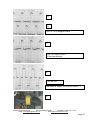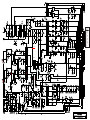
1
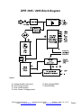
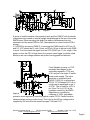
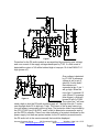
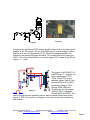
harman consumer group
SMPS
DPR
1005/2005
Theory of operation and
Service information
By Andy Andersen
Harman Consumer Group
250 Crossways Park Dr.
Woodbury, New York 11797
Email [email protected]
Web www.harmanservice.com
DPR 1005 / 2005 Block Diagram
Figure 1
A: Voltage Doubler and inrush
B: Over Voltage protect
C: Over Current protect
D: Over Current / Voltage protect
E: Multi Voltage SMPS
F: Mosfet Bridge
Harman Consumer Group
250 Crossways Park Dr.
Woodbury, New York 11797
Email [email protected]
Web www.harmanservice.com
Page 2
Operation summary
Applied AC line voltage for stand by.
AC line voltage from the relay board goes to connector CN101 and supplies the
voltage for transformer (T101). T101 supplies standby and run voltages +18VAB,
ST5V H8.4V (AC for display). These are the source voltages for the micro (IC62)
for stand by operation.
The applied AC flows through inrush resistors R105 and R104 then rectified by
BD101 to charge C106 and C107. BD101 with C106 and107 are configured as
voltage doublers for 120 operation. Jumper J102 is removed for 240 volt
operation. In either 120 or 240 volt operation 300 volts is developed for
secondary transformer T102.
Stand by to power on
When a High signal is received to connector P-S/W (from micro on main board)
Q201 turns on. Q201 controls optoisolator PC102. PC102 controls U101 at pin 3.
U101 is the driver IC for the SMPS that supplies run voltages +5VA, +5vd, +12V,12V, +18V, +24V, +44V for the main board.
Other activities at power on
When voltage is developed at D101 and C108 (off T102 of the SMPS) RL101
closes (Pins 3, 4 make contact) A short is produced across the in rush resistors
R105 and R104 (5W 15Ω) Current now flows through RL101 and not the inrush
resistors.
At the same time voltage is applied to relay SK41 (located on the Outlet Board
(rear relay board)). Its contacts are wired across the main power switch and is
used to prevent all the receivers current from flowing through the main power
switch (the switch is rated for 8amps, relay for 20 amps).
Power on
Once the secondary voltages are developed from T102 (smps), the micro sends
a signal to power on (4volt high) the high current SMPS used for the D2 audio
module (cn201 pin 11 P-CON, CN2 pin 1 PWR CNTR-2). IC U1 (PWM KA3525)
pin 10 goes low, and a PWM signal is developed to pins 11,14 (out A/B) to two
driver Transformers (T201, T202), then to a Mosfet Bridge to drive T103.
Harman Consumer Group
250 Crossways Park Dr.
Woodbury, New York 11797
Email [email protected]
Web www.harmanservice.com
Page 3
Details
Figure 2
When AC is applied to the SMPS,
R104 and R105 are used to protect
the inrush to capacitor C106 and
C107. After the voltages are
developed from the SMPS of T102,
Relay RL101 closes across the
inrush resistors.
For the 120 volt version to develop the 300
volts need to drive the two switch mode
power supplies a bridge diode assembly is
used for the full wave voltage doubler. For
the 230/240 volt SMPS a voltage doubler is
not necessary. To change from 120 to 240
volt operation, remove jumper J102 for the
SMPS part of the power supply. Please note
the standby transformer is specific for each
AC voltage.
Figure 3
The main power switch cannot
handle the current the DPR can
draw. A relay (SK41) was added to
shunt the power switch at turn on.
When the main switch is turned on
and after voltage is developed in
the stand by supply (from T101)
the relay will close. At this point the
main A/C portion of the power
Figure 4
switch assembly cannot turn off the
DPR. For power down the D/C portion of the power switch sends a command to
the micro to sequence the power supply down, the last step is to release the
power relay.
Harman Consumer Group
250 Crossways Park Dr.
Woodbury, New York 11797
Email [email protected]
Web www.harmanservice.com
Page 4
Figure 5
A group of small transistors, the protection latch and the PWM IC with its related
components are located on a small upright daughterboard at the rear of the main
SMPS board. When servicing this board, be aware of differences from the
schematic and the actual PCB for CN1 (the schematic is correct but the PCB is
wrong).
U1, KA3525 is a common PWM IC. In servicing the PWM check for VCC pin 15,
and VC, VCC should be 15 volts. Power on SD pin 10 has to be low for the PWM
to work. If not low check the signal from the CPU (CN201 pin 11) for a high. If the
power on from the CPU is high check for a protect event trigger (could be a bad
Mosfet or an over voltage problem and protect has triggered and latched).
From Standby to power on T102
develops the voltages for the
secondary regulators. T102 and
U101 are part of a single IC switch
mode power supply. The micro
sends an on command (pin6
CN201 P-S/W 5V) to optoisolator
PC102. PC102 keeps Q101 off so
a high can be developed on pin 3
of U101. The off state for U101 is
pin 3 low. Pin 4 of U101 is the
regulation control for the SMPS.
Regulation is controlled by
Figure 6
reference IC U201 (adjustable
precision shunt regulators) controlling optical coupler PC101.Caution must be
observed when working on this circuit. This is hot to the AC line voltage and is
supplied by 300 volts from the main filter caps C106 and C107.
Harman Consumer Group
250 Crossways Park Dr.
Woodbury, New York 11797
Email [email protected]
Web www.harmanservice.com
Page 5
Figure 7
Protection for the D2 audio module is accomplished by monitoring over voltage
and over current of the supply voltages developed by T103. If a fault event is
detected the output of U2 will be latched high to keep pin 10 of the PWM IC U1
high (power off).
Over voltage is detected
by IC U2A. A reference
voltage is set for pin 2
(about 4.8 volts) and if
that reference is
exceeded at pin 3, pin 1
will go high. When the
rise of pin 1 exceeds 6.2
volts (Zener D1 prevents
false trigger), a high will
Figure 8
be sent to pin 5 of U2B.
The output pin 7 will now
send a high to shut the D2 audio module supply off. The high from pin 7 is also
sent through diode D2 to latch pin 7 high. The output of the op amp can not go
low until power is removed from the op amp. The protection state is monitored by
the CPU (CN201 pin10 M.OCP), and if a fault is detected a command is sent to
put the DPR in standby. There is no other indication of a protect shutdown for the
power supply, but there are protect modes for the D2 module (as mentioned in
the D2 audio info in the service manual) that would be displayed.
Harman Consumer Group
250 Crossways Park Dr.
Woodbury, New York 11797
Email [email protected]
Web www.harmanservice.com
Page 6
Figure 9
Figure 10
Current sense transformer T203 detects the AC current flow for the high current
needed for the D2 module. The AC from T203 goes to a diode bridge, rectified
and the dc is sent to the protection IC U2. When the voltage exceeds 5 volt
reference, the protect will trigger and latch. Do not adjust the over current pot
VR201. This is set at the factory for a protect trigger of 31.2 amps at the 50 volt
output (1.6 load).
The output of the PWM IC (U1
KA3525 pins11, 14) drives two
driver transformers (T201,
T202). Using T201 for the
example, trigger high (5 Volts
through R16) turns on Q202
and stores energy in T201
through C248. When the
Trigger goes low the energy
Figure 11
stored in T201 is replaced
through D222 and Q203. The
result of using this dual transistor setup is almost perfect square wave at the
output of T201. The result is no ringing or over shoot at the pulse transformer
dual outputs.
Harman Consumer Group
250 Crossways Park Dr.
Woodbury, New York 11797
Email [email protected]
Web www.harmanservice.com
Page 7
300 volts DC supplies the
mosfets Q102-Q104. The
high current supply for the
D2 module comes from
T103. T103 is driven by 4
mosfets in a bridge mode to
produce 600 volt PP for
T103. Extreme caution is
needed when working
around the mosfets.
Figure 12
How to test and run the DPR with the D2 amp board removed from the
receiver.
After removing PCB (T/F code : PBD04KAM20) loaded with D2Audio,
and connecting wire as pictured, then you will be able to check the operation of
processor PCB and the SMPS. You can also check the signal 2ch-out and 8chpreout
(Remark): After checking, because of possible Semiconductor
damage on
Processor PCB, remove the connected
i w re first then load D2 AMP PCB.
[PCB CON3: schematic]
[PCB CON3: bottom view]
Wire added
P814
P815
Figure 13
Figure 14
Harman Consumer Group
250 Crossways Park Dr.
Woodbury, New York 11797
Email [email protected]
Web www.harmanservice.com
Page 8
DPR1005/2005: Tech notes in no order
Protection check connector CN1 is hooked up in the print correctly but on the
daughter board is hooked up to pin 5 of IC U2.
The pin outs for CN201 have a different description on the main board and the
pin numbers are reversed.
The output mosfets on the DPR1005 are not IRFP3050 but SKH30N40.
The service manual shows only the 120 version. You must refer to the parts list
for the correct value of the AC input components.
The grounds are common on the SMPS but note that current and digital will take
a different path out of the connectors. If a complaint of noise is noted check the
solder on the connectors.
The DPR series is not lead-free or ROSH compliant.
The standby transformer T101 will run warm. This is normal.
The Over Current pot can not be adjusted by the service centers. In the case of
the DPR2005 the 50 volt output load current would have to be set at 31.2 amps
(1.6Ω Load)
There are replacement components available except for the transformers.
The heat sink of U101 can be used has the hot ground
(ground for IC 101 and the power mosfets). Do not hookup
without adding a screw, the coating on the heat sink is an
insulator.
!! Caution !! must be used around the primary side of T103.
There is a 600 volt PP AC signal around the components!
Figure 15
Power on Timing:
The regulator SMPS (using IC U101) will turn on about one second before the D2
supply voltage raises. CN201 pin 6 (P-S/W) will turn on before pin11 (P-CON).
The voltage out of CN203 (50 volts for the DPR2005, 39 volts for the DPR1005)
turns on with a slow rise of 20v / Second.
Harman Consumer Group
250 Crossways Park Dr.
Woodbury, New York 11797
Email [email protected]
Web www.harmanservice.com
Page 9
A
B
Pins 16, 18 on daughter board
C
Pin 1 of T202 off D223
5 volts per division
E
300 volts PP
One half BTL output. 50 volts per division
D
Harman Consumer Group
250 Crossways Park Dr.
Woodbury, New York 11797
Email [email protected]
Web www.harmanservice.com
Page 10
T101
EI4115
6
7
5
8
1
2
3
9
RL101
ALE15B12
4
3
F101
250V T12A
LF101
10mH
CN101
LF102
10mH
C126
101 Y1
3
2
1
D101
UF4004
1
2
R105
5W15
R104
5W15
C127
152 Y1
C104
152 Y1
+
D102
1N4148
7
10
2
~
-
3
1
+
4
~
+
~
-
T102
EER3541
R123
1W1.5
3
C128
152 Y1
R102
1/2W1M
C101
275V474
C102
275V474X
+
R106
1W100K
C105
152 Y1
1
+
C109
630V472
R109
1W100K
C212
16V2200
D207
UF4004
11
+
R107
1W100K
C119
152 Y1
C107
200V1200
D204
31DF2
14
C120
102Y1
18
HS102
R202
1/4W 10
6
C114
224M
R114
1/4W22
1
16
7
Q203
A708
2
L101
L3550
KA1M088B-TV
Q103
IRFP350
U101
1M0880B
18
C116
224M
R118
1/4W22
R120
1/4W22
7
C117
224M
D218-221
1N4148
VR201
5K
R222
1K
15
11
14
13
6
5
7
R14
22
12
VCC
VREF
OUTA
+V
OUTB
-V
VC
COMP
RT
OSC
CT
SYNC
C11
104
R15
6.8KF
2
+
C229
10V470
SD
GND
CSS
R6
2.2K
C5
35V47
D2
1N4148
5
R11
4.7K
1
4
C6
223
7
R7
4.7K
Q2
2N2222
8
+
R12
62KF
C
50V4.7
C7
152J
R13
4.7KF
C13
104M
+
-
10
C8
35V47
8
R9
4.7KF
R10
22K
C4
104
C10
104
3
10
D224
1N4148
R225
5
R112
1/2W820K
+
+
C206
25V1000
L201
10uH
C220
16V2200
C232
104
+
C231
104
C204
10V1000
D213
1N4007
C221
10V470
C237
104
C238
104
R207
1/4W330
R208
1/4W4.7KF
2
H8.4V
3
GND
4
+44V
5
GND
6
P-S/W
7
ST5V
8
V.CK
9
+18VL
10
M.OCP
11
P-CON
On
2.6
2.6
.0
.0
.0
.0
5.7
4.4
.8
.0
.0
9.8
9.8
.0
42.5
.0
4.6
5.7
4.4
17.3
.0
4.
Pin 11 Red Wire
CN202
5267-10
+
L203
10uH
1
+18VA
2
+24V
3
GND
4
-12V
5
+12VA
6
GND
7
-5V
8
GND
9
+5VD
10
+5VA
1
+24V
2
GND
L204
10uH
R209
1/4W4.7KF
+
R204
1/2W 10K
CN204
5267-02
C209
35V470
C239
104
Q201
2N2222
R3
10KF
R224
1/4W4.7K
14
3
C246
104
O
C227
25V1000
I
8
+
-
9
1
2
3
22
4
+
CN1
5267-02
17
R214
1W22
D216
HER204
D217
HER204
1
2
+
L207
8uH
+
+
C243
105M
C222
50V2200
C223
50V2200
C224
50V2200
R215
10W1.5K
R216
10W2.2K
R217
10W2.2K
R218
10W2.2K
R219
10W2.2K
20
2
+
L206
100
D215
KCF25A20
11
R1
100KF
C241
1KV102
18
R122
5W470
G
R213
1W22
D214
KCF25A20
C118
2KV221
U208
KA7815
U2A
LM393A
1
C3
104
T103
EE5555A
C242
1KV102
L206-1
10
C225
25V1000
+
U207
KA7905
1
I
O
3
C226
10V470
G
C244
104
1
+39V
2
+39V
3
+39V
4
+39V
5
GND
6
GND
7
GND
8
GND
CN203
35313-08V
+
2
23
R4
4.7KF
C2
35V47
R2
9.1KF
C1
104
C245
104
C228
63V47
2.7KF
C254
1000PF
7
+
+
C203
10V2200
U201
TL431
R113
1/4W 47K
5
1
R5
2.2K
6
U2B
4
LM393A
Q1
2N2222
VR202
5K
C112
104
C121
250V 475K
D1
6.2V
9
3
DISC
+
C9
152J
16
+
4.7KF
2
1
C205
25V1000
C201
1KV102
OUT
R210
1/4W1K
- 4
R221
220
R18
1/4W100
R8
R201
1/4W 10
IN
H8.4V
R220
2K
1
2 +
R223
1/4W4.7
U1
KA3525
U202
S1117-50PI
1
Off
R211
1/4W4.7K
T202
EE1927
C247
104
R203
2W4.7K
PC102
ET1103
D
ZD104
1W15V
8
C110
104
Q101
C1008
T203
IRON13Áè
Q105
IRFP350
R121
1/4W3.9K
C111
50V47
R111
1/4W47
C113
50V1
E
ZD103
1W15V
5
R17
10
C233
104
+
+
Q104
IRFP350
R119
1/4W3.9K
2
B
2
C213
10V1000
L202
10uH
+
C250
104
2
1
C
G
R110
1/4W100
3
6
D223
1N4148
+
Voltage
CN201
5267-11
C208
35V1000
PC101
ET1103
1
Q205
A708
C234
104
4
T201
EE1927
C249
105M
10
5
ZD102
1W15V
8
Q204
C1008
C215
16V2200
3
+
2
R116
1/4W22
R117
1/4W3.9K
R16
10
C235
104
3
C211
63V100
D201
31DQ06
12
D104
UF4004
ZD101
1W15V
5
C115
224M
3
Q102
IRFP350
R115
1/4W3.9K
C202
1KV102
ZD201
1/2W5V
+
C207
35V2200
D203
HER204
300 Volts DC
D222
IN4148
C217
+
16V470
+
0
C248
105M
O
C210
63V100
4
Q202
C1008
L205
10uH
+
D103
UF4007
+
I
C252
103
3
U204
KA7805
2
+
D202
31DQ06
O
G
1
10
C251
103
3
U205
KIA7812
I
C214
25V1000
R108
1W220K
GND
A
G
16
5
J102
C103
275V474
C106
200V1200
O
2
15
C125
101 Y1
I
C216
+
25V1000
6
M43160-0302
C219
25V220
R206
1/4W100K
D212
IN4007
U206
KA7912
1
D205
HER204
+
+
2
4
17
8
U203
KA7818
3
OUT
R205
1/4W1K
D206
HER204
C108
35V470
IN
G
C218
35V470
BD201
DF06
BD101
600V25A
-
+
BD202
DF06
1
1
~
4
6
C253
100PF
Title
Size
A2
Date:
Document Number
AUDIO POWER
Rev
KJP-7013/DPR1005 - US
Wednesday, August 11, 2004
Sheet
1
1
of
1