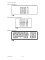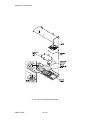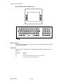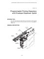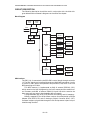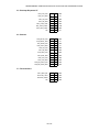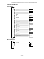
1
UPDATE NOTIFICATION
F8767
0387
Document No.:
D2-0198-A
Document Title:
NCR 56XX/personaS Self-Service Financial
Hardware Module Descriptions
Change No.:
30
Print Date:
March 2000
REASON FOR UPDATE:
The manual is revised to include information on modules in the Personas 86 ATM (5886), as
follows:
• Chapter 6.11 is an addendum to the TEC 40-Column Printer manual available from Repair Development in Peachtree.
• Chapter 10.5 is updated to include 5886 tactile keyboards.
• Chapter 12.3 is updated to show 5886 dispenser and depository shutters.
• Appendix 12.6-A describes the Stage 1 Personas 86 currency dispenser.
• Chapter 13.4 describes the Programmable Printing Depository with Envelope Dispenser Option.
• Chapter 18.9 describes the NLX Miscellaneous Interface Board.
UPDATE INSTRUCTIONS:
Replace the Front Cover with the new Front Cover.
Replace the Title Page with the new Title Page dated 0300.
Remove and discard the Contents pages vii to xii.
Insert the new Contents pages vii to xii dated March 2000.
Remove and discard the Revision Record pages xiii to xx.
Insert the new Revision Record xiii to xx dated March 2000.
Insert new Chapter 6.11, pages i through 2, to follow existing Chapter 6.7.
Remove and discard Chapter 10.5.
Insert new Chapter 10.5, pages i through 22, dated March 2000.
Remove and discard Chapter 12.3, pages 12.3-i through to page FO-1.
Insert new Chapter 12.3, pages i through 14 dated March 2000.
SEE OVER
UPDATE INSTRUCTIONS:
Remove and discard the contents pages of Chapter 12.6 (pages 12.6-i through to page 12.6-xii).
Insert new contents pages for Chapter 12.6, pages 12.6-i through to page 12.6-xii dated March 2000.
Insert new Chapter 12.6, Appendix A, pages 12.6-A-i through to page 12.6-A-10 to follow Chapter
12.6 Page 12.6-282.
Insert new Chapter 13.4, pages 13.4-i through to page 13.4-48 to follow Chapter 13.3.
Insert new section divider card for Section 18 - NLX PC Core to follow Chapter 17.1.
Insert new Chapter 18.9, pages 18.9-i through to page 18.9-36 to follow the new Section 18 divider
card.
Replace the Back Cover with the new Back Cover dated 0300.
NCR 56XX/Personas XX
Self-Service Financial Terminals
Hardware Module Descriptions
D2-0198-A
O300
The product described in this book is a licensed product of NCR Corporation.
Trademark Information
It is the policy of NCR Corporation (NCR) to improve products as new technology, components, software, and firmware
become available. NCR, therefore, reserves the right to change specifications without prior notice.
All features, functions, and operations described herein may not be marketed by NCR in all parts of the world. In some
instances, photographs are of equipment prototypes. Therefore, before using this document, consult with your NCR
representative or NCR office for information that is applicable and current.
To maintain the quality of our publications, we need your comments on the accuracy, clarity, organization, and value
of this book.
Address correspondence to:
NCR Financial Systems Group Ltd.
Information Solutions Dept.
Kingsway West
Dundee
Scotland
DD2 3XX
Copyright © 1994, 1995, 1996, 1997, 1998, 1999, 2000
By NCR Corporation
Dayton, Ohio U.S.A.
All Rights Reserved
PREFACE
Contents
Preface
This manual contains the descriptions of the operation, and servicing
information, on the hardware modules which make up the NCR 56XX and
Personas (58XX) series of Self-Service Financial Terminals (SSFTs). SSFTs
include Interactive Terminals, Account Services Terminals and Automated
Teller Machines (ATMs).
MANUAL ORGANIZATION
SECTIONS AND CHAPTERS
This publication is divided into the following sections:
z
z
z
z
z
z
z
z
z
z
z
z
z
z
z
z
z
z
Section 1 - General Description
Section 2 - PC Core
Section 3 - Power Supply and Distribution
Section 4 - High Order Communications
Section 5 - Audio, Video, and Graphics
Section 6 - Printers
Section 7 - Magnetic Card Reader/Writers
Section 8 - Encryptors
Section 9 - Disk Drives
Section 10 - Input Devices
Section 11 - Miscellaneous Interfaces
Section 12 - Currency Handling
Section 13 - Depository and Envelope Dispensers
Section 14 - Terminal Control Module (ISA Bus)
Section 15 - HI3 Terminal Control Module
Section 16 - Document Processing
Section 17 - Standard PC Core
Section 18 - NLX PC Core.
Each section covers a major group of modules. Chapters within the sections describe a single module within that group, for example Chapter 10.1 is
for the Alphanumeric Membrane Keyboard and Chapter 10.2 is for the
Numeric Membrane Keyboard.
The chapters within Section 1 give general information on the ranges of
SSFTs and tell you where to find more detailed information within the book
i
MARCH 2000
PREFACE
Chapter Numbering
Chapters are numbered within the sections by numbers such as: 7.8, meaning
Section 7, Chapter 8, or 9.3, meaning Section 9, Chapter 3. The page numbers
are of the form 7.7-1, 7.7-2, 7.7-3.....9.3-1, 9.3-2, 9.3-3.... and so on. The
exception to this is where we have included, as appendices, handbooks for
vendor products, for example, the TEC Service Manual for the 40-Column
Receipt/Journal Printer and the Zenith manual for the Colour Monitor. In
these cases we have left the numbering of the original intact, and they do not
follow the main sequence of numbering of the overall book.
UPDATES
From time to time you will receive updates as modules are changed or new
modules are issued.
DATES ON PAGES
When new chapters are issued to the manual the pages do not have a date on
them. If those pages are subsequently revised, then they will have the print
date of the update at the foot. An update package can, therefore, have a
mixture of new (undated) and revised (dated) pages.
REVISION RECORD
The Revision Record, following the main Contents pages, gives a list of all the
pages in the manual and their revision dates. You can use it to check that you
have all the current pages in the correct order.
YOUR COMMENTS
Your contributions to the manual are very much appreciated. If you find an
error, or you would like something included, you can let us know by sending in
the Reader’s Comment Form from the back of the manual, or, you can write
directly to:
NCR Financial Solutions Group Ltd.
Information Solutions Department,
Kingsway West,
Dundee,
Scotland DD2 3XX
You can also send in your comments via the Internet. You will find a comment form at WWW address:
http://www.ncr.com/product/infoprod/dundeeip
or you can contact us on e-mail at:
[email protected]
MARCH 2000
ii
CONTENTS
Contents
Contents
NCR 56XX/personaS
Self-Service Financial Terminals
Hardware Module Descriptions
Section 1 - General Description
1.1
1.2
1.3
1.4
1.5
1.6
1.7
5682 Overview
5663 Overview
5675 Overview
5674 Overview
5684 Overview
5685 Overview
5688 Overview
Section 2 - PC Core
2.1
2.2
2.3
2.4
2.5
PC Bus Board
Processor and Coprocessor
Self Service Personality Module and Serial Distributed Control
Link
512 KB Memory Expansion Board (3299-K130)
Memory Carrier Board
vii
MARCH 2000
CONTENTS
Section 3 - Power Supply and Distribution
3.1
3.2
3.3
3.4
3.5
3.6
3.7
3.8
3.9
3.10
System Power Supply Unit (550 W)
Reserved
DC Distribution Board
5682 AC Power Distribution Components
Power Distribution Board
5663 AC Power Distribution Components
56XX ATMs AC Power Distribution Components
System Power Supply Unit (650 W)
ASTEC Power Supply Unit
Slimline PSU
Section 4 - High Order Communications
4.1
4.2
4.3
4.4
4.5
4.6
4.7
PC Communications Module
Hayes Smartmodem 2400B
PC IBM Financial Loop Interface
Reserved
Reserved
NCR 16/4 Token Ring Adapter/ISA (Version 3)
PC MIRLAN Adapter
Section 5 - Audio, Video, and Graphics
5.1
5.2
5.3
5.4
5.5
5.6
5.7
5.8
5.9
5.10
5.11
5.12
5.13
5.14
5.15
5.16
5.17
5.18
MARCH 2000
Color Monitor
5682 SDC Videodisc Player
Video/Graphics Interface
Graphics Adapter
Audio Amplifier (Stereo)
SDC Dual RS-232-C (Video) Interface Board
Digital Sound Board - Playback
Beeper Amplifier
10 Inch VGA Colour Monitor
10 Inch Monochrome Monitor
Twelve Inch Colour Monitor
Audio Amplifier (Mono)
Private Audio Enable
NCR VGA Piggy-Back Board (3299-K072)
Video Graphics Adapter Enhanced - VGX
Graphics Adapter Enhanced - GX (Penny Graphics) and GX (Lite)
Twelve Inch Greyscale Monitor
56/588X Ten Inch VGA Colour Monitor (Y0F9151)
viii
CONTENTS
5.19
5.20
5.21
5.22
5.26
5.27
568X Ten Inch Sunlight Viewable Monochrome Monitor
Reserved
56/5870 10 Inch VGA Colour Monitor (CD10012XX)
5670 10 Inch VGA Mono Monitor
56XX EMCO 10 Inch VGA Colour Monitor (CD 10014XX)
5663 EMCO 10 Inch VGA Colour Monitor (CD 10013XX)
Section 6 - Printers
6.1
6.2
6.3
6.4
6.5
6.6
6.7
6.8 - 6.10
6.11
SDC 40 Column Receipt/Journal Printer
SDC 80 Column Statement Printer
SDC 80-Column Combined Statement/Passbook Printer
Statement Printer With Buncher
Page Turning Passbook Printer
40-Column Thermal Printers
80-Column Thermal Printer
Reserved
TEC 40-Column Thermal Printers
Section 7 - Magnetic Card Reader/Writers
7.1
7.2
7.3
7.4
7.5
7.6
7.7
7.8
7.9
7.10
7.11
7.12
7.14
SDC Dip Magnetic Stripe Reader Module
SDC Magnetic Card Reader Writer Track 1-2-3
SDC Magnetic Card Reader Track 2
Card Return On Power Failure Module
Card Capture Bins
Card Identification Module (CIM 86)
3 Track Write Magnetic Card Reader Writer
Smart Card Reader/Writer
Reserved
Swipe Card Reader
Reserved
SCRW - Card Return on Power Fail Module
EMV Smart Card Reader/Writer
Section 8 - Encryptors
8.1
8.2
8.3
Basic Alpha Pinpad Encryptor
Encryptor Keyboard Controller
High Integration - Basic Alpha Pinpad Encryptor
ix
MARCH 2000
CONTENTS
Section 9 - Disk Drives
9.1
9.2
9.3
9.4
9.5
Hard Disk Controller Board
Hard Disk Drive
Flexible Disk Drives
Fixed Disk Drives (H6X01-XXXX)
AT Disk Drive Interface Module
Section 10 - Input Devices
10.1
10.2
10.3
10.4
10.5
10.6
10.7
10.8
10.9
10.10
10.12
10.13
SDC Alphanumeric Membrane Keyboard
SDC Numeric Membrane Keyboard
SDC Touch Screen
Basic SDC Operator Panel
Moving Key Keyboards
Twelve Inch Touch Screen
Front Operator Panel
Enhanced Operator Panel
Keyboard Heater
SDC (AFE) Touch Screen
VGA Enhanced Rear Operator Panel
Operator Interface Board
Section 11 - Miscellaneous Interfaces
11.1
11.2
11.3
11.4
11.5
11.6
11.7
11.8
11.9
11.10
11.11
11.12
11.13
11.14
MARCH 2000
SDC Miscellaneous Interface Board
Remote Status Indicator
Terminal Lighting (5682)
Proximity Detector
In Service Indicator
Remote Relay and Night Depository Interfaces
Security Camera Interface
Door Access Unit Interface
Media Entry Indicators
Signage Unit
Terminal Lighting (ATMs)
Terminal lighting (5663)
SDC Single RS-232-C Interface Board
The Digital Camera System
x
CONTENTS
Section 12 - Currency Handling
12.1
12.2
12.3
12.4
12.5
12.6
The H-8010-56XX-XX-08 Currency Dispenser
The H-8015-STD1-01/02-08 Currency Cassette
Motorised Shutter Control
Coin Dispenser Module
The H-8010-56XX-XX-08 (IE) Currency Dispenser
The 56XX Enhanced Currency Dispenser
Section 13 - Depository and Envelope Dispensers
13.1
13.2
13.3
13.4
Programmable Printing Depository for 56XX ATMs
Motorized Envelope Dispensers
Single Processor - Programmable Printing Depository for 56XX
ATMs
Programmable Printing Depository with Envelope Dispenser
Option
Section 14 - Terminal Control Module (ISA Bus)
14.1
14.2
14.3
14.4
14.5
14.6
14.7
TCM System board
ISA-TCM Bus Board
ISA-TCM Video Graphics Array
Disk Interconnect
ISA-TCM I/O Board (5682)
TCM I/O Board (ATMs)
ISA-TCM I/O Board (5663)
Section 15 - HI3 Terminal Control Module
15.1
15.2
15.3
15.4
15.5
15.6
HI3 System Board
HI3 Bus Board
Miscellaneous Driver Board
Advanced System Board
5670 I/O Board
5670 ISA Expansion Board
Section 16 - Document Processing
16.1
16.2
Document Processing Module - ATM
The Document Processing Module
xi
MARCH 2000
CONTENTS
Section 17 - Standard PC Core
17.1
The Standard PC Core
Section 18 - NLX PC Core
18.1
MARCH 2000
NLX PC Core - Miscelaneous Interface Board
xii
REVISION RECORD
Contents
Revision Record
Use the following table to check if your manual is up to date. The revision date
that appears on each page is given in the last column.
Section
Chapter
Page Number
Date
Front matter:
Front cover
Title Page
0300
Preface
i/ii
March 2000
FCC Statement
iii to iv
December 1996
Safety Information
v to vi
November 1994
Contents
vii to xii
March 2000
Revision Record
xiii to xx
March 2000
1. General Description
Divider Card
Undated
1.1
1.1-i to 1.1-12
June 1991
1.2
1.2-i to 1.2-9
April 1991
1.3
1.3-i to 1.3-9
Undated
1.4
1.4-i to 1.4-8
Undated
1.5
1.5-i to 1.5-9
Undated
1.6
1.6-i to 1.6-8
Undated
1.7
1.7-i to 1.7-12
Undated
Divider Card
Undated
2. PC Core
2.1
2.1-i to 2.1-5
September 1991
FO-1 to FO-4
September 1991
2.2
2.2-i to 2.2-51
Undated
2.3
2.3-i to 2.3-65
May 1996
FO-1 to FO-19
July 1991
2.4
2.4-i to 2.4-4
Undated
2.5
2.5-i to 2.5-1
Undated
FO-1
Undated
Divider Card
Undated
3. Power Supply and Distribution
3.1
3.3
3.1-i to 3.1-12
May 1996
FO-1 to FO-10
December 1991
3.3-i
Undated
3.3-1 to 3.3-3
November 1992
FO-1
November 1992
FO-2
Undated
3.4
3.4-i to 3.4-6
November 1992
3.5
3.5-i to 3.5-8
June 1991
FO-1 to FO-2
March 1992
3.6-i to 3.6-6
October 1991
3.6
xiii
MARCH 2000
REVISION RECORD
Section
Chapter
Page Number
Date
3.7
3.7-i to 3.7-10
December 1993
3.8
3.9
3.10
4. High Order Communications
4.1
Undated
Undated
3.9-i to 3.9-17
Undated
FO-1 to FO-3
Undated
3.10-i to 3.10-26
Undated
Divider Card
Undated
i to iv
May 1993
4.1-1 to 4.1-24
May 1993
4.1-25/26
April 1995
4.1-27 to 4.1-42
May 1993
4.1-43/44
April 1995
4.1.45 to 4.1-54
May 1993
FO-1 to FO-13
Undated
4.1 Appendix A
4.1-A-i to 4.1-A-52
June 1991
4.2
4.2-i to 4.2-7
Undated
4.3
4.3-i to 4.3-74
December 1993
FO-1 to FO-8
December 1993
4.6
4.6-i to 4.6-10
March 1992
4.7
4.7-i to 4.7-51
December 1993
FO-1 to FO-7
December 1993
Divider Card
Undated
5. Audio, Video, & Graphics
5.1
5.1 Appendix A
5.1 Appendix B
MARCH 2000
3.8-i to 3.8-13
FO-1 to FO-6
5.1-i/ii
June 1995
5.1-1/2
January 1996
5.1-3 to 5.1-22
June 1995
FO-1 to FO-3
June 1995
5.1-A-i
June 1995
i to vii
Undated
1-1 to 1-3
Undated
2-1 to 2-3
Undated
3-1 to 3-10
Undated
4-1 to 4-11
Undated
5-1 to 5-14
Undated
6-1 to 6-13
Undated
7-1 to 7-21 (FO-1)
Undated
8-1 to 8-7 (FO-1)
Undated
8-9 to 8-11 (FO-2)
Undated
8-13 (FO-3)
Undated
8-15 to 8-17 (FO-4)
Undated
8-19 (FO-5)
Undated
8-21
Undated
5.1-B-1
June 1995
i to vii
Undated
1-1 to 1-3
Undated
2-1 to 2-4
Undated
3-1 to 3-11
Undated
4-1 to 4-19
Undated
5-1 to 5-22
Undated
6-1 to 6-17
Undated
7-1 to 7-3
Undated
xiv
REVISION RECORD
Section
Chapter
Page Number
Date
8-1 to 8-15
Undated
5.2
5.2-i to 5.2-10
November 1996
5.3
5.3-i to 5.3-27
Undated
FO-1 to FO-9
September 1990
5.4
5.4-i to 5.4-6
Undated
5.5
5.5-i to 5.5-5
December 1991
FO-1
Undated
FO-2 to FO-4
December 1991
5.6
5.6-i to 5.6-10
Undated
FO-1 to FO-4
Undated
5.7
5.7-i to 5.7-7
November 1992
5.8
5.8-i to 5.8-5
December 1991
5.9
5.9-i to 5.9-42
April 1991
FO-1 to FO-5
April 1991
5.10
5.11
5.10-i to 5.10-32
June 1991
FO-1 to FO-2
June 1991
5.11-i to 5.11-42
July 1993
FO-1 to FO-2
July 1993
5.12
5.12-i to 5.12-4
January 1994
5.13
5.13-i to 5.13-2
Undated
5.14
5.14-i to 5.14-12
Undated
FO-1 to FO-3
Undated
5.15
5.15-i to 5.15-10
Undated
5.16
i
September 1992
5.16-1 to 5.16-7
September 1992
5.17
5.18
5.19
5.17-i to 5.17-2
November 1992
5.17-3 to 5.17-6
July 1993
5.17-7 to 5.17-12
November 1992
5.17-13/14
July 1993
5.17-15/16
November 1992
5.17-17 to 5.17-22
July 1993
5.17-23 to 5.17-35
November 1992
FO-1 to FO-2
July 1993
5.18-i to 5.18-30
October 1999
FO-1 to FO-3
February 1994
5.19-i to 5.19-36
November 1996
FO-1 to FO-2
December 1992
5.21
5.21-i to 5.21-46
October 1999
5.22
5.22-i to 5.22-38
Undated
5.26
5.26-i to 5.26-58
Undated
5.27
5.27-i to 5.27-58
Undated
Divider Card
Undated
6.1
6.1-i to 6.1-11
January 1994
6.1 Appendix A
6.1-A-1
Undated
i/ii
Sep. 1991
1-i to 1-3
Undated
2-i to 2-28
Undated
3-i to 3-91
Undated
4-i to 4-5 (FO-1)
Undated
6. Printers
4-6 to 4-10 (FO-2)
Undated
4-11 to 4-28 (FO-3)
Undated
xv
MARCH 2000
REVISION RECORD
Section
Chapter
Date
4-29 to 4-41
Undated
5-i
Undated
FO-1 to FO-3
Nov. 1988
FO-4 to FO-6
Dec. 1988
FO-7
Apr. 1991
FO-8
Nov. 1990
FO-9
Apr. 1991
FO-10 to FO-12
Dec. 1988
FO-13
May 1992
FO-14
Jan. 1991
FO-15 to FO-18
Dec. 1988
FO-19
May 1992
6-i to 6-71
Undated
6.2
6.2-i to 6.2-10
June 1991
6.2 Appendix A
6.2-A-1
June 1991
i/ii
May 1990
1-i to 1-3
Undated
2-i to 2-19
Undated
3-i to 3-90
Undated
4-i to 4-28
Undated
5-i
Undated
FO-1
Apr.1989
FO-2
July 1989
FO-3
Mar. 1990
FO-4
Apr.1989
FO-5, FO-6
Feb. 1989
FO-7
Apr. 1989
FO-8
Jan. 1989
FO-9 to FO-11
Apr. 1989
6-i to 6-46
Undated
6.2-B-1 to 6.2-B-7
June 1991
6.2 Appendix C
6.2-C-1 to 6.2-C-6
June 1991
6.3
6.3-i/ii
May 1993
6.2 Appendix B
6.3 Appendix A
MARCH 2000
Page Number
6.3-iii to 6.3-10
Undated
6.3-11 to 6.3-14
May 1993
6.3-15 to 6.3-31
Undated
6.3-A-1/2
Undated
i/ii
Dec. 1994
1-i to 1-6
Undated
2-i to 2-23
Undated
3-i to 3-174
Undated
4-i to 4-59
Undated
5-i
Undated
FO-1
Oct. 1989
FO-2
Mar. 1990
FO-3
Oct. 1989
FO-4
Jan. 1990
FO-5
Nov. 1990
FO-6 to FO-7
Oct. 1989
FO-8
Nov. 1990
FO-9
Oct. 1989
xvi
REVISION RECORD
Section
Chapter
Page Number
Date
FO-10
Mar. 1991
6-i to 6-62
Undated
6.3 Appendix B
6.3-B-1 to 6.3-B-7
Undated
6.3 Appendix C
6.3-C-1 to 6.3-C-7
Undated
6.4
6.4-i to 6.4-28
Undated
FO-1 to FO-6
Undated
6.5
6.5-i to 6.5-186
June 1999
6.6
6.6-i to 6.6-16
September 1996
6.6 Appendix A
Title page
6.6 Appendix A
i to 86
6.6 Appendix B
Title page
December 1996
6.6 Appendix B
i to 96
6.7
6.7-i to 6.6-176
January 1997
FO-1 to FO-2
June 1995
6.11
7. Magnetic Card Reader/Writers
7.1
7.2
7.3
7.4
September 1996
6.7-A-1 to 6.7-A-26
January 1997
6.11-I to 6.11-2
Undated
Divider Card
Undated
7.1-i to 7.1-13
June 1991
FO-1 to FO-3
June 1991
7.2-i to 7.2-53
October 1991
FO-1 to FO-19
October 1991
7.3-i to 7.3-48
October 1991
FO-1 to FO-19
October 1991
7.4-i to 7.4-12
January 1994
FO-1 to FO-3
November 1992
FO-4 to FO-6
January 1994
7.5
7.5-i to 7.5-8
Undated
7.6
7.6-i/ii
May 1993
7.6-1 to 7.6-28
Undated
7.7
7.8
7.10
7.6-29 to 7.6-41
May 1993
FO-1 to FO-6
Undated
7.7-i to 7.7-61
Undated
FO-1 to FO-9
Undated
7.8-i to 7.8-42
May 1996
FO-1 to FO-21
November 1993
7.10-i to 7.10-12
Undated
7.10-13/14
April 1995
7.10-15 to 7.10-18
Undated
FO-1 to FO-2
Undated
7.12
7.12-i to 7.12-16
Undated
7.14
7.14-i to 7.14-56
Undated
Divider Card
Undated
8. Encryptors
8.1
8.2
8.3
9. Disk Drives
8.1-i to 8.1-19
June 1991
FO-1 to FO-4
June 1991
8.2-i to 8.2-18
June 1991
FO-1 to FO-4
June 1991
8.3-i to 8.3-12
Undated
Divider Card
Undated
9.1
9.1-i to 9.1-7
May 1996
9.2
9.2-i to 9.2-2
March 1996
9.3
9.3-i to 9.3-6
March 1996
xvii
MARCH 2000
REVISION RECORD
Section
Chapter
Page Number
Date
9.4
9.4-i to 9.4-8
September 1999
9.5
9.5-i to 9.5-7
January 1992
FO-1 to FO-2
June 1996
10. Input Devices
Divider Card
Undated
10.1
10.1-i to 10.1-7
May 1993
10.2
10.2-i to 10.2-5
May 1993
10.3
10.3-i to 10.3-8
Undated
10.3-9 to 10.3-12
July 1993
10.3-13 to 10.3-16
Undated
FO-1 to FO-23
Undated
10.4
10.4-i to 10.4-11
June 1991
FO-1 to FO-12
June 1991
10.5
10.5-i to 10.5-22
March 2000
10.6
10.6-i to 10.6-18
March 1996
FO-1 to FO-6
Undated
10.7
10.8
Undated
Undated
10.8-i to 10.8-15
Undated
FO-1 to F0-10
Undated
10.9
10.9-i to 10.9-3
Undated
10.10
10.10-i to 10.10-8
October 1994
10.12
10.12-i to 10.12-36
Undated
10.13
10.13-i to 10.13-14
Undated
Divider Card
Undated
11. Miscellaneous Interfaces
11.1
11.1-i to 11.1-22
November 1990
FO-1 to FO-14
Undated
11.2
11.2-i to 11.2-3
Undated
11.3
11.3-i to 11.3-4
Undated
11.4
11.4-i to 11.4-2
Undated
11.5
11.5-i to 11.5-3
Undated
11.6
11.6-i to 11.6-7
Undated
11.7
11.7-i to 11.7-5
Undated
11.8
11.8-i to 11.8-6
Undated
11.9
11.9-i to 11.9-6
Undated
FO-1 to FO-2
Undated
11.10
11.10-i to 11.10-15
Undated
FO-1 to FO-4
Undated
11.11
11.11-i to 11.11-4
Undated
11.12
11.12-i to 11.12-3
Undated
11.13
11.13-i to 11.13-11
Undated
FO-1 to FO-4
Undated
11.14
11.14-i to 11.14-77
Undated
11.14 Appendix A
11.14-A-i to 11.14-A-51
Undated
Divider Card
Undated
12. Currency Handling
12.1
12.1-i to 12.1-130
Undated
FO-1 to FO-26
Undated
12.2
12.2-i to 12.2-36
September 1999
12.3
12.3-i to 12.3-14
March 2000
12.4
12.4-i to 12.4-42
September 1995
12.5
MARCH 2000
10.7-i to 10.7-6
FO-1
12.5-i to 12.5-135
Undated
FO-1 to FO-25
Undated
xviii
REVISION RECORD
Section
Chapter
Page Number
Date
12.6
12.6-i to 12.6-xii
March 2000
12.6 Appendix A
12.6-1 to 12.6-282
May 1996
12.6-A-i to 12.6-A-10
Undated
13. Depository and Envelope Dispensers
13.1
Divider Card
Undated
13.1-i/ii
Undated
13.1-1 to 13.1-30
November 1992
13.1-31 13.1-34
May 1993
13.1-35 to 13.1-40
November 1992
FO-1 to FO-13
Undated
13.2
13.2-i to 13.2-24
June 1995
13.3
13.3-i to 13.3-37
Undated
FO-1 to FO-12
Undated
13.4
13.4-i to 13.4-48
14. Terminal Control Module (ISA Bus) Divider Card
14.1
Undated
Undated
14.1-i to 14.1-58
December 1992
FO-1 to FO-66
December 1992
14.1 Appendix A
14.1-A-i to 14.1-A-88
December 1992
14.2
14.2-i to 14.2-9
Undated
FO-1 to FO-5
Undated
14.3
14.4
14.5
14.6
14.7
15. HI3
15.1
14.3-i to 14.3-11
Undated
FO-1 to FO-8
Undated
14.4-i to 14.4-8
October 1991
FO-1
October 1991
14.5- i to 14.5-8
March 1996
FO-1 to FO-4
Undated
14.6-i to 14.6-6
Undated
FO-1 to FO-2
Undated
14.7-i to 14.7-10
May 1996
FO-1 to FO-4
Undated
Divider Card
Undated
15.1-i to 15.1-92
Undated
FO-1 to FO-38
Undated
15.1 Appendix A
15.1.A-1 to 15.1.A-182
Undated
15.2
15.2-i to 15.2-33
July 1993
FO-1 to FO-8
July 1993
15.3
15.3-i to 15.3-4
Undated
15.4
15.4-i to 15.4-136
Undated
15.4 Appendix A
15.4.A-i to 15.4.A-110
Undated
15.5
15.5-i to 15.5-24
Undated
15.6
15.6-i to 15.6-4
Undated
Divider Card
Undated
16. Document Processing
16.1
16.1-i to 16.1-134
June 1995
16.2
16.2-i to 16.2-10
Undated
17. Standard PC Core
17.1
18. NLX PC Core
18.9
16.2-11/12
January 1996
16.2-13 to 16.2-82
Undated
Divider Card
Undated
17.1-i to 17.1-18
Undated
Divider Card
Undated
18.9-i to 18.9-36
Undated
xix
MARCH 2000
REVISION RECORD
Section
Chapter
Page Number
Date
Back Matter
MARCH 2000
Reader’s Comment Form
0699
Back Cover
0300
xx
TEC 40-COLUMN THERMAL PRINTERS
Contents
TEC 40-Column Thermal Printers
Chapter 6.11
GENERAL DESCRIPTION ....................................................................................... 6.11-1
REWORK INFORMATION ...................................................................................... 6.11-1
SERVICE INFORMATION ....................................................................................... 6.11-2
CORRECTIONS AND CLARIFICATIONS ............................................................. 6.11-2
BLACK MARK CALIBRATION ......................................................................... 6.11-2
5886 (personaS86) ................................................................................................. 6.11-2
6.11-i
TEC 40-COLUMN THERMAL PRINTERS
6.11-ii
TEC 40-COLUMN THERMAL PRINTERS
Contents
Chapter 6.11
TEC 40-Column Thermal Printers
GENERAL DESCRIPTION
This chapter introduces the 40-column thermal printers made by the Toshiba
TEC Corporation. The original range of printers were designed to be direct
replacements for the Axiohm 40-column thermal printers.
A number of printer assemblies are made from a limited range of components:
z Receipt-only printers with either RS232 or SDC I/F boards
z Journal-only printers with either RS232 or SDC I/F boards
z Combined receipt and journal printers sharing a single SDC I/F board.
The receipt printers have a variety of transport configurations to suit particular ATMs.
This chapter has been added to the Module Descriptions publication to
identify errors, changes and additions that are not covered by the manufacturer’s original service manual.
REWORK INFORMATION
The information required to troubleshoot, rework and repair the printers is
contained in the manufacturer’s service manual. The manufacturer’s
reference numbers are:
z Document number: E0-30126
z Model number: N-40C-DT.
The service manual is available as a CD containing:
z Adobe Acrobat PDF files of:
z the body of the manual
z the schematic diagrams
z The source files as supplied by TEC:
z MS Word files and associated graphics for the body of the manual
z TIFF files for the scanned schematic diagrams.
The service manual is available from Repair Development in Peachtree.
The PDF files are also available on the intranet via the usual Information
Solutions Download pages.
6.11-1
TEC 40-COLUMN THERMAL PRINTERS
SERVICE INFORMATION
Field service information is contained in Chapter 13.11 of the FM0547 Service
Aids Mini Manual (SAMM).
CORRECTIONS AND CLARIFICATIONS
The following sections explain known errors and points of confusion in the
TEC Service Manual.
BLACK MARK CALIBRATION
In Appendix A (Diagnostics) on page A-20, Part (3) reads:
“(3) Press the RESET button (SW2). The printer calibrates the
black mark sensor level with feeding and stores the setting to
EEPROM.”
This should be read as:
“(3) Press the RESET button (SW2), wait until the level 0
diagnostic tests are complete (LEDs no longer flashing) and
then press the Paper Feed button. The printer feeds paper, calibrates the black mark sensor level and stores the setting to
EEPROM.”
5886 (personaS86)
The 40 column printers used in the 5886 ATM differ from those described in
the TEC service manual as follows:
z The receipt printer is mechanically the same as the printer described as
“model 5870R”. It differs from this in that it has an SDC I/F board in place
of the RS232 board used by the 5870. When referring to the Disassembly/
Assembly procedures you will have to switch between the “58XX” descriptions and the “5870R” descriptions depending on which part of the printer
is being worked on.
z The journal printer is similar to the model described as the “58XXJ” but
uses a different base plate.
z The mounting tray for the printers in the ATM is different from that illustrated.
6.11-2
MOVING KEY KEYBOARDS
Contents
Moving Key Keyboards
Chapter 10.5
GENERAL DESCRIPTION ....................................................................................... 10.5-1
KEYBOARD ARRANGEMENT.......................................................................... 10.5-1
Numeric Non-Tactile Keyboard........................................................................ 10.5-1
Numeric-Tactile Keyboard................................................................................ 10.5-2
5670 and 5886 Numeric-Tactile Keyboard ....................................................... 10.5-2
Alphanumeric Keyboards.................................................................................. 10.5-2
FDK Keyboards................................................................................................. 10.5-3
5886 FDK-Tactile Keyboard............................................................................. 10.5-3
CARDHOLDER KEYBOARD ............................................................................. 10.5-3
FUNCTION DISPLAY KEY KEYBOARD ......................................................... 10.5-4
KEYBOARD MATRICES .................................................................................... 10.5-4
Hardware Matrix Code...................................................................................... 10.5-4
FDK Keyboard Matrix ...................................................................................... 10.5-5
Numeric Keyboard Matrix ................................................................................ 10.5-6
Alphanumeric Keyboard Matrix ....................................................................... 10.5-7
CARDHOLDER KEYBOARD DISCONNECT FEATURE................................ 10.5-8
KEYBOARD IDENTIFICATION ........................................................................ 10.5-8
Numeric Keyboard Identification...................................................................... 10.5-8
Alphanumeric Keyboard Identification............................................................. 10.5-8
FDK Keyboard Identification............................................................................ 10.5-8
KEYBOARD CONNECTORS AND HARNESSES ............................................ 10.5-9
Cardholder Keyboard ........................................................................................ 10.5-9
FDK Keyboard ................................................................................................ 10.5-10
FDK Harness Controller Connector ................................................................ 10.5-10
KEYBOARD SCANNING.................................................................................. 10.5-11
COMPONENT REPLACEMENT ........................................................................... 10.5-12
Non-Tactile Keyboards ........................................................................................ 10.5-12
Membrane........................................................................................................ 10.5-12
Keytip .............................................................................................................. 10.5-12
Tactile Keyboards – Keytips with Circlips .......................................................... 10.5-15
Membrane........................................................................................................ 10.5-15
Keytip .............................................................................................................. 10.5-15
Tactile Keyboards – 5886 FDK ........................................................................... 10.5-18
10.5-i
MARCH 2000
MOVING KEY KEYBOARDS
DIAGNOSTICS ........................................................................................................ 10.5-19
LEVEL 0 .............................................................................................................. 10.5-19
LEVEL 1 .............................................................................................................. 10.5-19
Key Detect....................................................................................................... 10.5-19
SDC Turnaround ............................................................................................. 10.5-20
M_STATUS .................................................................................................... 10.5-20
M_DATA ........................................................................................................ 10.5-21
S_DATA.......................................................................................................... 10.5-21
STATE OF HEALTH REPORTING................................................................... 10.5-21
MARCH 2000
10.5-ii
MOVING KEY KEYBOARDS
Contents
Chapter 10.5
Moving Key Keyboards
GENERAL DESCRIPTION
This chapter describes the vandal resistant, Moving Key Keyboards installed
in NCR 56XX and SHUVRQDV (58XX) Self-Service Terminals (SSTs).
The three basic keyboard types are:
z Cardholder keyboards:
z Numeric
z Alphanumeric
z FDK (Function Display Keys).
In addition, there are tactile (click action) and non-tactile versions of each
type.
KEYBOARD ARRANGEMENT
The following illustrations show typical keyboard arrangements. The key
positions are programmable. The Parts Identification Manual (PIM) for the
terminal gives details of styles that are available. For this reason the numbers
shown on the keytips in the illustrations are the hardware matrix codes of the
keys.
Numeric Non-Tactile Keyboard
10.5-1
MARCH 2000
MOVING KEY KEYBOARDS
Numeric-Tactile Keyboard
5670 and 5886 Numeric-Tactile Keyboard
Alphanumeric Keyboards
MARCH 2000
10.5-2
MOVING KEY KEYBOARDS
FDK Keyboards
5886 FDK-Tactile Keyboard
07
03
06
02
05
01
04
00
CARDHOLDER KEYBOARD
The cardholder keyboard module comprises the following:
z Keyboard:
z Moulded housing
z Keytips
z Rubber click action seal (tactile, in-lobby ATMs only)
z Membrane and clamp plate
z Heater assembly (568X and 588X only)
z Keyboard controller board (refer to Chapters 8.1 to 8.3 for details of the
various encryptors which act as keyboard controllers).
The keyboard membrane connects to J4 on the keyboard controller. The
controller board is usually mounted in the keyboard housing. However, the
BAPE and the 6-connector version of the HI-BAPE may be fitted outside the
housing – for example, in the safe.
The keytips are generally stainless steel. The tactile, in-lobby keyboards
also have a chrome plated, zinc die cast border around the keytip.
10.5-3
MARCH 2000
MOVING KEY KEYBOARDS
FUNCTION DISPLAY KEY KEYBOARD
The FDK keyboard is positioned over the front of the CRT/LCD screen. The
FDK keyboard membranes are connected, through harnesses, to connectors J6
and J7 on the keyboard controller as follows:
z Left-hand FDKs to J6
z Right-hand FDKs to J7.
KEYBOARD MATRICES
The keys on the various keyboards form unique matrices.
Hardware Matrix Code
The hardware matrix code is a two-digit number which defines the key
position in the matrix. The first digit (0 to 7) represents the row and the
second digit (0 to 7) represents the column of the matrix. These rows and
columns do not represent the physical layout of the keys. The associated
signal names for rows and columns are:
z FDKs:
z Row = TXMAT0
z Columns = RXMAT0 – RXMAT7
z Numeric keyboards:
z Rows = TXNUM1 and TXNUM2
z Columns = RXNUM0 – RXNUM7
z Alphanumeric keyboards:
z Rows = TXNUM1 and TXNUM2 for the numeric keys and
TXMAT3 – TXMAT7 for the alpha keys
z Columns = RXMAT0 – RXMAT7.
MARCH 2000
10.5-4
MOVING KEY KEYBOARDS
FDK Keyboard Matrix
The FDK keyboard forms the 1 x 8 matrix shown in the following figure. The
pinouts for the separate 8-way connectors on each membrane are also shown.
The hardware matrix code is shown on the FDK arrangement.
10.5-5
MARCH 2000
MOVING KEY KEYBOARDS
Numeric Keyboard Matrix
The numeric keys form a 2 x 8 matrix. The following figure shows the matrix
with keys identified by the hardware matrix code numbers next to the
intersection of the lines and related to the key position on the overlay. Also
shown is the pinout of the membrane connector.
MARCH 2000
10.5-6
MOVING KEY KEYBOARDS
Alphanumeric Keyboard Matrix
The alphanumeric and alphanumeric-tactile keyboard has an alpha key
section and a numeric key section, each with its own key matrix. The following
figure shows the two matrices and the pinout of the membrane connector.
Keys are identified by the hardware matrix code numbers next to the
intersection of the lines of the matrix and these numbers are also related to
the key position on the overlay.
10.5-7
MARCH 2000
MOVING KEY KEYBOARDS
CARDHOLDER KEYBOARD DISCONNECT FEATURE
Pin 1 and pin 3 of the cardholder keyboard membrane connector are linked.
This link is used by the EKC security module (refer to Chapter 8.2 Encryptor
Keyboard Controller) as part of its keyboard disconnect feature.
KEYBOARD IDENTIFICATION
The host firmware identifies the cardholder and FDK keyboards by their
unique codes. These codes are created by linking certain pins of the keyboard's
membrane connector.
Numeric Keyboard Identification
The numeric keyboard identification code is created by linking pins 6 and 12
of the membrane connector.
Alphanumeric Keyboard Identification
The alphanumeric keyboard identification code is created by linking pins 6, 8,
and 12 of the membrane connector.
FDK Keyboard Identification
The FDK keyboard identification code is created by linking pins 1 and 2 of
both the FDK keyboard membrane connectors.
MARCH 2000
10.5-8
MOVING KEY KEYBOARDS
KEYBOARD CONNECTORS AND HARNESSES
The key arrays of the keyboards are brought out on extensions of the
membranes to their respective connectors.
Cardholder Keyboard
Keyboard Connector
The cardholder keyboard membrane is brought out to a dual 20-way Berg
clincher connector.
The pinouts for the numeric and alphanumeric keyboard membrane connectors are shown in the following diagram.
Internal Extension Harness
The cardholder keyboard internal extension harness is a one-to-one ribbon
cable used to connect the membrane connector to a connector on the end of the
keyboard moulding when the keyboard controller board is external to the
keyboard module.
External Harness
The cardholder keyboard external harness is a one-to-one ribbon cable used to
connect between the connector on the end of the keyboard moulding and
connector J4 on the keyboard controller board when the controller board is
external to the keyboard module.
10.5-9
MARCH 2000
MOVING KEY KEYBOARDS
FDK Keyboard
Keyboard Connector
On the FDK keyboard, each membrane is brought out through a separate
8-way connector and is connected, through the FDK harness, to the keyboard
connector.
The pinouts for both membrane connectors are shown below.
5674/75 ATM FDK Extension Harness
In the 5674/75 range of ATMs the FDK membranes are connected to the FDK
harness through an extension harness.
FDK Harness Controller Connector
The connections at the controller end of the FDK harness depend upon
whether the terminal is an EKC or non-EKC configuration.
EKC Configuration
In the EKC configuration, the controller end of the FDK harness is a 40-way
connector on the side of the keyboard module. Inside the keyboard module a
short harness connects the 40-way connector to J6 and J7 on the keyboard
controller. J6 receives the signals from the right-hand FDKs and J7 receives
the signals from the left-hand FDKs.
MARCH 2000
10.5-10
MOVING KEY KEYBOARDS
The pinout of the 40-way connector is as follows:
Non-EKC Configuration
In a non-EKC configuration, the controller end of the harness has two 8-way
connectors which connect directly to J6 and J7 on the keyboard controller. The
right-hand FDKs are connected to J6, the left-hand FDKs are connected to J7.
The pinouts of the 8-way connectors are shown in the following diagram:
KEYBOARD SCANNING
The keyboards scanning procedure, carried out by the keyboard controller, is
described in Chapters 8.1 and 8.3.
10.5-11
MARCH 2000
MOVING KEY KEYBOARDS
COMPONENT REPLACEMENT
Non-Tactile Keyboards
The disassembly procedure is covered by describing the replacement of the
following components:
z Membrane (or membrane sub-assembly)
z Keytips.
As the procedures for replacing the membrane and keytips on the cardholder and FDK keyboards are similar, both procedures are described showing
the cardholder alphanumeric keyboard. The following figure also shows the
EKC/SDC Keyboard controller and EKC security module inside the keyboard
moulding. If these are not present you will just have the internal harness connected directly to the membrane.
NOTE: With numeric keyboards from through-the-wall ATMs you may have
to remove keyboard heater components.
CAUTION
Carry out full EMC precautions if the keyboard contains the
EKC/SDC Keyboard Controller. Do not separate the security
module from the controller board.
Membrane
1. Place the keyboard assembly face down on a suitable work surface.
2. Remove the three screws securing the bottom metal cover to the keyboard
moulding and set aside the screws and the cover.
3. Disconnect the FDK connectors on the internal harness from J6 and J7 on
the keyboard controller board.
4. Disconnect the membrane connector from J4 on the keyboard controller
board.
5. Gently ease the controller board off the six metal stand-off posts.
6. Lift off the clear plastic insulating sheet from stand-off posts.
7. Unscrew the metal pillar and eleven screws securing the membrane clamp
plate to the plastic moulding. One of the screws is hidden by the internal
harness. Set the screws and pillar aside.
8. If the new membrane is supplied attached to a new clamp plate – proceed
to step 12.
9. Mark the position of the old membrane on the clamp plate and then
remove the membrane.
10. Peel the backing from the adhesive side of the replacement membrane.
11. Carefully position the new membrane on the clamp plate and press down.
12. Remove and check the interposer seal and, if necessary replace it.
13. Refit the interposer seal.
14. Reassemble the keyboard by reversing steps 2 to 7 above.
Keytip
1. Place the keyboard assembly face down on a suitable work surface.
2. Remove the three screws securing the bottom metal cover to the keyboard
MARCH 2000
10.5-12
MOVING KEY KEYBOARDS
moulding and set aside the screws and the cover.
3. Disconnect the FDK connectors on the internal harness from J6 and J7 on
the keyboard controller board.
4. Disconnect the membrane connector from J4 on the keyboard controller
board.
5. Gently ease the controller board off the six metal stand-off posts.
6. Lift off the clear plastic insulating sheet from stand-off posts.
7. Unscrew the metal pillar and eleven screws securing the membrane clamp
plate to the plastic moulding. One of the screws is hidden by the internal
harness. Set the clamp plate and the screws and pillar aside.
8. Remove and check the interposer seal and, if necessary replace it.
9. Remove the circlip from the appropriate keytip.
10. Remove the keytip from the moulding taking care not to lose the two
springs located under the keytip.
11. Check the keytip seals and if necessary replace them.
12. Make sure that the keytip seals are in place.
13. Refit the keytip springs and replacement keytip into the moulding.
14. Refit the circlip.
15. Refit the interposer seal.
16. Reassemble the keyboard by reversing steps 2 to 7 above.
10.5-13
MARCH 2000
MOVING KEY KEYBOARDS
Typical Non-Tactile Keyboard Assembly
MARCH 2000
10.5-14
MOVING KEY KEYBOARDS
Tactile Keyboards – Keytips with Circlips
The disassembly procedure is covered by describing the replacement of the
following components:
z Membrane (or membrane sub-assembly)
z Keytips.
As the procedures for replacing the membrane and keytips on the various
keyboards are similar, the procedures are described with illustrations of a
numeric-tactile keyboard in both in-lobby and through-the-wall variations.
The figures also show the HI-BAPE module inside the keyboard moulding. If a
keyboard controller is not present you will just have the internal harness connected directly to the membrane.
Membrane
1. Place the keyboard assembly face down on a suitable work surface.
2. Remove the screws securing the bottom metal cover to the keyboard
moulding and set aside the screws and the cover.
3. Disconnect the FDK connectors on the internal harness from J6 and J7 on
the keyboard controller board.
4. Disconnect the membrane connector from J4 on the controller board.
5. Gently ease the controller board off the stand-off posts.
6. Lift off the clear plastic insulating sheet.
7. Unscrew the six screws securing the membrane sub-assembly.
8. If the new membrane is supplied attached to a new clamp plate – proceed
to step 12.
9. Mark the position of the old membrane on the clamp plate and then
remove the membrane.
10. Peel the backing from the adhesive side of the replacement membrane.
11. Carefully position the new membrane on the clamp plate and press down.
12. In-lobby keyboards: remove and check the rubber click-action seal and, if
necessary, replace it before refitting it.
13. Reassemble the keyboard by reversing steps 2 to 7 above.
Keytip
1. Place the keyboard assembly face down on a suitable work surface.
2. Remove the screws securing the bottom metal cover to the keyboard
moulding and set aside the screws and the cover.
3. Disconnect the FDK connectors on the internal harness from J6 and J7 on
the keyboard controller board.
4. Disconnect the membrane connector from J4 on the controller board.
5. Gently ease the controller board off the stand-off posts.
6. Unscrew the six screws securing the membrane sub-assembly to the plastic moulding.
7. In-lobby keyboards: remove and check the rubber click-action seal and, if
necessary, replace it.
Through-the-Wall keyboards: remove the rubber keyboard actuator.
8. Remove the circlip from the appropriate keytip then remove the keytip.
9. Fit the replacement keytip and replace the circlip.
10. Through-the-Wall keyboards: replace the rubber keyboard actuator.
In-lobby keyboards: replace the rubber click-action seal.
11. Reassemble the keyboard by reversing steps 2 to 6 above.
10.5-15
MARCH 2000
MOVING KEY KEYBOARDS
An In-Lobby Tactile Keyboard Assembly
MARCH 2000
10.5-16
MOVING KEY KEYBOARDS
Rubber
Seal
A Through-the-Wall Tactile Keyboard Assembly
10.5-17
MARCH 2000
MOVING KEY KEYBOARDS
Tactile Keyboards – 5886 FDK
The disassembly/reassembly procedure is as follows:
1. Place the keyboard assembly face down on a suitable work surface.
2. Remove the 16 screws securing the metal back plate to the keyboard
moulding and set the screws and the back plate aside.
3. Remove the four screws securing the key sub-assembly to the plastic
moulding. These are the screws in the corners of the key sub-assembly
back plate. Put the screws aside and lift out the key sub-assembly.
4. Remove the four remaining screws from the back plate.
5. The key sub-assembly can now be separated into its component parts by
lifting off the back plate with the membrane attached, removing the rubber click-action seal and then lifting the individual keytips out of the
keytip housing.
6. Check the rubber click-action seal and replace it if necessary.
7. Reassemble the keyboard assembly by reversing steps 2 to 5 above, using
a new membrane/back plate assembly or keytips as required.
4
Places
16
Places
4
Places
MARCH 2000
10.5-18
MOVING KEY KEYBOARDS
DIAGNOSTICS
LEVEL 0
There are two sets of level 0 diagnostic tests associated with the keyboards:
z Tests for the SDC node on the keyboard controller board are documented
in Chapter 2.3
z Tests internal to the security module are documented in Chapter 8.2.
LEVEL 1
The level 1 diagnostic tests for the cardholder and FDK keyboards are as
follows:
z Key Detect
z SDC Turnaround.
Looping is only allowed on the SDC turnaround test.
Key Detect
The Key Detect test runs continually. The test echos, on the CRT or Operator
Panel, the hardware matrix code of the pressed key. Early versions of software
treat the matrix code as hexadecimal numbers and display three-digit decimal
representations of the matrix code numbers. Both sets of codes are shown in
the following figures.
NOTE: The test stops if no key depression is detected for seven seconds.
Hardware Matrix Code
10.5-19
MARCH 2000
MOVING KEY KEYBOARDS
Decimal Representation of Matrix Code
SDC Turnaround
The SDC Turnaround test carries out a turnaround test between the SDC
service and the module.
M_STATUS
The M_STATUS returned for the keyboard and FDK Key Detect test is as
follows:
M_STATUS
Meaning
00
No error
06
If the Security Module (SM) reset was successful (EKC only)
07
If the SM reset was unsuccessful (EKC only)
MARCH 2000
10.5-20
MOVING KEY KEYBOARDS
M_DATA
The M_DATA returned for the numeric and FDK keyboards Key Detect test is
the hardware matrix code for the last key entered, as shown in the following
figure.
S_DATA
The S_DATA returned in association with M_STATUS for the numeric and
FDK keyboards Key Detect test is as follows:
S_DATA
Meaning
00
GOOD
STATE OF HEALTH REPORTING
The keyboard module State Of Health (SOH) messages are displayed
continually on the rear operating panel of the terminal. They will be displayed
on the CRT when the terminal is in supervisor mode with the front interface
selected.
In addition to identifying the fault, the SOH message shows corrective
action.
An example of an SOH message for the keyboard module is as follows:
z
z
z
z
Alpha Keyboard
Main keyboard matrix
Exceeded life expectancy
Replace matrix soon.
10.5-21
MARCH 2000
MOVING KEY KEYBOARDS
MARCH 2000
10.5-22
MOTORISED SHUTTER CONTROL
Contents
Motorised Shutter Control
Chapter 12.3
INTRODUCTION ...................................................................................................... 12.3-1
FUNCTIONAL DESCRIPTION ................................................................................ 12.3-1
56XX SHUTTER ASSEMBLY............................................................................. 12.3-1
personaSXX SHUTTER ASSEMBLY .................................................................. 12.3-3
MOTORISED SHUTTER CONTROL BOARD .................................................. 12.3-4
Board Assembly ................................................................................................ 12.3-4
Circuit Description ............................................................................................ 12.3-5
POWER REQUIREMENTS .................................................................................. 12.3-5
SERVICE AIDS ......................................................................................................... 12.3-6
PREVENTIVE MAINTENANCE......................................................................... 12.3-6
ADJUSTMENTS ................................................................................................... 12.3-6
5674/75 Dispenser Shutter ................................................................................ 12.3-6
personaS86 Dispenser and Depository Shutters................................................ 12.3-7
LEVEL 0 DIAGNOSTICS .................................................................................... 12.3-8
LEVEL 1 DIAGNOSTICS .................................................................................... 12.3-8
Currency Dispenser Shutter .............................................................................. 12.3-8
M_STATUS ...................................................................................................... 12.3-8
M_DATA .......................................................................................................... 12.3-8
Envelope Depository Shutter ............................................................................ 12.3-9
M_STATUS ...................................................................................................... 12.3-9
M_DATA ........................................................................................................ 12.3-10
LEVEL 3 DIAGNOSTICS .................................................................................. 12.3-10
Tallies .............................................................................................................. 12.3-10
State Of Health Reporting ............................................................................... 12.3-10
CONNECTORS ................................................................................................... 12.3-11
Connector J1.................................................................................................... 12.3-11
Connector J2.................................................................................................... 12.3-11
SCHEMATIC DIAGRAMS ................................................................................ 12.3-11
12.3-i
MARCH 2000
MOTORISED SHUTTER CONTROL
MARCH 2000
12.3-ii
MOTORISED SHUTTER CONTROL
Contents
Chapter 12.3
Motorised Shutter Control
INTRODUCTION
This chapter describes the motor driven shutters used in NCR ATMs behind
the facia openings of the currency dispenser and the depository.
The shutter assemblies include a motorised shutter control pcb which
responds to open and close signals from the currency dispenser control board
or the depository control board to drive a 24 V dc motor to open or close the
shutter. The shutter control board also returns the state of the shutter (either
opened or closed) to the currency dispenser or depository control boards.
FUNCTIONAL DESCRIPTION
There are two types of shutter assembly: the early type found on 56XX ATMs
and the later type found on personaS ATMs. Both assemblies use a similar
Motorised Shutter Control Board.
56XX SHUTTER ASSEMBLY
On the early type of shutter assembly, found on 56XX ATMs, the 24 V dc motor
drives the shutter via a toothed gear train. A drive pin attached to the last
gear in the train, runs in a slot in the shutter. As the gear wheel turns the
shutter is driven open or closed. A metal sleeve over the drive pin acts as a
roller to reduce wear and give a smoother operation. The fully closed or open
position is detected when the beam of the upper or lower opto-transmissive
switches on the shutter control board is interrupted by a flag attached to the
shutter.
The following illustration shows the mechanical arrangement of the
depository exit shutter of a 5675 ATM as a typical example of the earlier type
of shutters driven by the motorised shutter control pcb. The depository transport entry sensor No.4 is attached to the depository shutter assembly. Refer to
Chapter 13.1 for a description of the operation of these sensors.
12.3-1
MARCH 2000
MOTORISED SHUTTER CONTROL
MARCH 2000
12.3-2
MOTORISED SHUTTER CONTROL
personaSXX SHUTTER ASSEMBLY
The shutter assemblies used on personaS ATMs have a different drive
arrangement from the 56XX type. In this case the 24 V dc motor drives an
offset cam. This cam turns against a plastic surface to lift the shutter blade
into the closed position across the facia slot or to lower it to open the slot. The
shutter blade moves up and down two PTFE coated guide rods attached to the
base of the shutter assembly. A flag on the shutter blade breaks the beam of
opto-transmissive switches on the motorised shutter control board to signal
when the shutter is fully closed or fully open. The following illustration shows
the personaS86 shutter assembly as an example of the current type.
Shutter Blade
Shutter Flag
Motorised Shutter
Control Board
24v DC
Motor
Drive Cam
Guide Rods
12.3-3
MARCH 2000
MOTORISED SHUTTER CONTROL
MOTORISED SHUTTER CONTROL BOARD
The Motorised Shutter Control Board is attached to the base assembly of the
shutter assembly.
The board receives the signal DISP_SOL- from the currency dispenser
control board (or DEPO_SOL- from the PPD control board) and returns the
sensor signals DISP_LOCK and DISP_OPEN (DEPO LOCK, DEPO OPEN) to
the respective control board.
A motor driver integrated circuit on the board controls the output of the
+24 Vdc to the shutter motor. The beams of opto-transmissive switches
mounted on the shutter control board are interrupted by a flag on the shutter
blade to sense the shutter fully open or fully closed.
Board Assembly
There are two different assemblies of Motorised Shutter Control Boards; one
on early shutter assemblies (56XX ATMs) and one on later assemblies
(personaSXX ATMs), these are shown in the following figures.
56XX Board Assembly
personaSXX Board Assembly
MARCH 2000
12.3-4
MOTORISED SHUTTER CONTROL
Circuit Description
The circuits on early and current assemblies of the Motorised Shutter Control
Board are very similar, differences being mainly restricted to component
changes. The following description covers all boards. The components
references shown round brackets ( ) are for the current board assembly. Refer
to the schematics at the end of this chapter while reading the following
description.
The motor is controlled by the UDN 2954 (A3952) motor driver chip at U7
(U5). This is a full-bridge pulse-width modulator driver which provides bidirectional control of the permanent magnet (field) 24 Vdc motor.
Motor operation is initiated by the DISP_SOL- signal. When this signal
goes low the shutter is driven open. The drive continues until the open sensor
U6 (U7) beam is broken by the shutter flag. The signal DISP_OPEN changes
state and produces a low level on pin 5 (1) of the motor driver IC to break the
motor drive.
When the DISP_SOL signal goes high, the shutter is driven closed. The
drive continues until the beam of the locked sensor U1 (U6) is broken by the
shutter flag. DISP_LOCK changes state and a low level is again applied to pin
5 (1) of the motor driver chip to break the motor drive.
The 74LS123 (74HC4538) multivibrator at U4 (U2) forms part of a protective circuit to limit the time the motor driver chip is enabled. When the signal
DISP_SOL- (SHUT_EN) changes state, the motor driver chip is enabled by the
input applied to pin 9, OE (pin 8, ENABLEb) for a time defined by an RC time
constant. This time is approximately 3 seconds only, to prevent a sensor failure causing the motor to run continuously and possibly damage the gears. The
timer U4 (U2) is retriggerable.
The output current of the motor driver is determined by the external
sense resistor R21 (R13). When the current through this resistor reaches its
set point, an internal one-shot turns off the sink drives for a time period of
approximately 12 microseconds, determined by an internal RC time constant.
POWER REQUIREMENTS
The logic components of the motorised shutter control board operate on +5 Vdc
and the shutter motors are driven by +24 Vdc.
12.3-5
MARCH 2000
MOTORISED SHUTTER CONTROL
SERVICE AIDS
The following sub-sections of this chapter give the field service information
for the motorised shutter components.
PREVENTIVE MAINTENANCE
The components of the motorised shutters and the controller board do not
require any preventive maintenance.
ADJUSTMENTS
5674/75 Dispenser Shutter
The dispenser shutter on the 5674/75 ATM requires to be adjusted so that,
when the shutter is closed, it does not strike the facia.
Adjust the shutter as follows:
1. Turn the gear wheels by hand until the drive pin is as near as possible to
top dead centre (see illustration).
2. Check for a gap of 0.13 mm (0.005 in.) between the shutter and the facia
moulding.
3. Slacken the four bolts attaching the shutter assembly to the facia moulding and adjust the assembly until the gap in step 2 is achieved.
4. Tighten the bolts and check the gap again.
There are no other adjustments associated with the dispenser or depository shutters or control board.
MARCH 2000
12.3-6
MOTORISED SHUTTER CONTROL
personaS86 Dispenser and Depository Shutters
The personaS86 shutters are fastened to studs on the lower face of the ATM
sleeve assembly by M6 nuts (see the following illustration). The shutter
assemblies can be moved towards and away from the facia. As the shutter
blade reaches the top of its travel (closed position) it contacts angled security
tabs attached to the facia. These tabs serve the double function of moving the
shutter blade into tight contact with the facia opening and of preventing the
blade being forced back in the event of vandal attack.
Shutter Blade
Facia
M6 Nuts
Set the shutter assembly to the facia as follows:
1. Wind the shutter assembly gearing so that the shutter is in its fully closed
position (shutter blade at top of travel).
2. Angle the shutter assembly so that you can pass the blade under the security tabs and locate the assembly on to the studs.
3. Push the shutter assembly towards the facia until the shutter blade
lightly contacts the ribs in the facia moulding at either side of the dispenser/depository openings.
4. Place the M6 nuts on to the studs and finger tighten to hold the shutter
assembly in position.
5. Use the level 1 diagnostic shutters tests (dispenser and depository) to verify unimpeded movement of the shutter blades before fully tightening the
nuts.
12.3-7
MARCH 2000
MOTORISED SHUTTER CONTROL
LEVEL 0 DIAGNOSTICS
There are no level 0 diagnostics tests associated with the motorised shutters.
LEVEL 1 DIAGNOSTICS
Level 1 diagnostic tests are available to test the currency dispenser and
envelope depository shutters.
Currency Dispenser Shutter
The test EXIT SHUTTER on the level 1 currency dispenser menu checks the
open and locked sensors. The SENSOR/SWITCH STATUS test determines the
state of all dispenser sensors and switches and reports them as M_DATA.
M_STATUS
The M_STATUS returned for the currency dispenser includes two values for
the exit shutter:
z 13 = GATE_OPEN, exit shutter jammed open
z 14 = GATE_CLOSED, exit shutter jammed closed.
M_DATA
The format of the M_DATA bytes returned by the dispenser varies according
which firmware level command has produced the response. In all responses
byte 0 gives the code of the firmware level command. The following list gives
only the values that apply to the dispenser shutter. For other values, refer to
Chapter 12.6.
Dispenser Format
z Byte 0 - Firmware Level Command
z 01 = Stack command
z 04 = Clear Main Transport command
z 13 = Learn Bill Parameters command.
z Byte 1 - Main Dispenser Status - See Chapter 12.6 for possible values.
z Byte 2 - Auxiliary Status Virtual Cassette Type 1
z 10 = Exit shutter not closed or closed sensor failed indicating not
closed, or open sensor failed indicating open.
z Bytes 3, 4, and 5 are for virtual casette types 2, 3, and 4 and have the
same description as byte 2.
Presenter Format
z Byte 0 - Firmware Level Command
z 02 = Present command
z 06 = Purge command
z 1C = Pre-present command.
z Byte 1 - Presenter Status
z 3C = Shutter jammed closed/closed during operation
z 3D = Shutter jammed open/opened during operation
z 3E = Shutter open sensor failed indicating open
z 3F = Shutter closed sensor failed indicating closed.
z Byte 2 - No values applicable to the shutter (refer to chapter 12.6)
MARCH 2000
12.3-8
MOTORISED SHUTTER CONTROL
Exit Shutter Format
The following M_DATA are returned by the EXIT SHUTTER test:
z Byte 0 - Firmware Level Command
z 14 = Exit Shutter command.
z Byte 1:
z 00 = Operation successful
z 01 = Shutter closed sensor indicated closed when it should have been
not closed
z Byte 2:
z 00 = Operation successful
z 01 = Shutter open sensor indicated open when it should have been not
open
z Byte 3
z 00 = Operation successful
z 01 = Shutter closed sensor indicated not closed when it should have
been closed
z Byte 4:
z 00 = Operation successful
z 01 = Shutter open sensor indicated not open when it should have been
open.
Sensor/Switch Status Format
The M_DATA returned by the SENSOR/SWITCH STATUS test, relevant to
the shutter, are as follows:
z Byte 0 - Firmware Level Command
z 17 = Sensor Test command.
z Byte 7 = Exit shutter open sensor (00 = closed, 01 = open)
z Byte 8 = Exit shutter closed sensor (00 = open, 01 = closed).
Envelope Depository Shutter
The SHUTTER/SENSOR STATUS test on the envelope depository level 1
diagnostics menu opens and closes the shutter and then displays the status of
the following sensors as M_DATA.
z
z
z
z
Transport sensors
Shutter sensors
Bin full sensor
Timing disk sensor.
M_STATUS
The M_STATUS returned for the envelope depository includes four values for
the shutter
z
z
z
z
02 = TRAN_JAM_SHUT_UP, transport jam and shutter jammed open
03 = TRAN_JAM_SHUT_UP, transport jam and shutter jammed closed
04 = SHUT_JAM_UP, shutter jammed open
05 = SHUT_JAM_DOWN, shutter jammed closed.
12.3-9
MARCH 2000
MOTORISED SHUTTER CONTROL
M_DATA
The M_DATA applicable to the depository shutter is as follows:
z Byte 0 - Transport (Refer to Chapter 13.4 for an explanation of the values
that this byte can take)
z Byte 1 - Shutter
z Bits 7 to 2 = not used
z Bit 1 = 1 Shutter jammed open
z Bit 0 = 1 Shutter jammed shut.
z Byte 4 - Shutter Open Sensor
z 00 = Sensor clear
z 01 = Sensor blocked/ shutter open
z 02 = Sensor failed indicating clear.
z Byte 5 - Shutter Closed Sensor
z 00 = Sensor clear
z 01 = Sensor blocked/ shutter closed
z 02 = Sensor failed indicating clear.
LEVEL 3 DIAGNOSTICS
Tallies
One system tally is recorded for the currency dispenser shutter:
z EXITSHUT = Exit shutter faults detected
Two system tallies are recorded for the envelope depository shutter:
z SHUTOPER = Shutter operations
z SHUTTJAM = Shutter jams.
State Of Health Reporting
The state of health (SOH) of the exit shutter is displayed on the CRT of the
ATM when the ATM is in supervisor mode. The SOH is also displayed
continually on the rear operator panel when one is fitted. The state of health
message identifies the fault and details corrective action.
An example of an SOH message for the dispenser shutter is as follows:
CURRENCY DISPENSER
EXIT SHUTTER
(0046) SHUTTER CLOSED SENSOR FAIL
INSPECT SENSOR NOW
An example of depository shutter SOH message is:
DEPOSITORY
SHUTTER
(0201) SHUTTER JAMMED OPEN
INSPECT NOW
MARCH 2000
12.3-10
MOTORISED SHUTTER CONTROL
CONNECTORS
There are two connectors on the motorised shutter control board.
Connector J1
12-way header connector J1 has the following pinout
DISP_ LOCK
7
1
GND
DISP _ OPEN
8
2
GND
DISP _ SOL-
9
3
GND
+5V
10
4
GND
+24V
11
5
GND
OPEN
12
6
LOCK
Connector J2
3-way header connector J2 provides the output to the dc shutter drive motor.
It has the following pinout and connects to the motor as shown:
SCHEMATIC DIAGRAMS
The following pages contains the schematic diagrams of the 56XX and 58XX
Motorised Shutter Control boards:
z Motorised Shutter Control Board Schematic 445-0598932 (Sheet 1 of 1)
z Motorised Shutter Control Board Schematic 445-0627688 (Sheet 1 of 1)
12.3-11
MARCH 2000
MOTORISED SHUTTER CONTROL
Motorised Shutter Control Board Schematic 445-0598932 (Sheet 1 of 1)
MARCH 2000
12.3-12
MOTORISED SHUTTER CONTROL
Motorised Shutter Control Board Schematic 445-0627688 (Sheet 1 of 1)
12.3-13
MARCH 2000
MOTORISED SHUTTER CONTROL
MARCH 2000
12.3-14
THE 56XX ENHANCED CURRENCY DISPENSER
Contents
The 56XX Enhanced Currency
Dispenser
Chapter 12.6
INTRODUCTION ...................................................................................................... 12.6-1
MANUFACTURING IMPLEMENTATION POINTS (MIPs) ............................ 12.6-1
Improved Electronics (IE) or New Electronics Currency Dispenser ............... 12.6-1
Enhanced Currency Dispenser ......................................................................... 12.6-2
ASIC Control Board ......................................................................................... 12.6-2
Note Thickness Sensor (NTS) .......................................................................... 12.6-2
AREAS OF CHANGE........................................................................................... 12.6-2
Enhanced Currency Dispenser and IE Dispensers ............................................ 12.6-2
ASIC Control Board.......................................................................................... 12.6-3
Note Thickness Sensor ...................................................................................... 12.6-3
ASIC CURRENCY DISPENSER CONTROL BOARD....................................... 12.6-3
NOTE THICKNESS SENSOR (NTS) .................................................................. 12.6-4
GENERAL DESCRIPTION ....................................................................................... 12.6-5
56XX ATM DISPENSER MODULE (TYPICAL) ............................................... 12.6-5
OPERATIONAL ENVIRONMENT ..................................................................... 12.6-5
VARIANTS ........................................................................................................... 12.6-5
CONTAINERS ...................................................................................................... 12.6-6
Standard Plastic Currency Cassette................................................................... 12.6-6
Purge Bin........................................................................................................... 12.6-7
SECURITY ............................................................................................................ 12.6-7
Standard Security .............................................................................................. 12.6-7
Tamper Indicating ............................................................................................. 12.6-7
SPECIFICATIONS ................................................................................................ 12.6-8
Currency Dimensions........................................................................................ 12.6-8
Test Media......................................................................................................... 12.6-8
Power Requirements ....................................................................................... 12.6-10
Weight ............................................................................................................. 12.6-10
Dispenser Dimensions..................................................................................... 12.6-10
FUNCTIONAL DESCRIPTION .............................................................................. 12.6-11
12.6-i
MARCH 2000
MECHANICAL DESCRIPTION ............................................................................. 12.6-11
PATH OF NOTES ............................................................................................... 12.6-11
PICK MODULE .................................................................................................. 12.6-12
Single Pick....................................................................................................... 12.6-12
Double Pick .................................................................................................... 12.6-13
Functions of the Pick Module ......................................................................... 12.6-13
Currency Cassette Guides and Latch .............................................................. 12.6-14
Cassette Present and Identity Sensors ............................................................. 12.6-14
Pick Module Keyplate ..................................................................................... 12.6-14
Pick Action ...................................................................................................... 12.6-15
Pick Sensor ...................................................................................................... 12.6-16
Cassette Low Sensor ....................................................................................... 12.6-17
Gulp Feed Detector ......................................................................................... 12.6-18
The Pick Module Gear Driven Transport........................................................ 12.6-19
PRESENTER MODULE ..................................................................................... 12.6-20
5670 ATM ....................................................................................................... 12.6-20
5670 Front Access Dispenser - Front View .................................................... 12.6-21
5670 Front Access Dispenser - Rear View ..................................................... 12.6-22
5670 Rear Access Dispenser - Front View ..................................................... 12.6-23
5670 Rear Access Dispenser - Rear View ...................................................... 12.6-24
5674/75 ATM - FRONT ACCESS ................................................................. 12.6-25
5674/75 ATM - REAR ACCESS.................................................................... 12.6-25
5684/85 TTW ATM ........................................................................................ 12.6-26
Linear Variable Displacement Transducer (LVDT) ....................................... 12.6-26
Note Thickness Sensor (NTS)......................................................................... 12.6-27
Pre-LVDT Sensor............................................................................................ 12.6-27
Stacker Transport ............................................................................................ 12.6-27
Stacker Wheel ................................................................................................. 12.6-28
Clamp Arm and Clamp/Purge Motor .............................................................. 12.6-28
Purge Gate ....................................................................................................... 12.6-29
Stack Sensor .................................................................................................... 12.6-29
Main Timing Disk ........................................................................................... 12.6-29
Presenter Transport and Motor........................................................................ 12.6-29
Arrangement of Presenter Transport Belts and Sensors.................................. 12.6-30
56XX ATM Front Access Transport............................................................... 12.6-30
56XX ATM Rear Access Transport................................................................ 12.6-31
Presenter Timing Disk..................................................................................... 12.6-31
Transport Sensors ............................................................................................ 12.6-31
Exit Sensor ...................................................................................................... 12.6-31
Shutter Assembly (5670 ATM only)............................................................... 12.6-32
Purge Bin Location Components .................................................................... 12.6-32
Purge Transport ............................................................................................... 12.6-33
Purge Sensors .................................................................................................. 12.6-33
Main Motor and Vacuum Pump...................................................................... 12.6-33
Motor Control Circuit...................................................................................... 12.6-33
ELECTRICAL DESCRIPTION ............................................................................... 12.6-34
ENHANCED CURRENCY DISPENSER CONTROL BOARD ............................ 12.6-34
ENHANCED CONTROL BOARD FUNCTIONAL BLOCK DIAGRAM........ 12.6-36
VOLTAGE AND CURRENT ............................................................................. 12.6-36
COMPATIBILITY............................................................................................... 12.6-36
MARCH 2000
12.6-ii
THE 56XX ENHANCED CURRENCY DISPENSER
DISPENSER SECURITY SWITCH ................................................................... 12.6-36
SCHEMATIC DESCRIPTION............................................................................ 12.6-37
SDC MICROCONTROLLER ............................................................................. 12.6-37
Port 0 Configuration........................................................................................ 12.6-37
Port 1 Configuration........................................................................................ 12.6-37
Port 2 Configuration........................................................................................ 12.6-37
Port 3 Configuration........................................................................................ 12.6-38
Peripheral Interface Adapter 1 ........................................................................ 12.6-38
Clock ............................................................................................................... 12.6-39
Configuration Switches ................................................................................... 12.6-39
Memory Requirements.................................................................................... 12.6-39
SDC Microprocessor Memory Map ................................................................ 12.6-40
SDC Memory Referenced I/O Map ................................................................ 12.6-40
SDC Microprocessor FPLA Boolean Equations............................................. 12.6-41
Communications Interface .............................................................................. 12.6-41
Inter-Processor Communications .................................................................... 12.6-41
EXECUTION MICROCONTROLLER .............................................................. 12.6-42
Port 0 Configuration........................................................................................ 12.6-42
Port 1 Configuration........................................................................................ 12.6-42
Port 2 Configuration........................................................................................ 12.6-42
Port 3 Configuration........................................................................................ 12.6-42
Clock ............................................................................................................... 12.6-42
Configuration Switches ................................................................................... 12.6-42
Memory Requirements.................................................................................... 12.6-43
Execution Microprocessor Memory Map ....................................................... 12.6-44
Execution Processor Memory Referenced I/O Map ....................................... 12.6-44
A/D Converter ................................................................................................. 12.6-44
Peripheral Interface Adapter 2 ........................................................................ 12.6-44
Inter-Processor Communications .................................................................... 12.6-46
Peripheral Interface Adapter 3 ........................................................................ 12.6-46
A/D Converter Operation ................................................................................ 12.6-47
Processing Multiplexer Inputs......................................................................... 12.6-48
Operation of the Transport Sensor LEDs........................................................ 12.6-49
Operation of TSEN5 (Exit Sensor) LED/Photosensor .................................... 12.6-49
Main Transport Timing Disk........................................................................... 12.6-49
A/D Converter Self-Test ................................................................................. 12.6-49
Stepper Motor Operation................................................................................. 12.6-50
Presenter Motor ............................................................................................... 12.6-50
Clamp Motor ................................................................................................... 12.6-51
Stepper Motor Characteristics......................................................................... 12.6-51
Main Motor ..................................................................................................... 12.6-52
Pick Module Present Identification ................................................................. 12.6-52
Security Shutter Operation .............................................................................. 12.6-52
Hardware Reset Control .................................................................................. 12.6-53
CONNECTOR ASSIGNMENT .......................................................................... 12.6-54
Power Interface Connector J1 ......................................................................... 12.6-54
SDC Interface Connector J2............................................................................ 12.6-54
Transport LEDs Connector J3......................................................................... 12.6-54
Optotransmissive Switches Connector J4 ....................................................... 12.6-55
Pick Modules Connector J5............................................................................. 12.6-55
Transport Sensors Connector J6...................................................................... 12.6-56
LVDT1 Connector J7 ...................................................................................... 12.6-56
12.6-iii
MARCH 2000
Note Thickness Sensor (NTS) Connector J8................................................... 12.6-56
LVDT2 Connector J9 ...................................................................................... 12.6-56
Intelligent Purge Bin Connector J10 ............................................................... 12.6-57
Security Shutter Solenoid Connector J11 (5670 ATM only) .......................... 12.6-57
Security Shutter Interface Connector J12........................................................ 12.6-57
Motors Connector J13 ..................................................................................... 12.6-57
RDI Interface Connector J14........................................................................... 12.6-58
SDC Microcontroller EPROM Code Selector Connector J15 ........................ 12.6-58
LVDT Test Jumper J16 ................................................................................... 12.6-58
ASIC DISPENSER CONTROL BOARD ................................................................ 12.6-59
ASIC CONTROL BOARD FUNCTIONAL BLOCK DIAGRAM .................... 12.6-60
VOLTAGE AND CURRENT ............................................................................. 12.6-60
COMPATIBILITY............................................................................................... 12.6-60
DISPENSER SECURITY SWITCH ................................................................... 12.6-61
SCHEMATIC DESCRIPTION............................................................................ 12.6-61
DISCO MICROCONTROLLER ......................................................................... 12.6-61
Port 0 Configuration........................................................................................ 12.6-61
Port 1 Configuration........................................................................................ 12.6-62
Port 2 Configuration........................................................................................ 12.6-62
Port 3 Configuration........................................................................................ 12.6-62
Memory Referenced I/O.................................................................................. 12.6-62
Clock ............................................................................................................... 12.6-63
Configuration Switches ................................................................................... 12.6-63
Memory Requirements.................................................................................... 12.6-63
Communications Interface .............................................................................. 12.6-64
Inter-Processor Communications .................................................................... 12.6-64
8032 (EXECUTION) MICROCONTROLLER................................................... 12.6-65
Port 0 Configuration........................................................................................ 12.6-65
Port 1 Configuration........................................................................................ 12.6-65
Port 2 Configuration........................................................................................ 12.6-65
Port 3 Configuration........................................................................................ 12.6-65
Clock ............................................................................................................... 12.6-65
DANCE ASIC MICROCONTROLLER ............................................................. 12.6-66
Configuration Switches ................................................................................... 12.6-66
Memory Requirements.................................................................................... 12.6-66
Memory Addressed I/O ................................................................................... 12.6-66
A/D Converter ................................................................................................. 12.6-66
Peripheral Interface Adapter 2 ........................................................................ 12.6-67
Inter-Processor Communications .................................................................... 12.6-68
Peripheral Interface Adapter 3 ........................................................................ 12.6-68
A/D Converter Operation ................................................................................ 12.6-69
Processing Multiplexer Inputs......................................................................... 12.6-70
Operation of the Transport Sensor LEDs........................................................ 12.6-71
Operation of TSEN5 (Exit Sensor) LED/Photosensor .................................... 12.6-71
Main Transport Timing Disk........................................................................... 12.6-72
A/D Converter Self-Test ................................................................................. 12.6-72
Stepper Motor Operation................................................................................. 12.6-72
Presenter Motor ............................................................................................... 12.6-73
Clamp Motor ................................................................................................... 12.6-73
Stepper Motor Programming........................................................................... 12.6-74
Stepper Motor Characteristics......................................................................... 12.6-74
MARCH 2000
12.6-iv
THE 56XX ENHANCED CURRENCY DISPENSER
Pick Module Present Identification ................................................................. 12.6-75
Security Shutter Operation .............................................................................. 12.6-75
Hardware Reset Control .................................................................................. 12.6-76
Strain Sensor Selection.................................................................................... 12.6-76
FIRMWARE OVERVIEW .................................................................................. 12.6-77
DISCO Memory Map...................................................................................... 12.6-77
SDC Memory Referenced I/O Map ................................................................ 12.6-77
Execution Microprocessor Memory Map ....................................................... 12.6-78
CONNECTOR ASSIGNMENT .......................................................................... 12.6-79
Power Interface Connector J1 ......................................................................... 12.6-79
SDC Interface Connector J2............................................................................ 12.6-79
Transport LEDs Connector J3......................................................................... 12.6-79
Optotransmissive Switches Connector J4 ....................................................... 12.6-80
Pick Modules Connector J5............................................................................. 12.6-80
Transport Sensors Connector J6...................................................................... 12.6-81
LVDT1 Connector J7 ...................................................................................... 12.6-81
NTS Connector J8 ........................................................................................... 12.6-81
LVDT2 Connector J9 ...................................................................................... 12.6-81
Security Shutter Solenoid Connector J10........................................................ 12.6-82
Security Shutter Interface Connector J11........................................................ 12.6-82
Intelligent Purge Bin J12................................................................................. 12.6-82
Motors Connector J13 ..................................................................................... 12.6-82
RDI Interface Connector J14........................................................................... 12.6-83
SDC Microcontroller EPROM Code Selector Connector J15 ........................ 12.6-83
LVDT Test Jumper J16 ................................................................................... 12.6-83
SINGLE PICK INTERFACE BOARD .................................................................... 12.6-84
VOLTAGE AND CURRENT ............................................................................. 12.6-85
COMPATIBILITY............................................................................................... 12.6-85
SCHEMATIC DESCRIPTION ................................................................................ 12.6-85
BUS OUTPUT .......................................................................................................... 12.6-85
CONNECTOR J1 PINOUT ................................................................................. 12.6-86
CONTROL LINES FROM THE DISPENSER CONTROL BOARD ................ 12.6-86
Pick Solenoid Disable ..................................................................................... 12.6-86
Pick Module Address Decode ......................................................................... 12.6-86
Pick Valve Solenoid Operation ....................................................................... 12.6-87
Sensor LEDs Enable........................................................................................ 12.6-87
Pick Module Magnetic Reed Switches............................................................ 12.6-87
Intelligent Cassette Interface ........................................................................... 12.6-88
SIGNAL OUTPUTS TO THE DISPENSER CONTROL BOARD.................... 12.6-88
Bill Picked Sensors.......................................................................................... 12.6-88
Gulp Feed ........................................................................................................ 12.6-88
Data Bus .......................................................................................................... 12.6-88
12.6-v
MARCH 2000
SENSORS AND ACTUATORS .............................................................................. 12.6-89
CONNECTOR J2 PINOUT ................................................................................. 12.6-89
OPTICAL SENSORS .......................................................................................... 12.6-89
Pick Arm Optotransmissive Switch ................................................................ 12.6-89
Bill Picked Sensor ........................................................................................... 12.6-89
PICK VALVE SOLENOID ................................................................................. 12.6-90
GULP FEED DETECTION................................................................................. 12.6-90
THERMISTOR .................................................................................................... 12.6-90
BUS INPUT .............................................................................................................. 12.6-91
CONNECTOR J3 PINOUT ................................................................................. 12.6-91
CONTROL SIGNALS ......................................................................................... 12.6-91
SENSOR AND CASSETTE DATA BUS SIGNALS ......................................... 12.6-92
INTELLIGENT CASSETTE INTERFACES .......................................................... 12.6-92
CONNECTOR J4................................................................................................. 12.6-92
DOUBLE PICK INTERFACE BOARD .................................................................. 12.6-93
VOLTAGE AND CURRENT ............................................................................. 12.6-94
COMPATIBILITY............................................................................................... 12.6-94
DOUBLE PICK MODULE ................................................................................. 12.6-94
SCHEMATIC DESCRIPTION ................................................................................ 12.6-95
BUS OUTPUT .......................................................................................................... 12.6-95
CONNECTOR J1 PINOUT ................................................................................. 12.6-96
CONTROL LINES FROM DISPENSER CONTROL BOARD ......................... 12.6-96
Pick Solenoid Disable ..................................................................................... 12.6-96
Pick Unit Address Decode .............................................................................. 12.6-96
Pick Valve Solenoid Operation ....................................................................... 12.6-97
Sensor LEDs Enable........................................................................................ 12.6-97
Pick Unit Magnetic Reed Switches ................................................................. 12.6-97
Intelligent Cassette Interface ........................................................................... 12.6-98
SIGNAL OUTPUTS TO THE DISPENSER CONTR0L BOARD..................... 12.6-98
Bill Picked Sensors.......................................................................................... 12.6-98
Gulp Feed ........................................................................................................ 12.6-98
Data Bus .......................................................................................................... 12.6-98
SENSORS AND ACTUATORS ............................................................................ 12.6-100
Connector J2 Pinout ...................................................................................... 12.6-100
OPTICAL SENSORS ........................................................................................ 12.6-100
Pick Arm Optotransmissive Switch .............................................................. 12.6-100
Bill Picked Sensor ......................................................................................... 12.6-101
PICK VALVE SOLENOID ............................................................................... 12.6-101
GULP FEED DETECTION............................................................................... 12.6-101
THERMISTOR .................................................................................................. 12.6-101
MARCH 2000
12.6-vi
THE 56XX ENHANCED CURRENCY DISPENSER
BUS INPUT ............................................................................................................ 12.6-103
CONNECTOR J3 PINOUT ............................................................................... 12.6-103
CONTROL SIGNALS ....................................................................................... 12.6-103
SENSOR AND CASSETTE DATA BUS SIGNALS ....................................... 12.6-104
INTELLIGENT CASSETTE INTERFACES ........................................................ 12.6-105
CONNECTOR J4............................................................................................... 12.6-105
CONNECTOR J5............................................................................................... 12.6-105
TRANSPORT AND TIMING SENSORS AND LEDS ......................................... 12.6-106
LINEAR VARIABLE DISPLACEMENT TRANSDUCER (LVDT) .............. 12.6-107
Bill Detection Voltage Waveforms ............................................................... 12.6-108
NOTE THICKNESS SENSOR (NTS) .............................................................. 12.6-110
Bill Detection Voltage Waveforms ............................................................... 12.6-111
FIRMWARE DESCRIPTION ................................................................................ 12.6-113
PERIPHERAL CONTROL INTERFACE......................................................... 12.6-114
Diagnostics Switch Pack (Enhanced Currency Dispenser Control Board)... 12.6-114
Diagnostics Switch Pack (ASIC Currency Dispenser Control Board) ......... 12.6-115
SDC Command Switch Pack......................................................................... 12.6-115
Execution Processor ...................................................................................... 12.6-116
SDC INTERFACES........................................................................................... 12.6-116
SDC Secondary Communications Interface.................................................. 12.6-116
SDC NVRAM Interface ................................................................................ 12.6-116
HOST SYSTEM INTERFACE ......................................................................... 12.6-117
DEVICE CONTROL INTERFACE .................................................................. 12.6-117
INTELLIGENT CONTAINERS INTERFACE ................................................ 12.6-117
TAMPER INDICATE SERVICE ...................................................................... 12.6-117
HARDWARE INTERFACE.............................................................................. 12.6-117
NODE CONTROL APPLICATION (NCA) INTERFACE .............................. 12.6-118
FIRMWARE COMMANDS.............................................................................. 12.6-118
I/O Commands .............................................................................................. 12.6-118
Diagnostic Commands .................................................................................. 12.6-119
Dispense Enable Switch ................................................................................ 12.6-120
Tamper Indicating Commands ...................................................................... 12.6-120
POWER-UP/SYSTEM RESET INITIALIZATION ......................................... 12.6-120
Firmware Initialization .................................................................................. 12.6-120
Bill Width and Singularity Learning ............................................................. 12.6-120
Device Initialization ...................................................................................... 12.6-120
VIRTUAL CASSETTE TYPES ........................................................................ 12.6-120
BILL SINGULARITY ....................................................................................... 12.6-122
BILL PRESENTATION ORDER ..................................................................... 12.6-122
CASSETTE IDENTIFICATION ....................................................................... 12.6-122
FIRMWARE MAP ............................................................................................ 12.6-123
ERROR RECOVERY........................................................................................ 12.6-123
Error Reporting ............................................................................................. 12.6-123
Error Recovery Procedures ........................................................................... 12.6-124
Error Thresholding ........................................................................................ 12.6-127
12.6-vii
MARCH 2000
STATE OF HEALTH (SOH) ................................................................................. 12.6-129
UPDATING STATE OF HEALTH................................................................... 12.6-129
DEFINITION OF MODULES’ NVRAM ......................................................... 12.6-129
Terminal Management Subsystems (TMS)................................................... 12.6-129
Module Error Log.......................................................................................... 12.6-129
Module History Area..................................................................................... 12.6-130
State Of Health Updating .............................................................................. 12.6-130
THE DISPENSE OPERATION ............................................................................. 12.6-131
SERVICE AIDS ..................................................................................................... 12.6-133
CURRENCY EVALUATION QUALIFICATION PROCEDURE....................... 12.6-133
CALIBRATING THE DISPENSER ................................................................. 12.6-133
ESTABLISHING SINGULARITY AND SIZE ................................................ 12.6-135
Calculation of Reject Rate............................................................................. 12.6-138
ERROR MESSAGES ........................................................................................ 12.6-139
Dispenser Clear Transport Error ................................................................... 12.6-139
Change Parameter Errors .............................................................................. 12.6-139
Learn Parameter Errors ................................................................................. 12.6-140
ELECTRICAL AND MECHANICAL ADJUSTMENTS ..................................... 12.6-142
DRIVE BELT TENSION .................................................................................. 12.6-142
LVDT SETTING STUDS.................................................................................. 12.6-143
REMOVING THE LVDT.................................................................................. 12.6-143
REPLACING THE LVDT................................................................................. 12.6-144
Tie-Bar Alignment ........................................................................................ 12.6-144
Shaft Assembly End-Play Adjustment .......................................................... 12.6-144
LVDT ADJUSTMENT...................................................................................... 12.6-146
Enhanced Dispenser Control Board .............................................................. 12.6-146
ASIC Currency Dispenser Control Board ..................................................... 12.6-147
Electronic Verification .................................................................................. 12.6-149
REPLACING AN ENHANCED CURRENCY DISPENSER
CONTROL BOARD WITH AN ASIC CURRENCY
DISPENSER CONTROL BOARD ................................................................... 12.6-150
REPLACING AN LVDT WITH AN NTS ........................................................ 12.6-151
REMOVING THE NTS ..................................................................................... 12.6-153
REPLACING THE NTS .................................................................................... 12.6-153
NTS ADJUSTMENTS....................................................................................... 12.6-153
NTS Electronic Verification.......................................................................... 12.6-154
PICK MODULE TIMING ................................................................................. 12.6-155
Separating the Pick Units of the Double Pick Module.................................. 12.6-156
Pick Unit Internal Timing ............................................................................. 12.6-156
Double Pick Module Pick Unit Relationship ................................................ 12.6-158
Presenter Timing ........................................................................................... 12.6-159
Pick Module To Presenter Timing ................................................................ 12.6-160
MARCH 2000
12.6-viii
THE 56XX ENHANCED CURRENCY DISPENSER
LEVEL 0 DIAGNOSTIC TESTING...................................................................... 12.6-163
ENHANCED CURRENCY DISPENSER CONTROL BOARD...................... 12.6-163
ASIC CURRENCY DISPENSER CONTROL BOARD................................... 12.6-164
SWITCHES AND LEDs INTERFACE............................................................. 12.6-164
MODE OPTION ................................................................................................ 12.6-165
ON-BOARD SWITCH SETTINGS .................................................................. 12.6-165
TEST SEQUENCES .......................................................................................... 12.6-165
TEST DESCRIPTIONS ..................................................................................... 12.6-166
TEST ROUTER ................................................................................................. 12.6-166
Purpose .......................................................................................................... 12.6-166
Description .................................................................................................... 12.6-166
Test Selection ................................................................................................ 12.6-166
Test Results ................................................................................................... 12.6-166
Notes.............................................................................................................. 12.6-166
TEST 01H - MICROCONTROLLER CONFIDENCE AND
EPROM SUMCHECK....................................................................................... 12.6-166
TEST 02H - SRAM DATA ............................................................................... 12.6-167
TEST 03H - SRAM ADDRESS ........................................................................ 12.6-168
TEST 04H - ALL RAM DATA ......................................................................... 12.6-169
TEST 05H - ALL RAM ADDRESS .................................................................. 12.6-169
TEST 06H - I2C BUS ........................................................................................ 12.6-170
LEVEL 1 DIAGNOSTIC TESTS........................................................................... 12.6-172
DIAGNOSTICS TEST MENUS ....................................................................... 12.6-172
CLEAR.......................................................................................................... 12.6-172
SET NOTES .................................................................................................. 12.6-172
STACK.......................................................................................................... 12.6-172
PRESENT...................................................................................................... 12.6-173
DISPENSE .................................................................................................... 12.6-173
MAIN MOTOR............................................................................................. 12.6-173
SELF TEST ................................................................................................... 12.6-173
EXIT SHUTTER........................................................................................... 12.6-173
SENSOR/SWITCH STATUS ....................................................................... 12.6-173
PRESENTER BILL DRIVE ......................................................................... 12.6-173
LEARN BILL PARAMETERS .................................................................... 12.6-173
PRESENTER CLAMP.................................................................................. 12.6-173
PICK VALVE ............................................................................................... 12.6-174
SDC TURNAROUND .................................................................................. 12.6-174
RUN-TO-RUN .............................................................................................. 12.6-174
Gulp Feed Detector Switch ........................................................................... 12.6-174
M_STATUS ....................................................................................................... 12.6-174
M_DATA ........................................................................................................... 12.6-175
Dispenser ....................................................................................................... 12.6-176
Presenter ........................................................................................................ 12.6-179
Main Motor ................................................................................................... 12.6-180
Exit Shutter.................................................................................................... 12.6-181
Presenter Bill Motor ...................................................................................... 12.6-181
Presenter Clamp ............................................................................................ 12.6-181
Sensor/Switch................................................................................................ 12.6-182
T_DATA ............................................................................................................ 12.6-183
Cassette Status/Self Test ............................................................................... 12.6-184
Learn Bill Parameters.................................................................................... 12.6-184
12.6-ix
MARCH 2000
REPLENISHMENT DATA............................................................................... 12.6-185
RS_DATA ..................................................................................................... 12.6-185
CURRENCY DISPENSER TI........................................................................... 12.6-185
Diagnostics Test Menu.................................................................................. 12.6-185
TAMPER INDICATION .............................................................................. 12.6-186
LEVEL 3 DIAGNOSTICS ..................................................................................... 12.6-187
S_DATA ............................................................................................................ 12.6-187
TALLIES ........................................................................................................... 12.6-187
Transaction Tallies ........................................................................................ 12.6-187
TMS Interface Support Area Tallies ............................................................. 12.6-188
STRAPPING........................................................................................................... 12.6-189
ENHANCED CURRENCY DISPENSER CONTROL BOARD ..................... 12.6-189
ASIC CURRENCY DISPENSER CONTROL BOARD................................... 12.6-190
FUSE FS1 .......................................................................................................... 12.6-191
PREVENTIVE MAINTENANCE ......................................................................... 12.6-192
CURRENCY/MEDIA CONTAINERS ............................................................. 12.6-192
PICK MODULES .............................................................................................. 12.6-192
Suction Cups ................................................................................................. 12.6-192
PRESENTER ASSEMBLY ............................................................................... 12.6-193
SHUTTER ASSEMBLIES ................................................................................ 12.6-194
LUBRICATION ..................................................................................................... 12.6-195
LUBRICANT TYPE.......................................................................................... 12.6-195
GENERAL INSTRUCTIONS ........................................................................... 12.6-195
Presenter Assembly ....................................................................................... 12.6-196
Pick Module .................................................................................................. 12.6-196
INTERNAL CABLES ............................................................................................ 12.6-197
DISPENSER INTERCONNECTION DIAGRAM ........................................... 12.6-197
PRESENTER SENSORS................................................................................... 12.6-198
Transport Sensors .......................................................................................... 12.6-198
Transport LEDs ............................................................................................. 12.6-199
Timing Disk and Clamp Sensors................................................................... 12.6-200
Shutter Sensor (5670 ATM only).................................................................. 12.6-200
PICK SENSORS AND VALVE........................................................................ 12.6-201
Single Pick Module ....................................................................................... 12.6-201
Double Pick Module - Sheet 1 of 2 ............................................................... 12.6-202
Double Pick Module - Sheet 2 of 2 ............................................................... 12.6-203
DISPENSER POWER AND ON-BOARD EXIT SHUTTER
INTERFACE (5670 ATM ONLY) .................................................................... 12.6-204
CONTROL BOARD TO PICK INTERFACE .................................................. 12.6-205
INTER-PICK HARNESS .................................................................................. 12.6-206
MARCH 2000
12.6-x
THE 56XX ENHANCED CURRENCY DISPENSER
ASSEMBLY AND SCHEMATIC DIAGRAMS ................................................... 12.6-207
LEDs AND SENSORS ...................................................................................... 12.6-207
Pick LED and Thermistor ............................................................................. 12.6-207
Pick Sensor .................................................................................................... 12.6-208
Pre-LVDT LED............................................................................................. 12.6-208
Pre-LVDT Sensor.......................................................................................... 12.6-209
Stack LED ..................................................................................................... 12.6-209
Stack Sensor .................................................................................................. 12.6-210
Purge Path LED............................................................................................. 12.6-210
Purge Path Sensor.......................................................................................... 12.6-211
Purge/Overflow LED .................................................................................... 12.6-211
Purge/Overflow Sensor ................................................................................. 12.6-212
Transport LED (Exit LED) (567X ATMs) ................................................... 12.6-212
Transport LED (Exit LED) (568X ATMs) ................................................... 12.6-213
Transport Sensor (Exit) ................................................................................. 12.6-213
Timing Disk Sensor....................................................................................... 12.6-214
Main Timing Disk Sensor ............................................................................. 12.6-215
Exit Shutter Sensor........................................................................................ 12.6-216
SCHEMATIC DIAGRAMS ................................................................................... 12.6-217
ENHANCED DISPENSER CONTROL BOARD ............................................ 12.6-217
ASIC DISPENSER CONTROL BOARD ......................................................... 12.6-217
SINGLE PICK INTERFACE BOARD ............................................................. 12.6-217
DOUBLE PICK INTERFACE BOARD ........................................................... 12.6-217
Appendix 12.6-A - personaS86 Currency Dispenser - Stage 1
12.6-xi
MARCH 2000
MARCH 2000
12.6-xii
PERSONAS86 CURRENCY DISPENSER - STAGE 1
Contents
personaS86
Currency Dispenser - Stage 1
Appendix12.6-A
INTRODUCTION ................................................................................................... 12.6A-1
GENERAL DESCRIPTION .................................................................................... 12.6A-3
PRESENTER TRANSPORT SENSORS ........................................................... 12.6A-3
INTERNAL CABLES ........................................................................................ 12.6A-4
Dispenser Interconnection Diagram............................................................... 12.6A-5
Presenter Cabling .......................................................................................... 12.6A-6
Presenter Motor ............................................................................................. 12.6A-9
DIAGNOSTICS .................................................................................................. 12.6A-9
12.6-A-i
PERSONAS86 CURRENCY DISPENSER - STAGE 1
12.6-A-ii
PERSONAS86 CURRENCY DISPENSER - STAGE 1
Contents
Appendix 12.6-A
personaS86
Currency Dispenser - Stage 1
Currency Dispenser - Stage1
INTRODUCTION
This appendix to Chapter 12.6 describes the unique features of the Stage 1
Currency Dispenser in the personaS86 ATM. The Stage 1 dispenser will
appear only in the first out personaS86 ATMs and will be superseded by a
dispenser to be known as the personaS86 Currency Dispenser and to be
described in a separate chapter of this publication.
The list below is a guide to which sections of Chapter 12.6 describe the
P86 Stage 1 Currency Dispenser:
z Only the Note Thickness Sensor is used
z Only the ASIC Currency Dispenser Control Board is used
z The shutter is mounted on the facia of the P86 ATM (refer to Chapter
12.3)
All currency containers are the same
The pick modules are the same
The presenter has increased in length but the operation is the same
The sensors are as before with the exception of the arrangement of presenter transport sensors T3, T4, and T5 (described in this appendix)
z The harnessing arrangement is slightly different (described in this appendix)
z Diagnostics are the same with the exception of the return from T6 on the
sensor test (described in this appendix).
z
z
z
z
The following illustration shows two views of the personaS86 presenter
assembly.
12.6-A-1
PERSONAS86 CURRENCY DISPENSER - STAGE 1
Purge Overfill LED
and
Purge Bin Microswitch
Purge Overfill Sensor
Stack Sensor
Clamp Down Sensor
Clamp Up Sensor
Purge Transport Sensor T1
Pre LVDT LED
Pre LVDT Sensor
T5
T4
T3
Present Timing
Disk Sensor
Main Timing Disk
Sensor
12.6-A-2
PERSONAS86 CURRENCY DISPENSER - STAGE 1
GENERAL DESCRIPTION
The Stage 1 personaS86 (P86) Currency Dispenser uses the 5670 electronics
described in the main body of Chapter 12.6. The unique features of the Stage 1
P86 dispenser is described under the following headings:
z Presenter Transport Sensors
z Internal Cables
z Diagnostics
PRESENTER TRANSPORT SENSORS
The following illustration shows the location of the sensors and LEDs
throughout the presenter. These are the same as in other through-the-wall
ATMs except for the arrangement of the exit sensors and LEDs T3, T4 and T5.
Exit Sensor T5
T4
T3
Stack Sensor T2
Purge Overfill
Sensor
Purge Transport Sensor T1
Pre-LVDT Sensor
The sensors T3 and T4 and the LEDs T3, T4, and T5 are attached to a single bracket as shown in the following illustration. Sensor T5 is attached to a
separate plastic holder between the exit shafts. The sensors and LEDs are discrete components, each individually wired back to the Dispenser Control
Board (see “Internal Cables”).
12.6-A-3
PERSONAS86 CURRENCY DISPENSER - STAGE 1
T5
T4
T3
INTERNAL CABLES
The following schematic diagrams show the internal cables of the personaS86
Stage 1 Currency Dispenser. Differences between these schematics and those
for the 56XX Currency Dispenser are:
z Plug number changes in connections to motors
z Transport sensors individually connected to Dispenser Control Board
z The loop on connector J6 between pins 7 and 8 to identify the personaS86
Stage 1 harness to software.
NOTE: The pick module connections remain the same and are not repeated
here.
12.6-A-4
PERSONAS86 CURRENCY DISPENSER - STAGE 1
Dispenser Interconnection Diagram
P1
AC Interlock
Main
P5 Motor
SSR
24 V DC Interlock
UNI
DC
M1
P Clamp
10 Motor
J13
J1
P9
personaS86 Harness
Detection Loop
J6
J3
Exit Sensor, Transport Sensors
Purge Overfill (P21), Purge Path (P18)
Pre-LVDT (P14), Stack Sensor (P24)
Exit LED, Transport LEDs, Purge
Overfill LED (P22), Pre-LVDT LED (P16),
Stack LED (P17), Purge LED (P23),
Purge Bin Present Switch (P23)
J4
Timing Disks - Main (P27), Present (P26)
Clamp Sensors, Up (P19) Down (P20)
J8
Note Thickness Sensor
J5
J1
Pick Interface
Dispenser Control Board
SDC Bus
Motorized Shutter
Control Board
J1
J2
Present
Motor
J2
J4
12.6-A-5
Pick Sensor (P1)
Pick LED (P3)
Gulp Feed Switch
Solenoid Valve
Pick Arm
Timing Disk (P4)
To Lower Pick
Module I/F (P1)
PERSONAS86 CURRENCY DISPENSER - STAGE 1
Presenter Cabling (Sheet 1 of 3)
2
3
4
6
14
18
T4 LED+ (RED)
BL
T4 LED
T3 LED+ (RED)
PUROF LED+
2
3
Purge
Overflow
LED
PLVDT LED+
V V V V V V
2
T1LED
T1LED+
PURGE IN
GND
T3 LED
R
Stack
LED
4
1
3
Pre-LVDT
LED
P23
4
3
2
Purge Path
LED and
Microswitch
1
7
8
11
12
15
16
4
2
CLUP LED
CLAMP UP
PRESTD LEDPRESTD LED
PRTDINT-
CLDOWN LEDCLDOWN LED
CLAMPDN
12.6-A-6
Main
Timing Disk
1
P19
4
CLUP LED-
2
Clamp Up
Sensor
1
P26
4
2
1
Present
Timing
Disk
P20
V V V
13
MAINTD
V V V
9
MAIN TD LED
P27
V V V
5
V V V
4
V V V
3
MAIN TD LED-
V V V
1
V V V
J4
V V V
Dispenser Control Board
23
24
1
V V V V
15
16
T2 LED+
V V
20
P17
T2 LED
BL
P16
PLVDT LED
KEY
19
T5 LED
R
R
T3 LED (BLACK)
PUROF LED
BL
V V V
17
T4 LED (BLACK)
V V
13
T5 LED+ (RED)
V V
5
T5 LED (BLACK)
V V
1
V V
V V V V V V V V V V
J3
4
2
1
Clamp
Down
Sensor
PERSONAS86 CURRENCY DISPENSER - STAGE 1
Presenter Cabling (Sheet 2 of 3)
J6
4
6
7
13
14
16
TSEN3+ (WHITE)
LOOP
KEY
PUR OVER
PUR OVER+
P18
TSEN1
TSEN1+
KEY
20
P24
TSEN2
TSEN2+
V V V V
2
8
3
Purge
Overflow
Sensor
T1 Sensor
(Purge Path)
4
P14
1
4
4
1
Pre-LVDT
Sensor
T2 Sensor
(Stack)
PRES A+
PRES C+
PRES B+
PRES D+
V V V V
1
2
P9
J13
7
3
PRE LVDT+
V V
19
W
T3
Sensor
2
PRE LVDT
V V V V
18
G
P21
4
V V
17
T5
Sensor
T4
Sensor
TSEN3 (GREEN)
V V V
15
G
W
W
V V V
8
TSEN4 (GREEN)
TSEN4+ (WHITE)
G
V V
5
TSEN5 E+ (WHITE)
V V
3
V V V V V V V V V V V V
2
TSEN5 E (GREEN)
V V
1
1
2
Presenter
3
Motor
4
CLAMP D+
+5 V
2
Clamp
3
Motor
4
3
SSR
V
6
12
CLAMP B+
1
V
5
V V V
9
10
CLAMP C+
V V V V
3
4
V V V V
P10
CLAMP A+
4
SSR
GND
MOTOR ON-
12.6-A-7
PERSONAS86 CURRENCY DISPENSER - STAGE 1
Presenter Cabling (Sheet 3 of 3)
J5
4
5
6
7
8
9
10
Dispenser Control Board
11
12
13
14
15
16
17
18
19
20
21
22
23
24
25
26
27
28
29
30
31
32
33
34
35
36
37
38
39
40
CAS ID2GND
CAS ID3GND
CAS ID4-
1C
2
3
4
5
6
7
8
9
10
GND
CAS TEMPGND
CASLOW-
11
12
13
14
15
GND
GULPLEDON_PICK
GND
GND
16
17
18
19
S0
S1
DISABLECOILENPICK
PSEN1
20
21
22
PSEN2
PSEN3
PSEN4
PICKTXD
23
24
25
26
27
28
29
PICK RXD
GND
GND
+12 V
+5 V
+5 V
30
31
32
33
34
GND
GND
GND
GND
+24 V
+24 V
+24 V
35
36
37
38
39
+24 V
12.6-A-8
40
Pick Interface Board
V V V V V V V V V V V V V V V V V V V V V V V V V V V V V V V V V V V V V V V V
3
V V V V V V V V V V V V V V V V V V V V V V V V V V V V V V V V V V V V V V V V
1
2
J1
CAS ID1GND
PERSONAS86 CURRENCY DISPENSER - STAGE 1
Presenter Motor
1 SSR
SSR 2
SSR/CAP1
V
LIVE
V
2
P5A
NEUTRAL
V
Frame
Ground
V
GROUND
V
3
V
CAP2
V V V
1
V V
P7
1
Presenter
2
Motor
3
2
1
Motor Run
Capacitor
DIAGNOSTICS
In the Level 1 Diagnostics Sensor/Switch Status test the value of M_DATA
returned for Byte 19 (TSEN6) should be greater than 80H. This input detects
the personaS86 harness and, therefore, the dispenser.
12.6-A-9
PERSONAS86 CURRENCY DISPENSER - STAGE 1
12.6-A-10
PROGRAMMABLE PRINTING DEPOSITORY WITH ENVELOPE DISPENSER OPTION
Contents
Programmable Printing Depository
with Envelope Dispenser Option
Chapter 13.4
INTRODUCTION ...................................................................................................... 13.4-1
GENERAL DESCRIPTION ....................................................................................... 13.4-1
DEPOSITORY BINS............................................................................................. 13.4-2
DISPENSER .......................................................................................................... 13.4-2
ENVELOPE SPECIFICATION ............................................................................ 13.4-3
Size .................................................................................................................... 13.4-3
Paper.................................................................................................................. 13.4-3
Construction ...................................................................................................... 13.4-3
Colour................................................................................................................ 13.4-3
FUNCTIONAL DESCRIPTION ................................................................................ 13.4-4
HARDWARE......................................................................................................... 13.4-4
Security Shutter ................................................................................................. 13.4-4
Transport System............................................................................................... 13.4-4
Envelope Dispenser........................................................................................... 13.4-4
Print Module...................................................................................................... 13.4-5
Depository Bin .................................................................................................. 13.4-5
Control Module ................................................................................................. 13.4-6
Sensors .............................................................................................................. 13.4-7
OPERATION ......................................................................................................... 13.4-9
Normal Operation Commands .......................................................................... 13.4-9
CIRCUIT DESCRIPTION................................................................................... 13.4-12
Block Diagram ................................................................................................ 13.4-12
SDC Interface.................................................................................................. 13.4-12
Ink Jet Drive .................................................................................................... 13.4-13
Temperature Monitor ...................................................................................... 13.4-14
Sensors ............................................................................................................ 13.4-14
Motor Control.................................................................................................. 13.4-15
SERVICE AIDS ....................................................................................................... 13.4-16
TEST TOOLS ........................................................................................................... 13.4-16
13.4-i
PROGRAMMABLE PRINTING DEPOSITORY WITH ENVELOPE DISPENSER OPTION
STRAPPING............................................................................................................. 13.4-16
ADJUSTMENTS ...................................................................................................... 13.4-16
DRIVE BELTS .................................................................................................... 13.4-16
PRINT HEAD REPLACEMENT ........................................................................ 13.4-17
Purging ............................................................................................................ 13.4-18
Ink Pad Repositioning ..................................................................................... 13.4-19
LUBRICATION ....................................................................................................... 13.4-20
GENERAL INSTRUCTIONS ............................................................................. 13.4-20
LUBRICATION POINTS.................................................................................... 13.4-20
TROUBLESHOOTING............................................................................................ 13.4-20
LEVEL 0 DIAGNOSTICS ....................................................................................... 13.4-20
INTERFACES ..................................................................................................... 13.4-21
LED Interface.................................................................................................. 13.4-21
Remote Diagnostic Interface (RDI) ................................................................ 13.4-22
START-UP MODE.............................................................................................. 13.4-22
Test Sequence.................................................................................................. 13.4-22
Test Router ...................................................................................................... 13.4-22
Test 1H - Microcontroller Confidence and EPROM Sumcheck..................... 13.4-22
Test 2H - SRAM Data ..................................................................................... 13.4-23
Test 3H - SRAM Address ............................................................................... 13.4-23
SELECTED TEST MODE .................................................................................. 13.4-23
Test 4H – Test All RAM Data (Clear NVRAM) ............................................ 13.4-23
LEVEL 1 DIAGNOSTICS ....................................................................................... 13.4-24
DEPOSITORY..................................................................................................... 13.4-24
TEST DESCRIPTIONS ....................................................................................... 13.4-24
Deposit and Print Data .................................................................................... 13.4-24
Deposit and Print Serial No............................................................................. 13.4-25
Shutter/Sensor Status....................................................................................... 13.4-25
Increment Serial Number ................................................................................ 13.4-25
Clear Transport................................................................................................ 13.4-25
Disable Depository.......................................................................................... 13.4-25
SDC Turnaround ............................................................................................. 13.4-26
Run-to-Run...................................................................................................... 13.4-26
Tamper Indication ........................................................................................... 13.4-26
M_STATUS ......................................................................................................... 13.4-26
M_DATA ............................................................................................................. 13.4-26
M_DATA (DEPOSITORY TI)............................................................................ 13.4-27
LEVEL 3 DIAGNOSTICS - TALLIES.................................................................... 13.4-28
DEPOSITORY..................................................................................................... 13.4-28
STATE OF HEALTH REPORTING ....................................................................... 13.4-28
CABLE AND CONNECTOR DATA ...................................................................... 13.4-29
INTERCONNECTION DIAGRAM .................................................................... 13.4-29
CONNECTOR PINOUTS ................................................................................... 13.4-30
J1 – SDC I/F .................................................................................................... 13.4-30
13.4-ii
PROGRAMMABLE PRINTING DEPOSITORY WITH ENVELOPE DISPENSER OPTION
J2 – Power ...................................................................................................... 13.4-30
J3 – Motors...................................................................................................... 13.4-30
J4 – Bin-In ....................................................................................................... 13.4-30
J5 – Envelope Dispenser I/F............................................................................ 13.4-31
J6 – Sensors..................................................................................................... 13.4-31
J7 – Facia Interface ......................................................................................... 13.4-31
J8 – Ink Jet Print Head ................................................................................... 13.4-32
J9 – Remote Diagnostics ................................................................................ 13.4-32
CABLING INFORMATION ............................................................................... 13.4-33
Sensor Harness ................................................................................................ 13.4-33
Bin-In Switch Harness .................................................................................... 13.4-33
Motor Harness ................................................................................................. 13.4-34
Power and Shutter Harness ............................................................................. 13.4-34
SDC Harness ................................................................................................... 13.4-34
Print Head Harness.......................................................................................... 13.4-35
SCHEMATICS ......................................................................................................... 13.4-36
13.4-iii
PROGRAMMABLE PRINTING DEPOSITORY WITH ENVELOPE DISPENSER OPTION
13.4-iv
PROGRAMMABLE PRINTING DEPOSITORY WITH ENVELOPE DISPENSER OPTION
Contents
Chapter 13.4
Programmable Printing Depository
with Envelope Dispenser Option
INTRODUCTION
This chapter describes the Programmable Printing Depository with Envelope
Dispenser Option (PPD-EDO) module available as a feature on the SHUVRQDV
(5886) ATM.
GENERAL DESCRIPTION
Controller
PCB
Main
Transport
Bin
Print
Head
External
Transport
Envelope
Dispenser
Envelope
Cassette
13.4-1
PROGRAMMABLE PRINTING DEPOSITORY WITH ENVELOPE DISPENSER OPTION
The PPD-EDO module combines the functions of a programmable printing
depository with those of an envelope dispenser. Under application control, an
envelope can be presented to the cardholder and then deposited by the cardholder via a single facia access slot.
During the deposit operation the envelope is printed with either a 4-digit
serial number or a code of up to 80 characters defined by the customer application.
The module can be configured two ways:
z Depository only
z Depository with envelope dispenser.
NOTE: The envelope dispenser will be released after the initial release of the
5886. The remainder of this chapter makes reference to the dispenser but
does not fully describe it. The chapter will be updated to include final
details of the dispenser when it is released.
DEPOSITORY BINS
The depository can use the following types of bin:
z Standard – an open-topped bin allowing easy access to deposited media
z Standard with access door – open-topped and with a door at the rear to
allow access to deposited media without removing the bin from the ATM
z Latchfast – a closed design with a media entry slot which is opened and
closed automatically as the bin is inserted and withdrawn from the depository. Access to deposited media is through a door at the rear secured by a
sealable catch.
The standard bin is the same as the one used on the 56xx and SHUVRQDV
range of ATMs. The other two bins are slightly modified versions of the existing 56xx and SHUVRQDV style bins. The modified bins are backwards compatible
and replace the existing bins for new production of SHUVRQDV ATMs.
DISPENSER
The envelope dispenser is a separate module attached to the depository. It is
controlled by the depository firmware and shares the external part of the
depository transport. The dispenser includes a removable envelope cassette.
13.4-2
PROGRAMMABLE PRINTING DEPOSITORY WITH ENVELOPE DISPENSER OPTION
ENVELOPE SPECIFICATION
Size
The size of envelope that can be used in the PPD-EDO is as follows:
z Length:
z Minimum: 203 mm (8.0 in.)
z Maximum: 254 mm (10.0 in.)
z Width:
z Minimum: 99 mm (3.90 in.)
z Maximum: 111 mm (4.37 in.).
Paper
The paper used to make the envelopes must have the following characteristics:
z
z
z
z
z
z
Paper Weight: 77 to 100 gm/m²
Burst Strength: 1.34 to 3.8 kg/cm²
Percentage of filler material: ≤ 20%
Sizing COBB: 28gm/m²
Smoothness Bendtsen: 450 mls/min
pH value: 5 to 7.
Construction
The recommended construction details for the envelopes are:
z Flap on the longest side
z Self-seal flap with adhesive along the complete length of the flap
z No apertures or holes are permissible within a central band 54 mm
(2.13in.) wide along the complete length of the envelope.
Moisture dependent seals are not recommended for ATM use.
Colour
The preferred background colour of the envelope within the print area is
white. However, alternatives are acceptable provided that characters are legible when produced by black or purple inks.
13.4-3
PROGRAMMABLE PRINTING DEPOSITORY WITH ENVELOPE DISPENSER OPTION
FUNCTIONAL DESCRIPTION
HARDWARE
The PPD-EDO hardware consists of the following parts:
z
z
z
z
z
z
z
z
Security shutter
Transport system
Envelope dispenser pick mechanism
Envelope cassette
Print module
Depository bin
Control module
Sensors.
Security Shutter
The motorized security shutter is mounted on the facia and is controlled by
the depository firmware. Sensors mounted on the shutter assembly indicate to
the firmware whether the shutter is open or closed. Refer to chapter 12.3 for
details of the shutter module.
Transport System
The transport system is a motorized, flat belt system designed to transport an
envelope of up to 12.7mm (0.5 in.) thick from the access slot in the facia to the
depository bin. Sensors are placed at various points along the transport in
order to monitor the movement of an envelope.
When an envelope dispenser is fitted, the dispenser transport feeds the
envelope into the depository transport via a merge gate. The transport carries
the envelope to the access slot where it is presented to the cardholder. If the
envelope is not removed, the transport will either drive it out through the
access slot or retract it and move it to the depository bin.
The system consists of three main parts:
z The external transport, running from the shutter to the merge gate
z The main transport, which carries the envelopes from the merge gate,
past the print head and into the depository bin
z The merge gate, which directs envelopes from the dispenser into the external transport.
The merge gate is spring-loaded and, in its rest position, blocks the path
from the dispenser. During a dispense operation, the gate is pushed open by
the passing envelope and guides the envelope into the external transport.
Envelope Dispenser
The envelope dispenser consists of two main components – a pick mechanism
and transport, and an envelope cassette.
Pick Mechanism
The pick mechanism is attached to the depository transport. The mechanism
uses flat belts to drive an envelope into a narrow throat where a soft roller
ensures that only a single envelope is picked.
13.4-4
PROGRAMMABLE PRINTING DEPOSITORY WITH ENVELOPE DISPENSER OPTION
Cassette
The cassette is designed to hold a stack of envelopes up to 150mm (5.90 in.)
high. The cassette can only be removed from the dispenser after first removing
the depository bin.
Print Module
The print module is a drop-on-demand ink-jet print head capable of generating a matrix of dots to form characters on a passing envelope.
When the PPD-EDO is powered up but idle, the print head continually
‘spits’ ink to keep the nozzles clear. If there is no envelope at the print position
the ink hits an absorbent pad.
The spit rate depends on the ambient temperature as follows:
Temperature
Spit Rate
Above 36°C (97.3°F)
every 6 seconds
19°C to 36°C (67 °F to 97.3°F)
every 18 seconds
14°C to 19°C (57.5 °F to 67 °F)
every 12 seconds
Below 14°C (57.5 °F)
every 6 seconds
At power on, or following a reset, a power-up purge is carried out – each
nozzle spits 512 times with a gap of 850 microseconds between each spit.
A dummy deposit print is carried out an hour after either the last deposit
print or the last dummy print. During a dummy print each nozzle spits 90
times with a gap of 850 microseconds between each spit.
The absorbent ink pad is held in a pivoting plastic cradle accessible from
the top of the mechanism.
Depository Bin
The depository can be specified with one of three types of bin:
z Standard
z Standard with access door
z Latchfast.
These are described in the section “GENERAL DESCRIPTION, DEPOSITORY BINS”.
Bin-Present Microswitch
If the depository is specified with a latchfast bin, a bin-present microswitch is
fitted. This is activated by the insertion and removal of the bin.
Bin Capacity
The capacity of the bins is dependent on the thickness of the envelopes deposited. The capacity of all bins is the same. Bin capacities are guaranteed for
98 per cent of bin fills.
Mix Ratio
Capacity
100% Thin
500
95% Thin and 5% Mix
450
90% Thin and 10% Mix
400
75% Thin and 25%Mix
300
13.4-5
PROGRAMMABLE PRINTING DEPOSITORY WITH ENVELOPE DISPENSER OPTION
Mix Ratio is defined as follows:
Mix Ratio
Envelope
Contents
100% Thin
95% Thin,
5% Mix
90%Thin,
10% Mix
75%Thin,
25% Mix
Mix per 500
2 cheques or notes
500
475
450
375
1 passbook
0
9
20
45
3 coins and 5 cheques or notes
0
8
15
40
56 notes
0
8
15
40
500
500
500
500
Total
Bin Full Reporting
The transport exit sensor is used to detect a bin full condition. This condition
is indicated by the Bin SOH message “Full Soon”. This message will change to
“Full” if the exit sensor remains blocked after three consecutive operations.
NOTE: If resistance is felt when removing a latchfast bin, clear the transport
at the exit sensor through the media removal door.
Control Module
The microprocessor based control module has two major functional blocks –
printer control and mechanism control. The mechanism control handles both
depository and dispenser functions.
The printer control block manages the functions related to printing,
including character generation, print buffering and timing.
Mechanism control handles the motors and sensors under the instruction
of the on-board firmware.
13.4-6
PROGRAMMABLE PRINTING DEPOSITORY WITH ENVELOPE DISPENSER OPTION
Sensors
The control module monitors the hardware using infra-red sensors comprising
LEDs paired with photo-transistors. The LEDs and sensors are small, plastic
assemblies hard-wired into the module harness. On the envelope depository
itself there are four transport sensors, an anti-fish sensor and a timing disk
sensor. The entry, second and exit sensors comprise separate LED and phototransistor modules. The other sensors are single opto-electronic switches.
If the depository uses a latchfast bin then a microswitch is fitted to act as
a “bin-in” sensor.
In addition to the depository sensors, the control board monitors two sensors on the security shutter and the four sensors on the envelope dispenser (if
fitted).
As the depository hardware and firmware is designed to be compatible
with older ATM software, confusion can arise over the names of some sensors.
The following table lists and briefly describes all the sensors in the depository.
Name
Alternative Names
Entry
Description
Detects envelopes entering the transport during deposits
and being presented when dispensed.
Second
Print or At Print
This sensor is used to track the movement of envelopes
and also to trigger printing during a deposit.
Merge Gate
(See NOTE)
Located on the Merge Gate mechanism, this sensor is
used to track the movement of envelopes from the dispenser transport into the external transport.
Exit
Bin Full
Detects envelopes leaving the transport.
Timing Disk
Monitors rotation of the depository transport drive shafts.
Bin-In
Detects the presence of a depository bin.
Anti-Fish
Tamper or Fish
Located on the Anti-Fish finger this sensor monitors the
position of the finger.
NOTE: In other depositories used in the SHUVRQDV and 56XX ATMs the third
sensor is the “At Print” sensor. See also “State Of Health Reporting”.
13.4-7
PROGRAMMABLE PRINTING DEPOSITORY WITH ENVELOPE DISPENSER OPTION
Sensor Locations
Exit
(Bin Full)
Anti-Fish
Finger
Merge
Gate
Second
Bin-In
Microswitch
Entry
Entry
During a deposit, the shutter is closed only after the envelope clears the entry
sensor.
During a dispense, the envelope is held at the end of the transport such
that the entry sensor remains blocked until the cardholder takes the envelope.
Second
In addition to position monitoring, the second sensor is used to initiate printing. During a deposit, printing starts as soon as an envelope clears the sensor.
Merge Gate
The merge gate sensor detects the position of the gate by means of a flag
attached to the gate. The gate is opened by the leading edge of an envelope
entering the gate from the dispenser transport and closes when the trailing
edge clears the gate.
During deposit operations the merge gate remains closed.
Exit
The exit sensor is placed just beyond the end of the transport above the depository bin. When an envelope clears this sensor it is assumed to have dropped
into the bin. A blocked exit sensor is interpreted as a Bin Full condition.
During deposit operations, the Bin Full condition becomes fatal on the
third successive occurrence of the exit sensor being blocked.
13.4-8
PROGRAMMABLE PRINTING DEPOSITORY WITH ENVELOPE DISPENSER OPTION
Timing Disk
The timing disk sensor monitors the rotation of one of the transport drive
shafts. It provides the timing pulses that the controller uses to determine
envelope movement.
Anti-Fish Finger
An anti-fish finger is mounted between the merge gate and the print head and
operates the sensor using a flag attached to the finger. Normally the finger
hangs vertically but it is pushed up and out of the way as an envelope passes.
OPERATION
The PPD-EDO is controlled by firmware residing on the controller PCB.
In normal operating mode the firmware controls and monitors the hardware in response to the following commands received from the customer application:
z
z
z
z
z
z
z
z
z
Reset depository
Clear depository
Enable depository
Disable depository
Read replenishment information
Increment serial number
Reset TI
Enable TI reporting
Disable TI reporting.
The firmware also handles the SDC slave node Level-0 diagnostics and
responds to various Level-1 and Level-3 diagnostic commands. These are
described in the sections “LEVEL 0 DIAGNOSTICS”, “LEVEL 1 DIAGNOSTICS” and “LEVEL 3 DIAGNOSTICS - TALLIES”.
Normal Operation Commands
Reset Depository
This command initializes the depository, resetting some error recovery counts
and internal control flags.
Clear Depository
The purpose of the clear depository command is to check that the depository is
clear and operable. The clear depository procedure is as follows:
1.
2.
3.
4.
The operation of the shutter is checked.
The transport and bin-full sensors an interrogated.
The printhead is checked for proper installation.
The anti-fish finger is confirmed to be in its rest position.
If a transport blockage is detected, the shutter is operated and the transport driven for 10 seconds. If a jam is detected this is repeated 3 times.
If an envelope is detected passing the printhead (clearing the second sensor) an attempt is made to print the data last sent to the print buffer.
A bin overfill condition will be returned as fatal if it is the third consecutive occurrence of this state or a dispense command is received after the first
or second occurrence.
13.4-9
PROGRAMMABLE PRINTING DEPOSITORY WITH ENVELOPE DISPENSER OPTION
Enable Depository
The purpose of the enable depository command is to allow a cardholder to
deposit an envelope, transport the envelope past the print head for marking
and then move it to the deposit bin.
The enable depository procedure is as follows:
1. The transport is checked to see if it is clear and if a deposit can be made.
2. Relevant data is transferred to the print buffer and the print head is enabled.
3. If all is in order the shutter is opened and a solicited response of “OK” is
returned. The motor is started and a five minute timer is initiated for the
envelope to be deposited.
If all is not in order a solicited response of “Bad” is returned.
4. When an envelope enters the transport 10 seconds is allowed for it to
reach the bin before a jam is noted.
5. When the envelope clears the entry sensor the shutter closes. When the
envelope clears the second sensor the data is printed.
6. When the envelope clears the exit sensor and falls into the bin, the unsolicited message of “Deposit Done” is returned.
7. If at the end of a deposit the anti-fish finger is not in its rest position, a
“Tamper” error is returned.
NOTE: The five minute timer is used to avoid the possibility of the transport
drive motor’s thermal cutout operating. If this happened the depository
would be disabled for 15 minutes.
Disable Depository
This command disables the depository, closing the shutter and stopping the
transport. If no envelope is in the transport, the unsolicited response to the
Enable Deposit command is not sent.
If an envelope is in the transport when a Disable Depository command is
received the transport will continue running until the envelope exits the
transport or a jam is detected.
z For a deposited envelope, the transport will continue to drive the envelope
through to the depository bin
z If an envelope is being dispensed it will either be driven out through the
shutter or it will be retracted and driven through to the depository bin.
NOTE: Whether an envelope is driven out or retracted is a configuration
option under customer control at the time of system build. The default
configuration is to drive an envelope out.
Read Replenishment Information
This command is used to obtain a report on the transport and timing disk sensors. The shutter is not checked and is reported as good.
Increment Serial Number
This command is used either to increment the serial number held in NVRAM
or to set the serial number to any desired new value when the appropriate
extra data is sent with the command.
13.4-10
PROGRAMMABLE PRINTING DEPOSITORY WITH ENVELOPE DISPENSER OPTION
Reset TI
This command initialises the Tamper Indication firmware and disables TI
reporting.
Enable TI reporting
This command enables TI reporting.
Disable TI reporting
This command disables TI reporting.
13.4-11
PROGRAMMABLE PRINTING DEPOSITORY WITH ENVELOPE DISPENSER OPTION
CIRCUIT DESCRIPTION
The following description should be read in conjunction with the block diagram below and the schematic diagrams at the end of the chapter.
Block Diagram
Depository
Timing
Disk
SDC
INT BIN
COMMS
Dispenser
Timing
Disk
Processor
64K
SRAM
ADC
Bin-In
Sensor
64K
EPROM
Envelope
Present
Sensor
Battery
Back Up
Analog
Mux
Anti-Fish
Sensor
Print Head
Monitor
Cassette
Present
Cassette
Low
Transport
Sensors
Temperature
Monitor
Dispenser
Present
Mux
Select
Print Head
Port
Expander
Depository
Motor
Shutter
Dispenser
Motor
SDC Interface
The SDC link is connected to the PPD-EDO control board through connector
J1. The SDC signals are interfaced through two MAX1487 transceiver circuits
(U1 and U2). SDC data is then passed to the processor (U16) which is an Intel
8032 operating at 12 MHz.
The 8032 memory is implemented as 64K of external EPROM (U11),
which contains the level 0 diagnostics, the link firmware and the module control firmware, and 64K of external SRAM (U4 and U8) which contains the
data areas and can contain downloadable device firmware.
A programmable logic array (U9) performs the memory and I/O mapping.
Memory mapped I/O for the processor consists of one Peripheral Interface
Adapter (PIA) 8255 (U21) and an Analog to Digital Converter (ADC) (U17).
Processor outputs are provided through the PIA and processor inputs are provided through the ADC.
13.4-12
PROGRAMMABLE PRINTING DEPOSITORY WITH ENVELOPE DISPENSER OPTION
There are 16 analog inputs to the control board, which are multiplexed to
the ADC (U17). The multiplexer (U14 and U18) select codes are provided from
the processor through PIA port A.
Non-volatile storage for SOH requirements is implemented by battery
backing the SRAM using a MAX691 power monitor circuit (U7) and a lithium
battery.
Ink Jet Drive
Power Control
Power to the print head is provided on the control board and is controlled by a
power transistor (Q3). Q3 will not pass the supply voltage to the print head
until the POWER_RESET- signal is high. This prevents damage to the print
head when the ATM is powered on or off. Q3 is enabled by Q2 which is turned
on by a high level signal (provided by pin 7 of comparator U30) at its base.
The signal level at pin 7 of U30 goes high when the voltage at pin 5 rises
above the 2.5V reference voltage on pin 6.
The magnitude of the supply voltage to the print head will be equal to 24V
minus the emitter-collector drop across Q3. This drop will be typically 0.5V.
Print Control
Print control information is sent from the control board to the flex circuit
interface board through connector J8.
Print data is fed to the printer through transistor arrays U38 and U39.
Each transistor is turned on by a high level signal on the output of one of the
twelve 74LS02 three-input AND gates (U33, U34 and U35). There is one
74LS02 for each ink jet.
Data is input to the 74LS02s from PIA port B and C along with an
enable_print signal. A strobe signal pulses each gate in turn, enabling the nozzles in the sequence 4, 10, 6, 12, 2, 8, 3, 9, 5, 11, 1, 7.
The strobe signal is derived as follows; if an enable_print signal is present
at the input of U37 (pin 11), the output of latch U37 enables a 4-bit counter
(U32) which is permanently clocked by a 5 microsecond clock. The counter output is fed into two cascaded 3 to 8 decoders (U27 and U28). The strobing is
turned off by the seventh bit from the decoder (U27) which is fed back through
U22 to reset the latch which disables the counter.
The 5 microsecond clock signal is derived from the ALE signal from the
processor. The ALE frequency is 1/6 of the oscillator frequency, that is, 2 MHz.
This signal is divided by a factor of ten by a 74LS90 (U31) giving a 5 microsecond clock signal.
Print Head Monitor
Two of the twelve printhead contacts (outputs from the MC1413 driver
transistors) are processed to determine if the printhead has been correctly
installed, or is faulty.
If either printhead contact line INK2 (U38 pin 10) or INK7 (U38 pin 13)
give a reading of less than 4V, this indicates that a printhead is either missing, not installed correctly or is faulty.
The printhead monitor provides a HEAD_LED signal which turns on a
LED located on the flexible print head interface board.
13.4-13
PROGRAMMABLE PRINTING DEPOSITORY WITH ENVELOPE DISPENSER OPTION
Temperature Monitor
A thermistor, mounted on the flex circuit interface board is connected to the
control board through connector J8 pins 19 and 20.
The thermistor forms a voltage divider with resistor R100. The output
from the divider is fed to voltage amplifier U24 pin 5.
J11
6
10
12
8
2
1
4
3
5
7
9
11
13
14
15
16
17
18
19
20
N/C
N/C
D1
LED_ANODE
HEAD_LED-
J12
JET9
1
JET10
2
JET7
3
JET12
4
JET11
5
HEADVOLT
6
JET2
7
JET1
8
JET4
9
JET3
10
JET8
11
JET5
12
JET6
13
N/C
THERMISTOR
R1
THERMISTOR_RTN
The amplifier output is fed to the processor through the multiplexer and
ADC. This enables the processor to monitor the temperature near the printhead and adjust the spit rate accordingly.
Sensors
The following sensors on the depository are monitored by the firmware:
z Two shutter sensors:
z Open
z Closed
z Four transport sensors:
z Entry
z Second
z Merge gate
z Exit (Bin Full)
z Anti-fish sensor
z Timing disk sensor
z Bin-in microswitch (if fitted).
When an envelope dispenser is fitted the following are also monitored:
z
z
z
z
Cassette present sensor
Cassette low sensor
Envelope transport (exit) sensor
Timing disk sensor.
13.4-14
PROGRAMMABLE PRINTING DEPOSITORY WITH ENVELOPE DISPENSER OPTION
NOTE: The firmware registers the presence of the envelope dispenser when
the dispenser harness is plugged in – the harness has a shorting loop
between pins 13 and 14 of connector J5.
Transport and Anti-Fish Sensors
The transport and anti-fish sensors are all opto-electronic. They are all
connected to the control board through connector J6. A clear sensor returns a
voltage of between 3V and 5V to the control board on the SEN lines and a
blocked sensor returns a voltage close to 1V. If the sensor clear voltage is
below 1.25V, the sensor is either out of alignment or needs cleaning.
The control board controls the sensors by turning the supply voltage to the
LEDs on and off. The LED voltage is supplied by a MOSFET transistor (U23).
The magnitude of the LED supply voltage is approximately 5V. The LED voltage is cut off by a low level signal on bit 6 of PIA U2 port C. This signal feeds
the gate of the MOSFET transistor U23 via buffers (U29). A high will turn off
the MOSFET.
Timing Disk Sensor
The timing disk sensor is connected to the control board through connector J6.
Its operation is different from that of the transport sensors in that the
phototransistor output is fed directly into a comparator (U36), which converts
the signal into a TTL voltage. The TTL signal is fed directly to the
microprocessor interrupt port P3.
Shutter Sensors
The shutter sensors are driven from the shutter control board and return logic
signals (SHUTTER_LOCK and SHUTTER_OPEN) to the control board
through connector J7.
Bin-In Sensor
A depository with a latchfast bin will have an optional bin-in microswitch connected to J4.
Motor Control
The depository motor is controlled by the MOTOR_ON signal (PIA U21 port C
bit 4). A low signal will turn on the motor driver U10.
13.4-15
PROGRAMMABLE PRINTING DEPOSITORY WITH ENVELOPE DISPENSER OPTION
SERVICE AIDS
The following sections contain information about the servicing and operating
procedures of the depository.
TEST TOOLS
None.
STRAPPING
There is an eight pole switch pack, U6, used for level 0 diagnostic testing.
Refer to the section “LEVEL 0 DIAGNOSTICS”.
For normal operation all switches must be off (up, away from the board).
ADJUSTMENTS
DRIVE BELTS
For optimum reliability it is important that the drive belts are set to the correct tension. Incorrectly tensioned belts cause excessive wear of both the belts
and bearings.
The tension should be set so that when light finger pressure is applied in
the middle of the belt there is a deflection of about 3 mm (0.12 in.).
The tension is adjusted by repositioning the motor/gearbox assembly
which is held by two securing screws. Adjust each belt in turn by loosening the
screw that is further from the belt to be adjusted and rotating the motor/gearbox assembly about the other screw until the tension is correct.
3mm
(0.12in)
13.4-16
PROGRAMMABLE PRINTING DEPOSITORY WITH ENVELOPE DISPENSER OPTION
PRINT HEAD REPLACEMENT
The print head must be replaced with a Hewlett Packard (HP) ink jet print
head cartridge, HP Part No. 92261A, (NCR Part No. 009-0005775).
The replacement interval is:
z Applications with SOH – every six months, or sooner if the SOH message
“End of Life Reached, Replace Print Head Now” is displayed
z Applications without SOH – every three months.
Replace the print head as follows:
1.
2.
3.
4.
Open the security enclosure.
Remove the deposit bin.
Push the green latch to the right and fully rack out the depository.
Check the ‘use before’ date on the packaging of the replacement print head
and if satisfactory, remove the packaging and purge the print head (see
“Purging” below).
5. Push the print head retaining latch down. If the terminal is powered up,
the head LED will light up.
1
2
6. Lower the print head slightly to release the locating pins from the carrier
then slide out the print head.
7. Insert the new, purged print head into the carrier so the locating pins
engage with the holes in the carrier.
8. Close the print head retaining latch by pulling it up. When the head is correctly positioned the LED will go out. Do not use excessive pressure – if
the LED does not go out, remove and refit the head.
9. Rack in the depository until the depository latch is engaged.
10. Replace the deposit bin.
11. Using level 1 diagnostics perform a Deposit and Character Generation
test and verify print quality.
13.4-17
PROGRAMMABLE PRINTING DEPOSITORY WITH ENVELOPE DISPENSER OPTION
Purging
The only time a print head should be purged is prior to its initial installation.
NOTE: If after installation there are any fail to print problems that may be
cured by purging, the print head must be replaced.
Purge the print head as follows:
1. Hold the cartridge so that the print face is horizontal.
2. Insert a metal probe, such as a straightened paper clip, into the hole in the
base of the plastic casing.
3. Keeping the print face horizontal, press the probe gently against the bladder until a droplet of ink covers most of the print face. Normally ink
appears in three drops – release the pressure when the drops join up.
13.4-18
PROGRAMMABLE PRINTING DEPOSITORY WITH ENVELOPE DISPENSER OPTION
4. Remove the probe and allow the ink to absorb slowly back into the print
head for approximately 30 seconds.
5. Wipe off any excess ink with a lint free tissue.
Ink Pad Repositioning
At every service call the absorbent ink pad should be checked and, if necessary, repositioned to bring a fresh area into use.
13.4-19
PROGRAMMABLE PRINTING DEPOSITORY WITH ENVELOPE DISPENSER OPTION
LUBRICATION
GENERAL INSTRUCTIONS
The following general instructions must be observed:
z Use clean lubricant from properly labelled containers
z Avoid excessive lubrication – apply only enough to provide a thin coating
on the entire bearing area or surface
z All parts to be lubricated should be free from dust, corrosion and metal
chips
z NCR lubricants should be thoroughly mixed before use – uniform consistency and colour denote adequate mixing.
LUBRICATION POINTS
When the module is assembled or reworked the bearings and spring anchor
points shown below require lubrication with NCR No.1 Grease.
A
A
B
C
B
C
B
B
C
C
B
C
A
A
A
A
A
A: Self Aligning Bearings
B: Spring Anchor Points
C: Bearings on Link Arms
A
TROUBLESHOOTING
None.
LEVEL 0 DIAGNOSTICS
When the control board is powered up or receives a reset command, part of the
firmware known as the Execution Diagnostic Subsystem (EDS) automatically
carries out a series of tests under the control of the Execution Processor.
The tests run in start-up mode, that is, they execute in sequence without
operator intervention. The tests check the basic functions of the board – such
as the operation of the processor, EPROM and SRAM. Limited testing is also
carried out on the ADC. If start-up is successful, control is passed to the depository application firmware. Test results are displayed on a bank of four LEDs.
The EDS may also be controlled via a Remote Diagnostics Interface connector which provides access to the LED and Reset signals.
An 8-pole switch pack is provided to run selected tests. These are SDC
slave node tests and details of these can be found in Chapter 2.3. One of these
13.4-20
PROGRAMMABLE PRINTING DEPOSITORY WITH ENVELOPE DISPENSER OPTION
tests can be used to clear NVRAM and so force the ATM to download the
depository firmware following the next system reset.
NOTE: The EDS does not test the sensor circuits. These can be tested fully
using Level 1 Diagnostics.
INTERFACES
There are two interfaces to the Execution Diagnostics Subsystem:
z On-board LEDs
z Hard-wired Remote Diagnostic Interface (RDI).
LED Interface
Remote
Diagnostics
Interface
LEDs
Switch Pack
1
2
3
4
The on-board LEDs are used to display the test number of the test being run
and the error code if a test fails. The LEDs display the codes as binary numbers:
LED
1
least -
decimal value:
1
2
3
4
- - - - significant bit - - - - - most
2
4
8
The following sections refer to the codes using hexadecimal numbers, for
example, test result BH (decimal 11) is represented by:
LED
1
2
3
4
Result BH
1
1
0
1
All test codes have numbers 7H or lower so LED 4 is always off during a
test. All error codes have numbers 8H or higher so LED 4 is always on following a failure. A successful test result is always number 0H, i.e. all LEDs off.
On successful completion of a test the EDS jumps to the next test without
displaying a pass code. If a test fails, the EDS displays the test ID for one second and then the error code for two seconds. If an error occurs in the router
then the LEDs do not flash but stay on permanently.
13.4-21
PROGRAMMABLE PRINTING DEPOSITORY WITH ENVELOPE DISPENSER OPTION
Remote Diagnostic Interface (RDI)
The EDS may be controlled via the RDI. The RDI is a hardware interface
which echoes the information on the LEDs and may also be used to drive the
board reset line.
START-UP MODE
Test Sequence
At start-up the following sequence of events takes place:
z Call initialization code
z Execute the tests in the following order:
z Test 1H – Microcontroller confidence and EPROM sumcheck
z Test 2H – SRAM data test
z Test 3H – SRAM address test
z Clear all SRAM to zero
z Pass control to the application firmware.
Test Router
Purpose
The Test Router controls the execution of the depository Execution Processor
diagnostics.
Test Results
LEDs
Status
0H
Start-up passed
EH
CPU quick check failed
FH
CPU probably stuck at reset
Note
The error codes displayed by the router do not flash.
Test 1H - Microcontroller Confidence and EPROM Sumcheck
Purpose
To test the microcontroller (MCU), check that the contents of the EPROM are
valid and also check the functionality of the A/D converter.
Test Results
LEDs
Status
0H
Pass
8H
MCU ALU fault
9H
MCU RAM fault
AH
MCU TIMER fault
BH
MCU interrupt control register fault
CH
MCU serial control register fault
DH
EPROM sumcheck fail
EH
A/D converter fail
13.4-22
PROGRAMMABLE PRINTING DEPOSITORY WITH ENVELOPE DISPENSER OPTION
Notes
1. On power-up the LEDs should indicate FH. If the LEDs stay at FH then
the MCU is possibly held in the RESET type state. If LEDs hang-up with
BH then initialization is not taking place.
2. The top two bytes of EPROM are reserved for Level 0 Diagnostics. The
checksum value is stored there.
Test 2H - SRAM Data
Purpose
This test checks all SRAM that is testable.
Test Results
LEDs
Status
0H
Pass
8H
Internal data error in lower part of SRAM (0 – 3FFFH)
9H
Internal data error in upper part of SRAM (4000H – 7FFFH)
AH
External data fault on lower part of SRAM (0 – 3FFFH)
BH
External data fault on upper part of SRAM (4000H – 7FFFH)
Note
The depository control board is populated with only one SRAM.
Test 3H - SRAM Address
Purpose
This test checks the whole of SRAM for hardware faults.
Test Results
LEDs
Status
0H
Pass
8H
Data error while verifying 00H write
9H
Data error while verifying 0FFH write - at address 000H
AH
SRAM address bus error in lower 8 lines
BH
SRAM address bus error in upper 8 lines
EH
Chip select fault
SELECTED TEST MODE
In selected test mode an 8-pole switch pack is used to run selected tests. These
are all SDC slave node tests and details can be found in Chapter 2.3.
To clear NVRAM, use the following test.
Test 4H – Test All RAM Data (Clear NVRAM)
This test will clear all the data in NVRAM, including all level 3 diagnostics
(tallies), and so should only be carried out when it is necessary to update or
reload the depository firmware.
13.4-23
PROGRAMMABLE PRINTING DEPOSITORY WITH ENVELOPE DISPENSER OPTION
Switch Setting
SW1
SW2
SW3
SW4
SW5
SW6
SW7
SW8
0
0
1
0
0
0
0
1
Test Result
LEDs
Status
0H
Pass
8H
Internal data fault in lower SRAM
9H
Internal data fault in upper SRAM
AH
External data fault in lower SRAM
BH
External data fault in upper SRAM
LEVEL 1 DIAGNOSTICS
DEPOSITORY
The level 1 diagnostics tests available for the envelope depository are:
z
z
z
z
z
z
z
z
Deposit and Print Data
Deposit and Print Serial No.
Shutter/Sensor Status
Increment Serial Number
Clear Transport
Disable Depository
SDC Turnaround
Run-to-Run.
If a latchfast bin is fitted an additional test is available on the envelope depository TI menu:
z Tamper Indication.
Looping is allowed on all tests.
NOTE: The M-DATA and M-STATUS codes for the tests are listed after the
test descriptions.
TEST DESCRIPTIONS
Deposit and Print Data
The Deposit and Print Data test is similar to a normal deposit operation. The
depository is enabled and the operator is prompted to insert an envelope. This
must be done within 10 seconds.
If an envelope is deposited the ASCII characters LDTX are printed on it
20 times as it is transported to the bin.
At the end of the test the operator is prompted to verify acceptability of
print position and quality.
The serial number is not incremented during this test. The tallies are not
incremented and error recovery is not attempted.
13.4-24
PROGRAMMABLE PRINTING DEPOSITORY WITH ENVELOPE DISPENSER OPTION
Deposit and Print Serial No.
The Deposit and Print Serial Number test is similar to a normal deposit operation. The depository is enabled and the operator is prompted to insert an
envelope. This must be done within 10 seconds.
If an envelope is deposited the serial number is printed on it 10 times as it
is transported to the bin.
At the end of the test the operator is prompted to verify acceptability of
print position and quality.
The serial number is incremented during this test. The tallies are not
incremented and error recovery is not attempted.
Shutter/Sensor Status
The Shutter/Sensor Status test opens and closes the shutter and then returns
the status of the following sensors.
z Shutter sensors
z Entry, second, merge gate and bin-full (exit) sensors
z Timing Disk sensor.
Increment Serial Number
The Increment Serial Number test increments the stored serial number by
one.
This test can only be verified by performing two successful “Deposit and
Print Serial No.” tests – one carried out before the test and one after. The
serial numbers on the two envelopes should then be compared.
Clear Transport
The Clear Transport test checks that the depository is clear and operable. The
clear transport procedure:
1.
2.
3.
4.
Checks the shutter operation.
Interrogates the transport sensors.
Checks the printhead is properly installed.
Checks the anti-fish finger is in its normal position.
If a transport blockage is detected, the shutter is operated and the transport driven for 10 seconds. If an envelope is detected passing the printhead an
attempt is made to print the data last sent to the print buffer.
A bin overfill condition will be returned as fatal if it is the third consecutive occurrence of this state.
NOTE: A GOOD status is returned if there is no blockage detected.
Disable Depository
The Disable Depository test disables the depository, closing the shutter and
stopping the transport.
If an envelope is in the transport when a Disable Depository command is
received the transport will continue running until the envelope exits the
transport or a jam is detected.
z For a deposited envelope, the transport will continue to drive the envelope
through to the depository bin
z If an envelope is being dispensed it will either be driven out through the
shutter or it will be retracted and driven through to the depository bin.
13.4-25
PROGRAMMABLE PRINTING DEPOSITORY WITH ENVELOPE DISPENSER OPTION
NOTE: Whether an envelope is driven out or retracted is a configuration
option under customer control at the time of system build. The default
configuration is to drive an envelope out.
SDC Turnaround
The SDC Turnaround test carries out a turnaround test between the SDC
service and the module.
Run-to-Run
The Run-to-Run test automatically performs, in sequence, the following tests:
z Clear Transport
z Shutter/Sensor Status
z Deposit and Print Serial Number.
Tamper Indication
This test returns the status of the envelope depository TI as M_DATA.
M_STATUS
The M_STATUS codes returned for the envelope depository are:
M_STATUS
Meaning
00
No error.
01
Transport jam.
02
Transport jam and shutter jammed open.
03
Transport jam and shutter jammed closed.
04
Shutter jammed open.
05
Shutter jammed closed.
06
Transport sensor failure.
07
Communications failure.
11
Depository bin overfill.
13
Timing disk failure.
15
Transport motor failure.
50
Anti-fish finger not in rest position.
52
Print head removed.
55
Interlock failure.
146
SDC link failure.
M_DATA
Bytes 0, 1 and 2 are bit encoded and the conditions are true when the appropriate bit is high (logic 1).
Byte 0 – Transport:
Bit 0 = 1
Entry sensor blocked
Bit 1 = 1
Second sensor blocked
Bit 2 = 1
Exit sensor blocked
Bit 3 = 1
Entry sensor failed or envelope not seen
Bit 4 = 1
Second sensor failed or envelope not seen
Bit 5 = 1
Merge gate open
Bit 6 = 1
Bin overfill
Bit 7 = 1
Bin absent
13.4-26
PROGRAMMABLE PRINTING DEPOSITORY WITH ENVELOPE DISPENSER OPTION
Bits 3 to 5 combined with bits 0 to 2 indicate whether the sensor failed
indicating blocked (indicated something that was not there) or indicating clear
(failed to detect something that was there).
Bit 6, bin overfill, will be high after the third consecutive occurrence of the
exit sensor being blocked.
Byte 1 – Shutter Sensors
Bit 0 = 1
Jammed shut
Bit 1 = 1
Jammed open
Bits 2 to 7
Not used
Byte 2 = Module/Printhead
Bits 1 to 3
Not used
Bit 4 = 1
Too many dots printed – printhead near end of life
Bits 5 and 6
Not used
Bit 7 = 1
Bin overfill
Bytes 3 to 10
These bytes correspond to the following sensors:
Byte
Sensor
3
Anti-Fish Finger
4
Shutter Open
5
Shutter Closed
6
Entry
7
Second
8
Merge Gate
9
Exit
10
Timing Disk
All the above sensors share a common set of bit values:
Bit 0 = 1
Sensor clear
Bit 1 = 1
Sensor blocked
Bit 2 = 1
Sensor failed indicating clear
M_DATA (DEPOSITORY TI)
The M_DATA returned for the envelope depository TI are:
0
TI on, bin in
1
TI on, bin out
2
TI off, bin in
3
TI off, bin out
13.4-27
PROGRAMMABLE PRINTING DEPOSITORY WITH ENVELOPE DISPENSER OPTION
LEVEL 3 DIAGNOSTICS - TALLIES
The tallies are incremented by one when the appropriate condition occurs during normal use and some diagnostic tests.
DEPOSITORY
The envelope depository tallies are as follows:
Tally number
Tally Mnemonic
Description
03H
DRVTRANS
Times the transport is driven.
04H
DEPOSJAM
Jams detected in the transport.
05H
SENSFAIL
Sensor failures.
06H
SHUTOPER
Shutter operations.
07H
SHUTTJAM
Shutter jams.
08H
ENABDEPO
Depository enabled.
09H
DEPNTDON
Deposit not done.
0AH
(reserved)
(reserved)
0BH
(reserved)
(reserved)
0CH
(reserved)
(reserved)
0DH
(reserved)
(reserved)
0EH
(reserved)
(reserved)
0FH
DEPOSDON
Deposits done.
10H
BINOVRFL
Bin overfill detected
STATE OF HEALTH REPORTING
Any State of Health (SOH) messages associated with the PPD-EDO are displayed on the rear operator panel. In addition to identifying a fault, the SOH
message will give details of any corrective action. SOH messages are only displayed at the top level menu.
In order to maintain compatibility with previous hardware and applications, the SOH messages have not been updated to reflect the new PPD-EDO
hardware. For the depository, the following messages are misleading:
SOH Code:
Meaning:
303H
Transport jammed at “At Print” sensor.
304H
Average number of successful operations between jams at “At Print” sensor
below threshold.
In both these cases the “At Print” sensor should be read as the “Merge
Gate” sensor.
13.4-28
PROGRAMMABLE PRINTING DEPOSITORY WITH ENVELOPE DISPENSER OPTION
CABLE AND CONNECTOR DATA
INTERCONNECTION DIAGRAM
J8
J12
Flex I/F
Print
Head
J11
Depository
Motor
J3
PPD - EDO Control PCB
J2
Dispenser
Motor
Shutter
Control
Board
Shutter
Motor
Open
Locked
Shutter
Sensors
Depository
Timing Disk
J6
Anti-Fish
Finger
Entry
Second (Print)
Merge Gate
Exit (Bin Full)
J4
Depository
Transport
Bin-In
J5
Cassette Present
Envelope Present
Cassette Low
Dispenser
Sensors
Dispenser
Timing Disk
Latchfast Bin Only
13.4-29
PROGRAMMABLE PRINTING DEPOSITORY WITH ENVELOPE DISPENSER OPTION
CONNECTOR PINOUTS
J1 – SDC I/F
N/C
1
2
N/C
DATA+
3
4
DATA-
RESET+
5
6
RESET-
N/C
7
8
N/C
SIG_REF
9
10
N/C
GND
1
9
+5V
J2 – Power
GND
2
10
N/C
N/C
3
11
N/C
GND
4
12
+24V
SHUTTER_LOCK
5
13
N/C
GND
6
14
SHUT_MOT_ON-
SHUTTER_OPEN
7
15
N/C
CHASSIS GND
8
16
+24V_I/L
ENV_DC_B
1
3
PPD_DC_A
ENV_DC_A
2
4
PPD_DC_B
TI_BIN_PRES-
1
GND
2
GND
3
J3 – Motors
J4 – Bin-In
13.4-30
PROGRAMMABLE PRINTING DEPOSITORY WITH ENVELOPE DISPENSER OPTION
J5 – Envelope Dispenser I/F
ENV_EXIT_LED
1
2
GND
ENV_EXIT_SEN
3
4
+5V
ENV_TIM_LED
5
6
GND
ENV_TIM_SEN
7
8
GND
ENV_CASS_LOW-
9
10
GND
ENV_CASS_PRES-
11
12
GND
ENV_DISP_PRES-
13
14
GND
N/C
15
16
N/C
PPD_ENTRY_LED
1
2
GND
PPD_ENTRY_SEN
3
4
+5V
PPD_PRINT_LED
5
6
GND
PPD_PRINT_SEN
7
8
+5V
PPD_TIM_LED
9
10
GND
J6 – Sensors
PPD_TIM_SEN
11
12
GND
PPD_GATE_LED
13
14
GND
PPD_GATE_SEN
15
16
GND
PPD_FISH_LED
17
18
GND
PPD_FISH_SEN
19
20
GND
PPD_BIN_OVER_LED
21
22
GND
PPD_BIN_OVER_SEN
23
24
GND
SHUT_MOT_ON-
1
2
GND
J7 – Facia Interface
SHUTTER_LOCK
3
4
GND
SHUTTER_OPEN
5
6
GND
N/C
7
8
GND
13.4-31
PROGRAMMABLE PRINTING DEPOSITORY WITH ENVELOPE DISPENSER OPTION
J8 – Ink Jet Print Head
IJET10-
1
2
IJET9-
IJET12-
3
4
IJET7-
IJET11-
5
6
N/C
HEADVOLT
7
8
HEAD_LED-
IJET2-
9
10
N/C
IJET1-
11
12
+5V
IJET4-
13
14
IJET3-
IJET8-
15
16
IJET5-
IJET6-
17
18
N/C
THERM
19
20
THERM_RET
+5V
1
2
RDI_RESET-
SWITCH1
3
4
N/C
SWITCH2
5
6
LED1
J9 – Remote Diagnostics
SWITCH3
7
8
SWITCH4
9
10
N/C
SWITCH5
11
12
LED3
SWITCH6
13
14
LED4
SWITCH7
15
16
N/C
SWITCH8
17
18
N/C
GND
19
20
GND
13.4-32
LED2
PROGRAMMABLE PRINTING DEPOSITORY WITH ENVELOPE DISPENSER OPTION
CABLING INFORMATION
Sensor Harness
J6
1
2
3
4
5
6
PPD-EDO Control Board
7
8
9
10
11
12
13
14
15
16
17
18
19
20
21
22
23
24
ENTRY_LED
Entry LED
RTN
ENTRY_SENSOR
Entry Sensor
+5V
2ND_LED
RTN
2nd (Print) LED
2ND_SENSOR
+5V
2nd (Print)
Sensor
TIMING_LED
RTN
Timing Disk
TIMING_SENSOR
RTN
GATE_LED
RTN
Merge Gate
GATE_SENSOR
RTN
FISH_LED
RTN
Anti-Fish
FISH_SENSOR
Finger
RTN
BIN_FULL_LED
RTN
Bin Full (Exit)
BIN_FULL_SENSOR
RTN
PPD-EDO Control Board
Bin-In Switch Harness
J4
1
3
TI_BIN_PRES-
NO
RTN
C
13.4-33
Bin-in
Microswitch
PROGRAMMABLE PRINTING DEPOSITORY WITH ENVELOPE DISPENSER OPTION
PPD-EDO Control Board
Motor Harness
J3
1
2
3
4
ED_ADPTR_P1
ENV_DC_B
ENV_DC_A
1
1
2
2
PPD_DC_A
Power and Shutter Harness
POWER_J1
+5V RTN
1
2
PPD-EDO Control Board
1
2
3
+24V RTN
4
5
SHUTTER LOCK
RTN
6
SHUTTER OPEN
7
8
9
+24V I/L RTN
+5V
10
12
13
14
15
16
3
4
5
6
7
8
9
10
11
11
+24V
RTN
SHUT MOT ONRTN
+24V I/L
12
13
14
15
16
SDC Harness
J1
SDC_J1
PPD-EDO Control Board
1
2
3
4
5
6
7
8
9
10
1
DATA+
DATARESET+
RESET-
2
3
4
5
6
7
8
SIG REF
ENV_DC_A
Dispenser
Motor
Depository
Motor
PPD_DC_B
J2
ENV_DC_B
9
10
13.4-34
PROGRAMMABLE PRINTING DEPOSITORY WITH ENVELOPE DISPENSER OPTION
Print Head Harness
J8
2
3
4
PPD-EDO Control Board
5
6
7
8
9
10
11
12
13
14
15
16
17
18
19
20
IJET10IJET9IJET12IJET7IJET11N/C
HEADVOLT
HEAD_LEDIJET2N/C
IJET1+5V
IJET4IJET3IJET8IJET5IJET6N/C
THERM
THERM_RET
13.4-35
1
2
3
4
5
6
7
8
9
10
11
12
13
14
15
16
17
18
19
20
Print Head Flex I/F Board
1
J12
PROGRAMMABLE PRINTING DEPOSITORY WITH ENVELOPE DISPENSER OPTION
SCHEMATICS
The PCB layout is shown below. The schematic diagrams are on the following
10 pages.
PCB Layout Diagram – Sheet 1 of 1
13.4-36
PROGRAMMABLE PRINTING DEPOSITORY WITH ENVELOPE DISPENSER OPTION
Schematic Diagram – Sheet 1 of 11
13.4-37
PROGRAMMABLE PRINTING DEPOSITORY WITH ENVELOPE DISPENSER OPTION
Schematic Diagram – Sheet 2 of 11
13.4-38
PROGRAMMABLE PRINTING DEPOSITORY WITH ENVELOPE DISPENSER OPTION
Schematic Diagram – Sheet 3 of 11
13.4-39
PROGRAMMABLE PRINTING DEPOSITORY WITH ENVELOPE DISPENSER OPTION
Schematic Diagram – Sheet 4 of 11
13.4-40
PROGRAMMABLE PRINTING DEPOSITORY WITH ENVELOPE DISPENSER OPTION
Schematic Diagram – Sheet 5 of 11
13.4-41
PROGRAMMABLE PRINTING DEPOSITORY WITH ENVELOPE DISPENSER OPTION
Schematic Diagram – Sheet 6 of 11
13.4-42
PROGRAMMABLE PRINTING DEPOSITORY WITH ENVELOPE DISPENSER OPTION
Schematic Diagram – Sheet 7 of 11
13.4-43
PROGRAMMABLE PRINTING DEPOSITORY WITH ENVELOPE DISPENSER OPTION
Schematic Diagram – Sheet 8 of 11
13.4-44
PROGRAMMABLE PRINTING DEPOSITORY WITH ENVELOPE DISPENSER OPTION
Schematic Diagram – Sheet 9 of 11
13.4-45
PROGRAMMABLE PRINTING DEPOSITORY WITH ENVELOPE DISPENSER OPTION
Schematic Diagram – Sheet 10 of 11
13.4-46
PROGRAMMABLE PRINTING DEPOSITORY WITH ENVELOPE DISPENSER OPTION
Schematic Diagram – Sheet 11 of 11
13.4-47
PROGRAMMABLE PRINTING DEPOSITORY WITH ENVELOPE DISPENSER OPTION
13.4-48
NLX PC CORE - MISCELLANEOUS INTERFACE BOARD
Contents
NLX PC Core Miscellaneous Interface Board
Chapter 18.9
INTRODUCTION ...................................................................................................... 18.9-1
GENERAL DESCRIPTION ....................................................................................... 18.9-1
NIGHTSAFE SERVICE........................................................................................ 18.9-2
ALARMS SERVICE ............................................................................................. 18.9-2
INDICATORS SERVICE...................................................................................... 18.9-2
PROXIMITY DETECTOR SERVICE.................................................................. 18.9-2
MEDIA ENTRY INDICATORS SERVICE ......................................................... 18.9-2
BOARD LAYOUT ................................................................................................ 18.9-3
POWER REQUIREMENT .................................................................................... 18.9-3
FUNCTIONAL DESCRIPTION ................................................................................ 18.9-4
SDC SECONDARY NODE ....................................................................................... 18.9-4
80C32 PROCESSOR ............................................................................................. 18.9-4
Clock ................................................................................................................. 18.9-4
I/O Port Assignment.......................................................................................... 18.9-4
Address Bus....................................................................................................... 18.9-5
Data Bus ............................................................................................................ 18.9-5
MANUFACTURING TEST INTERFACE ........................................................... 18.9-5
MEMORY.............................................................................................................. 18.9-5
Memory Map Requirements.............................................................................. 18.9-6
PALCE 16V8 Equations ................................................................................... 18.9-6
Memory Map..................................................................................................... 18.9-7
PERIPHERAL INTERFACE ADAPTER ............................................................. 18.9-7
Data I/O Lines ................................................................................................... 18.9-8
I/O Ports ............................................................................................................ 18.9-8
High Current Drives .......................................................................................... 18.9-9
Power-Up and Reset Conditions ....................................................................... 18.9-9
NLX MISC I/F RESET CONDITIONS .............................................................. 18.9-10
TURNAROUND TEST ....................................................................................... 18.9-10
18.9-i
NLX PC CORE - MISCELLANEOUS INTERFACE BOARD
MISCELLANEOUS INTERFACE CONNECTORS.......................................... 18.9-10
Tamper Switch ................................................................................................ 18.9-10
Media Entry/Exit Indicators ............................................................................ 18.9-11
Alarm Sensors ................................................................................................. 18.9-12
Night Deposit and Remote Relay.................................................................... 18.9-12
Remote Status Indicators................................................................................. 18.9-13
Remote Power Driver (5665 Advertising Light)............................................. 18.9-13
In-Service Indicator and Facia Lights ............................................................. 18.9-14
PC I/O THROUGH CONNECTIONS ..................................................................... 18.9-14
SSPA INTERFACE ............................................................................................. 18.9-14
SDC INTERFACE............................................................................................... 18.9-15
MISCELLANEOUS I/O ...................................................................................... 18.9-15
SWIPE READER INTERFACE .............................................................................. 18.9-15
POWER INTERFACE ............................................................................................. 18.9-16
POWER INPUT CONNECTOR ......................................................................... 18.9-16
AUXILIARY POWER CONNECTOR ............................................................... 18.9-16
FIRMWARE INTERFACE ...................................................................................... 18.9-17
MANUFACTURING TEST INTERFACE.............................................................. 18.9-17
SERVICE AIDS ....................................................................................................... 18.9-18
LEVEL 0 DIAGNOSTICS .................................................................................. 18.9-18
Error Reporting ............................................................................................... 18.9-18
Test 01H - Microcontroller Confidence And EPROM Sumcheck.................. 18.9-18
Test 02H - SRAM Data................................................................................... 18.9-19
Test 03H - SRAM Address ............................................................................. 18.9-20
LEVEL 1 DIAGNOSTICS .................................................................................. 18.9-22
Indicators......................................................................................................... 18.9-22
Turnaround Test Responses ............................................................................ 18.9-23
Proximity Detector .......................................................................................... 18.9-23
Nightsafe Depository....................................................................................... 18.9-24
Alarms ............................................................................................................. 18.9-25
Media Entry Indicators.................................................................................... 18.9-25
LEVEL 3 DIAGNOSTICS .................................................................................. 18.9-26
Nightsafe Depository....................................................................................... 18.9-26
SCHEMATIC DIAGRAMS ..................................................................................... 18.9-27
18.9-ii
NLX PC CORE - MISCELLANEOUS INTERFACE BOARD
Contents
Chapter 18.9
NLX PC Core Miscellaneous Interface Board
Interfaces
INTRODUCTION
This chapter describes the NLX Miscellaneous Interface Board which operates
in conjunction with the Self-Service Personality Adapter in the NLX PC Core
to provide the following miscellaneous interfaces to NCR Self-Service
Financial Terminals:
z
z
z
z
z
z
z
z
alarms
remote status indicators
facia light
in-service indicator
remote power driver
media entry/exit indicators
remote relay
night deposit safe.
The NLX Miscellaneous Interface Board provides connections for the
increased number of media entry/exit indicators required on the personaS86
and a drive for the 5665 advertising light.
GENERAL DESCRIPTION
The NLX Miscellaneous Interface Board is a four-layer printed board with
surface mounted components that provides breakout connections for the SDC
link and various I/O signals generated on the Self-Service Personality Adapter
(SSPA). The NLX Misc I/F also converts a standard RS-232 serial port into a
proprietary interface for a swipe card reader.
Control of the I/O lines, with the exception of the RS-232 port, is provided
through the following five services:
z
z
z
z
z
Nightsafe
Alarms
Indicators
Proximity detector
Media entry indicators.
18.9-1
NLX PC CORE - MISCELLANEOUS INTERFACE BOARD
NIGHTSAFE SERVICE
The nightsafe depository service is responsible for the access and control of
the Nightsafe Depository (NSD) which is situated next to the terminal. Three
types of NSD device are supported:
z The nightsafe supports monitoring of the bag drop switch only during a
deposit.
z The terminal:
z Controls the door bolt
z Monitors the bag drop switch during a deposit
z The terminal:
z controls the door bolt
z Monitors the bag drop switch during a deposit
z Senses that the door has been closed after the deposit.
ALARMS SERVICE
The Alarms Service senses and reports changes in the state of the six safe
sensors. The service polls the input lines and returns an unsolicited response
if a change of state is detected which lasts for at least 200 ms.
INDICATORS SERVICE
The Indicators Service is responsible for access and control of the following:
z
z
z
z
z
Remote status monitor
Remote relay
In-service indicator
Facia light
Remote power on/off.
PROXIMITY DETECTOR SERVICE
The Proximity Detector Service is provided for backwards compatibility.
Because there is no proximity detector present on the NLX Misc I/F Board, an
unsolicited response is never returned. A solicited response will return
“Inactive” always.
MEDIA ENTRY INDICATORS SERVICE
The Media Entry Indicators Service controls eight media entry/exit indicators
allocated (on the personaS86) as follows:
z
z
z
z
z
z
z
z
Cash dispenser
Statement printer
Receipt printer
Envelope dispenser
MCRW
Depository/DPM
Passbook printer
Spare.
18.9-2
NLX PC CORE - MISCELLANEOUS INTERFACE BOARD
BOARD LAYOUT
The main components on the NLX Misc I/F Board are identified in the
following figure:
(Manf. Test)
J2
(SSPA I/F)
J1
Diagnostic LEDs
(SDC I/F)
J4
J5
80C32
MICRO
J3
(Misc. I/O)
J7
(Swipe
Reader)
J6
(Tamper
Switch)
SRAM
J8
(Media
Entry/Exit
Indicators)
J9
(Aux.
Power)
80C55
PPI
J12
(Power
Input)
J16
(Media
Entry/Exit
Indicators)
J11
(Remote
Relay)
J13
(Remote
Status
Ind.)
Self Resetting
Fuse (R50)
J14
(Remote Power Driver)
J10
(Alarms)
J15
(In-Service Ind./
Facia Light)
POWER REQUIREMENT
Typical voltage and current requirements are:
z
z
z
z
+5 V ± 0.25 V @ 1.00 A (max)
+12 V ± 0.6 V @ 0.15 A (max)
-12 V ± 0.6 V @ 0.15 A (max)
+24 V ± 2.4 V @ 0.10 A (max).
NOTE: The above currents do not include external loads.
18.9-3
NLX PC CORE - MISCELLANEOUS INTERFACE BOARD
FUNCTIONAL DESCRIPTION
The circuits on the NLX Miscellaneous Interface Board carry out the following
distinct functions:
z SDC secondary node
z PC I/O through connection
z Swipe reader interface.
Refer to the schematic diagram at the end of this chapter when reading
the following sections.
SDC SECONDARY NODE
The SDC secondary node on the NLX Misc I/F is based on an Intel 80C32
processor operating at 12 MHz. The processor controls the link interface and
the device control functions. The link interface uses the 80C32 serial ports
operating in Mode 2 and the physical link interface connection is made via
RS485 transceivers.
The 80C32 memory is implemented as external EPROM containing the
level 0 diagnostics and the link interface firmware, and external static RAM
containing the downloaded miscellaneous interface driver and data areas.
Four LED indicators on the 80C32 ports P1.0 to P1.3 provide an interface to
the level 0 diagnostics.
A Misc I/O port interface is implemented using an 8255 Peripheral Interface Adapter (PIA).
A Programmable Array Logic (PAL) device performs memory mapping,
data transceiver control, and performs a number of device selects. It includes a
test input for manufacturing test.
80C32 PROCESSOR
Clock
The 80C32 processor operates at a clock rate of 12 MHz set by its internal
oscillator and an external crystal. This 12 MHz frequency provides the
required transfer rate on the SDC link (187.5 Kbits/sec) with the on-chip
UART operating in Mode 2 (Clock Frequency/64).
I/O Port Assignment
The processor I/O ports are assigned as follows:
Port
Assignment
P0.0 - P0.7
Multiplexed Address/data Bus: AD0-7
P2.0-P2.7
High Address Bus: A8-15
P1.0
LED Indicator 1)
P1.1
LED Indicator 2) 0 = OFF, 1 = ON
P1.2
LED Indicator 3)
P1.3
LED Indicator 4)
P1.4
Test Interface
P1.5
Turnaround Test Enable (TRNTST 1b)
P1.6
Test Interface
P1.7
SDC Transceiver Control: 0 = Transmit, 1 = Receive
18.9-4
NLX PC CORE - MISCELLANEOUS INTERFACE BOARD
Port
Assignment
P3.0
SDC Receive Data: RXD
P3.1
SDC Transmit Data: TXD
P3.6
Data Memory Write Strobe: WRb
P3.7
Data Memory Read Strobe: RDb
All other ports are unassigned.
Ports P1 and P2 are assigned as individual bits, therefore output to these
ports should be performed as bit operations to avoid accidental corruption of
other bits.
Reset puts all I/O port pins in a tri-state condition. They are pulled high
by internal pull-ups.
Address Bus
The port 0 address/data bus is de-multiplexed using a 74F573 octal
transparent latch strobed by ALE. Port 2 provides the high order address byte
during accesses to external program/data memory and I/O.
Data Bus
The data bus is buffered using a 74F245 octal transceiver. The transceiver
enable is driven via a pull-down resistor to allow in-circuit testing. Direction is
controlled by the signal RD_8032b which is generated by the PAL during both
Code and Data read cycles.
MANUFACTURING TEST INTERFACE
A Manufacturing Test Interface (MTI) connector is provided to activate and
monitor the level 0 diagnostics from external test equipment. Access to the
LED indicator, reset, and the 8032 P1.4 and P1.6 signals, is available on the 8way header MTI connector J2. The pinout of J2 is shown in the following
figure:
TEST_RSTb
1
2
P1.3
P1.4
3
4
P1.2
P1.6
5
6
P1.1
GND
7
8
P1.0
MEMORY
The SDC Node has 32 KB of PROM of which only 8K is used and decoded, and
128 KB of SRAM of which only 64 KB is used and decoded. The SRAM is not
battery backed, therefore all state-of-health and history information is lost on
power-down. The SDC driver is also required to be reloaded on each power-up.
The 80C32 operates with two independent external memory areas, a code
area containing program code, and a data area containing data. The two memory areas share the same address and data buses but are accessed via different control signals. The 80C32 expects the code area to be read only and so
generates a Program Store Enable (PSENb) as an output enable for the
EPROM. The data area must be read/write, therefore the 80C32 generates
RDb and WRb to access SRAM. To allow executable code to be downloaded to
and executed from SRAM, RDb is ORed with PSENb to produce RD_8032b.
18.9-5
NLX PC CORE - MISCELLANEOUS INTERFACE BOARD
Memory Map Requirements
To facilitate the download of device control code, the read/write memory that
contains the code must appear in the data area during download and in the
code area during execution.
The 80C32 executes from address 0000H after reset. For this reason the
lower portion of the code area is populated with EPROM containing startup
code.
A further constraint on the memory map is imposed by the DCX-51 executive which requires a 256 byte data area located at 0000H - 00FFH.
The 80C32 does not directly support external I/O ports, therefore part of
the data area is allocated as memory mapped I/O ports.
The following memory map shows the memory implementation of the SDC
MISC I/F secondary node. The upper 56 bytes of code area is mapped into the
corresponding data area to provide 56 bytes of downloadable code area.
Because the MISC I/F is configured as an SDC2 node, the I/O space is
located at 1E00H-1FFFH. This corresponds to an address in the 8 K EPROM
code area (000H - 1FFFH) therefore, the decoded I/O space does not impact
the downloadable code/data area. This area in the data space is unusable for
data storage.
A PALCE16V8 provides the necessary control signals to implement this
map.
PALCE 16V8 Equations
RD 8032b.TRST
= TEST_INPUT
CSROMb.TRST
= TEST_INPUT
CSRAMb.TRST
= TEST_INPUT
CSPIAb.TRST
= TEST_INPUT
WR_RDb.TRST
= TEST_INPUT
/RD_8032b
= (/PSENb + /RDb)
/CSROMb
= (/A15./.A14./A13)
{0000-01FFFH Code
/CSRAMb
= (A15
{8000-FFFFH Code or Data
+/A15.A14
{4000-7FFFH Code or Data
+/A15./A14.A13
{2000-3FFFH Code or Data
+/A15./A14./A13./A12.WR_RDb-
{
+/A15./A14./A13./A11.WR_RDb-
{0000-1DFFH Data only
+/A15./A14./A13./A10.WR_RDb-
{Omits memory mapped I/O
+/A15./A14./A13./A9.WR_RDb)
{(1E00-1FFFH)
/CSPIAb
= (+/A15./A14./A13./A12.A11.A10.A9)
/WR_RDb
= (/WRb + /RDb)
18.9-6
{1E00-1FFFH I/O
NLX PC CORE - MISCELLANEOUS INTERFACE BOARD
Memory Map
The memory map below is for an SDC2 node with 8 KBytes EPROM and
64 KBytes SRAM:
FFFF
32 KBytes
FFFF
Downloaded Code
Downloaded Code
32 KBytes
SRAM
SRAM
8000
8000
7FFF
7FFF
2000
2000
32 KBytes
1FFF
1FFF
SRAM
Memory Mapped I/O
8 KBytes
Startup Code
EPROM
EPROM
1E00
1DFF
Data Area
0100
256 Bytes DCX Data
0000
00FF
0000
Code Space (PSENb)
Data Space (WRb/RDb)
PERIPHERAL INTERFACE ADAPTER
An 8255 PIA is used to monitor and control the following devices:
z
z
z
z
z
z
z
z
alarms
remote status indicators
facia light
in-service indicator
remote power driver
media entry indicators
remote relay
night deposit safe.
The 8255 PIA is memory mapped and has a base address of 01FE8H. The
decode of the PIA base address has A2-A8 as don’t cares, therefore, it repeats
128 times throughout the 512 byte I/O space. The internal registers of the
8255 have the following addresses and descriptions.
Address
RDb
WRb
Description
01FE8H
H
L
Write to port A
01FE9H
H
L
Write to port B
01FEAH
H
L
Write to port C
01FEBH
H
L
Write configuration
18.9-7
NLX PC CORE - MISCELLANEOUS INTERFACE BOARD
Address
RDb
WRb
Description
01FE8H
L
H
Read port A data
01FE9H
L
H
Read port B data
01FEAH
L
H
Read port C data
01FEBH
L
H
Illegal combination
Data I/O Lines
The 8255 PIA on the NLX Misc I/F Board is designed to function in Mode 0
only. The control word for this configuration must be set to 90H as shown
below:
7
6
5
4
3
2
1
0
1
0
0
1
0
0
0
0
Control Word
Bit 7
Mode Set flag (1 = active)
Bits 6, 5
Group A Mode Selection (00 = Mode 0, 01 = Mode 1, 1X = Mode 2)
Bit 4
Port A (1 = input, 0 = output)
Bit 3
Port C Upper (1 = input, 0 = output)
Bit 2
Group B Mode Selection (1 = Mode 1, 0 = Mode 0)
Bit 1
Port B (1 = input, 0 = output)
Bit 0
Port C Lower (1 = input, 0 = output)
I/O Ports
Port A
Port A lines are buffered by a 74LS241 device and are always inputs. Port A
monitors the alarms, the night deposit door, and the presence of any money
bag deposited into the night deposit safe.
Port A
Bit 7
Door bolt state (night deposit door)
Bit 6
Bag drop switch (night deposit safe)
Bit 5
Safe sensor No. 5
Bit 4
Safe sensor No. 4
Bit 3
Safe sensor No. 3
Bit 2
Safe sensor No. 2
Bit 1
Safe sensor No. 1
Bit 0
Safe sensor No. 0
Port B
Port B lines are always outputs and are used to drive the remote status
indicator LEDs, the facia light, the in-service indicator, the remote relay, the
night safe solenoid, and the remote power driver.
Port B
Bit 7
Remote relay
Bit 6
NSD door solenoid
Bit 5
Facia light
18.9-8
NLX PC CORE - MISCELLANEOUS INTERFACE BOARD
Port B
Bit 4
In-service indicator
Bit 3
Remote power driver (5665 advertising light)
Bit 2
Remote status LED No. 2
Bit 1
Remote status LED No. 1
Bit 0
Remote status LED No. 0
Port C
Port C lines 0 - 7 are always outputs and are used to drive eight media entry/
exit indicators. Seven MEIs are used in the Misc I/F of the personaS86 and the
last one is reserved for future use.
Port C
Bit 7
MEI No. 3 Passbook indicator
Bit 6
MEI No. 2 Depository/DPM indicator
Bit 5
MEI No. 1 MCRW indicator
Bit 4
MEI No. 4 Envelope dispenser indicator
Bit 3
MEI No. 7 Receipt indicator
Bit 2
MEI No. 6 Statement indicator
Bit 1
MEI No. 5 Cash indicator
Bit 0
MEI No. 8 Reserved
High Current Drives
The NLX Misc I/F hardware provides high current power MOSFETs to drive
the facia light, the in-service indicator, and the remote power driver
(advertising light in the 5665).
Facia Light
The facia light is controlled by the 8255 PIA Port B, bit 5 (PB5) buffered by a
7406 device. A logic 0 is the active state, logic 1 is the inactive state.
In-Service Indicator (ISI)
The in-service indicator is controlled by the 8255 PIA Port b, bit 4 (PB4). A
logic 0 is the active state, logic 1 is the inactive state. It is a requirement to
turn on the ISI solenoid with a 250 ms negative going pulse and then to keep
it energized with a 53 Hz 50% duty cycle signal to prevent it from overheating.
This is accomplished using a 74LS123 monostable, a 555 timer, a 74LS132, a
7407 and a 7406.
Remote Power Driver
The remote power driver is controlled by the 8255 PIA Port B, bit 3 (PB3)
buffered by a 7406 device. A logic 0 is the active state, logic 1 is the inactive
state.
Power-Up and Reset Conditions
On power up and reset all ports are set to input mode (that is, all 24 lines will
be in a high impedance state). For this reason 10 Kilohm pull-ups are used on
Port B to guarantee a logic high level during this time. this is the inactive
state for all devices on Port B
18.9-9
NLX PC CORE - MISCELLANEOUS INTERFACE BOARD
NLX MISC I/F RESET CONDITIONS
The SDC secondary node resets on the following conditions:
1. Power Up and Power down: A Maxim MAX809 device monitors the +5 V
VCC supply to the board and provides a reset under the following conditions:
z VCC drops below 4.63 V
z VCC rises above 4.63 V for a minimum of 140 ms.
2. SDC Reset: The SDC secondary node is reset by a node driving the differential SDC reset lines active. The duration of this reset pulse is at least
200 ms.
3. External Diagnostics Reset: This is a reset from an external test device. It
must be at least of 50 ms duration. The diagnostic reset signal is pulled
high by a resistor on the NLX Misc I/F Board.
TURNAROUND TEST
A logic 0 on Port 1, bit 5 of the 80C32 (TRNTST1b) allows software controlled
turnaround testing of the PIA where the Port B lines of the PIA are looped
back into Port A. a logic 1 on TRNTST1b allows normal operation.
MISCELLANEOUS INTERFACE CONNECTORS
The following Miscellaneous Interface connectors are provided by the NLX
Misc I/F Secondary Node:
z
z
z
z
z
z
z
Tamper Switch
Media Entry/Exit Indicators (2)
Alarm Sensors
Night Deposit and Remote Relay
Remote Status Indicators
Remote Power Driver (5665 Advertising Light)
In-Service Indicator and Facia Lights.
The interfaces for the Night Deposit and Remote Relay are on an off-board
driver pcb.
Tamper Switch
The tamper switch 2-way header connector J6 (pinout shown below) allows an
internal PC security switch to be connected to the alarms circuit. The signals
are routed through the SSPA connector to a header on the SSPA board which
provides the interface for the switch. The ATM alarms harness connects to the
tamper switch connector.
1
TAL_OUT
2
TAL_IN
18.9-10
NLX PC CORE - MISCELLANEOUS INTERFACE BOARD
Media Entry/Exit Indicators
Drive is provided by the NLX Misc I/F Board for eight MEIs. Two drivers per
MEI are used to provide sufficient current. The signal polarity at the
connector is as follows:
Indicator
Function
MEI1A/B
1 = MEI1 OFF
MEI2A/B
1 = ME21 OFF
MEI3A/B
1 = MEI3 OFF
MEI4A/B
1 = MEI4 OFF
MEI5A/B
1 = MEI5 OFF
MEI6A/B
1 = MEI6 OFF
MEI7A/B
1 = MEI7 OFF
MEI8A/B
1 = MEI8 OFF
0= MEI1 ON
0= MEI2 ON
0= MEI3 ON
0= MEI4 ON
0= MEI5 ON
0= MEI6 ON
0= MEI7 ON
0= MEI8 ON
The rated LED current is 21 mA.
There are two connectors on the NLX Misc I/F Board carrying MEI signals. The pinouts are shown in the following two figures.
Media Entry/Exit Connector J8
J8 is a 16-way header connector with the following pinout:
N/C
1
2
+12 VOLTS
N/C
3
4
+12 VOLTS
N/C
5
6
+12 VOLTS
MEI1A
7
8
+12 VOLTS
MEI1B
9
10
N/C
MEI2A
11
12
MEI3B
MEI2B
13
14
MEI4B
MEI3A
15
16
MEI4A
Media Entry/Exit Connector J16
J16 is a 12-way header connector with the following pinout:
MEI5A
1
2
+12 VOLTS
MEI5B
3
4
+12 VOLTS
MEI6A
5
6
+12 VOLTS
MEI6B
7
8
MEI7A
9
10
MEI8B
MEI7B
11
12
MEI8A
18.9-11
+12 VOLTS
NLX PC CORE - MISCELLANEOUS INTERFACE BOARD
Alarm Sensors
The NLX Misc I/F Board provides six alarm sensor lines. These are pulled up
with 10 K resistors to make sure that an alarm condition exists if the harness
is disconnected. The control signal polarity at the connector is as follows:
Alarm
Function
CSTS (seismic/heat attack)
1 = Alarm
0 = No alarm
DSTS (safe door open)
1 = Alarm
0 = No alarm
SSTS (silent/duress alarm)
1 = Alarm
0 = No alarm
TSTS (tamper switches)
1 = Alarm
0 = No alarm
The alarms connector J10 is an 8-way header with the following pinout:
1
CSTS
2
DSTS
3
SSTS
4
TSTS
5
Reserved#0
6
Reserved#1
7
+12 VOLTS
8
GND
Night Deposit and Remote Relay
The driver and relay for the remote relay are located on the external driver
board. The relay contacts can switch up to 5 A at 30 V resistive load and 2 A at
30 V inductive load. The signal polarity at the connector is as follows:
Signal
RR
Function
1 = Relay ON, switch closed
0 = Relay OFF, switch open
The Darlington driver for the night deposit solenoid is located on the
external driver board. The 24 v supply is fused at 200 mA on the external
driver board. Two status inputs are provided, one for the bag drop switch and
a second for a door lock switch. The signal polarity at the connector is as follows:
Signal
ND
Function
1 = Solenoid ON, nightsafe unlocked
0 = Solenoid OFF, nightsafe locked
DOOR
1 = Door open
0 = Door shut
BAG
1 = No bag
0 = Bag sensed
18.9-12
NLX PC CORE - MISCELLANEOUS INTERFACE BOARD
The remote relay and night deposit connector is the 12-way header connector J11 with the following pinout:
+5 VOLTS
7
1
RR
+24 VOLTS
8
2
ND
+12 VOLTS
9
3
GND
-12 VOLTS
10
4
GND
N/C
11
5
GND
DOOR
12
6
BAG
Remote Status Indicators
The NLX Misc I/F Board provides drive for three LED indicators powered by a
fused 5 V supply. The fuse is a PolySwitch PTC device rated for 300 mA. The
signal polarity at the connector is as follows:
Signal
Function
LED0
1 = LED0 OFF
0 = LED0 ON
LED1
1 = LED1 OFF
0 = LED1 ON
LED2
1 = LED2 OFF
0 = LED2 ON
The LED current is rated at 10 mA.
The Remote Status connector is 4-way header J13 with the following
pinout:
1
LED0
2
LED1
3
LED2
4
FUSED +5 VOLTS
Remote Power Driver (5665 Advertising Light)
A power driver is provided by a power MOSFET switching 24 V. Maximum
switching current is 2 A. The In-Service Indicator and Facia Light drive
signals are replicated on this connector for use in non-cash terminals. The
signal polarity at the connector is as follows:
Signal
Function
Remote Power
1 = Drive High
0 = Drive Low
The Remote Power Drive connector J14 is a 6-way header with the following pinout:
ISI
4
1
+24 VOLTS
FACIA LIGHT
5
2
+24 VOLTS
REMOTE POWER
6
3
+24 VOLTS
18.9-13
NLX PC CORE - MISCELLANEOUS INTERFACE BOARD
In-Service Indicator and Facia Lights
In-Service Indicator drive is provided by a power MOSFET switching 24 V.
The maximum switching current is 2A. The signal polarity at the connector is
as follows:
Signal
Function
ISI
1 = ISI OFF
0 = ISI ON
Facia light drive is provided by a power MOSFET switching 24 V. The
maximum switching current is 2A. The ATM light ballast current is rated at
0.8 A (max) per light, therefore, two lights may be driven. The signal polarity
at the connector is as follows:
Signal
Function
FACIA LIGHT
1 = Light OFF
0 = LIght ON
The In-Service Indicator and Facia Light connector is the 4-way header
connector J15 which has the following pinout:
ISI
3
1
+24 VOLTS
FACIA LIGHT
4
2
+24 VOLTS
PC I/O THROUGH CONNECTIONS
The NLX Miscellaneous Interface Board provides the following through
connections:
z SDC Interface
z Miscellaneous I/O, which includes:
z Reset
z Comms LED
z Beeper
z Mode Switch.
SSPA INTERFACE
The signals connect to the SSPA module within the NLX PC Core via a 15-way
high density cable. The SSPA connector is on a split ground plane with
optional connections from the split plane to either logic or chassis ground
through OR resistors. The screw lock mountings for the connector also have
optional connections to either logic or chassis ground. All signals are
decoupled to the split ground plane with 100 pF capacitors to logic ground.
The SSPA connector is a 15-way high density type with the following pinout:
1
TAL_OUT
6
SDC_DATA_P
11
SDC_DATA_N
2
TAL_IN
7
SDC_RESET_P
12
SDC_RESET_N
3
GND
8
EXT_RESETb
13
RESET GND
4
BEEPER_A
9
SUPERVISOR
14
SUP GND
5
BEEPER_B
10
COMMS_LEDb
15
N/C
18.9-14
NLX PC CORE - MISCELLANEOUS INTERFACE BOARD
SDC INTERFACE
Through connection is provided for the SDC interface using two identical
connectors, one for the main SDC link to the modules in the ATM and one for
the SDC modules mounted locally within the I/O Module (for example the
SDC RS-2342 modules). The main link must be terminated at the far end and
the local link must be kept to a maximum length of 1 metre and must not be
terminated.
The SDC connectors J4 and J5 are 10-way vertical ejector connectors with
the following pinout:
N/C
1
2
N/C (KEY)
SDC_DATA_P
3
4
SDC_DATA_N
SDC_RESET_P
5
6
SDC_RESET_N
SDC_TX_EN_P
7
8
SDC_TX_EN_N
SDC_GND
9
10
N/C
NOTE: Pin 2 of each connector is missing to allow a polarising key to be
inserted in the mating connector.
MISCELLANEOUS I/O
The following signals are routed from the SSPA I/O connector to the Misc I/O
interface connector:
z
z
z
z
SUPERVISOR - Input from the terminal mode switch.
COMMS_LEDb - Output to the COMMS activity indicator.
EXT_RESETb - Input from the terminal Reset switch.
BEEPER_A, BEEPER_B - Output to the terminal beeper.
The Misc I/O connector is 8-way header J3 with the following pinout:
SUPERVISOR
1
2
+5 VOLTS
COMMS_LEDb-
3
4
GND
EXT_RESETb-
5
6
GND
BEEPER_B
7
8
BEEPER_A
SWIPE READER INTERFACE
The swipe reader interface converts a standard PC compatible RS-232 serial
port to a proprietary RS-232 interface for the swipe reader. The interface
converts signal DTRb to an open-collector TTL reset signal, SWIPE_RESETb.
The other RS-232 signals used by the swipe reader (RXD, TXD, RTSb, and
CTSb), pass through directly from the PC to the swipe reader module. DTRb
inactive high, (-12 V RS-232 level) produces SWIPE_RESETb active low. A
+5 V supply and additional grounds are also provided on the interface.
18.9-15
NLX PC CORE - MISCELLANEOUS INTERFACE BOARD
The swipe reader interface connector is the 10-way vertical ejector connector J7 which has the following pinout.
+5 VOLTS
1
2
GND
SWIPE_RESETb
3
4
GND
DTRb
5
6
GND
N/C
7
8
N/C
N/C
9
10
N/C (KEY)
POWER INTERFACE
The power interface supplies power to the NLX Misc I/F board and an
additional internal module via the Auxiliary Power connector.
POWER INPUT CONNECTOR
The power input connector is 16-way header connector J12 with the following
pinout:
GND
9
1
GND
GND
10
2
GND
+24 VOLTS
11
3
GND
N/C
12
4
GND
-12 VOLTS
13
5
N/C
+12 VOLTS
14
6
+5 VOLTS
+5 VOLTS
15
7
+5 VOLTS
+5 VOLTS
16
8
+5 VOLTS
The power connector is capable of handling the following current:
z
z
z
z
+5 V @ 30 A
+12 V @ 6 A
-12 V @ 6 A
+24 V @ 3.3 A.
AUXILIARY POWER CONNECTOR
The auxiliary power connector (8-way header J9) on the NLX Misc I/F is
provided to power another module. The connector has the following pinout:
+5 VOLTS
5
1
GND
+12 VOLTS
6
2
GND
-12 VOLTS
7
3
N/C
+24 VOLTS
8
4
GND
18.9-16
NLX PC CORE - MISCELLANEOUS INTERFACE BOARD
The auxiliary power connector is capable of handling the following current:
z
z
z
z
+5 V @ 6A
+12 V @ 6 A
-12 V @ 6 A
+24 V @ 3.3 A.
FIRMWARE INTERFACE
The NLX Misc I/F includes EPROM based Level 0 Diagnostics which execute
after reset or power up to test the functions of the SDC Secondary Node link
interface hardware. This is SDC Secondary Node Start-Up Level 0 only and no
selected tests are available. The diagnostics test the processor, EPROM, and
SRAM but do not test any functions specific to the NLX Misc I/F module.
Diagnostic test results are displayed on the four LED indicators. The EPROM
contains a bootloader to allow driver download.
MANUFACTURING TEST INTERFACE
Access to the indicator signals is available on the Manufacturing Test
Interface connector to enable control of the diagnostics from external test
equipment. The NLX Misc I/F Secondary Node can also be reset from the
external test device.
18.9-17
NLX PC CORE - MISCELLANEOUS INTERFACE BOARD
SERVICE AIDS
This section contains diagnostic information that can be used to identify
problems with the NLX Miscellaneous Interface Board when it is installed in
an ATM.
LEVEL 0 DIAGNOSTICS
The NLX Miscellaneous Interface Board runs onboard Level 0 diagnostic tests
at start-up. The results of these tests are shown on the onboard LEDs D1 to
D4. There are no switches on the board and, therefore, no selectable Level 0
tests.
The following three tests are run at start-up:
z Test 01H - Microcontroller confidence and EPROM sumcheck
z Test 02H - SRAM data
z Test 03H - SRAM address.
Error Reporting
The four LEDs on the NLX Miscellaneous Interface Board indicate the results of the
level 0 diagnostics start-up tests. While a test is running, its number is displayed on
LEDs 1 to 3 and LED 4 is OFF as shown below:
LED
4
0
3
2
1
<------Test ID------>
Test 01H - Microcontroller Confidence And EPROM Sumcheck
Purpose
To test the microcontroller (MCU) and check that the contents of the EPROM
are valid.
Description
The test performs the following steps:
1. Check the required MCU commands, flags and registers, needed to perform a sumcheck on the EPROM.
2. Perform an EPROM sumcheck.
3. Perform internal RAM checking using rolling one’s technique.
4. Check Remaining MCU commands, flags and registers.
5. Test microcontroller internal functions:
z Timers
z Interrupt control registers
z Serial channel.
18.9-18
NLX PC CORE - MISCELLANEOUS INTERFACE BOARD
Test Results
LED
Status
0H
Pass
8H
MCU ALU fault
9H
MCU RAM fault
AH
MCU timer fault
BH
MCU interrupt control register
fault
CH
MCU serial control register fault
DH
EPROM sumcheck fail
Notes
1. On power-up the LEDs should show FH. If they stay at this indication
then the MCU is possibly held in the Reset type state.
2. The following bytes in EPROM are reserved for level 0 diagnostics:
PROM Type
16 K x 8
32 K x 8
(27128)
(27256)
64 K x 8
(27512)
Reserved
03FFBH
07FFBH
0FFFBH
(to be set
03FFCH
07FFCH
0FFFCH
to zero)
03FFDH
07FFDH
0FFFDH
EPROM
03FFEH
07FFEH
0FFFEH
sumcheck
03FFFH
07FFFH
0FFFFH
Test 02H - SRAM Data
Purpose
To test all SRAM not allocated as non-volatile RAM (NVRAM).
Description
The test executes the following sequence:
1. SRAM data area boundaries are calculated as follows:
z Check for NVRAM area check bytes:
Location
Byte
0FFFFH
0AAH
0FFFEH
055H
0FFFDH
000H
0FFFCH
0FFH
0FFFBH
High byte of NVRAM base.
0FFFAH
Low byte of NVRAM base.
z Check locations 08000H and 08001H for the presence of a second
SRAM device.
18.9-19
NLX PC CORE - MISCELLANEOUS INTERFACE BOARD
z Check the following locations:
Location
Byte
0FFF9H
Program loaded flag
0FFF8H
High byte program store base
0FFF7H
Low byte program store base
0FFF6H
High byte program store end
0FFF5H
Low byte program store end
2. The first two bytes of SRAM under test are checked for any faults external
to the SRAM.
3. A one is rotated through each byte in the SRAM under test to check for
internal SRAM faults.
Test Results
LED
Status
0H
Pass
8H
Internal data error in lower SRAM
9H
Internal data error in upper SRAM
AH
External data fault on lower SRAM
BH
External data fault on upper SRAM
If the board is populated with only one SRAM then the error codes refer to the
upper or lower half of tested memory.
Test 03H - SRAM Address
Purpose
To check that there are no hard faults in memory not allocated as NVRAM.
Description
The test executes the following sequence:
1.
2.
3.
4.
The SRAM boundaries are calculated as in Test 02H.
00H is written to all SRAM under test and verified.
0FFH is written to Byte 0 of SRAM under test and verified.
A read back is performed by enabling one, and only one address line.
These are the diagonal addresses (1, 2, 4. 8...). If an address line fails to all
of SRAM under test, the data read back is 0FFH. If an address line fails
internally to one bit of SRAM, then the data read back is neither 00H or
0FFH.
18.9-20
NLX PC CORE - MISCELLANEOUS INTERFACE BOARD
Test Results
LED
Status
0H
Pass
8H
Data error while verifying 00H write
9H
Data error while verifying 0FFH write at address 0000H or 8000H
AH
Lower SRAM address bus error in lower
8 lines BA0 - 7
BH
Lower SRAM address bus error in
upper 8 lines BA8 - 15
CH
Upper SRAM address bus error in
lower 8 lines BA0 - 7
DH
Upper SRAM address bus error in
upper 8 lines BA8 - 15
EH
Chip select fault
If the board is populated with only one SRAM then the error codes refer to the
upper or lower half of tested memory.
18.9-21
NLX PC CORE - MISCELLANEOUS INTERFACE BOARD
LEVEL 1 DIAGNOSTICS
Level 1 diagnostic test are available in the ATM to test the following devices
that are connected to the NLX Misc I/F Board:
z Indicators:
z Facia light
z In-service indicator
z Remote relay indicator
z Remote status indicators
z
z
z
z
Proximity Detector
Nightsafe depository
Alarms
Media entry indicators.
Indicators
The tests offered on the Indicators menu are:
z
z
z
z
z
z
z
On-board Turnaround Test
Facia Light Indicator
In-Service Indicator
Remote Relay Indicator
Remote Status Indicators
Edge of Board Turnaround
SDC Turnaround.
Looping is allowed on all tests.
NOTE: The indicators will be returned to their original state at the end of
test.
On-Board Turnaround Test
The on-board turnaround test performs an on-board, parallel turnaround test
by using line P1.5 of the 80C32 to provide the loop between ports A and B.
Facia Light Indicator
The facia light indicator test turns on the facia light for three seconds and
then turns the light off for three seconds.
In-Service Indicator
The in-service indicator test causes the in-service indicator to be visible for
three seconds.
Remote Relay Indicator
The remote relay indicator test energizes and de-energizes the remote relay
for three seconds.
Remote Status Indicators
The remote status indicators test illuminates, in sequence, the three LEDs on
the remote status indicator panel for three seconds until all three LEDs are
lit. Then the LEDs are turned off.
18.9-22
NLX PC CORE - MISCELLANEOUS INTERFACE BOARD
Edge of Board Turnaround
The edge of board turnaround test performs a turnaround test on ports A and
B. A turnaround plug is required to successfully execute this test.
NOTE: The NLX miscellaneous Interface Board does not support the edge of
board turnaround test and, in systems with this board, this test will
always fail.
SDC Turnaround Test
The SDC turnaround test tests the serial port hardware.
Turnaround Test Responses
The on-board and edge of board turnaround tests are offered on the relevant
services supported, as follows:
Service
On-board
Indicators
X
Edge of board
X
Proximity Detector
X
Media Entry Indicators
X
M_STATUS
M_STATUS
Meaning
0
Good
3
Error in test
M_DATA
The M_DATA returned for the NLX Misc I/F board are:
z Byte (0-7) - Test state of I/O line (0-7):
z 30H = Good
z 31H = Stuck high
z 32H = Stuck low.
Proximity Detector
NOTE: The Proximity Detector is not supported by the NLX Miscellaneous
Interface Board. The tests are included here only to complete the description of the Miscellaneous Interface diagnostics.
The diagnostic tests for the Proximity Detector are:
z Proximity Detector State
z Port C Turnaround
z SDC Turnaround
Proximity Detector State
The proximity detector state test displays the current state of the proximity
detector as M_DATA and then disables unsolicited responses from the
proximity detector.
18.9-23
NLX PC CORE - MISCELLANEOUS INTERFACE BOARD
Port C Turnaround Test
The port C turnaround test performs a turnaround test on Port C of the
miscellaneous interface board. A Turnaround plug is required to successfully
execute this test.
NOTE: The port C turnaround test is not supported by the NLX Misc I/F
Board and will always fail in systems using this board.
Nightsafe Depository
The diagnostic tests for the Nightsafe Depository are:
z Deposit Bag
z Deposit Bag (Enhanced)
z Bag drop Switch Status
Looping is allowed on all tests.
NOTE: The deposit bag test offered depends on the night safe configured. In
enhanced mode, the DEPOSIT BAG caption is replaced by the DEPOSIT
BAG (ENHANCED) caption.
Deposit Bag
The deposit bag test:
z Attempts to unlock the nightsafe door and reports on this operation.
z If the door is successfully unlocked the test allows 60 seconds for a bag to
be deposited.
z If a deposit is not detected an attempt is made to activate the lock for
when the door is eventually closed. The outcome of this operation is
reported.
z If a deposit is detected, this is reported.
Deposit Bag (Enhanced)
The deposit bag (enhanced) test is the same as the deposit bag test plus, if the
door is closed within 10 seconds of the lock being activated, that is, no deposit
has been performed, the door closure is reported. If the door is not closed
within 10 seconds, the nightsafe depository is disabled.
Bag Drop Switch Status
The bag drop switch status test reports the status of the bag drop switch and,
if an enhanced nightsafe depository is being used, the state of the door is also
reported.
M_STATUS
The M_STATUS returned for the night safe tests are:
M_STATUS
Meaning
0
Bag drop switch is open
1
Bag drop switch is closed
2
Deposit not done and bag drop switch is open
18.9-24
NLX PC CORE - MISCELLANEOUS INTERFACE BOARD
M_DATA
M_DATA is only returned for the enhanced version of the nightsafe depository
as follows:
z Bit 0:
z 0 = Door closed
z 1 = Door open
z Bit 1:
z 0 = Bag drop switch open
z 1 = Bag drop switch closed.
Alarms
The test offered on the Alarms diagnostic menu is the Determine Sensor
Status test.
Determine Sensor Status
The determine sensor status test reports the state of the safe sensors as
T_DATA.
T_DATA
The T_DATA returned in response to the Determine Sensor Status test are:
z Byte 0 - sensor number 0:
z 30H = inactive
z 31H = active
z Byte 1 - sensor number 1:
z 30H = inactive
z 31H = active
z Byte 2 - sensor number 2:
z 30H = inactive
z 31H = active
z Byte 3 - sensor number 3:
z 30H = inactive
z 31H = active
z Byte 4 - sensor number 4:
z 30H = inactive
z 31H = active
z Byte 5 - sensor number 5:
z 30H = inactive
z 31H = active.
Media Entry Indicators
The following tests are offered on the Media Entry Indicators diagnostic
menu:
z Set Speed
z Indicators
z Port C Turnaround
Looping is allowed on the Indicators and Port C Turnaround tests.
18.9-25
NLX PC CORE - MISCELLANEOUS INTERFACE BOARD
Set Speed
The set speed test allows the blinking speed of the media entry indicators to
be selected from 1/4 Hz, 1/2 Hz, 1, 2, 4 Hz, or continuous, with the default
being 1 Hz.
Indicators
All indicators are turned on for nine seconds and then turned off.
Port C Turnaround Test
The port C turnaround test performs a turnaround test on Port C of the
miscellaneous interface board. A Turnaround plug is required to successfully
execute this test.
NOTE: The port C turnaround test is not supported by the NLX Misc I/F
Board and will always fail in systems using this board.
M_STATUS
M_STATUS
Meaning
0
GOOD
3
Turnaround test failed
LEVEL 3 DIAGNOSTICS
Level 3 diagnostics include S_DATA and Transaction Tallies. Of the devices
supported by the NLX Misc I/F Board, only the Nightsafe Depository records
level 3 diagnostics.
Nightsafe Depository
The level 3 diagnostics returned for the nightsafe depository are:
S_DATA
The S_DATA returned for the nightsafe depository are:
S_DATA
Meaning
00
GOOD (No error)
01
ROUTINE (Minor fault)
Tallies
The tallies recorded in the system NVRAM for the nightsafe depository are:
Tally
Description
ATTEMPTS
Door bolt solenoid successfully energised allowing a deposit to be attempted
DEPOSITS
A deposit has been carried out.
CLOSURES
The bag drop switch was closed upon receipt of an Unlock command. That is, a
deposit was not recorded owing to the bag drop switch being initially closed.
Even if a deposit is made it cannot be recorded as the switch is considered to be
faulty.
18.9-26
NLX PC CORE - MISCELLANEOUS INTERFACE BOARD
SCHEMATIC DIAGRAMS
The following pages contain the assembly drawing and the schematic
diagrams for the NLX Miscellaneous Interface Board:
z NLX Miscellaneous Interface - Assembly
z NLX Miscellaneous Interface - Schematic (Sheets 1 to 7)
18.9-27
NLX PC CORE - MISCELLANEOUS INTERFACE BOARD
NLX Miscellaneous Interface Board - Assembly (Sheet 1 of 1)
18.9-28
NLX PC CORE - MISCELLANEOUS INTERFACE BOARD
NLX Miscellaneous Interface Board - Schematic (Sheet 1 of 7)
18.9-29
NLX PC CORE - MISCELLANEOUS INTERFACE BOARD
NLX Miscellaneous Interface Board - Schematic (Sheet 2 of 7)
18.9-30
NLX PC CORE - MISCELLANEOUS INTERFACE BOARD
NLX Miscellaneous Interface Board - Schematic (Sheet 3 of 7)
18.9-31
NLX PC CORE - MISCELLANEOUS INTERFACE BOARD
NLX Miscellaneous Interface Board - Schematic (Sheet 4 of 7)
18.9-32
NLX PC CORE - MISCELLANEOUS INTERFACE BOARD
NLX Miscellaneous Interface Board - Schematic (Sheet 5 of 7)
18.9-33
NLX PC CORE - MISCELLANEOUS INTERFACE BOARD
NLX Miscellaneous Interface Board - Schematic (Sheet 6 of 7)
18.9-34
NLX PC CORE - MISCELLANEOUS INTERFACE BOARD
NLX Miscellaneous Interface Board - Schematic (Sheet 7 of 7)
18.9-35
NLX PC CORE - MISCELLANEOUS INTERFACE BOARD
18.9-36