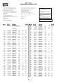
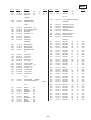
1
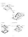
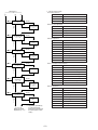
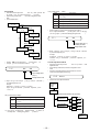
MZ-E33
SERVICE MANUAL
US Model
Canadian Model
AEP Model
E Model
Ver 1.1 1999. 01
US and foreign patents licensed from Dolby
Laboratories Licensing Corporation.
Model Name Using Similar Mechanism
MZ-E55
MD Mechanism Type
MT-MZE55-150
Optical Pick-up Mechanism Type
ODX-1A/1B
SPECIFICATIONS
System
Audio playing system
MiniDisc digital audio system
Laser diode properties
Material : GaAlAs
Wavelength : λ =790 nm
Emission duration : continuous
Laser output : less than 44.6 µW*
* This output is the value measured at a distance of 200 mm from the
objective lens surface on the optical pick-up block with 7 mm aperture.
Revolutions
400 rpm to 900 rpm (CLV)
Error correction
Advanced Cross Interleave Reed Solomon Code (ACIRC)
Sampling frequency
44.1kHz
Coding
Adaptive TRansform Acoustic Coding (ATRAC)
Modulation system
EFM (Eight to Fourteen Modulation)
Number of channels
2 stereo channels
1 monaural channel
Frequency response
20 to 20,000 Hz ± 3 dB
Wow and Flutter
Below measurable limit
Outputs
Headphones : stereo mini-jack, maximum output level 5mW+5mW,
load impedance 16 ohm
General
Power requirements
One LR6 (size AA) alkaline battery (not supplied)
Ni-MH rechargeable battery NH-9WM/NH-14WM
(not supplied)
R-6 sized Ni-MH rechargeable battery NH-MDAA (supplied)
Sony AC Power Adaptor AC-MZR55 (supplied) connected at the
DC IN 3V jack
Battery operation time
Batteries
Playback
LR6 (SG) (size AA)
Approx. 9.5 hours
Sony alkaline battery
R-6 sized Ni-MH
Approx. 8 hours
rechargeable battery
NH-MDAA
Chewing gum type
Approx. 7 hours
Ni-MH rechargeable
battery NH-14WM
Chewing gum type
Approx. 6.5 hours
Ni-MH rechargeable
battery NH-9WM (N)
Dimensions
Approx. 80 × 17.3 × 92 mm (w/h/d)
(3 1/4 × 11/16 × 3 5/8 in.)
not including projecting parts and controls
– Continued on next page –
PORTABLE MINIDISC PLAYER
MICROFILM
Mass
TABLE OF CONTENTS
Approx. 113 g (4.0 oz.) the player only
Approx. 155 g (5.5 oz.) incl. a premastered MD and a Sony
alkaline LR6 (SG) battery
Supplied accessories
AC power adaptor AC-MZR55 (1)
R-6 sized Ni-MH rechargeable battery NH-MDAA (1)
Rechargeable battery carrying case (1)
Headphones with a remote control
MDR-A34SP + RM-MZE33 (1) (US model)
MDR-E805SP + RM-MZE33 (1) (Canadian, AEP, E model)
MDR-E838SP + RM-MZE33 (1) (Hong Kong model)
Carrying pouch (1)
1. SERVICING NOTE ....................................................... 3
2. GENERAL ....................................................................... 4
3. DISASSEMBLY
3-1. Bottom Panel Assy .............................................................. 5
3-2. Upper Panel Assy ................................................................ 5
3-3. Main Board ......................................................................... 6
3-4. MD Assy ............................................................................. 6
3-5. OP Service Assy .................................................................. 6
Design and specifications are subject to change without notice.
4. TEST MODE ................................................................... 7
5. ELECTRICAL ADJUSTMENTS ............................ 11
6. DIAGRAMS
6-1. IC Pin Description ............................................................. 13
6-2. Block Diagram .................................................................. 15
6-3. Printed Wiring Board ........................................................ 18
6-4. Schematic Diagram ........................................................... 21
This MiniDisc player is classified as a CLASS 1 LASER
product.
The CLASS 1 LASER
PRODUCT label is located on
the bottom exterior.
7. EXPLODED VIEWS
7-1. Panel Section ..................................................................... 29
7-2. Main Board Section .......................................................... 30
7-3. Mechanism Deck Section .................................................. 31
IN NO EVENT SHALL SELLER BE
LIABLE FOR ANY DIRECT,
INCIDENTAL OR CONSEQUENTIAL
DAMAGES OF ANY NATURE, OR
LOSSES OR EXPENSES RESULTING
FROM ANY DEFECTIVE PRODUCT
OR THE USE OF ANY PRODUCT.
8. ELECTRICAL PARTS LIST .................................... 32
“MD WALKMAN” is a trademark of Sony
Corporation.
CAUTION
Use of controls or adjustments or performance of procedures
other than those specified herein may result in hazardous
radiation exposure.
Flexible Circuit Board Repairing
• Keep the temperature of the soldering iron around 270°C during
repairing.
• Do not touch the soldering iron on the same conductor of the
circuit board (within 3 times).
• Be careful not to apply force on the conductor when soldering
or unsoldering.
Notes on chip component replacement
• Never reuse a disconnected chip component.
• Notice that the minus side of a tantalum capacitor may be damaged by heat.
ATTENTION AU COMPOSANT AYANT RAPPORT
À LA SÉCURITÉ!!
SAFETY-RELATED COMPONENT WARNING!!
COMPONENTS IDENTIFIED BY MARK ! OR DOTTED LINE
WITH MARK ! ON THE SCHEMATIC DIAGRAMS AND IN
THE PARTS LIST ARE CRITICAL TO SAFE OPERATION.
REPLACE THESE COMPONENTS WITH SONY PARTS WHOSE
PART NUMBERS APPEAR AS SHOWN IN THIS MANUAL OR
IN SUPPLEMENTS PUBLISHED BY SONY.
LES COMPOSANTS IDENTIFIÉS PAR UNE MARQUE ! SUR LES
DIAGRAMMES SCHÉMATIQUES ET LA LISTE DES PIÈCES SONT
CRITIQUES POUR LA SÉCURITÉ DE FONCTIONNEMENT. NE
REMPLACER CES COMPOSANTS QUE PAR DES PIÈCES SONY
DONT LES NUMÉROS SONT DONNÉS DANS CE MANUEL OU
DANS LES SUPPLÉMENTS PUBLIÉS PAR SONY.
–2–
SECTION 1
SERVICING NOTE
1. When repairing this de
vice with the po wer on, if you remo ve the main boar d, this de vice stops w orking.
In this case , you w ork without the de vice stopping b y fastening the hook of the DOOR OPEN/CLOSE s
witc h (S801) with tape
.
S801
2. The electrical components diff
er accor ding to the ver sion of the system contr
ol IC (IC801). When replacing the IC801,
chec k its model
name and ad d or remo ve D1001 and/or R1001 as sho
wn belo w. For detailed inf ormation, see the Printed Wiring Boar d on pa ge 18 and
the Schematic Diagram on page 21.
RU6815MF-0004 (V er. 3.0) .... Add D1001 and R1001
RU6815MF-0005 (V er. 3.2) and later .... Remo ve D1001 and R1001
–3–
SECTION 2
GENERAL
–4–
This section is extracted
from instruction manual.
SECTION 3
DISASSEMBLY
• The equipment can be removed using the following procedure.
Bottom panel assy
Main board
Upper panel assy
Main board
MD assy
OP service assy
Note : Follow the disassembly procedure in the numerical order given.
3-1. BOTTOM PANEL ASSY
Note : When installing, fit the knobs and switches.
1 precision pan
screw (M1.4)
2 precision pan
screw (M1.4)
4 bottom panel assy
knobs
3 precision pan
screw (M1.4)
switches
3-2. UPPER PANEL ASSY
4 upper panel assy
3 precision pan
screw (M1.4)
2 precision pan
screw (M1.4)
1 button (OPEN)
–5–
3-3. MAIN BOARD
4 step screw
(MD)
3 precision pan
screw (M1.4)
2 precision pan
screw (M1.4)
5 toothed lock
screw
1 battery case lid
6
9 MAIN board
7 CN501
8 CN551
3-4. MD ASSY
3-5. OP SERVICE ASSY
1 claw
3 MD assy
3 main shaft
2 OP service assy
1 precision screw
2 claw
–6–
SECTION 4
TEST MODE
Configuration of Test Mode
The test mode has the configuration given belo
Display when test mode
is set
Setting the Test Mode
To enter the test mode
, two methods are a vailab le :
1. Entering method with key input.
Turn off the HOLD s witc h on the set. While holding do wn the
pke y on the set, press the f ollo wing remote commander ke
ys in
the following order :
+
n +
n =
n =
n +
n =
n +
n
=
n Pn P
2. Entering method by shorting the test point
Solder bridg e the test point TAP801 (TEST) on the main boar
d
(connect IC801 pin #™to GND), and turn on the PO WER.
VOL
+ key
Overall
adjustment
mode (Auto?)
p key
w.
” key
(Start ?)
p key
p key
VOL
– key
Adjustment ” key
mode
(Manu ?)
p key
Servo mode
0 0 0
+, – keys
Audio mode
1 0 0
+, – keys
Outline
• In this set, overall adjustment mode is made a
vailab le b y enter ing test mode to perform automatic adjustment of CD and MO.
In the overall adjustment mode, the disc is determined whether
it is CD or MO and adjustments are performed in sequence. If a
fault is f ound, the location of the fault is displa
yed. Also, in ser vo
mode,eachadjustmentcanbeautomaticallymade.
+, – keys
Servo mode
3 0 0
Displays of the LCD on the remote commander
are shown in parentheses.
R811
C807
R810
C806
TAP801
Test mode
Short : Test mode
Open : Normal mode
C805
TP911
Servo Mode
• Set the test mode , press the VOL – ke y and use the ”ke y to set
theser vomode .
• When the servo mode is set, use the
+
key and the =
key
to move the optical pick-up to the outer circumference and to
the inner cir cumf erence respectivel y.
• When entering another mode, refer to the configuration of test
mode.
1. Structure of Servo Mode
TP808
RB801
R808
TP819
Servo mode
0 0 0
IC801
Offset adjustment
0 1 0
+, – keys
p key
” key
Releasing the Test Mode
1. Whentestmodewasenteredwithke
yinput, turnoffthePO WER.
2. When test mode was entered b
y shor ting the test point, turn off
the PO WER and open the solder bridg
e of TAP801 (TEST
MODE) on the main board.
Operation of Setting on Test Mode
When the test mode is set, the LCD displays the following :
1
V1. 000
2
011 to 013
*1
” key
Laser power
adjustment
0 2 0
+, – keys
p key
p key
” key
p key
” key
021 to 024
*1
” key
3
(See page 8)
ROM version display
*1 Repeatedly press ” key
to change the mode.
(Refer to the following list
for a description of each
mode.)
LCD on remote commander
• The c yc le - the abo ve R OM ver sion displa y nAll lit nAll off
- is repeated.
(The ROM version is constantly displayed.)
• When the PLA Y MODE ke y is pressed and hold do
wn, the display at that time is held so that display can be checked.
–7–
2. Description of Each Mode
010 Offset adjustment
(See page 7.)
1
2
p key
3
MO adjustment
0 3 0
Mode
” key
Description
011
FE offset
012
TE offset
013
All servo ON
+, – keys
020 Laser power adjustment
p key
Low reflection
CD adjustment
0 4 0
CD adjustment
0 5 0
MO power E
023
CDL power
024
CD power
061 , 062
*1
071, 072,
073, 074
*1
p key
Description
031
MO FE balance
032
MO FE gain
033
MO ABCD gain
034
MO focus gain
035
MO tracking gain
036
MO RF gain
037
MO ADIP gain
038
MO focus bias E
039
CD focus bias A
Mode
” key
Description
041
Lower reflection CD FE balance
042
Lower reflection CD FE gain
043
Lower reflection CD ABCD gain
044
Lower reflection CD focus gain
045
Lower reflection CD tracking gain
046
Lower reflection CD RF offset
047
Lower reflection CD RF gain
048
Lower reflection CD focus bias
050 CD adjustment
” key
Mode
” key
p key
MO power A
022
040 Lower reflection CD adjustment
” key
” key
NV relation
0 9 0
+, – keys
051 to 058
*1
p key
+, – keys
p key
” key
” key
Automatic
adjustment
0 7 0
p key
021
Mode
041 to 048
*1
p key
Sled movement
0 6 0
Description
030 MO adjustment
” key
+, – keys
p key
” key
p key
+, – keys
p key
Mode
” key
+, – keys
p key
031 to 039
*1
091, 092,
093
*1
” key
*1 : Repeatedly press ” key
to change the mode.
Retern the Offset
(Refer to the following list
adjustment (0 1 0)
for a description of each
mode.)
–8–
Description
051
CD FE balance
052
CD FE gain
053
CD ABCD gain
054
CD focus gain
055
CD tracking gain
056
CD RF offset
057
CD RF gain
058
CD focus bias
060 Sled movement
Mode
Description
061
Sled in
062
Sled out 5
070 Automatic adjustment
Mode
Audio Mode
• Enter the test mode and press the
VOL – ke y.Then, press the ”
key and the VOL + ke y in this turn to enter audio mode
.
• When entering another mode
, ref er to the configuration of test
mode.
1. Structure of A udio Mode
• The mode No. 111 is f or S/N and cr osstalk. The mode No. 115
Description
071
Focus search
072
Access 32
073
ADER check
074
Tracking sensitivity adjust
Audio mode
1 0 0
p key
” key
Audio playback test
1 1 0
p key
090 NV relation
Mode
NV clear
092
Power OFF
093
Function code change
headphones
output
1kHz 0dB L/R
1 1 1
–12dB
” key
Description
091
” key
p key
Infinity Zero
1 1 2
–
” key
p key
1kHz 0dB L
1 1 3
–12dB
” key
p key
1kHz 0dB R
1 1 4
–12dB
” key
p key
1kHz –20dB L/R
1 1 5
p key
20Hz –20dB L/R
1 1 6
–20dB
” key
–20dB
” key
p key
20kHz –20dB L/R
1 1 7
–20dB
” key
p key 16kHz De-Emphasis
L/R
1 1 8
–20dB
” key
p key
100Hz 0dB L/R
1 1 9
–40dB
” key
is for distor tion factor and frequenc
y c haracteristics.
• When the VOL +/– ke ys is pressed in an
y mode , the v olume of
theheadphonesischanged(increased/decreased)inunitsofone
step. When the +
/=
ke ys is pressed, the v olume of the
headphonesismaximized/minimized.
• For the volume value, any changed value remains as it is basicall y.
However , when the v olume is s witc hed fr om 114 to 115 or 118
to 119, it returns the default v
alue .
–9–
Power Mode
• Enter the test mode and press the
VOL – ke y.Then, press the
key and the VOL – ke y in this turn to enter po
wer mode .
• When entering another mode
, ref er to the configuration of test
mode.
1. Power Mode Structure
Power mode
3 0 0
p key
Char ge status code (fir
”
1
” key
UNREG check
31 0
p key
+,– key
Description
Gum type battery not detected (AA battery available
or no battery)
2
Description Gum type battery detected
4
AC adaptor detected
5
Gum type battery not detected/AC adaptor detected
6
Gum type battery detected/AC adaptor detected
” key
• When in mode No. 321, the system automatically tries to detect
the A C adaptor and the batter
y. If char geab le,it star ts c har ging.
(No c har ge displa y and no LED flashing during this mode
.)
Power off
3 1 1
” key
p key
st digit)
Code
321
XX
” key
Voltage value (hex) *)
at battery terminal
Charge status code
” key
Charge test
3 2 0
p key
XX
* ) Batter y terminal v olta ge = Displa y volta ge v alue (he x) divided
by 256 and multiplied by 2.8
Example :
With displa y of A0 (he x), A0 (he x) = 160 (dec)
Terminal v olta ge = 160 divided b y 256 and m ultiplied b y 2.8
= 1.75 V
Charge start
3 2 1
• Press the Pke y to disconnect the po
wer in mode No.
• To displa y po wer inf ormation in mode No. 312.
312
XX
Supply DET
3 1 2
311.
Overall Adjustment Mode
• Enter the test mode and press the
VOL + ke y to enter o verall
adjustmentmode.
• When entering another mode, refer to the configuration of test
mode.
• When the overall adjustment mode is entered, the LCD on the
remote commander display the following :
XX
Input voltage value
(hex) *)
040
Charge status code
* ) Input v olta ge v alue = Displa y volta ge v alue (he x) divided b y
256 and multiplied by 9.016
Example :
With displa y of 50 (he x), 50 (he x) = 80 (dec)
Input v olta ge = 80 divided b y 256 and m ultiplied b y 9.016
= 2.8175 V
Auto?
1. Structure of Overall Adjustment Mode
Overall
adjustment
mode
Auto?
” key
Start ?
” key (to discriminate between CD and MO)
Char gestatuscode(seconddigit)
Code
0
Description
Unable to charge (No adaptor attached, or no power
CD automatic
adjustment
NG
if present)
8
Chargeable *1)
A
Servo system stopped/chargeable *1)
OK
MO automatic
adjustment
OK
NG
p key
p key
p key
p key
*1) Char geab le : AC adaptor attac hed and AA batter y a vailab le, or
AC adaptor attac hed and gum type batter
y a vailab le.
Adjustment
mode
Manu ?
– 10 –
SECTION 5
ELECTRICAL ADJUSTMENTS
Notes for Adjustment
• In this set, automatic adjustment of CD and MO can be per
formed by entering the test mode.
• Adjustments are performed in the overall adjustment mode. If
an item is determined as NG, the item is readjusted in servo
mode.
• In MO Automatic Adjustment Mode
-
Adjustment Method in Overall Adjustment Mode
1. Enter the test mode and press the
VOL + ke y to enter o verall
adjustmentmode.
2. Insert the test CD (TGYS-1) or SONY MO disk (recorded) commer ciall y a vailab le.
3. Press the ”ke y twice .The disc is determined whether it is CD
orMOandeac hadjustmentmodeisset.
Automaticadjustments
are perf ormed in the or der of the items listed belo
w.
• In CD Automatic Adjustment Mode
No.
Mode
1
061
Description
Sled in
2
071
Focus search
3
062
Sled out 5
4
051
CD FE balance
5
052
CD FE gain
6
051
CD FE balance
7
053
CD ABCD gain
8
054
CD focus gain
9
055
CD tracking gain
10
056
CD RF offset
11
057
CD RF gain
12
056
CD RF offset
13
058
CD Focus bias
– 11 –
No.
Mode
Description
1
061
Sled in
2
071
Focus search
3
062
Sled out
4
031
MO FE balance
5
032
MO FE gain
6
031
MO FE balance
7
033
MO ABCD gain
8
034
MO focus gain
9
035
MO tracking gain
10
036
MO RF gain
11
037
MO ADIP gain
12
039
MO focus bias A
13
073
ADER check
14
071
Focus search
15
031
MO FE balance
16
032
MO FE gain
17
031
MO FE balance
18
033
MO ABCD gain
19
034
MO focus gain
20
035
MO tracking gain
21
036
MO RF gain
22
037
MO ADIP gain
23
039
MO focus bias A
24
073
ADER check
25
061
Sled in
26
071
Focus search
27
041
Low reflection CD FE balance
28
042
Low reflection CD FE gain
29
041
Low reflection CD FE balance
30
043
Low reflection CD ABCD gain
31
044
Low reflection CD focus gain
32
045
Low reflection CD tracking gain
33
046
Low reflection CD RF offset
34
047
Low reflection CD RF gain
35
061
Sled in
36
071
Focus search
37
041
Low reflection CD FE balance
38
042
Low reflection CD FE gain
39
041
Low reflection CD FE balance
40
043
Low reflection CD ABCD gain
41
044
Low reflection CD focus gain
42
045
Low reflection CD tracking gain
43
046
Low reflection CD RF offset
44
047
Low reflection CD RF gain
* Remote commander display during automatic adjustment
057
Adjustment value (flashing)
Mode No. under adjustment
4. If result of automatic adjustment is OK, the following display
appears.
047
End-OK 5. If result of automatic adjustment is NG, the following display
appears.
051
NG
Error code
NG mode No.
* If NG, enter servo mode to perform automatic adjustment of the
item determined as NG.
Adjustment in Servo Mode Method
1. Wheneachadjustmentmodeissetaccordingtothestructureof
servo mode, the lower two digits of the mode No. and the adjustment value written in EEPROM are displayed and lit on the
LCD on the remote commander
.
052
Adjustment value (lit)
Mode No.
2. When the Pkey is pressed, the following display appears and
theautomaticadjustmentisperformed.
052
Adjustment value (flashing)
Note) Although the
VOL +/– ke ys can be used to c
hang e the
adjustment v alue to an y value , the y should not be used
whene verpossib le.
3. When the automatic adjustment is completed, the flashing adjustment value is lit.
052
Adjustment value (lit)
– 12 –
SECTION 6
DIAGRAMS
6-1. IC PIN DESCRIPTION
• IC801 RU6815MF-0004 (SYSTEM CONTROL)
Pin No.
Pin Name
I/O
Pin Description
1
HIDC MON
I
HIDC voltage monitor input.
2
UREG MON
I
Unreg voltage monitor input.
3
CHG MON
I
CHG voltage monitor input.
4
VREF
I
Reference voltage for power supply voltage adjustlment.
5
PLAY KEY
I
Set PLAY key input.
6
OPEN CLS SW
I
DOOR OPEN/CLOSE switch input.
7
RMC KEY
I
Remote commander key input.
8
SET KEY
I
Set key input.
9
XRESET
I
10
AVDD
—
A/D converter power supply (+2.8V).
11
AVSS
—
A/D converter Ground.
12
TYPE 0
I
Model discrimination terminal (Fixed at “L” ).
13
TYPE 1
I
Model discrimination terminal (Fixed at “H” ).
14
TYPE 2
I
Model discrimination terminal (Fixed at “L” ).
L : Close
Systen reset input (At reset : “L” ).
15
TYPE 3
I
Model discrimination terminal (Fixed at “L” ).
16
HOLD SW
I
Set HOLD switch input.
17
VREG CON
18
19
20
O
2.5V voltage on/off switch (Sub terminal) (not used).
—
Not used (Open).
—
Not used (Open).
MCK
I
—
Not used (Open).
22
VDD
—
Digital power supply (+2.8V).
23
VSS
21
24
Master clock input.
—
Digital Ground.
—
Not used (Open).
25
VSS
—
26
AVLS SW
I
Digital Ground.
27
DSP SINT
I
Interrupt input from DSP.
28
DBB 0
I
DIGITAL MEGABASS switch input (MID).
Set AVLS switch input.
29
DBB 1
I
DIGITAL MEGABASS switch input (MAX).
30
OPR LED
O
LED drive output.
31
XWK CLR
O
Power IC wakeup factor latch clear output and motor driver IC control signal outpt.
32
ADJUST
I
“Normally” Test mode select input (“L” : Test mode)
33
SLEEP
O
Power supply circuit OFF signal output.
34
SBUS CLK
O
SBB serial clock output.
35
SBUS DATA
O
SBB serial data output.
—
Not used (Open).
36
37
SLD 1 MON
I
Sled servo timing signal input.
38
SLD 2 MON
I
Sled servo timing signal input.
39
CLV VCON
O
Spindle servo drive voltage control output.
40
APC REF
O
Laser power control output.
41
V28-CON
O
Power voltage (+2.8V) correction control output.
42
CLV U MON
I
Spindle servo timing signal input.
43
CLV V MON
I
Spindle servo timing signal input.
44
CLV W MON
I
Spindle servo timing signal input.
45
CLV U CON
O
Spindle servo drive signal output.
46
CLV V CON
O
Spindle servo drive signal output.
47
CLV W CON
O
Spindle servo drive signal output.
– 13 –
Pin No.
Pin Name
I/O
Pin Description
48
CHG CONT
O
CHG control signal output.
49
CHG PWR
O
CHG power supply voltage control signal output.
50
VDD
—
Digital power supply (+2.8V).
51
VPP
—
Power for on board light.
52
VSS
—
Digital ground.
53
SLD 1R CON
O
Sled motor control signal output.
54
SLD 1F CON
O
Sled motor control signal output.
55
SLD 2R CON
O
Sled motor control signal output.
56
SLD 2F CON
O
Sled motor control signal output.
57
NIMH DET
I
NIMH detect signal input.
58
XDC IN
I
Power supply voltage input sense signal input.
59
GUM DET
I
Battery detect signal input.
60
—
Not used (Open).
61
SPCK
O
Serial clock output for Remote control communication. Not used (Open).
62
RMC DTCLK
I/O
Serial data input/output for Remote control communication.
—
Not used (Open).
63 – 66
67
SLD VCON
O
Sled servo outer voltage control output.
68
SLD PWR-UP
O
Baypass transistor control output for sled drive power supply.
69
HP MUTE
O
Headphone amplifier mute output.
70
HP STBY
O
Headphone amplifier standby output.
71
RMC SEL
O
TSB/SSB selection signal output to remote commander terminal. Not used (Open).
72
NV D0
O
Serial data signal output for NVRAM.
73
NV D1
I
Serial data signal input from NVRAM.
74
NV CLK
O
Serial clock signal output for NVRAM.
75
NV CS1
O
Chip select signal output for NVRAM.
76
VDD
—
Digital power supply (+2.8V).
77 – 79
LCD VL2 – 0
I
80
VSS
—
Digital ground.
81 – 87
LCD drive level power supply (Connected ground).
—
Not used (Open).
88 – 96
LCD SEG0 – 8
—
LCD Segment terminal. Not used (Open).
97 – 100
LCD COM0 – 3
—
LCD common terminal. Not used (Open).
– 14 –
MZ-E33
6-2. BLOCK DIAGRAM
– 15 –
– 16 –
– 17 –
MZ-E33
6-3. PRINTED WIRING BOARD
• Semiconductor
Location
Ref. No.
D351
D352
D801
D841
D901
D902
D903
D905
D1001
Location
H-11
H-11
D-16
F-8
F-5
H-14
H-4
H-3
H-16
IC301
IC302
IC501
IC551
IC552
IC601
IC603
IC801
IC802
IC901
IC902
IC903
F-7
E-8
B-13
G-14
H-12
C-15
B-16
F-16
C-16
F-15
G-17
G-4
Q501
Q551
Q552
Q901
Q902
Q903
Q905
Q906
C-13
F-14
F-13
F-3
G-16
H-16
G-3
F-17
Note:
• X : parts extracted from the component side.
• Y : parts extracted from the conductor side.
r
•
: Through hole.
• b : Pattern from the side which enables seeing.
(The other layer’s patterns are not indicated.)
Caution:
Pattern face side:
(Side B)
Parts face side:
(Side A)
Parts on the pattern face side seen from the
pattern face are indicated.
Parts on the parts face side seen from the
parts face are indicated.
* : The electrical components differ according to the version of the
system control IC (IC801). When replacing the IC801, check its
model name and add or remove D1001 and/or R1001 as shown
below.
RU6815MF-0004 (Ver 3.0) .... Add D1001 and R1001
RU6815MF-0005 (Ver 3.2) and later .... Remove D1001 and R1001
• R1001 mounting position
R1001
M901
SPINDLE
MOTOR
– 18 –
– 19 –
– 20 –
MZ-E33
6-4. SCHEMATIC DIAGRAM • Refer to page 25 for IC Block Diagrams.
• Waveforms
(MODE:PLAY)
1
* : The electrical components differ according to the version of the
system control IC (IC801). When replacing the IC801, check its
model name and add or remove D1001 and/or R1001 as shown
below.
RU6815MF-0004 (Ver 3.0) .... Add D1001 and R1001
RU6815MF-0005 (Ver 3.2) and later .... Remove D1001 and R1001
800mVp-p
VOLT/DIV : 200mV AC
IC501 @• TIME/DIV : 5 µsec
2
2.7Vp-p
23 µsec
VOLT/DIV : 1V AC
IC601 #ª TIME/DIV : 10 µsec
3
2.6Vp-p
482nsec
VOLT/DIV : 500mV AC
IC601 $¡ TIME/DIV : 200nsec
4
2.0 Vp-p
16.9344 MHz
VOLT/DIV : 500mV AC
IC601 $ª TIME/DIV : 20nsec
Note:
• All capacitors are in µF unless otherwise noted. pF: µµF
50 WV or less are not indicated except for electrolytics
and tantalums.
• All resistors are in Ω and 1/4 W or less unless otherwise
specified.
Note: The components identified by mark ! or dotted line
with mark ! are critical for safety.
Replace only with part number specified.
• A : B+ Line.
• Power voltage is dc 3 V and fed with regulated dc power
supply from battery terminal.
• Voltage and waveforms are dc with respect to ground
under no-signal conditions.
no mark : MD PLAY
• Voltages are taken with a VOM (Input impedance 10 MΩ).
Voltage variations may be noted due to normal production tolerances.
• Waveforms are taken with a oscilloscope.
Voltage variations may be noted due to normal production tolerances.
• Signal path.
J : MD
– 21 –
– 22 –
– 23 –
– 24 –
• IC Block Diagrams
IC552 TLC372CPWR
IC301 BA3577FS-E2
8
17 +B
6
DI
3
FO1
VM1
RO1
GND
H13
FO3
VM3
RO3
GND
H34
FO4
VM4
RO4
GND
H4
VC
49
48
47
46
45
44
43
42
41
40
39
38
37
R/W AMPS
AND
AUTO ERASE
EEPROM
2048bit
128 X 16
6 NC
DATA
REGISTER
PRE DRIVER
HI–BRIDGE
CONTROL
HI–BRIDGE
CONTROL
HI–BRIDGE
CONTROL
F12 55
R12 56
F11 57
5 GND
8
1ntOE
BEEP
1ntSTB
11 BEEP IN
IC901 MPC1830ADTBEL
VC
RESET
OSC2
19 VCON
PWM
DRIVER
VG
66 DRA8
65 DRA10
VG
IC903 RN5RG20AA-TL
3 OUT
1
2
3
4
5
6
7
8
9
PRE
DRIVER
10
11
12
13
14
15
16
17
18
WO
57 DRD3
56 VSS
IC 6
I-V
EXCHANGE
RF
ABCD
FE
ADIP
TE
REFNV
VJ 7
VI 8
35
HIV
34
HIW
33
P11
32
P12
31
VPS2
30
PO2
29
GND
PS
DVDD 15
28
PO1
SBUS 16
SCK 17
XREST 18
27
VPS1
26
GND
3P2
25
HOW
24
VD2
23
HOV
22
GND
3PI
21
HOU
20
VD
19
IN
PD NI
PD I
PD O
LD DRV
LD EMIT
LD VDD
9
10
11
12
13
14
ADIP
BPF
T-COUNT
REMOTE
CONTROL
DFCT
DGND 19
POWER
VREF OUT
A GND
A VCC
A GND
MCK
X0
X1
MCK I-O
VSS
MCK/2
PMCK
DOUT
VSS
BCK
AUDATA
LRCK
EMP
VDD
NC
NC
XBUSY
SINT
SCK
SBUS
RESET
VDD
MC
NC
NC
1 GND
CE 5
– 27 –
27 AGND
25 BPFC1
24 BPFC2
23 ADIP
–
– 26 –
32 S MONIT
26 REXT
V REF
– 25 –
SIGNAL
MONITOR
APC
+
26 27 28 29 30 31 32 33 34 35 36 37 38 39 40 41 42 43 44 45 46 47 48 49 50
33 AVCC
POWER
2 VDD
CLOCK
GENERATOR
POWER
30 OFC C1
29 EQ
28 RFOUT
EXT 4
51 VDD
35 AGND
34 TE
RF BUFFER/
EF EQ
53 DRD1
52 DRD0
CK176 25
POWER
FOCUS
-ERROR
VC
VO
59 XCAS
58 DRD2
I-V
EXCHANGE
36 ABCD
STEP–UP
PRE DRIVER
63 XRAS
62 DRA9
61 XOE2
60 XOE
ABCD
ADDITION
VG
STEP UP/DOWN
PRE DRIVER
POWER SW
PRE DRIVER
64 DRA11
55 XWE2
54 XWE
XBUSY
ATRAC
DECODER
20 D0
UO
8
16
XATWE
DREQ
SAW
DI 72
LI
FROUT 23
FFOUT 24
ATDT
10
VG 18
DO or DI
SLEEP UP/DOWN
/POWER SW
DECODER
GND
DCC1
SSB CONTROL
MONITOR I/O etc.
8
21 D1
VG 70
PWM 71
GND
DCC1
NC 20
TFOUT 21
TROUT 22
RD DT ECC
MODE
SELECT
IF 5
37 FE
22 T-COUNT
21 DFCT
VG
LI
WR REQ etc.
8 8
5
CHARGE
PUMP
C1H 16
C2H 17
VC
VD
8
12
22 PWM1
VG
L2L
SBW
SBR
SBA
SBD
8
16
EFM DATA A/B
ECC DATA
EBA
67 DRA7
PWM1
VG
23 SW
C2L 13
C1L 14
VB 15
VC 68
GND 69
GND
DCC2
S DATA
AC DATA
68 DRA6
24 PGND
L2H
AC
WDCK
8
NC 16
NC 17
NC 18
NC 19
SECTOR
DECODER
69 DRA5
OSC1
STEP-UP
DC / DC
CONVERTER
VC
VB2
AC BYCK
OFTRK 13
VSS 14
NC 15
25 VBH
SPCK
BUFF
IB 4
I-V
EXCHANGE
HIU
VG
27 VB2
26 VB1
VB SELECT
SPCK0 11
SPCK1 12
VC
VB
AC LRCK
AC WDCK
EFM ACIRC
DECODER
70 DRA4
CLPF 67
VB
9
VSS ADC 10
T-COUNT 11
DEFECT 12
28 CLK
VB1
EFM
PLCK
FLAG
71 DRA0
RGND 66
VB1
4
72 DRA1
DRAM & PERIPHERAL CONTROL ADDRESS GENERATOR
7
3
73 DRA2
SUBQ/ADIP
DECODER
DSSP
TE
VRT 8
VRB
75 VDD
74 DRA3
FE
ABCD
TE 6
ADIP
EFM
PLL
2nd MSB
FE 4
ABCD 5
RF
ADC
VREF 2
RF 3
VREG
65
CONT
VC
PRE DRIVER
7
9
VC
29 VBSEL
VC 10
SQREQ
VDD ADC 1
VBMON
VREG 64
31 FFCLR
30 SLEEP
XRST 8
ADIP
PLL
32 XWK4
REN
3 PHASE CONTROL
CRST
SYSTEM
CONTROL
1ntSTB
VC
DO
MI0
MI1
MI2
MI3
VSS
MICK
MOCK
MO0
MO1
MO2
MO3
VDD
PLCK
EFM
ADPLCK
ADIP–DATA
FON
FOK
ID3
ID2
DTC 6
ID1
100 99 98 97 96 95 94 93 92 91 90 89 86 87 86 85 84 83 82 81 80 79 78 77 76
ID0
33 XWK3
INM 4
RF 5
ADIP
35 XWK1
34 XWK2
BAND GAP
REFERENCE
VREF 3
TEST
CRCF
ERFLAG
IC601 µPD63731GC-9EU
I-V
EXCHANGE
36
VG
PRE
DRIVER
36 VSTB
VC
PWM
DRIVER
GND 1
VRMC 2
VC
BIAS
CONTROL
VC
MUTE T 10
VD
MUTE
ID 3
38 VREF OUT
31 OFC C2
OE 63
9
I-V
EXCHANGE
F13 60
R14 61
F14 62
ROE
MUTE
IA 2
POWER
EF BLANCE/
TRACKING-ERROR
ADIP
R11 58
R13 59
4
I-V
EXCHANGE
PRE DRIVER
VC
PRE DRIVER
HI–BRIDGE
CONTROL
IE 1
VG
VG
PRE DRIVER
7 NC
DECODER
VG
VG
ADD
BUFFERS
INSTRUCTION
REGISTER
12 NF2
DO
PWSTB T
50
VC
2
V–
4
3
2
13 OUT2
7
51
VC
1
INSTRUCTION
DECODE
CONTROL
AND
CLOCK
GENERATION
PWSTB
PWSTB
52
VC
SK
15 OUT1
14 GND
V IN2
53
VC
4
5
54
VC
V IN1
8 VCC
VPP
SW
16 NF1
BIAS OUT
VPP
GENERATOR
VREF
1
GND
H12
CS
RO2
18 VCC
+B
3
IC501 SN761054
VC
BIAS IN
VCC
VM2
2
FO2
RF OUT
R/F
IC551 MPC17A55FTA
GND
H2
1
IC802 AK93C55AV-L
5
6
7
V+
VC
RF IN
20 NC
19 NC
– 28 –
MIRROR
OFTRK
20 OFTRK
SECTION 7
EXPLODED VIEWS
• -XX and -X mean standardized parts, so
they may have some difference from the
original one.
• Color Indication of Appearance Parts
Example :
KNOB, BALANCE (WHITE) ... (RED)
• Accessories and packing materials are
given in the last of this parts list.
The components identified by
mark ! or dotted line with mark.
! are critical for safety.
Replace only with part number
specified.
N
N
NOTE:
• The mechanical parts with no reference
number in the exploded views are not supplied.
• Items marked “*” are not stocked since
they are seldom required for routine service.
Some delay should be anticipated
when ordering these items.
• Abbreviation
CND : Canadian model
HK : Hong Kong model
Parts Color Cabinet’s Color
Les composants identifiés par une
marque ! sont critiques pour
la sécurité.
Ne les remplacer que par une piéce
portant le numéro spécifié.
7-1. PANEL SECTION
6
1
6
6
3
6
2
4
5
6
Ref. No.
Part No.
Description
1
1
1
X-4950-595-1
X-4950-596-1
X-4950-597-1
PANELSUBASSY
PANELSUBASSY
PANELSUBASSY
1
2
X-4951-429-1
X-4950-598-1
2
2
2
3
4
Remark
Ref. No.
Part No.
Description
KNOB(DIGIT ALMEGAB ASS,A VLS)(BLA CK)
5
3-939-835-01
5
5
3-939-835-21
3-939-835-31
PANELSUBASSY
PANELSUBASSY
,UPPER(B)(BLA CK)(US)
,UPPER(N)(GOLD)
,UPPER(L)(BLUE)
(AEP ,E,HK)
,UPPER(Y)(YELLO W)(AEP)
,LO WER(B)(BLA CK)(US)
5
3-939-835-41
X-4950-599-1
X-4950-600-1
PANELSUBASSY
PANELSUBASSY
,LO WER(N)(GOLD)
,LO WER(L)(BLUE)
6
4-963-883-21
X-4951-430-1
3-010-287-01
4-986-349-01
PANELSUBASSY ,LO WER(Y)(YELLO
COLLAR(DCIN3V)
SPACER
6
4-963-883-32
(AEP ,E,HK)
W)(AEP)
– 29 –
Remark
(US)
KNOB(DIGIT ALMEGAB ASS,A VLS)(GOLD)
KNOB(DIGIT ALMEGAB ASS,A VLS)(BLUE)
(AEP ,E,HK)
KNOB(DIGIT ALMEGAB ASS,A VLS)(YELLO W)
(AEP)
SCREW (M1.4), PRECISION P AN (f or GOLD ,
BLUE,YELLOW)
SCREW (M1.4), PRECISION P AN (f or BLA CK)
(US)
7-2. MAIN BOARD SECTION
MT-MZE55-150
53
52
51
68
54
69
55
70
57
58
56
53
59
67
60
60
66
62
65
63
66
61
60
Ref. No.
Part No.
Description
51
52
52
52
4-212-361-02
X-4950-429-1
X-4950-503-1
X-4950-504-1
BUTTON(OPEN)
STRIPASSY(B),
STRIPASSY(N),
STRIPASSY(L),
52
X-4951-428-1
STRIPASSY(Y),
Remark
ORNAMENT AL(BLA CK)(US)
ORNAMENT AL(GOLD)
ORNAMENT AL(BLUE)
(AEP ,E,HK)
ORNAMENT AL(YELLO W)
(AEP)
53
54
* 55
56
56
4-982-418-01
X-4950-350-1
4-212-363-01
4-212-364-02
4-212-364-12
DAMPER
BRACKET(A)ASSY
BRACKET(C)
LID ,BATTER YCASE(BLA CK)(US)
LID,BATTER YCASE(GOLD)
56
56
4-212-364-22
4-212-364-31
LID ,BATTER YCASE(BLUE)(AEP
,E,HK)
LID ,BATTER YCASE(YELLO W)(AEP)
Ref. No.
64
Part No.
Description
57
58
59
60
61
X-4950-351-1
X-4950-354-1
4-212-366-01
4-963-883-21
4-994-886-01
BRACKET(B)ASSY
TERMINALASSY ,BATTER Y
CASE, BATTER Y
SCREW(M1.4), PRECISIONP AN
SCREW(MD),STEP
62
63
64
65
66
4-214-232-01
4-212-369-01
4-212-367-01
A-3323-069-A
3-335-797-01
SPRING(B ATTER Y), COMPRESSION
TERMINALPLA TE(PLUS)
HOLDER(TERMINALPLA
TE)
MAINBOARD,COMPLETE
SCREW(M1.4X2),TOOTHEDLOCK
67
68
69
70
3-315-454-01
4-217-658-01
4-216-847-01
4-218-050-01
SPACER(E)
SPACER(K)
SPACER(B ATT)
SPACER(B)
– 30 –
Remark
7-3. MECHANISM DECK SECTION
(MT-MZE55-150)
115
101
105
105
R1001
102
105
M902
106
104
103
M901
111
101
107
109
108
113
110
112
114
The components identified by
mark ! or dotted line with mark.
! are critical for safety.
Replace only with part number
specified.
Ref. No.
Part No.
Description
101
102
103
! 104
105
4-963-883-61
4-982-561-11
4-214-478-01
X-4949-164-1
4-963-883-21
SCREW(M1.4), PRECISIONP AN
SPRING,RACK
SHAFT ,MAIN
SER VICEASSY ,OP
SCREW(M1.4), PRECISIONP AN
106
107
108
109
1-670-707-11
4-965-893-01
4-982-555-01
4-212-899-01
CLVFLEXIBLEBO ARD
WASHER, GEAR(A)ST OPPER
GEAR(A)
SPRING,THRUST
Remark
Ref. No.
Les composants identifiés par une
marque ! sont critiques pour la
sécurité.
Ne les remplacer que par une piéce
portant le numéro spécifié.
Part No.
Description
110
111
112
113
114
3-349-825-82
X-4948-793-1
X-4950-414-3
4-986-811-01
4-212-896-04
SCREW ,PRECISION
REEDASSY
CHASSISASSY
SPRING(EJECT),TENSION
HOLDER
115
M901
M902
R1001
4-214-207-01
8-835-594-01
1-698-764-21
1-216-789-11
SHEET(OP)
MOTOR,DCSSM-01C03A/J-S(SPINDLE)
MOTOR,SLED(INCLUDINGGEAR)
MET ALCHIP
2.2
5%
– 31 –
Remark
1/16W
SECTION 8
ELECTRICAL PARTS LIST
MAIN
NOTE:
• Due to standardization, replacements in
the parts list may be different from the
parts specified in the diagrams or the
components used on the set.
• -XX and -X mean standardized parts, so
they may have some difference from the
original one.
• RESISTORS
All resistors are in ohms.
METAL:Metal-film resistor.
METAL OXIDE: Metal oxide-film resistor.
F:nonflammable
• Abbreviation
CND : Canadian model
HK : Hong Kong model
Ref. No.
• Items marked “*” are not stocked since
they are seldom required for routine service.
Some delay should be anticipated
when ordering these items.
• SEMICONDUCTORS
In each case, u : µ, for example:
uA.. : µA.. uPA.. : µPA..
uPB.. : µPB.. uPC.. : µPC.. uPD.. : µPD..
• CAPACITORS
uF : µF
• COILS
uH : µH
Part No.
Description
A-3323-069-A
MAINBOARD,COMPLETE
*********************
C101
C102
C103
C201
C202
1-135-181-21
1-125-899-11
1-115-156-11
1-135-181-21
1-125-899-11
TANT ALUMCHIP
TANT AL. CHIP
CERAMICCHIP
TANT ALUMCHIP
TANT AL. CHIP
4.7uF
220uF
1uF
4.7uF
220uF
20%
20%
20%
20%
6.3V
4V
10V
6.3V
4V
C203
C301
C302
C303
C304
1-115-156-11
1-117-919-11
1-119-750-11
1-109-982-11
1-127-690-21
CERAMICCHIP
TANT AL. CHIP
TANT AL. CHIP
CERAMICCHIP
TANT AL. CHIP
1uF
10uF
22uF
1uF
3.3uF
20%
20%
10%
20%
10V
6.3V
6.3V
10V
6.3V
C305
C306
C307
C308
C311
1-109-982-11
1-109-982-11
1-135-149-21
1-115-156-11
1-127-688-21
CERAMICCHIP
CERAMICCHIP
TANT ALUMCHIP
CERAMICCHIP
TANT AL. CHIP
1uF
1uF
2.2uF
1uF
10uF
10%
10%
20%
C312
C313
C314
C315
C501
1-127-688-21
1-115-156-11
1-119-750-11
1-164-156-11
1-107-826-11
TANT AL. CHIP
CERAMICCHIP
TANT AL. CHIP
CERAMICCHIP
CERAMICCHIP
10uF
1uF
22uF
0.1uF
0.1uF
20%
C502
C503
C504
C505
C506
1-117-720-11
1-164-227-11
1-162-962-11
1-164-156-11
1-162-970-11
CERAMICCHIP
CERAMICCHIP
CERAMICCHIP
CERAMICCHIP
CERAMICCHIP
4.7uF
0.022uF
470PF
0.1uF
0.01uF
C508
C509
C510
C511
C551
1-164-227-11
1-164-156-11
1-164-156-11
1-107-826-11
1-162-964-11
CERAMICCHIP
CERAMICCHIP
CERAMICCHIP
CERAMICCHIP
CERAMICCHIP
0.022uF
0.1uF
0.1uF
0.1uF
0.001uF
10%
10%
25V
25V
25V
16V
50V
C552
C553
C554
C555
C556
1-162-964-11
1-127-689-21
1-127-689-21
1-127-691-21
1-127-691-21
CERAMICCHIP
TANT AL. CHIP
TANT AL. CHIP
TANT AL. CHIP
TANT AL. CHIP
0.001uF
6.8uF
6.8uF
3.3uF
3.3uF
10%
20%
20%
20%
20%
50V
10V
10V
16V
16V
C557
C558
C559
C560
C561
1-117-720-11
1-117-720-11
1-115-566-11
1-115-566-11
1-115-566-11
CERAMICCHIP
CERAMICCHIP
CERAMICCHIP
CERAMICCHIP
CERAMICCHIP
4.7uF
4.7uF
4.7uF
4.7uF
4.7uF
10%
10%
10%
10V
10V
10V
10V
10V
20%
20%
10%
10%
10%
10%
10%
10V
10V
10V
10V
6.3V
6.3V
10V
6.3V
25V
16V
10V
25V
50V
25V
25V
Les composants identifiés par une
marque ! sont critiques pour
la sécurité.
Ne les remplacer que par une piéce
portant le numéro spécifié.
When indicating parts by reference
number, please include the board.
Remark
<CAP ACIT OR>
The components identified by
mark ! or dotted line with mark.
! are critical for safety.
Replace only with part number
specified.
Ref. No.
Part No.
Description
C562
C563
C564
C565
C568
1-109-982-11
1-117-720-11
1-117-232-11
1-117-919-11
1-117-370-11
CERAMICCHIP
CERAMICCHIP
TANT ALUM
TANT AL. CHIP
CERAMICCHIP
1uF
4.7uF
22uF
10uF
10uF
C569
C601
C602
C603
C604
1-117-370-11
1-164-156-11
1-162-970-11
1-162-970-11
1-162-970-11
CERAMICCHIP
CERAMICCHIP
CERAMICCHIP
CERAMICCHIP
CERAMICCHIP
10uF
0.1uF
0.01uF
0.01uF
0.01uF
C605
C607
C608
C609
C612
1-117-720-11
1-164-156-11
1-164-156-11
1-164-156-11
1-107-826-11
CERAMICCHIP
CERAMICCHIP
CERAMICCHIP
CERAMICCHIP
CERAMICCHIP
4.7uF
0.1uF
0.1uF
0.1uF
0.1uF
C801
C803
C804
C805
C806
1-162-962-11
1-162-970-11
1-162-964-11
1-164-156-11
1-164-227-11
CERAMICCHIP
CERAMICCHIP
CERAMICCHIP
CERAMICCHIP
CERAMICCHIP
470PF
0.01uF
0.001uF
0.1uF
0.022uF
10%
10%
10%
C807
C808
C809
C810
C832
1-164-227-11
1-164-156-11
1-164-156-11
1-107-826-11
1-162-964-11
CERAMICCHIP
CERAMICCHIP
CERAMICCHIP
CERAMICCHIP
CERAMICCHIP
0.022uF
0.1uF
0.1uF
0.1uF
0.001uF
10%
C833
C834
C901
C902
C903
1-162-964-11
1-164-156-11
1-162-964-11
1-162-970-11
1-107-826-11
CERAMICCHIP
CERAMICCHIP
CERAMICCHIP
CERAMICCHIP
CERAMICCHIP
0.001uF
0.1uF
0.001uF
0.01uF
0.1uF
10%
10%
10%
50V
25V
50V
25V
16V
C904
C905
C906
C907
C908
1-109-982-11
1-162-964-11
1-107-826-11
1-107-826-11
1-109-982-11
CERAMICCHIP
CERAMICCHIP
CERAMICCHIP
CERAMICCHIP
CERAMICCHIP
1uF
0.001uF
0.1uF
0.1uF
1uF
10%
10%
10%
10%
10%
10V
50V
16V
16V
10V
C909
C910
C911
C914
C915
1-107-826-11
1-162-970-11
1-127-688-21
1-125-899-11
1-162-970-11
CERAMICCHIP
CERAMICCHIP
TANT AL. CHIP
TANT AL. CHIP
CERAMICCHIP
0.1uF
0.01uF
10uF
220uF
0.01uF
10%
10%
20%
20%
10%
16V
25V
6.3V
4V
25V
C917
C918
C919
C920
C921
1-107-826-11
1-162-970-11
1-162-970-11
1-162-970-11
1-107-826-11
CERAMICCHIP
CERAMICCHIP
CERAMICCHIP
CERAMICCHIP
CERAMICCHIP
0.1uF
0.01uF
0.01uF
0.01uF
0.1uF
10%
10%
10%
10%
10%
16V
25V
25V
25V
16V
– 32 –
Remark
10%
20%
20%
10V
10V
4V
6.3V
10V
10%
10%
10%
10V
25V
25V
25V
25V
10%
10V
25V
25V
25V
16V
10%
10%
10%
10%
50V
25V
50V
25V
25V
25V
25V
25V
16V
50V
MAIN
Ref. No.
C922
C923
C924
Part No.
Description
1-107-826-11
1-127-688-21
1-164-156-11
CERAMICCHIP
TANT AL. CHIP
CERAMICCHIP
Remark
0.1uF
10uF
0.1uF
10%
20%
16V
6.3V
25V
Ref. No.
L902
L903
Part No.
Description
1-416-668-11
1-414-410-21
CHOKECOIL
INDUCTOR
Remark
10uH
10uH
<FIL TER>
<CONNECTOR>
LF901
CN501
* CN551
1-573-360-21
1-785-218-21
D352
D801
D841
D901
D902
8-719-045-87
8-719-051-01
8-719-066-17
8-719-420-51
8-719-066-16
DIODE MA4Z082W A-TX
LED CL-170HR-CD-T (OPR/CHG)
DIODE FTZ6.8E-T148
DIODE MA729
DIODE RB491D-T146
D903
D905
D1001
8-719-072-26
8-719-421-27
8-719-072-26
DIODE FS1J3-TP
DIODE MA728
DIODE FS1J3-TP
FERRITE (SMD), EMI
FERRITE (SMD), EMI
FERRITE (SMD), EMI
FERRITEBEADINDUCTOR
< IC >
IC301
IC302
IC501
IC551
IC552
8-759-431-56
8-759-541-32
8-759-538-56
8-759-390-25
8-759-358-40
IC BA3577FS-E2
IC AK4350-VF-E1
IC SN761054
IC MPC17A55FT A
IC TLC372CPWR
IC601
IC603
IC801
IC802
IC901
8-759-538-55
8-759-565-50
8-759-580-35
8-759-449-23
8-759-538-57
IC uPD63731GC-9EU
IC MN41X4400TT -10TIL
IC RU6815MF-0006
IC AK93C55A V-L
IC MPC1830ADTBEL
IC902
IC903
8-759-559-89
8-759-460-35
IC NJU7015R-TE2
IC RN5RG20AA-TL
<JACK>
J301
J901
1-778-368-11
1-779-080-11
Q501
Q551
Q552
Q901
Q902
8-729-922-10
8-729-904-87
8-729-929-11
8-729-046-49
8-729-905-35
TRANSISTOR 2SA1577-QR
TRANSISTOR 2SB1197K-R
TRANSISTOR DTC143ZE-TL
FET FDV304P
TRANSISTOR 2SC4081-R
Q903
Q905
Q906
8-729-046-44
8-729-929-67
8-729-905-35
TRANSIST OR ZDT6718T A
TRANSISTOR UMG5-TL
TRANSISTOR 2SC4081-R
<RESISTOR>
<FERRITEBEAD>
1-414-760-21
1-414-760-21
1-414-760-21
1-414-228-11
FIL TER, CHIPEMI(COMMONMODE)
<TRANSISTOR>
<DIODE>
FB101
FB201
FB601
FB842
1-416-405-21
CONNECTOR,FFC/FPC20P
CONNECTOR,FPC(ZIF)8P
JACK,HEADPHONE(
2/REMOTE)
JACK,DC(POLARITYUNIFIEDTYPE)
(DC IN 3V)
<COIL>
L301
L501
L551
L552
L553
1-414-754-11
1-414-754-11
1-412-031-11
1-412-031-11
1-414-400-11
INDUCTOR
INDUCTOR
INDUCTORCHIP
INDUCTORCHIP
INDUCTOR
10uH
10uH
47uH
47uH
22uH
L554
L555
L556
L601
L901
1-414-400-11
1-412-031-11
1-414-410-21
1-414-754-11
1-412-032-11
INDUCTOR
INDUCTORCHIP
INDUCTOR
INDUCTOR
INDUCTORCHIP
22uH
47uH
10uH
10uH
100uH
R101
R102
R103
R201
R202
1-216-835-11
1-216-831-11
1-216-829-11
1-216-835-11
1-216-831-11
MET ALCHIP
MET ALCHIP
MET ALCHIP
MET ALCHIP
MET ALCHIP
15K
6.8K
4.7K
15K
6.8K
5%
5%
5%
5%
5%
1/16W
1/16W
1/16W
1/16W
1/16W
R203
R301
R302
R303
R501
1-216-829-11
1-216-809-11
1-216-803-11
1-216-797-11
1-216-817-11
MET ALCHIP
MET ALCHIP
MET ALCHIP
MET ALCHIP
MET ALCHIP
4.7K
100
33
10
470
5%
5%
5%
5%
5%
1/16W
1/16W
1/16W
1/16W
1/16W
R502
R503
R505
R506
R507
1-216-827-11
1-216-853-11
1-216-841-11
1-216-864-11
1-216-864-11
MET ALCHIP
MET ALCHIP
MET ALCHIP
MET ALCHIP
MET ALCHIP
3.3K
470K
47K
0
0
5%
5%
5%
5%
5%
1/16W
1/16W
1/16W
1/16W
1/16W
R508
R509
R553
R554
R555
1-216-793-11
1-216-864-11
1-216-833-11
1-216-833-11
1-216-809-11
RES,CHIP
MET ALCHIP
MET ALCHIP
MET ALCHIP
MET ALCHIP
4.7
0
10K
10K
100
5%
5%
5%
5%
5%
1/16W
1/16W
1/16W
1/16W
1/16W
R556
R601
R602
R801
R802
1-216-853-11
1-216-813-11
1-216-833-11
1-216-845-11
1-216-845-11
MET ALCHIP
MET ALCHIP
MET ALCHIP
MET ALCHIP
MET ALCHIP
470K
220
10K
100K
100K
5%
5%
5%
5%
5%
1/16W
1/16W
1/16W
1/16W
1/16W
R803
R804
R808
R810
R811
1-216-853-11
1-216-853-11
1-216-825-11
1-216-827-11
1-216-827-11
MET ALCHIP
MET ALCHIP
MET ALCHIP
MET ALCHIP
MET ALCHIP
470K
470K
2.2K
3.3K
3.3K
5%
5%
5%
5%
5%
1/16W
1/16W
1/16W
1/16W
1/16W
R812
R814
R815
R816
R817
1-216-841-11
1-216-825-11
1-216-829-11
1-216-831-11
1-216-835-11
MET ALCHIP
MET ALCHIP
MET ALCHIP
MET ALCHIP
MET ALCHIP
47K
2.2K
4.7K
6.8K
15K
5%
5%
5%
5%
5%
1/16W
1/16W
1/16W
1/16W
1/16W
– 33 –
MZ-E33
MAIN
Ref. No.
Part No.
Description
R818
R819
R820
R821
R831
1-216-839-11
1-216-853-11
1-216-845-11
1-216-857-11
1-216-864-11
MET ALCHIP
MET ALCHIP
MET ALCHIP
MET ALCHIP
MET ALCHIP
33K
470K
100K
1M
0
5%
5%
5%
5%
5%
1/16W
1/16W
1/16W
1/16W
1/16W
Remark
Ref. No.
R832
R841
R842
R901
R902
1-216-864-11
1-216-809-11
1-216-809-11
1-216-845-11
1-216-853-11
MET ALCHIP
MET ALCHIP
MET ALCHIP
MET ALCHIP
MET ALCHIP
0
100
100
100K
470K
5%
5%
5%
5%
5%
1/16W
1/16W
1/16W
1/16W
1/16W
R903
R904
R906
R909
R910
1-216-863-11
1-216-845-11
1-216-827-11
1-216-847-11
1-218-871-11
RES,CHIP
MET ALCHIP
MET ALCHIP
MET ALCHIP
RES,CHIP
3.3M
100K
3.3K
150K
10K
5%
5%
5%
5%
0.50%
1/16W
1/16W
1/16W
1/16W
1/16W
X601
1-767-621-11 VIBRA TOR, CERAMIC(16.9344MHz)
*************************************************************
R915
R916
R917
R918
R919
1-216-809-11
1-216-833-11
1-216-845-11
1-216-821-11
1-218-887-11
MET ALCHIP
MET ALCHIP
MET ALCHIP
MET ALCHIP
RES,CHIP
100
10K
100K
1K
47K
5%
5%
5%
5%
0.50%
1/16W
1/16W
1/16W
1/16W
1/16W
! 104
X-4949-164-1 SER VICEASSY ,OP
106
1-670-707-11 CLVFLEXIBLEBO ARD
M901
8-835-594-01 MOTOR,DCSSM-01C03A/J-S(SPINDLE)
M902
1-698-764-21 MOTOR,SLED(INCLUDINGGEAR)
R1001
1-216-789-11 MET ALCHIP
2.2
5%
1/16W
*************************************************************
R920
R921
R922
R923
R924
1-217-671-11
1-217-671-11
1-216-849-11
1-218-915-11
1-216-845-11
MET ALCHIP
MET ALCHIP
MET ALCHIP
RES,CHIP
MET ALCHIP
1
1
220K
680K
100K
5%
5%
5%
0.50%
5%
1/10W
1/10W
1/16W
1/16W
1/16W
R925
R926
R927
R928
R929
1-216-851-11
1-218-899-11
1-218-899-11
1-218-891-11
1-218-903-11
MET ALCHIP
RES,CHIP
RES,CHIP
RES,CHIP
RES,CHIP
330K
150K
150K
68K
220K
5%
0.50%
0.50%
0.50%
0.50%
1/16W
1/16W
1/16W
1/16W
1/16W
R930
R931
R933
R934
R936
1-216-864-11
1-216-821-11
1-216-845-11
1-218-915-11
1-216-845-11
MET ALCHIP
MET ALCHIP
MET ALCHIP
RES,CHIP
MET ALCHIP
0
1K
100K
680K
100K
5%
5%
5%
0.50%
5%
1/16W
1/16W
1/16W
1/16W
1/16W
3-864-830-31
R937
R938
R939
R940
R942
1-216-841-11
1-216-847-11
1-216-843-11
1-216-845-11
1-216-864-11
MET ALCHIP
MET ALCHIP
MET ALCHIP
MET ALCHIP
MET ALCHIP
47K
150K
68K
100K
0
5%
5%
5%
5%
5%
1/16W
1/16W
1/16W
1/16W
1/16W
3-864-830-61
S805
S806
S807
S808
S902
1-233-961-11
1-233-979-11
1-233-977-11
Description
1-771-053-21
1-771-053-21
1-771-053-21
1-771-053-21
1-771-483-21
SWITCH, KEY BOARD (
(+)
SWITCH, KEY BOARD (
=)
SWITCH,KEYBOARD(VOLUME+)
SWITCH,KEYBOARD(VOLUME-)
SWITCH, PUSH (1 KEY) (B ATTER Y IN DET)
Remark
<THERMISTOR(POSITIVE)>
THP901
1-771-075-21
THERMISTOR,POSITIVE
< VIBRA TOR>
MISCELLANEOUS
***************
ACCESSORIES&P ACKINGMA TERIALS
********************************
!
1-418-049-11
1-475-831-62
1-528-947-11
3-864-830-11
3-864-830-21
3-864-830-41
3-864-830-51
3-864-830-71
4-972-888-01
8-953-218-90
8-953-278-90
8-953-304-90
<NETWORKRESISTOR>
RB551
RB552
RB801
Part No.
RES,NETWORK(CHIPTYPE) 1K
RES, NETWORK (CHIP TYPE) 1M
RES,NETWORK(CHIPTYPE) 470K
ADAPTOR,AC(AC-MZR55)(HK)
REMOTECONTROLUNIT(RM-MZE33)
BATTER YPACK(NH-MD AA)(HK)
MANU AL, INSTR UCTION(SP ANISH,CHINESE)
(AEP ,E)
MANUAL,INSTRUCTION(ENGLISH,FRENCH)
(US,CND)
MANUAL,INSTRUCTION(GERMAN,DUTCH)
(AEP)
MANU AL, INSTR UCTION(IT ALIAN,
POR TUGUESE)(AEP)
MANUAL,INSTRUCTION(SWEDISH,FINNISH)
(AEP)
MANUAL,INSTRUCTION(ENGLISH,CHINESE)
(AEP ,HK)
MANUAL,INSTRUCTION(FRENCH,RUSSIAN)
(AEP)
CASE, CARR YING
HEADPHONEMDR-E838SP//KSET(HK)
HEADPHONEMDR-A34SPSET(US)
RECEIVERMDR-E805SPSET(CND
,AEP ,E)
<SWITCH>
S301
S801
1-762-079-11
1-771-326-11
S802
S803
S804
1-762-078-11
1-762-078-11
1-771-053-21
SWITCH, SLIDE(DIGIT ALMEGAB ASS)
SWITCH,PUSHLEVER(1KEY)
(DOOROPEN/CLOSE)
SWITCH,SLIDE(HOLD)
SWITCH, SLIDE(A VLS)
SWITCH,KEYBOARD(
pSTOP/CHARGE)
The components identified by
mark ! or dotted line with mark.
! are critical for safety.
Replace only with part number
specified.
Sony Corporation
9-924-969-12
Personal A&V Products Company
– 34 –
Les composants identifiés par une
marque ! sont critiques pour la
sécurité.
Ne les remplacer que par une piéce
portant le numéro spécifié.
99A0478-1
Printed in Japan C1999. 1
Published by Quality Engineering Dept.
(Shibaura)