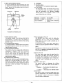
1
SHARP
SERVICE MANUAL
PDSM880004-MZ
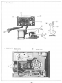
Floppy disk
Model MZ-80FD
Extension floppy disk
Model MZ-80FDK
MZ-BQFD
Floppy disk 1/0 card
Model MZ-80F10
, - - - - - - - - - ( Features
•
devices developed for
access to newly designed software regions in Personal
microcomputer System M2·80 Series.
•
5.25-inch floppy disk of miniaturized dual drive type,
Microcomputer
peripheral
MZ-BQFDK
In 2'drive mode, 286K byte data can be random·
access proces~d at high speeds.
•
Extension floppy disk (MZ·BOFOK) may be con -
nected in daisy chain system, thus enlarging the
memory capacity up \0 572K bytes.
•
Precision devices composed of 2 disk drive
and
The head can be
Units
switching regulator power supply.
brought into contact with diskette, only when
needed, 10 extend the life-time of diskette and head.
MZ-BOFlO
SHARP CORPORATION
,-----------------------------Contents----------------------------~
MZ-80FD and MZ-80FDK specifications
Precautions on servicing . . . . . . . . .
2
Differences between MZ-80FD and MZ-80FDK .
.2
System block diagram . . . . . . . . . . . . . .
.3
Circuit diagram of floppy disk I/O card (MZ-80FIO) .
.4
Operational principle of floppy disk ..
.9
Inspection and replacement of disk drive main parts.
13
Repair procedures . . . . . . . . . . . . . . . . _ .
19
Power supply section . . . . . . . . . . . . . . . . . . . . . . . . . . . .
21
Circuit diagram and printed wiring board . . . . . . . . . . . . . . .
23
Disassembled views . . . . . . . . . . . . . . . . . . . . . . . . . . . . .
35
Pack ing method . . . . . . . . . . . . . . . . . . . . . . . . . . . . . . .
38
Replacement parts list . . . . . . . . . . . . . . . . . . . . . . . . . . .
40
~-------.-----~--------------------------------------,
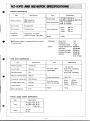
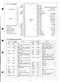
• General specifications
Specification
Item
Memory capacity
143K bytes/drive
(286K bytes/unit)
No. of tracks
70 tracks/drive
No. of sectors
16 sectors/track
Operating
conditions
Temperature: 5 to 25°C
Relative humidity: 20 to 80%
Item
Specification
AC 220V ±10%, 50 Hz
AC 240V ±10%, 50 Hz (for U.K.)
40W (at AC220V)
45W (at AC240V)
Rated voltage
Power consumption
Outer dimensions
Width;
Depth;
Height;
Weight
6.8 kg
Accessories:
* Specifications subject to change without prior notice
for improvement.
Option:
205 mm
320 mm
204 mm
Power cord
Braided wire
Instruction manual
Floppy interface card
Disk Basic
Connectin flat cable
Extension flat cable
Diskette
1 pc.
1 pc.
1 copy
MZ-80FIO
MZ-80FMD
MZ-80F 15
MZ-80F05
MZ-80FBD
(a set of 5 pcs.)
• Disk drive specifications
Item
143K bytes
Memory capacity
No. of tracks
70 tracks
Recording system
FM
Medium rotational speed
300 rpm
I nformation transfer rate
125K bits/sec
Average response time
100 msec
Head load time
50 msec
Motor starting time
1 sec
DC power supply
requ irements
+12V DC ±5%
0.9A (TYP), 1.8A (MAX)
+5V DC±5%
0.7A(TYP),1.0A(MAX)
Power consumption
12W (TYP)
Outer dimensions
(bezel not included)
Width;
Depth;
Height;
Weight
1.6 kg
• Power supply section specifications
Item
Specification
Item
Specification
Specification
Input
AC 220V ±10%, 50 Hz
AC 240V ± 10%, 50 Hz
(for U.K.)
Output
DC12V
DC5V
-1-
146 mm
203.2 mm
82.6 mm
PRECAUTIONS ON.SERVICING:·
•
•
•
•
•
The floppy disk is a precision device. Be careful not to give it an impact. Avoid servicing in a dusty place.
Take care not to allow foreign matters to come in the machine. (For diskette as welL)
Be sure to use the specified power supply voltage. Completely separate the power supply line from other
equipments emitting noises (such as large-sized motor), or cut off noises being mixed in the power supply line
with a line filter or the like.
Do not operate or service the unit near appliances generating magnetism, otherwise malfunction and/or erasure of
data and texts written in diskette may result.
Arrange system signal cables (flat cable, etc.) as far from other devices and power supply cord as possible.
Before transportation or moving to other place, be sure to attach the mouthpiece to the front Joor.
I
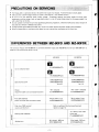
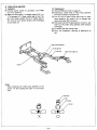
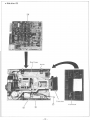
DIFFERENCES BETWEEN MZ-8OFD AND MZ·8OFDK
•
~---------------------------------------------~.----------------------------------------~
The extension floppy disk MZ-80FDK is connected between floppy disk MZ-80FD and I/O card (MZ-80F 10) to.
enable 4 units of disk drive (drives 1 to 4).
MZ-80FD
IT,
( I)-RiVE \
0
r,
W
(TLABZ0029PAZZ)
0)
u
Drive indication label
c
~
<1l
0)
Cl.
Cl.
<l:
MZ-80FDK
(TLABZ0034PAZZ)
iTI
(TLABZ0033PAZZ)
(T LABZ0035PAZZ)
(TSPC EOO04PAZZ)
(TSPCEOO05PAZZ)
(TSPCEOO06PAZZ)
(TSPCEOOO7PAZZ)
for U.K.
r------
Specification panel
for U. K.
Chassis
(signal flat cable to be connected herewith)
"IN" indicated
( LCHSM0090PASA)
"IN" "OUT" indicated
(LCHSM0092PASA)
Flat cable assembly
(socket with flat cable connection lead)
34-pin socket: 1 pc.
(DSOCN0040PAZZ)
34-pin socket: 2 pcs.
(DSOCN0056PAZZ)
....
0
'':
0)
+-'
-c
1---------------
-
Refer to setting of short pins and terminal
resistor on page 14.
Disk drive, PWB terminal
resistor and short pin
"K" labels on four sides
of the case
(TLABEOOO2PAZZ)
Packing case indication
0)
Cl
<1l
.::t!.
U
<1l
c...
Braided wire
Wire length: 900 mm
(DTiP-0039PAZZ)
-2-
Wire length: 500 mm
(DTiP-0042PAZZ)
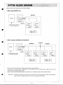
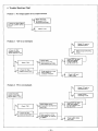
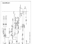
Below are shown the floppy disk system block diagrams.
• When using MZ-80FD only
MZ-80FD
r--------------~
I
I
I
MZ-80FIO E = T - - - - - , - - - - - - - - - - ,
MZ-80K
(1/0 card)
MZ-80I0
t
I
I
I
I
MZ-80F15
RAM required to extend)
( to more than 36K bytes
I
DRIVE 1
DRIVE 2
I
I
(With
terminal
resistor)
(Without
terminal
resistor)
I
I
I
I
I
Power ( 5V)
supply 12V
:
I
I
I
L _______________
~
• When using both MZ-80FD and MZ-80FDK
~
MZ-80K
-
MZ-80FIO
"/O~,d)
MZ-80IO
t
( RAM required to extend)
to more than 36K bytes _
rn
MZ -80F05
1
MZ-80FDK
~
MZ-80F15
MZ-80FD
r--------------'r------------- -,I
8
I
I=t
I
I
I
I
DRIVE4
DRIVE 3
(Without
terminal
resistor)
(Without
- terminal
resistor)
I
I
I
I
I
I
I
DRIVE 2
DRIVE 1
(Without
terminal
resistor)
(With
terminal
resistor)
I
Power ( 5V)
supply: 12V
I
I
Power ( 5V)
supply: 12V
I _______________
L _______________ JL
~
Up to 4 units of drive can be connected, as shown above, using daisy chain.
The signal line terminal resistor is applied only -to the last drive unit of the daisy chain. (Usage of two or more
terminal resistors causes damage to IC's.l
• When 4 drive units are being connected, they should be all in operating mode to ensure proper function.
* Daisy chain: Connection method to control two or more drive units. In this system, more than two connectors,
each of which is coupled with each drive unit, are connected with cables.
-3-
1.
Block diagram
-~
Buffer
H
Interface with bus line
• Port add re ss decode
~
• Bus driver
• Latch
r
Floppy control
circuit
Drive ready
detection
circuit
LSI (T3444M)
I
~
VFO circuit,
oscillation circuit
Address
decode
Bootstrap ROM
. For port addresses,
$F8, $F9, $FA and $FB are used .
. For ROM addresses,
$FOOO to $F3FF are used.
2.
Explanation on LSI T3444M
1)
Block diagram
CRDY
Transfer control
(3
8
r--------- -----------
~
I
:l
l
Write data
Read data
Co -
----
.f
I
I
S
J
Sector address
C
3
4
------,
t
M
i
Track address
i
'"I
-
G
I
'--
--.!-
WRITE DATA
I
I
I
I
@{D
---
WINDOW
I
I
I
CLOCK
I
I
I
I
r--
II
'--
ALU
---
t I nternal bus
I
8
t------t
t t _____ ~~~~I~i~n!~ _____ t
generator
INITIALIZE
-
VGG \5V)
I
I
~
Timing
INDEX
---
I
I
Immediate data
Timing
SYN, WTG, HDL,
STP, DRC, SDS
H
t
I
I
I
I
I
I
I
I Y·RAM 8 x 8 bits
I
t
r-READ DATA
X·RAM 8 x 8 bits
DRDY, WPR,
~- TRZ,
TND
control
•
r-I
I
Sequency
ROM 32Q x 24 bits
I
I
I
Vcc (5V):
I
'--- GND (QV)
I
IL ___________________________________
I
I
I
~
---------
-4-
--~
2)
Pin connections
40
VCC
2
39
SEM
3
38
INDEX
VGG
C3
Command bus
(MSB)
C2
Select command/status register
Index hole
Controller ready
4
37
CRDY
Co
(LSB)
5
36
GND (OV)
D7
(MSB)
6
35
WRITE-DATA
D6
7
34
DRDY
Ds
8
33
WPR
Write protect
D4
9
32
TRZ
Track zero
D3
10
T3444M
31
TND
Transfer end
D2
11
(LSI)
30
SYN
Synchronize
DI
12
29
WTG
Write gate
(LSB)
13
28
HDL
ROM
14
27
STP
Head load
Step
IN/OUT
15
26
DRC
Direction
Select track register
SET
16
25
SDS
Side select
Select sector register
SES
17
24
INIT
Initialize
Cl
Data bus
Do
Request memory reference
Input/output
Receive/transmit
Permit memory reference
R/T
18
23
CLOCK
PRM
19
22
WINDOW
GND
20
21
READ-DATA
Write data
Drive ready
Clock
Window
Read data
3) Pin description and function
Input/
output
Description
Description
Function
Power
5V
INIT
Input
Initializes, resets LSI.
Co -C 3
Input/
output
Used to transfer command/status.
3-state output.
505
Output
Command signal to select either
side 0 or side 1 of diskette
Input/
output
Used to transfer track/sector
address as well as read/write data.
3-state output.
DRC
Output
Command signal to dictate the
direction when stepping head.
STP
Output
Step pulse.
Output
SiQ.nal to request
read/write data.
7
ROM
transferring
---
Input
IN/OUT
SET
Input
....
-
--_.-
Input/output designation signal to
get access to tach register of
command/status,
track
and
sector.
Select signal to get access to track
register.
HDL
Output
Head load.
WTG
Output
Write gate.
SYN
Output
Command signal to indicate
whether or not clock is to be
synchronized with read data.
nm
Input
Command signal to indicate
whether or not data is to be read
and/or written through consecutive sectors.
SES
Input
Select signal to get access to
sector register.
RfT
Input
Input/output designation signal
to get access to read/write data
register.
TRZ
Input
Track zero.
WPR
Input
Write protect.
DRDY
Input
Drive ready.
Select signal to get access to read/
write data reg ister.
WRITE
DATA
Output
Write data
CRDY
Output
Signal to show if controller is
ready or not.
Input
PRM
------
Power
OV
READ
DATA
Input
Read data pulse is input.
INDEX
Input
Index hole.
WINDOW
Input
Strobing pulse when reading out
read data.
SEM
Input
Select signal to get access to
command/status register.
CLOCK
Input
Fundamental clock to cause operation.
VCC
Power
5V
GND
.-
-5L
Function
VGG
Do - 0
f---
Input/
output
3. Function of MZ-80F 10
1) Control of 4 drive units (max.)
1) Starting and stopping the motor
2) Selecting drive unit
3) Loading and Unloading the read/write head
4) Shifting the head (control of direction, gap
between and number of steps)
5) Generating drive ready signal
6) Detecting write protect and track 0
7) Separating read clock from drive into clock bit
and data bit
8) Collating and retrieving disk address data
9) Generating and checking CRC
(Cyclic Redandancy Check)
10) Generating sampling window pulse of read data
in VFO (Variable Frequency Oscillator) circuit
11) Serial and parallel conversion of read/write data
2)
*Cyclic Redandancy Check
A check carried out on read-out data to detect
errors.
Bootstrap function
Selecting a drive for ROM (SN74S474 or equivalent), reading 14 sectors from the beginning of
track 0 at the diskette being set in the drive, imd
finally loading the 14 sectors in RAM address
$9800.
The program loaded will be checked and jumped
into $9800. At that time, errors, if detected, will
be displayed as "ER: CAN'T BOOT" in the
CRT display. The set is then on monitor command wait.
(Types of errors)
1) Drive READY signal does not become high.
2) No master diskette used, or faulty master diskette.
3) I/O unit is not power suppy on.
4) MZ-80F IQ does not normally operate.
5) Signal cable is not correctly connected, or
damaged cable.
6) RAM has not been extended. (RAM should be
loaded with more than 36K bytes.)
7) Improper ROM or faulty circuits adjacent to ROM.
8) Others
Reference) ROM SN74S474 or equivalent
Part code
Part name
No. of bytes
RH-iX0219PAZZ{
SN74S474
J..LPB425C
82S141
} 512 byt"
RH-iX0238PAZZ{
J..LPB417C
82S181
} 1024 bytes
In applying the above ROM, jumper wire of PWB
pattern is put in between pin 21 and pin 22 of ROM
for short-circuit purpose in the course of production.
Note)
• The 512 byte ROM can be either short-circuited
or not during use .
• The 1024-byte ROM in use must be short-circuited.
L-__________________________________________________________ ._______________
-6-
4. Timing chart of VFO (Variable Frequency Oscillator) circuit
(H)
(H)
READ DATA
SN74LS74
WINDOW
(H)
I---~WCLK
LOADOBO C
8MHz
CK SN74LS161
1) When synchronizing signal is high (VFO circuit is asynchronous).
QB (2MHz)
Qc (lMHz)
1--1
1-1.0~s-l
.---_ _ _ _ _ _....,500ns
I
A
A
B
B
C
CLOCK
....
1·>-------4.0~ ------~.I
I
--------~I
I
k-1.25~s--l
WINDOW
I
1--1.0~s
1
--I
-I
4.0~s
I"
~
11
WCLK
1----.1
1.500ns
4.0~s
.. I
2) When synchronizing signal is low (VFO circuit is synchronous).
Read data is phase·synchronized with 8 MHz clock. The counter (SN74LS161) is initialized by means of the signal
and window nand operation. Namely, timing of read data, window and clock is adjusted as follows.
~R-EA-D-=DA=T=A=-lLJ
READ_D_A_TA~~
:
~~______________________________~r-l~
About ""1~.j
-----OLJ
WINDO~r----+i
f...:---l
I
L
CLOCU
LJ
LJ
11~s
:,
LJ
1.5~s
LJ
Ir------~
L--J
i~bOU~
LJ
.1
'----'
1.25~s
- - - - - - -
-7-
___
5. Ready detection circuit of selected drive units
<;: +5V
27K
33/LF
+1:1
FI
I
p
D R DY <E,~---1 Q
(DRIVE READY)
I I
....
-
~
I
1.
150 L"--_~
~033/LF
SN74LS122
,
SE
200ms
INDEX
-"""'LJ
--I
p
LJ
~8ms
u
U
Index signals, when continuously coming at intervals of 200ms; enable DRDY (drive ready) to be
kept high.
• Conditions for drive ready.
a) Diskette is inserted in proper direction.
b) Motor runs normally (300 rpm).
c) Index detection circuit functions normally.
d) F rant door is closed.
e) Select signals are transmitted to drive.
f) Specified power is supplied to drive.
g) Drive select signals are generated normally.
These signals consist of SE, S1 and SO.
SE
S1
X
X
1
1
1
1
0
0
0
1
1
0
•
•
•
SO
1
1
(I
jE--1
•
0
~-l""-< II 0 -.......-<..... INDEX
S1 and SO invalid, non-select mode
Drive 1 selected
Drive- -2- -selected
Drive 3 selected
Drive 4 selected
----------
-8-
When the above conditions a) thru f) have been all
satisfied, index pulses are transmitted at intervals
of 200ms.
When SE signal becomes 1, the retrigger one-shot
IC (SN74LS122) will be activated to cause DRDY
signal by input signal.
Floppy control LSI (T3444M) is given a command
to operate.
DRDY signal is then checked before an advancement to the next operation.
If DRDY signal is low, error indication is displayed
to interrupt the operation.
.'
[ OPERATIONAL PRI~IPLE OF. FLOPPY ·OISK
megnetic head in direct contact with a specified track
sector of 70 tracks formed in both surfaces of the
diskette.
The floppy disk is designed to rotate the so-called
"diskette," a magnetic disk storage unit, to read out
and write in data at high speeds by bringing the
1. Fundamental block diagram
Read data
Operation <(}-""7:":"""7.------'1''---------,
. d'
./Wnte ~
In Icator
. / protect.~
/ ' senso!/ Index~
sen_s~JJJ .
Read circui>
Head select
Drive
select
<:__
Write gate
Write protect
,/
.~/
Write data
~ Head load·
Write protectr """," .
la,*/'
.,
Write circuit
actuator
)-1 I
'-r--,..----,,...... Index I ! : .\
~'.
,
• 'I--....
Head load
_ _ _ _ _- - . j r - L - - - . l - . - " - 1
~~~:~ion
Motor ON
• T rack-,O;:-,O:----i
-=--"':';":"':"'=---1 Control circuit
Drive select
t----,
Head select
Motor ON
I
~
•
_ Rea1,write
-~d. ~:'I'
Diskette-
Motor
control circuit
2. Mechanism explanation
This device consists mainly of the following
mechanisms.
4) Diskette driving mechanism
A small-sized DC motor with tacho-generator is
employed. The motor rotation is transmitted
through the drive belt, spindle pulley and spindle
hub, thereby causing rotation of the diskette. This
spindle pulley is provided with a stroboscope to
check rotation interval.
5) Head load mechanism
To extend the life-time of diskette and head, the
head can be brought into contact with the diskette
only when in operation. This mechanism is controlled with drive select signals.
1) Read/write head
The head is attached to the arm through a leaf
spring.
The head can follow the motion of
diskette easily.
Signals read out of the head are transmitted
through FPC (Flexible Printed Cable) to the read
amp. circuit.
2) Carriage assembly
2 units of read/write head are mounted on the
carriage. The carriage is located with the stepping
motor and lead screw.
3) Head locating mechanism
This is a high-precision, reliable head locating
mechanism using stepping motor and screw-driven
ball/V-groove system.
The stepping motor is of 7.5°/pulse, steel plate
type.
One pulse of step signal causes a 2-step rotation
0
by 15 , thus pushing forward the head by one
track.
-9-
6) Write protect detection section
A luminous diode and a photo-transistor are used
to detect write protect notch of the diskette and
jacket. (Writing is not possible when the notch is
covered with label.)
Center hole
3. Interface
1) Interface signal
All lines are of TTL (transistor-transistor logic).
(1) Input signals
For input signals there are 10 kinds of input lines,
all of which are valid at low levels. These signal
lines are terminated at a 150-ohm integrated
resistor fitted in the IC socket of drive 1. The
signal voltage levels are as follows.
Label area
Write
protect
notch
High level I Invalid
Low level I Valid
Input impedance
Head
window
2.4 to 5.25V
o to O.4V
Pull-up to 5V at 150-ohm
resistor
Index hole
Description of diskette parts
CD Drive select signals (0 to 3)
7) Index detection section
The MZ-80FD has 2 drive units. ~y adding the
MZ-80FDK, up to 4 drive units are available.
These signals are used to select a desired one of
the four drive units.
At low levels of drive select signal, R/W head is
loaded to cause the operation indicator to light up.
This section consists of a luminous diode and a
phototransistor. An index hole of the diskette is
detected by this section to determil1e the starting
point of a track.
8) Track 00 detection section
A carriage position is detected with a limit switch.
When the carriage has reached the track 00 point,
track 00 signal is emitted.
9) Control electronics section
The electric circuit to control each mechanism is
composed of 2 sheets of PWB. One is to control
the DC motor control circuit. The other is to
control other circuits, say, detection and other
functions with respect to read/write, step, head
load, and other signals.
10) Diskette protect mechanism
Shutting the front door, with the diskette incompletely set in, can give damage to.the diskette, thus
shortening its life-time. To prevent such a drawback, this mechanism has been adopted so that the
front door con not be closed if the diskette is
improperly in.
Note)
Depending on which drive unit to use (Drive No.1
thru 4), it is necessary to process short pins of the
control PWB. See page 14.
@ Motor ON signal
The drive motor starts when the signal level becomes low. This signal level becomes high about
2 seconds after completion of all operations, if
no operation is commanded next. It thus interrupts the motor, extending the service life of
motor.
@ Direction select signal
The signal is' given to designate the shifting
direction of R/W head, when the step pulse is
input.
High level - - - Out direction (to diskette outer
portion)
Low level - - - I N direction (to diskette center)
® Step signal
This signal is given to move the R/W head in the
direction designated by the direction select signal.
The operation is done in the course of changing
from low levels to high levels.
- 10-
CID Write data signal
This signal is used to write in data on the diskette.
Each time changing high levels to low levels, the
current flowing in the R/W head is reversed to
write in data bit.
This write-in performance is available when write
gate signal is at low levels.
@ Write gate signal
This signal being at low levels, data can be written
on the diskette. At high levels, read-out or
sequential operation may be made.
(j) Side 1 select signal
This signal is given to decide which side of a
double-face diskette to read or write. The R/W
head of side 0 and that of side 1 are selected at
high levels and low levels, respectively.
@ Write protect signal
(2) Output signals
There are the following four kinds of output signal.
CD Index signal
By this signal the starting position of each track
can be detected. Each time the index hole of
diskette is detected with the detector, the track is
fed from the drive unit.
Usually, this signal level becomes low each time
the hole is detected at high levels. Therefore, the
leading edge of the signal indicates the beginning
of a track.
@ Track 00 signal
The low-level state of this signal signifies that
the R/W head is located at track 00 position (the
outermost track).
In any position other than track 00, the signal is at
high levels.
When the R/W head is at track 00, the head is held
at the position by the stopper even if another
signal to step outside is given. At this time,
however, the track 00 signal level becomes high.
By adding still another signal to step outside, the
motor phase is returned to cause track 00 signal
to become low.
This signal is used to detect whether or not write
protect for the diskette is provided. When a
diskette with write protect is in, the signal level
becomes low.
In usual operation, a diskette with write protect
enables to protect write statement within the
drive.
@) Read data signal
The signal is given to transfer data read from tile
diskette. Usually it is at high levels, while during
detection it comes down to low levels.
- 11 -
r
3) Timing
I
,~I
'\
-
DC POWER MOTOR
ON
DRIVE
SELECT
~100ms
- f----i
VALID TR KOO
AND WRT PRT
OUTPUT
VALID
INDEX
1-
I--
STEP
~~
500ns MAX
1000ILs M IN - -
I
[
Cl
11
... 15 MAX1
I
((
~500ns MAX
1DIRECTIO N
SELECT
MIN
((
1ILs
I
11
MI;-, ~
+-llLs ,-L.
MIN
+--llLs MIN
~
~--
~
--
~~
20ms
MIN
SIDE ON E
SELECT
--1.usMIN
~
I
lOms
MIN
,~\:
!
zl
--
WRITE
GATE
~
...
35ms MIN
"
1001LS MIN
((
1T
50ms MIN
lsec MIN
1000.usMIN-
1
I
a.....01
-
eIIi
l
:!ElI
~I
\~j
---t
WRITE
DATA
~I
((
-
-- --
1--8ILs M~~
_W_71
- + i+-- 100ILS MIN
VALID
READ
DATA
35ms MIN---...J 1--1000.uSMIN 100ILS MIN-I--
\
50ms MIN
\
I
VALID
I
I VALID
VALID
lsec MIN
Control and data timing
,~I
2)
Power supply unit interface
Specified supply voltage of DC 5V fDC 12V is fed from the power supply unit to the J2 connector of drive
control PWB.
-12-
I
'
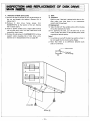
OFDlSKDRlYS··
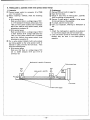
1. Removal of disk drive units
2. Belt
1) Remove 6 case set screws (3 mm) at the bottom of
the set and detach the cabinet. (Screws (A) in
below chart.)
2) Remove 4 disk drive fixing screws (LXBZ0067PAFN) at the button of the set. (Screws
(B) in below chart.)
3) Draw 2 power sockets and 2 signal cable sockets
off the disk drive units. Pull the 2 disk drive units
toward the front frame.
4) Remove 8 oval screws (LX-BZ0068PAFN) of drive
support plate coupling the 2 disk drive units.
(Screws (C) in Disassembled View on page 35)
1) Inspection
Check to see if the belt is stained with dust or dirt.
Also make sure that there is no unevenness,
scratch and thinned part.
2) Replacement
1) Take the belt off the spindle pulley while rotating
the pulley gradually by hand.
2) For applying the belt, put the belt first on the
motor pulley and then on the spindle pulley while
rotating the spindle pulley.
Note)
1. In putting on and off the belt, be careful so that it
be not caught by the motor pulley flange.
2. Note that there is no difference between both
sides of a new belt.
~
screws@
<!b
screws
- 13-
®
Motor pulley
Keep belt
off the flange.
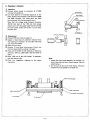
2) Setting of short pins and terminal resistor
3. PWB unit
1)
1)
2)
3)
4)
Replacement
•
Take connectors J3 and J4 off PWB.
Remove 4 PWB unit fixing screws (3 mm).
Detach PWB unit.
For reassembly, take the reverse order.
Before delivery, the drive units No. 1 thru 4 are
factory adjusted as tabulated below.
Drive No.
MZ-80FD
MZ-80FDK
1
2
3
4
HS
0
0
0
0
DSO
SHORT
0
0
0
·Co
DS1
0
SHORT
0
0
0
DS2
0
0
SHORT
0
MX
0
0
0
0
DS3
0
0
0
SHORT
Note)
•
•
In replacing PWB unit, it is necessary to check
which short pins to cut and whether or not
terminal resistor is required, depending on which
drive unit to use (DRIVE No.).
Short pin: Detach the short pins from the old
PWB unit and apply them to a new
PWB.
Terminal resistor: If the old PWB unit has no
terminal resistor, remove terminal
resistor from a new PWB.
c:
......
.c.
en
HM
Terminal
resistor
PWB unit fixing
screw (3 mm): 4 pcs.
connector
PWB unit
J4 connector
J1 signal
connector
Terminal resistor
-14-
0:
HS:
SHORT SHORT SHORT SHORT
Provided None
None
None
OPEN
Head load takes place by drive select: That is,
when signals of which drive is shorted among
the short pins DSO, DS1, DS2 and DS3
become low, head load is caused.
DSO---G: DRIVE SELECT signals
MX:
When using one drive unit, DSO thru DS3
become invalid by shorting this pin. Select
will be constantly kept.
When motor ON signals become low, head
HM:
load occurs.
4. Index lamp assembly
1) Inspection
Connect power socket to connector J2 of PWB
unit. Turn power on.
Make sure that there is a voltage range of DC 1 to
1.7V between B·11 (lower white lead of the 11th
pin from power socket) and A·11 (black lead of
the 11th pin from power socket), both belonging
to connector J3.
2) Replacement
CD
CD
®
®
@
@)
@
<ID
Remove PWB unit (refer to page 14).
Disconnect 2 lead wires of index lamp assembly
from the housing of connector J3.
Cut off the tie band fixing lead wires of index
lamp assembly (be careful not to damage lead
wires), and open the front door.
Take lead wires off the guide groove of carrier, and
draw out the index lamp assembly with tweezers
and fingers.
To attach, take the reverse order.
Carry out inspection, referring to description at
left.
Index lamp assembly
Note)
When attaching the index lamp assembly to the
carrier, fit the housing and LED in at the same
time.
{5;
Clfl:J
X
-15-
o
5. Media guide L assembly (with write protect sensor lamp)
2) Replacement
Remove PW8 unit (refer to page 14).
® Open the front door.
@ Detach 4 lead wires of media guide L assembly
from the housing of connector J3.
® Remove 2 media guide L assembly fixing screws
(3 mm) and take out the assembly.
@) To attach, take the reverse order.
@ Carry out inspection, referring to description at
left.
1) Inspection
Connect power socket to connector J2 of PW8
unit. Turn power on.
® Before inserting a diskette, check the following
items.
a) Write protect lamp
Make sure that there is a voltage range of DC 1
to 1.7V between 8-13 (lower yellow lead of the
13th pin from power socket) and A-13 (black
lead of the 13th pin from power socket), both
belonging to connector J3.
b) Write protect sensor
Make sure that there is a voltage range of DC 0
to O.5V between 8-14 (orange lead below the
14th pin ,from power socket) and A-14 (black
lead of the 14th pin from power socket), both
belonging to connector J3.
@ Put a write protect diskette (with write protect
seal being applied at the write protect notch of
diskette) in place, and shut the front door. Then
check the following item .
• Write protect sensor
Make sure that there is a voltage range of DC
2.5 to 5.25V between 8-14 and A-14 of
connector J3.
CD
CD
Note)
1. Attach the media guide L assembly by pushing it
to main frame stopper side and front bezel side.
2. Lamp and sensor cannot be individually replaced,
because they are built in the media guide L
assembly.
Media guide L assembly fixing screw
Write protect lamp
Push
Media guide L assembly
Front bezel
Main frame stopper
-16-
6. Operation indicator
1) Inspection
power socket to connector J2 of PWB
unit and turn power on.
(6i Let drive select 0 of interface signals be at low
levels (make a short between Jl-8 terminal of PWB
and PWB Ground), and make short pin DSO
circuit shorted. (Do not prolong this test.)
Note that the voltage range between connector
J3-B 10 (red lead of the 10th pin from power
socket) and J 3-A 10 (upper black lead of the 10th
pin from power socekt) will be DC 1 to 2V when
the lamp is lit.
CD Connect
Front bezel
LED holder
LED
Pull-out direction
Pull-out direction
2) Replacement
CD Remove PWB unit (refer to page 14).
@ Datach 2 lead wires of operation indicator from
the housing of connector J3, and take lead wires
out of the wire holder.
@ Open the front door.
® Remove 2 front bezel fixing screws (3 mm) and
the front bezel itself by pulling it forward.
® Draw out the holder 2 with tweezers in the arrow
direction. Take out LED holder. (See the sketch at
right.)
@ Draw LED out of the LED holder. To assemble,
take the reverse order.
(j) Carry out inspection, referring to the above
instruction.
Note:
1. Attach the front bezel assembly, by pushing it to
main frame side and main frame stopper. (See the
sketch below.)
2. Do not pull up the carrier with fingers, otherwise
excessive force is applied to the head arm.
Main frame stopper
Main frame side
Main frame side
fr
Front bezel fixing screw
Push
Push
Front bezel
Front door
- 17-
7. Drive motor assembly (DC motor and motor cont ro l PVIB unit )
2) Replacement
1) Inspectio n
power socket to connector J2 of PWB
unit. Turn power on.
@ led interface motor ON signals be at low levels
(make a short between Jl · 16 terminal of PWB unit
and PWB Ground) and run the motor. (Do not
prolong this test.)
j) Put a diskette in place and close the front door.
CD Remove PWB unit. (Refer to page 14.1
CD Connect
@
S)
~ Put off the belt. (Refer to page 13.)
Q) Cut off the tie band for fixing lead wires of motor
'V
Carry on head load.
Make sure that the stroboplate attached on the
spindle pulley appears to be stationary.
:ID
N ote)
The shifting rate of stroboplate is allowed to be up
to 1.5 pcs./sec.
®
(j)
and motor control PWB unit. Be careful not to
damage lead wires.
Remove 3 lead wires-coming from the motor
control PWB unit to connector J3-from the housing of connector J3.
Remove 2 motor control PWB unit fixing screws
(3 mm) and 2 DC motor fixing screws (3 mm).
Detach the DC motor and motor control PWB unit
from the main frame.
For assembly, take the reverse order.
Carry out inspection, referring to d~scription at
left.
(
Motor control PWB
un,t 1,~on9 screw
Varlllble relistor
Ilor motor splM1d adJusUTlem)
Motor control P'NB
Unit
Mo,,, ,,"'" '"
I
SP,ndle
"
11
Note)
In mounting the DC motor, the distance between
spindle pulley and motor pulley should be kept to
be 73 ±O.4 mm as shown above.
3) Ad justment
(1 At", the ,ompletion of the
,be"
'hook i"m •.
adjust the variable resistor of motor control PWB
unit so that the stroboplate appears to be completely stationary.
- 18-
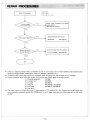
REPAIR
MZ-SOK
MZ-SOIO
[
MZ -SOFOI FOK
Start of d is k system
YES
;>------~
Check repair procedure for power
supply section.
(See pages 21 and 22.1
NO
YES
Check bootstrap function for
MZ·80FIO.
(See page 6.1
NO
YES
Trace the cause from the contents
of error message.
(See page 20.)
NO
End
•
Check by replacing several sheets of diskette to see if errors occur due to faulty diskette (data deterioration
caused by foreign matters, deformation, wear-out, damage, magnetism, etc.).
• Troubles in disk system often cause error messages. Trace the cause from the contents of error message.
• Replace suspected parts in the disk system with normal ones. Check again the trouble section.
1) Personal computer
MZ-80K
2) Interface unit
MZ·80I0
3) I/O card
MZ·80FIO
4) Diskette
MZ-80FMD, MZ-80FBD
5) Flat cable
MZ-80F15, MZ-80F05
6) Disk drive
• The signal circuits of floppy disk and I/O card operate at TTL levels of OV, +5V. Connect any system other than
micro-computer peripheral devices for MZ-80 series to see if signal levels are out of the range of 0 to +5V (max.
+5.25V).
-19-
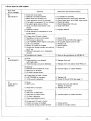
• Error chart for disk system
Error code
[Error message]
50
[NO READY]
Contents
Check item and corrective action
1) Drive fails to be ready.
Diskette is wrongly inserted.
Motor does not normally run.
0 Index detection circuit is improper.
o Flat cable is improperly fit in or broken.
o No select signal comes at drive.
o Drive unit door (front door) is not
closed.
o Diskette is faulty.
o Write operation is attempted in write
protect state.
o
o
o
o
o
o
Fit diskette in correctly.
Check belt and/or drive motor assembly.
Check index lamp, drive PWB, index sensor.
Check flat cable.
Check floppy disk I/O card.
Close front door.
o
Replace diskette.
o
o
o
o
o
o
o
o
o
o
o
o
Check IC13.
Check IC15 and IC16. (See page 7).
No CLOCK signal comes at LSI.
Replace LSI.
Check pattern.
Check IC.
3) Interface unit is faulty.
o
Refer to Service Manual for MZ-80 10.
o
o
2) Floppy disk I/O card is faulty.
Oscillation circuit is interrupted.
VFO circuit is abnormal.
LSI (T3444M) CRDY signal is not given.
LSI is not released.
Pattern is broken or bridged.
Conductive foreign matters are sticking
to IC, etc.
o PWB and connector are in inadequate
contact.
54
[UNFORMAT]
1) Drive
0 Head position is not aligned.
0 Replace drive unit.
(off-track state)
0 Head and amp. circuit are defective.
0 Replace drive unit and/or drive PWB unit.
2) Diskette
Diskette not formatted is in use.
CRC error in ID field.
0 ID field is broken down.
o
o
41
[DISK DATA
ERROR]
o
Initialize again, or replace diskette
o
o
3) Floppy disk I/O card is faulty.
LSI (T3444M) is improper.
VFO circuit is defective.
o
o
Replace LSI.
Check IC15 and IC16. (See page 7.)
1) Drive
SEEK error
o
o
Head shift is improper.
o
Check drive unit and diskette
Replace, if required.
Replace drive unit.
2) Diskette
CRC error in data field.
0 Data field is broken down.
0 ID field is defective.
0 Data mark detection error.
o
Initialize again, or replace diskette.
3) Floppy disk I/O card is faulty.
Pattern is broken or bridged.
Conductive foreign matters entered.
o
o
Check pattern.
Check for foreign matters.
o
o
o
o
- 20-
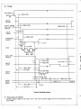
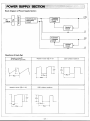
Block Diagram of Power Supply Section
'-'
AC
INPUT
..
~
+12 v
Cl)
f--
Cl)
LL
..
..
....
......
.---
.---
t--
L.....-
E
Transistor
Chopping
Circuit
Rectifying and
Smoothing
Circuit
0
en
c
cv
~
I
L.....-
Control
Circuit
1
G
-t"\
+5 v
Transistor
Chopping
Circuit
Control
Circuit
.J.
l
I
Waveform of Each Part
Waveform of p~Q)
of IC1 and pin I:!.J of IC2.
@
Waveform of pin
of IC1
~I
23V
3V
L
U
1-24/L5--1
1---45/L5-
I--- 451JS-----l
Waveform of pin
© of
IC2
0401 collector waveform
-
r---
~:l
~45/L5-
- 21-
0301 collector waveform
G
~
'-'
• Trouble Shooting Chart
Problem 1: No voltage appears at any output terminal.
n
Check AC cord
AC socket, Fl0l
AC switch and Cl0l.
Is there AC 220V (240V
for U.K.) present across
ClOP
y
Check Tl0l
Yes
Problem 2: +12V is not developed.
N~
Check ICl and its
peripheral parts.
r--
Y~
Is there AC 20V
present ac ross the
yellow lead of Tl0P
n
N
'--
Y~
Check Tl0l.
I
N~
Is there DC 23V
present across C201 ? I---
4
Yes
~
Check 0201
(short-circuit after
rectification) and F201.
Does waveform of the
chart appear in
collector of 0301 ?
Check output switching
circuit.
Leave R301 be open;
does there appear
0.3Vp-p pulse at
pin No.12 of ICl
i---
f---
Yes
Check L301 and
C304, C30S.
Problem 4: +5V is not developed.
r1
Check IC2 and its
peri pheral parts.
r-
Is there AC 20V
present across the
yellow lead of Tl 01 ?
n
Yes
Check nOl.
~
Check 0201 (shortNo
I"" circuit after rectification)
and F201.
Check output
switching circuit.
Leave R401 be open:
does there appear
0.3 Vp-p pulse at pin
NO.120f IC2
'--
~
Yes
Is there DC 23V
present across C201 ?
~
Y~
Does waveform of the
chart appear in collector
of 0401?
t---
Yes
- 22-
Check L402, C404,
and C408.
I--
I
I
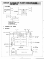
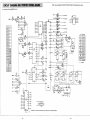
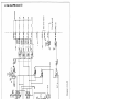
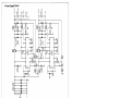
CIRCUIT"
Note) The circuit diagram and printed wiring board subject to change without prior notice .
• Floppy disk I/O card (MZ·80FIOl circuit
t ICH
.rOIl)
~3
.."
..
M.
....'".,
,
IIOTOII 011
". ,
c ""145 •
••
•
i!!...------m.
•
•
,
.
~.
~
-
~ ,
" ' ' - - - - -__ III'ItITt:UTt
- - --
- _ WRlTt ""TA
[> :
I PIN MARK
LSIH
-",
1.$174
,
::~::~~ ">-
...
....•••
."
'"
-"
~
'N
....
ICI.
nu ..
ICI3
CS'"
...
,
•
' -"
.-
- D-
Mod ified in the course of production (for common use w ith 1024 byte ROM )
-24 -
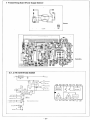
• Printed Wiring
Bo~rd
(Floppy disk I/O Card Section)
_
•....----..-."-'- _-.... ......
.. ,-.-.,._.
-.. .'
_.
...
::; ..
~-
-
~
-
..
.'.T.·... '..........
.
•
~."""iii'i·' · ·1
I
•
•
•
•
.J S~.·.:·--~:
~: ... :J
.-
•
-•
..
I
I
'"•
• • • 1 . :1 • •
.P."'
, •••
-
.lCIO
"iiili
!!.'.~ •
'"
'of .'~ ,,·..ri'.
• 2~
f ,.
..'
••
•
.,·
• • • • • •• 1,
..
•
'
•
'. .
'
"
•
'"
IC l
.
•••••• •
'!~
.
~ 1
.......
, I
•
"
•
,
P'''poc'i •• View
o
P. ",-I",.d face
D
Opp",i'. ,id<
No,.1 Pin t2 and pin 22 of IC7 (ROMI or. ,hO'!-C;,cu ;'ed w;,h jump.. ",i, • • , PW6 \>Otto'n in tho <:Cu'" cf Pled"O';"".
• le
Pin Assignments (Top View)
IC 1.12
RH-IXOO74PAZZ
SN74LS04N
IC2.3
RI-j-iXOO77PAZZ
SN74LS30N
IC4
RH-iXOO78PAZZ
SN74LS32N
SN74 LS02N
IC6
RH-iX0215PAZZ
SN74LS174N
IC7
RH-iX0219PAZZ
ROM SN74S474N
ICB
RH-iX0124PAZZ
SN74LS245N
IC 10.17
RH-iXOO7OPAZZ
SN74LSOON
IC 11
RH-iX0141PAZZ
SN74LS125N
IC 13
RH-iX0216PAZZ
SN74LS16.1N
IC9
RH-iXOOB1PAZZ
SN74LS139N
lG lA la 'YC ,v, lY21Y3GNO
ENABLE
'--y---J
"----v----l
SELeCT
DATA OUTPUTS
FUNCTION TAB LE
INPUTS
ENABLE SELECT
A
G
B
H
X
X
L
L
L
L
L
H
H
L
L
L
H
H
IC5
RH-iXOO71PAZZ
OUTPUTS
OUTPUTS
VO VI V2 V3
H
L
H
H
H
H
H
L
H
H
H
H
H
L
H
H
H
H
H
L
H = high level, L = low level, X '" irrelevant
OATA INPUTS
IC 15. 1B
RH-iXOO79PAZZ
SN74LS74N
IC 16
RH-iX0127PAZZ
SN74LS107N
IC 19
RH-iX0217PAZZ
~N74145
INPUTS
OUTPUT
VCC~~
FUNCTION TABLE
INPUTS
OUTPUTS
NO. CCBA 0123456789
0
LLLL LHHHHHHHHH
1
LLLH HLHHHHHHHH
2
LLHL HHLHHHHHHH
3 LLHH HHHLHHHHHH
4
LH L L HHHHLHHHHH
5 LHLH HHHHHLHHHH
LHHL HHHHHHLHHH
6
7 LHHH HHHHHHHLHH
8 HLLL HHHHHHHHLH
9 H l L H HHHHHHHHHL
HLHL HHHHHHHHHH
0
:::; HLHH HHHHHHHHHH
HHHHHHHHHH
« HHLL
> HHLH HHHHHHHHHH
~ HHHL HHHHHHHHHH
HHH HHHHHHHHHH
H - high level, L - low level
IC20
RH-iX0214PAZZ
SN74LS122N
IC 21
RH-iX0131PAZZ
SN7414N
IC22 - 24
RH-iX0220PAZZ
SN75452BP
- 26-
I
.....
i'.)
""
6J ,- <.~ I
3 OJI-6
+5V
t!5vbu~-~
+12V RETC;>"<-'
1/
"
I,
DRIVE SELECT OO'nv
,
J 1-3, 5," .., 3 I h
RN3
4.7K
+5V~
L:_:.J
J DS3
••
DS2
II"'~
,4
R42
150
r==':"
I
4-5V
6
4N
A
-+_____~--....,
J _1-_3_2_ _ _
SIDE ONE SELECT 9-
,
L 7JI50
~ ~IB
+5V
8
,pa
WP~
os
I
1_ .1
Ib
I l2B
qylOIJ
LSI4N
WRITE GATE Oo-.J_I-~2,-,4,--.....-_ _ _ _ _ _~
w d4R'"
WRITE DATA
:.,~~O
- HM
n
~
Write, power supply circuit
::~~A
OS
+5V~
IS9!5!5
CR2
READY
+5V
,
~3
~ 7e4e2
L J I IS955
WC;
WRITEA:l,
220
R44
ER/1
:ER/O
3-AI
~
""-"
IV
J3-AI0.
J3-A4
HS/O
WRITEloo
WRITEAo
WRITEIo,
..
LED
•
.....
;:to'
-
c
Cl
n
~'
n
::E
"'tI
Cl)
<'
...c..
~
UI
C
~
I
00
I
I,
I
I
LHe
+5V
,
'r'150
L~
4
.,..
ST~I-20"
DIRECTION
SELECT
I
WG
I3
,..
OUT
ITP!5!
'
OUT
~
PR
~
Stepper circuit
.,~
,vI
PM
+5V
rf;a
C23
0.01,11
+12V
+ ,2v
~
1
3-A2
I
.
Frame ground
-t
-1
,8 JI-26 OTRACK 00
rl.
~} for drive motor
J3-BI
4
I
I
rf;D
rf;C
rf;B
rf;A
STEPPER
•
§
i+
c
DJ
n
~'
n
:lE
"'tI
<'
CD
c.
...
~
C
in'
Read, index circuit
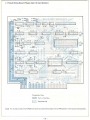
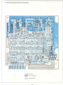
• Printed Wi,illll BoIIfd (Oi$k Drive Sec;tionl
J4
,~,
PM,,*,ti •• Vi.w
_
Pam-fin<ld face
D
Oppo ..... ide
-"'-
• Disk drive PWB, arrangement of test pins/connector pins
J1. I nterfaC8 codes
Pin No.
Code
Code
RETURN
1
2
RESERVED
RETURN
3
4
RESERVED
RETURN
5
6
DRIVE SELECT 3
RETURN
7
8
IN DEX
RETURN
9
10
DRIVE SELECT 0
RETURN
11
12
DRIVE SELECT 1
RETURN
13
14
DRIVE SELECT 2
RETURN
15
16
MOTOR ON
RETURN
17
18
DIRECTION SELECT
RETURN
19
20
STEP
RETURN
21
22
WRITE DATA
RETURN
23
24
WRITE GATE
RETURN
25
26
TRACK 00
RETURN
27
28
WRitE PROTECT
RETURN
29
30
READ DATA
RETURN
31
32
SIDE ONE SELECT
RETURN
33
34
RESERVED
PWB back side (solder-fitted side)
PWB front side (parts fitted side)
J2. Power supply
Pin No.
Code
1
+12V DC
2
+12V RETURN
3
+5V RETURN
4
+5V DC
- 31-
J3 Transducer
Wire
color
Pin No.
Code
Code
Wire
color
Blue
MOTOR ON
Al
Bl
+12V (DRIVE MOTOR)
Red
Brown
FLAME GROUND
A2
B2
+12V RETURN (DRIVE MOTOR)
Black
A3
B3
Green
HEAD LOAD
A4
B4
HEAD LOAD +12VDC
White
Black
STEPPER ifJA
A5
B5
+12V (STEPPER)
Red
Yellow STEPPER ifJB
A6
B6
+12V (STEPPER)
Red
STEPPER ifJC
A7
B7
STEPPER ifJD
Orange
Yellow TRACKOO SWITCH
(NORMAL CLOSE)
A8
B8
Key
Green
TRACKOO SWITCH
(NORMAL OPEN)
A9
B9
TRACK 00 SWITCH RETURN
White
Black
IN USE LED RETURN
Al0
Bl0
+IN USE LED
Red
Black
INDEX LED RETURN
All
Bll
+INDEX LED
White
Black
INDEX PTX RETURN
A12
B12
+INDEX PTX
Blue
Black
W/P LED RETURN
A13
B13
+W/P LED
Yellow
Black
W/P PTX RETURN
A14
B14
+W/P PTX
Orange
A15
B15
Brown
J4 Head
Wire
color
Code
SHIELD (HEAD 0)
Pin No.
Code
Al
Bl
SHIELD (HEAD 1)
A2
B2
KEY
Wire
color
Red
ERASE (HEAD 0)
A3
B3
ERASE (HEAD 1)
Red
Green
W/R ERASE RETURN (HEAD 0)
A4
B4
W/R ERASE RETURN (HEAD 1)
Green
Black
W/R (HEAD 0)
A5
B5
W/R (HEAD 1)
Black
A6
B6
A7
B7
W/R (HEAD 1)
White
White
W/R (HEAD 0)
Test points
Pin No.
lA
Code
PRE AMP lA
lB
PRE AMP lB
2A
PRE AMP 2A
2B
PRE AMP 2B
3
INDEX
4
ERASE
5
TRACK 00
G
GROUND
-32-
1
w
w
10"10
50 Hz
±
for U.K.
[ AC 240V
J
AC 220V
±10%
50 Hz
LtSOIOI
.&
POWOR
T 500mA
LtSWIOI
I
I
I
I
SUPPLY
L __ -'
1
I
CIOI
O.047}J1
250V I
r
Lt LIOI
ZOO05
CIRCUIT
I
1
I
I
CI02
O.C47}J
250\1
I
r---- ---,
Lt TlOI
P0029
2500~/35V
C201_C206
C307 +
IO~/35VJ
R407
4.7K
Q401
A892
Q301
A892
L402
Z0007
\
L301
Z0007
"
,
+
'"
+1
,
+1
LED
C408
10}J/35V
0+5V
IK
R309
/
10}J/35V
C306
0+12V
;::t."
g
~"
-<(')
1J
1J
(I)
I:
~
:e
~
•
• Printed Wiring Board (Power Supply Section)
Primary
F0294PA
Secondary
. le 1, 2 RH-iX0151PAZZ SG3524
~____~________________________
(1--,6)AEFOUT
....------------ OSC OUTPUT
,f-----~----------t-
INVERT INPUT
NON-INV INPUT.....:.:'------1
(91
COMPENSATION--'-----------......
141
(+) CURRENT lIMIT_-.::-:[5~1~~~~~·
(-) CURRENT LIMIT
SHUTDOWN (10)
Resistor values shown are nom mal
1 k!l
10 kil
[81
GROUND------~~~
- 34-
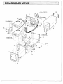
DISASSEM
VIEWS
~.~ 1'0'
~ .PI
,
(i~ (for MZ·80FD)
Ii
~~(for MZ·80FDK)
I
-
~
{]) '\\
~
"""D'I
(for MZ·80FD)
/(tl;I9'
/
/
R
~
(38)
'21 (for MZ-80FD)
~22.' (for MZ-80FDK)
P--@3)
'-25) (for MZ-BOFD)
,27' (for
MZ·BOFDK)
- 35-
(~
• Power Supply
6 '~
W
tI& -{j)
'jr
I
~_ @
I
(LEO PWBI
,.'
- ~ -
• Disk drivl! (21
Fmot d""r
Froot t>o,. 1
161
- 37-
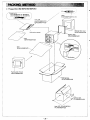
• Floppy Disk (MZ-80FD/MZ-80FDK)
"\1
~~;;;~l~O---)
Braided wire
DTip·0039PAZZ (for MZ·80FD)
DTip·0042PAZZ (for MZ·80FDK)
~
Label
/
(TLBHOOO2PAZZ) for U.K.
.~
A.C. cord
(QACCK0050AFZZ)
(QACCBOOOl PAZZ
Packing Add. (rear)
(SPAKA0027PAZZ)
I nstruction manual
------- Sack
(SSAK H0022PAZZ)
Sack
(SSAKH0030PAZZ)
/
Packing Add. (front)
(SPAKA0026PAZZ)
Packing Case
(SPAKC0095PAZZ)
Label [KJ (for MZ·80FDK)
(TLABE0002PAZZ)
-38-
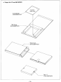
• Floppy disk I/O card (MZ-80FIO)
Protected Seat
(SPAKP0002PAZZ)
PWB Sleeve
(SPAKS0028PAZZ)
Packing Case
~---
(SPAKC0087PAZZ)
'--_ _ _ Seal x 2
(TSELF0001 PAZZ)
L -_ _ _ _ _ _ _ _ _ _ _ _ _ _ _ _ _ _ _ _ _ _ _ _ _ _ _ _ _ _ _ _ _ _ _ _ _ _ _ _ _ _ _
- 39-
~
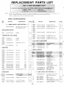
REPLACEMENT PARTS LIST
Be sure to use regular parts for securing the safety and reliability of the set. Parts marked with" 6. " and parts crosshatched (in black) are especially important for maintaining the safety and protecting ability of the set.
Be sure to replace them with parts of specified part number.
NOTES
MODEL MZ-80FD/MZ-80FDK
REF.
NO.
PART NO.
DESCRIPTION
CODE
* * * POWER SUPPLY UNIT SECTION * * *
DBOXDOOO9PAZZ
REF.
NO.
PART NO.
C303}
C403
C304
Assembled Power Supply unit
(Not replacement item)
CODE
VCOYKUl HM1B3K
O.OlBMFD 50V Film
AB
VCEAAU 1CM33BM
3.300MFD 16V Aluminum
AG
VCOY KU 1HM102K
0.001 MFD 50V Film
AB
C~07
VCSACU1VE106M
10MFD 35V Tantalum
AE
C409
C30B
VCOYKUl HM6B2K
0-D06BMFD 50V Film
AA
VCOYKUl HM332K
0.0033MFD 50V Film
AB
VCEAAU 1AM33BM
3.300MFD 10V Aluminum
AF
C305 }
C406
INTEGRATED CIRCUIT
DESCRIPTION
AI
C~61
C307
ICl \
IC2J
RH-iX0151 PAZZ
AW
SG3524
TRANSISTORS AND DIODES
0301}
0401
D201
D301 )
D302
D401
D402
VS2SAB92///-1
2SAB92
AN
VHDS5VB10//-l
S5VB1O
AL
VHDERBB1-004/
ERBB1-004 or RK-14
AG
C402 }
C405
C404
COl LS AND TRANSFORMER
RH-PX0033PAZZ
~Tl.a,
RESISTORS
R301 }
R401
VRD-ST2EF272J
2.7K ohm
1/4W
AA
R302}
R402
VRF-GV3DBR05K
0.05 ohm
2W
AD
R303}
R403
VRD-SU2EF563J
56K ohm
1/4W
AA
R304 }
R404
VRD-SU2EF272J
2.7K ohm
1/4W
AA
R305 }
R405
VRD-SU2EF472J
4.7K ohm
1/4W
AA
VRD-ST2EF472J
4.7K ohm
1/4W
AA
VRD-ST2EF153J
VRD-SU2EF332J
VRD-ST2EF 102J
VRD-SU2EF392J
15K ohm
3.3K ohm
1 K ohm
3.9K ohm
1/4W
1/4W
1/4W
1i4W
AA
AA
AA
AA
RVR-M0010PAZZ
Variable Resistor 1 K ohm
AC
R306 }
R406
R407
R307
R30B
R309
R40B
VR301 }
VR401
C2?1 }
RC-CZOl80PAZZ
VCEAAU 1 VM25BY
AO
Coil
AM
fuse T'SOOf!1A
'use'3..15.4.
4
DSOCN0064PAZZ
5
DSOCN0065PAZZ
6
7
B
9
OPLGZ0050PAZZ
PRDAR0021PAZZ
PRDAR0022PAZZ
LANGK0270PAZZ
10
11
12
LANGOO022PAZZ
LANGOO023PAZZ
PSPA KOO05VAZZ
Lead Wire with 4-Pin
Connector
Lead Wire with 2-Pin
Connector
2-Pin Plug
Radiation Plate
Radiation Plate
Switch. Inlet. Filter P.W.B.
Fixing Angle
PWB Fixing Angle
PWB Fixing Angle
LED Specer
AI
AG
AE
AC
AT
AD
AF
AD
AE
AA
* * * DISK DRIVE UNIT SECTION * * *
O.041MFO 2ooV'
RMEMR0001 PAZZ
Line capac:it~r
2.500MFD 35V Aluminum
AF
C206
C301 }
C401
C302
Coil
MISCE LLANEOUS
CAPACITORS
llCl01 }
llCl02
..... R11tN~AZ~
~L·~Qf; ':·RTBN~~.
L301 }
RTRNZOO07PAZZ
L402
RTRNZOO09PAZZ
L401
AD
LED
AI
VCK YPUl NBl 04Z
0.1 MFD 12V Ceramic
AB
VCOYKU1HM222K
0.0022MFD 50V Film
AA
13
14
15
16
95AF 140622-01
95AF12013B-Ol
95AF140630-01
95AF120151-01
17
9 5AF 140640-01
- 40-
Assembled Disk Drive Unit
(Not replacement item)
Belt
PWB Unit Ass'y
Index Lamp Ass'y
Medium Guide L Ass'y (with
Write Protect Sensor. Lamp)
Operation indicator
AI
BA
BL
BN
AZ
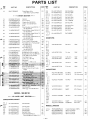
PARTS LIST
-
REF.
NO.
PART NO.
95AF130246-01
18
DESCRIPTION
CODE
REF.
NO.
PART NO.
Drive Motor Ass'y
(with Motor Control PWB)
BY
ICS
IC9
RH-iX0124PAZZ
RH-iXOOS1 PAZZ
SN74LS245N
SN74LS139N
AT
AL
IC10}
IC17
RH-iX0070PAZZ
SN74LSOON
AE
IC11
IC13
IC14
RH-iX0141PAZZ
RH-iX0216PAZZ
RH-iX0213PAZZ
SN74LS125N
SN74LS161N
LSI T3444M
AK
AN
BS
IC15}
IC1S
RH-iX0079PAZZ
SN74LS74N
AG
IC16
IC19
IC20
IC21
RH-IX0127PAZZ
RH-iX0217PAZZ
RH-iX0214PAZZ
RH-iX0131PAZZ
SN74LS107N
SN74145
SN74LS122N
SN7414N
AG
AM
AH
AM
R H-iX0220PAZZ
SN75452BP
AK
* * * OTHER SECTION * * *
19
20
21
22
23
24
GCABA8121PASA
GWAKP0005PASA
LCHSM0090PASA
LCHSM0092PASA
GLEGR0001PAZZ
T LABZ0029 PAZZ
25
TLABZ0033PAZZ
26
T LABZ0034PAZZ
TLABZ0035PAZZ
27
,.... 28
t"'"
29
30
31
LANGF0017PAZZ
LANG F0023PAZZ
LANG K0269PAZZ
DSOCN0040PAZZ
32
DSOCN0046PAZZ
33
OTANN0002PAZZ
DTiP-0039PAZZ
DTiP-0042PAZZ
LH LDF0015PAZZ
LH LDW0006PAZZ
LH LDW9003CEZZ
LBNDC0003PAZZ
PCUSG0005PAZZ
34
35
36
37
38
;
•.
Cabinet
Front Frame
Chassis (for MZ-SOFD)
Chasis (for MZ-SOFDK)
Foot
Drive Number Lavel DRIVE 1
(for MZ-SOFD)
Drive Number Label DRIVE 2
(for MZ-SOFD)
Drive Number Label DRIVE 3
(for MZ-SOFDK)
Drive Number Label DRIVE 4
(for MZ-SOFDK)
Drive Fixing Angle
Front Frame Fixing Angle
Flat Cable Ass'y Fixing Angle
Flat Cable Ass'y
(for MZ-SOFD)
Flat Cable Ass'y
(for MZ-SOFDK)
Ground Terminal
Braided Wire (for MZ-SOFD)
Braided Wire (for MZ-SOFDK)
Filter PWB Fixing Holder
Flat Cable Fixer
Cord Fixer. HW-146
Wire Band
Cushion 5 x 100 x t1.0
BF
AR
BH
BH
AB
AB
AB
IC\22 }
AB
AB
RESISTORS
AE
AM
AE
BP
LX-BZ0067PAFN
LX-BZ006SPAFN
40
VRD-SC2EF221 J
220 ohm
1/4W
V R D-SC2E F 102J
1 K ohm
1/4W
AA
VRD-SC2EF1S2J
VRD-SC2EF561J
1.SR ohm
560 ohm
1/4W
1/4W
AA
AA
VRD-SC2EF151J
150 ohm
1/4W
AA
VRD-SC2EF273J
27K ohm
1/4W
AA
BU
:~O )
AH
AS
AS
AC
AD
AA
AB
AA
R11
R13
R14
R7
R9
:;~ )
... . . / . . .
.•"el...~. :t.-""!"..•.•..•. ·~."""~.....,..•lf~••·.~~~"-':l.....·.
~v~ r~
~,\,,;oi.
"'":u \ VJ:'~~"',i~~;~,*"<'~:<i~'\
1 ;.oh
CODE
IC24
Cl)ACCKOO50AF.ZZ. A.C •.CEmlI
39
DESCRIPTION
R19
R15
Screw for Disk Drive
Screw for Disk Drive Fixing
Angle
CAPACITORS
TiNSE0007PAZZ
.1
.
TSPCEQClO4f'AZZ .
!:rs:\~Wt0*'F"'W'
,:",
,q.", '", '''~ 0""'~1i, dJ N'~I'
······'Tt::ABflOOQ2PAa-··~·l··.,w:;.,fil"·
T LAB EOOO 1PAZZ
T LAB E0002PAZZ
Caution Label
Label [Kj (for MZ-SOFD K)
•
AB
AB
MODEL MZ-80FIO
***
VCTYPU1BD104Z
VCEAAU1CW107Y
0.1 MFD
100 MFD
12V Ceram ic
16V Aluminum
AB
AB
C~ 1
VCSACU1AE106K
10 MFD
10V Tantalum
AE
VCCSPR 1H6331J
330PF
50V Ceramic
AA
VCCSPR1 H6561J
560PF
50V Ceramic
AA
VCSACU 1AE336K
33MFD
10V Tantalum
AF
VCCCPR1H3101J
VCOYKU1HM333K
100PF
0.033MFD
50V Ceramic
50V Film
AA
AB
11
13
17
19
.. ·.·.·.(fGrtyft
t '.
C1
C2
I/O CARD UNIT SECTION * * *
INTEGRATED CIRCUIT
IC1 }
IC12
RH-iX0074PAZZ
SN74LS04N
AE
IC2}
IC3
IC4
IC5
IC6
IC7
RH-iX0077PAZZ
SN74LS30N
AE
RH-iX007SPAZZ
RH-iX0071 PAZZ
RH-iX0215PAZZ
RH-iX0219PAZZ
SN74LS32N
SN74LS02N
SN74LS174N
ROM SN74S474N (or
RH-iX023SPAZZ IlPB417C)
AF
AE
AL
BD
C4}
CS
C5 }
C9
C6
C10
C12
C16
C1S
C20
C14
C15
MISCE LLANEOUS
XT AL
CN1
- 41-
RCRSA0009PAZZ
OPLGZ0049PAZZ
OSOCZ0010PAZZ
OSOCZOO 12PAZZ
Crystal Oscillator S MHz
34-Pin Connector
24-Pin IC Socket
40-Pin IC Socket
AP
AR
AM
AR
M E M0
T
A800820HO
I
Printed in Japan