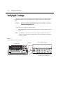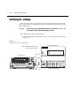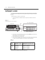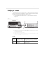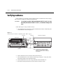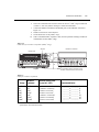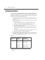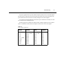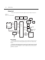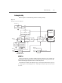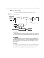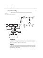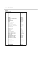
1
Model 2015
THD Multimeter
Service Manual
SENSE
Ω 4 WIRE
INPUT
HI
STEP SCAN CH1
REM
TALK
LSTN
SRQ
SHIFT
TIMER HOLD TRIG
FAST
CH2
MED
CH3
SLOW
CH4
CH5
REL
FILT
CH6
AUTO
CH7
CH8
ERR
CH9
BUFFER
CH10 MATH
REAR
STAT
4W
350V
PEAK
1000V
PEAK
!
2015 THD MULTIMETER
SHIFT
MATH
THD
dBm
DCV
ACV
DCI
dB
CONT
ACI
Ω2
LO
PERIOD TCOUPL
Ω4
FREQ
TEMP
RANGE
DELAY
LOCAL
POWER
HOLD
EX TRIG TRIG
SAVE
SETUP
SOURCE MEAS
LIMITS
ON/OFF
STORE RECALL
CONFIG
HALT
STEP
SCAN
TEST
500V
PEAK
INPUTS
F
R
CAL
FILTER
REL
GPIB
RS232
DIGITS RATE
AUTO
FRONT/REAR
3A 250V
RANGE
EXIT
ENTER
THD
Contains Servicing Information
AMPS
WARRANTY
Keithley Instruments, Inc. warrants this product to be free from defects in material and workmanship for a
period of 3 years from date of shipment.
Keithley Instruments, Inc. warrants the following items for 90 days from the date of shipment: probes,
cables, rechargeable batteries, diskettes, and documentation.
During the warranty period, we will, at our option, either repair or replace any product that proves to be
defective.
To exercise this warranty, write or call your local Keithley representative, or contact Keithley headquarters in
Cleveland, Ohio. You will be given prompt assistance and return instructions. Send the product, transportation prepaid, to the indicated service facility. Repairs will be made and the product returned, transportation
prepaid. Repaired or replaced products are warranted for the balance of the original warranty period, or at
least 90 days.
LIMITATION OF WARRANTY
This warranty does not apply to defects resulting from product modification without Keithley’s express written consent, or misuse of any product or part. This warranty also does not apply to fuses, software, nonrechargeable batteries, damage from battery leakage, or problems arising from normal wear or failure to follow instructions.
THIS WARRANTY IS IN LIEU OF ALL OTHER WARRANTIES, EXPRESSED OR IMPLIED,
INCLUDING ANY IMPLIED WARRANTY OF MERCHANTABILITY OR FITNESS FOR A PARTICULAR USE. THE REMEDIES PROVIDED HEREIN ARE BUYER’S SOLE AND EXCLUSIVE REMEDIES.
NEITHER KEITHLEY INSTRUMENTS, INC. NOR ANY OF ITS EMPLOYEES SHALL BE LIABLE
FOR ANY DIRECT, INDIRECT, SPECIAL, INCIDENTAL OR CONSEQUENTIAL DAMAGES ARISING OUT OF THE USE OF ITS INSTRUMENTS AND SOFTWARE EVEN IF KEITHLEY INSTRUMENTS, INC., HAS BEEN ADVISED IN ADVANCE OF THE POSSIBILITY OF SUCH DAMAGES.
SUCH EXCLUDED DAMAGES SHALL INCLUDE, BUT ARE NOT LIMITED TO: COSTS OF
REMOVAL AND INSTALLATION, LOSSES SUSTAINED AS THE RESULT OF INJURY TO ANY PERSON, OR DAMAGE TO PROPERTY.
1/99
Model 2015 THD Multimeter
Service Manual
©1998, Keithley Instruments, Inc.
All rights reserved.
Cleveland, Ohio, U.S.A.
Third Printing, June 1999
Document Number: 2015-902-01 Rev. C
Manual Print History
The print history shown below lists the printing dates of all Revisions and Addenda created
for this manual. The Revision Level letter increases alphabetically as the manual undergoes subsequent updates. Addenda, which are released between Revisions, contain important change information that the user should incorporate immediately into the manual. Addenda are numbered
sequentially. When a new Revision is created, all Addenda associated with the previous Revision
of the manual are incorporated into the new Revision of the manual. Each new Revision includes
a revised copy of this print history page.
Revision A (Document Number 2015-902-01) ................................................................. May 1998
Revision B (Document Number 2015-902-01) ..................................................................July 1998
Revision C (Document Number 2015-902-01) ................................................................. June 1999
All Keithley product names are trademarks or registered trademarks of Keithley Instruments, Inc.
Other brand names are trademarks or registered trademarks of their respective holders.
Safety Precautions
The following safety precautions should be observed before using this product and any associated instrumentation. Although some instruments and accessories would normally be used with non-hazardous voltages, there
are situations where hazardous conditions may be present.
This product is intended for use by qualified personnel who recognize shock hazards and are familiar with the
safety precautions required to avoid possible injury. Read the operating information carefully before using the
product.
The types of product users are:
Responsible body is the individual or group responsible for the use and maintenance of equipment, for ensuring
that the equipment is operated within its specifications and operating limits, and for ensuring that operators are
adequately trained.
Operators use the product for its intended function. They must be trained in electrical safety procedures and
proper use of the instrument. They must be protected from electric shock and contact with hazardous live circuits.
Maintenance personnel perform routine procedures on the product to keep it operating, for example, setting
the line voltage or replacing consumable materials. Maintenance procedures are described in the manual. The
procedures explicitly state if the operator may perform them. Otherwise, they should be performed only by service personnel.
Service personnel are trained to work on live circuits, and perform safe installations and repairs of products.
Only properly trained service personnel may perform installation and service procedures.
Exercise extreme caution when a shock hazard is present. Lethal voltage may be present on cable connector
jacks or test fixtures. The American National Standards Institute (ANSI) states that a shock hazard exists when
voltage levels greater than 30V RMS, 42.4V peak, or 60VDC are present. A good safety practice is to expect
that hazardous voltage is present in any unknown circuit before measuring.
Users of this product must be protected from electric shock at all times. The responsible body must ensure that
users are prevented access and/or insulated from every connection point. In some cases, connections must be
exposed to potential human contact. Product users in these circumstances must be trained to protect themselves
from the risk of electric shock. If the circuit is capable of operating at or above 1000 volts, no conductive part
of the circuit may be exposed.
As described in the International Electrotechnical Commission (IEC) Standard IEC 664, digital multimeter
measuring circuits (e.g., Keithley Models 175A, 199, 2000, 2001, 2002, and 2010) are Installation Category II.
All other instruments’ signal terminals are Installation Category I and must not be connected to mains.
Do not connect switching cards directly to unlimited power circuits. They are intended to be used with impedance limited sources. NEVER connect switching cards directly to AC mains. When connecting sources to
switching cards, install protective devices to limit fault current and voltage to the card.
Before operating an instrument, make sure the line cord is connected to a properly grounded power receptacle.
Inspect the connecting cables, test leads, and jumpers for possible wear, cracks, or breaks before each use.
For maximum safety, do not touch the product, test cables, or any other instruments while power is applied to
the circuit under test. ALWAYS remove power from the entire test system and discharge any capacitors before:
connecting or disconnecting cables or jumpers, installing or removing switching cards, or making internal
changes, such as installing or removing jumpers.
Do not touch any object that could provide a current path to the common side of the circuit under test or power
line (earth) ground. Always make measurements with dry hands while standing on a dry, insulated surface capable of withstanding the voltage being measured.
The instrument and accessories must be used in accordance with its specifications and operating instructions or
the safety of the equipment may be impaired.
Do not exceed the maximum signal levels of the instruments and accessories, as defined in the specifications
and operating information, and as shown on the instrument or test fixture panels, or switching card.
When fuses are used in a product, replace with same type and rating for continued protection against fire hazard.
Chassis connections must only be used as shield connections for measuring circuits, NOT as safety earth ground
connections.
If you are using a test fixture, keep the lid closed while power is applied to the device under test. Safe operation
requires the use of a lid interlock.
If a
tation.
screw is present, connect it to safety earth ground using the wire recommended in the user documen-
The ! symbol on an instrument indicates that the user should refer to the operating instructions located in
the manual.
The
symbol on an instrument shows that it can source or measure 1000 volts or more, including the combined effect of normal and common mode voltages. Use standard safety precautions to avoid personal contact
with these voltages.
The WARNING heading in a manual explains dangers that might result in personal injury or death. Always
read the associated information very carefully before performing the indicated procedure.
The CAUTION heading in a manual explains hazards that could damage the instrument. Such damage may
invalidate the warranty.
Instrumentation and accessories shall not be connected to humans.
Before performing any maintenance, disconnect the line cord and all test cables.
To maintain protection from electric shock and fire, replacement components in mains circuits, including the
power transformer, test leads, and input jacks, must be purchased from Keithley Instruments. Standard fuses,
with applicable national safety approvals, may be used if the rating and type are the same. Other components
that are not safety related may be purchased from other suppliers as long as they are equivalent to the original
component. (Note that selected parts should be purchased only through Keithley Instruments to maintain accuracy and functionality of the product.) If you are unsure about the applicability of a replacement component,
call a Keithley Instruments office for information.
To clean an instrument, use a damp cloth or mild, water based cleaner. Clean the exterior of the instrument only.
Do not apply cleaner directly to the instrument or allow liquids to enter or spill on the instrument. Products that
consist of a circuit board with no case or chassis (e.g., data acquisition board for installation into a computer)
should never require cleaning if handled according to instructions. If the board becomes contaminated and operation is affected, the board should be returned to the factory for proper cleaning/servicing.
Rev. 2/99
Table of Contents
1 Performance Verification
Introduction ........................................................................................ 1-2
Verification test requirements ............................................................ 1-3
Environmental conditions .............................................................. 1-3
Warm-up period ............................................................................. 1-3
Line power ..................................................................................... 1-3
Recommended test equipment ........................................................... 1-4
Verification limits ............................................................................... 1-5
Example reading limit calculation ................................................. 1-5
Calculating resistance reading limits ............................................. 1-5
Restoring factory defaults .................................................................. 1-6
Performing the verification test procedures ....................................... 1-7
Test summary ................................................................................. 1-7
Test considerations ......................................................................... 1-7
Verifying DC voltage ......................................................................... 1-8
Verifying AC voltage ....................................................................... 1-10
Verifying DC current ....................................................................... 1-12
Verifying AC current ........................................................................ 1-13
Verifying resistance ......................................................................... 1-14
Verifying temperature ...................................................................... 1-16
Verifying frequency ......................................................................... 1-17
Verifying total harmonic distortion .................................................. 1-18
Verifying function generator amplitude ........................................... 1-19
2 Calibration
Introduction ........................................................................................ 2-2
Environmental conditions .................................................................. 2-3
Warm-up period ............................................................................. 2-3
Line power ..................................................................................... 2-3
Calibration considerations ................................................................. 2-4
Calibration code ................................................................................. 2-5
Front panel calibration code ........................................................... 2-5
Remote calibration code ................................................................. 2-5
Comprehensive calibration ................................................................ 2-6
Calibration cycle ............................................................................ 2-6
Recommended equipment .............................................................. 2-6
Aborting calibration ....................................................................... 2-7
Front panel calibration ................................................................... 2-7
Preparing the Model 2015 for calibration ...................................... 2-7
Front panel short and open calibration ........................................... 2-8
DC volts calibration ....................................................................... 2-9
Resistance calibration ..................................................................
DC current calibration .................................................................
AC voltage calibration .................................................................
AC current calibration .................................................................
Distortion calibration ...................................................................
Function generator calibration .....................................................
Setting calibration dates and saving calibration ..........................
Remote calibration .......................................................................
Preparing the Model 2015 for calibration ....................................
Short and open calibration ...........................................................
DC volts calibration .....................................................................
Resistance calibration ..................................................................
DC current calibration .................................................................
AC voltage calibration .................................................................
AC current calibration .................................................................
Distortion calibration ...................................................................
Function generator calibration .....................................................
Programming calibration dates ....................................................
Saving calibration constants ........................................................
Locking out calibration ................................................................
Manufacturing calibration ...............................................................
Recommended test equipment .....................................................
Unlocking manufacturing calibration ..........................................
Measuring synthesizer signal amplitude ......................................
Front panel manufacturing calibration .........................................
Remote manufacturing calibration ..............................................
2-11
2-12
2-13
2-14
2-14
2-15
2-16
2-16
2-17
2-17
2-18
2-19
2-20
2-21
2-22
2-22
2-23
2-23
2-23
2-23
2-24
2-24
2-24
2-24
2-25
2-26
3 Routine Maintenance
Introduction ....................................................................................... 3-2
Setting the line voltage and replacing the line fuse ....................... 3-2
Replacing the AMPS fuse .............................................................. 3-3
4 Troubleshooting
Introduction .......................................................................................
Repair considerations ........................................................................
Power-on self-test ..............................................................................
Front panel tests ................................................................................
KEY test .........................................................................................
DISP test ........................................................................................
Principles of operation ......................................................................
Power supply .................................................................................
Display board .................................................................................
Digital circuitry ..............................................................................
4-2
4-3
4-4
4-5
4-5
4-5
4-6
4-6
4-8
4-9
Analog circuitry ........................................................................... 4-11
Distortion digital circuitry ............................................................ 4-13
Distortion analog circuitry ........................................................... 4-15
Sine generator circuitry ................................................................ 4-16
Troubleshooting ............................................................................... 4-18
Display board checks ................................................................... 4-18
Power supply checks .................................................................... 4-19
Digital circuitry checks ................................................................ 4-20
Analog signal switching states ..................................................... 4-21
5 Disassembly
Introduction ........................................................................................ 5-2
Handling and cleaning ....................................................................... 5-3
Handling PC boards ....................................................................... 5-3
Solder repairs ................................................................................. 5-3
Static sensitive devices ................................................................... 5-4
Assembly drawings ............................................................................ 5-5
Disassembly procedures .................................................................... 5-6
Case cover removal ........................................................................ 5-6
DMM board removal ...................................................................... 5-6
DSP board removal ........................................................................ 5-7
Front panel disassembly ................................................................. 5-8
Removing power components ........................................................ 5-8
Instrument reassembly ....................................................................... 5-9
Input terminal wire connections ..................................................... 5-9
Power module wire connections .................................................... 5-9
Changing trigger link lines .............................................................. 5-10
Main CPU firmware replacement .................................................... 5-11
6 Replaceable Parts
Introduction ........................................................................................ 6-2
Parts lists ............................................................................................ 6-2
Ordering information ......................................................................... 6-2
Factory service ................................................................................... 6-2
Component layouts ............................................................................ 6-2
A Specifications
Accuracy calculations ....................................................................... A-9
Calculating DC characteristics accuracy ....................................... A-9
Calculating AC characteristics accuracy ....................................... A-9
Calculating dBm characteristics accuracy .................................. A-10
Calculating dB characteristics accuracy ...................................... A-10
Distortion characteristics ............................................................. A-11
Calculating generator amplitude accuracy ..................................
Additional derating factors .........................................................
Optimizing measurement accuracy ................................................
DC voltage, DC current, and resistance ......................................
AC voltage and AC current .........................................................
Temperature ................................................................................
Optimizing measurement speed .....................................................
DC voltage, DC current, and resistance ......................................
AC voltage and AC current .........................................................
Temperature ................................................................................
A-12
A-12
A-13
A-13
A-13
A-13
A-14
A-14
A-14
A-14
B Calibration Reference
Introduction ...................................................................................... B-2
Command summary ......................................................................... B-3
Miscellaneous calibration commands .............................................. B-5
:CODE .......................................................................................... B-5
:COUNt? ....................................................................................... B-5
:INIT ............................................................................................. B-6
:LOCK .......................................................................................... B-6
:LOCK? ........................................................................................ B-7
:SAVE ........................................................................................... B-7
:DATE ........................................................................................... B-8
:NDUE .......................................................................................... B-8
DC calibration commands ................................................................ B-9
:STEP1 .......................................................................................... B-9
:STEP2 ........................................................................................ B-10
:STEP3 ........................................................................................ B-10
:STEP4 ........................................................................................ B-10
:STEP5 ........................................................................................ B-11
:STEP6 ........................................................................................ B-11
:STEP7 ........................................................................................ B-11
:STEP8 ........................................................................................ B-12
:STEP9 ........................................................................................ B-12
:STEP10 ...................................................................................... B-12
:STEP11 ...................................................................................... B-13
:STEP12 ...................................................................................... B-13
AC calibration commands .............................................................. B-14
:AC:STEP<n> ............................................................................. B-15
Distortion and function generator calibration commands ............. B-16
:DIST:STEP1 .............................................................................. B-16
:DIST:STEP2 .............................................................................. B-16
:FGEN:STEP1 ............................................................................ B-16
Manufacturing calibration commands ............................................
:AC:STEP<14|15> ......................................................................
:DC:STEP0 ..................................................................................
Remote error reporting ...................................................................
Error summary ............................................................................
Error queue ..................................................................................
Status byte EAV (Error Available) bit .........................................
Generating an SRQ on error ........................................................
Detecting calibration step completion ............................................
Using the *OPC? query ...............................................................
Using the *OPC command ..........................................................
Generating an SRQ on calibration complete ...............................
B-17
B-17
B-17
B-18
B-18
B-20
B-20
B-20
B-21
B-21
B-21
B-22
C Calibration Program
Introduction .......................................................................................
Computer hardware requirements .....................................................
Software requirements ......................................................................
Calibration equipment ......................................................................
General program instructions ...........................................................
C-2
C-2
C-2
C-2
C-3
List of Illustrations
1 Performance Verification
Connections for DC volts verification .............................................. 1-8
Connections for AC volts verification ............................................. 1-10
Connections for DC current verification ......................................... 1-12
Connections for AC current verification ......................................... 1-13
Connections for resistance verification (100Ω-10MΩ range) ........ 1-14
Connections for resistance verification (100MΩ range) ................. 1-15
Connections for frequency verification ........................................... 1-17
Connections for total harmonic distortion verification ................... 1-18
Connections for function generator amplitude verification ............ 1-19
2 Calibration
Low-thermal short connections ......................................................... 2-8
Connections for DC volts and ohms calibration ............................... 2-9
Connections for DC and AC amps calibration ................................ 2-12
Connections for AC volts calibration .............................................. 2-13
Connections for distortion calibration ............................................. 2-15
Connections for function generator calibration ............................... 2-15
Synthesizer connections for manufacturing calibration .................. 2-25
3 Routine Maintenance
Power module .................................................................................... 3-3
4 Troubleshooting
Power supply block diagram ............................................................. 4-6
Digital circuitry block diagram ......................................................... 4-8
Analog circuitry block diagram ....................................................... 4-11
Distortion digital circuitry block diagram ....................................... 4-13
Distortion analog circuitry block diagram ...................................... 4-15
Sine generator circuitry block diagram ........................................... 4-16
5 Disassembly
Trigger link line connections ........................................................... 5-10
List of Tables
1 Performance Verification
Recommended verification equipment ........................................... 1-4
DCV reading limits ........................................................................ 1-9
ACV reading limits ....................................................................... 1-11
DCI limits ..................................................................................... 1-12
ACI limits ..................................................................................... 1-13
Limits for resistance verification .................................................. 1-15
Thermocouple temperature verification reading limits ................ 1-16
2 Calibration
Recommended equipment for comprehensive calibration ............. 2-6
Comprehensive calibration procedures .......................................... 2-8
DC volts calibration summary ...................................................... 2-10
Ohms calibration summary .......................................................... 2-11
DC current calibration summary .................................................. 2-12
AC voltage calibration summary .................................................. 2-13
AC current calibration summary .................................................. 2-14
Distortion and function generator calibration summary .............. 2-15
DC voltage calibration programming steps .................................. 2-18
Resistance calibration programming steps ................................... 2-19
DC current calibration programming steps .................................. 2-20
AC voltage calibration programming steps .................................. 2-21
AC current calibration programming steps .................................. 2-22
Distortion and function generator calibration steps ..................... 2-22
Recommended equipment for manufacturing calibration ............ 2-24
3 Routine Maintenance
Power line fuse ............................................................................... 3-3
4 Troubleshooting
Power supply components .............................................................. 4-7
Display board checks ................................................................... 4-18
Power supply checks .................................................................... 4-19
Digital circuitry checks ................................................................ 4-20
DCV signal switching .................................................................. 4-21
ACV and FREQ signal switching ................................................. 4-21
Ω2 signal switching ...................................................................... 4-22
Ω4 signal switching ...................................................................... 4-22
Ω2/Ω4 reference switching .......................................................... 4-22
DCA signal switching .................................................................. 4-23
ACA signal switching ..................................................................
DCV signal multiplexing and gain ..............................................
ACV and ACA signal multiplexing and gain ...............................
DCA signal multiplexing and gain ..............................................
Ω2 signal multiplexing and gain ..................................................
Ω4 signal multiplexing and gain ..................................................
Switching device locations ............................................................
4-23
4-23
4-23
4-24
4-24
4-24
4-25
5 Disassembly
Input terminal wire colors .............................................................. 5-9
Power module wire colors .............................................................. 5-9
6 Replaceable Parts
DMM (mother) board parts list ...................................................... 6-3
Display board parts list .................................................................. 6-9
Distortion (DSP) board parts list .................................................. 6-10
Mechanical parts list .................................................................... 6-14
B Calibration Reference
Remote calibration command summary ....................................... B-3
DC calibration commands ............................................................. B-9
AC calibration commands ........................................................... B-14
Distortion and function generator calibration commands ........... B-16
Calibration error summary .......................................................... B-18
1
Performance
Verification
1-2
Performance Verification
Introduction
Use the procedures in this section to verify that Model 2015 Multimeter accuracy is within
the limits stated in the instrument’s one-year accuracy specifications. You can perform these verification procedures:
•
•
•
When you first receive the instrument to make sure that it was not damaged during shipment, and that the unit meets factory specifications.
If the instrument’s accuracy is questionable.
Following calibration.
WARNING
NOTE
The information in this section is intended only for qualified service personnel. Do not attempt these procedures unless you are qualified to do so.
If the instrument is still under warranty and its performance is outside specified
limits, contact your Keithley representative or the factory to determine the correct
course of action.
Performance Verification
1-3
Verification test requirements
Be sure that you perform the verification tests:
•
•
•
•
•
Under the proper environmental conditions.
After the specified warm-up period.
Using the correct line voltage.
Using the proper calibration equipment.
Using the specified reading limits.
Environmental conditions
Conduct your performance verification procedures in a test environment that has:
•
•
An ambient temperature of 18˚ to 28°C (65˚ to 82°F).
A relative humidity of less than 80% unless otherwise noted.
Warm-up period
Allow the Model 2015 Multimeter to warm up for at least one hour before conducting the verification procedures.
If the instrument has been subjected to temperature extremes (those outside the ranges stated
above), allow additional time for the instrument’s internal temperature to stabilize. Typically,
allow one extra hour to stabilize a unit that is 10°C (18°F) outside the specified temperature
range.
Also, allow the test equipment to warm up for the minimum time specified by the
manufacturer.
Line power
The Model 2015 Multimeter requires a line voltage of 100V/120V/220V/240V, ±10% and a
line frequency of 45Hz to 66Hz and 360Hz to 440Hz.
1-4
Performance Verification
Recommended test equipment
Table 1-1 summarizes recommended verification equipment. You can use alternate equipment
as long as that equipment has specifications at least as good as those listed in Table 1-1. Keep in
mind, however, that the calibrator will add to the uncertainty of each measurement.
Table 1-1
Recommended verification equipment
Fluke 5700A Calibrator:
DC voltage
AC voltage
(1kHz, 50kHz)
100mV:±14ppm
1.0V:±7ppm
10V:±5ppm
100V:±7ppm
1000V:±9ppm
100mV:±200ppm
1.0V:±82ppm
10V:±82ppm
100V:±90ppm
700V:±85ppm
DC current
10mA:±60ppm
100mA:±70ppm
1A:±110ppm
2.2A:±94ppm
AC current
(1kHZ)
1A:±690ppm
2.2A:±682ppm
Resistance
100Ω:±17ppm
1kΩ:±12ppm
10kΩ:±11ppm
100kΩ:±13ppm
1MΩ:±18ppm
10MΩ:±37ppm
100MΩ:±120ppm
Fluke 5725A Amplifier:
AC Voltage, 50kHz: 700V, ±375ppm
Keithley 3930A or 3940 Frequency Synthesizer:
1V RMS, 1kHz, ±5ppm
Stanford Research Systems DS-360 Ultra Low Distortion Function Generator:
1kHz, .0.95V RMS sine wave, -100dB THD
Miscellaneous Equipment:
Double banana plug to double banana plug shielded cable
BNC to double banana plug shielded cable
NOTE: The Fluke 5725A amplifier is necessary only if you wish to verify the 750V AC range at 50kHz.
Verification at 220V, 50kHz using only the 5700A calibrator is adequate for most applications.
Performance Verification
1-5
Verification limits
The verification limits stated in this section have been calculated using only the Model 2015
one-year accuracy specifications, and they do not include test equipment uncertainty. If a particular measurement falls slightly outside the allowable range, recalculate new limits based on
both Model 2015 specifications and pertinent calibration equipment specifications.
Example reading limit calculation
The following is an example of how reading limits have been calculated:
Assume you are testing the 10V DC range using a 10V input value. Using the Model 2015
one-year accuracy specification for 10V DC of ± (30ppm of reading + 5ppm of range), the calculated limits are:
Reading limits = 10V ± [(10V × 30ppm) + (10V × 5ppm)]
Reading limits = 10V ± (.0003 + .00005)
Reading limits = 10V ± .00035V
Reading limits = 9.99965V to 10.00035V
Calculating resistance reading limits
Resistance reading limits must be recalculated based on the actual calibration resistance values supplied by the equipment manufacturer. Calculations are performed in the same manner as
shown in the preceding example, except, of course, that you should use the actual calibration
resistance values instead of the nominal values when performing your calculations.
1-6
Performance Verification
Restoring factory defaults
Before performing the verification procedures, restore the instrument to its factory defaults
as follows:
1.
Press SHIFT and then SETUP. The instrument will display the following prompt:
RESTORE: FACT.
2.
Using either range key, select FACT, then restore the factory default conditions by pressing ENTER.
Factory defaults will be set as follows:
Speed: medium
Filter: 10 readings
3.
Performance Verification
1-7
Performing the verification test procedures
Test summary
Verification test procedures include:
•
•
•
•
•
•
•
•
•
DC volts
AC volts
DC current
AC current
Resistance
Temperature
Frequency
Total harmonic distortion
Function generator amplitude
If the Model 2015 is not within specifications and not under warranty, see the calibration procedures in Section 2.
Test considerations
When performing the verification procedures:
•
•
•
•
•
•
•
Be sure to restore factory defaults as outlined above.
After restoring factory defaults and selecting the measuring function, select the SLOW
integration rate with the RATE key.
Make sure that the equipment is properly warmed up and connected to the front panel
input jacks. Also make sure that the front panel input jacks are selected with the INPUTS
switch.
Do not use autoranging for any verification tests because autorange hysteresis may cause
the Model 2015 to be on an incorrect range. For each test signal, you must manually set
the correct range for the Model 2015 using the range keys.
Make sure the calibrator is in operate before you verify each measurement.
Always let the source signal settle before taking a reading.
Do not connect test equipment to the Model 2015 through a scanner or other switching
equipment.
WARNING
The maximum common-mode voltage (voltage between INPUT LO and
chassis ground) is 500V peak. Exceeding this value may cause a breakdown
in insulation, creating a shock hazard. Some of the procedures in this section may expose you to dangerous voltages. Use standard safety precautions when such dangerous voltages are encountered to avoid personal
injury caused by electric shock.
1-8
Performance Verification
Verifying DC voltage
Check DC voltage accuracy by applying accurate voltages from the DC voltage calibrator to
the Model 2015 INPUT jacks and verifying that the displayed readings fall within specified
limits.
CAUTION
Do not exceed 1100V peak between INPUT HI and INPUT LO because
instrument damage may occur.
Follow these steps to verify DC voltage accuracy:
1.
Connect the Model 2015 HI and LO INPUT jacks to the DC voltage calibrator as shown
in Figure 1-1.
NOTE
Use shielded, low-thermal connections when testing the 100mV and 1V ranges to
avoid errors caused by noise or thermal effects. Connect the shield to the calibrator’s
output LO terminal.
Figure 1-1
Connections for DC volts verification
Input HI
Model 2015
SENSE
Ω 4 WIRE
Output HI
INPUT
HI
REM
STEP SCAN CH1
TALK
LSTN
SRQ
SHIFT
TIMER HOLD TRIG
FAST
CH2
MED
CH3
SLOW
CH4
REL
CH5
FILT
CH6
AUTO
CH7
CH8
ERR
CH9
BUFFER
CH10 MATH
REAR
STAT
4W
350V
PEAK
DC Voltage Calibrator
1000V
PEAK
!
2015 THD MULTIMETER
SHIFT
MATH
THD
dBm
dB
CONT
DCV
ACV
DCI
ACI
Ω2
LO
PERIOD TCOUPL
Ω4
FREQ
LOCAL
POWER
HOLD
EX TRIG TRIG
SAVE
SETUP
SOURCE MEAS
THD
LIMITS
ON/OFF
STORE RECALL
CONFIG
HALT
STEP
SCAN
TEST
500V
PEAK
INPUTS
TEMP
RANGE
DELAY
F
R
CAL
FILTER
REL
GPIB
RS232
DIGITS RATE
AUTO
FRONT/REAR
3A 250V
RANGE
EXIT
ENTER
AMPS
Input
LO
Output
LO
Note: Use shielded, low-thermal cables
for 100mV and 1V ranges.
Performance Verification
2.
3.
4.
5.
1-9
Select the DC volts function by pressing the DCV key, and set the Model 2015 to the
100mV range. Select the SLOW integration rate with the RATE key.
Set the calibrator output to 0.00000mV DC, and allow the reading to settle.
Enable the Model 2015 REL mode. Leave REL enabled for the remainder of the DC
volts verification tests.
Source positive and negative and full-scale voltages for each of the ranges listed in
Table 1-2. For each voltage setting, be sure that the reading is within stated limits.
Table 1-2
DCV reading limits
Range
Applied DC voltage*
Reading limits (1 year, 18°-28°C)
100mV
1V
10V
100V
1000V
100.0000mV
1.000000V
10.00000V
100.0000V
1000.000V
99.9915 to 100.0085mV
0.999963 to 1.000037V
9.99965 to 10.00035V
99.9949 to 100.0051V
999.949 to 1000.051V
* Source positive and negative values for each range.
1-10
Performance Verification
Verifying AC voltage
Check AC voltage accuracy by applying accurate AC voltages at specific frequencies from
the AC voltage calibrator to the Model 2015 inputs and verifying that the displayed readings fall
within specified ranges.
CAUTION
Do not exceed 1100 V peak between INPUT HI and INPUT LO, or 8 × 10⁷
V•Hz input, because instrument damage may occur.
Follow these steps to verify AC voltage accuracy:
1.
Connect the Model 2015 HI and LO INPUT jacks to the AC voltage calibrator as shown
in Figure 1-2.
Figure 1-2
Connections for AC volts verification
AC Voltage Amplifier
Note: Amplifier required only
for 700V, 50kHz output.
Input HI
Model 2015
SENSE
Ω 4 WIRE
Output HI
INPUT
HI
REM
STEP SCAN CH1
TALK
LSTN
SRQ
SHIFT
TIMER HOLD TRIG
FAST
CH2
MED
CH3
SLOW
CH4
CH5
REL
FILT
CH6
AUTO
CH7
CH8
ERR
CH9
BUFFER
CH10 MATH
REAR
STAT
4W
350V
PEAK
1000V
PEAK
!
2015 THD MULTIMETER
SHIFT
MATH
THD
dBm
dB
CONT
DCV
ACV
DCI
ACI
Ω2
LO
PERIOD TCOUPL
Ω4
FREQ
POWER
HOLD
EX TRIG TRIG
SAVE
SETUP
SOURCE MEAS
THD
LIMITS
ON/OFF
STORE RECALL
CONFIG
HALT
STEP
SCAN
TEST
500V
PEAK
INPUTS
TEMP
RANGE
DELAY
LOCAL
F
R
CAL
FILTER
REL
GPIB
RS232
DIGITS RATE
AUTO
FRONT/REAR
3A 250V
RANGE
EXIT
ENTER
AMPS
Input
LO
Shielded cable
Output
LO
AC Voltage Calibrator
Performance Verification
2.
3.
4.
1-11
Select the AC volts function by pressing the ACV key, then choose the SLOW integration rate with the RATE key.
Set the Model 2015 for the 100mV range; make sure that REL is disabled.
Source 1kHz and 50kHz AC voltages for each of the ranges summarized in Table
1-3, and make sure that the respective Model 2015 readings fall within stated limits.
Table 1-3
ACV reading limits
ACV
range
Applied AC
voltage
1kHz reading limits
(1 year, 18°C-28°C)
50kHz reading limits
(1 year, 18°C-28°C)
100mV
1V
10V
100V
750V
100.0000mV
1.000000V
10.00000V
100.0000V
700.000V*
99.910 to 100.090mV
0.99910 to 1.00090V
9.9910 to 10.0090V
99.910 to 100.090V
699.36 to 700.64V
99.830 to 100.170mV
0.99830 to 1.00170V
9.98300 to 10.0170V
99.830 to 100.170V
698.79 to 701.21V
* If the 5725A amplifier is not available, change the 700V @ 50kHz step to 220V @
50kHz. Reading limits for 220V @ 50kHz = 219.36 to 220.64V.
1-12
Performance Verification
Verifying DC current
Check DC current accuracy by applying accurate DC currents from the DC current calibrator
to the AMPS input of the Model 2015 and verifying that the displayed readings fall within specified limits.
Follow these steps to verify DC current accuracy:
1.
Connect the Model 2015 AMPS and INPUT LO jacks to the calibrator as shown in
Figure 1-3.
Figure 1-3
Connections for DC current verification
DC Current Calibrator
Model 2015
SENSE
Ω 4 WIRE
INPUT
HI
REM
STEP SCAN CH1
TALK
LSTN
SRQ
SHIFT
TIMER HOLD TRIG
FAST
CH2
MED
CH3
SLOW
CH4
REL
CH5
FILT
CH6
AUTO
CH7
CH8
ERR
CH9
BUFFER
CH10 MATH
REAR
STAT
4W
350V
PEAK
1000V
PEAK
!
Input
LO
Output HI
2015 THD MULTIMETER
MATH
SHIFT
DCV
THD
ACV
dBm
DCI
dB
ACI
CONT
Ω2
LO
PERIOD TCOUPL
Ω4
FREQ
POWER
HOLD
EX TRIG TRIG
SAVE
SETUP
SOURCE MEAS
LIMITS
ON/OFF
STORE RECALL
CONFIG
HALT
STEP
SCAN
TEST
CAL
FILTER
REL
GPIB
RS232
500V
PEAK
INPUTS
TEMP
RANGE
DELAY
LOCAL
AUTO
F
R
FRONT/REAR
3A 250V
RANGE
EXIT
DIGITS RATE
AMPS
Amps
ENTER
THD
Output
LO
2.
3.
4.
Note: Be sure calibrator is set for
normal current output.
Select the DC current measurement function by pressing the DCI key, then choose the
SLOW integration rate with the RATE key.
Set the Model 2015 for the 10mA range.
Source positive and negative full-scale currents for each of the ranges listed in Table
1-4, and verify that the readings for each range are within stated limits.
Table 1-4
DCI limits
DCI
range
Applied DC current*
Reading limits (1 year, 18°C-28°C)
10mA
100mA
1A
3A
10.0000mA
100.0000mA
1.000000A
2.20000A
9.99460 to 10.00540mA
99.9100 to 100.0900mA
0.999160 to 1.000840A
2.197315 to 2.202685A
*Source positive and negative currents with values shown.
Performance Verification
1-13
Verifying AC current
Check AC current accuracy by applying accurate AC voltage current at specific frequencies
from the AC current calibrator to the Model 2015 input and verifying that the displayed readings
fall within specified limits. Follow these steps to verify AC current:
1.
Connect the Model 2015 AMPS and INPUT LO jacks to the calibrator as shown in
Figure 1-4.
Figure 1-4
Connections for AC current verification
Model 2015
SENSE
Ω 4 WIRE
Output HI
INPUT
HI
REM
STEP SCAN CH1
TALK
LSTN
SRQ
SHIFT
TIMER HOLD TRIG
FAST
CH2
MED
CH3
SLOW
CH4
CH5
REL
FILT
CH6
AUTO
CH7
CH8
ERR
CH9
BUFFER
CH10 MATH
REAR
STAT
4W
350V
PEAK
1000V
PEAK
!
2015 THD MULTIMETER
SHIFT
MATH
THD
dBm
dB
CONT
DCV
ACV
DCI
ACI
Ω2
LO
PERIOD TCOUPL
Ω4
FREQ
LOCAL
POWER
HOLD
EX TRIG TRIG
SAVE
SETUP
SOURCE MEAS
LIMITS
ON/OFF
STORE RECALL
CONFIG
HALT
STEP
SCAN
TEST
500V
PEAK
INPUTS
TEMP
RANGE
DELAY
F
R
CAL
FILTER
REL
GPIB
RS232
AUTO
FRONT/REAR
3A 250V
RANGE
EXIT
DIGITS RATE
AMPS
ENTER
THD
Input
LO
Amps
2.
3.
4.
Output
LO
AC Current Calibrator
Select the AC current function by pressing the ACI key, then choose the SLOW integration rate with the RATE key.
Set the Model 2015 for the 1A range.
Source 1A and 2.2A, 1kHz full-scale AC currents as summarized in Table 1-5, and
verify that the readings are within stated limits.
Table 1-5
ACI limits
ACV
range
Applied AC voltage
Reading limits @ 1kHz (1 year, 18°C-28°C)
1A
3A
1.000000A
2.20000A
0.99860 to 1.00140A
2.1949 to 2.2051A
1-14
Performance Verification
Verifying resistance
Check resistance by connecting accurate resistance values to the Model 2015 and verifying
that its resistance readings are within the specified limits.
CAUTION
Do not apply more than 1100V peak between INPUT HI and LO or more
than 350V peak between SENSE HI and LO, or instrument damage could
occur.
Follow these steps to verify resistance accuracy:
1.
Using shielded 4-wire connections, connect the Model 2015 INPUT and SENSE jacks
to the calibrator as shown in Figure 1-5.
Figure 1-5
Connections for resistance verification (100Ω-10MΩ ranges)
Sense HI
Sense HI
Resistance Calibrator
Model 2015
SENSE
Ω 4 WIRE
INPUT
HI
REM
STEP SCAN CH1
TALK
LSTN
SRQ
SHIFT
TIMER HOLD TRIG
FAST
CH2
MED
CH3
SLOW
CH4
CH5
REL
FILT
CH6
AUTO
CH7
CH8
ERR
CH9
BUFFER
CH10 MATH
REAR
STAT
4W
350V
PEAK
1000V
PEAK
!
Input
HI
Output
HI
2015 THD MULTIMETER
MATH
SHIFT
DCV
THD
ACV
dBm
DCI
dB
ACI
CONT
Ω2
LO
PERIOD TCOUPL
Ω4
FREQ
TEMP
RANGE
DELAY
LOCAL
POWER
HOLD
EX TRIG TRIG
SAVE
SETUP
SOURCE MEAS
LIMITS
ON/OFF
STORE RECALL
CONFIG
HALT
STEP
SCAN
TEST
500V
PEAK
INPUTS
F
R
CAL
FILTER
REL
GPIB
RS232
DIGITS RATE
AUTO
FRONT/REAR
3A 250V
RANGE
EXIT
ENTER
THD
AMPS
Input
LO
Output
LO
Sense LO
Sense LO
2.
3.
4.
5.
Note: Use shielded low-thermal cables to
minimize noise. Enable or disable
calibrator external sense as indicated
in procedure.
Set the calibrator for 4-wire resistance with external sense on.
Select the Model 2015 4-wire resistance function by pressing the Ω4 key, then choose
the SLOW integration rate with the RATE key.
Set the Model 2015 for the 100Ω range, and make sure the FILTER is on.
Recalculate reading limits based on actual calibrator resistance values.
Performance Verification
6.
Source the nominal full-scale resistance values for the 100Ω-10MΩ ranges summarized
in Table 1-6, and verify that the readings are within calculated limits.
7.
Connect the Model 2015 INPUT and SENSE jacks to the calibrator as shown in
Figure 1-6.
8.
9.
Disable external sense on the calibrator.
Set the Model 2015 for the 100MΩ range.
Source a nominal 100MΩ resistance value, and verify that the reading is within calculated limits for the 100MΩ range.
10.
Figure 1-6
Connections for resistance verification (100MΩ range)
Resistance Calibrator
Sense HI
Model 2015
SENSE
Ω 4 WIRE
INPUT
HI
REM
STEP SCAN CH1
TALK
LSTN
SRQ
SHIFT
TIMER HOLD TRIG
FAST
CH2
MED
CH3
SLOW
CH4
REL
CH5
FILT
CH6
AUTO
CH7
CH8
ERR
CH9
BUFFER
CH10 MATH
REAR
STAT
4W
350V
PEAK
1000V
PEAK
!
Input
HI
Output
HI
2015 THD MULTIMETER
MATH
THD
dBm
dB
CONT
DCV
ACV
DCI
ACI
Ω2
SHIFT
LO
PERIOD TCOUPL
Ω4
FREQ
TEMP
HOLD
EX TRIG TRIG
SAVE
SETUP
SOURCE MEAS
LIMITS
ON/OFF
STORE RECALL
CONFIG
HALT
STEP
SCAN
TEST
EXIT
ENTER
500V
PEAK
INPUTS
RANGE
DELAY
LOCAL
POWER
1-15
F
R
CAL
FILTER
REL
GPIB
RS232
AUTO
FRONT/REAR
3A 250V
RANGE
DIGITS RATE
THD
AMPS
Input
LO
Output
LO
Note: Use shielded cables to minimize noise.
Disable calibrator external sense mode.
Sense LO
Table 1-6
Limits for resistance verification
Ω Range
Nominal
resistance
Nominal reading limits
(1 year, 18°C-28°C)
Recalculated limits*
100Ω
1kΩ
10kΩ
100kΩ
1MΩ
10MΩ
100MΩ
100Ω
1kΩ
10kΩ
100kΩ
1MΩ
10MΩ
100MΩ
99.9860 to 100.0140Ω
0.999890 to 1.000110kΩ
9.99890 to 10.00110kΩ
99.9890 to 100.0110kΩ
0.999890 to 1.000110MΩ
9.99590 to 10.00410MΩ
99.8470 to 100.1530MΩ
__________ to __________ Ω
__________ to __________ kΩ
__________ to __________ kΩ
__________ to __________ kΩ
__________ to __________ MΩ
__________ to __________ MΩ
__________ to __________ MΩ
* Calculate limits based on actual calibration resistance values and Model 2015 one-year accuracy
specifications. See Verification limits.
1-16
Performance Verification
Verifying temperature
Thermocouple temperature readings are derived from DC volts measurements. For that reason, it is not necessary to independently verify the accuracy of temperature measurements. As
long as the DC volts function meets or exceed its specifications, temperature function accuracy
is automatically verified. However, temperature verification procedures are provided below for
those who wish to separately verify temperature accuracy.
1.
2.
3.
4.
Connect the DC voltage calibrator output terminals to the Model 2015 INPUT jacks
using low-thermal shielded connections. (Use 2-wire connections similar to those shown
in Figure 1-1.)
Configure the Model 2015 for °C units, type J temperature sensor, and 0°C simulated reference junction as follows:
A. Press SHIFT then SENSOR, and note the unit displays the temperature units:
UNITS: C. (If necessary, use the cursor and range keys to select °C units.)
B. Press ENTER. The unit then displays the thermocouple type: TYPE: J.
C. Select a type J temperature sensor, then press ENTER. The unit then displays the
reference junction type: JUNC: SIM.
D. Make certain that the simulated reference junction type is selected, then press
ENTER. The unit then displays the current simulated reference junction temperature: SIM: 023.
E. Using the cursor and range keys, set the reference junction temperature to 0°C, then
press ENTER to complete the temperature configuration process.
Select the temperature function by pressing the TEMP key.
Source each of the voltages summarized in Table 1-7, and verify that the temperature readings are within limits. Be sure to select the appropriate thermocouple type
for each group of readings. (See step 2 above.)
Table 1-7
Thermocouple temperature verification reading limits
Thermocouple
type
Applied DC
voltage*
Reading limits
(1 year, 18°C-28°C)
J
-7.659mV
0mV
42.280mV
-190.6 to -189.4°C
-5.730mV
0mV
54.138mV
-190.6 to -189.4°C
-0.5 to +0.5°C
1349.2 to 1350.8°C
K
-0.5 to +0.5°C
749.5 to 750.5°C
* Voltages shown are based on ITS-90 standard using 0°C reference
junction temperature. See text for procedure to set reference junction
temperature.
Performance Verification
1-17
Verifying frequency
Follow the steps below to verify the Model 2015 frequency function:
1.
2.
3.
4.
Connect the frequency synthesizer to the Model 2015 INPUT jacks. (See Figure 1-7.)
Set the synthesizer to output a 1kHz, 1V RMS sine wave.
Select the Model 2015 frequency function by pressing the FREQ key.
Verify that the Model 2015 frequency reading is between 0.9999kHz and 1.0001kHz.
Figure 1-7
Connections for frequency verification
BNC-to-Dual
Banana Plug
Adapter
Frequency Synthesizer
Model 2015
SENSE
Ω 4 WIRE
Main
Function
Output
INPUT
HI
REM
STEP SCAN CH1
TALK
LSTN
SRQ
SHIFT
TIMER HOLD TRIG
FAST
CH2
MED
CH3
SLOW
CH4
CH5
REL
FILT
CH6
AUTO
CH7
ERR
CH8
CH9
BUFFER
CH10 MATH
REAR
STAT
4W
350V
PEAK
1000V
PEAK
!
2015 THD MULTIMETER
MATH
SHIFT
DCV
THD
dBm
ACV
DCI
dB
CONT
ACI
Ω2
LO
PERIOD TCOUPL
Ω4
FREQ
LOCAL
POWER
HOLD
EX TRIG TRIG
SAVE
SETUP
SOURCE MEAS
LIMITS
ON/OFF
STORE RECALL
CONFIG
HALT
STEP
SCAN
TEST
500V
PEAK
INPUTS
TEMP
RANGE
DELAY
F
R
CAL
FILTER
REL
GPIB
RS232
DIGITS RATE
AUTO
FRONT/REAR
3A 250V
RANGE
EXIT
AMPS
ENTER
THD
50Ω BNC Coaxial Cable
1-18
Performance Verification
Verifying total harmonic distortion
Follow the steps below to verify the Model 2015 total harmonic distortion function.
1.
Connect the low-distortion function generator to the Model 2015 INPUT jacks. (See
Figure 1-8.)
Figure 1-8
Connections for total harmonic distortion verification
BNC-to-Dual
Banana Plug
Adapter
Model 2015
SENSE
Ω 4 WIRE
Low Distortion Function Generator
INPUT
HI
REM
STEP SCAN CH1
TALK
LSTN
SRQ
SHIFT
TIMER HOLD TRIG
FAST
CH2
MED
CH3
SLOW
CH4
REL
CH5
FILT
CH6
AUTO
CH7
ERR
CH8
CH9
BUFFER
CH10 MATH
REAR
STAT
4W
350V
PEAK
1000V
PEAK
!
Output
2015THD MULTIMETER
MATH
SHIFT
DCV
THD
ACV
dBm
DCI
dB
ACI
CONT
LO
PERIOD TCOUPL
Ω2
Ω4
FREQ
TEMP
RANGE
DELAY
LOCAL
POWER
HOLD
EX TRIG TRIG
SAVE
SETUP
SOURCE MEAS
LIMITS
ON/OFF
STORE RECALL
CONFIG
HALT
STEP
SCAN
TEST
CAL
FILTER
REL
GPIB
RS232
DIGITS RATE
500V
PEAK
INPUTS
AUTO
F
R
FRONT/REAR
3A 250V
RANGE
EXIT
AMPS
ENTER
THD
Coaxial Cable
2.
3.
Set the function generator to output a 1kHz, 0.95V RMS sine wave with an unbalanced,
high-impedance output.
Using the MEAS key, set the following operating modes:
4.
5.
TYPE: THD
FREQ: AUTO
UPR HARM: 10
UNITS: PERC
SFIL: NONE
Select the Model 2015 THD function by pressing SHIFT then THD.
Use the down RANGE key to select the 1V range.
6.
Verify that the Model 2015 THD reading is <0.004%.
Performance Verification
1-19
Verifying function generator amplitude
Follow the steps below to verify Model 2015 function generator amplitude:
1.
Connect the rear panel SOURCE OUTPUT jack to the front panel INPUT jacks. (See
Figure 1-9.)
Figure 1-9
Connections for function generator amplitude verification
Model 2015
SENSE
Ω 4 WIRE
Connect INPUT jacks to
rear panel SOURCE OUTPUT
INPUT
HI
REM
STEP SCAN CH1
TALK
LSTN
SRQ
SHIFT
TIMER HOLD TRIG
FAST
CH2
MED
CH3
SLOW
CH4
CH5
REL
FILT
CH6
AUTO
CH7
ERR
CH8
CH9
BUFFER
CH10 MATH
REAR
STAT
4W
350V
PEAK
1000V
PEAK
!
2015 THD MULTIMETER
MATH
DCV
SHIFT
THD
dBm
ACV
DCI
dB
CONT
ACI
Ω2
LO
PERIOD TCOUPL
Ω4
FREQ
LOCAL
HOLD
EX TRIG TRIG
POWER
SAVE
SETUP
SOURCE MEAS
LIMITS
ON/OFF
STORE RECALL
CONFIG
HALT
STEP
SCAN
TEST
500V
PEAK
INPUTS
TEMP
RANGE
DELAY
F
R
CAL
FILTER
REL
GPIB
RS232
DIGITS RATE
AUTO
FRONT/REAR
3A 250V
RANGE
EXIT
AMPS
ENTER
THD
2.
Use the SOURCE key to set the function generator operating modes as follows:
3.
SINE OUT: ON
FREQ: 1kHz
IMPEDANCE: HIZ
AMPL: 4.0000V
Press the ACV key to select the AC voltage function, and choose the 10V range.
4.
Verify that the AC voltage reading is between 3.986V and 4.014V.
2
Calibration
2-2
Calibration
Introduction
Use the procedures in this section to calibrate the Model 2015. Calibration procedures
include:
•
•
Comprehensive calibration: Usually the only calibration required in the field.
Manufacturing calibration: Usually only performed at the factory (unless the unit has
been repaired).
WARNING
This information in this section is intended only for qualified service personnel. Do not attempt these procedures unless you are qualified to do so.
All the procedures require accurate calibration equipment to supply precise DC and AC voltages, DC and AC currents, and resistance values. Comprehensive AC, DC, distortion, or function
generator calibration can be performed any time by an operator either from the front panel, or
by using the SCPI commands sent either over the IEEE-488 bus or the RS-232 port. DC-only,
distortion, and function generator calibration may be performed individually, if desired.
Calibration
2-3
Environmental conditions
Conduct the calibration procedures in a location that has:
•
•
An ambient temperature of 18° to 28°C (65° to 82°F)
A relative humidity of less than 80% unless otherwise noted
Warm-up period
Allow the Model 2015 Multimeter to warm up for at least one hour before performing
calibration.
If the instrument has been subjected to temperature extremes (those outside the ranges stated
in the above section) allow extra time for the instrument’s internal temperature to stabilize. Typically, allow one extra hour to stabilize a unit that is 10°C (18°F) outside the specified temperature range.
Also, allow the test equipment to warm up for the minimum time specified by the
manufacturer.
Line power
The Model 2015 Multimeter requires a line voltage of 100V/120V/220V/240V, ±10% and a
line frequency of 45Hz to 66Hz, or 360Hz to 440Hz.
2-4
Calibration
Calibration considerations
When performing the calibration procedures:
•
•
•
•
•
Make sure that the equipment is properly warmed up and connected to the appropriate
input jacks. Also make sure that the correct input jacks are selected with the INPUTS
switch.
Make sure the calibrator is in operate before you complete each calibration step.
Always let the source signal settle before calibrating each point.
Do not connect test equipment to the Model 2015 through a scanner or other switching
equipment.
If an error occurs during calibration, the Model 2015 will generate an appropriate error
message. See Appendix B for more information.
WARNING
The maximum common-mode voltage (voltage between INPUT LO and
chassis ground) is 500 V peak. Exceeding this value may cause a breakdown in insulation, creating a shock hazard. Some of the procedures in this
section may expose you to dangerous voltages. Use standard safety precautions when such dangerous voltages are encountered to avoid personal
injury caused by electric shock.
CAUTION
Do not exceed 1100V peak between INPUT HI and INPUT LO or 350V
peak between SENSE HI and SENSE LO. Exceeding these values may
result in instrument damage.
Calibration
2-5
Calibration code
Before performing comprehensive calibration, you must first unlock calibration by entering
the appropriate calibration code.
Front panel calibration code
For front panel calibration, follow these steps:
1.
2.
3.
4.
Access the calibration menu by pressing SHIFT CAL, and note that the instrument displays the following:
CAL: DATES
Use the up or down range key to scroll through the available calibration parameters until
the unit displays RUN, then press ENTER.
The Model 2015 then prompts you to enter a code:
CODE? 000000
(The factory default code is 002015.) Use the left and right arrow keys to move among
the digits; use the up range key to increment numbers, and press the down range key to
specify alphabetic letters. Confirm the code by pressing ENTER.
The Model 2015 allows you to define a new calibration code. Use the up and down range
keys to toggle between yes and no. Choose N if you do not want to change the code.
Choose Y if you want to change the code. The unit then prompts you to enter a new code.
Enter the code, and press ENTER.
Remote calibration code
If you are performing calibration over the IEEE-488 bus or the RS-232 port, send this command to unlock calibration:
:CAL:PROT:CODE '<8-character string>'.
The default code command is:
:CAL:PROT:CODE 'KI002015'.
2-6
Calibration
Comprehensive calibration
The comprehensive calibration procedure calibrates the DCV, DCI, ACV, ACI, ohms, and
generator functions You can also choose to calibrate only the DCV/DCI and resistance, ACV/
ACI, distortion, or generator functions.
These procedures are usually the only ones required in the field. Manufacturing calibration is
normally done only at the factory, but it should also be done in the field if the unit has been
repaired. See Manufacturing calibration at the end of this section for more information.
Calibration cycle
Perform comprehensive calibration at least once a year, or every 90 days to ensure the unit
meets the corresponding specifications.
Recommended equipment
Table 2-1 lists the recommended equipment you need for comprehensive, DC only, AC only,
distortion, and generator calibration procedures. You can use alternate equipment, such as a DC
transfer standard and characterized resistors, as long that equipment has specifications at least
as good as those listed in the table.
Table 2-1
Recommended equipment for comprehensive calibration
Fluke 5700A Calibrator:
DC voltage
10V:±5ppm
100V: ±ppm
AC voltage
(1kHz, 50kHz)*
10mV:±710ppm
100mV:±200ppm
1V:±82ppm
10V:±82ppm
100V:±90ppm
700V:±85ppm
DC current
AC current
(1kHz)
10mA:±60ppm
100mA:±70ppm
1A:±110ppm
100mA:±190ppm
1A:±690ppm
2A:±670ppm
Resistance
1kΩ:±12ppm
10kΩ:±11ppm
100kΩ:±13ppm
1MΩ:±18ppm
Stanford Research Systems DS-360 Ultra Low Distortion Function Generator:
1V RMS sine wave @ 137Hz, -100dB THD
1V RMS sine wave @ 844Hz, -100dB THD
Miscellaneous equipment:
Keithley 8610 low-thermal shorting plug
Double banana plug to double banana plug shielded cable
BNC to double banana plug shielded cable
* 1kHz specifications. 10mV and 700V points require 1kHz only.
All calibrator specifications are 90-day, 23°C ±5°C specifications and indicate total absolute uncertainty at
specified output.
Calibration
2-7
Aborting calibration
You can abort the front panel calibration process at any time by pressing EXIT. The instrument will then ask you to confirm your decision to abort with the following message:
ABORT CAL?
Press EXIT to abort calibration at this point, or press any other key to return to the calibration
process.
NOTE
The Model 2015 will not respond to any remote programming commands while the
ABORT CAL? message is displayed.
Front panel calibration
Follow the steps in the following paragraphs for comprehensive, DC only, AC only, distortion, and function generator calibration procedures.
The procedures for front panel calibration include:
•
•
•
•
•
•
•
•
•
•
Preparing the Model 2015 for calibration
Front panel short and open calibration
DC voltage calibration
Resistance calibration
DC current calibration
AC voltage calibration
AC current calibration
Distortion calibration
Function generator calibration
Setting calibration dates
Preparing the Model 2015 for calibration
1.
2.
3.
Turn on the Model 2015, and allow it to warm up for at least one hour before performing
calibration procedure.
Select the DCV function, and choose SLOW as the RATE (integration time = 10 PLC).
Start the calibration process as follows:
A. Access the calibration menu by pressing SHIFT then CAL.
B. Use the up and down range keys to scroll through the available calibration menu
items until the unit displays RUN, then press ENTER.
C. At the prompt, enter the calibration code. (The default code is 002015.) Use the left
and right arrow keys to move among the digits; use the up range key to increment
numbers, and press the down range key to specify alphabetic letters. Confirm the
code by pressing ENTER.
D. Choose N at the prompt to proceed without changing the code, then press ENTER.
2-8
Calibration
4.
Choose which of the calibration tests summarized in Table 2-2 you want to run at the
CAL: RUN prompt. Use the up and down range keys to scroll through the options; select
your choice by pressing ENTER.
Table 2-2
Comprehensive calibration procedures
Procedure
Menu choice
Procedures
Full calibration
DCV, DCI, and ohms
ACV and ACI
Distortion
Function generator*
ALL
DC
AC
DIST
FGEN
All comprehensive calibration steps. (DC, AC, DIST, FGEN)
DC voltage, DC current, and resistance calibration.
AC voltage and AC current.
Calibrate distortion.
Calibrate function generator.
*Perform AC calibration first if distortion or function generator calibration is done separately.
Front panel short and open calibration
At the Model 2015 prompt for a front panel short, do the following:
1.
Connect the Model 8610 low-thermal short to the instrument front panel INPUT and
SENSE terminals as shown in Figure 2-1. Make sure the INPUTS button is not pressed
in so that the front inputs are selected. Wait at least three minutes before proceeding to
allow for thermal equilibrium.
Figure 2-1
Low-thermal short connections
HI
S+
Model 2015
SENSE
Ω 4 WIRE
INPUT
HI
REM
STEP SCAN CH1
TALK
LSTN
SRQ
SHIFT
TIMER HOLD TRIG
FAST
CH2
MED
CH3
SLOW
CH4
REL
CH5
FILT
CH6
AUTO
CH7
ERR
CH8
CH9
BUFFER
CH10 MATH
REAR
STAT
4W
350V
PEAK
1000V
PEAK
!
2015 THD MULTIMETER
SHIFT
MATH
THD
dBm
dB
CONT
DCV
ACV
DCI
ACI
Ω2
LO
PERIOD TCOUPL
Ω4
FREQ
DELAY
POWER
HOLD
EX TRIG TRIG
SAVE
SETUP
SOURCE MEAS
LIMITS
ON/OFF
STORE RECALL
CONFIG
HALT
STEP
SCAN
TEST
500V
PEAK
INPUTS
TEMP
RANGE
LOCAL
Model 8610
Low-thermal
short
F
R
CAL
FILTER
REL
GPIB
RS232
DIGITS RATE
AUTO
FRONT/REAR
3A 250V
RANGE
EXIT
AMPS
ENTER
THD
S-
NOTE
LO
Be sure to connect the low-thermal short properly to the HI, LO, and SENSE terminals. Keep drafts away from low-thermal connections to avoid thermal drift, which
could affect calibration accuracy.
Calibration
2-9
2.
Press ENTER to start short-circuit calibration. While the unit is calibrating, it will
display:
CALIBRATING
3.
When the unit is done calibrating, it will display the following prompt:
OPEN CIRCUIT
4.
Remove the calibration short, and press ENTER. During this phase, the CALIBRATING message will be displayed.
DC volts calibration
After the front panel short and open procedure, the unit will prompt you for the first DC voltage: +10V. Do the following:
1.
Connect the calibrator to the Model 2015 as shown in Figure 2-2. Wait three minutes to
allow for thermal equilibrium before proceeding.
Figure 2-2
Connections for DC volts and ohms calibration
Sense HI
Sense HI
DC Voltage Calibrator
Model 2015
SENSE
Ω 4 WIRE
INPUT
HI
REM
STEP SCAN CH1
TALK
LSTN
SRQ
SHIFT
TIMER HOLD TRIG
FAST
CH2
MED
CH3
SLOW
CH4
CH5
REL
FILT
CH6
AUTO
CH7
CH8
ERR
CH9
BUFFER
CH10 MATH
REAR
STAT
4W
350V
PEAK
1000V
PEAK
!
Input
HI
Output
HI
2015 THD MULTIMETER
SHIFT
MATH
THD
dBm
dB
CONT
DCV
ACV
DCI
ACI
Ω2
LO
PERIOD TCOUPL
Ω4
FREQ
TEMP
EXIT
ENTER
RANGE
DELAY
LOCAL
POWER
HOLD
EX TRIG TRIG
SAVE
SETUP
SOURCE MEAS
LIMITS
ON/OFF
STORE RECALL
CONFIG
HALT
STEP
SCAN
TEST
500V
PEAK
INPUTS
F
R
CAL
FILTER
REL
GPIB
RS232
DIGITS RATE
AUTO
FRONT/REAR
3A 250V
RANGE
THD
AMPS
Input
LO
Output
LO
Sense LO
Sense LO
NOTE
2.
Note: Use shielded low-thermal cables to
minimize noise. Enable or disable
calibrator external sense as indicated
in procedure.
Although 4-wire connections are shown, the sense leads are connected and disconnected at various points in this procedure by turning calibrator external sense on or
off as appropriate. If your calibrator does not have provisions for turning external
sense on and off, disconnect the sense leads when external sensing is to be turned off,
and connect the sense leads when external sensing is to be turned on.
Set the calibrator to output DC volts, and turn external sense off.
2-10
Calibration
3.
Perform the steps listed in Table 2-3 to complete DC volts calibration. For each calibration step:
•
Set the calibrator to the indicated value, and make sure it is in operate.
•
Press the ENTER key to calibrate that step.
•
Wait until the Model 2015 finishes each step. (The unit will display the CALIBRATING message while calibrating.)
NOTE
If your calibrator cannot output the values recommended in Table 2-3, use the left and
right arrow keys, and the up and down range keys to set the Model 2015 display value
to match the calibrator output voltage.
Table 2-3
DC volts calibration summary
Calibration
step
Calibrator
voltage
Allowable range
+10V
-10V
100V
+10.00000V
-10.00000V
+100.0000V
+9V to +11V
-9V to -11V
+90V to +110V
Calibration
2-11
Resistance calibration
Completing the 100V DC calibration step ends the DC voltage calibration procedure. The
Model 2015 will then prompt you to connect 1kΩ. Follow these steps for resistance calibration:
1.
Set the calibrator output for resistance, and turn on external sense.
Use external sense (4-wire Ω) when calibrating all resistance ranges. Be sure that the
calibrator external sense mode is turned on.
NOTE
2.
Perform the calibration steps summarized in Table 2-4. For each step:
•
Set the calibrator to the indicated value, and place the unit in operate. (If the calibrator cannot output the exact resistance value, use the Model 2015 left and right
arrow keys and the range keys to adjust the Model 2015 display to agree with the
calibrator resistance.)
•
Press the ENTER key to calibrate each point.
•
Wait for the Model 2015 to complete each step before continuing.
Table 2-4
Ohms calibration summary
Calibration
step
Calibrator
resistance*
Allowable range
1kΩ
10kΩ
100kΩ
1MΩ
1kΩ
10kΩ
100kΩ
1MΩ
0.9kΩ to 1.1kΩ
9kΩ to 11kΩ
90kΩ to 110kΩ
0.9MΩ to 1.1MΩ
* Nominal resistance. Adjust Model 2015 calibration
parameter to agree with actual value.
2-12
Calibration
DC current calibration
After the 1MΩ resistance point has been calibrated, the unit will prompt you for 10mA. Follow these steps for DC current calibration:
1.
Connect the calibrator to the AMPS and INPUT LO terminals of the Model 2015 as
shown in Figure 2-3.
Figure 2-3
Connections for DC and AC amps calibration
Current Calibrator
Model 2015
SENSE
Ω 4 WIRE
INPUT
HI
REM
STEP SCAN CH1
TALK
LSTN
SRQ
SHIFT
TIMER HOLD TRIG
FAST
CH2
MED
CH3
SLOW
CH4
CH5
REL
FILT
CH6
AUTO
CH7
CH8
ERR
CH9
BUFFER
CH10 MATH
REAR
STAT
4W
350V
PEAK
1000V
PEAK
!
Input
LO
Output HI
2015 THD MULTIMETER
MATH
SHIFT
DCV
THD
dBm
ACV
DCI
dB
CONT
ACI
Ω2
LO
PERIOD TCOUPL
Ω4
FREQ
POWER
HOLD
EX TRIG TRIG
SAVE
SETUP
SOURCE MEAS
LIMITS
ON/OFF
STORE RECALL
CONFIG
HALT
STEP
SCAN
TEST
500V
PEAK
INPUTS
TEMP
RANGE
DELAY
LOCAL
F
R
CAL
FILTER
REL
GPIB
RS232
DIGITS RATE
AUTO
FRONT/REAR
3A 250V
RANGE
EXIT
AMPS
Amps
ENTER
THD
Output
LO
Note: Be sure calibrator is set for
normal current output.
2.
Calibrate each current step summarized in Table 2-5. For each step:
•
Set the calibrator to the indicated DC current, and make sure the unit is in operate.
•
Make sure the Model 2015 display indicates the correct calibration current.
•
Press ENTER to complete each step.
•
Allow the Model 2015 to finish each step.
NOTE
If you are performing DC-only calibration, proceed to Setting calibration dates.
Table 2-5
DC current calibration summary
Calibration step
Calibrator
current
Allowable range
10mA
100mA
1A
10.00000mA
100.0000mA
1.000000A
9mA to 11mA
90mA to 110mA
0.9A to 1.1A
Calibration
2-13
AC voltage calibration
Follow these steps for AC voltage calibration:
1.
Connect the calibrator to the Model 2015 INPUT HI and LO terminals as shown in
Figure 2-4.
Figure 2-4
Connections for AC volts calibration
Input HI
Model 2015
SENSE
Ω 4 WIRE
Output HI
INPUT
HI
REM
STEP SCAN CH1
TALK
LSTN
SRQ
SHIFT
TIMER HOLD TRIG
FAST
CH2
MED
CH3
SLOW
CH4
CH5
REL
FILT
CH6
AUTO
CH7
CH8
ERR
CH9
BUFFER
CH10 MATH
REAR
STAT
4W
350V
PEAK
AC Voltage Calibrator
1000V
PEAK
!
2015 THD MULTIMETER
SHIFT
MATH
THD
dBm
dB
CONT
DCV
ACV
DCI
ACI
Ω2
LO
PERIOD TCOUPL
Ω4
FREQ
POWER
HOLD
EX TRIG TRIG
SAVE
SETUP
SOURCE MEAS
LIMITS
ON/OFF
STORE RECALL
CONFIG
HALT
STEP
SCAN
TEST
500V
PEAK
INPUTS
TEMP
RANGE
DELAY
LOCAL
F
R
CAL
FILTER
REL
GPIB
RS232
DIGITS RATE
AUTO
FRONT/REAR
3A 250V
RANGE
EXIT
AMPS
ENTER
THD
2.
Input
LO
Output
LO
Perform the calibration steps summarized in Table 2-6. For each step:
•
Set the calibrator to the indicated value, and make sure the calibrator is in operate.
•
Press ENTER to complete each step.
•
Wait until the Model 2015 completes each step.
Table 2-6
AC voltage calibration summary
Calibration step
Calibrator voltage, frequency
10mV AC at 1kHz
100mV AC at 1kHz
100mV AC at 50kHz
1V AC at 1kHz
1V AC at 50kHz
10V AC at 1kHz
10V AC at 50kHz
100V AC at 1kHz
100V AC at 50kHz
700V AC at 1kHz
10.00000mV, 1kHz
100.0000mV, 1kHz
100.0000mV, 50kHz
1.000000V, 1kHz
1.000000V, 50kHz
10.00000V, 1kHz
10.00000V, 50kHz
100.0000V, 1kHz
100.0000V, 50kHz
700.000V, 1kHz
2-14
Calibration
AC current calibration
After the 700VAC at 1kHz point has been calibrated, the unit will prompt you for 100mA at
1kHz. Follow these steps for AC current calibration:
1.
2.
Connect the calibrator to the AMPS and INPUT LO terminals of the Model 2015 as
shown in Figure 2-3.
Perform the calibration steps summarized in Table 2-7. For each step:
•
Set the calibrator to the indicated current and frequency, and make sure the unit is
in operate.
•
Press ENTER to complete each calibration step.
•
Allow the unit to complete each step before continuing.
Table 2-7
AC current calibration summary
Calibration step
Calibrator current, frequency
100mA at 1kHz
1A at 1kHz
2A at 1kHz
100.0000mA, 1kHz
1.000000A, 1kHz
2.000000A, 1kHz
Distortion calibration
1.
2.
3.
4.
5.
6.
Following AC current calibration, the Model 2015 will prompt you for the first distortion
calibration point (see Table 2-8):
1V AT 137 HZ
Connect the low-distortion function generator to the front panel INPUT jacks (see Figure
2-5).
Set the function generator to output a 1V RMS sine wave at a frequency of 137Hz.
Press the Model 2015 ENTER key to complete the 137Hz calibration step. The unit will
prompt you for the second distortion calibration point:
1V AT 844 HZ
Set the function generator to output a 1V RMS sine wave at a frequency of 844Hz.
Press ENTER to complete the 844Hz calibration step.
Calibration
2-15
Figure 2-5
Connections for distortion calibration
BNC-to-Dual
Banana Plug
Adapter
Model 2015
SENSE
Ω 4 WIRE
Low Distortion Function Generator
INPUT
HI
REM
STEP SCAN CH1
TALK
LSTN
SRQ
SHIFT
TIMER HOLD TRIG
FAST
CH2
MED
CH3
SLOW
CH4
CH5
REL
FILT
CH6
CH7
AUTO
CH8
ERR
CH9
BUFFER
CH10 MATH
REAR
4W
STAT
350V
PEAK
1000V
PEAK
!
Output
2015 THD MULTIMETER
MATH
SHIFT
DCV
THD
ACV
dBm
DCI
dB
CONT
Ω2
ACI
LO
PERIOD TCOUPL
Ω4
FREQ
TEMP
RANGE
DELAY
LOCAL
POWER
HOLD
EX TRIG TRIG
SAVE
SETUP
SOURCE MEAS
LIMITS
ON/OFF
TEST
STORE RECALL
CONFIG
HALT
STEP
SCAN
500V
PEAK
INPUTS
F
R
CAL
FILTER
REL
GPIB
RS232
AUTO
FRONT/REAR
3A 250V
AMPS
RANGE
EXIT
DIGITS RATE
ENTER
THD
Coaxial Cable
Table 2-8
Distortion and function generator calibration summary
Calibration step
Calibration signal or connections
Distortion, 1V at 137Hz
Distortion, 1V at 844Hz
Function generator
1V RMS, 137Hz sine wave
1V RMS, 844Hz sine wave
SOURCE OUTPUT to INPUT
Function generator calibration
1.
Following distortion calibration, the Model 2015 will prompt you to connect the
SOURCE OUTPUT jack to the INPUT jacks:
INPUT FGEN
Connect the rear panel SOURCE OUTPUT jack to the front panel INPUT jacks (See
Figure 2-6.)
Press the ENTER key to complete function generator calibration.
2.
3.
Figure 2-6
Connections for function generator calibration
Model 2015
SENSE
Ω 4 WIRE
Connect INPUT jacks to
rear panel SOURCE OUTPUT
INPUT
HI
REM
STEP SCAN CH1
TALK
LSTN
SRQ
SHIFT
TIMER HOLD TRIG
FAST
CH2
MED
CH3
SLOW
CH4
CH5
REL
FILT
CH6
AUTO
CH7
ERR
CH8
CH9
BUFFER
CH10 MATH
REAR
STAT
4W
350V
PEAK
1000V
PEAK
!
2015 THD MULTIMETER
MATH
SHIFT
DCV
THD
ACV
dBm
DCI
dB
ACI
CONT
Ω2
LO
PERIOD TCOUPL
Ω4
FREQ
POWER
HOLD
EX TRIG TRIG
SAVE
SETUP
SOURCE MEAS
THD
LIMITS
ON/OFF
STORE RECALL
CONFIG
HALT
STEP
SCAN
TEST
CAL
FILTER
REL
GPIB
RS232
DIGITS RATE
500V
PEAK
INPUTS
TEMP
RANGE
DELAY
LOCAL
AUTO
F
R
FRONT/REAR
3A 250V
RANGE
EXIT
ENTER
AMPS
2-16
Calibration
Setting calibration dates and saving calibration
At the end of the calibration procedure, the instrument will display the CALIBRATION
COMPLETE message. Press ENTER to continue, and the Model 2015 will prompt you to enter
the calibration date and the calibration due date. Set these dates as follows:
1.
2.
3.
NOTE
At the CAL DATE: mm/dd/yy prompt, use the left and right arrow keys, and the range
keys to set the calibration date, then press ENTER.
The unit will then prompt you to enter the next calibration due date with this prompt:
CAL NDUE: mm/dd/yy. Use the left and right arrow keys, and the range keys to set the
calibration due date, then press ENTER.
The unit will prompt you to save new calibration constants with this message: SAVE
CAL? YES. To save the new constants, press ENTER. If you do not want to save the
new constants, press the down range key to toggle to NO, then press ENTER.
Calibration constants calculated during the current calibration procedure will not be
saved unless you choose the YES option. Previous calibration constants will be
retained if you select NO.
Remote calibration
Follow the steps in this section to perform comprehensive procedures via remote. See Appendix B for a detailed list and description of remote calibration commands.
When sending calibration commands, be sure that the Model 2015 completes each step before
sending the next command. You can do so either by observing the front panel CALIBRATING
message, or by detecting the completion of each step over the bus. (See Detecting calibration
step completion in Appendix B.)
The procedures for calibrating the Model 2015 via remote include:
•
•
•
•
•
•
•
•
•
•
•
•
NOTE
Preparing the Model 2015 for calibration
Front panel short and open calibration
DC volts calibration
Resistance calibration
DC current calibration
AC volts calibration
AC current calibration
Distortion calibration
Function generator calibration
Programming calibration dates
Saving calibration constants
Locking out calibration
As with front panel calibration, you can choose to perform comprehensive, DC-only,
AC-only, distortion, or function generator calibration. Be sure to include a space
character between each command and parameter.
Calibration
2-17
Preparing the Model 2015 for calibration
1.
2.
3.
4.
5.
6.
Connect the Model 2015 to the IEEE-488 bus of the computer using a shielded
IEEE-488 cable, such as the Keithley Model 7007, or connect the unit to a computer
through the RS-232 port using a straight-through 9-pin to 9-pin cable (use a 9-25-pin
adapter if necessary).
Turn on the Model 2015, and allow it to warm up for an hour before performing
calibration.
Select the DCV function, and choose SLOW as the rate (integration time = 10PLC).
Make sure the primary address of the Model 2015 is the same as the address specified in
the program that you will be using to send commands. (Use the GPIB key.)
Unlock the calibration function by sending this command:
:CAL:PROT:CODE 'KI002015'
(The above command shows the default code, KI002015. Substitute the correct code if
changed.)
Send the following command to initiate calibration:
:CAL:PROT:INIT
Short and open calibration
1.
NOTE
Connect the Model 8610 low-thermal short to the instrument INPUT and SENSE terminals as shown in Figure 2-1. Make sure the INPUTS button is not pressed in so that the
front inputs are active. Wait at least three minutes before proceeding to allow for thermal
equilibrium.
Be sure to connect the low-thermal short properly to the HI, LO, and SENSE terminals. Keep drafts away from low-thermal connections to avoid thermal drift, which
could affect calibration accuracy.
2.
Send the following command:
:CAL:PROT:DC:STEP1
3.
After the Model 2015 completes this step, remove the low-thermal short, and send this
command:
:CAL:PROT:DC:STEP2
2-18
Calibration
DC volts calibration
After front panel short and open steps, do the following:
1.
Connect the calibrator to the Model 2015 as shown in Figure 2-2. Allow three minutes
for thermal equilibrium.
NOTE
2.
Although 4-wire connections are shown, the sense leads are connected and disconnected at various points in this procedure by turning calibrator external sense on or
off as appropriate. If your calibrator does not have provisions for turning external
sense on and off, disconnect the sense leads when external sensing is to be turned off,
and connect the sense leads when external sensing is to be turned on.
Perform the calibration steps summarized in Table 2-9. For each step:
•
Set the calibrator to the indicated voltage, and make sure the unit is in operate. (Use
the recommended voltage if possible.)
•
Send the indicated programming command. (Change the voltage parameter if you
are using a different calibration voltage.)
•
Wait until the Model 2015 completes each step before continuing.
Table 2-9
DC voltage calibration programming steps
Calibration
step
Calibrator
voltage
Calibration command*
Parameter range
+10V
-10V
100V
+10.00000V
-10.00000V
100.0000V
:CAL:PROT:DC:STEP3 10
:CAL:PROT:DC:STEP4 10
:CAL:PROT:DC:STEP5 100
9 to 11
-9 to -11
90 to 110
* Use recommended value where possible. Change parameter accordingly if using a
different calibrator voltage.
Calibration
2-19
Resistance calibration
Follow these steps for resistance calibration:
1.
Set the calibrator to the resistance mode, and turn on external sensing.
Use external sense (4-wire Ω) when calibrating all resistance ranges. Be sure that the
calibrator external sense mode is turned on.
NOTE
2.
Perform the calibration steps summarized in Table 2-10. For each step:
•
Set the calibrator to the indicated resistance, and make sure the unit is in operate.
(Use the recommended resistance or the closest available value.)
•
Send the indicated programming command. (Change the command parameter if
you are using a different calibration resistance than that shown.)
•
Wait until the Model 2015 completes each step before continuing.
Table 2-10
Resistance calibration programming steps
Calibration
step
Calibrator
resistance
Calibration command*
Parameter range
1kΩ
10kΩ
100kΩ
1MΩ
1kΩ
10kΩ
100kΩ
1MΩ
:CAL:PROT:DC:STEP6 1E3
:CAL:PROT:DC:STEP7 10E3
:CAL:PROT:DC:STEP8 100E3
:CAL:PROT:DC:STEP9 1E6
900 to 1.1E3
9E3 to 11E3
90E3 to 110E3
900E3 to 1.1E6
* Use exact calibrator resistance value for parameter.
2-20
Calibration
DC current calibration
After the 1MΩ resistance point has been calibrated, follow these steps for DC current
calibration:
1.
2.
Connect the calibrator to the AMPS and INPUT LO terminals of the Model 2015 as
shown in Figure 2-3.
Perform the calibration steps listed in Table 2-11. For each step:
•
Set the calibrator to the indicated current, and make sure the unit is in operate. (Use
the recommended current if possible.)
•
Send the indicated programming command. (Change the current parameter if you
are using a different calibration current.)
•
Wait until the Model 2015 completes each step before continuing.
NOTE
If you are performing DC-only calibration, proceed to Programming calibration
dates.
Table 2-11
DC current calibration programming steps
Calibration
step
Calibrator
current
Calibration command*
Parameter range
10mA
100mA
1A
10.00000mA
100.00000mA
1.000000A
:CAL:PROT:DC:STEP10 10E-3
:CAL:PROT:DC:STEP11 100E-3
:CAL:PROT:DC:STEP12 1
9E-3 to 11E-3
90E-3 to 110E-3
0.9 to 1.1
* Change parameter if using different current.
Calibration
2-21
AC voltage calibration
Follow these steps for AC voltage calibration:
1.
2.
Connect the calibrator to the Model 2015 INPUT HI and LO terminals as shown in
Figure 2-4.
Perform the calibration steps summarized in Table 2-12. For each step:
•
Set the calibrator to the indicated voltage and frequency, and make sure the unit is
in operate. (You must use the stated voltage and frequency.)
•
Send the indicated programming command.
•
Wait until the Model 2015 completes each step before continuing.
Table 2-12
AC voltage calibration programming steps
Calibration step
Calibrator voltage,
frequency
Calibration command
10mV AC at 1kHz
100mV AC at 1kHz
100mV AC at 50kHz
1VAC at 1kHz
1VAC at 50kHz
10VAC at 1kHz
10VAC at 50kHz
100VAC at 1kHz
100VAC at 50kHz
700VAC at 1kHz
10.00000mV, 1kHz
100.0000mV, 1kHZ
100.0000mV, 50kHz
1.000000V, 1kHz
1.000000V, 50kHz
10.00000V, 1kHz
10.00000V, 50kHz
100.0000V, 1kHz
100.0000V, 50kHz
700.000V, 1kHz
:CAL:PROT:AC:STEP1
:CAL:PROT:AC:STEP2
:CAL:PROT:AC:STEP3
:CAL:PROT:AC:STEP4
:CAL:PROT:AC:STEP5
:CAL:PROT:AC:STEP6
:CAL:PROT:AC:STEP7
:CAL:PROT:AC:STEP8
:CAL:PROT:AC:STEP9
:CAL:PROT:AC:STEP10
2-22
Calibration
AC current calibration
Follow these steps for AC current calibration:
1.
2.
Connect the calibrator to the AMPS and INPUT LO terminals of the Model 2015 as
shown in Figure 2-3.
Perform the calibration steps summarized in Table 2-13. For each step:
•
Set the calibrator to the indicated current and frequency, and make sure the unit is
in operate. (You must use the stated current and frequency.)
•
Send the indicated programming command.
•
Wait until the Model 2015 completes each step before continuing.
Table 2-13
AC current calibration programming steps
Calibration step
Calibrator current, frequency
Calibration command
100mA at 1kHz
1A at 1kHz
2A at 1kHz
100.0000mA, 1kHz
1.000000A, 1kHz
2.000000A, 1kHz
:CAL:PROT:AC:STEP11
:CAL:PROT:AC:STEP12
:CAL:PROT:AC:STEP13
Distortion calibration
1.
2.
3.
4.
5.
Connect the low-distortion function generator to the front panel INPUT jacks (see Figure
2-5).
Set the function generator to output a 1V RMS sine wave at a frequency of 137Hz.
Send the following command to perform the 137Hz calibration step (see also Table
2-14):
:CAL:PROT:DIST:STEP1
Set the function generator to output a 1V RMS sine wave at a frequency of 844Hz.
Send the following command to perform the 844Hz calibration step:
:CAL:PROT:DIST:STEP2
Table 2-14
Distortion and function generator calibration steps
Calibration step
Calibration signal or connections Calibration command
Distortion, 1V at 137Hz 1V RMS, 137Hz sine wave
Distortion, 1V at 844Hz 1V RMS, 844Hz sine wave
Function generator
SOURCE OUTPUT to INPUT
:CAL:PROT:DIST:STEP1
:CAL:PROT:DIST:STEP2
:CAL:PROT:FGEN:STEP1
Calibration
2-23
Function generator calibration
1.
2.
Connect the rear panel SOURCE OUTPUT jack to the front panel INPUT jacks (see Figure 2-6.)
Send the following command to complete function generator calibration:
:CAL:PROT:FGEN:STEP1
Programming calibration dates
Program the present calibration date and calibration due date by sending the following
commands:
:CAL:PROT:DATE <year>, <month>, <day>
:CAL:PROT:NDUE <year>, <month>, <day>
For example, the following commands assume calibration dates of 12/15/97 and 3/14/98
respectively:
:CAL:PROT:DATE 1997, 12, 15
:CAL:PROT:NDUE 1998, 3, 14
Saving calibration constants
After completing the calibration procedure, send the following command to save the new calibration constants:
:CAL:PROT:SAVE
NOTE
Calibration constants will not be saved unless the :SAVE command is sent.
Locking out calibration
After saving calibration, send the following command to lock out calibration:
:CAL:PROT:LOCK
2-24
Calibration
Manufacturing calibration
The manufacturing procedure is normally performed only at the factory, but the necessary
steps are included here in case the unit is repaired, and the unit requires these calibration
procedures.
NOTE
If the unit has been repaired, the entire comprehensive calibration procedure should
also be performed in addition to the manufacturing calibration procedure.
Recommended test equipment
Table 2-15 summarizes the test equipment required for the manufacturing calibration steps.
In addition, you will need the calibrator and signal generator (see Table 2-1) to complete the
comprehensive calibration steps.
Table 2-15
Recommended equipment for manufacturing calibration
Keithley 3930A or 3940 Frequency Synthesizer:
1V RMS, 3Hz, ±5ppm
1V RMS, 1kHz, ±5ppm
Keithley Model 2001 or 2002 Digital Multimeter:
1V, 3Hz AC, ±0.13%
Keithley Model 8610 Low-thermal short
Unlocking manufacturing calibration
To unlock manufacturing calibration, press and hold in the SOURCE key while turning on
the power.
Measuring synthesizer signal amplitude
The 3Hz synthesizer signal amplitude must be accurately measured using the digital multimeter listed in Table 2-15. Proceed as follows:
1.
2.
3.
Connect the synthesizer output to the digital multimeter INPUT jacks. (See Figure 2-7
for typical connections.)
Turn on the synthesizer and multimeter, and allow a one-hour warm-up period before
measuring.
Set the synthesizer to output a 1V RMS sine wave at 3Hz; measure and record the signal
amplitude.
Calibration
2-25
Front panel manufacturing calibration
1.
Connect the low-thermal short to the rear panel input jacks, and select the rear inputs
with the INPUTS switch. Allow three minutes for thermal equilibrium.
Press in and hold the SOURCE key while turning on the power.
Press SHIFT then CAL, select RUN, then enter the appropriate calibration code (default:
002015).
Select ALL at the CAL:RUN prompt.
Press ENTER.
Perform the entire front panel comprehensive calibration procedure discussed earlier in
this section. (See Comprehensive calibration.)
Connect the synthesizer to the Model 2015 front panel INPUT jacks as shown in Figure
2-7. Select the front input jacks with the INPUTS switch.
2.
3.
4.
5.
6.
7.
Figure 2-7
Synthesizer connections for manufacturing calibration
BNC-to-Dual
Banana Plug
Adapter
Model 2015
SENSE
Ω 4 WIRE
Model 3930A or 3940 Synthesizer
Main
Function
Output
INPUT
HI
REM
STEP SCAN CH1
TALK
LSTN
SRQ
SHIFT
TIMER HOLD TRIG
FAST
CH2
MED
CH3
SLOW
CH4
CH5
REL
FILT
CH6
AUTO
CH7
ERR
CH8
CH9
BUFFER
CH10 MATH
REAR
STAT
4W
350V
PEAK
1000V
PEAK
!
2015 THD MULTIMETER
MATH
SHIFT
DCV
THD
dBm
ACV
DCI
dB
CONT
ACI
Ω2
LO
PERIOD TCOUPL
Ω4
FREQ
LOCAL
POWER
HOLD
EX TRIG TRIG
SAVE
SETUP
SOURCE MEAS
LIMITS
ON/OFF
STORE RECALL
CONFIG
HALT
STEP
SCAN
TEST
500V
PEAK
INPUTS
TEMP
RANGE
DELAY
F
R
CAL
FILTER
REL
GPIB
RS232
DIGITS RATE
AUTO
FRONT/REAR
3A 250V
RANGE
EXIT
AMPS
ENTER
THD
50Ω BNC Coaxial Cable
Note: Synthesizer output voltage
must be accurately measured.
(See text)
8.
9.
After the last AC current calibration step, the instrument will prompt you to enter 3Hz at
1V RMS and 1kHz with the following prompts:
•
Low-frequency cal: Set the synthesizer to output a 1V RMS, 3Hz sine wave. Use
the left and right arrow keys, and the range keys to adjust the display to agree with
the synthesizer amplitude you measured previously, then press ENTER.
•
Frequency cal: Set the synthesizer to output a 1V RMS, 1kHz sine wave. Enter
1.000000kHz at the prompt, then press ENTER.
Set the calibration dates, then save calibration to complete the process.
2-26
Calibration
Remote manufacturing calibration
1.
2.
3.
Connect the low-thermal short to the rear panel input jacks, and select the rear inputs
with the INPUTS switch. Allow three minutes for thermal equilibrium.
Press in and hold the SOURCE key while turning on the power.
Enable calibration by sending the :CODE command. For example, the default command
is:
:CAL:PROT:CODE 'KI002015'
4.
Initiate calibration by sending the following command:
:CAL:PROT:INIT
5.
Calibrate step 0 with the following command:
:CAL:PROT:AC:STEP0
6.
Perform the entire remote comprehensive calibration procedure discussed earlier in this
section. (See Comprehensive calibration.)
Connect the synthesizer to the Model 2015 INPUT jacks as shown in Figure 2-7. Select
the front input jacks with the INPUTS switch.
Set the synthesizer to output a 1V RMS, 3Hz sine wave, then send the following
command:
:CAL:PROT:AC:STEP14 <Cal_voltage>
Here <Cal_voltage> is the actual 3Hz synthesizer signal amplitude you measured
previously.
Set the synthesizer to output a 1V RMS, 1kHz sine wave, then send the following
command:
:CAL:PROT:AC:STEP15 1E3
7.
8.
9.
10.
Send the following commands to set calibration dates, save calibration, and lock out
calibration:
:CAL:PROT:DATE <year>, <month>, <day>
:CAL:PROT:NDUE <year>, <month>, <day>
:CAL:PROT:SAVE
:CAL:PROT:LOCK
3
Routine
Maintenance
3-2
Routine Maintenance
Introduction
The information in this section deals with routine type maintenance that can be performed by
the operator and includes procedures for replacing both the line fuse and the amps fuse.
Setting the line voltage and replacing the line fuse
WARNING
Disconnect the line cord at the rear panel, and remove all test leads connected to the instrument (front and rear) before replacing the line fuse.
The power line fuse is located in the power module next to the AC power receptacle (see
Figure 3-1). If the line voltage must be changed, or if the line fuse requires replacement, perform
the following steps:
1.
Place the tip of a flat-blade screwdriver into the power module by the fuse holder assembly (see Figure 3-1). Gently push in and to the left. Release pressure on the assembly,
and its internal spring will push it out of the power module.
2.
Remove the fuse, and replace it with the type listed in Table 3-1.
CAUTION
3.
4.
For continued protection against fire or instrument damage, replace the
fuse only with the type and rating listed. If the instrument repeatedly blows
fuses, locate and correct the cause of the trouble before replacing the fuse.
If configuring the instrument for a different line voltage, remove the line voltage selector
from the assembly, and rotate it to the proper position. When the selector is installed into
the fuse holder assembly, the correct line voltage appears inverted in the window.
Install the fuse holder assembly into the power module by pushing it in until it locks in
place.
Routine Maintenance
3-3
Figure 3-1
Power module
Model 2015
WARNING:NO INTERNAL OPERATOR SERVICABLE PARTS,SERVICE BY QUALIFIED PERSONNEL ONLY.
HI
MADE IN
U.S.A.
IEEE-488
350V
PEAK
1000V
PEAK
!
500V
PEAK
SOURCE
OUTPUT
3
4
1
2
INPUT
!
42V PEAK
INV/PULSE
SOURCE
OUTPUT
RS232
!
LO
SENSE
Ω 4W
(CHANGE IEEE ADDRESS
FROM FRONT PANEL)
TRIGGER
LINK
5
6
VMC
EXT TRIG
!
FUSE
LINE
500 mAT 100 VAC
120 VAC
(SB)
LINE RATING
50, 60Hz
40VA MAX
120
250 mAT 220 VAC
240 VAC
(SB)
Fuse
CAUTION:FOR CONTINUED PROTECTION AGAINST FIRE HAZARD,REPLACE FUSE WITH SAME TYPE AND RATING.
Spring
120
Line Voltage Selector
Window
Fuse Holder Assembly
Table 3-1
Power line fuse
Line Voltage
Rating
Keithley Part No.
100/120V
1/2A, 250V, 5 × 20 mm, slow-blow
FU-71
200/240V
1/4A, 250V, 5 × 20 mm, slow-blow
FU-96-4
Replacing the AMPS fuse
The AMPS fuse protects the current input from an over-current condition. Follow the steps
below to replace the AMPS fuse.
WARNING
Make sure the instrument is disconnected from the power line and other
equipment before replacing the AMPS fuse.
1.
2.
Turn off the power, and disconnect the power line and test leads.
From the front panel, gently push in the AMPS jack with your thumb, and rotate the fuse
carrier one-quarter turn counterclockwise. Release pressure on the jack, and its internal
spring will push the fuse carrier out of the socket.
3.
Remove the fuse, and replace it with the same type: 3A, 250V, fast blow, Keithley
part number FU-99-1.
3-4
Routine Maintenance
CAUTION
4.
Do not use a fuse with a higher current rating than specified, or instrument
damage may occur. If the instrument repeatedly blows fuses, locate and correct the cause of the trouble before replacing the fuse.
Install the new fuse by reversing the above procedure.
4
Troubleshooting
4-2
Troubleshooting
Introduction
This section of the manual will assist you in troubleshooting and repairing the Model 2015.
Included are self-tests, test procedures, troubleshooting tables, and circuit descriptions. It is left
to the discretion of the repair technician to select the appropriate tests and documentation needed
to troubleshoot the instrument.
WARNING
The information in this section is intended only for qualified service personnel. Do not perform these procedures unless you are qualified to do so. Some
of these procedures may expose you to hazardous voltages that could cause
personal injury or death. Use caution when working with hazardous
voltages.
Troubleshooting
4-3
Repair considerations
Before making any repairs to the Model 2015, be sure to read the following considerations.
CAUTION
•
•
•
•
•
The PC-boards are built using surface mount techniques and require specialized equipment and skills for repair. If you are not equipped and/or
qualified, it is strongly recommended that you send the unit back to the factory for repairs or limit repairs to the PC-board replacement level. Without
proper equipment and training, you could damage a PC-board beyond
repair.
Repairs will require various degrees of disassembly. However, it is recommended that
the Front Panel Tests be performed prior to any disassembly. The disassembly instructions for the Model 2015 are contained in Section 5 of this manual.
Do not make repairs to surface mount PC-boards unless equipped and qualified to do so
(see previous CAUTION).
When working inside the unit and replacing parts, be sure to adhere to the handling precautions and cleaning procedures explained in Section 5.
Many CMOS devices are installed in the Model 2015. These static-sensitive devices
require special handling as explained in Section 5.
Whenever a circuit board is removed or a component is replaced, the Model 2015 must
be recalibrated. See Section 2 for details on calibrating the unit.
4-4
Troubleshooting
Power-on self-test
During the power-on sequence, the Model 2015 will perform a checksum test on its EPROM
(U156 and U157) and test its RAM (U151 and U152). If one of these tests fails, the instrument
will lock up.
Troubleshooting
4-5
Front panel tests
There are two front panel tests: one to test the functionality of the front panel keys and one to
test the display. In the event of a test failure, refer to Display board checks for details on troubleshooting the display board.
KEY test
The KEY test allows you to check the functionality of each front panel key. Perform the following steps to run the KEY test:
1.
2.
3.
4.
Press SHIFT and then TEST to access the self-test options.
Use the up or down RANGE key to display “TEST: KEY”.
Press ENTER to start the test. When a key is pressed, the label name for that key is displayed to indicate that it is functioning properly. When the key is released, the message
“NO KEY PRESS” is displayed.
Pressing EXIT tests the EXIT key. However, the second consecutive press of EXIT
aborts the test and returns the instrument to normal operation.
DISP test
The display test allows you to verify that each segment and annunciator in the vacuum fluorescent display is working properly. Perform the following steps to run the display test:
1.
2.
3.
4.
Press SHIFT and then TEST to access the self-test options.
Use the up or down RANGE key to display “TEST: DISP”.
Press ENTER to start the test. There are four parts to the display test. Each time ENTER
is pressed, the next part of the test sequence is selected. The four parts of the test
sequence are as follows:
A. All annunciators are displayed.
B. The segments of each digit are sequentially displayed.
C. The 12 digits (and annunciators) are sequentially displayed.
D. The annunciators located at either end of the display are sequentially displayed.
When finished, abort the display test by pressing EXIT. The instrument returns to normal
operation.
4-6
Troubleshooting
Principles of operation
The following information is provided to support the troubleshooting tests and procedures
covered in this section of the manual. Refer to the following block diagrams:
Figure 4-1 — Power supply block diagram
Figure 4-2 — Digital circuitry block diagram
Figure 4-3 — Analog circuitry block diagram
Figure 4-4 — Distortion digital circuitry block diagram
Figure 4-5 — Distortion analog circuitry block diagram
Figure 4-6 — Sine generator circuitry block diagram
Power supply
The following information provides some basic circuit theory that can be used as an aid to
troubleshoot the power supply. A block diagram of the power supply is shown in Figure 4-1.
Figure 4-1
Power supply block diagram
Fuse
Power
Switch
Line
Voltage
Switch
Power
Transformer
Power
Transformer
CR104
C128, C156
U144
+5VD
CR116, CR117
C104, C108
U101
+37V
CR102
C131, C148
U119, U125
+15V
D Common
D Common
A Common
-15V
CR103
C146
U124
+5V, +5VRL
CR301
C350
U331
+5VD2
CR330
CR331
C562
C565
C568
U348
U349
U350
A Common
D Common
+15VF
F Common
-15VF
+5VF
Troubleshooting
4-7
AC power is applied to the AC power module receptacle (J1009). Power is routed through the
line fuse and line voltage selection switch of the power module to the power transformer. The
power transformer has a total of four secondary windings for the various supplies.
AC voltage for the display filaments is taken from a power transformer secondary at F1 and
F2, and then routed to the display board.
Each DC supply uses a rectifier and a capacitive filter, and many supplies use an IC regulator.
Table 4-1 summarizes rectifier, filter, and regulator circuits for the various DC supplies.
Table 4-1
Power supply components
Supply
Rectifier
Filter
Regulator
+5VD
+37V
+15V
-15V
+5V, +5VRL
+5VD2
+15VF
-15VF
+5VF
CR104
CR116, CR117
CR102
CR102
CR103
CR301
CR330
CR330
CR331
C128, C156
C104, C106
C148
C131
C146
C350
C562
C565
C568
U144
U101
U125
U119
U124
U331
U348
U349
U350
4-8
Troubleshooting
Display board
Display board components are shown in the digital circuitry block diagram in Figure 4-2.
Figure 4-2
Digital circuitry block diagram
NVRAM
U136
ROM
U156, U157
ROM
U156, U157
Keypad
O
P
T
O
XADTX
Analog
Circuitry
XADCLK
I
S
O
XADTS
(See Figure 4-3)
XADRX
Display Board
Controller
U401
ADTX
ADCLK
ADTS
68306
µP
ADRXB
U135
AT101
U150
U155
XTAL
Y101
IN
OUT
IN
OUT
Scan Control
Trigger
U146, U164
Display
DS401
TRIG IN
TDTX
TRIG OUT
TDCLK
RS-232
U159
RS-232
Port
GPIB
U158, U160,
U161
IEEE-488
Bus
Distortion
Digital Circuit
(See Figure 4-4)
TDTS
XTDRX
Trigger
Link
Microcontroller
U401 is the display board microcontroller that controls the display and interprets key data.
The microcontroller uses three internal peripheral I/O ports for the various control and read
functions.
Display data is serially transmitted to the microcontroller from the digital section via the TXB
line to the microcontroller RDI terminal. In a similar manner, key data is serially sent back to
the digital section through the RXB line via TDO. The 4MHz clock for the microcontroller is
generated by crystal Y401.
Troubleshooting
4-9
Display
DS401 is the display module, which can display up to 12 alpha-numeric characters and
includes the various annunciators.
The display uses a common multiplexing scheme with each character refreshed in sequence.
U402 and U403 are the drivers for the display characters and annunciators. Note that data for
the drivers are serially transmitted from the microcontroller (MOSI and PC1).
Filament voltage for the display is derived from the power supply transformer (F1 and F2).
The display drivers require +37VDC and +5VDC, which are supplied by U144 (+5VD) and
U101 (+37V).
Key matrix
The front panel keys (S401-S430) are organized into a row-column matrix to minimize the
number of microcontroller peripheral lines required to read the keyboard. A key is read by strobing the columns and reading all rows for each strobed column. Key-down data is interpreted by
the display microcontroller and sent back to the main microprocessor using proprietary encoding schemes.
Digital circuitry
Refer to Figure 4-2 for the following discussion on digital circuitry.
Microprocessor
U135 is a 68306 microprocessor that oversees all operating aspects of the instrument. The
MPU has a 16-bit data bus and provides an 18-bit address bus. It also has parallel and serial ports
for controlling various circuits. For example, the RXDA, TXDA, RXDB and TXDB lines are
used for the RS-232 interface.
The MPU clock frequency of 14.7456MHz is controlled by crystal Y101. MPU RESET is
performed momentarily (through C241) on power-up by the +5VD power supply.
Memory circuits
ROMs U156 and U157 store the firmware code for instrument operation. U157 stores the D0D7 bits of each data word, and U156 stores the D8-D15 bits.
RAMs U151 and U152 provide temporary operating storage. U152 stores the D0-D7 bits of
each data word, and U151 stores the D8-D15 bits.
Semi-permanent storage facilities include NVRAM U136. This IC stores such information as
instrument setup and calibration constants. Data transmission from this device is done in a serial
fashion.
4-10
Troubleshooting
RS-232 interface
Serial data transmission and reception is performed by the TXDB and RXDB lines of the
MPU. U159 provides the necessary voltage level conversion for the RS-232 interface port.
IEEE-488 interface
U158, U160, and U161 make up the IEEE-488 interface. U158, a 9914A GPIA, takes care of
routine bus overhead such as handshaking, while U160 and U161 provide the necessary buffering and drive capabilities.
Trigger circuits
Buffering for Trigger Link input and output is performed by U146. Trigger input and output
is controlled by the IRQ4 and PB3 lines of the MPU. U164 provides additional logic for the trigger input to minimize MPU control overhead.
At the factory, trigger output is connected to line 1 of the Trigger Link connector (resistor
R267 installed). Trigger input is connected to line 2 of the Trigger Link connector (resistor R270
installed).
Troubleshooting
4-11
Analog circuitry
Refer to Figure 4-3 for the following discussion on analog circuitry.
Figure 4-3
Analog circuitry block diagram
AMPS
DCA
Current
Shunts
K103, R158, R205
ACA
Distortion
Analog
Circuitry
(See Figure 4-5)
AC Switching
&
Gain
K102, U102, U103, U105,
U112, U118, U111, U110
ACV,
FREQ
INPUT
HI
SSP*
Q101,
Q102
DCV
Divider
R117, Q109,
Q114, Q136
SENSE
HI
SENSE
LO
DCV
OHMS
DCV & Ohms
Switching
K101, Q104,
Q105, Q108,
Q113, U115
X1
Buffer
U113
A/D
MUX &
Gain
BUFCOM U163, U166
U129, U132
ADC
U165
Digital
Circuitry
(See Figure 4-2)
Ohms I-Source
U133, Q123,
Q125, Q124,
Q126, Q119,
Q120, U123
DCV/100
Scanner
Output
X1 Buffer
Q121, U126
Scanner
Inputs
Scanner
Option
Scanner Control
* Solid State Protection
INPUT HI
INPUT HI protection is provided by the SSP (solid state protection) circuit. The SSP is primarily made up of Q101 and Q102. An overload condition opens Q101 and Q102, which disconnects the analog input signal from the rest of the analog circuit.
Note that for the 100VDC and 1000VDC ranges, Q101 and Q102 of the SSP are open. The
DC voltage signal is routed through the DCV Divider (Q114 and Q136 on) to the DCV switching circuit.
4-12
Troubleshooting
AMPS input
The ACA or DCA input signal is applied to the Current Shunt circuit, which is made up of
K103, R158, and R205. For the 10mA DC range, 10.1Ω (R158 + R205) is shunted across the
input. Relay K103 is energized (on) to select the shunts. For all other DCA ranges, and all ACA
ranges, 0.1Ω (R158) is shunted across the input (K103 off).
The ACA signal is then sent to the AC Switching & Gain circuit, while the DCA signal is
routed directly to the A/D MUX & Gain circuit.
Signal switching
Signal switching for DCV and OHMS is done by the DCV & Ohms Switching circuit. FETs
Q113, Q105, Q104, and Q108 connect the DCV or ohms signal to the X1 buffer (U113).
Note that the reference current for OHMS is generated by the Ohms I-Source circuit. For
4-wire ohms measurements, SENSE LO is connected to the circuit by turning on Q121.
Signal switching and gain for ACV, FREQ and ACA is done by the AC Switching & Gain
circuit, which is primarily made up of K102, U102, U103, U105, U112, U118, U111, and U110.
Note that U111 is used for frequency adjustment. The states of these analog switches vary from
unit to unit.
Multiplexer and A/D converter
All input signals, except FREQ, are routed to the A/D MUX & Gain circuit. The multiplexer
(U163) switches the various signals for measurement. In addition to the input signal, the multiplexer also switches among reference and zero signals at various phases of the measurement
cycle.
When the input signal is selected by the MUX, it is amplified by U132 and U166. Gain is
controlled by switches in U129 and associated resistors.
The multiplexed signals of the measurement cycle are routed to the A/D Converter (U165)
where it converts the analog signals to digital form. The digital signals are then routed through
an opto-isolator to the MPU to calculate a reading.
Troubleshooting
Distortion digital circuitry
Refer to Figure 4-4 for the following discussion on the distortion digital circuitry.
Figure 4-4
Distortion digital circuitry block diagram
ROM
U330
J
T
A
G
J3
OSC
DSP
U329
DIGITAL
(See Figure 4-2)
FPGA
U327
EEPROM
U326
FDTX
FDCLK
FDTS
TDTX
TDTS
TDCLK
TDVAL
U312, U313, U316, U317, U318, U319
OPTO ISO
OPTO ISO
XFDTX
XFDCLK
XFDTS
XTDTX
XTDCLK
XTDTS
XTDVAL
DISTORTION
ANALOG
CIRCUITRY
SINEGEN
CIRUITRY
(See Figure 4-5)
(See Figure 4-6)
4-13
4-14
Troubleshooting
DSP
U329 is a ADSP21061 digital signal processor that acquires ADC data, performs all distortion and noise calculations, and communicates the results to the microprocessor. The DSP has a
48-bit data bus and provides a 32-bit address bus. It has serial ports for communicating with
serial peripherals such as the ADC and DAC converters. The DSP also has 1Mb of internal RAM
for temporary data storage.
The DSP clock frequency of 33.0 MHz is controlled by oscillator Y303. DSP reset is performed by U333 through U327 and U326.
ROM U330 stores the firmware code for the DSP.
JTAG interface
J3 is the JTAG interface, and it is used for monitoring and debugging DSP code.
FPGA
U327 is an FPGA that provides all interface functions among the DSP, sine generator optoisolators, distortion analog circuitry, and the microprocessor. Upon power-up, the FPGA is configured by U326, an EEPROM.
Opto-isolators
U312, U313, U317, and U322 are drivers for the opto-isolators U316, U317, U318, U319,
U320, U321, and U304. These isolators eliminate leakage currents and ground currents among
the analog, digital, and sine wave generator circuits.
Troubleshooting
4-15
Distortion analog circuitry
Refer to Figure 4-5 for the following discussion on distortion analog circuitry.
Figure 4-5
Distortion analog circuitry block diagram
Analog
Circuitry
Amplifier Filter
U309, U310
ADC Converter
U311
Distortion
Digital
Circuitry
(See Figure 4-3)
(See Figure 4-4)
OSC
Y301
ADC Clock
Generator
U325
FPGA U314
EEPROM
U315
Amplifier filter
The buffered and scaled AC waveform from the analog circuitry (Figure 4-3) is fed to U309
and U310. U309 and U310 form an amplifier, antialiasing filter, and DC shifting circuit to condition the AC waveform for the distortion measurement ADC converter.
ADC converter
The distortion measurement circuitry uses a separate ADC converter from the rest of the
DMM measurements (see U165 in Figure 4-3). This ADC is a high-speed, high-resolution, lowdistortion sigma delta type. The ADC digital output is sent to the DSP through opto-isolators
shown in Figure 4-5.
ADC clock
Y301 is a fixed frequency clock that forms the input to U325, an adjustable frequency clock
generator. The output of this generator clocks the ADC, setting the acquisition rate. The clock
generator frequency is set by the microprocessor and is communicated through U314, the
FPGA. The FPGA, U314, is configured by U315, an EEPROM, upon power-up.
4-16
Troubleshooting
Sine generator circuitry
Refer to Figure 4-6 for the following discussion on the sine generator circuitry.
Figure 4-6
Sine generator circuitry block diagram
Inv Sine/
Pulse
Out
-1
Inv-Sine/pulse
Comparator
OSC
Attenuator
U303, U334
U335
Sine Generator
U301
Filter
U307
+1
K301
50/600 Ohm
Source
Output
U305
U306
U307
U308
FPGA
EEPROM
Distortion Digital Circuitry
(see Figure 4-4)
Sine generator
Y302 is a fixed frequency clock that forms the input to U301, the adjustable frequency sine
wave generator. The sine wave generator' s frequency is set by the microprocessor through the
FPGA, U334, and the opto-isolators U304, U320, and U321.
Attenuator
U303, U334, U335, and U302 form the adjustable attenuator that adjusts the sine wave output
amplitude. The output amplitude is set by the microprocessor through the FPGA, U334, and the
opto-isolators U304, U320, and U321.
Troubleshooting
4-17
Filter
U307, U336, and U337 form a low pass filter with a software-selectable cutoff frequency.
This filter is used to reduce spurious noise in the sine wave output. The filter cutoff frequency is
set by the microprocessor through the FPGA, U334, and opto-isolators U304, U320, and U321.
Outputs
The Model 2015 has two outputs. U305, U306, U307, and U308 form the main sine wave
output stage.
The secondary output may be either an inverted sine wave of the same magnitude and frequency as the main sine wave output, or a 5V pulse output of the same frequency as the main
sine wave. One IC is a comparator that squares up the main sine wave output. Another IC selects
whether the sinewave or the comparator is fed to the output.
K301 selects between either 50Ω or 600Ω output impedance.
4-18
Troubleshooting
Troubleshooting
Troubleshooting information for the various circuits is summarized below. See Principles of
operation for circuit theory.
Display board checks
If the front panel DISP test indicates that there is a problem on the display board, use Table
4-2.
Table 4-2
Display board checks
Step
Item/component
Required condition
Remarks
1
2
3
4
Front panel DISP test.
P1005, PIN 5
P1005, PIN 9
U401, PIN 1
Use front panel display test.
Digital +5V supply.
Display +37V supply.
Microcontroller RESET.
5
6
7
U401, PIN43
U401, PIN 32
U401, PIN 33
Verify that all segments operate.
+5V ±5%
+37V ±5%
Goes low briefly on power up,
then goes high.
4MHz square wave.
Pulse train every 1msec.
Brief pulse train when front
panel key is pressed.
Controller 4MHz clock.
Control from main processor.
Key down data sent to main
processor.
Troubleshooting
4-19
Power supply checks
Power supply problems can be checked out using Table 4-3.
Table 4-3
Power supply checks
Step
Item/component
Required condition
Remarks
1
2
3
Line fuse
Line voltage
Line power
4
5
6
7
8
9
10
11
12
U144, pin 2
U101, pin 7
U125, pin 3
U119, pin 3
U124, pin 3
U331, pin 2
U348, pin 3
U349, pin 3
U350, pin 3
Check continuity.
120V/240V as required.
Plugged into live receptacle,
power on.
+5V ±5%
+37V ±5%
+15V ±5%
-15V ±5%
+5V ±5%
+5V, ±3%
+15V, ±5%
-15V, ±5%
+5V, ±5%
Remove to check.
Check power module position.
Check for correct power-up
sequence.
+5VD, referenced to Common D.
+37V, referenced to Common D.
+15V, referenced to Common A.
-15V, referenced to Common A.
+5VRL, referenced to Common A.
+5VD2, referenced to Common D.
+15VA, referenced to Common F.
-15VA, referenced to Common F.
+5VA, referenced to Common F.
4-20
Troubleshooting
Digital circuitry checks
Digital circuit problems can be checked out using Table 4-4.
Table 4-4
Digital circuitry checks
Step
Item/component
Required condition
Remarks
1
Power-on test
RAM OK, ROM OK.
2
U152 pin 14
Digital common.
3
4
U152 pin 28
U135 pin 48
5
6
7
8
9
10
U135, lines A1-A23
U135, lines D1-D15
U135 pin 44
U159 pin 13
U159 pin 14
U158 pins 34-42
+5V
Low on power-up, then goes
high.
Check for stuck bits.
Check for stuck bits.
14.7456MHz
Pulse train during RS-232 I/O.
Pulse train during RS-232 I/O.
Pulse train during IEEE-488
Verify that RAM and ROM are
functional.
All signals referenced to digital
common.
Digital logic supply.
MPU RESET line.
U158 pins 26-31
U158 pin 24
U158 pin 25
U135 pin 84
U135 pin 91
U135 pin 90
U135 pin 89
I/O.
Pulses during IEEE-488 I/O.
Low with remote enabled.
Low during interface clear.
Pulse train.
Pulse train.
Pulse train.
Pulse train.
11
12
13
14
15
16
17
MPU address bus.
MPU data bus.
MPU clock.
RS-232 RX line.
RS-232 TX line.
IEEE-488 data bus.
IEEE-488 command lines.
IEEE-488 REN line.
IEEE-488 IFC line.
ADRXB
ADTX
ADCLK
ADTS
Troubleshooting
4-21
Analog signal switching states
Tables 4-5 through 4-11 provide switching states of the various relays, FETs, and analog
switches for the basic measurement functions and ranges. These tables can be used to assist in
tracing an analog signal from the input to the A/D multiplexer.
Table 4-5
DCV signal switching
Range
Q101
Q102
Q114
Q136
Q109
K101* Q113
Q105
Q104
Q108
Q121
100mV
1V
10V
100V
1000V
ON
ON
ON
OFF
OFF
ON
ON
ON
OFF
OFF
OFF
OFF
OFF
ON
ON
OFF
OFF
OFF
ON
ON
OFF
OFF
OFF
OFF
OFF
SET
SET
SET
SET
SET
OFF
OFF
OFF
OFF
OFF
ON
ON
ON
OFF
OFF
OFF
OFF
OFF
ON
ON
ON
ON
ON
ON
ON
OFF
OFF
OFF
OFF
OFF
Pin 8 switched to Pin 7
Pin 3 switched to Pin 4
* K101 set states:
Table 4-6
ACV and FREQ signal switching
Range Q101
100mV
1V
10V
100V
750V
ON
ON
ON
ON
ON
Q102
U103
K101* K102* pin 8
U103
pin 9
U105
pin 9
U105
pin 8
U103 U103
pin 16 pin 1
ON
ON
ON
ON
ON
RESET RESET ON
RESET RESET ON
OFF
RESET SET
OFF
RESET SET
OFF
RESET SET
ON
ON
OFF
OFF
OFF
OFF
OFF
ON
ON
ON
OFF
OFF
OFF
OFF
ON
OFF
ON
OFF
ON
OFF
* K101 and K102 reset states:
K101 and K102 set states:
Pin 8 switched to Pin 9
Pin 3 switched to Pin 2
Pin 8 switched to Pin 7
Pin 3 switched to Pin 4
ON
OFF
ON
OFF
OFF
U105
pin 1
U111
pin 16
ON
OFF
ON
OFF
OFF
OFF
OFF
OFF
OFF
OFF
4-22
Troubleshooting
Table 4-7
Ω2 signal switching
Range Q101
Q102
Q114
Q136
Q109
K101* K102* Q113
Q105
Q104
Q108
Q121
100Ω
1kΩ
10kΩ
100kΩ
1MΩ
10MΩ
100MΩ
ON
ON
ON
ON
ON
ON
ON
OFF
OFF
OFF
OFF
OFF
OFF
OFF
OFF
OFF
OFF
OFF
OFF
OFF
OFF
OFF
OFF
OFF
OFF
OFF
ON
ON
SET
SET
SET
SET
SET
SET
SET
ON
ON
ON
ON
ON
ON
ON
OFF
OFF
OFF
OFF
OFF
OFF
OFF
OFF
OFF
OFF
OFF
OFF
OFF
OFF
ON
ON
ON
ON
ON
ON
ON
ON
ON
ON
ON
ON
ON
ON
* K101 set states:
RESET OFF
RESET OFF
RESET OFF
RESET OFF
RESET OFF
RESET OFF
RESET OFF
Pin 8 switched to Pin 7
Pin 3 switched to Pin 4
Pin 8 switched to Pin 9
Pin 3 switched to Pin 2
K102 reset states:
Table 4-8
Ω4 signal switching
Range
Q101
Q102
Q114
Q136
Q109
K101* Q113
Q105
Q104
Q108
Q121
100Ω
1kΩ
10kΩ
100kΩ
1MΩ
10MΩ
100MΩ
ON
ON
ON
ON
ON
ON
ON
ON
ON
ON
ON
ON
ON
ON
OFF
OFF
OFF
OFF
OFF
OFF
OFF
OFF
OFF
OFF
OFF
OFF
OFF
OFF
OFF
OFF
OFF
OFF
OFF
ON
ON
SET
SET
SET
SET
SET
SET
SET
ON
ON
ON
ON
ON
OFF
OFF
OFF
OFF
OFF
OFF
OFF
ON
ON
OFF
OFF
OFF
OFF
OFF
OFF
OFF
OFF
OFF
OFF
OFF
OFF
OFF
OFF
ON
ON
ON
ON
ON
ON
ON
Pin 8 switched to Pin 7
Pin 3 switched to Pin 4
*K101 set states:
Table 4-9
Ω2/Ω4 reference switching
Range
U133/0.7
U133/7V
Q123
Q125
Q124
Q126
Q120
100Ω
1kΩ
10kΩ
100kΩ
1MΩ
10MΩ
100MΩ
OFF
OFF
OFF
ON
ON
OFF
OFF
ON
ON
ON
OFF
OFF
ON
ON
ON
ON
OFF
OFF
OFF
OFF
OFF
ON
ON
OFF
OFF
OFF
OFF
OFF
OFF
OFF
ON
ON
ON
ON
ON
OFF
OFF
ON
ON
ON
ON
ON
ON
ON
ON
ON
ON
OFF
OFF
Troubleshooting
4-23
Table 4-10
DCA signal switching
Range
K103
10mA
100mA
1A
3A
ON
OFF
OFF
OFF
Table 4-11
ACA signal switching
Range
K103
U105 U105
pin 16 pin 1
U111 U105
pin 16 pin 8
U103 U103
pin 16 pin 1
1A
3A
OFF
OFF
ON
ON
OFF
ON
OFF
OFF
ON
ON
OFF
OFF
OFF
OFF
Tables 4-12 through 4-16 can be used to trace the analog signal through the A/D multiplexer
(U163) to the final amplifier stage. These tables show the MUX lines (S3, S4, S6, S7) that are
selected for measurement during the SIGNAL phase of the multiplexing cycle. Also included
are switching states of analog switches (U129) that set up the gain for the final amplifier stage
(U166).
Table 4-12
DCV signal multiplexing and gain
Range
Signal
(U163)
U129
pin 1
U129
pin 8
U129
pin 9
Gain
(U166)
100mV
1V
10V
100V
1000V
S4
S4
S4
S4
S4
OFF
OFF
ON
OFF
ON
OFF
ON
OFF
ON
OFF
ON
OFF
OFF
OFF
OFF
×100
×10
×1
×10
×1
Table 4-13
ACV and ACA signal multiplexing and gain
Range
Signal
(U163)
U129
pin 1
U129
pin 8
U129
pin 9
Gain
(U166)
All
S3
ON
OFF
OFF
×1
4-24
Troubleshooting
Table 4-14
DCA signal multiplexing and gain
Range
Signal
(U163)
U129
pin 1
U129
pin 8
U129
pin 9
Gain
(U166)
10mA
100mA
1A
3A
S6
S6
S6
S6
OFF
OFF
OFF
OFF
OFF
OFF
OFF
ON
ON
ON
ON
OFF
×100
×100
×100
×10
Table 4-15
Ω2 signal multiplexing and gain
Range
Signal
(U163)
U129
pin 1
U129
pin 8
U129
pin 9
Gain
(U166)
100Ω
1kΩ
10kΩ
100kΩ
1MΩ
10MΩ
100MΩ
S4
S4
S4
S4
S4
S4
S4
OFF
OFF
OFF
OFF
ON
ON
ON
OFF
ON
ON
ON
OFF
OFF
OFF
ON
OFF
OFF
OFF
OFF
OFF
OFF
×100
×10
×10
×10
×1
×1
×1
Table 4-16
Ω4 signal multiplexing and gain
Range
Signal
(U163)
U129
pin 1
U129
pin 8
U129
pin 9
Gain
(U166)
100Ω
1kΩ
10kΩ
100kΩ
1MΩ
10MΩ
100MΩ
S4 then S7
S4 then S7
S4 then S7
S4 then S7
S4 then S7
S4 then S7
S4 then S7
OFF
OFF
OFF
OFF
ON
ON
ON
OFF
ON
ON
ON
OFF
OFF
OFF
ON
OFF
OFF
OFF
OFF
OFF
OFF
×100
×10
×10
×10
×1
×1
×1
Troubleshooting
4-25
Figure 4-3 provides a block diagram of the analog circuitry. Table 4-17 shows where the various switching devices are located in the block diagram.
Table 4-17
Switching device locations
Switching devices
Analog circuit section (see Figure 4-3)
Q101, Q102
Q114, Q136, Q109
K101, Q113, Q105, Q104, Q108
Q121
K102, U103, U105, U111
U133, Q120, Q123, Q124, Q125, Q126
K103
U129, U163
SSP (Solid State Protection)
DCV Divider
DCV and Ohms Switching
Sense LO
AC switching and Gain
Ohms I-Source
Current Shunts
A/D Mux and Gain
5
Disassembly
5-2
Disassembly
Introduction
This section explains how to handle, clean, and disassemble the Model 2015 Multimeter. Disassembly drawings are located at the end of this section.
Disassembly
5-3
Handling and cleaning
To avoid contaminating PC board traces with body oil or other foreign matter, avoid touching
the PC board traces while you are repairing the instrument. Motherboard areas covered by the
shield have high-impedance devices or sensitive circuitry where contamination could cause
degraded performance.
Handling PC boards
Observe the following precautions when handling PC boards:
•
•
•
•
•
Wear cotton gloves.
Only handle PC boards by the edges and shields.
Do not touch any board traces or components not associated with repair.
Do not touch areas adjacent to electrical contacts.
Use dry nitrogen gas to clean dust off PC boards.
Solder repairs
Observe the following precautions when soldering a circuit board:
•
•
•
•
Use an OA-based (organic activated) flux, and take care not to spread the flux to other
areas of the circuit board.
Remove the flux from the work area when you have finished the repair by using pure
water with clean, foam-tipped swabs or a clean, soft brush.
Once you have removed the flux, swab only the repair area with methanol, then blow dry
the board with dry nitrogen gas.
After cleaning, allow the board to dry in a 50°C, low-humidity environment for several
hours.
5-4
Disassembly
Static sensitive devices
CMOS devices operate at very high impedance levels. Therefore, any static that builds up on
you or your clothing may be sufficient to destroy these devices if they are not handled properly.
Use the following precautions to avoid damaging them:
CAUTION
•
•
•
•
•
•
•
Many CMOS devices are installed in the Model 2015. Handle all semiconductor devices as being static sensitive.
Transport and handle ICs only in containers specially designed to prevent static buildup. Typically, you will receive these parts in anti-static containers made of plastic or
foam. Keep these devices in their original containers until ready for installation.
Remove the devices from their protective containers only at a properly grounded work
station. Also, ground yourself with a suitable wrist strap.
Handle the devices only by the body; do not touch the pins.
Ground any printed circuit board into which a semiconductor device is to be inserted to
the bench or table.
Use only anti-static type desoldering tools.
Use only grounded-tip solder irons.
Once the device is installed in the PC board, it is normally adequately protected, and you
can handle the boards normally.
Disassembly
5-5
Assembly drawings
Use the following assembly drawings to assist you as you disassemble and re-assemble the
Model 2015. Also, refer to these drawings for information about the Keithley part numbers of
most mechanical parts in the unit. The drawings are located at the end of this section of the
manual.
•
•
•
•
•
Front Panel Assembly — 2015-040
Chassis/Transformer Power Module Assembly — 2015-050
Front Panel/Chassis Assembly — 2015-051
Chassis Assembly — 2015-052, 2015-053
Final Inspection — 2015-080
5-6
Disassembly
Disassembly procedures
Case cover removal
Follow the steps below to remove the case cover to gain access to internal parts.
WARNING
1.
2.
NOTE
3.
4.
5.
NOTE
Before removing the case cover, disconnect the line cord and any test leads
from the instrument.
Remove Handle — The handle serves as an adjustable tilt-bail. Adjust its position by
gently pulling it away from the sides of the instrument case and swinging it up or down.
To remove the handle, swing the handle below the bottom surface of the case and back
until the orientation arrows on the handles line up with the orientation arrows on the
mounting ears. With the arrows lined up, pull the ends of the handle away from the case.
Remove Mounting Ears — Remove the screw that secures each mounting ear. Pull down
and out on each mounting ear.
When re-installing the mounting ears, make sure to mount the right ear to the right
side of the chassis, and the left ear to the left side of the chassis. Each ear is marked
“RIGHT” or “LEFT” on its inside surface.
Remove Rear Bezel — To remove the rear bezel, loosen the two captive screws that secure the rear bezel to the chassis. Pull the bezel away from the case.
Removing Grounding Screws — Remove the two grounding screws that secure the case
to the chassis. They are located on the bottom of the case at the back.
Remove Cover — To remove the case, grasp the front bezel of the instrument, and carefully slide the chassis forward. Slide the chassis out of the metal case.
To gain access to the components under the DMM board shield, remove the shield,
which is secured to the DMM board by a single screw.
DMM board removal
Perform the following steps to remove the DMM (106) board. This procedure assumes that
the case cover is already removed.
1.
Remove the IEEE-488 and RS-232 fasteners.
The IEEE-488 and the RS-232 connectors each have two nuts that secure the connectors
to the rear panel. Remove these nuts.
2.
Remove the front/rear switch rod.
At the switch, place the edge of a flat-blade screw driver in the notch on the pushrod.
Gently twist the screw driver while pulling the rod from the shaft.
Disassembly
3.
4.
5.
6.
5-7
Disconnect the front and rear input terminals.
You must disconnect these input terminal connections for both the front and rear inputs:
•
INPUT HI and LO
•
SENSE HI and LO
•
AMPS
Remove all the connections except the front AMPS connection by pulling the wires off
the pin connectors. To remove the front panel AMPS input wire (white), first remove the
AMPS fuse holder, then use needle-nose pliers to grasp the AMPS wire near fuse housing. Push the wire forward and down to snap the spring out of the fuse housing. Carefully
pull the spring and contact tip out of the housing.
Unplug cables:
•
Unplug the display board ribbon cable from connector J1014.
•
Unplug the transformer cables from connectors J1016 and J1015.
•
Unplug the OPTION SLOT ribbon cable from connector J1017.
Remove the fastening screw that secures the DMM board to the chassis. One of these
screws is located along the left side of the unit towards the rear, and it also secures U114.
The other screw is located at the right front of the chassis near the front/rear switch,
S101.
During re-assembly, replace the board, and start the IEEE-488 and RS-232 connector
nuts and the mounting screw. Tighten all the fasteners once they are all in place and the
board is correctly aligned.
Remove the DMM board, which is held in place by edge guides on each side, by sliding
it forward until the board edges clear the guides. Carefully pull the DMM board from the
chassis.
DSP board removal
Perform the following steps to remove the DSP (136) board. This procedure assumes that the
case cover and the DMM board have been removed.
1.
2.
Remove the nuts from the two BNC jacks on the rear panel.
Unplug cables:
•
Unplug the power entry module cable, J1021.
•
Unplug the transformer primary connections, J1018 and J1019.
•
Unplug the transformer cable from J1020.
•
Unplug the DMM board connectors, J1022, J1024, and J1026.
•
Unplug the transformer cable, J1031.
3.
4.
Remove all seven screws that secure the DSP board to the chassis.
Slide the board toward the front of the chassis until the BNC jacks have cleared the chassis and the board is clear of the guide pins, then remove the board.
During re-assembly, replace the board by lining up the guide pins over the slots, then
slide the board toward the rear. Loosely install all screws, then install and tighten the
BNC jack nuts. Tighten all screws.
5-8
Disassembly
Front panel disassembly
Use the following procedures to remove the display board and/or the pushbutton switch pad:
NOTE
You must first remove the case cover, the front/rear input switch, and the front input
terminal wires as described earlier in this section.
1.
2.
Unplug the display board ribbon cable from connector J1014.
Remove the front panel assembly.
This assembly has four retaining clips that snap onto the chassis over four pem nut studs.
Two retaining clips are located on each side of the front panel. Pull the retaining clips
outward and, at the same time, pull the front panel assembly forward until it separates
from the chassis.
3.
Using a thin-bladed screw driver, pry the plastic PC board stop (located at the bottom of
the display board) until the bar separates from the casing. Pull the display board from the
front panel.
Remove the switch pad by pulling it from the front panel.
4.
Removing power components
The following procedures to remove the power transformer and/or power module require that
the case cover and motherboard be removed, as previously explained.
Power transformer removal
Perform the following steps to remove the power transformer:
1.
2.
3.
4.
Remove the DMM board.
Unplug the transformer wires that attach to the DSP board:
•
For TR-332, unplug J1018 and J1020.
•
For TR-328, unplug J1019 and J1031.
Remove the two nuts that secure the transformer to the bottom of the chassis.
Pull the black ground wire off the threaded stud, and remove the power transformer from
the chassis.
Power module removal
Perform the following steps to remove the power module:
1.
2.
3.
4.
Remove the DMM board.
Unplug connector J1021 from the DSP board.
Disconnect the power module's ground wire. This green and yellow wire connects to a
threaded stud on the chassis with a kep nut.
Squeeze the latches on either side of the power module while pushing the module from
the access hole.
Disassembly
5-9
Instrument reassembly
Reassemble the instrument by reversing the previous disassembly procedures. Make sure that
all parts are properly seated and secured, and that all connections are properly made. To ensure
proper operation, replace and securely fasten the shield.
WARNING
To ensure continued protection against electrical shock, verify that power
line ground (green and yellow wire attached to the power module) and the
power transformer ground (black wire) are connected to the chassis. When
installing the power transformer, be sure to re-connect the black ground
wire to the mounting stud on bottom of the chassis. Be sure to install the
bottom case screws to assure a good case-to-chassis ground connection.
Input terminal wire connections
During reassembly, use the information in Table 5-1 to connect input terminal wires.
Table 5-1
Input terminal wire colors
Input terminal
Front wire color
Rear wire color
INPUT HI
INPUT LO
SENSE HI
SENSE LO
AMPS
Red
Black
Yellow
Gray
White
White/Red
White/Black
White/Yellow
White/Gray
—
Power module wire connections
Use the information in Table 5-2 and DETAIL B of drawing 2015-050 to connect power module wires.
Table 5-2
Power module wire colors
Location
Wire color
Top wire
Right top
Right bottom
Left top
Left bottom
Gray
Violet
White
Red
Blue
5-10
Disassembly
Changing trigger link lines
The Model 2015 uses two lines of the Trigger Link rear panel connector as External Trigger
(EXT TRIG) input and Voltmeter Complete (VMC) output. At the factory, line 1 is configured
as VMC and line 2 as EXT TRIG.
NOTE
Line 1, 3, or 5 of the Trigger Link can be configured as VMC, while line 2, 4, or 6 can
be configured as EXT TRIG.
You can change trigger link line configurations by moving the position of resistors inside the
unit. Perform the following steps to change trigger link lines:
WARNING
1.
2.
3.
Make sure the instrument is disconnected from the power line and other
equipment before performing the following procedure.
Remove the cover from the instrument as explained in Case cover removal.
The resistors used to select the trigger link lines are located next to the Trigger Link
connector as shown in Figure 5-1. The “resistors” are actually solder beads that bridge
PC-board pads. If the factory default lines are selected, the solder beads will be located
at R270 (line 2, EXT TRIG) and R267 (line 1, VMC).
To change a trigger link line:
•
Use a soldering iron and solder sucker to remove the appropriate solder bead.
•
Using a solder with OA-based flux, apply a solder bead to the appropriate resistor
location.
•
Replace the cover on the instrument.
Figure 5-1
Trigger link line connections
DMM Board
(View from top)
Rear Panel
Trigger Link Lines
Line 1 = VMC (R267)
Line 2 = EXT TRIG (R270)
Line 3 = VMC (R266)
Line 4 = EXT TRIG (R268)
Line 5 = VMC (R265)
Line 6 = EXT TRIG (R269)
Solder Bead
R270
R269
R268
R270
R269
R268
Trigger
Link
Connector
(Factory Default Configured)
Disassembly
5-11
Main CPU firmware replacement
Changing the firmware may be necessary as upgrades become available. The firmware revision levels for the main and front panel CPUs are displayed during the power-on sequence. (The
main firmware revision level is displayed on the left; the front panel firmware revision level is
displayed on the right.) For example: REV: A01 A02 indicates a main firmware revision level
of A01 and a front panel firmware revision level of A02.
The firmware for the main CPU is located in the EPROMs U156 (EVEN) and U157 (ODD),
leadless ICs that resides in chip carriers on the PC board. To replace the CPU firmware, do the
following:
WARNING
1.
2.
Remove the case cover as described earlier in this section.
Locate U156 EVEN and U157 ODD (EPROMs) on the DMM (106) board. They are the
only devices installed in chip carriers (sockets).
CAUTION
3.
4.
NOTE
5.
6.
7.
Disconnect the instrument from the power lines, and remove the test leads
before changing the firmware.
EPROMs U156 and U157 are static-sensitive devices. Be sure to follow the
handling precautions explained in Static sensitive devices.
Using an appropriate chip extractor, remove U156 from its chip carrier.
Position the new U156 EPROM on the appropriate chip carrier. Make sure the notched
corner of the chip is aligned with the notch in the chip carrier.
Be sure to install the correct EPROMs at the ODD and EVEN locations. The instrument will not function if the EPROMs are installed in the wrong sockets.
With the EPROM properly positioned, push down on the chip until it completely seats
into the chip carrier.
Repeat steps 3 through 5 for EPROM U157.
After installation, make sure the instrument powers up normally before replacing the
cover.
5-12
Disassembly
6
Replaceable
Parts
6-2
Replaceable Parts
Introduction
This section contains replacement parts information and component layout drawings for the
Model 2015.
Parts lists
The electrical parts lists for the Model 2015 are shown in Tables 6-1 to 6-4. For part numbers
to the various mechanical parts and assemblies, use the Miscellaneous parts list and the assembly drawings provided at the end of Section 5.
Ordering information
To place an order, or to obtain information concerning replacement parts, contact your
Keithley representative or the factory (see inside front cover for addresses). When ordering
parts, be sure to include the following information:
•
•
•
•
•
Instrument model number (Model 2015)
Instrument serial number
Part description
Component designation (if applicable)
Keithley part number
Factory service
If the instrument is to be returned to Keithley Instruments for repair, perform the following:
•
•
•
•
Call the Repair Department at 1-800-552-1115 for a Return Material Authorization
(RMA) number.
Complete the service form at the back of this manual, and include it with the instrument.
Carefully pack the instrument in the original packing carton.
Write ATTENTION REPAIR DEPARTMENT and the RMA number on the shipping
label.
Component layouts
The following component layouts are provided in the following pages:
•
•
•
Motherboard (DMM board): 2015-100
Display board: 2010-110
THD (DSP) board: 2015-130
Replaceable Parts
Table 6-1
DMM (mother) board parts list
Keithley
part no.
Circuit designation
Description
AT101
IC, DUAL HIGH CMR/SPEED OPTO,
HCPL-2631
CAP, .01UF, 10%, 1000V, CERAMIC
CAP, .1UF, 10%, 25V, CERAMIC
IC-588
CAP, 100UF, 20%, 63V, ALUM ELEC
CAP, .22UF, 20%, 400V, FILM
CAP, 15P, 1%, 100V, CERAMIC
CAP, .1UF, 20%, 50V, CERAMIC
CAP, .1UF, 20%, 100V, CERAMIC
CAP, 2.2UF, 20%, 63V, POLYCARB
CAP, 47P, 5%, 100V, CERAMIC
C-403-100
C-513-.22
C-512-15P
C-418-.1
C-436-.1
C-480-2.2
C-465-47P
CAP, .1UF, 10%, 25V, CERAMIC
C-495-.1
CAP, .01, 5%, 50V, NPO
CAP, 1000P, 10%, 100V, CERAMIC
CAP, .33UF, 20%, 63V, POLYCARBONATE
CAP, .1UF, 20%, 50V, CERAMIC
CAP, 270PF, 5%, 100V, CERAMIC
CAP, 220PF, 10%, 100V, CERAMIC
CAP, 1000P, 10%, 100V, CERAMIC
CAP, .1UF, 10%, 25V, CERAMIC
C-514-.01
C-451-1000P
C-482-.33
C-418-.1
C-465-270P
C-451-220P
C-451-1000P
C-495-.1
CAP, .1UF, 10%, 25V, CERAMIC
C-495-.1
CAP, 2200UF, 20%, 35V, ALUM ELEC
CAP, .1UF, 10%, 25V, CERAMIC
CAP, .1UF, 10%, 25V, CERAMIC
C-468-2200
C-495-.1
C-495-.1
CAP, 33PF, 5%, 100V, CERAMIC
CAP, 1000pF, 20%, 50V, CERAMIC
CAP, 3300UF, 20%, 16V ALUM ELEC
CAP, 6800UF, -20+100%, 16V, ALUMINUM
CAP, 100PF, 5%, 100V, CERAMIC
CAP, .1UF, 10%, 25V, CERAMIC
CAP, .1UF, 10%, 25V, CERAMIC
CAP, 2200P, 10%, 100V, CERAMIC
CAP, 10UF, 20%, 25V, TANTALUM
C-465-33P
C-418-1000P
C-473-3300
C-313-6800
C-465-100P
C-495-.1
C-495-.1
C-430-2200P
C-440-10
C102
C103,128,149,161,167,169,172,178,223,
250
C104
C105
C106
C107
C108
C109
C110,141,150,158,176,219,220,222,224,
226
C111,116,118,122,153,155,202,210,
225,227
C112,248
C113,114,119,126,247
C115
C117,147,151,191,234,237
C120
C121,132,134,140
C123,245
C124,133,154,159,181,192,196,212,213,
230,
C125,138,139,142,152,162,173,190,204206
C131,148
C135,183,187,197,198,203,249
C136,170,182,193,194,199, 200,201,233,
232
C137
C145
C146
C156
C157,179
C160,163,174,180,186,207,208,214-218
C168,185,221
C171,177
C175
C-64-.01
C-495-.1
6-3
6-4
Replaceable Parts
Table 6-1
DMM (mother) board parts list (continued)
Circuit designation
Description
C209
C240,244
C241
C242,243
C251,253
C252
C254,263
C255-258
C264,265
C266
CR102,103
CR104
CR105,108,114
CR106
CR110,118
CR111,112,115-117
E101,102
J1006
J1007
J1008
J1014
J1015
J1016
J1017
CAP, 22UF, 20%, 25V, TANTALUM
CAP, 1000pF, 20%, 50V, CERAMIC
CAP, .01UF, 10%, 50V, CERAMIC
CAP, .01UF, 10%, 50V, CERAMIC
CAP, 47PF, 10%, 100V, CERAMIC
CAP, 22PF, 10%, 100V, CERAMIC
CAP, 47P, 5%, 100V, CERAMIC
CAP, 270PF, 5%, 100V, CERAMIC
CAP, 22P 5%, 100V CERAMIC
CAP, 10000PF, 20%, 63V, POLY-FILM
DIODE, BRIDGE, VM18
DIODE, SILICON, W04M
DIODE, SWITCHING, MMBD914
DIODE, BRIDGE PE05
DIODE, DUAL HSM-2822T31
DIODE, DUAL SWITCHING, BAV99L
SURGE ARRESTOR, CG3-1.5L
CONN, MICRODIN W/GND FINGERS
CONN, RT ANGLE, MALE, 9 PIN
CONN, RIGHT ANGLE, 24 PIN
CONN, HEADER STRAIGHT SOLDER PIN
CONNECTOR, HEADER
CONN, MALE, 5-PIN (MOLEX 42491)
CONNECTOR, HEADER STRAIGHT
SOLDER PIN
LATCHING HEADER, FRICTON, SGL ROW
LATCHING HEADER, 5-PIN
CONN, BERG 4-PIN
RELAY, MINATURE (DPDT) TQ2E-L2-5V
RELAY, MINI SIGNAL REL
FERRITE CHIP 600 OHM BLM32A07
FERRITE CHIP 600 OHM BLM32A07
CHOKE
CHOKE
BEEPER, 5V, 30MA, BRT1209P-06-C
TRANS, N-CHAN MOSFET, 2SK1412
TRANS, NPN, MMBT3904
TRANS, N CHANNEL JFET, SNJ132199
J1022
J1024
J1026
K101,102
K103
L101-104
L105,106
L107,108
L109
LS101
Q101,102
Q103,110,112,115,118,128,130
Q104-109,113,114,120,123-126,135
Keithley
part no.
C-440-22
C-418-1000P
C-491-.01
C-491-.01
C-451-47P
C-451-22P
C-465-47P
C-465-270P
C-465-22P
C-471-10000P
RF-52
RF-46
RF-83
RF-48
RF-95
RF-82
SA-4
CS-792
CS-761-9
CS-501
CS-368-16
CS-784-4
CS-784-5
CS-368-14
CS-724-3
CS-724-5
CS-724-4
RL-155
RL-163
CH-62
CH-62
CH-61
CH-63-22
EM-5
TG-276
TG-238
TG-294
Replaceable Parts
Table 6-1
DMM (mother) board parts list (continued)
Circuit designation
Description
Keithley
part no.
Q111,116,Q129
Q117,121,122
Q119
Q127,131-133
Q136,137
R101,102
R103,107,108,113,120,121,124,125,132
R104,105
R106
R109
R110,133
R111,165,182,190,200,279,284,296,298,
305
R112,164,
R114
R115
R118,175,276,282,295
R122,134,181,272
R123
R127
R129
R130,176,177,179,183,186,191,193,336
R135
R137,143,152
R139,148,163
R140,256,299,334
R142
R145,156,321,322
R146
R147
R149,151
R150
R153
R154,230,325-328,335,337
R155
R157
R158
R159,166,185,275,307,314
TRANS, PNP, MMBT3906L
N-CHANNEL SILICON JFET
TRANS, P CHANNEL JFET, J270
TRANS, N-MOSFET, VN0605T
TRANS, N CHANNEL JFET, SNJ132199
RES, 1M, 5%, 125MW, METAL FILM
RES, 24K, 5%, 1W, 200V, THICK FILM
RES, 549K, .1%, 1/4W, METAL FILM
RES, 11K, .1%, 1/10W, METAL FILM
RES, 1K, 1%, 125mW, METAL FILM
RES NET, 9K-1K, MICRO DIVIDER
RES, 1K, 1%, 100MW, THICK FILM
TG-244
TG-351
TG-166
TG-243
TG-294
R-375-1M
R-437-24K
R-315-549K
R-263-11K
R-391-1K
TF-246-2
R-418-1K
RES, 100K, 1%, 125mW, METAL FILM
RES, 604, 1%, 100MW, THICK FILM
RES, 5K, .1%, WIREWOUND
RES, 10K, 1%, 100MW, THICK FILM
RES, 1K, 1%, 125mW, METAL FILM
RES, 73.2K, 1%, 100MW, THICK FILM
RES, 33.2K, 1%, 100MW, THICK FILM
RES, 215, 1%, 100MW, THICK FILM
RES, 100K, 1%, 100MW, THICK FILM
RES, 33.2K, 1%, 100MW, THICK FILM
RES, 49.9K, 1%, 125MW, METAL FILM
RES, 24K, 5%, 1W, 200V, THICK FILM
RES, 1K, 1%, 100MW, THICK FILM
RES, 10, 5%, 125MW, METAL FILM
RES, 100, 1%, 100MW, THICK FILM
RES, 1.1M, 5%, 125MW, METAL FILM
RES, 732K, 1%, 100MW, THICK FILM
RES, 150, 1%, 100MW, THICK FILM
RES, 25.5K, 1%, 100MW, THICK FILM
RES NET, 3.6K MICRO DIVIDER
RES, 49.9K, 1%, 100MW THICK FILM
RES, 4.99K, 1%, 100MW THICK FILM
RES, 511, 1%, 100MW, THICK FILM
RES, .1, 1%, 2W, 4-TERMINAL MOLDED
RES, 475, 1%, 125mW, METAL FILM
R-391-100K
R-418-604
R-249-5K
R-418-10K
R-391-1K
R-418-73.2K
R-418-33.2K
R-418-215
R-418-100K
R-418-33.2K
R-391-49.9K
R-437-24K
R-418-1K
R-375-10
R-418-100
R-375-1.1M
R-418-732K
R-418-150
R-418-25.5K
TF-246-1
R-418-49.9K
R-418-4.99K
R-418-511
R-342-.1
R-391-475
6-5
6-6
Replaceable Parts
Table 6-1
DMM (mother) board parts list (continued)
Circuit designation
Description
Keithley
part no.
R160,167,172
R161,178,184,187,213,248,257,308,
331,332
R168
R169,214,218
R188
R189
R192
R194
R195
R201,204,206,208-211,223,229,231,233
R202,224,249,263,319
R205
R212,217,220,221,264,329,330
R215
R216
R225
R226,228,235,237,250,252,255
R234
R238,244,254,293
R241
R243,259
R245
R246
R261
R267,270
R271
R273,274
R277
R280,294
R283
R287
R288,289,290,333
R291,292
R297,278,281
R300
R302,303
R304
RES, 1M, 1%, 100MW, THICK FILM
RES, 100, 1%, 100MW, THICK FILM
R-418-1M
R-418-100
RES, 270, 5%, 250mW, METAL FILM
RES, 4.99K, 1%, 100MW, THICK FILM
RES, 49.9, 1%, 125mW, METAL FILM
RES, 3.01K, 1%, 125MW, METAL FILM
RES, 6.98K, 1%, 125MW, METAL FILM
RESISTOR, METAL FILM
RESISTOR, METAL FILM
RES, 4.75K, 1%, 100MW, THICK FILM
RES, 10K, 1%, 100MW, THICK FILM
RES, 10, .5%, 1/8W, METAL FILM
RES, 2.21K, 1%, 100MW, THICK FILM
RES, 4.42K, 1%, 125MW, METAL FILM
RES, 2.21K, 1%, 125mW, METAL FILM
RES, 470, 5%, 125MW, METAL FILM
RES, 475, 1%, 100MW, THICK FILM
RES, 5.11K, 1%, 100MW, THICK FILM
RES, 4.75K, 1%, 100MW, THICK FILM
RES, 34K, 1%, 100MW, THICK FILM
RES, 10, 10%, 100MW, THICK FILM
RES, 475, 1%, 100MW, THICK FILM
RES, 82.5, 1%, 100MW, THICK FILM
RES, 200, 1%, 100MW, THICK FILM
RES, .0499, 1%, 100MW, THICK FILM
RES NET
RES, 475, 1%, 125mW, METAL FILM
RES, 66.5K, 1%, 100MW, THICK FILM
RES, 49.9, 1%, 100MW THICK FILM
RES, 470, 5%, 125MW, METAL FILM
RES, 1.28M, .1%, 1/8W METAL FILM
RES, 1K, 1%, 100MW, THICK FILM
RES, 47.5K, 1%, 100MW THICK FILM
RES, 357, 1%, 100MW, THICK FILM
RES, 2.15K, 1%, 125MW, THIN FILM
RES, 499, 1%, 100MW, THICK FILM
RES, 20K, 1%, 100MW, THICK FILM
R-376-270
R-418-4.99K
R-391-49.9
R-391-3.01K
R-391-6.98K
R-443-7.06K
R-443-70.6K
R-418-4.75K
R-418-10K
R-246-10
R-418-2.21K
R-391-4.42K
R-391-2.21K
R-375-470
R-418-475
R-418-5.11K
R-418-4.75K
R-418-34K
R-418-10
R-418-475
R-418-82.5
R-418-200
R-418-.0499
TF-245
R-391-475
R-418-66.5K
R-418-49.9
R-375-470
R-176-1.28M
R-418-1K
R-418-47.5K
R-418-357
R-423-2.15K
R-418-499
R-418-20K
Replaceable Parts
Table 6-1
DMM (mother) board parts list (continued)
Circuit designation
Description
R309
R310
R311
R312,313
R315
R318
R320
R324
R338,339
S101
TP102-106
U101
U102,118
U103,105,111,129
U104
U106,109,121,130,134
U107,108
RES, 1K, .1%, 1/10W, METAL FILM
RES, 9.09K, .1%, 1/10W, METAL FILM
RES, 392, 1%, 100MW, THICK FILM
RES, 332K,1%, 100MW, THICK FILM
RES, 100K, 1%, 100MW, THICK FILM
RES, 73.2K, 1%, 100MW, THICK FILM
RES, 10, 10%, 100MW, THICK FILM
RES, 2K, 1%, 125mW, METAL FILM
RES, 49.9K, 1%, 100MW, THICK FILM
SWITCH, PUSHBUTTON, 8 POLE
CONN,TEST POINT
IC, VOLTAGE REG LM317M
IC, J-FET, OP-AMP, TLE2081CD
IC,CMOS ANALOG SWITCH DG211DY
IC, MOSFET DRIVER, TLP591B
IC, 8 STAGE SHIFT/STORE, MC14094BD
IC, PHOTO, DARLINGTON TRANS,
PS2506L-1
IC, TRMS TO DC CONVERTER, 637JR
IC, J-FET OP-AMP LF357M
IC, OP-AMP, LTC1050CS8
IC, DUAL J-FET OP-AMP, OP-282GS,
IC, QUAD COMPARATOR, LM339D
IC, DARLINGTON ARRAY, ULN2003L
IC, VOLT. COMPARATOR, LM311M
IC, NEG VOLTAGE REG -15V, 500MA,
79M15
IC, DUAL PICOAMP OP-AMP AD706JR
IC,+5V REGULATOR, 500mA, 7805
IC, POS VOLTAGE REG +15V, 500MA,
78M15
INTEGRATED CIRCUIT, OPA177GS
IC, CMOS ANAL SWITCH, DG444DY,
IC, 16BIT MICROPROCESSOR
MC68306FC16A
IC, SERIAL EPROM 24LC16B
IC, HI-SPEED BIFET OP-AMP, AD711JR
IC, DUAL BIPOLAR OP-AMP, LT1124CS8
U110
U112
U113,126
U114
U115,120,131
U116
U117,145
U119
U123
U124
U125
U132,138
U133
U135
U136
U137,166
U139
Keithley
part no.
R-263-1K
R-263-9.09K
R-418-392
R-418-332K
R-418-100K
R-418-73.2K
R-418-10
R-391-2K
R-418-49.9K
SW-468
CS-553
IC-846
IC-967
IC-768
IC-877
IC-772
IC-911
IC-796
IC-966
IC-791
IC-968
IC-774
IC-969
IC-776
IC-195
IC-910
IC-93
IC-194
IC-960
IC-866
LSI-154
LSI-153
IC-894
IC-955
6-7
6-8
Replaceable Parts
Table 6-1
DMM (mother) board parts list (continued)
Circuit designation
U141
U142
U144
U146
U147,164
U148,153
U149
Description
IC, PRECISION REFERENCE, LM399
IC, OP-AMP, NE5534D
IC, LOW DROPOUT REGULATOR, LM295T
IC, POS NAND GATES/INVERT, 74HCT14
IC, DUAL D-TYPE F/F, 74HC74
IC, QUAD 2 IN NOR, 74HCT02
IC, NCHAN LAT DMOS QUADFET,
SD5400CY
U150
IC, OPTOCOUPLER,2611
U151,152
IC, 32KX8 STAT CMOS RAM, D43256C
U154
IC, QUAD D FLIP FLOP W/CLK, RESET
74HC175
U155
IC, OPTOCOUPLER, 2601
U156
PROGRAMMED ROM
U157
PROGRAMMED
U158
IC, GPIB ADAPTER, 9914A
U159
IC, +5V RS-232 TRANSCEIVER, MAX202
U160
IC, OCTAL INTERFACE BUS, 75160
U161
IC, OCTAL INTER BUS TRANS, 75161
U163
IC, 8-CHAN ANA MULTIPLEXER, DG408DY
U165
PROGRAMMED ROM
VR101,114
VAR, 576V METAL OXIDE
VR102,117,118
DIODE, ZENER 6.0V, BZX84B6V2
VR103,104
DIODE, ZENER, 6.8V, MMSZ5235BT1
VR105,106,115,116
DIODE, ZENER 11V, MMSZ11T1
VR107,VR108
DIODE, ZENER 3.3V, MMBZ5226BL
VR109
DIODE, ZENER 17V, MMBZ5247BL
VR110
DIODE, ZENER 5.1V, BZX84C5V1
VR112,VR113
DIODE, ZENER, 6.2V, MMSZ6V2
Y101
CRYSTAL
Y102
OSCILLATOR HIGH SPEED CMOS 12MHZ
* Order current firmware revision (for example, A01).
Keithley
part no.
196-600A
IC-802
IC-962
IC-656
IC-773
IC-809
IC-893
IC-690
LSI-93-100
IC-923
IC-239
2015-804*
2015-803*
LSI-123
IC-952
IC-646
IC-647
IC-844
2000-802A02
VR-5
DZ-87
DZ-100
DZ-103
DZ-94
DZ-104
DZ-88
DZ-97
CR-55-1
CR-37
Replaceable Parts
Table 6-2
Display board parts list
Circuit designation
Description
Keithley
part no.
C401,402,411
CAP, .1UF, 20%, 50V, CERAMIC
C-418-.1
C403,404,405,407,409,410,412
CAP, .1UF, 10%, 25V, CERAMIC
C-495-.1
C406,408
CAP, 33PF, 10%, 100V, CERAMIC
C-451-33P
C413
CAP, 22UF, 20%, 6.3, TANTALUM
C-417-22
CR401,402
DIODE, MBR0520LT1
RF-103
DS401
DISPLAY
DD-52
P1014
CABLE ASSEMBLY
CA-123-16A
R401,402,403,404,406,409,411,414-416
RES, 15k, 1%, 100MW, THICK FILM
R-418-15K
R405,408,410,412
RES, 12.1, 1%, 125MW, METAL FILM
R-391-12.1
R413
RES, 13K, 1%, 100MW, THICK FILM
R-418-13K
R417,418
RES, 15k, 1%, 100MW, THICK FILM
R-418-15K
R419
RES, 10M, 5%, 125MW, METAL FILM
R-375-10M
R420,421
RES, 10K, 1%, 100MW, THICK FILM
R-418-10K
U401
PROGRAMMED ROM
2000-800*
U402,403
IC, LATCHED DRIVERS, UCN-5812EPF-1
IC-732
Y401
CRYSTAL, 4MHZ
CR-36-4M
* Order current firmware revision (for example, A02).
6-9
6-10
Replaceable Parts
Table 6-3
Distortion (DSP) board parts list
Circuit designation
Description
Keithley
part no.
C301,310,352,505,508,532,538,571
CAP, .1UF, 10%, 25V, CERAMIC
C-495-.1
C302,313,323,354,560,561,378-387,
CAP, .01UF, 10%, 50V, CERAMIC
C-491-.01
C303,325,355,399,511,550,573,344
CAP, 10U, 20%, 16V, TANTALUM
C-546-10
C304,305,396,397
CAP, 2200P, 1%, 50V, CERAMIC
C-532-2200P
C306,308,315-322,327,340-343,345,349,
356
CAP, .1UF, 10%, 25V, CERAMIC
C-495-.1
C309,517,525
CAP, 1000P, 10%, 100V, CERAMIC
C-451-1000P
C312,314,329-338,506,507,509,533-537,
570
CAP, .1UF, 10%, 25V, CERAMIC
C-495-.1
C324
CAP, 7.5P, 10%, 100V, CERAMIC
C-452-7.5P
C326
CAP, 100U, 20%, 16V, ALUM ELEC
C-547-100
C339,366
CAP, .1UF, 10%, 25V, CERAMIC
C-495-.1
C346,347
CAP, 47UF, 20%, 100V, ALUM ELEC
C-521-47
C350
CAPACITOR
C-473-4700
C353,357,388,389
CAP, .01UF, 10%, 50V, CERAMIC
C-491-.01
C358-365,523,524
CAP, 100PF, 5%, 100V, CERAMIC
C-465-100P
C367
CAP, 22UF, 20%, 25V, TANTALUM
C-440-22
C368-376,551-558,563,564,566,567,569
CAP, .1UF, 10%, 25V, CERAMIC
C-495-.1
C377,390,391
CAP, 10U, 20%, 16V, TANTALUM
C-546-10
C392,393,500,504,510,512,519-522,532
CAP, .1UF, 10%, 25V, CERAMIC
C-495-.1
C395,515
CAP, 220PF, 10%, 100V, CERAMIC
C-451-220P
C503
CAP, 33PF, 5%, 100V, CERAMIC
C-465-33P
C513
CAPACITOR
C-576-.022
C514
CAP, 2200P, 1%, 50V, CERAMIC
C-532-2200P
C516
CAP, .1UF, 20%, 63V, POLYCARBONATE
C-482-.1
C518
CAP, .01, 5%, 50V, NPO
C-514-.01
C527,528,572
CAP, 1000P, 10%, 100V, CERAMIC
C-451-1000P
C562,565
CAP, 1000UF, 20%, 50V, ALUM ELEC
C-469-1000
C568
CAP, 2200UF, -20 +100%, 25V, ALUM ELEC
C-314-2200
C574,575
CAP, 10UF, 20%, 25V, TANTALUM
C-440-10
CR301
SCHOTTKY DIODE
RF-121
CR302,303
DIODE, SWITCHING, MMBD914
RF-83
CR305-311
DIODE, SWITCHING, MMSD914T19
RF-112
CR330,331
DIODE, SILICON, W04M
RF-46
Replaceable Parts
6-11
Table 6-3
Distortion (DSP) board parts list (continued)
Circuit designation
Description
Keithley
part no.
HS331
HEAT SINK
HS-55
J1018,1019,1021
CONNECTOR, HEADER
CS-784-6
J1020
CONN, MALE 3 PIN
CS-784-3
J1028,1029
CONN, BNC RIGHT ANGLE PLASTIC
CS-506
J1030
CONN, DUAL 10-PIN-BERG
CS-389-8
J1031
CONN, MALE, 5-PIN (MOLEX 42491)
CS-784-5
K301
RELAY, MINI SIGNAL REL
RL-163
L301-303,305,311-313,315,318,323
FERRITE CHIP 600 OHM BLM32A07
CH-62
L306-309
CHOKE
CH-90-5
L310,319-321
FERRITE BEAD
CH-91
L314,316,317,322
CHOKE
CH-61
P1017
CABLE ASSEMBLY
CA-123-1A
Q301
TRANS, N-MOSFET, VN0605T
TG-243
Q302
TRANS, PNP, MMBT3906L
TG-244
R301,326
RES, 2K, 1%, 100MW, THICK FILM
R-418-2K
R302,303,306,307
RES, 1K, 1%, 100MW, THICK FILM
R-418-1K
R304,305
RES, 49.9, 1%, 100MW, THICK FILM
R-418-49.9
R308,310,316
RES, 10, 10%, 100MW, THICK FILM
R-418-10
R309,311,313,320,557
RES, 100, 1%, 100MW, THICK FILM
R-418-100
R312
RES, 174, 1%, 100MW, THICK FILM
R-418-174
R314,317,-319,339,342,534,535
RES, 100, 1%, 100MW, THICK FILM
R-418-100
R315,352,354,355,356,358,362
RES, 475, 1%, 100MW, THICK FILM
R-418-475
R321,348-351,357,559
RES, 475, 1%, 100MW, THICK FILM
R-418-475
R322,500
RES, 49.9, 1%, 100MW, THICK FILM
R-418-49.9
R323
RES, 30.1K, 1%, 100MW, THICK FILM
R-418-30.1K
R327,509,510,511
RES, 10K, 1%, 100MW, THICK FILM
R-418-10K
R328,330,331,523
RES, 2K, 1%, 100MW, THICK FILM
R-418-2K
R329,332-334,364-390,501,512-514,546
RES, 10K, 1%, 100MW, THICK FILM
R-418-10K
R338,520,530
RES, 10, 10%, 100MW, THICK FILM
R-418-10
R340,343,515,537-540
RES, 200, 1%, 100MW, THICK FILM
R-418-200
R341,344,507,508,527,532,533,558
RES, 1K, 1%, 100MW, THICK FILM
R-418-1K
R345-347,360,361,363,550-552
RES, 2.21K, 1%, 100MW, THICK FILM
R-418-2.21K
R359,518,521,524
RES, 7.5K, 1%, 100MW, THICK FILM
R-418-7.5K
6-12
Replaceable Parts
Table 6-3
Distortion (DSP) board parts list (continued)
Circuit designation
Description
Keithley
part no.
R392-394,542,547,553-555
RES, 10K, 1%, 100MW, THICK FILM
R-418-10K
R396-399
RES, 274, 1%, 100MW, THICK FILM
R-418-274
R502
RES, 4.75K, 1%, 100MW, THICK FILM
R-418-4.75K
R503-506
RES, 22.1K, 1%, 100MW, THICK FILM
R-418-22.1K
R516
RES, 200, 1%, 100MW, THICK FILM
R-418-200
R517
RES, 20K, 1%, 100MW, THICK FILM
R-418-20K
R519,526
RES, 45.3K, 1%, 100MW, THICK FILM
R-418-45.3K
R522
RES, 49.9K, 1%, 100MW, THICK FILM
R-418-49.9K
R525
RES, 15k, 1%, 100MW, THICK FILM
R-418-15K
R531
RES, 14K, 1%, 100MW, THICK FILM
R-418-14K
R536,548
RES,4.02K,1%,100MW, THICK FILM
R-418-4.02K
R541
RES, 100K, 1%, 100MW, THICK FILM
R-418-100K
R543
RES, 499K, 1%, 100MW, THICK FILM
R-418-499K
R544
RES, 7.5K, 1%, 100MW, THICK FILM
R-418-7.5K
R545
RES, 1.74K, 1%, 100MW, THICK FILM
R-418-1.74K
R549
RES, 3.65K, 1%, 100MW, THICK FILM
R-418-3.65K
R560
RES, .0499, 1%, 100MW, THICK FILM
R-418-.0499
R561
RES, 26.7K, 1%, 100MW, THICK FILM
R-418-26.7K
R562
RES, 66.5K, 1%, 100MW, THICK FILM
R-418-66.5K
R563
RES, 150K, 1%, 100MW, THICK FILM
R-418-150K
R564
RES, 110K, 1%, 100MW, THICK FILM
R-418-110K
RV301-304
VARISTOR
VR-17
SO315,326,346
SOCKET
SO-72
SO330
SOCKET PLCC-032-T-A
SO-143-32
TP301,304,308-310
CONNECTOR
CS-985
U301-325
CMOS, COMPLETE DDS SYNTHESIZER
IC-1141
U302
12-BIT VOLTAGE OUTPUT DAC
IC-1130
U303
IC, DIFF. AMP, AMP03GP
IC-988
U305-308,339-343
IC, J-FET, OP-AMP, TLE2081CD
IC-967
U309,310,335
DUAL BIPOLAR/JFET OPAMP
IC-1203
U311
LARGE SCALE IC SMT
LSI-216
U312,313,322,323
IC, HEX SCHMITT INV TRIGG 74HC14
IC-1103
U314,327,344
IC, FPGA, XC5202
LSI-193
Replaceable Parts
Table 6-3
Distortion (DSP) board parts list (continued)
Circuit designation
Description
Keithley
part no.
U315
PROGRAMMED ROM
2015-806*
U316-321,324
IC, OPTOCOUPLER, 2601
IC-239
U326
PROGRAMMED ROM
2015-807*
U329
LARGE SCALE IC SMT
LSI-217
U330
PROGRAMMED ROM
2015-805*
U331
5A POSITIVE FIXED REGULATOR
IC-1202
U332,345
IC, SUPPLY VOLT SUPERVISOR, TL7705A
IC-860
U334
INTEGRATED CIRCUIT SMT
IC-1245
U336-338
IC, CMOS ANAL SWITCH, DG444DY
IC-866
U346
PROGRAMMED ROM
2015-808*
U347
IC, VOLT. COMPARATOR, LM311M
IC-776
U348
INTEGRATED CIRCUIT
IC-96
U349
IC, -15V VOLTAGE REG, 7915
IC-174
U350
IC, +5V REGULATOR, 500mA, 7805
IC-93
W301-304
JUMPER
J-24-1
Y301-303
CRYSTAL SMT
CR-56-1
*Order current firmware revision (for example, A01).
6-13
6-14
Replaceable Parts
Table 6-4
Mechanical parts list
Qty.
Description
Keithley part no.
4
BANANA JACK, PUSH-IN BLACK
BJ-14-0
4
BANANA JACK, PUSH-IN RED
BJ-14-2
1
BEZEL, REAR
428-303D
4
CHOKE
CH-58-1A
1
CONTACT, CURRENT INPUT
2001-313C
1
COVER
2000-307C
1
DISPLAY LENS
2015-311A
2
FOOT
428-319A
2
FOOT, EXTRUDED
FE-22A
2
FOOT, RUBBER
FE-6
1
FRONT PANEL OVERLAY
2000-303B
1
FRONT/REAR SWITCH ROD
2001-322A
1
FUSE HOLDER
FH-35-1
1
FUSE, .5A, 250V
FU-71
1
FUSE, 3A, 250
FU-99-1
1
HANDLE
428-329F
2
HOLDER, FERRITE
2001-367A
1
JACK, CURRENT INPUT
2001-312D
1
JACK, CURRENT INPUT
V-2001-312D
1
LINE CORD
CO-7
1
MOTHERBOARD SHIELD
2000-306B
1
MOUNTING EAR, LEFT
428-338B
1
MOUNTING EAR, RIGHT
428-328E
1
POWER ROD
2001-320A
1
RFI CLIP, CHASSIS
2001-366-1A
1
SWITCHPAD
2015-314A
1
TEST LEADS
CA-22
1
TRANSFORMER
TR-328C
1
TRANSFORMER
TR-332A
A
Specifications
A-2
Specifications
DISTORTION CHARACTERISTICS
VOLTAGE RANGE: 100mV, 1V, 10V, 100V, 750V (user selectable).
INPUT IMPEDANCE: 1MΩ paralleled by <100pF.
DISPLAY RANGE: 0–100% or 0–100.00dB.
RESOLUTION: 0.0001% or 0.00001dB.
FUNDAMENTAL FREQUENCY RANGE: 20Hz–20kHz.
HARMONIC FREQUENCY RANGE: 40Hz–50kHz.
FREQUENCY RESOLUTION: 0.008Hz.
FREQUENCY ACCURACY: ±0.01% of reading.
FREQUENCY TEMPERATURE COEFFICIENT: ≤100ppm over operating temperature range.
MEASUREMENT
MODE
ACCURAC Y
(1 Year, 23°C ±5°C)
RESIDUAL
DISTORTION1
THD and individual
harmonic magnitudes
±0.8dB,
20Hz to 20kHz2
0.004% or –87dB
20Hz to 20kHz
THD + n
±1.5 dB,
100Hz to 20kHz2
0.056% or –65dB
20Hz to 20kHz
SINAD
±1.5dB
100Hz to 20kHz2
+65dB
20Hz to 20kHz
AC Level
V rms
±(0.13% of reading +
0.009% of range)
20Hz to 20kHz
Distortion Measurement Audio Filters
None
CCITT Weighting
CCIR
C-Message
CCIR/ARM
“A” Weighting
NUMBER OF HARMONICS INCLUDED IN THD CALCULATION: 2 to 64 (user selectable).
HI AND LO CUTOFF FILTERS (bus settable): 20Hz–50kHz. Can be combined to form brickwall bandpass filter.
Distortion Measurement Reading Rate3
FUNDAMENTAL
FREQUENCY
ACQUISITION
MODE
Single acquisition
or stored value
Automatic
FUNDAMENTAL
FREQUENCY
RANGE
20 Hz to 100 Hz
100 Hz to 1 kHz
1 kHz to 20 kHz
MINIMUM
READINGS
PER
SECOND
14
24
28
20 Hz to 30 Hz
30 Hz to 400 Hz
400 Hz to 20 kHz
5.5
6
6.6
Specifications
Frequency Sweep Reading Rate
NUMBER OF FREQUENCIES
5
30
100
200
TIME (seconds)4
0.2
1.1
3.5
6.9
Notes
1. Input signal at full scale.
2. VIN ≥20% of range and harmonics >–65dB.
3. Speeds are for default operating conditions (*RST), and display off, auto range off, binary data transfer, trig delay = 0.
4. Typical times: frequencies in 400–4kHz range, binary data transfer, TRIG DELAY = 0, Display OFF, Auto Range OFF. Data returned is THD
measurement plus AC voltage.
GENERATOR CHARACTERISTICS
FREQUENCY RANGE: 10–20kHz.
FREQUENCY RESOLUTION: 0.007Hz.
FREQUENCY ACCURACY: ±(0.015% of reading + 0.007Hz)1.
FREQUENCY TEMPERATURE COEFFICIENT: <100ppm over operating temperature range.
SOURCE OUTPUT:
Waveform: Sinewave.
Amplitude Range: 2V rms (50Ω and 600Ω) or 4V rms (HI Z).
Amplitude Resolution: 0.5mV rms (50Ω and 600Ω) or 1mV rms (HI Z).
Amplitude Accuracy: ±(0.3% of setting + 2mV)1, 4.
Amplitude Temperature Coefficient: Typically 0.015%/°C.
Amplitude Flatness: ±0.1dB1, 4, 5.
Output Impedance: 50Ω ± 1Ω or 600Ω ± 10Ω, user selectable.
THD: –64dB6.
Noise: 100µV rms2.
DC Offset Voltage: ±1.2mV1.
INV/PULSE OUTPUT (SINEWAVE MODE):
Frequency: Same as source output.
Amplitude Range: 2V rms (50Ω and 600Ω) or 4V rms (HI Z).
Amplitude Resolution: 0.5mV (50Ω and 600Ω) or 1mV rms (HI Z).
Amplitude Accuracy: ±(2.0% of setting + 2mV)1, 4.
Amplitude Flatness: ±0.1dB1, 4, 5.
Output Impedance: Same as Source Output setting.
THD: –64dB6.
Noise: 100µV rms2.
DC Offset Voltage: ±1.1mV typ., ±13mV max.1
A-3
A-4
Specifications
INV/PULSE OUTPUT (PULSE MODE):
Frequency: Same as source output.
Duty Cycle: 45% ±3%.
Output Impedance: Same output impedance as the source output.
Amplitude:
0.0V ±0.07V to 4.9V ±0.12V pulse open circuit1, 3.
0.0V ±0.05V to 3.3V ±0.08V pulse 100Ω load1, 3.
Overshoot:
1.0V maximum pulse open circuit3.
0.2V maximum with 100Ω load pulse open circuit3.
Undershoot: 1.1V maximum pulse open circuit3.
0.45V maximum with 100Ω load pulse open circuit3.
Notes
1. 1 year, 23°C ±5°C.
2. Measured at VOUT = 0V with gain 100 amplifier and 2-pole 50kHz low pass filter, Inv/Pulse in sinewave mode, HI Z output impedance, and no
load.
3. With HI Z output impedance and 1m 50Ω coaxial cable.
4. HI Z output impedance, no load.
5. 4V output.
6. THD measurement includes harmonics 2 through 5, 1V rms output, HI Z, no load.
DC CHARACTERISTICS
CONDITIONS: MED (1 PLC)1 or SLOW (10 PLC)
or MED (1 PLC) with filter of 10
TEST CURRENT
OR BURDEN
INPUT
RESOLUTION
VOLTAGE
RESISTANCE
FUNCTION
RANGE
VOLTAGE
100.0000 mV
1.000000 V
10.00000 V
100.0000 V
1000.000 V 9
RESISTANCE 15
100.0000
1.000000
10.00000
100.0000
1.000000
10.00000
100.0000
CURRENT
10.00000 mA
100.0000 mA
1.000000 A
3.00000 A
CONTINUITY 2W
DIODE TEST
Ω
kΩ
kΩ
kΩ
MΩ
MΩ 11
MΩ 11
1 kΩ
3.00000
10.00000
10.00000
ACCURACY: ±(ppm of reading + ppm of range)
(ppm = parts per million) (e.g., 10ppm = 0.001%)
V
V
V
0.1
1.0
10
100
1
µV
µV
µV
µV
mV
> 10 GΩ
> 10 GΩ
> 10 GΩ
10 MΩ ±1%
10 MΩ ±1%
90 DAY
23°C ± 5°
1 YEAR
23°C ± 5°
TEMPERATURE
COEFFICIENT
0°–18°C &
28°–50°C
30 + 30
15 + 6
15 + 4
15 + 6
20 + 6
40 + 35
25 + 7
20 + 5
30 + 6
35 + 6
50 + 35
30 + 7
30 + 5
45 + 6
45 + 6
2+6
2+1
2+1
5+1
5+1
30 + 30
20 + 6
20 + 6
20 + 6
20 + 6
150 + 6
800 + 30
80 + 40
80 + 10
80 + 10
80 + 10
80 + 10
200 + 10
1500 + 30
100 + 40
100 + 10
100 + 10
100 + 10
100 + 10
400 + 10
1500 + 30
8+6
8+1
8+1
8+1
8+1
25 + 1
150 + 1
14
24 HOUR
23°C ± 1°
100 µΩ
1 mΩ
10 mΩ
100 mΩ
1 Ω
10 Ω
100 Ω
1 mA
1 mA
100 µA
10 µA
10 µA
700 nA // 10MΩ
700 nA // 10MΩ
10
100
1
10
nA
nA
µA
µA
< 0.15 V
< 0.03 V
< 0.3 V
<1 V
60 + 15
100 + 150
200 + 15
1000 + 10
300 + 40
300 + 400
500 + 40
1200 + 15
500 + 40
500 + 400
800 + 40
1200 + 15
100 mΩ
1 mA
40 + 100
100 + 100
120 + 100
8+1
10 µV
10 µV
10 µV
1 mA
100 µA
10 µA
30 + 7
30 + 7
30 + 7
40 + 7
40 + 7
40 + 7
8+1
8+1
8+1
20 + 6
20 + 6
20 + 6
50 + 5
50 + 50
50 + 5
50 + 5
Specifications
A-5
DC OPERATING CHARACTERISTICS 2
FUNCTION
DCV (all ranges),
DCI (all ranges), and
2W Ohms (<10M range)
DIGITS
61⁄2 3, 4
61⁄2 3, 7
61⁄2 3, 5
51⁄2 3, 5
51⁄2 5
51⁄2 5
41⁄2 5
PLCs 8
10
1
1
0.1
0.1
0.04
0.01
READINGS/s
5
30
50
270
500
1000
2000
DC SYSTEM SPEEDS 2, 6
RANGE CHANGE 3: 50 / s.
FUNCTION CHANGE 3: 45 / s.
AUTORANGE TIME 3, 10: <30 ms.
ASCII READINGS TO RS-232 (19.2K BAUD): 55 / s.
MAX. INTERNAL TRIGGER RATE: 2000 / s.
MAX. EXTERNAL TRIGGER RATE: 400 / s.
DC GENERAL
LINEARITY OF 10VDC RANGE: ±(2ppm of reading + 1ppm of range).
DCV, Ω, TEMPERATURE, CONTINUITY, DIODE TEST INPUT PROTECTION: 1000V, all ranges.
MAXIMUM 4WΩ LEAD RESISTANCE: 10% of range per lead for 100Ω and 1kΩ ranges; 1kΩ per lead for all other ranges.
DC CURRENT INPUT PROTECTION: 3A, 250V fuse.
SHUNT RESISTOR: 0.1Ω for 3A, 1A and 100mA ranges. 10Ω for 10mA range.
CONTINUITY THRESHOLD: Adjustable 1Ω to 1000Ω.
AUTOZERO OFF ERROR: Add ±(2ppm of range error + 5µV) for <10 minutes and ±1°C change.
OVERRANGE: 120% of range except on 1000V, 3A and Diode.
SPEED AND NOISE REJECTION
RATE
10 PLC
1 PLC
0.1 PLC
0.01 PLC
READINGS/S
5
50
500
2000
DIGITS
61⁄2
61⁄2
51⁄2
41⁄2
RMS NOISE
10V RANGE
< 1.5 µV
< 4 µV
< 22 µV
< 150 µV
NMRR 12
60 dB
60 dB
—
—
CMRR 13
140 dB
140 dB
80 dB
80 dB
DC Notes
1. Add the following to ppm of range accuracy specification based on range:1V and 100V, 2ppm; 100mV, 15ppm; 100Ω, 15ppm; <1MΩ, 2ppm; 10mA and 1A, 2ppm;
100mA, 20ppm.
2. Speeds are for 60 Hz operation using factory default operating conditions (*RST). Autorange off, Display off, Trigger delay = 0.
3. Speeds include measurement and binary data transfer out the GPIB.
4. Auto zero off.
5. Sample count = 1024, auto zero off.
6. Auto zero off, NPLC = 0.01.
7. Ohms = 24 readings/second.
8. 1 PLC = 16.67ms @ 60Hz, 20ms @ 50Hz/400Hz. The frequency is automatically determined at power up.
9. For signal levels >500V, add 0.02ppm/V uncertainty for the portion exceeding 500V.
10. Add 120ms for ohms.
11. Must have 10% matching of lead resistance in Input HI and LO.
12. For line frequency ±0.1%.
13. For 1kΩ unbalance in LO lead.
14. Relative to calibration accuracy.
15. Specifications are for 4-wire ohms or 2-wire ohms with REL function.
A-6
Specifications
TRUE RMS AC VOLTAGE AND CURRENT CHARACTERISTICS
ACCURACY 1: ±(% of reading + % of range), 23°C ±5 °C
VOLTAGE
CALIBRATION
RANGE
RESOLUTION
CYCLE
100.0000 mV
0.1 µV
1.000000 V
1.0 µV
90 Days
10.00000 V
10 µV
100.0000 V
100 µV
1 Year
750.000 V
1 mV
CURRENT
RANGE
1.000000 A
3.00000 A
RESOLUTION
1 µA
10 µA
3 Hz–
10 Hz
1–2
0.05
DIGITS
61⁄2 3
61⁄2 3
61⁄2 4
61⁄2 3
61⁄2 4
0.60 + 0.08
4 + 0.5
0.35 + 0.03
0.06 + 0.03
0.12 + 0.05
0.60 + 0.08
4 + 0.5
TEMPERATURE
COEFFICIENT 8
0.035 + 0.003
0.005 + 0.003
0.006 + 0.005
0.01 + 0.006
CALIBRATION
CYCLE
90 Day/1 Year
90 Day/1 Year
3 Hz 10 Hz
0.30 + 0.04
0.35 + 0.06
10 Hz 5 kHz
0.10 + 0.04
0.15 + 0.06
TEMPERATURE
COEFFICIENT 8
0.035 + 0.006
0.015 + 0.006
2–3
0.15
3–4
0.30
READINGS/s
2s/reading
1.4
4.8
2.2
35
SLOW
0
0
0
0
0
0
100 kHz–
300 kHz
0.11 + 0.05
4–5
0.40
RATE
SLOW
MED
MED
FAST
FAST
BANDWIDTH
3 Hz–300 kHz
30 Hz–300 kHz
30 Hz–300 kHz
300 Hz–300 kHz
300 Hz–300 kHz
ADDITIONAL LOW FREQUENCY ERRORS ±(% of reading)
20Hz – 30Hz
30Hz – 50Hz
50Hz – 100Hz
100Hz – 200Hz
200Hz – 300Hz
> 300Hz
50 kHz–
100 kHz
0.05 + 0.03
AC OPERATING CHARACTERISTICS 2
FUNCTION
ACV (all ranges), and
ACI (all ranges)
20 kHz–
50 kHz
0.35 + 0.03
HIGH CREST FACTOR ADDITIONAL ERROR ±(% of reading) 7
CREST FACTOR:
ADDITIONAL ERROR:
10 Hz–
20 kHz
MED
0.3
0
0
0
0
0
AC SYSTEM SPEEDS 2, 5
FUNCTION/RANGE CHANGE 6: 4 / s.
AUTORANGE TIME: <3 s.
ASCII READINGS TO RS-232 (19.2K BAUD) 4: 50 / s.
MAX. INTERNAL TRIGGER RATE 4: 300 / s.
MAX. EXTERNAL TRIGGER RATE 4: 260 / s.
FAST
—
—
1.0
0.18
0.10
0
0.03 + 0.01
Specifications
A-7
AC GENERAL
INPUT IMPEDANCE: 1MΩ ±2% paralleled by <100pF.
ACV INPUT PROTECTION: 1000Vp.
MAXIMUM DCV: 400V on any ACV range.
ACI INPUT PROTECTION: 3A, 250V fuse.
BURDEN VOLTAGE: 1A Range: <0.3V rms. 3A Range: <1V rms.
SHUNT RESISTOR: 0.1Ω on all ACI ranges.
AC CMRR: >70dB with 1kΩ in LO lead.
MAXIMUM CREST FACTOR: 5 at full scale.
VOLT HERTZ PRODUCT: ≤8 × 10⁷ V·Hz.
OVERRANGE: 120% of range except on 750V and 3A ranges.
AC Notes
1. Specifications are for SLOW rate and sinewave inputs >5% of range.
2. Speeds are for 60 Hz operation using factory default operating conditions (*RST). Auto zero off, Auto range off, Display off, includes measurement and binary data
transfer out the GPIB.
3. 0.01% of step settling error. Trigger delay = 400ms.
4. Trigger delay = 0.
5. DETector:BANDwidth 300, NPLC = 0.01.
6. Maximum useful limit with trigger delay = 175ms.
7. Applies to non-sinewaves >5Hz.
8. Applies to 0°–18°C and 28°–50°C.
TRIGGERING AND MEMORY
READING HOLD SENSITIVITY: 0.01%, 0.1%, 1%, or 10% of reading.
TRIGGER DELAY: 0 to 99 hrs (1ms step size).
EXTERNAL TRIGGER LATENCY: 200µs + <300µs jitter with autozero off, trigger delay = 0.
MEMORY: 1024 readings.
MATH FUNCTIONS
Rel, Min/Max/Average/StdDev (of stored reading), dB, dBm, Limit Test, %, and mX+b with user defined units displayed.
dBm REFERENCE RESISTANCES: 1 to 9999Ω in 1Ω increments.
STANDARD PROGRAMMING LANGUAGES
SCPI (Standard Commands for Programmable Instruments)
REMOTE INTERFACE
GPIB (IEEE-488.1, IEEE-488.2) and RS-232C.
FREQUENCY AND PERIOD CHARACTERISTICS 1,2
ACV
RANGE
100 mV
to
750 V
FREQUENCY PERIOD
GATE
RANGE
RANGE
TIME
3 Hz
333 ms
1 s (SLOW)
to
to
0.1 s (MED)
500 kHz
2 µs
10 ms (FAST)
RESOLUTION
±(ppm of
reading)
0.333
3.33
33.3
ACCURACY
90 DAY/1 YEAR
±(% of reading)
0.01
0.01
0.01
A-8
Specifications
Frequency Notes
1. Specifications are for squarewave inputs >10% of ACV range, except 100mV range. On 100mV range frequency must be >10Hz if voltage is <20mV.
2. 20% overrange on all ranges except 750V range.
TEMPERATURE CHARACTERISTICS
THERMOCOUPLE 2, 3, 4
TYPE
J
K
T
RANGE
–200 to + 760°C
–200 to + 1372°C
–200 to + 400°C
RESOLUTION
0.001°C
0.001°C
0.001°C
90 DAY/1 YEAR (23°C ± 5°C)
Relative to
Reference Junction
±0.5°C
±0.5°C
±0.5°C
ACCURACY 1
Temperature Notes
1.
2.
3.
4.
For temperatures <–100°C, add ±0.1°C and >900°C add ±0.3°C.
Temperature can be displayed in °C, K or °F.
Accuracy based on ITS-90.
Exclusive of thermocouple error.
GENERAL SPECIFICATIONS
POWER SUPPLY: 100V / 120V / 220V / 240V ±10%.
LINE FREQUENCY: 45Hz to 66Hz, automatically sensed at power-up.
POWER CONSUMPTION: 25 VA.
OPERATING ENVIRONMENT: Specified for 0°C to 50°C. Specified to 80% R.H. at 35°C.
STORAGE ENVIRONMENT: –40°C to 70°C.
WARRANTY: 3 years.
SAFETY: Conforms with European Union Directive 73/23/EEC, EN 610110-1,
UL 3111-1.
EMC: Conforms with European Union Directive 89/336/EEC, EN 55011, EN 50082-1, EN 61000-3-2, EN 61000-3-3, FCC part 15 class B.
WARMUP: 1 hour to rated accuracy.
DIMENSIONS: Rack Mounting: 89mm high × 213mm wide × 370mm deep (31⁄2 in × 83⁄8 in × 149⁄16 in).
Bench Configuration (with handle and feet): 104mm high × 238mm wide × 370mm deep (41⁄8 in × 93⁄8 in × 149⁄16 in).
NET WEIGHT: 4.2kg (8.8 lbs).
SHIPPING WEIGHT: 5kg (11 lbs).
VOLT HERTZ PRODUCT: ≤8 × 10⁷V·Hz.
ACCESSORIES SUPPLIED: Model 1751 Safety Test Leads, User Manual, Service Manual.
Specifications
A-9
Accuracy calculations
The information below discusses how to calculate accuracy for both DC and AC characteristics.
Calculating DC characteristics accuracy
DC characteristics accuracy is calculated as follows:
Accuracy = ±(ppm of reading + ppm of range)
(ppm = parts per million, and 10ppm = 0.001%)
As an example of how to calculate the actual reading limits, assume that you are measuring
5V on the 10V range. You can compute the reading limit range from one-year DCV accuracy
specifications as follows:
Accuracy = ±(30ppm of reading + 5ppm of range)
±[(30ppm × 5V) + (5ppm × 10V)]
±(150µV + 50µV)
±200µV
Thus, the actual reading range is: 5V± 200µV, or from 4.9998V to 5.0002V
DC current and resistance calculations are performed in exactly the same manner using the
pertinent specifications, ranges, and input signal values.
Calculating AC characteristics accuracy
AC characteristics accuracy is calculated similarly, except that AC specifications are given as
follows:
Accuracy = ±(% of reading + % of range)
As an example of how to calculate the actual reading limits, assume that you are measuring
120V, 60Hz on the 750V range. You can compute the reading limit range from ACV one-year
accuracy specifications as follows:
Accuracy = ±(0.06% of reading + 0.03% of range)
±[(0.0006 × 120V) + (0.0003 × 750V)]
±(0.072V + 0.225V)
±0.297V
In this case, the actual reading range is: 120V ± 0.297V, or from 119.703V to 120.297V
AC current calculations are performed in exactly the same manner using the pertinent specifications, ranges, and input signal values.
A-10
Specifications
Calculating dBm characteristics accuracy
As an example of how to calculate the actual reading limits for a 13dBm measurement with
a reference impedance of 50Ω, assume an applied signal 0.998815V. The relationship between
voltage and dBm is as follows:
2
VIN / R REF
dBm = 10 log ---------------------------1mW
From the previous example on calculating DC characteristics accuracy, it can be shown that
0.998815V has an uncertainty of ±36.96445µV, or 0.998778V to 0.998852V, using one-year
specifications of the 1VDC range.
Expressing 0.998778V as dBm:
2
( 0.998778V ) / 50Ω
dBm = 10 log ------------------------------------------------- = 13.00032dBm
1mW
and expressing 0.998852V as dBm:
2
( 0.998852V ) / 50Ω
dBm = 10 log ------------------------------------------------- = 13.00032dBm
1mW
Thus, the actual reading range is 13dBm ± 0.00032dBm.
dBm and dB for other voltage inputs can be calculated in exactly the same manner using pertinent specifications, ranges, and reference impedances.
Specifications
A-11
Calculating dB characteristics accuracy
The relationship between voltage and dB is as follows:
V IN
dB = 20 log --------------V REF
As an example of how to calculate the actual readings limits for dB, with a user-defined VREF
of 10V, you must calculate the voltage accuracy and apply it to above equation.
To calculate a -60dB measurement, assume 10mVRMS for a VREF of 10V. Using the 100mV
range, one-year, 10Hz - 20kHz frequency band, and SLOW rate, the voltage limits are as follows:
Accuracy =
±[(0.06% of reading) + (0.03% of range)]
±[(0.006 × 10mV) + (0.0003 × 100mV)]
±[6µV + 30µV]
±36µV
Thus, the actual reading accuracy is 10mV ± 36µV or 10.036mV to 9.964mV. Applying the
voltage reading accuracy into the dB equation yields:
10.036mV
dBm = 20 log ------------------------- = -59.96879dB
10V
9.964mV
dBm = 20 log ---------------------- = -60.03133dB
10V
Thus, the actual reading accuracy is -60dB + 0.031213dB to -60dB - 0.031326dB.
dBm and dB for other voltage inputs can be calculated in exactly the same manner using pertinent specifications, ranges, and other reference voltages.
Additional derating factors
In some cases, additional derating factors must be applied to calculate certain accuracy values. For example, an additional derating factor must be added for DC voltages over 500V. Before
calculating accuracy, study the associated specification notes carefully to see if any derating factors apply.
A-12
Specifications
Optimizing measurement accuracy
The configurations listed below assume that the multimeter has had factory setups restored.
DC voltage, DC current, and resistance:
•
•
•
Select 6½ digits, 10 PLC, filter ON (up to 100 readings), fixed range.
Use REL on DC voltage and 2-wire resistance measurements.
Use 4-wire resistance measurements for best accuracy.
AC voltage and AC current:
•
Select 6½ digits, 10 PLC, filter ON (up to 100 readings), fixed range.
Temperature:
•
Select 6½ digits, 10 PLC, filter ON (up to 100 readings).
Distortion
•
Select 6½ digits, filter ON (up to 100 readings), distortion frequency AUTO, autorange ON.
Optimizing measurement speed
The configurations listed below assume that the multimeter has had factory setups restored.
DC voltage, DC current, and resistance:
•
Select 3½ digits, 0.01 PLC, filter OFF, fixed range.
AC voltage and AC current:
•
Select 3½ digits, 0.01 PLC, filter OFF, fixed range.
Temperature:
•
Select 3½ digits, 0.01 PLC, filter OFF.
For all functions, turn off the display and autozero and set the trigger delay to zero. Use the
:SAMPle:COUNt and READ? bus commands.
Distortion
•
Select frequency ACQUIRE or SET, filter OFF, distortion shaping filter NONE, autorange OFF.
B
Calibration
Reference
B-2
Calibration Reference
Introduction
This appendix contains detailed information about the various Model 2015 remote calibration
commands. Section 2 of this manual covers detailed calibration procedures. For information
about additional commands to control other instrument functions, refer to the Model 2015 User's
Manual.
Calibration Reference
B-3
Command summary
Table B-1 summarizes Model 2015 calibration commands.
Table B-1
Remote calibration command summary
Command
:CALibration
:PROTected
Description
Calibration root command.
All commands in this subsystem are protected by the calibration lock
(except queries and :CODE).
:CODE <up to 8 char. string>
Calibration code or password (default: KI002015).
:COUNt?
Request the number of times the unit has been calibrated.
:INITiate
Initiate calibration.
:LOCK
Lock out calibration (opposite of enabling cal with :CODE
command).
:LOCK?
Request comprehensive cal lock state. (0 = locked; 1 = unlocked).
:SAVE
Save cal constants to EEROM.
:DATE <year>, <month>, <day> Send cal date to 2015.
:DATE?
Request cal date from 2015.
:NDUE <year>, <month>, <day> Send next due cal date to 2015.
:NDUE?
Request next due cal date from 2015.
:DC
DC cal steps.
:STEP0
Rear terminal short step1.
:STEP1
Front terminal short circuit.
:STEP2
Open circuit.
:STEP3 <NRf>
10V DC step.
:STEP4 <NRf>
–10V DC step.
:STEP5 <NRf>
100V DC step.
:STEP6 <NRf>
1kΩ 4-wire step.
:STEP7 <NRf>
10kΩ 4-wire step.
:STEP8 <NRf>
100kΩ 4-wire step.
:STEP9 <NRf>
1MΩ 4-wire step.
:STEP10 <NRf>
10mA DC step.
:STEP11 <NRf>
100mA DC step.
:STEP12 <NRf>
1A DC step.
NOTES:
1. DC:STEP0, AC:STEP14, and AC:STEP15 are one-time factory calibration points and are valid only in manufacturing calibration mode.
2. Upper-case letters indicated short form of each command. For example, instead of sending
“:CALibration:PROTected:INITiate,” you can send “:CAL:PROT:INIT.”
B-4
Calibration Reference
Table B-1
Remote calibration command summary (continued)
Command
Description
:CALibration
Calibration root command.
:PROTected
:AC
AC cal steps.
:STEP1
10mV AC at 1kHz step.
:STEP2
100mV AC at 1kHz step.
:STEP3
100mV AC at 50kHz step.
:STEP4
1V AC at 1kHz step.
:STEP5
1V AC at 50kHz step.
:STEP6
10V AC at 1kHz step.
:STEP7
10V AC at 50kHz step.
:STEP8
100V AC at 1kHz step.
:STEP9
100V AC at 50kHz step.
:STEP10
700V AC at 1kHz step.
:STEP11
100mA AC at 1kHz step.
:STEP12
1A AC at 1kHz step.
:STEP13
2A AC at 1kHz step1.
:STEP14
1V AC at 3Hz step1.
:STEP15
1V AC at 1kHz step1.
:DIST
Distortion cal steps.
:STEP1
1V RMS at 137Hz step.
:STEP2
1V RMS at 844Hz step.
:FGEN
:STEP1
Calibrate function generator.
NOTES:
1. DC:STEP0, AC:STEP14, and AC:STEP15 are one-time factory calibration points and are valid only in manufacturing calibration mode.
2. Upper-case letters indicated short form of each command. For example, instead of sending
“:CALibration:PROTected:INITiate,” you can send “:CAL:PROT:INIT.”
Calibration Reference
B-5
Miscellaneous calibration commands
Miscellaneous commands perform miscellaneous calibration functions such as programming
the calibration code and date. These commands are discussed in detail in the following paragraphs.
:CODE
(:CALibration:PROTected:CODE)
Purpose
To program the calibration code or password so that you can perform the calibration procedures.
Format
:cal:prot:code '<char_string>'
Parameter
Up to a 8-character string including letters and numbers.
Description
The :CODE command enables the Model 2015 calibration procedures when
performing these procedures over the bus. In general, this command must be
sent to the unit before sending any other comprehensive or manufacturing
calibration command. The default calibration code is KI002015.
NOTES
The :CODE command should be sent only once before performing either the comprehensive or factory calibration. Do not send :CODE before each calibration step.
To change the code, first send the present code, then send the new code.
The code parameter must be enclosed in single quotes.
Example
:CAL:PROT:CODE 'KI002015'
Send default code of KI002015.
:COUNt?
(:CALibration:PROTected:COUNt?)
Purpose
To determine how many times the Model 2015 has been calibrated.
Format
:cal:prot:coun?
Response
<n> Calibration count.
Description
The :COUNt? command allows you to determine how many times the
Model 2015 has been calibrated.
NOTE
Use the :COUNt? command to help you monitor for unauthorized calibration
procedures.
Example
:CAL:PROT:COUN?
Request calibration count.
B-6
Calibration Reference
:INIT
(:CALibration:PROTected:INITiate)
Purpose
To initiate comprehensive and factory calibration procedures.
Format
:cal:prot:init
Parameter
None
Description
The :INIT command enables Model 2015 calibration when performing
these procedures over the bus. This command must be sent to the unit after
sending the :CODE command, but before sending any other calibration
command.
NOTE
The :INIT command should be sent only once before performing either DC, AC, or
factory calibration. Do not send :INIT before each calibration step.
Example
:CAL:PROT:INIT
Initiate calibration.
:LOCK
(:CALibration:PROTected:LOCK)
Purpose
To lock out comprehensive or manufacturing calibration.
Format
:cal:prot:lock
Parameter
None
Description
The :LOCK command allows you to lock out both comprehensive and manufacturing calibration after completing those procedures. Thus, :LOCK perfoms the opposite of enabling calibration with the :CODE command.
NOTE
To unlock comprehensive calibration, send the :CODE command. To unlock manufacturing calibration, hold in the SOURCE key while turning on the power.
Example
:CAL:PROT:LOCK
Lock out calibration.
Calibration Reference
B-7
:LOCK?
(:CALibration:PROTected:LOCK?)
Purpose
To read comprehensive calibration lock status.
Format
:cal:prot:lock?
Response
0
Comprehensive calibration locked.
1
Comprehensive calibration unlocked.
Description
The :LOCK? query requests status from the Model 2015 on calibration
locked/unlocked state. Calibration must be enabled sending the :CODE command before calibration can be performed.
Example
:CAL:PROT:LOCK?
Request cal lock state.
:SAVE
(:CALibration:PROTected:SAVE)
Purpose
To save calibration constants in EEROM after the calibration procedure.
Format
:cal:prot:save
Parameter
None
Description
The :SAVE command stores internally calculated calibration constants
derived during both comprehensive and manufacturing calibration in
EEROM. (EEROM is non-volatile memory.) Calibration constants will be
retained indefinitely once saved. Generally, :SAVE is sent after all other calibration steps (except for :LOCK).
NOTE
Calibration will be only temporary unless the :SAVE command is sent to permanently
store calibration constants.
Example
:CAL:PROT:SAVE
Save calibration constants.
B-8
Calibration Reference
:DATE
(:CALibration:PROTected:DATE)
Purpose
To send the calibration date to the instrument.
Format
:cal:prot:date <year>, <month>, <day>
Parameters
<year> = 1998 to 2097
<month> = 1 to 12
<day> = 1 to 31
Query format :cal:prot:date?
Response
<year>, <month>, <day>
Description
The :DATE command allows you to store the calibration date in instrument
memory for future reference. You can read back the date from the instrument
over the bus by using the :DATE? query or the CALIBRATION selection in
the front panel CAL menu.
NOTE
The year, month, and day parameters must be delimited by commas.
Examples
:CAL:PROT:DATE 1998,12,16
Send cal date (12/16/98).
:CAL:PROT:DATE?
Request cal date.
:NDUE
:CALibration:PROTected:NDUE)
Purpose
To send the next calibration due date to the instrument.
Format
:cal:prot:ndue <year>, <month>, <day>
Parameters
<year> = 1998 to 2097
<month> = 1 to 12
<day> = 1 to 31
Query format :cal:prot:ndue?
Response
<year>, <month>, <day>
Description
The :NDUE command allows you to store the date when calibration is next
due in instrument memory. You can read back the next due date from the
instrument over the bus by using the :NDUE? query or the front panel CAL
menu.
NOTE
The next due date parameters must be delimited by commas.
Examples
:CAL:PROT:NDUE 1998,12,16
Send due date (12/16/98).
:CAL:PROT:NDUE?
Request due date.
Calibration Reference
B-9
DC calibration commands
The :DC commands perform calibration of the DCV, DCI, and ohms functions. Table B-2
summarizes these calibration commands along with parameter limits.
Table B-2
DC calibration commands
Command
:CALibration
:PROTected
:DC
:STEP1
:STEP2
:STEP3 <NRf>
:STEP4 <NRf>
:STEP5 <NRf>
:STEP6 <NRf>
:STEP7 <NRf>
:STEP8 <NRf>
:STEP9 <NRf>
:STEP10 <NRf>
:STEP11 <NRf>
:STEP12 <NRf>
Description
Parameter limits
Front terminal short circuit.
Open circuit.
10V DC calibration step.
-10V DC calibration step.
100V DC calibration step.
1kΩ 4-wire calibration step.
10kΩ 4-wire calibration step.
100kΩ 4-wire calibration step.
1MΩ 4-wire calibration step.
10mA DC calibration step.
100mA DC calibration step.
1A DC calibration step.
9 to 11
-9 to -11
90 to 110
900 to 1.1E3
9E3 to 11E3
90E3 to 110E3
900E3 to 1.1E6
9E-3 to 11E-3
90E-3 to 110E-3
0.9 to 1.1
:STEP1
(:CALibration:PROTected:DC:STEP1)
Purpose
To perform front terminal short-circuit calibration.
Format
:cal:prot:dc:step1
Parameter
None
Description
:STEP1 performs the short-circuit calibration step in the comprehensive calibration procedure. Connect a low-thermal short (Model 8610) to the front
panel input jacks before sending this command.
Example
:CAL:PROT:DC:STEP1
Perform short-circuit calibration.
B-10
Calibration Reference
:STEP2
(:CALibration:PROTected:DC:STEP2)
Purpose
To perform front terminal open-circuit calibration.
Format
:cal:prot:dc:step2
Parameter
None
Description
:STEP2 performs the open-circuit calibration step in the comprehensive calibration procedure. Disconnect all cables and accessories from the input
jacks before sending this command.
Example
:CAL:PROT:DC:STEP2
Perform open circuit calibration.
:STEP3
(:CALibration:PROTected:DC:STEP3)
Purpose
To program the +10V comprehensive calibration step.
Format
:cal:prot:dc:step3 <Cal_voltage>
Parameter
<Cal_voltage> = 9 to 11 [V]
Description
:STEP3 programs the +10V DC comprehensive calibration step. The allowable range of the calibration voltage parameter is from 9 to 11, but 10 is recommended for best results.
Example
:CAL:PROT:DC:STEP3 10
Program 10V step.
:STEP4
(:CALibration:PROTected:DC:STEP4)
Purpose
To program the -10V DC comprehensive calibration step.
Format
:cal:prot:dc:step4 <Cal_voltage>
Parameter
<Cal_voltage> = -9 to -11 [V]
Description
:STEP4 programs the -10V DC comprehensive calibration step. The allowable range of the calibration voltage parameter is from -9 to -11, but -10 is
recommended for best results.
Example
:CAL:PROT:DC:STEP4 -10
Program -10V step.
Calibration Reference
B-11
:STEP5
(:CALibration:PROTected:DC:STEP5)
Purpose
To program the 100V DC comprehensive calibration step.
Format
:cal:prot:dc:step5 <Cal_voltage>
Parameter
<Cal_voltage> = 90 to 110 [V]
Description
:STEP5 programs the 100V DC comprehensive calibration step. The allowable range of the calibration voltage parameter is from 90 to 110, but 100 is
recommended for best results.
Example
:CAL:PROT:DC:STEP5 100
Program 100V step.
:STEP6
(:CALibration:PROTected:DC:STEP6)
Purpose
To program the 1kΩ 4-wire comprehensive calibration step.
Format
:cal:prot:dc:step6 <Cal_resistance>
Parameter
<Cal_resistance> = 900 to 1.1E3 [Ω]
Description
:STEP6 programs the 1kΩ 4-wire resistance comprehensive calibration step.
The allowable range of the calibration resistance parameter is from 900 to
1.1E3 but 1E3 is recommended for best results.
Example
:CAL:PROT:DC:STEP6 1E3
Program 1kΩ step.
:STEP7
(:CALibration:PROTected:DC:STEP7)
Purpose
To program the 10kΩ 4-wire comprehensive calibration step.
Format
:cal:prot:dc:step7 <Cal_resistance>
Parameter
<Cal_resistance> = 9E3 to 11E3 [Ω]
Description
:STEP7 programs the 10kΩ 4-wire resistance comprehensive calibration
step. The allowable range of the calibration resistance parameter is from 9E3
to 11E3, but 10E3 is recommended for best results.
Example
:CAL:PROT:DC:STEP7 10E3
Program 10kΩ step.
B-12
Calibration Reference
:STEP8
(:CALibration:PROTected:DC:STEP8)
Purpose
To program the 100kΩ 4-wire comprehensive calibration step.
Format
:cal:prot:dc:step8 <Cal_resistance>
Parameter
<Cal_resistance> = 90E3 to 110E3 [Ω]
Description
:STEP8 programs the 100kΩ 4-wire resistance comprehensive calibration
step. The allowable range of the calibration resistance parameter is from
90E3 to 110E3, but 100E3 is recommended for best results.
Example
:CAL:PROT:DC:STEP8 100E3
Program 100kΩ step.
:STEP9
(CALibration:PROTected:DC:STEP9)
Purpose
To program the 1MΩ comprehensive calibration step.
Format
:cal:prot:dc:step9 <Cal_resistance>
Parameter
<Cal_resistance> = 900E3 to 1.1E6 [Ω]
Description
:STEP9 programs the 1MΩ comprehensive calibration step. The allowable
range of the calibration resistance parameter is from 900E3 to 1.1E6. Use the
1E6 value whenever possible, or the closest possible value.
Example
:CAL:PROT:DC:STEP9
Program 1MΩ calibration step.
:STEP10
(CALibration:PROTected:DC:STEP10)
Purpose
To program the 10mA comprehensive calibration step.
Format
:cal:prot:dc:step10 <Cal_current>
Parameter
<Cal_current> = 9E-3 to 11E-3 [A]
Description
:STEP10 programs the 10mA comprehensive calibration step. The allowable range of the calibration current parameter is from 9E-3 to 11E-3. Use
the 10E-3 value whenever possible for best results.
Example
:CAL:PROT:DC:STEP10 10E-3
Program 10mA step.
Calibration Reference
B-13
:STEP11
(CALibration:PROTected:DC:STEP11)
Purpose
To program the 100mA comprehensive calibration step.
Format
:cal:prot:dc:step11 <Cal_current>
Parameter
<Cal_current> = 90E-3 to 110E-3 [A]
Description
:STEP11 programs the 100mA comprehensive calibration step. The allowable range of the calibration current parameter is from 90E-3 to 110E-3. Use
the 100E-3 value whenever possible for best results.
Example
:CAL:PROT:DC:STEP11 0.1
Program 100mA step.
:STEP12
(CALibration:PROTected:DC:STEP12)
Purpose
To program the 1A comprehensive calibration step.
Format
:cal:prot:dc:step12 <Cal_current>
Parameter
<Cal_current> = 0.9 to 1.1 [A]
Description
:STEP12 programs the 1A comprehensive calibration step. The allowable
range of the calibration current parameter is from 0.9 to 1.1. Use a value of
1 whenever possible for best results.
Example
:CAL:PROT:DC:STEP12 1
Program 1A step.
B-14
Calibration Reference
AC calibration commands
The :AC commands perform comprehensive (user) calibration of the ACV and ACI functions.
Table B-3 summarizes these calibration commands.
Table B-3
AC calibration commands
Command
:CALibration
:PROTected
:AC
:STEP1
:STEP2
:STEP3
:STEP4
:STEP5
:STEP6
:STEP7
:STEP8
:STEP9
:STEP10
:STEP11
:STEP12
:STEP13
Description
10mV AC at 1kHz calibration step.
100mV AC at 1kHz calibration step.
100mV AC at 50kHz calibration step.
1V AC at 1kHz calibration step.
1V AC at 50kHz calibration step.
10V AC at 1kHz calibration step.
10V AC at 50kHz calibration step.
100V AC at 1kHz calibration step.
100V AC at 50kHz calibration step.
700V AC at 1kHz calibration step.
100mA AC at 1kHz calibration step.
1A AC at 1kHz calibration step.
2A AC at 1kHz calibration step.
Calibration Reference
B-15
:AC:STEP<n>
(CALibration:PROTected:AC:STEP<n>)
Purpose
To program individual AC calibration steps.
Format
:cal:prot:ac:step<n>
Parameters
1
2
3
4
5
6
7
8
9
10
11
12
13
Description
The :AC:STEP command programs the 13 individual AC calibration steps;
<n> represents the calibration step number. The appropriate signal must be
connected to the instrument when programming each step, as summarized in
the parameters listed above.
Example
:CAL:PROT:AC:STEP7
10mV AC at 1kHz calibration step.
100mV AC at 1kHZ calibration step.
100mV AC at 50kHz calibration step.
1V AC at 1kHz calibration step.
1V AC at 50kHz calibration step.
10V AC at 1kHz calibration step.
10V AC at 50kHz calibration step.
100V AC at 1kHz calibration step.
100V AC at 50khz calibration step.
700V AC at 1kHz calibration step.
100mA AC at 1kHz calibration step.
1A AC at 1kHz calibration step.
2A AC at 1kHz calibration step.
Program 10V, 50kHz step.
B-16
Calibration Reference
Distortion and function generator calibration commands
Table B-4 summarizes distortion and function generator calibration commands.
Table B-4
Distortion and function generator calibration commands
Command
:CALibration
:PROTected
:DIST
:STEP1
:STEP2
:FGEN
:STEP1
Description
Distortion calibration commands.
1V RMS at 137Hz step.
1V RMS at 844Hz step.
Function generator calibration command.
:DIST:STEP1
(:CALibration:PROTected:DIST:STEP1)
:DIST:STEP2
(:CALibration:PROTected:DIST:STEP2)
Purpose
To perform distortion calibration steps.
Format
:cal:prot:dist:step1
:cal:prot:dist:step2
Parameters
None
Description
:DIST:STEP1 and :DIST:STEP2 perform distortion calibration steps. Apply
the 1V RMS 137Hz or 844Hz calibration signal to the INPUT jacks before
sending these commands.
Example
:CAL:PROT:DIST:STEP1
1V RMS at 137Hz step
1V RMS at 844Hz step
Perform 137Hz step.
:FGEN:STEP1
(:CALibration:PROTected:FGEN:STEP1)
Purpose
To perform function generator calibration.
Format
:cal:prot:fgen:step1
Parameter
None
Description
:FGEN:STEP1 performs function generator calibration. Connect the rear
panel SOURCE OUTPUT jack to the front panel INPUT jacks before sending this command.
Example
:CAL:PROT:FGEN:STEP1
Perform function generator calibration.
Calibration Reference
B-17
Manufacturing calibration commands
Three calibration steps are only performed at the factory or when the unit has been repaired:
:CALibration:PROTected:AC:STEP14
1V AC at 3Hz
:CALibration:PROTected:AC:STEP15
1V AC at 1kHz
:CALibration:PROTected:DC:STEP0
Rear terminal short circuit
:AC:STEP<14|15>
(CALibration:PROTected:AC:STEP<14|15>)
Purpose
To program individual AC manufacturing calibration steps.
Format
:cal:prot:ac:step14 <Cal_voltage>
:cal:prot:ac:step15 <Cal_frequency>
Parameters
<Cal_voltage> = 1 [1V nominal]
<Cal_frequency = 1E3 [1kHz nominal]
Description
The :AC:STEP14 and :AC:STEP:15 commands program the two manufacturing AC calibration steps. The appropriate signal must be connected to
the instrument when programming each step, as summarized by the parameters listed above.
Examples
:CAL:PROT:AC:STEP14 1
Program AC step 14.
:CAL:PROT:AC:STEP15 1E3
Program AC step 15.
:DC:STEP0
(:CALibration:PROTected:DC:STEP0)
Purpose
To perform rear terminal short-circuit calibration.
Format
:cal:prot:dc:step0
Parameter
None
Description
:STEP0 performs the rear short-circuit calibration step in the manufacturing
calibration procedure. Connect a low-thermal short (Model 8610) to the rear
panel input jacks, and select the rear inputs before sending this command.
Example
:CAL:PROT:DC:STEP0
Perform rear short-circuit calibration.
B-18
Calibration Reference
Remote error reporting
Methods to detect and determine the nature of calibration errors are discussed below.
Error summary
Table B-5 summarizes Model 2015 calibration errors.
Table B-5
Calibration error summary
Error number and description
+400,
+401,
+402,
+403,
+404,
+405,
+406,
+407,
+408,
+409,
+410,
+411,
+412,
+413,
+414,
+415,
+416,
+417,
+418,
+419,
+420,
+421,
+422,
+423,
+424,
+425,
+438,
+439,
"10 vdc zero error"
"100 vdc zero error"
"10 vdc full scale error"
"-10 vdc full scale error"
"100 vdc full scale error"
"-100 vdc full scale error"
"1k 2-w zero error"
"10k 2-w zero error"
"100k 2-w zero error"
"10M 2-w zero error "
"10M 2-w full scale error"
"10M 2-w open error"
"1k 4-w zero error"
"10k 4-w zero error"
"100k 4-w zero error"
"10M 4-w sense lo zero error"
"1k 4-w full scale error"
"10k 4-w full scale error"
"100k 4-w full scale error"
"1M 4-w full scale error"
"10M 4-w full scale error"
"10m adc zero error"
"100m adc zero error"
"10m adc full scale error"
"100m adc full scale error"
"1 adc full scale error"
"Date of calibration not set"
"Next date of calibration not set"
Calibration Reference
Table B-5
Calibration error summary (continued)
Error number and description
+450,
+451,
+452,
+453,
+454,
+455,
+456,
+457,
+458,
+459,
+460,
+461,
+462,
+463,
+464,
+465,
+466,
+467,
+468,
+469,
+470,
+471,
+472,
+473,
+480,
+481,
+482,
+485,
+500,
+513,
+514,
+515,
+516,
+517,
+610,
"100m vac dac error"
"1 vac dac error"
"10 vac dac error"
"100 vac dac error"
"100m vac zero error"
"100m vac full scale error"
"1 vac zero error"
"1 vac full scale error"
"1 vac noise error"
"10 vac zero error"
"10 vac full scale error"
"10 vac noise error"
"100 vac zero error"
"100 vac full scale error"
"750 vac zero error"
"750 vac full scale error"
"750 vac noise error"
"Post filter offset error"
"1 aac zero error"
"1 aac full scale error"
"3 aac zero error"
"3 aac full scale error"
"Input time constant error"
"Frequency gain error"
"Fgen full scale error"
"Fgen DC offset error"
"Fgen frequency gain error"
"1 vac distortion gain error"
"Calibration data invalid"
"AC calibration data lost"
"DC calibration data lost"
"Calibration dates lost"
"Fgen calibration data lost"
"Dist calibration data lost"
"Questionable calibration"
B-19
B-20
Calibration Reference
Error queue
As with other Model 2015 errors, any calibration error will be reported in the bus error queue.
You can read this queue by using the :SYST:ERR? query. The Model 2015 will respond with the
appropriate error message, as summarized in Table B-5.
Status byte EAV (Error Available) bit
Whenever an error is available in the error queue, the EAV (Error Available) bit (bit 2) of the
status byte will be set. Use the *STB? query or serial polling to obtain the status byte, then test
bit 2 to see if it is set. If the EAV bit is set, an error has occurred, and you can use the
:SYST:ERR? query to read the error and at the same time clear the EAV bit in the status byte.
Generating an SRQ on error
To program the instrument to generate an IEEE-488 bus SRQ when an error occurs, send the
following command: *SRE 4. This command will enable SRQ when the EAV bit is set. You can
then read the status byte and error queue as outlined above to check for errors, and to determine
the exact nature of the error.
Calibration Reference
B-21
Detecting calibration step completion
When sending remote calibration commands, you must wait until the instrument completes
the current operation before sending a command. You can use either *OPC? or *OPC to help
determine when each calibration step is completed.
Using the *OPC? query
With the *OPC? (operation complete) query, the instrument will place an ASCII 1 in the output queue when it has completed each step. To determine when the OPC response is ready, do
the following:
1.
2.
3.
Repeatedly test the MAV (Message Available) bit (bit 4) in the status byte and, wait until
it is set. (You can request the status byte by using the *STB? query or by serial polling.)
When MAV is set, a message is available in the output queue, and you can read the output
queue and test for an ASCII 1.
After reading the output queue, repeatedly test MAV again until it clears. At this point,
the calibration step is completed.
Using the *OPC command
The *OPC (operation complete) command can also be used to detect the completion of each
calibration step. To use *OPC to detect the end of each calibration step, you must do the
following:
1.
2.
Enable operation complete by sending *ESE 1. This command sets the OPC (operation complete bit) in the standard event enable register, allowing operation complete status from the standard event status register to set the ESB (event summary
bit) in the status byte when operation complete is detected.
Send the *OPC command immediately following each calibration command. For
example:
:CAL:PROT:DC:STEP1;*OPC
Note that you must include the semicolon (;) to separate the two commands and that the
*OPC command must appear on the same line as the calibration command.
3.
4.
After sending a calibration command, repeatedly test the ESB (Event Summary) bit (bit
5) in the status byte until it is set. (Use either the *STB? query or serial polling to request
the status byte.)
Once operation complete has been detected, clear OPC status using one of two methods:
(1) Use the *ESR? query, then read the response to clear the standard event status register, or (2) send the *CLS command to clear the status registers. Note that sending *CLS
will also clear the error queue and operation complete status.
B-22
Calibration Reference
Generating an SRQ on calibration complete
An IEEE-488 bus SRQ (service request) can be used to detect operation complete instead of
repeatedly polling the Model 2015. To use this method, send both *ESE 1 and *SRE 32 to the
instrument, then include the *OPC command at the end of each calibration command line, as
covered above. Refer to your controller's documentation for information on detecting and servicing SRQs.
C
Calibration
Program
C-2
Calibration Program
Introduction
This appendix includes a calibration program written in BASIC to help you calibrate the
Model 2015. Refer to Section 2 for more details on calibration procedures, equipment, and
connections.
Computer hardware requirements
The following computer hardware is required to run the calibration program:
•
•
•
IBM PC, AT, or compatible computer.
Keithley KPC-488.2, KPS-488.2, or KPC-488.2AT, or CEC PC-488 IEEE-488 interface
for the computer.
Two shielded IEEE-488 connecting cables (Keithley Model 7007).
Software requirements
In order to use the calibration program, you will need the following software:
•
•
•
Microsoft QBasic (supplied with MS-DOS 5.0 or later).
MS-DOS version 5.0 or later.
HP-style Universal Language Driver, CECHP.EXE (supplied with Keithley and CEC
interface cards listed above).
Calibration equipment
The following calibration equipment is required:
•
•
•
•
Fluke 5700A Calibrator
Low-distortion function generator
Keithley Model 8610 Calibration Short
Double banana plug to BNC cable.
See Section 2 for detailed equipment information.
Calibration Program
C-3
General program instructions
1.
2.
3.
4.
5.
6.
NOTE
7.
With the power off, connect the Model 2015 and the calibrator to the IEEE-488 interface
of the computer. Be sure to use shielded IEEE-488 cables for bus connections.
Turn on the computer, the Model 2015, and the calibrator. Allow the Model 2015 and the
calibrator to warm up for at least one hour before performing calibration.
Make sure the Model 2015 is set for a primary address of 16. (Use the front panel GPIB
key to check or change the address.)
Make sure the calibrator primary address is at its factory default setting of 4.
Make sure that the computer bus driver software (CECHP.EXE) is properly initialized.
Enter the QBasic editor, and type in the program below. Check thoroughly for errors,
then save it using a convenient filename.
The program assumes a default calibration code of KI002015. If the calibration code
has been changed, modify the :CAL:PROT:CODE parameter accordingly.
Run the program, and follow the prompts on the screen to perform calibration.
Program C-1
Model 2015 calibration program
' Model 2015 calibration program.
' Rev. 1.0, 4/30/98
OPEN "IEEE" FOR OUTPUT AS #1
' Open IEEE-488 output path.
OPEN "IEEE" FOR INPUT AS #2
' Open IEEE-488 input path.
PRINT #1, "INTERM CRLF"
' Set input terminator.
PRINT #1, "OUTTERM LF"
' Set output terminator.
PRINT #1, "REMOTE 4 16"
' Put 2015, 5700A in remote.
PRINT #1, "CLEAR"
' Send DCL.
PRINT #1, "OUTPUT 16;:SYST:PRES;*CLS"
' Initialize 2015.
PRINT #1, "OUTPUT 16;*ESE 1;*SRE 32"
' Enable OPC and SRQ
PRINT #1, "OUTPUT 4;*RST;*CLS;STBY"
' Reset 5700A calibrator.
PRINT #1, "OUTPUT 4;CUR_POST NORMAL"
' Normal current output.
C$ = ":CAL:PROT:"
' 2015 partial command header.
'
CLS
' Clear CRT.
PRINT "Model 2015 Multimeter Comprehensive Calibration Program"
PRINT #1, "OUTPUT 16;:CAL:PROT:CODE 'KI002015'" ' Send KI002015 cal code.
PRINT #1, "OUTPUT 16;:CAL:PROT:INIT"
' Initiate calibration.
GOSUB ErrCheck
RESTORE CmdList
'
FOR I = 1 TO 28
' Loop for all cal points.
READ Msg$, Cmd$
' Read message, cal strings.
SELECT CASE I
' Select cal sequence.
CASE 1, 2, 26, 27, 28
PRINT Msg$
GOSUB KeyCheck
C-4
Calibration Program
CASE 3
PRINT "Connect calibrator to INPUT and SENSE jacks."
PRINT "Wait 3 minutes."
GOSUB KeyCheck
PRINT #1, "OUTPUT 4;EXTSENSE OFF"
PRINT #1, "OUTPUT 4;"; Msg$
PRINT #1, "OUTPUT 4;OPER"
CASE 4, 5, 11, 12, 14 TO 22, 24 TO 25
PRINT #1, "OUTPUT 4;"; Msg$
PRINT #1, "OUTPUT 4;OPER"
CASE 6 TO 9
PRINT #1, "OUTPUT 4;"; Msg$
PRINT #1, "OUTPUT 4;EXTSENSE ON"
PRINT #1, "OUTPUT 4;OPER"
PRINT #1, "OUTPUT 4;OUT?"
PRINT #1, "ENTER 4"
INPUT #2, R, R$, s
Cmd$ = Cmd$ + " " + STR$(R)
CASE 10, 13, 23
J$ = "AMPS"
IF I = 13 THEN J$ = "INPUT HI"
PRINT #1, "OUTPUT 4;STBY"
PRINT "Connect calibrator to "; J$; " and INPUT LO jacks."
GOSUB KeyCheck
PRINT #1, "OUTPUT 4;"; Msg$
PRINT #1, "OUTPUT 4;OPER"
END SELECT
IF I > 2 AND I < 26 THEN GOSUB Settle
PRINT #1, "OUTPUT 16;"; C$; Cmd$; ";*OPC" ' Send cal command to 2015.
GOSUB CalEnd
' Wait until cal step ends.
GOSUB ErrCheck
' Check for cal error.
NEXT I
'
PRINT #1, "OUTPUT 4;STBY"
LINE INPUT "Enter calibration date (yyyy,mm,dd): "; D$
PRINT #1, "OUTPUT 16;:CAL:PROT:DATE "; D$
GOSUB ErrCheck
LINE INPUT "Enter calibration due date (yyyy,mm,dd): "; D$
PRINT #1, "OUTPUT 16;:CAL:PROT:NDUE "; D$
GOSUB ErrCheck
PRINT #1, "OUTPUT 16;:CAL:PROT:SAVE"
' Save calibration constants.
GOSUB ErrCheck
PRINT #1, "OUTPUT 16;:CAL:PROT:LOCK"
' Lock out calibration.
PRINT "Calibration completed."
PRINT #1, "OUTPUT 16;:SYST:PRES"
END
'
Calibration Program
KeyCheck:
' Check for key press routine.
WHILE INKEY$ <> "": WEND
' Flush keyboard buffer.
PRINT : PRINT "Press any key to continue (ESC to abort program)."
DO: I$ = INKEY$: LOOP WHILE I$ = ""
IF I$ = CHR$(27) THEN GOTO EndProg
' Abort if ESC is pressed.
RETURN
'
CalEnd:'
' Check for cal step completion.
PRINT "Performing calibration step #"; I
DO: PRINT #1, "SRQ?"
' Request SRQ status.
INPUT #2, s
' Input SRQ status byte.
LOOP UNTIL s
' Wait for operation complete.
PRINT #1, "OUTPUT 16;*ESR?"
' Clear OPC.
PRINT #1, "ENTER 16"
INPUT #2, s
PRINT #1, "SPOLL 16"
' Clear SRQ.
INPUT #2, s
RETURN
'
ErrCheck:
' Error check routine.
PRINT #1, "OUTPUT 16;:SYST:ERR?"
' Query error queue.
PRINT #1, "ENTER 16"
INPUT #2, E, Err$
IF E <> 0 THEN PRINT Err$: GOTO ErrCheck' Display error.
RETURN
'
Settle:
' Calibrator settling routine.
DO: PRINT #1, "OUTPUT 4;ISR?"
' Query status register.
PRINT #1, "ENTER 4"
INPUT #2, s
LOOP UNTIL (s AND &H1000)
' Test settle bit.
RETURN
'
EndProg:
' Close files, end program.
BEEP: PRINT "Calibration aborted."
PRINT #1, "OUTPUT 4;STBY"
PRINT #1, "OUTPUT 16;:SYST:PRES"
PRINT #1, "LOCAL 4 16"
CLOSE
END
'
CmdList:
DATA "Connect low-thermal short to inputs, wait 3 minutes.","DC:STEP1"
DATA "Disconnect low-thermal short from inputs.","DC:STEP2"
DATA "OUT 10 V,0 HZ","DC:STEP3 10"
DATA "OUT -10 V","DC:STEP4 -10"
DATA "OUT 100 V","DC:STEP5 100"
DATA "OUT 1 KOHM","DC:STEP6"
DATA "OUT 10 KOHM","DC:STEP7"
DATA "OUT 100 KOHM","DC:STEP8"
DATA "OUT 1 MOHM","DC:STEP9"
DATA "OUT 10 MA","DC:STEP10 10E-3"
DATA "OUT 100 MA","DC:STEP11 100E-3"
DATA "OUT 1A","DC:STEP12 1"
DATA "OUT 10 MV,1 KHZ","AC:STEP1"
DATA "OUT 100 MV,1 KHZ","AC:STEP2"
C-5
C-6
DATA
DATA
DATA
DATA
DATA
DATA
DATA
DATA
DATA
DATA
DATA
DATA
DATA
DATA
Calibration Program
"OUT 100 MV,50 KHZ","AC:STEP3"
"OUT 1 V,1 KHZ","AC:STEP4"
"OUT 1 V,50 KHZ","AC:STEP5"
"OUT 10 V,1 KHZ","AC:STEP6"
"OUT 10 V,50 KHZ","AC:STEP7"
"OUT 100 V,1 KHZ","AC:STEP8"
"OUT 100 V,50 KHZ","AC:STEP9"
"OUT 700 V,1 KHZ","AC:STEP10"
"OUT 100 MA,1 KHZ","AC:STEP11"
"OUT 1 A,1 KHZ","AC:STEP12"
"OUT 2 A,1 KHZ","AC:STEP13"
"Apply 1V RMS @ 137Hz to INPUT jacks","DIST:STEP1"
"Apply 1V RMS @ 844Hz to INPUT jacks","DIST:STEP2"
"Connect SOURCE OUTPUT to INPUT jacks","FGEN:STEP1"
Index
A
DISP test 4-5
Display board 4-8
Display board checks 4-18
Distortion analog circuitry 4-15
Distortion and function generator calibration
commands B-16
Distortion calibration 2-14, 2-22
Distortion characteristics A-11
Distortion digital circuitry 4-13
:DIST:STEP1 B-16
:DIST:STEP2 B-16
DMM board removal 5-6
DSP board removal 5-7
Aborting calibration 2-7
AC calibration commands B-14
AC current calibration 2-14, 2-22
AC voltage and AC current A-13, A-14
AC voltage calibration 2-13, 2-21
:AC:STEP<14|15> B-17
:AC:STEP<n> B-15
Accuracy calculations A-9
Additional derating factors A-12
Analog circuitry 4-11
Analog signal switching states 4-21
Assembly drawings 5-5
E
C
Calculating AC characteristics accuracy A-9
Calculating dB characteristics accuracy A-10
Calculating dBm characteristics accuracy A-10
Calculating DC characteristics accuracy A-9
Calculating generator amplitude accuracy A-12
Calculating resistance reading limits 1-5
Calibration 2-1
Calibration code 2-5
Calibration considerations 2-4
Calibration cycle 2-6
Calibration equipment C-2
Calibration program C-1
Calibration reference B-1
Case cover removal 5-6
Changing trigger link lines 5-10
:CODE B-5
Command summary B-3
Component layouts 6-2
Comprehensive calibration 2-6
Computer hardware requirements C-2
:COUNt? B-5
Environmental conditions 1-3, 2-3
Error queue B-20
Error summary B-18
Example reading limit calculation 1-5
F
Factory service 6-2
:FGEN:STEP1 B-16
Front panel calibration 2-7
Front panel calibration code 2-5
Front panel disassembly 5-8
Front panel manufacturing calibration 2-25
Front panel short and open calibration 2-8
Front panel tests 4-5
Function generator calibration 2-15, 2-23
G
General program instructions C-3
Generating an SRQ on calibration
complete B-22
Generating an SRQ on error B-20
H
D
:DATE B-8
DC calibration commands B-9
DC current calibration 2-12, 2-20
DC voltage, DC current, and
resistance A-13, A-14
DC volts calibration 2-9, 2-18
:DC:STEP0 B-17
Detecting calibration step completion B-21
Digital circuitry 4-9
Digital circuitry checks 4-20
Disassembly 5-1
Disassembly procedures 5-6
Handling and cleaning 5-3
Handling PC boards 5-3
I
:INIT B-6
Input terminal wire connections 5-9
Instrument reassembly 5-9
Introduction 1-2, 2-2, 3-2, 4-2, 5-2, 6-2, B-2,
C-2
K
KEY test 4-5
L
S
Line power 1-3, 2-3
:LOCK B-6
:LOCK? B-7
Locking out calibration 2-23
:SAVE B-7
Saving calibration constants 2-23
Setting calibration dates and saving
calibration 2-16
Setting the line voltage and replacing the line
fuse 3-2
Short and open calibration 2-17
Sine generator circuitry 4-16
Software requirements C-2
Solder repairs 5-3
Specifications A-1
Static sensitive devices 5-4
Status byte EAV (Error Available) bit B-20
:STEP1 B-9
:STEP2 B-10
:STEP3 B-10
:STEP4 B-10
:STEP5 B-11
:STEP6 B-11
:STEP7 B-11
:STEP8 B-12
:STEP9 B-12
:STEP10 B-12
:STEP11 B-13
:STEP12 B-13
M
Main CPU firmware replacement 5-11
Manufacturing calibration 2-24
Manufacturing calibration commands B-17
Measuring synthesizer signal amplitude 2-24
Miscellaneous calibration commands B-5
N
:NDUE B-8
O
Optimizing measurement accuracy A-13
Optimizing measurement speed A-14
Ordering information 6-2
P
Parts lists 6-2
Performance verification 1-1
Performing the verification test procedures 1-7
Power module wire connections 5-9
Power supply 4-6
Power supply checks 4-19
Power-on self-test 4-4
Preparing the Model 2015 for
calibration 2-7, 2-17
Principles of operation 4-6
Programming calibration dates 2-23
R
Recommended equipment 2-6
Recommended test equipment 1-4, 2-24
Remote calibration 2-16
Remote calibration code 2-5
Remote error reporting B-18
Remote manufacturing calibration 2-26
Removing power components 5-8
Repair considerations 4-3
Replaceable parts 6-1
Replacing the AMPS fuse 3-3
Resistance calibration 2-11, 2-19
Restoring factory defaults 1-6
Routine maintenance 3-1
T
Temperature A-13, A-14
Test considerations 1-7
Test summary 1-7
Troubleshooting 4-1, 4-18
U
Unlocking manufacturing calibration 2-24
Using the *OPC command B-21
Using the *OPC? query B-21
V
Verification limits 1-5
Verification test requirements 1-3
Verifying AC current 1-13
Verifying AC voltage 1-10
Verifying DC current 1-12
Verifying DC voltage 1-8
Verifying frequency 1-17
Verifying function generator amplitude 1-19
Verifying resistance 1-14
Verifying temperature 1-16
Verifying total harmonic distortion 1-18
W
Warm-up period 1-3, 2-3
Service Form
Model No. _____________ Serial N o. ___________________Date________________
Name and Telephone No. _________________________________________________________
Company ______________________________________________________________________
List all control settings, describe problem and check boxes that apply to problem. _________________________
__________________________________________________________________________________________
__________________________________________________________________________________________
❑ Intermittent
❑ Analog output follows display
❑ Particular range or function bad; specify
_______________________________
❑ IEEE failure
❑ Obvious problem on power-up
❑ Front panel operational ❑ All ranges or functions are bad
❑ Batteries and fuses are OK
❑ Checked all cables
Display or output (check one)
❑ Drifts
❑ Overload
❑ Unable to zero
❑ Will not read applied input
❑ Calibration only
❑ Certificate of calibration required
(attach any additional sheets as necessary)
❑ Unstable
❑ Data required
Show a block diagram of your measurement including all instruments connected (whether power is turned on or
not). Also, describe signal source.
Where is the measurement being performed? (factory, controlled laboratory, out-of-doors, etc.)_______________
__________________________________________________________________________________________
What power line voltage is used? ___________________ Ambient temperature? ________________________ °F
Relative humidity? ___________________________________________Other?___________________________
Any additional information. (If special modifications have been made by the user, please describe.)
__________________________________________________________________________________________
__________________________________________________________________________________________
Be sure to include your name and phone number on this service form.
Keithley Instruments, Inc.
28775 Aurora Road
Cleveland, Ohio 44139
Printed in the U.S.A.