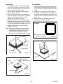
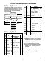
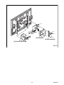
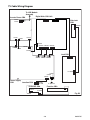
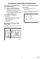
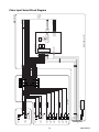
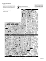
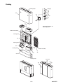
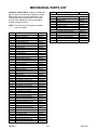
1
SERVICE MANUAL
42″ COLOR LCD TELEVISION
LC420SS8
IMPORTANT SAFETY NOTICE
Proper service and repair is important to the safe, reliable operation of all
Funai Equipment. The service procedures recommended by Funai and
described in this service manual are effective methods of performing
service operations. Some of these service special tools should be used
when and as recommended.
It is important to note that this service manual contains various CAUTIONS
and NOTICES which should be carefully read in order to minimize the risk
of personal injury to service personnel. The possibility exists that improper
service methods may damage the equipment. It also is important to
understand that these CAUTIONS and NOTICES ARE NOT EXHAUSTIVE.
Funai could not possibly know, evaluate and advice the service trade of all
conceivable ways in which service might be done or of the possible
hazardous consequences of each way. Consequently, Funai has not
undertaken any such broad evaluation. Accordingly, a servicer who uses a
service procedure or tool which is not recommended by Funai must first
use all precautions thoroughly so that neither his safety nor the safe
operation of the equipment will be jeopardized by the service method
selected.
TABLE OF CONTENTS
Specifications . . . . . . . . . . . . . . . . . . . . . . . . . . . . . . . . . . . . . . . . . . . . . . . . . . . . . . . . . . . . . . . . . . . . . . . . . . . 1-1
Important Safety Precautions . . . . . . . . . . . . . . . . . . . . . . . . . . . . . . . . . . . . . . . . . . . . . . . . . . . . . . . . . . . . . . . 2-1
Standard Notes for Servicing . . . . . . . . . . . . . . . . . . . . . . . . . . . . . . . . . . . . . . . . . . . . . . . . . . . . . . . . . . . . . . . 3-1
Cabinet Disassembly Instructions . . . . . . . . . . . . . . . . . . . . . . . . . . . . . . . . . . . . . . . . . . . . . . . . . . . . . . . . . . . . 4-1
Electrical Adjustment Instructions . . . . . . . . . . . . . . . . . . . . . . . . . . . . . . . . . . . . . . . . . . . . . . . . . . . . . . . . . . . . 5-1
How to initialize the LCD Television . . . . . . . . . . . . . . . . . . . . . . . . . . . . . . . . . . . . . . . . . . . . . . . . . . . . . . . . . . 6-1
Block Diagrams . . . . . . . . . . . . . . . . . . . . . . . . . . . . . . . . . . . . . . . . . . . . . . . . . . . . . . . . . . . . . . . . . . . . . . . . . . 7-1
Schematic Diagrams / CBA’s and Test Points. . . . . . . . . . . . . . . . . . . . . . . . . . . . . . . . . . . . . . . . . . . . . . . . . . . 8-1
Waveforms . . . . . . . . . . . . . . . . . . . . . . . . . . . . . . . . . . . . . . . . . . . . . . . . . . . . . . . . . . . . . . . . . . . . . . . . . . . . . 9-1
Wiring Diagram . . . . . . . . . . . . . . . . . . . . . . . . . . . . . . . . . . . . . . . . . . . . . . . . . . . . . . . . . . . . . . . . . . . . . . . . . 10-1
Exploded Views. . . . . . . . . . . . . . . . . . . . . . . . . . . . . . . . . . . . . . . . . . . . . . . . . . . . . . . . . . . . . . . . . . . . . . . . . 11-1
Mechanical Parts List . . . . . . . . . . . . . . . . . . . . . . . . . . . . . . . . . . . . . . . . . . . . . . . . . . . . . . . . . . . . . . . . . . . . 12-1
Electrical Parts List . . . . . . . . . . . . . . . . . . . . . . . . . . . . . . . . . . . . . . . . . . . . . . . . . . . . . . . . . . . . . . . . . . . . . . 13-1
The LCD panel is manufactured to provide many years of useful life.
Occasionally a few non active pixels may appear as a tiny spec of color.
This is not to be considered a defect in the LCD screen.
SPECIFICATIONS
< TUNER / NTSC >
ANT. Input ---------------------- 75 ohm Unbal., F type
Description
Condition
Unit
Nominal
Limit
1. AFT Pull-In Range
---
MHz
±2.3
±2.1
2. Syncronizing Sens.
TV.ch.4
CA.ch.31
CA.ch.87
dBµ
dBµ
dBµ
-------
20
20
23
Condition
Unit
Nominal
Limit
---
kHz
---
±100
ch.4
ch.10
ch.41
dBm
dBm
dBm
-------
-76/+6
-76/+6
-76/+6
Description
Condition
Unit
Nominal
Limit
1. Native Pixel Resolusion
Horizontal
Vertical
pixels
pixels
1920
1080
-----
---
cd/m2
500
---
Horizontal
Vertical
°
°
-----
-89 to +89
-89 to +89
Condition
Unit
Nominal
Limit
Horizontal
Vertical
%
%
5±5
5±5
-----
--x
y
°K
12000
0.272
0.278
--±10%
±10%
Horizontal
Vertical
line
line
720
480
-----
< TUNER / ATSC >
Description
1. Received Freq. Range (-28dBm)
2. ATSC Dynamic Range (min / max)
< LCD PANEL >
2. Brightness (w / filter)
3. Viewing Angle
< VIDEO >
Description
1. Over Scan
2. Color Temperature
3. Resolution (composite video)
1-1
A81H1SP
< AUDIO >
All items are measured across 8 Ω load at speaker output terminal with L.P.F. / Video1 Input.
Description
1. Audio Output Power
2. Audio Distortion
3. Audio Freq. Response (NTSC)
Condition
Unit
Nominal
Limit
10% THD: Lch/Rch
W
10.0/10.0
9.0/9.0
500mW: Lch/Rch
%
0.5/0.5
2.0/2.0
-6dB: Lch
-6dB: Rch
Hz
Hz
20 to 10 k
20 to 10 k
-----
Note: Nominal specifications represent the design specifications. All units should be able to approximate these.
Some will exceed and some may drop slightly below these specifications. Limit specifications represent
the absolute worst condition that still might be considered acceptable. In no case should a unit fail to meet
limit specifications.
1-2
A81H1SP
IMPORTANT SAFETY PRECAUTIONS
Prior to shipment from the factory, our products are strictly inspected for recognized product safety and electrical
codes of the countries in which they are to be sold. However, in order to maintain such compliance, it is equally
important to implement the following precautions when a set is being serviced.
Safety Precautions for LCD TV
Circuit
d. Leakage Current Hot Check - With the
instrument completely reassembled, plug the
AC line cord directly into a 120 V AC outlet. (Do
not use an isolation transformer during this
test.) Use a leakage current tester or a
metering system that complies with American
National Standards Institute (ANSI) C101.1
Leakage Current for Appliances and
Underwriters Laboratories (UL) 1410, (50.7).
With the instrument AC switch first in the on
position and then in the off position, measure
from a known earth ground (metal water pipe,
conduit, etc.) to all exposed metal parts of the
instrument (antennas, handle brackets, metal
cabinet, screw heads, metallic overlays, control
shafts, etc.), especially any exposed metal
parts that offer an electrical return path to the
chassis. Any current measured must not
exceed 0.5 milli-ampere. Reverse the
instrument power cord plug in the outlet and
repeat the test.
1. Before returning an instrument to the
customer, always make a safety check of the
entire instrument, including, but not limited to, the
following items:
a. Be sure that no built-in protective devices are
defective and have been defeated during
servicing. (1) Protective shields are provided
on this chassis to protect both the technician
and the customer. Correctly replace all missing
protective shields, including any removed for
servicing convenience. (2) When reinstalling
the chassis and/or other assembly in the
cabinet, be sure to put back in place all
protective devices, including but not limited to,
nonmetallic control knobs, insulating
fishpapers, adjustment and compartment
covers/shields, and isolation resistor/capacitor
networks. Do not operate this instrument or
permit it to be operated without all
protective devices correctly installed and
functioning. Servicers who defeat safety
features or fail to perform safety checks
may be liable for any resulting damage.
READING SHOULD
NOT BE ABOVE 0.5 mA
DEVICE
BEING
TESTED
b. Be sure that there are no cabinet openings
through which an adult or child might be able to
insert their fingers and contact a hazardous
voltage. Such openings include, but are not
limited to, (1) spacing between the Liquid
Crystal Panel and the cabinet mask, (2)
excessively wide cabinet ventilation slots, and
(3) an improperly fitted and/or incorrectly
secured cabinet back cover.
LEAKAGE
CURRENT
TESTER
_
+
TEST ALL EXPOSED
METAL SURFACES
ALSO TEST WITH
PLUG REVERSED
USING AC
ADAPTER PLUG
AS REQUIRED
c. Antenna Cold Check - With the instrument AC
plug removed from any AC source, connect an
electrical jumper across the two AC plug
prongs. Place the instrument AC switch in the
on position. Connect one lead of an ohmmeter
to the AC plug prongs tied together and touch
the other ohmmeter lead in turn to each tuner
antenna input exposed terminal screw and, if
applicable, to the coaxial connector. If the
measured resistance is less than 1.0 megohm
or greater than 5.2 megohm, an abnormality
exists that must be corrected before the
instrument is returned to the customer. Repeat
this test with the instrument AC switch in the off
position.
EARTH
GROUND
ANY MEASUREMENTS NOT WITHIN THE
LIMITS SPECIFIED HEREIN INDICATE A
POTENTIAL SHOCK HAZARD THAT MUST
BE ELIMINATED BEFORE RETURNING THE
INSTRUMENT TO THE CUSTOMER OR
BEFORE CONNECTING THE ANTENNA OR
ACCESSORIES.
2. Read and comply with all caution and safetyrelated notes on or inside the receiver cabinet, on
the receiver chassis, or on the Liquid Crystal
Panel.
2-1
LTVN_ISP
7. Product Safety Notice - Some electrical and
mechanical parts have special safety-related
characteristics which are often not evident from
visual inspection, nor can the protection they give
necessarily be obtained by replacing them with
components rated for higher voltage, wattage, etc.
Parts that have special safety characteristics are
identified by a # on schematics and in parts lists.
Use of a substitute replacement that does not
have the same safety characteristics as the
recommended replacement part might create
shock, fire, and/or other hazards. The product's
safety is under review continuously and new
instructions are issued whenever appropriate.
Prior to shipment from the factory, our products
are strictly inspected to confirm they comply with
the recognized product safety and electrical codes
of the countries in which they are to be sold.
However, in order to maintain such compliance, it
is equally important to implement the following
precautions when a set is being serviced.
3. Design Alteration Warning - Do not alter or add
to the mechanical or electrical design of this TV
receiver. Design alterations and additions,
including, but not limited to circuit modifications
and the addition of items such as auxiliary audio
and/or video output connections, might alter the
safety characteristics of this receiver and create a
hazard to the user. Any design alterations or
additions will void the manufacturer's warranty and
may make you, the servicer, responsible for
personal injury or property damage resulting
therefrom.
4. Hot Chassis Warning a. Some TV receiver chassis are electrically
connected directly to one conductor of the AC
power cord and maybe safety-serviced without
an isolation transformer only if the AC power
plug is inserted so that the chassis is
connected to the ground side of the AC power
source. To confirm that the AC power plug is
inserted correctly, with an AC voltmeter,
measure between the chassis and a known
earth ground. If a voltage reading in excess of
1.0 V is obtained, remove and reinsert the AC
power plug in the opposite polarity and again
measure the voltage potential between the
chassis and a known earth ground.
b. Some TV receiver chassis normally have 85V
AC(RMS) between chassis and earth ground
regardless of the AC plug polarity. This chassis
can be safety-serviced only with an isolation
transformer inserted in the power line between
the receiver and the AC power source, for both
personnel and test equipment protection.
c. Some TV receiver chassis have a secondary
ground system in addition to the main chassis
ground. This secondary ground system is not
isolated from the AC power line. The two
ground systems are electrically separated by
insulation material that must not be defeated or
altered.
5. Observe original lead dress. Take extra care to
assure correct lead dress in the following areas: a.
near sharp edges, b. near thermally hot parts-be
sure that leads and components do not touch
thermally hot parts, c. the AC supply, d. high
voltage, and, e. antenna wiring. Always inspect in
all areas for pinched, out of place, or frayed wiring.
Check AC power cord for damage.
6. Components, parts, and/or wiring that appear to
have overheated or are otherwise damaged
should be replaced with components, parts, or
wiring that meet original specifications.
Additionally, determine the cause of overheating
and/or damage and, if necessary, take corrective
action to remove any potential safety hazard.
2-2
LTVN_ISP
Precautions during Servicing
A. Parts identified by the # symbol are critical for
safety.
Replace only with part number specified.
B. In addition to safety, other parts and assemblies
are specified for conformance with regulations
applying to spurious radiation. These must also be
replaced only with specified replacements.
Examples: RF converters, RF cables, noise
blocking capacitors, and noise blocking filters, etc.
C. Use specified internal wiring. Note especially:
1) Wires covered with PVC tubing
2) Double insulated wires
3) High voltage leads
D. Use specified insulating materials for hazardous
live parts. Note especially:
1) Insulation Tape
2) PVC tubing
3) Spacers
4) Insulators for transistors.
E. When replacing AC primary side components
(transformers, power cord, etc.), wrap ends of
wires securely about the terminals before
soldering.
F. Observe that the wires do not contact heat
producing parts (heat sinks, oxide metal film
resistors, fusible resistors, etc.)
G. Check that replaced wires do not contact sharp
edged or pointed parts.
H. When a power cord has been replaced, check that
5~6 kg of force in any direction will not loosen it.
I.
Also check areas surrounding repaired locations.
J. Use care that foreign objects (screws, solder
droplets, etc.) do not remain inside the set.
K. When connecting or disconnecting the internal
connectors, first, disconnect the AC plug from the
AC supply outlet.
L. When installing parts or assembling the cabinet
parts, be sure to use the proper screws and
tighten certainly.
2-3
LTVN_ISP
Safety Check after Servicing
Examine the area surrounding the repaired location for damage or deterioration. Observe that screws, parts and
wires have been returned to original positions. Afterwards, perform the following tests and confirm the specified
values in order to verify compliance with safety standards.
1. Clearance Distance
When replacing primary circuit components, confirm
specified clearance distance (d) and (d') between
soldered terminals, and between terminals and
surrounding metallic parts. (See Fig. 1)
Chassis or Secondary Conductor
Primary Circuit
Table 1: Ratings for selected area
AC Line Voltage
Region
Clearance
Distance (d), (d’)
110 to 130 V
U.S.A. or
Canada
≥ 3.2 mm
(0.126 inches)
d'
d
Note: This table is unofficial and for reference only. Be
sure to confirm the precise values.
Fig. 1
2. Leakage Current Test
Confirm the specified (or lower) leakage current
between B (earth ground, power cord plug prongs) and
externally exposed accessible parts (RF terminals,
antenna terminals, video and audio input and output
terminals, microphone jacks, earphone jacks, etc.) is
lower than or equal to the specified value in the table
below.
Exposed Accessible Part
Z
AC Voltmeter
(High Impedance)
Measuring Method: (Power ON)
Insert load Z between B (earth ground, power cord plug
prongs) and exposed accessible parts. Use an AC
voltmeter to measure across both terminals of load Z.
See Fig. 2 and following table.
B
Earth Ground
Power Cord Plug Prongs
Fig. 2
Table 2: Leakage current ratings for selected areas
AC Line Voltage
Region
Load Z
Leakage Current (i)
Earth Ground (B) to:
110 to 130 V
U.S.A. or
Canada
0.15 µF CAP. & 1.5 kΩ
RES. Connected in parallel
i ≤ 0.5 mA rms
Exposed accessible
parts
Note: This table is unofficial and for reference only. Be sure to confirm the precise values.
2-4
LTVN_ISP
STANDARD NOTES FOR SERVICING
Circuit Board Indications
How to Remove / Install Flat Pack-IC
1. The output pin of the 3 pin Regulator ICs is
indicated as shown.
1. Removal
With Hot-Air Flat Pack-IC Desoldering Machine:
Top View
Out
1. Prepare the hot-air flat pack-IC desoldering
machine, then apply hot air to the Flat Pack-IC
(about 5 to 6 seconds). (Fig. S-1-1)
Bottom View
In
Input
2. For other ICs, pin 1 and every fifth pin are
indicated as shown.
5
Pin 1
10
3. The 1st pin of every male connector is indicated as
shown.
Fig. S-1-1
2. Remove the flat pack-IC with tweezers while
applying the hot air.
Pin 1
3. Bottom of the flat pack-IC is fixed with glue to the
CBA; when removing entire flat pack-IC, first apply
soldering iron to center of the flat pack-IC and heat
up. Then remove (glue will be melted). (Fig. S-1-6)
Pb (Lead) Free Solder
4. Release the flat pack-IC from the CBA using
tweezers. (Fig. S-1-6)
Pb free mark will be found on PCBs which use Pb
free solder. (Refer to figure.) For PCBs with Pb free
mark, be sure to use Pb free solder. For PCBs
without Pb free mark, use standard solder.
CAUTION:
1. The Flat Pack-IC shape may differ by models. Use
an appropriate hot-air flat pack-IC desoldering
machine, whose shape matches that of the Flat
Pack-IC.
2. Do not supply hot air to the chip parts around the
flat pack-IC for over 6 seconds because damage
to the chip parts may occur. Put masking tape
around the flat pack-IC to protect other parts from
damage. (Fig. S-1-2)
Pb free mark
3-1
TVN_SN
With Soldering Iron:
3. The flat pack-IC on the CBA is affixed with glue, so
be careful not to break or damage the foil of each
pin or the solder lands under the IC when
removing it.
CBA
1. Using desoldering braid, remove the solder from
all pins of the flat pack-IC. When you use solder
flux which is applied to all pins of the flat pack-IC,
you can remove it easily. (Fig. S-1-3)
Hot-air
Flat Pack-IC
Desoldering
Machine
Flat Pack-IC
Desoldering Braid
Soldering Iron
Masking
Tape
Tweezers
Flat Pack-IC
Fig. S-1-3
2. Lift each lead of the flat pack-IC upward one by
one, using a sharp pin or wire to which solder will
not adhere (iron wire). When heating the pins, use
a fine tip soldering iron or a hot air desoldering
machine. (Fig. S-1-4)
Fig. S-1-2
Sharp
Pin
Fine Tip
Soldering Iron
Fig. S-1-4
3. Bottom of the flat pack-IC is fixed with glue to the
CBA; when removing entire flat pack-IC, first apply
soldering iron to center of the flat pack-IC and heat
up. Then remove (glue will be melted). (Fig. S-1-6)
4. Release the flat pack-IC from the CBA using
tweezers. (Fig. S-1-6)
3-2
TVN_SN
With Iron Wire:
2. Installation
1. Using desoldering braid, remove the solder from
all pins of the flat pack-IC. When you use solder
flux which is applied to all pins of the flat pack-IC,
you can remove it easily. (Fig. S-1-3)
1. Using desoldering braid, remove the solder from
the foil of each pin of the flat pack-IC on the CBA
so you can install a replacement flat pack-IC more
easily.
2. Affix the wire to a workbench or solid mounting
point, as shown in Fig. S-1-5.
2. The “●” mark on the flat pack-IC indicates pin 1.
(See Fig. S-1-7.) Be sure this mark matches the 1
on the PCB when positioning for installation. Then
presolder the four corners of the flat pack-IC. (See
Fig. S-1-8.)
3. While heating the pins using a fine tip soldering
iron or hot air blower, pull up the wire as the solder
melts so as to lift the IC leads from the CBA
contact pads as shown in Fig. S-1-5.
3. Solder all pins of the flat pack-IC. Be sure that
none of the pins have solder bridges.
4. Bottom of the flat pack-IC is fixed with glue to the
CBA; when removing entire flat pack-IC, first apply
soldering iron to center of the flat pack-IC and heat
up. Then remove (glue will be melted). (Fig. S-1-6)
Example :
5. Release the flat pack-IC from the CBA using
tweezers. (Fig. S-1-6)
Note: When using a soldering iron, care must be
taken to ensure that the flat pack-IC is not
being held by glue. When the flat pack-IC is
removed from the CBA, handle it gently
because it may be damaged if force is applied.
Pin 1 of the Flat Pack-IC
is indicated by a " " mark.
Hot Air Blower
or
Fig. S-1-7
Presolder
Iron Wire
Soldering Iron
To Solid
Mounting Point
Fig. S-1-5
Flat Pack-IC
CBA
CBA
Fig. S-1-8
Fine Tip
Soldering Iron
Flat Pack-IC
Tweezers
Fig. S-1-6
3-3
TVN_SN
Instructions for Handling Semiconductors
Electrostatic breakdown of the semi-conductors may
occur due to a potential difference caused by
electrostatic charge during unpacking or repair work.
1. Ground for Human Body
Be sure to wear a grounding band (1 MΩ) that is
properly grounded to remove any static electricity that
may be charged on the body.
2. Ground for Workbench
Be sure to place a conductive sheet or copper plate
with proper grounding (1 MΩ) on the workbench or
other surface, where the semi-conductors are to be
placed. Because the static electricity charge on
clothing will not escape through the body grounding
band, be careful to avoid contacting semi-conductors
with your clothing.
<Incorrect>
CBA
<Correct>
Grounding Band
1MΩ
CBA
1MΩ
Conductive Sheet or
Copper Plate
3-4
TVN_SN
CABINET DISASSEMBLY INSTRUCTIONS
1. Disassembly Flowchart
Removal
Step/
Loc.
No.
This flowchart indicates the disassembly steps for the
cabinet parts, and the CBA in order to gain access to
item(s) to be serviced. When reassembling, follow the
steps in reverse order. Bend, route and dress the
cables as they were.
[9]
[1] Stand Base
[8] Jack CBA
[2] Stand Cover
[17] Side Jack CBA
[5] Jack Holder(D)
[9] Power Supply
CBA
[4] Inverter Power
CBA
[6] Shield Box
[10] PCB Holder
[15] Junction CBA
[7] Digital Main
CBA Unit
[11] Stand Shaft
(L,R)
[16] IR Sensor
CBA
Stand Shaft
D4 4(S-15)
(L, R)
---
Chassis
[12] Bracket
(L, R)
D4 6(S-16)
---
LCD
[13] Module
Assembly
D4 13(S-17)
-----
[12] Chassis
Bracket (L,R)
[15]
Junction
CBA
D4
*CL101A
D5
---
[13] LCD
Module Assembly
[16]
IR Sensor
CBA
D4
2(S-19)
D5
---
[17]
Side Jack
CBA
D4
2(S-20)
D5
---
D4 8(S-21)
---
D4 ---------------
---
↓
(3)
↓
(5)
[18] Speaker(s)
Fig.
No.
Removal
[19]
Front
Cabinet
Remove/*Unhook/
Unlock/Release/
Unplug/Unclamp/
Desolder
↓
(1)
↓
(2)
Note
↓
(4)
Note:
Stand Base D1 4(S-1), 4(S-2)
---
[2]
Stand
Cover
D1 ---------------
---
[3]
Rear
Cabinet
D1 6(S-3), 2(S-4), 11(S-5)
---
[4]
5(S-6), *CN701,
Inverter
D2
*CN702, *CN751,
Power CBA D5
*CN752, *CN753
---
[5]
Jack
Holder(D)
D2 (S-7), 2(S-8), 2(S-9)
---
[6]
Shield Box
D2 5(S-10), 2(S-11), (N-1)
---
[7]
*CN200, *CN201,
Digital Main D2
*CN202, *CN203,
CBA Unit
D5
*CN3707, *CN4201
---
D3 5(S-12), *CL7002A,
D5 *CN7002
---
Jack CBA
---
D4
3(S-18), *CL106B
D5
[1]
[8]
D3 8(S-13), *CN204,
D5 *CN801, *CN802
Function
CBA
2. Disassembly Method
Part
Note
[14]
[19] Front Cabinet
Step/
Loc.
No.
Remove/*Unhook/
Unlock/Release/
Unplug/Unclamp/
Desolder
---
[11]
[3] Rear Cabinet
Power
Supply
CBA
Fig.
No.
[10] PCB Holder D3 4(S-14)
[14] Function CBA
[18] Speaker(s)
Part
(1) Order of steps in procedure. When reassembling,
follow the steps in reverse order. These numbers
are also used as the Identification (location) No. of
parts in figures.
(2) Parts to be removed or installed.
(3) Fig. No. showing procedure of part location
(4) Identification of parts to be removed, unhooked,
unlocked, released, unplugged, unclamped, or
desoldered.
N = Nut, L = Locking Tab, S = Screw,
CN = Connector
* = Unhook, Unlock, Release, Unplug, or Desolder
e.g. 2(S-2) = two Screws (S-2),
2(L-2) = two Locking Tabs (L-2)
(5) Refer to the following "Reference Notes in the
Table."
4-1
A81H1DC
(S-5)
(S-5)
(S-3)
(S-4)
(S-3)
(S-4)
(S-5)
(S-5)
(S-3)
(S-5)
[3] Rear Cabinet
(S-3)
(S-5)
(S-5)
[2] Stand Cover
(S-1)
(S-1)
(S-2)
[1] Stand Base
(S-2)
Fig. D1
4-2
A81H1DC
(S-11)
(N-1)
(S-8)
[7] Digital Main
CBA Unit
(S-7)
(S-6)
(S-10)
[6] Shield Box
(S-9)
[5] Jack Holder(D)
(S-6)
[4] Inverter Power CBA
Fig. D2
4-3
A81H1DC
(S-14)
[10] PCB Holder
[8] Jack CBA
(S-14)
(S-14)
(S-12)
(S-13)
[9] Power Supply CBA
(S-14)
(S-13)
(S-13)
Fig. D3
4-4
A81H1DC
[19] Front Cabinet
[17] Side Jack CBA
[13] LCD Module
Assembly
(S-20)
(S-17)
(S-21)
[18] Speaker
(S-17)
(S-16)
(S-17)
(S-19)
[16] IR Sensor
CBA
(S-17)
(S-17)
(S-17)
(S-16)
(S-21)
[15] Junction
[18] Speaker CBA
(S-18)
(S-17)
(S-17)
(S-15)
[12] Chassis
Bracket (L)
[12] Chassis
Bracket (R)
[11] Stand Shaft (L)
(S-16)
[11] Stand Shaft (R)
[14] Function CBA
(S-15)
4-5
Fig. D4
A81H1DC
TV Cable Wiring Diagram
To LCD Module
Assembly
Digital Main CBA Unit
Inverter Power CBA
CN751
CN752
CN4201
Side Jack
CBA
CN3707
CL7002B
CN753
CN701
CN702
CN500 CN501
CN3701
CN3601 CN3702 CN3705
CN206
CN200
Jack CBA
CN201 CN202 CN203
CN7001
CL7002A
CN801
CN802
CN204
Power Supply
CBA
Junction CBA
CN100
CL101B
To Speaker
Function CBA
IR Sensor CBA
CL101A
CL106B
CL106A
Fig. D5
4-6
A81H1DC
ELECTRICAL ADJUSTMENT INSTRUCTIONS
How to set up the service mode:
General Note: “CBA” is abbreviation for
“Circuit Board Assembly.”
Service mode:
Note: Electrical adjustments are required after
replacing circuit components and certain
mechanical parts. It is important to perform
these adjustments only after all repairs and
replacements have been completed.
Also, do not attempt these adjustments unless
the proper equipment is available.
1. Use the service remote control unit.
2. Turn the power on.
3. Press the service button on the service remote
control unit. The following screen appears.
"*" differs depending on the models.
Test Equipment Required
Ver :
***********************
Boot
Push 0 key
System
Push 0 key
Pic Ver : ***********************
***********************
Picture :
Push 0 key
Submicon Ver : ******
1. DC Voltmeter
2. NTSC Pattern Generator (Color Bar W/White
Window, Red Color, Dot Pattern, Gray Scale,
Monoscope, Multi-Burst)
3. Remote control unit
4. Color Analyzer
How to make the Service remote
control unit:
Cut “A” portion of the attached remote control unit as
shown in Fig. 1.
service button
A
Fig. 1
5-1
A81H1EA
1. Purity Check Mode
The following adjustment normally are not attempted in
the field. Only when replacing the LCD Panel then adjust
as a preparation.
This mode cycles through full-screen displays of red,
green, blue, and white to check for non-active pixels.
2. White Balance Adjustment
1. Enter the Service mode.
Purpose: To mix red, green and blue beams correctly
for pure white.
2. Each time pressing [7] button on the service
remote control unit, the display changes as
follows.
Symptom of Misadjustment: White becomes bluish
or reddish.
Purity Check Mode
Test Point Adj. Point
Mode
Input
White mode
[7] button
Screen
[7] button
Red mode
White Purity
(APL 70%)
or
(APL 25%)
[CH. o/p] [VIDEO1]
C/D
buttons
M. EQ.
Spec.
Pattern Generator,
Color analyzer
x= 0.272 ± 0.005
y= 0.278 ± 0.005
Figure
It carries out in a darkroom.
[7] button
Perpendicularity
Green mode
L = 3 cm
[7] button
INPUT: WHITE 70%, 25%
Blue mode
Color Analyzer
1. Operate the unit for more than 20 minutes.
2. Input the White Purity.
INPUT SIGNAL
Note:
When entering this mode, the default setting is White mode.
25%=25IRE 70%=70IRE
3. Set the color analyzer to the CHROMA mode and
bring the optical receptor to the center on the
LCD-Panel surface after zero point calibration as
shown above.
Note: The optical receptor must be set
perpendicularly to the LCD Panel surface.
4. Enter the Service mode. Press [VOL. n] button on
the service remote control unit and select “C/D”
mode.
5-2
A81H1EA
5. [CUTOFF]
Press [3] button to select “COB” for Blue Cutoff
adjustment. Press [1] button to select “COR” for
Red Cutoff adjustment.
[DRIVE]
Press [6] button to select “DB” for Blue Drive
adjustment. Press [4] button to select “DR” for Red
Drive adjustment.
6. In each color mode, press [CH. o / p] buttons to
adjust the values of color.
7. Adjust Cutoff and Drive so that the color
temperature becomes 12000K (x= 0.272 / y=
0.278 ±0.005).
5-3
A81H1EA
HOW TO INITIALIZE THE LCD TELEVISION
How to initialize the LCD television:
1. Turn the power on.
2. To enter the service mode, press the service
button on the service remote control unit. (Refer to
page 5-1.)
- To cancel the service mode, press [POWER]
button on the remote control unit.
3. Press [INFO] button on the remote control unit to
initialize the LCD television.
4. "INITIALIZED" will appear in the upper right of the
screen. "INITIALIZED" color will change to green
from red when initialzing is complete.
6-1
A81H1INT
32
31
17
27
7-1
SUB-TXD 14
SUB-RXD 15
RESET 41
RESET 19
X-IN 22
X-OUT 23
BACKLIGHT-SW 12
P-ON-H2 25
PROTECT6 46
P-ON-H1 26
LED1
LED2
REMOTE
AMP-STBY
KEY-IN-1 3
IC3101 (SUB MICRO CONTROLLER)
+3.3V
TO AUDIO-2
BLOCK DIAGRAM
IC3302
4
54.1MHz
OSC
X3301
CN200
6
AMP-STBY
AMP-MUTE
AUDIO-SW1
AUDIO-SW2
AUDIO-SW3
AUDIO-SW4
AUDIO-SW5
A15 MAIN-RXD
B15 MAIN-TXD
C6 RESET
AK24 X-IN
AK23 X-OUT
AH25 AUDIO-MUTE
V27
V28
V29
W29
W30
RESET AH26
I2C-SCL-B AE26
I2C-SDA-B AD26
RESET AJ27
I2C-SCL-A B14
I2C-SDA-A A14
WP D17
IC3301 (MAIN MICRO CONTROLLER)
J1 BACKLIGHT-SW
J2 BACKLIGHT-ADJ
AG25 AMP-MUTE
KEY-IN-1
LED1
LED2
REMOTE
CN206
2 P-ON-H2
1 BACKLIGHT-ADJ
3 BACKLIGHT-SW
TO AUDIO-2
BLOCK
DIAGRAM
CN204
3
5
6
10
POWER SUPPLY CBA
CN200
14
15
13
CN202
LED1
6
LED2
5
REMOTE
16
AMP-STBY 15
AMP-MUTE 14
CN3701
14 P-ON-H2
15 BACKLIGHT-ADJ
13 BACKLIGHT-SW
5 RESET
DIGITAL MAIN CBA UNIT
Q3402
LEV. SHIFTER
+3.3V
AUDIO-MUTE
AUDIO-SW1
AUDIO-SW2
AUDIO-SW3
AUDIO-SW4
AUDIO-SW5
TO POWER SUPPLY-2
BLOCK DIAGRAM
TO AUDIO-1
BLOCK DIAGRAM
5
Q3401
LEV. SHIFTER
4 RESET
IC3102
4MHz
OSC
X3101
PROTECT6
P-ON-H1
CN3702
6
5
16
15
14
CN3701
6 KEY-IN-1
CN753
2
1
3
KEY-IN-1
LED1
LED2
REMOTE
IC3202 (MEMORY)
15 SCL
14 SDA
13 RESET
IC4002 (HDMI SW)
27 SCL
24 SDA
IC3001 (MTS/SAP AUDIO SIGNAL PROCESS)
25 SCL
26 SDA
KEY SWITCH
REMOTE
SENSOR
RS101
D101
POWER
D102
STANDBY
+3.3V
FUNCTION CBA
CL106B
2
INVERTER POWER CBA
IC3809 (TONE CONTROL)
37 SCL
38 SDA
35 RESET
IC3501 (VIDEO ADC)
6 SCL
5 SDA
7 WP
IR SENSOR CBA
CL106A
2 KEY-IN-1
TO POWER SUPPLY-1
BLOCK DIAGRAM
CL101A
9
7
6
2
P-ON-H2
BACKLIGHT-ADJ
BACKLIGHT-SW
CL101B
9
7
6
2
JUNCTION
CBA
CN100
3
5
6
10
System Control Block Diagram
BLOCK DIAGRAMS
A81H1BLS
C
Y
7-2
JK7005
JK7003
C
Y
1
2
3
PC-IN 14
13
12
15
JK3701
PC-R
PC-G
PC-B
PC-V-SYNC
PC-H-SYNC
COMPONENT
-Pr-IN2
COMPONENT
-Pb-IN2
COMPONENT
-Y-IN2
COMPONENT
-Pr-IN1
COMPONENT
-Pb-IN1
COMPONENT
-Y-IN1
JK7001
S-VIDEO-IN1
JK7002
VIDEO-IN1
CL7002A
5
1
3
5 SDA
6 SCL
IC3701 (MEMORY)
JACK CBA
Q7106
BUFFER
Q7105
BUFFER
Q7101
BUFFER
Q7102
BUFFER
CL7002B
5 VIDEO-IN2
1 S-VIDEO-C-IN2
3 S-VIDEO-Y-IN2
SIDE JACK CBA
JK7503
S-VIDEO-IN2
JK7502
VIDEO-IN2
Q7103
Q7104
BUFFER
BUFFER
WF4
WF2
WF5
WF3
WF6
CN7001
36
34
32
20
23
22
6
7
8
2
1
3
WF1
VIDEO-IN2
S-VIDEO-C-IN2
S-VIDEO-Y-IN2
VIDEO-IN1
S-VIDEO-C-IN1
S-VIDEO-Y-IN1
COMPONENT-Y-IN1
COMPONENT-Pb-IN1
COMPONENT-Pr-IN1
COMPONENT-Y-IN2
COMPONENT-Pb-IN2
COMPONENT-Pr-IN2
CN3707
5
7
9
21
18
19
35
34
33
39
40
38
MUX
CLAMP
ADC
43-50,
55-62,
76-83
DVI-V-SYNC 71
DVI-H-SYNC 70
DVI-CLOCK 68
OUTPUT
FORMATTING
CSC
MUX
DIGITAL MAIN CBA UNIT
14 PC-V-SYNC
13 PC-H-SYNC
9
6
11
25
22
27
20
18
15
IC3501(VIDEO ADC)
DVI-V-SYNC
DVI-H-SYNC
DVI-CLOCK
DVI-DATA(0-23)
VIDEO-IN2
S-VIDEO-C-IN2
S-VIDEO-Y-IN2
VIDEO-IN1
S-VIDEO-C-IN1
S-VIDEO-Y-IN1
TO LCD
DRIVE
BLOCK
DIAGRAM
VIDEO SIGNAL
Video Input Select Block Diagram
A81H1BLVIS
7-3
9 10
13
3
SIF/BB
SW
SW CTL
(R-CH)
AUDIO1
12
COMP1
15
COMP2
11
AUDIO2
14
(L-CH)
AUDIO1
1
COMP1
2
COMP2
4
AUDIO2
5
IC7001
(INPUT SELECT)
INPUT
VCA
WF7
JK7502
SIDE JACK CBA
AUDIO(R)
-IN2
AUDIO(L)
-IN2
JACK CBA
Q7002
SIF
DEMOD
COMPONENTAUDIO(R)-IN2
CL7002B
CL7002A
7 AUDIO(L)-IN2 7
9 AUDIO(R)-IN2 9
21
Q7001
JK7006
JK7004
CF3001
FILTER
IC3001(MTS/SAP AUDIO SIGNAL PROCESS)
COMPONENTAUDIO(L)-IN2
COMPONENTAUDIO(R)-IN1
COMPONENTAUDIO(L)-IN1
AUDIO(R)
-IN1
AUDIO(L)
-IN1
JK7002
SIF 3
TU3001(TUNER UNIT)
CN7001
14
12
16
15
SAP
FILTER
L-R
FILTER
L+R
FILTER
PCAUDIO-IN
HDMIAUDIO(R)-IN
JK4006
JK4005
(L-R)/SAP
SW
75uS
DE-EMPH
HDMIAUDIO(L)-IN
SAP OUT
FILTER
CN3707
27
29
25
26
SAP
DEMOD
OFFSET
CANCEL
SEL-AUDIO(L)
SEL-AUDIO(R)
AUDIO-SW4
AUDIO-SW5
STEREO
FILTER
SPECTRAL
RMS DET
SPECTRAL
FILTER
3
Q3809
Q3808
Q3807
Q3810
BUFFER
Q3811
BUFFER
AUDIO(R)
29
30
TO SYSTEM
CONTROL
BLOCK
DIAGRAM
TO
AUDIO-2
BLOCK
DIAGRAM
R-CH
L-CH
AUDIO(L)
AGC
AUDIO-SW1
AUDIO-SW2
AUDIO-SW3
AUDIO-SW4
AUDIO-SW5
MATRIX
Q3006
BUFFER
Q3005
BUFFER
OFFSET
CANCEL
DIGITAL MAIN CBA UNIT
9 10 11
SW CTL
TUNER
12
SEL
13
PC
15
HDMI
1
IC3802
(INPUT SELECT)
9 10 11
SW CTL
TUNER
12
SEL
13
PC
15
HDMI
1
3
WIDE BAND
EXPAND
IC3801
(INPUT SELECT)
SPECTRAL
EXPAND
WIDE BAND
RMS DET
dBX
DE-EMPH
WIDE BAND
FILTER
OFFSET
CANCEL
AUDIO SIGNAL
Audio-1 Block Diagram
A81H1BLA1
TO AUDIO-1
BLOCK
DIAGRAM
AUDIO(R)
AUDIO(L)
2
1
AUDIO
ADC
IC3803
(AUDIO ADC)
12
11
10
15
7-4
AUDIO
DAC
AUDIO-MUTE
Q3802
BUFFER
7
5
6
AA28
AA27
A5
1
IC3805
(OP AMP)
7
1
3
2
5
6
3
2
IC3803
(OP AMP)
AB29
AB30
AB28
AB27
AC27
AC28
TO SYSTEM
CONTROL
BLOCK DIAGRAM
DTV/HDMI
-AUDIO SIGNAL
TO LCD DRIVE
BLOCK DIAGRAM
AUDIO
DIGITAL
SIGNAL
PROCESS
DIGITAL MAIN CBA UNIT
A4
A2
A3
D6
IC3301
(DIGITAL SIGNAL PROCESS)
19
23
CN3707
CN7001
13 AUDIO(L)-OUT 28
15 AUDIO(R)-OUT 26
31 SPDIF-OUT
10
CN3702
CN202
10 AUDIO(L) 10
8 AUDIO(R) 8
DRIVE
Q3805
Q3804
MUTE-ON
TONE
CONTROL
TONE
CONTROL
Q3803
MUTE-ON
2
1
IC3809
(TONE CONTROL)
44
1
DRIVER2
DRIVER1
Q800
AMP-MUTE
AMP-STBY
21 22
SHUTDOWN
MUTE CONTROL
PWM2
PWM1
JACK CBA
POWER SUPPLY CBA
LPF2
LPF1
IC800 (AUDIO POWER AMP)
CN802
SP(R)+ 1
SP(R)- 2
35,36
31,32
JK7007
JK7008
DIGITALAUDIO-OUT
(COAXIAL)
AUDIO(R)
-OUT
AUDIO(L)
-OUT
TO SYSTEM
CONTROL
BLOCK
DIAGRAM
CN801
SP(L)+ 1
SP(L)- 2
9,10
13,14
AUDIO SIGNAL
CLN802
CLN801
SP902
SPEAKER
R-CH
SP901
SPEAKER
L-CH
Audio-2 Block Diagram
A81H1BLA2
7-5
TMDS-D0(+)
TMDS-D0(-)
TMDS-D1(+)
TMDS-D1(-)
TMDS-D2(+)
TMDS-D2(-)
TMDS-CLK(+)
TMDS-CLK(-)
DDC DATA
DDC CLK
JK4004
TMDS-D0(+)
7
TMDS-D0(-)
9
TMDS-D1(+)
4
TMDS-D1(-)
6
TMDS-D2(+)
1
TMDS-D2(-)
HDMI-IN1
3
TMDS-CLK(+)
10
TMDS-CLK(-)
12
DDC DATA
16
DDC CLK
15
JK4002
7
9
4
6
HDMI-IN2 1
3
10
12
16
15
VIDEO-IN2
S-VIDEO-C-IN2
S-VIDEO-Y-IN2
VIDEO-IN1
S-VIDEO-C-IN1
S-VIDEO-Y-IN1
62
61
65
64
68
67
59
58
70
71
22
21
25
24
28
27
19
18
31
30
Q3003
BUFFER
HDMI
SW
IC4002(HDMI SW)
DTV-IF(+) 21
DTV-IF(-) 20
TU-SCL 14
TU-SDA 15
VIDEO 4
TU3001 (TUNER UNIT)
TO VIDEO
INPUT SELECT
BLOCK DIAGRAM
DVI-V-SYNC
DVI-H-SYNC
DVI-CLOCK
DVI-DATA(0-23)
7
8
5
4
1
2
10
11
77
78
MATRIX
DEMOD.
P3
P4
T3
T4
HDMI
DECODER
V4
V3
M3
M4
L2 SDA
L1 SCL
AK20
AK19
AH6 TU-SCL
AG6 TU-SDA
AH20
AG15
AJ19
AK21
AH10
AH14
AG21
AD1 DVI-V-SYNC
AC4 DVI-H-SYNC
AD2 DVI-CLOCK
Y3,Y4,AA1-AA4,
AB1-AB4,AC1,AC2,
AD3,AD4,AE1-AE4,
AF1-AF4,AG1,AG2
VIDEO
ADC
A6,A7,B7,
B8,C7,C8,
D7,D8
TO AUDIO-2
BLOCK DIAGRAM
DTV/HDMI
-AUDIO SIGNAL
C27-C30,
D27-D30,
E27-E30,
F27-F30
G27,G28,H27,
H28,J27-J30,
K28-K30,L27,
L28,M27-M29
DATA(0-15)
ADDRESS(0-15)
AG3,AH1-AH3,
AJ1-AJ3,AK2
11
DVI-CLOCK D10
AUDIO
DECODER
54
DVI-H-SYNC B10
55
85-92
1,2,
93-96,
99,100
3-10
DATA(0-7)
B DATA(0-7)
A8,A11,B9,
G DATA(0-7)
B11,C9,C11,
D9,D11
A12,A13,B12, R DATA(0-7)
B13,C12,C13,
D12,D13
DVI-V-SYNC A10
VIDEO
DECODER
/OSD
DIGITAL MAIN CBA UNIT
DIGITAL
SIGNAL
PROCESS
IC3301(DIGITAL SIGNAL PROCESS)
49
50
46
47
44
45
38
39
41
42
36
37
33
34
31
32
26
27
28
29
CN4201
7
6
9
8
11
10
17
16
14
13
21
20
23
22
25
24
31
30
28
27
AUDIO SIGNAL
IC3203 (FLASH MEMORY)
L1-L3,M2,M3,
M7,M8,N2,N3,
N7,N8,P2,P3, ADDRESS(0-15)
P7,P8,R2
B1,B9,C2,C8,
D1,D3,D7,D9,
F1,F9,G2,G8, DATA(0-15)
H1,H3,H7,H9
IC3204 (SDRAM)
29-32, DATA(0-7)
41-44
PLL
TTL
PARALLEL
TO
LVDS
IC4201(LVDS TRANSMITTER)
VIDEO SIGNAL
TX1O-DATA0(+)
TX1O-DATA0(-)
TX1O-DATA1(+)
TX1O-DATA1(-)
TX1O-DATA2(+)
TX1O-DATA2(-)
TX1O-DATA3(+)
TX1O-DATA3(-)
TX1O-CLOCK(+)
TX1O-CLOCK(-)
TX1E-DATA0(+)
TX1E-DATA0(-)
TX1E-DATA1(+)
TX1E-DATA1(-)
TX1E-DATA2(+)
TX1E-DATA2(-)
TX1E-DATA3(+)
TX1E-DATA3(-)
TX1E-CLOCK(+)
TX1E-CLOCK(-)
LCD MODULE
LCD Drive Block Diagram
A81H1BLLCD
AC600
AC CORD
F500
8A/250V
8A/250V
LINE
FILTER
3
7-6
HOT
Q503
5
1
Q505
Q601
SW CTL
BRIDGE
RECTIFIER
Q506
Q600
SW
Q504
SW
D517 - D520
(AL+15V)
VCC 2
POWER
FACOTOR
CORRECTION
IC500 (PFC)
Q602
+15V REG.
OVER
CURRRENT
PROTECTOR
Q508
Q500,
Q501
DRIVE
Q502
BRIDGE
RECTIFIER
L501,L502 D500
Q509
CAUTION !
Fixed voltage (or Auto voltage selectable) power supply circuit is used in this unit.
If Main Fuse (F500) is blown , check to see that all components in the power supply
circuit are not defective before you connect the AC plug to the AC power supply.
Otherwise it may cause some components in the power supply circuit to fail.
IC503
(FEEDBACK)
1
2
4
3
16
11
6
8
9
12
13
14
15
10
3
4
2
1
7
2
IC600
(FEEDBACK)
T601
4
2
1
3
4
IC502
(FEEDBACK)
8A 250V
CONTINUE
POWER SUPPLY-2
BLOCK DIAGRAM
Q704
6
12 VCC HIGHVOLTAGE
RESONANT
CONTROL
5
Q701
SW
POWER SUPPLY CBA
3
4
3
4
T701
16
13
14
11
IC703
(ISOLATOR)
Q761
2
1
+13V
IC761 SHUNT
REG.
2
1
COLD
Q762
INV+24V
GND
BACKLIGHT-SW
BACKLIGHT-ADJ
BACKLIGHT-SW
BACKLIGHT-ADJ
P-ON-H2
CN752
1-5 INV+24V
CN751
1-5
6-10
12
13
TO SYSTEM
CONTROL
BLOCK
DIAGRAM
LCD MODULE
NOTE:
The voltage for parts in hot circuit is measured using
hot GND as a common terminal.
IC702
(FEEDBACK)
4
6
HOT
Q702
SW
11
15
IC701
(HIGH-VOLTAGE
RESONANT CONTROL)
INVERTER POWER CBA
Q703
SW
COLD
CN501
CN702
1 AL+15V
2
2 HOT-GND 1
CN701
CN500
1
1 +345V
2 HOT-GND 2
CAUTION ! : For continued protection against risk of fire,
replace only with same type 8A, 250V fuse.
ATTENTION : Utiliser un fusible de rechange de même type de 8A, 250V.
Power Supply-1 Block Diagram
A81H1BLP1
CONTINUE
POWER SUPPLY-1
BLOCK DIAGRAM
HOT
7-7
2
3
COLD
IC650 SHUNT
REG.
1
13
8
4
12
6
IC600
(FEEDBACK)
15
14
11
10
16
9
7
2
4
3
2
T601
4
IC503
(FEEDBACK)
2
3
1
1
4
IC502
(FEEDBACK)
HOT CIRCUIT. BE CAREFUL.
Q650
IC210,Q210,
Q211,Q212
SW+12V
Q220,Q221,
Q222
SW+5V
POWER SUPPLY CBA
IC220
+3.3V REG.
Q240,Q241,
Q242,Q243
SW+13V
Q250
+9V REG.
IC290
+3.3V REG.
Q200,Q201
SW+6V
AL+3.3V
VT+33V
+6V
+2.7V
+4V
+3V
P-ON+9V
LCD+12V
P-ON+6V
P-ON+6V
P-ON+9V
P-ON+3.3V
AMP+13V
CN200
11 +3V
9 +6V
7 +2.7V
CN201
20
4
8
10
12,13
14
16
21,22
17,18
CN202
22 P-ON-H1
CN203
23 PROTECT6
CN206
6 +13V
CN3701
11
9
7
CN3601
20
4
8
10
12,13
14
16
21,22
17,18
CN3702
22
CN3705
23
CN753
6
DIGITAL MAIN CBA UNIT
IC3603
+2.5V REG.
IC3601
+1.2V REG.
IC3605
+1.8V REG.
IC3604
+5V REG.
+3.3V REG.
IC3602
P-ON-H1
PROTECT6
INVERTER POWER CBA
AL+3.3V
VT+33V
P-ON+9V
LCD+12V
+3.3V
+5V
+2.5V
+1.2V
+1.8V
TO SYSTEM
CONTROL
BLOCK DIAGRAM
+13V
NOTE:
The voltage for parts in hot circuit is measured using
hot GND as a common terminal.
Power Supply-2 Block Diagram
A81H1BLP2
SCHEMATIC DIAGRAMS / CBA’S AND TEST POINTS
Standard Notes
WARNING
Many electrical and mechanical parts in this chassis
have special characteristics. These characteristics
often pass unnoticed and the protection afforded by
them cannot necessarily be obtained by using
replacement components rated for higher voltage,
wattage, etc. Replacement parts that have these
special safety characteristics are identified in this
manual and its supplements; electrical components
having such features are identified by the mark “#” in
the schematic diagram and the parts list. Before
replacing any of these components, read the parts list
in this manual carefully. The use of substitute
replacement parts that do not have the same safety
characteristics as specified in the parts list may create
shock, fire, or other hazards.
Notes:
1. Do not use the part number shown on these
drawings for ordering. The correct part number is
shown in the parts list, and may be slightly
different or amended since these drawings were
prepared.
2. All resistance values are indicated in ohms
(K = 103, M = 106).
3. Resistor wattages are 1/4W or 1/6W unless
otherwise specified.
4. All capacitance values are indicated in µF
(P = 10-6 µF).
5. All voltages are DC voltages unless otherwise
specified.
8-1
A81H1_SC
LIST OF CAUTION, NOTES, AND SYMBOLS USED IN THE SCHEMATIC DIAGRAMS ON
THE FOLLOWING PAGES:
1. CAUTION:
CAUTION: FOR CONTINUED PROTECTION AGAINST RISK OF FIRE, REPLACE ONLY WITH SAME
TYPE_A,_V FUSE.
ATTENTION: UTILISER UN FUSIBLE DE RECHANGE DE MÊME TYPE DE_A,_V.
2. CAUTION:
Fixed Voltage (or Auto voltage selectable) power supply circuit is used in this unit.
If Main Fuse (F500) is blown, first check to see that all components in the power supply circuit are not
defective before you connect the AC plug to the AC power supply. Otherwise it may cause some components
in the power supply circuit to fail.
3. Note:
1. Do not use the part number shown on the drawings for ordering. The correct part number is shown in the
parts list, and may be slightly different or amended since the drawings were prepared.
2. To maintain original function and reliability of repaired units, use only original replacement parts which are
listed with their part numbers in the parts list section of the service manual.
4. Voltage indications on the schematics are as shown below:
Plug the TV power cord into a standard AC outlet.:
2
1
(Unit: Volt)
3
5.0
Voltage
5.0
Power on mode
Indicates that the voltage
is not consistent here.
5. How to read converged lines
1-D3
3
Distinction Area
Line Number
(1 to 3 digits)
AREA D3
2
Examples:
1. "1-D3" means that line number "1" goes to the line number
1
"1" of the area "D3".
2. "1-B1" means that line number "1" goes to the line number
"1" of the area "B1".
1-B1
AREA B1
1-D3
A
B
C
D
6. Test Point Information
: Indicates a test point with a jumper wire across a hole in the PCB.
: Used to indicate a test point with a component lead on foil side.
: Used to indicate a test point with no test pin.
: Used to indicate a test point with a test pin.
8-2
A81H1_SC
Power Supply 1/3 Schematic Diagram
CAUTION !
Fixed voltage (or Auto voltage selectable) power supply circuit is used in this unit.
If Main Fuse (F500) is blown , check to see that all components in the power supply
circuit are not defective before you connect the AC plug to the AC power supply.
Otherwise it may cause some components in the power supply circuit to fail.
8A 250V
CAUTION ! : For continued protection against risk of fire,
replace only with same type 8A, 250V fuse.
ATTENTION : Utiliser un fusible de rechange de même type de 8A, 250V.
8-3
NOTE:
The voltage for parts in hot circuit is measured using
hot GND as a common terminal.
A81H1SCP1
Power Supply 2/3 Schematic Diagram
VOLTAGE CHART
CN200
Pin No.
Voltage
1
2
3
4
5
6
7
8
9
10
11
12
13
14
15
0
0
0
0
3.3
3.3
2.6
0
7.0
0
3.2
0
3.5
3.2
3.6
CN201
8-4
Pin No.
Voltage
1
2
3
4
5
6
7
8
9
10
11
12
13
14
15
16
0.9
2.7
0
32.9
0
12.3
0
7.0
0
2.6
0
3.9
3.9
3.2
0
9.1
17
5.6
18
19
20
21
5.6
0
3.3
12.3
22
12.3
23
0
A81H1SCP2
Power Supply 3/3 Schematic Diagram
VOLTAGE CHART
CN202
Pin No.
Voltage
1
2
3
4
5
6
7
8
9
10
11
12
13
14
15
16
17
18
19
20
21
22
23
0
0
0
3.3
0.9
3.3
0
--0
--0
3.3
5.1
3.6
0.1
3.3
0
3.6
0
3.6
0
3.1
2.7
CN203
8-5
Pin No.
Voltage
1
2
3
4
5
6
7
0
0
0
0
0
0
0
8
9
10
11
0
0
0
0
12
0
13
14
15
16
0
0
0
0
17
0
18
19
20
0
0
0
21
22
23
0
0
3.1
A81H1SCP3
Jack & Side Jack Schematic Diagram
VOLTAGE CHART
CN7001
8-6
Pin No.
Voltage
1
2
3
4
5
6
7
8
9
10
11
12
13
14
15
16
17
18
19
20
21
22
23
24
25
26
27
28
29
30
31
32
33
34
0
3.9
0
0
0
4.0
0
0
0
1.5
0
4.1
0
4.1
0
3.3
0
9.1
0
3.9
2.8
4.0
0
0
0
0
0
0
0
0
0
4.0
2.8
0
35
36
37
38
0
4.0
0
0
39
0
40
3.8
A81H1SCJ
Inverter Power Schematic Diagram
NOTE:
The voltage for parts in hot circuit is measured using
hot GND as a common terminal.
8-7
A81H1SCINV
Function Schematic Diagram
8-8
A81H1SCF
IR Sensor & Junction Schematic Diagram
8-9
A81H1SCIR
Digital Main 1/9 Schematic Diagram
1 NOTE:
The order of pins shown in this diagram is different from that of actual IC3301.
IC3301 is divided into seven and shown as IC3301 (1/7) ~ IC3301 (7/7) in this Digital Main Schematic Diagram Section.
8-10
A81H1SCD1
Digital Main 2/9 Schematic Diagram
1 NOTE:
The order of pins shown in this diagram is different from that of actual IC3301.
IC3301 is divided into seven and shown as IC3301 (1/7) ~ IC3301 (7/7) in this Digital Main Schematic Diagram Section.
8-11
A81H1SCD2
Digital Main 3/9 Schematic Diagram
1 NOTE:
The order of pins shown in this diagram is different from that of actual IC3301.
IC3301 is divided into seven and shown as IC3301 (1/7) ~ IC3301 (7/7) in this Digital Main Schematic Diagram Section.
8-12
A81H1SCD3
Digital Main 4/9 Schematic Diagram
8-13
A81H1SCD4
Digital Main 5/9 Schematic Diagram
8-14
A81H1SCD5
Digital Main 6/9 Schematic Diagram
1 NOTE:
The order of pins shown in this diagram is different from that of actual IC3301.
IC3301 is divided into seven and shown as IC3301 (1/7) ~ IC3301 (7/7) in this Digital Main Schematic Diagram Section.
8-15
A81H1SCD6
Digital Main 7/9 Schematic Diagram
1 NOTE:
The order of pins shown in this diagram is different from that of actual IC3301.
IC3301 is divided into seven and shown as IC3301 (1/7) ~ IC3301 (7/7) in this Digital Main Schematic Diagram Section.
8-16
A81H1SCD7
Digital Main 8/9 Schematic Diagram
1 NOTE:
The order of pins shown in this diagram is different from that of actual IC3301.
IC3301 is divided into seven and shown as IC3301 (1/7) ~ IC3301 (7/7) in this Digital Main Schematic Diagram Section.
8-17
A81H1SCD8
Digital Main 9/9 Schematic Diagram
1 NOTE:
The order of pins shown in this diagram is different from that of actual IC3301.
IC3301 is divided into seven and shown as IC3301 (1/7) ~ IC3301 (7/7) in this Digital Main Schematic Diagram Section.
8-18
A81H1SCD9
Power Supply CBA Top View
CAUTION !
Fixed voltage (or Auto voltage selectable) power supply circuit is used in this unit.
If Main Fuse (F500) is blown , check to see that all components in the power supply
circuit are not defective before you connect the AC plug to the AC power supply.
Otherwise it may cause some components in the power supply circuit to fail.
8A 250V
CAUTION ! : For continued protection against risk of fire,
replace only with same type 8A, 250V fuse.
ATTENTION : Utiliser un fusible de rechange de même type de 8A, 250V.
Because a hot chassis ground is present in the power
supply circuit, an isolation transformer must be used.
Also, in order to have the ability to increase the input
slowly,when troubleshooting this type power supply
circuit, a variable isolation transformer is required.
NOTE:
The voltage for parts in hot circuit is measured using
hot GND as a common terminal.
8-19
BA81H0F01012-1
Power Supply CBA Bottom View
CAUTION !
Fixed voltage (or Auto voltage selectable) power supply circuit is used in this unit.
If Main Fuse (F500) is blown , check to see that all components in the power supply
circuit are not defective before you connect the AC plug to the AC power supply.
Otherwise it may cause some components in the power supply circuit to fail.
8A 250V
CAUTION ! : For continued protection against risk of fire,
replace only with same type 8A, 250V fuse.
ATTENTION : Utiliser un fusible de rechange de même type de 8A, 250V.
Because a hot chassis ground is present in the power
supply circuit, an isolation transformer must be used.
Also, in order to have the ability to increase the input
slowly,when troubleshooting this type power supply
circuit, a variable isolation transformer is required.
NOTE:
The voltage for parts in hot circuit is measured using
hot GND as a common terminal.
8-20
BA81H0F01012-1
Jack CBA Top View
8-21
BA81H0F01022-1
Jack CBA Bottom View
WF4
PIN 2 OF
CN7001
PIN 6 OF
CN7001
WF5
PIN 1 OF
CN7001
PIN 7 OF
CN7001
WF6
PIN 3 OF
CN7001
PIN 8 OF
CN7001
WF7
PIN 12 OF
CN7001
PIN 14 OF
CN7001
WF1
PIN 20 OF
CN7001
PIN 36 OF
CN7001
WF2
PIN 22 OF
CN7001
PIN 32 OF
CN7001
WF3
PIN 23 OF
CN7001
PIN 34 OF
CN7001
8-22
BA81H0F01022-1
Inverter Power CBA Top View
NOTE:
The voltage for parts in hot circuit is measured using
hot GND as a common terminal.
Because a hot chassis ground is present in the power
supply circuit, an isolation transformer must be used.
Also, in order to have the ability to increase the input
slowly,when troubleshooting this type power supply
circuit, a variable isolation transformer is required.
8-23
BA81H0F01022-4
Inverter Power CBA Bottom View
NOTE:
The voltage for parts in hot circuit is measured using
hot GND as a common terminal.
Because a hot chassis ground is present in the power
supply circuit, an isolation transformer must be used.
Also, in order to have the ability to increase the input
slowly,when troubleshooting this type power supply
circuit, a variable isolation transformer is required.
8-24
BA81H0F01022-4
Function CBA Top View
Junction CBA Top & Bottom View
BA81H0F01012-4
Function CBA Bottom View
BA81H0F01012-2
8-25
IR Sensor CBA Top View
Side Jack CBA Top View
Side Jack CBA Bottom View
IR Sensor CBA Bottom View
BA81H0F01022-3
BA81H0F01012-3
8-26
WAVEFORMS
WF1 ~ WF7 = Waveforms to be observed at
Waveform check points.
(Shown in Schematic Diagram.)
Input: NTSC Color Bar Signal (with 1kHz Audio Signal)
WF1
Pin 20 of CN7001 (CVBS1)
Pin 36 of CN7001 (CVBS2)
CVBS
WF2
0.2V
0.2V
0.2V
Pin 7 of CN7001 (COMP1-Pb)
Pin 1 of CN7001 (COMP2-Pb)
VIDEO-Pb
WF6
20µs
WF7
20µs
AUDIO
0.2V
20µs
Pin 8 of CN7001 (COMP1-Pr)
Pin 3 of CN7001 (COMP2-Pr)
VIDEO-Pr
Pin 23 of CN7001 (S1-C)
Pin 34 of CN7001 (S2-C)
S-VIDEO-C
WF4
20µs
Pin 22 of CN7001 (S1-Y)
Pin 32 of CN7001 (S2-Y)
S-VIDEO-Y
WF3
WF5
0.2V
20µs
Pin 14 of CN7001 (JACK-SEL-L)
Pin 12 of CN7001 (JACK-SEL-R)
1V
0.5ms
Pin 6 of CN7001 (COMP1-Y)
Pin 2 of CN7001 (COMP2-Y)
VIDEO-Y
0.2V
20µs
9-1
A81H1WF
10-1
AUDIO(R)
-IN2
AUDIO(L)
-IN2
VIDEO
-IN2
S-VIDEO
-IN2
1
2
3
4
5
6
7
8
9
10
DIGITAL
-AUDIO-OUT
AUDIO(R)
-OUT
AUDIO(L)
-OUT
AUDIO(R)
-IN1
AUDIO(L)
-IN1
VIDEO
-IN1
S-VIDEO
-IN1
HOT-GND
AL+15V
+345V
HOT-GND
BACKLIGHT-ADJ
P-ON-H2
BACKLIGHT-SW
PROTECT3
PROTECT1(NU)
+13V
NU
GND
GND
CN3707
COMPONENT-Pb-IN2 40
COMPONENT-Y-IN2 39
COMPONENT-Pr-IN2 38
GND
37
GND
36
COMPONENT-Y-IN1 35
COMPONENT-Pb-IN1 34
COMPONENT-Pr-IN1 33
GND
32
SPDIF-OUT 31
30
GND
SEL-AUDIO(R) 29
GND
28
SEL-AUDIO(L)
27
AUDIO-SW5 26
AUDIO-SW4 25
24
P-ON+9V
P-ON+9V
23
GND
22
VIDEO-IN1 21
S-VIDEO-SW-IN1 20
S-VIDEO-Y-IN1 19
S-VIDEO-C-IN1 18
GND
17
GND
16
AUDIO(R)-OUT 15
GND
14
AUDIO(L)-OUT 13
GND
12
NU
11
GND
10
S-VIDEO-Y-IN2
9
S-VIDEO-SW-IN2 8
S-VIDEO-C-IN2
7
GND
6
VIDEO-IN2 5
GND
4
NU
3
NU
2
NU
1
CN753
1
2
3
4
5
6
7
8
9
CN701
1
2
CN702
1
2
CN206
1
2
3
4
5
6
7
8
9
CN500
1
2
CN501
2
1
CN204
CN100
CL101B
JUNCTION CBA
CL101A
CL106A
IR SENSOR CBA
1
2
3
4
AL+3.3V
KEY-IN1
NU
GND
D-SUB
CONNECTOR
DIGITAL MAIN CBA UNIT
HDMICONNECTOR-2
CN802
CLN802 1 SP(R)+
2 SP(R)-
SP902
SPEAKER
R-CH
HDMICONNECTOR-1
CN801
CLN801 1 SP(L)+
2 SP(L)-
AC600
AC CORD
POWER SUPPLY CBA
SP901
SPEAKER
L-CH
FUNCTION CBA
CL106B
1
2
3
4
INVERTER
POWER CBA
CN7001
1
2
COMPONENT
3
-Y-IN1
4
COMPONENT
5
-Pb-IN1
6
7
COMPONENT
-Pr-IN1
8
9
COMPONENT
10
-AUDIO(L)-IN1
11
COMPONENT
12
-AUDIO(R)-IN1
13
COMPONENT
14
-Y-IN2
JACK 15
CBA 16
COMPONENT
-Pb-IN2
17
18
COMPONENT
19
-Pr-IN2
20
COMPONENT
21
-AUDIO(L)-IN2
22
COMPONENT
23
-AUDIO(R)-IN2
24
25
CL7002A
CL7002B
26
27
1 S-VIDEO-C-IN2 1
2 S-VIDEO-SW-IN2 2
28
3 S-VIDEO-Y-IN2 3
29
4 GND
4
30
5 VIDEO-IN2 5
31
GND
32
6
6
SIDE
33
7 AUDIO(L)-IN2 7
JACK
8 GND
8
34
CBA
9 AUDIO(R)-IN2 9
35
36
10 GND
10
37
11 NU
11
38
12 NU
12
39
13 NU
13
14 NU
14
40
CN751
INV+24V
INV+24V
INV+24V
INV+24V
INV+24V
GND
GND
GND
GND
GND
NU
BACKLIGHT-SW
BACKLIGHT-ADJ
NU
CN752
INV+24V
INV+24V
INV+24V
INV+24V
INV+24V
GND
GND
GND
GND
GND
1
2
3
4
5
6
7
8
9
10
11
GND
NU
KEY-IN1
NU
LED1
LED2
NU
NU
AL+3.3V
REMOTE
GND
1
2
3
4
5
6
7
8
9
10
11
11
10
9
8
7
6
5
4
3
2
1
GND
NU
KEY-IN1
NU
LED1
LED2
NU
NU
AL+3.3V
REMOTE
GND
11
10
9
8
7
6
5
4
3
2
1
1
2
3
4
5
6
7
8
9
10
11
12
13
14
CN3601
1
2
3
4
5
6
7
8
9
10
11
12
13
14
15
16
17
18
19
20
21
22
23
CN3701
1
2
3
4
5
6
7
8
9
10
11
12
13
14
15
CN202
1
2
3
4
5
6
CN201
7
PROTECT2 1
8
PROTECT1 2
9
GND
3
10
VT+33V
4
11
GND
5
12
LCD-12V(NU) 6
13
GND
7
14
+6V
8
15
GND
9
16
+2.7V
10
17
11
GND
18
+4V
12
19
+4V
13
20
+3V
14
21
GND
15
22
P-ON+9V
16
23
17
P-ON+6V
CN203
P-ON+6V
18
1
GND
19
2
AL+3.3V
20
3
LCD+12V
21
4
LCD+12V
22
5
GND
23
6
CN200
7
NU
1
8
NU
2
9
NU
3
10
GND
4
11
NU
5
12
KEY-IN1
6
13
+2.7V
7
14
GND
8
15
+6V
9
16
GND
10
17
11
+3V
18
GND
12
19
BACKLIGHT-SW 13
20
P-ON-H2
14
21
BACKLIGHT-ADJ 15
22
23
TU3001 TUNER UNIT
CN3702
1
2
3
4
5
6
7
8
9
10
11
12
13
14
15
16
17
18
19
20
21
22
23
CN3705
1
GND
2
NU
GND
3
GND
4
GND
5
NU
6
GND
7
NU
8
GND
9
NU
10
11
GND
NU
12
GND
13
NU
14
GND
15
NU
16
17
GND
NU
18
NU
19
NU
20
NU
21
NU
22
PROTECT6 23
GND
NU
NU
LED3(NU)
LED2
LED1
GND
AUDIO(R)
GND
AUDIO(L)
GND
NU
NU
AMP-MUTE
AMP-STBY
REMOTE
GND
NU
GND
NU
GND
P-ON-H1
PROTECT3
CN4201
1
2
3
4
5
6
7
8
9
10
11
12
13
14
15
16
17
18
19
20
21
22
23
24
25
26
27
28
29
30
31
32
33
34
35
36
37
38
39
40
41
NU
NU
NU
NU
NU
TX1O-DATA0(-)
TX1O-DATA0(+)
TX1O-DATA1(-)
TX1O-DATA1(+)
TX1O-DATA2(-)
TX1O-DATA2(+)
GND
TX1O-CLOCK(-)
TX1O-CLOCK(+)
GND
TX1O-DATA3(-)
TX1O-DATA3(+)
NU
NU
TX1E-DATA0(-)
TX1E-DATA0(+)
TX1E-DATA1(-)
TX1E-DATA1(+)
TX1E-DATA2(-)
TX1E-DATA2(+)
GND
TX1E-CLOCK(-)
TX1E-CLOCK(+)
GND
TX1E-DATA3(-)
TX1E-DATA3(+)
V-COM
NU
GND
GND
GND
GND
LCD+12V
LCD+12V
LCD+12V
LCD+12V
LCD
MODULE
WIRING DIAGRAM
A81H1WI
EXPLODED VIEWS
Cabinet
A21
B6
A1
L2
L2
L4
L6
Side Jack CBA
A4
CLN801
B23
A23
L20
L1
L4
A22
L6
B1
SP901
L20
L2
SP902
L2
L1
A11
A13
L6
L11
IR Sensor
CBA
L4
L2
Junction
CBA
L11
L1
L4
L1
L11
CLN802
B20
L2
L9
L1
LCD-1
L1
A9
L2
L3
B7
L5
L11
Function CBA
A3
S5
A6
L6
CLN370
B8
A10
CLN420
Jack CBA
L11
L11
CLN752
A7
CLN751 L12
L3
B4
B7
L6
B22
L19
B9
Inverter Power
CBA
L11
L4
L4
B17
L12 B18
L3
See Electrical Parts List
for parts with this mark.
L3
L3
A12
L6
L15
CLN501
Power Supply CBA
A12
A12
B2
L9
A12
Digital Main
CBA Unit
B17
Digital Main
CBA Unit Parts
L7
L3
L12
B19 B18
L12
L8
L3
B3
L3
B5
L3
L12
B16
L12
AC600
11-1
A81H1CEX
Packing
Packing Tape
X2
X9
X3
X4
S12
X1
L6
Tape
X5
Tape
S2
Some Ref. Numbers are
not in sequence.
LCD Unit Assembly
Packing Tape
S4
Packing Tape
S3
Packing Tape
Stand Assembly
S3
S13
S6
Packing Tape
PP Band
S5
11-2
FR
ON
T
A81H1PEX
MECHANICAL PARTS LIST
PRODUCT SAFETY NOTE: Products marked with a
# have special characteristics important to safety.
Before replacing any of these components, read
carefully the product safety notice in this service
manual. Don't degrade the safety of the product
through improper servicing.
Ref. No.
Description
Part No.
PACKING
NOTE: Parts that are not assigned part numbers
(---------) are not available.
S2
STYROFORM TOP A81H0UH
1EM021800
S3
STYROFORM BOTTOM A81H0UH
1EM021801
S4
SET BAG A81H0UH
1EM322766
S5
SERIAL NO. LABEL L9750UA
----------
S6
STAND BAG A81H0UH
1EM424649
S12
CARTON(U) A81H1UH
1EM322741
S13
CARTON(L) A81H0UH
1EM322725
ACCESSORIES
Ref. No.
Description
Part No.
X1
BAG POLYETHYLENE 235X365XT0.03
0EM408420A
X2#
OWNERS MANUAL A81H1UH
1EMN22312
A1
FRONT CABINET A81H1UH
1EM021813
X3
REMOTE CONTROL NF020UD NF020UD
NF020UD
A3
CONTROL PLATE A81H0UH
1EM322723
X4
DRY BATTERY(SUNRISE) R6SSE/2S
XB0M451MS002
A4
REAR CABINET A81H1UH
1EM021814
X5
SCREW BAG A81N0UH
1EM424596
A6#
RATING LABEL A81H1UH
----------
X9
QUICK SETUP GUIDE A81H1UH
1EMN22313
A7
FUNCTION KNOB A81H0UH
1EM121947
A9
STAND COVER A81H0UH
1EM021739
A10
REAR COVER A7260JH
1EM322484
A11
LED LENS A7260JH
1EM221523
A12
STAND RUBBER FOOT L5001CB
1EM423855
A13
SENSOR LENS A7260JH
1EM221522
A21
POP LABEL A81H1UH
----------
A22
PUNCHING SHEET A81H0UH
1EM021740
A23
ENERGY STAR LABEL A81H0UH
----------
B1
CHASSIS BRACKET(L) A81H0UH
1EM121905
B2
CHASSIS BRACKET(R) A81H0UH
1EM121906
B3
SHIELD BOX A81H0UH
1EM122153
B4
PCB HOLDER A81H0UH
1EM121904
B5
JACK HOLDER(D) A81H1UH
1EM221636
B6
JACK HOLDER(S) A81H0UH
1EM221578
B7
STAND BASE A81H0UH
1EM221581
B8
STAND SHAFT(L) A81H0UH
1EM221579
B9
STAND SHAFT(R) A81H0UH
1EM221580
B20
GASKET A71F0UH
1EM424393
B22
GRAND TAPE A81H0UH
1EM425137
B23
GRAND TAPE (TR-19) A71F0UH
1EM424512
CLN370
WIRE ASSEMBLY 101 40PIN UL2896
WX1A81H0-101
CLN420
WIRE ASSEMBLY 201 36PIN AWG32
WX1A81H0-201
CLN501
WIRE ASSEMBLY 302 2PIN AWG24
WX1A81H0-302
CLN751
WIRE ASSEMBLY 304 14PIN AWG24
WX1A81H0-304
CLN752
WIRE ASSEMBLY 305 10PIN AWG24
WX1A81H0-305
CLN801
WIRE ASSEMBLY 306 2PIN AWG22
WX1A81H0-306
CLN802
WIRE ASSEMBLY 307 2PIN AWG22
WX1A81H0-307
L1
ASSEMBLY SCREW A81H0UH
1EM424524
L2
SCREW P-TIGHT M4X14 BIND HEAD+BLK
GBHP4140
L3
SCREW S-TIGHT M3X8 BIND HEAD+
GBJS3080
L4
SCREW P-TIGHT M3X10 BIND HEAD+
GBJP3100
L5
SCREW P-TIGHT M3*10 WASHERHEAD+
GCJP3100
L6
DOUBLE SEMS SCREW M4X10 + BLK
FPH34100
L7
SCREW B-TIGHT 3X10 BIND HEAD+ BLK
GBHB3100
L8
SCREW S-TIGHT M3X8 BIND HEAD+
GBHS3080
L9
DOUBLE SEMS SCREW M5X10 BLACK
M5X10
FPH35100
L11
SCREW SEMS M4X8 PAN HEAD +
FPJ34080
L15
NUT 3/8-32UNEF
0EM401451A
L19
HEX SCREW #4-40 7MM
1EM422042
L20
SCREW S-TIGHT 3X8 WASHER HEAD+BLAC
GCHS3080
LCD-1
LCD 42V TFT LC420WU5-SLA2
UDPULCDGS003
SP901
SPEAKER MAGNETIC YDP613-1FN
DSD0811EFU01
SP902
SPEAKER MAGNETIC YDP613-1FN
DSD0811EFU01
20070911
12-1
A81H1CA
ELECTRICAL PARTS LIST
DIGITAL MAIN CBA UNIT
PRODUCT SAFETY NOTE: Products marked with a
# have special characteristics important to safety.
Before replacing any of these components, read
carefully the product safety notice in this service
manual. Don't degrade the safety of the product
through improper servicing.
Ref. No.
Description
DIGITAL MAIN CBA UNIT
Part No.
1ESA14707 or
1ESA20892
MMA CBA
NOTES:
Ref. No.
Description
Part No.
1. Parts that are not assigned part numbers (---------)
are not available.
MMA CBA
Consists of the following:
1ESA14710 or
1ESA20888
2. Tolerance of Capacitors and Resistors are noted
with the following symbols.
POWER SUPPLY CBA
FUNCTION CBA
IR SENSOR CBA
JUNCTION CBA
-------------------------------------
C.....±0.25%
D.....±0.5%
F.....±1%
G.....±2%
J......±5%
K.....±10%
M.....±20%
N.....±30%
Z.....+80/-20%
POWER SUPPLY CBA
Ref. No.
Compatibility between the DIGITAL MAIN CBA
UNIT and the POWER SUPPLY CBA
For both DIGITAL MAIN CBA UNIT and POWER SUPPLY
CBA, two different types of connecters, either Type A(Serial
Number below 'J37713000') or Type B(Serial Number over
'J37713001'), are being used for this model.
Consequently, there are pairing compatibilities between
Type A and Type B when repairing these units. Refer to the
correlation table below and make sure to confirm the serial
number of the unit.
Description
POWER SUPPLY CBA
Consists of the following:
Part No.
----------
CAPACITORS
C203
ELECTROLYTIC CAP. 100µF/10V M
C204
ELECTROLYTIC CAP. 1000µF/10V M
CE1AMASDL101
CE1AMASDL102
C205
ELECTROLYTIC CAP. 1µF/50V M
CE1JMASDL1R0
C210
CERAMIC CAP.(AX) F Z 0.01µF/25V
CCA1EZTFZ103
C211
ELECTROLYTIC CAP. 1000µF/16V M
CE1CMASDL102
C220
ELECTROLYTIC CAP. 220µF/25V M
CE1EMASDL221
C221
ELECTROLYTIC CAP. 100µF/10V M
CE1AMASDL101
C231
ELECTROLYTIC CAP. 1µF/50V M
CE1JMASDL1R0
C250
ELECTROLYTIC CAP. 100µF/16V M
CE1CMASDL101
C251
ELECTROLYTIC CAP. 100µF/16V M
CE1CMASDL101
SERIAL
NUMBER
C290
CHIP CERAMIC CAP.(1608) F Z 0.1µF/50V
CHD1JZ30F104
C292
CHIP CERAMIC CAP.(1608) F Z 0.1µF/50V
CHD1JZ30F104
J3TWA23TG001
below J37713000
C293
CHIP CERAMIC CAP.(1608) F Z 0.1µF/50V
CHD1JZ30F104
JCTWA23TG004
over J37713001
C294
CHIP CERAMIC CAP.(1608) F Z 0.1µF/50V
CHD1JZ30F104
C295
CHIP CERAMIC CAP.(1608) F Z 0.1µF/50V
CHD1JZ30F104
C296
CHIP CERAMIC CAP.(1608) F Z 0.1µF/50V
CHD1JZ30F104
Type A
C297
CHIP CERAMIC CAP.(1608) F Z 0.1µF/50V
CHD1JZ30F104
DIGITAL MAIN CBA UNIT (1ESA14707)
C298
CHIP CERAMIC CAP.(1608) F Z 0.1µF/50V
CHD1JZ30F104
C299
CAP ELE STD-85 4700µF 6.3V SL
CE0KMZNDL472
C300
CAP ELE STD-85 4700µF 6.3V SL
CE0KMZNDL472
C301
ELECTROLYTIC CAP. 2200µF/16V M
CE1CMZNDL222
C500
ELECTROLYTIC CAPACITOR 100µF/400V
CA2H101NC230
C501#
CERAMIC CAP. B K 2200pF/500V
CCD2JKP0B222
C502#
METALIZED FILM CAP. 1µF/630V K
CT2K105DT037
C503
ELECTROLYTIC CAP. 10µF/50V M
CE1JMASDL100
C504
CERAMIC CAP.(AX) B K 0.1µF/50V
CA1J104TU011
C505
CERAMIC CAP.(AX) B K 0.022µF/50V
CA1J223TU011
C507
ELECTROLYTIC CAP. 22µF/25V M
CE1EMASDL220
C508
CERAMIC CAP.(AX) F Z 0.01µF/25V
CCA1EZTFZ103
C509
CERAMIC CAP.(AX) CH J 680pF/50V
CA1J681TU008
C510#
TF CAP. 1µF/50V
CT1J105MS045
C511
CERAMIC CAP(AX) CH J 33pF/50V
CA1J330TU008
C512
FILM CAP.(P) 0.1µF/50V J
CMA1JJS00104
C513
CERAMIC CAP.(AX) F Z 0.01µF/25V
CCA1EZTFZ103
C515
CERAMIC CAP. B K 0.01µF/500V
CCD2JKP0B103
C517
CERAMIC CAP. B K 0.01µF/500V
CCD2JKP0B103
C518#
METALIZED FILM CAP. 0.22µF/250V
CT2E224MS037
C519#
METALIZED FILM CAP. 0.22µF/250V
CT2E224MS037
C520#
METALIZED FILM CAP. 1µF/250V
CT2E105MS037
C523
SAFETY CAP. 1000pF/250V KX
CA2E102MR050
C524
CERAMIC CAP. BN 680pF/2KV
CCD3DKA0B681
TYPE
DIGITAL
MAIN CBA
UNIT
A
1ESA14707
1ESA14710
B
1ESA20892
1ESA20888
Part No.
POWER
(CN201, CN202,
SUPPLY CBA
CN203)
CN3601
CN3702
POWER SUPPLY CBA (1ESA14710)
CN201
CN202
CN3705
CN203
Type B
DIGITAL MAIN CBA UNIT (1ESA20892)
CN3601
CN3702
POWER SUPPLY CBA (1ESA20888)
CN201
20070911
CN202
CN3705
CN203
13-1
A81H1EL
Ref. No.
Description
Part No.
Ref. No.
Description
Part No.
C525
CERAMIC CAP.(AX) B K 1000pF/50V
CCA1JKT0B102
CN203
CONNECTOR 23P
Refer to page 13-1
C526
SAFETY CAP. 1000pF/250V KX
CA2E102MR050
CN204
242 SERIES CONNECTOR 224202111W1
J322C11TG001
C527
SAFETY CAP. 1000pF/250V KX
CA2E102MR050
CN206
TWG CONNECTOR 09P TWG-P09P-A1
J3TWA09TG001
C528
SAFETY CAP. 2200pF/250V KX
CA2E222MR050
CN500
WIRE ASSEMBLY 303 2PIN AWG18
WX1A81H0-303
C529
METALIZED FILM CAP. 0.1µF/250V
CT2E104MS037
CN501
J383C02UG004
C530
CERAMIC CAP.(AX) B K 0.01µF/50V
CA1J103TU011
CONNECTOR PRINT OSU
008283021200000S+
C531
CHIP CERAMIC CAP.(1608) B K 1000pF/50V
CHD1JK30B102
CN801
CONNECTOR BASE 2P(EH) B 2B-EHA(LF)(SN)
J3EHC02JG010
CN802
CONNECTOR BASE 2P(EH) B 2B-EHA(LF)(SN)
J3EHC02JG010
C532
CERAMIC CAP. B K 2200pF/500V
CCD2JKP0B222
C600
CERAMIC CAP. BN 1000pF/2KV
CCD3DKA0B102
C603
STACKED FILM CAP. 0. 0.15µF/50V J
CMA1JJS00154
C604
FILM CAP.(P) 0.033µF/50V J
CMA1JJS00333
D110
ZENER DIODE MTZJT-7710B
C605
CAP METALIZED FILM 2.2µF 50V
CT1J225MS045
D200
SWITCHING DIODE 1SS133(T-77)
QDTZ001SS133
C606
CERAMIC CAP.(AX) F Z 0.01µF/25V
CCA1EZTFZ103
D201
ZENER DIODE MTZJT-775.1B
QDTB0MTZJ5R1
QDTZ001SS133
DIODES
QDTB00MTZJ10
C607
ELECTROLYTIC CAP. 100µF/25V M
CE1EMASDL101
D202
SWITCHING DIODE 1SS133(T-77)
C608
ELECTROLYTIC CAP. 10µF/50V M
CE1JMASDL100
D210
SWITCHING DIODE 1SS133(T-77)
QDTZ001SS133
C609#
PP CAP. 0.0033µF/1.6KV J
CT3C332MS039
D220
ZENER DIODE MTZJT-775.6B
QDTB0MTZJ5R6
C610
ELECTROLYTIC CAP. 100µF/35V M
CE1GMASDL101
D221
PCB JUMPER D0.6-P10.0
JW10.0T
C653
ELECTROLYTIC CAP 3300µF/25V M
CE1EMZNDL332
D222
ZENER DIODE MTZJT-7715B
QDTB00MTZJ15
C654
ELECTROLYTIC CAP 3300µF/25V M
CE1EMZNDL332
D223
DIODE FR104-B
NDLZ000FR104
C655
ELECTROLYTIC CAP. 100µF/50V M
CE1JMASDL101
D224
ZENER DIODE MTZJT-773.9B
QDTB0MTZJ3R9
C656
ELECTROLYTIC CAP. 4700µF/10V M P=7.5
CE1AMZNDL472
D225
SWITCHING DIODE 1SS133(T-77)
QDTZ001SS133
C657
ELECTROLYTIC CAP. 4700µF/10V M P=7.5
CE1AMZNDL472
D227
SWITCHING DIODE 1SS133(T-77)
QDTZ001SS133
C658
ELECTROLYTIC CAP. 4700µF/10V M P=7.5
CE1AMZNDL472
D231
ZENER DIODE MTZJT-7733B
QDTB00MTZJ33
C659
ELECTROLYTIC CAP. 4700µF/10V M P=7.5
CE1AMZNDL472
D233
SWITCHING DIODE 1SS133(T-77)
QDTZ001SS133
C664
ELECTROLYTIC CAP. 4700µF/10V M P=7.5
CE1AMZNDL472
D240
SWITCHING DIODE 1SS133(T-77)
QDTZ001SS133
C668
ELECTROLYTIC CAP. 4700µF/10V M P=7.5
CE1AMZNDL472
D241
ZENER DIODE MTZJT-7716B
QDTB00MTZJ16
C669
ELECTROLYTIC CAP. 4700µF/10V M P=7.5
CE1AMZNDL472
D243
SWITCHING DIODE 1SS133(T-77)
QDTZ001SS133
C671
ELECTROLYTIC CAP. 4700µF/10V M P=7.5
CE1AMZNDL472
D250
ZENER DIODE MTZJT-7710B
QDTB00MTZJ10
C674
PCB JUMPER D0.6-P5.0
JW5.0T
D251
SWITCHING DIODE 1SS133(T-77)
QDTZ001SS133
C675
FILM CAP.(P) 0.1µF/50V J
CMA1JJS00104
D291
SWITCHING DIODE 1SS133(T-77)
QDTZ001SS133
C800
CHIP CERAMIC CAP. (1608) B K 1µF/16V
CHD1CK30B105
D500#
DIODE BRIDGE D10XB60-7000
QDWZ0D10XB60
C801
CHIP CERAMIC CAP. (1608) B K 1µF/16V
CHD1CK30B105
D503#
ZENER DIODE MTZJT-7727B
QDTB00MTZJ27
C802
ELECTROLYTIC CAP. 10µF/50V M
CE1JMASDL100
D504
SCHOTTKY BARRIER DIODE ERA81-004Q
QDLZRA81004Q
C803
CHIP CERAMIC CAP.(1608) B K 0.1µF/50V
CHD1JK30B104
D505
DIODE 1N5406
NDLZ001N5406
QDLZYG972S6R
C804
CHIP CERAMIC CAP.(1608) B K 0.1µF/50V
CHD1JK30B104
D506#
FAST RECOVERY DIODE YG972S6R
C805
ELECTROLYTIC CAP. 3.3µF/50V M
CE1JMASDL3R3
D507
SCHOTTKY BARRIER DIODE ERA81-004Q
QDLZRA81004Q
C806
CHIP CERAMIC CAP.(1608) B K 0.1µF/50V
CHD1JK30B104
D508#
ZENER DIODE MTZJT-7727B
QDTB00MTZJ27
C807
CHIP CERAMIC CAP.(1608) B K 0.1µF/50V
CHD1JK30B104
D509
SCHOTTKY BARRIER DIODE ERA81-004Q
QDLZRA81004Q
C808
ELECTROLYTIC CAP. 1000µF/25V M
CE1EMZNDL102
D510
ZENER DIODE MTZJT-7727B
QDTB00MTZJ27
C809
CHIP CERAMIC CAP.(1608) B K 0.1µF/50V
CHD1JK30B104
D511
SCHOTTKY BARRIER DIODE ERA81-004Q
QDLZRA81004Q
C810
CHIP CERAMIC CAP.(1608) B K 0.1µF/50V
CHD1JK30B104
D512
ZENER DIODE MTZJT-7724B
QDTB00MTZJ24
C811
CHIP CERAMIC CAP.(1608) B K 0.1µF/50V
CHD1JK30B104
D514
RECTIFIER DIODE 1N4005
NDQZ001N4005
C812
CHIP CERAMIC CAP.(1608) B K 0.1µF/50V
CHD1JK30B104
D516
ZENER DIODE MTZJT-7727B
QDTB00MTZJ27
C813
ELECTROLYTIC CAP. 10µF/50V M
CE1JMASDL100
D517
RECTIFIER DIODE 1N4005
NDQZ001N4005
C814
CERAMIC CAP.(AX) B K 0.1µF/50V
CA1J104TU011
D518
RECTIFIER DIODE 1N4005
NDQZ001N4005
C815
CERAMIC CAP.(AX) B K 0.1µF/50V
CA1J104TU011
D519
RECTIFIER DIODE 1N4005
NDQZ001N4005
C817
CHIP CERAMIC CAP.(2125) B K 4.7µF/16V
CHE1CK30B475
D520
RECTIFIER DIODE 1N4005
NDQZ001N4005
C818
CERAMIC CAP.(AX) B K 0.1µF/50V
CA1J104TU011
D521
ZENER DIODE MTZJT-7733B
QDTB00MTZJ33
C819
CHIP CERAMIC CAP.(1608) B K 0.1µF/50V
CHD1JK30B104
D522
ZENER DIODE MTZJT-7733B
QDTB00MTZJ33
C820
CHIP CERAMIC CAP. (1608) B K 1µF/16V
CHD1CK30B105
D523
ZENER DIODE MTZJT-7733B
QDTB00MTZJ33
C821
CHIP CERAMIC CAP. (1608) B K 1µF/16V
CHD1CK30B105
D550
PCB JUMPER D0.6-P5.0
JW5.0T
C822
CERAMIC CAP.(AX) B K 0.1µF/50V
CA1J104TU011
D600
ZENER DIODE MTZJT-7727B
QDTB00MTZJ27
C823
CHIP CERAMIC CAP.(2125) B K 4.7µF/16V
CHE1CK30B475
D601
SWITCHING DIODE 1SS133(T-77)
QDTZ001SS133
C826
CHIP CERAMIC CAP.(1608) B K 0.1µF/50V
CHD1JK30B104
D602
SWITCHING DIODE 1SS133(T-77)
QDTZ001SS133
C827
ELECTROLYTIC CAP. 10µF/50V M
CE1JMASDL100
D604
DIODE FR104-B
NDLZ000FR104
C828
ELECTROLYTIC CAP. 10µF/50V M
CE1JMASDL100
D606
ZENER DIODE MTZJT-7715B
QDTB00MTZJ15
C829
CHIP CERAMIC CAP. (1608) B K 1µF/16V
CHD1CK30B105
D607
SWITCHING DIODE 1SS133(T-77)
QDTZ001SS133
C830
CHIP CERAMIC CAP. (1608) B K 1µF/16V
CHD1CK30B105
D608#
DIODE 05NU42
QDTZ005NU42Q
D609
ZENER DIODE MTZJT-775.6B
QDTB0MTZJ5R6
CONNECTORS
CN200
D610
SWITCHING DIODE 1SS133(T-77)
QDTZ001SS133
D611
ZENER DIODE MTZJT-7727B
QDTB00MTZJ27
CONNECTOR PRINT MES C/15/S/
127301115K2
JCTWA15TG004
CN201
CONNECTOR 23P
Refer to page 13-1
D612
SWITCHING DIODE 1SS133(T-77)
QDTZ001SS133
CN202
CONNECTOR 23P
Refer to page 13-1
D614
ZENER DIODE MTZJT-7736B
QDTB00MTZJ36
20070911
13-2
A81H1EL
Ref. No.
Description
Part No.
Ref. No.
Description
Part No.
D615
ZENER DIODE MTZJT-7720B
QDTB00MTZJ20
Q504#
TRANSISTOR 2SA950-Y(TE2 F T)
QQSY02SA950F
D616
SWITCHING DIODE 1SS133(T-77)
QDTZ001SS133
Q505
TRANSISTOR KTC3199-GR-AT/P
NQS4KTC3199P
D650
SCHOTTKY BARRIER DIODE ERC84-009
QDLZERC84009
Q506
TRANSISTOR KTC3199-GR-AT/P
NQS4KTC3199P
D651
SCHOTTKY BARRIER DIODE ERC81-004
QDPZERC81004
Q508
TRANSISTOR KTA1267-GR-AT/P
NQS1KTA1267P
D652
SCHOTTKY BARRIER DIODE ERC81-004
QDPZERC81004
Q509
TRANSISTOR KTC3199-GR-AT/P
NQS4KTC3199P
D654
SCHOTTKY BARRIER DIODE ERC81-004
QDPZERC81004
Q600#
MOS FET 2SK3798(Q)
QFWZ2SK3798Q
D655
SWITCHING DIODE 1SS133(T-77)
QDTZ001SS133
Q601#
TRANSISTOR 2SC2120-Y(TE2 F T)
QQSY2SC2120F
D659
SWITCHING DIODE 1SS133(T-77)
QDTZ001SS133
Q602
TRANSISTOR 2SC2120-Y(TE2 F T)
QQSY2SC2120F
D661
CHIP ZENER DIODE CMZ22(TE12L Q)
QD1Z00CMZ22Q
Q650
TRANSISTOR KTC3199-GR-AT/P
NQS4KTC3199P
D664
SCHOTTKY BARRIER DIODE ERC81-004
QDPZERC81004
Q800
TRANSISTOR KTC3199-GR-AT/P
NQS4KTC3199P
D665
SCHOTTKY BARRIER DIODE ERC81-004
QDPZERC81004
D666
SCHOTTKY BARRIER DIODE ERC81-004
QDPZERC81004
R204
METAL OXIDE FILM RES. 2W J 1 Ω
RN021R0DP004
D667
SWITCHING DIODE 1SS133(T-77)
QDTZ001SS133
R205
CARBON RES. 1/4W J 10k Ω
RCX4JATZ0103
D668
SWITCHING DIODE 1SS133(T-77)
QDTZ001SS133
R206
CARBON RES. 1/4W J 330 Ω
RCX4JATZ0331
D669
DIODE 1N5406
NDLZ001N5406
R207
CARBON RES. 1/4W J 2.7k Ω
RCX4JATZ0272
D670
SWITCHING DIODE 1SS133(T-77)
QDTZ001SS133
R208
CHIP RES. 1/10W F 3.3k Ω
RRXAFR5H3301
D671
SWITCHING DIODE 1SS133(T-77)
QDTZ001SS133
R209
CHIP RES. 1/10W F 680 Ω
RRXAFR5H6800
RESISTORS
D672
SCHOTTKY BARRIER DIODE ERC84-009
QDLZERC84009
R210
CHIP RES. 1/10W F 560 Ω
RRXAFR5H5600
D673
DIODE FR104-B
NDLZ000FR104
R211
CHIP RES. 1/10W J 10k Ω
RRXAJR5Z0103
D674
SCHOTTKY BARRIER DIODE ERC81-004
QDPZERC81004
R212
CARBON RES. 1/4W J 15k Ω
RCX4JATZ0153
D675
SCHOTTKY BARRIER DIODE ERC81-004
QDPZERC81004
R213
CHIP RES. 1/10W J 22k Ω
RRXAJR5Z0223
D676
PCB JUMPER D0.6-P20.0
JW20.0T
R214
CHIP RES. 1/10W J 22k Ω
RRXAJR5Z0223
D678
SWITCHING DIODE 1SS133(T-77)
QDTZ001SS133
R215
CHIP RES. 1/10W J 6.8k Ω
RRXAJR5Z0682
D680
CHIP ZENER DIODE CRZ47(TE85L Q)
QD1Z00CRZ47Q
R216
CHIP RES. 1/10W J 1.8k Ω
RRXAJR5Z0182
R217
CARBON RES. 1/4W J 3.3k Ω
RCX4JATZ0332
ICS
IC210
IC SHUNT REGULATOR KIA431-AT/P
NSZBA0TJY036
R218
CARBON RES. 1/4W J 100 Ω
RCX4JATZ0101
IC220
IC LD1117V
NSZBA0SSS046
R219
CHIP RES. 1/10W F 8.2k Ω
RRXAFR5H8201
IC290
REGULATOR IC(3.5V) PQ035ZN1HZPH
QSZBA0TSH078
R220
RES METALIZED FILM T 1/4W F 1.00k Ω
RDC1001HH003
IC500#
IC PFC UC2853ADTR SOIC 8
NSZBA0TTY257
R221
CHIP RES. 1/10W F 620 Ω
RRXAFR5H6200
IC502#
PHOTO COUPLER LTV817MBF
NPEBLTV817MF
R222
CARBON RES. 1/4W J 2.7k Ω
RCX4JATZ0272
IC503#
PHOTO COUPLER LTV817MBF
NPEBLTV817MF
R223
CARBON RES. 1/4W J 2.7k Ω
RCX4JATZ0272
IC600#
PHOTO COUPLER LTV817MBF
NPEBLTV817MF
R224
CARBON RES. 1/4W J 4.7k Ω
RCX4JATZ0472
IC650#
IC SHUNT REGULATOR KIA431-AT/P
NSZBA0TJY036
R225
CHIP RES. 1/10W J 100k Ω
RRXAJR5Z0104
IC800
IC POWER AMP BD5422EFS-E2
QSZBA0TRM113
R226
CARBON RES. 1/4W J 10k Ω
RCX4JATZ0103
R227
CHIP RES. 1/10W J 10k Ω
RRXAJR5Z0103
COILS
L290
CHOKE COIL 22µH-K
LLBD00PKV021
R233
CARBON RES. 1/4W J 820 Ω
RCX4JATZ0821
L501#
FILTER LLBG00ZY2015
LLBG00ZY2015
R234
CHIP RES. 1/10W F 2.2k Ω
RRXAFR5H2201
L502#
FILTER LLBG00ZY2015
LLBG00ZY2015
R235
CARBON RES. 1/4W J 27k Ω
RCX4JATZ0273
L503
CIOL TOROIDAL HKBS-14D100-9810WRPF
LLET0Z0BF003
R236
CARBON RES. 1/4W J 3.3k Ω
RCX4JATZ0332
L800
COIL RADIAL LHLP10NB330M 33µH
LLF3300TU003
R237
METAL OXIDE FILM RES. 2W J 1 Ω
RN021R0DP004
L801
COIL RADIAL LHLP10NB330M 33µH
LLF3300TU003
R240
CARBON RES. 1/4W J 4.7k Ω
RCX4JATZ0472
L802
COIL RADIAL LHLP10NB330M 33µH
LLF3300TU003
R241
CHIP RES. 1/10W J 10k Ω
RRXAJR5Z0103
L803
COIL RADIAL LHLP10NB330M 33µH
LLF3300TU003
R242
CHIP RES. 1/10W J 3.3k Ω
RRXAJR5Z0332
L804
INDUCTOR 22µH-K-5FT
LLARKBSTU220
R243
CARBON RES. 1/4W J 1k Ω
RCX4JATZ0102
R244
METAL OXIDE FILM RES. 2W J 0.27 Ω
RN02R27DP004
NQS4KTC3199P
R245
CHIP RES. 1/10W J 10k Ω
RRXAJR5Z0103
CARBON RES. 1/4W J 100 Ω
RCX4JATZ0101
TRANSISTORS
Q200
TRANSISTOR KTC3199-GR-AT/P
Q201
PNP TRANSISTOR POWER 2SA1887(F)
QQWZ2SA1887F
R246
Q210
TRANSISTOR KTC3199-GR-AT/P
NQS4KTC3199P
R247
CARBON RES. 1/4W J 150 Ω
RCX4JATZ0151
Q211
TRANSISTOR KTA1267-GR-AT/P
NQS1KTA1267P
R248
CARBON RES. 1/4W J 150 Ω
RCX4JATZ0151
Q212
TRANSISTOR(PB FREE) KTC2026-Y/P
NQEYKTC2026P
R249
CHIP RES. 1/10W J 47k Ω
RRXAJR5Z0473
CHIP RES. 1/10W J 4.7k Ω
RRXAJR5Z0472
RN013R9DP003
Q220
TRANSISTOR(PB FREE) KTC2026-Y/P
NQEYKTC2026P
R250
Q221
TRANSISTOR KTC3199-GR-AT/P
NQS4KTC3199P
R251
METAL OXIDE FILM RES. 1W J 3.9 Ω
Q222
TRANSISTOR KTA1267-GR-AT/P
NQS1KTA1267P
R253
CARBON RES. 1/4W J 1k Ω
RCX4JATZ0102
Q240
TRANSISTOR 2SC2120-Y(TE2 F T)
QQSY2SC2120F
R254
CARBON RES. 1/4W J 6.8k Ω
RCX4JATZ0682
RRXAJR5Z0332
Q241
PNP TRANSISTOR POWER 2SA1887(F)
QQWZ2SA1887F
R255
CHIP RES. 1/10W J 3.3k Ω
Q242
TRANSISTOR 2SC2120-Y(TE2 F T)
QQSY2SC2120F
R256
CHIP RES. 1/10W J 47 Ω
RRXAJR5Z0470
Q243
TRANSISTOR KTA1267-GR-AT/P
NQS1KTA1267P
R257
CARBON RES. 1/4W J 3.3k Ω
RCX4JATZ0332
Q250
TRANSISTOR 2SD400(E)
QQUE002SD400
R292
CHIP RES. 1/10W J 4.7k Ω
RRXAJR5Z0472
CHIP RES. 1/10W J 1k Ω
RRXAJR5Z0102
Q500#
TRANSISTOR KTD1347-C-AT/P
NQSCKTD1347P
R293
Q501
TRANSISTOR KTB985-C-AT/P
NQSC0KTB985P
R294
CHIP RES. 1/10W J 1k Ω
RRXAJR5Z0102
Q502#
FET MOS 2SK3561(Q) IDSS100UA
QFWZ2SK3561Q
R500#
RES CEMENT 5W J 0.33 Ω
RW05R33KA050
Q503#
FET MOS 2SK3561(Q) IDSS100UA
QFWZ2SK3561Q
R501#
RES CEMENT 5W J 0.39 Ω
RW05R39KA050
20070911
13-3
A81H1EL
Ref. No.
Description
Ref. No.
Part No.
Description
Part No.
R502
CARBON RES. 1/4W J 220k Ω
RCX4JATZ0224
R617
METAL OXIDE FILM RES. 2W J 100k Ω
R503
CARBON RES. 1/4W J 220k Ω
RCX4JATZ0224
R650
RES METALIZED FILM T 1/4W F 2.21k Ω
RDC2211HH003
R504
CARBON RES. 1/4W J 56k Ω
RCX4JATZ0563
R651
RES METALIZED FILM T 1/4W F 1.00k Ω
RDC1001HH003
R506
CARBON RES. 1/4W J 22 Ω
RCX4JATZ0220
R652
RES METALIZED FILM T 1/4W F 332 Ω
RDC3320HH003
R507
CARBON RES. 1/4W J 15 Ω
RCX4JATZ0150
R653
RES METALIZED FILM T 1/4W F 2.21k Ω
RDC2211HH003
R508
CARBON RES. 1/4W J 220k Ω
RCX4JATZ0224
R654
RES METALIZED FILM T 1/4W F 2.21k Ω
RDC2211HH003
R509
CARBON RES. 1/4W J 15 Ω
RCX4JATZ0150
R655
CHIP RES.(1608) 1/10W 0 Ω
RRXAZR5Z0000
R510
CARBON RES. 1/4W J 22 Ω
RCX4JATZ0220
R656
CHIP RES. 1/10W J 3.3k Ω
RRXAJR5Z0332
R512
CARBON RES. 1/4W J 10k Ω
RCX4JATZ0103
R657
CHIP RES. 1/10W J 15k Ω
RRXAJR5Z0153
R513
CARBON RES. 1/4W J 10k Ω
RCX4JATZ0103
R662
CHIP RES. 1/10W J 2.2k Ω
RRXAJR5Z0222
R514
CARBON RES. 1/4W J 10k Ω
RCX4JATZ0103
R663
CHIP RES. 1/10W J 3.3k Ω
RRXAJR5Z0332
R515
CARBON RES. 1/4W J 4.7k Ω
RCX4JATZ0472
R665
CHIP RES. 1/10W J 10k Ω
RRXAJR5Z0103
R516
CARBON RES. 1/4W J 10k Ω
RCX4JATZ0103
R666
CHIP RES. 1/10W J 4.7k Ω
RRXAJR5Z0472
R517
CARBON RES. 1/4W J 10 Ω
RCX4JATZ0100
R672
CARBON RES. 1/4W J 2.2k Ω
RCX4JATZ0222
R518
CARBON RES. 1/4W J 10 Ω
RCX4JATZ0100
R673
CARBON RES. 1/4W J 1k Ω
RCX4JATZ0102
R519
CARBON RES. 1/4W J 27k Ω
RCX4JATZ0273
R674
CARBON RES. 1/4W J 39k Ω
RCX4JATZ0393
R520
CARBON RES. 1/4W J 56k Ω
RCX4JATZ0563
R800
CHIP RES. 1/10W F 100k Ω
RRXAFR5H1003
R521
CARBON RES. 1/4W J 180 Ω
RCX4JATZ0181
R801
CHIP RES. 1/10W J 390k Ω
RRXAJR5Z0394
R522
RES METALIZED FILM T 1/4W F 3.92k Ω
RDC3921HH003
R802
CHIP RES. 1/10W J 22k Ω
RRXAJR5Z0223
RN02104DP004
R523
PCB JUMPER D0.6-P5.0
JW5.0T
R803
CHIP RES. 1/10W F 51.0 k Ω
RRXAFR5H5102
R524
CARBON RES. 1/4W J 10k Ω
RCX4JATZ0103
R804
CHIP RES. 1/10W J 10k Ω
RRXAJR5Z0103
R525
RES METALIZED FILM T 1/4W F 100k Ω
RDC1003HH003
R805
CHIP RES. 1/10W F 51.0 k Ω
RRXAFR5H5102
R526
RES METALIZED FILM T 1/4W F 100k Ω
RDC1003HH003
R807
CHIP RES. 1/10W J 270k Ω
RRXAJR5Z0274
R527
RES METALIZED FILM T 1/4W F 100k Ω
RDC1003HH003
R808
CHIP RES. 1/10W F 100k Ω
RRXAFR5H1003
R528
RES METALIZED FILM T 1/4W F 27.4k Ω
RDC2742HH003
R809
CHIP RES. 1/10W J 10k Ω
RRXAJR5Z0103
R529
PCB JUMPER D0.6-P5.0
JW5.0T
R810
CHIP RES.(1608) 1/10W 0 Ω
RRXAZR5Z0000
R530
RES METALIZED FILM 1/4W F 274k Ω
RDC2743HH001
R811
CHIP RES. 1/10W J 100 Ω
RRXAJR5Z0101
R531
RES METALIZED FILM 1/4W F 274k Ω
RDC2743HH001
R532
RES METALIZED FILM 1/4W F 332k Ω
RDC3323HH001
AC600#
AC CORD LP-11W&PT218P-K90A&S
R533
RES METALIZED FILM 1/4W F 274k Ω
RDC2743HH001
B16
HEAT SINK EAI ASSEMBLY A81H0UH
1EM424642
R534
RES METALIZED FILM T 1/4W F 10.0k Ω
RDC1002HH003
B17
HEAT SINK EAJ ASSEMBLY A81H0UH
1EM424644
R537
RES METALIZED FILM T 1/4W F 100k Ω
RDC1003HH003
B18
HEAT SINK EAK ASSEMBLY A81H0UH
1EM424646
R539
CARBON RES. 1/4W J 2.2k Ω
RCX4JATZ0222
B19
HEAT SINK EAL ASSEMBLY A81H0UH
1EM424648
MISCELLANEOUS
WAC0172LW020
R540
CARBON RES. 1/4W J 2.2k Ω
RCX4JATZ0222
BC502
BEAD INDUCTOR FBR07HA121TB-00
LLBF00ZTU021
R541
CARBON RES. 1/4W J 2.2 Ω
RCX4JATZ02R2
BC503
BEAD INDUCTOR FBR07HA121TB-00
LLBF00ZTU021
R542
CARBON RES. 1/4W J 1k Ω
RCX4JATZ0102
BC504
BEAD INDUCTOR FBR07HA121TB-00
LLBF00ZTU021
R543
CARBON RES. 1/4W J 220k Ω
RCX4JATZ0224
BC505
BEAD INDUCTOR FBR07HA121TB-00
LLBF00ZTU021
R544#
SOLID RES.(UL) 1/2W 3.3M Ω
RSX2335KE010
BC506
PCB JUMPER D0.6-P5.0
JW5.0T
R545
SOLID RES.(UL) 1/2W 8.2M Ω
RSX2825KE010
BC507
PCB JUMPER D0.6-P5.0
JW5.0T
R546
CARBON RES. 1/4W J 220k Ω
RCX4JATZ0224
BC508
BEAD INDUCTOR FBR07HA121TB-00
LLBF00ZTU021
R547
CARBON RES. 1/4W J 27k Ω
RCX4JATZ0273
BC509
BEAD INDUCTOR FBR07HA121TB-00
LLBF00ZTU021
R548
CARBON RES. 1/4W J 100k Ω
RCX4JATZ0104
BC600
PCB JUMPER D0.6-P5.0
JW5.0T
R549
CARBON RES. 1/4W J 100k Ω
RCX4JATZ0104
BC601
PCB JUMPER D0.6-P5.0
JW5.0T
R550
CARBON RES. 1/4W J 100k Ω
RCX4JATZ0104
BC602
PCB JUMPER D0.6-P5.0
JW5.0T
R551
CARBON RES. 1/4W J 100k Ω
RCX4JATZ0104
BC603
PCB JUMPER D0.6-P5.0
JW5.0T
R553
CARBON RES. 1/4W J 2.7k Ω
RCX4JATZ0272
F500#
FUSE 8A/250V(PB FREE) 0215008.MXP
PBGZ20BAG022
R558
CARBON RES. 1/4W J 1k Ω
RCX4JATZ0102
FC600
CORE FERRITE TOROIDAL HF40T18X10X10
XL04018TE001
R559
CARBON RES. 1/4W J 47k Ω
RCX4JATZ0473
FH500
HOLDER FUSE CNT41-0014
1790424
R600
RES CEMENT 5W J 1.0 Ω
RW051R0KA050
FH501
HOLDER FUSE CNT41-0014
1790424
R603
CARBON RES. 1/4W J 150 Ω
RCX4JATZ0151
J115
CARBON RES. 1/4W J 1k Ω
RCX4JATZ0102
R604
CARBON RES. 1/4W J 220 Ω
RCX4JATZ0221
JS211
PCB JUMPER D0.6-P5.0
JW5.0T
R605
CARBON RES. 1/4W J 2.2k Ω
RCX4JATZ0222
JP200
PCB JUMPER D0.6-P5.0
JW5.0T
R606
CARBON RES. 1/4W J 470k Ω
RCX4JATZ0474
JP201
PCB JUMPER D0.6-P25.0
JW25.0T
R607
CARBON RES. 1/4W J 470k Ω
RCX4JATZ0474
JP202
PCB JUMPER D0.6-P10.0
JW10.0T
R608
CARBON RES. 1/4W J 470k Ω
RCX4JATZ0474
JP212
PCB JUMPER D0.6-P5.0
JW5.0T
R609
CARBON RES. 1/4W J 470k Ω
RCX4JATZ0474
JP511
PCB JUMPER D0.6-P5.0
JW5.0T
R610
CARBON RES. 1/4W J 220 Ω
RCX4JATZ0221
JP600
PCB JUMPER D0.6-P7.5
JW7.5T
R611
CARBON RES. 1/4W J 470 Ω
RCX4JATZ0471
JP601
PCB JUMPER D0.6-P7.5
JW7.5T
R612
CARBON RES. 1/4W J 180 Ω
RCX4JATZ0181
JP801
PCB JUMPER D0.6-P12.5
JW12.5T
R613
CARBON RES. 1/4W J 100 Ω
RCX4JATZ0101
L12
SCREW B-TIGHT D3X8 BIND HEAD+
GBJB3080
R614
CARBON RES. 1/4W J 2.2k Ω
RCX4JATZ0222
SA500#
SURGE ABSORBER 470V+-10PER
NVQZ10D471KB
R615
METAL OXIDE FILM RES. 1W J 10 Ω
RN01100DP003
SA502
SURGE ABSORBER 470V+-10PER
NVQZ10D471KB
R616
METAL OXIDE FILM RES. 2W J 100k Ω
RN02104DP004
20070911
13-4
A81H1EL
Ref. No.
Description
Part No.
SA503
SURGE ABSORBER RA-452MS-V7-Y
SA504
PCB JUMPER D0.6-P7.5
JW7.5T
T600#
TRANS POWER 7736
LTT3PC0KT033
TM601
EYELET TYPE D-1
0VM406868
TM602
EYELET TYPE D-1
0VM406868
Ref. No.
PDVAEA0DC452
TP500
PCB JUMPER D0.6-P10.0
JW10.0T
TP501
PCB JUMPER D0.6-P10.0
JW10.0T
TP650
PCB JUMPER D0.6-P10.0
JW10.0T
RS101
Description
PHOTO LINK MODULE KSM-712TH2E
Part No.
USESJRSKK044
JUNCTION CBA
Ref. No.
Description
JUNCTION CBA
Consists of the following:
Part No.
----------
CONNECTOR
CN100
242 SERIES CONNECTOR TUC-P11X-B1 WHT JCTUB11TG002
ST
FUNCTION CBA
Ref. No.
Description
FUNCTION CBA
Consists of the following:
Part No.
JACK ASSEMBLY
----------
Ref. No.
CAPACITORS
Description
Part No.
JACK ASSEMBLY
Consists of the following:
1ESA14714
JACK CBA
INVERTER POWER CBA
SIDE JACK CBA
----------------------------
C118
CHIP CERAMIC CAP.(1608) F Z 0.1µF/50V
CHD1JZ30F104
C119
CHIP CERAMIC CAP.(1608) F Z 0.1µF/50V
CHD1JZ30F104
R120
CARBON RES. 1/4W J 10k Ω
R121
PCB JUMPER D0.6-P5.0
JW5.0T
R124
CHIP RES. 1/10W J 1.5k Ω
RRXAJR5Z0152
R125
CHIP RES. 1/10W J 1.5k Ω
RRXAJR5Z0152
R126
CHIP RES. 1/10W J 2.2k Ω
RRXAJR5Z0222
R127
CHIP RES. 1/10W J 2.7k Ω
RRXAJR5Z0272
R128
CHIP RES. 1/10W J 4.7k Ω
RRXAJR5Z0472
ELECTROLYTIC CAP. 100µF/10V M H7
CE1AMASSL101
R129
CHIP RES. 1/10W J 6.8k Ω
C7001
RRXAJR5Z0682
C7002
CHIP CERAMIC CAP.(1608) F Z 0.1µF/50V
CHD1JZ30F104
C7003
ELECTROLYTIC CAP. 100µF/10V M H7
CE1AMASSL101
SW101
TACT SWITCH SKQSAB
SST0101AL038
C7040
ELECTROLYTIC CAP. 4.7µF/25V M H7
CE1EMASSL4R7
SW102
TACT SWITCH SKQSAB
SST0101AL038
C7041
ELECTROLYTIC CAP. 4.7µF/25V M H7
CE1EMASSL4R7
SW103
TACT SWITCH SKQSAB
SST0101AL038
C7042
CHIP CERAMIC CAP. CH J 12pF/50V
CHD1JJ3CH120
SW104
TACT SWITCH SKQSAB
SST0101AL038
C7043
CHIP CERAMIC CAP.(1608) CH J 100pF/50V
CHD1JJ3CH101
SW105
TACT SWITCH SKQSAB
SST0101AL038
C7044
CHIP CERAMIC CAP.(1608) CH J 100pF/50V
CHD1JJ3CH101
SW106
TACT SWITCH SKQSAB
SST0101AL038
C7045
ELECTROLYTIC CAP. 4.7µF/25V M H7
CE1EMASSL4R7
SW107
TACT SWITCH SKQSAB
SST0101AL038
C7046
ELECTROLYTIC CAP. 4.7µF/25V M H7
CE1EMASSL4R7
C7047
CHIP CERAMIC CAP. CH J 12pF/50V
CHD1JJ3CH120
C7048
CHIP CERAMIC CAP. CH J 12pF/50V
CHD1JJ3CH120
C7049
CHIP CERAMIC CAP. CH J 12pF/50V
CHD1JJ3CH120
C7050
ELECTROLYTIC CAP. 4.7µF/25V M H7
CE1EMASSL4R7
C7051
ELECTROLYTIC CAP. 4.7µF/25V M H7
CE1EMASSL4R7
C7052
CHIP CERAMIC CAP. CH J 12pF/50V
CHD1JJ3CH120
C7053
CHIP CERAMIC CAP. CH J 12pF/50V
CHD1JJ3CH120
C7054
CHIP CERAMIC CAP. CH J 12pF/50V
CHD1JJ3CH120
C7055
ELECTROLYTIC CAP. 47µF/16V M H7
CE1CMASSL470
C7056
CHIP CERAMIC CAP.(1608) CH J 100pF/50V
CHD1JJ3CH101
C7061
CHIP CERAMIC CAP.(1608) CH J 100pF/50V
CHD1JJ3CH101
C7062
CHIP CERAMIC CAP.(1608) CH J 100pF/50V
CHD1JJ3CH101
C7063
CHIP CERAMIC CAP.(1608) CH J 100pF/50V
CHD1JJ3CH101
C7064
CHIP CERAMIC CAP.(1608) CH J 100pF/50V
CHD1JJ3CH101
C7065
CHIP CERAMIC CAP.(1608) CH J 100pF/50V
CHD1JJ3CH101
C7066
CHIP CERAMIC CAP.(1608) CH J 100pF/50V
CHD1JJ3CH101
C7091
CHIP RES.(1608) 1/10W 0 Ω
RRXAZR5Z0000
C7092
CHIP CERAMIC CAP. B K 220pF/50V
CHD1JK30B221
RESISTORS
RCX4JATZ0103
JACK CBA
Ref. No.
MISCELLANEOUS
PCB JUMPER D0.6-P5.0
JW5.0T
IR SENSOR CBA
Ref. No.
Description
IR SENSOR CBA
Consists of the following:
Part No.
----------
CAPACITORS
C102
CHIP CERAMIC CAP.(1608) F Z 0.1µF/50V
CHD1JZ30F104
C103
CHIP CERAMIC CAP.(1608) F Z 0.1µF/50V
CHD1JZ30F104
C104
CHIP CERAMIC CAP.(1608) F Z 0.1µF/50V
CHD1JZ30F104
C105
CHIP CERAMIC CAP. F Z 0.01µF/50V
CHD1JZ30F103
C107
ELECTROLYTIC CAP. 47µF/16V M H7
CE1CMASSL470
DIODES
D101
LED 333GT/E
NPHZ00333GTE
D102
LED L-53HT
NP4Z000L53HT
Part No.
----------
CAPACITORS
SWITCHES
BC102
Description
JACK CBA
Consists of the following:
RESISTORS
R107
CHIP RES. 1/10W J 10 Ω
RRXAJR5Z0100
CHIP RES. 1/10W J 220 Ω
C7093
CHIP RES.(1608) 1/10W 0 Ω
RRXAZR5Z0000
R108
RRXAJR5Z0221
CHIP CERAMIC CAP. B K 220pF/50V
CHD1JK30B221
R109
CARBON RES. 1/4W J 1k Ω
C7094
RCX4JATZ0102
CHIP RES. 1/10W J 3.3k Ω
C7101
ELECTROLYTIC CAP. 4.7µF/25V M H7
CE1EMASSL4R7
R110
RRXAJR5Z0332
CHIP CERAMIC CAP.(1608) F Z 0.1µF/50V
CHD1JZ30F104
R111
CHIP RES. 1/10W J 100 Ω
C7102
RRXAJR5Z0101
CHIP RES.(1608) 1/10W 0 Ω
C7103
ELECTROLYTIC CAP. 4.7µF/25V M H7
CE1EMASSL4R7
R112
RRXAZR5Z0000
C7104
CHIP CERAMIC CAP.(1608) CH J 100pF/50V
CHD1JJ3CH101
R113
PCB JUMPER D0.6-P5.0
JW5.0T
C7105
CHIP CERAMIC CAP.(1608) CH J 100pF/50V
CHD1JJ3CH101
C7106
CHIP CERAMIC CAP.(1608) CH J 100pF/50V
CHD1JJ3CH101
MISCELLANEOUS
BC100
PCB JUMPER D0.6-P5.0
JW5.0T
C7107
CHIP CERAMIC CAP.(1608) CH J 100pF/50V
CHD1JJ3CH101
CL101
WIRE ASSEMBLY 003 11PIN AWG26
WX1A81H0-003
C7108
CHIP CERAMIC CAP.(1608) CH J 100pF/50V
CHD1JJ3CH101
CL106
WIRE ASSEMBLY 004 4PIN AWG26
WX1A81H0-004
C7201
ELECTROLYTIC CAP. 47µF/10V M H7
CE1AMASSL470
20070911
13-5
A81H1EL
Ref. No.
Description
Ref. No.
Part No.
Description
Part No.
C7202
ELECTROLYTIC CAP. 47µF/10V M H7
CE1AMASSL470
R7054
CHIP RES. 1/10W J 47k Ω
RRXAJR5Z0473
C7203
ELECTROLYTIC CAP. 47µF/10V M H7
CE1AMASSL470
R7055
CHIP RES. 1/10W J 24k Ω
RRXAJR5Z0243
C7204
ELECTROLYTIC CAP. 47µF/10V M H7
CE1AMASSL470
R7056
CARBON RES. 1/4W J 100 Ω
RCX4JATZ0101
C7205
ELECTROLYTIC CAP. 47µF/10V M H7
CE1AMASSL470
R7057
CHIP RES.(1608) 1/10W F 75 Ω
RRXAFR5H75R0
C7206
ELECTROLYTIC CAP. 47µF/10V M H7
CE1AMASSL470
R7058
CHIP RES. 1/10W J 100 Ω
RRXAJR5Z0101
C7211
CHIP CERAMIC CAP.(1608) F Z 0.1µF/50V
CHD1JZ30F104
R7059
CHIP RES.(1608) 1/10W F 75 Ω
RRXAFR5H75R0
C7213
CHIP CERAMIC CAP.(1608) F Z 0.1µF/50V
CHD1JZ30F104
R7061
CHIP RES.(1608) 1/10W F 75 Ω
RRXAFR5H75R0
C7215
CHIP CERAMIC CAP.(1608) F Z 0.1µF/50V
CHD1JZ30F104
R7062
CHIP RES. 1/10W J 47k Ω
RRXAJR5Z0473
C7216
CHIP CERAMIC CAP.(1608) F Z 0.1µF/50V
CHD1JZ30F104
R7063
CHIP RES. 1/10W J 24k Ω
RRXAJR5Z0243
R7064
CHIP RES. 1/10W J 47k Ω
RRXAJR5Z0473
R7065
CHIP RES. 1/10W J 24k Ω
RRXAJR5Z0243
R7066
CHIP RES. 1/10W J 100 Ω
RRXAJR5Z0101
R7067
CHIP RES.(1608) 1/10W F 75 Ω
RRXAFR5H75R0
CONNECTOR
CN7001
FMN CONNECTOR TOP 40P 40FMN-BTRKA(LF)(SN)
JCFNG40JG020
DIODES
D7001
SWITCHING DIODE 1SS133(T-77)
QDTZ001SS133
R7068
CHIP RES. 1/10W J 100 Ω
RRXAJR5Z0101
D7002
SWITCHING DIODE 1SS133(T-77)
QDTZ001SS133
R7069
CHIP RES.(1608) 1/10W F 75 Ω
RRXAFR5H75R0
R7071
CHIP RES.(1608) 1/10W F 75 Ω
RRXAFR5H75R0
R7072
CHIP RES. 1/10W J 75 Ω
RRXAJR5Z0750
R7081
CHIP RES.(1608) 1/10W 0 Ω
RRXAZR5Z0000
IC
IC7001
IC SWITCHING TC4052BF(ELNF)
QSZBA0TTS162
TRANSISTORS
Q7001
TRANSISTOR KTC3199-GR-AT/P
NQS4KTC3199P
R7082
CHIP RES.(1608) 1/10W 0 Ω
RRXAZR5Z0000
Q7002
TRANSISTOR KTC3199-GR-AT/P
NQS4KTC3199P
R7083
CHIP RES.(1608) 1/10W 0 Ω
RRXAZR5Z0000
Q7101
TRANSISTOR KTC3199-GR-AT/P
NQS4KTC3199P
R7084
PCB JUMPER D0.6-P5.0
JW5.0T
Q7102
TRANSISTOR KTC3199-GR-AT/P
NQS4KTC3199P
R7085
CHIP RES.(1608) 1/10W 0 Ω
RRXAZR5Z0000
Q7103
TRANSISTOR KTC3199-GR-AT/P
NQS4KTC3199P
R7086
PCB JUMPER D0.6-P5.0
JW5.0T
Q7104
TRANSISTOR KTC3199-GR-AT/P
NQS4KTC3199P
R7087
CHIP RES.(1608) 1/10W 0 Ω
RRXAZR5Z0000
Q7105
TRANSISTOR KTC3199-GR-AT/P
NQS4KTC3199P
R7091
CHIP RES.(1608) 1/10W 0 Ω
RRXAZR5Z0000
Q7106
TRANSISTOR KTC3199-GR-AT/P
NQS4KTC3199P
R7093
CHIP RES.(1608) 1/10W 0 Ω
RRXAZR5Z0000
R7094
CHIP RES.(1608) 1/10W 0 Ω
RRXAZR5Z0000
RESISTORS
R7000
PCB JUMPER D0.6-P5.0
JW5.0T
R7096
CHIP RES.(1608) 1/10W 0 Ω
RRXAZR5Z0000
R7001
CHIP RES. 1/10W J 10k Ω
RRXAJR5Z0103
R7101
CHIP RES. 1/10W J 18k Ω
RRXAJR5Z0183
R7002
CHIP RES. 1/10W J 10k Ω
RRXAJR5Z0103
R7102
CHIP RES. 1/10W J 10k Ω
RRXAJR5Z0103
R7003
CHIP RES. 1/10W J 22k Ω
RRXAJR5Z0223
R7103
CHIP RES. 1/10W J 10k Ω
RRXAJR5Z0103
R7004
CARBON RES. 1/4W J 22k Ω
RCX4JATZ0223
R7104
CHIP RES. 1/10W J 10k Ω
RRXAJR5Z0103
R7005
CHIP RES. 1/10W J 100k Ω
RRXAJR5Z0104
R7105
CHIP RES. 1/10W J 47k Ω
RRXAJR5Z0473
R7006
CHIP RES. 1/10W J 100k Ω
RRXAJR5Z0104
R7106
CHIP RES. 1/10W J 24k Ω
RRXAJR5Z0243
R7007
CHIP RES. 1/10W J 100k Ω
RRXAJR5Z0104
R7107
CHIP RES. 1/10W J 47k Ω
RRXAJR5Z0473
R7008
CHIP RES. 1/10W J 100k Ω
RRXAJR5Z0104
R7108
CHIP RES. 1/10W J 24k Ω
RRXAJR5Z0243
R7009
CHIP RES. 1/10W J 100k Ω
RRXAJR5Z0104
R7113
CHIP RES. 1/10W J 100 Ω
RRXAJR5Z0101
R7010
CHIP RES. 1/10W J 100k Ω
RRXAJR5Z0104
R7201
CARBON RES. 1/4W J 680 Ω
RCX4JATZ0681
R7011
CHIP RES. 1/10W J 100k Ω
RRXAJR5Z0104
R7202
CHIP CERAMIC CAP.(1608) CH J 100pF/50V
CHD1JJ3CH101
R7012
CHIP RES. 1/10W J 100k Ω
RRXAJR5Z0104
R7203
CHIP RES. 1/10W J 39k Ω
RRXAJR5Z0393
R7013
CARBON RES. 1/4W J 100k Ω
RCX4JATZ0104
R7204
CHIP RES. 1/10W J 33k Ω
RRXAJR5Z0333
R7014
CHIP RES. 1/10W J 100k Ω
RRXAJR5Z0104
R7206
CARBON RES. 1/4W J 680 Ω
RCX4JATZ0681
R7015
CARBON RES. 1/4W J 100k Ω
RCX4JATZ0104
R7207
CHIP CERAMIC CAP.(1608) CH J 100pF/50V
CHD1JJ3CH101
R7016
CHIP RES. 1/10W J 100k Ω
RRXAJR5Z0104
R7208
CHIP RES. 1/10W J 39k Ω
RRXAJR5Z0393
R7017
CHIP RES. 1/10W J 100k Ω
RRXAJR5Z0104
R7209
CHIP RES. 1/10W J 33k Ω
RRXAJR5Z0333
R7018
CHIP RES. 1/10W J 100k Ω
RRXAJR5Z0104
R7211
CARBON RES. 1/4W J 680 Ω
RCX4JATZ0681
R7019
CHIP RES. 1/10W J 100k Ω
RRXAJR5Z0104
R7212
CHIP CERAMIC CAP.(1608) CH J 100pF/50V
CHD1JJ3CH101
R7020
CHIP RES. 1/10W J 100k Ω
RRXAJR5Z0104
R7213
CHIP RES. 1/10W J 39k Ω
RRXAJR5Z0393
R7021
CHIP RES. 1/10W J 100 Ω
RRXAJR5Z0101
R7214
CHIP RES. 1/10W J 33k Ω
RRXAJR5Z0333
R7022
CHIP RES. 1/10W J 100 Ω
RRXAJR5Z0101
R7216
CARBON RES. 1/4W J 680 Ω
RCX4JATZ0681
R7031
PCB JUMPER D0.6-P5.0
JW5.0T
R7217
CHIP CERAMIC CAP.(1608) CH J 100pF/50V
CHD1JJ3CH101
R7032
PCB JUMPER D0.6-P5.0
JW5.0T
R7218
CHIP RES. 1/10W J 39k Ω
RRXAJR5Z0393
R7040
CHIP RES. 1/10W J 47k Ω
RRXAJR5Z0473
R7219
CHIP RES. 1/10W J 33k Ω
RRXAJR5Z0333
R7041
CHIP RES. 1/10W J 24k Ω
RRXAJR5Z0243
R7221
CARBON RES. 1/4W J 680 Ω
RCX4JATZ0681
R7043
CHIP RES. 1/10W J 47k Ω
RRXAJR5Z0473
R7222
CHIP CERAMIC CAP.(1608) CH J 100pF/50V
CHD1JJ3CH101
R7044
CHIP RES. 1/10W J 24k Ω
RRXAJR5Z0243
R7223
CHIP RES. 1/10W J 39k Ω
RRXAJR5Z0393
R7047
CHIP RES.(1608) 1/10W F 75 Ω
RRXAFR5H75R0
R7224
CHIP RES. 1/10W J 33k Ω
RRXAJR5Z0333
R7048
CHIP RES. 1/10W J 100 Ω
RRXAJR5Z0101
R7226
CARBON RES. 1/4W J 680 Ω
RCX4JATZ0681
R7049
CHIP RES. 1/10W J 75 Ω
RRXAJR5Z0750
R7227
CHIP CERAMIC CAP.(1608) CH J 100pF/50V
CHD1JJ3CH101
R7051
CHIP RES. 1/10W J 75 Ω
RRXAJR5Z0750
R7228
CHIP RES. 1/10W J 39k Ω
RRXAJR5Z0393
R7052
CHIP RES. 1/10W J 47k Ω
RRXAJR5Z0473
R7229
CHIP RES. 1/10W J 33k Ω
RRXAJR5Z0333
R7053
CHIP RES. 1/10W J 24k Ω
RRXAJR5Z0243
20070911
MISCELLANEOUS
13-6
A81H1EL
Ref. No.
CL7002
Description
Part No.
WIRE ASSEMBLY 005 14PIN AWG26
WX1A81H0-005
JK7001
JACK SW DIN PCB S YKF51-5379V
JYEJ040JC002
JK7002
JACK SW RCA PCB S RCA-347HDT-02
JYRJ030YUQ01
JK7003
JACK RCA PCB S 03 RCA-347HT-03
JXRJ030YUQ01
JK7004
JACK SW RCA PCB S RCA-228H(2)NI-01
JYRJ020YUQ02
Ref. No.
Description
Part No.
IC701#
IC HIGH-VOLTAGE RESONANT CONTR
L6599N
NSZBA0SSS312
IC702#
PHOTO COUPLER LTV817MBF
NPEBLTV817MF
IC703#
PHOTO COUPLER LTV817MBF
NPEBLTV817MF
IC761
IC SHUNT REGULATOR KIA431-AT/P
NSZBA0TJY036
TRANSISTORS
JK7005
JACK RCA PCB S 03 RCA-347HT-03
JXRJ030YUQ01
JK7006
JACK SW RCA PCB S RCA-228H(2)NI-01
JYRJ020YUQ02
Q701#
FET MOS 2SK3561(Q) IDSS100UA
QFWZ2SK3561Q
FET MOS 2SK3561(Q) IDSS100UA
QFWZ2SK3561Q
JK7007
JACK RCA PCB S AV-4B-70HH
JXRJ010SNJ06
Q702#
JK7008
JACK SW RCA PCB S RCA-228H(2)NI-01
JYRJ020YUQ02
Q703
TRANSISTOR KTA1267-GR-AT/P
NQS1KTA1267P
JS7002
PCB JUMPER D0.6-P7.5
JW7.5T
Q704
TRANSISTOR KTC3199-GR-AT/P
NQS4KTC3199P
Q761
TRANSISTOR KTC3199-GR-AT/P
NQS4KTC3199P
Q762
TRANSISTOR KTC3199-GR-AT/P
NQS4KTC3199P
INVERTER POWER CBA
Ref. No.
Description
INVERTER POWER CBA
Consists of the following:
RESISTORS
Part No.
----------
CAPACITORS
C701
ELECTROLYTIC CAPACITOR 150µF/400V
CA2H151NC229
C703
CAP METALIZED FILM 2.2µF 50V
CT1J225MS045
C706
FILM CAP. 0.33µF/50V J
CMA1JJS00334
C707
CERAMIC CAP.(AX) CH J 470pF/50V
CA1J471TU008
C709
FILM CAP.(P) 0.01µF/50V J
CMA1JJS00103
C710
FILM CAP. 0.33µF/50V J
CMA1JJS00334
C711
FILM CAP.(P) 0.1µF/50V J
CMA1JJS00104
C712
CERAMIC CAP. B K 220pF/500V
CCD2JKP0B221
C713
FILM CAP.(P) 0.1µF/50V J
CMA1JJS00104
C714
ELECTROLYTIC CAP. 10µF/50V M
CE1JMASDL100
C715
P.P.CAPACITOR 0.022µF/630V J
CT2K223MS086
C717
FILM CAP.(P) 0.0047µF/50V J
CMA1JJS00472
C718
CHIP CERAMIC CAP. F Z 0.01µF/50V
CHD1JZ30F103
C731
SAFETY CAP. 1000pF/250V KX
CA2E102MR050
C751
CAP ELE STD-85 4700µF/35V SL
CE1GMZNDL472
C752
CAP ELE STD-85 4700µF/35V SL
CE1GMZNDL472
C753
CAP ELE STD-85 4700µF/35V SL
CE1GMZNDL472
C754
CERAMIC CAP.(AX) F Z 0.1µF/50V
CCA1JZTFZ104
C755
CAP ELE STD-85 4700µF/35V SL
CE1GMZNDL472
C761
MYLAR CAP. 0.22µF/50V J
CMA1JJS00224
C763
CHIP CERAMIC CAP. F Z 0.01µF/50V
CHD1JZ30F103
C764
CHIP CERAMIC CAP. F Z 0.01µF/50V
CHD1JZ30F103
C786
CHIP CERAMIC CAP. (1608) B K 1µF/16V
CHD1CK30B105
CONNECTORS
R701
RES MATALIZED FILM 1/4W F 562k Ω
RDC5623HH001
R702
RES MATALIZED FILM 1/4W F 562k Ω
RDC5623HH001
R703
RES MATALIZED FILM 1/4W F 562k Ω
RDC5623HH001
R704
RES MATALIZED FILM 1/4W F 562k Ω
RDC5623HH001
R705
CARBON RES. 1/4W J 10 Ω
RCX4JATZ0100
R706
RES METALIZED FILM T 1/4W F 12.1k Ω
RDC1212HH003
R707
CARBON RES. 1/4W J 2.7k Ω
RCX4JATZ0272
R708
RES METALIZED FILM T 1/4W F 15.0k Ω
RDC1502HH003
R709
CARBON RES. 1/4W J 39 Ω
RCX4JATZ0390
R712
CARBON RES. 1/4W J 3.3k Ω
RCX4JATZ0332
R713
CARBON RES. 1/4W J 1M Ω
RCX4JATZ0105
R714
CARBON RES. 1/4W J 10k Ω
RCX4JATZ0103
R715
RES METALIZED FILM T 1/4W F 75.0 Ω
RDC75R0HH003
R718
CHIP RES. 1/10W J 10k Ω
RRXAJR5Z0103
R719
CHIP RES. 1/10W J 22k Ω
RRXAJR5Z0223
R720
CHIP RES. 1/10W J 47k Ω
RRXAJR5Z0473
R721
CHIP RES. 1/10W J 10k Ω
RRXAJR5Z0103
R722
CARBON RES. 1/4W J 39 Ω
RCX4JATZ0390
R723
CARBON RES. 1/4W J 39 Ω
RCX4JATZ0390
R724
CARBON RES. 1/4W J 39 Ω
RCX4JATZ0390
RCX4JATZ0560
R725
CARBON RES. 1/4W J 56 Ω
R726
CARBON RES. 1/4W J 100k Ω
RCX4JATZ0104
R727
CARBON RES. 1/4W J 56 Ω
RCX4JATZ0560
R728
CARBON RES. 1/4W J 100k Ω
RCX4JATZ0104
R753
CHIP RES. 1/10W J 22k Ω
RRXAJR5Z0223
R754
CARBON RES. 1/4W J 2.2k Ω
RCX4JATZ0222
R760
CARBON RES. 1/4W J 5.6k Ω
RCX4JATZ0562
R761
CHIP RES. 1/10W J 47k Ω
RRXAJR5Z0473
RCX4JATZ0102
CN701
CONNECTOR B2P3-VH(LF)(SN)
J3VH020JG001
R762
CARBON RES. 1/4W J 1k Ω
CN702
CONNECTOR PRINT OSU
008283021200000S+
J383C02UG004
R763
PCB JUMPER D0.6-P5.0
JW5.0T
R764
CHIP RES. 1/10W J 10k Ω
RRXAJR5Z0103
RDC9091HH003
CN751
CONNECTOR PRINT OSU B14B-PH-KS(LF)(SN)
J3PHC14JG029
CN752
PH CONNECTOR TOP 10P B10B-PH-KS(LF)(SN)
J3PHC10JG029
BOARD CONNECTOR 09P(PB FREE)
127301109K2
JCTWA09TG004
CN753
DIODES
D703
SWITCHING DIODE 1SS133(T-77)
QDTZ001SS133
D704
SWITCHING DIODE 1SS133(T-77)
QDTZ001SS133
D705
D706
SCHOTTKY BARRIER DIODE ERA81-004Q
SCHOTTKY BARRIER DIODE ERA81-004Q
QDLZRA81004Q
QDLZRA81004Q
D711
CHIP ZENER DIODE CRZ27(TE85L Q)
QD1Z00CRZ27Q
D712
CHIP ZENER DIODE CRZ36(TE85L Q)
QD1Z00CRZ36Q
D751
DIODE SCHOTTKY YG802C10R
QDQZYG802C10
R765
RES METALIZED FILM T 1/4W F 9.09k Ω
R766
PCB JUMPER D0.6-P5.0
JW5.0T
R767
RES METALIZED FILM T 1/4W F 2.21k Ω
RDC2211HH003
R768
CHIP RES. 1/10W J 2.7k Ω
RRXAJR5Z0272
R769
CHIP RES. 1/10W J 2.7k Ω
RRXAJR5Z0272
R770
CHIP RES. 1/10W J 22k Ω
RRXAJR5Z0223
R771
CHIP RES. 1/10W J 47k Ω
RRXAJR5Z0473
R772
CHIP RES. 1/10W J 3.3k Ω
RRXAJR5Z0332
R773
CHIP RES. 1/10W J 10k Ω
RRXAJR5Z0103
R784
CHIP RES. 1/10W J 100k Ω
RRXAJR5Z0104
R785
CHIP RES.(1608) 1/10W 0 Ω
RRXAZR5Z0000
R787
CHIP RES. 1/10W J 1k Ω
RRXAJR5Z0102
MISCELLANEOUS
D752
DIODE SCHOTTKY YG802C10R
D756
CHIP ZENER DIODE CRZ30(TE85L Q)
QDQZYG802C10
QD1Z00CRZ30Q
B17
HEAT SINK EAJ ASSEMBLY A81H0UH
D757
SWITCHING DIODE 1SS133(T-77)
QDTZ001SS133
B18
HEAT SINK EAK ASSEMBLY A81H0UH
1EM424646
D758
ZENER DIODE MTZJT-7727B
QDTB00MTZJ27
BC701
BEAD INDUCTOR FBR07HA121TB-00
LLBF00ZTU021
D781
SCHOTTKY BARRIER DIODE ERA81-004Q
QDLZRA81004Q
BC781
BEAD INDUCTOR FBR07HA121TB-00
LLBF00ZTU021
BC782
BEAD INDUCTOR FBR07HA121TB-00
LLBF00ZTU021
BC783
BEAD INDUCTOR FBR07HA121TB-00
LLBF00ZTU021
ICS
20070911
13-7
1EM424644
A81H1EL
Ref. No.
BC784
Description
Part No.
BEAD INDUCTOR FBR07HA121TB-00
LLBF00ZTU021
BC785
PCB JUMPER D0.6-P5.0
JW5.0T
L12
SCREW B-TIGHT D3X8 BIND HEAD+
GBJB3080
T701#
TRANS POWER ETS42LZ196AD
LTT4PC0MS004
SIDE JACK CBA
Ref. No.
Description
SIDE JACK CBA
Consists of the following:
Part No.
----------
RESISTORS
R7501
CHIP RES. 1/10W J 75 Ω
RRXAJR5Z0750
R7502
CHIP RES. 1/10W J 75 Ω
RRXAJR5Z0750
R7503
CHIP RES. 1/10W J 75 Ω
RRXAJR5Z0750
MISCELLANEOUS
JK7502
JACK SW RCA PCB S RCA-347HDT-02
JYRJ030YUQ01
JK7503
JACK SW DIN PCB S YKF51-5379V
JYEJ040JC002
20070911
13-8
A81H1EL