1
This literature was published years prior to the establishment of Agilent Technologies as a company independent from Hewlett-Packard
and describes products or services now available through Agilent. It may also refer to products/services no longer supported by Agilent. We
regret any inconvenience caused by obsolete information. For the latest information on Agilent’s test and measurement products go to:
www.agilent.com/find/products
product note
Or in the U.S., call Agilent Technologies at 1-800-452-4844 (8am–8pm EST)
8510XF
Network Analyzer
Using Power Leveling to
Control Test Port Output Power
Product Note 8510XF-1
Table of Contents
Introduction . . . . . . . . . . . . . . . . . . . . . . . . . . . . . . . . . . . . . . . . . .3
Power leveling . . . . . . . . . . . . . . . . . . . . . . . . . . . . . . . . . . . . . . . . .4
Power leveling operation . . . . . . . . . . . . . . . . . . . . . . . . . . . . . . . . .6
Power control . . . . . . . . . . . . . . . . . . . . . . . . . . . . . . . . . . . . . . . . .7
Measurements in the frequency domain . . . . . . . . . . . . . . . . . . . . .8
Measurements in the power domain . . . . . . . . . . . . . . . . . . . . . . . .11
Appendix A. Test port cable loss compensation . . . . . . . . . . . . . . .14
Appendix B. Wafer-probing environment considerations . . . . . . . .16
2
Introduction
Designers and manufacturers of active devices and components often need
to control the power level at the input port1 of their power-sensitive
devices, but find it difficult to overcome insertion losses created by components in the measurement path between the (RF) synthesizer output and
the test device. Accurate power control in stimulus-response measurement
systems is important for several reasons. For small signal measurements, it
is necessary to ensure that the device being measured is operating in its
linear region. It is also desirable to maintain as high a power level as possible to increase the dynamic range of the measurement. In some cases, it
may be necessary to make a measurement at a specified power level or to
measure the device parameters as a function of stimulus power.
Power leveling, which uses a feedback loop to set the power incident from
the test port1, along with a power calibration of the stimulus system, are
used to provide accurate control. Without power leveling, power variation
over a broad frequency sweep could easily be more than 10 dB, depending
on the power setting. The HP 8510XF is the first ultra-broadband vector
network analyzer (VNA) system capable of implementing power leveling to
set and control the power level at the test ports over the 0.045 to 110 GHz
frequency range without requiring a power calibration for each measurement. This note reviews the operational considerations for power leveling
with the HP 8510XF.
1. Throughout this document, “input port” refers to the point where the test device is
connected; in other words, the input port of the device-under-test (DUT). “Test port”
refers to either port 1 or port 2 of the HP 8510XF test head module.
3
Power leveling
Power leveling capability is standard with the HP 8510XF system. With
power leveling, power levels at the test ports are controlled with a typical
accuracy of ±1.0 dB and a control range greater than 20 dB over the entire
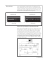
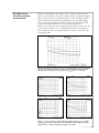
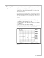
frequency range (0.045 to 110 GHz). The system comes with power leveling ready. Figure 1 shows test port power versus frequency with power leveling turned on in an HP 8510XF measurement system.
Leveled Power, Port 2
-6
-7
-8
-9
-10
-11
-12
-13
-14
0.0 0.8 1.6 5 13 21 29 3 44 52 60 68 7 83 91 99 10
45 25 05 .8 .6 .4 .2 7
.8 .6 .4 .2 6 .8 .6 .4 7.2
Output Port Power (dBm)
Output Port Power (dBm)
Leveled Power, Port 1
-6
-7
-8
-9
-10
-11
-12
-13
-14
0.0 0.7 1.4 4 11 18 25 32 4 47 54 61 68 7 83 90 97 10
.2 .4 .6 .8 0
.2 .4 .6 .8 6
45 65 85
.2 .4 .6 4.8
Frequency (GHz)
Frequency (GHz)
Figure 1. Leveled test port output power versus frequency, with power set to
–10 dBm at the test ports and frequency coverage from 0.045 to 110 GHz
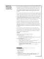
Figure 2 shows the HP 8510XF leveling loop. Power from the RF source is
first sampled by the directional coupler. The coupler output is down-converted by a mixer to the IF frequency (20MHz), which is then amplified
(using programmable gain steps), filtered and scaled prior to detection.
After the IF signal is converted to a DC voltage by the detector, the detector DC output is applied to a multiplying DAC, increasing the power setting
resolution. This signal is passed through the blanking switch before being
compared to the reference voltage. The output of this comparison (difference signal) drives an integrator, which in turn drives the power modulator, forcing the difference to zero. Power adjustment is done by changing
the reference voltage setting.
Figure 2. HP 8510XF leveling loop
4
To provide accurate power control, a two-level calibration process is used
to characterize the frequency response and the absolute gain-step values
of the system. These two levels are designed to counteract two different
sources of error: (1) imprecision in the step attenuators (a programmable
gain calibration), and (2) frequency-related variations in coupler and mixer
performance (a frequency response calibration). Both procedures are performed on each system at Hewlett-Packard before it leaves the factory.
The first level of this calibration process is the detector gain (programmable gain) calibration, performed to collect the correction factors of the step
attenuators in the programmable gain circuit. This calibration procedure
can be performed anytime by the user (it takes approximately two minutes). For measurements in which absolute power levels are critical, perform this calibration before every measurement calibration. If absolute
power levels are not important, perform this calibration infrequently (on a
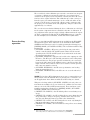
monthly basis, for example). Table 1 outlines this calibration procedure.
Table 1. Procedure for Detector Gain Calibration
HP 8510C Keystrokes1
Description
[SYSTEM] {MORE}
{RF POWER CONFIG} {MORE}
{RESET DET GAIN CAL}
Bring up the reset detector gain calibration menu.
Considerations:
The detector gain calibration process causes
some settings to change, and these are not
restored to their original conditions afterward.
Therefore, after the calibration, the system needs
to be returned to a known state. The first two
selections below are included as a convenience
(and as a reminder of the need to save the
present settings before running the calibration).
Select one of the following:
• {RUN CAL + USER PRST}
• {RUN CAL + FACT PRST}
• {RUN CAL NO PRESET}
• {CANCEL}
• Runs the detector gain calibration routine, and is
followed by a user preset.
• Runs the detector gain calibration routine, and is
followed by a factory preset.
• Runs the detector gain calibration routine, and is
not followed by a preset (system settings that are
altered by the calibration routine will not be
restored to their original conditions afterward).
• Exit the menu without running the calibration
routine, and return to the previous menu.
1. The front panel hardkey names are enclosed in brackets: [HARDKEYS].
The softkey names are italicized and enclosed in braces: {SOFTKEYS}.
5
The second level of this calibration process is the conversion loss (frequency response) calibration, performed to gather the correction factors to
counteract the frequency-related variations caused by the RF-to-IF conversion loss of the coupler and mixer. This calibration procedure can be performed as part of an annual maintenance (to be conducted either on-site
or at the local HP service center by HP customer service engineers with
the proper power level flatness kit and equipment). This procedure takes
approximately 3 to 4 hours.
The correction factors obtained during the above calibrations are valid only
for the system components that are installed at the time of calibration. If
any component in the system is replaced, both calibrations must be repeated. These components include the HP 8510XF millimeter-wave controller,
the left and right test head modules, and the RF and LO synthesizers.
Power leveling
operation
There are four different RF leveling functions available in the HP 8510XF
measurement system. These functions can be found in the RF POWER
CONFIG menu. This menu can be located by pressing the following keys:
[SYSTEM] {MORE} {RF POWER CONFIG}1. The four different RF leveling
functions are:
• {RF LEVEL: SYSTEM}—RF power is leveled at the test ports and is
entirely controlled by the HP 8510XF system. This is also the normal
operating mode. The HP 8510XF system is set in this mode at the time
the system leaves the factory.
• {RF LEVEL: INTERNAL}—RF power is leveled at the output port of the
RF source. The RF source (HP 83651B) performs its own leveling using
an internal detector. For proper operation of this mode, the connection
between the ALC output of the millimeter-wave controller and the ALC
input of the RF source must be removed. To return to normal operation,
this connection must be restored.
• {RF LEVEL: EXTERNAL}—the RF source performs its own leveling
using an external detector.
• {RF LEVEL: LEVELING OFF}—the RF source is set to the unleveled
mode.
NOTE: The last three RF leveling functions are not recommended for normal operation of the HP 8510XF. They are provided as a convenience for
use in applications where different methods of RF leveling are desired.
With power leveling enabled ({RF LEVEL: SYSTEM} selected), there are
four functions available to detect an “unleveled” condition (for more information, refer to the HP 8510XF system manual). These functions can be
found by pressing the following keys: [SYSTEM] {MORE} {RF POWER
CONFIG} {MORE}. These functions are:
• {DETECT UNL: ALWAYS}—the HP 8510C polls for errors during every
sweep.
• {DETECT UNL: SMART}—the HP 8510C polls for errors during the first
sweep following a change in frequency, and thereafter only if an error
was detected during the first sweep. This is the default mode.
• {DETECT UNL: ONCE}—the HP 8510C polls for errors only during the
first sweep following a change in frequency.
• {DETECT UNL: NEVER}—the HP 8510C does not poll for errors during
any sweep.
1. The front panel hardkey names are enclosed in brackets: [HARDKEYS].
The softkey names are italicized and enclosed in braces: {SOFTKEYS}.
6
Power control
Once power leveling is enabled ({RF LEVEL: SYSTEM} selected), the
HP 8510XF leveling loop will control the RF source, the millimeter-wave
controller and the test head modules to provide the user-requested test
port power. The test port power functions described below can be found
by pressing the following keys: STIMULUS [MENU] {POWER MENU}.
(NOTE: These port power functions are valid only when the {RF LEVEL:
SYSTEM} function is selected.)
• {PORT1 POWER}—followed by a number, this specifies a power level
setting for Port 1 in dBm. (If the ports are coupled, this setting also
applies to Port 2.)
• {PORT1 SLOPE ON} and {PORT1 SLOPE OFF}—used to enable and
disable power slope for Port 1. {PORT1 SLOPE ON}, followed by a
number, specifies the power slope setting for Port 1 in dB/GHz. The
current port power level is used as the power at the first frequency of
the sweep, and slope is then applied as frequency increases. Power slope
has no effect on CW measurements. (If the ports are coupled, this
setting also applies to Port 2.)
• {COUPLE PORTS} or {UNCOUPLE PORTS}—this softkey toggles
between the two labels. Pressing this softkey selects the displayed
function, but changes the display to show the opposite function. If
{COUPLE PORTS} is pressed, the Port 1 power level setting and power
slope setting are applied to Port 2. If {UNCOUPLE PORTS} is pressed,
the two ports have independent power level settings and power slope
settings, and the following softkeys will be displayed.
• {PORT2 POWER}—followed by a number, specifies a power level setting
for Port 2 in dBm.
• {PORT2 SLOPE ON} and {PORT2 SLOPE OFF}—used to enable and
disable power slope for Port 2. {PORT2 SLOPE ON}, followed by a
number, specifies the power slope setting for Port 2 in dB/GHz. The
current port power level is used as the power at the first frequency of
the sweep, and slope is then applied as frequency increases. Power slope
has no effect on CW measurements.
NOTE: Since the last two softkeys ({PORT2 POWER} and {PORT2
SLOPE ON/OFF}) control the power level from Port 2, they are displayed
only if the ports are uncoupled.
While using the system in this mode ({RF LEVEL: SYSTEM}), the user
may encounter the following error messages:
• “RF Unleveled”—displayed if test port power becomes unleveled.
This indicates that the specified test port power is too high for the
HP 8510XF leveling loop to maintain leveled power over the frequency
span. This error message should disappear as test port power is reduced
and leveling re-established.
• “No IF Found”—displayed if the IF is not found or too low. Check to
make sure that the RF source has an output signal and is properly
connected to the millimeter-wave controller. For more information,
please refer to the HP 8510C Service Manual, under the Running Error
Messages section.
• “IF Overload”—displayed if the IF is overloaded. Reducing the test port
power will remove this message.
7
Measurements in the
frequency domain
One of the benefits of the power leveling capability of the HP 8510XF measurement system is the ability to perform power measurements without
doing a power calibration each time. Since the input power level to the
device under test is kept constant, the HP 8510XF system can carry out
power measurements such as gain, gain compression and absolute power
on active devices simply, at the touch of a few keystrokes.
Table 2 provides step-by-step instructions for setting up and performing
measurements on an amplifier. Included are measurements of gain, gain
compression and absolute power.
Table 2. Gain, gain compression and absolute power measurements
of an amplifier in the frequency domain.
HP 8510C Keystrokes
Description
(1). Set up the HP 8510C.
[PRESET]
Return all instruments to a known state.
[START] Fstart [G/n]
[STOP] Fstop [G/n]
Set up the start and stop frequencies.
STIMULUS [MENU]
{NUMBER of POINTS} {#…}
Select the number of analyzer trace points.
RESPONSE [MENU]
{AVERAGING ON/RESTART}
#…[x1]
Set averaging as desired.
(2). Verify that power leveling is enabled.
[SYSTEM] {MORE}
Select RF “system” leveling.
{RF POWER CONFIG}
{RF LEVEL: SYSTEM}
{MORE} {DETECT UNL: SMART}
Select “smart” leveling detection.
(3). Set test port (port 1) power level.
STIMULUS [MENU]
{POWER MENU}
{PORT1 POWER} Pin [x1]
Set test port 1 power (Pin) below the amplifier's
(device-under-test, DUT) compression level.
(4). Perform a thru measurement calibration.
[S21]
Set up the analyzer for an S21 measurement.
[CAL]
{CAL #…}
{CALIBRATE: RESPONSE}
{THRU}
{DONE RESPONSE}
Perform a thru calibration to eliminate the frequency response errors of the path in the measurement. Be sure to include any adapters that
are part of the measurement in the thru calibration.
{CAL SET} {1}
Save the calibration in Cal Set 1
Considerations:
If test port cables are used to connect the amplifier, see Appendix A for test port cable
loss compensation. Since leveled power is provided at the test ports, power delivered to
the input port of the DUT may not be leveled due to the insertion loss of the test port
cable.
8
HP 8510C Keystrokes
Description (continued)
See Appendix B for wafer-probing environments.
(5). Connect amplifier (DUT) and measure gain.
Gain is displayed here as S21 versus frequency.
(6). Measure absolute power at the DUT output port.
RESPONSE [MENU]
Display absolute power at the DUT output port
{MORE}
(versus frequency) by entering a magnitude offset
{MAGNITUDE OFFSET} Pin [x1]
equivalent to the test port 1 power level during the
thru calibration (Pin). This value can also be calculated for any frequency measurement point by
adding Pin to S21:
• S21 = Pout/Pin
• Pout = S21✕Pin
(7). Set up 1 dB compression measurement.
RESPONSE [MENU]
Return the display to show gain, S21, by removing
{MORE}
magnitude offset.
{MAGNITUDE OFFSET} 0 [x1]
(8). Adjust display.
[REF VALUE] 0 [x1]
[SCALE] 1 [x1]
Set the reference value to 0, and the scale to 1 dB
per division for easy viewing.
(9). Normalize trace.
[DISPLAY] {DATA AND MEMORIES}
{DISPLAY –> MEMORY}
{MATH(/)}
By normalizing the measurement, the first
frequency point to drop by 1 dB will be easy to
identify.
(10). Increase power to find the 1 dB gain compression point.
STIMULUS [MENU]
Increase the test port power 1 dB at a time until
{POWER MENU}
one measurement point visibly drops. If needed,
{PORT1 POWER} use up arrow,
use the knob to adjust the test port power until a
rotate knob
1 dB drop has occurred, and note the test port
power level (Pcompression).
[MARKER] rotate knob
Measure the frequency, by using the knob to
place a marker at the 1 dB point.
(11). Measure gain at the 1 dB compression point.
[DISPLAY] {DATA AND MEMORIES}
Display gain (S21) versus frequency. The marker
{DISPLAY: DATA}
will indicate the amplifier's gain at the 1 dB
[AUTO]
compression point for that frequency.
(12). Calculate absolute power at the 1 dB compression point.
Absolute power at the 1 dB compression point (for the specified frequency point) can be
calculated by adding Pcompression. Pcompression is the test port power level identified when
the 1 dB gain compression point was found.
9
Example of the
frequency-domain
measurement
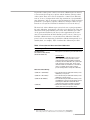
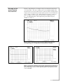
Figures 3 and 4 illustrate an example of the frequency-domain measurement covered in Table 2. The device-under-test was a broadband amplifier.
The measurements were made using 201 trace points and 128 averaging.
Figure 3 shows the measurement of absolute power at the DUT output
port versus frequency (step 6 of Table 2). Figure 4 shows that the 1-dB
compression point is different for each frequency(steps 7-11 of
Table 2). For comparison, the measurements shown were made at two different frequency points, one at 3.89 GHz and the other at 13.24 GHz. As
the frequency increases, it typically takes more power to reach the 1-dB
compression point.
Figure 3. Measurement of absolute power at the DUT output port versus frequency.
The top trace shows the S21 measurements of the DUT. The bottom trace shows
absolute power, the equivalent of Pin added to S21. Pin was set at –15 dBm
Figure 4a.
Figure 4b.
Figure 4c.
Figure 4d.
Figure 4. (a) At 3.89 GHz, the 1-dB compression point happens at Pin = –11 dBm,
and (b) S21 measures at 18.20 dB. (c) At 13.24 GHz, the 1-dB compression point
happens at Pin = –6 dBm, and (d) S21 measures at 13.64 dB.
10
Measurements in the
power domain
In the frequency domain, measurements are made at one test port power
level while sweeping in frequency. In the power domain, measurements are
made at one frequency point while sweeping in power. Similar to frequency-domain measurements, but sweeping in power, measurements such as
gain and gain compression can be easily accomplished without performing
a power calibration each time.
Before beginning power-domain measurements, the system must be calibrated in the frequency range of choice. This calibration is included in
Table 3, along with step-by-step instructions for setting up and performing
measurements of an amplifier. It is recommended that the chosen frequency range provides frequency steps of a convenient size. This allows the
measurement frequencies to be easily recalled later. For example, setting
start frequency to 1 GHz and stop frequency to 101 GHz, with the number
of points set to 101, gives measurement frequencies in 1 GHz increments.
Table 3. Gain and gain compression measurements of an amplifier
in the power domain.
HP 8510C Keystrokes
Description
(1). Set up the HP 8510C.
[PRESET]
Return all instruments to a known state.
[START] Fstart [G/n]
[STOP] Fstop [G/n]
Set up the start and stop frequencies.
STIMULUS [MENU]
{NUMBER of POINTS} {#…}
Select the number of analyzer trace points.
RESPONSE [MENU]
{AVERAGING ON/RESTART}
#… [x1]
Set averaging as desired.
(2). Verify that power leveling is enabled.
[SYSTEM] {MORE} {RF POWER
Select RF “system” leveling.
CONFIG} {RF LEVEL: SYSTEM}
{MORE} {DETECT UNL: SMART}
Select “smart” leveling detection.
(3). Set test port (port 1) power level.
STIMULUS [MENU]
{POWER MENU}
{PORT1 POWER} Pin [x1]
Set test port 1 power (Pin) below the amplifier‘s
(device-under-test, DUT) compression level.
(4). Perform a thru measurement calibration1.
[S21]
Set up the analyzer for an S21 measurement.
[CAL]
{CAL #…}
{CALIBRATE: RESPONSE}
{THRU}
{DONE RESPONSE}
Perform a thru calibration to eliminate the frequency response errors of the path in the measurement. Be sure to include any adapters that
are part of the measurement in the thru
calibration.
{CAL SET} {1}
Save the calibration in Cal Set 1
1. If a calibration is being performed or a previously stored Cal Set is being used, the
power-domain frequency of measurement must be a point in the original (frequencydomain) calibration. Otherwise, calibration will be automatically turned off.
11
HP 8510C Keystrokes
Description (continued)
(5). Connect amplifier (DUT) and measure gain.
Gain is displayed here as S21 versus frequency.
(6). Set up for a power-domain measurement.
[MARKER] rotate knob
Place a marker at the frequency point of
interest (Finterest)1.
[DOMAIN] {POWER}
Select power domain2.
(7). Adjust display for 1 dB compression measurement.
[MARKER]
Place a marker on the left side of the display.
[REF VALUE] [= MARKER]
Set the marker value to become the new
reference value.
[SCALE] 1 [x1]
Set the scale to 1 dB per division for easy viewing.
(8). To change start and stop test port power levels3:
[START] Pstart [x1]
Set up the start and stop test port power levels.
[STOP] Pstop [x1]
Set Pstart below the amplifier's compression level.
(9). Increase Pstop to find the 1 dB gain compression point.
[STOP] use up arrow,
Increase the stop test port power level 1 dB at a
rotate knob
time until the right half of the measurement trace
visibly drops. Then, use the knob to adjust the
power until a 1-dB drop has occurred, and note
the test port power level (Pcompression) for this
frequency point.
(10). To measure another frequency point4:
[DOMAIN] {POWER}
Select {NEXT PT. HIGH.}
Or {NEXT PT. LOW}
Use these keys to select the next frequency point of interest, either higher or
lower, and adjust Pstop as necessary.
1. If multiple markers are ON, the active marker is the one that will be used for the
power-domain frequency of measurement.
2. In the HP 8510XF system, the factory preset default settings for power-domain
measurements are as follows:
• Start: –35 dBm
• Stop: –15 dBm
3. In the power domain, the stimulus keys ([START], [STOP], [CENTER], [SPAN]) refer to
power and not frequency. Since the sweeps are done in power, the softkey {PORT1
POWER}, under STIMULUS [MENU] {POWER MENU}, has no effect in this mode.
4. If a calibration is being performed or a previously stored Cal Set is being used, the
power-domain frequency of measurement must be a point in the original (frequency
domain) calibration. Otherwise, calibration will be automatically turned off.
12
Example of the
power-domain
measurement
Figures 5 and 6 illustrate an example of the power-domain measurement
covered in Table 3. The device-under-test was a broadband amplifier. The
measurements were made using 201 trace points and 128 averaging. Figure
5 shows an S21 measurement (versus frequency) before Power Domain was
enabled (step 5 of Table 3). The marker marks the frequency of interest
(Finterest). Figure 6 shows the S21 measurement sweeping in power at
Finterest and identifying the 1-dB compression point at that frequency
(steps 6-9 of Table 3).
Figure 5. An S21 measurement (versus frequency) with the marker placed at
50.07 GHz and Pin set at –15 dBm (before Power Domain was enabled).
Figure 6a.
Figure 6b.
Figure 6. (a) An S21 measurement (versus power) at the frequency specified by the
marker in Figure 5. Note the default start and stop stimulus values. (b) By increasing the stop stimulus value, the 1-dB compression point at this frequency is found
to be at 3.415 dBm.
13
Appendix A.
Test port cable loss
compensation
Since leveled power is provided at the test ports of the HP 8510XF system,
test port cables that are used to connect between the test port and the
input port of the device-under-test (DUT) will reduce the power delivered
to the input port of the DUT. This reduction in power is due to the insertion loss of the test port cable. This section describes the basic steps one
can implement to compensate this loss and deliver leveled power at the
end of the test port cable.
If the insertion loss of the test port cable is characterized over frequency,
this data can be used in conjunction with power slope to compensate cable
loss resulting in leveled power at the end of the test port cable. (Power
slope of the HP 8510XF was covered above in the power control section.)
Example:
In this example, the following sequence of events took place:
1. A response (thru) calibration was performed on the HP 8510 VNA.
2. Insertion loss (S21) of a test port cable was characterized (see Figure
A1). In this case, the test port cable is the DUT.
3. Power (vs. frequency) at the end of the test port cable was examined
(see Figure A2).
4. The power slope value was calculated and applied.
The test port cable used in this example was an HP 11500J, a 1.0 mm test
port cable with male and female connectors and 16 cm in length.
Figure A1. Insertion loss (versus frequency) of a typical HP 11500J 1.0 mm test
port cable.
14
Figure A2 shows output power versus frequency at the end of the test port
cable as connected to the test port of the HP 8510XF system. The power
setting was –10 dBm. Since power at the test port is leveled, the slope
shown in Figure A2 is mainly due to the insertion loss of the test port
cable. Notice that the trace resembles that of Figure A1. By approximating
the trace as a straight line, the insertion loss of the cable can be compensated by applying power slope1.
0.0 0.7 1.3 2 8. 15 22 28 3 41 48 55 61 6 74 81 88 94 10 10
.6 1.2 7.8
45 05 65 .2 8 .4
.6 5.2 .8 .4
.6 8.2 .8 .4
End-of-test-port-cable, Port 2 Power
Output Power (dBm)
Output Power (dBm)
End-of-test-port-cable, Port 1 Power
-6
-7
-8
-9
-10
-11
-12
-13
-14
-6
-7
-8
-9
-10
-11
-12
-13
-14
Frequency (GHz)
0.0 0.6 1.3 1 8 14 20 27 3 40 46 52 59 65 7 7 8 91 97. 104
45 85 25 .96
.4 .8 .2 3.6
.4 .8 .2 .6 2 8.4 4.8 .2 6
5
Frequency (GHz)
Figure A2. Output power at the end of the test port cable versus frequency.
Power was set at –10 dBm. The test port cable used was an HP 11500J
Power slope calculation:
Since the insertion loss of cables is typically linear with frequency (as
shown in Figure A1), a best-fit line can be used to estimate the slope of
the line. The slope of the line in Figure A1 is approximately –3 dB/110 GHz
(equivalent to –0.027 dB/GHz ). To compensate for the insertion loss of the
cable shown in Figure A1, the power slope value would be +0.027 dB/GHz.
To enable power slope, follow this key sequence: STIMULUS [MENU]
{POWER MENU} {SLOPE ON} power_slope_value [x1]. (In this case,
power_slope_value would be 0.027.)
Using the technique described above, the approximated insertion loss of a
test port cable can be corrected by applying power slope, resulting in
“approximated” leveled power at the end of the test port cable. This way,
power delivered to the input port of the DUT is approximately leveled
across frequency.
1. As stated above in the power control section, power slope has no effect on CW
measurements (not applicable). Thus, this is valid in frequency domain, not power
domain.
15
Appendix B.
Wafer-probing
environment
considerations
On-wafer S-parameter measurements at frequencies up to 110 GHz can be
made using the HP 8510XF VNA system and Cascade Microtech1 or other
compatible wafer probers. Wafer probing allows immediate evaluation for
device characterization and selection before dicing the wafer and packaging. The ability to calibrate on-wafer and make real-time error-corrected
measurements with the HP 8510XF are the principle advantages of this
system.
Since leveled power is provided at the test ports of the HP 8510XF system,
test port cables and probes that are used to connect between the test port
and the wafer-under-test will reduce the power delivered to the wafer. This
reduction in power is mainly due to the insertion loss of the test port cable
and the probe. This appendix describes the basic steps one can implement
to compensate this loss and deliver leveled power at the probe tip. (For
information relating to on-wafer measurements, in particular on-wafer calibration, see HP Product Note 8510-6 or contact Cascade Microtech.)
By characterizing the insertion loss of the test port cable and the probe
(together) over frequency, power slope can be used in conjunction with
this data to compensate the loss, resulting in leveled power at the wafer.
(Since there are no power sensors for on-wafer measurements at this time,
the steps described below can be used to estimate power at the probes,
for all practical purposes, by taking advantage of the known test port reference plane.)
To characterize the combined insertion loss of a test port cable and a
probe (“cable + probe”), it is necessary to follow a two-step process. Step
1 is to perform a 1-port coaxial calibration at the test port, and step 2 is to
perform a “probe test” at the tip of the probe.(“Probe Test” is a feature of
Cascade Microtech's WinCal software.)
Example:
In this example, the following equipment was used:
From Hewlett-Packard:
• HP 8510XF 0.045 to 110 GHz VNA system.
• HP 11500J2 1.0 mm test port cable, male-to-female, 16 cm in length.
• HP 85059A DC to 110 GHz calibration kit.
From Cascade Microtech:
• Summit 9100, manual probe station.3
• ACP110L-GSG DC to 110 GHz low-loss probe, 150 mm pitch,
ground-signal-ground (G-S-G) configuration.
• P/N 104-783 W-band Impedance Standard Substrate (ISS), in G-S-G
configuration usable through 110 GHz.
• WinCalTM automated calibration software for vector network
analyzers.
1. Cascade Microtech is an HP Channel Partner and can be reached at:
Cascade Microtech, Inc.
2430 NW 206th Avenue
Beaverton, Oregon 97006
General: 1-800-854-8400
Sales: 1-800-550-3279
Support: 1-800-626-9395
www.cmicro.com
2. Different lengths of 1.0mm test port cables are also applicable. There are three lengths
available: HP 11500J (16cm), HP 11500K (20cm) and HP 11500L (24cm).
3. A manual probing station was used in this example. Other probing stations are also
applicable, such as semiautomatic probe stations.
16
The following sequence of events took place:
1. A 1-port coaxial calibration was performed at the test port of the
HP 8510 VNA.
2. The test port cable and the probe were connected to the same
test port that was just calibrated.
3. Using WinCal and with the test port calibration active on the VNA,
the probe test was performed.
4. The result was an S-parameter graph of the “cable + probe”
(see Figure B1).
The trace labeled S21, in Figure B1, shows the insertion loss (versus frequency) of a typical HP 11500J test port cable and a typical ACP110L-GSG
probe (together). S11 shows the reflection measurement at the test port,
and S22 shows the reflection measurement of the ACP110L-GSG probe tip.
Figure B1 was generated using Cascade’s WinCal calibration software.
Table B1 outlines the steps needed to generate Figure B1.
Looking at the trace in Figure B1, the slope of the line can be estimated
using straight-line approximation. The value of the slope can then be
applied in power slope to compensate for the insertion loss in the path
between the test port and the wafer. (Refer to Appendix A for power slope
calculation.)
Figure B1. S21 shows the total insertion loss (versus frequency) of a typical
HP 11500J test port cable and a typical ACP110L-GSG probe from Cascade
Microtech as measured and computed using Cascade’s Probe Test feature in their
WinCal calibration software
17
Table B1. Procedure to characterize a test port cable and a probe
together.
Description
(1). Coaxial calibration at the test port of the VNA
Using the front panel of the HP 8510,
• Set all desired settings: start and stop frequencies, number of points, averaging,
port power.
• Perform a 1-port calibration at a test port (for example, at test port 1)
• Save the calibration and turn it on.
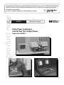
(2). Connect the test port cable and then the probe to the test port
(that is, connect the HP 11500J test port cable to test port 1, and then
connect in the probe as shown in Figure B2)
(3). Using WinCal, perform Probe Test
With WinCal running on a desktop PC1 controlling the HP 8510XF VNA system via
a GP-IB cable,
• Start WinCal. This will bring up a screen similar to the one shown in Figure B3.
• Select Probe Test from the Tools menu. This will bring up a screen similar to the
one shown in Figure B4.
• For this example, select Port 1 under Method.
• Measure the Open, Short and Load standards on the ISS.
• Click Compute, and it will display results similar to Figure B1.
(4). Power slope calculation
The S21 trace shown in Figure B1 can be used to approximate the value for
power slope.
Figure B2. Test port cable and probe connection.
1. PC requirements and detailed information on WinCal can be found in Cascade Microtech's
WinCal Software User Guide.
18
Figure B3. WinCal
Figure B4. Probe Test dialog box
19
References
1. On-Wafer Measurements Using the HP 8510 Network
Analyzer and Cascade Microtech Wafer Probes,
HP Product Note 8510-6, literature number 5954-1579.
2. Controlling Test Port Output Power, Flatness,
HP Product Note 8510-16, literature number 5091-0467E.
3. WinCal Software User Guide, Cascade Microtech.
For more information about
Hewlett-Packard test and measurement products, applications,
services, and for a current sales
office listing, visit our web site,
http://www.hp.com/go/tmdir. You
can also contact one of the following
centers and ask for a test and
measurement sales representative.
United States:
Hewlett-Packard Company
Test and Measurement Call Center
P.O. Box 4026
Englewood, CO 80155-4026
1 800 452 4844
Canada:
Hewlett-Packard Canada Ltd.
5150 Spectrum Way
Mississauga, Ontario L4W 5G1
(905) 206 4725
Europe:
Hewlett-Packard
European Marketing Centre
P.O. Box 999
1180 AZ Amstelveen
The Netherlands
(31 20) 547 9900
Japan:
Hewlett-Packard Japan Ltd.
Measurement Assistance Center
9-1, Takakura-Cho, Hachioji-Shi,
Tokyo 192, Japan
Tel: (81) 426-56-7832
Fax: (81) 426-56-7840
Latin America:
Hewlett-Packard
Latin American Region Headquarters
5200 Blue Lagoon Drive, 9th Floor
Miami, Florida 33126, U.S.A.
(305) 267 4245/4220
Australia/New Zealand:
Hewlett-Packard Australia Ltd.
31-41 Joseph Street
Blackburn, Victoria 3130, Australia
1 800 629 485
Asia Pacific:
Hewlett-Packard Asia Pacific Ltd
19/F Cityplaza One
1111 King's Road
Taikoo Shing, Hong Kong
tel: 852-2599-7777
fax: 852-2506-9285
Data Subject to Change
Copyright © 1999
Hewlett-Packard Company
Printed in U.S.A. 7/99
5968-5270E
20