1
ORDER NO. KM40608170CE
Telephone Equipment
KX-TS2350CAB
KX-TS2350CAC
KX-TS2350CAH
KX-TS2350CAR
KX-TS2350CAW
Integrated Telephone System
Black Version
Blue Version
Gray Version
Red Version
White Version
(for Kazakhstan)
(for Uzbekistan)
© 2006 Panasonic Communications Co., Ltd. All
rights reserved. Unauthorized copying and
distribution is a violation of law.
KX-TS2350CAB / KX-TS2350CAC / KX-TS2350CAH / KX-TS2350CAR / KX-TS2350CAW
Note:
Because section 3 of this manual is an extract from the operating instructions for this model, it is subject to change without notice.
You can download and refer to the original operating instructions on TSN Server for further information.
CONTENTS
Page
1 ABOUT LEAD FREE SOLDER (PbF: Pb free)
Page
3
7.1. Telephone Line Interface and Pulse Dial Circuit
13
1.1. Suggested PbF Solder
3
7.2. Tone Dial Circuit
13
1.2. How to Recognize that Pb Free Solder is Used
4
7.3. Power Circuit and Redial Back-up Circuit
14
2 FOR SERVICE TECHNICIANS
5
8 OPTION JUMPER TABLE
15
3 OPERATING INSTRUCTIONS
6
9 CPU DATA
16
3.1. Location of Controls
6
10 CABINET AND ELECTRICAL PARTS LOCATION
17
3.2. Connection
6
11 ACCESSORY AND PACKING MATERIALS
18
3.3. Troubleshooting
6
12 TERMINAL GUIDE OF ICs TRANSISTORS AND DIODES
19
4 DISASSEMBLY INSTRUCTIONS
7
13 REPLACEMENT PARTS LIST
20
5 TROUBLESHOOTING GUIDE
8
13.1. Base Unit
20
13.2. Accessories and Packing Materials
21
5.1. Service Hints
8
5.2. Pulse Dialing Problems
8
14 FOR SCHEMATIC DIAGRAM (SCHEMATIC DIAGRAM)
23
5.3. Problems With the Handset
9
15 SCHEMATIC DIAGRAM
24
5.4. Tone Dialing Problems
9
16 CIRCUIT BOARD
27
5.5. Problems With Ringer
10
16.1. Main (Component View)
27
5.6. How to Check IC1 (Scanning to the key)
11
16.2. Main (Flow Solder Side View)
28
6 BLOCK DIAGRAM
12
16.3. Operation (Flow Solder Side View)
29
7 CIRCUIT OPERATIONS
13
2
KX-TS2350CAB / KX-TS2350CAC / KX-TS2350CAH / KX-TS2350CAR / KX-TS2350CAW
1 ABOUT LEAD FREE SOLDER (PbF: Pb free)
Note:
In the information below, Pb, the symbol for lead in the periodic table of elements, will refer to standard solder or solder that
contains lead.
We will use PbF Solder when discussing the lead free solder used in our manufacturing process which is made from Tin (Sn),
Silver (Ag), and Copper (Cu).
This model, and others like it, manufactured using lead free solder will have PbF stamped on the PCB. For service and repair
work we suggest using the same type of solder.
Caution
• PbF solder has a melting point that is 50°F ~70°F (30°C ~ 40°C) higher than Pb solder. Please use a soldering iron with
temperature control and adjust it to 700°F ± 20°F (370°C ± 10°C).
• Exercise care while using higher temperature soldering irons.:
Do not heat the PCB for too long time in order to prevent solder splash or damage to the PCB.
• PbF solder will tend to splash if it is heated much higher than its melting point, approximately 1100°F (600°C).
• When applying PbF solder to double layered boards, please check the component side for excess which may flow onto the
opposite side (See the figure below).
1.1.
Suggested PbF Solder
There are several types of PbF solder available commercially. While this product is manufactured using Tin, Silver, and Copper
(Sn+Ag+Cu), you can also use Tin and Copper (Sn+Cu) or Tin, Zinc, and Bismuth (Sn+Zn+Bi). Please check the
manufacturer’s specific instructions for the melting points of their products and any precautions for using their product with other
materials.
The following lead free (PbF) solder wire sizes are recommended for service of this product: 0.3 mm, 0.6 mm and 1.0 mm.
3
KX-TS2350CAB / KX-TS2350CAC / KX-TS2350CAH / KX-TS2350CAR / KX-TS2350CAW
1.2.
How to Recognize that Pb Free Solder is Used
(Example: Main P.C.B.)
3
1
8
5
IC2
1
4
1
IC1
1
2 3
28
4 5 6
CN1
PbF
Marked
(Component View)
Note:
The location of the “PbF” mark is subject to change without notice.
4
7
8
9 10 11 12
KX-TS2350CAB / KX-TS2350CAC / KX-TS2350CAH / KX-TS2350CAR / KX-TS2350CAW
2 FOR SERVICE TECHNICIANS
ICs and LSIs are vulnerable to static electricity.
When repairing, the following precautions will help prevent recurring malfunctions.
1. Cover the plastic parts boxes with aluminum foil.
2. Ground the soldering irons.
3. Use a conductive mat on the worktable.
4. Do not touch IC or LSI pins with bare fingers.
5
KX-TS2350CAB / KX-TS2350CAC / KX-TS2350CAH / KX-TS2350CAR / KX-TS2350CAW
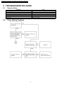
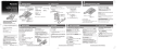
3 OPERATING INSTRUCTIONS
3.1.
Location of Controls
3.2.
Connection
3.3.
Troubleshooting
6
KX-TS2350CAB / KX-TS2350CAC / KX-TS2350CAH / KX-TS2350CAR / KX-TS2350CAW
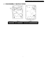
4 DISASSEMBLY INSTRUCTIONS
Shown in Fig —.
1
2
To remove —.
Cabinet Cover
P.C. Boards
Remove —.
Screws (2.6 × 10).............. (A) × 5
Remove the P.C.Boards
7
KX-TS2350CAB / KX-TS2350CAC / KX-TS2350CAH / KX-TS2350CAR / KX-TS2350CAW
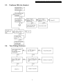
5 TROUBLESHOOTING GUIDE
5.1.
Service Hints
SYMPTOM
No Tone Dialing
Dead
Rings, no dial tone, no pulse or tone dial
No rings
No volume Handset
Buttons stick under upper cabinet assembly. From key board
No pulse dial
5.2.
CURE
Check IC1, Q2, Q1, C22 and VR1.
Check IC1, Q2, Q1 and D17.
Check Q1, Q2, D17, Q3 and IC1.
Check C1, R2 and IC2.
Check IC1, VR1, C15 and C22.
Adjust the setting of buttons.
Check Q1, Q2 and IC1.
Pulse Dialing Problems
8
KX-TS2350CAB / KX-TS2350CAC / KX-TS2350CAH / KX-TS2350CAR / KX-TS2350CAW
5.3.
Problems With the Handset
5.4.
Tone Dialing Problems
9
KX-TS2350CAB / KX-TS2350CAC / KX-TS2350CAH / KX-TS2350CAR / KX-TS2350CAW
5.5.
Problems With Ringer
10
KX-TS2350CAB / KX-TS2350CAC / KX-TS2350CAH / KX-TS2350CAR / KX-TS2350CAW
5.6.
How to Check IC1 (Scanning to the key)
11
Ringer
T
R
D24
S3
R102
R2
OFF
L R103
H
2
IC2
5
1
8
C1
D2
R14
D17
sv1
D23
R55
C34
Q8
Q2
Q1
6 BLOCK DIAGRAM
Q3
CS
12
CI
RING
FREQUENCY
DISCRIMINATION
FCI
HS/DP
MELODY
SEQUENCER
VDD
LINE ADAPTATION
POWER EXTRACTION
DC MASK
LI
MO
VSS
VDD
R9
AGND
CONTROL
LOGIC
LLC
SOFT CLIP
AGC
LINE
CURRENT
SENSE
LS
IC1
OSC
3.58
ADL
OSC
TONE
GENERATOR
C22
RI
RS
MFL
STB
R5
R10
AGND
C1
C4
R1
R2
R3
R4
M2
M1
RO
HS MIC
HS Speaker
KX-TS2350 BLOCK DIAGRAM
C3
LED
KEY
PAD
C2
DIALLER
MUTE
C9
MODE
RAM
R6
C5
KX-TS2350CAB / KX-TS2350CAC / KX-TS2350CAH / KX-TS2350CAR / KX-TS2350CAW
KX-TS2350CAB / KX-TS2350CAC / KX-TS2350CAH / KX-TS2350CAR / KX-TS2350CAW
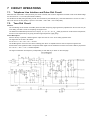
7 CIRCUIT OPERATIONS
7.1.
Telephone Line Interface and Pulse Dial Circuit
When the hook switch SW1 is ON (off-hook), the circuit is closed, and current is supplied to the base of Q2 via the diode bridge
D17 and Q2 is On → Q1 is ON (OFF-HOOK condition).
Q1 and Q2 are the dial pulse generating circuits, and are driven by the DIALER (IC1), when the DIALER Pin 10 of IC1 is LOW →
Q2 is OFF and Q1 is OFF (break). If port Pin 10 is HIGH → Q2 is ON → Q1 is ON (make).
7.2.
Tone Dial Circuit
Function:
The tone dialing circuit consists of a DTMF (Dual Tone Multi Frequency) signal generator (outputted from Pin 25 of the IC1) for
tone dialing, and also a circuit for outputting the signal to line.
The DTMF circuit identifies inputs from the 12 keys (1, 2, 3, 4, 5, 6, 7, 8, 9, 0, and #) by means of a total of seven frequencies,
that is four low frequencies (Low group) and three high frequencies (High group).
Circuit Description:
When a dial key is pressed, a DTMF signal is output from Pin 25 of IC1 as an analog synthetic wave.
The signal flow to the line is as follows.
Pin 25 of IC1 → Q3 → R9 → Q1 → Tel Line.
The DTMF signal is sent to the line via the following path. Q3 is an amplifier which is used to output the signal to line.
Shown below is the signal flow used to output the DTMF signal from the handset as a monitor tone when a dial key is pressed.
Pin 3 of IC1 → VR1 → C15 → Handset Speaker.
The signal combination and frequency corresponding to each dial key is shown on the next page.
13
KX-TS2350CAB / KX-TS2350CAC / KX-TS2350CAH / KX-TS2350CAR / KX-TS2350CAW
7.3.
Power Circuit and Redial Back-up Circuit
Function:
This set is powered from the line. When it is an OFF-HOOK status, Tel Line → D17 → Q1 → R9 → Pin 27 of IC1 (to become
the power supply for IC1 speech network).
The voltage from the line is turned into a constant voltage by D2 and then supplied to the IC1, reset circuit.
Through Tel Line → R1 → R3 → D17 → R14 to become the power supply for IC1, and the redial Back-up will be done.
14
KX-TS2350CAB / KX-TS2350CAC / KX-TS2350CAH / KX-TS2350CAR / KX-TS2350CAW
8 OPTION JUMPER TABLE
Note:
Refer to Main (Flow Solder Side View) (P.28)
15
KX-TS2350CAB / KX-TS2350CAC / KX-TS2350CAH / KX-TS2350CAR / KX-TS2350CAW
9 CPU DATA
(IC1)
U4
C1
C5 C4 C6
C2 C3
Clock frequency: 3.58MHz
Operating range: 13~100mA
U5
VSS
28
LS 1
MFL 2
RO 3
VDD 4
AGND 5
STB 6
CI 7
MO 8
LLC 9
VSS VSS
HS/DP 10
OSC 11
MODE 12
C4 13
C3 14
C2 15
C1 16
R4 17
R3 18
R2 19
R1 20
FCI 21
LED 22
M1 23
M2 24
CS 25
VSS 26
LI 27
RI 28
1
Pin
No.
Symbol
Description
Function
1
LS
2
MFL
MF Level Setting
This is the input for sending the line current.
A voltage divider connected from this pin to A GND and VSS can be used to set the DTMF level.
3
RO
Receive Output
This is the output for driving a dynamic earpiece with an impedance of 140 to 300
4
VDD
Positive Voltage Supply
This is the supply pin for the circuit.
5
AGND
Analogue Ground
6
STB
Side Tone Balance Input
7
CI
Complex Impedance Pin
This is the analog(ue) ground for the amplifiers.
This is the input for side tone cancellation.
For complex impedance a capacitor should be connected to this pin.
8
MO
Melody Output
PDM output of the melody generator for tone ringing. Hi-Z when not active.
9
LLC
Line Loss Compensation
Select pin for line loss compensation.
LLC = AGND: 20-50 mA LLC = VDD: 45-75 mA
10
HS/DP
11
OSC
12
MODE
Line Current Sense Input
LLC = VSS: none.
Hook Switch Input and Dial Pulse Output
This is an I/O that is pulled high by the hook switch when off-hook and an open
drain pulls it low during break periods of pulse dialing and flash.
Oscillator Input
Pin for ceramic resonator (3.58 MHz).
Signalling Mode Select Input
Mode pin
Row 2
Function
mode, 10 pps, 40/60 ms
Row 6
MF only, 82/82 ms
During temporary MF : 82/160 ms
13
C4
Keyboard Column
14
15
16
C3
C2
C1
Keyboard Column
Keyboard Column
Keyboard Column
17
R4
Keyboard Row
18
R3
Keyboard Row
19
R2
Keyboard Row
20
R1
Keyboard Row
21
FCI
Frequency Comparator Input
This is a Schmitt trigger input for ring frequency discrimination. Disabled during off-hook.
22
23
LED
M1
LED Output Driver
Microphone Input
Output for driving an LED that will be flashing when in Programme.
24
M2
Microphone Input
25
CS
Current Shunt Control Output
26
VSS
Negative Power Supply
27
LI
Line Input
This input is used for power extraction and line current sending.
28
RI
Receive Input
This is the input for the receive signal.
VSS
VSS
EMC ground connection
(see key arrangement in Schematic Diagram) the scanning to the key.
(see key arrangement in Schematic Diagram) the scanning to the key.
Differential inputs for the microphone (electric).
This N-channel open drain output controls the external high power shunt transistor
for the modulation of the line voltage and for shorting the line during make period
of pulse dialing.
16
KX-TS2350CAB / KX-TS2350CAC / KX-TS2350CAH / KX-TS2350CAR / KX-TS2350CAW
10 CABINET AND ELECTRICAL PARTS LOCATION
17
KX-TS2350CAB / KX-TS2350CAC / KX-TS2350CAH / KX-TS2350CAR / KX-TS2350CAW
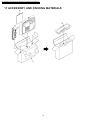
11 ACCESSORY AND PACKING MATERIALS
18
KX-TS2350CAB / KX-TS2350CAC / KX-TS2350CAH / KX-TS2350CAR / KX-TS2350CAW
12 TERMINAL GUIDE OF ICs TRANSISTORS AND DIODES
19
KX-TS2350CAB / KX-TS2350CAC / KX-TS2350CAH / KX-TS2350CAR / KX-TS2350CAW
13 REPLACEMENT PARTS LIST
1. RTL (Retention Time Limited)
Ref.
No.
Note:
Part No.
2
PQKM10610Z4
2
PQKM10610Z5
2
PQKM10610Z3
2
PQKM10610Z1
3
4
L0DDFD000002
PQSX10248Y
4
PQSX10248X
4
PQSX10248Z
5
PQKF10600X2
5
PQKF10600X4
5
PQKF10600X3
5
PQKF10600X5
5
PQKF10600X1
6
7
PQHA10018Y
PQKL10058Z2
7
PQKL10058Z4
All capacitors are in MICRO FARADS (µF)P=µµF
7
PQKL10058Z5
*Type & Wattage of Resistor
7
PQKL10058Z3
7
PQKL10058Z1
8
9
9
9
9
9
PQHA10025Z
PQGT19126Z
PQGT19309Z
PQGT19311Z
PQGT19310Z
PQGT19125Z
The marking (RTL) indicates that the Retention Time is
limited for this item.
After the discontinuation of this assembly in production,
the item will continue to be available for a specific period
of time. The retention period of availability is dependant
on the type of assembly, and in accordance with the
laws governing part and product retention. After the end
of this period, the assembly will no longer be available.
2. Important safety notice
Components identified by the
mark indicates special
characteristics important for safety. When replacing any of
these components, only use specified manufacture’s parts.
3. The S mark means the part is one of some identical parts.
For that reason, it may be different from the installed part.
4. ISO code (Example: ABS-94HB) of the remarks column
shows quality of the material and a flame resisting grade
about plastics.
5. RESISTORS & CAPACITORS
Unless otherwise specified;
All resistors are in ohms (Ω) K=1000Ω, M=1000kΩ
Part Name & Description
CABINET BODY (for KXTS2350CAC)
CABINET BODY (for KXTS2350CAH)
CABINET BODY (for KXTS2350CAR)
CABINET BODY (for KXTS2350CAW)
BUZZER
KEYBOARD SWITCH, 16 KEY (for
KX-TS2350CAB/CAC/CAR)
KEYBOARD SWITCH, 16 KEY (for
KX-TS2350CAH)
KEYBOARD SWITCH, 16 KEY (for
KX-TS2350CAW)
CABINET COVER (for KXTS2350CAB)
CABINET COVER (for KXTS2350CAC)
CABINET COVER (for KXTS2350CAH)
CABINET COVER (for KXTS2350CAR)
CABINET COVER (for KXTS2350CAW)
RUBBER PARTS, FOOT CUSHION
STAND, WALL MOUNT (for KXTS2350CAB)
STAND, WALL MOUNT (for KXTS2350CAC)
STAND, WALL MOUNT (for KXTS2350CAH)
STAND, WALL MOUNT (for KXTS2350CAR)
STAND, WALL MOUNT (for KXTS2350CAW)
RUBBER PARTS, FOOT CUSHION
NAME PLATE (for KX-TS2350CAB)
NAME PLATE (for KX-TS2350CAC)
NAME PLATE (for KX-TS2350CAH)
NAME PLATE (for KX-TS2350CAR)
NAME PLATE (for KX-TS2350CAW)
Remarks
PS-HB
PS-HB
PS-HB
PS-HB
PS-HB
PS-HB
PS-HB
PS-HB
PS-HB
PS-HB
PS-HB
PS-HB
PS-HB
PS-HB
13.1.2. Main P.C.Board Parts
13.1. Base Unit
13.1.1. Cabinet and Electrical Parts
Ref.
No.
Part No.
1
PQBH10033Z2
1
PQBH10033Z8
1
PQBH10033Z9
1
PQBH10033Z3
1
PQBH10033Z1
2
PQKM10610Z2
Part Name & Description
BUTTON, HOOK
TS2350CAB)
BUTTON, HOOK
TS2350CAC)
BUTTON, HOOK
TS2350CAH)
BUTTON, HOOK
TS2350CAR)
BUTTON, HOOK
TS2350CAW)
CABINET BODY
TS2350CAB)
Remarks
(for KX-
ABS-HB
(for KX-
ABS-HB
(for KX-
ABS-HB
(for KX-
ABS-HB
(for KX-
ABS-HB
(for KX-
PS-HB
20
Ref.
No.
PCB1
Part No.
PQWP1S2350CA
IC1
IC2
N5BCBZ000001
C1CA00000290
Q1
Q2
Q3
Q7
Q8
B1ACGP000007
PQVT2N6517CA
PQVTKSB564AC
PQVT2N6517CA
B1CEGF000004
D2
D8
D9
D13
D17
D23
D24
MA4051
B0EAAD000001
B0EAAD000001
MA4100
B0EDER000009
B0EAAD000001
B0EAAD000001
JACK1
JACK3
CN1
PQJJ1T029Z
PQJJ1T030Z
WBX10SS4AALM
S1
S2
S3
PQSH2B105Z
K0D112B00131
K0D113B00082
Part Name & Description
MAIN P.C.BOARD ASS´Y (RTL)
(ICs)
IC
IC
(TRANSISTORS)
TRANSISTOR(SI)
TRANSISTOR(SI)
TRANSISTOR(SI)
TRANSISTOR(SI)
TRANSISTOR(SI)
(DIODES)
DIODE(SI)
DIODE(SI)
DIODE(SI)
DIODE(SI)
DIODE(SI)
DIODE(SI)
DIODE(SI)
(JACKS AND CONNECTOR)
JACK, MODULAR
JACK, HANDSET
CONNECTOR
(SWITCHES)
PUSH SWITCH, HOOK
SLIDE SWITCH
SLIDE SWITCH
(RESISTORS)
Remarks
S
S
S
S
S
S
S
S
KX-TS2350CAB / KX-TS2350CAC / KX-TS2350CAH / KX-TS2350CAR / KX-TS2350CAW
Ref.
No.
R1
R2
R3
R4
R5
R6
R7
R8
R9
R10
R14
R16
R18
R20
R21
R22
R25
R26
R28
R29
R31
R32
R46
R47
R51
R52
R55
R101
R102
R103
JP18
JP22
JP23
Part No.
ERJ3GEYJ335
ERDS1TJ222
ERJ3GEYJ185
ERJ3GEYJ182
ERJ3GEYJ472
ERJ3GEYJ123
ERDS2TJ124
ERJ3GEYJ105
ERDS1TJ220
ERJ3GEYJ221
ERJ3GEYJ334
ERJ3GEYJ224
ERJ3GEYJ274
ERJ3GEYJ222
ERJ3GEYJ182
ERJ3GEYJ182
ERJ3GEYJ104
ERJ3GEYJ183
ERJ3GEYJ473
ERJ3GEYJ221
ERJ3GEYJ103
ERJ3GEYJ562
ERDS2TJ470
ERJ3GEY0R00
ERJ3GEYJ221
ERJ3GEYJ221
ERJ3GEYJ105
ERJ3GEYJ223
ERJ3GEYJ331
ERJ3GEYJ473
ERJ3GEY0R00
ERJ3GEY0R00
ERJ3GEY0R00
C1
C5
C6
C9
C11
C12
C13
C15
C16
C17
C21
C22
C26
C27
C29
C30
C31
C34
C38
C102
C103
F0C2E1050005
ECUV1C273KBV
ECEA1HKA010
ECEA0JKS220
ECEA0JKA101
ECUV1C473KBV
ECUV1C473KBV
ECEA1CKA100
F1B2H681A034
F1B2H681A034
ECUV1H153KBV
ECEA1CKA100
ECEA1HKA010
ECUV1C683KBV
ECEA1CKA100
ECUV1H120JCV
ECUV1C563KBV
ECEA0JU471
F1B1H1030003
ECEA1HKA100
ECUV1C563KBV
SA1
VR1
VR2
X1
PQVDDSS301L
PQNVZ6TLTB13
EVNDXAA03B24
PQVBZTA3.58M
Part Name & Description
3.3M
2.2K
1.8M
1.8K
4.7K
12K
120K
1M
22
220
330K
220K
270K
2.2K
1.8K
1.8K
100K
18K
47K
220
10K
5.6K
47
0
220
220
1M
22K
330
47K
0
0
0
(CAPACITORS)
1
0.027
1
22
100
0.047
0.047
10
680P
680P
0.015
10
1
0.068
10
12P
0.056
470
0.01
10
0.056
(OTHERS)
VARISTOR (SURGE ABSORBER)
VARIABLE RESISTOR
VARIABLE RESISTOR
CRYSTAL OSCILLATOR
Remarks
13.2. Accessories and Packing
Materials
S
Note:
(*1) You can download and refer to the Operating
Instructions (Instruction book) on TSN Server.
S
S
S
13.1.3. Operational P.C.Board Part
Ref.
No.
PCB2
Part No.
PQWP2TS500MX
Part Name & Description
Remarks
OPERATIONAL P. C. BOARD ASS´Y
(RTL)
21
Ref.
No.
A1
A2
Part No.
PQJA10075Z
PQJA212N
A2
PQJA212M
A3
A3
A3
A3
A3
A4
P1
PQJXE0501Z
PQJXE0527Z
PQJXE0529Z
PQJXE0518Z
PQJXE0511Z
PQQX15542Z
PQPK15476Z
Part Name & Description
CORD, TELEPHONE
CORD, HANDSET (for KXTS2350CAB/CAC/CAH/CAR)
CORD, HANDSET (for KXTS2350CAW)
HANDSET (for KX-TS2350CAB)
HANDSET (for KX-TS2350CAC)
HANDSET (for KX-TS2350CAH)
HANDSET (for KX-TS2350CAR)
HANDSET (for KX-TS2350CAW)
INSTRUCTION BOOK (*1)
GIFT BOX
Remarks
KX-TS2350CAB / KX-TS2350CAC / KX-TS2350CAH / KX-TS2350CAR / KX-TS2350CAW
Memo
22
KX-TS2350CAB / KX-TS2350CAC / KX-TS2350CAH / KX-TS2350CAR / KX-TS2350CAW
14 FOR SCHEMATIC DIAGRAM (SCHEMATIC DIAGRAM)
1. DC voltage measurements are taken with electronic voltmeter from negative terminal.
2. This schematic diagram may be modified at any time with the development of new technology.
Important Safety Notice:
mark have special characteristics important for safety. When replacing
Components identified by
any of these components, use only the manufacturer´s specified parts.
23
KX-TS2350CAB / KX-TS2350CAC / KX-TS2350CAH / KX-TS2350CAR / KX-TS2350CAW
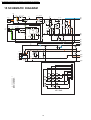
15 SCHEMATIC DIAGRAM
RING
R1 R3 1.8M
1M
R8
D22
NC
Q3
C20
Q2
120k
R19 NC
NC
10V
JP3
R7
22
NC
JP29
0
R18
1.8K
D13
Q7
R9
C23
47K
R4
TP1
270k
330K
50V10
C102
1
2
L
GND
IC2
NC
(3)
(4)
S
D
R55
NC
R54
Q8
G
D23
R46 47
K0.056
VSS
R101
22K
RI_
VDD
R14
8
7
L
6
5
47k
R105
R104
OUT
R102
0.33k
R103
OFF
3
D24
Low
4
2
250V1
High
C103
1
1
4
3
2
0
NC
Red+
Black-
S3
RI+
2.2K
(1/2W)
R2
500V680P
C1
R28
3
0.01ZF
TP2
TIP
OFF
C38
C17
Ringer
S1
2
TP5
2
ON
ON
3
5
TP6
(1)
(2)
Q1 R53
1
D2
2
TP3
4
4
5.1V
T
500V680P
D17
6
SA1
1
300V
R
C16
TP4
OFF
S1-2
C21 0.015
JACK1
3.3M
S1-1
0
1
POS1
(5)
(6)
1M
RINGER CIRCUIT
R25
SP+
SP_
VR1
C11
NC
C19
C13
6.3V100
NC
C18
(9)
0.068
C27
R24
1K
R20
50V1
C26
220
R23
VR2
20K
R21
MC_
R22
(HS_JACK)
1.8K
R52
C29
4
0.047
220
MC-
220
R29
3
C12
16V
10
2
SP+
C31
1
SP-
R51
0.056
MC+
1.8K
JACK3
(7)
(8)
2.2K
NC
16V10
MC+
100K
C15
(10)
(11)
0.047
(12)
CN1
1
4
5
2
6
3
7
1
C4
2
C3
3
C2
4
C1
5
R4
6
R3
7
R2
8
R1
9
Flash
10
row5
JJ1
8
JJ2
9
0
*
JJ3
JJ4
JJ5
#
Flash
JJ6
JJ7
Redial
JJ8
Vol+
Vol-
JJ9
KEY PAD
24
KX-TS2350CAB / KX-TS2350CAC / KX-TS2350CAH / KX-TS2350CAR / KX-TS2350CAW
FLT2
C22
IC1
16V10
R43
220
R10
(1)
(2)
R47
0
L3
C34
R32
6.3V470u
NC
JP11 NC
5.6k
JP12
R0
4
VDD
5
AGND
6
STB
7
NC
CI
8
M0
9
LLC
A
VS.VSS
JP13
R37
C9
11 OSC
C30 12P
C3
X1 3.58M
10 HS/DP
6.3V22u
D16
R26
18k
(3)
(4)
D15
0
R38
C24
MFL
3
FLT1
R5 4.7k
R6 12k
10k
R31
0.027
LS
2
0
C6 50V1
C5
1
12 MODE
13 C4
(5)
(6)
14 C3
15 C2
16 C1
(7)
(8)
17 R4
18 R3
19 R2
20 R1
(9)
R16
220K
21 FCI
22 LED
23 M1
(10)
(11)
24 M2
25 CS
26 VSS
27 L1
(12)
28 R1
CN1
C4
1
C3
2
C2
3
JP24
AL 100ms
20pps40%
JP15
20pps33%
JP23
10pps 40%
JP14
10pps33%
D8
D9
D10
JP17
2
3
S2
TONE
(TP_SWITCH)
JP26
AL
1
KX-TS2350 SCHEMATIC DIAGRAM
25
0
PULSE
JP27
AL Tone82ms
(10pps)
JP18
JP28
12
Tone82ms
11
row8
D11
10
row7
JP19
row5
JP16
0
Tone116mS
9
JP20
8
100ms
R1
Flash
JP21
7
270ms
6
R2
600ms
R3
JP22
5
AL 600ms
4
R4
JP25
C1
KX-TS2350CAB / KX-TS2350CAC / KX-TS2350CAH / KX-TS2350CAR / KX-TS2350CAW
Memo
26
SA1
C17
C16
GREEN
YELLOW
S1
3
1
5
2
6
3
JJ9
C1
4
1
JJ8
Q8
JJ5
JP27
D2
D16
C22
FLT2
R2
1
JJ3
JJ4
C102
1
JACK1
IC2
R46
JP29
JP13
JP12
JP11
FLT1
1
8
4
5
1
X1
CN1
4 5 6
PbF
2 3
JP3
Q2
Q7
IC1
ECB
ECB
ECB
Q1
D24
C20
C6
4
S3
7
28
D9
D8
D10
D11
9 10 11 12
ECB
Q3
JJ2
R9
D13
JJ7
*
C29
C15
C11
C26
VR1
VR2
2
3
4
1
JACK3
B
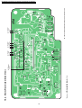
KX-TS2350 CIRCUIT BOARD (Main) Component View
PQUP11224Y
8
D22
BLACK
C38
JJ1
D23
GDS
C34
POS1
R7
JJ6
RED
S2
D15
GREEN
16.1. Main (Component View)
C9
27
L3
R53
YELLOW
16 CIRCUIT BOARD
KX-TS2350CAB / KX-TS2350CAC / KX-TS2350CAH / KX-TS2350CAR / KX-TS2350CAW
MC-
KX-TS2350 CIRCUIT BOARD (Main) Flow Solder Side View
KX-TS2350CAB / KX-TS2350CAC / KX-TS2350CAH / KX-TS2350CAR / KX-TS2350CAW
SP-
R21
R51
R52 C31
R22
MC+
R20
C27
C13
C19
C12
MC+ MC-
SP+
R29
C18
SP+
JP19
JP18
JP17
25
C23 R10
R106
VSS
RI-
C24
C30
4
5
A
R101
5
RI+
8
1
R54
Y
D17
TP6
28
3
TP3
TP1
TP2
R3
1
R18
TIP
R1
1
C21
R8
R55
RING
4
R14
VDD
R38
R26
R105
R102
R104
R103
TP5 TP4
R37
R32
C103
FLT2
1
{
R28
R4
C3
R47
R43
G
for Ringer
16.2. Main (Flow Solder Side View)
R25
R19
15
JP24
JP20
JP21
JP22
JP25
JP26
JP28
FLT1
{
JP23
JP15
JP16
3
{
JP14
1
for Flash*
for PULSE*
9
R6
C5
R31
R5
RED
RINGER1 BLACK
28
12
for TONE*
PbF
{
SP-
R23
*: Refer to OPTION JUMPER TABLE (P.15)
R24
10
1
CN1
29
#
9
6
3
PbF
REDIAL
FLASH
V-
V+
KX-TS2350 CIRCUIT BOARD (Operation) Flow Solder Side View
0
8
5
4
7
2
1
16.3. Operation (Flow Solder Side View)
KX-TS2350CAB / KX-TS2350CAC / KX-TS2350CAH / KX-TS2350CAR / KX-TS2350CAW
KX-TS2350CAB / KX-TS2350CAC / KX-TS2350CAH / KX-TS2350CAR / KX-TS2350CAW
30
G/N
KXTS2350CAB
KXTS2350CAC
KXTS2350CAH
KXTS2350CAR
KXTS2350CAW