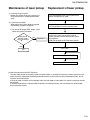
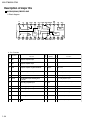
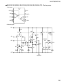
1
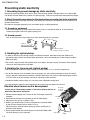
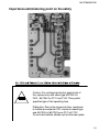
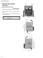
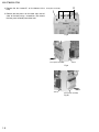
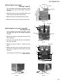
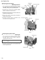
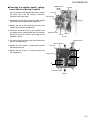
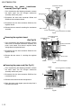
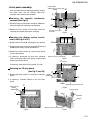
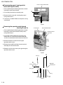
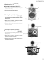
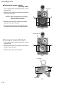
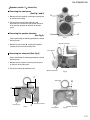
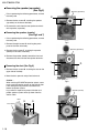
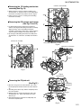
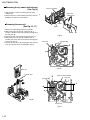
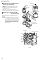
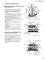
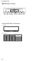
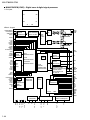
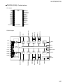
MX-GT80/MX-GT90
SERVICE MANUAL
COMPACT COMPONENT SYSTEM
MX-GT80 / MX-GT90
STANDBY/ON
PLAY & EXCHANGE
STANDBY
Area Suffix
CD-R/RW PLAYBACK
J
C
MX-GT80
SP-MXGT80
CA-MXGT80
U.S.A.
Canada
SP-MXGT80
STANDBY/ON
PLAY & EXCHANGE
STANDBY
CD-R/RW PLAYBACK
MX-GT90
SP-MXGT90
Each different point
Model
CD/DECK/RECEIVER
SPEAKER
MX-GT80
CA-MXGT80
SP-MXGT80
MX-GT90
CA-MXGT90
SP-MXGT90
SP-MXGT90
CA-MXGT90
OUTPUT POWER
MAIN SPEAKER
SUB WOOFER
55W / ch
130W / ch
70W / ch
160W / ch
Contents
Safety precautions
Important for laser products
Preventing static electricity
Importance administering
point on the safety
Disassembly method
Adjustment method
COPYRIGHT
1-2
1-3
1-4
1-5
1-6
1-28
Flow of functional operation
until TOC read
Maintenance of laser pickup
Replacement of laser pickup
Description of major ICs
2001 VICTOR COMPANY OF JAPAN, LTD.
1-32
1-33
1-33
1-34
No.20912
Feb. 2001
MX-GT80/MX-GT90
1. This design of this product contains special hardware and many circuits and components specially
for safety purposes. For continued protection, no changes should be made to the original design
unless authorized in writing by the manufacturer. Replacement parts must be identical to those
used in the original circuits. Services should be performed by qualified personnel only.
2. Alterations of the design or circuitry of the product should not be made. Any design alterations of
the product should not be made. Any design alterations or additions will void the manufacturer`s
warranty and will further relieve the manufacture of responsibility for personal injury or property
damage resulting therefrom.
3. Many electrical and mechanical parts in the products have special safety-related characteristics.
These characteristics are often not evident from visual inspection nor can the protection afforded
by them necessarily be obtained by using replacement components rated for higher voltage,
wattage, etc. Replacement parts which have these special safety characteristics are identified in
the Parts List of Service Manual. Electrical components having such features are identified by
shading on the schematics and by ( ) on the Parts List in the Service Manual. The use of a
substitute replacement which does not have the same safety characteristics as the recommended
replacement parts shown in the Parts List of Service Manual may create shock, fire, or other
hazards.
4. The leads in the products are routed and dressed with ties, clamps, tubings, barriers and the
like to be separated from live parts, high temperature parts, moving parts and/or sharp edges
for the prevention of electric shock and fire hazard. When service is required, the original lead
routing and dress should be observed, and it should be confirmed that they have been returned
to normal, after re-assembling.
5. Leakage currnet check (Electrical shock hazard testing)
After re-assembling the product, always perform an isolation check on the exposed metal parts
of the product (antenna terminals, knobs, metal cabinet, screw heads, headphone jack, control
shafts, etc.) to be sure the product is safe to operate without danger of electrical shock.
Do not use a line isolation transformer during this check.
Plug the AC line cord directly into the AC outlet. Using a "Leakage Current Tester", measure
the leakage current from each exposed metal parts of the cabinet , particularly any exposed
metal part having a return path to the chassis, to a known good earth ground. Any leakage
current must not exceed 0.5mA AC (r.m.s.)
Alternate check method
Plug the AC line cord directly into the AC outlet. Use an AC voltmeter having, 1,000 ohms
per volt or more sensitivity in the following manner. Connect a 1,500 10W resistor paralleled by
a 0.15 F AC-type capacitor between an exposed
AC VOLTMETER
metal part and a known good earth ground.
(Having 1000
Measure the AC voltage across the resistor with the
ohms/volts,
or more sensitivity)
AC voltmeter.
Move the resistor connection to eachexposed metal
part, particularly any exposed metal part having a
0.15 F AC TYPE
return path to the chassis, and meausre the AC
Place this
voltage across the resistor. Now, reverse the plug in
probe on
the AC outlet and repeat each measurement. voltage
each exposed
1500 10W
metal part.
measured Any must not exceed 0.75 V AC (r.m.s.).
This corresponds to 0.5 mA AC (r.m.s.).
Good earth ground
1. This equipment has been designed and manufactured to meet international safety standards.
2. It is the legal responsibility of the repairer to ensure that these safety standards are maintained.
3. Repairs must be made in accordance with the relevant safety standards.
4. It is essential that safety critical components are replaced by approved parts.
5. If mains voltage selector is provided, check setting for local voltage.
!
1-2
Burrs formed during molding may be left over on some parts of the chassis. Therefore,
pay attention to such burrs in the case of preforming repair of this system.
MX-GT80/MXGT90
Important for laser products
5.CAUTION : If safety switches malfunction, the laser is able
1.CLASS 1 LASER PRODUCT
to function.
2.DANGER : Invisible laser radiation when open and inter
6.CAUTION : Use of controls, adjustments or performance of
lock failed or defeated. Avoid direct exposure to beam.
procedures other than those specified herein may result in
3.CAUTION : There are no serviceable parts inside the
Laser Unit. Do not disassemble the Laser Unit. Replace
hazardous radiation exposure.
the complete Laser Unit if it malfunctions.
4.CAUTION : The compact disc player uses invisible laser
radiation and is equipped with safety switches which
prevent emission of radiation when the drawer is open and
the safety interlocks have failed or are defeated. It is
! CAUTION Please use enough caution not to
see the beam directly or touch it
in case of an adjustment or operation
check.
dangerous to defeat the safety switches.
VARNING : Osynlig laserstrålning är denna del är öppnad
ADVARSEL : Usynlig laserstråling ved åbning , når
och spårren är urkopplad. Betrakta ej strålen.
VARO
sikkerhedsafbrydere er ude af funktion. Undgå
: Avattaessa ja suojalukitus ohitettaessa olet
udsættelse for stråling.
alttiina näkymättömälle lasersäteilylle.Älä katso
ADVARSEL : Usynlig laserstråling ved åpning,når
säteeseen.
sikkerhetsbryteren er avslott. unngå utsettelse
for stråling.
REPRODUCTION AND POSITION OF LABELS
WARNING LABEL
DANGER : Invisibie laser radiation
VARO : Avattaessa ja suojalukitus
VARNING : Osynlig laserstrålning är ADVARSEL :Usynlig laserstråling
when open and interlock or
ohitettaessa olet alttiina
denna del är öppnad och spårren är
ved åbning , når
defeated.
näkymättömälle lasersäteilylle.Älä
urkopplad. Betrakta ej strålen.
sikkerhedsafbrydere er ude af
AVOID DIRECT EXPOSURE TO
katso säteeseen.
BEAM
(e)
(d)
(s)
funktion. Undgå udsættelse for
stråling.
(f)
1-3
MX-GT80/MX-GT90
Preventing static electricity
1. Grounding to prevent damage by static electricity
Electrostatic discharge (ESD), which occurs when static electricity stored in the body, fabric, etc. is discharged,
can destroy the laser diode in the traverse unit (optical pickup). Take care to prevent this when performing repairs.
2. About the earth processing for the destruction prevention by static electricity
In the equipment which uses optical pick-up (laser diode), optical pick-up is destroyed by the static electricity of
the work environment.
Be careful to use proper grounding in the area where repairs are being performed.
2-1 Ground the workbench
Ground the workbench by laying conductive material (such as a conductive sheet) or an iron plate over
it before placing the traverse unit (optical pickup) on it.
2-2 Ground yourself
Use an anti-static wrist strap to release any static electricity built up in your body.
(caption)
Anti-static wrist strap
Conductive material
(conductive sheet) or iron plate
3. Handling the optical pickup
1. In order to maintain quality during transport and before installation, both sides of the laser diode on the
replacement optical pickup are shorted. After replacement, return the shorted parts to their original condition.
(Refer to the text.)
2. Do not use a tester to check the condition of the laser diode in the optical pickup. The tester's internal power
source can easily destroy the laser diode.
4. Handling the traverse unit (optical pickup)
1. Do not subject the traverse unit (optical pickup) to strong shocks, as it is a sensitive, complex unit.
2. Cut off the shorted part of the flexible cable using nippers, etc. after replacing the optical pickup. For specific
details, refer to the replacement procedure in the text. Remove the anti-static pin when replacing the traverse
unit. Be careful not to take too long a time when attaching it to the connector.
3. Handle the flexible cable carefully as it may break when subjected to strong force.
4. It is not possible to adjust the semi-fixed resistor that adjusts the laser power. Do not turn it
Attention when traverse unit is decomposed
*Please refer to "Disassembly method" in the text for pick-up and how to
detach the CD traverse mechanism.
1. Remove the disk stopper and T. bracket on the CD changer mechanism
assembly.
2. Disconnect the harness from connector on the CD motor board.
3. CD traverse unit is put up as shown in Fig.1.
4. Solder is put up before the card wire is removed from connector CN601
on the CD servo control board as shown in Fig. 2.
(When the wire is removed without putting up solder, the CD pick-up
assembly might destroy.)
5. Please remove solder after connecting the card wire with CN601 when
you install picking up in the substrate.
1-4
CD changer
mechanism
assembly
CD traverse
unit
Fig.1
Flexible cable
Soldering
Fig.2
MX-GT80/MXGT90
Importance administering point on the safety
F102
F001
F101
Caution: For continued protection against risk of
fire, replace only with same type 5A/125V for
F001, 6A/125V for F101 and F102. This symbol
specifies type of fast operating fuse.
Precaution: Pour eviter risques de feux, remplacez
le fusible de surete de F001 comme le meme type
que 5A/125V, et 6A/125V pour F101 et F102.
^
Ce sont des fusibles suretes
qui functionnes rapide.
1-5
MX-GT80/MX-GT90
Disassembly method
A
Metal cover
<Main body>
Removing the metal cover
(See Fig.1 to 3)
1. Remove the six screws A on the back of the body.
2. Remove the two screws B
body.
on both sides of the
3. Remove the metal cover from the body by lifting the
rear part of the cover.
A
A
CAUTION: Do not break the front panel tab fitted to
the metal cover.
Fig.1
Metal cover
B
Fig.2
Metal cover
Fig.3
1-6
B
MX-GT80/MXGT90
Front panel assembly
Removing the CD changer mechanism
assembly (See Fig.4 and 5)
Prior to performing the following procedure, remove
the metal cover.
C
C
1. Disconnect the card wire from connector CN661 on
the Main board.
2. Remove the two screws C on the upper side of the
body and the two screws D on the back of the rear
panel.
CD changer
mechanism assembly
Main board
CN661
3. Remove the plastic rivet attaching the main board.
4. Pull both the rear panel and the front panel assembly
to the outside, then remove the CD changer
mechanism assembly by lifting the rear part of the
assembly.
Fig.4
CD changer mechanism assembly
Rear panel
Rear panel
Main board
CN661
D
Plastic rivet
CAUTION: To prevent damage to the CD fitting, be
sure to pull both the rear panel and the
front panel assembly enough to remove
the CD changer mechanism assembly.
Front panel assembly
Fig.5
Amplifier board
CN703
Wire clamp
Main board
CN870
CN871
Removing the front panel assembly
(See Fig.6 to 10)
CN315
Prior to performing the following procedure, remove
the metal cover and CD changer mechanism
assembly.
Front panel
assembly
1. Disconnect the card wires from connector CN870,
CN871 and CN315 on the main board respectively.
2. Remove the tie band and disconnect the wire from
connector CN703 on the amplifier board.
Fig.6
Transformer board
CN220
3. Disconnect the wire from connector CN220 on the
transformer board.
Front panel assembly
Main board
Fig.7
1-7
MX-GT80/MX-GT90
4. Remove the four screws E
body.
on the bottom of the
E
Front panel assembly
5. Release the two joints a on the lower right and left
sides of the body using a screwdriver, and remove
the front panel assembly toward the front.
(Bottom)
Fig.8
Joint a
Front panel assembly
Fig.9
Joint a
Front panel assembly
Fig.10
1-8
MX-GT80/MXGT90
Removing the tuner board
(See Fig.11 and 12)
CN1
Plastic rivet
Tuner board
Prior to performing the following procedure, remove
the metal cover and the CD changer mechanism
assembly.
Rear panel
1. Disconnect the card wire from connector CN1 on the
antenna board on the right side of the body.
2. Remove the plastic rivet fixing the antenna board.
3. Remove the two screws F on the back of the body.
Fig.11
G
Rear panel
F
Removing the rear cover / rear panel
(See Fig.12 to 15)
Prior to performing the following procedure, remove
the metal cover and the CD changer mechanism
assembly.
Joint b
Joint b
1. Remove the screw G attaching the rear cover on the
back of the body.
2. Push each tab of the four joints b in the direction of
the arrow and release.
3. Remove the eleven screws F
panel.
Rear cover
Fig.12
Rear panel
attaching the rear
4. Release the joints c on each lower side of the rear
panel using a screwdriver and remove the rear panel
backward.
F
F
Note : Remove the tuner board in case of necessity.
(Refer to Fig.21)
F
F
Fig.13
Joint c
Rear panel
Fig.15
Rear panel
Joint c
Fig.14
1-9
MX-GT80/MX-GT90
Main board
CN870
Removing the main board
(See Fig.16 and 17)
Prior to performing the following procedure, remove
the metal cover, the CD changer mechanism
assembly, the rear panel and the tuner board.
CN315
Front panel assembly
CN871
Amplifier board
CN704
CN706
1. Disconnect the card wires from connector CN870,
CN871 and CN315 on the main board.
2. Disconnect the flat wires from connector CN704 and
CN706 on the amplifier board.
3. Remove the screw H attaching the main board on
the right side of the body.
4. Disconnect connector CN211 and CN212 on the
main board from the regulator board.
Fig.16
Front panel assembly
Plastic rivet
Main board
Regulator board
H
CN211
CN212
Fig.17
Removing the speaker board
(See Fig.18)
Speaker board
Prior to performing the following procedure, remove
the metal cover, the CD changer mechanism
assembly and the rear panel.
REFERENCE: It is not necessary to remove the main
board.
1. Disconnect connector CN217 on the speaker board
from the regulator board.
Regulator board
CN217
Fig.18
1-10
MX-GT80/MXGT90
Amplifier board
CN703
CN704
Removing the amplifier board / voltage
board / heat sink (See Fig.19 and 20)
Tie band
Tie band
Prior to performing the following procedure, remove
the metal cover, the CD changer mechanism
Voltage board
assembly and the rear panel.
1. Disconnect the wires from connector CN703, CN704
and CN706 on the amplifier board respectively.
CN703
2. Remove the two tie band attaching the wire to the
amplifier board and the voltage board.
3. Disconnect connector CN215 on the amplifier board
and CN216 on the voltage board from the regulator
board (The heat sink and heat sink bracket will be
detached at once).
Regulator board
CN216
Fig.19
4. Pull out the upper and lower heat sink brackets from
the heat sink respectively.
5. Remove the four screws I
board to the heat sink.
attaching the amplifier
CN215
Amplifier board
Heat sink bracket
Heat sink
I
6. Remove the two screws J, the board bracket and
the voltage board.
Voltage board
I
J
Heat sink bracket
Fig.20
1-11
MX-GT80/MX-GT90
Removing the power transformer
assembly (See Fig.21 and 22)
Prior to performing the following procedure, remove
the metal cover, the CD changer mechanism
assembly and the rear panel.
1. Disconnect the wires from connector CN220 and
CN250 on the transformer board.
Tie band
Transformer board
CN250
CN220
Voltage board
Power cord
2. Disconnect the wire from connector CN204 on the
regulator board.
3. Remove the four screws k attaching the transformer
assembly.
Base chassis
Power cord stopper
Power transformer assembly
Fig.21
Removing the regulator board
(See Fig.23)
Transformer board
Regulator board CN220
K
CN204
Prior to performing the following procedure, remove
metal cover, CD changer mechanism assembly, rear
panel, tuner board, main board, amplifier board,
voltage board and speaker board.
Power transformer
assembly
1. Disconnect the wire from connector CN204 on the
regulator board.
K
2. Remove the two screws L attaching the regulator
board.
Tie band
Power cord stopper
CN250
Fig.22
Removing the power cord (See Fig.21)
CN204
Power transformer assembly
Prior to performing the following procedure, remove
the metal cover, the CD changer mechanism
assembly and the rear panel.
1. Disconnect the wire from connector CN250 on the
transformer board.
L
2. Remove the tie band from the voltage board.
3. Move the power cord stopper upward and pull out it
from the base chassis.
L
Regulator board
Fig.23
1-12
MX-GT80/MXGT90
<Front panel assembly>
Prior to performing the following procedure, remove
the metal cover, the CD changer mechanism
assembly and the front panel assembly.
Removing the cassette
assembly (See Fig.24)
mechanism
1. Disconnect the card wire from connector CN306 on
the head amplifier & mechanism control board.
2. Remove the four screws M and three screws M'
attaching the cassette mechanism assembly.
Head amplifier
& Mechanism control board
CN306
M
M
M
M'
M'
Cassette mechanism
assembly
M'
Fig.24
N
Removing the display system control
board (See Fig.25 to 27)
1. Remove the five screws N attaching the stay bracket.
N
2. Disconnect the card wires from connector CN316 and
CN880 on the display system control board.
3. Remove the seven screws O attaching the display
system control board.
4. If necessary, disconnect the wire from connector
CN911 on the front side of the display system control
board and unsolder FW915.
Stay bracket
Display system control board
Fig.25
O
CN316
If necessary, remove the CD play board. (Fig. 28)
Removing the CD play board
(See Fig.27 and 28)
O
O
1. Remove the three screws P attaching the CD eject FW915
(Soldering)
board.
O
O
2. If necessary, unsolder FW915 on the CD eject
board.
CN880
CD playt board
FW915
(Soldering)
P
Display system control board
Fig.26
CD play board
CN911
P
FW915
FW915
Display system control board
Fig.28
Fig.27
1-13
MX-GT80/MX-GT90
Preset / tuning switch board
Removing the preset / tuning switch
board (See Fig.29 and 30)
Prior to performing the following procedure, remove
the display system control board.
Q
1. Pull out the preset knob on the front panel.
2. Remove the five screws Q attaching the preset /
tuning switch board.
3. If necessary, unsolder FW901 on the preset / tuning
switch board.
Q
Fig.29
Removing the operation switch board
(See Fig.30 and 31)
Preset knob
Surround mode knob
Prior to performing the following procedure, remove
the display system control board and the preset /
tuning switch board.
Surround woofer
level knob
1. Pull out the volume knob on the front panel and
remove the nut. Pull out the surround mode knob
and the surround woofer level knob toward the front.
2. Remove the twelve screws R attaching the
operation switch board.
3. Remove the screw R' attaching the earth terminal
extending from the switch board.
Nut
4. Release each tab of the seven joints g retaining the
operation switch board.
Volume knob
Fig.30
R
Joints g
R
Operation
switch board
Joint g
R
Joint g
R
Joint g
Joints g
R
R R
Fig.31
1-14
R'
MX-GT80/MXGT90
Speaker section 1
(SP-MXGT80)
Removing the front panel (See Fig.1)
A
1. Remove the four screws A attaching the front panel
on the front of the body.
A
2. Pull out the front panel toward the front.
Front panel
Removing the speaker (tweeter)
(See Fig.2)
Prior to performing the following procedures, remove
the front panel.
A
A
1. Remove the two screws B attaching the speaker
(tweeter) on the front of the body.
Fig.1
2. Disconnect the wire from two speaker terminals of
the speaker (tweeter).
B
Speaker (squawker)
Removing the speaker (squawker)
(See Fig.3)
Prior to performing the following procedures, remove
the front panel.
Speaker (tweeter)
1. Remove the four screws C attaching the speaker
(squawker) on the front of the body.
Fig.2
2. Disconnect the wire from the two speaker terminals
of the speaker (squawker).
Speaker (squawker)
C
C
Fig.3
1-15
MX-GT80/MX-GT90
Removing the speaker (woofer)
(See Fig.4 and 5)
Punch panel
Prior to performing the following procedures, remove
the front panel.
1. Remove the six screws D attaching the punch panel
on the front of the body.
Attention : When reassembling the punch panel,
need to put glue all around. this is
important to prevent vibration.
D
D
2. Remove the four screws E attaching the speaker
(woofer) on the front of the body.
3. Pull out the speaker (woofer) toward the front and
disconnect the wire from the two speaker terminals.
Fig.4
Speaker (woofer)
Removing the sub panel (See Fig.6 )
Prior to performing the following procedures, remove
the front panel.
1. Remove the six screws F attaching the sub panel on
the back of the front panel.
E
E
2. Remove the sub panel toward the front.
Fig.5
Sub panel
F
F
Front panel
Fig.6
1-16
MX-GT80/MXGT90
Speaker section 2
(SP-MXGT90)
Removing the front panel
(See Fig.1 and 2)
1. Remove the four screws A attaching the front panel
on the front of the body.
A
A
2. Pull out the front panel toward the front and
disconnect the wire from the two speaker terminals
of the speaker (tweeter) on the back of the front
panel.
Removing the speaker (tweeter)
(See Fig.3)
Front panel
A
A
Fig.1
Prior to performing the following procedures, remove
the front panel.
Speaker (tweeter)
1. Remove the two screws B attaching the speaker
(tweeter) on the back of the front panel.
Front panel
Removing the sub panel (See Fig.4)
Prior to performing the following procedures, remove
the front panel.
1. Remove the six screws C attaching the sub panel
on the back of the front panel.
2. Pull out the sub panel toward the front.
Speaker terminals
Fig.2
C
Sub panel
B
C
Front panel
Fig.4
C
Speaker (tweeter)
Front panel
Speaker (tweeter)
Fig.3
1-17
MX-GT80/MX-GT90
Removing the speaker (squawker)
(See Fig.5)
Prior to performing the following procedures, remove
the front panel.
Speaker (squawker)
E
E
1. Remove the four screws E attaching the speaker
(squawker) on the front of the body.
2. Disconnect the wire from the two speaker terminals
of the speaker (squawker).
Removing the speaker (woofer)
(See Fig.6 and 7)
Prior to performing the following procedures, remove
the front panel.
Fig.5
1. Remove the eight screws D attaching the punch
panel on the front of the body.
Speaker (squawker)
2. Remove the six screws F attaching the speaker
(woofer) on the front of the body.
3. Remove the speaker (woofer) toward the front and
disconnect the wire from the two speaker terminals.
D
D
Removing the duct (See Fig.8)
1. Remove the four screws G attaching the duct on the
upper side of the body.
2. Move the duct upwards and pull out backward.
Caution :
When servicing SP-MXGT90 speaker system, never
push or pull the speaker system on the table or floor.
It will damage the leg cushions attached on the
bottom of speaker system.
Leg cushion is important to prevent vibration and
protect speaker system not to slip down from the
shelf or table.
Duct
G
Front panel
G
Punch panel
Fig.6
Speaker (woofer)
F
F
Fig.7
Fig.8
1-18
MX-GT80/MXGT90
A
Removing the CD Servo control board
(See Fig.1)
1.Remove the metal cover.
2.Remove the CD changer mechanism assembly.
3.From bottom side the CD changer mechanism assembly,
remove the four screws A retaining the CD servo control
board.
4.Absorb the four soldered positions "a" of the right and
left motors with a soldering absorber.
5.Pull out the earth wire on the CD changer mechanism
assembly.
6.Disconnect the connector CN854 on the CD servo
control board.
7.Disconnect the card wire CN601 and the connector
CN801 on the CD servo control board.
a
a
CN854
A
CN651
CD servo control board
CN652
CN801
CN151
CN601
Removing the CD tray assembly
(See Fig.2~4)
1. Remove the front panel assembly.
2. Remove the CD changer mechanism assembly.
3. Remove the CD Servo control board.
4. Remove the screw B' retaining the lod stopper.
5. From the T.bracket section "b" and clamper base
section "c" , remove both of the edges fixing the
rod(See Fig.2 and 3).
6. Remove the screw B retaining the disc stopper
(See Fig.3).
7. Remove the three screws C retaining the T.bracket
(See Fig.3).
8. Remove the screw D retaining the clamper assembly
(See Fig.3).
9. From the left side face of the chassis assembly, remove
the one screw E retaining both of the return spring and
lock lever(See Fig. 4).
10. By removing the pawl at the section "d" fixing the return
spring, dismount the return spring(See Fig.4).
11. Remove the three lock levers(See Fig.4).
Earth
wire
A
Fig.1
A
Clamper base
b
Rod
c
T.Braket
Fig.2
Disc stopper
T.Braket
d
B
C
C
B'
a
Lod stopper
(C/J version only)
Return spring
C
D
b
Lock lever
Clamper ass'y
E
Fig.4
Fig.3
1-19
MX-GT80/MX-GT90
Stopper
11. Check whether the lifter unit stopper has been caught
into the hole at the section "e" of CD tray assembly as
shown in Fig.5.
12. Make sure that the driver unit elevator is positioned as
shown in Fig.6 from to the second or fifth hole on the
left side face of the CD changer mechanism assembly.
[Caution] In case the driver unit elevator is not at above
position, set the elevator to the position as
shown in Fig.7 by manually turning the pulley
gear as shown in Fig.8.
e
13. Manually turn the motor pulley in the clockwise
direction until the lifter unit stopper is lowered from the
section "e" of CD tray assembly(See Fig.8).
14. Pull out all of the three stages of CD tray assembly in
the arrow direction "f" until these stages stop
(See Fig.6).
15. At the position where the CD tray assembly has
stopped, pull out the CD tray assembly while pressing
the two pawls "g and g' " on the back side of CD tray
assembly(See Fig.9). In this case, it is easy to pull out
the assembly when it is pulled out first from the stage
CD tray assembly.
CD tray
assembly
Fig.5
Chassis assembly
f
CD tray assembly
Refer to Fig.7
Pawl
Fig.7
g
Drive unit of elevator
Fig.6
CD 3
CD 2
CD 1
CD tray assembly
Pulley gear
Motor pulley
Pawl
Fig.8
1-20
Fig.9
g , g'
MX-GT80/MXGT90
Cams R1, R2 assembly
Removing the CD loading mechanism
assembly(See Fig.10)
1. While turning the cams R1 and R2 assembly in the
arrow direction "h" ,align the shaft "i" of the CD loading
mechanism assembly to the position shown in Fig.10.
2. Remove the four screws F retaining the CD loading
mechanism assembly.
Removing the CD traverse mechanism
(See Fig.11 and 12 )
Arrow
h
i
F
F
1. For dismounting only the CD traverse mechanism
without removing the CD loading mechanism assembly,
align the shaft "j" of the CD loading mechanism
assembly to the position shown Fig.11 while turning the
cam R1 and R2 assembly in the arrow direction "k" .
2. By raising the CD loading mechanism assembly in the
arrow direction "l", remove the assembly from the lifter
unit
F
F
Cam R1, R2 assembly
CD loading mechanism assembly
Fig.10
CD traverse mechanism
Arrow
k
j
Lifter unit
Arrow
l
Fig.11
Fig.12
CD Pickup unit
Removing the CD pick unit
(See Fig.13 )
1. Move the cam gear in the arrow direction "m" . Then,
the CD pickup unit will be moved in the arrow direction
"n" .
2. According to the above step, shift the CD pickup unit to
the center position.
3. While pressing the stopper retaining the shaft in the
arrow direction "o" , pull out the shaft in the arrow
direction "p".
4. After dismounting the shaft from the CD pickup unit,
remove the CD pickup unit
n
CD loading
mechanism
m
Shaft
Cam gear
Shaft
Shaft
p
o
Stopper
Stopper
Fig.13
1-21
MX-GT80/MX-GT90
Removing the try select switch board
(See Fig.14)
Chassis assembly
1. Remove the two screws G retaining the tray select
switch board.
2. Disconnect the tray select switch board from connector
CN804 on the CD servo control board.
Tray select
switch board
CN854
Removing the cam unit
(See Fig.15 ~17 )
1. Remove the CD loading mechanism assembly.
2. While turning the cam gear "q", align the Paul "r"
position of the drive unit to the notch position(Fig.16) on
the cam gear "q".
3. Pull out the drive unit and cylinder gear(See Fig.17).
4. While turning the cam gear "q", align the Paul "s"
position of the select lever to the notch position(Fig.18)
on the cam gear "q".
5. Remove the four screws H retaining the cam unit(cam
gear "q" and cams R1/R2 assembly)(See Fig.18).
CN851
CN804
G
Fig.14
Cam gear q
Drive unit
r
Fig.15
Drive unit
Cylinder gear
H
Cam gear q
Cams R1, R2 assembly
Cam unit
J
H
s
Fig.16
Select lever
Fig.17
1-22
MX-GT80/MXGT90
Removing the actuator motor and belt
(See Fig.18~21)
Gear bracket
1. Remove the two screws I retaining the gear bracket
(See Fig.18).
2. While pressing the pawl "t" fixing the gear bracket in the
arrow direction, remove the gear bracket
(See Fig.18).
3. From the notch "u section" on the chassis assembly
fixing the edge of gear bracket, remove and take out the
gear bracket(See Fig. 19).
4. Remove the belts respectively from the right and left
actuator motor pulleys and pulley gears(See Fig. 18).
5. After turning over the chassis assembly, remove the
actuator motor while spreading the four pawls "v" fixing
the right and left actuator motors in the arrow
direction(See Fig. 20).
[Note] When the chassis assembly is turned over under
the conditions wherein the gear bracket and belt
have been removed, then the pulley gear as well
as the gear, etc. constituting the gear unit can
possibly be separated to pieces. In such a case,
assemble these parts by referring to the assembly
and configuration diagram in Fig. 21.
Pulley gear
Belt
Motor pulley
I
Pawl
t
Pulley gear Belt
Motor pulley
I
Fig.18
Actuator motor
Chassis assembly
u
v
Gear bracket
v
Fig.20
Fig.19
Assembly and Configuration Diagram
Pulley gear
Gear B
Pulley gear
Cylinder gear
Gear B
Gear C
Select gear
Gross gear L
Gross gear U
Gear C
Fig.21
1-23
MX-GT80/MX-GT90
Slit washer
Removing the cams R1/R2 assembly
and cam gear q(See Fig.22)
Cam R2
Slit washer
1. Remove the slit washer fixing the cams R1 and R2
assembly.
2. By removing the two pawls "w" fixing the cam R1,
separate R2 from R1.
3. Remove the slit washer fixing the cam gear "q".
4. Pull out the cam gear "q" from the C.G. base assembly.
Cam gear q
J
Pawl
Cam R1
Removing the C.G. base assembly
(See Fig.22 and 23)
w
Pawl
w
Remove the three screws J retaining the C.G. base
assembly.
[Caution] To reassemble the cylinder gear, etc.with the
cam unit (cam gear and cans R1/R2 assembly),
gear unit and drive unit, align the position of the
pawl "x" on the drive unit to that of the notch on
the cam gear "q". Then, make sure that the
gear unit is engaged by turning the cam gear
"q" (See Fig. 24).
Cam switch board
C.G. base assembly
Fig.22
Cam gear q
Cam R1, R2 assembly
Notch
Pawl
x
Gear unit
Cylinder
gear
Drive unit
Gear bracket
Fig.23
1-24
MX-GT80/MXGT90
< Cassette mechanism section >
Cassette mechanism
Removing the playback,recording and eraser
heads (See Fig.1~3)
1. While shifting the trigger arms seen on the right
side of the head mount in the arrow direction,turn
the flywheel R in counterclockwise direction until
the head mount has gone out with a click
(See Fig. 1).
2. When the flywheel R is rotated in counterclockwise
direction, the playback / recording & eraser head will
be turned in counterclockwise direction from the
position in Fig.2 to that in Fig.3.
3. At this position, disconnect the flexible P.C.board
(outgoing from the playback head) from the
connector CN301 on the head amp. and mechanism
control P.C. board.
4. Remove the flexible P.C.board from the chassis
base.
5. Remove the spring "a" from behind the playback /
recording head.
6. Loosen the reversing azimuth screw retaining the
playback head.
7. Take out the playback head from the front of the
head mount.
8. The recording and eraser heads should also be
removed similarly according to Steps 1~7 above.
Reassembling the playback, recording
and eraser heads (See Fig.3)
1. Reassemble the playback head from the front of
the head mount to the position as shown in Fig.3.
2. Fix the reversing azimuth screw.
3. Set the spring a from behind the playback head.
4. Attach the flexible P.C.board to the chassis base
as shown in Fig.3.
5. The recording and eraser heads should also be
reassembled similarly according to Steps 1~4
above.
Flywheel R
Head mount
Trigger arm
Fig.1
(Mechanism A side)
Playback/Recording &
eraser head
Flexible
P.C.board
Spring "a"
Trigger arm
CN301
Head amplifier & mechanism
control P.C. board
Fig.2
Flywheel R
(Mechanism A side)
Reversing azimuth
screw
Playback head
Head
mount
Spring "a"
Flexible
P.C.board
CN302
FPC holder
Fig.3
Head amplifier &
mechanism control
P.C. board
(Mechanism B side)
1-25
MX-GT80/MX-GT90
Removing the head amp. and mechanism
control board (See Fig. 4)
1.Remove the cassette mechanism assembly.
2.After turning over the cassette mechanism
assembly,remove the five screws "A" retaining
the head amplifier & mechanism control board.
3.Disconnect the connectors CN303 on the board
and the connectors CN301 and on CN302 both
the right and left side reel pulse boards.
4.When necessary, remove the 4pin parallel
wire soldered to the main motor
A
Head amplifier &
mechanism control board
A
CN303
CN302
Removing the capstan motor assembly
CN301
A
Flexible
board
(See Fig.5 to 7)
1.Remove the six screws "B" retaining capstan
motor assembly (See Fig. 5).
2.While raising the capstan motor, remove the
capstan belts A and B respectively from the
motor pulley (See Fig. 6).
Flexible
board
A
Fig.4
B
B
Capstan motor
assembly
Caution 1: Be sure to handle the capstan
belts so carefully that these belts
will not be stained by grease and
other foreign matter. Moreover,
these belts should be hand while
referring to the capstan belt
hanging method.(See Fig.6 and 7)
B
B B B
Fig.5
Capstan motor
Capstan
belt A
Capstan
belt A
Capstan
belt B
Fig.7
1-26
A
Capstan
belt B
Motor pulley
Fig.6
MX-GT80/MXGT90
Removing the capstan motor (See Fig. 8)
C
Capstan motor
From the joint bracket, remove the two screws "C"
retaining the capstan motor.
Joint
bracket
Removing the flywheel (See Fig. 9,10)
1.Remove the head amp. and mechanism control
P.C.Board.
2.Remove the capstan motor assembly.
3.After turning over the cassette mechanism, remove
the two slit washers "b" fixing the capstan shafts
R and L, and pull out the flywheels R and L respectively
from behind the cassette mechanism.
C
Fig.8
Flywheel R
Flywheel L
a
Flywheel R
b
Slit
washer "a"
Flywheel L
Fig.10
Slit
washer "b"
Fig.9
Removing the reel pulse board and solenoid
(See Fig. 11)
1.Remove the five pawls (c,d,e,f,g) retaining
the reel pulse P.C.Board.
2.From the surface of the reel pulse P.C.Board parts,
remove the two pawls "h" and "i" retaining the solenoid.
c
h
d
e
f
g
Reel pulse board
i
Solenoid
Solenoid
Fig.11
1-27
MX-GT80/MX-GT90
Adjustment method
Measurement instruments required
for adjustment
1. Low frequency oscillator,
This oscillator should have a capacity to output 0dBs
to 600ohm at an oscillation frequency of 50Hz-20kHz.
2. Attenuator impedance : 600ohm
3. Electronic voltmeter
4. Frequency counter
5. Wow flutter meter
6. Test tape
VTT712 : For Tape speed and wow flutter ( 3kHz)
VTT724 : For Reference level (1kHz)
TMT7036 : For Head angle(10kHz),Play back frequency
characteristics(1kHz),and dubbing frequency
characteristics(63,1,10kHz)
Because of frequency-mixed tape with 63,1k,10k and
14kHz(250nWb/m -24dB).
Use this tape together with a filter.
7. Blank tape
TAPE : AC-225
8. Torque gauge : For play and back tension
Forward ; TW2111A, Reverse ; TW2121A
Fast Forward and Rewind ; TW2231A
9. Test disc
: CTS-1000(12cm),GRG-1211(8cm)
10. Jitter meter
Measurement conditions
Power supply voltage
AC120V(60Hz)
Measurement
output terminal : Speaker out
:TP101(Mesuring for TUNER/DECK/CD)
:Dummy load 6ohm
1-28
Radio input signal
AM modulation frequency : 400Hz
Modulation factor : 30%
FM modulation frequency : 400Hz
Frequency displacement : 22.5kHz
Frequency Range
AM
531kHz~1710kHz
FM
87.5MHz~108MHz
Standard measurement positions of volume
and switch
Power : Standby (Light STANDBY Indicator)
Sub woofer VOL. : Minimum
Sound mode : OFF
Main VOL. : 0 Minimum
Traverse mecha set position : Disc 1
Mic MIX VOL : MAX
ECHO : OFF
Precautions for measurement
1. Apply 30pF and 33kohm to the IF sweeper output
side and 0.082 F and 100kohm in series to
the sweeper input side.
2. The IF sweeper output level should be made as
low as possible within the adjustable range.
3. Since the IF sweeper is a fixed device, there is
no need to adjust this sweeper.
4. Since a ceramic oscillator is used, there is no need
to perform any MPX adjustment.
5. Since a fixed coil is used, there is no need to adjust
the FM tracking.
6. The input and output earth systems are separated.
In case of simultaneously measuring the voltage
in both of the input and output systems with an
electronic voltmeter for two channels, therefore,
the earth should be connected particularly.
7. In the case of BTL connection amplifier, the minus
terminal of speaker is not for earthing. Therefore,
be sure not to connect any other earth terminal
to this terminal. This system is of an OTL system.
MX-GT80/MXGT90
Arrangement of adjusting positions
Cassette mechanism section (Mechanism A section)
Cassette mechanism section (Back side)
Head azimuth
adjusting screw
(Forward side)
Head azimuth
adjusting screw
(Forward side)
Playback
head
Head azimuth
adjusting screw
(Reverse side)
Head azimuth
adjusting screw
(Reverse side)
Playback, recording and eraser
heads or playback head
Cassette Mechanism Unit Section
Tape speed ADJ
Bias ADJ L
Bias ADJ R
1-29
MX-GT80/MX-GT90
Tape recorder section
Items
Measurement
conditions
Measurement method
Standard
values
Adjusting
positions
Confirmation
of head angle
Test tape
:TMT7036(10kHz)
Measurement
output terminal
:Speaker terminal
Speaker R
(Load resistor:6 )
:Headphone terminal
1.Playback the test tape TMT7036(10kHz).
2.With the playback mechanism or recording &
playback mechanism, adjust the head azimuth
screw so that the forward and reverse output
levels become maximum.After adjustment,lock
the head azimuth at least by half a turn.
3.In either case,this adjustment should be
performed in both the forward and reverse
directions with the head azimuth screw.
Maximum
output
Adjust the head
azimuth screw
only when the
head has been
changed.
Confirmation
of tape speed
Test tape
:VTT712(3kHz) or
TMT7036(3kHz)
Measurement
output terminal
:Headphone terminal
<Constant speed>
Adjust VR301 so that the frequency counter reading
becomes 3,000Hz 60Hz when playing back the
test tape VTT712(3kHz)with the playback mechanism
or playback and recording mechanism after ending
forward winding of the tape.
Tape speed
of decks
(A and B)
:3,000Hz
60Hz
VR301
Reference values for confirmation items
Items
Double tape
speed
Measurement
conditions
Test tape
:TMT7036(10kHz)
Measurement
output terminal
:Speaker terminal
Speaker R
(Load resistance:6 )
measurement
output terminal
:Headphone terminal
Difference
between the
forward and
reverse speed.
P.mecha and
R/P mecha
speed
Wow & flutter
1-30
Test tape
:TMT7036(10kHz)
Measurement
output terminal
:Headphone terminal
Measurement method
After setting to the double speed motor, confirm
that the frequency counter reading becomes
4,800+400/-300Hz when the test tape VTT712
(3kHz) has been play back with the playback
mechanism.
Adjusting
Standard
positions
values
4,800+400/ Playback
-300Hz
mechanism side
When the test tape VTT712(3kHz) has been played
back with the playback mechanism or recording and
playback mechanism at the beginning of forward
winding, the frequency counter reading of the
difference between both of the mechanisms should
be 6.0Hz or less.
60Hz or
less
Both the playback
and recording &
playback
mechanism
When the test tape VTT712(3kHz) has been played
back with the playback mechanism or recording and
playback mechanism at the beginning of forward
winding the frequency counter reading of wow &
flutter should be 0.25% or less(WRMS).
with in
0.25%
JIS(WTD)
Both the playback
and recording &
playback
mechanism
MX-GT80/MXGT90
Electrical performance
Measurement
Measurement method
conditions
Adjustment of *Mode : Forward or
1.With the recording and playback mechanism,
recording bias
reverse mode
load the test tapes(AC-225 to TYP ),and set the
current
*Recording mode
mechanism to the recording and
(Reference
*Test tape
pausing conditions in advance.
value)
: AC-225
2.After connecting 100 in series to the recorder
Measurement output
head,measure the bias current with a valve
terminal
voltmeter at both of the terminals.
:Both recording and 3.After resetting the [PAUSE] mode,start recording.
headphone terminals At this time,adjust VR101 for LcH and VR201 for
RcH so that the recording bias current values
become 4.0 A (TYP ).
Standard
values
AC-225
:4.20 A
Adjusting
positions
LcH
:VR101
RcH
:VR201
Adjustment of
recording and
playback
frequency
characteristics
Output
deviation
between
1kHz and
10kH
:-1dB 2dB
LcH
:VR101
RcH
:VR201
Items
Reference frequency
:1kHz and 10kHz
(REF:-20dB)
Test tape
:TYP AC-225
Measurement input
terminal
:OSC IN
1.With the recording and playback mechanism,load
the test tape(AC-225 to TYP ),and set the
mechanism to the recording and pausing condition
in advance.
2.While repetitively inputting the reference frequency
signal of 1kHz and 10kHz from OSC IN, record and
playback the test tape.
3.While recording and playing back the test tape in
TYP ,adjust VR101 for LcH and VR201 for RcH
so that the output deviation between 1kHz and
10kHz becomes -1dB 2dB.
Reference values for electrical function confirmation items
Items
Measurement
conditions
Recording
*Recording and
bias frequency playback side forward
or reverse
*Test tape
:TYP
AC-225
*Measurement
terminal BIAS TP on
P.C.board
Eraser current *Recording and
(Reference
playback side forward
value)
or reverse
*Recording mode
*Test tape
:AC-225
Measurement terminal
Both of the eraser
head
Measurement method
1.While changing over to and from BIAS 1 and 2,
confirm that the frequency is changed.
2.With the recording and playback mechanism.
load the test tape (AC-225 to TYP ),and set the
mechanism to the recording and pausing
conditions in advance.
3.Confirm that the BIAS TP frequency on the
P.C.board is 100kHz 6kHz.
1.With the recording and playback mechanism,
load the test tapes(AC-225 to TYP ),and set the
mechanism to the recording and pausing condition
in advance.
2.After setting to the recording conditions,connect
1M in series to the eraser head on the recording
and playback mechanism side,and measure the
eraser current from both of the eraser terminal.
Standard
values
100kHz
+9kHz
-7kHz
Adjusting
positions
TYP
:75mA
1-31
MX-GT80/MX-GT90
Flow of functional operation until TOC read
Check Point
Play Key
Power ON
Slider turns REST
SW ON.
Confirm that the voltage at the pin5
of CN801 is "H"\"L"\"H".
Automatic tuning
of TE offset
Check that the voltage at the
Laser ON
pin40 of IC651 is + 5V?
Detection of disc
Automatic tuning of
Focus offset
Automatic measurement of
Focus S-curve amplitude
Disc is rotated
Tracking error waveform at TOC reading
pin 25 of
IC601(TE)
Confirm that the Focus error
S-cuve signal at the pin28 of
IC651 is approx.2Vp-p
Confirm that the signal from
pin24 IC651 is 0V as a
accelerated pulse during
approx.400ms.
Focus servo ON
(Tracking servo ON)
Approx.3sec
Approx
1.8V
VREF
Automatic measurement of
Tracking error amplitude
Disc states
to rotate
Tracking
Disc to be
servo
braked to stop
on states
TOC reading
finishes
measurement
Tracking
servo
off states
Automatic
of TE amplitude and
automatic tuning of
TE balance
Confirm the waveform of
the Tracking error signal.
at the pin 25 of IC601 (R604)
(See fig-1)
Automatic tuning of
Tracking error balance
500mv/div
2ms/div Fig.1
Automatic tuning of
Focus error balance
Automatic tuning of
Focus error gain
Automatic tuning of
Tracking error gain
TOC reading
Play a disc
1-32
Confirm the eys-pattern
at the lead of TP1
MX-GT80/MXGT90
Maintenance of laser pickup
(1) Cleaning the pick up lens
Before you replace the pick up, please try to
clean the lens with a alcohol soaked cotton
swab.
(2) Life of the laser diode
When the life of the laser diode has expired,
the following symptoms will appear.
Replacement of laser pickup
Turn off the power switch and, disconnect the
power cord from the ac outlet.
Replace the pickup with a normal one.(Refer
to "Pickup Removal" on the previous page)
1. The level of RF output (EFM output : ampli
tude of eye pattern) will below.
Is the level of
RFOUT under
1.25V 0.22Vp-p?
NO
Replace it.
Plug the power cord in, and turn the power on.
At this time, check that the laser emits for
about 3seconds and the objective lens moves
up and down.
Note: Do not observe the laser beam directly.
YES
O.K
Play a disc.
Check the eye-pattern at TP1.
Finish.
(3) Semi-fixed resistor on the APC PC board
The semi-fixed resistor on the APC printed circuit board which is attached to the pickup is used to adjust the laser
power. Since this adjustment should be performed to match the characteristics of the whole optical block, do not
touch the semi-fixed resistor.
If the laser power is lower than the specified value, the laser diode is almost worn out, and the laser pickup should
be replaced.
If the semi-fixed resistor is adjusted while the pickup is functioning normally, the laser pickup may be damaged
due to excessive current.
1-33
MX-GT80/MX-GT90
Description of major ICs
AN7345(IC302) PB/REC AMP
1. Block diagram
L1
L2
NF1
OUT1
EQ1
24
23
22
21
20
EQ
CTL1 RIN1 RNF1 ROUT1 CTL
19
18
Pre
Source
CTRL
Pre
AMP
16
17
15
ALC
AMP
RF
VCC
14
13
REPPLE
REJ
EQ
Pre
AMP
1
2
3
4
R1
R2
NF2
OUT2
5
ALC
ALC
AMP
CTRL
7
6
EQ2 CTL2
8
9
10
RIN2 RNF2 ROUT2 LC
11
12
LPF
GND
2. Pin Function
Pin
No.
I/O
Function
Pin
No.
Symbol
I/O
Function
1
R1
I
Playback amplifier input
13
Vcc
I
Power supply
2
R2
I
Playback amplifier input
14
RF
I
Ripple filter
3
NF2
I
Playback amplifier negative feedback
15
EQCTL
I
EQ control
4
OUT2
O
Playback amplifier output
16
ROUT1
O
Recording amplifier output
5
EQ2
I
Equalizer
17
RNF1
I
Recording amplifier negative feedback
6
CTL2
I
Pre Amplifier input switching time
constant
18
RIN1
I
Recording amplifier input
7
RIN2
I
Recording amplifier input
19
CTL1
I
Pre amplifier input switching control
8
RNF2
I
Recording amplifier negative feedback
20
EQ1
I
Equalizer
Recording amplifier output
21
OUT1
O
Playback amplifier output
NF1
I
Playback amplifier negative feedback
9
1-34
Symbol
ROUT2
O
10
LC
I
ALC low cut
22
11
LPF
I
ALC low pass filter
23
L2
I
Playback amplifier input
12
GND
I
24
L1
I
Playback amplifier input
MX-GT80/MXGT90
BA15218F-XE (IC652) / BA15218N (IC481,501,502,526,546,571) : Dual op. amp.
1. Pin layout
OUT1 1
8 Vcc
-IN1 2
7 OUT2
1
+IN1 3
6 -IN2
2
VEE 4
5 +IN2
2. Block diagram
Vcc
R1
Q8
Q5
Q13
Q18
Q19
Q11
-IN
Q1 Q2
Q9
R6
OTHER
CH
Q16
Q10
+IN
C2
R5
R7
R8
D1
Q12
Q6
Q3
R2
Q4
C1
R3
Q17
Q7
Q14 Q114 Q15
R4
R9
VEE
OUTPUT
1-35
MX-GT80/MX-GT90
1
2
3
4
5
6
REC
SW
G
P/B
SW
Vcc
GND
C O NT .
P/B
SW
G
REC
SW
BA3126N(IC301) : R/P Switch
7
8
LB1641 (IC851,IC852) : DC motor driver
1. Pin layout
1
2
3
4
GND OUT1 P1
VZ
5
6
IN1
7
8
9
IN2 VCC1 VCC2 P2
10
OUT2
2. Pin function
Input
1-36
Output
Mode
IN1
IN2
OUT1
OUT2
0
0
0
0
1
0
1
0
0
1
0
1
COUNTER-CLOCKWISE
1
1
0
0
Brake
Brake
CLOCKWISE
9
MX-GT80/MXGT90
BA3835S (IC812) : SPI B.P.F.
1.Block Diagrams
BIASC
1
BIAS
18 GND
VREFC
2
VREF
17
AOUT
RREF
3
REFERENCE
CURRENT
16
TEST
N.C.
4
15
N.C.
14
N.C.
13
SEL
12
C
11
B
10
A
N.C.
5
DIFOUT
6
105Hz
BPF
PEAK
HOLD
340Hz
BPF
PEAK
HOLD
1kHz
BPF
PEAK
HOLD
RES
RES
A-C
MPX
RES
CIN
7
AIN
8
VCC
9
DIF
3.4kHz
BPF
PEAK
HOLD
10.5kHz
BPF
PEAK
HOLD
RES
RES
DEC
2.Pin Function
No.
Symbol
I/O
Function
1
BIASC
-
Decoupling condenser connection terminal.
2
VREFC
-
Decoupling condenser connection terminal.
3
RPEF
-
Reference resistance connection terminal.
4
NC
-
Non connect.
5
NC
-
Non connect.
6
NC
-
Non connect.
7
CIN
-
Connected to GND of audio system through a condenser.
8
AIN
I
Inputs the audio signal through a condenser.
9
VCC
-
Power supply terminal.
10
SPI-A
O
Output selection control terminal.
11
SPI-B
O
Output selection control terminal.
12
SPI-C
O
Output selection control terminal.
13
SPICSB
O
Output selection control terminal.
14
NC
-
Non connect.
15
NC
-
Non connect.
16
TEST
-
Connected to GND upon normal use.
17
AOUT
O
Multi-plexor output terminal.
18
GND
-
Connect to GND.
1-37
MX-GT80/MX-GT90
BU2092/F(IC811):PORT EXPANDER
1.Terminal Layout
1
18
Vdd
DATA 2
17
OE
16
Q11
15
Q10
14
Q9
13
Q8
12
Q7
11
Q6
10
Q5
Vss
CLOCK 3
Q0
5
Q1
6
Q2
7
Q3
8
Q4
9
12BIT SHIFT RESISTER
4
12BIT STRAGE RESISTER
LCK
OUTPUT BUFFER(OPEN DRAIN)
CONTROL
CIRCUIT
2.Pin Function
Pin No.
Symbol
I/O
Function
1
Vss
-
Connect to GND
2
DATA
I
Serial Data input
3
CLOCK
I
Shift Clock of Data
4
LCK
I
Latch Clock of Data
5~16
Q0~Q11
O
Parallel Data Output
Latch Data L
H
OUTPUT ON OFF
1-38
17
OE
I
Output Enable
18
Vdd
-
Power Supply
MX-GT80/MXGT90
LA1838(IC1): FM AM IF AMP&detector, FM MPX decoder
1. Block Diagram
30
29
27
28
25
26
24
23
22
20
21
18
19
17
16
REG
ALC
AM
MIX
AM
FM
RF.AMP
DECODER
ANIT-BIRDIE
OSC
MUTE
BUFF
P-DET
STEREO
5N
SW
AGC
DET
AM IF
SD
COMP
VCO
384KHz
FF
38k
FF
19k / 2
10
11
12
FF
19k /LS
PILOT
DET
AM
S-METER
FM
S-METER S-CLRVE
AM/FM
IF-BUFF
TUNING
DRIVE
STEREO
DRIVE
PM
DET
FM IF
GND
2
1
5
VCC
8
9
Pin
No.
Symbol
I/O
Function
This is an input terminal of FM IF
signal.
16
L OUT
O
Left channel signal output.
O This is an out put terminal for AM
mixer.
17
R OUT
O Right channel signal output.
3
4
6
7
13
14
15
Pin
No.
Symbol
I/O
1
FM IN
I
2
AM MIX
3
FM IF
I
Bypass of FM IF
18
L IN
I
Input terminal of the left channel post
AMP.
4
AM IF
I
Input of AM IF Signal.
19
R IN
I
Input terminal of the right channel
post AMP.
5
GND
I
This is the device ground terminal.
20
RO
O
Mpx Right channel signal output.
6
TUNED
O
When the set is tuning, this terminal
becomes "L".
21
LO
O
Mpx Left channel signal output.
7
STEREO
O
Stereo indicator output. Stereo "L",
Mono: "H"
22
IF IN
I
Mpx input terminal
8
VCC
I
This is the power supply terminal.
23
FM OUT
O
FM detection output.
9
FM DET
I
FM detect transformer.
24
AM DET
O
AM detection output.
10
AM SD
I
This is a terminal of AM ceramic filter.
25
AM AGC
I
This is an AGC voltage input terminal
for AM
11
FM VSM
O
Adjust FM SD sensitivity.
26
AFC
I
2. Pin Function
This is an output terminal of voltage
for FM-AFC.
12
AM VSM
O
Adjust AM SD sensitivity.
27
AM RF
I
AM RF signal input.
13
MUTE
28
REG
O
Register value between pin 26 and pin28
desides the frequency width of the
14
FM/AM
I/O When the signal of IF REQ of IC121(
LC72131) appear, the signal of FM/AM
IF output. //Muting control input.
I
Change over the FM/AM input.
input signal.
29
AM OSC
I
Function
"H" :FM, "L" : AM
15
MONO/ST O Stereo : "H", Mono: "L"
30 OSC BUFFER O
This is a terminal of AM Local
oscillation circuit.
AM Local oscillation Signal output.
1-39
MX-GT80/MX-GT90
LA6541-X (IC801) : Servo driver
1. Pin Layout & block diagram
Vcc
Vref
Vin4
Vg4
24
23
22
21
Vo8
Vo7
20
19
Gnd
Vg3
Vin3
Cd
Res
17
16
15
14
13
11k
ohm
-
+
Vo5
18
Vcc
11k
ohm
-
Vo6
+
Level
shift
BTL
driver
BTL
driver
Level
shift
RESET
Level
shift
BTL
driver
BTL
driver
Level
shift
Regulator
11k
ohm
11k
ohm
1
2
3
4
Vcc
Mute
Vin1
Vg1
5
Vo1
6
Gnd
Vo2
7
8
9
10
11
12
Vo3
Vo4
Vg2
Vin2
Reg
out
Reg
In
2. Pin function
Pin
No.
Symbol
1
Vcc
Power supply (Shorted to pin 24)
2
Mute
All BTL amplifier outputs ON/OFF
3
Vin1
BTL AMP 1 input pin
4
Vg1
BTL AMP 1 input pin (For gain adjustment)
5
Vo1
BTL AMP 1 input pin (Non inverting side)
6
Vo2
BTL AMP 1 input pin (Inverting side)
7
Vo3
BTL AMP 2 input pin (Inverting side)
8
Vo4
BTL AMP 2 input pin (Non inverting side)
9
Vg2
BTL AMP 2 input pin (For gain adjustment)
10
Vin2
BTL AMP 2 input pin
11
Reg Out
12
Reg In
13
Res
Reset output
14
Cd
Reset output delay time setting (Capacitor connected externally)
15
Vin3
BTL AMP 3 input pin
16
Vg3
BTL AMP 3 input pin (For gain adjustment)
17
Vo5
BTL AMP 3 output pin (Non inverting side)
18
Vo6
BTL AMP 3 output pin (Inverting side)
19
Vo7
BTL AMP 4 output pin (Inverting side)
20
Vo8
BTL AMP 4 output pin (Non inverting side)
21
Vg4
BTL AMP 4 output pin (For gain adjustment)
22
Vin4
BTL AMP 4 output pin
23
Vref
Level shift circuit's reference voltage application
24
Vcc
Power supply (Shorted to pin 1)
1-40
Function
External transistor collector (PNP) connection. 5V power supply output
External transistor (PNP) base connection
MX-GT80/MXGT90
LC72136N (IC2) : PLL frequency synthesizer
1. Pin layout
XT
FM/AM
CE
DI
CLOCK
DO
FM/ST/VCO
AM/FM
1
2
3
4
5
6
7
8
9
10
SDIN 11
22
21
20
19
18
17
16
15
14
13
12
XT
GND
LPFOUT
LPFIN
PD
VCC
FMIN
AMIN
IFCONT
IFIN
2. Block diagram
Phase
Detector
Charge Pump
Reference
Driver
1
18
22
19
20
16
Swallow Counter
1/16,1/17 4bit
1/2
Unlock
Detector
12bit
Programmable
DriverS
15
12
3
4
C2B
I/F
5
Universal
Counter
Data Shift Register & Latch
6
Power
on
Reset
17
21
7
8
2
11 13
3. Pin function
Pin
No.
Pin
No.
Symbol
I/O
X'tal oscillator connect (75kHz)
12
IFIN
I
IF counter signal input
O
LOW:FM mode
13
IFCONT
O
IF signal output
I
When data output/input for 4pin(input) and
14
-
Not use
Symbol
I/O
1
XT
I
2
FM/AM
3
CE
Function
Function
6pin(output): H
4
DI
I
Input for receive the serial data from
15
AMIN
I
AM Local OSC signal output
controller
5
6
CLOCK
DO
I
Sync signal input use
16
FMIN
I
FM Local OSC signal input
O
Data output for Controller
17
VCC
-
Power suplly(VDD=4.5-5.5V)
Output port
7
FM/ST/VCO
O
"Low": MW mode
When power ON:Reset circuit move
18
PD
O
PLL charge pump output(H: Local OSC
frequency Height than Reference frequency.
L: Low Agreement: Height impedance)
8
AM/FM
O
Open state after the power on reset
19
LPFIN
I
Input for active lowpassfilter of PLL
9
LW
I/O
Input/output port
20
LPFOUT
O
Output for active lowpassfilter of PLL
10
MW
I/O
Input/output port
21
GND
-
Connected to GND
I/O
Data input/output
22
XT
I
X'tal oscillator(75KHz)
11
SDIN
1-41
MX-GT80/MX-GT90
MN101C35DEA1 (IC810) : System controller
Pin function (1/2)
1-42
Pin No.
Symbol
I/O
1
2
3
4
5
6
7
8
9,10
11
12,13
14
15
16C19
20
21
22
23
24
25
26
27
28
29
30
31
32
33
34
35
36
37
38
39
40
41
42
43
44
45
46
47~63
KCMND
MSTAT
KCLK
DATAOUT
DATAIN
CK
NC
VDD
OSC2,1
VSS
NC
MMOD
VREFKEY1~4
SLCKEY1
SLCKEY2
NC
SPIDTI
VREF+
MRDY
RESET
BASS VOL+
BASS VOLAUX MUTE
RDSDATA/KARA
SPI A
SPI B
REMIN
PHOTOA
PHOTOB
SOUNDMODE+
RDS_CLK
PRT
TAPE LED
ECON
POUT
VOLDA/EXT
VOLCK/EXT
EXTCE
SLCCE
VC3 RESET
G17~1
O
I
O
O
I
O
I/O
I
I
I
I
I
I
I
I
O
I
O
O
I
I
I
I
I
I
O
O
O
O
O
O
O
O
O
Function
VC3 Serial data output
VC3 status input
VC3 Serial clock
SLC/TUNER data output
TUNER data input
SLC/TUNER clock
Not used
Power supply +5V
Oscillation terminal (8MHz)
Connect to GND
Not used
Connect to GND
Connect to GND
Key matrix input 1~4
SLC Key input 1
SLC Key input 2
Not used
SPI Analog data input
AD +5V
VC3 Ready
Maicon reset
Bass volume +
Bass volume Mute muting
RDS Data / Karaoke
SPI A data
SPI B data
Remote control signal input
SLC Photo-A
SLC Photo-B
Soundmode reverse
RDS Clock
Protector input
Tape LED
Economy ON
Power ON
Volume / EXT IC Data
Volume / EXT IC CLK
EXT IC Chip select
SLC Chip enable
VC3 Reset
FL Display grid
MX-GT80/MXGT90
Pin function (2/2)
Pin No.
Symbol
I/O
Function
64~85
86
87
88
89
90
91
92
93
94
95
96
97
98
99
100
P22~P1
TUCE
SMUTE
SEARCH LE
CD1 LED
CD2 LED
CD3 LED
R SEARCH
MSI
MPX
INH
F SEARCH
VOL VOL +
SOUNDMODE
VPP
O
O
O
O
O
O
O
I
I
I
I
I
I
I
I
-
FL segment control signal output
Tuner chip enable
System mute
Skip LED
LED Control signal output (CD1)
LED Control signal output (CD2)
LED Control signal output (CD3)
Reverse skip
Music scan input
Tuner stereo indicator
Backup mode detect
Forward skip
Rotary encoder VOLRotary encoder VOL+
Soundmode foeward
-B for FL
1-43
MX-GT80/MX-GT90
MN662748RPM (IC651) : Digital servo & digital signal processer
1. Pin layout
20 ~
1
21
80
~
~
40
61
41 ~
60
2.Block diagram
LRCKIN(MSEL)
BCLK(SSEL)
SRDATAIN
(PSEL)
DIGITAL
DEEMPHSIS
8TIMES
OVER SAMPUNC
DIGITAL FILTER
IOSEL
1BIT
DAC
LOGIC
S
CLVS
CRC
BLKCK
CLDCK
SBCK
SUBC
DEMPH
RESY
FLAG6(RESY)
SSEL
SQCK
SUBQ
AVDD2
PEM
(L)
SUB
CODE
BUFFER
EFM
DEMODULATION
DIGITAL
AUDIO
INTERFASE
16k
SRAM
SYNC
INTERPOLATION
SUBCODE
DEMODULATION
DSL.
PLL
VCO
CIRC
ERROR
CORRECTION
DEINTERLEVE
MLD
MCLK
MDATA
CK384(EFM)
VCOF
BYTCK
SMCK
FCLK
CSEL
MSEL
X2
X1
OUTL
FLAG
IPFLAG
AVDD2
PCK
EFM
PLLF
DSLF
IREF
DRF
ARF
RSEL
PSEL
AVSS1
AVDD1
OUTR
PEM
(R)
MICRO
COMPUTER
INTERFACE
VCO
TX
DIGITAL
AUDIO
INTERFASE
ECM
INTER POLATION
SOFT MUTING DIGITAL
ATTENUATION
PEAK DETECTIVE
AUTO CUE
LRCK
SRDATA
BCLK
DMUTE
PC
TRKV
KICK
VREF
TRVSTR
ECS
TVD
TRD
FOD
TBAL
FBAL
TOFS
TES
/TLOCK
/FLOCK
PLAY
LDON
WVEL
SENSE
CLV
SERVO
D/A
CONVERTER
ITUNING
GENERATION
PITCH
CONTROL
ÊSTAT
OUTPUT
A/D
COVERTER
V V
D S
D S
1-44
D
V
D
D
1
D / /
V R T
S S E
S T S
1
T
F
E
T
E
R
F
E
N
V
INPUT
T
R
C
R
S
V
D
E
T
PORT
SERVO
TIMING GENERATOR
B
D
O
/
R
F
D
E
O
F
T
MX-GT80/MXGT90
3. Pin function
Function
1
BCLK
O Not used
2
LRCK
O
3
SRDATA O Not used
41
Symbol I/O
PLLF2
42 TOFS
Function
O Tracking error shunt signal output (H:shunt)
WVEL
Not used
44
ARF
I
RF signal input
45 IREF
I
Reference current input pin
I
Bias pin for DSL
4
DVDD1
I
Not used
43
Power supply (Digital)
5
DVSS1
I
Not used
Pin
No.
I
Dymbol I/O
I
Pin
No.
Connected to GND
6
TX
O Digital audio interface output
46 DRF
MCLK
CPU command clock signal input
I
(Data is latched at signal's rising point)
47 DSLF
I/O Loop filter pin for DSL
8
MDATA
I
48 PLLF
I/O Loop filter pin for PLL
9
MLD
I CPU command load signal input
49 VCOF
I
O Sense signal output
50
AVDD2
I
Power supply (Analog)
11
FLOCK
O Focus lock signal output Active :Low
51
AVSS2
Connected to GND (Analog)
12
TLOCK
O Tracking lock signal output Active :Low
52
EFM
Not used
13
BLKCK
O sub-code/block/clock signal output
53
PCK/
DSL2
O
14 SQCK
I
54
VCOF2
15
O Sub-code Q -code output
Status signal
17 STATUS O
(CRC,CUE,CLVS,TTSTOP,ECLV,SQOK)
I
56 SBCK
Not used
57
VSS
Connected to GND (for X'tal oscillation
circuit)
XI
I
Input of 16.9344MHz X'tal oscillation circuit
I
Reset signal input (L:Reset)
58
59 X2
60
VDD
BYTCK
62 CLDCK
23
PC
Not used
Not used
Not used
Spindle motor drive signal (Enforced
O
mode output) 3-State
Spindle motor drive signal (Servo error
O
signal output)
O Kick pulse output
Not used
FLAG
Not used
66 CLVS
Not used
27 TRD
O Tracking drive output
67
CRC
Not used
28
O Focus drive output
68
DEMPH
24 ECM
25
ECS
26
KICK
FOD
64 IPPLAG
65
I
Not used
30
FBAL
O Focus Balance adjust signal output
70 IOSEL
I
69 RESY
Not used
pull up
31
TBAL
O Tracking Balance adjust signal output
71
TEST
I
Reference voltage input pin for D/A
output block (TVD,FOD,FBA,TBAL)
63 FCLK
pull up
32
FE
I
Focus error signal input (Analog input)
72
AVDD1
I
I
Not used
Power supply (Digital)
33
TE
I
Tracking error signal input (Analog input)
73
OUT L
O Lch audio output
34
RF ENV
I
RF envelope signal input (Analog input)
74
AVSS1
I
29 VREF
I
I
61
O Traverse drive output
I
O Traverse enforced output
TVD
I
TRV
22
Power supply (for X'tal oscillation circuit)
I
21
O Output of X'tal oscillation circuit
I
Not used
I
Not used
PMCK
I
SMCK
20
I
19
I
RST
Not used
I
18
I
Connected to GND
The external circuit is regulated for crystal.
55 SUBC
I
16 DMUTE
Outside clock for sub-code Q resister input
DSL balance output
I
SUBQ
I
Not used
10 SENSE
I
CPU command data input
I
7
35
VDET
I
Vibration detect signal input (H:detect)
75
OUT R
O Rch audio output
36
OFT
I
RF detect signal input (L:detect)
78 PSEL
BDO input pin (L:detect)
79
RFDET
39
BDO
I
40
LDON
O Laser ON signal output (H:on)
MSEL
80 SSEL
I
38
pull up
I
77 CSEL
Connected to GND
I
76 RSEL
Track cross signal input
Connected to GND
I
Off track signal input (H:off track)
I
Connected to GND
I
I
37 TRCRS
Connected to GND
Pull up
1-45
MX-GT80/MX-GT90
STK402-030 (IC301) :
1.Pin layout
1
15
2.Block diagram
8
4
TR9
TR7
R13
R1
TR4
TR11
R6
R8
C1
C2
TR14
1
TR12
TR5
TR1
TR2
R11
R3
TR10
TR8
2
R4
R12
R5
TR3
TR15
TR6
TR13
R10
TR16
D1
R7
R2
R9
R14
9
SUB
5
1-46
13
12
7 6 10 11
14 15
MX-GT80/MXGT90
TDA7439 (IC436) : Control volume
1.Pin layout
SDA
CRE
Vs
AGND
ROUT
LOUT
R-IN4
R-IN3
R-IN2
R-IN1
L-IN1
L-IN2
L-IN3
L-IN4
MUXOUTL
1
30
2
29
3
28
4
27
5
26
6
25
7
24
8
23
9
22
10
21
11
20
12
19
13
18
14
CSL
DIG GND
TREBLE(R)
TREBLE(L)
MIN(L)
MOUT(L)
BOUT(L)
BIN(L)
BOUT(R)
BIN(R)
MOUT(R)
MIN(R)
INR
MUXOUTR
INL
17
TDA7439
15
16
MUXOUT
INL
TREBLE(L)
MIN(L)
MOT(L)
BIN(L)
BOUT(L)
2.Block diagram
15
16
27
26
25
23
24
L-IN1 11
G
VOLUME
TREBLE
MIDLE
BASS
L-IN2 12
SPEAKER
ATT
LEFT
L-IN3 13
L-IN4 14
30 SCL
0/30dB
2dB STEP
2
I C BUS DECODER LATCHES
1 SDA
R-IN1 10
29 DIG-GND
R-IN2 9
VOLUME
G
TREBLE
MIDLE
BASS
R-IN3 8
17
18
28
19
20
21
22
2
MOUT(R)
BIN(R)
BOUT(R)
CREF
3 Vs
4 AGND
MIN(R)
SUPPLY
TREBLE(R)
5 ROUT
INR
INPUT
MULTIPLEXER
GAIN
SPEAKER
ATT
RIGHT
MUXOUT
R-IN4 7
6 LOUT
1-47
MX-GT80/MX-GT90
VICTOR COMPANY OF JAPAN, LIMITED
AUDIO & COMMUNICATION BUSINESS DIVISION
PERSONAL & MOBILE NETWORK BUSINESS UNIT. 10-1,1chome,Ohwatari-machi,Maebashi-city,371-8543,Japan
(No.20912)
Printed in Japan
200102(V)


![ソファ用オットマン 大、中、小 組立・取扱説明書 [組立順序]](http://vs1.manualzilla.com/store/data/006692263_2-b01644fc3308a1723ac8ce2e20eeec92-150x150.png)