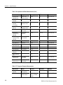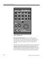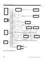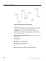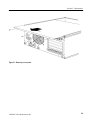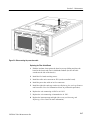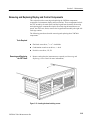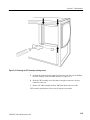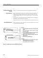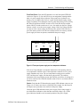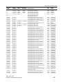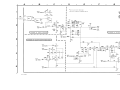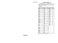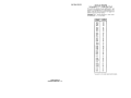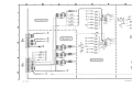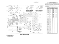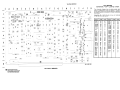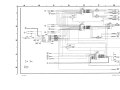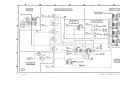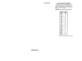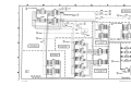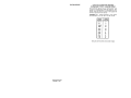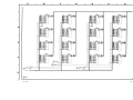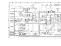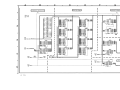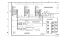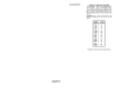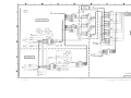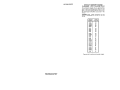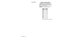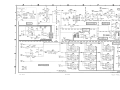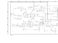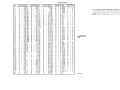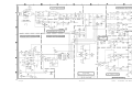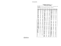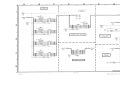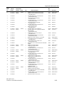
1
Service Manual VM700A Video Measurement Set 070-8165-03 Warning The servicing instructions are for use by qualified personnel only. To avoid personal injury, do not perform any servicing unless you are qualified to do so. Refer to the Safety Summary prior to performing service. Copyright E Tektronix, Inc., 1995, 1996. All rights reserved. Printed in U.S.A. Tektronix products are covered by U.S. and foreign patents, issued and pending. Information in this publication supersedes that in all previously published material. Specifications and price change privileges reserved. The following are registered trademarks: TEKTRONIX and TEK. This instrument, in whole or in part, may be protected by one or more U.S. or foreign patents or patent applications. Information provided upon request by Tektronix, Inc., P.O. Box 1000, Wilsonville, Oregon 97070–1000. For further information, contact: Tektronix, Inc., Corporate Offices, P.O. Box 1000, Wilsonville, OR 97070–1000, U.S.A. Phone: (503) 627–7111; TLX: 192825; TWX: (910) 467–8708; Cable: TEKWSGT. IBM AT and IBM XT are registered trademarks of International Business Machines, Inc. Epson is a registered trademark of Epson Inc. HP LaserJet, HP ThinkJet, and HP DeskJet are registered trademarks of Hewlett–Packard, Inc. Apple LaserWriter is a registered trademark of Apple Computer, Inc. Mention of third party products is as an example of a type of equipment that a user might employ and is not an endorsement for that product. WARRANTY Tektronix warrants that this product will be free from defects in materials and workmanship for a period of one (1) year from the date of shipment. If any such product proves defective during this warranty period, Tektronix, at its option, either will repair the defective product without charge for parts and labor, or will provide a replacement in exchange for the defective product. In order to obtain service under this warranty, Customer must notify Tektronix of the defect before the expiration of the warranty period and make suitable arrangements for the performance of service. Customer shall be responsible for packaging and shipping the defective product to the service center designated by Tektronix, with shipping charges prepaid. Tektronix shall pay for the return of the product to Customer if the shipment is to a location within the country in which the Tektronix service center is located. Customer shall be responsible for paying all shipping charges, duties, taxes, and any other charges for products returned to any other locations. This warranty shall not apply to any defect, failure or damage caused by improper use or improper or inadequate maintenance and care. Tektronix shall not be obligated to furnish service under this warranty a) to repair damage resulting from attempts by personnel other than Tektronix representatives to install, repair or service the product; b) to repair damage resulting from improper use or connection to incompatible equipment; c) to repair any damage or malfunction caused by the use of non-Tektronix supplies; or d) to service a product that has been modified or integrated with other products when the effect of such modification or integration increases the time or difficulty of servicing the product. THIS WARRANTY IS GIVEN BY TEKTRONIX WITH RESPECT TO THIS PRODUCT IN LIEU OF ANY OTHER WARRANTIES, EXPRESSED OR IMPLIED. TEKTRONIX AND ITS VENDORS DISCLAIM ANY IMPLIED WARRANTIES OF MERCHANTABILITY OR FITNESS FOR A PARTICULAR PURPOSE. TEKTRONIX’ RESPONSIBILITY TO REPAIR OR REPLACE DEFECTIVE PRODUCTS IS THE SOLE AND EXCLUSIVE REMEDY PROVIDED TO THE CUSTOMER FOR BREACH OF THIS WARRANTY. TEKTRONIX AND ITS VENDORS WILL NOT BE LIABLE FOR ANY INDIRECT, SPECIAL, INCIDENTAL, OR CONSEQUENTIAL DAMAGES IRRESPECTIVE OF WHETHER TEKTRONIX OR THE VENDOR HAS ADVANCE NOTICE OF THE POSSIBILITY OF SUCH DAMAGES. EC Declaration of Conformity We Tektronix Holland N.V. Marktweg 73A 8444 AB Heerenveen The Netherlands declare under sole responsibility that the VM700A meets the intent of Directive 89/336/EEC for Electromagnetic Compatibility. Compliance was demonstrated to the following specifications as listed in the Official Journal of the European Communities: EN 50081-1 Emissions: EN 55022 Class B Radiated and Conducted Emissions EN 50082-1 Immunity: IEC 801-2 Electrostatic Discharge Immunity IEC 801-3 RF Electromagnetic Field Immunity IEC 801-4 Electrical Fast Transient/Burst Immunity High-quality shielded cables must be used to ensure compliance to the above listed standards. Standards Compliance The VM700A complies with the following safety standards: H Underwriters Laboratories: UL1244 — Second Edition—Standard for Electrical and Electronic Measuring and Testing Equipment H Canadian Standards Association: C22.2 No. 231 Series–M89—CSA Safety Requirements for Electrical and Electronic Measuring and Testing Equipment H American National Standard: ANSI/ISA–S82–1988—Safety Standard for Electrical and Electronic Test, Measuring, Controlling and Related Equipment H International Standard: IEC 348—Second Edition—Safety Requirements for Electronic Measuring Apparatus The VM700A complies with the following regulatory standards: H U.S. EMI: FCC Rules, Part 15, Subpart J, Class A Preface This is a service manual for the VM700A video measurement set. The VM700A is a multi-function television test and measurement device that performs the functions of a waveform monitor, vector scope, automatic measurement set, and noise measurement set on acquired television signals. The user may select a display of numeric values to confirm the quality of the signal path, or may select graphic displays for more detailed analysis. Contents of the Manual This manual contains the following sections: 1. Specification - Lists the major specifications of the VM700A and the Option 01 and Option 11 measurements. Other option specifications are contained in the associated Option User Manuals. 2. Operating Information - Introduces the VM700A, describes its major features, and the controls and connectors of the instruments. 3. Theory of Operation - Contains functional circuit descriptions of the VM700A’s circuit boards to aid in understanding the instrument for servicing. 4. Verification and Adjustment- Procedures for verifying the operation of the VM700A and adjustments to return the VM700A to specification after a board exchange. 5. Maintenance - Customer service information and illustrated, step-by-step procedures for removing and replacing the field-replaceable assemblies of the VM700A. 6. Troubleshooting and Diagnostics - Contains information to help you troubleshoot the VM700A and replace faulty circuit boards or other defective system components. 7. Replaceable Electrical Parts List - The replaceable electrical parts are listed by assembly and circuit component number. 8. Diagram and Circuit Board Illustrations - Schematic diagrams and circuit board illustrations are supplied to assist in circuit repairs. 9. Replaceable Mechanical Parts List - Exploded views and lists of the replaceable mechanical parts are provided to aid in locating a replacement part. VM700A Video Measurement Set i Table of Contents Preface . . . . . . . . . . . . . . . . . . . . . . . . . . . . . . . . . . . . . . . . . . . . . . . . . . . . . . . . . Table of Contents . . . . . . . . . . . . . . . . . . . . . . . . . . . . . . . . . . . . . . . . . . . . . . . . . List of Figures . . . . . . . . . . . . . . . . . . . . . . . . . . . . . . . . . . . . . . . . . . . . . . . . . . . List of Tables . . . . . . . . . . . . . . . . . . . . . . . . . . . . . . . . . . . . . . . . . . . . . . . . . . . . General Safety Summary . . . . . . . . . . . . . . . . . . . . . . . . . . . . . . . . . . . . . . . . . . . Service Safety Summary . . . . . . . . . . . . . . . . . . . . . . . . . . . . . . . . . . . . . . . . . . . i iii x xii xv xvii Section 1:Specifications Physical Characteristics . . . . . . . . . . . . . . . . . . . . . . . . . . . . . . . . . . . . . . . . . . . . Power Requirements . . . . . . . . . . . . . . . . . . . . . . . . . . . . . . . . . . . . . . . . . . . . . . Environmental . . . . . . . . . . . . . . . . . . . . . . . . . . . . . . . . . . . . . . . . . . . . . . . . . . . PAL Measurement Specifications . . . . . . . . . . . . . . . . . . . . . . . . . . . . . . . . . . . . Measure Mode Specifications . . . . . . . . . . . . . . . . . . . . . . . . . . . . . . . . . . . . Auto Mode Measurements . . . . . . . . . . . . . . . . . . . . . . . . . . . . . . . . . . . . . . Other Timing Measurement . . . . . . . . . . . . . . . . . . . . . . . . . . . . . . . . . . . . . NTSC Measurement Specifications . . . . . . . . . . . . . . . . . . . . . . . . . . . . . . . . . . . Auto Mode Measurements . . . . . . . . . . . . . . . . . . . . . . . . . . . . . . . . . . . . . . 1-1 1-1 1-1 1-1 1-2 1-6 1-7 1-11 1-16 Section 2:Operating Information Automatic Video Measurements . . . . . . . . . . . . . . . . . . . . . . . . . . . . . . . . . . . . . Digital Waveform/Vectorscope . . . . . . . . . . . . . . . . . . . . . . . . . . . . . . . . . . . . . . Graphic Displays of Measurements . . . . . . . . . . . . . . . . . . . . . . . . . . . . . . . . . . . Picture Mode . . . . . . . . . . . . . . . . . . . . . . . . . . . . . . . . . . . . . . . . . . . . . . . . . . . . User-Programmable Functions . . . . . . . . . . . . . . . . . . . . . . . . . . . . . . . . . . . . . . . Hardcopy . . . . . . . . . . . . . . . . . . . . . . . . . . . . . . . . . . . . . . . . . . . . . . . . . . . . . . . Remote Operation . . . . . . . . . . . . . . . . . . . . . . . . . . . . . . . . . . . . . . . . . . . . . . . . White Phosphor CRT (Option 74) . . . . . . . . . . . . . . . . . . . . . . . . . . . . . . . . . . . . VM700A Controls and Connections . . . . . . . . . . . . . . . . . . . . . . . . . . . . . . . . . . Front Panel Controls . . . . . . . . . . . . . . . . . . . . . . . . . . . . . . . . . . . . . . . . . . . . . . Touch Screen . . . . . . . . . . . . . . . . . . . . . . . . . . . . . . . . . . . . . . . . . . . . . . . . . Keypad . . . . . . . . . . . . . . . . . . . . . . . . . . . . . . . . . . . . . . . . . . . . . . . . . . . . . Control Knob . . . . . . . . . . . . . . . . . . . . . . . . . . . . . . . . . . . . . . . . . . . . . . . . Rear Panel and Connections . . . . . . . . . . . . . . . . . . . . . . . . . . . . . . . . . . . . . . . . . Equipment/Signal Sources Required . . . . . . . . . . . . . . . . . . . . . . . . . . . . . . . . . . 2-1 2-1 2-1 2-2 2-2 2-2 2-2 2-2 2-2 2-2 2-3 2-3 2-6 2-6 2-8 Section 3:Theory of Operation Overview of The VM700A System . . . . . . . . . . . . . . . . . . . . . . . . . . . . . . . . . . . Analog Input Board (A1) . . . . . . . . . . . . . . . . . . . . . . . . . . . . . . . . . . . . . . . . . . . VM700A Video Measurement Set 3-1 3-2 iii Table of Contents Loop-Through Inputs and Input Buffers . . . . . . . . . . . . . . . . . . . . . . . . . . . . Mode Control . . . . . . . . . . . . . . . . . . . . . . . . . . . . . . . . . . . . . . . . . . . . . . . . Clamped Amplifiers . . . . . . . . . . . . . . . . . . . . . . . . . . . . . . . . . . . . . . . . . . . Clamp and Bias Generator . . . . . . . . . . . . . . . . . . . . . . . . . . . . . . . . . . . . . . Channel Selection . . . . . . . . . . . . . . . . . . . . . . . . . . . . . . . . . . . . . . . . . . . . . Differential Amplifier . . . . . . . . . . . . . . . . . . . . . . . . . . . . . . . . . . . . . . . . . . Dynamic Offset Generator and Offset Amplifier . . . . . . . . . . . . . . . . . . . . . Variable-Gain Amplifier . . . . . . . . . . . . . . . . . . . . . . . . . . . . . . . . . . . . . . . . Dither Generator and Dither Amplifier . . . . . . . . . . . . . . . . . . . . . . . . . . . . Calibration DAC . . . . . . . . . . . . . . . . . . . . . . . . . . . . . . . . . . . . . . . . . . . . . . Sync Selection . . . . . . . . . . . . . . . . . . . . . . . . . . . . . . . . . . . . . . . . . . . . . . . . DVM Selection and DVM . . . . . . . . . . . . . . . . . . . . . . . . . . . . . . . . . . . . . . The Genlock Board (A2) . . . . . . . . . . . . . . . . . . . . . . . . . . . . . . . . . . . . . . . . . . . Sound-In-Sync Filter . . . . . . . . . . . . . . . . . . . . . . . . . . . . . . . . . . . . . . . . . . . Sync Stripper . . . . . . . . . . . . . . . . . . . . . . . . . . . . . . . . . . . . . . . . . . . . . . . . . One-Shot . . . . . . . . . . . . . . . . . . . . . . . . . . . . . . . . . . . . . . . . . . . . . . . . . . . . Temperature Compensated Crystal Oscillator (TCXO) . . . . . . . . . . . . . . . . FH Synthesizer . . . . . . . . . . . . . . . . . . . . . . . . . . . . . . . . . . . . . . . . . . . . . . . Phase Lock Source Multiplex . . . . . . . . . . . . . . . . . . . . . . . . . . . . . . . . . . . . Phase-Locked Loop . . . . . . . . . . . . . . . . . . . . . . . . . . . . . . . . . . . . . . . . . . . P2 Frequency Divider . . . . . . . . . . . . . . . . . . . . . . . . . . . . . . . . . . . . . . . . . . Strobe Multiplex . . . . . . . . . . . . . . . . . . . . . . . . . . . . . . . . . . . . . . . . . . . . . . Divide by 8 . . . . . . . . . . . . . . . . . . . . . . . . . . . . . . . . . . . . . . . . . . . . . . . . . . Frame Pattern Recognition State Machine . . . . . . . . . . . . . . . . . . . . . . . . . . Frame Rate Synthesizer . . . . . . . . . . . . . . . . . . . . . . . . . . . . . . . . . . . . . . . . Timing Generation . . . . . . . . . . . . . . . . . . . . . . . . . . . . . . . . . . . . . . . . . . . . Status Decoder . . . . . . . . . . . . . . . . . . . . . . . . . . . . . . . . . . . . . . . . . . . . . . . The Analog-to-Digital (ADC) Board (A3) (Old Version) . . . . . . . . . . . . . . . . . . Signal Conditioning . . . . . . . . . . . . . . . . . . . . . . . . . . . . . . . . . . . . . . . . . . . Analog-to-Digital Conversion . . . . . . . . . . . . . . . . . . . . . . . . . . . . . . . . . . . Pipeline Buffers . . . . . . . . . . . . . . . . . . . . . . . . . . . . . . . . . . . . . . . . . . . . . . Data Pipeline Storage and Correction . . . . . . . . . . . . . . . . . . . . . . . . . . . . . . Timing Line Receivers . . . . . . . . . . . . . . . . . . . . . . . . . . . . . . . . . . . . . . . . . Timing Generation . . . . . . . . . . . . . . . . . . . . . . . . . . . . . . . . . . . . . . . . . . . . The Analog-to-Digital (ADC) Board (A3) (New Version) . . . . . . . . . . . . . . . . . +5 V and –5.2 V Regulators . . . . . . . . . . . . . . . . . . . . . . . . . . . . . . . . . . . . . Signal Conditioning Amplifier . . . . . . . . . . . . . . . . . . . . . . . . . . . . . . . . . . . A/D Converter . . . . . . . . . . . . . . . . . . . . . . . . . . . . . . . . . . . . . . . . . . . . . . . . Buffer . . . . . . . . . . . . . . . . . . . . . . . . . . . . . . . . . . . . . . . . . . . . . . . . . . . . . . Output Latch . . . . . . . . . . . . . . . . . . . . . . . . . . . . . . . . . . . . . . . . . . . . . . . . . Line and Frame Pulse Pipeline . . . . . . . . . . . . . . . . . . . . . . . . . . . . . . . . . . . Overrange Detector . . . . . . . . . . . . . . . . . . . . . . . . . . . . . . . . . . . . . . . . . . . . Sample Clock . . . . . . . . . . . . . . . . . . . . . . . . . . . . . . . . . . . . . . . . . . . . . . . . Filter Switch Board (A4) . . . . . . . . . . . . . . . . . . . . . . . . . . . . . . . . . . . . . . . . . . . Filter Select and Control . . . . . . . . . . . . . . . . . . . . . . . . . . . . . . . . . . . . . . . . Slot 0 . . . . . . . . . . . . . . . . . . . . . . . . . . . . . . . . . . . . . . . . . . . . . . . . . . . . . . . Slots 1-5 . . . . . . . . . . . . . . . . . . . . . . . . . . . . . . . . . . . . . . . . . . . . . . . . . . . . Output Amplifier . . . . . . . . . . . . . . . . . . . . . . . . . . . . . . . . . . . . . . . . . . . . . . CPU Board (A5) . . . . . . . . . . . . . . . . . . . . . . . . . . . . . . . . . . . . . . . . . . . . . . . . . . iv 3-2 3-2 3-2 3-2 3-4 3-4 3-4 3-4 3-4 3-4 3-4 3-5 3-6 3-6 3-6 3-6 3-7 3-7 3-8 3-8 3-9 3-10 3-10 3-10 3-10 3-10 3-11 3-11 3-11 3-12 3-12 3-12 3-14 3-14 3-14 3-14 3-14 3-16 3-16 3-16 3-16 3-16 3-16 3-17 3-17 3-17 3-17 3-19 3-19 VM700A Video Measurement Set Table of Contents CPU Clock . . . . . . . . . . . . . . . . . . . . . . . . . . . . . . . . . . . . . . . . . . . . . . . . . . System Bus . . . . . . . . . . . . . . . . . . . . . . . . . . . . . . . . . . . . . . . . . . . . . . . . . . Forced Instructions . . . . . . . . . . . . . . . . . . . . . . . . . . . . . . . . . . . . . . . . . . . . ROM and RAM . . . . . . . . . . . . . . . . . . . . . . . . . . . . . . . . . . . . . . . . . . . . . . . Switches . . . . . . . . . . . . . . . . . . . . . . . . . . . . . . . . . . . . . . . . . . . . . . . . . . . . LEDs . . . . . . . . . . . . . . . . . . . . . . . . . . . . . . . . . . . . . . . . . . . . . . . . . . . . . . . On-Board Peripherals . . . . . . . . . . . . . . . . . . . . . . . . . . . . . . . . . . . . . . . . . . EPROM/NVRAM Board (A6) . . . . . . . . . . . . . . . . . . . . . . . . . . . . . . . . . . . . . . . Data and Clock Inputs . . . . . . . . . . . . . . . . . . . . . . . . . . . . . . . . . . . . . . . . . . FIFO Input . . . . . . . . . . . . . . . . . . . . . . . . . . . . . . . . . . . . . . . . . . . . . . . . . . Address Bus Buffers . . . . . . . . . . . . . . . . . . . . . . . . . . . . . . . . . . . . . . . . . . . Decoding . . . . . . . . . . . . . . . . . . . . . . . . . . . . . . . . . . . . . . . . . . . . . . . . . . . . Timing Generation . . . . . . . . . . . . . . . . . . . . . . . . . . . . . . . . . . . . . . . . . . . . Enable Generation . . . . . . . . . . . . . . . . . . . . . . . . . . . . . . . . . . . . . . . . . . . . . DSACK and BERR Generation . . . . . . . . . . . . . . . . . . . . . . . . . . . . . . . . . . Power Up/Power Down Protection and Write Control . . . . . . . . . . . . . . . . . Data Acquisition Board (A7) . . . . . . . . . . . . . . . . . . . . . . . . . . . . . . . . . . . . . . . . FIFO Output . . . . . . . . . . . . . . . . . . . . . . . . . . . . . . . . . . . . . . . . . . . . . . . . . State Machine . . . . . . . . . . . . . . . . . . . . . . . . . . . . . . . . . . . . . . . . . . . . . . . . Main Clock . . . . . . . . . . . . . . . . . . . . . . . . . . . . . . . . . . . . . . . . . . . . . . . . . . Microprocessor Interface . . . . . . . . . . . . . . . . . . . . . . . . . . . . . . . . . . . . . . . Data Acquisition Memory . . . . . . . . . . . . . . . . . . . . . . . . . . . . . . . . . . . . . . . Min-Max IC . . . . . . . . . . . . . . . . . . . . . . . . . . . . . . . . . . . . . . . . . . . . . . . . . Controller Board (A8) . . . . . . . . . . . . . . . . . . . . . . . . . . . . . . . . . . . . . . . . . . . . . Bus Buffers . . . . . . . . . . . . . . . . . . . . . . . . . . . . . . . . . . . . . . . . . . . . . . . . . . Address Decoding . . . . . . . . . . . . . . . . . . . . . . . . . . . . . . . . . . . . . . . . . . . . . Control Register . . . . . . . . . . . . . . . . . . . . . . . . . . . . . . . . . . . . . . . . . . . . . . Clamp Timing Generator . . . . . . . . . . . . . . . . . . . . . . . . . . . . . . . . . . . . . . . DVM (APL) . . . . . . . . . . . . . . . . . . . . . . . . . . . . . . . . . . . . . . . . . . . . . . . . . Status Counter . . . . . . . . . . . . . . . . . . . . . . . . . . . . . . . . . . . . . . . . . . . . . . . . Interrupt/DSACK Generator . . . . . . . . . . . . . . . . . . . . . . . . . . . . . . . . . . . . . Front-End Control . . . . . . . . . . . . . . . . . . . . . . . . . . . . . . . . . . . . . . . . . . . . . ECL-to-TTL Converter . . . . . . . . . . . . . . . . . . . . . . . . . . . . . . . . . . . . . . . . . Missing Clock Detector . . . . . . . . . . . . . . . . . . . . . . . . . . . . . . . . . . . . . . . . Word Recognition . . . . . . . . . . . . . . . . . . . . . . . . . . . . . . . . . . . . . . . . . . . . . Sequencer (State Machine) . . . . . . . . . . . . . . . . . . . . . . . . . . . . . . . . . . . . . . Dynamic Settings . . . . . . . . . . . . . . . . . . . . . . . . . . . . . . . . . . . . . . . . . . . . . Display Memory Board (A9) . . . . . . . . . . . . . . . . . . . . . . . . . . . . . . . . . . . . . . . . Address Decoding . . . . . . . . . . . . . . . . . . . . . . . . . . . . . . . . . . . . . . . . . . . . . Bus Buffers . . . . . . . . . . . . . . . . . . . . . . . . . . . . . . . . . . . . . . . . . . . . . . . . . . Video Display Generator . . . . . . . . . . . . . . . . . . . . . . . . . . . . . . . . . . . . . . . . Dynamic RAM Controller . . . . . . . . . . . . . . . . . . . . . . . . . . . . . . . . . . . . . . System RAM . . . . . . . . . . . . . . . . . . . . . . . . . . . . . . . . . . . . . . . . . . . . . . . . . Front Panel Controller . . . . . . . . . . . . . . . . . . . . . . . . . . . . . . . . . . . . . . . . . Front Panel Board (A10A1) . . . . . . . . . . . . . . . . . . . . . . . . . . . . . . . . . . . . . . . . . VM700A Video Measurement Set 3-19 3-19 3-19 3-21 3-21 3-22 3-22 3-24 3-25 3-25 3-25 3-25 3-25 3-26 3-26 3-26 3-27 3-27 3-28 3-29 3-29 3-31 3-31 3-31 3-31 3-31 3-33 3-33 3-33 3-33 3-33 3-33 3-33 3-34 3-34 3-34 3-35 3-37 3-37 3-37 3-37 3-40 3-40 3-41 3-42 v Table of Contents Address Decoder . . . . . . . . . . . . . . . . . . . . . . . . . . . . . . . . . . . . . . . . . . . . . . Status Port . . . . . . . . . . . . . . . . . . . . . . . . . . . . . . . . . . . . . . . . . . . . . . . . . . . Configuration Register . . . . . . . . . . . . . . . . . . . . . . . . . . . . . . . . . . . . . . . . . Control Knob Encoder . . . . . . . . . . . . . . . . . . . . . . . . . . . . . . . . . . . . . . . . . Driver . . . . . . . . . . . . . . . . . . . . . . . . . . . . . . . . . . . . . . . . . . . . . . . . . . . . . . Synchronous Demodulator . . . . . . . . . . . . . . . . . . . . . . . . . . . . . . . . . . . . . . Integrator . . . . . . . . . . . . . . . . . . . . . . . . . . . . . . . . . . . . . . . . . . . . . . . . . . . . Overflow Detector . . . . . . . . . . . . . . . . . . . . . . . . . . . . . . . . . . . . . . . . . . . . A/D Converter . . . . . . . . . . . . . . . . . . . . . . . . . . . . . . . . . . . . . . . . . . . . . . . . Multiplexer . . . . . . . . . . . . . . . . . . . . . . . . . . . . . . . . . . . . . . . . . . . . . . . . . . Auto-Null Circuit . . . . . . . . . . . . . . . . . . . . . . . . . . . . . . . . . . . . . . . . . . . . . Touch-Screen Fundamentals . . . . . . . . . . . . . . . . . . . . . . . . . . . . . . . . . . . . . Keypad Board (A10A2) . . . . . . . . . . . . . . . . . . . . . . . . . . . . . . . . . . . . . . . . . . . . Control Knob . . . . . . . . . . . . . . . . . . . . . . . . . . . . . . . . . . . . . . . . . . . . . . . . Push Buttons . . . . . . . . . . . . . . . . . . . . . . . . . . . . . . . . . . . . . . . . . . . . . . . . . LEDs . . . . . . . . . . . . . . . . . . . . . . . . . . . . . . . . . . . . . . . . . . . . . . . . . . . . . . . Picture Monitor (A14) . . . . . . . . . . . . . . . . . . . . . . . . . . . . . . . . . . . . . . . . . . . . . Video Amplifier . . . . . . . . . . . . . . . . . . . . . . . . . . . . . . . . . . . . . . . . . . . . . . +12 V and + 5 V Supplies . . . . . . . . . . . . . . . . . . . . . . . . . . . . . . . . . . . . . . . Vertical Deflection . . . . . . . . . . . . . . . . . . . . . . . . . . . . . . . . . . . . . . . . . . . . Horizontal Deflection . . . . . . . . . . . . . . . . . . . . . . . . . . . . . . . . . . . . . . . . . . High Voltage . . . . . . . . . . . . . . . . . . . . . . . . . . . . . . . . . . . . . . . . . . . . . . . . . Trace Rotation . . . . . . . . . . . . . . . . . . . . . . . . . . . . . . . . . . . . . . . . . . . . . . . . Power Supply (A15) . . . . . . . . . . . . . . . . . . . . . . . . . . . . . . . . . . . . . . . . . . . . . . . Power Supply Block Circuit Description . . . . . . . . . . . . . . . . . . . . . . . . . . . . . . . Input Power Rectifier . . . . . . . . . . . . . . . . . . . . . . . . . . . . . . . . . . . . . . . . . . Housekeeping Power Supply . . . . . . . . . . . . . . . . . . . . . . . . . . . . . . . . . . . . Inverter Switching Circuit . . . . . . . . . . . . . . . . . . . . . . . . . . . . . . . . . . . . . . +12 V and 15 V Regulators . . . . . . . . . . . . . . . . . . . . . . . . . . . . . . . . . . . . . Alarm Sensing . . . . . . . . . . . . . . . . . . . . . . . . . . . . . . . . . . . . . . . . . . . . . . . . Alarm Logic . . . . . . . . . . . . . . . . . . . . . . . . . . . . . . . . . . . . . . . . . . . . . . . . . Fan Drive . . . . . . . . . . . . . . . . . . . . . . . . . . . . . . . . . . . . . . . . . . . . . . . . . . . Power Supply Detailed Circuit Description . . . . . . . . . . . . . . . . . . . . . . . . . . . . . Input Power Rectifier . . . . . . . . . . . . . . . . . . . . . . . . . . . . . . . . . . . . . . . . . . Pulse-Width Modulator (PWM) and Control Circuits . . . . . . . . . . . . . . . . . Power Switch Driver . . . . . . . . . . . . . . . . . . . . . . . . . . . . . . . . . . . . . . . . . . . Inverter Switching Circuit . . . . . . . . . . . . . . . . . . . . . . . . . . . . . . . . . . . . . . Secondary Rectifiers and Filtering . . . . . . . . . . . . . . . . . . . . . . . . . . . . . . . . +12 V and 15 V Regulators . . . . . . . . . . . . . . . . . . . . . . . . . . . . . . . . . . . . . Alarm Sensing . . . . . . . . . . . . . . . . . . . . . . . . . . . . . . . . . . . . . . . . . . . . . . . . Fan Drive . . . . . . . . . . . . . . . . . . . . . . . . . . . . . . . . . . . . . . . . . . . . . . . . . . . Alarm Logic . . . . . . . . . . . . . . . . . . . . . . . . . . . . . . . . . . . . . . . . . . . . . . . . . Data Acquisition/Controller Board (A18) . . . . . . . . . . . . . . . . . . . . . . . . . . . . . . Acquisition Introduction . . . . . . . . . . . . . . . . . . . . . . . . . . . . . . . . . . . . . . . . . . . Video Data and Clock Inputs . . . . . . . . . . . . . . . . . . . . . . . . . . . . . . . . . . . . FIFO/Demultiplexor . . . . . . . . . . . . . . . . . . . . . . . . . . . . . . . . . . . . . . . . . . . Acquisition Control . . . . . . . . . . . . . . . . . . . . . . . . . . . . . . . . . . . . . . . . . . . . Acquisition Clock . . . . . . . . . . . . . . . . . . . . . . . . . . . . . . . . . . . . . . . . . . . . . Data Bus Interface . . . . . . . . . . . . . . . . . . . . . . . . . . . . . . . . . . . . . . . . . . . . . Data Acquisition Memory (Static RAM) . . . . . . . . . . . . . . . . . . . . . . . . . . . Min-Max ASIC . . . . . . . . . . . . . . . . . . . . . . . . . . . . . . . . . . . . . . . . . . . . . . . Controller Introduction . . . . . . . . . . . . . . . . . . . . . . . . . . . . . . . . . . . . . . . . . . . . vi 3-42 3-43 3-43 3-43 3-43 3-43 3-43 3-44 3-44 3-44 3-44 3-44 3-45 3-46 3-46 3-46 3-46 3-46 3-46 3-46 3-48 3-49 3-49 3-50 3-50 3-50 3-50 3-51 3-52 3-52 3-52 3-52 3-52 3-52 3-53 3-54 3-54 3-55 3-55 3-56 3-58 3-60 3-63 3-63 3-63 3-63 3-64 3-66 3-66 3-66 3-66 3-67 VM700A Video Measurement Set Table of Contents Bus Buffers . . . . . . . . . . . . . . . . . . . . . . . . . . . . . . . . . . . . . . . . . . . . . . . . . . Controller ASIC . . . . . . . . . . . . . . . . . . . . . . . . . . . . . . . . . . . . . . . . . . . . . . Address Decoding . . . . . . . . . . . . . . . . . . . . . . . . . . . . . . . . . . . . . . . . . . . . . Output Latches and Analog Input Board Interface . . . . . . . . . . . . . . . . . . . . Clamp Counters . . . . . . . . . . . . . . . . . . . . . . . . . . . . . . . . . . . . . . . . . . . . . . Status Counter . . . . . . . . . . . . . . . . . . . . . . . . . . . . . . . . . . . . . . . . . . . . . . . . ECL-To-TTL Conversion . . . . . . . . . . . . . . . . . . . . . . . . . . . . . . . . . . . . . . . Data and Address Latches onto the BCD0-12 Bus . . . . . . . . . . . . . . . . . . . . Trigger RAM . . . . . . . . . . . . . . . . . . . . . . . . . . . . . . . . . . . . . . . . . . . . . . . . . Sequencer (State Machine) . . . . . . . . . . . . . . . . . . . . . . . . . . . . . . . . . . . . . . Dynamic Settings . . . . . . . . . . . . . . . . . . . . . . . . . . . . . . . . . . . . . . . . . . . . . Option 48 GPIB Interface Board (A19) . . . . . . . . . . . . . . . . . . . . . . . . . . . . . . . . Introduction . . . . . . . . . . . . . . . . . . . . . . . . . . . . . . . . . . . . . . . . . . . . . . . . . . . . . VM700A to GPIB Interface . . . . . . . . . . . . . . . . . . . . . . . . . . . . . . . . . . . . . . . . . Main Processor Address Buffers . . . . . . . . . . . . . . . . . . . . . . . . . . . . . . . . . . IA Bus Buffers . . . . . . . . . . . . . . . . . . . . . . . . . . . . . . . . . . . . . . . . . . . . . . . Block Select Switch and Identity Comparator . . . . . . . . . . . . . . . . . . . . . . . VM Decoders . . . . . . . . . . . . . . . . . . . . . . . . . . . . . . . . . . . . . . . . . . . . . . . . Window Control . . . . . . . . . . . . . . . . . . . . . . . . . . . . . . . . . . . . . . . . . . . . . . DSACKCTL PAL . . . . . . . . . . . . . . . . . . . . . . . . . . . . . . . . . . . . . . . . . . . . . VM Buffer Control . . . . . . . . . . . . . . . . . . . . . . . . . . . . . . . . . . . . . . . . . . . . Data Bus Buffer/Registers . . . . . . . . . . . . . . . . . . . . . . . . . . . . . . . . . . . . . . Dual-Port Memory Controller and Interface . . . . . . . . . . . . . . . . . . . . . . . . . . . . Dual-Port Read Address Selector . . . . . . . . . . . . . . . . . . . . . . . . . . . . . . . . . Mapped Addressing . . . . . . . . . . . . . . . . . . . . . . . . . . . . . . . . . . . . . . . . . . . Decoder Latch . . . . . . . . . . . . . . . . . . . . . . . . . . . . . . . . . . . . . . . . . . . . . . . . DRAMCNTL . . . . . . . . . . . . . . . . . . . . . . . . . . . . . . . . . . . . . . . . . . . . . . . . DPAssist/PLCC . . . . . . . . . . . . . . . . . . . . . . . . . . . . . . . . . . . . . . . . . . . . . . . Dual-Port Memory and Inter-Processor Communication Register . . . . . . . . . . . DRAM . . . . . . . . . . . . . . . . . . . . . . . . . . . . . . . . . . . . . . . . . . . . . . . . . . . . . . IPCOM Register . . . . . . . . . . . . . . . . . . . . . . . . . . . . . . . . . . . . . . . . . . . . . . GPIB Processor and Dual-Port Memory Interface . . . . . . . . . . . . . . . . . . . . . . . GPIB Processor . . . . . . . . . . . . . . . . . . . . . . . . . . . . . . . . . . . . . . . . . . . . . . . 20 MHz Clock . . . . . . . . . . . . . . . . . . . . . . . . . . . . . . . . . . . . . . . . . . . . . . . . Interrupt Control . . . . . . . . . . . . . . . . . . . . . . . . . . . . . . . . . . . . . . . . . . . . . . GPIB Buffer Control . . . . . . . . . . . . . . . . . . . . . . . . . . . . . . . . . . . . . . . . . . . Decoding, Timing, Watchdog Timer, Reset & Halt Generation, and Control Register . . . . . . . . . . . . . . . . . . . . . . . . . . . . . . . . . . . . . . . . . . . . . . . . . . . . . Decoding . . . . . . . . . . . . . . . . . . . . . . . . . . . . . . . . . . . . . . . . . . . . . . . . . . . . Acknowledge and Watchdog Timer . . . . . . . . . . . . . . . . . . . . . . . . . . . . . . . Control Register . . . . . . . . . . . . . . . . . . . . . . . . . . . . . . . . . . . . . . . . . . . . . . Reset/Request . . . . . . . . . . . . . . . . . . . . . . . . . . . . . . . . . . . . . . . . . . . . . . . . GPIB Interface, System Clock, Debug RS-232, and Forced Instruction Buffers GPIB Controller . . . . . . . . . . . . . . . . . . . . . . . . . . . . . . . . . . . . . . . . . . . . . . DUART and RS-232 Debug . . . . . . . . . . . . . . . . . . . . . . . . . . . . . . . . . . . . . Forced Instruction Buffers . . . . . . . . . . . . . . . . . . . . . . . . . . . . . . . . . . . . . . GPIB Bus Interface and Filters . . . . . . . . . . . . . . . . . . . . . . . . . . . . . . . . . . . GPIB Status LEDS . . . . . . . . . . . . . . . . . . . . . . . . . . . . . . . . . . . . . . . . . . . . 3-67 3-67 3-67 3-67 3-69 3-69 3-69 3-69 3-69 3-69 3-70 3-73 3-74 3-76 3-76 3-76 3-76 3-76 3-76 3-77 3-77 3-77 3-78 3-78 3-78 3-78 3-78 3-79 3-79 3-79 3-79 3-80 3-80 3-81 3-81 3-81 3-82 3-82 3-82 3-83 3-84 3-85 3-85 3-85 3-86 3-86 3-86 Section 4:Verification and Adjustment Procedure Power-up Diagnostics . . . . . . . . . . . . . . . . . . . . . . . . . . . . . . . . . . . . . . . . . . . . . VM700A Video Measurement Set 4-1 vii Table of Contents Test Equipment Required . . . . . . . . . . . . . . . . . . . . . . . . . . . . . . . . . . . . . . . . . . . System Verification Procedures . . . . . . . . . . . . . . . . . . . . . . . . . . . . . . . . . . . . . . Procedure 1: Measure Squarewave Procedure . . . . . . . . . . . . . . . . . . . . . . . Procedure 2: Measure Sinewave Procedure . . . . . . . . . . . . . . . . . . . . . . . . . Procedure 3: Measuring the Burst Frequency . . . . . . . . . . . . . . . . . . . . . . . . System Adjustment Procedures . . . . . . . . . . . . . . . . . . . . . . . . . . . . . . . . . . . . . . Procedure 1: Adjusting the Genlock Voltage-Controlled Oscillator (VCO) Procedure 2: Adjusting Filter Flatness . . . . . . . . . . . . . . . . . . . . . . . . . . . . . Procedure 3: Adjusting ADC Gain . . . . . . . . . . . . . . . . . . . . . . . . . . . . . . . . Procedure 4: ADC Clock Pulse Width Adjustment . . . . . . . . . . . . . . . . . . . Procedure 5: Adjusting the Calibration DAC (CalDAC) . . . . . . . . . . . . . . . Procedure 6: Adjusting the Display . . . . . . . . . . . . . . . . . . . . . . . . . . . . . . . Extended Adjustment Procedure . . . . . . . . . . . . . . . . . . . . . . . . . . . . . . . . . . . . . Procedure 1: Adjusting the Frequency Response . . . . . . . . . . . . . . . . . . . . . 4-1 4-3 4-3 4-4 4-6 4-7 4-7 4-11 4-14 4-14 4-15 4-16 4-19 4-19 Section 5:Maintenance Preventive Maintenance . . . . . . . . . . . . . . . . . . . . . . . . . . . . . . . . . . . . . . . . . . . . 5-1 Tools Required . . . . . . . . . . . . . . . . . . . . . . . . . . . . . . . . . . . . . . . . . . . . . . . 5-1 Cleaning . . . . . . . . . . . . . . . . . . . . . . . . . . . . . . . . . . . . . . . . . . . . . . . . . . . . 5-1 Visual Inspection . . . . . . . . . . . . . . . . . . . . . . . . . . . . . . . . . . . . . . . . . . . . . . 5-2 Static-Sensitive Components . . . . . . . . . . . . . . . . . . . . . . . . . . . . . . . . . . . . . . . . 5-3 Corrective Maintenance . . . . . . . . . . . . . . . . . . . . . . . . . . . . . . . . . . . . . . . . . . . . 5-4 Obtaining Replacement Parts . . . . . . . . . . . . . . . . . . . . . . . . . . . . . . . . . . . . 5-4 Customer Services . . . . . . . . . . . . . . . . . . . . . . . . . . . . . . . . . . . . . . . . . . . . . . . . 5-6 Circuit Board Jumper Settings . . . . . . . . . . . . . . . . . . . . . . . . . . . . . . . . . . . 5-6 Exchanging VM700A Modules . . . . . . . . . . . . . . . . . . . . . . . . . . . . . . . . . . 5-7 Customer Service Outside the U.S. . . . . . . . . . . . . . . . . . . . . . . . . . . . . . . . . 5-7 Removing and Replacing Instrument Cover Panels . . . . . . . . . . . . . . . . . . . . . . . 5-8 Tools Required . . . . . . . . . . . . . . . . . . . . . . . . . . . . . . . . . . . . . . . . . . . . . . . 5-8 Removing and Replacing a Cover Panel . . . . . . . . . . . . . . . . . . . . . . . . . . . 5-8 Locating the Major VM700A Components . . . . . . . . . . . . . . . . . . . . . . . . . . . . . 5-10 Removing and Replacing the CPU and EPROM/NVRAM Boards . . . . . . . . . . . 5-11 Tools Required . . . . . . . . . . . . . . . . . . . . . . . . . . . . . . . . . . . . . . . . . . . . . . . 5-11 Removing the Board . . . . . . . . . . . . . . . . . . . . . . . . . . . . . . . . . . . . . . . . . . . 5-11 Replacing the Board . . . . . . . . . . . . . . . . . . . . . . . . . . . . . . . . . . . . . . . . . . . 5-12 Removing and Replacing the Controller, Data Acquisition, and Display Memory Boards 5-13 Tools Required . . . . . . . . . . . . . . . . . . . . . . . . . . . . . . . . . . . . . . . . . . . . . . . 5-13 Gaining Access to the Right Side card cage . . . . . . . . . . . . . . . . . . . . . . . . . 5-13 Removing the Controller Board (A8) . . . . . . . . . . . . . . . . . . . . . . . . . . . . . . 5-13 Replacing the Controller Board . . . . . . . . . . . . . . . . . . . . . . . . . . . . . . . . . . 5-13 Removing the Data Acquisition Board (A7) . . . . . . . . . . . . . . . . . . . . . . . . 5-14 Replacing the Data Acquisition Board . . . . . . . . . . . . . . . . . . . . . . . . . . . . . 5-15 Removing the Display Memory Board (A9) . . . . . . . . . . . . . . . . . . . . . . . . 5-15 Replacing the Display Memory Board . . . . . . . . . . . . . . . . . . . . . . . . . . . . . 5-15 Replacing the card cage Retainer and Instrument Cover . . . . . . . . . . . . . . . 5-15 Removing and Replacing the Analog-Section Boards . . . . . . . . . . . . . . . . . . . . . 5-16 viii VM700A Video Measurement Set Table of Contents Tools Required . . . . . . . . . . . . . . . . . . . . . . . . . . . . . . . . . . . . . . . . . . . . . . . Removing and Replacing the Filter Switch Board (A4) . . . . . . . . . . . . . . . . Removing and Replacing the Analog Input Board (A1) . . . . . . . . . . . . . . . Removing and Replacing the ADC Board (A3) . . . . . . . . . . . . . . . . . . . . . . Removing and Replacing the Genlock Board (A2) . . . . . . . . . . . . . . . . . . . Removing and Replacing Plug-In Filter Modules . . . . . . . . . . . . . . . . . . . . . . . . Removing and Replacing Plug-In Filters on the Filter Switch Board . . . . . Removing and Replacing Plug-In Filters on the ADC Board . . . . . . . . . . . Removing and Replacing Display and Control Components . . . . . . . . . . . . . . . Tools Required . . . . . . . . . . . . . . . . . . . . . . . . . . . . . . . . . . . . . . . . . . . . . . . Removing and Replacing the CRT Bezel . . . . . . . . . . . . . . . . . . . . . . . . . . . Removing and Replacing the ON/STDBY Switch . . . . . . . . . . . . . . . . . . . . Removing and Replacing the Keypad Board Assembly . . . . . . . . . . . . . . . . Removing and Replacing the CRT Touch Panel . . . . . . . . . . . . . . . . . . . . . . Removing and Replacing the CRT Assembly . . . . . . . . . . . . . . . . . . . . . . . Removing and Replacing Power, Interconnect, and Cooling Components . . . . . Tools Required . . . . . . . . . . . . . . . . . . . . . . . . . . . . . . . . . . . . . . . . . . . . . . . Removing and Replacing the Power Supply . . . . . . . . . . . . . . . . . . . . . . . . Removing and Replacing the Main Interconnect Assembly . . . . . . . . . . . . . Removing and Replacing the Cooling Fan . . . . . . . . . . . . . . . . . . . . . . . . . . VM700A Rack Mounting Instructions . . . . . . . . . . . . . . . . . . . . . . . . . . . . . . . . . Unpackaging . . . . . . . . . . . . . . . . . . . . . . . . . . . . . . . . . . . . . . . . . . . . . . . . . Power Requirements . . . . . . . . . . . . . . . . . . . . . . . . . . . . . . . . . . . . . . . . . . . Changing the Ling Voltage Range and Fuse . . . . . . . . . . . . . . . . . . . . . . . . . Rack Mounting . . . . . . . . . . . . . . . . . . . . . . . . . . . . . . . . . . . . . . . . . . . . . . . Mounting the Rack Slides . . . . . . . . . . . . . . . . . . . . . . . . . . . . . . . . . . . . . . . Installation/Removal from the Rack . . . . . . . . . . . . . . . . . . . . . . . . . . . . . . . Rack Adjustments . . . . . . . . . . . . . . . . . . . . . . . . . . . . . . . . . . . . . . . . . . . . . Rack Slide Maintenance . . . . . . . . . . . . . . . . . . . . . . . . . . . . . . . . . . . . . . . . 5-16 5-16 5-18 5-19 5-20 5-22 5-22 5-24 5-25 5-25 5-25 5-26 5-26 5-28 5-28 5-30 5-30 5-30 5-32 5-33 5-35 5-35 5-35 5-35 5-35 5-36 5-38 5-38 5-38 Section 6:Troubleshooting and Diagnostics Troubleshooting and Diagnostics . . . . . . . . . . . . . . . . . . . . . . . . . . . . . . . . . . . . . General Troubleshooting . . . . . . . . . . . . . . . . . . . . . . . . . . . . . . . . . . . . . . . . . . . Troubleshooting Aids . . . . . . . . . . . . . . . . . . . . . . . . . . . . . . . . . . . . . . . . . . Major Assembly Interconnection . . . . . . . . . . . . . . . . . . . . . . . . . . . . . . . . . Troubleshooting Techniques . . . . . . . . . . . . . . . . . . . . . . . . . . . . . . . . . . . . . Isolating Operational Faults . . . . . . . . . . . . . . . . . . . . . . . . . . . . . . . . . . . . . . . . . Diagnostics . . . . . . . . . . . . . . . . . . . . . . . . . . . . . . . . . . . . . . . . . . . . . . . . . . . . . . VM700A Video Measurement Set 6-1 6-1 6-1 6-2 6-2 6-4 6-8 ix Table of Contents Power-Up Diagnostics . . . . . . . . . . . . . . . . . . . . . . . . . . . . . . . . . . . . . . . . . User-Selectable Diagnostics . . . . . . . . . . . . . . . . . . . . . . . . . . . . . . . . . . . . . Viewing Diagnostics Remotely . . . . . . . . . . . . . . . . . . . . . . . . . . . . . . . . . . . Viewing Stored Diagnostic Information . . . . . . . . . . . . . . . . . . . . . . . . . . . . Troubleshooting the CPU Board . . . . . . . . . . . . . . . . . . . . . . . . . . . . . . . . . . Troubleshooting the OEM Power Supply . . . . . . . . . . . . . . . . . . . . . . . . . . . Troubleshooting the CRT Display . . . . . . . . . . . . . . . . . . . . . . . . . . . . . . . . Troubleshooting the Tektronix Power Supply . . . . . . . . . . . . . . . . . . . . . . . 6-9 6-11 6-17 6-23 6-23 6-23 6-25 6-26 Section 7:Replaceable Electrical Parts Section 8:Diagrams/Circuit Board Illustrations Section 9:Replaceable Mechanical Parts List of Figures Figure 2-1: The VM700A front panel . . . . . . . . . . . . . . . . . . . . . . . . . . . . Figure 2-2: VM700A keypad . . . . . . . . . . . . . . . . . . . . . . . . . . . . . . . . . . Figure 2-3: VM700A Rear Panel . . . . . . . . . . . . . . . . . . . . . . . . . . . . . . . Figure 3-1: Analog input board (A1) block diagram . . . . . . . . . . . . . . . . . Figure 3-2: Genlock board (A2) block diagram . . . . . . . . . . . . . . . . . . . . Figure 3-3: ADC board (A3) block diagram (old design) . . . . . . . . . . . . . Figure 3-4: A/D Converter block diagram . . . . . . . . . . . . . . . . . . . . . . . . Figure 3-5: Filter switch board (A4) block diagram . . . . . . . . . . . . . . . . . Figure 3-6: CPU board block diagram . . . . . . . . . . . . . . . . . . . . . . . . . . . Figure 3-7: EPROM/NVRAM board (A6) block diagram . . . . . . . . . . . . Figure 3-8: Data acquisition board block diagram . . . . . . . . . . . . . . . . . . Figure 3-9: Controller board block diagram . . . . . . . . . . . . . . . . . . . . . . . Figure 3-10: Dither generator’s 64-step dither waveform . . . . . . . . . . . . . Figure 3-11: Display memory board block diagram . . . . . . . . . . . . . . . . . Figure 3-12: Front panel board block diagram . . . . . . . . . . . . . . . . . . . . . Figure 3-13: Keypad board (A10A2) block diagram . . . . . . . . . . . . . . . . Figure 3-14: Picture Monitor simplified block diagram . . . . . . . . . . . . . . Figure 3-15: Simplified block diagram of the power supply . . . . . . . . . . Figure 3-16: PWR FAIL and PWR RESET timing . . . . . . . . . . . . . . . . . . Figure 3-17: Fan drive voltage versus temperature . . . . . . . . . . . . . . . . . . Figure 3-18: Acquisition circuitry block diagram . . . . . . . . . . . . . . . . . . . Figure 3-19: Controller section block diagram . . . . . . . . . . . . . . . . . . . . . Figure 3-20: Dither generator 64-step dither waveform . . . . . . . . . . . . . . Figure 3-21: Simplified block diagram of the VM700A GPIB interface option board . . . . . . . . . . . . . . . . . . . . . . . . . . . . . . . . . . . . . x 2-3 2-4 2-7 3-3 3-7 3-13 3-15 3-18 3-20 3-24 3-28 3-32 3-36 3-38 3-42 3-45 3-47 3-51 3-58 3-59 3-65 3-68 3-71 3-73 VM700A Video Measurement Set Table of Contents Figure 3-22: GPIB board location in the VM700A . . . . . . . . . . . . . . . . . . Figure 3-23: GPIB board address space allocation as seen by the GPIB processor . . . . . . . . . . . . . . . . . . . . . . . . . . . . . . . . . . . . . . . . . . Figure 3-24: GPIB board address space allocation as seen by the VM700A processor . . . . . . . . . . . . . . . . . . . . . . . . . . . . . . . . . . . . . . . Figure 3-25: GPIB rear panel arrangement . . . . . . . . . . . . . . . . . . . . . . . . Figure 4-1: Adjustment locations from top view . . . . . . . . . . . . . . . . . . . . Figure 4-2: Display monitor centering adjustments . . . . . . . . . . . . . . . . . Figure 4-3: Adjustment locations changes . . . . . . . . . . . . . . . . . . . . . . . . Figure 4-4: Example gain-phase analyzer flatness waveforms for the VM700A . . . . . . . . . . . . . . . . . . . . . . . . . . . . . . . . . . . . . . . . . . . . Figure 4–5: New design ADC board adjustment locations . . . . . . . . . . . . Figure 5-1: Removing a cover panel . . . . . . . . . . . . . . . . . . . . . . . . . . . . . Figure 5-2: Major assemblies of the VM700A . . . . . . . . . . . . . . . . . . . . . Figure 5-3: Removing the card cage center support . . . . . . . . . . . . . . . . . Figure 5-4: Installing a board in the card cage . . . . . . . . . . . . . . . . . . . . . Figure 5-5: Loosening the screws on the right card cage retainer . . . . . . . Figure 5-6: Disconnecting the power bus cable . . . . . . . . . . . . . . . . . . . . Figure 5-7: Removing the attachment screws from the analog input board’s signal input connector plate . . . . . . . . . . . . . . . Figure 5-8: Disconnecting the shielded cable at J765 . . . . . . . . . . . . . . . . Figure 5-9: Plug in filter modules on early filter switch boards . . . . . . . . Figure 5-10: Plug in filter modules on later filter switch boards . . . . . . . Figure 5-11: Filter modules on the ADC board . . . . . . . . . . . . . . . . . . . . . Figure 5-12: Locating the bezel retaining screws . . . . . . . . . . . . . . . . . . . Figure 5-13: Removing the retaining screws from the keypad board . . . . Figure 5-14: Orienting connector J933 for installation on the keypad board . . . . . . . . . . . . . . . . . . . . . . . . . . . . . . . . . . . . . . . . Figure 5-15: Removing the CRT assembly retaining screws . . . . . . . . . . Figure 5-16: Removing the power supply retaining screws . . . . . . . . . . . Figure 5-17: Removing the main interconnect board assembly retaining screws from inside the left card cage . . . . . . . . . . . . . . . . . Figure 5-18: Construction of rack slides . . . . . . . . . . . . . . . . . . . . . . . . . . Figure 5-19: Rail detail for mounting rack slides . . . . . . . . . . . . . . . . . . . Figure 5-20: Mounting stationary rack sections . . . . . . . . . . . . . . . . . . . . Figure 5-21: Installing and removing the VM700A from the rack . . . . . . Figure 6-1: DIP Switch Settings on Early and Late EPROM/NVRAM Boards . . . . . . . . . . . . . . . . . . . . . . . . . . . . . . . . . . . . . . . . . . . . . . . . . Figure 6-2: Power-Up diagnostics selection display . . . . . . . . . . . . . . . . Figure 6-3: VM700A rear panel . . . . . . . . . . . . . . . . . . . . . . . . . . . . . . . . VM700A Video Measurement Set 3-74 3-83 3-84 3-86 4-10 4-17 4-22 4-23 4–25 5-9 5-10 5-11 5-12 5-14 5-17 5-18 5-20 5-22 5-23 5-24 5-25 5-27 5-27 5-29 5-31 5-33 5-36 5-37 5-37 5-38 6-8 6-14 6-18 xi Table of Contents Figure 6-4: Debug Mode Display Viewed from a Terminal or PC . . . . . . Figure 6-5: Front–panel power supply and over temperature indicators . . . . . . . . . . . . . . . . . . . . . . . . . . . . . . . . . . . . . . . . . . . . . . . Figure 6-6: Power Supply LED indicators . . . . . . . . . . . . . . . . . . . . . . . . Figure 6-7: Power Supply test points . . . . . . . . . . . . . . . . . . . . . . . . . . . . 6-21 6-27 6-28 6-30 Table 1-1: Physical Characteristics . . . . . . . . . . . . . . . . . . . . . . . . . . . . . Table 1-2: Power Requirements . . . . . . . . . . . . . . . . . . . . . . . . . . . . . . . . Table 1-3: Bar Line Time . . . . . . . . . . . . . . . . . . . . . . . . . . . . . . . . . . . . . Table 1-4: Bounce . . . . . . . . . . . . . . . . . . . . . . . . . . . . . . . . . . . . . . . . . . . Table 1-5: Burst Frequency . . . . . . . . . . . . . . . . . . . . . . . . . . . . . . . . . . . Table 1-6: Chrominance to Luminance . . . . . . . . . . . . . . . . . . . . . . . . . . Table 1-7: Chrominance Noise . . . . . . . . . . . . . . . . . . . . . . . . . . . . . . . . . Table 1-8: Chrominance Non–Linearity . . . . . . . . . . . . . . . . . . . . . . . . . . Table 1-9: Color Bar . . . . . . . . . . . . . . . . . . . . . . . . . . . . . . . . . . . . . . . . . Table 1-10: Differential Gain and Phase . . . . . . . . . . . . . . . . . . . . . . . . . Table 1-11: Frequency Response and Group Delay . . . . . . . . . . . . . . . . . Table 1-12: Horizontal Blanking . . . . . . . . . . . . . . . . . . . . . . . . . . . . . . . Table 1-13: Horizontal Timing . . . . . . . . . . . . . . . . . . . . . . . . . . . . . . . . . Table 1-14: Incidental Carrier Phase Modulation . . . . . . . . . . . . . . . . . . Table 1-15: Jitter . . . . . . . . . . . . . . . . . . . . . . . . . . . . . . . . . . . . . . . . . . . . Table 1-16: K-Factor . . . . . . . . . . . . . . . . . . . . . . . . . . . . . . . . . . . . . . . . Table 1-17: Line Frequency . . . . . . . . . . . . . . . . . . . . . . . . . . . . . . . . . . . Table 1-18: Luminance Non–Linearity . . . . . . . . . . . . . . . . . . . . . . . . . . Table 1-19: Multiburst . . . . . . . . . . . . . . . . . . . . . . . . . . . . . . . . . . . . . . . Table 1-20: Noise Spectrum . . . . . . . . . . . . . . . . . . . . . . . . . . . . . . . . . . . Table 1-21: SCH Phase . . . . . . . . . . . . . . . . . . . . . . . . . . . . . . . . . . . . . . . Table 1-22: Vertical Blanking . . . . . . . . . . . . . . . . . . . . . . . . . . . . . . . . . . Table 1-23: Line Blanking Timing Measurements . . . . . . . . . . . . . . . . . . Table 1-24: Field Blanking Timing Measurements . . . . . . . . . . . . . . . . . Table 1-25: Bar Rise Time . . . . . . . . . . . . . . . . . . . . . . . . . . . . . . . . . . . . Table 1-26: Amplitude and Phase Measurements . . . . . . . . . . . . . . . . . . Table 1-27: Frequency Response Measurements . . . . . . . . . . . . . . . . . . . Table 1-28: Waveform Distortion Measurements . . . . . . . . . . . . . . . . . . Table 1-29: Low Frequency Error . . . . . . . . . . . . . . . . . . . . . . . . . . . . . . Table 1-30: Noise Measurements . . . . . . . . . . . . . . . . . . . . . . . . . . . . . . . Table 1-31: Incidental Carrier Phase Modulation (ICPM) . . . . . . . . . . . . 1-1 1-1 1-2 1-2 1-2 1-2 1-3 1-3 1-3 1-3 1-4 1-4 1-4 1-4 1-5 1-5 1-5 1-5 1-5 1-6 1-6 1-6 1-6 1-7 1-7 1-7 1-8 1-9 1-9 1-9 1-10 List of Tables xii VM700A Video Measurement Set Table of Contents Table 1-32: Bar Line Time . . . . . . . . . . . . . . . . . . . . . . . . . . . . . . . . . . . . Table 1-33: Bounce . . . . . . . . . . . . . . . . . . . . . . . . . . . . . . . . . . . . . . . . . . Table 1-34: Burst Frequency . . . . . . . . . . . . . . . . . . . . . . . . . . . . . . . . . . Table 1-35: Chrominance–to–Luminance Gain and Delay . . . . . . . . . . . Table 1-36: Chrominance Frequency Response . . . . . . . . . . . . . . . . . . . . Table 1-37: Chrominance Noise . . . . . . . . . . . . . . . . . . . . . . . . . . . . . . . . Table 1-38: Chrominance Non–Linearity . . . . . . . . . . . . . . . . . . . . . . . . . Table 1-39: Color Bar . . . . . . . . . . . . . . . . . . . . . . . . . . . . . . . . . . . . . . . . Table 1-40: SMPTE Color Bar Nominal Values . . . . . . . . . . . . . . . . . . . Table 1-41: Differential Gain and Phase . . . . . . . . . . . . . . . . . . . . . . . . . Table 1-42: Frequency Response and Group Delay . . . . . . . . . . . . . . . . . Table 1-43: Horizontal Blanking . . . . . . . . . . . . . . . . . . . . . . . . . . . . . . . Table 1-44: Horizontal Timing . . . . . . . . . . . . . . . . . . . . . . . . . . . . . . . . . Table 1-45: Incidental Carrier Phase Modulation . . . . . . . . . . . . . . . . . . Table 1-46: Jitter . . . . . . . . . . . . . . . . . . . . . . . . . . . . . . . . . . . . . . . . . . . . Table 1-47: K-Factor . . . . . . . . . . . . . . . . . . . . . . . . . . . . . . . . . . . . . . . . Table 1-48: LineFrequency . . . . . . . . . . . . . . . . . . . . . . . . . . . . . . . . . . . . Table 1-49: Luminance Non–Linearity . . . . . . . . . . . . . . . . . . . . . . . . . . Table 1-50: Multiburst . . . . . . . . . . . . . . . . . . . . . . . . . . . . . . . . . . . . . . . Table 1-51: Noise Spectrum . . . . . . . . . . . . . . . . . . . . . . . . . . . . . . . . . . . Table 1-52: SCH Phase . . . . . . . . . . . . . . . . . . . . . . . . . . . . . . . . . . . . . . . Table 1-53: Vertical Blanking . . . . . . . . . . . . . . . . . . . . . . . . . . . . . . . . . . Table 1-54: RS–170A Horizontal Blanking Interval Timing Measurements . . . . . . . . . . . . . . . . . . . . . . . . . . . . . . . . . . . . . . . . . . Table 1-55: RS–170A Vertical Blanking Interval . . . . . . . . . . . . . . . . . . Table 1-56: FCC Horizontal Blanking Interval Timing Measurements . . . . . . . . . . . . . . . . . . . . . . . . . . . . . . . . . . . . . . . . . . Table 1-57: FCC Vertical Blanking Interval Timing Measurements . . . . Table 1-58: Amplitude and Phase Measurements . . . . . . . . . . . . . . . . . . Table 1-59: Frequency Response Measurements . . . . . . . . . . . . . . . . . . . Table 1-60: Incidental Carrier Phase Modulation . . . . . . . . . . . . . . . . . . Table 1-61: Color Bar Measurements . . . . . . . . . . . . . . . . . . . . . . . . . . . . Table 1-62: Out–of–Service Measurements . . . . . . . . . . . . . . . . . . . . . . . Table 1-63: Waveform Distortion Measurements . . . . . . . . . . . . . . . . . . Table 1-64: VIRS Measurements . . . . . . . . . . . . . . . . . . . . . . . . . . . . . . . Table 1-65: Signal–to–Noise Ratio Measurements . . . . . . . . . . . . . . . . . Table 3-1: CPU Switch Functions . . . . . . . . . . . . . . . . . . . . . . . . . . . . . . Table 4-1: Test Equipment Required for Verification and Adjustment . . . . . . . . . . . . . . . . . . . . . . . . . . . . . . . . . . . . . . . . . . . . . VM700A Video Measurement Set 1-11 1-11 1-11 1-12 1-12 1-12 1-12 1-13 1-13 1-13 1-13 1-14 1-14 1-14 1-14 1-15 1-15 1-15 1-15 1-15 1-16 1-16 1-16 1-16 1-17 1-17 1-17 1-18 1-19 1-19 1-19 1-19 1-20 1-20 3-21 4-2 xiii Table of Contents Table 5-1: Static Susceptibility . . . . . . . . . . . . . . . . . . . . . . . . . . . . . . . . . Table 5-2: Sold or Exchanged VM700A modules and other parts . . . . . . Table 5-3: VM700A Factory Default Jumper and Switch Settings . . . . . Table 6-1: VM700A Symptoms and Corrective Actions . . . . . . . . . . . . . Table 6-2: VM700A Power-Up Diagnostics . . . . . . . . . . . . . . . . . . . . . . Table 6-3: User-Selectable Diagnostics . . . . . . . . . . . . . . . . . . . . . . . . . . Table 6-4: Typical RS-232C Cable Wiring . . . . . . . . . . . . . . . . . . . . . . . Table 6-5: Typical RS-232C Cable Wiring . . . . . . . . . . . . . . . . . . . . . . . Table 6-6: A5 CPU Board Jumper Settings . . . . . . . . . . . . . . . . . . . . . . . Table 6-7: CPU Board Diagnostic LED Display Code . . . . . . . . . . . . . . Table 6-8: Power Supply LED Indicators . . . . . . . . . . . . . . . . . . . . . . . . Table 6-9: Power Supply Trouble Indicators . . . . . . . . . . . . . . . . . . . . . . Table 6-10: Power Supply Voltages . . . . . . . . . . . . . . . . . . . . . . . . . . . . . xiv 5-3 5-5 5-6 6-4 6-10 6-11 6-18 6-19 6-22 6-23 6-24 6-29 6-30 VM700A Video Measurement Set General Safety Summary Review the following safety precautions to avoid injury and prevent damage to this product or any products connected to it. Only qualified personnel should perform service procedures. Injury Precautions Use Proper Power Cord. To avoid fire hazard, use only the power cord specified for this product. Avoid Electric Overload. To avoid electric shock or fire hazard, do not apply a voltage to a terminal that is outside the range specified for that terminal. Avoid Overvoltage. To avoid electric shock or fire hazard, do not apply potential to any terminal, including the common terminal, that varies from ground by more than the maximum rating for that terminal. Avoid Electric Shock. To avoid injury or loss of life, do not connect or disconnect probes or test leads while they are connected to a voltage source. Ground the Product. This product is grounded through the grounding conductor of the power cord. To avoid electric shock, the grounding conductor must be connected to earth ground. Before making connections to the input or output terminals of the product, ensure that the product is properly grounded. Do Not Operate Without Covers. To avoid electric shock or fire hazard, do not operate this product with covers or panels removed. Use Proper Fuse. To avoid fire hazard, use only the fuse type and rating specified for this product. Do Not Operate in an Explosive Atmosphere. To avoid injury or fire hazard, do not operate this product in an explosive atmosphere. Product Damage Precautions Use Proper Power Source. Do not operate this product from a power source that applies more than the voltage specified. Use Proper Voltage Setting. Before applying power, ensure that the line selector is in the proper position for the power source being used. Provide Proper Ventilation. To prevent product overheating, provide proper ventilation. Do Not Operate With Suspected Failures. If you suspect there is damage to this product, have it inspected by qualified service personnel. Symbols and Terms Terms in this Manual. These terms may appear in this manual: VM700A Video Measurement Set xv Safety Summary WARNING. Warning statements identify conditions or practices that could result in injury or loss of life. CAUTION. Caution statements identify conditions or practices that could result in damage to this product or other property. Terms on the Product. These terms may appear on the product: DANGER indicates an injury hazard immediately accessible as you read the marking. WARNING indicates an injury hazard not immediately accessible as you read the marking. CAUTION indicates a hazard to property including the product. This symbol may appear in the Manual. Static-Sensitive Devices Symbols on the Product. The following symbols may appear on the product: DANGER High Voltage xvi Protective ground (earth) terminal ATTENTION Refer to manual VM700A Video Measurement Set Service Safety Summary Only qualified personnel should perform service procedures. Read this Service Safety Summary and the General Safety Summary before performing any service procedures. Do Not Service Alone Do not perform internal service or adjustments of this product unless another person capable of rendering first aid and resuscitation is present. Disconnect Power To avoid electric shock, disconnect the main power by means of the power cord or, if provided, the power switch. Use Caution When Servicing the CRT To avoid electric shock or injury, use extreme caution when handling the CRT. Only qualified personnel familiar with CRT servicing procedures and precautions should remove or install the CRT. CRTs retain hazardous voltages for long periods of time after power is turned off. Before attempting any servicing, discharge the CRT by shorting the anode to chassis ground. When discharging the CRT, connect the discharge path to ground and then the anode. Rough handling may cause the CRT to implode. Do not nick or scratch the glass or subject it to undue pressure when removing or installing it. When handling the CRT, wear safety goggles and heavy gloves for protection. Use Care When Servicing With Power On Dangerous voltages or currents may exist in this product. Disconnect power, remove battery (if applicable), and disconnect test leads before removing protective panels, soldering, or replacing components. To avoid electric shock, do not touch exposed connections. X-Radiation To avoid x-radiation exposure, do not modify or otherwise alter the high-voltage circuitry or the CRT enclosure. X-ray emissions generated within this product have been sufficiently shielded. VM700A Video Measurement Set xvii Service Safety Summary xviii VM700A Video Measurement Set Section 1:Specifications Section 1:Specifications Physical Characteristics Table 1-1: Physical Characteristics ÁÁÁÁÁÁÁÁÁÁÁ ÁÁÁÁÁÁÁÁÁÁÁ ÁÁÁÁÁÁÁÁÁÁÁ ÁÁÁÁÁÁÁÁÁÁÁ ÁÁÁÁÁÁÁÁÁÁÁ ÁÁÁÁÁÁÁÁÁÁÁ Characteristic Description Dimensions (WxHxD) 19.0 x 8.75 x 21.9 (483mm x 222mm x 556mm) Weight 45 lb (20 Kg) Power Requirements Table 1-2: Power Requirements ÁÁÁÁÁÁÁÁÁÁÁ ÁÁÁÁÁÁÁÁÁÁÁ ÁÁÁÁÁÁÁÁÁÁÁ ÁÁÁÁÁÁÁÁÁÁÁ ÁÁÁÁÁÁÁÁÁÁÁ ÁÁÁÁÁÁÁÁÁÁÁ ÁÁÁÁÁÁÁÁÁÁÁ ÁÁÁÁÁÁÁÁÁÁÁ ÁÁÁÁÁÁÁÁÁÁÁ ÁÁÁÁÁÁÁÁÁÁÁ ÁÁÁÁÁÁÁÁÁÁÁ ÁÁÁÁÁÁÁÁÁÁÁ Characteristic Description Mains Voltage 87 to 137 VAC (115 VAC nominal) 174 to 250 VAC (230 VAC nominal) Mains Frequency 47 to 63 Hz Power Consumption 250 Watts Environmental Operating Temperature Range: 0°C to 50°C ambient. PAL Measurement Specifications This section lists the specifications for each PAL measurement. The accuracies shown for measurements with averaging capabilities assume the default averaging factor of 32. All accuracies shown for measurements with “relative mode accuracy” assume that an averaging factor of 256 was used to create the reference. VM700A Video Measurement Set 1-1 Section 1 - Specification Measure Mode Specifications ÁÁÁÁÁÁÁÁ ÁÁÁÁÁÁÁÁ ÁÁÁÁÁÁÁÁ ÁÁÁÁÁÁÁÁ ÁÁÁÁÁÁÁÁ ÁÁÁÁÁÁÁÁ ÁÁÁÁÁÁÁÁ ÁÁÁÁÁÁÁÁ ÁÁÁÁÁÁÁÁ ÁÁÁÁÁÁÁÁ ÁÁÁÁÁÁÁÁ ÁÁÁÁÁÁÁÁ ÁÁÁÁÁÁÁÁ ÁÁÁÁÁÁÁÁ ÁÁÁÁÁÁÁÁ ÁÁÁÁÁÁÁÁ ÁÁÁÁÁÁÁÁ ÁÁÁÁÁÁÁÁ ÁÁÁÁÁÁÁÁ ÁÁÁÁÁÁÁÁ ÁÁÁÁÁÁÁÁ ÁÁÁÁÁÁÁÁ ÁÁÁÁÁÁÁÁ ÁÁÁÁÁÁÁÁ ÁÁÁÁÁÁÁÁ ÁÁÁÁÁÁÁÁ ÁÁÁÁÁÁÁÁ ÁÁÁÁÁÁÁÁ ÁÁÁÁÁÁÁÁ ÁÁÁÁÁÁÁÁ ÁÁÁÁÁÁÁÁ ÁÁÁÁÁÁÁÁ ÁÁÁÁÁÁÁÁ ÁÁÁÁÁÁÁÁ ÁÁÁÁÁÁÁÁ ÁÁÁÁÁÁÁÁ ÁÁÁÁÁÁÁÁ ÁÁÁÁÁÁÁÁ ÁÁÁÁÁÁÁÁ ÁÁÁÁÁÁÁÁ ÁÁÁÁÁÁÁÁ ÁÁÁÁÁÁÁÁ ÁÁÁÁÁÁÁÁ ÁÁÁÁÁÁÁÁ ÁÁÁÁÁÁÁÁ ÁÁÁÁÁÁÁÁ ÁÁÁÁÁÁÁÁ ÁÁÁÁÁÁÁÁ ÁÁÁÁÁÁÁÁ ÁÁÁÁÁÁÁÁ ÁÁÁÁÁÁÁÁ ÁÁÁÁÁÁÁÁ ÁÁÁÁÁÁÁÁÁ ÁÁÁÁÁÁÁÁÁ ÁÁÁÁÁÁÁÁÁ ÁÁÁÁÁÁÁÁÁ ÁÁÁÁÁÁÁÁÁ ÁÁÁÁÁÁÁÁÁ ÁÁÁÁÁÁÁÁÁ ÁÁÁÁÁÁÁÁÁ ÁÁÁÁÁÁÁÁÁ ÁÁÁÁÁÁÁÁÁ ÁÁÁÁÁÁÁÁÁ ÁÁÁÁÁÁÁÁÁ Table 1-3: Bar Line Time Range Absolute Mode Accuracy Relative Mode Accuracy Measurement Bar Level (b1 or Back Porch) 300 mV to 1.4 V ±0.5% ±0.2% Sync Level 50 mV to 600 mV ±0.5% ±0.2% Sync to Bar Top 350 mV to 2 V ±0.5% ±0.2% Sync/Bar Ratio 10% to 125% (100% nominal) ±0.5% ±0.2% Bar Tilt (Rec 569) 0 to 20% ±0.2% ±0.1% Line Time Distortion (Rec 567) 0 to 20% ±0.2% ±0.1% Bar Width 10 µs to 30 µs ±100 ns NA Table 1-4: Bounce Measurement Range Accuracy Peak Deviation 0 to 50% ±1% Settling Time 0 to 10 sec ±100 msec ÁÁÁÁÁÁÁÁÁ ÁÁÁÁÁÁÁÁÁ ÁÁÁÁÁÁÁÁÁ ÁÁÁÁÁÁÁÁÁ ÁÁÁÁÁÁÁÁÁ ÁÁÁÁÁÁÁÁÁ ÁÁÁÁÁÁÁÁÁ ÁÁÁÁÁÁÁÁÁ ÁÁÁÁÁÁÁÁÁ Table 1-5: Burst Frequency Measurement Range Accuracy Burst Frequency ±100 Hz ±0.5 Hz Table 1-6: Chrominance to Luminance ÁÁÁÁÁÁÁÁ ÁÁÁÁÁÁÁÁ ÁÁÁÁÁÁÁÁ ÁÁÁÁÁÁÁÁ ÁÁÁÁÁÁÁÁ ÁÁÁÁÁÁÁÁ ÁÁÁÁÁÁÁÁ ÁÁÁÁÁÁÁÁ ÁÁÁÁÁÁÁÁ ÁÁÁÁÁÁÁÁ ÁÁÁÁÁÁÁÁ ÁÁÁÁÁÁÁÁ ÁÁÁÁÁÁÁÁ ÁÁÁÁÁÁÁÁ ÁÁÁÁÁÁÁÁ ÁÁÁÁÁÁÁÁ ÁÁÁÁÁÁÁÁ ÁÁÁÁÁÁÁÁ ÁÁÁÁÁÁÁÁ ÁÁÁÁÁÁÁÁ ÁÁÁÁÁÁÁÁ ÁÁÁÁÁÁÁÁ ÁÁÁÁÁÁÁÁ ÁÁÁÁÁÁÁÁ 1-2 Range Absolute Mode Accuracy Relative Mode Accuracy Measurement Chrominance to Luminance Delay ±300 ns ±5 ns ±1.0 ns Chrominance to Luminance Gain Ratio 0 to 160% ±1.0% ±0.1% VM700A Video Measurement Set Section 1 - Specification ÁÁÁÁÁÁÁÁÁ ÁÁÁÁÁÁÁÁÁ ÁÁÁÁÁÁÁÁÁ ÁÁÁÁÁÁÁÁÁ ÁÁÁÁÁÁÁÁÁ ÁÁÁÁÁÁÁÁÁ ÁÁÁÁÁÁÁÁÁ ÁÁÁÁÁÁÁÁÁ ÁÁÁÁÁÁÁÁÁ ÁÁÁÁÁÁÁÁÁ ÁÁÁÁÁÁÁÁÁ ÁÁÁÁÁÁÁÁÁ Table 1-7: Chrominance Noise Measurement Range Accuracy AM Noise 20 to 80 dB 1 dB (20 to 60 dB) PM Noise 20 to 70 dB 1 dB (20 to 60 dB) Table 1-8: Chrominance Non–Linearity ÁÁÁÁÁÁÁÁ ÁÁÁÁÁÁÁÁ ÁÁÁÁÁÁÁÁ ÁÁÁÁÁÁÁÁ ÁÁÁÁÁÁÁÁ ÁÁÁÁÁÁÁÁ ÁÁÁÁÁÁÁÁ ÁÁÁÁÁÁÁÁ ÁÁÁÁÁÁÁÁ ÁÁÁÁÁÁÁÁ ÁÁÁÁÁÁÁÁ ÁÁÁÁÁÁÁÁ ÁÁÁÁÁÁÁÁ ÁÁÁÁÁÁÁÁ ÁÁÁÁÁÁÁÁ ÁÁÁÁÁÁÁÁ ÁÁÁÁÁÁÁÁ ÁÁÁÁÁÁÁÁ ÁÁÁÁÁÁÁÁ ÁÁÁÁÁÁÁÁ ÁÁÁÁÁÁÁÁ ÁÁÁÁÁÁÁÁ ÁÁÁÁÁÁÁÁ ÁÁÁÁÁÁÁÁ ÁÁÁÁÁÁÁÁ ÁÁÁÁÁÁÁÁ ÁÁÁÁÁÁÁÁ ÁÁÁÁÁÁÁÁ ÁÁÁÁÁÁÁÁ ÁÁÁÁÁÁÁÁ ÁÁÁÁÁÁÁÁ ÁÁÁÁÁÁÁÁ ÁÁÁÁÁÁÁÁ ÁÁÁÁÁÁÁÁ ÁÁÁÁÁÁÁÁ ÁÁÁÁÁÁÁÁ ÁÁÁÁÁÁÁÁ ÁÁÁÁÁÁÁÁ ÁÁÁÁÁÁÁÁ ÁÁÁÁÁÁÁÁ ÁÁÁÁÁÁÁÁ ÁÁÁÁÁÁÁÁ ÁÁÁÁÁÁÁÁ ÁÁÁÁÁÁÁÁ ÁÁÁÁÁÁÁÁ ÁÁÁÁÁÁÁÁ ÁÁÁÁÁÁÁÁ ÁÁÁÁÁÁÁÁ ÁÁÁÁÁÁÁÁ ÁÁÁÁÁÁÁÁ ÁÁÁÁÁÁÁÁ ÁÁÁÁÁÁÁÁ ÁÁÁÁÁÁÁÁ ÁÁÁÁÁÁÁÁ ÁÁÁÁÁÁÁÁ ÁÁÁÁÁÁÁÁ Range Absolute Mode Accuracy Relative Mode Accuracy Measurement Chrominance Amplitude 0 to 100% ±1.0% ±0.5% Chrominance Phase 0 to 360° ±1° ±0.2° Chrominance to Luminance Intermodulation –50 to +50% ±0.2% ±0.2% Range Absolute Mode Accuracy Relative Mode Accuracy Measurement Luminance Level 0 to 700 mV ±3.5 mV ±0.2% Chrominance Level (excluding gray and black) 0 to 700 mV ±1.0% of nominal ±0.2% Chrominance Phase ±180° ±0.5° ±0.1° Table 1-9: Color Bar Table 1-10: Differential Gain and Phase ÁÁÁÁÁÁÁÁ ÁÁÁÁÁÁÁÁ ÁÁÁÁÁÁÁÁ ÁÁÁÁÁÁÁÁ ÁÁÁÁÁÁÁÁ ÁÁÁÁÁÁÁÁ ÁÁÁÁÁÁÁÁ ÁÁÁÁÁÁÁÁ ÁÁÁÁÁÁÁÁ ÁÁÁÁÁÁÁÁ ÁÁÁÁÁÁÁÁ ÁÁÁÁÁÁÁÁ ÁÁÁÁÁÁÁÁ ÁÁÁÁÁÁÁÁ ÁÁÁÁÁÁÁÁ ÁÁÁÁÁÁÁÁ ÁÁÁÁÁÁÁÁ ÁÁÁÁÁÁÁÁ ÁÁÁÁÁÁÁÁ ÁÁÁÁÁÁÁÁ ÁÁÁÁÁÁÁÁ ÁÁÁÁÁÁÁÁ ÁÁÁÁÁÁÁÁ ÁÁÁÁÁÁÁÁ ÁÁÁÁÁÁÁÁ ÁÁÁÁÁÁÁÁ ÁÁÁÁÁÁÁÁ ÁÁÁÁÁÁÁÁ Range Absolute Mode Accuracy Relative Mode Accuracy Measurement Differential Gain (Minimum, Maximum, Peak) 0 to 100% ±0.3% ±0.03% Differential Phase (Minimum, Maximum, Peak) 0 to 360° ±0.3° ±0.03° VM700A Video Measurement Set 1-3 Section 1 - Specification ÁÁÁÁÁÁÁÁ ÁÁÁÁÁÁÁÁ ÁÁÁÁÁÁÁÁ ÁÁÁÁÁÁÁÁ ÁÁÁÁÁÁÁÁ ÁÁÁÁÁÁÁÁ ÁÁÁÁÁÁÁÁ ÁÁÁÁÁÁÁÁ ÁÁÁÁÁÁÁÁ ÁÁÁÁÁÁÁÁ ÁÁÁÁÁÁÁÁ ÁÁÁÁÁÁÁÁ ÁÁÁÁÁÁÁÁ ÁÁÁÁÁÁÁÁ ÁÁÁÁÁÁÁÁ ÁÁÁÁÁÁÁÁ ÁÁÁÁÁÁÁÁ ÁÁÁÁÁÁÁÁ ÁÁÁÁÁÁÁÁ ÁÁÁÁÁÁÁÁ ÁÁÁÁÁÁÁÁ ÁÁÁÁÁÁÁÁ ÁÁÁÁÁÁÁÁ ÁÁÁÁÁÁÁÁ ÁÁÁÁÁÁÁÁ ÁÁÁÁÁÁÁÁ ÁÁÁÁÁÁÁÁ ÁÁÁÁÁÁÁÁ ÁÁÁÁÁÁÁÁ ÁÁÁÁÁÁÁÁ ÁÁÁÁÁÁÁÁ ÁÁÁÁÁÁÁÁ Table 1-11: Frequency Response and Group Delay Range Absolute Mode Accuracy Relative Mode Accuracy Measurement Frequency Response to 5 MHz to 6 MHz 40 dB 40 dB 1.0 dB 2.0 dB 0.3 dB 0.6 dB Group Delay to 5 MHz to 6 MHz 1.0 µs 1.0 µs 20 ns 40 ns 5 ns 10 ns Table 1-12: Horizontal Blanking ÁÁÁÁÁÁÁÁÁ ÁÁÁÁÁÁÁÁÁ ÁÁÁÁÁÁÁÁÁ ÁÁÁÁÁÁÁÁÁ ÁÁÁÁÁÁÁÁÁ ÁÁÁÁÁÁÁÁÁ ÁÁÁÁÁÁÁÁÁ ÁÁÁÁÁÁÁÁÁ ÁÁÁÁÁÁÁÁÁ ÁÁÁÁÁÁÁÁÁ ÁÁÁÁÁÁÁÁÁ ÁÁÁÁÁÁÁÁÁ Measurement Range Absolute Mode Accuracy Blanking Start 0.1 to 4.2 µs ±50 ns Blanking End 6.8 to 12.2 µs ±50 ns Blanking Width 6.9 to 16.4 µs ±50 ns Table 1-13: Horizontal Timing ÁÁÁÁÁÁÁÁÁ ÁÁÁÁÁÁÁÁÁ ÁÁÁÁÁÁÁÁÁ ÁÁÁÁÁÁÁÁÁ ÁÁÁÁÁÁÁÁÁ ÁÁÁÁÁÁÁÁÁ ÁÁÁÁÁÁÁÁÁ ÁÁÁÁÁÁÁÁÁ ÁÁÁÁÁÁÁÁÁ ÁÁÁÁÁÁÁÁÁ ÁÁÁÁÁÁÁÁÁ ÁÁÁÁÁÁÁÁÁ ÁÁÁÁÁÁÁÁÁ ÁÁÁÁÁÁÁÁÁ ÁÁÁÁÁÁÁÁÁ ÁÁÁÁÁÁÁÁÁ ÁÁÁÁÁÁÁÁÁ ÁÁÁÁÁÁÁÁÁ ÁÁÁÁÁÁÁÁÁ ÁÁÁÁÁÁÁÁÁ ÁÁÁÁÁÁÁÁÁ ÁÁÁÁÁÁÁÁÁ ÁÁÁÁÁÁÁÁÁ ÁÁÁÁÁÁÁÁÁ Measurement Range Absolute Mode Accuracy Burst Level 80 to 600 mV ±1% Horizontal Sync Rise and Fall Time 80 ns to 1 µs ±10 ns Horizontal Sync Width 1 to 8 µs ±10 ns Burst Width 1.4 to 3 µs ±25 ns Sync to Burst Start 5 to 8 µs ±25 ns Sync Level 75 to 600 mV ±0.5% Table 1-14: Incidental Carrier Phase Modulation ÁÁÁÁÁÁÁÁÁ ÁÁÁÁÁÁÁÁÁ ÁÁÁÁÁÁÁÁÁ ÁÁÁÁÁÁÁÁÁ ÁÁÁÁÁÁÁÁÁ ÁÁÁÁÁÁÁÁÁ ÁÁÁÁÁÁÁÁÁ ÁÁÁÁÁÁÁÁÁ ÁÁÁÁÁÁÁÁÁ ÁÁÁÁÁÁÁÁÁ ÁÁÁÁÁÁÁÁÁ ÁÁÁÁÁÁÁÁÁ 1-4 Measurement Range Accuracy ICPM (requires zero carrier pulse and the quadrature output of the demodulator on Channel C) 0 to 90° ±1.0° VM700A Video Measurement Set Section 1 - Specification Table 1-15: Jitter ÁÁÁÁÁÁÁÁÁ ÁÁÁÁÁÁÁÁÁ ÁÁÁÁÁÁÁÁÁ ÁÁÁÁÁÁÁÁÁ ÁÁÁÁÁÁÁÁÁ ÁÁÁÁÁÁÁÁÁ ÁÁÁÁÁÁÁÁÁ ÁÁÁÁÁÁÁÁÁ ÁÁÁÁÁÁÁÁÁ Measurement Range Absolute Mode Accuracy Jitter (2 Field) ±20 ms ±10 ns Jitter Long Time ±20 ms ±10 ns Table 1-16: K-Factor ÁÁÁÁÁÁÁÁÁ ÁÁÁÁÁÁÁÁÁ ÁÁÁÁÁÁÁÁÁ ÁÁÁÁÁÁÁÁÁ ÁÁÁÁÁÁÁÁÁ ÁÁÁÁÁÁÁÁÁ ÁÁÁÁÁÁÁÁÁ ÁÁÁÁÁÁÁÁÁ ÁÁÁÁÁÁÁÁÁ ÁÁÁÁÁÁÁÁÁ ÁÁÁÁÁÁÁÁÁ ÁÁÁÁÁÁÁÁÁ ÁÁÁÁÁÁÁÁÁ ÁÁÁÁÁÁÁÁÁ ÁÁÁÁÁÁÁÁÁ ÁÁÁÁÁÁÁÁÁ ÁÁÁÁÁÁÁÁÁ ÁÁÁÁÁÁÁÁÁ Measurement Range Absolute Mode Accuracy 2T Pulse K-Factor 0 to 10% Kf ±0.3% KPB –10 to +5% KPB ±0.3% Pulse to Bar Ratio 10 to 125% ±0.7% Pulse Half Amplitude Duration (HAD) 100 to 500 ns ±5 ns Table 1-17: Line Frequency ÁÁÁÁÁÁÁÁÁ ÁÁÁÁÁÁÁÁÁ ÁÁÁÁÁÁÁÁÁ ÁÁÁÁÁÁÁÁÁ ÁÁÁÁÁÁÁÁÁ ÁÁÁÁÁÁÁÁÁ ÁÁÁÁÁÁÁÁÁ ÁÁÁÁÁÁÁÁÁ ÁÁÁÁÁÁÁÁÁ Measurement Range Accuracy Line Frequency ±3% ±0.1% Field Frequency ±3% ±0.1% Table 1-18: Luminance Non–Linearity ÁÁÁÁÁÁÁÁ ÁÁÁÁÁÁÁÁ ÁÁÁÁÁÁÁÁ ÁÁÁÁÁÁÁÁ ÁÁÁÁÁÁÁÁ ÁÁÁÁÁÁÁÁ ÁÁÁÁÁÁÁÁ ÁÁÁÁÁÁÁÁ ÁÁÁÁÁÁÁÁ ÁÁÁÁÁÁÁÁ ÁÁÁÁÁÁÁÁ ÁÁÁÁÁÁÁÁ ÁÁÁÁÁÁÁÁ ÁÁÁÁÁÁÁÁ ÁÁÁÁÁÁÁÁ ÁÁÁÁÁÁÁÁ ÁÁÁÁÁÁÁÁ ÁÁÁÁÁÁÁÁ ÁÁÁÁÁÁÁÁ ÁÁÁÁÁÁÁÁ ÁÁÁÁÁÁÁÁ ÁÁÁÁÁÁÁÁ ÁÁÁÁÁÁÁÁ ÁÁÁÁÁÁÁÁ ÁÁÁÁÁÁÁÁ ÁÁÁÁÁÁÁÁ ÁÁÁÁÁÁÁÁ ÁÁÁÁÁÁÁÁ ÁÁÁÁÁÁÁÁ ÁÁÁÁÁÁÁÁ ÁÁÁÁÁÁÁÁ ÁÁÁÁÁÁÁÁ ÁÁÁÁÁÁÁÁ ÁÁÁÁÁÁÁÁ ÁÁÁÁÁÁÁÁ ÁÁÁÁÁÁÁÁ ÁÁÁÁÁÁÁÁ ÁÁÁÁÁÁÁÁ ÁÁÁÁÁÁÁÁ ÁÁÁÁÁÁÁÁ ÁÁÁÁÁÁÁÁ ÁÁÁÁÁÁÁÁ ÁÁÁÁÁÁÁÁ ÁÁÁÁÁÁÁÁ Range Absolute Mode Accuracy Relative Mode Accuracy Measurement Luminance Non–Linearity 0 to 100% ±0.4% ±0.2% Range Absolute Mode Accuracy Relative Mode Accuracy Measurement Multiburst Flag Amplitude 0 to 700 mV ±0.5% NA Packets 1–5 (0.5, 1.0, 2.0, 4.0, 4.8 MHz) –40 to +6 dB ±0.1 dB ±0.03 dB Packet 6 (5.8 MHz) –40 to +6 dB ±0.2 dB ±0.06 dB Table 1-19: Multiburst VM700A Video Measurement Set 1-5 Section 1 - Specification Table 1-20: Noise Spectrum ÁÁÁÁÁÁÁÁÁ ÁÁÁÁÁÁÁÁÁ ÁÁÁÁÁÁÁÁÁ ÁÁÁÁÁÁÁÁÁ ÁÁÁÁÁÁÁÁÁ ÁÁÁÁÁÁÁÁÁ ÁÁÁÁÁÁÁÁÁ ÁÁÁÁÁÁÁÁÁ ÁÁÁÁÁÁÁÁÁ ÁÁÁÁÁÁÁÁÁ ÁÁÁÁÁÁÁÁÁ ÁÁÁÁÁÁÁÁÁ ÁÁÁÁÁÁÁÁÁ ÁÁÁÁÁÁÁÁÁ ÁÁÁÁÁÁÁÁÁ ÁÁÁÁÁÁÁÁÁ ÁÁÁÁÁÁÁÁÁ ÁÁÁÁÁÁÁÁÁ ÁÁÁÁÁÁÁÁÁ ÁÁÁÁÁÁÁÁÁ ÁÁÁÁÁÁÁÁÁ ÁÁÁÁÁÁÁÁÁ ÁÁÁÁÁÁÁÁÁ ÁÁÁÁÁÁÁÁÁ Measurement Range Absolute Mode Accuracy Unweighted Signal–to–Noise (5 MHz Low Pass) –20 to –80 dB ±0.4 dB (20 to 60 dB) ±1.0 dB (60 to 70 dB) –20 to –80 dB ±1.0 dB (20 to 60 dB) ±2.0 dB (60 to 70 dB) –20 to –80 dB ±1.0 dB (20 to 60 dB) ±2.0 dB (60 to 70 dB) Luminance Weighted Signal– to–Noise (5 MHz Low Pass and Unified Weighting) Chrominance Weighted Signal–to–Noise Table 1-21: SCH Phase ÁÁÁÁÁÁÁÁÁ ÁÁÁÁÁÁÁÁÁ ÁÁÁÁÁÁÁÁÁ ÁÁÁÁÁÁÁÁÁ ÁÁÁÁÁÁÁÁÁ ÁÁÁÁÁÁÁÁÁ Measurement Range Absolute Mode Accuracy SCH Phase ±90° ±5° Table 1-22: Vertical Blanking ÁÁÁÁÁÁÁÁÁ ÁÁÁÁÁÁÁÁÁ ÁÁÁÁÁÁÁÁÁ ÁÁÁÁÁÁÁÁÁ ÁÁÁÁÁÁÁÁÁ ÁÁÁÁÁÁÁÁÁ ÁÁÁÁÁÁÁÁÁ ÁÁÁÁÁÁÁÁÁ ÁÁÁÁÁÁÁÁÁ ÁÁÁÁÁÁÁÁÁ ÁÁÁÁÁÁÁÁÁ ÁÁÁÁÁÁÁÁÁ ÁÁÁÁÁÁÁÁÁ ÁÁÁÁÁÁÁÁÁ ÁÁÁÁÁÁÁÁÁ Measurement Range Absolute Mode Accuracy Equalizing Pulse Width 80 ns to 1 µs ±10 ns Broad Pulse Width 80 ns to 1 µs ±10 ns Vertical Blanking Field 1 19 to 30 lines NA Vertical Blanking Field 2 19 to 30 lines NA Auto Mode Measurements Table 1-23: Line Blanking Timing Measurements ÁÁÁÁÁÁÁÁÁ ÁÁÁÁÁÁÁÁÁ ÁÁÁÁÁÁÁÁÁ ÁÁÁÁÁÁÁÁÁ ÁÁÁÁÁÁÁÁÁ ÁÁÁÁÁÁÁÁÁ ÁÁÁÁÁÁÁÁÁ ÁÁÁÁÁÁÁÁÁ ÁÁÁÁÁÁÁÁÁ ÁÁÁÁÁÁÁÁÁ ÁÁÁÁÁÁÁÁÁ ÁÁÁÁÁÁÁÁÁ ÁÁÁÁÁÁÁÁÁ ÁÁÁÁÁÁÁÁÁ ÁÁÁÁÁÁÁÁÁ ÁÁÁÁÁÁÁÁÁ ÁÁÁÁÁÁÁÁÁ ÁÁÁÁÁÁÁÁÁ ÁÁÁÁÁÁÁÁÁ ÁÁÁÁÁÁÁÁÁ ÁÁÁÁÁÁÁÁÁ ÁÁÁÁÁÁÁÁÁ ÁÁÁÁÁÁÁÁÁ ÁÁÁÁÁÁÁÁÁ ÁÁÁÁÁÁÁÁÁ ÁÁÁÁÁÁÁÁÁ ÁÁÁÁÁÁÁÁÁ 1-6 Measurement Range Accuracy Colour Burst Duration 6 to 13 cycles (10 cycles nominal) ±0.1 cycle Front Porch Duration 0.5 to 3 µs (1.5 µs nominal) ±20 ns Line Blanking 9 to 16 µs (12 µs nominal) ±50 ns Line Sync Rise and Fall Times 120 to 300 ns 300 ns to 1 µs ±15 ns ±30 ns VM700A Video Measurement Set Section 1 - Specification Table 1-23: Line Blanking Timing Measurements (Cont.) ÁÁÁÁÁÁÁÁÁ ÁÁÁÁÁÁÁÁÁ ÁÁÁÁÁÁÁÁÁ ÁÁÁÁÁÁÁÁÁ ÁÁÁÁÁÁÁÁÁ ÁÁÁÁÁÁÁÁÁ ÁÁÁÁÁÁÁÁÁ ÁÁÁÁÁÁÁÁÁ ÁÁÁÁÁÁÁÁÁ ÁÁÁÁÁÁÁÁÁ ÁÁÁÁÁÁÁÁÁ ÁÁÁÁÁÁÁÁÁ ÁÁÁÁÁÁÁÁÁ ÁÁÁÁÁÁÁÁÁ ÁÁÁÁÁÁÁÁÁ ÁÁÁÁÁÁÁÁÁ ÁÁÁÁÁÁÁÁÁ ÁÁÁÁÁÁÁÁÁ ÁÁÁÁÁÁÁÁÁ ÁÁÁÁÁÁÁÁÁ ÁÁÁÁÁÁÁÁÁ Measurement Range Accuracy Line Sync 1.4 to 6.6 µs (4.7 µs nominal) ±10 ns Sync–to–Start of Burst 2.2 to 8 µs (5.6 µs nominal) ±20 ns Burst Duration 1.4 to 3 µs ±25 ns SCH Phase ±90° ±5° Table 1-24: Field Blanking Timing Measurements ÁÁÁÁÁÁÁÁÁ ÁÁÁÁÁÁÁÁÁ ÁÁÁÁÁÁÁÁÁ ÁÁÁÁÁÁÁÁÁ ÁÁÁÁÁÁÁÁÁ ÁÁÁÁÁÁÁÁÁ ÁÁÁÁÁÁÁÁÁ ÁÁÁÁÁÁÁÁÁ ÁÁÁÁÁÁÁÁÁ ÁÁÁÁÁÁÁÁÁ ÁÁÁÁÁÁÁÁÁ ÁÁÁÁÁÁÁÁÁ ÁÁÁÁÁÁÁÁÁ ÁÁÁÁÁÁÁÁÁ ÁÁÁÁÁÁÁÁÁ Measurement Range Accuracy Equalizing Pulse Duration 1.4 to 20 µs (2.35 µs nominal) ±10 ns Broad Pulse Separation 1.4 to 20 µs (4.7 µs nominal) ±10 ns Other Timing Measurement Table 1-25: Bar Rise Time ÁÁÁÁÁÁÁ ÁÁÁÁÁÁ ÁÁÁÁÁÁÁ ÁÁÁÁÁÁÁ ÁÁÁÁÁÁ ÁÁÁÁÁÁÁ ÁÁÁÁÁÁ ÁÁÁÁÁÁÁ ÁÁÁÁÁÁÁ ÁÁÁÁÁÁ ÁÁÁÁÁÁÁ ÁÁÁÁÁÁ ÁÁÁÁÁÁÁ ÁÁÁÁÁÁÁ ÁÁÁÁÁÁ Measurement Range Accuracy ITS Element Standard Bar Rise Time 120 to 300 ns 0.3 to 1.0 µs ±20 ns ±30 ns B2 Measured from 10% to 90% points Table 1-26: Amplitude and Phase Measurements ÁÁÁÁÁÁÁ ÁÁÁÁÁÁ ÁÁÁÁÁÁÁ ÁÁÁÁÁÁÁ ÁÁÁÁÁÁ ÁÁÁÁÁÁÁ ÁÁÁÁÁÁ ÁÁÁÁÁÁÁ ÁÁÁÁÁÁÁ ÁÁÁÁÁÁ ÁÁÁÁÁÁÁ ÁÁÁÁÁÁ ÁÁÁÁÁÁÁ ÁÁÁÁÁÁÁ ÁÁÁÁÁÁ ÁÁÁÁÁÁÁ ÁÁÁÁÁÁ ÁÁÁÁÁÁÁ ÁÁÁÁÁÁÁ ÁÁÁÁÁÁ ÁÁÁÁÁÁÁ ÁÁÁÁÁÁ ÁÁÁÁÁÁÁ ÁÁÁÁÁÁÁ ÁÁÁÁÁÁ ÁÁÁÁÁÁÁ ÁÁÁÁÁÁ ÁÁÁÁÁÁÁ ÁÁÁÁÁÁÁ ÁÁÁÁÁÁ ÁÁÁÁÁÁÁ ÁÁÁÁÁÁ ÁÁÁÁÁÁÁ ÁÁÁÁÁÁÁ ÁÁÁÁÁÁ ÁÁÁÁÁÁÁ ÁÁÁÁÁÁ ÁÁÁÁÁÁÁ ÁÁÁÁÁÁÁ ÁÁÁÁÁÁ ÁÁÁÁÁÁÁ ÁÁÁÁÁÁ ÁÁÁÁÁÁÁ ÁÁÁÁÁÁÁ ÁÁÁÁÁÁ ÁÁÁÁÁÁÁ ÁÁÁÁÁÁ ÁÁÁÁÁÁÁ ÁÁÁÁÁÁÁ ÁÁÁÁÁÁ ÁÁÁÁÁÁÁ ÁÁÁÁÁÁ ÁÁÁÁÁÁÁ ÁÁÁÁÁÁÁ ÁÁÁÁÁÁ Measurement Range Accuracy Average Picture Level 0 to 200% ±3% ITS Element Standard Sync Amplitude Error +100 to –50% (300 mV nominal) ±0.3% of nominal Live picture area CCIR Rec. 569 Sync Amplitude Error +100 to –50% (with Sound–in– (300 mV nominal) Sync) ±0.3% of nominal Last broad pulse in field CCIR Rec. 569 Burst Amplitude Error +80 to –50% (300 mV nominal) ±1.0% Live picture area CCIR Rec. 569 Chrominance Refer- –80 to +50% ence Amplitude Error (300 mV nominal) ±1.0% D2 CCIR Rec. 569 VM700A Video Measurement Set 1-7 Section 1 - Specification Table 1-26: Amplitude and Phase Measurements (Cont.) ÁÁÁÁÁÁÁ ÁÁÁÁÁÁ ÁÁÁÁÁÁÁ ÁÁÁÁÁÁÁ ÁÁÁÁÁÁ ÁÁÁÁÁÁÁ ÁÁÁÁÁÁ ÁÁÁÁÁÁÁ ÁÁÁÁÁÁÁ ÁÁÁÁÁÁ ÁÁÁÁÁÁÁ ÁÁÁÁÁÁ ÁÁÁÁÁÁÁ ÁÁÁÁÁÁÁ ÁÁÁÁÁÁ ÁÁÁÁÁÁÁ ÁÁÁÁÁÁ ÁÁÁÁÁÁÁ ÁÁÁÁÁÁÁ ÁÁÁÁÁÁ ÁÁÁÁÁÁÁ ÁÁÁÁÁÁ ÁÁÁÁÁÁÁ ÁÁÁÁÁÁÁ ÁÁÁÁÁÁ ÁÁÁÁÁÁÁ ÁÁÁÁÁÁ ÁÁÁÁÁÁÁ ÁÁÁÁÁÁÁ ÁÁÁÁÁÁ ÁÁÁÁÁÁÁ ÁÁÁÁÁÁ ÁÁÁÁÁÁÁ ÁÁÁÁÁÁÁ ÁÁÁÁÁÁ ÁÁÁÁÁÁÁ ÁÁÁÁÁÁ ÁÁÁÁÁÁÁ ÁÁÁÁÁÁÁ ÁÁÁÁÁÁ ÁÁÁÁÁÁÁ ÁÁÁÁÁÁ ÁÁÁÁÁÁÁ ÁÁÁÁÁÁÁ ÁÁÁÁÁÁ ÁÁÁÁÁÁÁ ÁÁÁÁÁÁ ÁÁÁÁÁÁÁ ÁÁÁÁÁÁÁ ÁÁÁÁÁÁ ÁÁÁÁÁÁÁ ÁÁÁÁÁÁ ÁÁÁÁÁÁÁ ÁÁÁÁÁÁÁ ÁÁÁÁÁÁ ÁÁÁÁÁÁÁ ÁÁÁÁÁÁ ÁÁÁÁÁÁÁ ÁÁÁÁÁÁÁ ÁÁÁÁÁÁ ÁÁÁÁÁÁÁ ÁÁÁÁÁÁ ÁÁÁÁÁÁÁ ÁÁÁÁÁÁÁ ÁÁÁÁÁÁ ÁÁÁÁÁÁÁ ÁÁÁÁÁÁ ÁÁÁÁÁÁÁ ÁÁÁÁÁÁÁ ÁÁÁÁÁÁ ÁÁÁÁÁÁÁ ÁÁÁÁÁÁ ÁÁÁÁÁÁÁ ÁÁÁÁÁÁÁ ÁÁÁÁÁÁ ÁÁÁÁÁÁÁ ÁÁÁÁÁÁ ÁÁÁÁÁÁÁ ÁÁÁÁÁÁÁ ÁÁÁÁÁÁ ÁÁÁÁÁÁÁ ÁÁÁÁÁÁ ÁÁÁÁÁÁÁ ÁÁÁÁÁÁÁ ÁÁÁÁÁÁ ÁÁÁÁÁÁÁ ÁÁÁÁÁÁ ÁÁÁÁÁÁÁ ÁÁÁÁÁÁÁ ÁÁÁÁÁÁ ÁÁÁÁÁÁÁ ÁÁÁÁÁÁ ÁÁÁÁÁÁÁ ÁÁÁÁÁÁÁ ÁÁÁÁÁÁ ÁÁÁÁÁÁÁ ÁÁÁÁÁÁ ÁÁÁÁÁÁÁ ÁÁÁÁÁÁÁ ÁÁÁÁÁÁ ÁÁÁÁÁÁÁ ÁÁÁÁÁÁ ÁÁÁÁÁÁÁ ÁÁÁÁÁÁÁ ÁÁÁÁÁÁ ÁÁÁÁÁÁÁ ÁÁÁÁÁÁ ÁÁÁÁÁÁÁ ÁÁÁÁÁÁÁ ÁÁÁÁÁÁ ÁÁÁÁÁÁÁ ÁÁÁÁÁÁ ÁÁÁÁÁÁÁ ÁÁÁÁÁÁÁ ÁÁÁÁÁÁ ÁÁÁÁÁÁÁ ÁÁÁÁÁÁ ÁÁÁÁÁÁÁ ÁÁÁÁÁÁÁ ÁÁÁÁÁÁ ÁÁÁÁÁÁÁ ÁÁÁÁÁÁ ÁÁÁÁÁÁÁ ÁÁÁÁÁÁÁ ÁÁÁÁÁÁ ÁÁÁÁÁÁÁ ÁÁÁÁÁÁ ÁÁÁÁÁÁÁ ÁÁÁÁÁÁÁ ÁÁÁÁÁÁ ÁÁÁÁÁÁÁ ÁÁÁÁÁÁ ÁÁÁÁÁÁÁ ÁÁÁÁÁÁÁ ÁÁÁÁÁÁ ÁÁÁÁÁÁÁ ÁÁÁÁÁÁ ÁÁÁÁÁÁÁ ÁÁÁÁÁÁÁ ÁÁÁÁÁÁ ÁÁÁÁÁÁÁ ÁÁÁÁÁÁ ÁÁÁÁÁÁÁ ÁÁÁÁÁÁÁ ÁÁÁÁÁÁ Measurement Range Accuracy ITS Element Standard Luminance Bar Amplitude Error ±30 to –70% (700 mV nominal) ±0.3% B2 CCIR Rec. 569 Luminance Bar Amplitude 200 to 900 mV ±2.2 mV B2 Luminance Bar Amplitude (% of carrier) 0 to 90% of Maximum Carrier ±0.3% B2 and Zero Carrier Residual Carrier (Bar Top) 0 to 90% of Maximum Carrier ±0.3% B2 and Zero Carrier Blanking Level 0 to 90% of Zero Carrier ±0.2% Live picture area CCIR Rep. 624–1 Chrominance– Luminance Gain Inequality ±75% of bar amplitude ±1.0% G1 or G2 CCIR Rec. 569 Chrominance– Luminance Delay Inequality ±300 ns (0 ns nominal) ±5 ns F or G1 or G2 CCIR Rec. 569 Sync/Bar Rel. 3/7 20 to 110% ±0.5% B2 CCIR Rec. 569 Sync to Bar Top 0.5 to 2 V ±0.5% B2 CCIR Rec. 569 C/L Gn Err (using modulated Pulse) ±50% ±1% F Sync Amplitude 75 to 600 mV ±2.1 mV Burst Amplitude 75 to 600 mV ±3 mV Burst Amplitude Difference ±2% Burst Quadrature Error ±1° Differential Gain (Peak and p–p) 0 to +100% (0% nominal ±0.3% D2 CCIR Rec. 569 Differential Phase (Peak and p–p) 0 to 360° (0° nominal) ±0.3° D2 CCIR Rec. 569 Table 1-27: Frequency Response Measurements ÁÁÁÁÁÁÁ ÁÁÁÁÁÁ ÁÁÁÁÁÁÁ ÁÁÁÁÁÁÁ ÁÁÁÁÁÁ ÁÁÁÁÁÁÁ ÁÁÁÁÁÁ ÁÁÁÁÁÁÁ ÁÁÁÁÁÁÁ ÁÁÁÁÁÁ ÁÁÁÁÁÁÁ ÁÁÁÁÁÁ ÁÁÁÁÁÁÁ ÁÁÁÁÁÁÁ ÁÁÁÁÁÁ ÁÁÁÁÁÁÁ ÁÁÁÁÁÁ ÁÁÁÁÁÁÁ ÁÁÁÁÁÁÁ ÁÁÁÁÁÁ ÁÁÁÁÁÁÁ ÁÁÁÁÁÁ ÁÁÁÁÁÁÁ ÁÁÁÁÁÁÁ ÁÁÁÁÁÁ 1-8 Measurement Range Accuracy ITS Element Standard Multiburst Flag Amplitude 20 to 130% of bar (60% nominal) ±0.5% C1 CCIR Rec. 567 Multiburst Amplitude 0 to 200% of flag (100% nominal) ±1.5% of flag (±2.5% of 5.8 MHz packet) C2 CCIR Rec. 567 VM700A Video Measurement Set Section 1 - Specification Table 1-28: Waveform Distortion Measurements ÁÁÁÁÁÁÁ ÁÁÁÁÁÁ ÁÁÁÁÁÁÁ ÁÁÁÁÁÁÁ ÁÁÁÁÁÁ ÁÁÁÁÁÁÁ ÁÁÁÁÁÁ ÁÁÁÁÁÁÁ ÁÁÁÁÁÁÁ ÁÁÁÁÁÁ ÁÁÁÁÁÁÁ ÁÁÁÁÁÁ ÁÁÁÁÁÁÁ ÁÁÁÁÁÁÁ ÁÁÁÁÁÁ ÁÁÁÁÁÁÁ ÁÁÁÁÁÁ ÁÁÁÁÁÁÁ ÁÁÁÁÁÁÁ ÁÁÁÁÁÁ ÁÁÁÁÁÁÁ ÁÁÁÁÁÁ ÁÁÁÁÁÁÁ ÁÁÁÁÁÁÁ ÁÁÁÁÁÁ ÁÁÁÁÁÁÁ ÁÁÁÁÁÁ ÁÁÁÁÁÁÁ ÁÁÁÁÁÁÁ ÁÁÁÁÁÁ ÁÁÁÁÁÁÁ ÁÁÁÁÁÁ ÁÁÁÁÁÁÁ ÁÁÁÁÁÁÁ ÁÁÁÁÁÁ ÁÁÁÁÁÁÁ ÁÁÁÁÁÁ ÁÁÁÁÁÁÁ ÁÁÁÁÁÁÁ ÁÁÁÁÁÁ ÁÁÁÁÁÁÁ ÁÁÁÁÁÁ ÁÁÁÁÁÁÁ ÁÁÁÁÁÁÁ ÁÁÁÁÁÁ ÁÁÁÁÁÁÁ ÁÁÁÁÁÁ ÁÁÁÁÁÁÁ ÁÁÁÁÁÁÁ ÁÁÁÁÁÁ ÁÁÁÁÁÁÁ ÁÁÁÁÁÁ ÁÁÁÁÁÁÁ ÁÁÁÁÁÁÁ ÁÁÁÁÁÁ ÁÁÁÁÁÁÁ ÁÁÁÁÁÁ ÁÁÁÁÁÁÁ ÁÁÁÁÁÁÁ ÁÁÁÁÁÁ ÁÁÁÁÁÁÁ ÁÁÁÁÁÁ ÁÁÁÁÁÁÁ ÁÁÁÁÁÁÁ ÁÁÁÁÁÁ ÁÁÁÁÁÁÁ ÁÁÁÁÁÁ ÁÁÁÁÁÁÁ ÁÁÁÁÁÁÁ ÁÁÁÁÁÁ ÁÁÁÁÁÁÁ ÁÁÁÁÁÁ ÁÁÁÁÁÁÁ ÁÁÁÁÁÁÁ ÁÁÁÁÁÁ ÁÁÁÁÁÁÁ ÁÁÁÁÁÁ ÁÁÁÁÁÁÁ ÁÁÁÁÁÁÁ ÁÁÁÁÁÁ ÁÁÁÁÁÁÁ ÁÁÁÁÁÁ ÁÁÁÁÁÁÁ ÁÁÁÁÁÁÁ ÁÁÁÁÁÁ Measurement Range Accuracy ITS Element Standard Baseline Distortion 50% of bar ±0.3% B1 CCIR Rec. 569 2T Pulse/Bar Ratio Error +25 to –90% (0% nominal) ±0.5% B1 CCIR Rec. 569 2T Pulse K–factor 0 to 10% Kf (0% Kf nominal) ±0.3% Kf B1 CCIR Rec. 569 Bar Tilt (End Points) 0 to +40% (0% nominal) ±0.2% B2 CCIR Rec. 567 Bar Tilt (Peak–to– Peak) 0 to +40% (0% nominal) ±0.2% B2 CCIR Rec. 567 Line Time Distortion 0 to 40% of bar ±0.2% B2 CCIR Rec. 560 Bar Tilt (Rec 569) 0 to 40% of bar ±0.2% B2 CCIR Rec. 569 Field Time Distortion 0 to 35% ±0.5% Field Square Wave Chrominance–Luminance Intermodulation ±50% (0% nominal) ±0.2% G1 or G2 CCIR Rec. 569 Luminance Non– linear Distortion 0 to 50% (0% nominal) ±0.4% D1 CCIR Rec. 569 Table 1-29: Low Frequency Error ÁÁÁÁÁÁÁÁ ÁÁÁÁÁÁÁÁ ÁÁÁÁÁÁÁÁ ÁÁÁÁÁÁÁÁ ÁÁÁÁÁÁÁÁ ÁÁÁÁÁÁÁÁ ÁÁÁÁÁÁÁÁ ÁÁÁÁÁÁÁÁ ÁÁÁÁÁÁÁÁ ÁÁÁÁÁÁÁÁ ÁÁÁÁÁÁÁÁ ÁÁÁÁÁÁÁÁ ÁÁÁÁÁÁÁÁ ÁÁÁÁÁÁÁÁ ÁÁÁÁÁÁÁÁ ÁÁÁÁÁÁÁÁ Measurement Range Accuracy Standard Low Frequency Error (Reported as: CCIR LF Error 50–550 Hz LF Error 10–1000 Hz LF Error) 0% to 25% (0% nominal) ±0.8% CCIR Rec. 569 Table 1-30: Noise Measurements ÁÁÁÁÁÁÁÁ ÁÁÁÁÁÁÁÁ ÁÁÁÁÁÁÁÁ ÁÁÁÁÁÁÁÁ ÁÁÁÁÁÁÁÁ ÁÁÁÁÁÁÁÁ ÁÁÁÁÁÁÁÁ ÁÁÁÁÁÁÁÁ ÁÁÁÁÁÁÁÁ ÁÁÁÁÁÁÁÁ ÁÁÁÁÁÁÁÁ ÁÁÁÁÁÁÁÁ ÁÁÁÁÁÁÁÁ ÁÁÁÁÁÁÁÁ ÁÁÁÁÁÁÁÁ ÁÁÁÁÁÁÁÁ ÁÁÁÁÁÁÁÁ ÁÁÁÁÁÁÁÁ ÁÁÁÁÁÁÁÁ ÁÁÁÁÁÁÁÁ ÁÁÁÁÁÁÁÁ ÁÁÁÁÁÁÁÁ ÁÁÁÁÁÁÁÁ ÁÁÁÁÁÁÁÁ ÁÁÁÁÁÁÁÁ ÁÁÁÁÁÁÁÁ ÁÁÁÁÁÁÁÁ ÁÁÁÁÁÁÁÁ ÁÁÁÁÁÁÁÁ ÁÁÁÁÁÁÁÁ ÁÁÁÁÁÁÁÁ ÁÁÁÁÁÁÁÁ Measurement Range Accuracy Standard Unweighted SNR (567) 26 to 60 dB 61 to 70 dB ±1.0 dB ±2.0 dB Measured on one quiet line per CCIR Rec. 567 Luminance Weighted SNR (567) 26 to 60 dB 61 to 70 dB ±1.0 dB ±2.0 dB Measured on one quiet line per CCIR Rec. 567 Chrominance Weighted SNR 26 to 60 dB 61 to 70 dB ±1.0 dB ±2.0 dB Measured on one quiet line per CCIR Rep. 637–2 Periodic SNR 26 to 60 dB 61 to 70 dB ±1.0 dB ±2.0 dB Measured on one quiet line per CCIR Rep. 637–2 VM700A Video Measurement Set 1-9 Section 1 - Specification Table 1-30: Noise Measurements (Cont.) ÁÁÁÁÁÁÁÁ ÁÁÁÁÁÁÁÁ ÁÁÁÁÁÁÁÁ ÁÁÁÁÁÁÁÁ ÁÁÁÁÁÁÁÁ ÁÁÁÁÁÁÁÁ ÁÁÁÁÁÁÁÁ ÁÁÁÁÁÁÁÁ ÁÁÁÁÁÁÁÁ ÁÁÁÁÁÁÁÁ ÁÁÁÁÁÁÁÁ ÁÁÁÁÁÁÁÁ ÁÁÁÁÁÁÁÁ ÁÁÁÁÁÁÁÁ ÁÁÁÁÁÁÁÁ ÁÁÁÁÁÁÁÁ ÁÁÁÁÁÁÁÁ ÁÁÁÁÁÁÁÁ ÁÁÁÁÁÁÁÁ ÁÁÁÁÁÁÁÁ Measurement Range Accuracy Standard Unweighted SNR (569) 26 to 60dB 61 to 70 dB ±1.0 dB ±2.0 dB Measured on one quiet line per CCIR Rec. 569 Luminance Weighted SNR (569) 26 to 60 dB 61 tp 70 dB ±1.0 dB ±2.0 dB Measured on one quiet line per CCIR Rec. 569 Table 1-31: Incidental Carrier Phase Modulation (ICPM) ÁÁÁÁÁÁÁÁÁÁÁÁÁ ÁÁÁÁÁÁÁ ÁÁÁÁÁÁÁ ÁÁÁÁÁÁÁÁÁÁÁÁÁ ÁÁÁÁÁÁÁ ÁÁÁÁÁÁÁ ÁÁÁÁÁÁÁÁÁÁÁÁÁ ÁÁÁÁÁÁÁ ÁÁÁÁÁÁÁ 1-10 Measurement Range Accuracy ICPM (requires zero Carrier Pulse and the quadrature output of the demodulator on Channel C) 0 to 30° ±1.0° VM700A Video Measurement Set Section 1 - Specification NTSC Measurement Specifications This section lists the specifications for each NTSC measurement. The accuracies shown for measurements with averaging capabilities assume the default averaging factor of 32. All accuracies shown for measurements with ”relative mode accuracy” assume that an averaging factor of 256 was used to create the reference. Table 1-32: Bar Line Time ÁÁÁÁÁÁÁÁ ÁÁÁÁÁÁÁÁ ÁÁÁÁÁÁÁÁ ÁÁÁÁÁÁÁÁ ÁÁÁÁÁÁÁÁ ÁÁÁÁÁÁÁÁ ÁÁÁÁÁÁÁÁ ÁÁÁÁÁÁÁÁ ÁÁÁÁÁÁÁÁ ÁÁÁÁÁÁÁÁ ÁÁÁÁÁÁÁÁ ÁÁÁÁÁÁÁÁ ÁÁÁÁÁÁÁÁ ÁÁÁÁÁÁÁÁ ÁÁÁÁÁÁÁÁ ÁÁÁÁÁÁÁÁ ÁÁÁÁÁÁÁÁ ÁÁÁÁÁÁÁÁ ÁÁÁÁÁÁÁÁ ÁÁÁÁÁÁÁÁ ÁÁÁÁÁÁÁÁ ÁÁÁÁÁÁÁÁ ÁÁÁÁÁÁÁÁ ÁÁÁÁÁÁÁÁ ÁÁÁÁÁÁÁÁ ÁÁÁÁÁÁÁÁ ÁÁÁÁÁÁÁÁ ÁÁÁÁÁÁÁÁ ÁÁÁÁÁÁÁÁ ÁÁÁÁÁÁÁÁ ÁÁÁÁÁÁÁÁ ÁÁÁÁÁÁÁÁ ÁÁÁÁÁÁÁÁ ÁÁÁÁÁÁÁÁ ÁÁÁÁÁÁÁÁ ÁÁÁÁÁÁÁÁ ÁÁÁÁÁÁÁÁ ÁÁÁÁÁÁÁÁ ÁÁÁÁÁÁÁÁ ÁÁÁÁÁÁÁÁ Measurement Range Absolute Mode Accuracy Relative Mode Accuracy Bar Level 50 to 200 IRE ±0.5% ±0.2% Sync Level 20 to 80 IRE ±0.5% ±0.2% Sync to Bar Top 70 to 280 IRE ±0.5% ±0.2% Sync/Bar Ratio 10% to 125% (100% nominal) ±0.5% ±0.2% Bar Tilt (Rec 569) 0 to 20% ±0.2% ±0.1% Line Time Distortion (Rec 567) 0 to 20% ±0.2% ±0.1% Bar Width 10 µS to 30 µS ±100 ns NA Table 1-33: Bounce ÁÁÁÁÁÁÁÁÁ ÁÁÁÁÁÁÁÁÁ ÁÁÁÁÁÁÁÁÁ ÁÁÁÁÁÁÁÁÁ ÁÁÁÁÁÁÁÁÁ ÁÁÁÁÁÁÁÁÁ ÁÁÁÁÁÁÁÁÁ ÁÁÁÁÁÁÁÁÁ ÁÁÁÁÁÁÁÁÁ Measurement Range Accuracy Peak Deviation 0 to 50% ±1% Settling Time 0 to 10 sec ±100 msec Table 1-34: Burst Frequency ÁÁÁÁÁÁÁÁÁ ÁÁÁÁÁÁÁÁÁ ÁÁÁÁÁÁÁÁÁ ÁÁÁÁÁÁÁÁÁ ÁÁÁÁÁÁÁÁÁ ÁÁÁÁÁÁÁÁÁ Measurement Range Relative Mode Accuracy Burst Frequency Error ±100 Hz ±0.5 Hz VM700A Video Measurement Set 1-11 Section 1 - Specification Table 1-35: Chrominance–to–Luminance Gain and Delay Measurement Range Absolute Mode Accuracy Relative Mode Accuracy Chrominance to Luminance Delay ±300 ns ±5 ns ±1.0 ns Chrominance to Luminance Gain Ratio 0 to 160% ±1.0% ±0.1% ÁÁÁÁÁÁÁÁ ÁÁÁÁÁÁÁÁ ÁÁÁÁÁÁÁÁ ÁÁÁÁÁÁÁÁ ÁÁÁÁÁÁÁÁ ÁÁÁÁÁÁÁÁ ÁÁÁÁÁÁÁÁ ÁÁÁÁÁÁÁÁ ÁÁÁÁÁÁÁÁ ÁÁÁÁÁÁÁÁ ÁÁÁÁÁÁÁÁ ÁÁÁÁÁÁÁÁ ÁÁÁÁÁÁÁÁ ÁÁÁÁÁÁÁÁ ÁÁÁÁÁÁÁÁ ÁÁÁÁÁÁÁÁ Table 1-36: Chrominance Frequency Response Measurement Range Absolute Mode Accuracy Relative Mode Accuracy Reference Amplitude 0 to 100 IRE ±1% ±0.5% Frequency Response 0 to 100 IRE ±1% ±0.5% ÁÁÁÁÁÁÁÁ ÁÁÁÁÁÁÁÁ ÁÁÁÁÁÁÁÁ ÁÁÁÁÁÁÁÁ ÁÁÁÁÁÁÁÁ ÁÁÁÁÁÁÁÁ ÁÁÁÁÁÁÁÁ ÁÁÁÁÁÁÁÁ ÁÁÁÁÁÁÁÁ ÁÁÁÁÁÁÁÁ ÁÁÁÁÁÁÁÁ ÁÁÁÁÁÁÁÁ Table 1-37: Chrominance Noise ÁÁÁÁÁÁÁÁÁ ÁÁÁÁÁÁÁÁÁ ÁÁÁÁÁÁÁÁÁ ÁÁÁÁÁÁÁÁÁ ÁÁÁÁÁÁÁÁÁ ÁÁÁÁÁÁÁÁÁ ÁÁÁÁÁÁÁÁÁ ÁÁÁÁÁÁÁÁÁ ÁÁÁÁÁÁÁÁÁ Measurement Range Absolute Mode Accuracy AM Noise 20 to 80 dB ±1 dB (20 to 60 dB) PM Noise 20 to 70 dB ±1 dB (20 to 60 dB) Table 1-38: Chrominance Non–Linearity ÁÁÁÁÁÁÁÁ ÁÁÁÁÁÁÁÁ ÁÁÁÁÁÁÁÁ ÁÁÁÁÁÁÁÁ ÁÁÁÁÁÁÁÁ ÁÁÁÁÁÁÁÁ ÁÁÁÁÁÁÁÁ ÁÁÁÁÁÁÁÁ ÁÁÁÁÁÁÁÁ ÁÁÁÁÁÁÁÁ ÁÁÁÁÁÁÁÁ ÁÁÁÁÁÁÁÁ ÁÁÁÁÁÁÁÁ ÁÁÁÁÁÁÁÁ ÁÁÁÁÁÁÁÁ ÁÁÁÁÁÁÁÁ ÁÁÁÁÁÁÁÁ ÁÁÁÁÁÁÁÁ ÁÁÁÁÁÁÁÁ ÁÁÁÁÁÁÁÁ 1-12 Measurement Range Absolute Mode Accuracy Relative Mode Accuracy Chrominance Amplitude 0 to 100% 1.0% 0.5% Chrominance Phase 0 to 360° 1° 0.2° Chrominance to Luminance Intermodulation 50 to 50% 0.2% 0.2% VM700A Video Measurement Set Section 1 - Specification Table 1-39: Color Bar Absolute Mode Accuracy Relative Mode Accuracy 0 to 100 IRE (0 to 714.3 mV) ±0.5 IRE ±0.2% Chrominance Level (excluding gray and black) 0 to 100 IRE (0 to 714.3 mV) ±1.0% of nominal ±0.2% Chrominance Phase ±180° of nominal ±0.5° of nominal ±0.1° ÁÁÁÁÁÁÁÁ ÁÁÁÁÁÁÁÁ ÁÁÁÁÁÁÁÁ ÁÁÁÁÁÁÁÁ ÁÁÁÁÁÁÁÁ ÁÁÁÁÁÁÁÁ ÁÁÁÁÁÁÁÁ ÁÁÁÁÁÁÁÁ ÁÁÁÁÁÁÁÁ ÁÁÁÁÁÁÁÁ ÁÁÁÁÁÁÁÁ ÁÁÁÁÁÁÁÁ ÁÁÁÁÁÁÁÁ ÁÁÁÁÁÁÁÁ ÁÁÁÁÁÁÁÁ ÁÁÁÁÁÁÁÁ ÁÁÁÁÁÁÁÁ ÁÁÁÁÁÁÁÁ ÁÁÁÁÁÁÁÁ ÁÁÁÁÁÁÁÁ ÁÁÁÁÁÁÁÁ ÁÁÁÁÁÁÁÁ ÁÁÁÁÁÁÁÁ ÁÁÁÁÁÁÁÁ ÁÁÁÁÁÁÁÁ ÁÁÁÁÁÁÁÁ ÁÁÁÁÁÁÁÁ ÁÁÁÁÁÁÁÁ ÁÁÁÁÁÁÁÁ ÁÁÁÁÁÁÁÁ ÁÁÁÁÁÁÁÁ ÁÁÁÁÁÁÁÁ ÁÁÁÁÁÁÁÁ ÁÁÁÁÁÁÁÁ ÁÁÁÁÁÁÁÁ ÁÁÁÁÁÁÁÁ ÁÁÁÁÁÁÁÁ ÁÁÁÁÁÁÁÁ ÁÁÁÁÁÁÁÁ ÁÁÁÁÁÁÁÁ ÁÁÁÁÁÁÁÁ ÁÁÁÁÁÁÁÁ ÁÁÁÁÁÁÁÁ ÁÁÁÁÁÁÁÁ ÁÁÁÁÁÁÁÁ ÁÁÁÁÁÁÁÁ ÁÁÁÁÁÁÁÁ ÁÁÁÁÁÁÁÁ ÁÁÁÁÁÁÁÁ ÁÁÁÁÁÁÁÁ ÁÁÁÁÁÁÁÁ ÁÁÁÁÁÁÁÁ ÁÁÁÁÁÁÁÁ ÁÁÁÁÁÁÁÁ ÁÁÁÁÁÁÁÁ ÁÁÁÁÁÁÁÁ ÁÁÁÁÁÁÁÁ ÁÁÁÁÁÁÁÁ ÁÁÁÁÁÁÁÁ ÁÁÁÁÁÁÁÁ Measurement Range Luminance Level Table 1-40: SMPTE Color Bar Nominal Values Color LUM (mV) Chroma P–P (mV) Phase (degrees) Yellow 494.6 444.2 167.1 Cyan 400.4 630.1 283.4 Green 345.9 588.5 240.8 Magenta 256.7 588.5 60.8 Red 202.2 630.1 103.4 Blue 108.1 444.2 347.1 Table 1-41: Differential Gain and Phase Measurement Range Absolute Mode Accuracy Relative Mode Accuracy Differential Gain 0 to 100% ±0.3% ±0.03% Differential Phase 0 to 360° ±0.3° ±0.03° ÁÁÁÁÁÁÁÁ ÁÁÁÁÁÁÁÁ ÁÁÁÁÁÁÁÁ ÁÁÁÁÁÁÁÁ ÁÁÁÁÁÁÁÁ ÁÁÁÁÁÁÁÁ ÁÁÁÁÁÁÁÁ ÁÁÁÁÁÁÁÁ ÁÁÁÁÁÁÁÁ ÁÁÁÁÁÁÁÁ ÁÁÁÁÁÁÁÁ ÁÁÁÁÁÁÁÁ Table 1-42: Frequency Response and Group Delay Measurement Range Absolute Mode Accuracy Relative Mode Accuracy Frequency Response ±40 dB ±1.0 dB ±0.3 dB Group Delay ±1.0 µs ±20 ns ±5 ns ÁÁÁÁÁÁÁÁ ÁÁÁÁÁÁÁÁ ÁÁÁÁÁÁÁÁ ÁÁÁÁÁÁÁÁ ÁÁÁÁÁÁÁÁ ÁÁÁÁÁÁÁÁ ÁÁÁÁÁÁÁÁ ÁÁÁÁÁÁÁÁ ÁÁÁÁÁÁÁÁ ÁÁÁÁÁÁÁÁ ÁÁÁÁÁÁÁÁ ÁÁÁÁÁÁÁÁ VM700A Video Measurement Set 1-13 Section 1 - Specification Table 1-43: Horizontal Blanking ÁÁÁÁÁÁÁÁÁ ÁÁÁÁÁÁÁÁÁ ÁÁÁÁÁÁÁÁÁ ÁÁÁÁÁÁÁÁÁ ÁÁÁÁÁÁÁÁÁ ÁÁÁÁÁÁÁÁÁ ÁÁÁÁÁÁÁÁÁ ÁÁÁÁÁÁÁÁÁ ÁÁÁÁÁÁÁÁÁ ÁÁÁÁÁÁÁÁÁ ÁÁÁÁÁÁÁÁÁ ÁÁÁÁÁÁÁÁÁ Measurement Range Absolute Mode Accuracy Blanking Start 0.1 to 4.2 µs ±50 ns Blanking End 6.8 to 12.2 µs ±50 ns Blanking Width 6.9 to 16.4 µs ±50 ns Table 1-44: Horizontal Timing ÁÁÁÁÁÁÁÁÁ ÁÁÁÁÁÁÁÁÁ ÁÁÁÁÁÁÁÁÁ ÁÁÁÁÁÁÁÁÁ ÁÁÁÁÁÁÁÁÁ ÁÁÁÁÁÁÁÁÁ ÁÁÁÁÁÁÁÁÁ ÁÁÁÁÁÁÁÁÁ ÁÁÁÁÁÁÁÁÁ ÁÁÁÁÁÁÁÁÁ ÁÁÁÁÁÁÁÁÁ ÁÁÁÁÁÁÁÁÁ ÁÁÁÁÁÁÁÁÁ ÁÁÁÁÁÁÁÁÁ ÁÁÁÁÁÁÁÁÁ ÁÁÁÁÁÁÁÁÁ ÁÁÁÁÁÁÁÁÁ ÁÁÁÁÁÁÁÁÁ Á ÁÁÁÁÁÁÁÁ ÁÁÁÁÁÁÁÁÁ ÁÁÁÁÁÁÁÁÁ ÁÁÁÁÁÁÁÁÁ ÁÁÁÁÁÁÁÁÁ ÁÁÁÁÁÁÁÁÁ ÁÁÁÁÁÁÁÁÁ ÁÁÁÁÁÁÁÁÁ ÁÁÁÁÁÁÁÁÁ ÁÁÁÁÁÁÁÁÁ ÁÁÁÁÁÁÁÁÁ ÁÁÁÁÁÁÁÁÁ ÁÁÁÁÁÁÁÁÁ ÁÁÁÁÁÁÁÁÁ ÁÁÁÁÁÁÁÁÁ ÁÁÁÁÁÁÁÁÁ ÁÁÁÁÁÁÁÁÁ ÁÁÁÁÁÁÁÁÁ ÁÁÁÁÁÁÁÁÁ ÁÁÁÁÁÁÁÁÁ ÁÁÁÁÁÁÁÁÁ ÁÁÁÁÁÁÁÁÁ ÁÁÁÁÁÁÁÁÁ ÁÁÁÁÁÁÁÁÁ ÁÁÁÁÁÁÁÁÁ Measurement Range Absolute Mode Accuracy Burst Level 10 to 80 IRE ±0.5% Horizontal Sync Rise and Fall Time 80 ns to 1 µs ±10 ns Horizontal Sync Width 3 to 7 µs ±10 ns Burst Width 6 to 13 cycles ±0.1 cycles (FCC) ±0.5 cycles (RS–170A) Sync to Burst Start (RS–170A) 4 to 10 µs ±150 ns Sync to Burst End (FCC) 4 to 10 µs ±25 ns Front Porch 0.1 to 3.5 µs ±10 ns (FCC) ±10 ns (RS–170A) Sync to Setup 8.8 to 13.0 µs ±10 ns Breezeway (FCC) 0.1 to 5 µs ±25 ns Sync Level 20 to 80 IRE ±0.5% Table 1-45: Incidental Carrier Phase Modulation ÁÁÁÁÁÁÁÁÁÁÁ ÁÁÁÁÁ ÁÁÁÁÁÁÁÁÁÁÁ ÁÁÁÁÁÁÁÁÁÁÁ ÁÁÁÁÁ ÁÁÁÁÁÁÁÁÁÁÁ ÁÁÁÁÁÁÁÁÁÁÁ ÁÁÁÁÁ ÁÁÁÁÁÁÁÁÁÁÁ Measurement Range Absolute Mode Accuracy ICPM (requires zero Carrier Pulse and the quadrature output of the demodulator on Channel C) 0 to 90° ±1.0° Table 1-46: Jitter ÁÁÁÁÁÁÁÁÁÁ ÁÁÁÁÁÁÁ ÁÁÁÁÁÁÁÁÁÁ ÁÁÁÁÁÁÁÁÁÁ ÁÁÁÁÁÁÁ ÁÁÁÁÁÁÁÁÁÁ ÁÁÁÁÁÁÁÁÁÁ ÁÁÁÁÁÁÁ ÁÁÁÁÁÁÁÁÁÁ 1-14 Measurement Range Absolute Mode Accuracy Jitter (2 Field) ±20 µs ±10 ns Jitter Long Time ±20 µs ±10 ns VM700A Video Measurement Set Section 1 - Specification Table 1-47: K-Factor ÁÁÁÁÁÁÁÁÁÁ ÁÁÁÁÁÁÁ ÁÁÁÁÁÁÁÁÁÁ ÁÁÁÁÁÁÁÁÁÁ ÁÁÁÁÁÁÁ ÁÁÁÁÁÁÁÁÁÁ ÁÁÁÁÁÁÁÁÁÁ ÁÁÁÁÁÁÁ ÁÁÁÁÁÁÁÁÁÁ ÁÁÁÁÁÁÁÁÁÁ ÁÁÁÁÁÁÁ ÁÁÁÁÁÁÁÁÁÁ ÁÁÁÁÁÁÁÁÁÁ ÁÁÁÁÁÁÁ ÁÁÁÁÁÁÁÁÁÁ ÁÁÁÁÁÁÁÁÁÁ ÁÁÁÁÁÁÁ ÁÁÁÁÁÁÁÁÁÁ Measurement Range Absolute Mode Accuracy 2T Pulse K–Factor 0 to 10% Kf ±0.3% KPB –10 to +5% KPB ±0.3% Pulse to Bar Ratio 10 to 125% ±0.7% Pulse Half Amplitude Duration (HAD) 100 to 500 ns ±5 ns Table 1-48: LineFrequency ÁÁÁÁÁÁÁÁÁÁ ÁÁÁÁÁÁÁ ÁÁÁÁÁÁÁÁÁÁ ÁÁÁÁÁÁÁÁÁÁ ÁÁÁÁÁÁÁ ÁÁÁÁÁÁÁÁÁÁ ÁÁÁÁÁÁÁÁÁÁ ÁÁÁÁÁÁÁ ÁÁÁÁÁÁÁÁÁÁ Measurement Range Absolute Mode Accuracy Line Frequency ±3% ±0.1% Field Frequency ±3% ±0.1% Table 1-49: Luminance Non–Linearity ÁÁÁÁÁÁÁÁ ÁÁÁÁÁÁÁÁ ÁÁÁÁÁÁÁÁ ÁÁÁÁÁÁÁÁ ÁÁÁÁÁÁÁÁ ÁÁÁÁÁÁÁÁ ÁÁÁÁÁÁÁÁ ÁÁÁÁÁÁÁÁ ÁÁÁÁÁÁÁÁ ÁÁÁÁÁÁÁÁ ÁÁÁÁÁÁÁÁ ÁÁÁÁÁÁÁÁ Measurement Range Absolute Mode Accuracy Relative Mode Accuracy Luminance Non–Linearity 0 to 100% ±0.4% ±0.2% Table 1-50: Multiburst Measurement Range Absolute Mode Accuracy Relative Mode Accuracy Reference Flag or Packet Amplitude 30 to 130 IRE ±1% NA Other Packets1 –40 to +6 dB ±0.1 dB ±0.03 dB ÁÁÁÁÁÁÁÁ ÁÁÁÁÁÁÁÁ ÁÁÁÁÁÁÁÁ ÁÁÁÁÁÁÁÁ ÁÁÁÁÁÁÁÁ ÁÁÁÁÁÁÁÁ ÁÁÁÁÁÁÁÁ ÁÁÁÁÁÁÁÁ ÁÁÁÁÁÁÁÁ ÁÁÁÁÁÁÁÁ ÁÁÁÁÁÁÁÁ ÁÁÁÁÁÁÁÁ ÁÁÁÁÁÁÁÁ ÁÁÁÁÁÁÁÁ ÁÁÁÁÁÁÁÁ ÁÁÁÁÁÁÁÁ 1 Total Harmonic Distortion on packets must be ≤46 dB. Table 1-51: Noise Spectrum ÁÁÁÁÁÁÁÁÁÁÁ ÁÁÁÁÁÁÁÁÁÁ ÁÁÁÁÁÁÁÁÁÁ ÁÁÁÁÁÁÁÁÁÁÁ ÁÁÁÁÁÁÁÁÁÁ ÁÁÁÁÁÁÁÁÁÁ ÁÁÁÁÁÁÁÁÁÁÁ ÁÁÁÁÁÁÁÁÁÁ ÁÁÁÁÁÁÁÁÁÁ ÁÁÁÁÁÁÁÁÁÁÁ ÁÁÁÁÁÁÁÁÁÁ ÁÁÁÁÁÁÁÁÁÁ ÁÁÁÁÁÁÁÁÁÁÁ ÁÁÁÁÁÁÁÁÁÁ ÁÁÁÁÁÁÁÁÁÁ Measurement Range Absolute Mode Accuracy Unweighted Signal–to–Noise Ratio (5 MHz Low Pass) –20 to –80 dB ±0.4 dB (–20 to –60 dB) ±1.0 dB (–60 to –70 dB) Weighted Signal–to–Noise Ratio (5 MHz Low Pass and Unified Weighting) –20 to –80 dB ±1.0 dB (–20 to –60 dB) ±2.0 dB (–60 to –70 dB) VM700A Video Measurement Set 1-15 Section 1 - Specification Table 1-52: SCH Phase ÁÁÁÁÁÁÁÁÁ ÁÁÁÁÁÁÁÁÁ ÁÁÁÁÁÁÁÁÁ ÁÁÁÁÁÁÁÁÁ ÁÁÁÁÁÁÁÁÁ ÁÁÁÁÁÁÁÁÁ Measurement Range Absolute Mode Accuracy SCH Phase ±90° ±5° Table 1-53: Vertical Blanking ÁÁÁÁÁÁÁÁÁ ÁÁÁÁÁÁÁÁÁ ÁÁÁÁÁÁÁÁÁ ÁÁÁÁÁÁÁÁÁ ÁÁÁÁÁÁÁÁÁ ÁÁÁÁÁÁÁÁÁ ÁÁÁÁÁÁÁÁÁ ÁÁÁÁÁÁÁÁÁ ÁÁÁÁÁÁÁÁÁ Measurement Range Absolute Mode Accuracy Equalizing Pulse Width 80 ns to 1 µs ±10 ns Serration Pulse Width 80 ns to 1 µs ±10 ns Auto Mode Measurements Table 1-54: RS–170A Horizontal Blanking Interval Timing Measurements ÁÁÁÁÁÁÁÁ ÁÁÁÁÁÁÁÁ ÁÁÁÁÁÁÁÁ ÁÁÁÁÁÁÁÁ ÁÁÁÁÁÁÁÁ ÁÁÁÁÁÁÁÁ ÁÁÁÁÁÁÁÁ ÁÁÁÁÁÁÁÁ ÁÁÁÁÁÁÁÁ ÁÁÁÁÁÁÁÁ ÁÁÁÁÁÁÁÁ ÁÁÁÁÁÁÁÁ ÁÁÁÁÁÁÁÁ ÁÁÁÁÁÁÁÁ ÁÁÁÁÁÁÁÁ ÁÁÁÁÁÁÁÁ ÁÁÁÁÁÁÁÁ ÁÁÁÁÁÁÁÁ ÁÁÁÁÁÁÁÁ ÁÁÁÁÁÁÁÁ ÁÁÁÁÁÁÁÁ ÁÁÁÁÁÁÁÁ ÁÁÁÁÁÁÁÁ ÁÁÁÁÁÁÁÁ ÁÁÁÁÁÁÁÁ ÁÁÁÁÁÁÁÁ ÁÁÁÁÁÁÁÁ ÁÁÁÁÁÁÁÁ ÁÁÁÁÁÁÁÁ ÁÁÁÁÁÁÁÁ ÁÁÁÁÁÁÁÁ ÁÁÁÁÁÁÁÁ ÁÁÁÁÁÁÁÁ ÁÁÁÁÁÁÁÁ ÁÁÁÁÁÁÁÁ ÁÁÁÁÁÁÁÁ ÁÁÁÁÁÁÁÁ ÁÁÁÁÁÁÁÁ ÁÁÁÁÁÁÁÁ ÁÁÁÁÁÁÁÁ ÁÁÁÁÁÁÁÁ ÁÁÁÁÁÁÁÁ ÁÁÁÁÁÁÁÁ ÁÁÁÁÁÁÁÁ ÁÁÁÁÁÁÁÁ ÁÁÁÁÁÁÁÁ ÁÁÁÁÁÁÁÁ ÁÁÁÁÁÁÁÁ Measurement Range Accuracy Test Signal Color Burst Width 6 to 13 cycles ±0.1 cycles Horizontal Blanking Front Porch Duration 0.5 to 2 µs ±20 ns Horizontal Blanking Horizontal Blanking Width 6 to 30 µs ±50 ns Horizontal Blanking Horizontal Sync Rise and Fall Time 80 to 120 ns 120 to 300 ns 300 ns to 1.0 µs –10 to +30 ns ±20 ns ±30 ns Horizontal Blanking Horizontal Sync Width 1 to 8 µs ±10 ns Horizontal Blanking SCH Phase ±90° ±5° Horizontal Blanking Sync to Setup 5 to 18 µs ±20 ns Horizontal Blanking Sync to Start of Burst 4 to 8 µs ±140 ns (0.5 cycles) ±20 ns Horizontal Blanking Table 1-55: RS–170A Vertical Blanking Interval ÁÁÁÁÁÁÁÁ ÁÁÁÁÁÁÁÁ ÁÁÁÁÁÁÁÁ ÁÁÁÁÁÁÁÁ ÁÁÁÁÁÁÁÁ ÁÁÁÁÁÁÁÁ ÁÁÁÁÁÁÁÁ ÁÁÁÁÁÁÁÁ ÁÁÁÁÁÁÁÁ ÁÁÁÁÁÁÁÁ ÁÁÁÁÁÁÁÁ ÁÁÁÁÁÁÁÁ ÁÁÁÁÁÁÁÁ ÁÁÁÁÁÁÁÁ ÁÁÁÁÁÁÁÁ ÁÁÁÁÁÁÁÁ ÁÁÁÁÁÁÁÁ ÁÁÁÁÁÁÁÁ ÁÁÁÁÁÁÁÁ ÁÁÁÁÁÁÁÁ 1-16 Measurement Range Accuracy Test Signal Equalizing Pulse Width 1 to 20 µs ±10 ns Vertical Blanking Serration Width 1 to 20 µs ±10 ns Vertical Blanking Vertical Blanking Width 19 to 29 lines –0.1 to +0.2 lines Vertical Blanking VM700A Video Measurement Set Section 1 - Specification Table 1-56: FCC Horizontal Blanking Interval Timing Measurements ÁÁÁÁÁÁÁÁ ÁÁÁÁÁÁÁÁ ÁÁÁÁÁÁÁÁ ÁÁÁÁÁÁÁÁ ÁÁÁÁÁÁÁÁ ÁÁÁÁÁÁÁÁ ÁÁÁÁÁÁÁÁ ÁÁÁÁÁÁÁÁ ÁÁÁÁÁÁÁÁ ÁÁÁÁÁÁÁÁ ÁÁÁÁÁÁÁÁ ÁÁÁÁÁÁÁÁ ÁÁÁÁÁÁÁÁ ÁÁÁÁÁÁÁÁ ÁÁÁÁÁÁÁÁ ÁÁÁÁÁÁÁÁ ÁÁÁÁÁÁÁÁ ÁÁÁÁÁÁÁÁ ÁÁÁÁÁÁÁÁ ÁÁÁÁÁÁÁÁ ÁÁÁÁÁÁÁÁ ÁÁÁÁÁÁÁÁ ÁÁÁÁÁÁÁÁ ÁÁÁÁÁÁÁÁ ÁÁÁÁÁÁÁÁ ÁÁÁÁÁÁÁÁ ÁÁÁÁÁÁÁÁ ÁÁÁÁÁÁÁÁ ÁÁÁÁÁÁÁÁ ÁÁÁÁÁÁÁÁ ÁÁÁÁÁÁÁÁ ÁÁÁÁÁÁÁÁ ÁÁÁÁÁÁÁÁ ÁÁÁÁÁÁÁÁ ÁÁÁÁÁÁÁÁ ÁÁÁÁÁÁÁÁ ÁÁÁÁÁÁÁÁ ÁÁÁÁÁÁÁÁ ÁÁÁÁÁÁÁÁ ÁÁÁÁÁÁÁÁ ÁÁÁÁÁÁÁÁ ÁÁÁÁÁÁÁÁ ÁÁÁÁÁÁÁÁ ÁÁÁÁÁÁÁÁ Measurement Range Accuracy Test Signal Breezeway Width 0.2 to 3.5 µs ±25 ns Horizontal Blanking Color Burst Width 6 to 13 cycles ±0.1 cycles Horizontal Blanking Front Porch Duration 0.5 to 2 µs ±10 ns Horizontal Blanking Horizontal Blanking Width 6 to 30 µs ±10 ns Horizontal Blanking Horizontal Sync Rise and Fall Time 80 to 120 ns 120 to 300 ns 300 ns to 1.0 µs –10 to +30 ns ±20 ns ±30 ns Horizontal Blanking Horizontal Sync Width 1 to 8 µs ±10 ns Horizontal Blanking Sync to Setup 5 to 18 µs ±20 ns Horizontal Blanking Sync to End of Burst 6 to 15 µs ±20 ns Horizontal Blanking Table 1-57: FCC Vertical Blanking Interval Timing Measurements ÁÁÁÁÁÁÁÁ ÁÁÁÁÁÁÁÁ ÁÁÁÁÁÁÁÁ ÁÁÁÁÁÁÁÁ ÁÁÁÁÁÁÁÁ ÁÁÁÁÁÁÁÁ ÁÁÁÁÁÁÁÁ ÁÁÁÁÁÁÁÁ ÁÁÁÁÁÁÁÁ ÁÁÁÁÁÁÁÁ ÁÁÁÁÁÁÁÁ ÁÁÁÁÁÁÁÁ ÁÁÁÁÁÁÁÁ ÁÁÁÁÁÁÁÁ ÁÁÁÁÁÁÁÁ ÁÁÁÁÁÁÁÁ ÁÁÁÁÁÁÁÁ ÁÁÁÁÁÁÁÁ ÁÁÁÁÁÁÁÁ ÁÁÁÁÁÁÁÁ Measurement Range Accuracy Test Signal Equalizing Pulse Width 25 to 100% of nominal horizontal sync pulse width ±0.3% Vertical Blanking Serration Width 1 to 20 µs ±10 ns Vertical Blanking Vertical Blanking Width 19 to 29 lines –0.1 lines to +0.2 lines Vertical Blanking Table 1-58: Amplitude and Phase Measurements ÁÁÁÁÁÁÁÁ ÁÁÁÁÁÁÁÁ ÁÁÁÁÁÁÁÁ ÁÁÁÁÁÁÁÁ ÁÁÁÁÁÁÁÁ ÁÁÁÁÁÁÁÁ ÁÁÁÁÁÁÁÁ ÁÁÁÁÁÁÁÁ ÁÁÁÁÁÁÁÁ ÁÁÁÁÁÁÁÁ ÁÁÁÁÁÁÁÁ ÁÁÁÁÁÁÁÁ ÁÁÁÁÁÁÁÁ ÁÁÁÁÁÁÁÁ ÁÁÁÁÁÁÁÁ ÁÁÁÁÁÁÁÁ ÁÁÁÁÁÁÁÁ ÁÁÁÁÁÁÁÁ ÁÁÁÁÁÁÁÁ ÁÁÁÁÁÁÁÁ ÁÁÁÁÁÁÁÁ ÁÁÁÁÁÁÁÁ ÁÁÁÁÁÁÁÁ ÁÁÁÁÁÁÁÁ ÁÁÁÁÁÁÁÁ ÁÁÁÁÁÁÁÁ ÁÁÁÁÁÁÁÁ ÁÁÁÁÁÁÁÁ ÁÁÁÁÁÁÁÁ ÁÁÁÁÁÁÁÁ ÁÁÁÁÁÁÁÁ ÁÁÁÁÁÁÁÁ ÁÁÁÁÁÁÁÁ ÁÁÁÁÁÁÁÁ ÁÁÁÁÁÁÁÁ ÁÁÁÁÁÁÁÁ ÁÁÁÁÁÁÁÁ ÁÁÁÁÁÁÁÁ ÁÁÁÁÁÁÁÁ ÁÁÁÁÁÁÁÁ ÁÁÁÁÁÁÁÁ ÁÁÁÁÁÁÁÁ ÁÁÁÁÁÁÁÁ ÁÁÁÁÁÁÁÁ ÁÁÁÁÁÁÁÁ ÁÁÁÁÁÁÁÁ ÁÁÁÁÁÁÁÁ ÁÁÁÁÁÁÁÁ ÁÁÁÁÁÁÁÁ ÁÁÁÁÁÁÁÁ ÁÁÁÁÁÁÁÁ ÁÁÁÁÁÁÁÁ ÁÁÁÁÁÁÁÁ ÁÁÁÁÁÁÁÁ ÁÁÁÁÁÁÁÁ ÁÁÁÁÁÁÁÁ ÁÁÁÁÁÁÁÁ ÁÁÁÁÁÁÁÁ ÁÁÁÁÁÁÁÁ ÁÁÁÁÁÁÁÁ Measurement Range Accuracy Test Signal Average Picture Level (APL) 0 to 200% ±3.0% Full Field Bar Top 0 to 90% of Maximum Carrier ±0.1% FCC/NTC–7 Composite Bar Amplitude 0 to 200 IRE ±0.3 IRE FCC/NTC–7 Composite Chrominance to Luminance Delay (Relative Chroma Time) ±300 ns ±5 ns FCC/NTC–7 Composite Chrominance to Luminance Gain (Relative Chroma Level) 0 to 160% ±1% FCC/NTC–7 Composite Differential Gain 0 to 100% ±0.3% FCC/NTC–7 Composite Differential Phase 0 to 360° ±0.3° FCC/NTC–7 Composite Luminance Non–linear Distortion 0 to 50% ±0.4% FCC/NTC–7 Composite VM700A Video Measurement Set 1-17 Section 1 - Specification Table 1-58: Amplitude and Phase Measurements (Cont.) ÁÁÁÁÁÁÁÁ ÁÁÁÁÁÁÁÁ ÁÁÁÁÁÁÁÁ ÁÁÁÁÁÁÁÁ ÁÁÁÁÁÁÁÁ ÁÁÁÁÁÁÁÁ ÁÁÁÁÁÁÁÁ ÁÁÁÁÁÁÁÁ ÁÁÁÁÁÁÁÁ ÁÁÁÁÁÁÁÁ ÁÁÁÁÁÁÁÁ ÁÁÁÁÁÁÁÁ ÁÁÁÁÁÁÁÁ ÁÁÁÁÁÁÁÁ ÁÁÁÁÁÁÁÁ ÁÁÁÁÁÁÁÁ ÁÁÁÁÁÁÁÁ ÁÁÁÁÁÁÁÁ ÁÁÁÁÁÁÁÁ ÁÁÁÁÁÁÁÁ ÁÁÁÁÁÁÁÁ ÁÁÁÁÁÁÁÁ ÁÁÁÁÁÁÁÁ ÁÁÁÁÁÁÁÁ ÁÁÁÁÁÁÁÁ ÁÁÁÁÁÁÁÁ ÁÁÁÁÁÁÁÁ ÁÁÁÁÁÁÁÁ ÁÁÁÁÁÁÁÁ ÁÁÁÁÁÁÁÁ ÁÁÁÁÁÁÁÁ ÁÁÁÁÁÁÁÁ ÁÁÁÁÁÁÁÁ ÁÁÁÁÁÁÁÁ ÁÁÁÁÁÁÁÁ ÁÁÁÁÁÁÁÁ ÁÁÁÁÁÁÁÁ ÁÁÁÁÁÁÁÁ ÁÁÁÁÁÁÁÁ ÁÁÁÁÁÁÁÁ ÁÁÁÁÁÁÁÁ ÁÁÁÁÁÁÁÁ ÁÁÁÁÁÁÁÁ ÁÁÁÁÁÁÁÁ ÁÁÁÁÁÁÁÁ ÁÁÁÁÁÁÁÁ ÁÁÁÁÁÁÁÁ ÁÁÁÁÁÁÁÁ ÁÁÁÁÁÁÁÁ ÁÁÁÁÁÁÁÁ ÁÁÁÁÁÁÁÁ ÁÁÁÁÁÁÁÁ ÁÁÁÁÁÁÁÁ ÁÁÁÁÁÁÁÁ ÁÁÁÁÁÁÁÁ ÁÁÁÁÁÁÁÁ ÁÁÁÁÁÁÁÁ ÁÁÁÁÁÁÁÁ ÁÁÁÁÁÁÁÁ ÁÁÁÁÁÁÁÁ ÁÁÁÁÁÁÁÁ ÁÁÁÁÁÁÁÁ ÁÁÁÁÁÁÁÁ ÁÁÁÁÁÁÁÁ ÁÁÁÁÁÁÁÁ ÁÁÁÁÁÁÁÁ ÁÁÁÁÁÁÁÁ ÁÁÁÁÁÁÁÁ ÁÁÁÁÁÁÁÁ ÁÁÁÁÁÁÁÁ ÁÁÁÁÁÁÁÁ ÁÁÁÁÁÁÁÁ ÁÁÁÁÁÁÁÁ ÁÁÁÁÁÁÁÁ ÁÁÁÁÁÁÁÁ ÁÁÁÁÁÁÁÁ ÁÁÁÁÁÁÁÁ ÁÁÁÁÁÁÁÁ ÁÁÁÁÁÁÁÁ ÁÁÁÁÁÁÁÁ Measurement Range Accuracy Test Signal Relative Burst Gain ±100% ±0.3% FCC/NTC–7 Composite Relative Burst Phase ±180° ±0.3° FCC/NTC–7 Composite Burst Amplitude (% of sync) 25 to 200% of sync ±1.0% Horizontal Blanking Burst Amplitude (% of Bar) 10 to 80% of Bar (10 to 80 IRE when Bar is not used) ±0.4% (±0.4 IRE) Horizontal Blanking Sync Amplitude (% of Bar) 20 to 80% of Bar (20 to 80 IRE when Bar is not used) ±0.3% (±0.3 IRE) Horizontal Blanking Blanking Level 0 to 90% of Maximum Carrier ±0.2% Horizontal Blanking Sync Variation 0 to 50% of Maximum Carrier (0 to 50% of Bar when Zero Carrier is not used and 0 to 50 IRE when Zero Carrier and Bar are not used) ±0.3% for Zero Carrier (±0.3% for Bar and ±0.3 IRE for no Zero Carrier and no Bar) Horizontal Blanking Blanking Variation 0 to 50% of Maximum Carrier (0 to 50% of Bar when Zero Carrier is not used and 0 to 50 IRE when Zero Carrier and Bar are not used) ±0.3% for Zero Carrier (±0.3% for Bar and ±0.3 IRE for no Zero Carrier and no Bar) Horizontal Blanking Table 1-59: Frequency Response Measurements ÁÁÁÁÁÁÁÁ ÁÁÁÁÁÁÁÁ ÁÁÁÁÁÁÁÁ ÁÁÁÁÁÁÁÁ ÁÁÁÁÁÁÁÁ ÁÁÁÁÁÁÁÁ ÁÁÁÁÁÁÁÁ ÁÁÁÁÁÁÁÁ ÁÁÁÁÁÁÁÁ ÁÁÁÁÁÁÁÁ ÁÁÁÁÁÁÁÁ ÁÁÁÁÁÁÁÁ ÁÁÁÁÁÁÁÁ ÁÁÁÁÁÁÁÁ ÁÁÁÁÁÁÁÁ ÁÁÁÁÁÁÁÁ ÁÁÁÁÁÁÁÁ ÁÁÁÁÁÁÁÁ ÁÁÁÁÁÁÁÁ ÁÁÁÁÁÁÁÁ ÁÁÁÁÁÁÁÁ ÁÁÁÁÁÁÁÁ ÁÁÁÁÁÁÁÁ ÁÁÁÁÁÁÁÁ ÁÁÁÁÁÁÁÁ ÁÁÁÁÁÁÁÁ ÁÁÁÁÁÁÁÁ ÁÁÁÁÁÁÁÁ ÁÁÁÁÁÁÁÁ ÁÁÁÁÁÁÁÁ ÁÁÁÁÁÁÁÁ ÁÁÁÁÁÁÁÁ 1-18 Measurement Range Accuracy Test Signal Multiburst Flag Amplitude 0 to 90% of Maximum Carrier (20 to 130% of Bar when Zero Carrier is not used and 20 to 130 IRE when Zero Carrier and Bar are not used) ±0.5% for Zero Carrier (±0.5% for Bar and ±0.5 IRE for no Zero Carrier and no Bar) FCC Multiburst or NTC–7 Combination Multiburst Packet Amplitudes 0 to 100% of Flag ±1% of Flag FCC Multiburst or NTC–7 Combination VM700A Video Measurement Set Section 1 - Specification ÁÁÁÁÁÁÁÁ ÁÁÁÁÁÁÁÁ ÁÁÁÁÁÁÁÁ ÁÁÁÁÁÁÁÁ ÁÁÁÁÁÁÁÁ ÁÁÁÁÁÁÁÁ ÁÁÁÁÁÁÁÁ ÁÁÁÁÁÁÁÁ ÁÁÁÁÁÁÁÁ ÁÁÁÁÁÁÁÁ ÁÁÁÁÁÁÁÁ ÁÁÁÁÁÁÁÁ ÁÁÁÁÁÁÁÁ ÁÁÁÁÁÁÁÁ ÁÁÁÁÁÁÁÁ ÁÁÁÁÁÁÁÁ ÁÁÁÁÁÁÁÁ ÁÁÁÁÁÁÁÁ ÁÁÁÁÁÁÁÁ ÁÁÁÁÁÁÁÁ Table 1-60: Incidental Carrier Phase Modulation Measurement Range ICPM (requires Zero 0 to 30° Carrier Pulse and the quadrature output of the demodulator on channel C) Accuracy Test Signal ±1.0° FCC or NTC–7 Composite ÁÁÁÁÁÁÁÁ ÁÁÁÁÁÁÁÁ ÁÁÁÁÁÁÁÁ ÁÁÁÁÁÁÁÁ ÁÁÁÁÁÁÁÁ ÁÁÁÁÁÁÁÁ ÁÁÁÁÁÁÁÁ ÁÁÁÁÁÁÁÁ ÁÁÁÁÁÁÁÁ ÁÁÁÁÁÁÁÁ ÁÁÁÁÁÁÁÁ ÁÁÁÁÁÁÁÁ ÁÁÁÁÁÁÁÁ ÁÁÁÁÁÁÁÁ ÁÁÁÁÁÁÁÁ ÁÁÁÁÁÁÁÁ ÁÁÁÁÁÁÁÁ ÁÁÁÁÁÁÁÁ ÁÁÁÁÁÁÁÁ ÁÁÁÁÁÁÁÁ ÁÁÁÁÁÁÁÁ ÁÁÁÁÁÁÁÁ ÁÁÁÁÁÁÁÁ ÁÁÁÁÁÁÁÁ Table 1-61: Color Bar Measurements Measurement Range Accuracy Test Signal Color Bar Amplitude Errors ±100% of nominal ±1.0% FCC Color Bars Color Bar Phase Errors ±180° from nominal ±0.5° FCC Color Bars Color Bar Chrominance to Luminance Gain Ratio 0 to 200% of nominal ±2% FCC Color Bars Table 1-62: Out–of–Service Measurements ÁÁÁÁÁÁÁÁ ÁÁÁÁÁÁÁÁ ÁÁÁÁÁÁÁÁ ÁÁÁÁÁÁÁÁ ÁÁÁÁÁÁÁÁ ÁÁÁÁÁÁÁÁ ÁÁÁÁÁÁÁÁ ÁÁÁÁÁÁÁÁ ÁÁÁÁÁÁÁÁ ÁÁÁÁÁÁÁÁ ÁÁÁÁÁÁÁÁ ÁÁÁÁÁÁÁÁ ÁÁÁÁÁÁÁÁ ÁÁÁÁÁÁÁÁ ÁÁÁÁÁÁÁÁ ÁÁÁÁÁÁÁÁ ÁÁÁÁÁÁÁÁ ÁÁÁÁÁÁÁÁ ÁÁÁÁÁÁÁÁ ÁÁÁÁÁÁÁÁ ÁÁÁÁÁÁÁÁ ÁÁÁÁÁÁÁÁ ÁÁÁÁÁÁÁÁ ÁÁÁÁÁÁÁÁ ÁÁÁÁÁÁÁÁ ÁÁÁÁÁÁÁÁ ÁÁÁÁÁÁÁÁ ÁÁÁÁÁÁÁÁ ÁÁÁÁÁÁÁÁ ÁÁÁÁÁÁÁÁ ÁÁÁÁÁÁÁÁ ÁÁÁÁÁÁÁÁ ÁÁÁÁÁÁÁÁ ÁÁÁÁÁÁÁÁ ÁÁÁÁÁÁÁÁ ÁÁÁÁÁÁÁÁ ÁÁÁÁÁÁÁÁ ÁÁÁÁÁÁÁÁ ÁÁÁÁÁÁÁÁ ÁÁÁÁÁÁÁÁ ÁÁÁÁÁÁÁÁ ÁÁÁÁÁÁÁÁ ÁÁÁÁÁÁÁÁ ÁÁÁÁÁÁÁÁ ÁÁÁÁÁÁÁÁ ÁÁÁÁÁÁÁÁ ÁÁÁÁÁÁÁÁ ÁÁÁÁÁÁÁÁ ÁÁÁÁÁÁÁÁ ÁÁÁÁÁÁÁÁ ÁÁÁÁÁÁÁÁ ÁÁÁÁÁÁÁÁ ÁÁÁÁÁÁÁÁ ÁÁÁÁÁÁÁÁ ÁÁÁÁÁÁÁÁ ÁÁÁÁÁÁÁÁ ÁÁÁÁÁÁÁÁ ÁÁÁÁÁÁÁÁ ÁÁÁÁÁÁÁÁ ÁÁÁÁÁÁÁÁ ÁÁÁÁÁÁÁÁ ÁÁÁÁÁÁÁÁ ÁÁÁÁÁÁÁÁ ÁÁÁÁÁÁÁÁ ÁÁÁÁÁÁÁÁ ÁÁÁÁÁÁÁÁ ÁÁÁÁÁÁÁÁ ÁÁÁÁÁÁÁÁ Measurement Range Accuracy Test Signal Field Time Distortion 0 to 40% ±0.5% Field Square Wave Table 1-63: Waveform Distortion Measurements Measurement Range Accuracy Test Signal Line Time Distortion 0 to 40% of Bar ±0.2% FCC or NTC–7 Composite Pulse to Bar Ratio 10 to 125% ±0.7% FCC or NTC–7 Composite Short Time Waveform Distortion (IEEE 511) 0 to 25% SD ±0.5% SD NTC–7 Composite Chrominance Non–linear Gain Distortion 5 to 35 IRE (20 IRE chroma) 45 to 160 IRE (80 IRE chroma) ±0.4 IRE NTC–7 Combination Chrominance Non–linear Phase Distortion 0 to 360° ±1.0° NTC–7 Combination Chrominance to Luminance Intermodulation ±50 IRE ±0.2 IRE NTC–7 Combination 2T K–Factor 0 to 10% Kf ±0.3% Kf FCC or NTC–7 Composite VM700A Video Measurement Set 1-19 Section 1 - Specification ÁÁÁÁÁÁÁÁ ÁÁÁÁÁÁÁÁ ÁÁÁÁÁÁÁÁ ÁÁÁÁÁÁÁÁ ÁÁÁÁÁÁÁÁ ÁÁÁÁÁÁÁÁ ÁÁÁÁÁÁÁÁ ÁÁÁÁÁÁÁÁ ÁÁÁÁÁÁÁÁ ÁÁÁÁÁÁÁÁ ÁÁÁÁÁÁÁÁ ÁÁÁÁÁÁÁÁ ÁÁÁÁÁÁÁÁ ÁÁÁÁÁÁÁÁ ÁÁÁÁÁÁÁÁ ÁÁÁÁÁÁÁÁ ÁÁÁÁÁÁÁÁ ÁÁÁÁÁÁÁÁ ÁÁÁÁÁÁÁÁ ÁÁÁÁÁÁÁÁ ÁÁÁÁÁÁÁÁ ÁÁÁÁÁÁÁÁ ÁÁÁÁÁÁÁÁ ÁÁÁÁÁÁÁÁ ÁÁÁÁÁÁÁÁ ÁÁÁÁÁÁÁÁ ÁÁÁÁÁÁÁÁ ÁÁÁÁÁÁÁÁ ÁÁÁÁÁÁÁÁ ÁÁÁÁÁÁÁÁ ÁÁÁÁÁÁÁÁ ÁÁÁÁÁÁÁÁ ÁÁÁÁÁÁÁÁ ÁÁÁÁÁÁÁÁ ÁÁÁÁÁÁÁÁ ÁÁÁÁÁÁÁÁ ÁÁÁÁÁÁÁÁ ÁÁÁÁÁÁÁÁ ÁÁÁÁÁÁÁÁ ÁÁÁÁÁÁÁÁ ÁÁÁÁÁÁÁÁ ÁÁÁÁÁÁÁÁ ÁÁÁÁÁÁÁÁ ÁÁÁÁÁÁÁÁ ÁÁÁÁÁÁÁÁ ÁÁÁÁÁÁÁÁ ÁÁÁÁÁÁÁÁ ÁÁÁÁÁÁÁÁ ÁÁÁÁÁÁÁÁ ÁÁÁÁÁÁÁÁ ÁÁÁÁÁÁÁÁ ÁÁÁÁÁÁÁÁ ÁÁÁÁÁÁÁÁ ÁÁÁÁÁÁÁÁ ÁÁÁÁÁÁÁÁ ÁÁÁÁÁÁÁÁ ÁÁÁÁÁÁÁÁ ÁÁÁÁÁÁÁÁ ÁÁÁÁÁÁÁÁ ÁÁÁÁÁÁÁÁ ÁÁÁÁÁÁÁÁ ÁÁÁÁÁÁÁÁ ÁÁÁÁÁÁÁÁ ÁÁÁÁÁÁÁÁ ÁÁÁÁÁÁÁÁ ÁÁÁÁÁÁÁÁ ÁÁÁÁÁÁÁÁ ÁÁÁÁÁÁÁÁ ÁÁÁÁÁÁÁÁ ÁÁÁÁÁÁÁÁ ÁÁÁÁÁÁÁÁ ÁÁÁÁÁÁÁÁ ÁÁÁÁÁÁÁÁ ÁÁÁÁÁÁÁÁ ÁÁÁÁÁÁÁÁ ÁÁÁÁÁÁÁÁ ÁÁÁÁÁÁÁÁ ÁÁÁÁÁÁÁÁ ÁÁÁÁÁÁÁÁ ÁÁÁÁÁÁÁÁ ÁÁÁÁÁÁÁÁ ÁÁÁÁÁÁÁÁ ÁÁÁÁÁÁÁÁ ÁÁÁÁÁÁÁÁ ÁÁÁÁÁÁÁÁ ÁÁÁÁÁÁÁÁ ÁÁÁÁÁÁÁÁ ÁÁÁÁÁÁÁÁ ÁÁÁÁÁÁÁÁ ÁÁÁÁÁÁÁÁ ÁÁÁÁÁÁÁÁ ÁÁÁÁÁÁÁÁ ÁÁÁÁÁÁÁÁ ÁÁÁÁÁÁÁÁ ÁÁÁÁÁÁÁÁ ÁÁÁÁÁÁÁÁ ÁÁÁÁÁÁÁÁ ÁÁÁÁÁÁÁÁ ÁÁÁÁÁÁÁÁ ÁÁÁÁÁÁÁÁ Table 1-64: VIRS Measurements Measurement Range Accuracy Test Signal VIRS Setup (Reference Black) –20 to +130% of Bar (–20 to +130 IRE when Bar is not used) ±0.2% (±0.5 IRE when Bar is not used) VIRS VIRS Chrominance Reference Amplitude 0 to 200% of burst amplitude (0 to 80% of Bar when burst is not used and 0 to 80 IRE when burst and bar are not used) ±1% (±0.1% when burst is VIRS not used and ±1 IRE when burst and bar are not used) VIRS Chrominance Phase Relative to Burst ±180° ±0.5° VIRS VIRS Luminance Reference 30 to 100% of Bar (30 to 100 IRE when bar is not used) ±0.2% (±0.2 IRE) VIRS Table 1-65: Signal–to–Noise Ratio Measurements 1-20 Measurement Range Accuracy Test Signal Unified Unweighted SNR 26 to 60 dB 61 to 70 dB ±1.0 dB ±2.0 dB Quiet Line Unified Luminance Weighted SNR 26 to 60 dB 61 to 70 dB ±1.0 dB ±2.0 dB Quiet Line NTC 7 Unweighted SNR 26 to 60 dB 61 to 70 dB ±1.0 dB ±2.0 dB Quiet Line NTC 7 Luminance Weighted SNR 26 to 60 dB 61 to 70 dB ±1.0 dB ±2.0 dB Quiet Line Periodic SNR 26 to 60 dB 61 to 70 dB ±1.0 dB ±2.0 dB Quiet Line VM700A Video Measurement Set Section 2:Operating Information Section 2: Operating Information The VM700A Video Measurement Set is a multi-function television test and measurement device with an easy to use interface. The VM700A performs the functions of a waveform monitor, vectorscope, automatic measurement set, and a noise measurement set on acquired television signals. Signals can be broadcast or from test equipment. The user may select numeric value displays to confirm signal path quality, or graphic displays for more detailed analysis. The VM700A can be operated directly using the front panel or remotely using one of the RS-232C ports on the rear panel. Automatic Video Measurements Auto mode makes standardized video measurements automatically, including those specified in the RS-250B/EIA-250C, NTC-7, and RS-170A video signal standards. These measurements can be compared with user-selectable limits. The VM700A generates a caution or alarm message if a measurement falls outside the selected limits. Reports can be formatted and printed at user-scheduled times. Digital Waveform/Vectorscope For detailed waveform analysis, you may display the actual signal and take additional measurements manually. In Waveform mode, cursors are available to aid in measuring time, frequency, and amplitude. These cursors allow precise location of 10, 50, and 90 percent points on any transition. You may expand the waveform display around any vertical or horizontal point. Since the data is digitized, the display remains bright at all expansion factors. The axes automatically expand with the waveform, so all units are correct as displayed. The Vector mode provides the normal vectorscope display. The vectors may be rotated or expanded, with the rotation angle and gain values displayed numerically on the screen. A unique “Find Colorbars” feature searches all video for colorbars and displays the vectors it finds. Select Line in both Waveform and Vector modes can be used to quickly specify any line for display or automatic measurement if the proper signal type is being measured. Graphic Displays of Measurements Measure mode provides graphic displays of measurements such as noise spectrum, group delay, and K-factor, for adjustment or closer analysis of the measurement. Most measurements can be made relative to a stored reference to VM700A Video Measurement Set 2-1 Section 2 - Operating Information minimize or eliminate signal source errors. Most measurements have averaging to reduce the effects of random noise. Picture Mode You may quickly verify the signal source using the picture mode display and select any line on the picture for viewing in the waveform or vector displays. User-Programmable Functions You can define a sequence of operations as a new function. For example, the measurements to be made on a transmitter demodulator video output could be identified with a function labeled DEMOD. A user would select this function to make all measurements and provide a printout. Hardcopy All information on screen may be printed on printer supporting PostScript1 or 24-pin Epson2 graphics via the standard RS-232C interface. Automatic measurement results can be printed on most ASCII printers using the same interface. Remote Operation The VM700A can be operated from a remote terminal via its RS-232C ports to monitor unattended transmission systems, or to put systems under computer control. White Phosphor CRT (Option 74) This option provides a display module with a white phosphor CRT instead of the standard green phosphor when a new instrument is ordered with Option 74 from the factory. All the display module adjustments are the same as those for the standard CRT. VM700A Controls and Connections This is a description of the VM700A front panel controls and rear panel connections. The VM700A can be operated directly using the front panel or remotely using one of the RS-232C ports on the rear panel. Front Panel Controls The front panel (shown in Figure 2-1) consists of a touch screen and a 20-button keypad with a control knob. 1 PostScript is a registered trademark of Adobe Systems, Inc. 2 Epson is a registered trademark of Epson Corp. 2-2 VM700A Video Measurement Set Section 2 - Operating Information Figure 2-1: The VM700A front panel Touch Screen Keypad The display (CRT) area of the VM700A features a touch screen for input. The touch screen displays input waveform signals, the digital vectorscope, a low-quality television picture of the input signal, graphic measurement displays, and automatic measurement results. Most of these modes include the line number of the video line being displayed. Many operations are performed by touching soft keys (shown as labeled rectangles) at the bottom of the touch screen. Other areas of the screen may display currently selected measurement parameters. When applicable, selection values are changed by rotating the large control knob. The keypad (shown in Figure 2-2) contains three five-button rows, plus an additional five buttons associated with the control knob. VM700A Video Measurement Set 2-3 Section 2 - Operating Information Figure 2-2: VM700A keypad Manual and Auto Operational Modes. The top row of buttons controls the operational modes, which are the major functions. The VM700A has five operational modes: four manual modes and Auto mode. The VM700A operates in one of these modes whenever it is powered on. The manual modes are Waveform, Vector, Picture, and Measure. The power-on default mode is Waveform. The manual modes perform the specified operation and provide a graphic display with digital readouts and status information. Auto mode makes measurements automatically and provides a tabular listing of the measurement results. Reporting of measurement results can be performed in either mode. Parameters such as clamping, sync source, and the displayed line (system line) are common for all the manual modes of operation. However, manual mode parameters do not carry over to Auto mode. Parameters for both Auto mode and the manual 2-4 VM700A Video Measurement Set Section 2 - Operating Information modes are set through the directory and file structure accessed through the Configure button. Freeze, Source Selection, and Average Functions. The second row in the keypad contains the Freeze button, the input channel selection buttons (grouped as SOURCE A, B, and C), and the Average button. Freeze Source Selection Source Invert Average When you select Freeze, acquisition of the signal is halted. The display can be moved, expanded or contracted, as described below under Control Knob, but the display is not updated. For all operational modes, one of the input sources is always selected. For some of the manual modes, an input source can be inverted. In Waveform and Vector modes, an inverted source can be the sole input or it can be added to another input. In Measure mode, an inverted source can only be added to another source. To invert a single source, press and hold the source button approximately one second, until the instrument beeps. When a source is inverted, the LED on the source button flashes. To invert a second source and add it to another, press and hold the normal source and while holding it, quickly press and release the inverted source. The LED on the inverted source will flash. The Average button enables uncorrelated or random noise reduction on the signal in Waveform and Vector modes and averaging of the signal in Measure mode. The amount of noise reduction (up to 30.10 dB) is set with the Noise soft keys. The number of averages (up to 256) is set with the Average Num soft keys. Support Functions. The third row in the keypad contains support functions: Menu, Help, Configure, Function, and Copy. All of these functions except Copy are toggled on and off, either by pressing the button twice (i.e., turned on by pressing once, and off by pressing again), or by selecting a different operational mode in the top row. Menu The Menu button displays a menu of soft keys across the bottom of the touch screen. In some cases, touching a softkey displays a further submenu of soft keys. Help Pressing the Help button activates the Help function. When Help is activated, pressing a button or selecting a softkey displays a brief explanation of that button’s softkey and function. When the Help function is active, all buttons and soft keys except Help lose their normal function and the LED on the Help button flashes. Pressing the Help button a second time turns off the Help function. VM700A Video Measurement Set 2-5 Section 2 - Operating Information Configure and Function The Configure and Function buttons and their uses are described in the user documentation. Copy Control Knob The Copy button sends a copy of the display (in user-selectable 24-pin Epson or PostScript format) to the VM700A print spooler to queue for printing. The LED in the Copy button flashes as long as the copy remains in the spooler. To delete the copy from the spooler, press the Configure button while the Copy LED is flashing and select the Cancel Copy softkey. This softkey only appears when a copy is pending in the spooler. To print the spooled copy, a suitable printer must be attached to one of the VM700A serial ports. The action of the control knob depends on its assignment for the current mode of operation. For example, in Waveform mode, rotating the control knob affects horizontal or vertical movement of the display or horizontal or vertical expansion of the display, depending on the selections of the Move/Expand button and the “left/right/up/down” button. In Auto mode, rotating the control knob scrolls through the list of measurements. When a user-configurable parameter is selected for changing, the control knob is rotated to make the change. The specific functions of the control knob in each mode are described in the relevant sections of the user documentation. Display and Graticule Intensity Control. To change the intensity of either the display or the graticule, hold down the appropriate button (Display or Graticule), and rotate the control knob. Select Line. The Select Line button changes the function of the control knob from the default Move/Expand action to line selection. The LED in the Select Line button is on when Select Line is active. To scroll through the field line by line, press the Select Line button and rotate the control knob. Depending on the operational mode, a menu of soft keys may also appear. The Select Line soft keys and the specific control knob functions are described in the relevant sections of the user documentation. Rear Panel and Connections The rear panel (shown in Figure 2-3) includes the line voltage and switching module, line voltage selector, fuse holder, a cooling fan, the signal input connectors, and the data ports. 2-6 VM700A Video Measurement Set Section 2 - Operating Information Figure 2-3: VM700A Rear Panel The following paragraphs briefly describe each of the rear panel features. Line voltage and switching module Includes the connector and filter for line input voltage, the line fuse, and the main power switch. Line voltage selector Selects either 115 or 230 VAC line input voltage. CAUTION. If you intend to operate the VM700A from a line voltage other than the voltage configured at the factory, you must replace the installed fuse with a fuse of the correct rating. See the label on the VM700A rear panel for fuse rating information. Operating the VM700A with the wrong fuse can result in severe damage. Exhaust fan VM700A Video Measurement Set Circulates air to internal components. 2-7 Section 2 - Operating Information Signal inputs3 External sync RS-232 ports Connections for Channel A, B, and C signal inputs to the VM700A. Allows connecting the VM700A to an external sync source. Connect the VM700A to a printer for printing displayed data, screens, and logging information. The RS 232 ports also enable the VM700A to be accessed remotely via a terminal or a PC. VM700A remote access configuration and commands are discussed in the user documentation. Equipment/Signal Sources Required Most measurements supported by the VM700A are performed on the television signal. The signals may be either off-the-air broadcast or looped-through programming signals. For testing the VM700A, the signal source may be provided by an appropriate test signal generator. In most cases, the VM700A needs a video signal in a specific format (NTSC or PAL) to perform a meaningful measurement. The VM700A sampling clock may also be driven from an external sync source. In Waveform mode, any signal can be displayed as long as it can be phase locked to the external sync source. 3 2-8 The signal inputs and the external sync connector are loop-through connections that must be terminated in 75Ω when they are not used. VM700A Video Measurement Set Section 3:Theory of Operation Section 3: Theory of Operation This section describes the operation of the VM700A. The section first describes the VM700A system, then details each circuit board at the block level. Block diagram illustrations accompany the appropriate text. NOTE. In the discussion of the signals throughout the circuit description, logic signal that are asserted (true) when low are indicated in several manners. The notation most used in this text is (TRUE_LOW) where parentheses are around the logic signal name. Another method is to precede the signal name with a slash /TRUE_LOW, and a third method is TRUE_LOW. Overview of The VM700A System The video signal enters the VM700A analog input board (A1) through one of three high-impedance loop-through connectors. After it buffers and clamps the input signal and selects a channel, the A1 board passes the signal to the A4 filter switch board where analog filtering (signal conditioning) occurs. After filtering the filter switch board returns the video signal to the A1 board for analog processing (offset, gain, and dither are dynamically applied). The signal then passes to the analog-to-digital (A/D) converter board (A3) where it is digitized. NOTE. The A/D Converter board in the VM700A Video Measurement Sets manufactured after April 1996 is a new version. The functional operation is the same, and the new assembly is directly replaceable for the older A3 assembly in the event a board exchange repair is ever needed. The A2 genlock board uses an external sync or the sync from one of the three video input channels to create a sampling pulse synchronized (genlocked) to the incoming sync pulses. A two-stage, 10-bit, analog-to-digital flash converter digitizes the video signal. After digital conversion, the differential ECL data is clocked to the controller board (A8) where it is converted to single-ended TTL. The TTL data is passed to acquisition memory (on the acquisition memory board, A7). NOTE. The A7 and the A8 circuit boards have been replaced by the combined acquisition/controller board, A18, in later manufactured instruments. A yet newer design of the A18 board is now in use for manufacturing and for circuit board replacement repairs after July of 1996. VM700A Video Measurement Set 3-1 Section 3 - Theory of Operation Besides converting ECL data to single-ended TTL, the controller board also handles the following analog processing hardware functions: clamping, input selection, sync source, filter selection, offset, gain, dither, and genlock. The data acquisition board (A7) stores acquired data and with the controller board controls data acquisition patterns. The memory on the data acquisition board (acquisition memory) consists of static RAM accessible by the CPU during data acquisition (the memory appears to be dual ported). The CPU board (A5) contains a 68020 microprocessor, 68881 floating-point unit, real-time clock, and two RS-232C ports. The EPROM/NVRAM board (A6) stores application programs. This board also stores system and configuration files created by the user. The display memory board (A9) converts acquired data to video and drives the VM700A display. This board contains a 68008 microprocessor that controls the touch-panel, control knob, and keyboard interfaces to the 68020. Analog Input Board (A1) The analog input board performs input selection and applies bias, clamping, offset, gain, and dither to the input video before digital conversion. This board also contains a calibration DAC (digital-to-analog converter) that is automatically switched into the signal path to ensure accuracy. A block diagram of the A1 circuit board is shown in Figure 3-1. Loop-Through Inputs and Input Buffers Mode Control Clamped Amplifiers Clamp and Bias Generator 3-2 The video channels and the external sync input have independent high-impedance loop-through inputs. Video channels are buffered to maintain high input impedance. From the controller board the mode control block passes or decodes instructions for controlling clamped amplifiers, sync selection, channel selection, calibration DAC/cal switch operation, and the DVM selection. The clamped amplifiers (there are three, one for each channel) can either DC couple or DC restore (clamp) the video signal. Clamping is applied before channel selection to allow independent clamping of video signals that are synchronous but mis-timed relative to each other. The bias level for each channel is summed with the buffered video just before clamping. The clamp and bias generator supplies the analog clamp and bias voltages to each clamped amplifier. This device is an 8-bit octal DAC, but only six outputs are used. VM700A Video Measurement Set Section 3 - Theory of Operation ÎÎ ÎÎ ÎÎÎ ÎÎ ÎÎ Î ÎÎ ÎÎ ÎÎÎ ÎÎ Î ÎÎÎÎÎ ÎÎÎ ÎÎ Î ÎÎ ÎÎÎ Î ÎÎÎÎÎ ÎÎ Î ÎÎ ÎÎ ÎÎÎ ÎÎ ÎÎ ÎÎÎ ÎÎ Î ÎÎ ÎÎ ÎÎÎ ÎÎ Î ÎÎÎÎÎ ÎÎÎ Î ÎÎ ÎÎÎ ÎÎÎ Î ÎÎÎ Î ÎÎÎ ÎÎ ÎÎ ÎÎ ÎÎ ÎÎ ÎÎ S ÎÎÎ ÎÎÎÎÎÎ ÎÎÎ ÎÎÎ ÎÎÎÎÎÎ aPossible channel selection combinations in hardware: A;, B, C, A"B, A"C, B"C, "A, "B. S ÎÎÎÎ ÎÎÎÎ ÎÎÎÎ ÎÎÎÎ aPossible front panel selections (using hardware and software): A;, B, C, A"B, A"C, B"C, B"A, C"A,, and C"B. Figure 3-1: Analog input board (A1) block diagram The DAC receives its data and address information from the controller board. The 3 address bits enable the appropriate DAC output (clamp or bias for channels A, B, or C) while the 8 data bits are converted to the actual clamp or bias voltage. VM700A Video Measurement Set 3-3 Section 3 - Theory of Operation Channel Selection Differential Amplifier Output from the clamped amplifiers is fed to a switching matrix that enables the user to select various combinations of input channels. The differential amplifier combines the differential output of the switching matrix and produces a single-ended video output signal which is passed, via coaxial cable, to the filter switch board. After being filtered (if filtering is needed) the video signal returns to the analog input board for offset, gain, and dither processing. On the analog input board an acquisition description supplied by the application (mode) dynamically applies dynamic offset, programmable variable gain, and dither to the input video. Dynamic Offset Generator and Offset Amplifier Eight data bits from the controller board drive the dynamic offset generator DAC and provide a dynamic offset range of –1.28 to +1.27 volts in 10-mV steps. This offset is summed with the video signal to keep the signal centered in the dynamic range of the analog-to-digital converter (ADC). The video signal with offset applied is buffered by the offset amplifier and passed to the variable gain amplifier. Variable-Gain Amplifier The variable gain amplifier is a multiplying DAC programmed to yield 0–7.75 X gain (in 1/4 X steps) to the video signal. This improves measurement accuracy by using the optimal dynamic range of the ADC. Dither Generator and Dither Amplifier Six bits of dither data from the controller board can be converted to 64 analog levels (usually, only the first 32 levels are used) to effectively increase the resolution of the 10-bit ADC. This is the same as an 8-LSB range in 1/8-LSB steps. The typical dither pattern is shown in Figure 3-10. The dither amplifier buffers the processed video signal before passing it to the ADC board where it is digitized. Calibration DAC Sync Selection The calibration DAC is a precision digital-to-analog converter used for gain compensation over the analog signal path (including the analog-to-digital converter). A calibration switch on each input channel couples the calibration signal onto the signal path at regular intervals. The output of the ADC provides calibration information that is stored in a look-up table. The VM700A uses the look-up table information to maintain its luminance accuracy specification without the need for periodic readjustments. The VM700A gets sync from one of two sources: H 3-4 Directly from the channel A, B, or C loop-through inputs VM700A Video Measurement Set Section 3 - Theory of Operation H From the external sync loop-through input To maintain a high impedance level for the video loop-through inputs, the sync selection buffers the selected signal. Following the sync selection is an amplifier that returns the video to the nominal one-volt level required by the sync stripper circuitry on the genlock board. The sync stripper needs a negative-going (inverted) sync pulse. To enable the instrument to lock to inverted video, the amplifier following the sync selection can be programmed to invert the (inverted) video selected as the sync source (push down the front panel SOURCE A/B/C button for about one second to invert the video). NOTE. Video appears on the display in whatever orientation (inverted or non-inverted) it appears at the input connector. When you push the SOURCE A/B/C button only the video used as the sync source is inverted. DVM Selection and DVM The DVM measures the average picture level (APL). Because deriving APL from the digitized video signal would mean acquiring a large quantity of data, the VM700A measures an analog average where the video exits to the filter switch board. This analog average is converted to a frequency output and sent to the controller board where it is read by a counter. The counter output is read by applications that furnish the APL readout on the display. Fifteen other inputs to the DVM selection block are selected by two multiplexers. The selections include: H Outputs of the clamped amplifiers H Offset Amplifier H Dither Amplifier H Calibration DAC H Video from the filter switch board H Analog ground H Clamp levels for channels A, B, and C H TEMPSENSE from a thermistor H +REF output from the precision voltage reference (not shown on the block diagram) VM700A Video Measurement Set 3-5 Section 3 - Theory of Operation The Genlock Board (A2) The genlock board sends a constant frequency sampling strobe to the analog-todigital converter board. The genlock board was designed to work with the NTSC, PAL, PAL-M, and PAL-N video standards, but present application firmware supports only the NTSC and PAL standards. The sampling strobe may be generated by one of four methods, or modes (the first three are used by existing firmware applications): The strobe may be phase locked to the incoming video signal (synchronous sampling mode), to force 910 (NTSC), 1135 (PAL), 909 (PAL-M), or 917 (PAL-N) samples per line. This is mode 1 operation. H The strobe may be phase locked to an internal 20.25 MHz temperature-controlled crystal oscillator (TCXO) and divided to NTSC or PAL line rates (asynchronous sampling mode). This method is used when the user wants to have 910/1135/909/917 samples per line, but it is more important to have constant, known intervals between samples than knowing where the samples are taken relative to the video. This method of generating the sampling strobe avoids errors that could be caused by the unstable signals typically found in VCRs. This is mode 2 operation. H When timing measurement precision is most important the strobe may be exactly 20.25 MHz. This eliminates the small timing errors inherent in phase-locked loop systems. This is mode 3 operation. H The strobe may be injected by an external generator if greater precision is required than is available from the internal 5 parts-per-million TCXO reference. This is mode 4 operation. Sound-In-Sync Filter The sound-in-sync filter reduces the level of the audio signal placed on the horizontal sync pulse. In some countries the sync stripper that follows this filter won’t operate properly if audio is present on the sync pulse. In the configuration mode a menu selection engages this filter. Sync Stripper The sync stripper removes all chrominance and luminance information from the baseband composite video signal, but leaves the horizontal and vertical sync information. One-Shot 3-6 H The output of the sync stripper is fed through a single-shot multivibrator to isolate the phase-locked loop from signal irregularities. Without this protection echoes from improperly terminated video lines could falsely re-trigger the coarse phase comparator. The output of the one-shot, a horizontal line-rate signal, is fed to the phase-lock source multiplex as one of the input selections to the phaselocked loop. VM700A Video Measurement Set Section 3 - Theory of Operation PHASE- LOCKED LOOP ÎÎÎÎÎ ÎÎÎÎ ÎÎÎÎ ÎÎ ÎÎÎÎ ÎÎÎÎÎ ÎÎÎ ÎÎÎÎÎ ÎÎÎÎ ÎÎÎÎ ÎÎ ÎÎÎÎ ÎÎÎÎÎ ÎÎÎ ÎÎÎÎÎÎ ÎÎÎÎÎÎÎÎÎÎÎÎÎÎÎÎÎ ÎÎÎ Î ÎÎÎÎ ÎÎÎÎ ÎÎÎÎ Î ÎÎÎ Î ÎÎÎ ÎÎ ÎÎÎ ÎÎÎ ÎÎÎ ÎÎÎÎ Î ÎÎÎÎ Î ÎÎÎ ÎÎÎ ÎÎ ÎÎÎ ÎÎÎ ÎÎÎ ÎÎÎÎ ÎÎÎ ÎÎÎ ÎÎÎÎÎÎÎ ÎÎÎÎ INPUT VIDEO INTERFACE SOUND-IN-SYNC FILTER ONE-SHOT SOURCE MUX SYNC STRIPPER C NTSC VCO C PHASE COMPARATOR PHASE-LOCK SOURCE MUX LOOP FILTER PAL VCO 8FSC/A ECL SSYNC DFL7 LOCKSYNC TTL VCO CONTROL FH SYNTHESIZER C C TEMPERATURE CONTROLLED CRYSTAL OSCILLATOR C FH SYNTH MUX C 8FSC C 8FSC ÎÎÎÎ ÎÎÎÎ ÎÎÎÎÎ ÎÎÎ ÎÎÎÎ ÎÎÎÎÎ ÎÎÎ ÎÎÎÎ ÎÎÎÎÎ ÎÎÎ ÎÎÎÎ Î ÎÎÎ ÎÎÎ ÎÎÎ Î ÎÎÎ Î Î CLR FRM REFCLK STROBE MUX MUX & FRAME PULSE GENERATION STATE MACHINE DFPL FRAME PATTERN RECOGNITION STATE MACHINE FIV2 WH, P2, Q2 DFL7 C EXTERNAL CLOCK (OPTIONAL) ÎÎÎ ÎÎÎ ÎÎÎ Î ÎÎÎ Î FRAME RATE SYNTHESIZER = CONTROL LINES C C STROBE TTL ÎÎÎÎÎ ÎÎÎÎÎ ÎÎÎÎÎ ÎÎÎÎÎ ÎÎÎÎÎ Î ÎÎÎÎÎ Î ÎÎÎÎ ÎÎÎÎ ÎÎÎÎ ÎÎ ÎÎÎÎ ÎÎ TIMING GENERATION SSYNC C MUX & LINE PULSE GENERATION STATE MACHINE FRAME LINE C STATUS DECODER HIGH LOCKED LOW HISTORY VCO OFF C CLOCK STROBE (4FSC) Figure 3-2: Genlock board (A2) block diagram Temperature Compensated Crystal Oscillator (TCXO) FH Synthesizer The TCXO provides a 20.25 MHz output that is divided to either an NTSC or PAL line-rate frequency and routed to the phase lock source multiplex as one of the input selections to the phase-locked loop. The VM700A uses this phaselocked loop input selection for asynchronous sampling. The first divider in the FH synthesizer, ÷C, is used as a timing reference generator for the frame pattern recognition state machine. The remaining VM700A Video Measurement Set 3-7 Section 3 - Theory of Operation circuitry divides the TCXO frequency and creates a horizontal line-rate signal during asynchronous operation. Timing Reference Generator Mode. When used as a timing reference generator in the synchronous sampling mode, the FH synthesizer mux selects the 4FSC (four times the sub-carrier frequency) output from ÷2 as the input to ÷C. ÷C divides by eight (for NTSC, PAL-M, PAL-N) or six (for PAL). This signal is again divided by 8 before reaching the frame pattern recognition state machine. When used as a timing reference generator in the asynchronous sampling mode, the FH synthesizer mux selects the TCXO output as the input to ÷C. ÷C divides by nine for all video standards. As in the synchronous sampling mode, this signal is again divided by 8 before reaching the frame pattern recognition state machine. FH Synthesizer. To create a horizontal line-rate signal for asynchronous operation, ÷C always divides by nine, dropping the signal frequency to 2.25 MHz. The ÷D output divides the 2.25 MHz by 143 (for NTSC and PAL-M), or 144 (for PAL or PAL-N), resulting in 15,734 kHz or 15,625 kHz signals, respectively. The ÷C output is divided by eight and used as a timing reference for the frame pattern recognition state machine. FH Synthesizer Multiplex. This mux is an ECL wire-OR gate rather than a conventional hardware multiplexer. Phase Lock Source Multiplex The phase lock source mux selects the input to the phase-locked loop. The two inputs to this mux are the horizontal line rate signals from the input video interface and the FH synthesizer. The output of this mux is an input to ÷B, which compares the phase lock source mux output (after it is converted to TTL levels) with its own output. This comparison changes the divide ratio of ÷B when the phase comparator is in coarse correction mode. Phase-Locked Loop Phase Comparator. The phase comparator operates in either coarse or fine phase correction mode, depending on these two inputs: H The output of the phase lock source mux (a line-rate pulse) H The output of the phase-locked loop feedback circuit, ÷B. The output of ÷B is a window that contains the centered leading edge of the line rate pulse. The mechanism for coarse phase correction is performed by both the phase comparator and ÷B. When the line-rate pulse is not in the window, ÷B (which is also a gray code up/down counter) changes its divide value. To run the gray code up/down counter, ÷B compares the phase lock source mux output (after it is converted to TTL levels), with its own output. Besides changing the ÷B divide ratio to bring the pulse into the window, the phase comparator also sends a 3-8 VM700A Video Measurement Set Section 3 - Theory of Operation relatively large signal to change the VCO output frequency. When the pulse is again in the window, the fine comparison mechanism takes over and ÷B locks to a static divide ratio. When the line-rate pulse is not centered, but is still in the window, the fine comparator sends a small compensating voltage. The amplitude and polarity of this voltage depends on the pulse’s position from the center of the window. The compensating voltage changes the VCO output frequency until the pulse is again centered in the window. The loop filter’s low band-width mode filters the voltage spikes caused by the comparator changing its output level. Loop Filter. The loop filter performs variable band-width filtering on the phase comparator output. When the phase comparator output is stable, the loop filter operates in a narrow-bandwidth mode supplying uniform input to the voltage controlled oscillator (VCO). However, a large input signal switches the loop filter to a wide-bandwidth mode and allows the VCO output to change rapidly. The rapidly changing VCO output allows the phase-locked loop to quickly re-acquire lock. NTSC/PAL VCO (Voltage Controlled Oscillator. When its input is (nominally) 0 volts (the phase-locked condition) the output of the VCO is a square wave at eight times the sub-carrier frequency. This signal is divided by ÷A and ÷B to obtain a line-rate window for input to the phase comparator. When the phaselocked loop is unlocked, the error-correction voltage sent from the phase comparator and loop filter changes the VCO output frequency to re-acquire phase lock. +A. +A divides the 8FSC output of the VCO by five (NTSC or PAL), seven (PAL-N), or nine (PAL-M). +B (Gray Code Up/Down Counter). The +B gray code up/down counter divides the output of ÷A by two, and also divides by 107 (PAL-M), 128 (PAL-N), 182 (NTSC), or 227 (PAL). The output of ÷B is a line-rate window used by the phase comparator. When the phase comparator is in the coarse comparison mode, the gray code up/down counter increments or decrements as necessary to change the window frequency and acquire phase lock. The gray code count changes the 182/227/107/128 factor by one, which changes the overall 8FSC divide factor up or down by 10 (for NTSC or PAL), 18 (for PAL-M), or 14 (for PAL-N). ÷2 Frequency Divider The ÷2 reduces the 8FSC VCO output to four times the sub-carrier frequency (4FSC) and ensures a 50-percent duty cycle output to the strobe multiplex. VM700A Video Measurement Set 3-9 Section 3 - Theory of Operation Strobe Multiplex The three inputs to the strobe mux are the output from the TCXO, the 4FSC output of the ÷2, and the optional external clock. The input actually selected becomes the strobe that clocks the quantizers on the ADC board. After being converted from ECL to TTL, the output of the strobe mux clocks the frame and line generation state machines and the ÷5. Divide by 8 To use the FH synthesizer as a counter, the output of ÷C is divided again by ÷8. The frame pattern recognition state machine uses this clock signal to reduce the number of states necessary between vertical intervals. Frame Pattern Recognition State Machine The frame pattern recognition state machine uses one of two algorithms (described below) to enable the mux and frame pulse generation state machine. If the frame pattern recognition state machine is disabled the output of the frame-rate synthesizer enables the mux and frame pulse generation state machine. Odd field recognition, the default algorithm used by the frame pattern recognition state machine, identifies vertical serration pulses and the transitions to equalizer pulses. After it identifies five NTSC or four PAL equalizing pulses (ignoring the first pulse), the frame pattern recognition state machine waits slightly less than half of a line before it opens a window (asserted low) for the mux and frame pulse generation state machine. The first line sync pulse of the odd fields falls within the window and triggers a frame pulse. All field recognition (or block recognition), the second algorithm used by the frame pattern recognition state machine, also identifies the vertical serration pulses. But instead of identifying the transitions to equalizer pulses this algorithm searches for the first occurrence of a normal 4.7 ms line sync pulse and opens a window approximately one line later (when the next sync pulse is expected). During all fields, line sync falls into the window and triggers the generation of a frame pulse at a field rate (in this case). Frame Rate Synthesizer Timing Generation 3-10 When the frame pattern recognition state machine is not used the ÷E and ÷5 divide the line-rate output of the FH synthesizer to a frame rate. In this case the output of the frame rate synthesizer enables the mux and frame pulse generation state machine. The ÷E divides by 105 (for NTSC or PAL-M; 5x105=525) or 125 (for PAL or PAL-N; 5x125=625). The frame rate synthesizer is not used by current existing firmware applications. MUX and Frame Pulse Generation State Machine. The mux and frame pulse generation state machine selects one of the following as its enable input: H The frame pattern recognition state machine output (DFPL, in Figure 3-2). H The frame rate synthesizer output (FIV2). VM700A Video Measurement Set Section 3 - Theory of Operation When a line sync pulse occurs while the window from either source is asserted, the state machine generates a one-clock-cycle frame pulse at the same time as the next positive-going edge of the clock (4FSC). MUX and Line Pulse Generation State Machine. The mux and line pulse generation state machine operates much like the mux and frame pulse generation state machine, but there is no qualifying window. Status Decoder The status decoder shows the state of the phase-locked loop and whether or not the loop has been unlocked since status was last checked. When lit, two amber LEDs (separated by a green LED) indicate that the phase-locked loop is unlocked. One LED indicates that the output of the VCO is being pulled high, the other that it’s being pulled low. The green LED indicates phase lock. A red LED, when lit, indicates that phase lock has been unlocked since the status of the phase lock was last checked. Checking the phase lock status resets the red LED. When lit, a third amber LED indicates that neither VCO is operating. This LED indicates mode 3 or mode 4 operation (referencing to a crystal source or to an external strobe signal, respectively) or a malfunction. Mode 3 and mode 4 operation are described in the first part of the genlock board discussion. The Analog-to-Digital (ADC) Board (A3) (Old Version) This ADC board has been replaced by a later designed ADC board. Newer manufactured Video Measurement Sets have the new board installed. The new board may also be used as direct replacement when a board exchange repair is made. The ADC board uses a 10-bit dual flash converter running at four times the subcarrier rate (the ADC board can run at sampling frequencies from DC to about 35 Ms/s (megasamples per second), but the actual sampling rate is controlled by the genlock board). The differential ECL data line outputs of the ADC board are converted to TTL levels on the controller board, then stored in acquisition memory on the data acquisition board (or on the combined acquisition/controller board, A18). Line and frame pulses and digitized data from the genlock board are clocked through a series of latches to preserve their timing relationship. Figure 3-3 shows a block diagram of the ADC board. Signal Conditioning Incoming video passes through the anti-aliasing filter to remove signal components above the Nyquist frequency (2 times the subcarrier frequency: 7.16 MHz for NTSC or 8.86 MHz for PAL). The filtered video is then buffered to drive the VM700A Video Measurement Set 3-11 Section 3 - Theory of Operation video delay line and the first equalization stage. The video delay line compensates for the propagation delay experienced by the video passing through the first 5-bit flash ADC and the 6-bit DAC. Both signals arrive simultaneously at the differential summing amplifier, effectively increasing the system’s throughput rate. Analog-to-Digital Conversion The 32-level quantization of the first 5-bit ADC input analog signal is supplied to an error-correction look-up table PROM. The PROM uses the quantization to generate the five most-significant bits (MSBs) of the 10-bit digital signal output by the ADC board. This 5-bit word is also applied to the 6-bit DAC to generate a coarse replica of the original analog video signal. The differential summing amplifier subtracts this coarse replica signal from the delayed input analog signal. The resulting difference signal is multiplied by eight and sent to the second quantization stage consisting of two additional 5-bit flash analog-to-digital converters arranged in a stacked configuration. The second quantization stage converts the difference signal to a 6-bit word. Four of the 6 bits make up the least significant bits (LSBs) of the output 10-bit word, while the two remaining MSBs are used for error correction. Voltage Reference Generators. To make circuit boards interchangeable and to allow more accurate calibration, the ADC board contains its own special-purpose power supplies. These supplies include precision voltage references for the 5-bit ADCs and the DAC. These power supplies incorporate Kelvin sensing to cancel the effects of contact resistance in the quantizer IC sockets. Pipeline Buffers These buffers provide the necessary isolation for the raw digitized data from the digital circuitry of the data pipeline storage and correction. Data Pipeline Storage and Correction Storage. Storage refers to the latches that temporarily store the data before it is clocked through to the error correction look-up table PROM by pulses from the timing generation block. Error Correction. Error correction for the inherent analog errors that are associated with quantizers (DC offset, drift, dynamic gain, etc.) is provided for the first quantizer. The two MSBs from the second quantization stage determine if the five bits from the first stage were perfect, or in error by ±1 first stage LSB. The error correction look-up table PROM then adds 1 to (or subtracts it from) the output of the first stage (or does nothing if no error was detected). This produces an error-corrected word which makes up the six MSBs of the 10-bit ADC board output. The four LSBs from the second quantization stage are added to this word to produce the final 10-bit output. 3-12 VM700A Video Measurement Set Section 3 - Theory of Operation ÎÎÎÎ ÎÎÎ ÎÎ ÎÎÎÎ ÎÎÎÎÎ Î ÎÎÎÎ ÎÎÎÎÎ ÎÎ ÎÎ Î BUFFER AMPL VIDEO FROM ANALOG INPUT BOARD VIDEO DELAY LINE DIFFERENTIAL SUMMING AMPL ANTIALIASING FILTER A 8X(A ± B) + B SIGNAL CONDITIONING V REF #2 2 − 10 SINGLE-ENDED DATA OUTPUT TO DAC PROBE 5 V REF #3 V REF #1 ÎÎÎ ÎÎÎÎ Î ÎÎÎ ÎÎÎÎ 2 2 5-BIT FLASH ADC 2 2 5-BIT FLASH ADC 5 Î 6-BIT DAC ANALOG TO DIGITAL CONVERSION 2 5-BIT FLASH ADC DIFFERENTIAL DATA & TIMING OUTPUT TO CONTROLLER BOARD 26 6 ÎÎ ÎÎ ÎÎÎ Î ÎÎ ÎÎ ÎÎÎÎ ÎÎÎ Î ÎÎ ÎÎ ÎÎ ÎÎ Î ÎÎÎÎ ÎÎ ÎÎÎ ÎÎ ÎÎ ÎÎ ÎÎÎÎ ÎÎ ÎÎÎ Î ÎÎ ÎÎÎ ÎÎ ÎÎ ÎÎ ÎÎÎ ÎÎ ÎÎ ÎÎ ÎÎÎ Î ÎÎÎ ÎÎ ÎÎ ÎÎ ÎÎÎ Î ÎÎÎ ÎÎ ÎÎ ÎÎ ÎÎÎ ÎÎÎ ÎÎ ÎÎ ÎÎ DATA PIPELINE STORAGE AND CORRECTION PIPELINE BUFFERS 5 2 D 4 D Q 2 D Q Q D 4 4 D(0...3) D 4 D(0...3) D(4...9) D 6 6 2 5 ERROR CORRECTION LOOKUP TABLE PROM 6 OR D 2 Q D(4...9) D OR LINE, FRAME LINE, FRAME ÎÎÎ Î ÎÎÎ ÎÎÎ ÎÎÎ ÎÎ ÎÎ ÎÎ ÎÎ Î Î Î Î Î ÎÎÎ ÎÎ ÎÎ ÎÎ ÎÎ ÎÎÎ ÎÎ ÎÎ ÎÎ ÎÎ Î ÎÎ Î ÎÎÎ Î ÎÎÎ Î Î ÎÎ ÎÎ ÎÎÎ ÎÎÎ Î Î ÎÎ ÎÎÎ Î ÎÎÎ ÎÎ ÎÎ ÎÎ ÎÎ Î ÎÎÎ ÎÎ ÎÎ ÎÎ ÎÎ LINE + LINE + CK1 CKA CKB CKC1/CKC2 FRAME + FRAME − 4FSC+ 5-15 ns 5 ns 15 ns 5 ns 5 ns 10 ns 7 ns 10 ns CKD 4FSC– TIMING GENERATION TIMING LINE RECEIVERS TO DAC PROBE (DATA READY PULSE) 2 TO CONTROLLER BOARD Figure 3-3: ADC board (A3) block diagram (old design) VM700A Video Measurement Set 3-13 Section 3 - Theory of Operation Timing Line Receivers Timing Generation These buffers provide a single-ended output of the differential LINE, FRAME, and 4FSC signals received from the genlock board. A series of discrete delay lines and buffers provide clean timing signals (derived from 4FSC) to the quantizers and the data pipeline. These timing signals clock the 10-bit data and the LINE and FRAME signals synchronously through the data pipeline. The output of the timing generation block also includes: 1. Timing signals sent to the controller board to keep track of the digitized data. 2. A data ready pulse (clock pulse) for the DAC probe output (a connector used to factory test the ADC). The Analog-to-Digital (ADC) Board (A3) (New Version) The following describes the operation of the later designed ADC board. It is a direct replacement for the older A3 assembly. See the electrical replaceable parts list for assembly part numbers and effective serial numbers. A block diagram of the new design ADC board is shown in Figure 3-4. A schematic diagram and component level parts list is not provided in this manual. +5 V and –5.2 V Regulators The +5 VA regulator provides a low-noise +5 V power source for the A/D converter and the signal conditioning operational amplifier. A simple 3-terminal regulator on the +15 V supply develops the +5 V source. Total current is typically 130 mA, max is 200 mA. The –5.2 VA source is a negative boost switching regulator producing low-noise –5.2 V for the A/D converter and the signal conditioning operational amplifier. Total current is typically 320 mA, maximum is 425 mA. Power to the digital ECL (–5VD) logic components is supplied by the –5.2 V supply from the main power supply of the instrument through an additional filter circuit. Signal Conditioning Amplifier 3-14 The signal-conditioning amplifier is a buffer between the anti-aliasing filter and the A/D Converter. The operational amplifier has 75 W input impedance, adjustable gain, and adjustable response. It has low distortion with 150 W output loading and operates between the +5 V and –5.2 V supplies. Its low impedance output directly drives the A/D Converter. An RC compensation network corrects for the small rolloff of the anti-aliasing filter at 5 MHz. VM700A Video Measurement Set Section 3 - Theory of Operation +5VA +15V +5 AND –5V REGULATORS –15V FLATNESS ADJUST –5VA –5.2V ADC IN TEST POINT SIGNAL CONDITIONING AMPL –5VD ANALOG SIGNAL IN COMP ADC FILTER GAIN ADJUST SIGNAL CONDITIONING AND REGULATORS CONDITIONED ANALOG SIGNAL D0–D9 SAMPLE CLK– ADC BUFFERS SAMPLE CLK+ OUTPUT LATCH CKD CONVERTER AND OUTPUT LATCH D0 - D9 –D0 - –D9 TO ACQUISITION –CKD CKD –OVERRANGE OVERANGE –FRAME OUT FRAME OUT –LINE OUT LINE OUT ASYNC SET ASYNC RESET OVERRANGE DETECTOR CC OUTLATCH 4 FSC –4 FSC DIGITAL GND SAMPLE CLOCK –CKD CKD FROM GENLOCK CC ASYNC SET ASYNC RESET H –H LINE AND FRAME PULSE PIPELINE –LINE OUT LINE OUT V –FRAME OUT –V FRAME OUT DELAYS AND OVERRANGE Figure 3-4: A/D Converter block diagram VM700A Video Measurement Set 3-15 Section 3 - Theory of Operation A/D Converter The A/D converter is a 12-bit monolithic converter. It has a dynamic voltage input range of "1 V and a conversion rate of 20 Megasamples per second. The clock and output samples are at ECL levels. The output is delayed by three clock cycles by the three-pass architecture of the A/D converter. Buffer The buffer is composed of 12 ECL buffers, one for each output line from the A/D converter. They are located close to the A/D Converter to minimize loading on the converter outputs and unclocked to minimize delays. Output Latch The output latch supplies differential drive for the cable transporting the data to the acquisition/controller. The latch is set and reset by ASYNC_SET and ASYNC_RESET from the acquisition/controller board. It is clocked by the OUT_LATCH clock derived from the 4FSC signal. Line and Frame Pulse Pipeline H-sync and V-sync from the GenLock board are applied to the Line and Frame Pulse Pipeline. The pipeline is a series of flip–flops that delays the frame and line sync by the same amount as the A/D converter delays the video. Overrange Detector Sample Clock 3-16 The Overrange detector checks to see if the eight most-significant bits of the 10-bit samples are either all 1’s or all 0’s. If either event occurs, Overrange is asserted for that sample. The 4FSC (four times the subcarrier frequency) signal from the GenLock board is a used to develop the sample clocks (SAMPLE CLK and –SAMPLE CLK) to the ADC and the acquisition clocks (CKD and –CDK) for the acquisition/controller board. The clocks to the acquisition system are connected through a 36-pin ribbon cable along with 10–bit data from the A/D converter and the Frame Out and Line Out signals. VM700A Video Measurement Set Section 3 - Theory of Operation Filter Switch Board (A4) The filter switch board performs analog filtering of the video signal. Filtering is performed by one of four filters mounted as daughter boards on the main circuit board (five filters on newer filter switch boards). The video signal is intercepted on the analog input board just after channel selection and then returned for analog processing (offset, gain, and dither). Figure 3-5 shows the filter switch board block diagram. On early filter switch boards, the filters include: high pass, low pass, differentiated step, and low-frequency noise. On newer filter switch boards, the filters include: NTSC band width limit, Chroma bandpass, IEEE low pass, differentiated step, and low-frequency noise. Filter Select and Control The controller board provides inputs to the filter select and control block. After decoding, these inputs select and control the desired filter. Note that only the low-frequency noise filter has controllable characteristics. This block also requests a six-bit filter ID from the filter in each slot and transmits it to the controller board. The filter select and control block provides three types of outputs: 1. Filter selection, (FSEL[0..5]). 2. Filter poll, a request for filter I.D. (FPOLL[1..5]) 3. Filter control, ID/CTRL[0..5], used only by the low-frequency noise filter. When FPOLL [1..5] requests a filter I.D. (FPOLL1 requests filter type in slot 1, etc.), the filter places its six-bit I.D. on the ID/CTRL[0..5] lines. The I.D. is relayed to the controller board. FIL3, from the controller board, is not decoded by the filter select and control block, but when asserted, switches the output amplifier from unity gain to eight-times gain. Slot 0 Slot 0 is the straight-through path of the filter switch board; it has no connectors for mounting a filter. In place of a filter, a resistor network provides a small amount of signal attenuation. The loss of each filter (in slots 1-5) is adjusted to match the loss from the resistance in slot 0. When control line FSEL0 is asserted, the switches at both ends of slot 0 close and place slot 0 in the signal path. Slots 1-5 Slots 1-5 accommodate the four plug-in filters. Of the eight control lines bused to slots 1-5, one is the FPOLL[1..5] line, and the remaining seven are the ID/CTRL[0..6] lines (see the description above). Like the resistor network in slot 0, the filters in slots 1-5 are selected by control lines FSEL1 through FSEL5. VM700A Video Measurement Set 3-17 Section 3 - Theory of Operation 1X/8X SELECT ÎÎÎ Î ÎÎÎ ÎÎÎ FILTER SELECT & CONTROL TO/FROM CONTROLLER 5 7 6 ÎÎÎ ÎÎÎ Î ÎÎÎ ÎÎÎ ÎÎÎ ÎÎÎ SLOT 0 VIDEO TO ANALOG INPUT BOARD OUTPUT AMPL 7 ÎÎÎ ÎÎÎ ÎÎ ÎÎÎÎÎÎ Î ÎÎÎ ÎÎÎ ÎÎÎÎÎÎÎÎÎ ÎÎÎ ÎÎÎ ÎÎÎ ÎÎÎ ÎÎÎ Î ÎÎÎÎÎÎÎÎÎ Î ÎÎÎ Î ÎÎÎÎÎÎÎÎÎ Î ÎÎÎ ÎÎÎ ÎÎÎ ÎÎÎ ÎÎÎ ÎÎ ÎÎÎÎÎÎ Î ÎÎÎ ÎÎÎ ÎÎÎÎÎÎÎÎÎ Î ÎÎÎ ÎÎÎ ÎÎÎ ÎÎÎ ÎÎÎ ÎÎ ÎÎÎÎÎÎ Î ÎÎÎ ÎÎÎ ÎÎÎÎÎÎÎÎÎ Î ÎÎÎ ÎÎÎ ÎÎÎ ÎÎÎ Î ÎÎÎÎÎÎ Î ÎÎÎ ÎÎÎÎÎÎÎÎÎ ÎÎÎ ÎÎÎ ÎÎÎ ÎÎ ÎÎ SELECT CONTROLAD FILTER POLL SLOT 1 FILTER 7 SLOT 2 FILTER 7 SLOT 3 VIDEO FROM ANALOG INPUT BOARD FILTER 7 SLOT 4 FILTER 7 SLOT 5 FILTER FILTER SLOT ASSIGNMENTS Early Option 11 Only All Later Versions 1 2 3 4 5 VACANT LOW PASS HIGH PASS DIFF STEP LF NOISE 1 2 3 4 5 NTSC BW LIMIT IEEE LOW PASS CHROMA BANDPASS DIFF STEP LF NOISE Figure 3-5: Filter switch board (A4) block diagram 3-18 VM700A Video Measurement Set Section 3 - Theory of Operation The only filter with controllable parameters is the low-frequency noise filter. The –3 dB point on this filter can be set to 1 kHz, 7.5 kHz, 10 kHz, or 15 kHz by ID/CTRL5 and ID/CTRL6. Output Amplifier The output amplifier provides the 75 W drive needed for the input to the analog input board. When the controller board asserts FIL3 the output amplifier switches to eight-times gain. CPU Board (A5) The central processing unit on the CPU board is a Motorola 68020 microprocessor running at 16.67 MHz. A Motorola 68881 floating point unit (FPU) processes floating-point instructions. The microprocessor and the FPU sit on a CPU bus that includes the 32 data lines, 32 address lines, and control lines from the 68020. All other buses on the CPU board are 8 bits wide. Figure 3-6 shows a block diagram of the CPU board. CPU Clock The CPU clock is a 33.3 MHz crystal oscillator divided by two to create the clock for the 68020 and 68881. The CPU is divided into six main sections, with each section connected to the CPU bus by a buffer. System Bus A buffer connects all 32 data and address lines and the appropriate control lines from the CPU bus to the system bus. The A6 EPROM/NVRAM, A7 data acquisition, A8 controller, and A9 display memory boards all interface with the A5 CPU board through the system bus. Forced Instructions The forced instruction mode causes the microprocessor to become a counter. In this mode the microprocessor reads instructions from the data bus one byte at a time. This mode lets you verify that the main CPU bus is functional. The forced instruction circuitry writes a bit pattern to the CPU bus that the microprocessor interprets as a ”move quick” instruction. The pattern is also used as data. The forced instruction requires 8 bits to perform (it uses the same 8 bits for both halves of the 16-bit instruction word), instead of the 16 bits required for a NO-OP (NO OPERATION) instruction. Closing the CPU board’s section ”F” DIP switch (moving the switch to the Up position) enables the forced instruction mode. In this mode normal operation is disabled and the board is in diagnostic mode. VM700A Video Measurement Set 3-19 Section 3 - Theory of Operation ÎÎÎÎ ÎÎÎÎ ÎÎÎÎ ÎÎÎÎ ÎÎÎÎ ÎÎÎÎ ÎÎÎÎ ÎÎÎÎ ÎÎÎÎ ÎÎÎÎ DATA BUS CPU 68020 CONTROL BUS ADDRESS BUS RESET ÎÎÎÎ ÎÎÎÎ ÎÎÎÎ ÎÎÎÎ ÎÎÎÎ FPU 68881 ÎÎÎÎ ÎÎÎÎ ÎÎÎÎ ÎÎÎÎ ÎÎÎÎÎÎ ÎÎÎÎÎÎ ÎÎÎÎÎÎ ÎÎÎÎÎÎ ÎÎÎÎÎÎ ÎÎÎÎÎÎ ÎÎÎÎÎÎ ÎÎÎÎÎÎ ÎÎÎÎÎÎ ÎÎÎÎÎÎ ÎÎÎÎÎÎ ÎÎÎÎÎÎ ÎÎÎÎÎÎ ÎÎÎÎÎÎ BUFFER BUFFER BUFFER/ LATCH BUFFER 2 FORCED INSTRUCTION 8 (DATA) SWITCHES 8 (DATA) 8 (DATA) ÎÎÎÎÎ ÎÎÎÎÎ ÎÎÎÎÎ ÎÎÎÎÎ ÎÎÎÎÎ ÎÎÎÎÎ ÎÎÎÎÎ ÎÎÎÎÎ ÎÎÎÎÎ DIAGNOSTIC LEDS 8 (DATA) ROM RAM 16 (ADDRESS) 6 ÎÎÎÎÎÎ ÎÎÎÎÎ ÎÎÎÎÎÎ ÎÎÎÎÎÎÎÎÎÎ ÎÎÎÎÎÎÎÎÎÎ ÎÎÎÎÎ ÎÎÎÎÎÎ ÎÎÎÎÎÎ ÎÎÎÎÎÎÎÎÎÎÎÎÎÎÎ 8 (DATA) BUFFER/ LATCH 4 NON-VOLATILE MEMORY 5 RS-232C INTERFACE 6 13 (ADDRESS) 14 ÎÎÎÎÎ ÎÎÎÎÎ ÎÎÎÎÎ ÎÎÎÎÎ ÎÎÎÎÎ 2 BUFFER Figure 3-6: CPU board block diagram REAL-TIME CLOCK 5 ADDRESS DECODING 3-20 ÎÎÎÎÎ ÎÎÎÎÎ ÎÎÎÎÎ ÎÎÎÎÎ ÎÎÎÎÎ ÎÎÎÎÎ SYSTEM BUS VM700A Video Measurement Set Section 3 - Theory of Operation All on-board buffers are connected to data lines 24 through 31, the lines used by 8-bit buses. If these data lines are functioning in a way that won’t allow the move quick instruction, the 68020 fails to count properly, or won’t count at all. As long as the 68020 can count properly and receive DSACK, the system continues to run, counting the address lines. The lower 16 address lines change state quickly and are easy to observe with an oscilloscope. The next 8 lines change state more slowly, and the top 8 change state so slowly that they are impractical to check with this method. The forced instruction mode also modifies the decoding of the on-board ROM and RAM. The ROM and RAM are decoded more frequently, allowing easier observation of their data lines. The ROM and RAM data buffer (not the ROM and RAM) is disabled by forced instruction mode The remainder of the system is disabled in this mode, to make it easier to get the ROM and RAM section running. Once ROM and RAM are working, on-board diagnostics are available. ROM and RAM The on-board ROM and RAM are both 8 bits wide and consist of 1 memory device each. The ROM (boot ROM) is 512 Kbits (64K by eight bits) and contains on-board diagnostics. The RAM is 64 Kbits (8K by eight bits). The ROM and RAM provide the initial start-up information for the CPU. The CPU initially executes instructions at address zero, the starting address of the boot ROM. On-board RAM at address 00020000 (hex) is used for data storage. Under normal operation (after the boot sequence is complete) the CPU executes instructions contained in EPROM on the EPROM/NVRAM board. System RAM on the display memory board is then used for data storage. Switches The CPU board contains one six-section DIP switch. The first section, the forced instruction mode switch (F), is not routinely read by the CPU. The Auto-Reset switch (A), cache disable switch (C), and the MODE switches are read through the buffer during normal operation. The information in Table 3-1 describes the function of each section of the switch. Table 3-1: CPU Switch Functions ÁÁÁÁÁÁÁÁ ÁÁÁÁÁÁÁÁÁ ÁÁÁÁÁÁÁÁ ÁÁÁÁÁÁÁÁÁ ÁÁÁÁÁÁÁÁ ÁÁÁÁÁÁÁÁÁ ÁÁÁÁÁÁÁÁ ÁÁÁÁÁÁÁÁÁ ÁÁÁÁÁÁÁÁ ÁÁÁÁÁÁÁÁÁ ÁÁÁÁÁÁÁÁ ÁÁÁÁÁÁÁÁÁ ÁÁÁÁÁÁÁÁ ÁÁÁÁÁÁÁÁÁ ÁÁÁÁÁÁÁÁ ÁÁÁÁÁÁÁÁÁ Switch Function F Forced Instruction A Auto-Reset Disable C Cache Disable MODE 000 Normal operation MODE 001 Forced touch screen calibration MODE 010 Factory use only VM700A Video Measurement Set 3-21 Section 3 - Theory of Operation Table 3-1: CPU Switch Functions (Cont.) ÁÁÁÁÁÁÁÁÁ ÁÁÁÁÁÁÁÁ ÁÁÁÁÁÁÁÁÁ ÁÁÁÁÁÁÁÁ ÁÁÁÁÁÁÁÁÁ ÁÁÁÁÁÁÁÁ ÁÁÁÁÁÁÁÁÁ ÁÁÁÁÁÁÁÁ ÁÁÁÁÁÁÁÁÁ ÁÁÁÁÁÁÁÁ Switch Function MODE 011 Factory use only MODE 100 Password enable MODE 101 Forced touch screen calibration and Password enable Other lines are read through the same buffer as the switches. These include: NVMENABLE Indicates whether the non-volatile memory devices throughout the instrument may be written to. POWERFAIL Notifies the CPU of an impending power failure. OVERTEMP Indicates that the power supply is about to be shut down by its temperature sensing circuitry. There is a short time delay between the assertion OVERTEMP and the time the supply actually shuts down. The switches are read at address 00030000 (hex). LEDs On-Board Peripherals Eight green LEDs on the CPU board are written by software and could potentially be used for diagnostic purposes. The diagnostic LEDs are written to at the same address as the DIP switches, 00030000 (hex). The CPU has three on-board peripherals: a real-time clock, non-volatile memory, and an RS-232C interface with two ports. These peripherals have more intricate timing requirements than other circuitry on the board, and the decoding and timing circuitry deal with these needs. Real-Time Clock. The real-time clock provides time and date for printouts, reports, and stored references in measure mode. If the on-board non-volatile memory is disabled the real-time clock can be read but not written to. Data from the clock is not read directly, but is read from a latch. The oscillator for the clock is referenced to the +5 V supply. The status of the +5 V supply is monitored at the 3.7 V lithium battery that provides the real-time clock backup power when instrument power is off. When the negative side of the battery drops below ground, the clock switches to the battery for power. The real-time clock is at address 00050000 (hex). Non-Volatile Memory. Non-volatile memory stores RS-232C port setup information, touch screen calibration factors, and CRCs (cyclic redundancy checks) for the touch-screen circuitry. 3-22 VM700A Video Measurement Set Section 3 - Theory of Operation When high, the NVMENABLE (non-volatile memory enable) line on the system bus enables VM700A non-volatile memory to be written. If the line is pulled low by an external hardware switch, non-volatile memory is effectively write-protected. J248 on the A11A2 main interface right board (one of three boards of the mother board assembly) and a plugged hole in the rear panel of the instrument (for a 9-pin D connector) allow disabling write to non-volatile memory by pulling the NVMENABLE line low. The non-volatile memory is at address 00040000 (hex). RS-232-C Interface. The RS-232C interface consists of a DUART (dual asynchronous receiver/transmitter), a PAL to control timing and prevent data bus conflicts, and an RS-232C driver for each of the two serial communications ports. Lines from the drivers to the rear panel serial ports are filtered to reduce EMI. The RS-232C interface is at address 00060000 (hex). VM700A Video Measurement Set 3-23 Section 3 - Theory of Operation EPROM/NVRAM Board (A6) The A6 EPROM/NVRAM board provides 4 or 5 Mbytes of program storage in the FLASH EPROM array (depending the number of memory parts loaded in the memory sockets). The board also provides 1 Mbyte of data storage in the nonvolatile memory array. The nonvolatile memory stores user-created configuration files and various system files. Figure 3-7 shows the EPROM/NVRAM board block diagram. Previous versions of the A6 board provided only 256 Kbytes of NVRAM memory. Servicing of the 1 Mbyte A6 Memory board is the same as the 256 Kbyte memory board. The physical board layout is slightly different in the area of the NVRAM memory chips (1 megabyte in eight, 128 X 8 memory chips) to accommodate the larger size and pin arrangement of the memories. An earlier version of the A6 board was provided with non-FLASH EPROM parts. Diagrams and circuit board illustrations for all three versions are provided in the Diagrams section of this manual. SYSTEM BUS 32 8 32 2 EPROM DATA BUS/NVRAM DATA BUS BUFFERS 8 3 ADDRESS BUS BUFFERS DECODING 3 TIMING GENERATION ENABLE GENERATION DSACK & BERR GENERATION 5 2 32 3 6 19 EPROM ARRAY 1 2 2 POWER UP/DOWN PROTECTION & WRITE CONTROL 1 8 19 NVRAM ARRAY 8 Figure 3-7: EPROM/NVRAM board (A6) block diagram 3-24 VM700A Video Measurement Set Section 3 - Theory of Operation Data and Clock Inputs Data enters the board via a 34-way connector, and consists of 16 data wires (D0-D15 on pins 2-17) and a clock wire (pin 32). Data entering the board must be stable for at least 10 ns before and after the clock’s rising edge. In the clock duty cycle the clock must be high for at least 5 ns, and low for at least 6 ns. U36B and U37 reshape the input clock, giving a 25-ns high pulse in each clock duty cycle. This reshaping gives the FIFO (first in/first out) dual-port RAM ICs the required write and chip-select pulse widths for input clock rates of up to 20 MHz. FIFO Input Sixteen-bit wide data at up to 20 MHz enters the dual-port RAM FIFO (U40-47) where it is demultiplexed to 32 bits at 10 MHz. The reshaped clock drives a GAL gray-code counter (U39) programmed to give a clock/2 output on pin 12 and the inverse on pin 14. When it is low, pin 12 writes to U40 through U43, and pin 14 does the same for U44 through U47. The board is connected to the system bus (68020) and uses all data and address lines and the appropriate control lines. Separate buffers for each ROM and NVRAM array buffer data onto the bus. The EPROM array buffer is output-only onto the bus and is read 32 bits wide. The NVRAM array is read or written eight bits wide with bidirectional buffering. Address Bus Buffers These buffer the least-significant address bits (A0 through A18) for the NVRAM array, and 19 address lines (A2 through A20) to the EPROM array. Because the EPROM array is addressed in 32-bit words, the two least-significant bits are not used. The data bus from the EPROM array is a 32 bit bus. If the CPU needs only a single byte or a 16-bit word from the EPROM array, it still receives a 32-bit word (long word) and sorts the desired byte or word from the 32-bit long word (the 68020 does this automatically). The data bus from the NVRAM is an 8-bit bus. Two read/write cycles are required for the CPU to get a 16-bit word, or four read/write cycles to get a long word from the NVRAM array. Decoding Timing Generation Decoding determines which (if any) EPROM set or NVRAM to access. When the address on the system bus is on the board but outside the location of the EPROM or NVRAM arrays, the board generates a bus error (BERR) signal. Timing generation supplies the timing needed to access the EPROM and NVRAM arrays. When an access to the EPROM array begins, so does a timing cycle. At the end of an appropriate access time, a DSACK (Data transfer and Size ACKnowledge) signal is generated. The same is true of the NVRAM array. VM700A Video Measurement Set 3-25 Section 3 - Theory of Operation In both cases, timing signals for enable generation are produced to prevent bus conflicts with other boards. Enable Generation Enable generation provides output enables for the EPROM and NVRAM arrays. With the appropriate timing these enables prevent data conflicts on the board’s internal bus. DSACK and BERR Generation BERR Generation. When the address on the system bus is on the board but decodes to a location outside the valid address range of the EPROM or NVRAM arrays, a bus error (BERR) signal is generated. The hardware cannot tell if an EPROM is missing or failed, so an access in either of these situations does not produce BERR. After an address strobe to the board occurs, the bus error generation circuitry waits approximately 100 ns and checks for EPROMSEL (EPROM SELect) or NVSEL (NVRAM SELect) output to be true. If neither are true, then the address is outside a valid address range and a BERR is generated. BERR is also generated if there is an attempt to write to a valid NVRAM address while the NVMLOCKED signal is asserted. If the SYSRESET (SYStem RESET) line is pulled low when an access occurs (this should not occur under normal circumstances), the write-enable lines to the NVRAMs are inhibited and BERR is not generated. DSACK Generation. If either a ROMSEL or NVSEL output is true when checked at the end of 100 ns, DSACK generation is enabled. Actual assertion of DSACKn is at a time appropriate to the speed of the memory devices being used. When the EPROM array is accessed, both DSACK0 and DSACK1 are asserted, indicating to the CPU that the access is 32-bits wide. When the NVRAM array is accessed, only DSACK0 is asserted, indicating to the CPU that the port being accessed is only 8-bits wide. For more information on how DSACK is used, refer to Motorola’s MC 68020 User’s Manual. Power Up/Power Down Protection and Write Control Write Control. The NVMENABLE (Non-Volatile Memory ENABLE) line on the system bus enables VM700A non-volatile memory to be written as long as it is high. If the line is pulled low by an external hardware switch, the non-volatile memories are write-protected. J248 on the A11A2 main interface right board and a plugged hole in the rear panel of the instrument (for a 9-pin D connector) allow the user to disable writing to non-volatile memories by pulling the NVMENABLE line low. NVMENABLE is buffered and becomes NVMLOCKED. Power Up/Power Down Protection. Power up/power down protection prevents a write-enable from being asserted while TTL logic levels fluctuate during power-up or power-down. During power-down, CMOS logic prevents writing to 3-26 VM700A Video Measurement Set Section 3 - Theory of Operation non-volatile memory until TTL levels drop to about 2 V. When TTL levels are 2 V or lower, the memory devices will not respond to input. Data Acquisition Board (A7) The data acquisition board is a programmable data interface between the ADC board and the 68020 microprocessor on the controller board. ECL-level data from the ADC board is sent to the controller board where it is converted to TTL levels, then passed to the data acquisition board. The controller board can be programmed to recognize data sequences and generate signals to the data acquisition board, telling it when to perform various tasks. Figure 3-8 shows a block diagram of the data acquisition board. This board and the Controller board (A8) have been replaced by a single Acquisition/Controller board (A18) in currently manufactured VM700s and for board swap repairs of either A7 or A8. On the transition to pin 12 low, a gray count from pins 15 through 18 of U39 changes to the next count, so the gray count counts at half the input clock rate. Two 16-bit writes can occur at each count address. The gray count drives the write-address bus of the dual-port RAM ICs. The WE-2 input on each RAM IC is driven from the reshaped clock. FIFO Output Device U48 resamples the FIFO gray code write address on the read clock, while U49 (a PROM) generates the FIFO output read address. Device U49 also generates these signals: H Next read address on pins 9-13 H FIFO overflow on pin 14 H FIFO Has Data (FHD) (true=High) on pin 16 and its complement (NFHD) on pin 15 H FIFO Almost Full (FAF) signal on pin 17 The FAF signal goes low when FIFO occupancy is greater than or equal to 10 (in the range 0-15). The FHD signal goes high when FIFO occupancy is greater than or equal to 2 (in the range 0-15). A FIFO Read Count Enable (FRCE) signal goes low to allow the FIFO read pointer to increment. When FIFOCLR goes low, it clears the FIFO by setting the read pointer equal to the write pointer, and also forces the FHD and NFHD lines high (not mutually inverted), FAF low, and FIFO overflow high (false). When FHD goes high it allows the state machine to run. When FIFOCLR goes high NFHD also goes high to stop FRCE from spuriously incrementing the read pointer (U35 pins 5 and 6). VM700A Video Measurement Set 3-27 Section 3 - Theory of Operation INPUT DATA MICROPROCESSOR RESET CLEAR DE-INTERLEAVER AND VIDEO FIFO 0-27 28-31 (0-13; 0-13) (14-15; 14-15) CLEAR MIN-MAX STORE MIN-MAX 0-27 DATA BUFFERS DATA BUS OUTPUT/READ ENABLE, FIFO CLEAR SIGNAL A 0-27 SIGNAL B DATA 28-31 DATA ACQUISITION MEMORY DATA 0-27 INSTRUCTION & VECTOR INTERRUPT AND CONTROLLER R/W SIGNAL C INTERRUPT OUTPUT ENABLE TEMPORARY STORE ADDRESS BUS LOAD IN SYSTEM BUS 0-19 COUNT OUT ÎÎÎÎÎ ÎÎÎÎÎ ÎÎÎÎÎ ÎÎÎÎÎ ADDRESS BUFFERS OUTPUT ENABLE ADDRESS OUT STATE MACHINE AND ADDRESS CONTROLLERS BUFFER FOR VECTOR JUMP ADDRESSES COUNTER CONTROL A19-A2 OUTPUT ENABLE A1 A0 0 COUNT ENABLE LOAD MICROPROCESSOR CLEAR Figure 3-8: Data acquisition board block diagram State Machine 3-28 This synchronous state machine includes a microcode instruction interpreter (U14 through U17). This interpreter reads data bits RD28-31 to the state machine as microcoded instructions. The interpreter also reads the FIFO trigger signals for vector interrupts (FT00-03). The state-machine program counter (a 20-bit counter, U7-U11) is also the address to write data to acquisition memory from the FIFO. VM700A Video Measurement Set Section 3 - Theory of Operation The address is fed to acquisition memory via U3-4. The outputs of U3-U4 are usually enabled onto the memory address bus. However, U1-U2 can be enabled by the microcode interpreter to generate the special vector interrupt addresses. U1-U2 have their inputs tied low except for pins 2 and 3 of U1; these are driven from the microcode interpreter. When a 68020 microprocessor access is granted, the state-machine is halted by gating the clock, and U5-6 are enabled to send the required read/write address to acquisition memory. The temporary store (U12-U13) can be enabled onto the data bus from the microcode interpreter. The data bus also goes to the load inputs of the counters U7-U11. The clear inputs to the counters are not driven from the microcode interpreter, but rather from a specially decoded 68020 address that allows the user to clear the state-machine for a new acquisition. When it is high, the state-machine disable signal (SMDIS) disables state-machine access to the memories (on pin 1 of U1-U4) and disables data bus access with U18, without affecting the state-machine state. The microcode interpreter is prevented from reading false instructions when the outputs of U1-U2 are enabled. Main Clock The main board clock is U20, a TTL-output compatible crystal oscillator running at 11.000 MHz. To get the correct clock shape for the acquisition RAM write pulses, the clock is shaped by U21-U22 to go high for 20 ns in each cycle on pin 7 of U21. Pin 6 of U21 is (CK). Inverted by the clock gates U23, (CK) provides the state-machine clock and r/(w) mode selection for the bottom 28 acquisition RAM data bits (R/WLS28) and the top 4 bits (DR/W) separately. This clock arrangement allows the state-machine to simultaneously write to the bottom 28 bits of the acquisition memory and read instructions from the top 4 data bits. Microprocessor Interface Because the acquisition board has its own 11 MHz clock, it is independent of the CPU microprocessor. The advantage of this independence is that if different microprocessor clock rates are used it doesn’t affect the operation of the acquisition board as long as the board meets bus timing requirements. But the microprocessor interface is asynchronous into the acquisition board. Interface circuits allow read and write requests to be synchronously interfaced to the board clock. Any 32-bit address causes U25 pin 19 to go low if its top 8 bits match the setting of SW1 (DIPSW). In the CPU access cycle, AS goes low shortly after, latching the pin-19 signal into U33a. Pin 7 Q then goes high, latching the address into U5-U6 (on ACLK), and also latching the r/(w )line from the microprocessor into U32a. There is now a r/(w) access request signal high on U33 pin 6 and a read/write select occurring slightly later on U32 pin 6. VM700A Video Measurement Set 3-29 Section 3 - Theory of Operation Because of the delay, if the r/w access request and read/write select signals are immediately re-sampled, an access request could be sampled with an invalid r/(w) select. For this reason the access request signal is delayed 45 ns by clocking it on (CK) (derived from pin 6 of U21 into U33B). Both signals are then re-sampled: r/w by U30:D0, and ACCESS by U32B (a JK flip-flop that sets an access service request). Device U31 is an array logic device programmed to handle access logic. If the access request is granted, pin 18 goes high and clears the request on the next clock period at pin 14 of U32B. Simultaneously, U30 pin 14 goes low. On the following clock period U30 pin 15 (AOE) goes low, disabling the statemachine clock on U32 pin 13 and selecting pins 2-5 to feed pins 4-7 (respectively) of U24. These signals come from a delayed version (through U30:D7) of the r/w signal, allowing the microprocessor 32-bit-wide read/write accesses to the acquisition memory for one clock period. Control lines on U26-U29 allow bidirectional access to the memory from the microprocessor data bus. U26-U29 are latched bidirectional interface ICs that accept data from B-A (CBA) on a falling DS signal (through U19C) or latch from A-B (CAB) from U31 pin 17 through U30:D2. U31 drives the output enables (GAB, GAB) separately. The state-machine clear signal is decoded on a write access with A23 high on U31 pin 3. SMCCLR goes low one clock period later. U48:D5-7 are a SMCCLR pulse extender from 1-4 clock pulses because IC31 is programmed as a flip-flop that is reset when its pin 8 goes low. The DSACK0-1 signals are driven from U34, a specially programmed array logic device. When pins 2-3 (for DSACK0-1) go low, these signals pull the DSACK lines low, but when are set high they pull the DSACK lines high until they reach a logic-high state. The DSACK0-1 signals then go open-circuit on the DSACK bus. Pins 2-3 are pulled high when the DS signal is high from the processor, pulling the (CLR) signal low on U21B pin 15. When the DS line goes low, the J input to U21B is high, so the state of U21B remains unchanged. When the access granted signal on U31 pin 18 goes high (this event is delayed by one clock period through IC30:D1) a clock period later, the Q output of U21B goes low and pulls the DSACK signals low. The signals are asynchronously reset when DS goes high again, completing the handshake cycle. NOTE. All clock-period delays used in this circuit are required for operation. These must not be changed for any reason. 3-30 VM700A Video Measurement Set Section 3 - Theory of Operation Data Acquisition Memory The acquisition board accepts 16k x 4 static RAMs with 55 ns (or lower) access times, and with industry standard pinout. The memory may be of any static type (as long as it is fast enough) with up to 20 total address bits and 32 data bits, where the top 4 data bits can have r/w control independent of the bottom 28 bits. The chip-select control (U38) selects the 32-bit-wide bank according to the most significant 3 address bits above the individual device address range. Min-Max IC The Min-Max IC (U383) holds the FIFO minimum and maximum data the until it is read, then it restarts. This IC also samples frame/line sync and overflows. Controller Board (A8) The controller board performs these functions: H Controls the VM700A analog front end H Receives and processes digitized data from the ADC board and passes it to acquisition memory H Controls acquisition patterns Figure 3-9 shows a block diagram for the controller board. Bus Buffers Address Decoding All 32 data lines and the required control and address lines from the system bus are buffered on this board. Many of the data and address lines are buffered on the board a second time before being used to drive multiple devices. Address lines A20-A31 are decoded into 7 control signals. These address lines and the control lines buffered from the system bus direct the operation of the controller board. Analog Input Board Interface. This block (not on the block diagram) is an extension of main address decoding. It performs the following functions: H Enables the controller board DVM block H Clocks four control registers on the analog input board (the mode control and DVM selection blocks) H Latches 12 bits of data into the calibration DAC (located on the analog input board) H Loads eight bits of data into each register of the bias and clamp level octal DAC (located on the analog input board). VM700A Video Measurement Set 3-31 Section 3 - Theory of Operation Figure 3-9: Controller board block diagram 3-32 VM700A Video Measurement Set Section 3 - Theory of Operation Control Register Clamp Timing Generator The control register reads eight bits from the controller board data bus. Four of these bits control the clamp timing generator. Two bits are used to set the ADC board’s diagnostic mode. One of the two remaining bits sets the mode of the word recognizer, and the other sets the mode of the sequencer and dynamic settings circuitry. An EPROM stores 16 patterns selected by the four bits from the control register. The selected pattern provides gating for input signal clamping and the DVM. The gating information is fed to a PAL that drives a triple timer/counter. The ATRIG, BTRIG, and CTRIG outputs from the triple-timer/counter drive a one-shot multivibrator on the analog input board. Trigger pulses are generated for each line where clamping is to be applied. These pulses determine the point on a line where clamping begins; other control lines on this board control circuitry on the analog input board that sets the clamp level and duration. The FRAME and 2H signals (from the ADC board via the ECL-to-TTL converter and from the genlock board, respectively) provide timing information to the EPROM. DVM (APL) The analog input board converts an analog average of the selected channel’s input video level to a frequency output. The DVM is a 16-bit counter enabled by the gating pattern from the clamp timing generator. The DVM is reset every frame by the FRAME pulse. Status Counter This triple-timer/counter counts status pulses from the data acquisition board. The status pulses may be used by applications to indicate events occurring in an acquisition pattern. Interrupt/DSACK Generator This block generates DSACK (data transfer and size acknowledge) for most of the slower devices on the controller board and generates interrupt request IRQ5. Two lines on the data acquisition board (INT and STATUS3) generate the interrupt request. The microprocessor then reads an 8-bit register to determine the interrupt source. Front-End Control ECL-to-TTL Converter The previously buffered data and address lines are buffered again and sent to the front end of the instrument, along with buffered control lines and address decodes. These lines, through a separate connector to each board, control the operation of the analog input board, the genlock board, and the filter switch board. The differential ECL signals from the ADC board, D0–D9, FRAME_OUT, LINE_OUT, CKD (ClocK Data) and OVERRANGE are converted to singleended TTL outputs before being used by the controller board. VM700A Video Measurement Set 3-33 Section 3 - Theory of Operation Missing Clock Detector Word Recognition The missing clock detector is a one-shot multivibrator that sends the signal NOCLK if no clock transitions are detected for approximately one microsecond. The NOCLK bit indicates that clock is missing so the application can respond appropriately. The word recognition circuitry is used by applications to identify bit patterns in the digitized data. It also sends digitized data from the ADC board to the FIFO (first-in, first-out) circuitry on the data acquisition board. Data and Address Latches. The data from the ADC board is latched into the data latch and clocked out by SCLK, re-synchronizing the data to the clock signal. The microprocessor loads an address latch with 14 bits of address. A bit from the control register,TRUN, can switch the trigger RAM input from data latch output (normal operation) to address latch output. Switching trigger RAM input to address latch output allows the microprocessor to access the trigger RAM. The microprocessor then writes a 4-bit pattern into the trigger RAM through the 4-bit enable buffer. One of the 14 bits from the data or address latch clears the address register in the sequencer. The other 13 bits (10 bits of data, over-range, FRAME, and LSYNC) are sent to the trigger RAM and an enable buffer, which sends the data to the data acquisition board. 4-Bit Enable Buffer. When enabled by the appropriate control lines, the microprocessor writes patterns (before an acquisition) into the trigger RAM through the 4-bit enable buffer. Trigger RAM. The trigger RAM performs the actual word recognition. When the microprocessor writes an appropriate 4-bit-wide pattern into the trigger RAM (from the 4-bit enable buffer), the four output bits change when certain ranges of input data (identified by bit pattern) occur. The output is four bits of the 16-bit input to the sequencer. Input data that causes output bit changes includes (but is not limited to) sync, active video, tape drop-out, and zero carrier pulse. Sequencer (State Machine) Sequencer output drives the dynamic settings circuitry and sends control bits to the data acquisition board. These control bits cause the program counter on the data acquisition board to jump to preset addresses. As with the word recognition circuitry, the static RAM for the sequencer is loaded with program information from the microprocessor and used as program memory. A bit from the control register (SRUN) enables address and data buffers of the system bus to have access to static RAM. Address and Data Buffers. When the address buffer is enabled, the static RAM can be read and written by the microprocessor from the data buffer before starting the sequencer. 3-34 VM700A Video Measurement Set Section 3 - Theory of Operation Address Register. The normal input to static RAM is the 16 bits from the address register. The four TRIG bits, the OVERFLOW bit, and 11 bits (out of 32) from the output of static RAM comprise the 16-bit input to the register. The TRIG bits are the output of trigger RAM. The 11 address bits are the 11 LSBs from the output of the sequencer static RAM that are also fed through an address latch to the dynamic settings static RAM as its normal input. (Nine of these bits are used in current hardware; the other two are reserved for future expansion.) Static RAM. The 32-bit word output of the static RAM memory block goes to a number of circuits when the sequencer is running. Eleven bits of the output are fed to an address latch. The same 11 bits are also routed to the address register as the program counter. Sixteen bits of the output are fed as data to the 16-bit counter, while two more bits provide counter control. 16-Bit Counter. Sixteen of the 32 bits output by the sequencer static RAM are used as data by this counter. The two control bits determine the count direction and whether the counter is to be loaded with the 16 data bits or is to hold the current count. When the counter overflows, the CARRY bit is returned to the address register. The CARRY bit can be used to count samples, lines, frames, or whatever the application needs to count. Address Latch. The 11 bits received by the address latch are clocked through to the dynamic settings static RAM. These are the same 11 address bits that are returned to the address register from the output of the sequencer static RAM, but delayed one clock cycle. Control Word Latch. This latch holds a three-bit control word issued to the data acquisition board. These control bits cause the program counter on the data acquisition board to jump to preset addresses. Dynamic Settings This circuitry sends additional front-end control data to the Analog Input, Genlock, and Filter Switch boards. The key requirement for this block is that its outputs must be able to change rapidly, because offset, gain, dither, input selection, and filter selection may change many times during a single line of video. The dynamic settings static RAM can be accessed by the CPU anytime, even during an acquisition. The same control bit (SRUN) that disables the sequencer static RAM determines if the microprocessor access requires synchronization. Dither Generator. Six of the eight bits sent to the dither generator are used as data and the remaining two are for control. The dither generator’s four control states are: clear, sequence to the next dither level, hold the current level, or load a custom six-bit dither value. Figure 3-10 shows the dither generator’s pre-defined, built-in dither waveform sequence. VM700A Video Measurement Set 3-35 Section 3 - Theory of Operation Figure 3-10: Dither generator’s 64-step dither waveform Address and Data Buffers. When the dynamic settings address buffer is enabled the CPU can read or write the dynamic settings static RAM from the dynamic settings data buffer. This can occur while the sequencer is running. Static RAM. Static RAM input from the CPU may be buffered or it may be connected to the 11-bit output from the sequencer address latch. The 11-bit output from the sequencer allows for different dynamic output settings for each step of the sequencer program. Output Latches and Analog Input Board Interface. The 32 bits of output latches are divided this way: 3-36 H Eight offset bits H Eight gain bits H Eight bits to drive a dither generator H Three bits of input selection control H The CPHASE bit inverts the clock phase on the genlock board to allow sampling midway between previous samples. H Four bits control filter selection on the A4 filter switch board VM700A Video Measurement Set Section 3 - Theory of Operation Display Memory Board (A9) The display memory board contains both the video display circuitry and instrument system RAM. This board also contains the front panel and touch screen microprocessor (and its associated support circuitry), a Motorola 68008. Figure 3-11 shows a block diagram of the display memory board. Address Decoding Bus Buffers Video Display Generator This block performs coarse address decoding (fine decoding is performed where the decoded signals are needed). All 32 data lines and some address and control lines from the system bus are buffered as they enter the board. Video Control Register. The video control register controls the video window displayed on the CRT. Of 2048 lines of video in video memory, 480 can be displayed at one time. The value in the video control register determines where the first line (of the 480) is located in video memory. This line can be anywhere in the 2048 lines of video memory because the video can wrap from the end of memory to the beginning, if desired. Video Address Counter. The video address counter counts video lines for the video RAM address generator. Vertical sync pulses reset the value of the counters to the value in the video control register. The count increments by one each time the video address counter receives a horizontal sync pulse. The output of this counter is the address to the video RAM address generator. Video RAM Address Generator. The video RAM address generator multiplexes the three types of video RAM accesses; refresh, video, and CPU access. All video RAM accesses are through this block and require decoding before they can be used by the video RAM. Video RAM Selector. The video RAM selector controls the enabling and disabling of the individual memory devices in the video RAM. Because these devices are slow, the video RAM selector disables one device while the next is being read and the third is being enabled. This scheme significantly increases the output speed of video RAM. Video RAM. The video RAM is dual-port dynamic video RAM. Each memory device is 64K by 4 bits. Each row of eight devices stores data for one of the two bit planes. Pixels are clocked out of the two rows in parallel, but 32-bit access by the CPU can be performed independently on either row. Video RAM is accessed in three ways: refresh, video, and CPU. The refresh access simply takes the refresh address generated by the dynamic RAM controller’s timing/arbitration logic and places it on the video RAM address lines. A video access is a video RAM data transfer (a multiplexed address). First the rows and then the columns supplied by the video address counter are fed into the video RAM. VM700A Video Measurement Set 3-37 Section 3 - Theory of Operation SYSTEM BUS 16 DATA BUS BUFFER 32 CONTROL BUS BUFFER ADDRESS DECODING IRQ4 INTERRUPT GENERATOR 2 ÎÎ VIDEO ADDRESS COUNTER DSACK GENERATOR 32 VIDEO CONTROL REGISTER LOAD HORIZ SYNC TIMING 16 REQ1 REQ2 TIMING/ARBITRATION LOGIC 32 VIDEO ADDRESS VERT SYNC GENERATOR 8 DSACK SEL1 SEL2 ÎÎ 20 MHZ CLOCK ADDRESS VIDEO RAM ADDRESS GENERATOR DECODERS/DRIVERS TIMING VRAM ADDRESS RAS Î VIDEO RAM SELECTOR Î 8 BIT PLANE 3 MEG/4 MEG DYNAMIC (SYSTEM) RAM 0 V H 32 ÎÎÎ Î ÎÎ ÎÎ ÎÎ VIDEO OUTPUT Î Î Î ONE SHOT VIDEO DISPLAY GENERATOR TO FRONT PANEL BOARD DYNAMIC RAM CONTROLLER 1 PIXEL MUX I OUT ÎÎ W E VIDEO RAM I OUT 200 KHZ DT/OE BITPLANE 0 1 PIXEL CLOCK BRIGHTNESS CONTROL DAC CAS 32 HORIZ SYNC GENERATOR CENTER ONE SHOT HORIZ DRIVE CENTER BUFFERS Î Î VERT DRIVE CENTERING CONTROL IRQ3 INTEGRATE TIMER INTERRUPT CONTROL/ ADDRESS DECODER 8K RAM FRONT PANEL CONTROLLER 8 MHZ CPU CLOCK ADDRESS DATA 1 KHZ BUS INTERFACE 68020 INTERRUPT CLOCK BUS GRANT IRQ FRONT PANEL PROCESSOR 68008 BUS REQUEST 64K EPROM 16 8 20 DATA DATA 8 DATA 8 8 CONTROL ADDRESS CONTROL ADDRESS 8 DATA ADDRESS DATA 68008 BUS Figure 3-11: Display memory board block diagram 3-38 VM700A Video Measurement Set Section 3 - Theory of Operation Microprocessor access is also a multiplexed operation. In this case, the system bus address lines supply the row and column information. The microprocessor has a 32-bit parallel access to video RAM. The output port of video RAM provides two 8-bit data streams (one for each bit plane) to the pixel multiplexer. Pixel Clock, Horizontal and Vertical Sync Generators. The pixel clock is a 25 MHz oscillator that is divided by the horizontal sync generator to the 30.6 kHz horizontal scan rate. The horizontal sync pulse is asserted during the horizontal blanking interval. The 30.6 kHz horizontal sync pulse is divided to exactly 60 Hz by the vertical sync generator. The vertical sync pulse is asserted during the vertical blanking interval. Besides supplying the horizontal and vertical drive for the CRT display, vertical sync also resets the video address counter to the value in the video control register. Horizontal sync increments the count of the video address counter. It also issues a data transfer request to the dynamic RAM controller. Pixel Multiplexer. The pixel multiplexer receives the two, 8-bit data streams and converts them into serial data streams corresponding to the two bit planes on the display. Brightness Control DAC. The brightness control DAC (an 8-bit dual DAC) sets the brightness level for each bit plane. Writing an 8-bit word to the DAC sets current levels that drive the video output circuitry. The current outputs are switched on and off by the pixel multiplexer. Video Output. The video output circuitry multiplexes the switched currents from the brightness control DAC into a single current source, which becomes the video signal. Should the same pixel in both bit planes be on simultaneously, the brighter of the two pixels receives priority. The video signal is sent to the monitor through a cable with 150 W impedance to ground. Centering Control. The vertical and horizontal drive signals are derived from the vertical and horizontal sync pulses. These sync pulses are passed through one-shot multivibrators to the monitor assembly. Centering is accomplished by varying the transitions of the one-shots. Interrupt Generator. Every vertical sync pulse generated creates an interrupt request, IRQ4. Vector mode uses this interrupt to switch video windows every frame to prevent flashing or streaking on the display. The interrupt generator also generates DSACK from all registers on the board except DRAM. VM700A Video Measurement Set 3-39 Section 3 - Theory of Operation Dynamic RAM Controller 20 MHz Clock. The 20 MHz clock provides timing for the timing/arbitration logic block. It is also divided to 76 KHz to supply the refresh clock. Timing/Arbitration Logic. The heart of this block is a dual-port dynamic RAM controller. By handling requests from two processors, this controller allows dynamic RAM to be used as dual-port RAM. It also generates the necessary timing signals and handles the refresh timing and address multiplexing for the system dynamic RAM. Address multiplexing for the video RAM is performed by the video RAM address generator. Instead of two processors accessing standard dynamic RAM, this implementation uses a processor and a video generator (and support circuitry) to access dual-port dynamic video RAM. Microprocessor address decode enters the block as REQ1, horizontal sync as REQ2. Every horizontal sync pulse causes another data transfer in the video RAM. An internal shift register in video RAM receives data from the RAM array. The data is then shifted out as a line of video. The dual-port dynamic RAM controller IC (with its internal refresh counter) synchronizes REQ1 and REQ2 to the 20 MHz clock and allows only one type of request at a time. Decoders/Drivers. The decoders/drivers decode and route the signals from the timing/arbitration logic to the appropriate block of memory. Here are the ways this block handles RAM accesses: H Refreshes all RAM simultaneously H Transfers data to both rows (bit planes) of video RAM simultaneously H During any microprocessor read or write access, decodes the rows of RAM (decodes one of two rows of video RAM or one of four rows of system RAM) During a microprocessor write access, additional decoding determines which of the four bytes will be written. The CPU can write from one to four bytes into memory at a time, so the decoders/drivers must decode the number of bytes to be written and enable only the appropriate number of RAM ICs for that data. DSACK Generator. The DSACK generator provides the rapid signal generation needed to run the dynamic video RAM and dynamic system RAM with a minimal number of wait states. This DSACK generator is much faster than the DSACK generator in the interrupt controller. System RAM 3-40 System RAM consists of 3 MBytes of dynamic RAM, but for future expansion the circuit board’s capacity is 4 MBytes. Currently, 24 of the possible 32 one-megabit devices are installed on the circuit board. VM700A Video Measurement Set Section 3 - Theory of Operation Each memory device is 256K by 4 bits, so eight are required to fill the 32 bit bus. Each row provides one MByte of RAM. Front Panel Controller CPU Interface. The CPU interface consists of buffers and timing circuits that bridge the CPU system bus with the front-panel processor bus. The CPU sends an address that is decoded by the CPU interface as a bus request. When the front panel processor completes its current instruction, it issues a bus grant and surrenders the bus. The CPU interface hardware then connects the CPU to the front-panel processor bus so it can read or write the program execution RAM (8K RAM). When the read/write is complete, the bus request is removed after a 1 microsecond time-out. After removal of the bus request the 68008 continues to execute its program. Front Panel Processor. This microprocessor controls the A10A1 front panel board and A10A2 keypad board, and interfaces those circuits with the CPU. The CPU clock provides the 8 MHz reference for the front-panel processor. 1 kHz Interrupt Clock. This clock (actually 976.5625 Hz) generates 1 millisecond interrupt requests to the 68008. This interrupt is derived from the 8 MHz CPU clock and is used for timing and debouncing of the push buttons on the A10A2 keypad board. Interrupt Controller/Address Decoder. Four address lines are decoded to select various devices on this board that are on the front-panel processor bus. This block also generates interrupt request IRQ3 to interrupt the CPU when needed. 64K EPROM/8K RAM. The 64K EPROM stores the programs that the 68008 runs. The 8K RAM provides space for program execution. Although the 8K RAM is not dual-port RAM, the bus arbitration employed yields that effect. Either the front-panel processor or the CPU, through the CPU bus interface, can access this RAM. Buffers. The eight data lines, four address lines, and a few control lines are buffered before being sent to the A10A1 front panel board. Integrate Timer. The integrate timer provides varying width pulses to the integrator on the A10A1 front panel board. The integrator circuitry scales the input to an ADC to use most of the available dynamic range without over driving the ADC. This provides accurate identification of a “touch” location. The integrate timer block consists of a divider and a counter. A 200 kHz clock (CLK200) from the A10A1 front panel board is divided into 80-ms pulses that are counted by the counter. The front-panel processor loads an 8-bit value into the counter. The counter always counts to 255. The actual integrate time is varied by loading the counter with a different starting value. The front-panel processor also uses the integrate timer’s counter output as a hardware timer for some operations to eliminate dependence on software timing loops. VM700A Video Measurement Set 3-41 Section 3 - Theory of Operation Front Panel Board (A10A1) The front panel board decodes input from the control knob and touch screen and relays push button and LED information to and from the A10A2 keypad board. The front panel board’s connector to the display memory board contains most of the lines of the 68008 bus, including lines for relaying push button and LED information to and from the keypad board. Additional lines for power and the signals INTEGRATE and CLK200 are provided. Figure 3-12 shows a block diagram for the front panel board. Address Decoder Four bits of address information are decoded into various enable lines for both the front panel board and the keypad board. ÎÎ ÎÎÎÎÎÎ ÎÎÎÎ ÎÎÎÎÎÎ ÎÎÎÎ ÎÎ ÎÎÎÎÎÎ ÎÎÎÎ ÎÎÎÎ ÎÎÎÎÎÎ ÎÎ ÎÎÎÎ ÎÎÎÎÎÎ ÎÎÎÎ ÎÎÎÎÎÎ ÎÎÎÎ ÎÎÎÎ ÎÎÎÎÎÎ ÎÎÎÎ ÎÎ ÎÎ ÎÎÎÎ ÎÎ ÎÎ ÎÎÎÎ ÎÎÎÎ ÎÎÎÎ ÎÎÎÎ ÎÎ Î ÎÎÎÎÎ ÎÎÎÎÎ Î Î ÎÎÎÎ ÎÎÎ ÎÎÎÎÎ ÎÎÎÎÎ ÎÎ ÎÎÎÎÎÎÎÎÎÎ ÎÎÎÎ ÎÎÎÎ ÎÎÎÎÎÎÎÎÎÎ TO/FROM MEMORY BOARD STATUS PORT ADDRESS DECODER CONFIGURATION REGISTER DIGITAL KNOB AUTONULL ÎÎ ÎÎ ÎÎ ÎÎ ÎÎ ÎÎ ÎÎ ÎÎ ÎÎ TO/FROM KEYBOARD OVERFLOW DETECTOR SYNCHRONOUS DEMODULATOR INVERTER CLK200 ÎÎÎÎÎ ÎÎÎÎÎ ÎÎÎÎÎ ÎÎÎÎÎ MULTIPLEXER Figure 3-12: Front panel board block diagram 3-42 INTEGRATOR A/D CONVERTOR ÎÎ ÎÎ ÎÎ ÎÎ ÎÎ ÎÎ ÎÎ ÎÎ ÎÎ ÎÎ TO/FROM TOUCH PANEL VM700A Video Measurement Set Section 3 - Theory of Operation Status Port Three inputs concerning the status of some touch-screen related hardware (INTEGRATE, ADCBUSY, RAIL) are enabled on the data bus when the address decoder asserts STATUS. INTEGRATE asserted indicates that an integration is in progress and ADCBUSY indicates that a conversion is in progress. RAIL indicates that the integrator has reached the limit at which the A/D converter will overflow, causing the current integration to abort. Configuration Register The 68008 writes to the configuration register. The outputs are BEEP, which drives the instrument’s beeper and various lines that control touch screen operation. Control Knob Encoder The control knob is mounted on the keypad board and transmits two bits of gray-code data to the control knob block. Because these gray-code bits are 90° out of phase, the direction of knob travel can be determined. The encoder produces 50 pulses per 360° rotation of the control knob, and therefore 200 transitions/counts per revolution. An encoder PAL and an eight-bit up/down counter converts each 360° clockwise rotation of the control knob into 200 counts up and each counterclockwise rotation into 200 counts down. The count is enabled on the data bus by KNOB0. Driver An oscillator in the driver produces a 199 kHz square wave called CLK200. CLK200 is used by the A/D converter, control knob encoder, and the integrate timer on the display memory board. A 199 kHz sine wave output from the same oscillator drives a power amplifier that delivers a 6-volt peak sine wave to the input of a transformer. The centertapped output of the transformer provides an in-phase and out-of-phase component of the driver output used in determining the location of a touch to the touch screen. Synchronous Demodulator Integrator The synchronous demodulator converts ac at the center tap of the transformer to double-ended DC. A diode clamp in the synchronous demodulator provides static protection for the VM700A internal circuitry. When the screen is not being touched the integrator converts the double-ended output of the synchronous demodulator to a single-ended output, then integrates the signal for 20 milliseconds. The conversion and integration provides noise reduction and gain to the small voltage present. The signal is scaled and offset so the output from the integrator varies between 0 and 5 volts DC, the range of the A/D converter. VM700A Video Measurement Set 3-43 Section 3 - Theory of Operation Overflow Detector The overflow detector monitors the output of the integrator. If the integrator output is outside the 0 to +5 volt DC range, the overflow detector generates the RAIL signal. This indicates the current integrate cycle should be terminated, as the signal would be outside the range of the A/D converter. When the overflow detector generates the RAIL signal, firmware controlling the integrate timer on the display memory board reduces integrate time by half. This reduces the output of the integrator to within the A/D converter range. Firmware then multiplies A/D converter output by two (as many times as it was halved) to determine actual current through the touch screen. A/D Converter Multiplexer The A/D converter transforms the 0-5 volt DC output of the integrator into a 10-bit digital word. CONVERT starts the conversion process and READADC places the converted output on the data bus. Both are asserted by the address decoder. During conversion the A/D converter sends ADCBUSY to the status port. ADCBUSY prevents enabling the converter’s output before it completes a conversion. The multiplexer handles the complex switching of the in-phase and out-of-phase outputs of the transformer to the left, right, top, and bottom of the touch screen. For a brief discussion of touch screen operation see the section titled Touch Screen Fundamentals. To protect VM700A circuitry from static discharge 24 pairs of clamping diodes are tied directly to the lines coming from the touch screen. The multiplexer also drives an LED that indicates the state of the touch screen by its flash frequency. A 2 Hz flash rate indicates the touch screen is attempting to restart, but can’t bring the balanced modulator (transformer) into balance. A 10 Hz flash rate indicates normal operation with no one touching the screen. When the touch screen is touched, the LED glows steadily (actually, it flashes at 50 Hz). 3-44 Auto-Null Circuit Component variances typically cause the balanced modulator to be unbalanced when the screen isn’t touched. The Auto-Null circuit performs a coarse balance on the balanced modulator (transformer) by applying a variable capacitance to its out-of-phase side. The 68008 microprocessor drives an 8-bit DAC, whose output varies the charge on the capacitor. Fine balance of the balanced modulator is provided by firmware. Touch-Screen Fundamentals The touch screen and the transformer in the driver block (see the previous discussion titled Driver) form a balanced modulator. With no pressure on the touch screen, the center tap of the transformer is at 0 volts. A finger touching the screen upsets the balance and current flow through the finger is sensed at the transformer center tap. The synchronous demodulator converts the current to a VM700A Video Measurement Set Section 3 - Theory of Operation voltage, and then demodulates the voltage by multiplying it by the output of the driver block. The result is a voltage proportional to the current through the finger. This measurement is taken four times to determine the X and Y coordinates of the touch. Because certain factors vary the amount of current flow through the finger (touch pressure and location, moistness of skin), two Z-axis measurements (one for X, ZX and one for Y, ZY) are taken to determine the amount of current flow for the touch, independent of its position. These are factored into the X and Y readings to obtain the absolute coordinates of the touch. The complex switching required to make these readings is performed by the multiplexer (see the previous discussion titled Multiplexer). Keypad Board (A10A2) The VM700A front-panel push buttons, LEDs, and the control knob are connected to the keypad board. The keypad board is connected to the front panel board through a flex cable that carries power, the 68008 data bus, enable signals from the front panel board’s address decoder, and two bits of data from the control knob. Figure 3-13 shows the keypad board. (KEY)0 (KEY)1 Push Buttons Push Buttons LEDs LEDs (KEY)2 FPD(0...7) To/From Front Panel Board Reset LED0 LEDs LED1 LED2 Control Knob Figure 3-13: Keypad board (A10A2) block diagram VM700A Video Measurement Set 3-45 Section 3 - Theory of Operation Control Knob The control knob is a mechanical switch with conductive plastic contacts. One terminal of the switch is grounded and the other two lines are connected to circuitry on the front panel board that decodes the knob’s output. Push Buttons The front panel push buttons are momentary contact, single-pole, single-throw switches divided into two groups of eight and one group of four. The push buttons drive three 8-bit buffers, which are read by the 68008 (enabled by KEY[0..2]). Firmware provides contact debouncing. LEDs The front panel LEDs are driven by three 8-bit latches. The 68008 writes bit patterns into the latches, turning on the appropriate LEDs. Picture Monitor (A14) The Picture Monitor produces the visual display of the VM700A. It is has vertical and horizontal deflection circuitry to drive the trace on the raster-scan CRT, a video amplifier, the high voltage circuitry, and the CRT in a complete assembly. A simplified block diagram is shown in Figure 3-14. Video Amplifier The Video Amplifier amplifies the incoming video signal to levels necessary to drive the CRT cathode. A input circuit formed by emitter-follower Q379, common-base amplifier Q395, and a second emitter-follower, Q297, provides impedance matching and current drive to the output video amplifier. In the output video amplifier (a cascode circuit), the video signal is inverted by Q284, a common emitter circuit. Its output current directly drives a common base amplifier, Q280, whose output drives the CRT cathode. As the input video signal is increasing in amplitude, the inverted video signal drives the cathode negative with respect to its +55V reference level thereby causing the beam current to increase. +12 V and + 5 V Supplies The incoming +12 V is filtered by a pi filter formed by C350, L230, and C335 to provide the +12 V supply. A second +12 V (+12 V1) is obtained through R295. That voltage is applied to a 5 V zener diode, VR365, through R368 to supply the +5 V source. Vertical Deflection The vertical deflection circuit provides the drive current to the vertical deflection yoke. A free-running oscillator circuit, U193, produces a ramp signal and an amplified vertical deflection signal. The basic frequency of the oscillator is set to 60 Hz by the adjustment of R195, the VERT HOLD potentiometer. The length of the ramp signal, and consequently the vertical synchronization, is set by the V Sync signal. 3-46 VM700A Video Measurement Set Section 3 - Theory of Operation High Voltage +V +12 V and +5 V Supply +5V +12V Brightness Focus H Sync Horizontal Deflection +55V –100V Horiz + Horiz Position Horiz Sync Horiz – Video Amplifier +550 V Video In Video Out +12V Contrast Vertical Deflection V Sync Vertical + Vertical – Vert Position Vert Linearity Vert Hold Vert Size Figure 3-14: Picture Monitor simplified block diagram When the V Sync is received, the vertical ramp is terminated, and a new one begins. The RAMP OUT, pin 1, signal is applied to the AMP IN, pin 10, for amplification to drive the vertical deflection yoke. The output of U193 at pin 10 is inverted from the original ramp. Yoke current is sensed by R71. Pin 10 of U193 is the summing node for the input of the ramp operational amplifier and the ramp output is on pin 4. The vertical height of the display is set by the adjustment of R176, the Vert Size potentiometer. Vertical position is set by R181 which sets the DC level of the vertical deflection yoke to produce an offset that centers the display vertically. A portion of the RAMP OUT signal from pin 1 is fed back through a shaping circuit to the RAMP GEN input on pin 12. The shape of the ramp fed back is VM700A Video Measurement Set 3-47 Section 3 - Theory of Operation adjustable by R183, the Vert Lin potentiometer, to set the vertical linearity of the raster. Blanking Amplifier. Blanking between vertical sweeps is produced by the blanking amplifier, Q174. In the interval between ramps, the level of the vertical deflection signal from U193, pin 4, rapidly rises toward +30 V to retrace the beam back to the vertical starting point. That rise is seen by Q174 via C262, and the transistor quickly saturates. The negative pulse at the collector of Q174 is AC coupled via C164 to the control grid of the CRT to cut off the beam current between vertical deflection ramps. In the output of the blanking amplifier, R68, the BRIGHTNESS adjustment, sets the level of beam current between blanking pulses. Spot Eliminator. An additional circuit formed by CR164, CR163, C67, and R160, produces an extra bias to the control grid to positively cut off beam current during turn on of the VM700A. The pulse at turn on is transitory as the power supplies turn on. As the +55 V and –100 V voltage supplies come up, the voltage at the junction of CR164 and R160 biases on CR164. The charging current through C67 adds a negative biasing pulse to the control grid. At the voltages stabilize and C67 becomes charged, current through CR164 stops, and the extra bias pulse is terminated. Horizontal Deflection The horizontal deflection circuit provides the drive current to the deflection yoke. H Sync from pin 6 of J170 is applied to a sync inverter, Q340, through Jumper JP360. The inverted horizontal sync signal is applied to the Sync In input, pin 3, of U160, a PLL (phase-locked loop) circuit that produces the horizontal deflection signal. The frequency of the loop is synchronized to the incoming H Sync signal after setting the correct frequency with the Horiz Sync control, R261. Further amplification of the signal is done by Q146 and Q118 to provide the necessary levels to drive the horizontal deflection yoke. Transformer coupling through T140 from Q146 to the base of Q118 provides DC isolation between the two circuits. At the collector of Q118, the horizontal retrace pulses have a amplitude of approximately 320 V. The nearly constant voltage level between the retrace pulses produces a ramp of current to the horizontal deflection yoke. Diode CR120 prevents the collector of Q118 from going negative on overshoots from the deflection yoke. The other side of the horizontal deflection yoke is AC referenced to ground through L300 (a saturable reactor), L12 (the Horizontal Width adjustment), and C17. Diode CR19 catches negative overshoots of the horizontal deflection signal. A circuit from the output of Q118 to the SAW IN input of U160, pin 4, provides feedback to the PLL circuit. The Horiz Position control, R153, in the feedback path, is adjustable to fine position the active picture area within the raster scanned width. 3-48 VM700A Video Measurement Set Section 3 - Theory of Operation +20 V Boost Supply. A circuit composed of CR152, CR320, C238, C239, C60, R142, and a winding (pin 1 to pin 3) of T220 (in the high voltage supply) boosts the +12 V source to +20 V to supply the collector voltage for Q146. High Voltage The high voltage supply provides the CRT anode voltage, the focus voltage, and the +55 V and –100 V sources. Drive to T220, the high voltage transformer, is provided through a set of taps on the multitap primary winding. The CRT anode voltage and the –100 V supply are taken from separate secondary windings in the transformer. A diode internal to the transformer module rectifies the high voltage for the CRT. That voltage is also referenced to ground internally in the transformer module. The –100 V winding is rectified by CR125 and capacitively filtered by C65. Focus Voltage and Dynamic Focus. The output of the +550 V winding of T220 is rectified by CR236 and filtered by an RC pi filter composed of C127, C148, and R235. The +550 V is applied directly to grid G2 of the CRT and through R49 to the FOCUS pot. The main focus voltage of about +100 V is set by FOCUS pot R66 through a DC restorer circuit composed of C58, CR55, R57, and R53. Dynamic focusing, to optimize edge focusing of the CRT, is applied from a series resonant LC circuit formed by L105 and C110 off the –100 V winding of T220. The dynamic focusing waveform approximates a negative-going parabola between the pulses of the winding output voltage. That waveform is ac coupled through C42 to the focus voltage. The dynamic focusing waveform is shaped by the adjustment of L105 to produce the best edge focus in conjunction with the setting of the FOCUS pot for best overall focus. Trace Rotation The Trace Rotation circuit drives a separate deflection coil on the neck of the CRT. That winding produces a magnetic field that permits adjustment to horizontally level the raster. Differential deflection voltage is produced by the circuit formed by U90A and U90B. A voltage reference of +6 V is provided by a voltage divider formed by R86 and R88. That reference is applied to the non-inverting input of U90B. The adjustable voltage from the trace rotation potentiometer, R96, is applied to the non-inverting input of U90A. When the amplifiers are balanced, no current flows through the trace rotation coil. When the trace rotation pot is adjusted to unbalance the two amplifiers, the output of U90B at pin 7, is driven to return the balance to that amplifier. That change is coupled through R91 to the inverting input of U90A to produce an equal change in the opposite direction at pin 1, thereby producing a current through the trace rotation coil. Reversing the position R96 causes current in the opposite direction in the trace rotation coil. The overall adjustment range for trace rotation is approximately "3.4_. Diodes CR78, CR79, CR92, and CR99 are clamping diodes on the outputs of the amplifiers that catch transient spikes from the trace rotation coil. VM700A Video Measurement Set 3-49 Section 3 - Theory of Operation Power Supply (A15) The power supply assembly is a Tektronix-made module that is a direct replacement for the OEM power supply assembly previously supplied. It is completely compatible with all previous VM700 and VM700A instruments, mechanically and electrically, and may be used as a repair replacement for the OEM power supplies. The new supply is an inverter switching supply composed of a primary rectifier, the inverter switching circuit, 12 V and 15 V regulators, alarm sensing circuitry that monitors for overvoltage, overcurrent, and over temperature conditions, and the alarm logic circuitry that shuts down the inverter switching circuitry in the event of a problem. A simplified block diagram is shown in Figure 3-15. Power Supply Block Circuit Description 3-50 Input Power Rectifier The Input Power Rectifier receives the mains AC voltage and rectifies it to provide the drive power to the inverter switching circuitry. A line voltage switch sets the supply to operate on a nominal voltage of either 115 VAC or 230 VAC. On 230 V operation, the primary rectifier acts as a full-wave bridge rectifier; for 115 V operation, the primary rectifier is configured as a full-wave voltage doubler. The primary bridge rectifier is protected by the mains line fuse and surge suppressors. A mains line filter at the input of the power supply reduces conducted and radiated EMI from and to the VM700A. Additional components in the rectifier output provide line filtering and common-mode noise rejection for further reduction of conducted electromagnetic interference. Input surge current and overvoltage protection components are included in the input rectifier circuit to prevent major component damage in the event that incorrect line voltage is applied to the AC input. Housekeeping Power Supply A second power supply provides the housekeeping (or keep-alive) power source. This supply provides power to the logic circuitry that controls the power supply STBY/ON logic circuitry. It is supplied via a transformer that is wired with the power line switch to provide the correct voltage to the primary for either line voltage. The rectifier for the housekeeping supply is full-wave and its output is capacitive filtered. The secondary voltage is regulated by a 3-terminal regulator. Both sides of the transformer secondary are fused with self-healing fusing devices. One of the sensing signals (LINE SENSE) to the power supply logic circuitry is developed from the secondary of the housekeeping supply transformer. VM700A Video Measurement Set Section 3 - Theory of Operation ÎÎÎ ÎÎÎÎ ÎÎÎ ÎÎÎÎ ÎÎÎÎÎÎÎ ÎÎÎÎ ÎÎÎÎÎ ÎÎÎÎÎ ÎÎÎÎÎ Input Power Rectifier Line Voltage Switch ÎÎÎÎÎÎÎ ÎÎÎÎÎÎÎ ÎÎÎÎÎÎÎ ÎÎÎÎÎÎÎ ÎÎÎÎÎÎÎ +Vp Secondary Rectifiers Inverter Switching Circuit Î Î +5 Va −5.2 Va +5 V RET Housekeeping Supply +16.5 V −16.5 V HOUSEKEEPING +14.4 V +15 V ÎÎÎÎÎ ÎÎÎÎ ÎÎÎÎÎ ÎÎÎÎ ÎÎÎÎÎÎÎÎÎ ÎÎÎÎÎÎÎÎÎ Power Switch Driver Pulse Width Modulator +16.5 V −15 V 12 V & 15 V Regulators Primary Current Sensing ÎÎ ÎÎ +12 V 15 V RET SD CURRENT SENSE +15CS −15CS 12CS SD OVERCURRENT /OVERVOLTS /UNDERVOLTS PS FAIL LED Alarm Logic OVERTEMP LED /UNDERVOLTS Alarm Sensing /POWER FAIL LINE SENSE T1 T2 POWER OFF +14.4 V +12 V ÎÎÎ ÎÎÎ ÎÎÎ ÎÎ ÎÎ Fan Drive Î Î FAN+ FAN RET t° Figure 3-15: Simplified block diagram of the power supply Inverter Switching Circuit This circuitry comprises the Pulse Width Modulator, the Switching Transistor Drivers, the Switching Transistors, and the Secondary Rectifiers and Filters. Secondary outputs of the power transformer are full-wave rectified and filtered to provide +5 V, –5 V, +16.5 V, and –16.5 V. The +16.5 V and –16.5 V are further regulated to produce the +15 V and –15 V supplies to the VM700A and the +12 VM700A Video Measurement Set 3-51 Section 3 - Theory of Operation V display module power. The source voltage for the Fan Drive circuit is also provided by the +12 V supply. +12 V and 15 V Regulators The +12 V and the + and –15 V regulators are similar in operation. The +12 V regulator is operating with more head room than the + and –15 V regulators, and the circuitry is modified to adjust for that difference. Each regulator is a combined operational amplifier and FET current pass element with a feedback loop to the operational amplifier from the output voltage. Alarm Sensing The Alarm Sensing circuitry looks at the various supply voltages to check for undervoltage, overvoltage, overcurrent, and power fail conditions. The status of these conditions are the signals fed to the Alarm Logic circuitry. Alarm Logic Each of the alarm sensing outputs is monitored by the Alarm Logic circuitry. That circuitry also monitors the temperature sense signals. Depending on the state of the sense signals, the Alarm Logic circuitry can issue a shutdown signal (SD) to the Pulse Width Modulator (PWM) to stop the power supply from operating. The Alarm Logic circuitry also drives the Over Temp LED and PS Fail LED front-panel indicators as feedback to the user of the existing problem. Fan Drive A separate Fan Drive circuit provides a temperature-related drive voltage to the fan. As the temperature rises, the fan is driven faster to compensate for the rise. The temperature sensing element for the voltage control is mounted on the 5 V power supply heat sink. Power Supply Detailed Circuit Description The power supply is a current-mode controlled, multiple output inverter operating at a frequency of 100 kHz. The inverter is driven by a preregulator. The outputs are regulated by pulse-width modulating the preregulator. The power supply is monitored for undervoltage, overvoltage, overcurrent, and over temperature conditions. Use diagrams 1 and 2 for assembly A15 to follow the detailed circuit description. Input Power Rectifier 3-52 The AC mains voltage is applied to the input power rectifier through a Line Filter (FL1), Fuse F1, and the Master Power Switch (S1) on the rear panel of the instrument. A bleeder resistor, R1, is placed across the input filter to discharge the filter capacitors when AC power is removed. The inrush of turn-on current is controlled by surge suppressor RT1, and RV1 and RV2 protect the input circuitry from a major overload in the event that an incorrect mains voltage is applied when the power supply is set to operate on 115 VAC. A spark gap device, E3, also acts to protect the circuitry that follows it by firing and causing the input fuse to open in the event of a major overvoltage. VM700A Video Measurement Set Section 3 - Theory of Operation 115V/230V Switching (S2). The Line Selector switch, S2, converts the power supply from a bridge rectifier for 230 V operation to full-wave doubler for 115 V operation. When the Line Selector is set for 230 VAC operation, diode bridge CR1 is a conventional bridge rectifier. For 115 VAC operation, the top 2 diodes of CR1 and filter capacitors C3 and C4 act as a full-wave voltage doubling circuit. The rectified voltage is applied across both C3 and C4 on alternate half cycles of the input voltage. The output voltage is then taken across them in series so the output voltage is the sum of the voltages across each capacitor. Bleeder resistor R5, across the filter capacitors, drains the capacitor charge when power is removed. A neon indicator, DS1, lights when the primary power is up. Common-mode EMI filtering of the rectified voltage is provided by L2, C6, C7, C8, C9, and C10. Resistors R8 and R9 provide damping for the inductance of L2. The output voltage for either 115 V or 230 V operation is approximately 300 VDC. The switching action of S2 also switches the primary winding of T1 to produce the same voltage output from the secondary winding for either line voltage position. For 115 V operation, the two primary windings are in parallel, and for 230 V operation the two windings are in series. Jumper J13 may be pulled to disconnect the input rectifier from the switching power supply. This permits a service person to determine if the input rectifier circuitry is functioning correctly without the load. CAUTION. Jumper J13 is for testing purposes only. Troubleshooting should be attempted only by an experienced service person. Pulse-Width Modulator (PWM) and Control Circuits PWM U8 is a pulse-width modulated, current-mode controller that drives the preregulator stage. The preregulator is controlled by the output of the +5 V supply. This make +5 V the regulated output; the other voltages (–5 V, –16.5 V, and +16.5 V) are set by the turns ratio of T2. The PWM uses the +5 V output voltage and information about the current in L3 to control pulse-width modulation of the preregulator. On pins 8 and 9 of U8, C39 and R18 set the frequency of operation at approximately 100 kHz. Pin 2 of U8 is a +5 V ± 5 mV voltage reference. The +5 V output of the supply is divided to 2.5 V by R41 and R42 and applied to the error amplifier that is internal to U8 at pin 6 (– pin). Pin 5, the + pin of the error amplifier, is the reference voltage for the error amplifier. The regulating point for the +5 V output is set by R39, a variable potentiometer, that adjusts the reference voltage on pin 5. Compensation and feedback for the error amplifier is provided by R50 and C42. VM700A Video Measurement Set 3-53 Section 3 - Theory of Operation The current information from L3 is applied as a trapezoidal-type waveform to U8 at pin 4. Transistor Q13 adds a small portion of the timing ramp on pin 8 to the current signal at pin 4 to improve noise immunity and to set the PWM correctly for current-mode operation. Both these signals, the +5 V feedback at pin 6 and the current signal with the added ramp at pin 4, must be present for U8 to work properly. The shutdown signal (SD) applied to pin 16 of U8, is used to turn off the Pulse-Width Modulator. The SD signal is developed by the Shutdown Gate, U26B, in the Alarm Logic circuitry. The signal is high when the power STBY/ON switch is in STBY and for a number of irregular conditions of the power supply (overvoltage, over temperature, or overcurrent). CAUTION. Jumper J10 is for testing purposes only. It may be pulled to eliminate the SD signal for testing of the PWM during troubleshooting, but this also eliminates all the shutdown control by the control logic circuitry. Troubleshooting should be attempted only by an experienced service person. By design, the voltage level required to shut off the PWM is low compared to the high logic level from the Shutdown gate. A diode clamping circuit formed by R43 and CR17 prevents the SD level from exceeding the forward bias drop of the diode, about 0.6 V. Capacitor C43 bypasses fast transients from the SD input. Power Switch Driver The pulse-width modulated outputs of PWM U8 are at pins 11 and 14. The output pulses are buffered by the high-current FET driver device, U11, whose output pins 12 and 13 drive the primary of T4. The secondaries of transformer T4 drive the gates of the pulse-width modulated switching FETs, Q8 and Q10. The leading edges of the pulses from U8, pins 11 and 14, are also used to trigger comparator U7A. The comparator output clocks U10A, a D-type flip-flop configured as a toggling circuit that changes state with clock. This circuit is used to produce the 50% duty cycle pulses which are also buffered by U11. These outputs drive the primary of T5 which, in turn, drives the gates of inverter switching FETs Q2 and Q3. Inverter Switching Circuit Preregulator. The preregulator consists of T4, Q8, Q10, L3, CR9, C23, and C24. Parallel FET transistors, Q8 and Q10 are driven alternately, each at a 50 kHz rate. The gates of Q8 and Q9 are driven by the PWM, U8, through FET driver U11 and pulse transformer T4. Current Sensing. Transformer T3 and transistors Q11 and 12 form a current sense circuit that functions to sense the current in the step-down inductor L3. This circuit provides a scaled-down replica of the switching FET current to pin 4 of PWM U8. Inverter. The inverter consists of T2, Q2,and Q3. FET transistors Q2 and Q3 are also driven alternately, each at 50 kHz, and provide a 50 kHz switching rate to the primary of T2. They are not pulse-width modulated, but driven at a 50% duty 3-54 VM700A Video Measurement Set Section 3 - Theory of Operation cycle, through pulse transformer T5. Drive to the pulse transformers, T4 and T5, is supplied by U11, a high-current FET driver device. The inverter is driven in a one-half bridge configuration. Capacitors C23 and C24 divide the full voltage at L3 by half, and the voltage across each capacitor is alternately applied to the primary winding of transformer T2 through the switching action of Q2 and Q3. This configuration produces a self-correcting circuit action that equalizes the positive and negative voltage swings seen by the primary of T2 and keeps T2 out of saturation. Secondary Rectifiers and Filtering The approximately 180 V, square-wave voltage across the primary winding of switching transformer T2 is stepped down in two center-tapped secondaries to provide drive to the ±5 V and ±16.5 V rectifier and filter circuits. The 16.5 V secondary has two + outputs developed, one to drive the +12 V Series-Pass Regulator and the other to drive the +15 V Series-Pass Regulator. Each of the secondary output voltages is full-wave rectified and filtered using choke input filter sections. The +5 V output uses two L-sections; the others use a single L-section filter. A crowbar circuit on the –5.2 V output, composed of silicon-controlled rectifier (SCR) Q130 and Zener diode VR130, will fire in the event of a problem with the regulating circuitry that causes an overvoltage condition to occur. If the –5.2 V exceeds about –6 V, SCR Q130 fires and loads the power supply to shut it down. +12 V and 15 V Regulators The +12 V Series-Pass Regulator (U12A and Q16) and the +15 V and –15 V Series-Pass Regulators (Q17, Q19, Q18, Q20, U5, and U6) are very similar circuits. +12 V Regulator. This complete linear regulator circuit, operational amplifier U12A, and series-pass element Q16, may be viewed as an operational amplifier circuit with R64 acting as the feedback resistor and R65 as RIN. The closed loop gain of the circuit is then set by the ratio of the resistor values. Operational amplifier U12A has its non-inverting input pin supplied via the feedback resistor from the output of the series-pass element (the regulated +12 V). A 5 V reference voltage developed by U5, a band-gap reference device, is applied to the inverting input of U12A, pin 2. The output level of U12A then follows the feedback voltage and is non-inverted at this point. The inversion occurs in the series-pass element, a P-channel FET. With reduced loading of the supply, an increasing voltage from U12A decreases the conduction of the pass element, Q16, thereby reducing the output voltage. With more loading, the output voltage would tend to decrease, and the operational amplifier output also decreases. This increases conduction in the series-pass element to counter the decreasing output voltage by suppling more current to the load. From pin 1 of U12A there is a frequency response limiting feedback circuit formed by C640 and R640 back to the inverting input of the operational amplifier, pin 2. VM700A Video Measurement Set 3-55 Section 3 - Theory of Operation + and –15 V Regulators. The + and –15 V regulator pass elements, Q17 and Q19, are complementary, with Q17 being a P-channel FET and Q19 an N-channel FET. In the +15 V regulator, which operates just like the +12 V regulator circuit, U6A is referenced to the +5 V developed by U5. Operational amplifier U6B is referenced to ground. In both, the feedback signal from the output voltage is still applied to the non-inverting input of the amplifiers. With reduced loading of the supply, an increasing voltage (more positive on the +15 V or more negative on the –15 V) decreases the conduction of the pass elements thereby reducing the voltage. With more loading, the output voltage would tend to decrease and the operational amplifier output will cause the pass elements to increase conduction to counter the decreasing output voltage. Overcurrent Sensing. Each of the regulators has a current sensing resistor and circuit to provide overcurrent information to the Alarm Sensing circuitry. In the +12 V regulator, that resistor is R63. The total current to the +12 V load passes through R63. Resistors R645 and R644 offset the emitter voltage of Q560 to a level that accounts for the nominal voltage drop across the sensing resistor, R63, and the diode drop of CR260. Diode CR260 in the base circuit of Q560 provides thermal compensation to the bias circuit . If the voltage drop across the resistor becomes excessive (too much current), Q560 becomes forward biased, and the high +12CS signal is applied to the Alarm Sensing circuitry. Like circuitry in the + and –15 V regulators senses overcurrent in those supplies and produces the +15CS and –15CS signals to the overcurrent comparators in the Alarm Sensing circuitry. Alarm Sensing LED Indicators. LED indicators (DS2 through DS6) are placed on the input voltage side of the Power Supply Supervisor, U16. These indicators provide a quick visual check to see if the expected input voltages to U16 are present if troubleshooting of the power supply ever becomes necessary. Power Supply Supervisor. The Power Supply Supervisor, U16, monitors the power supply voltages and the LINE SENSE input. If any of the voltages do not meet the expected level (over or under), the Power Supply Supervisor outputs the appropriate alarm signal (/OVERVOLTS, /PWR FAIL, and /UNDERVOLTS). Each of the positive voltages is monitored on a separate input. A resistive voltage divider sets the input voltage at 2.5 volts. The –5.2 and –15 V supplies are combined at the input to an internal inverter circuit. The output of the inverter circuit is then monitored at pin 14 of U16. The LS input of U16, pin 5, monitors the LINE SENSE signal from the housekeeping supply. That line also has diode-OR’ed signals from the Shutdown Logic Gate input and the PWM regulation detector. Any of those signals going low causes the Power Supply Supervisor to output the /PWR FAIL signal to the main instrument to warn it that power failure is imminent. The supervisor also develops a voltage reference from pin 3. That voltage is used for the reference voltage in the overcurrent comparators and the power reset comparator. 3-56 VM700A Video Measurement Set Section 3 - Theory of Operation The width of the valid range (tolerance) of input voltages is set by the voltage on pin 1 (LTH) to be 8%. Power Reset Comparator. When the power supply is going down, it is important that the memory devices in the VM700A are not written with random data as the voltage decreases. There are two signals generated from the Alarm Sensing circuitry to aid in producing an orderly shutdown of the processor and memory devices. These two signals are /PWR FAIL, a warning that the power supply is going down, and /PWR RESET, a signal that prevents further writing as the voltage continues falling to the off state. The /PWR FAIL signal is developed by the Power Supply Supervisor, U16, immediately as the power is turned off. The /PWR RESET signal is developed by comparator U20B as the voltage decreases to the point that an /UNDERVOLTS signal is generated by the Power Supply Supervisor. The time delay between the two events permits the processor to shutdown while the voltage level is still high enough to permit proper operation. When the voltage is coming up, it is also important that the memory devices in the instrument are not written to randomly. The Power Reset Comparator has an RC timing circuit on its non-inverting input that prevents the /PWR RESET from going high for a period of time after the undervoltage condition is removed (see Figure 3-16). The delay permits the power supply voltage to stabilize before the processor is permitted to start operating. Overcurrent Comparators. The outputs of the + and –5 V overcurrent comparators (U21A and B) and the +12, +15, and –15 V overcurrent comparators (U30A and B) are diode-OR’ed together (through CR 46 – CR 50) to produce a single input to the overcurrent alarm logic circuit. Any individual supply that is overloaded causes a shut down of the power supply through the shutdown logic circuitry. The +12 and +15 V overcurrent comparator (U30A) and the –15 V overcurrent comparator (U30B) are referenced to the VREF output of U16, pin 3. The two halves of U30A and U30B are mirrored, so both comparator circuits produce a low output in an overcurrent condition of the monitored supply. The +12CS signal and the +15CS signal from the regulators are also diode-OR’ed at the input of U30A by CR84 on the +15CS signal line and by CR88 on the +12CS signal line. These two signal lines are pulled down to ground through R85 when neither current sense signal is active. The –15CS signal line is pulled up to the +14.4 V housekeeping source through R87 when that signal line is inactive. The + and –5 V overcurrent comparators take their inputs from both sides of the current sensing resistors in the supply outputs. The voltage difference is very small, so some conditioning circuitry is required to set up the correct comparator operation. These two circuits are also mirrors of each other. The –5 V circuit is described, but the +5 V circuit operates in the same manner. VM700A Video Measurement Set 3-57 Section 3 - Theory of Operation 88% Supply Voltage Percent 50% of Nominal Value 0% Turn On Delay Time Turn Off Delay Time /PWR Reset (J5, Pin 3) /PWR Fail (J5, Pin 4) /Undervolts (U16, Pin 10) Figure 3-16: PWR FAIL and PWR RESET timing The voltage across R28 in the –5 V supply (–5.2 VI to –5.2 VO) appears across the input of U21B attenuated by R124 and R122. Capacitor C81, across the input pins to U21B provides noise suppression. Zener diode VR3 sets a voltage across R122 and R124 in series. That produces a voltage at the junction of R124 and R122 that is slightly higher (less negative) than the –5.2 VI input. (The –5.2 VI comes from the regulated supply end of the current sense resistor.) As load on the –5.2 V supply increases, the –5.2 VO side of the sense resistor becomes less negative, approaching the voltage level set on the non-inverting input of U21B. If the current rises to the point that –5.2 VO exceeds that level, comparator U21B switches to a low output and forward biases CR46 to send the overcurrent alarm to the alarm logic circuit. Fan Drive 3-58 The variable-speed fan is powered from a thermally controlled +12 to +30 V supply. A graph of the fan drive voltage versus the temperature is shown in Figure 3-17. Temperature sensing is done by RT5, a thermistor mounted on the 5 V heat sink. There are provisions for two additional temperature sensing elements in the main instrument, but those are not used at present. Thermistor RT5 has a negative temperature coefficient, so as the temperature rises, the VM700A Video Measurement Set Section 3 - Theory of Operation voltage at the junction of R136 and RT5 decreases. When the temperature gets high enough that the voltage biases on CR51, the input to U24A begins to follow the temperature changes. The three temperature sense inputs are diode-OR’ed at the non-inverting input of U24A, a voltage follower operational amplifier. The highest sensed temperature controls the input to U24A by biasing off the diodes that have a higher voltage on their cathodes. 30 25 20 POWER SUPPLY OVER TEMP SHUT DOWN FAN DRIVE VOLTS 15 13 12 10 0 20 30 40 60 70 TEMPERATURE OF THE HEAT SINK IN DEGREES CELSIUS 80 100 Figure 3-17: Fan drive voltage versus temperature The output of U24A is summed with the voltage feedback from the output of the fan power supply. The feedback signal varies the output switching signal from U25, a Pulse-Width Modulator. Without the temperature feedback through R140, the feedback through R141 sets the output voltage to minimum, at about +12 V. The added temperature feedback modifies that provided from the fan drive circuit to vary the duty cycle of the drive signals to Q24 in proportion to the VM700A Video Measurement Set 3-59 Section 3 - Theory of Operation temperature. The output of U24A decreases as the temperature increases, so the feedback voltage at pin 2 of U25B decreases. This makes the Pulse-Width Modulator output turn Q24 on for longer periods of time to increase the drive voltage to the fan. The Fan Drive circuit, composed of Q24, L13, CR56, and C91, is a boosted power supply to produce the variable drive voltage to the fan. The pulse width modulator and Q24 are powered from the +12 V supply, but the boosted voltage to the fan can be up to 30 VDC. When Q24 conducts, energy is stored in the magnetic field of L13. As Q24 shuts down, the energy must be returned to the circuit. The voltage on the anode of CR56 increases due to the inductive rise and the diode is biased on. The energy is rapidly transferred to C91 and CR56 becomes reverse biased to remove the inductor from the circuit. Until the next pulse of energy from L13, the stored charge of C91 supplies the drive voltage to the fan. The Pulse-Width Modulator and feedback circuit controls the fan drive voltage within a range of +12 to +30 VDC. If Q24 remains off, the voltage on C91 will reduce to below the +12 V supply and CR56 will again become forward biased through L13, so the minimum output drive voltage to the fan is approximately +12 VDC. Jumper J12 is a servicing jumper. When it is removed, the ground reference to the feedback input is removed, and the PWM shuts off. The fan drive then reduces to minimum. CAUTION. Jumper J12 is for testing purposes only. It may be pulled to eliminate the feedback signals from the input of U25. Troubleshooting should be attempted only by an experienced service person. Alarm Logic The temperature sensing elements also provide input to the Over Temp Indicator Comparator, U22A, and the Over Temp Shutdown Comparator, U22B. The over temperature indicator circuit provides an advance warning that the temperature is too high, in advance of an actual over temperature shutdown. Over Temperature Comparators. Resistors R145, R146, and R147 set up slightly different references to the two comparators. When the voltage at the common inputs to the two comparators drops to about 5.4 V, the output pin of comparator U22A will drop and DS10, the internal over temperature LED is turned on. That low is inverted by U28E and applied to the front-panel over temperature LED (located next to the front-panel STBY/ON switch) to turn it on. The user will then have a visual indication that an over temperature condition exists. If the temperature continues to rise, the voltage on the inputs to the two comparators continues to decrease. At about 4.4 V, the power supply temperature is high enough that a shutdown is necessary. At that point the output of U22B goes low and sends the over temperature alarm to U26A in the shutdown logic 3-60 VM700A Video Measurement Set Section 3 - Theory of Operation circuitry. Negative-logic NOR gate U26A (any low in gives a high out) also has the /OVERVOLTS signal from the Power Monitor, U16, as an input. Shutdown Logic. A high output from U26A due to either an overvoltage condition or an excessive over temperature condition fires SCR Q25 and applies a low to the shutdown gate U26B and the PS FAIL LED gate U26C. Once fired, the SCR latches the circuit in the shutdown state until the power supply is completely turned off to remove the +14.4 V housekeeping voltage. The Shutdown Logic gate, U26B, has an input from U26A that is the combined overvoltage and over temperature shutdown signal; an input from U28A that is the overcurrent shutdown signal, combined from all the overcurrent sensing circuits; and an input from U28D from the front panel STBY/ON switch. Any of these inputs going low generates a high SD signal to the Pulse-Width Modulator to turn off the switching signals to the Inverter FETs. Overvoltage Indicator. If an overvoltage condition exists, the /OVERVOLTS signal from U16 is applied to both U26A as input to the shutdown logic circuit and to an overvoltage indicator circuit. The /OVERVOLTS signal is inverted by U28C to fire SCR Q26. When that device fires, the overvoltage indicator LED, DS8 turns on to assist in troubleshooting an error condition in event of a power supply overvoltage problem. The SCR ensures that the indicator will remain on until the power supply is completely turned off to remove the +14.4 housekeeping supply voltage. Overcurrent Comparator. The overcurrent comparator, U20A, is referenced at 2.5 V from U16, pin 3. That reference is applied to the inverting input of U20A, so under normal conditions, the output of U20A is at ground. The OVERCURRENT signal is therefore low, and the output of inverter U28A is high. The overcurrent LED will be off, and both the PS FAIL LED gate, U26C, and Shutdown gate, U26B, will have a high signal on the overcurrent input pins. The overcurrent signal input to U20A is formed by combining the outputs of the individual power supply overcurrent comparators. When an overcurrent condition on any power supply is detected, the common anode side of diodes CR47 through CR50 is pulled low. That low charges C86 through R132 to forward bias Q23. The delay provided by the time constant of C86-R132 prevents an overcurrent condition from being generated by the current inrush when the power supply first turns on. When the voltage on C86 reaches the forward bias point of Q23, that transistor turns on, and its collector voltage rises to the +14.4 V level. This forward biases CR89 to immediately charge C85 to that same level. The output of comparator U20A then goes up to the +14.4 V housekeeping voltage level. That is inverted by U28A, and the overcurrent indicator, DS9, turns on. That low from U28A also causes a shutdown to be generated from U26B to turn off the PWM, U8, and a high output from U26C, the PS FAIL LED gate. The high from U26C biases on Q27 to supply current to the front panel PS FAIL LED indicator (located near the STBY/ON switch). VM700A Video Measurement Set 3-61 Section 3 - Theory of Operation When the PWM shuts down, the overcurrent signal from the individual power supplies will be removed, but the shut down signal must not be removed from the PWM for a short period of time. This is done by the time it takes C85 to discharge through R89 and R124. While C85 charged rapidly through CR89 for an overcurrent condition, that diode is reversed biased when the overcurrent condition goes away, and discharges more slowly to a level that causes the comparator to again switch its output low. That delay is how long the PWM remains off before it tries to restart. When an overcurrent condition exists, the PWM tries to run as C86 charges up and shuts down while C85 discharges. The difference between the two times (run to off) is about 1:5 and the overcurrent indicator LED, DS9, will blink. STBY/ON Switch Circuit. The front-panel STBY/ON switch controls the POWER OFF logic signal to the shutdown circuitry. The master power ON/OFF switch to the power supply is located on the rear panel of the instrument. When the front-panel STBY/ON switch is in the ON position, the POWER OFF signal line is pulled low. This low is inverted by U28D and applied to the Shutdown Logic Gate, U26B, to allow the PWM to start operating if no other shutdown condition exists. With the STBY/ON switch is in the STBY position, the POWER OFF control line is pulled high by R262 back to the +14.4 V supply. This high is inverted by U28D, and U26B applies a SD signal to the PWM that prevents it from outputting drive signals to the inverter switching FETs. Also, with the POWER OFF control line high, diode CR259 is forward biased by the high POWER OFF signal. This removes the /UV LED signal as a control signal from the PS FAIL LED gate so the front-panel PS FAIL LED does not turn on with the STBY/ON switch in the STBY position. Power Supply Failure Warning. A second output developed from U28D is the /POFF signal. A low /POFF signal forward biases CR201 in the LINE SENSE input signal line to the Power Supply Supervisor, U16, to pull the line sense input (pin 5) of that device low. The Power Supply Supervisor then outputs the /PWR FAIL signal to the main instrument to provide immediate warning that the power supply is going down. Another input to this same signal line is the RDETECT signal via CR48 from the PWM, U8. This signal detects when the PWM is out of regulation and also causes the Power Supply Supervisor to issue the power failure imminent signal to the main instrument. This warning to the main instrument also occurs when the master power ON/OFF switch is turned off. 3-62 VM700A Video Measurement Set Section 3 - Theory of Operation Data Acquisition/Controller Board (A18) The combined Data Acquisition/Controller board (A18) is a direct hardware replacement for the two separate boards (A7 Data Acquisition and A8 Controller) used in earlier VM700A instruments. The new board is installed in all new manufactured VM700A Video Measurement Sets. It may also be retrofitted in previously manufactured instruments as hardware upgrades are installed. When A18 is installed, it is nominally placed in the board slot previously used for the Controller board (A8). A redesigned version of the Data Acquisition/Controller board (A18) is now in use. The board has all the functionality of the previous A18 circuit board in a surface-mounted component design circuit board. The new design is also a direct replacement for both the older version of the A18 circuit board and as a replacement for the two separate circuit board, A7 and A8. A circuit diagram and replaceable electrical parts list for the new design are not provided. In the following circuit description, the functions described are the same, but the specific component circuit numbers called out are not used in the new design of the Acquisition/Controller board. Acquisition Introduction The acquisition portion of the board is a programmable data interface between the ADC board and the CPU microprocessor. ECL-level data from the ADC board is sent to the ECL-TTL converter then passed to the data acquisition section. The controller state machine can be programmed to recognize data sequences and generate signals to the data acquisition section, telling it when to perform various tasks. Figure 3-18 shows a block diagram of the data acquisition section of the Acquisition/Controller board. Video Data and Clock Inputs FIFO/Demultiplexor Data from the ADC board enters the Acquisition/Controller board via J1, a 34-pin connector. The inputs are differential ECL-levels, and the inputs are terminated by 100 Ω resistors. ASYNC-SET and SYNC-RESET are outputs controlling the ADC board. The FIFO (first in/first out) consists of register files U59 and U70 and a controlling device U60. The controller makes the synchronous register files (U59, and U70) behave as a FIFO file. Acquisition Data In. This video data bus input is fed into the inputs of both U59 and U70, and written to the address set on WA0-3 bus on a CLK rising clock edge if /WE is low. The write enable, /WE, for both U59 and U70 is driven from WC1 a divide-by-2 counter in U59. The WC0 output from U59 provides the /WRITE signal to U60. VM700A Video Measurement Set 3-63 Section 3 - Theory of Operation Acquisition Clock. If the data and /WE and WA0-3 are stable 8 ns before, and 2 ns after the rising edge of this clock, register files U59 and U70 will behave correctly. Acquisition Data Bus. This bus may be driven and read by many devices in the acquisition section. Mostly, data is read from the FIFO register files (U59 and U70) into the static RAM (U71-U86). Clock In. This master clock input (RCLK on U60) increments the FIFO read pointers in U60. All occupancy signals output from U60 are timed from this clock (synchronized on the rising edge). Occupancy Out. This collection of signals gives the Acquisition Control section information about whether the FIFO register files are empty, half-full, or have overflowed. Control In. These signals (from Acquisition Control) dictate when to increment the read pointers, and when to clear the FIFO. Also, the output enable (OE) signal on U59 and U70 controls enabling the register files onto the acquisition data bus. Acquisition Control This block consists of U58, DL62, and U63. It is the control and timing center of the Acquisition system. It handles static RAM access arbitration, CPU dualporting, state-machine instruction interpretation, CPU handshaking, the real-time control, FIFO control, Min-Max control, static RAM control and address sequencing for these RAM. CPU Handshake. The CPU handshake is handled in U58, which takes in all the CPU controls signals (/AS, /DS, R//W, /SYSRESET) and the board address (/BDSEL) decoded from U63, and signals back to U63 when to generate DSACKS CPU Control Data. These four signals control latching of data into bidirectional latches U64 through U67. They enable the latched data either to the CPU data bus or the acquisition data bus. FIFO Occupancy. These signals from U60 (S3, S4, and S5 on pins 5, 6, and 14 respectively) in the FIFO tells Acquisition Control U58 to disable CPU accesses to the static RAM when the RAM is too full and to resume accesses when the FIFO is empty. The S3 signal tell the CPU that the FIFO is half full and S4 tells the CPU that the FIFO has data (one or more). If a FIFO overflow occurs (STATUS3, S5), an interrupt to the CPU is generated. The overflow condition should never occur. FIFO Control. The FIFO Control signals control the output of data in the FIFO register files onto the Acquisition Data bus. They clear the FIFO when needed and increment the FIFO read pointer as the FIFO data is output. 3-64 VM700A Video Measurement Set Section 3 - Theory of Operation VIDEO INPUT VIDEO CLOCK 32 CPU DATA ÎÎÎÎÎÎÎ ÎÎÎÎÎÎÎ ÎÎÎÎÎÎÎ ÎÎÎÎÎÎÎ ÎÎÎÎÎÎÎ ÎÎÎÎÎÎÎ ÎÎÎÎÎÎÎ ÎÎÎÎÎÎÎ 16 ÎÎÎÎÎÎÎ ÎÎÎÎÎÎÎ ÎÎÎÎÎÎÎ ÎÎÎÎÎÎÎ ÎÎÎÎÎÎÎ ÎÎÎÎÎÎÎ ÎÎÎÎÎÎÎ ÎÎÎÎÎÎÎ ÎÎÎÎÎÎÎ ÎÎÎÎÎÎÎ ÎÎÎÎÎÎÎ ÎÎÎÎÎÎÎ ÎÎÎÎÎÎÎ ÎÎÎÎÎÎÎ ÎÎÎÎÎÎÎ ÎÎÎÎÎÎÎ ÎÎÎÎÎÎÎ ÎÎÎÎÎÎÎ ÎÎÎÎÎÎÎ ÎÎÎÎÎÎÎ ÎÎÎÎÎÎÎ ÎÎÎÎÎÎÎ ÎÎÎÎÎÎÎ ÎÎÎÎÎÎÎ ÎÎÎÎÎÎÎ ÎÎÎÎÎÎÎ ÎÎÎÎÎÎÎ ÎÎÎÎÎÎÎ ÎÎÎÎÎÎÎ ÎÎÎÎÎÎÎ ÎÎÎÎÎÎÎ CLOCK IN CPU DATA ACQUISITION DATA DATA BUS INTERFACE CONTROL IN CONTROL IN 4 ACQUISITION CONTROL CLOCK CLOCK IN 3 FIFO OCCUPANCY 3 FIFO CONTROL CPU DSACK1/ CPU INTERFACE 4 DSACKS 2 MIN-MAX CONTROL ÎÎÎÎÎ ÎÎÎÎÎ ÎÎÎÎÎ ÎÎÎÎÎ 16 MHZ XTAL CLOCK OUT 30 OCCUPANCY OUT CONTROL IN CPU HANDSHAKE CPU ADDRESS ÎÎÎÎÎÎÎÎ ÎÎÎÎÎÎÎÎ ÎÎÎÎÎÎÎÎ ÎÎÎÎÎÎÎÎ ÎÎÎÎÎÎÎÎ ÎÎÎÎÎÎÎÎ ÎÎÎÎÎÎÎÎ RAM DATA BUS ACQUISITION DATA CPU ADDRESS ÎÎÎÎÎÎÎÎ ÎÎÎÎÎÎÎÎ ÎÎÎÎÎÎÎÎ ÎÎÎÎÎÎÎÎ ÎÎÎÎÎÎÎÎ ÎÎÎÎÎÎÎÎ ÎÎÎÎÎÎÎÎ ÎÎÎÎÎÎÎÎ ÎÎÎÎÎÎÎÎ ÎÎÎÎÎÎÎÎ ACQUISITION DATA IN ACQUISITION CLOCK IN ACQUISITION DATA OUT FIFO/ DEMULTIPLEXOR CPU CONTROL DATA 2 MIN-MAX DATA STATIC RAM RAM CONTROL 3 RAM ADDRESS 17 CONTROL IN CLOCK IN 5 ADDRESS SIGNALS TO CONTROL SECTION Figure 3-18: Acquisition circuitry block diagram VM700A Video Measurement Set 3-65 Section 3 - Theory of Operation MIN-MAX Control. These signals control when to allow data to be read by the Min-Max application specific integrated circuit (ASIC) device and when to read and/or clear data accumulated by the Min-Max ASIC. RAM Control. The RAM control signals timing of the static RAM /CS (chip select) strobe, the /WE states for DATA (0–27), and the /WE for DATA (28–31). DATA (28–31) carry the acquisition state machine instructions. RAM Addresses. The Acquisition Control section is also an address sequence generator for acquisition storage address control. It also passes the CPU address in a CPU access cycle. Acquisition Data. This port takes in data from the acquisition bus as addresses used in GOTO looping instructions or interrupts, and outputs real-time control signals or temporary register contents. Signals to Control Section. These signals are used to establish when an acquisition or a part of an acquisition is completed. A FIFO overflow, if one should ever occur, and the main controller clock from DL62 are part of the information grouped in these signals. Acquisition Clock Data Bus Interface The acquisition control clock circuit, Y1, is a TTL-output compatible crystal oscillator running at 16.000 MHz. Various delayed versions of it are derived by DL62. The clocks are used in the acquisition ASIC (U58) for accurate timing of the control activities. One clock output is fed to the controller section. Because the Acquisition/Controller board has its own 20 MHz clock (it is independent of the CPU microprocessor) the CPU microprocessor interface is asynchronous into the acquisition section of the board. The data bus interface controls connection between the CPU data bus and the acquisition data bus to allow static RAM accesses. Data Acquisition Memory (Static RAM) The acquisition memory consist of sixteen, 64 K x 4 bit fast (25 ns or lower access times) static type RAM in two rows of eight devices, with 17 total address bits and 32-bit-wide data bus. The acquisition controller selects one of the 2 banks of 8 static RAM (U71 through U78 or U79 through U86) by decoding the most-significant bit of the address bus in U87. Min-Max ASIC The min-max ASIC (U61) keeps a running record of the minimum and maximum video data read from the FIFO, as well as latching whether a line or frame pulse or an over- or under-flow has occurred. Reading the Min-Max results resets the circuit to begin a new accumulation. 3-66 VM700A Video Measurement Set Section 3 - Theory of Operation Controller Introduction The controller portion of the board performs these functions: H Controls the VM700A analog front end H Receives and processes digitized data from the ADC board and passes it to acquisition memory H Controls acquisition patterns Figure 3-19 shows a block diagram for the controller circuitry. Bus Buffers All 32 data lines and the required control and address lines from the system bus are buffered on this board. Many of the data and address lines are buffered on the board a second time before being used to drive multiple devices. Controller ASIC The majority of the control logic and high speed logic functions are incorporated into the controller ASIC (application specific integrated circuit). The controller now has new functionality for DVM and clamp gating. The controller handles CPU interfacing, DVM and clamp counter gating control, bus routing control, DVM counting, and some of the buffers that handle data flow. Address Decoding Address decoding is handled by GAL U63 as is the decoding for the Acquisition section of the board. Output Latches and Analog Input Board Interface This block (U54, U55, U52 U53, and U56) controls the dynamic gains, offsets, input selections, and dither. The dither counter is implemented in PAL U56 and octal D flip-flop U53. The output signals from this block are fed directly to the Analog boards in the top compartment of the instrument. They perform the following actions: H Enables the controller board DVM block in U8. H Loads four control registers within U8 (the mode control and DVM selection blocks) H Latches 12 (as 8 + 4) bits of data into the calibration DAC (located on the analog input board) via U26 (controlled from U8). H Loads 8 bits of data into each register of the bias and clamp level octal DAC (located on the analog input board) via buffer U26 and the controlling signals from U8. VM700A Video Measurement Set 3-67 Section 3 - Theory of Operation ÎÎ ÎÎÎÎ ÎÎÎÎ ÎÎÎÎ Î Î CPU SYSTEM BUS A0-1, A12-23 A2-11 D0-31 ÎÎÎÎÎÎ ÎÎÎÎÎÎ 32 10 DATA BUFFER A24-31 ADDRESS BUFFER BD0-31 BD16-31 16 ÎÎÎ ÎÎÎ ADDRESS DECODER CONTROL 2 TTL-TO-ECL CONVERTER CONTROLLER ASIC ADC MODE CONTROL 2 OE BA10-15 STATUS PULSES FROM DATA ACQUISITION BOARD SEQUENCER ADDRESS BUFFER BA0-9 ÎÎÎÎ ÎÎÎÎ ÎÎÎÎ FRAME STATUS COUNTERS SCLK ÎÎÎÎ Î ÎÎÎÎ ÎÎÎÎ ÎÎÎÎÎ ÎÎÎÎÎ ÎÎÎÎÎ ÎÎÎÎ ÎÎÎÎ SMA0-13 13 SD0-31 BCD0--12 BD0-3 14 SCLK DATA LATCH 2 ADDRESS TRIGGER RAM 8K X 4 DATA CONTROL 14 SEQUENCER STATIC RAM 16K X 32 CONTROL 10 OE 13 ÎÎÎÎ ÎÎÎÎ ÎÎÎÎ ÎÎÎÎ OE SEQUENCE CLR RADDRESS REGISTER ECL-TTL CONVERTER CK FRAME LINE OVR RNG DATA ADDRESS OE LATCH CLAMP COUNTERS BA0-15 CONTROL 13 TO ANALOG INPUT BOARD CLAMP COUNTERS LSYNC 32 TO DATA ACQUISITION SECTION SMA9-12 TA0-3 DATA BUFFER 4 SMA0-8 SD0-8 ÎÎÎÎ ÎÎÎÎ ÎÎÎÎ 32 SD0-31 DATA BUFFER 3 SD29-31 11 SD0-10 Î Î Î ÎÎÎÎÎ ÎÎÎÎÎ ADDRESS OE BUFFER 11 ÎÎ ÎÎ ÎÎÎÎ ÎÎÎÎ ÎÎÎÎ ÎÎÎÎ ÎÎÎÎ ÎÎÎÎ ÎÎÎÎ CARRY SMA13 11 CONTROL 5 STATIC RAM 2K X 32 CONTROL BD0-31 SD12-27 SCLK CD13-15 TO DATA ACQUISITION SECTION 16 CONTROL DATA 16-BIT COUNTER RCO DYNAMIC OE ADDRESS LATCH CONTROL WORD LATCH 2 SD11,28 DATA BUFFER OUTPUT LATCHES AND ANALOG INPUT BOARD INTERFACE Figure 3-19: Controller section block diagram 3-68 VM700A Video Measurement Set Section 3 - Theory of Operation Clamp Counters Sixteen patterns, selected by the four bits from the control register, are stored in U8. The selected pattern provides gating for input signal clamping and the DVM. The gating information drives a triple timer/counter, U6. The ATRIG, BTRIG, and CTRIG outputs from the triple-timer/counter drive a one-shot multivibrator on the analog input board. Trigger pulses are generated for each line where clamping is to be applied. These pulses determine the point on a line where clamping begins; other control lines on this board control circuitry on the analog input board that sets the clamp level and duration. Status Counter The triple timer/counter, U7, counts status pulses from the acquisition section of the board. The status pulses may be used by applications to indicate events occurring in an acquisition pattern. ECL-To-TTL Conversion Data and Address Latches onto the BCD0-12 Bus The differential ECL signals from the ADC board (D0–D9, FRAME_OUT, LINE_OUT, CKD, and OVERRANGE) are converted to single-ended TTL outputs by U9, U10, U11, U12, and U13 before being used by the Acquisition/ Controller board. A TTL-to-ECL conversion of OLS and PSR from U8 to ECL levels is done via U19. These signals (Sync Reset and Async Set) control the modes of the ADC board so that it either outputs all ones or zeros or does conversion operations. The data from the ADC board are latched into the data latches (U15 and U16) and clocked out by SCLK, re-synchronizing the data to the clock signal. Controller ASIC U8 loads address latch U20 with 10 bits of address. Three additional bits (BCD13 – 15) are added from U8 to complete the address. Bits from the control register, /RUN and /STOP, can switch the trigger RAM input from data latch output (normal operation) to address latch output. Switching the trigger RAM input to the output of the address latch allows the CPU microprocessor to access the trigger RAM. The microprocessor then writes a 4-bit pattern into the trigger RAM through a 4-bit enable buffer, U18. The 13 bits (10 bits of data plus over-range, FRAME, and LSYNC) are sent to the trigger RAM and and to the data acquisition sections of the board. Trigger RAM The trigger RAM (U17) performs the actual word recognition. When the microprocessor writes an appropriate 4-bit wide pattern into the trigger RAM (from the 4-bit enable buffer, U18), the four output bits change when certain ranges of input data (identified by bit pattern) occur. The output is four bits of the 16-bit input to the sequencer. Input data that could be programmed in U17 to trigger sequences may include sync, tape dropout, zero-carrier pulses, etc. Sequencer (State Machine) Sequencer outputs drive the dynamic settings circuitry and send control bits to the data acquisition board. These control bits cause the program counter on the data acquisition board to jump to preset addresses. VM700A Video Measurement Set 3-69 Section 3 - Theory of Operation As with the word recognition circuitry, the sequencer static RAM is loaded with program information from the CPU microprocessor. A bit from the control register (SRUN) in U8 enables address and data buffers of the system bus to have access to static RAM. Sequencer Address and Data Buffers (U27, U8, and U22–U25). When the address buffer is enabled, the sequencer static RAM can be read and written by the microprocessor from the data buffer before starting the sequencer. Address Register. The normal input to static RAM is the 16 bits from the sequencer address register (U28 and U29). The four TRIG bits, the 16-bit counter CARRY bit, and 11 bits (out of 32) from the output of static RAM comprise the 16-bit input to the register. The TRIG bits are the output of trigger RAM. The 11 address bits are the 11 LSBs from the output of the sequencer static RAM that are also fed through an address latch, U41 and U42, to the dynamic settings static RAM as its normal input (nine of these address bits are used in current hardware; the other two are reserved for future expansion.) Static RAM. The 32-bit word output of the static RAM memory block (U30 through U37) goes to a number of circuits when the sequencer is running. Eleven bits of the output are fed to an address latch. The same 11 bits are also routed to the address register as the program counter. Sixteen bits of the output are fed as data to the 16-bit counter, while two more bits provide counter control. Three other of these bits provide signalling to the acquisition section of the board. 16-Bit Counter. Sixteen of the 32 bits output by the sequencer static RAM are used as data by the 16-bit counter (U38 and U39). The two control bits determine the count direction and whether the counter is to be loaded with the 16 data bits or is to hold the current count. When the counter overflows, the CARRY bit is returned to the address register. The CARRY bit can be used to count samples, lines, frames, or whatever the application needs to count. Dynamic Address Latch. The 11 bits received by this address latch (U41 and U42) are clocked through to the dynamic settings static RAM (U44 through U47). These are the same 11 address bits that are returned to the address register from the output of the sequencer static RAM, but delayed one clock cycle. Control Word Latch. The control word latch (U43) holds a three-bit control word issued to the data acquisition section of the board. These control bits cause the program counter in the data acquisition section of the board to jump to preset addresses. Dynamic Settings 3-70 This circuitry sends additional front-end control data to the Analog Input, Genlock, and Filter Switch boards. The key requirement for this block is that its outputs must be able to change rapidly, because offset, gain, dither, input selection, and filter selection may change many times during a single line of video. VM700A Video Measurement Set Section 3 - Theory of Operation The dynamic settings static RAM (U44 through U47) can be accessed by the 68020 anytime, even during an acquisition. The same control bit (SRUN) that disables the sequencer static RAM determines if the microprocessor access requires synchronization. Six of the eight bits sent to the dither generator implemented in U53 and PAL U56. These six bits are used as data; the other two are for control. The dither generator’s four control states are: clear, sequence to the next dither level, hold the current level, and load a custom six-bit dither value. Figure 3-20 shows the pre-defined dither waveform sequence built into the dither generator. Figure 3-20: Dither generator 64-step dither waveform When the dynamic settings address buffer is enabled, the CPU (a 68020) can read or write the dynamic settings static RAM from the dynamic settings data buffer (U48 through U51). This can occur while the sequencer is running. Address buffers for the CPU access are implemented by U57 and part of U8. The CPU (68020) can be given access to the dynamic settings static RAM or the static RAM addresses may be connected to the 11-bit output from the sequencer address latch. The 11-bit output from the sequencer allows for different dynamic output settings for each step of the sequencer program. VM700A Video Measurement Set 3-71 Section 3 - Theory of Operation The 32 bits of output latches are divided this way: H Eight offset bits H Eight gain bits H Eight bits to drive a dither generator H Three bits of input selection control H The CPHASE bit inverts the clock phase on the genlock board to allow sampling midway between previous samples. H Four bits control filter selection on the A4 filter switch board Microprocessor access is also a multiplexed operation. The DSACK generator within U8 provides the rapid signal generation needed for a minimal number of CPU wait states. This DSACK generator is much faster than the DSACK generator in the interrupt controller. 3-72 VM700A Video Measurement Set Section 3 - Theory of Operation Option 48 GPIB Interface Board (A19) ŸŸ ŸŸŸŸŸŸŸŸŸŸŸŸŸŸŸŸŸŸŸŸŸŸ ŸŸ ŸŸ ŸŸ ÎΟŸŸ ŸŸÎÎÎÎÎ ÜÜ Ò Û Š Ü ÎÎÎÎÎ ÜÜ Ò Û Š Ü ÜÜÜÜÜÜÜÜÜÜÜÜÜÜÜÜÜÜ Ü ÎÎ ÎÎÎÎÎ ÜÜ Ò Û Š Ü ÎÎÎÎÎ Ü Ò Û Š Ü ŠŠŠŠŠŠŠŠŠŠŠŠ Ü ÎŸŸŸŸ ÎÎÎÎÎ Ò Û Š Ü Ü ÎÎ ÎÎÎÎÎ Ò Û Š Ü ÒÒÒÒ ÎÎÎÎÎ Ò Û Š Ü ÎÎÎÎÎ Ò Û Š Ü ÎÎÎÎÎ ÒÛŠ Ü ÎÎÎÎ Ò Û Š Ü ÕÕÕÕÕÕÕÕ ÛÛ ÎÎÎÎ Ò Û Õ ÕÕÕÕÕÕÕÕ ÎÎÎÎ Ò Û Õ ÎÎÎÎ Ò Û ÒÒÒÒ Õ ÎÎÎÎ Ò Û ÚÚÚÚÚÚ Õ ÎÎÎÎ Ò Û Õ ÎÎÎÎ Ò Û Õ Ò Û Õ Ò Û Õ Õ Õ Õ ÎÎ ÎÎ ÕÕÕÕÕÕ ÕÕÕÕ Õ ÎÎ ÎÎ Õ Õ ÎÎ ÎÎÎ Õ D0-31 2 (BR) 4 VM700 Main Processor Dual-Port Memory Interface 1/2 VM700 Main Processor Decoding 1 6 BA0-25 D0-31 J100A, B, C to VM700A BA0-25 VM700 Main Processor Address Buffers 2 BA0-25 IA1-23 A0-31 VM700 Main Processor Access Control & Timing 3 1 3 3 3 1 IA1-23 DPRD0-31 GPIB Processor Dual-Port Memory Interface ID0-15 (BR) Control Signals 7 Dual-Port Memory Controller 3 DPRD0-31 Clocks 5 (IDTACK) DPRA2-21 4 GPIB Processor 4 IA1-23 BA0-25 Dual-Port Memory 2 MRA0-9 IA1-23 3 3 (IBERR) Decoding, Timing, and Watchdog 5 Timer IA1-23 DPRD0-31 DPRA2-21 IR/(W) Inter-processor Communication Register 3 (SYS RESET) J10 GPIB Connector ID0-15 GPIB Interface ID0-15 IA1-23 6 IA1-23 GPIB Status Indicators IA1-23 Reset and Halt Generation and General Control Register 5 ID0-15 System Clock Tick, Debug RS-232, and Forced Inst Buffers 6 Figure 3-21: Simplified block diagram of the VM700A GPIB interface option board VM700A Video Measurement Set 3-73 Section 3 - Theory of Operation Introduction The GPIB Interface Board (A19) contains a GPIB processor, a GPIB controller, Dual Port RAM, and additional circuity to handle communication between the GPIB processor and the VM700A processor and communicate with remote devices via the GPIB bus. Figure 3-21 shows the functional blocks and bus interconnections of the GPIB board. Figure 3-22 shows the installed location of the A19 circuit board in a fully optioned instrument. A19 GPIB Interface board ÎÎÎÎÎÎÎÎÎÎÎÎÎÎÎÎÎÎÎ ÎÎ Î Î ÜÜÜ ÎÎ ÎÎÎÎÎÎÎÎÎÎÎÎÎÎÎÎÎÎÎ ÎÎ Î ÜÜÜÜÜÜÜÜÜÜÜÜÜÜ Î ÎÎÎ ÎÎ ÎÎ ÜÜÜÜÜÜÜÜÜÜÜÜÜÜ Î ŽŽŽ ÎÎÎ ÎÎ ÎÎ ÜÜÜÜÜÜÜÜÜÜÜÜÜÜ Î ÎÎ ÎÎ ÜÜÜÜÜÜÜÜÜÜÜÜÜÜ Î ÜÜÜÜÜÜÜÜÜÜÜÜÜ ÎÎ ÎÎ ÎÎÎÎÎÎÎÎÎÎÎÎÎÎÎÎÎÎÎÎÎ ÜÜÜÜÜÜÜÜÜÜÜÜÜ Î ÎÎ ÎÎ ÎÎÎÎÎÎÎÎÎÎÎÎÎÎÎÎÎÎÎÎÎ Front Right Side of Instrument Figure 3-22: GPIB board location in the VM700A The GPIB processor tracks the state of the GPIB, handles attention messages, and performs protocol conversions. It is a separate processor that is loosely coupled to the main processor in the VM700A by interrupts and shared memory. The shared memory and the inter-processor communications register (IPC register) are accessible by either processor and are used to communicate between the processors. Besides the shared memory spaces, the GPIB processor has some private RAM space that is not directly accessible by the VM700A processor. The private RAM space is used by the GPIB processor as stack space to hold local variables and intermediate results. Another section of the memory space is the program RAM area. It is treated as ROM space by the GPIB processor and cannot be written to by the GPIB processor. The operating code for the GPIB board is store in the ROM of the VM700A. On initialization, a copy of that code is loaded into the program RAM space of the GPIB processor by the VM700A processor. It is not possible for the two processors to access the shared memory at the same time. Either one or the other processor can access the shared RAM space or the IPC register. Both the shared RAM and the IPC register share the same controlling hardware. The Dual Port RAM controller has arbitration circuitry that controls accesses to the shared memory space to prevent contention. When both processors are accessing the shared space, this circuitry alternates accesses so neither processor blocks the other from the shared memory space. 3-74 VM700A Video Measurement Set Section 3 - Theory of Operation The GPIB processor has no memory cache so it gets its program instructions from the program RAM space. Most of the remaining access time, the GPIB processor is doing reads and writes to and from the shared and private RAM space. It is important that the VM700A processor not be blocked from accessing the shared space so it may communicate with the GPIB processor. When the VM700A processor request access, the Dual Port RAM controller grants it access. However, as long as both processors are making accesses, they will be alternated so that the GPIB processor is not blocked. An exception to this is when either processor is doing a read-modify-write cycle (RMC). During such a cycle, the processor making the access has control and the other is blocked for the duration of the cycle. After the RMC is completed, the other processor is granted access if it is requesting it. During normal operation, communications between the two processors take place via the shared RAM and the IPC register. The IPC register allow either processor to set an interrupt flag to the other processor. When an interrupt occurs, the inter-processor communication is written to buffer then the other processor is interrupted to let it know a message is ready. When the interrupt has finished, the interrupted processor accesses the data to complete the communication. A second type of access occurs in the debug mode. There is a debug window that allows the VM700A processor to see all 16 Mbytes of the 24-bit addresses of the GPIB processor. The GPIB processor has only 23 address lines with A0 being the missing one. That A0 address bit is controlled by an upper and lower data strobe to make the correct byte selection. The address space is divided into different areas, and each of these spaces use only a portion of the available addresses for active memory. Attempting to read or write to unused addresses in any of the memory divisions will cause a bus error. Access by the VM700A processor through the debug window halts the GPIB processor. The GPIB processor relinquishes control of its address bus and the VM700A processor takes control. The GPIB processor memory decoding circuitry is used by the VM700A processor to see the address space so the debug window can be used to test most of the GPIB hardware. An exception to this is the GPIB processor interrupts. The VM700A processor has no means to see or handle interrupts to the GPIB processor. The GPIB interface is composed of the GPIB controller, U200, the DIO and Interface buffers, U199 and U201 respectively, the GPIB control logic PAL, U203, and the GPIB status PAL, U207. The GPIB controller handles the bus handshake, and transfers data into and out of the GPIB interface board via the two buffers. Data coming into the GPIB processor via the bus are interpreted, and any that are for the VM700A are sent on to the VM700A processor through the Dual Port memory communications path. VM700A Video Measurement Set 3-75 Section 3 - Theory of Operation VM700A to GPIB Interface Main Processor Address Buffers The address buffers (U103, U104, U105, and U106) buffer the address and other selected control signals from the VM700A to the GPIB board. The buffered addresses are on the BA (0–25) bus. IA Bus Buffers These bus buffers, U107, U108, and U109 take bits BA1 through BA23 from the buffered address bus and connect them to the internal 60101 processor address bus IA bus (1–23). This circuitry allows debug access through the window into the GPIB board. This access is not used during normal operation of the GPIB board. Block Select Switch and Identity Comparator The block select switch must currently be set for the upper four bits 0 and the lower two to 1. The top six bits of the GPIB hex board base address are 0C (or 0000 11 in binary). Comparator U100 compares the upper six bits of the board address as set by the block select switch with the upper six bits from the VM700A address bus. The output signal on bin 19, the BLOCK signal (active low), is asserted whenever any address within the 64 Mbyte address space of the GPIB board is accessed. The BLOCK signal line must go low to enable the address decoding circuitry. VM Decoders Decoders U110 and U111 are used for accesses to the shared dual-port RAM and to the IPC register (inter-processor communications register). This is a different path than is accessed by U107, U108, and U109. The high addresses are decoded by U110, VMDECODH and the low addresses are decoded by U111, VMDECODL. Decoder U111 produces only one output, the low register address (LOREGADR) signal to U110. This signal permits decoding of the IPC register addresses all the way down to the end and avoid multiple image addresses for that register. Decoder U110 produces three output signals. These signals are a bus request output BR, a RAM chip enable (VMCERAM), and a register select (VMREGSEL). The bus request signal (BR) goes to U505, the window control device to let it know that the VM700A is requesting a window access to the 68010 bus. For access to the RAM (VMCERAM) is asserted. This accesses either the dual ported area or the program area of the RAM. When accessing the IPC register, (VMREGSEL) is asserted. This register is used to assist in handling communications between the VM700A processor and the GPIB processor. Window Control 3-76 The window control device (WNDOWCTL, U505) is only involved in window accesses. The bus request line going to the GPIB processor also goes to U505 and the DSACKCTL PAL U115. After the bus request line is asserted and the VM700A Video Measurement Set Section 3 - Theory of Operation bus grant line is also asserted when IDTACK, IBERR, and the address strobe (as read from pin 18) are all high, U505 knows that the GPIB processor has relinquished control of the bus. The window control device then can assert address strobe, upper and lower data strobes (at the appropriate times), and can also assert window enable, (WNDENABLE), to turn on U107, U108, and U109 to put the address from the VM700A on the internal address bus, IA (1–23). The GPIB processor bus does not have a 0 bit; the upper and lower data strobes are used to select the byte. The (WNDENABLE) strobe also turns on the data bus buffer/registers. DSACKCTL PAL When (IDTACK) is received by the DSACKCTL PAL, U115, DSACK is asserted back to the VM700A processor. Depending on whether the access is a window access (16-bit) or an access to the IPC register, the shared RAM or the Program RAM (all treated as a 32-bit data), the DSACKCTL device will assert either the (WDDSACK), for 16-bit data or the LWDSACK, for 32-bit data, signal. Data selector U113 selects the appropriate signal lines to be asserted back to the VM700A processor. If a bus error occurs, the bus error signal IBERR passes through U115 and appears on the GPBERR signal line to be passed back through U113 to the VM700A processor. A simple RC delay circuit is built into the DSDLYOUT1 and DSDLYOUT2 signal lines back to their respective inputs on U115. The (ENABLEDS) strobe to enable U113 is asserted as soon as access has begun, and it remains asserted after the address strobe is unasserted because of the time delay on DSDLYIN2 going high. (LWDSACK), (WDDSACK), and (GPBERR) all go high as soon as the VM700A address strobe (AS) goes high. The built-in delay of the DSDLYIN2 signal going high prevents U113 from being disabled immediately. This pulls the (DSACK 0), (DSACK 1), and (BERR) lines actively high for about 40 ns to return them to the level they need to be at before U113 is turned off. VM Buffer Control Data Bus Buffer/Registers The VM buffer control device, U126, selects the appropriate outputs to enable based on the input signal states. It controls the direction and timing of data flow between the two data busses. These devices (U122, U123, U124, and U125) are bidirectional octal bus drivers that are used to communicate data between the VM700A processor and the GPIB processor. Direction, enabling, and data clocking is controlled by U126 the VMBUFCTL PAL. They can be used to transfer either 16-bit words or 32-bit long words as needed for the access being made. When not enabled, the outputs are tri-stated. Either real time data or latched data can be transferred between the connected busses as determined by the control signals from U126. VM700A Video Measurement Set 3-77 Section 3 - Theory of Operation Dual-Port Memory Controller and Interface Dual-Port Read Address Selector Data Selector (U134). This device provides 4 bits of the dual port RAM address for selecting between the portions of the RAM to access. DRAMMAP (U601). The RAM is divided into three parts and two different sizes of memory may be used. The address inputs are remapped by U601 for the processor accesses to RAM. Mapped Addressing Address data is available long before it is really needed. This is done so that the data can be accessed more quickly. The selection of where the data is going is done late in the access process. When the selection has been determined, the DRAM controller, U130, asserts either (SEL1) or (SEL2). These are asserted very late in the access time, so the addresses have to be available at the selected chip within nanoseconds. The (SEL2) signal is applied to the A/B inputs of the dual-port address selectors to switch them to the correct address input lines. The timing of this selection process is critical, and the addresses selectors are very fast. Ringing in the signals lines due to the fast transients between the data selectors and U130 is damped by the addition of RC501 and RC502 on the DPRA bus lines. When (SEL1) is asserted, the VM700A processor is making a RAM access; (SEL2) is asserted for GPIB processor accesses. Decoder Latch This device,U602, decodes the input addresses from the VM700A and GPIB board processors into the appropriate format. There are four bits output from each side of the decoder: LTCHVB0–3 and LTCHGB0–3 (latch VM700A byte flag and latch GPIB byte flag, respectively). These outputs are applied to U138 in parallel to provide the fastest possible access times to the selected devices after (CASEN) is asserted. The selected data from U130 as must be passed through U138 as soon as it is available. Two other outputs from U602 are the LTCHVMRD and LTCHGPRD signals. These signals must be held stable for the VM700A or the GPIB accesses. The (RAMWE) and (RAMOE) signals are derived by U138 from the byte flag and read bits. If no byte flags are asserted, the access is to the IPC register, and the (IPCREGEN) bit is asserted. For an IPC register access, neither the (VMCERAM) bit or the (GPCERAM) bit will be asserted at the inputs of U602. DRAMCNTL 3-78 This device, U138, converts the (CASEN) line into 1 of 4 CAS signals: (RAMCAS) 0–4, and buffers the RAM write enable and RAM output enable lines: (RAMWE) and (RAMOE). There are eight memory parts to be driven by the (RAMWE) and (RAMOE) signals. For byte reading or writing, one or more pairs of RAM devices are accessed at the same time. VM700A Video Measurement Set Section 3 - Theory of Operation DPAssist/PLCC The DPAssist device, U507, is used to support the operation of the DRAM controller, U130. The 33.333 MHz clock provided by Y501 goes to the DRAM controller, U130, and the dual-port assist IC, U507. The 33.333 MHz clock is used in U130 to provide the timing for DRAM accesses. Its frequency is determined by the speed of the RAMS, and permits the use of 100 ns DRAMS within the required time limits for RAM access and data settling. The RCLK (refresh clock) output of U507 on pin 24 is a divided down version of the 33.333 MHz clock. Once an access has been completed, and the processor with access relinquishes the bus, the other processor has preference and it will get the next DRAM or IPC register cycle if it is requesting it. DRAM and IPC registers accesses use the same processor cycle and occur in the same address space, so are equivalent cycles even though they accessing different device. DPAssist does not assert a request for the other processor if an RMC (read-modify-write cycle) is occurring. Every read access by the GPIB processor, U162 (diagram 3A19) is assumed to be an RMC until the (IAS) line goes back high at the end of the cycle. Dual-Port Memory and Inter-Processor Communication Register DRAM IPCOM Register The address and data lines to the DRAM devices (U142, U143, U144, U149, U145, U146, U147, and U148) are damped by series RC packages on the bus lines. The data lines, DPRD bus (0–31), are also pulled up to + 5 V through pull-up resistor packages. The damping on the DRAM address lines prevents them from ringing. The IPCOM register (U504) implements all the functions of the inter-processor communications register. The applied clock, CLK10 MHZ, is used to form the internal clocks within U504. Register enable and read or write signals control the activity of the register. When the (IPCREGEN) signal is asserted, it means that a read or write to the register can occur. The (IPCREAD) and (IPCWRITE) strobes contain timing information controlling when to start and end the activity (read or write). The (IPCWRITE) strobe occurs later than (IPCREAD) to permit data to stabilize before a write is attempted. The (SEL1) and (SEL2) strobes tell which processor has been granted IPC access. Within the register, the GPIB processor can set or reset only certain bits. The VM700A processor also can only set or reset certain bits. Some bits may be set by one processor and only cleared by the other processor. One example of how this function is used is that the GPIB processor may mask its interrupt bits so that when a critical section of code is being performed the VM700A processor can be prevented from interrupting. The VM700A processor can recognize that it is prevented from access, but it cannot clear the GPIB interrupt mask bits. VM700A Video Measurement Set 3-79 Section 3 - Theory of Operation The remaining bits of the register may be set, reset, or cleared in similar fashion by the processors as needed to maintain smooth communications between the two processors. DPRA 2 determines which of the two addresses are being accessed. It determines if the “read it or set it” or “read it or clear it” location is being accessed. Reading the bits can be done when the DPRA 2 line is either low or high, but it can only be set by writing to the bits when DPRA 2 is low and can only be cleared by writing to the bits when DPRA 2 is high. Two different resets are provided, (GPRESET) and (SYSRSET). The (GPRESET) permits only certain of the bits to be reset to clear the GPIB processor while (SYSRSET) initializes everything. Outputs of U505 include the register done line (IPCREGDONE). This signal is sent back to the DPASSIST PAL (diagram 2A19) to indicate that the activity being done by the IPCOMM register is finished. On a read cycle, the (IPCREGDONE) signal is returned quickly as data is merely placed on the bus and the bit is asserted. On a write cycle, some extra time is involved in getting the data clocked and latched before the (IPCREGDONE) line is asserted. Other signals are RAMSIZE, going to the address decoding circuitry, and the program protect (PPROTECT) signal, also to the decoding circuitry. The (PPROTECT) line, when asserted, prevents the VM700A processor from writing to the program RAM. When the line is cleared, the VM700A processor can write to the program RAM. The RESETGP and HALTGP outputs go to the interrupt circuit of the GPIB processor. That processor may be reset, thereby clearing everything, or it may be just halted by the VM700A processor, after which it can resume where it left off in its operation. Two interrupt request signals (IPCIRQ) to the GPIB processor and (IRQ1) to the VM700A processor are also output from U504. Within the IPC register there is a mask bit used to mask the interrupt bits appropriately. The VM700A processor has control over the mask bit for the (IRQ1) signal. The GPIB processor sets the (IRQ1) bit, and VM700A clears the interrupt request. Conversely, the GPIB processor has control of the mask bit for the (IPCIRQ) output. The VM700A processors sets the (IPCIRQ) bit and the GPIB processor clears it. Inverter U509A inverts the output of the VMIRQ pin of U504 to obtain the correct logic for the (IRQ1) interrupt request signal to the VM700A processor. GPIB Processor and Dual-Port Memory Interface GPIB Processor 3-80 The GPIB processor is used in the standard processor configuration. All of its 23 address lines and 16 data lines and several control lines go through damping resistors that eliminate overshoot ringing. Each of the address and data lines are also pulled up to the +5 V supply through pull-up resistor packages. VM700A Video Measurement Set Section 3 - Theory of Operation 20 MHz Clock Interrupt Control The clock circuit is a self-contained reference frequency source with an output frequency of 20 MHz. That is output as the DELAYCLK signal to U505 (diagram 1A19) and U606 (diagram 5A19). The 20 MHz clock is divided twice. In U164A it is divided to produce the CLK10MHZ and (CLOCK10MHZ) clocks and the ACKCLK. That 10 MHz is divided once more by U164B to produce the 5 MHz GPIBCLK signal for use by the GPIB Interface (diagram 6A19). The Interrupt Control PAL looks at address lines IA1–IA3 and IA16–IA19 and at the function code lines IFC0–IFC2 from the GPIB Processor. The PAL decides if an interrupt acknowledge cycle is in progress. If it is not (or if a forced instruction is not taking place), nothing further happens at the outputs of U605. If an interrupt acknowledge cycle is taking place, the (VPA) line is asserted back to the GPIB processor. During an interrupt, when the GPIB Processor does an interrupt acknowledge access, if the VPA (valid peripheral address) bit is asserted, the processor does an auto vector based on the state of the IPL0–IPL2 lines. The CPU space cycles for the GPIB processor are identified by the value on address lines IA16 – IA19 during a cycle. An interrupt acknowledge cycle has a function code of 111, all three function code bits (IFC0–IFC2) are high, and the CPI space type field (IA16–IA19) is 1111. The interrupt control PAL recognizes these bit states and looks at address bits IA1–IA3 to determine the interrupt level that is being acknowledged by this cycle. All interrupt levels including the highest level, the (NMI), are acknowledged by the assertion of the (VPA) signal line to tell the GPIB processor to auto vector to the appropriate interrupt vector. For a NMI, the (NMICLR) bit is also asserted to clear the hardware causing the NMI. (NMI is used for engineering purposes only). Forced Instruction Mode (FINST). This feature is used in troubleshooting. In normal operation, the (FINST) bit is pulled high. With a jumper installed on J101, everything else is taken off the bus. The (FINST) line is inverted in U605 for application to the RESET/REQUEST device, U610 (diagram 5A19). All response to interrupts is also disabled. A piece of psuedo data is asserted on the data bus, and the processor goes into a continuous count cycle that exercises all the address lines. Address lines can then be easily checked for stuck bits. GPIB Buffer Control PAL U158 controls the buffers that interface between the GPIB processor, the Dual-Port Memory, and the IPC register. The interface buffers can either gate the data straight through or they can latch the input data and output it in a later cycle. Access to all 32 bits of the buffer at the same time is not done. Since the GPIB processor data bus is only 16 bits wide, accesses are to the upper 16 bits or the lower 16 bits or one of the 8 bit bytes of the upper or lower 16 bits. These buffers are used not only for access to the Dual-Port Memory and the IPC register, but when the VM700A does a window access for debug purposes, these buffers are used to wrap the lower 16 bits to the upper 16 bits. The VM700A processor accesses 16-bit data on data lines 31–16, so to access the lower 16 bits, VM700A Video Measurement Set 3-81 Section 3 - Theory of Operation the data has to be wrapped to the upper 16 data lines. When the VM700A processor performs a debug write to the Dual-Port Memory, the lower 16 bits are written through U156 and U157 unto the GPIB processor data bus, then back through U154 and U155 to the lower 16 bits of the Dual Port Memory. The upper 16 bits are written to the Dual-Port Memory directly through the data buffers of the VM700A processor. Decoding, Timing, Watchdog Timer, Reset & Halt Generation, and Control Register Decoding The main decoding occurs in PAL U608. The Decode Zero PAL (U607) eliminates images from the memory space. The (ZREGLO) line is asserted when all zeros are present on the address lines looked at by the PAL. The (Z17TO6) line is asserted when bits 6 through 17 of the addresses are all zero. These output along with the other inputs applied to the main decoder, U608, permit decoding to access the RS-232 debug interface (U611, diagram 6A19), the GPIB controller (U200, diagram 6A19, and the general control register (U609) without images. Figure 3-23 shows the GPIB board address allocation as seen by the GPIB processor. When the VM700A processor is making an access through the debug window, it is asserting the address on the internal address bus (IA1–IA23). The VM700A processor accesses are made through the same hardware as the GPIB processor uses for its accesses. With exception of a few data paths, the GPIB processor hardware can be thoroughly checked by the VM700A processor. Figure 3-23 is a map of the GPIB board address space allocation as seen by the VM700A processor. Acknowledge and Watchdog Timer Watchdog Timer. This device has a 10 µs timer used to time the how long the address strobe and data strobe are asserted. If a data acknowledge (IDTACK) does not happens within 10 µs after these strobes are asserted, the watchdog timer times out and generates a bus error (IBERR). This time out prevents accesses that don’t access any device from causing a system hang. Acknowledge. The acknowledge part of U606 creates acknowledgements for a number of devices or events that do not create their own. One of these for example is the (QUIKEND) signal. When a register access is done, it is very fast, so the (QUICKEND) signal is asserted to tell U606 to assert the data acknowledgement (IDTACK) line right away. When accesses to the control register or RAM are made, these accesses take some time to finish. The acknowledgement portion of U606 waits for the (CREDONE) or GPACCEND lines, respectively, to become true before the miscellaneous data acknowledgement line (MISCDT) is asserted. The feedback from the right side of R610 (IDTACK) back to the DTACK input of U606 permits the signal on pin 3 to be viewed not as the level at pin 18, but as the 3-82 VM700A Video Measurement Set Section 3 - Theory of Operation actual level of the (IDTACK) line. Depending on the current flow through R610, these two levels may be close to the same or somewhat different. 0xf00000 0xe00000 0xd00000 Private RAM (0.25 or 1 Mbyte) 0xc00000 0xb00000 0xa00000 0x900000 Dual-Port RAM (0.25 or 1 Mbyte) 0x800000 Inter-Processor Communication Reg (U504) 0x700000 0x600000 0x500000 GPIB Controller (U200) 0x400000 General Control Register (U609) 0x300000 RS-232 Interface (U611) 0x200000 ÎÎÎÎÎÎÎÎÎÎÎÎÎ ÎÎÎÎÎÎÎÎÎÎÎÎÎ 0x100000 Program RAM (0.5 or 2 Mbytes) 0x000000 Figure 3-23: GPIB board address space allocation as seen by the GPIB processor Control Register This register (U609) accesses in the same manner as the IPC register. It is normally only accessible by the GPIB processor, but the VM700A can access this register via the debug window. This register controls the group execute trigger (GET) and handles the BYTEIO input which is the DMA request bit from the GPIB device. The BYTEIO bit provides a means to easily determine if a byte input or output request is pending at the GPIB interface. VM700A Video Measurement Set 3-83 Section 3 - Theory of Operation Access “window” (primarily for debugging) Base + 0x03000000 Program RAM (0.5 or 2 Mbytes) Base + 0x02000000 Inter-Processor Communications Register Base + 0x01000000 Dual-Port RAM (0.25 or 1 Mbyte) Base + 0x0000000 “Base” is the address of the board on the VM700A bus (set by Block select switch S100) Figure 3-24: GPIB board address space allocation as seen by the VM700A processor The CLKTICK input from the DUART (U611, diagram 6A19) is used to generate system timing. It is a square-wave signal that sets a register bit on the rising edge. This asserts the CTICKIRQ output (nominally a 60 Hz clock tick) to the GPIB processor via the RESET/REQUEST device, U610. Accesses to the Control Register are enabled by the CRSELECT bit from the main decode PAL. The IR/(W) bit controls reading or writing to the register and the IA2 address line is used to control the choice of either setting register bits or resetting them on a write. Some of the bits are either read only or can be set only under special circumstances. Reset/Request 3-84 Reset. In the schematic, the top half of U610 provides the reset function. Timing of the various internal functions is provided by the (CLK10MHZ) clock signal. Reset must be set for at least 132 clock cycles to make sure the GPIB processor is completely reset. If the RESETGP signal is asserted momentarily, the (GPRESET) along with the (CPURESET) and (CPUHALT) lines will be asserted for 136 clock cycles. To fully reset the GPIB processor, both (CPURESET) and (CPUHALT) have to be asserted. (CPUHALT) remains asserted for a slight period of time after (CPURESET) is removed to meet the requirements of the GPIB processor. VM700A Video Measurement Set Section 3 - Theory of Operation If (SYSRSET) is asserted, it asserts a complete GPIB reset, and the (GPRESET), (CPUHALT), and (CPURESET) lines are all asserted. The GPIB processor can execute a reset instruction. This instruction asserts only the (CPURESET) line from the GPIB processor which is then read by U610 (pins 23 and 24 of U610 are both bidirectional). If (CPURESET) from the GPIB processor is asserted, it is passed to pin 26 to become the (GPRESET) signal that resets only the GPIB board; the GPIB processor is not reset. If the GPIB processor is halted because of a failure of some type on the GPIB processor bus, a halt without an assertion of the HALTGP input will cause U610 to assert reset on the GPIB processor to restart the operation in an attempt to get the GPIB board going again. For troubleshooting purposes, this auto reset may be disabled by placing a jumper across the pins of J602. With this jumper in place, whenever a failure halt occurs, the auto-reset is disabled so that the halted state may be examined to attempt to locate the reason for failure. Request. The request portion of U610 is an interrupt priority encoder. The interrupt requests are coded onto the three interrupt priority lines back to the GPIB processor with the highest priority interrupt present being passed to the GPIB processor. The profiling NMI (non-maskable interrupt) has the highest priority and IPCIRQ has the lowest priority. If the forced instruction (FINST) line is asserted, the priority encoding onto the (IPL)0–(IPL)2 lines is disabled. GPIB Interface, System Clock, Debug RS-232, and Forced Instruction Buffers GPIB Controller DUART and RS-232 Debug The GPIB controller (U200 and U166A), with the assistance of U203, transfers data into and out of the GPIB board and handles the GPIB handshaking over the interface bus. PAL device U203 takes care of the unusual timing of events required of the GPIB controller. The 10 MHz ACKCLK signal (acknowledge clock) is applied to U166A, a highly metastable resistant D flip-flop. The D input to U166A is always high through pull-up resistor R183. From U203, the ACKDLYOUT signal holds the flip-flop cleared as long as that signal is low. When it goes high, the flip-flop clocks a 1 out to the ACKDLYIN input of U203. This provides part of the timing required for accesses to the GPIB Controller. This device (U611) is a DUART (dual asynchronous receiver/transmitter). The RS-232 portion of the device is used during the development stage of the circuit board for debugging purposes. On production circuit boards, the RS-232 and baud rate jumper connectors are absent. Other parts of U611 perform circuit functions in normal operation of the option board. The built-in timer in the part develops the system clock, CLKTICK, for the operating system. Outputs OP5 and OP6 control two of the GPIB status indicators on the rear panel circuit board. Output OP7, via inverter U102C, provides the SC control bit to both U207 and U201. In U207, the SC bit is used to control the SYS CTL LED indicator. It switches U201, one of the GPIB interface device, between either VM700A Video Measurement Set 3-85 Section 3 - Theory of Operation being able to assert the REN and IFC line, in the case where the GPIB board of the VM700A is the system controller, or just being able to receive the REN and IFC assertions from another system controller. Forced Instruction Buffers These buffers (U612, U613) are hard wired with the forced instruction code on the input pins. When enabled by the (FINSTEN) line being asserted, the forced instruction word is placed on the 16-bit ID0–15 data bus. The data is a MOVE QUICK instruction to the GPIB processor which has the same affect as a NOP (no operation) command. It is used to increment the GPIB processor through its address lines for debugging purposes. The address lines can then be checked to make sure none are stuck. GPIB Bus Interface and Filters The common-mode filters (FL101 and FL102) on the GPIB data and handshake lines reduce the EMI to acceptable levels. Data is handled by GPIB bus interface U199 and the handshake signals are handled by GPIB bus interface U201. These interfaces are bidirectional for passing the signals to and from the GPIB controller U200. GPIB Status LEDS The GPIBSTAT device, U207, drives the LED status indicators on the rear panel of the GPIB interface board. The (LSTN), (TALK), (SREQ), and (CACT) (controller active) bits are all derived from the various control and handshake lines coming from the GPIB controller. The REM LED is driven by a signal from the DUART. Pin OP6 (REMOTE) drives the REM LED on the rear panel of the GPIB board. Pin OP5 (LOCKED) of U611 drives the LOCK LED indicator. Figure 3-25 shows the rear panel and status LED arrangement for the circuit board. LSTN SREQ TALK LOCK SYS CTL REM CACT Figure 3-25: GPIB rear panel arrangement 3-86 VM700A Video Measurement Set Section 4:Verification and Adjustment Procedure Section 4:Verification and Adjustment Procedure The procedures in this section are of two types: verification and adjustment. The procedures in the first part of this section are done with the covers on the VM700A to verify its operation and may be used to determine the need for readjustment. After a board exchange, certain adjustments may be needed to compensate the overall system performance. Follow the directions found in the adjustment procedures part of this section when readjustment is needed. The instrument’s performance to published specifications is verified by other methods during a factory calibration. Power-up Diagnostics Hold down the Auto hardkey when you power up the instrument. After about 5 seconds, release the Auto hardkey. This runs the full set of internal diagnostics. Check that all tests pass as they run. If a test fails, refer to the appropriate text in Section 6 for further actions you can take to determine which board or boards may be at fault. To check for soft errors (possible intermittent operation), enter the Configure files and set the Diagnostic Selection file to run all diagnostics. If you see a Diagnostic Errors file, either use the Delete soft key to erase it (if it is not needed), or check it for the last error saved and note its time for reference. Select Measure mode by pressing the Measure hardkey, then set the diagnostics to loop continuously (DiagsLoop). NOTE. This equipment requires a 20 minute warm-up period before starting the verification procedures. The instrument must be powered on for at least 20 minutes. Run the diagnostics while you let the VM700A warm for 20 minutes before starting the verification checks (the diagnostics can be looped as long as desired to more rigorously check for intermittent errors). Use the Abort Diagnostic soft key to halt diagnostic looping. Return to the Configure menu and check the Diagnostic Errors file for new errors. See the Diagnostics information in Section 6 of this manual for more information on the diagnostics tests and their operation. Test Equipment Required The test equipment needed to perform the verification and adjustment procedures is shown in Table 4-1. The specific pieces of equipment required to perform a procedure are shown at the beginning of that procedure. Note that the Gain-Phase analyzer is required for the extended adjustment procedure only. VM700A Video Measurement Set 4-1 Section 4 - Verification and Adjustment Procedure Table 4-1: Test Equipment Required for Verification and Adjustment Equipment Minimum Specification Purpose Example Video amplitude calibration fixture (VAC) with TM500 or TM5000 series power module Square wave 0.0 mV to 999.9 mV peak; accuracy 0.05%, resolution 0.1 mV Reference standard for amplitude verification Tektronix 067-0916-00 Leveled sine-wave generator 75 Ω output impedance; output flat within ±0.025 dB ([0.3%) to 6 MHz Measure sine wave, filter flatness adjustment Hewlett-Packard 3336C Sine-wave generator with option 005 1 Television signal generator NTSC, full field and burst capability, accurate to ±1 Hz NTSC test signal source Tektronix TSG-170A or equivalent Television signal generator PAL, full field and burst capability, accurate to ±1 Hz PAL test signal source Tektronix TSG-271 or equivalent Frequency counter External reference capability or ratio A/B, 8-digit display Adjust the GenLock VCO Tektronix DC 503A or equivalent Test oscilloscope Horizontal timing to 5 ns/div, 0.5 V/div, trigger slope selector, and auto level triggering. Adjust the ADC clock pulse width. Tektronix 2465B or equivalent Digital multimeter DC Volts range, 20 mV to 200 V; 3-1/2-digit display Adjust the GenLock VCO, adjust CalDac Tektronix DM 502A or equivalent Coaxial cable, 2 required 75 Ω impedance, highquality noise free; 1-meter length Signal interconnections Tektronix part number 012-0074-00 Termination 75 Ω precision, BNC connectors Signal termination Tektronix part number 011-0102-01 Alignment tool Non-metallic, flat-blade Adjust potentiometers and capacitors Tektronix part number 003-1364-00 Screwdrivers Pozidriv 1X and 2X Remove and replace cover panel screws Gain-phase analyzer 75 Ω impedance Extended flatness adjustment Hewlett-Packard 4194A Impedance/Gain-Phase analyzer Feed-through termination 75 Ω impedance, BNC connectors Signal termination Tektronix part number 011-0055-01 Adapter, 2 required BNC female to SMB male snap-on connector Signal interconnections for extended flatness adjustment Omni/Spectra part number 3280-2224-00 2 ÁÁÁÁÁÁÁÁÁ ÁÁÁÁÁÁÁÁ ÁÁÁÁÁÁÁÁÁ ÁÁÁÁÁÁÁÁ ÁÁÁÁÁÁÁÁÁ ÁÁÁÁÁÁÁÁ ÁÁÁÁÁÁÁÁÁ ÁÁÁÁÁÁÁÁ ÁÁÁÁÁÁÁÁÁ ÁÁÁÁÁÁÁÁ ÁÁÁÁÁÁÁÁÁ ÁÁÁÁÁÁÁÁ ÁÁÁÁÁÁÁÁÁ ÁÁÁÁÁÁÁÁ ÁÁÁÁÁÁÁÁÁ ÁÁÁÁÁÁÁÁ ÁÁÁÁÁÁÁÁÁ ÁÁÁÁÁÁÁÁ ÁÁÁÁÁÁÁÁÁ ÁÁÁÁÁÁÁÁ ÁÁÁÁÁÁÁÁÁ ÁÁÁÁÁÁÁÁ ÁÁÁÁÁÁÁÁÁ ÁÁÁÁÁÁÁÁ ÁÁÁÁÁÁÁÁÁ ÁÁÁÁÁÁÁÁ ÁÁÁÁÁÁÁÁÁ ÁÁÁÁÁÁÁÁ ÁÁÁÁÁÁÁÁÁ ÁÁÁÁÁÁÁÁ ÁÁÁÁÁÁÁÁÁ ÁÁÁÁÁÁÁÁ ÁÁÁÁÁÁÁÁÁ ÁÁÁÁÁÁÁÁ ÁÁÁÁÁÁÁÁÁ ÁÁÁÁÁÁÁÁ ÁÁÁÁÁÁÁÁÁ ÁÁÁÁÁÁÁÁ ÁÁÁÁÁÁÁÁÁ ÁÁÁÁÁÁÁÁ ÁÁÁÁÁÁÁÁÁ ÁÁÁÁÁÁÁÁ ÁÁÁÁÁÁÁÁÁ ÁÁÁÁÁÁÁÁ ÁÁÁÁÁÁÁÁÁ ÁÁÁÁÁÁÁÁ ÁÁÁÁÁÁÁÁÁ ÁÁÁÁÁÁÁÁ ÁÁÁÁÁÁÁÁÁ ÁÁÁÁÁÁÁÁ ÁÁÁÁÁÁÁÁÁ ÁÁÁÁÁÁÁÁ ÁÁÁÁÁÁÁÁÁ ÁÁÁÁÁÁÁÁ ÁÁÁÁÁÁÁÁÁ ÁÁÁÁÁÁÁÁ ÁÁÁÁÁÁÁÁÁ ÁÁÁÁÁÁÁÁ ÁÁÁÁÁÁÁÁÁ ÁÁÁÁÁÁÁÁ ÁÁÁÁÁÁÁÁÁ ÁÁÁÁÁÁÁÁ ÁÁÁÁÁÁÁÁÁ ÁÁÁÁÁÁÁÁ ÁÁÁÁÁÁÁÁÁ ÁÁÁÁÁÁÁÁ ÁÁÁÁÁÁÁÁÁ ÁÁÁÁÁÁÁÁ ÁÁÁÁÁÁÁÁÁ ÁÁÁÁÁÁÁÁ ÁÁÁÁÁÁÁÁÁ ÁÁÁÁÁÁÁÁ ÁÁÁÁÁÁÁÁÁ ÁÁÁÁÁÁÁÁ ÁÁÁÁÁÁÁÁÁ ÁÁÁÁÁÁÁÁ ÁÁÁÁÁÁÁÁÁ ÁÁÁÁÁÁÁÁ ÁÁÁÁÁÁÁÁÁ ÁÁÁÁÁÁÁÁ ÁÁÁÁÁÁÁÁÁ ÁÁÁÁÁÁÁÁ ÁÁÁÁÁÁÁÁÁ ÁÁÁÁÁÁÁÁ ÁÁÁÁÁÁÁÁÁ ÁÁÁÁÁÁÁÁ ÁÁÁÁÁÁÁÁÁ ÁÁÁÁÁÁÁÁ ÁÁÁÁÁÁÁÁÁ ÁÁÁÁÁÁÁÁ ÁÁÁÁÁÁÁÁÁ ÁÁÁÁÁÁÁÁ ÁÁÁÁÁÁÁÁÁ ÁÁÁÁÁÁÁÁ ÁÁÁÁÁÁÁÁÁ ÁÁÁÁÁÁÁÁ ÁÁÁÁÁÁÁÁÁ ÁÁÁÁÁÁÁÁ ÁÁÁÁÁÁÁÁÁ ÁÁÁÁÁÁÁÁ ÁÁÁÁÁÁÁÁÁ ÁÁÁÁÁÁÁÁ ÁÁÁÁÁÁÁÁÁ ÁÁÁÁÁÁÁÁ ÁÁÁÁÁÁÁÁÁ ÁÁÁÁÁÁÁÁ ÁÁÁÁÁÁÁÁÁ ÁÁÁÁÁÁÁÁ ÁÁÁÁÁÁÁÁÁ ÁÁÁÁÁÁÁÁ ÁÁÁÁÁÁÁÁÁ ÁÁÁÁÁÁÁÁ 4-2 1 The flatness accuracy required of the leveled sine-wave generator is only to the bandwidth needed to perform the VM700A verification and adjustments. It is not specified to be that flat over the entire bandwidth of the generator. 2 Omni/Spectra is a MACOM company: 140 Fourth Avenue, Waltham, MA 02254, USA or 77 Milford Road, Reading, Berks., RG1 8LG, England. The example connector is a distributor part. VM700A Video Measurement Set Section 4 - Verification and Adjustment Procedure System Verification Procedures CAUTION. If the results yielded by the verification procedures in this section are within the limits specified, further calibration and adjustment is not necessary and is not recommended. Adjusting the VM700A unnecessarily (for example, to get a “better” reading on a calibration result that is within limits) can introduce errors into a functional instrument. Procedure 1: Measure Squarewave Procedure This procedure checks the amplitude accuracy of the instrument. An externally applied precision reference signal is used to check the complete signal path through the instrument. Test Equipment Required H Video amplitude calibration fixture (VAC). Tektronix 067-0916-00. H Coaxial cable, 75 Ω high-quality noise free; 1-meter length. Tektronix 012-0074-00. Procedure: Measure Squarewave 1. Connect the VAC to channel A of the VM700A (leave the input unterminated). 2. Set the controls of the VAC for NTSC, +LUM, and 700.0 mV. 3. On the VM700A, press the Measure key, the Diags soft key (if not already in Diagnostics mode), and the Measure Squarewave soft key. 4. Check the VM700A for a reading of 700 mV ± 2.1 mV. NOTE. If the voltage measured in step 4 is out of the specified limits, go to Adjustment Procedure 5: Adjusting the Calibration DAC. If the VM700A TV Standard (NTSC or PAL) firmware version is earlier than 2.04, contact Tektronix service support (see If You Need Customer Services for further information). 5. Move the test signal and select the appropriate channel to repeat the check for channel B and channel C. 6. Disconnect the VAC from the VM700A. VM700A Video Measurement Set 4-3 Section 4 - Verification and Adjustment Procedure Procedure 2: Measure Sinewave Procedure This procedure is to be used as a check for proper VM700A system level adjustment. It checks the frequency response flatness over the instrument’s operating range. Test Equipment Required H Leveled sine-wave generator, 75 Ω output impedance, output flat within ±0.025 dB (±0.3%) to 6 MHz. Example: HP 3336C with option 005. H Termination, 75 Ω precision BNC. Tektronix 011-0102-01, or equivalent. H Coaxial cable, 75 Ω high-quality noise free; 1-meter length. Tektronix 012-0074-00. Procedure: Measure Sinewave 1. Connect the leveled sine-wave generator output to the VM700A channel to be tested (start with channel A). Terminate the channel loop-through output connection in 75 Ω. 2. Set the leveled sine-wave generator for 50 kHz at an output level of 500 mV into 75 Ω. NOTE. If the example leveled sine-wave generator is being used, the output level should be set for –3.81 dBm. 3. Press the Measure hardkey, then, if necessary, display the VM700A Diagnostics directory by pressing the Diags soft key. In diagnostics, run the sine-wave measurement application by pressing the Measure~Sinewave soft key. 4. After the measurement application has initialized, turn Averaging on by pressing the Average hardkey until the Average hardkey light is lit. When the display stabilizes, press the Freeze hardkey. The Delta Amp reading should remain at 0. If the Delta Amp reading changes, press the Freeze key again, as many times as needed, until the Delta Amp reading remains at 0. This is now the reference to which all other measurements are compared. 5. Set the leveled sine-wave generator for a frequency of 4.43 MHz; do not change the output level. 6. To speed up the response to the frequency change, toggle the Average hardkey off, then back on again after the display has re-stabilized. 7. Check that the amplitude is within ±0.5% (Delta Amp of ± 0.5% or less) of the 50 kHz reference level stored in step 4. 4-4 VM700A Video Measurement Set Section 4 - Verification and Adjustment Procedure 8. Set the leveled sine-wave generator for 5.8 MHz; do not change the output level. 9. Again, to speed up the response to the frequency change, toggle the Average hardkey off, then back on again after the display has re-stabilized. 10. Check that the amplitude is within ±0.55% of the reference level stored in step 4. 11. Change the TV Standard parameter from PAL to NTSC by pressing the XY Arrow hardkey. Change the filter selection from No Filter to the NTSC bandwidth limiting filter by pressing the Move/Expand hardkey until the filter displays NTSC BW Lim. 12. Return the leveled sine-wave generator to 50 kHz; do not change the output level. 13. To speed up the response to the frequency change, toggle the Average hardkey off, then back on again after the display has re-stabilized. 14. Check that the amplitude is within ±0.5% of the reference level stored in step 4. 15. Reset the leveled sine-wave generator for 3.6 MHz; do not change the output level. 16. To speed up the response to the frequency change, toggle the Average hardkey off, then back on again after the display has re-stabilized. 17. Check that the amplitude is within ±0.5% of the reference level stored in step 4. 18. Change the Filter parameter from NTSC BW Lim to Chroma BP by pressing the Move/Expand hardkey. Don’t change the settings on the leveled sine-wave generator. 19. To speed up the response to the filter change, toggle the Average hardkey off, then back on again after the display has re-stabilized. 20. Check that the amplitude is within ±0.5% of the reference level stored in step 4. 21. Change the TV standard parameter to PAL by pressing the XY Arrow hardkey. 22. Change the leveled sine-wave generator frequency to 4.43 MHz; do not change the output level. 23. To speed up the response to the frequency change, toggle the Average hardkey off, then back on again after the display has re-stabilized. VM700A Video Measurement Set 4-5 Section 4 - Verification and Adjustment Procedure 24. Check that the amplitude is within ±0.5% of the reference level stored in step 4. 25. Repeats steps 1 through 7 for channel B and channel C. 26. Disconnect the test equipment from the VM700A. NOTE. If the response on channel A is out of limits, go to Adjustment Procedure 2, Adjusting Filter Flatness. If either channel B or channel C does not pass but channel A does, the Analog input board may need replacement. Check with your nearest Tektronix representative or factory service for assistance and board replacement information. Procedure 3: Measuring the Burst Frequency This procedure checks the calibration of the internal oscillator using a signal source of known frequency. NOTE. To successfully run this procedure, the internal oscillator of the VM700A must be completely stable. Power on the VM700A at least 20 minutes before performing this procedure. Test Equipment Required Specification Checked H Television signal generator with full field and burst capability, accurate to ±1 Hz. Tektronix TSG-170A or equivalent. H Coaxial cable, 75 Ω high-quality noise free; 1-meter length. Tektronix 012-0074-00. H Termination, 75 Ω precision BNC. Tektronix 011-0102-01 or equivalent. Burst frequency accurate to ±10 Hz using the internal frequency reference. NOTE. The frequency of the signal generator used must be accurate to ±1 Hz to ensure a valid limit check reference on the burst frequency measurement. Procedure: Measuring the Burst Frequency 1. Disconnect all signal inputs from the VM700A. 2. Press the Measure hardkey and touch the Video soft key, if necessary, to recall the Video measurement menu. 4-6 VM700A Video Measurement Set Section 4 - Verification and Adjustment Procedure 3. Touch the Burst Frequency soft key. With no signal applied, the VM700A displays a warning message that tells you to check the signal source because a signal cannot be found. The burst frequency measurement starts automatically after 3 seconds (the Loss of Sync indicator blinks). 4. Press the Menu hardkey and touch the Reference soft key in the menu display. 5. Touch the Zero Set soft key to set the measurement reference for the internal oscillator. 6. Connect the signal generator (full field and burst) to the channel A input (terminate the loop through with a 75 Ω BNC termination). 7. Check that the burst frequency measurement is 0 ± 10 Hz using the internal frequency reference. NOTE. If the measurement result obtained is outside of the specification limits, go to Adjustment Procedure 1: Adjusting the Genlock Board’s Voltage-Controlled Oscillator. System Adjustment Procedures After a board replacement, certain adjustments may be needed to compensate the overall system performance. The procedures in this section may be used to make those adjustments. NOTE. These procedures are not complete board level adjustments. Most of the factory adjustments are made during testing before the boards are assembled into the VM700A. The adjustments given here are those used to verify and adjust the instrument at the system level. Procedure 1: Adjusting the Genlock Voltage-Controlled Oscillator (VCO) This procedure verifies the VM700A genlock VCO by comparing it to a frequency standard. If the genlock VCO requires adjusting, this procedure also describes the adjustment process. Test Equipment Required H Signal generator. Tektronix TSG-170A or equivalent for NTSC or Tektronix TSG-271 or equivalent for PAL. Both signal generators are needed for dual-standard instruments. H Frequency counter with external reference or Ratio A/B. Tektronix DC 503A or equivalent. VM700A Video Measurement Set 4-7 Section 4 - Verification and Adjustment Procedure H Digital voltmeter with 3-1/2-digit display. Tektronix DM 502A or equivalent. H Termination, 75 Ω precision BNC. Tektronix 011-0102-01. H Coaxial cables, 75 Ω high-quality, noise free BNC; 1-meter length, 2 each. Tektronix 012-0074-00. H Non-metallic, flat-blade adjusting tool. Tektronix 003-1364-00. CAUTION. This procedure requires access to a radio-frequency standard signal. If you do not have access to a radio-frequency standard signal, do not attempt to adjust the frequency of the VM700A genlock crystal oscillator. Specification Checked Genlock VCO: within ±5 Hz of a radio-frequency standard 1 MHz signal when checked with the following procedure. Single standard instruments, either NTSC or PAL, need only one VCO checked. For dual-standard instruments both must be checked. Procedure: Verifying the Genlock Voltage-Controlled Oscillator 1. Connect a radio-frequency standard 1 MHz signal to the external reference input of the frequency counter (channel B of the example counter). 2. Connect the subcarrier output of the appropriate video signal generator (NTSC or PAL) to the signal input of the frequency counter (channel A of the example counter). 3. Using the suggested frequency counter, the ratio of the channel A to channel B signal is used to determine when the frequency of the test signal is adjusted correctly. Adjust the signal generator until the frequency counter displays the exact TV standard subcarrier frequency for the VCO being checked (3.579545 MHz for NTSC or 4.43361875 for PAL). 4. Connect the composite video output of the signal generator to the VM700A channel A input (terminate channel A with the 75 Ω termination). 5. With the VM700A powered off, remove the three top cover holding screws (found at the rear of the instrument) and slide the top cover panel back enough to expose the genlock board (just behind the CRT module). Power on the instrument and allow it to warm for 20 minutes if not already warmed up. 6. For dual-standard instruments, select either NTSC or PAL mode, as needed for the VCO being checked. This may be done by pressing the Measure hardkey then the Video~Standard soft key to identify the applied composite 4-8 VM700A Video Measurement Set Section 4 - Verification and Adjustment Procedure video signal source. Then press the Waveform hardkey to return to the Waveform mode. Selecting the TV standard in this manner is temporary, and the configuration returns to match that set in the Video Source file at the next power up. Alternately, you may use the Configure menus to set the Video Source file for the TV standard you have applied to the channel. 7. Connect the DVM plus lead to TP 322 on the Genlock board and the minus lead to chassis ground. Check that the voltage is about 0 V (0 V ± 25 mV). The VM700A must be locked to the external input signal. CAUTION. If the VM700A meets the limits described, skip step 8 and go to step 9. Adjusting the VM700A unnecessarily (for example, to get a “better” reading on a calibration result that is within limits) can introduce errors into a functional instrument. 8. Adjust the VCO adjusting screw for the TV standard you are checking (either NTSC or PAL) for a DVM reading as close as possible to 0 V (0 V ± 25 mV). The VCOs are located in metal housings on the Genlock board near the back of the Display Monitor (CRT) (see Figure 4-1). NOTE. If your instrument is a dual standard instrument, check both VCOs before continuing with step 9. 9. Disconnect the DVM from the VM700A and reinstall the instrument covers. 10. Disconnect all signal inputs from the VM700A, then wait 5 minutes while the internal temperature of the instrument stabilizes. 11. Press the Measure hardkey and touch the Video soft key, if necessary, to recall the Video measurement menu. 12. Touch the Burst Frequency soft key. With no signal applied, the VM700A displays a warning message that tells you to check the signal source because a signal cannot be found. The burst frequency measurement starts automatically after 3 seconds (the Loss of Sync indicator blinks). 13. Press the Menu hardkey and touch the Reference soft key in the menu display. 14. Touch the Zero Set soft key to set the measurement reference for the internal oscillator. VM700A Video Measurement Set 4-9 Section 4 - Verification and Adjustment Procedure ÓÎÎ Î Î ÎÎ ÎÎ Î Î ÎÎ ÎÎ ÎÎ Î Î Ó Î ÓÓ ÎÎÎ ÎÎ ÎÎ ÎÎ ÎÎ ÎÎ Î Ó ÎÎÎÎ Î Î ÎÎ Ó ÎÎÎÎÎÎÎÎÎÎÎÓ ÎÎÎÎÎ ÓÓ Î Î Î Î ÎÎÎÎÎÎÎÎÎÎÎ Ó ÎÎÎÎÎÎÎÎÎÎÎ ÓÓ Ó ÎÎÎÎÎÎÎÎÎÎÎ Ó ÎÎÎÎÎÎÎÎÎÎÎ Ó Ó ÎÎ ÎÎÎÎÎÎÎÎÎÎÎ Ó Ó Î Î Î ÎÎÎÎÎÎÎÎÎÎÎ ÓÓ Ó ÎÎ Î ÎÎÎÎÎÎÎÎÎÎÎ Ó ÎÎÎÎÎÎÎÎÎÎÎ ÓÓ Ó Î Î ÎÎ Ó ÎÎÎ Î ÎÎ Î Î ÎÎ ÓÓ Ó ÎÎÎÎÎ Î Î Î Î Ó Î ÎÎ ÎÎÎÎ ÎÎ ÎÎÎ ÎÎÎ ÎÎ ÎÎ ÎÎ ÎÎÎÎÎ Î Î ÓÓÎ Ó Î Î ÎÎ ÎÎ ÎÎ ÎÎ ÎÎÎ ÎÎÎ ÎÎ ÎÎ ÎÎ ÎÎÎÎÎ Î Î Ó Î ÎÎÎÎÎÎ ÎÎ ÎÎÎ ÎÎÎ ÎÎ ÎÎÎÎÎ Î Î ÓÓÎ Ó Î ÎÎÎÎ ÎÎ ÎÎ ÎÎ ÎÎÎÎÎÎ Î Î Ó Î ÎÎ Î ÓÓ Ó ÎÎÎ Î ÎÎ Ó Î Î ÎÎÎ Î ÎÎ Î Î ÎÎ ÎÎ ÓÓ Ó ÎÎ Î ÎÎÎ Î ÎÎ Î Î Ó ÎÎ Î ÎÎÎ Î ÎÎ Î ÎÎÎ Ó Ó ÎÎ Î ÎÎ Î ÎÎ Î ÎÎÎ Î ÎÎ Î Î ÓÓ Î Ó ÎÎÎ ÎÎÎÎ Î Î ÎÎ Î Î ÎÎ Î ÎÎ Î Ó ÎÎÎÎ ÎÎÎ ÎÎÎÎ Î Î ÎÎ Î Î ÎÎ Î ÓÓ Î Ó ÎÎÎ ÎÎÎÎ Î Î ÎÎ Î Î ÎÎ Î Ó ÓÓÎÎÎÎ Ó Î Ó ÎÎÎÎÎÎÎÎÎÎÎÎÎÎ Î ÓÎÎÎÎÎÎÎÎÎÎÎÎÎÎ Ó Î Ó Ó ÎÎÎÎÎÎÎÎÎÎÎ Î ÓÓ Ó ÎÎÎÎÎÎÎÎÎÎÎ Î Ó Ó Ó TP610 GND FAN CAL DAC C727 J922 J924 C526 C333 C922 CH C CH B J923 CH A A4 FILTER SWITCH BOARD A1 ANALOG INPUT BOARD NTSC BW 50 KHZ LEVEL ADJUST J550 R474 CALDAC OFFSET R476 CALDAC REFERENCE R744 TCXO REFERENCE NTSC BW 50 KHZ LEVEL ADJUST C628 SIGNAL CONDITIONING FREQUENCY RESPONSE CHROMA FILTER FLATNESS ADJUST CHROMA FILTER LEVEL ADJUST C436 X1 FREQ RESPONSE J765 R619 ADC GAIN A2 GENLOCK BOARD TP322 VCO CONTROL VOLTAGE PAL VCO ADJUST NTSC VCO ADJUST A3 ADC BOARD FRONT Figure 4-1: Adjustment locations from top view 4-10 VM700A Video Measurement Set Section 4 - Verification and Adjustment Procedure 15. Connect the signal generator (full field and burst) to the channel A input (terminate the loop through with a 75 Ω BNC termination). 16. Check that the burst frequency measurement is 0 ± 10 Hz using the internal frequency reference. Do this procedure for NTSC and PAL TV signals if the VM700A is a dual standard instrument. CAUTION. If the VM700A meets the limits described, skip step 17. Adjusting the VM700A unnecessarily (for example, to get a “better” reading on a calibration result that is within limits) can introduce errors into a functional instrument. 17. If adjustment is needed, slide the top cover back enough to expose the Genlock board and quickly adjust R744, TCXO REFERENCE, on the Genlock board to set the Burst Frequency measurement to zero. Slide the top cover back on the VM700A. After 5 minutes, check the Burst Frequency measurement again to verify that it remains within tolerance. NOTE. If you performed this procedure after getting out-of-limit results from Verification Procedure 3 (Measuring the Burst Frequency), return to Procedure 3 now. Procedure 2: Adjusting Filter Flatness This procedure is used to adjust the frequency response flatness over the operating range of the VM700A after a board exchange repair or after it is determined that the flatness is out of tolerance by doing the Measure Sinewave check procedure. Test Equipment Required H Leveled sine-wave generator, 75 Ω output impedance, output flat within ±0.025 dB ([0.3%) to 6 MHz. Example: HP 3336C with option 005. H Termination, 75 Ω precision, Tektronix 011-0102-01, or equivalent. H Coaxial cable, 75 Ω high-quality noise free; 1-meter length. Tektronix 012-0074-00. Procedure: Adjusting Filter Flatness 1. Set the leveled sine-wave generator for 50 kHz at 500 mV into 75 Ω. NOTE. If the example leveled sine-wave generator is being used, the output level is set to –3.81 dBm. 2. Connect channel A of the VM700A to the leveled sine-wave generator and terminate the channel A loop-through output connection in 75 Ω. VM700A Video Measurement Set 4-11 Section 4 - Verification and Adjustment Procedure 3. Press the Measure hardkey and move to the VM700A Diagnostics directory by pressing the Diags soft key if necessary. In the Diagnostics directory, run the sine-wave measurement application by pressing the Measure~Sinewave soft key. 4. Once the measurement application has initialized, turn Averaging on by pressing the Average hardkey until the Average hardkey light is on. When the display stabilizes, press the Freeze hardkey. The Delta Amp reading should remain at 0. If the Delta Amp reading changes, press the Freeze key again, as many times as needed, until the Delta Amp reading remains at 0. This is now the reference to which all other measurements are compared. 5. Set the leveled sine-wave generator for 4.43 MHz; do not change the output level setting. 6. To speed up the response to the frequency change, toggle the Average hardkey off, then back on again after the display has re-stabilized. 7. Check that the change in amplitude is within ± 0.5% of the 50 kHz reference level stored in step 4. If the amplitude is in tolerance skip to step 8. If Averaging is not off, turn it so you can see response changes. Adjust C628 on the ADC board (or C57, MID FREQ, on the new design ADC board) to bring the flatness at 4.43 MHz into specification (approximately ±0.02% or less difference when compared to the 50 kHz reference). 8. Set the leveled sine-wave generator for 5.8 MHz, but do not change the output level setting. 9. If Averaging is on, speed up the response to the frequency change by toggling the “Average” hardkey off, then back on again after the display has re-stabilized. 10. Check that the amplitude is within ± 0.55% of the reference level stored in step 4. If it is in tolerance skip to step 11. If the amplitude is out of tolerance, you can try the adjustment of step 7 again to set the amount of change (Delta Amp) to the positive side of the tolerance (i.e. nearer the +0.02% limit) as a compromise. You may also need to start the procedure all over again to re-establish the reference level (it may have drifted slightly from when you first acquired it). You should next determine if the problem is only on one channel or on all channels. If only one channel is involved, the Analog Input board may need the flatness adjustments for the input channels done (that procedure is described in the Extended Adjustment Procedure later in this section). If all channels are involved, the ADC board may need adjustment or repair (part of the Analog Input board is also a single-channel signal path, but the ADC board is the most likely problem area when all channels are affected). The flatness adjustment of the ADC board is also described in the Extended Adjustment Procedure as part of the system frequency response adjustments. 4-12 VM700A Video Measurement Set Section 4 - Verification and Adjustment Procedure 11. Change the TV standard parameter from PAL to NTSC by pressing the XY Arrow hardkey. Change the filter selection from No Filter to NTSC Band-Width Limiting Filter by pressing the Move/Expand hardkey until the filter displays NTSC BW Lim. 12. Return the leveled sine-wave generator to 50 kHz; do not change the output level setting. 13. Let the display stabilize. 14. Adjust the NTSC BP filter 50 kHz Level adjust on the Filter Switch board so that the change in amplitude (Delta Amp) is within ± 0.02% of the reference level stored in step 4. See Figure 4-1 for the adjustment locations. 15. Reset the leveled sine-wave generator for 3.6 MHz; do not change the output level setting. 16. Let the display stabilize. 17. Adjust the NTSC BP Filter Flatness adjust on the Filter Switch board so the change in amplitude (Delta Amp) is within ± 0.02% of the reference level stored in step 4. 18. Change the Filter parameter from NTSC BW Lim to Chroma BP by pressing the Move/Expand hardkey. Don’t change the settings on the leveled sine-wave generator. 19. Let the display stabilize. 20. Adjust the Chroma Filter Level adjust, so that the change in amplitude (Delta Amp) is within ± 0.02% of the reference level stored in step 5. 21. Change the TV standard parameter to PAL by pressing the XY Arrow hardkey. 22. Change the leveled sine-wave generator frequency to 4.43 MHz, but do not change the output level setting. 23. Let the display stabilize. 24. Adjust the Chroma Filter Flatness adjust, so that the change in amplitude (Delta Amp) is within ± 0.02% of the reference level stored in step 4. 25. Disconnect the cables and test equipment from the VM700A. VM700A Video Measurement Set 4-13 Section 4 - Verification and Adjustment Procedure Procedure 3: Adjusting ADC Gain The ADC gain is auto-calibrated during normal VM700A operation. This check and adjustment should only be done as part of a board exchange repair to set the adjustment to a nominal setting for auto-calibration. Test Equipment Required H Non-metallic, flat-blade adjusting tool. Tektronix 003-1364-00. Procedure: Adjusting ADC Gain 1. Press the Measure key, then the Diags and the ADC Gain Adjust soft keys. 2. The VM700A should display 100% ± 3%. CAUTION. If the VM700A meets the limits described, skip step 3. Adjusting the VM700A unnecessarily (for example, to get a “better” reading on a calibration result that is within limits) can introduce errors into a functional instrument. 3. If the number displayed is outside the tolerance range, remove the top cover of the VM700A and carefully adjust R619, ADC Gain, on the ADC board (A3) to bring the number to 100%. NOTE. The ADC board has been redesigned. Later versions of the ADC board have different circuit numbers. Use the alternate step 3 adjustment for the newer circuit board. Alternate Step 3. If the number displayed is outside the tolerance range, remove the top cover of the VM700A and carefully adjust R21, ADC Gain, on the ADC board (A3) to bring the number to 100%. See Figure 4-5 for the adjustment location. NOTE. The following adjustment procedure is not required for the older design ADC board or the newest version of the ADC board. An unlabeled potentiometer that had been added to the ADC circuit board was removed for the newest version. The circuit number for this potentiometer is R110. Procedure 4: Clock Pulse Width Adjustment for ADC Boards with R110. If potentiometer R110 is not on your ADC board, skip this adjustment. See Figure 4-5 for the location of the potentiometer. Procedure: Adjusting the ADC Clock Pulse Width 1. Press the Measure key, then the Video and the V_Blank soft keys. This sets the sample clock to 20.25 MHz. 4-14 VM700A Video Measurement Set Section 4 - Verification and Adjustment Procedure 2. Connect oscilloscope CH 1 probe ground (using a short lead) to TP17 GND. Connect the probe tip to TP12 (CLK). See Figure 4-5 for test point and adjustment locations. 3. Set the oscilloscope controls: CH 1 VOLTS/DIV CH 1 Input Coupling CH 1 Trace A SEC/DIV Trigger SOURCE Trigger LEVEL Trigger SLOPE Cursors Cursors ∆t 0.5 V/DIV 1 MΩ DC ON 5 ns/div CH 1 AUTO LVL + (plus) TRACK 28 ns 4. Vertically center the waveform, and adjust the horizontal position to place the rising edge of the positive clock pulse at a convenient major division on the horizontal axis. You may use the cursors set for a ∆t of 28 ns to assist in making the check and adjustment (if needed). 5. Check the ADC clock pulse width (measured between the 50% points on the rising and falling edges of the waveform) for a pulse width of 28 ± 0.5 ns. 6. If the pulse width is not correct in step 5, adjust potentiometer R110 for a positive pulse width of 28 ± 0.5 ns. NOTE. You can cause the ADC to lock up if you adjust the clock pulse too far out of the adjustment range, especially too narrow. If this should occur, adjust the clock pulse for the correct width and recycle the power to the VM700A to restore correct operation. Procedure 5: Adjusting the Calibration DAC (CalDAC) This procedure adjusts the calibration DAC. Run this procedure by selecting it with the soft key in the Diags directory. Follow the directions displayed on the VM700A screen for adjusting the Analog Input board (A1) amplitude and offset voltages. Test Equipment Required H Digital voltmeter with 3-1/2-digit display. Tektronix DM 502A or equivalent. H Non-metallic, flat-blade adjusting tool. Tektronix 003-1364-00. VM700A Video Measurement Set 4-15 Section 4 - Verification and Adjustment Procedure NOTE. The CalDAC adjustment procedure is available only on VM700A video measurement sets running firmware version 2.04 and later. Run this procedure only if Verification Procedure 1 (Measure Squarewave) yields incorrect results. Adjusting the VM700A unnecessarily (for example, to get a “better” reading on a calibration result that is within limits) can introduce errors into a functional instrument Procedure: Adjusting the CalDAC 1. Press the Measure button and the Diags soft key. 2. Press the CalDAC adjustment soft key. 3. Remove the VM700A top cover and connect the digital voltmeter to TP610 on the analog input board (A1). 4. Adjust R474, CalDac Offset, on the Analog Input board for –1.2793 V. 5. Press the C button. 6. Adjust R476, CalDac Reference, on the Analog Input board for 0.0000 V. 7. Press the C button. 8. Check for a +1.2777 V (±0.001 V) reading at TP610. 9. Press the Measure button to exit the CalDAC procedure. 10. Power off the VM700A and replace the top cover. NOTE. If you performed this procedure after getting out-of-limit results from Verification Procedure 1 (Measure Squarewave), return to Procedure 1 now. Procedure 6: Adjusting the Display This procedure adjusts the display after a monitor or Display Memory board (A9) replacement. The replacement monitor, when supplied by Tektronix, has been aligned for proper operation in the VM700A, but Trace Rotation (a monitor control) and vertical and horizontal centering (adjustments on the Display Memory board) may be needed to align the replacement display. If the Display Memory board is replaced, usually only the horizontal and vertical centering (step 4) may need readjustment. The final procedure is to set the power-up display intensity and calibrate the touch screen. Test Equipment Required H Non-metallic, flat-blade adjusting tool. Tektronix 003-1364-00. Procedure: Display Monitor Adjustment 4-16 VM700A Video Measurement Set Section 4 - Verification and Adjustment Procedure 1. Power off the instrument, disconnect its power cord, and remove the leftand right-side covers. 2. Reconnect power to the VM700A, power it on, and let it complete its power on initialization. The waveform graticule is the default display at power on. 3. Look at the lower left corner of the waveform graticule. It should form a 90∞ right angle. If not, adjust the Trace Rotation control (located on the left side of the monitor chassis) to level the form graticule trace across the screen. 4. Check the display’s horizontal and vertical centering. If display positioning is not satisfactory (off center or horizontal folded back), adjust the appropriate control (Horiz or Vert Centering, located beneath the side retainer plate on the A9 Display Memory board, right side of the VM700A, see Figure 4-2) to align the display on the CRT. 5. If the power-on display intensity is not satisfactory, adjust the brightness level. This adjustment is located on the bottom of the CRT display module. NOTE. The power-up brightness level seldom needs adjustment in normal operation. 6. Power off the VM700A. Press and hold the Configure button while powering on the instrument. ÎÎ Î Î ÎÎ Î ÎÎÎ Î Î Horizontal Centering Î ÎÎ Î Î Vertical Centering Figure 4-2: Display monitor centering adjustments 7. After about 3 seconds the VM700A displays the touch screen calibration display. VM700A Video Measurement Set 4-17 Section 4 - Verification and Adjustment Procedure 8. Follow the displayed directions to complete the calibration. When the calibration is finished, the VM700A goes through the power up sequence. 9. Power off the VM700A and replace all cabinet covers and retaining screws. 10. Hold the Auto button in and power on the instrument. This runs the full set of diagnostics at power on. Check that the instrument passes all diagnostic tests. 4-18 VM700A Video Measurement Set Section 4 - Verification and Adjustment Procedure Extended Adjustment Procedure Procedure 1: Adjusting the Frequency Response After a board exchange in the analog input section of the instrument, the analog system may need readjustment. This procedure first checks the overall system response. If the verification checks fail, the system may need readjustment. The adjustments provided are to compensate the system frequency response after a board replacement; they are not complete board level adjustments. Use the adjustments only as necessary to return the instrument to specification. NOTE. This procedure requires precision test equipment to make the needed measurements for alignment. If you do not have the required test equipment, we recommend that you have the adjustment procedure done at the factory. Contact your nearest Tektronix representative for information. Test Equipment Required H H H H H H H Gain-phase analyzer, 75 Ω output impedance. Example: Hewlett Packard 4194A Impedance/Gain-phase analyzer. Coaxial cable, 75 Ω high-quality, low-noise BNC; 1-meter length, 2 each. Tektronix 012-0074-00. Termination, 75 Ω feed-through BNC. Tektronix 011-0055-01. Termination, 75 Ω precision BNC. Tektronix 011-0102-01. Female-to-female adapter BNC. Tektronix 103-0070-00. Adapter, snap-on SMB male to BNC female, 2 each. Example: Omni/Spectra part number 3280-2224-00. Non-metallic, flat-blade adjustment tool. Tektronix 003-1364-00. Specifications Checked H Analog board frequency response: flat within 30 mdB to 8 MHz when checked with setup described. H System frequency response: flat within 30 mdB to 6 MHz when checked with setup described. Procedure: Checking the Frequency Response 1. Remove the VM700A top cover to access the adjustments. 2. Set the controls on the gain-phase analyzer as needed. For the example gain-phase analyzer, the controls are set as shown in the following gainphase analyzer setups. VM700A Video Measurement Set 4-19 Section 4 - Verification and Adjustment Procedure ÁÁÁÁÁÁ ÁÁÁÁÁÁÁÁÁÁÁÁ ÁÁÁÁÁÁÁ ÁÁÁÁÁÁ ÁÁÁÁÁÁÁ ÁÁÁÁÁÁ ÁÁÁÁÁÁÁ ÁÁÁÁÁÁ ÁÁÁÁÁÁÁ ÁÁÁÁÁÁ ÁÁÁÁÁÁÁ ÁÁÁÁÁÁ ÁÁÁÁÁÁÁ ÁÁÁÁÁÁ ÁÁÁÁÁÁÁ ÁÁÁÁÁÁ ÁÁÁÁÁÁÁ ÁÁÁÁÁÁ ÁÁÁÁÁÁÁ ÁÁÁÁÁÁ ÁÁÁÁÁÁÁ ÁÁÁÁÁÁ ÁÁÁÁÁÁÁ ÁÁÁÁÁÁ ÁÁÁÁÁÁÁ ÁÁÁÁÁÁ ÁÁÁÁÁÁÁ ÁÁÁÁÁÁ ÁÁÁÁÁÁÁ Gain–Phase Analyzer Setup Control Setting A-max 200 mdB A/div 30 mdB Function GainPhase Sweep Log Osc Level 300 mVolts Start Freq 100 kHz Stop Freq 20 MHz Marker 8 MHz Output Dual Input Ref 75 Ω, 0 dB Input Test 1 Meg, 20 dB 3. In the VM700A Diagnostics mode (press Measure, then Diags), run the sine-wave measurement application by pressing the Measure~Sinewave soft key. 4. Disconnect the cable connecting the Analog Input board to the ADC board (J550 to J765) and remove it from the VM700A. 5. Connect an SMB-to-BNC adapter to a 75-Ω BNC cable, attach a 75-Ω feed-through termination, and connect it to the test channel input connector of the gain-phase analyzer. 6. Connect a second SMB-to-BNC adapter to a 75-Ω BNC cable and connect the BNC end of the second cable to the dual output connector of the gain-phase analyzer. 7. Connect the two cable adapters on the ends of the BNC cables together using the cable removed from between the Analog Input and ADC boards. Normalize the cables and the gain-phase analyzer to remove the cable effects from the measurement (see the gain-phase analyzer operator’s manual for the procedure to normalize the cables). 8. Disconnect the SMB cable and the SMB-to-BNC adapter from the BNC cable going to the output of the gain-phase analyzer and connect that cable to the VM700A channel A input (terminate channel A with a 75-Ω termination). 9. Connect the input of the gain-phase analyzer to J550 on the Analog Input board via the SMB cable, SMB-to-BNC adapter, and BNC cable just normalized. 10. Bypass the Filter Switch board by removing the cables from J922 and J923 on the Analog Input board and connecting the jumper (removed from J924) between J922 pin 2 and J923 pin 2. 4-20 VM700A Video Measurement Set Section 4 - Verification and Adjustment Procedure 11. Check that the frequency response for channel A is flat within 30 mdB peak-to-peak (one major division on the example test equipment display) to 8 MHz. NOTE. This bandwidth may reduce to 7 MHz with no penalty in the accuracy of the automatic measurements. The 8 MHz bandwidth is a factory calibration requirement to reduce the long-term aging effects of new components on flatness. 12. Check the frequency response for channels B and C. CAUTION. If the VM700A meets the limits described in steps 11 and 12, skip steps 13 and 14 and go to step 15. Adjusting the VM700A unnecessarily (for example, to get a “better” reading on a calibration result that is within limits) can introduce errors into a functional instrument. 13. If the channel A frequency response is outside the limits specified in step 11, adjust C727 (you can also adjust C922 if necessary) to bring it into specification (see Figure 4-1). A modification of the circuitry added an additional adjustment (R929) to the assembly. If your board has been modified as indicated in Figure 4-3, use the following procedure to adjust the flatness. Normally, the necessary flatness is obtained by adjusting only C922 as the replacement board has been pretested and adjusted. If you cannot achieve the necessary flatness by adjusting C922, adjust C922 for best flatness, then adjust R929 to improve the response curve. These adjustments are interactive and may have to be repeated several times to achieve the correct response curve. CAUTION. Adjusting C922 (or R929) affects all three channels equally. If you need to adjust C922 (or R929), you will have to re-check that all channels meet the flatness specification. Some adjustments may have been slightly compromised in the factory calibration so that all the channels fall within specification. If an adjustment is done to optimize one channel, it may push one or both of the others out of limits. VM700A Video Measurement Set 4-21 Section 4 - Verification and Adjustment Procedure ÎÎ Î ÎÎ Î ÎÎ Î ÎÎ Î ÎÎ ÎÎ ÎÎ Î ÎÎ Î ÎÎÎÎÎÎÎÎÎÎ ÎÎ ÎÎ ÎÎ Î Î Î Î Î ÎÎÎ ÎÎÎÎ ÎÎ Î Î ÎÎÎ Î Î Î Î Î Î Î TP610 GND CAL DAC J922 C526 C333 CH C J924 C727 R929 C922 CH B A1 ANALOG INPUT BOARD CH A A4 FILTER SWITCH BOARD Change Location and Added Part Î Î C335 (added) C436 X1 FREQ RESPONSE Added Part Figure 4-3: Adjustment locations changes 14. If the channel B and channel C frequency responses are outside the limits specified in step 11, adjust C526 for channel B and C333 for channel C (be sure to connect the cable and termination to the appropriate input channel connectors and select that channel as the signal source). 15. Reinstall cables and jumpers removed in step 10 to their original positions, but leave the SMB cable between the Analog Input board and ADC board disconnected. 16. Set the marker on the gain-phase analyzer to 6 MHz and check that the frequency response is flat within 30 mdB peak-to-peak. NOTE. If the VM700A meets the limits described in step 16, skip step 17. 17. If the frequency response is outside the limits specified in step 16, adjust C436 on the filter switch board to bring it into specification. Re-verify that all channels meet specification after adjusting C436. NOTE: A later modification adds an additional R and C series compensation network in parallel. If the additional network is on your board, the capacitor (designated C335), may also require adjustment to attain the proper response curve 4-22 VM700A Video Measurement Set Section 4 - Verification and Adjustment Procedure limits. Adjustment of C436 and C335 are interactive and may need to be repeated several times if adjustment is needed. C922 (AND R929) AFFECTS THIS AREA OF THE CURVE ON ALL 3 CHANNELS. A. Adjust C922 (and R929 if necessary) for best flatness on all channels. B. Bandpass too low. Adjust the Input C for the affected channel. C. Bandpass too wide and peaked. Adjust C436 (and C335 if present) for best flatness on all channels. D. Typical correct flatness curve. All points of curve within +30 mdB to 8 MHz. Figure 4-4: Example gain-phase analyzer flatness waveforms for the VM700A NOTE. If your VM700A has a new design ADC board installed or you are installing a new design ADC board for a module-exchange repair, use the following steps to check and adjust its flatness. 18. Reconnect the SMB cable between Analog Input board and the ADC board, and connect the gain/phase input cable to J2 on the ADC board. 19. Set the controls on the gain-phase analyzer as needed. For the example gain-phase analyzer, the controls are set as shown in the following gainphase analyzer setups. VM700A Video Measurement Set 4-23 Section 4 - Verification and Adjustment Procedure ÁÁÁÁÁÁ ÁÁÁÁÁÁÁÁÁÁÁÁ ÁÁÁÁÁÁÁ ÁÁÁÁÁÁ ÁÁÁÁÁÁÁ ÁÁÁÁÁÁ ÁÁÁÁÁÁÁ ÁÁÁÁÁÁ ÁÁÁÁÁÁÁ ÁÁÁÁÁÁ ÁÁÁÁÁÁÁ ÁÁÁÁÁÁ ÁÁÁÁÁÁÁ ÁÁÁÁÁÁ ÁÁÁÁÁÁÁ ÁÁÁÁÁÁ ÁÁÁÁÁÁÁ ÁÁÁÁÁÁ ÁÁÁÁÁÁÁ ÁÁÁÁÁÁ ÁÁÁÁÁÁÁ ÁÁÁÁÁÁ ÁÁÁÁÁÁÁ ÁÁÁÁÁÁ ÁÁÁÁÁÁÁ ÁÁÁÁÁÁ ÁÁÁÁÁÁÁ ÁÁÁÁÁÁ ÁÁÁÁÁÁÁ Gain–Phase Analyzer Setup Control Setting A-max –1.95 dB A/div 30 mdB Function GainPhase Sweep Log Osc Level 300 mVolts Start Freq 100 kHz Stop Freq 20 MHz Marker 5.8 MHz Output Dual Input Ref 75 Ω, 0 dB Input Test 1 Meg, 20 dB 20. Check that the frequency response is flat with 1 division (30 mdB) up to 5.8 MHz on the gain/phase analyzer. 21. If the frequency response is not flat within 30 mdB, adjust C57 (the MID FREQ adjustment) and R22 (the HIGH FREQ adjustment) as needed to obtain the correct response. See Figure 4-5 for the adjustment locations. 22. Power off the VM700A. Disconnect the test cables. 23. Re-install the instrument covers. Hold the Auto button in and power on the instrument. This runs the full set of diagnostics at power on. Check that the instrument passes all diagnostic tests. 4-24 VM700A Video Measurement Set Section 4 - Verification and Adjustment Procedure ÎÎÎ ÎÎ ÎÎÎ ÎÎÎ ÎÎ ÎÎÎ ÎÎÎ ÎÎÎ ÎÎ ÎÎÎ ÎÎÎ ÎÎ ÎÎÎ ÎÎÎ ÎÎ ÎÎ ÎÎ Î ÎÎ ÎÎ ÎÎ ÎÎ ÎÎ ÎÎ ÎÎ ÎÎ ÎÎ ÎÎ ÎÎ Î Î J765 ADC CLOCK PULSE WIDTH R110 ADJUSTMENT (OMITTED ON NEWEST VERSION) TP17 GND +CLK –CLK J2 TP15 TP12 HIGH FREQ GAIN Î Î Î MID FREQ A3 ADC Board Figure 4-5: New design ADC board adjustment locations VM700A Video Measurement Set 4-25 Section 4 - Verification and Adjustment Procedure 4-26 VM700A Video Measurement Set Section 5:Maintenance Section 5:Maintenance This part contains general procedures for the care and maintenance of the VM700A. It also describes how to remove and replace circuit boards and other components and how to obtain customer services when you need them. The material in this section is designed to guide you through board and module replacement, but not component repair. If the instrument does not function properly, troubleshooting and corrective measures should be taken immediately to prevent additional problems. CAUTION. The following procedures should be performed only by qualified service personnel. Performing these procedures incorrectly could damage the instrument. Refer all repair and replacement procedures to a qualified service technician. Preventive Maintenance Preventive maintenance consists of cleaning, visual inspection, performance checking, and, if needed, readjustment. The VM700A requires little periodic maintenance. The preventive maintenance schedule established for the instrument should be based on the environment in which it is operated and the amount of use. Under average conditions, scheduled preventive maintenance should be performed every 12 months of operation. CAUTION. Cleaning and general care of the VM700A should be performed only when the instrument is powered off and the power cord removed from electrical mains. Tools Required Cleaning H Clean, non-abrasive cloth. H Non-abrasive liquid glass cleaner. H Isopropyl alcohol. H Static free vacuum cleaner with small brush attachment. The instrument should be cleaned often enough to prevent dust or dirt from accumulating. Dirt acts as a thermal insulating blanket that prevents effective heat dissipation, and can provide high-resistance electrical leakage paths between conductors or components in a humid environment. VM700A Video Measurement Set 5-1 Section 5 - Maintenance Exterior Clean the dust from the outside of the instrument by wiping with a soft cloth. You may use a brush to remove dust from around the selector buttons, knobs, and connectors. Hardened dirt may be removed with a cloth dampened in water that contains a mild detergent or non-abrasive glass cleaner. Abrasive cleaners should not be used. CRT Clean the crt touch screen with a soft, lint-free cloth dampened with glass cleaner. Interior Use low-pressure dry air to remove accumulated dust and dirt (high-velocity air can damage some parts). Hardened dirt or grease may be removed with a cotton swab or pipe cleaner dampened with isopropyl alcohol. Abrasive cleaners should not be used. If the circuit board assemblies must be removed for cleaning, follow the instructions in the removal and replacement procedures of this section. After cleaning, allow the interior to thoroughly dry before applying power to the instrument. CAUTION. Do not allow water to get inside any enclosed assembly or component. Do not clean any plastic materials with organic cleaning solvents, such as benzene, toluene, xylene, acetone, or similar compounds, because they may damage the plastic. The Touch Screen and the Front Bezel Air Filters. When the touch screen of the VM700A becomes dirty through normal use, clean it by carefully applying a small quantity of glass cleaner and wiping the screen dry with the clean, non-abrasive cloth. At regular intervals, inspect the front bezel air filters for accumulated dust. NOTE. You can better see the filters through the air intake slots if you shine a bright light on the front of the instrument. When you see accumulated dust on the front bezel air filters, carefully vacuum the front of the instrument to remove it. Visual Inspection After cleaning, carefully check the instrument for defective connections, damaged parts, and improperly seated transistors, integrated circuits, or circuit boards. The remedy for most visible defects is obvious; however, if heatdamaged parts are discovered, determine the cause of overheating before replacing the damaged part, to prevent additional damage. Periodic checks of the transistors and integrated circuits are not recommended. 5-2 VM700A Video Measurement Set Section 5 - Maintenance Static-Sensitive Components This instrument contains electrical components that are susceptible to damage from static discharge. Static voltages 1 kV to 30 kV are common in unprotected environments. Table 5-1 shows the relative static discharge susceptibility of various semiconductor classes. ÁÁÁÁÁÁÁÁÁÁÁ ÁÁÁÁÁÁÁÁÁÁÁÁ ÁÁÁÁÁÁÁÁÁÁÁ ÁÁÁÁÁÁÁÁÁÁÁÁ ÁÁÁÁÁÁÁÁÁÁÁ ÁÁÁÁÁÁÁÁÁÁÁÁ ÁÁÁÁÁÁÁÁÁÁÁ ÁÁÁÁÁÁÁÁÁÁÁÁ ÁÁÁÁÁÁÁÁÁÁÁ ÁÁÁÁÁÁÁÁÁÁÁÁ ÁÁÁÁÁÁÁÁÁÁÁ ÁÁÁÁÁÁÁÁÁÁÁÁ ÁÁÁÁÁÁÁÁÁÁÁ ÁÁÁÁÁÁÁÁÁÁÁÁ ÁÁÁÁÁÁÁÁÁÁÁ ÁÁÁÁÁÁÁÁÁÁÁÁ ÁÁÁÁÁÁÁÁÁÁÁ ÁÁÁÁÁÁÁÁÁÁÁÁ ÁÁÁÁÁÁÁÁÁÁÁ ÁÁÁÁÁÁÁÁÁÁÁÁ ÁÁÁÁÁÁÁÁÁÁÁ ÁÁÁÁÁÁÁÁÁÁÁÁ ÁÁÁÁÁÁÁÁÁÁÁ ÁÁÁÁÁÁÁÁÁÁÁÁ Table 5-1: Static Susceptibility Relative Susceptibility Levels a Voltage MOS and CMOS 100 - 500 V ECL 200 - 500 V Schottky Signal Diodes 250 V Schottky TTL 500 V HF Bipolar Transistors 400 - 600 V JFETs 600 - 800 V Linear microcircuits 400 - 1,000 V (est.) Low-Power Schottky TTL 900 V TTL 1,200 V a Voltage equivalent for levels (voltage discharged from a 100 pF capacitor through a 100 W resistance. Observe the following precautions to avoid damage: 1. Minimize handling of static-sensitive components. 2. Transport and store static-sensitive components or assemblies in their original containers, on a metal rail, or on conductive foam. Label any package that contains static-sensitive components or assemblies. 3. Discharge the static voltage from your body, by wearing a wrist grounding strap, while handling these components. Servicing static-sensitive assemblies or components should be done only at a static-free work station by qualified personnel. 4. Nothing capable of generating or holding a static charge should be allowed on the work station surface. 5. Keep the component leads shorted together whenever possible. 6. Pick up the components by the body, never by the leads. 7. Do not slide the components over any surface. 8. Avoid handling components in areas that have a floor or work surface covering capable of generating a static charge. VM700A Video Measurement Set 5-3 Section 5 - Maintenance 9. Use a soldering iron that is connected to earth ground. 10. Use only special antistatic, suction, or wick-type desoldering tools. Corrective Maintenance NOTE. No user repair should be attempted during the warranty period. Module service and exchange should be performed only by qualified service personnel. Obtaining Replacement Parts Replacement parts are available through the local Tektronix, Inc. field office or representative. Changes to Tektronix instruments are sometimes made to accommodate improved components, as they become available, and to improve circuit performance. Therefore, it is important to include the following information when ordering parts: 1. Part Number 2. Instrument Type or Number 3. Serial Number 4. Modification or Option Number (if applicable) If a part has been replaced with a new or improved part, the new part will be shipped (if it is a direct replacement). If the part is not directly replaceable, the local Tektronix field office or representative will contact the customer concerning any changes. After any repair, circuit readjustment may be required. Servicing the VM700A Video Measurement Set consists of isolating faults by performing diagnostic and troubleshooting functions and then replacing defective modules. For information on troubleshooting the VM700A, see Diagnostics and Troubleshooting. Table 5-2 lists the VM700A modules that may be exchanged or purchased. Notice that some older boards are now obsolete and have been replaced by new assemblies. 5-4 VM700A Video Measurement Set Section 5 - Maintenance ÁÁÁÁÁ ÁÁÁÁÁÁÁÁÁÁÁ ÁÁÁÁÁ ÁÁÁÁÁÁ ÁÁÁÁÁ ÁÁÁÁÁÁÁÁÁÁÁ ÁÁÁÁÁ ÁÁÁÁÁÁ ÁÁÁÁÁ ÁÁÁÁÁÁÁÁÁÁÁ ÁÁÁÁÁ ÁÁÁÁÁÁ ÁÁÁÁÁ ÁÁÁÁÁÁÁÁÁÁÁ ÁÁÁÁÁ ÁÁÁÁÁÁ ÁÁÁÁÁ ÁÁÁÁÁÁÁÁÁÁÁ ÁÁÁÁÁ ÁÁÁÁÁÁ ÁÁÁÁÁ ÁÁÁÁÁÁÁÁÁÁÁ ÁÁÁÁÁ ÁÁÁÁÁÁ ÁÁÁÁÁ ÁÁÁÁÁÁÁÁÁÁÁ ÁÁÁÁÁ ÁÁÁÁÁÁ ÁÁÁÁÁ ÁÁÁÁÁÁÁÁÁÁÁ ÁÁÁÁÁ ÁÁÁÁÁÁ Table 5-2: Sold or Exchanged VM700A modules and other parts Part No. Module Sold Outright Exchanged 671-0535-xx Analog input board (A1) x x 672-1294-xx Genlock board (A2) x x 672-1296-xx ADC board (A3) x x 672-1295-xx Filter switch board (with filters) (A4) x x 671-1051-xx CPU board (A5) x x 672-1321-xx NTSC EPROM board (A6) Obsolete x 671-2675-xx 4 Meg Flash EPROM board (A6) x x ÁÁÁÁÁ ÁÁÁÁÁÁÁÁÁÁÁ ÁÁÁÁÁ ÁÁÁÁÁÁ ÁÁÁÁÁ ÁÁÁÁÁÁÁÁÁÁÁ ÁÁÁÁÁ ÁÁÁÁÁÁ ÁÁÁÁÁ ÁÁÁÁÁÁÁÁÁÁÁ ÁÁÁÁÁ ÁÁÁÁÁÁ ÁÁÁÁÁ ÁÁÁÁÁÁÁÁÁÁÁ ÁÁÁÁÁ ÁÁÁÁÁÁ ÁÁÁÁÁ ÁÁÁÁÁÁÁÁÁÁÁ ÁÁÁÁÁ ÁÁÁÁÁÁ ÁÁÁÁÁ ÁÁÁÁÁÁÁÁÁÁÁ ÁÁÁÁÁ ÁÁÁÁÁÁ ÁÁÁÁÁ ÁÁÁÁÁÁÁÁÁÁÁ ÁÁÁÁÁ ÁÁÁÁÁÁ ÁÁÁÁÁ ÁÁÁÁÁÁÁÁÁÁÁ ÁÁÁÁÁ ÁÁÁÁÁÁ ÁÁÁÁÁ ÁÁÁÁÁÁÁÁÁÁÁ ÁÁÁÁÁ ÁÁÁÁÁÁ ÁÁÁÁÁ ÁÁÁÁÁÁÁÁÁÁÁ ÁÁÁÁÁ ÁÁÁÁÁÁ ÁÁÁÁÁ ÁÁÁÁÁÁÁÁÁÁÁ ÁÁÁÁÁ ÁÁÁÁÁÁ ÁÁÁÁÁ ÁÁÁÁÁÁÁÁÁÁÁ ÁÁÁÁÁ ÁÁÁÁÁÁ ÁÁÁÁÁ ÁÁÁÁÁÁÁÁÁÁÁ ÁÁÁÁÁ ÁÁÁÁÁÁ ÁÁÁÁÁ ÁÁÁÁÁÁÁÁÁÁÁ ÁÁÁÁÁ ÁÁÁÁÁÁ ÁÁÁÁÁ ÁÁÁÁÁÁÁÁÁÁÁ ÁÁÁÁÁ ÁÁÁÁÁÁ ÁÁÁÁÁ ÁÁÁÁÁÁÁÁÁÁÁ ÁÁÁÁÁ ÁÁÁÁÁÁ ÁÁÁÁÁ ÁÁÁÁÁÁÁÁÁÁÁ ÁÁÁÁÁ ÁÁÁÁÁÁ ÁÁÁÁÁ ÁÁÁÁÁÁÁÁÁÁÁ ÁÁÁÁÁ ÁÁÁÁÁÁ ÁÁÁÁÁ ÁÁÁÁÁÁÁÁÁÁÁ ÁÁÁÁÁ ÁÁÁÁÁÁ ÁÁÁÁÁ ÁÁÁÁÁÁÁÁÁÁÁ ÁÁÁÁÁ ÁÁÁÁÁÁ ÁÁÁÁÁ ÁÁÁÁÁÁÁÁÁÁÁ ÁÁÁÁÁ ÁÁÁÁÁÁ ÁÁÁÁÁ ÁÁÁÁÁÁÁÁÁÁÁ ÁÁÁÁÁ ÁÁÁÁÁÁ ÁÁÁÁÁ ÁÁÁÁÁÁÁÁÁÁÁ ÁÁÁÁÁ ÁÁÁÁÁÁ ÁÁÁÁÁ ÁÁÁÁÁÁÁÁÁÁÁ ÁÁÁÁÁ ÁÁÁÁÁÁ ÁÁÁÁÁ ÁÁÁÁÁÁÁÁÁÁÁ ÁÁÁÁÁ ÁÁÁÁÁÁ ÁÁÁÁÁ ÁÁÁÁÁÁÁÁÁÁÁ ÁÁÁÁÁ ÁÁÁÁÁÁ ÁÁÁÁÁ ÁÁÁÁÁÁÁÁÁÁÁ ÁÁÁÁÁ ÁÁÁÁÁÁ 671-3543-xx 5 Meg Flash EPROM board (A6) x x 671-1306-xx Data Acquisition board (A7) Obsolete x 671-0534-xx Controller board (A8) Obsolete x 671-1911-xx Acquisition/Controller board (A18) x x 671-0533-xx Display memory board; Std. (A9) x x 671-2607-xx Camera Opt./Display Memory (A9) x x 672-1299-xx Front Panel board (A10) x x 672-1298-xx Motherboard (A11) x x 672-0072-xx OEM CRT Display assembly (A14) Obsolete x 657-0098-xx Tektronix Green Display assy. (A14) x x 657-0099-xx Tektronix White Display assy. (A14) x x 119-2630-xx OEM Power supply assembly (A15) Obsolete x 119-4258-xx Tektronix Power supply assy. (A15) x x 671-0111-xx On-off switch assembly (A16) x 671-2337-xx GPIB Interface board (A19) x 671-0695-xx Main filter switch board x 671-0714-xx High-pass filter x 671-0715-xx Low-pass filter x 671-0716-xx Low-frequency noise filter x 671-0748-xx Differential-step filter x 671-0110-xx Video delay x 671-0500-xx NTSC anti-alias filter x 119-2616-xx Fan and attachment clips x 344-0452-xx Fan attachment clips x 174-1163-xx Ribbon cable, on-off assembly x 174-1165-xx 75 W coaxial cable to Genlock board x 174-0843-xx 50 W coaxial cable to ADC board x VM700A Video Measurement Set x x 5-5 Section 5 - Maintenance Customer Services For service, parts, module exchange, returns, or technical support, call the Tektronix Hotline between 8:00 AM and 5:00 PM Pacific Time, Monday through Friday at this phone number: 1-800-TEKWIDE (1–800–835–9133) Hotline personnel will direct your inquiry to the proper support group. Circuit Board Jumper Settings The default jumper and switch settings for each of the circuit boards in the VM700A are found in Table 5-3. The majority of the settings are used for factory testing, but some are set for various hardware configurations. The normal settings are provided here in the event that a jumper or switch setting is changed during a board replacement or a maintenance procedure. Table 5-3: VM700A Factory Default Jumper and Switch Settings ÁÁÁÁÁ ÁÁÁÁÁÁ ÁÁÁÁÁÁ ÁÁÁÁÁÁÁ ÁÁÁÁÁÁ ÁÁÁÁÁ ÁÁÁÁÁÁ ÁÁÁÁÁÁ ÁÁÁÁÁÁÁ ÁÁÁÁÁÁ ÁÁÁÁÁ ÁÁÁÁÁÁ ÁÁÁÁÁÁ ÁÁÁÁÁÁÁ ÁÁÁÁÁÁ ÁÁÁÁÁ ÁÁÁÁÁÁ ÁÁÁÁÁÁ ÁÁÁÁÁÁÁ ÁÁÁÁÁÁ ÁÁÁÁÁ ÁÁÁÁÁÁ ÁÁÁÁÁÁ ÁÁÁÁÁÁÁ ÁÁÁÁÁÁ ÁÁÁÁÁ ÁÁÁÁÁÁ ÁÁÁÁÁÁ ÁÁÁÁÁÁÁ ÁÁÁÁÁÁ ÁÁÁÁÁ ÁÁÁÁÁÁ ÁÁÁÁÁÁ ÁÁÁÁÁÁÁ ÁÁÁÁÁÁ ÁÁÁÁÁ ÁÁÁÁÁÁ ÁÁÁÁÁÁ ÁÁÁÁÁÁÁ ÁÁÁÁÁÁ ÁÁÁÁÁ ÁÁÁÁÁÁ ÁÁÁÁÁÁ ÁÁÁÁÁÁÁ ÁÁÁÁÁÁ ÁÁÁÁÁ ÁÁÁÁÁÁ ÁÁÁÁÁÁ ÁÁÁÁÁÁÁ ÁÁÁÁÁÁ ÁÁÁÁÁ ÁÁÁÁÁÁ ÁÁÁÁÁÁ ÁÁÁÁÁÁÁ ÁÁÁÁÁÁ ÁÁÁÁÁ ÁÁÁÁÁÁ ÁÁÁÁÁÁ ÁÁÁÁÁÁÁ ÁÁÁÁÁÁ ÁÁÁÁÁ ÁÁÁÁÁÁ ÁÁÁÁÁÁ ÁÁÁÁÁÁÁ ÁÁÁÁÁÁ ÁÁÁÁÁ ÁÁÁÁÁÁ ÁÁÁÁÁÁ ÁÁÁÁÁÁÁ ÁÁÁÁÁÁ ÁÁÁÁÁ ÁÁÁÁÁÁ ÁÁÁÁÁÁ ÁÁÁÁÁÁÁ ÁÁÁÁÁÁ ÁÁÁÁÁ ÁÁÁÁÁÁ ÁÁÁÁÁÁ ÁÁÁÁÁÁÁ ÁÁÁÁÁÁ ÁÁÁÁÁ ÁÁÁÁÁÁ ÁÁÁÁÁÁ ÁÁÁÁÁÁÁ ÁÁÁÁÁÁ ÁÁÁÁÁ ÁÁÁÁÁÁ ÁÁÁÁÁÁ ÁÁÁÁÁÁÁ ÁÁÁÁÁÁ ÁÁÁÁÁ ÁÁÁÁÁÁ ÁÁÁÁÁÁ ÁÁÁÁÁÁÁ ÁÁÁÁÁÁ ÁÁÁÁÁ ÁÁÁÁÁÁ ÁÁÁÁÁÁ ÁÁÁÁÁÁÁ ÁÁÁÁÁÁ Board Jumper or Switch No. Purpose Description Default A1 Analog J555 Factory Test Output null 2,3 J924 Factory Test Output null 1 1,2 J955 Factory Test Output null 2 None or 2,3 J318 Factory Test Control voltage disable 1,2 J573 Factory Test Decoded frame disable 1,2 J779 Factory Test Coarse correction defeat 1,2 A3 ADC J246 Factory Test Error correction disable 2,3 A4 Filter Switch J712 Factory Test Input null 2,3 A5 CPU J307, J308 Baud rate setting See user manual Both On S405 FAC mode See service manual All down A6 EPROM (672-1321-xx) S196 Factory Set Block select 1,3,4,5 Open 2,6 Closed A7 Acquisition S941 Factory Set Board Address 4,5 Open 1,2,3,6,7,8 Closed A2 Genlock 5-6 VM700A Video Measurement Set Section 5 - Maintenance Exchanging VM700A Modules If you call for a VM700A module exchange, you must supply the instrument serial number, the firmware version number (accessed by pressing the Configure button), and the module’s complete part number to ensure receiving the correct replacement. If the module you request is in stock, it will usually be sent to you the same day. After you receive the replacement module, the faulty module must be returned immediately to Tektronix via prepaid common-carrier freight. Use the packaging material from the replacement module and the furnished shipping label to prepare the faulty module for shipment. Ship the faulty module to: Tektronix Inc. Measurement Business Division Module Exchange Center M/S 78–593 PO Box 500 Beaverton, Oregon 97077–0500 Tektronix charges a standard fee for each out-of-warranty module exchanged. This fee will be quoted when you request the exchange module. If the faulty module is not received at the above address within 30 days of your request of an operating exchange module, the full catalog price of the module will be invoiced. Your module is not eligible for exchange if: 1. The module is damaged during repair attempts by personnel other than Tektronix Representatives. 2. The module is damaged through improper use or connection to incompatible equipment. 3. The module has been modified by the customer. 4. The module has been modified to the customer’s specifications by Tektronix. In these cases Tektronix invoices the full catalog price of a replacement module. Call your local Tektronix field office for further information. Customer Service Outside the U.S. Customers outside the United States should contact their local Tektronix sales subsidiary or distributor for details on servicing the VM700A. VM700A Video Measurement Set 5-7 Section 5 - Maintenance Removing and Replacing Instrument Cover Panels Most VM700A circuit boards may be accessed for servicing by first removing three sheet-metal panels that cover the top and two sides of the instrument. Removing the keypad board assembly (and other display and control components) from the front of the instrument also requires removing the instrument’s bottom cover panel. The four cover panels are positioned with slotted corner extrusions and fastened with screws to the instrument rear panel. Removing each cover panel requires removing its fastening screws on the rear panel and sliding the panel toward the rear of the instrument and off the tracks. Replacing each cover panel is the reverse of the removal procedure. WARNING. This instrument contains hazardous voltages. Before removing covers or performing disassembly/reassembly procedures, always shut off instrument power at the rear-panel switch and disconnect the power cord from electrical mains. Failure to do this could result in dangerous electrical shock. Use the following procedures to remove and replace the VM700A cover panels. Tools Required H Removing and Replacing a Cover Panel Pozidriv screwdriver, 1X. 1. Remove the screws at the rear edge of the instrument cover panel. 2. Remove the panel by sliding it carefully to the rear of the instrument and off its tracks (see Figure 5-1). 3. Set the panel aside. Replace the cover panel by guiding it onto its tracks, sliding it all the way to the front of the instrument, and installing the screws. 5-8 VM700A Video Measurement Set Section 5 - Maintenance Figure 5-1: Removing a cover panel VM700A Video Measurement Set 5-9 Section 5 - Maintenance Locating the Major VM700A Components As you face the front of the VM700A (in its operating position), the CPU (A5) and EPROM/NVRAM (A6) boards are located in the left-side card cage. The controller (A8), data acquisition (A7), and display memory (A9) boards are located in the right-side card cage. The analog section boards (analog input A1, genlock A2, ADC A3, and filter switch A4) are mounted, with screws and standoffs, on a bulkhead under the top cover panel (see Figure 5-2). Figure 5-2: Major assemblies of the VM700A 5-10 VM700A Video Measurement Set Section 5 - Maintenance Removing and Replacing the CPU and EPROM/NVRAM Boards You may use these procedures to remove and replace both boards. To remove these boards you must first remove the left side cover and carrying handle and the retainers and screws holding the boards in the card cage. Tools Required H Flat-blade screwdriver, 3/16 or 1/4 inch blade. H Pozidriv screwdriver, 1X. Figure 5-3: Removing the card cage center support Removing the Board 4. Remove the left side cover panel (see Removing and Replacing a Cover Panel for more information). 5. Remove the retaining screw from the card cage center support and remove the center support from the card cage (see Figure 5-3). 6. Remove the circuit board retaining screw from the appropriate circuit board. NOTE. It may also be necessary to remove or loosen the circuit board retaining screw immediately above the one retaining the circuit board you are removing. VM700A Video Measurement Set 5-11 Section 5 - Maintenance 7. Unplug the board using the ejector tab and remove the board from the card cage. Figure 5-4: Installing a board in the card cage Replacing the Board 1. Guide the board onto the card cage track and slide it into the card cage connector (see Figure 5-4). 2. Align the circuit board connector pins with the card cage connector and seat the board in the connector. 3. Replace the circuit board retaining screw. 4. Replace the circuit board center support and screw. 5. Replace the carrying handle cover and screws (see Removing and Replacing a Cover Panel for more information). 5-12 VM700A Video Measurement Set Section 5 - Maintenance Removing and Replacing the Controller, Data Acquisition, and Display Memory Boards As you face the front of the VM700A (in the operating position), the controller (A8), data acquisition (A7), and display memory (A9) boards are located in a card cage on the right side. To remove these boards you must first remove the right side cover and the card cage retainer. You must also disconnect one or more cables from each board. The following procedures explain how to remove these boards. WARNING. This instrument contains hazardous voltages. Before removing covers or performing disassembly/reassembly procedures, always shut off instrument power at the rear-panel switch and disconnect the power cord from electrical mains. Failure to do this may result in dangerous electrical shock. Tools Required H H Gaining Access to the Right Side card cage Flat-blade screwdriver, 3/16 or 1/4 inch blade. Pozidriv screwdriver, 1X. Remove the instrument cover (see Removing and Replacing a Cover Panel for more information) and card cage retainer to expose the controller, data acquisition, and display memory boards for removal. 1. After removing the cover panel loosen (but do not remove) two screws on the front of the card cage retainer (see Figure 5-5). 2. Slide the retainer carefully to the left, until the screw heads clear the slots, and remove it. Removing the Controller Board (A8) The controller board occupies the card cage top slot (slot A8). To remove this board you must first disconnect five ribbon cables. 1. Spread the cable ejector tabs to disconnect each cable from the board. 2. Applying pressure to the board’s ejector tabs, remove the board from the card cage. Replacing the Controller Board 1. Guide the board onto the card cage track and slide it into the card cage connector. 2. Ensuring that it aligns with the card cage connector, press firmly to seat the board in the connector. VM700A Video Measurement Set 5-13 Section 5 - Maintenance 3. Reinstall each of the five cables, ensuring that they are firmly seated in the board connectors. 4. Replace the card cage retainer and instrument cover (see Replacing the card cage Retainer and Instrument Cover for more information). Removing the Data Acquisition Board (A7) The data acquisition board (A7) usually occupies the second slot of the card cage. Before removing this board you must disconnect a ribbon cable. 1. Spread the cable ejector tabs to disconnect the cable. 2. Apply pressure to the board’s ejector tabs and remove the board from the card cage. Figure 5-5: Loosening the screws on the right card cage retainer 5-14 VM700A Video Measurement Set Section 5 - Maintenance Replacing the Data Acquisition Board 1. Guide the board onto the card cage track and slide it into the card cage connector. 2. Ensuring that it aligns with the card cage connector, seat the board in the connector. 3. Reinstall the cable, ensuring that it is fully seated in the board connector. 4. Replace the card cage retainer and instrument cover (see Replacing the card cage Retainer and Instrument Cover for more information). Removing the Display Memory Board (A9) The display memory board occupies the bottom slot in the card cage (slot A9). Before removing this board you must disconnect two cables. 1. Spread its cable ejector tabs to disconnect the larger of the two cables. 2. Disconnect the smaller cable by carefully pulling on its connector to separate it from the board. 3. Apply pressure to the board ejector tabs and remove the board from the card cage. Replacing the Display Memory Board 1. Guide the board onto the card cage track and slide it into the card cage connector. 2. Ensuring that it aligns with the card cage connector, seat the board in the connector. 3. Reinstall the cables, ensuring that they are fully seated in their board connectors. 4. Replace the card cage retainer and instrument cover (see Replacing the card cage Retainer and Instrument Cover for more information). Replacing the card cage Retainer and Instrument Cover You may use the following procedure to replace the card cage retainer and the instrument cover. 1. Replace the card cage retainer by first inserting its upper tabs through the chassis slots. Complete the installation by guiding the retainer slots carefully over the circuit board locator tabs. 2. When the screw heads extend through the slotted holes, lock the card cage retainer in position by sliding it to the right. 3. Tighten the retaining screws. 4. Replace the instrument cover (see Removing and Replacing a Cover Panel for more information). VM700A Video Measurement Set 5-15 Section 5 - Maintenance Removing and Replacing the Analog-Section Boards The analog section consists of the A1, A2, A3, and A4 circuit boards. Located in the top bay of the VM700A, these circuit boards may be accessed by first removing the instrument top cover panel. Removing and replacing these boards also requires removing the right side cover panel and card cage retainer to disconnect and replace various cables. Because of cable routing, analog-section boards must be removed in a specific order. For example, to remove and replace the analog input board, the filter switch board must first be removed. The following procedures are organized for proper analog-section board removal and replacement. Tools Required H Removing and Replacing the Filter Switch Board (A4) Pozidriv screwdriver, 1X, 2X. Removing and replacing the filter switch board consists of removing the instrument top and right-side covers, removing a flat cable assembly, disconnecting two wires and a cable, and removing the screws holding the board in position. With the screws removed the board may be lifted from the VM700A chassis and set aside. Replacing this board is the reverse of the removal procedure. You may use the following procedures to remove and replace the filter switch board. Removing the Filter Switch Board 1. Remove the instrument top and right-side covers (see Removing and Replacing a Cover Panel for more information). 2. Disconnect the power bus cable at its five connectors, remove and set it aside (see Figure 5-6). 3. Remove the wire connecting A4 J915 to A1 J922 at the J922 end only. 4. Remove the wire connecting A4 unmarked to A1 J923 at the J923 end only. 5. Remove the card cage retainer (see Gaining Access to the Right Side card cage for information on how to perform this procedure). 6. Remove the cable from its connector at J221 on the controller board (A8). 7. Remove the five board retaining screws. 8. Carefully lift the board from the VM700A chassis and set it aside. 5-16 VM700A Video Measurement Set Section 5 - Maintenance Figure 5-6: Disconnecting the power bus cable Replacing the Filter Switch Board 1. Hold the insulator sheet against the board to prevent folding and place the board in the chassis and onto it’s bulkhead standoffs (be sure the cable extends out the side of the chassis). 2. Install the five board retaining screws. 3. Install the cable on its connector at J221 (on the controller board). 4. Install the power bus cable on its five connectors. 5. Install the right-side card cage retainer (see Replacing the card cage Retainer and Instrument Cover for information on how to perform this procedure). 6. Replace the wire connecting A4 J915 to A1 J922. 7. Replace the wire connecting A4 unmarked to A1 J923. 8. Replace the instrument top and right-side covers (see Removing and Replacing a Cover Panel for more information). VM700A Video Measurement Set 5-17 Section 5 - Maintenance Removing and Replacing the Analog Input Board (A1) Removing and replacing this board consists of removing the filter switch board, removing two wires and a ribbon cable, and removing the board’s retainer screws. With the screws removed the board may be lifted from the VM700A chassis and set aside. Replacing the board is the reverse of this procedure. You may use the following procedures to remove and replace the analog input board. Removing the Analog Input Board 1. Remove the filter switch board (see Removing the Filter Switch Board for more information). 2. Disconnect the wire at J132 and the shielded cable at J550 and move them aside. 3. Disconnect the ribbon cable at J325 on the controller board (the second cable from the right). Figure 5-7: Removing the attachment screws from the analog input board’s signal input connector plate 4. At the back of the instrument remove the screws holding the signal input connector to the instrument rear panel (see Figure 5-7). 5. Remove the eight board retaining screws (seven on the perimeter and one in the center) and carefully lift the board from the VM700A chassis. 5-18 VM700A Video Measurement Set Section 5 - Maintenance Replacing the Analog Input Board 1. Carefully place the board in the VM700A chassis by guiding the signal input connectors through the slot in the rear panel and positioning the board on its bulkhead standoffs. Make sure the ribbon cable extends through the slot in the right side of the chassis. 2. Replace the eight board retaining screws and the screws holding the signal input connector to the instrument rear panel. 3. Connect the ribbon cable at J325 on the controller board. 4. Connect the wire at J132 and the shielded cable at J550. 5. Replace the filter switch board (see Replacing the Filter Switch Board for more information). 6. Replace the instrument top and right-side covers (see Removing and Replacing a Cover Panel for more information). Removing and Replacing the ADC Board (A3) Removing and replacing the ADC board consists of removing the instrument top and right-side covers, disconnecting three flat cable assemblies, disconnecting a shielded cable, and removing the screws holding the board in position. With the screws removed the board may be lifted from the VM700A chassis and set aside. Replacing this board is the reverse of the removal procedure. You may use the following procedures to remove and replace the filter switch board. Removing the ADC Board 1. Remove the instrument top and right-side covers (see Removing and Replacing a Cover Panel for more information). 2. Disconnect the flat 10-conductor cable between J111 and J195 (on the genlock board). We recommend that you remove the connector at the genlock-board end (J195) because it’s easier to access. 3. Disconnect the shielded cable between J765 (located on the ADC board’s filter board) and J550 on the analog input board (see Figure 5-8). 4. At the controller board (right side of the instrument), disconnect the cable at J828. 5. Disconnect the power bus cable at its five connectors, remove and set it aside. 6. Remove the five board retaining screws and carefully lift the board from the VM700A chassis. VM700A Video Measurement Set 5-19 Section 5 - Maintenance Figure 5-8: Disconnecting the shielded cable at J765 Replacing the ADC Board 1. Hold the insulator sheet against the board to prevent folding and carefully place the board in the chassis and onto it’s bulkhead standoffs (be sure the cable extends out the side of the chassis). 2. Install the five board retaining screws. 3. Install the cable on its connector at J828 (on the controller board). 4. Install the flat 10-conductor cable at J195 (on the genlock board). 5. Install the shielded cable at J765 (on the ADC board’s filter board). 6. Install the power bus cable at its five connectors. 7. Install the right-side card cage retainer and instrument cover (see Replacing the card cage Retainer and Instrument Cover for information on how to perform this procedure). 8. Replace the instrument top and right-side covers (see Removing and Replacing a Cover Panel for more information). Removing and Replacing the Genlock Board (A2) 5-20 Removing the genlock board consists of removing the VM700A top and right-side cover panels, removing the ADC board, disconnecting a flat cable and a wire, and removing seven screws. With the screws removed the board may be lifted from the VM700A chassis and set aside. Replacing this board is the reverse of the removal procedure. VM700A Video Measurement Set Section 5 - Maintenance You may use the following procedures to remove and replace the genlock board. Removing the Genlock Board 1. Remove the instrument top and right-side covers (see Removing and Replacing a Cover Panel for more information). 2. Remove the ADC board (see Removing the ADC Board for more information). 3. Disconnect the flat 10-conductor cable between J111 (on the ADC board) and J195. We recommend that you remove the connector at the genlockboard end (J195) because it’s easier to access. 4. Disconnect the wire at J914. 5. Remove the seven board retaining screws and carefully lift the board from the VM700A chassis. Replacing the Genlock Board 1. Place the board carefully on its hardware standoffs, ensuring that the ribbon cable is positioned with its connector through the slot in the right side of the instrument chassis. 2. Install the seven board retaining screws. 3. Connect the wire at J914. 4. Connect the flat 10-conductor cable between J111 (on the ADC board) and J195. 5. Replace the ADC board (see Replacing the ADC Board) for more information. 6. Replace the instrument top and right-side covers (see Removing and Replacing a Cover Panel for more information). VM700A Video Measurement Set 5-21 Section 5 - Maintenance Removing and Replacing Plug-In Filter Modules Four small plug-in filter modules (five on later filter-switch boards) are mounted vertically in a slotted housing on the filter switch board. On the VM700A, these modules occupy slots 2-5 (slots 1-5 on later filter-switch boards) of the filter housing. Removable anti-alias and video delay filter modules are mounted on the ADC board. Each of these modules are retained with screws and standoff hardware. Filters modules on both boards may be removed and replaced without removing the boards from the VM700A. This section describes removing and replacing plug-in filter modules on the filter switch and ADC boards. Removing and Replacing Plug-In Filters on the Filter Switch Board 1. Remove the instrument top cover (see Removing and Replacing a Cover Panel for more information). Figure 5-9: Plug in filter modules on early filter switch boards 2. Remove the retaining clamp from the plug-in filter housing by removing two screws as shown in Figure 5-9 (on later filter switch boards, remove the retaining cover by removing the 4 screws, as shown in Figure 5-10). 5-22 VM700A Video Measurement Set Section 5 - Maintenance Figure 5-10: Plug in filter modules on later filter switch boards 3. Carefully remove the filter board from its housing by pulling it straight up and off its connectors. NOTE. The position of the VM700A filters in the slots depends on the ship date of the instrument. On the early filter switch board, the filters include: high pass, low pass, differentiated step, and low-frequency noise. On later filter switch boards, the filters include: NTSC bandwidth limit, Chroma bandpass, IEEE low pass, differentiated step, and low-frequency noise. Replacing the filter-board is the reverse of the above procedure. VM700A Video Measurement Set 5-23 Section 5 - Maintenance Removing and Replacing Plug-In Filters on the ADC Board 1. Remove the instrument top cover (see Removing and Replacing a Cover Panel for more information). 2. If you are removing the anti-alias filter module (location shown in Figure 5-11), remove the shielded cable from its connector at J765. CAUTION. Magnetic fields can alter inductor settings. Do not use magnetic tools to perform the following step. 3. Remove the filter-module retaining screws. Video delay module Anti-alias filter module Figure 5-11: Filter modules on the ADC board 4. Lift the filter module away from the ADC board. Replacing the filter module is the reverse of the above procedure. CAUTION. When replacing the filter module, carefully guide its pin connectors onto the mating pins of the ADC board. Make sure the connectors align with the pins before pushing the module down on the standoffs. 5-24 VM700A Video Measurement Set Section 5 - Maintenance Removing and Replacing Display and Control Components This section describes removing and replacing the VM700A components responsible for instrument display and user interface. These components include the CRT assembly, the touch panel, and the keypad board assembly. Removing and replacing these components requires first removing the instrument cover panels, the CRT bezel, and (to remove the keypad board assembly) the right side card cage retainer. The following procedures describe removing and replacing these VM700A components. Tools Required Removing and Replacing the CRT Bezel H Flat-blade screwdriver, 3/16 or 1/4 inch blade. H Combination wrench or nut driver, 3/16 inch. H Pozidriv screwdriver, 1X, 2X. 1. Remove and replace the instrument cover panels (see Removing and Replacing a Cover Panel for more information). Figure 5-12: Locating the bezel retaining screws VM700A Video Measurement Set 5-25 Section 5 - Maintenance 2. Remove the four screws holding the bezel to the front frame (see Figure 5-12). 3. Carefully separate the bezel from the frame and disconnect the 5-conductor cable from the ON/STDBY switch. 4. Lift the bezel away from the instrument and set it aside. CRT bezel replacement is the reverse of the above procedure. CAUTION. Use care in tightening the bezel retaining screws. The threaded bezel inserts can be stripped from the bezel if the screws are over-tightened. Removing and Replacing the ON/STDBY Switch 1. Remove and replace the CRT bezel (see Removing and Replacing the CRT Bezel for more information). 2. From the circuit side of the ON/STDBY switch remove the two nuts holding the switch assembly to the bezel. 3. Separate the switch and its front plate from the bezel. ON/STDBY switch replacement is the reverse of the above procedure. Removing and Replacing the Keypad Board Assembly 1. Remove the CRT bezel (see the above procedure for more information). 2. Remove the right side card cage cover (see Gaining Access to the Right Side card cage for more information). 3. Disconnect the cable at J822 on the display memory board. 4. Remove the flat-head screws holding the keypad board assembly bracket to the VM700A front frame (see Figure 5-13). 5. Carefully separate the keypad board assembly from the instrument. 6. On the back of the keypad board assembly, remove the touch panel connector at J933 and the ground wire attached to the standoff. 7. Remove the keypad board assembly and set it aside. Keypad board assembly replacement is the reverse of the removal procedure. 5-26 VM700A Video Measurement Set Section 5 - Maintenance Figure 5-13: Removing the retaining screws from the keypad board Figure 5-14: Orienting connector J933 for installation on the keypad board VM700A Video Measurement Set 5-27 Section 5 - Maintenance CAUTION. When reinstalling connector J933 on the keypad board assembly, orient the connector with its key facing the center of the board (see Figure 5-14). Any other connector orientation is incorrect and could cause component failure on instrument power up. Removing and Replacing the CRT Touch Panel 1. Remove the CRT bezel (see Removing and Replacing the CRT Bezel for more information). 2. Remove the keypad board assembly (see Removing and Replacing the Keypad Board Assembly for more information). NOTE. It is not necessary to remove the ground wire on the keypad board assembly if you are removing just the CRT touch panel. 3. Remove the four flat-head screws, lift the CRT touch panel away from the CRT, and set it aside. 4. Touch panel replacement is the reverse of the removal procedure. Removing and Replacing the CRT Assembly 1. Remove the CRT bezel (see Removing and Replacing the CRT Bezel for more information). 2. Remove the right side card cage cover (see Gaining Access to the Right Side card cage for more information). 3. Remove the keypad board assembly (see Removing and Replacing the Keypad Board Assembly for more information). 4. Remove the CRT touch panel (see step 4 of the above procedure for more information). 5-28 VM700A Video Measurement Set Section 5 - Maintenance Figure 5-15: Removing the CRT assembly retaining screws 5. Position the instrument on its right side and remove the four screws holding the CRT assembly to the VM700A chassis (see Figure 5-15). 6. Slide the CRT assembly out of the chassis enough to remove the 10-wire connector at the rear. 7. Remove the CRT assembly from the VM700A chassis and set it aside. CRT assembly replacement is the reverse of the above procedure. VM700A Video Measurement Set 5-29 Section 5 - Maintenance Removing and Replacing Power, Interconnect, and Cooling Components This section describes how to remove and replace the power supply, the main interconnect board, and the cooling fan. Tools Required Removing and Replacing the Power Supply H Flat-blade screwdriver, 3/16 or 1/4 inch blade. H Pozidriv screwdriver, 2X. H Combination or open-end wrench, 11/32 inch. H Small wire cutters. The power supply is located on the right side of the VM700A, below the right-side card cage. You may remove the power supply by first removing the cover panels of the VM700A(see Removing and Replacing a Cover Panel for more information) and turning the instrument upside down. The following procedure describes removing and replacing the power supply. WARNING. This instrument contains hazardous voltages. Before removing covers or performing disassembly/reassembly procedures, always shut off instrument power at the rear-panel switch and disconnect the power cord from electrical mains. Failure to do this could result in dangerous electrical shock. NOTE. The power supply is field removeable for replacement only; it is not a field-serviceable unit. 1. Position the VM700A with its bottom facing up and remove the wires and connectors from the power supply. NOTE. The connections are labeled on the power supply. We suggest that you tag each wire with a label as you remove it, for easy replacement later. 5-30 VM700A Video Measurement Set Section 5 - Maintenance Figure 5-16: Removing the power supply retaining screws 2. From the bottom of the instrument, remove attaching screws (one screw must be accessed through a slot in the power supply housing). See Figure 5-16 for the location of the bottom power supply attaching screws (there are two more on the rear panel). 3. At the rear panel, remove more screws. 4. Move the power supply to clear the corner rail overhang and, holding the wires aside, carefully lift it straight up and out of the VM700A chassis. Power supply replacement is the reverse of the removal procedure. VM700A Video Measurement Set 5-31 Section 5 - Maintenance CAUTION. When replacing the power supply, make sure the replacement power supply’s line voltage switch is set to the correct line voltage. If the line voltage switch is not set correctly the VM700A and the power supply could be severely damaged. Removing and Replacing the Main Interconnect Assembly The main interconnect assembly consists of three circuit boards assembled with connectors, screws, and spacers. This assembly is replaced as a unit. All VM700A circuit boards in the two card cages plug into the main interconnect assembly. Removing and replacing this assembly requires removing the boards from the card cages, removing wires and attaching screws, and lifting the main interconnect assembly from the instrument. The following procedure describes removing and replacing the main interconnect assembly. 1. Remove the CPU and EPROM/NVRAM boards from the left card cage (see Removing and Replacing the CPU and EPROM/NVRAM Boards for more information. 2. Remove the controller, data acquisition, and display memory boards (see Removing and Replacing the Controller, Data Acquisition, and Display Memory Boards for more information. 3. From the top of the instrument, disconnect the power bus cable at its five connectors, remove and set it aside. 4. From the bottom of the instrument, remove the connectors and terminal wires between the power supply and the main interconnect assembly. 5. Inside the left card cage, remove the six screws holding the main interconnect assembly to the card cage back panel (see Figure 5-17). NOTE. The main interconnect assembly retaining screws are easier to remove if you first place the instrument on it’s right side and then use a long-shank screwdriver (allowing more hand clearance) to remove them. 6. With the instrument placed upside down, carefully push the power supply wiring aside and move the main interconnect assembly up and out of the chassis. Main interconnect assembly replacement is the reverse of the above procedure. 5-32 VM700A Video Measurement Set Section 5 - Maintenance Figure 5-17: Removing the main interconnect board assembly retaining screws from inside the left card cage Removing and Replacing the Cooling Fan Removing and replacing the cooling fan requires removing the top and bottom cover panels (see Removing and Replacing a Cover Panel for more information), removing the power supply, and removing the harness retainers that attach the fan’s wire harness to the bottom of the left card cage. NOTE. On some VM700As, retainer clips are used with the cooling fan mounting screws instead of threaded nuts. On these VM700As it is not necessary to remove the power supply to gain access to the cooling fan. With these items removed, the cooling fan and it’s guard can be removed by removing the retaining screws and nuts. The following steps describe removing and replacing the cooling fan. WARNING. This instrument contains hazardous voltages. Before removing instrument covers to perform disassembly/reassembly procedures, always shut off instrument power at the rear-panel switch and disconnect the power cord from electrical mains. Failure to do this may result in dangerous electrical shock. 1. Turn the instrument upside down and remove the power supply (see Removing and Replacing the Power Supply for more information). 2. With cutters, remove the plastic retainers holding the fan wire harness to the bottom of the left card cage. VM700A Video Measurement Set 5-33 Section 5 - Maintenance 3. Remove the screws and nuts holding the cooling fan and separate the fan and its finger guard from the back panel. NOTE. We suggest that you remove the two screws accessible from the bottom first. Then, turn the instrument right-side up, remove the remaining two screws, and carefully lift the fan clear of the instrument. Cooling fan replacement is the reverse of the above procedure. 5-34 VM700A Video Measurement Set Section 5 - Maintenance VM700A Rack Mounting Instructions Unpackaging When unpack aging the VM700A for installation, keep the shipping carton and packaging material. If returning the VM700A for repairs should become necessary, you will then have packaging available that will provide adequate protection from the USPS or UPS. Power Requirements The VM700A will operate with line frequencies from 47 to 63 kHz, over two line voltage ranges. The low voltage range is from 90 VAC to 132 VAC; 115 VAC nominal. The high voltage range is from 180 VAC to 250 VAC; 230 VAC nominal. WARNING. For your protection and to avoid damage to the instrument, shut the instrument off before removing or replacing any circuit boards, connectors, or jumpers. Changing the Ling Voltage Range and Fuse The voltage range selection switch and fuse holder are located on the lower left corner of the rear panel of the VM700A. The VM700A is shipped from the factory set for 115 VAC operation. If this setting must be changed to 230 VAC, simply set the voltage range selection switch to the 230 V position to operate in the high voltage range. The 8 A fast-blow fuse provides the proper protection in the low voltage range and must be replaced with a 4 A fast blow fuse for operation in the high voltage range. (With the Tektronix-manufactured power supply, identified by a push-button ON/OFF switch on the rear panel, the fuse values are 6 A and 3 A, respectively, rather than 8 A and 4 A.) NOTE. If you wish to use Password protection for your user-definable configuration, DlP switch settings on the A5 CPU board must be changed. Section 3 of the Operator’s Manual/, Configuring the VM700A, contains a detailed description of how Password operates. Rack Mounting The VM700A fits in a standard 19-inch rack and is shipped with the necessary hardware for rack mounting. Spacing between the front rails of the rack must be at least 17-3/4 inches to allow clearance for the rack slides. Rack slides conveniently mount in any rack that has a front-to-rear rail spacing between 15-1/2 and 28 inches. Six inches of clearance between the rear panel of VM700A Video Measurement Set 5-35 Section 5 - Maintenance the VM700A and the rear rack panel is required for connector space and to provide adequate air circulation. The rack slides consist of two assemblies, one for each side of the rack. Each assembly consists of three sections, as shown in Figure 5-18. The stationary section of each rack slide attaches to the rack rails. The chassis section mounts on the VM700A and is installed at the factory. The chassis section slides into the intermediate section, which in turn slides into the stationary section. Figure 5-18: Construction of rack slides Mounting the Rack Slides 5-36 Locate the proper holes in the rack rails as shown in Figure 5-19. Notice that the hole spacing varies with the type of rack. When installing the slides in EIA-type racks, make certain that the slides are attached to the 1/2inch-spaced holes. Install the stationary section of the rack slides as shown in Figure 5-20. Make sure the stationary sections are horizontally aligned, level and parallel. VM700A Video Measurement Set Section 5 - Maintenance Figure 5-19: Rail detail for mounting rack slides Figure 5-20: Mounting stationary rack sections VM700A Video Measurement Set 5-37 Section 5 - Maintenance Installation/Removal from the Rack Rack Adjustments Figure 5-21 shows how to install and remove the instrument from the rack. After installation, the rack slides may bind if they are not properly adjusted. To adjust the slides, slide the instrument out about 10 inches, slightly loosen the screws holding the slides to the front rails, and allow them to seek an unbound position. Re-tighten the screws and check the tracks for smooth operation by sliding the instrument in and out of the rack several times. To fasten the instrument securely in the rack, tighten the knurled retaining screw. Rack Slide Maintenance The rack slides do not require lubrication. The dark gray finish on the rack slides is a permanent, lubricated coating. Figure 5-21: Installing and removing the VM700A from the rack 5-38 VM700A Video Measurement Set Section 6:Troubleshooting and Diagnostics Section 6:Troubleshooting and Diagnostics Troubleshooting and Diagnostics The part contains information on troubleshooting procedures and the diagnostics available with the VM700A General Troubleshooting The material contained here is general and is not intended to cover specific cases. Note that the manual itself is considered a troubleshooting aid, and as such a brief discussion of its contents is in order. Troubleshooting Aids Foldout Pages. The foldout pages at the back of the manual contain information that is useful in troubleshooting the instrument. Schematic diagrams and circuit board illustrations are found there. Diagrams - Schematic diagrams are the most often used troubleshooting aids. The circuit number and electrical value of each component is shown on the diagram. The first page has definitions of the symbology used on the schematic diagrams. Refer to the Replaceable Electrical Parts list for a complete description of each component. Circuits that are mounted on circuit boards or assemblies are enclosed in a border, with the name and assembly number shown on the border. NOTE. Check the Change Information section in the rear of the manual for corrections and modifications to the instrument and the manual. Board Illustrations Electrical components, connectors, and test points are identified on circuit board illustrations, which are located on the back of a preceding schematic diagram. Circuit boards are grid numbered, with the lowest number in the upper left corner; highest number in the lower right. Parts Locating Charts Generally, components mounted on etched circuit boards are assigned circuit numbers according to their geographic location within the assembly, beginning with the lowest numbers at the upper left corner (as pictured in the illustration). The schematic diagrams are assigned location grids, and a parts locating chart (for each schematic diagram) gives grid locations of components on that schematic. VM700A Video Measurement Set 6-1 Section 6 - Troubleshooting and Diagnostics Assembly and Circuit Numbering - The circuit board assemblies are assigned assembly numbers. Fig. 3-1 shows the circuit board assembly locations for this instrument. Parts Lists. There are two separate parts lists in this manual. The List of Replaceable Electrical Parts precedes the schematic diagrams and circuit board illustrations. The List of Replaceable Mechanical Parts accompanied by exploded view drawings, follows the schematic diagrams and circuit board illustrations. Replaceable Electrical Parts – This list is arranged by assembly as designated in ANSI Standard Y32.16-1975. The list begins with the part numbers for the major assemblies (etched circuit boards). Each circuit board is identified by an A# (Assembly Number). The circuit numbers of the individual components in the parts list is made up by combining the assembly number with the individual circuit number. EXAMPLE: R117 on Assembly (circuit board) A3 would be listed in the Replaceable Electrical Parts list as A3R117. NOTE. Always consult the parts list for part numbers and descriptions when ordering replacement parts. Some parts may have been replaced or have a different part number in an individual instrument. Also check the “Change Information” at the back of the manual for the most recent changes. Replaceable Mechanical Parts – This list is arranged so that it corresponds to the exploded view drawing for major instrument components. Major Assembly Interconnection Signals and power supply voltages are passed through the instrument by a system of interconnecting cables. The connector holders on these cables have numbers that identify terminal connectors; numerals used are from 2 up. A triangular key symbol is used to identify pin 1 on the circuit board to assist in aligning the correct pins on the mating connector. Troubleshooting Techniques The following procedure is designed to assist in isolating problems, which in turn expedites repairs and minimizes down time. 1. Ensure that the malfunction actually exists. This is done by running the diagnostics to ensure that the instrument is operating as intended by Tektronix. The diagnostics are described in the diagnostics section of this manual. 2. Determine and evaluate all trouble symptoms. This is accomplished by isolating the problem to a general area such as an assembly. 6-2 VM700A Video Measurement Set Section 6 - Troubleshooting and Diagnostics CAUTION. Use extreme care when probing with meter leads or probes, because of the high component density and limited access within the instrument. The inadvertent movement of leads or a probe could cause a short circuit or transient voltage capable of destroying components. 3. Determine the nature of the problem. Attempt to make the determination of whether the instrument is out of calibration or if there has been a component failure. Once the type of failure has been determined, identify the functional area most likely at fault. 4. Visually inspect the suspect assembly for obvious defects. Most commonly these will be broken or loose components, improperly seated components, overheated or burned components, chafed insulation, etc. In the case of overheated components, determine the cause of overheating and correct the cause before re-applying power. 5. Use successive electrical checks to locate the source of the problem. At times it may be necessary to change a calibration adjustment to determine if a circuit is operational, but since this can destroy instrument calibration, care should be exercised. Before changing an adjustment, note its position so that it can be returned to its original setting. 6. Determine the extent of the repair. If the necessary repair is complex, it may be advisable to contact your local Tektronix field office or representative before continuing. Repair of the VM700A generally consists of replacing defective modules. If the repair is minor, see the parts list for replacement information. 7. Remove defective modules and exchange them with the factory. If repair requires replacing a circuit board or other assembly, the removal and replacement procedures for the assemblies can be found in the Maintenance and Replacement Procedures. Refer also the section If You Need Customer Services for information on exchanging defective modules with the factory. Troubleshooting the VM700A is a matter of following a logical series of steps that isolate a problem to a specific system module such as a circuit board, power supply, or display monitor. After isolating the problem, repair consists of replacing the faulty module and checking the instrument for correct operation. Some VM700A faults can be isolated to just one system module. Correcting these faults requires replacing the faulty module. Other faults may be caused by one or more defective system modules. In either case, the VM700A diagnostics routines can assist in isolating the fault to field-replaceable modules. These routines can also evaluate each of the instrument’s major hardware components to provide a high degree of confidence that measurement results produced by the instrument are correct. VM700A Video Measurement Set 6-3 Section 6 - Troubleshooting and Diagnostics The best way to repair multiple-module faults is to replace one module at a time, checking the instrument’s operation after each replacement, until you have located and replaced the faulty module. This part of the section presents a series of operational fault symptoms and suggests corrective actions. The most efficient way to use the information involves a two-step approach: 1. Compare the failure symptoms you are experiencing with the symptoms presented in Table 6-1. 2. Run the VM700A built-in diagnostics routines to assist in isolating the failure. Following these steps will typically isolate any VM700A fault to a fieldreplaceable module such as a circuit board. WARNING. High voltages are present inside the VM700A chassis. These voltages can cause serious injury. Leave all service procedures that require removing instrument covers to qualified service personnel. For information on how to return defective instrument modules to Tektronix for repair, see Obtaining Replacement Parts in Section 5. Isolating Operational Faults Table 6-1 lists a series of instrument faults or failures, related possible causes, and suggested corrective actions. Together with the diagnostics, you may use the information in the table to characterize faulty VM700A operation and as a guide to repair. The remove and replace instructions are in Maintenance, Section 5 of this manual. ÁÁÁÁÁÁÁÁ ÁÁÁÁÁÁÁÁ ÁÁÁÁÁÁÁÁÁÁÁÁÁÁÁ ÁÁÁÁÁÁÁÁ ÁÁÁÁÁÁÁÁ ÁÁÁÁÁÁÁÁÁÁÁÁÁÁÁ ÁÁÁÁÁÁÁÁ ÁÁÁÁÁÁÁÁ ÁÁÁÁÁÁÁÁÁÁÁÁÁÁÁ ÁÁÁÁÁÁÁÁ ÁÁÁÁÁÁÁÁ ÁÁÁÁÁÁÁÁÁÁÁÁÁÁÁ ÁÁÁÁÁÁÁÁ ÁÁÁÁÁÁÁÁ ÁÁÁÁÁÁÁÁÁÁÁÁÁÁÁ ÁÁÁÁÁÁÁÁ ÁÁÁÁÁÁÁÁ ÁÁÁÁÁÁÁÁÁÁÁÁÁÁÁ ÁÁÁÁÁÁÁÁ ÁÁÁÁÁÁÁÁ ÁÁÁÁÁÁÁÁÁÁÁÁÁÁÁ ÁÁÁÁÁÁÁÁ ÁÁÁÁÁÁÁÁ ÁÁÁÁÁÁÁÁÁÁÁÁÁÁÁ ÁÁÁÁÁÁÁÁ ÁÁÁÁÁÁÁÁ ÁÁÁÁÁÁÁÁÁÁÁÁÁÁÁ ÁÁÁÁÁÁÁÁ ÁÁÁÁÁÁÁÁ ÁÁÁÁÁÁÁÁÁÁÁÁÁÁÁ ÁÁÁÁÁÁÁÁ ÁÁÁÁÁÁÁÁ ÁÁÁÁÁÁÁÁÁÁÁÁÁÁÁ Table 6-1: VM700A Symptoms and Corrective Actions 6-4 Symptom Possible Cause Corrective Action No display (blank screen) Faulty power supply Check power supply. See Troubleshooting the Power Supply. Faulty CRT Replace CRT assembly. See Removing and Replacing the CRT Assembly. Loose Cables Check for loose AC line cord, CRT connector, or power supply connections. To gain access to the CRT connector, see Removing and Replacing the CRT Assembly. To gain access to power supply connections, see Removing and Replacing the Power Supply. Blown mains (line) fuse Check fuse on rear panel. VM700A Video Measurement Set Section 6 - Troubleshooting and Diagnostics ÁÁÁÁÁÁÁÁ ÁÁÁÁÁÁÁÁ ÁÁÁÁÁÁÁÁÁÁÁÁÁÁÁ ÁÁÁÁÁÁÁÁ ÁÁÁÁÁÁÁÁ ÁÁÁÁÁÁÁÁÁÁÁÁÁÁÁ ÁÁÁÁÁÁÁÁ ÁÁÁÁÁÁÁÁ ÁÁÁÁÁÁÁÁÁÁÁÁÁÁÁ ÁÁÁÁÁÁÁÁ ÁÁÁÁÁÁÁÁ ÁÁÁÁÁÁÁÁÁÁÁÁÁÁÁ ÁÁÁÁÁÁÁÁ ÁÁÁÁÁÁÁÁ ÁÁÁÁÁÁÁÁÁÁÁÁÁÁÁ ÁÁÁÁÁÁÁÁ ÁÁÁÁÁÁÁÁ ÁÁÁÁÁÁÁÁÁÁÁÁÁÁÁ ÁÁÁÁÁÁÁÁ ÁÁÁÁÁÁÁÁ ÁÁÁÁÁÁÁÁÁÁÁÁÁÁÁ ÁÁÁÁÁÁÁÁ ÁÁÁÁÁÁÁÁ ÁÁÁÁÁÁÁÁÁÁÁÁÁÁÁ ÁÁÁÁÁÁÁÁ ÁÁÁÁÁÁÁÁ ÁÁÁÁÁÁÁÁÁÁÁÁÁÁÁ ÁÁÁÁÁÁÁÁ ÁÁÁÁÁÁÁÁ ÁÁÁÁÁÁÁÁÁÁÁÁÁÁÁ ÁÁÁÁÁÁÁÁ ÁÁÁÁÁÁÁÁ ÁÁÁÁÁÁÁÁÁÁÁÁÁÁÁ ÁÁÁÁÁÁÁÁ ÁÁÁÁÁÁÁÁ ÁÁÁÁÁÁÁÁÁÁÁÁÁÁÁ ÁÁÁÁÁÁÁÁ ÁÁÁÁÁÁÁÁ ÁÁÁÁÁÁÁÁÁÁÁÁÁÁÁ ÁÁÁÁÁÁÁÁ ÁÁÁÁÁÁÁÁ ÁÁÁÁÁÁÁÁÁÁÁÁÁÁÁ ÁÁÁÁÁÁÁÁ ÁÁÁÁÁÁÁÁ ÁÁÁÁÁÁÁÁÁÁÁÁÁÁÁ ÁÁÁÁÁÁÁÁ ÁÁÁÁÁÁÁÁ ÁÁÁÁÁÁÁÁÁÁÁÁÁÁÁ ÁÁÁÁÁÁÁÁ ÁÁÁÁÁÁÁÁ ÁÁÁÁÁÁÁÁÁÁÁÁÁÁÁ ÁÁÁÁÁÁÁÁ ÁÁÁÁÁÁÁÁ ÁÁÁÁÁÁÁÁÁÁÁÁÁÁÁ ÁÁÁÁÁÁÁÁ ÁÁÁÁÁÁÁÁ ÁÁÁÁÁÁÁÁÁÁÁÁÁÁÁ ÁÁÁÁÁÁÁÁ ÁÁÁÁÁÁÁÁ ÁÁÁÁÁÁÁÁÁÁÁÁÁÁÁ ÁÁÁÁÁÁÁÁ ÁÁÁÁÁÁÁÁ ÁÁÁÁÁÁÁÁÁÁÁÁÁÁÁ ÁÁÁÁÁÁÁÁ ÁÁÁÁÁÁÁÁ ÁÁÁÁÁÁÁÁÁÁÁÁÁÁÁ ÁÁÁÁÁÁÁÁ ÁÁÁÁÁÁÁÁ ÁÁÁÁÁÁÁÁÁÁÁÁÁÁÁ ÁÁÁÁÁÁÁÁ ÁÁÁÁÁÁÁÁ ÁÁÁÁÁÁÁÁÁÁÁÁÁÁÁ ÁÁÁÁÁÁÁÁ ÁÁÁÁÁÁÁÁ ÁÁÁÁÁÁÁÁÁÁÁÁÁÁÁ ÁÁÁÁÁÁÁÁ ÁÁÁÁÁÁÁÁ ÁÁÁÁÁÁÁÁÁÁÁÁÁÁÁ ÁÁÁÁÁÁÁÁ ÁÁÁÁÁÁÁÁ ÁÁÁÁÁÁÁÁÁÁÁÁÁÁÁ ÁÁÁÁÁÁÁÁ ÁÁÁÁÁÁÁÁ ÁÁÁÁÁÁÁÁÁÁÁÁÁÁÁ ÁÁÁÁÁÁÁÁ ÁÁÁÁÁÁÁÁ ÁÁÁÁÁÁÁÁÁÁÁÁÁÁÁ ÁÁÁÁÁÁÁÁ ÁÁÁÁÁÁÁÁ ÁÁÁÁÁÁÁÁÁÁÁÁÁÁÁ ÁÁÁÁÁÁÁÁ ÁÁÁÁÁÁÁÁ ÁÁÁÁÁÁÁÁÁÁÁÁÁÁÁ ÁÁÁÁÁÁÁÁ ÁÁÁÁÁÁÁÁ ÁÁÁÁÁÁÁÁÁÁÁÁÁÁÁ ÁÁÁÁÁÁÁÁ ÁÁÁÁÁÁÁÁ ÁÁÁÁÁÁÁÁÁÁÁÁÁÁÁ ÁÁÁÁÁÁÁÁ ÁÁÁÁÁÁÁÁ ÁÁÁÁÁÁÁÁÁÁÁÁÁÁÁ Table 6-1: VM700A Symptoms and Corrective Actions (Cont.) Symptom Possible Cause Corrective Action Faulty CPU board (A5) Check the CPU board’s green LED (see CPU board Diagnostic LED). Replace the CPU board. See Removing and Replacing the CPU Board. Glitches and spikes in Waveform mode Faulty display memory board (A9) Replace the display memory board. See Removing and Replacing the Display Memory Board. Faulty ADC board (A3) Replace ADC board. See Removing and Replacing the ADC Board. Faulty data acquisition board (A7) Replace the data acquisition board. See Removing and Replacing the Data Acquisition Board. Faulty controller board (A8) Replace the controller board. See Removing and Replacing the Controller Board. VM700A displays the re-initializing message or hangs Faulty analog input board (A1) Replace the analog input board. See Removing and Replacing the Analog Input Board. Faulty genlock board (A2) Replace the genlock board. See Removing and Replacing the Genlock Board. Faulty ADC board (A3) Replace the ADC board. See Removing and Replacing the ADC Board. Faulty controller board (A8) Replace the controller board. See Removing and Replacing the Controller Board. Faulty data acquisition board (A7) Replace the data acquisition board. See Removing and Replacing the Data Acquisition Board. Faulty EPROM/NVRAM board (A6) Replace the EPROM/NVRAM board. See Removing and Replacing the EPROM/NVRAM Board. Faulty display memory board (A9) Replace the display memory board. See Removing and Replacing the Display Memory Board. Faulty CRT touch panel Replace the CRT touch panel. See Removing and Replacing the CRT Touch Panel. Faulty front panel (A10A1) or keypad board (A10A2) Replace front panel/keypad board assembly. See Removing and Replacing the Keypad Board. CRT touch panel not operating Faulty CRT touch panel or cabling Replace CRT touch panel. See Removing and Replacing the CRT Touch Panel. NOTE: If the touch panel is not functioning, the VM700A will either Loose connections Check connections on back of front panel board. See Section 5, Removing and Replacing the CRT Touch Panel. VM700A Video Measurement Set 6-5 Section 6 - Troubleshooting and Diagnostics ÁÁÁÁÁÁÁÁ ÁÁÁÁÁÁÁÁ ÁÁÁÁÁÁÁÁÁÁÁÁÁÁÁ ÁÁÁÁÁÁÁÁ ÁÁÁÁÁÁÁÁ ÁÁÁÁÁÁÁÁÁÁÁÁÁÁÁ ÁÁÁÁÁÁÁÁ ÁÁÁÁÁÁÁÁ ÁÁÁÁÁÁÁÁÁÁÁÁÁÁÁ ÁÁÁÁÁÁÁÁ ÁÁÁÁÁÁÁÁ ÁÁÁÁÁÁÁÁÁÁÁÁÁÁÁ ÁÁÁÁÁÁÁÁ ÁÁÁÁÁÁÁÁ ÁÁÁÁÁÁÁÁÁÁÁÁÁÁÁ ÁÁÁÁÁÁÁÁ ÁÁÁÁÁÁÁÁ ÁÁÁÁÁÁÁÁÁÁÁÁÁÁÁ ÁÁÁÁÁÁÁÁ ÁÁÁÁÁÁÁÁ ÁÁÁÁÁÁÁÁÁÁÁÁÁÁÁ ÁÁÁÁÁÁÁÁ ÁÁÁÁÁÁÁÁ ÁÁÁÁÁÁÁÁÁÁÁÁÁÁÁ ÁÁÁÁÁÁÁÁ ÁÁÁÁÁÁÁÁ ÁÁÁÁÁÁÁÁÁÁÁÁÁÁÁ ÁÁÁÁÁÁÁÁ ÁÁÁÁÁÁÁÁ ÁÁÁÁÁÁÁÁÁÁÁÁÁÁÁ ÁÁÁÁÁÁÁÁ ÁÁÁÁÁÁÁÁ ÁÁÁÁÁÁÁÁÁÁÁÁÁÁÁ ÁÁÁÁÁÁÁÁ ÁÁÁÁÁÁÁÁ ÁÁÁÁÁÁÁÁÁÁÁÁÁÁÁ ÁÁÁÁÁÁÁÁ ÁÁÁÁÁÁÁÁ ÁÁÁÁÁÁÁÁÁÁÁÁÁÁÁ ÁÁÁÁÁÁÁÁ ÁÁÁÁÁÁÁÁ ÁÁÁÁÁÁÁÁÁÁÁÁÁÁÁ ÁÁÁÁÁÁÁÁ ÁÁÁÁÁÁÁÁ ÁÁÁÁÁÁÁÁÁÁÁÁÁÁÁ ÁÁÁÁÁÁÁÁ ÁÁÁÁÁÁÁÁ ÁÁÁÁÁÁÁÁÁÁÁÁÁÁÁ ÁÁÁÁÁÁÁÁ ÁÁÁÁÁÁÁÁ ÁÁÁÁÁÁÁÁÁÁÁÁÁÁÁ ÁÁÁÁÁÁÁÁ ÁÁÁÁÁÁÁÁ ÁÁÁÁÁÁÁÁÁÁÁÁÁÁÁ ÁÁÁÁÁÁÁÁ ÁÁÁÁÁÁÁÁ ÁÁÁÁÁÁÁÁÁÁÁÁÁÁÁ ÁÁÁÁÁÁÁÁ ÁÁÁÁÁÁÁÁ ÁÁÁÁÁÁÁÁÁÁÁÁÁÁÁ ÁÁÁÁÁÁÁÁ ÁÁÁÁÁÁÁÁ ÁÁÁÁÁÁÁÁÁÁÁÁÁÁÁ ÁÁÁÁÁÁÁÁ ÁÁÁÁÁÁÁÁ ÁÁÁÁÁÁÁÁÁÁÁÁÁÁÁ ÁÁÁÁÁÁÁÁ ÁÁÁÁÁÁÁÁ ÁÁÁÁÁÁÁÁÁÁÁÁÁÁÁ ÁÁÁÁÁÁÁÁ ÁÁÁÁÁÁÁÁ ÁÁÁÁÁÁÁÁÁÁÁÁÁÁÁ ÁÁÁÁÁÁÁÁ ÁÁÁÁÁÁÁÁ ÁÁÁÁÁÁÁÁÁÁÁÁÁÁÁ ÁÁÁÁÁÁÁÁ ÁÁÁÁÁÁÁÁ ÁÁÁÁÁÁÁÁÁÁÁÁÁÁÁ ÁÁÁÁÁÁÁÁ ÁÁÁÁÁÁÁÁ ÁÁÁÁÁÁÁÁÁÁÁÁÁÁÁ ÁÁÁÁÁÁÁÁ ÁÁÁÁÁÁÁÁ ÁÁÁÁÁÁÁÁÁÁÁÁÁÁÁ ÁÁÁÁÁÁÁÁ ÁÁÁÁÁÁÁÁ ÁÁÁÁÁÁÁÁÁÁÁÁÁÁÁ ÁÁÁÁÁÁÁÁ ÁÁÁÁÁÁÁÁ ÁÁÁÁÁÁÁÁÁÁÁÁÁÁÁ ÁÁÁÁÁÁÁÁ ÁÁÁÁÁÁÁÁ ÁÁÁÁÁÁÁÁÁÁÁÁÁÁÁ ÁÁÁÁÁÁÁÁ ÁÁÁÁÁÁÁÁ ÁÁÁÁÁÁÁÁÁÁÁÁÁÁÁ ÁÁÁÁÁÁÁÁ ÁÁÁÁÁÁÁÁ ÁÁÁÁÁÁÁÁÁÁÁÁÁÁÁ ÁÁÁÁÁÁÁÁ ÁÁÁÁÁÁÁÁ ÁÁÁÁÁÁÁÁÁÁÁÁÁÁÁ ÁÁÁÁÁÁÁÁ ÁÁÁÁÁÁÁÁ ÁÁÁÁÁÁÁÁÁÁÁÁÁÁÁ ÁÁÁÁÁÁÁÁ ÁÁÁÁÁÁÁÁ ÁÁÁÁÁÁÁÁÁÁÁÁÁÁÁ Table 6-1: VM700A Symptoms and Corrective Actions (Cont.) Symptom Possible Cause Corrective Action display the re-initializing message or hang. This is not the only problem that can cause this symptom (see previous symptom). Conductive coating on inside of bezel is touching CRT touch screen (VM700 instruments below serial number 21135, or VM700A instruments below serial number 22406 only) Remove bezel and scrape or sand conductive EMI coating on the back away from the area surrounding the CRT opening. Clean carefully before replacing. To remove and replace the bezel, see Section 5, Removing and Replacing the CRT Bezel. Faulty front panel (A10A1) or keypad board (A10A2) Replace the front panel/keypad board assembly. See Section 5, Removing and Replacing the Keypad Board. Faulty display memory board (A9) Replace the display memory board. See Section 5, Removing and Replacing the Display Memory Board. Noise at fixed intervals in Line Spectrum mode Faulty data acquisition board (A7) Replace the data acquisition board. See Section 5, Removing and Replacing the Data Acquisition Board. RAM test failure Faulty display memory board (A9) Replace the display memory board. See Section 5, Removing and Replacing the Display Memory Board. Faulty interconnect board socket Replace the interconnect board. See Section 5, Removing and Replacing the Interconnect Board. Faulty EPROM/NVRAM board (A6) Replace the EPROM/NVRAM board. See Section 5, Removing and Replacing the EPROM/NVRAM Board. Faulty interconnect board (A11) Replace the interconnect board. See Section 5, Removing and Replacing the Interconnect Board. DIP switches on EPROM/ NVRAM board set incorrectly Verify the settings of the DIP switches. See Figure 6-1. Faulty ADC board (A3) Replace the ADC board. See Section 5, Removing and Replacing the ADC Board. Faulty analog input board (A1) Replace analog input board. See Section 5, Removing and Replacing the Analog Input Board. Faulty power supply Check power supply. See Power Supply Diagnostics in this section. Faulty or blocked cooling fan Check cooling fan for operation and for obstructions blocking air flow. Loose connections to cooling fan Check cooling fan connections. See Section 5, Removing and Replacing the Cooling Fan. Clogged or dirty front bezel air filters Clean the front bezel air filters. See Section 5, Cleaning the Front Bezel Air Filters. Power supply is in “over temperature shutdown mode” Same as OVERTEMP symptom. ROM test failure Analog gain out of specification OVERTEMP status LED lit POWER/FAIL Status LED lit 6-6 VM700A Video Measurement Set Section 6 - Troubleshooting and Diagnostics ÁÁÁÁÁÁÁÁ ÁÁÁÁÁÁÁÁ ÁÁÁÁÁÁÁÁÁÁÁÁÁÁÁ ÁÁÁÁÁÁÁÁ ÁÁÁÁÁÁÁÁ ÁÁÁÁÁÁÁÁÁÁÁÁÁÁÁ ÁÁÁÁÁÁÁÁ ÁÁÁÁÁÁÁÁ ÁÁÁÁÁÁÁÁÁÁÁÁÁÁÁ ÁÁÁÁÁÁÁÁ ÁÁÁÁÁÁÁÁ ÁÁÁÁÁÁÁÁÁÁÁÁÁÁÁ ÁÁÁÁÁÁÁÁ ÁÁÁÁÁÁÁÁ ÁÁÁÁÁÁÁÁÁÁÁÁÁÁÁ ÁÁÁÁÁÁÁÁ ÁÁÁÁÁÁÁÁ ÁÁÁÁÁÁÁÁÁÁÁÁÁÁÁ ÁÁÁÁÁÁÁÁ ÁÁÁÁÁÁÁÁ ÁÁÁÁÁÁÁÁÁÁÁÁÁÁÁ ÁÁÁÁÁÁÁÁ ÁÁÁÁÁÁÁÁ ÁÁÁÁÁÁÁÁÁÁÁÁÁÁÁ ÁÁÁÁÁÁÁÁ ÁÁÁÁÁÁÁÁ ÁÁÁÁÁÁÁÁÁÁÁÁÁÁÁ ÁÁÁÁÁÁÁÁ ÁÁÁÁÁÁÁÁ ÁÁÁÁÁÁÁÁÁÁÁÁÁÁÁ ÁÁÁÁÁÁÁÁ ÁÁÁÁÁÁÁÁ ÁÁÁÁÁÁÁÁÁÁÁÁÁÁÁ ÁÁÁÁÁÁÁÁ ÁÁÁÁÁÁÁÁ ÁÁÁÁÁÁÁÁÁÁÁÁÁÁÁ ÁÁÁÁÁÁÁÁ ÁÁÁÁÁÁÁÁ ÁÁÁÁÁÁÁÁÁÁÁÁÁÁÁ ÁÁÁÁÁÁÁÁ ÁÁÁÁÁÁÁÁ ÁÁÁÁÁÁÁÁÁÁÁÁÁÁÁ ÁÁÁÁÁÁÁÁ ÁÁÁÁÁÁÁÁ ÁÁÁÁÁÁÁÁÁÁÁÁÁÁÁ ÁÁÁÁÁÁÁÁ ÁÁÁÁÁÁÁÁ ÁÁÁÁÁÁÁÁÁÁÁÁÁÁÁ ÁÁÁÁÁÁÁÁ ÁÁÁÁÁÁÁÁ ÁÁÁÁÁÁÁÁÁÁÁÁÁÁÁ ÁÁÁÁÁÁÁÁ ÁÁÁÁÁÁÁÁ ÁÁÁÁÁÁÁÁÁÁÁÁÁÁÁ ÁÁÁÁÁÁÁÁ ÁÁÁÁÁÁÁÁ ÁÁÁÁÁÁÁÁÁÁÁÁÁÁÁ ÁÁÁÁÁÁÁÁ ÁÁÁÁÁÁÁÁ ÁÁÁÁÁÁÁÁÁÁÁÁÁÁÁ ÁÁÁÁÁÁÁÁ ÁÁÁÁÁÁÁÁ ÁÁÁÁÁÁÁÁÁÁÁÁÁÁÁ ÁÁÁÁÁÁÁÁ ÁÁÁÁÁÁÁÁ ÁÁÁÁÁÁÁÁÁÁÁÁÁÁÁ ÁÁÁÁÁÁÁÁ ÁÁÁÁÁÁÁÁ ÁÁÁÁÁÁÁÁÁÁÁÁÁÁÁ Á ÁÁÁÁÁÁÁÁÁÁÁÁÁÁ ÁÁÁÁÁÁÁÁ ÁÁÁÁÁÁÁÁ ÁÁÁÁÁÁÁÁÁÁÁÁÁÁÁ ÁÁÁÁÁÁÁÁ ÁÁÁÁÁÁÁÁ ÁÁÁÁÁÁÁÁÁÁÁÁÁÁÁ ÁÁÁÁÁÁÁÁ ÁÁÁÁÁÁÁÁ ÁÁÁÁÁÁÁÁÁÁÁÁÁÁÁ ÁÁÁÁÁÁÁÁ ÁÁÁÁÁÁÁÁ ÁÁÁÁÁÁÁÁÁÁÁÁÁÁÁ ÁÁÁÁÁÁÁÁ ÁÁÁÁÁÁÁÁ ÁÁÁÁÁÁÁÁÁÁÁÁÁÁÁ ÁÁÁÁÁÁÁÁ ÁÁÁÁÁÁÁÁ ÁÁÁÁÁÁÁÁÁÁÁÁÁÁÁ Table 6-1: VM700A Symptoms and Corrective Actions (Cont.) Symptom Possible Cause Corrective Action POWER/FAIL Status LED lit (cont) Faulty monitor pulling down 12 V on power supply Diagnose by disconnecting 12 V monitor supply cable (P3) at power supply and retrying startup. If POWER/ FAIL status LED does not light with 12 V cable disconnected, replace CRT module. Faulty power supply Check power supply. See Power Supply Diagnostics in this section. Load on power supply exceeds design limit Check power supply. See Power Supply Diagnostics in this section. Loose cable connections Check cable connections. Faulty genlock board (A2) Replace the genlock board. See Removing and Replacing the Genlock Board. No waveform display, or a “Loss of Sync” message in waveform mode Faulty controller board (A8) Replace the controller board. See Removing and (Later instruments A18) Replacing the Controller Board. Screen brightness won’t adjust VM700A Video Measurement Set Faulty analog input board (A1) Replace analog input board. See Section 5, Removing and Replacing the Analog Input Board. Incorrect input signal (incorrect H sync or V sync signal) Verify that horizontal and vertical sync signals are being sent. Signal too noisy (signal/ noise ratio below required minimum) Correct the cause of low S/N ratio signal. Incorrect sync source selected Select correct sync source. Faulty CRT display module Replace the CRT module. See Removing and Replacing the CRT Display. Faulty front panel (A10A1) or keypad board (A10A2) Replace the front panel/keypad board assembly. See Removing and Replacing the Keypad Board assembly. Faulty display memory board (A9) Replace the display memory board. See Removing and Replacing the Display Memory Board. 6-7 Section 6 - Troubleshooting and Diagnostics Figure 6-1: DIP Switch Settings on Early and Late EPROM/NVRAM Boards Diagnostics The VM700A contains two levels of diagnostic routines: H 6-8 Power-up diagnostics (low-level diagnostics) always run during the instrument’s power-up cycle and test the CPU board (A5), EPROM board (A6), and Display Memory (A9) and Front Panel boards (A10). Power-up diagnostics check those system components needed to run the user-selectable diagnostics. VM700A Video Measurement Set Section 6 - Troubleshooting and Diagnostics H Power-Up Diagnostics User-selectable diagnostics (high-level diagnostics) test other VM700A hardware components. The various tests in this group can be user selected to run once at power-up (after the low-level diagnostics), in a continuous loop, or on demand. The power-up, or low-level, diagnostics perform basic tests on the operation of the A5 CPU board, the A6 EPROM board, and the A9 Display Memory board. The VM700A displays the name of the low-level test in progress as each test proceeds. When tests of the three boards are completed, the VM700A displays the message: —*—*—LOW LEVEL DIAGNOSTICS COMPLETE —*—*— then runs the diagnostics routines specified by the user in the Diagnostics Selection file. This file is found in the /nvram0/ConfigFiles directory. The power-up diagnostics are listed and described in Table 6-2. Bypassing the Power-Up Diagnostics. To bypass all power-up diagnostics (both low-level and high-level), press and hold the Waveform button when you power on the VM700A. (If the VM700A is being started cold, hold the button for three to five seconds; if the VM700A is already warmed up, one or two seconds is enough.) The VM700A displays the message: —* —* —INITIALIZING IN QUICK START MODE —* —* — then proceeds with system initialization. Power-Up Diagnostic Errors. When a low-level diagnostic routine detects an error, the VM700A displays the message: — Press any Front Panel Button or — — Toggle 1 of 3 CPU “MODE” switches to CONTINUE — Automatically Continues in 60 Seconds then waits for a response from the user. The first line of the message (”Press any Front Panel Button”) only appears if the VM700A has passed enough tests that the front panel buttons are operative. Pressing a front panel button allows the VM700A to try to power up in its normal state. If the Automatically Continues line appears, the number counts down from 60 to show the remaining time. VM700A Video Measurement Set 6-9 Section 6 - Troubleshooting and Diagnostics ÁÁÁÁÁÁÁÁ ÁÁÁÁÁÁÁÁ ÁÁÁÁÁÁÁÁÁÁÁÁÁÁÁ ÁÁÁÁÁÁÁÁ ÁÁÁÁÁÁÁÁ ÁÁÁÁÁÁÁÁÁÁÁÁÁÁÁ ÁÁÁÁÁÁÁÁ ÁÁÁÁÁÁÁÁ ÁÁÁÁÁÁÁÁÁÁÁÁÁÁÁ ÁÁÁÁÁÁÁÁ ÁÁÁÁÁÁÁÁ ÁÁÁÁÁÁÁÁÁÁÁÁÁÁÁ ÁÁÁÁÁÁÁÁ ÁÁÁÁÁÁÁÁ ÁÁÁÁÁÁÁÁÁÁÁÁÁÁÁ ÁÁÁÁÁÁÁÁ ÁÁÁÁÁÁÁÁ ÁÁÁÁÁÁÁÁÁÁÁÁÁÁÁ ÁÁÁÁÁÁÁÁ ÁÁÁÁÁÁÁÁ ÁÁÁÁÁÁÁÁÁÁÁÁÁÁÁ ÁÁÁÁÁÁÁÁ ÁÁÁÁÁÁÁÁ ÁÁÁÁÁÁÁÁÁÁÁÁÁÁÁ ÁÁÁÁÁÁÁÁ ÁÁÁÁÁÁÁÁ ÁÁÁÁÁÁÁÁÁÁÁÁÁÁÁ ÁÁÁÁÁÁÁÁ ÁÁÁÁÁÁÁÁ ÁÁÁÁÁÁÁÁÁÁÁÁÁÁÁ ÁÁÁÁÁÁÁÁ ÁÁÁÁÁÁÁÁ ÁÁÁÁÁÁÁÁÁÁÁÁÁÁÁ ÁÁÁÁÁÁÁÁ ÁÁÁÁÁÁÁÁ ÁÁÁÁÁÁÁÁÁÁÁÁÁÁÁ ÁÁÁÁÁÁÁÁ ÁÁÁÁÁÁÁÁ ÁÁÁÁÁÁÁÁÁÁÁÁÁÁÁ ÁÁÁÁÁÁÁÁ ÁÁÁÁÁÁÁÁ ÁÁÁÁÁÁÁÁÁÁÁÁÁÁÁ ÁÁÁÁÁÁÁÁ ÁÁÁÁÁÁÁÁ ÁÁÁÁÁÁÁÁÁÁÁÁÁÁÁ ÁÁÁÁÁÁÁÁ ÁÁÁÁÁÁÁÁ ÁÁÁÁÁÁÁÁÁÁÁÁÁÁÁ ÁÁÁÁÁÁÁÁ ÁÁÁÁÁÁÁÁ ÁÁÁÁÁÁÁÁÁÁÁÁÁÁÁ ÁÁÁÁÁÁÁÁ ÁÁÁÁÁÁÁÁ ÁÁÁÁÁÁÁÁÁÁÁÁÁÁÁ ÁÁÁÁÁÁÁÁ ÁÁÁÁÁÁÁÁ ÁÁÁÁÁÁÁÁÁÁÁÁÁÁÁ ÁÁÁÁÁÁÁÁ ÁÁÁÁÁÁÁÁ ÁÁÁÁÁÁÁÁÁÁÁÁÁÁÁ ÁÁÁÁÁÁÁÁ ÁÁÁÁÁÁÁÁ ÁÁÁÁÁÁÁÁÁÁÁÁÁÁÁ ÁÁÁÁÁÁÁÁ ÁÁÁÁÁÁÁÁ ÁÁÁÁÁÁÁÁÁÁÁÁÁÁÁ ÁÁÁÁÁÁÁÁ ÁÁÁÁÁÁÁÁ ÁÁÁÁÁÁÁÁÁÁÁÁÁÁÁ ÁÁÁÁÁÁÁÁ ÁÁÁÁÁÁÁÁ ÁÁÁÁÁÁÁÁÁÁÁÁÁÁÁ Table 6-2: VM700A Power-Up Diagnostics Board Tested Test Name Description CPU Math Co-processor Checks for exception errors when the math co-processor performs floating-point computations. CPU NVRAM a Decoding Segment Size Address Lines Data Lines Valid Memory Standard RAM test. Checks decoded address space size. Checks the size of the RAM segment. Checks address integrity. Checks data bus integrity. Performs checkerboard pattern to test RAM. Display/Front Panel Shared RAM a Decoding Segment Size Address Lines Data Lines Valid Memory Standard RAM test. Checks decoded address space size. Checks the size of the RAM segment. Checks address integrity. Checks data bus integrity. Performs checkerboard pattern to test RAM. EPROM/NVRAM Probe Board Type Board Type Parts in Set Determines type of board. Possible board types are: 1.5, 3.0, 6.0, or 12.0 Mbyte. Information contained in each EPROM determines quantity of EPROMs on the board. Total CRC Check Runs 32-bit CRC check on ROM space and compares the result with a CRC stored in the CPU board’s NVRAM. Part CRC Check Runs only if total CRC check fails. This test runs a 16-bit CRC check of each EPROM on the board. Test also checks for correct part location on board. Total CRC Store Runs only if total CRC check fails. If total CRC check fails but part CRC check passes, this test computes a 32-bit CRC (based on the results of the 16-bit CRCs for each PROM) and stores it in the CPU board’s NVRAM. a Contents of RAM are copied to main system RAM before the test runs. This preserves the contents of RAM. If main system RAM is bad, the test returns ???, indicating it did not run. If the front panel buttons do not operate, you can use the following procedure to allow the VM700A to continue powering up: 1. Power off the VM700A. 2. Remove the VM700A from the equipment rack (if rack-mounted). 3. Remove the two screws from the rear panel that hold the left side cover (as viewed from the front of the instrument). 4. Slide the left side cover about two-thirds of the way back. 5. On the A5 CPU board (the bottom board) locate the six-section DIP switch with the markings “FAC|MODE|” printed on the circuit board in front of it. 6. Power the VM700A back on. 6-10 VM700A Video Measurement Set Section 6 - Troubleshooting and Diagnostics 7. When the error message is displayed, click any of the three switches above the word MODE (the three closest to the front of the instrument) up, then back down to continue. User-Selectable Diagnostics High-level diagnostics can be run during a power-up sequence (Power-Up mode), on demand, or in a continuous loop. Table 6-3 lists and describes the VM700A user-selectable diagnostics. Table 6-3: User-Selectable Diagnostics ÁÁÁÁÁÁÁ ÁÁÁÁÁÁÁ ÁÁÁÁÁÁÁÁÁÁÁÁÁÁÁÁÁ ÁÁÁÁÁÁÁ ÁÁÁÁÁÁÁ ÁÁÁÁÁÁÁÁÁÁÁÁÁÁÁÁÁ ÁÁÁÁÁÁÁ ÁÁÁÁÁÁÁ ÁÁÁÁÁÁÁÁÁÁÁÁÁÁÁÁÁ ÁÁÁÁÁÁÁ ÁÁÁÁÁÁÁ ÁÁÁÁÁÁÁÁÁÁÁÁÁÁÁÁÁ ÁÁÁÁÁÁÁ ÁÁÁÁÁÁÁ ÁÁÁÁÁÁÁÁÁÁÁÁÁÁÁÁÁ ÁÁÁÁÁÁÁ ÁÁÁÁÁÁÁ ÁÁÁÁÁÁÁÁÁÁÁÁÁÁÁÁÁ ÁÁÁÁÁÁÁ ÁÁÁÁÁÁÁ ÁÁÁÁÁÁÁÁÁÁÁÁÁÁÁÁÁ ÁÁÁÁÁÁÁ ÁÁÁÁÁÁÁ ÁÁÁÁÁÁÁÁÁÁÁÁÁÁÁÁÁ ÁÁÁÁÁÁÁ ÁÁÁÁÁÁÁ ÁÁÁÁÁÁÁÁÁÁÁÁÁÁÁÁÁ ÁÁÁÁÁÁÁ ÁÁÁÁÁÁÁ ÁÁÁÁÁÁÁÁÁÁÁÁÁÁÁÁÁ ÁÁÁÁÁÁÁ ÁÁÁÁÁÁÁ ÁÁÁÁÁÁÁÁÁÁÁÁÁÁÁÁÁ ÁÁÁÁÁÁÁ ÁÁÁÁÁÁÁ ÁÁÁÁÁÁÁÁÁÁÁÁÁÁÁÁÁ ÁÁÁÁÁÁÁ ÁÁÁÁÁÁÁ ÁÁÁÁÁÁÁÁÁÁÁÁÁÁÁÁÁ ÁÁÁÁÁÁÁ ÁÁÁÁÁÁÁ ÁÁÁÁÁÁÁÁÁÁÁÁÁÁÁÁÁ ÁÁÁÁÁÁÁ ÁÁÁÁÁÁÁ ÁÁÁÁÁÁÁÁÁÁÁÁÁÁÁÁÁ ÁÁÁÁÁÁÁ ÁÁÁÁÁÁÁ ÁÁÁÁÁÁÁÁÁÁÁÁÁÁÁÁÁ ÁÁÁÁÁÁÁ ÁÁÁÁÁÁÁ ÁÁÁÁÁÁÁÁÁÁÁÁÁÁÁÁÁ ÁÁÁÁÁÁÁ ÁÁÁÁÁÁÁ ÁÁÁÁÁÁÁÁÁÁÁÁÁÁÁÁÁ ÁÁÁÁÁÁÁ ÁÁÁÁÁÁÁ ÁÁÁÁÁÁÁÁÁÁÁÁÁÁÁÁÁ ÁÁÁÁÁÁÁ ÁÁÁÁÁÁÁ ÁÁÁÁÁÁÁÁÁÁÁÁÁÁÁÁÁ ÁÁÁÁÁÁÁ ÁÁÁÁÁÁÁ ÁÁÁÁÁÁÁÁÁÁÁÁÁÁÁÁÁ ÁÁÁÁÁÁÁ ÁÁÁÁÁÁÁ ÁÁÁÁÁÁÁÁÁÁÁÁÁÁÁÁÁ ÁÁÁÁÁÁÁ ÁÁÁÁÁÁÁ ÁÁÁÁÁÁÁÁÁÁÁÁÁÁÁÁÁ ÁÁÁÁÁÁÁ ÁÁÁÁÁÁÁ ÁÁÁÁÁÁÁÁÁÁÁÁÁÁÁÁÁ ÁÁÁÁÁÁÁ ÁÁÁÁÁÁÁ ÁÁÁÁÁÁÁÁÁÁÁÁÁÁÁÁÁ ÁÁÁÁÁÁÁ ÁÁÁÁÁÁÁ ÁÁÁÁÁÁÁÁÁÁÁÁÁÁÁÁÁ ÁÁÁÁÁÁÁ ÁÁÁÁÁÁÁ ÁÁÁÁÁÁÁÁÁÁÁÁÁÁÁÁÁ ÁÁÁÁÁÁÁ ÁÁÁÁÁÁÁ ÁÁÁÁÁÁÁÁÁÁÁÁÁÁÁÁÁ ÁÁÁÁÁÁÁ ÁÁÁÁÁÁÁ ÁÁÁÁÁÁÁÁÁÁÁÁÁÁÁÁÁ ÁÁÁÁÁÁÁ ÁÁÁÁÁÁÁ ÁÁÁÁÁÁÁÁÁÁÁÁÁÁÁÁÁ ÁÁÁÁÁÁÁ ÁÁÁÁÁÁÁ ÁÁÁÁÁÁÁÁÁÁÁÁÁÁÁÁÁ Board Tested Test Name Description Genlock Status Checks Verifies that the Genlock status register correctly represents the hardware configuration. These tests must pass to run the lock tests. Successful completion of these tests requires that the Controller (A8) be operating correctly. NTSC (or PAL) VCO Lock Checks the board’s ability to acquire and hold lock using each VCO. The test forcefully breaks lock by toggling rapidly between internal and external sync with the genlock configured for the opposite standard. Then the genlock is configured for the standard being tested and time-to-lock is measured. Controller Control Registers Checks mode, Genlock configuration, Genlock status, and filter control registers with 8-bit walking-1 and walking-0 patterns. Checks analog input register for writeability (no bus errors). Checks DVM readback register for readability. Overrange Detector Checks bit 4 of the Controller interrupt register. ADC output is latched high to force the bit to set, and latched low to clear it. Clock Detector Checks bit 2 of the Controller interrupt register. Disables the sample clock to cause the bit to set, then re-enables the sample clock to clear the bit. Clamp Counters (A–C) and Acq Sig Counters (Sig0–Sig2) Checks the counter chips. Performs walking-1 and walking-0 tests (read and write) and checks countdown over several reads. Register File Runs only on later Controller/Acquisition boards. State Machine Settings, Trigger, and Sequence RAM Checks SRUN and TRUN lines of the settings RAM; control, data, and address lines of the trigger RAM. Runs a checkerboard pattern test on the trigger RAM. Tests state machine sequence RAM. RAM Fills RAM with psuedo-random sequence, then reads and verifies it. FIFO Checks that data moves through the FIFO without overflow, even with processor bus contentions. Load /Looping Checks that acquisition state machine can be programmed to write the contents of temporary store into acquisition memory locations, and that it can process acquisition program GOTO instructions. Acquisition Successful completion of these tests requires that Genlock (A2) and Controller (A8) boards be operating correctly. VM700A Video Measurement Set 6-11 Section 6 - Troubleshooting and Diagnostics ÁÁÁÁÁÁÁ ÁÁÁÁÁÁÁ ÁÁÁÁÁÁÁÁÁÁÁÁÁÁÁÁÁ ÁÁÁÁÁÁÁ ÁÁÁÁÁÁÁ ÁÁÁÁÁÁÁÁÁÁÁÁÁÁÁÁÁ ÁÁÁÁÁÁÁ ÁÁÁÁÁÁÁ ÁÁÁÁÁÁÁÁÁÁÁÁÁÁÁÁÁ ÁÁÁÁÁÁÁ ÁÁÁÁÁÁÁ ÁÁÁÁÁÁÁÁÁÁÁÁÁÁÁÁÁ ÁÁÁÁÁÁÁ ÁÁÁÁÁÁÁ ÁÁÁÁÁÁÁÁÁÁÁÁÁÁÁÁÁ ÁÁÁÁÁÁÁ ÁÁÁÁÁÁÁ ÁÁÁÁÁÁÁÁÁÁÁÁÁÁÁÁÁ ÁÁÁÁÁÁÁ ÁÁÁÁÁÁÁ ÁÁÁÁÁÁÁÁÁÁÁÁÁÁÁÁÁ ÁÁÁÁÁÁÁ ÁÁÁÁÁÁÁ ÁÁÁÁÁÁÁÁÁÁÁÁÁÁÁÁÁ ÁÁÁÁÁÁÁ ÁÁÁÁÁÁÁ ÁÁÁÁÁÁÁÁÁÁÁÁÁÁÁÁÁ ÁÁÁÁÁÁÁ ÁÁÁÁÁÁÁ ÁÁÁÁÁÁÁÁÁÁÁÁÁÁÁÁÁ ÁÁÁÁÁÁÁ ÁÁÁÁÁÁÁ ÁÁÁÁÁÁÁÁÁÁÁÁÁÁÁÁÁ ÁÁÁÁÁÁÁ ÁÁÁÁÁÁÁ ÁÁÁÁÁÁÁÁÁÁÁÁÁÁÁÁÁ ÁÁÁÁÁÁÁ ÁÁÁÁÁÁÁ ÁÁÁÁÁÁÁÁÁÁÁÁÁÁÁÁÁ ÁÁÁÁÁÁÁ ÁÁÁÁÁÁÁ ÁÁÁÁÁÁÁÁÁÁÁÁÁÁÁÁÁ ÁÁÁÁÁÁÁ ÁÁÁÁÁÁÁ ÁÁÁÁÁÁÁÁÁÁÁÁÁÁÁÁÁ ÁÁÁÁÁÁÁ ÁÁÁÁÁÁÁ ÁÁÁÁÁÁÁÁÁÁÁÁÁÁÁÁÁ ÁÁÁÁÁÁÁ ÁÁÁÁÁÁÁ ÁÁÁÁÁÁÁÁÁÁÁÁÁÁÁÁÁ ÁÁÁÁÁÁÁ ÁÁÁÁÁÁÁ ÁÁÁÁÁÁÁÁÁÁÁÁÁÁÁÁÁ ÁÁÁÁÁÁÁ ÁÁÁÁÁÁÁ ÁÁÁÁÁÁÁÁÁÁÁÁÁÁÁÁÁ ÁÁÁÁÁÁÁ ÁÁÁÁÁÁÁ ÁÁÁÁÁÁÁÁÁÁÁÁÁÁÁÁÁ ÁÁÁÁÁÁÁ ÁÁÁÁÁÁÁ ÁÁÁÁÁÁÁÁÁÁÁÁÁÁÁÁÁ ÁÁÁÁÁÁÁ ÁÁÁÁÁÁÁ ÁÁÁÁÁÁÁÁÁÁÁÁÁÁÁÁÁ ÁÁÁÁÁÁÁ ÁÁÁÁÁÁÁ ÁÁÁÁÁÁÁÁÁÁÁÁÁÁÁÁÁ ÁÁÁÁÁÁÁ ÁÁÁÁÁÁÁ ÁÁÁÁÁÁÁÁÁÁÁÁÁÁÁÁÁ ÁÁÁÁÁÁÁ ÁÁÁÁÁÁÁ ÁÁÁÁÁÁÁÁÁÁÁÁÁÁÁÁÁ ÁÁÁÁÁÁÁ ÁÁÁÁÁÁÁ ÁÁÁÁÁÁÁÁÁÁÁÁÁÁÁÁÁ ÁÁÁÁÁÁÁ ÁÁÁÁÁÁÁ ÁÁÁÁÁÁÁÁÁÁÁÁÁÁÁÁÁ ÁÁÁÁÁÁÁ ÁÁÁÁÁÁÁ ÁÁÁÁÁÁÁÁÁÁÁÁÁÁÁÁÁ ÁÁÁÁÁÁÁ ÁÁÁÁÁÁÁ ÁÁÁÁÁÁÁÁÁÁÁÁÁÁÁÁÁ ÁÁÁÁÁÁÁ ÁÁÁÁÁÁÁ ÁÁÁÁÁÁÁÁÁÁÁÁÁÁÁÁÁ ÁÁÁÁÁÁÁ ÁÁÁÁÁÁÁ ÁÁÁÁÁÁÁÁÁÁÁÁÁÁÁÁÁ ÁÁÁÁÁÁÁ ÁÁÁÁÁÁÁ ÁÁÁÁÁÁÁÁÁÁÁÁÁÁÁÁÁ ÁÁÁÁÁÁÁ ÁÁÁÁÁÁÁ ÁÁÁÁÁÁÁÁÁÁÁÁÁÁÁÁÁ ÁÁÁÁÁÁÁ ÁÁÁÁÁÁÁ ÁÁÁÁÁÁÁÁÁÁÁÁÁÁÁÁÁ ÁÁÁÁÁÁÁ ÁÁÁÁÁÁÁ ÁÁÁÁÁÁÁÁÁÁÁÁÁÁÁÁÁ ÁÁÁÁÁÁÁ ÁÁÁÁÁÁÁ ÁÁÁÁÁÁÁÁÁÁÁÁÁÁÁÁÁ ÁÁÁÁÁÁÁ ÁÁÁÁÁÁÁ ÁÁÁÁÁÁÁÁÁÁÁÁÁÁÁÁÁ Table 6-3: User-Selectable Diagnostics (Cont.) Board Tested Test Name Description Optional Hardware ”Pass” indicates hardware present and working; “NA” indicates hardware not available. External Triggers Checks that Controller trigger RAM can be used to recognize when certain bits in the ADC data stream are set. Causes signal interrupts that are counted by the Controller’s Sig0, Sig1, Sig2 counters. Long Acquisitions Runs long acquisitions to verify interaction of Controller and Acquisition state machines. Sample Dropping Uses Controller state machine to toggle offset level (a dynamic setting on the Analog Input board), while a long acquisition runs. Analyzes the acquired data to detect missing samples. Mode Checks Output latches in all zeros, all ones, normal, and overflow-bit modes and checks the ADC output by running an acquisition and scanning acquired data. The overflow bit test generates a drive level to overrange the board, then acquires data and checks to verify that the board’s overrange bit was set. Tests involving the Calibration DAC require that the Analog Input (A1) board be operating correctly. Bit Patterns Generates a calibration DAC drive level that produces an ADC level corresponding to the bit pattern shown in the individual test. The diagnostic runs a long acquisition and searches the acquired data for the individual test’s bit pattern. Analog Input DVM Calibrates the DVM to the standard gating patterns for both TV standards (and the gating pattern that enables the DVM for all video lines) using a precise 1.000 volt reference and ground. a DC Paths Checks that a nominal DC voltage can be routed through each input channel to the ADC. Gain Control Checks gain control range and bit weights. b Calibration DAC Checks the range and bit weights of the calibration DAC. Offset Control Checks the range and bit weights of the offset-control DAC. Input Selection Checks the input selection switch by setting the channel bias DACs to different levels on each channel and measuring the net bias for each switch setting. ADC Successful completion of these tests requires that Genlock (A2), Controller (A8), and Acquisition (A7) boards be operating correctly. Successful completion of these tests requires that Genlock (A2), Controller (A8), and Acquisition (A7) boards be operating correctly. Analog Input (cont) 6-12 VM700A Video Measurement Set Section 6 - Troubleshooting and Diagnostics ÁÁÁÁÁÁÁ ÁÁÁÁÁÁÁ ÁÁÁÁÁÁÁÁÁÁÁÁÁÁÁÁÁ ÁÁÁÁÁÁÁ ÁÁÁÁÁÁÁ ÁÁÁÁÁÁÁÁÁÁÁÁÁÁÁÁÁ ÁÁÁÁÁÁÁ ÁÁÁÁÁÁÁ ÁÁÁÁÁÁÁÁÁÁÁÁÁÁÁÁÁ ÁÁÁÁÁÁÁ ÁÁÁÁÁÁÁ ÁÁÁÁÁÁÁÁÁÁÁÁÁÁÁÁÁ ÁÁÁÁÁÁÁ ÁÁÁÁÁÁÁ ÁÁÁÁÁÁÁÁÁÁÁÁÁÁÁÁÁ ÁÁÁÁÁÁÁ ÁÁÁÁÁÁÁ ÁÁÁÁÁÁÁÁÁÁÁÁÁÁÁÁÁ ÁÁÁÁÁÁÁ ÁÁÁÁÁÁÁ ÁÁÁÁÁÁÁÁÁÁÁÁÁÁÁÁÁ ÁÁÁÁÁÁÁ ÁÁÁÁÁÁÁ ÁÁÁÁÁÁÁÁÁÁÁÁÁÁÁÁÁ ÁÁÁÁÁÁÁ ÁÁÁÁÁÁÁ ÁÁÁÁÁÁÁÁÁÁÁÁÁÁÁÁÁ ÁÁÁÁÁÁÁ ÁÁÁÁÁÁÁ ÁÁÁÁÁÁÁÁÁÁÁÁÁÁÁÁÁ ÁÁÁÁÁÁÁ ÁÁÁÁÁÁÁ ÁÁÁÁÁÁÁÁÁÁÁÁÁÁÁÁÁ ÁÁÁÁÁÁÁ ÁÁÁÁÁÁÁ ÁÁÁÁÁÁÁÁÁÁÁÁÁÁÁÁÁ ÁÁÁÁÁÁÁ ÁÁÁÁÁÁÁ ÁÁÁÁÁÁÁÁÁÁÁÁÁÁÁÁÁ ÁÁÁÁÁÁÁ ÁÁÁÁÁÁÁ ÁÁÁÁÁÁÁÁÁÁÁÁÁÁÁÁÁ ÁÁÁÁÁÁÁ ÁÁÁÁÁÁÁ ÁÁÁÁÁÁÁÁÁÁÁÁÁÁÁÁÁ ÁÁÁÁÁÁÁ ÁÁÁÁÁÁÁ ÁÁÁÁÁÁÁÁÁÁÁÁÁÁÁÁÁ ÁÁÁÁÁÁÁ ÁÁÁÁÁÁÁ ÁÁÁÁÁÁÁÁÁÁÁÁÁÁÁÁÁ ÁÁÁÁÁÁÁ ÁÁÁÁÁÁÁ ÁÁÁÁÁÁÁÁÁÁÁÁÁÁÁÁÁ ÁÁÁÁÁÁÁ ÁÁÁÁÁÁÁ ÁÁÁÁÁÁÁÁÁÁÁÁÁÁÁÁÁ ÁÁÁÁÁÁÁ ÁÁÁÁÁÁÁ ÁÁÁÁÁÁÁÁÁÁÁÁÁÁÁÁÁ ÁÁÁÁÁÁÁ ÁÁÁÁÁÁÁ ÁÁÁÁÁÁÁÁÁÁÁÁÁÁÁÁÁ ÁÁÁÁÁÁÁ ÁÁÁÁÁÁÁ ÁÁÁÁÁÁÁÁÁÁÁÁÁÁÁÁÁ ÁÁÁÁÁÁÁ ÁÁÁÁÁÁÁ ÁÁÁÁÁÁÁÁÁÁÁÁÁÁÁÁÁ Table 6-3: User-Selectable Diagnostics (Cont.) Board Tested Test Name Description Bias Control Range (for each channel) Checks each channel’s bias control DAC for range and bit weights. Verifies each DAC for independence by changing the other two and monitoring the one being tested to verify that its range and bit weight remain unchanged. Clamp (for each channel) Checks each channel’s clamp level DAC for range and bit weights. Verifies each DAC for independence by changing the other two and monitoring the one being tested to verify that its range and bit weight remain unchanged. Measures fast- and slow-clamp response time by timing a 100 mV clamp-level change. Verifies fast clamping at each possible clamp-pulse width. Filter Times 8 Gain Using the ADC, two Cal DAC DC levels are measured with x8 gain off, two more with it on, and the gain is calculated from the ratio of the differences. Successful completion of these tests requires that Genlock (A2), Controller (A8), Acquisition (A7), and Analog Input (A1) boards be operating correctly. Filter Slot n (for slots 0 through 5) Slot 0 is a bypass path, rather than a filter slot. These tests include filter ID and frequency response sub-tests. The filter ID sub-test checks instrument firmware to determine the TV standard and release version. This information is used by the diagnostic to determine valid filter IDs for each slot. The frequency response sub-test generates a psuedo square-wave signal by switching channel input between A and B, with each channel input clamped to a different DC level. The signal is routed through the filter slot under test to the ADC, acquired, and analyzed. Discrepancies are displayed on screen. When an empty slot is correctly identified, this test displays NA. a Each gating pattern has a different number of active video lines, so the ratio of the NTSC-pattern cal factor to always-on pattern equals the ratio of NTSC pattern active lines to the always-on pattern number. Likewise for PAL. b Range is the arithmetic sum of the measured bit weights, and bit weights are measured as the effect of toggling only the indicated bit. Diagnostics Selection File. The Diagnostics Selection file allows you to specify the high-level diagnostics that run automatically at power-up. When the VM700A is powered on, the diagnostics selected in the Diagnostics Selection file are run. The contents of the Diagnostics Selection file are shown in Figure 6-2. VM700A Video Measurement Set 6-13 Section 6 - Troubleshooting and Diagnostics Power Up Diagnostics Selection Genlock~Diagnostic Controller~Diagnostic Acquisition~Diagnostic ADC~Diagnostic AnalogInput~Diagnostic FilterBoard~Diagnostic AudioProcessor~Diagnostic AudioAnalog~Diagnostic GPIB~Diagnostic Selected Line 6 Not Selected Figure 6-2: Power-Up diagnostics selection display 1 All diagnostic routines on the “Selected” side execute at power up. To select or unselect a diagnostic from the Diagnostics Selection file: 1. Press the Configure button. 2. Press the Configure Files softkey. 3. Select the Diagnostics Selection file. 4. Turn the control knob until the diagnostic’s name is highlighted. Touching the vertical center of the left half of the screen selects the highlighted diagnostic; touching the vertical center of the right half unselects it. 1 6-14 The AudioProcessor “Diagnostic and AudioAnalog” Diagnostic selections are available only with the VM700A Audio option. GPIB~Diagnostic is available only with the VM700A GPIB interface option. VM700A Video Measurement Set Section 6 - Troubleshooting and Diagnostics 5. Press the Update & Exit softkey to write out (save) any changes to the file; press the No change & Exit softkey to leave the file as it was when it was last saved. Running User-Selectable Diagnostics on Power-Up. When the VM700A is powered on, the diagnostic routines selected in the Diagnostics Selection file run automatically after the low-level diagnostics are completed. Bypassing User-Selectable Diagnostics on Power-Up. You may bypass the power-up diagnostics. Doing so shortens the power-up sequence, but it also prevents the VM700A from performing self tests at power-up. To bypass all power-up diagnostics (both low-level and high-level), press and hold the Waveform button when you power up the VM700A. If the VM700A is being started cold, hold the button for three to five seconds; if the VM700A is already warmed up, one or two seconds should do it. The VM700A displays the message: —*—*—INITIALIZING IN QUICK START MODE—*—*— then proceeds with system initialization. To bypass each user-selectable diagnostic, press the Abort Diagnostic softkey when that diagnostic is running. The VM700A proceeds to the next selected diagnostic in the Diagnostics Selection file. After the last selected diagnostic either runs or is aborted, the VM700A proceeds with system initialization. Running Individual Diagnostics. You may run individual, user-selectable diagnostics on demand either by pressing the Measure button during normal instrument operation or by powering the instrument up with the Measure button held in. To run a specific diagnostic during normal instrument operation: 1. Press the Measure button. 2. Press the Diags soft key. The contents of the VM700A Diagnostics directory are displayed. They include the user-selectable diagnostics available on power-up (listed in the Diagnostics Selection file), the DiagsLoop routine (described later in this section), and the routines AdcGain Adjustment, CalDAC adjustment, Measure Sine wave, and Measure Square wave (described in the section Verification and Adjustment, elsewhere in this manual). Each diagnostic consists of a series of tests, and each series is organized into test families. When running individual diagnostics, you have two display choices: Power-Up Mode and Interactive Mode. These are described below. VM700A Video Measurement Set 6-15 Section 6 - Troubleshooting and Diagnostics To run a diagnostic, touch the icon representing that diagnostic in the directory window. When each diagnostic starts, you are prompted to select a run mode from the softkeys at the bottom of the screen. The available choices are: Power-Up Mode. Runs the selected diagnostic the same way it would run during power-up. Power-Up Mode, when selected, displays the Change Run Mode softkey. Touching the Change Run Mode softkey returns you to the SELECT RUN MODE screen. Power-Up Mode displays a line for each family of tests that passes. If any of the tests within the family fail, Power-Up Mode pauses, displays a list indicating which tests passed or failed, then displays two additional softkeys labeled Continue and Rerun Test. Continue resumes the diagnostic. Rerun Test repeats execution of the test family. Certain of the diagnostics will also display the message Automatically Continues in 60 Seconds after a failure and count down as the time elapses. When all the tests within a diagnostic routine have been completed, the Select Run Mode screen is displayed. Interactive Mode. Provides a greater level of detail for most tests within a diagnostic routine than Power-Up Mode. Interactive Mode, when selected, displays the Change Run Mode softkey. Touching the Change Run Mode softkey returns you to the SELECT RUN MODE screen. Interactive Mode lists all tests within each test family, and indicates whether each test passed or failed. Upon completion of each family of tests, Interactive Mode pauses and displays two additional softkeys, labeled Continue and Rerun Test. Continue resumes the diagnostic. Rerun Test repeats execution of the test family. When all the tests within a diagnostic routine have been completed and the Continue softkey is selected, the Select Run Mode screen is displayed. Running User-Selectable Diagnostics Continuously (DiagsLoop).You may, at times, want to run the user-selectable diagnostics continuously. Continuous (or looped) diagnostics are useful if you are looking for intermittent errors. The DiagsLoop application is located in the VM700A Diagnostics directory. DiagsLoop repeatedly runs the diagnostic routines selected in the Diagnostics Selection file. DiagsLoop displays the same level of information as the Power-Up Mode of individual diagnostic execution, but DiagsLoop does not pause when failures occur. Results from all failed tests are written to the Diagnostic Errors file. To stop DiagsLoop execution, press the Abort Looping softkey. The Diagnostic Errors File When user-selectable diagnostics are run at power-up or during DiagsLoop, all errors detected are written to the Diagnostic Errors file, found in directory /nvram0/ConfigFiles. The Diagnostic Errors file is automati- 6-16 VM700A Video Measurement Set Section 6 - Troubleshooting and Diagnostics cally created when an error is detected by user-selectable diagnostics. The contents of this file may be printed using the Print File softkey. NOTE. The maximum capacity for the Diagnostic Errors file is 100 lines. If the number of errors detected produces a longer file, the earliest results are scrolled out, and a message stating that fact is included. Auto Reset (Running All Diagnostics) If a malfunction causes the VM700A to reinitialize during normal operation, the VM700A tries to initialize in Auto Reset mode. This mode forces execution of all diagnostics, both low- and highlevel, regardless of the state of the Diagnostics Selection file. Forcing Auto Reset If all diagnostic routines in the Diagnostics Selection file are set to Not Selected, no diagnostics run at power up . If the VM700A does not complete system initialization because of a fault, the diagnostics are not available to assist in isolating the problem. In this case, you can use the following procedure to force Auto Reset mode to ensure that all diagnostic routines run at power up, regardless of the state of the Diagnostics Selection file. To force Auto Reset mode: 1. Power off the VM700A. 2. Press and hold the Auto button and power on the VM700A. 3. After about 5 seconds, release the Auto button. The VM700A runs all low-level and user-selectable diagnostics when you force Auto Reset. Viewing Diagnostics Remotely You will not be able to view diagnostic results if the VM700A display either is not operating or is operating improperly. The VM700A supplies a method, known as Debug mode, to view diagnostic results on a terminal or PC should the display be malfunctioning. In Debug mode, the VM700A redirects the low-level diagnostics display data to the rear panel PORT 0 serial connector. To view the diagnostics you must connect a terminal or PC to PORT 0. If you connect a PC, you must also run a terminal emulator program on the PC to read the output from the VM700A. Connecting a Terminal or PC. The VM700A has two RS-232C DTE serial ports on its rear panel (see Figure 6-3). These serial ports can be used to send graphics and reports to a printer, for remote operation via a modem, or for viewing diagnostics by direct serial connection to an RS-232C device such as a terminal. Both serial port 25-pin male D connectors are located on the A5 CPU board and are accessible from the rear panel of the instrument, as shown in Figure 6-3. VM700A Video Measurement Set 6-17 Section 6 - Troubleshooting and Diagnostics Figure 6-3: VM700A rear panel The Communications Setup file (located in the Configure Files directory) contains the parameter settings for the serial ports. Typical Communications Setup choices for VM700A-to-PC communications are shown in Table 6-4. ÁÁÁÁÁÁÁÁ ÁÁÁÁÁÁÁÁ ÁÁÁÁÁÁÁÁ ÁÁÁÁÁÁÁÁ ÁÁÁÁÁÁÁÁ ÁÁÁÁÁÁÁÁ ÁÁÁÁÁÁÁÁ ÁÁÁÁÁÁÁÁ ÁÁÁÁÁÁÁÁ ÁÁÁÁÁÁÁÁ ÁÁÁÁÁÁÁÁ ÁÁÁÁÁÁÁÁ ÁÁÁÁÁÁÁÁ ÁÁÁÁÁÁÁÁ ÁÁÁÁÁÁÁÁ ÁÁÁÁÁÁÁÁ ÁÁÁÁÁÁÁÁ ÁÁÁÁÁÁÁÁ ÁÁÁÁÁÁÁÁ ÁÁÁÁÁÁÁÁ ÁÁÁÁÁÁÁÁ ÁÁÁÁÁÁÁÁ ÁÁÁÁÁÁÁÁ ÁÁÁÁÁÁÁÁ Table 6-4: Typical RS-232C Cable Wiring 6-18 Parameter Selection Parameter Selection Protocol None Parity None Baud Rate to match PC Reset Character Disabled Flow Control XON/XOFF Carrier Detect Disabled Character Size 8 VM700A Video Measurement Set Section 6 - Troubleshooting and Diagnostics NOTE. Not all RS-232C devices use control lines as described in this section. Refer to the instruction manual of the equipment you are connecting (for example, a terminal) to the VM700A to determine exactly how it should be connected. Table 6-5 lists cable configurations that should work in most cases. The pin numbers listed for the Terminal (DTE) are the most common locations for the corresponding signals.2 ÁÁÁÁÁÁÁÁÁÁÁÁÁÁÁ ÁÁÁÁÁÁÁÁÁÁÁÁÁÁÁ ÁÁÁÁÁÁÁÁ ÁÁÁÁÁÁÁÁ ÁÁÁÁÁÁÁÁ ÁÁÁÁÁÁÁÁ ÁÁÁÁÁÁÁÁÁÁÁÁÁÁÁ ÁÁÁÁÁÁÁÁÁÁÁÁÁÁÁ ÁÁÁÁÁÁÁÁ ÁÁÁÁÁÁÁÁ ÁÁÁÁÁÁÁÁ ÁÁÁÁÁÁÁÁ ÁÁÁÁÁÁÁÁ ÁÁÁÁÁÁÁÁ ÁÁÁÁÁÁÁÁ ÁÁÁÁÁÁÁÁ ÁÁÁÁÁÁÁÁ ÁÁÁÁÁÁÁÁ ÁÁÁÁÁÁÁÁ ÁÁÁÁÁÁÁÁ ÁÁÁÁÁÁÁÁ ÁÁÁÁÁÁÁÁ ÁÁÁÁÁÁÁÁ ÁÁÁÁÁÁÁÁ ÁÁÁÁÁÁÁÁ ÁÁÁÁÁÁÁÁ ÁÁÁÁÁÁÁÁ ÁÁÁÁÁÁÁÁ ÁÁÁÁÁÁÁÁ ÁÁÁÁÁÁÁÁ ÁÁÁÁÁÁÁÁ ÁÁÁÁÁÁÁÁ ÁÁÁÁÁÁÁÁ ÁÁÁÁÁÁÁÁ ÁÁÁÁÁÁÁÁ ÁÁÁÁÁÁÁÁ ÁÁÁÁÁÁÁÁ ÁÁÁÁÁÁÁÁ ÁÁÁÁÁÁÁÁ ÁÁÁÁÁÁÁÁ ÁÁÁÁÁÁÁÁ ÁÁÁÁÁÁÁÁ ÁÁÁÁÁÁÁÁ ÁÁÁÁÁÁÁÁ ÁÁÁÁÁÁÁÁÁÁÁÁÁÁÁÁÁÁÁÁÁÁÁÁÁÁÁÁÁ ÁÁÁÁÁÁÁÁ ÁÁÁÁÁÁÁÁ ÁÁÁÁÁÁÁÁ ÁÁÁÁÁÁÁÁ ÁÁÁÁÁÁÁÁÁÁÁÁÁÁÁÁÁÁÁÁÁÁÁÁÁÁÁÁÁ Table 6-5: Typical RS-232C Cable Wiring VM700A (DTE) to Terminal (DTE) VM700A (DTE) to Modem (DCE) VM700A Pin No. Terminal Pin No. VM700A Pin No. Modem Pin No. 1 1 (Chassis GND) 1 1 2 3 (RX) 2 2 3 2 (TX) 3 3 4 5 (CTS) 4 4 5 4 (RTS) 5 5 7 7 (Signal GND) 7 7 20 6 (DSR) a 8 8 20 20 a This connection may not be needed. Serial Port Signal Description. This information describes the signals the VM700A transmits and the input signals it requires on all active serial port pins. Pin 1 — Chassis Ground Pin 2 — TX (Transmit Data). The VM700A transmits data on this pin. Pin 3 — RX (Receive Data). The VM700A receives data on this pin. Pin 4 — RTS (Request To Send [data to the VM700A]) H 2 With Flow Control: CTS/RTS selected, RTS normally connects to the CTS line of a terminal and is active when the VM700A is ready to receive data. When the receive buffers are nearing capacity, RTS goes inactive, indicating to the sending device to stop transmitting data to the VM700A. Conversely, when the receive buffers are nearly empty, RTS goes high, telling the sending device to resume sending data to the VM700A. This process continues until data transfer is completed. Both ends of a DTE-to-DTE cable are usually female DB-25 connectors. However, the DTE-to-DCE cable is female on the DTE (VM700A) end, and usually male on the DCE (modem) end. VM700A Video Measurement Set 6-19 Section 6 - Troubleshooting and Diagnostics H With Flow Control: None or XON/XOFF selected, RTS is always active. Pin 5 — CTS (Clear To Send) H With Flow Control: CTS/RTS selected, the VM700A is enabled to transmit data by a high level on pin 5 and is disabled by a low level. Pin 5 is normally connected to the RTS line of a terminal. H With Flow Control: None or XON/XOFF selected, the VM700A transmits data regardless of the CTS level. Pin 7 — Signal Ground Pin 8 — CD (Carrier Detect). This signal typically comes from a modem and indicates that a phone connection is made. Pin 20 — DTR (Data Terminal Ready). This pin is always high when the VM700A is powered on. Modems typically require this signal to be a high level to answer the phone. If you are connecting a PC to the VM700A, you will also have to run a terminal emulator program in order to read what the VM700A outputs. Entering Debug Mode. If the front panel buttons are not operating, you may enter Debug mode using this procedure: 1. Switch the VM700A power off. 2. Remove the VM700A from the equipment rack (if rack-mounted). 3. Remove the two screws from the rear panel that retain the left side cover (viewed from the front of the instrument). 4. Slide the left side cover about two-thirds of the way back. 5. On the A5 CPU board (bottom board) locate the six-section DIP switch with the markings “FAC|MODE|” printed on the circuit board in front of it. 6. Set the three rightmost switches (nearest the front of the instrument) to the UP position to enable Debug mode. 7. Power on the VM700A. If the front panel buttons are operating, you may enter Debug mode using this procedure: 1. Power off the VM700A. 2. Press and hold the Help push button while powering the VM700A on. 3. After about 5 seconds, release the Help push button. 6-20 VM700A Video Measurement Set Section 6 - Troubleshooting and Diagnostics The terminal or PC displays the same menu (shown below), regardless of how you enter Debug mode. In Debug mode, diagnostic information is redirected to serial port 0. To direct Debug mode output to PORT 1, set the switch above the “C” on the “FAC|MODE|” DIP switch to the UP position. Running Diagnostics in Debug Mode. When the VM700A first enters Debug mode, the menu shown in Figure 6-4 appears on the terminal screen: –– DEBUG MODE –– Key (N) (A) (Q) (T) (D) ... ... ... ... ... Selection Boot Instrument in NORMAL (Power Up) mode Boot Instrument in AUTO RESET mode Boot Instrument in QUICK START mode Run TOUCHPANEL Calibration –CLEAR– FileSystem Nvram (1) ... Run CPU Board Diagnostic (2) ... Run Display/FP Board Diagnostic (3) ... Run Main Rom Board Diagnostic (H) ... Run Instrument in HIGH LEVEL DEBUG mode (–) ... Reprint Menu *** Press one of the indicated keys *** Figure 6-4: Debug Mode Display Viewed from a Terminal or PC The following options are available from within Debug mode by pressing the indicated key: N - Normal (Power-Up) Mode – causes the VM700A to initialize as though the instrument was just powered up. This mode runs the low-level diagnostics, starts the operating system, then runs all high-level diagnostics specified in the Diagnostics Selection file. A - Auto Reset Mode – executes all user-selectable diagnostic routines, regardless of the state of the Diagnostics Selection file. This mode operates just like Normal (Power-Up) Mode, except all high-level diagnostics are run. Q - Quick Start Mode – initializes the VM700A (or attempts to) without running any diagnostics, low- or high-level. T - Touch Panel Calibration – runs a routine that calibrates the touch panel to compensate for changes in thermal environment. VM700A Video Measurement Set 6-21 Section 6 - Troubleshooting and Diagnostics D - Debugger – Intended for factory service personnel only. C - CLEAR- FileSystem Nvram – restores the file system to its original factory configuration. CAUTION. Any changes made to the NVRAM file system will be lost if option (C) is selected. 1 (CPU Board), 2 (Display/FP Board), 3 (Main Rom Board) – These selections run the specified low-level diagnostics in a manner similar to the Interactive mode of user-selectable diagnostics. Upon completion of each test, the VM700A pauses with the prompt message: While each low-level diagnostic runs in Debug mode, the terminal display is nearly identical to the corresponding VM700A display during a normal (non-Debug mode) power-up. When the diagnostic routine completes all its tests, the terminal displays the Debug mode main menu once more. H - High Level Debug Mode – powers up the VM700A without running any diagnostics, and takes you straight to the /nvram0/VM700A Diagnostics directory. From this point, you can run any diagnostic, or use the softkeys to get to the Console or Diagnostic Error files. NOTE. If you want to use the VM700A after running it in High Level Debug mode, power the instrument down and start it back up again normally to guarantee that all internal constants set during the power-up procedure are correct. Serial Port Setup for Low-Level Diagnostics, Debug Mode. In Debug mode, the low-level diagnostics use the four possible settings of two jumpers on the A5 CPU board to determine the transmit and receive baud rates when the instrument is initialized. Table 6-5 specifies the baud rates available with these jumpers. Table 6-6: A5 CPU Board Jumper Settings ÁÁÁÁÁÁ ÁÁÁÁÁÁ ÁÁÁÁÁÁÁ ÁÁÁÁÁÁÁ ÁÁÁÁÁÁ ÁÁÁÁÁÁ ÁÁÁÁÁÁÁÁÁÁÁÁÁ ÁÁÁÁÁÁÁ ÁÁÁÁÁÁÁ ÁÁÁÁÁÁ ÁÁÁÁÁÁ ÁÁÁÁÁÁÁÁÁÁÁÁÁ ÁÁÁÁÁÁ ÁÁÁÁÁÁ ÁÁÁÁÁÁÁÁÁÁÁÁÁ ÁÁÁÁÁÁÁ ÁÁÁÁÁÁÁ ÁÁÁÁÁÁ ÁÁÁÁÁÁ ÁÁÁÁÁÁÁÁÁÁÁÁÁ ÁÁÁÁÁÁ ÁÁÁÁÁÁ ÁÁÁÁÁÁÁ ÁÁÁÁÁÁÁ ÁÁÁÁÁÁ ÁÁÁÁÁÁ ÁÁÁÁÁÁÁ ÁÁÁÁÁÁÁ ÁÁÁÁÁÁ ÁÁÁÁÁÁ ÁÁÁÁÁÁÁ ÁÁÁÁÁÁÁ 6-22 Jumper 1 (J308) Jumper 2 (J307) Transmit Baud Rate Receive Baud Rate On On If settings are stored in non-volatile memory (Communication Setup file), they are used. Otherwise, both transmit and receive default to 19,200 baud. On Off 19200 19200 Off On 300 19200 Off Off 300 300 VM700A Video Measurement Set Section 6 - Troubleshooting and Diagnostics NOTE. When you use one of the non-default jumper states (i.e., J307 or J308 set to OFF), the following communication parameter settings are used: protocol none; character size 8; flow control XON/XOFF; parity none; reset character none. Viewing Stored Diagnostic Information If the VM700A diagnostics detect a problem, the Console and the Diagnostic Errors files may contain information useful for troubleshooting a problem (the Diagnostic Errors file was explained previously). The Console File. Whenever the VM700A initializes, information is stored in the console file, located in the / directory (the topmost). If a malfunction causes the VM700A to auto reset, the console file could contain useful information. You can use the Print File softkey to make a copy of the console file. The console file is rewritten each time the VM700A is powered on. After comparing the failure symptoms with the information in Table 6-1 and running the self-test diagnostics, you may use the removal and replacement procedures given in Section 5 to remove and replace the faulty module. Return faulty VM700A modules to your Tektronix service center for exchange. Troubleshooting the CPU Board The CPU board has 8 status LED that are used by the low-level diagnostics to display error codes. These status LED can be viewed by removing the left-side instrument cover. The errors code in Table 6-7 are displayed by the status LED (O is lit; X is off): Table 6-7: CPU Board Diagnostic LED Display Code ÁÁÁÁÁÁ ÁÁÁÁÁÁÁÁÁÁÁÁÁÁÁÁÁÁ ÁÁÁÁÁÁ ÁÁÁÁÁÁÁÁÁÁÁÁÁÁÁÁÁÁ ÁÁÁÁÁÁ ÁÁÁÁÁÁÁÁÁÁÁÁÁÁÁÁÁÁ ÁÁÁÁÁÁ ÁÁÁÁÁÁÁÁÁÁÁÁÁÁÁÁÁÁ ÁÁÁÁÁÁ ÁÁÁÁÁÁÁÁÁÁÁÁÁÁÁÁÁÁ ÁÁÁÁÁÁ ÁÁÁÁÁÁÁÁÁÁÁÁÁÁÁÁÁÁ ÁÁÁÁÁÁ ÁÁÁÁÁÁÁÁÁÁÁÁÁÁÁÁÁÁ ÁÁÁÁÁÁ ÁÁÁÁÁÁÁÁÁÁÁÁÁÁÁÁÁÁ ÁÁÁÁÁÁ ÁÁÁÁÁÁÁÁÁÁÁÁÁÁÁÁÁÁ Troubleshooting the OEM Power Supply Code Description OOOOOOOO No Error (normal operation) OXXXXXXX mDelay() routine failed (this routine uses the real-time clock to calibrate a counter for short time delays) XXXXXXXO Real-time clock failure: clock not running XXXXXXOX Real-time clock failure: clock running too fast XXXXXXOO Real-time clock failure: clock running too slow XXXXXOXX Real-time clock failure: invalid data returned from clock chip The VM700A purchased power supply is a 100 kHz switching supply capable of delivering more than 350 watts. The power supply is not field repairable. Repairs to the VM700A for power supply problems are done by board exchange. For information on exchanging this or other VM700A modules, see Exchanging VM700A Modules earlier in this manual. VM700A Video Measurement Set 6-23 Section 6 - Troubleshooting and Diagnostics You may view the indicators by sliding the right-side instrument cover back about 8 inches and looking through the metal cutout provided. The four red and six green LED supply the information listed in the table. A short in a power supply circuit is indicated when the associated green status LED fails to light. Table 6-8: Power Supply LED Indicators ÁÁÁÁÁÁÁÁÁÁÁÁ ÁÁÁÁÁÁÁÁÁÁÁÁ ÁÁÁÁÁÁÁÁÁÁÁÁ ÁÁÁÁÁÁÁÁÁÁÁÁ ÁÁÁÁÁÁÁÁÁÁÁÁ ÁÁÁÁÁÁÁÁÁÁÁÁ ÁÁÁÁÁÁÁÁÁÁÁÁ ÁÁÁÁÁÁÁÁÁÁÁÁ ÁÁÁÁÁÁÁÁÁÁÁÁ ÁÁÁÁÁÁÁÁÁÁÁÁ ÁÁÁÁÁÁÁÁÁÁÁÁ ÁÁÁÁÁÁÁÁÁÁÁÁ ÁÁÁÁÁÁÁÁÁÁÁÁÁÁÁÁÁÁÁÁÁÁÁ ÁÁÁÁÁÁÁÁÁÁÁÁ ÁÁÁÁÁÁÁÁÁÁÁÁ ÁÁÁÁÁÁÁÁÁÁÁÁÁÁÁÁÁÁÁÁÁÁÁ Red LED Green LED a Under volts (UV) –15.0 V Over volts (OV) –5.2 V Over Current (OI) 5.0 V Over Temp (OT) 12.0 V 15.0 V 18.0 V (Keep Alive) a A short in a circuit is indicated when the associated green status LED fails to light. Isolating a Power Supply Fault. The following procedure may be used to determine if a power supply problem is caused by an external problem or the power supply itself has failed. 1. Determine if the fault is caused by the power supply or by an external loading problem such as a shorted circuit board or reversed connector. Experiment by removing circuit boards one at a time to see if the power supply operates or status lights change. 2. If the power supply operates only with all circuit boards disconnected, either the supply can’t deliver power to its load or the external load exceeds the rated specifications. 3. Exchange the power supply module and retest. WARNING. High voltages are present inside the VM700A chassis. These voltages can cause serious injury. Leave all service procedures that require removing instrument covers to qualified service personnel. Interpreting the Red Fault LED on the Power Supply. UV and OV—Lighted under-voltage (UV) and over-voltage (OV) LED usually indicate a power supply failure. To check for this condition isolate the power supply from the instrument (remove boards and disconnect the cables to the power supply) to verify whether the fault is in the supply or outside. When you locate the problem module, return it for repair. For information on removing boards or power supply cables, see the Removal and Replacement Procedures. 6-24 VM700A Video Measurement Set Section 6 - Troubleshooting and Diagnostics OI—A lighted over-current LED (OI) can be caused by an external load greater than the supply can deliver, or by failure of the supply to deliver its rated load. To check for this condition, remove instrument circuit boards and cycle the power off and on to determine if the fault is caused by a shorted component on a circuit board. If the over-current fault goes away after you remove a board or cable assembly from the instrument, that assembly is probably the faulty module. Return it for replacement or repair. OT—A lighted over-temperature LED (OT) is also displayed on the instrument’s front panel on-off switch plate. Constant air flow is needed to keep power supply temperatures in an operational range. The power supply has a temperature-sense circuit that shuts the unit down before high temperatures can damage sensitive circuits. If the over-temperature LED is lit the following conditions may exist: H The cooling fan may have failed or wires to the fan may not be connected to the proper drive pins. If the fan fails to run, check for a fan-drive voltage of 12 to 24 volts. Remove the cooling fan power connector at the power supply to see if the voltage on the connector pins is correct. Because the fan operates on 24 Vdc, it can be checked with an external bench supply. H Air filters in the instrument’s front bezel may be clogged, limiting air flow through the instrument and causing a rapid increase in internal temperatures. This may shut the instrument down after about 3 to 5 minutes. Using a mini-vacuum cleaner, remove dust from the filters. For information on cleaning the front bezel air filters, see Cleaning the Touch Screen and Front Bezel Air Filters. H The power supply may be overheating because of extreme loading conditions. Check the OI status LED and isolate the faulty load by removing boards and disconnecting power supply cables. H The fan-drive circuit may be faulty. Check the drive wires to the fan for a 12 to 28 volt drive signal. Remove and replace the power supply if it is faulty. For information on how to return defective instrument modules to Tektronix for repair, see Exchanging VM700A Modules. Troubleshooting the CRT Display The display module is a 9-inch diagonal, 640 x 480 pixel, monochrome CRT unit. The display is adjusted at the factory for optimum viewing brightness. The interactive touch screen is attached in front of the CRT. It can be removed for replacement of the touch screen or the display module, if necessary. If the CRT display fails, the faulty unit must be removed and replaced. Refer to the following procedure to determine if the CRT display is faulty. Isolating a CRT Display Fault. Two types of CRT display failures can occur: VM700A Video Measurement Set 6-25 Section 6 - Troubleshooting and Diagnostics H No display (blank screen) H No display and POWER SUPPLY FAIL LED lit For no display (blank screen) CRT display symptoms, follow this procedure: 1. Make sure that +12 V is present on pin 7 of the CRT display connector (on the back of the display module). If +12 V is not present, remove the 10-pin drive connector to see if the +12 V comes up. If it does, the CRT display may be loading the power supply. 2. With an oscilloscope, probe pins 6 (horizontal sync), 8 (video), and 9 (vertical sync) of the CRT display connector for valid drive signals. 3. Adjust the brightness and contrast controls on the bottom of the CRT display unit to see if they affect the display. 4. Swap the display memory board (A9) with another display memory board to verify that the fault lies in the CRT display. For blank screen and lighted POWER SUPPLY FAIL LED symptoms, follow this procedure: 1. Switch the instrument power off at the rear-panel switch. 2. Disconnect the CRT 12 V power connector (P3) at the power supply and switch instrument power on to see if the monitor was loading the power supply. If the POWER SUPPLY FAIL LED is no longer lit with the 12 V cable disconnected, replace the CRT display module. For information on replacing the CRT display module, see Removing and Replacing Display and Control Components in Section 5. When a CRT display module is replaced, minor adjustments may be necessary to center the display or fine-adjust its brightness level. Refer to Procedure 5: Adjusting the Display in Section 4 if readjustment is needed. After replacing the touch screen, recalibrate it by holding down the Configure button while switching instrument power on. Follow the instructions on the VM700A display. Troubleshooting the Tektronix Power Supply 6-26 The VM700A power supply is a high efficiency switching supply. The Tektronix–manufactured power supply is a direct replacement for the OEM power supply. Circuit diagrams, a circuit description, and an electrical parts list are provided for the Tektronix–manufactured power supply; however, it is not a field repairable module. Field repairs to a VM700A with a power supply problem are done by board exchange. For information on exchanging the power supply or other VM700A modules, see Exchanging VM700A Modules. VM700A Video Measurement Set Section 6 - Troubleshooting and Diagnostics Front Panel Check. Check the LED indicators over the front panel STBY/ON switch (see Figure 6-5). One red LED is an over temperature warning and the other is a power supply failure indicator. If the green Power indicator is on, primary power is applied, the line fuse is good, and the housekeeping voltage supply is operating. If no indicators come on, either the primary power circuitry has failed or the master ON/OFF switch is OFF. Check the line fuse and the master ON/OFF switch to make sure it is on. Also make sure the Line Voltage Selector switch is set to the correct supply voltage. If the Line Voltage Selector was not set to the correct setting, the fuse may have opened. If the line fuse is good, the master switch is ON, the Line Voltage Selector set correctly, and the power supply still does not operate, troubleshoot the power supply. ÏÏÏÏÏÏÏÏÏÏÏÏÏ ÏÏÏÏÏÏÏÏÏÏÏÏÏ ÎÎ ÎÎ ÎÎ ÎÎÏÏÏÏÏ ÎÎ ÎÎ ÎÎÎÎ ÏÏÏÏÏ ÎÎÎÎ ÏÏÏÏÏÏÏÏÏÏÏÏÏ ÏÏÏÏÏ ÏÏÏÏÏÏÏÏÏÏÏÏÏÏÏ ÏÏÏÏÏÏÏÏÏÏÏÏÏ ÏÏÏÏÏÏÏÏÏÏÏÏÏÏÏ ÏÏÏÏÏÏÏÏÏÏÏÏÏÏÏ P/S Fail STBY Power Over Temp ON Figure 6-5: Front–panel power supply and over temperature indicators If the Over Temp indicator is on and the instrument is still operating, then an over temperature condition exists. If the temperature continues to rise a power supply shutdown may occur. The over temperature warning occurs at about 50°C, and the power supply will shut down at about 60°C. The ambient temperature may be too high to operate the VM700A or the flow of cooling air is cut off or restricted. The VM700A should be shut off to let it cool down before a shutdown occurs. Checks. Check that the VH (housekeeping supply) LED indicator comes on (see Figure 6-6). If it does not come on, replace the power supply. See the Removal and Replacement procedures for removal of the power supply. Check the green LED indicators on the power supply. Each voltage supply is provided with an indicator to show that the associated voltage is up. All the green indicators should be on for normal operation of the power supply. VM700A Video Measurement Set 6-27 Section 6 - Troubleshooting and Diagnostics ÎÎ ÎÎÎ ÎÎÎÎÎÎÎÎÎÎÎÎÎÎÎÎÎÎÎÎÎ ÎÎÎÎ Î ÎÎÎÎÎÎÎÎÎÎÎÎÎÎÎÎÎÎÎÎÎ ÎÎ ÎÎÎÎÎÎÎÎÎÎÎÎÎÎÎÎÎÎÎÎÎ ÎÎÎ ÎÎÎÎ Î ÎÎÎÎÎÎÎÎÎÎÎÎÎÎÎÎÎÎÎÎÎ ÎÎ ÎÎÎÎÎÎÎÎÎÎÎÎÎÎÎÎÎÎÎÎÎ ÎÎÎ ÎÎÎÎÎÎÎÎÎÎÎÎÎÎÎÎÎÎÎÎÎ ÎÎÎÎ Î ÎÎ ÎÎÎÎÎÎÎÎÎÎÎÎÎÎÎÎÎÎÎÎÎ ÎÎÎ ÎÎÎÎÎÎÎÎÎÎÎÎÎÎÎÎÎÎÎÎÎ ÎÎÎÎ Î ÎÎ ÎÎÎÎÎÎÎÎÎÎÎÎÎÎÎÎÎÎÎÎÎ ÎÎÎ ÎÎÎÎÎÎÎÎÎÎÎÎÎÎÎÎÎÎÎÎÎ ÎÎÎ ÎÎ ÎÎÎÎÎÎÎÎÎÎÎÎÎÎÎÎÎÎÎÎÎ ÎÎÎ ÎÎÎÎÎÎÎÎÎÎÎÎÎÎÎÎÎÎÎÎÎ ÎÎÎÎÎÎÎÎÎÎÎÎÎÎÎÎÎÎÎÎÎ ÎÎÎ ÎÎ ÎÎÎ ÎÎÎÎÎÎÎÎÎÎÎÎÎÎÎÎÎÎÎÎÎ Front OT = OVERTEMPERATURE OI = OVERCURRENT OV = OVERVOLTS UV = UNDERVOLTS RED LED INDICATORS ALL OFF WHEN NORMAL Î UV OV OI OT GREEN LED INDICATORS ALL ON WHEN NORMAL ÌÌ ÌÌÌÌ ÌÌÌÌ ÌÌ ÌÌ ÌÌÌÌ ÌÌÌÌ ÌÌ −15 −5.2 +5 +12 +15 VH Figure 6-6: Power Supply LED indicators Check that none of the RED indicators are lit. If any are on, a power supply problem is indicated. If the VH (housekeeping voltage) LED is on and the other green voltage indicators are flashing on and off, check the status of the OI (over current) LED. If the OI LED is flashing or on solid, there may be excessive loading on the power supply by the VM700A circuitry. See Table 6-9 for checks and actions for the various trouble indications. CAUTION. Turn off the VM700A before removing or installing any circuit board. Internal Checl. If the PS Fail indicator is on, there is a power supply problem. Turn off the master ON/OFF switch on the rear panel of the VM700A and remove the holding screws from the right side (as viewed from the front) cover. Slide the cover back about 8 inches to gain visual access to the power supply LED indicators. Locate the power supply LED indicators near the front at the bottom of the chassis (see Figure 6-6). Turn the master ON/OFF switch back ON. 6-28 VM700A Video Measurement Set Section 6 - Troubleshooting and Diagnostics Table 6-9: Power Supply Trouble Indicators ÁÁÁÁÁÁÁ ÁÁÁÁÁÁÁÁÁÁÁ ÁÁÁÁÁÁÁÁÁÁÁÁÁ ÁÁÁÁÁÁÁ ÁÁÁÁÁÁÁÁÁÁÁ ÁÁÁÁÁÁÁÁÁÁÁÁÁ ÁÁÁÁÁÁÁ ÁÁÁÁÁÁÁÁÁÁÁ ÁÁÁÁÁÁÁÁÁÁÁÁÁ ÁÁÁÁÁÁÁ ÁÁÁÁÁÁÁÁÁÁÁ ÁÁÁÁÁÁÁÁÁÁÁÁÁ ÁÁÁÁÁÁÁ ÁÁÁÁÁÁÁÁÁÁÁ ÁÁÁÁÁÁÁÁÁÁÁÁÁ ÁÁÁÁÁÁÁ ÁÁÁÁÁÁÁÁÁÁÁ ÁÁÁÁÁÁÁÁÁÁÁÁÁ ÁÁÁÁÁÁÁ ÁÁÁÁÁÁÁÁÁÁÁ ÁÁÁÁÁÁÁÁÁÁÁÁÁ ÁÁÁÁÁÁÁ ÁÁÁÁÁÁÁÁÁÁÁ ÁÁÁÁÁÁÁÁÁÁÁÁÁ ÁÁÁÁÁÁÁ ÁÁÁÁÁÁÁÁÁÁÁ ÁÁÁÁÁÁÁÁÁÁÁÁÁ ÁÁÁÁÁÁÁ ÁÁÁÁÁÁÁÁÁÁÁ ÁÁÁÁÁÁÁÁÁÁÁÁÁ ÁÁÁÁÁÁÁ ÁÁÁÁÁÁÁÁÁÁÁ ÁÁÁÁÁÁÁÁÁÁÁÁÁ ÁÁÁÁÁÁÁ ÁÁÁÁÁÁÁÁÁÁÁ ÁÁÁÁÁÁÁÁÁÁÁÁÁ ÁÁÁÁÁÁÁ ÁÁÁÁÁÁÁÁÁÁÁ ÁÁÁÁÁÁÁÁÁÁÁÁÁ ÁÁÁÁÁÁÁ ÁÁÁÁÁÁÁÁÁÁÁ ÁÁÁÁÁÁÁÁÁÁÁÁÁ ÁÁÁÁÁÁÁ ÁÁÁÁÁÁÁÁÁÁÁ ÁÁÁÁÁÁÁÁÁÁÁÁÁ ÁÁÁÁÁÁÁ ÁÁÁÁÁÁÁÁÁÁÁ ÁÁÁÁÁÁÁÁÁÁÁÁÁ ÁÁÁÁÁÁÁ ÁÁÁÁÁÁÁÁÁÁÁ ÁÁÁÁÁÁÁÁÁÁÁÁÁ ÁÁÁÁÁÁÁ ÁÁÁÁÁÁÁÁÁÁÁ ÁÁÁÁÁÁÁÁÁÁÁÁÁ ÁÁÁÁÁÁÁ ÁÁÁÁÁÁÁÁÁÁÁ ÁÁÁÁÁÁÁÁÁÁÁÁÁ ÁÁÁÁÁÁÁ ÁÁÁÁÁÁÁÁÁÁÁ ÁÁÁÁÁÁÁÁÁÁÁÁÁ ÁÁÁÁÁÁÁ ÁÁÁÁÁÁÁÁÁÁÁ ÁÁÁÁÁÁÁÁÁÁÁÁÁ ÁÁÁÁÁÁÁ ÁÁÁÁÁÁÁÁÁÁÁ ÁÁÁÁÁÁÁÁÁÁÁÁÁ ÁÁÁÁÁÁÁ ÁÁÁÁÁÁÁÁÁÁÁ ÁÁÁÁÁÁÁÁÁÁÁÁÁ ÁÁÁÁÁÁÁ ÁÁÁÁÁÁÁÁÁÁÁ ÁÁÁÁÁÁÁÁÁÁÁÁÁ ÁÁÁÁÁÁÁ ÁÁÁÁÁÁÁÁÁÁÁ ÁÁÁÁÁÁÁÁÁÁÁÁÁ ÁÁÁÁÁÁÁ ÁÁÁÁÁÁÁÁÁÁÁ ÁÁÁÁÁÁÁÁÁÁÁÁÁ ÁÁÁÁÁÁÁ ÁÁÁÁÁÁÁÁÁÁÁ ÁÁÁÁÁÁÁÁÁÁÁÁÁ ÁÁÁÁÁÁÁ ÁÁÁÁÁÁÁÁÁÁÁ ÁÁÁÁÁÁÁÁÁÁÁÁÁ ÁÁÁÁÁÁÁ ÁÁÁÁÁÁÁÁÁÁÁ ÁÁÁÁÁÁÁÁÁÁÁÁÁ Indicator Checks Action Undervoltage LED on Check Supply LED indicators to check for a missing supply voltage. Replace power supply using board exchange. For information on how to return defective instrument modules to Tektronix for repair, see Exchanging VM700A Modules. Over Voltage LED on Check that all the green Supply LED indicators are off except the VH LED. The supply will be in shutdown mode. Turn the master ON/OFF switch off and back on to recycle the power supply shutdown control circuitry. Check that the power supply operates normally after power is reapplied and the front–panel STBY/ON switch is turned on. If not, replace the power supply. Over Temperature LED on Check Supply LED indicators to see if an over temperature shutdown has occurred. The green LED indicators for the supply will be on if a shutdown has not yet occurred. Check that the fan is operating. Turn off the master ON/OFF switch and let the VM700A cool down before restarting the power. When the power comes back on check that the fan operates and that the power supply operates correctly. Over temperature shutdown of the supply will occur at about 10°C over the warning temperature. At that point, all the green power supply indicators except the VH LED will be off. Over Current LED on Check for flashing supply LED indicators. Check the air filters in the instrument’s front bezel. If they become clogged, the lack of air flow may cause overheating. Use a mini–vacuum cleaner to remove the dust from the filters. For more information on cleaning the front bezel air filters, see Cleaning the Touch Screen and Front Bezel Air Filters. Check for possible excessive loading on a power supply by the VM700A. Troubleshoot the VM700A for excessive loading problems. Circuit boards may be unplugged, one at a time, to check for board related loading. If the over current fault goes away after you remove a circuit board or disconnect a cable assembly from the instrument, that circuit board may be the faulty module. Replace with a known good module to check. Return a faulty module for replacement or repair. Minimum load to maintain operation of the power supply is 30 W total including at least a 10 W (2A) load on the +5.1 V supply. WARNING. High voltages present inside the VM700A chassis can cause serious injury. All service procedures that require removing instrument covers should be done only by a qualified service person. Power Supply Voltage and Ripple Checks. To check the power supply for voltage and ripple tolerances, the bottom cover of the VM700A must be removed. Turn off the VM700A and remove the bottom cover. Use Figure 6-7 to locate the VM700A Video Measurement Set 6-29 Section 6 - Troubleshooting and Diagnostics power supply voltage test points; refer to Table 6-10 for the tolerance and ripple values. –15 V GND GND +12 V ÎÎÎÎ ÎÎÎÎÎ Î Î ÎÎ Î ÎÎÎÎ ÎÎÎÎ ÎÎÎÎ ÎÎ ÎÎÎ Î ÎÎ ÎÎ Î Î ÎÎ ÏÏÏ ÎÎ ÏÏÏ ÎÎ ÎÎ ÎÎ ÑÑÑ ÎÎ ÏÏÏ ÎÎ ÏÏÏ ÏÏÏ Î Î ÎÎ Î ÎÎÎÎ ÎÎÎÎÎÎÎÎ Î ÎÎ Î ÎÎ ÎÎÎ ÎÎÎ ÑÑÑ ÏÏÏ ÎÎ ÏÏÏ ÎÎ ÏÏÏ ÎÎÎÎ ÎÎÎ Î ÏÏÏ ÎÎ Î Î ÑÑÑ Î ÎÎ Î Î ÎÎ Î Î ÎÎÎ ÎÎ J5 +12 V to +28 V FAN J4 J2 +5 V GROUND –5.2 V J3 +15 V Figure 6-7: Power Supply test points Table 6-10: Power Supply Voltages ÁÁÁÁÁ ÁÁÁÁÁÁÁÁ ÁÁÁÁÁÁÁÁ ÁÁÁÁÁÁÁÁ ÁÁÁÁÁ ÁÁÁÁÁÁÁÁ ÁÁÁÁÁÁÁÁ ÁÁÁÁÁÁÁÁ ÁÁÁÁÁ ÁÁÁÁÁÁÁÁ ÁÁÁÁÁÁÁÁ ÁÁÁÁÁÁÁÁ ÁÁÁÁÁ ÁÁÁÁÁÁÁÁ ÁÁÁÁÁÁÁÁ ÁÁÁÁÁÁÁÁ ÁÁÁÁÁ ÁÁÁÁÁÁÁÁ ÁÁÁÁÁÁÁÁ ÁÁÁÁÁÁÁÁ ÁÁÁÁÁ ÁÁÁÁÁÁÁÁ ÁÁÁÁÁÁÁÁ ÁÁÁÁÁÁÁÁ ÁÁÁÁÁ ÁÁÁÁÁÁÁÁ ÁÁÁÁÁÁÁÁ ÁÁÁÁÁÁÁÁ ÁÁÁÁÁ ÁÁÁÁÁÁÁÁ ÁÁÁÁÁÁÁÁ ÁÁÁÁÁÁÁÁ ÁÁÁÁÁ ÁÁÁÁÁÁÁÁ ÁÁÁÁÁÁÁÁ ÁÁÁÁÁÁÁÁ ÁÁÁÁÁ ÁÁÁÁÁÁÁÁ ÁÁÁÁÁÁÁÁ ÁÁÁÁÁÁÁÁ Voltage Tolerance @ Standard Load P.A.R.D. Maxa (mV) (Ripple) Circuitry Supplied +5 Vdc ±1% @ 18A 150 TTL Logic +15 Vdc ±2% @ 1 A 120 Analog —15 Vdc ±2% @ 1.2 A 120 Analog +12 Vdc ±2% @ 1 A 150 Display 12 to 30 Vdc Fan Drive —5.2 Vdc ±3% @ 5 A VH 14.4 V @ 50 mAb 150 ECL Logic Control Circuitry a Total Periodic and Random Deviations (Pard) measured at the power supply output connector includes peak–to–peak noise, ripple, switching spikes, etc., within a bandwidth from 5 Hz to 20 MHz. bThe housekeeping voltage (VH) is 11.4 V before the rest of the power supply comes on line. 6-30 VM700A Video Measurement Set Section 7:Replaceable Electrical Parts List Replaceable Electrical Parts This section contains a list of the components that are replaceable for the VM700A. Use this list to identify and order replacement parts. There is a separate Replaceable Electrical Parts list for each instrument. Parts Ordering Information Replacement parts are available from or through your local Tektronix, Inc., Field Office or representative. Changes to Tektronix instruments are sometimes made to accommodate improved components as they become available and to give you the benefit of the latest circuit improvements. Therefore, when ordering parts, it is important to include the following information in your order. H H H H Part number Instrument type or model number Instrument serial number Instrument modification number, if applicable If a part you have ordered has been replaced with a new or improved part, your local Tektronix, Inc., Field Office or representative will contact you concerning any change in part number. Change information, if any, is located at the rear of this manual. Using the Replaceable Electrical Parts List The tabular information in the Replaceable Electrical Parts list is arranged for quick retrieval. Understanding the structure and features of the list will help you find all of the information you need for ordering replaceable parts. Cross Index–Mfr. Code Number to Manufacturer Abbreviations List of Assemblies The Mfg. Code Number to Manufacturer Cross Index for the electrical parts list is located immediately after this page. The cross index provides codes, names, and addresses of manufacturers of components listed in the electrical parts list. Abbreviations conform to American National Standards Institute (ANSI) standard Y1.1. A list of assemblies can be found at the beginning of the electrical parts list. The assemblies are listed in numerical order. When the complete component number of a part is known, this list will identify the assembly in which the part is located. VM700A Video Measurement Set 7–1 Replaceable Electrical Parts Column Descriptions Component No. (Column 1) The component circuit number appears on the diagrams and circuit board illustrations, located in the diagrams section. Assembly numbers are also marked on each diagram and circuit board illustration, in the Diagram section and on the mechanical exploded views, in the mechanical parts list. The component number is obtained by adding the assembly number prefix to the circuit number. Example a. Component Number A23R1234 A23 R1234 Assembly Number Circuit Number Read: Resistor 1234 of Assembly 23 Example b. A23A2R1234 Component Number A23 A2 R1234 Assembly Number Subassembly Number Read: Resistor 1234 of Subassembly 2 of Assembly 23 Circuit Number The electrical parts list is arranged by assemblies in numerical sequence (A1, with its subassemblies and parts, precedes A2, with its subassemblies and parts). Mechanical subparts to the circuit boards are listed in the electrical parts list. These mechanical subparts are listed with their associated electrical part (for example, fuse holder follows fuse). Chassis-mounted parts and cable assemblies have no assembly number prefix and are located at the end of the electrical parts list. Tektronix Part No. (Column 2) Indicates part number to be used when ordering replacement part from Tektronix. Serial/Assembly No. (Column 3 and 4) Column three (3) indicates the serial or assembly number at which the part was first used. Column four (4) indicates the serial or assembly number at which the part was removed. No serial or assembly number entered indicates part is good for all serial numbers. Name and Description (Column 5) An item name is separated from the description by a colon (:). Because of space limitations, an item name may sometimes appear as incomplete. Use the U.S. Federal Catalog handbook H6-1 for further item name identification. The mechanical subparts are shown as *ATTACHED PARTS* / *END ATTACHED PARTS* or *MOUNTING PARTS* / *END MOUNTING PARTS* in column five (5). Mfr. Code (Column 6) Mfr. Part No. (Column 7) 7–2 Indicates the code number of the actual manufacturer of the part. (Code to name and address cross reference can be found immediately after this page.) Indicates actual manufacturer’s part number. VM700A Video Measurement Set Replaceable Electrical Parts Cross Index – Mfr. Code Number To Manufacturer Mfr. Code. Manufacturer Address City, State, Zip Code 00213 MSD INC 700 ORANGE ST DARLINGTON, SC 29532 00779 AMP INC 2800 FULLING MILL PO BOX 3608 HARRISBURG PA 17105 01295 TEXAS INSTRUMENTS INC SEMICONDUCTOR GROUP 13500 N CENTRAL EXPY PO BOX 655303 DALLAS TX 75262–5303 01686 RCL ELECTRONICS/SHALLCROSS INC SUB OF HIRSCH AND ASSOCIATES INC 195 MCGREGOR ST MANCHESTER NH 03102–3731 02111 SPECTROL ELECTRONICS CORP 4051 GREYSTONE DRIVE ONTARIO, CA 91761 02113 COILCRAFT INC 1102 SILVER LAKE RD CARY IL 60013–1658 02660 AMPHENOL CORP INDUSTRIAL TECHNOLOGY DIVISION (ITD) 720 SHERMAN AVENUE HAMDEN CT 06514 02875 HUDSON TOOL AND DIE CO INC 18 MALVERN ST NEWARK NJ 07105–1511 03877 GILBERT ENGINEERING CO INC 5310 W CAMELBACK RD GLENDALE, AZ 85301–7503 04222 AVX/KYOCERA DIV OF AVX CORP 19TH AVE SOUTH P O BOX 867 MYRTLE BEACH SC 29577 04426 ITW SWITCHES DIV OF ILLINOIS TOOL WORKS INC 6615 W IRVING PARK RD CHICAGO IL 60634–2410 04713 MOTOROLA INC SEMICONDUCTOR PRODUCTS SECTOR 5005 E MCDOWELL RD PHOENIX AZ 85008–4229 05276 ITT POMONA ELECTRONICS DIV 1500 E 9TH ST PO BOX 2767 POMONA CA 91766–3835 05292 ITT COMPONENTS DIV 05347 ULTRONIX INC 461 N 22ND ST PO BOX 1090 GRAND JUNCTION CO 81502 05464 INDUSTRIAL ELECTRONIC ENGINEERS INC 7440 LEMONA AVE VAN NUYS CA 91405–1136 05791 LYN–TRON INC 3150 DAMON WAY BURBANK CA 91505–1015 06090 RAYCHEM CORP 300 CONSTITUTION DRIVE MENLO PARK CA 94025–1111 07716 IRC, INC 2850 MT PLEASANT AVE BURLINGTON IA 52601 09023 CORNELL–DUBILIER ELECTRONICS DIV FEDERAL PACIFIC ELECTRIC CO 2652 DALRYMPLE ST SANFORD NC 27330 09353 C AND K COMPONENTS INC 15 RIVERDALE AVE NEWTON MA 02158–1057 0BYG1 TADIRAN ELECTRONIC IND INC 40 SEAVIEW BLVD PORT WASHINGTON NY 11050 0B0A9 DALLAS SEMICONDUCTOR CORP 4350 BELTWOOD PKWY SOUTH DALLAS TX 75244 0C8T6 CITEL AMERICA INC 1111 PARK CENTRE BLVD SUITE 474 MIAMI, FL 33169 0GV52 SCHAFFNER EMC INC 9–B FADEM ROAD SPRINGFIELD, NJ 07081 0H1N5 TOSHIBA MARCON ELECTRONICS AMERICA CORPORATION 998 FIRST EDGE DRIVE VERNON HILLS IL 60061 0JR03 ZMAN MAGNETICS INC 7633 S 180th KENT WA 98032 0JR04 TOSHIBA AMERICA INC ELECTRONICS COMPONENTS DIV 9775 TOLEDO WAY IRVINE CA 92718 0JR05 TRIQUEST CORP 3000 LEWIS AND CLARK HWY VANCOUVER WA 98661–2999 0J260 COMTEK MANUFACTURING OF OREGON (METALS) PO BOX 4200 BEAVERTON OR 97076–4200 0J9P4 DELTA ENGINEERING 19500 SW TETON TUALATIN OR 97062 0J9R2 HARISON ELECTRIC CO LTD ASAHIMACHI 5–CHOME IMABARI EHIME JAPAN 00261 REV AUG 1996 VM700A Video Measurement Set CLIFTON NJ 7–3 Replaceable Electrical Parts Mfr. Code. Manufacturer Address City, State, Zip Code 0KBZ5 MORELLIS Q & D PLASTICS 1812 16TH AVE PO BOX 487 FOREST GROVE OR 97116–0487 0KB01 STAUFFER SUPPLY 810 SE SHERMAN PORTLAND OR 97214 0LUA3 PHILIPS COMPONENTS 100 PROVIDENCE PIKE SLATERSVILLE, RI 02876 0MS63 QUALITY TECHNOLOGIES CORP 610 N MARY AVENUE SUNNYVALE CA 94086 0N0K0 CALOGIC CORP 237 WHITNEY PLACE FREMONT CA 94539 0P569 BARKER MICROFARADS INC PO BOX 697 HILLSVILLE VA 24343 0TJ19 QUALITY SEMICONDUCTOR INC 851 MARTIN AVENUE SANTA CLARA CA 95050–2903 11236 CTS CORPORATION RESISTOR NETWORKS DIVISION 406 PARR ROAD BERNE IN 46711–9506 11502 IRC, INC PO BOX 1860 BOONE NC 28607–1860 11532 TELEDYNE RELAYS TELEDYNE INDUSTRIES INC SUB OF TELEDYNE INC 12525 DAPHNE AVE HAWTHORNE CA 90250–3308 12406 ELPAC ELECTRONICS INC 1562 REYNOLDS AVE IRVINE, CA 92714–5612 12617 HAMLIN INC 612 EAST LAKE STREET LAKE MILLS WI 53551 12969 MICROSEMI CORPORATION WATERTOWN DIVISION 530 PLEASANT STREET WATERTOWN MA 02172 13103 THERMALLOY CO INC 2021 W VALLEY VIEW LN PO BOX 810839 DALLAS TX 75381 13919 BURR–BROWN RESEARCH CORP 6730 S TUCSON BLVD P O BOX 11400 TUCSON AZ 85734 14301 ANDERSON ELECTRONICS INC PO BOX 89 HOLLIDAYSBURG PA 16648–0089 14552 MICROSEMI CORP 2830 S FAIRVIEW ST SANTA ANA CA 92704–5948 14752 ELECTRO CUBE INC 1710 S DEL MAR AVE SAN GABRIEL CA 91776–3825 14936 GENERAL INSTRUMENT CORP POWER SEMICONDUCTOR DIV 600 W JOHN ST HICKSVILLE NY 11802–0709 15454 KETEMA RODAN DIVISION 2900 BLUE STAR STREET ANAHEIM CA 92806–2591 15513 DATA DISPLAY PRODUCTS 301 CORAL CIR EL SEGUNDO CA 90245–4620 15912 THOMAS AND BETTS CORP ELECTRONICS GROUP 76 FAIRBANKS IRVINE CA 92718 17856 SILICONIX INC 2201 LAURELWOOD RD SANTA CLARA CA 95054–1516 18565 CHOMERICS INC 77 DRAGON COURT WOBURN MA 01801–1039 18612 VISHAY INTERTECHNOLOGY INC VISHAY RESISTOR PRODUCTS GROUP 63 LINCOLN HWY MALVERN PA 19355–2120 18736 VOLTRONICS CORP WEST STREET PO BOX 476 EAST HANOVER NJ 07936–2822 18796 MURATA ELECTRONICS NORTH AMERICA INC. STATE COLLEGE OPERATIONS 1900 W COLLEGE AVE STATE COLLEGE PA 16801–2723 19396 ILLINOIS TOOL WORKS INC PAKTRON DIV 1205 MCCONVILLE RD PO BOX 4539 LYNCHBURG VA 24502–4535 19701 PHILIPS COMPONENTS DISCRETE PRODUCTS DIV RESISTIVE PRODUCTS FACILITY AIRPORT ROAD PO BOX 760 MINERAL WELLS TX 76067–0760 1CH66 PHILIPS SEMICONDUCTORS 811 E ARQUES AVENUE PO BOX 3409 SUNNYVALE CA 94088–3409 1ES66 MAXIM INTEGRATED PRODUCTS INC 120 SAN GABRIEL DRIVE SUNNYVALE CA 94086 21022 CONNOR–WINFIELD CORP 2111 COMPREHENSIVE DRIVE AURORA, IL 60505 21847 FEI MICROWAVE INC 825 STEWART DR SUNNYVALE CA 94086–4514 7–4 REV AUG 1996 VM700A Video Measurement Set Replaceable Electrical Parts Mfr. Code. Manufacturer Address City, State, Zip Code 22519 DATA DELAY DEVICES INC 3 MT PROSPECT AVE CLIFTON NJ 07013 22526 BERG ELECTRONICS INC (DUPONT) 857 OLD TRAIL RD ETTERS PA 17319 23875 M–TRON INDUSTRIES INC PO BOX 630 100 DOUGLAS ST YANKTON SD 57078–0630 24165 SPRAGUE ELECTRIC CO 267 LOWELL ROAD HUDSON, NH 03051 24355 ANALOG DEVICES INC 1 TECHNOLOGY DRIVE NORWOOD MA 02062 24546 DALE ELECTRONICS A VISHAY INTERTECHNOLOGY INC CO 550 HIGH ST BRADFORD PA 16701–3737 24931 SPECIALTY CONNECTOR CO INC 2100 EARLYWOOD DR PO BOX 547 FRANKLIN IN 46131 26364 COMPONENTS CORP 6 KINSEY PLACE DENVILLE NJ 07834–2611 26742 METHODE ELECTRONICS INC 7447 W WILSON AVE CHICAGO IL 60656–4548 27014 NATIONAL SEMICONDUCTOR CORP 2900 SEMICONDUCTOR DR SANTA CLARA CA 95051–0606 27264 MOLEX INC 2222 WELLINGTON COURT LISLE IL 60532–1613 28733 CERAMIC MAGNETICS INC 16 LAW DR FAIRFIELD NJ 07006 2K262 BOYD CORP 6136 NE 87th AVE PO BOX 20038 PORTLAND OR 97220 24564 2N936 VISHAY ELECTRONIC COMPONENTS 1122 23RD STREET COLUMBUS, NE 68601 30161 AAVID ENGINEERING INC ONE KOOL PATH PO BOX 400 LACONIA NH 03247 30817 INSTRUMENT SPECIALTIES CO INC EXIT 53 RT 80 BOX A DELAWARE WATER GAP PA 18327 31433 KEMET ELECTRONICS CORP P O BOX 5928 GREENVILLE, SC 29606 31918 ITT SCHADOW INC 8081 WALLACE RD EDEN PRAIRIE MN 55344–2224 32997 BOURNS INC TRIMPOT DIV 1200 COLUMBIA AVE RIVERSIDE CA 92507–2114 34335 ADVANCED MICRO DEVICES 901 THOMPSON PL PO BOX 3453 SUNNYVALE CA 94086–3413 34371 HARRIS SEMICONDUCTOR SEMICONDUCTOR SECTOR MS 58–71 PO BOX 883 MELBOURNE, FL 32902–0883 34641 INSTRUMENT SPECIALTIES CO INC 1111 STANLEY DR PO BOX 365 EULESS TX 76039 34649 INTEL CORP 3065 BOWERS AVE PO BOX 58130 SANTA CLARA CA 95051 37942 NORTH AMERICAN CAPACITOR CO INDIANAPOLIS ROAD, HWY 240 PO BOX 240 GREEN CASTLE, IN 46135 48726 UNITRODE INTEGRATED CIRCUITS CORP (UICC) 7 CONTINENTAL BLVD PO BOX 399 MERRIMACK NH 03054–0399 50139 ALLEN–BRADLEY CO ELECTRONIC COMPONENTS 1414 ALLEN BRADLEY DR EL PASO TX 79936 50140 K AND L MICROWAVE INC SUB OF DOVER CORP 408 COLES CIR SALISBURY MD 21801–3214 50434 HEWLETT–PACKARD CO OPTOELECTRONICS DIV 370 W TRIMBLE RD SAN JOSE CA 95131–1008 50558 ELECTRONIC CONCEPTS INC 526 INDUSTRIAL WAY W EATONTOWN NJ 07724–2212 51642 CENTRE ENGINEERING INC 2820 E COLLEGE AVE STATE COLLEGE PA 16801–7515 51993 INTERNATIONAL RECTIFIER 233 KANSAS STREET EL SEGUNDO, CA 90245 52763 STETCO INC 3344 SCHIERHORN FRANKLIN PARK IL 60131 52769 SPRAGUE–GOODMAN ELECT INC 1700 SHAMES DRIVE WESTBURY, NY 11590 REV AUG 1996 VM700A Video Measurement Set 7–5 Replaceable Electrical Parts Mfr. Code. Manufacturer Address City, State, Zip Code 53387 3M COMPANY ELECTRONIC PRODUCTS DIV 3M AUSTIN CENTER AUSTIN TX 78769–2963 54937 DEYOUNG MANUFACTURING INC 12920 NE 125TH WAY KIRKLAND WA 98034–7716 55322 SAMTEC INC 810 PROGRESS BLVD PO BOX 1147 NEW ALBANY IN 47150–2257 55566 R A F ELECTRONIC HARDWARE INC 95 SILVERMINE RD SEYMOUR CT 06483–3915 55680 NICHICON /AMERICA/ CORP 927 E STATE PKY SCHAUMBURG IL 60195–4526 56845 DALE ELECTRONICS INC 2300 RIVERSIDE BLVD PO BOX 74 NORFOLK NE 68701–2242 57027 INTERNATIONAL RESISTIVE PRODUCTS INC 4222 S STAPLES CORPUS CHRISTI TX 78411–2702 57357 BASIC ELECTRONICS CO INC 11762 WESTERN AVE UNIT O STANTON CA 90680–3449 57668 ROHM CORPORATION 15375 BARRANCA PARKWAY SUITE B207 IRVINE CA 92718 57924 BOURNS INC INTEGRATED TECHNOLOGY DIVISION 1400 NORTH 1000 WEST LOGAN UT 84321 58050 TEKA PRODUCTS INC 45 SALEM ST PROVIDENCE RI 02907 58614 COMMUNICATIONS INSTRUMENTS INC HWY 74 EAST PO BOX 520 FAIRVIEW, NC 28730 59660 TUSONIX INC 7741 N BUSINESS PARK DR PO BOX 37144 TUCSON AZ 85740–7144 5Y400 TRIAX METAL PRODUCTS INC DIV OF BEAVERTON PARTS MFG CO 1800 NW 216TH AVE HILLSBORO OR 97124–6629 61058 MATSUSHITA ELECTRIC CORP OF AMERICA PANASONIC INDUSTRIAL CO DIV TWO PANASONIC WAY SECAUCUS NJ 07094 61429 FOX ELECTRONICS DIV OF FOX ELECTRONICS INC 5842 CORPORATION CIRCLE FOR MEYERS FL 33905 61772 INTEGRATED DEVICE TECHNOLOGY 3236 SCOTT BLVD SANTA CLARA CA 95051 61857 SAN–0 INDUSTRIAL CORP 91–3 COLIN DRIVE HOLBROOK NY 11741 61935 SCHURTER INC 1016 CLEGG COURT PETALUMA CA 94952–1152 62643 UNITED CHEMICON INC 9801 W HIGGINS ST SUITE 430 ROSEMONT, IL 60018–4771 62786 HITACHI AMERICA LTD HITACHI PLAZA 2000 SIERRA POINT PARKWAY BRISBANE CA 94005 63058 MCKENZIE TECHNOLOGY 910 PAGE AVENUE FREMONT CA 94538 63791 STAR MICRONICS INC 200 PARK AVE SUITE 2308 NEW YORK NY 10166–0001 64155 LINEAR TECHNOLOGY CORP 1630 MCCARTHY BLVD MILPITAS CA 95035–7417 64537 KDI/TRIANGLE ELECTRONICS INC 60 S JEFFERSON RD WHIPPANY, NJ 07981 65786 CYPRESS SEMICONDUCTOR CORP 3901 N 1ST ST SAN JOSE CA 95134–1506 66958 SGS THOMSON MICROELECTRONICS 1000 E BELL RD PHOENIX AZ 85022–2649 71400 BUSSMANN DIV OF COOPER INDUSTRIES INC 114 OLD STATE RD PO BOX 14460 ST LOUIS MO 63178 73138 BI TECHNOLOGIES CORPORATION 4141 PALM ST FULLERTON CA 92635 73743 FISCHER SPECIAL MFG CO 111 INDUSTRIAL RD COLD SPRING KY 41076–9749 75042 IRC ELECTRONIC COMPONENTS PHILADELPHIA DIV TRW FIXED RESISTORS 401 N BROAD ST PHILADELPHIA PA 19108–1001 75498 MULTICOMP INC 3005 SW 154TH TERRACE #3 BEAVERTON OR 97006 7–6 REV AUG 1996 VM700A Video Measurement Set Replaceable Electrical Parts Mfr. Code. Manufacturer Address City, State, Zip Code 76493 BELL INDUSTRIES INC JW MILLER DIV 306 E ALONDRA BLVD PO BOX 2859 GARDENA, CA 90247–1059 78189 ILLINOIS TOOL WORKS INC SHAKEPROOF DIV ST CHARLES ROAD ELGIN IL 60120 80009 TEKTRONIX INC 14150 SW KARL BRAUN DR PO BOX 500 BEAVERTON OR 97077–0001 81073 GRAYHILL INC 561 HILLGROVE AVE PO BOX 10373 LA GRANGE IL 60525–5914 86445 PENN FIBRE AND SPECIALTY CO INC SUB OF PACIFIC TUBE CO 4343 G ST PO BOX 4890A PHILADELPHIA PA 19124–4325 86928 SEASTROM MFG CO INC 456 SEASTROM STREET TWIN FALLS, ID 83301 91293 JOHANSON MFG CO 400 ROCKWAY VALLEY RD BOONTON NJ 07005 91506 AUGAT IPD 452 JOHN DIETSCH BLVD PO BOX 2510 ATTLEBORO FALLS MA 02763 91637 DALE ELECTRONICS INC 2064 12TH AVE PO BOX 609 COLUMBUS NE 68601–3632 98159 RUBBER TECK INC 19115 HAMILTON AVE PO BOX 389 GARDENA CA 90247 98978 INTERNATIONAL ELECTRONIC RESEARCH CORP 135 W MAGNOLIA BLVD PO BOX 7704 BURBANK CA 91502 9M860 ELECTRONIC SUB ASSEMBLY MFG CORP (ESAM) 930 SE M STREET PO BOX 376 GRANTS PASS OR 97526–3248 D5243 ROEDERSTEIN ERNST GMBH LUDMILLASTRASSE 23 8300 LANDSHUT GERMANY S5302 KOA CO LTD 3672 INA NATANO–PREF 396 JAPAN TK0303 FAB TEK INC 17 SUGAR HOLLOW RD DANBURY CT 06810 TK0435 LEWIS SCREW CO 4300 S RACINE AVE CHICAGO IL 60609–3320 TK0515 EVOX–RIFA INC 100 TRI–STATE INTERNATIONAL SUITE 290 LINCOLNSHIRE IL 60015 TK0679 DILECTRON INC 2669 S MRYTLE AVE MONROVIA CA 91016 TK0875 MATSUO ELECTRONICS INC 831 S DOUBLAS ST EL SEGUNDO CA 92641 TK0891 MICONICS 1 FAIRCHILD AVE PLAINVIEW NY 11803 TK0974 SANGSHIN CORP 26830 PACIFIC HWY SOUTH KENT WA 98031 TK1146 MITSUBISHI ELECTRONICS 1050 E ARQUES AVENUE SUNNYVALE CA 94086 TK1312 LEMO USA INC 335 TESCONI CIR PO BOX 11006 SANTA ROSA CA 95406 TK1441 GFS MANUFACTURING INC 6 PROGRESS DR PO BOX 1409 DOVER NH 03820 TK1462 YAMAICHI ELECTRONICS CO LTD 2ND FLOOR NEW KYOEI BLDG 17–11 3–CHROME SHIBAURA MINATO–KU TOKYO JAPAN TK1465 BEAVERTON PARTS MFG CO 1800 NW 216TH AVE HILLSBORO OR 97124–6629 TK1499 AMLAN INC 97 THORNWOOD RD STAMFORD CT 06903–2617 TK1547 MOORE ELECTRONICS INC (DIST) 19500 SW 90TH COURT PO BOX 1030 TUALATIN OR 97062 TK1601 PULSE ENGINEERING INC 2801 MOORPARK AVE SUITE 7 SAN JOSE CA 95128 TK1727 PHILIPS NEDERLAND BV AFD ELONCO POSTBUS 90050 5600 PB EINDHOVEN THE NETHERLANDS TK1743 UNITRODE (UK) LTD 6 CRESSWELL PARK BLACKHEATH LONDON SE 3 9RD ENGLAND REV AUG 1996 VM700A Video Measurement Set 7–7 Replaceable Electrical Parts Mfr. Code. Manufacturer TK1828 LITE SPECIALTY METAL WORKS 20460 SW AVERY CT TUALATIN OR 97062 TK1857 HIROSE ELECTRIC USA INC 2688 WESTHILLS COURT SIMI VALLEY, CA 93065–6235 TK1913 WIMA THE INTER–TECHNICAL GROUP IND 2269 SAW MILL RIVER ROAD PO BOX 127 ELMSFORD NY 10523 TK1947 NORTHWEST ETCH TECHNOLOGY 2601 S HOOD ST PO BOX 110610 TACOMA, WA 98411–0610 TK1989 GASKET SPECIALTIES 4968 NE 122ND AVE PORTLAND OR 97220 TK2039 MULTIPOWER INC 3005 SW 154 TERRACE #1 BEAVERTON OR 97006 TK2058 TDK CORPORATION OF AMERICA 1600 FEEHANVILLE DRIVE MOUNT PROSPECT, IL 60056 TK2073 TOKYO AMERICA INC 565 W GULF ROAD ARLINGTON HEIGHTS IL 60005 TK2096 KELVIN ASSOCIATES 14724 VENTURA BLVD SUITE 1003 SHERMAN OAKS CA 91403–3501 TK2204 ELMEC TECHNOLOGY OF AMERICA INC 1225 RIDGECREST ST MONTEREY PARK CA 91754 TK2262 RPM ENTERPRISES SUB OF MICROSEMI CORP 3305 W CASTOR ST SANTA ANA CA 92704 TK2319 COLLMER 14368 PROTON RD DALLAS TX 75244 TK2419 DISPLAY TEK INC 35 LEIHIGH ST PO BOX 553 GENEVA NY 14456 TK2424 CHAMPION TECHNOLOGIES 2553 N EDGINGTON ST FRANKLIN PARK IL 60131 TK2469 UNITREK CORPORATION 3000 LEWIS & CLARK WAY SUITE #2 VANCOUVER WA 98601 TK2501 K–TRONICS INC PO BOX 4398 BISBEE AZ 85603–5603 TK2562 MOLDING SPECIALITIES INC 3000 LEWIS & CLARK HWY VANCOUVER, WA 98661–2999 TK2598 MAXIM – ASIC 14150 SW KARL BRAUN DRIVE BEAVERTON, OR 97077 TK2601 MAXTEK COMPONENTS CORPORATION 13335 SW TERMAN RD PO BOX 1480 BEAVERTON, OR 97075–1480 TK2611 STACKPOLE CORPORATION PO BOX 14466 RALEIGH, NC 27610 7–8 Address City, State, Zip Code REV AUG 1996 VM700A Video Measurement Set Replaceable Electrical Parts Replaceable Electrical Parts Component Tektronix Serial / Assembly Number Number Part Number Effective Discontinued Name & Description Mfr. Code Mfr. Part Number A1 A1 A1 A1 A1 A1 A1 A2 A2 A2 A2 A2A1 A2A1 A2A1 A2A1 A2A1A1 A2A1A2 A3 A3 A3 A3 A3 A3 A3 A3A1A5 A4 A4 A4 A4 A4 A4 A4 A4A1 A4A1 A4A1 A4A1A1 A4A1A1 A4A1A1 A4A1A2 A4A1A3 A4A1A4 A4A1A4 A4A1A4 A4A1A5 A5 A5 A5 A5 A5 A5 A5 A5 A5 A5 A5 CIRCUIT BD ASSY:ANALOG INPUT CIRCUIT BD ASSY:ANALOG INPUT CIRCUIT BD ASSY:ANALOG INPUT CIRCUIT BD ASSY:ANALOG INPUT CIRCUIT BD ASSY:ANALOG INPUT CIRCUIT BD ASSY:ANALOG INPUT CIRCUIT BD ASSY:ANALOG INPUT CIRCUIT BD ASSY:GEN LOCK CIRCUIT BD ASSY:GEN LOCK CIRCUIT BD ASSY:GEN LOCK CIRCUIT BD ASSY:GEN LOCK CIRCUIT BD ASSY:GEN LOCK CIRCUIT BD ASSY:GEN LOCK CIRCUIT BD ASSY:GEN LOCK CIRCUIT BD ASSY:GEN LOCK CIRCUIT BD ASSY:GENLOCK VCO,PAL CIRCUIT BD ASSY:GENLOCK VCO,NTSC CIRCUIT BD ASSY:ADC CKT BD SUBASSY:ADC CIRCUIT BD ASSY:ADC CIRCUIT BD ASSY:ADC CIRCUIT BD ASSY:ADC CIRCUIT BD ASSY:ADC CIRCUIT BD ASSY:ADC CIRCUIT BD ASSY:PAL,ADC FILTER CIRCUIT BD ASSY:FILTER SW CIRCUIT BD ASSY:FILTER SW CIRCUIT BD ASSY:FILTER SW CIRCUIT BD ASSY:FILTER SW CIRCUIT BD ASSY:FILTER SW CIRCUIT BD ASSY:FILTER SW CIRCUIT BD ASSY:FILTER SW CIRCUIT BD ASSY:FILTER CIRCUIT BD ASSY:FILTER CIRCUIT BD ASSY:FILTER CIRCUIT BD ASSY:HIGHPASS FILTER CIRCUIT BD ASSY:CHROMA BANDPASS FILTER CIRCUIT BD ASSY:CHROMA BANDPASS FILTER CIRCUIT BD ASSY:DIFF STEP FILTER CIRCUIT BD ASSY:LF NOISE FILTER CIRCUIT BD ASSY:LOW PASS FILTER CIRCUIT BD ASSY:LOW PASS FILTER CIRCUIT BD ASSY:IEEE LOW PASS FILTER CIRCUIT BD ASSY:NTSC BW LIMIT FILTER CIRCUIT BD ASSY:CPU II CIRCUIT BD ASSY:CPU II CIRCUIT BD ASSY:CPU II CIRCUIT BD ASSY:CPU II CIRCUIT BD ASSY:CPU II CIRCUIT BD ASSY:CPU CIRCUIT BD ASSY:CPU CIRCUIT BD ASSY:CPU CIRCUIT BD ASSY:CPU CIRCUIT BD ASSY:CPU CIRCUIT BD ASSY:CPU 80009 80009 80009 80009 80009 80009 80009 80009 80009 80009 80009 80009 80009 80009 80009 80009 80009 80009 80009 80009 80009 80009 80009 80009 80009 80009 80009 80009 80009 80009 80009 80009 80009 80009 80009 80009 80009 80009 80009 80009 80009 80009 80009 80009 80009 80009 80009 80009 80009 80009 80009 80009 80009 80009 80009 671053505 671053506 671053507 671053509 671053510 671053511 671053512 672129401 672129402 672129403 672129404 671010501 671010502 671010503 671010504 671056200 671056300 672129604 672129605 672129608 672129611 672129612 672332100 672332101 671151001 672129503 672129504 672134400 672134401 672134402 672134403 672134405 671069501 671069502 671069503 671071401 671071800 671071801 671074801 671071602 671071501 671071502 671190900 671071700 671105100 671105101 671105102 671105103 671105104 671105105 671105106 671105107 671105108 671105109 671105110 671–0535–05 671–0535–06 671–0535–07 671–0535–09 671–0535–10 671–0535–11 671–0535–12 672–1294–01 672–1294–02 672–1294–03 672–1294–04 671–0105–01 671–0105–02 671–0105–03 671–0105–04 671–0562–00 671–0563–00 672–1296–04 672–1296–05 672–1296–08 672–1296–11 672–1296–12 672–3321–00 672–3321–02 671–1510–01 672–1295–03 672–1295–04 672–1344–00 672–1344–01 672–1344–02 672–1344–03 672–1344–05 671–0695–01 671–0695–02 671–0695–03 671–0714–01 671–0718–00 671–0718–01 671–0748–01 671–0716–02 671–0715–01 671–0715–02 671–1909–00 671–0717–00 671–1051–00 671–1051–01 671–1051–02 671–1051–03 671–1051–04 671–1051–05 671–1051–06 671–1051–07 671–1051–08 671–1051–09 671–1051–10 B022000 B022448 B022694 B023423 B040701 B040857 B042559 B022000 B023423 B030691 B040697 672–1294–01 672–1294–02 672–1294–03 672–1294–04 B022447 B022693 B023422 B040700 B040856 B042558 B022000 B022014 B023423 B031237 B042559 B043074 B043211 B022013 B023422 B031236 B042558 B043073 B043210 B022000 B022031 B022762 B023423 B040311 B042569 B043136 672–1295–03 672–1344–01 672–1344–02 671–0695–01 671–0695–02 B022030 B022761 B023422 B040310 B042568 B043135 671–0695–01 671–0695–01 671–0695–02 671–0695–02 B022000 B022007 B022031 B022150 B022294 B022602 B023000 B030275 B031199 B031237 B041926 REV AUG 1996 VM700A Video Measurement Set B023422 B030690 B040696 672–1294–01 672–1294–02 672–1294–03 672–1344–00 672–1344–01 671–0695–01 671–0695–01 671–0695–01 B022006 B022030 B022149 B022293 B022601 B022999 B030274 B031198 B031236 B041925 7–9 Replaceable Electrical Parts Component Tektronix Serial / Assembly Number Number Part Number Effective Discontinued A6 A6 A6 A6 A6 A6 A6 672–1319–00 672–1319–02 672–1319–03 671–1910–00 671–1910–02 671–1910–04 671–2675–00 B022000 B022294 B022762 B023177 B031237 B041938 B041938 B022293 B022761 B023176 B031236 B041937 B041938 A6 A6 A6 A6 671–1910–01 671–1910–03 671–1910–05 671–3543–00 B030768 B031237 B041938 B041938 B031236 B041937 B041938 A6 A6 A6 A6 A6 A6 672–1346–00 672–1346–01 671–1910–00 671–1910–02 671–1910–04 671–2675–00 B022609 B022726 B023001 B031237 B041938 B041938 B022725 B023000 B031236 B04937 B041938 A6 A6 A6 A6 671–1910–01 671–1910–03 671–1910–05 671–3543–00 B030768 B031237 B041938 B041938 B031236 B041937 B041938 A6 A6 A6 A6 A6 A6 672–0283–00 672–0283–01 671–1910–00 671–1910–02 671–1910–04 671–2675–00 B022609 B022715 B022955 B031237 B041938 B041938 B022714 B022954 B031236 B041937 B041938 A6 A6 A6 A6 671–1910–01 671–1910–03 671–1910–05 671–3543–00 B030768 B031237 B041938 B041938 B031236 B041937 B041938 A7 A7 A8 A8 A8 A8 A9 A9 A9 671–1306–00 671–1306–01 671–0534–03 671–0534–04 671–0534–05 671–0534–06 671–0533–02 671–0533–05 671–0533–06 B022000 B022471 B022000 B022150 B022313 B022766 B022000 B022353 B040249 B022470 A9 671–2607–00 B022000 B040248 A9 671–2607–01 B040249 A10 A10 A10 A10 A10A1 672–1299–03 672–1299–04 672–1299–05 672–1299–06 ––––––––––– B022000 B022806 B030247 B030500 7–10 B022149 B022312 B022765 B030100 B022352 B040248 B022805 B030246 B030499 Name & Description CIRCUIT BD ASSY:EPROM CIRCUIT BD ASSY:EPROM CIRCUIT BD ASSY:EPROM CIRCUIT BD ASSY:FLASH EPROM/NVRAM,4M CIRCUIT BD ASSY:FLASH EPROM/NVRAM,4M CIRCUIT BD ASSY:FLASH EPROM/NVRAM,4M CIRCUIT BD ASSY:FLASH EPROM/4M,WITH 256,NVRAM (4M,OPTION 11 ONLY) CIRCUIT BD ASSY:FLASH EPROM/NVRAM,5M CIRCUIT BD ASSY:FLASH EPROM/NVRAM,5M CIRCUIT BD ASSY:FLASH EPROM/NVRAM,5M CKT BD ASSY:FLASH EPROM/5M,W/1M NVRAM,VM700A;22 (5M,OPTION 11 ONLY) CIRCUIT BD ASSY:EPROM CIRCUIT BD ASSY:EPROM CIRCUIT BD ASSY:FLASH EPROM/NVRAM,4M CIRCUIT BD ASSY:FLASH EPROM/NVRAM,4M CIRCUIT BD ASSY:FLASH EPROM/NVRAM,4M CIRCUIT BD ASSY:FLASH EPROM/4M,WITH 256,NVRAM (4M,OPTION 01 ONLY) CIRCUIT BD ASSY:FLASH EPROM/NVRAM,5M CIRCUIT BD ASSY:FLASH EPROM/NVRAM,5M CIRCUIT BD ASSY:FLASH EPROM/NVRAM,5M CKT BD ASSY:FLASH EPROM/5M,W/1M NVRAM,VM700A;22 (5M,OPTION 01 ONLY) CIRCUIT BD ASSY:EPROM CIRCUIT BD ASSY:EPROM CIRCUIT BD ASSY:FLASH EPROM/NVRAM,4M CIRCUIT BD ASSY:FLASH EPROM/NVRAM,4M CIRCUIT BD ASSY:FLASH EPROM/NVRAM,4M CIRCUIT BD ASSY:FLASH EPROM/4M,WITH 256,NVRAM (4M,OPTION 01,11 DUAL ONLY) CIRCUIT BD ASSY:FLASH EPROM/NVRAM,5M CIRCUIT BD ASSY:FLASH EPROM/NVRAM,5M CIRCUIT BD ASSY:FLASH EPROM/NVRAM,5M CKT BD ASSY:FLASH EPROM/5M,W/1M NVRAM,VM700A;22 (5M,OPTION 01,11 DUAL ONLY) CIRCUIT BD ASSY:DATA ACQUISITION CIRCUIT BD ASSY:DATA ACQUISITION 2 CIRCUIT BD ASSY:CONTROLLER CIRCUIT BD ASSY:CONTROLLER CIRCUIT BD ASSY:CONTROLLER CIRCUIT BD ASSY:CONTROLLER CIRCUIT BD ASSY:DISPLAY MEMORY II CIRCUIT BD ASSY:DISPLAY MEMORY II CIRCUIT BD ASSY:DISPLAY MEMORY II (STANDARD ONLY) CIRCUIT BD ASSY:CAMERA MEAS OPT21 DISPLAY MEMORY II CIRCUIT BD ASSY:CAMERA MEAS OPT 21 DISPLAY MEMORY II (OPTION 21 ONLY) CIRCUIT BD ASSY:FRONT PANEL CIRCUIT BD ASSY:FRONT PANEL CIRCUIT BD ASSY:FRONT PANEL CIRCUIT BD ASSY:FRONT PANEL CIRCUIT BD ASSY:FRONT PANEL (FOR REPLACEMENT SEE A10) Mfr. Code Mfr. Part Number 80009 80009 80009 80009 80009 80009 80009 672131900 672131902 672131903 671191000 671191002 671191004 671267500 80009 80009 80009 80009 671191001 671191003 671191005 671354300 80009 80009 80009 80009 80009 80009 672134600 672134601 671191000 671191002 671191004 671267500 80009 80009 80009 80009 671191001 671191003 671191005 671354300 80009 80009 80009 80009 80009 80009 672028300 672028301 671191000 671191002 671191004 671267500 80009 80009 80009 80009 671191001 671191003 671191005 671354300 80009 80009 80009 80009 80009 80009 80009 80009 80009 671130600 671130601 671053403 671053404 671053405 671053406 671053302 671053305 671053306 80009 671260700 80009 671260701 80009 80009 80009 80009 672129903 672129904 672129905 672129906 REV AUG 1996 VM700A Video Measurement Set Replaceable Electrical Parts Component Tektronix Serial / Assembly Number Number Part Number Effective Discontinued Name & Description Mfr. Code Mfr. Part Number 80009 80009 80009 80009 80009 80009 672129800 671011400 671011300 671011200 657007203 657009801 80009 80009 657008801 657009901 80009 80009 657007202 657009800 80009 80009 657008800 657009900 80009 671103301 A10A2 ––––––––––– A10A1A1 ––––––––––– A11 A11A1 A11A2 A11A3 A14 A14 672–1298–00 671–0114–00 671–0113–00 671–0112–00 657–0072–03 657–0098–01 B022000 B041886 B041885 A14 A14 657–0088–01 657–0099–01 B022000 B041886 B041885 A14A1 A14A1 657–0072–02 657–0098–00 657–0072–03 657–0098–01 657–0072–03 A14A1 A14A1 657–0088–00 657–0099–00 657–0088–01 657–0099–01 657–0088–01 A14A1A1 671–1033–01 657–0072–02 657–0072–02 CIRCUIT BD ASSY:KEY (FOR REPLACEMENT SEE A10) CIRCUIT BD ASSY:OSCILLATOR (FOR REPLACEMENT SEE A10) CIRCUIT BD ASSY:MOTHER CIRCUIT BD ASSY:BUS INTERCONNECT CIRCUIT BD ASSY:MAIN INTERFACE,RIGHT CIRCUIT BD ASSY:MAIN INTERFACE,LEFT MODULAR SUBASSY:W/TOUCH PANEL MODULAR ASSY:W/TOUCH PANEL,VM700A (STANDARD ONLY) MODULAR SUBASSY:W/TOUCH PANEL,WHITE PHOSPHOR MODULAR ASSY:DISPLAY MODULE ASSY,VM700AOPT 74 (OPTION 74 ONLY) MODULAR SUBASSY:DISPLAY MODULE ASSY FOR VM700 MODULAR ASSY:DISPLAY MODULE ASSY,VM700A (STANDARD ONLY) MODULAR SUBASSY:DISPLAY MODULE ASSY FOR VM700A MODULAR ASSY:DISPLAY MODULE ASSY,VM700AOPT 74 (OPTION 74 ONLY) CIRCUIT BD ASSY:TRP A14A1A1 A14A1A1 671–1922–01 671–1033–01 657–0098–00 657–0088–00 657–0088–00 CIRCUIT BD ASSY:DISPLAY CIRCUIT BD ASSY:TRP 80009 80009 671192201 671103301 A14A1A1 A15 671–1922–01 119–2630–01 657–0099–00 B022000 B022999 80009 TK2039 671192201 119–2630–01 A15 119–4258–00 B030000 B031029 80009 119425800 A15 119–4258–01 B031030 B031213 80009 119425801 A15 119–4258–02 B031214 B040562 80009 119425802 A15 119–4258–03 B040563 B040808 80009 119425803 A15 119–4258–04 B040809 80009 119425804 A15A1 A16 A18 A18 A18 A18 A18 A18 A18 A18 A18 A19 ––––––––––– 671–0111–00 671–1911–00 671–1911–01 671–1911–02 671–1911–03 671–1911–04 671–1911–05 671–1911–06 671–1911–05 671–3922–00 671–2337–00 119–4258–00 CIRCUIT BD ASSY:DISPLAY POWER SUPPLY:IN 115/230 47–63 HZ, OUT 5V 40A, 15V 3A, –15V 3A,12V2.5A, –5.2V 8A, VAR FAN OUT 9–29V (REPLACEABLE AS ASSEMBLY ONLY) POWER SUPPLY:IN 115/230 47–63MHZ,OUT 5V 4OA,15V 3A,15V 3A,12V 2.5,–5.2V 2A,VAR FAN OUT12–24V POWER SUPPLY:IN 115/230 47–63MHZ,OUT 5V 40A,15V 3A,12V 2.5,–5.2V 2A,VAR FAN OUT 12–24V POWER SUPPLY:IN 115/230 47–63MHZ,OUT 5V 4OA,15V 3A,12V 2.5,–5.2V 2A,VAR FAN OUT 12–24V POWER SUPPLY:IN 115/230 47–63MHZ,OUT 5V 40A,15V 3A,12V 2.5,–5.2V 2A,VAR FAN OUT 12–24V POWER SUPPLY:IN 115/230 47–63MHZ,OUT 5V40A,15V,3A,12V 2.5,–5.2V VAR FAN OUT 12–24V CIRCUIT BD ASSY:POWER SUPPLY CIRCUIT BD ASSY:ON/OFF CIRCUIT BD ASSY:DATA ACQUISITION/CONTROLLER CIRCUIT BD ASSY:DATA ACQUISITION/CONTROLLER CIRCUIT BD ASSY:DATA ACQUISITION/CONTROLLER CIRCUIT BD ASSY:DATA ACQUISTION/CONTROLLER CIRCUIT BD ASSY:DATA ACQUISITION/CONTROLLER CIRCUIT BD ASSY:DATA ACQUISITION/CONTROLLER CIRCUIT BD ASSY:DATA ACQUISITION/CONTROLLER CIRCUIT BD ASSY:DATA ACQUISITION/CONTROLLER CIRCUIT BD ASSY:DATA ACQUISITION/CONTROLLER CIRCUIT BD ASSY:GPIB 80009 80009 80009 80009 80009 80009 80009 80009 80009 80009 80009 671011100 671191100 671191101 671191102 671191103 671191104 671191105 671191106 671191105 671392200 671233700 672–1299–05 B030000 B030140 B030218 B031049 B031199 B031224 B041888 B041980 B043166 REV AUG 1996 VM700A Video Measurement Set B030139 B030217 B031048 B031198 B031223 B041887 B041979 B043165 7–11 Replaceable Electrical Parts Component Tektronix Serial / Assembly Number Number Part Number Effective Discontinued A1 A1 A1 A1 A1 A1 A1 671–0535–05 671–0535–06 671–0535–07 671–0535–09 671–0535–10 671–0535–11 671–0535–12 B022000 B022448 B022694 B023423 B040701 B040857 B042559 B022447 B022693 B023422 B040700 B040856 B042558 337–2816–00 337–3672–00 386–5581–01 348–0274–00 A1C121 A1C122 A1C125 A1C126 A1C130 A1C132 A1C149 A1C159 A1C169 A1C170 A1C178 A1C179 A1C212 A1C215 A1C219 A1C220 A1C221 A1C222 A1C223 A1C236 A1C238 A1C239 A1C243 A1C250 A1C262 A1C263 A1C264 A1C271 A1C272 A1C310 A1C311 A1C313 A1C324 A1C325 A1C325 A1C332 A1C333 A1C340 A1C342 A1C350 A1C355 A1C371 A1C372 A1C373 7–12 281–0775–02 281–0775–02 281–0810–00 281–0775–02 290–0745–00 281–0775–02 281–0809–00 281–0809–00 281–0809–00 281–0775–02 283–0625–00 285–1062–00 281–0775–02 281–0775–02 281–0770–00 281–0775–02 281–0775–02 285–1301–00 281–0775–02 281–0775–02 281–0770–00 281–0770–00 281–0775–02 281–0775–02 281–0775–02 281–0775–02 281–0775–02 281–0775–02 281–0812–00 281–0775–02 281–0709–00 283–0160–00 281–0775–02 283–0185–01 283–0185–01 281–0775–02 281–0220–00 283–0743–00 281–0775–02 281–0775–02 290–0745–00 281–0775–02 281–0775–02 281–0770–00 671–0535–05 671–0535–07 671–0535–06 Name & Description CIRCUIT BD ASSY:ANALOG INPUT CIRCUIT BD ASSY:ANALOG INPUT CIRCUIT BD ASSY:ANALOG INPUT CIRCUIT BD ASSY:ANALOG INPUT CIRCUIT BD ASSY:ANALOG INPUT CIRCUIT BD ASSY:ANALOG INPUT CIRCUIT BD ASSY:ANALOG INPUT *ATTACHED PARTS* SHIELD,ELEC:CKT BD (QUANTITY 7) SHIELD,ELEC:STICK ON,FINGER TYPE,6.0 L PLATE,BNC:VM700A SHLD GSKT,ELEK:FINGER TYPE *END ATTACHED PARTS* CAP,FXD,CERA C:MLC;0.1UF,20%,50V,X7R,0.265 CAP,FXD,CERA C:MLC;0.1UF,20%,50V,X7R,0.265 CAP,FXD,CERA C:MLC;5.6PF,+/–0.5PF,100V,0.100 X 0.170 CAP,FXD,CERA C:MLC;0.1UF,20%,50V,X7R,0.265 CAP,FXD,ALUM:;22UF,20%,50V,8 X 11MM CAP,FXD,CERA C:MLC;0.1UF,20%,50V,X7R,0.265 CAP,FXD,CERA C:MLC;200 PF,5%,100V,0.100 X0.170 CAP,FXD,CERA C:MLC;200 PF,5%,100V,0.100 X0.170 CAP,FXD,CERA C:MLC;200 PF,5%,100V,0.100 X0.170 CAP,FXD,CERA C:MLC;0.1UF,20%,50V,X7R,0.265 CAP,FXD CA DI:220PF,1%,500V CAP,FXD,PLASTIC:0.005UF,1%,200V CAP,FXD,CERA C:MLC;0.1UF,20%,50V,X7R,0.265 CAP,FXD,CERA C:MLC;0.1UF,20%,50V,X7R,0.265 CAP,FXD,CER DI:1000PF,20%,100V CAP,FXD,CERA C:MLC;0.1UF,20%,50V,X7R,0.265 CAP,FXD,CERA C:MLC;0.1UF,20%,50V,X7R,0.265 CAP,FXD,PLSTC:MTLZD FILM;0.47UF,10%,50V,7.2 X 9.5MM CAP,FXD,CERA C:MLC;0.1UF,20%,50V,X7R,0.265 CAP,FXD,CERA C:MLC;0.1UF,20%,50V,X7R,0.265 CAP,FXD,CER DI:1000PF,20%,100V CAP,FXD,CER DI:1000PF,20%,100V CAP,FXD,CERA C:MLC;0.1UF,20%,50V,X7R,0.265 CAP,FXD,CERA C:MLC;0.1UF,20%,50V,X7R,0.265 CAP,FXD,CERA C:MLC;0.1UF,20%,50V,X7R,0.265 CAP,FXD,CERA C:MLC;0.1UF,20%,50V,X7R,0.265 CAP,FXD,CERA C:MLC;0.1UF,20%,50V,X7R,0.265 CAP,FXD,CERA C:MLC;0.1UF,20%,50V,X7R,0.265 CAP,FXD,CERA C:MLC;1000PF,10%,100V,0.100 X CAP,FXD,CERA C:MLC;0.1UF,20%,50V,X7R,0.265 CAP,FXD,CER DI:7PF,+/–,0.1PF,500V CAP,FXD,CER DI:1.5PF,+/–0.1PF,50V CAP,FXD,CERA C:MLC;0.1UF,20%,50V,X7R,0.265 CAP,FXD,CER:SLC;2.5PF,+/– 0.1PF,50V,C0J,.150 X .150 CAP,FXD,CER:SLC;2.5PF,+/– 0.1PF,50V,C0J,.150 X .150 CAP,FXD,CERA C:MLC;0.1UF,20%,50V,X7R,0.265 CAP,VAR,CER DI:1.0–5.5PF,400VDC,PC MTG CAP,FXD CA DI:43PF,2%,500V CAP,FXD,CERA C:MLC;0.1UF,20%,50V,X7R,0.265 CAP,FXD,CERA C:MLC;0.1UF,20%,50V,X7R,0.265 CAP,FXD,ALUM:;22UF,20%,50V,8 X 11MM CAP,FXD,CERA C:MLC;0.1UF,20%,50V,X7R,0.265 CAP,FXD,CERA C:MLC;0.1UF,20%,50V,X7R,0.265 CAP,FXD,CER DI:1000PF,20%,100V Mfr. Code Mfr. Part Number 80009 80009 80009 80009 80009 80009 80009 671053505 671053506 671053507 671053509 671053510 671053511 671053511 TK1947 337–2816–00 34641 5Y400 30817 337–3672–00 ORDER BY DESC 97–555–05 04222 04222 04222 04222 0H1N5 04222 04222 04222 04222 04222 TK0891 19396 04222 04222 04222 04222 04222 TK1913 04222 04222 04222 04222 04222 04222 04222 04222 04222 04222 04222 04222 52763 51642 04222 59660 59660 04222 52763 09023 04222 04222 0H1N5 04222 04222 04222 SA205C104MAA SA205C104MAA SA102A5R6DAA SA205C104MAA CEUSM1J220 SA205C104MAA SA101A201JAA SA101A201JAA SA101A201JAA SA205C104MAA RDM10FD221F03 502F02PP460R–AE SA205C104MAA SA205C104MAA SA101C102MAA SA205C104MAA SA205C104MAA MKS2 0.47/50/10 SA205C104MAA SA205C104MAA SA101C102MAA SA101C102MAA SA205C104MAA SA205C104MAA SA205C104MAA SA205C104MAA SA205C104MAA SA205C104MAA SA101C102KAA SA205C104MAA 2RDPZZ007 7P00B 100050NP0159B SA205C104MAA 8101–A050–COJO– 8101–A050–COJO– SA205C104MAA 313613210 CDA10ED430G03 SA205C104MAA SA205C104MAA CEUSM1J220 SA205C104MAA SA205C104MAA SA101C102MAA REV AUG 1996 VM700A Video Measurement Set Replaceable Electrical Parts Component Tektronix Serial / Assembly Number Number Part Number Effective Discontinued Name & Description Mfr. Code Mfr. Part Number A1C374 A1C375 A1C410 A1C417 A1C420 A1C422 A1C423 A1C424 A1C430 A1C431 A1C432 A1C433 A1C434 A1C435 A1C440 A1C443 A1C444 A1C451 A1C452 A1C453 A1C455 A1C455 A1C456 A1C457 A1C460 A1C471 A1C472 A1C473 A1C474 A1C475 A1C476 A1C514 A1C520 A1C521 A1C522 A1C522 A1C526 A1C530 A1C531 A1C532 A1C533 A1C535 A1C536 A1C540 A1C542 A1C544 A1C545 A1C552 A1C555 A1C556 A1C560 A1C570 A1C571 A1C572 A1C573 A1C574 A1C575 A1C576 CAP,FXD,CER DI:1000PF,20%,100V CAP,FXD,CER DI:1000PF,20%,100V CAP,FXD,CERA C:MLC;0.1UF,20%,50V,X7R,0.265 CAP,FXD,CER DI:1.5PF,+/–0.1PF,50V CAP,FXD,CERA C:MLC;0.1UF,20%,50V,X7R,0.265 CAP,FXD,CERA C:MLC;0.1UF,20%,50V,X7R,0.265 CAP,FXD,CERA C:MLC;0.1UF,20%,50V,X7R,0.265 CAP,FXD,CER DI:1000PF,20%,100V CAP,FXD,CERA C:MLC;0.1UF,20%,50V,X7R,0.265 CAP,FXD,CERA C:MLC;0.1UF,20%,50V,X7R,0.265 CAP,FXD,CERA C:MLC;0.1UF,20%,50V,X7R,0.265 CAP,FXD,CERA C:MLC;0.1UF,20%,50V,X7R,0.265 CAP,FXD,PLSTC:MTLZD FILM;0.47UF,10%,50V,7.2 X 9.5MM CAP,FXD,CERA C:MLC;0.1UF,20%,50V,X7R,0.265 CAP,FXD CA DI:27 PF,2%,500V CAP,FXD,CERA C:MLC;0.1UF,20%,50V,X7R,0.265 CAP,FXD,CERA C:MLC;0.1UF,20%,50V,X7R,0.265 CAP,FXD,CERA C:MLC;0.1UF,20%,50V,X7R,0.265 CAP,FXD,CERA C:MLC;0.1UF,20%,50V,X7R,0.265 CAP,FXD,CERA C:MLC;0.1UF,20%,50V,X7R,0.265 CAP,FXD,CER DI:1PF,+/–0.1PF,50V CAP,FXD,CER DI:0.5PF,+/–0.1PF,100V CAP,FXD,CERA C:MLC;0.1UF,20%,50V,X7R,0.265 CAP,FXD,CERA C:MLC;0.1UF,20%,50V,X7R,0.265 CAP,FXD,CERA C:MLC;0.1UF,20%,50V,X7R,0.265 CAP,FXD,CERA C:MLC;22PF,10%,100V,0.100 X 0.170 CAP,FXD,CER DI:1000PF,20%,100V CAP,FXD,CER DI:1000PF,20%,100V CAP,FXD,CER DI:1000PF,20%,100V CAP,FXD,CER DI:1000PF,20%,100V CAP,FXD,CERA C:MLC;0.1UF,20%,50V,X7R,0.265 CAP,FXD,CER DI:7PF,+/–,0.1PF,500V CAP,FXD,CERA C:MLC;0.1UF,20%,50V,X7R,0.265 CAP,FXD,CERA C:MLC;0.1UF,20%,50V,X7R,0.265 CAP,FXD,CER:SLC;2.5PF,+/– 0.1PF,50V,C0J,.150 X .150 CAP,FXD,CER:SLC;2.5PF,+/– 0.1PF,50V,C0J,.150 X .150 CAP,VAR,CER DI:1.0–5.5PF,400VDC,PC MTG CAP,FXD,CERA C:MLC;0.1UF,20%,50V,X7R,0.265 CAP,FXD,CERA C:MLC;0.1UF,20%,50V,X7R,0.265 CAP,FXD,CERA C:MLC;0.1UF,20%,50V,X7R,0.265 CAP,FXD,CERA C:MLC;0.1UF,20%,50V,X7R,0.265 CAP,FXD,CER DI:1000PF,20%,100V CAP,FXD,CER DI:1000PF,20%,100V CAP,FXD CA DI:27 PF,2%,500V CAP,FXD,CER DI:1000PF,20%,100V CAP,FXD CA DI:43PF,2%,500V CAP,FXD,CERA C:MLC;0.1UF,20%,50V,X7R,0.265 CAP,FXD,CERA C:MLC;0.01UF,10%,100V CAP,FXD,ALUM:;33UF,20%,50V,6 X 11MM,0.1SP CAP,FXD,CERA C:MLC;0.1UF,20%,50V,X7R,0.265 CAP,FXD,CERA C:MLC;0.1UF,20%,50V,X7R,0.265 CAP,FXD,CER DI:1000PF,20%,100V CAP,FXD,CER DI:1000PF,20%,100V CAP,FXD,CER DI:1000PF,20%,100V CAP,FXD,CER DI:1000PF,20%,100V CAP,FXD,CER DI:1000PF,20%,100V CAP,FXD,CER DI:1000PF,20%,100V CAP,FXD,CER DI:1000PF,20%,100V 04222 04222 04222 51642 04222 04222 04222 04222 04222 04222 04222 04222 TK1913 04222 TK0891 04222 04222 04222 04222 04222 51642 51642 04222 04222 04222 04222 04222 04222 04222 04222 04222 52763 04222 04222 59660 59660 52763 04222 04222 04222 04222 04222 04222 TK0891 04222 09023 04222 TK1743 55680 04222 04222 04222 04222 04222 04222 04222 04222 04222 SA101C102MAA SA101C102MAA SA205C104MAA 100050NP0159B SA205C104MAA SA205C104MAA SA205C104MAA SA101C102MAA SA205C104MAA SA205C104MAA SA205C104MAA SA205C104MAA MKS2 0.47/50/10 SA205C104MAA RDM15ED270G03 SA205C104MAA SA205C104MAA SA205C104MAA SA205C104MAA SA205C104MAA T100–050–NPO–10 W150–100–NP0–50 SA205C104MAA SA205C104MAA SA205C104MAA SA102A220KAA SA101C102MAA SA101C102MAA SA101C102MAA SA101C102MAA SA205C104MAA 2RDPZZ007 7P00B SA205C104MAA SA205C104MAA 8101–A050–COJO– 8101–A050–COJO– 313613210 SA205C104MAA SA205C104MAA SA205C104MAA SA205C104MAA SA101C102MAA SA101C102MAA RDM15ED270G03 SA101C102MAA CDA10ED430G03 SA205C104MAA CGB103KEX UVX1H330MEA SA205C104MAA SA205C104MAA SA101C102MAA SA101C102MAA SA101C102MAA SA101C102MAA SA101C102MAA SA101C102MAA SA101C102MAA 281–0770–00 281–0770–00 281–0775–02 283–0160–00 281–0775–02 281–0775–02 281–0775–02 281–0770–00 281–0775–02 281–0775–02 281–0775–02 281–0775–02 285–1301–00 281–0775–02 283–0779–00 281–0775–02 281–0775–02 281–0775–02 281–0775–02 281–0775–02 283–0158–00 283–0348–00 281–0775–02 281–0775–02 281–0775–02 281–0759–00 281–0770–00 281–0770–00 281–0770–00 281–0770–00 281–0775–02 281–0709–00 281–0775–02 281–0775–02 283–0185–01 283–0185–01 281–0220–00 281–0775–02 281–0775–02 281–0775–02 281–0775–02 281–0770–00 281–0770–00 283–0779–00 281–0770–00 283–0743–00 281–0775–02 281–0773–00 290–0920–00 281–0775–02 281–0775–02 281–0770–00 281–0770–00 281–0770–00 281–0770–00 281–0770–00 281–0770–00 281–0770–00 671–0535–05 671–0535–07 671–0535–06 671–0535–05 671–0535–07 671–0535–06 REV AUG 1996 VM700A Video Measurement Set 7–13 Replaceable Electrical Parts Component Tektronix Serial / Assembly Number Number Part Number Effective Discontinued Name & Description Mfr. Code Mfr. Part Number A1C577 A1C578 A1C580 A1C596 A1C597 A1C620 A1C621 A1C622 A1C624 A1C625 A1C637 A1C640 A1C660 A1C666 A1C668 A1C678 A1C681 A1C692 A1C694 A1C711 A1C714 A1C721 A1C722 A1C724 A1C724 A1C727 A1C730 A1C731 A1C732 A1C733 A1C734 A1C735 A1C740 A1C743 A1C744 A1C745 A1C747 A1C748 A1C763 A1C769 A1C782 A1C784 A1C792 A1C793 A1C797 A1C798 A1C821 A1C822 A1C832 A1C841 A1C842 A1C843 A1C845 A1C846 A1C861 A1C862 A1C864 A1C885 CAP,FXD,CER DI:1000PF,20%,100V CAP,FXD,CERA C:MLC;0.1UF,20%,50V,X7R,0.265 CAP,FXD,ELCTLT:100UF,20%,25VDC CAP,FXD,CERA C:MLC;0.1UF,20%,50V,X7R,0.265 CAP,FXD,CERA C:MLC;0.1UF,20%,50V,X7R,0.265 CAP,FXD,CERA C:MLC;0.1UF,20%,50V,X7R,0.265 CAP,FXD,CERA C:MLC;0.1UF,20%,50V,X7R,0.265 CAP,FXD,CERA C:MLC;0.1UF,20%,50V,X7R,0.265 CAP,FXD,CERA C:MLC;0.1UF,20%,50V,X7R,0.265 CAP,FXD,CER DI:1000PF,20%,100V CAP,FXD,CER DI:1000PF,20%,100V CAP,FXD,CERA C:MLC;0.1UF,20%,50V,X7R,0.265 CAP,FXD,CERA C:MLC;0.01UF,10%,100V CAP,FXD,CERA C:MLC;0.1UF,20%,50V,X7R,0.265 CAP,FXD,CERA C:MLC;0.1UF,20%,50V,X7R,0.265 CAP,FXD,CERA C:MLC;0.1UF,20%,50V,X7R,0.265 CAP,FXD,CERA C:MLC;0.1UF,20%,50V,X7R,0.265 CAP,FXD,ELCTLT:100UF,20%,25VDC CAP,FXD,CERA C:MLC;0.1UF,20%,50V,X7R,0.265 CAP,FXD,CER DI:1.5PF,+/–0.1PF,50V CAP,FXD,CER DI:7PF,+/–,0.1PF,500V CAP,FXD,CERA C:MLC;0.1UF,20%,50V,X7R,0.265 CAP,FXD,CERA C:MLC;0.1UF,20%,50V,X7R,0.265 CAP,FXD,CER:SLC;2.5PF,+/– 0.1PF,50V,C0J,.150 X .150 CAP,FXD,CER:SLC;2.5PF,+/– 0.1PF,50V,C0J,.150 X .150 CAP,VAR,CER DI:1.0–5.5PF,400VDC,PC MTG CAP,FXD,PLSTC:MTLZD FILM;0.47UF,10%,50V,7.2 X 9.5MM CAP,FXD,CERA C:MLC;0.1UF,20%,50V,X7R,0.265 CAP,FXD,CERA C:MLC;0.1UF,20%,50V,X7R,0.265 CAP,FXD,CERA C:MLC;0.1UF,20%,50V,X7R,0.265 CAP,FXD,CERA C:MLC;0.1UF,20%,50V,X7R,0.265 CAP,FXD,CERA C:MLC;0.1UF,20%,50V,X7R,0.265 CAP,FXD,CERA C:MLC;0.1UF,20%,50V,X7R,0.265 CAP,FXD CA DI:27 PF,2%,500V CAP,FXD,CERA C:MLC;0.1UF,20%,50V,X7R,0.265 CAP,FXD,CERA C:MLC;0.1UF,20%,50V,X7R,0.265 CAP,FXD,CERA C:MLC;0.1UF,20%,50V,X7R,0.265 CAP,FXD,CERA C:MLC;0.1UF,20%,50V,X7R,0.265 CAP,FXD,CERA C:MLC;0.1UF,20%,50V,X7R,0.265 CAP,FXD,CERA C:MLC;0.1UF,20%,50V,X7R,0.265 CAP,FXD,CERA C:MLC;0.1UF,20%,50V,X7R,0.265 CAP,FXD,ELCTLT:100UF,20%,25VDC CAP,FXD,CERA C:MLC;0.1UF,20%,50V,X7R,0.265 CAP,FXD,ELCTLT:47UF,20%,25V CAP,FXD,ELCTLT:100UF,20%,25VDC CAP,FXD,ELCTLT:47UF,20%,25V CAP,FXD,CERA C:MLC;0.1UF,20%,50V,X7R,0.265 CAP,FXD,CERA C:MLC;0.1UF,20%,50V,X7R,0.265 CAP,FXD,CERA C:MLC;0.1UF,20%,50V,X7R,0.265 CAP,FXD CA DI:43PF,2%,500V CAP,FXD,CERA C:MLC;0.1UF,20%,50V,X7R,0.265 CAP,FXD CA DI:110PF,1%,100V CAP,FXD,CERA C:MLC;0.1UF,20%,50V,X7R,0.265 CAP,FXD,CERA C:MLC;0.1UF,20%,50V,X7R,0.265 CAP,FXD,CERA C:MLC;0.1UF,20%,50V,X7R,0.265 CAP,FXD,CERA C:MLC;22PF,10%,100V,0.100 X 0.170 CAP,FXD,CERA C:MLC;0.1UF,20%,50V,X7R,0.265 CAP,FXD,CERA C:MLC;0.1UF,20%,50V,X7R,0.265 04222 04222 0H1N5 04222 04222 04222 04222 04222 04222 04222 04222 04222 TK1743 04222 04222 04222 04222 0H1N5 04222 51642 52763 04222 04222 59660 59660 52763 TK1913 04222 04222 04222 04222 04222 04222 TK0891 04222 04222 04222 04222 04222 04222 04222 0H1N5 04222 55680 0H1N5 55680 04222 04222 04222 09023 04222 TK0891 04222 04222 04222 04222 04222 04222 SA101C102MAA SA205C104MAA CEUSM1E101 SA205C104MAA SA205C104MAA SA205C104MAA SA205C104MAA SA205C104MAA SA205C104MAA SA101C102MAA SA101C102MAA SA205C104MAA CGB103KEX SA205C104MAA SA205C104MAA SA205C104MAA SA205C104MAA CEUSM1E101 SA205C104MAA 100050NP0159B 2RDPZZ007 7P00B SA205C104MAA SA205C104MAA 8101–A050–COJO– 8101–A050–COJO– 313613210 MKS2 0.47/50/10 SA205C104MAA SA205C104MAA SA205C104MAA SA205C104MAA SA205C104MAA SA205C104MAA RDM15ED270G03 SA205C104MAA SA205C104MAA SA205C104MAA SA205C104MAA SA205C104MAA SA205C104MAA SA205C104MAA CEUSM1E101 SA205C104MAA UVX1V470MPAITD CEUSM1E101 UVX1V470MPAITD SA205C104MAA SA205C104MAA SA205C104MAA CDA10ED430G03 SA205C104MAA RDM15FD111F03 SA205C104MAA SA205C104MAA SA205C104MAA SA102A220KAA SA205C104MAA SA205C104MAA 7–14 281–0770–00 281–0775–02 290–0973–00 281–0775–02 281–0775–02 281–0775–02 281–0775–02 281–0775–02 281–0775–02 281–0770–00 281–0770–00 281–0775–02 281–0773–00 281–0775–02 281–0775–02 281–0775–02 281–0775–02 290–0973–00 281–0775–02 283–0160–00 281–0709–00 281–0775–02 281–0775–02 283–0185–01 283–0185–01 281–0220–00 285–1301–00 281–0775–02 281–0775–02 281–0775–02 281–0775–02 281–0775–02 281–0775–02 283–0779–00 281–0775–02 281–0775–02 281–0775–02 281–0775–02 281–0775–02 281–0775–02 281–0775–02 290–0973–00 281–0775–02 290–0943–01 290–0973–00 290–0943–01 281–0775–02 281–0775–02 281–0775–02 283–0743–00 281–0775–02 283–0630–00 281–0775–02 281–0775–02 281–0775–02 281–0759–00 281–0775–02 281–0775–02 671–0535–05 671–0535–07 671–0535–06 REV AUG 1996 VM700A Video Measurement Set Replaceable Electrical Parts Component Tektronix Serial / Assembly Number Number Part Number Effective Discontinued A1C893 A1C922 A1C922 A1C922 A1C933 A1C940 A1C942 A1C943 A1C944 A1C945 A1C946 A1C956 A1C957 A1C977 A1C978 A1CR246 A1CR247 A1CR260 A1CR261 A1CR262 A1CR263 A1CR320 A1CR417 A1CR420 A1CR421 A1CR520 A1CR521 A1CR551 A1CR653 A1CR654 A1CR655 A1CR656 A1CR657 A1CR688 A1CR689 A1CR694 A1CR714 A1CR720 A1CR721 A1CR753 A1CR787 A1CR794 A1CR826 A1CR831 A1CR832 A1CR835 A1CR837 A1CR881 A1CR882 A1CR883 A1E342 A1E644 A1F588 A1J110 281–0775–02 281–0182–00 281–0178–00 281–0220–00 281–0775–02 283–0181–00 281–0775–02 281–0775–02 281–0775–02 283–0643–00 283–0629–00 283–0728–00 283–0643–00 290–0943–01 290–0943–01 152–0141–02 152–0141–02 152–0141–02 152–0141–02 152–0141–02 152–0141–02 152–0040–00 152–0040–00 152–0141–02 152–0141–02 152–0141–02 152–0141–02 152–0066–00 152–0141–02 152–0141–02 152–0141–02 152–0141–02 152–0141–02 152–0040–00 152–0040–00 152–0040–00 152–0040–00 152–0141–02 152–0141–02 152–0141–02 152–0141–02 152–0040–00 152–0141–02 152–0141–02 152–0141–02 152–0141–02 152–0141–02 152–0141–02 152–0141–02 152–0141–02 276–0543–02 276–0543–02 159–0208–00 131–3635–00 A1J110 131–3378–00 671–0535–06 671–0535–05 671–0535–11 671–0535–12 671–0535–10 671–0535–12 671–0535–05 671–0535–06 671–0535–05 671–0535–05 REV AUG 1996 VM700A Video Measurement Set Name & Description CAP,FXD,CERA C:MLC;0.1UF,20%,50V,X7R,0.265 CAP,VAR,PLASTIC:1.8–10PF,300V CAP,VAR,PLASTIC:1–3.5PF,500V CAP,VAR,CER DI:1.0–5.5PF,400VDC,PC MTG CAP,FXD,CERA C:MLC;0.1UF,20%,50V,X7R,0.265 CAP,FXD,CER DI:1.8PF,+/–0.1%,100V CAP,FXD,CERA C:MLC;0.1UF,20%,50V,X7R,0.265 CAP,FXD,CERA C:MLC;0.1UF,20%,50V,X7R,0.265 CAP,FXD,CERA C:MLC;0.1UF,20%,50V,X7R,0.265 CAP,FXD CA DI:22PF,0.5%,500V CAP,FXD CA DI:62PF,1%,500V CAP,FXD CA DI:120PF,1%,500V CAP,FXD CA DI:22PF,0.5%,500V CAP,FXD,ELCTLT:47UF,20%,25V CAP,FXD,ELCTLT:47UF,20%,25V DIODE,SIG:ULTRA FAST;40V,150MA,4NS,2PF DIODE,SIG:ULTRA FAST;40V,150MA,4NS,2PF DIODE,SIG:ULTRA FAST;40V,150MA,4NS,2PF DIODE,SIG:ULTRA FAST;40V,150MA,4NS,2PF DIODE,SIG:ULTRA FAST;40V,150MA,4NS,2PF DIODE,SIG:ULTRA FAST;40V,150MA,4NS,2PF DIODE,RECT:600V,1A,50A IFSM DIODE,RECT:600V,1A,50A IFSM DIODE,SIG:ULTRA FAST;40V,150MA,4NS,2PF DIODE,SIG:ULTRA FAST;40V,150MA,4NS,2PF DIODE,SIG:ULTRA FAST;40V,150MA,4NS,2PF DIODE,SIG:ULTRA FAST;40V,150MA,4NS,2PF DIODE,RECT:400V,1A,IFSM=30A,1.2VF,2US DIODE,SIG:ULTRA FAST;40V,150MA,4NS,2PF DIODE,SIG:ULTRA FAST;40V,150MA,4NS,2PF DIODE,SIG:ULTRA FAST;40V,150MA,4NS,2PF DIODE,SIG:ULTRA FAST;40V,150MA,4NS,2PF DIODE,SIG:ULTRA FAST;40V,150MA,4NS,2PF DIODE,RECT:600V,1A,50A IFSM DIODE,RECT:600V,1A,50A IFSM DIODE,RECT:600V,1A,50A IFSM DIODE,RECT:600V,1A,50A IFSM DIODE,SIG:ULTRA FAST;40V,150MA,4NS,2PF DIODE,SIG:ULTRA FAST;40V,150MA,4NS,2PF DIODE,SIG:ULTRA FAST;40V,150MA,4NS,2PF DIODE,SIG:ULTRA FAST;40V,150MA,4NS,2PF DIODE,RECT:600V,1A,50A IFSM DIODE,SIG:ULTRA FAST;40V,150MA,4NS,2PF DIODE,SIG:ULTRA FAST;40V,150MA,4NS,2PF DIODE,SIG:ULTRA FAST;40V,150MA,4NS,2PF DIODE,SIG:ULTRA FAST;40V,150MA,4NS,2PF DIODE,SIG:ULTRA FAST;40V,150MA,4NS,2PF DIODE,SIG:ULTRA FAST;40V,150MA,4NS,2PF DIODE,SIG:ULTRA FAST;40V,150MA,4NS,2PF DIODE,SIG:ULTRA FAST;40V,150MA,4NS,2PF SHLD BEAD,ELEK:FERRITE SHLD BEAD,ELEK:FERRITE FUSE,WIRE LEAD:2A,125V,5 SEC CONN,RF JACK:BNC;50 OHM,FEMALE,RTANG,PCB/REAR PNL,0.625 H X 0.187TAIL,W/O MTG FLANGE,W/O MTG POSTS,METAL BODY,GOLD CONN,RF JACK:BNC;50 OHM,FEMALE,RTANG,PCB/REAR PNL,0.5–28 THD,0.625 H X 0.187 TAIL,W/O Mfr. Code Mfr. Part Number 04222 19701 TK1727 52763 04222 51642 04222 04222 04222 TK0891 TK0891 TK0891 TK0891 55680 55680 27014 27014 27014 27014 27014 27014 0LUA3 0LUA3 27014 27014 27014 27014 0LUA3 27014 27014 27014 27014 27014 0LUA3 0LUA3 0LUA3 0LUA3 27014 27014 27014 27014 0LUA3 27014 27014 27014 27014 27014 27014 27014 27014 28733 28733 61857 00779 SA205C104MAA 2805D1R810BH03F 2222–809–05001 313613210 SA205C104MAA 100 100NP0189B SA205C104MAA SA205C104MAA SA205C104MAA RDM10ED220D03 RDM10ED620F03 RDM15FD121F03 RDM10ED220D03 UVX1V470MPAITD UVX1V470MPAITD FDH9427 FDH9427 FDH9427 FDH9427 FDH9427 FDH9427 1N5061 1N5061 FDH9427 FDH9427 FDH9427 FDH9427 1N5060 FDH9427 FDH9427 FDH9427 FDH9427 FDH9427 1N5061 1N5061 1N5061 1N5061 FDH9427 FDH9427 FDH9427 FDH9427 1N5061 FDH9427 FDH9427 FDH9427 FDH9427 FDH9427 FDH9427 FDH9427 FDH9427 ORDER BY DESC ORDER BY DESC SP5–2A 227676–1 00779 227677–1 7–15 Replaceable Electrical Parts Component Tektronix Serial / Assembly Number Number Part Number Effective Discontinued 210–1039–00 213–0816–00 220–0497–00 A1J132 131–0608–00 A1J210 131–3635–00 671–0535–05 A1J210 131–3378–00 671–0535–06 671–0535–05 210–1039–00 213–0816–00 220–0497–00 A1J310 131–3635–00 671–0535–05 A1J310 131–3378–00 671–0535–06 671–0535–05 210–1039–00 213–0816–00 220–0497–00 A1J410 131–3635–00 671–0535–05 A1J410 131–3378–00 671–0535–06 671–0535–05 210–1039–00 213–0816–00 220–0497–00 A1J510 131–3635–00 671–0535–05 A1J510 131–3378–00 671–0535–06 210–1039–00 213–0816–00 7–16 671–0535–05 Name & Description *MOUNTING PARTS* WASHER,LOCK:0.521 ID,INT,0.025 THK,SST (QUANTITY 2) SCREW,TPG,TC:2–56 X 0.188L,TYPE T,PNH,STL (QUANTITY 2) NUT,PLAIN,HEX:0.5–28 X 0.562 HEX,BRS CD PL (QUANTITY 2) *END MOUNTING PARTS* CONN,TER NAL:PRESSFIT/PCB;MALE,STR,0.025SQ, 0.248 MLG X 0.137 TAIL,50 GOLD,PHZ BRZ,W/FERRULE (QUANTITY 2) CONN,RF JACK:BNC;50 OHM,FEMALE,RTANG,PCB/REAR PNL,0.625 H X 0.187TAIL,W/O MTG FLANGE,W/O MTG POSTS,METAL BODY,GOLD CONN,RF JACK:BNC;50 OHM,FEMALE,RTANG,PCB/R EAR PNL,0.5–28 THD,0.625 H X 0.187 TAIL,W/O *MOUNTING PARTS* WASHER,LOCK:0.521 ID,INT,0.025 THK,SST (QUANTITY 2) SCREW,TPG,TC:2–56 X 0.188L,TYPE T,PNH,STL (QUANTITY 2) NUT,PLAIN,HEX:0.5–28 X 0.562 HEX,BRS CD PL (QUANTITY 2) *END MOUNTING PARTS* CONN,RF JACK:BNC;50 OHM,FEMALE,RTANG,PCB/REAR PNL,0.625 H X 0.187TAIL,W/O MTG FLANGE,W/O MTG POSTS,METAL BODY,GOLD CONN,RF JACK:BNC;50 OHM,FEMALE,RTANG,PCB/REAR PNL,0.5–28 THD,0.625 H X 0.187 TAIL,W/O *MOUNTING PARTS* WASHER,LOCK:0.521 ID,INT,0.025 THK,SST (QUANTITY 2) SCREW,TPG,TC:2–56 X 0.188L,TYPE T,PNH,STL (QUANTITY 2) NUT,PLAIN,HEX:0.5–28 X 0.562 HEX,BRS CD PL (QUANTITY 2) *END MOUNTING PARTS* CONN,RF JACK:BNC;50 OHM,FEMALE,RTANG,PCB/REAR PNL,0.625 H X 0.187TAIL,W/O MTG FLANGE,W/O MTG POSTS,METAL BODY,GOLD CONN,RF JACK:BNC;50 OHM,FEMALE,RTANG,PCB/REAR PNL,0.5–28 THD,0.625 H X 0.187 TAIL,W/O *MOUNTING PARTS* WASHER,LOCK:0.521 ID,INT,0.025 THK,SST (QUANTITY 2) SCREW,TPG,TC:2–56 X 0.188L,TYPE T,PNH,STL (QUANTITY 2) NUT,PLAIN,HEX:0.5–28 X 0.562 HEX,BRS CD PL (QUANTITY 2) *END MOUNTING PARTS* CONN,RF JACK:BNC;50 OHM,FEMALE,RTANG,PCB/REAR PNL,0.625 H X 0.187TAIL,W/O MTG FLANGE,W/O MTG POSTS,METAL BODY,GOLD CONN,RF JACK:BNC;50 OHM,FEMALE,RTANG,PCB/REAR PNL,0.5–28 THD,0.625 H X 0.187 TAIL,W/O *MOUNTING PARTS* WASHER,LOCK:0.521 ID,INT,0.025 THK,SST (QUANTITY 2) SCREW,TPG,TC:2–56 X 0.188L,TYPE T,PNH,STL (QUANTITY 2) Mfr. Code Mfr. Part Number 0KB01 1224–02–00–0541 0KB01 ORDER BY DESC 73743 ORDER BY DESC 22526 48283–018 00779 227676–1 00779 227677–1 0KB01 1224–02–00–0541 0KB01 ORDER BY DESC 73743 ORDER BY DESC 00779 227676–1 00779 227677–1 0KB01 1224–02–00–0541 0KB01 ORDER BY DESC 73743 ORDER BY DESC 00779 227676–1 00779 227677–1 0KB01 1224–02–00–0541 0KB01 ORDER BY DESC 73743 ORDER BY DESC 00779 227676–1 00779 227677–1 0KB01 1224–02–00–0541 0KB01 ORDER BY DESC REV AUG 1996 VM700A Video Measurement Set Replaceable Electrical Parts Component Tektronix Serial / Assembly Number Number Part Number Effective Discontinued 220–0497–00 A1J550 131–0391–00 210–1160–00 A1J555 131–0608–00 A1J610 131–3635–00 671–0535–05 A1J610 131–3378–00 671–0535–06 671–0535–05 210–1039–00 213–0816–00 220–0497–00 A1J619 131–3635–00 671–0535–05 A1J619 131–3378–00 671–0535–06 671–0535–05 210–1039–00 213–0816–00 220–0497–00 A1J690 131–4136–00 671–0535–05 A1J690 131–4884–00 671–0535–08 A1J718 131–3635–00 671–0535–05 A1J718 131–3378–00 671–0535–06 210–1039–00 213–0816–00 220–0497–00 A1J922 131–0608–00 A1J923 131–0608–00 REV AUG 1996 VM700A Video Measurement Set 671–0535–07 671–0535–05 Name & Description NUT,PLAIN,HEX:0.5–28 X 0.562 HEX,BRS CD PL (QUANTITY 2) *END MOUNTING PARTS* CONN,RF JACK:SMB;MALE,STR,PCB,GOLD/GOLD,0.293 H X 0.155 TAIL,3/0.045 SQ TAIL 0.038 DIA CTR COND,0.2 SQ PCB,0.312 HEX *ATTACHED PARTS* WASHER,FLAT:0.129 ID X 0.25 OD X 0.031 TEFLON *END ATTACHED PARTS* CONN,TER NAL:PRESSFIT/PCB;MALE,STR,0.025SQ,0.248 MLG X 0.137 TAIL,50 GOLD,PHZ BRZ,W/FERRULE (QUANTITY 3) CONN,RF JACK:BNC;50 OHM,FEMALE,RTANG,PCB/REAR PNL,0.625 H X 0.187TAIL,W/O MTG FLANGE,W/O MTG POSTS,METAL BODY,GOLD CONN,RF JACK:BNC;50 OHM,FEMALE,RTANG,PCB/REAR PNL,0.5–28 THD,0.625 H X 0.187 TAIL,W/O *MOUNTING PARTS* WASHER,LOCK:0.521 ID,INT,0.025 THK,SST (QUANTITY 2) SCREW,TPG,TC:2–56 X 0.188L,TYPE T,PNH,STL (QUANTITY 2) NUT,PLAIN,HEX:0.5–28 X 0.562 HEX,BRS CD PL (QUANTITY 2) *END MOUNTING PARTS* CONN,RF JACK:BNC;50 OHM,FEMALE,RTANG,PCB/REAR PNL,0.625 H X 0.187TAIL,W/O MTG FLANGE,W/O MTG POSTS,METAL BODY,GOLD CONN,RF JACK:BNC;50 OHM,FEMALE,RTANG,PCB/REAR PNL,0.5–28 THD,0.625 H X 0.187 TAIL,W/O *MOUNTING PARTS* WASHER,LOCK:0.521 ID,INT,0.025 THK,SST (QUANTITY 2) SCREW,TPG,TC:2–56 X 0.188L,TYPE T,PNH,STL (QUANTITY 2) NUT,PLAIN,HEX:0.5–28 X 0.562 HEX,BRS CD PL (QUANTITY 2) *END MOUNTING PARTS* CONN,HDR PWR:PCB;MALE,STR,1 X 10,0.156CTR,0.450 MLG X 0.172 TAIL,0.045 SQ,GOLD CONN,HDR PWR:PCB;MALE,STR,1 X 10,0.156CTR,0.450 MLG X 0.125 TAIL,W/FRICTION LOCK,GOLD,94–V0 CONN,RF JACK:BNC;50 OHM,FEMALE,RTANG,PCB/REAR PNL,0.625 H X 0.187TAIL,W/O MTG FLANGE,W/O MTG POSTS,METAL BODY,GOLD CONN,RF JACK:BNC;50 OHM,FEMALE,RTANG,PCB/REAR PNL,0.5–28 THD,0.625 H X 0.187 TAIL,W/O *MOUNTING PARTS* WASHER,LOCK:0.521 ID,INT,0.025 THK,SST (QUANTITY 2) SCREW,TPG,TC:2–56 X 0.188L,TYPE T,PNH,STL (QUANTITY 2) NUT,PLAIN,HEX:0.5–28 X 0.562 HEX,BRS CD PL (QUANTITY 2) *END MOUNTING PARTS* CONN,TER NAL:PRESSFIT/PCB;MALE,STR,0.025SQ,0.248 MLG X 0.137 TAIL,50 GOLD,PHZ BRZ,W/FERRULE (QUANTITY 2) CONN,TER NAL:PRESSFIT/PCB;MALE,STR,0.025SQ,0.248 MLG X 0.137 TAIL,50 GOLD,PHZ BRZ,W/FERRULE (QUANTITY 2) Mfr. Code Mfr. Part Number 73743 ORDER BY DESC 24931 32JR105–1 86445 ORDER BY DESC 22526 48283–018 00779 227676–1 00779 227677–1 0KB01 1224–02–00–0541 0KB01 ORDER BY DESC 73743 ORDER BY DESC 00779 227676–1 00779 227677–1 0KB01 1224–02–00–0541 0KB01 ORDER BY DESC 73743 ORDER BY DESC 27264 26–48–2101 26742 3162–8–110–01 00779 227676–1 00779 227677–1 0KB01 1224–02–00–0541 0KB01 ORDER BY DESC 73743 ORDER BY DESC 22526 48283–018 22526 48283–018 7–17 Replaceable Electrical Parts Component Tektronix Serial / Assembly Number Number Part Number Effective Discontinued A1J924 131–0608–00 A1J955 131–0608–00 A1J965 A1K314 A1K512 A1K718 A1L336 174–0839–00 148–0147–00 148–0147–00 148–0147–00 108–1417–00 A1L338 108–1417–00 A1L539 108–1417–00 A1L635 108–1417–00 A1L683 108–0422–00 A1L737 108–1417–00 A1L782 108–0422–00 A1L834 108–1417–00 A1L947 114–0310–00 671–0535–05 A1L947 114–0310–01 671–0535–10 671–0535–10 337–1417–00 A1L955 114–0310–00 671–0535–05 A1L955 114–0310–01 671–0535–10 337–1417–00 A1P555 A1P924 A1Q114 A1Q119 A1Q131 A1Q217 A1Q222 A1Q238 A1Q239 A1Q246 A1Q247 A1Q248 A1Q260 A1Q261 A1Q262 A1Q263 A1Q264 A1Q265 A1Q342 7–18 131–0993–02 131–0993–02 151–0190–00 151–0190–00 151–0188–00 151–0301–00 151–0190–00 151–0190–00 151–0190–00 151–0188–00 151–0188–00 151–0188–00 151–0188–00 151–0188–00 151–0188–00 151–0188–00 151–0188–00 151–0188–00 151–1022–00 671–0535–10 Name & Description CONN,TER NAL:PRESSFIT/PCB;MALE,STR,0.025SQ,0.248 MLG X 0.137 TAIL,50 GOLD,PHZ BRZ,W/FERRULE (QUANTITY 3) CONN,TER NAL:PRESSFIT/PCB;MALE,STR,0.025SQ,0.248 MLG X 0.137 TAIL,50 GOLD,PHZ BRZ,W/FERRULE (QUANTITY 3) CA ASSY,SP,ELEC:60,30 AWG,9.2 L,RIBBON RELAY,ARM:2 FORM C,1A,28VDC,COIL,5VDC,62 OHMS RELAY,ARM:2 FORM C,1A,28VDC,COIL,5VDC,62 OHMS RELAY,ARM:2 FORM C,1A,28VDC,COIL,5VDC,62 OHMS INDUCTOR,FXD:CUSTOM,SIGNAL;45UH,2%,IDC<5 MA,RDC<7 OHM INDUCTOR,FXD:CUSTOM,SIGNAL;45UH,2%,IDC<5 MA,RDC<7 OHM INDUCTOR,FXD:CUSTOM,SIGNAL;45UH,2%,IDC<5 MA,RDC<7 OHM INDUCTOR,FXD:CUSTOM,SIGNAL;45UH,2%,IDC<5 MA,RDC<7 OHM INDUCTOR,FXD:CUSTOM,POWER;80UH,20%,IDC<2 A,RDC<0.15 OHM,Q>30@40KHZ INDUCTOR,FXD:CUSTOM,SIGNAL;45UH,2%,IDC<5 MA,RDC<7 OHM INDUCTOR,FXD:CUSTOM,POWER;80UH,20%,IDC<2 A,RDC<0.15 OHM,Q>30@40KHZ INDUCTOR,FXD:CUSTOM,SIGNAL;45UH,2%,IDC<5 MA,RDC<7 OHM INDUCTOR,VAR:CUSTOM;26–82UH,ON FORM 276–0231–00,68.5T W/43 AWG INDUCTOR,VAR:CUSTOM;40–100UH,ON FORM 276–0231–00,76.5T W/43 AWG *ATTACHED PARTS* SHIELD,ELEC:0.55 SQ X 0.685 INCH HIGH *END ATTACHED PARTS* INDUCTOR,VAR:CUSTOM;26–82UH,ON FORM 276–0231–00,68.5T W/43 AWG INDUCTOR,VAR:CUSTOM;40–100UH,ON FORM 276–0231–00,76.5T W/43 AWG *ATTACHED PARTS* SHIELD,ELEC:0.55 SQ X 0.685 INCH HIGH *END ATTACHED PARTS* BUS,CONDUCTOR:SHUNT ASSEMBLY,RED BUS,CONDUCTOR:SHUNT ASSEMBLY,RED TRANSISTOR,SIG:BIPOLAR,NPN;40V,200MA,300MHZ,AMPL TRANSISTOR,SIG:BIPOLAR,NPN;40V,200MA,300MHZ,AMPL TRANSISTOR,SIG:BIPOLAR,PNP;40V,200MA,250MHZ,AMPL TRANSISTOR,SIG:BIPOLAR,PNP;60V,600MA,200MHZ,AMPL TRANSISTOR,SIG:BIPOLAR,NPN;40V,200MA,300MHZ,AMPL TRANSISTOR,SIG:BIPOLAR,NPN;40V,200MA,300MHZ,AMPL TRANSISTOR,SIG:BIPOLAR,NPN;40V,200MA,300MHZ,AMPL TRANSISTOR,SIG:BIPOLAR,PNP;40V,200MA,250MHZ,AMPL TRANSISTOR,SIG:BIPOLAR,PNP;40V,200MA,250MHZ,AMPL TRANSISTOR,SIG:BIPOLAR,PNP;40V,200MA,250MHZ,AMPL TRANSISTOR,SIG:BIPOLAR,PNP;40V,200MA,250MHZ,AMPL TRANSISTOR,SIG:BIPOLAR,PNP;40V,200MA,250MHZ,AMPL TRANSISTOR,SIG:BIPOLAR,PNP;40V,200MA,250MHZ,AMPL TRANSISTOR,SIG:BIPOLAR,PNP;40V,200MA,250MHZ,AMPL TRANSISTOR,SIG:BIPOLAR,PNP;40V,200MA,250MHZ,AMPL TRANSISTOR,SIG:BIPOLAR,PNP;40V,200MA,250MHZ,AMPL TRANSISTOR,SIG:JFET,N–CH;4V,75MA,80 OHM,SELECTED FOR VGS(OFF) Mfr. Code Mfr. Part Number 22526 48283–018 22526 48283–018 TK1462 11532 11532 11532 0JR03 ORDER BY DESC 172–5/28 172–5/28 172–5/28 108–1417–00 0JR03 108–1417–00 0JR03 108–1417–00 0JR03 108–1417–00 0JR03 108–O422–00 0JR03 108–1417–00 0JR03 108–O422–00 0JR03 108–1417–00 0JR03 114–0310–00 0JR03 114–0310–01 02875 SO–9649–CN 0JR03 114–0310–00 0JR03 114–0310–01 02875 SO–9649–CN 00779 00779 0JR04 0JR04 0JR04 04713 0JR04 0JR04 0JR04 0JR04 0JR04 0JR04 0JR04 0JR04 0JR04 0JR04 0JR04 0JR04 17856 1–850100–O 1–850100–O 2N3904 2N3904 2N3906 2N2907A 2N3904 2N3904 2N3904 2N3906 2N3906 2N3906 2N3906 2N3906 2N3906 2N3906 2N3906 2N3906 FN1234 REV AUG 1996 VM700A Video Measurement Set Replaceable Electrical Parts Component Tektronix Serial / Assembly Number Number Part Number Effective Discontinued A1Q344 A1Q352 A1Q416 A1Q548 A1Q644 151–0220–00 151–0302–00 151–0301–00 151–0220–00 151–1022–00 A1Q654 151–0272–00 A1Q656 A1Q658 151–0712–00 151–0220–00 136–0252–01 A1Q753 A1Q754 A1Q755 A1Q788 A1Q796 A1Q813 A1Q835 151–0298–00 151–0298–00 151–0427–00 151–0406–00 151–0407–00 151–0301–00 151–0272–00 A1Q850 151–0272–00 A1Q877 A1Q878 A1Q928 A1R111 A1R112 A1R113 A1R114 A1R115 A1R116 A1R121 A1R122 A1R123 A1R124 A1R125 A1R130 A1R131 A1R132 A1R133 A1R140 A1R141 A1R142 A1R143 A1R144 A1R145 A1R146 A1R147 A1R148 A1R149 A1R160 A1R161 A1R162 A1R163 A1R164 A1R165 151–0710–00 151–0622–00 151–0459–00 322–3211–00 322–3093–00 322–3093–00 322–3211–00 321–0348–00 315–0102–00 322–3227–00 315–0102–00 315–0101–00 321–0261–00 315–0112–00 315–0221–00 315–0100–00 315–0103–00 315–0103–00 315–0753–00 315–0753–00 315–0102–00 315–0103–00 315–0102–00 315–0201–00 315–0393–00 315–0203–00 315–0393–00 315–0362–00 315–0201–00 315–0362–00 315–0393–00 315–0203–00 315–0393–00 315–0201–00 REV AUG 1996 VM700A Video Measurement Set Name & Description TRANSISTOR,SIG:BIPOLAR,PNP;40V,200MA,400MHZ,AMPL TRANSISTOR,SIG:BIPOLAR,NPN;40V,800MA,300MHZ,AMPL TRANSISTOR,SIG:BIPOLAR,PNP;60V,600MA,200MHZ,AMPL TRANSISTOR,SIG:BIPOLAR,PNP;40V,200MA,400MHZ,AMPL TRANSISTOR,SIG:JFET,N–CH;4V,75MA,80 OHM,SELECTED FOR VGS(OFF) TRANSISTOR,SIG:BIPOLAR,PNP;15V,30MA,2.0GHZ,AMPL, DUAL MPSH69 TRANSISTOR,SIG:BIPOLAR,PNP;20V,50MA,600MHZ,AMPL TRANSISTOR,SIG:BIPOLAR,PNP;40V,200MA,400MHZ,AMPL *MOUNTING PARTS* SOCKET,PIN TERM:PCB;FEM,STR,ACCOM 0.013–0.020 DIA PIN,TIN/TIN SLEEVE,CLOSED BOTTOM,0.178 L,0.038 DIA (QUANTITY 3) *END MOUNTING PARTS* TRANSISTOR,SIG:BIPOLAR,NPN;12V,40MA,3.5GHZ,AMPL TRANSISTOR,SIG:BIPOLAR,NPN;12V,40MA,3.5GHZ,AMPL TRANSISTOR,SIG:BIPOLAR,NPN;15V,50MA,900 MHZ,AMPL TRANSISTOR,SIG:BIPOLAR,PNP;175V,1.0A,200MHZ,AMPL TRANSISTOR:NPN,SI,TO–39 TRANSISTOR,SIG:BIPOLAR,PNP;60V,600MA,200MHZ,AMPL TRANSISTOR,SIG:BIPOLAR,PNP;15V,30MA,2.0GHZ,AMPL, DUAL MPSH69 TRANSISTOR,SIG:BIPOLAR,PNP;15V,30MA,2.0GHZ,AMPL, DUAL MPSH69 TRANSISTOR,SIG:BIPOLAR,NPN;40V,1.0A,50MHZ,AMPL TRANSISTOR,SIG:BIPOLAR,PNP;40V,1.0A,50MHZ,AMPL TRANSISTOR:PNP,SI,TO–18 RES,FXD,FILM:1.54K OHM,1%,0.2W,TC=T0 ,SMALL BODY RES,FXD,FILM:90.9 OHM,1%,0.2W,TC=T0 ,SMALL RES,FXD,FILM:90.9 OHM,1%,0.2W,TC=T0 ,SMALL RES,FXD,FILM:1.54K OHM,1%,0.2W,TC=T0 ,SMALL BODY RES,FXD,FILM:41.2K OHM,1%,0.125W,TC=T0 RES,FXD,FILM:1K OHM,5%,0.25W RES,FXD,FILM:2.26K OHM,1%,0.2W,TC=T0 ,SMALL BODY RES,FXD,FILM:1K OHM,5%,0.25W RES,FXD,FILM:100 OHM,5%,0.25W RES,FXD,FILM:5.11K OHM,1%,0.125W,TC=T0 RES,FXD,FILM:1.1K OHM,5%,0.25W RES,FXD,FILM:220 OHM,5%,0.25W RES,FXD,FILM:10 OHM,5%,0.25W RES,FXD,FILM:10K OHM,5%,0.25W RES,FXD,FILM:10K OHM,5%,0.25W RES,FXD,FILM:75K OHM,5%,0.25W RES,FXD,FILM:75K OHM,5%,0.25W RES,FXD,FILM:1K OHM,5%,0.25W RES,FXD,FILM:10K OHM,5%,0.25W RES,FXD,FILM:1K OHM,5%,0.25W RES,FXD,FILM:200 OHM,5%,0.25W RES,FXD,FILM:39K OHM,5%,0.25W RES,FXD,FILM:20K OHM,5%,0.25W RES,FXD,FILM:39K OHM,5%,0.25W RES,FXD,FILM:3.6K OHM,5%,0.25W RES,FXD,FILM:200 OHM,5%,0.25W RES,FXD,FILM:3.6K OHM,5%,0.25W RES,FXD,FILM:39K OHM,5%,0.25W RES,FXD,FILM:20K OHM,5%,0.25W RES,FXD,FILM:39K OHM,5%,0.25W RES,FXD,FILM:200 OHM,5%,0.25W Mfr. Code Mfr. Part Number 27014 04713 04713 27014 17856 S036228.22 2N2222A 2N2907A S036228.22 FN1234 80009 151027200 04713 27014 MPSH81 S036228.22 00779 1–332095–2 04713 04713 27014 04713 04713 04713 80009 MRF914 MRF914 2N5770 2N3637 2N3501 2N2907A 151027200 80009 151027200 04713 04713 04713 91637 91637 91637 91637 19701 50139 91637 50139 50139 80009 50139 50139 50139 50139 50139 50139 50139 50139 50139 50139 50139 50139 50139 50139 50139 50139 50139 50139 50139 50139 50139 MPSW01A MPS6727 2N3251A CCF501G15400F CCF50–2F90R90F CCF50–2F90R90F CCF501G15400F 5043ED41K20F CB1025 CCF502G2261FT CB1025 CB1015 321–0261–00 CB1125 CB2215 CB1005 CB1035 CB1035 CB7535 CB7535 CB1025 CB1035 CB1025 CB2015 CB3935 CB2035 CB3935 CB3625 CB2015 CB3625 CB3935 CB2035 CB3935 CB2015 7–19 Replaceable Electrical Parts Component Tektronix Serial / Assembly Number Number Part Number Effective Discontinued Name & Description Mfr. Code Mfr. Part Number A1R166 A1R167 A1R168 A1R169 A1R178 A1R211 A1R212 A1R213 A1R215 A1R220 A1R221 A1R223 A1R230 A1R231 A1R232 A1R233 A1R234 A1R235 A1R236 A1R237 A1R238 A1R239 A1R240 A1R241 A1R242 A1R243 A1R244 A1R245 A1R246 A1R247 A1R250 A1R251 A1R252 A1R253 A1R254 A1R255 A1R256 A1R257 A1R259 A1R260 A1R261 A1R262 A1R263 A1R264 A1R265 A1R266 A1R268 A1R269 A1R270 A1R271 A1R272 A1R274 A1R275 A1R276 A1R277 A1R278 A1R310 A1R311 RES,FXD,FILM:39K OHM,5%,0.25W RES,FXD,FILM:20K OHM,5%,0.25W RES,FXD,FILM:39K OHM,5%,0.25W RES,FXD,FILM:3.6K OHM,5%,0.25W RES,FXD,FILM:15.4K OHM,1%,0.125W,TC=T0 RES,FXD,FILM:1K OHM,5%,0.25W RES,FXD,FILM:1K OHM,5%,0.25W RES,FXD,FILM:1K OHM,5%,0.25W RES,FXD,FILM:10 OHM,5%,0.25W RES,FXD,FILM:10 OHM,5%,0.25W RES,FXD,FILM:3.6K OHM,5%,0.25W RES,FXD,FILM:620 OHM,5%,0.25W RES,FXD,FILM:1K OHM,5%,0.25W RES,FXD,FILM:10K OHM,5%,0.25W RES,FXD,FILM:75K OHM,5%,0.25W RES,FXD,FILM:10K OHM,5%,0.25W RES,FXD,FILM:10K OHM,5%,0.25W RES,FXD,FILM:1K OHM,5%,0.25W RES,FXD,FILM:1K OHM,5%,0.25W RES,FXD,FILM:10K OHM,5%,0.25W RES,FXD,FILM:2M OHM,5%,0.25W RES,FXD,FILM:10K OHM,5%,0.25W RES,FXD,FILM:2M OHM,5%,0.25W RES,FXD,FILM:30K OHM,5%,0.25W RES,FXD,FILM:10K OHM,5%,0.25W RES,FXD,FILM:10K OHM,5%,0.25W RES,FXD,FILM:1K OHM,5%,0.25W RES,FXD,FILM:1K OHM,5%,0.25W RES,FXD,FILM:1K OHM,5%,0.25W RES,FXD,FILM:100K OHM,5%,0.25W RES,FXD,FILM:6.98K OHM,1%,0.125W,TC=T0 RES,FXD,FILM:14.0K OHM,1%,0.125W,TC=T0 RES,FXD,FILM:14.3K OHM,1%,0.2W,TC=T0,SMALL BODY RES,FXD,FILM:1K OHM,5%,0.25W RES,FXD,FILM:1K OHM,5%,0.25W RES,FXD,FILM:14.3K OHM,1%,0.2W,TC=T0,SMALL BODY RES,FXD,FILM:6.98K OHM,1%,0.125W,TC=T0 RES,FXD,FILM:14.0K OHM,1%,0.125W,TC=T0 RES,FXD,FILM:150 OHM,5%,0.25W RES,FXD,FILM:1K OHM,5%,0.25W RES,FXD,FILM:1K OHM,5%,0.25W RES,FXD,FILM:10 OHM,5%,0.25W RES,FXD,FILM:40.2K OHM,1%,0.125W,TC=T0 RES,FXD,FILM:9.76K OHM,1%,0.125W,TC=T0 RES,FXD,FILM:2.05K OHM,1%,0.2W,TC=T0 ,SMALL BODY RES,FXD,FILM:1.8K OHM,5%,0.25W RES,FXD,FILM:953 OHM,1%,0.125W,TC=T9 RES,VAR,NONWW:TRMR,100 OHM,0.5W CERMET RES,FXD,FILM:14.0K OHM,1%,0.125W,TC=T0 RES,FXD,FILM:6.98K OHM,1%,0.125W,TC=T0 RES,FXD,FILM:14.3K OHM,1%,0.2W,TC=T0 RES,FXD,FILM:METAL FILM,20K OHM,1%,0.2W,TC=100 RES,FXD,FILM:2.2K OHM,5%,0.25W RES,FXD,FILM:20K OHM,5%,0.25W RES,FXD,FILM:20K OHM,5%,0.25W RES,FXD,FILM:10 OHM,5%,0.25W RES,FXD,FILM:2.2K OHM,5%,0.25W RES,FXD,FILM:2.2K OHM,5%,0.25W 50139 50139 50139 50139 80009 50139 50139 50139 50139 50139 50139 50139 50139 50139 50139 50139 50139 50139 50139 50139 50139 50139 50139 50139 50139 50139 50139 50139 50139 50139 50139 80009 91637 50139 50139 91637 80009 80009 50139 50139 50139 50139 80009 80009 57668 50139 80009 02111 80009 80009 91637 91637 50139 50139 50139 50139 50139 50139 CB3935 CB2035 CB3935 CB3625 321–0307–00 CB1025 CB1025 CB1025 CB1005 CB1005 CB3625 CB6215 CB1025 CB1035 CB7535 CB1035 CB1035 CB1025 CB1025 CB1035 CB2055 CB1035 CB2055 CB3035 CB1035 CB1035 CB1025 CB1025 CB1025 CB1045 ADVISE 321–0303–00 CCF50G14301F CB1025 CB1025 CCF50G14301F 321–0274–00 321–0303–00 CB1515 CB1025 CB1025 CB1005 321–0347–00 321–0288–00 CRB20 FXE 2K05 CB1825 321–0191–09 65Y101T010 321–0303–00 321–0274–00 CCF50G14301F CCF501G20001F CB2225 CB2035 CB2035 CB1005 CB2225 CB2225 7–20 315–0393–00 315–0203–00 315–0393–00 315–0362–00 321–0307–00 315–0102–00 315–0102–00 315–0102–00 315–0100–00 315–0100–00 315–0362–00 315–0621–00 315–0102–00 315–0103–00 315–0753–00 315–0103–00 315–0103–00 315–0102–00 315–0102–00 315–0103–00 315–0205–00 315–0103–00 315–0205–00 315–0303–00 315–0103–00 315–0103–00 315–0102–00 315–0102–00 315–0102–00 315–0104–00 321–0274–00 321–0303–00 322–3304–00 315–0102–00 315–0102–00 322–3304–00 321–0274–00 321–0303–00 315–0151–00 315–0102–00 315–0102–00 315–0100–00 321–0347–00 321–0288–00 322–3223–00 315–0182–00 321–0191–09 311–0622–00 321–0303–00 321–0274–00 322–3304–00 322–3318–00 315–0222–00 315–0203–00 315–0203–00 315–0100–00 315–0222–00 315–0222–00 REV AUG 1996 VM700A Video Measurement Set Replaceable Electrical Parts Component Tektronix Serial / Assembly Number Number Part Number Effective Discontinued Name & Description Mfr. Code Mfr. Part Number A1R313 A1R316 A1R320 A1R321 A1R322 315–0203–00 311–0622–00 322–3293–00 322–3289–00 321–1731–00 RES,FXD,FILM:20K OHM,5%,0.25W RES,VAR,NONWW:TRMR,100 OHM,0.5W CERMET RES,FXD:METAL FILM,11K OHM,1%,0.2W,TC=100 RES,FXD:METAL FILM,10K OHM,1%,0.2W,TC=100 RES,FXD,FILM:500K OHM,1%,0.125W,TC=TO 50139 02111 57668 91637 07716 A1R323 A1R324 A1R325 A1R326 A1R327 A1R328 A1R330 A1R331 A1R332 A1R333 A1R334 A1R335 A1R336 A1R337 A1R338 A1R339 A1R341 A1R341 A1R342 A1R345 A1R346 A1R347 A1R348 A1R349 A1R350 A1R351 A1R352 A1R353 A1R354 A1R355 A1R356 A1R357 A1R360 321–0618–00 315–0100–00 322–3172–00 322–3199–00 322–3197–00 315–0131–00 322–3289–00 315–0103–00 315–0100–00 315–0104–00 322–3085–00 315–0203–00 315–0201–00 315–0152–00 315–0152–00 311–2230–00 321–1617–06 322–3265–00 321–0281–07 315–0241–00 321–0319–00 315–0150–00 315–0222–00 315–0222–00 315–0103–00 315–0102–00 315–0150–00 315–0102–00 322–3282–00 322–3213–00 315–0241–00 321–0319–00 308–0750–00 57668 50139 57668 57668 57668 50139 91637 50139 50139 50139 91637 50139 50139 50139 50139 TK2073 07716 57668 07716 50139 80009 50139 50139 50139 50139 50139 50139 50139 57668 57668 50139 80009 05347 A1R362 308–0747–00 05347 207A–90000T A1R364 A1R365 A1R366 A1R367 A1R368 A1R410 A1R412 A1R415 A1R416 A1R418 A1R420 A1R421 A1R422 A1R423 A1R424 A1R431 322–3289–00 322–3289–00 322–3289–00 322–0173–07 321–0641–07 315–0101–00 322–3085–00 315–0222–00 315–0222–00 315–0203–00 315–0222–00 315–0222–00 315–0222–00 315–0222–00 315–0205–00 315–0103–00 RES,FXD,FILM:250K OHM,1%,0.125W,TC=T0 RES,FXD,FILM:10 OHM,5%,0.25W RES,FXD,FILM:604 OHM,1%,0.2W,TC=T0 ,SMALL BODY RES,FXD,FILM:1.15K OHM,1%,0.2W,TC=T0 ,SMALL BODY RES,FXD,FILM:1.1K OHM,1%,0.2W,TC=T0 ,SMALL BODY RES,FXD,FILM:130 OHM,5%,0.25W RES,FXD:METAL FILM,10K OHM,1%,0.2W,TC=100 RES,FXD,FILM:10K OHM,5%,0.25W RES,FXD,FILM:10 OHM,5%,0.25W RES,FXD,FILM:100K OHM,5%,0.25W RES,FXD:METAL FILM,75 OHM,1%,0.2W,TC=100 RES,FXD,FILM:20K OHM,5%,0.25W RES,FXD,FILM:200 OHM,5%,0.25W RES,FXD,FILM:1.5K OHM,5%,0.25W RES,FXD,FILM:1.5K OHM,5%,0.25W RES,VAR,TRMR:CERMET,500 OHM,20%,0.5W,0.197 SQ RES,FXD,FILM:5.85K OHM,0.25%,0.125W,TC=T9 RES,FXD:METAL FILM,5.62K OHM,1%,0.2W,TC=100 RES,FXD:METAL FILM,8.25K OHM,0.1%,0.125W,TC=25 PPM RES,FXD,FILM:240 OHM,5%,0.25W RES,FXD,FILM:20.5K OHM,1%,0.125W,TC=T0 RES,FXD,FILM:15 OHM,5%,0.25W RES,FXD,FILM:2.2K OHM,5%,0.25W RES,FXD,FILM:2.2K OHM,5%,0.25W RES,FXD,FILM:10K OHM,5%,0.25W RES,FXD,FILM:1K OHM,5%,0.25W RES,FXD,FILM:15 OHM,5%,0.25W RES,FXD,FILM:1K OHM,5%,0.25W RES,FXD,FILM:8.45K OHM,1%,0.2W,TC=T0 ,SMALL BODY RES,FXD,FILM:1.62K OHM,1%,0.2W,TC=T0 RES,FXD,FILM:240 OHM,5%,0.25W RES,FXD,FILM:20.5K OHM,1%,0.125W,TC=T0 RES,FXD,WW:1K OHM,0.01%,0.125W,TC=5PPM MULTILAYER,AXIAL LEAD RES,FXD,WW:9K OHM,0.01%,0.125W,TC=5PPM MULTILAYER,AXIAL LEAD RES,FXD:METAL FILM,10K OHM,1%,0.2W,TC=100 RES,FXD:METAL FILM,10K OHM,1%,0.2W,TC=100 RES,FXD:METAL FILM,10K OHM,1%,0.2W,TC=100 RES,FXD,FILM:619 OHM,0.1%,0.125W TC=T9 RES,FXD,FILM:1.8K OHM,0.1,0.125W,TC=T9 RES,FXD,FILM:100 OHM,5%,0.25W RES,FXD:METAL FILM,75 OHM,1%,0.2W,TC=100 RES,FXD,FILM:2.2K OHM,5%,0.25W RES,FXD,FILM:2.2K OHM,5%,0.25W RES,FXD,FILM:20K OHM,5%,0.25W RES,FXD,FILM:2.2K OHM,5%,0.25W RES,FXD,FILM:2.2K OHM,5%,0.25W RES,FXD,FILM:2.2K OHM,5%,0.25W RES,FXD,FILM:2.2K OHM,5%,0.25W RES,FXD,FILM:2M OHM,5%,0.25W RES,FXD,FILM:10K OHM,5%,0.25W CB2035 65Y101T010 CRB20 FXE 11K0 CCF50G10001F CEA 500 K 1 PERCENT T0 CRB25 FXE 250 K CB1005 CRB20 FXE 604E CRB20 FXE 1K15 CRB20 FXE 1K10 CB1315 CCF50G10001F CB1035 CB1005 CB1045 CCF501G75R00F CB2035 CB2015 CB1525 CB1525 GF06UT2 501 M L20 CEAE58500C CRB20 FXE 5K62 CEAE82500B CB2415 321–0319–00 CB1505 CB2225 CB2225 CB1035 CB1025 CB1505 CB1025 CRB20 FXE 8K45 CRB20 FXE 1K62 CB2415 321–0319–00 207A–10000T 91637 91637 91637 91637 07716 50139 91637 50139 50139 50139 50139 50139 50139 50139 50139 50139 CCF50G10001F CCF50G10001F CCF50G10001F CCF502C619R0B CEAE 18000B CB1015 CCF501G75R00F CB2225 CB2225 CB2035 CB2225 CB2225 CB2225 CB2225 CB2055 CB1035 671–0535–05 671–0535–05 671–0535–07 REV AUG 1996 VM700A Video Measurement Set 671–0535–06 671–0535–06 7–21 Replaceable Electrical Parts Component Tektronix Serial / Assembly Number Number Part Number Effective Discontinued Name & Description Mfr. Code Mfr. Part Number A1R432 A1R436 A1R440 A1R440 A1R441 A1R442 A1R443 A1R444 A1R445 A1R449 A1R450 A1R451 A1R452 A1R453 A1R454 A1R455 A1R456 A1R472 A1R474 A1R476 A1R514 A1R515 A1R516 A1R520 A1R521 A1R522 A1R523 A1R524 A1R531 A1R532 A1R533 A1R534 A1R544 A1R554 A1R555 A1R556 A1R557 A1R610 A1R611 A1R612 A1R614 A1R615 A1R616 A1R617 A1R618 A1R620 A1R621 315–0362–00 315–0100–00 322–3265–00 321–1617–06 321–0281–07 315–0104–00 315–0201–00 315–0201–00 311–2230–00 322–3318–00 315–0100–00 322–3085–00 322–3085–00 322–3318–00 315–0100–00 322–3175–00 322–3222–00 315–0203–00 311–0605–00 311–0605–00 315–0101–00 322–3085–00 311–0622–00 315–0222–00 315–0222–00 322–3199–00 322–3197–00 315–0131–00 322–3085–00 315–0203–00 315–0100–00 315–0205–00 315–0222–00 315–0511–00 311–1757–00 311–0978–00 322–3344–00 322–3172–00 322–3289–00 322–3289–00 315–0103–00 315–0103–00 322–3289–00 322–3289–00 315–0222–00 322–3293–00 321–1731–00 RES,FXD,FILM:3.6K OHM,5%,0.25W RES,FXD,FILM:10 OHM,5%,0.25W RES,FXD:METAL FILM,5.62K OHM,1%,0.2W,TC=100 RES,FXD,FILM:5.85K OHM,0.25%,0.125W,TC=T9 RES,FXD:METAL FILM,8.25K OHM,0.1%,0.125W,TC=25 PPM RES,FXD,FILM:100K OHM,5%,0.25W RES,FXD,FILM:200 OHM,5%,0.25W RES,FXD,FILM:200 OHM,5%,0.25W RES,VAR,TRMR:CERMET,500 OHM,20%,0.5W,0.197 SQ RES,FXD,FILM:METAL FILM,20K OHM,1%,0.2W,TC=100 RES,FXD,FILM:10 OHM,5%,0.25W RES,FXD:METAL FILM,75 OHM,1%,0.2W,TC=100 PPM RES,FXD:METAL FILM,75 OHM,1%,0.2W,TC=100 PPM RES,FXD,FILM:METAL FILM,20K OHM,1%,0.2W,TC=100 RES,FXD,FILM:10 OHM,5%,0.25W RES,FXD,FILM:649 OHM,1%,0.2W,TC=T0 RES,FXD:METAL FILM,2K OHM,1%,0.2W,TC=100 PPM RES,FXD,FILM:20K OHM,5%,0.25W RES,VAR,NONWW:TRMR,200 OHM,0.5W CERMET RES,VAR,NONWW:TRMR,200 OHM,0.5W CERMET RES,FXD,FILM:100 OHM,5%,0.25W RES,FXD:METAL FILM,75 OHM,1%,0.2W,TC=100 PPM RES,VAR,NONWW:TRMR,100 OHM,0.5W CERMET RES,FXD,FILM:2.2K OHM,5%,0.25W RES,FXD,FILM:2.2K OHM,5%,0.25W RES,FXD,FILM:1.15K OHM,1%,0.2W,TC=T0 ,SMALL BODY RES,FXD,FILM:1.1K OHM,1%,0.2W,TC=T0 ,SMALL BODY RES,FXD,FILM:130 OHM,5%,0.25W RES,FXD:METAL FILM,75 OHM,1%,0.2W,TC=100 PPM RES,FXD,FILM:20K OHM,5%,0.25W RES,FXD,FILM:10 OHM,5%,0.25W RES,FXD,FILM:2M OHM,5%,0.25W RES,FXD,FILM:2.2K OHM,5%,0.25W RES,FXD,FILM:510 OHM,5%,0.25W RES,VAR,NONWW:2.5K OHM 10%,.5W LIN,CERMET RES,VAR,NONWW:TRMR,250 OHM,0.5W CERMET RES,FXD,FILM:37.4K OHM,1%,0.2W,TC=T0 ,SMALL BODY RES,FXD,FILM:604 OHM,1%,0.2W,TC=T0 ,SMALL BODY RES,FXD:METAL FILM,10K OHM,1%,0.2W,TC=100 PPM RES,FXD:METAL FILM,10K OHM,1%,0.2W,TC=100 PPM RES,FXD,FILM:10K OHM,5%,0.25W RES,FXD,FILM:10K OHM,5%,0.25W RES,FXD:METAL FILM,10K OHM,1%,0.2W,TC=100 PPM RES,FXD:METAL FILM,10K OHM,1%,0.2W,TC=100 PPM RES,FXD,FILM:2.2K OHM,5%,0.25W RES,FXD:METAL FILM,11K OHM,1%,0.2W,TC=100 PPM RES,FXD,FILM:500K OHM,1%,0.125W,TC=TO 50139 50139 57668 07716 07716 50139 50139 50139 TK2073 91637 50139 91637 91637 91637 50139 57668 91637 50139 32997 32997 50139 91637 02111 50139 50139 57668 57668 50139 91637 50139 50139 50139 50139 50139 32997 32997 57668 57668 91637 91637 50139 50139 91637 91637 50139 57668 07716 A1R622 A1R623 A1R628 A1R630 A1R631 A1R632 A1R633 A1R634 A1R635 A1R636 321–0618–00 315–0100–00 315–0205–00 315–0104–00 315–0152–00 315–0100–00 315–0303–00 315–0152–00 315–0103–00 315–0362–00 RES,FXD,FILM:250K OHM,1%,0.125W,TC=T0 RES,FXD,FILM:10 OHM,5%,0.25W RES,FXD,FILM:2M OHM,5%,0.25W RES,FXD,FILM:100K OHM,5%,0.25W RES,FXD,FILM:1.5K OHM,5%,0.25W RES,FXD,FILM:10 OHM,5%,0.25W RES,FXD,FILM:30K OHM,5%,0.25W RES,FXD,FILM:1.5K OHM,5%,0.25W RES,FXD,FILM:10K OHM,5%,0.25W RES,FXD,FILM:3.6K OHM,5%,0.25W 57668 50139 50139 50139 50139 50139 50139 50139 50139 50139 CB3625 CB1005 CRB20 FXE 5K62 CEAE58500C CEAE82500B CB1045 CB2015 CB2015 GF06UT2 501 M L20 CCF501G20001F CB1005 CCF501G75R00F CCF501G75R00F CCF501G20001F CB1005 CRB20 FXE 649E CCF501G20000F CB2035 3329H–G48–201 3329H–G48–201 CB1015 CCF501G75R00F 65Y101T010 CB2225 CB2225 CRB20 FXE 1K15 CRB20 FXE 1K10 CB1315 CCF501G75R00F CB2035 CB1005 CB2055 CB2225 CB5115 3326H–G48–252 3329H–K28–251 CRB20 FXE 37K4 CRB20 FXE 604E CCF50G10001F CCF50G10001F CB1035 CB1035 CCF50G10001F CCF50G10001F CB2225 CRB20 FXE 11K0 CEA 500 K 1 PERCENT T0 CRB25 FXE 250 K CB1005 CB2055 CB1045 CB1525 CB1005 CB3035 CB1525 CB1035 CB3625 7–22 671–0535–05 671–0535–07 671–0535–06 671–0535–05 671–0535–06 REV AUG 1996 VM700A Video Measurement Set Replaceable Electrical Parts Component Tektronix Serial / Assembly Number Number Part Number Effective Discontinued Name & Description Mfr. Code Mfr. Part Number A1R637 A1R640 A1R641 A1R642 A1R643 A1R644 A1R645 A1R645 A1R646 A1R647 315–0100–00 321–0281–07 315–0222–00 315–0102–00 315–0100–00 315–0201–00 322–3265–00 321–1617–06 315–0222–00 321–0961–07 RES,FXD,FILM:10 OHM,5%,0.25W RES,FXD:METAL FILM,8.25K OHM,0.1%,0.125W,TC=25 PPM RES,FXD,FILM:2.2K OHM,5%,0.25W RES,FXD,FILM:1K OHM,5%,0.25W RES,FXD,FILM:10 OHM,5%,0.25W RES,FXD,FILM:200 OHM,5%,0.25W RES,FXD:METAL FILM,5.62K OHM,1%,0.2W,TC=100 PPM RES,FXD,FILM:5.85K OHM,0.25%,0.125W,TC=T9 RES,FXD,FILM:2.2K OHM,5%,0.25W RES,FXD,FILM:500.5 OHM,0.1%,0.125W,TC=T9 50139 07716 50139 50139 50139 50139 57668 07716 50139 07716 A1R648 321–0961–07 RES,FXD,FILM:500.5 OHM,0.1%,0.125W,TC=T9 07716 A1R649 A1R650 A1R651 A1R652 A1R653 A1R654 A1R655 A1R656 A1R657 A1R658 A1R666 A1R667 A1R697 A1R698 A1R711 A1R712 A1R718 315–0103–00 322–3110–00 322–3162–00 315–0470–00 315–0470–00 322–3162–00 322–3110–00 315–0222–00 315–0201–00 315–0201–00 321–0816–00 321–0816–00 308–0240–00 308–0240–00 315–0203–00 315–0101–00 321–1731–00 RES,FXD,FILM:10K OHM,5%,0.25W RES,FXD,FILM:137 OHM,1%,0.2W,TC=T0 ,SMALL BODY RES,FXD:METAL FILM,475 OHM,1%,0.2W,TC=100 PPM RES,FXD,FILM:47 OHM,5%,0.25W RES,FXD,FILM:47 OHM,5%,0.25W RES,FXD:METAL FILM,475 OHM,1%,0.2W,TC=100 PPM RES,FXD,FILM:137 OHM,1%,0.2W,TC=T0 ,SMALL BODY RES,FXD,FILM:2.2K OHM,5%,0.25W RES,FXD,FILM:200 OHM,5%,0.25W RES,FXD,FILM:200 OHM,5%,0.25W RES,FXD,FILM:5K OHM,1%,0.125W,TC=T0 RES,FXD,FILM:5K OHM,1%,0.125W,TC=T0 RES,FXD,WW:2 OHM,5%,3W AXIAL LEADS RES,FXD,WW:2 OHM,5%,3W AXIAL LEADS RES,FXD,FILM:20K OHM,5%,0.25W RES,FXD,FILM:100 OHM,5%,0.25W RES,FXD,FILM:500K OHM,1%,0.125W,TC=TO 50139 91637 91637 50139 50139 91637 91637 50139 50139 50139 80009 80009 05347 05347 50139 50139 07716 A1R722 A1R723 A1R724 A1R725 A1R726 A1R727 A1R734 A1R735 A1R738 A1R740 A1R741 315–0222–00 315–0222–00 311–0622–00 322–3199–00 322–3197–00 315–0131–00 322–3085–00 315–0203–00 315–0205–00 315–0222–00 321–0961–07 RES,FXD,FILM:2.2K OHM,5%,0.25W RES,FXD,FILM:2.2K OHM,5%,0.25W RES,VAR,NONWW:TRMR,100 OHM,0.5W CERMET RES,FXD,FILM:1.15K OHM,1%,0.2W,TC=T0 ,SMALL BODY RES,FXD,FILM:1.1K OHM,1%,0.2W,TC=T0 ,SMALL BODY RES,FXD,FILM:130 OHM,5%,0.25W RES,FXD:METAL FILM,75 OHM,1%,0.2W,TC=100 PPM RES,FXD,FILM:20K OHM,5%,0.25W RES,FXD,FILM:2M OHM,5%,0.25W RES,FXD,FILM:2.2K OHM,5%,0.25W RES,FXD,FILM:500.5 OHM,0.1%,0.125W,TC=T9 50139 50139 02111 57668 57668 50139 91637 50139 50139 50139 07716 A1R742 321–0961–07 RES,FXD,FILM:500.5 OHM,0.1%,0.125W,TC=T9 07716 A1R743 A1R744 A1R745 A1R746 315–0201–00 315–0104–00 315–0203–00 321–0085–07 RES,FXD,FILM:200 OHM,5%,0.25W RES,FXD,FILM:100K OHM,5%,0.25W RES,FXD,FILM:20K OHM,5%,0.25W RES,FXD,FILM:75 OHM,0.1%,0.125W,TC=T9 50139 50139 50139 07716 A1R747 321–0085–07 RES,FXD,FILM:75 OHM,0.1%,0.125W,TC=T9 07716 A1R748 A1R750 A1R751 A1R754 A1R755 A1R756 A1R757 311–2230–00 321–0097–07 321–0097–07 315–0470–00 315–0101–00 315–0101–00 315–0222–00 RES,VAR,TRMR:CERMET,500 OHM,20%,0.5W,0.197 SQ RES,FXD,FILM:100 OHM,0.1%,0.125W,TC=T9 RES,FXD,FILM:100 OHM,0.1%,0.125W,TC=T9 RES,FXD,FILM:47 OHM,5%,0.25W RES,FXD,FILM:100 OHM,5%,0.25W RES,FXD,FILM:100 OHM,5%,0.25W RES,FXD,FILM:2.2K OHM,5%,0.25W TK2073 50139 50139 50139 50139 50139 50139 CB1005 CEAE82500B CB2225 CB1025 CB1005 CB2015 CRB20 FXE 5K62 CEAE58500C CB2225 CEA 500.5OHM 0.1PERCENT T9 CEA 500.5OHM 0.1PERCENT T9 CB1035 CCF50–137R0F CCF50G475R0F CB4705 CB4705 CCF50G475R0F CCF50–137R0F CB2225 CB2015 CB2015 321–0816–00 321–0816–00 MS3–2ROOJ MS3–2ROOJ CB2035 CB1015 CEA 500 K 1 PERCENT T0 CB2225 CB2225 65Y101T010 CRB20 FXE 1K15 CRB20 FXE 1K10 CB1315 CCF501G75R00F CB2035 CB2055 CB2225 CEA 500.5OHM 0.1PERCENT T9 CEA 500.5OHM 0.1PERCENT T9 CB2015 CB1045 CB2035 CEA 75 OHM 0.1 PERCENT T9 CEA 75 OHM 0.1 PERCENT T9 GF06UT2 501 M L20 ADVISE ADVISE CB4705 CB1015 CB1015 CB2225 671–0535–05 671–0535–07 REV AUG 1996 VM700A Video Measurement Set 671–0535–06 7–23 Replaceable Electrical Parts Component Tektronix Serial / Assembly Number Number Part Number Effective Discontinued A1R758 A1R759 A1R760 A1R761 A1R762 A1R763 A1R764 A1R765 A1R766 A1R767 A1R794 A1R796 A1R811 A1R812 A1R813 A1R820 A1R821 A1R822 A1R823 A1R827 A1R830 A1R831 A1R832 A1R833 A1R834 A1R835 A1R836 A1R837 A1R842 A1R843 A1R844 A1R846 A1R850 A1R851 A1R852 322–3132–00 311–0978–00 321–0816–00 321–0816–00 321–0639–00 311–0633–00 311–0633–00 322–3202–00 322–3233–00 322–3262–00 315–0102–00 307–0104–00 315–0222–00 315–0222–00 322–3085–00 322–3172–00 322–3293–00 321–0618–00 315–0100–00 315–0432–00 315–0104–00 315–0152–00 315–0100–00 315–0303–00 315–0152–00 322–3177–00 322–3213–00 322–3213–00 321–0609–07 321–0609–07 315–0330–00 315–0100–00 311–0634–00 315–0332–00 131–0566–00 A1R853 131–0566–00 A1R854 A1R855 A1R856 A1R857 A1R862 A1R876 A1R877 A1R880 A1R884 A1R890 A1R891 A1R892 A1R924 A1R925 A1R929 315–0332–00 321–0771–01 323–0128–00 322–3256–00 321–0124–00 315–0101–00 315–0101–00 315–0102–00 307–0104–00 321–0319–00 321–0319–00 315–0103–00 322–3092–00 311–0633–00 311–2235–00 A1R930 A1R930 A1R931 A1R932 315–0133–00 317–0113–00 322–3162–00 322–3289–00 7–24 671–0535–12 671-0535-12 671–0535–12 Name & Description RES,FXD,FILM:232 OHM,1%,0.2W,TC=T0 ,SMALL BODY RES,VAR,NONWW:TRMR,250 OHM,0.5W CERMET RES,FXD,FILM:5K OHM,1%,0.125W,TC=T0 RES,FXD,FILM:5K OHM,1%,0.125W,TC=T0 RES,FXD,FILM:9.6K OHM,1%,0.125W,TC=T0 RES,VAR,NONWW:TRMR,5K OHM,0.5W CERMET RES,VAR,NONWW:TRMR,5K OHM,0.5W CERMET RES,FXD,FILM:1.24K OHM,1%,0.2W,TC=T0 ,SMALL BODY RES,FXD,FILM:2.61K OHM,1%,0.2W,TC=T0 ,SMALL BODY RES,FXD,FILM:5.23K OHM,1%,0.2W,TC=T0 RES,FXD,FILM:1K OHM,5%,0.25W RES,FXD,CMPSN:3.3 OHM,5%,0.25W RES,FXD,FILM:2.2K OHM,5%,0.25W RES,FXD,FILM:2.2K OHM,5%,0.25W RES,FXD:METAL FILM,75 OHM,1%,0.2W,TC=100 PPM RES,FXD,FILM:604 OHM,1%,0.2W,TC=T0 ,SMALL BODY RES,FXD:METAL FILM,11K OHM,1%,0.2W,TC=100 PPM RES,FXD,FILM:250K OHM,1%,0.125W,TC=T0 RES,FXD,FILM:10 OHM,5%,0.25W RES,FXD,FILM:4.3K OHM,5%,0.25W RES,FXD,FILM:100K OHM,5%,0.25W RES,FXD,FILM:1.5K OHM,5%,0.25W RES,FXD,FILM:10 OHM,5%,0.25W RES,FXD,FILM:30K OHM,5%,0.25W RES,FXD,FILM:1.5K OHM,5%,0.25W RES,FXD:METAL FILM,681 OHM,1%,0.2W,TC=100 PPM RES,FXD,FILM:1.62K OHM,1%,0.2W,TC=T0 RES,FXD,FILM:1.62K OHM,1%,0.2W,TC=T0 RES,FXD,FILM:480 OHM,0.1%,0.125W,TC=T9 RES,FXD,FILM:480 OHM,0.1%,0.125W,TC=T9 RES,FXD,FILM:33 OHM,5%,0.25W RES,FXD,FILM:10 OHM,5%,0.25W RES,VAR,NONWW:TRMR,500 OHM,0.5W CERMET RES,FXD,FILM:3.3K OHM,5%,0.25W BUS,CONDUCTOR:DUMMY RES,0.094 OD X 0.225 L W/WIRE LEADS BUS,CONDUCTOR:DUMMY RES,0.094 OD X 0.225 L W/WIRE LEADS RES,FXD,FILM:3.3K OHM,5%,0.25W RES,FXD,FILM:50 OHM,0.5%,0.125W,TC=T0 RES,FXD,FILM:210 OHM,1%,0.5W,TC=T0 RES,FXD,FILM:4.53K OHM,1%,0.2W,TC=T0 ,SMALL BODY RES,FXD,FILM:191 OHM,1%,0.125W,TC=T0 RES,FXD,FILM:100 OHM,5%,0.25W RES,FXD,FILM:100 OHM,5%,0.25W RES,FXD,FILM:1K OHM,5%,0.25W RES,FXD,CMPSN:3.3 OHM,5%,0.25W RES,FXD,FILM:20.5K OHM,1%,0.125W,TC=T0 RES,FXD,FILM:20.5K OHM,1%,0.125W,TC=T0 RES,FXD,FILM:10K OHM,5%,0.25W RES,FXD,FILM:88.7 OHM,1%,0.2W,TC=T0 ,SMALL BODY RES,VAR,NONWW:TRMR,5K OHM,0.5W CERMET RES,VAR,TRMR:CERMET,10K OHM,20%,0.5W,0.197 SQ,TOP ADJUST RES,FXD,FILM:13K OHM,5%,0.25W RES,FXD,CMPSN:11K OHM,5%,0.125W RES,FXD:METAL FILM,475 OHM,1%,0.2W,TC=100 PPM RES,FXD:METAL FILM,10K OHM,1%,0.2W,TC=100 PPM Mfr. Code Mfr. Part Number 91637 32997 50139 50139 07716 32997 32997 57668 91637 57668 50139 50139 50139 50139 91637 57668 57668 57668 50139 50139 50139 50139 50139 50139 50139 91637 57668 57668 07716 07716 50139 50139 32997 50139 24546 CCF50–2–G232ROFT 3329H–K28–251 ADVISE ADVISE CEAD96000F 3329H–L58–502 3329H–L58–502 CRB20 FXE 1K24 CCF50–2–G2611FT CRB20 FXE 5K23 CB1025 CB33G5 CB2225 CB2225 CCF501G75R00F CRB20 FXE 604E CRB20 FXE 11K0 CRB25 FXE 250 K CB1005 CB4325 CB1045 CB1525 CB1005 CB3035 CB1525 CCF50–2G681R0F CRB20 FXE 1K62 CRB20 FXE 1K62 CEAE480R0B CEAE480R0B CB3305 CB1005 3329H–L58–501 CB3325 OMA0207 24546 OMA0207 50139 19701 80009 91637 80009 50139 50139 50139 50139 80009 80009 50139 91637 32997 32997 CB3325 5033 323–0128–00 CCF50–2–G4531FT 321–0124–00 CB1015 CB1015 CB1025 CB33G5 321–0319–00 321–0319–00 CB1035 CCF501G88R70F 3329H–L58–502 3362U–1–103R 50139 80009 91637 91637 CB1335 317–0113–00 CCF50G475R0F CCF50G10001F REV AUG 1996 VM700A Video Measurement Set Replaceable Electrical Parts Component Tektronix Serial / Assembly Number Number Part Number Effective Discontinued Name & Description Mfr. Code Mfr. Part Number A1R933 321–0961–07 RES,FXD,FILM:500.5 OHM,0.1%,0.125W,TC=T9 07716 A1R934 A1R935 A1R936 A1R937 A1R938 A1R939 315–0203–00 315–0151–00 321–0735–07 322–3085–00 321–0754–07 321–0145–01 RES,FXD,FILM:20K OHM,5%,0.25W RES,FXD,FILM:150 OHM,5%,0.25W RES,FXD,FILM:1.001K OHM,0.1%,0.125W,TC=T9 RES,FXD:METAL FILM,75 OHM,1%,0.2W,TC=100 PPM RES,FXD,FILM:900 OHM,0.1%,0.125W,TC=T9 RES,FXD,FILM:316 OHM,0.5%,0.125W,TC=T0 50139 50139 07716 91637 80009 07716 A1R941 A1R943 A1R944 A1R946 A1R955 A1R976 A1R977 A1TP220 315–0203–00 315–0222–00 315–0100–00 315–0221–00 321–0663–00 301–0101–00 301–0101–00 214–4085–00 50139 50139 50139 50139 07716 19701 19701 26364 A1TP250 214–4085–00 26364 104–01–02 A1TP252 214–4085–00 26364 104–01–02 A1TP254 214–4085–00 26364 104–01–02 A1TP256 214–4085–00 26364 104–01–02 A1TP339 214–4085–00 26364 104–01–02 A1TP360 214–4085–00 26364 104–01–02 A1TP362 214–4085–00 26364 104–01–02 A1TP450 214–4085–00 26364 104–01–02 A1TP453 136–0352–00 00779 50462–7 A1TP519 214–4085–00 26364 104–01–02 A1TP534 214–4085–00 26364 104–01–02 A1TP610 214–4085–00 26364 104–01–02 A1TP735 214–4085–00 26364 104–01–02 A1TP780 214–4085–00 26364 104–01–02 A1TP782 214–4085–00 26364 104–01–02 A1TP783 214–4085–00 26364 104–01–02 A1TP819 214–4085–00 26364 104–01–02 A1TP825 214–4085–00 26364 104–01–02 A1TP844 214–4085–00 26364 104–01–02 A1TP932 214–4085–00 26364 104–01–02 A1U116 156–3124–00 RES,FXD,FILM:20K OHM,5%,0.25W RES,FXD,FILM:2.2K OHM,5%,0.25W RES,FXD,FILM:10 OHM,5%,0.25W RES,FXD,FILM:220 OHM,5%,0.25W RES,FXD,FILM:1.07K OHM,0.5%,0.125W,TC=T2 RES,FXD,FILM:100 OHM,5%,0.5W RES,FXD,FILM:100 OHM,5%,0.5W TERM,TEST POINT:0.070 ID,0.220 H,0.063 DIAP CB,0.015 X 0.032 BRASS,W/RED NYLON COLLAR TERM,TEST POINT:0.070 ID,0.220 H,0.063 DIAP CB,0.015 X 0.032 BRASS,W/RED NYLON COLLAR TERM,TEST POINT:0.070 ID,0.220 H,0.063 DIAP CB,0.015 X 0.032 BRASS,W/RED NYLON COLLAR TERM,TEST POINT:0.070 ID,0.220 H,0.063 DIAP CB,0.015 X 0.032 BRASS,W/RED NYLON COLLAR TERM,TEST POINT:0.070 ID,0.220 H,0.063 DIAP CB,0.015 X 0.032 BRASS,W/RED NYLON COLLAR TERM,TEST POINT:0.070 ID,0.220 H,0.063 DIAP CB,0.015 X 0.032 BRASS,W/RED NYLON COLLAR TERM,TEST POINT:0.070 ID,0.220 H,0.063 DIAP CB,0.015 X 0.032 BRASS,W/RED NYLON COLLAR TERM,TEST POINT:0.070 ID,0.220 H,0.063 DIAP CB,0.015 X 0.032 BRASS,W/RED NYLON COLLAR TERM,TEST POINT:0.070 ID,0.220 H,0.063 DIAP CB,0.015 X 0.032 BRASS,W/RED NYLON COLLAR SOCKET,PIN TERM:PCB;FEMALE,STR,ACCOM 0.014 –0.026 LEAD,0.178 L X 0.05DIA,0.070 X 0.014 TERM,TEST POINT:0.070 ID,0.220 H,0.063 DIAP CB,0.015 X 0.032 BRASS,W/RED NYLON COLLAR TERM,TEST POINT:0.070 ID,0.220 H,0.063 DIAP CB,0.015 X 0.032 BRASS,W/RED NYLON COLLAR TERM,TEST POINT:0.070 ID,0.220 H,0.063 DIAP CB,0.015 X 0.032 BRASS,W/RED NYLON COLLAR TERM,TEST POINT:0.070 ID,0.220 H,0.063 DIAP CB,0.015 X 0.032 BRASS,W/RED NYLON COLLAR TERM,TEST POINT:0.070 ID,0.220 H,0.063 DIAP CB,0.015 X 0.032 BRASS,W/RED NYLON COLLAR TERM,TEST POINT:0.070 ID,0.220 H,0.063 DIAP CB,0.015 X 0.032 BRASS,W/RED NYLON COLLAR TERM,TEST POINT:0.070 ID,0.220 H,0.063 DIAP CB,0.015 X 0.032 BRASS,W/RED NYLON COLLAR TERM,TEST POINT:0.070 ID,0.220 H,0.063 DIAP CB,0.015 X 0.032 BRASS,W/RED NYLON COLLAR TERM,TEST POINT:0.070 ID,0.220 H,0.063 DIAP CB,0.015 X 0.032 BRASS,W/RED NYLON COLLAR TERM,TEST POINT:0.070 ID,0.220 H,0.063 DIAP CB,0.015 X 0.032 BRASS,W/RED NYLON COLLAR TERM,TEST POINT:0.070 ID,0.220 H,0.063 DIAP CB,0.015 X 0.032 BRASS,W/RED NYLON COLLAR IC SC:CMOS,ANALOG MUX;4 CHANNEL,DI ISOLATED,VIDEO CEA 500.5OHM 0.1PERCENT T9 CB2035 CB1515 CEAE10010B CCF501G75R00F 321–0754–07 CEA 316 OHM 0.5 PERCENT T0 CB2035 CB2225 CB1005 CB2215 CEAC10700D 5053CX100RDJ 5053CX100RDJ 104–01–02 34371 HI3–0524–5 671–0535–05 REV AUG 1996 VM700A Video Measurement Set 671–0535–06 7–25 Replaceable Electrical Parts Component Tektronix Serial / Assembly Number Number Part Number Effective Discontinued A1U126 156–2910–00 A1U154 A1U175 A1U216 156–0733–02 156–0733–02 156–2910–00 A1U224 A1U232 A1U243 A1U264 A1U266 156–1843–00 156–3125–00 156–0936–00 156–2516–00 156–2842–00 A1U270 A1U278 A1U326 A1U328 A1U338 A1U352 A1U373 A1U375 A1U425 A1U430 A1U436 156–3589–00 156–1843–00 155–0233–01 156–3331–00 156–3330–00 156–1843–00 156–2256–00 156–1270–00 156–3125–00 156–3330–00 156–2910–00 A1U442 A1U458 A1U464 156–0936–00 155–0233–01 156–3510–00 A1U468 156–2459–00 A1U477 A1U523 A1U528 A1U533 A1U535 A1U542 156–1270–00 156–3331–00 155–0233–01 156–3330–00 156–3330–00 156–2910–00 A1U553 A1U618 A1U628 A1U638 156–0991–00 156–1843–00 156–3125–00 156–2910–00 A1U664 A1U668 A1U668 156–1589–00 160–5125–00 160–5125–01 136–0752–00 A1U676 156–0480–02 136–0728–00 A1U688 156–0285–00 210–0586–00 211–0008–00 7–26 671–0535–05 671–0535–10 671–0535–09 Name & Description IC SC:CMOS,ANALOG MUX;DUAL SPDT,DIELECTRIC ISOLATED IC,DIGITAL:LSTTL,MULTIVIBRATOR IC,DIGITAL:LSTTL,MULTIVIBRATOR IC SC:CMOS,ANALOG MUX;DUAL SPDT,DIELECTRIC ISOLATED IC,LINEAR:BIPOLAR,OP–AMP;DUAL,LOW OFFSET IC,LINEAR:BIFET,OP–AMP IC,LINEAR:BIPOLAR,OP–AMP;TRANSCONDUCTANCE IC SC:BIPOLAR,TEMPERATURE SENSOR;CURRENT OUT IC,LINEAR:BIPOLAR,VOLTAGE REFERENCE;POSITIVE, 10V,0.05%,20PPM,SERIES IC,CONVERTER:BIPOLAR,V/F OR F/V IC,LINEAR:BIPOLAR,OP–AMP;DUAL,LOW OFFSET MICROCKT,LINEAR:OPERATIONAL AMPLIFIERH1038 MICROCKT,HYBRID:HB9032–10 MICROCKT,HYBRID:HB9100 IC,LINEAR:BIPOLAR,OP–AMP;DUAL,LOW OFFSET IC,DIGITAL:HCMOS,GATE;QUAD 2–INPUT NAND IC SC:BIFET,ANALOG MUX;8 CHANNEL,850 OHM,1.6US IC,LINEAR:BIFET,OP–AMP MICROCKT,HYBRID:HB9100 IC SC:CMOS,ANALOG MUX;DUAL SPDT,DIELECTRIC ISOLATED IC,LINEAR:BIPOLAR,OP–AMP;TRANSCONDUCTANCE MICROCKT,LINEAR:OPERATIONAL AMPLIFIERH1038 IC,CONVERTER:CMOS,D/A;OCTAL,8 BIT,VOLTAGE OUT,MPU COMPATIBLE,PARALLEL BUS IC,CONVERTER:BIPOLAR,D/A;12 BIT,VOLTAGEOUT,MPU COMPATIBLE,REFERENCE IC SC:BIFET,ANALOG MUX;8 CHANNEL,850 OHM,1.6US MICROCKT,HYBRID:HB9032–10 MICROCKT,LINEAR:OPERATIONAL AMPLIFIERH1038 MICROCKT,HYBRID:HB9100 MICROCKT,HYBRID:HB9100 IC SC:CMOS,ANALOG MUX;DUAL SPDT,DIELECTRIC ISOLATED IC,LINEAR:BIPOLAR,VR;POSITIVE,5.0V,100MA,5% IC,LINEAR:BIPOLAR,OP–AMP;DUAL,LOW OFFSET IC,LINEAR:BIFET,OP–AMP; IC SC:CMOS,ANALOG MUX;DUAL SPDT,DIELECTRIC ISOLATED IC,CONV:BIPOLAR,D/A;12 BIT,CURRENTOUT,MULTIPLYING MICROCKT,DGTL:LOW PWR PRGM ARRAY LOGIC,PRGM IC,DIGITAL:LOW PWR PRGM ARRAY LOGIC,PRGM PAL16L8–4CN,DIP20 *MOUNTING PARTS* SOCKET,DIP:PCB;FEMALE,STR,2 X 10,0.3 CTR,0.210 H X 0.128 TAIL,TIN,PHOS BRONZE *END MOUNTING PARTS* IC,DIGITAL:LSTTL,GATES *MOUNTING PARTS* SKT,PL–IN ELEK:PCB;14 POS,2 X 7,0.1 X 0.3CTR,0.210 H X 0.140 TAIL,TIN *END MOUNTING PARTS* IC,LINEAR:BIPOLAR,VR;POS,12V,1.0A,4% *MOUNTING PARTS* NUT,PL,ASSEM WA:4–40 X 0.25,STL CD PL SCREW,MACHINE:4–40 X 0.25,PNH,STL Mfr. Code Mfr. Part Number 34371 HI3–0303–5 01295 01295 34371 SN74LS221N SN74LS221N HI3–0303–5 24355 64155 34371 24355 64155 OP14EP LT1055CN8 CA3080AS/5 AD592BN LT1021CCN8–10 13919 24355 TK2601 80009 80009 24355 01295 24355 64155 80009 34371 VFC320CG OP14EP 155023301 156333100 156333000 OP14EP SN74HC00N MUX08–063Q LT1055CN8 156333000 HI3–0303–5 34371 TK2601 24355 CA3080AS/5 155023301 AD7228KN 24355 AD667JN 24355 80009 TK2601 80009 80009 34371 MUX08–063Q 156333100 155023301 156333000 156333000 HI3–0303–5 01295 24355 64155 34371 UA78L05ACLP OP14EP LT1055CN8 HI3–0303–5 24355 80009 80009 DAC312HP 160512500 160512501 00779 2–641602–3 01295 SN74LS08N 00779 2–641599–3 01295 UA7812CKC TK0435 TK0435 ORDER BY DESC ORDER BY DESC REV AUG 1996 VM700A Video Measurement Set Replaceable Electrical Parts Component Tektronix Serial / Assembly Number Number Part Number Effective Discontinued A1U724 A1U728 A1U733 A1U735 A1U742 A1U747 A1U767 A1U772 A1U775 A1U784 156–3331–00 155–0233–01 156–3330–00 156–3330–00 156–0936–00 155–0233–01 156–0368–00 156–1646–00 156–1646–00 156–0872–00 210–0586–00 211–0008–00 A1U848 A1U848 155–0228–00 155–0228–01 671–0535–05 671–0535–07 671–0535–07 136–0753–00 A1U856 A1U856 155–0228–00 155–0228–01 671–0535–05 671–0535–07 136–0753–00 A1U864 156–0509–00 A1U868 A1U873 A1U875 A1U890 A1U935 A1U946 A1VR132 A1VR420 A1VR421 A1VR422 A1VR520 A1VR621 A1VR722 156–0368–00 156–1646–00 156–1646–00 156–0158–00 155–0233–01 156–3330–00 152–0166–00 152–0807–00 152–0807–00 152–0807–00 152–0807–00 152–0807–00 152–0807–00 REV AUG 1996 VM700A Video Measurement Set 671–0535–07 Name & Description *END MOUNTING PARTS* MICROCKT,HYBRID:HB9032–10 MICROCKT,LINEAR:OPERATIONAL AMPLIFIERH1038 MICROCKT,HYBRID:HB9100 MICROCKT,HYBRID:HB9100 IC,LINEAR:BIPOLAR,OP–AMP;TRANSCONDUCTANCE MICROCKT,LINEAR:OPERATIONAL AMPLIFIERH1038 IC,DIGITAL:ECL,TRANSLATOR;QUAD TTL TOECL IC,DIGITAL:HCTCMOS,FLIP FLOP;OCTAL D–TYPE,3–STATE IC,DIGITAL:HCTCMOS,FLIP FLOP;OCTAL D–TYPE,3–STATE IC,LINEAR:BIPOLAR,VR;NEGATIVE,–12V,1.0A,4% *MOUNTING PARTS* NUT,PL,ASSEM WA:4–40 X 0.25,STL CD PL SCREW,MACHINE:4–40 X 0.25,PNH,STL *END MOUNTING PARTS* MICROCKT,DGTL:5 BIT A/D CONVERTER MICROCKT,DGTL:5 BIT A/D CONVERTER *MOUNTING PARTS* SOCKET,PIN TERM:U/W 0.043 DIA PIN *END MOUNTING PARTS* MICROCKT,DGTL:5 BIT A/D CONVERTER MICROCKT,DGTL:5 BIT A/D CONVERTER *MOUNTING PARTS* SOCKET,PIN TERM:U/W 0.043 DIA PIN *END MOUNTING PARTS* IC,CONVERTER:BIPOLAR,D/A;8 BIT,400NS, MULTIPLYING,CUR OUT IC,DIGITAL:ECL,TRANSLATOR;QUAD TTL TOECL IC,DIGITAL:HCTCMOS,FLIP FLOP;OCTAL D–TYPE,3–STATE IC,DIGITAL:HCTCMOS,FLIP FLOP;OCTAL D–TYPE,3–STATE IC,LINEAR:BIPOLAR,OP–AMP;DUAL MICROCKT,LINEAR:OPERATIONAL AMPLIFIERH1038 MICROCKT,HYBRID:HB9100 DIODE,ZENER:6.2V,5%,0.4W SE COND DVC,DI:ZEN,SI,2.7V,5%,400MW,DO–35OR DO–7 SE COND DVC,DI:ZEN,SI,2.7V,5%,400MW,DO–35OR DO–7 SE COND DVC,DI:ZEN,SI,2.7V,5%,400MW,DO–35OR DO–7 SE COND DVC,DI:ZEN,SI,2.7V,5%,400MW,DO–35OR DO–7 SE COND DVC,DI:ZEN,SI,2.7V,5%,400MW,DO–35OR DO–7 SE COND DVC,DI:ZEN,SI,2.7V,5%,400MW,DO–35OR DO–7 Mfr. Code Mfr. Part Number 80009 TK2601 80009 80009 34371 TK2601 04713 0JR04 0JR04 01295 156333100 155023301 156333000 156333000 CA3080AS/5 155023301 MC10124L TC74HCT374AP TC74HCT374AP UA7912CKC TK0435 TK0435 ORDER BY DESC ORDER BY DESC 80009 TK2601 155022800 155022801 91506 SLST–1AG4–1 80009 TK2601 155022800 155022801 91506 SLST–1AG4–1 1CH66 MC1408–8N 04713 0JR04 0JR04 01295 TK2601 80009 04713 04713 04713 04713 04713 04713 04713 MC10124L TC74HCT374AP TC74HCT374AP MC1458P 155023301 156333000 1N5995BRL 1N4371A 1N4371A 1N4371A 1N4371A 1N4371A 1N4371A 7–27 Replaceable Electrical Parts Component Tektronix Serial / Assembly Number Number Part Number Effective Discontinued Name & Description Mfr. Code Mfr. Part Number A2 A2 A2 A2 672–1294–01 672–1294–02 672–1294–03 672–1294–04 B022000 B023423 B030691 B040697 B023422 B030690 B040696 CIRCUIT BD ASSY:GEN LOCK CIRCUIT BD ASSY:GEN LOCK CIRCUIT BD ASSY:GEN LOCK CIRCUIT BD ASSY:GEN LOCK 80009 80009 80009 80009 672129401 672129402 672129403 672129404 A2A1 A2A1 A2A1 A2A1 671–0105–01 671–0105–02 671–0105–03 671–0105–04 672–1294–01 672–1294–02 672–1294–03 672–1294–04 672–1294–01 672–1294–02 672–1294–03 CIRCUIT BD ASSY:GEN LOCK CIRCUIT BD ASSY:GEN LOCK CIRCUIT BD ASSY:GEN LOCK CIRCUIT BD ASSY:GEN LOCK *ATTACHED PARTS* SHIELD,ELEC:0.55 SQ X 0.685 INCH HIGH *END ATTACHED PARTS* CAP,FXD,CERA C:MCL;0.1UF,20%,50V,Z5U,0.170 CAP,FXD,CERA C:MCL;0.1UF,20%,50V,Z5U,0.170 CAP,FXD,CERA C:MLC;22PF,10%,100V,0.100 X 0.170 CAP,FXD,CERA C:MCL;0.1UF,20%,50V,Z5U,0.170 CAP,FXD,CERA C:MCL;0.1UF,20%,50V,Z5U,0.170 CAP,FXD CA DI:10PF,+/–0.5PF,500V CAP,FXD CA DI:10PF,+/–0.5PF,500V CAP,FXD CA DI:10PF,+/–0.5PF,500V CAP,FXD,CERA C:MCL;0.1UF,20%,50V,Z5U,0.170 CAP,FXD,CERA C:MCL;0.1UF,20%,50V,Z5U,0.170 CAP,FXD,CERA C:MCL;0.1UF,20%,50V,Z5U,0.170 CAP,FXD,ELCTLT:100UF,20%,25VDC CAP,FXD,CER DI:0.01UF,10%,50V CAP,FXD,PLASTIC:0.1UF,5%,100V CAP,FXD CA DI:560PF,1%,300V CAP,FXD,CERA C:MCL;0.1UF,20%,50V,Z5U,0.170 CAP,FXD,CERA C:MCL;0.1UF,20%,50V,Z5U,0.170 CAP,FXD,CERA C:MCL;0.1UF,20%,50V,Z5U,0.170 CAP,FXD,CERA C:MCL;0.1UF,20%,50V,Z5U,0.170 CAP,FXD,ELCTLT:10UF,20%,25V NPLZD CAP,FXD,CERA C:MCL;0.1UF,20%,50V,Z5U,0.170 CAP,FXD,CERA C:MCL;0.1UF,20%,50V,Z5U,0.170 CAP,FXD,CER DI:1000PF,10%,200V CAP,FXD,CERA C:MCL;0.1UF,20%,50V,Z5U,0.170 CAP,FXD CA DI:10PF,+/–0.5PF,500V CAP,FXD,CERA C:MCL;0.1UF,20%,50V,Z5U,0.170 CAP,FXD,CERA C:MCL;0.1UF,20%,50V,Z5U,0.170 CAP,FXD,CERA C:MCL;0.1UF,20%,50V,Z5U,0.170 CAP,FXD,CERA C:MCL;0.1UF,20%,50V,Z5U,0.170 CAP,FXD,CERA C:MCL;0.1UF,20%,50V,Z5U,0.170 CAP,FXD,CERA C:MCL;0.1UF,20%,50V,Z5U,0.170 CAP,FXD,CERA C:MLC;22PF,10%,100V,0.100 X 0.170 CAP,FXD,CERA C:MCL;0.1UF,20%,50V,Z5U,0.170 CAP,FXD,CERA C:MLC;0.22UF,10%,50V,X7R,0.30 CAP,FXD,CERA C:MCL;0.1UF,20%,50V,Z5U,0.170 CAP,FXD,CERA C:MLC;0.01UF,10%,100V CAP,FXD,CERA C:MLC;0.01UF,10%,100V CAP,FXD,CERA C:MCL;0.1UF,20%,50V,Z5U,0.170 CAP,FXD,CERA C:MCL;0.1UF,20%,50V,Z5U,0.170 CAP,FXD,CERA C:MCL;0.1UF,20%,50V,Z5U,0.170 CAP,FXD,CERA C:MCL;0.1UF,20%,50V,Z5U,0.170 CAP,FXD,ALUM:10UF,20%,50V,ESR=16.58 OHM (120HZ,20C) CAP,FXD,CERA C:MLC;0.027UF,20%,50V,0.100 X CAP,FXD,CERA C:MCL;0.1UF,20%,50V,Z5U,0.170 CAP,FXD CA DI:253PF,5%,500V CAP,FXD,ELCTLT:1UF,20%,35V 80009 80009 80009 80009 671010501 671010502 671010503 671010504 02875 SO–9649–CN 04222 04222 04222 04222 04222 TK0891 TK0891 TK0891 04222 04222 04222 0H1N5 04222 14752 TK0891 04222 04222 04222 04222 0P569 04222 04222 04222 04222 TK0891 04222 04222 04222 04222 04222 04222 04222 04222 04222 04222 TK1743 TK1743 04222 04222 04222 04222 55680 04222 04222 TK0891 D5243 SA105E104MAA SA105E104MAA SA102A2A120KAA SA105E104MAA SA105E104MAA RDM15CD100D03 RDM15CD100D03 RDM15CD100D03 SA105E104MAA SA105E104MAA SA105E104MAA CEUSM1E101 SR075C103KAA 230B1B104J RDM15FC561F03 SA105E104MAA SA105E104MAA SA105E104MAA SA105E104MAA 30D472 SA105E104MAA SA105E104MAA SR212A102KAA SA105E104MAA RDM15CD100D03 SA105E104MAA SA105E104MAA SA105E104MAA SA105E104MAA SA105E104MAA SA105E104MAA SA102A2A120KAA SA105E104MAA SR305C224KAA SA105E104MAA CGB103KEX CGB103KEX SA105E104MAA SA105E104MAA SA105E104MAA SA105E104MAA UVX1H100MAA SA2A105C273MAA SA105E104MAA RDM15FD2530J03 ETP–1A 1UF 35V 337–1417–00 A2A1C179 A2A1C192 A2A1C237 A2A1C246 A2A1C254 A2A1C264 A2A1C266 A2A1C270 A2A1C282 A2A1C284 A2A1C292 A2A1C312 A2A1C316 A2A1C328 A2A1C356 A2A1C369 A2A1C377 A2A1C378 A2A1C385 A2A1C412 A2A1C417 A2A1C423 A2A1C429 A2A1C448 A2A1C452 A2A1C463 A2A1C467 A2A1C472 A2A1C476 A2A1C479 A2A1C517 A2A1C521 A2A1C523 A2A1C526 A2A1C545 A2A1C546 A2A1C550 A2A1C551 A2A1C552 A2A1C562 A2A1C579 A2A1C624 A2A1C626 A2A1C627 A2A1C628 A2A1C629 7–28 281–0775–01 281–0775–01 281–0759–00 281–0775–01 281–0775–01 283–0648–00 283–0648–00 283–0648–00 281–0775–01 281–0775–01 281–0775–01 290–0973–00 283–0238–00 285–1075–00 283–0690–00 281–0775–01 281–0775–01 281–0775–01 281–0775–01 290–0290–00 281–0775–01 281–0775–01 283–0359–00 281–0775–01 283–0648–00 281–0775–01 281–0775–01 281–0775–01 281–0775–01 281–0775–01 281–0775–01 281–0759–00 281–0775–01 283–0339–00 281–0775–01 281–0773–00 281–0773–00 281–0775–01 281–0775–01 281–0775–01 281–0775–01 290–0974–00 281–0815–00 281–0775–01 283–0598–00 290–0534–00 REV AUG 1996 VM700A Video Measurement Set Replaceable Electrical Parts Component Tektronix Serial / Assembly Number Number Part Number Effective Discontinued A2A1C638 A2A1C644 A2A1C652 A2A1C657 A2A1C664 A2A1C669 A2A1C679 A2A1C682 A2A1C719 A2A1C724 A2A1C733 A2A1C754 A2A1C764 A2A1C782 A2A1C811 A2A1C815 A2A1C816 A2A1C826 A2A1C827 A2A1C832 A2A1C835 290–0573–00 281–0775–01 281–0775–01 283–0238–00 281–0775–01 283–0796–00 281–0775–01 281–0775–01 283–0598–00 283–0194–00 281–0775–01 281–0775–01 281–0775–01 281–0775–01 281–0775–01 290–0950–00 281–0775–01 281–0775–01 281–0775–01 283–0190–00 290–0986–00 A2A1C838 290–0986–00 A2A1C845 A2A1C912 A2A1C914 A2A1C916 A2A1C923 A2A1C925 A2A1C930 A2A1C934 A2A1C935 A2A1C936 290–0920–00 290–0950–00 281–0775–01 290–0950–00 281–0775–01 290–0534–00 281–0775–01 281–0775–01 281–0775–01 290–0986–00 A2A1C938 290–0986–00 A2A1CR323 A2A1CR324 A2A1CR325 A2A1CR423 A2A1CR515 A2A1DS173 A2A1DS175 A2A1DS176 A2A1DS177 A2A1DS179 A2A1F830 A2A1J195 152–0141–02 152–0141–02 152–0141–02 152–0141–02 152–0141–02 150–1200–00 150–1198–00 150–1199–00 150–1198–00 150–1198–00 159–0204–00 131–0608–00 A2A1J295 131–0608–00 A2A1J318 131–0608–00 REV AUG 1996 VM700A Video Measurement Set Name & Description CAP,FXD,ELCTLT:2.7UF,20%,50V CAP,FXD,CERA C:MCL;0.1UF,20%,50V,Z5U,0.170 CAP,FXD,CERA C:MCL;0.1UF,20%,50V,Z5U,0.170 CAP,FXD,CER DI:0.01UF,10%,50V CAP,FXD,CERA C:MCL;0.1UF,20%,50V,Z5U,0.170 CAP,FXD CA DI:100PF,5%,500V CAP,FXD,CERA C:MCL;0.1UF,20%,50V,Z5U,0.170 CAP,FXD,CERA C:MCL;0.1UF,20%,50V,Z5U,0.170 CAP,FXD CA DI:253PF,5%,500V CAP,FXD,CER DI:4.7UF,20%,50V CAP,FXD,CERA C:MCL;0.1UF,20%,50V,Z5U,0.170 CAP,FXD,CERA C:MCL;0.1UF,20%,50V,Z5U,0.170 CAP,FXD,CERA C:MCL;0.1UF,20%,50V,Z5U,0.170 CAP,FXD,CERA C:MCL;0.1UF,20%,50V,Z5U,0.170 CAP,FXD,CERA C:MCL;0.1UF,20%,50V,Z5U,0.170 CAP,FXD,ELCTLT:100UF,+50–20%,50WVDC CAP,FXD,CERA C:MCL;0.1UF,20%,50V,Z5U,0.170 CAP,FXD,CERA C:MCL;0.1UF,20%,50V,Z5U,0.170 CAP,FXD,CERA C:MCL;0.1UF,20%,50V,Z5U,0.170 CAP,FXD,CER DI:0.47UF,5%,50V CAP,FXD,ALUM:47UF,20%,50V,ESR=3.53OHM (120HZ,20C),6.3 X 16MM CAP,FXD,ALUM:47UF,20%,50V,ESR=3.53OHM (120HZ,20C),6.3 X 16MM CAP,FXD,ALUM:33UF,20%,50V,6 X 11MM,0.1SP CAP,FXD,ELCTLT:100UF,+50–20%,50WVDC CAP,FXD,CERA C:MCL;0.1UF,20%,50V,Z5U,0.170 CAP,FXD,ELCTLT:100UF,+50–20%,50WVDC CAP,FXD,CERA C:MCL;0.1UF,20%,50V,Z5U,0.170 CAP,FXD,ELCTLT:1UF,20%,35V CAP,FXD,CERA C:MCL;0.1UF,20%,50V,Z5U,0.170 CAP,FXD,CERA C:MCL;0.1UF,20%,50V,Z5U,0.170 CAP,FXD,CERA C:MCL;0.1UF,20%,50V,Z5U,0.170 CAP,FXD,ALUM:47UF,20%,50V,ESR=3.53OHM (120HZ,20C),6.3 X 16MM CAP,FXD,ALUM:47UF,20%,50V,ESR=3.53OHM (120HZ,20C),6.3 X 16MM DIODE,SIG:ULTRA FAST;40V,150MA,4NS,2PF DIODE,SIG:ULTRA FAST;40V,150MA,4NS,2PF DIODE,SIG:ULTRA FAST;40V,150MA,4NS,2PF DIODE,SIG:ULTRA FAST;40V,150MA,4NS,2PF DIODE,SIG:ULTRA FAST;40V,150MA,4NS,2PF LT E TTING DIO:RED,2V LT E TTING DIO:AMBER,2V LT E TTING DIO:GREEN,2V LT E TTING DIO:AMBER,2V LT E TTING DIO:AMBER,2V FUSE,WIRE LEAD:3.0A,125V,5 SECONDS,T&R,SAF CONTR CONN,TER NAL:PRESSFIT/PCB;MALE,STR,0.025 SQ,0.248 MLG X 0.137 TAIL,50 GOLD,PHZ BRZ,W/FERRULE (QUANTITY 10) CONN,TER NAL:PRESSFIT/PCB;MALE,STR,0.025 SQ,0.248 MLG X 0.137 TAIL,50 GOLD,PHZ BRZ,W/FERRULE (QUANTITY 4) CONN,TER NAL:PRESSFIT/PCB;MALE,STR,0.025 SQ,0.248 MLG X 0.137 TAIL,50 GOLD,PHZ BRZ,W/FERRULE (QUANTITY 3) Mfr. Code Mfr. Part Number TK0875 04222 04222 04222 04222 TK0974 04222 04222 TK0891 04222 04222 04222 04222 04222 04222 0H1N5 04222 04222 04222 04222 55680 DTS5002–275M SA105E104MAA SA105E104MAA SR075C103KAA SA105E104MAA DM10E101J5 SA105E104MAA SA105E104MAA RDM15FD2530J03 SR505E475MAA SA105E104MAA SA105E104MAA SA105E104MAA SA105E104MAA SA105E104MAA CEUSM1H101 SA105E104MAA SA105E104MAA SA105E104MAA SR305C474JAA TVX1H470MAA 55680 TVX1H470MAA 55680 0H1N5 04222 0H1N5 04222 D5243 04222 04222 04222 55680 UVX1H330MEA CEUSM1H101 SA105E104MAA CEUSM1H101 SA105E104MAA ETP–1A 1UF 35V SA105E104MAA SA105E104MAA SA105E104MAA TVX1H470MAA 55680 TVX1H470MAA 27014 27014 27014 27014 27014 15513 15513 15513 15513 15513 61857 22526 FDH9427 FDH9427 FDH9427 FDH9427 FDH9427 PC080–R2 PC080–A2A1 PC080–G2 PC080–A2A1 PC080–A2A1 SP7–3A 48283–018 22526 48283–018 22526 48283–018 7–29 Replaceable Electrical Parts Component Tektronix Serial / Assembly Number Number Part Number Effective Discontinued A2A1J358 131–0391–00 210–1160–00 A2A1J573 131–0608–00 A2A1J578 131–0608–00 A2A1J694 A2A1J779 174–0838–00 131–0608–00 A2A1J914 131–0608–00 A2A1J928 131–4136–00 671–0105–01 A2A1J928 131–4884–00 671–0105–02 A2A1L722 108–0317–00 A2A1P318 A2A1P573 A2A1P779 A2A1Q134 A2A1Q136 A2A1Q146 A2A1Q234 A2A1Q236 A2A1Q532 A2A1Q533 A2A1Q534 A2A1Q535 A2A1Q536 A2A1Q644 A2A1Q645 A2A1R138 A2A1R139 A2A1R141 A2A1R142 A2A1R143 A2A1R144 A2A1R168 A2A1R169 A2A1R171 A2A1R184 131–0993–02 131–0993–02 131–0993–02 151–0302–00 151–0301–00 151–0302–00 151–0302–00 151–0301–00 151–0261–00 151–0302–00 151–0302–00 151–0301–00 151–0301–00 151–0220–00 151–0302–00 315–0103–00 315–0182–00 315–0182–00 315–0561–00 315–0332–00 315–0332–00 315–0102–00 315–0471–00 315–0102–00 307–0526–00 A2A1R211 A2A1R212 A2A1R237 A2A1R238 A2A1R239 A2A1R240 A2A1R241 322–3238–00 322–3289–00 315–0561–00 315–0561–00 315–0102–00 315–0103–00 315–0391–00 7–30 671–0105–01 Name & Description CONN,RF JACK:SMB;MALE,STR,PCB,GOLD/GOLD,0.293 H X 0.155 TAIL,3/0.045 SQ TAIL 0.038 DIA CTR COND,0.2 SQ PCB,0.312 HEX *MOUNTING PARTS* WASHER,FLAT:0.129 ID X 0.25 OD X 0.031 TEFLON *END ATTACHED PARTS* CONN,TER NAL:PRESSFIT/PCB;MALE,STR,0.025 SQ,0.248 MLG X 0.137 TAIL,50 GOLD,PHZ BRZ,W/FERRULE (QUANTITY 3) CONN,TER NAL:PRESSFIT/PCB;MALE,STR,0.025 SQ,0.248 MLG X 0.137 TAIL,50 GOLD,PHZ BRZ,W/FERRULE (QUANTITY 2) CA ASSY,SP,ELEC:34,30 AWG,9.2 L,RIBBON CONN,TER NAL:PRESSFIT/PCB;MALE,STR,0.025 SQ,0.248 MLG X 0.137 TAIL,50 GOLD,PHZ BRZ,W/FERRULE (QUANTITY 3) CONN,TER NAL:PRESSFIT/PCB;MALE,STR,0.025 SQ,0.248 MLG X 0.137 TAIL,50 GOLD,PHZ BRZ,W/FERRULE (QUANTITY 2) CONN,HDR PWR:PCB;MALE,STR,1 X 10,0.156CTR, 0.450 MLG X 0.172 TAIL,0.045 SQ,GOLD CONN,HDR PWR:PCB;MALE,STR,1 X 10,0.156CTR, 0.450 MLG X 0.125 TAIL,W/FRICTION LOCK,GOLD,94–V0 INDUCTOR,FXD:CUSTOM,POWER;15UH,10%,IDC<460MA, RDC<1.2 OHM,Q>[email protected],SRF>30 MHZ,POWDERED IRON BUS,CONDUCTOR:SHUNT ASSEMBLY,RED BUS,CONDUCTOR:SHUNT ASSEMBLY,RED BUS,CONDUCTOR:SHUNT ASSEMBLY,RED TRANSISTOR,SIG:BIPOLAR,NPN;40V,800MA,300MHZ,AMPL TRANSISTOR,SIG:BIPOLAR,PNP;60V,600MA,200MHZ,AMPL TRANSISTOR,SIG:BIPOLAR,NPN;40V,800MA,300MHZ,AMPL TRANSISTOR,SIG:BIPOLAR,NPN;40V,800MA,300MHZ,AMPL TRANSISTOR,SIG:BIPOLAR,PNP;60V,600MA,200MHZ,AMPL XSTR,SIG:BIPOLAR,PNP;60V,50MA,100MHZ,AMPL,DUAL TRANSISTOR,SIG:BIPOLAR,NPN;40V,800MA,300MHZ,AMPL TRANSISTOR,SIG:BIPOLAR,NPN;40V,800MA,300MHZ,AMPL TRANSISTOR,SIG:BIPOLAR,PNP;60V,600MA,200MHZ,AMPL TRANSISTOR,SIG:BIPOLAR,PNP;60V,600MA,200MHZ,AMPL TRANSISTOR,SIG:BIPOLAR,PNP;40V,200MA,400MHZ,AMPL TRANSISTOR,SIG:BIPOLAR,NPN;40V,800MA,300MHZ,AMPL RES,FXD,FILM:10K OHM,5%,0.25W RES,FXD,FILM:1.8K OHM,5%,0.25W RES,FXD,FILM:1.8K OHM,5%,0.25W RES,FXD,FILM:560 OHM,5%,0.25W RES,FXD,FILM:3.3K OHM,5%,0.25W RES,FXD,FILM:3.3K OHM,5%,0.25W RES,FXD,FILM:1K OHM,5%,0.25W RES,FXD,FILM:470 OHM,5%,0.25W RES,FXD,FILM:1K OHM,5%,0.25W RES,NTWK:THICK FILM,(5)510 OHM,10%,0.125W EACH,TC=100 PPM,SIP6,PIN 1 COMMON RES,FXD,FILM:2.94K OHM,1%,0.2W,TC=T0 RES,FXD:METAL FILM,10K OHM,1%,0.2W,TC=100 PPM RES,FXD,FILM:560 OHM,5%,0.25W RES,FXD,FILM:560 OHM,5%,0.25W RES,FXD,FILM:1K OHM,5%,0.25W RES,FXD,FILM:10K OHM,5%,0.25W RES,FXD,FILM:390 OHM,5%,0.25W Mfr. Code Mfr. Part Number 24931 32JR105–1 86445 ORDER BY DESC 22526 48283–018 22526 48283–018 TK1462 22526 ORDER BY DESC 48283–018 22526 48283–018 27264 26–48–2101 26742 3162–8–110–01 0JR03 108–0317–00 00779 00779 00779 04713 04713 04713 04713 04713 80009 04713 04713 04713 04713 27014 04713 50139 50139 50139 50139 50139 50139 50139 50139 50139 11236 1–850100–O 1–850100–O 1–850100–O 2N2222A 2N2907A 2N2222A 2N2222A 2N2907A 151026100 2N2222A 2N2222A 2N2907A 2N2907A S036228.22 2N2222A CB1035 CB1825 CB1825 CB5615 CB3325 CB3325 CB1025 CB4715 CB1025 750–61–R510 OHM OR 770–61R510 CRB20 FXE 2K94 CCF50G10001F CB5615 CB5615 CB1025 CB1035 CB3915 57668 91637 50139 50139 50139 50139 50139 REV AUG 1996 VM700A Video Measurement Set Replaceable Electrical Parts Component Tektronix Serial / Assembly Number Number Part Number Effective Discontinued Name & Description Mfr. Code Mfr. Part Number A2A1R242 A2A1R243 A2A1R244 A2A1R245 A2A1R246 A2A1R262 A2A1R265 A2A1R268 A2A1R269 A2A1R276 315–0391–00 315–0332–00 315–0182–00 315–0182–00 315–0332–00 307–1318–00 315–0271–00 315–0271–00 315–0271–00 307–0539–00 RES,FXD,FILM:390 OHM,5%,0.25W RES,FXD,FILM:3.3K OHM,5%,0.25W RES,FXD,FILM:1.8K OHM,5%,0.25W RES,FXD,FILM:1.8K OHM,5%,0.25W RES,FXD,FILM:3.3K OHM,5%,0.25W RES NTWK,FXD,FI:(2) 162 OHM,(2) 260 OHM,2%,0.125W RES,FXD,FILM:270 OHM,5%,0.25W RES,FXD,FILM:270 OHM,5%,0.25W RES,FXD,FILM:270 OHM,5%,0.25W RES NTWK,FXD,FI:(7)510 OHM,10%,1W 50139 50139 50139 50139 50139 57924 50139 50139 50139 11236 A2A1R284 A2A1R286 A2A1R292 A2A1R294 A2A1R315 A2A1R316 A2A1R317 A2A1R318 A2A1R319 A2A1R320 A2A1R334 A2A1R335 A2A1R336 A2A1R337 A2A1R338 A2A1R339 A2A1R355 A2A1R356 A2A1R366 A2A1R368 315–0102–00 315–0102–00 307–0596–00 315–0222–00 315–0104–00 315–0104–00 315–0393–00 315–0105–00 315–0391–00 315–0753–00 315–0430–00 315–0391–00 315–0430–00 315–0391–00 315–0430–00 315–0431–00 315–0511–00 315–0331–00 307–1318–00 307–0503–00 50139 50139 80009 50139 50139 50139 50139 50139 50139 50139 50139 50139 50139 50139 50139 50139 50139 50139 57924 11236 A2A1R376 A2A1R416 A2A1R418 A2A1R424 A2A1R425 A2A1R426 A2A1R427 A2A1R432 A2A1R442 307–1318–00 322–3289–00 322–3297–00 322–3258–00 322–3289–00 315–0244–00 315–0104–00 315–0153–00 307–0526–00 A2A1R452 A2A1R453 A2A1R458 A2A1R462 A2A1R465 A2A1R473 A2A1R475 A2A1R488 A2A1R489 A2A1R499 A2A1R516 A2A1R520 A2A1R521 A2A1R522 A2A1R523 A2A1R524 315–0271–00 307–1318–00 307–1318–00 315–0101–00 307–1318–00 315–0511–00 315–0102–00 307–1412–00 307–1413–00 307–1411–00 315–0123–00 321–0413–00 322–3342–00 322–3289–00 315–0122–00 315–0362–00 RES,FXD,FILM:1K OHM,5%,0.25W RES,FXD,FILM:1K OHM,5%,0.25W RES NTWK,FXD,FI:7,2.2K OHM,2%,1.0WTC=250PPM/DEG C RES,FXD,FILM:2.2K OHM,5%,0.25W RES,FXD,FILM:100K OHM,5%,0.25W RES,FXD,FILM:100K OHM,5%,0.25W RES,FXD,FILM:39K OHM,5%,0.25W RES,FXD,FILM:1M OHM,5%,0.25W RES,FXD,FILM:390 OHM,5%,0.25W RES,FXD,FILM:75K OHM,5%,0.25W RES,FXD,FILM:43 OHM,5%,0.25W RES,FXD,FILM:390 OHM,5%,0.25W RES,FXD,FILM:43 OHM,5%,0.25W RES,FXD,FILM:390 OHM,5%,0.25W RES,FXD,FILM:43 OHM,5%,0.25W RES,FXD,FILM:430 OHM,5%,0.25W RES,FXD,FILM:510 OHM,5%,0.25W RES,FXD,FILM:330 OHM,5%,0.25W RES NTWK,FXD,FI:(2) 162 OHM,(2) 260 OHM,2%,0.125W RES NTWK,FXD,FI:(9) 510 OHM,20%,0.125WTC=50PPM/DEG C RES NTWK,FXD,FI:(2) 162 OHM,(2) 260 OHM,2%,0.125W RES,FXD:METAL FILM,10K OHM,1%,0.2W,TC=100 PPM RES,FXD:METAL FILM,12.1K OHM,1%,0.2W,TC=100 PPM RES,FXD:METAL FILM,4.75K OHM,1%,0.2W,TC=100 PPM RES,FXD:METAL FILM,10K OHM,1%,0.2W,TC=100 PPM RES,FXD,FILM:240K OHM,5%,0.25W RES,FXD,FILM:100K OHM,5%,0.25W RES,FXD,FILM:15K OHM,5%,0.25W RES,NTWK:THICK FILM,(5)510 OHM,10%,0.125W EACH,TC=100 PPM,SIP6,PIN 1 COMMON RES,FXD,FILM:270 OHM,5%,0.25W RES NTWK,FXD,FI:(2) 162 OHM,(2) 260 OHM,2%,0.125W RES NTWK,FXD,FI:(2) 162 OHM,(2) 260 OHM,2%,0.125W RES,FXD,FILM:100 OHM,5%,0.25W RES NTWK,FXD,FI:(2) 162 OHM,(2) 260 OHM,2%,0.125W RES,FXD,FILM:510 OHM,5%,0.25W RES,FXD,FILM:1K OHM,5%,0.25W RES NTWK,FXD,FI:560 OHM,6 PIN,2%,0.30W RES NTWK,FXD,FI:1.2K OHM,6 PIN,2%,0.30W RES NTWK,FXD,FI:(5)470 OHM,10 PIN,2%,0.50W RES,FXD,FILM:12K OHM,5%,0.25W RES,FXD,FILM:196K OHM,1%,0.125W,TC=T0 RES,FXD,FILM:35.7K OHM,1%,0.2W,TC=T0 ,SMALL BODY RES,FXD:METAL FILM,10K OHM,1%,0.2W,TC=100 PPM RES,FXD,FILM:1.2K OHM,5%,0.25W RES,FXD,FILM:3.6K OHM,5%,0.25W CB3915 CB3325 CB1825 CB1825 CB3325 4604X–4W1–000 CB2715 CB2715 CB2715 750–81–R510 OHM OR 770–81–R51 CB1025 CB1025 307–0596–00 CB2225 CB1045 CB1045 CB3935 CB1055 CB3915 CB7535 CB4305 CB3915 CB4305 CB3915 CB4305 CB4315 CB5115 CB3315 4604X–4W1–000 750–101–R510 OR 770–101–R510 4604X–4W1–000 CCF50G10001F CRB20 FXE 12K1 CCF50–2–G4751FT CCF50G10001F CB2445 CB1045 CB1535 750–61–R510 OHM OR 770–61R510 CB2715 4604X–4W1–000 4604X–4W1–000 CB1015 4604X–4W1–000 CB5115 CB1025 CSC06A–01–561G CSC06A–01–122G CSC10A–03–471G CB1235 NOT AVAILABLE CRB20 FXE 35K7 CCF50G10001F CB1225 CB3625 REV AUG 1996 VM700A Video Measurement Set 57924 91637 57668 56845 91637 50139 50139 50139 11236 50139 57924 57924 50139 57924 50139 50139 91637 91637 91637 50139 50139 57668 91637 50139 50139 7–31 Replaceable Electrical Parts Component Tektronix Serial / Assembly Number Number Part Number Effective Discontinued A2A1R525 A2A1R526 A2A1R527 A2A1R528 A2A1R531 A2A1R532 A2A1R533 A2A1R534 A2A1R535 A2A1R536 A2A1R537 A2A1R538 A2A1R544 A2A1R549 A2A1R552 A2A1R554 315–0103–00 315–0512–00 315–0243–00 315–0623–00 322–3126–00 315–0103–00 315–0243–00 315–0362–00 315–0122–00 322–3097–00 322–3097–00 315–0101–00 315–0102–00 315–0103–00 315–0332–00 307–0526–00 A2A1R574 A2A1R586 A2A1R625 A2A1R631 A2A1R635 A2A1R636 A2A1R637 A2A1R642 A2A1R642 A2A1R643 A2A1R647 A2A1R648 A2A1R649 A2A1R672 A2A1R712 A2A1R733 A2A1R744 A2A1R764 315–0222–00 315–0102–00 315–0270–00 315–0163–00 322–3469–00 315–0562–00 315–0473–00 315–0101–00 315–0512–00 315–0103–00 315–0202–00 315–0820–00 322–3273–00 315–0103–00 315–0272–00 311–0644–00 311–1879–00 307–1175–00 A2A1R833 A2A1R839 A2A1TP145 301–0120–00 301–0330–00 214–4085–00 A2A1TP182 214–4085–00 A2A1TP322 214–4085–00 A2A1TP324 214–4085–00 A2A1TP342 214–4085–00 A2A1TP434 214–4085–00 A2A1TP439 214–4085–00 A2A1TP444 214–4085–00 A2A1TP514 214–4085–00 A2A1TP523 214–4085–00 7–32 671–0105–01 671–0105–03 671–0105–02 Name & Description RES,FXD,FILM:10K OHM,5%,0.25W RES,FXD,FILM:5.1K OHM,5%,0.25W RES,FXD,FILM:24K OHM,5%,0.25W RES,FXD,FILM:62K OHM,5%,0.25W RES,FXD,FILM:200 OHM,1%,0.2W,TC=T0 ,SMALL BODY RES,FXD,FILM:10K OHM,5%,0.25W RES,FXD,FILM:24K OHM,5%,0.25W RES,FXD,FILM:3.6K OHM,5%,0.25W RES,FXD,FILM:1.2K OHM,5%,0.25W RES,FXD:METAL FILM,100 OHM,1%,0.2W,TC=100 PPM RES,FXD:METAL FILM,100 OHM,1%,0.2W,TC=100 PPM RES,FXD,FILM:100 OHM,5%,0.25W RES,FXD,FILM:1K OHM,5%,0.25W RES,FXD,FILM:10K OHM,5%,0.25W RES,FXD,FILM:3.3K OHM,5%,0.25W RES,NTWK:THICK FILM,(5)510 OHM,10%,0.125W EACH,TC=100 PPM,SIP6,PIN 1 COMMON RES,FXD,FILM:2.2K OHM,5%,0.25W RES,FXD,FILM:1K OHM,5%,0.25W RES,FXD,FILM:27 OHM,5%,0.25W RES,FXD,FILM:16K OHM,5%,0.25W RES,FXD,FILM:750K OHM,1%,0.2W,TC=T0 ,SMALL BODY RES,FXD,FILM:5.6K OHM,5%,0.25W RES,FXD,FILM:47K OHM,5%,0.25W RES,FXD,FILM:100 OHM,5%,0.25W RES,FXD,FILM:5.1K OHM,5%,0.25W RES,FXD,FILM:10K OHM,5%,0.25W RES,FXD,FILM:2K OHM,5%,0.25W RES,FXD,FILM:82 OHM,5%,0.25W RES,FXD:METAL FILM,6.81K OHM,1%,0.2W,TC=100 PPM RES,FXD,FILM:10K OHM,5%,0.25W RES,FXD,FILM:2.7K OHM,5%,0.25W RES,VAR,NONWW:TRMR,20K OHM,0.5W CERMET RES,VAR,NONWW:TRMR,20K OHM,0.5W LINEAR CERMET RES,NTWK:THICK FILM,(9)2.2K OHMS,BUSSED,2%,0.20W EACH,TC=100 PPM,SIP10 RES,FXD,FILM:12 OHM,5%,0.5W RES,FXD,FILM:33 OHM,5%,0.5W TERM,TEST POINT:0.070 ID,0.220 H,0.063 DIAP CB,0.015 X 0.032 BRASS,W/RED NYLON COLLAR TERM,TEST POINT:0.070 ID,0.220 H,0.063 DIAP CB,0.015 X 0.032 BRASS,W/RED NYLON COLLAR TERM,TEST POINT:0.070 ID,0.220 H,0.063 DIAP CB,0.015 X 0.032 BRASS,W/RED NYLON COLLAR TERM,TEST POINT:0.070 ID,0.220 H,0.063 DIAP CB,0.015 X 0.032 BRASS,W/RED NYLON COLLAR TERM,TEST POINT:0.070 ID,0.220 H,0.063 DIAP CB,0.015 X 0.032 BRASS,W/RED NYLON COLLAR TERM,TEST POINT:0.070 ID,0.220 H,0.063 DIAP CB,0.015 X 0.032 BRASS,W/RED NYLON COLLAR TERM,TEST POINT:0.070 ID,0.220 H,0.063 DIAP CB,0.015 X 0.032 BRASS,W/RED NYLON COLLAR TERM,TEST POINT:0.070 ID,0.220 H,0.063 DIAP CB,0.015 X 0.032 BRASS,W/RED NYLON COLLAR TERM,TEST POINT:0.070 ID,0.220 H,0.063 DIAP CB,0.015 X 0.032 BRASS,W/RED NYLON COLLAR TERM,TEST POINT:0.070 ID,0.220 H,0.063 DIAP CB,0.015 X 0.032 BRASS,W/RED NYLON COLLAR Mfr. Code Mfr. Part Number 50139 50139 50139 50139 91637 50139 50139 50139 50139 91637 91637 50139 50139 50139 50139 11236 50139 50139 50139 50139 57668 50139 50139 50139 50139 50139 50139 50139 91637 50139 50139 32997 32997 91637 CB1035 CB5125 CB2435 CB6235 CCF501G200ROF CB1035 CB2435 CB3625 CB1225 CCF501G100R0F CCF501G100R0F CB1015 CB1025 CB1035 CB3325 750–61–R510 OHM OR 770–61R510 CB2225 CB1025 CB2705 CB1635 CRB20 FXE 750K CB5625 CB4735 CB1015 CB5125 CB1035 CB2025 CB8205 CCF50–2–G68100F CB1035 CB2725 3329H–L58–203 3299W–1–203 CSC10A01–222G 19701 19701 26364 5053CX12R00J 5053CX33R00J 104–01–02 26364 104–01–02 26364 104–01–02 26364 104–01–02 26364 104–01–02 26364 104–01–02 26364 104–01–02 26364 104–01–02 26364 104–01–02 26364 104–01–02 REV AUG 1996 VM700A Video Measurement Set Replaceable Electrical Parts Component Tektronix Serial / Assembly Number Number Part Number Effective Discontinued A2A1TP562 214–4085–00 A2A1TP614 214–4085–00 A2A1TP622 136–0352–00 A2A1TP735 136–0352–00 A2A1TP812 214–4085–00 A2A1TP814 214–4085–00 A2A1TP816 214–4085–00 A2A1TP818 214–4085–00 A2A1TP822 214–4085–00 A2A1TP913 214–4085–00 A2A1TP917 214–4085–00 A2A1TP924 214–4085–00 A2A1TP926 214–4085–00 A2A1U242 A2A1U252 A2A1U264 A2A1U264 156–1640–00 156–0230–02 160–4624–00 160–4624–01 671–0105–01 671–0105–03 671–0105–03 136–0925–00 A2A1U276 A2A1U278 A2A1U288 A2A1U292 A2A1U366 A2A1U376 A2A1U394 156–0956–02 156–0368–03 156–0368–03 156–2044–00 156–0641–01 156–0316–04 160–5127–00 136–0752–00 A2A1U418 A2A1U436 156–1191–01 156–0048–00 A2A1U446 A2A1U455 A2A1U466 A2A1U485 A2A1U485 156–0230–02 156–1640–00 156–0641–01 160–5126–00 160–5126–01 671–0105–01 671–0105–04 136–0752–00 REV AUG 1996 VM700A Video Measurement Set 671–0105–03 Name & Description TERM,TEST POINT:0.070 ID,0.220 H,0.063 DIAP CB,0.015 X 0.032 BRASS,W/RED NYLON COLLAR TERM,TEST POINT:0.070 ID,0.220 H,0.063 DIAP CB,0.015 X 0.032 BRASS,W/RED NYLON COLLAR SOCKET,PIN TERM:PCB;FEMALE,STR,ACCOM 0.014 –0.026 LEAD,0.178 L X 0.05DIA,0.070 X 0.014 SOCKET,PIN TERM:PCB;FEMALE,STR,ACCOM 0.014 –0.026 LEAD,0.178 L X 0.05DIA,0.070 X 0.014 TERM,TEST POINT:0.070 ID,0.220 H,0.063 DIAP CB,0.015 X 0.032 BRASS,W/RED NYLON COLLAR TERM,TEST POINT:0.070 ID,0.220 H,0.063 DIAP CB,0.015 X 0.032 BRASS,W/RED NYLON COLLAR TERM,TEST POINT:0.070 ID,0.220 H,0.063 DIAP CB,0.015 X 0.032 BRASS,W/RED NYLON COLLAR TERM,TEST POINT:0.070 ID,0.220 H,0.063 DIAP CB,0.015 X 0.032 BRASS,W/RED NYLON COLLAR TERM,TEST POINT:0.070 ID,0.220 H,0.063 DIAP CB,0.015 X 0.032 BRASS,W/RED NYLON COLLAR TERM,TEST POINT:0.070 ID,0.220 H,0.063 DIAP CB,0.015 X 0.032 BRASS,W/RED NYLON COLLAR TERM,TEST POINT:0.070 ID,0.220 H,0.063 DIAP CB,0.015 X 0.032 BRASS,W/RED NYLON COLLAR TERM,TEST POINT:0.070 ID,0.220 H,0.063 DIAP CB,0.015 X 0.032 BRASS,W/RED NYLON COLLAR TERM,TEST POINT:0.070 ID,0.220 H,0.063 DIAP CB,0.015 X 0.032 BRASS,W/RED NYLON COLLAR IC,DIGITAL:ECL,RECEIVER;TRIPLE LINE IC,DIGITAL:ECL,FLIP FLOP;DUAL D–TYPE MASTER IC,DIGITAL:ECL,PLD;PAL,10H20P8,6NS,210MA IC,DIGITAL:ECL,PAL,PRGM,10E301,6NS,DIP24.3 *MOUNTING PARTS* SOCKET,DIP:PCB;24 POS,2 X 12,0.1 X 0.3 CTR,0.196 H X 0.130 TAIL,BECU,TIN,ACCOM 0.008–0.015THRU 0.014 X 0.022 LEADS *END MOUNTING PARTS* IC,DIGITAL:LSTTL,BUFFER/DRIVER IC,DIGITAL:ECL,TRANSLATOR;QUAD TTL–TO–ECL IC,DIGITAL:ECL,TRANSLATOR;QUAD TTL–TO–ECL IC,DIGITAL:LSTTL,BUS TRANSCEIVER;OCTAL, NONINV IC,DIGITAL:ECL,COUNTER;UNIVERSAL HEXADECIMAL IC,DIGITAL:ECL,TRANSLATOR;QUAD ECL TOTTL IC,DIGITAL:STTL,PLD;PAL,16L8,15NS,180MA *MOUNTING PARTS* SOCKET,DIP:PCB;FEMALE,STR,2 X 10,0.3 CTR,0.210 H X 0.128 TAIL,TIN,PHOS BRONZE *END MOUNTING PARTS* IC,LINEAR:BIFET,OP–AMP;6MV VOS IC,LINEAR:BIPOLAR,TRANSISTOR ARRAY;(5),NPN,(1)DIFF PAIR,(3)IND,15V,50MA,300MHZ,AMPLIFIER IC,DIGITAL:ECL,FLIP FLOP;DUAL D–TYPE MASTER IC,DIGITAL:ECL,RECEIVER;TRIPLE LINE IC,DIGITAL:ECL,COUNTER;UNIVERSAL HEXADECIMAL MICROCKT,DGTL:LOW PWR PRGM ARRAY LOGIC,PRGM IC,DIGITAL:LOW PWR PRGM ARRAY LOGIC,PRGM PAL126L8–4CN,DIP20 *MOUNTING PARTS* SOCKET,DIP:PCB;FEMALE,STR,2 X 10,0.3 CTR,0.210 H X 0.128 TAIL,TIN,PHOS BRONZE *END MOUNTING PARTS* Mfr. Code Mfr. Part Number 26364 104–01–02 26364 104–01–02 00779 50462–7 00779 50462–7 26364 104–01–02 26364 104–01–02 26364 104–01–02 26364 104–01–02 26364 104–01–02 26364 104–01–02 26364 104–01–02 26364 104–01–02 26364 104–01–02 04713 04713 80009 80009 MC10H116P MC10131L 160462400 160462401 00779 2–641932–3 01295 04713 04713 01295 04713 04713 80009 SN74LS244N MC10124P MC10124P SN74LS652NT MC10136P MC10125P 160–5127–00 00779 2–641602–3 01295 34371 TL072ACP CA3046 04713 04713 04713 80009 80009 MC10131L MC10H116P MC10136P 160512600 160512601 00779 2–641602–3 7–33 Replaceable Electrical Parts Component Tektronix Serial / Assembly Number Number Part Number Effective Discontinued A2A1U518 156–1225–00 A2A1U546 A2A1U552 A2A1U558 A2A1U584 156–0368–03 156–0733–02 156–0205–02 160–5562–01 136–0752–00 A2A1U588 160–5133–00 136–0925–00 A2A1U627 155–0144–01 136–0729–00 A2A1U656 160–5134–00 136–0925–00 A2A1U675 160–5132–00 136–0925–00 A2A1U686 160–5135–00 136–0925–00 A2A1U726 A2A1U758 156–0515–03 160–5565–00 136–0925–00 A2A1U777 160–5563–00 136–0925–00 A2A1U784 160–5561–00 136–0752–00 A2A1U824 A2A1U828 7–34 156–1160–00 156–0991–00 Name & Description IC,LINEAR:BIPOLAR,COMPARATOR;DUAL,OPEN COLLECTOR,300NS IC,DIGITAL:ECL,TRANSLATOR;QUAD TTL–TO–ECL IC,DIGITAL:LSTTL,MULTIVIBRATOR IC,DIGITAL:ECL,GATE;QUAD 2–INPUT OR IC,DIGITAL:STTL,PLD;PAL,16R8,37MHZ,180MA *MOUNTING PARTS* SOCKET,DIP:PCB;FEMALE,STR,2 X 10,0.3 CTR,0.210 H X 0.128 TAIL,TIN,PHOS BRONZE *END MOUNTING PARTS* MICROCKT,DGTL:CMOS,512 X 8 RGTR PROM,PRGM *MOUNTING PARTS* SOCKET,DIP:PCB;24 POS,2 X 12,0.1 X 0.3 CTR,0.196 H X 0.130 TAIL,BECU,TIN,ACCOM 0.008–0.015THRU 0.014 X 0.022 LEADS *END MOUNTING PARTS* MICROCKT,LINEAR:16 LEAD DUAL IN INLINE TVSYNC STRIPPER *MOUNTING PARTS* SOCKET,DIP:PCB;FEMALE,STR,2 X 8,16 POS,0.1 *END MOUNTING PARTS* MICROCKT,DGTL:CMOS,512 X 8 RGTR PROM,PRGM *MOUNTING PARTS* SOCKET,DIP:PCB;24 POS,2 X 12,0.1 X 0.3 CTR,0.196 H X 0.130 TAIL,BECU,TIN,ACCOM 0.008–0.015THRU 0.014 X 0.022 LEADS *END MOUNTING PARTS* MICROCKT,DGTL:CMOS,2048 X 8 RGTR PROM,PRGM *MOUNTING PARTS* SOCKET,DIP:PCB;24 POS,2 X 12,0.1 X 0.3 CTR,0.196 H X 0.130 TAIL,BECU,TIN,ACCOM 0.008–0.015THRU 0.014 X 0.022 LEADS *END MOUNTING PARTS* MICROCKT,DGTL:CMOS,512 X 8 RGTR PROM,PRGM *MOUNTING PARTS* SOCKET,DIP:PCB;24 POS,2 X 12,0.1 X 0.3 CTR,0.196 H X 0.130 TAIL,BECU,TIN,ACCOM 0.008–0.015THRU 0.014 X 0.022 LEADS *END MOUNTING PARTS* IC SC:CMOS,ANALOG MUX;TRIPLE SPDT MICROCKT,DGTL:CMOS,8192 X 8 PROM,PRGM 7C263–40,DIP24N *MOUNTING PARTS* SOCKET,DIP:PCB;24 POS,2 X 12,0.1 X 0.3 CTR,0.196 H X 0.130 TAIL,BECU,TIN,ACCOM 0.008–0.015THRU 0.014 X 0.022 LEADS *END MOUNTING PARTS* MICROCKT,DGTL:ARRAY LOGIC CRO DEVICE,PRGM *MOUNTING PARTS* SOCKET,DIP:PCB;24 POS,2 X 12,0.1 X 0.3 CTR,0.196 H X 0.130 TAIL,BECU,TIN,ACCOM 0.008–0.015THRU 0.014 X 0.022 LEADS *END MOUNTING PARTS* IC,DIGITAL:STTL,PLD;PAL,16R8,37MHZ,180MA *MOUNTING PARTS* SOCKET,DIP:PCB;FEMALE,STR,2 X 10,0.3 CTR,0.210 H X 0.128 TAIL,TIN,PHOS BRONZE *END MOUNTING PARTS* IC,LINEAR:BIPOLAR,VR;POSITIVE,12V,100MA,4% IC,LINEAR:BIPOLAR,VR;POSITIVE,5.0V,100MA,5% Mfr. Code Mfr. Part Number 01295 LM393P 04713 01295 04713 80009 MC10124P SN74LS221N MC10102P 160–5562–01 00779 2–641602–3 80009 160513300 00779 2–641932–3 TK2598 155014401 00779 2–641600–3 80009 160513400 00779 2–641932–3 80009 160513200 00779 2–641932–3 80009 160513500 00779 2–641932–3 04713 80009 MC14053BCP 160556500 00779 2–641932–3 80009 160556300 00779 2–641932–3 80009 160–5561–00 00779 2–641602–3 27014 01295 LM78L12ACH UA78L05ACLP REV AUG 1996 VM700A Video Measurement Set Replaceable Electrical Parts Component Tektronix Serial / Assembly Number Number Part Number Effective Discontinued A2A1U922 A2A1U949 156–1207–00 156–0655–01 210–0586–00 211–0008–00 A2A1Y746 119–2626–01 A2A1A1 671–0562–00 337–3415–00 A2A1A1C1 A2A1A1C2 A2A1A1C3 A2A1A1C4 A2A1A1C5 A2A1A1C6 A2A1A1C7 A2A1A1C8 A2A1A1C9 A2A1A1C10 A2A1A1C11 A2A1A1C12 A2A1A1CR1 A2A1A1L1 283–5003–00 283–5011–00 283–5011–00 283–5000–00 281–0165–00 283–5014–00 283–5014–00 283–5004–00 283–5000–00 283–5004–00 283–5004–00 283–5011–00 152–5010–00 108–5072–00 A2A1A1L2 108–5005–00 A2A1A1P320 A2A1A1Q1 A2A1A1Q2 A2A1A1R1 A2A1A1R2 A2A1A1R3 A2A1A1R4 A2A1A1R5 A2A1A1R6 A2A1A1R7 A2A1A1R8 A2A1A1R9 131–1426–00 151–5011–00 151–5011–00 321–5030–00 321–5030–00 321–5030–00 321–5030–00 321–5043–00 321–5017–00 321–5017–00 321–5030–00 321–5043–00 A2A1A2 671–0563–00 337–3415–00 A2A1A2C1 A2A1A2C2 A2A1A2C4 A2A1A2C5 A2A1A2C6 A2A1A2C7 A2A1A2C8 A2A1A2C9 A2A1A2C10 A2A1A2C11 283–5003–00 283–5001–00 283–5011–00 281–0165–00 283–5014–00 283–5014–00 283–5004–00 283–5009–00 283–5004–00 283–5004–00 REV AUG 1996 VM700A Video Measurement Set Name & Description IC,LINEAR:BIPOLAR,VR;NEGATIVE,–12V,500MA,3% IC,LINEAR:BIPOLAR,VOLTAGE REGULATOR;BURN–IN *MOUNTING PARTS* NUT,PL,ASSEM WA:4–40 X 0.25,STL CD PL SCREW,MACHINE:4–40 X 0.25,PNH,STL *END MOUNTING PARTS* OSCILLATOR,RF:TCXO;20.25 MHZ,+/–0.0005%,HCMOS, 40/60 SYMMETRY,TR/TF=5NS,I INPUT=30MA,FEQ ADJUST +/–10PPM,14 PIN DIP CAN CIRCUIT BD ASSY:GENLOCK VCO *ATTACHED PARTS* SHIELD,ELEC:GENLOCK *END ATTACHED PARTS* CAP,FXD,CERA C:MLC;0.01UF,10%,50V,X7R,1206 CAP,FXD,CERA C:MLC;33PF,5%,50V,NPO,1206 CAP,FXD,CERA C:MLC;33PF,5%,50V,NPO,1206 CAP,FXD,CERA C:MLC;10PF,5%,50V,NPO,1206 CAP,VAR,AIR DI:0.8–10PF,250V CAP,FXD,CERA C:MLC;330PF,5%,50V,NPO,1206 CAP,FXD,CERA C:MLC;330PF,5%,50V,NPO,1206 CAP,FXD,CERA C:MLC;0.1UF,10%,25V,X7R,1206 CAP,FXD,CERA C:MLC;10PF,5%,50V,NPO,1206 CAP,FXD,CERA C:MLC;0.1UF,10%,25V,X7R,1206 CAP,FXD,CERA C:MLC;0.1UF,10%,25V,X7R,1206 CAP,FXD,CERA C:MLC;33PF,5%,50V,NPO,1206 DIODE,SIG:VVC;30V,29PF,C3/25=5.75 INDUCTOR,FXD:SIGNAL;1UH,5%,IDC<460 MA,RDC<1.75 OHM,Q>33,SRF>290 MHZ INDUCTOR,FXD:SIGNAL;560NH,10%,IDC<580 MA,RDC<1.33 OHM,Q>30,SRF>415 MHZ CONN,HDR:PCB;MALE,RTANG,1 X 36,0.1CTR,0.23 TRANSISTOR,SIG:BIPOLAR,NPN;12V,50MA,900MHZ,AMPL TRANSISTOR,SIG:BIPOLAR,NPN;12V,50MA,900MHZ,AMPL RES,FXD:THICK FILM;10.0K OHM,1%,0.125W,TC=100 PPM RES,FXD:THICK FILM;10.0K OHM,1%,0.125W,TC=100 PPM RES,FXD:THICK FILM;10.0K OHM,1%,0.125W,TC=100 PPM RES,FXD:THICK FILM;10.0K OHM,1%,0.125W,TC=100 PPM RES,FXD:THICK FILM;47.5 OHM,1%,0.125W,TC=100 PPM RES,FXD:THICK FILM;825 OHM,1%,0.125W,TC=100 RES,FXD:THICK FILM;825 OHM,1%,0.125W,TC=100 RES,FXD:THICK FILM;10.0K OHM,1%,0.125W,TC=100 PPM RES,FXD:THICK FILM;47.5 OHM,1%,0.125W,TC=100 PPM CIRCUIT BD ASSY:GENLOCK VCO,NTSC *ATTACHED PARTS* SHIELD,ELEC:GENLOCK *END ATTACHED PARTS* CAP,FXD,CERA C:MLC;0.01UF,10%,50V,X7R,1206 CAP,FXD,CERA C:MLC;100PF,5%,50V,NPO,1206 CAP,FXD,CERA C:MLC;33PF,5%,50V,NPO,1206 CAP,VAR,AIR DI:0.8–10PF,250V CAP,FXD,CERA C:MLC;330PF,5%,50V,NPO,1206 CAP,FXD,CERA C:MLC;330PF,5%,50V,NPO,1206 CAP,FXD,CERA C:MLC;0.1UF,10%,25V,X7R,1206 CAP,FXD,CERA C:MLC;15PF,5%,50V,NPO,0.126 X CAP,FXD,CERA C:MLC;0.1UF,10%,25V,X7R,1206 CAP,FXD,CERA C:MLC;0.1UF,10%,25V,X7R,1206 Mfr. Code Mfr. Part Number 27014 01295 LM320H–12 UA7952CKC3 TK0435 TK0435 ORDER BY DESC ORDER BY DESC 21022 LS12DH 80009 671056200 57357 BE1 11613 TK2058 TK2058 TK2058 TK2058 91293 TK2058 TK2058 TK2058 TK2058 TK2058 TK2058 TK2058 0LUA3 02113 C3216X7R1H103K– C3216C0G1H330J– C3216C0G1H330J– C3216COG1H100J– 5201/3469 C3216C0G1H331J– C3216C0G1H331J– C3216X7R1E104K– C3216COG1H100J– C3216X7R1E104K– C3216X7R1E104K– C3216C0G1H330J– BBY40TRL 1008CS–102XJB(A 02113 1008CS–561XKB(A 22526 0LUA3 0LUA3 50139 50139 50139 50139 57668 50139 50139 50139 57668 65524–136 BFS17 T/R BFS17 T/R BCK1002FT BCK1002FT BCK1002FT BCK1002FT MCR18FWEA47E5 BCK8250FT BCK8250FT BCK1002FT MCR18FWEA47E5 80009 671056300 57357 BE1 11613 TK2058 TK2058 TK2058 91293 TK2058 TK2058 TK2058 TK2058 TK2058 TK2058 C3216X7R1H103K– C3216C0G1H101J– C3216C0G1H330J– 5201/3469 C3216C0G1H331J– C3216C0G1H331J– C3216X7R1E104K– C3216C0G1H150J– C3216X7R1E104K– C3216X7R1E104K– 7–35 Replaceable Electrical Parts Component Tektronix Serial / Assembly Number Number Part Number Effective Discontinued A2A1A2C12 A2A1A2C13 A2A1A2CR1 A2A1A2L1 283–5011–00 283–5000–00 152–5010–00 108–5072–00 A2A1A2L2 108–5005–00 A2A1A2P120 A2A1A2Q1 A2A1A2Q2 A2A1A2R1 A2A1A2R2 A2A1A2R3 A2A1A2R4 A2A1A2R5 A2A1A2R6 A2A1A2R7 A2A1A2R8 A2A1A2R9 131–1426–00 151–5011–00 151–5011–00 321–5030–00 321–5030–00 321–5030–00 321–5030–00 321–5043–00 321–5017–00 321–5017–00 321–5030–00 321–5043–00 7–36 Name & Description CAP,FXD,CERA C:MLC;33PF,5%,50V,NPO,1206 CAP,FXD,CERA C:MLC;10PF,5%,50V,NPO,1206 DIODE,SIG:VVC;30V,29PF,C3/25=5.75 INDUCTOR,FXD:SIGNAL;1UH,5%,IDC<460 MA,RDC<1.75 OHM,Q>33,SRF>290 MHZ INDUCTOR,FXD:SIGNAL;560NH,10%,IDC<580 MA,RDC<1.33 OHM,Q>30,SRF>415 MHZ CONN,HDR:PCB;MALE,RTANG,1 X 36,0.1CTR,0.23 TRANSISTOR,SIG:BIPOLAR,NPN;12V,50MA,900MHZ,AMPL TRANSISTOR,SIG:BIPOLAR,NPN;12V,50MA,900MHZ,AMPL RES,FXD:THICK FILM;10.0K OHM,1%,0.125W,TC=100 PPM RES,FXD:THICK FILM;10.0K OHM,1%,0.125W,TC=100 PPM RES,FXD:THICK FILM;10.0K OHM,1%,0.125W,TC=100 PPM RES,FXD:THICK FILM;10.0K OHM,1%,0.125W,TC=100 PPM RES,FXD:THICK FILM;47.5 OHM,1%,0.125W,TC=100 PPM RES,FXD:THICK FILM;825 OHM,1%,0.125W,TC=100 RES,FXD:THICK FILM;825 OHM,1%,0.125W,TC=100 RES,FXD:THICK FILM;10.0K OHM,1%,0.125W,TC=100 PPM RES,FXD:THICK FILM;47.5 OHM,1%,0.125W,TC=100 PPM Mfr. Code Mfr. Part Number TK2058 TK2058 0LUA3 02113 C3216C0G1H330J– C3216COG1H100J– BBY40TRL 1008CS–102XJB2A 02113 1008CS–561XKB2A 22526 0LUA3 0LUA3 50139 50139 50139 50139 57668 50139 50139 50139 57668 65524–136 BFS17 T/R BFS17 T/R BCK1002FT BCK1002FT BCK1002FT BCK1002FT MCR18FWEA47E5 BCK8250FT BCK8250FT BCK1002FT MCR18FWEA47E5 REV AUG 1996 VM700A Video Measurement Set Replaceable Electrical Parts Component Tektronix Serial / Assembly Number Number Part Number Effective Discontinued Name & Description Mfr. Code Mfr. Part Number A3 A3 A3 A3 A3 A3 A3 A3A1 A3A1C113 A3A1C114 A3A1C115 A3A1C119 A3A1C125 A3A1C131 A3A1C135 A3A1C144 A3A1C147 A3A1C166 A3A1C186 A3A1C219 A3A1C224 A3A1C226 A3A1C234 A3A1C235 A3A1C236 A3A1C238 A3A1C239 A3A1C259 A3A1C268 A3A1C275 A3A1C279 A3A1C289 A3A1C322 A3A1C327 A3A1C329 A3A1C333 A3A1C337 A3A1C348 A3A1C357 A3A1C358 A3A1C368 A3A1C377 A3A1C378 A3A1C379 A3A1C384 A3A1C398 A3A1C444 A3A1C445 A3A1C446 A3A1C453 A3A1C462 A3A1C463 A3A1C464 A3A1C468 A3A1C486 A3A1C487 A3A1C488 A3A1C511 80009 80009 80009 80009 80009 80009 80009 672129604 672129605 672129608 672129611 672129612 672332100 672332101 0H1N5 TK0875 TK0875 TK0679 04222 04222 04222 04222 04222 04222 04222 04222 04222 04222 04222 04222 04222 04222 04222 04222 04222 04222 04222 04222 04222 04222 04222 04222 04222 04222 04222 04222 04222 80009 04222 80009 04222 04222 04222 04222 04222 04222 04222 04222 04222 04222 04222 04222 04222 0H1N5 CEUSM1E470–Q DTS5002–104M DTS5002–104M TC501–NPO–309D 12105C104KATBA SA105E104MAA 12105C104KATBA SA105E104MAA 12105C104KATBA SA105E104MAA SA105E104MAA SA105E104MAA 12105C104KATBA 12105C104KATBA 12105C104KATBA 12105C104KATBA 12105C104KATBA 12105C104KATBA SA105E104MAA SA105E104MAA SA105E104MAA SA105E104MAA SA105E104MAA SA105E104MAA 12105C104KATBA SA105E104MAA SA105E104MAA 12105C104KATBA SA105E104MAA SA105E104MAA SR155C103MAA SA105E104MAA SA105E104MAA 281081100 SA105E104MAA 281081100 SA105E104MAA SA105E104MAA SA105E104MAA SA105E104MAA SA105E104MAA SA105E104MAA SA105E104MAA SA105E104MAA SA105E104MAA SA105E104MAA SA105E104MAA SA105E104MAA SA105E104MAA CEUSM1E470–Q 672–1296–04 672–1296–05 672–1296–08 672–1296–11 672–1296–12 672–3321–00 672–3321–01 290–0943–00 290–0572–00 290–0572–00 283–0223–00 283–0353–00 281–0775–01 283–0353–00 281–0775–01 283–0353–00 281–0775–01 281–0775–01 281–0775–01 283–0353–00 283–0353–00 283–0353–00 283–0353–00 283–0353–00 283–0353–00 281–0775–01 281–0775–01 281–0775–01 281–0775–01 281–0775–01 281–0775–01 283–0353–00 281–0775–01 281–0775–01 283–0353–00 281–0775–01 281–0775–01 283–0220–00 281–0775–01 281–0775–01 281–0811–00 281–0775–01 281–0811–00 281–0775–01 281–0775–01 281–0775–01 281–0775–01 281–0775–01 281–0775–01 281–0775–01 281–0775–01 281–0775–01 281–0775–01 281–0775–01 281–0775–01 281–0775–01 290–0943–00 B022000 B022014 B023423 B031237 B042559 B043074 B043211 672–1296–12 672–1296–12 672–1296–12 REV AUG 1996 VM700A Video Measurement Set B022013 B023422 B031236 B042558 B043073 B043210 672–3321–00 672–3321–00 672–3321–00 672–3321–00 672–3321–00 672–3321–00 672–3321–00 672–3321–00 672–3321–00 672–3321–00 672–3321–00 672–3321–00 672–3321–00 672–3321–00 672–3321–00 672–3321–00 672–3321–00 672–3321–00 672–3321–00 672–3321–00 672–3321–00 672–3321–00 672–3321–00 672–3321–00 672–3321–00 672–3321–00 672–3321–00 672–3321–00 672–3321–00 672–3321–00 672–3321–00 672–3321–00 672–3321–00 672–3321–00 672–3321–00 672–3321–00 672–3321–00 672–3321–00 672–3321–00 672–3321–00 672–3321–00 672–3321–00 672–3321–00 672–3321–00 672–3321–00 672–3321–00 672–3321–00 672–3321–00 672–3321–00 672–3321–00 CIRCUIT BD ASSY:ADC CKT BD SUBASSY:ADC CIRCUIT BD ASSY:ADC CIRCUIT BD ASSY:ADC CIRCUIT BD ASSY:ADC CIRCUIT BD ASSY:ADC CIRCUIT BD ASSY:ADC CIRCUIT BD SUBASSY:ADC CAP,FXD,ALUM:47UF,+50–20%,25V,6 X 11MM CAP,FXD,ELCTLT:0.1UF,20%,50V CAP,FXD,ELCTLT:0.1UF,20%,50V CAP,FXD,CER DI:3PF,+/–5PF,50V CAP,FXD,CER DI:0.1UF,10%,50V CAP,FXD,CERAMIC:MCL;0.1UF,20%,50V,Z5U,0.170 CAP,FXD,CER DI:0.1UF,10%,50V CAP,FXD,CERAMIC:MCL;0.1UF,20%,50V,Z5U,0.170 CAP,FXD,CER DI:0.1UF,10%,50V CAP,FXD,CERAMIC:MCL;0.1UF,20%,50V,Z5U,0.170 CAP,FXD,CERAMIC:MCL;0.1UF,20%,50V,Z5U,0.170 CAP,FXD,CERAMIC:MCL;0.1UF,20%,50V,Z5U,0.170 CAP,FXD,CER DI:0.1UF,10%,50V CAP,FXD,CER DI:0.1UF,10%,50V CAP,FXD,CER DI:0.1UF,10%,50V CAP,FXD,CER DI:0.1UF,10%,50V CAP,FXD,CER DI:0.1UF,10%,50V CAP,FXD,CER DI:0.1UF,10%,50V CAP,FXD,CERAMIC:MCL;0.1UF,20%,50V,Z5U,0.170 CAP,FXD,CERAMIC:MCL;0.1UF,20%,50V,Z5U,0.170 CAP,FXD,CERAMIC:MCL;0.1UF,20%,50V,Z5U,0.170 CAP,FXD,CERAMIC:MCL;0.1UF,20%,50V,Z5U,0.170 CAP,FXD,CERAMIC:MCL;0.1UF,20%,50V,Z5U,0.170 CAP,FXD,CERAMIC:MCL;0.1UF,20%,50V,Z5U,0.170 CAP,FXD,CER DI:0.1UF,10%,50V CAP,FXD,CERAMIC:MCL;0.1UF,20%,50V,Z5U,0.170 CAP,FXD,CERAMIC:MCL;0.1UF,20%,50V,Z5U,0.170 CAP,FXD,CER DI:0.1UF,10%,50V CAP,FXD,CERAMIC:MCL;0.1UF,20%,50V,Z5U,0.170 CAP,FXD,CERAMIC:MCL;0.1UF,20%,50V,Z5U,0.170 CAP,FXD,CERAMIC:MLC;0.01UF,20%,50V,X7R,0.20 CAP,FXD,CERAMIC:MCL;0.1UF,20%,50V,Z5U,0.170 CAP,FXD,CERAMIC:MCL;0.1UF,20%,50V,Z5U,0.170 CAP,FXD,CERAMIC;10PF,100V CAP,FXD,CERAMIC:MCL;0.1UF,20%,50V,Z5U,0.170 CAP,FXD,CERAMIC;10PF,100V CAP,FXD,CERAMIC:MCL;0.1UF,20%,50V,Z5U,0.170 CAP,FXD,CERAMIC:MCL;0.1UF,20%,50V,Z5U,0.170 CAP,FXD,CERAMIC:MCL;0.1UF,20%,50V,Z5U,0.170 CAP,FXD,CERAMIC:MCL;0.1UF,20%,50V,Z5U,0.170 CAP,FXD,CERAMIC:MCL;0.1UF,20%,50V,Z5U,0.170 CAP,FXD,CERAMIC:MCL;0.1UF,20%,50V,Z5U,0.170 CAP,FXD,CERAMIC:MCL;0.1UF,20%,50V,Z5U,0.170 CAP,FXD,CERAMIC:MCL;0.1UF,20%,50V,Z5U,0.170 CAP,FXD,CERAMIC:MCL;0.1UF,20%,50V,Z5U,0.170 CAP,FXD,CERAMIC:MCL;0.1UF,20%,50V,Z5U,0.170 CAP,FXD,CERAMIC:MCL;0.1UF,20%,50V,Z5U,0.170 CAP,FXD,CERAMIC:MCL;0.1UF,20%,50V,Z5U,0.170 CAP,FXD,CERAMIC:MCL;0.1UF,20%,50V,Z5U,0.170 CAP,FXD,ALUM:47UF,+50–20%,25V,6 X 11MM 7–37 Replaceable Electrical Parts Component Tektronix Serial / Assembly Number Number Part Number Effective Discontinued Name & Description Mfr. Code Mfr. Part Number A3A1C512 A3A1C516 A3A1C518 A3A1C521 A3A1C522 A3A1C523 A3A1C536 A3A1C545 A3A1C546 A3A1C552 A3A1C556 A3A1C558 A3A1C565 A3A1C566 A3A1C567 A3A1C568 A3A1C572 A3A1C573 A3A1C575 A3A1C582 A3A1C614 A3A1C615 A3A1C617 A3A1C628 A3A1C637 A3A1C638 A3A1C647 A3A1C648 A3A1C657 A3A1C662 A3A1C663 A3A1C664 A3A1C666 A3A1C668 A3A1C671 A3A1C672 A3A1C672 A3A1C674 A3A1C677 A3A1C678 A3A1C679 A3A1C681 A3A1C685 A3A1C765 A3A1C766 A3A1C771 A3A1C785 A3A1C787 A3A1C793 A3A1C797 A3A1C798 A3A1C863 A3A1C865 A3A1C866 A3A1C873 A3A1C883 A3A1C885 A3A1C887 52763 04222 04222 0H1N5 04222 04222 04222 04222 04222 04222 04222 04222 04222 04222 04222 04222 04222 04222 04222 04222 04222 52763 04222 TK1727 04222 04222 04222 04222 04222 04222 04222 04222 04222 04222 D5243 0H1N5 TK0875 TK0891 04222 04222 0H1N5 04222 04222 04222 04222 04222 0H1N5 04222 0H1N5 04222 04222 04222 04222 04222 0H1N5 04222 04222 04222 2RDPZZ007 7P50B SA105E104MAA SA105E104MAA CEUSM1E470–Q SA105E104MAA SA105E104MAA SA105E104MAA SA105E104MAA SA105E104MAA SA105E104MAA SA105E104MAA SA105E104MAA 12105C104KATBA 12105C104KATBA SA105E104MAA SA105E104MAA SA105E104MAA 12105C104KATBA 12105C104KATBA SA105E104MAA SA105E104MAA RDPL130GCOG SA105E104MAA 2222–809–05003 SA105E104MAA SA105E104MAA SA105E104MAA SA105E104MAA SA105E104MAA 12105C104KATBA 12105C104KATBA SA105E104MAA SA105E104MAA SA105E104MAA ETP–1B 2.2UF 25 CEUSM1H010 DTS5002–104M RDM15ED270G03 SA105E104MAA SR405E205MAA CEUSM1E470–Q SA105E104MAA SA105E104MAA SA205C104MAA SA205C104MAA SA105E104MAA CEUSM1E470–Q SA105E104MAA CEUSM1E470–Q SA105E104MAA SA105E104MAA SA105E104MAA SA205C104MAA SA205C104MAA CEUSM1E101 SA105E104MAA SA105E104MAA SA105E104MAA 7–38 281–0722–00 281–0775–01 281–0775–01 290–0943–00 281–0775–01 281–0775–01 281–0775–01 281–0775–01 281–0775–01 281–0775–01 281–0775–01 281–0775–01 283–0353–00 283–0353–00 281–0775–01 281–0775–01 281–0775–01 283–0353–00 283–0353–00 281–0775–01 281–0775–01 281–0657–00 281–0775–01 281–0184–00 281–0775–01 281–0775–01 281–0775–01 281–0775–01 281–0775–01 283–0353–00 283–0353–00 281–0775–01 281–0775–01 281–0775–01 290–0523–00 290–0891–00 290–0572–00 283–0779–00 281–0775–01 283–0212–00 290–0943–00 281–0775–01 281–0775–01 281–0775–02 281–0775–02 281–0775–01 290–0943–00 281–0775–01 290–0943–00 281–0775–01 281–0775–01 281–0775–01 281–0775–02 281–0775–02 290–0973–00 281–0775–01 281–0775–01 281–0775–01 672–1296–08 672–3321–00 672–3321–00 672–3321–00 672–3321–00 672–3321–00 672–3321–00 672–3321–00 672–3321–00 672–3321–00 672–3321–00 672–3321–00 672–3321–00 672–3321–00 672–3321–00 672–3321–00 672–3321–00 672–3321–00 672–3321–00 672–3321–00 672–3321–00 672–3321–00 672–3321–00 672–3321–00 672–3321–00 672–3321–00 672–3321–00 672–3321–00 672–3321–00 672–3321–00 672–3321–00 672–3321–00 672–3321–00 672–3321–00 672–3321–00 672–3321–00 672–1296–07 672–3321–00 672–3321–00 672–3321–00 672–3321–00 672–3321–00 672–3321–00 672–3321–00 672–3321–00 672–3321–00 672–3321–00 672–3321–00 672–3321–00 672–3321–00 672–3321–00 672–3321–00 672–3321–00 672–3321–00 672–3321–00 672–3321–00 672–3321–00 672–3321–00 672–3321–00 CAP,FXD,CER DI:7.5PF,+/–0.1PF,500VDOGBONE,SMALL CAP,FXD,CERAMIC:MCL;0.1UF,20%,50V,Z5U,0.170 CAP,FXD,CERAMIC:MCL;0.1UF,20%,50V,Z5U,0.170 CAP,FXD,ALUM:47UF,+50–20%,25V,6 X 11MM CAP,FXD,CERAMIC:MCL;0.1UF,20%,50V,Z5U,0.170 CAP,FXD,CERAMIC:MCL;0.1UF,20%,50V,Z5U,0.170 CAP,FXD,CERAMIC:MCL;0.1UF,20%,50V,Z5U,0.170 CAP,FXD,CERAMIC:MCL;0.1UF,20%,50V,Z5U,0.170 CAP,FXD,CERAMIC:MCL;0.1UF,20%,50V,Z5U,0.170 CAP,FXD,CERAMIC:MCL;0.1UF,20%,50V,Z5U,0.170 CAP,FXD,CERAMIC:MCL;0.1UF,20%,50V,Z5U,0.170 CAP,FXD,CERAMIC:MCL;0.1UF,20%,50V,Z5U,0.170 CAP,FXD,CER DI:0.1UF,10%,50V CAP,FXD,CER DI:0.1UF,10%,50V CAP,FXD,CERAMIC:MCL;0.1UF,20%,50V,Z5U,0.170 CAP,FXD,CERAMIC:MCL;0.1UF,20%,50V,Z5U,0.170 CAP,FXD,CERAMIC:MCL;0.1UF,20%,50V,Z5U,0.170 CAP,FXD,CER DI:0.1UF,10%,50V CAP,FXD,CER DI:0.1UF,10%,50V CAP,FXD,CERAMIC:MCL;0.1UF,20%,50V,Z5U,0.170 CAP,FXD,CERAMIC:MCL;0.1UF,20%,50V,Z5U,0.170 CAP,FXD,CER DI:13PF,2%,500V CAP,FXD,CERAMIC:MCL;0.1UF,20%,50V,Z5U,0.170 CAP,VAR,PLASTIC:2–18PF,500VDC CAP,FXD,CERAMIC:MCL;0.1UF,20%,50V,Z5U,0.170 CAP,FXD,CERAMIC:MCL;0.1UF,20%,50V,Z5U,0.170 CAP,FXD,CERAMIC:MCL;0.1UF,20%,50V,Z5U,0.170 CAP,FXD,CERAMIC:MCL;0.1UF,20%,50V,Z5U,0.170 CAP,FXD,CERAMIC:MCL;0.1UF,20%,50V,Z5U,0.170 CAP,FXD,CER DI:0.1UF,10%,50V CAP,FXD,CER DI:0.1UF,10%,50V CAP,FXD,CERAMIC:MCL;0.1UF,20%,50V,Z5U,0.170 CAP,FXD,CERAMIC:MCL;0.1UF,20%,50V,Z5U,0.170 CAP,FXD,CERAMIC:MCL;0.1UF,20%,50V,Z5U,0.170 CAP,FXD,ELCTLT:2.2UF,20%,20V CAP,FXD,ELCTLT:1UF,+75 –10%,50V CAP,FXD,ELCTLT:0.1UF,20%,50V CAP,FXD,MICA DI:27 PF,2%,500V CAP,FXD,CERAMIC:MCL;0.1UF,20%,50V,Z5U,0.170 CAP,FXD,CER DI:2UF,20%,50V CAP,FXD,ALUM:47UF,+50–20%,25V,6 X 11MM CAP,FXD,CERAMIC:MCL;0.1UF,20%,50V,Z5U,0.170 CAP,FXD,CERAMIC:MCL;0.1UF,20%,50V,Z5U,0.170 CAP,FXD,CERAMIC:MLC;0.1UF,20%,50V,X7R,0.265 CAP,FXD,CERAMIC:MLC;0.1UF,20%,50V,X7R,0.265 CAP,FXD,CERAMIC:MCL;0.1UF,20%,50V,Z5U,0.170 CAP,FXD,ALUM:47UF,+50–20%,25V,6 X 11MM CAP,FXD,CERAMIC:MCL;0.1UF,20%,50V,Z5U,0.170 CAP,FXD,ALUM:47UF,+50–20%,25V,6 X 11MM CAP,FXD,CERAMIC:MCL;0.1UF,20%,50V,Z5U,0.170 CAP,FXD,CERAMIC:MCL;0.1UF,20%,50V,Z5U,0.170 CAP,FXD,CERAMIC:MCL;0.1UF,20%,50V,Z5U,0.170 CAP,FXD,CERAMIC:MLC;0.1UF,20%,50V,X7R,0.265 CAP,FXD,CERAMIC:MLC;0.1UF,20%,50V,X7R,0.265 CAP,FXD,ELCTLT:100UF,20%,25VDC CAP,FXD,CERAMIC:MCL;0.1UF,20%,50V,Z5U,0.170 CAP,FXD,CERAMIC:MCL;0.1UF,20%,50V,Z5U,0.170 CAP,FXD,CERAMIC:MCL;0.1UF,20%,50V,Z5U,0.170 REV AUG 1996 VM700A Video Measurement Set Replaceable Electrical Parts Component Tektronix Serial / Assembly Number Number Part Number Effective Discontinued Name & Description Mfr. Code Mfr. Part Number A3A1C888 A3A1C889 A3A1C894 A3A1C895 A3A1C896 A3A1C972 A3A1C976 A3A1C983 A3A1C985 A3A1C986 281–0775–01 281–0775–01 283–0220–00 281–0775–01 290–0943–00 290–0943–00 290–0973–00 281–0775–01 283–0649–00 290–1312–00 672–3321–00 672–3321–00 672–3321–00 672–3321–00 672–3321–00 672–3321–00 672–3321–00 672–3321–00 672–3321–00 672–3321–00 04222 04222 04222 04222 0H1N5 0H1N5 0H1N5 04222 TK0891 55680 SA105E104MAA SA105E104MAA SR155C103MAA SA105E104MAA CEUSM1E470–Q CEUSM1E470–Q CEUSM1E101 SA105E104MAA RDM15FD1050F03 UPR2F2R2MPHITD A3A1C988 A3A1C992 A3A1C994 A3A1CR245 A3A1CR767 A3A1CR864 A3A1CR888 A3A1CR889 A3A1DL126 281–0775–01 290–0943–00 290–0943–00 152–0141–02 152–0141–02 152–0141–02 152–0141–02 152–0141–02 119–3050–00 672–3321–00 672–3321–00 672–3321–00 672–3321–00 672–3321–00 672–3321–00 672–3321–00 672–3321–00 672–3321–00 04222 0H1N5 0H1N5 27014 27014 27014 27014 27014 TK2204 SA105E104MAA CEUSM1E470–Q CEUSM1E470–Q FDH9427 FDH9427 FDH9427 FDH9427 FDH9427 FDC 5005 A3A1DL136 119–3050–00 672–3321–00 TK2204 FDC 5005 A3A1DL146 119–3049–00 672–3321–00 TK2204 FDD10005 A3A1DL222 119–3052–00 672–3321–00 TK2204 VDS 1110 A3A1DL227 119–3050–00 672–3321–00 TK2204 FDC 5005 A3A1DL232 119–3047–00 672–3321–00 TK2204 FDS 15005 A3A1DL237 119–3050–00 672–3321–00 TK2204 FDC 5005 A3A1DL239 119–3048–00 672–3321–00 TK2204 FDD 7005 A3A1DL336 119–3049–00 672–3321–00 TK2204 FDD10005 A3A1DS194 150–1020–00 672–3321–00 15513 PC080–RL5 A3A1F989 A3A1F996 A3A1J111 159–0059–00 159–0059–00 131–0608–00 672–3321–00 672–3321–00 672–3321–00 61857 61857 22526 SPI–5A SPI–5A 48283–018 A3A1J164 A3A1J185 174–0838–00 131–3213–00 672–3321–00 672–3321–00 TK1462 58050 ORDER BY DESC 182–0644–SD11 A3A1J192 A3A1J246 131–1857–00 131–0608–00 672–3321–00 672–3321–00 58050 22526 082–3644–SS10 48283–018 A3A1J419 131–0591–00 672–3321–00 22526 47352–000 A3A1J439 131–0591–00 672–3321–00 22526 47352–000 A3A1J577 131–0608–00 672–3321–00 22526 48283–018 REV AUG 1996 VM700A Video Measurement Set CAP,FXD,CERAMIC:MCL;0.1UF,20%,50V,Z5U,0.170 CAP,FXD,CERAMIC:MCL;0.1UF,20%,50V,Z5U,0.170 CAP,FXD,CERAMIC:MLC;0.01UF,20%,50V,X7R,0.20 CAP,FXD,CERAMIC:MCL;0.1UF,20%,50V,Z5U,0.170 CAP,FXD,ALUM:47UF,+50–20%,25V,6 X 11MM CAP,FXD,ALUM:47UF,+50–20%,25V,6 X 11MM CAP,FXD,ELCTLT:100UF,20%,25VDC CAP,FXD,CERAMIC:MCL;0.1UF,20%,50V,Z5U,0.170 CAP,FXD,MICA DI:105PF,1%,500V CAP,FXD,ALUM:2.2UF,20%,315V;10 X 125MM,0.2SP, RADIAL,105 DEG,T&A CAP,FXD,CERAMIC:MCL;0.1UF,20%,50V,Z5U,0.170 CAP,FXD,ALUM:47UF,+50–20%,25V,6 X 11MM CAP,FXD,ALUM:47UF,+50–20%,25V,6 X 11MM DIODE,SIG:ULTRA FAST;40V,150MA,4NS,2PF DIODE,SIG:ULTRA FAST;40V,150MA,4NS,2PF DIODE,SIG:ULTRA FAST;40V,150MA,4NS,2PF DIODE,SIG:ULTRA FAST;40V,150MA,4NS,2PF DIODE,SIG:ULTRA FAST;40V,150MA,4NS,2PF DELAY LINE,ELEC:5.0NS +/–0.3NS,50 OHM,350MHZ, FDC5005,SIP03 DELAY LINE,ELEC:5.0NS +/–0.3NS,50 OHM,350MHZ, FDC5005,SIP03 DELAY LINE,ELEC:10NS +/–0.5NS,50 OHM,150MHZ, FDD10005,SIP03 DELAY LINE,ELEC:VARIABLE 0–10NS,50/100 OHM, TR 1.3NS,VDS1110,DIP16.3 DELAY LINE,ELEC:5.0NS +/–0.3NS,50 OHM,350MHZ, FDC5005,SIP03 DELAY LINE,ELEC:15NS +1NS,50 OHM,TR 1.5NS,FDS15005, DIP16.3 DELAY LINE,ELEC:5.0NS +/–0.3NS,50 OHM,350MHZ, FDC5005,SIP03 DELAY LINE,ELEC:7.0NS +/–0.4NS,50 OHM,220MHZ, FDD7005,SIP03 DELAY LINE,ELEC:10NS +/–0.5NS,50 OHM,150MHZ, FDD10005,SIP03 DIODE,OPTO:LED;RED,635NM,1.0MCD AT 5V,90 DEG VIEW,INTEGRAL RESISTOR,SUBMINIATURE RIGHT ANGLE FUSE,WIRE LEAD:5A,125V FUSE,WIRE LEAD:5A,125V CONN,TERMINAL:PRESSFIT/PCB;MALE,STR,0.025 SQ,0.248 MLG X 0.137 TAIL,50 GOLD,PHZ BRZ,W/FERRULE (QUANTITY 10) CA ASSY,SP,ELEC:34,30 AWG,9.2 L,RIBBON CONN,HDR:PCB;MALE,STR,2 X 6,0.1 CTR,0.318MLG X 0.100 TAIL,30GOLD CONN,HDR:PCB;MALE,STR,1 X 36,0.1 CTR,0.230 CONN,TERMINAL:PRESSFIT/PCB;MALE,STR,0.025 SQ,0.248 MLG X 0.137 TAIL,50 GOLD,PHZ BRZ,W/FERRULE (QUANTITY 3) TERM,PIN:PCB/PRESSFIT;MALE,STR,0.025 SQ,0.698 MLG X 0.137 TAIL,0.835 L,PHOS BRZ,50 GOLD,0.049 +/– 0.002 PCB (QUANTITY 2) TERM,PIN:PCB/PRESSFIT;MALE,STR,0.025 SQ,0.698 MLG X 0.137 TAIL,0.835 L,PHOS BRZ,50 GOLD,0.049 +/– 0.002 PCB (QUANTITY 2) CONN,TERMINAL:PRESSFIT/PCB;MALE,STR,0.025 SQ,0.248 MLG X 0.137 TAIL,50 GOLD,PHZ BRZ,W/FERRULE (QUANTITY 2) 7–39 Replaceable Electrical Parts Component Tektronix Serial / Assembly Number Number Part Number Effective Discontinued Name & Description Mfr. Code Mfr. Part Number A3A1J712 131–0608–00 672–3321–00 22526 48283–018 A3A1J716 131–0591–00 672–3321–00 22526 47352–000 A3A1J995 131–4136–00 672–1296–07 27264 26–48–2101 A3A1J995 131–4884–00 26742 3162–8–110–01 A3A1L675 108–0655–00 672–3321–00 0JR03 108–0655–00 A3A1P246 A3A1Q786 A3A1Q882 A3A1Q966 131–0993–02 151–0736–00 151–0406–00 151–0647–00 672–3321–00 672–3321–00 672–3321–00 672–3321–00 00779 0JR04 04713 04713 1–850100–O 2N4401 2N3637 MJE15031 210–0586–00 210–1171–00 211–0012–00 214–3036–00 342–0563–00 672–3321–00 672–3321–00 672–3321–00 672–3321–00 672–3321–00 TK0435 00261 TK0435 98978 18565 ORDER BY DESC A7148516P2 ORDER BY DESC 7–363–BA 69–11–8805–1674 04713 57668 11236 2N3501 CRB20 FXE 121E 750–101–R510 OR 770–101–R510 CB5105 750–101–R510 OR 770–101–R510 750–101–R510 OR 770–101–R510 750–101–R510 OR 770–101–R510 CB2215 CB1015 CB1015 CB5105 CB5105 CB5105 CB1525 750–81–R510 OHM OR 770–81–R51 4604X–4W1–000 750–81–R510 OHM OR 770–81–R51 750–61–R510 OHM OR 770–61R510 4604X–4W1–000 4604X–4W1–000 4604X–4W1–000 CB1015 CB5105 CB5105 CCF50–2F237R0F NOT AVAILABLE CB1015 CB1055 A3A1Q973 A3A1R119 A3A1R131 151–0407–00 322–3105–00 307–0503–00 A3A1R149 A3A1R159 315–0510–00 307–0503–00 672–3321–00 672–3321–00 A3A1R179 307–0503–00 672–3321–00 A3A1R185 307–0503–00 672–3321–00 A3A1R195 A3A1R212 A3A1R218 A3A1R241 A3A1R242 A3A1R243 A3A1R244 A3A1R266 315–0221–00 315–0101–00 315–0101–00 315–0510–00 315–0510–00 315–0510–00 315–0152–00 307–0539–00 672–3321–00 672–3321–00 672–3321–00 672–3321–00 672–3321–00 672–3321–00 672–3321–00 672–3321–00 CONN,TERMINAL:PRESSFIT/PCB;MALE,STR,0.025 SQ,0.248 MLG X 0.137 TAIL,50 GOLD,PHZ BRZ,W/FERRULE (QUANTITY 3) TERM,PIN:PCB/PRESSFIT;MALE,STR,0.025 SQ,0.698 MLG X 0.137 TAIL,0.835 L,PHOS BRZ,50 GOLD,0.049 +/– 0.002 PCB (QUANTITY 2) CONN,HDR PWR:PCB;MALE,STR,1 X 10,0.156CTR, 0.450 MLG X 0.172 TAIL,0.045 SQ,GOLD CONN,HDR PWR:PCB;MALE,STR,1 X 10,0.156CTR, 0.450 MLG X 0.125 TAIL,W/FRICTION LOCK,GOLD,94–V0 INDUCTOR,FXD:CUSTOM,SIGNAL;63NH,Q>73@50MHZ, ON FORM 276–0153–00 BUS,CONDUCTOR:SHUNT ASSEMBLY,RED TRANSISTOR,SIG:BIPOLAR,NPN;40V,600MA,250MHZ,AMPL TRANSISTOR,SIG:BIPOLAR,PNP;175V,1.0A,200MHZ,AMPL TRANSISTOR,PWR:BIPOLAR,PNP;150V,8.0A,30MHZ,AMPL *ATTACHED PARTS* NUT,PL,ASSEM WA:4–40 X 0.25,STL CD PL WASHER,SHLDR:0.12 ID X 0.143 OD X 0.07 D SCREW,MACHINE:4–40 X 0.375,PNH,STL HEAT SINK,SEMIC:XSTR,TO–220;ALUMINUM,BLK ANODIZE INSULATOR,PLATE:XSTR,FIBERGLASS REINFORCED SILICON RUBBER *END ATTACHED PARTS* TRANSISTOR:NPN,SI,TO–39 RES,FXD:METAL FILM,121 OHM,1%,0.2W,TC=100 PPM RES NTWK,FXD,FI:(9) 510 OHM,20%,0.125WTC=50PPM/ DEG C RES,FXD,FILM:51 OHM,5%,0.25W RES NTWK,FXD,FI:(9) 510 OHM,20%,0.125WTC=50PPM/ DEG C RES NTWK,FXD,FI:(9) 510 OHM,20%,0.125WTC=50PPM/ DEG C RES NTWK,FXD,FI:(9) 510 OHM,20%,0.125WTC=50PPM/ DEG C RES,FXD,FILM:220 OHM,5%,0.25W,MI RES,FXD,FILM:100 OHM,5%,0.25W,MI RES,FXD,FILM:100 OHM,5%,0.25W,MI RES,FXD,FILM:51 OHM,5%,0.25W RES,FXD,FILM:51 OHM,5%,0.25W RES,FXD,FILM:51 OHM,5%,0.25W RES,FXD,FILM:1.5K OHM,5%,0.25W RES NTWK,FXD,FI:(7)510 OHM,10%,1W A3A1R268 A3A1R269 307–1318–00 307–0539–00 672–3321–00 672–3321–00 RES NTWK,FXD,FI:(2) 162 OHM,(2) 260 OHM,2%,0.125W RES NTWK,FXD,FI:(7)510 OHM,10%,1W 57924 11236 A3A1R284 307–0526–00 672–3321–00 11236 A3A1R294 A3A1R296 A3A1R298 A3A1R310 A3A1R311 A3A1R312 A3A1R313 A3A1R314 A3A1R315 A3A1R347 307–1318–00 307–1318–00 307–1318–00 315–0101–00 315–0510–00 315–0510–00 322–3133–00 321–0111–00 315–0101–00 315–0105–00 672–3321–00 672–3321–00 672–3321–00 672–3321–00 672–3321–00 672–3321–00 672–3321–00 672–3321–00 672–3321–00 672–3321–00 RES,NTWK:THICK FILM,(5)510 OHM,10%,0.125W EACH,TC=100 PPM,SIP6,PIN 1 COMMON RES NTWK,FXD,FI:(2) 162 OHM,(2) 260 OHM,2%,0.125W RES NTWK,FXD,FI:(2) 162 OHM,(2) 260 OHM,2%,0.125W RES NTWK,FXD,FI:(2) 162 OHM,(2) 260 OHM,2%,0.125W RES,FXD,FILM:100 OHM,5%,0.25W,MI RES,FXD,FILM:51 OHM,5%,0.25W RES,FXD,FILM:51 OHM,5%,0.25W RES,FXD,FILM:237 OHM,1%,0.2W,TC=T0MI,SMALL BODY RES,FXD,FILM:140 OHM,1%,0.125W,TC=T0 RES,FXD,FILM:100 OHM,5%,0.25W RES,FXD,FILM:1M OHM,5%,0.25W 7–40 672–1296–08 672–1296–12 672–3321–00 672–3321–00 672–3321–00 672–3321–00 50139 11236 11236 11236 50139 50139 50139 50139 50139 50139 50139 11236 57924 57924 57924 50139 50139 50139 91637 50139 50139 50139 REV AUG 1996 VM700A Video Measurement Set Replaceable Electrical Parts Component Tektronix Serial / Assembly Number Number Part Number Effective Discontinued Name & Description Mfr. Code Mfr. Part Number A3A1R350 307–0539–00 672–3321–00 RES NTWK,FXD,FI:(7)510 OHM,10%,1W 11236 A3A1R359 307–0539–00 672–3321–00 RES NTWK,FXD,FI:(7)510 OHM,10%,1W 11236 A3A1R368 307–0539–00 672–3321–00 RES NTWK,FXD,FI:(7)510 OHM,10%,1W 11236 A3A1R375 307–0539–00 672–3321–00 RES NTWK,FXD,FI:(7)510 OHM,10%,1W 11236 A3A1R382 A3A1R388 307–1318–00 307–0539–00 672–3321–00 672–3321–00 RES NTWK,FXD,FI:(2) 162 OHM,(2) 260 OHM,2%,0.125W RES NTWK,FXD,FI:(7)510 OHM,10%,1W 57924 11236 A3A1R392 307–0526–00 672–3321–00 11236 A3A1R399 307–0526–00 672–3321–00 A3A1R465 A3A1R513 A3A1R520 307–1318–00 322–3085–00 308–0431–00 672–3321–00 672–3321–00 672–3321–00 RES,NTWK:THICK FILM,(5)510 OHM,10%,0.125W EACH,TC=100 PPM,SIP6,PIN 1 COMMON RES,NTWK:THICK FILM,(5)510 OHM,10%,0.125W EACH,TC=100 PPM,SIP6,PIN 1 COMMON RES NTWK,FXD,FI:(2) 162 OHM,(2) 260 OHM,2%,0.125W RES,FXD:METAL FILM,75 OHM,1%,0.2W,TC=100 PPM RES,FXD,WW:120 OHM,5%,3W AXIAL LEADS 57924 91637 91637 A3A1R526 A3A1R533 321–0097–07 308–0431–00 672–3321–00 672–3321–00 RES,FXD,FILM:100 OHM,0.1%,0.125W,TC=T9 RES,FXD,WW:120 OHM,5%,3W AXIAL LEADS 50139 91637 A3A1R535 A3A1R555 A3A1R557 A3A1R563 A3A1R564 A3A1R569 A3A1R573 A3A1R574 A3A1R587 307–1318–00 307–1318–00 322–3085–00 322–3030–00 322–3193–00 325–0390–00 322–3030–00 322–3201–00 321–1264–07 672–3321–00 672–3321–00 672–3321–00 672–3321–00 672–3321–00 672–3321–00 672–3321–00 672–3321–00 672–3321–00 RES NTWK,FXD,FI:(2) 162 OHM,(2) 260 OHM,2%,0.125W RES NTWK,FXD,FI:(2) 162 OHM,(2) 260 OHM,2%,0.125W RES,FXD:METAL FILM,75 OHM,1%,0.2W,TC=100 PPM RES,FXD:METAL FILM,20 OHM,1%,0.2W,TC=100 PPM RES,FXD:METAL FILM,1K OHM,1%,0.2W,TC=100 PPM RES,FXD,FILM:8K OHM,0.02%,0.3W TC=1PPM/DEG C RES,FXD:METAL FILM,20 OHM,1%,0.2W,TC=100 PPM RES,FXD:METAL FILM,1.21K OHM,1%,0.2W,TC=100 PPM RES,FXD,FILM:5.56K OHM,0.1%,0.125W,TC=T9 57924 57924 91637 57668 91637 18612 57668 91637 07716 A3A1R588 A3A1R611 A3A1R614 321–0609–07 321–0370–00 321–0143–07 672–3321–00 672–3321–00 672–3321–00 RES,FXD,FILM:480 OHM,0.1%,0.125W,TC=T9MI RES,FXD,FILM:69.8K OHM,1%,0.125W,TC=T0 RES,FXD,FILM:301 OHM,0.1%,0.125W,TC=T9MI 07716 50139 07716 A3A1R615 A3A1R616 322–3239–00 321–0143–07 672–3321–00 672–3321–00 RES,FXD,FILM:3.01K OHM,1%,0.2W,TC=T0MI,SMALL BODY RES,FXD,FILM:301 OHM,0.1%,0.125W,TC=T9MI 91637 07716 A3A1R619 A3A1R622 A3A1R623 A3A1R624 A3A1R632 A3A1R653 311–0622–00 321–0928–07 321–0097–07 322–3255–00 321–0097–07 307–0526–00 672–3321–00 672–3321–00 672–3321–00 672–3321–00 672–3321–00 672–3321–00 02111 50139 50139 57668 50139 11236 A3A1R658 A3A1R659 A3A1R673 A3A1R676 A3A1R677 A3A1R686 A3A1R687 A3A1R691 A3A1R695 A3A1R721 A3A1R722 A3A1R723 A3A1R796 315–0511–00 315–0511–00 325–0389–00 322–3098–00 325–0390–00 322–3158–00 315–0391–00 315–0912–00 311–1897–00 321–0095–00 322–3085–00 322–3193–00 322–3193–00 672–3321–00 672–3321–00 672–3321–00 672–3321–00 672–3321–00 672–3321–00 672–3321–00 672–3321–00 672–3321–00 672–3321–00 672–3321–00 672–3321–00 672–3321–00 RES,VAR,NONWW:TRMR,100 OHM,0.5W CERMET RES,FXD,FILM:250 OHM,0.1%,0.125W,TC=T9 RES,FXD,FILM:100 OHM,0.1%,0.125W,TC=T9MI RES,FXD,FILM:4.42K OHM,1%,0.2W,TC=T0MI,SMALL BODY RES,FXD,FILM:100 OHM,0.1%,0.125W,TC=T9MI RES,NTWK:THICK FILM,(5)510 OHM,10%,0.125W EACH,TC=100 PPM,SIP6,PIN 1 COMMON RES,FXD,FILM:510 OHM,5%,0.25W RES,FXD,FILM:510 OHM,5%,0.25W RES,FXD,FILM:102.4 OHM,0.02%,0.3W TC=1.5PPM/DEG C RES,FXD,FILM:102 OHM,1%,0.2W,TC=T0MI,SMALL BODY RES,FXD,FILM:8K OHM,0.02%,0.3W TC=1PPM/DEG C RES,FXD,FILM:432 OHM,1%,0.2W,TC=T0 ,SMALL BODY RES,FXD,FILM:390 OHM,5%,0.25W RES,FXD,FILM:9.1K OHM,5%,0.25W RES,VAR,NONWW:TRMR,25K OHM,10%,0.5W,LIN CERMET RES,FXD,FILM:95.3 OHM,1%,0.125W,TC=T0 RES,FXD:METAL FILM,75 OHM,1%,0.2W,TC=100 PPM RES,FXD:METAL FILM,1K OHM,1%,0.2W,TC=100 PPM RES,FXD:METAL FILM,1K OHM,1%,0.2W,TC=100 PPM 750–81–R510 OHM OR 770–81–R51 750–81–R510 OHM OR 770–81–R51 750–81–R510 OHM OR 770–81–R51 750–81–R510 OHM OR 770–81–R51 4604X–4W1–000 750–81–R510 OHM OR 770–81–R51 750–61–R510 OHM OR 770–61R510 750–61–R510 OHM OR 770–61R510 4604X–4W1–000 CCF501G75R00F CW–2B–60–1200–J–T/ R ADVISE CW–2B–60–1200–J–T/ R 4604X–4W1–000 4604X–4W1–000 CCF501G75R00F CRB 20 FXE 20E0 CCF501G10000F S102K 8K000–.02% CRB 20 FXE 20E0 CCF501G12100F CEA 5.56 K OHM 0.1 PERCENT T9 CEAE480R0B NOT AVAILABLE CEA 301 OHM 0.1 PERCENT T–9 CCF501G30100F CEA 301 OHM 0.1 PERCENT T–9 65Y101T010 ADVISE ADVISE CRB20 FXE 4K42 ADVISE 750–61–R510 OHM OR 770–61R510 CB5115 CB5115 S102K 102R40–.02% CRB20 FXE 102E S102K 8K000–.02% CCF501G4320FT CB3915 CB9125 3299W–1–253 ADVISE CCF501G75R00F CCF501G10000F CCF501G10000F REV AUG 1996 VM700A Video Measurement Set 11236 50139 50139 18612 57668 18612 91637 50139 50139 32997 50139 91637 91637 91637 7–41 Replaceable Electrical Parts Component Tektronix Serial / Assembly Number Number Part Number Effective Discontinued Name & Description Mfr. Code Mfr. Part Number A3A1R797 A3A1R872 A3A1R875 A3A1R881 A3A1R884 A3A1R886 A3A1R887 A3A1R892 A3A1R974 A3A1R975 A3A1R982 A3A1R984 A3A1R985 A3A1TP112 315–0151–00 308–0620–00 308–0620–00 315–0512–00 315–0151–00 322–3289–00 322–3289–00 322–3193–00 315–0102–00 308–0710–00 315–0392–00 321–1687–07 321–1682–07 214–4085–00 672–3321–00 672–3321–00 672–3321–00 672–3321–00 672–3321–00 672–3321–00 672–3321–00 672–3321–00 672–3321–00 672–3321–00 672–3321–00 672–3321–00 672–3321–00 672–3321–00 50139 91637 91637 50139 50139 91637 91637 91637 50139 91637 50139 07716 07716 26364 CB1515 RS2B–27ROF RS2B–27ROF CB5125 CB1515 CCF50G10001F CCF50G10001F CCF501G10000F CB1025 CPF–1–0R27JT1–T/R CB3925 CEAE13281B ADVISE 104–01–02 A3A1TP114 214–4085–00 672–3321–00 26364 104–01–02 A3A1TP118 214–4085–00 672–3321–00 26364 104–01–02 A3A1TP119 214–4085–00 672–3321–00 26364 104–01–02 A3A1TP146 131–0608–00 672–3321–00 22526 48283–018 A3A1TP152 214–4085–00 672–3321–00 26364 104–01–02 A3A1TP188 214–4085–00 672–3321–00 26364 104–01–02 A3A1TP189 214–4085–00 672–3321–00 26364 104–01–02 A3A1TP196 214–4085–00 672–3321–00 26364 104–01–02 A3A1TP248 214–4085–00 672–3321–00 26364 104–01–02 A3A1TP249 214–4085–00 672–3321–00 26364 104–01–02 A3A1TP356 214–4085–00 672–3321–00 26364 104–01–02 A3A1TP357 214–4085–00 672–3321–00 26364 104–01–02 A3A1TP579 214–4085–00 672–3321–00 26364 104–01–02 A3A1TP580 214–4085–00 672–3321–00 26364 104–01–02 A3A1TP595 214–4085–00 672–3321–00 26364 104–01–02 A3A1TP657 214–4085–00 672–3321–00 26364 104–01–02 A3A1TP658 214–4085–00 672–3321–00 26364 104–01–02 A3A1TP659 214–4085–00 672–3321–00 26364 104–01–02 A3A1TP777 214–4085–00 672–3321–00 26364 104–01–02 A3A1TP784 214–4085–00 672–3321–00 26364 104–01–02 A3A1TP792 214–4085–00 672–3321–00 26364 104–01–02 A3A1TP794 214–4085–00 672–3321–00 26364 104–01–02 7–42 RES,FXD,FILM:150 OHM,5%,0.25W RES,FXD,WW:27.0 OHM,1%,3W AXIAL LEADS RES,FXD,WW:27.0 OHM,1%,3W AXIAL LEADS RES,FXD,FILM:5.1K OHM,5%,0.25W RES,FXD,FILM:150 OHM,5%,0.25W RES,FXD:METAL FILM,10K OHM,1%,0.2W,TC=100 PPM RES,FXD:METAL FILM,10K OHM,1%,0.2W,TC=100 PPM RES,FXD:METAL FILM,1K OHM,1%,0.2W,TC=100 PPM RES,FXD,FILM:1K OHM,5%,0.25W RES,FXD:0.27 OHM,5%,1W RES,FXD,FILM:3.9K OHM,5%,0.25W RES,FXD,FILM:13.28K OHM,0.1%,0.125W,TC=T9 RES,FXD,FILM:5.7K OHM,0.1%,0.125W,TC=T9 TERM,TEST POINT:0.070 ID,0.220 H,0.063 DIAP CB,0.015 X 0.032 BRASS,W/RED NYLON COLLAR TERM,TEST POINT:0.070 ID,0.220 H,0.063 DIAP CB,0.015 X 0.032 BRASS,W/RED NYLON COLLAR TERM,TEST POINT:0.070 ID,0.220 H,0.063 DIAP CB,0.015 X 0.032 BRASS,W/RED NYLON COLLAR TERM,TEST POINT:0.070 ID,0.220 H,0.063 DIAP CB,0.015 X 0.032 BRASS,W/RED NYLON COLLAR CONN,TERMINAL:PRESSFIT/PCB;MALE,STR,0.025 SQ,0.248 MLG X 0.137 TAIL,50 GOLD,PHZ BRZ,W/FERRULE TERM,TEST POINT:0.070 ID,0.220 H,0.063 DIAP CB,0.015 X 0.032 BRASS,W/RED NYLON COLLAR TERM,TEST POINT:0.070 ID,0.220 H,0.063 DIAP CB,0.015 X 0.032 BRASS,W/RED NYLON COLLAR TERM,TEST POINT:0.070 ID,0.220 H,0.063 DIAP CB,0.015 X 0.032 BRASS,W/RED NYLON COLLAR TERM,TEST POINT:0.070 ID,0.220 H,0.063 DIAP CB,0.015 X 0.032 BRASS,W/RED NYLON COLLAR TERM,TEST POINT:0.070 ID,0.220 H,0.063 DIAP CB,0.015 X 0.032 BRASS,W/RED NYLON COLLAR TERM,TEST POINT:0.070 ID,0.220 H,0.063 DIAP CB,0.015 X 0.032 BRASS,W/RED NYLON COLLAR TERM,TEST POINT:0.070 ID,0.220 H,0.063 DIAP CB,0.015 X 0.032 BRASS,W/RED NYLON COLLAR TERM,TEST POINT:0.070 ID,0.220 H,0.063 DIAP CB,0.015 X 0.032 BRASS,W/RED NYLON COLLAR TERM,TEST POINT:0.070 ID,0.220 H,0.063 DIAP CB,0.015 X 0.032 BRASS,W/RED NYLON COLLAR TERM,TEST POINT:0.070 ID,0.220 H,0.063 DIAP CB,0.015 X 0.032 BRASS,W/RED NYLON COLLAR TERM,TEST POINT:0.070 ID,0.220 H,0.063 DIAP CB,0.015 X 0.032 BRASS,W/RED NYLON COLLAR TERM,TEST POINT:0.070 ID,0.220 H,0.063 DIAP CB,0.015 X 0.032 BRASS,W/RED NYLON COLLAR TERM,TEST POINT:0.070 ID,0.220 H,0.063 DIAP CB,0.015 X 0.032 BRASS,W/RED NYLON COLLAR TERM,TEST POINT:0.070 ID,0.220 H,0.063 DIAP CB,0.015 X 0.032 BRASS,W/RED NYLON COLLAR TERM,TEST POINT:0.070 ID,0.220 H,0.063 DIAP CB,0.015 X 0.032 BRASS,W/RED NYLON COLLAR TERM,TEST POINT:0.070 ID,0.220 H,0.063 DIAP CB,0.015 X 0.032 BRASS,W/RED NYLON COLLAR TERM,TEST POINT:0.070 ID,0.220 H,0.063 DIAP CB,0.015 X 0.032 BRASS,W/RED NYLON COLLAR TERM,TEST POINT:0.070 ID,0.220 H,0.063 DIAP CB,0.015 X 0.032 BRASS,W/RED NYLON COLLAR REV AUG 1996 VM700A Video Measurement Set Replaceable Electrical Parts Component Tektronix Serial / Assembly Number Number Part Number Effective Discontinued Name & Description Mfr. Code Mfr. Part Number A3A1TP795 214–4085–00 672–3321–00 26364 104–01–02 A3A1TP799 214–4085–00 672–3321–00 26364 104–01–02 A3A1TP877 214–4085–00 672–3321–00 26364 104–01–02 A3A1TP972 214–4085–00 672–3321–00 26364 104–01–02 A3A1TP988 214–4085–00 672–3321–00 26364 104–01–02 A3A1U122 A3A1U132 A3A1U154 A3A1U174 A3A1U215 A3A1U238 A3A1U254 A3A1U264 A3A1U274 A3A1U279 A3A1U288 A3A1U318 A3A1U324 A3A1U328 A3A1U342 A3A1U342 A3A1U345 A3A1U355 156–1639–00 156–1639–00 156–1639–00 156–1639–00 156–0308–04 156–1640–00 156–1639–00 156–1639–00 156–1639–00 156–1639–00 156–1639–00 156–2223–00 156–1640–00 156–0182–02 156–0182–02 136–0729–00 160–5119–00 160–5120–00 672–3321–00 672–3321–00 672–3321–00 672–3321–00 672–3321–00 672–3321–00 672–3321–00 672–3321–00 672–3321–00 672–3321–00 672–3321–00 672–3321–00 672–3321–00 672–3321–00 672–3321–00 672–3321–00 672–3321–00 672–3321–00 672–3321–00 672–3321–00 672–3321–00 672–3321–00 672–3321–00 672–1296–11 672–3321–00 672–3321–00 672–3321–00 672–1296–07 672–3321–00 04713 04713 04713 04713 04713 04713 04713 04713 04713 04713 04713 27014 04713 04713 04713 00779 80009 80009 MC10H131P MC10H131P MC10H131P MC10H131P MC10115P MC10H116P MC10H131P MC10H131P MC10H131P MC10H131P MC10H131P LM337LZ MC10H116P MC10105P MC10105P 2–641600–3 160511900 160512000 00779 2–641600–3 04713 04713 80009 80009 04713 04713 80009 TK2598 MC10H186P MC10H186P 156054300 156199200 MC10H176P MC10H176P 155028901 155028902 53387 TK1828 2–0068–05400–00 214–4011–00 80009 80009 155027700 155027701 55322 ICO–316–NGT 34371 HA3–5033–5 80009 TK2598 155028901 155028902 53387 TK1828 2–0068–05400–00 214–4011–00 TK2601 165224300 136–0729–00 A3A1U364 A3A1U374 A3A1U379 A3A1U379 A3A1U386 A3A1U395 A3A1U458 A3A1U458 156–3119–00 156–3119–00 156–0543–00 156–1992–00 156–1712–00 156–1712–00 155–0289–01 155–0289–02 672–1296–12 672–1296–08 136–0813–00 214–4011–00 A3A1U565 A3A1U565 155–0277–00 155–0277–01 672–3321–00 672–3321–00 672–1296–04 672–1296–03 672–3321–00 136–0971–00 672–3321–00 A3A1U575 156–1984–00 672–3321–00 A3A1U578 A3A1U578 155–0289–01 155–0289–02 A3A1U622 672–1296–06 672–1296–05 672–3321–00 136–0813–00 214–4011–00 672–3321–00 672–3321–00 165–2243–00 672–3321–00 REV AUG 1996 VM700A Video Measurement Set TERM,TEST POINT:0.070 ID,0.220 H,0.063 DIAP CB,0.015 X 0.032 BRASS,W/RED NYLON COLLAR TERM,TEST POINT:0.070 ID,0.220 H,0.063 DIAP CB,0.015 X 0.032 BRASS,W/RED NYLON COLLAR TERM,TEST POINT:0.070 ID,0.220 H,0.063 DIAP CB,0.015 X 0.032 BRASS,W/RED NYLON COLLAR TERM,TEST POINT:0.070 ID,0.220 H,0.063 DIAP CB,0.015 X 0.032 BRASS,W/RED NYLON COLLAR TERM,TEST POINT:0.070 ID,0.220 H,0.063 DIAP CB,0.015 X 0.032 BRASS,W/RED NYLON COLLAR IC,DIGITAL:ECL,FLIP FLOP;DUAL D–TYPE MASTER–SLAVE IC,DIGITAL:ECL,FLIP FLOP;DUAL D–TYPE MASTER–SLAVE IC,DIGITAL:ECL,FLIP FLOP;DUAL D–TYPE MASTER–SLAVE IC,DIGITAL:ECL,FLIP FLOP;DUAL D–TYPE MASTER–SLAVE IC,DIGITAL:ECL,BUFFER;QUAD DIFFERENTIAL LINE RCVR IC,DIGITAL:ECL,RECEIVER;TRIPLE LINE IC,DIGITAL:ECL,FLIP FLOP;DUAL D–TYPE MASTER–SLAVE IC,DIGITAL:ECL,FLIP FLOP;DUAL D–TYPE MASTER–SLAVE IC,DIGITAL:ECL,FLIP FLOP;DUAL D–TYPE MASTER–SLAVE IC,DIGITAL:ECL,FLIP FLOP;DUAL D–TYPE MASTER–SLAVE IC,DIGITAL:ECL,FLIP FLOP;DUAL D–TYPE MASTER–SLAVE IC,LINEAR:BIPOLAR,VR;NEGATIVE,ADJUSTABLE,100MA,4% IC,DIGITAL:ECL,RECEIVER;TRIPLE LINE IC,DIGITAL:ECL,GATE IC,DIGITAL:ECL,GATE SOCKET,DIP:PCB;FEMALE,STR,2 X 8,16 POS,0.1 MICROCKT,DGTL:ECL,256 X 4 PROM,PRGM MICROCKT,DGTL:ECL,256 X 4 PROM,PRGM *MOUNTING PARTS* SOCKET,DIP:PCB;FEMALE,STR,2 X 8,16 POS,0.1 *END MOUNTING PARTS* IC,DIGITAL:ECL,FLIP FLOP;HEX D–TYPE, WITH RESET IC,DIGITAL:ECL,FLIP FLOP;HEX D–TYPE, WITH RESET IC,DIGITAL:ECL,BUFFER;HEX, WITH ENABLE IC,DIGITAL:ECL,BUFFER;HEX, WITH ENABLE IC,DIGITAL:ECL,FLIP FLOP;HEX D–TYPE MASTER–SLAVE IC,DIGITAL:ECL,FLIP FLOP;HEX D–TYPE MASTER–SLAVE MICROCKT,DGTL:A–D CONV,0.25V REF VOLTAGE M233 IC,ASIC:BIPOLAR,5 BIT A/D CONV;FULL CUSTOM,M233 *ATTACHED PARTS* SKT,PL–IN ELEK:CHIP CARRIER,68 CONTACTS HT SK,MICROCKT:STEEL,ASTM,B449 *END ATTACHED PARTS* MICROCKT,LINEAR:SUMMING AMPLIFIER IC,ASIC:BIPOLAR,AMPLIFIER;SUMING AMP M232 *MOUNTING PARTS* SKT,PL–IN ELEK:DIP,16 PIN,2 X 8,0.1 X 0.3 CTR,0.095 H X 0.1 TAIL,T/GMIN TEMP RATING 100 DEG C,ACCOM 0.015–0.022 *END MOUNTING PARTS* IC,LINEAR:BIPOLAR,OP–AMP;UNITY GAIN FOLLOWER/ BUFFER,250MHZ,80MA MICROCKT,DGTL:A–D CONV,0.25V REF VOLTAGE M233 IC,ASIC:BIPOLAR,5 BIT A/D CONV;FULL CUSTOM,M233 *ATTACHED PARTS* SKT,PL–IN ELEK:CHIP CARRIER,68 CONTACTS HT SK,MICROCKT:STEEL,ASTM,B449 *END ATTACHED PARTS* MICROCKT,LINEAR:OP–AMP 7–43 Replaceable Electrical Parts Component Tektronix Serial / Assembly Number Number Part Number Effective Discontinued Name & Description 337–3160–00 A3A1U642 A3A1U642 A3A1U652 A3A1U654 A3A1U654 A3A1U684 A3A1U778 155–0290–01 155–0290–02 672–3321–00 672–1296–06 672–1296–04 672–3321–00 136–0813–00 214–3503–01 672–3321–00 672–3321–00 155–0282–00 672–3321–00 136–0972–00 672–3321–00 156–0543–00 156–1992–00 156–1582–00 156–0846–00 672–1296–12 672–1296–11 672–3321–00 672–3321–00 672–3321–00 *ATTACHED PARTS* SHIELD,ELEC:CIRCUIT BOARD *END ATTACHED PARTS* MICROCKT,DGTL:A–D CONVERTER,1V REF VOLTAGE IC,ASIC:BIPOLAR,5 BIT D/A CONV;FULL CUSTOM,M369 *ATTACHED PARTS* SKT,PL–IN ELEK:CHIP CARRIER,68 CONTACTS HT SK,MICROCKT:ALUMINUM *END ATTACHED PARTS* MICROCKT,DGTL:DGTL TO ANALOG CONVERTER M219B *MOUNTING PARTS* SKT,DIP:PCB;FEMALE,STR,2 X 10,0.1 X 0.3CTR,0.095 H X 0.105 TAIL,GOLD/TIN,ACCOM 0.015–0.020 DIA 0.15 L PIN *END MOUNTING PARTS* IC,DIGITAL:ECL,BUFFER;HEX, WITH ENABLE IC,DIGITAL:ECL,BUFFER;HEX, WITH ENABLE IC,LINEAR:BIPOLAR,OP–AMP;LOW OFFSET VOLTAGE IC,LINEAR:BIPOLAR,VR;NEGATIVE,–5.0V,1.0A,4.0% *MOUNTING PARTS* NUT,PL,ASSEM WA:4–40 X 0.25,STL CD PL SCREW,MACHINE:4–40 X 0.25,PNH,STL *END MOUNTING PARTS* IC,LINEAR:BIPOLAR,OP–AMP;DUAL IC,LINEAR:BIPOLAR,V REF;POS,10V,0.05%,5PPM,SERIES IC,LINEAR:BIPOLAR,VR;POSITIVE,5.0V,1.0A,4% *MOUNTING PARTS* NUT,PL,ASSEM WA:4–40 X 0.25,STL CD PL SCREW,MACHINE:4–40 X 0.25,PNH,STL *END MOUNTING PARTS* IC,LINEAR:BIPOLAR,OP–AMP DIODE,ZENER:6.2V,5%,1W DIODE,ZENER:6.2V,5%,1W DIODE,ZENER:3V,5%,0.4W DIODE,ZENER:3V,5%,0.4W BUS,CONDUCTOR:DUMMY RES,0.094 OD X 0.225L BUS,CONDUCTOR:DUMMY RES,0.094 OD X 0.225L 210–0586–00 211–0008–00 672–3321–00 672–3321–00 156–0158–00 156–1322–00 156–0277–00 672–3321–00 672–3321–00 672–3321–00 210–0586–00 211–0008–00 672–3321–00 672–3321–00 A3A1U982 A3A1VR515 A3A1VR524 A3A1VR583 A3A1VR586 A3A1W334 A3A1W335 156–0067–00 152–0757–00 152–0757–00 152–0278–00 152–0278–00 131–0566–00 131–0566–00 672–3321–00 672–3321–00 672–3321–00 672–3321–00 672–3321–00 672–3321–00 672–3321–00 A3A1A1 A3A1A1C100 A3A1A1C114 A3A1A1C115 A3A1A1C200 A3A1A1C201 A3A1A1C204 A3A1A1C212 A3A1A1J110 A3A1A1J112 A3A1A1J214 A3A1A1J216 A3A1A1L101 283–0644–00 283–0181–00 283–0743–00 283–0632–00 283–0743–00 283–0644–00 283–0181–00 136–0263–04 136–0263–04 136–0263–04 136–0263–04 108–0436–00 672–3321–00 672–3321–00 672–3321–00 672–3321–00 672–3321–00 672–3321–00 672–3321–00 672–3321–00 672–3321–00 672–3321–00 672–3321–00 672–3321–00 672–3321–00 A3A1A1L105 A3A1A1L203 114–0424–00 108–0181–01 672–3321–00 672–3321–00 A3A1A1L211 114–0424–00 672–3321–00 CIRCUIT BD ASSY:VIDEO DELAY LINE CAP,FXD,MICA DI:150PF,1%,500V CAP,FXD,CER DI:1.8PF,+/–0.1%,100V CAP,FXD,MICA DI:43PF,2%,500V CAP,FXD,MICA DI:87PF,1%,500V CAP,FXD,MICA DI:43PF,2%,500V CAP,FXD,MICA DI:150PF,1%,500V CAP,FXD,CER DI:1.8PF,+/–0.1%,100V SOCKET,PIN TERM:PCB;FEMALE,STR,ACCOM 0.025 SOCKET,PIN TERM:PCB;FEMALE,STR,ACCOM 0.025 SOCKET,PIN TERM:PCB;FEMALE,STR,ACCOM 0.025 SOCKET,PIN TERM:PCB;FEMALE,STR,ACCOM 0.025 INDUCTOR,FXD:CUSTOM,SIGNAL;240UH,Q>54@25MHZ, ON FORM 276–0153–00,13T W/33 AWG COIL,RF:VAR,1.16UH PRESET INDUCTOR,FXD:CUSTOM,SIGNAL;165NH,Q>54@25MHZ, ON FORM 276–0153–00 COIL,RF:VAR,1.16UH PRESET A3A1A2 A3A1A2C116 281–0775–01 672–3321–00 672–3321–00 CIRCUIT BD ASSY:REFERENCE GEN CAP,FXD,CERAMIC:MCL;0.1UF,20%,50V,Z5U,0.170 A3A1U789 A3A1U893 A3A1U962 7–44 Mfr. Code Mfr. Part Number TK1947 337–3160–00 80009 TK2598 155029001 155029002 53387 TK1828 2–0068–05400–00 214–3503–01 TK2598 155028200 55322 ICO–320–NGT 80009 80009 24355 27014 156054300 156199200 OP07–203P (STD LM320T–5.0 TK0435 TK0435 ORDER BY DESC ORDER BY DESC 01295 24355 01295 MC1458P AD581LH UA7805CKC TK0435 TK0435 ORDER BY DESC ORDER BY DESC 01295 04713 04713 04713 04713 24546 24546 UA741CP 1N4735ARL 1N4735ARL 1N4372ARL 1N4372ARL OMA0207 OMA0207 TK0891 51642 09023 TK0891 09023 TK0891 51642 22526 22526 22526 22526 0JR03 RDM15FD151F03 100 100NP0189B CDA10ED430G03 RDM15ED870F03 CDA10ED430G03 RDM15FD151F03 100 100NP0189B 75377–001 75377–001 75377–001 75377–001 108–0436–00 0JR03 0JR03 TO BE ASSIGNED 108–0181–01 0JR03 TO BE ASSIGNED 04222 SA105E104MAA REV AUG 1996 VM700A Video Measurement Set Replaceable Electrical Parts Component Tektronix Serial / Assembly Number Number Part Number Effective Discontinued Name & Description Mfr. Code Mfr. Part Number A3A1A2C211 A3A1A2C212 A3A1A2C213 A3A1A2P119 290–0523–00 290–0523–00 281–0775–01 131–1425–00 672–3321–00 672–3321–00 672–3321–00 672–3321–00 D5243 D5243 04222 22526 ETP–1B 2.2UF 25 ETP–1B 2.2UF 25 SA105E104MAA 65521–136 A3A1A2P119 A3A1A2R111 A3A1A2R112 A3A1A2R113 A3A1A2R115 A3A1A2R116 A3A1A2R117 A3A1A2R118 A3A1A2R211 A3A1A2R212 A3A1A2R213 A3A1A2R214 A3A1A2R215 A3A1A2R216 A3A1A2U116 131–1426–00 322–3508–07 322–3504–07 311–1338–00 322–3485–07 322–3501–07 322–3504–07 322–3518–09 315–0131–00 315–0102–00 315–0131–00 315–0102–00 322–3506–07 322–3503–07 156–2702–00 672–3321–00 672–3321–00 672–3321–00 672–3321–00 672–3321–00 672–3321–00 672–3321–00 672–3321–00 672–3321–00 672–3321–00 672–3321–00 672–3321–00 672–3321–00 672–3321–00 672–3321–00 22526 91637 91637 02111 91637 91637 91637 56845 50139 50139 50139 50139 91637 91637 07933 65524–136 44.44K OHM 200.0K OHM 43P203T672 CCF501C50000B 4.53K OHM 200.0K OHM CCF501C1871B CB1315 CB1025 CB1315 CB1025 100.0K OHM 10.20K OHM RC4560 A3A1A3 A3A1A3C116 A3A1A3C211 A3A1A3C212 A3A1A3C213 A3A1A3P119 281–0775–01 290–0523–00 290–0523–00 281–0775–01 131–1425–00 672–3321–00 672–3321–00 672–3321–00 672–3321–00 672–3321–00 672–3321–00 04222 D5243 D5243 04222 22526 SA105E104MAA ETP–1B 2.2UF 25 ETP–1B 2.2UF 25 SA105E104MAA 65521–136 A3A1A3P119 A3A1A3R111 A3A1A3R112 A3A1A3R114 A3A1A3R115 A3A1A3R116 A3A1A3R117 A3A1A3R118 A3A1A3R212 A3A1A3R214 A3A1A3R216 A3A1A3U116 131–1426–00 322–3498–07 322–3510–07 311–1338–00 322–3507–07 322–3499–07 322–3504–07 315–0222–00 315–0102–00 315–0102–00 315–0222–00 156–2702–00 672–3321–00 672–3321–00 672–3321–00 672–3321–00 672–3321–00 672–3321–00 672–3321–00 672–3321–00 672–3321–00 672–3321–00 672–3321–00 672–3321–00 22526 91637 91637 02111 91637 91637 91637 50139 50139 50139 50139 07933 65524–136 38.25K OHM 68.1 43P203T672 2.056K OHM 1.96K OHM 200.0K OHM CB2225 CB1025 CB1025 CB2225 RC4560 A3A1A4 A3A1A4C116 A3A1A4C211 A3A1A4C212 A3A1A4C213 A3A1A4P119 281–0775–01 290–0523–00 290–0523–00 281–0775–01 131–1425–00 672–3321–00 672–3321–00 672–3321–00 672–3321–00 672–3321–00 672–3321–00 04222 D5243 D5243 04222 22526 SA105E104MAA ETP–1B 2.2UF 25 ETP–1B 2.2UF 25 SA105E104MAA 65521–136 A3A1A4P119 A3A1A4R111 A3A1A4R113 A3A1A4R114 A3A1A4R115 A3A1A4R116 A3A1A4R117 A3A1A4R118 131–1426–00 322–3504–07 311–1338–00 311–1338–00 315–0222–00 315–0222–00 322–3511–07 322–3500–07 672–3321–00 672–3321–00 672–3321–00 672–3321–00 672–3321–00 672–3321–00 672–3321–00 672–3321–00 22526 91637 02111 02111 50139 50139 91637 91637 65524–136 200.0K OHM 43P203T672 43P203T672 CB2225 CB2225 113.0 2.10K OHM REV AUG 1996 VM700A Video Measurement Set CAP,FXD,ELCTLT:2.2UF,20%,20V CAP,FXD,ELCTLT:2.2UF,20%,20V CAP,FXD,CERAMIC:MCL;0.1UF,20%,50V,Z5U,0.170 CONN,HDR:PCB;MALE,RTANG,1 X 36,0.1CTR,0.230 MLG X 0.090 TAIL,30 GOLD,STACKABLE CONN,HDR:PCB;MALE,RTANG,1 X 36,0.1CTR,0.23 RES,FXD,FILM:44.44K OHM,0.1%,0.2W,TC=T9 RES,FXD,FILM:200.0K OHM,0.1%,0.2W,TC=T9 RES,VAR,NONWW:TRMR,20K OHM,0.75W CERMET RES,FXD,FILM:5K OHM,0.1%,0.2W,TC=T9 RES,FXD,FILM:4.53K OHM,0.1%,0.2W,TC=T9 RES,FXD,FILM:200.0K OHM,0.1%,0.2W,TC=T9 RES,FXD,FILM:1.87K OHM,1%,0.2W,TC=T9 RES,FXD,FILM:130 OHM,5%,0.25W RES,FXD,FILM:1K OHM,5%,0.25W RES,FXD,FILM:130 OHM,5%,0.25W RES,FXD,FILM:1K OHM,5%,0.25W RES,FXD,FILM:100.0K OHM,0.1%,0.2W,TC=T9 RES,FXD,FILM:10.20K OHM,0.1%,0.2W,TC=T9 IC,LINEAR:BIPOLAR,OP–AMP,DUAL,HIGH OUTPUT CURRENT,4560,DIP08.3 CIRCUIT BD ASSY:REFERENCE GEN CAP,FXD,CERAMIC:MCL;0.1UF,20%,50V,Z5U,0.170 CAP,FXD,ELCTLT:2.2UF,20%,20V CAP,FXD,ELCTLT:2.2UF,20%,20V CAP,FXD,CERAMIC:MCL;0.1UF,20%,50V,Z5U,0.170 CONN,HDR:PCB;MALE,RTANG,1 X 36,0.1CTR,0.230 MLG X 0.090 TAIL,30 GOLD,STACKABLE CONN,HDR:PCB;MALE,RTANG,1 X 36,0.1CTR,0.23 RES,FXD,FILM:38.25K OHM,0.1%,0.2W,TC=T9,SMALL BODY RES,FXD,FILM:68.1K OHM,0.1%,0.2W,TC=T9,SMALL BODY RES,VAR,NONWW:TRMR,20K OHM,0.75W CERMET RES,FXD,FILM:2.056K OHM,0.1%,0.2W,TC=T9,SMALL BODY RES,FXD,FILM:1.96K OHM,0.1%,0.2W,TC=T9 ,SMALL BODY RES,FXD,FILM:200.0K OHM,0.1%,0.2W,TC=T9,SMALL BODY RES,FXD,FILM:2.2K OHM,5%,0.25W RES,FXD,FILM:1K OHM,5%,0.25W RES,FXD,FILM:1K OHM,5%,0.25W RES,FXD,FILM:2.2K OHM,5%,0.25W IC,LINEAR:BIPOLAR,OP–AMP,DUAL,HIGH OUTPUT CURRENT,4560,DIP08.3 CIRCUIT BD ASSY:REFERENCE GEN CAP,FXD,CERAMIC:MCL;0.1UF,20%,50V,Z5U,0.170 CAP,FXD,ELCTLT:2.2UF,20%,20V CAP,FXD,ELCTLT:2.2UF,20%,20V CAP,FXD,CERAMIC:MCL;0.1UF,20%,50V,Z5U,0.170 CONN,HDR:PCB;MALE,RTANG,1 X 36,0.1CTR,0.230 MLG X 0.090 TAIL,30 GOLD,STACKABLE CONN,HDR:PCB;MALE,RTANG,1 X 36,0.1CTR,0.23 RES,FXD,FILM:200.0K OHM,0.1%,0.2W,TC=T9 RES,VAR,NONWW:TRMR,20K OHM,0.75W CERMET RES,VAR,NONWW:TRMR,20K OHM,0.75W CERMET RES,FXD,FILM:2.2K OHM,5%,0.25W RES,FXD,FILM:2.2K OHM,5%,0.25W RES,FXD,FILM:113.0K OHM,0.1%,0.2W,TC=T9 RES,FXD,FILM:2.10K OHM,0.1%,0.2W,TC=T9 7–45 Replaceable Electrical Parts Component Tektronix Serial / Assembly Number Number Part Number Effective Discontinued Name & Description Mfr. Code Mfr. Part Number A3A1A4R212 A3A1A4R214 A3A1A4R215 A3A1A4R216 A3A1A3U116 315–0102–00 315–0102–00 322–3512–07 322–3509–07 156–2702–00 RES,FXD,FILM:1K OHM,5%,0.25W RES,FXD,FILM:1K OHM,5%,0.25W RES,FXD,FILM:42.05K OHM,0.1%,0.2W,TC=T9 RES,FXD,FILM:2.162K OHM,0.1%,0.2W,TC=T9 IC,LINEAR:BIPOLAR,OP–AMP,DUAL,HIGH OUTPUT CURRENT,4560,DIP08.3 50139 50139 91637 91637 07933 CB1025 CB1025 42.05K OHM 2.162K OHM RC4560 A3A1A5 A3A1A5C715 A3A1A5C717 A3A1A5C718 A3A1A5C719 A3A1A5C720 A3A1A5C730 A3A1A5C734 A3A1A5C735 A3A1A5C736 A3A1A5C740 A3A1A5C743 A3A1A5C745 A3A1A5C747 A3A1A5C756 A3A1A5C765 A3A1A5J710 671–1510–01 283–0649–00 283–0672–00 283–0728–00 283–0631–00 283–0668–00 283–0768–00 283–0766–00 283–0669–00 283–0791–00 283–0691–00 283–0632–00 283–0665–00 283–0693–00 283–0780–00 283–0768–00 136–0263–04 80009 TK0891 TK0891 TK0891 TK0891 TK0891 TK0891 TK0891 TK0891 TK0891 TK0891 TK0891 TK0891 TK0891 TK0891 TK0891 22526 671151001 RDM15FD1050F03 RDM15FD201F03 RDM15FD121F03 RDM15FD950F03 RDM15FD1840F03 RDM15FD132OFO3 RDM15ED470D03 RDM15FD361F03 RDM15FD1560F03 RDM15FC651F03 RDM15ED870F03 RDM15FD191F03 RDM19FD1731F03 RDM15FD1250F03 RDM15FD132OFO3 75377–001 A3A1A5J750 131–0608–00 22526 48283–018 A3A1A5J752 131–0608–00 22526 48283–018 A3A1A5J755 131–0608–00 22526 48283–018 A3A1A5J759 131–0608–00 22526 48283–018 A3A1A5J765 131–0391–00 24931 32JR105–1 A3A1A5L720 A3A1A5L729 A3A1A5L730 A3A1A5L737 A3A1A5L747 A3A1A5P750 114–0453–00 114–0453–00 114–0450–00 114–0451–00 114–0452–00 131–0993–00 54937 54937 54937 54937 54937 22526 500–4731 500–4731 500–4728 500–4730 500–4729 65474–006 A3A1A5P752 131–0993–00 22526 65474–006 A3A1A5P755 131–0993–00 22526 65474–006 A3A1A5P759 131–0993–00 22526 65474–006 A3A1A5T755 A3A1A5T765 120–1779–00 120–1854–00 CIRCUIT BD ASSY:PAL,ADC FILTER CAP,FXD,MICA DI:105PF,1%,500V CAP,FXD,MICA DI:200PF,1%,500V CAP,FXD,MICA DI:120PF,1%,500V CAP,FXD,MICA DI:95PF,1%,500V CAP,FXD,MICA DI:184PF,1%,100V CAP,FXD,MICA DI:132 PF,1%,500V CAP,FXD,MICA DI:47 PF,1%,500V CAP,FXD,MICA DI:360PF,1%,500V CAP,FXD,MICA DI:156PF,1%,500V CAP,FXD,MICA DI:650PF,1%,300V CAP,FXD,MICA DI:87PF,1%,500V CAP,FXD,MICA DI:190PF,1%,100V CAP,FXD,MICA DI:1730PF,1%,500V CAP,FXD,MICA DI:125PF,1%,500V CAP,FXD,MICA DI:132 PF,1%,500V SOCKET,PIN TERM:PCB;FEMALE,STR,ACCOM 0.025 (QUANTITY 2) CONN,TERMINAL:PRESSFIT/PCB;MALE,STR,0.025 SQ,0.248 MLG X 0.137 TAIL,50 GOLD,PHZ BRZ,W/FERRULE (QUANTITY 3) CONN,TERMINAL:PRESSFIT/PCB;MALE,STR,0.025 SQ,0.248 MLG X 0.137 TAIL,50 GOLD,PHZ BRZ,W/FERRULE (QUANTITY 3) CONN,TERMINAL:PRESSFIT/PCB;MALE,STR,0.025 SQ,0.248 MLG X 0.137 TAIL,50 GOLD,PHZ BRZ,W/FERRULE (QUANTITY 3) CONN,TERMINAL:PRESSFIT/PCB;MALE,STR,0.025 SQ,0.248 MLG X 0.137 TAIL,50 GOLD,PHZ BRZ,W/FERRULE (QUANTITY 3) CONN,RF JACK:SMB;MALE,STR,PCB,GOLD/GOLD,0.293 H X 0.155 TAIL,3/0.045 SQ TAIL 0.038 DIA CTR COND,0.2 SQ PCB,0.312 HEX COIL,RF:VAR,1.31UH–1.44UH,POT CORE COIL,RF:VAR,1.31UH–1.44UH,POT CORE COIL,RF:VAR,1.91UH–2.11UH,POT CORE COIL,RF:VAR,0.780UH–0.862UH,POT CORE COIL,RF:VAR,0.654UH–0.722UH,POT CORE CONN,BOX:SHUNT;FEMALE,STR,1 X 2,0.1 CTR,0.385 H,30 GOLD,BLACK,JUMPER CONN,BOX:SHUNT;FEMALE,STR,1 X 2,0.1 CTR,0.385 H,30 GOLD,BLACK,JUMPER CONN,BOX:SHUNT;FEMALE,STR,1 X 2,0.1 CTR,0.385 H,30 GOLD,BLACK,JUMPER CONN,BOX:SHUNT;FEMALE,STR,1 X 2,0.1 CTR,0.385 H,30 GOLD,BLACK,JUMPER TRANSFORMER,RF:VAR,1.34–1.47UH TRANSFORMER,RF:VAR,2.55UH–2.81UH,POT CORE 54937 54937 500–4306 500–4732 7–46 672–3321–00 672–3321–00 672–3321–00 672–3321–00 672–3321–00 REV AUG 1996 VM700A Video Measurement Set Replaceable Electrical Parts Component Number Tektronix Serial / Assembly Number Part Number Effective Discontinued Name & Description Mfr. Code Mfr. Part Number A4 A4 A4 A4 A4 A4 A4 672–1295–03 672–1295–04 672–1344–00 672–1344–01 672–1344–02 672–1344–03 672–1344–05 B022000 B022031 B022762 B023423 B040311 B042569 B043136 B022030 B022761 B023422 B040310 B042568 B043135 80009 80009 80009 80009 80009 80009 80009 672129503 672129504 672134400 672134401 672134402 672134403 672134405 211–0033–00 B022000 B022761 TK0435 ORDER BY DESC 343–1409–00 B022000 B022761 80009 343140900 361–0137–00 210–0004–00 B022000 B022762 B022761 80009 78189 361013700 1204–00–00–0541 211–0661–00 B022762 TK0435 ORDER BY DESC 337–3739–00 361–1590–00 B022762 B022762 5Y400 05791 337–3739–00 NY–6941–0440–1. 361–1591–00 B022762 CIRCUIT BD ASSY:FILTER SW CIRCUIT BD ASSY:FILTER SW CIRCUIT BD ASSY:FILTER SW CIRCUIT BD ASSY:FILTER SW CIRCUIT BD ASSY:FILTER SW CIRCUIT BD ASSY:FILTER SW CIRCUIT BD ASSY:FILTER SW *ATTACHED PARTS* SCR,ASSEM WSHR:4–40 X 0.312,PNH,STL,CD PL POZ,W/EXT LK WSHR (QUANTITY 2) RETAINER,CKT BD:4.05 X 0.5 X 0.125,PC (QUANTITY 2) SPCR,POST:1.345 L W/4–40 THD EA END,ACETAL,0.25 OD WASHER,LOCK:#4 INTL,0.015 THK,STL (QUANTITY 2) SCR,ASSEM WSHR:4–40 X 0.25,PNH,STL,CD PL,POZ,MACH (QUANTITY 4) SHIELD,ELEC:FILTER BOARD SPACER,STANDOFF:0.250 DIA X 1.375 L W/4–40X (QUANTITY 2) SPACER,STANDOFF:0.250 DIA X 1.375 L W/4–40XLD FINISH (QUANTITY 2) *END ATTACHED PARTS* 05791 AL–6941–0440–1. 671–0695–01 671–0695–02 671–0695–03 672–1295–03 672–1344–01 672–1344–02 CIRCUIT BD ASSY:FILTER CIRCUIT BD ASSY:FILTER CIRCUIT BD ASSY:FILTER *ATTACHED PARTS* WASHER,LOCK:#4 INTL,0.015 THK,STL (QUANTITY 2) NUT,PL,ASSEM WA:4–40 X 0.25,STL CD PL (QUANTITY 4) SCR,ASSEM WSHR:4–40 X 0.312,PNH,STL,CD PL POZ,W/EXT LK WSHR (QUANTITY 6) SHIELD,ELEC:CIRCUIT BOARD GUIDE,CKT BD:3.935 X 1.35 X 0.55,PLASTIC (QUANTITY 2) SPCR,POST:1.345 L W/4–40 THD EA END,ACETAL,0.25 OD (QUANTITY 2) *END ATTACHED PARTS* CAP,FXD,ELCTLT:100UF,20%,25VDC CAP,FXD,ELCTLT:100UF,20%,25VDC CAP,FXD,ALUM:10UF,20%,50V,ESR=16.58 OHM (120HZ,20C) CAP,FXD,ALUM:10UF,20%,50V,ESR=16.58 OHM (120HZ,20C) CAP,FXD,ELCTLT:100UF,20%,25VDC CAP,FXD,ELCTLT:100UF,20%,25VDC CAP,FXD,ELCTLT:100UF,20%,25VDC CAP,FXD,ELCTLT:100UF,20%,25VDC CAP,FXD,CERAMIC:MLC;0.1UF,20%,50V,X7R,0.265 CAP,FXD,CERAMIC:MLC;0.1UF,20%,50V,X7R,0.265 CAP,FXD,CERAMIC:MLC;0.1UF,20%,50V,X7R,0.265 CAP,FXD,CERAMIC:MLC;0.1UF,20%,50V,X7R,0.265 CAP,FXD,CERAMIC:MLC;0.1UF,20%,50V,X7R,0.265 CAP,FXD,CERAMIC:MLC;10PF,10%,200V,NPO,0.100 CAP,FXD,ELCTLT:100UF,20%,25VDC CAP,FXD,CERAMIC:MLC;0.1UF,20%,50V,X7R,0.265 CAP,FXD,ELCTLT:100UF,20%,25VDC 80009 80009 80009 671069501 671069502 671069503 78189 1204–00–00–0541 TK0435 ORDER BY DESC TK0435 ORDER BY DESC TK1947 0KBZ5 337–3160–00 ORDER BY DESC 80009 361013700 0H1N5 0H1N5 55680 55680 0H1N5 0H1N5 0H1N5 0H1N5 04222 04222 04222 04222 04222 04222 0H1N5 04222 0H1N5 CEUSM1E101 CEUSM1E101 UVX1H100MAA UVX1H100MAA CEUSM1E101 CEUSM1E101 CEUSM1E101 CEUSM1E101 SA205C104MAA SA205C104MAA SA205C104MAA SA205C104MAA SA205C104MAA SA102A100KAA CEUSM1E101 SA205C104MAA CEUSM1E101 A4A1 A4A1 A4A1 210–0004–00 210–0586–00 211–0033–00 337–3160–00 351–0837–00 361–0137–00 A4A1C114 A4A1C116 A4A1C128 A4A1C129 A4A1C230 A4A1C231 A4A1C239 A4A1C249 A4A1C321 A4A1C322 A4A1C331 A4A1C332 A4A1C342 A4A1C351 A4A1C384 A4A1C397 A4A1C413 290–0973–00 290–0973–00 290–0974–00 290–0974–00 290–0973–00 290–0973–00 290–0973–00 290–0973–00 281–0775–02 281–0775–02 281–0775–02 281–0775–02 281–0775–02 281–0757–00 290–0973–00 281–0775–02 290–0973–00 REV AUG 1996 VM700A Video Measurement Set 672–1344–00 672–1344–01 7–47 Replaceable Electrical Parts Component Number Tektronix Serial / Assembly Number Part Number Effective Discontinued Name & Description Mfr. Code Mfr. Part Number A4A1C415 A4A1C429 A4A1C436 A4A1C439 A4A1C441 A4A1C456 A4A1C465 A4A1C547 A4A1C578 A4A1C595 A4A1C611 A4A1C617 A4A1C628 A4A1C639 A4A1C655 A4A1C657 A4A1C664 A4A1C683 A4A1C685 A4A1C748 A4A1C777 A4A1C835 A4A1C847 A4A1C853 A4A1C864 A4A1C877 A4A1C883 A4A1C892 A4A1C911 A4A1C913 A4A1CR211 A4A1CR232 A4A1CR234 A4A1CR235 A4A1CR335 A4A1CR336 A4A1CR536 A4A1CR537 A4A1CR561 A4A1CR562 A4A1CR563 A4A1CR564 A4A1CR574 A4A1CR575 A4A1CR627 A4A1CR628 A4A1J148 290–0973–00 281–0775–02 281–0123–00 281–0775–02 281–0757–00 283–0615–00 281–0123–00 281–0775–02 281–0775–02 281–0775–02 281–0893–00 281–0775–02 281–0893–00 281–0893–00 281–0893–00 281–0775–02 281–0893–00 281–0893–00 281–0775–02 281–0775–02 281–0775–02 281–0893–00 281–0775–02 281–0893–00 281–0893–00 281–0775–02 281–0893–00 281–0775–02 281–0893–00 281–0775–02 152–0040–00 152–0040–00 152–0040–00 152–0040–00 152–0141–02 152–0141–02 152–0141–02 152–0141–02 152–0141–02 152–0141–02 152–0141–02 152–0141–02 152–0141–02 152–0141–02 152–0141–02 152–0141–02 131–4136–00 671–0695–01 0H1N5 04222 59660 04222 04222 TK0891 59660 04222 04222 04222 04222 04222 04222 04222 04222 04222 04222 04222 04222 04222 04222 04222 04222 04222 04222 04222 04222 04222 04222 04222 0LUA3 0LUA3 0LUA3 0LUA3 27014 27014 27014 27014 27014 27014 27014 27014 27014 27014 27014 27014 27264 CEUSM1E101 SA205C104MAA 518–000A5–25 SA205C104MAA SA102A100KAA RDM15ED330J03 518–000A5–25 SA205C104MAA SA205C104MAA SA205C104MAA SA102A4R7DAA SA205C104MAA SA102A4R7DAA SA102A4R7DAA SA102A4R7DAA SA205C104MAA SA102A4R7DAA SA102A4R7DAA SA205C104MAA SA205C104MAA SA205C104MAA SA102A4R7DAA SA205C104MAA SA102A4R7DAA SA102A4R7DAA SA205C104MAA SA102A4R7DAA SA205C104MAA SA102A4R7DAA SA205C104MAA 1N5061 1N5061 1N5061 1N5061 FDH9427 FDH9427 FDH9427 FDH9427 FDH9427 FDH9427 FDH9427 FDH9427 FDH9427 FDH9427 FDH9427 FDH9427 26–48–2101 A4A1J148 131–4884–00 671–0695–02 26742 3162–8–110–01 A4A1J415 131–0608–00 22526 48283–018 A4A1J418 131–0608–00 22526 48283–018 A4A1J529 131–0589–00 22526 48283–087 7–48 671–0695–01 CAP,FXD,ELCTLT:100UF,20%,25VDC CAP,FXD,CERAMIC:MLC;0.1UF,20%,50V,X7R,0.265 CAP,VAR,CER DI:5–25PF,100V CAP,FXD,CERAMIC:MLC;0.1UF,20%,50V,X7R,0.265 CAP,FXD,CERAMIC:MLC;10PF,10%,200V,NPO,0.100 CAP,FXD,MICA DI:33PF,5%,500V CAP,VAR,CER DI:5–25PF,100V CAP,FXD,CERAMIC:MLC;0.1UF,20%,50V,X7R,0.265 CAP,FXD,CERAMIC:MLC;0.1UF,20%,50V,X7R,0.265 CAP,FXD,CERAMIC:MLC;0.1UF,20%,50V,X7R,0.265 CAP,FXD,CERAMIC:MLC;4.7PF,+/–0.5PF,100V,0.100 X 0.170 CAP,FXD,CERAMIC:MLC;0.1UF,20%,50V,X7R,0.265 CAP,FXD,CERAMIC:MLC;4.7PF,+/–0.5PF,100V,0.100 X 0.170 CAP,FXD,CERAMIC:MLC;4.7PF,+/–0.5PF,100V,0.100 X 0.170 CAP,FXD,CERAMIC:MLC;4.7PF,+/–0.5PF,100V,0.100 X 0.170 CAP,FXD,CERAMIC:MLC;0.1UF,20%,50V,X7R,0.265 CAP,FXD,CERAMIC:MLC;4.7PF,+/–0.5PF,100V,0.100 X 0.170 CAP,FXD,CERAMIC:MLC;4.7PF,+/–0.5PF,100V,0.100 X 0.170 CAP,FXD,CERAMIC:MLC;0.1UF,20%,50V,X7R,0.265 CAP,FXD,CERAMIC:MLC;0.1UF,20%,50V,X7R,0.265 CAP,FXD,CERAMIC:MLC;0.1UF,20%,50V,X7R,0.265 CAP,FXD,CERAMIC:MLC;4.7PF,+/–0.5PF,100V,0.100 X 0.170 CAP,FXD,CERAMIC:MLC;0.1UF,20%,50V,X7R,0.265 CAP,FXD,CERAMIC:MLC;4.7PF,+/–0.5PF,100V,0.100 X 0.170 CAP,FXD,CERAMIC:MLC;4.7PF,+/–0.5PF,100V,0.100 X 0.170 CAP,FXD,CERAMIC:MLC;0.1UF,20%,50V,X7R,0.265 CAP,FXD,CERAMIC:MLC;4.7PF,+/–0.5PF,100V,0.100 X 0.170 CAP,FXD,CERAMIC:MLC;0.1UF,20%,50V,X7R,0.265 CAP,FXD,CERAMIC:MLC;4.7PF,+/–0.5PF,100V,0.100 X 0.170 CAP,FXD,CERAMIC:MLC;0.1UF,20%,50V,X7R,0.265 DIODE,RECT:600V,1A,50A IFSM DIODE,RECT:600V,1A,50A IFSM DIODE,RECT:600V,1A,50A IFSM DIODE,RECT:600V,1A,50A IFSM DIODE,SIG:ULTRA FAST;40V,150MA,4NS,2PF DIODE,SIG:ULTRA FAST;40V,150MA,4NS,2PF DIODE,SIG:ULTRA FAST;40V,150MA,4NS,2PF DIODE,SIG:ULTRA FAST;40V,150MA,4NS,2PF DIODE,SIG:ULTRA FAST;40V,150MA,4NS,2PF DIODE,SIG:ULTRA FAST;40V,150MA,4NS,2PF DIODE,SIG:ULTRA FAST;40V,150MA,4NS,2PF DIODE,SIG:ULTRA FAST;40V,150MA,4NS,2PF DIODE,SIG:ULTRA FAST;40V,150MA,4NS,2PF DIODE,SIG:ULTRA FAST;40V,150MA,4NS,2PF DIODE,SIG:ULTRA FAST;40V,150MA,4NS,2PF DIODE,SIG:ULTRA FAST;40V,150MA,4NS,2PF CONN,HDR PWR:PCB;MALE,STR,1 X 10,0.156CTR, 0.450 MLG X 0.172 TAIL,0.045 SQ,GOLD CONN,HDR PWR:PCB;MALE,STR,1 X 10,0.156CTR, 0.450 MLG X 0.125 TAIL,W/FRICTION LOCK,GOLD,94–V0 CONN,TERMINAL:PRESSFIT/PCB;MALE,STR,0.025 SQ,0.248 MLG X 0.137 TAIL,50 GOLD,PHZ BRZ,W/FERRULE (QUANTITY 2) CONN,TERMINAL:PRESSFIT/PCB;MALE,STR,0.025 SQ,0.248 MLG X 0.137 TAIL,50 GOLD,PHZ BRZ,W/FERRULE (QUANTITY 2) TERMINAL,PIN:PRESSFIT/PCB;MALE,STR,0.025 S Q,0.343 MLG X 0.122 TAIL,0.465 L,50 GOLD,W/FERRULE (QUANTITY 5) REV AUG 1996 VM700A Video Measurement Set Replaceable Electrical Parts Component Number Tektronix Serial / Assembly Number Part Number Effective Discontinued Name & Description Mfr. Code Mfr. Part Number A4A1J539 131–0589–00 22526 48283–087 A4A1J549 131–0589–00 22526 48283–087 A4A1J569 131–0589–00 22526 48283–087 A4A1J589 131–0589–00 22526 48283–087 A4A1J712 131–0608–00 22526 48283–018 A4A1J729 131–0589–00 22526 48283–087 A4A1J739 131–0589–00 22526 48283–087 A4A1J749 131–0589–00 22526 48283–087 A4A1J769 131–0589–00 22526 48283–087 A4A1J789 131–0589–00 22526 48283–087 A4A1J795 A4A1J829 174–0838–00 131–0589–00 TK1462 22526 ORDER BY DESC 48283–087 A4A1J839 131–0589–00 22526 48283–087 A4A1J849 131–0589–00 22526 48283–087 A4A1J869 131–0589–00 22526 48283–087 A4A1J889 131–0589–00 22526 48283–087 A4A1J915 131–0608–00 22526 48283–018 A4A1L354 108–0146–00 0JR03 108–0146–00 A4A1L364 108–0422–00 0JR03 108–O422–00 A4A1P528 131–0589–00 22526 48283–087 A4A1P538 131–0589–00 22526 48283–087 A4A1P558 131–0589–00 22526 48283–087 REV AUG 1996 VM700A Video Measurement Set TERMINAL,PIN:PRESSFIT/PCB;MALE,STR,0.025 SQ,0.343 MLG X 0.122 TAIL,0.465 L,50 GOLD,W/FERRULE (QUANTITY 5) TERMINAL,PIN:PRESSFIT/PCB;MALE,STR,0.025 SQ,0.343 MLG X 0.122 TAIL,0.465 L,50 GOLD,W/FERRULE (QUANTITY 5) TERMINAL,PIN:PRESSFIT/PCB;MALE,STR,0.025 SQ,0.343 MLG X 0.122 TAIL,0.465 L,50 GOLD,W/FERRULE (QUANTITY 5) TERMINAL,PIN:PRESSFIT/PCB;MALE,STR,0.025 SQ,0.343 MLG X 0.122 TAIL,0.465 L,50 GOLD,W/FERRULE (QUANTITY 5) CONN,TERMINAL:PRESSFIT/PCB;MALE,STR,0.025 SQ,0.248 MLG X 0.137 TAIL,50 GOLD,PHZ BRZ,W/FERRULE (QUANTITY 3) TERMINAL,PIN:PRESSFIT/PCB;MALE,STR,0.025 SQ,0.343 MLG X 0.122 TAIL,0.465 L,50 GOLD,W/FERRULE (QUANTITY 5) TERMINAL,PIN:PRESSFIT/PCB;MALE,STR,0.025 SQ,0.343 MLG X 0.122 TAIL,0.465 L,50 GOLD,W/FERRULE (QUANTITY 5) TERMINAL,PIN:PRESSFIT/PCB;MALE,STR,0.025 SQ,0.343 MLG X 0.122 TAIL,0.465 L,50 GOLD,W/FERRULE (QUANTITY 5) TERMINAL,PIN:PRESSFIT/PCB;MALE,STR,0.025 SQ,0.343 MLG X 0.122 TAIL,0.465 L,50 GOLD,W/FERRULE (QUANTITY 5) TERMINAL,PIN:PRESSFIT/PCB;MALE,STR,0.025 SQ,0.343 MLG X 0.122 TAIL,0.465 L,50 GOLD,W/FERRULE (QUANTITY 5) CA ASSY,SP,ELEC:34,30 AWG,9.2 L,RIBBON TERMINAL,PIN:PRESSFIT/PCB;MALE,STR,0.025 SQ,0.343 MLG X 0.122 TAIL,0.465 L,50 GOLD,W/FERRULE (QUANTITY 5) TERMINAL,PIN:PRESSFIT/PCB;MALE,STR,0.025 SQ,0.343 MLG X 0.122 TAIL,0.465 L,50 GOLD,W/FERRULE (QUANTITY 5) TERMINAL,PIN:PRESSFIT/PCB;MALE,STR,0.025 SQ,0.343 MLG X 0.122 TAIL,0.465 L,50 GOLD,W/FERRULE (QUANTITY 5) TERMINAL,PIN:PRESSFIT/PCB;MALE,STR,0.025 SQ,0.343 MLG X 0.122 TAIL,0.465 L,50 GOLD,W/FERRULE (QUANTITY 5) TERMINAL,PIN:PRESSFIT/PCB;MALE,STR,0.025 SQ,0.343 MLG X 0.122 TAIL,0.465 L,50 GOLD,W/FERRULE (QUANTITY 5) CONN,TERMINAL:PRESSFIT/PCB;MALE,STR,0.025 SQ,0.248 MLG X 0.137 TAIL,50 GOLD,PHZ BRZ,W/FERRULE (QUANTITY 2) INDUCTOR,FXD:CUSTOM,SIGNAL;5.5UH,10%,IMAX<350 MA,Q>[email protected],ON FORM 307–0005–01,57T W/39 AWG INDUCTOR,FXD:CUSTOM,POWER;80UH,20%,IDC<2 A, RDC<0.15 OHM,Q>30@40KHZ TERMINAL,PIN:PRESSFIT/PCB;MALE,STR,0.025 SQ,0.343 MLG X 0.122 TAIL,0.465 L,50 GOLD,W/FERRULE (QUANTITY 15) TERMINAL,PIN:PRESSFIT/PCB;MALE,STR,0.025 SQ,0.343 MLG X 0.122 TAIL,0.465 L,50 GOLD,W/FERRULE (QUANTITY 15) TERMINAL,PIN:PRESSFIT/PCB;MALE,STR,0.025 SQ,0.343 MLG X 0.122 TAIL,0.465 L,50 GOLD,W/FERRULE (QUANTITY 15) 7–49 Replaceable Electrical Parts Component Number Tektronix Serial / Assembly Number Part Number Effective Discontinued Name & Description Mfr. Code Mfr. Part Number A4A1P568 131–0589–00 22526 48283–087 A4A1P578 131–0589–00 A4A1P712 A4A1Q344 A4A1Q346 A4A1Q451 A4A1Q453 A4A1Q514 A4A1Q526 A4A1Q549 A4A1Q579 A4A1Q645 A4A1Q675 A4A1Q714 A4A1Q734 A4A1Q764 A4A1Q812 A4A1Q835 A4A1Q856 A4A1Q865 A4A1Q885 A4A1Q923 A4A1Q925 A4A1Q954 A4A1Q982 A4A1R123 A4A1R124 A4A1R125 A4A1R126 A4A1R131 22526 48283–087 131–0993–02 151–1103–00 151–1103–00 151–0190–00 151–0190–00 151–0712–00 151–0712–00 151–0712–00 151–0712–00 151–0712–00 151–0712–00 151–0188–00 151–0188–00 151–0188–00 151–0712–00 151–0712–00 151–0712–00 151–0712–00 151–0712–00 151–0712–00 151–0188–00 151–0188–00 151–0188–00 322–3133–00 321–0140–00 322–3171–00 322–3133–00 308–0075–00 TERMINAL,PIN:PRESSFIT/PCB;MALE,STR,0.025 SQ,0.343 MLG X 0.122 TAIL,0.465 L,50 GOLD,W/FERRULE (QUANTITY 15) TERMINAL,PIN:PRESSFIT/PCB;MALE,STR,0.025 SQ,0.343 MLG X 0.122 TAIL,0.465 L,50 GOLD,W/FERRULE (QUANTITY 15) BUS,CONDUCTOR:SHUNT ASSEMBLY,RED TRANSISTOR,SIG:DMOSFET,N–CH;ENH,2V,50MA,45OHM TRANSISTOR,SIG:DMOSFET,N–CH;ENH,2V,50MA,45OHM TRANSISTOR,SIG:BIPOLAR,NPN;40V,200MA,300MHZ,AMPL TRANSISTOR,SIG:BIPOLAR,NPN;40V,200MA,300MHZ,AMPL TRANSISTOR,SIG:BIPOLAR,PNP;20V,50MA,600MHZ,AMPL TRANSISTOR,SIG:BIPOLAR,PNP;20V,50MA,600MHZ,AMPL TRANSISTOR,SIG:BIPOLAR,PNP;20V,50MA,600MHZ,AMPL TRANSISTOR,SIG:BIPOLAR,PNP;20V,50MA,600MHZ,AMPL TRANSISTOR,SIG:BIPOLAR,PNP;20V,50MA,600MHZ,AMPL TRANSISTOR,SIG:BIPOLAR,PNP;20V,50MA,600MHZ,AMPL TRANSISTOR,SIG:BIPOLAR,PNP;40V,200MA,250MHZ,AMPL TRANSISTOR,SIG:BIPOLAR,PNP;40V,200MA,250MHZ,AMPL TRANSISTOR,SIG:BIPOLAR,PNP;40V,200MA,250MHZ,AMPL TRANSISTOR,SIG:BIPOLAR,PNP;20V,50MA,600MHZ,AMPL TRANSISTOR,SIG:BIPOLAR,PNP;20V,50MA,600MHZ,AMPL TRANSISTOR,SIG:BIPOLAR,PNP;20V,50MA,600MHZ,AMPL TRANSISTOR,SIG:BIPOLAR,PNP;20V,50MA,600MHZ,AMPL TRANSISTOR,SIG:BIPOLAR,PNP;20V,50MA,600MHZ,AMPL TRANSISTOR,SIG:BIPOLAR,PNP;20V,50MA,600MHZ,AMPL TRANSISTOR,SIG:BIPOLAR,PNP;40V,200MA,250MHZ,AMPL TRANSISTOR,SIG:BIPOLAR,PNP;40V,200MA,250MHZ,AMPL TRANSISTOR,SIG:BIPOLAR,PNP;40V,200MA,250MHZ,AMPL RES,FXD,FILM:237 OHM,1%,0.2W,TC=T0MI,SMALL BODY RES,FXD,FILM:280 OHM,1%,0.125W,TC=T0 MI RES,FXD,FILM:590 OHM,1%,0.2W,TC=T0MI,SMALL BODY RES,FXD,FILM:237 OHM,1%,0.2W,TC=T0MI,SMALL BODY RES,FXD,WW:100 OHM,5%,3W 00779 0N0K0 0N0K0 0JR04 0JR04 04713 04713 04713 04713 04713 04713 0JR04 0JR04 0JR04 04713 04713 04713 04713 04713 04713 0JR04 0JR04 0JR04 91637 50139 57668 91637 05347 A4A1R133 301–0100–00 RES,FXD,FILM:10 OHM,5%,0.50W MI 19701 A4A1R135 308–0075–00 RES,FXD,WW:100 OHM,5%,3W 05347 A4A1R137 301–0100–00 RES,FXD,FILM:10 OHM,5%,0.50W MI 19701 A4A1R313 308–0231–00 RES,FXD,WW:220 OHM,5%,3W AXIAL LEADS 05347 A4A1R322 308–0231–00 RES,FXD,WW:220 OHM,5%,3W AXIAL LEADS 05347 A4A1R323 321–0085–07 RES,FXD,FILM:75 OHM,0.1%,0.125W,TC=T9MI 07716 A4A1R324 A4A1R325 A4A1R326 A4A1R326 A4A1R327 A4A1R328 A4A1R333 A4A1R336 A4A1R337 A4A1R338 A4A1R339 315–0750–00 315–0122–00 315–0122–00 315–0680–00 315–0680–00 315–0680–00 315–0680–00 321–0114–07 321–0118–04 322–3126–00 321–0816–07 RES,FXD,FILM:75 OHM,5%,0.25W MI RES,FXD,FILM:1.2K OHM,5%,0.25W MI RES,FXD,FILM:1.2K OHM,5%,0.25W MI RES,FXD,FILM:68 OHM,5%,0.25W MI RES,FXD,FILM:68 OHM,5%,0.25W MI RES,FXD,FILM:68 OHM,5%,0.25W MI RES,FXD,FILM:68 OHM,5%,0.25W MI RES,FXD,FILM:150 OHM,0.1%,0.125W,TC=T9 MI RES,FXD,FILM:165 OHM,0.1%,0.125W,TC=T2MI RES,FXD,FILM:200 OHM,1%,0.2W,TC=T0MI,SMALL BODY RES,FXD,FILM:5K OHM,0.1%,0.125W,TC=T9MI 50139 50139 50139 50139 50139 50139 50139 07716 07716 91637 TK1727 1–850100–O SD210DE SD210DE 2N3904 2N3904 MPSH81 MPSH81 MPSH81 MPSH81 MPSH81 MPSH81 2N3906 2N3906 2N3906 MPSH81 MPSH81 MPSH81 MPSH81 MPSH81 MPSH81 2N3906 2N3906 2N3906 CCF50–2F237R0F NOT AVAILABLE CRB20 FXE 590E CCF50–2F237R0F CS4 100 OHM 5 PERCENT SFR30 2322–180–13100 CS4 100 OHM 5 PERCENT SFR30 2322–180–13100 MS3 220 OHM 5 PERCENT MS3 220 OHM 5 PERCENT CEA 75 OHM 0.1 PERCENT T9 CB7505 CB1225 CB1225 CB6805 CB6805 CB6805 CB6805 CEAE150R0B CEAC165R0B CCF501G200ROF MPR24–2322–141–5K 000 7–50 REV AUG 1996 VM700A Video Measurement Set Replaceable Electrical Parts Component Number Tektronix Serial / Assembly Number Part Number Effective Discontinued Name & Description Mfr. Code Mfr. Part Number A4A1R352 A4A1R353 A4A1R354 A4A1R355 A4A1R356 A4A1R365 A4A1R366 A4A1R367 A4A1R426 A4A1R441 A4A1R442 A4A1R443 A4A1R444 A4A1R445 A4A1R446 A4A1R447 A4A1R448 A4A1R449 A4A1R454 A4A1R455 A4A1R492 322–3264–00 321–0814–07 315–0332–00 315–0432–00 315–0152–00 322–3147–00 315–0103–00 315–0242–00 315–0221–00 315–0103–00 315–0560–00 315–0562–00 315–0103–00 315–0511–00 315–0511–00 315–0911–00 315–0103–00 315–0103–00 315–0103–00 315–0202–00 307–0503–00 57668 07716 50139 50139 50139 57668 50139 50139 50139 50139 50139 50139 50139 50139 50139 50139 50139 50139 50139 50139 11236 A4A1R512 A4A1R514 A4A1R515 A4A1R516 A4A1R517 A4A1R518 A4A1R519 A4A1R520 A4A1R521 A4A1R522 A4A1R526 A4A1R527 A4A1R538 A4A1R545 A4A1R546 A4A1R547 A4A1R548 A4A1R554 A4A1R555 A4A1R556 A4A1R576 A4A1R577 A4A1R578 A4A1R579 A4A1R585 A4A1R586 A4A1R587 A4A1R613 A4A1R614 A4A1R615 A4A1R625 A4A1R626 A4A1R628 A4A1R629 A4A1R632 A4A1R635 315–0751–00 315–0101–00 315–0301–00 315–0270–00 315–0121–00 315–0510–00 315–0301–00 315–0270–00 315–0510–00 311–0978–00 317–0300–00 315–0680–00 315–0510–00 315–0510–00 315–0510–00 315–0680–00 315–0680–00 315–0270–00 315–0301–00 315–0101–00 315–0510–00 315–0510–00 315–0680–00 315–0270–00 315–0101–00 315–0301–00 315–0510–00 315–0510–00 321–0229–00 315–0221–00 315–0681–00 315–0121–00 315–0101–00 315–0510–00 311–0978–00 315–0221–00 CRB20 FXE 5K49 T9–55 335R6B CB3325 CB4325 CB1525 CRB20 FXE 332E CB1035 CB2425 CB2215 CB1035 CB5605 CB5625 CB1035 CB5115 CB5115 CB9115 CB1035 CB1035 CB1035 CB2025 750–101–R510 OR 770–101–R510 CB7515 CB1015 CB3015 CB2705 CB1215 CB5105 CB3015 CB2705 CB5105 3329H–K28–251 BB3005 CB6805 CB5105 CB5105 CB5105 CB6805 CB6805 CB2705 CB3015 CB1015 CB5105 CB5105 CB6805 CB2705 CB1015 CB3015 CB5105 CB5105 NOT AVAILABLE CB2215 CB6815 CB1215 CB1015 CB5105 3329H–K28–251 CB2215 REV AUG 1996 VM700A Video Measurement Set RES,FXD,FILM:5.49K OHM,1%,0.2W,TC=T0 RES,FXD,FILM:335.6 OHM,0.1%,0.125W,TC=T9 MI RES,FXD,FILM:3.3K OHM,5%,0.25W MI RES,FXD,FILM:4.3K OHM,5%,0.25W MI RES,FXD,FILM:1.5K OHM,5%,0.25W MI RES,FXD:METAL FILM,332 OHM,1%,0.2W,TC=100 PPM RES,FXD,FILM:10K OHM,5%,0.25W MI RES,FXD,FILM:2.4K OHM,5%,0.25W MI RES,FXD,FILM:220 OHM,5%,0.25W,MI RES,FXD,FILM:10K OHM,5%,0.25W MI RES,FXD,FILM:56 OHM,5%,0.25W MI RES,FXD,FILM:5.6K OHM,5%,0.25W MI RES,FXD,FILM:10K OHM,5%,0.25W MI RES,FXD,FILM:510 OHM,5%,0.25W MI RES,FXD,FILM:510 OHM,5%,0.25W MI RES,FXD,FILM:910 OHM,5%,0.25W MI RES,FXD,FILM:10K OHM,5%,0.25W MI RES,FXD,FILM:10K OHM,5%,0.25W MI RES,FXD,FILM:10K OHM,5%,0.25W MI RES,FXD,FILM:2K OHM,5%,0.25W MI RES NTWK,FXD,FI:(9) 510 OHM,20%,0.125WTC=50PPM/DEG C RES,FXD,FILM:750 OHM,5%,0.25W MI RES,FXD,FILM:100 OHM,5%,0.25W,MI RES,FXD,FILM:300 OHM,5%,0.25W MI RES,FXD,FILM:27 OHM,5%,0.25W MI RES,FXD,FILM:120 OHM,5%,0.25W MI RES,FXD,FILM:51 OHM,5%,0.25W MI RES,FXD,FILM:300 OHM,5%,0.25W MI RES,FXD,FILM:27 OHM,5%,0.25W MI RES,FXD,FILM:51 OHM,5%,0.25W MI RES,VAR,NONWW:TRMR,250 OHM,0.5W CERMET RES,FXD,CMPSN:30 OHM,5%,0.125W RES,FXD,FILM:68 OHM,5%,0.25W MI RES,FXD,FILM:51 OHM,5%,0.25W MI RES,FXD,FILM:51 OHM,5%,0.25W MI RES,FXD,FILM:51 OHM,5%,0.25W MI RES,FXD,FILM:68 OHM,5%,0.25W MI RES,FXD,FILM:68 OHM,5%,0.25W MI RES,FXD,FILM:27 OHM,5%,0.25W MI RES,FXD,FILM:300 OHM,5%,0.25W MI RES,FXD,FILM:100 OHM,5%,0.25W,MI RES,FXD,FILM:51 OHM,5%,0.25W MI RES,FXD,FILM:51 OHM,5%,0.25W MI RES,FXD,FILM:68 OHM,5%,0.25W MI RES,FXD,FILM:27 OHM,5%,0.25W MI RES,FXD,FILM:100 OHM,5%,0.25W,MI RES,FXD,FILM:300 OHM,5%,0.25W MI RES,FXD,FILM:51 OHM,5%,0.25W MI RES,FXD,FILM:51 OHM,5%,0.25W MI RES,FXD,FILM:2.37K OHM,1%,0.125W,TC=T0MI RES,FXD,FILM:220 OHM,5%,0.25W,MI RES,FXD,FILM:680 OHM,5%,0.25W MI RES,FXD,FILM:120 OHM,5%,0.25W MI RES,FXD,FILM:100 OHM,5%,0.25W,MI RES,FXD,FILM:51 OHM,5%,0.25W MI RES,VAR,NONWW:TRMR,250 OHM,0.5W CERMET RES,FXD,FILM:220 OHM,5%,0.25W,MI 50139 50139 50139 50139 50139 50139 50139 50139 50139 32997 50139 50139 50139 50139 50139 50139 50139 50139 50139 50139 50139 50139 50139 50139 50139 50139 50139 50139 50139 50139 50139 50139 50139 50139 32997 50139 7–51 Replaceable Electrical Parts Component Number Tektronix Serial / Assembly Number Part Number Effective Discontinued Name & Description Mfr. Code Mfr. Part Number A4A1R637 A4A1R638 A4A1R645 A4A1R646 A4A1R647 A4A1R648 A4A1R656 A4A1R658 A4A1R661 A4A1R662 A4A1R663 A4A1R666 A4A1R667 A4A1R675 A4A1R676 A4A1R677 A4A1R678 A4A1R679 A4A1R687 A4A1R713 A4A1R715 A4A1R716 A4A1R721 A4A1R722 A4A1R723 A4A1R724 A4A1R737 A4A1R738 A4A1R745 A4A1R746 A4A1R747 A4A1R754 A4A1R755 A4A1R756 A4A1R757 A4A1R767 A4A1R768 A4A1R774 A4A1R775 A4A1R776 A4A1R778 315–0681–00 315–0121–00 315–0101–00 315–0301–00 315–0270–00 315–0681–00 315–0121–00 315–0510–00 311–0978–00 315–0221–00 315–0510–00 315–0121–00 315–0681–00 315–0101–00 315–0301–00 315–0270–00 315–0681–00 315–0121–00 315–0221–00 311–0978–00 315–0301–00 315–0270–00 315–0911–00 315–0152–00 315–0362–00 321–0155–00 315–0331–00 315–0102–00 315–0362–00 315–0152–00 315–0121–00 311–0978–00 315–0221–00 315–0301–00 315–0101–00 315–0331–00 315–0102–00 315–0362–00 315–0152–00 315–0121–00 321–0085–07 RES,FXD,FILM:680 OHM,5%,0.25W MI RES,FXD,FILM:120 OHM,5%,0.25W MI RES,FXD,FILM:100 OHM,5%,0.25W,MI RES,FXD,FILM:300 OHM,5%,0.25W MI RES,FXD,FILM:27 OHM,5%,0.25W MI RES,FXD,FILM:680 OHM,5%,0.25W MI RES,FXD,FILM:120 OHM,5%,0.25W MI RES,FXD,FILM:51 OHM,5%,0.25W MI RES,VAR,NONWW:TRMR,250 OHM,0.5W CERMET RES,FXD,FILM:220 OHM,5%,0.25W,MI RES,FXD,FILM:51 OHM,5%,0.25W MI RES,FXD,FILM:120 OHM,5%,0.25W MI RES,FXD,FILM:680 OHM,5%,0.25W MI RES,FXD,FILM:100 OHM,5%,0.25W,MI RES,FXD,FILM:300 OHM,5%,0.25W MI RES,FXD,FILM:27 OHM,5%,0.25W MI RES,FXD,FILM:680 OHM,5%,0.25W MI RES,FXD,FILM:120 OHM,5%,0.25W MI RES,FXD,FILM:220 OHM,5%,0.25W,MI RES,VAR,NONWW:TRMR,250 OHM,0.5W CERMET RES,FXD,FILM:300 OHM,5%,0.25W MI RES,FXD,FILM:27 OHM,5%,0.25W MI RES,FXD,FILM:910 OHM,5%,0.25W MI RES,FXD,FILM:1.5K OHM,5%,0.25W MI RES,FXD,FILM:3.6K OHM,5%,0.25W MI RES,FXD,FILM:402 OHM,1%,0.125W,TC=T0 MI RES,FXD,FILM:330 OHM,5%,0.25W MI RES,FXD,FILM:1K OHM,5%,0.25W MI RES,FXD,FILM:3.6K OHM,5%,0.25W MI RES,FXD,FILM:1.5K OHM,5%,0.25W MI RES,FXD,FILM:120 OHM,5%,0.25W MI RES,VAR,NONWW:TRMR,250 OHM,0.5W CERMET RES,FXD,FILM:220 OHM,5%,0.25W,MI RES,FXD,FILM:300 OHM,5%,0.25W MI RES,FXD,FILM:100 OHM,5%,0.25W,MI RES,FXD,FILM:330 OHM,5%,0.25W MI RES,FXD,FILM:1K OHM,5%,0.25W MI RES,FXD,FILM:3.6K OHM,5%,0.25W MI RES,FXD,FILM:1.5K OHM,5%,0.25W MI RES,FXD,FILM:120 OHM,5%,0.25W MI RES,FXD,FILM:75 OHM,0.1%,0.125W,TC=T9MI 50139 50139 50139 50139 50139 50139 50139 50139 32997 50139 50139 50139 50139 50139 50139 50139 50139 50139 50139 32997 50139 50139 50139 50139 50139 50139 50139 50139 50139 50139 50139 32997 50139 50139 50139 50139 50139 50139 50139 50139 07716 A4A1R779 A4A1R784 A4A1R785 A4A1R786 A4A1R811 A4A1R812 A4A1R813 A4A1R814 A4A1R815 A4A1R825 A4A1R826 A4A1R831 A4A1R834 A4A1R835 A4A1R843 A4A1R845 315–0510–00 311–0978–00 315–0301–00 315–0101–00 315–0101–00 317–0300–00 322–3184–00 322–3106–00 322–3097–00 315–0510–00 315–0101–00 311–0978–00 315–0510–00 317–0300–00 315–0152–00 315–0101–00 RES,FXD,FILM:51 OHM,5%,0.25W MI RES,VAR,NONWW:TRMR,250 OHM,0.5W CERMET RES,FXD,FILM:300 OHM,5%,0.25W MI RES,FXD,FILM:100 OHM,5%,0.25W,MI RES,FXD,FILM:100 OHM,5%,0.25W,MI RES,FXD,CMPSN:30 OHM,5%,0.125W RES,FXD,FILM:806 OHM,1%,0.2W,TC=T0 RES,FXD,FILM:124 OHM,1%,0.2W,TC=100PPM RES,FXD:METAL FILM,100 OHM,1%,0.2W,TC=100 PPM RES,FXD,FILM:51 OHM,5%,0.25W MI RES,FXD,FILM:100 OHM,5%,0.25W,MI RES,VAR,NONWW:TRMR,250 OHM,0.5W CERMET RES,FXD,FILM:51 OHM,5%,0.25W MI RES,FXD,CMPSN:30 OHM,5%,0.125W RES,FXD,FILM:1.5K OHM,5%,0.25W MI RES,FXD,FILM:100 OHM,5%,0.25W,MI 50139 32997 50139 50139 50139 50139 57668 91637 91637 50139 50139 32997 50139 50139 50139 50139 CB6815 CB1215 CB1015 CB3015 CB2705 CB6815 CB1215 CB5105 3329H–K28–251 CB2215 CB5105 CB1215 CB6815 CB1015 CB3015 CB2705 CB6815 CB1215 CB2215 3329H–K28–251 CB3015 CB2705 CB9115 CB1525 CB3625 NOT AVAILABLE CB3315 CB1025 CB3625 CB1525 CB1215 3329H–K28–251 CB2215 CB3015 CB1015 CB3315 CB1025 CB3625 CB1525 CB1215 CEA 75 OHM 0.1 PERCENT T9 CB5105 3329H–K28–251 CB3015 CB1015 CB1015 BB3005 CRB20 FXE 806E CCF502G124ROFT CCF501G100R0F CB5105 CB1015 3329H–K28–251 CB5105 BB3005 CB1525 CB1015 7–52 REV AUG 1996 VM700A Video Measurement Set Replaceable Electrical Parts Component Number Tektronix Serial / Assembly Number Part Number Effective Discontinued Name & Description Mfr. Code Mfr. Part Number A4A1R846 A4A1R848 A4A1R849 A4A1R852 A4A1R856 A4A1R860 A4A1R861 A4A1R863 A4A1R864 A4A1R866 A4A1R867 A4A1R874 A4A1R875 A4A1R876 A4A1R878 A4A1R879 A4A1R882 A4A1R885 A4A1R888 315–0362–00 315–0102–00 315–0121–00 315–0270–00 317–0300–00 315–0510–00 311–0978–00 315–0510–00 317–0300–00 315–0270–00 315–0301–00 315–0101–00 315–0152–00 315–0362–00 315–0102–00 315–0121–00 315–0270–00 317–0300–00 307–0503–00 50139 50139 50139 50139 50139 50139 32997 50139 50139 50139 50139 50139 50139 50139 50139 50139 50139 50139 11236 A4A1R911 A4A1R913 A4A1R916 A4A1R921 A4A1R922 A4A1R923 A4A1R924 A4A1R926 A4A1R927 A4A1R932 A4A1R933 A4A1R944 A4A1R956 A4A1R974 A4A1R975 A4A1RT513 A4A1RT616 A4A1RT636 A4A1RT657 A4A1RT665 A4A1RT686 A4A1RT725 A4A1RT832 A4A1RT862 A4A1RT915 A4A1RT945 A4A1RT973 A4A1TP386 315–0510–00 315–0331–00 311–0978–00 315–0102–00 315–0121–00 315–0270–00 315–0301–00 315–0152–00 315–0362–00 315–0270–00 315–0301–00 315–0331–00 311–0978–00 315–0331–00 311–0978–00 307–0126–00 307–0126–00 307–0126–00 307–0126–00 307–0126–00 307–0126–00 307–0126–00 307–0126–00 307–0126–00 307–0126–00 307–0126–00 307–0126–00 214–4085–00 50139 50139 32997 50139 50139 50139 50139 50139 50139 50139 50139 50139 32997 50139 32997 91637 91637 91637 91637 91637 91637 91637 91637 91637 91637 91637 91637 26364 CB3625 CB1025 CB1215 CB2705 BB3005 CB5105 3329H–K28–251 CB5105 BB3005 CB2705 CB3015 CB1015 CB1525 CB3625 CB1025 CB1215 CB2705 BB3005 750–101–R510 OR 770–101–R510 CB5105 CB3315 3329H–K28–251 CB1025 CB1215 CB2705 CB3015 CB1525 CB3625 CB2705 CB3015 CB3315 3329H–K28–251 CB3315 3329H–K28–251 C247 C247 C247 C247 C247 C247 C247 C247 C247 C247 C247 C247 104–01–02 A4A1TP412 214–4085–00 26364 104–01–02 A4A1TP416 214–4085–00 26364 104–01–02 A4A1TP424 214–4085–00 26364 104–01–02 A4A1TP454 214–4085–00 26364 104–01–02 A4A1TP468 214–4085–00 26364 104–01–02 REV AUG 1996 VM700A Video Measurement Set RES,FXD,FILM:3.6K OHM,5%,0.25W MI RES,FXD,FILM:1K OHM,5%,0.25W MI RES,FXD,FILM:120 OHM,5%,0.25W MI RES,FXD,FILM:27 OHM,5%,0.25W MI RES,FXD,CMPSN:30 OHM,5%,0.125W RES,FXD,FILM:51 OHM,5%,0.25W MI RES,VAR,NONWW:TRMR,250 OHM,0.5W CERMET RES,FXD,FILM:51 OHM,5%,0.25W MI RES,FXD,CMPSN:30 OHM,5%,0.125W RES,FXD,FILM:27 OHM,5%,0.25W MI RES,FXD,FILM:300 OHM,5%,0.25W MI RES,FXD,FILM:100 OHM,5%,0.25W,MI RES,FXD,FILM:1.5K OHM,5%,0.25W MI RES,FXD,FILM:3.6K OHM,5%,0.25W MI RES,FXD,FILM:1K OHM,5%,0.25W MI RES,FXD,FILM:120 OHM,5%,0.25W MI RES,FXD,FILM:27 OHM,5%,0.25W MI RES,FXD,CMPSN:30 OHM,5%,0.125W RES NTWK,FXD,FI:(9) 510 OHM,20%,0.125WTC=50PPM/DEG C RES,FXD,FILM:51 OHM,5%,0.25W MI RES,FXD,FILM:330 OHM,5%,0.25W MI RES,VAR,NONWW:TRMR,250 OHM,0.5W CERMET RES,FXD,FILM:1K OHM,5%,0.25W MI RES,FXD,FILM:120 OHM,5%,0.25W MI RES,FXD,FILM:27 OHM,5%,0.25W MI RES,FXD,FILM:300 OHM,5%,0.25W MI RES,FXD,FILM:1.5K OHM,5%,0.25W MI RES,FXD,FILM:3.6K OHM,5%,0.25W MI RES,FXD,FILM:27 OHM,5%,0.25W MI RES,FXD,FILM:300 OHM,5%,0.25W MI RES,FXD,FILM:330 OHM,5%,0.25W MI RES,VAR,NONWW:TRMR,250 OHM,0.5W CERMET RES,FXD,FILM:330 OHM,5%,0.25W MI RES,VAR,NONWW:TRMR,250 OHM,0.5W CERMET RES,THERMAL:100 OHM,10%,NTC RES,THERMAL:100 OHM,10%,NTC RES,THERMAL:100 OHM,10%,NTC RES,THERMAL:100 OHM,10%,NTC RES,THERMAL:100 OHM,10%,NTC RES,THERMAL:100 OHM,10%,NTC RES,THERMAL:100 OHM,10%,NTC RES,THERMAL:100 OHM,10%,NTC RES,THERMAL:100 OHM,10%,NTC RES,THERMAL:100 OHM,10%,NTC RES,THERMAL:100 OHM,10%,NTC RES,THERMAL:100 OHM,10%,NTC TERM,TEST POINT:0.070 ID,0.220 H,0.063 DIAP CB,0.015 X 0.032 BRASS,W/RED NYLON COLLAR TERM,TEST POINT:0.070 ID,0.220 H,0.063 DIAP CB,0.015 X 0.032 BRASS,W/RED NYLON COLLAR TERM,TEST POINT:0.070 ID,0.220 H,0.063 DIAP CB,0.015 X 0.032 BRASS,W/RED NYLON COLLAR TERM,TEST POINT:0.070 ID,0.220 H,0.063 DIAP CB,0.015 X 0.032 BRASS,W/RED NYLON COLLAR TERM,TEST POINT:0.070 ID,0.220 H,0.063 DIAP CB,0.015 X 0.032 BRASS,W/RED NYLON COLLAR TERM,TEST POINT:0.070 ID,0.220 H,0.063 DIAP CB,0.015 X 0.032 BRASS,W/RED NYLON COLLAR 7–53 Replaceable Electrical Parts Component Number Tektronix Serial / Assembly Number Part Number Effective Discontinued Name & Description Mfr. Code Mfr. Part Number A4A1TP472 214–4085–00 26364 104–01–02 A4A1TP474 214–4085–00 26364 104–01–02 A4A1TP479 214–4085–00 26364 104–01–02 A4A1TP732 131–0608–00 22526 48283–018 A4A1TP762 131–0608–00 22526 48283–018 A4A1TP919 214–4085–00 26364 104–01–02 A4A1TP922 214–4085–00 26364 104–01–02 A4A1TP957 214–4085–00 26364 104–01–02 A4A1TP963 214–4085–00 26364 104–01–02 A4A1TP972 214–4085–00 26364 104–01–02 A4A1U122 A4A1U127 A4A1U216 156–1529–00 156–2223–00 156–0872–00 27014 27014 01295 LM317LZ LM337LZ UA7912CKC TK0435 TK0435 ORDER BY DESC ORDER BY DESC 01295 UA7812CKC TK0435 TK0435 ORDER BY DESC ORDER BY DESC TK2601 01295 34371 165224300 SN74ALS652NT CA3102E 00779 2–641599–3 34371 CA3102E 00779 2–641599–3 34371 CA3102E 00779 2–641599–3 04713 34371 SN74LS259N CA3102E 00779 2–641599–3 210–0586–00 211–0033–00 A4A1U232 156–0285–00 210–0586–00 211–0033–00 A4A1U333 A4A1U495 A4A1U612 165–2243–00 156–2292–00 156–0534–00 136–0728–00 A4A1U644 156–0534–00 136–0728–00 A4A1U674 156–0534–00 136–0728–00 A4A1U692 A4A1U814 156–0874–00 156–0534–00 136–0728–00 7–54 TERM,TEST POINT:0.070 ID,0.220 H,0.063 DIAP CB,0.015 X 0.032 BRASS,W/RED NYLON COLLAR TERM,TEST POINT:0.070 ID,0.220 H,0.063 DIAP CB,0.015 X 0.032 BRASS,W/RED NYLON COLLAR TERM,TEST POINT:0.070 ID,0.220 H,0.063 DIAP CB,0.015 X 0.032 BRASS,W/RED NYLON COLLAR CONN,TERMINAL:PRESSFIT/PCB;MALE,STR,0.025 SQ,0.248 MLG X 0.137 TAIL,50 GOLD,PHZ BRZ,W/FERRULE CONN,TERMINAL:PRESSFIT/PCB;MALE,STR,0.025 SQ,0.248 MLG X 0.137 TAIL,50 GOLD,PHZ BRZ,W/FERRULE TERM,TEST POINT:0.070 ID,0.220 H,0.063 DIAP CB,0.015 X 0.032 BRASS,W/RED NYLON COLLAR TERM,TEST POINT:0.070 ID,0.220 H,0.063 DIAP CB,0.015 X 0.032 BRASS,W/RED NYLON COLLAR TERM,TEST POINT:0.070 ID,0.220 H,0.063 DIAP CB,0.015 X 0.032 BRASS,W/RED NYLON COLLAR TERM,TEST POINT:0.070 ID,0.220 H,0.063 DIAP CB,0.015 X 0.032 BRASS,W/RED NYLON COLLAR TERM,TEST POINT:0.070 ID,0.220 H,0.063 DIAP CB,0.015 X 0.032 BRASS,W/RED NYLON COLLAR IC,LINEAR:BIPOLAR,VR;POSITIVE,ADJUSTABLE,100MA,5% IC,LINEAR:BIPOLAR,VR;NEGATIVE,ADJUSTABLE,100MA,4% IC,LINEAR:BIPOLAR,VR;NEGATIVE,–12V,1.0A,4% *MOUNTING PARTS* NUT,PL,ASSEM WA:4–40 X 0.25,STL CD PL SCR,ASSEM WSHR:4–40 X 0.312,PNH,STL,CD PL POZ,W/EXT LK WSHR *END MOUNTING PARTS* IC,LINEAR:BIPOLAR,VR;POSITIVE,12V,1.0A,4% *MOUNTING PARTS* NUT,PL,ASSEM WA:4–40 X 0.25,STL CD PL SCR,ASSEM WSHR:4–40 X 0.312,PNH,STL,CD PL POZ,W/EXT LK WSHR *END MOUNTING PARTS* MICROCKT,LINEAR:OP–AMP IC,DIGITAL:ALSTTL,TRANSCEIVER;OCTAL NONINV IC,LINEAR:BIPOLAR,AMPLIFIER;DUAL,DIFFERENTIAL,W/ CURRENT SOURCE TRANS,1.0GHZ FT *MOUNTING PARTS* SKT,PL–IN ELEK:PCB;14 POS,2 X 7,0.1 X 0.3 CTR,0.210 H X 0.140 TAIL,TIN *END MOUNTING PARTS* IC,LINEAR:BIPOLAR,AMPLIFIER;DUAL,DIFFERENTIAL,W/ CURRENT SOURCE TRANS,1.0GHZ FT *MOUNTING PARTS* SKT,PL–IN ELEK:PCB;14 POS,2 X 7,0.1 X 0.3 CTR,0.210 H X 0.140 TAIL,TIN *END MOUNTING PARTS* IC,LINEAR:BIPOLAR,AMPLIFIER;DUAL,DIFFERENTIAL,W/ CURRENT SOURCE TRANS,1.0GHZ FT *MOUNTING PARTS* SKT,PL–IN ELEK:PCB;14 POS,2 X 7,0.1 X 0.3 CTR,0.210 H X 0.140 TAIL,TIN *END MOUNTING PARTS* IC,DIGITAL:LSTTL,LATCH;8–BIT ADDRESSABLE IC,LINEAR:BIPOLAR,AMPLIFIER;DUAL,DIFFERENTIAL,W/ CURRENT SOURCE TRANS,1.0GHZ FT *MOUNTING PARTS* SKT,PL–IN ELEK:PCB;14 POS,2 X 7,0.1 X 0.3 CTR,0.210 H X 0.140 TAIL,TIN REV AUG 1996 VM700A Video Measurement Set Replaceable Electrical Parts Component Number Tektronix Serial / Assembly Number Part Number Effective Discontinued Name & Description A4A1U844 156–0534–00 136–0728–00 A4A1U874 156–0534–00 136–0728–00 A4A1U898 A4A1U898 160–5572–00 160–5572–01 671–0695–01 671–0695–03 671–0695–02 136–0925–00 A4A1VR315 A4A1VR316 A4A1W918 152–0757–00 152–0757–00 131–0566–00 A4A1A1 A4A1A1 A4A1A1 A4A1A1C1 A4A1A1C2 A4A1A1C3 A4A1A1C4 A4A1A1C6 A4A1A1C7 A4A1A1C7 A4A1A1C216 A4A1A1C218 A4A1A1C413 A4A1A1C415 A4A1A1CR1 A4A1A1CR2 A4A1A1CR319 A4A1A1J112 671–0714–01 671–0718–00 671–0718–01 283–0622–00 283–0644–00 283–0784–00 283–0665–00 283–0149–00 281–0139–00 281–0140–00 283–0788–00 283–0776–00 283–0769–00 283–0594–00 152–0141–02 152–0141–02 152–0141–02 131–2002–00 A4A1A1J216 131–0608–00 A4A1A1J312 131–2002–00 A4A1A1J412 131–2002–00 A4A1A1J413 131–0608–00 671–0718–00 A4A1A1L5 A4A1A1L6 114–0366–00 108–0509–00 671–0718–00 671–0718–00 A4A1A1L214 A4A1A1L314 114–0432–00 114–0431–00 671–0714–01 671–0695–01 671–0695–02 672–1344–05 671–0718–00 671–0718–00 671–0718–00 671–0718–00 671–0718–00 671–0718–00 671–0718–01 671–0714–01 671–0695–01 672–1344–03 671–0714–01 671–0714–01 671–0718–00 671–0718–00 671–0714–01 671–0714–01 671–0714–01 671–0714–01 671–0714–01 671–0714–01 REV AUG 1996 VM700A Video Measurement Set 671–0718–01 671–0714–01 671–0714–01 *END MOUNTING PARTS* IC,LINEAR:BIPOLAR,AMPLIFIER;DUAL,DIFFERENTIAL,W/ CURRENT SOURCE TRANS,1.0GHZ FT *MOUNTING PARTS* SKT,PL–IN ELEK:PCB;14 POS,2 X 7,0.1 X 0.3 CTR,0.210 H X 0.140 TAIL,TIN *END MOUNTING PARTS* IC,LINEAR:BIPOLAR,AMPLIFIER;DUAL,DIFFERENTIAL,W/ CURRENT SOURCE TRANS,1.0GHZ FT *MOUNTING PARTS* SKT,PL–IN ELEK:PCB;14 POS,2 X 7,0.1 X 0.3 CTR,0.210 H X 0.140 TAIL,TIN *END MOUNTING PARTS* IC,DIGITAL:STTL,PLD;PAL,20L10,50NS,165MA IC,DIGITAL:CMOS,PLD;EEPLD,22V10,25NS,33.3MHZ,90MA *MOUNTING PARTS* SKT,DIP:PCB;24 POS,2 X 12,0.1 X 0.3 CTR,0.196 H X 0.130 TAIL,BECU,TIN,ACCOM 0.008–0.015THRU 0.014 X 0.022 LEADS *END MOUNTING PARTS* DIODE,ZENER:6.2V,5%,1W DIODE,ZENER:6.2V,5%,1W BUS,CONDUCTOR:DUMMY RES,0.094 OD X 0.225L CIRCUIT BD ASSY:HIGHPASS FILTER CIRCUIT BD ASSY:CHROMA BANDPASS FILTER CIRCUIT BD ASSY:CHROMA BANDPASS FILTER CAP,FXD,MICA DI:450PF,1%,300V CAP,FXD,MICA DI:150PF,1%,500V CAP,FXD,MICA DI:40PF,2%,500V CAP,FXD,MICA DI:190PF,1%,100V CAP,FXD,CER DI:25PF,2%,200V CAP,VAR,CER DI:2.5–9PF,100V CAP,VAR,CER DI:5–25PF,100V CAP,FXD,MICA DI:267PF,1%,500V CAP,FXD,MICA DI:2130 PF,1%,500V CAP,FXD,MICA DI:278 PF,1%,500V CAP,FXD,MICA DI:0.001UF,1%,100V DIODE,SIG:ULTRA FAST;40V,150MA,4NS,2PF DIODE,SIG:ULTRA FAST;40V,150MA,4NS,2PF DIODE,SIG:ULTRA FAST;40V,150MA,4NS,2PF CONN,BOX:PCB;FEM,RTANG,1 X 5,0.1 CTR,0.14 X 0.115 TAIL,2 X5 PCB,0.31 X 0.1 CTR PTH,40 GOLD,SIDE ENTRY CONN,TERMINAL:PRESSFIT/PCB;MALE,STR,0.025 SQ,0.248 MLG X 0.137 TAIL,50 GOLD,PHZ BRZ,W/FERRULE (QUANTITY 3) CONN,BOX:PCB;FEMALE,RTANG,1 X 5,0.1 CTR,0.14 X 0.115 TAIL,2 X5 PCB,0.31 X 0.1 CTR PTH,40 GOLD,SIDE ENTRY CONN,BOX:PCB;FEMALE,RTANG,1 X 5,0.1 CTR,0.14 X 0.115 TAIL,2 X5 PCB,0.31 X 0.1 CTR PTH,40 GOLD,SIDE ENTRY CONN,TERMINAL:PRESSFIT/PCB;MALE,STR,0.025 SQ,0.248 MLG X 0.137 TAIL,50 GOLD,PHZ BRZ,W/FERRULE (QUANTITY 3) COIL,RF:VARIABLE,2.40–2.70UH,Q MIN190 @ 2.6 INDUCTOR,FXD:CUSTOM,SIGNAL;2.45UH,10%,IDC<3 10 MA,Q>[email protected],ON FORM 276–0153–00 INDUCTOR,VAR:9.5–10.5UH,POT CORE INDUCTOR,VAR:13.7–15.2UH,POT CORE Mfr. Code Mfr. Part Number 34371 CA3102E 00779 2–641599–3 34371 CA3102E 00779 2–641599–3 80009 80009 160557200 160557201 00779 2–641932–3 04713 04713 24546 1N4735ARL 1N4735ARL OMA0207 80009 80009 80009 TK0891 TK0891 TK0891 TK0891 59660 59660 59660 TK0891 TK0891 TK0891 TK0891 27014 27014 27014 22526 671071401 671071800 671071800 RDM15FD451F03 RDM15FD151F03 RDM15ED400G03 RDM15FD191F03 865–528T2H250G 518–031 A 2.5–9 518–031 A 5–25 RDM15FD2670F03 RDM19FD2131F03 RDM15FD278OFO3 RDM15FA102F03 FDH9427 FDH9427 FDH9427 65001–110 22526 48283–018 22526 65001–110 22526 65001–110 22526 48283–018 54937 0JR03 114–0366–00 108–0509–00 54937 54937 500–4460 500–4459 7–55 Replaceable Electrical Parts Component Number Tektronix Serial / Assembly Number Part Number Effective Discontinued Name & Description Mfr. Code Mfr. Part Number A4A1A1P216 131–0993–00 22526 65474–006 A4A1A1R1 A4A1A1R2 A4A1A1R3 A4A1A1R3 A4A1A1R112 A4A1A1R114 A4A1A1R417 322–3126–07 322–3188–00 311–2276–00 311–2275–00 322–3289–00 311–2231–00 321–0122–00 91637 91637 TK2073 80009 91637 TK2073 91637 CCF50–2–C200ROB CCF501G887R0F GF06VT2 101 M L 311227500 CCF50G10001F GF06UT2 102 M L CMF55116G182ROF A4A1A2 A4A1A2C213 A4A1A2C314 A4A1A2C316 A4A1A2C318 A4A1A2C414 A4A1A2CR316 A4A1A2J112 671–0748–01 281–0775–02 283–0666–00 283–0594–00 283–0773–00 281–0898–00 152–0141–02 131–2002–00 80009 04222 TK0891 TK0891 TK0891 04222 27014 22526 671074801 SA205C104MAA RDM15FA891G03 RDM15FA102F03 RDM15FC5780F03 MA107A7R5DAA FDH9427 65001–110 A4A1A2J312 131–2002–00 22526 65001–110 A4A1A2J412 131–2002–00 22526 65001–110 A4A1A2L218 108–0360–00 0JR03 108–0360–00 A4A1A2L313 108–0341–00 0JR03 108–0341–00 A4A1A2L411 108–1112–00 0JR03 108–1112–00 A4A1A2R114 A4A1A2R119 A4A1A2R211 A4A1A2R212 315–0270–00 322–3342–00 321–0368–00 322–3130–00 50139 57668 50139 57668 CB2705 CRB20 FXE 35K7 NOT AVAILABLE RB20FX221E A4A1A2R215 A4A1A2R311 A4A1A2R415 311–2229–00 315–0102–00 321–0090–00 CIRCUIT BD ASSY:DIFF STEP FILTER CAP,FXD,CERAMIC:MLC;0.1UF,20%,50V,X7R,0.265 CAP,FXD,MICA DI:890PF,2%,100V CAP,FXD,MICA DI:0.001UF,1%,100V CAP,FXD,MICA DI:578 PF,1%,300V CAP,FXD,CER DI:7.5PF,+/–0.5PF,500VTUBULAR,MI DIODE,SIG:ULTRA FAST;40V,150MA,4NS,2PF CONN,BOX:PCB;FEMALE,RTANG,1 X 5,0.1 CTR,0.14 X 0.115 TAIL,2 X5 PCB,0.31 X 0.1 CTR PTH,40 GOLD,SIDE ENTRY CONN,BOX:PCB;FEMALE,RTANG,1 X 5,0.1 CTR,0.14 X 0.115 TAIL,2 X5 PCB,0.31 X 0.1 CTR PTH,40 GOLD,SIDE ENTRY CONN,BOX:PCB;FEMALE,RTANG,1 X 5,0.1 CTR,0.14 X 0.115 TAIL,2 X5 PCB,0.31 X 0.1 CTR PTH,40 GOLD,SIDE ENTRY INDUCTOR,FXD:CUSTOM,POWER;46UH,20%,IDC<570 MA,Q>[email protected],ON FORM 276–0043–00,62T W/34 INDUCTOR,FXD:CUSTOM,POWER;1.4UH,IDC<470 MA,Q>[email protected],ON FORM 276–0153–00,37T W/38 AWG INDUCTOR,FXD:CUSTOM,SIGNAL;170UH,10%,ON FORM 276–0288–00,105T W/38 AWG RES,FXD,FILM:27 OHM,5%,0.25W MI RES,FXD,FILM:35.7K OHM,1%,0.2W,TC=T0MI,SMALL BODY RES,FXD,FILM:66.5K OHM,1%,0.125W,TC=T0MI RES,FXD:METAL FILM,221 OHM,1%,0.2W,TC=100 PPM,AXIAL,T&R,SMALLBODY RES,VAR,TRMR:CERMET,250 OHM,20%,0.5W,0.197 SQ RES,FXD,FILM:1K OHM,5%,0.25W MI RES,FXD,FILM:84.5 OHM,1%,0.125W,TC=T0MI TK2073 50139 50139 GF06UT2 251 M L20 CB1025 NOT AVAILABLE A4A1A3 A4A1A3C115 A4A1A3C116 A4A1A3C211 A4A1A3C212 A4A1A3C213 A4A1A3C214 A4A1A3C215 A4A1A3C217 A4A1A3C314 A4A1A3C315 A4A1A3C316 A4A1A3C317 A4A1A3C318 A4A1A3C415 A4A1A3C416 A4A1A3C417 A4A1A3CR317 A4A1A3J112 671–0716–02 283–0690–00 283–0210–00 281–0775–02 281–0775–02 283–0594–00 283–0690–00 283–0769–00 285–1190–00 283–0594–00 283–0690–00 283–0769–00 285–1190–00 283–0690–00 283–0663–00 281–0910–00 281–0910–00 152–0141–02 131–2002–00 CIRCUIT BD ASSY:LF NOISE FILTER CAP,FXD,MICA DI:560PF,1%,300V CAP,FXD,CER DI:0.0056UF,20%,100V CAP,FXD,CERAMIC:MLC;0.1UF,20%,50V,X7R,0.265 CAP,FXD,CERAMIC:MLC;0.1UF,20%,50V,X7R,0.265 CAP,FXD,MICA DI:0.001UF,1%,100V CAP,FXD,MICA DI:560PF,1%,300V CAP,FXD,MICA DI:278 PF,1%,500V CAP,FXD,MTLZD:0.056 UF,5%,250 V CAP,FXD,MICA DI:0.001UF,1%,100V CAP,FXD,MICA DI:560PF,1%,300V CAP,FXD,MICA DI:278 PF,1%,500V CAP,FXD,MTLZD:0.056 UF,5%,250 V CAP,FXD,MICA DI:560PF,1%,300V CAP,FXD,MICA DI:16.8PF,+/0.5PF,500V CAP,FXD,CER DI:1800PF,1%,50VTAPED & REELED CAP,FXD,CER DI:1800PF,1%,50VTAPED & REELED DIODE,SIG:ULTRA FAST;40V,150MA,4NS,2PF CONN,BOX:PCB;FEMALE,RTANG,1 X 5,0.1 CTR,0.14 X 0.115 TAIL,2 X5 PCB,0.31 X 0.1 CTR PTH,40 GOLD,SIDE ENTRY 80009 TK0891 04222 04222 04222 TK0891 TK0891 TK0891 05292 TK0891 TK0891 TK0891 05292 TK0891 TK0891 04222 04222 27014 22526 671071602 RDM15FC561F03 SR301C562MAA SA205C104MAA SA205C104MAA RDM15FA102F03 RDM15FC561F03 RDM15FD278OFO3 PMT3R ADVISE RDM15FA102F03 RDM15FC561F03 RDM15FD278OFO3 PMT3R ADVISE RDM15FC561F03 RDM15CD16R8D03 MA205A182FAA MA205A182FAA FDH9427 65001–110 7–56 671–0718–00 671–0718–00 671–0718–00 671–0718–01 671–0714–01 671–0714–01 671–0714–01 671–0718–01 671–0714–01 671–0714–01 671–0714–01 CONN,BOX:SHUNT;FEMALE,STR,1 X 2,0.1 CTR,0. 385 H,30 GOLD,BLACK,JUMPER RES,FXD,FILM:200 OHM,0.1%,0.2W,TC=T9 RES,FXD,FILM:887 OHM,1%,0.2W,TC=T0MI,SMALL BODY RES,VAR,NONWW:TRMR,100 OHM,20%,0.5WLINEAR,MI RES,VAR,NONWW:TRMR,200 OHM,20%,0.5WLINEAR,MI RES,FXD:METAL FILM;10K OHM,1%,0.2W,TC=100 PPM RES,VAR,TRMR:CERMET;1K OHM,20%,0.5W,0.197 SQ RES,FXD,FILM:182 OHM,1%,0.125W,TC=T0 REV AUG 1996 VM700A Video Measurement Set Replaceable Electrical Parts Component Number Tektronix Serial / Assembly Number Part Number Effective Discontinued Name & Description Mfr. Code Mfr. Part Number A4A1A3J312 131–2002–00 22526 65001–110 A4A1A3J412 131–2002–00 22526 65001–110 A4A1A3L114 108–1417–00 0JR03 108–1417–00 A4A1A3L211 108–1417–00 0JR03 108–1417–00 A4A1A3L419 108–0800–00 76493 9230–90 A4A1A3R114 A4A1A3R117 A4A1A3R118 A4A1A3R119 A4A1A3R213 A4A1A3R214 A4A1A3R215 A4A1A3R216 A4A1A3R217 A4A1A3R314 A4A1A3R315 A4A1A3R316 A4A1A3R317 A4A1A3R318 A4A1A3R319 A4A1A3R411 A4A1A3R412 A4A1A3R413 A4A1A3R414 A4A1A3R418 A4A1A3U116 A4A1A3U116 A4A1A3U218 A4A1A3U218 A4A1A3U318 A4A1A3U318 315–0221–00 321–0351–00 321–0917–07 321–1755–07 322–3295–00 321–0307–00 322–3324–00 322–3211–00 321–0351–00 321–0332–00 322–3344–00 322–3360–00 322–3248–00 321–0351–00 321–0917–07 321–0351–00 321–1755–07 321–0612–07 311–2226–00 321–0612–07 156–1699–00 156–1699–00 156–1788–00 156–1788–00 156–1699–00 156–1699–00 50139 19701 57027 24546 91637 TK1727 91637 91637 19701 19701 91637 91637 91637 19701 57027 19701 24546 TK1727 TK2073 TK1727 27014 27014 27014 27014 27014 27014 CB2215 5043ED44K20F RC55–D–27K2–B–R NE55E 65.7 K OH CCF50G11501F MR25–2322–151–1 CCF50–2F23201F CCF501G15400F 5043ED44K20F 5043ED28K00F CCF501G37401F CCF501G54901F CCF50G37400F 5043ED44K20F RC55–D–27K2–B–R 5043ED44K20F NE55E 65.7 K OH MPR24–2322–141– GF06UT2 500 M L MPR24–2322–141– LF412CN LF412CN LF13509N LF13509N LF412CN LF412CN A4A1A4 A4A1A4 A4A1A4 A4A1A4C217 A4A1A4C219 A4A1A4C219 A4A1A4C316 A4A1A4C316 A4A1A4C317 A4A1A4C415 A4A1A4C417 A4A1A4C417 A4A1A4CR311 A4A1A4CR312 A4A1A4J112 671–0715–01 671–0715–02 671–1909–00 283–0790–00 283–0692–00 283–0631–00 283–0605–00 283–0667–00 283–0677–00 283–0637–00 283–0728–00 283–0640–00 152–0141–02 152–0141–02 131–2002–00 80009 80009 80009 TK0891 TK0891 TK0891 TK0891 TK0891 TK0891 TK0891 TK0891 TK0891 27014 27014 22526 671071501 671071502 671190900 RDM19FD851F03 RDM15FC671F03 RDM15FD950F03 RDM15FC6780F03 RDM15FD421F03 RDM15ED820F03 RDM15ED200D03 RDM15FD121F03 RDM15FD161F03 FDH9427 FDH9427 65001–110 A4A1A4J312 131–2002–00 22526 65001–110 A4A1A4J412 131–2002–00 22526 65001–110 A4A1A4L211 108–0016–00 0JR03 108–0016–00 CONN,BOX:PCB;FEMALE,RTANG,1 X 5,0.1 CTR,0.14 X 0.115 TAIL,2 X5 PCB,0.31 X 0.1 CTR PTH,40 GOLD,SIDE ENTRY CONN,BOX:PCB;FEMALE,RTANG,1 X 5,0.1 CTR,0.14 X 0.115 TAIL,2 X5 PCB,0.31 X 0.1 CTR PTH,40 GOLD,SIDE ENTRY INDUCTOR,FXD:CUSTOM,SIGNAL;45UH,2%,IDC<5 MA,RDC<7 OHM INDUCTOR,FXD:CUSTOM,SIGNAL;45UH,2%,IDC<5 MA,RDC<7 OHM INDUCTOR,FXD:SIGNAL;820UH,10%,IDC<40 MA,RDC<65 OHM,Q>[email protected],SRF>3.8MHZ,EPOXY MOLDED RES,FXD,FILM:220 OHM,5%,0.25W,MI RES,FXD,FILM:44.2K OHM,1%,0.125W,TC=T0MI RES,FXD,FILM:27.2K OHM,0.1%,0.125W,TC=T9 RES,FXD,FILM:65.7K OHM,0.1%,0.125W,TC=T9 RES,FXD:METAL FILM;11.5K OHM,1%,0.2W,TC=100 RES,FXD,FILM:15.4K OHM,1%,0.125W,TC=T0MI RES,FXD,FILM:23.2K OHM,1%,0.2W,TC=T0MI,SMALL BODY RES,FXD,FILM:1.54K OHM,1%,0.2W,TC=T0MI,SMALL BODY RES,FXD,FILM:44.2K OHM,1%,0.125W,TC=T0MI RES,FXD,FILM:28.0K OHM,1%,0.125W,TC=T0MI RES,FXD,FILM:37.4K OHM,1%,0.2W,TC=T0MI,SMALL BODY RES,FXD,FILM:54.9K OHM,1%,0.2W,TC=T0MI.SMALL BODY RES,FXD,FILM:3.74K OHM,1%,0.2W,TC=T0 RES,FXD,FILM:44.2K OHM,1%,0.125W,TC=T0MI RES,FXD,FILM:27.2K OHM,0.1%,0.125W,TC=T9 RES,FXD,FILM:44.2K OHM,1%,0.125W,TC=T0MI RES,FXD,FILM:65.7K OHM,0.1%,0.125W,TC=T9 RES,FXD,FILM:500 OHM,0.1%,0.125W,TC=T9MI RES,VAR,TRMR:CERMET;50 OHM,20%,0.5W,0.197 SQ RES,FXD,FILM:500 OHM,0.1%,0.125W,TC=T9MI IC,LINEAR:BIFET,OP–AMP;DUAL,LOW OFFSET,LOW DRIFT IC,LINEAR:BIFET,OP–AMP;DUAL,LOW OFFSET,LOW DRIFT IC,MISC:BIFET,ANALOG MUX;DUAL 4 CHANNEL IC,MISC:BIFET,ANALOG MUX;DUAL 4 CHANNEL IC,LINEAR:BIFET,OP–AMP;DUAL,LOW OFFSET,LOW DRIFT IC,LINEAR:BIFET,OP–AMP;DUAL,LOW OFFSET,LOW DRIFT 671–0716–02 671–0716–02 671–0716–02 671–0695–01 671–0695–01 671–0695–02 671–0695–01 671–0695–01 671–0715–01 671–1909–00 671–0715–01 671–1909–00 671–1909–00 671–0715–01 671–0715–01 671–1909–00 671–0715–02 671–0715–02 671–0715–02 671–0715–02 671–1909–00 671–0715–01 REV AUG 1996 VM700A Video Measurement Set 671–0715–02 CIRCUIT BD ASSY:LOW PASS FILTER CIRCUIT BD ASSY:LOW PASS FILTER CIRCUIT BD ASSY:IEEE LOW PASS FILTER CAP,FXD,MICA DI:850PF,1%,500V CAP,FXD,MICA DI:670PF,1%,300V CAP,FXD,MICA DI:95PF,1%,500V CAP,FXD,MICA DI:678PF,1%,300V CAP,FXD,MICA DI:420PF,1%,500V CAP,FXD,MICA DI:82PF,1%,500V CAP,FXD,MICA DI:20PF,2.5%,500V CAP,FXD,MICA DI:120PF,1%,500V CAP,FXD,MICA DI:160PF,1%,500V DIODE,SIG:ULTRA FAST;40V,150MA,4NS,2PF DIODE,SIG:ULTRA FAST;40V,150MA,4NS,2PF CONN,BOX:PCB;FEMALE,RTANG,1 X 5,0.1 CTR,0.14 X 0.115 TAIL,2 X5 PCB,0.31 X 0.1 CTR PTH,40 GOLD,SIDE ENTRY CONN,BOX:PCB;FEM,RTANG,1 X 5,0.1 CTR,0.14 X 0.115 TAIL,2 X5 PCB,0.31 X 0.1 CTR PTH,40 GOLD,SIDE ENTRY CONN,BOX:PCB;FEM,RTANG,1 X 5,0.1 CTR,0.14 X 0.115 TAIL,2 X5 PCB,0.31 X 0.1 CTR PTH,40 GOLD,SIDE ENTRY INDUCTOR,FXD:CUSTOM,SIG;26UH,IMAX<630MA, Q>[email protected],ON FORM 276–0043–00 7–57 Replaceable Electrical Parts Component Number Tektronix Serial / Assembly Number Part Number Effective Discontinued Name & Description Mfr. Code Mfr. Part Number A4A1A4L211 108–0146–00 671–1909–00 0JR03 108–0146–00 A4A1A4L213 A4A1A4L314 114–0332–00 108–0765–00 671–0715–01 671–0715–02 80009 0JR03 114033200 108–0765–00 A4A1A4R112 A4A1A4R112 A4A1A4R114 A4A1A4R114 A4A1A4R114 A4A1A4R414 A4A1A4R414 321–0245–00 322–3254–00 311–2231–00 311–2234–00 311–2232–00 321–0124–00 322–3126–00 671–0715–01 671–1909–00 671–0715–01 671–0715–02 671–1909–00 671–0715–01 671–1909–00 671–0715–02 19701 91637 TK2073 TK2073 TK2073 TK1727 91637 5033ED3K48F CCF502G4321FT GF06UT2 102 M L GF06UT2 502 M L GF06UT2 202 M L MR25 2322–151–1 CCF501G200ROF A4A1A5 A4A1A5C1 A4A1A5C2 A4A1A5C3 A4A1A5C5 A4A1A5C6 A4A1A5C7 A4A1A5C8 A4A1A5CR1 A4A1A5J112 671–0717–00 281–0716–00 281–0620–00 281–0772–00 281–0621–00 283–0665–00 283–0776–00 281–0140–00 152–0141–02 131–2002–00 671–0695–02 671–0717–00 671–0717–00 671–0717–00 671–0717–00 671–0717–00 671–0717–00 671–0717–00 671–0717–00 671–0717–00 80009 52763 52763 04222 52763 TK0891 TK0891 59660 27014 22526 671071700 2RDPZZ007 13P8L 2RDPZZ007 Z1POL SA101C472KAA 2RDPZZ007 12POL RDM15FD191F03 RDM19FD2131F03 518–038A–5–25 FDH9427 65001–110 A4A1A5J312 131–2002–00 671–0717–00 22526 65001–110 A4A1A5J412 131–2002–00 671–0717–00 22526 65001–110 A4A1A5J413 131–0608–00 671–0717–00 22526 48283–018 A4A1A5J414 131–0608–00 671–0717–00 22526 48283–018 A4A1A5L1 120–1882–00 671–0717–00 54937 500–4992 A4A1A5L2 A4A1A5L3 114–0364–00 114–0473–00 671–0717–00 671–0717–00 54937 54937 500–3893 500–4991 A4A1A5L4 A4A1A5L5 114–0450–00 114–0474–00 671–0717–00 671–0717–00 54937 54937 500–4728 500–4990 A4A1A5L6 108–0509–00 671–0717–00 0JR03 108–0509–00 A4A1A5P414 131–0993–00 671–0717–00 22526 65474–006 A4A1A5R1 A4A1A5R2 A4A1A5R3 A4A1A5R4 322–3126–07 322–3254–00 322–3243–00 311–2270–00 671–0717–00 671–0717–00 671–0717–00 671–0717–00 91637 91637 91637 TK2073 CCF50–2–C200ROB CCF502G4321FT CCF50–1–G33200F GF06VT2 103 M L 7–58 671–0715–01 671–0715–02 671–0715–02 INDUCTOR,FXD:CUSTOM,SIG;5.5UH,10%,IMAX<350MA, Q>[email protected],ON FORM 307–0005–01,57T W/39 AWG INDUCTOR,VAR:12–20UH,ON FORM 276–0080–00 INDUCTOR,FXD:CUSTOM,SIGNAL;17.1UH,2.5%,Q=50 @2.5MHZ,ON FORM 276–0082–00,76T W/39 AWG RES,FXD,FILM:3.48K OHM,1%,0.125W,TC=T0MI RES,FXD,FILM:4.32K OHM,1%,0.2W,TC=T0MI,SMALL BODY RES,VAR,TRMR:CERMET;1K OHM,20%,0.5W,0.197 SQ RES,VAR,TRMR:CERMET;5K OHM,20%,0.5W,0.197 SQ RES,VAR,TRMR:CERMET;2K OHM,20%,0.5W,0.197 SQ RES,FXD,FILM:191 OHM,1%,0.125W, TC=T0MI RES,FXD,FILM:200 OHM,1%,0.2W,TC=T0MI,SMALL BODY CIRCUIT BD ASSY:NTSC BW LIMIT FILTER CAP,FXD,CER DI:13.8PF,1%,500V CAP,FXD,CER DI:21PF,1%,500V CAP,FXD,CERAMIC:MLC;4700PF,10%,100V,0.100 X CAP,FXD,CER DI:12PF,1%,500V CAP,FXD,MICA DI:190PF,1%,100V CAP,FXD,MICA DI:2130 PF,1%,500V CAP,VAR,CER DI:5–25PF,100V DIODE,SIG:ULTRA FAST;40V,150MA,4NS,2PF CONN,BOX:PCB;FEM,RTANG,1 X 5,0.1 CTR,0.14 X 0.115 TAIL,2 X5 PCB,0.31 X 0.1 CTR PTH,40 GOLD,SIDE ENTRY CONN,BOX:PCB;FEM,RTANG,1 X 5,0.1 CTR,0.14 X 0.115 TAIL,2 X5 PCB,0.31 X 0.1 CTR PTH,40 GOLD,SIDE ENTRY CONN,BOX:PCB;FEM,RTANG,1 X 5,0.1 CTR,0.14 X 0.115 TAIL,2 X5 PCB,0.31 X 0.1 CTR PTH,40 GOLD,SIDE ENTRY CONN,TERMINAL:PRESSFIT/PCB;MALE,STR,0.025 SQ,0.248 MLG X 0.137 TAIL,50 GOLD,PHZ BRZ,W/FERRULE (QUANTITY 2) CONN,TERMINAL:PRESSFIT/PCB;MALE,STR,0.025 SQ,0.248 MLG X 0.137 TAIL,50 GOLD,PHZ BRZ,W/FERRULE (QUANTITY 2) TRANSFORMER,RF:VAR 4.8–5.3UH,PRESET TO 5.1UH,+/–1%,Q=200,RATIO 1:1,POT CORE COIL,RF:VARIABLE,1.42–1.68UHPOT CORE INDUCTOR,VAR:28–34UH,PRESET TO 30UH (1%),Q>100@L=30UH,POT CORE COIL,RF:VAR,1.91UH–2.11UH,POT CORE INDUCTOR,VAR:7.7–9.0UH,PRESET TO 8.5UH (1%),Q>180@L=8.5UH,POT CORE INDUCTOR,FXD:CUSTOM,SIGNAL;2.45UH,10%,IDC<310 MA,Q>[email protected],ON FORM 276–0153–00 CONN,BOX:SHUNT;FEMALE,STR,1 X 2,0.1 CTR,0.385 H,30 GOLD,BLACK,JUMPER RES,FXD,FILM:200 OHM,0.1%,0.2W,TC=T9 RES,FXD,FILM:4.32K OHM,1%,0.2W,TC=T0MI,SMALL BODY RES,FXD:METAL FILM;3.32K OHM,1%,0.2W,TC=100 RES,VAR,TRMR:CERMET;10K OHM,20%,0.5W,0.197SQ REV AUG 1996 VM700A Video Measurement Set Replaceable Electrical Parts Component Tektronix Serial / Assembly Number Number Part Number Effective Discontinued Name & Description Mfr. Code Mfr. Part Number A5 A5 A5 A5 A5 A5 A5 A5 A5 A5 A5 80009 80009 80009 80009 80009 80009 80009 80009 80009 80009 80009 671105100 671105101 671105102 671105103 671105104 671105105 671105106 671105107 671105108 671105109 671105110 TK2562 0KB01 80009 105–0160–00 ORDER BY DESC 386666500 TK0435 ORDER BY DESC 0KB01 214–3903–01 TK1465 220–0098–00 0BYG1 TK1499 TL2100/P HW–047 04222 04222 04222 04222 04222 04222 04222 04222 04222 04222 04222 04222 04222 04222 04222 62643 04222 04222 04222 04222 04222 04222 04222 55680 04222 04222 04222 04222 04222 04222 55680 0H1N5 SA105E104MAA SA105E104MAA SA105E104MAA SA105E104MAA SA105E104MAA SA105E104MAA SA105E104MAA SA105E104MAA SA105E104MAA SA105E104MAA SA105E104MAA SA105E104MAA SA105E104MAA SA105E104MAA SA105E104MAA 672D676 SA105E104MAA SA105E104MAA SA105E104MAA SA105E104MAA SA105E104MAA SA105E104MAA SA105E104MAA UVX1H100MAA MD015E224ZAA SA105E104MAA MD015E224ZAA MD015E224ZAA SA105E104MAA MD015E224ZAA UVX1H100MAA CEUSM1A220 671–1051–00 671–1051–01 671–1051–02 671–1051–03 671–1051–04 671–1051–05 671–1051–06 671–1051–07 671–1051–08 671–1051–09 671–1051–10 B022000 B022007 B022031 B022150 B022294 B022602 B023000 B030275 B031199 B031237 B041926 105–0160–00 214–1337–00 386–6665–00 211–0661–00 214–3903–01 220–0098–00 A5BT706 A5BT706 146–0045–00 343–0549–00 A5C109 A5C115 A5C122 A5C128 A5C134 A5C140 A5C152 A5C214 A5C221 A5C222 A5C233 A5C234 A5C249 A5C252 A5C260 A5C277 A5C310 A5C317 A5C333 A5C349 A5C364 A5C404 A5C420 A5C429 A5C433 A5C443 A5C456 A5C458 A5C465 A5C472 A5C476 A5C519 281–0775–01 281–0775–01 281–0775–01 281–0775–01 281–0775–01 281–0775–01 281–0775–01 281–0775–01 281–0775–01 281–0775–01 281–0775–01 281–0775–01 281–0775–01 281–0775–01 281–0775–01 290–0932–00 281–0775–01 281–0775–01 281–0775–01 281–0775–01 281–0775–01 281–0775–01 281–0775–01 290–0974–00 283–0423–00 281–0775–01 283–0423–00 283–0423–00 281–0775–01 283–0423–00 290–0974–00 290–0776–00 REV AUG 1996 VM700A Video Measurement Set B022006 B022030 B022149 B022293 B022601 B022999 B030274 B031198 B031236 B041925 CIRCUIT BD ASSY:CPU II CIRCUIT BD ASSY:CPU II CIRCUIT BD ASSY:CPU II CIRCUIT BD ASSY:CPU II CIRCUIT BD ASSY:CPU II CIRCUIT BD ASSY:CPU II CIRCUIT BD ASSY:CPU II CIRCUIT BD ASSY:CPU II CIRCUIT BD ASSY:CPU II CIRCUIT BD ASSY:CPU II CIRCUIT BD ASSY:CPU II *ATTACHED PARTS* EJECTOR,CKT BD:WHITE PLASTIC PIN,SPRING:0.25 L X 0.103 OD,STL CD PL PANEL,CKT BD:VM700A (QUANTITY 4) SCR,ASSEM WSHR:4–40 X 0.25,PNH,STL,CD PL,POZ,MACH (QUANTITY 4) SCREW,JACK:4–40 X 0.312 EXT THD,4–40 INT THD,0.188 HEX,STEEL,CADPLATE NUT BLOCK:4–40 THRU,ALUMINUM (QUANTITY 2) *END ATTACHED PARTS* BATTERY,DRY:3.4V,1.75AH,AA CELL STRAP,TIEDOWN,E:0.098 W X 4.0 L,ZYTEL (QUANTITY 2) CAP,FXD,CERAMIC:MCL;0.1UF,20%,50V,Z5U,0.170 CAP,FXD,CERAMIC:MCL;0.1UF,20%,50V,Z5U,0.170 CAP,FXD,CERAMIC:MCL;0.1UF,20%,50V,Z5U,0.170 CAP,FXD,CERAMIC:MCL;0.1UF,20%,50V,Z5U,0.170 CAP,FXD,CERAMIC:MCL;0.1UF,20%,50V,Z5U,0.170 CAP,FXD,CERAMIC:MCL;0.1UF,20%,50V,Z5U,0.170 CAP,FXD,CERAMIC:MCL;0.1UF,20%,50V,Z5U,0.170 CAP,FXD,CERAMIC:MCL;0.1UF,20%,50V,Z5U,0.170 CAP,FXD,CERAMIC:MCL;0.1UF,20%,50V,Z5U,0.170 CAP,FXD,CERAMIC:MCL;0.1UF,20%,50V,Z5U,0.170 CAP,FXD,CERAMIC:MCL;0.1UF,20%,50V,Z5U,0.170 CAP,FXD,CERAMIC:MCL;0.1UF,20%,50V,Z5U,0.170 CAP,FXD,CERAMIC:MCL;0.1UF,20%,50V,Z5U,0.170 CAP,FXD,CERAMIC:MCL;0.1UF,20%,50V,Z5U,0.170 CAP,FXD,CERAMIC:MCL;0.1UF,20%,50V,Z5U,0.170 CAP,FXD,ELCTLT:390UF,+100–10%,15VDC CAP,FXD,CERAMIC:MCL;0.1UF,20%,50V,Z5U,0.170 CAP,FXD,CERAMIC:MCL;0.1UF,20%,50V,Z5U,0.170 CAP,FXD,CERAMIC:MCL;0.1UF,20%,50V,Z5U,0.170 CAP,FXD,CERAMIC:MCL;0.1UF,20%,50V,Z5U,0.170 CAP,FXD,CERAMIC:MCL;0.1UF,20%,50V,Z5U,0.170 CAP,FXD,CERAMIC:MCL;0.1UF,20%,50V,Z5U,0.170 CAP,FXD,CERAMIC:MCL;0.1UF,20%,50V,Z5U,0.170 CAP,FXD,ALUM:10UF,20%,50V,ESR=16.58 OHM (120HZ,20C) CAP,FXD,CER DI:0.22UF,+80–20%,50VDIP STYLE CAP,FXD,CERAMIC:MCL;0.1UF,20%,50V,Z5U,0.170 CAP,FXD,CER DI:0.22UF,+80–20%,50VDIP STYLE CAP,FXD,CER DI:0.22UF,+80–20%,50VDIP STYLE CAP,FXD,CERAMIC:MCL;0.1UF,20%,50V,Z5U,0.170 CAP,FXD,CER DI:0.22UF,+80–20%,50VDIP STYLE CAP,FXD,ALUM:10UF,20%,50V,ESR=16.58 OHM (120HZ,20C) CAP,FXD,ALUM:22UF,20%,10V,ESR=15.07 OHM (120HZ,20C) 7–59 Replaceable Electrical Parts Component Tektronix Serial / Assembly Number Number Part Number Effective Discontinued Name & Description Mfr. Code Mfr. Part Number A5C543 A5C565 A5C614 A5C618 A5C631 A5C633 A5C646 A5C648 A5C658 A5C664 A5C668 A5C711 A5C713 A5C715 A5C733 A5C735 A5C743 A5C751 A5C753 A5C766 A5C767 A5C803 A5C804 A5C805 A5C806 A5C807 A5C816 A5C824 A5C826 A5C846 A5C855 A5C858 A5C874 A5C879 A5C883 281–0775–01 281–0775–01 281–0775–01 281–0775–01 281–0775–01 281–0775–01 281–0775–01 281–0775–01 281–0775–01 281–0775–01 281–0775–01 281–0775–01 281–0775–01 281–0775–01 281–0775–01 281–0775–01 281–0775–01 281–0775–01 281–0775–01 281–0775–01 281–0775–01 283–0167–00 283–0051–00 283–0154–00 283–0154–00 281–0299–00 283–0066–00 281–0865–00 281–0775–01 281–0775–01 283–0185–01 283–0260–00 281–0775–01 281–0775–01 290–0967–00 04222 04222 04222 04222 04222 04222 04222 04222 04222 04222 04222 04222 04222 04222 04222 04222 04222 04222 04222 04222 04222 04222 04222 04222 04222 18736 80009 04222 04222 04222 59660 04222 04222 04222 0H1N5 SA105E104MAA SA105E104MAA SA105E104MAA SA105E104MAA SA105E104MAA SA105E104MAA SA105E104MAA SA105E104MAA SA105E104MAA SA105E104MAA SA105E104MAA SA105E104MAA SA105E104MAA SA105E104MAA SA105E104MAA SA105E104MAA SA105E104MAA SA105E104MAA SA105E104MAA SA105E104MAA SA105E104MAA SR211C104KAA SR211A332JAA SR155A220JAA SR155A220JAA EP14 283006600 SA201A102JAA SA105E104MAA SA105E104MAA 8101–A050–COJO– SR152A5R6CAA SA105E104MAA SA105E104MAA CE02W1E220C A5C886 A5C887 A5C910 A5C911 A5C920 A5C921 A5C922 A5C923 A5C924 A5C925 A5C926 A5C927 A5C942 A5C943 A5C960 A5C961 A5C962 A5C963 A5C964 A5C965 A5C966 A5C967 283–0479–00 290–0973–00 283–0167–00 283–0167–00 283–0359–00 283–0359–00 283–0359–00 283–0359–00 283–0359–00 283–0359–00 281–0775–01 283–0359–00 283–0359–00 283–0359–00 281–0775–01 283–0359–00 283–0359–00 283–0359–00 283–0359–00 283–0359–00 283–0359–00 283–0359–00 04222 0H1N5 04222 04222 04222 04222 04222 04222 04222 04222 04222 04222 04222 04222 04222 04222 04222 04222 04222 04222 04222 04222 MD025E474ZAB CEUSM1E101 SR211C104KAA SR211C104KAA SR212A102KAA SR212A102KAA SR212A102KAA SR212A102KAA SR212A102KAA SR212A102KAA SA105E104MAA SR212A102KAA SR212A102KAA SR212A102KAA SA105E104MAA SR212A102KAA SR212A102KAA SR212A102KAA SR212A102KAA SR212A102KAA SR212A102KAA SR212A102KAA 7–60 CAP,FXD,CERAMIC:MCL;0.1UF,20%,50V,Z5U,0.170 CAP,FXD,CERAMIC:MCL;0.1UF,20%,50V,Z5U,0.170 CAP,FXD,CERAMIC:MCL;0.1UF,20%,50V,Z5U,0.170 CAP,FXD,CERAMIC:MCL;0.1UF,20%,50V,Z5U,0.170 CAP,FXD,CERAMIC:MCL;0.1UF,20%,50V,Z5U,0.170 CAP,FXD,CERAMIC:MCL;0.1UF,20%,50V,Z5U,0.170 CAP,FXD,CERAMIC:MCL;0.1UF,20%,50V,Z5U,0.170 CAP,FXD,CERAMIC:MCL;0.1UF,20%,50V,Z5U,0.170 CAP,FXD,CERAMIC:MCL;0.1UF,20%,50V,Z5U,0.170 CAP,FXD,CERAMIC:MCL;0.1UF,20%,50V,Z5U,0.170 CAP,FXD,CERAMIC:MCL;0.1UF,20%,50V,Z5U,0.170 CAP,FXD,CERAMIC:MCL;0.1UF,20%,50V,Z5U,0.170 CAP,FXD,CERAMIC:MCL;0.1UF,20%,50V,Z5U,0.170 CAP,FXD,CERAMIC:MCL;0.1UF,20%,50V,Z5U,0.170 CAP,FXD,CERAMIC:MCL;0.1UF,20%,50V,Z5U,0.170 CAP,FXD,CERAMIC:MCL;0.1UF,20%,50V,Z5U,0.170 CAP,FXD,CERAMIC:MCL;0.1UF,20%,50V,Z5U,0.170 CAP,FXD,CERAMIC:MCL;0.1UF,20%,50V,Z5U,0.170 CAP,FXD,CERAMIC:MCL;0.1UF,20%,50V,Z5U,0.170 CAP,FXD,CERAMIC:MCL;0.1UF,20%,50V,Z5U,0.170 CAP,FXD,CERAMIC:MCL;0.1UF,20%,50V,Z5U,0.170 CAP,FXD,CER DI:0.1UF,10%,100V CAP,FXD,CER DI:0.0033UF,5%,100V CAP,FXD,CER DI:22PF,5%,50V CAP,FXD,CER DI:22PF,5%,50V CAP,VAR,CER DI:14PF,50V CAP,FXD,CER DI:2.5PF,+/–0.5PF,200V CAP,FXD,CER DI:1000PF,5%,100V CAP,FXD,CERAMIC:MCL;0.1UF,20%,50V,Z5U,0.170 CAP,FXD,CERAMIC:MCL;0.1UF,20%,50V,Z5U,0.170 CAP,FXD,CER:SLC;2.5PF,+/– 0.1PF,50V,C0J,.150 X .150 CAP,FXD,CER DI:5.6PF,+/–0.25PF,200V CAP,FXD,CERAMIC:MCL;0.1UF,20%,50V,Z5U,0.170 CAP,FXD,CERAMIC:MCL;0.1UF,20%,50V,Z5U,0.170 CAP,FXD,ALUM:22UF,20%,25V,ESR=10.55 OHM (120HZ,20C),5 X 12MM CAP,FXD,CER DI:0.47UF,+80–20%,25VDIP STYLE CAP,FXD,ELCTLT:100UF,20%,25VDC CAP,FXD,CER DI:0.1UF,10%,100V CAP,FXD,CER DI:0.1UF,10%,100V CAP,FXD,CER DI:1000PF,10%,200V CAP,FXD,CER DI:1000PF,10%,200V CAP,FXD,CER DI:1000PF,10%,200V CAP,FXD,CER DI:1000PF,10%,200V CAP,FXD,CER DI:1000PF,10%,200V CAP,FXD,CER DI:1000PF,10%,200V CAP,FXD,CERAMIC:MCL;0.1UF,20%,50V,Z5U,0.170 CAP,FXD,CER DI:1000PF,10%,200V CAP,FXD,CER DI:1000PF,10%,200V CAP,FXD,CER DI:1000PF,10%,200V CAP,FXD,CERAMIC:MCL;0.1UF,20%,50V,Z5U,0.170 CAP,FXD,CER DI:1000PF,10%,200V CAP,FXD,CER DI:1000PF,10%,200V CAP,FXD,CER DI:1000PF,10%,200V CAP,FXD,CER DI:1000PF,10%,200V CAP,FXD,CER DI:1000PF,10%,200V CAP,FXD,CER DI:1000PF,10%,200V CAP,FXD,CER DI:1000PF,10%,200V REV AUG 1996 VM700A Video Measurement Set Replaceable Electrical Parts Component Tektronix Serial / Assembly Number Number Part Number Effective Discontinued Name & Description Mfr. Code Mfr. Part Number A5C979 A5C983 281–0775–01 290–0967–00 04222 0H1N5 SA105E104MAA CE02W1E220C A5C986 A5C987 A5CR123 A5CR426 A5CR508 A5CR509 A5CR514 A5CR515 A5CR614 A5CR759 A5CR881 A5CR981 A5DS202 A5DS203 A5DS204 A5DS205 A5DS206 A5DS207 A5DS208 A5DS209 A5DS604 283–0479–00 290–0973–00 152–0725–00 152–0322–00 152–0322–00 152–0322–00 152–0322–00 152–0322–00 152–0141–02 152–0141–02 152–0066–00 152–0066–00 150–1157–00 150–1157–00 150–1157–00 150–1157–00 150–1157–00 150–1157–00 150–1157–00 150–1157–00 150–1020–00 04222 0H1N5 21847 50434 50434 50434 50434 50434 27014 27014 0LUA3 0LUA3 15513 15513 15513 15513 15513 15513 15513 15513 15513 MD025E474ZAB CEUSM1E101 A2X1582 5082–2672–T25 5082–2672–T25 5082–2672–T25 5082–2672–T25 5082–2672–T25 FDH9427 FDH9427 1N5060 1N5060 PC080–G12 PC080–G12 PC080–G12 PC080–G12 PC080–G12 PC080–G12 PC080–G12 PC080–G12 PC080–RL5 A5F283 159–0193–00 61857 SP5–10A A5F311 A5FL920 159–0205–00 119–3580–00 61857 TK2058 SP7–1A ZJSR–5101–102TA A5FL921 119–3580–00 TK2058 ZJSR–5101–102TA A5FL922 119–3580–00 TK2058 ZJSR–5101–102TA A5FL923 119–3580–00 TK2058 ZJSR–5101–102TA A5FL924 119–3580–00 TK2058 ZJSR–5101–102TA A5FL925 119–3580–00 TK2058 ZJSR–5101–102TA A5FL927 119–3580–00 TK2058 ZJSR–5101–102TA A5FL928 119–3580–00 TK2058 ZJSR–5101–102TA A5FL929 119–3580–00 TK2058 ZJSR–5101–102TA A5FL961 119–3580–00 TK2058 ZJSR–5101–102TA A5FL962 119–3580–00 TK2058 ZJSR–5101–102TA A5FL963 119–3580–00 TK2058 ZJSR–5101–102TA A5FL964 119–3580–00 TK2058 ZJSR–5101–102TA A5FL965 119–3580–00 TK2058 ZJSR–5101–102TA A5FL966 119–3580–00 TK2058 ZJSR–5101–102TA A5FL967 119–3580–00 TK2058 ZJSR–5101–102TA REV AUG 1996 VM700A Video Measurement Set CAP,FXD,CERAMIC:MCL;0.1UF,20%,50V,Z5U,0.170 CAP,FXD,ALUM:22UF,20%,25V,ESR=10.55 OHM (120HZ,20C),5 X 12MM CAP,FXD,CER DI:0.47UF,+80–20%,25VDIP STYLE CAP,FXD,ELCTLT:100UF,20%,25VDC SEMICOND DVC,DI:SI,SCHOTTKY,20V,1.2PF,DO–35 DIODE,SIG:SCHTKY;15V,410MVF AT 1MA,1.2PF DIODE,SIG:SCHTKY;15V,410MVF AT 1MA,1.2PF DIODE,SIG:SCHTKY;15V,410MVF AT 1MA,1.2PF DIODE,SIG:SCHTKY;15V,410MVF AT 1MA,1.2PF DIODE,SIG:SCHTKY;15V,410MVF AT 1MA,1.2PF DIODE,SIG:ULTRA FAST;40V,150MA,4NS,2PF DIODE,SIG:ULTRA FAST;40V,150MA,4NS,2PF DIODE,RECT:400V,1A,IFSM=30A,1.2VF,2US DIODE,RECT:400V,1A,IFSM=30A,1.2VF,2US LT EMITTING DIO:GREEN,6.7MA LT EMITTING DIO:GREEN,6.7MA LT EMITTING DIO:GREEN,6.7MA LT EMITTING DIO:GREEN,6.7MA LT EMITTING DIO:GREEN,6.7MA LT EMITTING DIO:GREEN,6.7MA LT EMITTING DIO:GREEN,6.7MA LT EMITTING DIO:GREEN,6.7MA DIODE,OPTO:LED;RED,635NM,1.0MCD AT 5V,90 DEG VIEW,INTEGRAL RESISTOR,SUBMINIATURE RIGHT ANGLE FUSE,WIRE LEAD:10A,60V,FAST BLOW,5 SEC,SAFETY CONTROLLED FUSE,WIRE LEAD:1A,125V,5 SECONDS FILTER,EMI:T–CIRCUIT;140MHZ MAX,INS LOSS 15 DB@30–800MHZ,25DB @70–200MHZ,1A,50V,1000PF FILTER,EMI:T–CIRCUIT;140MHZ MAX,INS LOSS 15 DB@30–800MHZ,25DB @70–200MHZ,1A,50V,1000PF FILTER,EMI:T–CIRCUIT;140MHZ MAX,INS LOSS 15 DB@30–800MHZ,25DB @70–200MHZ,1A,50V,1000PF FILTER,EMI:T–CIRCUIT;140MHZ MAX,INS LOSS 15 DB@30–800MHZ,25DB @70–200MHZ,1A,50V,1000PF FILTER,EMI:T–CIRCUIT;140MHZ MAX,INS LOSS 15 DB@30–800MHZ,25DB @70–200MHZ,1A,50V,1000PF FILTER,EMI:T–CIRCUIT;140MHZ MAX,INS LOSS 15 DB@30–800MHZ,25DB @70–200MHZ,1A,50V,1000PF FILTER,EMI:T–CIRCUIT;140MHZ MAX,INS LOSS 15 DB@30–800MHZ,25DB @70–200MHZ,1A,50V,1000PF FILTER,EMI:T–CIRCUIT;140MHZ MAX,INS LOSS 15 DB@30–800MHZ,25DB @70–200MHZ,1A,50V,1000PF FILTER,EMI:T–CIRCUIT;140MHZ MAX,INS LOSS 15 DB@30–800MHZ,25DB @70–200MHZ,1A,50V,1000PF FILTER,EMI:T–CIRCUIT;140MHZ MAX,INS LOSS 15 DB@30–800MHZ,25DB @70–200MHZ,1A,50V,1000PF FILTER,EMI:T–CIRCUIT;140MHZ MAX,INS LOSS 15 DB@30–800MHZ,25DB @70–200MHZ,1A,50V,1000PF FILTER,EMI:T–CIRCUIT;140MHZ MAX,INS LOSS 15 DB@30–800MHZ,25DB @70–200MHZ,1A,50V,1000PF FILTER,EMI:T–CIRCUIT;140MHZ MAX,INS LOSS 15 DB@30–800MHZ,25DB @70–200MHZ,1A,50V,1000PF FILTER,EMI:T–CIRCUIT;140MHZ MAX,INS LOSS 15 DB@30–800MHZ,25DB @70–200MHZ,1A,50V,1000PF FILTER,EMI:T–CIRCUIT;140MHZ MAX,INS LOSS 15 DB@30–800MHZ,25DB @70–200MHZ,1A,50V,1000PF FILTER,EMI:T–CIRCUIT;140MHZ MAX,INS LOSS 15 DB@30–800MHZ,25DB @70–200MHZ,1A,50V,1000PF 7–61 Replaceable Electrical Parts Component Tektronix Serial / Assembly Number Number Part Number Effective Discontinued Name & Description Mfr. Code Mfr. Part Number A5J305 131–1425–00 22526 65521–136 A5J307 131–1425–00 22526 65521–136 A5J308 131–1426–00 22526 65524–136 A5J490 131–3517–00 15912 FXR150–012–2 78189 1202–00–00–0541 73743 12157–50 0KB01 ORDER BY DESC 22526 65521–136 00779 747047–3 TK0435 ORDER BY DESC TK0435 ORDER BY DESC 22526 65524–136 TK1312 ERA.0S.302.CLL 78189 1220–02–00–0541 00779 747047–3 TK0435 ORDER BY DESC TK0435 ORDER BY DESC 12617 HE721A6314 0JR03 120–0407–00 0JR03 120–0407–00 0JR03 120–0407–00 0JR03 120–0407–00 0JR03 120–0407–00 0JR03 120–0407–00 0JR03 120–0407–00 210–0001–00 210–0405–00 211–0185–00 A5J906 131–1425–00 A5J927 131–2199–00 210–0586–00 211–0012–00 A5J944 131–1426–00 A5J946 131–1652–00 210–0012–00 A5J960 131–2199–00 210–0586–00 211–0012–00 A5K946 148–0076–00 A5L920 120–0407–00 A5L921 120–0407–00 A5L923 120–0407–00 A5L924 120–0407–00 A5L963 120–0407–00 A5L965 120–0407–00 A5L966 120–0407–00 7–62 671–1051–00 671–1051–08 CONN,HDR:PCB;MALE,RTANG,1 X 36,0.1CTR,0.230 MLG X 0.090 TAIL,30 GOLD,STACKABLE (QUANTITY 6) CONN,HDR:PCB;MALE,RTANG,1 X 36,0.1CTR,0.230 MLG X 0.090 TAIL,30 GOLD,STACKABLE (QUANTITY 2) CONN,HDR:PCB;MALE,RTANG,1 X 36,0.1CTR,0.23 (QUANTITY 2) CONN,DIN:PCB;FEMALE,RTANG,3 X 50,0.1 CTR,0.504 MLG X 0.118 TAIL,30 GOLD *MOUNTING PARTS* WASHER,LOCK:#2 INTL,0.013 THK,STL (QUANTITY 2) NUT,PLAIN,HEX:2–56 X 0.188,BRS CD PL (QUANTITY 2) SCREW,MACHINE:2–56 X 0.438,PNH,STL (QUANTITY 2) *END MOUNTING PARTS* CONN,HDR:PCB;MALE,RTANG,1 X 36,0.1CTR,0.230 MLG X 0.090 TAIL,30 GOLD,STACKABLE (QUANTITY 2) CONN,DSUB:PCB/PNL;MALE,RTANG,25 POS,0.112 CTR,0.590 MLG X 0.125 TAIL,4–40 THD INSERT,GOLD/TIN *MOUNTING PARTS* NUT,PL,ASSEM WA:4–40 X 0.25,STL CD PL (QUANTITY 2) SCREW,MACHINE:4–40 X 0.375,PNH,STL (QUANTITY 2) *END MOUNTING PARTS* CONN,HDR:PCB;MALE,RTANG,1 X 36,0.1CTR,0.23 (QUANTITY 2) CONN,CIRC:PNL/LEMO;FEM,STR,2 POS,ONE MALE,ONE FEM,0.767 L,SLDR CUP,0.362 DIA MTG HOLE,00 SHELL SIZE *ATTACHED PARTS* WASHER,LOCK:0.384 ID,INTL,0.022 THK,STL *END ATTACHED PARTS* CONN,DSUB:PCB/PNL;MALE,RTANG,25 POS,0.112CTR, 0.590 MLG X 0.125 TAIL,4–40 THD INSERT,GOLD/TIN *MOUNTING PARTS* NUT,PL,ASSEM WA:4–40 X 0.25,STL CD PL (QUANTITY 2) SCREW,MACHINE:4–40 X 0.375,PNH,STL (QUANTITY 2) *END MOUNTING PARTS* RELAY,REED:1 FORM A; 100VDC, 0.25A,10W, COIL 5VDC, 500 OHMS INDUCTOR,FXD:SIGNAL;25.7UH,32%,TOROID CORE 276–0557–01,5 TURNS WITH 27 AWG WIRE 176–0010–XX INDUCTOR,FXD:SIGNAL;25.7UH,32%,TOROID CORE 276–0557–01,5 TURNS WITH 27 AWG WIRE 176–0010–XX INDUCTOR,FXD:SIGNAL;25.7UH,32%,TOROID CORE 276–0557–01,5 TURNS WITH 27 AWG WIRE 176–0010–XX INDUCTOR,FXD:SIGNAL;25.7UH,32%,TOROID CORE 276–0557–01,5 TURNS WITH 27 AWG WIRE 176–0010–XX INDUCTOR,FXD:SIGNAL;25.7UH,32%,TOROID CORE 276–0557–01,5 TURNS WITH 27 AWG WIRE 176–0010–XX INDUCTOR,FXD:SIGNAL;25.7UH,32%,TOROID CORE 276–0557–01,5 TURNS WITH 27 AWG WIRE 176–0010–XX INDUCTOR,FXD:SIGNAL;25.7UH,32%,TOROID CORE 276–0557–01,5 TURNS WITH 27 AWG WIRE 176–0010–XX REV AUG 1996 VM700A Video Measurement Set Replaceable Electrical Parts Component Tektronix Serial / Assembly Number Number Part Number Effective Discontinued Name & Description Mfr. Code Mfr. Part Number A5P307 131–0993–00 22526 65474–006 A5P308 131–0993–00 22526 65474–006 A5Q426 A5Q426 A5Q429 A5Q429 A5Q522 A5Q522 A5Q525 A5Q525 A5Q529 A5Q529 A5Q764 A5R116 A5R123 A5R124 A5R125 A5R127 A5R128 A5R129 A5R145 A5R175 A5R177 A5R272 151–0424–00 151–0223–00 151–0424–00 151–0223–00 151–0424–00 151–0223–00 151–0424–00 151–0223–00 151–0424–00 151–0223–00 151–0273–00 315–0102–00 315–0270–00 315–0270–00 315–0270–00 315–0100–00 315–0102–00 315–0270–00 315–0101–00 315–0101–00 307–0841–00 307–0717–00 04713 04713 04713 04713 04713 04713 04713 04713 04713 04713 04713 50139 50139 50139 50139 50139 50139 50139 50139 50139 73138 11236 A5R281 A5R311 A5R326 A5R327 A5R340 A5R341 A5R342 A5R355 A5R357 A5R358 A5R368 315–0331–00 307–0675–00 307–0841–00 307–0841–00 307–0841–00 307–0841–00 307–0841–00 307–0841–00 307–0841–00 307–0841–00 307–0445–00 A5R373 A5R374 A5R409 A5R419 A5R420 A5R421 A5R426 A5R427 A5R428 A5R429 A5R508 A5R514 A5R520 A5R521 A5R525 307–0841–00 307–0841–00 307–0650–00 315–0621–00 315–0332–00 315–0103–00 315–0152–00 315–0102–00 315–0102–00 315–0102–00 315–0472–00 315–0472–00 315–0102–00 315–0152–00 307–0445–00 A5R526 A5R527 A5R528 315–0102–00 315–0102–00 315–0332–00 MPS2369A MPS2369A MPS2369A MPS2369A MPS2369A MPS2369A MPS2369A MPS2369A MPS2369A MPS2369A 2N5088 CB1025 CB2705 CB2705 CB2705 CB1005 CB1025 CB2705 CB1015 CB1015 ADVISE 750–83–R100 OR 770–83–R100 CB3315 210A102 ADVISE ADVISE ADVISE ADVISE ADVISE ADVISE ADVISE ADVISE 750–101–R4.7 K TUBE PACKED ADVISE ADVISE 750–101–R2.7K CB6215 CB3325 CB1035 CB1525 CB1025 CB1025 CB1025 CB4725 CB4725 CB1025 CB1525 750–101–R4.7 K TUBE PACKED CB1025 CB1025 CB3325 671–1051–00 671–1051–09 671–1051–00 671–1051–09 671–1051–00 671–1051–09 671–1051–00 671–1051–09 671–1051–00 671–1051–09 REV AUG 1996 VM700A Video Measurement Set 671–1051–09 671–1051–09 671–1051–09 671–1051–09 671–1051–09 CONN,BOX:SHUNT;FEMALE,STR,1 X 2,0.1 CTR,0.385 H,30 GOLD,BLACK,JUMPER CONN,BOX:SHUNT;FEMALE,STR,1 X 2,0.1 CTR,0.385 H,30 GOLD,BLACK,JUMPER TRANSISTOR,SIG:BIPOLAR,NPN;15V,500MA,SWITCHING TRANSISTOR,SIG:BIPOLAR,NPN;15V,500MA,SWITCHING TRANSISTOR,SIG:BIPOLAR,NPN;15V,500MA,SWITCHING TRANSISTOR,SIG:BIPOLAR,NPN;15V,500MA,SWITCHING TRANSISTOR,SIG:BIPOLAR,NPN;15V,500MA,SWITCHING TRANSISTOR,SIG:BIPOLAR,NPN;15V,500MA,SWITCHING TRANSISTOR,SIG:BIPOLAR,NPN;15V,500MA,SWITCHING TRANSISTOR,SIG:BIPOLAR,NPN;15V,500MA,SWITCHING TRANSISTOR,SIG:BIPOLAR,NPN;15V,500MA,SWITCHING TRANSISTOR,SIG:BIPOLAR,NPN;15V,500MA,SWITCHING TRANSISTOR,SIG:BIPOLAR,NPN;30V,50MA,50MHZ,AMPL RES,FXD,FILM:1K OHM,5%,0.25W MI RES,FXD,FILM:27 OHM,5%,0.25W MI RES,FXD,FILM:27 OHM,5%,0.25W MI RES,FXD,FILM:27 OHM,5%,0.25W MI RES,FXD,FILM:10 OHM,5%,0.25W MI RES,FXD,FILM:1K OHM,5%,0.25W MI RES,FXD,FILM:27 OHM,5%,0.25W MI RES,FXD,FILM:100 OHM,5%,0.25W,MI RES,FXD,FILM:100 OHM,5%,0.25W,MI RES NTWK,FXD,FI:(4)10 OHM,10%,0.3W RES NTWK,FXD,FI:4,100 OHM,2%,0.3W EACH RES,FXD,FILM:330 OHM,5%,0.25W MI RES NTWK,FXD,FI:(9),1K OHM,2%,1.25W RES NTWK,FXD,FI:(4)10 OHM,10%,0.3W RES NTWK,FXD,FI:(4)10 OHM,10%,0.3W RES NTWK,FXD,FI:(4)10 OHM,10%,0.3W RES NTWK,FXD,FI:(4)10 OHM,10%,0.3W RES NTWK,FXD,FI:(4)10 OHM,10%,0.3W RES NTWK,FXD,FI:(4)10 OHM,10%,0.3W RES NTWK,FXD,FI:(4)10 OHM,10%,0.3W RES NTWK,FXD,FI:(4)10 OHM,10%,0.3W RES,NTWK:THICK FILM,(9) 4.7K OHM,2%,0.2W EACH,TC=100 PPM,SIP10,PIN 1 COMMON RES NTWK,FXD,FI:(4)10 OHM,10%,0.3W RES NTWK,FXD,FI:(4)10 OHM,10%,0.3W RES NTWK,FXD,FI:9,2.7K OHM,5%,0.150W RES,FXD,FILM:620 OHM,5%,0.25W MI RES,FXD,FILM:3.3K OHM,5%,0.25W MI RES,FXD,FILM:10K OHM,5%,0.25W MI RES,FXD,FILM:1.5K OHM,5%,0.25W MI RES,FXD,FILM:1K OHM,5%,0.25W MI RES,FXD,FILM:1K OHM,5%,0.25W MI RES,FXD,FILM:1K OHM,5%,0.25W MI RES,FXD,FILM:4.7K OHM,5%,0.25W MI RES,FXD,FILM:4.7K OHM,5%,0.25W MI RES,FXD,FILM:1K OHM,5%,0.25W MI RES,FXD,FILM:1.5K OHM,5%,0.25W MI RES,NTWK:THICK FILM,(9) 4.7K OHM,2%,0.2W EACH,TC=100 PPM,SIP10,PIN 1 COMMON RES,FXD,FILM:1K OHM,5%,0.25W MI RES,FXD,FILM:1K OHM,5%,0.25W MI RES,FXD,FILM:3.3K OHM,5%,0.25W MI 50139 50139 73138 73138 73138 73138 73138 73138 73138 73138 11236 73138 73138 11236 50139 50139 50139 50139 50139 50139 50139 50139 50139 50139 50139 11236 50139 50139 50139 7–63 Replaceable Electrical Parts Component Tektronix Serial / Assembly Number Number Part Number Effective Discontinued Name & Description Mfr. Code Mfr. Part Number A5R541 307–0445–00 11236 A5R556 307–0445–00 A5R572 307–0445–00 A5R580 A5R612 A5R613 A5R614 A5R615 A5R625 A5R641 A5R656 A5R672 A5R673 A5R682 A5R724 A5R725 A5R726 A5R733 A5R736 307–0828–00 315–0102–00 315–0113–00 315–0511–00 315–0472–00 307–0675–00 307–0675–00 307–0675–00 307–0675–00 307–0719–00 307–0675–00 315–0472–00 315–0101–00 307–0648–00 315–0101–00 307–0717–00 RES,NTWK:THICK FILM,(9) 4.7K OHM,2%,0.2W EACH,TC=100 PPM,SIP10,PIN 1 COMMON RES,NTWK:THICK FILM,(9) 4.7K OHM,2%,0.2W EACH,TC=100 PPM,SIP10,PIN 1 COMMON RES,NTWK:THICK FILM,(9) 4.7K OHM,2%,0.2W EACH,TC=100 PPM,SIP10,PIN 1 COMMON RES NTWK,FXD,FI:4,33 OHM,2%,0.30W RES,FXD,FILM:1K OHM,5%,0.25W MI RES,FXD,FILM:11K OHM,5%,0.25W MI RES,FXD,FILM:510 OHM,5%,0.25W MI RES,FXD,FILM:4.7K OHM,5%,0.25W MI RES NTWK,FXD,FI:(9),1K OHM,2%,1.25W RES NTWK,FXD,FI:(9),1K OHM,2%,1.25W RES NTWK,FXD,FI:(9),1K OHM,2%,1.25W RES NTWK,FXD,FI:(9),1K OHM,2%,1.25W RES NTWK,FXD,FI:9,1.5K OHM,2%,0.15W EACH RES NTWK,FXD,FI:(9),1K OHM,2%,1.25W RES,FXD,FILM:4.7K OHM,5%,0.25W MI RES,FXD,FILM:100 OHM,5%,0.25W,MI RES NTWK,FXD,FI:8,100 OHM,2%,0.125 W RES,FXD,FILM:100 OHM,5%,0.25W,MI RES NTWK,FXD,FI:4,100 OHM,2%,0.3W EACH 50139 50139 50139 50139 50139 50139 50139 50139 50139 50139 50139 50139 50139 11236 50139 11236 A5R752 A5R759 A5R760 315–0101–00 315–0431–00 307–0741–00 RES,FXD,FILM:100 OHM,5%,0.25W,MI RES,FXD,FILM:430 OHM,5%,0.25W MI RES NTWK,FXD,FI:7,3.3K OHM,2%,0.19W EACH 50139 50139 11236 A5R773 A5R785 A5R811 A5R823 A5R836 307–0648–00 315–0103–00 315–0202–00 307–0446–00 307–0717–00 RES NTWK,FXD,FI:8,100 OHM,2%,0.125 W RES,FXD,FILM:10K OHM,5%,0.25W MI RES,FXD,FILM:2K OHM,5%,0.25W MI RES NTWK,FXD,FI:10K OHM,20%,(9)RES RES NTWK,FXD,FI:4,100 OHM,2%,0.3W EACH 11236 50139 50139 11236 11236 A5R871 A5R905 A5R910 A5R911 A5R927 A5R960 A5S405 A5T944 A5TP106 315–0103–00 315–0104–00 315–0104–00 315–0103–00 307–0737–00 307–0737–00 260–2064–00 120–0487–00 214–4085–00 50139 50139 50139 50139 57668 57668 81073 0JR03 26364 A5TP184 214–4085–00 26364 104–01–02 A5TP457 214–4085–00 26364 104–01–02 A5TP906 214–4085–00 26364 104–01–02 A5TP981 214–4085–00 26364 104–01–02 A5U121 A5U128 A5U134 A5U143 156–3106–00 156–2321–00 156–2340–00 160–5137–00 RES,FXD,FILM:10K OHM,5%,0.25W MI RES,FXD,FILM:100K OHM,5%,0.25W MI RES,FXD,FILM:100K OHM,5%,0.25W MI RES,FXD,FILM:10K OHM,5%,0.25W MI RES NTWK,FXD,FI:10,6.2K OHM,2%,0.19 EACH RES NTWK,FXD,FI:10,6.2K OHM,2%,0.19 EACH SWITCH,ROCKER:(6)SPST,125MA,30VDC XFMR,TOROID:5 TURNS,BIFILAR,3T2 TERM,TEST POINT:0.070 ID,0.220 H,0.063 DIAP CB,0.015 X 0.032 BRASS,W/RED NYLON COLLAR TERM,TEST POINT:0.070 ID,0.220 H,0.063 DIAP CB,0.015 X 0.032 BRASS,W/RED NYLON COLLAR TERM,TEST POINT:0.070 ID,0.220 H,0.063 DIAP CB,0.015 X 0.032 BRASS,W/RED NYLON COLLAR TERM,TEST POINT:0.070 ID,0.220 H,0.063 DIAP CB,0.015 X 0.032 BRASS,W/RED NYLON COLLAR TERM,TEST POINT:0.070 ID,0.220 H,0.063 DIAP CB,0.015 X 0.032 BRASS,W/RED NYLON COLLAR IC,DIGITAL:HCMOS,COUNTER;14–STAGE BINARY RIPPLE IC,DIGITAL:ASTTL,GATE;QUAD 2–INPUT AND IC,DIGITAL:ASTTL,GATE;DUAL 4–INPUT NAND IC,DIGITAL:STTL,PLD;PAL,20L8,25NS,210MA *MOUNTING PARTS* SOCKET,DIP:PCB;24 POS,2 X 12,0.1 X 0.3 CTR,0.196 H X 0.130 TAIL,BECU,TIN,ACCOM 0.008–0.015THRU 0.014 X 0.022 LEADS 750–101–R4.7 K TUBE PACKED 750–101–R4.7 K TUBE PACKED 750–101–R4.7 K TUBE PACKED 108B330 OR 708B330 CB1025 CB1135 CB5115 CB4725 210A102 210A102 210A102 210A102 210A152F 210A102 CB4725 CB1015 761–3–R100 CB1015 750–83–R100 OR 770–83–R100 CB1015 CB4315 750–81–R3.3K OR 770–81–R3.3K 761–3–R100 CB1035 CB2025 750–101–R10K 750–83–R100 OR 770–83–R100 CB1035 CB1045 CB1045 CB1035 ADVISE ADVISE 76YY2759S 120–0487–00 104–01–02 01295 01295 01295 80009 SN74HC4020N SN74AS08N SN74AS20N 160513700 00779 2–641932–3 136–0925–00 7–64 671–1051–09 11236 11236 REV AUG 1996 VM700A Video Measurement Set Replaceable Electrical Parts Component Tektronix Serial / Assembly Number Number Part Number Effective Discontinued Name & Description A5U146 A5U162 156–2167–00 160–7168–00 671–1051–00 671–1051–00 A5U162 160–7168–01 671–1051–01 671–1051–01 A5U162 160–7168–02 671–1051–02 671–1051–02 A5U162 160–7282–00 671–1051–03 671–1051–03 A5U162 160–7282–01 671–1051–04 671–1051–04 A5U162 160–7282–02 671–1051–05 671–1051–05 A5U162 160–7282–03 671–1051–06 671–1051–06 A5U162 160–7282–04 671–1051–07 671–1051–07 A5U162 160–7282–05 671–1051–08 136–0755–00 A5U209 156–1998–00 136–0752–00 A5U213 160–5548–00 136–0752–00 A5U216 A5U227 A5U228 A5U241 156–2338–00 156–2324–00 156–2496–00 156–2613–00 136–0752–00 A5U243 160–5138–00 136–0925–00 A5U255 A5U262 156–2235–00 156–1842–00 136–0755–00 A5U268 156–1748–02 136–0752–00 A5U325 156–2434–00 REV AUG 1996 VM700A Video Measurement Set *END MOUNTING PARTS* IC,DIGITAL:ASTTL,GATE;HEX INV BUFFER MICROCKT,DGTL:CMOS,65536 X 8 EPROM,W/3 STATE OUT,PRGM,27C512,DIP28 MICROCKT,DGTL:CMOS,65536 X 8 EPROM,W/3 STATE OUT,PRGM,27C512,DIP28 MICROCKT,DGTL:CMOS,65536 X 8 EPROM,W/3 STATE OUT,PRGM,27C512,DIP28 MICROCKT,DGTL:CMOS,65536 X 8 EPROM,W/3 STATE OUT,PRGM,27C512,DIP28 MICROCKT,DGTL:CMOS,65536 X 8 EPROM,W/3 STATE OUT,PRGM,27C512,DIP28 MICROCKT,DGTL:CMOS,65536 X 8 EPROM,W/3 STATE OUT,PRGM,27C512,DIP28 MICROCKT,DGTL:CMOS,65536 X 8 EPROM,W/3 STATE OUT,PRGM,27C512,DIP28 IC,DIGITAL:CMOS,EPROM;65536 X 8,W/3 STATE OUT,27C512,DIP28.6 IC,DIGITAL:CMOS,EPROM;65536 X 8 W/3 STATE OUT,27C512,DIP28.6 *MOUNTING PARTS* SKT,DIP:PCB;FEM,STR,2 X 14,28 POS,0.1 X 0.6 CTR,0.175 H X0.130 TAIL,BECU,TIN,ACCOM 0.008–0.0015 X 0.014–0.022 *END MOUNTING PARTS* IC,DIGITAL:ALSTTL,FLIP FLOP;OCTAL D–TYPE, W/CLEAR *MOUNTING PARTS* SOCKET,DIP:PCB;FEMALE,STR,2 X 10,0.3 CTR,0.210 H X 0.128 TAIL,TIN,PHOS BRONZE *END MOUNTING PARTS* IC,DIGITAL:STTL,PLD;PAL,16R4,25NS,28.5MHZ,180MA *MOUNTING PARTS* SOCKET,DIP:PCB;FEMALE,STR,2 X 10,0.3 CTR,0.210 H X 0.128 TAIL,TIN,PHOS BRONZE *END MOUNTING PARTS* IC,DIGITAL:ASTTL,FLIP FLOP;DUAL D–TYPE IC,DIGITAL:ASTTL,GATE;TRIPLE 3–INPUT NOR IC,DIGITAL:ASTTL,GATE;TRIPLE 3–INPUT NAND IC,DIGITAL:ASTTL,LATCH;OCTAL D–TYPE TRANS, 3–STATE *MOUNTING PARTS* SOCKET,DIP:PCB;FEMALE,STR,2 X 10,0.3 CTR,0.210 H X 0.128 TAIL,TIN,PHOS BRONZE *END MOUNTING PARTS* IC,DIGITAL:STTL,PLD;PAL,20L8,25NS,210MA *MOUNTING PARTS* SOCKET,DIP:PCB;24 POS,2 X 12,0.1 X 0.3 CTR,0.196 H X 0.130 TAIL,BECU,TIN,ACCOM 0.008–0.015THRU 0.014 X 0.022 LEADS *END MOUNTING PARTS* IC,DIGITAL:ASTTL,GATE;QUAD 2–INPUT ORBUFFER/DRVR IC,MEMORY:CMOS,SRAM;8K X 8,150NS,OE *MOUNTING PARTS* SKT,DIP:PCB;FEM,STR,2 X 14,28 POS,0.1 X 0.6 CTR,0.175 H X0.130 TAIL,BECU,TIN,ACCOM 0.008–0.0015 X 0.014–0.022 *END MOUNTING PARTS* IC,DIGITAL:ALSTTL,TRANSCEIVER;OCTAL NONINV *MOUNTING PARTS* SOCKET,DIP:PCB;FEMALE,STR,2 X 10,0.3 CTR,0.210 H X 0.128 TAIL,TIN,PHOS BRONZE *END MOUNTING PARTS* IC,DIGITAL:ASTTL,BUFFER/DRIVER;NONINVOCTAL Mfr. Code Mfr. Part Number 01295 80009 SN74AS1004AN 160716800 80009 160716801 80009 160716802 80009 160728200 80009 160728201 80009 160728202 80009 160728203 80009 160728204 80009 160728205 00779 2–641605–3 01295 SN74ALS273N 00779 2–641602–3 80009 160554800 00779 2–641602–3 01295 01295 01295 01295 SN74AS74N SN74AS27N 74AS10N SN74AS573AN 00779 2–641602–3 80009 160513800 00779 2–641932–3 01295 62786 SN74AS1032AN HM6264AP–10 00779 2–641605–3 01295 SN74ALS245AN 00779 2–641602–3 01295 SN74AS244N 7–65 Replaceable Electrical Parts Component Tektronix Serial / Assembly Number Number Part Number Effective Discontinued Name & Description 136–0752–00 A5U341 156–2434–00 136–0752–00 A5U356 156–2434–00 136–0752–00 A5U372 156–2434–00 136–0752–00 A5U410 A5U413 156–2392–00 156–2391–00 136–0752–00 A5U420 156–2396–00 A5U422 A5U443 156–2392–00 156–2515–00 136–0878–00 A5U465 156–2616–00 671–1051–00 A5U465 156–3265–00 671–1051–10 136–0849–00 A5U510 156–3062–00 A5U624 156–2391–00 136–0752–00 A5U625 156–2930–00 136–0752–00 A5U638 160–5142–00 136–0752–00 7–66 671–1051–09 *MOUNTING PARTS* SOCKET,DIP:PCB;FEMALE,STR,2 X 10,0.3 CTR,0.210 H X 0.128 TAIL,TIN,PHOS BRONZE *END MOUNTING PARTS* IC,DIGITAL:ASTTL,BUFFER/DRIVER;NONINVOCTAL *MOUNTING PARTS* SOCKET,DIP:PCB;FEMALE,STR,2 X 10,0.3 CTR,0.210 H X 0.128 TAIL,TIN,PHOS BRONZE *END MOUNTING PARTS* IC,DIGITAL:ASTTL,BUFFER/DRIVER;NONINVOCTAL *MOUNTING PARTS* SOCKET,DIP:PCB;FEMALE,STR,2 X 10,0.3 CTR,0.210 H X 0.128 TAIL,TIN,PHOS BRONZE *END MOUNTING PARTS* IC,DIGITAL:ASTTL,BUFFER/DRIVER;NONINVOCTAL *MOUNTING PARTS* SOCKET,DIP:PCB;FEMALE,STR,2 X 10,0.3 CTR,0.210 H X 0.128 TAIL,TIN,PHOS BRONZE *END MOUNTING PARTS* IC,DIGITAL:HCMOS,GATE;HEX INV, SCHMITT TRIG IC,DIGITAL:ALSTTL,BUFFER/DRIVER;OCTALNONINV, 3–STATE *MOUNTING PARTS* SOCKET,DIP:PCB;FEMALE,STR,2 X 10,0.3 CTR,0.210 H X 0.128 TAIL,TIN,PHOS BRONZE *END MOUNTING PARTS* IC,MISC:BIPOLAR,PWR SUPPLY SUPERVISOR;MPU RESET GENERATOR,5V SUPPLY SENSING IC,DIGITAL:HCMOS,GATE;HEX INV, SCHMITT TRIG IC,PROCESSOR:HCMOS,MIPRCS;32–BIT,16.7MHZ *MOUNTING PARTS* SOCKET,PGA:PCB;114 POS,13 X 13,0.1 X0.1 CTR,0.250 H X 0.110 TAIL,TIN,NON–SYMMETRICAL,LIF,PAT 1337 *END MOUNTING PARTS* IC,PROCESSOR:HCMOS,COPROCESSOR;FLOATINGPOINT,16.67MHZ IC,PROCESSOR:NMOS,COPROCESSOR;FLOATING POINT 33MHZ *MOUNTING PARTS* SOCKET,PGA:PCB,MOT 68000;68 POS,10 X 10,0.1 ICAL,PAT 1006,LIF,GOLD *END MOUNTING PARTS* IC,DIGITAL:HCMOS,GATE;QUAD 2–INPUT NAND,SCHMITT TRIGGER IC,DIGITAL:ALSTTL,BFR/DRVR;OCTALNONINV, 3–STATE *MOUNTING PARTS* SOCKET,DIP:PCB;FEMALE,STR,2 X 10,0.3 CTR,0.210 H X 0.128 TAIL,TIN,PHOS BRONZE *END MOUNTING PARTS* IC,DIGITAL:ASTTL,BUS XCVR;OCTAL, NONINV, 3–STATE *MOUNTING PARTS* SOCKET,DIP:PCB;FEMALE,STR,2 X 10,0.3 CTR,0.210 H X 0.128 TAIL,TIN,PHOS BRONZE *END MOUNTING PARTS* IC,DIGITAL:STTL,PLD;PAL,16L8,35NS,90MA,PRGM *MOUNTING PARTS* SOCKET,DIP:PCB;FEMALE,STR,2 X 10,0.3 CTR,0.210 H X 0.128 TAIL,TIN,PHOS BRONZE *END MOUNTING PARTS* Mfr. Code Mfr. Part Number 00779 2–641602–3 01295 SN74AS244N 00779 2–641602–3 01295 SN74AS244N 00779 2–641602–3 01295 SN74AS244N 00779 2–641602–3 04713 01295 MC74HC14AN SN74ALS541N 00779 2–641602–3 01295 TL7705ACP 04713 04713 MC74HC14AN MC68020RC16E 00779 916223–3 80009 156261600 04713 MC68882RC33A 00779 916220–2 01295 SN74HC132N 01295 SN74ALS541N 00779 2–641602–3 01295 SN74AS245N 00779 2–641602–3 80009 160–5142–00 00779 2–641602–3 REV AUG 1996 VM700A Video Measurement Set Replaceable Electrical Parts Component Tektronix Serial / Assembly Number Number Part Number Effective Discontinued Name & Description Mfr. Code Mfr. Part Number A5U641 01295 SN74AS245N 00779 2–641602–3 01295 01295 SN74AS174N SN74AS245N 00779 2–641602–3 01295 01295 SN74AS11N SN74AS245N 00779 2–641602–3 04713 01295 01295 01295 SN74LS148N SN74HC32N SN74HC132N SN74ALS652NT 00779 2–641932–3 80009 00779 160514100 2–641932–3 80009 160513900 00779 2–641932–3 80009 160514000 00779 2–641932–3 01295 01295 01295 SN74AS174N SN74AS174N SN74ALS541N 00779 2–641602–3 01295 01295 34371 SN74AS257N SN74ALS38AN ICM7170CPG/IPG 00779 2–641604–3 0B0A9 04713 DS1225Y MC68681P 156–2930–00 136–0752–00 A5U652 A5U656 156–2928–00 156–2930–00 136–0752–00 A5U663 A5U672 156–2968–00 156–2930–00 136–0752–00 A5U674 A5U716 A5U719 A5U724 156–1252–00 156–2463–00 156–3062–00 156–2292–00 136–0925–00 A5U735 160–5141–00 136–0925–00 A5U742 160–5139–00 136–0925–00 A5U744 160–5140–00 136–0925–00 A5U758 A5U760 A5U772 156–2928–00 156–2928–00 156–2391–00 136–0752–00 A5U773 A5U783 A5U818 156–2377–00 156–2178–00 156–2478–00 136–0751–00 A5U836 A5U859 156–2991–00 156–2103–00 REV AUG 1996 VM700A Video Measurement Set IC,DIGITAL:ASTTL,BUS TRANSCEIVER;OCTAL, NONINV, 3–STATE *MOUNTING PARTS* SOCKET,DIP:PCB;FEMALE,STR,2 X 10,0.3 CTR,0.210 H X 0.128 TAIL,TIN,PHOS BRONZE *END MOUNTING PARTS* IC,DIGITAL:ASTTL,FLIP FLOP;HEX D–TYPE, CLEAR IC,DIGITAL:ASTTL,BUS XCVR;OCTAL, NONINV, 3–STATE *MOUNTING PARTS* SOCKET,DIP:PCB;FEMALE,STR,2 X 10,0.3 CTR,0.210 H X 0.128 TAIL,TIN,PHOS BRONZE *END MOUNTING PARTS* IC,DIGITAL:ASTTL,GATE;TRIPLE 3–INPUT AND IC,DIGITAL:ASTTL,BUS XCVR;OCTAL, NONINV, 3–STATE *MOUNTING PARTS* SOCKET,DIP:PCB;FEMALE,STR,2 X 10,0.3 CTR,0.210 H X 0.128 TAIL,TIN,PHOS BRONZE *END MOUNTING PARTS* IC,DIGITAL:LSTTL,MUX/ENCDR;8–TO–3 PRIORITY ENCDR IC,DIGITAL:HCMOS,GATE;QUAD 2–INPUT OR IC,DGTL:HCMOS,GATE;QUAD 2–INP NAND,SCHMITT TRGR IC,DIGITAL:ALSTTL,TRANSCEIVER;OCTAL NONINV *MOUNTING PARTS* SOCKET,DIP:PCB;24 POS,2 X 12,0.1 X 0.3 CTR,0.196 H X 0.130 TAIL,BECU,TIN,ACCOM 0.008–0.015THRU 0.014 X 0.022 LEADS *END MOUNTING PARTS* IC,DIGITAL:STTL,PLD;PAL,20R4,28.5MHZ,210MA SOCKET,DIP:PCB;24 POS,2 X 12,0.1 X 0.3 CTR,0.196 H X 0.130 TAIL,BECU,TIN,ACCOM 0.008–0.015THRU 0.014 X 0.022 LEADS IC,DIGITAL:STTL,PLD;PAL,20L8,25NS,210MA *MOUNTING PARTS* SOCKET,DIP:PCB;24 POS,2 X 12,0.1 X 0.3 CTR,0.196 H X 0.130 TAIL,BECU,TIN,ACCOM 0.008–0.015THRU 0.014 X 0.022 LEADS *END MOUNTING PARTS* IC,DIGITAL:STTL,PLD;PAL,20L8,25NS,210MA *MOUNTING PARTS* SOCKET,DIP:PCB;24 POS,2 X 12,0.1 X 0.3 CTR,0.196 H X 0.130 TAIL,BECU,TIN,ACCOM 0.008–0.015THRU 0.014 X 0.022 LEADS *END MOUNTING PARTS* IC,DIGITAL:ASTTL,FLIP FLOP;HEX D–TYPE, CLEAR IC,DIGITAL:ASTTL,FLIP FLOP;HEX D–TYPE, CLEAR IC,DIGITAL:ALSTTL,BFR/DRVR;OCTALNONINV, 3–STATE *MOUNTING PARTS* SOCKET,DIP:PCB;FEMALE,STR,2 X 10,0.3 CTR,0.210 H X 0.128 TAIL,TIN,PHOS BRONZE *END MOUNTING PARTS* IC,DIGITAL:ASTTL,MUX;QUAD 2–TO–1 DATA SEL, 3–STATE IC,DIGITAL:ALSTTL,GATE;QUAD 2–INPUT NAND BFR, OC IC,PROCESSOR:CMOS,PERIPHERAL;RTC, CLK CALENDAR *MOUNTING PARTS* SOCKET,DIP:PCB;STR,2 X 12,24 POS,0.1 X 0.608–0.015 X 0.014–0.022 LEADS *END MOUNTING PARTS* IC,MEM:CMOS,NVRAM;8K X 8,200NS,SRAM,INT BTRY IC,PROCESSOR:NMOS,PERIPHERAL;DUART 7–67 Replaceable Electrical Parts Component Tektronix Serial / Assembly Number Number Part Number Effective Discontinued Name & Description 136–0757–00 A5U874 156–3511–00 136–0756–00 A5U882 A5U933 156–1160–00 156–3511–00 136–0756–00 A5U965 A5U982 A5VR521 A5VR614 A5W941 A5W974 A5Y116 156–0645–02 156–1207–00 152–0227–00 152–0760–00 131–0566–00 131–0566–00 119–2624–00 A5Y811 158–0361–00 346–0032–00 A5Y856 158–0271–00 352–0130–01 7–68 *MOUNTING PARTS* SKT,DIP:PCB;FEM,STR,2 X 20,40 POS,0.1 X 0.6 CTR,0.175 H X0.130 TAIL,BECU,TIN,ACCOM 0.008–0.015 X 0.014–0.022 *END MOUNTING PARTS* IC,MISC:TTL,INTERFACE;TRIPLE RS–232 LINE DRIVER/RECEIVER,LOW POWER SHUTDOWN MODE,3–STATE *MOUNTING PARTS* SOCKET,DIP:PCB;FEMALE,STR,2 X 9,18 POS,0.1 *END MOUNTING PARTS* IC,LINEAR:BIPOLAR,VR;POSITIVE,12V,100MA,4% IC,MISC:TTL,INTERFACE;TRIPLE RS–232 LINE DRIVER/RECEIVER,LOW POWER SHUTDOWN MODE,3–STATE *MOUNTING PARTS* SOCKET,DIP:PCB;FEMALE,STR,2 X 9,18 POS,0.1 *END MOUNTING PARTS* IC,DIGITAL:LSTTL,GATES IC,LINEAR:BIPOLAR,VR;NEGATIVE,–12V,500MA,3% DIODE,ZENER:6.2V,5%,0.4W DIODE,ZENER:6.2V,2%,0.4W BUS,CONDUCTOR:DUMMY RES,0.094 OD X 0.225L BUS,CONDUCTOR:DUMMY RES,0.094 OD X 0.225L OSCILLATOR,RF:33.333MHZ, +/– 0.005%,TTL,4 PIN 14 PIN DIP COMPATIBLE XTAL UNIT,QTZ:1.048576MHZ,0.001% *ATTACHED PARTS* STRAP,RETAINING:0.075 DIA X 4.0 L,MLD RBR *END ATTACHED PARTS* XTAL UNIT,QTZ:3.6864MHZ, 50PPM,SERIES,ESR 120 OHMS,HC–18/U OR HC–49UPKG *MOUNTING PARTS* HLDR,XTAL UNIT:STEEL TIN PL *END MOUNTING PARTS* Mfr. Code Mfr. Part Number 00779 2–641606–3 64155 LT1039CN 00779 2–641601–3 27014 64155 LM78L12ACH LT1039CN 00779 2–641601–3 01295 27014 04713 04713 24546 24546 14301 SN74LS14N LM320H–12 1N753ARL SZG30205 OMA0207 OMA0207 012–405–02183 50140 150–19240 98159 2829–75–4 61429 FOX–0368S 5Y400 ORDER BY DESC REV AUG 1996 VM700A Video Measurement Set Replaceable Electrical Parts Component Tektronix Serial / Assembly Number Number Part Number Effective Discontinued Name & Description Mfr. Code Mfr. Part Number A6 A6 A6 A6 A6 A6 A6 672–1319–00 672–1319–02 672–1319–03 671–1910–00 671–1910–02 671–1910–04 671–2675–00 B022000 B022294 B022762 B023177 B031237 B041938 B041938 B022293 B022761 B023176 B031236 B041937 B041938 80009 80009 80009 80009 80009 80009 80009 672131900 672131902 672131903 671191000 671191002 671191004 671267500 A6 A6 A6 A6 671–1910–01 671–1910–03 671–1910–05 671–3543–00 B030768 B031237 B041938 B041938 B031236 B041937 B041938 80009 80009 80009 80009 671191001 671191003 671191005 671354300 A6 A6 A6 A6 A6 A6 672–1346–00 672–1346–01 671–1910–00 671–1910–02 671–1910–04 671–2675–00 B022609 B022726 B023001 B031237 B041938 B041938 B022725 B023000 B031236 B04937 B041938 80009 80009 80009 80009 80009 80009 672134600 672134601 671191000 671191002 671191004 671267500 A6 A6 A6 A6 671–1910–01 671–1910–03 671–1910–05 671–3543–00 B030768 B031237 B041938 B041938 B031236 B041937 B041938 80009 80009 80009 80009 671191001 671191003 671191005 671354300 A6 A6 A6 A6 A6 A6 672–0283–00 672–0283–01 671–1910–00 671–1910–02 671–1910–04 671–2675–00 B022609 B022715 B022955 B031237 B041938 B041938 B022714 B022954 B031236 B041937 B041938 80009 80009 80009 80009 80009 80009 672028300 672028301 671191000 671191002 671191004 671267500 A6 A6 A6 A6 671–1910–01 671–1910–03 671–1910–05 671–3543–00 B030768 B031237 B041938 B041938 B031236 B041937 B041938 80009 80009 80009 80009 671191001 671191003 671191005 671354300 TK2562 0KB01 0J260 0J260 0J260 80009 TK0435 105–0160–00 ORDER BY DESC 386–5591–01 386–5591–01 386–5591–01 386666400 ORDER BY DESC TK1465 220–0098–00 80009 80009 80009 TK1989 98159 337363300 337363300 337363300 337–3671–00 2829–75–4 98159 2829–75–4 98159 2829–75–4 105–0160–00 214–1337–00 386–5591–01 386–5591–01 386–5591–01 386–6664–00 211–0661–00 672–0283–00 672–1319–00 672–1346–00 672–0283–01 672–1319–03 672–1346–01 220–0098–00 337–3633–00 337–3633–00 337–3633–00 337–3671–00 346–0032–00 672–0283–00 672–1319–00 672–1346–00 671–1910–00 672–0283–00 672–0283–01 672–1319–03 672–1346–01 671–1910–05 672–0283–01 346–0032–00 672–1319–00 672–1319–03 346–0032–00 672–1346–00 672–1346–01 REV AUG 1996 VM700A Video Measurement Set CIRCUIT BD ASSY:EPROM CIRCUIT BD ASSY:EPROM CIRCUIT BD ASSY:EPROM CIRCUIT BD ASSY:FLASH EPROM/NVRAM,4M CIRCUIT BD ASSY:FLASH EPROM/NVRAM,4M CIRCUIT BD ASSY:FLASH EPROM/NVRAM,4M CIRCUIT BD ASSY:FLASH EPROM/4M,WITH 256,NVRAM (4M,OPTION 11 ONLY) CIRCUIT BD ASSY:FLASH EPROM/NVRAM,5M CIRCUIT BD ASSY:FLASH EPROM/NVRAM,5M CIRCUIT BD ASSY:FLASH EPROM/NVRAM,5M CKT BD ASSY:FLASH EPROM/5M,W/1M NVRAM,VM700A;22 (5M,OPTION 11 ONLY) CIRCUIT BD ASSY:EPROM CIRCUIT BD ASSY:EPROM CIRCUIT BD ASSY:FLASH EPROM/NVRAM,4M CIRCUIT BD ASSY:FLASH EPROM/NVRAM,4M CIRCUIT BD ASSY:FLASH EPROM/NVRAM,4M CIRCUIT BD ASSY:FLASH EPROM/4M,WITH 256,NVRAM (4M,OPTION 01 ONLY) CIRCUIT BD ASSY:FLASH EPROM/NVRAM,5M CIRCUIT BD ASSY:FLASH EPROM/NVRAM,5M CIRCUIT BD ASSY:FLASH EPROM/NVRAM,5M CKT BD ASSY:FLASH EPROM/5M,W/1M NVRAM,VM700A;22 (5M,OPTION 01 ONLY) CIRCUIT BD ASSY:EPROM CIRCUIT BD ASSY:EPROM CIRCUIT BD ASSY:FLASH EPROM/NVRAM,4M CIRCUIT BD ASSY:FLASH EPROM/NVRAM,4M CIRCUIT BD ASSY:FLASH EPROM/NVRAM,4M CIRCUIT BD ASSY:FLASH EPROM/4M,WITH 256,NVRAM (4M,OPTION 01,11 DUAL ONLY) CIRCUIT BD ASSY:FLASH EPROM/NVRAM,5M CIRCUIT BD ASSY:FLASH EPROM/NVRAM,5M CIRCUIT BD ASSY:FLASH EPROM/NVRAM,5M CKT BD ASSY:FLASH EPROM/5M,W/1M NVRAM,VM700A;22 (5M,OPTION 01,11 DUAL ONLY) *ATTACHED PARTS* EJECTOR,CKT BD:WHITE PLASTIC PIN,SPRING:0.25 L X 0.103 OD,STL CD PL PANEL,ROM:VM700A PANEL,ROM:VM700A PANEL,ROM:VM700A PANEL,ROM:386–5591–02 & 337–3892–00ASSEMBLED SCR,ASSEM WSHR:4–40 X 0.25,PNH,STL,CD PL,POZ,MACH (QUANTITY 4) NUT BLOCK:4–40 THRU,ALUMINUM (QUANTITY 2) SHIELD,ELEC:PROTECTIVE,PLASTIC SHIELD,ELEC:PROTECTIVE,PLASTIC SHIELD,ELEC:PROTECTIVE,PLASTIC SHIELD,CKT BD:POLYIMIDE STRAP,RETAINING:0.075 DIA X 4.0 L,MLD RBR (QUANTITY 4) STRAP,RETAINING:0.075 DIA X 4.0 L,MLD RBR (QUANTITY 4) STRAP,RETAINING:0.075 DIA X 4.0 L,MLD RBR (QUANTITY 4) 7–69 Replaceable Electrical Parts Component Tektronix Serial / Assembly Number Number Part Number Effective Discontinued Name & Description 346–0032–00 671–1910–00 346–0032–00 671–1910–01 A6BT134 A6BT134 146–0045–00 343–0549–00 A6C127 A6C139 A6C145 A6C155 A6C158 A6C159 A6C159 A6C159 A6C166 A6C166 A6C166 A6C175 A6C177 A6C178 A6C178 A6C178 A6C236 A6C237 A6C238 A6C239 A6C246 A6C255 A6C256 A6C257 A6C272 A6C274 A6C313 A6C315 A6C323 A6C325 A6C336 A6C356 A6C376 A6C418 A6C428 A6C433 A6C439 A6C453 A6C459 A6C473 A6C479 A6C510 A6C523 A6C525 A6C529 A6C557 A6C558 A6C577 A6C579 A6C675 281–0775–01 281–0775–01 281–0775–01 281–0775–01 281–0814–00 281–0775–01 281–0775–01 281–0775–01 281–0775–01 281–0775–01 281–0775–01 281–0775–01 281–0814–00 281–0775–01 281–0775–01 281–0775–01 281–0775–01 283–0190–00 283–0486–00 281–0812–00 281–0775–01 281–0812–00 283–0486–00 281–0775–01 281–0775–01 281–0775–01 281–0775–01 281–0775–01 281–0775–01 281–0775–01 281–0775–01 281–0775–01 281–0775–01 281–0775–01 281–0775–01 281–0775–01 281–0775–01 281–0775–01 281–0775–01 281–0775–01 281–0775–01 281–0775–01 281–0775–01 281–0775–01 281–0775–01 281–0775–01 281–0775–01 281–0775–01 281–0775–01 281–0775–01 7–70 672–0283–00 672–1319–00 672–1346–00 672–0283–00 672–1319–00 672–1346–00 672–0283–01 672–1319–03 672–1346–01 672–0283–01 672–1319–03 672–1346–01 672–0283–00 672–1319–00 672–1346–00 672–0283–01 672–1319–03 672–1346–01 STRAP,RETAINING:0.075 DIA X 4.0 L,MLD RBR (QUANTITY 2) STRAP,RETAINING:0.075 DIA X 4.0 L,MLD RBR (QUANTITY 2) *END ATTACHED PARTS* BATTERY,DRY:3.4V,1.75AH,AA CELL STRAP,TIEDOWN,E:0.098 W X 4.0 L,ZYTEL (QUANTITY 2) CAP,FXD,CERAMIC:MCL;0.1UF,20%,50V,Z5U,0.170 CAP,FXD,CERAMIC:MCL;0.1UF,20%,50V,Z5U,0.170 CAP,FXD,CERAMIC:MCL;0.1UF,20%,50V,Z5U,0.170 CAP,FXD,CERAMIC:MCL;0.1UF,20%,50V,Z5U,0.170 CAP,FXD,CERAMIC:MLC;100 PF,10%,100V,0.100 X CAP,FXD,CERAMIC:MCL;0.1UF,20%,50V,Z5U,0.170 CAP,FXD,CERAMIC:MCL;0.1UF,20%,50V,Z5U,0.170 CAP,FXD,CERAMIC:MCL;0.1UF,20%,50V,Z5U,0.170 CAP,FXD,CERAMIC:MCL;0.1UF,20%,50V,Z5U,0.170 CAP,FXD,CERAMIC:MCL;0.1UF,20%,50V,Z5U,0.170 CAP,FXD,CERAMIC:MCL;0.1UF,20%,50V,Z5U,0.170 CAP,FXD,CERAMIC:MCL;0.1UF,20%,50V,Z5U,0.170 CAP,FXD,CERAMIC:MLC;100 PF,10%,100V,0.100 X CAP,FXD,CERAMIC:MCL;0.1UF,20%,50V,Z5U,0.170 CAP,FXD,CERAMIC:MCL;0.1UF,20%,50V,Z5U,0.170 CAP,FXD,CERAMIC:MCL;0.1UF,20%,50V,Z5U,0.170 CAP,FXD,CERAMIC:MCL;0.1UF,20%,50V,Z5U,0.170 CAP,FXD,CER DI:0.47UF,5%,50V CAP,FXD,CER DI:1.0UF,10%,50V CAP,FXD,CERAMIC:MLC;1000PF,10%,100V,0.100 X CAP,FXD,CERAMIC:MCL;0.1UF,20%,50V,Z5U,0.170 CAP,FXD,CERAMIC:MLC;1000PF,10%,100V,0.100 X CAP,FXD,CER DI:1.0UF,10%,50V CAP,FXD,CERAMIC:MCL;0.1UF,20%,50V,Z5U,0.170 CAP,FXD,CERAMIC:MCL;0.1UF,20%,50V,Z5U,0.170 CAP,FXD,CERAMIC:MCL;0.1UF,20%,50V,Z5U,0.170 CAP,FXD,CERAMIC:MCL;0.1UF,20%,50V,Z5U,0.170 CAP,FXD,CERAMIC:MCL;0.1UF,20%,50V,Z5U,0.170 CAP,FXD,CERAMIC:MCL;0.1UF,20%,50V,Z5U,0.170 CAP,FXD,CERAMIC:MCL;0.1UF,20%,50V,Z5U,0.170 CAP,FXD,CERAMIC:MCL;0.1UF,20%,50V,Z5U,0.170 CAP,FXD,CERAMIC:MCL;0.1UF,20%,50V,Z5U,0.170 CAP,FXD,CERAMIC:MCL;0.1UF,20%,50V,Z5U,0.170 CAP,FXD,CERAMIC:MCL;0.1UF,20%,50V,Z5U,0.170 CAP,FXD,CERAMIC:MCL;0.1UF,20%,50V,Z5U,0.170 CAP,FXD,CERAMIC:MCL;0.1UF,20%,50V,Z5U,0.170 CAP,FXD,CERAMIC:MCL;0.1UF,20%,50V,Z5U,0.170 CAP,FXD,CERAMIC:MCL;0.1UF,20%,50V,Z5U,0.170 CAP,FXD,CERAMIC:MCL;0.1UF,20%,50V,Z5U,0.170 CAP,FXD,CERAMIC:MCL;0.1UF,20%,50V,Z5U,0.170 CAP,FXD,CERAMIC:MCL;0.1UF,20%,50V,Z5U,0.170 CAP,FXD,CERAMIC:MCL;0.1UF,20%,50V,Z5U,0.170 CAP,FXD,CERAMIC:MCL;0.1UF,20%,50V,Z5U,0.170 CAP,FXD,CERAMIC:MCL;0.1UF,20%,50V,Z5U,0.170 CAP,FXD,CERAMIC:MCL;0.1UF,20%,50V,Z5U,0.170 CAP,FXD,CERAMIC:MCL;0.1UF,20%,50V,Z5U,0.170 CAP,FXD,CERAMIC:MCL;0.1UF,20%,50V,Z5U,0.170 CAP,FXD,CERAMIC:MCL;0.1UF,20%,50V,Z5U,0.170 CAP,FXD,CERAMIC:MCL;0.1UF,20%,50V,Z5U,0.170 CAP,FXD,CERAMIC:MCL;0.1UF,20%,50V,Z5U,0.170 Mfr. Code Mfr. Part Number 98159 2829–75–4 98159 2829–75–4 0BYG1 TK1499 TL2100/P HW–047 04222 04222 04222 04222 TK1743 04222 04222 04222 04222 04222 04222 04222 TK1743 04222 04222 04222 04222 04222 04222 04222 04222 04222 04222 04222 04222 04222 04222 04222 04222 04222 04222 04222 04222 04222 04222 04222 04222 04222 04222 04222 04222 04222 04222 04222 04222 04222 04222 04222 04222 04222 SA105E104MAA SA105E104MAA SA105E104MAA SA105E104MAA CGB101KEN SA105E104MAA SA105E104MAA SA105E104MAA SA105E104MAA SA105E104MAA SA105E104MAA SA105E104MAA CGB101KEN SA105E104MAA SA105E104MAA SA105E104MAA SA105E104MAA SR305C474JAA SR305C105KAA SA101C102KAA SA105E104MAA SA101C102KAA SR305C105KAA SA105E104MAA SA105E104MAA SA105E104MAA SA105E104MAA SA105E104MAA SA105E104MAA SA105E104MAA SA105E104MAA SA105E104MAA SA105E104MAA SA105E104MAA SA105E104MAA SA105E104MAA SA105E104MAA SA105E104MAA SA105E104MAA SA105E104MAA SA105E104MAA SA105E104MAA SA105E104MAA SA105E104MAA SA105E104MAA SA105E104MAA SA105E104MAA SA105E104MAA SA105E104MAA SA105E104MAA REV AUG 1996 VM700A Video Measurement Set Replaceable Electrical Parts Component Tektronix Serial / Assembly Number Number Part Number Effective Discontinued Name & Description Mfr. Code Mfr. Part Number A6C716 A6C718 A6C726 A6C728 A6C734 A6C754 A6C774 A6C798 A6C832 A6C838 A6C852 A6C858 A6C858 A6C858 A6C872 A6C872 A6C872 A6C878 A6C878 A6C878 A6C898 A6C898 A6C898 A6C912 A6C912 A6C912 A6C914 A6C922 A6C924 A6C926 A6C934 A6C938 A6C944 A6C955 A6C958 A6C968 A6C974 A6C984 A6C999 A6C1301 A6C2301 A6C2302 A6C3301 A6C3302 A6C3303 A6C3304 A6C3305 A6C3306 A6C3307 A6C3308 A6C3309 A6C3310 A6C3311 A6C4301 A6C4302 A6C4303 A6C4304 A6C4305 04222 04222 04222 04222 04222 04222 04222 04222 04222 04222 04222 04222 04222 04222 04222 04222 04222 04222 04222 04222 04222 04222 04222 04222 04222 04222 04222 04222 04222 04222 04222 62643 04222 04222 04222 04222 04222 04222 04222 04222 04222 04222 04222 0H1N5 TK1743 04222 04222 04222 04222 04222 04222 04222 04222 04222 04222 04222 04222 04222 SA105E104MAA SA105E104MAA SA105E104MAA SA105E104MAA SA105E104MAA SA105E104MAA SA105E104MAA SA105E104MAA SA105E104MAA SA105E104MAA SA105E104MAA SA105E104MAA SA105E104MAA SA105E104MAA SA105E104MAA SA105E104MAA SA105E104MAA SA105E104MAA SA105E104MAA SA105E104MAA SA105E104MAA SA105E104MAA SA105E104MAA SA105E104MAA SA105E104MAA SA105E104MAA SA105E104MAA SA105E104MAA SA105E104MAA SR505E475MAA SA105E104MAA 672D676 SA101C102KAA SA105E104MAA SA105E104MAA SA105E104MAA SA105E104MAA SA105E104MAA SA105E104MAA SA105E104MAA SA105E104MAA SA105E104MAA SA105E104MAA CEUSM1H101 CGB103KEX SA105E104MAA SA105E104MAA SA105E104MAA SA105E104MAA SA105E104MAA SA105E104MAA SA105E104MAA SA105E104MAA SA105E104MAA SA105E104MAA SA105E104MAA SA105E104MAA SA105E104MAA 281–0775–01 281–0775–01 281–0775–01 281–0775–01 281–0775–01 281–0775–01 281–0775–01 281–0775–01 281–0775–01 281–0775–01 281–0775–01 281–0775–01 281–0775–01 281–0775–01 281–0775–01 281–0775–01 281–0775–01 281–0775–01 281–0775–01 281–0775–01 281–0775–01 281–0775–01 281–0775–01 281–0775–01 281–0775–01 281–0775–01 281–0775–01 281–0775–01 281–0775–01 283–0194–00 281–0775–01 290–0932–00 281–0812–00 281–0775–01 281–0775–01 281–0775–01 281–0775–01 281–0775–01 281–0775–01 281–0775–01 281–0775–01 281–0775–01 281–0775–01 290–0950–00 281–0773–00 281–0775–01 281–0775–01 281–0775–01 281–0775–01 281–0775–01 281–0775–01 281–0775–01 281–0775–01 281–0775–01 281–0775–01 281–0775–01 281–0775–01 281–0775–01 672–0283–00 672–1319–00 672–1346–00 672–0283–00 672–1319–00 672–1346–00 672–0283–00 672–1319–00 672–1346–00 672–0283–00 672–1319–00 672–1346–00 672–0283–00 672–1319–00 672–1346–00 671–1910–00 671–1910–00 671–1910–00 671–1910–00 671–1910–00 671–1910–00 671–1910–00 671–1910–00 671–1910–00 671–1910–00 671–1910–00 671–1910–00 671–1910–00 671–1910–00 671–1910–00 671–1910–00 671–1910–00 671–1910–00 671–1910–00 REV AUG 1996 VM700A Video Measurement Set 672–0283–01 672–1319–03 672–1346–01 672–0283–01 672–1319–03 672–1346–01 672–0283–01 672–1319–03 672–1346–01 672–0283–01 672–1319–03 672–1346–01 672–0283–01 672–1319–03 672–1346–01 CAP,FXD,CERAMIC:MCL;0.1UF,20%,50V,Z5U,0.170 CAP,FXD,CERAMIC:MCL;0.1UF,20%,50V,Z5U,0.170 CAP,FXD,CERAMIC:MCL;0.1UF,20%,50V,Z5U,0.170 CAP,FXD,CERAMIC:MCL;0.1UF,20%,50V,Z5U,0.170 CAP,FXD,CERAMIC:MCL;0.1UF,20%,50V,Z5U,0.170 CAP,FXD,CERAMIC:MCL;0.1UF,20%,50V,Z5U,0.170 CAP,FXD,CERAMIC:MCL;0.1UF,20%,50V,Z5U,0.170 CAP,FXD,CERAMIC:MCL;0.1UF,20%,50V,Z5U,0.170 CAP,FXD,CERAMIC:MCL;0.1UF,20%,50V,Z5U,0.170 CAP,FXD,CERAMIC:MCL;0.1UF,20%,50V,Z5U,0.170 CAP,FXD,CERAMIC:MCL;0.1UF,20%,50V,Z5U,0.170 CAP,FXD,CERAMIC:MCL;0.1UF,20%,50V,Z5U,0.170 CAP,FXD,CERAMIC:MCL;0.1UF,20%,50V,Z5U,0.170 CAP,FXD,CERAMIC:MCL;0.1UF,20%,50V,Z5U,0.170 CAP,FXD,CERAMIC:MCL;0.1UF,20%,50V,Z5U,0.170 CAP,FXD,CERAMIC:MCL;0.1UF,20%,50V,Z5U,0.170 CAP,FXD,CERAMIC:MCL;0.1UF,20%,50V,Z5U,0.170 CAP,FXD,CERAMIC:MCL;0.1UF,20%,50V,Z5U,0.170 CAP,FXD,CERAMIC:MCL;0.1UF,20%,50V,Z5U,0.170 CAP,FXD,CERAMIC:MCL;0.1UF,20%,50V,Z5U,0.170 CAP,FXD,CERAMIC:MCL;0.1UF,20%,50V,Z5U,0.170 CAP,FXD,CERAMIC:MCL;0.1UF,20%,50V,Z5U,0.170 CAP,FXD,CERAMIC:MCL;0.1UF,20%,50V,Z5U,0.170 CAP,FXD,CERAMIC:MCL;0.1UF,20%,50V,Z5U,0.170 CAP,FXD,CERAMIC:MCL;0.1UF,20%,50V,Z5U,0.170 CAP,FXD,CERAMIC:MCL;0.1UF,20%,50V,Z5U,0.170 CAP,FXD,CERAMIC:MCL;0.1UF,20%,50V,Z5U,0.170 CAP,FXD,CERAMIC:MCL;0.1UF,20%,50V,Z5U,0.170 CAP,FXD,CERAMIC:MCL;0.1UF,20%,50V,Z5U,0.170 CAP,FXD,CER DI:4.7UF,20%,50V CAP,FXD,CERAMIC:MCL;0.1UF,20%,50V,Z5U,0.170 CAP,FXD,ELCTLT:390UF,+100–10%,15VDC CAP,FXD,CERAMIC:MLC;1000PF,10%,100V,0.100 X CAP,FXD,CERAMIC:MCL;0.1UF,20%,50V,Z5U,0.170 CAP,FXD,CERAMIC:MCL;0.1UF,20%,50V,Z5U,0.170 CAP,FXD,CERAMIC:MCL;0.1UF,20%,50V,Z5U,0.170 CAP,FXD,CERAMIC:MCL;0.1UF,20%,50V,Z5U,0.170 CAP,FXD,CERAMIC:MCL;0.1UF,20%,50V,Z5U,0.170 CAP,FXD,CERAMIC:MCL;0.1UF,20%,50V,Z5U,0.170 CAP,FXD,CERAMIC:MCL;0.1UF,20%,50V,Z5U,0.170 CAP,FXD,CERAMIC:MCL;0.1UF,20%,50V,Z5U,0.170 CAP,FXD,CERAMIC:MCL;0.1UF,20%,50V,Z5U,0.170 CAP,FXD,CERAMIC:MCL;0.1UF,20%,50V,Z5U,0.170 CAP,FXD,ELCTLT:100UF,+50–20%,50WVDC CAP,FXD,CERAMIC:MLC;0.01UF,10%,100V CAP,FXD,CERAMIC:MCL;0.1UF,20%,50V,Z5U,0.170 CAP,FXD,CERAMIC:MCL;0.1UF,20%,50V,Z5U,0.170 CAP,FXD,CERAMIC:MCL;0.1UF,20%,50V,Z5U,0.170 CAP,FXD,CERAMIC:MCL;0.1UF,20%,50V,Z5U,0.170 CAP,FXD,CERAMIC:MCL;0.1UF,20%,50V,Z5U,0.170 CAP,FXD,CERAMIC:MCL;0.1UF,20%,50V,Z5U,0.170 CAP,FXD,CERAMIC:MCL;0.1UF,20%,50V,Z5U,0.170 CAP,FXD,CERAMIC:MCL;0.1UF,20%,50V,Z5U,0.170 CAP,FXD,CERAMIC:MCL;0.1UF,20%,50V,Z5U,0.170 CAP,FXD,CERAMIC:MCL;0.1UF,20%,50V,Z5U,0.170 CAP,FXD,CERAMIC:MCL;0.1UF,20%,50V,Z5U,0.170 CAP,FXD,CERAMIC:MCL;0.1UF,20%,50V,Z5U,0.170 CAP,FXD,CERAMIC:MCL;0.1UF,20%,50V,Z5U,0.170 7–71 Replaceable Electrical Parts Component Tektronix Serial / Assembly Number Number Part Number Effective Discontinued Name & Description Mfr. Code Mfr. Part Number A6C4306 A6C4307 A6C4308 A6C4309 A6C4310 A6C4311 A6C4312 A6C4313 A6C4314 A6C4315 A6C4316 A6C4317 A6C4318 A6C4319 A6C4320 A6C4321 A6C4322 A6C4323 A6C4324 A6C4325 A6C4326 A6C4327 A6C4328 A6C5301 A6CR974 A6CR974 A6CR974 A6CR974 A6CR975 A6CR976 A6CR977 A6CR978 A6CR5501 A6DS3401 A6F298 A6J495 04222 55680 04222 04222 04222 04222 04222 04222 55680 04222 04222 04222 04222 04222 04222 55680 04222 04222 04222 04222 04222 04222 55680 04222 50434 50434 50434 27014 50434 50434 50434 50434 27014 15513 61857 15912 SA105E104MAA UVX1V4R7MAA SA105E104MAA SA105E104MAA SA105E104MAA SA105E104MAA SA105E104MAA SA105E104MAA UVX1V4R7MAA SA105E104MAA SA105E104MAA SA105E104MAA SA105E104MAA SA105E104MAA SA105E104MAA UVX1V4R7MAA SA105E104MAA SA105E104MAA SA105E104MAA SA105E104MAA SA105E104MAA SA105E104MAA UVX1V4R7MAA SA105E104MAA 5082–2672–T25 5082–2672–T25 5082–2672–T25 FDH9427 5082–2672–T25 5082–2672–T25 5082–2672–T25 5082–2672–T25 FDH9427 PCL200–BA SP5–10A FXR150–012–2 78189 1202–00–00–0541 73743 12157–50 281–0775–01 290–0782–00 281–0775–01 281–0775–01 281–0775–01 281–0775–01 281–0775–01 281–0775–01 290–0782–00 281–0775–01 281–0775–01 281–0775–01 281–0775–01 281–0775–01 281–0775–01 290–0782–00 281–0775–01 281–0775–01 281–0775–01 281–0775–01 281–0775–01 281–0775–01 290–0782–00 281–0775–01 152–0322–00 152–0322–00 152–0322–00 152–0141–02 152–0322–00 152–0322–00 152–0322–00 152–0322–00 152–0141–02 150–1120–00 159–0193–00 131–3517–00 671–1910–00 671–1910–00 671–1910–00 671–1910–00 671–1910–00 671–1910–00 671–1910–00 671–1910–00 671–1910–00 671–1910–00 671–1910–00 671–1910–00 671–1910–00 671–1910–00 671–1910–00 671–1910–00 671–1910–00 671–1910–00 671–1910–00 671–1910–00 671–1910–00 671–1910–00 671–1910–00 671–1910–00 672–0283–00 672–1319–00 672–1346–00 671–1910–00 A6Q3101 A6Q3101 A6Q3102 A6Q3102 A6Q3103 A6Q3104 A6Q3105 A6R117 151–0424–00 151–0223–00 151–0424–00 151–0223–00 151–1229–00 151–1230–00 151–0327–00 307–0677–00 671–1910–00 671–1910–02 671–1910–00 671–1910–02 671–1910–00 671–1910–00 671–1910–00 672–0283–00 672–0283–01 CAP,FXD,CERAMIC:MCL;0.1UF,20%,50V,Z5U,0.170 CAP,FXD,AL:4.7UF,20%,35V,ESR=42.33 OHM (120HZ,20C) CAP,FXD,CERAMIC:MCL;0.1UF,20%,50V,Z5U,0.170 CAP,FXD,CERAMIC:MCL;0.1UF,20%,50V,Z5U,0.170 CAP,FXD,CERAMIC:MCL;0.1UF,20%,50V,Z5U,0.170 CAP,FXD,CERAMIC:MCL;0.1UF,20%,50V,Z5U,0.170 CAP,FXD,CERAMIC:MCL;0.1UF,20%,50V,Z5U,0.170 CAP,FXD,CERAMIC:MCL;0.1UF,20%,50V,Z5U,0.170 CAP,FXD,AL:4.7UF,20%,35V,ESR=42.33 OHM (120HZ,20C) CAP,FXD,CERAMIC:MCL;0.1UF,20%,50V,Z5U,0.170 CAP,FXD,CERAMIC:MCL;0.1UF,20%,50V,Z5U,0.170 CAP,FXD,CERAMIC:MCL;0.1UF,20%,50V,Z5U,0.170 CAP,FXD,CERAMIC:MCL;0.1UF,20%,50V,Z5U,0.170 CAP,FXD,CERAMIC:MCL;0.1UF,20%,50V,Z5U,0.170 CAP,FXD,CERAMIC:MCL;0.1UF,20%,50V,Z5U,0.170 CAP,FXD,AL:4.7UF,20%,35V,ESR=42.33 OHM (120HZ,20C) CAP,FXD,CERAMIC:MCL;0.1UF,20%,50V,Z5U,0.170 CAP,FXD,CERAMIC:MCL;0.1UF,20%,50V,Z5U,0.170 CAP,FXD,CERAMIC:MCL;0.1UF,20%,50V,Z5U,0.170 CAP,FXD,CERAMIC:MCL;0.1UF,20%,50V,Z5U,0.170 CAP,FXD,CERAMIC:MCL;0.1UF,20%,50V,Z5U,0.170 CAP,FXD,CERAMIC:MCL;0.1UF,20%,50V,Z5U,0.170 CAP,FXD,AL:4.7UF,20%,35V,ESR=42.33 OHM (120HZ,20C) CAP,FXD,CERAMIC:MCL;0.1UF,20%,50V,Z5U,0.170 DIODE,SIG:SCHTKY;15V,410MVF AT 1MA,1.2PF DIODE,SIG:SCHTKY;15V,410MVF AT 1MA,1.2PF DIODE,SIG:SCHTKY;15V,410MVF AT 1MA,1.2PF DIODE,SIG:ULTRA FAST;40V,150MA,4NS,2PF DIODE,SIG:SCHTKY;15V,410MVF AT 1MA,1.2PF DIODE,SIG:SCHTKY;15V,410MVF AT 1MA,1.2PF DIODE,SIG:SCHTKY;15V,410MVF AT 1MA,1.2PF DIODE,SIG:SCHTKY;15V,410MVF AT 1MA,1.2PF DIODE,SIG:ULTRA FAST;40V,150MA,4NS,2PF DIODE,OPTO:LED;AMBER,583NM,8MCD AT 20MA,T1 FUSE,WIRE LEAD:10A,60V,FAST BLOW,5 SEC,SAF CONTR CONN,DIN:PCB;FEMALE,RTANG,3 X 50,0.1 CTR,0.504 MLG X 0.118 TAIL,30 GOLD *MOUNTING PARTS* WASHER,LOCK:#2 INTL,0.013 THK,STL (QUANTITY 2) NUT,PLAIN,HEX:2–56 X 0.188,BRS CD PL (QUANTITY 2) SCREW,MACHINE:2–56 X 0.438,PNH,STL (QUANTITY 2) *END MOUNTING PARTS* TRANSISTOR,SIG:BIPOLAR,NPN;15V,500MA,SWITCHING TRANSISTOR,SIG:BIPOLAR,NPN;15V,500MA,SWITCHING TRANSISTOR,SIG:BIPOLAR,NPN;15V,500MA,SWITCHING TRANSISTOR,SIG:BIPOLAR,NPN;15V,500MA,SWITCHING TRANSISTOR,PWR:MOS,P–CH;60V,12A,0.3 OHM TRANSISTOR,PWR:MOS,N–CH;50V,10A,0.1 OHM TRANSISTOR,SIG:BIPOLAR,PNP;12V,80MA,SWITCHING RES NTWK,FXD,FI:4,56 OHM,2%,0.2W A6R117 307–0677–00 672–1319–00 672–1319–03 RES NTWK,FXD,FI:4,56 OHM,2%,0.2W 11236 A6R117 307–0677–00 672–1346–00 672–1346–01 RES NTWK,FXD,FI:4,56 OHM,2%,0.2W 11236 672–0283–01 672–1319–03 672–1346–01 671–1910–00 671–1910–00 210–0001–00 210–0405–00 211–0185–00 7–72 671–1910–01 671–1910–01 0KB01 ORDER BY DESC 04713 04713 04713 04713 04713 04713 27014 11236 MPS2369A MPS2369A MPS2369A MPS2369A MTD2955E1 MTD10N05E1 PN4258 750–83–R56 OR 770–83–R56 750–83–R56 OR 770–83–R56 750–83–R56 OR 770–83–R56 REV AUG 1996 VM700A Video Measurement Set Replaceable Electrical Parts Component Tektronix Serial / Assembly Number Number Part Number Effective Discontinued Name & Description Mfr. Code Mfr. Part Number A6R117 307–0717–00 671–1910–00 RES NTWK,FXD,FI:4,100 OHM,2%,0.3W EACH 11236 A6R118 A6R118 A6R118 A6R118 315–0101–00 315–0101–00 315–0101–00 307–0717–00 672–0283–00 672–1319–00 672–1346–00 671–1910–00 672–0283–01 672–1319–03 672–1346–01 RES,FXD,FILM:100 OHM,5%,0.25W,MI RES,FXD,FILM:100 OHM,5%,0.25W,MI RES,FXD,FILM:100 OHM,5%,0.25W,MI RES NTWK,FXD,FI:4,100 OHM,2%,0.3W EACH 50139 50139 50139 11236 A6R119 307–0677–00 672–0283–00 672–0283–01 RES NTWK,FXD,FI:4,56 OHM,2%,0.2W 11236 A6R119 307–0677–00 672–1319–00 672–1319–03 RES NTWK,FXD,FI:4,56 OHM,2%,0.2W 11236 A6R119 307–0677–00 672–1346–00 672–1346–01 RES NTWK,FXD,FI:4,56 OHM,2%,0.2W 11236 A6R119 307–0717–00 671–1910–00 RES NTWK,FXD,FI:4,100 OHM,2%,0.3W EACH 11236 A6R126 A6R126 A6R126 A6R126 A6R157 A6R157 A6R157 A6R157 A6R158 A6R158 A6R158 A6R168 A6R168 A6R168 A6R168 A6R169 A6R169 A6R169 A6R169 315–0102–00 315–0102–00 315–0102–00 322–3193–00 315–0102–00 315–0102–00 315–0102–00 322–3193–00 315–0102–00 315–0102–00 315–0102–00 315–0472–00 315–0472–00 315–0472–00 322–3258–00 315–0221–00 315–0221–00 315–0221–00 322–3114–00 672–0283–00 672–1319–00 672–1346–00 671–1910–00 672–0283–00 672–1319–00 672–1346–00 671–1910–00 672–0283–00 672–1319–00 672–1346–00 672–0283–00 672–1319–00 672–1346–00 671–1910–00 672–0283–00 672–1319–00 672–1346–00 671–1910–00 672–0283–01 672–1319–03 672–1346–01 RES,FXD,FILM:1K OHM,5%,0.25W,MI RES,FXD,FILM:1K OHM,5%,0.25W,MI RES,FXD,FILM:1K OHM,5%,0.25W,MI RES,FXD:METAL FILM,1K OHM,1%,0.2W,TC=100 PPM RES,FXD,FILM:1K OHM,5%,0.25W,MI RES,FXD,FILM:1K OHM,5%,0.25W,MI RES,FXD,FILM:1K OHM,5%,0.25W,MI RES,FXD:METAL FILM,1K OHM,1%,0.2W,TC=100 PPM RES,FXD,FILM:1K OHM,5%,0.25W,MI RES,FXD,FILM:1K OHM,5%,0.25W,MI RES,FXD,FILM:1K OHM,5%,0.25W,MI RES,FXD,FILM:4.7K OHM,5%,0.25W,MI RES,FXD,FILM:4.7K OHM,5%,0.25W,MI RES,FXD,FILM:4.7K OHM,5%,0.25W,MI RES,FXD:METAL FILM,4.75K OHM,1%,0.2W,TC=100 PPM RES,FXD,FILM:220 OHM,5%,0.25W,MI RES,FXD,FILM:220 OHM,5%,0.25W,MI RES,FXD,FILM:220 OHM,5%,0.25W,MI RES,FXD:METAL FILM,150 OHM,1%,0.2W,TC=100 PPM 50139 50139 50139 91637 50139 50139 50139 91637 50139 50139 50139 50139 50139 50139 56845 50139 50139 50139 57668 A6R176 A6R176 A6R176 A6R176 315–0221–00 315–0221–00 315–0221–00 322–3114–00 672–0283–00 672–1319–00 672–1346–00 671–1910–00 672–0283–01 672–1319–03 672–1346–01 50139 50139 50139 57668 A6R178 A6R178 A6R178 A6R179 317–0102–00 317–0102–00 317–0102–00 307–0741–00 672–0283–00 672–1319–00 672–1346–00 672–0283–01 672–1319–03 672–1346–01 RES,FXD,FILM:220 OHM,5%,0.25W,MI RES,FXD,FILM:220 OHM,5%,0.25W,MI RES,FXD,FILM:220 OHM,5%,0.25W,MI RES,FXD:METAL FILM,150 OHM,1%,0.2W,TC=100 PPM,AXIAL,T&R,SMALLBODY RES,FXD,CMPSN:1K OHM,5%,0125W RES,FXD,CMPSN:1K OHM,5%,0125W RES,FXD,CMPSN:1K OHM,5%,0125W RES NTWK,FXD,FI:7,3.3K OHM,2%,0.19W EACH 50139 50139 50139 11236 A6R235 A6R235 A6R235 A6R235 315–0101–00 315–0101–00 315–0101–00 307–0717–00 672–0283–00 672–1319–00 672–1346–00 671–1910–00 672–0283–01 672–1319–03 672–1346–01 RES,FXD,FILM:100 OHM,5%,0.25W,MI RES,FXD,FILM:100 OHM,5%,0.25W,MI RES,FXD,FILM:100 OHM,5%,0.25W,MI RES NTWK,FXD,FI:4,100 OHM,2%,0.3W EACH 50139 50139 50139 11236 A6R247 A6R247 A6R247 A6R248 A6R248 A6R248 A6R249 A6R249 A6R249 315–0560–00 315–0560–00 315–0560–00 315–0560–00 315–0560–00 315–0560–00 315–0560–00 315–0560–00 315–0560–00 672–0283–00 672–1319–00 672–1346–00 672–0283–00 672–1319–00 672–1346–00 672–0283–00 672–1319–00 672–1346–00 672–0283–01 672–1319–03 672–1346–01 672–0283–01 672–1319–03 672–1346–01 672–0283–01 672–1319–03 672–1346–01 RES,FXD,FILM:56 OHM,5%,0.25W,MI RES,FXD,FILM:56 OHM,5%,0.25W,MI RES,FXD,FILM:56 OHM,5%,0.25W,MI RES,FXD,FILM:56 OHM,5%,0.25W,MI RES,FXD,FILM:56 OHM,5%,0.25W,MI RES,FXD,FILM:56 OHM,5%,0.25W,MI RES,FXD,FILM:56 OHM,5%,0.25W,MI RES,FXD,FILM:56 OHM,5%,0.25W,MI RES,FXD,FILM:56 OHM,5%,0.25W,MI 50139 50139 50139 50139 50139 50139 50139 50139 50139 750–83–R100 OR 770–83–R100 CB1015 CB1015 CB1015 750–83–R100 OR 770–83–R100 750–83–R56 OR 770–83–R56 750–83–R56 OR 770–83–R56 750–83–R56 OR 770–83–R56 750–83–R100 OR 770–83–R100 CB1025 CB1025 CB1025 CCF501G10000F CB1025 CB1025 CB1025 CCF501G10000F CB1025 CB1025 CB1025 CB4725 CB4725 CB4725 CCF50–2–G4751FT CB2215 CB2215 CB2215 CRB20–FX–150E–AXI AL CB2215 CB2215 CB2215 CRB20–FX–150E–AXI AL BB1025 BB1025 BB1025 750–81–R3.3K OR 770–81–R3.3K CB1015 CB1015 CB1015 750–83–R100 OR 770–83–R100 CB5605 CB5605 CB5605 CB5605 CB5605 CB5605 CB5605 CB5605 CB5605 REV AUG 1996 VM700A Video Measurement Set 672–0283–01 672–1319–03 672–1346–01 672–0283–01 672–1319–03 672–1346–01 672–0283–01 672–1319–03 672–1346–01 672–0283–01 672–1319–03 672–1346–01 7–73 Replaceable Electrical Parts Component Tektronix Serial / Assembly Number Number Part Number Effective Discontinued Name & Description Mfr. Code Mfr. Part Number A6R258 A6R258 A6R258 A6R258 A6R259 A6R259 A6R259 A6R259 A6R265 A6R265 A6R265 A6R265 A6R268 315–0560–00 315–0560–00 315–0560–00 322–3073–00 315–0560–00 315–0560–00 315–0560–00 322–3073–00 315–0472–00 315–0472–00 315–0472–00 322–3258–00 307–0677–00 RES,FXD,FILM:56 OHM,5%,0.25W,MI RES,FXD,FILM:56 OHM,5%,0.25W,MI RES,FXD,FILM:56 OHM,5%,0.25W,MI RES,FXD:METAL FILM,56.2 OHM,1%,0.2W,TC=100 PPM RES,FXD,FILM:56 OHM,5%,0.25W,MI RES,FXD,FILM:56 OHM,5%,0.25W,MI RES,FXD,FILM:56 OHM,5%,0.25W,MI RES,FXD:METAL FILM,56.2 OHM,1%,0.2W,TC=100 PPM RES,FXD,FILM:4.7K OHM,5%,0.25W,MI RES,FXD,FILM:4.7K OHM,5%,0.25W,MI RES,FXD,FILM:4.7K OHM,5%,0.25W,MI RES,FXD:METAL FILM,4.75K OHM,1%,0.2W,TC=100 PPM RES NTWK,FXD,FI:4,56 OHM,2%,0.2W 50139 50139 50139 57668 50139 50139 50139 57668 50139 50139 50139 56845 11236 A6R278 A6R292 A6R292 A6R292 A6R292 A6R293 A6R293 A6R293 A6R294 A6R294 A6R294 A6R515 307–1174–00 315–0100–00 315–0100–00 315–0100–00 307–0841–00 315–0100–00 315–0100–00 315–0100–00 315–0100–00 315–0100–00 315–0100–00 307–0717–00 RES NTWK,FXD,FI:3.3K OHM,2% RES,FXD,FILM:10 OHM,5%,0.25W,MI RES,FXD,FILM:10 OHM,5%,0.25W,MI RES,FXD,FILM:10 OHM,5%,0.25W,MI RES NTWK,FXD,FI:(4)10 OHM,10%,0.3W RES,FXD,FILM:10 OHM,5%,0.25W,MI RES,FXD,FILM:10 OHM,5%,0.25W,MI RES,FXD,FILM:10 OHM,5%,0.25W,MI RES,FXD,FILM:10 OHM,5%,0.25W,MI RES,FXD,FILM:10 OHM,5%,0.25W,MI RES,FXD,FILM:10 OHM,5%,0.25W,MI RES NTWK,FXD,FI:4,100 OHM,2%,0.3W EACH 91637 50139 50139 50139 73138 50139 50139 50139 50139 50139 50139 11236 A6R517 307–0717–00 RES NTWK,FXD,FI:4,100 OHM,2%,0.3W EACH 11236 A6R519 307–0717–00 RES NTWK,FXD,FI:4,100 OHM,2%,0.3W EACH 11236 A6R523 A6R523 A6R523 A6R523 A6R524 A6R524 A6R524 A6R524 A6R526 A6R526 A6R526 A6R568 315–0101–00 315–0101–00 315–0101–00 322–3097–00 315–0101–00 315–0101–00 315–0101–00 322–3097–00 315–0102–00 315–0102–00 315–0102–00 307–0677–00 672–0283–00 672–1319–00 672–1346–00 671–1910–00 672–0283–00 672–1319–00 672–1346–00 671–1910–00 672–0283–00 672–1319–00 672–1346–00 672–0283–00 672–0283–01 672–1319–03 672–1346–01 672–0283–01 672–1319–03 672–1346–01 672–0283–01 RES,FXD,FILM:100 OHM,5%,0.25W,MI RES,FXD,FILM:100 OHM,5%,0.25W,MI RES,FXD,FILM:100 OHM,5%,0.25W,MI RES,FXD:METAL FILM,100 OHM,1%,0.2W,TC=100 PPM RES,FXD,FILM:100 OHM,5%,0.25W,MI RES,FXD,FILM:100 OHM,5%,0.25W,MI RES,FXD,FILM:100 OHM,5%,0.25W,MI RES,FXD:METAL FILM,100 OHM,1%,0.2W,TC=100 PPM RES,FXD,FILM:1K OHM,5%,0.25W,MI RES,FXD,FILM:1K OHM,5%,0.25W,MI RES,FXD,FILM:1K OHM,5%,0.25W,MI RES NTWK,FXD,FI:4,56 OHM,2%,0.2W 50139 50139 50139 91637 50139 50139 50139 91637 50139 50139 50139 11236 A6R568 307–0677–00 672–1319–00 672–1319–03 RES NTWK,FXD,FI:4,56 OHM,2%,0.2W 11236 A6R568 307–0677–00 672–1346–00 672–1346–01 RES NTWK,FXD,FI:4,56 OHM,2%,0.2W 11236 A6R568 307–0717–00 671–1910–00 RES NTWK,FXD,FI:4,100 OHM,2%,0.3W EACH 11236 A6R613 307–0717–00 RES NTWK,FXD,FI:4,100 OHM,2%,0.3W EACH 11236 A6R633 307–0677–00 672–0283–00 672–0283–01 RES NTWK,FXD,FI:4,56 OHM,2%,0.2W 11236 A6R633 307–0677–00 672–1319–00 672–1319–03 RES NTWK,FXD,FI:4,56 OHM,2%,0.2W 11236 A6R633 307–0677–00 672–1346–00 672–1346–01 RES NTWK,FXD,FI:4,56 OHM,2%,0.2W 11236 CB5605 CB5605 CB5605 CRB20 FXE 56E2 CB5605 CB5605 CB5605 CRB20 FXE 56E2 CB4725 CB4725 CB4725 CCF50–2–G4751FT 750–83–R56 OR 770–83–R56 CSC10A01–332G CB1005 CB1005 CB1005 ADVISE CB1005 CB1005 CB1005 CB1005 CB1005 CB1005 750–83–R100 OR 770–83–R100 750–83–R100 OR 770–83–R100 750–83–R100 OR 770–83–R100 CB1015 CB1015 CB1015 CCF501G100R0F CB1015 CB1015 CB1015 CCF501G100R0F CB1025 CB1025 CB1025 750–83–R56 OR 770–83–R56 750–83–R56 OR 770–83–R56 750–83–R56 OR 770–83–R56 750–83–R100 OR 770–83–R100 750–83–R100 OR 770–83–R100 750–83–R56 OR 770–83–R56 750–83–R56 OR 770–83–R56 750–83–R56 OR 770–83–R56 7–74 672–0283–00 672–1319–00 672–1346–00 671–1910–00 672–0283–00 672–1319–00 672–1346–00 671–1910–00 672–0283–00 672–1319–00 672–1346–00 671–1910–00 672–0283–01 672–1319–03 672–1346–01 672–0283–00 672–1319–00 672–1346–00 671–1910–00 672–0283–00 672–1319–00 672–1346–00 672–0283–00 672–1319–00 672–1346–00 672–0283–01 672–1319–03 672–1346–01 672–0283–01 672–1319–03 672–1346–01 672–0283–01 672–1319–03 672–1346–01 672–0283–01 672–1319–03 672–1346–01 672–0283–01 672–1319–03 672–1346–01 672–0283–01 672–1319–03 672–1346–01 REV AUG 1996 VM700A Video Measurement Set Replaceable Electrical Parts Component Tektronix Serial / Assembly Number Number Part Number Effective Discontinued Name & Description Mfr. Code Mfr. Part Number A6R633 307–0717–00 671–1910–00 RES NTWK,FXD,FI:4,100 OHM,2%,0.3W EACH 11236 A6R635 307–0677–00 672–0283–00 672–0283–01 RES NTWK,FXD,FI:4,56 OHM,2%,0.2W 11236 A6R635 307–0677–00 672–1319–00 672–1319–03 RES NTWK,FXD,FI:4,56 OHM,2%,0.2W 11236 A6R635 307–0677–00 672–1346–00 672–1346–01 RES NTWK,FXD,FI:4,56 OHM,2%,0.2W 11236 A6R635 307–0717–00 671–1910–00 RES NTWK,FXD,FI:4,100 OHM,2%,0.3W EACH 11236 A6R637 307–0677–00 672–0283–00 672–0283–01 RES NTWK,FXD,FI:4,56 OHM,2%,0.2W 11236 A6R637 307–0677–00 672–1319–00 672–1319–03 RES NTWK,FXD,FI:4,56 OHM,2%,0.2W 11236 A6R637 307–0677–00 672–1346–00 672–1346–01 RES NTWK,FXD,FI:4,56 OHM,2%,0.2W 11236 A6R637 307–0717–00 671–1910–00 RES NTWK,FXD,FI:4,100 OHM,2%,0.3W EACH 11236 A6R643 307–0677–00 672–0283–00 672–0283–01 RES NTWK,FXD,FI:4,56 OHM,2%,0.2W 11236 A6R643 307–0677–00 672–1319–00 672–1319–03 RES NTWK,FXD,FI:4,56 OHM,2%,0.2W 11236 A6R643 307–0677–00 672–1346–00 672–1346–01 RES NTWK,FXD,FI:4,56 OHM,2%,0.2W 11236 A6R643 307–0717–00 671–1910–00 RES NTWK,FXD,FI:4,100 OHM,2%,0.3W EACH 11236 A6R645 307–0677–00 672–0283–00 672–0283–01 RES NTWK,FXD,FI:4,56 OHM,2%,0.2W 11236 A6R645 307–0677–00 672–1319–00 672–1319–03 RES NTWK,FXD,FI:4,56 OHM,2%,0.2W 11236 A6R645 307–0677–00 672–1346–00 672–1346–01 RES NTWK,FXD,FI:4,56 OHM,2%,0.2W 11236 A6R645 307–0717–00 671–1910–00 RES NTWK,FXD,FI:4,100 OHM,2%,0.3W EACH 11236 A6R647 307–0677–00 672–0283–00 672–0283–01 RES NTWK,FXD,FI:4,56 OHM,2%,0.2W 11236 A6R647 307–0677–00 672–1319–00 672–1319–03 RES NTWK,FXD,FI:4,56 OHM,2%,0.2W 11236 A6R647 307–0677–00 672–1346–00 672–1346–01 RES NTWK,FXD,FI:4,56 OHM,2%,0.2W 11236 A6R647 307–0717–00 671–1910–00 RES NTWK,FXD,FI:4,100 OHM,2%,0.3W EACH 11236 A6R653 307–0677–00 672–0283–00 672–0283–01 RES NTWK,FXD,FI:4,56 OHM,2%,0.2W 11236 A6R653 307–0677–00 672–1319–00 672–1319–03 RES NTWK,FXD,FI:4,56 OHM,2%,0.2W 11236 A6R653 307–0677–00 672–1346–00 672–1346–01 RES NTWK,FXD,FI:4,56 OHM,2%,0.2W 11236 A6R653 307–0717–00 671–1910–00 RES NTWK,FXD,FI:4,100 OHM,2%,0.3W EACH 11236 A6R655 307–0677–00 672–0283–00 672–0283–01 RES NTWK,FXD,FI:4,56 OHM,2%,0.2W 11236 A6R655 307–0677–00 672–1319–00 672–1319–03 RES NTWK,FXD,FI:4,56 OHM,2%,0.2W 11236 A6R655 307–0677–00 672–1346–00 672–1346–01 RES NTWK,FXD,FI:4,56 OHM,2%,0.2W 11236 A6R655 307–0717–00 671–1910–00 RES NTWK,FXD,FI:4,100 OHM,2%,0.3W EACH 11236 A6R657 307–0677–00 672–0283–00 RES NTWK,FXD,FI:4,56 OHM,2%,0.2W 11236 750–83–R100 OR 770–83–R100 750–83–R56 OR 770–83–R56 750–83–R56 OR 770–83–R56 750–83–R56 OR 770–83–R56 750–83–R100 OR 770–83–R100 750–83–R56 OR 770–83–R56 750–83–R56 OR 770–83–R56 750–83–R56 OR 770–83–R56 750–83–R100 OR 770–83–R100 750–83–R56 OR 770–83–R56 750–83–R56 OR 770–83–R56 750–83–R56 OR 770–83–R56 750–83–R100 OR 770–83–R100 750–83–R56 OR 770–83–R56 750–83–R56 OR 770–83–R56 750–83–R56 OR 770–83–R56 750–83–R100 OR 770–83–R100 750–83–R56 OR 770–83–R56 750–83–R56 OR 770–83–R56 750–83–R56 OR 770–83–R56 750–83–R100 OR 770–83–R100 750–83–R56 OR 770–83–R56 750–83–R56 OR 770–83–R56 750–83–R56 OR 770–83–R56 750–83–R100 OR 770–83–R100 750–83–R56 OR 770–83–R56 750–83–R56 OR 770–83–R56 750–83–R56 OR 770–83–R56 750–83–R100 OR 770–83–R100 750–83–R56 OR 770–83–R56 REV AUG 1996 VM700A Video Measurement Set 672–0283–01 7–75 Replaceable Electrical Parts Component Tektronix Serial / Assembly Number Number Part Number Effective Discontinued Name & Description Mfr. Code Mfr. Part Number A6R657 307–0677–00 672–1319–00 672–1319–03 RES NTWK,FXD,FI:4,56 OHM,2%,0.2W 11236 A6R657 307–0677–00 672–1346–00 672–1346–01 RES NTWK,FXD,FI:4,56 OHM,2%,0.2W 11236 A6R657 307–0717–00 671–1910–00 RES NTWK,FXD,FI:4,100 OHM,2%,0.3W EACH 11236 A6R661 307–0677–00 672–0283–00 672–0283–01 RES NTWK,FXD,FI:4,56 OHM,2%,0.2W 11236 A6R661 307–0677–00 672–1319–00 672–1319–03 RES NTWK,FXD,FI:4,56 OHM,2%,0.2W 11236 A6R661 307–0677–00 672–1346–00 672–1346–01 RES NTWK,FXD,FI:4,56 OHM,2%,0.2W 11236 A6R661 307–0717–00 671–1910–00 RES NTWK,FXD,FI:4,100 OHM,2%,0.3W EACH 11236 A6R663 307–0677–00 672–0283–00 672–0283–01 RES NTWK,FXD,FI:4,56 OHM,2%,0.2W 11236 A6R663 307–0677–00 672–1319–00 672–1319–03 RES NTWK,FXD,FI:4,56 OHM,2%,0.2W 11236 A6R663 307–0677–00 672–1346–00 672–1346–01 RES NTWK,FXD,FI:4,56 OHM,2%,0.2W 11236 A6R663 307–0717–00 671–1910–00 RES NTWK,FXD,FI:4,100 OHM,2%,0.3W EACH 11236 A6R665 307–0677–00 672–0283–00 672–0283–01 RES NTWK,FXD,FI:4,56 OHM,2%,0.2W 11236 A6R665 307–0677–00 672–1319–00 672–1319–03 RES NTWK,FXD,FI:4,56 OHM,2%,0.2W 11236 A6R665 307–0677–00 672–1346–00 672–1346–01 RES NTWK,FXD,FI:4,56 OHM,2%,0.2W 11236 A6R665 307–0717–00 671–1910–00 RES NTWK,FXD,FI:4,100 OHM,2%,0.3W EACH 11236 A6R667 307–0677–00 672–0283–00 672–0283–01 RES NTWK,FXD,FI:4,56 OHM,2%,0.2W 11236 A6R667 307–0677–00 672–1319–00 672–1319–03 RES NTWK,FXD,FI:4,56 OHM,2%,0.2W 11236 A6R667 307–0677–00 672–1346–00 672–1346–01 RES NTWK,FXD,FI:4,56 OHM,2%,0.2W 11236 A6R667 307–0717–00 671–1910–00 RES NTWK,FXD,FI:4,100 OHM,2%,0.3W EACH 11236 A6R673 A6R788 A6R888 A6R954 A6R954 A6R954 A6R954 A6R964 A6R964 A6R964 A6R964 307–1174–00 307–1174–00 307–1174–00 315–0472–00 315–0472–00 315–0472–00 322–3258–00 315–0101–00 315–0101–00 315–0101–00 307–0717–00 672–0283–00 672–1319–00 672–1346–00 671–1910–00 672–0283–00 672–1319–00 672–1346–00 671–1910–00 RES NTWK,FXD,FI:3.3K OHM,2% RES NTWK,FXD,FI:3.3K OHM,2% RES NTWK,FXD,FI:3.3K OHM,2% RES,FXD,FILM:4.7K OHM,5%,0.25W,MI RES,FXD,FILM:4.7K OHM,5%,0.25W,MI RES,FXD,FILM:4.7K OHM,5%,0.25W,MI RES,FXD:METAL FILM,4.75K OHM,1%,0.2W,TC=100 PPM RES,FXD,FILM:100 OHM,5%,0.25W,MI RES,FXD,FILM:100 OHM,5%,0.25W,MI RES,FXD,FILM:100 OHM,5%,0.25W,MI RES NTWK,FXD,FI:4,100 OHM,2%,0.3W EACH 91637 91637 91637 50139 50139 50139 56845 50139 50139 50139 11236 A6R968 A6R974 A6R974 A6R974 A6R974 A6R975 A6R975 A6R975 A6R975 A6R976 322–3193–00 315–0102–00 315–0102–00 315–0102–00 322–3193–00 315–0331–00 315–0331–00 315–0331–00 322–3147–00 315–0472–00 671–1910–00 672–0283–00 672–1319–00 672–1346–00 671–1910–00 672–0283–00 672–1319–00 672–1346–00 671–1910–00 672–0283–00 RES,FXD:METAL FILM,1K OHM,1%,0.2W,TC=100 PPM RES,FXD,FILM:1K OHM,5%,0.25W,MI RES,FXD,FILM:1K OHM,5%,0.25W,MI RES,FXD,FILM:1K OHM,5%,0.25W,MI RES,FXD:METAL FILM,1K OHM,1%,0.2W,TC=100 PPM RES,FXD,FILM:330 OHM,5%,0.25W,MI RES,FXD,FILM:330 OHM,5%,0.25W,MI RES,FXD,FILM:330 OHM,5%,0.25W,MI RES,FXD:METAL FILM,332 OHM,1%,0.2W,TC=100 PPM RES,FXD,FILM:4.7K OHM,5%,0.25W,MI 91637 50139 50139 50139 91637 50139 50139 50139 57668 50139 750–83–R56 OR 770–83–R56 750–83–R56 OR 770–83–R56 750–83–R100 OR 770–83–R100 750–83–R56 OR 770–83–R56 750–83–R56 OR 770–83–R56 750–83–R56 OR 770–83–R56 750–83–R100 OR 770–83–R100 750–83–R56 OR 770–83–R56 750–83–R56 OR 770–83–R56 750–83–R56 OR 770–83–R56 750–83–R100 OR 770–83–R100 750–83–R56 OR 770–83–R56 750–83–R56 OR 770–83–R56 750–83–R56 OR 770–83–R56 750–83–R100 OR 770–83–R100 750–83–R56 OR 770–83–R56 750–83–R56 OR 770–83–R56 750–83–R56 OR 770–83–R56 750–83–R100 OR 770–83–R100 CSC10A01–332G CSC10A01–332G CSC10A01–332G CB4725 CB4725 CB4725 CCF50–2–G4751FT CB1015 CB1015 CB1015 750–83–R100 OR 770–83–R100 CCF501G10000F CB1025 CB1025 CB1025 CCF501G10000F CB3315 CB3315 CB3315 CRB20 FXE 332E CB4725 7–76 672–0283–01 672–1319–03 672–1346–01 672–0283–01 672–1319–03 672–1346–01 672–0283–01 672–1319–03 672–1346–01 672–0283–01 672–1319–03 672–1346–01 672–0283–01 REV AUG 1996 VM700A Video Measurement Set Replaceable Electrical Parts Component Tektronix Serial / Assembly Number Number Part Number Effective Discontinued Name & Description Mfr. Code Mfr. Part Number A6R976 A6R976 A6R976 A6R977 A6R977 A6R977 A6R977 A6R978 A6R978 A6R978 A6R978 A6R988 315–0472–00 315–0472–00 322–3258–00 315–0472–00 315–0472–00 315–0472–00 322–3258–00 315–0103–00 315–0103–00 315–0103–00 322–3289–00 307–0717–00 RES,FXD,FILM:4.7K OHM,5%,0.25W,MI RES,FXD,FILM:4.7K OHM,5%,0.25W,MI RES,FXD:METAL FILM,4.75K OHM,1%,0.2W,TC=100 PPM RES,FXD,FILM:4.7K OHM,5%,0.25W,MI RES,FXD,FILM:4.7K OHM,5%,0.25W,MI RES,FXD,FILM:4.7K OHM,5%,0.25W,MI RES,FXD:METAL FILM,4.75K OHM,1%,0.2W,TC=100 PPM RES,FXD,FILM:10K OHM,5%,0.25W,MI RES,FXD,FILM:10K OHM,5%,0.25W,MI RES,FXD,FILM:10K OHM,5%,0.25W,MI RES,FXD:METAL FILM,10K OHM,1%,0.2W,TC=100 PPM RES NTWK,FXD,FI:4,100 OHM,2%,0.3W EACH 50139 50139 56845 50139 50139 50139 56845 50139 50139 50139 91637 11236 A6R989 A6R990 307–1174–00 307–0717–00 RES NTWK,FXD,FI:3.3K OHM,2% RES NTWK,FXD,FI:4,100 OHM,2%,0.3W EACH 91637 11236 A6R1203 A6R1207 A6R1539 A6R2201 A6R2202 A6R2203 A6R2204 A6R3201 A6R3202 A6R3203 A6R3204 A6R3205 A6R3206 A6R3207 A6R3208 A6R3209 A6R3210 A6R3211 A6R3212 A6R3213 A6R3214 A6R3215 A6R3216 A6R3217 A6R3218 A6R3219 A6R3220 A6R5201 A6R5274 A6R5275 A6R5589 A6R5590 A6R5794 A6R5795 A6R5894 A6R5895 A6S196 A6S3501 307–0717–00 322–3258–00 307–0717–00 322–3097–00 322–3193–00 322–3097–00 307–0717–00 322–3193–00 322–3097–00 322–3258–00 322–3258–00 322–3204–00 322–3250–00 322–3250–00 322–3204–00 322–3250–00 322–3250–00 322–3246–00 322–3246–00 322–3306–00 322–3230–00 322–3258–00 322–3193–00 322–3193–00 322–3114–00 307–1174–00 307–0659–00 322–3162–00 307–0717–00 307–0717–00 307–0717–00 307–0717–00 307–0717–00 307–0717–00 307–0717–00 307–0717–00 260–1589–00 260–2549–00 11236 56845 11236 91637 91637 91637 11236 91637 91637 56845 56845 91637 91637 91637 91637 91637 91637 91637 91637 91637 91637 56845 91637 91637 91637 91637 11502 91637 11236 11236 11236 11236 11236 11236 11236 11236 81073 31918 A6TP116 214–4085–00 RES NTWK,FXD,FI:4,100 OHM,2%,0.3W EACH RES,FXD:METAL FILM;4.75K OHM,1%,0.2W,TC=100 RES NTWK,FXD,FI:4,100 OHM,2%,0.3W EACH RES,FXD:METAL FILM;100 OHM,1%,0.2W,TC=100 PPM RES,FXD:METAL FILM;1K OHM,1%,0.2W,TC=100 PPM RES,FXD:METAL FILM;100 OHM,1%,0.2W,TC=100 PPM RES NTWK,FXD,FI:4,100 OHM,2%,0.3W EACH RES,FXD:METAL FILM;1K OHM,1%,0.2W,TC=100 PPM RES,FXD:METAL FILM;100 OHM,1%,0.2W,TC=100 PPM RES,FXD:METAL FILM;4.75K OHM,1%,0.2W,TC=100 RES,FXD:METAL FILM;4.75K OHM,1%,0.2W,TC=100 RES,FXD,FILM:1.3K OHM,1%,0.2W,TC=T0MI,SMALL RES,FXD:METAL FILM;3.92K OHM,1%,0.2W,TC=100 RES,FXD:METAL FILM;3.92K OHM,1%,0.2W,TC=100 RES,FXD,FILM:1.3K OHM,1%,0.2W,TC=T0MI,SMALL RES,FXD:METAL FILM;3.92K OHM,1%,0.2W,TC=100 RES,FXD:METAL FILM;3.92K OHM,1%,0.2W,TC=100 RES,FXD,FILM:3.57K OHM,1%,0.2W,TC=T0MI,SMALL BODY RES,FXD,FILM:3.57K OHM,1%,0.2W,TC=T0MI,SMALL BODY RES,FXD:METAL FILM;15K OHM,1%,0.2W,TC=100 PPM RES,FXD,FILM:2.43K OHM,1%,0.2W,TC=T0MI,SMALL BODY RES,FXD:METAL FILM;4.75K OHM,1%,0.2W,TC=100 RES,FXD:METAL FILM;1K OHM,1%,0.2W,TC=100 PPM RES,FXD:METAL FILM;1K OHM,1%,0.2W,TC=100 PPM RES,FXD:METAL FILM;150 OHM,1%,0.2W,TC=100 PPM RES NTWK,FXD,FI:3.3K OHM,2% RES,FXD,FILM:2.2 OHM,5%,0.25W RES,FXD:METAL FILM;475 OHM,1%,0.2W,TC=100 PPM RES NTWK,FXD,FI:4,100 OHM,2%,0.3W EACH RES NTWK,FXD,FI:4,100 OHM,2%,0.3W EACH RES NTWK,FXD,FI:4,100 OHM,2%,0.3W EACH RES NTWK,FXD,FI:4,100 OHM,2%,0.3W EACH RES NTWK,FXD,FI:4,100 OHM,2%,0.3W EACH RES NTWK,FXD,FI:4,100 OHM,2%,0.3W EACH RES NTWK,FXD,FI:4,100 OHM,2%,0.3W EACH RES NTWK,FXD,FI:4,100 OHM,2%,0.3W EACH SWITCH,ROCKER:(6)SPST,125MA,30VDC SWITCH,PUSH:SPST;MOM,NO,300 GRM FRC,GOLD CONTACTS,RIGHT ANGLE,TOPSEALED,SHORT ACTUATOR TERM,TEST POINT:0.070 ID,0.220 H,0.063 DIAP CB,0.015 X 0.032 BRASS,W/RED NYLON COLLAR CB4725 CB4725 CCF50–2–G4751FT CB4725 CB4725 CB4725 CCF50–2–G4751FT CB1035 CB1035 CB1035 CCF50G10001F 750–83–R100 OR 770–83–R100 CSC10A01–332G 750–83–R100 OR 770–83–R100 750–83–R100 OR CCF50–2–G4751FT 750–83–R100 OR CCF501G100R0F CCF501G10000F CCF501G100R0F 750–83–R100 OR CCF501G10000F CCF501G100R0F CCF50–2–G4751FT CCF50–2–G4751FT CCF501G13000F CCF50–2F39200F CCF50–2F39200F CCF501G13000F CCF50–2F39200F CCF50–2F39200F CCF501G35700F CCF501G35700F CCF50–2–G1502F CCF50–2–G2431FT CCF50–2–G4751FT CCF501G10000F CCF501G10000F CCF50–2–G1500F CSC10A01–332G TF07 2.2 OHM +– CCF50G475R0F 750–83–R100 OR 750–83–R100 OR 750–83–R100 OR 750–83–R100 OR 750–83–R100 OR 750–83–R100 OR 750–83–R100 OR 750–83–R100 OR 76SB06S KSA0V431 26364 104–01–02 672–1319–00 672–1346–00 671–1910–00 672–0283–00 672–1319–00 672–1346–00 671–1910–00 672–0283–00 672–1319–00 672–1346–00 671–1910–00 671–1910–00 671–1910–00 671–1910–00 671–1910–00 671–1910–00 671–1910–00 671–1910–00 671–1910–00 671–1910–00 671–1910–00 671–1910–00 671–1910–00 671–1910–00 671–1910–00 671–1910–00 671–1910–00 671–1910–00 671–1910–00 671–1910–00 671–1910–00 671–1910–00 671–1910–00 671–1910–00 671–1910–00 671–1910–00 671–1910–00 671–1910–00 671–1910–00 671–1910–00 671–1910–00 671–1910–00 671–1910–00 671–1910–00 671–1910–00 671–1910–00 671–1910–00 671–1910–00 REV AUG 1996 VM700A Video Measurement Set 672–1319–03 672–1346–01 672–0283–01 672–1319–03 672–1346–01 672–0283–01 672–1319–03 672–1346–01 7–77 Replaceable Electrical Parts Component Tektronix Serial / Assembly Number Number Part Number Effective Discontinued Name & Description Mfr. Code Mfr. Part Number A6TP279 214–4085–00 26364 104–01–02 A6TP916 214–4085–00 26364 104–01–02 A6TP994 214–4085–00 26364 104–01–02 A6U138 156–3849–00 0B0A9 DS1211 A6U142 A6U148 A6U148 A6U148 A6U148 156–2377–00 160–6721–00 160–6721–00 160–6721–00 160–8071–00 136–0752–00 672–0283–00 672–1319–00 672–1346–00 671–1910–00 672–0283–00 672–0283–01 672–1319–03 672–1346–01 01295 80009 80009 80009 80009 00779 SN74AS257N 160672100 160672100 160672100 160–8071–00 2–641602–3 136–0752–00 672–1319–00 672–1319–03 00779 2–641602–3 136–0752–00 672–1346–00 672–1346–01 00779 2–641602–3 136–0925–00 671–1910–00 00779 2–641932–3 01295 01295 01295 01295 01295 01295 01295 04713 01295 01295 01295 0JR04 0JR04 0JR04 80009 TK1146 TK1146 TK1146 0JR04 0JR04 0JR04 80009 TK1146 TK1146 TK1146 80009 80009 80009 80009 SN74AS74N SN74AS02N SN74AS02N SN74AS02N SN74AS1032AN SN74AS1032AN SN74AS1032AN MC74F521N SN74AS1008N/J SN74AS1008N/J SN74AS1008N/J TC55257CPL–10L TC55257CPL–10L TC55257CPL–10L 156594001 M5M51008FP–10LL M5M51008AFP–10L M5M51008AFP–10L TC55257CPL–10L TC55257CPL–10L TC55257CPL–10L 156594001 M5M51008FP–10LL M5M51008AFP–10L M5M51008AFP–10L 160672300 160672300 160672300 160807300 00779 2–641604–3 01295 80009 80009 SN74F138N 160672200 160672200 A6U152 A6U162 A6U162 A6U162 A6U168 A6U168 A6U168 A6U172 A6U178 A6U178 A6U178 A6U215 A6U215 A6U215 A6U215 A6U215 A6U215 A6U215 A6U225 A6U225 A6U225 A6U225 A6U225 A6U225 A6U225 A6U244 A6U244 A6U244 A6U244 156–2338–00 156–2343–00 156–2343–00 156–2343–00 156–2235–00 156–2235–00 156–2235–00 156–0441–00 156–2430–00 156–2430–00 156–2430–00 156–3850–00 156–3850–00 156–3850–00 156–5940–01 156–6151–00 156–6151–01 156–6151–01 156–3850–00 156–3850–00 156–3850–00 156–5940–01 156–6151–00 156–6151–01 156–6151–01 160–6723–00 160–6723–00 160–6723–00 160–8073–00 672–0283–01 672–0283–00 672–1319–00 672–1346–00 672–0283–00 672–1319–00 672–1346–00 672–0283–01 672–1319–03 672–1346–01 672–0283–01 672–1319–03 672–1346–01 672–0283–00 672–1319–00 672–1346–00 672–0283–00 672–1319–00 672–1346–00 671–1910–00 671–1910–04 671–2675–00 671–3543–00 672–0283–00 672–1319–00 672–1346–00 671–1910–00 671–1910–04 671–2675–00 671–3543–00 672–0283–00 672–1319–00 672–1346–00 671–1910–00 672–0283–01 672–1319–03 672–1346–01 672–0283–01 672–1319–03 672–1346–01 671–1910–03 671–1910–05 672–0283–01 672–1319–03 672–1346–01 671–1910–03 671–1910–05 672–0283–01 672–1319–03 672–1346–01 136–0751–00 A6U265 A6U272 A6U272 7–78 156–1727–00 160–6722–00 160–6722–00 672–0283–00 672–1319–00 672–0283–01 672–1319–03 TERM,TEST POINT:0.070 ID,0.220 H,0.063 DIAP CB,0.015 X 0.032 BRASS,W/RED NYLON COLLAR TERM,TEST POINT:0.070 ID,0.220 H,0.063 DIAP CB,0.015 X 0.032 BRASS,W/RED NYLON COLLAR TERM,TEST POINT:0.070 ID,0.220 H,0.063 DIAP CB,0.015 X 0.032 BRASS,W/RED NYLON COLLAR IC,MISC:CMOS,PWR SUPPLY SUPERVISOR;NONVOLAT ILE CMOS RAM BATTERY BACKUP,W/3–8 DECODER IC,DIGITAL:ASTTL,MUX;QUAD 2–TO–1 DATA SEL, 3–STATE IC,DIGITAL:STTL,PLD;PAL,16L8,10NS,180MA IC,DIGITAL:STTL,PLD;PAL,16L8,10NS,180MA IC,DIGITAL:STTL,PLD;PAL,16L8,10NS,180MA IC,DIGITAL:STTL,PLD;PAL,20L8,10NS,210MA SOCKET,DIP:PCB;FEMALE,STR,2 X 10,0.3 CTR,0.210 H X 0.128 TAIL,TIN,PHOS BRONZE SOCKET,DIP:PCB;FEMALE,STR,2 X 10,0.3 CTR,0.210 H X 0.128 TAIL,TIN,PHOS BRONZE SOCKET,DIP:PCB;FEMALE,STR,2 X 10,0.3 CTR,0.210 H X 0.128 TAIL,TIN,PHOS BRONZE SOCKET,DIP:PCB;24 POS,2 X 12,0.1 X 0.3 CTR,0.196 H X 0.130 TAIL,BECU,TIN,ACCOM 0.008–0.015THRU 0.014 X 0.022 LEADS IC,DIGITAL:ASTTL,FLIP FLOP;DUAL D–TYPE IC,DIGITAL:ASTTL,GATE;QUAD 2–INPUT NOR IC,DIGITAL:ASTTL,GATE;QUAD 2–INPUT NOR IC,DIGITAL:ASTTL,GATE;QUAD 2–INPUT NOR IC,DIGITAL:ASTTL,GATE;QUAD 2–INPUT ORBUFFER/DRVR IC,DIGITAL:ASTTL,GATE;QUAD 2–INPUT ORBUFFER/DRVR IC,DIGITAL:ASTTL,GATE;QUAD 2–INPUT ORBUFFER/DRVR IC,DIGITAL:FTTL,COMPARATOR;8–BIT IDENTITY,/P=/Q,STD IC,DIGITAL:ASTTL,GATE;QUAD 2–INPUT AND DRVR IC,DIGITAL:ASTTL,GATE;QUAD 2–INPUT AND DRVR IC,DIGITAL:ASTTL,GATE;QUAD 2–INPUT AND DRVR IC,MEMORY:CMOS,SRAM;32K X 8,120NS,3UA,OE IC,MEMORY:CMOS,SRAM;32K X 8,120NS,3UA,OE IC,MEMORY:CMOS,SRAM;32K X 8,120NS,3UA,OE MICROCKT,DGTL: IC,MEMORY:CMOS,SRAM;128K X 8,100NS,15UA,OE IC,MEMORY:CMOS,SRAM;128K X 8,100NS,15UA,OE IC,MEMORY:CMOS,SRAM;128K X 8,100NS,15UA,OE IC,MEMORY:CMOS,SRAM;32K X 8,120NS,3UA,OE IC,MEMORY:CMOS,SRAM;32K X 8,120NS,3UA,OE IC,MEMORY:CMOS,SRAM;32K X 8,120NS,3UA,OE MICROCKT,DGTL: IC,MEMORY:CMOS,SRAM;128K X 8,100NS,15UA,OE IC,MEMORY:CMOS,SRAM;128K X 8,100NS,15UA,OE IC,MEMORY:CMOS,SRAM;128K X 8,100NS,15UA,OE MICROCKT,DGTL:TTL,PRGM EVENT GEN,2971A,DIP24.6 MICROCKT,DGTL:TTL,PRGM EVENT GEN,2971A,DIP24.6 MICROCKT,DGTL:TTL,PRGM EVENT GEN,2971A,DIP24.6 MICROCKT,DGTL:TTL,MISC,PROGRAMMABLE EVENT GENERATOR;2917A,PRGM,DIP24.6 *MOUNTING PARTS* SOCKET,DIP:PCB;STR,2 X 12,24 POS,0.1 X 0.608–0.015 X 0.014–0.022 LEADS *END MOUNTING PARTS* IC,DIGITAL:FTTL,DEMUX/DECODER;1–OF–8 DECODER IC,DIGITAL:STTL,PLD;PAL,20L8,25NS,210MA IC,DIGITAL:STTL,PLD;PAL,20L8,25NS,210MA REV AUG 1996 VM700A Video Measurement Set Replaceable Electrical Parts Component Tektronix Serial / Assembly Number Number Part Number Effective Discontinued Name & Description Mfr. Code Mfr. Part Number A6U272 A6U272 80009 80009 160672200 160–8074–00 00779 2–641932–3 01295 01295 01295 01295 SN74AS244N SN74AS244N SN74AS244N SN74AS245N 00779 2–641602–3 34335 AM28F020–200PC 0JR04 0JR04 0JR04 80009 TK1146 TK1146 TK1146 0JR04 0JR04 0JR04 80009 TK1146 TK1146 TK1146 34335 01295 TC55257CPL–10L TC55257CPL–10L TC55257CPL–10L 156594001 M5M51008FP–10LL M5M51008AFP–10L M5M51008AFP–10L TC55257CPL–10L TC55257CPL–10L TC55257CPL–10L 156594001 M5M51008FP–10LL M5M51008AFP–10L M5M51008AFP–10L AM28F020–200PC SN74AS244N 00779 2–641602–3 01295 SN74AS244N 00779 2–641602–3 01295 01295 01295 01295 SN74AS244N SN74AS244N SN74AS244N SN74AS245N 00779 2–641602–3 01295 SN74AS244N 00779 2–641602–3 0JR04 0JR04 0JR04 80009 TC55257CPL–10L TC55257CPL–10L TC55257CPL–10L 156594001 160–6722–00 160–8074–00 672–1346–00 671–1910–00 672–1346–01 136–0925–00 A6U274 A6U274 A6U274 A6U274 156–2434–00 156–2434–00 156–2434–00 156–2930–00 672–0283–00 672–1319–00 672–1346–00 671–1910–00 672–0283–01 672–1319–03 672–1346–01 136–0752–00 A6U333 156–4071–00 671–1910–01 A6U415 A6U415 A6U415 A6U415 A6U415 A6U415 A6U415 A6U425 A6U425 A6U425 A6U425 A6U425 A6U425 A6U425 A6U436 A6U539 156–3850–00 156–3850–00 156–3850–00 156–5940–01 156–6151–00 156–6151–01 156–6151–01 156–3850–00 156–3850–00 156–3850–00 156–5940–01 156–6151–00 156–6151–01 156–6151–01 156–4071–00 156–2434–00 672–0283–00 672–1319–00 672–1346–00 671–1910–00 671–1910–04 671–2675–00 671–3543–00 672–0283–00 672–1319–00 672–1346–00 671–1910–00 671–1910–04 671–2675–00 671–3543–00 671–1910–01 672–0283–01 672–1319–03 672–1346–01 671–1910–03 671–1910–05 672–0283–01 672–1319–03 672–1346–01 671–1910–03 671–1910–05 136–0752–00 A6U559 156–2434–00 136–0752–00 A6U589 A6U589 A6U589 A6U589 156–2434–00 156–2434–00 156–2434–00 156–2930–00 672–0283–00 672–1319–00 672–1346–00 671–1910–00 672–0283–01 672–1319–03 672–1346–01 136–0752–00 A6U685 156–2434–00 136–0752–00 A6U713 A6U713 A6U713 A6U713 156–3850–00 156–3850–00 156–3850–00 156–5940–01 672–0283–00 672–1319–00 672–1346–00 671–1910–00 REV AUG 1996 VM700A Video Measurement Set 672–0283–01 672–1319–03 672–1346–01 671–1910–03 IC,DIGITAL:STTL,PLD;PAL,20L8,25NS,210MA IC,DIGITAL:STTL,PLD;PAL,20L8,25NS,210MA *MOUNTING PARTS* SOCKET,DIP:PCB;24 POS,2 X 12,0.1 X 0.3 CTR,0.196 H X 0.130 TAIL,BECU,TIN,ACCOM 0.008–0.015THRU 0.014 X 0.022 LEADS *END MOUNTING PARTS* IC,DIGITAL:ASTTL,BUFFER/DRIVER;NONINVOCTAL IC,DIGITAL:ASTTL,BUFFER/DRIVER;NONINVOCTAL IC,DIGITAL:ASTTL,BUFFER/DRIVER;NONINVOCTAL IC,DIGITAL:ASTTL,BUS XCVR;OCTAL, NONINV, 3–STATE *MOUNTING PARTS* SOCKET,DIP:PCB;FEMALE,STR,2 X 10,0.3 CTR,0.210 H X 0.128 TAIL,TIN,PHOS BRONZE *END MOUNTING PARTS* IC,MEMORY:CMOS,EPROM,256K X 8,200NS;FLASH, 28F020,DIP32.6 IC,MEMORY:CMOS,SRAM;32K X 8,120NS,3UA,OE IC,MEMORY:CMOS,SRAM;32K X 8,120NS,3UA,OE IC,MEMORY:CMOS,SRAM;32K X 8,120NS,3UA,OE MICROCKT,DGTL: IC,MEMORY:CMOS,SRAM;128K X 8,100NS,15UA,OE IC,MEMORY:CMOS,SRAM;128K X 8,100NS,15UA,OE IC,MEMORY:CMOS,SRAM;128K X 8,100NS,15UA,OE IC,MEMORY:CMOS,SRAM;32K X 8,120NS,3UA,OE IC,MEMORY:CMOS,SRAM;32K X 8,120NS,3UA,OE IC,MEMORY:CMOS,SRAM;32K X 8,120NS,3UA,OE MICROCKT,DGTL: IC,MEMORY:CMOS,SRAM;128K X 8,100NS,15UA,OE IC,MEMORY:CMOS,SRAM;128K X 8,100NS,15UA,OE IC,MEMORY:CMOS,SRAM;128K X 8,100NS,15UA,OE IC,MEMORY:CMOS,EPROM,256K X 8,200NS;FLASH,28F020 IC,DIGITAL:ASTTL,BUFFER/DRIVER;NONINVOCTAL *MOUNTING PARTS* SOCKET,DIP:PCB;FEMALE,STR,2 X 10,0.3 CTR,0.210 H X 0.128 TAIL,TIN,PHOS BRONZE *END MOUNTING PARTS* IC,DIGITAL:ASTTL,BUFFER/DRIVER;NONINVOCTAL *MOUNTING PARTS* SOCKET,DIP:PCB;FEMALE,STR,2 X 10,0.3 CTR,0.210 H X 0.128 TAIL,TIN,PHOS BRONZE *END MOUNTING PARTS* IC,DIGITAL:ASTTL,BUFFER/DRIVER;NONINVOCTAL IC,DIGITAL:ASTTL,BUFFER/DRIVER;NONINVOCTAL IC,DIGITAL:ASTTL,BUFFER/DRIVER;NONINVOCTAL IC,DIGITAL:ASTTL,BUS XCVR;OCTAL, NONINV, 3–STATE *MOUNTING PARTS* SOCKET,DIP:PCB;FEMALE,STR,2 X 10,0.3 CTR,0.210 H X 0.128 TAIL,TIN,PHOS BRONZE *END MOUNTING PARTS* IC,DIGITAL:ASTTL,BUFFER/DRIVER;NONINVOCTAL *MOUNTING PARTS* SOCKET,DIP:PCB;FEMALE,STR,2 X 10,0.3 CTR,0.210 H X 0.128 TAIL,TIN,PHOS BRONZE *END MOUNTING PARTS* IC,MEMORY:CMOS,SRAM;32K X 8,120NS,3UA,OE IC,MEMORY:CMOS,SRAM;32K X 8,120NS,3UA,OE IC,MEMORY:CMOS,SRAM;32K X 8,120NS,3UA,OE MICROCKT,DGTL: 7–79 Replaceable Electrical Parts Component Tektronix Serial / Assembly Number Number Part Number Effective Discontinued Name & Description Mfr. Code Mfr. Part Number A6U713 A6U713 A6U713 A6U723 A6U723 A6U723 A6U723 A6U723 A6U723 A6U723 A6U730 A6U794 A6U794 A6U794 A6U794 TK1146 TK1146 TK1146 0JR04 0JR04 0JR04 80009 TK1146 TK1146 TK1146 34335 01295 01295 01295 01295 M5M51008FP–10LL M5M51008AFP–10L M5M51008AFP–10L TC55257CPL–10L TC55257CPL–10L TC55257CPL–10L 156594001 M5M51008FP–10LL M5M51008AFP–10L M5M51008AFP–10L AM28F020–200PC SN74AS244N SN74AS244N SN74AS244N SN74AS245N 00779 2–641602–3 0JR04 0JR04 0JR04 80009 TK1146 TK1146 TK1146 0JR04 0JR04 0JR04 80009 TK1146 TK1146 TK1146 34335 01295 01295 01295 01295 TC55257CPL–10L TC55257CPL–10L TC55257CPL–10L 156594001 M5M51008FP–10LL M5M51008AFP–10L M5M51008AFP–10L TC55257CPL–10L TC55257CPL–10L TC55257CPL–10L 156594001 M5M51008FP–10LL M5M51008AFP–10L M5M51008AFP–10L AM28F020–200PC SN74AS244N SN74AS244N SN74AS244N SN74AS245N 00779 2–641602–3 01295 01295 01295 SN74HC132N SN74HC32N SN74AS245N 00779 2–641602–3 80009 160807600 00779 2–641602–3 80009 160–8072–00 00779 2–641932–3 156–6151–00 156–6151–01 156–6151–01 156–3850–00 156–3850–00 156–3850–00 156–5940–01 156–6151–00 156–6151–01 156–6151–01 156–4071–00 156–2434–00 156–2434–00 156–2434–00 156–2930–00 671–1910–04 671–2675–00 671–3543–00 672–0283–00 672–1319–00 672–1346–00 671–1910–00 671–1910–04 671–2675–00 671–3543–00 671–1910–01 672–0283–00 672–1319–00 672–1346–00 671–1910–00 671–1910–05 672–0283–01 672–1319–03 672–1346–01 671–1910–03 671–1910–05 672–0283–01 672–1319–03 672–1346–01 136–0752–00 A6U816 A6U816 A6U816 A6U816 A6U816 A6U816 A6U816 A6U826 A6U826 A6U826 A6U826 A6U826 A6U826 A6U826 A6U834 A6U894 A6U894 A6U894 A6U894 156–3850–00 156–3850–00 156–3850–00 156–5940–01 156–6151–00 156–6151–01 156–6151–01 156–3850–00 156–3850–00 156–3850–00 156–5940–01 156–6151–00 156–6151–01 156–6151–01 156–4071–00 156–2434–00 156–2434–00 156–2434–00 156–2930–00 672–0283–00 672–1319–00 672–1346–00 671–1910–00 671–1910–04 671–2675–00 671–3543–00 672–0283–00 672–1319–00 672–1346–00 671–1910–00 671–1910–04 671–2675–00 671–3543–00 671–1910–01 672–0283–00 672–1319–00 672–1346–00 671–1910–00 136–0752–00 A6U958 A6U968 A6U996 156–3062–00 156–2463–00 156–2930–00 136–0752–00 A6U2001 A6U2002 7–80 160–8076–00 671–1910–00 136–0752–00 671–1910–00 160–8072–00 671–1910–00 136–0925–00 671–1910–00 672–0283–01 672–1319–03 672–1346–01 671–1910–03 671–1910–05 672–0283–01 672–1319–03 672–1346–01 671–1910–03 671–1910–05 672–0283–01 672–1319–03 672–1346–01 IC,MEMORY:CMOS,SRAM;128K X 8,100NS,15UA,OE IC,MEMORY:CMOS,SRAM;128K X 8,100NS,15UA,OE IC,MEMORY:CMOS,SRAM;128K X 8,100NS,15UA,OE IC,MEMORY:CMOS,SRAM;32K X 8,120NS,3UA,OE IC,MEMORY:CMOS,SRAM;32K X 8,120NS,3UA,OE IC,MEMORY:CMOS,SRAM;32K X 8,120NS,3UA,OE MICROCKT,DGTL: IC,MEMORY:CMOS,SRAM;128K X 8,100NS,15UA,OE IC,MEMORY:CMOS,SRAM;128K X 8,100NS,15UA,OE IC,MEMORY:CMOS,SRAM;128K X 8,100NS,15UA,OE IC,MEMORY:CMOS,EPROM,256K X 8,200NS;FLASH,28F020 IC,DIGITAL:ASTTL,BUFFER/DRIVER;NONINVOCTAL IC,DIGITAL:ASTTL,BUFFER/DRIVER;NONINVOCTAL IC,DIGITAL:ASTTL,BUFFER/DRIVER;NONINVOCTAL IC,DIGITAL:ASTTL,BUS XCVR;OCTAL, NONINV, 3–STATE *MOUNTING PARTS* SOCKET,DIP:PCB;FEMALE,STR,2 X 10,0.3 CTR,0.210 H X 0.128 TAIL,TIN,PHOS BRONZE *END MOUNTING PARTS* IC,MEMORY:CMOS,SRAM;32K X 8,120NS,3UA,OE IC,MEMORY:CMOS,SRAM;32K X 8,120NS,3UA,OE IC,MEMORY:CMOS,SRAM;32K X 8,120NS,3UA,OE MICROCKT,DGTL: IC,MEMORY:CMOS,SRAM;128K X 8,100NS,15UA,OE IC,MEMORY:CMOS,SRAM;128K X 8,100NS,15UA,OE IC,MEMORY:CMOS,SRAM;128K X 8,100NS,15UA,OE IC,MEMORY:CMOS,SRAM;32K X 8,120NS,3UA,OE IC,MEMORY:CMOS,SRAM;32K X 8,120NS,3UA,OE IC,MEMORY:CMOS,SRAM;32K X 8,120NS,3UA,OE MICROCKT,DGTL: IC,MEMORY:CMOS,SRAM;128K X 8,100NS,15UA,OE IC,MEMORY:CMOS,SRAM;128K X 8,100NS,15UA,OE IC,MEMORY:CMOS,SRAM;128K X 8,100NS,15UA,OE IC,MEMORY:CMOS,EPROM,256K X 8,200NS;FLASH,28F020 IC,DIGITAL:ASTTL,BUFFER/DRIVER;NONINVOCTAL IC,DIGITAL:ASTTL,BUFFER/DRIVER;NONINVOCTAL IC,DIGITAL:ASTTL,BUFFER/DRIVER;NONINVOCTAL IC,DIGITAL:ASTTL,BUS XCVR;OCTAL, NONINV, 3–STATE *MOUNTING PARTS* SOCKET,DIP:PCB;FEMALE,STR,2 X 10,0.3 CTR,0.210 H X 0.128 TAIL,TIN,PHOS BRONZE *END MOUNTING PARTS* IC,DGTL:HCMOS,GATE;QUAD 2–INP NAND,SCHMITT TRIG IC,DIGITAL:HCMOS,GATE;QUAD 2–INPUT OR IC,DIGITAL:ASTTL,BUS XCVR;OCTAL, NONINV, 3–STATE *MOUNTING PARTS* SOCKET,DIP:PCB;FEMALE,STR,2 X 10,0.3 CTR,0.210 H X 0.128 TAIL,TIN,PHOS BRONZE *END MOUNTING PARTS* IC,DIGITAL:STTL,PLD;PAL, 16L8 *MOUNTING PARTS* SOCKET,DIP:PCB;FEMALE,STR,2 X 10,0.3 CTR,0.210 H X 0.128 TAIL,TIN,PHOS BRONZE *END MOUNTING PARTS* IC,DIGITAL:STTL,PLD;PAL,20L8,10NS,210MA *MOUNTING PARTS* SOCKET,DIP:PCB;24 POS,2 X 12,0.1 X 0.3 CTR,0.196 H X 0.130 TAIL,BECU,TIN,ACCOM 0.008–0.015THRU 0.014 X 0.022 LEADS REV AUG 1996 VM700A Video Measurement Set Replaceable Electrical Parts Component Tektronix Serial / Assembly Number Number Part Number Effective Discontinued Name & Description A6U3001 160–8075–00 671–1910–00 136–0925–00 671–1910–00 156–1748–02 671–1910–00 136–0752–00 671–1910–00 160–8077–00 160–8077–01 160–8077–01 671–1910–00 671–1910–04 671–1910–05 136–0925–00 671–1910–00 160–8078–00 160–8078–01 160–8078–01 671–1910–00 671–1910–04 671–1910–05 136–0925–00 671–1910–00 A6U3005 A6U3006 156–3580–00 156–1664–00 671–1910–00 671–1910–00 A6U3007 156–2391–00 671–1910–00 A6U3008 156–4073–00 671–1910–00 A6U3009 156–4047–00 671–1910–00 A6U3010 156–4072–00 671–1910–00 A6U3011 156–4072–00 671–1910–00 A6W314 A6W324 A6W419 A6W429 A6W522 A6W522 A6W522 A6W544 A6W544 A6W544 A6W545 A6W545 A6W545 A6W546 A6W546 A6W546 A6W717 A6W727 131–0566–00 131–0566–00 131–0566–00 131–0566–00 131–0566–00 131–0566–00 131–0566–00 131–0566–00 131–0566–00 131–0566–00 131–0566–00 131–0566–00 131–0566–00 131–0566–00 131–0566–00 131–0566–00 131–0566–00 131–0566–00 A6U3002 A6U3003 A6U3003 A6U3003 A6U3004 A6U3004 A6U3004 672–0283–00 672–1319–00 672–1346–00 672–0283–00 672–1319–00 672–1346–00 672–0283–00 672–1319–00 672–1346–00 672–0283–00 672–1319–00 672–1346–00 REV AUG 1996 VM700A Video Measurement Set 671–1910–03 671–1910–03 672–0283–01 672–1319–03 672–1346–01 672–0283–01 672–1319–03 672–1346–01 672–0283–01 672–1319–03 672–1346–01 672–0283–01 672–1319–03 672–1346–01 *END MOUNTING PARTS* IC,DIGITAL:STTL,PLD;PAL,20L8,25NS,210MA *MOUNTING PARTS* SOCKET,DIP:PCB;24 POS,2 X 12,0.1 X 0.3 CTR,0.196 H X 0.130 TAIL,BECU,TIN,ACCOM 0.008–0.015THRU 0.014 X 0.022 LEADS *END MOUNTING PARTS* IC,DIGITAL:ALSTTL,TRANSCEIVER;OCTAL NONINV *MOUNTING PARTS* SOCKET,DIP:PCB;FEMALE,STR,2 X 10,0.3 CTR,0.210 H X 0.128 TAIL,TIN,PHOS BRONZE *END MOUNTING PARTS* IC,DIGITAL:STTL,PLD;PAL,20RA10,20NS,30MHZ,200MA IC,DIGITAL:CMOS,PLD;EEPLD,20RA10,20NS,100MA IC,DIGITAL:CMOS,PLD;EEPLD,20RA10,20NS,100MA *MOUNTING PARTS* SOCKET,DIP:PCB;24 POS,2 X 12,0.1 X 0.3 CTR,0.196 H X 0.130 TAIL,BECU,TIN,ACCOM 0.008–0.015THRU 0.014 X 0.022 LEADS *END MOUNTING PARTS* MICROCKT,DGTL:STTL,PLD;PAL,20RA10,20NS,30MHZ IC,DIGITAL:CMOS,PLD;EEPLD,20RA10,20NS,100MA IC,DIGITAL:CMOS,PLD;EEPLD,20RA10,20NS,100MA *MOUNTING PARTS* SOCKET,DIP:PCB;24 POS,2 X 12,0.1 X 0.3 CTR,0.196 H X 0.130 TAIL,BECU,TIN,ACCOM 0.008–0.015THRU 0.014 X 0.022 LEADS *END MOUNTING PARTS* IC,DIGITAL:FTTL,COUNTER;8–BIT BIDIRECTIONAL IC,DIGITAL:ALSTTL,FLIP FLOP;OCTAL NONINV D–TYPE, 3–STATE IC,DIGITAL:ALSTTL,BUFFER/DRIVER;OCTALNONINV, 3–STATE IC,MISC:BIPOLAR,PWR SUPPLY SUPERVISOR;MPU RESET GENERATOR,12VSUPPLY SENSING IC,LINEAR:BIPOLAR,VR;POSITIVE,12.0V,750MA,1%,LOWDROPOUT,ENABLE PIN IC,MISC:BIPOLAR,PWR SUPPLY SUPERVISOR;MPU RESET GENERATOR,5V SUPPLY SENSING IC,MISC:BIPOLAR,PWR SUPPLY SUPERVISOR;MPU RESET GENERATOR,5V SUPPLY SENSING BUS,CONDUCTOR:DUMMY RES,0.094 OD X 0.225L BUS,CONDUCTOR:DUMMY RES,0.094 OD X 0.225L BUS,CONDUCTOR:DUMMY RES,0.094 OD X 0.225L BUS,CONDUCTOR:DUMMY RES,0.094 OD X 0.225L BUS,CONDUCTOR:DUMMY RES,0.094 OD X 0.225L BUS,CONDUCTOR:DUMMY RES,0.094 OD X 0.225L BUS,CONDUCTOR:DUMMY RES,0.094 OD X 0.225L BUS,CONDUCTOR:DUMMY RES,0.094 OD X 0.225L BUS,CONDUCTOR:DUMMY RES,0.094 OD X 0.225L BUS,CONDUCTOR:DUMMY RES,0.094 OD X 0.225L BUS,CONDUCTOR:DUMMY RES,0.094 OD X 0.225L BUS,CONDUCTOR:DUMMY RES,0.094 OD X 0.225L BUS,CONDUCTOR:DUMMY RES,0.094 OD X 0.225L BUS,CONDUCTOR:DUMMY RES,0.094 OD X 0.225L BUS,CONDUCTOR:DUMMY RES,0.094 OD X 0.225L BUS,CONDUCTOR:DUMMY RES,0.094 OD X 0.225L BUS,CONDUCTOR:DUMMY RES,0.094 OD X 0.225L BUS,CONDUCTOR:DUMMY RES,0.094 OD X 0.225L Mfr. Code Mfr. Part Number 80009 160–8075–00 00779 2–641932–3 01295 SN74ALS245AN 00779 2–641602–3 80009 80009 80009 160807700 160–8077–01 160–8077–01 00779 2–641932–3 80009 80009 80009 160807800 160807801 160807801 00779 2–641932–3 04713 01295 MC74F269N SN74ALS574BN 01295 SN74ALS541N 01295 TL7712ACP 01295 TL751M12CKC 04713 MC34064P–5 04713 MC34064P–5 24546 24546 24546 24546 24546 24546 24546 24546 24546 24546 24546 24546 24546 24546 24546 24546 24546 24546 OMA0207 OMA0207 OMA0207 OMA0207 OMA0207 OMA0207 OMA0207 OMA0207 OMA0207 OMA0207 OMA0207 OMA0207 OMA0207 OMA0207 OMA0207 OMA0207 OMA0207 OMA0207 7–81 Replaceable Electrical Parts Component Tektronix Serial / Assembly Number Number Part Number Effective Discontinued Name & Description Mfr. Code Mfr. Part Number A6W913 A6W923 A6XU333 131–0566–00 131–0566–00 136–0963–00 24546 24546 00779 OMA0207 OMA0207 2–644018–3 A6XU339 136–0963–00 00779 2–644018–3 A6XU353 136–0963–00 00779 2–644018–3 A6XU359 136–0963–00 00779 2–644018–3 A6XU373 136–0963–00 00779 2–644018–3 A6XU379 136–0963–00 00779 2–644018–3 A6XU436 136–0963–00 00779 2–644018–3 A6XU456 136–0963–00 00779 2–644018–3 A6XU476 136–0963–00 00779 2–644018–3 A6XU533 136–0963–00 00779 2–644018–3 A6XU553 136–0963–00 00779 2–644018–3 A6XU573 136–0963–00 00779 2–644018–3 A6XU730 136–0963–00 00779 2–644018–3 A6XU737 136–0963–00 00779 2–644018–3 A6XU750 136–0963–00 00779 2–644018–3 A6XU757 136–0963–00 00779 2–644018–3 A6XU770 136–0963–00 00779 2–644018–3 A6XU777 136–0963–00 00779 2–644018–3 A6XU834 136–0963–00 00779 2–644018–3 A6XU854 136–0963–00 00779 2–644018–3 7–82 BUS,CONDUCTOR:DUMMY RES,0.094 OD X 0.225L BUS,CONDUCTOR:DUMMY RES,0.094 OD X 0.225L SOCKET,DIP:PCB;32,2 X 16,0.1 X 0.6 CTR,0.210 H X 0.12 TAIL,PHOS BRZ,ACCOM 0.008–0.014 THICK LEAD,DUAL (IC REPLACEABLE AT A6 ONLY) SOCKET,DIP:PCB;32,2 X 16,0.1 X 0.6 CTR,0.210 H X 0.12 TAIL,PHOS BRZ,ACCOM 0.008–0.014 THICK LEAD,DUAL (IC REPLACEABLE AT A6 ONLY) SOCKET,DIP:PCB;32,2 X 16,0.1 X 0.6 CTR,0.210 H X 0.12 TAIL,PHOS BRZ,ACCOM 0.008–0.014 THICK LEAD,DUAL (IC REPLACEABLE AT A6 ONLY) SOCKET,DIP:PCB;32,2 X 16,0.1 X 0.6 CTR,0.210 H X 0.12 TAIL,PHOS BRZ,ACCOM 0.008–0.014 THICK LEAD,DUAL (IC REPLACEABLE AT A6 ONLY) SOCKET,DIP:PCB;32,2 X 16,0.1 X 0.6 CTR,0.210 H X 0.12 TAIL,PHOS BRZ,ACCOM 0.008–0.014 THICK LEAD,DUAL (IC REPLACEABLE AT A6 ONLY) SOCKET,DIP:PCB;32,2 X 16,0.1 X 0.6 CTR,0.210 H X 0.12 TAIL,PHOS BRZ,ACCOM 0.008–0.014 THICK LEAD,DUAL (IC REPLACEABLE AT A6 ONLY) SOCKET,DIP:PCB;32,2 X 16,0.1 X 0.6 CTR,0.210 H X 0.12 TAIL,PHOS BRZ,ACCOM 0.008–0.014 THICK LEAD,DUAL (IC REPLACEABLE AT A6 ONLY) SOCKET,DIP:PCB;32,2 X 16,0.1 X 0.6 CTR,0.210 H X 0.12 TAIL,PHOS BRZ,ACCOM 0.008–0.014 THICK LEAD,DUAL (IC REPLACEABLE AT A6 ONLY) SOCKET,DIP:PCB;32,2 X 16,0.1 X 0.6 CTR,0.210 H X 0.12 TAIL,PHOS BRZ,ACCOM 0.008–0.014 THICK LEAD,DUAL (IC REPLACEABLE AT A6 ONLY) SOCKET,DIP:PCB;32,2 X 16,0.1 X 0.6 CTR,0.210 H X 0.12 TAIL,PHOS BRZ,ACCOM 0.008–0.014 THICK LEAD,DUAL (IC REPLACEABLE AT A6 ONLY) SOCKET,DIP:PCB;32,2 X 16,0.1 X 0.6 CTR,0.210 H X 0.12 TAIL,PHOS BRZ,ACCOM 0.008–0.014 THICK LEAD,DUAL (IC REPLACEABLE AT A6 ONLY) SOCKET,DIP:PCB;32,2 X 16,0.1 X 0.6 CTR,0.210 H X 0.12 TAIL,PHOS BRZ,ACCOM 0.008–0.014 THICK LEAD,DUAL (IC REPLACEABLE AT A6 ONLY) SOCKET,DIP:PCB;32,2 X 16,0.1 X 0.6 CTR,0.210 H X 0.12 TAIL,PHOS BRZ,ACCOM 0.008–0.014 THICK LEAD,DUAL (IC REPLACEABLE AT A6 ONLY) SOCKET,DIP:PCB;32,2 X 16,0.1 X 0.6 CTR,0.210 H X 0.12 TAIL,PHOS BRZ,ACCOM 0.008–0.014 THICK LEAD,DUAL (IC REPLACEABLE AT A6 ONLY) SOCKET,DIP:PCB;32,2 X 16,0.1 X 0.6 CTR,0.210 H X 0.12 TAIL,PHOS BRZ,ACCOM 0.008–0.014 THICK LEAD,DUAL (IC REPLACEABLE AT A6 ONLY) SOCKET,DIP:PCB;32,2 X 16,0.1 X 0.6 CTR,0.210 H X 0.12 TAIL,PHOS BRZ,ACCOM 0.008–0.014 THICK LEAD,DUAL (IC REPLACEABLE AT A6 ONLY) SOCKET,DIP:PCB;32,2 X 16,0.1 X 0.6 CTR,0.210 H X 0.12 TAIL,PHOS BRZ,ACCOM 0.008–0.014 THICK LEAD,DUAL (IC REPLACEABLE AT A6 ONLY) SOCKET,DIP:PCB;32,2 X 16,0.1 X 0.6 CTR,0.210 H X 0.12 TAIL,PHOS BRZ,ACCOM 0.008–0.014 THICK LEAD,DUAL (IC REPLACEABLE AT A6 ONLY) SOCKET,DIP:PCB;32,2 X 16,0.1 X 0.6 CTR,0.210 H X 0.12 TAIL,PHOS BRZ,ACCOM 0.008–0.014 THICK LEAD,DUAL (IC REPLACEABLE AT A6 ONLY) SOCKET,DIP:PCB;32,2 X 16,0.1 X 0.6 CTR,0.210 H X 0.12 TAIL,PHOS BRZ,ACCOM 0.008–0.014 THICK LEAD,DUAL (IC REPLACEABLE AT A6 ONLY) REV AUG 1996 VM700A Video Measurement Set Replaceable Electrical Parts Component Tektronix Serial / Assembly Number Number Part Number Effective Discontinued Name & Description Mfr. Code Mfr. Part Number A6XU874 136–0963–00 00779 2–644018–3 A6XU932 136–0963–00 00779 2–644018–3 A6XU952 136–0963–00 00779 2–644018–3 A6XU972 136–0963–00 00779 2–644018–3 A6Y235 119–1413–00 14301 AE 404–417 REV AUG 1996 VM700A Video Measurement Set SOCKET,DIP:PCB;32,2 X 16,0.1 X 0.6 CTR,0.210 H X 0.12 TAIL,PHOS BRZ,ACCOM 0.008–0.014 THICK LEAD,DUAL (IC REPLACEABLE AT A6 ONLY) SOCKET,DIP:PCB;32,2 X 16,0.1 X 0.6 CTR,0.210 H X 0.12 TAIL,PHOS BRZ,ACCOM 0.008–0.014 THICK LEAD,DUAL (IC REPLACEABLE AT A6 ONLY) SOCKET,DIP:PCB;32,2 X 16,0.1 X 0.6 CTR,0.210 H X 0.12 TAIL,PHOS BRZ,ACCOM 0.008–0.014 THICK LEAD,DUAL (IC REPLACEABLE AT A6 ONLY) SOCKET,DIP:PCB;32,2 X 16,0.1 X 0.6 CTR,0.210 H X 0.12 TAIL,PHOS BRZ,ACCOM 0.008–0.014 THICK LEAD,DUAL (IC REPLACEABLE AT A6 ONLY) OSC,XTAL CLOCK:20.0MHZ, +/–0.05 %, TTL, 4PIN 14 PIN DIP COMPATIBLE 7–83 Replaceable Electrical Parts Component Tektronix Serial / Assembly Number Number Part Number Effective Discontinued Name & Description Mfr. Code Mfr. Part Number A7 A7 80009 80009 671130600 671130601 TK2562 105–0160–00 0KB01 ORDER BY DESC 04222 04222 04222 04222 04222 04222 04222 04222 04222 04222 04222 04222 04222 04222 04222 04222 04222 04222 TK1743 TK1743 04222 04222 TK1743 04222 04222 04222 04222 04222 04222 04222 04222 04222 04222 04222 04222 04222 04222 04222 04222 04222 04222 04222 04222 TK1743 04222 TK1743 04222 04222 04222 04222 SA105E104MAA SA105E104MAA SA105E104MAA SA105E104MAA SA105E104MAA SA105E104MAA SA105E104MAA SA105E104MAA SA105E104MAA SA105E104MAA SA105E104MAA SA105E104MAA SA105E104MAA SA105E104MAA SA105E104MAA SA105E104MAA SA105E104MAA SA105E104MAA CGB101KEN CGB101KEN SA105E104MAA SA105E104MAA CGB101KEN SA105E104MAA SA105E104MAA SA105E104MAA SA105E104MAA SA105E104MAA SA105E104MAA SA105E104MAA SA105E104MAA SA105E104MAA SA105E104MAA SA105E104MAA SA105E104MAA SA105E104MAA SA105E104MAA SA105E104MAA SA105E104MAA SA105E104MAA SA105E104MAA SA105E104MAA SA105E104MAA CGB101KEN SA105E104MAA CGB101KEN SA105E104MAA SA105E104MAA SA105E104MAA SA105E104MAA 671–1306–00 671–1306–01 105–0160–00 214–1337–00 A7C104 A7C107 A7C110 A7C113 A7C116 A7C119 A7C122 A7C126 A7C130 A7C134 A7C138 A7C141 A7C150 A7C152 A7C155 A7C158 A7C189 A7C193 A7C201 A7C222 A7C234 A7C238 A7C239 A7C241 A7C244 A7C247 A7C250 A7C252 A7C255 A7C258 A7C283 A7C290 A7C301 A7C304 A7C307 A7C310 A7C313 A7C316 A7C319 A7C322 A7C326 A7C330 A7C334 A7C338 A7C383 A7C401 A7C438 A7C441 A7C444 A7C447 7–84 281–0775–01 281–0775–01 281–0775–01 281–0775–01 281–0775–01 281–0775–01 281–0775–01 281–0775–01 281–0775–01 281–0775–01 281–0775–01 281–0775–01 281–0775–01 281–0775–01 281–0775–01 281–0775–01 281–0775–01 281–0775–01 281–0814–00 281–0814–00 281–0775–01 281–0775–01 281–0814–00 281–0775–01 281–0775–01 281–0775–01 281–0775–01 281–0775–01 281–0775–01 281–0775–01 281–0775–01 281–0775–01 281–0775–01 281–0775–01 281–0775–01 281–0775–01 281–0775–01 281–0775–01 281–0775–01 281–0775–01 281–0775–01 281–0775–01 281–0775–01 281–0814–00 281–0775–01 281–0814–00 281–0775–01 281–0775–01 281–0775–01 281–0775–01 B022000 B022471 B022470 CIRCUIT BD ASSY:DATA ACQUISITION CIRCUIT BD ASSY:DATA ACQUISITION 2 *ATTACHED PARTS* EJECTOR,CKT BD:WHITE PLASTIC (QUANTITY 2) PIN,SPRING:0.25 L X 0.103 OD,STL CD PL (QUANTITY 2) *END ATTACHED PARTS* CAP,FXD,CERAMIC:MCL;0.1UF,20%,50V,Z5U,0.170 CAP,FXD,CERAMIC:MCL;0.1UF,20%,50V,Z5U,0.170 CAP,FXD,CERAMIC:MCL;0.1UF,20%,50V,Z5U,0.170 CAP,FXD,CERAMIC:MCL;0.1UF,20%,50V,Z5U,0.170 CAP,FXD,CERAMIC:MCL;0.1UF,20%,50V,Z5U,0.170 CAP,FXD,CERAMIC:MCL;0.1UF,20%,50V,Z5U,0.170 CAP,FXD,CERAMIC:MCL;0.1UF,20%,50V,Z5U,0.170 CAP,FXD,CERAMIC:MCL;0.1UF,20%,50V,Z5U,0.170 CAP,FXD,CERAMIC:MCL;0.1UF,20%,50V,Z5U,0.170 CAP,FXD,CERAMIC:MCL;0.1UF,20%,50V,Z5U,0.170 CAP,FXD,CERAMIC:MCL;0.1UF,20%,50V,Z5U,0.170 CAP,FXD,CERAMIC:MCL;0.1UF,20%,50V,Z5U,0.170 CAP,FXD,CERAMIC:MCL;0.1UF,20%,50V,Z5U,0.170 CAP,FXD,CERAMIC:MCL;0.1UF,20%,50V,Z5U,0.170 CAP,FXD,CERAMIC:MCL;0.1UF,20%,50V,Z5U,0.170 CAP,FXD,CERAMIC:MCL;0.1UF,20%,50V,Z5U,0.170 CAP,FXD,CERAMIC:MCL;0.1UF,20%,50V,Z5U,0.170 CAP,FXD,CERAMIC:MCL;0.1UF,20%,50V,Z5U,0.170 CAP,FXD,CERAMIC:MLC;100 PF,10%,100V,0.100 X CAP,FXD,CERAMIC:MLC;100 PF,10%,100V,0.100 X CAP,FXD,CERAMIC:MCL;0.1UF,20%,50V,Z5U,0.170 CAP,FXD,CERAMIC:MCL;0.1UF,20%,50V,Z5U,0.170 CAP,FXD,CERAMIC:MLC;100 PF,10%,100V,0.100 X CAP,FXD,CERAMIC:MCL;0.1UF,20%,50V,Z5U,0.170 CAP,FXD,CERAMIC:MCL;0.1UF,20%,50V,Z5U,0.170 CAP,FXD,CERAMIC:MCL;0.1UF,20%,50V,Z5U,0.170 CAP,FXD,CERAMIC:MCL;0.1UF,20%,50V,Z5U,0.170 CAP,FXD,CERAMIC:MCL;0.1UF,20%,50V,Z5U,0.170 CAP,FXD,CERAMIC:MCL;0.1UF,20%,50V,Z5U,0.170 CAP,FXD,CERAMIC:MCL;0.1UF,20%,50V,Z5U,0.170 CAP,FXD,CERAMIC:MCL;0.1UF,20%,50V,Z5U,0.170 CAP,FXD,CERAMIC:MCL;0.1UF,20%,50V,Z5U,0.170 CAP,FXD,CERAMIC:MCL;0.1UF,20%,50V,Z5U,0.170 CAP,FXD,CERAMIC:MCL;0.1UF,20%,50V,Z5U,0.170 CAP,FXD,CERAMIC:MCL;0.1UF,20%,50V,Z5U,0.170 CAP,FXD,CERAMIC:MCL;0.1UF,20%,50V,Z5U,0.170 CAP,FXD,CERAMIC:MCL;0.1UF,20%,50V,Z5U,0.170 CAP,FXD,CERAMIC:MCL;0.1UF,20%,50V,Z5U,0.170 CAP,FXD,CERAMIC:MCL;0.1UF,20%,50V,Z5U,0.170 CAP,FXD,CERAMIC:MCL;0.1UF,20%,50V,Z5U,0.170 CAP,FXD,CERAMIC:MCL;0.1UF,20%,50V,Z5U,0.170 CAP,FXD,CERAMIC:MCL;0.1UF,20%,50V,Z5U,0.170 CAP,FXD,CERAMIC:MCL;0.1UF,20%,50V,Z5U,0.170 CAP,FXD,CERAMIC:MLC;100 PF,10%,100V,0.100 X CAP,FXD,CERAMIC:MCL;0.1UF,20%,50V,Z5U,0.170 CAP,FXD,CERAMIC:MLC;100 PF,10%,100V,0.100 X CAP,FXD,CERAMIC:MCL;0.1UF,20%,50V,Z5U,0.170 CAP,FXD,CERAMIC:MCL;0.1UF,20%,50V,Z5U,0.170 CAP,FXD,CERAMIC:MCL;0.1UF,20%,50V,Z5U,0.170 CAP,FXD,CERAMIC:MCL;0.1UF,20%,50V,Z5U,0.170 REV AUG 1996 VM700A Video Measurement Set Replaceable Electrical Parts Component Tektronix Serial / Assembly Number Number Part Number Effective Discontinued Name & Description Mfr. Code Mfr. Part Number A7C450 A7C452 A7C455 A7C458 A7C462 A7C467 A7C472 A7C477 A7C501 A7C504 A7C507 A7C510 A7C513 A7C516 A7C519 A7C522 A7C526 A7C530 A7C534 A7C538 A7C601 A7C630 A7C634 A7C638 A7C641 A7C644 A7C647 A7C650 A7C652 A7C655 A7C658 A7C701 A7C702 A7C704 A7C707 A7C710 A7C713 A7C716 A7C719 A7C722 A7C738 A7C762 A7C766 A7C767 A7C770 A7C772 A7C776 A7C777 A7C782 A7C790 A7C795 A7C841 A7C850 A7C860 A7C866 A7C872 A7C879 A7C890 04222 04222 04222 04222 04222 04222 04222 04222 04222 04222 04222 04222 04222 04222 04222 04222 04222 04222 04222 TK1743 TK1743 04222 04222 04222 04222 04222 04222 04222 04222 04222 04222 04222 TK1743 04222 04222 04222 04222 04222 04222 04222 TK1743 04222 04222 04222 04222 04222 04222 04222 04222 04222 04222 04222 04222 04222 04222 04222 04222 04222 SA105E104MAA SA105E104MAA SA105E104MAA SA105E104MAA SA105E104MAA SA105E104MAA SA105E104MAA SA105E104MAA SA105E104MAA SA105E104MAA SA105E104MAA SA105E104MAA SA105E104MAA SA105E104MAA SA105E104MAA SA105E104MAA SA105E104MAA SA105E104MAA SA105E104MAA CGB101KEN CGB101KEN SA105E104MAA SA105E104MAA SA105E104MAA SA105E104MAA SA105E104MAA SA105E104MAA SA105E104MAA SA105E104MAA SA105E104MAA SA105E104MAA SA105E104MAA CGB101KEN SA105E104MAA SA105E104MAA SA105E104MAA SA105E104MAA SA105E104MAA SA105E104MAA SA105E104MAA CGB101KEN SA105E104MAA SA105E104MAA SA105E104MAA SA105E104MAA SA105E104MAA SA105E104MAA SA105E104MAA SA105E104MAA SA105E104MAA SA105E104MAA SA105E104MAA SA105E104MAA SA105E104MAA SA105E104MAA SA105E104MAA SA105E104MAA SA105E104MAA 281–0775–01 281–0775–01 281–0775–01 281–0775–01 281–0775–01 281–0775–01 281–0775–01 281–0775–01 281–0775–01 281–0775–01 281–0775–01 281–0775–01 281–0775–01 281–0775–01 281–0775–01 281–0775–01 281–0775–01 281–0775–01 281–0775–01 281–0814–00 281–0814–00 281–0775–01 281–0775–01 281–0775–01 281–0775–01 281–0775–01 281–0775–01 281–0775–01 281–0775–01 281–0775–01 281–0775–01 281–0775–01 281–0814–00 281–0775–01 281–0775–01 281–0775–01 281–0775–01 281–0775–01 281–0775–01 281–0775–01 281–0814–00 281–0775–01 281–0775–01 281–0775–01 281–0775–01 281–0775–01 281–0775–01 281–0775–01 281–0775–01 281–0775–01 281–0775–01 281–0775–01 281–0775–01 281–0775–01 281–0775–01 281–0775–01 281–0775–01 281–0775–01 REV AUG 1996 VM700A Video Measurement Set CAP,FXD,CERAMIC:MCL;0.1UF,20%,50V,Z5U,0.170 CAP,FXD,CERAMIC:MCL;0.1UF,20%,50V,Z5U,0.170 CAP,FXD,CERAMIC:MCL;0.1UF,20%,50V,Z5U,0.170 CAP,FXD,CERAMIC:MCL;0.1UF,20%,50V,Z5U,0.170 CAP,FXD,CERAMIC:MCL;0.1UF,20%,50V,Z5U,0.170 CAP,FXD,CERAMIC:MCL;0.1UF,20%,50V,Z5U,0.170 CAP,FXD,CERAMIC:MCL;0.1UF,20%,50V,Z5U,0.170 CAP,FXD,CERAMIC:MCL;0.1UF,20%,50V,Z5U,0.170 CAP,FXD,CERAMIC:MCL;0.1UF,20%,50V,Z5U,0.170 CAP,FXD,CERAMIC:MCL;0.1UF,20%,50V,Z5U,0.170 CAP,FXD,CERAMIC:MCL;0.1UF,20%,50V,Z5U,0.170 CAP,FXD,CERAMIC:MCL;0.1UF,20%,50V,Z5U,0.170 CAP,FXD,CERAMIC:MCL;0.1UF,20%,50V,Z5U,0.170 CAP,FXD,CERAMIC:MCL;0.1UF,20%,50V,Z5U,0.170 CAP,FXD,CERAMIC:MCL;0.1UF,20%,50V,Z5U,0.170 CAP,FXD,CERAMIC:MCL;0.1UF,20%,50V,Z5U,0.170 CAP,FXD,CERAMIC:MCL;0.1UF,20%,50V,Z5U,0.170 CAP,FXD,CERAMIC:MCL;0.1UF,20%,50V,Z5U,0.170 CAP,FXD,CERAMIC:MCL;0.1UF,20%,50V,Z5U,0.170 CAP,FXD,CERAMIC:MLC;100 PF,10%,100V,0.100 X CAP,FXD,CERAMIC:MLC;100 PF,10%,100V,0.100 X CAP,FXD,CERAMIC:MCL;0.1UF,20%,50V,Z5U,0.170 CAP,FXD,CERAMIC:MCL;0.1UF,20%,50V,Z5U,0.170 CAP,FXD,CERAMIC:MCL;0.1UF,20%,50V,Z5U,0.170 CAP,FXD,CERAMIC:MCL;0.1UF,20%,50V,Z5U,0.170 CAP,FXD,CERAMIC:MCL;0.1UF,20%,50V,Z5U,0.170 CAP,FXD,CERAMIC:MCL;0.1UF,20%,50V,Z5U,0.170 CAP,FXD,CERAMIC:MCL;0.1UF,20%,50V,Z5U,0.170 CAP,FXD,CERAMIC:MCL;0.1UF,20%,50V,Z5U,0.170 CAP,FXD,CERAMIC:MCL;0.1UF,20%,50V,Z5U,0.170 CAP,FXD,CERAMIC:MCL;0.1UF,20%,50V,Z5U,0.170 CAP,FXD,CERAMIC:MCL;0.1UF,20%,50V,Z5U,0.170 CAP,FXD,CERAMIC:MLC;100 PF,10%,100V,0.100 X CAP,FXD,CERAMIC:MCL;0.1UF,20%,50V,Z5U,0.170 CAP,FXD,CERAMIC:MCL;0.1UF,20%,50V,Z5U,0.170 CAP,FXD,CERAMIC:MCL;0.1UF,20%,50V,Z5U,0.170 CAP,FXD,CERAMIC:MCL;0.1UF,20%,50V,Z5U,0.170 CAP,FXD,CERAMIC:MCL;0.1UF,20%,50V,Z5U,0.170 CAP,FXD,CERAMIC:MCL;0.1UF,20%,50V,Z5U,0.170 CAP,FXD,CERAMIC:MCL;0.1UF,20%,50V,Z5U,0.170 CAP,FXD,CERAMIC:MLC;100 PF,10%,100V,0.100 X CAP,FXD,CERAMIC:MCL;0.1UF,20%,50V,Z5U,0.170 CAP,FXD,CERAMIC:MCL;0.1UF,20%,50V,Z5U,0.170 CAP,FXD,CERAMIC:MCL;0.1UF,20%,50V,Z5U,0.170 CAP,FXD,CERAMIC:MCL;0.1UF,20%,50V,Z5U,0.170 CAP,FXD,CERAMIC:MCL;0.1UF,20%,50V,Z5U,0.170 CAP,FXD,CERAMIC:MCL;0.1UF,20%,50V,Z5U,0.170 CAP,FXD,CERAMIC:MCL;0.1UF,20%,50V,Z5U,0.170 CAP,FXD,CERAMIC:MCL;0.1UF,20%,50V,Z5U,0.170 CAP,FXD,CERAMIC:MCL;0.1UF,20%,50V,Z5U,0.170 CAP,FXD,CERAMIC:MCL;0.1UF,20%,50V,Z5U,0.170 CAP,FXD,CERAMIC:MCL;0.1UF,20%,50V,Z5U,0.170 CAP,FXD,CERAMIC:MCL;0.1UF,20%,50V,Z5U,0.170 CAP,FXD,CERAMIC:MCL;0.1UF,20%,50V,Z5U,0.170 CAP,FXD,CERAMIC:MCL;0.1UF,20%,50V,Z5U,0.170 CAP,FXD,CERAMIC:MCL;0.1UF,20%,50V,Z5U,0.170 CAP,FXD,CERAMIC:MCL;0.1UF,20%,50V,Z5U,0.170 CAP,FXD,CERAMIC:MCL;0.1UF,20%,50V,Z5U,0.170 7–85 Replaceable Electrical Parts Component Tektronix Serial / Assembly Number Number Part Number Effective Discontinued Name & Description Mfr. Code Mfr. Part Number A7C908 A7C917 A7C935 A7C960 A7C966 A7C972 A7C985 A7C992 A7DL191 A7DL768 A7F939 281–0775–01 281–0775–01 281–0775–01 281–0775–01 281–0775–01 281–0775–01 281–0775–01 281–0775–01 119–2705–00 119–2705–00 159–0193–00 04222 04222 04222 04222 04222 04222 04222 04222 22519 22519 61857 SA105E104MAA SA105E104MAA SA105E104MAA SA105E104MAA SA105E104MAA SA105E104MAA SA105E104MAA SA105E104MAA DDU–8–5020 DDU–8–5020 SP5–10A A7J271 131–1465–01 53387 3431–1202 78189 1202–00–00–0541 73743 12157–50 0KB01 ORDER BY DESC 15912 FXR150–012–2 78189 1202–00–00–0541 73743 12157–50 0KB01 ORDER BY DESC 50139 91637 91637 91637 50139 91637 91637 50139 91637 91637 50139 91637 91637 11236 108B330 OR 708B CCF501G100R0F CCF501G100R0F CCF501G100R0F 108B330 OR 708B CCF501G100R0F CCF501G100R0F 108B330 OR 708B CCF501G100R0F CCF501G100R0F 108B330 OR 708B CCF501G100R0F CCF501G100R0F 750–101–R4.7 K 81073 04713 01295 1CH66 65786 65786 65786 65786 65786 65786 65786 65786 76SB08S MC74F163AN SN74AS109N N74F50109N CY7C164–35PC CY7C164–35PC CY7C164–35PC CY7C164–35PC CY7C164–35PC CY7C164–35PC CY7C164–35PC CY7C164–35PC 210–0001–00 210–0405–00 211–0185–00 A7J926 131–3517–00 210–0001–00 210–0405–00 211–0185–00 A7R124 A7R201 A7R222 A7R238 A7R324 A7R338 A7R401 A7R524 A7R538 A7R601 A7R624 A7R701 A7R738 A7R943 307–0828–00 322–3097–00 322–3097–00 322–3097–00 307–0828–00 322–3097–00 322–3097–00 307–0828–00 322–3097–00 322–3097–00 307–0828–00 322–3097–00 322–3097–00 307–0445–00 A7S941 A7U134 A7U186 A7U186 A7U201 A7U204 A7U207 A7U210 A7U213 A7U216 A7U219 A7U222 260–1721–00 156–1935–00 156–3123–00 156–3834–00 156–3231–00 156–3231–00 156–3231–00 156–3231–00 156–3231–00 156–3231–00 156–3231–00 156–3231–00 7–86 671–1306–00 671–1306–01 671–1306–00 CAP,FXD,CERAMIC:MCL;0.1UF,20%,50V,Z5U,0.170 CAP,FXD,CERAMIC:MCL;0.1UF,20%,50V,Z5U,0.170 CAP,FXD,CERAMIC:MCL;0.1UF,20%,50V,Z5U,0.170 CAP,FXD,CERAMIC:MCL;0.1UF,20%,50V,Z5U,0.170 CAP,FXD,CERAMIC:MCL;0.1UF,20%,50V,Z5U,0.170 CAP,FXD,CERAMIC:MCL;0.1UF,20%,50V,Z5U,0.170 CAP,FXD,CERAMIC:MCL;0.1UF,20%,50V,Z5U,0.170 CAP,FXD,CERAMIC:MCL;0.1UF,20%,50V,Z5U,0.170 DELAY LINE,DATA:20NS,4 TAPS,5NS EACH,DIP8 TTL DELAY LINE,DATA:20NS,4 TAPS,5NS EACH,DIP8 TTL FUSE,WIRE LEAD:10A,60V,FAST BLOW,5 SEC,SAFETY CONTROLLED CONN,HDR:PCB;MALE,RTANG,2 X 17,0.1CTR,0.300 H X 0.112 TAIL,SHRD/3 SIDES,CTR PLZ,30 GOLD,LONG LATCH *MOUNTING PARTS* WASHER,LOCK:#2 INTL,0.013 THK,STL (QUANTITY 2) NUT,PLAIN,HEX:2–56 X 0.188,BRS CD PL (QUANTITY 2) SCREW,MACHINE:2–56 X 0.438,PNH,STL (QUANTITY 2) *END MOUNTING PARTS* CONN,DIN:PCB;FEMALE,RTANG,3 X 50,0.1 CTR,0.504 MLG X 0.118 TAIL,30 GOLD *MOUNTING PARTS* WASHER,LOCK:#2 INTL,0.013 THK,STL (QUANTITY 2) NUT,PLAIN,HEX:2–56 X 0.188,BRS CD PL (QUANTITY 2) SCREW,MACHINE:2–56 X 0.438,PNH,STL (QUANTITY 2) *END MOUNTING PARTS* RES NTWK,FXD,FI:4,33 OHM,2%,0.30W RES,FXD:METAL FILM;100 OHM,1%,0.2W,TC=100 PPM RES,FXD:METAL FILM;100 OHM,1%,0.2W,TC=100 PPM RES,FXD:METAL FILM;100 OHM,1%,0.2W,TC=100 PPM RES NTWK,FXD,FI:4,33 OHM,2%,0.30W RES,FXD:METAL FILM;100 OHM,1%,0.2W,TC=100 PPM RES,FXD:METAL FILM;100 OHM,1%,0.2W,TC=100 PPM RES NTWK,FXD,FI:4,33 OHM,2%,0.30W RES,FXD:METAL FILM;100 OHM,1%,0.2W,TC=100 PPM RES,FXD:METAL FILM;100 OHM,1%,0.2W,TC=100 PPM RES NTWK,FXD,FI:4,33 OHM,2%,0.30W RES,FXD:METAL FILM;100 OHM,1%,0.2W,TC=100 PPM RES,FXD:METAL FILM;100 OHM,1%,0.2W,TC=100 PPM RES,NTWK:THICK FILM;(9) 4.7K OHM,2%,0.2W EACH,TC=100 PPM SWITCH,ROCKER:8,SPST,125MA,30VDC, IC,DIGITAL:FTTL,COUNTER;SYNCH 4–BIT BINARY IC,DIGITAL:ASTTL,FLIP FLOP;DUAL J–K, PRESET, CLEAR IC,DIGITAL:FTTL,FLIP FLOP;DUAL J–K, PRESET IC,MEMORY:CMOS,SRAM;16K X 4,35NS IC,MEMORY:CMOS,SRAM;16K X 4,35NS IC,MEMORY:CMOS,SRAM;16K X 4,35NS IC,MEMORY:CMOS,SRAM;16K X 4,35NS IC,MEMORY:CMOS,SRAM;16K X 4,35NS IC,MEMORY:CMOS,SRAM;16K X 4,35NS IC,MEMORY:CMOS,SRAM;16K X 4,35NS IC,MEMORY:CMOS,SRAM;16K X 4,35NS REV AUG 1996 VM700A Video Measurement Set Replaceable Electrical Parts Component Tektronix Serial / Assembly Number Number Part Number Effective Discontinued Name & Description Mfr. Code Mfr. Part Number A7U226 A7U230 A7U238 A7U241 A7U244 A7U247 A7U250 A7U252 A7U255 A7U258 A7U334 A7U338 A7U341 A7U344 A7U347 A7U350 A7U352 A7U355 A7U358 A7U363 A7U368 A7U373 A7U378 A7U383 61772 61772 65786 65786 65786 65786 65786 65786 65786 65786 04713 65786 65786 65786 65786 65786 65786 65786 65786 80009 80009 80009 80009 80009 74FCT827BP 74FCT827BP CY7C164–35PC CY7C164–35PC CY7C164–35PC CY7C164–35PC CY7C164–35PC CY7C164–35PC CY7C164–35PC CY7C164–35PC MC74F163AN CY7C164–35PC CY7C164–35PC CY7C164–35PC CY7C164–35PC CY7C164–35PC CY7C164–35PC CY7C164–35PC CY7C164–35PC 156337500 156337500 156337500 156337500 156374100 00779 2–641606–3 80009 80009 160511300 160511301 00779 2–641602–3 65786 65786 65786 65786 65786 65786 65786 65786 61772 61772 04713 65786 65786 65786 65786 65786 65786 65786 65786 65786 65786 65786 CY7C164–35PC CY7C164–35PC CY7C164–35PC CY7C164–35PC CY7C164–35PC CY7C164–35PC CY7C164–35PC CY7C164–35PC 74FCT827BP 74FCT827BP MC74F163AN CY7C164–35PC CY7C164–35PC CY7C164–35PC CY7C164–35PC CY7C164–35PC CY7C164–35PC CY7C164–35PC CY7C164–35PC CY7C164–35PC CY7C164–35PC CY7C164–35PC 156–3851–00 156–3851–00 156–3231–00 156–3231–00 156–3231–00 156–3231–00 156–3231–00 156–3231–00 156–3231–00 156–3231–00 156–1935–00 156–3231–00 156–3231–00 156–3231–00 156–3231–00 156–3231–00 156–3231–00 156–3231–00 156–3231–00 156–3375–00 156–3375–00 156–3375–00 156–3375–00 156–3741–00 136–0757–00 A7U390 A7U390 160–5113–00 160–5113–01 671–1306–00 671–1306–01 136–0752–00 A7U401 A7U404 A7U407 A7U410 A7U413 A7U416 A7U419 A7U422 A7U426 A7U430 A7U434 A7U538 A7U541 A7U544 A7U547 A7U550 A7U552 A7U555 A7U558 A7U601 A7U604 A7U607 156–3231–00 156–3231–00 156–3231–00 156–3231–00 156–3231–00 156–3231–00 156–3231–00 156–3231–00 156–3851–00 156–3851–00 156–1935–00 156–3231–00 156–3231–00 156–3231–00 156–3231–00 156–3231–00 156–3231–00 156–3231–00 156–3231–00 156–3231–00 156–3231–00 156–3231–00 REV AUG 1996 VM700A Video Measurement Set 671–1306–00 IC,DIGITAL:FCTCMOS,BUFFER;10–BIT IC,DIGITAL:FCTCMOS,BUFFER;10–BIT IC,MEMORY:CMOS,SRAM;16K X 4,35NS IC,MEMORY:CMOS,SRAM;16K X 4,35NS IC,MEMORY:CMOS,SRAM;16K X 4,35NS IC,MEMORY:CMOS,SRAM;16K X 4,35NS IC,MEMORY:CMOS,SRAM;16K X 4,35NS IC,MEMORY:CMOS,SRAM;16K X 4,35NS IC,MEMORY:CMOS,SRAM;16K X 4,35NS IC,MEMORY:CMOS,SRAM;16K X 4,35NS IC,DIGITAL:FTTL,COUNTER;SYNCH 4–BIT BINARY IC,MEMORY:CMOS,SRAM;16K X 4,35NS IC,MEMORY:CMOS,SRAM;16K X 4,35NS IC,MEMORY:CMOS,SRAM;16K X 4,35NS IC,MEMORY:CMOS,SRAM;16K X 4,35NS IC,MEMORY:CMOS,SRAM;16K X 4,35NS IC,MEMORY:CMOS,SRAM;16K X 4,35NS IC,MEMORY:CMOS,SRAM;16K X 4,35NS IC,MEMORY:CMOS,SRAM;16K X 4,35NS IC,MEMORY:CMOS,SRAM;16 X 4,DUAL PORT IC,MEMORY:CMOS,SRAM;16 X 4,DUAL PORT IC,MEMORY:CMOS,SRAM;16 X 4,DUAL PORT IC,MEMORY:CMOS,SRAM;16 X 4,DUAL PORT MICROCKT,DGTL:SYNCHRONIUS COMMULATIVE 10BIT *MOUNTING PARTS* SOCKET,DIP:PCB;FEM,STR,2 X 20,40 POS,0.1 X 0.6 CTR,0.175 H X0.130 TAIL,BECU,TIN,ACCOM 0.008–0.015 X 0.014–0.022 IC *END MOUNTING PARTS* IC,DIGITAL:CMOS,PLD;EEPLD,16V8,25NS,90MA MICROCKT,DGTL:CMOS,PLD,16 IN,8 OUT,REGESTERED, GAL,10NS,16V8A–10,DIP20.3 *MOUNTING PARTS* SOCKET,DIP:PCB;FEMALE,STR,2 X 10,0.3 CTR,0.210 H X 0.128 TAIL,TIN,PHOS BRONZE *END MOUNTING PARTS* IC,MEMORY:CMOS,SRAM;16K X 4,35NS IC,MEMORY:CMOS,SRAM;16K X 4,35NS IC,MEMORY:CMOS,SRAM;16K X 4,35NS IC,MEMORY:CMOS,SRAM;16K X 4,35NS IC,MEMORY:CMOS,SRAM;16K X 4,35NS IC,MEMORY:CMOS,SRAM;16K X 4,35NS IC,MEMORY:CMOS,SRAM;16K X 4,35NS IC,MEMORY:CMOS,SRAM;16K X 4,35NS IC,DIGITAL:FCTCMOS,BUFFER;10–BIT IC,DIGITAL:FCTCMOS,BUFFER;10–BIT IC,DIGITAL:FTTL,COUNTER;SYNCH 4–BIT BINARY IC,MEMORY:CMOS,SRAM;16K X 4,35NS IC,MEMORY:CMOS,SRAM;16K X 4,35NS IC,MEMORY:CMOS,SRAM;16K X 4,35NS IC,MEMORY:CMOS,SRAM;16K X 4,35NS IC,MEMORY:CMOS,SRAM;16K X 4,35NS IC,MEMORY:CMOS,SRAM;16K X 4,35NS IC,MEMORY:CMOS,SRAM;16K X 4,35NS IC,MEMORY:CMOS,SRAM;16K X 4,35NS IC,MEMORY:CMOS,SRAM;16K X 4,35NS IC,MEMORY:CMOS,SRAM;16K X 4,35NS IC,MEMORY:CMOS,SRAM;16K X 4,35NS 7–87 Replaceable Electrical Parts Component Tektronix Serial / Assembly Number Number Part Number Effective Discontinued Name & Description Mfr. Code Mfr. Part Number A7U610 A7U613 A7U616 A7U619 A7U622 A7U626 A7U630 A7U634 A7U663 A7U668 A7U673 A7U678 A7U701 A7U704 A7U707 A7U710 A7U713 A7U716 A7U719 A7U722 A7U726 A7U730 A7U734 A7U738 A7U741 A7U744 A7U747 A7U750 A7U752 A7U755 A7U758 A7U763 A7U773 A7U779 A7U785 65786 65786 65786 65786 65786 61772 61772 04713 80009 80009 80009 80009 65786 65786 65786 65786 65786 65786 65786 65786 61772 61772 04713 65786 65786 65786 65786 65786 65786 65786 65786 01295 80009 04713 80009 CY7C164–35PC CY7C164–35PC CY7C164–35PC CY7C164–35PC CY7C164–35PC IDT74FCT821BP IDT74FCT821BP MC74F163AN 156337500 156337500 156337500 156337500 CY7C164–35PC CY7C164–35PC CY7C164–35PC CY7C164–35PC CY7C164–35PC CY7C164–35PC CY7C164–35PC CY7C164–35PC IDT74FCT821BP IDT74FCT821BP MC74F163AN CY7C164–35PC CY7C164–35PC CY7C164–35PC CY7C164–35PC CY7C164–35PC CY7C164–35PC CY7C164–35PC CY7C164–35PC SN74AS109N 156315400 MC74F158AN 160511200 00779 2–641932–3 61772 01295 01295 61772 01295 01295 61772 61772 01295 IDT74FCT374AP SN74AS32N SN74F138N IDT74FCT374AP SN74AS109N SN74AS32N IDT74FCT821BP IDT74FCT821BP SN74AS652NT 01295 SN74AS652NT 01295 SN74AS652NT 01295 SN74AS652NT 04713 80009 MC74F521N 160511500 156–3231–00 156–3231–00 156–3231–00 156–3231–00 156–3231–00 156–3121–00 156–3121–00 156–1935–00 156–3375–00 156–3375–00 156–3375–00 156–3375–00 156–3231–00 156–3231–00 156–3231–00 156–3231–00 156–3231–00 156–3231–00 156–3231–00 156–3231–00 156–3121–00 156–3121–00 156–1935–00 156–3231–00 156–3231–00 156–3231–00 156–3231–00 156–3231–00 156–3231–00 156–3231–00 156–3231–00 156–3123–00 156–3154–00 156–1997–00 160–5112–00 136–0925–00 A7U786 A7U795 A7U847 A7U856 A7U863 A7U876 A7U886 A7U895 A7U904 156–3120–00 156–2339–00 156–1727–00 156–3120–00 156–3123–00 156–2339–00 156–3121–00 156–3121–00 156–2236–00 A7U913 156–2236–00 A7U922 156–2236–00 A7U931 156–2236–00 A7U938 A7U956 156–0441–00 160–5115–00 7–88 IC,MEMORY:CMOS,SRAM;16K X 4,35NS IC,MEMORY:CMOS,SRAM;16K X 4,35NS IC,MEMORY:CMOS,SRAM;16K X 4,35NS IC,MEMORY:CMOS,SRAM;16K X 4,35NS IC,MEMORY:CMOS,SRAM;16K X 4,35NS IC,DIGITAL:FCTCMOS,FLIP FLOP;10–BIT D–TYPE IC,DIGITAL:FCTCMOS,FLIP FLOP;10–BIT D–TYPE IC,DIGITAL:FTTL,COUNTER;SYNCH 4–BIT BINARY IC,MEMORY:CMOS,SRAM;16 X 4,DUAL PORT IC,MEMORY:CMOS,SRAM;16 X 4,DUAL PORT IC,MEMORY:CMOS,SRAM;16 X 4,DUAL PORT IC,MEMORY:CMOS,SRAM;16 X 4,DUAL PORT IC,MEMORY:CMOS,SRAM;16K X 4,35NS IC,MEMORY:CMOS,SRAM;16K X 4,35NS IC,MEMORY:CMOS,SRAM;16K X 4,35NS IC,MEMORY:CMOS,SRAM;16K X 4,35NS IC,MEMORY:CMOS,SRAM;16K X 4,35NS IC,MEMORY:CMOS,SRAM;16K X 4,35NS IC,MEMORY:CMOS,SRAM;16K X 4,35NS IC,MEMORY:CMOS,SRAM;16K X 4,35NS IC,DIGITAL:FCTCMOS,FLIP FLOP;10–BIT D–TYPE IC,DIGITAL:FCTCMOS,FLIP FLOP;10–BIT D–TYPE IC,DIGITAL:FTTL,COUNTER;SYNCH 4–BIT BINARY IC,MEMORY:CMOS,SRAM;16K X 4,35NS IC,MEMORY:CMOS,SRAM;16K X 4,35NS IC,MEMORY:CMOS,SRAM;16K X 4,35NS IC,MEMORY:CMOS,SRAM;16K X 4,35NS IC,MEMORY:CMOS,SRAM;16K X 4,35NS IC,MEMORY:CMOS,SRAM;16K X 4,35NS IC,MEMORY:CMOS,SRAM;16K X 4,35NS IC,MEMORY:CMOS,SRAM;16K X 4,35NS IC,DIGITAL:ASTTL,FLIP FLOP;DUAL J–K, PRESET, CLEAR IC,DIGITAL:ACTCMOS,GATE;TRIPLE 3–INPUT NAND IC,DIGITAL:FTTL,MUX;QUAD 2–TO–1 DATA SELECTOR, INV MICROCKT,DGTL:CMOS,1K X 8 RGTR PROM,PRGM W/3 STATE OUT,CY7C235,DIP24 *MOUNTING PARTS* SOCKET,DIP:PCB;24 POS,2 X 12,0.1 X 0.3 CTR,0.196 H X 0.130 TAIL,BECU,TIN,ACCOM 0.008–0.015THRU 0.014 X 0.022 LEADS *END MOUNTING PARTS* IC,DIGITAL:FCTCMOS,FLIP FLOP;OCTAL D–TYPE,3–STATE IC,DIGITAL:ASTTL,GATE;QUAD 2–INPUT OR IC,DIGITAL:FTTL,DEMUX/DECODER;1–OF–8 DECODER IC,DIGITAL:FCTCMOS,FLIP FLOP;OCTAL D–TYPE,3–STATE IC,DIGITAL:ASTTL,FLIP FLOP;DUAL J–K, PRESET, CLEAR IC,DIGITAL:ASTTL,GATE;QUAD 2–INPUT OR IC,DIGITAL:FCTCMOS,FLIP FLOP;10–BIT D–TYPE IC,DIGITAL:FCTCMOS,FLIP FLOP;10–BIT D–TYPE IC,DIGITAL:ASTTL,TRANSCEIVER;OCTAL, WITH REGISTER, NONINV, 3–STATE IC,DIGITAL:ASTTL,TRANSCEIVER;OCTAL, WITH REGISTER, NONINV, 3–STATE IC,DIGITAL:ASTTL,TRANSCEIVER;OCTAL, WITH REGISTER, NONINV, 3–STATE IC,DIGITAL:ASTTL,TRANSCEIVER;OCTAL, WITH REGISTER, NONINV, 3–STATE IC,DIGITAL:FTTL,COMPARATOR;8–BIT IDENTITY,/P=/Q,STD IC,DIGITAL:CMOS,PLD;EEPLD,16V8,25NS,90MA REV AUG 1996 VM700A Video Measurement Set Replaceable Electrical Parts Component Tektronix Serial / Assembly Number Number Part Number Effective Discontinued Name & Description 136–0752–00 A7U963 A7U969 A7U981 156–3123–00 156–1722–00 160–5116–00 136–0752–00 A7U989 160–5117–00 136–0752–00 A7U996 160–5118–00 136–0752–00 A7Y869 119–2625–00 REV AUG 1996 VM700A Video Measurement Set *MOUNTING PARTS* SOCKET,DIP:PCB;FEMALE,STR,2 X 10,0.3 CTR,0.210 H X 0.128 TAIL,TIN,PHOS BRONZE *END MOUNTING PARTS* IC,DIGITAL:ASTTL,FLIP FLOP;DUAL J–K, PRESET, CLEAR IC,DIGITAL:FTTL,GATE;HEX INV IC,DIGITAL:CMOS,PLD;EEPLD,16V8,25NS,90MA *MOUNTING PARTS* SOCKET,DIP:PCB;FEMALE,STR,2 X 10,0.3 CTR,0.210 H X 0.128 TAIL,TIN,PHOS BRONZE *END MOUNTING PARTS* IC,DIGITAL:CMOS,PLD;EEPLD,16V8,25NS,90MA *MOUNTING PARTS* SOCKET,DIP:PCB;FEMALE,STR,2 X 10,0.3 CTR,0.210 H X 0.128 TAIL,TIN,PHOS BRONZE *END MOUNTING PARTS* IC,DIGITAL:CMOS,PLD;EEPLD,16V8,25NS,90MA *MOUNTING PARTS* SOCKET,DIP:PCB;FEMALE,STR,2 X 10,0.3 CTR,0.210 H X 0.128 TAIL,TIN,PHOS BRONZE *END MOUNTING PARTS* OSCILLATOR,RF:11.0 MHZ, +/– 0.005 %, TTL, 4 Mfr. Code Mfr. Part Number 00779 2–641602–3 01295 04713 80009 SN74AS109N MC74F04N 160511600 00779 2–641602–3 80009 160511700 00779 2–641602–3 80009 160511800 00779 2–641602–3 14301 012–405–02182 7–89 Replaceable Electrical Parts Component Tektronix Serial / Assembly Number Number Part Number Effective Discontinued Name & Description Mfr. Code Mfr. Part Number A8 A8 A8 A8 80009 80009 80009 80009 671053403 671053404 671053405 671053406 TK2562 105–0160–00 0KB01 ORDER BY DESC 04222 04222 04222 04222 04222 04222 04222 2N936 55680 SA105E104MAA SA105E104MAA SA105E104MAA SA105E104MAA SA105E104MAA SA105E104MAA SA105E104MAA 516D106M063JL7B TVXIE221MAA 04222 04222 04222 04222 04222 04222 04222 04222 04222 04222 04222 04222 04222 04222 04222 04222 04222 04222 04222 04222 04222 04222 04222 04222 04222 04222 04222 04222 04222 04222 04222 04222 04222 04222 04222 04222 04222 04222 SA105E104MAA SA105E104MAA SA105E104MAA SA105E104MAA SA105E104MAA SA105E104MAA SA105E104MAA SR152A221KAA SR152A221KAA SR152A221KAA SA105E104MAA SA105E104MAA SA105E104MAA SA105E104MAA SA105E104MAA SA105E104MAA SA105E104MAA SA105E104MAA SA105E104MAA SA105E104MAA SA105E104MAA SA105E104MAA SA105E104MAA SA105E104MAA SA105E104MAA SA105E104MAA SA105E104MAA SA105E104MAA SA105E104MAA SA105E104MAA SA105E104MAA SA105E104MAA SA105E104MAA SA105E104MAA SA105E104MAA SA105E104MAA SA105E104MAA SA105E104MAA 671–0534–03 671–0534–04 671–0534–05 671–0534–06 105–0160–00 214–1337–00 A8C110 A8C115 A8C140 A8C145 A8C150 A8C152 A8C154 A8C155 A8C164 281–0775–01 281–0775–01 281–0775–01 281–0775–01 281–0775–01 281–0775–01 281–0775–01 290–1107–00 290–0966–00 A8C166 A8C170 A8C180 A8C230 A8C235 A8C240 A8C250 A8C254 A8C256 A8C258 A8C259 A8C260 A8C262 A8C280 A8C285 A8C330 A8C340 A8C356 A8C360 A8C364 A8C380 A8C385 A8C430 A8C440 A8C450 A8C452 A8C460 A8C470 A8C530 A8C535 A8C540 A8C542 A8C550 A8C552 A8C554 A8C556 A8C560 A8C562 281–0775–01 281–0775–01 281–0775–01 281–0775–01 281–0775–01 281–0775–01 281–0775–01 283–0108–00 283–0108–00 283–0108–00 281–0775–01 281–0775–01 281–0775–01 281–0775–01 281–0775–01 281–0775–01 281–0775–01 281–0775–01 281–0775–01 281–0775–01 281–0775–01 281–0775–01 281–0775–01 281–0775–01 281–0775–01 281–0775–01 281–0775–01 281–0775–01 281–0775–01 281–0775–01 281–0775–01 281–0775–01 281–0775–01 281–0775–01 281–0775–01 281–0775–01 281–0775–01 281–0775–01 7–90 B022000 B022150 B022313 B022766 B022149 B022312 B022765 B030100 CIRCUIT BD ASSY:CONTROLLER CIRCUIT BD ASSY:CONTROLLER CIRCUIT BD ASSY:CONTROLLER CIRCUIT BD ASSY:CONTROLLER *ATTACHED PARTS* EJECTOR,CKT BD:WHITE PLASTIC (QUANTITY 2) PIN,SPRING:0.25 L X 0.103 OD,STL CD PL (QUANTITY 2) *END ATTACHED PARTS* CAP,FXD,CERAMIC:MCL;0.1UF,20%,50V,Z5U,0.170 CAP,FXD,CERAMIC:MCL;0.1UF,20%,50V,Z5U,0.170 CAP,FXD,CERAMIC:MCL;0.1UF,20%,50V,Z5U,0.170 CAP,FXD,CERAMIC:MCL;0.1UF,20%,50V,Z5U,0.170 CAP,FXD,CERAMIC:MCL;0.1UF,20%,50V,Z5U,0.170 CAP,FXD,CERAMIC:MCL;0.1UF,20%,50V,Z5U,0.170 CAP,FXD,CERAMIC:MCL;0.1UF,20%,50V,Z5U,0.170 CAP,FXD,ALUM:10UF,20%,50V;6 X 12 MM,AXIAL CAP,FXD,ALUM:220UF,20%,25V,ESR=1.06 OHM (120HZ,20C),8 X 16MM CAP,FXD,CERAMIC:MCL;0.1UF,20%,50V,Z5U,0.170 CAP,FXD,CERAMIC:MCL;0.1UF,20%,50V,Z5U,0.170 CAP,FXD,CERAMIC:MCL;0.1UF,20%,50V,Z5U,0.170 CAP,FXD,CERAMIC:MCL;0.1UF,20%,50V,Z5U,0.170 CAP,FXD,CERAMIC:MCL;0.1UF,20%,50V,Z5U,0.170 CAP,FXD,CERAMIC:MCL;0.1UF,20%,50V,Z5U,0.170 CAP,FXD,CERAMIC:MCL;0.1UF,20%,50V,Z5U,0.170 CAP,FXD,CER DI:220PF,10%,200V CAP,FXD,CER DI:220PF,10%,200V CAP,FXD,CER DI:220PF,10%,200V CAP,FXD,CERAMIC:MCL;0.1UF,20%,50V,Z5U,0.170 CAP,FXD,CERAMIC:MCL;0.1UF,20%,50V,Z5U,0.170 CAP,FXD,CERAMIC:MCL;0.1UF,20%,50V,Z5U,0.170 CAP,FXD,CERAMIC:MCL;0.1UF,20%,50V,Z5U,0.170 CAP,FXD,CERAMIC:MCL;0.1UF,20%,50V,Z5U,0.170 CAP,FXD,CERAMIC:MCL;0.1UF,20%,50V,Z5U,0.170 CAP,FXD,CERAMIC:MCL;0.1UF,20%,50V,Z5U,0.170 CAP,FXD,CERAMIC:MCL;0.1UF,20%,50V,Z5U,0.170 CAP,FXD,CERAMIC:MCL;0.1UF,20%,50V,Z5U,0.170 CAP,FXD,CERAMIC:MCL;0.1UF,20%,50V,Z5U,0.170 CAP,FXD,CERAMIC:MCL;0.1UF,20%,50V,Z5U,0.170 CAP,FXD,CERAMIC:MCL;0.1UF,20%,50V,Z5U,0.170 CAP,FXD,CERAMIC:MCL;0.1UF,20%,50V,Z5U,0.170 CAP,FXD,CERAMIC:MCL;0.1UF,20%,50V,Z5U,0.170 CAP,FXD,CERAMIC:MCL;0.1UF,20%,50V,Z5U,0.170 CAP,FXD,CERAMIC:MCL;0.1UF,20%,50V,Z5U,0.170 CAP,FXD,CERAMIC:MCL;0.1UF,20%,50V,Z5U,0.170 CAP,FXD,CERAMIC:MCL;0.1UF,20%,50V,Z5U,0.170 CAP,FXD,CERAMIC:MCL;0.1UF,20%,50V,Z5U,0.170 CAP,FXD,CERAMIC:MCL;0.1UF,20%,50V,Z5U,0.170 CAP,FXD,CERAMIC:MCL;0.1UF,20%,50V,Z5U,0.170 CAP,FXD,CERAMIC:MCL;0.1UF,20%,50V,Z5U,0.170 CAP,FXD,CERAMIC:MCL;0.1UF,20%,50V,Z5U,0.170 CAP,FXD,CERAMIC:MCL;0.1UF,20%,50V,Z5U,0.170 CAP,FXD,CERAMIC:MCL;0.1UF,20%,50V,Z5U,0.170 CAP,FXD,CERAMIC:MCL;0.1UF,20%,50V,Z5U,0.170 CAP,FXD,CERAMIC:MCL;0.1UF,20%,50V,Z5U,0.170 CAP,FXD,CERAMIC:MCL;0.1UF,20%,50V,Z5U,0.170 REV AUG 1996 VM700A Video Measurement Set Replaceable Electrical Parts Component Tektronix Serial / Assembly Number Number Part Number Effective Discontinued Name & Description Mfr. Code Mfr. Part Number A8C570 A8C572 A8C580 A8C582 A8C586 A8C630 A8C640 A8C650 A8C652 A8C660 A8C670 A8C680 A8C688 A8C730 A8C735 A8C740 A8C745 A8C750 A8C752 A8C755 A8C758 A8C760 A8C765 A8C770 A8C775 A8C780 A8C785 A8C786 A8C788 A8C789 A8C830 A8C840 A8C842 A8C844 A8C850 A8C855 A8C860 A8C864 A8C868 A8C870 A8C885 A8C888 A8C940 A8C942 A8C944 A8C946 A8C955 A8C958 A8C960 A8C964 A8C965 A8C980 A8C982 A8C984 A8C985 A8C986 A8F490 04222 04222 04222 04222 04222 04222 04222 04222 04222 04222 04222 04222 04222 04222 04222 04222 04222 04222 04222 04222 04222 04222 04222 04222 04222 04222 04222 55680 04222 04222 04222 04222 04222 04222 04222 04222 04222 04222 04222 04222 04222 04222 04222 04222 04222 04222 04222 04222 04222 2N936 04222 04222 04222 2N936 04222 55680 61857 SA105E104MAA SA105E104MAA SA105E104MAA SA105E104MAA SA105E104MAA SA105E104MAA SA105E104MAA SA105E104MAA SA105E104MAA SA105E104MAA SA105E104MAA SA105E104MAA SA105E104MAA SA105E104MAA SA105E104MAA SA105E104MAA SA105E104MAA SA105E104MAA SA105E104MAA SA105E104MAA SA105E104MAA SA105E104MAA SA105E104MAA SA105E104MAA SA105E104MAA SA105E104MAA SA105E104MAA TVXIE221MAA SA105E104MAA SA105E104MAA SA105E104MAA SA105E104MAA SA105E104MAA SA105E104MAA SA105E104MAA SA105E104MAA SA105E104MAA SA105E104MAA SA105E104MAA SA105E104MAA SA105E104MAA SA105E104MAA SA105E104MAA SA102A101JAA SA105E104MAA SA105E104MAA SA105E104MAA SA105E104MAA SA105E104MAA 516D106M063JL7B SA105E104MAA SA105E104MAA SA105E104MAA 516D106M063JL7B SA105E104MAA TVXIE221MAA SP5–10A 281–0775–01 281–0775–01 281–0775–01 281–0775–01 281–0775–01 281–0775–01 281–0775–01 281–0775–01 281–0775–01 281–0775–01 281–0775–01 281–0775–01 281–0775–01 281–0775–01 281–0775–01 281–0775–01 281–0775–01 281–0775–01 281–0775–01 281–0775–01 281–0775–01 281–0775–01 281–0775–01 281–0775–01 281–0775–01 281–0775–01 281–0775–01 290–0966–00 281–0775–01 281–0775–01 281–0775–01 281–0775–01 281–0775–01 281–0775–01 281–0775–01 281–0775–01 281–0775–01 281–0775–01 281–0775–01 281–0775–01 281–0775–01 281–0775–01 281–0775–01 281–0765–00 281–0775–01 281–0775–01 281–0775–01 281–0775–01 281–0775–01 290–1107–00 281–0775–01 281–0775–01 281–0775–01 290–1107–00 281–0775–01 290–0966–00 159–0193–00 REV AUG 1996 VM700A Video Measurement Set CAP,FXD,CERAMIC:MCL;0.1UF,20%,50V,Z5U,0.170 CAP,FXD,CERAMIC:MCL;0.1UF,20%,50V,Z5U,0.170 CAP,FXD,CERAMIC:MCL;0.1UF,20%,50V,Z5U,0.170 CAP,FXD,CERAMIC:MCL;0.1UF,20%,50V,Z5U,0.170 CAP,FXD,CERAMIC:MCL;0.1UF,20%,50V,Z5U,0.170 CAP,FXD,CERAMIC:MCL;0.1UF,20%,50V,Z5U,0.170 CAP,FXD,CERAMIC:MCL;0.1UF,20%,50V,Z5U,0.170 CAP,FXD,CERAMIC:MCL;0.1UF,20%,50V,Z5U,0.170 CAP,FXD,CERAMIC:MCL;0.1UF,20%,50V,Z5U,0.170 CAP,FXD,CERAMIC:MCL;0.1UF,20%,50V,Z5U,0.170 CAP,FXD,CERAMIC:MCL;0.1UF,20%,50V,Z5U,0.170 CAP,FXD,CERAMIC:MCL;0.1UF,20%,50V,Z5U,0.170 CAP,FXD,CERAMIC:MCL;0.1UF,20%,50V,Z5U,0.170 CAP,FXD,CERAMIC:MCL;0.1UF,20%,50V,Z5U,0.170 CAP,FXD,CERAMIC:MCL;0.1UF,20%,50V,Z5U,0.170 CAP,FXD,CERAMIC:MCL;0.1UF,20%,50V,Z5U,0.170 CAP,FXD,CERAMIC:MCL;0.1UF,20%,50V,Z5U,0.170 CAP,FXD,CERAMIC:MCL;0.1UF,20%,50V,Z5U,0.170 CAP,FXD,CERAMIC:MCL;0.1UF,20%,50V,Z5U,0.170 CAP,FXD,CERAMIC:MCL;0.1UF,20%,50V,Z5U,0.170 CAP,FXD,CERAMIC:MCL;0.1UF,20%,50V,Z5U,0.170 CAP,FXD,CERAMIC:MCL;0.1UF,20%,50V,Z5U,0.170 CAP,FXD,CERAMIC:MCL;0.1UF,20%,50V,Z5U,0.170 CAP,FXD,CERAMIC:MCL;0.1UF,20%,50V,Z5U,0.170 CAP,FXD,CERAMIC:MCL;0.1UF,20%,50V,Z5U,0.170 CAP,FXD,CERAMIC:MCL;0.1UF,20%,50V,Z5U,0.170 CAP,FXD,CERAMIC:MCL;0.1UF,20%,50V,Z5U,0.170 CAP,FXD,ALUM:220UF,20%,25V,ESR=1.06 OHM (120HZ,20C) CAP,FXD,CERAMIC:MCL;0.1UF,20%,50V,Z5U,0.170 CAP,FXD,CERAMIC:MCL;0.1UF,20%,50V,Z5U,0.170 CAP,FXD,CERAMIC:MCL;0.1UF,20%,50V,Z5U,0.170 CAP,FXD,CERAMIC:MCL;0.1UF,20%,50V,Z5U,0.170 CAP,FXD,CERAMIC:MCL;0.1UF,20%,50V,Z5U,0.170 CAP,FXD,CERAMIC:MCL;0.1UF,20%,50V,Z5U,0.170 CAP,FXD,CERAMIC:MCL;0.1UF,20%,50V,Z5U,0.170 CAP,FXD,CERAMIC:MCL;0.1UF,20%,50V,Z5U,0.170 CAP,FXD,CERAMIC:MCL;0.1UF,20%,50V,Z5U,0.170 CAP,FXD,CERAMIC:MCL;0.1UF,20%,50V,Z5U,0.170 CAP,FXD,CERAMIC:MCL;0.1UF,20%,50V,Z5U,0.170 CAP,FXD,CERAMIC:MCL;0.1UF,20%,50V,Z5U,0.170 CAP,FXD,CERAMIC:MCL;0.1UF,20%,50V,Z5U,0.170 CAP,FXD,CERAMIC:MCL;0.1UF,20%,50V,Z5U,0.170 CAP,FXD,CERAMIC:MCL;0.1UF,20%,50V,Z5U,0.170 CAP,FXD,CER DI:100PF,5%,100V CAP,FXD,CERAMIC:MCL;0.1UF,20%,50V,Z5U,0.170 CAP,FXD,CERAMIC:MCL;0.1UF,20%,50V,Z5U,0.170 CAP,FXD,CERAMIC:MCL;0.1UF,20%,50V,Z5U,0.170 CAP,FXD,CERAMIC:MCL;0.1UF,20%,50V,Z5U,0.170 CAP,FXD,CERAMIC:MCL;0.1UF,20%,50V,Z5U,0.170 CAP,FXD,ALUM:10UF,20%,50V;6 X 12 MM,AXIAL CAP,FXD,CERAMIC:MCL;0.1UF,20%,50V,Z5U,0.170 CAP,FXD,CERAMIC:MCL;0.1UF,20%,50V,Z5U,0.170 CAP,FXD,CERAMIC:MCL;0.1UF,20%,50V,Z5U,0.170 CAP,FXD,ALUM:10UF,20%,50V;6 X 12 MM,AXIAL CAP,FXD,CERAMIC:MCL;0.1UF,20%,50V,Z5U,0.170 CAP,FXD,ALUM:220UF,20%,25V,ESR=1.06 OHM (120HZ,20C) FUSE,WIRE LEAD:10A,60V,FAST BLOW,5 SEC,SAF CONT 7–91 Replaceable Electrical Parts Component Tektronix Serial / Assembly Number Number Part Number Effective Discontinued Name & Description Mfr. Code Mfr. Part Number A8J221 131–4048–00 TK1462 NFP–34A–0112A A8J325 131–4049–00 TK1462 NFP–60A–0112A A8J390 131–3517–00 15912 FXR150–012–2 78189 1202–00–00–0541 73743 12157–50 0KB01 ORDER BY DESC TK1462 NFP–34A–0112A 53387 3431–1202 TK1462 NFP–34A–0112A 50139 91637 50139 91637 50139 91637 50139 91637 11236 50139 50139 91637 11236 11236 50139 50139 50139 11236 50139 11236 11236 11236 11236 57924 50139 50139 11236 11236 11236 11236 11236 57924 57924 57924 57924 57924 57924 50139 50139 CB1015 CCF501G100R0F CB1015 CCF501G100R0F CB1025 CCF501G10000F CB1025 CCF501G10000F 750–101–R2.7K 210A102 CB1015 CCF501G100R0F 750–101–R2.7K 750–101–R2.7K CB6805 CB6805 CB6805 750–101–R2.7K 210A102 750–101–R2.7K 750–101–R2.7K 750–101–R2.7K 750–101–R2.7K 4310R–102–330 CB3305 CB3305 750–101–R2.7K 750–101–R2.7K 750–101–R2.7K 750–101–R2.7K 750–101–R2.7K 4310R–102–330 4310R–102–330 4310R–102–330 4310R–102–330 4310R–102–330 4310R–102–330 CB5615 CB1015 210–0001–00 210–0405–00 211–0185–00 A8J620 131–4048–00 A8J725 131–1465–01 A8J828 131–4048–00 A8R146 A8R146 A8R148 A8R148 A8R160 A8R160 A8R165 A8R165 A8R180 A8R230 A8R240 A8R240 A8R280 A8R285 A8R340 A8R350 A8R352 A8R380 A8R435 A8R530 A8R540 A8R550 A8R552 A8R570 A8R580 A8R582 A8R620 A8R630 A8R640 A8R650 A8R652 A8R670 A8R675 A8R760 A8R765 A8R770 A8R775 A8R820 A8R830 315–0101–00 322–3097–00 315–0101–00 322–3097–00 315–0102–00 322–3193–00 315–0102–00 322–3193–00 307–0650–00 307–0675–00 315–0101–00 322–3097–00 307–0650–00 307–0650–00 315–0680–00 315–0680–00 315–0680–00 307–0650–00 307–0675–00 307–0650–00 307–0650–00 307–0650–00 307–0650–00 307–1187–00 315–0330–00 315–0330–00 307–0650–00 307–0650–00 307–0650–00 307–0650–00 307–0650–00 307–1187–00 307–1187–00 307–1187–00 307–1187–00 307–1187–00 307–1187–00 315–0561–00 315–0101–00 7–92 671–0534–03 671–0534–06 671–0534–03 671–0534–06 671–0534–03 671–0534–06 671–0534–03 671–0534–06 671–0534–05 671–0534–03 671–0534–06 671–0534–05 671–0534–03 671–0534–05 671–0534–05 671–0534–05 671–0534–05 CONN,HDR:PCB;MALE,RTANG,2 X 17,0.05 X 0.1CTR,0.326 H X 0.106TAIL,0.075 STAGGERED PCB,W/EJECTOR LATCH CONN,HDR:PCB;MALE,RTANG,2 X 30,0.05 X 0.1CTR,0.326 H X 0.106TAIL,0.075 STAGGERED PCB,W/EJECTOR LATCH CONN,DIN:PCB;FEMALE,RTANG,3 X 50,0.1 CTR,0.504 MLG X 0.118 TAIL,30 GOLD *MOUNTING PARTS* WASHER,LOCK:#2 INTL,0.013 THK,STL (QUANTITY 2) NUT,PLAIN,HEX:2–56 X 0.188,BRS CD PL (QUANTITY 2) SCREW,MACHINE:2–56 X 0.438,PNH,STL (QUANTITY 2) *END MOUNTING PARTS* CONN,HDR:PCB;MALE,RTANG,2 X 17,0.05 X 0.1CTR,0.326 H X 0.106TAIL,0.075 STAGGERED PCB,W/EJECTOR LATCH CONN,HDR:PCB;MALE,RTANG,2 X 17,0.1CTR,0.300 H X 0.112 TAIL,SHRD/3 SIDES,CTR PLZ,30 GOLD,LONG LATCH CONN,HDR:PCB;MALE,RTANG,2 X 17,0.05 X 0.1CTR,0.326 H X 0.106TAIL,0.075 STAGGERED PCB,W/EJECTOR LATCH RES,FXD,FILM:100 OHM,5%,0.25W,MI RES,FXD:METAL FILM,100 OHM,1%,0.2W,TC=100 PPM RES,FXD,FILM:100 OHM,5%,0.25W,MI RES,FXD:METAL FILM,100 OHM,1%,0.2W,TC=100 PPM RES,FXD,FILM:1K OHM,5%,0.25W,MI RES,FXD:METAL FILM,1K OHM,1%,0.2W,TC=100 PPM RES,FXD,FILM:1K OHM,5%,0.25W,MI RES,FXD:METAL FILM,1K OHM,1%,0.2W,TC=100 PPM RES NTWK,FXD,FI:9,2.7K OHM,5%,0.150W RES NTWK,FXD,FI:(9),1K OHM,2%,1.25W RES,FXD,FILM:100 OHM,5%,0.25W,MI RES,FXD:METAL FILM,100 OHM,1%,0.2W,TC=100 PPM RES NTWK,FXD,FI:9,2.7K OHM,5%,0.150W RES NTWK,FXD,FI:9,2.7K OHM,5%,0.150W RES,FXD,FILM:68 OHM,5%,0.25W,MI RES,FXD,FILM:68 OHM,5%,0.25W,MI RES,FXD,FILM:68 OHM,5%,0.25W,MI RES NTWK,FXD,FI:9,2.7K OHM,5%,0.150W RES NTWK,FXD,FI:(9),1K OHM,2%,1.25W RES NTWK,FXD,FI:9,2.7K OHM,5%,0.150W RES NTWK,FXD,FI:9,2.7K OHM,5%,0.150W RES NTWK,FXD,FI:9,2.7K OHM,5%,0.150W RES NTWK,FXD,FI:9,2.7K OHM,5%,0.150W RES NTWK,FXD,FI:33 OHM,2%,1.25W RES,FXD,FILM:33 OHM,5%,0.25W,MI RES,FXD,FILM:33 OHM,5%,0.25W,MI RES NTWK,FXD,FI:9,2.7K OHM,5%,0.150W RES NTWK,FXD,FI:9,2.7K OHM,5%,0.150W RES NTWK,FXD,FI:9,2.7K OHM,5%,0.150W RES NTWK,FXD,FI:9,2.7K OHM,5%,0.150W RES NTWK,FXD,FI:9,2.7K OHM,5%,0.150W RES NTWK,FXD,FI:33 OHM,2%,1.25W RES NTWK,FXD,FI:33 OHM,2%,1.25W RES NTWK,FXD,FI:33 OHM,2%,1.25W RES NTWK,FXD,FI:33 OHM,2%,1.25W RES NTWK,FXD,FI:33 OHM,2%,1.25W RES NTWK,FXD,FI:33 OHM,2%,1.25W RES,FXD,FILM:560 OHM,5%,0.25W,MI RES,FXD,FILM:100 OHM,5%,0.25W,MI REV AUG 1996 VM700A Video Measurement Set Replaceable Electrical Parts Component Tektronix Serial / Assembly Number Number Part Number Effective Discontinued Name & Description Mfr. Code Mfr. Part Number A8R830 A8R835 322–3097–00 307–0717–00 RES,FXD:METAL FILM,100 OHM,1%,0.2W,TC=100 PPM RES NTWK,FXD,FI:4,100 OHM,2%,0.3W EACH 91637 11236 A8R840 A8R850 A8R860 A8R865 A8R885 A8R930 315–0561–00 315–0561–00 307–1187–00 307–1187–00 307–1187–00 307–0717–00 RES,FXD,FILM:560 OHM,5%,0.25W,MI RES,FXD,FILM:560 OHM,5%,0.25W,MI RES NTWK,FXD,FI:33 OHM,2%,1.25W RES NTWK,FXD,FI:33 OHM,2%,1.25W RES NTWK,FXD,FI:33 OHM,2%,1.25W RES NTWK,FXD,FI:4,100 OHM,2%,0.3W EACH 50139 50139 57924 57924 57924 11236 A8R935 307–0717–00 RES NTWK,FXD,FI:4,100 OHM,2%,0.3W EACH 11236 A8R950 A8R952 A8R954 A8R954 A8R956 A8R956 A8R958 A8R958 315–0561–00 315–0561–00 315–0103–00 322–3289–00 315–0101–00 322–3097–00 315–0101–00 322–3097–00 50139 50139 50139 91637 50139 91637 50139 91637 A8R960 A8TP130 315–0330–00 214–4085–00 50139 26364 CB3305 104–01–02 A8TP280 214–4085–00 26364 104–01–02 A8TP530 214–4085–00 26364 104–01–02 A8TP580 214–4085–00 26364 104–01–02 A8TP940 214–4085–00 26364 104–01–02 A8TP980 214–4085–00 26364 104–01–02 A8U120 160–5570–00 RES,FXD,FILM:560 OHM,5%,0.25W,MI RES,FXD,FILM:560 OHM,5%,0.25W,MI RES,FXD,FILM:10K OHM,5%,0.25W,MI RES,FXD:METAL FILM,10K OHM,1%,0.2W,TC=100 PPM RES,FXD,FILM:100 OHM,5%,0.25W,MI RES,FXD:METAL FILM,100 OHM,1%,0.2W,TC=100 PPM RES,FXD,FILM:100 OHM,5%,0.25W,MI RES,FXD:METAL FILM,100 OHM,1%,0.2W,TC=100 PPM,AXIAL,T&R,SMALLBODY RES,FXD,FILM:33 OHM,5%,0.25W,MI TERM,TEST POINT:0.070 ID,0.220 H,0.063 DIAP CB,0.015 X 0.032 BRASS,W/RED NYLON COLLAR TERM,TEST POINT:0.070 ID,0.220 H,0.063 DIAP CB,0.015 X 0.032 BRASS,W/RED NYLON COLLAR TERM,TEST POINT:0.070 ID,0.220 H,0.063 DIAP CB,0.015 X 0.032 BRASS,W/RED NYLON COLLAR TERM,TEST POINT:0.070 ID,0.220 H,0.063 DIAP CB,0.015 X 0.032 BRASS,W/RED NYLON COLLAR TERM,TEST POINT:0.070 ID,0.220 H,0.063 DIAP CB,0.015 X 0.032 BRASS,W/RED NYLON COLLAR TERM,TEST POINT:0.070 ID,0.220 H,0.063 DIAP CB,0.015 X 0.032 BRASS,W/RED NYLON COLLAR MICROCKT,DGTL:10 LOW OUT ARRAY LOGIC,PRGM *MOUNTING PARTS* SOCKET,DIP:PCB;24 POS,2 X 12,0.1 X 0.3 CTR,0.196 H X 0.130 TAIL,BECU,TIN,ACCOM 0.008–0.015THRU 0.014 X 0.022 LEADS *END MOUNTING PARTS* IC,DIGITAL:ALSTTL,FLIP FLOP;DUAL D–TYPE W/CLEAR IC,DIGITAL:ALSTTL,FLIP FLOP;DUAL D–TYPE W/CLEAR IC,DIGITAL:ALSTTL,BFR/DRVR;OCTALNONINV,3–STATE IC,DIGITAL:ALSTTL,GATE;8–INPUT NAND IC,DIGITAL:ALSTTL,FLIP FLOP;DUAL D–TYPE W/CLEAR IC,DIGITAL:HCMOS,COUNTER;12–STAGE BINARY RIPPLE MICROCKT,DGTL:NMOS,65536 X 8 EPROM, PRGMW/3STATE OUT,27512,DIP28 *MOUNTING PARTS* SOCKET,DIP:PCB;FEMALE,STR,2 X 14,28 POS,0.1 X 0.6 CTR,0.175 H X0.130 TAIL,BECU,TIN,ACCOM 0.008–0.0015 X 0.014–0.022 *END MOUNTING PARTS* IC,DGTL:LSTTL,CNTR;8–BIT, WITH STOR RGTR, 3–STATE IC,DIGITAL:ALSTTL,TRANSCEIVER;OCTAL NONINV *MOUNTING PARTS* SOCKET,DIP:PCB;FEMALE,STR,2 X 10,0.3 CTR,0.210 H X 0.128 TAIL,TIN,PHOS BRONZE *END MOUNTING PARTS* CCF501G100R0F 750–83–R100 OR 770–83–R100 CB5615 CB5615 4310R–102–330 4310R–102–330 4310R–102–330 750–83–R100 OR 770–83–R100 750–83–R100 OR 770–83–R100 CB5615 CB5615 CB1035 CCF50G10001F CB1015 CCF501G100R0F CB1015 CCF501G100R0F 80009 160557000 00779 2–641932–3 01295 01295 01295 01295 01295 0JR04 80009 SN74ALS74AN SN74ALS74AN SN74ALS541N SN74ALS30AN SN74ALS74AN TC74HC4040P 160511102 00779 2–641605–3 01295 01295 SN74LS590N SN74ALS245AN 00779 2–641602–3 671–0534–06 671–0534–03 671–0534–06 671–0534–03 671–0534–06 671–0534–03 671–0534–06 671–0534–06 136–0925–00 A8U125 A8U135 A8U140 A8U145 A8U150 A8U160 A8U170 156–1756–00 156–1756–00 156–2391–00 156–1910–00 156–1756–00 156–2601–00 160–5111–02 136–0755–00 A8U175 A8U180 156–2331–00 156–1748–02 136–0752–00 REV AUG 1996 VM700A Video Measurement Set 671–0534–05 671–0534–05 671–0534–05 7–93 Replaceable Electrical Parts Component Tektronix Serial / Assembly Number Number Part Number Effective Discontinued Name & Description Mfr. Code Mfr. Part Number A8U230 01295 SN74ALS245AN 00779 2–641602–3 34649 82C54–2 01295 80009 80009 SN74AS00 (N OR 160510501 160510502 00779 2–641602–3 80009 160511000 00779 2–641932–3 01295 01295 SN74LS590N SN74ALS245AN 00779 2–641602–3 01295 SN74ALS245AN 00779 2–641602–3 80009 80009 160557103 160557104 00779 2–641932–3 01295 34649 SN74ALS652NT P82C54–2 01295 SN74ALS541N 00779 2–641602–3 80009 160510300 00779 2–641602–3 01295 SN74ALS245AN 00779 2–641602–3 01295 SN74ALS541N 156–1748–02 136–0752–00 A8U240 156–3237–00 A8U250 A8U260 A8U260 156–2484–00 160–5105–01 160–5105–02 671–0534–03 671–0534–05 671–0534–04 136–0752–00 A8U265 160–5110–00 136–0925–00 A8U270 A8U280 156–2331–00 156–1748–02 136–0752–00 A8U285 156–1748–02 136–0752–00 A8U330 A8U330 160–5571–03 160–5571–04 136–0925–00 A8U340 A8U350 156–2292–00 156–2773–00 A8U365 156–2391–00 136–0752–00 A8U368 160–5103–00 136–0752–00 A8U380 156–1748–02 136–0752–00 A8U385 7–94 156–2391–00 671–0534–03 671–0534–05 671–0534–04 IC,DIGITAL:ALSTTL,TRANSCEIVER;OCTAL NONINV *MOUNTING PARTS* SOCKET,DIP:PCB;FEMALE,STR,2 X 10,0.3 CTR,0.210 H X 0.128 TAIL,TIN,PHOS BRONZE *END MOUNTING PARTS* IC,PROCESSOR:CMOS,PERIPHERAL;PROGRAMMABLE INTERVAL TIMER IC,DIGITAL:ASTTL,GATE;QUAD 2–INPUT NAND IC,DIGITAL:STTL,PLD;PAL,16R4,25NS,28.5MHZ,180MA IC,DIGITAL:STTL,PLD;PAL,16R4,25NS,28.5MHZ,180MA *MOUNTING PARTS* SOCKET,DIP:PCB;FEMALE,STR,2 X 10,0.3 CTR,0.210 H X 0.128 TAIL,TIN,PHOS BRONZE *END MOUNTING PARTS* IC,DIGITAL:STTL,PLD;PAL,20RA10,30NS,20MHZ,200MA *MOUNTING PARTS* SOCKET,DIP:PCB;24 POS,2 X 12,0.1 X 0.3 CTR,0.196 H X 0.130 TAIL,BECU,TIN,ACCOM 0.008–0.015THRU 0.014 X 0.022 LEADS *END MOUNTING PARTS* IC,DGTL:LSTTL,CNTR;8–BIT, WITH STOR RGTR, 3–STATE IC,DIGITAL:ALSTTL,TRANSCEIVER;OCTAL NONINV *MOUNTING PARTS* SOCKET,DIP:PCB;FEMALE,STR,2 X 10,0.3 CTR,0.210 H X 0.128 TAIL,TIN,PHOS BRONZE *END MOUNTING PARTS* IC,DIGITAL:ALSTTL,TRANSCEIVER;OCTAL NONINV *MOUNTING PARTS* SOCKET,DIP:PCB;FEMALE,STR,2 X 10,0.3 CTR,0.210 H X 0.128 TAIL,TIN,PHOS BRONZE *END MOUNTING PARTS* MICROCKT,DGTL:ARRAY LOGIC,MIVRO DEVICE,PRGM MICROCKT,DGTL:ARRAY LOGIC,MIVRO DEVICE,PRGM,AMPAL22V10,DIP24 *MOUNTING PARTS* SOCKET,DIP:PCB;24 POS,2 X 12,0.1 X 0.3 CTR,0.196 H X 0.130 TAIL,BECU,TIN,ACCOM 0.008–0.015THRU 0.014 X 0.022 LEADS *END MOUNTING PARTS* IC,DIGITAL:ALSTTL,TRANSCEIVER;OCTAL NONINV IC,PROCESSOR:CMOS,PERIPHERAL;PROGRAMMABLE INTERVAL TIMER,8MHZ IC,DIGITAL:ALSTTL,BFR/DRVR;OCTALNONINV, 3–STATE *MOUNTING PARTS* SOCKET,DIP:PCB;FEMALE,STR,2 X 10,0.3 CTR,0.210 H X 0.128 TAIL,TIN,PHOS BRONZE *END MOUNTING PARTS* MICROCKT,DGTL:LOW PWR PRGM ARRAY LOGIC,PRGM *MOUNTING PARTS* SOCKET,DIP:PCB;FEMALE,STR,2 X 10,0.3 CTR,0.210 H X 0.128 TAIL,TIN,PHOS BRONZE *END MOUNTING PARTS* IC,DIGITAL:ALSTTL,TRANSCEIVER;OCTAL NONINV *MOUNTING PARTS* SOCKET,DIP:PCB;FEMALE,STR,2 X 10,0.3 CTR,0.210 H X 0.128 TAIL,TIN,PHOS BRONZE *END MOUNTING PARTS* IC,DIGITAL:ALSTTL,BFR/DRVR;OCTALNONINV, 3–STATE *MOUNTING PARTS* REV AUG 1996 VM700A Video Measurement Set Replaceable Electrical Parts Component Tektronix Serial / Assembly Number Number Part Number Effective Discontinued Name & Description 136–0752–00 A8U430 156–2612–00 136–0752–00 A8U435 156–2391–00 136–0752–00 A8U440 160–5109–00 136–0752–00 A8U445 156–2992–00 136–0925–00 A8U450 A8U452 156–2612–00 156–2612–00 136–0752–00 A8U455 156–2992–00 136–0925–00 A8U458 156–2992–00 136–0925–00 A8U460 156–2612–00 136–0752–00 A8U465 156–2992–00 136–0925–00 A8U475 A8U475 160–5106–00 136–0752–00 A8U480 A8U480 160–5100–00 160–5100–01 671–0534–03 671–0534–04 REV AUG 1996 VM700A Video Measurement Set 671–0534–03 SOCKET,DIP:PCB;FEMALE,STR,2 X 10,0.3 CTR,0.210 H X 0.128 TAIL,TIN,PHOS BRONZE *END MOUNTING PARTS* IC,DIGITAL:ASTTL,FLIP FLOP;OCTAL D–TYPE, INV,3–STATE *MOUNTING PARTS* SOCKET,DIP:PCB;FEMALE,STR,2 X 10,0.3 CTR,0.210 H X 0.128 TAIL,TIN,PHOS BRONZE *END MOUNTING PARTS* IC,DIGITAL:ALSTTL,BFR/DRVR;OCTALNONINV, 3–STATE *MOUNTING PARTS* SOCKET,DIP:PCB;FEMALE,STR,2 X 10,0.3 CTR,0.210 H X 0.128 TAIL,TIN,PHOS BRONZE *END MOUNTING PARTS* MICROCKT,DGTL:HEX 16 INP RGTR AND/OR,PRGM *MOUNTING PARTS* SOCKET,DIP:PCB;FEMALE,STR,2 X 10,0.3 CTR,0.210 H X 0.128 TAIL,TIN,PHOS BRONZE *END MOUNTING PARTS* IC,MEMORY:CMOS,SRAM;2K X 8,35NS,OE *MOUNTING PARTS* SOCKET,DIP:PCB;24 POS,2 X 12,0.1 X 0.3 CTR,0.196 H X 0.130 TAIL,BECU,TIN,ACCOM 0.008–0.015THRU 0.014 X 0.022 LEADS *END MOUNTING PARTS* IC,DIGITAL:ASTTL,FLIP FLOP;OCTAL D–TYPE, INV,3–STATE IC,DIGITAL:ASTTL,FLIP FLOP;OCTAL D–TYPE, INV,3–STATE *MOUNTING PARTS* SOCKET,DIP:PCB;FEMALE,STR,2 X 10,0.3 CTR,0.210 H X 0.128 TAIL,TIN,PHOS BRONZE *END MOUNTING PARTS* IC,MEMORY:CMOS,SRAM;2K X 8,35NS,OE *MOUNTING PARTS* SOCKET,DIP:PCB;24 POS,2 X 12,0.1 X 0.3 CTR,0.196 H X 0.130 TAIL,BECU,TIN,ACCOM 0.008–0.015THRU 0.014 X 0.022 LEADS *END MOUNTING PARTS* IC,MEMORY:CMOS,SRAM;2K X 8,35NS,OE *MOUNTING PARTS* SOCKET,DIP:PCB;24 POS,2 X 12,0.1 X 0.3 CTR,0.196 H X 0.130 TAIL,BECU,TIN,ACCOM 0.008–0.015THRU 0.014 X 0.022 LEADS *END MOUNTING PARTS* IC,DIGITAL:ASTTL,FLIP FLOP;OCTAL D–TYPE, INV,3–STATE *MOUNTING PARTS* SOCKET,DIP:PCB;FEMALE,STR,2 X 10,0.3 CTR,0.210 H X 0.128 TAIL,TIN,PHOS BRONZE *END MOUNTING PARTS* IC,MEMORY:CMOS,SRAM;2K X 8,35NS,OE *MOUNTING PARTS* SOCKET,DIP:PCB;24 POS,2 X 12,0.1 X 0.3 CTR,0.196 H X 0.130 TAIL,BECU,TIN,ACCOM 0.008–0.015THRU 0.014 X 0.022 LEADS *END MOUNTING PARTS* MICROCKT,DGTL:OCTAL 16 INP,PRGM SOCKET,DIP:PCB;FEMALE,STR,2 X 10,0.3 CTR,0.210 H X 0.128 TAIL,TIN,PHOS BRONZE MICROCKT,DGTL:OCTAL 20 INP AND/OR,PRGMLOGIC MICROCKT,DGTL:OCTAL 20 INP AND/OR,PRGM LOGIC ARRAY,20L8A,DIP24 Mfr. Code Mfr. Part Number 00779 2–641602–3 01295 SN74AS574N 00779 2–641602–3 01295 SN74ALS541N 00779 2–641602–3 80009 160510900 00779 2–641602–3 65786 CY7C128A–35PC 00779 2–641932–3 01295 01295 SN74AS574N SN74AS574N 00779 2–641602–3 65786 CY7C128A–35PC 00779 2–641932–3 65786 CY7C128A–35PC 00779 2–641932–3 01295 SN74AS574N 00779 2–641602–3 65786 CY7C128A–35PC 00779 2–641932–3 80009 00779 160510600 2–641602–3 80009 80009 160510000 160510001 7–95 Replaceable Electrical Parts Component Tektronix Serial / Assembly Number Number Part Number Effective Discontinued Name & Description 136–0925–00 A8U485 156–2391–00 136–0752–00 A8U488 156–2391–00 136–0752–00 A8U530 A8U540 A8U550 A8U552 A8U560 A8U570 156–2612–00 156–1748–02 156–1748–02 156–1748–02 156–1748–02 160–5107–00 136–0752–00 A8U580 160–5564–00 136–0752–00 A8U630 A8U640 A8U650 A8U652 A8U660 A8U670 A8U680 A8U688 A8U730 156–1748–02 156–1748–02 156–1748–02 156–1748–02 156–1748–02 156–2612–00 156–2612–00 156–2391–00 156–2864–00 136–0752–00 A8U735 156–2864–00 136–0752–00 A8U740 156–3461–00 136–0727–00 136–0728–00 A8U745 156–3461–00 136–0727–00 136–0728–00 7–96 *MOUNTING PARTS* SOCKET,DIP:PCB;24 POS,2 X 12,0.1 X 0.3 CTR,0.196 H X 0.130 TAIL,BECU,TIN,ACCOM 0.008–0.015THRU 0.014 X 0.022 LEADS *END MOUNTING PARTS* IC,DIGITAL:ALSTTL,BFR/DRVR;OCTALNONINV, 3–STATE *MOUNTING PARTS* SOCKET,DIP:PCB;FEMALE,STR,2 X 10,0.3 CTR,0.210 H X 0.128 TAIL,TIN,PHOS BRONZE *END MOUNTING PARTS* IC,DIGITAL:ALSTTL,BFR/DRVR;OCTALNONINV, 3–STATE *MOUNTING PARTS* SOCKET,DIP:PCB;FEMALE,STR,2 X 10,0.3 CTR,0.210 H X 0.128 TAIL,TIN,PHOS BRONZE *END MOUNTING PARTS* IC,DIGITAL:ASTTL,FLIP FLOP;OCTAL D–TYPE, INV,3–STATE IC,DIGITAL:ALSTTL,TRANSCEIVER;OCTAL NONINV IC,DIGITAL:ALSTTL,TRANSCEIVER;OCTAL NONINV IC,DIGITAL:ALSTTL,TRANSCEIVER;OCTAL NONINV IC,DIGITAL:ALSTTL,TRANSCEIVER;OCTAL NONINV MICROCKT,DGTL:OCTAL 16 INP,PRGM *MOUNTING PARTS* SOCKET,DIP:PCB;FEMALE,STR,2 X 10,0.3 CTR,0.210 H X 0.128 TAIL,TIN,PHOS BRONZE *END MOUNTING PARTS* MICROCKT,DGTL:OCTAL 16 INP AND/OR INV,PRGM *MOUNTING PARTS* SOCKET,DIP:PCB;FEMALE,STR,2 X 10,0.3 CTR,0.210 H X 0.128 TAIL,TIN,PHOS BRONZE *END MOUNTING PARTS* IC,DIGITAL:ALSTTL,TRANSCEIVER;OCTAL NONINV IC,DIGITAL:ALSTTL,TRANSCEIVER;OCTAL NONINV IC,DIGITAL:ALSTTL,TRANSCEIVER;OCTAL NONINV IC,DIGITAL:ALSTTL,TRANSCEIVER;OCTAL NONINV IC,DIGITAL:ALSTTL,TRANSCEIVER;OCTAL NONINV IC,DIGITAL:ASTTL,FLIP FLOP;OCTAL D–TYPE, INV,3–STATE IC,DIGITAL:ASTTL,FLIP FLOP;OCTAL D–TYPE, INV,3–STATE IC,DIGITAL:ALSTTL,BFR/DRVR;OCTALNONINV, 3–STATE IC,DIGITAL:FTTL,BUFFER;OCTAL, BUFFER/DRVR, 3–STATE *MOUNTING PARTS* SOCKET,DIP:PCB;FEMALE,STR,2 X 10,0.3 CTR,0.210 H X 0.128 TAIL,TIN,PHOS BRONZE *END MOUNTING PARTS* IC,DIGITAL:FTTL,BUFFER;OCTAL, BUFFER/DRVR, 3–STATE *MOUNTING PARTS* SOCKET,DIP:PCB;FEMALE,STR,2 X 10,0.3 CTR,0.210 H X 0.128 TAIL,TIN,PHOS BRONZE *END MOUNTING PARTS* IC,MEMORY:CMOS,SRAM;16K X 4,25NS *MOUNTING PARTS* SKT,PL–IN ELEK:MICROCKT,8 CONTACT SKT,PL–IN ELEK:PCB;14 POS,2 X 7,0.1 X 0.3CTR,0.210 H X 0.140 TAIL,TIN *END MOUNTING PARTS* IC,MEMORY:CMOS,SRAM;16K X 4,25NS *MOUNTING PARTS* SKT,PL–IN ELEK:MICROCKT,8 CONTACT SKT,PL–IN ELEK:PCB;14 POS,2 X 7,0.1 X 0.3CTR,0.210 H X 0.140 TAIL,TIN Mfr. Code Mfr. Part Number 00779 2–641932–3 01295 SN74ALS541N 00779 2–641602–3 01295 SN74ALS541N 00779 2–641602–3 01295 01295 01295 01295 01295 80009 SN74AS574N SN74ALS245AN SN74ALS245AN SN74ALS245AN SN74ALS245AN 160510700 00779 2–641602–3 80009 160556400 00779 2–641602–3 01295 01295 01295 01295 01295 01295 01295 01295 01295 SN74ALS245AN SN74ALS245AN SN74ALS245AN SN74ALS245AN SN74ALS245AN SN74AS574N SN74AS574N SN74ALS541N SN74F541N 00779 2–641602–3 01295 SN74F541N 00779 2–641602–3 TK1146 M5M5188BP–25 00779 00779 2–640463–3 2–641599–3 TK1146 M5M5188BP–25 00779 00779 2–640463–3 2–641599–3 REV AUG 1996 VM700A Video Measurement Set Replaceable Electrical Parts Component Tektronix Serial / Assembly Number Number Part Number Effective Discontinued Name & Description A8U750 156–3461–00 136–0727–00 136–0728–00 A8U752 156–3461–00 136–0727–00 136–0728–00 A8U755 156–3461–00 136–0727–00 136–0728–00 A8U758 156–3461–00 136–0727–00 136–0728–00 A8U760 156–3461–00 136–0727–00 136–0728–00 A8U765 156–3461–00 136–0727–00 136–0728–00 A8U770 156–3508–00 A8U775 156–3508–00 A8U780 156–2391–00 A8U785 156–2391–00 A8U788 156–2391–00 A8U830 156–2114–00 136–0729–00 A8U835 156–2290–00 136–0729–00 A8U840 A8U850 A8U852 156–3509–00 156–3509–00 156–2289–00 REV AUG 1996 VM700A Video Measurement Set *END MOUNTING PARTS* IC,MEMORY:CMOS,SRAM;16K X 4,25NS *MOUNTING PARTS* SKT,PL–IN ELEK:MICROCKT,8 CONTACT SKT,PL–IN ELEK:PCB;14 POS,2 X 7,0.1 X 0.3CTR,0.210 H X 0.140 TAIL,TIN *END MOUNTING PARTS* IC,MEMORY:CMOS,SRAM;16K X 4,25NS *MOUNTING PARTS* SKT,PL–IN ELEK:MICROCKT,8 CONTACT SKT,PL–IN ELEK:PCB;14 POS,2 X 7,0.1 X 0.3CTR,0.210 H X 0.140 TAIL,TIN *END MOUNTING PARTS* IC,MEMORY:CMOS,SRAM;16K X 4,25NS *MOUNTING PARTS* SKT,PL–IN ELEK:MICROCKT,8 CONTACT SKT,PL–IN ELEK:PCB;14 POS,2 X 7,0.1 X 0.3CTR,0.210 H X 0.140 TAIL,TIN *END MOUNTING PARTS* IC,MEMORY:CMOS,SRAM;16K X 4,25NS *MOUNTING PARTS* SKT,PL–IN ELEK:MICROCKT,8 CONTACT SKT,PL–IN ELEK:PCB;14 POS,2 X 7,0.1 X 0.3CTR,0.210 H X 0.140 TAIL,TIN *END MOUNTING PARTS* IC,MEMORY:CMOS,SRAM;16K X 4,25NS *MOUNTING PARTS* SKT,PL–IN ELEK:MICROCKT,8 CONTACT SKT,PL–IN ELEK:PCB;14 POS,2 X 7,0.1 X 0.3CTR,0.210 H X 0.140 TAIL,TIN *END MOUNTING PARTS* IC,MEMORY:CMOS,SRAM;16K X 4,25NS *MOUNTING PARTS* SKT,PL–IN ELEK:MICROCKT,8 CONTACT SKT,PL–IN ELEK:PCB;14 POS,2 X 7,0.1 X 0.3CTR,0.210 H X 0.140 TAIL,TIN *END MOUNTING PARTS* IC,DIGITAL:ASTTL,FLIP FLOP;OCTAL D–TYPE, NONINV, CLEAR, 3–STATE IC,DIGITAL:ASTTL,FLIP FLOP;OCTAL D–TYPE, NONINV, CLEAR, 3–STATE IC,DIGITAL:ALSTTL,BUFFER/DRIVER;OCTALNONINV, 3–STATE IC,DIGITAL:ALSTTL,BUFFER/DRIVER;OCTALNONINV, 3–STATE IC,DIGITAL:ALSTTL,BUFFER/DRIVER;OCTALNONINV, 3–STATE IC,DIGITAL:ECL,RECEIVER;QUAD LINE *MOUNTING PARTS* SOCKET,DIP:PCB;FEMALE,STR,2 X 8,16 POS,0.1 *END MOUNTING PARTS* IC,DIGITAL:ECL,TRANSLATOR;QUAD ECL–TO–TTL *MOUNTING PARTS* SOCKET,DIP:PCB;FEMALE,STR,2 X 8,16 POS,0.1 *END MOUNTING PARTS* IC,DIGITAL:FTTL,COUNTER;SYNCH 8–BIT UP/DOWN IC,DIGITAL:FTTL,COUNTER;SYNCH 8–BIT UP/DOWN IC,DIGITAL:ECL,TRANSLATOR;QUAD TTL–TO–ECL *MOUNTING PARTS* Mfr. Code Mfr. Part Number TK1146 M5M5188BP–25 00779 00779 2–640463–3 2–641599–3 TK1146 M5M5188BP–25 00779 00779 2–640463–3 2–641599–3 TK1146 M5M5188BP–25 00779 00779 2–640463–3 2–641599–3 TK1146 M5M5188BP–25 00779 00779 2–640463–3 2–641599–3 TK1146 M5M5188BP–25 00779 00779 2–640463–3 2–641599–3 TK1146 M5M5188BP–25 00779 00779 2–640463–3 2–641599–3 01295 SN74AS575NT 01295 SN74AS575NT 01295 SN74ALS541N 01295 SN74ALS541N 01295 SN74ALS541N 04713 MC10H115P 00779 2–641600–3 04713 MC10H125P 00779 2–641600–3 1CH66 1CH66 04713 N74F1779N N74F1779N MC10H124P 7–97 Replaceable Electrical Parts Component Tektronix Serial / Assembly Number Number Part Number Effective Discontinued Name & Description 136–0729–00 A8U860 156–1664–00 A8U865 A8U868 A8U880 156–2612–00 156–2323–00 156–3461–00 136–0727–00 136–0728–00 A8U885 156–1664–00 A8U888 A8U930 156–2612–00 156–2290–00 136–0729–00 A8U935 156–2290–00 136–0729–00 A8U950 A8U955 156–1713–00 156–2290–00 136–0729–00 A8U960 A8U960 A8U960 A8U963 156–1756–00 155–0397–00 156–1611–00 156–1756–00 A8U965 A8U980 A8U985 A8W925 A8Y250 156–2159–00 156–1756–00 156–2339–00 131–0566–00 119–1413–00 7–98 671–0534–03 671–0534–04 671–0534–06 671–0534–06 671–0534–03 671–0534–05 SOCKET,DIP:PCB;FEMALE,STR,2 X 8,16 POS,0.1 *END MOUNTING PARTS* IC,DIGITAL:ALSTTL,FLIP FLOP;OCTAL NONINV D–TYPE, 3–STATE IC,DIGITAL:ASTTL,FLIP FLOP;OCTAL D–TYPE, INV,3–STATE IC,DIGITAL:ASTTL,GATE;HEX INVERTER IC,MEMORY:CMOS,SRAM;16K X 4,25NS *MOUNTING PARTS* SKT,PL–IN ELEK:MICROCKT,8 CONTACT SKT,PL–IN ELEK:PCB;14 POS,2 X 7,0.1 X 0.3CTR,0.210 H X 0.140 TAIL,TIN *END MOUNTING PARTS* IC,DIGITAL:ALSTTL,FLIP FLOP;OCTAL NONINV D–TYPE, 3–STATE IC,DIGITAL:ASTTL,FLIP FLOP;OCTAL D–TYPE, INV,3–STATE IC,DIGITAL:ECL,TRANSLATOR;QUAD ECL–TO–TTL *MOUNTING PARTS* SOCKET,DIP:PCB;FEMALE,STR,2 X 8,16 POS,0.1 *END MOUNTING PARTS* IC,DIGITAL:ECL,TRANSLATOR;QUAD ECL–TO–TTL *MOUNTING PARTS* SOCKET,DIP:PCB;FEMALE,STR,2 X 8,16 POS,0.1 *END MOUNTING PARTS* IC,DIGITAL:ECL,MULTIVIBRATOR;RETRIG MONOSTABLE IC,DIGITAL:ECL,TRANSLATOR;QUAD ECL–TO–TTL *MOUNTING PARTS* SOCKET,DIP:PCB;FEMALE,STR,2 X 8,16 POS,0.1 *END MOUNTING PARTS* IC,DIGITAL:ALSTTL,FLIP FLOP;DUAL D–TYPE W/CLEAR MICROCIRCUIT:74ALS74 & 74F74 ASSEMBLY IC,DIGITAL:FTTL,FLIP FLOP;DUAL D–TYPE IC,DIGITAL:ALSTTL,FLIP FLOP;DUAL D–TYPE W/CLEAR (PART OF U960 COMBO ONLY) IC,DIGITAL:ASTTL,MUX;QUAD 2–TO–1 DATA SEL, NONINV IC,DIGITAL:ALSTTL,FLIP FLOP;DUAL D–TYPE W/CLEAR IC,DIGITAL:ASTTL,GATE;QUAD 2–INPUT OR BUS,CONDUCTOR:DUMMY RES,0.094 OD X 0.225L OSC,XTAL CLOCK:20.0MHZ, +/–0.05 %, TTL, 4PIN 14 PIN DIP COMPATIBLE Mfr. Code Mfr. Part Number 00779 2–641600–3 01295 SN74ALS574BN 01295 01295 TK1146 SN74AS574N SN74AS04N M5M5188BP–25 00779 00779 2–640463–3 2–641599–3 01295 SN74ALS574BN 01295 04713 SN74AS574N MC10H125P 00779 2–641600–3 04713 MC10H125P 00779 2–641600–3 04713 04713 MC10198P MC10H125P 00779 2–641600–3 01295 80009 04713 01295 SN74ALS74AN 155039700 MC74F74N SN74ALS74AN 01295 01295 01295 24546 14301 SN74AS157N SN74ALS74AN SN74AS32N OMA0207 AE 404–417 REV AUG 1996 VM700A Video Measurement Set Replaceable Electrical Parts Component Tektronix Serial / Assembly Number Number Part Number Effective Discontinued Name & Description Mfr. Code Mfr. Part Number A9 A9 A9 671–0533–02 671–0533–05 671–0533–06 B022000 B022353 B040249 B022352 B040248 80009 80009 80009 671053302 671053305 671053306 A9 A9 671–2607–00 671–2607–01 B022000 B040249 B040248 80009 80009 671260700 671260701 TK2562 105–0160–00 05276 013–100–1000–47 0KB01 ORDER BY DESC 04222 55680 0H1N5 04222 04222 04222 04222 04222 04222 04222 04222 04222 04222 04222 04222 04222 04222 04222 04222 04222 04222 04222 04222 04222 04222 04222 04222 04222 04222 04222 04222 04222 04222 04222 04222 04222 04222 04222 04222 04222 04222 04222 04222 SA105E104MAA UVX1H100MAA CEUSM1A221 MD025E474ZAB MD025E474ZAB MD025E474ZAB MD025E474ZAB MD025E474ZAB MD025E474ZAB MD025E474ZAB MD025E474ZAB MD025E474ZAB MD025E474ZAB MD025E474ZAB MD025E474ZAB SA105E104MAA SA105E104MAA SA105E104MAA MD025E474ZAB MD025E474ZAB MD025E474ZAB MD025E474ZAB MD025E474ZAB MD025E474ZAB MD025E474ZAB MD025E474ZAB MD025E474ZAB MD025E474ZAB MD025E474ZAB MD025E474ZAB MD025E474ZAB MD025E474ZAB MD025E474ZAB MD025E474ZAB SA105E104MAA SA105E104MAA SA105E104MAA MD025E474ZAB MD025E474ZAB MD025E474ZAB MD025E474ZAB MD025E474ZAB MD025E474ZAB 105–0160–00 131–0157–00 214–1337–00 A9C116 A9C118 A9C119 A9C123 A9C125 A9C127 A9C143 A9C145 A9C147 A9C155 A9C157 A9C163 A9C173 A9C175 A9C177 A9C190 A9C196 A9C218 A9C221 A9C223 A9C225 A9C228 A9C231 A9C243 A9C245 A9C248 A9C251 A9C253 A9C255 A9C258 A9C271 A9C273 A9C275 A9C278 A9C290 A9C296 A9C314 A9C316 A9C321 A9C326 A9C328 A9C336 A9C341 281–0775–01 290–0974–00 290–0944–00 283–0479–00 283–0479–00 283–0479–00 283–0479–00 283–0479–00 283–0479–00 283–0479–00 283–0479–00 283–0479–00 283–0479–00 283–0479–00 283–0479–00 281–0775–01 281–0775–01 281–0775–01 283–0479–00 283–0479–00 283–0479–00 283–0479–00 283–0479–00 283–0479–00 283–0479–00 283–0479–00 283–0479–00 283–0479–00 283–0479–00 283–0479–00 283–0479–00 283–0479–00 283–0479–00 283–0479–00 281–0775–01 281–0775–01 281–0775–01 283–0479–00 283–0479–00 283–0479–00 283–0479–00 283–0479–00 283–0479–00 REV AUG 1996 VM700A Video Measurement Set CIRCUIT BD ASSY:DISPLAY MEMORY II CIRCUIT BD ASSY:DISPLAY MEMORY II CIRCUIT BD ASSY:DISPLAY MEMORY II (STANDARD ONLY) CIRCUIT BD ASSY:CAMERA MEAS OPT21 DISPL MEM II CIRCUIT BD ASSY:CAMERA MEAS OPT 21 DSPL MEM II (OPTION 21 ONLY) *ATTACHED PARTS* EJECTOR,CKT BD:WHITE PLASTIC (QUANTITY 2) TERMINAL,PIN:0.25 L X 0.04 OD,BRS,SLDR PL (QUANTITY 2 ON BACK) PIN,SPRING:0.25 L X 0.103 OD,STL CD PL (QUANTITY 2) *END ATTACHED PARTS* CAP,FXD,CERAMIC:MCL;0.1UF,20%,50V,Z5U,0.170 CAP,FXD,ALUM:10UF,20%,50V,ESR=16.58 OHM (120HZ,20C) CAP,FXD,ELCTLT:220UF,+50–20%,10V CAP,FXD,CER DI:0.47UF,+80–20%,25VDIP STYLE CAP,FXD,CER DI:0.47UF,+80–20%,25VDIP STYLE CAP,FXD,CER DI:0.47UF,+80–20%,25VDIP STYLE CAP,FXD,CER DI:0.47UF,+80–20%,25VDIP STYLE CAP,FXD,CER DI:0.47UF,+80–20%,25VDIP STYLE CAP,FXD,CER DI:0.47UF,+80–20%,25VDIP STYLE CAP,FXD,CER DI:0.47UF,+80–20%,25VDIP STYLE CAP,FXD,CER DI:0.47UF,+80–20%,25VDIP STYLE CAP,FXD,CER DI:0.47UF,+80–20%,25VDIP STYLE CAP,FXD,CER DI:0.47UF,+80–20%,25VDIP STYLE CAP,FXD,CER DI:0.47UF,+80–20%,25VDIP STYLE CAP,FXD,CER DI:0.47UF,+80–20%,25VDIP STYLE CAP,FXD,CERAMIC:MCL;0.1UF,20%,50V,Z5U,0.170 CAP,FXD,CERAMIC:MCL;0.1UF,20%,50V,Z5U,0.170 CAP,FXD,CERAMIC:MCL;0.1UF,20%,50V,Z5U,0.170 CAP,FXD,CER DI:0.47UF,+80–20%,25VDIP STYLE CAP,FXD,CER DI:0.47UF,+80–20%,25VDIP STYLE CAP,FXD,CER DI:0.47UF,+80–20%,25VDIP STYLE CAP,FXD,CER DI:0.47UF,+80–20%,25VDIP STYLE CAP,FXD,CER DI:0.47UF,+80–20%,25VDIP STYLE CAP,FXD,CER DI:0.47UF,+80–20%,25VDIP STYLE CAP,FXD,CER DI:0.47UF,+80–20%,25VDIP STYLE CAP,FXD,CER DI:0.47UF,+80–20%,25VDIP STYLE CAP,FXD,CER DI:0.47UF,+80–20%,25VDIP STYLE CAP,FXD,CER DI:0.47UF,+80–20%,25VDIP STYLE CAP,FXD,CER DI:0.47UF,+80–20%,25VDIP STYLE CAP,FXD,CER DI:0.47UF,+80–20%,25VDIP STYLE CAP,FXD,CER DI:0.47UF,+80–20%,25VDIP STYLE CAP,FXD,CER DI:0.47UF,+80–20%,25VDIP STYLE CAP,FXD,CER DI:0.47UF,+80–20%,25VDIP STYLE CAP,FXD,CER DI:0.47UF,+80–20%,25VDIP STYLE CAP,FXD,CERAMIC:MCL;0.1UF,20%,50V,Z5U,0.170 CAP,FXD,CERAMIC:MCL;0.1UF,20%,50V,Z5U,0.170 CAP,FXD,CERAMIC:MCL;0.1UF,20%,50V,Z5U,0.170 CAP,FXD,CER DI:0.47UF,+80–20%,25VDIP STYLE CAP,FXD,CER DI:0.47UF,+80–20%,25VDIP STYLE CAP,FXD,CER DI:0.47UF,+80–20%,25VDIP STYLE CAP,FXD,CER DI:0.47UF,+80–20%,25VDIP STYLE CAP,FXD,CER DI:0.47UF,+80–20%,25VDIP STYLE CAP,FXD,CER DI:0.47UF,+80–20%,25VDIP STYLE 7–99 Replaceable Electrical Parts Component Tektronix Serial / Assembly Number Number Part Number Effective Discontinued Name & Description Mfr. Code Mfr. Part Number A9C346 A9C351 A9C352 A9C354 A9C364 A9C371 A9C375 A9C377 A9C380 A9C384 A9C413 A9C423 A9C425 A9C433 A9C443 A9C453 A9C455 A9C463 A9C472 A9C475 A9C477 A9C486 A9C488 A9C525 A9C532 A9C534 A9C537 A9C543 A9C545 A9C549 A9C554 A9C565 A9C569 A9C572 A9C592 A9C614 A9C616 A9C628 A9C634 A9C636 A9C639 A9C644 A9C646 A9C656 A9C664 A9C666 A9C674 A9C678 A9C684 A9C722 A9C723 A9C724 A9C733 A9C742 A9C743 A9C745 A9C752 A9C753 04222 04222 04222 04222 04222 04222 04222 04222 04222 04222 04222 04222 04222 04222 04222 04222 04222 04222 04222 04222 04222 04222 04222 04222 04222 04222 04222 TK0891 04222 04222 04222 04222 04222 04222 04222 04222 04222 04222 04222 04222 14752 04222 04222 04222 04222 04222 04222 04222 04222 04222 TK0891 04222 TK0891 04222 04222 04222 04222 TK1743 MD025E474ZAB MD025E474ZAB MD025E474ZAB MD025E474ZAB MD025E474ZAB MD025E474ZAB SA105E104MAA SA105E104MAA SA105E104MAA SA105E104MAA MD025E474ZAB MD025E474ZAB MD025E474ZAB MD025E474ZAB MD025E474ZAB MD025E474ZAB MD025E474ZAB MD025E474ZAB SA105E104MAA SA105E104MAA SA105E104MAA MD025E474ZAB MD025E474ZAB SA105E104MAA SA105E104MAA SA105E104MAA SA105E104MAA RDM10FD221F03 SA105E104MAA SA105E104MAA SA105E104MAA SA105E104MAA SA105E104MAA SA105E104MAA SA105E104MAA SA105E104MAA SA105E104MAA SA105E104MAA SA105E104MAA SA105E104MAA (D) 650D1A104F SA105E104MAA SA105E104MAA SA105E104MAA SA105E104MAA SA105E104MAA SA105E104MAA SA105E104MAA SA105E104MAA SA105E104MAA RDM15FA102F03 SA105E104MAA RDM15FD471F03 SA105E104MAA MDO11C103MAB MDO11C103MAB SA105E104MAA CGB101KEN 7–100 283–0479–00 283–0479–00 283–0479–00 283–0479–00 283–0479–00 283–0479–00 281–0775–01 281–0775–01 281–0775–01 281–0775–01 283–0479–00 283–0479–00 283–0479–00 283–0479–00 283–0479–00 283–0479–00 283–0479–00 283–0479–00 281–0775–01 281–0775–01 281–0775–01 283–0479–00 283–0479–00 281–0775–01 281–0775–01 281–0775–01 281–0775–01 283–0625–00 281–0775–01 281–0775–01 281–0775–01 281–0775–01 281–0775–01 281–0775–01 281–0775–01 281–0775–01 281–0775–01 281–0775–01 281–0775–01 281–0775–01 285–1305–00 281–0775–01 281–0775–01 281–0775–01 281–0775–01 281–0775–01 281–0775–01 281–0775–01 281–0775–01 281–0775–01 283–0594–00 281–0775–01 283–0620–00 281–0775–01 283–0811–00 283–0811–00 281–0775–01 281–0814–00 CAP,FXD,CER DI:0.47UF,+80–20%,25VDIP STYLE CAP,FXD,CER DI:0.47UF,+80–20%,25VDIP STYLE CAP,FXD,CER DI:0.47UF,+80–20%,25VDIP STYLE CAP,FXD,CER DI:0.47UF,+80–20%,25VDIP STYLE CAP,FXD,CER DI:0.47UF,+80–20%,25VDIP STYLE CAP,FXD,CER DI:0.47UF,+80–20%,25VDIP STYLE CAP,FXD,CERAMIC:MCL;0.1UF,20%,50V,Z5U,0.170 CAP,FXD,CERAMIC:MCL;0.1UF,20%,50V,Z5U,0.170 CAP,FXD,CERAMIC:MCL;0.1UF,20%,50V,Z5U,0.170 CAP,FXD,CERAMIC:MCL;0.1UF,20%,50V,Z5U,0.170 CAP,FXD,CER DI:0.47UF,+80–20%,25VDIP STYLE CAP,FXD,CER DI:0.47UF,+80–20%,25VDIP STYLE CAP,FXD,CER DI:0.47UF,+80–20%,25VDIP STYLE CAP,FXD,CER DI:0.47UF,+80–20%,25VDIP STYLE CAP,FXD,CER DI:0.47UF,+80–20%,25VDIP STYLE CAP,FXD,CER DI:0.47UF,+80–20%,25VDIP STYLE CAP,FXD,CER DI:0.47UF,+80–20%,25VDIP STYLE CAP,FXD,CER DI:0.47UF,+80–20%,25VDIP STYLE CAP,FXD,CERAMIC:MCL;0.1UF,20%,50V,Z5U,0.170 CAP,FXD,CERAMIC:MCL;0.1UF,20%,50V,Z5U,0.170 CAP,FXD,CERAMIC:MCL;0.1UF,20%,50V,Z5U,0.170 CAP,FXD,CER DI:0.47UF,+80–20%,25VDIP STYLE CAP,FXD,CER DI:0.47UF,+80–20%,25VDIP STYLE CAP,FXD,CERAMIC:MCL;0.1UF,20%,50V,Z5U,0.170 CAP,FXD,CERAMIC:MCL;0.1UF,20%,50V,Z5U,0.170 CAP,FXD,CERAMIC:MCL;0.1UF,20%,50V,Z5U,0.170 CAP,FXD,CERAMIC:MCL;0.1UF,20%,50V,Z5U,0.170 CAP,FXD,MICA DI:220PF,1%,500V CAP,FXD,CERAMIC:MCL;0.1UF,20%,50V,Z5U,0.170 CAP,FXD,CERAMIC:MCL;0.1UF,20%,50V,Z5U,0.170 CAP,FXD,CERAMIC:MCL;0.1UF,20%,50V,Z5U,0.170 CAP,FXD,CERAMIC:MCL;0.1UF,20%,50V,Z5U,0.170 CAP,FXD,CERAMIC:MCL;0.1UF,20%,50V,Z5U,0.170 CAP,FXD,CERAMIC:MCL;0.1UF,20%,50V,Z5U,0.170 CAP,FXD,CERAMIC:MCL;0.1UF,20%,50V,Z5U,0.170 CAP,FXD,CERAMIC:MCL;0.1UF,20%,50V,Z5U,0.170 CAP,FXD,CERAMIC:MCL;0.1UF,20%,50V,Z5U,0.170 CAP,FXD,CERAMIC:MCL;0.1UF,20%,50V,Z5U,0.170 CAP,FXD,CERAMIC:MCL;0.1UF,20%,50V,Z5U,0.170 CAP,FXD,CERAMIC:MCL;0.1UF,20%,50V,Z5U,0.170 CAP,FXD,PLASTIC:0.1UF,1%,50V CAP,FXD,CERAMIC:MCL;0.1UF,20%,50V,Z5U,0.170 CAP,FXD,CERAMIC:MCL;0.1UF,20%,50V,Z5U,0.170 CAP,FXD,CERAMIC:MCL;0.1UF,20%,50V,Z5U,0.170 CAP,FXD,CERAMIC:MCL;0.1UF,20%,50V,Z5U,0.170 CAP,FXD,CERAMIC:MCL;0.1UF,20%,50V,Z5U,0.170 CAP,FXD,CERAMIC:MCL;0.1UF,20%,50V,Z5U,0.170 CAP,FXD,CERAMIC:MCL;0.1UF,20%,50V,Z5U,0.170 CAP,FXD,CERAMIC:MCL;0.1UF,20%,50V,Z5U,0.170 CAP,FXD,CERAMIC:MCL;0.1UF,20%,50V,Z5U,0.170 CAP,FXD,MICA DI:0.001UF,1%,100V CAP,FXD,CERAMIC:MCL;0.1UF,20%,50V,Z5U,0.170 CAP,FXD,MICA DI:470PF,1%,500V CAP,FXD,CERAMIC:MCL;0.1UF,20%,50V,Z5U,0.170 CAP,FXD,CER DI:0.01UF,20%,100V CAP,FXD,CER DI:0.01UF,20%,100V CAP,FXD,CERAMIC:MCL;0.1UF,20%,50V,Z5U,0.170 CAP,FXD,CERAMIC:MLC;100 PF,10%,100V,0.100 X REV AUG 1996 VM700A Video Measurement Set Replaceable Electrical Parts Component Tektronix Serial / Assembly Number Number Part Number Effective Discontinued Name & Description Mfr. Code Mfr. Part Number A9C756 A9C763 A9C764 A9C766 A9C768 A9C772 A9C774 A9C776 A9C778 A9C788 A9C827 A9C829 A9C836 A9C838 A9C846 A9C856 A9C858 A9C864 A9C872 A9C875 A9C882 A9C885 A9C888 A9C912 A9C913 A9C914 A9C918 A9C922 A9C926 A9C928 A9C936 A9C952 A9C966 A9C974 A9CR738 A9CR746 A9F494 A9J712 281–0775–01 281–0775–01 281–0775–01 281–0775–01 283–0204–00 281–0775–01 281–0775–01 281–0775–01 283–0811–00 283–0479–00 281–0775–01 281–0775–01 281–0775–01 281–0775–01 281–0775–01 281–0775–01 281–0775–01 281–0775–01 290–1107–00 281–0775–01 290–0747–00 290–0747–00 290–0966–00 283–0811–00 283–0479–00 283–0811–00 290–0986–00 283–0479–00 281–0775–01 290–0986–00 281–0775–01 281–0775–01 281–0775–01 281–0775–01 152–0141–02 152–0141–02 159–0193–00 131–1425–00 04222 04222 04222 04222 04222 04222 04222 04222 04222 04222 04222 04222 04222 04222 04222 04222 04222 04222 2N936 04222 0H1N5 0H1N5 55680 04222 04222 04222 55680 04222 04222 55680 04222 04222 04222 04222 27014 27014 61857 22526 SA105E104MAA SA105E104MAA SA105E104MAA SA105E104MAA SR155E103MAA SA105E104MAA SA105E104MAA SA105E104MAA MDO11C103MAB MD025E474ZAB SA105E104MAA SA105E104MAA SA105E104MAA SA105E104MAA SA105E104MAA SA105E104MAA SA105E104MAA SA105E104MAA 516D106M063JL7B SA105E104MAA CE02W1E101F CE02W1E101F TVXIE221MAA MDO11C103MAB MD025E474ZAB MDO11C103MAB TVX1H470MAA MD025E474ZAB SA105E104MAA TVX1H470MAA SA105E104MAA SA105E104MAA SA105E104MAA SA105E104MAA FDH9427 FDH9427 SP5–10A 65521–136 A9J712 A9J822 131–1426–00 131–4048–00 22526 TK1462 65524–136 NFP–34A–0112A 78189 1202–00–00–0541 73743 12157–50 0KB01 ORDER BY DESC 22526 48283–018 15912 FXR150–012–2 0JR04 0JR04 0JR04 0JR04 2N3906 2N3906 2N3906 2N3906 210–0001–00 210–0405–00 211–0185–00 A9J873 131–0608–00 A9P395 131–3517–00 A9Q714 A9Q716 A9Q724 A9Q726 151–0188–00 151–0188–00 151–0188–00 151–0188–00 REV AUG 1996 VM700A Video Measurement Set CAP,FXD,CERAMIC:MCL;0.1UF,20%,50V,Z5U,0.170 CAP,FXD,CERAMIC:MCL;0.1UF,20%,50V,Z5U,0.170 CAP,FXD,CERAMIC:MCL;0.1UF,20%,50V,Z5U,0.170 CAP,FXD,CERAMIC:MCL;0.1UF,20%,50V,Z5U,0.170 CAP,FXD,CER DI:0.01UF,20%,50V CAP,FXD,CERAMIC:MCL;0.1UF,20%,50V,Z5U,0.170 CAP,FXD,CERAMIC:MCL;0.1UF,20%,50V,Z5U,0.170 CAP,FXD,CERAMIC:MCL;0.1UF,20%,50V,Z5U,0.170 CAP,FXD,CER DI:0.01UF,20%,100V CAP,FXD,CER DI:0.47UF,+80–20%,25VDIP STYLE CAP,FXD,CERAMIC:MCL;0.1UF,20%,50V,Z5U,0.170 CAP,FXD,CERAMIC:MCL;0.1UF,20%,50V,Z5U,0.170 CAP,FXD,CERAMIC:MCL;0.1UF,20%,50V,Z5U,0.170 CAP,FXD,CERAMIC:MCL;0.1UF,20%,50V,Z5U,0.170 CAP,FXD,CERAMIC:MCL;0.1UF,20%,50V,Z5U,0.170 CAP,FXD,CERAMIC:MCL;0.1UF,20%,50V,Z5U,0.170 CAP,FXD,CERAMIC:MCL;0.1UF,20%,50V,Z5U,0.170 CAP,FXD,CERAMIC:MCL;0.1UF,20%,50V,Z5U,0.170 CAP,FXD,ALUM:10UF,20%,50V;6 X 12 MM,AXIAL CAP,FXD,CERAMIC:MCL;0.1UF,20%,50V,Z5U,0.170 CAP,FXD,ELCTLT:100UF,+50–20%,25WVDC CAP,FXD,ELCTLT:100UF,+50–20%,25WVDC CAP,FXD,ALUM:220UF,20%,25V,ESR=1.06 OHM (120HZ,20C) CAP,FXD,CER DI:0.01UF,20%,100V CAP,FXD,CER DI:0.47UF,+80–20%,25VDIP STYLE CAP,FXD,CER DI:0.01UF,20%,100V CAP,FXD,ALUM:47UF,20%,50V,ESR=3.53OHM (120HZ,20C) CAP,FXD,CER DI:0.47UF,+80–20%,25VDIP STYLE CAP,FXD,CERAMIC:MCL;0.1UF,20%,50V,Z5U,0.170 CAP,FXD,ALUM:47UF,20%,50V,ESR=3.53OHM (120HZ,20C) CAP,FXD,CERAMIC:MCL;0.1UF,20%,50V,Z5U,0.170 CAP,FXD,CERAMIC:MCL;0.1UF,20%,50V,Z5U,0.170 CAP,FXD,CERAMIC:MCL;0.1UF,20%,50V,Z5U,0.170 CAP,FXD,CERAMIC:MCL;0.1UF,20%,50V,Z5U,0.170 DIODE,SIG:ULTRA FAST;40V,150MA,4NS,2PF DIODE,SIG:ULTRA FAST;40V,150MA,4NS,2PF FUSE,WIRE LEAD:10A,60V,FAST BLOW,5 SEC,SAF CONT CONN,HDR:PCB;MALE,RTANG,1 X 36,0.1CTR,0.230 MLG X 0.090 TAIL,30 GOLD,STACKABLE CONN,HDR:PCB;MALE,RTANG,1 X 36,0.1CTR,0.23 CONN,HDR:PCB;MALE,RTANG,2 X 17,0.05 X 0.1CTR,0.326 H X 0.106TAIL,0.075 STAGGERED PCB,W/EJECTOR LATCH *MOUNTING PARTS* WASHER,LOCK:#2 INTL,0.013 THK,STL (QUANTITY 2) NUT,PLAIN,HEX:2–56 X 0.188,BRS CD PL (QUANTITY 2) SCREW,MACHINE:2–56 X 0.438,PNH,STL (QUANTITY 2) *END MOUNTING PARTS* CONN,TERMINAL:PRESSFIT/PCB;MALE,STR,0.025 SQ,0.248 MLG X 0.137 TAIL,50 GOLD,PHZ BRZ,W/FERRULE (QUANTITY 2) CONN,DIN:PCB;FEMALE,RTANG,3 X 50,0.1 CTR,0.504 MLG X 0.118 TAIL,30 GOLD TRANSISTOR,SIG:BIPOLAR,PNP;40V,200MA,250MHZ,AMPL TRANSISTOR,SIG:BIPOLAR,PNP;40V,200MA,250MHZ,AMPL TRANSISTOR,SIG:BIPOLAR,PNP;40V,200MA,250MHZ,AMPL TRANSISTOR,SIG:BIPOLAR,PNP;40V,200MA,250MHZ,AMPL 7–101 Replaceable Electrical Parts Component Tektronix Serial / Assembly Number Number Part Number Effective Discontinued Name & Description Mfr. Code Mfr. Part Number A9Q736 A9Q737 A9Q745 A9Q874 A9Q875 A9R181 A9R191 A9R281 A9R291 A9R398 A9R514 A9R524 A9R526 A9R542 A9R562 151–0188–00 151–0188–00 151–0188–00 151–0190–00 151–0190–00 307–0650–00 307–0650–00 307–0650–00 307–0650–00 307–0828–00 307–0598–00 307–1187–00 307–1187–00 315–0101–00 307–0528–00 0JR04 0JR04 0JR04 0JR04 0JR04 11236 11236 11236 11236 50139 64537 57924 57924 50139 11236 2N3906 2N3906 2N3906 2N3904 2N3904 750–101–R2.7K 750–101–R2.7K 750–101–R2.7K 750–101–R2.7K 108B330 OR 708B330 ADVISE 4310R–102–330 4310R–102–330 CB1015 750–81–R39 A9R564 307–0528–00 11236 750–81–R39 A9R572 A9R612 A9R614 A9R615 A9R636 A9R637 A9R723 A9R724 A9R725 A9R726 A9R727 A9R728 A9R732 A9R737 307–0649–00 311–1283–00 315–0222–00 311–1283–00 315–0102–00 315–0102–00 315–0102–00 315–0102–00 315–0102–00 315–0102–00 315–0102–00 307–0598–00 321–1712–06 322–3114–00 11236 32997 50139 32997 50139 50139 50139 50139 50139 50139 50139 64537 07716 57668 A9R742 A9R745 A9R746 A9R747 A9R748 A9R749 A9R753 A9R754 A9R755 A9R756 A9R757 A9R758 A9R762 A9R766 A9R778 A9R798 A9R798 A9R798 A9R798 A9R822 A9R824 A9R826 A9R832 A9R842 A9R855 322–3289–00 322–3222–00 322–3222–00 322–3181–00 323–0126–00 323–0126–00 322–3289–00 322–3289–00 322–3289–00 322–3222–00 322–3222–00 315–0152–00 315–0472–00 315–0102–00 315–0330–00 315–0330–00 322–3085–00 315–0330–00 322–3085–00 307–1187–00 307–1187–00 307–1187–00 323–0085–00 307–0650–00 307–0824–00 761–3–R33 OHM 3329S–L58–103 CB2225 3329S–L58–103 CB1025 CB1025 CB1025 CB1025 CB1025 CB1025 CB1025 ADVISE CEAE440000C CRB20–FX–150E–AXI AL CCF50G10001F CCF501G20000F CCF501G20000F CCF501G750ROF PME70 PME70 CCF50G10001F CCF50G10001F CCF50G10001F CCF501G20000F CCF501G20000F CB1525 CB4725 CB1025 CB3305 CB3305 CCF501G75R00F CB3305 CCF501G75R00F 4310R–102–330 4310R–102–330 4310R–102–330 PME70 750–101–R2.7K 208B151 7–102 671–0533–02 671–0533–06 671–2607–00 671–2607–01 671–0533–05 671–2607–00 TRANSISTOR,SIG:BIPOLAR,PNP;40V,200MA,250MHZ,AMPL TRANSISTOR,SIG:BIPOLAR,PNP;40V,200MA,250MHZ,AMPL TRANSISTOR,SIG:BIPOLAR,PNP;40V,200MA,250MHZ,AMPL TRANSISTOR,SIG:BIPOLAR,NPN;40V,200MA,300MHZ,AMPL TRANSISTOR,SIG:BIPOLAR,NPN;40V,200MA,300MHZ,AMPL RES NTWK,FXD,FI:9,2.7K OHM,5%,0.150W RES NTWK,FXD,FI:9,2.7K OHM,5%,0.150W RES NTWK,FXD,FI:9,2.7K OHM,5%,0.150W RES NTWK,FXD,FI:9,2.7K OHM,5%,0.150W RES NTWK,FXD,FI:4,33 OHM,2%,0.30W RES NTWK,FXD,FI:7,330 OHM,2%,1.0W TC=250 PPM/DEG C RES NTWK,FXD,FI:33 OHM,2%,1.25W RES NTWK,FXD,FI:33 OHM,2%,1.25W RES,FXD,FILM:100 OHM,5%,0.25W,MI RES NTWK,FXD,FI:(7)39 OHM,20%,0.125W TC=50PPM/DEG C RES NTWK,FXD,FI:(7)39 OHM,20%,0.125W TC=50PPM/DEG C RES NTWK,FXD,FI:8,33 OHM,2%,0.125W RES,VAR,NONWW:TRMR,10K OHM,0.5W CERMET RES,FXD,FILM:2.2K OHM,5%,0.25W MI RES,VAR,NONWW:TRMR,10K OHM,0.5W CERMET RES,FXD,FILM:1K OHM,5%,0.25W MI RES,FXD,FILM:1K OHM,5%,0.25W MI RES,FXD,FILM:1K OHM,5%,0.25W MI RES,FXD,FILM:1K OHM,5%,0.25W MI RES,FXD,FILM:1K OHM,5%,0.25W MI RES,FXD,FILM:1K OHM,5%,0.25W MI RES,FXD,FILM:1K OHM,5%,0.25W MI RES NTWK,FXD,FI:7,330 OHM,2%,1.0W TC=250 PPM/DEG C RES,FXD,FILM:4.4K OHM,0.25%,0.125W,TC=T9 MI RES,FXD:METAL FILM,150 OHM,1%,0.2W,TC=100 PPM,AXIAL,T&R,SMALL BODY RES,FXD:METAL FILM,10K OHM,1%,0.2W,TC=100 PPM RES,FXD:METAL FILM,2K OHM,1%,0.2W,TC=100 PPM RES,FXD:METAL FILM,2K OHM,1%,0.2W,TC=100 PPM RES,FXD,FILM:750 OHM,1%,0.2W,TC=T0MI,SMALL BODY RES,FXD,FILM:200 OHM,1%,0.5W,TC=T0 RES,FXD,FILM:200 OHM,1%,0.5W,TC=T0 RES,FXD:METAL FILM,10K OHM,1%,0.2W,TC=100 PPM RES,FXD:METAL FILM,10K OHM,1%,0.2W,TC=100 PPM RES,FXD:METAL FILM,10K OHM,1%,0.2W,TC=100 PPM RES,FXD:METAL FILM,2K OHM,1%,0.2W,TC=100 PPM RES,FXD:METAL FILM,2K OHM,1%,0.2W,TC=100 PPM RES,FXD,FILM:1.5K OHM,5%,0.25W MI RES,FXD,FILM:4.7K OHM,5%,0.25W MI RES,FXD,FILM:1K OHM,5%,0.25W MI RES,FXD,FILM:33 OHM,5%,0.25W MI RES,FXD,FILM:33 OHM,5%,0.25W MI RES,FXD:METAL FILM,75 OHM,1%,0.2W,TC=100 PPM RES,FXD,FILM:33 OHM,5%,0.25W MI RES,FXD:METAL FILM,75 OHM,1%,0.2W,TC=100 PPM RES NTWK,FXD,FI:33 OHM,2%,1.25W RES NTWK,FXD,FI:33 OHM,2%,1.25W RES NTWK,FXD,FI:33 OHM,2%,1.25W RES,FXD,FILM:75.0 OHM,1%,0.5W,TC=T0 RES NTWK,FXD,FI:9,2.7K OHM,5%,0.150W RES NTWK,FXD,FI:4,150 OHM,2%,0.3W EACH 91637 91637 91637 91637 64537 64537 91637 91637 91637 91637 91637 50139 50139 50139 50139 50139 91637 50139 91637 57924 57924 57924 64537 11236 50139 REV AUG 1996 VM700A Video Measurement Set Replaceable Electrical Parts Component Tektronix Serial / Assembly Number Number Part Number Effective Discontinued Name & Description Mfr. Code Mfr. Part Number A9R856 A9R874 307–0824–00 307–0540–00 RES NTWK,FXD,FI:4,150 OHM,2%,0.3W EACH RES NTWK,FXD,FI:(5)1K OHM,2%,0.7W 50139 11236 A9R875 307–0540–00 RES NTWK,FXD,FI:(5)1K OHM,2%,0.7W 11236 A9R878 A9R932 A9R933 A9R944 A9R945 A9R946 A9R946 A9R946 A9R946 A9R951 A9R954 A9R964 A9R964 A9R964 A9R964 A9R965 307–0650–00 315–0102–00 315–0330–00 307–0650–00 315–0330–00 315–0330–00 322–3085–00 315–0330–00 322–3085–00 315–0332–00 307–0650–00 315–0330–00 322–3085–00 315–0330–00 322–3085–00 307–0445–00 11236 50139 50139 11236 50139 50139 91637 50139 91637 50139 11236 50139 91637 50139 91637 11236 A9R965 A9R965 322–3075–00 307–0445–00 671–0533–06 671–2607–00 A9R965 A9TP114 322–3075–00 214–4085–00 671–2607–01 57668 26364 A9TP382 214–4085–00 26364 104–01–02 A9TP515 214–4085–00 26364 104–01–02 A9TP819 214–4085–00 26364 104–01–02 A9TP969 214–4085–00 26364 104–01–02 A9U124 156–3011–00 RES NTWK,FXD,FI:9,2.7K OHM,5%,0.150W RES,FXD,FILM:1K OHM,5%,0.25W MI RES,FXD,FILM:33 OHM,5%,0.25W MI RES NTWK,FXD,FI:9,2.7K OHM,5%,0.150W RES,FXD,FILM:33 OHM,5%,0.25W MI RES,FXD,FILM:33 OHM,5%,0.25W MI RES,FXD:METAL FILM,75 OHM,1%,0.2W,TC=100 PPM RES,FXD,FILM:33 OHM,5%,0.25W MI RES,FXD:METAL FILM,75 OHM,1%,0.2W,TC=100 PPM RES,FXD,FILM:3.3K OHM,5%,0.25W MI RES NTWK,FXD,FI:9,2.7K OHM,5%,0.150W RES,FXD,FILM:33 OHM,5%,0.25W MI RES,FXD:METAL FILM,75 OHM,1%,0.2W,TC=100 PPM RES,FXD,FILM:33 OHM,5%,0.25W MI RES,FXD:METAL FILM,75 OHM,1%,0.2W,TC=100 PPM RES,NTWK:THICK FILM,(9) 4.7K OHM,2%,0.2W EACH,TC=100 PPM,SIP10,PIN 1 COMMON RES,FXD,FILM:59 OHM,1%,0.2W,TC=T0 MI,SMALL BODY RES,NTWK:THICK FILM,(9) 4.7K OHM,2%,0.2W EACH,TC=100 PPM,SIP10,PIN 1 COMMON RES,FXD,FILM:59 OHM,1%,0.2W,TC=T0 MI,SMALL BODY TERM,TEST POINT:0.070 ID,0.220 H,0.063 DIAP CB,0.015 X 0.032 BRASS,W/RED NYLON COLLAR TERM,TEST POINT:0.070 ID,0.220 H,0.063 DIAP CB,0.015 X 0.032 BRASS,W/RED NYLON COLLAR TERM,TEST POINT:0.070 ID,0.220 H,0.063 DIAP CB,0.015 X 0.032 BRASS,W/RED NYLON COLLAR TERM,TEST POINT:0.070 ID,0.220 H,0.063 DIAP CB,0.015 X 0.032 BRASS,W/RED NYLON COLLAR TERM,TEST POINT:0.070 ID,0.220 H,0.063 DIAP CB,0.015 X 0.032 BRASS,W/RED NYLON COLLAR IC,MEMORY:CMOS,DRAM;256K X 4, 120NS *MOUNTING PARTS* SOCKET,DIP:PCB;FEMALE,STR,2 X 10,0.3 CTR,0.210 H X 0.128 TAIL,TIN,PHOS BRONZE *END MOUNTING PARTS* IC,MEMORY:CMOS,DRAM;256K X 4, 120NS *MOUNTING PARTS* SOCKET,DIP:PCB;FEMALE,STR,2 X 10,0.3 CTR,0.210 H X 0.128 TAIL,TIN,PHOS BRONZE *END MOUNTING PARTS* IC,MEMORY:CMOS,DRAM;256K X 4, 120NS *MOUNTING PARTS* SOCKET,DIP:PCB;FEMALE,STR,2 X 10,0.3 CTR,0.210 H X 0.128 TAIL,TIN,PHOS BRONZE *END MOUNTING PARTS* IC,MEMORY:CMOS,DRAM;256K X 4, 120NS *MOUNTING PARTS* SOCKET,DIP:PCB;FEMALE,STR,2 X 10,0.3 CTR,0.210 H X 0.128 TAIL,TIN,PHOS BRONZE *END MOUNTING PARTS* IC,MEMORY:CMOS,DRAM;256K X 4, 120NS *MOUNTING PARTS* 208B151 770–61–R1K OR 750–61–R1K 770–61–R1K OR 750–61–R1K 750–101–R2.7K CB1025 CB3305 750–101–R2.7K CB3305 CB3305 CCF501G75R00F CB3305 CCF501G75R00F CB3325 750–101–R2.7K CB3305 CCF501G75R00F CB3305 CCF501G75R00F 750–101–R4.7 K TUBE PACKED CRB20 FXE 59E 750–101–R4.7 K TUBE PACKED CRB20 FXE 59E 104–01–02 TK1146 M5M44256BP–10 00779 2–641602–3 TK1146 M5M44256BP–10 00779 2–641602–3 TK1146 M5M44256BP–10 00779 2–641602–3 TK1146 M5M44256BP–10 00779 2–641602–3 TK1146 M5M44256BP–10 671–0533–02 671–0533–06 671–2607–00 671–2607–01 671–0533–05 671–0533–02 671–0533–06 671–2607–00 671–2607–01 671–0533–02 671–0533–05 136–0752–00 A9U126 156–3011–00 136–0752–00 A9U128 156–3011–00 136–0752–00 A9U134 156–3011–00 136–0752–00 A9U136 156–3011–00 REV AUG 1996 VM700A Video Measurement Set 671–2607–00 671–2607–00 671–0533–05 671–2607–00 57668 11236 7–103 Replaceable Electrical Parts Component Tektronix Serial / Assembly Number Number Part Number Effective Discontinued Name & Description 136–0752–00 A9U138 156–3011–00 136–0752–00 A9U154 156–3011–00 136–0752–00 A9U156 156–3011–00 136–0752–00 A9U158 156–3011–00 136–0752–00 A9U164 156–3011–00 136–0752–00 A9U166 156–3011–00 136–0752–00 A9U168 156–3011–00 136–0752–00 A9U184 156–1748–02 136–0752–00 A9U194 156–1748–02 136–0752–00 A9U216 A9U222 156–2073–00 156–3011–00 136–0752–00 A9U224 156–3011–00 136–0752–00 7–104 SOCKET,DIP:PCB;FEMALE,STR,2 X 10,0.3 CTR,0.210 H X 0.128 TAIL,TIN,PHOS BRONZE *END MOUNTING PARTS* IC,MEMORY:CMOS,DRAM;256K X 4, 120NS *MOUNTING PARTS* SOCKET,DIP:PCB;FEMALE,STR,2 X 10,0.3 CTR,0.210 H X 0.128 TAIL,TIN,PHOS BRONZE *END MOUNTING PARTS* IC,MEMORY:CMOS,DRAM;256K X 4, 120NS *MOUNTING PARTS* SOCKET,DIP:PCB;FEMALE,STR,2 X 10,0.3 CTR,0.210 H X 0.128 TAIL,TIN,PHOS BRONZE *END MOUNTING PARTS* IC,MEMORY:CMOS,DRAM;256K X 4, 120NS *MOUNTING PARTS* SOCKET,DIP:PCB;FEMALE,STR,2 X 10,0.3 CTR,0.210 H X 0.128 TAIL,TIN,PHOS BRONZE *END MOUNTING PARTS* IC,MEMORY:CMOS,DRAM;256K X 4, 120NS *MOUNTING PARTS* SOCKET,DIP:PCB;FEMALE,STR,2 X 10,0.3 CTR,0.210 H X 0.128 TAIL,TIN,PHOS BRONZE *END MOUNTING PARTS* IC,MEMORY:CMOS,DRAM;256K X 4, 120NS *MOUNTING PARTS* SOCKET,DIP:PCB;FEMALE,STR,2 X 10,0.3 CTR,0.210 H X 0.128 TAIL,TIN,PHOS BRONZE *END MOUNTING PARTS* IC,MEMORY:CMOS,DRAM;256K X 4, 120NS *MOUNTING PARTS* SOCKET,DIP:PCB;FEMALE,STR,2 X 10,0.3 CTR,0.210 H X 0.128 TAIL,TIN,PHOS BRONZE *END MOUNTING PARTS* IC,MEMORY:CMOS,DRAM;256K X 4, 120NS *MOUNTING PARTS* SOCKET,DIP:PCB;FEMALE,STR,2 X 10,0.3 CTR,0.210 H X 0.128 TAIL,TIN,PHOS BRONZE *END MOUNTING PARTS* IC,DIGITAL:ALSTTL,TRANSCEIVER;OCTAL NONINV *MOUNTING PARTS* SOCKET,DIP:PCB;FEMALE,STR,2 X 10,0.3 CTR,0.210 H X 0.128 TAIL,TIN,PHOS BRONZE *END MOUNTING PARTS* IC,DIGITAL:ALSTTL,TRANSCEIVER;OCTAL NONINV *MOUNTING PARTS* SOCKET,DIP:PCB;FEMALE,STR,2 X 10,0.3 CTR,0.210 H X 0.128 TAIL,TIN,PHOS BRONZE *END MOUNTING PARTS* IC,DIGITAL:ASTTL,MUX;8–TO–1 DATA SELECTOR IC,MEMORY:CMOS,DRAM;256K X 4, 120NS *MOUNTING PARTS* SOCKET,DIP:PCB;FEMALE,STR,2 X 10,0.3 CTR,0.210 H X 0.128 TAIL,TIN,PHOS BRONZE *END MOUNTING PARTS* IC,MEMORY:CMOS,DRAM;256K X 4, 120NS *MOUNTING PARTS* SOCKET,DIP:PCB;FEMALE,STR,2 X 10,0.3 CTR,0.210 H X 0.128 TAIL,TIN,PHOS BRONZE *END MOUNTING PARTS* Mfr. Code Mfr. Part Number 00779 2–641602–3 TK1146 M5M44256BP–10 00779 2–641602–3 TK1146 M5M44256BP–10 00779 2–641602–3 TK1146 M5M44256BP–10 00779 2–641602–3 TK1146 M5M44256BP–10 00779 2–641602–3 TK1146 M5M44256BP–10 00779 2–641602–3 TK1146 M5M44256BP–10 00779 2–641602–3 TK1146 M5M44256BP–10 00779 2–641602–3 01295 SN74ALS245AN 00779 2–641602–3 01295 SN74ALS245AN 00779 2–641602–3 01295 TK1146 SN74AS151N M5M44256BP–10 00779 2–641602–3 TK1146 M5M44256BP–10 00779 2–641602–3 REV AUG 1996 VM700A Video Measurement Set Replaceable Electrical Parts Component Tektronix Serial / Assembly Number Number Part Number Effective Discontinued Name & Description Mfr. Code Mfr. Part Number A9U226 TK1146 M5M44256BP–10 00779 2–641602–3 TK1146 M5M44256BP–10 00779 2–641602–3 TK1146 M5M44256BP–10 00779 2–641602–3 TK1146 M5M44256BP–10 00779 2–641602–3 TK1146 M5M44256BP–10 00779 2–641602–3 TK1146 M5M44256BP–10 00779 2–641602–3 TK1146 M5M44256BP–10 00779 2–641602–3 TK1146 M5M44256BP–10 00779 2–641602–3 TK1146 M5M44256BP–10 00779 2–641602–3 TK1146 M5M44256BP–10 00779 2–641602–3 01295 SN74ALS245AN 00779 2–641602–3 80009 160–6093–00 156–3011–00 136–0752–00 A9U232 156–3011–00 136–0752–00 A9U234 156–3011–00 136–0752–00 A9U236 156–3011–00 136–0752–00 A9U252 156–3011–00 136–0752–00 A9U254 156–3011–00 136–0752–00 A9U256 156–3011–00 136–0752–00 A9U262 156–3011–00 136–0752–00 A9U264 156–3011–00 136–0752–00 A9U266 156–3011–00 136–0752–00 A9U284 156–1748–02 136–0752–00 A9U288 160–6093–00 REV AUG 1996 VM700A Video Measurement Set IC,MEMORY:CMOS,DRAM;256K X 4, 120NS *MOUNTING PARTS* SOCKET,DIP:PCB;FEMALE,STR,2 X 10,0.3 CTR,0.210 H X 0.128 TAIL,TIN,PHOS BRONZE *END MOUNTING PARTS* IC,MEMORY:CMOS,DRAM;256K X 4, 120NS *MOUNTING PARTS* SOCKET,DIP:PCB;FEMALE,STR,2 X 10,0.3 CTR,0.210 H X 0.128 TAIL,TIN,PHOS BRONZE *END MOUNTING PARTS* IC,MEMORY:CMOS,DRAM;256K X 4, 120NS *MOUNTING PARTS* SOCKET,DIP:PCB;FEMALE,STR,2 X 10,0.3 CTR,0.210 H X 0.128 TAIL,TIN,PHOS BRONZE *END MOUNTING PARTS* IC,MEMORY:CMOS,DRAM;256K X 4, 120NS *MOUNTING PARTS* SOCKET,DIP:PCB;FEMALE,STR,2 X 10,0.3 CTR,0.210 H X 0.128 TAIL,TIN,PHOS BRONZE *END MOUNTING PARTS* IC,MEMORY:CMOS,DRAM;256K X 4, 120NS *MOUNTING PARTS* SOCKET,DIP:PCB;FEMALE,STR,2 X 10,0.3 CTR,0.210 H X 0.128 TAIL,TIN,PHOS BRONZE *END MOUNTING PARTS* IC,MEMORY:CMOS,DRAM;256K X 4, 120NS *MOUNTING PARTS* SOCKET,DIP:PCB;FEMALE,STR,2 X 10,0.3 CTR,0.210 H X 0.128 TAIL,TIN,PHOS BRONZE *END MOUNTING PARTS* IC,MEMORY:CMOS,DRAM;256K X 4, 120NS *MOUNTING PARTS* SOCKET,DIP:PCB;FEMALE,STR,2 X 10,0.3 CTR,0.210 H X 0.128 TAIL,TIN,PHOS BRONZE *END MOUNTING PARTS* IC,MEMORY:CMOS,DRAM;256K X 4, 120NS *MOUNTING PARTS* SOCKET,DIP:PCB;FEMALE,STR,2 X 10,0.3 CTR,0.210 H X 0.128 TAIL,TIN,PHOS BRONZE *END MOUNTING PARTS* IC,MEMORY:CMOS,DRAM;256K X 4, 120NS *MOUNTING PARTS* SOCKET,DIP:PCB;FEMALE,STR,2 X 10,0.3 CTR,0.210 H X 0.128 TAIL,TIN,PHOS BRONZE *END MOUNTING PARTS* IC,MEMORY:CMOS,DRAM;256K X 4, 120NS *MOUNTING PARTS* SOCKET,DIP:PCB;FEMALE,STR,2 X 10,0.3 CTR,0.210 H X 0.128 TAIL,TIN,PHOS BRONZE *END MOUNTING PARTS* IC,DIGITAL:ALSTTL,TRANSCEIVER;OCTAL NONINV *MOUNTING PARTS* SOCKET,DIP:PCB;FEMALE,STR,2 X 10,0.3 CTR,0.210 H X 0.128 TAIL,TIN,PHOS BRONZE *END MOUNTING PARTS* IC,DIGITAL:STTL,PLD;PAL,20L8,25NS,210MA *MOUNTING PARTS* 7–105 Replaceable Electrical Parts Component Tektronix Serial / Assembly Number Number Part Number Effective Discontinued Name & Description 136–0925–00 A9U294 156–1748–02 136–0752–00 A9U312 A9U318 156–2073–00 156–2978–00 136–0977–00 A9U320 156–3011–00 136–0752–00 A9U322 156–3011–00 136–0752–00 A9U326 156–2978–00 136–0977–00 A9U328 156–2978–00 136–0977–00 A9U330 156–3011–00 136–0752–00 A9U332 156–3011–00 136–0752–00 A9U338 156–2978–00 136–0977–00 A9U348 156–2978–00 136–0977–00 A9U350 156–3011–00 136–0752–00 7–106 SOCKET,DIP:PCB;24 POS,2 X 12,0.1 X 0.3 CTR,0.196 H X 0.130 TAIL,BECU,TIN,ACCOM 0.008–0.015THRU 0.014 X 0.022 LEADS *END MOUNTING PARTS* IC,DIGITAL:ALSTTL,TRANSCEIVER;OCTAL NONINV *MOUNTING PARTS* SOCKET,DIP:PCB;FEMALE,STR,2 X 10,0.3 CTR,0.210 H X 0.128 TAIL,TIN,PHOS BRONZE *END MOUNTING PARTS* IC,DIGITAL:ASTTL,MUX;8–TO–1 DATA SELECTOR IC,MEMORY:NMOS,65536 X 4 DUAL PORT DRAM *MOUNTING PARTS* SOCKET,DIP:PCB;24 POS,2 X 12,0.1 X 0.4 CTR,0.165 H X 0.125 TAIL,30 GOLD/TIN SLEEVE,ACCOM 0.017–0.022 LEAD *END MOUNTING PARTS* IC,MEMORY:CMOS,DRAM;256K X 4, 120NS *MOUNTING PARTS* SOCKET,DIP:PCB;FEMALE,STR,2 X 10,0.3 CTR,0.210 H X 0.128 TAIL,TIN,PHOS BRONZE *END MOUNTING PARTS* IC,MEMORY:CMOS,DRAM;256K X 4, 120NS *MOUNTING PARTS* SOCKET,DIP:PCB;FEMALE,STR,2 X 10,0.3 CTR,0.210 H X 0.128 TAIL,TIN,PHOS BRONZE *END MOUNTING PARTS* IC,MEMORY:NMOS,65536 X 4 DUAL PORT DRAM *MOUNTING PARTS* SOCKET,DIP:PCB;24 POS,2 X 12,0.1 X 0.4 CTR,0.165 H X 0.125 TAIL,30 GOLD/TIN SLEEVE,ACCOM 0.017–0.022 LEAD *END MOUNTING PARTS* IC,MEMORY:NMOS,65536 X 4 DUAL PORT DRAM *MOUNTING PARTS* SOCKET,DIP:PCB;24 POS,2 X 12,0.1 X 0.4 CTR,0.165 H X 0.125 TAIL,30 GOLD/TIN SLEEVE,ACCOM 0.017–0.022 LEAD *END MOUNTING PARTS* IC,MEMORY:CMOS,DRAM;256K X 4, 120NS *MOUNTING PARTS* SOCKET,DIP:PCB;FEMALE,STR,2 X 10,0.3 CTR,0.210 H X 0.128 TAIL,TIN,PHOS BRONZE *END MOUNTING PARTS* IC,MEMORY:CMOS,DRAM;256K X 4, 120NS *MOUNTING PARTS* SOCKET,DIP:PCB;FEMALE,STR,2 X 10,0.3 CTR,0.210 H X 0.128 TAIL,TIN,PHOS BRONZE *END MOUNTING PARTS* IC,MEMORY:NMOS,65536 X 4 DUAL PORT DRAM *MOUNTING PARTS* SOCKET,DIP:PCB;24 POS,2 X 12,0.1 X 0.4 CTR,0.165 H X 0.125 TAIL,30 GOLD/TIN SLEEVE,ACCOM 0.017–0.022 LEAD *END MOUNTING PARTS* IC,MEMORY:NMOS,65536 X 4 DUAL PORT DRAM *MOUNTING PARTS* SOCKET,DIP:PCB;24 POS,2 X 12,0.1 X 0.4 CTR,0.165 H X 0.125 TAIL,30 GOLD/TIN SLEEVE,ACCOM 0.017–0.022 LEAD *END MOUNTING PARTS* IC,MEMORY:CMOS,DRAM;256K X 4, 120NS *MOUNTING PARTS* SOCKET,DIP:PCB;FEMALE,STR,2 X 10,0.3 CTR,0.210 H X 0.128 TAIL,TIN,PHOS BRONZE Mfr. Code Mfr. Part Number 00779 2–641932–3 01295 SN74ALS245AN 00779 2–641602–3 01295 80009 SN74AS151N 156297800 63058 DIP 424–003B–F TK1146 M5M44256BP–10 00779 2–641602–3 TK1146 M5M44256BP–10 00779 2–641602–3 80009 156297800 63058 DIP 424–003B–F 80009 156297800 63058 DIP 424–003B–F TK1146 M5M44256BP–10 00779 2–641602–3 TK1146 M5M44256BP–10 00779 2–641602–3 80009 156297800 63058 DIP 424–003B–F 80009 156297800 63058 DIP 424–003B–F TK1146 M5M44256BP–10 00779 2–641602–3 REV AUG 1996 VM700A Video Measurement Set Replaceable Electrical Parts Component Tektronix Serial / Assembly Number Number Part Number Effective Discontinued Name & Description A9U352 156–3011–00 136–0752–00 A9U356 156–2978–00 136–0977–00 A9U358 156–2978–00 136–0977–00 A9U360 156–3011–00 136–0752–00 A9U362 156–3011–00 136–0752–00 A9U368 156–2978–00 136–0977–00 A9U376 A9U378 A9U382 A9U392 A9U394 A9U418 156–1962–00 156–2260–00 156–1754–01 156–2098–00 156–1611–00 156–2978–00 136–0977–00 A9U426 156–2978–00 136–0977–00 A9U428 156–2978–00 136–0977–00 A9U438 156–2978–00 136–0977–00 A9U448 156–2978–00 REV AUG 1996 VM700A Video Measurement Set *END MOUNTING PARTS* IC,MEMORY:CMOS,DRAM;256K X 4, 120NS *MOUNTING PARTS* SOCKET,DIP:PCB;FEMALE,STR,2 X 10,0.3 CTR,0.210 H X 0.128 TAIL,TIN,PHOS BRONZE *END MOUNTING PARTS* IC,MEMORY:NMOS,65536 X 4 DUAL PORT DRAM *MOUNTING PARTS* SOCKET,DIP:PCB;24 POS,2 X 12,0.1 X 0.4 CTR,0.165 H X 0.125 TAIL,30 GOLD/TIN SLEEVE,ACCOM 0.017–0.022 LEAD *END MOUNTING PARTS* IC,MEMORY:NMOS,65536 X 4 DUAL PORT DRAM *MOUNTING PARTS* SOCKET,DIP:PCB;24 POS,2 X 12,0.1 X 0.4 CTR,0.165 H X 0.125 TAIL,30 GOLD/TIN SLEEVE,ACCOM 0.017–0.022 LEAD *END MOUNTING PARTS* IC,MEMORY:CMOS,DRAM;256K X 4, 120NS *MOUNTING PARTS* SOCKET,DIP:PCB;FEMALE,STR,2 X 10,0.3 CTR,0.210 H X 0.128 TAIL,TIN,PHOS BRONZE *END MOUNTING PARTS* IC,MEMORY:CMOS,DRAM;256K X 4, 120NS *MOUNTING PARTS* SOCKET,DIP:PCB;FEMALE,STR,2 X 10,0.3 CTR,0.210 H X 0.128 TAIL,TIN,PHOS BRONZE *END MOUNTING PARTS* IC,MEMORY:NMOS,65536 X 4 DUAL PORT DRAM *MOUNTING PARTS* SOCKET,DIP:PCB;24 POS,2 X 12,0.1 X 0.4 CTR,0.165 H X 0.125 TAIL,30 GOLD/TIN SLEEVE,ACCOM 0.017–0.022 LEAD *END MOUNTING PARTS* IC,DIGITAL:FTTL,BFR;OCTAL NONINV BFR/DRVR, 3–STATE IC,DIGITAL:FTTL,MUX/ENCODER;DUAL 4–TO–1,3–STATE IC,DIGITAL:ALSTTL,BUFFER;OCTAL,3–STATE IC,DIGITAL:ALSTTL,COUNTER;SYNCH 4–BITBINARY IC,DIGITAL:FTTL,FLIP FLOP;DUAL D–TYPE IC,MEMORY:NMOS,65536 X 4 DUAL PORT DRAM *MOUNTING PARTS* SOCKET,DIP:PCB;24 POS,2 X 12,0.1 X 0.4 CTR,0.165 H X 0.125 TAIL,30 GOLD/TIN SLEEVE,ACCOM 0.017–0.022 LEAD *END MOUNTING PARTS* IC,MEMORY:NMOS,65536 X 4 DUAL PORT DRAM *MOUNTING PARTS* SOCKET,DIP:PCB;24 POS,2 X 12,0.1 X 0.4 CTR,0.165 H X 0.125 TAIL,30 GOLD/TIN SLEEVE,ACCOM 0.017–0.022 LEAD *END MOUNTING PARTS* IC,MEMORY:NMOS,65536 X 4 DUAL PORT DRAM *MOUNTING PARTS* SOCKET,DIP:PCB;24 POS,2 X 12,0.1 X 0.4 CTR,0.165 H X 0.125 TAIL,30 GOLD/TIN SLEEVE,ACCOM 0.017–0.022 LEAD *END MOUNTING PARTS* IC,MEMORY:NMOS,65536 X 4 DUAL PORT DRAM *MOUNTING PARTS* SOCKET,DIP:PCB;24 POS,2 X 12,0.1 X 0.4 CTR,0.165 H X 0.125 TAIL,30 GOLD/TIN SLEEVE,ACCOM 0.017–0.022 LEAD *END MOUNTING PARTS* IC,MEMORY:NMOS,65536 X 4 DUAL PORT DRAM *MOUNTING PARTS* Mfr. Code Mfr. Part Number TK1146 M5M44256BP–10 00779 2–641602–3 80009 156297800 63058 DIP 424–003B–F 80009 156297800 63058 DIP 424–003B–F TK1146 M5M44256BP–10 00779 2–641602–3 TK1146 M5M44256BP–10 00779 2–641602–3 80009 156297800 63058 DIP 424–003B–F 04713 04713 01295 01295 04713 80009 MC74F244N MC74F253N SN74ALS244CN SN74ALS161BN MC74F74N 156297800 63058 DIP 424–003B–F 80009 156297800 63058 DIP 424–003B–F 80009 156297800 63058 DIP 424–003B–F 80009 156297800 63058 DIP 424–003B–F 80009 156297800 7–107 Replaceable Electrical Parts Component Tektronix Serial / Assembly Number Number Part Number Effective Discontinued Name & Description 136–0977–00 A9U456 156–2978–00 136–0977–00 A9U458 156–2978–00 136–0977–00 A9U468 156–2978–00 136–0977–00 A9U474 A9U476 A9U478 A9U494 156–2260–00 156–2260–00 156–2260–00 156–3591–00 136–0757–00 A9U524 160–6630–00 671–0533–02 671–0533–05 A9U524 A9U524 160–6630–01 160–6630–00 671–0533–06 671–2607–00 671–2607–00 A9U524 160–6630–01 671–2607–01 136–0925–00 A9U528 A9U532 A9U536 A9U544 160–6098–00 156–2786–01 156–2482–00 160–6254–00 136–0925–00 A9U548 A9U552 A9U555 156–1756–00 156–1974–00 160–5097–00 136–0925–00 A9U558 A9U564 A9U574 A9U576 A9U578 7–108 156–1754–01 156–2786–01 156–2339–00 156–2292–00 156–2292–00 SOCKET,DIP:PCB;24 POS,2 X 12,0.1 X 0.4 CTR,0.165 H X 0.125 TAIL,30 GOLD/TIN SLEEVE,ACCOM 0.017–0.022 LEAD *END MOUNTING PARTS* IC,MEMORY:NMOS,65536 X 4 DUAL PORT DRAM *MOUNTING PARTS* SOCKET,DIP:PCB;24 POS,2 X 12,0.1 X 0.4 CTR,0.165 H X 0.125 TAIL,30 GOLD/TIN SLEEVE,ACCOM 0.017–0.022 LEAD *END MOUNTING PARTS* IC,MEMORY:NMOS,65536 X 4 DUAL PORT DRAM *MOUNTING PARTS* SOCKET,DIP:PCB;24 POS,2 X 12,0.1 X 0.4 CTR,0.165 H X 0.125 TAIL,30 GOLD/TIN SLEEVE,ACCOM 0.017–0.022 LEAD *END MOUNTING PARTS* IC,MEMORY:NMOS,65536 X 4 DUAL PORT DRAM *MOUNTING PARTS* SOCKET,DIP:PCB;24 POS,2 X 12,0.1 X 0.4 CTR,0.165 H X 0.125 TAIL,30 GOLD/TIN SLEEVE,ACCOM 0.017–0.022 LEAD *END MOUNTING PARTS* IC,DIGITAL:FTTL,MUX/ENCODER;DUAL 4–TO–1,3–STATE IC,DIGITAL:FTTL,MUX/ENCODER;DUAL 4–TO–1,3–STATE IC,DIGITAL:FTTL,MUX/ENCODER;DUAL 4–TO–1,3–STATE IC,DIGITAL:FTTL,MISC;DRAM CONTROLLER,W/ DUAL–PORT ARBITER SOCKET,DIP:PCB;FEMALE,STR,2 X 20,40 POS,0.1 X 0.6 CTR,0.175 H X0.130 TAIL,BECU,TIN,ACCOM 0.008–0.015 X 0.014–0.022 IC MICROCKT,DGTL:TTL,PRGM LOGIC ARRAY,PRGM PAL20L8–10,DIP24.3 IC,DIGITAL:CMOS,PLD;EEPLD,20V8,10NS,115MA MICROCKT,DGTL:TTL,PRGM LOGIC ARRAY,PRGM PAL20L8–10,DIP24.3 IC,DIGITAL:CMOS,PLD;EEPLD,20V8,10NS,115MA *MOUNTING PARTS* SOCKET,DIP:PCB;24 POS,2 X 12,0.1 X 0.3 CTR,0.196 H X 0.130 TAIL,BECU,TIN,ACCOM 0.008–0.015THRU 0.014 X 0.022 LEADS *END MOUNTING PARTS* IC,DIGITAL:STTL,PLD;PAL,20L8,15NS,210MA IC,DIGITAL:FCTCMOS,BUFFER;OCTAL,3–STATE IC,DIGITAL:ASTTL,BFR/DRVR;INV OCTAL, DRVR, 3–STATE IC,DIGITAL:STTL,PLD;PAL,20L8,15NS,210MA *MOUNTING PARTS* SOCKET,DIP:PCB;24 POS,2 X 12,0.1 X 0.3 CTR,0.196 H X 0.130 TAIL,BECU,TIN,ACCOM 0.008–0.015THRU 0.014 X 0.022 LEADS *END MOUNTING PARTS* IC,DIGITAL:ALSTTL,FLIP FLOP;DUAL D–TYPE W/CLEAR IC,DIGITAL:FTTL,FLIP FLOP;DUAL J–K, NEG EDGE TRIG IC,DIGITAL:STTL,PLD;PAL,22V10,35NS,18MHZ,180MA *MOUNTING PARTS* SOCKET,DIP:PCB;24 POS,2 X 12,0.1 X 0.3 CTR,0.196 H X 0.130 TAIL,BECU,TIN,ACCOM 0.008–0.015THRU 0.014 X 0.022 LEADS *END MOUNTING PARTS* IC,DIGITAL:ALSTTL,BUFFER;OCTAL,3–STATE IC,DIGITAL:FCTCMOS,BUFFER;OCTAL,3–STATE IC,DIGITAL:ASTTL,GATE;QUAD 2–INPUT OR IC,DIGITAL:ALSTTL,TRANSCEIVER;OCTAL NONINV IC,DIGITAL:ALSTTL,TRANSCEIVER;OCTAL NONINV Mfr. Code Mfr. Part Number 63058 DIP 424–003B–F 80009 156297800 63058 DIP 424–003B–F 80009 156297800 63058 DIP 424–003B–F 80009 156297800 63058 DIP 424–003B–F 04713 04713 04713 1CH66 MC74F253N MC74F253N MC74F253N N74F764–1N 00779 2–641606–3 80009 160663000 80009 80009 160663001 160663000 80009 160663001 00779 2–641932–3 80009 61772 01295 80009 160–6098–00 IDT74FCT244AP SN74AS240(N/J) 160–6254–00 00779 2–641932–3 01295 04713 80009 SN74ALS74AN MC74F112N 160509700 00779 2–641932–3 01295 61772 01295 01295 01295 SN74ALS244CN IDT74FCT244AP SN74AS32N SN74ALS652NT SN74ALS652NT REV AUG 1996 VM700A Video Measurement Set Replaceable Electrical Parts Component Tektronix Serial / Assembly Number Number Part Number Effective Discontinued Name & Description Mfr. Code Mfr. Part Number A9U584 A9U586 A9U588 A9U592 A9U624 A9U626 A9U644 A9U646 A9U648 A9U656 A9U666 A9U668 156–1756–00 156–2334–00 156–2334–00 156–2338–00 156–2389–00 156–2389–00 156–2389–00 156–2323–00 156–2601–00 156–1919–00 156–1756–00 156–2543–00 01295 01295 01295 01295 01295 01295 01295 01295 0JR04 04713 01295 01295 SN74ALS74AN SN74ALS191N SN74ALS191N SN74AS74N SN74AS867NT SN74AS867NT SN74AS867NT SN74AS04N TC74HC4040P MC74F109N SN74ALS74AN SN74LS686NT A9U674 A9U674 A9U674 A9U674 160–5091–00 160–5091–01 160–5091–00 160–5091–01 80009 80009 80009 80009 160509100 160509101 160509100 160509101 00779 2–641932–3 01295 01295 01295 01295 80009 SN74ALS191N SN74ALS74AN SN74ALS244CN SN74LS221N 160–6095–00 00779 2–641602–3 01295 01295 01295 SN74LS221N TL074CN SN74LS686NT 24355 AD7528JN 01295 01295 01295 80009 LM311P SN74ALS244CN SN74ALS273N 160609600 80009 80009 160609601 160609600 80009 160609601 00779 2–641602–3 27014 01295 01295 01295 01295 01295 LM78L12ACH SN74ALS244CN SN74ALS161BN SN74HC4020N SN74ALS74AN SN74ALS245AN 00779 2–641602–3 671–0533–02 671–0533–06 671–2607–00 671–2607–01 671–0533–05 671–2607–00 136–0925–00 A9U684 A9U686 A9U688 A9U732 A9U734 156–2334–00 156–1756–00 156–1754–01 156–0733–02 160–6095–00 136–0752–00 A9U742 A9U754 A9U762 156–0733–02 156–1200–01 156–2543–00 A9U764 156–2493–00 A9U766 A9U782 A9U784 A9U786 156–1126–00 156–1754–01 156–1998–00 160–6096–00 671–0533–02 671–0533–05 A9U786 A9U786 160–6096–01 160–6096–00 671–0533–06 671–2607–00 671–2607–00 A9U786 160–6096–01 671–2607–01 136–0752–00 A9U788 A9U834 A9U836 A9U838 A9U848 A9U854 156–1160–00 156–1754–01 156–2098–00 156–3106–00 156–1756–00 156–1748–02 136–0752–00 REV AUG 1996 VM700A Video Measurement Set IC,DIGITAL:ALSTTL,FLIP FLOP;DUAL D–TYPE W/CLEAR IC,DIGITAL:ALSTTL,COUNTER;SYNCH 4–BITUP/DWN BIN IC,DIGITAL:ALSTTL,COUNTER;SYNCH 4–BITUP/DWN BIN IC,DIGITAL:ASTTL,FLIP FLOP;DUAL D–TYPE IC,DIGITAL:ASTTL,CNTR;SYNCH 8–BIT UP/DWN, ASYNCH IC,DIGITAL:ASTTL,CNTR;SYNCH 8–BIT UP/DWN, ASYNCH IC,DIGITAL:ASTTL,CNTR;SYNCH 8–BIT UP/DWN, ASYNCH IC,DIGITAL:ASTTL,GATE;HEX INVERTER IC,DIGITAL:HCMOS,COUNTER;12–STAGE BINARY RIPPLE IC,DIGITAL:FTTL,FLIP FLOP;DUAL J–K, PRESET IC,DIGITAL:ALSTTL,FLIP FLOP;DUAL D–TYPE W/CLEAR IC,DIGITAL:LSTTL,COMPARATOR;8–BIT MAGNITUDE, WITH ENABLE MICROCKT,DGTL:10 LOW OUT ARRAY LOGIC,PRGM IC,DIGITAL:CMOS,PLD;PAL,22V10,15NS,45MHZ,180MA MICROCKT,DGTL:10 LOW OUT ARRAY LOGIC,PRGM IC,DIGITAL:CMOS,PLD;PAL,22V10,15NS,45MHZ,180MA *MOUNTING PARTS* SOCKET,DIP:PCB;24 POS,2 X 12,0.1 X 0.3 CTR,0.196 H X 0.130 TAIL,BECU,TIN,ACCOM 0.008–0.015THRU 0.014 X 0.022 LEADS *END MOUNTING PARTS* IC,DIGITAL:ALSTTL,COUNTER;SYNCH 4–BITUP/DWN BIN IC,DIGITAL:ALSTTL,FLIP FLOP;DUAL D–TYPE W/CLEAR IC,DIGITAL:ALSTTL,BUFFER;OCTAL,3–STATE IC,DIGITAL:LSTTL,MULTIVIBRATOR IC,DIGITAL:STTL,PLD;PAL,16R6,15NS,180MA *END MOUNTING PARTS* SOCKET,DIP:PCB;FEMALE,STR,2 X 10,0.3 CTR,0.210 H X 0.128 TAIL,TIN,PHOS BRONZE *END MOUNTING PARTS* IC,DIGITAL:LSTTL,MULTIVIBRATOR IC,LINEAR:BIFET,OP–AMP IC,DIGITAL:LSTTL,COMPARATOR;8–BIT MAGNITUDE, WITH ENABLE IC,CONVERTER:CMOS,D/A;DUAL,8 BIT,180NS,CURRENT OUTPUT,MPU COMPATIBLE,MULTIPLYING IC,LINEAR:BIPOLAR,COMPARATOR;OPEN COLL,200NS IC,DIGITAL:ALSTTL,BUFFER;OCTAL,3–STATE IC,DIGITAL:ALSTTL,FLIP FLOP;OCTAL D–TYPE, W/CLEAR MICROCKT,DGTL:LOW POWER,LOGIC ARRAY,PRGM PAL16L8A–4,DIP20 IC,DIGITAL:CMOS,PLD;EEPLD,16V8,15NS,90MA MICROCKT,DGTL:LOW POWER,LOGIC ARRAY,PRGM PAL16L8A–4,DIP20 IC,DIGITAL:CMOS,PLD;EEPLD,16V8,15NS,90MA *MOUNTING PARTS* SOCKET,DIP:PCB;FEMALE,STR,2 X 10,0.3 CTR,0.210 H X 0.128 TAIL,TIN,PHOS BRONZE *END MOUNTING PARTS* IC,LINEAR:BIPOLAR,VR;POSITIVE,12V,100MA,4% IC,DIGITAL:ALSTTL,BUFFER;OCTAL,3–STATE IC,DIGITAL:ALSTTL,COUNTER;SYNCH 4–BITBINARY IC,DIGITAL:HCMOS,COUNTER;14–STAGE BINARY RIPPLE IC,DIGITAL:ALSTTL,FLIP FLOP;DUAL D–TYPE W/CLEAR IC,DIGITAL:ALSTTL,TRANSCEIVER;OCTAL NONINV *MOUNTING PARTS* SOCKET,DIP:PCB;FEMALE,STR,2 X 10,0.3 CTR,0.210 H X 0.128 TAIL,TIN,PHOS BRONZE 7–109 Replaceable Electrical Parts Component Tektronix Serial / Assembly Number Number Part Number Effective Discontinued Name & Description A9U856 A9U862 156–1756–00 156–1748–02 136–0752–00 A9U864 A9U866 A9U868 A9U868 A9U868 A9U868 156–2456–00 156–2427–00 160–5092–00 160–5092–01 160–5092–00 160–5092–01 671–0533–02 671–0533–06 671–2607–00 671–2607–01 671–0533–05 671–2607–00 136–0925–00 A9U912 A9U922 A9U946 A9U946 A9U946 A9U946 156–1160–00 156–1207–00 160–6097–00 160–6097–01 160–6097–00 160–6097–01 136–0752–00 A9U952 156–1915–00 136–0751–00 A9U956 A9U982 156–2096–00 156–1842–00 136–0755–00 A9U986 160–5099–05 136–0755–00 A9Y396 119–1413–00 A9Y638 119–1953–00 A9Y932 119–1897–00 7–110 671–0533–02 671–0533–06 671–2607–00 671–2607–01 671–0533–05 671–2607–00 *END MOUNTING PARTS* IC,DIGITAL:ALSTTL,FLIP FLOP;DUAL D–TYPE W/CLEAR IC,DIGITAL:ALSTTL,TRANSCEIVER;OCTAL NONINV *MOUNTING PARTS* SOCKET,DIP:PCB;FEMALE,STR,2 X 10,0.3 CTR,0.210 H X 0.128 TAIL,TIN,PHOS BRONZE *END MOUNTING PARTS* IC,DIGITAL:LSTTL,COUNTER;8–BIT BINARY, WITH IC,DIGITAL:ALSTTL,GATE;HEX INV, OC MICROCKT,DGTL:10 LOW OUT ARRAY LOGIC,PRGM IC,DIGITAL:CMOS,PLD;EEPLD,22V10,25NS,33.3MHZ,90MA MICROCKT,DGTL:10 LOW OUT ARRAY LOGIC,PRGM IC,DIGITAL:CMOS,PLD;EEPLD,22V10,25NS,33.3MHZ,90MA *MOUNTING PARTS* SOCKET,DIP:PCB;24 POS,2 X 12,0.1 X 0.3 CTR,0.196 H X 0.130 TAIL,BECU,TIN,ACCOM 0.008–0.015THRU 0.014 X 0.022 LEADS *END MOUNTING PARTS* IC,LINEAR:BIPOLAR,VR;POSITIVE,12V,100MA,4% IC,LINEAR:BIPOLAR,VR;NEGATIVE,–12V,500MA,3% MICROCKT,DGTL:QUAD,LOGIC ARRAY,PRGMPAL16R4A–4 IC,DIGITAL:CMOS,PLD;EEPLD,16V8,25NS,90MA MICROCKT,DGTL:QUAD,LOGIC ARRAY,PRGMPAL16R4A–4 IC,DIGITAL:CMOS,PLD;EEPLD,16V8,25NS,90MA *MOUNTING PARTS* SOCKET,DIP:PCB;FEMALE,STR,2 X 10,0.3 CTR,0.210 H X 0.128 TAIL,TIN,PHOS BRONZE *END MOUNTING PARTS* IC,PROCESSOR:NMOS,MICROPROCESSOR;16–BITWITH SOCKET,DIP:PCB;STR,2 X 12,24 POS,0.1 X 0.608–0.015 X 0.014–0.022 LEADS IC,DIGITAL:ALSTTL,FLIP FLOP;QUAD D–TYPE, W/CLEAR IC,MEMORY:CMOS,SRAM;8K X 8,150NS,OE *MOUNTING PARTS* SOCKET,DIP:PCB;FEMALE,STR,2 X 14,28 POS,0.1 X 0.6 CTR,0.175 H X0.130 TAIL,BECU,TIN,ACCOM 0.008–0.0015 X 0.014–0.022 *END MOUNTING PARTS* MICROCKT,DGTL:CMOS,65536 X 8 EPROM,W/3 STATE OUT,PRGM,27C512,DIP28 *MOUNTING PARTS* SOCKET,DIP:PCB;FEMALE,STR,2 X 14,28 POS,0.1 X 0.6 CTR,0.175 H X0.130 TAIL,BECU,TIN,ACCOM 0.008–0.0015 X 0.014–0.022 *END MOUNTING PARTS* OSC,XTAL CLOCK:20.0MHZ, +/–0.05 %, TTL, 4PIN 14 PIN DIP COMPATIBLE OSC,XTAL CLOCK:TTL;25 MHZ,0.01%,0–70 DEGC,14 PIN DIP COMPATABLE,0.110 L 0.020 DIA LEADS OSCILLATOR,RF:XTAL CONTROLLED,8.00MHZ,0.01% Mfr. Code Mfr. Part Number 01295 01295 SN74ALS74AN SN74ALS245AN 00779 2–641602–3 01295 01295 80009 80009 80009 80009 SN74LS592N SN74ALS05AN/J 160509200 160509201 160509200 160509201 00779 2–641932–3 27014 27014 80009 80009 80009 80009 LM78L12ACH LM320H–12 160609700 160609701 160609700 160609701 00779 2–641602–3 80009 00779 156191500 2–641604–3 01295 62786 SN74ALS175N HM6264AP–10 00779 2–641605–3 80009 160509905 00779 2–641605–3 14301 AE 404–417 TK2424 RASCO PLUS 25.0 61429 F1100H 8.000 MH REV AUG 1996 VM700A Video Measurement Set Replaceable Electrical Parts Component Number Tektronix Serial / Assembly Number Part Number Effective Discontinued Name & Description Mfr. Code Mfr. Part Number A10 A10 A10 A10 A10A1 672–1299–03 672–1299–04 672–1299–05 672–1299–06 ––––––––––– 80009 80009 80009 80009 672129903 672129904 672129905 672129906 A10A1C172 A10A1C182 A10A1C242 A10A1C316 A10A1C328 A10A1C328 A10A1C332 A10A1C340 A10A1C340 A10A1C342 A10A1C345 A10A1C355 A10A1C372 A10A1C386 A10A1C413 A10A1C426 A10A1C428 A10A1C446 A10A1C453 A10A1C458 A10A1C472 A10A1C476 A10A1C486 A10A1C513 A10A1C526 A10A1C528 A10A1C541 A10A1C553 A10A1C554 A10A1C573 A10A1C586 A10A1C613 A10A1C626 A10A1C628 A10A1C641 A10A1C659 A10A1C669 A10A1C713 A10A1C726 A10A1C728 A10A1C741 A10A1C744 A10A1C748 A10A1C760 A10A1C763 A10A1C766 A10A1C773 A10A1C780 281–0775–01 281–0775–01 281–0775–01 281–0775–01 283–0167–00 131–0566–00 283–0692–00 283–0785–00 283–0645–00 281–0775–01 283–0260–00 281–0775–01 281–0775–01 281–0775–01 281–0775–01 281–0775–01 281–0775–01 281–0775–01 281–0775–01 281–0775–01 281–0775–01 283–0169–00 281–0775–01 281–0775–01 281–0775–01 281–0775–01 281–0775–01 283–0177–00 283–0177–00 281–0775–01 281–0775–01 281–0775–01 281–0775–01 281–0775–01 281–0775–01 281–0809–00 281–0775–01 281–0775–01 281–0775–01 281–0775–01 281–0775–01 283–0177–00 281–0775–01 281–0775–01 281–0809–00 283–0169–00 281–0775–01 285–1340–00 04222 04222 04222 04222 04222 24546 TK0891 TK0891 TK0891 04222 04222 04222 04222 04222 04222 04222 04222 04222 04222 04222 04222 04222 04222 04222 04222 04222 04222 04222 04222 04222 04222 04222 04222 04222 04222 04222 04222 04222 04222 04222 04222 04222 04222 04222 04222 04222 04222 TK1913 SA105E104MAA SA105E104MAA SA105E104MAA SA105E104MAA SR211C104KAA OMA0207 RDM15FC671F03 RDM15FD251F03 RDM15FC791F03 SA105E104MAA SR152A5R6CAA SA105E104MAA SA105E104MAA SA105E104MAA SA105E104MAA SA105E104MAA SA105E104MAA SA105E104MAA SA105E104MAA SA105E104MAA SA105E104MAA SR302C223KAA SA105E104MAA SA105E104MAA SA105E104MAA SA105E104MAA SA105E104MAA SR303E105ZAA SR303E105ZAA SA105E104MAA SA105E104MAA SA105E104MAA SA105E104MAA SA105E104MAA SA105E104MAA SA101A201JAA SA105E104MAA SA105E104MAA SA105E104MAA SA105E104MAA SA105E104MAA SR303E105ZAA SA105E104MAA SA105E104MAA SA101A201JAA SR302C223KAA SA105E104MAA MKS2 .01/63/10 A10A1C782 A10A1C819 A10A1C821 281–0775–01 281–0775–01 281–0775–01 04222 04222 04222 SA105E104MAA SA105E104MAA SA105E104MAA B022000 B022806 B030247 B030500 672–1299–00 672–1299–00 672–1299–05 672–1299–00 672–1299–03 672–1299–06 REV AUG 1996 VM700A Video Measurement Set B022805 B030246 B030499 672–1299–04 672–1299–04 672–1299–04 672–1299–05 CIRCUIT BD ASSY:FRONT PANEL CIRCUIT BD ASSY:FRONT PANEL CIRCUIT BD ASSY:FRONT PANEL CIRCUIT BD ASSY:FRONT PANEL CIRCUIT BD ASSY:FRONT PANEL (FOR REPLACEMENT SEE A10) CAP,FXD,CERAMIC:MCL;0.1UF,20%,50V,Z5U,0.170 CAP,FXD,CERAMIC:MCL;0.1UF,20%,50V,Z5U,0.170 CAP,FXD,CERAMIC:MCL;0.1UF,20%,50V,Z5U,0.170 CAP,FXD,CERAMIC:MCL;0.1UF,20%,50V,Z5U,0.170 CAP,FXD,CER DI:0.1UF,10%,100V BUS,CONDUCTOR:DUMMY RES,0.094 OD X 0.225L CAP,FXD,MICA DI:670PF,1%,300V CAP,FXD,MICA DI:250PF,1%,500V CAP,FXD,MICA DI:790PF,1%,300V CAP,FXD,CERAMIC:MCL;0.1UF,20%,50V,Z5U,0.170 CAP,FXD,CER DI:5.6PF,+/–0.25PF,200V CAP,FXD,CERAMIC:MCL;0.1UF,20%,50V,Z5U,0.170 CAP,FXD,CERAMIC:MCL;0.1UF,20%,50V,Z5U,0.170 CAP,FXD,CERAMIC:MCL;0.1UF,20%,50V,Z5U,0.170 CAP,FXD,CERAMIC:MCL;0.1UF,20%,50V,Z5U,0.170 CAP,FXD,CERAMIC:MCL;0.1UF,20%,50V,Z5U,0.170 CAP,FXD,CERAMIC:MCL;0.1UF,20%,50V,Z5U,0.170 CAP,FXD,CERAMIC:MCL;0.1UF,20%,50V,Z5U,0.170 CAP,FXD,CERAMIC:MCL;0.1UF,20%,50V,Z5U,0.170 CAP,FXD,CERAMIC:MCL;0.1UF,20%,50V,Z5U,0.170 CAP,FXD,CERAMIC:MCL;0.1UF,20%,50V,Z5U,0.170 CAP,FXD,CER DI:0.022UF,10%,200V CAP,FXD,CERAMIC:MCL;0.1UF,20%,50V,Z5U,0.170 CAP,FXD,CERAMIC:MCL;0.1UF,20%,50V,Z5U,0.170 CAP,FXD,CERAMIC:MCL;0.1UF,20%,50V,Z5U,0.170 CAP,FXD,CERAMIC:MCL;0.1UF,20%,50V,Z5U,0.170 CAP,FXD,CERAMIC:MCL;0.1UF,20%,50V,Z5U,0.170 CAP,FXD,CER DI:1UF,+80–20%,25V CAP,FXD,CER DI:1UF,+80–20%,25V CAP,FXD,CERAMIC:MCL;0.1UF,20%,50V,Z5U,0.170 CAP,FXD,CERAMIC:MCL;0.1UF,20%,50V,Z5U,0.170 CAP,FXD,CERAMIC:MCL;0.1UF,20%,50V,Z5U,0.170 CAP,FXD,CERAMIC:MCL;0.1UF,20%,50V,Z5U,0.170 CAP,FXD,CERAMIC:MCL;0.1UF,20%,50V,Z5U,0.170 CAP,FXD,CERAMIC:MCL;0.1UF,20%,50V,Z5U,0.170 CAP,FXD,CERAMIC:MLC;200 PF,5%,100V,0.100 X0.170 CAP,FXD,CERAMIC:MCL;0.1UF,20%,50V,Z5U,0.170 CAP,FXD,CERAMIC:MCL;0.1UF,20%,50V,Z5U,0.170 CAP,FXD,CERAMIC:MCL;0.1UF,20%,50V,Z5U,0.170 CAP,FXD,CERAMIC:MCL;0.1UF,20%,50V,Z5U,0.170 CAP,FXD,CERAMIC:MCL;0.1UF,20%,50V,Z5U,0.170 CAP,FXD,CER DI:1UF,+80–20%,25V CAP,FXD,CERAMIC:MCL;0.1UF,20%,50V,Z5U,0.170 CAP,FXD,CERAMIC:MCL;0.1UF,20%,50V,Z5U,0.170 CAP,FXD,CERAMIC:MLC;200 PF,5%,100V,0.100 X0.170 CAP,FXD,CER DI:0.022UF,10%,200V CAP,FXD,CERAMIC:MCL;0.1UF,20%,50V,Z5U,0.170 CAP,FXD,PLASTIC:METALIZED FILM;0.01UF,10%,63V, POLYESTER,7.2 X .7MM CAP,FXD,CERAMIC:MCL;0.1UF,20%,50V,Z5U,0.170 CAP,FXD,CERAMIC:MCL;0.1UF,20%,50V,Z5U,0.170 CAP,FXD,CERAMIC:MCL;0.1UF,20%,50V,Z5U,0.170 7–111 Replaceable Electrical Parts Component Number Tektronix Serial / Assembly Number Part Number Effective Discontinued Name & Description Mfr. Code Mfr. Part Number A10A1C860 A10A1C865 A10A1C879 A10A1C885 A10A1C888 A10A1C890 A10A1C895 A10A1C899 A10A1C952 A10A1C958 A10A1C968 A10A1C977 A10A1CR126 A10A1CR339 A10A1CR339 A10A1CR439 A10A1CR441 A10A1CR570 A10A1CR571 A10A1CR822 281–0775–01 281–0775–01 281–0775–01 290–0966–00 290–1107–00 281–0775–01 283–0479–00 283–0479–00 281–0775–01 281–0775–01 283–0555–00 281–0775–01 152–0333–00 152–0581–00 322–3284–00 152–0333–00 152–0333–00 152–0333–00 152–0333–00 152–0964–00 04222 04222 04222 55680 2N936 04222 04222 04222 04222 04222 TK0891 04222 12969 04713 91637 12969 12969 12969 12969 TK2262 SA105E104MAA SA105E104MAA SA105E104MAA TVXIE221MAA 516D106M063JL7B SA105E104MAA MD025E474ZAB MD025E474ZAB SA105E104MAA SA105E104MAA RDM19FD202F03 SA105E104MAA NDP261 1N5817 CCF501G88700F NDP261 NDP261 NDP261 NDP261 DM 308BT100SP–4 A10A1CR842 152–0964–00 TK2262 DM 308BT100SP–4 A10A1CR922 152–0964–00 TK2262 DM 308BT100SP–4 A10A1CR942 152–0964–00 TK2262 DM 308BT100SP–4 A10A1DS411 A10A1F890 A10A1J159 150–1077–00 159–0208–00 174–0923–00 05464 61857 TK2469 LL201R SP5–2A 174–0923–00 A10A1J933 A10A1LS111 A10A1P695 A10A1Q228 A10A1Q646 A10A1Q654 A10A1R123 A10A1R127 A10A1R127 A10A1R223 A10A1R265 A10A1R265 A10A1R267 A10A1R267 A10A1R315 A10A1R329 A10A1R330 A10A1R336 A10A1R336 A10A1R338 A10A1R338 A10A1R343 A10A1R345 A10A1R443 A10A1R444 A10A1R511 A10A1R546 131–2401–00 119–2520–00 174–0838–00 151–0190–00 151–0103–00 151–0134–00 311–0978–00 315–0103–00 322–3289–00 322–3179–00 315–0563–00 315–0823–00 315–0563–00 315–0823–00 321–0274–00 322–3193–07 322–3193–07 315–0242–00 322–3289–00 315–0202–00 322–3284–00 315–0682–00 315–0391–00 315–0103–00 315–0103–00 315–0331–00 315–0391–00 58050 63791 TK1462 0JR04 04713 04713 32997 50139 91637 57668 50139 50139 50139 50139 50139 91637 91637 50139 91637 50139 57668 50139 50139 50139 50139 50139 50139 082–2544–SD10 HMB–06 ORDER BY DESC 2N3904 2N2219A 2N2905A 3329H–K28–251 CB1035 CCF50G10001F CRB20 FXE 715E CB5635 CB8235 CB5635 CB8235 ADVISE CCF501C10000B CCF501C10000B CB2425 CCF50G10001F CB2025 CRB20 FXE 8K87 CB6825 CB3915 CB1035 CB1035 CB3315 CB3915 7–112 672–1299–00 672–1299–05 672–1299–00 672–1299–00 672–1299–05 672–1299–00 672–1299–03 672–1299–04 672–1299–03 672–1299–04 672–1299–00 672–1299–00 672–1299–00 672–1299–00 672–1299–05 672–1299–00 672–1299–05 672–1299–04 672–1299–04 672–1299–04 672–1299–04 672–1299–03 672–1299–03 672–1299–04 672–1299–04 672–1299–04 672–1299–04 672–1299–04 CAP,FXD,CERAMIC:MCL;0.1UF,20%,50V,Z5U,0.170 CAP,FXD,CERAMIC:MCL;0.1UF,20%,50V,Z5U,0.170 CAP,FXD,CERAMIC:MCL;0.1UF,20%,50V,Z5U,0.170 CAP,FXD,ALUM:220UF,20%,25V,ESR=1.06 OHM (120HZ,20C) CAP,FXD,ALUM:10UF,20%,50V;6 X 12 MM,AXIAL CAP,FXD,CERAMIC:MCL;0.1UF,20%,50V,Z5U,0.170 CAP,FXD,CER DI:0.47UF,+80–20%,25VDIP STYLE CAP,FXD,CER DI:0.47UF,+80–20%,25VDIP STYLE CAP,FXD,CERAMIC:MCL;0.1UF,20%,50V,Z5U,0.170 CAP,FXD,CERAMIC:MCL;0.1UF,20%,50V,Z5U,0.170 CAP,FXD,MICA DI:2000PF,1%,500V CAP,FXD,CERAMIC:MCL;0.1UF,20%,50V,Z5U,0.170 DIODE,SIG:ULTRA FAST;80V,4NS,1VF AT200MA,2.0PF DIODE,RECT:SCHTKY;20V,1A,.450VF,25A IFSM RES,FXD,FILM:8.87K OHM,1%,0.2W,TC=T0MI,SMALL BODY DIODE,SIG:ULTRA FAST;80V,4NS,1VF AT200MA,2.0PF DIODE,SIG:ULTRA FAST;80V,4NS,1VF AT200MA,2.0PF DIODE,SIG:ULTRA FAST;80V,4NS,1VF AT200MA,2.0PF DIODE,SIG:ULTRA FAST;80V,4NS,1VF AT200MA,2.0PF DIODE,SIG:ULTRA FAST;ARRAY,6 COM CATH/COMANODE PAIR,12 DIODES,50V,200MA,4NS,2.5PF DIODE,SIG:ULTRA FAST;ARRAY,6 COM CATH/COMANODE PAIR,12 DIODES,50V,200MA,4NS,2.5PF DIODE,SIG:ULTRA FAST;ARRAY,6 COM CATH/COMANODE PAIR,12 DIODES,50V,200MA,4NS,2.5PF DIODE,SIG:ULTRA FAST;ARRAY,6 COM CATH/COMANODE PAIR,12 DIODES,50V,200MA,4NS,2.5PF LT EMITTING DIO:RED,650NM,40MA MAX FUSE,WIRE LEAD:2A,125V,5 SEC CA ASSY,SP:FLAT FLEX;FLX,25,27 AWG,0.050 CTR,2.0 L,RTANG STAGGERED PCB ON BOTH ENDS CONN,HDR:PCB;MALE,STR,2 X 25,0.1 CTR,0.230 TRANSDUCER:AUDIO,2.2KHZ,W/DRIVE CKT CA ASSY,SP,ELEC:34,30 AWG,9.2 L,RIBBON TRANSISTOR,SIG:BIPOLAR,NPN;40V,200MA,300MHZ,AMPL TRANSISTOR,SIG:BIPOLAR,NPN;40V,800MA,300MHZ,AMPL TRANSISTOR,SIG:BIPOLAR,PNP;60V,600MA,200MHZ,AMPL RES,VAR,NONWW:TRMR,250 OHM,0.5W CERMET RES,FXD,FILM:10K OHM,5%,0.25W MI RES,FXD:METAL FILM,10K OHM,1%,0.2W,TC=100 PPM RES,FXD,FILM:715 OHM,1%,0.2W,TC=T0MI,SMALL BODY RES,FXD,FILM:56K OHM,5%,0.25W TELEQ,MI RES,FXD,FILM:82K OHM,5%,0.25W MI RES,FXD,FILM:56K OHM,5%,0.25W TELEQ,MI RES,FXD,FILM:82K OHM,5%,0.25W MI RES,FXD,FILM:6.98K OHM,1%,0.125W,TC=T0MI RES,FXD,FILM:1K OHM,0.1%,0.2W,TC=T9 MI,SMALL BODY RES,FXD,FILM:1K OHM,0.1%,0.2W,TC=T9 MI,SMALL BODY RES,FXD,FILM:2.4K OHM,5%,0.25W MI RES,FXD:METAL FILM,10K OHM,1%,0.2W,TC=100 PPM RES,FXD,FILM:2K OHM,5%,0.25W MI RES,FXD,FILM:8.87K OHM,1%,0.2W,TC=T0MI,SMALL BODY RES,FXD,FILM:6.8K OHM,5%,0.25W MI RES,FXD,FILM:390 OHM,5%,0.25W MI RES,FXD,FILM:10K OHM,5%,0.25W MI RES,FXD,FILM:10K OHM,5%,0.25W MI RES,FXD,FILM:330 OHM,5%,0.25W MI RES,FXD,FILM:390 OHM,5%,0.25W MI REV AUG 1996 VM700A Video Measurement Set Replaceable Electrical Parts Component Number Tektronix Serial / Assembly Number Part Number Effective Discontinued Name & Description Mfr. Code Mfr. Part Number A10A1R547 A10A1R548 A10A1R549 A10A1R549 315–0682–00 315–0223–00 315–0333–00 131–0566–00 50139 50139 50139 24546 CB6825 CB2235 CB3335 OMA0207 A10A1R550 A10A1R562 A10A1R564 A10A1R568 A10A1R569 A10A1R572 A10A1R574 A10A1R575 A10A1R576 A10A1R580 A10A1R648 A10A1R649 A10A1R680 A10A1R742 A10A1R761 A10A1R762 A10A1R764 A10A1R765 A10A1R768 A10A1R769 A10A1R770 315–0220–00 315–0182–00 315–0302–00 315–0562–00 315–0221–00 321–0929–07 321–0926–07 321–0239–07 315–0471–00 315–0103–00 307–0103–00 307–0103–00 322–3289–07 315–0220–00 315–0133–00 315–0133–00 315–0331–00 315–0273–00 321–0239–07 321–0239–07 321–0816–07 RES,FXD,FILM:6.8K OHM,5%,0.25W MI RES,FXD,FILM:22K OHM,5%,0.25W MI RES,FXD,FILM:33K OHM,5%,0.25W MI BUS,CONDUCTOR:DUMMY RES,0.094 OD X 0.225 L W/WIRE LEADS RES,FXD,FILM:22 OHM,5%,0.25W MI RES,FXD,FILM:1.8K OHM,5%,0.25W MI RES,FXD,FILM:3K OHM,5%,0.25W MI RES,FXD,FILM:5.6K OHM,5%,0.25W MI RES,FXD,FILM:220 OHM,5%,0.25W,MI RES,FXD,FILM:2.5K OHM,0.1%,0.125W,TC=T9 RES,FXD,FILM:4K OHM,0.1%,0.125W,TC=T9MI RES,FXD,FILM:3.01K OHM,0.1%,0.125W,TC=T9MI RES,FXD,FILM:470 OHM,5%,0.25W MI RES,FXD,FILM:10K OHM,5%,0.25W MI RES,FXD,CMPSN:2.7 OHM,5%,0.25W MI RES,FXD,CMPSN:2.7 OHM,5%,0.25W MI RES,FXD,FILM:10K OHM,0.1%,0.2W,TC=T9,T&R,SM BODY RES,FXD,FILM:22 OHM,5%,0.25W MI RES,FXD,FILM:13K OHM,5%,0.25W MI RES,FXD,FILM:13K OHM,5%,0.25W MI RES,FXD,FILM:330 OHM,5%,0.25W MI RES,FXD,FILM:27K OHM,5%,0.25W MI RES,FXD,FILM:3.01K OHM,0.1%,0.125W,TC=T9MI RES,FXD,FILM:3.01K OHM,0.1%,0.125W,TC=T9MI RES,FXD,FILM:5K OHM,0.1%,0.125W,TC=T9MI 50139 50139 50139 50139 50139 07716 07716 07716 50139 50139 50139 50139 91637 50139 50139 50139 50139 50139 07716 07716 TK1727 A10A1R771 321–0816–07 RES,FXD,FILM:5K OHM,0.1%,0.125W,TC=T9MI TK1727 A10A1R772 321–0816–07 RES,FXD,FILM:5K OHM,0.1%,0.125W,TC=T9MI TK1727 A10A1R774 321–0816–07 RES,FXD,FILM:5K OHM,0.1%,0.125W,TC=T9MI TK1727 A10A1R775 A10A1R776 A10A1R864 A10A1T558 A10A1TP195 315–0391–00 315–0391–00 315–0102–00 120–1640–00 214–4085–00 50139 50139 50139 0JR03 26364 A10A1TP311 214–4085–00 26364 104–01–02 A10A1TP315 214–4085–00 26364 104–01–02 A10A1TP342 214–4085–00 26364 104–01–02 A10A1TP345 214–4085–00 26364 104–01–02 A10A1TP358 214–4085–00 26364 104–01–02 A10A1TP455 214–4085–00 26364 104–01–02 A10A1TP558 214–4085–00 26364 104–01–02 A10A1TP562 214–4085–00 26364 104–01–02 A10A1TP568 214–4085–00 26364 104–01–02 A10A1TP580 214–4085–00 RES,FXD,FILM:390 OHM,5%,0.25W MI RES,FXD,FILM:390 OHM,5%,0.25W MI RES,FXD,FILM:1K OHM,5%,0.25W MI TRANSFORMER,RF:Z60316T#31 BIFILAR 8T #31 TERM,TEST POINT:0.070 ID,0.220 H,0.063 DIAP CB,0.015 X 0.032 BRASS,W/RED NYLON COLLAR TERM,TEST POINT:0.070 ID,0.220 H,0.063 DIAP CB,0.015 X 0.032 BRASS,W/RED NYLON COLLAR TERM,TEST POINT:0.070 ID,0.220 H,0.063 DIAP CB,0.015 X 0.032 BRASS,W/RED NYLON COLLAR TERM,TEST POINT:0.070 ID,0.220 H,0.063 DIAP CB,0.015 X 0.032 BRASS,W/RED NYLON COLLAR TERM,TEST POINT:0.070 ID,0.220 H,0.063 DIAP CB,0.015 X 0.032 BRASS,W/RED NYLON COLLAR TERM,TEST POINT:0.070 ID,0.220 H,0.063 DIAP CB,0.015 X 0.032 BRASS,W/RED NYLON COLLAR TERM,TEST POINT:0.070 ID,0.220 H,0.063 DIAP CB,0.015 X 0.032 BRASS,W/RED NYLON COLLAR TERM,TEST POINT:0.070 ID,0.220 H,0.063 DIAP CB,0.015 X 0.032 BRASS,W/RED NYLON COLLAR TERM,TEST POINT:0.070 ID,0.220 H,0.063 DIAP CB,0.015 X 0.032 BRASS,W/RED NYLON COLLAR TERM,TEST POINT:0.070 ID,0.220 H,0.063 DIAP CB,0.015 X 0.032 BRASS,W/RED NYLON COLLAR TERM,TEST POINT:0.070 ID,0.220 H,0.063 DIAP CB,0.015 X 0.032 BRASS,W/RED NYLON COLLAR CB2205 CB1825 CB3025 CB5625 CB2215 CEAE25000B CEAE40000B CEAE30100B CB4715 CB1035 CB27G5 CB27G5 CCF501C10001B CB2205 CB1335 CB1335 CB3315 CB2735 CEAE30100B CEAE30100B MPR24–2322–141– 5K000 MPR24–2322–141– 5K000 MPR24–2322–141– 5K000 MPR24–2322–141– 5K000 CB3915 CB3915 CB1025 120–1640–00 104–01–02 26364 104–01–02 672–1299–00 672–1299–00 672–1299–05 REV AUG 1996 VM700A Video Measurement Set 672–1299–04 672–1299–04 7–113 Replaceable Electrical Parts Component Number Tektronix Serial / Assembly Number Part Number Effective Discontinued Name & Description Mfr. Code Mfr. Part Number A10A1TP582 214–4085–00 26364 104–01–02 A10A1TP658 214–4085–00 26364 104–01–02 A10A1TP862 214–4085–00 26364 104–01–02 A10A1TP919 214–4085–00 26364 104–01–02 A10A1TP962 214–4085–00 26364 104–01–02 A10A1TP990 214–4085–00 26364 104–01–02 A10A1U144 A10A1U175 A10A1U185 A10A1U321 A10A1U346 156–1998–00 156–2392–00 156–2094–00 156–3074–01 156–1367–00 01295 04713 01295 80009 24355 SN74ALS273N MC74HC14AN SN74ALS04BN 156307401 AD7524JN A10A1U362 A10A1U376 156–3509–00 160–6100–00 1CH66 80009 N74F1779N 160610000 00779 2–641602–3 01295 1ES66 01295 01295 04713 01295 27014 SN74ALS138AN DG405DJ/C30251 SN74ALS02AN SN74HCT02N MC34082P SN74ALS244CN ADC1001CCJ–1 01295 1ES66 1ES66 01295 1ES66 1ES66 80009 04713 01295 1ES66 1ES66 1ES66 1ES66 17856 04713 04713 SN74ALS138AN DG405DJ/C30251 DG405DJ/C30251 SN74ALS138AN DG405DJ/C30251 DG405DJ/C30251 156040700 MC34084P LM393P DG405DJ/C30251 DG405DJ/C30251 DG405DJ/C30251 DG405DJ/C30251 DG271CJ SZ13203 (1N965B SZ13203 (1N965B 04222 04222 04222 04222 04222 04222 04222 SA105E104MAA SA105E104MAA SA105E104MAA SA105E104MAA SA105E104MAA SA105E104MAA SA105E104MAA 672–1299–00 672–1299–04 136–0752–00 A10A1U392 A10A1U421 A10A1U432 A10A1U432 A10A1U446 A10A1U462 A10A1U476 156–2100–00 156–3166–00 156–2092–00 156–3626–00 156–2873–00 156–1754–01 156–2347–00 A10A1U492 A10A1U521 A10A1U532 A10A1U592 A10A1U621 A10A1U632 A10A1U662 A10A1U674 A10A1U684 A10A1U721 A10A1U732 A10A1U755 A10A1U855 A10A1U870 A10A1VR928 A10A1VR929 156–2100–00 156–3166–00 156–3166–00 156–2100–00 156–3166–00 156–3166–00 156–0407–00 156–2817–00 156–1225–00 156–3166–00 156–3166–00 156–3166–00 156–3166–00 156–3311–00 152–0243–00 152–0243–00 A10A2 ––––––––––– A10A2C152 A10A2C344 A10A2C360 A10A2C460 A10A2C532 A10A2C544 A10A2C560 281–0775–01 281–0775–01 281–0775–01 281–0775–01 281–0775–01 281–0775–01 281–0775–01 7–114 672–1299–03 672–1299–04 672–1299–03 TERM,TEST POINT:0.070 ID,0.220 H,0.063 DIAP CB,0.015 X 0.032 BRASS,W/RED NYLON COLLAR TERM,TEST POINT:0.070 ID,0.220 H,0.063 DIAP CB,0.015 X 0.032 BRASS,W/RED NYLON COLLAR TERM,TEST POINT:0.070 ID,0.220 H,0.063 DIAP CB,0.015 X 0.032 BRASS,W/RED NYLON COLLAR TERM,TEST POINT:0.070 ID,0.220 H,0.063 DIAP CB,0.015 X 0.032 BRASS,W/RED NYLON COLLAR TERM,TEST POINT:0.070 ID,0.220 H,0.063 DIAP CB,0.015 X 0.032 BRASS,W/RED NYLON COLLAR TERM,TEST POINT:0.070 ID,0.220 H,0.063 DIAP CB,0.015 X 0.032 BRASS,W/RED NYLON COLLAR IC,DIGITAL:ALSTTL,FLIP FLOP;OCTAL D–TYPE, W/CLEAR IC,DIGITAL:HCMOS,GATE;HEX INV, SCHMITT TRIG IC,DIGITAL:ALSTTL,GATE;HEX INV IC,MISC:BIPOLAR,WAVEFORM GEN;SINE,SQ,TRIANGLE IC,CONVERTER:CMOS,D/A;8 BIT,400NS,CURRENT OUT,MPU COMPATIBLE,MULTIPLYING IC,DIGITAL:FTTL,COUNTER;SYNCH 8–BIT UP/DOWN MICROCKT,DGTL:STTL,OCTAL 16 INP RGTR,PRGM *MOUNTING PARTS* SOCKET,DIP:PCB;FEMALE,STR,2 X 10,0.3 CTR,0.210 H X 0.128 TAIL,TIN,PHOS BRONZE *END MOUNTING PARTS* IC,DIGITAL:ALSTTL,DEMUX/DECODER;3–TO–8 LINE IC,MISC:CMOS,ANALOG SW;DUAL DPST,55 OHM,+/–15V IC,DIGITAL:ALSTTL,GATE;QUAD 2–INPUT NOR IC,DIGITAL:HCTCMOS,GATE;QUAD 2–INPUT NOR IC,LINEAR:BIFET,OP–AMP;DUAL IC,DIGITAL:ALSTTL,BUFFER;OCTAL,3–STATE IC,CONVERTER:TTL,A/D;10–BIT,200US,SAR,MPU COMPATIBLE,BYTE OUTPUT IC,DIGITAL:ALSTTL,DEMUX/DECODER;3–TO–8 LINE IC,MISC:CMOS,ANALOG SW;DUAL DPST,55 OHM,+/–15V IC,MISC:CMOS,ANALOG SW;DUAL DPST,55 OHM,+/–15V IC,DIGITAL:ALSTTL,DEMUX/DECODER;3–TO–8 LINE IC,MISC:CMOS,ANALOG SW;DUAL DPST,55 OHM,+/–15V IC,MISC:CMOS,ANALOG SW;DUAL DPST,55 OHM,+/–15V IC,MISC:BIPOLAR,MULTIPLIER;FOUR QUADRANT IC,LINEAR:BIFET,OP–AMP;QUAD IC,LINEAR:BIPOLAR,COMPTR;DUAL,OPEN COLL,300NS IC,MISC:CMOS,ANALOG SW;DUAL DPST,55 OHM,+/–15V IC,MISC:CMOS,ANALOG SWH;DUAL DPST,55 OHM,+/–15V IC,MISC:CMOS,ANALOG SW;DUAL DPST,55 OHM,+/–15V IC,MISC:CMOS,ANALOG SW;DUAL DPST,55 OHM,+/–15V IC,MISC:CMOS,ANALOG SWITCH;QUAD,HIGH SPEED ML DIODE,ZENER:15V,5%,0.4W DIODE,ZENER:15V,5%,0.4W CIRCUIT BD ASSY:KEY (FOR REPLACEMENT SEE A10) CAP,FXD,CERAMIC:MCL;0.1UF,20%,50V,Z5U,0.170 CAP,FXD,CERAMIC:MCL;0.1UF,20%,50V,Z5U,0.170 CAP,FXD,CERAMIC:MCL;0.1UF,20%,50V,Z5U,0.170 CAP,FXD,CERAMIC:MCL;0.1UF,20%,50V,Z5U,0.170 CAP,FXD,CERAMIC:MCL;0.1UF,20%,50V,Z5U,0.170 CAP,FXD,CERAMIC:MCL;0.1UF,20%,50V,Z5U,0.170 CAP,FXD,CERAMIC:MCL;0.1UF,20%,50V,Z5U,0.170 REV AUG 1996 VM700A Video Measurement Set Replaceable Electrical Parts Component Number Tektronix Serial / Assembly Number Part Number Effective Discontinued Name & Description Mfr. Code Mfr. Part Number A10A2DS142 150–1029–00 0MS63 MV5474C.6480 0KBZ5 0KBZ5 ORDER BY DESC 352–0866–01 0MS63 0MS63 MV5374C MV5474C.6480 0KBZ5 ORDER BY DESC 0MS63 91637 11236 91637 11236 11236 TK1857 MV5374C CSC11B–1–271G 750–101–R18K OR CSC11B–1–271G 750–101–R18K OR 750–101–R18K OR HL20–LSR TK1857 HL20–1101 TK1857 HL20–LSR TK1857 HL20–1101 TK1857 HL20–LSR TK1857 HL20–1101 TK1857 HL20–LSR TK1857 HL20–0101 TK1857 HL20–LSR TK1857 HL20–0101 TK1857 HL20–LSR TK1857 HL20–1101 TK1857 HL20–LSR TK1857 HL20–1101 TK1857 HL20–LSR TK1857 HL20–1101 352–0866–00 352–0866–01 A10A2DS144 A10A2DS242 672–1299–03 672–1299–06 150–1064–00 150–1029–00 352–0866–00 A10A2DS244 A10A2R140 A10A2R160 A10A2R420 A10A2R440 A10A2R540 A10A2S110 150–1064–00 307–0738–00 307–0862–00 307–0738–00 307–0862–00 307–0862–00 260–2384–00 366–0671–00 A10A2S120 260–2384–00 366–0671–00 A10A2S130 260–2384–00 366–0671–00 A10A2S150 260–2384–00 366–0672–00 A10A2S160 260–2384–00 366–0672–00 A10A2S210 260–2384–00 366–0671–00 A10A2S220 260–2384–00 366–0671–00 A10A2S230 260–2384–00 366–0671–00 REV AUG 1996 VM700A Video Measurement Set 672–1299–06 DIODE,OPTO:LED;GRN,565NM,1MCD AT 20MA,3.0VF AT 20MA,T–1 3/4 *MOUNTING PARTS* HOLDER,LED:DUAL HOLDER,LED:DUAL (QUANTITY 1 AT DS142/DS144) *END MOUNTING PARTS* LT EMITTING DIO:YELLOW,585NM,40 MA MAX DIODE,OPTO:LED;GRN,565NM,1MCD AT 20MA,3.0VF AT 20MA,T–1 3/4 *MOUNTING PARTS* HOLDER,LED:DUAL (QUANTITY 1 AT DS242/DS244) *END MOUNTING PARTS* LT EMITTING DIO:YELLOW,585NM,40 MA MAX RES NTWK,FXD,FI:10,270 OHM,2%,0.19 EACH RES NTWK,FXD,FI:9,18K OHM,2%,0.15W EACH RES NTWK,FXD,FI:10,270 OHM,2%,0.19 EACH RES NTWK,FXD,FI:9,18K OHM,2%,0.15W EACH RES NTWK,FXD,FI:9,18K OHM,2%,0.15W EACH SWITCH,PUSH:SPST;MOM,NO,100 GRM FRC,COND RUBBER CONTACTS,RED LED,W/KEYCAP *ATTACHED PARTS* PUSH BUTTON:W/LENS,HL20–1101 *END ATTACHED PARTS* SWITCH,PUSH:SPST;MOM,NO,100 GRM FRC,COND RUBBER CONTACTS,RED LED,W/KEYCAP *ATTACHED PARTS* PUSH BUTTON:W/LENS,HL20–1101 *END ATTACHED PARTS* SWITCH,PUSH:SPST;MOM,NO,100 GRM FRC,COND RUBBER CONTACTS,RED LED,W/KEYCAP *ATTACHED PARTS* PUSH BUTTON:W/LENS,HL20–1101 *END ATTACHED PARTS* SWITCH,PUSH:SPST;MOM,NO,100 GRM FRC,COND RUBBER CONTACTS,RED LED,W/KEYCAP *ATTACHED PARTS* PUSH BUTTON:W/O LENS,HL20–0101 *END ATTACHED PARTS* SWITCH,PUSH:SPST;MOM,NO,100 GRM FRC,COND RUBBER CONTACTS,RED LED,W/KEYCAP *ATTACHED PARTS* PUSH BUTTON:W/O LENS,HL20–0101 *END ATTACHED PARTS* SWITCH,PUSH:SPST;MOM,NO,100 GRM FRC,COND RUBBER CONTACTS,RED LED,W/KEYCAP *ATTACHED PARTS* PUSH BUTTON:W/LENS,HL20–1101 *END ATTACHED PARTS* SWITCH,PUSH:SPST;MOM,NO,100 GRM FRC,COND RUBBER CONTACTS,RED LED,W/KEYCAP *ATTACHED PARTS* PUSH BUTTON:W/LENS,HL20–1101 *END ATTACHED PARTS* SWITCH,PUSH:SPST;MOM,NO,100 GRM FRC,COND RUBBER CONTACTS,RED LED,W/KEYCAP *ATTACHED PARTS* PUSH BUTTON:W/LENS,HL20–1101 7–115 Replaceable Electrical Parts Component Number Tektronix Serial / Assembly Number Part Number Effective Discontinued Name & Description A10A2S250 260–2384–00 366–0672–00 A10A2S260 260–2384–00 366–0672–00 A10A2S310 260–2384–00 366–0671–00 A10A2S320 260–2384–00 366–0671–00 A10A2S330 260–2384–00 366–0671–00 A10A2S340 260–2384–00 366–0671–00 A10A2S410 260–2384–00 366–0671–00 A10A2S420 260–2384–00 366–0671–00 A10A2S430 260–2384–00 366–0671–00 A10A2S450 A10A2S510 311–2193–00 260–2384–00 366–0671–00 A10A2S520 260–2384–00 366–0671–00 A10A2S530 7–116 260–2384–00 *END ATTACHED PARTS* SWITCH,PUSH:SPST;MOM,NO,100 GRM FRC,COND RUBBER CONTACTS,RED LED,W/KEYCAP *ATTACHED PARTS* PUSH BUTTON:W/O LENS,HL20–0101 *END ATTACHED PARTS* SWITCH,PUSH:SPST;MOM,NO,100 GRM FRC,COND RUBBER CONTACTS,RED LED,W/KEYCAP *ATTACHED PARTS* PUSH BUTTON:W/O LENS,HL20–0101 *END ATTACHED PARTS* SWITCH,PUSH:SPST;MOM,NO,100 GRM FRC,COND RUBBER CONTACTS,RED LED,W/KEYCAP *ATTACHED PARTS* PUSH BUTTON:W/LENS,HL20–1101 *END ATTACHED PARTS* SWITCH,PUSH:SPST;MOM,NO,100 GRM FRC,COND RUBBER CONTACTS,RED LED,W/KEYCAP *ATTACHED PARTS* PUSH BUTTON:W/LENS,HL20–1101 *END ATTACHED PARTS* SWITCH,PUSH:SPST;MOM,NO,100 GRM FRC,COND RUBBER CONTACTS,RED LED,W/KEYCAP *ATTACHED PARTS* PUSH BUTTON:W/LENS,HL20–1101 *END ATTACHED PARTS* SWITCH,PUSH:SPST;MOM,NO,100 GRM FRC,COND RUBBER CONTACTS,RED LED,W/KEYCAP *ATTACHED PARTS* PUSH BUTTON:W/LENS,HL20–1101 *END ATTACHED PARTS* SWITCH,PUSH:SPST;MOM,NO,100 GRM FRC,COND RUBBER CONTACTS,RED LED,W/KEYCAP *ATTACHED PARTS* PUSH BUTTON:W/LENS,HL20–1101 *END ATTACHED PARTS* SWITCH,PUSH:SPST;MOM,NO,100 GRM FRC,COND RUBBER CONTACTS,RED LED,W/KEYCAP *ATTACHED PARTS* PUSH BUTTON:W/LENS,HL20–1101 *END ATTACHED PARTS* SWITCH,PUSH:SPST;MOM,NO,100 GRM FRC,COND RUBBER CONTACTS,RED LED,W/KEYCAP *ATTACHED PARTS* PUSH BUTTON:W/LENS,HL20–1101 *END ATTACHED PARTS* ENCODER,DIGITAL:INCREMENTAL,2 CHAN,50PPR/CH SWITCH,PUSH:SPST;MOM,NO,100 GRM FRC,COND RUBBER CONTACTS,RED LED,W/KEYCAP *ATTACHED PARTS* PUSH BUTTON:W/LENS,HL20–1101 *END ATTACHED PARTS* SWITCH,PUSH:SPST;MOM,NO,100 GRM FRC,COND RUBBER CONTACTS,RED LED,W/KEYCAP *ATTACHED PARTS* PUSH BUTTON:W/LENS,HL20–1101 *END ATTACHED PARTS* SWITCH,PUSH:SPST;MOM,NO,100 GRM FRC,COND RUBBER CONTACTS,RED LED,W/KEYCAP Mfr. Code Mfr. Part Number TK1857 HL20–LSR TK1857 HL20–0101 TK1857 HL20–LSR TK1857 HL20–0101 TK1857 HL20–LSR TK1857 HL20–1101 TK1857 HL20–LSR TK1857 HL20–1101 TK1857 HL20–LSR TK1857 HL20–1101 TK1857 HL20–LSR TK1857 HL20–1101 TK1857 HL20–LSR TK1857 HL20–1101 TK1857 HL20–LSR TK1857 HL20–1101 TK1857 HL20–LSR TK1857 HL20–1101 61058 TK1857 EWT–XAK01950B HL20–LSR TK1857 HL20–1101 TK1857 HL20–LSR TK1857 HL20–1101 TK1857 HL20–LSR REV AUG 1996 VM700A Video Measurement Set Replaceable Electrical Parts Component Number Tektronix Serial / Assembly Number Part Number Effective Discontinued Name & Description *ATTACHED PARTS* PUSH BUTTON:W/LENS,HL20–1101 *END ATTACHED PARTS* IC,DIGITAL:HCMOS;BUFFER IC,DIGITAL:ALSTTL,FLIP FLOP;OCTAL D–TYPE, W/CLEAR IC,DIGITAL:HCMOS;BUFFER IC,DIGITAL:ALSTTL,FLIP FLOP;OCTAL D–TYPE, W/CLEAR IC,DIGITAL:HCMOS;BUFFER IC,DIGITAL:ALSTTL,FLIP FLOP;OCTAL D–TYPE, W/CLEAR 366–0671–00 A10A2U154 A10A2U362 A10A2U440 A10A2U462 A10A2U540 A10A2U562 156–3113–00 156–1998–00 156–3113–00 156–1998–00 156–3113–00 156–1998–00 A10A1A1 ––––––––––– 672–1299–05 131–0590–00 214–1721–00 214–4085–00 A10A1A1C300 A10A1A1C302 A10A1A1C304 A10A1A1C306 A10A1A1CR310 A10A1A1CR312 A10A1A1R300 A10A1A1R302 A10A1A1R304 A10A1A1R306 A10A1A1R308 A10A1A1R310 A10A1A1R316 A10A1A1R318 A10A1A1R320 A10A1A1U320 283–0203–00 283–0647–00 283–0647–00 283–0111–00 152–0195–00 152–0195–00 311–1920–00 322–3346–00 322–3243–00 322–3385–00 322–3269–00 322–3306–00 322–3484–00 311–1920–00 322–3231–00 156–2873–00 672–1299–05 672–1299–05 672–1299–05 672–1299–05 672–1299–05 672–1299–05 672–1299–05 672–1299–05 672–1299–05 672–1299–05 672–1299–05 672–1299–05 672–1299–05 672–1299–05 672–1299–05 672–1299–05 REV AUG 1996 VM700A Video Measurement Set CIRCUIT BD ASSY:OSCILLATOR (FOR REPLACEMENT SEE A10) *ATTACHED PARTS* TERMINAL,PIN:PCB/PRESSFIT;MALE,STR,0.025 SQ,0.573 MLG X 0.137 TAIL,0.710 L,PHOS BRZ,50 GOLD,W/FERRULE (QUANTITY 14) PIN,SPRING:0.375 L X 0.069,CS CD PL (QUANTITY 4) TERM,TEST POINT:0.070 ID,0.220 H,0.063 DIAP CB,0.015 X 0.032 BRASS,W/RED NYLON COLLAR *END ATTACHED PARTS* CAP,FXD,CER DI:0.47UF,20%,50V CAP,FXD,MICA DI:70PF,1%,100V CAP,FXD,MICA DI:70PF,1%,100V CAP,FXD,CER DI:0.1UF,20%,50V DIODE,ZENER:5.1V,5%,0.4W DIODE,ZENER:5.1V,5%,0.4W RES,VAR,NONWW:TRMR,500 OHM,10%,0.5 W LIN CERMET RES,FXD:METAL FILM;39.2K OHM,1%,0.2W,TC=100 RES,FXD:METAL FILM;3.32K OHM,1%,0.2W,TC=100 RES,FXD:METAL FILM;100K OHM,1%,0.2W,TC=100 PPM RES,FXD,FILM:6.19K OHM,1%,0.2W,TC=T0MI,SMALL BODY RES,FXD:METAL FILM;15K OHM,1%,0.2W,TC=100 PPM RES,FXD,FILM:600 OHM,1%,0.2W,TC=TOSMALL BODY RES,VAR,NONWW:TRMR,500 OHM,10%,0.5 W LIN CERMET RES,FXD,FILM:2.49K OHM,1%,0.2W,TC=T0MI,SMALL BODY IC,LINEAR:BIFET,OP–AMP;DUAL Mfr. Code Mfr. Part Number TK1857 HL20–1101 0JR04 01295 0JR04 01295 0JR04 01295 TC74HC240AP SN74ALS273N TC74HC240AP SN74ALS273N TC74HC240AP SN74ALS273N 22526 47351–000 0KB01 214–1721–00 26364 104–01–02 04222 TK0891 TK0891 04222 14552 14552 32997 91637 91637 91637 91637 91637 91637 32997 91637 04713 SR305C474MAA RDM15ED700F03 RDM15ED700F03 SR215C104MAA CD332125 CD332125 3386C–1–501 CCF50–2–G39201F CCF50–1–G33200F CCF501G10002F CCF501G61900F CCF50–2–G1502F CCF501G600R0F 3386C–1–501 CCF50–1G24900F MC34082P 7–117 Replaceable Electrical Parts Component Tektronix Serial / Assembly Number Number Part Number Effective Discontinued Name & Description Mfr. Code Mfr. Part Number A11 80009 672129800 80009 129020800 9M860 9M860 ORDER BY DESC ORDER BY DESC 9M860 ORDER BY DESC 86928 73743 ORDER BY DESC 3040–402 TK0435 7772–312 TK0435 TK0435 ORDER BY DESC ORDER BY DESC TK0435 1541–300 TK0435 17691–300 0J260 385–0079–00 80009 385010900 80009 00779 671011400 536427–5 78189 1202–00–00–0541 73743 12157–50 TK0435 ORDER BY DESC 00779 536427–5 78189 1202–00–00–0541 73743 12157–50 TK0435 ORDER BY DESC 80009 671011300 22526 65521–136 55680 55680 55680 55680 55680 55680 TK0891 TK0891 61857 TLB1H102MCA UVX1V221MPA UVX1V221MPA UVX1V221MPA UVX1V221MPA UVX1V221MPA RDM15FA102F03 RDM15FA102F03 SPI–5A 672–1298–00 129–0208–00 174–0841–00 196–3165–00 196–3166–00 210–0055–00 210–0408–00 211–0244–00 211–0507–00 211–0510–00 211–0514–00 211–0658–00 385–0079–00 385–0109–00 A11A1 A11A1J310 671–0114–00 131–3516–01 210–0001–00 210–0405–00 211–0062–00 A11A1J320 131–3516–01 210–0001–00 210–0405–00 211–0062–00 A11A2 671–0113–00 131–1425–00 A11A2C230 A11A2C240 A11A2C242 A11A2C244 A11A2C246 A11A2C248 A11A2C257 A11A2C258 A11A2F200 7–118 290–0984–00 290–0963–00 290–0963–00 290–0963–00 290–0963–00 290–0963–00 283–0594–00 283–0594–00 159–0059–00 CIRCUIT BD ASSY:MOTHER *ATTACHED PARTS* SPCR,POST:0.312 L,6–32 STUD,BRS,ALBALOY PL,0.25 HEX (QUANTITY 6) CA ASSY,SP,ELEC:10,18 AWG,4.88 L,RIBBON SAF CONT LEAD,ELECTRICAL:12 AWG,4.4 L,BLACK (QUANTITY 2) LEAD,ELECTRICAL:12 AWG,4.5 L,RED (QUANTITY 2) WASHER,LOCK:#6 SPLIT,0.031 THK,STL NUT,PLAIN,HEX:6–32 X 0.312,BRS CD PL (QUANTITY 8) SCR,ASSEM WSHR:4–40 X 0.312,PNH,STL,CD PL,POZ (QUANTITY 2) SCREW,MACHINE:6–32 X 0.312,PNH,STL SCREW,MACHINE:6–32 X 0.375,PNH,STL (QUANTITY 2) SCREW,MACHINE:6–32 X 0.750,PNH,STL (QUANTITY 2) SCR,ASSEM WSHR:6–32 X 0.312,PNH,STL,POZ (QUANTITY 5) SPACER,POST:0.375 L W/6–32 THD THRU,AL 0.25 (QUANTITY 8) SPACER,POST:0.312 L W/4–40 THD THRU,NYL (QUANTITY 2) CIRCUIT BD ASSY:BUS INTERCONNECT CONN,DIN:PCB;MALE,STR,3 X 50,0.1 CTR,0.457 *MOUNTING PARTS* WASHER,LOCK:#2 INTL,0.013 THK,STL (QUANTITY 2) NUT,PLAIN,HEX:2–56 X 0.188,BRS CD PL (QUANTITY 2) SCREW,MACHINE:2–56 X 0.312,PNH,STL (QUANTITY 2) *END MOUNTING PARTS* CONN,DIN:PCB;MALE,STR,3 X 50,0.1 CTR,0.457 *MOUNTING PARTS* WASHER,LOCK:#2 INTL,0.013 THK,STL (QUANTITY 2) NUT,PLAIN,HEX:2–56 X 0.188,BRS CD PL (QUANTITY 2) SCREW,MACHINE:2–56 X 0.312,PNH,STL (QUANTITY 2) *END MOUNTING PARTS* CIRCUIT BD ASSY:MAIN INTERFACE,RIGHT *ATTACHED PARTS* CONN,HDR:PCB;MALE,RTANG,1 X 36,0.1CTR,0.230 MLG X 0.090 TAIL,30 GOLD,STACKABLE *END ATTACHED PARTS* CAP,FXD,ELCTLT:1000UF,20%,50V CAP,FXD,ALUM:220UF,+50–20%,25WVDC,10 X12MM CAP,FXD,ALUM:220UF,+50–20%,25WVDC,10 X12MM CAP,FXD,ALUM:220UF,+50–20%,25WVDC,10 X12MM CAP,FXD,ALUM:220UF,+50–20%,25WVDC,10 X12MM CAP,FXD,ALUM:220UF,+50–20%,25WVDC,10 X12MM CAP,FXD,MICA DI:0.001UF,1%,100V CAP,FXD,MICA DI:0.001UF,1%,100V FUSE,WIRE LEAD:5A,125V REV AUG 1996 VM700A Video Measurement Set Replaceable Electrical Parts Component Tektronix Serial / Assembly Number Number Part Number Effective Discontinued Name & Description Mfr. Code Mfr. Part Number A11A2J200 131–2909–00 26742 3109–3–110–17 A11A2J210 131–3516–01 00779 536427–5 78189 1202–00–00–0541 73743 12157–50 TK0435 ORDER BY DESC 00779 536427–5 78189 1202–00–00–0541 73743 12157–50 TK0435 ORDER BY DESC 00779 536427–5 78189 1202–00–00–0541 73743 12157–50 TK0435 ORDER BY DESC 00779 536427–5 78189 1202–00–00–0541 73743 12157–50 TK0435 ORDER BY DESC 22526 65521–136 22526 65521–136 15912 FXR150–012–2 78189 1202–00–00–0541 73743 12157–50 0KB01 ORDER BY DESC 91637 91637 CW–2B–2R000J CW–2B–2R000J 80009 00779 671011200 536427–5 78189 1202–00–00–0541 210–0001–00 210–0405–00 211–0062–00 A11A2J220 131–3516–01 210–0001–00 210–0405–00 211–0062–00 A11A2J230 131–3516–01 210–0001–00 210–0405–00 211–0062–00 A11A2J240 131–3516–01 210–0001–00 210–0405–00 211–0062–00 A11A2J245 131–1425–00 A11A2J255 131–1425–00 A11A2P260 131–3517–00 210–0001–00 210–0405–00 211–0185–00 A11A2R240 A11A2R242 308–0240–00 308–0240–00 A11A3 A11A3J110 671–0112–00 131–3516–01 210–0001–00 REV AUG 1996 VM700A Video Measurement Set CONN,HDR PWR:PCB;MALE,RTANG,1 X 10,0.156 CTR,0.46 MLG X 0.156 TAIL,20 GOLD,0.302 FROM CONN,DIN:PCB;MALE,STR,3 X 50,0.1 CTR,0.457 *MOUNTING PARTS* WASHER,LOCK:#2 INTL,0.013 THK,STL (QUANTITY 2) NUT,PLAIN,HEX:2–56 X 0.188,BRS CD PL (QUANTITY 2) SCREW,MACHINE:2–56 X 0.312,PNH,STL (QUANTITY 2) *END MOUNTING PARTS* CONN,DIN:PCB;MALE,STR,3 X 50,0.1 CTR,0.457 *MOUNTING PARTS* WASHER,LOCK:#2 INTL,0.013 THK,STL (QUANTITY 2) NUT,PLAIN,HEX:2–56 X 0.188,BRS CD PL (QUANTITY 2) SCREW,MACHINE:2–56 X 0.312,PNH,STL (QUANTITY 2) *END MOUNTING PARTS* CONN,DIN:PCB;MALE,STR,3 X 50,0.1 CTR,0.457 *MOUNTING PARTS* WASHER,LOCK:#2 INTL,0.013 THK,STL (QUANTITY 2) NUT,PLAIN,HEX:2–56 X 0.188,BRS CD PL (QUANTITY 2) SCREW,MACHINE:2–56 X 0.312,PNH,STL (QUANTITY 2) *END MOUNTING PARTS* CONN,DIN:PCB;MALE,STR,3 X 50,0.1 CTR,0.457 *MOUNTING PARTS* WASHER,LOCK:#2 INTL,0.013 THK,STL (QUANTITY 2) NUT,PLAIN,HEX:2–56 X 0.188,BRS CD PL (QUANTITY 2) SCREW,MACHINE:2–56 X 0.312,PNH,STL (QUANTITY 2) *END MOUNTING PARTS* CONN,HDR:PCB;MALE,RTANG,1 X 36,0.1CTR,0.230 MLG X 0.090 TAIL,30 GOLD,STACKABLE CONN,HDR:PCB;MALE,RTANG,1 X 36,0.1CTR,0.230 MLG X 0.090 TAIL,30 GOLD,STACKABLE CONN,DIN:PCB;FEMALE,RTANG,3 X 50,0.1 CTR,0.504 MLG X 0.118 TAIL,30 GOLD *MOUNTING PARTS* WASHER,LOCK:#2 INTL,0.013 THK,STL (QUANTITY 2) NUT,PLAIN,HEX:2–56 X 0.188,BRS CD PL (QUANTITY 2) SCREW,MACHINE:2–56 X 0.438,PNH,STL (QUANTITY 2) *END MOUNTING PARTS* RES,FXD,WW:2 OHM,5%,3W RES,FXD,WW:2 OHM,5%,3W CIRCUIT BD ASSY:MAIN INTERFACE,LEFT CONN,DIN:PCB;MALE,STR,3 X 50,0.1 CTR,0.457 *MOUNTING PARTS* WASHER,LOCK:#2 INTL,0.013 THK,STL (QUANTITY 2) 7–119 Replaceable Electrical Parts Component Tektronix Serial / Assembly Number Number Part Number Effective Discontinued Name & Description 210–0405–00 211–0062–00 A11A3J120 131–3516–01 210–0001–00 210–0405–00 211–0062–00 A11A3J130 131–3516–01 210–0001–00 210–0405–00 211–0062–00 A11A3J140 131–3516–01 210–0001–00 210–0405–00 211–0062–00 A11A3J150 131–3516–01 210–0001–00 210–0405–00 211–0062–00 A11A3P160 131–3517–00 210–0001–00 210–0405–00 211–0185–00 7–120 NUT,PLAIN,HEX:2–56 X 0.188,BRS CD PL (QUANTITY 2) SCREW,MACHINE:2–56 X 0.312,PNH,STL (QUANTITY 2) *END MOUNTING PARTS* CONN,DIN:PCB;MALE,STR,3 X 50,0.1 CTR,0.457 *MOUNTING PARTS* WASHER,LOCK:#2 INTL,0.013 THK,STL (QUANTITY 2) NUT,PLAIN,HEX:2–56 X 0.188,BRS CD PL (QUANTITY 2) SCREW,MACHINE:2–56 X 0.312,PNH,STL (QUANTITY 2) *END MOUNTING PARTS* CONN,DIN:PCB;MALE,STR,3 X 50,0.1 CTR,0.457 *MOUNTING PARTS* WASHER,LOCK:#2 INTL,0.013 THK,STL (QUANTITY 2) NUT,PLAIN,HEX:2–56 X 0.188,BRS CD PL (QUANTITY 2) SCREW,MACHINE:2–56 X 0.312,PNH,STL (QUANTITY 2) *END MOUNTING PARTS* CONN,DIN:PCB;MALE,STR,3 X 50,0.1 CTR,0.457 *MOUNTING PARTS* WASHER,LOCK:#2 INTL,0.013 THK,STL (QUANTITY 2) NUT,PLAIN,HEX:2–56 X 0.188,BRS CD PL (QUANTITY 2) SCREW,MACHINE:2–56 X 0.312,PNH,STL (QUANTITY 2) *END MOUNTING PARTS* CONN,DIN:PCB;MALE,STR,3 X 50,0.1 CTR,0.457 *MOUNTING PARTS* WASHER,LOCK:#2 INTL,0.013 THK,STL (QUANTITY 2) NUT,PLAIN,HEX:2–56 X 0.188,BRS CD PL (QUANTITY 2) SCREW,MACHINE:2–56 X 0.312,PNH,STL (QUANTITY 2) *END MOUNTING PARTS* CONN,DIN:PCB;FEMALE,RTANG,3 X 50,0.1 CTR,0.504 MLG X 0.118 TAIL,30 GOLD *MOUNTING PARTS* WASHER,LOCK:#2 INTL,0.013 THK,STL (QUANTITY 2) NUT,PLAIN,HEX:2–56 X 0.188,BRS CD PL (QUANTITY 2) SCREW,MACHINE:2–56 X 0.438,PNH,STL (QUANTITY 2) *END MOUNTING PARTS* Mfr. Code Mfr. Part Number 73743 12157–50 TK0435 ORDER BY DESC 00779 536427–5 78189 1202–00–00–0541 73743 12157–50 TK0435 ORDER BY DESC 00779 536427–5 78189 1202–00–00–0541 73743 12157–50 TK0435 ORDER BY DESC 00779 536427–5 78189 1202–00–00–0541 73743 12157–50 TK0435 ORDER BY DESC 00779 536427–5 78189 1202–00–00–0541 73743 12157–50 TK0435 ORDER BY DESC 15912 FXR150–012–2 78189 1202–00–00–0541 73743 12157–50 0KB01 ORDER BY DESC REV AUG 1996 VM700A Video Measurement Set Replaceable Electrical Parts Component Number Tektronix Serial / Assembly Number Part Number Effective Discontinued Name & Description Mfr. Code Mfr. Part Number A14 A14 657–0072–03 657–0098–01 B022000 B041886 B041885 80009 80009 657007203 657009801 A14 A14 657–0088–01 657–0099–01 B022000 B041886 B041885 80009 80009 657008801 657009901 A14A1 A14A1 657–0072–02 657–0098–00 657–0072–03 657–0098–01 657–0072–03 80009 80009 657007202 657009800 A14A1 A14A1 657–0088–00 657–0099–00 657–0088–01 657–0099–01 657–0088–01 80009 80009 657008800 657009900 A14A1 A14A1 A14A1 671–1033–01 671–1033–01 671–1922–01 657–0072–02 657–0088–00 657–0099–00 657–0072–02 657–0088–00 80009 80009 80009 671103301 671103301 671192201 108–1460–00 210–0055–00 671–1033–01 671–1033–01 75498 86928 128–8059–EA ORDER BY DESC TK0435 ORDER BY DESC 50558 04222 0H1N5 59660 59660 0H1N5 04222 0H1N5 0H1N5 62643 TK0891 59660 12406 59660 0H1N5 TK1913 MP1–9596J SA101C472KAA CEUFM1E101 818–602ZSUO103P 0818–590–Y550–0 CEUSM1V330–T12 SA101C681KAA CE04W2V010A CE04W2V3R3B SME50VB222M18X3 RDM19FD252J03 818–602ZSUO103P PFR9765 818–602ZSUO103P CEBSM1C221M–T4 MKS2 .01/63/10 04222 04222 55680 0H1N5 55680 04222 55680 05292 05292 62643 62643 04222 0H1N5 04222 0H1N5 55680 05292 04222 04222 04222 SR305E503ZAA SA105E473MAA UVP1H010MAAITD CE04W2V010A UVX1E470MDA1TD SA102A330JAA UVX1V4R7MAA1TD PMT 3R .1J 100 PMT 3R .1J 100 SME50VB222M18X3 SME50VB222M18X3 SA102A101JAA CEBSM2D100M SA101C472KAA CEBSM2D100M UVP1H010MAAITD PMT 3R ADVISE SA105E104MAA SA102C331MAA SA102A101JAA 211–0507–00 A14A1C17 A14A1C25 A14A1C33 A14A1C42 A14A1C58 A14A1C60 A14A1C64 A14A1C65 A14A1C67 A14A1C72 A14A1C110 A14A1C127 A14A1C136 A14A1C148 A14A1C150 A14A1C154 285–1456–00 281–0772–00 290–0942–00 283–0013–00 283–0280–00 290–0920–01 281–0820–00 290–0852–00 290–0806–00 290–0916–00 283–0729–00 283–0013–00 285–1262–00 283–0013–00 290–0944–01 285–1340–00 A14A1C156 A14A1C157 A14A1C162 A14A1C164 A14A1C172 A14A1C188 A14A1C196 A14A1C198 A14A1C199 A14A1C238 A14A1C239 A14A1C240 A14A1C248 A14A1C250 A14A1C251 A14A1C262 A14A1C272 A14A1C275 A14A1C276 A14A1C288 283–0010–00 281–0813–00 290–0778–01 290–0852–00 290–0943–02 281–0819–00 290–0782–01 285–1189–00 285–1189–00 290–0916–00 290–0916–00 281–0765–00 290–0768–00 281–0772–00 290–0768–00 290–0778–01 285–1188–00 281–0775–01 281–0767–00 281–0765–00 REV AUG 1996 VM700A Video Measurement Set MODULAR SUBASSY:W/TOUCH PANEL MODULAR ASSY:W/TOUCH PANEL,VM700A (STANDARD ONLY) MODULAR SUBASSY:W/TOUCH PNL,WHITE PHOSPHOR MODULAR ASSY:DISPLAY MODULE ASSY,VM700AOPT74 (OPTION 74 ONLY) MODULAR ASSY:DISPLAY MODULE ASSY FOR VM700 MODULAR ASSY:DISPLAY MODULE ASSY,VM700A (STANDARD ONLY) MODULAR ASSY:DISPLAY MODULE ASSY FOR VM700A MODULAR ASSY:DISPLAY MODULE ASSY,VM700AOPT74 (OPTION 74 ONLY) CIRCUIT BD ASSY:TRP CIRCUIT BD ASSY:TRP CKT BD ASSY:DISPLAY *ATTACHED PARTS* COIL,RF:FXD,TRACE ROTATION,1200TURNS,DCR WASHER,LOCK:#6 SPLIT,0.031 THK,STL (QUANTITY 4) SCREW,MACHINE:6–32 X 0.312,PNH,STL (QUANTITY 4) *END ATTACHED PARTS* CAP,FXD,MTLZD:1.7UF,5%,100V CAP,FXD,CERAMIC:MLC;4700PF,10%,100V,0.100 X CAP,FXD,ELCTLT:100UF,+100–10%,25V,ALUMINUM CAP,FXD,CER DI:0.01UF,–0+100%,1000V,DISC CAP,FXD,CER DI:2200PF,10%,2000V CAP,FXD,ALUM:33UF,20%,50V,6 X 11MM CAP,FXD,CERAMIC:MLC;680 PF,10%,50V,0.100 X0.170 CAP,FXD,ALUM:1UF,+75%–10%,350V,0.680 X0.414 CAP,FXD,ELCTLT:3.3UF,+75–10%,350VDC CAP,FXD,ALUM:2200UF,20%,35V,18 X 35MM,LS=7.5MM CAP,FXD,MICA DI:2500PF,5%,500V CAP,FXD,CER DI:0.01UF,–0+100%,1000V,DISC CAP,FXD,PLASTIC:0.015UF,5%,400VDC CAP,FXD,CER DI:0.01UF,–0+100%,1000V,DISC CAP,FXD,ELCTLT:220UF,20%,10V,LEADSPACING 0.2 CAP,FXD,PLASTIC:METALIZED FILM;0.01UF,10%,63V, POLYESTER,7.2 X .7MM CAP,FXD,CER DI:0.05UF,+80–20%,50V CAP,FXD,CERAMIC:MLC;0.047UF,20%,50V,0.100 X CAP,FXD,AL:1UF,20%,50V,ESR=198.94 OHM (120HZ,20C) CAP,FXD,ALUM:1UF,+75%–10%,350V,0.680 X0.414 CAP,FXD,ELCTLT:47UF,20%,25VTAPED & REELED CAP,FXD,CERAMIC:MLC;33 PF,5%,50V,0.100 X 0.170 CAP,FXD,AL:4.7UF,20%,35V,ESR=42.33 OHM (120HZ,20C) CAP,FXD,MTLZD:0.1 UF,5%,100 V CAP,FXD,MTLZD:0.1 UF,5%,100 V CAP,FXD,ALUM:2200UF,20%,35V,18 X 35MM,LS=7.5MM CAP,FXD,ALUM:2200UF,20%,35V,18 X 35MM,LS=7.5MM CAP,FXD,CER DI:100PF,5%,100V CAP,FXD,ELCTLT:10UF,+50–20%,100WVDC CAP,FXD,CERAMIC:MLC;4700PF,10%,100V,0.100 X CAP,FXD,ELCTLT:10UF,+50–20%,100WVDC CAP,FXD,AL:1UF,20%,50V,ESR=198.94 OHM (120HZ,20C) CAP,FXD,MTLZD:0.082 UF,5%,100 V CAP,FXD,CERAMIC:MCL;0.1UF,20%,50V,Z5U,0.170 CAP,FXD,CERAMIC:MLC;330PF,20%,100V,0.100 X0.170 CAP,FXD,CER DI:100PF,5%,100V 7–121 Replaceable Electrical Parts Component Number Tektronix Serial / Assembly Number Part Number Effective Discontinued Name & Description Mfr. Code Mfr. Part Number A14A1C298 A14A1C335 A14A1C364 290–0950–00 290–0916–00 290–1311–00 A14A1C366 A14A1JP360 A14A1Q118 A14A1Q146 A14A1Q174 A14A1Q280 A14A1Q284 A14A1Q297 A14A1Q340 A14A1Q379 A14A1Q395 A14A1Q396 A14A1Q397 A14A1R23 A14A1R45 A14A1R57 0H1N5 62643 55680 CEUSM1H101 SME50VB222M18X3 UPL1H100MDH1TD 281–0775–01 131–0566–00 151–0679–00 151–0476–00 151–0347–02 151–0756–00 151–0411–00 151–0712–02 151–0190–00 151–0188–00 151–0188–00 151–0188–00 151–0190–00 315–0472–00 302–0473–00 315–0106–00 CAP,FXD,ELCTLT:100UF,+50–20%,50WVDC CAP,FXD,ALUM:2200UF,20%,35V,18 X 35MM,LS=7.5MM CAP,FXD,ALUM:10UF,20%,50V,ESR=1.4 OHM(100KHZ,20C),5X11MM,105C,5000HRS CAP,FXD,CERAMIC:MCL;0.1UF,20%,50V,Z5U,0.170 BUS,CONDUCTOR:DUMMY RES,0.094 OD X 0.225L XSTR,PWR:BIPOLAR,NPN;400V,12A,SWITCHING XSTR,PWR:BIPOLAR,NPN;100V,3.0A,3.0MHZ,AMPL XSTR,SIG:BIPOLAR,NPN;160V,600MA,100MHZ,AMPLIFIER XSTR,SIG:BIPOLAR,NPN;100V,100MA,500MHZ,AMPLIFIER XSTR,SIG:BIPOLAR,NPN;30V,400MA,1.2GHZ,AMPL XSTR,SIG:BIPOLAR,PNP;20V,50MA,600MHZ,AMPLIFIER XSTR,SIG:BIPOLAR,NPN;40V,200MA,300MHZ,AMPL XSTR,SIG:BIPOLAR,PNP;40V,200MA,250MHZ,AMPL XSTR,SIG:BIPOLAR,PNP;40V,200MA,250MHZ,AMPL XSTR,SIG:BIPOLAR,PNP;40V,200MA,250MHZ,AMPL XSTR,SIG:BIPOLAR,NPN;40V,200MA,300MHZ,AMPL RES,FXD,FILM:4.7K OHM,5%,0.25W MI RES,FXD,FILM:47K OHM,10%,0.5W MI RES,FXD,FILM:10M OHM,5%,0.25W MI 04222 24546 04713 04713 04713 04713 04713 04713 0JR04 0JR04 0JR04 0JR04 0JR04 50139 19701 19701 A14A1R71 308–0459–00 RES,FXD,WW:1.1 OHM,5%,3W AXIAL LEADS 05347 A14A1R86 A14A1R88 A14A1R91 A14A1R93 A14A1R94 A14A1R97 A14A1R98 A14A1R122 A14A1R165 A14A1R167 A14A1R170 A14A1R243 A14A1R249 A14A1R256 A14A1R274 A14A1R277 A14A1R290 A14A1R293 A14A1R295 A14A1R346 A14A1R374 A14A1R377 A14A1R393 A14A1U193 315–0473–00 315–0473–00 315–0472–00 307–0113–00 307–0113–00 315–0473–00 315–0473–00 302–0472–00 302–0471–00 315–0472–00 315–0472–00 301–0471–00 315–0100–00 321–0317–00 307–0104–00 315–0100–00 315–0103–00 315–0103–00 315–0100–00 315–0472–00 315–0103–00 315–0270–00 315–0100–00 156–1693–03 50139 50139 50139 50139 50139 50139 50139 19701 19701 50139 50139 19701 50139 80009 50139 50139 50139 50139 50139 50139 50139 50139 50139 80009 A14A1VR365 152–0279–00 RES,FXD,FILM:47K OHM,5%,0.25W MI RES,FXD,FILM:47K OHM,5%,0.25W MI RES,FXD,FILM:4.7K OHM,5%,0.25W MI RES,FXD,CMPSN:5.1 OHM,5%,0.25W MI RES,FXD,CMPSN:5.1 OHM,5%,0.25W MI RES,FXD,FILM:47K OHM,5%,0.25W MI RES,FXD,FILM:47K OHM,5%,0.25W MI RES,FXD,CMPSN:4.7K OHM,10%,0.5W MI RES,FXD,CMPSN:470 OHM,10%,0.5W MI RES,FXD,FILM:4.7K OHM,5%,0.25W MI RES,FXD,FILM:4.7K OHM,5%,0.25W MI RES,FXD,FILM:470 OHM,5%,0.5W MI RES,FXD,FILM:10 OHM,5%,0.25W MI RES,FXD,FILM:19.6K OHM,1%,0.125W,TC=T0 MI RES,FXD,CMPSN:3.3 OHM,5%,0.25W MI RES,FXD,FILM:10 OHM,5%,0.25W MI RES,FXD,FILM:10K OHM,5%,0.25W MI RES,FXD,FILM:10K OHM,5%,0.25W MI RES,FXD,FILM:10 OHM,5%,0.25W MI RES,FXD,FILM:4.7K OHM,5%,0.25W MI RES,FXD,FILM:10K OHM,5%,0.25W MI RES,FXD,FILM:27 OHM,5%,0.25W MI RES,FXD,FILM:10 OHM,5%,0.25W MI IC,MISC:BIPOLAR,VIDEO SUBSYSTEM;VERTICAL DEFLECTION SYSTEM DIODE,ZENER;5.1V,5%,0.4W;IN751A SA105E104MAA OMA0207 MJE13009 TIP31C 2N5551RLRP MRF531 2N5943 MPSH81RLRP 2N3904 2N3906 2N3906 2N3906 2N3904 CB4725 5053CX47K00K SFR25 2322–181–63106 CS4 1.1 OHM 5 PERCENT CB4735 CB4735 CB4725 CB51G5 CB51G5 CB4735 CB4735 5053CX4K700K 5053CX470R0K CB4725 CB4725 5053CX 470R0J CB1005 321–0317–00 CB33G5 CB1005 CB1035 CB1035 CB1005 CB4725 CB1035 CB2705 CB1005 156169303 80009 152027900 7–122 REV AUG 1996 VM700A Video Measurement Set Replaceable Electrical Parts Component Tektronix Serial / Assembly Number Number Part Number Effective Discontinued Name & Description Mfr. Code Mfr. Part Number A15 119–2630–01 B022000 B022999 TK2039 119–2630–01 A15 119–4258–00 B030000 B031029 80009 119425800 A15 119–4258–01 B031030 B031213 80009 119425801 A15 119–4258–02 B031214 B040562 80009 119425802 A15 119–4258–03 B040563 B040808 80009 119425803 A15 119–4258–04 B040809 80009 119425804 TK0435 ORDER BY DESC TK0435 ORDER BY DESC 0JR05 0J9P4 80009 ORDER BY DESC 441–1997–00 441199701 80009 159034200 71400 MSL–3 TK1547 0JR05 61935 61935 0KB01 198–5786–00 ORDER BY DESC FEK 031 1666 031 1673 (FEU M ORDER BY DESC TK0435 ORDER BY DESC TK1828 214–4453–00 D5243 D5243 0H1N5 F1772–415–2000 F1772–415–2000 CEAUF2D102M42 0H1N5 CEAUF2D102M42 TK2058 TK0515 TK0515 TK0515 TK0515 TK1913 55680 55680 TK1913 TK1913 TK1743 62643 62643 62643 FK26X5R2A104K–T PME 290 MB 5100 PME 290 MB 5100 PME 290 MB 5100 PME 290 MB 5100 MKC4 1.5/400/20 UVX1V471MPA UVX1E470MDA1TD MKC4 2.2/250/10 MKC4 2.2/250/10 CGB103KEX RXC25B251W12X24 RXC25B251W12X24 RXC25B251W12X24 211–0510–00 211–0661–00 426–0568–00 441–1997–00 441–1997–01 A15F1 159–0342–00 A15F1 159–0005–00 119–4258–00 119–4258–01 198–5786–00 200–0237–04 200–2264–00 204–0832–00 210–0873–00 A15A1 ––––––––––– 119–4258–00 211–0008–00 214–4453–00 A15A1C1 A15A1C2 A15A1C3 285–1252–00 285–1252–00 290–1294–00 A15A1C4 290–1294–00 A15A1C5 A15A1C6 A15A1C7 A15A1C8 A15A1C9 A15A1C10 A15A1C11 A15A1C16 A15A1C23 A15A1C24 A15A1C25 A15A1C26 A15A1C27 A15A1C28 283–0167–02 285–1196–00 285–1196–00 285–1196–00 285–1196–00 285–1336–00 290–0919–00 290–0943–02 285–1347–00 285–1347–00 281–0773–00 290–0800–00 290–0800–00 290–0800–00 REV AUG 1996 VM700A Video Measurement Set 119–4258–00 POWER SUPPLY:IN 115/230 47–63 HZ, OUT 5V 40A, 15V 3A, –15V 3A,12V2.5A, –5.2V 8A, VAR FAN OUT 9–29V (REPLACEABLE AS ASSEMBLY ONLY) POWER SUPPLY:IN 115/230 47–63HZ,OUT 5V 4OA,15V 3A,15V 3A,12V 2.5,–5.2V 2A,VAR FAN OUT12–24V POWER SUPPLY:IN 115/230 47–63HZ,OUT 5V 40A, 15V 3A,12V 2.5,–5.2V 2A,VAR FAN OUT 12–24V POWER SUPPLY:IN 115/230 47–63HZ,OUT 5V 4OA, 15V 3A,12V 2.5,–5.2V 2A,VAR FAN OUT 12–24V POWER SUPPLY:IN 115/230 47–63HZ,OUT 5V 40A, 15V 3A,12V 2.5,–5.2V 2A,VAR FAN OUT 12–24V POWER SUPPLY:IN 115/230 47–63MHZ,OUT 5V40A, 15V,3A,12V 2.5,–5.2V VAR FAN OUT 12–24V *ATTACHED PARTS* SCREW,MACHINE:6–32 X 0.375,PNH,STL (QUANTITY 7, BACK OF HEAT SINK) SCR,ASSEM WSHR:4–40 X 0.25,PNH,STL,CD PL,POZ,MACH (QUANTITY 10 TO MOUNT A15A1 TO PS CHASSIS) FRAME,PUSH BTN:576 CHAS,PWR SPLY:ALUMINUM CHAS,PWR SPLY:ALUMINUM *END ATTACHED PARTS* FUSE,CARTRIDGE:6 AMP,250V,SLOW BLOW,0.250X1.250 (FOR 90 – 132 VAC OPERATION) FUSE,CRTG:3AG,3A,250V,30SEC,UL LISTED,CSA CERT (FOR 180 – 250 VAC OPOERATION) *ATTACHED PARTS* WIRE SET,ELEC:VM700A COVER,FUHLR:PLASTIC CAP,FUSEHOLDER:3AG FUSES BODY,FUSEHOLDER:3AG & 5 X 20MM FUSES WASHER,FLAT:0.5 ID X 0.688 OD X 0.047,RBR *END ATTACHED PARTS* CIRCUIT BD ASSY:POWER SUPPLY *ATTACHED PARTS* SCREW,MACHINE:4–40 X 0.25,PNH,STL (QUANTITY 3, BACK OF THRU HEAT SINK) HEAT SINK:ALUMINUM *END ATTACHED PARTS* CAP,FXD,PLASTIC:0.15UF,10%,250VAC CAP,FXD,PLASTIC:0.15UF,10%,250VAC CAP,FXD,ALUM:1000UF,20%,200V,40 X 35 MM;SNAP–IN TERM,105 DEG CAP,FXD,ALUM:1000UF,20%,200V,40 X 35 MM;SNAP–IN TERM,105 DEG CAP,FXD,CER DI:0.1UF,10%,100V,0.2 SPACING CAP,FXD,PPR DI:0.01UF,20%,250V CAP,FXD,PPR DI:0.01UF,20%,250V CAP,FXD,PPR DI:0.01UF,20%,250V CAP,FXD,PPR DI:0.01UF,20%,250V CAP,FXD,MTLZD:1.5UF,20%,400VDC CAP,FXD,ALUM:470UF,+50–20%,35V CAP,FXD,ELCTLT:47UF,20%,25VTAPED & REELED CAP,FXD,FILM:POLYCRBNT FILM;2.2UF,10%,250V,LS=1.07 CAP,FXD,FILM:POLYCRBNT FILM;2.2UF,10%,250V,LS=1.07 CAP,FXD,CERAMIC:MLC;0.01UF,10%,100V CAP,FXD,ELCTLT:250UF,+100–10%,20V CAP,FXD,ELCTLT:250UF,+100–10%,20V CAP,FXD,ELCTLT:250UF,+100–10%,20V 7–123 Replaceable Electrical Parts Component Tektronix Serial / Assembly Number Number Part Number Effective Discontinued Name & Description Mfr. Code Mfr. Part Number A15A1C30 A15A1C31 A15A1C32 A15A1C33 A15A1C34 A15A1C35 A15A1C36 A15A1C37 A15A1C38 A15A1C39 A15A1C40 A15A1C41 A15A1C42 A15A1C43 A15A1C44 A15A1C45 A15A1C46 A15A1C49 A15A1C51 A15A1C52 A15A1C53 A15A1C54 A15A1C56 A15A1C57 A15A1C58 A15A1C59 A15A1C60 A15A1C61 A15A1C62 A15A1C64 A15A1C74 A15A1C75 A15A1C76 A15A1C81 A15A1C82 A15A1C83 A15A1C84 A15A1C85 A15A1C86 A15A1C87 A15A1C88 A15A1C89 A15A1C90 A15A1C91 A15A1C92 A15A1C125 A15A1C147 A15A1C150 A15A1C151 A15A1C157 A15A1C157 A15A1C158 A15A1C185 A15A1C201 A15A1C290 A15A1C291 A15A1C292 A15A1C293 04222 04222 04222 62643 04222 62643 04222 04222 04222 TK2058 TK2058 55680 59660 TK1743 55680 62643 62643 62643 55680 TK1743 TK1743 62643 04222 04222 04222 04222 55680 55680 55680 TK1743 TK2058 TK1743 TK2058 TK2058 TK1743 TK1743 TK2058 55680 0H1N5 55680 18796 TK2058 04222 62643 TK1743 04222 TK2058 TK1743 04222 04222 04222 04222 55680 TK2058 TK0515 TK0515 TK0515 TK0515 SR305C105KAA SR305C105KAA SA101C102KAA RXC25B251W12X24 SR305C105KAA RXC25B251W12X24 SR305C105KAA SR591A471JAAAP1 SR305C105KAA FK22COG2A332J–T FK26X5R2A104K–T UVX1H100MAA 0835–591–Y5E0–1 CGB103KEX UVX1E470MDA1TD SMEBP50VB1R0M5X SMEBP50VB1R0M5X RXC25B251W12X24 UVX1E470MDA1TD CGB103KEX CGB103KEX RXC25B251W12X24 SR305C105KAA SA101C102KAA SR591A471JAAAP1 SR591A471JAAAP1 UVX1E470MDA1TD UVX1E470MDA1TD UVX1E470MDA1TD CGB103KEX FK26X5R2A104K–T CGB103KEX FK22COG2A332J–T FK26X5R2A104K–T CGB103KEX CGB103KEX FK26X5R2A104K–T UVX1H100MAA CEUSM1E101 UVX1E470MDA1TD RPE122166X7R223 FK22COG2A332J–T SR591A471JAAAP1 672D708A CGB103KEX SR305C105KAA FK20Z5U1H104Z–T CGB103KEX SR305C105KAA SR305C224MAA SR305C224MAA SR305C224MAA UVX1H100MAA FK26X5R2A104K–T PME271Y415K PME271Y415K PME 290 MB 5100 PME 290 MB 5100 7–124 283–0486–00 283–0486–00 281–0812–00 290–0800–00 283–0486–00 290–0800–00 283–0486–00 283–0197–02 283–0486–00 283–0051–02 283–0167–02 290–0974–00 283–0065–00 281–0773–00 290–0943–02 290–0778–00 290–0778–00 290–0800–00 290–0943–02 281–0773–00 281–0773–00 290–0800–00 283–0486–00 281–0812–00 283–0197–02 283–0197–02 290–0943–02 290–0943–02 290–0943–02 281–0773–00 283–0167–02 281–0773–00 283–0051–02 283–0167–02 281–0773–00 281–0773–00 283–0167–02 290–0974–00 290–0973–00 290–0943–02 283–0239–00 283–0051–02 283–0197–02 290–0798–00 281–0773–00 283–0486–00 283–0024–02 281–0773–00 283–0486–00 283–0198–00 283–0198–00 283–0198–00 290–0974–00 283–0167–02 285–1381–00 285–1381–00 285–1196–00 285–1196–00 119–4258–01 119–4258–01 119–4258–01 CAP,FXD,CER DI:1.0UF,10%,50V CAP,FXD,CER DI:1.0UF,10%,50V CAP,FXD,CERAMIC:MLC;1000PF,10%,100V,0.100 X CAP,FXD,ELCTLT:250UF,+100–10%,20V CAP,FXD,CER DI:1.0UF,10%,50V CAP,FXD,ELCTLT:250UF,+100–10%,20V CAP,FXD,CER DI:1.0UF,10%,50V CAP,FXD,CER DI:470PF,5%,50VTAPED & REELED CAP,FXD,CER DI:1.0UF,10%,50V CAP,FXD,CER DI:0.0033UF,5%,100V,SQUARE,MI CAP,FXD,CER DI:0.1UF,10%,100V,0.2 SPACING CAP,FXD,ALUM:10UF,20%,50V,ESR=16.58 OHM (120HZ,20C) CAP,FXD,CER DI:0.001UF,5%,50V CAP,FXD,CERAMIC:MLC;0.01UF,10%,100V CAP,FXD,ELCTLT:47UF,20%,25VTAPED & REELED CAP,FXD,ALUM:1UF,20%,50V,5 X 11 MM,NONPOLAR CAP,FXD,ALUM:1UF,20%,50V,5 X 11 MM,NONPOLAR CAP,FXD,ELCTLT:250UF,+100–10%,20V CAP,FXD,ELCTLT:47UF,20%,25VTAPED & REELED CAP,FXD,CERAMIC:MLC;0.01UF,10%,100V CAP,FXD,CERAMIC:MLC;0.01UF,10%,100V CAP,FXD,ELCTLT:250UF,+100–10%,20V CAP,FXD,CER DI:1.0UF,10%,50V CAP,FXD,CERAMIC:MLC;1000PF,10%,100V,0.100 X CAP,FXD,CER DI:470PF,5%,50VTAPED & REELED CAP,FXD,CER DI:470PF,5%,50VTAPED & REELED CAP,FXD,ELCTLT:47UF,20%,25VTAPED & REELED CAP,FXD,ELCTLT:47UF,20%,25VTAPED & REELED CAP,FXD,ELCTLT:47UF,20%,25VTAPED & REELED CAP,FXD,CERAMIC:MLC;0.01UF,10%,100V CAP,FXD,CER DI:0.1UF,10%,100V,0.2 SPACING CAP,FXD,CERAMIC:MLC;0.01UF,10%,100V CAP,FXD,CER DI:0.0033UF,5%,100V,SQUARE,MI CAP,FXD,CER DI:0.1UF,10%,100V,0.2 SPACING CAP,FXD,CERAMIC:MLC;0.01UF,10%,100V CAP,FXD,CERAMIC:MLC;0.01UF,10%,100V CAP,FXD,CER DI:0.1UF,10%,100V,0.2 SPACING CAP,FXD,ALUM:10UF,20%,50V,ESR=16.58 OHM (120HZ,20C) CAP,FXD,ELCTLT:100UF,20%,25VDC CAP,FXD,ELCTLT:47UF,20%,25VTAPED & REELED CAP,FXD,CER DI:0.022UF,10%,50V CAP,FXD,CER DI:0.0033UF,5%,100V,SQUARE,MI CAP,FXD,CER DI:470PF,5%,50VTAPED & REELED CAP,FXD,ELCTLT:180UF,+100–10%,40V CAP,FXD,CERAMIC:MLC;0.01UF,10%,100V CAP,FXD,CER DI:1.0UF,10%,50V CAP,FXD,CER DI:0.1UF,+80–20%,50V CAP,FXD,CERAMIC:MLC;0.01UF,10%,100V CAP,FXD,CER DI:1.0UF,10%,50V CAP,FXD,CERAMIC:MLC;0.22UF,20%,50V,X7R,0.30 CAP,FXD,CERAMIC:MLC;0.22UF,20%,50V,X7R,0.30 CAP,FXD,CERAMIC:MLC;0.22UF,20%,50V,X7R,0.30 CAP,FXD,ALUM:10UF,20%,50V,ESR=16.58 OHM (120HZ,20C) CAP,FXD,CER DI:0.1UF,10%,100V,0.2 SPACING CAP,FXD,MTLZD:1500PF,10%,250V CAP,FXD,MTLZD:1500PF,10%,250V CAP,FXD,PPR DI:0.01UF,20%,250V CAP,FXD,PPR DI:0.01UF,20%,250V REV AUG 1996 VM700A Video Measurement Set Replaceable Electrical Parts Component Tektronix Serial / Assembly Number Number Part Number Effective Discontinued Name & Description Mfr. Code Mfr. Part Number A15A1C420 A15A1C470 A15A1C570 A15A1C640 A15A1C900 A15A1CR1 04222 04222 04222 04222 04222 TK2319 SR075C103KAA SR201A301JAA SR305C105KAA SR591A471JAAAP1 SR305C105KAA RKBPC606 TK0435 TK0435 98978 ORDER BY DESC ORDER BY DESC PB1–2CB 04713 04713 04713 04713 27014 27014 04713 MUR120RL MUR120RL MUR120RL MUR120RL FDH9427 FDH9427 MUR850 TK0303 332–012 04713 04713 14936 1N5817RL (TAPE 1N5817RL (TAPE MBR4045–PT TK0435 2K262 ORDER BY DESC 342–0354–00 04713 MBR1635 13103 TK0435 18565 7721–7PPS ORDER BY DESC 69–11–8805–1674 04713 MBR1635 13103 TK0435 18565 7721–7PPS ORDER BY DESC 69–11–8805–1674 27014 04713 04713 27014 27014 27014 27014 27014 27014 04713 FDH9427 1N5817RL (TAPE 1N5817RL (TAPE FDH9427 FDH9427 FDH9427 FDH9427 FDH9427 FDH9427 MUR1620CT 13103 TK0435 18565 7721–7PPS ORDER BY DESC 69–11–8805–1674 283–0238–00 283–0213–00 283–0486–00 283–0197–02 283–0486–00 152–0750–00 210–0586–00 211–0014–00 214–1914–00 A15A1CR2 A15A1CR3 A15A1CR4 A15A1CR5 A15A1CR6 A15A1CR7 A15A1CR9 152–0601–01 152–0601–01 152–0601–01 152–0601–01 152–0141–02 152–0141–02 152–0839–00 214–2518–01 A15A1CR10 A15A1CR12 A15A1CR14 152–0581–04 152–0581–04 152–1170–00 211–0511–00 342–0354–00 A15A1CR15 152–0884–00 210–1178–00 211–0012–00 342–0563–00 A15A1CR16 152–0884–00 210–1178–00 211–0012–00 342–0563–00 A15A1CR17 A15A1CR22 A15A1CR26 A15A1CR27 A15A1CR28 A15A1CR29 A15A1CR30 A15A1CR31 A15A1CR32 A15A1CR33 152–0141–02 152–0581–04 152–0581–04 152–0141–02 152–0141–02 152–0141–02 152–0141–02 152–0141–02 152–0141–02 152–0539–00 210–1178–00 211–0012–00 342–0563–00 REV AUG 1996 VM700A Video Measurement Set CAP,FXD,CER DI:0.01UF,10%,50V CAP,FXD,CER DI:300PF,5%,100V CAP,FXD,CER DI:1.0UF,10%,50V CAP,FXD,CER DI:470PF,5%,50VTAPED & REELED CAP,FXD,CER DI:1.0UF,10%,50V DIO,RECT:FAST RCVRY;BRDG,600V,3A,IFSM=125A,250NS *ATTACHED PARTS* NUT,PL,ASSEM WA:4–40 X 0.25,STL CD PL SCREW,MACHINE:4–40 X 0.5,PNH,STL HEAT SINK,DIODE:(2)0.15 DIA HOLES,AL *END ATTACHED PARTS* DIODE,RECT:ULTRA FAST;150V,25NS,35A IFSM DIODE,RECT:ULTRA FAST;150V,25NS,35A IFSM DIODE,RECT:ULTRA FAST;150V,25NS,35A IFSM DIODE,RECT:ULTRA FAST;150V,25NS,35A IFSM DIODE,SIG:ULTRA FAST;40V,150MA,4NS,2PF DIODE,SIG:ULTRA FAST;40V,150MA,4NS,2PF DIODE,RECT:FAST RCVRY;500V,8A,50NS *ATTACHED PARTS* HEAT SINK,XSTR:TO–202/TO–220,AL *END ATTACHED PARTS* DIODE,RECT:SCHTKY;20V,1A,.450VF,25A IFSM DIODE,RECT:SCHTKY;20V,1A,.450VF,25A IFSM DIODE,RECT:SCHTKY;DUAL,40V,40A,COM–CATH *ATTACHED PARTS* SCREW,MACHINE:6–32 X 0.5,PNH,STL INSULATOR,PLATE:TRANSISTOR,SILICONE RUBBER *END ATTACHED PARTS* DIODE,RECT:SCHTKY;35V,16A,150A IFSM,630MVF *ATTACHED PARTS* WASHER,SHLDR:U/W TO–220 TRANSISTOR SCREW,MACHINE:4–40 X 0.375,PNH,STL INSULATOR,PLATE:XSTR,FIBERGLASS REINFORCED SILICON RUBBER *END ATTACHED PARTS* DIODE,RECT:SCHTKY;35V,16A,150A IFSM,630MVF *ATTACHED PARTS* WASHER,SHLDR:U/W TO–220 TRANSISTOR SCREW,MACHINE:4–40 X 0.375,PNH,STL INSULATOR,PLATE:XSTR,FIBERGLASS REINFORCED SILICON RUBBER *END ATTACHED PARTS* DIODE,SIG:ULTRA FAST;40V,150MA,4NS,2PF DIODE,RECT:SCHTKY;20V,1A,.450VF,25A IFSM DIODE,RECT:SCHTKY;20V,1A,.450VF,25A IFSM DIODE,SIG:ULTRA FAST;40V,150MA,4NS,2PF DIODE,SIG:ULTRA FAST;40V,150MA,4NS,2PF DIODE,SIG:ULTRA FAST;40V,150MA,4NS,2PF DIODE,SIG:ULTRA FAST;40V,150MA,4NS,2PF DIODE,SIG:ULTRA FAST;40V,150MA,4NS,2PF DIODE,SIG:ULTRA FAST;40V,150MA,4NS,2PF DIODE,RECT:ULTRA FAST;200V,8A,100A IFSM,35NS, COM–CATH *ATTACHED PARTS* WASHER,SHLDR:U/W TO–220 TRANSISTOR SCREW,MACHINE:4–40 X 0.375,PNH,STL INSULATOR,PLATE:XSTR,FIBERGLASS REINFORCED SILICON RUBBER 7–125 Replaceable Electrical Parts Component Tektronix Serial / Assembly Number Number Part Number Effective Discontinued Name & Description A15A1CR35 A15A1CR35 A15A1CR36 A15A1CR36 A15A1CR37 A15A1CR37 A15A1CR38 A15A1CR38 A15A1CR46 A15A1CR47 A15A1CR48 A15A1CR49 A15A1CR50 A15A1CR51 A15A1CR52 A15A1CR53 A15A1CR56 A15A1CR84 A15A1CR88 A15A1CR89 A15A1CR151 A15A1CR201 A15A1CR202 A15A1CR258 A15A1CR259 A15A1CR260 A15A1CR261 A15A1CR262 A15A1CR640 A15A1CR651 A15A1DS1 A15A1DS2 A15A1DS2 A15A1DS3 A15A1DS3 A15A1DS4 A15A1DS4 A15A1DS5 A15A1DS5 A15A1DS6 A15A1DS6 A15A1DS7 152–0754–00 152–1192–00 152–0754–00 152–1192–00 152–0754–00 152–1192–00 152–0754–00 152–1192–00 152–0141–02 152–0141–02 152–0141–02 152–0141–02 152–0141–02 152–0141–02 152–0141–02 152–0141–02 152–0601–01 152–0141–02 152–0141–02 152–0141–02 152–0141–02 152–0141–02 152–0670–00 152–0141–02 152–0141–02 152–0141–02 152–0141–02 152–0141–02 152–0141–02 152–0141–02 150–0030–00 150–1119–00 150–1160–00 150–1119–00 150–1160–00 150–1119–00 150–1160–00 150–1119–00 150–1160–00 150–1119–00 150–1160–00 150–1118–00 119–4258–00 119–4258–04 119–4258–00 119–4258–04 119–4258–00 119–4258–04 119–4258–00 119–4258–04 1194258–03 119–4258–00 119–4258–00 119–4258–00 119–4258–03 119–4258–00 119–4258–03 119–4258–00 119–4258–03 119–4258–00 119–4258–03 119–4258–00 119–4258–03 119–4258–00 119–4258–02 A15A1DS7 150–1171–00 119–4258–03 A15A1DS8 150–1118–00 119–4258–00 A15A1DS8 150–1171–00 119–4258–03 A15A1DS9 150–1118–00 119–4258–00 A15A1DS9 150–1171–00 119–4258–03 A15A1DS10 150–1118–00 119–4258–00 A15A1DS10 150–1171–00 119–4258–03 A15A1DS11 150–1119–00 119–4258–00 7–126 119–4258–03 119–4258–03 119–4258–03 119–4258–02 119–4258–02 119–4258–02 119–4258–02 119–4258–02 119–4258–02 119–4258–02 119–4258–02 119–4258–02 *END ATTACHED PARTS* DIODE,RECT:SCHTKY;40V,8A,380A IFSM,AXIAL LEAD DIODE,RECT:SCHTKY;100V,5A,150A IFSM,790MVF,AX LEAD DIODE,RECT:SCHTKY;40V,8A,380A IFSM,AXIAL LEAD DIODE,RECT:SCHTKY;100V,5A,150A IFSM,790MVF,AX LEAD DIODE,RECT:SCHTKY;40V,8A,380A IFSM,AXIAL LEAD DIODE,RECT:SCHTKY;100V,5A,150A IFSM,790MVF,AX LEAD DIODE,RECT:SCHTKY;40V,8A,380A IFSM,AXIAL LEAD DIODE,RECT:SCHTKY;100V,5A,150A IFSM,790MVF,AX LEAD DIODE,SIG:ULTRA FAST;40V,150MA,4NS,2PF DIODE,SIG:ULTRA FAST;40V,150MA,4NS,2PF DIODE,SIG:ULTRA FAST;40V,150MA,4NS,2PF DIODE,SIG:ULTRA FAST;40V,150MA,4NS,2PF DIODE,SIG:ULTRA FAST;40V,150MA,4NS,2PF DIODE,SIG:ULTRA FAST;40V,150MA,4NS,2PF DIODE,SIG:ULTRA FAST;40V,150MA,4NS,2PF DIODE,SIG:ULTRA FAST;40V,150MA,4NS,2PF DIODE,RECT:ULTRA FAST;150V,25NS,35A IFSM DIODE,SIG:ULTRA FAST;40V,150MA,4NS,2PF DIODE,SIG:ULTRA FAST;40V,150MA,4NS,2PF DIODE,SIG:ULTRA FAST;40V,150MA,4NS,2PF DIODE,SIG:ULTRA FAST;40V,150MA,4NS,2PF DIODE,SIG:ULTRA FAST;40V,150MA,4NS,2PF DIODE,RECT:SCHTKY;40V,3A,IFSM=80A,VF=525MV DIODE,SIG:ULTRA FAST;40V,150MA,4NS,2PF DIODE,SIG:ULTRA FAST;40V,150MA,4NS,2PF DIODE,SIG:ULTRA FAST;40V,150MA,4NS,2PF DIODE,SIG:ULTRA FAST;40V,150MA,4NS,2PF DIODE,SIG:ULTRA FAST;40V,150MA,4NS,2PF DIODE,SIG:ULTRA FAST;40V,150MA,4NS,2PF DIODE,SIG:ULTRA FAST;40V,150MA,4NS,2PF LAMP,GLOW:60–90V MAX,0.6MA,A28–T,WIRE LEADS DIODE,OPTO:LED;GREEN,562NM,2MCD AT 20MA,T1 DIO,OPTO:LED;GRN,569NM,4,2MCD AT 10MA,HLMP–1521 DIODE,OPTO:LED;GREEN,562NM,2MCD AT 20MA,T1 DIO,OPTO:LED;GRN,569NM,4,2MCD AT 10MA,HLMP–1521 DIODE,OPTO:LED;GREEN,562NM,2MCD AT 20MA,T1 DIO,OPTO:LED;GRN,569NM,4,2MCD AT 10MA,HLMP–1521 DIODE,OPTO:LED;GREEN,562NM,2MCD AT 20MA,T1 DIO,OPTO:LED;GRN,569NM,4,2MCD AT 10MA,HLMP–1521 DIODE,OPTO:LED;GREEN,562NM,2MCD AT 20MA,T1 DIO,OPTO:LED;GRN,569NM,4,2MCD AT 10MA,HLMP–1521 DIODE,OPTO:LED;RED,635NM,6MCD AT 20MA,T1 W/SPEC SPACER LENGTH DIODE,OPTO:LED;RED,626NM,3MCD AT 10MA,60 DEG VIEW ANGL DIODE,OPTO:LED;RED,635NM,6MCD AT 20MA,T1 W/SPEC SPACER LENGTH DIODE,OPTO:LED;RED,626NM,3MCD AT 10MA,60 DEG VIEW ANGL DIODE,OPTO:LED;RED,635NM,6MCD AT 20MA,T1 W/SPEC SPACER LENGTH DIODE,OPTO:LED;RED,626NM,3MCD AT 10MA,60 DEG VIEW ANGL DIODE,OPTO:LED;RED,635NM,6MCD AT 20MA,T1 W/SPEC SPACER LENGTH DIODE,OPTO:LED;RED,626NM,3MCD AT 10MA,60 DEG VIEW ANGL DIODE,OPTO:LED;GREEN,562NM,2MCD AT 20MA,T1 Mfr. Code Mfr. Part Number 51993 51993 51993 51993 51993 51993 51993 51993 27014 27014 27014 27014 27014 27014 27014 27014 04713 27014 27014 27014 27014 27014 04713 27014 27014 27014 27014 27014 27014 27014 0J9R2 15513 50434 15513 50434 15513 50434 15513 50434 15513 50434 15513 95–4421 (80SQ04 50SQ100 95–4421 (80SQ04 50SQ100 95–4421 (80SQ04 50SQ100 95–4421 (80SQ04 50SQ100 FDH9427 FDH9427 FDH9427 FDH9427 FDH9427 FDH9427 FDH9427 FDH9427 MUR120RL FDH9427 FDH9427 FDH9427 FDH9427 FDH9427 1N5822 FDH9427 FDH9427 FDH9427 FDH9427 FDH9427 FDH9427 FDH9427 NE–2B(AC/DC)R–T SP830928–2 QLMP–1587 SP830928–2 QLMP–1587 SP830928–2 QLMP–1587 SP830928–2 QLMP–1587 SP830928–2 QLMP–1587 SP830928–1 50434 HLMP–1302–002 15513 SP830928–1 50434 HLMP–1302–002 15513 SP830928–1 50434 HLMP–1302–002 15513 SP830928–1 50434 HLMP–1302–002 15513 SP830928–2 REV AUG 1996 VM700A Video Measurement Set Replaceable Electrical Parts Component Tektronix Serial / Assembly Number Number Part Number Effective Discontinued Name & Description Mfr. Code Mfr. Part Number A15A1DS11 A15A1E3 A15A1F3 150–1160–00 119–0181–00 307–1593–00 50434 0C8T6 06090 QLMP–1587 BBS–230V +/–15% RXE–020 A15A1F4 307–1593–00 06090 RXE–020 A15A1FL1 119–4353–00 0GV52 FX326–6/02 TK0435 ORDER BY DESC TK0435 ORDER BY DESC 00779 641215–5 27264 26–48–2104 27264 09–47–1022 55566 739–B–1032–S–27 TK0435 ORDER BY DESC 22526 65521–136 27264 10–32–1021 22526 48283–018 22526 48283–018 22526 48283–018 TK1601 0JR03 62911 108–1519–00 TK1441 85–1086–1 TK1441 85–1086–1 0JR03 108–0554–00 0JR03 108–0958–00 0JR03 108–0958–00 0JR03 108–0958–00 0JR03 108–O422–00 22526 65474–006 119–4258–03 210–0586–00 211–0012–00 A15A1J1 131–4885–00 A15A1J2 131–2993–00 A15A1J3 131–4036–00 A15A1J4 129–1402–00 212–0518–00 A15A1J5 131–1425–00 A15A1J7 131–5444–00 A15A1J10 131–0608–00 A15A1J12 131–0608–00 A15A1J13 131–0608–00 A15A1L2 A15A1L3 120–1654–00 108–1519–00 A15A1L4 108–1289–00 A15A1L5 108–1289–00 A15A1L6 108–0554–00 A15A1L8 108–0958–00 A15A1L10 108–0958–00 A15A1L12 108–0958–00 A15A1L13 108–0422–00 A15A1P10 131–0993–00 REV AUG 1996 VM700A Video Measurement Set DIO,OPTO:LED;GRN,569NM,4,2MCD AT 10MA,HLMP–1521 ARSR,ELEC SURGE:230V, +/–15%; GAS DISCHARGE RES,THERMAL:CIRCUIT PROTECTOR,0.2 AMP,SELFRESETTING THERMAL FUSE;60 VOLT,0.290 D X 0.120 THK,RADIAL LEADS RES,THERMAL:CIRCUIT PROTECTOR,0.2 AMP,SELFRESETTING THERMAL FUSE;60 VOLT,0.290 D X 0.120 THK,RADIAL LEADS FILTER,RFI:6A,250V,50/60HZ,FLG MT,RTANGL PC TERM *MOUNTING PARTS* NUT,PL,ASSEM WA:4–40 X 0.25,STL CD PL (QUANTITY 2,ATTACH TO CHASSIS) SCREW,MACHINE:4–40 X 0.375,PNH,STL (QUANTITY 2,ATTACH TO CHASSIS) *END MOUNTING PARTS* CONN,HDR:PCB;MALE,STR,1 X 5,0.1 CTR,0.290MLG X 0.130 TAIL,PLZ WALL,W/FRICT LOCK,20 GOLD,(0.295 MLG) CONN,HDR PWR:PCB;MALE,RTANG,1 X 10,0.156 CTR,0.450 MLG X 0.172 TAIL,PLZ WALL,20 GOLD,WALL ONPCB CONN,HDR PWR::PCB;MALE,RTANG,1 X 2,0.156 CTR,0.450 MLG X 0.172 TAIL,PLZ WALL,20 GOLD SPACER,POST:0.125 SPACING,10–32 INT THREAD,SWAGE MOUNT,0.375 OD,STEEL,TIN PLATE (QUANTITY 4) *MOUNTING PARTS* SCREW,MACHINE:10–32 X 0.312,PNH,STL (QUANTITY 4) *END MOUNTING PARTS* CONN,HDR:PCB;MALE,RTANG,1 X 36,0.1CTR,0.230 MLG X 0.090 TAIL,30 GOLD,STACKABLE CONN,HDR PWR:PCB;MALE,STR,1 X 2,0.200 CTR, 0.420 MLG C 0.142 TAIL,W/FRICTION LOCK,TIN CONN,TERMINAL:PRESSFIT/PCB;MALE,STR,0.025 SQ,0.248 MLG X 0.137 TAIL,50 GOLD,PHZ BRZ,W/FERRULE (QUANTITY 2) CONN,TERMINAL:PRESSFIT/PCB;MALE,STR,0.025 SQ,0.248 MLG X 0.137 TAIL,50 GOLD,PHZ BRZ,W/FERRULE (QUANTITY 2) CONN,TERMINAL:PRESSFIT/PCB;MALE,STR,0.025 SQ,0.248 MLG X 0.137 TAIL,50 GOLD,PHZ BRZ,W/FERRULE (QUANTITY 2) TRANSFORMER,PWR:8MH,1.5A,COMMON MODE, INDUCTOR,FXD:POWER;1.03MH,10%,IMAX<2.5 A,RDC<0.18 OHM,SRF>1.8MHZ,TOROID CORE INDUCTOR,FXD:POWER,BOBBIN;1UH,IDC=30 A,RW=0.0012 OHM,FREQ=100KHZ INDUCTOR,FXD:POWER,BOBBIN;1UH,IDC=30 A,RW=0.0012 OHM,FREQ=100KHZ INDUCTOR,FXD:CUSTOM,POWER;5UH,20%,I<7A,RDC<0.01 OHM,ROD CORE 276–0147–00 INDUCTOR,FXD:CUSTOM,POWER;50UH,10%,IDC<3 A, RDC<0.027 OHM,BOBBIN 276–0240–00,30.5T W/20 INDUCTOR,FXD:CUSTOM,POWER;50UH,10%,IDC<3 A, RDC<0.027 OHM,BOBBIN 276–0240–00,30.5T W/20 INDUCTOR,FXD:CUSTOM,POWER;50UH,10%,IDC<3 A, RDC<0.027 OHM,BOBBIN 276–0240–00,30.5T W/20 INDUCTOR,FXD:CUSTOM,POWER;80UH,20%,IDC<2 A, RDC<0.15 OHM,Q>30@40KHZ CONN,BOX:SHUNT;FEMALE,STR,1 X 2,0.1 CTR,0.385 H,30 GOLD,BLACK,JUMPER 7–127 Replaceable Electrical Parts Component Tektronix Serial / Assembly Number Number Part Number Effective Discontinued Name & Description Mfr. Code Mfr. Part Number A15A1P12 131–0993–00 22526 65474–006 A15A1P13 131–0993–00 22526 65474–006 A15A1Q2 151–1282–00 66958 IRFP450FI TK0435 13103 ORDER BY DESC G4 66958 IRFP450FI TK0435 13103 ORDER BY DESC G4 66958 IRFP450FI TK0435 13103 ORDER BY DESC G4 66958 IRFP450FI TK0435 13103 ORDER BY DESC G4 0JR04 0JR04 0JR04 34371 2N3906 2N3906 2N3904 IRF9530 TK0435 13103 30161 ORDER BY DESC 7721–7PPS 590102B03600 18565 69–11–8805–1674 34371 IRF9530 TK0435 13103 13103 ORDER BY DESC 7721–7PPS 6234B–MT 18565 69–11–8805–1674 0JR04 04713 2N3906 MTP15N05E TK0435 13103 13103 ORDER BY DESC 7721–7PPS 6234B–MT 18565 69–11–8805–1674 211–0578–00 342–0927–00 A15A1Q3 151–1282–00 211–0578–00 342–0927–00 A15A1Q8 151–1282–00 211–0578–00 342–0927–00 A15A1Q10 151–1282–00 211–0578–00 342–0927–00 A15A1Q11 A15A1Q12 A15A1Q13 A15A1Q16 151–0188–00 151–0188–00 151–0190–00 151–1253–00 210–0586–00 210–1178–00 214–4516–00 342–0563–00 A15A1Q17 151–1253–00 210–0586–00 210–1178–00 214–1815–00 342–0563–00 A15A1Q18 A15A1Q19 151–0188–00 151–1171–00 210–0586–00 210–1178–00 214–1815–00 342–0563–00 7–128 CONN,BOX:SHUNT;FEMALE,STR,1 X 2,0.1 CTR,0.385 H,30 GOLD,BLACK,JUMPER CONN,BOX:SHUNT;FEMALE,STR,1 X 2,0.1 CTR,0.385 H,30 GOLD,BLACK,JUMPER TRANSISTOR,PWR:MOS,N–CH;500V,9.0A,0.4 OHM *ATTACHED PARTS* SCREW,MACHINE:6–32 X 0.438,PNH,STL PAD,CNDCT,XSTR:GRAPHITE FOIL,TO–218/TO3P/T0–24, THM GRAFOIL G4 *END ATTACHED PARTS* TRANSISTOR,PWR:MOS,N–CH;500V,9.0A,0.4 OHM *ATTACHED PARTS* SCREW,MACHINE:6–32 X 0.438,PNH,STL PAD,CNDCT,XSTR:GRAPHITE FOIL,TO–218/TO3P/T0–24, THM GRAFOIL G4 *END ATTACHED PARTS* TRANSISTOR,PWR:MOS,N–CH;500V,9.0A,0.4 OHM *ATTACHED PARTS* SCREW,MACHINE:6–32 X 0.438,PNH,STL PAD,CNDCT,XSTR:GRAPHITE FOIL,TO–218/TO3P/T0–24, THM GRAFOIL G4 *END ATTACHED PARTS* TRANSISTOR,PWR:MOS,N–CH;500V,9.0A,0.4 OHM *ATTACHED PARTS* SCREW,MACHINE:6–32 X 0.438,PNH,STL PAD,CNDCT,XSTR:GRAPHITE FOIL,TO–218/TO3P/T0–24, THM GRAFOIL G4 *END ATTACHED PARTS* TRANSISTOR,SIG:BIPOLAR,PNP;40V,200MA,250MHZ,AMPL TRANSISTOR,SIG:BIPOLAR,PNP;40V,200MA,250MHZ,AMPL TRANSISTOR,SIG:BIPOLAR,NPN;40V,200MA,300MHZ,AMPL TRANSISTOR,PWR:MOS,P–CH;60V,12A,0.3 OHM *ATTACHED PARTS* NUT,PL,ASSEM WA:4–40 X 0.25,STL CD PL WASHER,SHLDR:U/W TO–220 TRANSISTOR HEAT SINK,TRANS:XSTR,TO–220/TO–218;ALUM,BLACK ANODIZE,(2)SOLDERABLE TABS INSULATOR,PLATE:XSTR,FIBERGLASS REINFORCED SILICON RUBBER *END ATTACHED PARTS* TRANSISTOR,PWR:MOS,P–CH;60V,12A,0.3 OHM *ATTACHED PARTS* NUT,PL,ASSEM WA:4–40 X 0.25,STL CD PL WASHER,SHLDR:U/W TO–220 TRANSISTOR HEAT SINK,SEMIC:XSTR,TO–202/TO–220;VERTICAL MOUNT,(2)SOLDERABLETABS,ALUM,BLACK ANODIZE INSULATOR,PLATE:XSTR,FIBERGLASS REINFORCED SILICON RUBBER *END ATTACHED PARTS* TRANSISTOR,SIG:BIPOLAR,PNP;40V,200MA,250MHZ,AMPL TRANSISTOR,PWR:MOS,N–CH;50V,12A,0.12 OHM *ATTACHED PARTS* NUT,PL,ASSEM WA:4–40 X 0.25,STL CD PL WASHER,SHLDR:U/W TO–220 TRANSISTOR HEAT SINK,SEMIC:XSTR,TO–202/TO–220;VERTICAL MOUNT,(2)SOLDERABLETABS,ALUM,BLACK ANODIZE INSULATOR,PLATE:XSTR,FIBERGLASS REINFORCED SILICON RUBBER *END ATTACHED PARTS* REV AUG 1996 VM700A Video Measurement Set Replaceable Electrical Parts Component Tektronix Serial / Assembly Number Number Part Number Effective Discontinued Name & Description Mfr. Code Mfr. Part Number A15A1Q20 A15A1Q23 A15A1Q24 A15A1Q25 A15A1Q26 A15A1Q27 A15A1Q130 A15A1Q560 A15R1 A15R2 A15R5 A15R6 151–0190–00 151–0188–00 151–1171–00 151–0503–00 151–0503–00 151–0190–00 151–0528–00 151–0188–00 301–0105–00 315–0100–02 305–0104–00 315–0106–00 TRANSISTOR,SIG:BIPOLAR,NPN;40V,200MA,300MHZ,AMPL TRANSISTOR,SIG:BIPOLAR,PNP;40V,200MA,250MHZ,AMPL TRANSISTOR,PWR:MOS,N–CH;50V,12A,0.12 OHM THYRISTOR,PWR:BIPOLAR,SCR;30V,800MA RMS THYRISTOR,PWR:BIPOLAR,SCR;30V,800MA RMS TRANSISTOR,SIG:BIPOLAR,NPN;40V,200MA,300MHZ,AMPL THYRISTOR,PWR:BIPOLAR,SCR;50V,16A RMS,PHASE TRANSISTOR,SIG:BIPOLAR,PNP;40V,200MA,250MHZ,AMPL RES,FXD,FILM:1M OHM,5%,0.50W MI RES,FXD,CMPSN:10 OHM,5%,0.25W MI RES,FXD,CMPSN:100K OHM,5%,2W RES,FXD,FILM:10M OHM,5%,0.25W MI 0JR04 0JR04 04713 0LUA3 0LUA3 0JR04 04713 0JR04 19701 50139 11502 19701 A15R8 A15R9 A15R18 315–0103–03 315–0103–03 322–3265–00 50139 50139 57668 A15R20 315–0270–01 119–4258–00 119–4258–03 RES,FXD,CMPSN:10K OHM,5%,0.25W AB ONLY, MI RES,FXD,CMPSN:10K OHM,5%,0.25W AB ONLY, MI RES,FXD:METAL FILM,5.62K OHM,1%,0.2W,TC=100 PPM,AXIAL,T&R,SMALL BODY RES,FXD,CMPSN:27 OHM,5%,0.25W 2N3904 2N3906 MTP15N05E 2N5064 2N5064 2N3904 2N6400 2N3906 5053CX1M000J CB1005 GF–3 OR GS–3 1003J SFR25 2322–181–63106 CB1035 CB1035 CRB20 FXE 5K62 A15R20 A15R21 315–0200–00 315–0270–01 119–4258–04 119–4258–00 119–4258–03 RES,FXD,FILM:20 OHM,5%,0.25W MI RES,FXD,CMPSN:27 OHM,5%,0.25W 50139 50139 A15R21 A15R22 A15R23 A15R27 A15R28 A15R33 A15R34 A15R35 A15R36 A15R37 A15R38 A15R39 A15R40 A15R41 A15R42 A15R43 A15R45 A15R46 A15R47 A15R48 A15R49 A15R50 A15R52 A15R53 A15R54 A15R55 A15R56 A15R57 A15R61 A15R63 A15R64 A15R65 A15R67 A15R69 A15R70 A15R71 315–0200–00 301–0101–03 301–0101–03 308–0875–00 308–0875–00 315–0100–02 315–0100–02 322–3001–00 322–3001–00 322–3056–00 322–3224–00 311–2231–00 322–3226–00 322–3260–00 322–3260–00 322–3235–00 322–3271–00 322–3299–00 322–3289–00 322–3264–00 322–3202–00 322–3481–00 322–3289–00 322–3235–00 322–3235–00 315–0100–02 315–0100–02 315–0100–02 308–0165–00 308–0165–00 322–3275–00 322–3260–00 322–3318–00 322–3289–00 322–3260–00 322–3139–00 119–4258–04 RES,FXD,FILM:20 OHM,5%,0.25W MI RES,FXD,CMPSN:100 OHM,5%,0.5W MI RES,FXD,CMPSN:100 OHM,5%,0.5W MI RES,FXD,WW:0.003 OHM,5%,5W RES,FXD,WW:0.003 OHM,5%,5W RES,FXD,CMPSN:10 OHM,5%,0.25W MI RES,FXD,CMPSN:10 OHM,5%,0.25W MI RES,FXD:METAL FILM,10 OHM,1%,0.2W,TC=100 PPM RES,FXD:METAL FILM,10 OHM,1%,0.2W,TC=100 PPM RES,FXD,FILM:37.4 OHM,1%,0.2W,TC=T0MI,SMALL BODY RES,FXD,FILM:2.1K OHM,1%,0.2W,TC=T0MI,SMALL BODY RES,VAR,TRMR:CERMET,1K OHM,20%,0.5W,0.197 SQ RES,FXD:METAL FILM,2.21K OHM,1%,0.2W,TC=100 PPM RES,FXD,FILM:4.99K OHM,1%,0.2W,TC=T0 RES,FXD,FILM:4.99K OHM,1%,0.2W,TC=T0 RES,FXD:METAL FILM,2.74K OHM,1%,0.2W,TC=100 PPM RES,FXD,FILM:6.49K OHM,1%,0.2W,TC=T0MI,SMALL BODY RES,FXD,FILM:12.7K OHM,1%,0.2W,TC=T0MI,SMALL BODY RES,FXD:METAL FILM,10K OHM,1%,0.2W,TC=100 PPM RES,FXD,FILM:5.49K OHM,1%,0.2W,TC=T0 RES,FXD,FILM:1.24K OHM,1%,0.2W,TC=T0MI,SMALL BODY RES,FXD,FILM:1M OHM.1%,0.2W,TC=T0MI,SMALL BODY RES,FXD:METAL FILM,10K OHM,1%,0.2W,TC=100 PPM RES,FXD:METAL FILM,2.74K OHM,1%,0.2W,TC=100 PPM RES,FXD:METAL FILM,2.74K OHM,1%,0.2W,TC=100 PPM RES,FXD,CMPSN:10 OHM,5%,0.25W MI RES,FXD,CMPSN:10 OHM,5%,0.25W MI RES,FXD,CMPSN:10 OHM,5%,0.25W MI RES,FXD,WW:0.5 OHM,5%,5W RES,FXD,WW:0.5 OHM,5%,5W RES,FXD,FILM:7.15K OHM,1%,0.2W,TC=T0MI,SMALL BODY RES,FXD,FILM:4.99K OHM,1%,0.2W,TC=T0 RES,FXD,FILM:MET FILM,20K OHM,1%,0.2W,TC=100 PPM RES,FXD:METAL FILM,10K OHM,1%,0.2W,TC=100 PPM RES,FXD,FILM:4.99K OHM,1%,0.2W,TC=T0 RES,FXD:METAL FILM,274 OHM,1%,0.2W,TC=100 PPM 50139 50139 50139 TK2501 TK2501 50139 50139 91637 91637 91637 91637 TK2073 91637 91637 91637 57668 91637 57668 91637 57668 57668 57668 91637 57668 57668 50139 50139 50139 05347 05347 57668 91637 91637 91637 91637 91637 REV AUG 1996 VM700A Video Measurement Set 50139 CB2705 (TAPE AND REEL) CB2005 CB2705 (TAPE AND REEL) CB2005 EB1015 EB1015 TMR5 TMR5 CB1005 CB1005 CCF501G10R00F CCF501G10R00F CCF50–2F37R40F CCF50–2F21000F GF06UT2 102 M L20 CCF501G22100F CCF501G49900F CCF501G49900F CRB20 FXE 2K74 CCF50–2–G–64900FT CRB20 FXE 12K7 CCF50G10001F CRB20 FXE 5K49 CRB20 FXE 1K24 CRB20 FXE 1M00 CCF50G10001F CRB20 FXE 2K74 CRB20 FXE 2K74 CB1005 CB1005 CB1005 CS7 R500J CS7 R500J CRB20 FXE 7K15 CCF501G49900F CCF501G20001F CCF50G10001F CCF501G49900F CCF501G274ROF 7–129 Replaceable Electrical Parts Component Tektronix Serial / Assembly Number Number Part Number Effective Discontinued Name & Description Mfr. Code Mfr. Part Number A15R72 A15R73 A15R74 A15R75 A15R76 A15R77 A15R78 A15R79 322–3193–00 322–3231–00 322–3231–00 322–3260–00 322–3306–00 322–3139–00 322–3039–00 308–0760–00 RES,FXD:METAL FILM,1K OHM,1%,0.2W,TC=100 PPM RES,FXD,FILM:2.49K OHM,1%,0.2W,TC=T0MI,SMALL BODY RES,FXD,FILM:2.49K OHM,1%,0.2W,TC=T0MI,SMALL BODY RES,FXD,FILM:4.99K OHM,1%,0.2W,TC=T0 RES,FXD:METAL FILM,15K OHM,1%,0.2W,TC=100 PPM RES,FXD:METAL FILM,274 OHM,1%,0.2W,TC=100 PPM RES,FXD,FILM:24.9 OHM,1%,0.2W,TC=T0 RES,FXD,WW:0.2 OHM,10%,2W 91637 57668 57668 91637 91637 91637 91637 91637 A15R80 A15R81 A15R82 322–3318–00 322–3039–00 308–0760–00 RES,FXD,FILM:MET FILM,20K OHM,1%,0.2W,TC=100 PPM RES,FXD,FILM:24.9 OHM,1%,0.2W,TC=T0 RES,FXD,WW:0.2 OHM,10%,2W 91637 91637 91637 A15R83 A15R84 A15R85 A15R86 A15R87 A15R88 A15R89 A15R90 A15R94 A15R95 A15R96 A15R97 A15R98 A15R99 A15R100 A15R101 A15R102 A15R103 A15R104 A15R105 A15R106 A15R107 A15R108 A15R109 A15R110 A15R111 A15R112 A15R113 A15R114 A15R121 A15R122 A15R123 A15R124 A15R125 A15R125 A15R126 A15R127 A15R127 A15R127 A15R127 A15R128 A15R129 A15R132 A15R134 A15R135 322–3318–00 322–3213–00 322–3356–00 322–3280–00 322–3280–00 322–3356–00 322–3418–00 322–3289–00 322–3210–00 322–3210–00 322–3155–00 322–3270–02 322–3203–00 322–3287–00 322–3231–00 322–3232–00 322–3231–00 322–3210–00 322–3155–00 322–3262–00 322–3306–00 322–3203–00 322–3305–00 322–3305–00 322–3135–00 322–3228–00 322–3258–00 322–3258–00 322–3356–00 315–0122–00 322–3216–00 322–3001–00 322–3001–00 322–3258–00 322–3193–00 322–3012–00 322–3012–00 322–3011–00 322–3007–00 322–3014–00 322–3160–00 315–0122–00 322–3265–00 322–3258–00 322–3202–00 RES,FXD,FILM:MET FILM,20K OHM,1%,0.2W,TC=100 PPM RES,FXD,FILM:1.62K OHM,1%,0.2W,TC=T0 RES,FXD,FILM:49.9K OHM,1%,0.2W,TC=T0MI,SMALL BODY RES,FXD,FILM:8.06K OHM,1%,0.2W,TC=T0MI,SMALL BODY RES,FXD,FILM:8.06K OHM,1%,0.2W,TC=T0MI,SMALL BODY RES,FXD,FILM:49.9K OHM,1%,0.2W,TC=T0MI,SMALL BODY RES,FXD:METAL FILM,221K OHM,1%,0.2W,TC=100 PPM RES,FXD:METAL FILM,10K OHM,1%,0.2W,TC=100 PPM RES,FXD:METAL FILM,1.5K OHM,1%,0.2W,TC=100 PPM RES,FXD:METAL FILM,1.5K OHM,1%,0.2W,TC=100 PPM RES,FXD,FILM:402 OHM,1%,0.2W,TC=T0MI,SMALL BODY RES,FXD,FILM:6.34K OHM,0.5%,0.2W,TC=T2 RES,FXD,FILM:1.27K OHM,1%,0.2W,TC=T0 MI,SMALL BODY RES,FXD,FILM:9.53K OHM,1%,0.2W,TC=T0MI,SMALL BODY RES,FXD,FILM:2.49K OHM,1%,0.2W,TC=T0MI,SMALL BODY RES,FXD,FILM:2.55K OHM,1%,0.2W,TC=T0MI,SMALL BODY RES,FXD,FILM:2.49K OHM,1%,0.2W,TC=T0MI,SMALL BODY RES,FXD:METAL FILM,1.5K OHM,1%,0.2W,TC=100 PPM RES,FXD,FILM:402 OHM,1%,0.2W,TC=T0MI,SMALL BODY RES,FXD,FILM:5.23K OHM,1%,0.2W,TC=T0 RES,FXD:METAL FILM,15K OHM,1%,0.2W,TC=100 PPM RES,FXD,FILM:1.27K OHM,1%,0.2W,TC=T0 MI,SMALL BODY RES,FXD,FILM:14.7K OHM,1%,0.2W,TC=T0MI,SMALL BODY RES,FXD,FILM:14.7K OHM,1%,0.2W,TC=T0MI,SMALL BODY RES,FXD,FILM:249 OHM,1%,0.2W,TC=T0MI,SMALL BODY RES,FXD,FILM:2.32K OHM,1%,0.2W,TC=T0MI,SMALL BODY RES,FXD:METAL FILM,4.75K OHM,1%,0.2W,TC=100 PPM RES,FXD:METAL FILM,4.75K OHM,1%,0.2W,TC=100 PPM RES,FXD,FILM:49.9K OHM,1%,0.2W,TC=T0MI,SMALL BODY RES,FXD,FILM:1.2K OHM,5%,0.25W MI RES,FXD,FILM:1.74K OHM,1%,0.2W,TC=T0MI,SMALL BODY RES,FXD:METAL FILM,10 OHM,1%,0.2W,TC=100 PPM RES,FXD:METAL FILM,10 OHM,1%,0.2W,TC=100 PPM RES,FXD:METAL FILM,4.75K OHM,1%,0.2W,TC=100 PPM RES,FXD:METAL FILM,1K OHM,1%,0.2W,TC=100 PPM RES,FXD,FILM:13 OHM,1%,0.2W,TC=T0MI,SMALL BODY RES,FXD,FILM:13 OHM,1%,0.2W,TC=T0MI,SMALL BODY RES,FXD,FILM:12.7 OHM,1%,0.2W,TC=T0 MI,SMALL BODY RES,FXD,FILM:11.5 OHM,1%,0.2W,TC=T0MI,SMALL BODY RES,FXD,FILM:13.7 OHM,1%,0.2W,TC=T0 RES,FXD,FILM:453 OHM,1%,0.2W,TC=T0MI,SMALL BODY RES,FXD,FILM:1.2K OHM,5%,0.25W MI RES,FXD:METAL FILM,5.62K OHM,1%,0.2W,TC=100 PPM RES,FXD:METAL FILM,4.75K OHM,1%,0.2W,TC=100 PPM RES,FXD,FILM:1.24K OHM,1%,0.2W,TC=T0MI,SMALL BODY 91637 57668 57668 91637 91637 57668 57668 91637 57668 57668 57668 57668 57668 91637 57668 57668 57668 57668 57668 57668 91637 57668 91637 91637 57668 57668 56845 56845 57668 50139 57668 91637 91637 56845 91637 91637 91637 57668 57668 57668 57668 50139 57668 56845 57668 CCF501G10000F CRB20 FXE 2K49 CRB20 FXE 2K49 CCF501G49900F CCF50–2–G1502F CCF501G274ROF CCF50–2–G24R90FT CW–2B .2 OHM 10 PERCENT CCF501G20001F CCF50–2–G24R90FT CW–2B .2 OHM 10 PERCENT CCF501G20001F CRB20 FXE 1K62 CRB20 FXE 49K9 CCF501G80600F CCF501G80600F CRB20 FXE 49K9 CRB20 FXE 221K CCF50G10001F CRB20 FXE 1K50 CRB20 FXE 1K50 CRB20 FXE 402E CRB20 DYE 6K34 CRB20 FXE 1K27 CCF50G95300F CRB20 FXE 2K49 CRB20 FXE 2K55 CRB20 FXE 2K49 CRB20 FXE 1K50 CRB20 FXE 402E CRB20 FXE 5K23 CCF50–2–G1502F CRB20 FXE 1K27 CCF50–2–G1472FT CCF50–2–G1472FT CRB20 FXE 249E CRB20 FXE 2K32 CCF50–2–G4751FT CCF50–2–G4751FT CRB20 FXE 49K9 CB1225 CRB20 FXE 1K74 CCF501G10R00F CCF501G10R00F CCF50–2–G4751FT CCF501G10000F CCF50–2F13RROF CCF50–2F13RROF CRB20FXE12E7 CRB20FXE511E CRB20FXE78E7 CRB20 FXE 453E CB1225 CRB20 FXE 5K62 CCF50–2–G4751FT CRB20 FXE 1K24 7–130 119–4258–00 119–4258–02 119–4258–01 119–4258–00 119–4258–02 119–4258–02 119–4258–02 119–4258–01 REV AUG 1996 VM700A Video Measurement Set Replaceable Electrical Parts Component Tektronix Serial / Assembly Number Number Part Number Effective Discontinued Name & Description Mfr. Code Mfr. Part Number A15R136 A15R137 A15R138 A15R139 A15R140 A15R141 A15R142 A15R143 A15R144 A15R145 A15R146 A15R147 A15R150 A15R151 A15R152 A15R153 A15R154 A15R155 A15R156 A15R157 A15R158 A15R159 A15R160 A15R161 A15R162 A15R163 A15R164 A15R165 A15R166 A15R167 A15R168 A15R169 A15R201 A15R230 A15R258 A15R260 A15R261 A15R262 A15R420 A15R640 A15R641 A15R642 A15R643 A15R644 A15R645 A15R646 A15R647 A15R648 A15R649 A15R650 A15R651 A15R652 A15R653 A15A1RT1 A15A1RT5 91637 57668 57668 91637 57668 57668 91637 91637 91637 57668 91637 57668 91637 91637 57668 91637 91637 91637 57668 57668 57668 57668 57668 57668 57668 57668 57668 91637 91637 91637 57668 57668 91637 91637 57668 57668 57668 56845 91637 91637 91637 91637 19701 57668 57668 91637 57668 57668 91637 50139 91637 91637 91637 15454 91637 CCF50–2F46401F CRB20 FXE 348K CRB20 FXE 348K CCF50–2F38302F CRB20 FXE 2K32 CRB20 FXE 5K62 CCF50–2F32401F CCF50G10001F CCF50G10001F CRB20 FXE 8K87 CCF501G10000F CRB20 FXE 4K42 CCF50G10001F CCF50G15002F CRB20 FXE 7K50 CCF50–2–G24R90FT CCF501G750ROF CPF–1–0R51JT1–T/R CRB20 FXE 2K74 CRB20 FXE 2K74 CRB20 FXE 2K74 CRB20 FXE 1K24 CRB20 FXE 2K74 CRB20 FXE 1K37 CRB20 FXE 1K37 CRB20 FXE 1K37 CRB20 FXE 1K37 CCF501G200ROF CCF501G200ROF CCF50G10001F CRB20 FXE 1K50 CRB20FXE39K2 CCF50G10001F CCF501G10000F CRB20 FXE 49K9 CRB20 FXE 301K CRB20 FXE 49K9 CCF50–2–G4751FT CCF501G40200F CCF501G274ROF CCF50G10001F CCF50–2–G24R90FT 5053CX270K0J CRB20 FXE 1K58 CRB20 FXE 357E CCF50–2G76R80F CRB20 FXE 1K58 CRB20 FXE 1K58 CCF501G97R60FT CB6225 CCF50–1–G33200F CCF50G10001F CCF50G10001F SG200–S STRAI A1232 TK0435 ORDER BY DESC 322–3353–00 322–3437–00 322–3437–00 322–3441–00 322–3228–00 322–3265–00 322–3338–00 322–3289–00 322–3289–00 322–3284–00 322–3193–00 322–3255–00 322–3289–00 322–3402–00 322–3277–00 322–3039–00 322–3181–00 308–0793–00 322–3235–00 322–3235–00 322–3235–00 322–3202–00 322–3235–00 322–3206–00 322–3206–00 322–3206–00 322–3206–00 322–3126–00 322–3126–00 322–3289–00 322–3210–00 322–3346–00 322–3289–00 322–3193–00 322–3356–00 322–3431–00 322–3356–00 322–3258–00 322–3251–00 322–3139–00 322–3289–00 322–3039–00 301–0274–00 322–3212–00 322–3150–00 322–3086–00 322–3212–00 322–3212–00 322–3096–00 315–0622–00 322–3243–00 322–3289–00 322–3289–00 307–0746–00 307–0919–00 211–0012–00 REV AUG 1996 VM700A Video Measurement Set RES,FXD,FILM:46.4K OHM,1%,0.2W,TC=T0 MI,SMALL BODY RES,FXD,FILM:348K OHM,1%,0.2W,TC=T0 MI,SMALL BODY RES,FXD,FILM:348K OHM,1%,0.2W,TC=T0 MI,SMALL BODY RES,FXD,FILM:383K OHM,1%,0.2W,TC=T0 MI,SMALL BODY RES,FXD,FILM:2.32K OHM,1%,0.2W,TC=T0MI,SMALL BODY RES,FXD:METAL FILM,5.62K OHM,1%,0.2W,TC=100 PPM RES,FXD,FILM:32.4K OHM,1%,0.2W,TC=T0MI,SMALL BODY RES,FXD:METAL FILM,10K OHM,1%,0.2W,TC=100 PPM RES,FXD:METAL FILM,10K OHM,1%,0.2W,TC=100 PPM RES,FXD,FILM:8.87K OHM,1%,0.2W,TC=T0MI,SMALL BODY RES,FXD:METAL FILM,1K OHM,1%,0.2W,TC=100 PPM RES,FXD,FILM:4.42K OHM,1%,0.2W,TC=T0MI,SMALL BODY RES,FXD:METAL FILM,10K OHM,1%,0.2W,TC=100 PPM RES,FXD:METAL FILM,150K OHM,1%,0.2W,TC=100 PPM RES,FXD,FILM:7.5K OHM,1%,0.2W,TC=T0 RES,FXD,FILM:24.9 OHM,1%,0.2W,TC=T0 RES,FXD,FILM:750 OHM,1%,0.2W,TC=T0MI,SMALL BODY RES,FXD:0.51 OHM,5%,1WTC=150PPM/DEG C,MI RES,FXD:METAL FILM,2.74K OHM,1%,0.2W,TC=100 PPM RES,FXD:METAL FILM,2.74K OHM,1%,0.2W,TC=100 PPM RES,FXD:METAL FILM,2.74K OHM,1%,0.2W,TC=100 PPM RES,FXD,FILM:1.24K OHM,1%,0.2W,TC=T0MI,SMALL BODY RES,FXD:METAL FILM,2.74K OHM,1%,0.2W,TC=100 PPM RES,FXD,FILM:1.37K OHM,1%,0.2W,TC=T0MI,SMALL BODY RES,FXD,FILM:1.37K OHM,1%,0.2W,TC=T0MI,SMALL BODY RES,FXD,FILM:1.37K OHM,1%,0.2W,TC=T0MI,SMALL BODY RES,FXD,FILM:1.37K OHM,1%,0.2W,TC=T0MI,SMALL BODY RES,FXD,FILM:200 OHM,1%,0.2W,TC=T0MI,SMALL BODY RES,FXD,FILM:200 OHM,1%,0.2W,TC=T0MI,SMALL BODY RES,FXD:METAL FILM,10K OHM,1%,0.2W,TC=100 PPM RES,FXD:METAL FILM,1.5K OHM,1%,0.2W,TC=100 PPM RES,FXD:METAL FILM,39.2K OHM,1%,0.2W,TC=100 PPM RES,FXD:METAL FILM,10K OHM,1%,0.2W,TC=100 PPM RES,FXD:METAL FILM,1K OHM,1%,0.2W,TC=100 PPM RES,FXD,FILM:49.9K OHM,1%,0.2W,TC=T0MI,SMALL BODY RES,FXD,FILM:301K OHM,1%,0.2W,TC=T0 RES,FXD,FILM:49.9K OHM,1%,0.2W,TC=T0MI,SMALL BODY RES,FXD:METAL FILM,4.75K OHM,1%,0.2W,TC=100 PPM RES,FXD,FILM:4.02K OHM,1%,0.2W,TC=T0 RES,FXD:METAL FILM,274 OHM,1%,0.2W,TC=100 PPM RES,FXD:METAL FILM,10K OHM,1%,0.2W,TC=100 PPM RES,FXD,FILM:24.9 OHM,1%,0.2W,TC=T0 RES,FXD,FILM:270K OHM,5%,0.5W MI RES,FXD,FILM:1.58K OHM,1%,0.2W,TC=T0 MI,SMALL BODY RES,FXD,FILM:357 OHM,1%,0.2W,TC=T0MI,SMALL BODY RES,FXD,FILM:76.8 OHM,1%,0.2W,TC=T0MI,SMALL BODY RES,FXD,FILM:1.58K OHM,1%,0.2W,TC=T0 MI,SMALL BODY RES,FXD,FILM:1.58K OHM,1%,0.2W,TC=T0 MI,SMALL BODY RES,FXD,FILM:97.6 OHM,1%.0.2W,TC=T0 MI,SMALL BODY RES,FXD,FILM:6.2K OHM,5%,0.25W MI RES,FXD:METAL FILM,3.32K OHM,1%,0.2W,TC=100 PPM RES,FXD:METAL FILM,10K OHM,1%,0.2W,TC=100 PPM RES,FXD:METAL FILM,10K OHM,1%,0.2W,TC=100 PPM RES,THERMAL:5 OHM,10%,7A/DEG C, RES,THERMAL:100K OHM,10% @ 25DEG C *MOUNTING PARTS* SCREW,MACHINE:4–40 X 0.375,PNH,STL *END MOUNTING PARTS* 7–131 Replaceable Electrical Parts Component Tektronix Serial / Assembly Number Number Part Number Effective Discontinued Name & Description Mfr. Code Mfr. Part Number A15A1RV1 34371 V130LA20A 06090 VERSAFIT 34371 V130LA20A 06090 VERSAFIT 31918 NE18–00–EE–N–47 80009 366116000 04426 80009 18–000–0019 120191000 75498 129–0140–EB 75498 129–0140–EC TK1441 85–801–5 TK1441 TK1441 26364 85–404–2 85–404–2 104–01–02 26364 104–01–02 26364 104–01–02 26364 104–01–02 26364 104–01–02 22526 48283–018 22526 48283–018 22526 48283–018 22526 48283–018 22526 48283–018 22526 48283–018 22526 48283–018 22526 48283–018 22526 48283–018 22526 48283–018 307–0449–00 162–0676–00 A15A1RV2 307–0449–00 162–0676–00 A15A1S1 260–2443–00 366–1160–00 A15A1S2 A15A1T1 260–2116–00 120–1910–00 A15A1T2 120–1911–00 119–4258–00 A15A1T2 120–1911–01 119–4258–01 A15A1T3 120–1670–00 A15A1T4 A15A1T5 A15A1TP2 120–1655–00 120–1655–00 214–4085–00 A15A1TP3 214–4085–00 A15A1TP4 214–4085–00 A15A1TP5 214–4085–00 A15A1TP6 214–4085–00 A15A1TP10 131–0608–00 A15A1TP11 131–0608–00 A15A1TP12 131–0608–00 A15A1TP13 131–0608–00 A15A1TP14 131–0608–00 A15A1TP15 131–0608–00 A15A1TP16 131–0608–00 A15A1TP17 131–0608–00 A15A1TP18 131–0608–00 A15A1TP19 131–0608–00 7–132 119–4258–00 RES,V SENSITIVE:MOV; 130VRMS, 175VDC, 70J,6500A, VAR 228V, CLAMP 340V1900PF *ATTACHED PARTS* INSUL SLVG,ELEC:HT SHRINK,0.75 IDPOLYOLEFIN,BLK,135 DEG C0.033 WALL THK *END ATTACHED PARTS* RES,V SENSITIVE:MOV; 130VRMS, 175VDC, 70J,6500A, VAR 228V, CLAMP 340V1900PF *ATTACHED PARTS* INSUL SLVG,ELEC:HT SHRINK,0.75 IDPOLYOLEFIN,BLK,135 DEG C0.033 WALL THK *END ATTACHED PARTS* SWITCH,PWR:DPDT;PUSH PUSH ALT ACT,PC PINS,6A 250VAC/1A 100VDC,36A AC SURGE,RIGHT ANG MNT,W/HARDENED WIRE BAIL:NE18 TYPE *ATTACHED PARTS* PUSH BUTTON:CHARCOAL,0.523 X 0.253 X 0.43 *END ATTACHED PARTS* SWITCH,SLIDE:DPDT,10A,125VAC,LINE SEL XFMR,PWR:DUAL PRI/SEC,PRI,115/230 VAC,50/60HZ,SEC 2–18 VAC,0.28A;BOARD MOUNT,1.3 X 1.6,UL/CSA/VDE XFMR,PWR:SWITCHING,40KHZ,PRI 150V,W/SHIELD,SEC 16VCT 2.5A,5VCT60A,LEAD–FOIL,2.06 X 2.11,1.43 HIGH TRANSFORMER,PWR:SWITCHING,40KHZ,PRIMARY,84VD FOIL,2.06 X 2.11,1.43 HIGH TRANSFORMER:CURRENT SENSE,DUAL,TWO CORE,1.100,1.100,POTTED TRANSFORMER,PWR:GATE DR,1:1:1,1.5MH,50KHZ TRANSFORMER,PWR:GATE DR,1:1:1,1.5MH,50KHZ TERM,TEST POINT:0.070 ID,0.220 H,0.063 DIAP CB,0.015 X 0.032 BRASS,W/RED NYLON COLLAR TERM,TEST POINT:0.070 ID,0.220 H,0.063 DIAP CB,0.015 X 0.032 BRASS,W/RED NYLON COLLAR TERM,TEST POINT:0.070 ID,0.220 H,0.063 DIAP CB,0.015 X 0.032 BRASS,W/RED NYLON COLLAR TERM,TEST POINT:0.070 ID,0.220 H,0.063 DIAP CB,0.015 X 0.032 BRASS,W/RED NYLON COLLAR TERM,TEST POINT:0.070 ID,0.220 H,0.063 DIAP CB,0.015 X 0.032 BRASS,W/RED NYLON COLLAR CONN,TERMINAL:PRESSFIT/PCB;MALE,STR,0.025 SQ,0.248 MLG X 0.137 TAIL,50 GOLD,PHZ BRZ,W/FERRULE CONN,TERMINAL:PRESSFIT/PCB;MALE,STR,0.025 SQ,0.248 MLG X 0.137 TAIL,50 GOLD,PHZ BRZ,W/FERRULE CONN,TERMINAL:PRESSFIT/PCB;MALE,STR,0.025 SQ,0.248 MLG X 0.137 TAIL,50 GOLD,PHZ BRZ,W/FERRULE CONN,TERMINAL:PRESSFIT/PCB;MALE,STR,0.025 SQ,0.248 MLG X 0.137 TAIL,50 GOLD,PHZ BRZ,W/FERRULE CONN,TERMINAL:PRESSFIT/PCB;MALE,STR,0.025 SQ,0.248 MLG X 0.137 TAIL,50 GOLD,PHZ BRZ,W/FERRULE CONN,TERMINAL:PRESSFIT/PCB;MALE,STR,0.025 SQ,0.248 MLG X 0.137 TAIL,50 GOLD,PHZ BRZ,W/FERRULE CONN,TERMINAL:PRESSFIT/PCB;MALE,STR,0.025 SQ,0.248 MLG X 0.137 TAIL,50 GOLD,PHZ BRZ,W/FERRULE CONN,TERMINAL:PRESSFIT/PCB;MALE,STR,0.025 SQ,0.248 MLG X 0.137 TAIL,50 GOLD,PHZ BRZ,W/FERRULE CONN,TERMINAL:PRESSFIT/PCB;MALE,STR,0.025 SQ,0.248 MLG X 0.137 TAIL,50 GOLD,PHZ BRZ,W/FERRULE CONN,TERMINAL:PRESSFIT/PCB;MALE,STR,0.025 SQ,0.248 MLG X 0.137 TAIL,50 GOLD,PHZ BRZ,W/FERRULE REV AUG 1996 VM700A Video Measurement Set Replaceable Electrical Parts Component Tektronix Serial / Assembly Number Number Part Number Effective Discontinued Name & Description Mfr. Code Mfr. Part Number A15A1TP20 214–4085–00 26364 104–01–02 A15A1TP21 214–4085–00 26364 104–01–02 A15A1TP22 214–4085–00 26364 104–01–02 A15A1U2 A15A1U5 A15A1U5 A15A1U6 A15A1U7 A15A1U8 156–0285–00 156–1631–00 156–1631–01 156–2873–00 156–1225–00 156–3827–00 01295 01295 01295 04713 01295 48726 UA7812CKC TL431CLP TL431CLPM MC34082P LM393P UC3846N A15A1U10 A15A1U11 A15A1U12 A15A1U16 156–0366–00 156–2462–00 156–0853–00 156–4205–00 04713 17856 01295 80009 MC14013BCP D469ADJ LM358P 156420500 A15A1U20 A15A1U21 A15A1U22 A15A1U24 A15A1U25 156–1225–00 156–1226–00 156–1225–00 156–0853–00 156–4104–00 01295 1CH66 01295 01295 48726 LM393P LM319N LM393P LM358P UC3843N A15A1U26 A15A1U28 A15A1U30 A15A1VR2 A15A1VR3 A15A1VR130 156–0524–00 156–0494–00 156–1225–00 152–0175–01 152–0175–01 152–0175–01 04713 04713 01295 80009 80009 80009 MC14023BCP MC14049UBCP LM393P 152017501 152017501 152017501 119–4258–00 119–4258–01 REV AUG 1996 VM700A Video Measurement Set 119–4258–00 TERM,TEST POINT:0.070 ID,0.220 H,0.063 DIAP CB,0.015 X 0.032 BRASS,W/RED NYLON COLLAR TERM,TEST POINT:0.070 ID,0.220 H,0.063 DIAP CB,0.015 X 0.032 BRASS,W/RED NYLON COLLAR TERM,TEST POINT:0.070 ID,0.220 H,0.063 DIAP CB,0.015 X 0.032 BRASS,W/RED NYLON COLLAR IC,LINEAR:BIPOLAR,VR;POSITIVE,12V,1.0A,4% IC,LINEAR:BIPOLAR,VR;SHUNT,ADJUSTABLE,100MA IC,LINEAR:BIPOLAR,VR;ADJUSTABLE,SHUNT,100MA,2.2% IC,LINEAR:BIFET,OP–AMP;DUAL IC,LINEAR:BIPOLAR,COMPTR;DUAL,OPEN COLL,300NS IC,LINEAR:BIPOLAR,SW–REGULATOR CONTROLLER;PWM, CURRENT MODE,PUSH–PULL TOTEM POLE OUTPUTS IC,DIGITAL:CMOS,FLIP FLOP;DUAL D–TYPE IC,MISC:CMOS,MISC;QUAD POWER MOSFET GATE DRVR IC,LINEAR:BIPOLAR,OP–AMP;DUAL,SINGLESUPPLY IC,MISC:BIPOLAR,PWR SUPPLY SUPERVIS0R;OVER/ UNDER VOLTAGE MONITOR,QUAD,W/REFERENCE IC,LINEAR:BIPOLAR,COMPTR;DUAL,OPEN COLL,300NS IC,LINEAR:BIPOLAR,COMPTR;DUAL,OPEN COLL,80NS IC,LINEAR:BIPOLAR,COMPTR;DUAL,OPEN COLL,300NS IC,LINEAR:BIPOLAR,OP–AMP;DUAL,SINGLESUPPLY IC,LINEAR:BIPOLAR,SW–REGULATOR CONTROLLER;PWM, CURRENT MODE,SINGLE TOTEM POLE OUTPUT IC,DIGITAL:CMOS,GATE;TRIPLE 3–INPUT NAND IC,DIGITAL:CMOS,BUFFER/DRIVER;HEX INV IC,LINEAR:BIPOLAR,COMTR;DUAL,OPEN COLL,300NS SEMICOND DVC,DI:ZEN,SI,5.6V,5%,0.4W,DO–71N752A SEMICOND DVC,DI:ZEN,SI,5.6V,5%,0.4W,DO–71N752A SEMICOND DVC,DI:ZEN,SI,5.6V,5%,0.4W,DO–71N752A 7–133 Replaceable Electrical Parts Component Tektronix Serial / Assembly Number Number Part Number Effective Discontinued A16 A16DS155 671–0111–00 150–1043–00 352–0865–00 A16DS160 150–1029–00 352–0865–00 A16DS165 150–1043–00 352–0865–00 A16J140 A16R150 A16S145 7–134 131–1857–00 315–0222–00 260–2392–00 Name & Description CIRCUIT BD ASSY:ON/OFF DIODE,OPTO:LED;RED,635NM,1.5MCD @ IF=20MA *MOUNTING PARTS* HOLDER,LED:SINGLE *END MOUNTING PARTS* DIODE,OPTO:LED;GRN,565NM,1MCD AT 20MA,3.0VF AT 20MA,T–1 3/4 *MOUNTING PARTS* HOLDER,LED:SINGLE *END MOUNTING PARTS* DIODE,OPTO:LED;RED,635NM,1.5MCD @ IF=20MA *MOUNTING PARTS* HOLDER,LED:SINGLE *END MOUNTING PARTS* CONN,HDR:PCB;MALE,STR,1 X 36,0.1 CTR,0.230 RES,FXD,FILM:2.2K OHM,5%,0.25W MI SWITCH,ROCKER:DPDT,5A,120VAC Mfr. Code Mfr. Part Number 80009 0MS63 671011100 MV5774C 0KBZ5 ORDER BY DESC 0MS63 MV5474C.6480 0KBZ5 ORDER BY DESC 0MS63 MV5774C 0KBZ5 ORDER BY DESC 58050 50139 09353 082–3644–SS10 CB2225 7201–J1–C–Q–E REV AUG 1996 VM700A Video Measurement Set Replaceable Electrical Parts Component Tektronix Serial / Assembly Number Number Part Number Effective Discontinued A18 A18 A18 A18 A18 A18 A18 A18 A18 671–1911–00 671–1911–01 671–1911–02 671–1911–03 671–1911–04 671–1911–05 671–1911–06 671–1911–05 671–3922–00 B030000 B030140 B030218 B031049 B031199 B031224 B041888 B041980 B043166 B030139 B030217 B031048 B031198 B031223 B041887 B041979 B043165 105–0160–00 214–1337–00 A18C1 290–0966–00 671–3922–00 A18C3 A18C4 A18C5 A18C6 A18C10 A18C11 A18C41 A18C42 A18C43 A18C44 A18C45 A18C46 A18C47 A18C50 A18C51 A18C52 A18C53 A18C54 A18C55 A18C56 A18C57 A18C58 A18C59 A18C60 A18C61 A18C62 A18C63 A18C64 A18C65 A18C66 A18C67 A18C68 A18C69 A18C70 A18C71 A18C72 A18C73 A18C74 A18C75 A18C76 A18C77 290–1107–00 290–1107–00 290–0966–00 290–1107–00 281–0759–00 281–0765–00 281–0916–00 281–0916–00 281–0916–00 281–0916–00 281–0916–00 281–0916–00 281–0916–00 281–0916–00 281–0916–00 281–0916–00 281–0916–00 281–0916–00 281–0916–00 281–0916–00 281–0916–00 281–0916–00 281–0916–00 281–0916–00 281–0916–00 281–0916–00 281–0916–00 281–0916–00 281–0916–00 281–0916–00 281–0916–00 281–0916–00 281–0916–00 281–0916–00 281–0916–00 281–0916–00 281–0916–00 281–0916–00 281–0916–00 281–0916–00 281–0916–00 671–3922–00 671–3922–00 671–3922–00 671–3922–00 671–3922–00 671–3922–00 671–3922–00 671–3922–00 671–3922–00 671–3922–00 671–3922–00 671–3922–00 671–3922–00 671–3922–00 671–3922–00 671–3922–00 671–3922–00 671–3922–00 671–3922–00 671–3922–00 671–3922–00 671–3922–00 671–3922–00 671–3922–00 671–3922–00 671–3922–00 671–3922–00 671–3922–00 671–3922–00 671–3922–00 671–3922–00 671–3922–00 671–3922–00 671–3922–00 671–3922–00 671–3922–00 671–3922–00 671–3922–00 671–3922–00 671–3922–00 671–3922–00 REV AUG 1996 VM700A Video Measurement Set Name & Description CIRCUIT BD ASSY:DATA ACQUISITION/CONTROLLER CIRCUIT BD ASSY:DATA ACQUISITION/CONTROLLER CIRCUIT BD ASSY:DATA ACQUISITION/CONTROLLER CIRCUIT BD ASSY:DATA ACQUISITION/CONTROLLER CIRCUIT BD ASSY:DATA ACQUISITION/CONTROLLER CIRCUIT BD ASSY:DATA ACQUISITION/CONTROLLER CIRCUIT BD ASSY:DATA ACQUISITION/CONTROLLER CIRCUIT BD ASSY:DATA ACQUISITION/CONTROLLER CIRCUIT BD ASSY:DATA ACQUISITION/CONTROLLER *ATTACHED PARTS* EJECTOR,CKT BD:WHITE PLASTIC (QUANTITY 2) PIN,SPRING:0.25 L X 0.103 OD,STL CD PL (QUANTITY 2) *END ATTACHED PARTS* CAP,FXD,ALUM:;220UF,20%,25V,ESR=1.06 OHM (120HZ,20C),8 X 16MM CAP,FXD,ALUM:10UF,20%,50V;6 X 12 MM,AXIAL CAP,FXD,ALUM:10UF,20%,50V;6 X 12 MM,AXIAL CAP,FXD,AL:;220UF,20%,25V,ESR=1.06 OHM (120HZ,20C) CAP,FXD,ALUM:10UF,20%,50V;6 X 12 MM,AXIAL CAP,FXD,CERAMIC:MLC;22PF,10%,100V,0.100 X 0.170 CAP,FXD,CER DI:100PF,5%,100V CAP,FXD,CER DI:0.047UF,+/–10%,50V,AXIAL,0.120 INCH DIA CAP,FXD,CER DI:0.047UF,+/–10%,50V,AXIAL,0.120 INCH DIA CAP,FXD,CER DI:0.047UF,+/–10%,50V,AXIAL,0.120 INCH DIA CAP,FXD,CER DI:0.047UF,+/–10%,50V,AXIAL,0.120 INCH DIA CAP,FXD,CER DI:0.047UF,+/–10%,50V,AXIAL,0.120 INCH DIA CAP,FXD,CER DI:0.047UF,+/–10%,50V,AXIAL,0.120 INCH DIA CAP,FXD,CER DI:0.047UF,+/–10%,50V,AXIAL,0.120 INCH DIA CAP,FXD,CER DI:0.047UF,+/–10%,50V,AXIAL,0.120 INCH DIA CAP,FXD,CER DI:0.047UF,+/–10%,50V,AXIAL,0.120 INCH DIA CAP,FXD,CER DI:0.047UF,+/–10%,50V,AXIAL,0.120 INCH DIA CAP,FXD,CER DI:0.047UF,+/–10%,50V,AXIAL,0.120 INCH DIA CAP,FXD,CER DI:0.047UF,+/–10%,50V,AXIAL,0.120 INCH DIA CAP,FXD,CER DI:0.047UF,+/–10%,50V,AXIAL,0.120 INCH DIA CAP,FXD,CER DI:0.047UF,+/–10%,50V,AXIAL,0.120 INCH DIA CAP,FXD,CER DI:0.047UF,+/–10%,50V,AXIAL,0.120 INCH DIA CAP,FXD,CER DI:0.047UF,+/–10%,50V,AXIAL,0.120 INCH DIA CAP,FXD,CER DI:0.047UF,+/–10%,50V,AXIAL,0.120 INCH DIA CAP,FXD,CER DI:0.047UF,+/–10%,50V,AXIAL,0.120 INCH DIA CAP,FXD,CER DI:0.047UF,+/–10%,50V,AXIAL,0.120 INCH DIA CAP,FXD,CER DI:0.047UF,+/–10%,50V,AXIAL,0.120 INCH DIA CAP,FXD,CER DI:0.047UF,+/–10%,50V,AXIAL,0.120 INCH DIA CAP,FXD,CER DI:0.047UF,+/–10%,50V,AXIAL,0.120 INCH DIA CAP,FXD,CER DI:0.047UF,+/–10%,50V,AXIAL,0.120 INCH DIA CAP,FXD,CER DI:0.047UF,+/–10%,50V,AXIAL,0.120 INCH DIA CAP,FXD,CER DI:0.047UF,+/–10%,50V,AXIAL,0.120 INCH DIA CAP,FXD,CER DI:0.047UF,+/–10%,50V,AXIAL,0.120 INCH DIA CAP,FXD,CER DI:0.047UF,+/–10%,50V,AXIAL,0.120 INCH DIA CAP,FXD,CER DI:0.047UF,+/–10%,50V,AXIAL,0.120 INCH DIA CAP,FXD,CER DI:0.047UF,+/–10%,50V,AXIAL,0.120 INCH DIA CAP,FXD,CER DI:0.047UF,+/–10%,50V,AXIAL,0.120 INCH DIA CAP,FXD,CER DI:0.047UF,+/–10%,50V,AXIAL,0.120 INCH DIA CAP,FXD,CER DI:0.047UF,+/–10%,50V,AXIAL,0.120 INCH DIA CAP,FXD,CER DI:0.047UF,+/–10%,50V,AXIAL,0.120 INCH DIA CAP,FXD,CER DI:0.047UF,+/–10%,50V,AXIAL,0.120 INCH DIA CAP,FXD,CER DI:0.047UF,+/–10%,50V,AXIAL,0.120 INCH DIA Mfr. Code Mfr. Part Number 80009 80009 80009 80009 80009 80009 80009 80009 80009 671191100 671191101 671191102 671191103 671191104 671191105 671191106 671191105 671392200 TK2562 105–0160–00 0KB01 ORDER BY DESC 55680 TVXIE221MAA 2N936 2N936 55680 2N936 04222 04222 04222 04222 04222 04222 04222 04222 04222 04222 04222 04222 04222 04222 04222 04222 04222 04222 04222 04222 04222 04222 04222 04222 04222 04222 04222 04222 04222 04222 04222 04222 04222 04222 04222 04222 04222 516D106M063JL7B 516D106M063JL7B TVXIE221MAA 516D106M063JL7B SA102A220KAA SA102A101JAA SA115C473KAA SA115C473KAA SA115C473KAA SA115C473KAA SA115C473KAA SA115C473KAA SA115C473KAA SA115C473KAA SA115C473KAA SA115C473KAA SA115C473KAA SA115C473KAA SA115C473KAA SA115C473KAA SA115C473KAA SA115C473KAA SA115C473KAA SA115C473KAA SA115C473KAA SA115C473KAA SA115C473KAA SA115C473KAA SA115C473KAA SA115C473KAA SA115C473KAA SA115C473KAA SA115C473KAA SA115C473KAA SA115C473KAA SA115C473KAA SA115C473KAA SA115C473KAA SA115C473KAA SA115C473KAA SA115C473KAA 7–135 Replaceable Electrical Parts Component Tektronix Serial / Assembly Number Number Part Number Effective Discontinued Name & Description Mfr. Code Mfr. Part Number A18C78 A18C79 A18C80 A18C81 A18C82 A18C83 A18C84 A18C85 A18C86 A18C87 A18C88 A18C89 A18C90 A18C91 A18C92 A18C93 A18C94 A18C95 A18C96 A18C97 A18C98 A18C99 A18C100 A18C101 A18C102 A18C103 A18C104 A18C105 A18C107 A18C112 A18C113 A18C114 A18C115 A18C116 A18C117 A18C118 A18C119 A18C120 A18C121 A18C122 A18C123 A18C124 A18C125 A18C126 A18C127 A18C128 A18C129 A18C130 A18C131 A18C132 A18C133 A18C134 A18C135 A18C136 A18C137 A18C138 A18C139 A18C140 CAP,FXD,CER DI:0.047UF,+/–10%,50V,AXIAL,0.120 INCH DIA CAP,FXD,CER DI:0.047UF,+/–10%,50V,AXIAL,0.120 INCH DIA CAP,FXD,CER DI:0.047UF,+/–10%,50V,AXIAL,0.120 INCH DIA CAP,FXD,CER DI:0.047UF,+/–10%,50V,AXIAL,0.120 INCH DIA CAP,FXD,CER DI:0.047UF,+/–10%,50V,AXIAL,0.120 INCH DIA CAP,FXD,CER DI:0.047UF,+/–10%,50V,AXIAL,0.120 INCH DIA CAP,FXD,CER DI:0.047UF,+/–10%,50V,AXIAL,0.120 INCH DIA CAP,FXD,CER DI:0.047UF,+/–10%,50V,AXIAL,0.120 INCH DIA CAP,FXD,CER DI:0.047UF,+/–10%,50V,AXIAL,0.120 INCH DIA CAP,FXD,CER DI:0.047UF,+/–10%,50V,AXIAL,0.120 INCH DIA CAP,FXD,CER DI:0.047UF,+/–10%,50V,AXIAL,0.120 INCH DIA CAP,FXD,CER DI:0.047UF,+/–10%,50V,AXIAL,0.120 INCH DIA CAP,FXD,CER DI:0.047UF,+/–10%,50V,AXIAL,0.120 INCH DIA CAP,FXD,CER DI:0.047UF,+/–10%,50V,AXIAL,0.120 INCH DIA CAP,FXD,CER DI:0.047UF,+/–10%,50V,AXIAL,0.120 INCH DIA CAP,FXD,CER DI:0.047UF,+/–10%,50V,AXIAL,0.120 INCH DIA CAP,FXD,CER DI:0.047UF,+/–10%,50V,AXIAL,0.120 INCH DIA CAP,FXD,CER DI:0.047UF,+/–10%,50V,AXIAL,0.120 INCH DIA CAP,FXD,CER DI:0.047UF,+/–10%,50V,AXIAL,0.120 INCH DIA CAP,FXD,CER DI:0.047UF,+/–10%,50V,AXIAL,0.120 INCH DIA CAP,FXD,CER DI:0.047UF,+/–10%,50V,AXIAL,0.120 INCH DIA CAP,FXD,CER DI:0.047UF,+/–10%,50V,AXIAL,0.120 INCH DIA CAP,FXD,CER DI:0.047UF,+/–10%,50V,AXIAL,0.120 INCH DIA CAP,FXD,CER DI:0.047UF,+/–10%,50V,AXIAL,0.120 INCH DIA CAP,FXD,CER DI:0.047UF,+/–10%,50V,AXIAL,0.120 INCH DIA CAP,FXD,CER DI:0.047UF,+/–10%,50V,AXIAL,0.120 INCH DIA CAP,FXD,CER DI:0.047UF,+/–10%,50V,AXIAL,0.120 INCH DIA CAP,FXD,CER DI:0.047UF,+/–10%,50V,AXIAL,0.120 INCH DIA CAP,FXD,CERAMIC:MLC;150PF,10%,100V,0.100 X0.170 CAP,FXD,CER DI:0.047UF,+/–10%,50V,AXIAL,0.120 INCH DIA CAP,FXD,CER DI:0.047UF,+/–10%,50V,AXIAL,0.120 INCH DIA CAP,FXD,CER DI:0.047UF,+/–10%,50V,AXIAL,0.120 INCH DIA CAP,FXD,CER DI:0.047UF,+/–10%,50V,AXIAL,0.120 INCH DIA CAP,FXD,CER DI:0.047UF,+/–10%,50V,AXIAL,0.120 INCH DIA CAP,FXD,CER DI:0.047UF,+/–10%,50V,AXIAL,0.120 INCH DIA CAP,FXD,CER DI:0.047UF,+/–10%,50V,AXIAL,0.120 INCH DIA CAP,FXD,CER DI:0.047UF,+/–10%,50V,AXIAL,0.120 INCH DIA CAP,FXD,CER DI:0.047UF,+/–10%,50V,AXIAL,0.120 INCH DIA CAP,FXD,CER DI:0.047UF,+/–10%,50V,AXIAL,0.120 INCH DIA CAP,FXD,CER DI:0.047UF,+/–10%,50V,AXIAL,0.120 INCH DIA CAP,FXD,CER DI:0.047UF,+/–10%,50V,AXIAL,0.120 INCH DIA CAP,FXD,CER DI:0.047UF,+/–10%,50V,AXIAL,0.120 INCH DIA CAP,FXD,CER DI:0.047UF,+/–10%,50V,AXIAL,0.120 INCH DIA CAP,FXD,CER DI:0.047UF,+/–10%,50V,AXIAL,0.120 INCH DIA CAP,FXD,CER DI:0.047UF,+/–10%,50V,AXIAL,0.120 INCH DIA CAP,FXD,CER DI:0.047UF,+/–10%,50V,AXIAL,0.120 INCH DIA CAP,FXD,CER DI:0.047UF,+/–10%,50V,AXIAL,0.120 INCH DIA CAP,FXD,CER DI:0.047UF,+/–10%,50V,AXIAL,0.120 INCH DIA CAP,FXD,CER DI:0.047UF,+/–10%,50V,AXIAL,0.120 INCH DIA CAP,FXD,CER DI:0.047UF,+/–10%,50V,AXIAL,0.120 INCH DIA CAP,FXD,CER DI:0.047UF,+/–10%,50V,AXIAL,0.120 INCH DIA CAP,FXD,CER DI:0.047UF,+/–10%,50V,AXIAL,0.120 INCH DIA CAP,FXD,CER DI:0.047UF,+/–10%,50V,AXIAL,0.120 INCH DIA CAP,FXD,CER DI:0.047UF,+/–10%,50V,AXIAL,0.120 INCH DIA CAP,FXD,CER DI:0.047UF,+/–10%,50V,AXIAL,0.120 INCH DIA CAP,FXD,CER DI:0.047UF,+/–10%,50V,AXIAL,0.120 INCH DIA CAP,FXD,CER DI:0.047UF,+/–10%,50V,AXIAL,0.120 INCH DIA CAP,FXD,CER DI:0.047UF,+/–10%,50V,AXIAL,0.120 INCH DIA 04222 04222 04222 04222 04222 04222 04222 04222 04222 04222 04222 04222 04222 04222 04222 04222 04222 04222 04222 04222 04222 04222 04222 04222 04222 04222 04222 04222 04222 04222 04222 04222 04222 04222 04222 04222 04222 04222 04222 04222 04222 04222 04222 04222 04222 04222 04222 04222 04222 04222 04222 04222 04222 04222 04222 04222 04222 04222 SA115C473KAA SA115C473KAA SA115C473KAA SA115C473KAA SA115C473KAA SA115C473KAA SA115C473KAA SA115C473KAA SA115C473KAA SA115C473KAA SA115C473KAA SA115C473KAA SA115C473KAA SA115C473KAA SA115C473KAA SA115C473KAA SA115C473KAA SA115C473KAA SA115C473KAA SA115C473KAA SA115C473KAA SA115C473KAA SA115C473KAA SA115C473KAA SA115C473KAA SA115C473KAA SA115C473KAA SA115C473KAA SA101A151KAA SA115C473KAA SA115C473KAA SA115C473KAA SA115C473KAA SA115C473KAA SA115C473KAA SA115C473KAA SA115C473KAA SA115C473KAA SA115C473KAA SA115C473KAA SA115C473KAA SA115C473KAA SA115C473KAA SA115C473KAA SA115C473KAA SA115C473KAA SA115C473KAA SA115C473KAA SA115C473KAA SA115C473KAA SA115C473KAA SA115C473KAA SA115C473KAA SA115C473KAA SA115C473KAA SA115C473KAA SA115C473KAA SA115C473KAA 7–136 281–0916–00 281–0916–00 281–0916–00 281–0916–00 281–0916–00 281–0916–00 281–0916–00 281–0916–00 281–0916–00 281–0916–00 281–0916–00 281–0916–00 281–0916–00 281–0916–00 281–0916–00 281–0916–00 281–0916–00 281–0916–00 281–0916–00 281–0916–00 281–0916–00 281–0916–00 281–0916–00 281–0916–00 281–0916–00 281–0916–00 281–0916–00 281–0916–00 281–0786–00 281–0916–00 281–0916–00 281–0916–00 281–0916–00 281–0916–00 281–0916–00 281–0916–00 281–0916–00 281–0916–00 281–0916–00 281–0916–00 281–0916–00 281–0916–00 281–0916–00 281–0916–00 281–0916–00 281–0916–00 281–0916–00 281–0916–00 281–0916–00 281–0916–00 281–0916–00 281–0916–00 281–0916–00 281–0916–00 281–0916–00 281–0916–00 281–0916–00 281–0916–00 671–3922–00 671–3922–00 671–3922–00 671–3922–00 671–3922–00 671–3922–00 671–3922–00 671–3922–00 671–3922–00 671–3922–00 671–3922–00 671–3922–00 671–3922–00 671–3922–00 671–3922–00 671–3922–00 671–3922–00 671–3922–00 671–3922–00 671–3922–00 671–3922–00 671–3922–00 671–3922–00 671–3922–00 671–3922–00 671–3922–00 671–3922–00 671–3922–00 671–3922–00 671–3922–00 671–3922–00 671–3922–00 671–3922–00 671–3922–00 671–3922–00 671–3922–00 671–3922–00 671–3922–00 671–3922–00 671–3922–00 671–3922–00 671–3922–00 671–3922–00 671–3922–00 671–3922–00 671–3922–00 671–3922–00 671–3922–00 671–3922–00 671–3922–00 671–3922–00 671–3922–00 671–3922–00 671–3922–00 671–3922–00 671–3922–00 671–3922–00 671–3922–00 REV AUG 1996 VM700A Video Measurement Set Replaceable Electrical Parts Component Tektronix Serial / Assembly Number Number Part Number Effective Discontinued Name & Description Mfr. Code Mfr. Part Number 04222 04222 04222 80009 04222 80009 04222 04222 04222 04222 22519 61857 TK1462 SA115C473KAA SA101A151KAA SA102A101JAA 283103700 SA102A101JAA 283103700 SA101A151KAA SA102A101JAA SA105E104MAA SA105E104MAA DDU–7F–25 SP5–10A NFP–34A–0112A TK1462 NFP–34A–0112A TK1462 NFP–34A–0112A TK1462 NFP–60A–0112A 15912 FXR150–012–2 78189 1202–00–00–0541 73743 12157–50 0KB01 ORDER BY DESC 0JR03 108–0733–00 0JR03 108–0212–00 0JR03 108–0212–00 11236 11236 11236 11236 91637 91637 91637 91637 11236 750–101–R2.7K 750–101–R2.7K 750–101–R2.7K 750–101–R2.7K CCF501G100R0F CCF501G100R0F CCF501G100R0F CCF50G475R0F 750–83–R100 OR 770–83–R100 750–83–R100 OR 770–83–R100 750–83–R100 OR 770–83–R100 CCF50–2F562R0F CCF50–2F562R0F CCF50–2F562R0F 750–101–R2.7K 4310R–102–330 4310R–102–330 4310R–102–330 CCF501G100R0F CCF501G100R0F A18C141 A18C142 A18C143 A18C144 A18C145 A18C146 A18C147 A18C148 A18C149 A18C150 A18DL62 A18F1 A18J1 281–0916–00 281–0786–00 281–0765–00 283–1037–00 281–0765–00 283–1037–00 281–0786–00 281–0765–00 281–0775–01 281–0775–01 119–4103–00 159–0193–00 131–4048–00 671–3922–00 671–3922–00 671–3922–00 671–3922–00 671–3922–00 671–3922–00 671–3922–00 671–3922–00 671–3922–00 671–3922–00 671–3922–00 671–3922–00 671–3922–00 A18J2 131–4048–00 671–3922–00 A18J3 131–4048–00 671–3922–00 A18J4 131–4049–00 671–3922–00 A18J5 131–3517–00 671–3922–00 210–0001–00 671–3922–00 210–0405–00 671–3922–00 211–0185–00 671–3922–00 A18L63 108–0733–00 671–3922–00 A18L64 108–0212–00 671–3922–00 A18L65 108–0212–00 671–3922–00 A18R1 A18R2 A18R3 A18R4 A18R8 A18R9 A18R10 A18R11 A18R12 307–0650–00 307–0650–00 307–0650–00 307–0650–00 322–3097–00 322–3097–00 322–3097–00 322–3162–00 307–0717–00 671–3922–00 671–3922–00 671–3922–00 671–3922–00 671–3922–00 671–3922–00 671–3922–00 671–3922–00 671–3922–00 CAP,FXD,CER DI:0.047UF,+/–10%,50V,AXIAL,0.120 INCH DIA CAP,FXD,CERAMIC:MLC;150PF,10%,100V,0.100 X0.170 CAP,FXD,CER DI:100PF,5%,100V CAP,FXD,CERAMIC:MLC;0.1UF,10%,50V,Z5V,0.745 CAP,FXD,CER DI:100PF,5%,100V CAP,FXD,CERAMIC:MLC;0.1UF,10%,50V,Z5V,0.745 CAP,FXD,CERAMIC:MLC;150PF,10%,100V,0.100 X0.170 CAP,FXD,CER DI:100PF,5%,100V CAP,FXD,CERAMIC:MCL;0.1UF,20%,50V,Z5U,0.170 CAP,FXD,CERAMIC:MCL;0.1UF,20%,50V,Z5U,0.170 DELAY LINE,ELEC:22.5NS W/10 TAPS,2.5NS EA,TTL BFR FUSE,WIRE LEAD:10A,60V,FAST BLOW,5 SEC,SAF CONT CONN,HDR:PCB;MALE,RTANG,2 X 17,0.05 X 0.1CTR,0.326 H X 0.106TAIL,0.075 STAGGERED PCB,W/EJECTOR LATCH CONN,HDR:PCB;MALE,RTANG,2 X 17,0.05 X 0.1CTR,0.326 H X 0.106TAIL,0.075 STAGGERED PCB,W/EJECTOR LATCH CONN,HDR:PCB;MALE,RTANG,2 X 17,0.05 X 0.1CTR,0.326 H X 0.106TAIL,0.075 STAGGERED PCB,W/EJECTOR LATCH CONN,HDR:PCB;MALE,RTANG,2 X 30,0.05 X 0.1CTR,0.326 H X 0.106TAIL,0.075 STAGGERED PCB,W/EJECTOR LATCH CONN,DIN:PCB;FEMALE,RTANG,3 X 50,0.1 CTR,0.504 MLG X 0.118 TAIL,30 GOLD *MOUNTING PARTS* WASHER,LOCK:#2 INTL,0.013 THK,STL (QUANTITY 2) NUT,PLAIN,HEX:2–56 X 0.188,BRS CD PL (QUANTITY 2) SCREW,MACHINE:2–56 X 0.438,PNH,STL (QUANTITY 2) *END MOUNTING PARTS* INDUCTOR,FXD:CUSTOM,SIGNAL;117NH,10%, Q>45@25MHZ,ON FORM 276–0145–00,11T W/33 AWG INDUCTOR,FXD:CUSTOM,SIGNAL;495NH ON FORM 315–0331–01 INDUCTOR,FXD:CUSTOM,SIGNAL;495NH ON FORM 315–0331–01 RES NTWK,FXD,FI:9,2.7K OHM,5%,0.150W RES NTWK,FXD,FI:9,2.7K OHM,5%,0.150W RES NTWK,FXD,FI:9,2.7K OHM,5%,0.150W RES NTWK,FXD,FI:9,2.7K OHM,5%,0.150W RES,FXD:METAL FILM;100 OHM,1%,0.2W,TC=100 PPM RES,FXD:METAL FILM;100 OHM,1%,0.2W,TC=100 PPM RES,FXD:METAL FILM;100 OHM,1%,0.2W,TC=100 PPM RES,FXD:METAL FILM;475 OHM,1%,0.2W,TC=100 PPM RES NTWK,FXD,FI:4,100 OHM,2%,0.3W EACH A18R13 307–0717–00 671–3922–00 RES NTWK,FXD,FI:4,100 OHM,2%,0.3W EACH 11236 A18R14 307–0717–00 671–3922–00 RES NTWK,FXD,FI:4,100 OHM,2%,0.3W EACH 11236 A18R15 A18R16 A18R17 A18R18 A18R19 A18R20 A18R21 A18R22 A18R23 322–3169–00 322–3169–00 322–3169–00 307–0650–00 307–1187–00 307–1187–00 307–1187–00 322–3097–00 322–3097–00 671–3922–00 671–3922–00 671–3922–00 671–3922–00 671–3922–00 671–3922–00 671–3922–00 671–3922–00 671–3922–00 RES,FXD:METAL FILM;562 OHM,1%,0.2W,TC=100 PPM RES,FXD:METAL FILM;562 OHM,1%,0.2W,TC=100 PPM RES,FXD:METAL FILM;562 OHM,1%,0.2W,TC=100 PPM RES NTWK,FXD,FI:9,2.7K OHM,5%,0.150W RES NTWK,FXD,FI:33 OHM,2%,1.25W RES NTWK,FXD,FI:33 OHM,2%,1.25W RES NTWK,FXD,FI:33 OHM,2%,1.25W RES,FXD:METAL FILM;100 OHM,1%,0.2W,TC=100 PPM RES,FXD:METAL FILM;100 OHM,1%,0.2W,TC=100 PPM 91637 91637 91637 11236 57924 57924 57924 91637 91637 REV AUG 1996 VM700A Video Measurement Set 7–137 Replaceable Electrical Parts Component Tektronix Serial / Assembly Number Number Part Number Effective Discontinued Name & Description Mfr. Code Mfr. Part Number A18R25 A18R26 A18R27 A18R28 A18R29 A18R30 A18R31 A18R32 A18R33 A18R34 A18R36 A18R37 A18R38 A18R39 A18R40 A18R41 A18R43 A18R45 A18R47 A18R48 A18R49 A18R50 A18R51 A18R52 A18R53 A18R54 A18R55 A18R56 322–3289–00 322–3169–00 322–3169–00 307–0650–00 307–0650–00 307–0650–00 307–0650–00 307–0675–00 307–1187–00 307–1187–00 307–1187–00 307–1187–00 307–0650–00 307–0650–00 307–0650–00 307–0650–00 322–3193–00 322–3097–00 322–3097–00 322–3047–00 322–3097–00 322–3030–00 322–3162–00 322–3047–00 322–3105–00 307–1187–00 307–1187–00 307–0828–00 671–3922–00 671–3922–00 671–3922–00 671–3922–00 671–3922–00 671–3922–00 671–3922–00 671–3922–00 671–3922–00 671–3922–00 671–3922–00 671–3922–00 671–3922–00 671–3922–00 671–3922–00 671–3922–00 671–3922–00 671–3922–00 671–3922–00 671–3922–00 671–3922–00 671–1911–04 671–1911–04 671–3922–00 671–3922–00 671–3922–00 671–3922–00 671–3922–00 RES,FXD:METAL FILM;10K OHM,1%,0.2W,TC=100 PPM RES,FXD:METAL FILM;562 OHM,1%,0.2W,TC=100 PPM RES,FXD:METAL FILM;562 OHM,1%,0.2W,TC=100 PPM RES NTWK,FXD,FI:9,2.7K OHM,5%,0.150W RES NTWK,FXD,FI:9,2.7K OHM,5%,0.150W RES NTWK,FXD,FI:9,2.7K OHM,5%,0.150W RES NTWK,FXD,FI:9,2.7K OHM,5%,0.150W RES NTWK,FXD,FI:(9),1K OHM,2%,1.25W RES NTWK,FXD,FI:33 OHM,2%,1.25W RES NTWK,FXD,FI:33 OHM,2%,1.25W RES NTWK,FXD,FI:33 OHM,2%,1.25W RES NTWK,FXD,FI:33 OHM,2%,1.25W RES NTWK,FXD,FI:9,2.7K OHM,5%,0.150W RES NTWK,FXD,FI:9,2.7K OHM,5%,0.150W RES NTWK,FXD,FI:9,2.7K OHM,5%,0.150W RES NTWK,FXD,FI:9,2.7K OHM,5%,0.150W RES,FXD:METAL FILM;1K OHM,1%,0.2W,TC=100 PPM RES,FXD:METAL FILM;100 OHM,1%,0.2W,TC=100 PPM RES,FXD:METAL FILM;100 OHM,1%,0.2W,TC=100 PPM RES,FXD,FILM:30.1 OHM,1%,0.2W,TC=T0,SMALL BODY RES,FXD:METAL FILM;100 OHM,1%,0.2W,TC=100 PPM RES,FXD:METAL FILM;20 OHM,1%,0.2W,TC=100 PPM RES,FXD:METAL FILM;475 OHM,1%,0.2W,TC=100 PPM RES,FXD,FILM:30.1 OHM,1%,0.2W,TC=T0,SMALL BODY RES,FXD:METAL FILM;121 OHM,1%,0.2W,TC=100 PPM RES NTWK,FXD,FI:33 OHM,2%,1.25W RES NTWK,FXD,FI:33 OHM,2%,1.25W RES NTWK,FXD,FI:4,33 OHM,2%,0.30W 91637 91637 91637 11236 11236 11236 11236 50139 57924 57924 57924 57924 11236 11236 11236 11236 91637 91637 91637 57668 91637 57668 91637 57668 57668 57924 57924 50139 A18R57 307–0828–00 671–3922–00 RES NTWK,FXD,FI:4,33 OHM,2%,0.30W 50139 A18R58 A18R59 A18R60 A18R60 A18R60 A18R61 A18R62 A18R64 A18RC1 307–1187–00 307–1187–00 322–3105–00 322–3085–00 322–3097–00 322–3097–00 322–3051–00 322–3085–00 307–1585–00 671–3922–00 671–3922–00 671–1911–00 671–1911–04 671–3922–00 671–3922–00 671–3922–00 671–3922–00 671–3922–00 57924 57924 57668 91637 91637 91637 57668 91637 91637 A18RC2 307–1586–00 671–3922–00 91637 CSRC–11C30–500J A18RC3 307–1585–00 671–3922–00 91637 CSRC–09C30–500J A18RC4 307–1586–00 671–3922–00 91637 CSRC–11C30–500J A18TP1 214–4085–00 671–3922–00 26364 104–01–02 A18TP2 214–4085–00 671–3922–00 26364 104–01–02 A18TP3 214–4085–00 671–3922–00 26364 104–01–02 A18TP4 214–4085–00 671–3922–00 26364 104–01–02 A18TP5 214–4085–00 671–3922–00 26364 104–01–02 A18TP6 214–4085–00 671–3922–00 RES NTWK,FXD,FI:33 OHM,2%,1.25W RES NTWK,FXD,FI:33 OHM,2%,1.25W RES,FXD:METAL FILM;121 OHM,1%,0.2W,TC=100 PPM RES,FXD:METAL FILM;75 OHM,1%,0.2W,TC=100 PPM RES,FXD:METAL FILM;100 OHM,1%,0.2W,TC=100 PPM RES,FXD:METAL FILM;100 OHM,1%,0.2W,TC=100 PPM RES,FXD:METAL FILM;33.2 OHM,1%,0.2W,TC=100 PPM RES,FXD:METAL FILM;75 OHM,1%,0.2W,TC=100 PPM RES NTWK,FXD,FI:TERMN NTWK,8,50 OHM RESISTORS AND 8 ,220PFCAPS IN SERIES,9 PIN SIP,PIN 1 COMMON RES NTWK,FXD,FI:TERMN NTWK,10,50 OHM RESISTORS AND 10 220PFCAPS IN SERIES,11PIN SIP,PIN 1 COMMON RES NTWK,FXD,FI:TERMN NTWK,8,50 OHM RESISTORS AND 8 ,220PFCAPS IN SERIES,9 PIN SIP,PIN 1 COMMON RES NTWK,FXD,FI:TERMN NTWK,10,50 OHM RESISTORS AND 10 220PFCAPS IN SERIES,11PIN SIP,PIN 1 COMMON TERM,TEST POINT:0.070 ID,0.220 H,0.063 DIAP CB,0.015 X 0.032 BRASS,W/RED NYLON COLLAR TERM,TEST POINT:0.070 ID,0.220 H,0.063 DIAP CB,0.015 X 0.032 BRASS,W/RED NYLON COLLAR TERM,TEST POINT:0.070 ID,0.220 H,0.063 DIAP CB,0.015 X 0.032 BRASS,W/RED NYLON COLLAR TERM,TEST POINT:0.070 ID,0.220 H,0.063 DIAP CB,0.015 X 0.032 BRASS,W/RED NYLON COLLAR TERM,TEST POINT:0.070 ID,0.220 H,0.063 DIAP CB,0.015 X 0.032 BRASS,W/RED NYLON COLLAR TERM,TEST POINT:0.070 ID,0.220 H,0.063 DIAP CB,0.015 X 0.032 BRASS,W/RED NYLON COLLAR CCF50G10001F CCF50–2F562R0F CCF50–2F562R0F 750–101–R2.7K 750–101–R2.7K 750–101–R2.7K 750–101–R2.7K 210A102 4310R–102–330 4310R–102–330 4310R–102–330 4310R–102–330 750–101–R2.7K 750–101–R2.7K 750–101–R2.7K 750–101–R2.7K CCF501G10000F CCF501G100R0F CCF501G100R0F CRB20FXE30E1 CCF501G100R0F CRB 20 FXE 20E0 CCF50G475R0F CRB20FXE30E1 CRB20 FXE 121E 4310R–102–330 4310R–102–330 108B330 OR 708B330 108B330 OR 708B330 4310R–102–330 4310R–102–330 CRB20 FXE 121E CCF501G75R00F CCF501G100R0F CCF501G100R0F CRB20FXE33E2 CCF501G75R00F CSRC–09C30–500J 26364 104–01–02 7–138 671–1911–00 671–1911–00 671–1911–00 671–1911–01 671–1911–05 671–1911–03 REV AUG 1996 VM700A Video Measurement Set Replaceable Electrical Parts Component Tektronix Serial / Assembly Number Number Part Number Effective Discontinued A18TP7 214–4085–00 671–3922–00 A18U1 A18U2 A18U3 A18U4 A18U5 A18U6 A18U7 A18U7 A18U8 156–1748–02 156–1748–02 156–1748–02 156–1748–02 156–3888–00 156–3237–00 156–2773–00 156–3237–00 156–4066–00 671–3922–00 671–3922–00 671–3922–00 671–3922–00 671–3922–00 671–3922–00 671–1911–01 671–3922–00 671–3922–00 A18U9 A18U10 A18U11 A18U12 A18U13 A18U14 A18U15 A18U16 A18U17 A18U18 A18U19 A18U20 A18U22 A18U23 A18U24 A18U25 A18U26 A18U27 A18U28 A18U29 A18U30 A18U31 A18U32 A18U33 A18U34 A18U35 A18U36 A18U37 A18U38 A18U39 A18U40 A18U41 A18U42 A18U43 A18U44 A18U45 A18U46 A18U47 A18U48 A18U49 A18U50 A18U51 A18U52 671–1911–00 671–1911–02 136–0906–00 671–3922–00 156–2290–00 156–2290–00 156–2114–00 156–2290–00 156–2290–00 156–1713–00 156–2953–00 156–2953–00 156–3461–00 156–1748–02 156–2289–00 156–4113–00 156–1748–02 156–1748–02 156–1748–02 156–1748–02 156–1748–02 156–3888–00 156–3508–00 156–3508–00 156–3461–00 156–3461–00 156–3461–00 156–3461–00 156–3461–00 156–3461–00 156–3461–00 156–3461–00 156–3509–00 156–3509–00 156–1722–00 156–2953–00 156–2953–00 156–2953–00 156–2992–00 156–2992–00 156–2992–00 156–2992–00 156–1748–02 156–1748–02 156–1748–02 156–1748–02 156–2953–00 671–3922–00 671–3922–00 671–3922–00 671–3922–00 671–3922–00 671–3922–00 671–3922–00 671–3922–00 671–3922–00 671–3922–00 671–3922–00 671–3922–00 671–3922–00 671–3922–00 671–3922–00 671–3922–00 671–3922–00 671–3922–00 671–3922–00 671–3922–00 671–3922–00 671–3922–00 671–3922–00 671–3922–00 671–3922–00 671–3922–00 671–3922–00 671–3922–00 671–3922–00 671–3922–00 671–3922–00 671–3922–00 671–3922–00 671–3922–00 671–3922–00 671–3922–00 671–3922–00 671–3922–00 671–3922–00 671–3922–00 671–3922–00 671–3922–00 671–3922–00 REV AUG 1996 VM700A Video Measurement Set Name & Description TERM,TEST POINT:0.070 ID,0.220 H,0.063 DIAP CB,0.015 X 0.032 BRASS,W/RED NYLON COLLAR IC,DIGITAL:ALSTTL,TRANSCEIVER;OCTAL NONINV IC,DIGITAL:ALSTTL,TRANSCEIVER;OCTAL NONINV IC,DIGITAL:ALSTTL,TRANSCEIVER;OCTAL NONINV IC,DIGITAL:ALSTTL,TRANSCEIVER;OCTAL NONINV IC,DIGITAL:FTTL,BUFFER;10–BIT,3–STATE IC,PROCESSOR:CMOS,PRPHL;PRGM INTERVAL TIMER IC,PROCESSOR:CMOS,PRPHL;PRGM INTERVAL TIMER IC,PROCESSOR:CMOS,PRPHL;PRGM INTERVAL TIMER IC,ASIC:CMOS,GATE ARRAY;VM700A CONTR GLUE LOGIC *MOUNTING PARTS* SOCKET,PGA:PCB;145 POS,15 X 15,0.1 X0.1 CTR,0.250 H X 0.125 TAIL,TIN,NON–SYMMETRICAL,LIF,PAT 1521 *END MOUNTING PARTS* IC,DIGITAL:ECL,TRANSLATOR;QUAD ECL–TO–TTL IC,DIGITAL:ECL,TRANSLATOR;QUAD ECL–TO–TTL IC,DIGITAL:ECL,RECEIVER;QUAD LINE IC,DIGITAL:ECL,TRANSLATOR;QUAD ECL–TO–TTL IC,DIGITAL:ECL,TRANSLATOR;QUAD ECL–TO–TTL IC,DIGITAL:ECL,MULTIVIBRATOR;RETRIG MONOSTABLE IC,DITL:FTTL,FLIP FLOP;OCTAL NONINV D–TYPE,3–STATE IC,DGTL:FTTL,FLIP FLOP;OCTAL NONINV D–TYPE,3–STATE IC,MEMORY:CMOS,SRAM;16K X 4,25NS IC,DIGITAL:ALSTTL,TRANSCEIVER;OCTAL NONINV IC,DIGITAL:ECL,TRANSLATOR;QUAD TTL–TO–ECL IC,DIGITAL:FTTL,FLIP FLOP;10–BIT,3–STATE IC,DIGITAL:ALSTTL,TRANSCEIVER;OCTAL NONINV IC,DIGITAL:ALSTTL,TRANSCEIVER;OCTAL NONINV IC,DIGITAL:ALSTTL,TRANSCEIVER;OCTAL NONINV IC,DIGITAL:ALSTTL,TRANSCEIVER;OCTAL NONINV IC,DIGITAL:ALSTTL,TRANSCEIVER;OCTAL NONINV IC,DIGITAL:FTTL,BUFFER;10–BIT,3–STATE IC,DGTL:ASTTL,FLIP FLOP;OCTAL D–TYPE, NONINV,CLR IC,DGTL:ASTTL,FLIP FLOP;OCTAL D–TYPE, NONINV,CLR IC,MEMORY:CMOS,SRAM;16K X 4,25NS IC,MEMORY:CMOS,SRAM;16K X 4,25NS IC,MEMORY:CMOS,SRAM;16K X 4,25NS IC,MEMORY:CMOS,SRAM;16K X 4,25NS IC,MEMORY:CMOS,SRAM;16K X 4,25NS IC,MEMORY:CMOS,SRAM;16K X 4,25NS IC,MEMORY:CMOS,SRAM;16K X 4,25NS IC,MEMORY:CMOS,SRAM;16K X 4,25NS IC,DIGITAL:FTTL,COUNTER;SYNCH 8–BIT UP/DOWN IC,DIGITAL:FTTL,COUNTER;SYNCH 8–BIT UP/DOWN IC,DIGITAL:FTTL,GATE;HEX INV IC,DGTL:FTTL,FLIP FLOP;OCTAL NONINV D–TYPE,3–STATE IC,DGTL:FTTL,FLIP FLOP;OCTAL NONINV D–TYPE,3–STATE IC,DGTL:FTTL,FLIP FLOP;OCTAL NONINV D–TYPE,3–STATE IC,MEMORY:CMOS,SRAM;2K X 8,35NS,OE IC,MEMORY:CMOS,SRAM;2K X 8,35NS,OE IC,MEMORY:CMOS,SRAM;2K X 8,35NS,OE IC,MEMORY:CMOS,SRAM;2K X 8,35NS,OE IC,DIGITAL:ALSTTL,TRANSCEIVER;OCTAL NONINV IC,DIGITAL:ALSTTL,TRANSCEIVER;OCTAL NONINV IC,DIGITAL:ALSTTL,TRANSCEIVER;OCTAL NONINV IC,DIGITAL:ALSTTL,TRANSCEIVER;OCTAL NONINV IC,DGTL:FTTL,FLIP FLOP;OCTAL NONINV D–TYPE,3–STATE Mfr. Code Mfr. Part Number 26364 104–01–02 01295 01295 01295 01295 04713 34649 34649 34649 80009 SN74ALS245AN SN74ALS245AN SN74ALS245AN SN74ALS245AN MC74F827N 82C54–2 P82C54–2 82C54–2 156406600 00779 916225–3 04713 04713 04713 04713 04713 04713 01295 01295 TK1146 01295 04713 1CH66 01295 01295 01295 01295 01295 04713 01295 01295 TK1146 TK1146 TK1146 TK1146 TK1146 TK1146 TK1146 TK1146 1CH66 1CH66 04713 01295 01295 01295 65786 65786 65786 65786 01295 01295 01295 01295 01295 MC10H125P MC10H125P MC10H115P MC10H125P MC10H125P MC10198P SN74F574N SN74F574N M5M5188BP–25 SN74ALS245AN MC10H124P 74F821N SN74ALS245AN SN74ALS245AN SN74ALS245AN SN74ALS245AN SN74ALS245AN MC74F827N SN74AS575NT SN74AS575NT M5M5188BP–25 M5M5188BP–25 M5M5188BP–25 M5M5188BP–25 M5M5188BP–25 M5M5188BP–25 M5M5188BP–25 M5M5188BP–25 N74F1779N N74F1779N MC74F04N SN74F574N SN74F574N SN74F574N CY7C128A–35PC CY7C128A–35PC CY7C128A–35PC CY7C128A–35PC SN74ALS245AN SN74ALS245AN SN74ALS245AN SN74ALS245AN SN74F574N 7–139 Replaceable Electrical Parts Component Tektronix Serial / Assembly Number Number Part Number Effective Discontinued A18U53 A18U54 A18U55 A18U56 A18U57 A18U58 A18U59 156–2953–00 156–2953–00 156–2953–00 160–5109–00 671–3922–00 671–3922–00 671–3922–00 671–3922–00 136–0752–00 671–3922–00 156–3888–00 156–4063–00 671–3922–00 671–3922–00 136–0906–00 671–3922–00 156–4064–00 671–3922–00 136–1058–00 671–3922–00 A18U60 A18U61 156–4065–00 156–3741–01 A18U63 160–8189–00 671–3922–00 136–0752–00 671–3922–00 156–4068–00 156–4068–00 156–4068–00 156–4068–00 156–3668–00 156–3668–00 156–4064–00 671–3922–00 671–3922–00 671–3922–00 671–3922–00 671–3922–00 671–3922–00 671–3922–00 136–1058–00 671–3922–00 A18U64 A18U65 A18U66 A18U67 A18U68 A18U69 A18U70 A18U71 A18U71 A18U72 A18U72 A18U73 A18U73 A18U74 A18U74 A18U75 A18U75 A18U76 A18U76 A18U77 A18U77 A18U78 A18U78 A18U79 A18U79 A18U80 A18U80 A18U81 7–140 156–4070–00 156–4350–00 156–4070–00 156–4350–00 156–4070–00 156–4350–00 156–4070–00 156–4350–00 156–4070–00 156–4350–00 156–4070–00 156–4350–00 156–4070–00 156–4350–00 156–4070–00 156–4350–00 156–4070–00 156–4350–00 156–4070–00 156–4350–00 156–4070–00 671–1911–00 671–1911–00 671–1911–04 671–1911–00 671–1911–04 671–1911–00 671–1911–04 671–1911–00 671–1911–04 671–1911–00 671–1911–04 671–1911–00 671–1911–04 671–1911–00 671–1911–04 671–1911–00 671–1911–04 671–1911–00 671–1911–04 671–1911–00 671–1911–04 671–1911–00 671–1911–05 671–3922–00 671–1911–03 671–3922–00 671–1911–03 671–3922–00 671–1911–03 671–3922–00 671–1911–03 671–3922–00 671–1911–03 671–3922–00 671–1911–03 671–3922–00 671–1911–03 671–3922–00 671–1911–03 671–3922–00 671–1911–03 671–3922–00 671–1911–03 671–3922–00 671–1911–03 Name & Description IC,DGTL:FTTL,FLIP FLOP;OCTAL NONINV D–TYPE,3–STATE IC,DGTL:FTTL,FLIP FLOP;OCTAL NONINV D–TYPE,3–STATE IC,DGTL:FTTL,FLIP FLOP;OCTAL NONINV D–TYPE,3–STATE MICROCKT,DGTL:HEX 16 INP RGTR AND/OR,PRGM *MOUNTING PARTS* SOCKET,DIP:PCB;FEMALE,STR,2 X 10,0.3 CTR,0.210 H X 0.128 TAIL,TIN,PHOS BRONZE *END MOUNTING PARTS* IC,DIGITAL:FTTL,BUFFER;10–BIT,3–STATE IC,ASIC:CMOS,GATE ARRAY;VM700A ACQUISTION 1C *MOUNTING PARTS* SOCKET,PGA:PCB;145 POS,15 X 15,0.1 X0.1 CTR,0.250 H X 0.125 TAIL,TIN,NON–SYMMETRICAL,LIF,PAT 1521 *END MOUNTING PARTS* IC,ASIC:CMOS,GATE ARRAY;DUAL PORT REGISTER FILE *MOUNTING PARTS* SKT,PL–IN ELEK:PLCC,68 POS,0.152 TAIL,GOLD, FOR AMP CERAMIC PKG ONLY *END MOUNTING PARTS* IC,ASIC:CMOS,GATE ARRAY;VM700A FIFO CONTROLLER IC,ASIC:CMOS,GATE ARRAY;SYNCHRONOUS CUMUMATIVE 10–BIT MIN–MAXSTORE,VM700A IC,DIGITAL:CMOS,PLD;EEPLD,16V8,15NS,90MA *MOUNTING PARTS* SOCKET,DIP:PCB;FEMALE,STR,2 X 10,0.3 CTR,0.210 H X 0.128 TAIL,TIN,PHOS BRONZE *END MOUNTING PARTS* IC,DIGITAL:FCTCMOS,TRANSCEIVER;OCTAL REGISTERED IC,DIGITAL:FCTCMOS,TRANSCEIVER;OCTAL REGISTERED IC,DIGITAL:FCTCMOS,TRANSCEIVER;OCTAL REGISTERED IC,DIGITAL:FCTCMOS,TRANSCEIVER;OCTAL REGISTERED IC,DIGITAL:FCTCMOS,LATCH;10–BIT BUS INTFC, D–TYPE IC,DIGITAL:FCTCMOS,LATCH;10–BIT BUS INTFC, D–TYPE IC,ASIC:CMOS,GATE ARRAY;DUAL PORT REGISTER FILE *MOUNTING PARTS* SKT,PL–IN ELEK:PLCC,68 POS,0.152 TAIL,GOLD, FOR AMP CERAMIC PKG ONLY *END MOUNTING PARTS* IC,MEMORY:BICMOS,SRAM;64K X 4,25NS IC, MEMORY:CMOS,SRAM;64K X 4,20NS IC,MEMORY:BICMOS,SRAM;64K X 4,25NS IC, MEMORY:CMOS,SRAM;64K X 4,20NS IC,MEMORY:BICMOS,SRAM;64K X 4,25NS IC, MEMORY:CMOS,SRAM;64K X 4,20NS IC,MEMORY:BICMOS,SRAM;64K X 4,25NS IC, MEMORY:CMOS,SRAM;64K X 4,20NS IC,MEMORY:BICMOS,SRAM;64K X 4,25NS IC, MEMORY:CMOS,SRAM;64K X 4,20NS IC,MEMORY:BICMOS,SRAM;64K X 4,25NS IC, MEMORY:CMOS,SRAM;64K X 4,20NS IC,MEMORY:BICMOS,SRAM;64K X 4,25NS IC, MEMORY:CMOS,SRAM;64K X 4,20NS IC,MEMORY:BICMOS,SRAM;64K X 4,25NS IC, MEMORY:CMOS,SRAM;64K X 4,20NS IC,MEMORY:BICMOS,SRAM;64K X 4,25NS IC, MEMORY:CMOS,SRAM;64K X 4,20NS IC,MEMORY:BICMOS,SRAM;64K X 4,25NS IC, MEMORY:CMOS,SRAM;64K X 4,20NS IC,MEMORY:BICMOS,SRAM;64K X 4,25NS Mfr. Code Mfr. Part Number 01295 01295 01295 80009 SN74F574N SN74F574N SN74F574N 160510900 00779 2–641602–3 04713 80009 MC74F827N 156406300 00779 916225–3 80009 156406400 00779 641749–2 80009 80009 156406500 156374101 80009 160818900 00779 2–641602–3 0TJ19 0TJ19 0TJ19 0TJ19 61772 61772 80009 QS74FCT652ATP QS74FCT652ATP QS74FCT652ATP QS74FCT652ATP IDT74FCT841BP IDT74FCT841BP 156406400 00779 641749–2 62786 TK1146 62786 TK1146 62786 TK1146 62786 TK1146 62786 TK1146 62786 TK1146 62786 TK1146 62786 TK1146 62786 TK1146 62786 TK1146 62786 HM6708AP–25 M5M5258BP–20 HM6708AP–25 M5M5258BP–20 HM6708AP–25 M5M5258BP–20 HM6708AP–25 M5M5258BP–20 HM6708AP–25 M5M5258BP–20 HM6708AP–25 M5M5258BP–20 HM6708AP–25 M5M5258BP–20 HM6708AP–25 M5M5258BP–20 HM6708AP–25 M5M5258BP–20 HM6708AP–25 M5M5258BP–20 HM6708AP–25 REV AUG 1996 VM700A Video Measurement Set Replaceable Electrical Parts Component Tektronix Serial / Assembly Number Number Part Number Effective Discontinued A18U81 A18U82 A18U82 A18U83 A18U83 A18U84 A18U84 A18U85 A18U85 A18U86 A18U86 A18U87 A18U88 A18U89 A18Y1 156–4350–00 156–4070–00 156–4350–00 156–4070–00 156–4350–00 156–4070–00 156–4350–00 156–4070–00 156–4350–00 156–4070–00 156–4350–00 156–1727–00 156–0645–02 156–4341–00 119–1413–00 671–1911–04 671–1911–00 671–1911–04 671–1911–00 671–1911–04 671–1911–00 671–1911–04 671–1911–00 671–1911–04 671–1911–00 671–1911–04 671–1911–00 671–3922–00 671–1911–03 671–3922–00 671–1911–03 671–3922–00 671–1911–03 671–3922–00 671–1911–03 671–3922–00 671–1911–03 671–3922–00 671–3922–00 671–3922–00 671–3922–00 671–1911–03 A18Y1 119–1408–00 671–1911–04 671–3922–00 REV AUG 1996 VM700A Video Measurement Set Name & Description IC, MEMORY:CMOS,SRAM;64K X 4,20NS IC,MEMORY:BICMOS,SRAM;64K X 4,25NS IC, MEMORY:CMOS,SRAM;64K X 4,20NS IC,MEMORY:BICMOS,SRAM;64K X 4,25NS IC, MEMORY:CMOS,SRAM;64K X 4,20NS IC,MEMORY:BICMOS,SRAM;64K X 4,25NS IC, MEMORY:CMOS,SRAM;64K X 4,20NS IC,MEMORY:BICMOS,SRAM;64K X 4,25NS IC, MEMORY:CMOS,SRAM;64K X 4,20NS IC,MEMORY:BICMOS,SRAM;64K X 4,25NS IC, MEMORY:CMOS,SRAM;64K X 4,20NS IC,DIGITAL:FTTL,DEMUX/DECODER;1–OF–8 DECODER IC,DIGITAL:LSTTL,GATES IC,DIGITAL:BICMOS,BUFFER/DRIVER;DUAL,3–STATE OSC,XTAL CLOCK:20.0MHZ, +/–0.05 %, TTL, 4PIN 14 PIN DIP COMPATIBLE OSC,XTAL CLOCK:16MHZ,0.01%,TTL,4 PIN 14 PIN Mfr. Code Mfr. Part Number TK1146 62786 TK1146 62786 TK1146 62786 TK1146 62786 TK1146 62786 TK1146 01295 01295 01295 14301 M5M5258BP–20 HM6708AP–25 M5M5258BP–20 HM6708AP–25 M5M5258BP–20 HM6708AP–25 M5M5258BP–20 HM6708AP–25 M5M5258BP–20 HM6708AP–25 M5M5258BP–20 SN74F138N SN74LS14N SN64BCT306P AE 404–417 23875 792–010 7–141 Replaceable Electrical Parts Component Tektronix Serial / Assembly Number Number Part Number Effective Discontinued Name & Description Mfr. Code Mfr. Part Number A19 80009 671233700 TK2562 TK0435 105–0160–00 7772–312 0KB01 TK1465 ORDER BY DESC 220–0098–00 80009 337389200 5Y400 386–6232–00 62643 04222 04222 04222 04222 04222 04222 04222 04222 04222 04222 04222 TK1743 TK1743 04222 04222 04222 04222 04222 04222 04222 TK2058 TK2058 04222 04222 04222 04222 04222 04222 04222 TK2058 TK2058 TK2058 TK2058 TK2058 TK2058 TK2058 TK2058 04222 04222 04222 04222 04222 04222 04222 04222 672D676 SA105E104MAA SA105E104MAA SA105E104MAA SA105E104MAA SA105E104MAA SA105E104MAA SA105E104MAA SA105E104MAA SA105E104MAA SA105E104MAA SA105E104MAA CGB101KEN CGB101KEN SA105E104MAA SA105E104MAA SA105E104MAA SA105E104MAA SA105E104MAA SA105E104MAA SA105E104MAA FK22X7R1H224K–T FK22X7R1H224K–T SA105E104MAA SA105E104MAA SA105E104MAA SA105E104MAA SA105E104MAA SA105E104MAA SA105E104MAA FK22X7R1H224K–T FK22X7R1H224K–T FK22X7R1H224K–T FK22X7R1H224K–T FK22X7R1H224K–T FK22X7R1H224K–T FK22X7R1H224K–T FK22X7R1H224K–T SA105E104MAA SA105E104MAA SA105E104MAA SA105E104MAA SA105E104MAA SA105E104MAA SA105E104MAA SA105E104MAA 671–2337–00 105–0160–00 211–0244–00 214–1337–00 220–0098–00 337–3892–00 386–6232–00 A19C100 A19C103 A19C104 A19C105 A19C106 A19C107 A19C109 A19C110 A19C111 A19C112 A19C113 A19C114 A19C116 A19C117 A19C120 A19C121 A19C128 A19C129 A19C130 A19C131 A19C132 A19C133 A19C134 A19C135 A19C137 A19C138 A19C139 A19C140 A19C141 A19C145 A19C148 A19C149 A19C150 A19C151 A19C152 A19C153 A19C154 A19C155 A19C160 A19C161 A19C162 A19C163 A19C164 A19C167 A19C168 A19C169 7–142 290–0932–00 281–0775–01 281–0775–01 281–0775–01 281–0775–01 281–0775–01 281–0775–01 281–0775–01 281–0775–01 281–0775–01 281–0775–01 281–0775–01 281–0814–00 281–0814–00 281–0775–01 281–0775–01 281–0775–01 281–0775–01 281–0775–01 281–0775–01 281–0775–01 283–0339–01 283–0339–01 281–0775–01 281–0775–01 281–0775–01 281–0775–01 281–0775–01 281–0775–01 281–0775–01 283–0339–01 283–0339–01 283–0339–01 283–0339–01 283–0339–01 283–0339–01 283–0339–01 283–0339–01 281–0775–01 281–0775–01 281–0775–01 281–0775–01 281–0775–01 281–0775–01 281–0775–01 281–0775–01 CIRCUIT BD ASSY:GPIB *ATTACHED PARTS* EJECTOR,CKT BD:WHITE PLASTIC SCR,ASSEM WSHR:4–40 X 0.312,PNH,STL,CD PL,POZ (QUANTITY 4) PIN,SPRING:0.25 L X 0.103 OD,STL CD PL NUT BLOCK:4–40 THRU,ALUMINUM (QUANTITY 2) SHIELD,ELEC:BE CU,CLIP ON,1 X 60 (QUANTITY 2) PANEL,GPIB:VM700A *END ATTACHED PARTS* CAP,FXD,ELCTLT:390UF,+100–10%,15VDC CAP,FXD,CERAMIC:MCL;0.1UF,20%,50V,Z5U,0.170 CAP,FXD,CERAMIC:MCL;0.1UF,20%,50V,Z5U,0.170 CAP,FXD,CERAMIC:MCL;0.1UF,20%,50V,Z5U,0.170 CAP,FXD,CERAMIC:MCL;0.1UF,20%,50V,Z5U,0.170 CAP,FXD,CERAMIC:MCL;0.1UF,20%,50V,Z5U,0.170 CAP,FXD,CERAMIC:MCL;0.1UF,20%,50V,Z5U,0.170 CAP,FXD,CERAMIC:MCL;0.1UF,20%,50V,Z5U,0.170 CAP,FXD,CERAMIC:MCL;0.1UF,20%,50V,Z5U,0.170 CAP,FXD,CERAMIC:MCL;0.1UF,20%,50V,Z5U,0.170 CAP,FXD,CERAMIC:MCL;0.1UF,20%,50V,Z5U,0.170 CAP,FXD,CERAMIC:MCL;0.1UF,20%,50V,Z5U,0.170 CAP,FXD,CERAMIC:MLC;100 PF,10%,100V,0.100 X CAP,FXD,CERAMIC:MLC;100 PF,10%,100V,0.100 X CAP,FXD,CERAMIC:MCL;0.1UF,20%,50V,Z5U,0.170 CAP,FXD,CERAMIC:MCL;0.1UF,20%,50V,Z5U,0.170 CAP,FXD,CERAMIC:MCL;0.1UF,20%,50V,Z5U,0.170 CAP,FXD,CERAMIC:MCL;0.1UF,20%,50V,Z5U,0.170 CAP,FXD,CERAMIC:MCL;0.1UF,20%,50V,Z5U,0.170 CAP,FXD,CERAMIC:MCL;0.1UF,20%,50V,Z5U,0.170 CAP,FXD,CERAMIC:MCL;0.1UF,20%,50V,Z5U,0.170 CAP,FXD,CERAMIC:MLC;0.22UF,10%,50V,X7R,0.300 X 0.300 CAP,FXD,CERAMIC:MLC;0.22UF,10%,50V,X7R,0.300 X 0.300 CAP,FXD,CERAMIC:MCL;0.1UF,20%,50V,Z5U,0.170 CAP,FXD,CERAMIC:MCL;0.1UF,20%,50V,Z5U,0.170 CAP,FXD,CERAMIC:MCL;0.1UF,20%,50V,Z5U,0.170 CAP,FXD,CERAMIC:MCL;0.1UF,20%,50V,Z5U,0.170 CAP,FXD,CERAMIC:MCL;0.1UF,20%,50V,Z5U,0.170 CAP,FXD,CERAMIC:MCL;0.1UF,20%,50V,Z5U,0.170 CAP,FXD,CERAMIC:MCL;0.1UF,20%,50V,Z5U,0.170 CAP,FXD,CERAMIC:MLC;0.22UF,10%,50V,X7R,0.300 X 0.300 CAP,FXD,CERAMIC:MLC;0.22UF,10%,50V,X7R,0.300 X 0.300 CAP,FXD,CERAMIC:MLC;0.22UF,10%,50V,X7R,0.300 X 0.300 CAP,FXD,CERAMIC:MLC;0.22UF,10%,50V,X7R,0.300 X 0.300 CAP,FXD,CERAMIC:MLC;0.22UF,10%,50V,X7R,0.300 X 0.300 CAP,FXD,CERAMIC:MLC;0.22UF,10%,50V,X7R,0.300 X 0.300 CAP,FXD,CERAMIC:MLC;0.22UF,10%,50V,X7R,0.300 X 0.300 CAP,FXD,CERAMIC:MLC;0.22UF,10%,50V,X7R,0.300 X 0.300 CAP,FXD,CERAMIC:MCL;0.1UF,20%,50V,Z5U,0.170 CAP,FXD,CERAMIC:MCL;0.1UF,20%,50V,Z5U,0.170 CAP,FXD,CERAMIC:MCL;0.1UF,20%,50V,Z5U,0.170 CAP,FXD,CERAMIC:MCL;0.1UF,20%,50V,Z5U,0.170 CAP,FXD,CERAMIC:MCL;0.1UF,20%,50V,Z5U,0.170 CAP,FXD,CERAMIC:MCL;0.1UF,20%,50V,Z5U,0.170 CAP,FXD,CERAMIC:MCL;0.1UF,20%,50V,Z5U,0.170 CAP,FXD,CERAMIC:MCL;0.1UF,20%,50V,Z5U,0.170 REV AUG 1996 VM700A Video Measurement Set Replaceable Electrical Parts Component Tektronix Serial / Assembly Number Number Part Number Effective Discontinued Name & Description Mfr. Code Mfr. Part Number A19C170 A19C171 A19C174 A19C175 A19C178 A19C214 A19C215 A19C216 A19C220 A19C221 A19C222 A19C223 A19C224 A19C509 A19C510 A19C511 A19C512 A19C515 A19C516 A19C517 A19C518 A19C522 A19C523 A19C524 A19C601 A19C602 A19C603 A19C604 A19C605 A19C606 A19C607 A19C608 A19C609 A19C610 A19C611 A19C612 A19CR100 A19CR101 A19DS101 A19DS102 281–0775–01 281–0775–01 281–0775–01 281–0775–01 281–0775–01 281–0814–00 281–0814–00 281–0814–00 281–0775–01 281–0775–01 281–0775–01 281–0775–01 281–0775–01 283–0339–01 283–0339–01 283–0339–01 283–0339–01 283–0339–01 283–0339–01 283–0339–01 283–0339–01 281–0775–01 283–0198–00 283–0339–01 281–0775–01 283–0198–00 283–0339–01 283–0339–01 283–0339–01 283–0198–00 283–0339–01 283–0159–02 283–0260–01 281–0775–01 281–0775–01 281–0775–01 152–0322–00 152–0322–00 150–1120–00 150–1090–00 04222 04222 04222 04222 04222 TK1743 TK1743 TK1743 04222 04222 04222 04222 04222 TK2058 TK2058 TK2058 TK2058 TK2058 TK2058 TK2058 TK2058 04222 04222 TK2058 04222 04222 TK2058 TK2058 TK2058 04222 TK2058 TK2058 04222 04222 04222 04222 50434 50434 15513 15513 SA105E104MAA SA105E104MAA SA105E104MAA SA105E104MAA SA105E104MAA CGB101KEN CGB101KEN CGB101KEN SA105E104MAA SA105E104MAA SA105E104MAA SA105E104MAA SA105E104MAA FK22X7R1H224K–T FK22X7R1H224K–T FK22X7R1H224K–T FK22X7R1H224K–T FK22X7R1H224K–T FK22X7R1H224K–T FK22X7R1H224K–T FK22X7R1H224K–T SA105E104MAA SR305C224MAA FK22X7R1H224K–T SA105E104MAA SR305C224MAA FK22X7R1H224K–T FK22X7R1H224K–T FK22X7R1H224K–T SR305C224MAA FK22X7R1H224K–T FK16COG1H180J–T SR292A5R6CAAAP1 SA105E104MAA SA105E104MAA SA105E104MAA 5082–2672–T25 5082–2672–T25 PCL200–BA SP850211 A19DS103 A19DS104 A19DS105 A19DS106 A19DS107 A19F100 A19FL100 150–1111–00 150–1111–00 150–1120–00 150–1111–00 150–1111–00 159–0193–00 119–4472–00 15513 15513 15513 15513 15513 61857 TK2058 PCL200–MG PCL200–MG PCL200–BA PCL200–MG PCL200–MG SP5–10A ZJY51R5–8PA A19FL101 119–4472–00 TK2058 ZJY51R5–8PA A19FL102 119–4472–00 TK2058 ZJY51R5–8PA A19FL103 119–4472–00 TK2058 ZJY51R5–8PA REV AUG 1996 VM700A Video Measurement Set CAP,FXD,CERAMIC:MCL;0.1UF,20%,50V,Z5U,0.170 CAP,FXD,CERAMIC:MCL;0.1UF,20%,50V,Z5U,0.170 CAP,FXD,CERAMIC:MCL;0.1UF,20%,50V,Z5U,0.170 CAP,FXD,CERAMIC:MCL;0.1UF,20%,50V,Z5U,0.170 CAP,FXD,CERAMIC:MCL;0.1UF,20%,50V,Z5U,0.170 CAP,FXD,CERAMIC:MLC;100 PF,10%,100V,0.100 X CAP,FXD,CERAMIC:MLC;100 PF,10%,100V,0.100 X CAP,FXD,CERAMIC:MLC;100 PF,10%,100V,0.100 X CAP,FXD,CERAMIC:MCL;0.1UF,20%,50V,Z5U,0.170 CAP,FXD,CERAMIC:MCL;0.1UF,20%,50V,Z5U,0.170 CAP,FXD,CERAMIC:MCL;0.1UF,20%,50V,Z5U,0.170 CAP,FXD,CERAMIC:MCL;0.1UF,20%,50V,Z5U,0.170 CAP,FXD,CERAMIC:MCL;0.1UF,20%,50V,Z5U,0.170 CAP,FXD,CERAMIC:MLC;0.22UF,10%,50V,X7R,0.300 X 0.300 CAP,FXD,CERAMIC:MLC;0.22UF,10%,50V,X7R,0.300 X 0.300 CAP,FXD,CERAMIC:MLC;0.22UF,10%,50V,X7R,0.300 X 0.300 CAP,FXD,CERAMIC:MLC;0.22UF,10%,50V,X7R,0.300 X 0.300 CAP,FXD,CERAMIC:MLC;0.22UF,10%,50V,X7R,0.300 X 0.300 CAP,FXD,CERAMIC:MLC;0.22UF,10%,50V,X7R,0.300 X 0.300 CAP,FXD,CERAMIC:MLC;0.22UF,10%,50V,X7R,0.300 X 0.300 CAP,FXD,CERAMIC:MLC;0.22UF,10%,50V,X7R,0.300 X 0.300 CAP,FXD,CERAMIC:MCL;0.1UF,20%,50V,Z5U,0.170 CAP,FXD,CERAMIC:MLC;0.22UF,20%,50V,X7R,0.30 CAP,FXD,CERAMIC:MLC;0.22UF,10%,50V,X7R,0.300 X 0.300 CAP,FXD,CERAMIC:MCL;0.1UF,20%,50V,Z5U,0.170 CAP,FXD,CERAMIC:MLC;0.22UF,20%,50V,X7R,0.30 CAP,FXD,CERAMIC:MLC;0.22UF,10%,50V,X7R,0.300 X 0.300 CAP,FXD,CERAMIC:MLC;0.22UF,10%,50V,X7R,0.300 X 0.300 CAP,FXD,CERAMIC:MLC;0.22UF,10%,50V,X7R,0.300 X 0.300 CAP,FXD,CERAMIC:MLC;0.22UF,20%,50V,X7R,0.30 CAP,FXD,CERAMIC:MLC;0.22UF,10%,50V,X7R,0.300 X 0.300 CAP,FXD,CER DI:18PF,5%,50VTAPE & REEL CAP,FXD,CER DI:5.6PF,+/– 0.25PF,200VAMMO PACK CAP,FXD,CERAMIC:MCL;0.1UF,20%,50V,Z5U,0.170 CAP,FXD,CERAMIC:MCL;0.1UF,20%,50V,Z5U,0.170 CAP,FXD,CERAMIC:MCL;0.1UF,20%,50V,Z5U,0.170 DIODE,SIG:SCHTKY;15V,410MVF AT 1MA,1.2PF DIODE,SIG:SCHTKY;15V,410MVF AT 1MA,1.2PF DIODE,OPTO:LED;AMBER,583NM,8MCD AT 20MA,T1 DIODE,OPTO:LED;RED,626NM,4MCD AT 10MA,60 DEG VIEW ANGLE,RT ANGLE MT W/EVEN SHEARED LEADS LT EMITTING DIO:GREEN,D565NM,35MA LT EMITTING DIO:GREEN,D565NM,35MA DIODE,OPTO:LED;AMBER,583NM,8MCD AT 20MA,T1 LT EMITTING DIO:GREEN,D565NM,35MA LT EMITTING DIO:GREEN,D565NM,35MA FUSE,WIRE LEAD:10A,60V,FAST BLOW,5 SEC,SAFETY FILTER,RF:EMI/RFI;50V,500MA,0.12 OHMS MAX DCR,200 OHMS IMPEADANCE AT 20–300MHZ,4 COMMON MODE CHOKE COILS FILTER,RF:EMI/RFI;50V,500MA,0.12 OHMS MAX DCR,200 OHMS IMPEADANCE AT 20–300MHZ,4 COMMON MODE CHOKE COILS FILTER,RF:EMI/RFI;50V,500MA,0.12 OHMS MAX DCR,200 OHMS IMPEADANCE AT 20–300MHZ,4 COMMON MODE CHOKE COILS FILTER,RF:EMI/RFI;50V,500MA,0.12 OHMS MAX DCR,200 OHMS IMPEADANCE AT 20–300MHZ,4 COMMON MODE CHOKE COILS 7–143 Replaceable Electrical Parts Component Tektronix Serial / Assembly Number Number Part Number Effective Discontinued Name & Description Mfr. Code Mfr. Part Number A19J100 131–3517–00 15912 FXR150–012–2 A19J101 131–0608–00 22526 48283–018 A19J103 131–3410–00 00779 553811–2 02660 57–1912–01 EA B TK0435 ORDER BY DESC 22526 48283–018 57668 11236 CRB20 FXE 332E 750–81–R3.3K OR 770–81–R3.3K CCF50–2–G4751FT 750–83–R100 OR 770–83–R100 CSC08A–03–100G 750–61–R2K 750–101–R4.7 K TUBE PACKED 750–101–R4.7 K TUBE PACKED 750–101–R4.7 K TUBE PACKED 750–101–R4.7 K TUBE PACKED 750–101–R10K 750–101–R10K 750–101–R10K 750–101–R10K 750–83–R100 OR 770–83–R100 108B330 OR 708B330 750–101–R10K 750–61–R2K CCF50–2F39200F CCF50–2F39200F 750–83–R100 OR 750–61–R2K 208B151 750–81–R150 OHM 750–101–R10K 750–101–R10K 750–83–R100 OR 770–83–R100 750–83–R100 OR 770–83–R100 750–83–R100 OR 770–83–R100 750–83–R100 OR 770–83–R100 750–83–R100 OR 770–83–R100 A19J602 131–0608–00 A19R100 A19R102 322–3147–00 307–0741–00 CONN,DIN:PCB;FEMALE,RTANG,3 X 50,0.1 CTR,0.504 MLG X 0.118 TAIL,30 GOLD CONN,TERMINAL:PRESSFIT/PCB;MALE,STR,0.025 SQ,0.248 MLG X 0.137 TAIL,50 GOLD,PHZ BRZ,W/FERRULE (QUANTITY 2) CONN,RIBBON:PCB/PNL;FEMALE,RTANG,24 POS,0.085 CTR,0.469 MLG X 0.157 TAIL,6–32 THD PNL *MOUNTING PARTS* SPCR,POST:0.531 L,M3.5 X 0.6 INT/6–32 EXT,STL,0.312 HEX (QUANTITY 2) SCREW,MACHINE:6–32 X 0.250,PNH,STL (QUANTITY 2) *END MOUNTING PARTS* CONN,TERMINAL:PRESSFIT/PCB;MALE,STR,0.025 SQ,0.248 MLG X 0.137 TAIL,50 GOLD,PHZ BRZ,W/FERRULE (QUANTITY 2) RES,FXD:METAL FILM;332 OHM,1%,0.2W,TC=100 PPM RES NTWK,FXD,FI:7,3.3K OHM,2%,0.19W EACH A19R103 A19R111 322–3258–00 307–0717–00 RES,FXD:METAL FILM;4.75K OHM,1%,0.2W,TC=100 RES NTWK,FXD,FI:4,100 OHM,2%,0.3W EACH 56845 11236 A19R112 A19R114 A19R120 307–0841–00 307–0637–00 307–0445–00 91637 11236 11236 A19R121 307–0445–00 A19R122 307–0445–00 A19R123 307–0445–00 A19R126 A19R127 A19R128 A19R129 A19R132 307–0446–00 307–0446–00 307–0446–00 307–0446–00 307–0717–00 RES NTWK,FXD,FI:(4)10 OHM,10%,0.3W RES NTWK,FXD,FI:5,2K OHM,2%,0.125W RES,NTWK:THICK FILM;(9) 4.7K OHM,2%,0.2W EACH,TC=100 PPM,SIP10,PIN 1 COMMON RES,NTWK:THICK FILM;(9) 4.7K OHM,2%,0.2W EACH,TC=100 PPM,SIP10,PIN 1 COMMON RES,NTWK:THICK FILM;(9) 4.7K OHM,2%,0.2W EACH,TC=100 PPM,SIP10,PIN 1 COMMON RES,NTWK:THICK FILM;(9) 4.7K OHM,2%,0.2W EACH,TC=100 PPM,SIP10,PIN 1 COMMON RES NTWK,FXD,FI:10K OHM,20%,(9)RES RES NTWK,FXD,FI:10K OHM,20%,(9)RES RES NTWK,FXD,FI:10K OHM,20%,(9)RES RES NTWK,FXD,FI:10K OHM,20%,(9)RES RES NTWK,FXD,FI:4,100 OHM,2%,0.3W EACH 11236 11236 11236 11236 11236 A19R136 A19R137 A19R138 A19R141 A19R142 A19R168 A19R183 A19R184 A19R186 A19R187 A19R188 A19R189 307–0828–00 307–0446–00 307–0637–00 322–3250–00 322–3250–00 307–0717–00 307–0637–00 307–0824–00 307–0611–00 307–0446–00 307–0446–00 307–0717–00 RES NTWK,FXD,FI:4,33 OHM,2%,0.30W RES NTWK,FXD,FI:10K OHM,20%,(9)RES RES NTWK,FXD,FI:5,2K OHM,2%,0.125W RES,FXD:METAL FILM;3.92K OHM,1%,0.2W,TC=100 RES,FXD:METAL FILM;3.92K OHM,1%,0.2W,TC=100 RES NTWK,FXD,FI:4,100 OHM,2%,0.3W EACH RES NTWK,FXD,FI:5,2K OHM,2%,0.125W RES NTWK,FXD,FI:4,150 OHM,2%,0.3W EACH RES NTWK,FXD,FI:7,150 OHM,5%,1.125 W RES NTWK,FXD,FI:10K OHM,20%,(9)RES RES NTWK,FXD,FI:10K OHM,20%,(9)RES RES NTWK,FXD,FI:4,100 OHM,2%,0.3W EACH 50139 11236 11236 91637 91637 11236 11236 50139 11236 11236 11236 11236 A19R502 307–0717–00 RES NTWK,FXD,FI:4,100 OHM,2%,0.3W EACH 11236 A19R503 307–0717–00 RES NTWK,FXD,FI:4,100 OHM,2%,0.3W EACH 11236 A19R504 307–0717–00 RES NTWK,FXD,FI:4,100 OHM,2%,0.3W EACH 11236 A19R505 307–0717–00 RES NTWK,FXD,FI:4,100 OHM,2%,0.3W EACH 11236 129–0887–02 211–0504–00 7–144 11236 11236 11236 REV AUG 1996 VM700A Video Measurement Set Replaceable Electrical Parts Component Tektronix Serial / Assembly Number Number Part Number Effective Discontinued Name & Description Mfr. Code Mfr. Part Number A19R506 307–0717–00 RES NTWK,FXD,FI:4,100 OHM,2%,0.3W EACH 11236 A19R507 307–0717–00 RES NTWK,FXD,FI:4,100 OHM,2%,0.3W EACH 11236 A19R508 307–0717–00 RES NTWK,FXD,FI:4,100 OHM,2%,0.3W EACH 11236 A19R509 307–0717–00 RES NTWK,FXD,FI:4,100 OHM,2%,0.3W EACH 11236 A19R510 307–0717–00 RES NTWK,FXD,FI:4,100 OHM,2%,0.3W EACH 11236 A19R511 307–0717–00 RES NTWK,FXD,FI:4,100 OHM,2%,0.3W EACH 11236 A19R512 A19R513 A19R514 A19R515 A19R516 A19R517 A19R518 A19R519 A19R520 A19R521 A19R522 307–0828–00 307–0828–00 307–0828–00 307–0828–00 307–0828–00 307–0828–00 307–0828–00 307–0828–00 307–0828–00 307–0828–00 307–0717–00 RES NTWK,FXD,FI:4,33 OHM,2%,0.30W RES NTWK,FXD,FI:4,33 OHM,2%,0.30W RES NTWK,FXD,FI:4,33 OHM,2%,0.30W RES NTWK,FXD,FI:4,33 OHM,2%,0.30W RES NTWK,FXD,FI:4,33 OHM,2%,0.30W RES NTWK,FXD,FI:4,33 OHM,2%,0.30W RES NTWK,FXD,FI:4,33 OHM,2%,0.30W RES NTWK,FXD,FI:4,33 OHM,2%,0.30W RES NTWK,FXD,FI:4,33 OHM,2%,0.30W RES NTWK,FXD,FI:4,33 OHM,2%,0.30W RES NTWK,FXD,FI:4,100 OHM,2%,0.3W EACH 50139 50139 50139 50139 50139 50139 50139 50139 50139 50139 11236 A19R523 307–0717–00 RES NTWK,FXD,FI:4,100 OHM,2%,0.3W EACH 11236 A19R535 307–0717–00 RES NTWK,FXD,FI:4,100 OHM,2%,0.3W EACH 11236 A19R536 307–0717–00 RES NTWK,FXD,FI:4,100 OHM,2%,0.3W EACH 11236 A19R539 A19R540 A19R544 322–3097–00 307–1482–00 322–3114–00 RES,FXD:METAL FILM;100 OHM,1%,0.2W,TC=100 PPM RES NTWK,FXD,FI:7,4.7K,SIP RES,FXD:METAL FILM;150 OHM,1%,0.2W,TC=100 PPM 91637 57924 57668 A19R545 322–3114–00 RES,FXD:METAL FILM;150 OHM,1%,0.2W,TC=100 PPM 57668 A19R601 307–0717–00 RES NTWK,FXD,FI:4,100 OHM,2%,0.3W EACH 11236 A19R602 A19R603 322–3193–00 307–0717–00 RES,FXD:METAL FILM;1K OHM,1%,0.2W,TC=100 PPM RES NTWK,FXD,FI:4,100 OHM,2%,0.3W EACH 91637 11236 A19R604 307–0717–00 RES NTWK,FXD,FI:4,100 OHM,2%,0.3W EACH 11236 A19R605 A19R606 A19R607 A19R608 322–3193–00 322–3193–00 322–3193–00 307–0741–00 RES,FXD:METAL FILM;1K OHM,1%,0.2W,TC=100 PPM RES,FXD:METAL FILM;1K OHM,1%,0.2W,TC=100 PPM RES,FXD:METAL FILM;1K OHM,1%,0.2W,TC=100 PPM RES NTWK,FXD,FI:7,3.3K OHM,2%,0.19W EACH 91637 91637 91637 11236 A19R609 A19R610 A19R611 A19R612 A19R613 322–3001–00 322–3051–00 322–3051–00 322–3097–00 307–0741–00 RES,FXD:METAL FILM;10 OHM,1%,0.2W,TC=100 PPM RES,FXD:METAL FILM;33.2 OHM,1%,0.2W,TC=100 PPM RES,FXD:METAL FILM;33.2 OHM,1%,0.2W,TC=100 PPM RES,FXD:METAL FILM;100 OHM,1%,0.2W,TC=100 PPM RES NTWK,FXD,FI:7,3.3K OHM,2%,0.19W EACH 91637 57668 57668 91637 11236 A19R614 307–0651–00 RES NTWK,FXD,FI:5,3.3K OHM,5%,0.150W 11236 A19RC100 307–1587–00 91637 A19RC101 307–1585–00 RES NTWK,FXD,FI:TERMN NTWK,8 100 OHM RESISTORS AND 8 220PFCAPS IN SERIES,9 PIN SIP,PIN 1 COMMON RES NTWK,FXD,FI:TERMN NTWK,8,50 OHM RESISTORS AND 8 ,220PFCAPS IN SERIES,9 PIN SIP,PIN 1 COMMON 750–83–R100 OR 770–83–R100 750–83–R100 OR 770–83–R100 750–83–R100 OR 770–83–R100 750–83–R100 OR 770–83–R100 750–83–R100 OR 770–83–R100 750–83–R100 OR 770–83–R100 108B330 OR 708B330 108B330 OR 708B330 108B330 OR 708B330 108B330 OR 708B330 108B330 OR 708B330 108B330 OR 708B330 108B330 OR 708B330 108B330 OR 708B330 108B330 OR 708B330 108B330 OR 708B330 750–83–R100 OR 770–83–R100 750–83–R100 OR 770–83–R100 750–83–R100 OR 770–83–R100 750–83–R100 OR 770–83–R100 CCF501G100R0F 4608X–101–472 CRB20–FX–150E–AXI AL CRB20–FX–150E–AXI AL 750–83–R100 OR 770–83–R100 CCF501G10000F 750–83–R100 OR 770–83–R100 750–83–R100 OR 770–83–R100 CCF501G10000F CCF501G10000F CCF501G10000F 750–81–R3.3K OR 770–81–R3.3K CCF501G10R00F CRB20FXE33E2 CRB20FXE33E2 CCF501G100R0F 750–81–R3.3K OR 770–81–R3.3K 750–61–R3.3K OHM OR 770–61–R3 CSRC–09C30–101J/2 21K CSRC–09C30–500J/2 21K REV AUG 1996 VM700A Video Measurement Set 91637 7–145 Replaceable Electrical Parts Component Tektronix Serial / Assembly Number Number Part Number Effective Discontinued Name & Description Mfr. Code Mfr. Part Number A19RC102 307–1586–00 91637 A19RC103 307–1587–00 CSRC–11C30–500J/22 1K CSRC–09C30–101J A19RC104 307–1587–00 A19RC105 307–1587–00 A19RC501 307–1588–00 A19RC502 307–1588–00 A19S100 A19TP100 260–1589–00 214–4085–00 A19TP101 214–4085–00 A19TP102 214–4085–00 A19TP103 214–4085–00 A19U100 156–0441–00 136–0752–00 A19U102 A19U103 156–3062–00 156–2864–00 136–0752–00 A19U104 156–2864–00 136–0752–00 A19U105 156–2864–00 136–0752–00 A19U106 156–2864–00 136–0752–00 A19U107 A19U108 A19U109 A19U110 156–2391–00 156–2391–00 156–2391–00 160–9288–00 136–0925–00 A19U111 160–9276–00 136–0752–00 7–146 RES NTWK,FXD,FI:TERNTWKMN ,10,50 OHM RESISTORS AND 10 220PFCAPS IN SERIES,11PIN SIP,PIN 1 COMMON RES NTWK,FXD,FI:TERMN NTWK,8 100 OHM RESISTORS AND 8 220PFCAPS IN SERIES,9 PIN SIP,PIN 1 COMMON RES NTWK,FXD,FI:TERMN NTWK,8 100 OHM RESISTORS AND 8 220PFCAPS IN SERIES,9 PIN SIP,PIN 1 COMMON RES NTWK,FXD,FI:TERMN NTWK,8 100 OHM RESISTORS AND 8 220PFCAPS IN SERIES,9 PIN SIP,PIN 1 COMMON RES NTWK,FXD FI:TERMN NTWK,10,100OHM RESISTORS AND 10,220PFCAPS IN SERIES,11PIN SIP,PIN 1 COMMON RES NTWK,FXD FI:TERMN NTWK,10,100OHM RESISTORS AND 10,220PFCAPS IN SERIES,11PIN SIP,PIN 1 COMMON SWITCH,ROCKER:(6)SPST,125MA,30VDC TERM,TEST POINT:0.070 ID,0.220 H,0.063 DIAP CB,0.015 X 0.032 BRASS,W/RED NYLON COLLAR TERM,TEST POINT:0.070 ID,0.220 H,0.063 DIAP CB,0.015 X 0.032 BRASS,W/RED NYLON COLLAR TERM,TEST POINT:0.070 ID,0.220 H,0.063 DIAP CB,0.015 X 0.032 BRASS,W/RED NYLON COLLAR TERM,TEST POINT:0.070 ID,0.220 H,0.063 DIAP CB,0.015 X 0.032 BRASS,W/RED NYLON COLLAR IC,DIGITAL:FTTL,COMPARATOR;8–BIT IDENTITY,/P=/Q,STD *MOUNTING PARTS* SOCKET,DIP:PCB;FEMALE,STR,2 X 10,0.3 CTR,0.210 H X 0.128 TAIL,TIN,PHOS BRONZE *END MOUNTING PARTS* IC,DGTL:HCMOS,GATE;QUAD 2–INP NAND,SCHMITT TRIG IC,DIGITAL:FTTL,BUFFER;OCTAL, BUFFER/DRVR, 3–STATE *MOUNTING PARTS* SOCKET,DIP:PCB;FEMALE,STR,2 X 10,0.3 CTR,0.210 H X 0.128 TAIL,TIN,PHOS BRONZE *END MOUNTING PARTS* IC,DIGITAL:FTTL,BUFFER;OCTAL,BUFFER/DRVR ,3–STATE *MOUNTING PARTS* SOCKET,DIP:PCB;FEMALE,STR,2 X 10,0.3 CTR,0.210 H X 0.128 TAIL,TIN,PHOS BRONZE *END MOUNTING PARTS* IC,DIGITAL:FTTL,BUFFER;OCTAL,BUFFER/DRVR, 3–STATE *MOUNTING PARTS* SOCKET,DIP:PCB;FEMALE,STR,2 X 10,0.3 CTR,0.210 H X 0.128 TAIL,TIN,PHOS BRONZE *END MOUNTING PARTS* IC,DIGITAL:FTTL,BUFFER;OCTAL, BUFFER/DRVR, 3–STATE *MOUNTING PARTS* SOCKET,DIP:PCB;FEMALE,STR,2 X 10,0.3 CTR,0.210 H X 0.128 TAIL,TIN,PHOS BRONZE *END MOUNTING PARTS* IC,DIGITAL:ALSTTL,BFR/DRVR;OCTALNONINV, 3–STATE IC,DIGITAL:ALSTTL,BFR/DRVR;OCTALNONINV, 3–STATE IC,DIGITAL:ALSTTL,BFR/DRVR;OCTALNONINV, 3–STATE IC,DIGITAL:STTL,PLD;PAL,20L8,25NS,210MA *MOUNTING PARTS* SOCKET,DIP:PCB;24 POS,2 X 12,0.1 X 0.3 CTR,0.196 H X 0.130 TAIL,BECU,TIN,ACCOM 0.008–0.015THRU 0.014 X 0.022 LEADS *END MOUNTING PARTS* IC,DIGITAL:STTL,PLD;PAL,16L8,15NS,180MA *MOUNTING PARTS* SOCKET,DIP:PCB;FEMALE,STR,2 X 10,0.3 CTR,0.210 H X 0.128 TAIL,TIN,PHOS BRONZE 91637 91637 81073 26364 CSRC–09C30–101J/2 21K CSRC–09C30–101J/2 21K CSRC–11C30–101J/22 1K CSRC–11C30–101J/22 1K 76SB06S 104–01–02 26364 104–01–02 26364 104–01–02 26364 104–01–02 04713 MC74F521N 00779 2–641602–3 01295 01295 SN74HC132N SN74F541N 00779 2–641602–3 01295 SN74F541N 00779 2–641602–3 01295 SN74F541N 00779 2–641602–3 01295 SN74F541N 00779 2–641602–3 01295 01295 01295 80009 SN74ALS541N SN74ALS541N SN74ALS541N 160928800 00779 2–641932–3 80009 160927600 00779 2–641602–3 91637 91637 91637 REV AUG 1996 VM700A Video Measurement Set Replaceable Electrical Parts Component Tektronix Serial / Assembly Number Number Part Number Effective Discontinued Name & Description A19U113 156–2377–00 136–0729–00 A19U115 160–9274–00 136–0752–00 A19U122 156–2236–00 136–0925–00 A19U123 156–2236–00 136–0925–00 A19U124 156–2236–00 136–0925–00 A19U125 156–2236–00 136–0925–00 A19U126 160–9270–00 136–0752–00 A19U130 A19U131 A19U132 A19U133 A19U134 A19U135 A19U138 156–4265–00 156–2159–00 156–2159–00 156–2159–00 156–2159–00 156–2159–00 160–9283–00 136–0925–00 A19U142 A19U143 A19U144 A19U145 156–3546–00 156–3546–00 156–3546–00 156–3546–00 REV AUG 1996 VM700A Video Measurement Set *END MOUNTING PARTS* IC,DIGITAL:ASTTL,MUX;QUAD 2–TO–1 DATA SEL, 3–STATE *MOUNTING PARTS* SOCKET,DIP:PCB;FEMALE,STR,2 X 8,16 POS,0.1 *END MOUNTING PARTS* IC,DIGITAL:STTL,PLD;PAL,16L8,10NS,180MA *MOUNTING PARTS* SOCKET,DIP:PCB;FEMALE,STR,2 X 10,0.3 CTR,0.210 H X 0.128 TAIL,TIN,PHOS BRONZE *END MOUNTING PARTS* IC,DIGITAL:ASTTL,TRANSCEIVER;OCTAL, WITH REGISTER, NONINV, 3–STATE *MOUNTING PARTS* SOCKET,DIP:PCB;24 POS,2 X 12,0.1 X 0.3 CTR,0.196 H X 0.130 TAIL,BECU,TIN,ACCOM 0.008–0.015THRU 0.014 X 0.022 LEADS *END MOUNTING PARTS* IC,DIGITAL:ASTTL,TRANSCEIVER;OCTAL, WITH REGISTER, NONINV, 3–STATE *MOUNTING PARTS* SOCKET,DIP:PCB;24 POS,2 X 12,0.1 X 0.3 CTR,0.196 H X 0.130 TAIL,BECU,TIN,ACCOM 0.008–0.015THRU 0.014 X 0.022 LEADS *END MOUNTING PARTS* IC,DIGITAL:ASTTL,TRANSCEIVER;OCTAL, WITH REGISTER, NONINV, 3–STATE *MOUNTING PARTS* SOCKET,DIP:PCB;24 POS,2 X 12,0.1 X 0.3 CTR,0.196 H X 0.130 TAIL,BECU,TIN,ACCOM 0.008–0.015THRU 0.014 X 0.022 LEADS *END MOUNTING PARTS* IC,DIGITAL:ASTTL,TRANSCEIVER;OCTAL, WITH REGISTER, NONINV, 3–STATE *MOUNTING PARTS* SOCKET,DIP:PCB;24 POS,2 X 12,0.1 X 0.3 CTR,0.196 H X 0.130 TAIL,BECU,TIN,ACCOM 0.008–0.015THRU 0.014 X 0.022 LEADS *END MOUNTING PARTS* IC,DIGITAL:STTL,PLD;PAL,16L8,25NS,180MA *MOUNTING PARTS* SOCKET,DIP:PCB;FEMALE,STR,2 X 10,0.3 CTR,0.210 H X 0.128 TAIL,TIN,PHOS BRONZE *END MOUNTING PARTS* IC,PROCESSOR:FTTL,CONTROLLER;1 MEG DRAM,DUAL IC,DIGITAL:ASTTL,MUX;QUAD 2–TO–1 DATASEL, NONINV IC,DIGITAL:ASTTL,MUX;QUAD 2–TO–1 DATA SEL, NONINV IC,DIGITAL:ASTTL,MUX;QUAD 2–TO–1 DATA SEL, NONINV IC,DIGITAL:ASTTL,MUX;QUAD 2–TO–1 DATA SEL, NONINV IC,DIGITAL:ASTTL,MUX;QUAD 2–TO–1 DATA SEL, NONINV IC,DIGITAL:STTL,PLD;PAL,20L8,10NS,210MA *MOUNTING PARTS* SOCKET,DIP:PCB;24 POS,2 X 12,0.1 X 0.3 CTR,0.196 H X 0.130 TAIL,BECU,TIN,ACCOM 0.008–0.015THRU 0.014 X 0.022 LEADS *END MOUNTING PARTS* IC,MEMORY:CMOS,262144 X 4 DRAM514256Z–10,ZIP20 IC,MEMORY:CMOS,262144 X 4 DRAM514256Z–10,ZIP20 IC,MEMORY:CMOS,262144 X 4 DRAM514256Z–10,ZIP20 IC,MEMORY:CMOS,262144 X 4 DRAM514256Z–10,ZIP20 Mfr. Code Mfr. Part Number 01295 SN74AS257N 00779 2–641600–3 80009 160927400 00779 2–641602–3 01295 SN74AS652NT 00779 2–641932–3 01295 SN74AS652NT 00779 2–641932–3 01295 SN74AS652NT 00779 2–641932–3 01295 SN74AS652NT 00779 2–641932–3 80009 160927000 00779 2–641602–3 1CH66 01295 01295 01295 01295 01295 80009 74F1765N SN74AS157N SN74AS157N SN74AS157N SN74AS157N SN74AS157N 160928300 00779 2–641932–3 TK1146 TK1146 TK1146 TK1146 M5M4256AL–10 M5M4256AL–10 M5M4256AL–10 M5M4256AL–10 7–147 Replaceable Electrical Parts Component Tektronix Serial / Assembly Number Number Part Nu