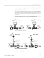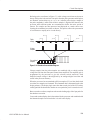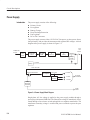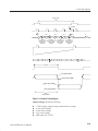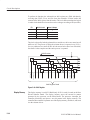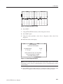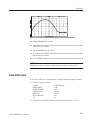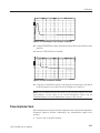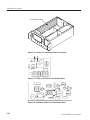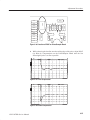
1
Service Manual 1503C Metallic Time-Domain Reflectometer 070-7170-05 This document applies to firmware version 5.04 and above. Warning The servicing instructions are for use by qualified personnel only. To avoid personal injury, do not perform any servicing unless you are qualified to do so. Refer to all safety summaries prior to performing service. www.tektronix.com Copyright © Tektronix, Inc. All rights reserved. Tektronix products are covered by U.S. and foreign patents, issued and pending. Information in this publication supercedes that in all previously published material. Specifications and price change privileges reserved. Tektronix, Inc., P.O. Box 500, Beaverton, OR 97077 TEKTRONIX and TEK are registered trademarks of Tektronix, Inc. WARRANTY Tektronix warrants that the products that it manufactures and sells will be free from defects in materials and workmanship for a period of one (1) year from the date of shipment. If a product proves defective during this warranty period, Tektronix, at its option, either will repair the defective product without charge for parts and labor, or will provide a replacement in exchange for the defective product. In order to obtain service under this warranty, Customer must notify Tektronix of the defect before the expiration of the warranty period and make suitable arrangements for the performance of service. Customer shall be responsible for packaging and shipping the defective product to the service center designated by Tektronix, with shipping charges prepaid. Tektronix shall pay for the return of the product to Customer if the shipment is to a location within the country in which the Tektronix service center is located. Customer shall be responsible for paying all shipping charges, duties, taxes, and any other charges for products returned to any other locations. This warranty shall not apply to any defect, failure or damage caused by improper use or improper or inadequate maintenance and care. Tektronix shall not be obligated to furnish service under this warranty a) to repair damage resulting from attempts by personnel other than Tektronix representatives to install, repair or service the product; b) to repair damage resulting from improper use or connection to incompatible equipment; c) to repair any damage or malfunction caused by the use of non-Tektronix supplies; or d) to service a product that has been modified or integrated with other products when the effect of such modification or integration increases the time or difficulty of servicing the product. THIS WARRANTY IS GIVEN BY TEKTRONIX IN LIEU OF ANY OTHER WARRANTIES, EXPRESS OR IMPLIED. TEKTRONIX AND ITS VENDORS DISCLAIM ANY IMPLIED WARRANTIES OF MERCHANTABILITY OR FITNESS FOR A PARTICULAR PURPOSE. TEKTRONIX’ RESPONSIBILITY TO REPAIR OR REPLACE DEFECTIVE PRODUCTS IS THE SOLE AND EXCLUSIVE REMEDY PROVIDED TO THE CUSTOMER FOR BREACH OF THIS WARRANTY. TEKTRONIX AND ITS VENDORS WILL NOT BE LIABLE FOR ANY INDIRECT, SPECIAL, INCIDENTAL, OR CONSEQUENTIAL DAMAGES IRRESPECTIVE OF WHETHER TEKTRONIX OR THE VENDOR HAS ADVANCE NOTICE OF THE POSSIBILITY OF SUCH DAMAGES. Table of Contents General Safety Summary . . . . . . . . . . . . . . . . . . . . . . . . . . . . . . . . . . . . . . . . . . . Service Safety Summary . . . . . . . . . . . . . . . . . . . . . . . . . . . . . . . . . . . . . . . . . . . xiii xv General Information . . . . . . . . . . . . . . . . . . . . . . . . . . . . . . . . . . . . . . . . xvii Installation and Repacking . . . . . . . . . . . . . . . . . . . . . . . . . . . . . . . . . . . . . . . . . . Contacting Tektronix . . . . . . . . . . . . . . . . . . . . . . . . . . . . . . . . . . . . . . . . . . . . . . xviii xiv Operating Instructions . . . . . . . . . . . . . . . . . . . . . . . . . . . . . . . . . . . . . . 1–1 Overview . . . . . . . . . . . . . . . . . . . . . . . . . . . . . . . . . . . . . . . . . . . . . . . . . . . . . . . Preparing to Use the 1503C . . . . . . . . . . . . . . . . . . . . . . . . . . . . . . . . . . . . . . . . . Display . . . . . . . . . . . . . . . . . . . . . . . . . . . . . . . . . . . . . . . . . . . . . . . . . . . . . . . . . Front-Panel Controls . . . . . . . . . . . . . . . . . . . . . . . . . . . . . . . . . . . . . . . . . . . . . . Menu Selections . . . . . . . . . . . . . . . . . . . . . . . . . . . . . . . . . . . . . . . . . . . . . . . . . . Test Preparations . . . . . . . . . . . . . . . . . . . . . . . . . . . . . . . . . . . . . . . . . . . . . . . . . Cable Test Procedure . . . . . . . . . . . . . . . . . . . . . . . . . . . . . . . . . . . . . . . . . . . . . . Additional Features (Menu Selected) . . . . . . . . . . . . . . . . . . . . . . . . . . . . . . . . . . 1–1 1–5 1–6 1–6 1–8 1–11 1–13 1–25 Operating Instructions Operator Performance Checks Operator Performance Checks . . . . . . . . . . . . . . . . . . . . . . . . . . . . . . . 2–1 Specifications . . . . . . . . . . . . . . . . . . . . . . . . . . . . . . . . . . . . . . . . . . . . . . 3–1 Electrical Characteristics . . . . . . . . . . . . . . . . . . . . . . . . . . . . . . . . . . . . . . . . . . . Environmental Characteristics . . . . . . . . . . . . . . . . . . . . . . . . . . . . . . . . . . . . . . . Physical Characteristics . . . . . . . . . . . . . . . . . . . . . . . . . . . . . . . . . . . . . . . . . . . . 3–1 3–3 3–4 Specifications Options and Accessories 1503C MTDR Service Manual Options and Accessories . . . . . . . . . . . . . . . . . . . . . . . . . . . . . . . . . . . . . 4–1 Option 04: YT–1 Chart Recorder . . . . . . . . . . . . . . . . . . . . . . . . . . . . . . . . . . . . . Option 05: Metric Default . . . . . . . . . . . . . . . . . . . . . . . . . . . . . . . . . . . . . . . . . . Option 06: EthernetR . . . . . . . . . . . . . . . . . . . . . . . . . . . . . . . . . . . . . . . . . . . . . . Option 07: YT–1S Chart Recorder . . . . . . . . . . . . . . . . . . . . . . . . . . . . . . . . . . . Option 08: Token Ring Adapter . . . . . . . . . . . . . . . . . . . . . . . . . . . . . . . . . . . . . . Option 09: Universal Service Ordering Code . . . . . . . . . . . . . . . . . . . . . . . . . . . Option 10: Token Ring Interface . . . . . . . . . . . . . . . . . . . . . . . . . . . . . . . . . . . . . Power Cord Options . . . . . . . . . . . . . . . . . . . . . . . . . . . . . . . . . . . . . . . . . . . . . . . Accessories . . . . . . . . . . . . . . . . . . . . . . . . . . . . . . . . . . . . . . . . . . . . . . . . . . . . . . 4–1 4–1 4–1 4–16 4–17 4–17 4–17 4–18 4–19 i Table of Contents Circuit Descriptions Circuit Descriptions . . . . . . . . . . . . . . . . . . . . . . . . . . . . . . . . . . . . . . . . . 5–1 Introduction . . . . . . . . . . . . . . . . . . . . . . . . . . . . . . . . . . . . . . . . . . . . . . . . . . . . . Power Supply . . . . . . . . . . . . . . . . . . . . . . . . . . . . . . . . . . . . . . . . . . . . . . . . . . . . Processor System . . . . . . . . . . . . . . . . . . . . . . . . . . . . . . . . . . . . . . . . . . . . . . . . . Option Port Interface . . . . . . . . . . . . . . . . . . . . . . . . . . . . . . . . . . . . . . . . . . . . . . Video Processor . . . . . . . . . . . . . . . . . . . . . . . . . . . . . . . . . . . . . . . . . . . . . . . . . . Timebase . . . . . . . . . . . . . . . . . . . . . . . . . . . . . . . . . . . . . . . . . . . . . . . . . . . . . . . Pulse Generator/Sampler . . . . . . . . . . . . . . . . . . . . . . . . . . . . . . . . . . . . . . . . . . . Front Panel . . . . . . . . . . . . . . . . . . . . . . . . . . . . . . . . . . . . . . . . . . . . . . . . . . . . . . Display Module . . . . . . . . . . . . . . . . . . . . . . . . . . . . . . . . . . . . . . . . . . . . . . . . . . Option 06 (EthernetR) . . . . . . . . . . . . . . . . . . . . . . . . . . . . . . . . . . . . . . . . . . . . . 5–1 5–4 5–7 5–10 5–13 5–15 5–23 5–25 5–29 5–41 Calibration and Adjustments ii Calibration . . . . . . . . . . . . . . . . . . . . . . . . . . . . . . . . . . . . . . . . . . . . . . . . 6–1 Introduction . . . . . . . . . . . . . . . . . . . . . . . . . . . . . . . . . . . . . . . . . . . . . . . . . . . . . 6–1 Calibration Performance Check . . . . . . . . . . . . . . . . . . . . . . . . . . . . . . 6–1 Display Module Check . . . . . . . . . . . . . . . . . . . . . . . . . . . . . . . . . . . . . . . . . . . . . Front Panel Check . . . . . . . . . . . . . . . . . . . . . . . . . . . . . . . . . . . . . . . . . . . . . . . . Horizontal Scale (Timebase) Check . . . . . . . . . . . . . . . . . . . . . . . . . . . . . . . . . . . Vertical Position (Offset) Check . . . . . . . . . . . . . . . . . . . . . . . . . . . . . . . . . . . . . Noise Check . . . . . . . . . . . . . . . . . . . . . . . . . . . . . . . . . . . . . . . . . . . . . . . . . . . . . Impedance Check . . . . . . . . . . . . . . . . . . . . . . . . . . . . . . . . . . . . . . . . . . . . . . . . . Offset/Gain Check . . . . . . . . . . . . . . . . . . . . . . . . . . . . . . . . . . . . . . . . . . . . . . . . RAM/ROM Check . . . . . . . . . . . . . . . . . . . . . . . . . . . . . . . . . . . . . . . . . . . . . . . . Pulse Balance Check . . . . . . . . . . . . . . . . . . . . . . . . . . . . . . . . . . . . . . . . . . . . . . Pulse Width Check . . . . . . . . . . . . . . . . . . . . . . . . . . . . . . . . . . . . . . . . . . . . . . . . Auto Pulse Select Check . . . . . . . . . . . . . . . . . . . . . . . . . . . . . . . . . . . . . . . . . . . Jitter Check . . . . . . . . . . . . . . . . . . . . . . . . . . . . . . . . . . . . . . . . . . . . . . . . . . . . . . Aberrations Check . . . . . . . . . . . . . . . . . . . . . . . . . . . . . . . . . . . . . . . . . . . . . . . . Pulse Amplitude Check . . . . . . . . . . . . . . . . . . . . . . . . . . . . . . . . . . . . . . . . . . . . Option 04/07: YT-1/YT-1S Chart Recorder Check . . . . . . . . . . . . . . . . . . . . . . . Option 05: Metric Default Check . . . . . . . . . . . . . . . . . . . . . . . . . . . . . . . . . . . . . Option 06: EthernetR Adapter Checks . . . . . . . . . . . . . . . . . . . . . . . . . . . . . . . . 6–2 6–4 6–8 6–10 6–12 6–14 6–14 6–15 6–16 6–17 6–20 6–21 6–23 6–27 6–30 6–31 6–31 Adjustment Procedures . . . . . . . . . . . . . . . . . . . . . . . . . . . . . . . . . . . . . . 6–37 Visual Inspection . . . . . . . . . . . . . . . . . . . . . . . . . . . . . . . . . . . . . . . . . . . . . . . . . Power Supply Checks and Adjustments . . . . . . . . . . . . . . . . . . . . . . . . . . . . . . . Main Board "12 VDC Check and Adjust . . . . . . . . . . . . . . . . . . . . . . . . . . . . . LCD Check and Adjustment . . . . . . . . . . . . . . . . . . . . . . . . . . . . . . . . . . . . . . . . Pulser/Sampler Voltage Check . . . . . . . . . . . . . . . . . . . . . . . . . . . . . . . . . . . . . . . Sampling Efficiency Adjustment . . . . . . . . . . . . . . . . . . . . . . . . . . . . . . . . . . . . . 1st Blow-By Compensation Adjustment . . . . . . . . . . . . . . . . . . . . . . . . . . . . . . . Output Impedance Check . . . . . . . . . . . . . . . . . . . . . . . . . . . . . . . . . . . . . . . . . . . Option 06: EthernetR Adapter Adjustments . . . . . . . . . . . . . . . . . . . . . . . . . . . . After Adjustments are Completed . . . . . . . . . . . . . . . . . . . . . . . . . . . . . . . . . . . . 6–38 6–38 6–42 6–46 6–49 6–51 6–54 6–56 6–58 6–59 1503C MTDR Service Manual Table of Contents Maintenance Maintenance . . . . . . . . . . . . . . . . . . . . . . . . . . . . . . . . . . . . . . . . . . . . . . . 7–1 Introduction . . . . . . . . . . . . . . . . . . . . . . . . . . . . . . . . . . . . . . . . . . . . . . . . . . . . . Preventive Maintenance . . . . . . . . . . . . . . . . . . . . . . . . . . . . . . . . . . . . . . . . . . . . Part Removal and Replacement . . . . . . . . . . . . . . . . . . . . . . . . . . . . . . . . . . . . . . Troubleshooting . . . . . . . . . . . . . . . . . . . . . . . . . . . . . . . . . . . . . . . . . . . . . . . . . . Control Panel Installation . . . . . . . . . . . . . . . . . . . . . . . . . . . . . . . . . . . . . . . . . . . Installing the Case Cover Over the Chassis . . . . . . . . . . . . . . . . . . . . . . . . . . . . . 7–1 7–1 7–2 7–13 7–18 7–19 Replaceable Electrical Parts Replaceable Electrical Parts . . . . . . . . . . . . . . . . . . . . . . . . . . . . . . . . . . 8–1 Diagrams . . . . . . . . . . . . . . . . . . . . . . . . . . . . . . . . . . . . . . . . . . . . . . . . . 9–1 Diagrams Replaceable Mechanical Parts Replaceable Mechanical Parts . . . . . . . . . . . . . . . . . . . . . . . . . . . . . . . . 10–1 Glossary Index 1503C MTDR Service Manual iii Table of Contents List of Figures Figure 1–1: Figure 1–2: Figure 1–3: Figure 1–4: Figure 1–5: Figure 1–6: Figure 1–7: Figure 1–8: Figure 1–9: Figure 1–10: Figure 1–11: Figure 1–12: Figure 1–13: Figure 1–14: Figure 1–15: Figure 1–16: Figure 1–17: Figure 1–18: Figure 1–19: Figure 1–20: Figure 1–21: Figure 1–22: Figure 1–23: Figure 1–24: Figure 1–25: Figure 1–26: Figure 1–27: Figure 1–28: Figure 1–29: iv Rear Panel Voltage Selector, Fuse, AC Receptacle . . . . . Display Showing Low Battery Indication . . . . . . . . . . . . 1503C Front-Panel Controls . . . . . . . . . . . . . . . . . . . . . . Display and Indicators . . . . . . . . . . . . . . . . . . . . . . . . . . . Vp Set at .30, Cursor Beyond Reflected Pulse (Setting Too Low) . . . . . . . . . . . . . . . . . . . . . . . . . . . . . . Vp Set at .99, Cursor Less Than Reflected Pulse (Setting Too High) . . . . . . . . . . . . . . . . . . . . . . . . . . . . . . Vp Set at .66, Cursor on Rising Edge of Reflected Pulse (Set Correctly) . . . . . . . . . . . . . . . . . . . . . . . . . . . . . . . . . 20-ft Cable at 5 ft/div . . . . . . . . . . . . . . . . . . . . . . . . . . . Short in the Cable . . . . . . . . . . . . . . . . . . . . . . . . . . . . . . Open in the Cable . . . . . . . . . . . . . . . . . . . . . . . . . . . . . . 455-ft Cable . . . . . . . . . . . . . . . . . . . . . . . . . . . . . . . . . . . 455-ft Cable with 20 ft/div, Cursor Off Screen . . . . . . . . Return Loss . . . . . . . . . . . . . . . . . . . . . . . . . . . . . . . . . . . Reflection Adjusted to One Division in Height . . . . . . . Display with VIEW INPUT Turned Off . . . . . . . . . . . . . Display of a Stored Waveform . . . . . . . . . . . . . . . . . . . . Display of a Stored Waveform and Current Waveform . Display of a Stored Waveform, Current Waveform, and Difference Waveform . . . . . . . . . . . . . . . . . . . . . . . . Waveform Moved to Top Half of Display . . . . . . . . . . . . Current Waveform Centered, Stored Waveform Above . . . . . . . . . . . . . . . . . . . . . . . . . . . . . . . . . . . . . . . Current Waveform Center, Stored Waveform Above, Difference Below . . . . . . . . . . . . . . . . . . . . . . . . . . . . . . Waveform of Three-Foot Lead-in Cable . . . . . . . . . . . . . Cursor Moved to End of Three-Foot Lead-in Cable . . . . Cursor Moved to End of Three-Foot Lead-in Cable . . . . Cursor Moved to 0.00 ft . . . . . . . . . . . . . . . . . . . . . . . . . Incident Pulse at Four Divisions, FILTER at Desired Setting . . . . . . . . . . . . . . . . . . . . . . . . . . . . . . . . Waveform Viewed in Normal Operation . . . . . . . . . . . . . Waveform Showing Intermittent Short . . . . . . . . . . . . . . Waveform Display with No Outgoing Pulses . . . . . . . . . 1–1 1–4 1–5 1–6 1–12 1–13 1–13 1–14 1–14 1–15 1–15 1–16 1–16 1–17 1–18 1–19 1–19 1–20 1–20 1–21 1–21 1–22 1–23 1–23 1–24 1–24 1–25 1–26 1–26 1503C MTDR Service Manual Table of Contents Figure 1–30: A Captured Single Sweep . . . . . . . . . . . . . . . . . . . . . . . . 1–27 Figure 2–1: Figure 2–2: Figure 2–3: Figure 2–4: Figure 2–5: Figure 2–6: Figure 2–7: Figure 2–8: Figure 2–9: Figure 2–10: Figure 2–11: Figure 2–12: Figure 2–13: Start-up Measurement Display . . . . . . . . . . . . . . . . . . . . Measurement Display with 10-foot Cable . . . . . . . . . . . Cursor at End of 10-foot Cable . . . . . . . . . . . . . . . . . . . . Cursor at End of 10-foot Cable, Vp Set to .30 . . . . . . . . Flatline Display Out to 50,000+ Feet . . . . . . . . . . . . . . . Waveform Off the Top of the Display . . . . . . . . . . . . . . . Waveform at the Bottom of the Display . . . . . . . . . . . . . Waveform with Gain at 57 dB . . . . . . . . . . . . . . . . . . . . . Distance at –2.00 ft . . . . . . . . . . . . . . . . . . . . . . . . . . . . . Pulse Adjusted to Four Major Divisions in Height . . . . . Waveform Centered, Cursor at 10.00 ft . . . . . . . . . . . . . Pulse Adjusted to Four Major Divisions in Height . . . . . Aberrations Less Than Four Divisions Out to 30.00 ft . . . . . . . . . . . . . . . . . . . . . . . . . . . . . . . . . . . . . . Pulse Adjusted to Four Major Divisions in Height . . . . . Aberrations Less Than Four Divisions Out to 300.00 ft . . . . . . . . . . . . . . . . . . . . . . . . . . . . . . . . . . . . . Pulse Adjusted to Four Major Divisions in Height . . . . . Aberrations Less Than Four Divisions Out to 3000.00 ft . . . . . . . . . . . . . . . . . . . . . . . . . . . . . . . . . . . . 2–2 2–2 2–3 2–3 2–4 2–4 2–5 2–5 2–7 2–7 2–8 2–8 Figure 2–14: Figure 2–15: Figure 2–16: Figure 2–17: Figure 4–1: Figure 4–2: Figure 4–3: Figure 4–4: Figure 4–5: Figure 4–6: Figure 4–7: Figure 4–8: Figure 4–9: Figure 4–10: 1503C MTDR Service Manual A Typical Ethernet System . . . . . . . . . . . . . . . . . . . . . . . N-Type Male T-Connector . . . . . . . . . . . . . . . . . . . . . . . N-Type Female T-Connector . . . . . . . . . . . . . . . . . . . . . . System 1 – Tap Hidden by Traffic (1 avg, 50 ft/div. 35 dB) . . . . . . . . . . . . . . . . . . . . . . . . . System 1 – Traffic and Tap Nearly Identical (4 avg, 50 ft/div, 35 dB) . . . . . . . . . . . . . . . . . . . . . . . . . System 1 – Tap Becoming Visible (16 avg, 50 ft/div, 35 dB) . . . . . . . . . . . . . . . . . . . . . . . . System 1 – Tap Quite Visible (128 avg, 50 ft/div, 35 dB) . . . . . . . . . . . . . . . . . . . . . . . System 1 – No Traffic (1 avg, 50 ft/div, 35 dB) . . . . . . . . . . . . . . . . . . . . . . . . . System 1 – Tap Expanded, No Traffic (1 avg, 2 ft/div, 35 dB) . . . . . . . . . . . . . . . . . . . . . . . . . . System 2 – Cable w/ Revision One Repeater (1 avg, 200ft/div, 2.25dB) . . . . . . . . . . . . . . . . . . . . . . . . 2–9 2–9 2–10 2–10 2–11 4–2 4–5 4–5 4–10 4–10 4–11 4–11 4–11 4–12 4–12 v Table of Contents Figure 4–11: Figure 4–12: Figure 4–13: Figure 4–14: Figure 4–15: Figure 4–16: Figure 4–17: Figure 4–18: Figure 4–19: Figure 4–20: Figure 4–21: Figure 5–1: Figure 5–2: Figure 5–3: Figure 5–4: Figure 5–5: Figure 5–6: Figure 5–7: Figure 5–8: Figure 5–9: Figure 5–10: Figure 5–11: Figure 5–12: Figure 5–13: Figure 5–14: Figure 5–15: Figure 5–16: Figure 5–17: Figure 5–18: vi System 2 – First Tap, No Traffic (1 avg, 1 ft/div, 44.5 dB) . . . . . . . . . . . . . . . . . . . . . . . . . System 2 – Same Tap with 5% Traffic (1 avg, 1 ft/div, 44.5 dB) . . . . . . . . . . . . . . . . . . . . . . . . . System 2 – Same Tap, Increased Averaging (16 avg, 1 ft/div, 44.5 dB) . . . . . . . . . . . . . . . . . . . . . . . . System 2 – Farther Out, More Gain (128 avg, 10 ft/div, 53.5 dB) . . . . . . . . . . . . . . . . . . . . . . System 2 – 1000-ft Cable at 10 ns (128 avg, 100 ft/div, 43.75 dB) . . . . . . . . . . . . . . . . . . . . System 2 – Previous Waveform Expanded (128 avg, 20 ft/div, 54.75 dB) . . . . . . . . . . . . . . . . . . . . . System 2 – Next Group of Taps (128 avg, 20 ft/div, 54.75 dB) . . . . . . . . . . . . . . . . . . . . . System 2 – Group of Taps Expanded (128 avg, 10 ft/div, 54.75 dB) . . . . . . . . . . . . . . . . . . . . . System 2 – Another Group of Taps (128 avg, 10 ft/div, 54.75 dB) . . . . . . . . . . . . . . . . . . . . . System 2 – End of Cable (128 avg, 20 ft/div, 61.25 dB) . . . . . . . . . . . . . . . . . . . . . Typical Frequency Response Curve with EthernetR Option 06 . . . . . . . . . . . . . . . . . . . . . . . . . . . . System Block Diagram . . . . . . . . . . . . . . . . . . . . . . . . . . Waveform Accumulation Diagram . . . . . . . . . . . . . . . . . Power Supply Block Diagram . . . . . . . . . . . . . . . . . . . . . Processor Block Diagram . . . . . . . . . . . . . . . . . . . . . . . . Option Port Interface Block Diagram . . . . . . . . . . . . . . . Video Processor Block Diagram . . . . . . . . . . . . . . . . . . . Video Processor Output . . . . . . . . . . . . . . . . . . . . . . . . . . Timebase Block Diagram . . . . . . . . . . . . . . . . . . . . . . . . Timebase Control . . . . . . . . . . . . . . . . . . . . . . . . . . . . . . Combined Effects of Time Delay . . . . . . . . . . . . . . . . . . Calibration of Delay Zero and 50-ns Analog Delay . . . . Pulse Generator/Sampler Block Diagram . . . . . . . . . . . . Front Panel Block Diagram . . . . . . . . . . . . . . . . . . . . . . . Display Module Block Diagram . . . . . . . . . . . . . . . . . . . SBE Cell . . . . . . . . . . . . . . . . . . . . . . . . . . . . . . . . . . . . . Row Driver Block Diagram . . . . . . . . . . . . . . . . . . . . . . Column Driver Block Diagram . . . . . . . . . . . . . . . . . . . . Row Timing Diagram . . . . . . . . . . . . . . . . . . . . . . . . . . . 4–12 4–13 4–13 4–13 4–14 4–14 4–14 4–15 4–15 4–15 4–16 5–2 5–3 5–4 5–8 5–11 5–13 5–15 5–16 5–17 5–18 5–19 5–23 5–26 5–29 5–31 5–31 5–32 5–33 1503C MTDR Service Manual Table of Contents Figure 5–19: Figure 5–20: Figure 5–21: Figure 5–22: Column Timing Diagram . . . . . . . . . . . . . . . . . . . . . . . . Shift Register . . . . . . . . . . . . . . . . . . . . . . . . . . . . . . . . . . CPU and Display Memory Interface . . . . . . . . . . . . . . . . Option 06 (EthernetR) Block Diagram . . . . . . . . . . . . . 5–35 5–36 5–39 5–41 Figure 6–1: Figure 6–2: Figure 6–3: Figure 6–4: Figure 6–5: Figure 6–6: Figure 6–7: Figure 6–8: Figure 6–9: Figure 6–10: Figure 6–11: Figure 6–12: Figure 6–13: Figure 6–14: Typical Start-Up Display . . . . . . . . . . . . . . . . . . . . . . . . . Waveform on the Display . . . . . . . . . . . . . . . . . . . . . . . . Setup Menu . . . . . . . . . . . . . . . . . . . . . . . . . . . . . . . . . . . Main Menu . . . . . . . . . . . . . . . . . . . . . . . . . . . . . . . . . . . Diagnostics Menu . . . . . . . . . . . . . . . . . . . . . . . . . . . . . . Front Panel Diagnostic Display . . . . . . . . . . . . . . . . . . . . Front Panel Diagnostic Display . . . . . . . . . . . . . . . . . . . . Front Panel Diagnostic Display . . . . . . . . . . . . . . . . . . . . Front Panel Diagnostic Display . . . . . . . . . . . . . . . . . . . . Waveform on the Display with No Cable Attached . . . . Waveform on the Display with 10-ft Cable Attached . . . Cursor on Rising Edge of Reflected Pulse at 5 ft/div . . . Cursor on Rising Edge of Reflected Pulse at 1 ft/div . . . Cursor on Rising Edge of Reflected Pulse with Vp at .84 . . . . . . . . . . . . . . . . . . . . . . . . . . . . . . . . . . . . . Flatline Display to >50,000 ft . . . . . . . . . . . . . . . . . . . . . Waveform at Top of the Display . . . . . . . . . . . . . . . . . . Waveform at Bottom of the Display . . . . . . . . . . . . . . . . Waveform at Center of the Display . . . . . . . . . . . . . . . . . Distance Moved Beyond Trailing Edge of Pulse . . . . . . Noise with Gain at 57 dB . . . . . . . . . . . . . . . . . . . . . . . . Noise Diagnostic Display . . . . . . . . . . . . . . . . . . . . . . . . Service Diagnostic Menu . . . . . . . . . . . . . . . . . . . . . . . . Service Diagnostic Menu . . . . . . . . . . . . . . . . . . . . . . . . Service Diagnostic Menu . . . . . . . . . . . . . . . . . . . . . . . . Pulse Appx. Five Divisions High . . . . . . . . . . . . . . . . . . Current Waveform Shifted from Stored Waveform . . . . Initial Pulse . . . . . . . . . . . . . . . . . . . . . . . . . . . . . . . . . . . Pulse Adjusted to Six Divisions High . . . . . . . . . . . . . . . Cursor on Leading Edge at Center Graticule . . . . . . . . . Cursor on Trailing Edge at Center Graticule . . . . . . . . . Initial Pulse with Cursor at 0.00 ft . . . . . . . . . . . . . . . . . Waveform on Auto Pulse Select . . . . . . . . . . . . . . . . . . . Initial Pulse Centered on Horizontal Graticule . . . . . . . . 6–2 6–2 6–3 6–4 6–5 6–5 6–6 6–7 6–7 6–8 6–8 6–9 6–9 Figure 6–15: Figure 6–16: Figure 6–17: Figure 6–18: Figure 6–19: Figure 6–20: Figure 6–21: Figure 6–22: Figure 6–23: Figure 6–24: Figure 6–25: Figure 6–26: Figure 6–27: Figure 6–28: Figure 6–29: Figure 6–30: Figure 6–31: Figure 6–32: Figure 6–33: 1503C MTDR Service Manual 6–9 6–10 6–11 6–11 6–11 6–12 6–13 6–13 6–14 6–14 6–15 6–16 6–17 6–18 6–18 6–19 6–19 6–20 6–21 6–21 vii Table of Contents Figure 6–34: Figure 6–35: Figure 6–36: Figure 6–37: Figure 6–38: Figure 6–39: Figure 6–40: Figure 6–41: Figure 6–42: Figure 6–43: Figure 6–44: Figure 6–45: Figure 6–46: Figure 6–47: Figure 6–48: Figure 6–49: Figure 6–50: Figure 6–51: Figure 6–52: Figure 6–53: Figure 6–54: Figure 6–55: Figure 6–56: Figure 6–57: Figure 6–58: Figure 6–59: Figure 6–60: Figure 6–61: Figure 6–62: Figure 6–63: Figure 6–64: Figure 6–65: Figure 6–66: Figure 6–67: Figure 6–68: Figure 6–69: Figure 6–70: Figure 6–71: viii Gain Increased to 30.00 dB . . . . . . . . . . . . . . . . . . . . . . . Jitter Apparent Using Max Hold . . . . . . . . . . . . . . . . . . . Cursor at –2.00 ft . . . . . . . . . . . . . . . . . . . . . . . . . . . . . . . Pulse Height at Four Divisions at 1 ft/div . . . . . . . . . . . . Gain Increased to 25.00 dB . . . . . . . . . . . . . . . . . . . . . . . Pulse Height at Four Divisions at 2 ft/div . . . . . . . . . . . . Gain Increased to 30.00 dB . . . . . . . . . . . . . . . . . . . . . . . Pulse Height at Four Divisions at 50 ft/div . . . . . . . . . . . Gain Increased to 30.00 dB . . . . . . . . . . . . . . . . . . . . . . . Pulse Height at Four Divisions at 500 ft/div . . . . . . . . . . Gain Increased to 30.00 dB . . . . . . . . . . . . . . . . . . . . . . . Oscilloscope Waveform . . . . . . . . . . . . . . . . . . . . . . . . . 1503C Waveform of 1000-ns Pulse . . . . . . . . . . . . . . . . 1503C Waveform of 100-ns Pulse . . . . . . . . . . . . . . . . . 1503C Waveform of 2-ns Pulse . . . . . . . . . . . . . . . . . . . Head Alignment Chart Print . . . . . . . . . . . . . . . . . . . . . . Equipment Setup . . . . . . . . . . . . . . . . . . . . . . . . . . . . . . . Main Menu . . . . . . . . . . . . . . . . . . . . . . . . . . . . . . . . . . . Ethernet Menu . . . . . . . . . . . . . . . . . . . . . . . . . . . . . . . . . Ethernet Menu . . . . . . . . . . . . . . . . . . . . . . . . . . . . . . . . . Ethernet Menu . . . . . . . . . . . . . . . . . . . . . . . . . . . . . . . . . Ethernet Menu . . . . . . . . . . . . . . . . . . . . . . . . . . . . . . . . . Ethernet Menu . . . . . . . . . . . . . . . . . . . . . . . . . . . . . . . . . Circuit Board Locations in the Instrument . . . . . . . . . . . Power Supply Board . . . . . . . . . . . . . . . . . . . . . . . . . . . . Power Supply Test Points TP1020 and TP1010 . . . . . . Power Supply Test Point TP2030 . . . . . . . . . . . . . . . . . Connector Plug P5040 and Pins J5040 on Bottom of Main Board . . . . . . . . . . . . . . . . . . . . . . . . . . . . . . . . . . . Power Supply Test Point TP1020 . . . . . . . . . . . . . . . . . Power Supply Test Point TP2030 . . . . . . . . . . . . . . . . . Location of Main Board in Instrument . . . . . . . . . . . . . . Main Board Probe Points . . . . . . . . . . . . . . . . . . . . . . . . Waveform on Display . . . . . . . . . . . . . . . . . . . . . . . . . . . Battery Connections to Power Supply Board . . . . . . . . . CR2012 on Power Supply Board . . . . . . . . . . . . . . . . . . Display Showing Power is Battery . . . . . . . . . . . . . . . . . Display Showing Battery Voltage is Low . . . . . . . . . . . . R2012 on Power Supply Board . . . . . . . . . . . . . . . . . . . . 6–22 6–22 6–23 6–24 6–24 6–25 6–25 6–26 6–26 6–27 6–27 6–28 6–29 6–29 6–30 6–30 6–32 6–32 6–33 6–33 6–34 6–34 6–35 6–37 6–39 6–39 6–40 6–40 6–41 6–41 6–42 6–42 6–43 6–44 6–44 6–45 6–45 6–46 1503C MTDR Service Manual Table of Contents Figure 6–72: Figure 6–73: Figure 6–74: Figure 6–75: Figure 6–76: Figure 6–77: Figure 6–78: Figure 6–79: Figure 6–80: Figure 6–81: Figure 6–82: Figure 6–83: Figure 6–84: Figure 6–85: Figure 6–86: Figure 6–87: Figure 6–88: Figure 6–89: Figure 6–90: Figure 6–91: Figure 6–92: Figure 6–93: Figure 7–1: Figure 7–2: Figure 7–3: Figure 7–4: Figure 7–5: Figure 7–6: Figure 7–7: Figure 7–8: Figure 7–9: Figure 7–10: Figure 7–11: Figure 7–12: Figure 7–13: Figure 7–14: 1503C MTDR Service Manual R1018 on Front Panel Board . . . . . . . . . . . . . . . . . . . . . . LCD Pattern with Contrast Too Light . . . . . . . . . . . . . . . LCD Pattern with Contrast Too Dark . . . . . . . . . . . . . . . LCD Pattern Adjusted for Sharpness . . . . . . . . . . . . . . . Waveform with Contrast Too Light . . . . . . . . . . . . . . . . . Waveform with Contrast Adjusted Correctly . . . . . . . . . Location of Pulser/Sampler Board in Instrument . . . . . . TP1081 and TP1082 on Pulser/Sampler Board . . . . . . . VR3020 and VR30212 on Pulser/Sampler Board . . . . . . Service Diagnostic Menu . . . . . . . . . . . . . . . . . . . . . . . . Location of Pulser/Sampler Board in Instrument . . . . . . Location of R1080 on Pulser/Sampler Board . . . . . . . . . Service Diagnostic Efficiency Readout . . . . . . . . . . . . . . Location of Pulser/Sampler Board in Instrument . . . . . . Location of R2097 on Pulser/Sampler Board . . . . . . . . . Over-Compensated . . . . . . . . . . . . . . . . . . . . . . . . . . . . . Under-Compensated . . . . . . . . . . . . . . . . . . . . . . . . . . . . Correctly Compensated . . . . . . . . . . . . . . . . . . . . . . . . . . Location of Pulser/Sampler Board in Instrument . . . . . . Location of C3010, TP3020, and TP3030 on Pulser/Sampler Board . . . . . . . . . . . . . . . . . . . . . . . . . . . Main Menu . . . . . . . . . . . . . . . . . . . . . . . . . . . . . . . . . . . L2010, R1011, and R1013 on Option 06 Board . . . . . . . Location of Voltage Selector, Fuse Holder on Rear Panel Power Supply Module and P/O Rear Panel . . . . . . . . . . Main Board . . . . . . . . . . . . . . . . . . . . . . . . . . . . . . . . . . . EPROM on Main Board . . . . . . . . . . . . . . . . . . . . . . . . . Lithium Battery on Main Board . . . . . . . . . . . . . . . . . . . Display Module/Front Panel Board Screw Locations . . . Display Module/Front Panel Board Showing Hex Nuts . Location of Default Jumper on Front Panel Board . . . . . Default Jumper Positions . . . . . . . . . . . . . . . . . . . . . . . . Main Board TP1041 . . . . . . . . . . . . . . . . . . . . . . . . . . . . Main Board TP3040 and Main Board TP3041 . . . . . . . . Main Board TP4040 and Main Board TP6010 . . . . . . . . Main Board TP7010 and Main Board TP9011 . . . . . . . . Main Board TP9041 and Front Panel CABLE Connector . . . . . . . . . . . . . . . . . . . . . . . . . . . . . . . . . . . . 6–47 6–47 6–47 6–48 6–48 6–49 6–50 6–50 6–50 6–52 6–52 6–53 6–53 6–54 6–55 6–55 6–55 6–56 6–56 6–57 6–57 6–58 7–2 7–4 7–7 7–7 7–8 7–10 7–11 7–12 7–12 7–13 7–17 7–17 7–17 7–18 ix Table of Contents Figure 7–15: Installing the Case Cover Over the Chassis . . . . . . . . . . 7–20 Figure 9–1: Figure 9–2: Special Schematic Symbols . . . . . . . . . . . . . . . . . . . . . . Component Locator – Main Board . . . . . . . . . . . . . . . . . Schematics – Main Board . . . . . . . . . . . . . . . . . . . . . . Component Locator – Front Panel Board . . . . . . . . . . . . Schematics – Front Panel . . . . . . . . . . . . . . . . . . . . . . Component Locator – Power Supply Board . . . . . . . . . . Schematics – Power Supply . . . . . . . . . . . . . . . . . . . . . . Component Locator – Pulser/Sampler Board . . . . . . . . . Schematics – Pulser/Sampler . . . . . . . . . . . . . . . . . . . Component Locator – EthernetBoard . . . . . . . . . . . . . . . Schematics – Ethernet Board . . . . . . . . . . . . . . . . . . . . . 9–3 9–15 9–16 9–25 9–26 9–28 9–29 9–31 9–32 9–34 9–35 Cabinet . . . . . . . . . . . . . . . . . . . . . . . . . . . . . . . . . . . . . . Frame, Assemblies and Front Panel Controls . . . . . . . . . Option 06 EthernetR . . . . . . . . . . . . . . . . . . . . . . . . . . . . Power Supply . . . . . . . . . . . . . . . . . . . . . . . . . . . . . . . . . 10–13 10–15 10–17 10–19 Figure 9–3: Figure 9–4: Figure 9–5: Figure 9–6: Figure 10–1: Figure 10–2: Figure 10–3: Figure 10–4: x 1503C MTDR Service Manual Table of Contents List of Tables 1503C MTDR Service Manual Shipping Carton Test Strength . . . . . . . . . . . . . . . . . . . . . . . . . . . . . . . . . . xvii Fuse / Voltage Ratings . . . . . . . . . . . . . . . . . . . . . . . . . . . . . . . . . . . . . . . . Vp of Various Dielectric Types . . . . . . . . . . . . . . . . . . . . . . . . . . . . . . . . . Impedance of Various Cable Types . . . . . . . . . . . . . . . . . . . . . . . . . . . . . . Cable Length / Suggested Pulse / Suggested ft/div . . . . . . . . . . . . . . . . . . 1–2 1–11 1–12 1–14 Operator Performance Checks – Equipment Required . . . . . . . . . . . . . . . 2–1 Specifications: Electrical Characteristics . . . . . . . . . . . . . . . . . . . . . . . . . Specifications: Environmental Characteristics . . . . . . . . . . . . . . . . . . . . . Specifications: Physical Characteristics . . . . . . . . . . . . . . . . . . . . . . . . . . 3–1 3–3 3–4 Option 06 Ethernet: Electrical Characteristics . . . . . . . . . . . . . . . . . . . . . 4–16 Option Port Wiring Configuration . . . . . . . . . . . . . . . . . . . . . . . . . . . . . . . Row Driver Latch Bits . . . . . . . . . . . . . . . . . . . . . . . . . . . . . . . . . . . . . . . . Column Driver Latch Bits . . . . . . . . . . . . . . . . . . . . . . . . . . . . . . . . . . . . . Controller Periods . . . . . . . . . . . . . . . . . . . . . . . . . . . . . . . . . . . . . . . . . . . Option 06 Ethernet Control Lines . . . . . . . . . . . . . . . . . . . . . . . . . . . . . . . 5–12 5–34 5–36 5–37 5–41 Calibration Performance Check – Equipment Required . . . . . . . . . . . . . . Pulse Widths with Allowable Tolerances . . . . . . . . . . . . . . . . . . . . . . . . . Auto Pulse: Distance per Division and Pulse Width . . . . . . . . . . . . . . . . . Option 06 EthernetR Checks – Equipment Required . . . . . . . . . . . . . . . . Adjustment Procedures – Equipment Required . . . . . . . . . . . . . . . . . . . . Main Board Voltages, Tolerances, Test Point Locations . . . . . . . . . . . . . . Pulser/Sampler Voltages and Test Point Locations . . . . . . . . . . . . . . . . . . Impedance Range and Specification . . . . . . . . . . . . . . . . . . . . . . . . . . . . . 6–1 6–19 6–20 6–31 6–37 6–40 6–51 6–58 Maintenance – Equipment Required . . . . . . . . . . . . . . . . . . . . . . . . . . . . . Power Cord Conductor Color Code . . . . . . . . . . . . . . . . . . . . . . . . . . . . . Sealing Materials . . . . . . . . . . . . . . . . . . . . . . . . . . . . . . . . . . . . . . . . . . . . 7–1 7–6 7–18 xi Table of Contents xii 1503C MTDR Service Manual General Safety Summary Review the following safety precautions to avoid injury and prevent damage to this product or any products connected to it. To avoid potential hazards, use this product only as specified. Only qualified personnel should perform service procedures. To Avoid Fire or Personal Injury Use Proper Power Cord. Use only the power cord specified for this product and certified for the country of use. Use Proper Voltage Setting. Before applying power, ensure that the line selector is in the proper position for the power source being used. Power Source This product is intended to operate from a power source that will not apply more than 250 volts RMS between the supply conductors or between the supply conductor and ground. A protective ground connection, by way of the grounding conductor in the power cord, is essential for safe operation. Ground the Product. This product is grounded through the grounding conductor of the power cord. To avoid electric shock, the grounding conductor must be connected to earth ground. Before making connections to the input or output terminals of the product, ensure that the product is properly grounded. The standard power cord (161-0288-00) is rated for outdoor use. All other optional power cords are rated for indoor use only. Observe All Terminal Ratings. To avoid fire or shock hazard, observe all ratings and markings on the product. Consult the product manual for further ratings information before making connections to the product. Do not apply a potential to any terminal, including the common terminal, that exceeds the maximum rating of that terminal. Replace Batteries Properly. Replace batteries only with the proper type and rating specified. Recharge Batteries Properly. Recharge batteries for the recommended charge cycle only. Use Proper AC Adapter. Use only the AC adapter specified for this product. Do Not Operate Without Covers. Do not operate this product with covers or panels removed. Use Proper Fuse. Use only the fuse type and rating specified for this product. Avoid Exposed Circuitry. Do not touch exposed connections and components when power is present. 1503C MTDR Service Manual xiii General Safety Summary Do Not Operate With Suspected Failures. If you suspect there is damage to this product, have it inspected by qualified service personnel. Do Not Operate in an Explosive Atmosphere. Symbols and Terms Terms in this Manual. These terms may appear in this manual: WARNING. Warning statements identify conditions or practices that could result in injury or loss of life. CAUTION. Caution statements identify conditions or practices that could result in damage to this product or other property. Terms on the Product. These terms may appear on the product: DANGER indicates an injury hazard immediately accessible as you read the marking. WARNING indicates an injury hazard not immediately accessible as you read the marking. CAUTION indicates a hazard to property including the product. Symbols on the Product. The following symbols may appear on the product: CAUTION Refer to Manual xiv WARNING High Voltage Double Insulated Protective Ground (Earth) Terminal 1503C MTDR Service Manual Service Safety Summary Only qualified personnel should perform service procedures. Read this Service Safety Summary and the General Safety Summary before performing any service procedures. Do Not Service Alone Do not perform internal service or adjustments of this product unless another person capable of rendering first aid and resuscitation is present. Disconnect Power To avoid electric shock, disconnect the main power by means of the power cord or the power switch. Use Care When Servicing With Power On Dangerous voltages or currents may exist in this product. Disconnect power, remove battery, and disconnect test leads before removing protective panels, soldering, or replacing components. To avoid electric shock, do not touch exposed connections. Disposal of Batteries This instrument contains a lead-acid battery. Some states and/or local jurisdictions might require special disposition/recycling of this type of material in accordance with Hazardous Waste guidelines. Check your local and state regulations prior to disposing of an old battery. Tektronix Factory Service will accept 1503C batteries for recycling. If you choose to return the battery to us for recycling, the battery cases must be intact, the battery should be packed with the battery terminals insulated against possible short-circuits, and should be packed in shock-absorbant material. Tektronix, Inc. Attn: Service Department P.O. Box 500 Beaverton, Oregon 97077 U.S.A. For more information, call 1-800-833-9200. 1503C MTDR Service Manual xv Service Safety Summary xvi 1503C MTDR Service Manual General Information Product Description The Tektronix 1503C Metallic-cable Time-Domain Reflectometer (MTDR) is a cable test instrument that uses radar principles to determine the electrical characteristics of metallic cables. The 1503C generates a half-sine wave signal, applies it to the cable under test, and detects and processes the reflected voltage waveform. These reflections are displayed in the 1503C liquid crystal display (LCD), where distance measurements may be made using a cursor technique. Impedance information may be obtained through interpreting waveform amplitude. The waveform may be temporarily stored within the 1503C and recalled or may be printed using the optional dot matrix strip chart recorder, which installs into the front-panel Option Port. Battery Operation The 1503C may be operated from an AC power source or an internal lead-gel battery, which supplies a minimum of eight hours operating time (see the Specifications chapter for specifics). Options Options available for the 1503C are explained in the Options and Accessories chapter of this manual. Standards, Documents, and References Used Terminology used in this manual is in accordance with industry practice. Abbreviations are in accordance with ANSI Y1.1–19722, with exceptions and additions explained in parentheses in the text. Graphic symbology is based on ANSI Y32.2–1975. Logic symbology is based on ANSI Y32.14–1973 and manufacturer’s data books or sheets. A copy of ANSI standards may be obtained from the Institute of Electrical and Electronic Engineers, 345 47th Street, New York, NY 10017. Changes and History Information Changes that involve manual corrections and/or additional data will be incorporated into the text and that page will show a revision date on the inside bottom edge. History information is included in any diagrams in gray. 1503C MTDR Service Manual xvii General Information Installation and Repacking Unpacking and InItial Inspection Before unpacking the 1503C from its shipping container or carton, inspect for signs of external damage. If the carton is damaged, notify the carrier. The shipping carton contains the basic instrument and its standard accessories. Refer to the replaceable parts list in the Service Manual for a complete listing. If the contents of the shipping container are incomplete, if there is mechanical damage or defect, or if the instrument does not meet operational check requirements, contact your local Tektronix Field Office or representative. If the shipping container is damaged, notify the carrier as well as Tektronix. The instrument was inspected both mechanically and electrically before shipment. It should be free if mechanical damage and meet or exceed all electrical specifications. Procedures to check operational performance are in the Performance Checks appendix. These checks should satisfy the requirements for most receiving or incoming inspections. Power Source and Power Requirements The 1503C is intended to be operated from a power source that will not apply more than 250 volts RMS between the supply conductors or between either supply conductor and ground. A protective ground connection, by way of the grounding conductor in the power cord, is essential for safe operation. The AC power connector is a three-way polarized plug with the ground (earth) lead connected directly to the instrument frame to provide electrical shock protection. If the unit is connected to any other power source, the unit frame must be connected to earth ground. Power and voltage requirements are printed on the back panel. The 1503C can be operated from either 115 VAC or 230 VAC nominal line voltage at 45 Hz to 440 Hz, or a 12 VDC supply, or an internal battery. Further information on the 1503C power requirements can be found in the Safety Summary in this section and in the Operating Instructions chapter. Repacking for Shipment When the 1503C is to be shipped to a Tektronix Service Center for service or repair, attach a tag showing the name and address of the owner, name of the individual at your firm who may be contacted, the complete serial number of the instrument, and a description of the service required. If the original packaging is unfit for use or is not available, repackage the instrument as follows: 1. Obtain a carton of corrugated cardboard having inside dimensions that are at least six inches greater than the equipment dimensions to allow for cushioning. The test strength of the shipping carton should be 275 pounds (102.5 kg). Refer to the following table for test strength requirements: xviii 1503C MTDR Service Manual General Information SHIPPING CARTON TEST STRENGTH Gross Weight (lb) Carton Test Strength (lb) 0 – 10 200 11 – 30 275 31 – 120 375 121 – 140 500 141 – 160 600 CAUTION. The battery should be removed from the instrument before shipping. If it is necessary to ship the battery, it should be wrapped and secured separately before being packed with the instrument. 2. Install the front cover on the 1503C and surround the instrument with polyethylene sheeting to protect the finish. 3. Cushion the instrument on all sides with packing material or urethane foam between the carton and the sides of the instrument. 4. Seal with shipping tape or an industrial stapler. If you have any questions, contact your local Tektronix Field Office or representative. 1503C MTDR Service Manual xix General Information Contacting Tektronix Product Support For questions about using Tektronix measurement products, call toll free in North America: 1-800-833-9200 6:00 a.m. – 5:00 p.m. Pacific time Or contact us by e-mail: [email protected] For product support outside of North America, contact your local Tektronix distributor or sales office. Service support Tektronix offers a range of services, including Extended Warranty Repair and Calibration services. Contact your local Tektronix distributor or sales office for details. For a listing of worldwide service centers, visit our web site. xx Toll-free Number In North America: 1-800-833-9200 An operator can direct your call. Postal Address Tektronix, Inc. Department or name (if known) P.O. Box 500 Beaverton, OR 97077 USA Web site www.tektronix.com 1503C MTDR Service Manual Operating Instructions Overview Handling The 1503C front panel is protected by a watertight cover, in which the standard accessories are stored. Secure the front cover by snapping the side latches outward. If the instrument is inadvertently left on, installing the front cover will turn off the POWER switch automatically. The carrying handle rotates 325° and serves as a stand when positioned beneath the instrument. The 1503C can be stored in temperatures ranging from –62° C to +85° C if a battery is not installed. If a battery is installed and the storage temperature is below –35° C or above +65° C, the battery pack should be removed and stored separately (see 1503C Service Manual for instructions on removing the battery). Battery storage temperature should be between –35° C to +65° C. Powering the 1503C In the field, the 1503C can be powered using the internal battery. For AC operation, check the rear panel for proper voltage setting. The voltage selector can be seen through the window of the protective cap. If the setting differs from the voltage available, it can be easily changed. Simply remove the protective cap and select the proper voltage using a screwdriver. REMOVE CAP TO SELECT VOLTAGE REMOVE CAP TO REPLACE FUSE Voltage Selector Line Fuse AC Power Cord Receptacle Figure 1–1: Rear Panel Voltage Selector, Fuse, AC Receptacle The 1503C is intended to be operated from a power source that will not apply more than 250 V RMS between the supply conductors or between either supply conductor 1503C MTDR Service Manual 1–1 Operating Instructions and ground. A protective ground connection by way of the grounding conductor in the power cord is essential for safe operation. The AC power connector is a three-way polarized plug with the ground (earth) lead connected to the instrument frame to provide electrical shock protection. If the unit is connected to any other power source, the unit frame must be connected to an earth ground. See Safety and Installation section. CAUTION. If you change the voltage selector, you must change the line fuse to the appropriate value as listed near the fuse holder and in the table below. FUSE RATING 250 V 0.3 A T 0.15 A T VOLTAGE RATING NOMINAL RANGE 115 VAC (90 – 132 VAC) 230 VAC (180 – 250 VAC) Care of the Battery Pack CAUTION. Read these instructions concerning the care of the battery pack. They contain instructions that reflect on your safety and the performance of the instrument. The 1503C can be powered by a rechargeable lead-gel battery pack that is accessible only by removing the case from the instrument. When AC power is applied, the battery pack is charged at a rate that is dependent on the battery charge state. The battery pack will operate the 1503C for a minimum of eight continuous hours (including making 30 chart recordings) if the LCD backlight is turned off. Battery Charging The battery pack will charge fully in 16 hours when the instrument is connected, via the power cord, to an AC power source with the instrument turned off. The instrument may be turned on and operated while the batteries are charging, but this will increase the charging time. For longest battery life, a full charge is preferred over a partial charge. For maximum capacity, the batteries should be charged within a temperature range of +20° C to +25° C. However, the batteries can be charged within a temperature range of 0° C to +40° C and operated in temperatures ranging from –10° C to +55° C. 1–2 1503C MTDR Service Manual Operating Instructions CAUTION. Do not charge battery pack below 0° C or above +40° C. Do not discharge battery pack below –10° C or above +55° C. If removing the battery pack during or after exposure to these extreme conditions, turn the instrument off and remove the AC power cord. The battery pack should be stored within a temperature range of –35° C to +65° C. However, the self-discharge rate will increase as the temperature increases. If the instrument is stored with the battery pack installed, the battery pack should be charged every 90 days. A fully charged battery pack will lose about 12% of its capacity in three to four months if stored between +20° C and +25° C. NOTE. The battery pack in the 1503C is inside the instrument case with no external access. Refer removal and replacement to qualified service personnel. Battery Removal 1. Ensure that the instrument power is off. 2. If the instrument is connected to an AC power source, remove the AC power cable from the source and from the instrument. 3. If installed, remove the chart recorder, or other device, from the option port. 4. Loosen the four screws on the back of the case and set the instrument face-up on a flat surface. 5. Swing the handle out of the way of the front panel. 6. Break the chassis seal by pushing downward with both hands on the handle pivots on each side of the case. 7. Grasp the case with one hand and tilt the chassis out with the other. Lift by grasping the outside perimeter of the front panel. CAUTION. Do not lift the instrument by the front-panel controls. The controls will be damaged if you do so. 8. Remove the top shield from the instrument by gently lifting the rear edge near the sides of the instrument. 9. Unplug the battery cable positive lead at the battery. 10. Unplug the battery cable negative lead at the battery. 11. Unplug the battery cable at the power supply. 1503C MTDR Service Manual 1–3 Operating Instructions 12. Remove the cable. 13. Remove the two screws mounting the battery clamp to the chassis. 14. Carefully remove the clamp without touching the battery terminals. 15. Lift the battery out. To re-install or replace the battery, repeat the above steps in reverse order. Low Battery If the battery is low, it will be indicated on the LCD (bat/low). If this is the case, protective circuitry will shut down the 1503C within minutes. Either switch to AC power or work very fast. If the instrument is equipped with a chart recorder, using the recorder will further reduce the battery level, or the added load might shut down the instrument. bat/low 0.00 ft O N O F F Low Battery Indicator O F F O F F 50 W 1 avg 0.00 dB 5000 ft 2 ns Figure 1–2: Display Showing Low Battery Indication Protection circuits in the charger prevent deep discharge of the batteries during instrument operation. The circuits automatically shut down the instrument whenever battery voltage falls below approximately 10 V. If shutdown occurs, the batteries should be fully recharged before further use. NOTE. Turn the POWER switch off after instrument shutdown to prevent continued discharge of the batteries. Low Temperature Operation When the instrument is stored at temperatures below –10° C, voids might develop in the liquid crystal display (LCD). These voids should disappear if the instrument is placed in an ambient temperature w +5° C for 24 hours. When operating the 1503C in an environment below +10° C, a heater will activate. The element is built into the LCD module and will heat the display to permit normal operation. Depending on the surrounding temperature, it might take up to 15 minutes to completely warm the crystals in the LCD. Once warmed, the display will operate normally. 1–4 1503C MTDR Service Manual Operating Instructions Preparing to Use the 1503C Check the power requirements, remove the front cover, and you are ready to test cables. The following pages explain the front-panel controls. 10 9 8 11 Tektronix 12 ac MENU VIEW INPUT 13 VIEW STORE 14 VIEW DIFF 15 METALLIC TDR 1503C CABLE TESTER POSITION 0.00 ft O N POSITION O F F O F F STORE O F F PULSE WIDTH 50 Ω 1 avg IMPEDANCE NOISE FILTER INPUT PROTECTED 400 V PEAK MAX CABLE 1 ft 0.00 db VERT SCALE 2 ns DIST/DIV .4 .3 HORZ VERT 1 2 SET REF 3 4 5 .5 Vp .04 .6 .03 .7 .02 .8 .01 .9 .00 6 .05 .06 .07 .08 .09 POWER (PULL ON) 7 Figure 1–3: 1503C Front-Panel Controls CAUTION. Do not connect to circuits or cables with live voltages greater than 400 V peak. Voltages exceeding 400 V might damage the 1503C front-end circuits. 1503C MTDR Service Manual 1–5 Operating Instructions Display Power Type Cursor Waveform Front-Panel to Cursor Distance Window ac View Input Indicator O N View Store Indicator O F F View Difference Indicator O F F Store Indicator O F F 0.00 ft Grid 50 W 1 avg 0.00 dB 5000 ft 2 ns Selected Selected Selected Selected Selected Impedance Noise Filter Vertical Scale Distance per Pulse Width Division Figure 1–4: Display and Indicators Front-Panel Controls 1. CABLE: A female BNC connector for attaching a cable to the 1503C for testing. IMPEDANCE NOISE FILTER VERT SCALE DIST/DIV 1–6 2. IMPEDANCE: A four-position rotary switch that selects the output impedance of the cable test signal. Available settings are 50, 75, 93, and 125 Ohms. The selected value is displayed above the control on the LCD. 3. NOISE FILTER: If the displayed waveform is noisy, the apparent noise can be reduced by using noise averaging. Averaging settings are between 1 and 128. The time for averaging is directly proportional to the averaging setting chosen. A setting of 128 might take the instrument up to 35 seconds to acquire and display a waveform. The first two positions on the NOISE FILTER control are used for setting the vertical and horizontal reference points. The selected value or function is displayed above the control on the LCD. 4. VERT SCALE: This control sets the vertical gain, displayed in dB, or the vertical sensitivity, displayed in mr per division. Although the instrument defaults to dB, you may choose the preferred mode from the Setup Menu. The selected value is displayed above the control on the LCD. 5. DIST/DIV: Determines the number of feet (or meters) per division across the display. The minimum setting is 1 ft/div (0.25 meters) and the maximum setting is 5000 ft/div (1000 meters). The selected value is displayed above the control on the LCD. 1503C MTDR Service Manual Operating Instructions A standard instrument defaults to ft/div. A metric instrument (Option 05) defaults to m/div, but either may be changed temporarily from the menu. The default can be changed by changing an internal jumper (see Chapter 7). Vp .4 .3 .5 .03 .6 .04 .05 .7 .02 .9 .8 .01 .00 .06 .07 .08 .09 POWER (PULL ON) PULSE WIDTH n POSITION o 6. Vp: The two Velocity of Propagation controls are set according to the propagation velocity factor of the cable being tested. For example, solid polyethylene commonly has a Vp of 0.66. Solid polytetraflourethylene (Teflon ) is approximately 0.70. Air is 0.99. The controls are decaded: the left control is the first digit and the right control is the second digit. For example, with a Vp of 0.30, the first knob would be set to .3 and the second knob to .00. 7. POWER: Pull for power ON and push in for power OFF. When the front cover is installed, this switch is automatically pushed OFF. 8. PULSE WIDTH: This is a five-position rotary switch that selects the pulse width of the cable test signal. The available settings are: 2, 10, 100, 1000 nanoseconds, and AUTO. The selected value is displayed on the LCD adjacent to the control. The AUTO setting sets the pulse width according to the distance registered at the right side of the LCD. The selected value is displayed to the left of this control on the LCD. 9. POSITION: This is a continuously rotating control that positions the displayed waveform vertically, up or down the LCD. n o 10. n o POSITION n o POSITION: This is a continuously rotating control that moves a vertical cursor completely across the LCD graticule. In addition, the waveform is also moved when the cursor reaches the extreme right or left side of the display. A readout (seven digits maximum) is displayed in the upper right corner of the LCD, showing the distance from the front panel BNC to the current cursor location. MENU 11. MENU: This pushbutton provides access to the menus and selects items chosen from the menus. VIEW INPUT 12. VIEW INPUT: When pushed momentarily, this button toggles the display of the waveform acquired at the CABLE connector. This function is useful to stop displaying a current waveform to avoid confusion when looking at a stored waveform. This function defaults to ON when the instrument is powered up. VIEW STORE 13. VIEW STORE: When pushed momentarily, this button toggles the display of the stored waveform. VIEW DIFF 14. VIEW DIFF: When pushed momentarily, this button toggles the display of the current waveform minus the stored waveform and shows the difference between them. STORE 1503C MTDR Service Manual 15. STORE: When pushed momentarily, the waveform currently displayed will be stored in the instrument memory. If a waveform is already stored, pushing this button will erase it. The settings of the stored waveform are available from the first level menu under View Stored Waveform Settings. 1–7 Operating Instructions Menu Selections There are several layers of menu, as explained below. Main Menu The Main Menu is entered by pushing the MENU button on the front panel. 1. Return to Normal Operations puts the instrument into normal operation mode. 2. Help with Instrument Controls explains the operation of each control. When a control or switch is adjusted or pushed, a brief explanation appears on the LCD. 3. Cable Information has these choices: a. Help with Cables gives a brief explanation of cable parameters. b. Velocity of Propagation Values displays a table of common dielectrics and their Vp values. These are nominal values. The manufacturer’s listed specifications should be used whenever possible. c. Impedance Values displays impedances of common cables. In some cases, these values have been rounded off. Manufacturer’s specifications should be checked for precise values. d. Finding Unknown Vp Values describes a procedure for finding an unknown Vp. 4. Setup Menu controls the manner in which the instrument obtains and displays its test results. a. Acquisition Control Menu has these choices: i. Max Hold Is: On/Off. Turn Max Hold on by pushing MENU then STORE. In this mode, waveforms are accumulated on the display. Max Hold can be deactivated by pushing STORE or the mode exited by using the Setup Menu. ii. Pulse Is: On/Off. Turns the pulse generator off so the 1503C does not send out pulses. iii. Single Sweep Is: On/Off. This function is much like a still camera; it will acquire one waveform and hold it. b. Vertical Scale Is: dB/mr. This offers you a choice as to how the vertical gain of the instrument is displayed. You may choose decibels or millirho. When powered down, the instrument will default to decibels when powered back up. c. Distance/Div Is: ft/m. Offers you a choice of how the horizontal scale is displayed. You may choose from feet per division or meters per division. 1–8 1503C MTDR Service Manual Operating Instructions When powered up, the instrument will default to feet unless the internal jumper has been moved to the meters position. Instructions on changing this default are contained in Chapter 7. d. Light Is: On/Off. This control turns the electroluminescent backlight behind the LCD on or off. 5. Diagnostics Menu lists an extensive selection of diagnostics to test the operation of the instrument. a. Service Diagnostics Menu has these choices: i. Sampling Efficiency Diagnostic displays a continuous efficiency diagnostic of the sampling circuits. ii. Noise Diagnostic measures the internal RMS noise levels of the instrument. iii. Impedance Diagnostic tests the output impedance circuits in the instrument. iv. Offset/Gain Diagnostic reports out-of–tolerance steps in the programmable gain stage. This can help a service technician to quickly isolate the cause of waveform distortion problems. v. RAM/ROM Diagnostics Menu performs tests on the RAM (Random Access Memory) and the ROM (Read Only Memory). vi. Timebase Is: Normal - Auto Correction / Diagnostic - No Correction. When in Normal - Auto Correction, the instrument compensates for variations in temperature and voltage. This condition might not be desirable while calibrating the instrument. While in Diagnostic - No Correction, the circuits will not correct for these variations. b. Front Panel Diagnostics aids in testing the front panel. c. LCD Diagnostics Menu has these choices: i. LCD Alignment Diagnostic generates a dot pattern of every other pixel on the LCD. These pixels can be alternated to test the LCD. ii. Response Time Diagnostic generates alternate squares of dark and light, reversing their order. This tests the response time of the LCD and can give an indication of the effectiveness of the LCD heater in a cold environment. iii. LCD Drive Test Diagnostic generates a moving vertical bar pattern across the LCD. iv. Contrast Adjust allows you to adjust the contrast of the LCD. It generates an alternating four-pixel pattern. The nominal contrast is set 1503C MTDR Service Manual 1–9 Operating Instructions internally. When in Contrast Adjust mode, VERT SCALE is used as the contrast adjustment control. This value ranges from 0 to 255 units and is used by the processor to evaluate and correct circuit variations caused by temperature changes in the environment. d. Chart Diagnostics Menu offers various tests for the optional chart recorder. i. LCD Chart allows adjusting the number of dots per segment and the number of prints (strikes) per segment. ii. Head Alignment Chart generates a pattern to allow mechanical alignment of the optional chart recorder. 6. View Stored Waveform Settings displays the instrument settings for the stored waveform. 7. Option Port Menu contains three items. Two items allow configuration of the option port for communicating with devices other than the optional chart recorder and one item test the option port. a. Option Port Diagnostic creates a repeating pattern of signals at the option port to allow service technicians to verify that all signals are present and working correctly. b. Set Option Port Timing allows adjustment of the data rate used to communicate with external devices. The timing rate between bytes can be set from about 0.05 to 12.8 milliseconds. c. Option Port Debugging Is Off/On. Off is quiet, On is verbose. This chooses how detailed the error message reporting will be when communicating with an external device. It is possible to connect the instrument to a computer through a parallel interface with a unique software driver. Because different computers vary widely in processing speed, the instrument must be able to adapt to differing data rates while communicating with those computers. With user-developed software drivers, the ability to obtain detailed error messages during the development can be very useful. For more information, contact your Tektronix Customer Service representatives. They have information describing the option port hardware and software protocol and custom development methods available. The SP-232, a serial interface product, also allows for connection of the 1503C to other instrumentation, including computers, via the option port. SP-232 is an RS-232C-compatible interface. For more information, contact your Tektronix Customer Service Representative. They can provide you with additional details on the hardware and software protocol. 8. Display Contrast (Software Version 5.02 and above) 1–10 1503C MTDR Service Manual Operating Instructions a. Press the MENU button firmly once. If the display is very light or very dark, you might not be able to see a change in the contrast. b. Turn the VERTICAL SCALE knob slowly clockwise to darken the display or counterclockwise to lighten the display. If you turn the knob far enough, the contrast will wrap from the darkest to lightest value. c. When the screen is clearly readable, press the MENU button again to return to normal measurement operation. The new contrast value will remain in effect until the instrument is turned off. Test Preparations The Importance of Vp (Velocity of Propagation) Vp is the speed of a signal down the cable given as a percentage of the speed of light in free space. It is sometimes expressed as a whole number (e.g., 66) or a percentage (e.g., 66%). On the 1503C, it is the percentage expressed as a decimal number (e.g., 66% = .66). If you do not know the velocity of propagation, you can get a general idea from the following table, or use the Help with Cables section of the Cable Information menu. You can also find the Vp with the procedure that follows using a cable sample. NOTE. If you do not know the Vp of your cable, it will not prevent you from finding a fault in your cable. However, if the Vp is set wrong, the distance readings will be affected. All Vp settings should be set for the cable under test, not the supplied jumper cable. Vp of Various Dielectric Types Dielectric Jelly Filled Polyethylene (PIC, PE, or SPE) PTFE (Teflon R) or TFE Pulp Insulation Foam or Cellular PE (FPE) Semi-solid PE (SSPE) Air (helical spacers) 1503C MTDR Service Manual Probable Vp .64 .66 .70 .72 .78 .84 .98 1–11 Operating Instructions Impedance of Various Cable Types 50 W RG–4 RG–8/U RG–9/U RG–58/U RG–62/U RG–81 RG–93 RG–142B/U RG–225/U RG–303B/U RG–316/U RG–393/U Vertebrae Helix 75 W 93 W 125 W RG–6/U RG–11/U RG–12/U RG–13/U RG–59/U RG–124/U RG–140/U RG–179/U 75 Video RG–7/U RG–22/U RG–62/U RG–71/U RG–111/U Twisted Pair RG–23/U RG–63/U RG–79/U RG–89/U Flat Lead Twisted Pair Finding an Unknown Vp 1. Obtain a known length of cable of the exact type you wish to test. Attach the cable to the CABLE connector on the front panel. 2. Pull POWER on. 3. Turn the DIST/DIV to an appropriate setting (e.g., if trying to find the Vp of a three-foot cable, turn the DIST/DIV to 1 ft/div). n o POSITION control until the distance reading is the same as the 4. Turn the known length of this cable. 5. Turn the Vp controls until the cursor is resting on the rising portion of the reflected pulse. The Vp controls of the instrument are now set to the Vp of the cable. The following three illustrations show settings too low, too high, and correct for a sample three-foot cable. ac 3.00 ft O N O F F O F F O F F Figure 1–5: Vp Set at .30, Cursor Beyond Reflected Pulse (Setting Too Low) 1–12 1503C MTDR Service Manual Operating Instructions ac 3.00 ft O N O F F O F F O F F Figure 1–6: Vp Set at .99, Cursor Less Than Reflected Pulse (Setting Too High) ac 3.00 ft O N O F F O F F O F F Figure 1–7: Vp Set at .66, Cursor on Rising Edge of Reflected Pulse (Set Correctly) Cable Test Procedure Distance to the Fault Be sure to read the previous paragraphs on Vp. 1. Set the 1503C controls: POWER CABLE IMPEDANCE NOISE FILTER DIST/DIV Vp PULSE WIDTH On Cable to BNC 50 1 avg (see below) (per cable) (per cable) 2. If you know approximately how long the cable is, set the DIST/DIV appropriately (e.g., 20-ft cable would occupy four divisions on the LCD if 5 ft/div was used). The entire cable should be displayed. 1503C MTDR Service Manual 1–13 Operating Instructions ac 0.00 ft O N O F F O F F O F F Figure 1–8: 20-ft Cable at 5 ft/div If the cable length is unknown, set DIST/DIV to 5000 ft/div and continue to decrease the setting until the reflected pulse is visible. Depending on the cable length and the amount of pulse energy absorbed by the cable, it might be necessary to increase the VERT SCALE to provide more gain to see the reflected pulse. The best pulse width is dependent on the cable length. A short pulse can be completely dissipated in a long cable. Increasing the pulse width will allow the reflected pulse to be more visible when testing long cables. AUTO will select the pulse width for you, depending on the distance on the right side of the LCD. CABLE LENGTH 0 to 100 ft 51 to 500 ft 501 to 5000 ft 5001 to 50,000 ft SUGGESTED PULSE 2 ns 10 ns 100 ns 1000 ns SUGGESTED ft/div 10 ft/div 50 ft/div 500 ft/div 5000 ft/div When the entire cable is displayed, you can tell if there is an open or a short. Essentially, a drop in the pulse is a short and a rise in the pulse is an open. Less catastrophic faults can be seen as hills and valleys in the waveform. Bends and kinks, frays, water, and interweaving all have distinctive signatures. ac 0.00 ft O N O F F Short O F F O F F Figure 1–9: Short in the Cable 1–14 1503C MTDR Service Manual Operating Instructions ac 20.00 ft O N Open O F F O F F O F F Figure 1–10: Open in the Cable n o POSITION 3. To find the distance to the fault or end of the cable, turn the control until the cursor rests on the leading edge of the rising or falling reflected pulse (see Figure 1–10). Read the distance in the distance window in the upper right corner of the display. A more thorough inspection might be required. This example uses a longer cable: 4. When inspecting a 455-foot cable, a setting of 100 ft/div allows a relatively fast inspection. If needed, turn VERT SCALE to increase the gain. The higher the gain, the smaller the faults that can be detected. If noise increases, increase the NOISE FILTER setting. ac 455.00 ft O N O F F O F F O F F Figure 1–11: 455-ft Cable n o 5. Change DIST/DIV to 20 ft/div. The entire cable can now be inspected in detail on the LCD. Turn the POSITION control so the cursor travels to the far right side of the LCD. Keep turning and the cable will be “dragged” across the display. 1503C MTDR Service Manual 1–15 Operating Instructions ac 299.80 ft Cursor O N O F F O F F O F F Figure 1–12: 455-ft Cable with 20 ft/div, Cursor Off Screen A “rise” or “fall” is a signature of an impedance mismatch (fault). A dramatic rise in the pulse indicates and open. A dramatic lowering of the pulse indicates a short. Variations, such as inductive and capacitive effects on the cable, will appears as bumps and dips in the waveform. Capacitive faults appear as a lowering of the pulse (e.g., water in the cable). Inductive faults appear as a rising of the pulse (e.g., kinks in the cable). Whenever an abnormality is found, set the cursor at the beginning of the fault and read the distance to the fault on the distance window of the LCD. Return Loss Measurements Return loss is another was of measuring impedance changes in a cable. Mathematically, return loss is related to rho by the formula: Return Loss (in dB) = –20 * log (base ten) of Absolute Value of Rho (Vref/Vinc) To measure return loss with the 1503C, note the height of the incident pulse, then adjust the reflected pulse to be the same height that the incident pulse was and read the dB on the LCD display. The amount of vertical scale change that was needed is the return loss in dB. ac 455.00 ft O N Loss O F F O F F O F F Figure 1–13: Return Loss A large return loss means that most of the pulse energy was lost instead of being returned as a reflection. The lost energy might have been sent down the cable or absorbed by a terminator or load on the cable. A terminator matched to the cable 1–16 1503C MTDR Service Manual Operating Instructions would absorb most of the pulse, so its return loss would be large. An open or short would reflect all the energy, so its return loss would be zero. Reflection Coefficient Measurements The 1503C can be made to display in m /div instead of dB through MENU. 1. Press MENU. 2. Select Setup Menu. 3. Press MENU. 4. Select Vertical Scale is: Decibels. 5. Press MENU. This changes the selection to Vertical Scale is: Millirho. 6. Press MENU again to exit from the Setup Menu. 7. Press MENU again to return to normal operation. The reflection coefficient is a measure of the impedance change at a point in the cable. It is the ratio of the signal reflected back from a point divided by the signal going into that point. It is designated by the Greek letter , and is written in this manual as Rho. The 1503C measures reflection coefficient in millirho (thousandths of a rho). To measure a reflection, adjust VERT SCALE to make the reflection one division high. Read the reflection coefficient directly off the display above the VERT SCALE control. For reflections that are greater than 500 m /div, adjust VERT SCALE for a reflection that is two divisions high and multiply the VERT SCALE reading by two. ac 455.00 ft O N O F F O F F O F F Figure 1–14: Reflection Adjusted to One Division in Height In an ideal transmission system with no changes in impedance, there will be no reflections, so rho is equal to zero. A good cable that is terminated in its characteristic impedance is close to ideal and will appear as a flat line on the 1503C display. 1503C MTDR Service Manual 1–17 Operating Instructions Small impedance changes, like those from a connector, might have reflections from 10 to 100 m . If rho is positive, it indicates an impedance higher than that of the cable before the reflection. It will show as an upward shift or bump on the waveform. If rho is negative, it indicates an impedance lower than that of the cable prior to the reflection. It will show as a downward shift or dip on the waveform. If the cable has an open or short, all the energy sent out by the 1503C will be reflected. This is a reflection coefficient of rho = 1, or +1000 m for the open and –1000 m for the short. Effect of Cable Attenuation on Return Loss and Reflection Coefficient Measurements Cable attenuation influences the return loss and reflection coefficient measurements made with the 1503C. If you desire to measure the return loss of only an impedance mismatch, the cable attenuation, as measured with an open or short circuit on the cable, must be subtracted from the directly measured value. For reflection coefficient, the directly measured value of rho must be divided by the value measured with an open or short circuit on the cable. These calculations can be done manually, or the instrument can perform them by proper use of the VERT SET REF function. It is is not possible to measure the cable under test with an open or short, sometimes another cable of similar type is available to use as a reference. Note that cable attenuation is strongly influenced by signal frequency and, therefore, will be different from one pulse width to another on the 1503C. Using VIEW INPUT When pushed, the VIEW INPUT button displays the input at the front panel CABLE connector. When VIEW INPUT is turned off and no other buttons are pushed, the display will not have a waveform on it (see Figure 1–15). The default condition when the instrument is powered up is to have VIEW INPUT on. ac 0.00 ft O N O F F O F F O F F Figure 1–15: Display with VIEW INPUT Turned Off 1–18 1503C MTDR Service Manual Operating Instructions How to Store the Waveform When pushed, the STORE button puts the current waveform being displayed into memory. If already stored, pushing STORE again will erase the stored waveform. ac 3.00 ft O N O F F O F F O N Figure 1–16: Display of a Stored Waveform The front panel control settings and the menu-accessed settings are also stored. They are accessed under View Stored Waveform Settings in the first level of the menu. Using VIEW STORE The VIEW STORE button, when pushed on, displays the waveform stored in the memory as a dotted line. If there is no waveform in memory, a message appears on the LCD informing you of this. ac O N 3.00 ft Stored Waveform O N O F F O N Figure 1–17: Display of a Stored Waveform and Current Waveform Using VIEW DIFF When pushed on, the VIEW DIFF button displays the difference between the current waveform and the stored waveform as a dotted line. If no waveform has been stored, a message will appear. The difference waveform is made by subtracting each point in the stored waveform from each point in the current waveform. NOTE. If the two waveforms are identical (e.g., if STORE is pushed and VIEW DIFF is immediately pushed) the difference would be zero. Therefore you would see the difference waveform as a straight line. 1503C MTDR Service Manual 1–19 Operating Instructions ac 3.00 ft O N O N O N Difference Waveform O N Figure 1–18: Display of a Stored Waveform, Current Waveform, and Difference Waveform The VIEW DIFF waveform will move up and down with the current input as you move the n o POSITION control. Any of the waveforms may be turned on or off independently. You might want to turn off some waveforms if the display becomes too busy or confusing. NOTE. Because the stored waveform is not affected by changes in the instrument controls, care should be taken with current waveform settings or the results could be misleading. One method to minimize the overlapping of the waveforms in VIEW DIFF is: 1. Move the waveform to be stored into the top half of the display. ac 3.00 ft O N O F F O F F O N Figure 1–19: Waveform Moved to Top Half of Display 2. Push STORE to capture the waveform. Remember, once it is stored, this waveform cannot be moved on the display. 3. Move the current waveform (the one you want to compare against the stored waveform) to the center of the display. 1–20 1503C MTDR Service Manual Operating Instructions 4. Push VIEW STORE and the stored waveform will appear above the current waveform. ac 3.00 ft O N O N O F F O N Figure 1–20: Current Waveform Centered, Stored Waveform Above 5. Push VIEW DIFF and the difference waveform will appear below the current waveform. ac 3.00 ft O N O N O N O N Figure 1–21: Current Waveform Center, Stored Waveform Above, Difference Below Notice the VIEW INPUT waveform is solid, VIEW DIFF is dotted, and VIEW STORE is dot-dash. There are many situations where the VIEW DIFF function can be useful. One common situation is to store the waveform of a suspect cable, repair the cable, then compare the two waveforms after the repair. During repairs, the VIEW INPUT, VIEW DIFF, and VIEW STORE waveforms can be used to judge the effectiveness of the repairs. The optional chart recorder can be used to make a chart of the three waveforms to document the repair. Another valuable use for the VIEW DIFF function is for verifying cable integrity before and after servicing or periodic maintenance that requires moving or disconnecting the cable. The VIEW DIFF function is useful when you want to see any changes in the cable. In some systems, there might be several reflections coming back from each branch of the network. It might become necessary to disconnect branch lines from the cable 1503C MTDR Service Manual 1–21 Operating Instructions under test to determine whether a waveform represents a physical fault or is simply an echo from one of the branches. The STORE and VIEW DIFF functions allow you to see and compare the network with and without branches. Two important things to be observed when using the VIEW DIFF function: If you change either the VERT SCALE or DIST/DIV, you will no longer be comparing features that are the same distance apart or of the same magnitude on the display. It is possible to save a feature (e.g., a connector or tap) at one distance down the cable and compare it to a similar feature at a different distance by moving the POSITION and n o POSITION controls. H When this is done, great care should be taken to make sure the vertical and horizontal scales are identical for the two waveforms being compared. If either the stored or current waveform is clipped at the top or bottom of the display, the difference waveform will be affected. n o H Using Horizontal Set Reference HORZ SET REF ( mode) allows you to offset the distance reading. For example, a lead-in cable to a switching network is three feet long and you desire to start the measurement after the end of the lead-in cable. HORZ SET REF makes it simple. ac 0.00 ft O N O F F O F F End of 3-ft cable O F F Figure 1–22: Waveform of Three-Foot Lead-in Cable 1. Turn the NOISE FILTER control to HORZ SET REF. The noise readout on the LCD will show: set . n o 2. Turn the POSITION control to set the cursor where you want to start the distance reading. This will be the new zero reference point. For a three-foot lead-in cable, the cursor should be set at 3.00 ft. 1–22 1503C MTDR Service Manual Operating Instructions ac 3.00 ft O N O F F O F F O F F Figure 1–23: Cursor Moved to End of Three-Foot Lead-in Cable 3. Push STORE. 4. Turn the NOISE FILTER control to 1 avg. The instrument is now in HORZ SET REF, or delta mode. The distance window should now read 0.00 ft. As the cursor is scrolled down the cable, the distance reading will now be from the new zero reference point. 0.00 ft D ac O N O F F O F F O F F Figure 1–24: Cursor Moved to End of Three-Foot Lead-in Cable NOTE. Vp changes will affect where the reference is set on the cable. Be sure to set the Vp first, then set the delta to the desired location. 5. To exit HORZ SET REF, use the following procedure: a. Turn the NOISE FILTER control to HORZ SET REF. b. Turn DIST/DIV to 1 ft/div. If the distance reading is extremely high, you might want to use a higher setting initially, then turn to 1 ft/div for the next adjustment. n o c. Turn the 1503C MTDR Service Manual POSITION control until the distance window reads 0.00 ft. 1–23 Operating Instructions ac 0.00 ft O N O F F O F F move cursor to reference and Press STORE O F F Figure 1–25: Cursor Moved to 0.00 ft d. Push STORE. e. Turn NOISE FILTER to desired setting. Using Vertical Set Reference VERT SET REF works similar to HORZ SET REF except that it sets a reference for gain (pulse height) instead of distance. This feature allows zeroing the dB scale at whatever pulse height is desired. 1. Turn NOISE FILTER fully counterclockwise. “Set Ref” will appear in the noise averaging area of the LCD. 2. Adjust the incident pulse to the desired height (e.g., four divisions). It might be necessary to adjust n o POSITION. ac 0.00 ft O N O F F O F F O F F return FILTER to desired setting ... Figure 1–26: Incident Pulse at Four Divisions, FILTER at Desired Setting 3. Push STORE. 4. Return NOISE FILTER to the desired setting. Notice that the dB scale is now set to 0.00 dB. 5. To exit VERT SET REF, use the following procedure: a. Make sure the vertical scale is in dB mode (access the Setup Menu if change is needed). 1–24 1503C MTDR Service Manual Operating Instructions b. Turn NOISE FILTER to VERT SET REF. c. Adjust VERT SCALE to obtain 0.00 dB. d. Push STORE. e. Turn NOISE FILTER to desire filter setting. Because dB is actually a ratio between the energy sent out and the energy reflected back, using VERT SET REF does not affect the dB difference measured. NOTE. Do not use Auto Pulse Width when making measurements in VERT SET REF. Auto Pulse Width changes the pulse width at 100, 500, and 5000 feet. If the pulse width changes while in VERT SET REF, it could result in an erroneous reading. Manually controlling the pulse width assures the pulse width remains the same for both the incident and reflective pulses. Additional Features (Menu Selected) Max Hold The 1503C will capture and store waveforms on an ongoing basis. This is useful when the cable or wire is subjected to intermittent or periodic conditions. The 1503C will monitor the line and display any fluctuations on the LCD. 1. Attach the cable to the 1503C front-panel CABLE connector. 2. Push MENU to access the main menu. 3. Scroll to Setup Menu and push MENU again. 4. Scroll to Acquisition Control Menu and push MENU again. 5. Scroll to Max Hold is: Off and push MENU again. This line will change to Max Hold is: On. The monitoring function is now ready to activate. 6. Repeatedly push MENU until the instrument returns to normal operation. ac 0.00 ft O N O N Figure 1–27: Waveform Viewed in Normal Operation 1503C MTDR Service Manual 1–25 Operating Instructions 7. When you are ready to monitor this cable for intermittents, push STORE. The 1503C will now capture any changes in the cable. ac 0.12 ft O N Captured changes O N Figure 1–28: Waveform Showing Intermittent Short 8. To exit monitor mode, push STORE again. 9. To exit Max Hold, access the Acquisition Control Menu again, turn off Max Hold, and push MENU repeatedly until the instrument returns to normal operation. Pulse On/Off This feature puts the 1503C in a “listening mode” by turning off the pulse generator. 1. Attach a cable to the 1503C front-panel CABLE connector. 2. Push MENU to access the Main Menu. 3. Scroll to Setup Menu and push MENU again. 4. Scroll to Acquisition Control Menu and push MENU again. 5. Scroll to Pulse is: On and push MENU again. This will change to Pulse is: Off. ac 0.00 ft O N O F F O F F O F F Figure 1–29: Waveform Display with No Outgoing Pulses 6. Repeatedly press MENU until the instrument returns to normal operation. This feature allows the 1503C to act much like a non-triggered oscilloscope. In this mode, the 1503C is acting as a detector only. Any pulses detected will not originate 1–26 1503C MTDR Service Manual Operating Instructions from the instrument, so any distance readings will be invalid. If you are listening to a local area network, for example, it is possible to detect traffic, but not possible to measure the distance to its origin. Pulse is: Off can be used in conjunction with Max Hold is: On. 7. To exit Pulse is: Off, access the Acquisition Control Menu again, turn the pulse back on, then repeatedly push MENU until the instrument returns to normal operation. Single Sweep The single sweep function will acquire one waveform only and display it. 1. Attach a cable to the 1503C front-panel CABLE connector. 2. Push MENU to access the Main Menu. 3. Scroll to Setup Menu and push MENU again. 4. Scroll to Acquisition Control Menu and push MENU again. 5. Scroll to Single Sweep is: Off and push MENU again. This will change to Single Sweep is: On. 6. Repeatedly press MENU until the instrument returns to normal operation. 7. When you are ready to begin a sweep, push VIEW INPUT. A sweep will also be initiated when you change any of the front-panel controls. This allows you to observe front panel changes without exiting the Single Sweep mode. As in normal operation, averaged waveforms will take longer to acquire. ac 0.00 ft O F F O F F O F F O F F Figure 1–30: A Captured Single Sweep 8. To exit Single Sweep is: On, access the Acquisition Control Menu again, turn the Single Sweep back off, then repeatedly push MENU until the instrument returns to normal operation. 1503C MTDR Service Manual 1–27 Operating Instructions 1–28 1503C MTDR Service Manual Operator Performance Checks This chapter contains performance checks for many of the functions of the 1503C. They are recommended for incoming inspections to verify that the instrument is functioning properly. Procedures to verify the actual performance requirements are provided in the Chapter 6. Performing these checks will assure you that your instrument is in good working condition. These checks should be performed upon receipt of a new instrument or one that has been serviced or repaired. It does not test all portions of the instrument to Calibration specifications. The purpose of these checks is not to familiarize a new operator with the instrument. If you are not experienced with the instrument, you should read the Operating Instructions chapter of this manual before going on with these checks. If the instrument fails any of these checks, it should be serviced. Many failure modes affect only some of the instrument functions. Equipment Required 50 93 Item precision terminator 10-foot coaxial cable Tektronix Part Number 011–0123–00 012–1351–00 Getting Ready Disconnect any cables from the front-panel CABLE connector. Connect the instrument to a suitable power source (a fully charged optional battery pack or AC line source). If you are using AC power, make sure the fuse and power switch are correct for the voltage you are using (115 VAC requires a different fuse than 230 VAC). Power On Pull the POWER switch on the front panel. If a message does not appear on the display within a second or two, turn the instrument off. There are some failure modes that could permanently damage or ruin the LCD if the power is left on for more than a minute or so. Refer to the Troubleshooting section of the Maintenance chapter in this manual. Metric Instruments Option 05 instruments default to metric; however, you can change the metric scale to ft/div in the Setup Menu or use the metric numbers provided. To change the readings, press the MENU button. Using the n o POSITION control, scroll down to Setup Menu and press MENU again. Scroll down to Distance/Div is: m/div and press MENU again. This will change to ft/div. Press the MENU button repeatedly to 1503C MTDR Service Manual 2–1 Operator Performance Checks return to normal operation mode. If the instrument power is turned off, these checks must be repeated again when the instrument is powered on again. Set Up Set the 1503C front-panel controls: IMPEDANCE NOISE FILTER VERT SCALE DIST/DIV Vp PULSE WIDTH 1. Horizontal Scale (Timebase) Check 93 1 avg 10.00 dB 2 ft/div (0.25 m) .84 2 ns If the instrument fails this check, it must be repaired before any distance measurements can be made with it. 1. Turn the 1503C power on. The display should look very similar to Figure 2–1. bat 0.00 ft O N O F F O F F O F F Figure 2–1: Start-up Measurement Display 2. Connect the 10-foot cable to the front-panel CABLE connector. The display should now look like Figure 2–2. bat 0.00 ft O N O F F O F F O F F Figure 2–2: Measurement Display with 10-foot Cable 2–2 1503C MTDR Service Manual Operator Performance Checks n o 3. Using the POSITION control, measure the distance to the rising edge of the waveform at the open end of the cable. The distance shown on the display distance window (upper right corner of the LCD) should be from 9.7 to 10.3 feet (2.95 to 3.14 m). bat 10.00 ft O N O F F O F F O F F Figure 2–3: Cursor at End of 10-foot Cable n o POSITION control, measure the distance 4. Change the Vp to .30. Using the to the rising edge of the waveform at the open end of the cable. The distance shown on the display distance window (upper right corner of the LCD) should be from 3.50 to 3.70 feet (1.05 to 1.11 m). bat 3.60 ft O N O F F O F F O F F Figure 2–4: Cursor at End of 10-foot Cable, Vp Set to .30 5. Remove the 10-foot cable and connect the 50 front-panel controls to: VERT SCALE DIST/DIV PULSE WIDTH terminator. Change the 1503C 0.00 dB 5000 ft/div (1000 m/div) 1000 ns n o POSITION control clockwise until the display distance window 6. Turn the reads a distance greater the 50,000 feet (15,259 m). The waveform should 1503C MTDR Service Manual 2–3 Operator Performance Checks remain a flat line from zero to this distance. bat 50600.00 ft O N O F F O F F O F F Figure 2–5: Flatline Display Out to 50,000+ Feet 2. Vertical Position (Offset) Check If the instrument fails this test, it can be used, but should be serviced when possible. Not all of the waveforms will be viewable at all gain settings. 1. Using the n o POSITION control, verify that the entire waveform can be moved to the very top of the display (off the graticule area). bat 50600.00 ft O N Waveform off display O F F O F F O F F Figure 2–6: Waveform Off the Top of the Display 2. Using the n o POSITION control, verify that the entire waveform can be moved to the very bottom of the display (to the bottom graticule line). 2–4 1503C MTDR Service Manual Operator Performance Checks bat 50600.00 ft O N O F F O F F Waveform O F F Figure 2–7: Waveform at the Bottom of the Display 3. Noise Check If the instrument fails this check, it may still be usable for measurements of large faults that do not require a lot of gain. A great deal of noise reduction can be made using the NOISE FILTER control. Send your instrument to be serviced when possible. 1. Set the PULSE WIDTH to 2 ns. Using the n o POSITION control and VERT SCALE control, set the gain to 57 dB with the waveform centered vertically in the display. bat 50600.00 ft O N O F F O F F O F F Figure 2–8: Waveform with Gain at 57 dB 2. Press MENU. 3. Using the n o POSITION control, select Diagnostics Menu. 4. Press MENU again. 5. Using the n o POSITION control, select Service Diagnostic Menu. 6. Press MENU again. 7. Using the n o POSITION control, select Noise Diagnostics. 8. Press MENU again and follow the instructions on the display. 1503C MTDR Service Manual 2–5 Operator Performance Checks 9. Exit from Noise Diagnostics, but do not exit from the Service Diagnostic Menu yet. 4. Offset/Gain Check If the instrument fails this check, it should not be used for loss or impedance measurements. Send it to be serviced when possible. 1. In the Service Diagnostic Menu, select the Offset/Gain Diagnostic and follow the directions on the display. There are three screens of data presented in this diagnostic. The Pass/Fail level is 3% for any single gain setting tested. 2. Exit from Offset/Gain Diagnostic, but do not leave the Service Diagnostic Menu yet. 5. Impedance Check If the instrument fails this check, it should not be used for loss or impedance measurements. 1. In the Service Diagnostic Menu, select the Impedance Diagnostic and follow the directions on the screen. Passable tolerances are: 50 W 75 W 93 W 125 W 47.0 to 50.0 W 71.0 to 75.0 W 88 to 93 W 118 to 125 W 2. Exit from the Impedance Diagnostic, but do not leave the Service Diagnostic Menu yet. 6. Sampling Efficiency Check If the instrument fails this check, the waveforms might not look normal. If the efficiency is more than 100%, the waveforms will appear noisy. If the efficiency is below the lower limit, the waveform will take longer (more pixels) to move from the bottom to the top of the reflected pulse. This smoothing effect might completely hide some faults that would normally only be one or two pixels wide on the display. 1. In the Service Diagnostic Menu, select Sampling Efficiency and follow the directions on the screen. 2. When done with the test, press the MENU button repeatedly until the instrument returns to normal operation. 7. Aberrations Check If the aberrations are too large, they can be confused with minor faults in the cable near the instrument. n o 1. Turn the POSITION control counterclockwise until the display distance window reads less than 20.00 ft (6.10 m). 2–6 1503C MTDR Service Manual Operator Performance Checks 2. Set the DIST/DIV control to 1 ft/div (0.25 m/div). ac –2.00 ft O N O F F O F F O F F Figure 2–9: Distance at –2.00 ft n o POSITION control counterclockwise until the display distance 3. Turn the window reads –2.00 ft (–0.62 m). 4. Set the 1503C front-panel controls: IMPEDANCE NOISE FILTER VERT SCALE PULSE WIDTH Vp 50 W 1 avg 0.00 dB 2 ns .99 5. Connect the 50 W precision terminator to the front panel. 6. Turn the NOISE FILTER control completely counterclockwise to the VERT SET REF position. 7. Use VERT SCALE to increase the height of the pulse to four major divisions. ac –2.00 ft O N O F F O F F O F F Figure 2–10: Pulse Adjusted to Four Major Divisions in Height 8. Press STORE. 9. Turn the NOISE FILTER control back to 1 avg. 1503C MTDR Service Manual 2–7 Operator Performance Checks 10. Place the baseline of the waveform on the center graticule using the n POSITION control. o 11. Increase VERT SCALE to 25.00 dB n o POSITION control, verify that the aberrations are less than four 12. Using the divisions high out to 10 feet (3.05 m). ac 10.00 ft O N O F F O F F O F F Figure 2–11: Waveform Centered, Cursor at 10.00 ft 13. Return the cursor to –2.00 ft (–0.61 m). 14. Turn NOISE FILTER back to VERT SET REF. 15. Set the DIST/DIV to 2 ft/div (0.5 m/div). 16. Turn PULSE WIDTH to 10 ns. 17. Adjust the pulse height to four major divisions. ac –2.00 ft O N O F F O F F O F F Figure 2–12: Pulse Adjusted to Four Major Divisions in Height 18. Press STORE. 19. Return the NOISE FILTER control to 1 avg. 2–8 1503C MTDR Service Manual Operator Performance Checks 20. Place the baseline of the waveform on the center graticule using the n POSITION control. o 21. Increase VERT SCALE to 30.00 dB. n o POSITION control, verify that the aberrations are less than four 22. Using the divisions high out to 30 feet (9.15 m) ac 30.00 ft O N O F F O F F O F F Figure 2–13: Aberrations Less Than Four Divisions Out to 30.00 ft 23. Return the cursor to –2.00 ft (–0.61 m). 24. Turn NOISE FILTER back to VERT SET REF. 25. Set the DIST/DIV to 50 ft/div (10 m/div). 26. Turn PULSE WIDTH to 100 ns. 27. Adjust the pulse height to four major divisions. ac –2.00 ft O N O F F O F F O F F Figure 2–14: Pulse Adjusted to Four Major Divisions in Height 28. Press STORE. 29. Return the NOISE FILTER control to 1 avg. 1503C MTDR Service Manual 2–9 Operator Performance Checks 30. Place the baseline of the waveform on the center graticule using the n POSITION control. o 31. Increase VERT SCALE to 30.00 dB. n o POSITION control, verify that the aberrations are less than four 32. Using the divisions high out to 300 feet (91.50 m). ac 300.00 ft O N O F F O F F O F F Figure 2–15: Aberrations Less Than Four Divisions Out to 300.00 ft 33. Return the cursor to –2.00 ft (–0.61 m). 34. Turn NOISE FILTER back to VERT SET REF. 35. Set the DIST/DIV to 500 ft/div (10 m/div). 36. Turn PULSE WIDTH to 1000 ns. 37. Adjust the pulse height to four major divisions. ac –2.00 ft O N O F F O F F O F F Figure 2–16: Pulse Adjusted to Four Major Divisions in Height 38. Press STORE. 39. Return the NOISE FILTER control to 1 avg. 40. Place the baseline of the waveform on the center graticule using the n POSITION control. o 2–10 1503C MTDR Service Manual Operator Performance Checks 41. Increase VERT SCALE to 30.00 dB. n o POSITION control, verify that the aberrations are less than four 42. Using the divisions high out to 3000 feet (915.00 m) ac 3000.00 ft O N O F F O F F O F F Figure 2–17: Aberrations Less Than Four Divisions Out to 3000.00 ft Conclusions If the instrument failed Aberrations or Sampling Efficiency checks, it is probably still adequate for all but extremely minor fault measurements. If it failed the Horizontal Scale check, you should not use the instrument until the cause of the failure has been identified and corrected. All of the previous checks only test the major functional blocks of the instrument that could prevent you from being able to make measurements. It is possible for the front-panel controls or the LCD to have problems that would interfere with controlling or displaying measurements. Most problems of this type would become evident as you perform the checks. If you suspect a problem of this nature, you should have the instrument checked by a qualified service technician. If the instrument passed all of the previous checks, it is ready for use. If your instrument is equipped with Option 06 (Ethernet), refer to Calibration, Chapter 6. 1503C MTDR Service Manual 2–11 Operator Performance Checks 2–12 1503C MTDR Service Manual Specifications The tables in this chapter list the characteristics and features that apply to this instrument after it has had a warm-up period of at least five minutes. The Performance Requirement column describes the limits of the Characteristic. Supplemental Information describes features and typical values or other helpful information. Electrical Characteristics Characteristic Test Pulse Width Accuracy Pulse Amplitude Terminated Unterminated Pulse Shape Pulse Output Impedance Accuracy Pulse Repetition Time Vertical Scale Performance Requirement Selected: 2 ns, 10 ns, 100 ns, 1000 ns 2 ns "1 ns; 10 ns, 100 ns, 1000 ns "10% Measured at half sine amplitude point with matching termination. –2.5 VDC "10% for 10 ns, 100 ns, 1000 ns; 2 ns "20% –5.0 VDC "10% for 10 ns, 100 ns, 1000 ns Internal cable length prevents 2 ns pulse from reaching full unterminated voltage 1/2 sine Selected: 50 , 75 , 93 , 125 1% 350 s nominal 0 dB to 63.75 dB gain Accuracy "3% Set Adjustment Set incident pulse within "3% Vertical Position Displayed Noise Supplemental Information 256 values at 0.25 dB increments Combined with vertical scale control. Any waveform point moveable to center screen. Random v"1.0 division peak with 57 dB gain, filter set to 1 v"1.0 division peak with 63 dB gain, filter set to 8 Aberrations v–30 dB p–p for 10 ns, 100 ns, 1000 ns test pulse v–25 dB p–p for 2 ns test pulse With matching terminator at panel. Beyond three test pulse widths after test pulse. Within three test pulse widths after test pulse. dB is relative to test pulse. (continued next page) 1503C MTDR Service Manual 3–1 Specifications Characteristic Cable Connection Coupling Max Input Susceptibility Distance Cursor Resolution Cursor Readout Range Resolution Performance Requirement Supplemental Information Capacitively coupled "400 V (DC + peak, AC at maximum frequency of 440 Hz). No damage with application for up to 30 seconds (might affect measurement capability). 1/25 of 1 major division –2 ft to w50,000 ft (–0.61 m to 15,230 m) 5 digit readout 0.04 ft Accuracy Horizontal Scale Within 2% "0.02 ft at 1 ft/div Range Horizontal Position 0 to 50,000 ft (0 to 10,000 m) Any distance to full scale can be moved on screen Vp must be set within "0.5% of cable 1 ft/div to 5000 ft/div (0.25 m/div to 1000 m/div) 12 values: 1, 2, 5 sequence Vp Range 0.30 to 0.99 Resolution 0.01 Accuracy Custom Option Port within "1% Line Voltage 115 VAC (90 to 132 VAC) 45 to 440 Hz 230 VAC (180 to 250 VAC) 45 to 440 Hz Battery Pack Operation 3–2 8 hours minimum, 30 chart recordings maximum Full Charge Time 20 hours maximum Overcharge Protection Charging discontinues once full charge is attained Discharge Protection Operation terminates prior to battery damage Charge Capacity 3.4 Amp-hours typical Charge Indicator Bat/low will be indicated on LCD when capacity reaches approximately 10% Propagation velocity relative to air Tek chart recorder is designed to operate with the 1503C. Produces a high resolution thermal dot matrix recording and waveform and control values. Fused at 0.3 A Fused at 0.15 A +15° C to +25° C charge and discharge temperature, LCD backlight off. Operation of instrument with backlight on or at temperatures below +10° C will degrade battery operation specification 1503C MTDR Service Manual Specifications Environmental Characteristics Characteristic Temperature Operating Non-operating Performance Requirement Supplemental Information –10° C to +55° C Battery capacity reduced at other than +15°C to +25°C –62° C to +85° C With battery removed. Storage temp with battery in is –20° C to +55° C. Contents on nonvolatile memory (stored waveform) might be lost at temps below –40° C. Humidity Altitude Operating to 100% Non-operating Vibration to 40,000 ft 5 to 15 Hz, 0.06 inch p–p 15 to 25 Hz, 0.04 inch p–p 25 to 55 Hz, 0.013 inch p–p MIL–T–28800C, Class 3 30 g, 11 ms 1/2 sine wave, total of 18 shocks MIL–T–28800C, Class 3 Shock, Mechanical Pulse MIL–T–28800C, Class 3 to 10,000 ft MIL–STD–810, Method 516, Procedure V Bench Handling Operating 4 drops each face at 4 inches or 45 degrees with opposite edge as pivot Cabinet on, front cover off Non-operating 4 drops each face at 4 inches or 45 degrees with opposite edge as pivot. Satisfactory operation after drops. 1 inch double-amplitude orbital path at 5 Hz, 6 faces Cabinet off, front cover off Loose Cargo Bounce Water Resistance Operating Non-operating Salt Atmosphere Sand and Dust Washability Fungus Inert Splash-proof and drip-proof Watertight with 3 feet of water above top of case Withstand 48 hours, 20% solution without corrosion Operates after test with cover on, non-operating Capable of being washed Materials are fungus inert MIL–STD–810, Method 514, Procedure XI, Part 2 MIL–T–28800C, Style A Front cover off Front cover on MIL–STD–810, Method 510, Procedure I (continued next page) 1503C MTDR Service Manual 3–3 Specifications Certifications and Compliances Category Standard or description EC Declaration of Conformity – Meets intent of Directive 89/336/EEC for Electromagnetic Compatibility. Compliance was demonstrated EMC to the following specifications as listed in the Official Journal of the European Union: EN 50081-1 Emissions: EN 55022 Class B Radiated and Conducted Emissions EN 60555-2 AC Power Line Harmonic Emissions EN 50082-1 Immunity: IEC 801-2 Electrostatic Discharge Immunity IEC 801-3 RF Electromagnetic Field Immunity IEC 801-4 Electrical Fast Transient/Burst Immunity IEC 801-5 Power Line Surge Immunity Australia/New Zealand Complies with EMC provision of Radiocommunications Act per the following standard(s): Declaration of Conformity – EMC AS/NZS 2064.1/2 Industrial, Scientific, and Medical Equipment: 1992 EMC Compliance Meets the intent of Directive 89/336/EEC for Electromagnetic Compatibility when it is used with the product(s) stated in the specifications table. Refer to the EMC specification published for the stated products. May not meet the intent of the directive if used with other products. FCC Compliance Emissions comply with FCC Code of Federal Regulations 47, Part 15, Subpart B, Class A Limits. Safety Standards U.S. Nationally Recognized UL1244 Standard for electrical and electronic measuring and test equipment. Testing Laboratory Listing Canadian Certification CAN/CSA C22.2 No. 231 CSA safety requirements for electrical and electronic measuring and test equipment. European Union Compliance Low Voltage Directive 73/23/EEC, amended by 93/68/EEC EN 61010-1/A2 Additional Compliance Safety Certification Compliance Equipment Type Safety Class Overvoltage Category Pollution Degree Installation (Overvoltage) Category IEC61010-1/A2 Safety requirements for electrical equipment for measurement, control, and laboratory use. Safety requirements for electrical equipment for measurement, control, and laboratory use. Test and measuring Class 1 (as defined in IEC 61010-1, Annex H) – grounded product Overvoltage Category II (as defined in IEC 61010-1, Annex J) Pollution Degree 3 (as defined in IEC 61010-1). Terminals on this product may have different installation (overvoltage) category designations. The installation categories are: CAT III Distribution-level mains (usually permanently connected). Equipment at this level is typically in a fixed industrial location. CAT II Local-level mains (wall sockets). Equipment at this level includes appliances, portable tools, and similar products. Equipment is usually cord-connected. CAT I Secondary (signal level) or battery operated circuits of electronic equipment. (continued next page) 3–4 1503C MTDR Service Manual Specifications Category Pollution Degree Standard or description A measure of the contaminates that could occur in the environment around and within a product. Typically the internal environment inside a product is considered to be the same as the external. Products should be used only in the environment for which they are rated. Pollution Degree 1 No pollution or only dry, nonconductive pollution occurs. Products in this category are generally encapsulated, hermetically sealed, or located in clean rooms. Pollution Degree 2 Normally only dry, nonconductive pollution occurs. Occasionally a temporary conductivity that is caused by condensation must be expected. This location is a typical office/home environment. Temporary condensation occurs only when the product is out of service. Pollution Degree 3 Conductive pollution, or dry, nonconductive pollution that becomes conductive due to condensation. These are sheltered locations where neither temperature nor humidity is controlled. The area is protected from direct sunshine, rain, or direct wind. Pollution Degree 4 Pollution that generates persistent conductivity through conductive dust, rain, or snow. Typical outdoor locations. Physical Characteristics Characteristic Description Weight without cover 14.5 lbs (6.57 kg) with cover 16 lbs (7.25 kg) with cover, chart recorder, and battery pack Shipping Weight domestic 20 lbs (9.07 kg) 25.5 lbs (11.57 kg) export 25.5 lbs (11.57 kg) 5.0 inches (127 mm) with handle 12.4 inches (315 mm) without handle 11.8 inches (300 mm) with cover on 16.5 inches (436 mm) with handle extended to front 18.7 inches (490 mm) Height Width Depth 1503C MTDR Service Manual 3–5 Specifications 3–6 1503C MTDR Service Manual Options and Accessories The following options are available for the 1503C MTDR: Option 04: YT–1 Chart Recorder Option 04 instruments come equipped with a chart printer. Refer to the YT–1/ YT–1S Chart Recorder Instruction Manual that comes with this option for instructions on operation, paper replacement, and maintenance. Option 05: Metric Default Option 05 instruments will power up in the metric measurements mode. Standard measurements may be selected from the menu, but metric will be the default. Option 06: Ethernet Option 06 instruments include circuitry that allows the 1503C to test an Ethernet bus using time-domain reflectometry with minimum disruption to the IEEE 802.3 protocol. What is Ethernet? Ethernet was invented by the Xerox Corporation in 1973 to allow various data devices to use a common communications bus. In an Ethernet system, signals flow in all directions and the transceivers attached to the Ethernet receive all transmissions. Ethernet cable is typically 50 with 50 terminators at each end to prevent signal reflections. Reflections can interfere with transmissions sent out by the system. ThinWire, Cheapernet, and Thin Ethernet are variations of Ethernet. These are usually used as a branch of the main network with a limited number of stations. They use a more flexible cable and are usually connected to each Media Access Unit (MAU) with a T-connector instead of a tap. Segments are the smaller sub-networks in an Ethernet system. Each segment can be up to 500 meters long and have up to 100 transceiver taps. Each tap must have at least 2.5 meters of cable between itself and the next tap. 1503C MTDR Service Manual 4–1 Options and Accessories Server Server Main Frame Server Term Main Frame Server Printer Printer Main Frame Main Frame Term Host Foreign Host Fiber Optic Link Host Host Bridge Gateway Main Frame Network Main Frame PC MicroĆ Computer PC PC MicroĆ Computer Figure 4–1: A Typical Ethernet System Transceivers transmit data to and from the stations on the Ethernet bus. The typical Ethernet data rate is 10 million bits per second. At each tap is a transceiver (MAU) sending and receiving this data. They also provide electrical isolation between the coaxial cable and the station as well as housing the electronics that detect carrier signals and recognize the collision of two signals. 4–2 1503C MTDR Service Manual Options and Accessories Taps are what the transceivers are attached to. A bridge connects several network segments. Depending on the hardware used (e.g., fiber optics), a network might extend up to 22,000 meters. Repeaters are used to increase the effective length of a cable to allow more transceivers. Due to distance limitations, two transceivers can have a maximum of two repeaters between them. Servers let a network share resources, such as terminals, disks, printers, etc. The 1503C with Option 06 allows testing of an Ethernet bus while the network is active. This is important because some installations might be interactive with other installations that are dependent on the Ethernet. Physically, Option 06 is a piggyback circuit board attached to the Sampler/Pulser board in the 1503C. A special EPROM replaces the standard EPROM on the main board, allowing Option 06 to be transparent to the standard instrument, but accessible through the Ethernet Menu and the Setup/Acquisition Menu. Option 06 performs three functions: Test Procedures for a Working Network 1503C MTDR Service Manual H A 50 H Generates a DC signal that emulates the –1.05 VDC carrier signal H Generates a DC signal that emulates the –1.7 VDC collision signal. terminator for the network Before Starting, here are some things you should know to make Ethernet tests easier: H You need Option 06 for testing an active network. H Make measurements from the end of a segment. H If possible, isolate the segment you plan to test. H Use the shortest pulse width possible. H Do not use Auto pulse width mode. If it selects the 100 ns or 1000 ns pulse, it might disrupt traffic on working networks. H Use the simplest possible test first. H Operate the 1503C on AC power when using the option chart printer. H Changes made in the menus do not take effect until the instrument is returned to normal operation. This prevents erroneous menu selections from creating disruptions. H Have the network documentation ready. If available, have prior TDR profiles of the network that you will be comparing. 4–3 Options and Accessories Introduction H If possible, turn off repeaters and bridges to other networks to minimize the extent of a possible disruption the 1503C might cause. H If you use a jumper cable, make sure that it matches the network cable impedance. The three-foot jumper furnished with the instrument is 50 . The IEEE 802.3 standard recommends only one earth ground per segment. When connected to AC power, the 1503C provides an earth ground to the coaxial shield. There is no connection to ground when the 1503C is used with the optional battery pack and the AC power cord is disconnected. The first test usually run on an active network is the normal sweep with the 2 ns or 10 ns pulse and the DC 50 W termination is: On from the Ethernet Menu. This test provides basic TDR tests with a 50 W termination for the net. If the network traffic is low (3 to 4%), this test is very effective. The 2 ns and 10 ns pulses are narrower than the time occupied by a single bit and usually will not cause any collisions. All other tests in the Ethernet Menu have potentially destructive effects on working networks. CAUTION. The test just described should find most problems. Before going any further, know what you are doing. Carrier and collision tests have the potential of causing problems on an active network. Read the warnings and instructions carefully. Try to limit tests to one segment during times of low traffic. The second test is the Single Sweep with Carrier is: Off/On. This test asserts the carrier signal of –1.05 V, then single-sweeps the network and drops the carrier signal. The test occupies the network for one to 20 seconds, depending on the NOISE FILTER setting. The third test, Carrier Test is: Off/On, helps track down transceivers suspected if ignoring the carrier sense signal. This test holds the carrier signal of –1.05 V, turns off the pulse, and turns on MAX HOLD. The 1503C then acts as a traffic monitor. If spikes appear on the display, it is likely a transceiver is not responding to the carrier signal and is “babbling.” Basic Test Procedure The following procedure describes the fundamental tests with 50 W DC termination is: On. When performing other Ethernet tests, use essentially the same procedure. A full description of individual tests, including custom tests, follows: If you wish to disconnect and reconnect the 1503C to the cable segment, use a BNC T-connector between the instrument and a 50 W jumper cable (e.g., RG-58U). To one side of the T-connector, connect a 50 W terminator (the double termination is about a 25 W mismatch – much less likely to cause problems than an open circuit). The terminator can be removed during testing, allowing the 1503C to become the 50 W load. When removing the 1503C (or there is a power failure), the terminator 4–4 1503C MTDR Service Manual Options and Accessories should be reconnected, restoring the normal 50 W load for the network. The BNC T-connector also allows another point of access for an oscilloscope if you need to look for signal quality or noise levels. Once the 1503C 50 W termination has been turned on, tests are similar to standard measurements on an coaxial 50 W cable. Remember to use only the 2 ns or 10 ns pulse widths. However, the waveforms might be a little different, due to traffic on the network. Following are suggestions on how to set up test fixtures that will provide flexibility and provide network safety in case of power interruptions to the 1503C. 50 Before Testing ÂÂÂ ÂÂÂ ÂÂÂ Ethernet Male type N terminator 50 To 1503C Front Panel terminator During Testing ÂÂÂÂ ÂÂÂÂ ÂÂÂÂ Ethernet Male type N To 1503C Front Panel Figure 4–2: N-Type Male T-Connector To 1503C Front Panel Before Testing During Testing To 1503C Front Panel Female to Female BNC to BNC 50 terminator Female to Female BNC to BNC Female type N 50 terminator Ethernet Female type N Ethernet Figure 4–3: N-Type Female T-Connector 1. Before removing the Ethernet cable terminator, make sure you have the correct adapters and cables ready. 1503C MTDR Service Manual 4–5 Options and Accessories 2. Set the 1503C front-panel controls: CABLE IMPEDANCE NOISE FILTER VERT SCALE DIST/DIV PULSE WIDTH Vp POWER see below 50 W 1 avg see below appropriate setting for cable length 2 ns or 10 ns * to cable specifications ON (see below) CAUTION. * DO NOT use the Auto pulse width mode. The longer pulses will cause problems on working networks. 3. Request the system administrator to notify network users of possible disruptions. 4. Using the POSITION control, access the Ethernet Menu. 5. Scroll to 50 W DC Termination is: Off and turn it On. 6. Return to normal operation. 7. As previously described, connect one end of a 50 W jumper cable to the frontpanel CABLE connector, then connect the other end to one side of the BNC T-connector (see Figures 4–2 and 4–3). 8. Connect the Ethernet cable to the BNC T-connector. 9. Remove the 50 terminator. At this point, you are testing on an active network. CAUTION. The 50 W termination of the 1503C is not maintained with the power off. In case of power failure, immediately replace the 50 W terminator on the BNC T-connector. 10. With the NOISE FILTER set at 1 avg, traffic will appear as large random noise spikes. If the traffic is severe enough to make measurements difficult, increase the NOISE FILTER setting. NOTE. The traffic on the display has no relationship to where it came from on the cable. In fact, traffic can appear on the display beyond the end of the cable. 11. A VERT SCALE setting of 30 dB will normally allow you to see normal taps at the near end of a network. Greater distances might require more gain, depending on the loss of the cable and the pulse width. 4–6 1503C MTDR Service Manual Options and Accessories Descriptions of Test in the Ethernet Menu The following tests are composed of several functions found in the Acquisition Control Menu. These combinations are displayed in the Ethernet Menu as a user convenience. Most of the tests in the Ethernet Menu can be recreated or modified. That is explained at the end of this section. Changes made in the Ethernet Menu will affect some of the Setup Menu and Acquisition Control Menu functions. For example, if Carrier Test is: Off/On is turned on, the 50 W termination will also be turned on because it is necessary for the carrier test to work. 50 W DC Termination is: Off/On CAUTION. This must be on when testing on a working network or reflections will cause collisions on the network. This entry is a duplicate of the entry in the Setup Menu/Acquisition Control Menu. Its function is to allow direct control of the termination inside the 1503C. With the 50 W DC termination on, the 1503C will function normally as a cable tester. This is usually the only test needed to check a network cable. CAUTION. The 100 ns and 1000 ns pulses might cause collisions. Longer pulses are more likely to generate collisions than shorter pulses. On networks with traffic less than 3 to 4%, a 2 ns pulse causes no measurable change in network statistics. Even on heavily tapped cables, the 2 ns pulse can usually be used for distances to 700 feet. The 10 ns pulse should be suitable for those longer segments that still fall within the 802.3 specifications (under 500 meters). Single Sweep with Carrier is: Off/On CAUTION. This can interrupt prior traffic and cause late collisions. It can also disrupt devices or applications that require periodic network traffic. When this test is selected, the 1503C will assert a –1.05 VDC signal on the net long enough to take a single waveform at the NOISE FILTER level selected. This is the equivalent to the average voltage level of a normal transmission and should cause the transceivers to assert Carrier Detect. This has the effect of causing most devices on the net to defer transmission until the 1503C is finished. This takes from about one to 20 seconds, depending on noise averaging, and reduces the traffic displayed on the waveform. 1503C MTDR Service Manual 4–7 Options and Accessories NOTE. Movement of any control that would change or move the waveform will start a new sweep and assert the –1.05 VDC. For example, if you use the vertical position control continuously for 20 seconds, you would be asserting the false traffic for that duration and you are likely to disrupt the network. Carrier Test is: Off/On CAUTION. This carrier signal will stop traffic on the network. This might abort many application programs and might cause communications problems. This test asserts the –1.05 VDC signal on the network, turns off the normal 1503C pulse, and sets up the MAX HOLD mode. This is intended to help find transceivers that have a faulty Carrier Detect. To use this test, have the network prepared for disruption and turn the test on via the Ethernet Menu. Any traffic observed is being transmitted in spite of a signal simulating a carrier. This might be due to a transceiver not asserting its carrier detect line, a host not reading its carrier detect line, or some other reason. This is not unusual with some equipment. One way to isolate which units are doing this is to disconnect them one at a time until it stops. Collision Test is: Off/On CAUTION. The collision signal will stop traffic on the network. This might abort many application programs and might cause communications problems. This test is similar to the carrier test except that it asserts a –1.7 VDC signal to simulate a collision on the network. Descriptions of Tests in the Setup Menu/ Acquisition Control Menu The entries in this menu allow you to set up custom tests on networks in addition to the preset ones in the Ethernet Menu. This is intended for users who are familiar enough with Ethernet to anticipate the results. Changes in this menu can affect the state of other entries that are mutually exclusive or necessary for the chosen entry. For example, turning on the Collision Output Signal is: Off/On will also turn off the carrier output signal because only one voltage can be sent out. Only the function of the entries unique to Option 06 will be explained. For the others, refer to the Operating Instructions chapter of this manual. 4–8 1503C MTDR Service Manual Options and Accessories 50 W DC Termination is: Off/On CAUTION. This must be on for use on a working network or reflections will cause collisions on the network. This entry is a duplicate of the entry in the Ethernet Menu. Its function is to allow direct control of the low frequency termination inside the 1503C. With the 50 W DC termination is: On, the 1503C will functions normally to test the cable. This is usually the only test needed to check a network cable. Carrier (–1.05V) Output Signal is: Off/On CAUTION. The carrier signal will stop most traffic on the network. This might abort many application programs and might cause communications problems. When this test is on, the 1503C will assert a –1.05 VDC level on a 50 W load (–2.1 VDC open circuit). This signal is intended to be equivalent to the average of a standard Ethernet transmission and should trigger the carrier detect circuit on all the transceivers. Because most applications will defer transmission when this signal is present, it can be used to test transceivers and systems, or to reduce traffic for 1503C testing. Collision (–1.7V) Output Signal is: Off/On CAUTION. The collision signal will stop most traffic on the network. This might abort many application programs and might cause communications problems. When this test is on, the 1503C will assert a –1.7 VDC level on a 50 W load (–3.4 VDC open circuit). This signal is intended to be equivalent to the average of two colliding Ethernet transmissions and should trigger the collision detect circuit on all the transceivers. This should cause applications to back off and retry, then eventually abort, as defined in the 802.3 standard. Therefore, it can be used to test units that do not respond to this signal or to stop traffic for TDR testing. Customizing Your Own Tests Access the Acquisition Control Menu located under the Setup Menu. The various tests listed can be used in any combination. Remember that the tests will not be activated until you return the 1503C to normal operation, so any combination can be chosen, then activated. 1503C MTDR Service Manual 4–9 Options and Accessories Waveform Signatures By now you probably have a good idea what traffic looks like on the display and how you can use the NOISE FILTER to reduce it. Other signatures might also appear on the display. Terminators are small reflections seen as stationary bumps and dips. A perfect terminator would not reflect any energy, and theoretically would be invisible on the 1503C display. Because of small impedance differences between the cable and the terminator, a small amount of energy will be reflected. The signature of a terminator tends to go either up or down. Because a terminator absorbs nearly all the energy of a pulse, the normal ripples in the waveform (minor changes in impedance) will not be present after a terminator. The point where the waveform becomes flat is a clue to the location of a terminator. Taps commonly have a characteristic down-then-up reflection. The TDR pulse will continue to travel past a tap because only part of the pulse’s energy is reflected. This allows the 1503C to read signatures well beyond taps. Following are examples of tests made on two Ethernet systems: ac 173.36 ft O N O F F O F F O N Figure 4–4: System 1 – Tap Hidden by Traffic (1 avg, 50 ft/div, 35 dB) ac 173.36 ft O N O F F O F F O N Figure 4–5: System 1 – Traffic and Tap Nearly Identical (4 avg, 50 ft/div, 35 dB) 4–10 1503C MTDR Service Manual Options and Accessories ac 173.36 ft O N O F F O F F O N Figure 4–6: System 1 – Tap Becoming Visible (16 avg, 50 ft/div, 35 dB) ac 173.36 ft O N O F F O F F O N Figure 4–7: System 1 – Tap Quite Visible (128 avg, 50 ft/div, 35 dB) ac 173.36 ft O N O F F O F F O N Figure 4–8: System 1 – No Traffic (1 avg, 50 ft/div, 35 dB) 1503C MTDR Service Manual 4–11 Options and Accessories 19 ac 167.56 ft O N O F F O F F O F F Figure 4–9: System 1 – Tap Expanded, No Traffic (1 avg, 2 ft/div, 35 dB) ac 0.00 ft O N O F F O F F O F F Figure 4–10: System 2 – Cable w/ Revision One Repeater * (1 avg, 200ft/div, 2.25dB) * Revision One repeaters must sense collisions and place a jam signal on both segments. When using the carrier sense voltage level while sending out pulses (e.g., Single Sweep with Carrier is: On) the pulses might exceed the collision or traffic thresholds of the repeater, causing it to send back jamming packets that are synchronized with the 1503C. This creates an unusual waveform that looks similar to data. As a rule, repeaters should be shut down prior to testing a segment to prevent such occurrences. ac 484.56 ft O N O F F O F F O F F Figure 4–11: System 2 – First Tap, No Traffic (1 avg, 1 ft/div, 44.5 dB) 4–12 1503C MTDR Service Manual Options and Accessories ac 484.56 ft O N O F F O F F O F F Figure 4–12: System 2 – Same Tap with 5% Traffic (1 avg, 1 ft/div, 44.5 dB) ac 484.56 ft O N O F F O F F O F F Figure 4–13: System 2 – Same Tap, Increased Averaging (16 avg, 1 ft/div, 44.5 dB) ac 742.52 ft O N O F F O F F O F F Figure 4–14: System 2 – Farther Out, More Gain (128 avg, 10 ft/div, 53.5 dB) 1503C MTDR Service Manual 4–13 Options and Accessories ac 714.12 ft O N O F F O F F O F F Figure 4–15: System 2 – 1000-ft Cable at 10 ns (128 avg, 100 ft/div, 43.75 dB) ac 755.24 ft O N O F F O F F O F F Figure 4–16: System 2 – Previous Waveform Expanded (128 avg, 20 ft/div, 54.75 dB) ac 1116.84 ft O N O F F O F F O F F Figure 4–17: System 2 – Next Group of Taps (128 avg, 20 ft/div, 54.75 dB) 4–14 1503C MTDR Service Manual Options and Accessories ac 1034.44 ft O N O F F O F F O F F Figure 4–18: System 2 – Group of Taps Expanded (128 avg, 10 ft/div, 54.75 dB) ac 1314.84 ft O N O F F O F F O F F Figure 4–19: System 2 – Another Group of Taps (128 avg, 10 ft/div, 54.75 dB) ac 1438.04 ft O N O F F O F F O F F Figure 4–20: System 2 – End of Cable (128 avg, 20 ft/div, 61.25 dB) 1503C MTDR Service Manual 4–15 Options and Accessories Electrical Characteristics Following are the specifications for the Ethernet board: Characteristic Performance Requirement DC Termination 50 , "1 DC Voltage Offsets 0.0 V "0.02 V –1.05 VDC and –1.7 VDC "0.15 V into 50 Overvoltage Protection Floating Ground Supplemental Information See typical frequency response curve below this table to estimate at other frequencies. Once the termination is turned on, it will remain on until specifically turned off by the operator, at which time a warning to remove the 1503C from the network will be shown on the display. Leaving the TDR on the network with the termination turned off will cause traffic disruption and errors. AC pulse voltage is present on top of DC offsets while measuring. Voltages only asserted when 50 termination is on. Circuit cuts out leaving standard 1503C protection for voltages greater than "11 V. Only when used with battery pack. IEEE 802.3 specifies a single ground on the bus. 70 Option 06 Board 1503C Ohms 60 50 1503C with Option 06 40 30 10 2 10 3 10 104 105 Frequency 10 6 10 7 108 Figure 4–21: Typical Frequency Response Curve with Ethernet Option 06 4–16 1503C MTDR Service Manual Options and Accessories Option 07: YT–1S Chart Recorder Option 07 instruments come equipped with a splashproof chart printer. Refer to the YT–1/ YT–1S Chart Recorder Instruction Manual that comes with this option for instructions on operation, paper replacement, and maintenance. Option 08: Token Ring Adapter Option 08 instruments come with an adapter that allows you to connect the 1503C to networks containing ECL connectors. The adapter isolates the receive pair from the transmit pair at the ECL connector and allows you to select one or the other to be routed to the input BNC connector on the 1503C. Option 09: Universal Service Ordering Code Option 09 instruments come with an adapter that allows you to connect the 1503C to LANs using type RJ-45 connectors using the Universal Service Ordering Code. The adapter allows selection of each of the four twisted pairs. CAUTION. The RJ–45 USOC adapter (Option 09) is the same connector used for many telephone installations. Active telephone wires will have 40 to 60 VDC on one pair and this will destroy the 1502-series instrument. Do not use Option 09 with 1502, 1502B or 1502C instruments. Option 10: Token Ring Interface Option 10 instruments come with an adapter that allows you to connect the 1503C to Token Ring networks via the MAU. 1503C MTDR Service Manual 4–17 Options and Accessories Power Cord Options The following power cord options are available for the 1503C TDR (for part numbers, refer to the end of the Replaceable Mechanical Parts list). Note that these options require inserting a 0.15 A fuse in the rear panel fuse holder. NOTE. The only power cord rated for outdoor use is the standard cord included with the instrument (unless otherwise specified). All other optional power cords are rated for indoor use only. 4–18 Option A1: 220 VAC, 16 A, Universal Europe Option A2: 240 VAC, 13 A, United Kingdom Option A3: 240 VAC, 10 A, Australia Option A4: 240 VAC, 15A, North America Option A5: 240 VAC, 6 A, Switzerland 1503C MTDR Service Manual Options and Accessories Accessories The Standard and Optional accessory part numbers are provided at the end of the Replaceable Mechanical Parts list. Standard Accessories Internal lead–gel Battery Assembly Replacement Fuse (AC line fuse, 115 VAC) Replacement Fuse (AC line fuse, 230 VAC) Power Cord (outdoor rated) Option Port Cover Assembly 50 W BNC Terminator BNC Connector, female-to-female 93 W 10-foot Test Cable (S/N wB010625) Connector, BNC female to Alligator Clips (S/N wB010625) BNC Connector male to N female (w/ Option 06 only) 50 W 3-foot Test Cable (w/ Option 06 only) Operator Manual Slide Rule Calculator Accessory Pouch Optional Accessories Service Manual (B01 instrument) Service Manual (B02 instrument) Battery Chart Recorder, YT–1S Chart Paper, single roll Chart Paper, 25-roll pack Chart Paper, 100-roll pack Cable, Interconnect, 360 inches Connector, BNC male to BNC male 1503C MTDR Service Manual 4–19 Options and Accessories Connector, BNC female to Alligator Clip (S/N wB010625) Connector, BNC female to Hook-tip Leads Connector, BNC female to Dual Banana Plug Connector, BNC male to Dual Binding Post Connector, BNC male to N female Connector, BNC female to N male Connector, BNC female to UHF male Connector, BNC female to UHF female Connector, BNC female to Type F male Connector, BNC male to Type F female Connector, BNC female to GR Connector, BNC male to GR Precision 50 W Cable (S/N wB010625) Terminator, 75 W BNC Adapter, Direct Current Isolation Network Pulse Inverter Token Ring Network Adapter Twisted Pair Adapter – USOC Adapter Star LAN Adapter Token Ring Interface 4–20 1503C MTDR Service Manual Circuit Descriptions Introduction This chapter describes how the instrument works. First is a circuit overview and how it relates to the block diagram (Figure 5–1, next page). Following that are the separate sections of the instrument, discussed in detail. The 1503C uses time-domain reflectometry techniques to detect and display the impedance characteristics of a metallic cable from one end of the cable. This is accomplished by applying a narrow pulse to the cable and monitoring the resulting voltage over a period of time. If the cable has a known propagation velocity, the time delay to a particular reflection can be interpreted in cable distance. Amplitude of the reflected voltage is a function of the cable impedance and the applied pulse and, therefore, can be interpreted in dB or in rho. The 1503C instrument is comprised of several subsections, as shown in the block diagram (Figure 5–1). These are organized as a processor system, which controls several peripheral circuits to achieve overall instrument performance. The processor system reads the front-panel control settings to determine the cable information that you selected for viewing. Distance settings are converted to equivalent time values and loaded into the timebase circuits. The timebase generates repetitive strobe signals to trigger the pulser/sampler circuits. Pulse strobes cause a single pulse to be applied to the cable under test. Each sampler strobe causes a single sample of the cable voltage to be taken during a very short interval. The timebase precisely controls the time delay of the sample strobe relative to the pulse strobe. When many sequential samples are recombined, a replica of the cable voltage is formed. This sampling technique allows extremely rapid repetitive waveforms to be viewed in detail. 1503C MTDR Service Manual 5–1 Circuit Descriptions Cable Front End Front Panel Board Drivers LCD Pulser Sampler Controls, LCD Bias and temp. compensation Digital Bus Main Board Timebase CPU Digital Z80 Analog RAM ROM Signal Processing Decoding Offset Gain A/D converter Option Port Power Bus Power Supply Control AC to DC Converter DC to DC Converter Battery Figure 5–1: System Block Diagram 5–2 1503C MTDR Service Manual Circuit Descriptions Referring to the waveforms in Figure 5–2, cable voltage waveforms are shown at the top. Each pulse is the result of a test pulse from the pulse generator and all pulses are identical. At time delays (tn, tn+1, tn+2, etc.) after the pulses begin, a sample of the pulse amplitude is taken. Each of these samples is digitized and stored in the processor until sufficient points are accumulated to define the entire period of interest. The samples are then processed and displayed at a much slower rate, forming the recombined waveform as shown. This process allows the presentation of waveforms too rapidly to be viewed directly. Cable voltage Voltage samples Recombined samples tn É É É Á Á Á Á È ÉÉ ÁÁ È ÉÉ ÁÁ È ÉÉ ÁÁ È tn+1 tn+2 È È È È Figure 5–2: Waveform Accumulation Diagram Voltage samples from the pulser/sampler are combined with a vertical position voltage derived from the front-panel control, then amplified. The amplifier gain is programmed by the processor to give the selected vertical sensitivity. Each amplified sample voltage is then digitized by an analog-to-digital converter and stored in the processor memory. When the processor has accumulated sufficient samples (251) to form the desired waveform, the samples are formatted. This formatted data is then transferred to the display memory. The display logic routes the data to each pixel of the LCD, where each digital data bit determines whether or not a particular pixel is turned on or off. Between each waveform, samples are taken at the leading edge of the 2 s pulse for the timebase correction. Cursor and readout display data is determined by the processor and combined with the formatted sample waveform before it is sent to the display. 1503C MTDR Service Manual 5–3 Circuit Descriptions Power Supply Introduction The power supply consists of the following: H H H H H H Primary Circuit Pre-regulator Battery Charger Deep Discharge Protection Port-regulator DC-to-DC Converters The power supply converts either 115/230 VAC line power, or takes power from a lead-gel battery, and provides the instrument with regulated DC voltages. A block diagram of the power supply is shown in Figure 5–3. 115/230 volt AC line EMI Line Filter Fuse and Line Select Switch Step down XFMR Rectifier & Filter Cap. + 30 VDC Switcher & Prereq. Instr. Pwr. Switch + 15.8 VDC Battery Charger Battery + 12 VDC + 10 to 15.5 VDC Transistor Power Switch Switcher and Post–regulator + 16.2 VDC DC to DC Converter + 16 VDC ± 5 VDC DC Power to Instrument ± 15 VDC Deep Discharge Protection Power Status Figure 5–3: Power Supply Block Diagram Single-phase AC line voltage is applied to the power supply module through a power plug with internal EMI filter. The filtered line voltage is immediately fused, routed through a line selector switch and applied to a stepdown transformer. The transformer secondary voltage is rectified and power switched to power the post regulator. 5–4 1503C MTDR Service Manual Circuit Descriptions A switching pre-regulator reduces this voltage to +15.8 VDC and is used to power the battery charger. This voltage is also processed through a rectifier and power switch to power the post-regulator. If a battery is installed, the battery charger operates as a current source to provide a constant charging current. Voltage limiting circuits in the charger prevent battery overcharge by reducing the charge current as the battery voltages approaches +12.5 VDC. The battery is lead-gel, providing a terminal voltage of 10 to 12.5 VDC, with a nominal capacity of up to 2.0 Amp-Hours. It also is connected through a rectifier to the instrument’s power switch and post-regulator. When the power switch is closed, an FET power transistor is momentarily turned on by the deep discharge protection circuit. If the voltage to the post-regulator rises to +9.7 VDC or greater, the transistor switch remains on. If at any time, the voltage drops below +9.7 VDC, the transistor turns off and the power switch must be recycled to restart the instrument. This operation prevents discharge of the battery below +10 VDC. Such a discharge could cause a reverse charge in a weak cell, resulting in permanent cell damage. The post-regulator is a boost switching regulator that increases its input voltage to a constant +16.2 VDC output. This voltage is supplied directly to the processor for large loads, such as the display heater, electroluminescent backlight, and options port. The post-regulator also supplies a DC-to-DC converter that generates "5 VDC and "15 VDC for use in the instrument. Status signals indicating whether the instrument is running on AC line voltage or the battery, and if the battery is approaching turn-off level, are supplied to the instrument by the deep-discharge protection circuits. Primary Circuit The AC line power is received by the connector in the EMI filter (FL1). This filter prevents high frequency signals generated in the instrument from being conducted back to the AC power line. The line voltage is fused (F101) and switched (S201) to the primary step-down transformer (T201). Both the switch and the fuse can be accessed from the outside of the instrument via covers on the rear of the cabinet. The primary of T201 is wound in two identical sections. These sections are connected by S201 (in parallel for 110 VAC operation or in series for 220 VAC operation). The secondary of T201 is connected by a short two-wire cable to the Power Supply Board. The MOV (R101), across one of T201’s primaries, protects the power supply if 220 VAC is applied while S2011 is in the 110 VAC position. Fuse F101 will open in this event. Pre-Regulator 1503C MTDR Service Manual The secondary voltage is full-wave rectified by CR1010 and filtered by capacitor C1010. The large value of this capacitor allows it to supply energy to the instrument between half cycles of the line voltage. 5–5 Circuit Descriptions Integrated circuit U1010 is a pulse-width modulator switching regulator controller. It oscillates at approximately 70 kHz and provides drive pulses to switching transistors Q1010 and Q1011. The output pulses from these transistors are filtered to DC by flyback rectifier CR2010, choke L1010, and capacitors C2010 and C2012. The resulting +16.6 VDC is fed back to the regulator U1010 by voltage divider R1016 and R1015. It is then compared to a +2.5 VDC reference voltage from, U1011. To increase the output voltage, U1010 increases the pulse width of the drive to Q1010 and Q1011. To reduce the output voltage, U1010 decreases the pulse width to Q1010 and Q1011. This assures that a constant +16.6 VDC is maintained. Resistor R1010 acts as a current sensing shunt in the pre-regulator return line. In the event that a circuit fault draws excess current, the voltage developed across R1010 (and filtered by R1011, R1012, and C1011) will cause U1010 to reduce the pulse width of the pre-regulator. This protects the pre-regulator from damage due to overload. Battery Charger The battery charger consists of a linear regulator integrated circuit, U2010, and associated components. U2010 is connected as a current source, drawing current from the +15.8 VDC and supplying it to the battery through T2012. The voltage drop across T2012 is fed back to U2010 through diode CR2014 to control charging current at a nominal 150 mA. Diode CR2013 and voltage divider R2010 and R2011 provide a voltage clamp to U2010’s feedback terminal to limit the maximum voltage that can be applied to the battery through CR2015. As the voltage R2012 and CR2015 approaches the clamp voltage, battery charging current is gradually reduced to trickle charge. Rectifier CR2015 prevents battery discharge through the charger when AC line voltage is not present. Rectifier CR2012 allows the battery to power the instrument when AC power is not present. 5–6 Deep Discharge Protection Pre-regulator or battery voltage is applied to Q2011 and Q2012 when the instrument power switch is pulled on. The rising voltage causes Q2011 and Q2012 to turn on due to the momentary low gate voltage while C2011 is charging. During this time, voltage comparator U1020A compares the switched voltage to a +2.5 VDC reference from U1022. If the voltage is greater than +9.7 VDC, U1020A turns on, drawing current through Q2010 and R2015 to keep the gates of Q2011 and Q2012 near ground and the transistors turned on. If the voltage is less than +9.7 VDC (or drops to that value later), U1020A and Q2010 turn off, allowing C2011 to charge to the input voltage and turn off Q2011 and Q2012. When turned off, the deep discharge protection circuit limits current drawn from the battery to only a few microamperes. Post-Regulator The post-regulator receives from +9.7 to +15.5 VDC and boosts it to +16.2 VDC by switching Q2022 on and off with a pulse-width modulated signal. When Q2022 is turned on, input voltage is applied across choke L2020, causing the current in L2020 to increase. When Q2022 is turned off, the stored energy in L2020 will cause 1503C MTDR Service Manual Circuit Descriptions the current to continue flowing through CR2021 to filter capacitor C2025. Due to its stored energy, the voltage developed across L2020 adds to the input voltage, allowing C2025 to be charged to a voltage greater than the input. The switching of Q2022 is controlled by pulse-width modulator U1023. The post-regulator output voltage is fed back to U1023 through R1025 and R1024 and compared to the +2.5 VDC reference from U1022. Low output voltage causes wider pulses to be supplied to Q2022, storing more energy in L2020 during each pulse. This results in a higher output voltage. High output voltage, however, reduces pulse width and reverses the preceding process. U1023 oscillates at approximately 80 kHz and supplies a synchronizing signal to the pre-regulator at that frequency when the instrument is operating on AC power. This raises the pre-regulator frequency to the same 80 kHz. This synchronization eliminates beat frequency interference between the two regulators. The synchronizing signal from U1023 is also supplied to Q2021, where it is amplified to CMOS levels and buffered by gate U2030A. The signal is then used to clock flip-flop U1024B to produce a 40 kHz square wave output at Q and Q. These square waves are buffered by other U2030 inverters and used to drive DC-to-DC transistors Q2030 and Q2031. DC-to-DC Converter Transistors Q2030 and Q2031 apply push-pull power to the primary of T1030 at 40 kHz by switching the +16.2 VDC alternately between the primary windings. The resulting transformer secondary voltages are rectified and filtered by CR1034, C1032, C1033, and C1034 to produce +15 VDC and –15 VDC. Other secondary voltages are rectified and filtered by CR1030, CR1031, CR1032, CR1033, C1030, C1031, and C1037 to produce +5 VDC and –5 VDC. Diodes CR2031 and CR2030 rectify the primary voltage and clamp it to the voltage level that is across C2031. This prevents voltage transients caused by the rapid switching of Q2030 and Q2031 and prevents the leakage inductance of T1030’s primary from creating excessive voltage stress. R2030 provides a discharge path from C2031. T1031 and C1036 provide additional filtering of the +16 VDC supply. Processor System Introduction The processor system consists of the following: H H H Microprocessor Address Decoding and Memory Interrupt Logic The processor system provides control and calculation functions for the instrument. A block diagram of the processor system is shown in Figure 5–4 (next page). 1503C MTDR Service Manual 5–7 Circuit Descriptions An eight-bit microprocessor, clocked at 5 MHz, provides the processing capability in a bus-organized system. Instructions are read from the program memory EPROM and executed by the microprocessor to accomplish essentially all instrument functions. Random access memory is connected to the microprocessor through its data and address busses, allowing it to store and retrieve control, video, and display data, as required. 5 MHz CLOCK MICROPROCESSOR DATA ADDRESS PROGRAM MEMORY EPROM INTERRUPT LOGIC INTERRUPT AND STATUS INPUTS RANDOM ACCESS MEMORY ADDRESS DECODING SELECT DATA SELECT AND ADDRESS SIGNALS TO CIRCUITS AND OPTIONS PORT Figure 5–4: Processor Block Diagram The processor communicates with all other instrument circuits via the address, data, and select signals, and receives requests for service from those circuits via the interrupt and status signals. Select signals are generated in address decoding circuits under control of the processor and used to read or write data from a circuit, or to trigger a circuit function. Interrupts from those circuits are combined in the interrupt logic to generate an interrupt request to the microprocessor. The processor responds by reading a data word from this logic to determine the source of the interrupt, or status data, and then performs the required service routine. Microprocessor The microprocessor, U1023, is a single chip processor using Z80 architecture constructed in high-speed CMOS logic. Each data word, or byte, is eight bits wide and the microprocessor has a 16-bit address capability, allowing it to address up to 65,536 memory locations. The processor’s 5 MHz clock is derived from a crystal oscillator in the timebase circuits. When +5 VDC power is applied to C1030 and R1032, the rising voltage momentarily applies a positive signal to the input of gate U1031B. The resulting 5–8 1503C MTDR Service Manual Circuit Descriptions negative pulse at the gate output is supplied to U1023’s reset input, causing the microprocessor to start at the beginning of its programmed routine each time power is applied. Address Decoding and Memory The 16-bit address space of Z80 processor U1023 is divided into five primary areas. They are: H H H H H Program Memory (EPROM) space RAM space Non-volatile RAM space Display RAM space Enable and Select Signal space Program Memory (EPROM) The program memory is stored in 64 kilobyte (kb) EPROM U2020, which is divided into two 32–kb bank-switched halves. Both halves occupy locations OOOOH to 7FFFH in the processor’s address space. The most significant address bit on the EPROM, which determines which bank is addressed, is set by flip-flop U2030A. This bank-switching flip-flop can be toggled by the processor with two select lines, decoded in the enable and select signal address space. The select signal for the EPROM is generated by combined address line A15 with the MREQ signal in U1045A. Whenever the processor addresses a location where A15 is not set, the program memory will be selected to place data on the bus. RAM The first RAM is eight-kilobyte memory U1021, selected by a signal generated by a 1-of-8 decoder, U1022. This decoder operates on the three most significant address bits (A15, A14, A13) in combination with MREQ. Each of its decodes represents a selection of a particular 1/8 th of addressable locations. The first four decode signals are not used because they are located in the program memory space. The fifth decode is the select signal for the first RAM, occupying locations 8OOOH to 9FFFH. Non-Volatile RAM Space The second RAM is also an 8-kb memory, U1020, made non-volatile by lithium battery BT1010 and non-volatile memory controller U1010. The select signal for this RAM is generated similarly to that for the first RAM with the sixth 1/8 th decode of U1022. This decode occupies AOOOH to BFFFH. Display RAM Space The display RAM is also an 8-kb memory, U1040, located in the display module. It is selected by the seventh decode of U1022. It occupies locations COOOH to DFFFH. Enable and Select Signal Space The remaining addressable space is used to generate enable, select, or trigger signals, which read, write, and control other circuits of the instrument. The eighth 1/ th decode signal of U1022 is used to enable four other 1-of-8 decoders: U2021, 8 U2022, U2024, and U2026. These four decoders are further selected by the four 1503C MTDR Service Manual 5–9 Circuit Descriptions combinations of A12 and A11 and operate on A10, A9, and A8 to generate the enable, select, and trigger signals CS00 through CS31. These occupy the remaining address space, locations EOOOH to FFFFH. An automatic wait state is inserted for all circuits selected by U2022. The wait state is used by the processor to compensate for the slow access times of U2041, U2046, and U4020 on the Main Board; U2023 on the Front Panel Board; and U2040 on the display module. The wait request is generated by U1041. The select signals from U2024 are also modified through U1043B by a 200-ns pulse. This pulse is created from gates U1042B, U1031C, U2040C, and J-K flip-flop U2033A. This circuit creates a write pulse that ends prior to the completion of the processor bus cycle, thus meeting data hold time requirements for some selected ICs. Additional Decoding The most significant address bit on the EPROM is set or reset by bank-switching flip-flop U2023A. Another control signal, heat disable, is generated by a similar flip-flop, U2023B. This is also toggled by two select lines. Interrupt Logic The interrupt logic consists of an eight-bit tri-state buffer, U1032, and gates U1030 and U1031D. Six interrupt requests signals are logically OR’d by U1030, then inverted by U1031D and applied to the microprocessor interrupt request input. Five of the interrupts are received from the video ADC, the digital timebase, a real-time counter, the front panel control ADC, and from the Option Port connector. The sixth interrupt input is unused. The six interrupt requests and two power status signals are connected to pull-up resistors R1033 and the inputs of buffer U1032. When the microprocessor responds to an interrupt request, it selects U1032, allowing the eight inputs to that device to be placed on the data bus for reading. The processor system outputs six control signals to the Driver/Sampler module. These signals are loaded from the data bus into latch U3010 by a select signal from the address decoder. These signals are used by the 1503C Driver/Sampler and the Option 06 adapter (if equipped). Option Port Interface Introduction The option port interface consists of the following: H H H 5–10 Supply Controller Buffers Output Latch 1503C MTDR Service Manual Circuit Descriptions The option port interface provides the connection between the processor system and external options. This port has a unique protocol that must be followed for proper and safe operation. Further information can be obtained by contacting your Tektronix customer service representative. A block diagram of the option port interface is shown in Figure 5–5. The processor system provides all the data and control for the interface. Data, Address, and Control lines are all buffered for increased drive. The power to the option port is switchable to reduce power consumption, if necessary. The other outputs are available for control and protocol purposes. POWER SUPPLY CONTROLLER SWITCHED POWER DATA ADDRESS BUFFERS CONTROL OUTPUT LATCH Figure 5–5: Option Port Interface Block Diagram Supply Control The +16 VDC and +5 VDC power outputs to the option port are switched supplies controlled by the microprocessor system. CS14 and CS15 are used to set and clear flip-flop U1011B. This feeds comparators U1012A and U1012B. The positive (+) input to the comparators is set at 2.5 volts, so the CMOS flip-flop will drive the negative (–) terminals above and below that voltage level. The comparators are powered with a +16 VDC and a –12 VDC source to give a good output swing in controlling the FET switches. The output of U1012A controls the +16 VDC switch and is pulled up via a 20 kW resistor, R2011. The output is also passed through two 100 kW resistors, R2012 and R2013, to prevent the FETs from being over-driven. Two parallel FETs, Q2011 and Q2012, control the supply. To reduce the instantaneous draw from the instrument supply when first turning the switch on, capacitive feedback is used (C2016). This feedback slows the turn-on time, allowing a capacitive load to be charged without affecting the instrument supply. A stabilizing 100 W resistor, R2010, is also located in the feedback loop. 1503C MTDR Service Manual 5–11 Circuit Descriptions NOTE. There are specified limits to this type of circuitry. Load specifications must be followed. The arrangement of the +5 VDC switch is similar except that a 10 kW to 100 kW resistive divider is used to ensure the switch has a definite turn-on. A single FET, Q1010, controls the +5 VDC output. Buffers Data lines to the option port pass through the bus transceiver, U2011. Address lines RD’ and WR’ are driven by U2012. CS22, from the processor system, enables these drivers with RD controlling the transceiver direction. U2012 outputs are pulled up by the switched +5 VDC supply, via R2015. The data lines are pulled down via R2014. WR’ is a modified write pulse 200 ns long, created to give a rising edge prior to the disabling of the drivers. This pulse is created by flip-flop U2033A. Output Latch The output latch U1011A is controlled by A0 and A1, with select signal CS10. The output of this latch is optionally used in the interface protocol. Two more lines are used in the option port interface. IR4 is an interrupt signal that is active low when creating processor interrupts. R-T TRIG is also available at the interface. This is the trigger pulse generated in the analog timebase. Option Port Wiring Configuration Label D0 D1 D2 D3 D4 D5 D6 D7 A0’ A1’ A2’ A3’ RD’ WR’ CS22 5–12 J2010 (on Main Board) Option Port (D-Connector) 3 2 1 1 24 25 22 24 20 23 18 22 16 21 14 20 12 19 10 18 8 17 6 16 7 4 5 3 9 5 1503C MTDR Service Manual Circuit Descriptions J2010 (on Main Board) 11 Label IA IR4 R-T TRIG SW+16 Option Port (D-Connector) 6 13 7 2 14 25 23 13 12 +16RTN 21 19 11 10 SW+5 +5RTN 17 9 4 15 15 8 Video Processor Introduction The video processor system consists of the following: H H H H Vertical Position DAC Summing Amplifier Video Amplifier Video DAC The video processor receives sampled video from the pulser/sampler and outputs a digitized video signal to the processor system data bus. A block diagram of the video processor is shown in Figure 5–6. INTERRUPT REQUEST DATA BUS Sampled Video from Pulser/Sampler DATA CONTROL VIDEO ADC CONTROL VERTICAL POSITION DAC SUMMER AMPLIFIER COMBINED VIDEO VIDEO AMPLIFIER DATA CONTROL Figure 5–6: Video Processor Block Diagram Vertical position information is loaded by the processor system into a DAC to generate a DC signal. Sampled video is combined with this vertical position DC voltage in a summing amplifier in order to allow vertical positioning of the displayed waveform. 1503C MTDR Service Manual 5–13 Circuit Descriptions The combined video and position signal is amplified by the user-selected gain in the video amplifier. Gain of the amplifier is set by the processor system via the data bus and video amplifier select signal. The amplified video is digitized by the video ADC upon receipt of a control signal from the processor system. The processor is notified by the ADC interrupt request when the conversion has been completed. The processor then reads the value via the data bus. Vertical Position DAC The vertical position DC voltage is generated by a digital-to-analog converter consisting of U2046 and U3041. DAC integrated circuit U2046 receives a +2.5 VDC reference voltage from U3040 and multiplies it by a 14-bit digital value loaded from the data bus under control of the processor. The resulting current output of U2046 is amplified by operational amplifier U3041 to a proportional voltage of zero to –2.5 VDC. Summing Amplifier The summing amplifier consists of operational amplifier U8041; input resistors R8044, R8046, and R8047; and a feedback resistor, R8045. Summation of the DAC output through R8047 with the +2.5 VDC reference through R8046 causes the vertical position signal range to be enlarged and shifted to achieve an effective output of –2.5 VDC to +2.5 VDC. Sampled video, through R8044, is summed with the vertical position signal at the input node of U8041. Resistor T8045 determines the gain of U8041 and is paralleled with C8040 to reduce high frequency gain for noise reduction. The sampled video input may be observed at TP9041. Video Amplifier Combined video from the summing amplifier is further amplified by a three-stage programmable video amplifier. The first stage of this amplifier consists of amplifier U7040, voltage divider T8040 through R8043, and analog multiplexer U8040. Voltage gains of 0, 16, 32, or 48 dB are achieved by switching U8040 to connect one of the four points from the resistive voltage divider to the inverting input of U7040. This causes the amplifier gain to be equal to the attenuation factor of the voltage divider point selected. The second stage consists of amplifier U5040, voltage divider R6040 through R6047, and analog multiplexer U6040. This stage operates similar to the first stage except eight voltage gains are provided from 0 to 14 dB in 2-dB steps. The third stage consists of amplifier U3042, voltage divider T4040 through R4047, and analog multiplexer U4040. This stage operates similar to the first and second stages except eight voltage gains are provided from 0 to 1.75 dB in 0.25-dB steps. The gain of each of the three amplifier stages is controlled by the processor system by loading latch U2044 with the appropriate 8-bit word from the data bus. Digital 5–14 1503C MTDR Service Manual Circuit Descriptions word 00 (all 0s) selects 0 dB gain and word FF (all 1s) selects 63.75 dB gain. All intervening values of 0.25 dB multiples are similarly chosen. The output of the video amplifier is filtered by R2040 and C2043 for noise reduction, then sent to the analog-to-digital converter. The output may be observed at TP4040 (see Figure 5–7). 20nS 200mV Figure 5–7: Video Processor Output Video Analog-to-Digital Converter The output of the video amplifier is converted to its digital equivalent value by ADC device U2041. The conversion is done using successive approximation technique to compare the video voltage to the +2.5 VDC reference from U3040. The device is clocked by a 1.25 MHz clock derived from the timebase oscillator, and completes its 12-bit plus sign conversion in approximately 100 s. Gate U2040 provides an OR function for the ADC start conversion trigger and read pulses from the processor system. Either pulse selects the ADC for control and concurrent pulses select the trigger (WR input) or read (RD input) functions. Upon completing a conversion, the processor system is notified by an interrupt request (IR0) from U2041. Timebase Introduction 1503C MTDR Service Manual The timebase circuits receive video sample time delay values in digital form from the processor system and generate precisely timed strobes to the pulser/sampler circuits. Digital counters determine the delay in 50 ns multiples, and analog circuits further define the delay to fractions of that period. A block diagram of the timebase circuits is shown in Figure 5–8 (next page). 5–15 Circuit Descriptions The digital portion of the timebase contains a clock generator that develops all frequencies used in the instrument electronics. Clock Generator SYSTEM CLOCKS 20 MHz 5 MHz 2.5 MHz 1.25 MHz 625 KHz DATA CONTROL DATA CONTROL 2.5 MHz 20 MHz PRT Counter Pulse Former 2.5 MHz 20 MHz Course Delay Counter Fine Delay Counter Time Delay Circuit Stobe Driver RAMP TRIGGER PROCESSOR CONTROL PULSE GENERATOR Ramp Generator Delay Cal Ramp Cal Timebase Correction TIMEBASE INTERRUPT DRIVER TRIGGER Voltage Comparator Strobe Driver SAMPLER 50 ns analog delay cal Vref DIGITAL TIMEBASE DATA CONTROL Analog Timebase DAC ANALOG TIMEBASE Figure 5–8: Timebase Block Diagram A programmable digital counter, clocked at 2.5 MHz, is used to determine the PRT (pulse repetition time) of the pulser/sampler test pulse. The 1503C is programmed with a PRT of 350 s. The output of the PRT counter is used to trigger a delay counter, also clocked at 2.5 MHz, to provide coarse (400-ns resolution) digital time delay. The end of this time delay triggers a fine delay counter, which is clocked at 20 MHz, providing 50-ns resolution to the sampler time delay. Both the coarse time delay and the fine delay counters are programmed by the processor via the data bus. The end of the coarse delay is used to generate a timebase interrupt request to the processor to inform it that a sample is being taken and a timebase update is required for the next sample. The output of the fine delay counter is provided to the analog timebase circuits for further delay control to become the sampler trigger. The beginning of the coarse delay counter period is detected by a pulse former, which generates a driver trigger for the analog timebase. 5–16 1503C MTDR Service Manual Circuit Descriptions The analog timebase circuits receive the driver and sampler triggers and provide strobes to the pulser/sampler. The driver trigger is delayed by an analog time delay and amplified by a driver circuit to provide the driver strobe. The ramp trigger is used to start a linear voltage ramp generator. A voltage comparator detects the time when this ramp reaches the programmed voltage of the timebase DAC (digital-to-analog converter) and signals a driver to produce a strobe for the video sampler. The timebase DAC is programmed by the processor to provide a voltage proportional to the portion of the 50-ns time delay period desired. Timebase control by the processor system is shown in Figure 5–9. Each period of the pulse rate, the processor calculates a new 33-bit digital time delay value for the next sample to be taken. The sixteen most significant bits of this value are loaded into the coarse delay counter, causing it to count that number of 2.5 MHz clock periods before starting the fine delay counter. 33-BIT DIGITAL TIME DELAY VALUE MSB LSB 16 BITS PRT PULSE 3 BITS 14 BITS COURSE DELAY COUNTER FINE DELAY COUNTER ANALOG DELAY 2.5 MHz CLOCK 20 MHZ CLOCK STROBE TO SAMPLER Figure 5–9: Timebase Control The next three bits from the processor time delay value are loaded into the fine delay counter. This counter starts at the end of the coarse delay, and counts the selected number of 20 MHz clock periods (0 through 7) before triggering the analog delay. The analog delay circuit receives the 14 least significant bits of the time delay word. A digital-to-analog conversion provides a proportional voltage, which is compared to a linear voltage ramp to produce the programmed time delay (0 to 50 ns). The timing diagram in Figure 5–10 (next page) shows the combined effects of the three time delays. The output of the PRT counter, waveform (a), begins the coarse delay (b). The falling edge of this signal triggers the driver strobe (c), which causes a pulse to be applied to the cable test output. 1503C MTDR Service Manual 5–17 Circuit Descriptions PRT COUNTER (a) COURSE DELAY COUNTER (b) DRIVER STOBE (c) FINE DELAY COUNTER (d) RAMP TRIGGER [EXPANDED] 16 BIT PROGRAMMED DELAY 400 ns 3 bit prgm delay (e) 14 BITDAC OUTPUT RAMP GENERATOR [EXPANDED] (f) SAMPLER STROBE (g) Figure 5–10: Combined Effects of Time Delay At the end of the coarse delay, the rising edge of this signal enables the fine delay (d), which produces a single ramp trigger pulse after the programmed delay. This pulse is shown expanded in waveform (e). The ramp generator waveform (f), also shown expanded, has a linear voltage ramp beginning on the falling edge of the trigger. This voltage is compared to the voltage from the timebase DAC, such that when the ramp exceeds the DAC voltage, the sampler strobe (g) falls. This falling edge is used as the sampler strobe for video sampling. At the beginning of each sweep, the zero distance reference is calibrated to the front-panel connector and the length of the analog ramp to 50 ns. Zero distance reference is calibrated by setting the digital and analog timebase for zero delay. Then the processor adjusts the driver delay so as to sample at the 10% point of the pulse. The ramp is calibrated by removing 50 ns of delay (one 50-ns clock cycle) from the sample trigger and then reinserting it with the analog delay. The processor adjusts the reference for the timebase DAC so as to sample at the previous level. This matches the analog delay to the 50-ns period of the clock. 5–18 1503C MTDR Service Manual 1503C MTDR Service Manual SAMPLE TRIG TP2030 TRIG TO SAMPLER TP7010 TRIG TO PULSE GEN. TP9011 TP2031 PULSE TRIG DIGITAL DELAY 20 MHz CLK 50 ns RAMP START 0V = 0 DELAY FIXED CIRCUIT DELAYS 4V = 50ns DELAY 0V COMPARATOR LEVEL = 0 DELAY COMPARATOR LEVEL SET TO SAMPLE PULSE AT 10% POINT ON OUTPUT PULSE 50 ns DELAY COMPARATOR OUTPUT 10% LEVEL PULSE OUT COMPARATOR LEVEL SET SO SAMPLE TAKEN AT 10% POINT ON OUTPUT PULSE ∼∼ 50 ns RAMP SET DELAY ZERO SET START PULSE VAR. DELAY RAMP TO SET DELAY ZERO 50 ns Circuit Descriptions Figure 5–11: Calibration of Delay Zero and 50-ns Analog Delay 5–19 Circuit Descriptions Digital Timebase All digital clocks from the instrument are derived from a 20 MHz crystal oscillator, U2031. Flip-flops U2042A and U2042B divide the clock frequency to 10 MHz and 5 MHz respectively. The 5 MHz output is provided to the microprocessor and to TP2041. Gate U2034B decodes one of the four states if U2042 and provides a 5 MHz pulse to U2033B. Flip-flop U2033B is clocked by the 20 MHz clock and divides the 5 MHz signals to 2.5 MHz synchronously with the 20 MHz. The 2.5 MHz clock is further divided to 1.25 MHz by U2025A and 625 kHz by U2025B. The PRT, coarse delay, and real-time counters are contained in a triple, 16-bit, programmable counter device, U2030. The PRT and coarse delay counters are clocked at the 2.5 MHz rate. The output of the PRT counter, pin 10 of U2030, is applied to the trigger input of the coarse delay counter as a start-count signal. The negative-going pulse from the coarse delay counter, pin 13 of U2030, is input to a two-stage shift register, U2032C and U2032D. This shift register is also clocked at 2.5 MHz and serves to delay the signal and reduce its skew relative to the 20 MHz clock. The Q (inverted output) of U2032C is a positive-going pulse that is supplied to a three-stage shift register, U2036B, U2036D, and U2036A, which is clocked at 20 MHz from inverter U2034A. The leading edge of the pulse is decoded by NAND gate U2045B, which also ANDs the signal with the 20 MHz clock from inverter U2045A. The resulting driver trigger pulse is a negative-going pulse of nominally 25 ns width. The falling edge of this pulse is determined by the edge of the 20 MHz input to gate U2045B and is used as the driver trigger. The coarse delay pulse from shift register U2032D and U2032C us decoded by NOR gate U2034C to detect the pulse rising edge (end of the negative pulse). The resulting positive pulse is 400 ns wide (one cycle of the 2.5 MHz clock). This pulse is shifted through flip-flop U2036C to synchronize it with the 20 MHz clock and applied to the count enable input of U2037, a four-bit programmable counter. Counter U2037 will have been preset to a count of 8 through 15 by the processor through latch U2043 with CS11. While the count enable pulse is present, it will count exactly eight times at the 20 MHz rate, thus passing through count 15 after 0 through 7 clock pulses. The terminal count (TC) output of U2037 is a decode of count 15. Thus this signal creates the fine delay pulse after the programmed delay. This positive-going pulse is gated with the 20 MHz clock by NAND gate U2045C to provide a 25 ns negative-going pulse for the ramp trigger. Ramp timing is derived from the trigger falling edge. The end of the coarse delay, detected by gate U2034C, is used to clock U2027A, which generates an interrupt request to inform the processor that a sample is being taken. An acknowledge pulse, CS16, from the address decoder resets this flip-flop. Analog Timebase 5–20 The logic driver trigger from the digital timebase is first amplified by transistor stage Q9021. The trigger is capacitively coupled through C8022 and R9027 to shift it to analog levels. The collector of Q9021 is clamped to –0.5 VDC between pulses by CR8020 and rises to +6 VDC peak during the 25 ns pulse. This signal is applied to 1503C MTDR Service Manual Circuit Descriptions C8021 through R8025 to generate an exponentially rising pulse of about 4 VDC peak during the pulse width. Dual transistor Q8020 is a differential amplifier that is used as a voltage comparator to detect when the pulse on C8021 has reached the DC voltage level set through U4021B and R8023 by the zero-distance calibration circuit. This DC voltage level, from zero to 4 VDC, allows setting the time when the voltage comparator switches (a range of about 20 ns). Dual transistor Q9020 is connected as a current source, providing a constant 2-mA bias to the emitters of Q8020. Between pulses, this current flows through Q8020B. When the exponential pulse reaches the adjustable voltage level, the current is rapidly transferred to Q8020A, causing a negative-going pulse at R8020. This pulse is coupled to the output stage, Q9010, through C9020 and R9020. Transistor Q9010 is biased to 0.5 mA between pulses to obtain fast turn-on, and provides a positive-going 5 VDC pulse to U8010B and U8010C. Flip-flop U7010A is set or reset by the processor to steer the pulse either to the option port or the driver. The negative-going pulse from gate U8010B or U8010C is logically OR’d by U8010A, then applied to C9010 and R9010. This pulse is fed back to the input of the gates U8010B and U8010C through CR9010 to obtain a one-shot action, which stretches the driver strobe pulse width to 5 s. The driver strobe is made available at TP9011. The ramp trigger pulse from the digital timebase is AC-coupled by C3040 and R3041 to Q4040. Diode CR3031 allows the negative-going pulse to pass directly, while R3040 limits the input current sue to the re-charging of C3040 between pulses. The output of Q4040 is held at ground by L5030 between pulses and rises to 6 VDC during the pulse. Choke L5030 is center tapped to provide an equal negative-going pulse at its undriven end. This pulse is fed through C5033 and R4032 to the emitter of Q4031 to obtain positive feedback to Q4040. This forms a one-shot circuit with the pulse width determined by C5033 and R4032. The 25 ns ramp trigger pulse is thus stretched to about 80 ns at L5030. Dual transistor Q5032 operates as a current source, providing a constant 5-mA current, which is used to charge C5032 to create a linear voltage ramp. Between ramp trigger pulses, this current is conducted through CR4032 and L5030 to ground, creating a voltage of 0.5 VDC on C5032. The positive one-shot pulse from Q4040 turns off CR4032 and directs the charging current to C5032. The negative-going pulse from L5030 is connected to C5032 through CR5030 to provide a cancelling effect for the positive pulse being coupled through the capacitance of CR4032. The linear rising voltage pulse from C5032 is buffered by source-follower Q5031 and emitter-follower Q5030 to provide a low output impedance and prevent loading the ramp. Transistor Q7030 provides a constant 2-mA bias current to junction FET Q5031. The ramp voltage is AC-coupled to voltage comparator Q7021 by C7030 to remove the DC offset voltage developed in the preceding circuits. A small negative DC voltage of approximately –200 mV is added by voltage divider R7032 and R7025 to hold the voltage comparator off between pulses. 1503C MTDR Service Manual 5–21 Circuit Descriptions Voltage comparator Q7021 is biased at 2 mA by dual transistor Q5020. During the linearly rising ramp voltage, it compares the ramp to a programmed DC sample reference voltage produced by the timebase DAC circuit. When the ramp reaches the sample reference value, Q7021A rapidly turns on to produce a negative-going signal across R7024. This pulse is coupled through C7022 and R7021 to turn on Q6020, providing a positive pulse to the base of Q7020. The negative-going sampler strobe coming from Q7020 is supplied to the sampler and to TP7010. Timebase DAC U4020 and amplifier U5010 inverts and multiplies VREF by the 14-bit digital word loaded by the processor. It is filtered for noise by R7026 and C5023 and connected to comparator Q7021 through R7027 to set the analog delay (0 to 50 ns). To calibrate the analog delay to 50 ns, the processor sets IR2 (IR2 high) and loads a new 12-bit word in latches U3021 and U3022 (max 1-bit change per sweep) with chip selects CS11 and CS12. DAC U3023 multiplies the reference current (1 mA set by R3020) by the digital word from the latches. The DAC output current and the current from the last two LSBs (which comes from the latches through R3031, R3033, R3039, and R4020) are summed by U4021A and forced through R4021. This develops a correction voltage at TP4020 of "5 VDC and a sensitivity of 2.5 mV per bit (the currents from the LSBs have been complimented by the processor to correct their phase). The DAC circuit is designed to nominally run at half of full dynamic range (2048/4096) of 2 mA, that generate 1 mA of current at the summing node. That current is balanced out by 1 mA of current from R4020, giving a nominal output of zero volts at TP4020 and TP4021. U5020, R5020, R5021, and C5021 scale the correction signal (up to "5 VDC) at TP4020 to "0.4 VDC at VREF of U4020. Resistors R5023 and R5022 furnish a current to offset VREF to a –4 VDC "0.4 VDC (equivalent to "5 ns) correction signal to the 50 ns analog delay. To calibrate, the zero-distance delay (IR2) is set low, and through R3037 and CR3030, turns on Q3030, whose collector (through R3036 and R3035) raises the cathode of CR4030 to +6 VDC. This allows R4023 to turn on Q4030. Capacitor C4022, through R4030 and Q4030, is charged to the new corrected level at TP4020 that was asked for by the processor. The correction voltage on C4022 from buffer amplifier U4021B is scaled by voltage divider R8023, R8022, and R8021 from a range of "5 VDC to a range of zero to 3.5 VDC. This voltage is applied to the base of comparator Q8020B, which provides "10 ns of zero-distance delay adjustment. Components C3048, R3042, R2032, C3047, R2034, and C8024 are used to reduce jitter and cross-coupling between circuits. 5–22 1503C MTDR Service Manual Circuit Descriptions Pulse Generator/Sampler Introduction The front-end consists of two major circuits: H H Pulse Generator Sampler The pulse generator is triggered by a line from the Main Board and sends out a pulse via the front-panel connector. The sampler, which is also triggered from the Main Board, takes its input from the signal returning from the test cable via the front-panel connector, then generates a steady-state sample of a small time segment of the input as its video out. A block diagram of the pulse generator/sampler is shown in Figure 5–12. ± 15V ± 12V Regulator Pulse trigger Pulse generator ± 12V On board supply Front panel cable connector Output Amp with selectable Impedance Protection circuit Pulse width select Impedance select Pulse Generator Sampler 1st Sampler strobe generator 1st Sample bridge Bridge bias Sample trigger Preamp 2nd Sampler Video output Figure 5–12: Pulse Generator/Sampler Block Diagram Pulse Generator 1503C MTDR Service Manual The pulse generator has four available pulse widths: 2 ns, 10 ns, 100 ns, and 1000 ns. Four output impedances are also available: 50 W, 75 W, 93 W, and 125 W. The pulses 5–23 Circuit Descriptions are generated by applying a voltage to an LC tank. The tank will then ring or flyback at its resonant frequency. By varying the values of the inductor and capacitor, different pulse widths and heights can be obtained. The 1503C pulse generator has four such tanks, each one having a specific pulse width. One tank circuit at a time is selected by the analog switches in U1050 by turning on one of the four driver transistors (Q2050, Q2051, Q2052, and Q2053), and one of the four buffer transistors (Q2030, Q2031, Q2032, and Q2033). The four output buffers sum together at TP2030. The signal is then amplified by emitter-follower Q2034 and common-base stage Q3021. The final stage is Class C output driver Q3020. The output driver is biased Class C for two reasons: it has lower power consumption and it clips the bottom 1V of signal providing a cleaner output. The output driver is also where the output impedance switching is accomplished. BY changing the collector load resistance with FET switches, the reverse termination changes. The networks on the emitter also change to keep the gain and bandwidth of the stage constant. This circuitry has two limitations: first, a variation in the “on” resistance of the FETs causes slight errors in the termination at low frequencies, and second, the “off” capacitance of the switches makes them effectively partially “on” at high frequencies, causing additional termination errors. Sampler Sequential sampling provides a means to display fast-changing signals that are outside the bandwidth capabilities of the vertical display system of the 1503C. One single point of a pulse is measured and stored. During the next pulse, the instantaneous amplitude of the next point on the waveform is measured and stored. This process is repeated for 250 pulses to collect a representative waveform. Between waveforms, the 1503C samples the leading edge of the 2-ns pulse to get data needed for the timebase correction circuit. In the 1503C, the input signal is first measured by a fast sampler with about 500 MHz of bandwidth. The output of the first sampler is re-sampled by the second sampler to provide a steady signal for the A-to-D converter on the Main Board. 5–24 First Sample Bridge Diodes CR3090, CR3091, CR3092, and CR3093 form a bridge-style sample gate. Normally, these diodes are back-biased to prevent CR3091 and CR3093 from being turned on by the large input signal expected. Two strobes of opposite polarity have sufficient amplitude to overcome the back-bias. The two strobes turn on all the diodes in the bridge, allowing current to flow from the input to storage capacitor C2090. Operational amplifiers U1090A and U1090B furnish the "2 VDC of back-bias relative to the feedback from the second sampler to keep the bridge bias centered at the input level. Preamp Amplifier U2080 is a positive feedback amplifier with C2080 providing the feedback capacitance. The gain of this amplifier is set by R1080 and R2074 to raise the voltage across C2090 to increase sampling efficiency of the first sampler. Compensation for diode bridge capacitance is via R2097, which feeds a small 1503C MTDR Service Manual Circuit Descriptions amount of signal into the negative input of the preamp. Op-Amp U2070A is a buffer amplifier to drive the second sampler. Second Sampler The sample of the signal from the preamp is gated through Q2060 to C1064, where it is stored until the next sample is taken. The signal in C1064 is buffered by U2070B and is then used in three places. First, it sets the center of the first sampler bridge bias through R2082. Second, it holds the first sampler capacitor C2090 at the current input voltage through R2080 and R2081. Third, the signal is sent to TP3051 and the Main Board as the video output. First Sample Gate Strobe Generator The sample trigger goes to Q3050 and C3065, which form a 7-ns delay needed for compatibility with the Main Board timebase correction circuit. This circuit triggers Q3070, which amplifies the sample trigger to a +12 VDC pulse to trigger the second sample gate strobe trigger through R3071 and to drive Q3080 through commonmode transformer T3070. When Q3080 is turned on, +10 VDC and –10 VDC pulses are generated. This is coupled through C3080, C3081, and common-mode transformer T3080 to the 16 W clipping lines, which reduce the pulse width to approximately 500 ps. The pulses are then coupled to the first sample bridge through common-mode transformer T3081, C2081, and C3082. Second Sample Gate Strobe Generator Transistors Q3061 and Q3062 form a one-shot pulse generator that produces a 5- s pulse to drive the second sample gate through Q3060. Diode CR2062 clamps the trailing edge of the strobe at –7 VDC while CR2060 and CR2061 provide transient protection for Q3060. Front Panel Introduction The Front Panel Board consists of the following circuits for these controls: H H H H Push Button Switches and Latches Rotary Binary Switches Resistive Shaft Encoders Analog-to-Digital Converter for Shaft Encoders The Front Panel Board consists of the following circuits for the display module: H H H Electroluminescent Backlight Switch and Power Supply Display Heater Circuitry Display Drive Voltage (Contrast) Temperature Compensation The Front Panel Board contains most of the instrument control as well as some circuitry for the display module. A block diagram of the Front Panel Board is shown in Figure 5–13 (next page). 1503C MTDR Service Manual 5–25 Circuit Descriptions Push Button Switches MENU VIEW INPUT VIEW STORE VIEW DIFF STORE L A T C H E S 50 - Pin Connector Data Bus IMPEDANCE NOISE FILTER FEET/DIV PULSEWIDTH M U L T I P L E X E R S Address/ Control Bus Vp ANALOG-DIGITAL-CONVERTER Rotary Binary Switches HORIZONTAL POSITION From Temp Sensors VERTICAL POSITION VERTICAL SCALE To LCD Heater LCD Heater Drive Circuitry Resistive Shaft Encoder To LCD Drivers LCD Drive Voltage Circuitry EL Switching Circuitry Figure 5–13: Front Panel Block Diagram 5–26 EL Power Supply To EL Backlight 50 - Pin Connector 1503C MTDR Service Manual Circuit Descriptions Push Button Switches and Latches The push button switches are normally open momentary switches When depressed, these switches tie the inputs of NOR gate latches U3021, U3022, and U3023 to +5 VDC, setting the latches. The latches are reset by control signal ADCRD. The processor updates the instrument configuration by periodically reading the state of the latches through multiplexers U2024, U3025, and U3031. These switches control: H H H H H Rotary Binary Switches MENU VIEW INPUT VIEW STORE VIEW DIFF STORE The rotary binary switches provide a 4-bit binary value, indicating their position. The outputs are tied to the inputs of the multiplexers. The position of the rotary switches control the following functions: H H H H H H FILTERING, SET REF, SET DELTA HORIZONTAL GAIN (DIST/DIV) VP COARSE VP FINE PULSE WIDTH IMPEDANCE Switch Multiplexers The switch multiplexers are U2024, U2025, U3025, and U3031. These dual four-channel multiplexers multiplex the switch settings of the push button and rotary switches onto the data bus. The control signal MUXCS, in conjunction with A2, selects the multiplexers while A0 and A1 determine which switch bank is placed on the data bus. Resistive Shaft Encoders The resistive shaft encoders R1022, R2024, and R3020 are dual-concentric, 360° rotation potentiometers, with the wipers set 180° out of phase with respect to each other. The wipers are tied to the analog-to-digital converter inputs of ADC U2023. The three resistive shaft encoders control the following functions: H H H Analog-to-Digital Converter 1503C MTDR Service Manual VERTICAL GAIN VERTICAL POSITION HORIZONTAL POSITION (Cursor) The ADC, U2023, is an eight-channel analog-to-digital converter. It converts the voltages on the wipers of the resistive shaft encoders to a digital value, depending on the position of the encoders. It also converts the voltage on the display thermistor (TSENSE) and the chart recorder thermistor divider circuits into digital values 5–27 Circuit Descriptions representing the corresponding temperatures. The temperature data is used by the processor to compensate the LCD drive voltage and chart recorder print parameters for variations in temperature. The control signal TRIG ADC is used to start a conversion; ADC RD reads the value; and A0, A1, and A2 select one of the eight channels for conversion. Control signal EOC notifies the processor of a conversion completion, via the IR3 line. Electroluminescent Backlight Switch and Power Supply The EL (electroluminescent) backlight is switched by software. Control signal LIGHTCS, with RD or WR, sets or resets (respectively) NOR latch U3020. The output of the latch is applied to the + side of comparator U2020B; the – side is held at 2.5 VDC. When the output of the latch is high, the comparator output is +16 VDC, which turns off the gate of P-channel FET Q1030, turning off power to the EL power supply, PS2030. When the output is low, the comparator output is 0V, which turns on the FET, turning on the power to the EL power supply. R1031, C3030, and C3031 serve to filter noise introduced to the +16 VDC supply by the EL power supply. Display Heater Circuitry The display heater circuitry regulates the application of power to the display heater (see Indium Tin Oxide Heater later in this chapter for more information). When the display thermistor divider senses the display temperature has dropped below +10° C, the heater can be turned on if the control signal HEAT ENABLE is not asserted. For reasons of power economy, the chart recorder and display heater are not allowed to operate concurrently. The processor does this by asserting HEAT ENABLE while making a chart recording. When HEAT ENABLE is low, N–channel FET Q2020 is off, making the voltage on the + side of the comparator, U2020A, approximately +5 VDC. This will allow the + side (chart recorder) to always be greater than the – side (display thermistor divider voltage). The output of the comparator will be +16 VDC, which turns off P-channel FET Q1020. This turns off the power to the display heater.. When HEAT DISABLE is high, Q2020 will turn on and the voltage on the + side of the comparator will be approximately 2.5 volts. When the display thermistor divider voltage (– side) is above 2.5 volts (about +10° C), the comparator output will be 0 V, which will turn on Q1020. This will turn on the heater. As the temperature rises above +10° C, the thermistor divider voltage will be less than 2.5 V and Q1020 will turn off, shutting off power to the heater. Display Temperature Compensation 5–28 The LCD drive voltage compensation circuitry adjusts the drive voltage (contrast) to assure a constant display contrast within the operating temperature range of the instrument. The display thermistor is attached to the LCD and forms the sensor in the display thermistor divider circuit. Its output is a voltage related to the display temperature. This voltage is read by the processor through the analog-to-digital converter, U2023. The processor uses this voltage value to determine a drive voltage. This is sent to digital-to-analog converter U2021 via the data bus. The output of the DAC is amplified to op-amp U2010A and applied as the LCD drive voltage. As the temperature of the display (thermistor divider voltage) changes, the 1503C MTDR Service Manual Circuit Descriptions processor modifies the drive voltage via the DAC. In this manner, the drive voltage is compensated due to variations in display temperature. Trimmer potentiometer R1011 is used to offset the drive voltage produced by U2010A to compensate for variations in display cells and thermistors. Display Module Introduction The display module consists of the following: H H H H H LCD Cell Row Driver/Controller Board and Column Driver Board Electroluminescent Backlight Indium Tin Oxide (ITO) Heater Mechanical frame, which supports the above subassemblies board-to-board elastomer The display module function is to take bit pattern data generated by the instrument internal electronics and display it on the LCD. A block diagram of the display module is shown in Figure 5–14. column driver [4] ÄÄ ÄÄ ÄÄ ÄÄ ÄÄ ÄÄ ÄÄ ÄÄ DISPLAY MEMORY 4K X 8 DATA ADDR DATA/CONTROL 64 64 ADDR 64 64 64 upper SBE CELL 128 X 256 ROW DRIVER flex cable DATA/CONTROL CONTROLLER 40-PIN CONNECTOR column elastomer 64 ÄÄ ÄÄ ÄÄ ÄÄ ÄÄ ÄÄ ÄÄ ÄÄ lower column elastomer 64 64 64 64 column driver [4] ROW DRIVER/ CONTROLLER BOARD COLUMN DRIVER BOARD Figure 5–14: Display Module Block Diagram 1503C MTDR Service Manual 5–29 Circuit Descriptions The LCD cell is the “video screen” that displays information generated by the processor. The processor updates the display memory periodically with a new picture and the display memory holds this bit pattern data. This data is received by the display controller and sent to the drivers along with some control and timing signals that provide operating information to the drivers. The row and column drivers are attached electrically to the LCD cell through elastomeric connectors and a flex cable. These drivers place signal voltages on the electrode matrix in the LCD cell and thus generate the video display. There are other circuits contained in the display module. An indium tin oxide (ITO) heater warms the display during cold temperatures. A temperature sensor attached to the display provides display temperature data to the heater and drive voltage circuitry (see Front Panel text in this chapter). An electroluminescent backlight provides illumination in low light conditions. LCD Cell The LCD cell provided in the 1503C uses an advanced technology known as Superbirefringent Effect (SBE) to obtain greatly improved contrast and viewing angle over conventional LCD cells. The function of the LCD module is to receive bit pattern data from the CPU and display it. First, the processor generates a 4k X 8-bit pattern image in its own memory. It then writes this bit pattern, via the data bus, to the display memory, U1040, in the form of a block transfer. The bit pattern is mapped in the display memory and later on the LCD cell. Second, the LCD controller, U2040, reads the bit pattern from the display RAM, formats it, and sends it to the column drivers. Last, the column drivers and the row drivers generate select and non-select voltages based on the timing, control, and data signals received from the controller. These voltages are applied to the LCD cell matrix, turning off and on pixels that match the bit pattern in the display memory. The pattern of pixels form the image on the display. The cell is physically composed of two planes of glass, two polarizers, a matrix of transparent electrodes, and a filling of liquid crystal material. A plating of indium tin oxide on the back plane of glass is used as a heater, but is not used in the display process. Electrically, the cell is a 128 X 256 pixel display, each pixel being an intersection of a row and a column. These intersections are like small capacitors. When a non-select voltage (about 1.5 VRMS) is applied to a row and a column, their intersection is turned off (see Figure 5–15, next page). That is, light is allowed to pass through the display and reflect back from the transflector, creating an “off” pixel. A select voltage (about 1.7 VRMS) turns the intersection on. That is, the light is not allowed to pass through the crystalline material and is, therefore, not reflected back from the transflector, creating an “on” pixel. 5–30 1503C MTDR Service Manual Circuit Descriptions ROW 1 ROW 2 ROW 64 ROW 65 ROW 127 ROW 128 COLUMN 1 COLUMN 2 COLUMN 255 COLUMN 256 LOWER HALF SCREEN UPPER HALF SCREEN Figure 5–15: SBE Cell Row and Column Drivers There is one row driver, located on the Row Driver/Controller Board. There are eight column drivers, located on the Column Driver Board. The row and column drivers receive control, timing, and data signals from the controller and translate them to properly timed voltages that are placed on the pixel matrix. The voltages are placed on the matrix by the flex cable for the rows and by the elastomers for the columns. LP GND N.C. 64 - BIT SHIFT REGISTER LATCH 64 - BIT LATCH ST Vccd V5 FR 64 - BIT LEVEL SHIFTER V2 +5 ROW 64 - ROW 128 ROW 1 - ROW 65 Figure 5–16: Row Driver Block Diagram 1503C MTDR Service Manual 5–31 Circuit Descriptions The function of the row driver is to sequentially address each of the rows of the display. The on or off state of the pixels on the addressed row is then determined by the voltages on the columns. The row driver addresses each line, one after another, completing the scanning at the refresh rate of 125 Hz. The column driver is similar to the row driver except bit pattern data is level-shifted rather than the start pulse. The column drivers provide select and non-select voltages to the column electrodes according to the bit pattern data. The presence of select or non-select voltages on the columns, in conjunction with the currently selected row pair determine which pixels are on or off on that row pair. The column drivers regulate the select and non-select voltages as the row drivers select rows. The result is a bit pattern displayed on the screen that represents a waveform. Ein Eclk 16 position 4-bit wide shift register Q Q Lp D3 D2 D1 D0 Eout Xscl D 64 - Bit Latch Fr Seg 63 64 - Bit Level Shifter Column X 64 +5 V3 V4 Vlcd Gnd Column X Figure 5–17: Column Driver Block Diagram Row Driver The row driver is an 80-pin flat pack located on the Row Driver/Controller Board. It is composed of a 64-bit shift register, U2020, a 64-bit latch, and a 64-bit level shifter. The row driver has the following relevant inputs: H H H 5–32 ST <start pulse>: Input to the shift register <Din on SED 1190> LP <latch pulse = LATCH>: Falling-edge triggered, this shifts data in the shift register and latches contents of the shift register into the latch <Y SCL on SED 1190> FR <frame signal>: Defines the select and non-select voltages. 1503C MTDR Service Manual Circuit Descriptions 1 Frame = 8 ms 63 64 1 2 3 63 64 +5 V2 V5 Scanning select pulse VLDC +5 V2 V5 VLDC +5 V2 X–LP LP V5 VLDC Figure 5–18: Row Timing Diagram The relevant outputs: Row 1 through 64 are paralleled outputs driving both sides of the display. One set of outputs drive rows 1 through 64 and the other set drive rows 65 through 128 on the LCD. 1503C MTDR Service Manual 5–33 Circuit Descriptions Supply Voltages include the following: H H H H H +5 VDC supply voltage for logic and select drive voltage V2 non-select drive voltage V5 non-select drive voltage VLCD select voltage GND return for +5 VDC. To perform its function, the row driver receives a start pulse at the beginning of a frame. LP shifts this start pulse into the shift register. The contents are then transferred to the latch. The level shifter shifts the logical 1s and 0s in the latch into select and non-select voltages according to FR (see table at top of next page). FR 0 Bit X in Latch 0 Row X Output V5 non-select 0 1 +5 VDC select 1 0 V2 non-select 1 1 VLCD select ST, LP, and FR are sent by the controller in such a way that a scanning select voltage is applied sequentially to the rows, with the polarity of the select voltage alternating with FR, every frame. The alteration is required to place an AC voltage on the pixels. Column Driver A column driver is composed of several blocks: 16-position, 4-bit wide shift register; 64-bit latch; 64-bit level shifter; and an enable flip-flop. A column driver has the following relevant inputs: H H H H H H D3–D0 <data MSB to data LSB>: Bit pattern data for data formatted and sent by the controller XSCL <column (X) shift clock>: Shifts D3–D0 in parallel groups of four bits LP <latch pulse>: Latches data in shift register into 64-bit latch FR <frame signal>: Defines select and non-select voltages EIN <enable in>: Input to the enable flip-flop ECLK <enable clock>: Clocks EIN into the enable flip-flop. The relevant outputs: H Columns 1 to 64: These are the 64 outputs from the level shifter. NOTE. The manufacturer’s pinout of the outputs are numbered in order of shift (seg 63 – seg 0). The nomenclature herein refers to the outputs in column order. Therefore, seg 63 corresponds to Column 1 and seg 0 corresponds to Column 64. H 5–34 EOUT: Output from the enable flip-flop. 1503C MTDR Service Manual Circuit Descriptions One Line Extra 1 1 16 1 16 1 16 1 64 16 1 First Column Second Column Third Column Forth Column Driver Pair Driver Pair Driver Pair Driver Pair Enable Enable Enable Enable 64-LP +5V (Select Bits) V3(Non Select Bits) V4(Non Select Bits) Vlcd (Select Bits) One Frame Figure 5–19: Column Timing Diagram Supply Voltages include the following: H H H H H 1503C MTDR Service Manual +5 VDC supply voltage for logic and select drive voltage V3 non-select voltage V4 non-select voltage VLCD select voltage GND return for +5 VDC 5–35 Circuit Descriptions To perform its function, the column driver shift registers are filled with data by receiving data, XSCL, ECLK, and EIN from the controller. LP then latches the contents of the shift registers into the latches. The level shifter translates the logical 1s and 0s in the latch into select and non-select voltages according to FR (see table). FR 0 Bit X in Latch 0 Column X Output V4 0 1 VLCD 1 0 V3 1 1 +5 VDC Xscl The pixels selected by both the column drivers and the row driver are turned on; all others are off. The process of filling the column drivers is repeated every LP (i.e., for every addressed row until all lines in both screen halves have been refreshed). One frame is thus complete and the entire process is repeated. Shift Direction D3 D2 D1 Col X Seg 0 + 64 Col X Seg 1 + 63 Col X Seg 62 + 1 Col X Seg 63 D0 Shift Register Detail Figure 5–20: Shift Register Display Memory 5–36 The display memory is an 8k X 8 RAM (only 4k X 8 is used), located on the Row Driver/Controller Board. The display memory stores the current bit pattern generated by the processor on the Main Board. The processor interrupts the controller periodically and places a new bit pattern in the display memory. The controller then reads the bit pattern out of the display memory, formats it, and sends it to the column drivers. 1503C MTDR Service Manual Circuit Descriptions Controller The controller, located on the Row Driver/Controller Board, generates control and timing signals for the row and column drivers, and formats bit pattern data stored in the display memory, which is then sent to the column drivers. The function of the controller is to read bit pattern data from the display memory and format it. This data is then sent (along with control and timing signals) to the column and row drivers, which drive the LCD to provide the pattern on the display. Row Driver Interface The row driver requires a start pulse at the beginning of each frame, 64 latch pulses following that to scan the start pulse down the rows, and a framing signal to generate the AC select voltage. These signals are generated by the controller as shown in the row driver timing diagram (Figure 5–18). The controller, running at a clock rate of 0.625 MHz, generates ST, LP, and FR with the following periods: ST LP FR 8 ms 125 s 16 ms NOTE. The manufacturer’s nomenclature on the controller differs somewhat: ST = FRP, LP = LIP, and FR = FRMB. Column Driver Interface Thee column drivers require more control and timing signals than the row driver. These include: EIN, ECLK, XSCL, D3 – D0, LP, and FR. EIN is required at the start of every line to enable the first (leftmost, as seen from the front of the display) column driver pair. ECLK is required once to latch in EIN and three times after that to enable the successive column driver pairs. Each successive ECLK must occur every 16 XSCL pulses (i.e., after each column driver pair is full of 64 bits (4 X 16 bits)). XSCL is required 16 times per column driver pair per line to shift in the bit pattern data. Therefore, a total of 64 XSCL are required per line for the four column driver pairs. XSCL is generated by U3030, a counter clocked by CLP or LP from the controller. It must be generated as such because the controller was designed to use with 80-channel column drivers instead of 64-channel column drivers. The controller version of ECLK, CE0, is generated every 20 XSCL pulses rather than every 16 XSCL pulses as required by the 64-channel column drivers. The counter is used to translate XSCL into ECLK. 1503C MTDR Service Manual 5–37 Circuit Descriptions As a consequence of generating ECLK as above, EIN must also be generated. This is done with the U3065 flip-flop pair. The flip-flop pair is set when LP and LE0 are asserted and hold set until XSCL (CLP) shifts in a logic 0 after the pulse. EIN is held high for a duration long enough to enable the first column driver pair. CPU and Display Memory Interface There are two data buses and two address buses on the controller. The first data bus, DB7 – DB0, is used to access registers internal to the controller. These internal registers are used to initialize the controller. The second data bus, RD7 – RD0, is used to read bit pattern data from the display memory. The data bus from the display memory is tied directly to the RD7 – RD0 data bus, and indirectly through a bidirectional bus transceiver, U1050, to the DB7 – DB0 data bus. The DB7 – DB0 data bus is tied directly to the CPU data bus through the 40-pin connector. The first address bus, MA12 – MA0, is tied to the display memory and addresses it. MA12 – MA0 can have one of two sources. The first is an internal address in the controller, which is the address of the currently accessed bit pattern data byte. The second is the address resent on the second address bus, A11 – A0. This second address bus is tied to the CPU address bus through the 40-pin connector and is used to address the display memory during the time the CPU is updating the display memory. The control signal DIEN controls the multiplexing of the internal address and A11 – A0 to MA12 – MA0. A15 – A12 are tied low. There are several other relevant control signals to the controller: CS <chip select>, WR <write>, and RD <read>. CS and WR are used in conjunction with A0 to write to the internal registers. CS and RD in conjunction with A0 to read them. XT is the system clock, from which all timing in the controller is derived. It is supplied via the 40-pin connector at 0.625 MHz. DRAM <display memory select> is used with WR by the CPU to select and write to the display memory. DRAM and RD are used to read. The combinational logic associated with the selection of the display memory is such that the memory is set to the selected read mode at all times except when the CPU accesses it. In that case, it could be either selected read or selected write at the discretion of the CPU. This combinational logic also controls the flow of data through the transceiver. 5–38 1503C MTDR Service Manual Circuit Descriptions CS RD WR D7-D0 Read Data from Internal Register Write Data to Internal Register Read and Write for Internal Register Timing PRAM RD WR WR on RAM 0E on RAM Read Data from Display Memory to CPU Read Data from Display Memory to Controller Write Data to Display Memory from CPU Figure 5–21: CPU and Display Memory Interface 1503C MTDR Service Manual 5–39 Circuit Descriptions In operation, the controller is usually accessing the display memory and refreshing the screen with the bit pattern data. At the rate of about 10 Hz, the CPU intervenes in the refresh operation to update the bit pattern display memory. This operation occurs as a block transfer of 4k X 8 from the CPU memory to the display memory. This block transfer takes place in about 17 ms. During thew block transfer, the controller cannot access display memory and, therefore, sends null data to the screen. Electroluminescent Backlight Because the LCD display is non-emitting, a light source is needed for low light applications. This source is provided by an electroluminescent (EL) backlight behind the transflector. The EL backlight is a long-life device, requiring a 130 VAC, 400 Hz supply. This supply is routed from the Front Panel Board through the 40-pin connector to pads on the Row Driver/Controller Board. The leads on the backlight are then attached to these pads. CAUTION. The pads for the EL backlight are exposed when the display module is removed from the front panel. They operate from a high voltage source. Do not turn on the backlight when the pads are exposed. Indium Tin Oxide Heater Because the LCD display response time slows down rapidly at temperatures below +10° C, a heater is required to maintain the temperature of the LCD cell at +10° C when the ambient temperature falls below +10° C. The heating element is a resistive plating of indium tin oxide (ITO) on the back side of the row pane. This plating has a resistance of about 64 W. The power for the heater is supplied through the 40-pin connector to pads on the Row Driver/Controller Board, similar to those for the EL backlight. A thermistor, RT1030, is attached to the lip of the row pane opposite the cable. This thermistor is used to track the temperature of the LCD cell and turn on the heater power (+16 VDC) when the temperature falls below +5° C. With a supply voltage of +16 VDC, the heater dissipates about 4W. The circuitry to control the temperature is located on the Front Panel Board. The thermistor leads are attached to pads on the Row Driver/Controller Board, similar to the heater, and routed through the 40-pin connector. 5–40 1503C MTDR Service Manual Circuit Descriptions Option 06 (Ethernet) Introduction Option 06 consists of the following: H H H H H Load and Diplexer Output Amplifier Relay and Driver Over-voltage Sensing Control Switches Option 06 extends the frequency range of the standard instrument 50 W termination down to DC. This is accomplished via a diplexed load. Two additional DC voltages are allowed to the output by connecting the load to a voltage source. Additionally, the circuit disconnects the DC load if external voltages are applied above a certain limit. A block diagram of Option 06 is shown in Figure 5–22. Control 2 Control Switches Relay Load From Main Board Output Amp Diplex Inductor To front panel CABLE connector Over-voltage Sensing Circuit Relay Driver Figure 5–22: Option 06 (Ethernet) Block Diagram Ethernet is a registered trademark of the Xerox Corporation. Control Lines The control lines from the Main Board set the normal operation of the instrument as follows: Control Line Voltages A (Pin 10) B (Pin 11) 0 0 1503C MTDR Service Manual Relay Off DC Output Voltage into 50 W AC Coupled 5 0 On –1.05 VDC 0 5 On –1.7 VDC 5 5 On 0.0 volts 5–41 Circuit Descriptions 5–42 Output Amplifier The control of the output voltage is done by selecting which of the analog switches in U1031 is on. The switches connect either R1036 or R1037 to the +5 VREF. This causes Op–Amp U1030B, buffer transistors Q1020 and Q1021, and feedback resistor R1034 to hold either –2.1 or –3.4 VDC at the transistor emitters. If both switches are off, R1035 holds the input of U1030B at ground so the output voltage is 0.0 volts. Relay and Driver The control lines are also OR’d together by CR2025 and CR2024 to enable the relay driver. If either or both are high, current flows through R2031 to hold pin 3 of U1030A at 0.6 VDC. Because pin 2 is at –0.6 VDC, the output of U1030A goes high. This turns on Q2020 and drives the relay K1020. If both control lines are low, less current flows through R1031 and pin 3 of U1030A will be at –1.3 VDC. Because this is below pin 2, the output on pin 1 will be low and the relay will be off. The –1.3 VDC and –0.6 VDC on pins 3 and 2 are set by the voltage dividers from the +5 VREF and –10 VREF, composed of R2025, R2026, R2027, and R2030. Over-Voltage Sensing The relay can also be turned off by the over-voltage sensing circuit. This works by current flowing from L2010 through R2020. Depending on polarity, this current flows through either CR2020 or CR2021 and charges either C2030 or C2031 as a peak hold circuit. Because C2030 and C2031 are on pins 2 and 3 if U1030A, the voltage change will turn off the relay if it gets bigger than the normal 1.2-volt difference. This happens at about 10 – 12 volts peak-to-peak on L2010. Zener diodes VR2020 and VR2021 clamp these voltages to prevent damage to U1030. Load and Diplexer L2010 is the diplexer low-pass element. It creates a corner at about 8 kHz with the 50 load (R1011) to compliment the 0.44 F capacitor and 50 W impedance on the standard 1503C Pulser/Sampler Board. R1012 and trim pot R1013 allow compensation for the series resistance of L2010. Resistor R1010 (2 kW) and capacitor C1010 (10 pF) are a damping network to prevent ringing after the test pulses. 1503C MTDR Service Manual Calibration Introduction This chapter is divided into the Calibration Performance Check and Additional Checks and Adjustment Procedures. The Calibration Performance Check is a series of checks to compare the instrument parameters to the published specifications. This procedure is similar to the Operator Performance Check (Chapter 2), but additionally lists actions to take if the Calibration Performance Check is not met. The Adjustment Procedures are a series of steps designed to bring the instrument up to standards after repair or performance check. Calibration Performance Check The purpose of this procedure is to assure that the instrument is in good working condition and should be performed on an instrument that has been serviced or repaired, as well as at regular intervals. This procedure is not intended to familiarize you with the instrument. If you are not experienced with this instrument, you should read the Operation chapter of this manual before going on with these checks. If the instrument fails any of these tests, it should be calibrated or otherwise serviced. Many failure modes affect only some functions of the instrument. Equipment Required 50 Equipment precision terminator 10-ft measured cable Performance Required "1% Tek Part Number 011–0123–00 93 , VP .84 012–1351–00 Getting Ready Disconnect any cables from the front panel CABLE connector. Connect the instrument to a suitable power source (a fully charged optional battery or AC line source). If you are using AC power, make sure the fuse and power selector switch on the rear panel are correct for the voltage you are using (115 VAC requires a different fuse than 230 VAC). Metric Instruments Option 05 (metric) instruments default to m/div instead of ft/div. You can change this in the Setup menu, or you may use the metric numbers provided. To change the readings to ft/div, press the MENU button. Scroll down to Distance/Div is: m/div 1503C MTDR Service Manual 6–1 Calibration and press MENU again. That menu line will change to Distance/Div is: ft/div. Exit by pressing MENU until the instrument returns to normal operation. If the instrument power is turned off, this procedure must be repeated when the instrument is again powered up. The metric default can be changed to standard default. See the Maintenance chapter of this manual for details. Display Module Check Liquid Crystal Display 1. Pull the POWER switch on the front panel. If a message does not appear on the display within a few seconds, turn the instrument off. If start–up assistance needed, Push MENU button. 1503C ROM version x.xx Ethernet Copyright 1987, 1988 Tektronix Redmond, OR Figure 6–1: Typical Start-Up Display CAUTION. There are some failure modes that could permanently damage the LCD if the power is left on more than a minute or so. 2. Observe that the LCD characters and waveform are legible. If the LCD is too dark or smeared, or if the display has patches of low contrast, refer to the Adjustments section of this chapter. ac 0.00 ft O N O F F O F F O F F Figure 6–2: Waveform on the Display 6–2 1503C MTDR Service Manual Calibration NOTE. If the LCD does not appear to be working properly, refer to the Troubleshooting section in the Maintenance chapter as well as the Circuit Description chapter of this manual. EL Backlight The EL backlight should come on with power up. The LCD will have a light-green glow. 1. Press MENU. 2. Use the n POSITION o control to scroll to Setup Menu. 3. Press MENU again. 4. Use the n o POSITION control to scroll to Light is: ON. Exit Setup Menu Acquisition Control Menu Vertical Scale is: Decibels Distance/Div is: ft/div Light is: ON Move n Position to select, then push MENU button o Figure 6–3: Setup Menu 5. Press MENU. The EL backlight should go off and the menu line will change to Light is: OFF. 6. Scroll to Light is: OFF and press MENU to turn the light back on. 7. Press MENU again to exit the Setup Menu. 8. Press MENU again to exit the Main Menu. You should be able to read the LCD in all conditions of illumination, from full sunlight to a darkened room. The EL backlight might very gradually begin to decrease in brightness after approximately 3,000 hours of use. NOTE. If the EL Backlight is dim or does not work properly, refer to the Troubleshooting section or the EL Backlight Replacement section in the Maintenance chapter of this manual. 1503C MTDR Service Manual 6–3 Calibration Front Panel Check If the instrument fails any of these checks, measurements corresponding to the failed control might be inaccurate or unobtainable. Presets and Menu Access 1. Set the front-panel controls: CABLE IMPEDANCE NOISE FILTER VERT SCALE DIST/DIV PULSE WIDTH VP POWER No connection Full CW (clockwise) Full CW Default (see note below) Full CW Full CW .30 Off NOTE. A default setting is where the instrument will be set when power is switched on. For example, VERT SCALE will always be 0.00 dB when the instrument is powered on. 2. Turn POWER on. Wait for initialization and normal operation display. 3. Press MENU. 4. Use the n POSITION o control to scroll to Diagnostics Menu. Return to Normal Operation Help with Instrument Controls Cable Information Menu Setup Menu Diagnostics Menu View Stored Waveform Settings Option Port Menu Ethernet Menu Move n Position to select, then push MENU button o Figure 6–4: Main Menu 5. Press MENU. This will display the Diagnostics Menu. 6–4 1503C MTDR Service Manual Calibration Exit Diagnostics Menu Service Diagnostic Menu Front Panel Diagnostic LCD Diagnostics Menu Chart Diagnostics Menu Move n Position to select, then push MENU button o Figure 6–5: Diagnostics Menu 6. Use the n o POSITION control to scroll to Front Panel Diagnostic. 7. Press MENU. This will display the Front Panel Diagnostics. Pushbutton Switches 1. Press VIEW INPUT. The LCD switch reading should change to 1 (see Figure 6–6, third line of text). n o Front Panel Diagnostic, test all switches. Hold down MENU button to Exit. Switch: 1 temp: 85 Vp: 0.30 Control 142 n o Control Vertical Scale Switch Reading 0 11 181 190 24 Figure 6–6: Front Panel Diagnostic Display 2. Press VIEW STORE. The LCD switch reading should change to 2. 3. Press VIEW DIFF. The LCD switch reading should change to 3. 4. Press STORE. The LCD switch reading should change to 4. Rotating Controls 1. Rotate IMPEDANCE counterclockwise to its far stop. The LCD switch reading should be 5. 2. Slowly rotate this control clockwise to its far stop. Each position should increase the switch reading one count, starting at 5 and ending with 8. 1503C MTDR Service Manual 6–5 Calibration 3. Rotate NOISE FILTER counterclockwise to VERT SET REF. The switch reading on the display should be 9. 4. Slowly rotate this control clockwise to its far stop. Each position should increase the switch reading one count, starting at 9 and ending with 18. 5. Rotate DIST/DIV counterclockwise to VERT SET REF. The switch reading on the display should be 19. 6. Slowly rotate this control clockwise to its far stop. Each position should increase the switch reading one count, starting at 19 and ending with 30. 7. The display should currently show a VP of 0.30. Slowly rotate the left VP control to full clockwise. Each click should correspond to the front-panel control setting. 8. Rotate the right VP control to full clockwise. Again, the LCD reading should match the front-panel control setting. The final reading with both controls fully clockwise should be 0.99. n o Front Panel Diagnostic, test all switches. Hold down MENU button to Exit. Switch: 1 temp: 84 Vp: 0.30 Control 142 n o Control Vertical Scale Vp Reading 0 11 181 190 24 Figure 6–7: Front Panel Diagnostic Display 9. Rotate PULSE WIDTH counterclockwise to its far stop. The switch reading should be 31. 10. Slowly rotate this control clockwise to its far stop. Each position should increase the switch reading one count, starting at 31 and ending with 35. n o POSITION control, slowly in either direction. The bar graph 11. Rotate the shown on the display represents the two elements of each control. The readings to the right of the bar graph represent numbers used by the instrument to calculate the position of the knob. As the control is rotated, these values and the bar graph will change. The lower value in each column should be between 0 and 10 while the higher number is between 245 and 255. 6–6 1503C MTDR Service Manual Calibration n o Front Panel Diagnostic, test all switches. Hold down MENU button to Exit. Switch: 35 temp: 82 Vp: 0.99 Control n o Control Vertical Scale 0 170 12 181 172 8 Corresponding Numbers Bar Graph Figure 6–8: Front Panel Diagnostic Display 12. Rotate the n o POSITION control slowly in either direction. The lower value in each column should be between 0 and 10 while the higher number is between 245 and 255. 13. Rotate the VERT SCALE control slowly in either direction. The lower value in each column should be between 0 and 10 while the higher number is between 245 and 255. Thermistor This is a numerical reading from the thermistor located on the LCD. If it is not operating properly, the LCD heater might not come on in cold environments. This could result in slow or unreadable displays. 1. The displayed temp reading should be between 50 and 90, depending on the ambient temperature. If the thermistor is defective, the reading will be near 0 or 255. n o Front Panel Diagnostic, test all switches. Hold down MENU button to Exit. Switch: 1 temp: 78 Vp: 0.30 Control 142 n o Control Vertical Scale Temperature Reading 0 11 181 190 24 Figure 6–9: Front Panel Diagnostic Display 2. Press MENU repeatedly until the instrument returns to normal operation. Conclusion 1503C MTDR Service Manual If any of the controls or functions are defective or indicate erratic response, the function affected by that control could be in error. The defective control should be replaced. See the Maintenance chapter of this manual. 6–7 Calibration Horizontal Scale (Timebase) Check If the instrument fails this check, it must be repaired before any distance measurements are made with it. 1. Set the front-panel controls: CABLE IMPEDANCE NOISE FILTER VERT SCALE DIST/DIV PULSE WIDTH VP No connection (see text) 93 1 avg 10.00 dB 5 ft/div 2 ns .99 2. Turn on the instrument. The display should look very similar to Figure 6–10. ac 0.00 ft O N O F F O F F O F F Figure 6–10: Waveform on the Display with No Cable Attached 3. Connect the 10-ft test cable to the front-panel CABLE connector. The display should look like Figure 6–11. NOTE. If a cable other than the 10-ft test lead with a VP other than .84 is used, the distance numbers in this check will vary. ac 0.00 ft O N O F F O F F O F F Figure 6–11: Waveform on the Display with 10-ft Cable Attached 6–8 1503C MTDR Service Manual Calibration n o 4. Using the POSITION control, set the cursor on the rising edge of the reflected pulse. ac 11.80 ft O N O F F O F F O F F Figure 6–12: Cursor on Rising Edge of Reflected Pulse at 5 ft/div 5. Change the DIST/DIV to 1 ft/div and again place the cursor on the rising edge of the reflected pulse. The distance window should read between 11.30 and 12.20 ft. ac 11.80 ft O N O F F O F F O F F Figure 6–13: Cursor on Rising Edge of Reflected Pulse at 1 ft/div 6. Change the VP to .84 and reposition the cursor to the rising edge of the reflected pulse. The distance window should read between 9.70 and 10.3 ft. ac 10.00 ft O N O F F O F F O F F Figure 6–14: Cursor on Rising Edge of Reflected Pulse with Vp at .84 1503C MTDR Service Manual 6–9 Calibration 7. Remove the 10–ft cable and connect the 50 W terminator. 8. Set the DIST/DIV control to 5000 ft/div. 9. Change the PULSE WIDTH to 1000 ns. n o POSITION control clockwise until the display distance window 10. Rotate the shows a distance greater than 50,000 ft. The waveform should remain flat from zero to this distance. ac 50409.96 ft O N O F F O F F O F F Figure 6–15: Flatline Display to >50,000 ft NOTE. If the Timebase does not appear to be working properly, refer to the Circuit Descriptions chapter and the Troubleshooting section of the Maintenance chapter of this manual. Vertical Position (Offset) Check If the instrument fails only this check, it can be used but should be serviced. Not all waveforms will be viewable at all gain settings. 1. Set the front-panel controls: CABLE IMPEDANCE NOISE FILTER VERT SCALE DIST/DIV PULSE WIDTH VP n o 2. Set the 50 W terminator 50 W 1 avg 0.00 dB (see text) 2 ns .99 POSITION control so the distance window reads –2.00 ft. 3. Set DIST/DIV to 1 ft/div. 4. Using the n o POSITION control, verify that the entire waveform can be moved upward past the center graticule line. 6–10 1503C MTDR Service Manual Calibration 5. Remover the terminator. ac –2.00 ft O N O F F O F F O F F Figure 6–16: Waveform at Top of the Display 6. Using the n o POSITION control, verify that the entire waveform can be moved to the very bottom of the display. The top of the pulse should be lower than the center graticule line. ac –2.00 ft O N O F F O F F O F F Figure 6–17: Waveform at Bottom of the Display 7. Center the pulse in the display. The pulse should be about two divisions high. ac –2.00 ft O N O F F O F F O F F Figure 6–18: Waveform at Center of the Display 1503C MTDR Service Manual 6–11 Calibration NOTE. If the instrument fails this check, refer to the Circuit Descriptions chapter and the Troubleshooting section of the Maintenance chapter of this manual. Noise Check If the instrument fails this check, it might still be usable for measurements of large faults that do not require a lot of gain. A great deal of noise reduction is available with the NOISE FILTER control. 1. Set the front-panel controls: CABLE IMPEDANCE NOISE FILTER VERT SCALE DIST/DIV PULSE WIDTH VP 50 W terminator 50 W 1 avg 0.00 dB 50 ft/div 2 ns .99 n o 2. Turn the POSITION control until the distance window reads between 200.00 and 250.00 ft. ac 248.00 ft O N O F F O F F O F F Figure 6–19: Distance Moved Beyond Trailing Edge of Pulse 3. Change DIST/DIV to 1 ft/div. 4. Using the VERT SCALE control, set the gain to 57 dB. 5. Use the n o POSITION control to keep the waveform centered on the display. 6–12 1503C MTDR Service Manual Calibration ac 248.00 ft O N O F F O F F O F F Figure 6–20: Noise with Gain at 57 dB 6. Press MENU. 7. Using the n o POSITION control, scroll to Diagnostics Menu. 8. Press MENU again. 9. Using the same procedure, select Service Diagnostic Menu, then Noise Diagnostic. 10. Read the results on the display. Noise Diagnostic Continuous Result Update Acceptable Range 0 – 11 Pixels Result 4 vertical scale at 57 dB, 2 ns Pulse width, and cursor at location to sample. – Push MENU button to Exit – Figure 6–21: Noise Diagnostic Display NOTE. If the instrument does not meet this specification, refer to the Circuit Descriptions chapter and the Troubleshooting section of the Maintenance chapter of this manual. 11. Press MENU once to return to the Service Diagnostic Menu. Do not exit from the Service Diagnostic Menu because you will use it in the next check. 1503C MTDR Service Manual 6–13 Calibration Impedance Check If the instrument fails this check, it should not be used for loss or impedance measurements. 1. While in the Service Diagnostic Menu, select the Impedance Diagnostic and follow the directions shown on the display. Exit Service Diagnostic Menu Sampling Efficiency Diagnostic Noise Diagnostic Impedance Diagnostic Offset/Gain Diagnostic RAM/ROM Diagnostics Timebase is: Normal – Auto Correction Move n Position to select, then push MENU button o Figure 6–22: Service Diagnostic Menu 2. Press MENU once to return to the Service Diagnostic Menu. Do not exit from the Service Diagnostic Menu because you will use it in the next check. Offset/Gain Check If the instrument fails this check, it should not be used for loss or impedance measurements. 1. While in the Service Diagnostic Menu, select the Offset/Gain Diagnostic and follow the directions shown on the display. Exit Service Diagnostic Menu Sampling Efficiency Diagnostic Noise Diagnostic Impedance Diagnostic Offset/Gain Diagnostic RAM/ROM Diagnostics Timebase is: Normal – Auto Correction Move n Position to select, then push MENU button o Figure 6–23: Service Diagnostic Menu 2. There are five screens of data presented in this diagnostic. The Pass/Fail level is 3% for worst case. 6–14 1503C MTDR Service Manual Calibration NOTE. The 48 dB step might fail intermittently. If a more accurate reading is desired, TP9041 on the Main Board or TP1060 on the Pulser/Sampler Board must be grounded during the check. See the Maintenance chapter for the case and EMI shield removal instructions. 3. Press MENU once to return to the Service Diagnostic Menu. Do not exit from the Service Diagnostic Menu because you will use it in the next check. RAM/ROM Check If the instrument fails this check, various functions might be affected. Without the RAM/ROM functions operating correctly, it is doubtful you would have gotten this far. This check will give you assurance that the RAM/ROM circuits are operating properly. 1. In the Service Diagnostic Menu, select the RAM/ROM Diagnostics. Exit Service Diagnostic Menu Sampling Efficiency Diagnostic Noise Diagnostic Impedance Diagnostic Offset/Gain Diagnostic RAM/ROM Diagnostics Timebase is: Normal – Auto Correction Move n Position to select, then push MENU button o Figure 6–24: Service Diagnostic Menu 2. Press MENU. The diagnostic is automatic and will display the result on the LCD. 3. Turn the instrument off, then on again. This will reset it for the next check. NOTE. If the instrument fails any of the last three checks, refer to the Circuit Descriptions chapter and the Troubleshooting section of the Maintenance chapter of this manual. 1503C MTDR Service Manual 6–15 Calibration Pulse Balance Check If the instrument fails this check, the pulse balance might be too small to be useful at some ranges. It might also be a clue to problems in the pulser/sampler board. 1. Set the front-panel controls: CABLE IMPEDANCE VERT SCALE DIST/DIV PULSE WIDTH VP n o 2. Using the no connection 50 W 5.00 dB 10 ft/div 1000 ns .99 POSITION control, adjust the distance window to read –2.00 ft. 3. Increase DIST/DIV to 100 ft/div. 4. Center the pulse on the display. 5. Verify that the pulse is between 4.5 and 6.5 divisions high. ac –2.00 ft O N O F F O F F O F F Figure 6–25: Pulse Appx. Five Divisions High 6. Press STORE. 7. Press VIEW STORE. 8. Change IMPEDANCE to 75 W. 9. Verify that no more than 0.5 dB gain is needed to equalize the current waveform and the stored waveform. NOTE. Use the n o POSITION control to move the current waveform slightly for easier comparison. 6–16 1503C MTDR Service Manual Calibration ac –2.00 ft O N O N O F F O N Figure 6–26: Current Waveform Shifted Slightly from Stored Waveform 10. Change IMPEDANCE to 93 W. 11. Verify that no more than 0.5 dB gain is needed to equalize the current waveform and the stored waveform. 12. Change IMPEDANCE to 125 W. 13. Verify that no more than 0.5 dB gain is needed to equalize the current waveform and the stored waveform. 14. Press STORE to return to normal viewing mode and erase the stored waveform. NOTE. If the instrument fails any portion of this check, refer to the Circuit Descriptions chapter for help in troubleshooting the pulser/sampler board. Pulse Width Check If the pulse width is out of specification, resolution and range might be affected. 1. Set the front-panel controls: CABLE IMPEDANCE NOISE FILTER VERT SCALE DIST/DIV PULSE WIDTH VP n o 2. Using the 1503C MTDR Service Manual 50 W terminator 50 W 1 avg see text 1 ft/div 2 ns .99 POSITION control, set the distance window to –2.00 ft. 6–17 Calibration ac –2.00 ft O N O F F O F F O F F Figure 6–27: Initial Pulse 3. Adjust VERT SCALE for a pulse height of six divisions. 4. Keep the pulse centered on the display with the n o POSITION control so the pulse is three divisions above and three below the center horizontal graticule line. ac –2.00 ft O N O F F O F F O F F Figure 6–28: Pulse Adjusted to Six Divisions High 5. Turn NOISE FILTER to HORZ SET REF. 6. Position the cursor at the point where the leading edge of the pulse crosses the center horizontal graticule line. 7. Press STORE. 8. Set NOISE FILTER back to 1 avg. 6–18 1503C MTDR Service Manual Calibration ac 0.00 ft O N O F F O F F O F F Figure 6–29: Cursor on Leading Edge at Center Graticule n o POSITION control, position the cursor at the point where the 9. Using the trailing edge of the pulse crosses the center horizontal graticule line. ac 1.16 ft O N O F F O F F O F F Figure 6–30: Cursor on Trailing Edge at Center Graticule 10. Read the distance in the distance window. The pulse widths and allowable tolerances are listed in the table below. PULSE 2 ns DIST/DIV 1 MINIMUM n (ft) 0.500 MAXIMUM n (ft) 1.460 10 ns 1 4.390 5.320 100 ns 10 43.900 53.220 1000 ns 100 439.000 537.000 11. Repeat the above procedures for each pulse width. NOTE. If the instrument fails any portion of this check, refer to the Circuit Descriptions chapter for help in troubleshooting the pulser/sampler board. 12. Turn the instrument off, then on again. This will reset it for the next check. 1503C MTDR Service Manual 6–19 Calibration Auto Pulse Select Check If the auto pulse circuit is not working, the pulse width will have to be manually selected. 1. Set the front-panel controls: 50 W terminator 50 W 1 avg 0.00 dB 1 ft/div Auto .99 CABLE IMPEDANCE NOISE FILTER VERT SCALE DIST/DIV PULSE WIDTH VP NOTE. The instrument should not be in HORZ SET REF ( mode). 2. Set the distance window first to –2.00 ft to make sure the pulse is on screen, then to 0.00 ft. The distance window directly affects which pulse that Auto Pulse selects. ac 0.00 ft O N O F F O F F O F F Figure 6–31: Initial Pulse with Cursor at 0.00 ft 3. Slowly turn DIST/DIV and observe the pulse width reading on the display, as well as the actual pulse. The readings should increase and the pulse width should widen. Readings should match the table below. DIST / DIV 1 ft 6–20 PULSE WIDTH 2 ns DIST / DIV 100 ft PULSE WIDTH 100 ns 2 ft 2 ns 200 ft 100 ns 5 ft 2 ns 500 ft 1000 ns 10 ft 2 ns 1000 ft 1000 ns 20 ft 10 ns 2000 ft 1000 ns 50 ft 10 ns 5000 ft 1000 ns 1503C MTDR Service Manual Calibration ac 0.00 ft O N O F F O F F O F F auto Figure 6–32: Waveform on Auto Pulse Select NOTE. If the Auto Pulse Select check fails, refer to the Circuit Descriptions chapter describing the software of the instrument. Jitter Check 1. Set the front-panel controls: CABLE IMPEDANCE NOISE FILTER VERT SCALE DIST/DIV PULSE WIDTH VP 50 W terminator 50 W 1 avg 0.00 dB 1 ft/div 2 ns .99 2. Center the rising edge of the pulse on the center horizontal graticule line. ac 0.00 ft O N O F F O F F O F F Figure 6–33: Initial Pulse Centered on Horizontal Graticule 3. Increase the VERT SCALE control to 30.00 dB. 1503C MTDR Service Manual 6–21 Calibration ac 0.00 ft O N O F F O F F O F F Figure 6–34: Gain Increased to 30.00 dB 4. Verify that the leading edge of the pulse moves less than one minor division horizontally (< 0.2 ft). NOTE. Use the Max Hold function found in the Acquisition Control menu within the Setup Menu. It can simplify this measurement for you by displaying jitter accumulating in the waveform over a period of time (more than 30 seconds). See the Operation chapter for directions on using Max Hold. ac 0.00 ft O N O F F O F F O N Figure 6–35: Jitter Apparent Using Max Hold NOTE. If the instrument does not pass this check, potential problem areas are the Pulser/Sampler board and the Timebase circuitry. Refer to the Circuit Descriptions chapter and the Maintenance chapter of this manual. 5. Turn the instrument off, then on again. This will reset it for the next check. 6–22 1503C MTDR Service Manual Calibration Aberrations Check If the aberrations are out of specification, small discontinuities might not be seen and accuracy of the instrument might be affected. n o POSITION control counterclockwise until the display distance 1. Turn the window reads less than 20.00 ft. 2. Set the DIST/DIV control to 1 ft/div. n o POSITION control counterclockwise until the distance window 3. Turn the reads –2.00 ft. 4. Set the front-panel controls: IMPEDANCE NOISE FILTER VERT SCALE PULSE WIDTH VP 50 W 1 avg 0.00 dB 2 ns .99 ac –2.00 ft O N O F F O F F O F F Figure 6–36: Cursor at –2.00 ft 5. Connect the 50 W precision terminator to the front panel. 6. Turn the NOISE FILTER control completely counterclockwise to the VERT SET REF position. 7. Using VERT SCALE, increase the height of the pulse to four major divisions. 8. Press STORE. 9. Turn NOISE FILTER back to 1 avg. 1503C MTDR Service Manual 6–23 Calibration ac –2.00 ft O N O F F O F F O F F Figure 6–37: Pulse Height at Four Divisions at 1 ft/div 10. Using the n o POSITION control, place the baseline of the waveform on the center graticule. 11. Increase VERT SCALE to 25.00 dB. ac 10.00 ft O N O F F O F F O F F Figure 6–38: Gain Increased to 25.00 dB n o 12. Using the POSITION control, scroll along the waveform and verify the aberrations are less than four divisions high out to 10 feet, excluding any aberration that is part of the initial pulse. 13. Return the cursor to –2.00 ft. 14. Turn NOISE FILTER back to VERT SET REF again. 15. Set DIST/DIV to 2 ft/div. 16. Turn PULSE WIDTH to 10 ns. 17. Adjust the pulse height to four major divisions. 18. Press STORE. 19. Return the NOISE FILTER control to 1 avg. 6–24 1503C MTDR Service Manual Calibration ac –2.00 ft O N O F F O F F O F F Figure 6–39: Pulse Height at Four Divisions at 2 ft/div 20. Move the baseline of the waveform to the center graticule. 21. Increase VERT SCALE to 30.00 dB. ac 30.00 ft O N O F F O F F O F F Figure 6–40: Gain Increased to 30.00 dB n o POSITION control, scroll along the waveform and verify that all 22. Using the of the aberrations are less than four divisions high out to 30 feet. 23. Return the cursor to –2.00 ft. 24. Turn NOISE FILTER back to VERT SET REF again. 25. Set DIST/DIV to 50 ft/div. 26. Turn PULSE WIDTH to 100 ns. 27. Adjust the pulse height to four major divisions. 28. Press STORE. 29. Return the NOISE FILTER control to 1 avg. 1503C MTDR Service Manual 6–25 Calibration ac –2.00 ft O N O F F O F F O F F Figure 6–41: Pulse Height at Four Divisions at 50 ft/div 30. Using the n o POSITION control, place the baseline of the waveform on the center graticule. 31. Increase VERT SCALE to 30.00 dB. ac 300.00 ft O N O F F O F F O F F Figure 6–42: Gain Increased to 30.00 dB n o 32. Using the POSITION control, scroll along the waveform and verify that all of the aberrations are less than four divisions high out to 300 feet. 33. Return the cursor to –2.00 ft. 34. Turn NOISE FILTER back to VERT SET REF again. 35. Set DIST/DIV to 500 ft/div. 36. Turn PULSE WIDTH to 1000 ns. 37. Adjust the pulse height to four major divisions. 38. Press STORE. 39. Return the NOISE FILTER control to 1 avg. 6–26 1503C MTDR Service Manual Calibration ac –2.00 ft O N O F F O F F O F F Figure 6–43: Pulse Height at Four Divisions at 500 ft/div 40. Using the n o POSITION control, place the baseline of the waveform on the center graticule. 41. Increase VERT SCALE to 30.00 dB. ac 3000.00 ft O N O F F O F F O F F Figure 6–44: Gain Increased to 30.00 dB n o 42. Using the POSITION control, scroll along the waveform and verify that all of the aberrations are less than four divisions high out to 3000 feet. NOTE. If the instrument fails the aberrations checks, potential problems exist in the Pulser/Sampler circuitry. Refer to the Circuit Descriptions chapter and the Troubleshooting section of the Maintenance chapter of this manual. Pulse Amplitude Check If the instrument does not pass the Pulse Amplitude check, range and the Impedance Diagnostic might be affected. Additionally, loss measurements might not be accurate. 1. Set the 1503C front-panel controls: 1503C MTDR Service Manual 6–27 Calibration CABLE IMPEDANCE NOISE FILTER VERT SCALE DIST/DIV PULSE WIDTH VP POWER 10-ft test cable 50 W 1 avg 10.00 dB 1 ft/div 1000 ns .66 On 2. On the far end of the test cable, attach the 50 W through-terminator. 3. Then attach the through-terminator to Channel 1 of the oscilloscope. 4. Set the scope controls: Vertical Horizontal Timing Trigger n o 5. Using the 0.5 Volts/div 0.2 s – slope POSITION control, set the distance window to –2.00 ft. 6. Change DIST/DIV to 100 ft/div. 7. Measure the pulse height on the scope. 500mV 200nS Figure 6–45: Oscilloscope Waveform 6–28 1503C MTDR Service Manual Calibration ac –2.00 ft O N O F F O F F O F F Figure 6–46: 1503C Waveform of 1000-ns Pulse 8. Using VERT SCALE, adjust the pulse height on the 1503C to match the pulse height on the scope. The pulse height on both instruments should be between 4.5 and 5.5 divisions. The 1503C is now set for 0.5 Volts per division. NOTE. Once the 1000 ns pulse has been checked, the 1503C display is used to confirm the rest of the pulse widths. If desired, however, the scope can be used. While pulses can be measured directly with the scope, a fairly fast (500 MHz) scope is necessary for the shorter pulses. 9. Change PULSE WIDTH to 100 ns. 10. Change DIST/DIV to 10 ft/div. 11. Verify that the pulse height on the 1503C is between 4.5 and 5.5 divisions. ac –2.00 ft O N O F F O F F O F F Figure 6–47: 1503C Waveform of 100-ns Pulse 12. Change PULSE WIDTH to 10 ns. 1503C MTDR Service Manual 6–29 Calibration 13. Change DIST/DIV to 1 ft/div. 14. Verify that the pulse height on the 1503C is between 4.5 and 5.5 divisions. 15. Change PULSE WIDTH to 2 ns. 16. Leave DIST/DIV at 1 ft/div. 17. Verify that the pulse height on the 1503C is between 4 and 6 divisions. ac –2.00 ft O N O F F O F F O F F Figure 6–48: 1503C Waveform of 2-ns Pulse Option 04/07: YT-1/YT-1S Chart Recorder Check If the instrument does not pass this check, chart recordings might not be possible. 1. Access the Chart Diagnostics Menu found under the Diagnostics Menu. 2. Scroll to Head Alignment Chart and follow the directions. 3. Press MENU to exit this diagnostic. Figure 6–49: Head Alignment Chart Print 4. There should be approximately six inches of narrow-spaced lines and six inches of wide-spaced lines. The total length of both should be between 10.87 and 12.76 inches. Fold the paper at the last narrow-spaced line and the two ends should be of equal length (half narrow, half wide). 6–30 1503C MTDR Service Manual Calibration NOTE. If the chart recorder does not pass this check, refer to the YT-1/YT-1S Chart Recorder Instruction Manual (070–6270–xx) for service information. Option 05: Metric Default Check Option 05 requires no check other than to turn on the instrument and see if it displays in meters. Instructions for changing the default can be found in the Maintenance chapter of this manual. Option 06: Ethernet Adapter Checks NOTE. If your instrument does not have Option 06, proceed to the Final Performance Check. This procedure is to check the Option 06 circuit board after it has been serviced or repaired. If the instrument does not pass this check, measurements might be affected for both Ethernet systems and standard cable tests. Adjustments for Option 06 are included at the end of this section. This procedure should be performed at the time the standard instrument performance checks are performed or whenever you suspect possible incorrect operation of the Ethernet option. Correct operation of the Option 06 depends on correct operation of the basic instrument. Equipment Required Equipment Example or Tek P/N Digital Multimeter DM502 BNC T-connector Tek 103–0030–xx Equipment Setup 1. Connect a BNC T-connector to the front panel CABLE connector of the 1503C. 2. On one side of the adapter, connect a 50 W terminator. 3. Connect the other side to the digital multimeter. 1503C MTDR Service Manual 6–31 Calibration 50 terminator 1503C Front Panel To DMM Figure 6–50: Equipment Setup 4. Set the 1503C front-panel controls: IMPEDANCE NOISE FILTER VERT SCALE PULSE WIDTH 50 W 1 avg 0.00 dB 2 ns (settings for other controls do not affect this check) 5. Turn POWER on. 6. Press MENU. 7. Scroll to Ethernet Menu. Return to Normal Operation Help with Instrument Controls Cable Information Menu Setup Menu Diagnostics Menu View Stored Waveform Settings Option Port Menu Ethernet Menu Move n Position to select, then push MENU button o Figure 6–51: Main Menu 8. Press MENU again. 9. Scroll to 50 W termination is: Off. 10. Press MENU. This will change that selection to 50 W termination is: On. 6–32 1503C MTDR Service Manual Calibration Exit Ethernet Menu 50 DC termination is: On Single Sweep with Carrier is: Off Carrier Test is: Off Collision Test is: Off Move n Position to select, then push MENU button o Figure 6–52: Ethernet Menu 11. Exit the menus. Returning to normal operation mode activates the menu selection. 12. Set the DMM to measure Volts DC. 13. Verify that the voltage measured is less than 0.2 VDC. Carrier Offset Voltage Check 1. Re-enter the Ethernet Menu. 2. Scroll to Carrier Test is: Off. 3. Press MENU. This will change that selection to Carrier Test is: On. Exit Ethernet Menu 50 DC termination is: On Single Sweep with Carrier is: Off Carrier Test is: On Collision Test is: Off Move n Position to select, then push MENU button o Figure 6–53: Ethernet Menu 4. Exit the menus. Returning to normal operation mode activates the menu selection. 5. Verify that the voltage measured is between –0.9 VDC and –1.2 VDC. 1503C MTDR Service Manual 6–33 Calibration Collision Offset Voltage Check 1. Re-enter the Ethernet Menu. 2. Scroll to Collision Test is: Off. 3. Press MENU. This will change that selection to Collision Test is: On. Exit Ethernet Menu 50 DC termination is: On Single Sweep with Carrier is: Off Carrier Test is: On Collision Test is: Off Move n Position to select, then push MENU button o Figure 6–54: Ethernet Menu 4. Exit the menus. Returning to normal operation mode activates the menu selection. 5. Verify that the voltage measured is between –1.55 VDC and –1.85 VDC. 6. Write your results on a piece of paper because you will use this reading in the Impedance Check. 7. Remove the 50 W terminator from the T-connector. 8. The voltage displayed should now be between –3.2 VDC and –3.8 VDC. 9. Also write this reading down for the next check. 10. Enter the Ethernet Menu again. Exit Ethernet Menu 50 DC termination is: Off Single Sweep with Carrier is: Off Carrier Test is: Off Collision Test is: Off Move n Position to select, then push MENU button o Figure 6–55: Ethernet Menu 6–34 1503C MTDR Service Manual Calibration 11. Scroll to 50 W termination is: On. 12. Press MENU. This will change that selection to 50W termination is: Off. 13. Exit the menus. Returning to normal operation mode activates the menu selection. 14. The DC voltage should drop to a nominal zero Volts. If it remains at –1.7 VDC, the relay is not working correctly on the option board and requires service. DC Impedance Check 1. Enter the Ethernet Menu. 2. Scroll to 50 W termination is: Off. 3. Press MENU. This will change that selection to 50 W termination is: On. Exit Ethernet Menu 50 DC termination is: On Single Sweep with Carrier is: Off Carrier Test is: Off Collision Test is: Off Move n Position to select, then push MENU button o Figure 6–56: Ethernet Menu 4. Exit the menus. Returning to normal operation mode activates the menu selection. 5. Set the DMM to measure resistance. 6. Measure the output resistance of the 1503C by connecting the DMM to one side of the BNC T-connector. Note this number. 7. Reverse the leads and make another measurement. Note this number. 8. Add the two numbers and divide by two to get the average. The result should be between 49 W and 51 W. An alternate method is to measure the carrier or collision DC voltage, as follows: 1. Measure the resistance on the BNC T-connector with the 50 W terminator connected to the opposite side 2. Disconnect the terminator and measure the resistance again. 1503C MTDR Service Manual 6–35 Calibration 3. The DC output impedance can then be calculated as follows: Zo = Vo Vt –1 * Zt Where: Zo is the output impedance Vo is the open circuit voltage Vt is the terminated voltage and Zt is the 50 W terminator resistance. NOTE. If the instrument passes these checks, the Option 06 board is functioning correctly. For adjustments, refer to the procedure immediately following this. Any other problems will require troubleshooting the circuitry. Refer to the Circuit Descriptions and Maintenance chapters of this manual. 6–36 1503C MTDR Service Manual Adjustment Procedures Equipment Required Equipment Digital Multimeter Performance Required Range: 0 to 200 VDC Example or Tek P/N DM502 Oscilloscope > 10 MHz, 7.5 V/cm Tek 2465B or equivalent Variable AC Source with power meter GenRad W10MT3W or equiv. Variable DC Power Supply 0 to 14 VDC, 3 A 50 Feed-through Terminator 3-foot Coaxial Cable 011–0049–01 50 012–1350–00 Metric Instruments Metric default timing is made by moving a jumper on the back of the Front Panel Board (see Maintenance chapter of this manual). To make the calibration easier, this jumper will be moved to the standard timing position during calibration, then moved back to the metric position when calibration is completed. Before Starting On early instruments, there is an adjustment on the Main Board used for timebase compensation, identified as R2034. Because of a slight crosstalk effect between circuits, measurements of a certain length cable would show a small glitch. This adjustment eliminated the problem and subsequent improvements in circuit board design eliminated the need for the adjustment. If your instrument has this adjustment, it has been set at the factory and requires no further attention. Power Supply Module Pulser/Sampler Board Power Supply Board Main Board Figure 6–57: Circuit Board Locations in the Instrument 1503C MTDR Service Manual 6–37 Adjustment Procedures Visual Inspection If any repairs are made to the instrument, or if it has been disassembled, we recommend a visual inspection be made. 1. Check all screws for tightness and that the screw heads are not burred or rounded. 2. Set the line voltage switch on the rear panel to 110V and check for the proper fuse (0.3 A). 3. Check if the LCD has been cleaned on the outside and the implosion shield of the front panel has been cleaned on the inside. 4. Check that the knobs and buttons work properly. The NOISE FILTER, DIST/DIV, and both VP knobs have detents; all others should rotate smoothly. Check that the knobs are tight (no loose set screws). Check that the set screw on the POWER switch shaft is tight. 5. Check the cables for proper connection polarity and tightness. Make sure the cables on the front of the Main Board come down from the plug into the instrument instead of curving toward the outside. All cables should have the exposed ends away from the metal chassis. 6. If any components were replaced by soldering, check for solder balls, excess flux, and wire clippings. Good soldering practices must be followed when repairing this instrument. Power Supply Checks and Adjustments Power-Up Procedure 1. Set the front-panel controls: NOISE FILTER DIST/DIV VP 1 avg 1 ft/div .99 2. Make sure the POWER switch is in the OFF position. 3. Connect the 115 VAC output of the Variac into the AC socket on the rear of the 1503C. Voltage Checks 1. Pull the POWER switch to the ON position. 2. Observe that the power draw does not exceed 4 Watts on the Variac. 6–38 1503C MTDR Service Manual Adjustment Procedures Power Supply Board Figure 6–58: Power Supply Board 3. Connect the positive (+) voltmeter probe to TP1020 (+16.6 VDC – it might be marked as 15.8 V on some older power supplies). 4. Connect the negative (–) probe to TP1010 (ground). J1010 R1015 R1011 U1010 TP1020 R1016 R1020 R1021 U1011 R1012 R1010 C1011 – CR1010 + VR1012 C1012 R1017 C1013 C1014 Q1010 R1018 Q1011 L1010 U1020 R1013 C2010 R1014 C1015 CR1011 C1016 Q1012 R1022 R1023 TP1010 U1021 C2013 Figure 6–59: Power Supply Test Points TP1020 and TP1010 5. Verify that the supply voltage is 16.6 VDC and there is a minimal current drawn (< 2W) from the Variac. 6. Connect the positive (+) voltmeter probe to TP2030. The negative (–) voltmeter probe should remain connected to ground. The reading should be +16.2 VDC (see following table for tolerances). 1503C MTDR Service Manual 6–39 Adjustment Procedures C2030 U2030 T1030 R2031 R2025 R2026 Q2021 Q2030 Q2031 CR2030 CR2031 R2027 C2024 CR2021 R2032 Q2022 C2025 C2031 R2030 TP2030 Figure 6–60: Power Supply Test Point TP2030 Supply +16.2 VDC Range +15.9 to +16.4 VDC Test Point TP2030 Location Power Supply Board +5.0 VDC +4.85 to +5.25 VDC Pin 1, J5040 Main Board –5.0 VDC –4.85 to –5.25 VDC Pin 3, J5040 Main Board +15.0 VDC +14.7 to +15.3 VDC Pin 4, J5040 Main Board –15.0 VDC –14..7 to –15.3 VDC Pin 6, J5040 Main Board 7. Make a mental note of the location where the ribbon cable from the power supply is plugged into the Main Board, then turn the instrument over. NOTE. When the instrument is turned over, you will be looking at the top (component side) of the Main Board. 14 2 13 1 Connector plug P5040 on bottom of Main Board. 1 13 2 14 Connector pin J5040 on top of Main Board. Figure 6–61: Connector Plug P5040 and Pins J5040 on Bottom of Main Board The J5040 pins go through the circuit board and appear on the top (component side) of the Main Board. J5040/P5040 is the input from the power supply. The other end of the cable is J1030/P1030 on the Power Supply Board. Measure the voltages on the pins listed in the table and verify the supply voltages. 6–40 1503C MTDR Service Manual Adjustment Procedures Range Check 1. Connect the positive (+) probe to the +16.6 VDC supply (TP1020) on the Power Supply Board. J1010 R1015 R1016 R1011 R1010 U1011 U1010 R1012 TP1020 R1020 R1021 C1011 – CR1010 U1020 R1013 VR1012 C1012 R1017 C1013 C1014 R1022 Q1010 Figure 6–62: Power Supply Test Point TP1020 2. Change the AC output voltage on the Variac to 132 VAC. 3. Verify that the +16.6 VDC supply remains regulated (+16.4 to +16.8 VDC). 4. Reduce the Variac output voltage to 90 VAC. 5. Verify that the +16.6 VDC supply is still regulated (+16.4 to +16.8 VDC). 6. Move the positive (+) probe to the +16.2 VDC supply (TP2030) Q2030 Q2031 CR2030 CR2031 R2027 C2024 CR2021 R2032 Q2022 C2025 C2031 R2030 TP2030 Figure 6–63: Power Supply Test Point TP2030 7. Reduce the Variac output voltage until the +16.2 VDC (and the instrument) shut down. This voltage must be lower than 90 VAC. 8. Raise the Variac output voltage to 120 VAC. The instrument should remain shut down. 9. Turn the 1503C POWER off. 1503C MTDR Service Manual 6–41 Adjustment Procedures Main Board "12 VDC Check and Adjust +12 VDC Main Board Figure 6–64: Location of Main Board in Instrument 1. Turn the instrument over to access the Main Board. 2. Attach the positive (+) probe from the voltmeter to the + side (facing the edge of the board) of C9031. 3. Attach the negative (–) probe to the other side of C9035. C2030 Q7030 C8024 R7034 R7033 R7032 R7031 R7030 C7023 R7028 R7027 R7026 R7025 R7024 C7022 Q7021 R8043 R8042 R8041 R8040 C8022 R8028 R8027 R8026 CR8029 R8025 GND R9032 R9031 C9035 C9031 C9030 C9025 R9027 C9024 R9026 R9025 R9024 C9023 R9023 Q9021 U9030 C9034 C9033 R9030 C9032 (+) Figure 6–65: Main Board Probe Points 4. Turn the instrument POWER on and check that less than 4 Watts is drawn from the Variac. 5. Adjust R9032 for +12.0 VDC. 6–42 1503C MTDR Service Manual Adjustment Procedures –12 VDC 1. Move the positive (+) probe to the – side of C9035 (the side away from the edge of the board). 2. Verify that the voltage is –11.8 to –12.2 VDC. 3. Verify that the LCD shows the following display: ac 0.00 ft O N O F F O F F O F F Figure 6–66: Waveform on Display You might have to adjust R1018 (Contrast Adjust) on the Front Panel Board to get a clear display (see LCD Check and Adjustments in this section). DC Power Check 1. Turn the POWER off. 2. Remove the AC plug from the rear panel of the instrument. 3. If a battery is present, disconnect the wire from the battery to the Power Supply board. 4. Connect an external 12 VDC power supply into the battery connector (see Figure 6–67, next page). Pins 1 and 4 are ground. Pins 2 and 3 are positive (supply) terminals. 5. Adjust the external 12 VDC supply for +11.5 VDC output at the terminals of the battery input. 6. Connect a DC ammeter in series with the positive (+) side of the 12 VDC supply. 7. Turn the power on. The current measurement must not exceed 350 mA. 1503C MTDR Service Manual 6–43 Adjustment Procedures Red & Orange Fuse Battery Yellow & Brown Wire Power Supply Board Battery Connector J2010 Figure 6–67: Battery Connections to Power Supply Board 8. Connect the positive (+) probe of the voltmeter to the front side of CR2012 on the Power Supply Board (this is the large diode next to J2010. The positive probe should be on the non-banded end of the diode). 2 3 9. Connect the negative probe to ground. 1 U2010 CR2015 CR2011 J2010 CR2012 TP2010 (+) CR2012 Figure 6–68: CR2012 on Power Supply Board 10. Turn the 1503C POWER on. The instrument should initialize and go into normal operation. The display will be normal except ac in the upper left corner will have changed to bat. 6–44 1503C MTDR Service Manual Adjustment Procedures bat 0.00 ft O N O F F O F F O F F Figure 6–69: Display Showing Power is Battery 11. Reduce the output voltage of the DC power supply until bat/low appears in the upper left corner of the display. bat/low 0.00 ft O N O F F O F F O F F Figure 6–70: Display Showing Battery Voltage is Low 12. Verify that the DC supply voltage is between 10.6 and 11.0 VDC. 13. Remove the voltmeter probes from the 1503C. 14. Remove the external 12 VDC power supply cable from the battery connector. 15. Reconnect the battery wire to the Power Supply board and to the battery. 16. Connect the AC supply cord to the rear panel. Charging Current Check (with optional battery) 1. Turn the POWER off. 2. Connect a voltmeter across the 4 W resistor, R2012, located on the Power Supply Board. 3. Connect the positive (+) probe to the side nearest the front panel and the negative (–) probe to the other end. The voltage drop across R2012 should be between 0.4 and 1.2 VDC. 1503C MTDR Service Manual 6–45 Adjustment Procedures Q1012 L1010 C2010 R2012 R2011 C2012 CR2013 CR2010 1 U2010 R2012 2 3 CR2014 CR2015 S2010 CR2011 J2010 CR2012 TP2010 Figure 6–71: R2012 on Power Supply Board 4. Turn the POWER on. The voltage reading across R2012 should change only slightly ("10 mV). NOTE. The charging current will vary according to the level of charge already on the battery. With a fully charged battery, the voltage across R2012 should be approximately 0.4 VDC. With a battery below 11 Volts, R2012 should read approximately 1.2 VDC. LCD Check and Adjustment 1. Turn POWER on. 2. Push MENU. 3. Using the n o POSITION control, scroll to Diagnostics Menu. 4. Push MENU. 5. Scroll to LCD Diagnostics Menu. 6. Push MENU. 7. Scroll to LCD Alignment Diagnostic. 8. Push MENU. 6–46 1503C MTDR Service Manual Adjustment Procedures R1018 Figure 6–72: R1018 on Front Panel Board 9. Observe the LCD as you adjust R1018 (Contrast Adjust) counterclockwise until the entire pattern starts to dim. ÄÄÄÄÄÄÄÄÄÄÄÄÄÄÄÄÄ ÄÄÄÄÄÄÄÄÄÄÄÄÄÄÄÄÄ ÄÄÄÄÄÄÄÄÄÄÄÄÄÄÄÄÄ ÄÄÄÄÄÄÄÄÄÄÄÄÄÄÄÄÄ ÄÄÄÄÄÄÄÄÄÄÄÄÄÄÄÄÄ ÄÄÄÄÄÄÄÄÄÄÄÄÄÄÄÄÄ ÄÄÄÄÄÄÄÄÄÄÄÄÄÄÄÄÄ ÄÄÄÄÄÄÄÄÄÄÄÄÄÄÄÄÄ ÄÄÄÄÄÄÄÄÄÄÄÄÄÄÄÄÄ Push MENU 1 sec to alternate, 2 secs to quit Figure 6–73: LCD Pattern with Contrast Too Light Push MENU 1 sec to alternate, 2 secs to quit Figure 6–74: LCD Pattern with Contrast Too Dark 10. Turn R1018 clockwise until the entire pattern is clear and sharp. 1503C MTDR Service Manual 6–47 Adjustment Procedures Push MENU 1 sec to alternate, 2 secs to quit Figure 6–75: LCD Pattern Adjusted for Sharpness 11. Press MENU once quickly. The ON pixels will be toggled off and the OFF pixels will be toggled on. Watch to see if all the pixels are being activated. 12. Once contrast has been set using the LCD pattern, verify it with a normal waveform display. a. Ensure that the instrument has been at 75° F "5° F (25° C "3° C) for at least one hour (operating or non-operating). b. Turn the instrument on and allow it to warm up for at least five minutes. If the instrument was already on (e.g., you are performing this adjustment immediately after steps 1 – 11), then cycle the power off, then back on again to return it to default settings. c. While a waveform is on the display, adjust R1018 on the Front Panel Board counterclockwise until most of the display has dimmed. ac 0.00 ft O N O F F O F F O F F Figure 6–76: Waveform with Contrast Too Light d. Start rotating R1018 slowly clockwise until all of the pixels are just visible on the display. If you go too far, restart the adjustments at step c. e. Rotate R1018 one quarter turn clockwise past the point of step d. 6–48 1503C MTDR Service Manual Adjustment Procedures NOTE. It is important to always determine the proper contrast setting by coming from a faded display. It takes a higher threshold voltage to turn a pixel on than it does to turn one off. If it is done from the other direction, the display will be too bright. f. Inspect the display for any bleeding (areas that are too dark) or any fading (areas that are too light). g. Turn the instrument off. h. After waiting a few seconds, turn the instrument back on. i. Reinspect the display for bleeding or fading. j. Readjust R1018 if necessary. ac 0.00 ft O N O F F O F F O F F Figure 6–77: Waveform with Contrast Adjusted Correctly If the Contrast Adjust is set properly, you will be able to see the cursor clearly when it is moved rapidly across the display. If any residual images are made by the cursor movement, they should fade out quickly. NOTE. If you are unable to adjust the contrast, or if pixels are not functioning, see the Troubleshooting section in the Maintenance chapter of this manual. Pulser/Sampler Voltage Check No front panel adjustments are necessary for this check. 1. Remove the EMI shield covering the Pulser/Sampler Board. 1503C MTDR Service Manual 6–49 Adjustment Procedures Pulser/Sampler Board Figure 6–78: Location of Pulser/Sampler Board in Instrument TP1081 TP1080 U1090 C1082 R1090 R1091 1 C1090 TP1082 3 14 C1085 080 R2080 C1091 R2096 R2095 R2094 R2093 R2092 R2091 R2090 R2082 R2081 Figure 6–79: TP1081 and TP1082 on Pulser/Sampler Board 15 14 13 R3034 C3020 R3020 R3023 R3022 CR3021 CR3020 TP3020 TP3030 R3024 VR3020 C3034 VR3021 R3043 C3021 Q2033 R3012 R3011 R3010 C3011 Q2034 R2030 Q3020 C3010 J3010 R2031 Q3021 C2030 R3021 R3032 Figure 6–80: VR3020 and VR30212 on Pulser/Sampler Board 6–50 1503C MTDR Service Manual Adjustment Procedures 2. Using a voltmeter, verify the voltages at the test points listed in the following table: Test Point TP1081 Voltage +12 VDC +0.3 VDC TP1082 –12 VDC +0.3 VDC Anode of VR3020 –4.9 VDC to –5.7 VDC Cathode of VR3021 +4.9 VDC to +5.7 VDC NOTE. If you intend to proceed to the Sampling Efficiency Adjustment from this point, leave the EMI shield off. If you are now finished, proceed to step 4 below. 3. Replace the EMI shield. Be sure to dress the ribbon cable properly in the cutout provided in order to prevent it from being smashed when securing the shield. Sampling Efficiency Adjustment 1. Set the front-panel controls: CABLE IMPEDANCE NOISE FILTER VERT SCALE DIST/DIV PULSE WIDTH VP POWER no connection 50 W 1 avg 0.00 dB 1 ft/div 2 ns .99 On 2. Press MENU. 3. Scroll to Diagnostics Menu. 4. Press MENU. 5. Scroll to Service Diagnostic Menu. 1503C MTDR Service Manual 6–51 Adjustment Procedures Exit Service Diagnostic Menu Sampling Efficiency Diagnostic Noise Diagnostic Offset/Gain Diagnostic RAM/ROM Diagnostics Timebase is: Normal – Auto Correction Move n Position to select, then push MENU button o Figure 6–81: Service Diagnostic Menu 6. Press MENU. 7. Scroll to Sampling Efficiency Diagnostic. 8. Press MENU. 9. Follow the directions on the display. Pulser/Sampler Board Figure 6–82: Location of Pulser/Sampler Board in Instrument 6–52 1503C MTDR Service Manual Adjustment Procedures TP1081 C1090 C1081 R1090 R1091 TP1082 TP1080 R1074 R1073 R1072 R1071 R1070 U1070 U1090 C1082 C1083 U1080 R1080 C1080 R2096 R2095 R2094 R2093 R2092 R2091 R2090 R2074 R2073 R2072 R2071 R2070 R1066 C2080 U2080 C1091 C1085 R2082 R2081 R2080 C1070 C2070 2070 2071 C1084 R2083 Figure 6–83: Location of R1080 on Pulser/Sampler Board 10. Adjust R1080 on the Pulser/Sampler Board for an efficiency reading of 80%. Sampling Efficiency Diagnostic Continuous Result Update Acceptable Range 70% – 90% Result 80% – Push MENU button to Exit – Figure 6–84: Service Diagnostic Efficiency Readout 11. If 80% is exceeded when making the adjustment, go back to the minimum reading and slowly move upward again. 12. Press MENU to return to normal operations. NOTE. If you intend to proceed to the 1st Blow-by Compensation Adjustment from this point, leave the EMI shield off. If you are now finished, proceed to step 13 below. 13. Replace the EMI shield. Be sure to dress the ribbon cable properly in the cutout provided in order to prevent it from being smashed when securing the shield. 1503C MTDR Service Manual 6–53 Adjustment Procedures 1st Blow-By Compensation Adjustment 1. Set the front-panel controls: CABLE IMPEDANCE NOISE FILTER VERT SCALE DIST/DIV PULSE WIDTH VP POWER n o 2. Adjust the display. no connection 50 W 1 avg 35.00 dB 200 ft/div 1000 ns .99 On POSITION control to center the trailing edge of the pulse on the 3. Use the n o POSITION control to center the baseline of the waveform. Pulser/Sampler Board Figure 6–85: Location of Pulser/Sampler Board in Instrument 6–54 1503C MTDR Service Manual Adjustment Procedures R3094 R3092 CR3092 CR3091 R2093 CR3090 C2090 R2094 R3090 R2097 R2095 CR3093 R3093 R2096 R2092 R2091 R2080 C3082 R3091 R3083 C2081 R2081 R2083 R2082 R3081 R2098 R2090 Figure 6–86: Location of R2097 on Pulser/Sampler Board 4. While observing the baseline near the trailing edge of the pulse, adjust R2097 (1st Blow-by Compensation) on the Pulser/Sampler Board until the line following the pulse is as flat as possible. ac 0.00 ft O N O F F O F F O F F Figure 6–87: Over-Compensated ac 0.00 ft O N O F F O F F O F F Figure 6–88: Under-Compensated 1503C MTDR Service Manual 6–55 Adjustment Procedures ac 0.00 ft O N O F F O F F O F F Figure 6–89: Correctly Compensated NOTE. If you intend to proceed to the Output Impedance Check from this point, leave the EMI shield off. If you are now finished, proceed to step 5 below. 5. Replace the EMI shield. Be sure to dress the ribbon cable properly in the cutout provided in order to prevent it from being smashed when securing the shield. Output Impedance Check Pulser/Sampler Board Figure 6–90: Location of Pulser/Sampler Board in Instrument 1. Set the front-panel controls: CABLE IMPEDANCE NOISE FILTER VERT SCALE DIST/DIV PULSE WIDTH VP POWER 6–56 see below 50 W 1 avg 0.00 dB 1 ft/div 2 ns .99 Off 1503C MTDR Service Manual Adjustment Procedures 15 14 13 R3020 R3021 R3012 R3011 R3010 Q3020 R3023 R3022 C3011 TP3020 TP3030 J3010 CR3021 CR3020 C3010 R3024 Figure 6–91: Location of C3010, TP3020, and TP3030 on Pulser/Sampler Board 2. If your instrument has a serial number of B035922 or lower, use a small jumper wire to short across C3010 on the Pulser/Sampler Board. If your instrument has a serial number of B035923 or higher, use a small jumper wire to short between TP3030 and TP3020 on the Pulser/Sampler Board. 3. Turn POWER on. 4. Push MENU. 5. Scroll to Service Diagnostic Menu. 6. Push MENU. 7. Scroll to Impedance Diagnostic. Exit Service Diagnostic Menu Sampling Efficiency Diagnostic Noise Diagnostic Impedance Diagnostic Offset/Gain Diagnostic RAM/ROM Diagnostic Timebase is: Normal – Auto Correction Move n Position to select, then push MENU button o Figure 6–92: Main Menu 8. Push MENU. 9. Follow the instructions on the display. 10. Note the results of the Impedance Diagnostic test and compare them with the table below. 1503C MTDR Service Manual 6–57 Adjustment Procedures Range 50 W Specification 49.50 W to 50.50 W 75 W 74.25 W to 75.75 W 93 W 92.07 W to 93.93 W 125 W 123.75 W to 126.25 W 11. Remove the jumper. 12. Press MENU to return to normal operations. 13. Replace the EMI shield covering the Pulser/Sampler board. Be sure to dress the ribbon cable properly in the cutout provided in order to prevent it from being smashed when securing the shield. Option 06: Ethernet Adapter Adjustments If your instrument does not have Option 06, proceed to After Adjustments are Completed. This procedure is to adjust the Option 06 board after it has been serviced or repaired. 1. Make sure the 1503C power is off. 2. Because this adjustment requires a critical resistance measurement, note the resistance of the leads used with your DMM. R1011 R1034 R1035 R1036 R1037 R1030 R1031 R1032 R1033 R1020 R1013 C1021 R1012 R1010 C1020 C1010 Q1021 Q1020 Relay side of R1011 Adjust R1013 K1020 R2021 R2022 U1031 C2033C2032 R2032 R2033 R2034 VR2030 C2034 Q2020 R2023 R2024 R2025 R2026 R2027 R2030 R2031 C2031C2030 C2020 VR2020 VR2021 CR2024 CR2025 CR2022 CR2023 CR2020 L2010 CR2021 R2020 U1030 C2035 U2030 J2030 Output side of L2010 Figure 6–93: L2010, R1011, and R1013 on Option 06 Board 3. Connect one lead of the DMM to the output side of L2010 (the jumper wire between the Option 06 Board and the Pulser/Sampler Board). 4. Connect the other DMM lead to the relay side of R1011. 6–58 1503C MTDR Service Manual Adjustment Procedures 5. Adjust R1013 for a resistance measurement between 49.9 W and 50.1 W. Do not forget to take into account the DMM lead resistance. 6. Double check your measurement, then seal R1013 with a small amount of Humiseal (Tek part 006–1744–xx) or trim-pot glue. After Adjustments are Completed 1. If the instrument is Option 05 (metric), refer to the Maintenance chapter to return the metric default jumper to its proper position. 2. Reinstall the 1503C in its case (refer to the Maintenance chapter of this manual). Care should be taken to follow the directions to maintain watertight integrity of the case. 3. Turn back to the Calibration section of this chapter and perform all those Performance Checks that did not require case-off adjustments. 1503C MTDR Service Manual 6–59 Adjustment Procedures 6–60 1503C MTDR Service Manual Maintenance Introduction This chapter contains information on preventive and corrective maintenance, troubleshooting, panel control assembly procedures, and shipping instructions. Please refer to schematics for physical location of circuits and components. NOTE. We recommend that service be performed at an authorized Tektronix Service Center or by a technician skilled in sampling and pulse techniques. Equipment Required This is a list of common tools needed to accomplish all the maintenance procedures that follow: 5/16” hex nut driver Phillips-head screwdriver 11/32” hex nut driver Straight-blade screwdriver 1/16” hex wrench Torque driver 5/16” open-end wrench Soldering and desoldering tools 7/16” open-end wrench Cotton swabs, non-woven wipes 1/2” open-end wrench Isopropyl alcohol, LocTite R, etc. Preventive Maintenance Preventive maintenance includes cleaning, visual inspection, and lubrication. A convenient time to perform preventive maintenance is during the periodic performance check/calibration procedure. If the instrument has been subjected to extreme environments or harsh handling, more frequent maintenance might be necessary. Cleaning CAUTION. Do not use chemical agents that contain benzene, toluene, xylene, acetone, etc., because of possible damage to plastics in the instrument. The exterior case and front panel should be washed gently with mild soap and water. The faceplate in front of the LCD should be cleaned gently with Kendall Webril non-woven wipes (Tek P/N 006–0164–00), or equivalent, moistened with isopropyl alcohol. 1503C MTDR Service Manual 7–1 Maintenance The interior of the 1503C is protected from dirt and dust as long as the option port and case are intact. However, if interior cleaning is necessary, blow off accumulated dust with low-pressure air and remove the remaining dirt with a soft brush, cotton swab, or pipe cleaner moistened with isopropyl alcohol. Lubrication All the switches and potentiometers on the 1503C are sealed from external contaminants and, therefore, require little maintenance and no lubrication. Occasionally, blowing out accumulated dust is all that is needed. Visual Inspection Obvious defects, such as broken connections, damaged boards, frayed cables, improperly seated components, and heat-damaged components should be corrected first before attempting further troubleshooting. Heat damage usually indicates a deeper problem somewhere in the circuitry and should be traced and corrected immediately. We do not recommend electrical checks of individual components because defective components will become evident during instrument operation. Recalibration After maintenance has been performed, the instrument should be checked as per the procedures in the Calibration chapter of this manual. Part Removal and Replacement AC Fuse The fuse is accessible through the rear panel of the case. 1. Unscrew the fuse cover and remove. REMOVE CAP TO SELECT VOLTAGE REMOVE CAP TO REPLACE FUSE Figure 7–1: Location of Voltage Selector and Fuse Holder on Rear Panel 7–2 1503C MTDR Service Manual Maintenance 2. Use a straight-blade screwdriver to remove the fuse holder. 3. Check the voltage selector for proper voltage setting. If the instrument voltage selector is set for 115 VAC, replace the fuse with a 0.3 A fuse (Tek P/N 159–0029–00). If the voltage selector is set for 230 VAC, replace the fuse with a 0.15 A fuse (Tek P/N 159–0054–00). 4. Replace the fuse holder. 5. Replace the access cover. Removal of Case and EMI Shields 1. Remove the instrument front cover. 2. If installed, remove the chart recorder, or other device, from the option port. 3. Loosen the four screws on the back of the case and set the instrument face-up on a flat surface. 4. Swing the handle out of the way of the front panel. 5. Break the chassis seal by pushing downward with both hands on the handle pivots on each side of the case. 6. Grasp the case with one hand and tilt the chassis out with the other. Lift by grasping the outside perimeter of the front panel. 7. Remove the screw in the middle of the bottom EMI shield. Remove the top and bottom shields from the chassis by carefully running a straight-blade screwdriver between the shield and the groove in the chassis rail. CAUTION. Do not lift the instrument by the front-panel controls. The controls will be damaged if you do so. Removing the Power Supply Module 1. From the Power Supply Board, remove the 14-conductor ribbon cable. This is a keyed connector, so polarity is guaranteed upon reinstallation (Figure 7–2, callout 5, next page). 2. Remove the screw and washer located below the power switch on the instrument side panel (Figure 7–2, 7) 3. Remove the screw and washer holding the power supply module to the bottom chassis (Figure 7–2, 4). 4. Remove two screws holding the power supply module to the rear chassis panel. One is located near the AC power receptacle and the other is directly above the fuse holder (Figure 7–2, 6). 5. Remove the power supply module from the instrument by moving it toward the front of the instrument, guiding the power switch away from the mechanical linkage assembly. 1503C MTDR Service Manual 7–3 Maintenance NOTE. The screws identified as 1 hold the circuit board to the module. They should not be removed until you are ready to remove this circuit board from the module (next procedure). 1 2 3 4 1 7 Top View of Power Supply Module 5 1 1 6 End View of Rear Panel 6 Figure 7–2: Power Supply Module and P/O Rear Panel Removing the Power Supply Board 1. Remove the power supply module per previous procedure. 2. Remove the two-conductor harmonica connector (Figure 7–2, 3, previous page). 3. Remove the four-conductor harmonica connector (Figure 7–2, 2). 7–4 1503C MTDR Service Manual Maintenance 4. Remove four screws holding the circuit board to the module (Figure 7–2, 1). 5. Remove the Power Supply Board by carefully lifting up. Be sure the large capacitor on the bottom of the board clears the two nut blocks on the module side panels. If the board or the capacitor binds on either the nut blocks or the chassis side panel screw, remove the nut blocks. Removing the Power Transformer 1. Remove the power supply module and circuit board per previous procedures. 2. Remove the three screws holding the side panel on the power supply module 3. Remove the side panel. This will provide access to the transformer. 4. Unsolder the six wires attached to the power transformer. 5. Unsolder the varistor (R101) from lugs 4 and 5. 6. Remove the two screws and lock-washers holding the power transformer to the chassis. 7. Lift out the transformer. NOTE. When reassembling, add a small amount of LocTiteR to the two transformer mounting screws in step 6. Removing the Power Cord Receptacle 1. Remove the power supply module, circuit board, and transformer per previous procedures. 2. Unsolder the three wires on the filter unit. 3. Remove the two screws and the spacer holding the receptacle. 4. Remove the filter unit from the rear of the module. Removing the Fuse Holder and Voltage Selector 1. Remove the power supply module, circuit board, and transformer per previous procedures. 2. Unsolder all four wires from the voltage selector switch. 3. Unsolder the two wires from the fuse holder. 4. Unscrew the hold-down nuts from both units. 5. Remove both units from the rear of the module. 1503C MTDR Service Manual 7–5 Maintenance Power Cord Conductor Color Code Conductor Ungrounded (line) Color Brown Alternate Color Black Grounded (neutral) Blue White Grounded (earth) Green/Yellow Green Removing the Battery 1. Unplug the battery cable at the battery and at the plug on the Power Supply board. 2. Remove the two (2) screws securing the battery clamp to the chassis. 3. Remove the battery clamp, making sure not to short the terminals with the clamp. 4. Carefully lift the battery from the chassis. Removing the Main Board 1. From the top side of the instrument, remove the multi-colored cable (power supply) from the Main Board. 2. Turn the instrument upside down to expose the top of the Main Board. 3. Remove the three multi-colored cables from the component side of the Main Board. This can be accomplished by inserting a small straight-blade screwdriver in the key and gently prying the connector from the board. Take care to guide the connectors straight off to avoid bending the pins. 4. Remove the eight screws and the center spacer post (with washer and locknut) that fasten the Main Board to the chassis. 5. Remove the Main Board, taking care to avoid binding on the power switch mechanical linkage. NOTE. One of the corner screws (see Figure 7–3, next page) holds a ground strap connector. 7–6 1503C MTDR Service Manual Maintenance Figure 7–3: Main Board EPROM Replacement 1. Use an IC puller that is designed to extract multi-pin microcircuits to remove the EPROM from its socket. Front of Instrument Figure 7–4: EPROM on Main Board 2. When installing a new EPROM, make sure the notch in the IC is facing toward the front of the instrument and all pins are inserted correctly in the socket. 1503C MTDR Service Manual 7–7 Maintenance Lithium Battery Replacement Typically, the lithium battery for the non-volatile memory will last over seven years. If it requires replacement, use the following procedure. CAUTION. To avoid personal injury, observe proper procedures for handling and disposal of lithium batteries. Improper handling might cause fire, explosion, or severe burns. Do not recharge, crush, disassemble, heat the battery above 212° F (100° C), incinerate, or expose the contents of the battery to water. Dispose of the battery in accordance with local, state, and federal regulations. Typically, small quantities (less than 20 batteries) can be safely disposed of with ordinary garbage or in a sanitary landfill, but check local regulations before doing this. 1. Remove the Main Board as described in a previous procedure. U1011 Unsolder here Lithium Cell U1010 Unsolder here Figure 7–5: Lithium Battery on Main Board 2. Unsolder the four leads of the lithium battery, being careful not to overheat the cell. 3. Remove the cell from the Main Board. 4. Install a new battery and solder the leads to the Main Board. CAUTION. Be sure that the new battery is one that is supplied or authorized by Tektronix. An improper replacement cell could cause irreversible damage to the Main Board circuitry. 7–8 1503C MTDR Service Manual Maintenance Removing the Pulser/Sampler Board NOTE. If the instrument is equipped with Option 06, Ethernet Adapter Board, follow the instructions under Option 06 in this chapter. There is an illustration in the Replaceable Mechanical Parts chapter showing the Option 06 and Pulser/Sampler Boards. 1. Remove the two screws and washers holding the cover to the chassis. 2. Remove the cover by sliding it toward the center of the instrument. When re-assembling, make sure the cable is placed under the slot provided. 3. Disconnect the multi-conductor cable from the circuit board. 4. Remove the coaxial cable from the circuit board. 5. Remove the circuit board from the instrument by sliding it out of the card guides. Option 06 (EthernetR) Option 06 is a piggyback board mounted on the Pulser/Sampler Board. The following instructions describe the removal of the two boards as they are installed in the instrument. If you have purchased an Option 06 kit to be installed in an existing non-Option 06 1503C instrument, the instructions for installation are provided in that kit. There is an illustration in the Replaceable Mechanical Parts chapter showing the Option 06 and Pulser/Sampler Boards. 1. Remove the two screws and washers holding the cover to the chassis. 2. Remove the cover by sliding it toward the center of the instrument. When re-assembling, make sure the cable is placed under the slot provided. 3. Disconnect the ground strap and SMC connector from the Pulser/Sampler Board. 4. Disconnect the ribbon cable from both boards. 5. Remove the circuit boards from the instrument by sliding them out of the card guides. 6. Unsolder the jumper wire between the Option 06 and the Pulser/Sampler Boards. 7. Remove the standoff between the Option 06 and the Pulser/Sampler Boards. Removing the Front Panel Assembly 1. Using a hex wrench, disassemble the power switch linkage. This disconnects the front-panel switch shaft from the linkage block. 2. Remove the three multi-conductor cables from the Main Board. 1503C MTDR Service Manual 7–9 Maintenance 3. Remove the Pulser/Sampler Board EMI shield. 4. Remove the coaxial cable from the Pulser/Sampler Board. 5. Remove the four corner screws on the instrument front panel. 6. Carefully guide the coaxial cable through the Pulser/Sampler card cage. 7. Remove the Front Panel Assembly from the instrument chassis. Removing the Display Module/Front Panel Board 1. Using the previous procedure, remove the Front Panel Assembly from the instrument. 2. Remove all knobs. 3. Remove the hex nuts and washers from the front-panel controls. 4. Remove the buttons by pressing gently on the rubber boot behind each button. CAUTION. Take care not to use a sharp object to remove the buttons because it might puncture the rubber boot, thereby subjecting the instrument to moisture/water intrusion. Figure 7–6: Display Module/Front Panel Board Screw Locations 7–10 1503C MTDR Service Manual Maintenance NOTE. When re-assembling, push the rubber boot down on the switch shaft so that the switch button can easily be replaced. 5. Remove the four screws holding the Display Module/Front Panel Board to the front panel (see Figure 7–6, previous page). 6. Carefully lift the Display Module/Front Panel Board from the front panel. Removing the Front Panel Board from the Display Module 1. Remove the four hex nuts (two are shown in Figure 7–7) that hold the Display Module to the Front Panel Board. 2. Disconnect the ribbon cable from the boards. 3. Carefully separate the Display Module from the Front Panel Board. Figure 7–7: Display Module/Front Panel Board Showing Hex Nuts CAUTION. Do not further disassemble the Display Module. Elastomeric splices are used between the circuit boards and they require special alignment fixtures. Parts replacement requires special surface-mount technology. Changing the Default to Metric The instrument will power up displaying DIST/DIV measurements as meters (m/div) or feet (ft/div). Although either measurement mode may be chosen from the Setup Menu, the default can easily be changed to cause the preferred mode to come up automatically at power up. 1. Remove the instrument from the case. 2. Remove the bottom EMI shield. 1503C MTDR Service Manual 7–11 Maintenance Ribbon Cable Connectors Main Board Jumper Front Panel Board Figure 7–8: Location of Default Jumper on Front Panel Board 3. From the bottom side of the instrument, peer into the space between the Main Board and the Front Panel Board. The default jumper is located behind the screw that holds the Front Panel Assembly to the front-panel mounting stud. Top of Instrument Metric Front Panel Board Jumper Standard Bottom of Instrument Figure 7–9: Default Jumper Positions 4. Using a needle-nose plier, slip the jumper off the pins and move it to the desired default position (top for meters, bottom for feet). Removing the Option Port Assembly 1. Remove the Power Supply Module as shown in a previous procedure. 2. Remove the Front Panel Assembly as previously described. 3. Remove the ribbon cable on the Main Board that connects the Main Board to the Option Port Assembly. 4. Remove the screw and washer from the instrument side panel. 5. Remove the nut from the bottom of the instrument. 6. The Option Port Assembly may be disassembled further by removing the four screws from the back of the assembly. This will allow easy access for replacement of the Option Port connector. 7–12 1503C MTDR Service Manual Maintenance Troubleshooting Troubleshooting Flow Chart When encountering difficulties with the instrument, first use the troubleshooting chart in the Operation chapter. This might eliminate any minor problems such as fuse or power problems. The following troubleshooting flow charts (next three pages) are designed to give you an idea where to start. The Circuit Descriptions and Schematics chapters will give further assistance toward solving the problem. The Main Board waveforms represented on the flow chart are representative of an instrument in operation per the setup at the top of the flow chart. Additional Main Board waveforms are also included in this section. Test Point Waveforms The following Main Board waveforms are similar to the waveforms found on the troubleshooting flow chart. In some cases, however, the oscilloscope was set to show timing rather than the detail of the waveform. For example, TP7010 on the flow chart shows the detail of the pulse, but the same test point in the following figures shows the repetition rate. Set the 1503C front-panel controls: CABLE NOISE FILTER VERT SCALE DIST/DIV Vp Vertical Position Horizontal Position Attach 10-ft cable 1 avg (3rd position CW) default 1 ft/div (4th position CW) .84 default default 100nS 2V Figure 7–10: Main Board TP1041 (waveforms continued on page 7–17) 1503C MTDR Service Manual 7–13 7–14 Check power supply module. Bad Fix indicated board or cabling. Unplug each board to find fault. Good Check Power Supply +/–5V, +/–15V, +16.2V per Adjustment Procedure. Unplug ribbon cable from power supply. Cycle power off/on. Recheck power supply per previous step. Bad START Troubleshooting Chart - Case Off No Display clearly shows text or graticule? Check display system. No change If display blank or black, adjust contrast (R1014) per Adjustment Procedure. Good Yes Check processor system. Front Panel diagnostic passed. Yes Check front panel board. Run front panel and RAM/ROM Diagnosis No Instrument responds normally to controls? Attach 10 ft cable 1 avg (3rd position CW) 1 ft/DIV (4th position CW) .84 2 ns RAM/ROM diagnostic won’t run or diagnostic failed. CABLE IMPEDANCE NOISE FILTER DIST/DIV Vp PULSE WIDTH Set Front Panel controls: Run Calibration Performance Check. Check chart recorder or other extra function modules. Yes Is waveform normal? No 2 Go to Maintenance 1503C MTDR Service Manual Maintenance CONTINUE 2 Waveform off top or bottom of display or wrong height? Waveform flat line? No Go to 3 Yes Good Check video TP9041 on main board with scope. Good Check signal on CABLE with scope at all pulse widths. Bad Check pulse strobe TP9011 on main board with scope. Bad Bad Check sample strobe TP7010 on main board with scope. Good Check trigger TP3040 on main board with scope. Bad Good Good Check ramp trigger TP3041 on main board with scope. Bad Bad Good Check video amp. Check sampler on front end board 1503C MTDR Service Manual Check analog delay on main board. Check digital delay on main board. Check pulser on front end board. 7–15 Maintenance Leading edge not at zero, wrong length, or with discontinuities. CONTINUE 3 No Check chart recorder or other extra function modules. Yes Check for <± 5 volts TP4020 and TP4021 on main board. Yes Check digital delay on main board. 7–16 No Check analog delay on main board. Run Calibration Performance Check. 1503C MTDR Service Manual Maintenance 50nS 50nS 2V 2V Figure 7–11: Main Board TP3040 Main Board TP3041 20nS 200mV 20nS 2V Figure 7–12: Main Board TP4040 Main Board TP6010 200uS 2V Figure 7–13: Main Board TP7010 100uS 2V Main Board TP9011 (waveforms continued next page) 1503C MTDR Service Manual 7–17 Maintenance 2nS 10nS 200mV Figure 7–14: Main Board TP9041 When All Else Fails 1V Front Panel CABLE Connector If it becomes necessary to ship the instrument to an authorized Tektronix Service Center, follow the packing instructions as described in Repacking for Shipment on page xvi. Control Panel Installation Watertight Seals To prevent moisture and dirt from getting into the 1503C, special seals are used around the LCD faceplate, options port, front panel, and front-panel button boot. Removing the front-panel button boot or other rubber seals will require special resealing procedures to retain the instrument weathertightness. A list of sealants is provided on the next page to aid in reinstallation. However, we recommend that resealing be done only by an authorized Tektronix Service Center. The front panel/cover seal should be inspected regularly and replaced every six to eight months, depending on the operating environment and use. All other seals should be inspected during normal adjustment/calibration periods, paying special attention to the front panel/case seal and option port seal. CAUTION. If the case, option port, or a front panel control is removed, the weathertight integrity of the instrument will be compromised. 7–18 1503C MTDR Service Manual Maintenance Sealing Materials Tek Part No. 006–2302–00 Sealant Dow Corning 3145 Adhesive Sealant Comments Use to secure rubber boot around buttons, implosion shield to front panel 252–0199–00 Dow Corning 3140 Coating Use to secure case gaskets to chassis (more fluid sealant than 3145 with 24-hour cure time) 006–2207–00 GE G–661 Silicon Grease Light coating on case gaskets to prevent sticking and provide a good seal 006–0034–00 Isopropyl alcohol Cleaning agent If a rubber boot or gasket is replaced: 1. Remove the old gasket. 2. Remove all dried adhesive. 3. Clean area with alcohol and let dry. 4. Run a small bead of 3140 Coating/Adhesive in the cutout where the new gasket will go. 5. Smooth the adhesive into an even, thin layer. 6. Clean the new gasket with alcohol and let dry. 7. Place the gasket on the adhesive and smooth into place. Make sure the edges are secure and there are no air bubbles under the gasket. 8. Let dry for 24 hours before using or reassembling the front panel. 9. Use silicon grease on the outer side of the front panel gasket and the battery gasket where they contact the instrument case. The instrument rotary controls, the fuse and line voltage select access covers are sealed with rubber O-rings. These are not glued in place, but should be inspected and replaced if necessary. Installing the Case Cover Over the Chassis 1. Place the instrument chassis face down on a solid, non-slip surface so that the rear panel is facing upward. 2. Reach inside the case and use your fingers to push the four captive mounting screws out so that their heads stick up and out of the rear feet. 3. Align the case with the chassis. 1503C MTDR Service Manual 7–19 Maintenance 4. Gently lower the case over the chassis until the front of the case makes contact with the groove that surrounds the front panel casting. Captive mounting screws (4) Case Chassis Front panel casting Figure 7–15: Installing the Case Cover Over the Chassis 5. Using a flat-blade screwdriver, secure the four mounting screws (seven inch-pounds of torque). Each screw should be started by turning it counterclockwise once, then clockwise. Alternately tighten each screw, gradually, a few turns at a time. 6. Check the gap between the case and the front panel casting to make sure that the case and front panel are mated evenly all around. If not mated properly, loosen the screws, reposition the case, then tighten the screws again. 7–20 1503C MTDR Service Manual Replaceable Electrical Parts Parts Ordering Information Replacement parts are available from your Tektronix field office or representative. When ordering parts, include the part number plus instrument type, serial number, and modification number (if applicable). If a part is replaced with a new or improved part, your Tektronix representative will contact you regarding any change in part number. List of Assemblies A list of assemblies is found at the beginning of the replaceable electrical parts list. Assemblies are listed in numerical order. When the complete component number of a part is known, this list identifies the assembly in which the part is located. Mfr. Code Number-to-Manufacturer Cross Index The manufacturer code number-to-manufacturer cross index provides codes, names, and addresses of manufacturers of components listed in the replaceable electrical parts list. Abbreviations Component Number Abbreviations conform to ANSI standard Y1.1. (Column 1 of electrical parts list) A numbering method is used to identify assemblies, subassemblies, and parts. An example of this numbering method and typical expansions is as follows: A23A2R1234 = A23 ↓ Assembly Number A2 ↓ Subassembly Number R1234 ↓ Circuit Number Read: resistor 1234 of subassembly 2 of assembly 23. Only circuit numbers appear on the schematics and circuit board illustrations. Each schematic and illustration is marked with its assembly number. Assembly numbers are also marked on the mechanical exploded view located in the replaceable mechanical parts list. A component number is obtained by adding the assembly number prefix to the circuit number. This parts list is arranged by assemblies in numerical sequence (e.g., assembly A1 with its subassemblies and parts precedes A2 with its subassemblies and parts). Chassis-mounted parts have no assembly number prefix and are illustrated at the end of the replaceable mechanical parts list. 8–1 1503C MTDR Service Manual Replaceable Electrical Parts Tektronix Part No. (Column 2) This column lists the part number used when ordering a replacement part from Tektronix. Serial/Model No. (Columns 3 and 4) Column 3 lists the serial number of the first instrument or the suffix number of the circuit board in which the part was used. Column 4 lists the serial number of the last instrument or the suffix number of the circuit board in which the part was used. No entry indicates that the part is used in all instruments. Name and Description (Column 5) In this parts list, the item name is separated from its description by a colon (:). Because of space limitations, the item name may appear to be incomplete. For further item name identification, refer to the U.S. Federal Cataloging Handbook, H6–1. Mfg. Code (Column 6) This column lists the code number of the manufacturer of the part. Mfg. Part Number (Column 7) This column lists the manufacturer’s part number. 8–2 1503C MTDR Service Manual Replaceable Electrical Parts Manufacturers Cross Index Mfr. Code Manufacturer Address City, State, Zip Code TK2460 VIKAY AMERICA INC 195 WEST MAIN ST SUITE 19 AVON CT 06001 01002 GENERAL ELECTRIC CO 381 UPPER BROADWAY FORT EDWARDS NY 12828–1021 01121 ALLEN–BRADLEY CO 1201 S 2ND ST MILWAUKEE WI 53204–2410 01295 TEXAS INSTRUMENTS INC 13500 N CENTRAL EXPY PO BOX 655303 DALLAS TX 75262–5303 01686 RCL ELECTRONICS/SHALLCROSS INC 195 MCGREGOR ST MANCHESTER NH 03102–3731 02111 SPECTROL ELECTRONICS CORP 4051 GREYSTONE DRIVE ONTARIO CA 91761 04222 AVX CERAMICS 19TH AVE SOUTH PO BOX 867 MYRTLE BEACH SC 29577 04426 ITW SWITCHES 6615 W IRVING PARK RD CHICAGO IL 60634–2410 04713 MOTOROLA INC 5005 E MCDOWELL RD PHOENIX AZ 85008–4229 060D9 UNITREK CORPORATION 3000 COLUMBIA HOUSE BLDG SUITE 120 VANCOUVER WA 98661 07716 IRC, INC 2850 MT PLEASANT AVE BURLINGTON IA 52601 09353 C AND K COMPONENTS INC 15 RIVERDALE AVE NEWTON MA 02158–1057 09922 FRAMATOME CONNECTORS USA INC 51 RICHARDS AVE PO BOX 5200 NORWALK CT 06856 0B0A9 DALLAS SEMICONDUCTOR CORP 4350 BELTWOOD PKWY SOUTH DALLAS TX 75244 0GV52 SCHAFFNER EMC INC 9–B FADEM ROAD SPRINGFIELD NJ 07081 0H1N5 UNITED CHEMI–CON INC 9801 W HIGGINS RD ROSEMONT, IL 60018–4771 0JR03 ZMAN MAGNETICS INC 7633 S 180th KENT WA 98032 0JR04 TOSHIBA AMERICA INC 9775 TOLEDO WAY IRVINE CA 92718 10392 GENERAL STAPLE CO INC 59–12 37TH ST WOODSIDE NY 11377–2523 12697 CLAROSTAT MFG CO INC 12055 ROJAS DRIVE SUITE K EL PASE TX 79936 12954 MICROSEMI CORP – SCOTTSDALE 8700 E THOMAS RD PO BOX 1390 SCOTTSDALE AZ 85252 12969 MICROSEMI CORP – WATERTOWN 530 PLEASANT STREET WATERTOWN MA 02172 13409 SENSITRON SEMICONDUCTOR 221 W INDUSTRY COURT DEER PARK NY 11729–4605 14433 ITT SEMICONDUCTORS DIV 2540 N 1ST ST SUITE 203 SAN JOSE CA 95131–1016 14552 MICROSEMI CORP 2830 S FAIRVIEW ST SANTA ANA CA 92704–5948 14936 GENERAL INSTRUMENT CORP 600 W JOHN ST HICKSVILLE NY 11802–0709 16546 PHILIPS COMPONENTS 4561 COLORADO BLVD LOS ANGELES CA 90039–1103 17856 TEMIC NORTH AMERICA SILICONIX 2201 LAURELWOOD RD SANTA CLARA CA 95054–1516 18324 PHILIPS SEMICONDUCTORS 830 STEWARD RD SUNNYVALE CA 94088 18796 MURATA ERIE NORTH AMERICAN INC 1900 W COLLEGE AVE STATE COLLEGE PA 16801–2723 19701 PHILIPS COMPONENTS DISCRETE PRODUCT AIRPORT RD PO BOX 760 MINERAL WELLS TX 76067–0760 21845 SOLITRON DEVICES INC 3301 ELECTRONICS WAY WEST PALM BEACH FL 33407 21847 FEI MICROWAVE INC 825 STEWART DR SUNNYVALE CA 94086–4514 22526 BERG ELECTRONICS 825 OLD TRAIL RD ETTERS PA 17319 24165 SPRAGUE ELECTRIC CO 267 LOWELL ROAD HUDSON NH 03051 24355 ANALOG DEVICES INC 1 TECHNOLOGY DR NORWOOD MA 02062 8–3 1503C MTDR Service Manual Replaceable Electrical Parts Manufacturers Cross Index (Cont.) Mfr. Code Manufacturer 27014 NATIONAL SEMICONDUCTOR CORP 2900 SEMICONDUCTOR DR SANTA CLARA CA 95051–0606 31433 KEMET ELECTRONICS CORP PO BOX 5928 GREENVILLE SC 29606 32997 BOURNS INC TRIMPOT DIV 1200 COLUMBIA AVE RIVERSIDE CA 92507–2114 34333 LINFINITY MICROELECTRONICS 11861 WESTERN AVE GARDEN GROVE CA 92641 34371 HARRIS CORP PO BOX 883 MELBOURNE FL 32902–0883 34649 INTEL CORP 3065 BOWERS AVE PO BOX 58130 SANTA CLARA CA 95051 50434 HEWLETT–PACKARD CO 370 W TRIMBLE RD SAN JOSE CA 95131–1008 53387 3M COMPANY 3M AUSTIN CENTER AUSTIN TX 78769–2963 54937 DEYOUNG MANUFACTURING INC 12920 NE 125TH WAY KIRKLAND WA 98034–7716 55680 NICHICON /AMERICA/ CORP 927 E STATE PKY SCHAUMBURG IL 60195–4526 56637 RCD COMPONENTS INC 520 E INDUSTRIAL PARK DR MANCHESTER NH 03103 56845 DALE ELECTRONICS INC 2300 RIVERSIDE BLVD PO BOX 74 NORFOLK NE 68701–2242 56866 QUALITY THERMISTOR INC 2096 SOUTH COLE RD SUITE 7 BOISE ID 83705 57668 ROHM CORP 15375 BARRANCA PARKWAY SUITE B207 IRVINE CA 92718 58050 TEKA PRODUCTS INC 45 SALEM ST PROVIDENCE RI 02907 61935 SCHURTER INC 1016 CLEGG COURT PETALUMA CA 94952–1152 62643 UNITED CHEMICON INC 9801 W HIGGINS RD ROSEMONT IL 60018–4771 63312 ENDICOTT RESEARCH GROUP INC 2601 WAYNE ST PO BOX 269 ENDICOTT NY 13760–3272 64537 KDI/TRIANGLE ELECTRONICS 60 S JEFFERSON RD WHIPPANY NJ 07981 71400 BUSSMAN 114 OLD STATE RD PO BOX 14460 ST LOUIS MO 63178 71590 CGE SWITCHES – USA PO BOX 1587 FORT DODGE IA 50501 75042 IRC ELECTRONIC COMPONENTS 401 N BROAD ST PHILADELPHIA PA 19108–1001 75378 CTS KNIGHTS INC 400 REIMANN AVE SANDWICH IL 60548–1846 75915 LITTLEFUSE TRACOR INC 800 E NORTHWEST HWY DES PLAINES, IL 60016–3049 80009 TEKTRONIX INC 14150 SW KARL BRAUN DR PO BOX 500 BEAVERTON OR 97077–0001 81073 GRAYHILL INC 561 HILLGROVE AVE PO BOX 10373 LA GRANGE IL 60525–5914 81855 EAGLE–PICHER INDUSTRIES INC COUPLES DEPT C – PORTER STS PO BOX 47 JOPLIN MO 64801 91637 DALE ELECTRONICS INC 2064 12TH AVE PO BOX 609 COLUMBUS NE 68601–3632 8–4 Address City, State, Zip Code 1503C MTDR Service Manual Replaceable Electrical Parts Replaceable Parts List Assy Number Tektronix Part Number Serial No. Effective Serial No. Discont’d Qty Name & Description Mfr. Code Mfr. Part Number CIRCUIT BOARD ASSEMBLIES A1 672–1388–00 CKT BD ASSY:MAIN W/EPROM 80009 672–1388–00 A1 672–1390–00 CKT BD ASSY:MAIN W/EPROM (ETHERNET OPTION 06 ONLY) 80009 672–1390–00 A1A1 A2 A3A1 A4 A5 A6 670–9285–04 B020000 670–9285–05 B023543 B023542 672–1389–00 670–9286–04 B020000 670–9286–05 B023543 B023542 CKT BD ASSY:MAIN W/O EPROM 80009 670–9285–04 CKT BD ASSY:MAIN W/O EPROM 80009 670–9285–05 CKT BD ASSY:FRONT PANEL 80009 672–1389–00 CKT BD ASSY:POWER SUPPLY 80009 670–9286–04 CKT BD ASSY:POWER SUPPLY 80009 670–9286–05 670––9290–03 B020000 B023542 CKT BD ASSY:L/R PULSER SAMPLER 80009 670–9290–03 670––9290–04 B023543 B024251 CKT BD ASSY:L/R PULSER SAMPLER 80009 670–9290–04 670––9290–05 B024252 B024700 CKT BD ASSY:L/R PULSER SAMPLER 80009 670–9290–05 670––9290–06 B024701 B025257 CKT BD ASSY:L/R PULSER SAMPLER 80009 670–9290–06 670––9290–07 B025258 B025371 CKT BD ASSY:L/R PULSER SAMPLER 80009 670–9290–07 670––9290–08 B025372 CKT BD ASSY:L/R PULSER SAMPLER 80009 670–9290–08 672–1241–00 B020000 118–9050–01 B023854 671–0443–00 B010100 671–0443–01 B023648 ––––– ––––– B023853 B023647 CKT BD ASSY:DISPLAY MODULE 80009 672–1241–00 CKT BD ASSY:DISPLAY MODULE 80009 118–9050–01 CKT BD ASSY:ETHERNET 80009 671–0443–00 CKT BD ASSY:ETHERNET 80009 671–0443–01 WIRE ASSEMBLIES 8–5 1503C MTDR Service Manual Replaceable Electrical Parts Replaceable Parts List (Cont.) Assy Number Tektronix Part Number Mfr. Code Mfr. Part Number A1 672–1388–XX CKT BD ASSY:MAIN BOARD W/EPROM & BATTERY (STANDARD INSTRUMENT) A1U2020 160–9008–00 IC,DGTL:EPROM,PRGM 80009 160–9008–00 A1BT1010 146–0049–00 BATTERY,STORAGE:3.5V,750MAH SFTY CONT 81855 LTC–7P A1 672–1390–XX CKT BD ASSY:MAIN BOARD E/EPROM & BATTERY (ETHERNET OPTION 06 ONLY) A1U2020 160–4411–06 IC,DGTL:EPROM,PRGM 80009 160–4411–06 A1BT1010 146–0049–00 BATTERY,STORAGE:3.5V,750MAH SFTY CONT 81855 LTC–7P A1A1 670–9285–XX CKT BD ASSY:MAIN A1A1C1010 281–0925–01 CAP,FXD,CER DI:MLC,0.22UF,20%,50V,Z5U 31433 C114C224M5Y5CA A1A1C1011 281–0925–01 CAP,FXD,CER DI:MLC,0.22UF,20%,50V,Z5U 31433 C114C224M5Y5CA A1A1C1020 281–0925–01 CAP,FXD,CER DI:MLC,0.22UF,20%,50V,Z5U 31433 C114C224M5Y5CA A1A1C1021 281–0925–01 CAP,FXD,CER DI:MLC,0.22UF,20%,50V,Z5U 31433 C114C224M5Y5CA A1A1C1022 283–0359–01 CAP,FXD,CER DI:1000PF,5%,200V SQ 31433 C322C102J2G5CA A1A1C1023 283–0359–01 CAP,FXD,CER DI:1000PF,5%,200V SQ 31433 C322C102J2G5CA A1A1C1024 283–0359–01 CAP,FXD,CER DI:1000PF,5%,200V SQ 31433 C322C102J2G5CA A1A1C1030 283–0190–00 CAP,FXD,CER DI:0.47UF,5%,50V SQ 04222 SR305C474JAA A1A1C1031 281–0925–01 CAP,FXD,CER DI:MLC,0.22UF,20%,50V,Z5U 31433 C114C224M5Y5CA A1A1C1032 283–0359–01 CAP,FXD,CER DI:1000PF,5%,200V SQ 31433 C322C102J2G5CA A1A1C1040 281–0925–01 CAP,FXD,CER DI:MLC,0.22UF,20%,50V,Z5U 31433 C114C224M5Y5CA A1A1C1041 281–0925–01 CAP,FXD,CER DI:MLC,0.22UF,20%,50V,Z5U 31433 C114C224M5Y5CA A1A1C1042 290–1087–00 CAP,FXD,ELCTLT:100UF,25V,AXIAL 1W344 KMC25T101M8X11LL A1A1C1043 281–0925–01 CAP,FXD,CER DI:MLC,0.22UF,20%,50V,Z5U 31433 C114C224M5Y5CA A1A1C2010 281–0925–01 CAP,FXD,CER DI:MLC,0.22UF,20%,50V,Z5U 31433 C114C224M5Y5CA A1A1C2011 290–0748–00 CAP,FXD,ELCTLT:10UF,+50–20%,25W VDC 0J9R5 CEUST1E100 A1A1C2012 281–0925–01 CAP,FXD,CER DI:MLC,0.22UF,20%,50V,Z5U 31433 C114C224M5Y5CA A1A1C2013 281–0925–01 CAP,FXD,CER DI:MLC,0.22UF,20%,50V,Z5U 31433 C114C224M5Y5CA A1A1C2014 281–0925–01 CAP,FXD,CER DI:MLC,0.22UF,20%,50V,Z5U 31433 C114C224M5Y5CA A1A1C2015 283–0111–04 CAP,FXD,CER DI:0.1UF,20%,50V SQ 04222 SR595C104MAAAP1 A1A1C2016 283–0238–00 CAP,FXD,CER DI:0.01UF,10%,50V SQ 04222 SR155C103KAA A1A1C2020 281–0925–01 CAP,FXD,CER DI:MLC,0.22UF,20%,50V,Z5U 31433 C114C224M5Y5CA 8–6 Serial No. Effective Serial No. Discont’d Qty Name & Description 1503C MTDR Service Manual Replaceable Electrical Parts Replaceable Parts List (Cont.) Assy Number Tektronix Part Number A1A1C2021 Serial No. Effective Serial No. Discont’d Name & Description Mfr. Code Mfr. Part Number 281–0925–01 CAP,FXD,CER DI:MLC,0.22UF,20%,50V,Z5U 31433 C114C224M5Y5CA A1A1C2030 281–0925–01 CAP,FXD,CER DI:MLC,0.22UF,20%,50V,Z5U 31433 C114C224M5Y5CA A1A1C2031 281–0925–01 CAP,FXD,CER DI:MLC,0.22UF,20%,50V,Z5U 31433 C114C224M5Y5CA A1A1C2032 281–0925–01 CAP,FXD,CER DI:MLC,0.22UF,20%,50V,Z5U 31433 C114C224M5Y5CA A1A1C2033 281–0925–01 CAP,FXD,CER DI:MLC,0.22UF,20%,50V,Z5U 31433 C114C224M5Y5CA A1A1C2034 281–0925–01 CAP,FXD,CER DI:MLC,0.22UF,20%,50V,Z5U 31433 C114C224M5Y5CA A1A1C2035 281–0925–01 CAP,FXD,CER DI:MLC,0.22UF,20%,50V,Z5U 31433 C114C224M5Y5CA A1A1C2036 281–0925–01 CAP,FXD,CER DI:MLC,0.22UF,20%,50V,Z5U 31433 C114C224M5Y5CA A1A1C2037 281–0925–01 CAP,FXD,CER DI:MLC,0.22UF,20%,50V,Z5U 31433 C114C224M5Y5CA A1A1C2038 281–0925–01 CAP,FXD,CER DI:MLC,0.22UF,20%,50V,Z5U 31433 C114C224M5Y5CA A1A1C2039 283–0067–00 CAP,FXD,CER DI:0.001UF,10%,200V 18796 DD09B10 Y5F 102K 200V A1A1C2040 283–0059–02 CAP,FXD,CER DI:1UF,20%,50V 04222 SR305C105MAATRSTDII A1A1C2041 283–0059–02 CAP,FXD,CER DI:1UF,20%,50V 04222 SR305C105MAATRSTDII A1A1C2042 281–0925–01 CAP,FXD,CER DI:MLC,0.22UF,20%,50V,Z5U 31433 C114C224M5Y5CA A1A1C2043 283–0238–00 CAP,FXD,CER DI:0.01UF,10%,50V SQ 04222 SR155C103KAA A1A1C2044 281–0925–01 CAP,FXD,CER DI:MLC,0.22UF,20%,50V,Z5U 31433 C114C224M5Y5CA A1A1C2045 281–0272–00 CAP,FXD,CER DI:0.1UF,10%,50V DIP 04222 SA115C104KAA A1A1C2046 283–0067–00 CAP,FXD,CER DI:0.001UF,10%,200V 18796 DD09B10 Y5F 102K 200V A1A1C3020 281–0925–01 CAP,FXD,CER DI:MLC,0.22UF,20%,50V,Z5U 31433 C114C224M5Y5CA A1A1C3021 281–0925–01 CAP,FXD,CER DI:MLC,0.22UF,20%,50V,Z5U 31433 C114C224M5Y5CA A1A1C3022 281–0925–01 CAP,FXD,CER DI:MLC,0.22UF,20%,50V,Z5U 31433 C114C224M5Y5CA A1A1C3023 281–0925–01 CAP,FXD,CER DI:MLC,0.22UF,20%,50V,Z5U 31433 C114C224M5Y5CA A1A1C3030 283–0181–00 CAP,FXD,CER DI:1.8PF,+/–0.1%,100V SQ 24165 5024E0200RD221K A1A1C3040 283–0107–00 CAP,FXD,CER DI:51PF,5%,200V SQ 04222 SR202A510JAA A1A1C3041 283–0167–00 CAP,FXD,CER DI:0.1UF,10%,100V SQ 04222 SR211C104KAA A1A1C3042 283–0108–02 CAP,FXD,CER DI:220PF,10%,200V SQ 04222 SR075A221KAAAP1 A1A1C3043 283–0330–00 CAP,FXD,CER DI:100PF,5%,50V SQ 16546 CN15C101J A1A1C3044 283–0359–01 CAP,FXD,CER DI:1000PF,5%,200V SQ 31433 C322C102J2G5CA A1A1C3045 281–0925–01 CAP,FXD,CER DI:MLC,0.22UF,20%,50V,Z5U 31433 C114C224M5Y5CA A1A1C3046 281–0925–01 CAP,FXD,CER DI:MLC,0.22UF,20%,50V,Z5U 31433 C114C224M5Y5CA A1A1C3047 283–0181–00 CAP,FXD,CER DI:1.8PF,+/–0.1%,100V SQ 24165 5024E0200RD221K A1A1C3048 283–0359–01 CAP,FXD,CER DI:1000PF,5%,200V SQ 31433 C322C102J2G5CA A1A1C4020 281–0925–01 CAP,FXD,CER DI:MLC,0.22UF,20%,50V,Z5U 31433 C114C224M5Y5CA A1A1C4021 283–0359–01 CAP,FXD,CER DI:1000PF,5%,200V SQ 31433 C322C102J2G5CA A1A1C4022 285–1241–00 CAP,FXD,PLASTIC:0.22UF,10%,100V 12954 B32571.22/10/100 A1A1C4030 281–0925–01 CAP,FXD,CER DI:MLC,0.22UF,20%,50V,Z5U 31433 C114C224M5Y5CA A1A1C4040 281–0813–00 CAP,FXD,CER DI:MLC,0.04UF,20%,50V 04222 SA105E473MAA A1A1C4041 290–0748–00 CAP,FXD,ELCTLT:10UF,+50–20%,25W VDC 0J9R5 CEUST1E100 Qty 8–7 1503C MTDR Service Manual Replaceable Electrical Parts Replaceable Parts List (Cont.) Assy Number Tektronix Part Number A1A1C5010 Name & Description Mfr. Code Mfr. Part Number 283–0330–00 CAP,FXD,CER DI:100PF,5%,50V SQ 16546 CN15C101J A1A1C5020 283–0359–01 CAP,FXD,CER DI:1000PF,5%,200V SQ 31433 C322C102J2G5CA A1A1C5021 283–0359–01 CAP,FXD,CER DI:1000PF,5%,200V SQ 31433 C322C102J2G5CA A1A1C5022 281–0925–01 CAP,FXD,CER DI:MLC,0.22UF,20%,50V,Z5U 31433 C114C224M5Y5CA A1A1C5023 283–0359–01 CAP,FXD,CER DI:1000PF,5%,200V SQ 31433 C322C102J2G5CA A1A1C5024 283–0177–00 CAP,FXD,CER DI:1UF,+80–20%,25V 04222 SR305E105ZAA A1A1C5025 283–0177–00 CAP,FXD,CER DI:1UF,+80–20%,25V 04222 SR305E105ZAA A1A1C5030 281–0813–00 CAP,FXD,CER DI:MLC,0.04UF,20%,50V 04222 SA105E473MAA A1A1C5031 281–0813–00 CAP,FXD,CER DI:MLC,0.04UF,20%,50V 04222 SA105E473MAA A1A1C5032 281–0798–00 CAP,FXD,CER DI:51PF,1%,100V TUBULAR,MI 04222 SA101A510GAA A1A1C5033 283–0330–00 CAP,FXD,CER DI:100PF,5%,50V SQ 16546 CN15C101J A1A1C5040 283–0330–00 CAP,FXD,CER DI:100PF,5%,50V SQ 16546 CN15C101J A1A1C5041 281–0925–01 CAP,FXD,CER DI:MLC,0.22UF,20%,50V,Z5U 31433 C114C224M5Y5CA A1A1C5042 281–0925–01 CAP,FXD,CER DI:MLC,0.22UF,20%,50V,Z5U 31433 C114C224M5Y5CA A1A1C6030 281–0925–01 CAP,FXD,CER DI:MLC,0.22UF,20%,50V,Z5U 31433 C114C224M5Y5CA A1A1C6031 283–0177–00 CAP,FXD,CER DI:1UF,+80–20%,25V 04222 SR305E105ZAA A1A1C6032 281–0925–01 CAP,FXD,CER DI:MLC,0.22UF,20%,50V,Z5U 31433 C114C224M5Y5CA A1A1C7010 283–0111–04 CAP,FXD,CER DI:0.1UF,20%,50V SQ 04222 SR595C104MAAAP1 A1A1C7020 281–0813–00 CAP,FXD,CER DI:MLC,0.04UF,20%,50V 04222 SA105E473MAA A1A1C7021 281–0925–01 CAP,FXD,CER DI:MLC,0.22UF,20%,50V,Z5U 31433 C114C224M5Y5CA A1A1C7022 283–0359–01 CAP,FXD,CER DI:1000PF,5%,200V SQ 31433 C322C102J2G5CA A1A1C7023 283–0177–00 CAP,FXD,CER DI:1UF,+80–20%,25V 04222 SR305E105ZAA A1A1C7030 283–0059–02 CAP,FXD,CER DI:1UF,20%,50V 04222 SR305C105MAATRSTDII A1A1C7040 283–0330–00 CAP,FXD,CER DI:100PF,5%,50V SQ 16546 CN15C101J A1A1C7041 281–0925–01 CAP,FXD,CER DI:MLC,0.22UF,20%,50V,Z5U 31433 C114C224M5Y5CA A1A1C7042 281–0925–01 CAP,FXD,CER DI:MLC,0.22UF,20%,50V,Z5U 31433 C114C224M5Y5CA A1A1C7043 290–0748–00 CAP,FXD,ELCTLT:10UF,+50–20%,25W VDC 0J9R5 CEUST1E100 A1A1C8010 281–0925–01 CAP,FXD,CER DI:MLC,0.22UF,20%,50V,Z5U 31433 C114C224M5Y5CA A1A1C8020 283–0010–00 CAP,FXD,CER DI:0.05UF,+80–20%,50V SQ 04222 SR305E503ZAA A1A1C8021 281–0798–00 CAP,FXD,CER DI:51PF,1%,100V TUBULAR,MI 04222 SA101A510GAA A1A1C8022 283–0330–00 CAP,FXD,CER DI:100PF,5%,50V SQ 16546 CN15C101J A1A1C8023 281–0925–01 CAP,FXD,CER DI:MLC,0.22UF,20%,50V,Z5U 31433 C114C224M5Y5CA A1A1C8024 283–0348–00 CAP,FXD,CER DI:0.5PF,+/–0.1PF,100V 31433 C312C109D1G5EA A1A1C8040 283–0156–00 CAP,FXD,CER DI:1000PF,+80–20%,200V SQ 04222 SR152E102ZAA A1A1C9010 283–0111–04 CAP,FXD,CER DI:0.1UF,20%,50V SQ 04222 SR595C104MAAAP1 A1A1C9011 281–0813–00 CAP,FXD,CER DI:MLC,0.04UF,20%,50V 04222 SA105E473MAA A1A1C9020 283–0359–01 CAP,FXD,CER DI:1000PF,5%,200V SQ 31433 C322C102J2G5CA A1A1C9021 281–0925–01 CAP,FXD,CER DI:MLC,0.22UF,20%,50V,Z5U 31433 C114C224M5Y5CA 8–8 Serial No. Effective Serial No. Discont’d Qty 1503C MTDR Service Manual Replaceable Electrical Parts Replaceable Parts List (Cont.) Assy Number Tektronix Part Number A1A1C9022 Serial No. Effective Serial No. Discont’d Name & Description Mfr. Code Mfr. Part Number 281–0813–00 CAP,FXD,CER DI:MLC,0.04UF,20%,50V 04222 SA105E473MAA A1A1C9023 281–0925–01 CAP,FXD,CER DI:MLC,0.22UF,20%,50V,Z5U 31433 C114C224M5Y5CA A1A1C9024 281–0813–00 CAP,FXD,CER DI:MLC,0.04UF,20%,50V 04222 SA105E473MAA A1A1C9025 281–0925–01 CAP,FXD,CER DI:MLC,0.22UF,20%,50V,Z5U 31433 C114C224M5Y5CA A1A1C9030 281–0925–01 CAP,FXD,CER DI:MLC,0.22UF,20%,50V,Z5U 31433 C114C224M5Y5CA A1A1C9031 290–0748–00 CAP,FXD,ELCTLT:10UF,+50–20%,25W VDC 0J9R5 CEUST1E100 A1A1C9032 283–0359–01 CAP,FXD,CER DI:1000PF,5%,200V SQ 31433 C322C102J2G5CA A1A1C9033 283–0359–01 CAP,FXD,CER DI:1000PF,5%,200V SQ 31433 C322C102J2G5CA A1A1C9034 281–0925–01 CAP,FXD,CER DI:MLC,0.22UF,20%,50V,Z5U 31433 C114C224M5Y5CA A1A1C9035 290–0748–00 CAP,FXD,ELCTLT:10UF,+50–20%,25W VDC 0J9R5 CEUST1E100 A1A1CR1020 152–0322–00 DIODE DVC,DI:SCHOTTKY,SI,15V,1.2PF 21847 A2X600 A1A1CR1021 152–0322–00 DIODE DVC,DI:SCHOTTKY,SI,15V,1.2PF 21847 A2X600 A1A1CR1022 152–0322–00 DIODE DVC,DI:SCHOTTKY,SI,15V,1.2PF 21847 A2X600 A1A1CR1023 152–0322–00 DIODE DVC,DI:SCHOTTKY,SI,15V,1.2PF 21847 A2X600 A1A1CR3031 152–0322–00 DIODE DVC,DI:SCHOTTKY,SI,15V,1.2PF 21847 A2X600 A1A1CR4030 152–0141–02 DIODE,SIG:ULTRA FAST;40V,150MA,4NS,2PF 01295 1N4152R A1A1CR4031 152–0322–00 DIODE DVC,DI:SCHOTTKY,SI,15V,1.2PF 21847 A2X600 A1A1CR4032 152–0725–00 DIODE DVC,DI:SI,SCHOTTKY,20V,1.2PF 21847 A2X1582 A1A1CR5030 152–0725–00 DIODE DVC,DI:SI,SCHOTTKY,20V,1.2PF 21847 A2X1582 A1A1CR5040 152–0322–00 DIODE DVC,DI:SCHOTTKY,SI,15V,1.2PF 21847 A2X600 A1A1CR8020 152–0322–00 DIODE DVC,DI:SCHOTTKY,SI,15V,1.2PF 21847 A2X600 A1A1CR9010 152–0322–00 DIODE DVC,DI:SCHOTTKY,SI,15V,1.2PF 21847 A2X600 A1A1J2010 131–3361–00 CONN,HDR:PCB,MALE,RTANG,2 X 13,0.1 CTR 53387 3593–5002 A1A1J5040 131–4183–00 CONN,HDR:PCB,MALE,STR,2 X 7,0.1 CTR 53387 3598–6002 A1A1J9010 131–3359–00 CONN,HDR:PCB,MALE,RTANG,2 X 10,0.1 CTR 53387 3592–5002 A1A1L5030 120–1606–00 XFMR,RF:INDUCTOR 86–10 0JR03 120–1606–00 A1A1L5040 108–0509–01 COIL,RF:FIXED,2.45UH +/–10%,AXIAL LEAD 0JR03 108–0509–01 A1A1Q1010 151–1176–00 XSTR,PWR:MOS,P–CH;100V,1.0A,0.6 OHM 04713 IRFD9120 A1A1Q1020 151–0190–00 XSTR,SIG:BIPOLAR,NPN;40V,200MA,300MHZ,AMP 01295 SKA3703 A1A1Q1021 151–0188–00 XSTR,SIG:BIPOLAR,PNP;40V,200MA,250MHZ,AMP 03508 X39H3162 A1A1Q1030 151–0190–00 XSTR,SIG:BIPOLAR,NPN;40V,200MA,300MHZ,AMP 01295 SKA3703 A1A1Q1031 151–0188–00 XSTR,SIG:BIPOLAR,PNP;40V,200MA,250MHZ,AMP 03508 X39H3162 A1A1Q2011 151–1176–00 XSTR,PWR:MOS,P–CH;100V,1.0A,0.6 OHM 04713 IRFD9120 A1A1Q2012 151–1176–00 XSTR,PWR:MOS,P–CH;100V,1.0A,0.6 OHM 04713 IRFD9120 Qty 8–9 1503C MTDR Service Manual Replaceable Electrical Parts Replaceable Parts List (Cont.) Assy Number Tektronix Part Number Serial No. Effective A1A1Q3030 151–0276–01 A1A1Q4030 151–1078–00 A1A1Q4031 151–0441–00 B020000 151–0711–00 B026006 Serial No. Discont’d B026005 Qty Name & Description Mfr. Code Mfr. Part Number XSTR,SIG:BIPOLAR,PNP;50V,50MA,40MHZ,AMP 04713 2N5087RLRP XSTR,SIG:JFET,N–CH;3.5V,75MA,90 OHM;TO–92 04713 SPF3040 XSTR,SIG:BIPOLAR,NPN;15V,40MA,1.0GHZ,AMP 04713 2N3839 XSTR,SIG:BIPOLAR,NPN,25V,50MA,650MHZ,TO–92 04713 MPSH10 A1A1Q4040 151–0271–00 XSTR,SIG:BIPOLAR,PNP;15V,30MA,2.0GHZ,AMP 01295 SKA4504 A1A1Q5020 151–0308–00 XSTR,SIG:BIPOLAR,NPN;45V,30MA,60MHZ,AMP 04713 2N2918 A1A1Q5030 151–0441–00 B020000 XSTR,SIG:BIPOLAR,NPN;15V,40MA,1.0GHZ,AMP 04713 2N3839 151–0711–00 B026006 XSTR,SIG:BIPOLAR,NPN,25V,50MA,650MHZ,TO–92 04713 MPSH10 21845 F1585 B026005 A1A1Q5031 151–1012–00 XSTR,SIG:JFET,N–CH,6V,15MA,4.5MS,AMP A1A1Q5032 151–0261–00 XSTR,SIG:BIPOLAR,PNP;60V,50MA,100MHZ,AMP 04713 2N3810 A1A1Q6020 151–0271–00 XSTR,SIG:BIPOLAR,PNP;15V,30MA,2.0GHZ,AMP 01295 SKA4504 A1A1Q7020 151–0441–00 B020000 XSTR,SIG:BIPOLAR,NPN;15V,40MA,1.0GHZ,AMP 04713 2N3839 151–0711–00 B026006 XSTR,SIG:BIPOLAR,NPN,25V,50MA,650MHZ,TO–92 04713 MPSH10 XSTR,SIG:BIPOLAR,NPN;15V,50MA,600MHZ,AMP 04713 MD918 XSTR,SIG:BIPOLAR,NPN;15V,40MA,1.0GHZ,AMP 04713 2N3839 XSTR,SIG:BIPOLAR,NPN,25V,50MA,650MHZ,TO–92 04713 MPSH10 A1A1Q7021 151–0139–00 A1A1Q7030 151–0441–00 B020000 151–0711–00 B026006 B026005 B026005 A1A1Q8020 151–0139–00 XSTR,SIG:BIPOLAR,NPN;15V,50MA,600MHZ,AMP 04713 MD918 A1A1Q9010 151–0271–00 XSTR,SIG:BIPOLAR,PNP;15V,30MA,2.0GHZ,AMP 01295 SKA4504 A1A1Q9020 151–0308–00 XSTR,SIG:BIPOLAR,NPN;45V,30MA,60MHZ,AMP 04713 2N2918 A1A1Q9021 151–0271–00 XSTR,SIG:BIPOLAR,PNP;15V,30MA,2.0GHZ,AMP 01295 SKA4504 A1A1R1010 322–3162–00 RES,FXD:METAL FILM:475 OHM,1%,0.2W 57668 CRB20 FXE 475E A1A1R1011 322–3289–00 RES,FXD:METAL FILM:10.0K OHM,1%,0.2W 57668 CRB20 FXE 10K0 A1A1R1012 322–3289–00 RES,FXD:METAL FILM:10.0K OHM,1%,0.2W 57668 CRB20 FXE 10K0 A1A1R1013 322–3289–00 RES,FXD:METAL FILM:10.0K OHM,1%,0.2W 57668 CRB20 FXE 10K0 A1A1R1014 322–3385–00 RES,FXD:METAL FILM:100K OHM,1%,0.2W 57668 CRB20 FXE 100K A1A1R1015 322–3318–00 RES,FXD:METAL FILM:20.0K OHM,1%,0.2W 57668 CRB20 FXE 20K0 A1A1R1016 322–3097–00 RES,FXD:METAL FILM:100 OHM,1%,0.2W 57668 CRB20 FXE 100E A1A1R1020 322–3289–00 RES,FXD:METAL FILM:10.0K OHM,1%,0.2W 57668 CRB20 FXE 10K0 A1A1R1021 322–3289–00 RES,FXD:METAL FILM:10.0K OHM,1%,0.2W 57668 CRB20 FXE 10K0 A1A1R1022 322–3289–00 RES,FXD:METAL FILM:10.0K OHM,1%,0.2W 57668 CRB20 FXE 10K0 A1A1R1023 322–3289–00 RES,FXD:METAL FILM:10.0K OHM,1%,0.2W 57668 CRB20 FXE 10K0 A1A1R1032 322–3437–00 RES,FXD,FILM:348K OHM,1%,0.2W 57668 CRB20 FXE 348K A1A1R1033 307–0446–00 RES NTWK,FXD,FI:10K OHM,20%,(9)RES 01121 210A103 A1A1R1035 321–0756–00 RES,FXD,FILM:50K OHM,1%,0.125W 01121 ADVISE A1A1R2010 322–3097–00 RES,FXD:METAL FILM:100 OHM,1%,0.2W 57668 CRB20 FXE 100E A1A1R2011 322–3318–00 RES,FXD:METAL FILM:20.0K OHM,1%,0.2W 57668 CRB20 FXE 20K0 A1A1R2012 322–3385–00 RES,FXD:METAL FILM:100K OHM,1%,0.2W 57668 CRB20 FXE 100K 8–10 1503C MTDR Service Manual Replaceable Electrical Parts Replaceable Parts List (Cont.) Assy Number Tektronix Part Number A1A1R2013 Serial No. Effective Serial No. Discont’d Name & Description Mfr. Code Mfr. Part Number 322–3385–00 RES,FXD:METAL FILM:100K OHM,1%,0.2W 57668 CRB20 FXE 100K A1A1R2014 307–0446–00 RES NTWK,FXD,FI:10K OHM,20%,(9)RES 01121 210A103 A1A1R2015 307–0446–00 RES NTWK,FXD,FI:10K OHM,20%,(9)RES 01121 210A103 A1A1R2030 322–3239–00 RES,FXD,FILM:3.01K OHM,1%,0.2W 57668 CRB20 FXE 3K01 A1A1R2031 322–3239–00 RES,FXD,FILM:3.01K OHM,1%,0.2W 57668 CRB20 FXE 3K01 A1A1R2033 322–3293–00 RES,FXD:METAL FILM:11.0K OHM,1%,0.2W 57668 CRB20 FXE 11K0 A1A1R2034 311–0634–00 RES,VAR,NONWW:TRMR,500 OHM,0.5W CERMET 32997 3329H–L58–501 A1A1R2040 322–3139–00 RES,FXD:METAL FILM:274 OHM,1%,0.2W 57668 CRB20 FXE 274E A1A1R2041 322–3134–00 RES,FXD,FILM:243 OHM,1%,0.2W 57668 CRB20 FXE243E A1A1R2042 322–3134–00 RES,FXD,FILM:243 OHM,1%,0.2W 57668 CRB20 FXE243E A1A1R2043 322–3126–00 RES,FXD,FILM:200 OHM,1%,0.2W 91637 CCF501G200R0F A1A1R3010 322–3097–00 RES,FXD:METAL FILM:100 OHM,1%,0.2W 57668 CRB20 FXE 100E A1A1R3020 322–3297–00 RES,FXD:METAL FILM:12.1K OHM,1%,0.2W 57668 CRB20 FXE 12K1 A1A1R3030 322–3097–00 RES,FXD:METAL FILM:100 OHM,1%,0.2W 57668 CRB20 FXE 100E A1A1R3031 322–3356–00 RES,FXD,FILM:49.9K OHM,1%,0.2W 57668 CRB20 FXE 49K9 A1A1R3032 322–3327–00 RES,FXD,FILM:24.9K OHM,1%,0.2W 57668 CRB20 FXE 24K9 A1A1R3033 322–3165–00 RES,FXD,FILM:511 OHM,1%,0.2W 57668 CRB20 FXE 511E A1A1R3034 322–3261–00 RES,FXD,FILM:5.11K OHM,1%,0.2W 91637 CCF50G5111FT A1A1R3035 322–3289–00 RES,FXD:METAL FILM:10.0K OHM,1%,0.2W 57668 CRB20 FXE 10K0 A1A1R3036 322–3243–00 RES,FXD:METAL FILM:3.32K OHM,1%,0.2W 91637 CCF50–1–G33200F A1A1R3037 322–3314–00 RES,FXD:METAL FILM:18.2K OHM,1%,0.2W 57668 CRB20 FXE 18K2 A1A1R3038 322–3306–00 RES,FXD:METAL FILM:15.0K OHM,1%,0.2W 57668 CRB20 FXE 15K0 A1A1R3039 322–3327–00 RES,FXD,FILM:24.9K OHM,1%,0.2W 57668 CRB20 FXE 24K9 A1A1R3040 322–3385–00 RES,FXD:METAL FILM:100K OHM,1%,0.2W 57668 CRB20 FXE 100K A1A1R3041 322–3126–00 RES,FXD,FILM:200 OHM,1%,0.2W 91637 CCF501G200R0F A1A1R3042 322–3173–00 RES,FXD,FILM:619 OHM,1%,0.2W 91637 CCF50–2F619R0F A1A1R4020 322–3297–00 RES,FXD:METAL FILM:12.1K OHM,1%,0.2W 57668 CRB20 FXE 12K1 A1A1R4021 322–3261–00 RES,FXD,FILM:5.11K OHM,1%,0.2W 91637 CCF50G5111FT A1A1R4022 322–3385–00 RES,FXD:METAL FILM:100K OHM,1%,0.2W 57668 CRB20 FXE 100K A1A1R4023 322–3347–00 RES,FXD,FILM:40.2K OHM,1%,0.2W 91637 CCF50–2–G40201F A1A1R4030 322–3126–00 RES,FXD,FILM:200 OHM,1%,0.2W 91637 CCF501G200R0F A1A1R4031 322–3325–00 RES,FXD,FILM:23.7K OHM,1%,0.2W 57668 CRB20 FXE 23K7 A1A1R4032 322–3261–00 RES,FXD,FILM:5.11K OHM,1%,0.2W 91637 CCF50G5111FT A1A1R4040 322–3281–00 RES,FXD:METAL FILM:8.25K OHM,1%,0.2W 57668 CRB20 FXE 8K25 A1A1R4041 322–3134–00 RES,FXD,FILM:243 OHM,1%,0.2W 57668 CRB20 FXE243E A1A1R4042 322–3135–00 RES,FXD,FILM:249 OHM,1%,0.2W 57668 CRB20 FXE 249E A1A1R4043 321–0136–00 RES,FXD,FILM:255 OHM,1%,0.125W 19701 5043ED255R0F A1A1R4044 322–3137–00 RES,FXD,FILM:261 OHM,1%,0.2W 57668 CRB20 FXE 261E Qty 8–11 1503C MTDR Service Manual Replaceable Electrical Parts Replaceable Parts List (Cont.) Assy Number Tektronix Part Number A1A1R4045 Name & Description Mfr. Code Mfr. Part Number 322–3138–00 RES,FXD,FILM:267 OHM,1%,0.2W 57668 CRB20 FXE 267E A1A1R4046 322–3139–00 RES,FXD:METAL FILM:274 OHM,1%,0.2W 57668 CRB20 FXE 274E A1A1R4047 322–3141–00 RES,FXD,FILM:287 OHM,1%,0.2W 57668 CRB20 FXE 287E A1A1R4048 322–3001–00 RES,FXD:METAL FILM:10 OHM,1%,0.2W 57668 CRB20 FXE10E0 A1A1R5020 322–3395–07 RES,FXD,FILM:127K OHM,1%,0.2W 57668 BZE127K A1A1R5021 322–3289–00 RES,FXD:METAL FILM:10.0K OHM,1%,0.2W 57668 CRB20 FXE 10K0 A1A1R5022 322–3337–00 RES,FXD,FILM:31.6K OHM,1%,0.2W 91637 CCF502G31601FT A1A1R5023 322–3164–00 RES,FXD,FILM:499 OHM,1%,0.2W 57668 CRB20 FXE 499E A1A1R5024 322–3001–00 RES,FXD:METAL FILM:10 OHM,1%,0.2W 57668 CRB20 FXE10E0 A1A1R5025 322–3001–00 RES,FXD:METAL FILM:10 OHM,1%,0.2W 57668 CRB20 FXE10E0 A1A1R5026 322–3068–00 RES,FXD:METAL FILM:49.9 OHM,0.1%,0.2W 57668 CRB20 FXE 49E9 A1A1R5030 322–3280–00 RES,FXD,FILM:8.06K OHM,1%,0.2W 57668 CRB20 FXE 8K06 A1A1R5031 322–3222–00 RES,FXD:METAL FILM:2.00K OHM,1%,0.2W 57668 CRB20 FXE 2K00 A1A1R5032 322–3097–00 RES,FXD:METAL FILM:100 OHM,1%,0.2W 57668 CRB20 FXE 100E A1A1R5033 322–3068–00 RES,FXD:METAL FILM:49.9 OHM,0.1%,0.2W 57668 CRB20 FXE 49E9 A1A1R5034 322–3184–00 RES,FXD,FILM:806 OHM,1%,0.2W 57668 CRB20 FXE 806E A1A1R5035 322–3250–00 RES,FXD:METAL FILM:3.92K OHM,1%,0.2W 91637 CCF50–2F39200F A1A1R6030 322–3068–00 RES,FXD:METAL FILM:49.9 OHM,0.1%,0.2W 57668 CRB20 FXE 49E9 A1A1R6031 322–3262–00 RES,FXD,FILM:5.23K OHM,1,0.2W 57668 CRB20 FXE 5K23 A1A1R6032 322–3251–00 RES,FXD,FILM:4.02K OHM,1%,0.2W 57668 CRB20 FXE 4K02 A1A1R6033 322–3139–00 RES,FXD:METAL FILM:274 OHM,1%,0.2W 57668 CRB20 FXE 274E A1A1R6040 322–3222–00 RES,FXD:METAL FILM:2.00K OHM,1%,0.2W 57668 CRB20 FXE 2K00 A1A1R6041 321–0960–07 RES,FXD,FILM:513 OHM,0.1%,0.125W 01121 ADVISE A1A1R6042 322–3175–00 RES,FXD,FILM:649 OHM,1%,0.2W 57668 CRB20 FXE 649E A1A1R6043 322–3185–00 RES,FXD:METAL FILM:825 OHM,1%,0.2W 57668 CRB20 FXE 825E A1A1R6044 322–3194–00 RES,FXD,FILM:1.02K OHM,1%,0.2W 91637 CCF50–2G10200F A1A1R6045 322–3204–00 RES,FXD,FILM:1.30K OHM,1%,0.2W 57668 CRB20 FXE 1K30 A1A1R6046 322–3213–00 RES,FXD,FILM:1.62K OHM,1%,0.2W 57668 CRB20 FXE 1K62 A1A1R6047 322–3223–00 RES,FXD,FILM:2.05K OHM,1%,0.2W 57668 CRB20 FXE 2K05 A1A1R7010 322–3114–00 RES,FXD:METAL FILM:150 OHM,1%,0.2W 57668 CRB20–FX150E A1A1R7011 322–3097–00 RES,FXD:METAL FILM:100 OHM,1%,0.2W 57668 CRB20 FXE 100E A1A1R7012 322–3097–00 RES,FXD:METAL FILM:100 OHM,1%,0.2W 57668 CRB20 FXE 100E A1A1R7013 322–3105–00 RES,FXDMETAL FILM:121 OHM 1%,0.2W 57668 CRB20 FXE 121E A1A1R7014 322–3154–00 RES,FXD:METAL FILM:392 OHM,1%,0.2W 57668 RB20 FX392E A1A1R7015 322–3154–00 RES,FXD:METAL FILM:392 OHM,1%,0.2W 57668 RB20 FX392E A1A1R7020 322–3310–00 RES,FXD,FILM:16.5K OHM,1%,0.2W 57668 CRB20 FXE 16K5 A1A1R7021 321–0038–00 RES,FXD,FILM:24.3 OHM,1%,0.125W 57668 CRB14 FXE 24.3 A1A1R7022 322–3306–00 RES,FXD:METAL FILM:15.0K OHM,1%,0.2W 57668 CRB20 FXE 15K0 8–12 Serial No. Effective Serial No. Discont’d Qty 1503C MTDR Service Manual Replaceable Electrical Parts Replaceable Parts List (Cont.) Assy Number Tektronix Part Number A1A1R7023 Serial No. Effective Serial No. Discont’d Name & Description Mfr. Code Mfr. Part Number 322–3097–00 RES,FXD:METAL FILM:100 OHM,1%,0.2W 57668 CRB20 FXE 100E A1A1R7024 322–3193–00 RES,FXD:METAL FILM:1K OHM,1%,0.2W 57668 CRB20 FXE 1K00 A1A1R7025 322–3193–00 RES,FXD:METAL FILM:1K OHM,1%,0.2W 57668 CRB20 FXE 1K00 A1A1R7026 322–3193–00 RES,FXD:METAL FILM:1K OHM,1%,0.2W 57668 CRB20 FXE 1K00 A1A1R7027 322–3097–00 RES,FXD:METAL FILM:100 OHM,1%,0.2W 57668 CRB20 FXE 100E A1A1R7028 322–3068–00 RES,FXD:METAL FILM:49.9 OHM,0.1%,0.2W 57668 CRB20 FXE 49E9 A1A1R7029 322–3342–00 RES,FXD,FILM:35.7K OHM,1%,0.2W 57668 CRB20 FXE 35K7 A1A1R7030 322–3222–00 RES,FXD:METAL FILM:2.00K OHM,1%,0.2W 57668 CRB20 FXE 2K00 A1A1R7031 322–3306–00 RES,FXD:METAL FILM:15.0K OHM,1%,0.2W 57668 CRB20 FXE 15K0 A1A1R7032 321–0720–00 RES,FXD,FILM:60K OHM,1%,0.125W 91637 CMF55–116–G–60001FT A1A1R7033 322–3269–00 RES,FXD,FILM:6.19K OHM,1%,0.2W 91637 CCF501G61900F A1A1R7034 322–3068–00 RES,FXD:METAL FILM:49.9 OHM,0.1%,0.2W 57668 CRB20 FXE 49E9 A1A1R7040 322–3001–00 RES,FXD:METAL FILM:10 OHM,1%,0.2W 57668 CRB20 FXE10E0 A1A1R8010 321–0038–00 RES,FXD,FILM:24.3 OHM,1%,0.125W 57668 CRB14 FXE 24.3 A1A1R8011 321–0312–00 RES,FXD,FILM:17.4K OHM,1%,0.125W 07716 CEAD17401F A1A1R8012 321–0631–00 RES,FXD,FILM:12.5K OHM,1%,0.125W 07716 CEA T0 1% 12.5K A1A1R8013 322–3126–00 RES,FXD,FILM:200 OHM,1%,0.2W 91637 CCF501G200R0F A1A1R8014 322–3068–00 RES,FXD:METAL FILM:49.9 OHM,0.1%,0.2W 57668 CRB20 FXE 49E9 A1A1R8020 322–3193–00 RES,FXD:METAL FILM:1K OHM,1%,0.2W 57668 CRB20 FXE 1K00 A1A1R8021 322–3325–00 RES,FXD,FILM:23.7K OHM,1%,0.2W 57668 CRB20 FXE 23K7 A1A1R8022 322–3283–00 RES,FXD,FILM:8.66K OHM,1%,0.2W 57668 CRB20 FXE 8K66 A1A1R8023 322–3289–00 RES,FXD:METAL FILM:10.0K OHM,1%,0.2W 57668 CRB20 FXE 10K0 A1A1R8024 322–3097–00 RES,FXD:METAL FILM:100 OHM,1%,0.2W 57668 CRB20 FXE 100E A1A1R8025 321–0174–00 RES,FXD,FILM:634 OHM,1%,0.125W 19701 5043ED634ROF A1A1R8026 322–3306–00 RES,FXD:METAL FILM:15.0K OHM,1%,0.2W 57668 CRB20 FXE 15K0 A1A1R8027 322–3306–00 RES,FXD:METAL FILM:15.0K OHM,1%,0.2W 57668 CRB20 FXE 15K0 A1A1R8028 322–3306–00 RES,FXD:METAL FILM:15.0K OHM,1%,0.2W 57668 CRB20 FXE 15K0 A1A1R8040 321–0782–03 RES,FXD,FILM:40 OHM,0.25%,0.125W 03888 PME5540 OHM 0.25 A1A1R8041 322–3128–00 RES,FXD,FILM:210 OHM,1%,0.2W 57668 CRB20 FXE210E A1A1R8042 322–3205–00 RES,FXD,FILM:1.33K OHM,1%,0.2W 57668 CRB20 FXE 1K33 A1A1R8043 321–0620–00 RES,FXD,FILM:8.45K OHM,0.25%,0.125W 91637 CMF55–116–D–84500CT A1A1R8044 322–3318–00 RES,FXD:METAL FILM:20.0K OHM,1%,0.2W 57668 CRB20 FXE 20K0 A1A1R8045 322–3318–00 RES,FXD:METAL FILM:20.0K OHM,1%,0.2W 57668 CRB20 FXE 20K0 A1A1R8046 322–3318–00 RES,FXD:METAL FILM:20.0K OHM,1%,0.2W 57668 CRB20 FXE 20K0 A1A1R8047 322–3289–00 RES,FXD:METAL FILM:10.0K OHM,1%,0.2W 57668 CRB20 FXE 10K0 A1A1R9010 322–3114–00 RES,FXD:METAL FILM:150 OHM,1%,0.2W 57668 CRB20–FX150E A1A1R9011 322–3258–00 RES,FXD:METAL FILM:4.75K OHM,1%,0.2W 56845 CCF50–2–G4751FT A1A1R9012 322–3143–00 RES,FXD,FILM:301 OHM,1%,0.2W 57668 CRB20 FXE 301E Qty 8–13 1503C MTDR Service Manual Replaceable Electrical Parts Replaceable Parts List (Cont.) Assy Number Tektronix Part Number A1A1R9013 Name & Description Mfr. Code Mfr. Part Number 322–3306–00 RES,FXD:METAL FILM:15.0K OHM,1%,0.2W 57668 CRB20 FXE 15K0 A1A1R9014 322–3310–00 RES,FXD,FILM:16.5K OHM,1%,0.2W 57668 CRB20 FXE 16K5 A1A1R9015 322–3342–00 RES,FXD,FILM:35.7K OHM,1%,0.2W 57668 CRB20 FXE 35K7 A1A1R9020 321–0038–00 RES,FXD,FILM:24.3 OHM,1%,0.125W 57668 CRB14 FXE 24.3 A1A1R9021 322–3097–00 RES,FXD:METAL FILM:100 OHM,1%,0.2W 57668 CRB20 FXE 100E A1A1R9022 322–3280–00 RES,FXD,FILM:8.06K OHM,1%,0.2W 57668 CRB20 FXE 8K06 A1A1R9023 322–3097–00 RES,FXD:METAL FILM:100 OHM,1%,0.2W 57668 CRB20 FXE 100E A1A1R9024 322–3222–00 RES,FXD:METAL FILM:2.00K OHM,1%,0.2W 57668 CRB20 FXE 2K00 A1A1R9025 322–3306–00 RES,FXD:METAL FILM:15.0K OHM,1%,0.2W 57668 CRB20 FXE 15K0 A1A1R9026 322–3234–00 RES,FXD,FILM:2.67K OHM,1%,0.2W 91637 CCF50–2F26700F A1A1R9027 322–3126–00 RES,FXD,FILM:200 OHM,1%,0.2W 91637 CCF501G200R0F A1A1R9030 322–3371–00 RES,FXD,FILM:71.5K OHM,1%,0.2W 57668 CRB20 FXE 71K5 A1A1R9031 322–3331–00 RES,FXD:METAL FILM:27.4K OHM,1%,0.2W 57668 CRB20 FXE 27K4 A1A1R9032 311–0633–00 RES,VAR,NONWW:TRMR,5K OHM,0.5W CERMET 32997 3329H–L58–502 A1A1TP1040 214–0579–02 B010100 B023052 TERM,TEST POINT:0.052 ID,0.169 H,0.465 L 10392 7–16150–8 A1A1TP1041 214–0579–02 B010100 B023052 TERM,TEST POINT:0.052 ID,0.169 H,0.465 L 10392 7–16150–8 A1A1TP2040 214–0579–02 B010100 B023052 TERM,TEST POINT:0.052 ID,0.169 H,0.465 L 10392 7–16150–8 A1A1TP3040 214–0579–02 B010100 B023052 TERM,TEST POINT:0.052 ID,0.169 H,0.465 L 10392 7–16150–8 A1A1TP3041 214–0579–02 B010100 B023052 TERM,TEST POINT:0.052 ID,0.169 H,0.465 L 10392 7–16150–8 A1A1TP4020 214–0579–02 B010100 B023052 TERM,TEST POINT:0.052 ID,0.169 H,0.465 L 10392 7–16150–8 A1A1TP4021 214–0579–02 B010100 B023052 TERM,TEST POINT:0.052 ID,0.169 H,0.465 L 10392 7–16150–8 A1A1TP4040 214–0579–02 B010100 B023052 TERM,TEST POINT:0.052 ID,0.169 H,0.465 L 10392 7–16150–8 A1A1TP6010 214–0579–02 B010100 B023052 TERM,TEST POINT:0.052 ID,0.169 H,0.465 L 10392 7–16150–8 A1A1TP7010 214–0579–02 B010100 B023052 TERM,TEST POINT:0.052 ID,0.169 H,0.465 L 10392 7–16150–8 A1A1TP9010 214–0579–02 B010100 B023052 TERM,TEST POINT:0.052 ID,0.169 H,0.465 L 10392 7–16150–8 A1A1TP9011 214–0579–02 B010100 B023052 TERM,TEST POINT:0.052 ID,0.169 H,0.465 L 10392 7–16150–8 A1A1TP9040 214–0579–02 B010100 B023052 TERM,TEST POINT:0.052 ID,0.169 H,0.465 L 10392 7–16150–8 A1A1TP9041 214–0579–02 B010100 B023052 TERM,TEST POINT:0.052 ID,0.169 H,0.465 L 10392 7–16150–8 A1A1U1010 156–2760–00 IC,DIGITAL:CMOS,MISC;NONVOLATILE CONTROL 0B0A9 DS1210 A1A1U1011 156–2763–00 IC,DIGITAL:HCMOS,FLIP FLOP;DUAL J–K 04713 MC74HC113N A1A1U1012 156–1225–00 IC,LINEAR:BIPOLAR,COMPARATOR;DUAL 01295 LM393P A1A1U1020 156–2473–00 IC,MEMORY:CMOS,SRAM;8K X 8,200NS,200NA 0JR04 TC5564PL–20 A1A1U1021 156–2473–00 IC,MEMORY:CMOS,SRAM;8K X 8,200NS,200NA 0JR04 TC5564PL–20 A1A1U1022 156–2583–00 IC,DIGITAL:HCMOS,DEMUX/DECODER 01295 SN74HC138N A1A1U1023 156–2587–00 IC,DGTL:CPU 6MHZ,Z–80 DIP40 0JR04 TMPZ84C00AP–6 A1A1U1030 156–3059–00 IC,DIGITAL:HCMOS,GATES;8–INPUT NAND 27014 MM74HC30N A1A1U1031 156–2392–00 IC,DIGITAL:HCMOS,GATE;HEX INV, SCHMITT TRIG 04713 MC74HC14N 8–14 Serial No. Effective Serial No. Discont’d Qty 1503C MTDR Service Manual Replaceable Electrical Parts Replaceable Parts List (Cont.) Assy Number Tektronix Part Number A1A1U1032 Serial No. Effective Serial No. Discont’d Name & Description Mfr. Code Mfr. Part Number 156–1994–00 IC,DIGITAL:CMOS,BUFFER/DRIVER;OCTAL INV 27014 MM74C240 A1A1U1034 156–0991–02 IC,LINEAR:VOLTAGE REGULATOR 04713 MC78L05ACPRP A1A1U1040 156–3058–00 IC,DIGITAL:HCMOS,GATE;DUAL 4–INPUT NAND 01295 SN74HC20N A1A1U1041 156–2009–00 IC,DIGITAL:HCMOS,FLIP FLOP;DUAL D–TYP 01295 SN74HC74N A1A1U1042 156–3180–00 IC,DIGITAL:HCMOS,GATE;TRIPLE 3–INPUT NOR 04713 MC74HC27N A1A1U1043 156–2463–00 IC,DITIAL:HCMOS,GATE;QUAD 2–INPUT OR 01295 SN74HC32N A1A1U2011 156–2415–00 IC,DIGITAL:HCMOS,TRANSCEIVER;OCTAL,NONINV 04713 MC74HC245AN A1A1U2012 156–3110–00 IC,DIGITAL:HCMOS,BUFFER;NONINV OCTAL 27014 MM74HC244N 136–0755–00 SOCKET,DIP:PCB,28 POS,2 X 14,0.1 X 0.6 CTR 09922 DILB28P–108 A1A1U2021 156–2583–00 IC,DIGITAL:HCMOS,DEMUX/DECODER 01295 SN74HC138N A1A1U2022 156–2583–00 IC,DIGITAL:HCMOS,DEMUX/DECODER 01295 SN74HC138N A1A1U2023 156–2009–00 IC,DIGITAL:HCMOS,FLIP FLOP;DUAL D–TYP 01295 SN74HC74N A1A1U2024 156–2583–00 IC,DIGITAL:HCMOS,DEMUX/DECODER 01295 SN74HC138N A1A1U2025 156–2763–00 IC,DIGITAL:HCMOS,FLIP FLOP;DUAL J–K 04713 MC74HC113N A1A1U2026 156–2583–00 IC,DIGITAL:HCMOS,DEMUX/DECODER 01295 SN74HC138N A1A1U2027 156–2763–00 IC,DIGITAL:HCMOS,FLIP FLOP;DUAL J–K 04713 MC74HC113N A1A1U2030 156–2767–00 IC,DGTL:CHMOS,COUNTER TIMER 82C54 34649 P82C54 A1A1U2031 119–2736–00 CRYSTAL,SCOPE 75378 MXO–55GA–3I–20M A1A1U2032 156–2096–00 IC,DIGITAL:ALSTTL,FLIP FLOP;QUAD D–TYPE 01295 SN74ALS175N A1A1U2033 156–2759–00 IC,DIGITAL:ALSTTL,FLIP FLOP;DUAL J–K 01295 74ALS113 A1A1U2034 156–2092–00 IC,DIGITAL:ALSTTL,GATE;QUAD 2–INPUT NOR 01295 SN74ALS02N A1A1U2036 156–2096–00 IC,DIGITAL:ALSTTL,FLIP FLOP;QUAD D–TYPE 01295 SN74ALS175N A1A1U2037 156–2098–00 IC,DIGITAL:ALSTTL,COUNTER;SYNCH 4–BIT 01295 SN74ALS161BN A1A1U2040 156–2437–00 IC,DIGITAL:HCTCMOS,GATE;QUAD 2–INPUT AND 34371 CD74HCT08E17 A1A1U2041 156–2768–00 IC,LINEAR:12 BIT PLUS SIGN 1205 27014 ADC1205 A1A1U2042 156–2759–00 IC,DIGITAL:ALSTTL,FLIP FLOP;DUAL J–K 01295 74ALS113 A1A1U2043 156–2421–00 IC,DIGITAL:HCMOS,FLIP FLOP;QUAD D–TYPE 04713 MC74HC175N A1A1U2044 156–3107–00 IC,DIGITAL:HCMOS,FLIP FLOP;OCTAL D–TYPE 01295 SN74HC374N A1A1U2045 156–1752–00 IC,DIGITAL:FTTL,GATE;TRIPLE 3–INPUT NAND 04713 MC 74F10N A1A1U2046 156–3151–00 IC,INTFC:CMOS,D/A CONVERTER 24355 AD7534JN A1A1U3010 156–3107–00 IC,DIGITAL:HCMOS,FLIP FLOP;OCTAL D–TYPE 01295 SN74HC374N A1A1U3020 156–2026–00 IC,DIGITAL:HCMOS,GATE;QUAD 2–INPUT NOR 04713 MC74HC02AN A1A1U3021 156–3107–00 IC,DIGITAL:HCMOS,FLIP FLOP;OCTAL D–TYPE 01295 SN74HC374N A1A1U3022 156–2421–00 IC,DIGITAL:HCMOS,FLIP FLOP;QUAD D–TYPE 04713 MC74HC175N A1A1U3023 156–0927–00 IC,LINEAR:DIGITAL TO ANALOG CONVERTER 04713 MC3410CL A1A1U3040 156–1173–00 IC,LINEAR:BIPOLAR,VOLT REF;POS,2.5V,1.0% 04713 MC1403U A1A1U3041 156–0854–00 IC,LINEAR:BIPOLAR,OP–AMP 24355 OP08FP OR PM308–026P A1A1U3042 156–1114–00 IC,LINEAR:MOS/FET INP,COS/MOS OUT,OP AMP 34371 CA3160E Qty 8–15 1503C MTDR Service Manual Replaceable Electrical Parts Replaceable Parts List (Cont.) Assy Number Tektronix Part Number A1A1U4020 Name & Description Mfr. Code Mfr. Part Number 156–3151–00 IC,INTFC:CMOS,D/A CONVERTER 24355 AD7534JN A1A1U4021 156–1699–00 IC,LINEAR:DUAL BI–FET,OPNL AMPL,LOW OFFSET 01295 TL288CP A1A1U4040 156–0513–00 IC,MISC:CMOS,ANALOG MUX;8 CHANNEL 04713 MC14051BCP A1A1U5010 156–0854–00 IC,LINEAR:BIPOLAR,OP–AMP 24355 OP08FP OR PM308–026P A1A1U5020 156–1156–00 IC,LINEAR:BIFET,OP–AMP;;LF356N,DIP08.3 04713 LF356N A1A1U5040 156–1114–00 IC,LINEAR:MOS/FET INP,COS/MOS OUT,OP AMP 34371 CA3160E A1A1U6040 156–0513–00 IC,MISC:CMOS,ANALOG MUX;8 CHANNEL 04713 MC14051BCP A1A1U7010 156–2763–00 IC,DIGITAL:HCMOS,FLIP FLOP;DUAL J–K 04713 MC74HC113N A1A1U7040 156–1114–00 IC,LINEAR:MOS/FET INP,COS/MOS OUT,OP AMP 34371 CA3160E A1A1U8010 156–1707–00 IC,DIGITAL:FTTL,GATE;QUAD 2–INPUT NAND 04713 MC74F00 (N OR J) A1A1U8040 156–0513–00 IC,MISC:CMOS,ANALOG MUX;8 CHANNEL 04713 MC14051BCP A1A1U8041 156–1114–00 IC,LINEAR:MOS/FET INP,COS/MOS OUT,OP AMP 34371 CA3160E A1A1U9030 156–0496–00 IC,LINEAR:VOLTAGE REGULATOR RC4194D,MI 34333 SG4194CJ A1A1VR3030 152–0647–00 DIODE,ZENER:6.8V,5%,0.4W;1N957B 04713 1N957B A1A1VR6030 152–0514–00 DIODE,ZENER:10V,1%,0.4W;MZ4104D 04713 MZ4104D A2 672–1389–XX CIRCUIT BD ASSY:FRONT PANEL A2C1011 283–0359–00 CAP,FXD,CER DI:1000PF,10%,200V SQUARE 18796 RPE112NPO102K200V A2C1015 283–0359–01 CAP,FXD,CER DI:1000PF,5%,200V SQUARE 31433 C322C102J2G5CA A2C2010 281–0925–01 CAP,FXD,CER DI:MLC,0.22UF,20%,50V,ZRU 31433 C114C224M5Y5CA A2C2011 281–0925–01 CAP,FXD,CER DI:MLC,0.22UF,20%,50V,ZRU 31433 C114C224M5Y5CA A2C2020 281–0925–01 CAP,FXD,CER DI:MLC,0.22UF,20%,50V,ZRU 31433 C114C224M5Y5CA A2C2021 290–0974–00 CAP,FXD,ELCTLT:10UF,20%,50VDC AL 55680 UVX1H100MAA A2C2022 290–0974–00 CAP,FXD,ELCTLT:10UF,20%,50VDC AL 55680 UVX1H100MAA A2C2023 281–0925–01 CAP,FXD,CER DI:MLC,0.22UF,20%,50V,ZRU 31433 C114C224M5Y5CA A2C2024 281–0925–01 CAP,FXD,CER DI:MLC,0.22UF,20%,50V,ZRU 31433 C114C224M5Y5CA A2C2025 283–0492–00 CAP,FXD,CER DI:1000PF,20% DIP STYLE 04222 MD015C102MAA A2C2026 283–0492–00 CAP,FXD,CER DI:1000PF,20% DIP STYLE 04222 MD015C102MAA A2C2027 283–0492–00 CAP,FXD,CER DI:1000PF,20% DIP STYLE 04222 MD015C102MAA A2C2028 283–0492–00 CAP,FXD,CER DI:1000PF,20% DIP STYLE 04222 MD015C102MAA A2C2030 281–0925–01 CAP,FXD,CER DI:MLC,0.22UF,20%,50V,ZRU 31433 C114C224M5Y5CA A2C2031 283–0492–00 CAP,FXD,CER DI:1000PF,20% DIP STYLE 04222 MD015C102MAA A2C2032 283–0492–00 CAP,FXD,CER DI:1000PF,20% DIP STYLE 04222 MD015C102MAA 8–16 Serial No. Effective Serial No. Discont’d Qty 1503C MTDR Service Manual Replaceable Electrical Parts Replaceable Parts List (Cont.) Assy Number Tektronix Part Number A2C2033 Serial No. Effective Serial No. Discont’d Name & Description Mfr. Code Mfr. Part Number 281–0925–01 CAP,FXD,CER DI:MLC,0.22UF,20%,50V,ZRU 31433 C114C224M5Y5CA A2C2034 281–0925–01 CAP,FXD,CER DI:MLC,0.22UF,20%,50V,ZRU 31433 C114C224M5Y5CA A2C3010 281–0925–01 CAP,FXD,CER DI:MLC,0.22UF,20%,50V,ZRU 31433 C114C224M5Y5CA A2C3020 281–0925–01 CAP,FXD,CER DI:MLC,0.22UF,20%,50V,ZRU 31433 C114C224M5Y5CA A2C3021 281–0925–01 CAP,FXD,CER DI:MLC,0.22UF,20%,50V,ZRU 31433 C114C224M5Y5CA A2C3022 281–0925–01 CAP,FXD,CER DI:MLC,0.22UF,20%,50V,ZRU 31433 C114C224M5Y5CA A2C3023 281–0925–01 CAP,FXD,CER DI:MLC,0.22UF,20%,50V,ZRU 31433 C114C224M5Y5CA A2C3030 290–0919–00 CAP,FXD,ELCTLT:470UF,+50–20%,35V AL 1W344 KME35VB471M10X20LL A2C3031 290–0919–00 CAP,FXD,ELCTLT:470UF,+50–20%,35V AL 1W344 KME35VB471M10X20LL A2C3032 281–0925–01 CAP,FXD,CER DI:MLC,0.22UF,20%,50V,ZRU 31433 C114C224M5Y5CA A2C3033 281–0925–01 CAP,FXD,CER DI:MLC,0.22UF,20%,50V,ZRU 31433 C114C224M5Y5CA A2C3034 281–0925–01 CAP,FXD,CER DI:MLC,0.22UF,20%,50V,ZRU 31433 C114C224M5Y5CA A2J1020 131–3147–00 CONN,HDR:PCB,MALE,STR,2 X 25,0.1 CTR 22526 66506–032 A2J3030 131–1857–00 CONN,HDR:PCB,MALE,STR,1 X 36,0.1 CTR 58050 082–3644–SS10 A2PS2030 119–2370–00 CONVERTER:DC – AC,15V IN,80V AT 400 HZ 63312 LPS15–1–2 A2Q1020 151–1176–00 XSTR,PWR:MOS,P–CH;100V,1.0A,0.6 OHM 04713 IRFD9120 A2Q1030 151–1176–00 XSTR,PWR:MOS,P–CH;100V,1.0A,0.6 OHM 04713 IRFD9120 A2Q2020 151–1121–01 XSTR,PWR:MOS,N–CH,60V,0.5A,3.0 OHM 17856 VN0606L–TA A2R1010 322–3385–00 RES,FXD:METAL FILM:100K OHM,1%,0.2W 57668 CRB20 FXE 100K A2R1011 321–0816–00 RES,FXD,FILM:5K OHM,1%,0.125W 01121 ADVISE A2R1012 322–3097–00 RES,FXD:METAL FILM:100 OHM,1%,0.2W 5768 CRB20 FXE 100E A2R1013 322–3347–00 RES,FXD,FILM:40.2K OHM,1%,0.2W 91637 CCF50–2–G40201F A2R1018 311–1337–00 RES,VAR,NONWW:TRMR,25K OHM,0.5W CERMET 02111 43P253T672 A2R1020 322–3097–00 RES,FXD:METAL FILM:100 OHM,1%,0.2W 5768 CRB20 FXE 100E A2R1021 322–3385–00 RES,FXD:METAL FILM:100K OHM,1%,0.2W 57668 CRB20 FXE 100K A2R1022 311–2400–00 RES,VAR,PLASTIC:DUAL 10K,10% NO STOPS 12697 CM45241 A2R1023 322–3385–00 RES,FXD:METAL FILM:100K OHM,1%,0.2W 57668 CRB20 FXE 100K A2R1024 322–3385–00 RES,FXD:METAL FILM:100K OHM,1%,0.2W 57668 CRB20 FXE 100K A2R1025 322–3385–00 RES,FXD:METAL FILM:100K OHM,1%,0.2W 57668 CRB20 FXE 100K A2R1026 322–3385–00 RES,FXD:METAL FILM:100K OHM,1%,0.2W 57668 CRB20 FXE 100K A2R1027 322–3385–00 RES,FXD:METAL FILM:100K OHM,1%,0.2W 57668 CRB20 FXE 100K A2R1030 322–3385–00 RES,FXD:METAL FILM:100K OHM,1%,0.2W 57668 CRB20 FXE 100K A2R1031 322–3059–00 RES,FXD,FILM:40.2 OHM,1%,0.2W 91637 CCF50–2G40R020FT A2R2010 322–3385–00 RES,FXD:METAL FILM:100K OHM,1%,0.2W 57668 CRB20 FXE 100K Qty 8–17 1503C MTDR Service Manual Replaceable Electrical Parts Replaceable Parts List (Cont.) Assy Number Tektronix Part Number A2R2020 Name & Description Mfr. Code Mfr. Part Number 322–3001–00 RES,FXD:METAL FILM:10 OHM,1%,0.2W 57668 CRB20 FXE 10E0 A2R2021 322–3385–00 RES,FXD:METAL FILM:100K OHM,1%,0.2W 57668 CRB20 FXE 100K A2R2022 321–0523–00 RES,FXD,FILM:2.74M OHM,1%,0.125W 07716 CEA 2.74 M OHM A2R2024 311–2400–00 RES,VAR,PLASTIC:DUAL 10K,10% NO STOPS 12697 CM45241 A2R2030 322–3385–00 RES,FXD:METAL FILM:100K OHM,1%,0.2W 57668 CRB20 FXE 100K A2R2031 322–3385–00 RES,FXD:METAL FILM:100K OHM,1%,0.2W 57668 CRB20 FXE 100K A2R2032 322–3347–00 RES,FXD,FILM:40.2K OHM,1%,0.2W 91637 CCF50–2–G40201F A2R2034 322–3385–00 RES,FXD:METAL FILM:100K OHM,1%,0.2W 57668 CRB20 FXE 100K A2R2035 322–3385–00 RES,FXD:METAL FILM:100K OHM,1%,0.2W 57668 CRB20 FXE 100K A2R2036 322–3385–00 RES,FXD:METAL FILM:100K OHM,1%,0.2W 57668 CRB20 FXE 100K A2R2037 322–3385–00 RES,FXD:METAL FILM:100K OHM,1%,0.2W 57668 CRB20 FXE 100K A2R3010 322–3385–00 RES,FXD:METAL FILM:100K OHM,1%,0.2W 57668 CRB20 FXE 100K A2R3011 322–3385–00 RES,FXD:METAL FILM:100K OHM,1%,0.2W 57668 CRB20 FXE 100K A2R3020 311–2400–00 RES,VAR,PLASTIC:DUAL 10K,10% NO STOPS 12697 CM45241 A2R3024 307–0504–00 RES NTWK,FXD,FI:(15) 300K OHM,2%,0.125W 01121 316A304 A2R3031 307–0504–00 RES NTWK,FXD,FI:(15) 300K OHM,2%,0.125W 01121 316A304 A2RT2038 307–0751–00 RES,THERMAL:20K OHM,5% 56866 QTMC–19J A2S1010 260–2091–00 SWITCH,PUSH:1 BTN,1 POLE RECORD/SWEEP 71590 2LL199NB021074 A2S1011 260–2091–00 SWITCH,PUSH:1 BTN,1 POLE RECORD/SWEEP 71590 2LL199NB021074 A2S2010 260–2091–00 SWITCH,PUSH:1 BTN,1 POLE RECORD/SWEEP 71590 2LL199NB021074 A2S2011 260–2091–00 SWITCH,PUSH:1 BTN,1 POLE RECORD/SWEEP 71590 2LL199NB021074 A2S3010 260–2091–00 SWITCH,PUSH:1 BTN,1 POLE RECORD/SWEEP 71590 2LL199NB021074 A2S3011 260–2286–01 SWITCH,ROTARY:IMPEDENCE STOP 04426 47–012–0012 A2S3012 260–2269–01 SWITCH,ROTARY:NOISE PC MOUNT 04426 47–012–0014 A2S3020 260–2368–01 SWITCH,ROTARY:HORIZONTAL SCALE 80009 260–2368–01 A2S3021 260–2287–01 SWITCH,ROTARY:VP COURSE 04426 47–012–0011 A2S3022 260–2269–01 SWITCH,ROTARY:NOISE PC MOUNT 04426 47–012–0014 A2S3023 260–2369–01 SWITCH,ROTARY:PULSE WIDTH 80009 260–2369–01 A2U2010 156–0853–00 IC,LINEAR:BIPOLAR,OP–AMP;DUAL 18324 NE532 A2U2020 156–1225–00 IC,LINEAR:BIPOLAR,COMPARATOR;DUAL 04713 LM393N A2U2021 156–1367–00 IC,CONVERTER:CMOS,D/A;8 BIT,400NS 24355 AD7524JN A2U2022 156–2463–00 IC,DIGTIAL:HCMOS,GATE;QUAD 2–INPUT OR 01295 SN74HC32N A2U2023 156–2589–00 IC,CONVERTER:TTL,A/D;8–BIT,100US,SAR 80009 156–2589–00 A2U2024 156–2758–00 IC,DIGITAL:HCMOS,MUX/ENCODER;DUAL 0JR04 TC74HC253AP A2U2025 156–2758–00 IC,DIGITAL:HCMOS,MUX/ENCODER;DUAL 0JR04 TC74HC253AP 8–18 Serial No. Effective Serial No. Discont’d Qty 1503C MTDR Service Manual Replaceable Electrical Parts Replaceable Parts List (Cont.) Assy Number Tektronix Part Number A2U3020 Serial No. Effective Serial No. Discont’d Name & Description Mfr. Code Mfr. Part Number 156–2026–00 IC,DIGITAL:HCMOS,GATE;QUAD 2–INPUT NOR 04713 MC74HC02AN A2U3021 156–2026–00 IC,DIGITAL:HCMOS,GATE;QUAD 2–INPUT NOR 04713 MC74HC02AN A2U3022 156–2026–00 IC,DIGITAL:HCMOS,GATE;QUAD 2–INPUT NOR 04713 MC74HC02AN A2U3023 156–2026–00 IC,DIGITAL:HCMOS,GATE;QUAD 2–INPUT NOR 04713 MC74HC02AN A2U3025 156–2758–00 IC,DIGITAL:HCMOS,MUX/ENCODER;DUAL 0JR04 TC74HC253AP A2U3031 156–2758–00 IC,DIGITAL:HCMOS,MUX/ENCODER;DUAL 0JR04 TC74HC253AP A3A1 670–9286–XX CIRCUIT BD ASSY:POWER SUPPLY Qty POWER SUPPLY ASSEMBLY – CHASSIS MNT ELEC PARTS – SEE FIG. 10–4 RMPL A3A1C1010 290–0997–00 CAP,FXD,ELCTLT:3000UF,–10% +75%,75V 24165 53D268 A3A1C1011 283–0220–02 CAP,FXD,CER DI:0.01UF,20%,50V 04222 AR205C103MAATRSTDII A3A1C1012 283–0359–01 CAP,FXD,CER DI:1000PF,5%,200V 31433 C322C102J2G5CA A3A1C1013 281–0925–01 CAP,FXD,CER DI:MLC,0.22UF,20%,50V 31433 C114C224M5Y5CA A3A1C1014 283–0359–01 CAP,FXD,CER DI:1000PF,5%,200V 31433 C322C102J2G5CA A3A1C1015 283–0359–01 CAP,FXD,CER DI:1000PF,5%,200V 31433 C322C102J2G5CA A3A1C1016 283–0107–00 CAP,FXD,CER DI:51PF,5%,200V 04222 SR202A510JAA A3A1C1030 283–0059–02 CAP,FXD,CER DI:1UF,20%,50V 04222 SR305C105MAATRSTDII A3A1C1031 283–0059–02 CAP,FXD,CER DI:1UF,20%,50V 04222 SR305C105MAATRSTDII A3A1C1032 290–0536–04 CAP,FXD,ELCTLT:10UF,20%,25V 24165 199D106X0025CA1 A3A1C1033 290–0536–04 CAP,FXD,ELCTLT:10UF,20%,25V 24165 199D106X0025CA1 A3A1C1034 283–0177–00 CAP,FXD,CER DI:1UF,+80–20%,25V 04222 SR305E105ZAA A3A1C1035 283–0177–00 CAP,FXD,CER DI:1UF,+80–20%,25V 04222 SR305E105ZAA A3A1C1036 283–0177–00 CAP,FXD,CER DI:1UF,+80–20%,25V 04222 SR305E105ZAA A3A1C1037 290–0973–01 CAP,FXD,ELCTLT:100UF,20%,25VDC AL 1W344 SME35VB101M8X11FT A3A1C1038 283–0177–00 CAP,FXD,CER DI:1UF,+80–20%,25V 04222 SR305E105ZAA A3A1C2010 290–0973–01 CAP,FXD,ELCTLT:100UF,20%,25VDC AL 1W344 SME35VB101M8X11FT A3A1C2011 290–0517–00 CAP,FXD,ELCTLT:6.8UF,20%,35V 24165 199D685X0035DA1 A3A1C2012 290–0973–01 CAP,FXD,ELCTLT:100UF,20%,25VDC AL 1W344 SME35VB101M8X11FT A3A1C2013 283–0198–00 CAP,FXD,CER DI:0.22UF,20%,50V 04222 SR305C224MAA A3A1C2020 283–0051–00 CAP,FXD,CER DI:0.0033UF,5%,100V 04222 SR301A332JAA A3A1C2021 290–0745–02 CAP,FXD,ELCTLT:22UF,+50–10%,25V,AL 55680 UVX2A220MPA A3A1C2022 283–0010–00 CAP,FXD,CER DI:0.05UF,+80–20%,50V 04222 SR305E503ZAA A3A1C2023 283–0220–02 CAP,FXD,CER DI:0.01UF,20%,50V 04222 AR205C103MAATRSTDII 8–19 1503C MTDR Service Manual Replaceable Electrical Parts Replaceable Parts List (Cont.) Assy Number Tektronix Part Number A3A1C2024 Name & Description Mfr. Code Mfr. Part Number 281–0925–01 CAP,FXD,CER DI:MLC,0.22UF,20%,50V 31433 C114C224M5Y5CA A3A1C2025 290–0846–00 CAP,FXD,ELCTLT:47UF,+75–20%,35V AL 0J9R5 CEUSM1J470 A3A1C2030 281–0925–01 CAP,FXD,CER DI:MLC,0.22UF,20%,50V 31433 C114C224M5Y5CA A3A1C2031 283–0059–02 CAP,FXD,CER DI:1UF,20%,50V 04222 SR305C105MAATRSTDII A3A1CR1010 152–0406–00 DIODE,RECT:BRIDGE,250V,3A,1.2VF 14936 GBPC604 A3A1CR1011 152–0322–00 DIODE DVC,DI:SCHOTTKY,SI,15V,1.2PF 50434 5082–2672 A3A1CR1030 152–0582–00 DIODE,RECT:SCHTKY,20V,3A,.475VF,80A 04713 1N5820 A3A1CR1031 152–0582–00 DIODE,RECT:SCHTKY,20V,3A,.475VF,80A 04713 1N5820 A3A1CR1032 152–0581–00 DIODE,RECT:SCHTKY,20V,1A,.450VF,25A 14936 SB120–5 A3A1CR1033 152–0581–00 DIODE,RECT:SCHTKY,20V,1A,.450VF,25A 14936 SB120–5 A3A1CR1034 152–0779–00 DIODE,RECT:FAST RCVRY;BRIDGE,200V 80009 152–0779–00 A3A1CR2010 152–0601–00 DIODE,RECT:ULTRA FAST;150V,25NS,35A 04713 MUR115 A3A1CR2011 152–1165–00 DIODE,RECT:600V,4A,50NS 04713 MUR460RL A3A1CR2012 152–0582–00 DIODE,RECT:SCHTKY,20V,3A,.475VF,80A 04713 1N5820 A3A1CR2013 152–0322–00 DIODE DVC,DI:SCHOTTKY,SI,15V,1.2PF 50434 5082–2672 A3A1CR2014 152–0322–00 DIODE DVC,DI:SCHOTTKY,SI,15V,1.2PF 50434 5082–2672 A3A1CR2015 152–0836–00 DIODE DVC,DI:RECT,SI,1A,40V 1N5819 80009 152–0836–00 A3A1CR2016 152–0141–02 DIODE,SIG:ULTRA FAST;40V,150MA,4NS,2PF 14433 1N4152 A3A1CR2020 152–0322–00 DIODE DVC,DI:SCHOTTKY,SI,15V,1.2PF 50434 5082–2672 A3A1CR2021 152–0601–00 DIODE,RECT:ULTRA FAST;150V,25NS,35A 04713 MUR115 A3A1CR2030 152–0333–00 DIODE DVC,DI:SW,SI,55V,200MA 12969 NDP261 A3A1CR2031 152–0333–00 DIODE DVC,DI:SW,SI,55V,200MA 12969 NDP261 A3A1J1010 131–4177–00 CONN,HDR:PCB,MALE,STR,1 X 31,0.15 CTR 80009 131–4177–00 A3A1J1030 131–3445–00 CONN,HDR:PCB,MALE,RTANG,2 X 7,0.1 CTR 80009 131–3445–00 A3A1J2010 131–1857–00 CONN,HDR:PCB,MALE,STR,1 X 36,0.1 CTR 58050 082–3644–SS10 A3A1L1010 108–1230–00 COIL,RF:FIXED,100UH,5% POT CORE 54937 500–3990 A3A1L2020 108–1230–00 COIL,RF:FIXED,100UH,5% POT CORE 54937 500–3990 A3A1Q1010 151–1176–00 XSTR,PWR:MOS,P–CH;100V,1.0A,0.6 OHM 04713 IRFD9120 A3A1Q1011 151–1176–00 XSTR,PWR:MOS,P–CH;100V,1.0A,0.6 OHM 04713 IRFD9120 A3A1Q1012 151–0736–00 XSTR:NPN,SI,TO–92 2N4401 04713 2N4401 A3A1Q2010 151–0736–00 XSTR:NPN,SI,TO–92 2N4401 04713 2N4401 A3A1Q2011 151–1176–00 XSTR,PWR:MOS,P–CH;100V,1.0A,0.6 OHM 04713 IRFD9120 A3A1Q2012 151–1176–00 XSTR,PWR:MOS,P–CH;100V,1.0A,0.6 OHM 04713 IRFD9120 A3A1Q2020 151–0188–00 XSTR,SIG:BIPOLAR,PNP;40V,200MA,250MHZ,AMP 03508 X39H3162 8–20 Serial No. Effective Serial No. Discont’d Qty 1503C MTDR Service Manual Replaceable Electrical Parts Replaceable Parts List (Cont.) Assy Number Tektronix Part Number A3A1Q2021 Serial No. Effective Serial No. Discont’d Name & Description Mfr. Code Mfr. Part Number 151–0424–00 XSTR:NPN,SI,TO–92 MPS2369A 04713 MPS2369A A3A1Q2022 151–1136–00 XSTR,PWR:MOS,N–CH;100V,14A,0.16 OHM 04713 MTP12N10E A3A1Q2030 151–1063–00 XSTR,PWR:MOS,N–CH;60V,0.8A,0.8 OHM 04713 IRFD113 A3A1Q2031 151–1063–00 XSTR,PWR:MOS,N–CH;60V,0.8A,0.8 OHM 04713 IRFD113 A3A1R1010 308–0839–00 RES,FXD:0.1 OHM,5%,1.0W MI 56637 BW1 0.1 OHM A3A1R1011 322–3193–00 RES,FXD:METAL FILM:1K OHM,1%,0.2W 57668 CRB20 FXE 1K00 A3A1R1012 322–3222–00 RES,FXD:METAL FILM:2K OHM,1%,0.2W 57668 CRB20 FXE 2K00 A3A1R1013 322–3309–00 RES,FXD,FILM:16.2K OHM,1%,0.2W 91637 CCF50–2–G16201FT A3A1R1014 322–3243–00 RES,FXD:METAL FILM:3.32K OHM,1%,0.2W 91637 CCF50–1–G3200F A3A1R1015 322–3231–00 RES,FXD,FILM:2.49K OHM,1%,0.2W 57668 CRB20 FXE 2K49 A3A1R1016 322–3303–00 RES,FXD,FILM:14K OHM,1%,0.2W 57668 CRB20 FXE 14K0 A3A1R1017 322–3243–00 RES,FXD:METAL FILM:3.32K OHM,1%,0.2W 91637 CCF50–1–G3200F A3A1R1018 322–3318–00 RES,FXD:METAL FILM:20K OHM,1%,0.2W 57668 CRB20 FXE 20K0 A3A1R1020 322–3189–00 RES,FXD,FILM:909 OHM,1%,0.2W 57668 CRB20 FXE 909E A3A1R1021 322–3293–00 RES,FXD,FILM:11K OHM,1%,0.2W 57668 CRB20 FXE 11K0 A3A1R1022 322–3191–00 RES,FXD,FILM:953 OHM,1%,0.2W 57668 CRB20 FXE 953E A3A1R1023 322–3235–00 RES,FXD:METAL FILM:2.74K OHM,1%,0.2W 57668 CRB20 FXE 2K74 A3A1R1024 322–3231–00 RES,FXD,FILM:2.49K OHM,1%,0.2W 57668 CRB20 FXE 2K49 A3A1R1025 321–0302–00 RES,FXD,FILM:13.7K OHM,1%,0.125W 57668 CRB20 FXE 13K7 A3A1R1026 322–3193–00 RES,FXD:METAL FILM:1K OHM,1%,0.2W 57668 CRB20 FXE 1K00 A3A1R1030 317–0027–00 RES,FXD,CMPSN:2.7 OHM,5%,0.125W 01121 BB27G5 A3A1R2010 322–3257–00 RES,FXD,FILM:4.64K OHM,1%,0.2W 91637 CCF50–2–G46400FT A3A1R2011 322–3300–02 RES,FXD,FILM:13K OHM,1%,0.2W 57668 CRB20 DYE 13K0 A3A1R2012 308–0739–00 RES,FXD,WW:4 OHM,1%,3W 01686 T2B–79–4 A3A1R2013 322–3385–00 RES,FXD:METAL FILM:100K OHM,1%,0.2W 57668 CRB20 FXE 100K A3A1R2014 322–3357–00 RES,FXD,FILM:51.1K OHM,1%,0.2W 57668 CRB20 FXE 51K1 A3A1R2015 322–3289–00 RES,FXD:METAL FILM:10K OHM,1%,0.2W 57668 CRB20 FXE 10K0 A3A1R2016 322–3097–00 RES,FXD:METAL FILM:100 OHM,1%,0.2W 57668 CRB20 FXE 100E A3A1R2017 322–3385–00 RES,FXD:METAL FILM:100K OHM,1%,0.2W 57668 CRB20 FXE 100K A3A1R2018 322–3385–00 RES,FXD:METAL FILM:100K OHM,1%,0.2W 57668 CRB20 FXE 100K A3A1R2020 321–0253–00 RES,FXD,FILM:4.22K OHM,1%,0.125W 19701 5033ED 4K 220F A3A1R2021 322–3222–00 RES,FXD:METAL FILM:2K OHM,1%,0.2W 57668 CRB20 FXE 2K00 A3A1R2022 322–3193–00 RES,FXD:METAL FILM:1K OHM,1%,0.2W 57668 CRB20 FXE 1K00 A3A1R2023 322–3261–00 RES,FXD,FILM:5.11K OHM,1%,0.2W 91637 CCF50G5111FT A3A1R2024 322–3239–00 RES,FXD,FILM:3.01K OHM,1%,0.2W 57668 CRB20 FXE 3K01 A3A1R2025 322–3239–00 RES,FXD,FILM:3.01K OHM,1%,0.2W 57668 CRB20 FXE 3K01 A3A1R2026 322–3289–00 RES,FXD:METAL FILM:10K OHM,1%,0.2W 57668 CRB20 FXE 10K0 Qty 8–21 1503C MTDR Service Manual Replaceable Electrical Parts Replaceable Parts List (Cont.) Assy Number Tektronix Part Number A3A1R2027 Name & Description Mfr. Code Mfr. Part Number 308–0839–00 RES,FXD:0.1 OHM,5%,1.0W MI 56637 BW1 0.1 OHM A3A1R2030 322–3326–00 RES,FXD,FILM:24.3K OHM,1%,0.2W 91637 CCF50–2F24301F A3A1R2031 317–0027–00 RES,FXD,CMPSN:2.7 OHM,5%,0.125W 01121 BB27G5 A3A1R2032 308–0767–00 RES,FXD:1.1 OHM,5%,1W MI 75042 SP–20–1.1 OHM –5% A3A1S2010 260–2370–00 SWITCH,TOGGLE:SPDT,3A,250VAC 80009 260–2370–00 A3A1T1030 120–1608–00 XFMR,PWR:SW,40KHZ,IN 16.2V,OUT +/–15V 34MA 0JR03 120–1608–00 A3A1T1031 120–0487–00 XFMR,TOROID:5 TURNS,BIFILAR,3T2 0JR03 120–0487–00 A3A1TP1010 214–0579–02 B020000 B023052 TERM,TEST POINT:0.052 ID,0.169 H,0.465 L 10392 7–16150–8 A3A1TP1020 214–0579–02 B020000 B023052 TERM,TEST POINT:0.052 ID,0.169 H,0.465 L 10392 7–16150–8 A3A1TP2010 214–0579–02 B020000 B023052 TERM,TEST POINT:0.052 ID,0.169 H,0.465 L 10392 7–16150–8 A3A1TP2030 214–0579–02 B020000 B023052 TERM,TEST POINT:0.052 ID,0.169 H,0.465 L 10392 7–16150–8 A3A1U1010 156–0933–00 IC,LINEAR:REGULATOR,PULSE WIDTH 34333 SG3524N A3A1U1011 156–1173–00 IC,LINEAR:BIPOLAR,VOLT REF;POS,2.5V,1.0% 04713 MC1403U A3A1U1020 156–1225–00 IC,LINEAR:BIPOLAR,COMPARATOR;DUAL 04713 LM393N A3A1U1021 156–1225–00 IC,LINEAR:BIPOLAR,COMPARATOR;DUAL 04713 LM393N A3A1U1022 156–1173–00 IC,LINEAR:BIPOLAR,VOLT REF;POS,2.5V,1.0% 04713 MC1403U A3A1U1023 156–0933–00 IC,LINEAR:REGULATOR,PULSE WIDTH 34333 SG3524N A3A1U1024 156–0366–00 IC,DIGITAL:CMOS,FLIP FLOP;DUAL D–TYPE 04713 MC14013BCP A3A1U2010 156–1161–00 IC,LINEAR:BIPOLAR,VOLT REG;POS,ADJ 04713 LM317T A3A1U2030 156–0494–00 IC,DIGITAL:CMOS,BUFFER/DRIVER;HEX INV 04713 MC14049UBCP A3A1VR1012 152–0217–00 DIODE,ZENER:8.2V,5%,0.4W 14552 TD3810979 A4 670–9290–XX CKT BD ASSY:L/R PULSER SAMPLER A4C1040 283–0845–00 CAP,FXD,MICA:3600PF,500V 00853 D195E362GO A4C1060 290–0523–00 B010100 CAP,FXD,ELCTLT:2.2UF,20%,20V TANTALUM 24165 196D225X0020HA1 290–0536–00 B020258 CAP,FXD,ELCTLT:10UF,20%,25V TANTALUM 24165 199D106X0025CA1 A4C1061 290–0523–00 B010100 CAP,FXD,ELCTLT:2.2UF,20%,20V TANTALUM 24165 196D225X0020HA1 290–0536–00 B020258 CAP,FXD,ELCTLT:10UF,20%,25V TANTALUM 24165 199D106X0025CA1 A4C1062 283–0024–03 CAP,FXD,CER DI:0.1UF,+80–20%,50V 04222 SR215E104ZAATR A4C1063 290–0523–00 CAP,FXD,ELCTLT:2.2UF,20%,20V TANTALUM 24165 196D225X0020HA1 8–22 Serial No. Effective Serial No. Discont’d B020257 B020257 Qty 1503C MTDR Service Manual Replaceable Electrical Parts Replaceable Parts List (Cont.) Assy Number Tektronix Part Number A4C1064 Serial No. Effective Serial No. Discont’d Name & Description Mfr. Code Mfr. Part Number 285–0627–00 CAP,FXD,PLASTIC:0.0033UF,5%,100V MI 01002 61F10AC332 A4C1065 283–0359–01 CAP,FXD,CER DI:1000PF,5%,200V SQ 31433 C322C102J2G5CA A4C1066 283–0359–01 CAP,FXD,CER DI:1000PF,5%,200V SQ 31433 C322C102J2G5CA A4C1070 283–0024–03 CAP,FXD,CER DI:0.1UF,+80–20%,50V 04222 SR215E104ZAATR A4C1080 290–0782–00 CAP,FXD,ELCTLT:4.7UF,+75–20%,35VDC AL 55680 UVX1V4R7MAA A4C1081 283–0024–03 CAP,FXD,CER DI:0.1UF,+80–20%,50V 04222 SR215E104ZAATR A4C1082 283–0330–00 CAP,FXD,CER DI:100PF,5%,50V SQ 16546 CN15C101J A4C1083 283–0024–03 CAP,FXD,CER DI:0.1UF,+80–20%,50V 04222 SR215E104ZAATR A4C1084 283–0024–03 CAP,FXD,CER DI:0.1UF,+80–20%,50V 04222 SR215E104ZAATR A4C1085 283–0154–00 CAP,FXD,CER DI:22PF,5%,50V SQ 04222 SR155A220JAA A4C1090 283–0024–03 CAP,FXD,CER DI:0.1UF,+80–20%,50V 04222 SR215E104ZAATR A4C1091 283–0024–03 CAP,FXD,CER DI:0.1UF,+80–20%,50V 04222 SR215E104ZAATR A4C2013 283–0203–00 CAP,FXD,CER DI:0.47UF,20%,50V SQ 04222 SR305SC474MAA A4C2014 283–0203–00 CAP,FXD,CER DI:0.47UF,20%,50V SQ 04222 SR305SC474MAA A4C2015 283–0203–00 CAP,FXD,CER DI:0.47UF,20%,50V SQ 04222 SR305SC474MAA A4C2020 290–0536–00 CAP,FXD,ELCTLT:10UF,20%,25V TANTALUM 24165 199D106X0025CA1 A4C2021 283–0203–00 CAP,FXD,CER DI:0.47UF,20%,50V SQ 04222 SR305SC474MAA A4C2022 283–0203–00 CAP,FXD,CER DI:0.47UF,20%,50V SQ 04222 SR305SC474MAA A4C2023 283–0203–00 CAP,FXD,CER DI:0.47UF,20%,50V SQ 04222 SR305SC474MAA A4C2030 283–0024–03 CAP,FXD,CER DI:0.1UF,+80–20%,50V 04222 SR215E104ZAATR A4C2040 283–0175–00 CAP,FXD,CER DI:10PF,5%,200V SQ 04222 ADVISE A4C2041 283–0670–00 CAP,FXD,MICA DI:375PF,1%,500V 00853 D155F3750F0 A4C2042 283–0743–00 CAP,FXD,MICA DI:43PF,2%,500V 00853 D105E430G0 A4C2043 283–0024–03 CAP,FXD,CER DI:0.1UF,+80–20%,50V 04222 SR215E104ZAATR A4C2050 283–0024–03 CAP,FXD,CER DI:0.1UF,+80–20%,50V 04222 SR215E104ZAATR A4C2051 290–0523–00 CAP,FXD,ELCTLT:2.2UF,20%,20V TANTALUM 24165 196D225X0020HA1 A4C2060 281–0851–00 CAP,FXD,CER DI:180PF,5%,100VDC TUBULAR 04222 SA101A181JAA A4C2070 283–0024–03 CAP,FXD,CER DI:0.1UF,+80–20%,50V 04222 SR215E104ZAATR A4C2071 283–0024–03 CAP,FXD,CER DI:0.1UF,+80–20%,50V 04222 SR215E104ZAATR A4C2072 290–0536–00 CAP,FXD,ELCTLT:10UF,20%,25V TANTALUM 24165 199D106X0025CA1 A4C2073 283–0024–03 CAP,FXD,CER DI:0.1UF,+80–20%,50V 04222 SR215E104ZAATR A4C2080 283–0779–00 CAP,FXD,MICA DI:27 PF,2%,500V 00853 D155E270G0 A4C2081 283–0139–00 CAP,FXD,CER DI:150PF,20%,50V SQ 18796 RPE110COG151K50V A4C2090 283–0779–00 CAP,FXD,MICA DI:27 PF,2%,500V 00853 D155E270G0 A4C3010 283–0417–00 CAP,FXD,CER DI:0.22UF,20%,400V SQ 04222 SR501E224MAA A4C3011 283–0417–00 CAP,FXD,CER DI:0.22UF,20%,400V SQ 04222 SR501E224MAA A4C3020 283–0203–00 CAP,FXD,CER DI:0.47UF,20%,50V SQ 04222 SR305SC474MAA A4C3021 283–0190–00 CAP,FXD,CER DI:0.47UF,5%,50V SQ 04222 SR305C474JAA Qty 8–23 1503C MTDR Service Manual Replaceable Electrical Parts Replaceable Parts List (Cont.) Assy Number Tektronix Part Number Serial No. Effective Serial No. Discont’d A4C3030 283–0024–03 B020000 283–0328–00 B023756 283–0024–03 B020000 283–0328–00 B023756 A4C3031 Name & Description Mfr. Code Mfr. Part Number B023755 CAP,FXD,CER DI:0.1UF,+80–20%,50V 04222 SR215E104ZAATR CAP,FXD,CER DI:0.033UF,+80–20%,200V 18796 RPE122166Z5U303Z200V B023755 CAP,FXD,CER DI:0.1UF,+80–20%,50V 04222 SR215E104ZAATR CAP,FXD,CER DI:0.033UF,+80–20%,200V 18796 RPE122166Z5U303Z200V Qty A4C3032 290–0536–00 CAP,FXD,ELCTLT:10UF,20%,25V TANTALUM 24165 199D106X0025CA1 A4C3033 290–0536–00 CAP,FXD,ELCTLT:10UF,20%,25V TANTALUM 24165 199D106X0025CA1 A4C3034 283–0359–01 CAP,FXD,CER DI:1000PF,5%,200V SQ 31433 C322C102J2G5CA A4C3040 283–0203–00 CAP,FXD,CER DI:0.47UF,20%,50V SQ 04222 SR305SC474MAA A4C3050 290–0536–00 CAP,FXD,ELCTLT:10UF,20%,25V TANTALUM 24165 199D106X0025CA1 A4C3051 283–0024–03 CAP,FXD,CER DI:0.1UF,+80–20%,50V 04222 SR215E104ZAATR A4C3052 283–0156–00 CAP,FXD,CER DI:1000PF,+80–20%,200V SQ 04222 SR152E102ZAA A4C3060 283–0024–03 CAP,FXD,CER DI:0.1UF,+80–20%,50V 04222 SR215E104ZAATR A4C3061 283–0175–00 CAP,FXD,CER DI:10PF,5%,200V SQ 31433 C315C100D2G5CA A4C3062 283–0175–00 CAP,FXD,CER DI:10PF,5%,200V SQ 31433 C315C100D2G5CA A4C3063 283–0196–00 CAP,FXD,CER DI:270PF,10%,50V 16299 SR155C271KAA A4C3064 290–0523–00 CAP,FXD,ELCTLT:2.2UF,20%,20V TANTALUM 24165 196D225X0020HA1 A4C3065 283–0175–00 CAP,FXD,CER DI:10PF,5%,200V SQ 31433 C315C100D2G5CA A4C3070 283–0196–00 CAP,FXD,CER DI:270PF,10%,50V 16299 SR155C271KAA A4C3071 283–0024–03 CAP,FXD,CER DI:0.1UF,+80–20%,50V 04222 SR215E104ZAATR A4C3072 283–0024–03 A4C3080 283–0196–00 B020000 283–0107–01 B025372 283–0196–00 B020000 283–0107–01 B025372 A4C3081 CAP,FXD,CER DI:0.1UF,+80–20%,50V 04222 SR215E104ZAATR B025371 CAP,FXD,CER DI:270PF,10%,50V 16299 SR155C271KAA CAP,FXD,CER DI:51PF,5%,200V 04222 SR292A510JAA B025371 CAP,FXD,CER DI:270PF,10%,50V 16299 SR155C271KAA CAP,FXD,CER DI:51PF,5%,200V 04222 SR292A510JAA A4C3082 283–0139–00 CAP,FXD,CER DI:150PF,20%,50V SQ 18796 RPE110COG151K50V A4CR1010 152–0333–00 DIODE DVC,DI:SW,SI,55V,200MA 03508 DJ2011 A4CR1030 152–0333–00 DIODE DVC,DI:SW,SI,55V,200MA 03508 DJ2011 A4CR1031 152–0333–00 DIODE DVC,DI:SW,SI,55V,200MA 03508 DJ2011 A4CR2050 152–0322–00 DIODE DVC,DI:SCHOTTKY,SI,15V,1.2PF 21847 A2X600 A4CR2060 152–0333–00 DIODE DVC,DI:SW,SI,55V,200MA 03508 DJ2011 A4CR2061 152–0333–00 DIODE DVC,DI:SW,SI,55V,200MA 03508 DJ2011 A4CR2062 152–0333–00 DIODE DVC,DI:SW,SI,55V,200MA 03508 DJ2011 A4CR2063 152–0322–00 DIODE DVC,DI:SCHOTTKY,SI,15V,1.2PF 21847 A2X600 A4CR3020 152–0333–00 DIODE DVC,DI:SW,SI,55V,200MA 03508 DJ2011 A4CR3021 152–0333–00 DIODE DVC,DI:SW,SI,55V,200MA 03508 DJ2011 A4CR3040 152–0503–00 DIODE,SIG:SRD;35V,500PS TS,250NS TL,4.65PF 28480 5082–8872 A4CR3070 152–0322–00 DIODE DVC,DI:SCHOTTKY,SI,15V,1.2PF 21847 A2X600 8–24 1503C MTDR Service Manual Replaceable Electrical Parts Replaceable Parts List (Cont.) Assy Number Tektronix Part Number A4CR3090 Serial No. Effective Serial No. Discont’d Name & Description Mfr. Code Mfr. Part Number 153–0044–00 DIODE DVC SE:SIGNAL,4 MTCH 152–0322–03 80009 153–0044–00 A4CR3091 153–0044–00 DIODE DVC SE:SIGNAL,4 MTCH 152–0322–03 80009 153–0044–00 A4CR3092 153–0044–00 DIODE DVC SE:SIGNAL,4 MTCH 152–0322–03 80009 153–0044–00 A4CR3093 153–0044–00 DIODE DVC SE:SIGNAL,4 MTCH 152–0322–03 80009 153–0044–00 A4J3010 131–0391–00 CONN,RF,JACK:MALE 24931 32JR105–1 A4J3040 131–3360–00 CONN,HDR:PCB,MALE,STR,2 X 10 53387 3592–6002 A4L1040 108–1277–00 COIL,RF:80UH,5%,INDUCTOR 54937 108–1277–00 A4L2040 108–1278–00 COIL,RF:7.5UH,5%,INDUCTOR 0JR03 Z611 A4L2041 108–1279–00 COIL,RF:590UH,5%,INDUCTOR 0JR03 Z612 A4Q1010 151–0190–00 XSTR,SIG:BIPOLAR,NPN;40V,200MA,300MHZ,AMP 01295 SKA3703 A4Q1020 151–0567–00 XSTR,SIG:MOS,N–CH;ENH,60V,200MA,5 OHM 04713 2N7000 A4Q1021 151–0567–00 XSTR,SIG:MOS,N–CH;ENH,60V,200MA,5 OHM 04713 2N7000 A4Q1022 151–0567–00 XSTR,SIG:MOS,N–CH;ENH,60V,200MA,5 OHM 04713 2N7000 A4Q1030 151–0190–00 XSTR,SIG:BIPOLAR,NPN;40V,200MA,300MHZ,AMP 01295 SKA3703 A4Q1031 151–0190–00 XSTR,SIG:BIPOLAR,NPN;40V,200MA,300MHZ,AMP 01295 SKA3703 A4Q1060 151–0190–00 XSTR,SIG:BIPOLAR,NPN;40V,200MA,300MHZ,AMP 01295 SKA3703 A4Q2010 151–0567–00 XSTR,SIG:MOS,N–CH;ENH,60V,200MA,5 OHM 04713 2N7000 A4Q2011 151–0567–00 XSTR,SIG:MOS,N–CH;ENH,60V,200MA,5 OHM 04713 2N7000 A4Q2012 151–0567–00 XSTR,SIG:MOS,N–CH;ENH,60V,200MA,5 OHM 04713 2N7000 A4Q2030 151–0188–00 XSTR,SIG:BIPOLAR,PNP;40V,200MA,250MHZ,AMP 03508 X39H3162 A4Q2031 151–0188–00 XSTR,SIG:BIPOLAR,PNP;40V,200MA,250MHZ,AMP 03508 X39H3162 A4Q2032 151–0271–00 XSTR,SIG:BIPOLAR,PNP;15V,30MA,2.0GHZ,AMP 01295 SKA4504 A4Q2033 151–0271–00 XSTR,SIG:BIPOLAR,PNP;15V,30MA,2.0GHZ,AMP 01295 SKA4504 A4Q2034 151–0448–00 B020000 B023755 XSTR:NPN,SI,TO–46 2N5836 FAMILY 04713 SRF504 151–0965–00 B023756 B024251 XSTR,SIG:BIPOLAR,NPN,10V,80MA,6.0GHZ,AMP 04713 MPS571 151–0951–00 B024252 XSTR,SIG:BIPOLAR,NPN,15V,75MA,4.5GHZ,AMP 80009 151–0951–00 Qty A4Q2040 151–0441–00 XSTR,SIG:BIPOLAR,NPN;15V,40MA,1.0GHZ,AMP 04713 2N3839 A4Q2050 151–0190–00 XSTR,SIG:BIPOLAR,NPN;40V,200MA,300MHZ,AMP 01295 SKA3703 A4Q2051 151–0190–00 XSTR,SIG:BIPOLAR,NPN;40V,200MA,300MHZ,AMP 01295 SKA3703 A4Q2052 151–0441–00 XSTR,SIG:BIPOLAR,NPN;15V,40MA,1.0GHZ,AMP 04713 2N3839 A4Q2053 151–0271–00 XSTR,SIG:BIPOLAR,PNP;15V,30MA,2.0GHZ,AMP 01295 SKA4504 A4Q2060 151–1103–00 XSTR,SIG:DMOS,N–CH;ENH,30V,50MA,45 OHM 17856 DM1140/SD210DE A4Q3020 151–1174–00 B020000 B023755 XSTR:NPN,RF BFR96,TO–46 04713 MRF–965 151–0965–00 B023756 B024251 XSTR,SIG:BIPOLAR,NPN,10V,80MA,6.0GHZ,AMP 04713 MPS571 151–0951–00 B024252 XSTR,SIG:BIPOLAR,NPN,15V,75MA,4.5GHZ,AMP 80009 151–0951–00 8–25 1503C MTDR Service Manual Replaceable Electrical Parts Replaceable Parts List (Cont.) Assy Number Tektronix Part Number Serial No. Effective Serial No. Discont’d A4Q3021 151–0296–00 A4Q3035 151–0188–00 A4Q3050 151–0448–00 B020000 B023755 151–0965–00 B023756 B024251 151–0951–00 B024252 Qty Name & Description Mfr. Code Mfr. Part Number XSTR,SIG:BIPOLAR,PNP;10V,30MA,4.0GHZ,AMP 04713 SS443 XSTR,SIG:BIPOLAR,PNP;40V,200MA,250MHZ,AMP 03508 X39H3162 XSTR:NPN,SI,TO–46 2N5836 FAMILY 04713 SRF504 XSTR,SIG:BIPOLAR,NPN,10V,80MA,6.0GHZ,AMP 04713 MPS571 XSTR,SIG:BIPOLAR,NPN,15V,75MA,4.5GHZ,AMP 80009 151–0951–00 A4Q3060 151–0188–00 XSTR,SIG:BIPOLAR,PNP;40V,200MA,250MHZ,AMP 03508 X39H3162 A4Q3061 151–0190–00 XSTR,SIG:BIPOLAR,NPN;40V,200MA,300MHZ,AMP 01295 SKA3703 A4Q3062 151–0190–00 XSTR,SIG:BIPOLAR,NPN;40V,200MA,300MHZ,AMP 01295 SKA3703 A4Q3070 151–0271–00 XSTR,SIG:BIPOLAR,PNP;15V,30MA,2.0GHZ,AMP 01295 SKA4504 A4Q3080 151–1174–00 B020000 B023755 XSTR:NPN,RF BFR96,TO–46 04713 MRF–965 151–0965–00 B023756 B024251 XSTR,SIG:BIPOLAR,NPN,10V,80MA,6.0GHZ,AMP 04713 MPS571 151–0951–00 B024252 XSTR,SIG:BIPOLAR,NPN,15V,75MA,4.5GHZ,AMP 80009 151–0951–00 A4R1010 315–0204–00 RES,FXD,FILM:200K OHM,5%,0.25W 01121 CB2045 A4R1011 315–0243–00 RES,FXD,FILM:24K OHM,5%,0.25W 01121 CB2435 A4R1012 315–0104–00 RES,FXD,FILM:100K OHM,5%,0.25W 01121 CB1045 A4R1013 315–0101–00 RES,FXD,FILM:100 OHM,5%,0.25W 01121 CB1015 A4R1022 315–0104–00 RES,FXD,FILM:100K OHM,5%,0.25W 01121 CB1045 A4R1023 315–0104–00 RES,FXD,FILM:100K OHM,5%,0.25W 01121 CB1045 A4R1030 315–0104–00 RES,FXD,FILM:100K OHM,5%,0.25W 01121 CB1045 A4R1031 315–0204–00 RES,FXD,FILM:200K OHM,5%,0.25W 01121 CB2045 A4R1032 315–0104–00 RES,FXD,FILM:100K OHM,5%,0.25W 01121 CB1045 A4R1033 315–0243–00 RES,FXD,FILM:24K OHM,5%,0.25W 01121 CB2435 A4R1034 315–0204–00 RES,FXD,FILM:200K OHM,5%,0.25W 01121 CB2045 A4R1035 315–0104–00 RES,FXD,FILM:100K OHM,5%,0.25W 01121 CB1045 A4R1036 315–0243–00 RES,FXD,FILM:24K OHM,5%,0.25W 01121 CB2435 A4R1037 315–0470–00 RES,FXD,FILM:47 OHM,5%,0.25W 01121 CB4705 A4R1038 315–0101–00 RES,FXD,FILM:100 OHM,5%,0.25W 01121 CB1015 A4R1050 315–0204–00 RES,FXD,FILM:200K OHM,5%,0.25W 01121 CB2045 A4R1051 315–0204–00 RES,FXD,FILM:200K OHM,5%,0.25W 01121 CB2045 A4R1052 315–0242–00 RES,FXD,FILM:2.4K OHM,5%,0.25W 01121 CB2425 A4R1053 315–0204–00 RES,FXD,FILM:200K OHM,5%,0.25W 01121 CB2045 A4R1054 315–0101–00 RES,FXD,FILM:100 OHM,5%,0.25W 01121 CB1015 A4R1060 315–0204–00 RES,FXD,FILM:200K OHM,5%,0.25W 01121 CB2045 A4R1061 315–0243–00 RES,FXD,FILM:24K OHM,5%,0.25W 01121 CB2435 A4R1062 315–0101–00 RES,FXD,FILM:100 OHM,5%,0.25W 01121 CB1015 A4R1063 315–0204–00 A4R1064 315–0101–00 8–26 B010100 B025257 RES,FXD,FILM:200K OHM,5%,0.25W 01121 CB2045 RES,FXD,FILM:100 OHM,5%,0.25W 01121 CB1015 1503C MTDR Service Manual Replaceable Electrical Parts Replaceable Parts List (Cont.) Assy Number A4R1065 Tektronix Part Number Serial No. Effective 315–0220–00 B020258 315–0101–00 B010100 315–0220–00 B020258 Serial No. Discont’d B020257 Qty Name & Description Mfr. Code Mfr. Part Number RES,FXD,FILM:20 OHM,5%,0.25W 50139 CB2005 RES,FXD,FILM:100 OHM,5%,0.25W 01121 CB1015 RES,FXD,FILM:20 OHM,5%,0.25W 50139 CB2005 01121 CB1015 A4R1066 315–0101–00 RES,FXD,FILM:100 OHM,5%,0.25W A4R1070 321–0631–03 RES,FXD,FILM:12.5K OHM,0.25%,0.125W 19701 5033RC12K500C A4R1071 322–3389–00 RES,FXD,FILM:110K OHM,0.25%,0.2W 56845 CCF–50–2–1103F A4R1072 321–0645–00 RES,FXD,FILM:100K OHM,0.5%,0.125W 19701 5033RC1003D A4R1073 321–0645–00 RES,FXD,FILM:100K OHM,0.5%,0.125W 19701 5033RC1003D A4R1074 322–3396–00 RES,FXD,FILM:130K OHM,1%,0.2W 57668 CRB20 FXE 130K A4R1080 311–1917–00 RES,VAR,NONWW:TRMR,5K OHM,10%,0.5 W 32997 3386C–1–502 A4R1090 315–0101–00 RES,FXD,FILM:100 OHM,5%,0.25W 01121 CB1015 A4R1091 315–0101–00 RES,FXD,FILM:100 OHM,5%,0.25W 01121 CB1015 A4R2010 315–0104–00 RES,FXD,FILM:100K OHM,5%,0.25W 01121 CB1045 A4R2011 315–0104–00 RES,FXD,FILM:100K OHM,5%,0.25W 01121 CB1045 A4R2012 315–0104–00 RES,FXD,FILM:100K OHM,5%,0.25W 01121 CB1045 A4R2020 322–3093–00 RES,FXD,FILM:90.9 OHM,1%,0.2W 91637 CCF50–2F90R90F A4R2021 322–3093–00 RES,FXD,FILM:90.9 OHM,1%,0.2W 91637 CCF50–2F90R90F A4R2022 322–3135–00 RES,FXD,FILM:249 OHM,1%,0.2W 57668 CRB20 FXE 249E A4R2023 322–3133–00 RES,FXD,FILM:237 OHM,1%,0.2W 91637 CCF50–2F237R0F A4R2030 315–0470–00 RES,FXD,FILM:47 OHM,5%,0.25W 01121 CB4705 A4R2031 315–0300–00 RES,FXD,FILM:30 OHM,5%,0.25W 01121 CB3005 A4R2040 315–0432–00 RES,FXD,FILM:4.3K OHM,5%,0.25W 01121 CB4325 A4R2041 315–0432–00 RES,FXD,FILM:4.3K OHM,5%,0.25W 01121 CB4325 A4R2042 315–0470–00 RES,FXD,FILM:47 OHM,5%,0.25W 01121 CB4705 A4R2043 315–0432–00 RES,FXD,FILM:4.3K OHM,5%,0.25W 01121 CB4325 A4R2044 315–0432–00 RES,FXD,FILM:4.3K OHM,5%,0.25W 01121 CB4325 A4R2050 315–0243–00 RES,FXD,FILM:24K OHM,5%,0.25W 01121 CB2435 A4R2051 315–0101–00 RES,FXD,FILM:100 OHM,5%,0.25W 01121 CB1015 A4R2052 315–0243–00 RES,FXD,FILM:24K OHM,5%,0.25W 01121 CB2435 A4R2053 315–0243–00 RES,FXD,FILM:24K OHM,5%,0.25W 01121 CB2435 A4R2054 315–0101–00 RES,FXD,FILM:100 OHM,5%,0.25W 01121 CB1015 A4R2055 315–0103–00 RES,FXD,FILM:10K OHM,5%,0.25W 01121 CB1035 A4R2060 315–0752–00 RES,FXD,FILM:7.5K OHM,5%,0.25W 01121 CB7525 A4R2061 315–0562–00 RES,FXD,FILM:5.6K OHM,5%,0.25W 01121 CB5625 A4R2062 315–0562–00 RES,FXD,FILM:5.6K OHM,5%,0.25W 01121 CB5625 A4R2063 322–3385–00 RES,FXD:METAL FILM:100K OHM,1%,0.2W 57668 CRB20 FXE 100K A4R2064 315–0273–00 RES,FXD,FILM:27K OHM,5%,0.25W 01121 CB2735 A4R2065 315–0333–00 RES,FXD,FILM:33K OHM,5%,0.25W 01121 CB3335 8–27 1503C MTDR Service Manual Replaceable Electrical Parts Replaceable Parts List (Cont.) Assy Number Tektronix Part Number A4R2066 Name & Description Mfr. Code Mfr. Part Number 315–0102–00 RES,FXD,FILM:1K OHM,5%,0.25W 01121 CB1025 A4R2067 315–0101–00 RES,FXD,FILM:100 OHM,5%,0.25W 01121 CB1015 A4R2070 315–0101–00 RES,FXD,FILM:100 OHM,5%,0.25W 01121 CB1015 A4R2071 315–0101–00 RES,FXD,FILM:100 OHM,5%,0.25W 01121 CB1015 A4R2072 315–0101–00 RES,FXD,FILM:100 OHM,5%,0.25W 01121 CB1015 A4R2073 315–0101–00 RES,FXD,FILM:100 OHM,5%,0.25W 01121 CB1015 A4R2074 322–3242–00 RES,FXD,FILM:3.24K OHM,1%,0.2W 57668 CRB20 FXE 3K24 A4R2075 315–0102–00 RES,FXD,FILM:1K OHM,5%,0.25W 01121 CB1025 A4R2076 315–0472–00 RES,FXD,FILM:4.7K OHM,5%,0.25W 01121 CB4725 A4R2080 315–0105–00 RES,FXD,FILM:1M OHM,5%,0.25W 01121 CB1055 A4R2081 315–0105–00 RES,FXD,FILM:1M OHM,5%,0.25W 01121 CB1055 A4R2082 322–3260–00 RES,FXD,FILM:4.99K OHM,1%,0.2W 57668 CRB20 FXE 4K99 A4R2083 315–0473–00 RES,FXD,FILM:47K OHM,5%,0.25W 01121 CB4735 A4R2090 322–3260–00 RES,FXD,FILM:4.99K OHM,1%,0.2W 57668 CRB20 FXE 4K99 A4R2091 322–3297–00 RES,FXD:METAL FILM:12.1K OHM,1%,0.2W 57668 CRB20 FXE 12K1 A4R2092 322–3364–00 RES,FXD,FILM:60.4K OHM,1%,0.2W 57668 CRB20 FXE 60K4 A4R2093 322–3289–00 RES,FXD,FILM:10K OHM,1%,0.2W 57668 CRB20 FXE 10K0 A4R2094 322–3297–00 RES,FXD:METAL FILM:12.1K OHM,1%,0.2W 57668 CRB20 FXE 12K1 A4R2095 322–3364–00 RES,FXD,FILM:60.4K OHM,1%,0.2W 57668 CRB20 FXE 60K4 A4R2096 322–3289–00 RES,FXD,FILM:10K OHM,1%,0.2W 57668 CRB20 FXE 10K0 A4R2097 311–1917–00 RES,VAR,NONWW:TRMR,5K OHM,10%,0.5 W 32997 3386C–1–502 A4R2098 315–0390–00 RES,FXD,FILM:39 OHM,5%,0.25W 01121 CB3905 A4R3010 321–0799–02 RES,FXD,FILM:146.8 OHM,0.5%,0.125W 01121 ADVISE A4R3011 321–0153–00 RES,FXD,FILM:383 OHM,1%,0.125W 19701 5043ED383R0F A4R3012 321–0857–01 RES,FXD,FILM:360 OHM,0.5%,0.125W 19701 5033RD360R0F A4R3020 315–0472–00 RES,FXD,FILM:4.7K OHM,5%,0.25W 01121 CB4725 A4R3021 315–0470–00 RES,FXD,FILM:47 OHM,5%,0.25W 01121 CB4705 A4R3022 315–0243–00 B020000 RES,FXD,FILM:24K OHM,5%,0.25W 01121 CB2435 315–0472–00 B024701 RES,FXD,FILM:4.7K OHM,5%,0.25W 01121 CB4725 315–0243–00 B020000 RES,FXD,FILM:24K OHM,5%,0.25W 01121 CB2435 315–0472–00 B024701 RES,FXD,FILM:4.7K OHM,5%,0.25W 01121 CB4725 A4R3023 Serial No. Effective Serial No. Discont’d B024700 B024700 Qty A4R3024 321–1087–01 RES,FXD,FILM:79.6 OHM,0.5%,0.125W 07716 CEAD79R60D A4R3030 315–0101–00 RES,FXD,FILM:100 OHM,5%,0.25W 01121 CB1015 A4R3031 315–0151–00 B020000 RES,FXD,FILM:150 OHM,5%,0.25W 01121 CB1515 315–0131–00 B024701 RES,FXD,FILM:130 OHM,5%,0.25W 19701 5043CX130R0J A4R3032 321–0612–00 RES,FXD,FILM:500 OHM,1%,0.125W 07716 CEAD500R0F A4R3033 315–0471–00 RES,FXD,FILM:470 OHM,5%,0.25W 01121 CB4715 A4R3034 315–0472–00 RES,FXD,FILM:4.7K OHM,5%,0.25W 01121 CB4725 8–28 B024700 1503C MTDR Service Manual Replaceable Electrical Parts Replaceable Parts List (Cont.) Assy Number Tektronix Part Number A4R3035 Serial No. Effective Serial No. Discont’d Name & Description Mfr. Code Mfr. Part Number 315–0162–00 RES,FXD,FILM:1.6K OHM,5%,0.25W 19701 5043EMIK600J A4R3036 315–0332–00 RES,FXD,FILM:3.3K OHM,5%,0.25W 01121 CB3325 A4R3040 315–0470–00 RES,FXD,FILM:47 OHM,5%,0.25W 01121 CB4705 A4R3041 321–0063–00 RES,FXD,FILM:44.2 OHM,0.5%,0.125W 01121 CC A4R3042 315–0101–00 RES,FXD,FILM:100 OHM,5%,0.25W 01121 CB1015 A4R3043 315–0100–00 RES,FXD,FILM:10 OHM,5%,0.25W 01121 CB1005 A4R3044 315–0243–00 RES,FXD,FILM:24K OHM,5%,0.25W 01121 CB2435 A4R3045 315–0121–00 RES,FXD,FILM:120 OHM,5%,0.25W 01121 CB1215 A4R3046 315–0102–00 RES,FXD,FILM:1K OHM,5%,0.25W 01121 CB1025 A4R3050 315–0101–00 RES,FXD,FILM:100 OHM,5%,0.25W 01121 CB1015 A4R3051 315–0102–00 RES,FXD,FILM:1K OHM,5%,0.25W 01121 CB1025 A4R3052 315–0121–00 RES,FXD,FILM:120 OHM,5%,0.25W 01121 CB1215 A4R3060 315–0203–00 RES,FXD,FILM:20K OHM,5%,0.25W 01121 CB2035 A4R3061 315–0153–00 RES,FXD,FILM:15K OHM,5%,0.25W 01121 CB1535 A4R3062 315–0163–00 RES,FXD,FILM:16K OHM,5%,0.25W 01121 CB1635 A4R3063 315–0562–00 RES,FXD,FILM:5.6K OHM,5%,0.25W 01121 CB5625 A4R3064 315–0103–00 RES,FXD,FILM:10K OHM,5%,0.25W 01121 CB1035 A4R3070 315–0301–00 RES,FXD,FILM:300 OHM,5%,0.25W 01121 CB3015 A4R3071 315–0102–00 RES,FXD,FILM:1K OHM,5%,0.25W 01121 CB1025 A4R3072 315–0103–00 RES,FXD,FILM:10K OHM,5%,0.25W 01121 CB1035 A4R3073 315–0752–00 RES,FXD,FILM:7.5K OHM,5%,0.25W 01121 CB7525 A4R3074 315–0101–00 RES,FXD,FILM:100 OHM,5%,0.25W 01121 CB1015 A4R3075 315–0472–00 RES,FXD,FILM:4.7K OHM,5%,0.25W 57668 NTR25J–E04K7 A4R3076 315–0102–00 RES,FXD,FILM:1K OHM,5%,0.25W 01121 CB1025 A4R3077 315–0101–00 RES,FXD,FILM:100 OHM,5%,0.25W 01121 CB1015 A4R3080 317–0160–00 RES,FXD,CMPSN:16 OHM,5%,0.125W 01121 BB1605 A4R3081 317–0821–00 RES,FXD,CMPSN:820 OHM,5%,0.125W 01121 BB8215 A4R3082 317–0160–00 RES,FXD,CMPSN:16 OHM,5%,0.125W 01121 BB1605 A4R3083 317–0821–00 RES,FXD,CMPSN:820 OHM,5%,0.125W 01121 BB8215 A4R3090 315–0103–00 RES,FXD,FILM:10K OHM,5%,0.25W 01121 CB1035 A4R3091 315–0390–00 RES,FXD,FILM:39 OHM,5%,0.25W 01121 CB3905 A4R3092 315–0103–00 RES,FXD,FILM:10K OHM,5%,0.25W 01121 CB1035 A4R3093 321–1068–07 RES,FXD,FILM:50.5 OHM,0.1%,0.125W 07716 CEA A4R3094 315–0101–00 RES,FXD,FILM:100 OHM,5%,0.25W 01121 CB1015 A4T3070 120–1394–01 XFMR,RF:TOROID,1:1,5 TURNS,3UH +/–30% 0JR03 120–1394–01 A4T3080 120–1397–01 XFMR,SIG:BIFILAR,460NH,30%,2T,TOROID CORE 0JR03 120–1394–01 A4T3081 120–1396–01 XFMR,RF:TOROID,1:1,4 TURNS,1.9UH +/–30% 0JR03 120–1396–01 Qty 8–29 1503C MTDR Service Manual Replaceable Electrical Parts Replaceable Parts List (Cont.) Assy Number Tektronix Part Number Serial No. Effective Serial No. Discont’d Name & Description Mfr. Code Mfr. Part Number A4TP1060 214–0579–02 B010100 A4TP1080 214–0579–02 B010100 B023052 TERM,TEST POINT:0.052 ID,0.169 H,0.465 L 10392 7–16150–8 B023052 TERM,TEST POINT:0.052 ID,0.169 H,0.465 L 10392 7–16150–8 A4TP1081 214–0579–02 B010100 B023052 TERM,TEST POINT:0.052 ID,0.169 H,0.465 L 10392 7–16150–8 A4TP1082 A4TP2030 214–0579–02 B010100 B023052 TERM,TEST POINT:0.052 ID,0.169 H,0.465 L 10392 7–16150–8 214–0579–02 B010100 B023052 TERM,TEST POINT:0.052 ID,0.169 H,0.465 L 10392 7–16150–8 A4TP3020 214–0579–02 B010100 B023052 TERM,TEST POINT:0.052 ID,0.169 H,0.465 L 10392 7–16150–8 A4TP3030 214–0579–02 B010100 B023052 TERM,TEST POINT:0.052 ID,0.169 H,0.465 L 10392 7–16150–8 A4TP3040 214–0579–02 B010100 B023052 TERM,TEST POINT:0.052 ID,0.169 H,0.465 L 10392 7–16150–8 A4TP3050 214–0579–02 B010100 B023052 TERM,TEST POINT:0.052 ID,0.169 H,0.465 L 10392 7–16150–8 A4TP3051 214–0579–02 B010100 B023052 TERM,TEST POINT:0.052 ID,0.169 H,0.465 L 10392 7–16150–8 A4U1040 156–0941–01 IC,DIGITAL:CMOS,GATES;QUAD 2–INPUT NAND 27014 MM74C00N/A+ A4U1050 156–0514–00 IC,MISC:CMOS,ANALOG MUX;DUAL 4 CHANNEL 04713 MC14052BCP A4U1070 156–0853–00 IC,LINEAR:BIPOLAR,OP–AMP;DUAL,SINGLE SUPP 04713 LM358N A4U1080 156–1490–00 IC,LINEAR:VOLTAGE REFERENCE 2–PIN TO 52 1ES66 ICL8069CCSQ2 A4U1090 156–1291–00 IC,LINEAR:BIFET,OP–AMP;DUAL,LOW POWER 01295 TL062CP A4U2070 156–1291–00 IC,LINEAR:BIFET,OP–AMP;DUAL,LOW POWER 01295 TL062CP A4U2080 156–1149–00 IC,LINEAR:BIFET,OP–AMP,LF351N 27014 LF351N A4VR2080 152–0055–00 DIODE,ZENER:11V,5%,0.4W;1N962B 04713 SZG35009K1 1N962BRL A4VR3020 152–0892–00 DIODE,ZENER:5.6V,5%,5W;1N5339B 04713 1N5339B A4VR3021 152–0892–00 DIODE,ZENER:5.6V,5%,5W;1N5339B 04713 1N5339B A4VR3080 152–0055–00 DIODE,ZENER:11V,5%,0.4W;1N962B 04713 SZG35009K1 1N962BRL A6 671–0443–XX CKT BD ASSY:ETHERNET A6C1010 283–0648–00 CAP,FXD,MICA DI:10PF,+/–0.5PF,500V 09023 CD15CD100D03 A6C1020 290–0523–00 CAP,FXD,ELCTLT:2.2UF,20%,20V TANTALUM 24165 196D225X0020HA1 A6C10201 290–0523–00 CAP,FXD,ELCTLT:2.2UF,20%,20V TANTALUM 24165 196D225X0020HA1 A6C2020 290–0523–00 CAP,FXD,ELCTLT:2.2UF,20%,20V TANTALUM 24165 196D225X0020HA1 A6C2030 283–0024–03 CAP,FXD,CER DI:0.1UF,20%,50V,5ZU 04222 SR595E104MAAAP1 A6C2031 283–0024–03 CAP,FXD,CER DI:0.1UF,20%,50V,5ZU 04222 SR595E104MAAAP1 A6C2032 290–0523–00 CAP,FXD,ELCTLT:2.2UF,20%,20V TANTALUM 24165 196D225X0020HA1 A6C2033 290–0523–00 CAP,FXD,ELCTLT:2.2UF,20%,20V TANTALUM 24165 196D225X0020HA1 A6C2034 290–0523–00 CAP,FXD,ELCTLT:2.2UF,20%,20V TANTALUM 24165 196D225X0020HA1 A6C2035 283–0024–03 CAP,FXD,CER DI:0.1UF,20%,50V,5ZU 04222 SR595E104MAAAP1 8–30 Qty 1503C MTDR Service Manual Replaceable Electrical Parts Replaceable Parts List (Cont.) Assy Number Tektronix Part Number A6CR2020 Serial No. Effective Serial No. Discont’d Name & Description Mfr. Code Mfr. Part Number 152–0752–00 DIODE DVC,DI:RECT,SI,1A,1500V 04713 MR1–1600 A6CR2021 152–0752–00 DIODE DVC,DI:RECT,SI,1A,1500V 04713 MR1–1600 A6CR2022 152–0333–00 DIODE DVC,DI:SW,SI,55V,200MA 03508 DJ2011 A6CR2023 152–0141–02 DIODE,SIG:ULTRA FAST;40V,150MA 01295 1N4152R A6CR20234 152–0141–02 DIODE,SIG:ULTRA FAST;40V,150MA 01295 1N4152R A6CR2025 152–0141–02 DIODE,SIG:ULTRA FAST;40V,150MA 01295 1N4152R A6J2030 131–3359–00 CONN,HDR:PCB;MALE,RTANG,2 X 10,0.1 CTR 80009 131–3359–00 A6K1020 148–0146–00 RELAY,REED:1 FORM A,500VDC,COIL 5VDC 12617 ORDER BY DESCR A6L2010 114–0342–00 COIL,RF:VARIABLE,0.95–1.05MH POT CORE 54937 114–0342–00 A6Q1020 151–0188–00 XSTR,SIG:BIPOLAR,PNP;40V,200MA,250MHZ,AMP 03508 X39H3162 A6Q1021 151–0190–00 XSTR,SIG:BIPOLAR,NPN;40V,200MA,300MHZ,AMP 01295 SKA3703 A6Q2020 151–0190–00 XSTR,SIG:BIPOLAR,NPN;40V,200MA,300MHZ,AMP 01295 SKA3703 A6R1010 321–0222–00 RES,FXD,FILM:2.00K OHM,1%,0.125W 07716 CEAD20000F A6R1011 308–0585–00 RES,FXD,WW:50 OHM,0.5%,5W AXIAL LEADS 14193 SA5050R0D A6R1012 321–0159–00 RES,FXD,FILM:442 OHM,1%,0.125W 19701 5043ED442R0F A6R1013 311–1261–00 RES,VAR,NONWW:TRMR,500 OHM,0.5W CERMET 73138 62MR500346D A6R1020 303–0330–00 RES,FXD,CMPSN:33 OHM,5%,1W 01121 GB3305 A6R1030 308–0431–00 RES,FXD,WW:120 OHM,5%,3W AXIAL LEADS 14193 SA31–1200J A6R1031 321–0756–00 RES,FXD,FILM:50K OHM,1%,0.125W 19701 5033RD50K00F A6R1032 321–0193–00 RES,FXD,FILM:1K OHM,1%,0.125W 07716 CEAD10000F A6R1033 321–0260–00 RES,FXD,FILM:4.99K OHM,1%,0.125W 07716 CEAD 49900F A6R1034 321–0318–00 RES,FXD,FILM:20.0K OHM,1%,0.125W 07716 CEAD20001F A6R1035 321–0318–00 RES,FXD,FILM:20.0K OHM,1%,0.125W 07716 CEAD20001F A6R1036 321–0354–00 RES,FXD,FILM:47.5K OHM,1%,0.125W 07716 CEAD47501F A6R1037 321–0334–00 RES,FXD,FILM:29.4K OHM,1%,0.125W 07716 CEAD29401F A6R2020 321–0289–00 RES,FXD,FILM:10.0K OHM,1%,0.125W 07716 CEAD10001F A6R2021 303–0184–00 RES,FXD,CMPSN:180K OHM,5%,1W 01121 GB1845 A6R2022 303–0184–00 RES,FXD,CMPSN:180K OHM,5%,1W 01121 GB1845 A6R2023 321–0318–00 RES,FXD,FILM:20.0K OHM,1%,0.125W 07716 CEAD20001F A6R2024 321–0983–00 RES,FXD,FILM:4.5 MEG OHM,1%,0.125W 07716 CEA 4.5M 1 PERCENT A6R2025 321–0385–00 RES,FXD,FILM:100K OHM,1%,0.125W 07716 CEAD10002F A6R2026 321–0391–00 RES,FXD,FILM:115K OHM,1%,0.125W 07716 CEAD11502F A6R2027 321–0756–00 RES,FXD,FILM:50K OHM,1%,0.125W 19701 5033RD50K00F Qty 8–31 1503C MTDR Service Manual Replaceable Electrical Parts Replaceable Parts List (Cont.) Assy Number Tektronix Part Number A6R2030 Serial No. Effective Serial No. Discont’d Name & Description Mfr. Code Mfr. Part Number 321–0373–00 RES,FXD,FILM:75.0K OHM,1%,0.125W 07716 CEAD75001F A6R2031 321–0367–00 RES,FXD,FILM:64.9K OHM,1%,0.125W 07716 CEAD64901F A6R2032 321–0097–00 RES,FXD,FILM:100 OHM,1%,0.125W 07716 CEAD100R0F A6R2033 321–0097–00 RES,FXD,FILM:100 OHM,1%,0.125W 07716 CEAD100R0F A6R2034 321–0260–00 RES,FXD,FILM:4.99K OHM,1%,0.125W 07716 CEAD 49900F A6U1030 156–1699–00 IC,LINEAR:DUAL BI–FET,OPNL AMP 01295 TL288CP A6U1031 156–0514–00 IC,MISC:CMOS,ANALOG MUX;DUAL 4 CHANNEL 04713 MC14052BCP A6U2030 156–1437–00 IC,LINEAR:BIPOLAR,VOLT REF;POS,5V,1.0% 04713 MC1404AU5 A6VR2020 152–0055–00 DIODE,ZENER:11V,5%,0.4W 04713 SZG35009K1 1N962BRL A6VR2021 152–0055–00 DIODE,ZENER:11V,5%,0.4W 04713 SZG35009K1 1N962BRL A6VR2030 152–0514–00 DIODE,ZENER:10V,1%,0.4W 04713 MZ4104D Qty WIRE ASSEMBLIES W2010 174–0950–00 CA ASSY,SP,ELEC:26,28 AWG,11.0L 80009 174–0950–00 W2020 174–1539–00 CA ASSY,SP,ELEC:4,22 AWG,9.0 L,RIBBON (FROM A3A1J2010 TO BATT – INCLUDES 5A FUSE) 80009 174–1539–00 W3010 174–0956–00 CA ASSY,RF:50 OHM COAX,2.9L (FROM A4J3010 TO J100 FRONT PANEL) 80009 174–0956–00 W5040 174–0953–00 CA ASSY,SP,ELEC:14,26 AWG,6.125L (FROM A3A1J1030 TO A1A1J5040) 80009 174–0953–00 W6010 174–0951–00 CA ASSY,SP,ELEC:20,28 AWG,300V,RMS (FROM DISPLAY MODULE A5 AND A2A1J1020 TO A1A1J6010) 80009 174–0951–00 W9010 174–1014–00 CA ASSY,SP,ELEC:20,28 AWG,RIBBON (FOR STANDARD INSTRUMENT AND OPTION 06) (FROM A4J3040 TO A6J2030 TO A1A1J9010) 80009 174–1014–00 J101 174–0957–00 CA ASSY,PWR:2 STRAND W/CONN (FROM A3A1J1010 TO TRANS A3T201) 80009 174–0957–00 WIRE SET,ELEC:POWER SUPPLY MODULE (CONN AND GROUND WIRES, SET OF TWO) 80009 198–5460–01 198–5460–01 8–32 B010100 B023217 1503C MTDR Service Manual Diagrams General Information Assembly Numbers Each assembly in the instrument is assigned an assembly number (e.g., A1). The assembly number appears in the title block of the schematic diagram, in the title for the circuit board component location illustration, and in the lookup table for the schematic diagram component locator. The replaceable parts list is arranged by assemblies in numerical sequence: the components are listed by component number. Grid Coordinates The schematic diagram and circuit board component location illustration have grids. A lookup table with the grid coordinates is provided for to help you locate the component. Electrical Parts Locator The component locator lookup table provides an alphanumeric listing of all circuit numbers for the circuit boards in the instrument. Corresponding to each circuit number is a schematic page reference, the locator for that schematic page, and the locator for the circuit board. The locator lists are given for each circuit board, ordered by that board’s assembly number: An example entry is as follows: C10306 Schematic Page ↓ 2B Schematic Locator ↓ D8 Board Locator ↓ C1 Read: Capacitor C10306 is found on schematic 2B in grid D8. Its physical location is grid C1 on the circuit board. A locator list and circuit board grid are also given on each circuit board illustration. Schematic Symbols Graphic symbols and class designation letters are based on ANSI standards. Logic symbology reflects the actual part function, not the logic function performed. Therefore, logic symbols should reflect manufacturer’s data. Component Values Electrical components shown on the diagrams are in the following units: Resistors = Ohm (Ω) 1503C MTDR Service Manual 9–1 Diagrams Capacitors = Farad (F) Inductors = Henry (H) All capacitors and inductors indicate their units; resistors only indicate the appropriate scale factor. Scale factors are given by the following standard: M k m u n p Component Number mega kilo milli micro (µ) nano pico 106 103 10–3 10–6 10–9 10–12 A numbering method is used to identify assemblies, subassemblies, and parts. An example of this numbering method and typical expansions is as follows: A23A2R1234 = A23 ↓ Assembly Number A2 ↓ Subassembly Number R1234 ↓ Circuit Number Read: resistor 1234 of subassembly 2 of assembly 23. Only circuit numbers appear on the schematics, circuit board illustrations, and electrical parts locator lists. Each schematic and illustration is marked with its assembly number. Assembly numbers are also marked on the mechanical exploded view located in the replaceable mechanical parts list. A component number is obtained by adding the assembly number prefix to the circuit number. The component number may then be used to reference a part in the replaceable electrical parts list. 9–2 1503C MTDR Service Manual Diagrams Refer to diagram 3A Internal adjustment Test point Connector to 3D Instrument type Board name Functional name Assembly part number Assembly reference number Diagram number Figure 9–1: Special Schematic Symbols 1503C MTDR Service Manual 9–3 Diagrams A1 – MAIN CIRCUIT NUMBER BT1010 2 G2 A1 C1010 C1011 C1020 C1021 C1022 C1023 2 2 2 2 2 2 G4 A4 B4 D1 E2 E1 A1 A1 B1 B1 B1 B1 C1024 C1030 C1031 C1032 C1040 C1041 2 2 2 2 3 3 F1 C1 A4 F1 B4 B4 B1 C1 C1 C1 D1 D1 C1042 C1043 C2010 C2011 C2012 C2013 1 2 5 5 2 4 G2 A4 G3 G2 B4 A4 D1 D1 A2 A2 A2 A2 C2014 C2015 C2016 C2020 C2021 C2030 4 5 5 3 7 7 B4 F3 F2 B4 B4 C4 A2 A2 A2 B2 B2 C2 C2031 C2032 C2033 C2034 C2035 C2036 7 7 7 7 7 7 B2 C4 C4 D4 D4 D4 C2 C2 C2 C2 C2 C2 C2037 C2038 C2039 C2040 C2041 C2042 7 7 6 6 6 6 E4 E4 B1 C3 D3 B3 C2 C2 C2 D2 D2 D2 C2043 C2044 C2045 C2046 6 7 7 6 E4 E4 B2 D3 D2 D2 D2 D2 ✝ 9–4 SCHEM LOCATION PAGE SCHEM BRD CIRCUIT NUMBER SCHEM PAGE LOCATION SCHEM BRD CIRCUIT NUMBER SCHEM PAGE C3020 C3021 C3022 C3023 C3030 C3040 2 8A 8A 8A 8B 8B B4 E4 E4 D3 A1 A2 C3041 C3042 C3043 C3044 C3045 C3046 6 6 6 6 6 6 C3047 C3048 C4020 C4021 C4022 C4030 LOCATION SCHEM BRD B3 B3 B3 B3 C3 D3 C7030 C7040 C7041 C7042 C7043 C8010 8B 6 6 6 1 8A D2 D2 G1 G1 F2 F2 C7 D7 D7 D7 D7 A8 C3 G2 B2 B2 H1 H1 D3 D3 D3 D3 D3 D3 C8020 C8021 C8022 C8023 C8024 C8040 8A 8A 8A 8B 8B 6 D2 C2 A1 G4 E2 C2 B8 B8 B8 B8 B8 D8 8B 8B 8B 8A 8A 8B A2 A1 D3 E3 G3 B1 D3 D3 B4 B4 B4 C4 C9010 C9011 C9020 C9021 C9022 C9023 8A 8A 8A 8A 8A 8A G2 F1 D1 C1 D2 C2 A9 A9 B9 B9 B9 B9 C4040 C4041 C5010 C5020 C5021 C5022 8B 1 8B 8B 8B 8B C2 F2 E3 D4 B4 B3 D4 D4 A5 B5 B5 B5 C9024 C9025 C9030 C9031 C9032 C9033 8A 8B 5 5 5 5 C1 G4 B1 C1 B1 B2 B9 B9 C9 C9 C9 C9 C5023 C5024 C5025 C5030 C5031 C5032 8B 8B 8B 8B 8B 8B F2 G3 G3 E3 C1 C2 B5 B5 B5 C5 C5 C5 C9034 C9035 5 5 B1 C1 C9 C9 C5033 C5040 C5041 C5042 C6030 C6031 8B 6 6 6 8B 8B B3 F2 G1 G1 E2 B1 C5 D5 D5 D5 C6 C6 CR1020 CR1021 CR1022 CR1023 CR3031 CR4030 2 2 2 2 8B 8A F2 F2 F1 F1 B2 F3 B1 B1 B1 B1 C3 C4 C6032 C7010 C7020 C7021 C7022 C7023 8B 8B 8B 8B 8B 8B D1 G1 G1 E1 F2 D2 C6 A7 B7 B7 B7 B7 CR4031 CR4032 CR5030 CR5040 CR8020 CR9010 8B 8B 8B 8B 8A 8A A3 C2 C3 B2 C2 G2 C4 C4 C5 D5 B8 A9 J2010 J5040 † J6010 1 1 1 C3 E2 F3 A2 D5 A6 Back Side Components 1503C MTDR Service Manual Diagrams A1 – MAIN CIRCUIT NUMBER SCHEM PAGE LOCATION SCHEM BRD J9010 1 B2 A9 L5030 L5040 8B 1 C2 G2 C5 D5 Q1010 Q1020 Q1021 Q1030 Q1031 Q2011 5 2 2 2 2 5 F3 F1 F2 F1 F1 F2 A1 B1 B1 C1 C1 A2 Q2012 Q3030 Q4030 Q4031 Q4040 Q5020A 5 8A 8A 8B 8B 8B G2 E3 F3 B2 B2 E2 A2 C3 C4 C4 D4 B5 Q5020B Q5030 Q5031 Q5032A Q5032B Q6020 8B 8B 8B 8B 8B 8B E2 D2 D2 C2 C2 F2 B5 C5 C5 C5 C5 B6 Q7020 Q7021 Q7030 Q8020 Q9010 Q9020A 8B 8B 8B 8A 8A 8A G2 E2 D2 D2 E2 C2 B7 B7 C7 B8 A9 B9 Q9020B Q9021 8A 8A D2 B1 B9 B9 R1010 R1011 R1012 R1013 R1014 R1015 2 5 5 5 5 5 G2 D3 D3 E3 F3 E3 A1 A1 A1 A1 A1 A1 R1016 R1020 R1021 R1022 R1023 5 2 2 2 2 F3 E2 F1 F1 E1 A1 B1 B1 B1 B1 1503C MTDR Service Manual CIRCUIT NUMBER SCHEM PAGE LOCATION SCHEM BRD CIRCUIT NUMBER SCHEM PAGE R1032 R1033 R1035 R2010 R2011 R2012 2 2 2 5 5 5 C1 B2 C1 F2 E2 F1 R2013 R2014 R2015 R2030 R2031 R2033 5 4 4 7 7 8B R2034 R2040 R2041 R2042 R2043 R3010 LOCATION SCHEM BRD C1 C1 C1 A2 A2 A2 R4043 R4044 R4045 R4046 R4047 R4048 6 6 6 6 6 1 H3 H3 H3 H2 H2 E2 D4 D4 D4 D4 D4 D4 F2 F2 F3 F1 D3 C1 A2 A2 A2 C2 C2 C2 R5020 R5021 R5022 R5023 R5024 R5025 8B 8B 8B 8B 8B 8B A4 B3 B3 A3 G3 G3 B5 B5 B5 B5 B5 B5 8B 6 7 7 7 2 B1 E4 G3 G2 A2 C2 C2 D2 D2 D2 D2 A3 R5026 R5030 R5031 R5032 R5033 R5034 8B 8B 8B 8B 8B 8B E2 E2 D2 D1 C2 C1 B5 C5 C5 C5 C5 C5 R3020 R3030 R3031 R3032 R3033 R3034 8A 8A 8A 8A 8A 8A C4 D3 C3 C3 C3 E3 B3 C3 C3 C3 C3 C3 R5035 R6030 R6031 R6032 R6033 R6040 8B 8B 8B 8B 8B 6 C2 D2 C2 C1 D1 F4 C5 C6 C6 C6 C6 D6 R3035 R3036 R3037 R3038 R3039 R3040 8A 8A 8A 8B 8B 8B F3 F3 B3 B2 B2 B2 C3 C3 C3 C3 C3 D3 R6041 R6042 R6043 R6044 R6045 R6046 6 6 6 6 6 6 F3 F3 F3 F3 F3 F2 D6 D6 D6 D6 D6 D6 R3041 R3042 R4020 R4021 R4022 R4023 8B 8B 8A 8A 8A 8A A2 A1 D4 E3 C3 F3 D3 D3 B4 B4 B4 B4 R6047 R7010 R7011 R7012 R7013 R7014 6 8A 5 8B 8B 8B F2 G2 E2 G1 G1 F2 D6 A7 A7 A7 A7 A7 R4030 R4031 R4032 R4040 R4041 R4042 8A 8B 8B 6 6 6 G3 B2 B3 H4 H3 H3 C4 C4 C4 D4 D4 D4 R7015 R7020 R7021 R7022 R7023 R7024 8B 8B 8B 8B 8B 8B G2 F2 F2 F1 E1 F1 A7 B7 B7 B7 B7 B7 9–5 Diagrams A1 – MAIN CIRCUIT NUMBER SCHEM PAGE CIRCUIT NUMBER SCHEM PAGE R7025 R7026 R7027 R7028 R7029 R7030 8B 8B 8B 8B 8B 8B E2 F2 F2 F3 F1 F2 B7 B7 B7 B7 B7 C7 R9023 R9024 R9025 R9026 R9027 R9030 8A 8A 8A 8A 8A 5 D2 D2 C2 B1 B1 B2 R7031 R7032 R7033 R7034 R7040 R8010 8B 8B 8B 8B 1 8A E2 D2 D2 D2 F2 F2 C7 C7 C7 C7 D7 A8 R9031 R9032 5 5 8A 8A 8A 8A 8A 8A E2 E2 E2 D2 D1 E2 A8 A8 A8 A8 B8 B8 TP1040 TP1041 TP2040 TP3040 TP3041 TP4020 R8011 R8012 R8013 R8014 R8020 R8021 R8022 R8023 R8024 R8025 R8026 R8027 8A 8A 8A 8A 8A 8A E2 E2 D2 C2 B2 B1 B8 B8 B8 B8 B8 B8 R8028 R8040 R8041 R8042 R8043 R8044 8A 6 6 6 6 6 B1 E3 E3 E3 E2 C2 B8 D8 D8 D8 D8 D8 R8045 R8046 R8047 R9010 R9011 R9012 6 6 6 8A 8A 8A C2 C2 C2 H2 H2 F2 D8 D8 D8 A9 A9 A9 R9013 R9014 R9015 R9020 R9021 R9022 8A 8A 8A 8A 8A 8A F1 E2 E1 E1 C1 C2 A9 A9 A9 B9 B9 B9 9–6 LOCATION SCHEM BRD LOCATION SCHEM BRD CIRCUIT NUMBER SCHEM PAGE LOCATION SCHEM BRD B9 B9 B9 B9 B9 C9 U1034 U1040A U1040B U1041A U1041B U1042A 7 3 3 3 3 3 B1 B3 C3 D4 E4 C4 C1 D1 D1 D1 D1 D1 B2 B2 C9 C9 2 7 7 7 7 8A C1 E1 B1 G3 G3 H4 D1 D1 D2 D3 D3 B4 U1042B U1042C U1043A U1043B U1043C U1043D 3 3 2 3 2 2 B1 B3 D2 E2 B3 C3 D1 D1 D1 D1 D1 D1 TP4021 TP4040 TP6010 TP7010 TP9010 TP9011 8A 6 8B 8B 8B 8A H3 H2 F4 G2 E3 G2 B4 D4 A6 A7 A9 A9 U2011 U2012A U2012B U2020 U2021 U2022 4 4 4 2 3 3 D1 D3 D2 D3 E3 G1 A2 A2 A2 B2 B2 B2 TP9040 TP9041 8A 6 B2 A2 D9 D9 U2023A U2023B U2024 U2025A U2025B U2026 2 3 3 7 7 3 C4 G3 F2 F1 G1 F2 B2 B2 B2 B2 B2 B2 U1010 U1011A U1011B U1012A U1012B U1020 2 4 5 5 5 2 G2 D4 C3 E2 E3 G3 A1 A1 A1 A1 A1 B1 U2027A U2027B U2030 U2031 U2032 U2033A 7 7 7 7 7 3 C4 A4 B2 C1 C2 B2 B2 B2 C2 C2 C2 C2 U1021 U1022 U1023 U1030 U1031A U1031B 2 2 2 2 2 2 E3 E2 D1 B1 G2 C1 B1 B1 B1 C1 C1 C1 U2033B U2034A U2034B U2034C U2034D U2036 7 7 7 7 7 7 F1 G1 E2 C3 B4 E2 C2 C2 C2 C2 C2 C2 U1031C U1031D U1031E U1031F U1032A U1032B 3 2 2 2 2 2 B2 C1 A2 A3 B1 B2 C1 C1 C1 C1 C1 C1 U2037 U2040A U2040B U2040C U2040D U2041 7 6 5 3 7 6 E3 B3 B3 C2 E1 C3 C2 D2 D2 D2 D2 D2 1503C MTDR Service Manual Diagrams A1 – MAIN CIRCUIT NUMBER SCHEM LOCATION PAGE SCHEM BRD U2042A U2042B U2043 U2044 U2045A U2045B 7 7 7 6 7 7 D1 D1 D3 B1 G2 G3 D2 D2 D2 D2 D2 D2 U2045C U2046 U3010 U3020A U3020B U3020C 7 6 2 3 3 3 G3 B3 B3 F4 F4 B3 D2 D2 A3 B3 B3 B3 U3020D U3021 U3022 U3023 U3040 U3041 3 8A 8A 8A 6 6 B4 B3 B4 C3 B3 B2 B3 B3 B3 B3 D3 D3 U3042 U4020 U4021A U4021B U4040 U5010 6 8B 8A 8A 6 8B G2 C3 D4 G3 G3 E4 D3 B4 B4 B4 D4 A5 U5020 U5040 U6040 U7010A U7010B U7040 8B 6 6 8A 8A 6 B4 E2 E3 G1 D3 D2 B5 D5 D6 A7 A7 D7 U8010A U8010B U8010C U8040 U8041 U9030 8A 8A 8A 6 6 5 G2 F2 F2 D3 C2 C1 A8 A8 A8 D8 D8 C9 VR3030 VR6030 8A 8B B3 C1 C3 C6 1503C MTDR Service Manual 9–7 Diagrams A2 – FRONT PANEL CIRCUIT NUMBER SCHEM PAGE CIRCUIT NUMBER SCHEM PAGE C1011 C1015 C2010 C2011 C2020 C2021 10B 10A 10A 10A 10A 10B D1 B1 A3 A3 C1 E1 A1 A1 A2 A2 B2 B2 R1021 R1022A R1022B R1023 R1024 R1025 10A 10B 10B 10B 10A 10A C1 C3 C4 C2 B1 B1 C2022 C2023 C2024 C2025 C2026 C2027 10B 10B 10A 10B 10B 10B E2 G4 B1 B3 E4 B3 B2 B2 B2 B2 B2 B2 R1026 R1027 R1030 R1031 R2010 R2020 10A 10B 10B 10B 10A 10B C2028 C2030 C2031 C2032 C2033 C2034 10B 10A 10B 10B 10B 10B E4 C1 C3 C4 D3 D4 B2 C2 C2 C2 C2 C2 R2021 R2022 R2024A R2024B R2030 R2031 C3010 C3020 C3021 C3022 C3023 C3030 † 10A 10B 10A 10A 10A 10B A4 H4 C1 C1 B1 D3 A3 B3 B3 B3 B3 C3 C3031 † C3032 C3033 C3034 10B 10A 10A 10B D3 C3 C3 B4 C3 C3 C3 C3 J1020 † J3030 † 10B 10A F1 H1 C1 C3 PS2030 † 10B F2 C2 Q1020 Q1030 Q2020 10A 10B 10A C1 D3 A1 B1 C1 B2 R1010 R1011 R1012 R1013 R1018 R1020 10A 10B 10B 10A 10B 10B B2 D1 E2 B2 D1 D1 A1 A1 A1 A1 A1 B1 ✝ 9–8 LOCATION SCHEM BRD LOCATION SCHEM BRD CIRCUIT NUMBER SCHEM PAGE LOCATION SCHEM BRD B1 B1 B1 B1 B1 B1 U2010A U2010B U2020A U2020B U2021 U2022A 10B 10C 10A 10B 10B 10C D1 D2 B1 C3 C1 F2 A2 A2 B2 B2 B2 B2 A1 C3 D2 D2 B2 F1 B1 B1 C1 C1 A2 B2 U2022B U2022B U2022C U2023 U2024 U2025 10B 10C 10B 10B 10A 10A B1 F2 B2 E3 G1 G2 B2 B2 B2 B2 B2 B2 10A 10A 10B 10B 10B 10B B3 C1 A3 A3 D4 E4 B2 B2 B2 B2 C2 C2 U3020A U3020B U3020C U3020D U3021A U3021B 10B 10B 10B 10B 10B 10C B3 B3 B3 B3 B1 C2 B3 B3 B3 B3 B3 B3 R2032 R2034 R2035 R2036 R2037 R3010 10B 10B 10B 10B 10B 10A D3 B3 B3 C3 C4 B4 C2 C2 C2 C2 C2 A3 U3021C U3021D U3022A U3022B U3022C U3022D 10A 10A 10A 10A 10A 10A B2 B2 B3 B3 B2 B3 B3 B3 B3 B3 B3 B3 R3011 R3020A R3020B R3024 R3031 10A 10B 10B 10A 10A B3 D4 D4 D1 E1 A3 B3 B3 B3 C3 U3023A U3023B U3023C U3023D U3025 U3031 10A 10A 10A 10A 10A 10A B4 B3 B4 B4 G2 G3 B3 B3 B3 B3 B3 C3 RT2038 10B D3 C2 S1010 S1011 S2010 S2011 S3010 S3011 10A 10A 10A 10A 10A 10A A2 A2 A3 A3 A4 D1 A1 A1 A2 A2 A3 A3 S3012 S3020 S3021 S3022 S3023 10A 10A 10A 10A 10A C2 E2 D3 C4 C3 A3 B3 B3 B3 B3 Back Side Components 1503C MTDR Service Manual Diagrams A3A1 – POWER SUPPLY CIRCUIT NUMBER ✝ SCHEM LOCATION PAGE SCHEM BRD CIRCUIT NUMBER SCHEM PAGE LOCATION SCHEM BRD CIRCUIT NUMBER SCHEM LOCATION PAGE SCHEM BRD C1010 † C1011 C1012 C1013 C1014 C1015 1A 1A 1A 1A 1A 1A B2 B3 C4 F2 D3 C4 A1 A1 A1 A1 A1 A1 CR2010 CR2011 CR2012 CR2013 CR2014 CR2015 1A 1A 1A 1A 1A 1A E3 G2 G2 G2 G2 G2 A2 A2 A2 A2 A2 A2 R1017 R1018 R1020 R1021 R1022 R1023 1A 1A 1A 1A 1A 1A D3 C4 B6 B5 B7 B7 A1 A1 B1 B1 B1 B1 C1016 C1030 C1031 C1032 C1033 C1034 1A 1A 1A 1A 1A 1A C4 G5 G5 F4 F4 F3 A1 C1 C1 C1 C1 C1 CR2016 CR2020 CR2021 CR2030 CR2031 1A 1A 1A 1A 1A A5 D7 D6 F6 F6 A2 B2 B2 C2 C2 R1024 R1025 R1026 R1030 R2010 R2011 1A 1A 1A 1A 1A 1A C7 C6 E7 G5 F2 F2 B1 B1 B1 C1 A2 A2 C1035 C1036 C1037 C1038 C2010 C2011 1A 1A 1A 1A 1A 1A F4 G5 G5 F6 F3 A5 C1 C1 C1 C1 A2 A2 J1010 J1030 J2010 1A 1A 1A B2 G4 H2 A1 C1 A2 L1010 L2020 1A 1A E3 D6 A1 B2 R2012 R2013 R2014 R2015 R2016 R2017 1A 1A 1A 1A 1A 1A G2 A6 A6 B6 A5 A5 A2 A2 A2 A2 A2 A2 C2012 C2013 C2020 C2021 C2022 C2023 1A 1A 1A 1A 1A 1A F3 B6 C7 D5 C7 C7 A2 A2 B2 B2 B2 B2 Q1010 Q1011 Q1012 Q2010 Q2011 Q2012 1A 1A 1A 1A 1A 1A E2 F2 E2 B6 B5 B5 A1 A1 A1 A2 A2 A2 R2018 R2020 R2021 R2022 R2023 R2024 1A 1A 1A 1A 1A 1A B5 C7 D7 D7 D7 C7 A2 B2 B2 B2 B2 B2 C2024 C2025 C2030 C2031 1A 1A 1A 1A E7 E6 E8 G6 B2 B2 C2 C2 Q2020 Q2021 Q2022 Q2030 Q2031 1A 1A 1A 1A 1A D7 D8 D7 F6 F6 B2 B2 B2 C2 C2 CR1010 CR1011 CR1030 CR1031 CR1032 CR1033 1A 1A 1A 1A 1A 1A B2 E3 F4 F5 F5 F5 A1 A1 C1 C1 C1 C1 R1010 R1011 R1012 R1013 R1014 R1015 1A 1A 1A 1A 1A 1A B3 B3 B3 C3 D2 B3 A1 A1 A1 A1 A1 A1 R2025 R2026 R2027 R2030 R2031 R2032 1A 1A 1A 1A 1A 1A D7 D8 D7 G6 G4 G7 B2 B2 B2 C2 C2 C2 S2010 1A A5 A2 T1030 T1031 1A 1A F5 G6 C1 C1 CR1034 1A F3 C1 R1016 1A B3 A1 TP1010 1A A3 A1 Back Side Components 1503C MTDR Service Manual 9–9 Diagrams A3A1 – POWER SUPPLY CIRCUIT NUMBER SCHEM PAGE TP1020 TP2010 TP2030 1A 1A 1A G2 B2 E6 B1 A2 C2 U1010 U1011 U1020A U1020B U1021A U1021B 1A 1A 1A 1A 1A 1A C4 D3 B6 B6 B7 B8 A1 A1 B1 B1 B1 B1 U1022 U1023 U1024B U2010 U2030A U2030B 1A 1A 1A 1A 1A 1A C6 C7 E7 G2 E8 F7 B1 B1 B1 A2 C2 C2 U2030C U2030D U2030E 1A 1A 1A F7 F7 F7 C2 C2 C2 VR1012 1A D2 A1 9–10 LOCATION SCHEM BRD 1503C MTDR Service Manual Diagrams A4 – L/R PULSER SAMPLER CIRCUIT NUMBER SCHEM PAGE LOCATION SCHEM BRD CIRCUIT NUMBER SCHEM PAGE C1040 C1060 C1061 C1062 C1063 C1064 4B 4A 4A 4A 4B 4A C7 A2 B4 B4 B3 E3 C1065 C1066 C1070 C1080 C1081 C1082 4A 4A 4A 4A 4A 4A C1083 C1084 C1085 C1090 C1091 C2013 D1 F1 F1 F1 F1 F1 C3021 C3030 C3031 C3032 C3033 C3034 4B 4B 4B 4B 4B 4B H4 E2 E2 E2 A6 A6 B3 C3 C3 C3 C3 C3 A2 A4 E4 A3 B5 H4 F1 F1 G1 H1 H1 H1 C3040 C3050 C3051 C3052 C3060 C3061 4B 4B 4B 4A 4A 4A D7 B2 B1 A6 D3 C4 D3 E3 E3 E3 F3 F3 4A 4A 4A 4A 4A 4B E5 E4 F4 H3 H4 G2 H1 H1 H1 I1 I1 A2 C3062 C3063 C3064 C3065 C3070 C3071 4A 4A 4A 4A 4A 4A C4 B6 B2 B6 D6 B5 F3 F3 F3 F3 G3 G3 C2014 C2015 C2020 C2021 C2022 C2023 4B 4B 4B 4B 4B 4B F2 F2 E4 G4 F4 F4 A2 A2 B2 B2 B2 B2 C3072 C3080 C3081 C3082 4A 4A 4A 4A D5 D6 D6 F6 G3 H3 H3 H3 C2030 C2040 C2041 C2042 C2043 C2050 4B 4B 4B 4B 4B 4B D3 C3 C6 C5 C2 C4 C2 D2 D2 D2 D2 E2 CR1010 CR1030 CR1031 CR2050 CR2060 CR2061 4B 4B 4B 4B 4A 4A G7 G6 F5 B2 D2 D3 A1 C1 C1 E2 F2 F2 C2051 C2060 C2070 C2071 C2072 C2073 4B 4A 4A 4A 4A 4A C5 C4 E5 C5 D5 D7 E2 F2 G2 G2 G2 G2 CR2062 CR2063 CR3020 CR3021 CR3040 CR3070 4A 4A 4B 4B 4B 4A D3 C4 H2 H2 C3 B6 F2 F2 B3 B3 D3 G3 C2080 C2081 C2090 C3010 C3011 C3020 4A 4A 4A 4B 4B 4B E5 F6 F6 H3 H3 E3 H2 H2 I2 A3 A3 B3 CR3090 CR3091 CR3092 CR3093 4A 4A 4A 4A F6 G6 G6 G6 I3 I3 I3 I3 J3010 J3040 4B 4A H3 B7 A3 D3 1503C MTDR Service Manual LOCATION SCHEM BRD CIRCUIT NUMBER SCHEM PAGE LOCATION SCHEM BRD L1040 L2040 L2041 4B 4B 4B C7 C6 C5 D1 D2 D2 Q1010 Q1020 Q1021 Q1022 Q1030 Q1031 4B 4B 4B 4B 4B 4B F7 G4 F4 F5 F7 F6 A1 B1 B1 B1 C1 C1 Q1060 Q2010 Q2011 Q2012 Q2030 Q2031 4B 4B 4B 4B 4B 4B A4 G2 F2 F2 D7 D6 F1 A2 A2 A2 C2 C2 Q2032 Q2033 Q2034 Q2040 Q2050 Q2051 4B 4B 4B 4B 4B 4B D5 D3 D2 C3 B6 C5 C2 C2 C2 D2 E2 E2 Q2052 Q2053 Q2060 Q3020 Q3021 Q3035 4B 4B 4A 4B 4B 4B C5 B2 D3 E3 E3 D2 E2 E2 F2 B3 B3 C3 Q3050 Q3060 Q3061 Q3062 Q3070 Q3080 4A 4A 4A 4A 4A 4A B6 C3 C4 C4 C6 D6 E3 F3 F3 F3 G3 H3 R1010 R1011 R1012 R1013 R1022 R1023 4B 4B 4B 4B 4B 4B G7 F7 F8 E4 F4 F4 A1 A1 A1 A1 B1 B1 R1030 R1031 4B 4B G4 G7 C1 C1 9–11 Diagrams A4 – L/R PULSER SAMPLER 9–12 CIRCUIT NUMBER SCHEM PAGE LOCATION SCHEM BRD CIRCUIT NUMBER SCHEM LOCATION PAGE SCHEM BRD CIRCUIT NUMBER SCHEM PAGE R1032 R1033 R1034 R1035 R1036 R1037 4B 4B 4B 4B 4B 4B F7 E6 F6 F6 E5 D6 C1 C1 C1 C1 C1 C1 R2051 R2052 R2053 R2054 R2055 R2060 4B 4B 4B 4B 4B 4A C2 C5 B3 B1 B5 D4 R1038 R1050 R1051 R1052 R1053 R1054 4B 4B 4B 4B 4B 4B D7 B7 B7 B7 B5 B6 C1 E1 E1 E1 E1 E1 R2061 R2062 R2063 R2064 R2065 R2066 4A 4A 4A 4A 4A 4A R1060 R1061 R1062 R1063 R1064 R1065 4B 4B 4B 4B 4A 4A A5 A3 A3 A4 A3 A2 F1 F1 F1 F1 F1 F1 R2067 R2070 R2071 R2072 R2073 R2074 R1066 R1070 R1071 R1072 R1073 R1074 4A 4A 4A 4A 4A 4A D2 A4 B4 B4 B4 A2 F1 G1 G1 G1 G1 G1 R1080 R1090 R1091 R2010 R2011 R2012 4A 4A 4A 4B 4B 4B E4 H4 H3 F2 F2 G2 R2020 R2021 R2022 R2023 R2030 R2031 4B 4B 4B 4B 4B 4B R2040 R2041 R2042 R2043 R2044 R2050 4B 4B 4B 4B 4B 4B LOCATION SCHEM BRD E2 E2 E2 E2 E2 F2 R3031 R3032 R3033 R3034 R3035 R3036 4B 4B 4B 4B 4B 4B E2 G4 D1 D2 C1 C2 C3 C3 C3 C3 C3 C3 D4 C2 C4 D3 C4 D4 F2 F2 F2 F2 F2 F2 R3040 R3041 R3042 R3043 R3044 R3045 4B 4B 4B 4B 4B 4B D3 D7 D7 A6 C4 A2 D3 D3 D3 D3 D3 D3 4A 4A 4A 4A 4A 4A C5 D4 E5 E3 E5 E4 F2 G2 G2 G2 G2 G2 R3046 R3050 R3051 R3052 R3060 R3061 4B 4A 4A 4A 4A 4A B2 B7 B6 A6 C3 C3 D3 E3 E3 E3 F3 F3 R2075 R2076 R2080 R2081 R2082 R2083 4A 4A 4A 4A 4A 4A D7 D6 F4 F4 G4 F5 G2 G2 H2 H2 H2 H2 R3062 R3063 R3064 R3070 R3071 R3072 4A 4A 4A 4A 4A 4A B6 C4 B6 C6 C6 C6 F3 F3 F3 G3 G3 G3 H1 I1 I1 A2 A2 A2 R2090 R2091 R2092 R2093 R2094 R2095 4A 4A 4A 4A 4A 4A G5 G4 G3 H3 G5 G4 I2 I2 I2 I2 I2 I2 R3073 R3074 R3075 R3076 R3077 R3080 4A 4A 4A 4A 4A 4A B6 C2 D5 D5 B5 E6 G3 G3 G3 G3 G3 H3 E4 G3 F3 F4 E3 D2 B2 B2 B2 B2 C2 C2 R2096 R2097 R2098 R3010 R3011 R3012 4A 4A 4A 4B 4B 4B H5 G5 F6 G3 F3 F3 I2 I2 I2 A3 A3 A3 R3081 R3082 R3083 R3090 R3091 R3092 4A 4A 4A 4A 4A 4A E6 E6 E6 F7 F6 F5 H3 H3 H3 I3 I3 I3 D7 D6 D5 C4 C5 B6 D2 D2 D2 D2 D2 E2 R3020 R3021 R3022 R3023 R3024 R3030 4B 4B 4B 4B 4B 4B E3 E3 H2 H2 G3 E1 B3 B3 B3 B3 B3 C3 R3093 R3094 4A 4A G6 G6 I3 I3 T3070 T3080 T3081 4A 4A 4A D6 E6 E6 G3 H3 H3 1503C MTDR Service Manual Diagrams A4 – L/R PULSER SAMPLER CIRCUIT NUMBER SCHEM PAGE LOCATION SCHEM BRD TP1060 TP1080 TP1081 TP1082 TP2030 TP3020 4A 4A 4A 4A 4B 4B D2 B3 B3 B5 D5 H3 F1 H1 H1 H1 C2 B3 TP3030 TP3040 TP3050 TP3051 4B 4B 4A 4A H3 A2 A6 G2 C3 D3 E3 E3 U1040A U1040B U1040C U1040D U1050 U1070A 4B 4B 4B 4B 4B 4A E5 E6 E7 E7 A7 B3 D1 D1 D1 D1 E1 G1 U1070B U1080 U1090A U1090B U2070A U2070B 4A 4A 4A 4A 4A 4A B5 A3 H3 H5 E4 E3 G1 H1 I1 I1 G2 G2 U2080 4A E4 H2 VR2080 VR3020 VR3021 VR3080 4A 4B 4B 4A D7 H2 H2 D5 H2 B3 B3 H3 1503C MTDR Service Manual 9–13 Diagrams A6 – ETHERNET – OPTION 06 CIRCUIT NUMBER SCHEM PAGE C1010 C1020 C1021 C2020 C2030 C2031 13 13 13 13 13 13 G2 E2 E1 G4 D4 D3 A1 B1 B1 B2 C2 C2 R2021 R2022 R2023 R2024 R2025 R2026 13 13 13 13 13 13 D3 D3 F4 E3 D3 C4 B2 B2 B2 B2 B2 B2 C2032 C2033 C2034 C2035 13 13 13 13 E3 E4 C4 C3 C2 C2 C2 C2 CR2020 CR2021 CR2022 CR2023 CR2024 CR2025 13 13 13 13 13 13 D3 D3 F3 G3 C2 B2 B2 B2 B2 B2 B2 B2 R2027 R2030 R2031 R2032 R2033 R2034 13 13 13 13 13 13 D3 D4 C2 E4 E3 B4 B2 C2 C2 C2 C2 C2 U1030A U1030B U1031 U2030 13 13 13 13 E4 E2 C1 B3 C1 C1 C1 C2 J2030 13 B2 C2 K1020 13 G2 B1 VR2020 VR2021 VR2030 13 13 13 D3 E4 B4 B2 B2 C2 L2010 13 H2 A2 Q1020 Q1021 Q2020 13 13 13 F2 F2 F4 B1 B1 B2 R1010 R1011 R1012 R1013 R1020 R1030 13 13 13 13 13 13 G2 G2 G2 G1 F2 F1 A1 A1 A1 A1 B1 C1 R1031 R1032 R1033 R1034 R1035 R1036 13 13 13 13 13 13 E1 E2 E2 E3 D2 D2 C1 C1 C1 C1 C1 C1 R1037 R2020 13 13 D2 G2 C1 B2 9–14 LOCATION SCHEM BRD CIRCUIT NUMBER SCHEM LOCATION PAGE SCHEM BRD 1503C MTDR Service Manual Replaceable Mechanical Parts This section contains a list of the replaceable mechanical components for the 1503C. Use this list to identify and order replacement parts. Parts Ordering Information Replacement parts are available through your local Tektronix field office or representative. Changes to Tektronix instruments are sometimes made to accommodate improved components as they become available and to give you the benefit of the latest circuit improvements. Therefore, when ordering parts, it is important to include the following information in your order. H Part number H Instrument type or model number H Instrument serial number H Instrument modification number, if applicable If you order a part that has been replaced with a different or improved part, your local Tektronix field office or representative will contact you concerning any change in part number. Change information, if any, is located at the rear of this manual. Using the Replaceable Mechanical Parts List The tabular information in the Replaceable Mechanical Parts List is arranged for quick retrieval. Understanding the structure and features of the list will help you find all of the information you need for ordering replacement parts. The following table describes the content of each column in the parts list. 10–1 1503C MTDR Service Manual Replaceable Mechanical Parts Parts List Column Descriptions Column Column Name Description 1 Figure & Index Number Items in this section are referenced by figure and index numbers to the exploded view illustrations that follow. 2 Tektronix Part Number Use this part number when ordering replacement parts from Tektronix. 3 and 4 Serial Number Column three indicates the serial number at which the part was first effective. Column four indicates the serial number at which the part was discontinued. No entries indicates the part is good for all serial numbers. 5 Qty This indicates the quantity of parts used. 6 Name & Description An item name is separated from the description by a colon (:). Because of space limitations, an item name may sometimes appear as incomplete. Use the U.S. Federal Catalog handbook H6-1 for further item name identification. 7 Mfr. Code This indicates the code of the actual manufacturer of the part. 8 Mfr. Part Number This indicates the actual manufacturer’s or vendor’s part number. Abbreviations Abbreviations conform to American National Standard ANSI Y1.1–1972. Chassis Parts Chassis-mounted parts and cable assemblies are located at the end of the Replaceable Electrical Parts List. Mfr. Code to Manufacturer Cross Index The table titled Manufacturers Cross Index shows codes, names, and addresses of manufacturers or vendors of components listed in the parts list. 10–2 1503C MTDR Service Manual Replaceable Mechanical Parts Manufacturers Cross Index Mfr. Code Manufacturer Address City, State, Zip Code TK0588 UNIVERSAL PRECISION PRODUCTS 1775 NW 216TH HILLSBORO, OR 97123 TK0914 WESTERN SINTERING CO INC 2620 STEVENS DRIVE RICHLAND, WA 99352 TK1423 WACHTEL CO INC THE 1100–B L AVENIDA ST MOUNTAIN VIEW, CA 94043 TK1943 NEILSEN MANUFACTURING INC 3501 PORTLAND ROAD NE SALEM, OR 97303 TK2324 RMS COMPANY 7645 BAKER ST NE MINNEAPOOLIS, MN 55432–3421 TK2545 ORNELAS INTERPRISES INC 7275 NW EVERGREEN PKWY #100 HILLSBORO, OR 97124 TK2624 ROSS OPTICAL INDUSTRIES INC 1410 GAIL BORDEN PLACE EL PASO, TX 79935 TK2233 AMERICAN SLIDE CHART CORPORATION 14827 NEEDLES ST. SEPULVEDA, CA 91343 TK2548 XEROX CORPORATION 14181 SW MILLIKAN WAY BEAVERTON, OR 97005 TK2582 TUFF CAT USA LLC 814 N HAYDEN MEADOWS DRIVE PORTLAND, OR 97217 TK6159 ARROW/RICHEY ELECTRONICS ARROW/RICHEY VALUE ADDED 3601 SW MURRY BLVD SUITE 60 BEAVERTON, OR 97005 TK6372 VOLEX INTERCONNECT INC POWER CORD PRODUCTS 5350 LAKEVIEW PARKWAY SOUTH DRIVE, SUITE D INDIANAPOLIS, IN 46268 0J260 COMTEK MANUF OF OREGON PO BOX 4200 BEAVERTON ,OR 97076–4200 0J4C1 TVT DIECASTING AND MFG INC 7330 SW LANDMARK LANE PORTLAND, OR 97223 0DWW6 MICRO PWER ELECTRONICS 7973 SW CIRRUS DRIVE,BLDG. #22 BEAVERTON, OR 97005 0J4Z2 PRECISION PRINTERS 165 SPRINGHILL DRIVE GRAND VALLEY, CA 95945 0J7N9 MCX INC 30608 SAN ANTONIO ST HAYWARD, CA 94544 OJ9P4 DELTA ENGINEERING 19500 SW TETON TUALATIN, OR 97062 0JR05 TRIQUEST CORP 3000 LEWIS AND CLARK HWY VANCOUVER, WA 98661–2999 0JRZ5 GASKET TECHNOLOGY 478 NE 219TH AVENUE TROUTDALE, OR 97060 OKB01 STAUFFER SUPPLY 810 SE SHERMAN PORTLAND, OR 97214 0KB05 NORTH STAR NAMEPLATE 5750 NE MOORE COURT HILLSBORO, OR 97124–6474 00779 AMP INC 2800 FULLING MILL PO BOX 3608 HARRISBURG, PA 17105 06915 RICHCO PLASTIC CO 5825 N TRIPP AVE CHICAGO, IL 60646–6013 22526 BERG ELECTRONICS INC 825 OLD TRAIL RD ETTERS, PA 17319 04963 MINNESOTA MINING AND MFG CO 3M CENTER ST PAUL, MN 55101–1428 28334 3–D POLYMERS 13026 NORMANDIE AVE GARDENA, CA 90249–2126 2K262 BOYD CORP 6136 NE 87TH AVE PO BOX 20038 PORTLAND, OR 97220 2X013 MCGUIRE BEARING CO 947 SE MARKET ST PORTLAND, OR 97214–3556 53387 MINNESOTA MINING MFG CO PO BOX 2963 AUSTIN, TX 78769–2963 58474 SUPERIOR ELECTRIC CO THE 383 MIDDLE ST BRISTOL, CT 06010–7438 5H194 AIR–OIL PRODUCTS CORP 2400 E BURNSIDE PORTLAND, OR 97214–1752 5Y400 TRIAX METAL PRODUCTS INC 1800 216TH AVE NW HILLSBORO, OR 97124–6629 61935 SCHURTER INC 1016 CLEGG COURT PETALUMA, CA 94952–1152 73893 MICRODOT INC 50631 E RUSSELL SCHMIDT BLVD MT CLEMENS, MI 48045 10–3 1503C MTDR Service Manual Replaceable Mechanical Parts Manufacturers Cross Index (Cont.) Mfr. Code Manufacturer Address City, State, Zip Code 03877 GILBERT ENGINEERING CO INC 5310 W CAMELBACK RD GLENDALE, AZ 85301–7503 05276 ITT POMONA ELECTRONICS 1500 E NINTH ST POMONA, CA 91766–3835 060D9 UNITREK CORPORATION 3000 COLUMBIA HOUSE BLVD, SUITE 1 20 VANCOUVER, WA 98661 24931 FCI/BERG ELECTRONICS INC RF/COAXIAL DIV 2100 EARLYWOOD DR PO BOX 547 FRANKLIN, IN 46131 54318 ASTRO–MED INC 600 EAST GREENWICH AVE WEST WARWICK, RI 02893 57793 UNITED MICROWAVE PRODUCTS INC 22129 S VERMONT AVE PO BOX V TORRANCE, CA 90507 64537 KDI/TRIANGLE CORPORATION 60 S JEFFERSON RD WHIPPANY, NJ 07981 71400 BUSSMANN DIVISION COOPER INDUSTRIES INC PO BOX 14460 ST LOUIS, MO 63178 74868 AMPHENOL CORP RF/MICROWAVE OPERATIONS 1 KENNEDY AVE DANBURY, CT 06810–5803 7X318 KASO PLASTICS INC 11015 A NE 39TH VANCOUVER, WA 98662 80009 TEKTRONIX INC 14150 SW KARL BRAUN DR PO BOX 500 BEAVERTON, OR 97077–0001 85471 BOYD CORP 13885 RAMONA AVE CHINO, CA 91710 91094 ESSEX GROUP INC SUFLEX/IWP DIV BAY RD NEWMARKET, NH 03857–9601 91836 KINGS ELECTRONICS CO INC 40 MARBLEDALE ROAD TUCKAHOE, NY 10707–3420 98291 ITT CANNON RF PRODUCTS 585 E MAIN ST NEW BRITAIN, CT 06051 10–4 1503C MTDR Service Manual Replaceable Mechanical Parts Replaceable Mechanical Parts List Fig. & Index Number Tektronix Part Number Serial No. Effective Serial No. Discont’d Qty FIG. 10-1 Name & Description Mfr. Code Mfr. Part Number 7X318 650–3676–00 CABINET 650–3676–00 1 COVER,LID ASSY:LID/COVER ASSEMBLY –1 105–0684–01 2 . LATCH ASSEMBLY: 0J4C1 105–0684–01 –2 213–0839–00 2 . SCR,TPG,TF:4–24 X 0.5 L,FLH,POZ 0KB01 213–0839–00 –3 214–0787–00 1 . STEM,LATCH:ACCESS BOX 7X318 1082 –4 204–0282–00 1 . BODY LATCH:ACCESS BOX,DELRIN 7X318 1267 –5 214–2389–00 2 . PIN,ACTUATOR:POWER SWITCH TK0588 214–2389–00 –6 334–9302–00 1 MARKER,IDENT:MARKED TEKTRONIX 0J4Z2 334–9302–00 –7 062–9363–00 1 CARD,INFO:QUICK REFERENCE 0J4Z2 062–9363–00 –8 334–7475–00 1 MARKER,IDENT:MARKED 1502C 0KB05 334–7475–00 334–8896–00 1 MARKER,IDENT:VOLTAGE WARNING LABEL 0KB05 334–8896–00 650–3677–00 1 CABINET ASSY:BUCKET/HANDLE ASSEMBLY 7X318 650–3677–00 –9 200–1805–00 2 . COVER,HDL LATCH: 0JR05 200–1805–00 –10 213–0739–00 2 . SCR,MACH:10–32 X 0.375,HEX HD,SSTW/NYLON OKB01 213–0739–00 –11 210–1231–00 2 . WSHR,SHLDR:0.82 X 0.9 X 0.07,FBR 0KB01 210–1231–00 –12 386–3303–01 2 . PLATE,SECURING:HANDLE,STEEL TK1943 386–3303–01 –13 107–0035–00 4 . DISC,FRICTION:0.38 X 1.865 X 0.031,ASB 2K262 107–0035–00 –14 210–1501–00 B023241 –15 367–0204–01 B010100 367–0449–00 B023241 B023240 4 . WSHR,FRICTION:1.820 X 0.388,304SS 20GA 0J9P4 210–1501–00 1 . HANDLE,CARRY:11.7 L,BLK VINYL W/HDW 0J9P4 367–0204–01 1 . HANDLE,CARRY:BLACK VINYL, 302 SST 0J9P4 367–0449–00 –16 131–1705–01 1 . CONN,RCPT,ELEC:POWER INTERCONNECT 7X318 131–1705–01 –17 213–0012–00 2 . SCREW,TPG,TC:4–40 X 0.375,TYPE T,FLH 100 DEG 73893 ORD BY DESCR –18 348–0419–00 2 . FOOT,CABINET:FRONT,BLK POLYURETHANE 7X318 1046 –19 211–0507–00 4 . SCR,MACH:6–32 X 0.312,PNH,POZ 0KB01 211–0507–00 –20 348–0420–01 2 . FOOT,CABINET:REAR,BLK POLYURETHANE 7X318 1048 –21 213–0451–02 4 . SCR,EXT,RLV:10–24 X 1.75,SST,PSVT 0KB01 213–0451–02 –22 354–0175–00 4 . RING,RTNG:TYPE E EXT,U/O 0.188 2X013 1000–18–ST–CD –23 213–0183–00 2 . SCR,TPG,TF:6–20 X 0.5,TYPEB,PNH,POZ 0KB01 213–0183–00 –24 348–0444–00 4 . SEAL,BOLT:0.186 X 0.443,0.05 THK 80009 348–0444–00 –25 386–4704–00 2 . PLATE,REINF:3.8 X 0.434,STL 7X318 386–4704–00 –26 334–7662–02 1 . MARKER,IDENT:MKD REMOVE COVER TO; & W/VOLT INFO 0KB05 334–7662–02 –27 200–3805–00 1 . COVER,FUSE:VOLTAGE SELECT,PC,CLEAR 0JR05 200–3805–00 –28 214–4276–00 2 . THUMBSCREW:6–32 X 0.50,0.317 OD,SST TK2324 214–4276–00 –29 348–1167–00 1 . GASKET:FUSE & VOLTAGE SELECT COVER 0JRZ5 348–1167–00 10–5 1503C MTDR Service Manual Replaceable Mechanical Parts Replaceable Mechanical Parts List (Cont.) Fig. & Index Number Tektronix Part Number Serial No. Effective Serial No. Discont’d Qty FIG. 10-2. Name & Description Mfr. Code Mfr. Part Number FRAME AND FRONT PANEL –1 366–2097–00 4 SHELL,KNOB:DOVE GRAY,0.060 X 0.375 7X318 1076 –2 366–2104–00 1 KNOB:SET REF/W DOT SET FOR 90 7X318 1078 –3 366–2098–00 2 SHELL,KNOB:DOVE GRAY W/INDEX DOT 7X318 1077 EACH KNOB INCLUDES: 213–0153–00 1 . SETSCREW:5–40 X 0.125,STL,HEX SKT 0KB01 ORDER BY DESCR –4 131–4178–00 1 CONN,RCPT,ELEC:BNC,FEMALE SHORTING 91836 752–17–9 –5 650–3697–00 1 DUST COVER ASSEMBLY W/STRAP 7X318 650–3697–00 ––––– ––––– 1 SWITCH,ROTARY (SEE A2S3011 REPL) ––––– ––––– 1 SWITCH,ROTARY (SEE A2S3012 REPL) ––––– ––––– 1 RESISTOR,VARIABLE (SEE A2R3020 REPL) ––––– ––––– 1 SWITCH ROTARY (SEE A2S3020 REPL) ––––– ––––– 1 SWITCH ROTARY (SEE A2S3021 REPL) ––––– ––––– 1 SWITCH ROTARY (SEE A2S3022 REPL) ––––– ––––– 1 SWITCH ROTARY (SEE A2S3023) ––––– ––––– 1 RESISTOR,VARIABLE (SEE A2R2024 REPL) ––––– ––––– 1 RESISTOR,VARIABLE (SEE A2R1022 REPL) EACH SWITCH AND VARIABLE RESISTOR INCLUDES: –6 210–0583–00 1 . NUT,PLAIN HEX:0.25–32 X 0.312 0KB01 210–0583–00 –7 210–0940–00 1 . WSHR,FLAT:0.25 X 0.375 X 0.02,STL CD PL 0KB01 210–0940–00 –8 354–0581–00 1 . O–RING:0.25 X 0.062 OD XSECT 5H194 2–010–S455–70 –9 348–1145–01 . SEAL,CONT SHAFT:0.125 X 0.187 OD X 0.3 L 80009 348–1145–01 EACH VARIABLE RESISTOR INCLUDES: –10 366–0655–05 1 PUSH BUTTON:MENU,0.523 X 0.253 0JR05 366–0655–05 –11 366–0655–01 1 PUSH BUTTON:VIEW INPUT 0JR05 366–0655–01 –12 366–0655–02 1 PUSH BUTTON:VIEW STORE 0JR05 366–0655–02 –13 366–0655–03 1 PUSH BUTTON:VIEW DIFF 0JR05 366–0655–03 –14 366–0655–04 1 PUSH BUTTON:STORE 0JR05 366–0655–04 –15 334–7111–01 1 MARKER,IDENT:MARKED 1502C 0KB05 334–7111–01 –16 213–1089–00 4 SCREW,TYPE–F:6–32 X .500,FLH,POS,410 SS OKB01 213–1089–00 –17 614–0389–01 1 FRONT PANEL ASSEMBLY 80009 614–0389–01 –18 348–0477–00 1 . SEAL,RBR STRIP:0.94W X 0.062THK X 28.0L 2K262 R–10460 –19 348–0477–00 1 . SEAL,RBR STRIP:0.94W X 0.062THK X 28.0L 2K262 R–10460 –20 348–1144–00 1 . GASKET,COND:ELASTOMER W/AL 0JRZ5 348–1144–00 –21 348–0920–00 1 . SHLD GSKT,ELEC:PUSH BUTTON 28334 348–0920–00 –22 331–0502–00 1 . WINDOW,DSP,PORT:2.335 X 4.357 X 0.125,GLASS TK2624 331–0502–00 –23 ––––– ––––– 1 CKT BD ASSY:FRONT PANEL (SEE A2 REPL) 10–6 1503C MTDR Service Manual Replaceable Mechanical Parts Replaceable Mechanical Parts List (Cont.) Fig. & Index Number Tektronix Part Number Serial No. Effective Serial No. Discont’d Qty Name & Description Mfr. Code Mfr. Part Number 0KB01 211–0658–00 22526 65474–006 80009 342–0731–00 –24 211–0658–00 4 SCR,ASSEM WSHR:6–32 X 0.312,PNH,POZ –25 ––––– ––––– AR . CONN,HDR:PCB,MALE (SEE A2 REPL) –26 131–0993–00 1 . . BUS CONDUCTOR:SHUNT/SHORTING,FEMALE –27 ––––– ––––– 1 . CONN,HDR:PCB,MALE (SEE A2 REPL) –28 342–0731–00 1 INSULATOR:FISHPAPER,3.6 X 3.0 –29 ––––– ––––– 1 DISPLAY MODULE:(SEE A5 REPL) –30 220–0407–00 4 NUT,SLFLKG,HEX:6–32 X 0.312 HEX 0KB01 220–0407–00 –31 337–2193–05 2 SHIELD,ELEC:EMI,BOTTOM TK1943 337–2193–05 211–0661–00 7 SCR,ASSEM WSHR:4–40 X 0.25,PNH,POZ 0KB01 211–0661–00 129–1092–00 1 SPACER,POST:0.605 L,4–40,HEX 58474 BP21BLACK 210–1307–00 1 WHSR,LOCK:0.115 ID,SPLIT 0KB01 210–1307–00 210–1002–00 1 WSHR,FLAT:0.125 X 0.25 OD X 0.022 0KB01 210–1002–00 334–8135–00 1 MKR,IDENT:MKD EMI SHIELD INSTRU 0J4Z2 334–8135–00 –32 650–3714–00 1 ON/OFF SHAFT ASSEMBLY TK2545 650–3714–00 –33 220–0961–00 1 NUT BLOCK:6–32 X 0.438,AL,CHROMATE 5Y400 220–0961–00 –34 213–0966–00 1 . SETSCREW:6–32 X 0.188 HEX,W/NYLON 80009 213–0966–00 0KB01 211–0005–00 (NOT ILLUSTRATED AT THIS TIME) NOTE: THE FOLLOWING FOUR COMPONENTS ARE SUBPARTS OF THE CHASSIS ASSEMBLY –35 211–0005–00 3 . SCR,MACH:4–40 X 0.125,PNH,POZ –36 210–0851–00 3 . WSHR,FLAT:0.119 X 0.375 OD X 0.025 0KB01 210–0851–00 –37 105–0954–01 1 . LEVER:3.25L X 0.5W X 0.05,AL 80009 105–0954–01 –38 384–1674–01 1 . EXTENSION SHAFT:7.59 L X 0.5,AL 80009 384–1674–01 –39 650–3699–00 1 CHART EXTRUSION ASSEMBLY 0J7N9 650–3699–00 –40 212–0001–00 2 SCR,MACH:8–32 X 0.25,PNH,POZ 0KB01 212–0001–00 –41 210–0008–00 2 WSHR,LOCK:#8,INTL,0.02 THK 0KB01 ORD BY DESCR –42 210–0458–00 1 NUT,PL,ASSEM WA:8–32 X 0.344 0KB01 ORD BY DESCR –43 ––––– ––––– 1 CA ASSY: (SEE WIRE ASSEMBLIES) 200–3737–00 1 COVER,FRONT:OPTION PORT 0J9P4 200–3737–00 COVER PORT INCLUDES: –44 200–3451–01 . COVER,PORT: 5Y400 200–3451–01 –45 348–1118–01 1 . GASKET:OPTION PORT COVER,0.062 THK 0JRZ5 348–1118–01 –46 105–0959–01 1 . LCH,OPT PORT COVER:STEEL,ZINC PLATE TK1423 DZUSDP109SMOD –47 407–3675–00 1 . FRAME:OPTION PORT COVER 0J9P4 407–3675–00 –48 213–0123–00 2 . SCR,TPG,TF:6–32 X 0.375,FLH100 DEG,POZ 0KB01 ORD BY DESCR –49 650–3742–00 1 COVER,GASKET ASSY:RANGE BOARD 0J9P4 650–3742–00 –50 211–0661–00 2 SCR,ASSEM WSHR:4–40 X 0.25,PNH,POZ 0KB01 211–0661–00 –51 ––––– ––––– 1 CKT BD ASSY: (SEE A4 REPL) 10–7 1503C MTDR Service Manual Replaceable Mechanical Parts Replaceable Mechanical Parts List (Cont.) Fig. & Index Number Tektronix Part Number Serial No. Effective Serial No. Discont’d Qty Name & Description Mfr. Code Mfr. Part Number –52 131–0391–00 1 . CONN,RF JACK:SMB,50 OHM 98291 051–051–0049 –53 131–3360–00 1 . CONN,HDR:PCB,MALE,SHRD/4SIDES 53387 N2520–6002UB –54 441–1683–00 1 CHASSIS,FRONT:AL NOTE: FRONT CHASSIS IS A SUBPART TO CHASSIS ASSY 0J260 441–1683–00 –55 211–0661–00 2 SCR,ASSEM WSHR:4–40 X 0.25,PNH,POZ 0KB01 211–0661–00 210–1307–00 2 WSHR,LOCK:0.115 ID,SPLIT 0KB01 ORD BY DESCR 211–0007–00 1 SCR,MACH:4–40 X 0.188,PNH,POZ 0KB01 211–0007–00 –56 –57 210–1307–00 1 WSHR,LOCK:0.115 ID,SPLIT 0KB01 ORD BY DESCR –58 351–0755–00 B024162 4 GUIDE,CKT BD:POLYCARBONATE,2.5 L NOTE: CKT BD GUIDES ARE SUBPARTS OF CHASSIS ASSY 06915 TCG1–2.500–03 –59 210–0586–00 1 NUT,PL,ASSEM W:4–40 X 0.25 0KB01 ORD BY DESCR –60 ––––– ––––– 1 POWER SUPPLY ASSY: (SEE A3 REPL) –61 211–0007–00 1 SCR,MACH:4–40 X 0.188,PNH,POZ 0KB01 211–0007–00 211–0105–00 1 SCR,MACH:4–40 X 0.188,FLH,POZ 0KB01 ORD BY DESCR 211–0661–00 1 SCR,ASSEM WSHR:4–40 X 0.25,PNH,POZ 0KB01 211–0661–00 –62 211–0198–00 2 SCR,MACH:4–40 X 0..438,PNH,POZ 0KB01 211–0198–00 –63 210–0005–00 1 WSHR,LOCK:#6 EXT,0.02 THK,STL,CD PL 0KB01 210–0005–00 –64 ––––– ––––– 1 CKT BD ASSY: (SEE A1 REPL) –65 211–0661–00 9 SCR,ASSEM WSHR:4–40 X 0.25,PNH,POZ 0KB01 211–0661–00 –66 131–3361–00 1 . CONN,HDR:PCD,MALE,RTANG W/SHRD 53387 2526–5002UB –67 131–3181–00 1 . CONN,HDR:PCB,MALE,RTANG W.SHRD 53387 2540–5002UB –68 131–3359–00 1 . CONN,HDR:PCB,MALE,2 X 10 53387 2520–5002UB –69 136–0755–00 1 . SKT,DIP:FEMALE,2 X 14 00779 2–641605–3 –70 131–4183–00 1 . CONN,HDR:PCB,MALE,2 X 7 53387 2514–6002UB –71 213–0904–00 4 SCR,TPG,TR:6–32 X 0.5 PNH,TORX 0KB01 213–0904–00 –72 ––––– ––––– 1 CHASSIS,MAIN:AL (SEE PWR SUPPLY ASSY) BATTERY ASSY 80009 040–1276–01 –73 343–1436–00 . CLAMP,BTRY MT:ALUMINUM 0J260 343–1436–00 040–1276–01 1 –74 212–0001–00 2 . SCREW,MACH:8–32 X 0.25,PNH,STL CD PL,POZ 0KB01 212–0001–00 –75 210–0007–00 2 . WSHR,LOCK:#8 EXT,0.02 THK,CD PL STL 0KB01 ORD BY DESCR –76 348–0090–00 3 . PAD,CUSHIONING:2.03 X 0.69 X 0.312 SI RBR 85471 R–1047OMED/PSA 0DWW6 LCR–12V3.4P –77 146–0066–00 1 . BATTERY:12V LEAD ACID,3.4AH,5.28 X 2.36 X 2.6 RECT ––––– ––––– 1 . CA ASSY:(SEE WIRE ASSYS) 10–8 1503C MTDR Service Manual Replaceable Mechanical Parts Replaceable Mechanical Parts List (Cont.) Fig. & Index Number Tektronix Part Number Serial No. Effective Serial No. Discont’d Qty FIG. 10-3 Name & Description Mfr. Code Mfr. Part Number 78189 S51–060545–0X 1503C OPTION 06 –1 ––––– ––––– 1 CKT BD ASSY: (SEE A6 REPL) –2 211–0658–00 2 SCR,ASSEM WSHR:6–32 X 0.312,PNH,POZ –3 385–0122–00 1 SPACER,POST:0.937 L W/6–32THD,AL 0.25 HEX 80009 385–0122–00 –4 131–3359–00 1 . CONN,HDR:MALE,RTANG,2 X 10 53387 2520–5002UB –5 351–0755–00 2 GUIDE,CKT BD:POLYCARBONATE,2.5 L 06915 TCG1–2.500–03 FIG. 10-4 –1 POWER SUPPLY ––––– ––––– 1 CKT BD ASSY:( SEE A3A1 REPL) –2 211–0661–00 4 SCR,ASSEM WSHR:4–40 X 0.25,PNH,POZ 0KB01 211–0661–00 –3 131–3445–00 1 . CONN,HDR:MALE,RTANG,2 X 7 53387 2514–5002UB –4 131–4177–00 AR . CONN,HDR:MALE,STR,1 X 31 W/INSUL 22562 65576–131 –5 131–1857–00 AR . CONN,HDR:MALE,STR,1 X 36 22526 65507–B6 ––––– ––––– 1 . XSTR: (SEE CHASSIS MOUNTED PARTS) –6 211–0507–00 1 . SCR,MACH:6–32 X 0.312,PNH,POZ 0KB01 211–0507–00 –7 210–0561–00 1 . NUT,PL,HEEX:6–32 X 0.188 0KB01 210–0561–00 ––––– ––––– 1 . IC: (SEE A3A1U2010 REPL) –8 211–0507–00 1 . SCR,MACH:6–32 X 0.312,PNH,POZ 0KB01 211–0507–00 –9 210–0561–00 1 . NUT,PL,HEX:6–32 X 0.188 0KB01 210–0561–00 253–0188–00 1 . TAPE,PRESS SENS:URETHANE FOAM 24963 4008 3/4 162–0503–00 AR . INSUL SLVG,ELEC:0.042 ID/ACRYLIC/FBRGLASS 91094 ORD BY DESCR POWER SUPPLY ASSEMBLY WITH CHASSIS MOUNTED ELECTRICAL PARTS 0J7N9 650–3715–00 650–3715–00 –10 220–0547–01 4 . NUT BLOCK:4–40 X 0.282 TK0914 ORD BY DESCR –11 211–0105–00 4 . SCR,MACH:4–40 X 0.188,FLH,POZ 0KB01 211–0105–00 –12 ––––– ––––– 1 . CHASSIS,PWR SUPPLY:SIDE –13 211–0105–00 –14 120–1607–00 B020000 120–1922–00 B023218 –15 B023217 3 . SCR,MACH:4–40 X 0.188,FLH,POZ OKB01 211–0105–00 1 . A3T201 XFMR: PWR,115/230VAC,50/60HZ 08779 DP241–6–24 1 . A3T201 XFMR: PWR,115/230VAC,50/60HZ 0JR03 Z–91260A 307–0449–00 1 . A3R101 RES, V SENSITIVE:1900PF,100A,130V 34371 V130LA20A 212–0112–00 2 . SCR,MACH:8–32 X 0.188,TRH,SST,POZ 0KBO1 ORD BY DESCR –16 210–0002–00 2 . WSHR,LOCK:#8 EXT,0.02 THK 0KBO1 ORD BY DESCR –17 260–2372–00 1 . A3S201 SWITCH,ROTARY: 61935 033–4501 –18 204–0832–00 1 . BODY,FUSEHLDR:3AG & 5 X 20MM FUSES 61935 031 1673 10–9 1503C MTDR Service Manual Replaceable Mechanical Parts Replaceable Mechanical Parts List (Cont.) Fig. & Index Number –19 Tektronix Part Number Serial No. Effective Serial No. Discont’d Mfr. Code Qty Name & Description Mfr. Part Number 159–0029–01 1 . A3F101 FUSE CARTRIDGE:BUSSMAN ONLY 71400 MDL3/10 159–0054–00 1 . A3F101 FUSE CARTRIDGE:3AG,0.15A,250V 71400 MDL 15/100 200–2264–00 1 . CAP,FUSEHLDR:3AG FUSES,SFTY CONTROL 61935 FEK 031 1666 –20 119–3488–00 1 . A3FL1 FILTER,RFI: 1A,115/230VAC,50/60HZ 0GV52 FN328–1/01 –21 211–0101–00 2 . SCR,MACH:4–40 X 0.25,FLH,100 DEG,POZ 0KB01 ORD BY DESCR –22 210–0202–00 1 . TERMINAL,LUG:0.146 ID,LOCKING 0KB01 210–0202–00 –23 211–0658–00 1 . SCR,ASSEM,WA:6–32 X 0.312,PNH,POZ 0KB01 211–0658–00 –24 ––––– ––––– 1 . CHASSIS,PWR SUPPLY: 334–3379–01 1 . MARKER,IDENT:MKD GROUND SYMBOL 0KB05 334–3379–01 161–0066–00 1 CA ASSY,PWR:3,18 AWG,250V/10A,98 INCH,STR,IEC320,RCPT X NEMA 5–15P,US 0B445 ECM–161–0066–00 161–0066–10 1 CA ASSY,PWR:3,1.0 MM SQ,250V/10A,2.5 METER,STR,IEC320,RCPT X 13A,FUSED UK PLUG (13A FUSE),UNI TK2541 ORD BY DESCR 161–0066–11 1 CA ASSY,PWR:3,1.0MM SQ,250V/10A,2.5 METER,STR,IEC320,RCPT,AUSTRALIA 80126 ORD BY DESCR 161–0066–12 1 CA ASSY,PWR:3,18 AWG,250V/10A,98 INCH,STR,IEC320,RCPT X NEMA 6–15P,US S3109 ORD BY DESCR 161–0154–00 1 CA ASSY,PWR:3,1.0MM SQ,250V/10A,2.5 METER,STR,IEC320,RCPT,SWISS 5F520 86515030 POWER CORD OPTIONS STANDARD ACCESSORIES 016–0915–00 1 BATTERY ASSY:1502C/1503C 80009 016–0915–00 159–0029–01 1 FUSE,CARTRIDGE:3AG,0.3A,250V,12 MIN,BUSSMAN ONLY 71400 MDL3/10 159–0054–00 1 FUSE,CARTRIDGE:3AG,0.15A,250V,25SEC 71400 MDL 15/100 161–0228–00 1 CABLE ASSY,PWR:3,18 AWG,98 L,SJTWA,BLK, 60 DEG C,MC–6–3C X STR,BME,10A/125V TK6372 FH49061 200–3737–00 1 COVER,FRONT:OPTION PORT 0J260 011–0123–00 1 TERMN,COAXIAL:50 OHM,BNC,VSWR DC–4GHZ 1.15 64537 T190CS 103–0028–00 1 ADAPTER, CONNEC:BNC FEMALE TO FEMALE, 1.3 L, GOLD/NICKEL 24931 28A100–2 012–1351–00 1 CABLE,INTCON:93 OHM,10 FEET L,W/STR RELIEF TK6159 ASI 65293 013–0261–00 1 ACCESS,ADAPTER:2 WIRE,FEMALE,BNC/W STR RELIEF TO ALLIGATOR CLIPS,7.0 L TK6159 PAMONA #2630 103–0058–00 1 ADAPTER,CONN:N FEMALE TO BNC MALE 91836 KN–99–46 012–1350–00 1 CABLE,INTCON:50 OHM,3 FEET L,W/STR RELIEF TK6159 ASI 65289 070–7323–XX 1 MANUAL,TECH:OPERATORS,1503C 80009 003–1419–00 1 SLIDE RULE:TDR W/MANUAL TK2233 10–10 1503C MTDR Service Manual Replaceable Mechanical Parts Replaceable Mechanical Parts List (Cont.) Fig. & Index Number Tektronix Part Number Serial No. Effective Serial No. Discont’d Qty Name & Description Mfr. Code Mfr. Part Number OPTIONAL ACCESSORIES 016–0814–00 1 POUCH,ACCESSORY:11.5 L X 9.5 W X 1.75 H,VINYL TK2582 070–7170–01 1 MANUAL,TECH:SERVICE,1503C S/N B01 TK2548 070–7170–XX 1 MANUAL,TECH:SERVICE,1503C S/N B02 80009 070–7170–00 040–1276–00 1 MOD KIT:150XC OPTION 03 BATTERY INCLUDING INSTRUCTIONS 80009 040–1276–00 119–3616–00 1 CHART RECORDER:SPLASH PROOF YTIS 54318 YT–1S 006–7647–00 1 PAPER,CHART:THERMAL,YT1,SINGLE (100 FEET) 54318 40952–903 006–7677–00 1 PAPER,CHART:THERMAL,YT1,BOX OF 25 80009 006–7681–00 1 PAPER,CHART:THERMAL,YT1,BOX OF 100 80009 006–7681–00 012–0671–03 1 CABLE,INTCON:360.0 L PA1 TO OPTION 060D9 012–0671–03 103–0029–00 1 ADAPTER, CONN:BNC MALE TO MALE 24931 28A101–4 013–0261–00 1 ACCESS,ADAPTER:2 WIRE,FEMALE,BNC/W STR RELIEF TO ALLIGATOR CLIPS,7.0 L TK6159 PAMONA #2630 013–0076–01 1 ADAPTER,CONN:BNC TO RETRACTABLE HOOK TIP 05276 MODEL 3788 103–0090–00 1 ADAPTER, CONNEC:BNC FEMALE TO DUAL BANANA PLUG 05276 1269 ADAPTER 103–0035–00 1 ADAPTER, CONNEC:BNC DUAL BINDING POST 05276 1296 103–0058–00 1 ADAPTER,CONN:N FEMALE TO BNC MALE 91836 KN–99–46 103–0045–00 1 ADAPTER, CONN:N MALE TO BNC FEMALE 24931 29 JP104–3 103–0015–00 1 ADAPTER,CONN:BNC TO UHF 24931 29JP100–3 103–0032–00 1 ADAPTER,CONN:BNC MALE TO UHF FEMALE 74868 30429–2 103–0158–00 1 ADAPTER, CONN:BNC FEMALE TO F SERIES MALE 24931 29JP151–1 013–0126–00 1 ADAPTER,CONN:BNC PLUG TO F JACK (BNC MALE TO F TYPE FEMALE) 80009 013–0126–00 017–0063–00 1 ADAPTER,CONN:GR TO TEK CONN,W/PNL MT NUT 03877 0874–9700 017–0064–00 1 ADAPTER,CONN:TYPE BNC TO GR,MALE 57793 ORD BY DESCR 012–1350–00 1 CABLE,INTCON:50 OHM,3 FEET L,W/STR RELIEF TK6159 ASI 65289 011–0102–00 1 TERMN,COAXIAL:75 OHM,BNC 80009 011–0102–00 015–0327–00 1 FILTER,DIR CUR:1502 80009 015–0327–00 013–0169–00 1 ADAPTER ASSY:ISLN XFMR,BALANCED OUTPUT 80009 013–0169–00 015–0495–00 1 XFMR,PULSE:INVERTER,TORIOD,1503,8 BIFILAR TURNS 80009 015–0495–00 015–0500–00 1 ADAPTER KIT:TOKEN RING NETWORK 80009 015–0500–00 015–0579–00 1 ADAPTER,TDR:USOC NETWORK 80009 015–0578–00 1 ADAPTER KIT:STARLAN NETWORK 060D9 015–0600–00 1 ADAPTER,RING:TOKEN RING INTERFACE 80009 070–7170–01 015–0600–00 10–11 1503C MTDR Service Manual Replaceable Mechanical Parts 26 29 28 27 21 20 25 24 7 23 13 4 13 18 3 22 14 19 12 2 11 9 10 16 17 8 15 5 6 1 Figure 10-1: 1503C Cabinet 1503C MTDR Service Manual 10-13 Replaceable Mechanical Parts 55 71 50 70 49 37 38 38 73 A4 51 A2 23 58 59 54 A5 77 28 21 76 75 74 27 24 29 26 53 35 22 36 37 52 65 56 62 57 63 A3 60 16 8 40 41 25 64 30 72 66 10 34 11 33 12 A1 69 31 67 42 68 13 14 4 61 1 5 2 45 9 44 6 7 19 20 17 3 43 15 32 18 39 48 47 46 Figure 10-2: 1503C Frame, Assemblies and Front Panel Controls 1503C MTDR Service Manual 10-15 Replaceable Mechanical Parts 3 2 2 1 A6 4 5 Figure 10-3: 1503C Option 06 (Ethernet) 1503C MTDR Service Manual 10-17 Replaceable Mechanical Parts 2 7 1 3 A3A1 9 5 8 10 19 18 6 17 11 4 14 15 21 20 16 22 23 24 13 12 Figure 10-4: 1503C Power Supply 1503C MTDR Service Manual 10-19 Glossary Aberrations Imperfections or variations from a desired signal. In TDRs, a pulse of electrical energy is sent out over the cable. As the pulse-generating circuitry is turned on and off, the pulse is often distorted slightly and no longer is a perfect step or sine-shaped waveform. AC Alternating current is a method of delivering electrical energy by periodically changing the direction of the flow of electrons in the circuit or cable. Even electrical signals designed to deliver direct current (DC) usually fluctuate enough to have an AC component. Accuracy The difference between a measured, generated, or displayed value and the true value. Cable Electrical conductors that are usually insulated and often shielded. Most cables are made of metal and are designed to deliver electrical energy from a source (such as a radio transmitter) across a distance to a load (such as an antenna) with minimal energy loss. Most cables consist of two conductors, one to deliver the electrical signal and another to act as a return path, which keeps both ends of the circuit at nearly the same electrical potential. In early electrical systems and modern systems that over long distances use the earth and/or air as the return path, and the term “ground” or “ground wire” is often used to describe one of the wires in a cable pair. Cable Attenuation The amount of signal that is absorbed in the cable as the signal propagates down it. Cable attenuation is typically low at low frequencies and higher at high frequencies and should be corrected for in some TDR measurements. Cable attenuation is usually expressed in decibels at one or several frequencies. See also: dB and Series Loss. Cable Fault Any condition that makes the cable less efficient at delivering electrical energy than it was designed to be. Water leaking through the insulation, poorly mated connectors, and bad splices are typical types cable faults. Capacitance Characteristic Impedance 1503C MTDR Service Manual (see Reactance) Cables are designed to match the source and load for the electrical energy that they carry. The designed impedance is often called the characteristic impedance of the cable. The arrangement of the conductors with respect to each other is the major factor in designing the impedance of cables. Glossary–1 Glossary Conductor Any substance that will readily allow electricity to flow through it. Good conductors are metals such as silver, copper, gold, aluminum, and zinc (in that order). dB dB is an abbreviation for decibel. Decibels are a method of expressing power or voltage ratios. The decibel scale is logarithmic. It is often used to express the efficiency of power distribution systems when the ratio consists of the energy put into the system divided by the energy delivered (or is some cases, lost) by the system. Our instrument measures return loss. The formula for decibels is: dB = 2– log (Vi/Vl) where Vi is the voltage of the incident pulse, Vl is the voltage reflected back by the load, and log is the decimal-based logarithmic function. The dB vertical scale on our instrument refers to the amount of voltage gain (amplification) the instrument applies to the signal before displaying it. For example, when the instrument is amplifying the voltage by one hundred, the dB scale would read 40 dB, which is 20 log 100. DC Direct current is a method of delivering electrical energy by maintaining a constant flow of electrons in one direction. Even circuits designed to generate only AC often have a DC component. Dielectric (see Insulation) Domain A mathematical term that refers to the set of numbers that can be put into a function (the set of numbers that comes out of the function is called the “range”). A time-domain instrument performs its function by measuring time. Impedance The total opposition to the flow of electrical energy is a cable or circuit. Impedance is made partly of resistance (frequency independent) and partly of reactance (frequency dependent). Although impedance is expressed in units of Ohms, it must not be confused with the simple resistance that only applies to DC signals. Technically, impedance is a function of the frequency of the electrical signal, so it should be specified at a frequency. As a practical matter, the impedance of most cables changes very little over the range of frequencies they are designed for. Impedance Mismatch A point in a cable or system where the incident electrical energy is redistributed into absorbed, reflected, and/or transmitted electrical energy. The transmitted electrical energy after the mismatch is less than the incident electrical energy. Incident Pulse The pulse of electrical energy sent out by the TDR. The waveform shown by the TDR consists of this pulse and the reflections of it coming back from the cable or circuit being tested. Inductance Glossary–2 (see Reactance) 1503C MTDR Service Manual Glossary Insulation A protective coating on an electrical conductor that will not readily allow electrical energy to flow away from the conductive part of the cable or circuit. Insulation is also called dielectric. The kind of dielectric used in a cable determines how fast electricity can travel through the cable (see Velocity of Propagation). Jitter The short term error or uncertainty in the clock (timebase) of a TDR. If the timing from sample to sample is not exact, the waveform will appear to move back and forth rapidly. LCD An acronym for Liquid Crystal Display. It is the kind of display used on this instrument, so the terms display and LCD are often used interchangeably. Millirho rho ( ) is the reflection coefficient of a cable or power delivery system. It is the ratio of the voltage reflected back from the cable or circuit due to cable faults or an impedance mismatch at the load, divided by the voltage applied to the cable. Millirho are thousandths of one rho. Rho measurements are often used to judge how well the cable is matched to the load at the other end of the cable. If there is an open circuit in the cable, nearly all the energy will be reflected back when a pulse is sent down the cable. The reflected voltage will equal the incident pulse voltage and rho will be +1. If there is a short circuit in the cable, nearly all the energy will be delivered back to the instrument through the ground or return conductor instead of being sent to the load. The polarity of the reflected pulse will be the opposite of the incident pulse and rho will be –1. If there is no mismatch between the cable and the load, almost no energy will be reflected back and rho will be 0. In general, a load or fault with higher impedance than the cable will return a rho measurement of 0 to +1, and a load or fault with a lower impedance will return a rho measurement of 0 to –1. The scale for rho measurements is determined by the height of the incident pulse. A pulse two divisions high means that each division is 0.5 rho (500 millirho). A pulse set to be four divisions high would make each division 0.25 rho (250 millirho). Noise Any unwanted electrical energy that interferes with a signal or measurement. Most noise is random with respect to the signals sent by the TDR to make a measurement and will appear on the waveform, constantly constantly moving up and down on the display. The NOISE FILTER control sets how many waveforms will be averaged together to make the waveform displayed. Noisy waveforms appear to fluctuate around the real signal. Because it is random, noise will sometimes add to the real signal and sometimes subtract energy from the real signal. By adding several noisy waveforms together, the noise can be “averaged” out of the signal because the average amount of noise adding to the signal will be nearly the same as the average amount of noise subtracting from the signal. More waveforms in an average are more likely to approach the real signal (although it takes longer to acquire and add together more waveforms). 1503C MTDR Service Manual Glossary–3 Glossary Open Circuit In a cable, a broken conductor will not allow electrical energy to flow through it. These circuits are also called broken circuits. The circuit is open to the air (which looks like a very high impedance). Precision The statistical spread or variation in a value repeatedly measured, generated, or displayed under constant conditions. Also called repeatability. Reactance A conductor’s opposition to the flow of AC electrical energy through it. All conductors have some reactance. Reactance is made up of capacitance and inductance. Capacitance is the ability of conductors separated by thin layers if insulation (dielectric) to store energy between them. Inductance is the ability of a conductor to produce induced voltage when the electrical current through it varies. All conductors have some capacitance and inductance, so all conductors have some reactance, which means they all have impedance. Reflectometer An instrument that uses reflections to make measurements. Our reflectometers use electrical energy that is reflected back from points along a cable. Resistance A conductor’s opposition to the flow of DC electrical energy through it. All conductors have a certain amount of resistance. Resistance is the low (or zero) frequency part of impedance. Resolution For a given parameter, the smallest increment or change in value that can be measured, generated, or displayed. Return Loss The amount of energy reflected or returned from a cable indicates how much the impedance in the system is mismatched. The ratio of the energy sent out by the TDR, divided by the energy reflected back, expressed in the logarithmic dB scale, is called return loss. Rho (r) Risetime (see Millirho) The time it takes a pulse signal to go from 10% to 90% of the change in voltage. RMS An acronym for Root Mean Squared. RMS is a way of measuring how much deviation there is from a known (or desired) waveform. It is also the method used to calculate how much power is contained in an AC waveform. Sampling Efficiency Our instruments make measurements by taking a succession of samples in time and displaying them as a waveform with voltage on the vertical scale (up and down) and Glossary–4 1503C MTDR Service Manual Glossary time along the horizontal scale (across the display). The circuitry that captures and holds the samples cannot instantly change from one voltage level to another. It might take the circuit several samples to settle in at the new voltage after a rapid change in the waveform. How efficiently the circuit moves from one sampled voltage level to the next is called sampling efficiency. If the efficiency is too low, the waveforms will be smoothed or rounded. If the efficiency is too high (above 100%), the circuit will actually move beyond the new voltage level in a phenomenon known as overshoot, which becomes an unwanted source of noise in the waveform. Series Loss Conductors all have some DC resistance to the flow of electrical energy through them. The amount of resistance per unit length is usually nearly constant for a cable. The energy lost overcoming this series resistance is called series loss. The series loss must be compensated for when measuring the return loss or impedance mismatch at the far end of long cables. Short Circuit In a cable, a short circuit is a place where the signal conductor comes into electrical contact with the return path or ground conductor. The electrical circuit is actually shorter than was intended. Short circuits are caused by worn, leaky, or missing insulation. Stability The change in accuracy of a standard or item of test equipment over an extended period of time. Unless otherwise specified, the period of time is assumed to be the calibration interval (might also apply to range, resolution, or precision as a function of time). The term stability might also be used to denote changes resulting from environmental influences, such as temperature, humidity, vibration, and shock. TDR An acronym for Time-Domain Reflectometer. These instruments are also called cable radar. They send out pulses of energy and time the interval to reflections. If the velocity of the energy through the cable is known, distances to faults in the cable can be displayed or computed. Conversely, the speed that the energy travels through a cable of known length can also be computed. The way in which the energy is reflected and the amount of the energy reflected indicate the condition of the cable. Velocity of Propagation (Vp) Electrical energy travels at the same speed as light in a vacuum. It travels slower than that everywhere else. The speed that it travels in a cable is often expressed as the relative velocity of propagation. This value is just a ration of the speed in the cable to the speed of light (so it is always a number between 0 and 1). A velocity of propagation value of 0.50 indicates that the electrical energy moves through the cable at half the speed of light. Waveform Averaging 1503C MTDR Service Manual (see Noise) Glossary–5 Glossary Glossary–6 1503C MTDR Service Manual Index A Accessories, 4–19 Optional, 4–19 Standard, 4–19 accessories, standard, 4–19 Altitude Spec, 3–3 B Battery (see Power), 1–2 Battery Pack Spec, 3–2 BNC Connector, 4–19 Bridge, 4–3 C Cable Length vs. Pulse, 1–14 Open, 1–15 Short, 1–14 Test Procedure, 1–13 Distance to Fault, 1–13 Horizontal Set Reference, 1–22 Reflection Coefficient, 1–17 Return Loss, 1–16 Store Waveform, 1–19 Vertical Set Reference, 1–24 View Difference, 1–19 View Input, 1–18 View Store, 1–19 Cable Connection Spec, 3–2 Cable Types, 1–12 Calibration Adjustment Procedure, 6–37 1st Blow-by Compensation, 6–54 Equipment Required, 6–37 Ethernet Adjustments, 6–58 Ethernet Checks, 6–31 **"* +, '$, '$$"+"'& +, '$, %(& )-"(%&, )-"* )-"(%&, ,-( LCD, 6–46 Metric Instruments, 6–37 Output Impedance, 6–56 Power Supply, 6–38 !* "& -**&, 1503C MTDR Service Manual '.* "& '* '.*/( & !# '$, !#+ Pulse Amplitude, 6–27 Pulser/Sampler Voltages, 6–49 Sampling Efficiency, 6–51 Timebase Compensation, 6–37 Visual Inspection, 6–38 General, 6–1 Performance Check, 6–1 Aberrations, 6–23 Auto Pulse Select, 6–20 Chart Recorder, 6–30 Display Module, 6–2 #$" !, Equipment Required, 6–1 Front Panel, 6–4 &- ++ *+,+ -+!-,,'& .",!+ ',,"& '&,*'$+ !*%"+,'* Getting Ready, 6–1 Horizontal Scale, 6–8 Impedance, 6–14 Jitter, 6–21 Metric Default, 6–31 Metric Instruments, 6–1 Noise, 6–12 Offset, 6–10 Offset/Gain, 6–14 Pulse Balance, 6–16 Pulse Width, 6–17 RAM/ROM, 6–15 Timebase, 6–8 Vertical Position, 6–10 Carrier, 4–3, 4–9 Characteristics Electrical, 3–1 Ethernet, 4–16 Environmental, 3–3 Physical, 3–4 Cheapernet, 4–1 Checks (see Performance Checks), 2–1 Circuit Description Display Module Block Diagram, 5–29 Index–1 Index Column Driver, 5–34 Column Driver Interface, 5–37 Column Drivers, 5–31 Controller, 5–37 CPU and Display Memory Timing Diagram, 5–39 CPU Interface, 5–38 EL Backlight, 5–40 General, 5–29 ITO Heater, 5–40 LCD Cell, 5–30 Memory, 5–36 Memory Interface, 5–38 Row Driver, 5–32 Row Driver Interface, 5–37 Row Drivers, 5–31 SBE Cell, 5–31 Shift Register, 5–36 Front Panel Analog-to-Digital Converter, 5–27 Block Diagram, 5–26 Display Heater, 5–28 Display Temperature Compensation, 5–28 EL Backlight, 5–28 General, 5–25 Push Button Switches and Latches, 5–27 Resistive Shaft Encoders, 5–27 Rotary Binary Switches, 5–27 Switch Multiplexers, 5–27 Front-End, 5–23 Introduction, 5–1 Option 06 (Ethernet) Blcok Diagram, 5–41 Control Lines, 5–41 General, 5–41 Load and Diplexer, 5–42 Output Amplifier, 5–42 Over-Volatge Sensing, 5–42 Relay and Driver, 5–42 Option Port Interface Block Diagram, 5–11, 5–13 Buffers, 5–12 General, 5–10 Output Latch, 5–12 Supply Control, 5–11 Wiring Configuration, 5–12 Power Supply Battery Charger, 5–6 Block Diagram, 5–4 Index–2 DC-to-DC Converter, 5–7 Deep Discharge Protection, 5–6 General, 5–4 Post-Regulator, 5–6 Pre-Regulator, 5–5 Primary Circuit, 5–5 Processor, Block Diagram, 5–8 Processor System Address Decoding, 5–9 Decoding, 5–10 Display RAM Space, 5–9 Enable and Select Signal space, 5–9 EPROM, 5–9 General, 5–7 Interrupt Logic, 5–10 Memory, 5–9 Microprocessor, 5–8 Non-volatile RAM Space, 5–9 Program Memory, 5–9 RAM, 5–9 Pulse Generator/Sampler, 5–23 Block Diagram, 5–23 First Sample Bridge, 5–24 First Sample Gate Strobe Generator, 5–25 General, 5–23 Preamp, 5–24 Pulse Generator, 5–23 Sampler, 5–24 Second Sample Gate Strobe Generator, 5–25 Second Sampler, 5–25 System Block Diagram, 5–2 Timebase Analog, 5–20 Block Diagram, 5–16 Calibration of Delay Diagram, 5–19 Control Diagram, 5–17 Digital, 5–20 General, 5–15 Time Delay Diagram, 5–18 Video Processor General, 5–13 Output Scope Waveform, 5–15 Summing Amplifier, 5–14 Vertical Position DAC, 5–14 Video ADC, 5–15 Video Amplifier, 5–14 Waveform Accumulation Diagram, 5–3 Collision, 4–3 Connectors BNC – BNC, 4–19 BNC to Alligator, 4–20 BNC to Banana, 4–20 1503C MTDR Service Manual Index BNC to Binding Post, 4–20 BNC to F Type, 4–20 BNC to GR, 4–20 BNC to Hook Tips, 4–20 BNC to N Type, 4–20 BNC to UHF, 4–20 Controls Cable Connector, 1–6 Distance / Division, 1–6 Front Panel, 1–5, 1–6 Horizontal Position, 1–7 Impedance, 1–6 Menu Button, 1–7 Noise Filter, 1–6 Power, 1–7 Pulse Width, 1–7 Store Button, 1–7 Velocity of Propagation, 1–7 Vertical Position, 1–7 Vertical Scale, 1–6 View Difference Button, 1–7 View Input Button, 1–7 View Store Button, 1–7 Cursor Spec, 3–2 Termination, 4–9, 4–10 Test Procedure, 4–4 Testing Networks, 4–3 Transceivers, 4–2 Typical System, 4–2 Waveform Signatures, 4–10 What is it?, 4–1 F Features (see Menu), 1–25 Frequency Response Curve, 4–16 Fungus Spec, 3–3 Fuse, 4–19 Fuse (see Power), 1–2 H Handling, 1–1 Height Spec, 3–4 Horizontal Scale Spec, 3–2 Horizontal Set Reference, 1–22 Humidity Spec, 3–3 D I Depth Spec, 3–4 Impedance (see also Controls), 1–6 Impedance of Cables, 1–12 Indicators, 1–6 Isolation Network, 4–20 E Electromagnetic Spec, 3–4 Ethernet Bridge, 4–3 Carrier, 4–9 Collision, 4–9 Custom Tests, 4–9 Electrical Characteristics, 4–16 Frequency Response Curve, 4–16 Introduction, 4–4 Menu, 4–7 Carrier, 4–7, 4–8 Collision, 4–8 Single Sweep, 4–7 Termination, 4–7 N-Type Female T-Connector, 4–5 N-Type Male T-Connector, 4–5 Repeaters, 4–3 Segments, 4–1 Servers, 4–3 Specifications, 4–16 Taps, 4–3, 4–10 1503C MTDR Service Manual L Loss, 1–16 M Maintenance Assembly / Disassembly, (see Removal / Replacement), 7–2 Equipment Required, 7–1 General, 7–1 Metric Default, 7–11 Part Removal / Replacement, 7–2 AC Fuse, 7–2 Battery, 7–6 Case Cover Installaation, 7–19 Control Panel, Watertight Seals, 7–18 Display Module, Removal, 7–10 Ethernet Board, Removal, 7–9 Index–3 Index Front Panel Assembly, Removal, 7–9 Front Panel Board $&,# $&,# (&$ ")'#- &+# Fuse Holder, Removal, 7–5 Main Board '#$%* "*!"+$ **(- $&,"% Option 06, Removal, 7–9 Option Port Assembly, Removal, 7–12 Power Cord, Conductor Color Code, 7–6 Power Cord Receptacle, Removal, 7–5 Power Supply Board, Removal, 7–4 Power Supply Module, Removal, 7–3 Power Transformer, Removal, 7–5 Pulser/Sampler Board, Removal, 7–9 Remove Case, 7–3 Remove EMI Shields, 7–3 Sealing Materials, 7–19 Voltage Selector, Removal, 7–5 Preventive, 7–1 Cleaning, 7–1 Lubrication, 7–2 Recalibration, 7–2 Visual Inspection, 7–2 Troubleshooting, 7–13 Flow Chart, 7–13 Waveforms, 7–13 When All Else Fails, 7–18 Maximum Hold, 1–25 Menu, 1–8, 1–25 Cables, 1–8 Diagnostics, 1–9 Chart Recorder, 1–10 #" %$%* !(* Front Panel, 1–9 LCD, 1–9 #" %$%* &%*()* (", )* )'&%) "$ Service, 1–9 $'% &") )* "% $'#"% ""%- "$) Display Contrast, 1–10 Impedance, 1–8 Main, 1–8 Maximum Hold, 1–25 Index–4 Option Port, 1–10 Debugging, 1–10 Diagnostic, 1–10 Timing, 1–10 Pulse, 1–26 Setup, 1–8 Acquisition Control, 1–8 Backlight, 1–9 Distance / Division, 1–8 Maximum Hold, 1–8 Pulse, 1–8 Single Sweep, 1–8 Vertical Scale, 1–8 Single Sweep, 1–27 Velocity of Propagation, 1–8 View Stored Waveform, 1–10 N Noise (see also Controls), 1–6 Noise Spec, 3–1 O Open, 1–15 Option Port Cover, 4–19 Options, 4–1 Chart Recorder (04), 4–1 Chart Recorder (07), 4–17 Ethernet (06), 4–1 Metric Default (05), 4–1 Power Cords, 4–18 Token Ring Adapter (08), 4–17 Token Ring Interface (10), 4–17 USOC (09), 4–17 P Performance Checks, 2–1 Aberrations, 2–6 Conclusions, 2–11 Equipment Required, 2–1 Horizontal Scale, 2–2 Impedance, 2–6 Noise, 2–5 Offset / Gain, 2–6 Sampling Efficiency, 2–6 Set Up, 2–2 Vertical Position, 2–4 Pouch, 4–19 1503C MTDR Service Manual Index Power AC Receptacle, 1–1 Battery, Low Indicator, 1–4 Battery Pack Care of, 1–2 Charging, 1–2 Cords, 4–18 Fuse, 1–1 Fuse Rating, 1–2 Voltage Rating, 1–2 Voltage Selector, 1–1 Voltages, 1–1 Pulse, 1–14, 1–26 Pulse (see also Controls), 1–7 Pulse Inverter, 4–20 Pulse Spec, 3–1 R Reflection Coefficient, 1–17 Repeaters, 4–3 Return Loss, 1–16 S Salt Atmosphere Spec, 3–3 Sand and Dust Spec, 3–3 Scale (see Controls), 1–6 Segments, 4–1 Servers, 4–3 Service Manual, 4–19 Shock Spec, 3–3 Short, 1–14 Single Sweep, 1–27 Slide Rule, 4–19 Specifications, 3–1 Electrical, 3–1 Environmental, 3–3 Physical, 3–4 Store the Waveform, 1–19 1503C MTDR Service Manual T Taps, 4–3, 4–10 Temperature, Low, 1–4 Terminator, 4–3, 4–5, 4–9, 4–10, 4–19 Test Cable, 4–19 Thin Ethernet, 4–1 ThinWire, 4–1 Token Ring Adapter, 4–20 Interface, 4–20 Transceivers, 4–2 U USOC Adapter, 4–20 V Velocity of Propagation, 1–11 Table of Types, 1–11 Unknown Vp, 1–12 Velocity of Propagation (See also Controls), 1–7 Velocity of Propagation Spec, 3–2 Vertical Scale Spec, 3–1 Vertical Set Reference, 1–24 Vibration Spec, 3–3 View Difference, 1–19 View Input, 1–18 View Store, 1–19 Voltage (see Power), 1–2 Voltage Spec, 3–2 Vp (see Velocity of Propagation), 1–11 W Water Resistance Spec, 3–3 Waveform Storage, 1–19 Weight Spec, 3–4 Index–5 Index Index–6 1503C MTDR Service Manual