1
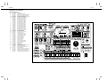
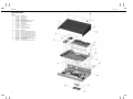
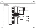
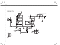
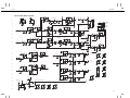
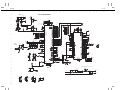
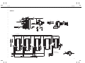
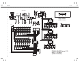
Feb, 1998
MC-505
SPECIFICATIONS
MC-505
Issued by RJA
TABLE OF CONTENTS
Page
SPECIFICATIONS•••••••••••••••••••••••••••••••••••••••••••••••••••••••••••••••••••••••••••••••••••••••••••••••••••••••••••••1
PANEL LAYOUT ••••••••••••••••••••••••••••••••••••••••••••••••••••••••••••••••••••••••••••••••••••••••••••••••••••••••••••2, 3
EXPLODED VIEW•••••••••••••••••••••••••••••••••••••••••••••••••••••••••••••••••••••••••••••••••••••••••••••••••••••••••••••4
PARTS LIST •••••••••••••••••••••••••••••••••••••••••••••••••••••••••••••••••••••••••••••••••••••••••••••••••••••••••••••••••5, 6
IDENTIFYING THE VERSION NUMBER •••••••••••••••••••••••••••••••••••••••••••••••••••••••••••••••••••••••••••••••••6
SAVING AND LOADING USER DATA ••••••••••••••••••••••••••••••••••••••••••••••••••••••••••••••••••••••••••••••••••••6
FACTORY PRESET•••••••••••••••••••••••••••••••••••••••••••••••••••••••••••••••••••••••••••••••••••••••••••••••••••••••••••7
TEST MODE•••••••••••••••••••••••••••••••••••••••••••••••••••••••••••••••••••••••••••••••••••••••••••••••••••••••••••••••8~12
UPGRADING THE FLASH ROM
SOFTWARE VERSION •••••••••••••••••••••••••••••••••••••••••••••••••••••••••••••••••••••••••••••••••••12
NOTICE ••••••••••••••••••••••••••••••••••••••••••••••••••••••••••••••••••••••••••••••••••••••••••••••••••••••••••••••••••••••••12
BLOCK DIAGRAM •••••••••••••••••••••••••••••••••••••••••••••••••••••••••••••••••••••••••••••••••••••••••••••••••••••••••••13
CIRCUIT BOARD •••••••••••••••••••••••••••••••••••••••••••••••••••••••••••••••••••••••••••••••••••••••••••••••••••••••14, 15
CIRCUIT DIAGRAM ••••••••••••••••••••••••••••••••••••••••••••••••••••••••••••••••••••••••••••••••••••••••••••••••••••16~24
D BEAM CONTROLLER
LOW BOOST
MAX
MIN
0
LPF
BPF
HPF
PKG
ON
OCTAVE
MIN
FILTER/AMPLIFIER
PITCH
WAVE
SELECT
NEXT
CURRENT
TURNTABLE
CUT+
RESO
AD LIB
MAX
CUTOFF
COARSE TUNE
FINE TUNE
SONG
ARPEGGIATOR
PLAY QUANTIZE
MODE
RND PAN
ENVELOPE
T1
T2
T3
AMP
DISPLAY
ON
TIMING
ACCENT RATE
VELOCITY
RANGE
DELAY
TEMPO
/MIXER
PTN/
SONG
PTN
SET
BANK
RPS
SET
PRESET USER
PATCH
REVERB
CARD
DELAY
EFX
DEPTH
DEPTH
EFX
LEVEL
PART MIXER
DEC
A
D
S
INC
RATE
R
PORTAMENTO
PAGE
ON
PAN
KEY SHIFT
DELAY TIME
CTRL 1
FEEDBACK
EFX DELAY LEVEL
CTRL 2
REVERB LEVEL
DELAY LEVEL
EFX OUTPUT LEVEL
EFX/OUT
TIME
MEGAMIX
CTRL 3
PART
SELECT
UNDO/
REDO
QTZ SELECT
PART
MUTE
SEQUENCER
MUTE CTRL
BWD
/TIE
VALUE
INITIALIZE PARAM COPY
TONE RHYTHM
MUTE
SELECT
KEYBOARD PAD
BD
SD
HH
CLP
CYM TOM/PERC
TONE SWITCH
SCALE
HIT
STOP
TONE SELECT
FWD
/REST
MEASURE
ENTER
EXIT
OTHERS
PLAY
REC
Arpeggiator
Others
EDIT
13
14
15
16
CARD
DUMP
REALTIME ERASE
SHIFT
TAP
PTN/SONG
COPY
ERASE
DELETE
INSERT
TRANSPOSE
ARPEGGIO
GRID
GROOVE
SHUFFLE
REVERB
DELAY
WAVE/FXM
PITCH
F-ENV
LEVEL
PLAY QUANTIZE
PATCH
P-ENV
PITCH
CHG VELO CHG GATE SHIFT CLK DATA THIN QUANTIZE
EFX
SEQ OUT
FILTER
PAN
A-ENV
RECLOCK
TUNE/SOUND CONTROLLER SEQUENCER
SETUP
FILTER
MIDI
MEMORY INFO
SYSTEM
LFO 2
LFO 1
AMPLIFIER
LFO
COMMON
SOLO/PORTA
COMMON
MOD
PITCH BEND AFTER TOUCH
RHY TONE
CONTROL
Copyright c 1998 by ROLAND CORPORATION
All rights reserved. No part of this publication may be reproduced in any form without the written permission of
ROLAND CORPORATION.
17059911
Effect
Play Quantize
DEMO
12
RPS
●Control Knob
Part Mixer
Realtime Modify
SOLO
DELAY
REVERB TIME
HF DAMP
EFX REVERB LEVEL
PTN
CALL
●DBeam Controller
CATEGORY
REVERB
TRANSPOSE
●Power Consumption
15W
Printed in Japan (CR) AD00 1
●Dimensions
462(W) x 320(D) x 110(H) mm
18-3/16(W) x 12-5/8(D) x 4-3/8(H) inches
●Weight
5 Kg / 11 lbs 1 oz
●Accessories
Owner's Manual Set(English)
Owner's Manual Set(Japanese)
Card Protector
AC Cord
100V
117V
230V EU
230V E
240V A
●Options
Stereo Headphones
Pedal Switch
Audio Connection Cable
MIDI Cable
SmartMedia
R, 1, 2, 3, 4, 5, 6, 7
Cutoff, Resonance,
LFO Depth, Coarse Tune,
Envelope(Depth, Attack,
Decay, Sustain, Release)
Portament Time
Reverb, Delay, EFX
Timing, Velocity
Grid, Groove (71types), Shuffle
Accent Rate(53 styles)
Low Boost, Master Volume
16 characters x 2
7 Segments, 6 Digits(LED)
●Power Supply
AC100V(50/60Hz), AC117V, AC230V, AC240V
28 types
FILTER
FUNC
HOLD
8 + Mute Ctrl
50
248
466
200 (Max)
200 (Max)
approx. 95,000 notes (Internal)
approx. 220,000 notes (2M Card)
approx. 480,000 notes (4M Card)
60
30
20.0 - 240.0 (Max)
96 ticks per quarter note
Realtime, Step1, Step2
T4
SHUFFLE
OCTAVE
RPS Set
Pattern Set
Tempo
Resolution
Recording Method
●Display
LCD
PITCH
GROOVE
WRITE
TONE PAN
LFO 1
SELECT
SLAVE
GRID
REVERB
●Sequencer
Tracks
Songs
Preset Patterns
RPS Patterns
User Patterns
Card Patterns
Note Storage
64 voices
24 Parts (Main:8 + RPS:16)
Reverb, Delay, EFX (24 types)
Preset:512, User:256, Card:512
Preset: 26, User: 20, Card: 20
RESONANCE
TONE LEVEL
MIDI
PTN
●Tone Generator
Maximum Polyphony
Parts
Built-in Effects
Patches
Rhythm Set
●Connectors
Mix Output Jack L(MONO), R
Direct Output Jack 1 L(MONO), R
Direct Output Jack 2 L(MONO), R
Headphone Jack (stereo)
MIDI Connectors (in, out)
Foot Control Jack
Memory Card Slot
AC Inlet
MEMORY CARD
VOLUME
●Keyboard Pad
16 keys
MC-505
(PNo.71010678)
(PNo.71010601)
(PNo.01346312)
(PNo.00894367)
(PNo.00894378)
(PNo.00894389)
(PNo.00907001)
(PNo.23495124)
RH-20/80/120
DP-2/6, BOSS FS-5U
PJ-1M
PCS-075W/150W/250W
MSC15/25/50
S2M-5/S4M-5
Feb, 1998
MC-505
LOCATION OF CONTROLS
FRONT VIEW PARTS LIST
No.
Part Number Part Name
q~e 01343112
J R-KNOB MF BLK/LCG
q
01013545
ROTARY POT. RK09L12D0 10KBX2
w
01013556
ROTARY POT. RK09L1140 10KB
e
01342545
ROTARY POT. RK09L1140 10KB with click
r~!6 01343478
TACT SWITCH SKQNAE
r~!3 00560745
LED (Green) SLR-325MCT31
00348490
LED (Red) SLR-325VCT31
r
00900145
D S-KEYTOP SD1H BLK
t
00900189
D S-KEYTOP SX1H BLK
y
01012978
D S-KEYTOP SX1H MCG
u
01129767
D S-KEYTOP SX1H DRD
i
00900156
D S-KEYTOP SD2H BLK
o
01343189
D S-KEYTOP SX2H LCG
!0
00904256
D S-KEYTOP SX4H BLK
!1
22495277
D S-KEYTOP MD1H BLK
!2
22495344
D S-KEYTOP MD1H RED
!3
00125734
D S-KEYTOP MD1H LCG
!4
22495274
D S-KEYTOP MX1H BLK
!5
00125723
D S-KEYTOP MX1H LCG
!6~!7 01125890
D S-KEYTOP SD1H-A CLR
!6
01232201
TACT SW. SKHJGS
!7
01232212
TACT SW. SKHJGR
!8~@0 00125590
TACT SW. EVQ QJJ 05Q
!9~@0 01348623
LED SLR-56VCT32
!8
22495371
T S-KEYTOP MX1H BLK
!9
01013356
T S-KEYTOP MD1H LCG
@0
22495372
T S-KEYTOP MD1H BLK
@1
01342490
LED SLZ-290B-17-T1
@2
01342489
LED SLZ-190B-17-T1
@3
01348634
LED SLR-56MCT32
@4
01348623
LED SLR-56VCT32
@5
00897289
LED SML1216W
@6
01343223
LCD UNIT DM1628-0AAB
@7
01342534
7-segment LED SL-9351S
@8
01343078
DISPLAY COVER
@9~#0 01343090
LED SPACER
@9
01341623
LED TLN201
#0
01342578
PHOTO DIODE TPS708
#1
01343089
D-BEAM CONTROLLER ESCT BLK
#2
01345912
F S-KNOB S BLK LCG
01342134
SLIDE POT. EWA NKE C10 B14
#3~#4 01346112
MOLD KNOB BLK
#3
01343312
SLIDE POT. RS25111C6 10KB L=15
#4
01343301
SLIDE POT. RS25111A6 10KB L=15
#5
22485303
D R-KNOB L BLK 248-303(knob)
01013223
ROTARY ENCODER EVQ VEM F01 24B
29 30
VOLUME
D BEAM CONTROLLER
LOW BOOST
1
MAX
MIN
MAX
4
FILTER/AMPLIFIER
PITCH
WAVE
SELECT
NEXT
25
0
LPF
BPF
3
21
6
OCTAVE
MIN
CURRENT
TURNTABLE
CUT +
RESO
AD LIB
1
22
MEMORY CARD
28
31
ON
23
16
ARPEGGIATOR
PLAY QUANTIZE
MODE
GRID
2
22
VELOCITY
REVERB
26
ACCENT RATE
SLAVE
T2
T3
T4
24
DISPLAY
RANGE
DELAY
22
EFX
TEMPO
/MIXER
17
4
2
PTN/
SONG
PTN
SET
RPS
SET
PRESET USER
PATCH
REVERB
DELAY
19
19
4
8
LEVEL
8
DELAY TIME
CTRL 1
FEEDBACK
EFX DELAY LEVEL
CTRL 2
REVERB LEVEL
DELAY LEVEL
EFX OUTPUT LEVEL
UNDO/
REDO
7
5
QTZ SELECT
19
OCTAVE
8
32
PART MIXER
DEC
D
A
PART
MUTE
32
32
32
32
32
INC
32
TRANSPOSE
8
PORTAMENTO
9
ON
4
CATEGORY
32
5
DEPTH
RATE
PAGE
2
4
TIME
MEGAMIX
35
SEQUENCER
MUTE CTRL
17
17
17
17
17
17
BD
SD
HH
CLP
CYM TOM/PERC
16
16
16
16
16
4
TONE SWITCH
SCALE
17
16
17
17
HIT
OTHERS
EXIT
16
16
15
BWD
/TIE
VALUE
TONE SELECT
FWD
/REST
10
15
STOP
DEMO
14
PLAY
11
EDIT
13
12
13
14
15
16
20
19
19
20
19
REALTIME ERASE
PTN
CALL
8
RPS
SHIFT
19
19
20
COPY
ERASE
DELETE
INSERT
TRANSPOSE
ARPEGGIO
GRID
GROOVE
SHUFFLE
REVERB
DELAY
WAVE/FXM
PITCH
F-ENV
LEVEL
19
20
19
19
20
19
20
19
18
15
TAP
PTN/SONG
PLAY QUANTIZE
PATCH
P-ENV
PITCH
2
CHG VELO CHG GATE SHIFT CLK DATA THIN QUANTIZE
EFX
SEQ OUT
PAN
A-ENV
FILTER
AMPLIFIER
RECLOCK
TUNE/SOUND CONTROLLER SEQUENCER
SETUP
FILTER
MIDI
MEMORY INFO
CARD
DUMP
SYSTEM
LFO 1
LFO 2
LFO
COMMON
SOLO/PORTA
COMMON
MOD
MEASURE
ENTER
14
HOLD
5
R
EFX/OUT
4
4
S
SOLO
TONE RHYTHM
MUTE
SELECT
22
DEPTH
6
4
KEYBOARD PAD
34 34 34 34
DELAY
22
PART
SELECT
INITIALIZE PARAM COPY
3
22
EFX
9
REVERB
21
CTRL 3
33
CARD
KEY SHIFT
5
2
REVERB TIME
HF DAMP
EFX REVERB LEVEL
WRITE
22
FILTER
BANK
PAN
2
TONE PAN
LFO 1
SELECT
AMP
FUNC
5
RESONANCE
TONE LEVEL
PITCH
T1
24
ON
TIMING
ENVELOPE
2
SHUFFLE
CUTOFF
RND PAN
MIDI
PTN
5
GROOVE
5
COARSE TUNE
FINE TUNE
SONG
2
PKG
-
4
23
27
2
HPF
PITCH BEND AFTER TOUCH
CONTROL
RHY TONE
REC
12
MC-505
Feb, 1998
REAR VIEW PARTS LIST
No.
Part Number Part Name
q
12499175
G S-BUTTON S1H BLK
13129160
PUSH SW. SDDLB1-B-D-2 TV-5 5A/250V
w
00125023
AC INLET PWI1818 (INL-7) 10A/250V 3P
e
01341178
CARD CONNECTER CN015S-3013-0
01343101
CARD ESCUTCHEON D C-ESCT BX1H BLK
r
13429825
MIDI JACK YKF51-5054
t
22150756
JACK NUT 2
y
13449283
JACK HLJ7101-01-3010
u
13449284
JACK HLJ7001-01-3010
CAUTION
RISK OF ELECTRIC SHOCK
DO NOT OPEN
ATTENTION:
RISQUE DE CHOC ELECTRIQUE NE PAS OUVRIR
TO REDUCE THE RISK OF FIRE OR ELECTRIC SHOCK,
DO NOT EXPOSE THIS APPLIANCE TO RAIN OR MOISTURE.
1
S2M-5/S4M-5
THIS CLASS B DIGITAL APPARATUS MEETS ALL REQUIREMENTS OF THE CANADIAN INTERFERENCE-CAUSING EQUIPMENT REGULATIONS.
CET APPAREIL NUMÉRIQUE DE LA CLASSE B RESPECTE TOUTES LES EXIGENCES DU RÈGLEMENT SUR LE MATÉRIEL BROUILLEUR DU CANADA.
THIS DEVICE COMPLIES WITH PART 15 OF THE FCC RULES. OPERATION IS SUBJECT TO THE FOLLOWING TWO CONDITIONS: (1) THIS DEVICE MAY NOT CAUSE HARMFUL
INTERFERENCE, AND (2) THIS DEVICE MUST ACCEPT ANY INTERFERENCE RECEIVED, INCLUDING INTERFERENCE THAT MAY CAUSE UNDESIRED OPERATION.
WARNING:
2
3
4
5
The DBeam has been licensed from Interactive Light, Inc.
6
7
3
Feb, 1998
MC-505
EXPLODED VIEW
[PARTS]
No.
q
w
e
r
t
y
u
i
o
!0
!1
!2
Part Cord
12359139
01343067
01450512
71010656
01451678
71013567
01343123
71010634
01125890
01343056
01343223
01343078
Part Name
Foot FF-018 BLK
Bottom Cover
Wiring Power
Inlet Board Assy
Switching Regulator KW1AA265
Main Esct Set (Main Board)
PWB Holder
Panel Esct Set
DS-Keytop SD1H-A CLR
Top Panel
LCD DM 1628-OAAB
MC-505 Display Cover
No.
a
b
c
d
e
f
g
h
i
j
Part Cord
40011045
40011056
40011067
40011090
40238501
40011201
40230978
40011490
22150756
40011745
Part Name
Binding Tap tight B 2x6mm ZC (x4)
Binding Tap tight B 3x6mm ZC (x29)
Binding Tap tight B 3x8mm ZC (x3)
Binding Tap tight B 3x6mm BZC (x10)
Binding Tap tight P 4x8mm BZC (x2)
Pan Tap tight P 3x8mm BZC (x4)
Binding Evatight CE 4x12mm BZC (x1)
Sems 3x6mm BZC (x3)
Jack Nut 2 (x8)
M4 Nut with Spring Washer ZC (x1)
4
Feb, 1998
MC-505
PARTS LIST
SAFETY PRECAUTIONS:*2
The parts marked ! have
safety-related characteristics.
Use only listed parts for
replacement.
CONSIDERATIONS ON PARTS ORDERING
When ordering any parts listed in the parts list, please specify the following items in the order sheet.
QTY
PART NUMBER
DESCRIPTION
MODEL NUMBER
Ex.
10
22575241
Sharp Key
C-20/50
15
2247017300
Knob (orange)
DAC-15D
Failure to completely fill the above items with correct number and description will result in delayed or
even undelivered replacement.
#
#
#
#
#
NOTE1:The parts marked # are new.(initial parts)
NOTE2:The parts marked ! have safety-related characteristics.
Use only listed parts for replacement
01343056
01343067
01343078
01343134
01343145
12359139
15329104
15309101
15319101
15319105
15329507
15329503
15329511
15329502
15129151
15129427
00785945
15119163
MC-505 TOP PANEL
MC-505 BOTTOM COVER
MC-505 DISPLAY COVER
MC-505 POT DUST COVER A
MC-505 POT DUST COVER B
FOOT FF-018 BLK
CHASSIS
#
01343123
#
#
#
#
D S-KEYTOP MX1H LCG
D S-KEYTOP MD1H LCG
D S-KEYTOP SD1H BLK
D S-KEYTOP SD2H BLK
D S-KEYTOP SX1H BLK
D S-KEYTOP SX4H BLK
D S-KEYTOP SX1H MCG
D S-KEYTOP SX1H DRD
D S-KEYTOP SX2H LCG
D S-KEYTOP MX1H BLK
D S-KEYTOP MD1H BLK
D S-KEYTOP MD1H RED
D S-KEYTOP SD1H-A CLR
G S-BUTTON S1H BLK
MOLD KNOB BLK
D R-KNOB L BLK 248-303
J R-KNOB MF BLK/LCG
F S-KNOB S BLK LCG
T S-KEYTOP MX1H BLK
T S-KEYTOP MD1H BLK
T S-KEYTOP MD1H LCG
light gray
light gray
black
#
gray
red
#
13129160
01232212
01232201
00125590
01343478
red
clear
Power SW
Envelope
Encoder
round knob
center fader
Tap
Keypad
Keypad
#
#
#
SDDLB1-B-D-2 TV-5 5A/250V
SKHJGR
SKHJGS
EVQ QJJ 05Q
SKQNAE
power
push SW with green LED
push SW with orange LED
push SW for keypads
push SW
SW6 on IB
SW3,46-53 on PB
SW9-12,29-34 on PB
SW67-83 on PB
SW1,2,4,5,7,8,SW13-28, 38-45,54-66,SW84-86 on PB
YKF51-5054
HLJ7001-01-3010
HLJ7101-01-3010
MIDI
PHONES
PEDAL,OUTPUTs
JK8 on MB
JK6 on MB
JK1-5,7,9 on MB
DM1628-0AAB
SL-9351S
LCD unit
7 segment
D8,9 on PB
DISPLAY UNIT
#
#
01343223
01342534
CPU
TG
Gate Array
Wave Memory
Preset Data
User Data
Program
OpAmp
TR Array
2SK368-GR
2SA1037KR
2SC2412KR
2SC3326A
DTA114EK
DTA124EK
DTC114TK
DTC124EK
2SC1815-GR
2SC2235-Y
RN1224
RN2227
FET
Q33 on MB
Q13,22,30 on MB
Q30 on MB
Q3-12,31,32,35,36 on MB
Q26,27,29 on MB
Q16,20 on MB
Q34 on MB
Q17 on MB
Q5 on PB
Q10 on PB
Q19-26 on PB
Q1-4,6-9,11-18,27-29 on PB
#
#‰
71013567
MAIN ESCT SET
NOTE1:MAIN ESCT SET includes the following parts
#
********
01343101
#
#
#
#
#
71010634
PANEL ESCT SET
NOTE2:PANEL ESCT SET includes the following parts.
#
#
MAIN BOARD ASSY
D C-ESCT BX1H BLK
#
#
#
71010656
INLET BOARD ASSY
D2-5 on MB
DA11,12 on MB
DA3-6,8-10,13-16 on MB
D5 on PB
D13,14,17,18,21,33,35,37, D43-53,56,58,61-64,D67,73,
74,77-90,93-106,D113,114, 116-119,D140-149,D
152-163 on PB
01341623
00897289
00560745
00348490
TLN201 Infrared
SML1216W
SLR-325MCT31
SLR-325VCT31
D4 on PB
Bi-colored
green
red
01348634
01348623
01342489
SLR-56MCT32
SLR-56VCT32
SLZ-190B-17-T1
green
red
red
01342490
SLZ-290B-17-T1
green
D6 on PB
D108 on PB
D15,16,36,38-42,D57,68,75,76,91,92,D109-111.121-123,
150,151 on PB
D19,20 on PB"
D22,23,124-139 on PB
D1,7,11,12,24-32,34,D55,59,60,65,66,69-72,D107,112,
115,120 on PB
D2,3,10,54 on PB"
EXBV8V101JV
EXBV8V103JV
RCE9A103JAG7A
MCR50-101J
MCR50JZH470
RGLD8X103J
RGLD8X104J
Quad ladder
Quad ladder
Octal array
1/2W
1/2W
Octal array
Octal array
RA8-12,20-22,24-29 on MB
RA30-33 on MB
RA13,17-19,23 on MB
R363,364 on MB"
R186,187,204,205 on MB
RA2 on PB
RA1,3 on PB
25mm slide
25mm clicked
30mm slide
VR1 on MB
VR4-7,14-17 on PB
VE3,13 on PB
VR1,2 on PB
VR9-12 on PB
VR8 on PB
VR18-25 on PB
00126112
15409113
15399965
15399926
15399952
13919140
13919142
POTENTIOMETER,TRIMMER
#
T S-KEYTOP MX1H BLK
T S-KEYTOP MD1H BLK
T S-KEYTOP MD1H LCG
D-BEAM CONTROLLER ESCT BLK
LED SPACER
DAN202K
DAP202K
DA204U
TPS708 Photo Diode
MA165
13299206
01013556
01342545
01013545
01343301
01343312
01342134
ENVD8AA03B24
RK09L1140 10KB
RK09L1140 10KB with click
RK09K12D0 10KBX2
RS25111A6 10KB L=15
RS25111C6 10KB L=15
EWA NKE C10 B14
CAPACITOR
PCB ASSY
22495371
22495372
01013356
01343089
01343090
15339105
15339109
01121323
01342578
01014645
RESISTOR
JACK, SOCKET
13429825
13449284
13449283
Reset IC
Photo Coupler
DRAM 4Mbit
DRAM 16Mbit
LED
SWITCH
!
OpAmp
OpAmp
IC17 on MB
IC25 on MB
IC29 on MB
IC22 on MB
IC19 on MB
IC49 on MB
IC30,31,36-48,50, IC53,55,59 on MB
IC32 on MB
IC15,34 on MB
IC20 ON MB
IC10 on MB
IC8 on MB
IC23 on MB
IC24 on MB
IC1 on MB
IC3 on MB
IC2 on MB
IC9 on MB
IC7 on MB
IC5 on MB
IC4 on MB
IC3,4,7 on PB
IC1,5,6 on PB
IC10 on PB
IC8 on PB
IC2 on PB
IC9 on PB
DIODE
MC-505 PWB HOLDER
KNOB, BUTTON
00125723
00125734
00900145
00900156
00900189
00904256
01012978
01129767
01343189
22495274
22495277
22495344
01125890
12499175
01346112
22485303
01343112
01345912
22495371
22495372
01013356
TC7W04F
TC7W08F
TC7W74F
TC74HC245AF
TC74HC393AF
M5218AFP
UPC4570G2
TA78L05F +5V Regulator
M51953BFP
PC-410X
TC514260DJS-60
UPD4218160LE-60
TC74HC175AF
TC74HC32AF
HD6437042AE11F
RA01-005
M60205-0601FP
LHMNOPNH
UPD23C16000WGY-835-MKH
LH28F800SUT-70
LH28F800SUT-70
TC74HC4051AP
TC74HC138AP
TC74HC245AP
TC74HC574AP
UPC4570HA
TD62593AP
TRANSISTOR
CASING
#
#
#
#
#
15249121
00127490
00232634
15259778T0
15259809T0
15189261
15289105
15289402
15199937
15289125
01126612
00893312
15259758T0
15259716T0
01342423
00897078
00343823
01342401
01454634
00899812
00899812
15169596
15169550T0
15169552T0
15169556T0
15189189
00456856
00236545
00239601
00239434
00239490
00236301
00239534
00239578
00236378
AMZV0050J224 0200
AMZV0050J104 0200
AMZV0050J182 0200
AMZV0050J103 0200
AMZV0050J222 0200
AMZV0050J223 0200
AMZV0050J473 0200
AMZV0050J822 0200
C120,127 on MB
C117,121,124,203,328,C333,335 on MB
C128,144,152,160,170,C330 on MB
C7 on PB
C123,135,147,156,165,C174 on MB
C122,129 on MB
C118,125,205 on MB
C202 on MB
INDUCTOR,FILTER
00903167
12449355
N2012Z601T02
FBR07HA850TB00
SMD
Ferrite bead
L7-10,13-16,23-27 on MB
L1 on PB
MA-406 24.576MHz
MA-406 7.056MHz
for TG
for CPU
X2 on MB
X1 on MB
EVQ VEM F01 24B
EN1 on PB
52806-1410
B7B-XH-A
52147-1010
52147-1110
52147-1210
52147-1310
53253-0410
FFC Connector
CRYSTAL OSCILLATOR
#
00901912
01126267
ENCODER
01013223
IC
15259709T0
15259720T0
15289714
00346490
15249104
15259885
15249111
00233756
CONNECTOR
TC74HC10FAF
TC74HC74AF
UPD63200GS
TC3W01F
TC7S04F
TC7S32F
TC7WU04F
TC7W02F
DAC
IC18 on MB
IC35 on MB
IC11-13 on MB
IC21,28 on MB
IC52 on MB
IC56 on MB
IC14,26 on MB
IC57 on MB
#
#
00904612
13369592
13369605
13369606
13369607
13369678
13369926
CN4 on MB
CN9 on MB
CN1,6 on MB
CN7 on MB
CN8 on MB
CN5 on MB
CN2 on MB
5
Feb, 1998
MC-505
01341178
13429299
13429300
13429301
13429317
CN015S-3013-0
51048-1000
51048-1100
51048-1200
51048-1300
Card Connector
CN3 on MB
CN3,5 on PB
CN6 on PB
CN7 on PB
CN1 on PB
WIRING,CABLE
#
#
#
#
#
#
#
#
00890390
00890423
00890601
01450756
01450767
01450501
01450512
01450523
01232978
RIBBON CABL 10X100-P2.0
RIBBON CABL 10X300-P2.0
RIBBON CABL 11X300-P2.0
RIBBON CABL 12X300-P2.0
RIBBON CABL 13X200-P2.0
MC-505 WIRING INLET
MC-505 WIRING POWER
MC-505 WIRING BEAM
TD-10 WIRING GND
MB-PB
MB-PB
MB-PB
MB-PB
MB-PB
IB-PS
PS-MB
PB-MB
Inlet-Chassis
POWER SUPPLY UNIT
#
01451678
KW1AA265
PWI1818 (INL-7) 10A/250V 3P
#
01343156
40018512
40236612
CPU
DATA
CPU Version=1.00
Bld=022 97/08/18
SAVING AND LOADING THE USER DATA
Binding Taptight B 2*6mm ZC
Binding Taptight B 3*6mm ZC
Binding Taptight B 3*8mm ZC
Binding Taptight B 3*6mm BZC
Binding Taptight P 4*8mm BZC
Pan Taptight P 3*8mm ZC
Pan Taptight P 3*8mm BZC
Binding Evatite CE 4*12mm BZC
Sems 3*6mm BZC
JACK NUT 2
M4 NUT with Spring washer ZC
* You can save the user data to a memory card (=SmartMedia).
Before perform the data saving, you must format a memory card by
using the following procedure.
PACKING CASE
#
#
SYSTEM
JK1 on IB
SCREW
40011045
40011056
40011067
40011090
40238501
40011189
40011201
40230978
40011490
22150756
40011745
1. Turn the power on.
2. While holding [TEMPO/MIXER], [PTN/SONG] and [PATCH], press
keyboard pad [12],[14] and [16] in order.
3. The system program version will be displayed.
Every time press the keyboard PAD [16] , readout on the display
changes as follows.
SYS Version=1.00
Bld=100 97/12/05
Switching Regulator
AC INLET
00125023
IDENTIFYING THE VERSION NUMBER
S Format a Memory Card (SmartMedia)
MC-505 PACKING CASE
VINYL BAG 0.03*50*60
VINYL BAG MIRROR MAT 0.5*600*460
1. Insert a memory card (2MB or 4MB type) into the memory card slot.
MISCELLANEOUS
#
#
#
#
#
#
13459171
00453223
01346312
01343089
01343090
01343101
01450734
01450745
12199584
RCS00000C
LED SPACER LDS-70G
MC-505 CARD PROTECTOR
D-BEAM CONTROLLER ESCT BLK
LED SPACER
D C-ESCT BX1H BLK
JACK LEAF
QFP HEATSINK
M1698 Grounding terminal
Test terminal
TP1,2 on MB
D4,5 on PB
DBeam
on PB
on PB
on MB
JK1,3 on MB
Card escutcheon
covering
2. Hold down [SHIFT] and press keyboard pad [15].
This takes you to the screen for formatting cards.
CARD:Format
Are You Sure ?
ACCESSORIES(Standard)
#
#
00894367
00894378
00894389
00907001
23495124
71010678
71010601
AC CORD SET 100V
AC CORD SET 120V
AC CORD SET 230V
AC CORD SET 240VE
AC CORD SET 240VA
Owner's Manual set
Owner's Manual set
SP18A+IS14 VCTF2X.75
SP301+IS14 SJT18/3
SP22+IS14 H05VV-F3G1.0
KP-610,GTBS-3,KS-31A
SC-114-J01 ES303-10HMA
English
Japanese
3. Press [ENTER].
The following display will appear, and the format operation will be
carried out.
Processing...
Keep Power ON !
4. When formatting ends, the following display will appear.
CARD:Format
Complete !
5. Press [EXIT] to exit the setting page.
S Saving the user data (User Backup)
1. Hold down [SHIFT] and press keyboard pad [15]. You will enter the
CARD section's format page.
2. Press PAGE [>] to select the User Backup page.
CARD:User BackUp
Are You Sure ?
3. Press [ENTER].
The following display will appear, and the User Backup operation will
be carried out.
Processing...
Keep Power ON !
6
DAT Version=1.00
Bld=030 97/09/29
Feb, 1998
MC-505
4. When User Backup has been completed, the following display will
appear.
CARD:User BackUp
Complete !
FACTORY PRESET
1. Turn the power on while holding down the [SHIFT].
Display shows as follows.
FACTORY PRESET
ALL
5. Press [EXIT] to exit the setting page.
User Backup complete.
2. Press [ENTER] button to load the factory preset data.
NOTICE: It takes a few minutes to complete the data loading.
Never turn the power off during this procedure.
S Restoring the Saved Settings Back to Internal Memory (Backup Load)
* This operation loads the contents of a backup file that was saved on a
card block into internal memory.
1. Make sure that the memory card is inserted in the memory card slot.
To abort a command, press [EXIT] button.
2. Hold down [SHIFT] and press keyboard pad [15].
You will enter the CARD section's Format page.
3. Press PAGE [>] twice to select the Backup Load page.
CARD:BackUp Load
Are You Sure ?
4. Press [ENTER]. The following display will appear, and the Backup
Load operation will be carried out.
Processing...
Keep Power ON !
5. When Backup Load is completed, the following display will appear.
CARD:BackUp Load
Complete !
6. Press [EXIT] to exit the setting page.
Backup Load complete.
7
Feb, 1998
MC-505
9. Sound Test
10. DSP Test
11. LCD Test
TEST MODE
NOTICE: Before executing test mode, be sure to backup user data as
explained in the section "Saving and Loading user data". And
when you execute test mode, the various parameters will be
given special settings. After executing test mode, be sure to
load the Factory preset data, and the User data.
• Exiting the each Test item
Press [ENTER] while holding down [EXIT].
The test will be suspended and MC-505 return to basic test mode
display.
1. Memory Test
S Required items
1-1. Press [ENTER] in the basic test display. Memory Test will be started.
The following display will appear.
1-2. When the test of the each device end, display --- will change to "ok"
MIDI Cable
SmartMedia x2 (Formatted / Protected)
Foot pedal (DP-2 etc.)
Monitor Speaker (MA-12 etc.)
Prg Dat Usr
--- --- ---
Ram
---
or "NG".
If test result are OK, next test runs automatically.
2. MIDI Test
S Entering the TEST MODE
1. Connect the Monitor Speaker to the MIX OUT of the MC-505.
Troubleshooting for Memory test
Result of Test
Check
2. Turn the power on while holding down [DBeam TYPE], [DBeam ON]
and [FUNC].
You will enter the TEST MODE and the following basic display will
appear.
MC-505 Test Mode
Ver1.00
Prg NG!
Dat NG!
Usr NG!
Ram NG!
Check IC4 on MAIN BOARD
Check IC6 or IC7 on MAIN BOARD
Check IC5 on MAIN BOARD
Check IC8 on MAIN BOARD
When Memory Test ends normally, MIDI Test runs automatically.
( or in the initial display of the test mode, press keyboard Pad [2] while
holding down [SHIFT])
3. Press [ENTER].TEST MODE will be started.
2-1. When MIDI test starts, the following display appears.
As a rule, tests are in the order of test number, but you can select the
each test items directly by pressing the Keyboard pad [1] to [11] while
pressing [SHIFT] button.
2-2. Make a loop with MIDI cable that connects MIDI IN and MIDI OUT.
MC-505 Test MIDI
Connect
---
S Exiting the TEST MODE
When LCD Test ends, the following display appears.
( or in the initial display of the test mode, press keyboard Pad [16] while
holding down [SHIFT])
Factory Data Set
Ready ??
Does the LCD display "ok"?
2-3. Press [ENTER]. The system program version will be displayed.
2-4. And press the [ENTER] again. You can check the program version
MC-505 Test MIDI
SYS Version 1.00
Press [ENTER] button to load the factory preset data.
NOTICE: It takes a few minutes to complete the data loading.
Never turn the power off during this procedure.
To abort a command, press [BWD] button.
S Test Items
The MC-505 has the following 11 test items.
Some test items will be started automatically, when the next previous test
ends normally.
1. Memory Test
2.MIDI Test (Identifying the program version)
3.Card Test
4.Pedal Test
5. SW/LED Test
6. Encoder Test
7. A/D Test
8. DBeam Test
8
number of the CPU and Preset Data.
2-5. Remove the MIDI cable.
Display shows " Disconnect ok", and then next test runs
automatically.
3. Card Test
Troubleshooting for MIDI test
Result of Test
"Connect ok" is not appeared
Check
Check IC52
Is the signal detects from PIN 1 and PIN 4 ?
Check IC20
Is the signal detects from PIN 2 and PIN 4 ?
Check Q16/17
Is the Low level signal detects from the base of Q16 ?
Feb, 1998
MC-505
5. SW & LED Test
When MIDI Test ends normally, Card Test runs automatically.
( or in the initial display of the test mode, press keyboard Pad [3] while
holding down [SHIFT])
When Pedal Test ends normally, SW & LED Test runs automatically.
( or in the initial display of the test mode, press keyboard Pad [5] while
holding down [SHIFT])
3-1. When Card test starts, the following display appears.
3-2. Insert a card with write protected.
5-1. When SW & LCD test starts, the following display appears.
All the LEDs turning on?
Card Protect--Read/Write
---
SW & LED Test
off
Remove the card once, and insert the card with not write protected.
Does the LCD display "ok"?
4. Pedal Test
Troubleshooting for Card test
Result of Test
Check
No response
Check IC25(Pin 1/2/7), IC57(Pin 3)
If the Card is inserted, Voltage of IC25 Pin 1 becomes high level.
Protect NG!
Check R1, IC1
Is the voltage of CWPSNS Low level?
Read/Write NG!
Check IC24(Pin 3/6)
Is the level of XCWR/XCRE change during the test?
5-2. Press all the buttons one by one. Then each names of buttons
appear on the display.
And buttons that have corresponding LEDs are put out its LEDs.
Press all the buttons for turning off the all LEDs.
To check the 7 segment LED and Beat LED, use [WAVESELECT]
button.
Check that the segment light in order, and Beat LED turns RED and
Green.
Is button name appeared on the display?
Are all the LEDs turning off?
5-3. If test ends normally, press [ENTER] to start next test.
Check IC22, RA19
Is there something wrong with card bus ?
Troubleshooting for the SW & LED Test
Result of Test
Check
Check IC24(Pin 8)/IC23
Is there something wrong with decoder?
One of the LEDs does not lit.
Check the condition of connection of LED
Two or more LEDs do not lit.
Refer to the circuit diagram, check the transistor, buffer(74HC245),
or decoder(74HC138) around the LED circuitry.
Check the IC25(PIN 3,Write)
Is the voltage of WP high level?
One of the SWs does not work. Check the diode and condition of connection of SW
When Card Test ends normally, Pedal Test runs automatically.
( or in the initial display of the test mode, press keyboard Pad [4] while
holding down [SHIFT])
To or more SWs do not work.
Refer to the circuit diagram, check the decoder and transistor array.
LED stays on.
Check the short circuit of signal lines of LED.
6. Encoder Test
4-1. When Pedal test starts, the following display appears.
4-2. Connect the Foot Pedal to the Pedal Jack.
Pedal Test
off
When Switch and LED Test ends normally, Encoder Test runs
automatically.
( or in the initial display of the test mode, press keyboard Pad [6] while
holding down [SHIFT])
6-1. When Encoder test starts, the following display appears.
Encoder Test
val= 0
4-3. Step on a Pedal. And check that "on" have been displayed.
4-4. Foot off the Pedal. And check that "off" have been displayed.
6-2. Rotate the encoder clockwise slowly. Check that the" val" changes
from 0 to +24.
4-5. Pedal test ends and next test runs automatically.
Troubleshooting for the Pedal Test
Result of Test
Check
No response
Display remains
"on"
Check Q20 / Is signal level of the PEDAL change?
6-3. Rotate the encoder counterclockwise slowly. Check that the" val"
changes from +24 to -24.
NOTE: To prevent the error, not to rotate the encoder fast.
Display remains "on" Check the condition of connection of L27, R224/225
6-4. When encoder test ends, "OK" appears on the display.
6-5. If test ends normally, press [ENTER] to start next test.
9
Feb, 1998
MC-505
Troubleshooting for the Encoder Test
Result of Test
Check
Troubleshooting for DBeam Test
Result of Test
"val" does not change MAIN BOARD IC17 ; Is puls generated ?
Check the condition of connection of R278-283,C284/285 on the
MAIN BOARD
Error result even if rotate
the encoder slowly
check the encoder
The value appears on the 7seg-LED, Make an adjustment to DBeam controller with reference to [Adjusting DBeam
controller](page **).
even if not passing your hand over
the DBeam controller.
7. AD Test
The value not appears on the 7segLED, even if passing your hand
over the DBeam controller.
The value does not reach to 127,
even if move your hand closer to the
DBeam controller.
When Encoder Test ends normally, AD Test runs automatically.
( or in the initial display of the test mode, press keyboard Pad [7] while
holding down [SHIFT])
Check
Check IC18,IC19 on the main board.
Is pulse detected from PULSE, DBPLS?
Check IC50,IC59,Q33 on main board.
The value does not reach to 127, even if move your hand closer to the DBeam controller.
When passing your hand over the DBeam controller, is potential of the pin 1 of IC50 change ?
Is signal detected from pin 3 of IC59 ?
Check the condition of connection of CN2 on main board.
And Inspect the CN2 on the main board for breaks.
7-1. When AD test starts, the MC-505 goes into standby mode.
Move each knob, name and value of the knob are displayed.
Move all the knobs and sliders fully one by one. (excluding
"VOLUME" and LOW BOOST)
Is pulse detected from Input and Output of the IC2 on the panel board.
Check D4,D5 of the panel board.
Is a driving circuit of D4 work?
In the case of D4 is drive correctly and no signal detected from IC2, probably D5 is broken.
NOTE: To prevent the error, not to move the knobs or slider
simultaneously.
Check that the value changes 0 from 127.
7-2. When test ends, press [ENTER] to start next test.
9. Sound Test
Troubleshooting for the AD Test
Result of Test
Check
No response
Inspect the signal path of AMUX0, AMUX1, AMUX2 for breaks or short circuit.
Value does not reach the 0 or 127 Check the power supply of the panel
Check the analog switches (74HC4051;IC3,4,7 on PB)
Inspect the capacitor that is attached to the potentiometer for short circuit
Error result even if move the knob
or slider one by one
Inspect the signal path of the potentiometer for short circuit
Check analog switch whether signal of AN0/1/2 are not corrupted.
8. DBeam Test
When AD Test ends normally, DBeam Test runs automatically.
( or in the initial display of the test mode, press keyboard Pad [8] while
holding down [SHIFT])
8-1. When passing your hand over the DBeam controller, the value
appears on the 7-segment LED.
Raise or lower your hand. Check that the value changes 0 from 127.
8-2. When test ends, press [ENTER] to start next test.
9-1. Rotate the VOLUME knob fully clockwise, and rotate the LOW
BOOST knob fully counterclockwise.
9-2. Connect the Monitor to the MIXOUT Jack of the MC-505. And also
connect the Headphone to the PHONES Jack. In the case of you
use one Monitor, be sure to insert the opened plug into the another
channel of the Mix output to obtain the correct wave form.
Verify the waveform being output by the oscilloscope, and check the
sound.
9-3. When sound test starts, sound output from L ch of the MIXOUT and
Headphone.
Every time press the [ENTER], output channel is switched.
At first, MC-505 output sinusoidal wave from each jacks, and next
square wave form is output.
Change the connection of the monitor to corresponding jack.
Pitch of the sound is deferent depends on each jack.
Verify that no undesired sound is heard.
Verify that no undesired waveform or voltage detected.
Start
press [ENTER]
•
•
•
•
press [ENTER]
•
•
•
•
•
MIXOUT /L
MIXOUT /R
DIRECT1/L
DIRECT1/R
DIRECT2/L
DIRECT2/R
MIXOUT /L
MIXOUT /R
DIRECT1/L
DIRECT1/R
DIRECT2/L
DIRECT2/R
sinusoidal wave
sinusoidal wave
sinusoidal wave
sinusoidal wave
sinusoidal wave
sinusoidal wave
square wave
square wave
square wave
square wave
square wave
square wave
9-4. Connect the monitor to the MIXOUT, and press [ENTER].
Sinusoidal wave sound output from the center.
10
Feb, 1998
MC-505
9-5. Rotate the LOW BOOST knob fully clockwise.
Next press [OCTAVE] located near the LOW BOOST knob.
Verify that no undesired sound is heard.
Verify that no undesired waveform or voltage detected.
9-6. When test ends, press [ENTER] to start next test.
Troubleshooting of the Sound Test
Result of Test
Check
No sound
Check D/A converter (uPD63200;IC11-13)
Check around the power supply, digital signal, filter circuitry.
If OP-Amp is heated, probably it is broken.
Check the condition of connection and short circuit of capacitors and resistors.
Check around mute circuitry.
Control voltage of the 2SC3326(printed CCA)is normally -15V.
More than 4V detected from 6pin of IC34?
Sound is too loud,soft or distorted Check around filter circuitry.
Check the condition of connection and short circuit of the feedback resistor and ground resistor
Check around mute circuitry
Sound is too loud,soft or distorted
Check around filter circuitry.
Check the condition of connection and short circuit of the feedback resistor and ground resistor
Check around mute circuitry
10. DSP Test
square wave form is corrupted
treble is heavy
Check around filter circuitry
treble is heavy Check the condition of connection short circuit, and breaks of the capacitors.
OCTAVE sound output even if
indicator is not lit.
Or no sound output even if indicator
is lit.
Check Q31,Q32
Base resistor carries voltage of -15V in active, and +5 in inactive.
Check Q3,Q4
Is square wave of +5V/-15V input to base resistor ?
Check IC35
Is square wave output from pin 5 by the double frequency of
the square wave that input to pin 3.
Check IC45,Q1
Is square wave detected from collector of the Q1
Sample waveforms of Sound Test
When AD Test ends normally, DSP Test runs automatically.
( or in the initial display of the test mode, press keyboard Pad [10] while
holding down [SHIFT])
10-1. When DSP test starts, test runs automatically and 7 part are
checked.
If test result are OK, O appears on the display and if NG, X
appears on the display.
10-2. If test result is OK, press [ENTER] to start next test.
Troubleshooting for the DSP Test
Result of test
Check
"x" displayed
Check IC10
Bleak or etc.
Check IC3
Pin 119-143
11. LCD Test
When DSP Test ends normally, LCD Test runs automatically.
( or in the initial display of the test mode, press keyboard Pad [11] while
holding down [SHIFT])
11-1. When LCD Test starts, all the dots of the LCD will light.
Check that the contrast of the LCD changes by rotating the
encoder clockwise and counterclockwise.
When LOW BOOST and OCTAVE function are used.
11
Feb, 1998
MC-505
11-2. When test ends, press [ENTER].
Troubleshooting for the LCD Test
Result of Test
Check
One of the dot is not lit
Replace the LCD unit.
Contrast of the LCD is not changed
Contrast of the LCD is pale, even if
adjust its contrast maximum level.
Contrast of the LCD is dark , even if
adjust its contrast minimum level
Check R262
Is PWM waveform input to the QFP side of the R262?
than 16.)
While playing, a check sum appears on the display.
One=**** : Check sum of the each file.
Al=**** :
Total.
After all the files have been played, compare the original checksum
(described on disk label) with the current checksum for discrepancy.
MC-505 Sys-Verup
One=9244 Al=360F
Check IC31
Check the condition of connection of resistors and capacitors, and its input / output voltage.
Make hot and cool TH1, if the bounds of the contrast change
is large, there is a possibility that the component is broken
Check DA8
Is there short in the circuit ?
If the above check points are normal, replace the LCD unit.
Test Mode complete.
UPGRADING FLASH ROM SOFTWARE VERSION
MC-505 uses the FLASH MEMORY. So the program can be update the
program by transferring the data from the upgrading disk (SMF format),
through MIDI.
NOTICE : Before executing this software upgrade(including "Factory
Preset"), save user data referring to the section "Saving and
Loading user data", if necessary. If not , the user data will be
erased.
S Required Items
•MC-505 Version Up Disk Set (PNo. 17048669)
(The Version up disk contains the MC-505 program converted into SMF
data.
Obtain the latest version from the service center.)
•Sequencer ÅiAnything that will playback SMF will do.
•MIDI cable
4. Perform the Factory Preset Data loading.
(See page 7(FACTORY PRESET) for more details.)
NOTICE : As for MC-505, this procedure must be carried out after
executing the update procedure.If not, some strange problem
may occur later.
The update procedure is now complete.
NOTICE
1. Adjusting DBeam controller
When you replace MAIN ESCT ASSY, DBeam controller adjustment is
necessary.
1-1.
1-2.
1-3.
Remove the bottom cover.
Connect the test probe of the oscilloscope to the Tap
Point of the MAIN BOARD.
TP 1: +
TP 2: -(GND)
Adjust the voltage output from TP 1 to 0V by using
VR1.
NOTE : When you adjust the voltage, be sure to keep MC505 in a horizontal position, and keep any object and
strong light (fluorescent lamp etc.) away from around
the photoreceiver.
Please don't observe the voltage in a state of the
photoreceiver side down.
S Update procedure
2. Group wires
1. Connect MIDI OUT of the Sequencer with MIDI IN of the MC-505.
2. Turn the power on while holding down [TEMPO/MIXER], [PTN SET]
and [PATCH] button.
Display shows as follows.
MC-505 Sys-Verup
Y= ENTER/N= EXIT
3. Press the [ENTER] button, then MC-505 checks the ROM-ID number.
And display shows as follows.
MC-505 Sys-Verup
Please Send Data
Check to see that the display shows as described above and then
playback the SMF data.
When the update procedure is in normal operation, [PATCH] LED will
blink.
The file names are as follows.
_000001.mid
_000002.mid
|
_000016.mid.
(For cases where program data volume is small, the file count is less
12
The wirings that connect MAIN ESCT BOARD ASSY and PANEL
BOARD are tied.
This action is necessary to keep wirings from contacting with Power
Supply Unit.
Once you cut the tie, please take this action again for safety.
Feb, 1998
1
A
MC-505
2
3
4
5
6
7
8
9
10
11
12
13
14
15
16
17
18
19
20
21
22
23
24
25
26
27
28
BLOCK DIAGRAM
B
LCD UNIT
C
D4 TLN201
Infrared
DM1628-0AAB
D
D5 TPS708
Photo Diode
RK09L12D0
PANEL BOARD
E
VOLUME
MATRIX
F
SW&LED MATRIX
VR2
Receiver
Dbeam
Driver
IC2
UPC4570HA
Q5,Q10
LOWBOOST &
OCTAVE OCTAVE
PD0-7
PULSE
XDBPLS
DBV
Buffer
IC49
PHONES
JK6
Sampling and LPF
IC50,IC59,Q33
Buffer/LPF
IC40,43,55
UPC4570G
H
PB0-7
I
Pulse
Processor
IC18,19
Gate Array
AN0-2
J
CPU
PEDAL
IC2
IC3
IC11
IC12
MIXOUT
Mixer
IC47
UPC4570G
Buffer/LPF
IC36,IC37
UPC4570G
JK2,JK4
DIRECT1
JK1,JK3
IC13
Wave Data
IC9
LHMNOPNH
HD6437042AE11F
Buffer
Q20
DTC114EK
DRAM for
Effects
IC10
TC514260
RA01-005
DBCLK
IC1
L
Tone
Generator
DAC
M60205-0601FP
JK9
M
VR1
M5218
G
K
RK09L12D0
UPD63200
Buffer/LPF
IC38,IC39
UPC4570G
DIRECT2
JK5,JK7
Address Bus
Data Bus
N
Control Lines
O
P
Q
Receiver
IC20
PC410X
Transmitter
IC52
Q16,17,34
Bus Buffer
IC22
74HC245
Card Controle
IC23,24,25
Program
IC4
User Data
IC5
PresetData
IC6(NIU)
PresetData
IC7
UPD4218160LE
LH28F800SUT
LH28F800SUT
LH28F016SUT
UPD23C16000WGY835-MKH
CS1 Decoder
A21 IC21
TC3W01
R
S
T
Work RAM
IC8
SYSCS
USRCS
Card Slot CN3;CN015-0301
MIDI JK8
YKF51-5054
U
13
Feb, 1998
MC-505
1
A
B
C
D
E
F
G
H
I
J
K
L
M
N
O
P
Q
R
S
T
U
14
2
3
4
5
6
CIRCUIT BOARD
‰MAIN ESCT SET (71013567)
7
8
9
10
11
12
13
14
15
16
17
18
19
20
21
22
23
24
25
26
27
28
Feb, 1998
1
MC-505
2
3
4
5
6
7
8
9
10
11
12
13
14
15
16
17
18
19
20
21
22
23
24
25
26
27
28
A
B
PANEL ESCT SET (71010634)
C
D
E
F
G
H
I
J
K
L
M
N
O
P
Q
R
S
T
U
15
Feb, 1998
MC-505
1
A
B
2
3
4
5
6
7
8
9
10
11
12
13
14
15
16
17
18
19
20
21
22
23
24
25
CIRCUIT DIAGRAM
MAIN DIAGRAM
A[0..21]
D[0..15]
C
F
G
H
I
J
K
XCARD
XCCTL
XCBSY
CWPSNS
CS1
PRECS
FINT
XEJECT
XINS
XCSNS
XRD
XWRL
XCARD
X C C TL
XCBSY
CWPSNS
CS1
PRECS
FINT
X E J E CT
XINS
XCSNS
XRD
XWRL
A[0..21]
XRD
X W RL
N
Q
R
S
T
U
16
D1L
D1R
D1L
D1R
D2L
D2R
D2L
D2R
XPINT
XPWAIT
XPCS
OCT
OUTPUT (MIX), MUTE CONTR OL
OUTPUT (DIRECT 1, 2)
MEMORY
XRST
XPCS
XPWAIT
XPINT
OCT
DBV
XDBPLS
PB[0..7]
IOEN
BEAT_R
BEAT_G
AMUX[0..2]
PB[0..7]
PULSE
AN0
AN1
AN2
AMUX[0..2]
X R ST
X D B PLS
PULSE
AN0
AN1
AN2
AMUX[0..2]
DBV
A
F
D
F
A
D
PULSE
PB[0..7]
IOEN
BEAT_R
B E A T _G
O
P
ML
MR
TONE
GENERATOR
L
M
ML
MR
D[0..15]
X R ST
E
A[0..21]
D[0..15]
RAS
CASL
CASH
RDWR
X R ST
D
A[0..21]
D[0..15]
RAS
CASL
CASH
RDWR
D BEAM CTRL
ENCA
ENCB
TAPINT
SSEN
LLCK
SS[0..2]
LS[0..3]
PD[0..7]
RS
RXW
LE
LCD[0..7]
LCDPWM
CPU and PERIPHERAL
SS[0..2]
LS[0..3]
PD[0..7]
LCD[0..7]
ENCA
ENCB
TAPINT
SSEN
LLCK
SS[0..2]
LS[0..3]
PD[0..7]
RS
RXW
LE
LCD[0..7]
LCDPWM
PANEL I/O
26
27
28
Feb, 1998
1
MC-505
2
3
4
5
6
7
8
9
10
11
12
13
14
15
16
17
18
19
20
21
22
23
24
25
26
27
28
A
B
C143
10/16
2
3
D1L
R142
100k
G
2
IC36A
-
8
0.1u
C381
NIU
1
+
UPC4570G
R139
4.7k
R140
4.7k
-
1
R137
R138
1k
680
(1/10W) (1/10W)
C142
10/16
R144
R141
100k
3
+
IC37A
UPC4570G
C144
1 8 0 0p
A
A
H
I
5
D1R
J
A
R152
15k
6
6
-
R159
7
+
IC36B
UPC4570G
R162
100k
+
UPC4570G
A 0.1u
- 15
C364
+ 15
C382
100p
10k
A
Q5
2SC3326A
F
F
0.1u
-
IC37C
+
UPC4570G
C365
C360
100p
C151
10/16
Direct_1(L)
R342
8.2k
A
IC36C
C188
2
4
1
C149
NIU
R154
NIU
-
4
R341
4.7k
C147
2200p
JK1
HLJ7101-01-3010
1
A
R151
27k
L7
N2012Z601
4
A
8
A
C358
1 0 0p
+ 15
C177
R133
15k
4.7k
R160
5
+
4.7k
C383
NIU
7
IC37B
UPC4570G
R157
R158
1k
680
(1/10W) (1/10W)
C150
10/16
R165
R161
100k
JK3
HLJ7101-01-3010
2
4
1
Direct_1(R)
A 0.1u
- 15
C179
+ 15
1
A
C152
1 8 0 0p
A
L8
N2012Z601
3
F
R340
8.2k
C384
100p
10k
8
E
R339
4.7k
C141
NIU
R134
NIU
2
D
R132
27k
3
OUTPUT (DIRECT 1,2)
0.1u
-
IC38C
+
UPC4570G
2
C
A
F
F
Q7
2SC3326A
C190
4
A
A
C362
100p
L
2
3
D2L
S
IC39A
UPC4570G
R179
R180
4.7k
4.7k
1
R177
R178
1k
680
(1/10W) (1/10W)
C158
10/16
R184
R181
100k
3
+
IC38A
UPC4570G
C160
1 8 0 0p
A
R346
8.2k
A
C363
1 0 0p
A
R192
15k
6
C168
10/16
6
5
D2R
R201
100k
+
7
IC39B
UPC4570G
R198
4.7k
R199
5
+
4.7k
C170
1 8 0 0p
A
A
A
Q9
2SC3326A
-
IC39C
+
UPC4570G
C367
A 0.1u
F
- 15
F
C166
NIU
C389
NIU
7
IC38B
UPC4570G
R196
R197
1k
680
(1/10W) (1/10W)
C167
10/16
R206
R200
100k
L16
N2012Z601
JK7
HLJ7101-01-3010
2
4
1
Direct_2(R)
1
A
MUTE
C174
2200p
0.1u
C386
100p
10k
+ 15
Direct_2(L)
1
A
C366
JK5
HLJ7101-01-3010
2
4
1
3
R345
4.7k
C165
2 2 0 0p R 1 9 3
NIU
L15
N2012Z601
- 15
C392
100p
10k
2
R191
27k
P
R
1
+
-
C385
NIU
A
O
Q
-
R182
100k
N
R173
15k
2
C159
10/16
M
A
A 0.1u
8
R344
8.2k
C157
NIU
4
R343
4.7k
C156
2 2 0 0p R 1 7 4
NIU
3
R172
27k
2
K
A
Q11
2 S C 3 3 2 6A
F
F
+5V when muting,
otherwise -15V
T
U
17
Feb, 1998
MC-505
1
2
3
4
5
6
7
8
9
10
11
12
13
14
15
16
17
18
19
20
21
22
23
24
25
A
B
C
D BEAM CTRL
+ 15
R240 R241
820k
68k
D
R242
12k
DBV: Voltage Output for A/D port (0to5V)
E
1
1
R237
68k
3
D
R238
120k
53253-0410
1
J
2
A
R232
10k
R233
1k
- 15
A R383
47k
R231
120k
K
IC59B
UPC4570G
6
M
7
1
+
D +5
A
R
S
T
U
18
3
1
2
3
R247
R239
R329
100k
NIU
NIU
A
A
TP2
RCS00000C
7
A
IC50B
UPC4570G
+ 15
R384
47k
C203
+
1
IC59A
UPC4570G
0.1u
A
+ 15
Q22
2SA1037KR
D4
DAN202K
3
8
0.1u
C210
0.1u
A
- 15
IC50C
UPC4570G
+
- 15
+
C423
0.1u
1
33k
A C214
10/16
C421
0.1u
IC59C
UPC4570G
4
R330
+ 15
C209
C204
10/16
8
2
C420
15p
1
2
XDBPLS
1.5k
3
R245
3.3k
4
Q
TP1
RCS00000C
R246
O
P
+
2
A
N
-
5
Q33
2SK368GR
C202
8200p
-
5
C436
47p
3
L
R228
4.7k
C212
0.1u
R382
100
DBV
+
VR1
EVND8AA03B24
- 15
C205
0.047u
6
R365
NIU
D3
DAN202K
3
C434
10p
2
4
3
2
1
3
I
4
3
2
1
DA12
DAP202K
2
H
CN2
R229
15k
R236
15k
2
+ 15
G
DA13
DA204U
R235
10k
R230
33k
3
R331
100
IC50A
UPC4570G
1
2
1
3
C213
0.1u
2
R234
2.2k
1
F
1
D +5
DA11
DAP202K
- 15
C380
0.01u
D
26
27
28
Feb, 1998
MC-505
D
3
Q
1
A +5
6
DEVIDER
A
Q3
R109
F
2
H
R124
22k
0.047u
NORM_R
R125
22k
I
-
5
A
6
IC41B
6
C335
0.1u
R320
47k
R113
10k
C326
7
5
+
UPC4570G
A
6
100/16
-
7
5
R119
10k
+
IC53B
UPC4570G
A
2
C333
0.1u
7
R350
330
IC42B
UPC4570G
R318
2SC3326A
R131
R117
22k
3
R105
10k
A
6
+
R359
100k
R114
10k
10/16
-
5
7
IC44B
UPC4570G
R337
100k
A
A
A
Q32
2SC3326A
R322
2.2k
LBSND_R
R128
15k
6
4.7k
5
R127
10k
A
-
C356
IC46B
UPC4570G
C359
C148
NIU
10/16
R148
680
(1/10W)
C431
+
UPC4570G
R104
100k
M
R98
1
R99
4.7k
IC40A
-
3
1
NORM_L
3
VOLRTN_L
1
-
R150
100k
A
IC48A
UPC4570G
R169
NIU
A
Q6
2SC3326A
1
+
R304
100k
IC43A
UPC4570G
+
UPC4570G
C330
1800p
A
4.7k
1
+
A
3
2
10/16
-
A
5
VOLRTN_R
C155
NIU
10/16
R167
1k
(1/10W)
C354
100p
C126
A
-
5
6
7
+
UPC4570G
R126
100k
C407
100p
R120
R121
4.7k
4.7k
6
R123
10k
IC40B
-
7
5
R188
4.7k
NORM_R
+
UPC4570G
C128
1800p
A
A
1
2
R207
4.7k
C176
3
+ 15
C164
100p
100/16
-
1
M51953BFP
+ 15
C134
Mix Out(R
N2012Z601
-
IC47C
+
UPC4570G
0.1u
-
IC48C
+
UPC4570G
F
A
C139
- 15
0.1u
A
C140
- 15
0.1u
+
R187
47
(1/2W)
1
IC49A
R189
100k
A
Q10
2SC3326A
L13
N2012Z601
2
3
1
C406
100p
0.1u
JK6
HLJ7001-01-3010
Phones
0.1u
C171
100/16
R204
47
(1/2W)
-
5
+
7
IC49B
R208
100k
A
Q12
2SC3326A
C409
100p
L14
IC53C
+
UPC4570G
M5218AFP
A
C339
- 15
0.1u
+ 15
C340
-
IC55C
+
UPC4570G
C410
+ 15
10/16
-
IC46C
+
UPC4570G
A
- 15
A
C341
- 15
0.1u
N2012Z601
F
R209
2.2k
IC49C
+
0.1u
R205
47
(1/2W)
1
-
F
A
0.1u
100p
-
C175
F
R190
2.2k
C432
C169
6
+ 15
0.1u
+ 15
A
C433
- 15
0.1u
A
C184
+ 15
0.1u
10/16
D
+ 15
0.1u
A
8
8
8
8
-
IC40C
-
IC41C
-
IC42C
-
IC43C
+
UPC4570G
+
UPC4570G
+
UPC4570G
+
UPC4570G
C192
0.1u
- 15
A
C193
0.1u
- 15
4
- 15
C187
C183
+ 15
0.1u
3
R214
100k
IC34
D
C182
+ 15
0.1u
4
GND
C181
4
4
1
2
3
8
5
D
4
R211
10k
NC
NC
NC
NC
DLY
Q13
2SA1037KR
R213
10k
6
VCC
RST
7
+ 15
2
10k
R210
470
- 15
0.1u
MUTE
R212
D +5
L10
A
R186
47
(1/2W)
1
M5218AFP
+5V when muting, otherwise -15V
100/16
C404
100p
R203
22k
A
2
C137
F
R171
10k
3
R
A
C173
C162
M5218AFP
D5
DAN202K
S
R170
100k
A
- 15
0.1u
0.1u
R185
22k
3
+ 15
UPC4570G
C408
IC43B
UPC4570G
A
5
7
IC45C
+
C338
+
C135
2200p
Mute Conto
7
IC48B
UPC4570G
A
Q
Q8
2SC3326A
JK4
HLJ7101-01-3010
2
4
1
A
-
-
UPC4570G
C136
10/16
C405
NIU
IC55B
6
10/16
MR
R112
15k
1
+
R305
100k
IC44C
+
8
A
R118
10k
-
C133
R168
680
(1/10W)
3
R354
8.2k
C153
NIU
2
A
C361
-
+ 15
0.1u
F
2
O
R353
4.7k
R163
NIU
JK2
HLJ7101-01-3010
A
3
10/16
R111
27k
Mix Out(L/Mono)
2
6
C131
+ 15
0.1u
2
N
C321
C130
2
4
1
F
R153
10k
A
R166
2.2k
A
C123
2200p
A
NORM_R
A
L9
100/16
+
IC47B
UPC4570G
N2012Z601
C400
100p
5
7
4
-
3
ML
2
IC55A
2
10/16
2
R101
10k
R129
18k
R388
10k
-
8
C119
C320
C402
NIU
6
1
R373
100k
R147
1k
(1/10W)
C399
100p
R368
2.2k
8
C350
100p
Q36
2SC3326A
R372
4.7k
7
+
2
L
U
NORM_L
100/16
R146
2.2k
A
C403
100p
IC47A
UPC4570G
A
MUTE
R326
A
R96
10k
R90
15k
A
+
A
C429
R370
12k
100/16
1
8
R352
8.2k
3
A
1
3
R351
4.7k
A
T
R387
10k
-
4
K
R107
18k
C430
100p
A
R149
NIU
C145
NIU
2
1
10/16
R145
NIU
C396
100p
R367
2.2k
C352
IC46A
UPC4570G
LBRTN_R
R89
27k
Q35
2SC3326A
R371
4.7k
1
+
A
J
P
-
R369
100k
C355
C127
0.22u
R130
4.7k
1
A
2
4.7k
C124
0.1u
3
R122
100k
Q4
1
1
R349
100k
R116
22k
+
100k
R106
15k
10/16
DA10
DA204U
-
LBSND_L
LBRTN_L
2
0.022u
C125
100/16
C428
Cutting off low
level signal
C397
100p
C398
100p
A
A
R366
12k
C427
100p
A
R110
10k
3
C129
R335
100k
A
Q31
2SC3326A
2SC3326A
2
G
R358
100k
IC44A
UPC4570G
R313
2.2k
A
R325
47k
4.7k
+
1
A
A
R327
A
R108
4.7k
1
100k
R321
100k
R316
100k
R92
10k
10/16
-
3
8
IC42A
UPC4570G
2
C120
0.22u
4
IC53A
UPC4570G
3
52147-1010
8
+
1
+
A
C426
4
-
C351
4
Master
Volume
4
3
R97
10k
R95
22k
R306
1k
LowBoost
Volume
4
A
1
R94
22k
VOLSND_L
VOLRTN_L
VOLSND_R
VOLRTN_R
10
9
8
7
6
5
4
3
2
1
8
+
UPC4570G
100/16
-
CN1
10
9
8
7
6
5
4
3
2
1
LBSND_L
LBRTN_L
LBSND_R
LBRTN_R
DA16
DA204U
8
A
3
R348
330
0.1u
28
3
4
3
1
A
3
C121
0.1u
-
C349
100/16
0.1u
2
R100
47k
2
IC41A
2
3
C327
100/16
- 15
C117
27
DA15
DA204U
3
E
R103
22k
2
-15V when
OCTAVE is ON,
else +5V
2
R102
22k
0.047u
NORM_L
C325
C328
R347
100k
26
R309
22k
- 15
R355
100k
DA9
DA204U
3
C118
R91
10k
R310
22k
D
HIGH=+5V / LOW=-15V
C394
100p
C395
100p
A
0.022u
R88
10k
25
3
1
C122
47k
C324
0.1u
A
1
D
R303
4.7k
DA14
DA204U
2
Q29
DTA114EK
A
R302
Q30
2SA1037KR
1
OCT
CLK
Q
24
4
R357
2.7k
A
R82
100k
A
R312
100k
330
2
1
10k
R81
1k
23
A +5
R308
R307
10k
5
22
2
MIXING left and right
R76
+
21
3
R84
100k
A
2
20
A +5
IC35A
TC74HC74F
Q1
2SC2412KR
19
1
5
IC45A
UPC4570G
A +5
18
2
IC35B
TC74HC74F
6
17
1
A
IC35C
TC74HC74F
1
+
A
GND
8
3
16
3
A +5
R80
10k
VCC
C113
0.1u
IC45B
UPC4570G
7
100/16
-
7
Q
13
A
C
Q
CLK
2
15
R74
10k
CLIPPING signal
C114
14
10
D
11
PR
B
14
A +5
C393
100p
9
13
R79
100k
A +5
12
12
2
R78
10k
11
3
OUTPUT (MIX), MUTE CONTROL
10
2
9
3
8
4
7
PR
6
R
5
1
4
3
3
R
A
2
2
1
A
C194
0.1u
- 15
A
C195
- 15
0.1u
19
Feb, 1998
MC-505
2
3
A
4
2
4
4
2
10
F
Q16
DTA124EK
12
13
14
15
16
17
20
21
22
23
24
0.1u
C76
0.1u
C82
0.1u
C71
0.1u
C77
0.1u
25
26
27
0.1u
1
D +5
2
D
R221
D
4
73
75
78
79
2
Q34
DTC114TK
D
3
4
D +5
IC52
TC7S04F
5
3
IC20
PC410
M o d e 2 : I n t e rnal ROM Enable
Clock Mod e: x4
D +5
C440
1k
47
48
50
51
MDTX
MDRX
D
MD3
MD2
MD1
MD0
1
2
3
4
5
6
7
8
9
G
RA18
10kx8
*/IRQ7/A21
*/WAIT/IRQ6/A20
*/BREQ/IRQ5/A19
*/BACK/IRQ4/A18
PB1/A17
PB0/A16
PC15/A15
PC14/A14
PC13/A13
PC12/A12
PC11/A11
PC10/A10
PC9/A9
PC8/A8
PC7/A7
PC6/A6
PC5/A5
PC4/A4
PC3/A3
PC2/A2
PC1/A1
PC0/A0
A / D P ort Input Impedance
=max. 1 kohm
I
99
98
96
95
94
93
92
91
D
AN2
AN1
AN0
DBV
D +5
C200
0.1u
D +5
3
C78
C197
10/16
3
97
1
1
1
D +5
4.7k
DA3
D DA204U
D
JK9
DA4
DA204U
DA5
DA204U
R68
DA6
DA204U
AVSS
80
220
C88
0.1u
HLJ7101-01-3010
L
F
PA13/WRH
PA12/WRL
PA14/RD
*/POE3/RDWR
WDTOVF
PLLVCC
*/POE0/RAS
*/POE2/CASH
*/POE1/CASL
82
L6
0R0
M
R69
D 470p
81
74
TC7WU04F
IC14D
4
1
N
4
1
C110
15p
7
D
TC7WU04F
O
72
XTAL
X1
7.056MHz
D
IC14A
R71
100
R72
470
TC7WU04F
*/PA9/IRQ3
*/PA8/IRQ2
*/SCK1/IRQ1
*/SCK0/IRQ0
NMI
EXTAL
8
5
*/PA7/CS3
*/PA6/CS2
PA11/CS1
PA10/CS0
PLLCAP
3.3k
IC14C
TC7WU04F
6
2
IC14B
3
C109
0.1u
8
7
6
5
A21
A19
A18
A17
1
2
3
4
1
2
3
4
1
2
3
4
1
2
3
4
8
7
6
5
8
7
6
5
8
7
6
5
8
7
6
5
A16
A15
A14
A13
A12
A11
A10
A9
A8
A7
A6
A5
A4
A3
A2
A1
A0
R56
100
*/PE2/DREQ1
*/PE3/DRAK1
*/IRQOUT/DACK1
*/PE0/DREQ0
*/PE1/DRAK0
*/AH/DACK0
C96
15p
D
D
52
53
54
56
57
58
59
60
62
63
64
66
67
68
69
70
84
RES/VPP
CK/PA15
D +5
36
38
34
28
35
XRST
4
D
R
1
2
3
8
5
NC
NC
NC
NC
DLY
RA17
RA10
100x4
10kx8
RA11
100x4
D +5
24
26
25
44
45
40
41
42
43
46
49
76
A19
A18
A17
23
22
21
A5
A4
A3
A2
A1
A0
20
19
18
17
16
15
87
88
2
85
86
1
XWRL
34
35
36
XGAREQ
XGAACK
31
32
GAWAIT
37
XCS0
41
39
38
XRD
D
24
XGAINT
55
54
51
50
49
48
47
46
45
44
43
42
XCARD
XCCTL
83
58
57
56
XCBSY
FINT
TAPINT
XPINT
27
30
26
CPUCK
XRST
D
CWPSNS
PEDAL
OCT
XLCDREQ
R70
100
C70
0.1u
C84
0.1u
7
MIDI IN
WRHO
WRLO
WAIT IN
PORT7
PORT6
PORT5
PORT4
PORT3
PORT2
PORT1
PORT0
D7
D6
D5
D4
D3
D2
D1
D0
PWM 2
PWM 1
ENC B
ENC A
XRD
XWRH
XWRL
SS3
SS2
SS1
SS0
XDREQ
XDACK
WAIT OUT
LS3
LS2
LS1
LS0
CS6
CS4
CS2
SSEN
LLCK
XIREQ
ECS11
ECS10
ECS9
ECS8
ECS7
ECS6
ECS5
ECS4
ECS3
ECS2
ECS1
ECS0
PD7
PD6
PD5
PD4
PD3
PD2
PD1
PD0
RS/CD
R/W
LE/RD
EXTINT2
EXTINT1
EXTINT0
LCD
LCD
LCD
LCD
LCD
LCD
LCD
LCD
CLK IN
CLK OUT
RESET
M60205-0601FP
DBCLK
AMUX[0..2]
D
A5
A4
A3
A2
A1
A0
R226
1k
1
2
XGAACK
0.1u
A21
A20
A19
14
13
12
11
10
9
8
7
D7
D6
D5
D4
D3
D2
D1
D0
XPCS
PRECS
CS1
XGAINT
C69
IC2
RAS
CASH
CASL
XCS0
0.1u
D
RA12
100x4
D15
D14
D13
D12
D11
D10
D9
D8
D7
D6
D5
D4
D3
D2
D1
D0
C83
7
6
5
4
3
2
1
0
6
AMUX[0..2]
MDRX
4
5
25
XPWAIT
66
65
64
63
62
61
60
59
AMUX2
AMUX1
AMUX0
3
67
DBCLK
IOEN
BEAT_R
BEAT_G
LCDPWM
69
68
74
73
72
71
SS2
SS1
SS0
IC17A
TC7W04F
7
1
78
77
76
75
LS3
LS2
LS1
LS0
2
IC57A
TC7W02F
C80
D
PD7
PD6
PD5
PD4
PD3
PD2
PD1
PD0
RS
RXW
LE
LCD7
LCD6
LCD5
LCD4
LCD3
LCD2
LCD1
LCD0
SS[0..2]
SS[0..2]
LS[0..2]
LS[0..3]
PD[0..7]
LCD[0..7]
D
LCD[0..7]
CPUCK
5
XEJECT
3
IC57B
TC7W02F
D
D
This circuit generates LED drive pulse for
D B e am Ctrl
D +5
IC19B
13
C201
1/50
IC15
M51953BFP
D
XRST
3
5
IC17B
TC7W04F
DBCLK
12
CK
CLR
QD
QC
QB
QA
8
9
10
11
TC74HC393F
5
4
3
6
IC18B
TC74HC10F
11
10
9
8
IC18C
TC74HC10F
PULSE
D +5
13
2
1
12
IC18A
TC74HC10F
D +5
D +5
IC18D
TC74HC10F
C62
0.1u
IC19A
1
2
TC74HC393F
7
4
D
D
D
CK
CLR
QD
QC
QB
QA
6
5
4
3
TC74HC393F
D
7
IC57C
TC7W02F
C74
0.1u
GND
14
8
T
IC19C
14
D +5
C419
0.1u
VCC
S
IC17D
TC7W04F
0.1u
SSEN
LLCK
90
91
92
100
99
98
97
96
95
94
93
D +5
ENCA
IC17C
TC7W04F
70
81
89
88
87
86
85
84
83
82
ENCB
6
PD[0..7]
CPU
6
GND
RST
VCC
D +5
1
D11
D4
D3
D12
D10
D5
D2
D13
D9
D6
D1
D14
D8
D7
D0
D15
6
3
23
27
33
39
55
61
71
90
101
109
R11
1k
Q
RA9
100x4
2
3
4
5
6
7
8
9
2
3
4
5
6
7
8
9
XWRL
XRD
RDWR
HD6437042AE11F
D +5
7
RA13
10kx8
S y s t e m Clock = 2 8 .224MHz
VSS
VSS
VSS
VSS
VSS
VSS
VSS
VSS
VSS
VSS
VSS
R65
1k
P
RA8
100x4
PLLVSS
D
C89
R73
1M
D +5
22
20
19
18
17
16
15
14
13
12
11
10
9
8
7
6
5
4
1
2
3
4
0.1u
D
1
D
AVCC
2
2
2
2
3
PEDAL
R225
2
4
1
K
3
PD15/D15
PD14/D14
PD13/D13
PD12/D12
PD11/D11
PD10/D10
PD9/D9
PD8/D8
PD7/D7
PD6/D6
PD5/D5
PD4/D4
PD3/D3
PD2/D2
PD1/D1
PD0/D0
AN7/PF7
AN6/PF6
AN5/PF5
AN4/PF4
AN3/PF3
AN2/PF2
AN1/PF1
AN0/PF0
100
Q20
DTA124EK
3
1
L27
N2012Z601
D +5
2
R224
10k
PEDAL
SWITCH
PE13/TIOC4B/*
PE12/TIOC4A
PE11/TIOC3D
PE10/TIOC3C
PE9/TIOC3B
PE8/TIOC3A
PE7/TIOC2B
PE6/TIOC2A
PE5/TIOC1B
PE4/TIOC1A
D +5
1
32
31
30
29
PB[0..7]
PB[0..7]
H
PB7
PB6
PB5
PB4
PB3
PB2
PB1
PB0
PB7
PB6
PB5
PB4
PB3
PB2
PB1
PB0
D[0..15]
GAWAIT
TXD1/PA4
RXD1/PA3
TXD0/PA1
RXD0/PA0
112
111
110
108
107
106
105
104
102
89
A[0..21]
CPU Data
D[0..15]
IC1
R386
10k
CPU Address
A[0..21]
D
8
D
4
R220
220
3
C196
0.1u
C81
79
52
29
2
2
N2012Z601
R219
220
D +5
6
Q17
DTC124EK
VDD
VDD
VDD
VDD
3
D
VSS
VSS
VSS
VSS
VSS
VSS
D2
DAN202K
F
L26
80
53
40
33
28
1
2
L25
21
37
65
77
103
R218
100
D
20
19
D +5
XRST
VCC
VCC
VCC
VCC
VCC
R217
120
1
F
U
18
3
L24
D
J
11
1
5
E
9
CPU and PERIPHERAL
24
22
25
14
12
15
L23
N2012Z601
1
1
3
D
8
D +5
30
40
50
60
5
B
C
7
(Reverse Type)
OUT
5
6
JK8
YKF51-5054
MIDI
IN
5
2
1
XDBPLS
28
Feb, 1998
MC-505
1
A
2
3
4
5
6
7
8
9
10
11
12
13
14
15
16
17
18
19
20
21
22
23
24
25
26
27
28
MEMORY
B
C
IC25A
R248
100k
D
CWPSNS
TC7W08F
1
7
G
CD3
CD2
CD1
CD0
IC25B
TC7W08F
CWPSNS
5
XEJECT
6
3
H
XCWR
ALE
CLE
D
I
XWRL
9
1
9
8
10
XCCTL
Q4
Q3
Q2
Q1
RESET
CLK
BDIR
CLE
ALE
14
11
6
3
Q4
Q3
Q2
Q1
1
XCARD
2
XRD
5
3
XCCE
6
XCWR
D
D0
D1
D2
D3
D4
D5
D6
D7
XCRE
4
IC24B
TC74HC32AF
IC23
D
12
D
C215
0.1u
XCARD
A8
A7
A6
A5
A4
A3
A2
A1
G
DIR
D 0.1u
C a rd to Host (BDIR=0)
10kx8
11
12
13
14
15
16
17
18
B8
B7
B6
B5
B4
B3
B2
B1
CD0
CD1
CD2
CD3
CD4
CD5
CD6
CD7
CD0
CD1
CD7
CD2
CD6
CD3
CD5
CD4
9
8
7
6
5
4
3
2
1
D
IC22
TC74HC245AF
( 74HCT245AF)
D
H o st to Card (BDIR=1)
IC24E
CN015S-3013-0
TC74HC32AF
4
7
IC25C
TC7W08F
( S mart Media 5.0V only)
RA19
BDIR
D +5
C219
13
IC24D
TC74HC32AF
9
8
7
6
5
4
3
2
19
1
TC74HC175F
D +5
11
D +5
20
D4
D3
D2
D1
XWRL
VCC
CD7
CD6
CD5
CD4
IC24C
TC74HC32AF
15
10
7
2
GND
F
13
12
5
4
D1
D3
D2
D0
C216
0.1u
IC24A
TC74HC32AF
10
XCBSY
D 0.1u
14
XCCE
XCRE
D +5
C217
16
10k
R249
10k
SW2
SW1
SENS2
SENS1
VCC
CE
RE
R/B
GND
NC
I/O8
I/O7
I/O6
I/O5
VCC
VSS
VSS
I/O4
I/O3
I/O2
I/O1
WP
WE
ALE
CLE
VSS
VCC
R1
D 0.1u
GND
D +5
XEJECT
8
C218
E
60
50
40
30
22
21
20
19
18
17
16
15
14
13
12
11
10
9
8
7
6
5
4
3
2
1
2
XRST
CN3
8
D +5
D
D
J
K
CPU Address
A[0..21]
A[0..21]
D[0..15]
L
CPU Data
N
O
D +5
D +5
C211
100/16
C437
100/16
D
D
D +5
C206
P
100/16
D +5
R252
D
33k
4
5
6
7
8
10
11
12
13
17
18
19
20
22
23
24
25
26
27
28
32
R
A20
A19
A18
A17
A16
A15
A14
A13
A12
A11
A10
A9
A8
A7
A6
A5
A4
A3
A2
A1
A0
D +5
53
RY/BY
2
14
55
54
56
31
16
1
Q
S
A19
A18
A17
A16
A15
A14
A13
A12
A11
A10
A9
A8
A7
A6
A5
A4
A3
A2
A1
CE1
CE0
WE
OE
WP
BYTE
RP
3/5
DQ15
DQ14
DQ13
DQ12
DQ11
DQ10
DQ9
DQ8
DQ7
DQ6
DQ5
DQ4
DQ3
DQ2
DQ1
DQ0
52
50
47
45
41
39
36
34
51
49
46
44
40
38
35
33
D15
D14
D13
D12
D11
D10
D9
D8
D7
D6
D5
D4
D3
D2
D1
D0
10/16
NC
NC
NC
VPP
VCC
VCC
VCC
VSS
VSS
VSS
56P-TSOP
D +5
15
9
37
43
21
42
48
4
5
6
7
8
10
11
12
13
17
18
19
20
22
23
24
25
26
27
28
32
R251
C222
0.1u
D
C226
0.1u
LH28F800SUT-70@
D
C438
D +5
3
29
30
A19
A18
A17
A16
A15
A14
A13
A12
A11
A10
A9
A8
A7
A6
A5
A4
A3
A2
A1
D
33k
A20
A19
A18
A17
A16
A15
A14
A13
A12
A11
A10
A9
A8
A7
A6
A5
A4
A3
A2
A1
A0
D +5
53
RY/BY
2
14
55
54
56
31
16
1
CE1
CE0
WE
OE
WP
BYTE
RP
3/5
DQ15
DQ14
DQ13
DQ12
DQ11
DQ10
DQ9
DQ8
DQ7
DQ6
DQ5
DQ4
DQ3
DQ2
DQ1
DQ0
52
50
47
45
41
39
36
34
51
49
46
44
40
38
35
33
D8
D9
D10
D11
D12
D13
D14
D15
D0
D1
D2
D3
D4
D5
D6
D7
10/16
NC
NC
NC
VPP
VCC
VCC
VCC
VSS
VSS
VSS
D +5
C223
0.1u
D
R255
15
9
37
43
21
42
48
33k
C227
0.1u
D
4
5
6
7
8
10
11
12
13
17
18
19
20
22
23
24
25
26
27
28
32
53
RY/BY
2
14
55
54
56
31
16
1
CE1
CE0
WE
OE
WP
BYTE
RP
3/5
DQ15
DQ14
DQ13
DQ12
DQ11
DQ10
DQ9
DQ8
DQ7
DQ6
DQ5
DQ4
DQ3
DQ2
DQ1
DQ0
52
50
47
45
41
39
36
34
51
49
46
44
40
38
35
33
D15
D14
D13
D12
D11
D10
D9
D8
D7
D6
D5
D4
D3
D2
D1
D0
A21
A19
A18
A17
A16
A15
A14
A13
A12
A11
A10
A9
A8
A7
A6
A5
A4
A3
A2
A1
D +5
NC
NC
NC
VPP
VCC
VCC
VCC
VSS
VSS
VSS
LH28F016SUT-70@
3
29
30
C224
0.1u
9
37
43
21
42
48
D
1
24
27
12
36
D
D
NC
NC
A18
A17
A16
A15
A14
A13
A12
A11
A10
A9
A8
A7
A6
A5
A4
A3
A2
A1
A0
D +5
15
C323
0.1u
13
11
14
15
2
3
4
5
6
7
8
9
10
16
17
18
19
20
21
22
23
W/B
CE
OE/OE/DC
IC
IC
IC8
A-1/O15
O14
O13
O12
O11
O10
O9
O8
O7
O6
O5
O4
O3
O2
O1
O0
VCC
VCC
GND
GND
GND
GND
UPD23C16000WGY(R)
48P-TSOP(I)
Reverse-Bend
56P-TSOP
XRST
XRD
RAS
CASH
D +5
46
44
42
40
35
33
31
29
45
43
41
39
34
32
30
28
D15
D14
D13
D12
D11
D10
D9
D8
D7
D6
D5
D4
D3
D2
D1
D0
A10
A9
A8
A7
A6
A5
A4
A3
A2
A1
CASL
15k
RDWR
C225
0.1u
14
30
31
13
29
A9
A8
A7
A6
A5
A4
A3
A2
A1
A0
NC
NC
NC
NC
NC
RAS
UCAS
LCAS
WE
OE
I/O16
I/O15
I/O14
I/O13
I/O12
I/O11
I/O10
I/O9
I/O8
I/O7
I/O6
I/O5
I/O4
I/O3
I/O2
I/O1
VCC
VCC
VCC
GND
GND
GND
41
40
39
38
36
35
34
33
10
9
8
7
5
4
3
2
D8
D9
D10
D11
D12
D13
D14
D15
D7
D6
D5
D4
D3
D2
D1
D0
D +5
C198
100/16
1
6
21
D
C228
0.1u
22
37
42
C221
0.1u
D
D
UPD4218160LE
D
D
42P-SOJ
D
(60ns)
C220
0.1u
D
C229
0.1u D + 5
(120ns)
2 - C AS Control
E a r l y W rite Access
B u r s t A c c ess Available
C A S B efore RAS Reflesh
D +5
R389
D
A21
33k
2
1
3
CS1
D
IC21
TC3W01F
B
A
G
Y2
Y1
Y0
5
6
7
USRCS
SYSCS
4
R254
37
38
25
26
47
48
28
27
26
25
24
23
20
19
18
17
11
12
15
16
32
D +5
(70ns)
T
16M-DRAM
IC7
D
56P-TSOP (70ns)
(70ns)
A20
A19
A18
A17
A16
A15
A14
A13
A12
A11
A10
A9
A8
A7
A6
A5
A4
A3
A2
A1
A0
D +5
D
D
XWRL
SYSCS
U
A21
A19
A18
A17
A16
A15
A14
A13
A12
A11
A10
A9
A8
A7
A6
A5
A4
A3
A2
A1
C439
D +5
3
29
30
LH28F800SUT-70@
D
16M-Mask
IC6
8
M
16M-Flash(NIU)
IC5
VCC
8M-Flash
IC4
GND
8M-Flash
USRCS
D
PRECS
FINT
21
Feb, 1998
MC-505
1
2
3
4
5
6
7
8
9
10
11
12
13
14
15
16
17
18
19
20
21
22
23
24
25
26
27
28
A
PANEL I/O
LCD Contlast Voltage
2
H
D
2
- 15
1
2
3
4
5
6
7
8
9
10
11
12
13
C237
C238
C239
100p
100p
100p
D
D
C240
220/6.3
1M
1
CN6
1
2
3
4
5
6
7
8
9
10
9
8
7
6
5
4
3
2
C252
0.01u
D
1M
C379
0.01u
D
+ 15
0.1u
D
-
IC31C
+
UPC4570G
1
2
3
4
5
6
7
8
9
10
11
N
C271
100p
C273
100p
C272
C274
100p
100p
D
PB[0..7]
100x4
4
3
2
1
4
3
2
1
O
5
6
7
8
5
6
7
8
C275 100p
C277 100p
Q
U
22
Y0
Y1
Y2
C286
0.1u
12
11
10
9
8
7
6
5
4
3
2
1
12
11
10
9
8
7
6
5
4
3
2
1
D +5
VCC
G
5
6
7
8
SS2
SS1
SS0
SSEN
D +5
R275
C267
C268
C269
C270
100p
100p
100p
100p
D
R277
1k
A
- 15
D
1
D
1
2
3
4
5
6
7
CN9
Q
R279
D +5
1k
ENCA
ENCB
R283
1k
C284
C285
0.01u
0.01u
3
TC7W74F
D
R281
R282
1k
5
CLK
15k
1k
Power
Supply
IC29A
Q
C279
R280
C283
22/16
2
0.01u
R278
15k
D
1
2
3
4
5
6
7
D +5
15k
R276
D +5
+ 15
KeyPad
SS[0..2]
100x4
4
3
2
1
(Value Dial)
C282
D + 5 0.1u
IC29B
D
B7B-XH-A
TC7W74F
8
3
SS[0..2]
D
RA27
220/6.3
C281
470/16
D
B
A
Y2
Y1
Y0
5
6
7
GND
2
1
LS[0..3]
D
IC28
TC3W01F
4
T
C265
100p
52147-1210
AMUX1
AMUX0
S
C264
100p
C280
D
D
CN8
IOEN
R
C263
100p
1k
C278 100p
100x4
D +5
C262
100p
C276 100p
RA29
P
1
2
3
4
5
6
7
8
9
10
11
52147-1110
RA28
PB7
PB6
PB5
PB4
PB3
PB2
PB1
PB0
LS[0..3]
CN7
0.1u
PB[0..7]
LS3
LS2
LS1
LS0
RA26
100x4
D C266 - 15
M
1
2
3
4
7
L
8
7
6
5
C261
Molex Wire Trap
C254
C256
C258
C260
100p
100p
100p
100p
C253
C255
C257
C259
C241
100p
100p
100p
100p
100p
D
R274
D
D
D
Molex Wire Trap
IC30C
+
UPC4570G
D 0.1u - 15
C378
0.01u
D
D
52147-1010
100x4
100x4
AN0
100
R273
1M
0.01u
AN2
100
UPC4570G
-
C250
R271
7
+
4
RA24
RA25
8
7
6
5
8
7
6
5
+
4
LLCK
1
2
3
4
1
2
3
4
5
1
2
3
4
5
6
7
8
9
10
8
PD7
PD6
PD5
PD4
PD3
PD2
PD1
PD0
J
K
PD[0..7]
C377
0.01u
D
UPC4570G
R272
7
+ 15
0.1u
AN1
100
UPC4570G
-
5
C251
IC31B
-
C248
R269
1
IC30B
6
D
6
AMUX[0..2]
D
R270
D
PD[0..7]
+
C249
0.01u
D +5
I
-
3
D
AMUX[0..2]
IC30A
2
0R0
D
RA23
10kx8
100
100
100
AMUX0
AMUX1
AMUX2
D
1k
R259
R260
R261
PULSE
52147-1310
R258
C236
0.1u
L30
D
R264
6.8k
1
LCV
C247
0.1u
TH1
NTH5G1M33B103J
D
52806-1410
C243
C245
100p
100p
C242
C244
100p
100p
1
2
3
4
5
6
7
8
9
10
11
12
13
( T h e r m istor)
DA8
DA204U
D +5
(1/10W)
220
8
100x4
D
R3
10k
R257
(1/10W)
220
CN5
PR
G
C246
100p
D
LCD
Module
R256
D +5
IC31A
UPC4570G
CL
RA22
8
7
6
5
8
7
6
5
8
7
6
5
1
+
BEAT_R
6
LE
RXW
RS
1
2
3
4
1
2
3
4
1
2
3
4
1
2
3
4
5
6
7
8
9
10
11
12
13
14
-
3
C425
0.1u
CN4
1
2
3
4
5
6
7
8
9
10
11
12
13
14
2
1
BEAT_G
GND
LCD7
LCD6
LCD5
LCD4
LCD3
LCD2
LCD1
LCD0
0R0
R265
1k
8
L29
100x4
100x4
R262
10k
Q27
DTA114EK
VCC
E
1
3
LCD[0..7]
Molex FFC/FPC Connector
(1.0mm pitch)
52806-1410
LCDPWM
(00904612)
D +5
Q26
DTA114EK
0.1u
+
D D 5
RA20
RA21
D +5
C424
3
LCD[0..7]
R263
2.2k
4
R2
12k
min.=-0.2V(Dark)
C231
C233
C235
100p
100p
100p
C230
C232
C234
100p
100p
100p
D
F
+ 15
m a x = 0 . 7 V (Bright)
2
C
3
B
TAPINT
Feb, 1998
1
MC-505
2
3
4
5
6
7
8
9
10
11
12
13
14
15
16
17
18
19
20
21
22
23
25
26
27
28
1
A
24
RA4
RGLD8X
100k
2
3
4
5
6
7
8
9
D
B
CN6
LD7
LD6
LD5
LD4
LD3
LD2
LD0
1
Q7
C
LD1
SOURCE
D +5
3
R16
RN2227
R17
2
33
R18
33
R19
33
R20
33
R21
33
R22
33
33
R23
33
D +5
51048-1100
3
D +5
VCC
1
E
16
2
GND
EN
VALUE
IC5
TC74HC138P
A
SW83
B
TAP
8
1
4
2
C
B
A
G2B
G2A
G1
D
D +5
2
5
4
6
3
2
1
EN1A
RN2227
Q1
C25
D
7
9
10
11
12
13
14
15
5
9
14
DP1
DP2
DP3
28
22
12
G1
G2
G3
F1
F2
F3
E1
E2
E3
27
23
17
1
6
10
2
7
11
D1
D2
D3
4
8
13
C1
C2
C3
24
20
15
A1
A2
A3
B1
B2
B3
25
21
16
(ANODE COMMON)
PRESET
2
1
2
D33
2
SW9A
2
1
1
2
EFX
4
3
1
SW26
1
D37
2
D58
D47
2
MODE
1
2
ARPEGGIATOR
ON
2
SELECT
SW7
1
1
1
2
D17
2
SW15
1
QUANTIZE
SW13
1
4
3
D BEAM ON
2
2
2
1
2
1
2
DEC
D14
2
1
2
SW21
1
SW14
1
RND PAN
D61
4
3
2
2
1
D BEAM SEL
PAN
KEY SHIFT
SW31A
2
2
1
SW31B
D +5
5
2
1
2
D11
1
2
D60
1
2
D65
1
2
D69
1
2
1
TURN
TABLE
LSCAN5
WF1
HPF
REVERB
DELAY
SSCAN8
EFX/OUT
SW30A
2
2
1
Q15
5
2
D28
1
2
D7
1
2
D66
1
2
D70
HH
CUT
+RESO
LSCAN6
RN2227
WF2
BPF
1
2
CTRL1
1
2
2
D31
1
2
D38
1
2
D75
1
2
D76
1
2
D92
1
2
1
AD LIB
WF3
TEMPO
PART SEL
PART MUTE
10
SW34B
6
SW50B
5
6
SW10B
5
6
D34
5
2
D39
1
2
D107
1
2
D112
1
2
D91
1
2
1
3
4
CYM
PRESET
WF4
PTN SET
SCALE1
SCALE2
TONE SELECT
LSCAN8
2
SW35B
D +5
SW51B
5
6
SW11B
5
6
D57
5
2
D40
1
2
D110
1
2
D111
1
2
D115
1
2
1
SW86
1
2
SHIFT
3
2
RPS
2
1
2
D87
1
2
D89
D88
2
SW85
1
D73
D86
1
2
1
1
D104
2
1
1
2
SW62
1
2
OCTAVE +
OCTAVE -
SW84
1
2
PTN CALL
LD7
LD6
LD5
LD4
LD3
LD2
LD1
LD0
11
12
13
14
15
16
17
18
O8
O7
O6
O5
O4
O3
O2
O1
TOM/PERC
USER
PORTAMENT ON
PTN/SONG
OCTAVE-
OCTAVE+
I8
I7
I6
I5
I4
I3
I2
I1
LED DATA
RA1
RGLD8X
100k
D-FF
8
7
6
5
4
3
2
1
D
12
13
14
15
16
17
18
19
IC8
TC74HC574P
Q7
Q6
Q5
Q4
Q3
Q2
Q1
Q0
D7
D6
D5
D4
D3
D2
D1
D0
OE
CLK
CN5
AN2
9
8
7
6
5
4
3
2
1
11
AN2
D7
D6
D5
D4
D3
D2
D1
D0
FCLK
1
2
3
4
5
6
7
8
9
10
1
2
3
4
5
6
7
8
9
10
51048-1000
SCALE3
10
5
LSCAN9
2
D
SW36B
D +5
6
SW52B
5
6
SW12B
5
6
D68
5
2
D41
1
2
D121
1
2
D122
1
2
D
D
D120
1
2
1
1
Q13
SW61
1
HOLD
D +5
0.1
IC9
TD62593AP
9
1
6
C43
LED
SINK
RHYTHM MUTE
LSCAN7
D +5
RN2227
D103
D67
2
2
2
UNDO/REDO
1
D10
5
CLP
3
RN2227
D85
1
1
1
2
2
EDIT
D35
D62
D43
D97
2
SW66
1
SW64
1
2
3
4
5
6
7
8
9
6
20
SW49B
5
VCC
3
Q11
3
S
2
TEMPO
BD
GND
6
RN2227
R
SW16
1
2
TRANSPOSE
SW39
1
SWITCH
DATA
1
1
8
Q
4
3
SW65
1
SCALE
2
WRITE
CTRL3
NC
Q14
TC74HC138P
D
2
1
D +5
SW33B
D +5
Q12
D
SW46A
2
1
R
D72
CTRL2
4
3
SW63
1
SW38
2
PORTAMENT
ON
2
7
9
10
11
12
13
14
15
6
D3
2
G2B
G2A
G1
Y7
Y6
Y5
Y4
Y3
Y2
Y1
Y0
VCC
C
B
A
5
2
IC6
16
5
4
6
P
3
GND
O
3
2
1
6
SW48B
GND
0.1
D
SW32B
D +5
1
D +5
1
C41
2
PTN SET
1
SD
SW17
1
SD
1
D77
1
RN2227
4
3
2
6
D25
SW47A
2
1
1
3
N
5
D2
1
6
SW47B
4
3
SW25
1
2
LEVEL
2
PAGE >
D117
PKG
SW24
1
1
AMP
2
PTN/SONG
4
3
MUTE CTRL
2
MEGA
MIX
2
BD
SW18
1
HH
1
R
LSCAN4
4
3
2
SSCAN7
3
Q16
1
1
D116
2
RHYTHM MUTE
1
1
SW29A
2
1
2
2
2
7 SEL
D161
1
SW28
1
1
2
2
2
1
SW55
1
TONE SEL
D140
2
2
1
1
SOLO
SW54
1
2
2
2
D162
1
2
2
SW48A
2
1
2
5
4
3
D78
6
2
1
1
D59
SW27
1
PAGE <
2
D55
2
1
D54
1
5
D71
SW23
1
2
D12
2
D30
2
SW46B
D95
SHUFFLE
1
GROOVE
D94
GRID
1
SLAVE
2
RPS SET
D93
FILTER
SW32A
SW30B
6
RN2227
M
SW19
1
CLP
2
MIDI
MUTE-CTRL
D +5
Q17
4
3
3
SSCAN6
LSCAN3
RN2227
L
SW49A
2
1
1
4
3
1
2
1
1
2
2
2
PART MUTE
D56
D32
1
1
1
2
2
D29
1
D141
2
SW41
PART SEL
1
D26
1
2
2
2
SW40
1
D163
1
1
2
2
LFO1
D63
D23
D27
1
1
2
1
5
INC
1
1
D80
2
SW33A
D20
SW29B
6
1
Q18
PATCH
CYM
2
2
4
SSCAN5
1
D64
ARPEGGIATOR ON
PTN
2
1
OCTAVE
1
2
LPF
4
3
D118
PITCH
2
1
1
SONG
D BEAM ON
4
3
SW8
2
2
1
D142
1
1
2
1
1
2
2
D53
1
1
2
D52
1
SW22
D51
2
D50
1
SW20
1
2
SW50A
1
1
LSCAN2
D +5
3
6
HIT
CARD
SOLO
RPS SET
HOLD
TRANSPOSE
SCALE4
LSCAN10
2
RN2227
SW37B
6
U
2
SW34A
2
FUNC
RN2227
K
T
5
D36
2
6
D22
D15
D96
3
LED
SCAN
5
D1
1
6
D24
1
Q9
D19
SW3B
D79
J
SW9B
D +5
D81
2
2
FUNC
2
TOM/PERC
SW2
1
1
2
1
D106
D45
2
2
1
1
SW57
1
SW3A
2
1
OCTAVE
SW1
1
D49
1
2
D13
2
D21
2
D18
2
1
D105
2
D46
1
SW5
1
WAVE SEL
ENTER
SW10A
4
3
2
2
2
5
SSCAN4
4
3
USER
SW51A
2
1
SW4
1
2
LSCAN1
4
3
1
LDATA7
SW35A
2
1
SWITCH
SCAN
2
1
HIT
100
LDATA6
100
LDATA5
100
LDATA4
100
LDATA3
100
LDATA2
47
LDATA1
33
LDATA0
1
3
RN2227
6
2
2
D +5
Q8
1
R31
SW11A
4
3
2
R30
SSCAN3
47
I
2
2
LD7
LD6
R29
EXIT
1
R28
SW52A
2
1
2
2
R27
LD5
LD4
LD3
R26
4
3
SW56
1
CARD
2
R25
2
1
4
3
2
R24
RN2227
LD2
LD1
3
SW12A
2
1
OTHERS
SW36A
LD0
Q3
SSCAN2
LD[0..7]
D +5
D
4
3
D44
7
1
D
SW53A
2
1
1
RN2227
4
3
D100
SW37A
2
1
D99
SL-9351S
D9
2
SSCAN1
COM3
D98
5
9
14
28
22
12
G1
G2
G3
F1
F2
F3
E1
E2
E3
27
23
17
1
6
10
2
7
11
D1
D2
D3
4
8
13
C1
C2
C3
24
20
15
SL-9351S
7SEG RIGHT
COM2
2
8
18
COM3
D8
3
TC74HC138P
19
(ANODE COMMON)
D
D
1
18
7SEG LEFT
COM2
D
1
Q4
19
COM1A
COM1B
2
D +5
3
26
D84
RN2227
COM1A
COM1B
DP1
DP2
DP3
3
26
B1
B2
B3
3
1
Q6
D83
G
G2B
G2A
G1
IC1
7
9
10
11
12
13
14
15
0.1
D82
5
4
6
Y7
Y6
Y5
Y4
Y3
Y2
Y1
Y0
2
D +5
C
B
A
VCC
3
2
1
1
16
D
A1
A2
A3
D +5
GND
F
25
21
16
2
RN2227
1
D +5
D48
C5
Y7
Y6
Y5
Y4
Y3
Y2
Y1
Y0
3
0.1
H
1
2
3
4
5
6
7
8
9
10
11
1
D
D +5
1
Q2
1
2
3
4
5
6
7
8
9
10
11
LS3
LS2
LS1
LS0
SS2
SS1
SS0
SSEN
ENC1B
ENC1A
TAP
Main Matrix Managed by Gate-Array
SW53B
5
7
6
D108
5
OTHERS
2
D16
1
PLAY
GREEN
2
D42
1
WAVE SEL
2
D150
1
PATCH
2
D151
1
PTN CALL
2
D123
1
RPS
2
1
EDIT
PANEL BOARD (page 1/2)
ASSY 71010645
(PWB 01343467)
23
Feb, 1998
MC-505
5
6
7
8
9
10
11
12
A
+ 15
D Beam Controller
C2
C3
3.3k
VREF
- 15
A
3
16
R9
+ 15
100k
C42
7
6
5
4
3
2
1
0
R15
A
A
4
G
C10
- 15
VR20A 2
10kB
C37
1
2
1
0.1
2
SW58
1
2
SW59
1
VR22A 2
10kB
C39
VR23A 2
10kB
C40
0.1
VR24A 2
10kB
C32
2
SW60
1
2
REC
0.1
D
2
2
PLAY
2
STOP
MEASURE
2
2
FWD
2
BWD
0.1
0.1
D
3
D
4
C27
10/16
C44
10/16
C26
10/16
C45
10/16
C35
10/16
0.1
D
6
D
D
D
D
D
D
D
LFO1.DEPTH
7
TIME
RA2
RGLD8X
10k
CA1
NIU
IC3
TC74HC4051AP
D +5
9
8
7
6
5
4
3
2
1
C11
1
2
5
D132
1
2
7
D134
1
2
9
D136
1
2
11
2
13
15
L1
FBR07HA850TB-00
2
D129
1
2
D131
1
2
D133
1
2
D135
1
2
D137
1
2
D139
1
2
AN2
VCC
GND
D +5
10
16
C46
1
1
VCC
C24
R
D
2
3
4
5
6
7
8
9
Y0
Y1
Y2
TIMING
1
1
2
3
4
5
6
7
8
9
10
11
12
1
2
3
4
5
6
7
8
9
10
11
12
IOEN
CN7
51048-1200
D
VR7A 2
10kB
C28
0.1
D
RGLD8X
100k
SCAN
Sub Matrix Directly Managed by CPU
VR6A 2
10kB
C22
0.1
RA3
LED DATA
S
2
C23
DD0
DD1
DD2
DD3
DD4
DD5
DD6
DD7
0.1
D
ACCENT RATE
3
3
VR14A 2
10kB
C29
VR15A 2
10kB
C30
0.1
D
0.1
D
REVERB
VR16A 2
10kB
C34
1
D
3
3
D
1
1
D
2
2
2
2
D
D +5
100K
1
D
SINK
Q26
1
D
1
1
D
D
R40
3
Q25
D
100
RN1224
3
Q24
D
R39
100
RN1224
3
Q23
R38
100
RN1224
3
Q22
R37
100
RN1224
3
Q21
1
1
D
100
RN1224
3
Q20
R36
1
3
Q19
100
RN1224
1
2
3
R35
2
100
RN1224
2
100
RN1224
R34
2
P
R33
RESONANCE
0.1
D
R32
CUTOFF
7
16
4
2
5
1
12
15
14
13
14
1
12
3
10
1
8
19
1
6
9
8
7
6
5
4
3
2
4
D
PITCH
8
GND
7
6
5
4
3
2
1
0
0.1
2
D
TC74HC4051AP
G
DIR
D127
1
3
AN2
IC10
TC74HC245P
A8
A7
A6
A5
A4
A3
A2
A1
D125
2
0.1
D
IC4
1
20
O
1
D138
1
0.1
R
VR5A
10kB
VEE
3
D130
1
0.1
D
S
VR4A 2
10kB
C15
9
10
11
6
2
B8
B7
B6
B5
B4
B3
B2
B1
1
D128
1
D
VR3A 2
10kB
C14
C
B
A
INH
2
A
VR12A 2
10kB
C13
0.1
D
3
D126
1
D
COM
D124
2
VR11A 2
10kB
C20
0.1
D
ENV.DEPTH
11
12
13
14
15
16
17
18
N
0.1
D
D +5
1
0.1
REC
VR10A 2
10kB
C19
3
3
0.1
2
VR9A 2
10kB
C18
3
VR8A 2
10kB
C17
D +5
D
3
1
2
C16
D109
1
D
SW DATA
M
7
4
2
5
1
12
15
14
13
0.1
SDATA0
SDATA1
SDATA2
SDATA3
SDATA4
SDATA5
SDATA6
SDATA7
3
2
16
1
1
3
2
14
2
12
2
10
2
8
2
6
2
4
2
2
2
2
8
GND
VR18A 2
10kB
C31
0.1
D
DELAY
3
1
VCC
0.1
D
EFX
VR19A
10kB
1
2
16
3
1
SW82
1
2
SW80
7
6
5
4
3
2
1
0
1
1
1
1
2
D147
1
1
SW78
D149
2
SW76
D159
1
SW74
D157
2
D145
1
1
D154
1
SW72
D155
2
D152
1
2
1
SW70
9
8
7
6
5
4
3
2
D
KSCAN2
1
15
COM
13
2
11
2
9
2
7
2
5
2
3
2
2
2
1
3
3
2
1
SW81
1
VEE
2
9
10
11
6
SW79
1
C
B
A
INH
2
3
SW77
1
1
2
D160
SW75
1
D158
2
D148
SW73
1
D146
2
D156
SW71
1
D144
D153
2
1
1
1
1
1
1
1
1
1
SW69
1
L
24
0.1
D
5
1
2
D143
SW67
1
K
U
VR17A
10kB
KSCAN1
SW68
T
VR13A 2
10kB
C33
AN0
2
Q28
RN2227
2
2
METRONOME
3
Q29
RN2227
Q
VR25A 2
10kB
C21
1
1
D113
D74
SW45
1
0.1
D
D119
2
D102
SW44
1
D +5
1
2
D114
1
1
1
1
SW43
1
D101
D90
2
1
KSCAN0
VR21A 2
10kB
C38
1
C36
3
2
D +5
5
A
3
A
D
UPC4570HA
10/16
D +5
7
D
+
UPC4570HA
D +5
J
2
+
3
D
0.1
-
3
D
-
IC2C
4
2
5
1
12
15
14
13
C9
10/16
1.8
8
GND
1
D
VCC
3
D
COM
1
R8
INLET BOARD
ASSY 71010656
(PWB 01343467)
IC7
TC74HC4051AP
D +5
IC2A
I
1
2
3
4
5
6
7
8
9
10
11
12
13
AMUX0
AMUX1
AMUX2
AN1
8
3
SW42
SDDLB1-B1-D-2
D
UPC4570HA
1M
1.8
1
3
2
1
D
D
0.01
R14
D +5
CN4
3
2
1
2
100K
+
2SC2235Y
100
F
Q27
RN2227
28
D
R
C12
10/16
C1
10/16
1
-
6
R13
H
R6
3
7
C7
SIG
100
SOURCE
27
3P-SDN
3
Q10
VR2A
VR2B
LOW BOOST
A
26
SW6A
1
PWI-1818
C4
100/16
1
10k
IC2B
A
A
3
R12
25
100K
1
1k
2
21
11
21
11
VR1A
VR1B
VOLUME
24
VEE
TPS708
R7
10k
BEAT
R5
9
10
11
6
TLN201
150P
E
23
JK1
1
10kB
D +5
3
10kB
22
C
B
A
INH
D5
1
10kB
21
R11
BEAM
1
10kB
20
100K
R10
C6
1/50
D4
2
22
19
2
D
1
12
R4
2
D
D6
22
C8
22
PULSE
R1
22
Q5
2SC1815GR
12
18
CN1
51048-1300
3
1
R2
23
13
23
13
D
17
R3
0.1
10/16
3
PULSE
16
2
1
2
LBRTN_R
LBSND_R
LBRTN_L
LBSND_L
+ 15
D +5
Pulse Clock
6.84 kHz
Duty 12.5%
P u l s e W i dth 18.3us
1
2
3
4
5
6
7
8
9
10
VOLRTN_R
VOLSND_R
VOLRTN_L
VOLSND_L
C
15
CN2
53253-0410
1
2
3
4
D +5
1
2
3
4
5
6
7
8
9
10
B
14
1
2
3
4
CN3
51048-1000
13
1
4
3
3
1
2
3
4
5
6
7
8
9
10
11
12
13
2
1
9
1
1
PANEL BOARD (page 2/2)
ASSY 71010645
(PWB 01343467)
D
D