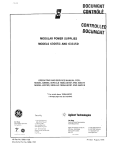
1
About this Manual
We’ve added this manual to the Agilent website in an effort to help you support
your product. This manual is the best copy we could find; it may be incomplete
or contain dated information. If we find a more recent copy in the future, we will
add it to the Agilent website.
Support for Your Product
Agilent no longer sells this product. Our service centers may be able
to perform calibration and repair if necessary, but no other support from
Agilent is available. You will find any other available product information on the
Agilent Test & Measurement website, www.tm.agilent.com.
HP References in this Manual
This manual may contain references to HP or Hewlett-Packard. Please note that
Hewlett-Packard's former test and measurement, semiconductor products and
chemical analysis businesses are now part of Agilent Technologies. We have
made no changes to this manual copy. In other documentation, to reduce
potential confusion, the only change to product numbers and names has been in
the company name prefix: where a product number/name was HP XXXX the
current name/number is now Agilent XXXX. For example, model number
HP8648A is now model number Agilent 8648A.
r/i~ HEWLETT
~a PACKARD
OPERATING AND SERVICE MANUAL
MAINFRAME
8080A
PART OF 8080
HIGH FREQUENCY PULSE/WORD GENERATOR SYSTEM
SERIAL NUMBERS
This manual applies directly to instrument serial number
1604G00461
For instruments with lower serial numbers,refer to the backdating information in Section 8 of this module manual.
For instruments with higher serial numbers, refer to the
Manual Change sheets at the end of this module manual.
0236
L...-
COPYRIGHT HEWLETT-PACKARD GMBH 1982
HERRENBERGER STR. 130,7030 BbBLINGEN, WEST GERMANY
MANUAL PART NO. 08080-90002
MICROFICHE PART NO. 08080-90502
Printed in the Federal Repu blic of Germany, 2/82
- - - - - - - - - - - - - - - - - - - - List of Contents/Tables/illustrations/Schematic Diagrams
CONTENTS
Section 1
1-1
1-4
1-6
1-9
1-11
1-13
1-15
1-17
1-19
General Information
1-1
Section 7
Introduction
Specifications
Safety Considerations
Instruments Covered By Manual
Description
Options
Accessories Supplied
Accessories Available
Recommended Test Equipment
1-1
1-1
1-1
1-1
1-1
1-1
1-2
1-2
1-2
7-1
7-3
Section 8
Installation
2-1
Table
Introduction
Front Handle/Rack Mounting
Preparation for Use
Power Requirements
Power Cable
Operating Environment
Storage And Shipment
2-1
2-1
2-1
2-1
2-1
2-1
2-2
2-2
1-1
1-2
6-1
Operation
3-1
Line On/Off Switch
Voltage Selection
Special Operating Conditions
Operator's Checks
3-1
3-1
3-1
3-1
Performance Checks
4-1
Introduction
4-1
8-1
8-3
Service
7-1
Introduction
Recommended Test Equipment
7-1
7-1
Backdating
8-1
Introduction
Change Sequence
8-1
8-1
TABLES
Section 2
2-1
2-3
2-5
2-7
2-8
2-10
2-15
2-17
Section 3
I nitial Inspection
6-2
7-1
7-2
B-1
Page
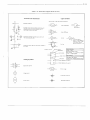
Recommended Test Equipment
Specifications
Abbreviations for Replaceable Parts
List
Replaceable Parts
Reference Designators
Schematic Diagram Symbols
Backdating Changes
1-3
1-3
6-2
6-5
7-1
7-2
.
ILLUSTRATIONS
3-1
3-3
3-5
3-7
Section 4
4-1
Figure
1-1
1-2
1-3
1-4
2-1
Section 5
5-1
5--3
5-9
5-11
5-13
5-15
5-17
Section 6
6-1
6-3
6-5
6-8
Adjustments
5-1
Introduction
Safety Considerations
Test Equipment Required
AI ignment Tool
Related Adjustments
Cover Removal
Power Supply Adjustments
5-1
5-1
5-1
5-1
5-1
5-1
5-2
Replaceable Parts
6-1
Introduction
Abbreviations
Replaceable Parts
Ordering Information
6-1
6-1
6-1
6-1
2-2
5-1
6-1
6-2
Page
8080A Mainframe and Supplied
Accessories. . . . . . . . . . . . . . . . . . . . 1-0
Serial Number Plate
1-1
Power Cables Available: Plug
Identifications
1-2
Front Handle/Rack Mounting Options .. 1-2
Removing Plastic Trim
2-1
Line Voltage and Fuse Selection
2-2
Power Supply Test Setup
5-2
B080A Mainframe Replaceable Parts
6-4
aOaOA Mainframe Cabinet Parts
6-5
SCHEMATIC DIAGRAMS
Page
Diagram
2
3
A1 Switching Board, A2 Driver &
Filter Board
A3 Analog Supply Board
A4 Distribution Board
7-15
7-17
7-19
"
-
.......
~
POWER
CABLE
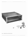
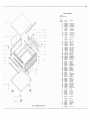
Figure 1-1. aOaOA Mainframe and Supplied Accessories
- - - - - - - - - - - - - - - - - - - - - - - - - - - - - - SECTION 1
---------~---~--~-------GENERAlINFORMAnONJ
1-1
INTRODUCTION
1-2
This Operating and Service manual contains
information required to install, operate, test, adjust and
service the Hewlett-Packard Model BOBOA Mainframe.
Figure 1-1 shows the mainframe and accessories
suppl ied. This section covers instrument identification,
description, accessories, specifications, and other basic
information.
1-3
A microfiche version of this manual is available on 4 x 6 inch microfilm transparencies (order number on title page). Each microfiche contains up to 60
photo-duplicates of the manual pages. The microfiche
package also includes the latest Manual Changes supplement as well as all pertinent Service Notes.
1-4
the serial number only change when there is a significant
change to the instrument. The last five digits are assigned
to instruments sequentially. The contents of this manual
apply directly to the instrument serial number quoted
on the title page. For instru ments with lower serial numbers, refer to the backdating information in Section 8 of
this module manual. For instruments with higher serial
numbers, refer to the Manual Change sheets at the end
of this module manual. I n add ition to cha nge information, the Manual Change sheets may contain information
for correcting errors in the manual. To keep this manual
as up-to-date and accurate as possible, Hewlett-Packard
recommends that you periodically request the latest
Manual Change supplement. The supplement for this
manual is identified with this manual's print date and
part number, both of which appear on this module
manual's title page. Complimentary copies of the supplement are available from Hewlett-Packard.
SPECIFICATIONS
HEWLETT - PACKARD GmbH
1-5
Instrument specifications are listed in
table 1-2. These specifications are the performance
standards or limits against which the instrument is
tested.
[1536G00062
BbBlINGEN.
Figure 1-1. Serial Number Plate
1-6
SAFETY CONSIDERATIONS
1-7
The Model 8080A Mainframe is a Safety
Class 1 instrument (it has an exposed metal chassis that
is directly connected to earth via the power supply
cable). This instrument has been designed according to
international safety standards and has been supplied in a
safe condition.
1-8
This operating and service manual contains
information, cautions, and warning which must be followed by the user to ensure safe operation and to maintain
the instrument in a safe condition.
1-9
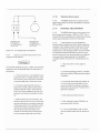
INSTRUMENTS COVERED BY MANUAL
1-10
Attached to the rear of this instrument is a
serial nu mber plate (figure 1-1). The first four digits of
1-11
DESCRIPTION
1-12
The 8080A Mainframe provides housing and
power supplies for the 8080A system modules. The
Ma inframe is a fu II rack width module and can be rack
mounted or used as a bench·top instrument.
1-13
OPTIONS
1-14
The following options are available:
Option 907
Option 908
Option 909
Option 910
I
Front Handle Kit
Rack Flange Kit
see
Rack Flange with
Figure
Front Handle Kit
1-3
Additional manual
binder, mainframe manual.
These options will be shipped with the instrument,
if ordered with the instrument.
1-15
ACCESSORIES SUPPLIED
15400A Blank Panel 1/4 mainframe width
15401A Blank Panel 1/8 mainframe width.
1-16
The 8080A Mai nframe is supplied complete
with the following items (see also Figure 1-1).
ITEM
1A Fuse for 230 V
operation
2A Fuse for 115 V
operation
Power cable
Manual
These panels are intended to fill empty sections of the
mainframe and maintain the complete RFI shielding.
HP PART NUMBER
15402A Feedthru panel (6xBNCl, 1/8 mainframe width. This panel provides 6
extra front panel BNC connectors for
front panel access to internal outputs.
15104A Pulse Adder/Splitter
2110-0007
2110-0303
see Figure 1-2
08080-90002
1-19
1-17
ACCESSORIES AVAILABLE
1-18
The following accessories are available for the
8080 mainframe:
NEMA TYPE
HP Part No. 8120-1348
SCHUKO TYPE
HP Parr No. 8120-1689
RECOMMENDED TEST EQUIPMENT
1-20
Equipment required to maintain the model
8080A mainframe is listed in Table 1-1. Other equipment can be substituted if it meets or exceeds the critical specifications listed in the table.
BRITISH STANDARD TYPE
HP Part No. 8120-1351
USED IN AUSTRALIA
HP Part No. 8120-1369
I'
\
LINE = BLACK
NEUTRAL = WHITE
GROUND = YELLOW/GREEN
LINE = BROWN
NEUTRAL = BLUE
GROUND = YELLOW/GREEN
LINE = BROWN
NEUTRAL = BLUE
GROUND = YELLOW/GREEN
,
LINE = BROWN
NEUTRAL = BLUE
GROUND = YELLOW/GREEN
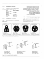
Figure 1-2. Power Cables Available: Plug Identification
Front hand les only
Order option 907
(Kit no. 5061-0089)
Rack flange/Front hand Ie kit
Order Option 909
(Kit no. 5061-0083)
Figure 1-3. Front Handle/Rack Mounting Options
Rack flanges only
Order option 908
(Kit no. 5061-0077)
Table 1-1. Recommended Test Equipment
Instrument
Critical Specification
Recommended Model
Digital Voltmeter
up to ± 20 V dc
HP 35658
Adjustments
DC Power Supply
0- 35 V
HP 62058
Adjustments
Variac
Isolating Transformer
-
Used in
Adjustments
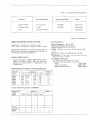
Table 1-2. Specifications
8080A MAINFRAME SPECIFICATIONS
ENVIRONMENTAL
Specifications describe the warranted performance over the temperature range from OOC to 550C.
Storage Temperature: -40°C to 75°C
Operating Temperature: OOC to 55°C
Humidity Range: 95 % RH, OOC to 40°C
POWER: 115/230 V rms +10 %, -22 %, 48-66 Hz, 200 V
max.
Supplemental characteristics provide information useful in
applying the instrument by giving typical or nominal, but
non-warranted, performance parameters.
WEIGHT: net 5 kg (lllbs), shipping 9 kg (19.9Ibsl.
DIMENSIONS: 133 mm high x 426 mm wide x 422 mm
deep (5.2 x 16.8 x 16.6 in).
MODULE COMPATIBILITY
ACCESSORIES SUPPLIED:
2 m Power Cord, 230 V fuse, 115 V fuse.
Operating and Service Manual consisting of:
8 inder
9282-0540
General Information
08080-90011
SOSOA Mainframe Manual
08080-90002
Houses combinations of BOB1A, 8084A, 80B3A, B091A,
8092A and 8093A modules. Maximum power considerations are shown below in "Supplemental Power
Characteristics".
SUPPLEMENTAL POWER CHARACTERISTICS
MODULE
LOAD (A)
MODULE
TYPE
+10 V
-5.2 V
-10 V
-20 V
8081A
8084A
8083A
8091A
8092A
8093A
0.08
0.25
0.39
0.27
0.75
0.06
0.22
364
0.18
0.34
0.08
0.27
0.7
0.02
001
0.003
0.4
0.29
0.17
0.22
-
0.40
0.75
0.13
WIDTH
1/4
1/2
1/4
1/4
1/4
1/8
Aid for calculatin::l number of 8080A's:
MODULES
TO BE
USED
WIDTH
LOAD (AI
+10 V
-5.2 V
-10 V
-20 V
1.1
7.4
10
0.9
TOTAL
MAX PER
80BOA
1/1
-----------------------------SECTION 2
----~-~~-----~~-----~~-----~INSTALL~IONJ
2-1
INTRODUCTION
2-2
This section provides installation instructions for the Model 8080A Ma inframe and its accessories. It also includes information about initial inspection
and damage claims, preparation for use, and packaging,
storage and shipment.
2-3
PREPARATION FOR USE
2-8
Power Requirements
2-9
The 8080A requ ires a power source of 115
or 230Vac +10%, -22% at a frequency of 48 to 66 Hz
single phase. The maximum power consumption is
200VA.
INITIAL INSPECTION
2-4
Inspect the shipping container for damage. If
the container or cushioning material is damaged, it
should be kept until the contents of the shipment have
been checked for completeness and the instrument has
been checked mechanically and electrically. The contents of the shi pment should be as shown in Figure 1-1
plus any accessories that were ordered with the instrument. Procedures for checking the electrical operation
are given in Section 3. If the contents are incomplete, if
there is mechanical damage or defect, or if the 8080A
does not pass the operator's checks, notify the nearest
Hewlett-Packard Sales/Service office. If the shipping
container is damaged, or the cushioning material shows
signs of stress, notify the carrier as well as the HewlettPackard office. Keep the shipping materials for carrier's
inspection, The HP office will arrange for repair or replacement without waiting for settlement.
2-5
2-7
2-10
2-11
In accordance with international safety standards, this instrument is equipped with a three-wire
power cable. When connected to an appropriate ac
power receptacle, this cable grounds the instrument
cabinet. The type of power cable shipped with each instrument depends on the country of destination. Refer
to fjgure 1-2 for the part numbers of the power cords
available.
2-12
If the plug on the cable supplied does not fit
your power outlet, then cut the cable at the plug end
and connect a suitable plug. The plug should meet local
safety requirements and include the following features:
Minimum current rating of 2A
Grou nd connection
Cable clamp.
FRONT HANDLE/RACK MOUNTING
2-6
Figure 1-3 shows the front handle and rack
mou nting options. If handles are fitted and subsequently
need to be removed, the plastic trim must first be taken
off as shown in figure 2-1.
Power Cable
The colour coding used in the cable will depend on the
cable su ppl ied (see figure 1-2).
2-13
Line Voltage Selection
CAUTION
l..ih a corner 01 the pl."S1Il: 111m wtfh a
clnd
gllle
iI
!hil'O I~O Ii<
Figure 2-1. Removing Plastic Trim
~clewdrlye,
tile Ch'ifCllon o( tne SHOW.
BEFORE SWITCHING ON THIS INSTRUMENT, make sure that the instrument is set
to the local line voltage,
2-15
rr
~
FUSE
o
I
Screwdriver slot
in this position
for 11 OV operation.
Use 2A fuse.
Screwdriver slot
in this position
for 220V operation.
Use 1A fuse.
Figure 2-2. Line Voltage and Fuse Selection
2-14
Figure 2-2 provides instructions for line
voltage and fuse selection.
I
WARNING
I
To avoid the possibility of injury or death, the following
precautions must be followed before the instrument is
switched on:
a. If this instrument is to be energized via an
autotransformer for voltage reduction, make
sure that the common terminal is connected
to the grounded pole of the power source.
b. The power cable plug shall only be inserted into a socket outlet provided with a
protective ground contact. The protective
action must not be negated by the use of an
extension cord without a protective conductor.
c. Before switching on the instrument, the
protective ground terminal of the instrument
must be connected to a protective conductor
of the power cable. This is verified by checking that the resistance between the instrument chassis and the front panels of all
modules in the instrument and the ground
pin of the power cable plug is zero orims.
Operating Environment
2-16
The 8080A Mainframe will operate within
specifications when the ambient temperature is between
ooe and 55 0 C.
2-17
STORAGE AND SHI PMENT
2-18
The 8080A Mainframe can be stored or shipped at temperatures between -40 0 e and 75 0 e. The instrument should be protected from temperature extremes
which cause condensation within the instrument.
2-19
If the instrument ;s to be shipped to a
Hewlett-Packard Sales/Service Office, attach a tag showing owner, return address, model number and full serial
number and the type of service required. The original
shipping carton and packaging material may be re-usable
but the Hewlett-Packard Sales/Service office will also
provide information and recommendations on materials
to be used if the original packing is not available or
re-usable. General instructions for re-packing are as follows:
1. Wrap instrument in heavy paper or
plastic.
2. Use strong shipping container. A doublewall carton made of 350-pound test material
is adequate.
3. Use enough shock-absorbing material (3
to 4-inch layer) around all sides of instrument to provide firm cushion and prevent
movement inside conta iner. Protect control
panel with cardboard.
4. Seal shipping container securely.
5. Mark shipping container F RAGI LE to
encourage careful handling.
6. In any correspondence, refer to instrument by model number and full serial number.
SECTION 3
OPERATION
1-
3-1
LINE ON/OFF SWITCH
3-5
3-2
The only control on the aOaOA Mainframe
front panel is a push-far-ON, push-far-OFF, LINE switch
that switches power to the power supplies in the Ma inframe. There is also a filament lamp that is lit for power
ON.
3-6
3-3
3-7
VOLTAGE SELECTION
3-4
There is a 11 OV/220V line voltage selector
on the 8080A rear panel. This should be set up as described in section 2-13.
J
SPECIAL OPERATING CONDITIONS
The only precaution that must be observed
while operating the 8080A Mainframe is that the air
holes in the top and bottom covers are not obstructed.
OPERATOR'S CHECKS
3-8
The only operator's check on the 8080A
Mainframe is to switch the LINE OFF/ON switch on the
front panel to ON and check that the line lamp is lit.
r------------------------------SECTION 4
L . . . - - - - - - - - - - - - - - - - - - - - - - - - P E R F O R M A N C E CHECKS
4-1
INTRODUCTION
4-2
The only performance tests necessary on the
Modell aOaOA are output voltage checks, and these are
included in the Model aOaOA Adjustments section (section 5).
,------------------------------SECTION 5
'-----------------------------ADJUSTMENTS
5-1
INTRODUCTION
5-2
This section describes the adjustments reo
quired to return the Model 8080A to peak operating
condition. Included in this section are test setups and
check and adjustment procedures. Removal and replacement procedures and an adjustment location diagram are
also included.
5-3
5-7
Make sure that only fuses with the required
rated current and of the specified type (normal blow,
time delay, etc.) are used for replacement. The use of
repaired fuses and the short·circuiting of fuseholders
must be avoided.
5-8
Whenever it is likely that the protection has
been impaired, the instrument must be made inoperative
and be secured against any unintended operation.
SAFETY CONSIDERATIONS
5-4
Although this instrument has been designated
in accordance with international safety standards, this
manual contains information, cautions, and warnings
which must be followed to ensure safe operation and to
maintain the instrument in a safe \~ondition (see sections
2 and 3). Service and adjustments should be performed
only by qualified service personnel.
WARNING
Any interruption of the protective (grounding) conductor inside or outside the instrument or disconnection of
the protective earth terminal is likely to make the apparatur dangerous. Intentional interruption is prohibited.
5-9
5-10
Table 1-1 contains a list of test equipment
and test accessories required in the adjustment procedures. In addition, the table contains the required minimum specifications and a suggested manufacturer's
model number.
5-11
5-6
Capacitors inside the instrument may still be
charged even if the instrument has been disconnected
from its source of supply.
ALIGNMENT TOOL
5-12
A non-metallic alignment tool must be used
when any adjustments are made to the power supply
potentiometers.
5-13
5-5
Any adjustment, maintenance, and repair of
the opened instrument under voltage should be avoided
as much as possible and, when inevitable, should be carried out only by a skilled person who is aware of the
hazard involved. The opening of covers or removal of
parts, except those to which access can be gained by
hand, may expose live parts, and also accessible termi·
nals may be live.
TEST EQUIPMENT REQUIRED
RELATED ADJUSTMENTS
5-14
The four regulated power supply adjustments
given are independent of each other and can be performed
in any order. The unregulated -6.5 V should be checked
before and after any regulated supply adjust.
5-15
COVER REMOVAL
5-16
Remove the upper two feet from the rear of
the Model 8080A. Unscrew and remove the top cover.
5-17
POWER SUPPLY ADJUSTMENTS
4.
Switch the instrument off and remove the power
cable.
5.
Remove all modu les from the S080A Mainframe.
6.
Remove the white/orange wire of A 1T2 from the
Al board
7.
Solder a wire from
to
the A 1 component layout.
8.
Connect 25.0 V DC to
and
as
shown on the A2 component layout ('+' to
A2CR5 Anode and '-' to A2C11).
Figure 5-1. Power Supply Test Setup
9.
Connect Oscilloscope to testpoint D (output
pin 6 of Ul).
EQUIPMENT
10.
Vary power supply voltage slightly, and check
that the duty cycle does not change. i.e. maximum duty cycle is reached.
DESCRIPTION
Ad igital voltmeter is used to check the power supply
voltages. They are then adjusted for the correct value.
DIGITAL
Digital Voltmeter
Variable Line Transformer
DC Power Supply 0-35 V
Oscilloscope
VOLT .... ETEA
HP 3465A
.
@
CD
0
as shown on
(i)
(NOTE: When the power supply voltage reaches
approx. 15 Volt, A2Ul turns off and does not
start again with increasing voltage. Set DC supply
again to 25 V, switch it off and after a few
seconds switch it on again).
PROCEDURE
11.
Set A2 R26 so that no duty cycle change appears
and check duty cycle for 50 % plus minus 4 %.
If necessary change A2 R28. (Factory selected).
12.
Increase power supply voltage slowly, watch decreasing duty cycle (negative part) and set
voltage so that the output signal of U1 is just
prior to disappearing.
13.
Connect Oscilloscope probe to collector 030
(TP E) and adjust Minimum Duty Cycle with
A2R29 for 2.0 to 2.5 fls.
14.
Disconnect DC Power Supply, remove wire and
resolder white orange wire.
Recheck TP 2 voltage.
15.
Install switched supply and connect to the
Analog Board.
Vary line voltage with variable line transformer
between +10 % and -22 %. The output voltages
should not change.
16.
Connect appropriate line power (115 V /230 V)
and use DVM to measure voltage at TP 2 on the
Analog Board. This should read approx. -8.5 V.
If necessary, adjust A2R26 using an isolated
screwdriver. Access to A2R26 is gained through
a hole in the bottom cover of the power supply
box.
1.
Set variable line transformer and 8080A to the
appropriate line voltage (115 V or 230 V).
2.
With the modules in the S080A check the power
supply voltages on 8080A board A3 (Analog
Supply).
*
Testpoint
+10V
-20 V
-10 V
-5.2 V
3.
G .
~ J I "'"
'~-11' (;~
Adjust
Voltages
((
{W)./-·,
-~~WO-m.\l
A3R4
A3R75
A3R55
A3R31
+10V±10mV
-20 V ± 10 mV
-10 V ± 10 mV
-5.2 V ± 10 mV
NOTE: The following steps are only necessary if
regulations is insuffient or a repair has been made
in the power supply area, if so then perform the
following procedure:
!~, J-
17.
Switch off 8080A Mainframe, plug in and reconnect all modules.
18.
Check test point voltages on Analog Supply board
A3:
'"**
1b"
shou Id be more positive than +11.5 V
should be more negative than -6.5 V
shou Id be more positive than +2 V
..
L"'jl'I r
.....
\II
~~?r~
.<,~ "
~
should be more positive than +3 V __
\:!.(
-/
Re-adjust A2 R26 if necessary (~t-TP2)
19.
Check the power supply voltage according to
step 2.
ANALOG SUPPLY
BOARD A3 08060-66503
c.
e73
~i "
rV-.
-QQ-
~R75\
-c:TI::J-
;f~ A~J -I R 78 ~,
s~~~
i1l
~~G~ ~
~~
01000
c b •
----
Jl
1
2
,
3
5
6
7
8
9
10
. . . - - - - - - - - - - - - - - - - - - - - - - - - - - - - - - SECTION 6
' - - - - - - - - - - - - - - - - - - - - - - - - - - - REPLACEABLE PARTS
6-1
INTRODUCTION
6-7
The information given for each part consists
of the following:
6-2
This section contains information for ordering parts. Table 6-1 lists abbreviations used in the parts
lists and elsewhere in the manual. Table 6-2 contains
the names and addresses that correspond to the manufacturer code numbers. Table 6-3 lists all replaceable
parts in reference designator order.
6-3
ABBREVIATIONS
6-4
Table 6-1 lists abbreviations used in the
parts lists, schematics and elsewhere in the manual. In
some cases two forms of the abbreviation are used, one
all in capital letters, and one partial or no capitals. This
occurs because the abbreviations in the parts lists are
always all capitals. However, in the schematics and other
parts of the manual, the same abbreviations may have
upper and lower case letters.
6-5
a. The Hewlett-Packard part number.
b. The total quantity (Qty) in the instrument. This is given only once for each part at the first appearance of the part in the list.
e: The description of the part.
REPLACEABLE PARTS
6-6
Table 6-2 is the list of replaceable parts and
is organised as follows:
a. Illustrated parts breakdowns for chassis
mou nted parts.
b. Chassis mounted parts in alphanumerical
order by reference designator.
c. Electrical assemblies and their components in alphanumerical order by reference
designator.
6-8
ORDERING INFORMATION
6-9
To order a part listed in the replaceable parts
table, quote the Hewlett-Packard part nu mber, indicate
the quantity requ ired, and address the order to the
nearest Hewlett-Packard office (list of Sales/Service
offices at the rear of the 8080A Mainframe manual).
6-10
To order a part that is not Iisted in the replaceable parts table, include the instru ment model number, instrument serial number, the description and
function of the part, and the number of parts required,
address the order to the nearest Hewlett-Packard office.
Table 6 --1. Reference Designators and Abbreviations
REFERENCE DESIGNATIONS
A
AT
B .
BT
C
CP
CR
DC
OL
OS
assembly
. attenuatar; isolator;
terminatIon
fan; motor
battery
capacitor
coupler
diode; diode
thyl'istor; varactor
directional coupler
. delay line
annunciator;
signaling device
(audible or visual):
lamp; LEO
miscellaneous
E
electrical part
F
. fuse
FL
H
HY
J
.
K
L
M
MP
filter
hardware
. circulator
electrical connector
(stationary portion);
jack
relay
coil; inductor
meter
miscellaneous
mechanical part
Q
A
AT
S
electricat connector
{movable portion!;
plug
transistor: SCA;
triOde thyristor
resistOr
thermistor
switch
. transformer
term inal board
thermocouple
T
TB
TC
TP
U
VA
W
x
y
z
voltage regulator;
breakdown diode
. cable; transmission
path; wira
socket
. crystal unit (piezo.
electric or quaru:)
l:U ned cavity; tu ned
circu it
test point
integrated circuit;
microcircu~t
eleCl:ron tube
V
ABBREVIATIONS
A
ac .
ACCESS
ADJ
AID.
ampere
afternating current
accessory
adjustment
analog-to·digital
audIO frequency
automatic
frequency control
AGe
. automatic gain
conuol
AL .
aluminum
ALC
automatic level
control
AM
amplitude modula·
tion
AMPL
amplifier
APC
au tomatic phase
control
ASSY.
assembly
AUX
auxiliary
avg
average
AWG
American wi re
gauge
BAL
. balance
BCD
. binary COded
decimal
BD
board
BE CU
. beryllium
copper
BFO
beat frequency
oscillator
BH
binder head
BKDN
breakdown
BP
bandpass
BPF.
bandpass filter
BAS
brass
BWO
bac kward ·wave
oscillator
CAL
calibrate
ccw.
counter-clockwise
CER
ceram,e
CHAN
channel
cm .
centimeter
CMO
cabinet mount only
COAX
coaxial
COEF
. coefficient
COM
common
COMP
composition
COMPL
. complete
CONN
connectOr
CP .
. cadmium plate
CRT
cath Ode-ray tube
CTL
. complement.3 r y
transistor logic
AF
AFC
continuous wave
CW
. clockwise
cm
centimeter
digital·to·analog
D/A.
decibel
dB
dBm
decibel referred
to
mW
direct current
dc.
degree (temperature
deg
interval or difference)
,.a
. degree (plane angle!
degree Celsius
°C
!centigrade}
OF
degree Fahrenheit
OK
. degree KelVin
DEPC
deposited carbon
DET
detec lor
diam
diameter
diameter (used in
DIA
pans list)
DI FF AMPL.
differentia~
amplifIer
div
d lvision
DPOT
. double·pole.
double·th row
DA .
drive
DSB
double sideband
d ;ode transistor
DTL
logic
DVM
. digital voltmeter
emitter coupled
FCL
logic
EMF
. electromotive force
EDP
. electronic data
proces.sing
ELECT.
. electrolytic
ENCAP,
encapsulated
EXT
external
F
farad
F ET
field·effect
CW
transistor
F/F
flip·flop
FH
. fiatt head
FIL H
tillister head
FM . frequency modulation
FP
front panel
FREQ
frequency
FXD
fixed
9 .
gram
GE
germanium
GHz
gigahertz
GL .
.~a~
GAD
ground{ed)
H .
henry
h
HET
HEX
HO
HOW
HF
HG
HI
HP
HPF.
HR
HV
Hz
IC .
10.
IF.
hour
. heterodyne
hexagonal
head
hardware
high frequency
mercury
high
Hewlett·Packard
high pasS filter
hour (used in
parts list!
high VOltage
Hertz
integrated circuit
inside diameter
intermediate
frequency
impregnated
IMPG.
inch
in
incandescent
INCD.
include(s)
INCL.
input
INP.
insu latfon
INS.
INT.
kg
kHz
interna~
kilogram
k i\ohertz
kilohm
kS1
kilOVOlt
kV
pound
Ib
inductance·
LC
capacitance
light-emitting diode
LED
low frequency
LF
. . long
LG
left hand
LH
limit
LIM.
linear taper (used
LIN.
in parts list)
lin
linear
L K WASH
lock washer
LO.
low; local oscillator
LOG
logarithmic taper
(used In parts list!
. logarithm(;c)
log
low pass fIlter
LPF .
low voltage
LV
meter (distance!
m.
mA
milli~mpere
maximum
MAX
.
megohm
MS1
meg (10 6 ) (used
MEG
in parts list>
MET FLM . .
metal f'lIm
MET OX.
metallic oxide
MF.
,medium frequency;
microfarad (used in
parts list)
MFR
manufacturer
mg .
· mitligram
MHz
megahertz
millihenry
mH
mho
. mho
MIN
· minimum
min.
minute (timel
. minute (plane
angle)
MINAT.
· miniature
mm.
millimeter
MOD
modulator
MOM
momentary
MOS
metal-Ox ide
sem iconducto r
. millisecond
ms .
MTG
· mounting
MTA
meter (indicating
device)
mV
milliVOlt
mVac.
millivolt, ac
mVdc
millivolt. dc
mVpk
milliVOlt, peak
mVp-p
millivolt. peak·
to·peak
mVrms.
millivolt,rms
mW .
, milliwatt
MUX
. multiplex
MY
mylar
fJA
. microampere
JJ.F.
microfarad
JJ.H
microhenry
JJmho.
micrOmho
j.J.s. .
microsecond
JJ.V
. microvolt
IJ.Vac
microvoH, ac
JJ.Vdc.
. microvOlt, dc
JJ.Vp-p
microvOlt. peak.
to·peak
I1Vrms
micrOVOlt, rms
JJ.W
microwatt
nA
. nanoampere
NC
no connection
N/C.
normally closed
NE
neon
NEG
negative
nF
nanofarad
NI PL
, nickel plate
N/O
normally open
NOM
. nominal
NOTE
' - - - - - - - - - - - - - - - - - - - - All abbreviations in the parts list will be in upper·case. - - - - - - - - - - - -
...1
Table 6-1. Reference Designators and Abbreviations (cont'd)
NORM
normal
NPN
negatlve·positivenegative
NPO
. negative-posItive
:zero (zero temoera·
ture coeffICIent)
NRFR
_ nOt recommended
for field rep'acement
NSR
ns.
nW
aBO
POT
p-p
PP
11')
PPM
order by deSCfiption
outside diameter
00
OH
OP AMPL
freQuency
PRR
PS
PT
PTM
PWV
moduli::Hlon
peak working
VOltage
pulse-amplitude
modUlation
printed cirCUIt
putse-code modula
tion; pulse-count
modulation
pulse·duration
modulation
pIcofarad
pF
PH SR2
PHL
PIN.
PIV
phosphor bronze
Phillips
P OSI tive-in t r insicnegative
peak inverse
RC
resistance-capac I lance
RECT
rectifier
REF
reference
REG
regulated
REPL
replaceable
RF
radiO frequency
RFI.
radiO frequency
peak
phase lock
phase lock
oscillator
phase modulatIon
POSI tive-negative·
positive
PIa.
part Of
pOlyStyrene
porcelaIn
posirive; pOsition{s)
(used In parts Ifst)
POSN
posi·tlon
SPG
SR
SPST
silicon
RLC
RMO
rms
RNO
ROM
R&P
RWV
S
resIstance
Inductance·
capacitance
rack mount only
rOOt mean·square
round
read-only memory
rack and panel
reverse work ,n9
voltage
scatteflng parameter
. slide
signal to· noise ratio
single-pole.
double·throw
spring
split ring
SIngle-pole,
SIngle-throw
SSB
single stdeband
SST.
stainless steel
STL
, steel
SO
sQuare
SWR
standH"lg,wave ratio
SYNC
synchronize
T
timed (slow-blow fuse)
TA
tantalum
TC
temperaru re
compensating
TO
time delay
TERM
terminal
TFT
lhln-idm transistor
TGL
THO
THRU
TI
TaL
second (t,mel
second {p lane a n91 e)
. slow·blow (fuse)
TRIM
TSTR
TTL
toggle
th'ead
through
titanium
tolerance
. trimmer
tranSistOr
transistor· transistor
logic
TV
TVI
TWT
U
te.evlsion
teleVIsion interference
traveling wave tube
. micro (laO) (used
In parts list)
UF
microfarad (used In
parts lis r)
UHF
uttrahigh frequency
unregulated
UNREG
~used
V
VA
Qu~ncy
VOlts, ae
variable
voltage·conlrolied
OSCillatOr
Vdc
volts, dc
vOlts, dc, work ing
VOCW
(used ,n parts list)
V(F)
vOlts, filtered
In parts list)
SCR
silicon controlled
rectifier; screw
SE
selenium
SECT
sections
SEMICON
semicon·
ductor
SHF
superhlgh fre-
VOlt
voltampere
V;l,c
VAR
VCO
MULTIPLIERS
Abbreviation
T
G
M
k
da
d
c
m
IJ.
n
p
f
Prefix
Multiple
tera
10 12
10 9
10 6
10 3
10
10 -1
10 -2
10 -3
10 -6
10 -9
10 -12
10 -15
10 -1S
glga
mega
kilo
deka
decl
centi
mlili
mIcro
nano
pica
femto
atto
NOTE
L-----------------
AII
VFO
silver
hand
SoB
PM
PNP.
POLY
PORC
PaS
interference
round head; right
RH
voltage
pk
PL
PLO
pulse time
modulalion
option
oscillator
oxide
ounce
_ ohm
PAM
POM
pOint
pulse·width
peak (used in parts
I,st)
PC
pIcosecond
, operational
P
PCM
rep~tlljon
PWM
amplifier
n
pulse
SI
SIL
SL
SNR
SPOT.
rate
. oval head
OPT
OSC
OX
oz
pu Ise-posi t ton
modulation
PREAMPL.
preamplifier
PRF.
Du fse·repetition
not separately
repl aceabl e
nanosecond
nanowatt
potentiometer
peak ·to-peak
peak·to·peak (used
parts list)
abbreVIations in the parts list will be in upper·case,
VHF
Vpk
Vp-p
Vrms
VSWR
variable·f requency
oscillator
very·h igh frequency
volts, peak
volts, peak-to·peak
. volts. rms
vOltage standing
wave ratio
voltage-tuned
VTO
oscillator
VTVM
V(X}
W
W
WIV
Vacuum-tube
voltmeter
, volts, switched
, watt
, with
working inverse
voltage
WW
W/O
YIG
20
wirewound
, without
yttrium-Iran-garnet
characteristIC
impedance
6-4-------------------------------~---------------
MPa
~
I
/
/
"- I
/
11
/
/
-,
~I
~
02
03
USE THERMAL
COM POUND 6040-0265
- - + - i f - - MP 8
--fI=r
-I-
.-
r;=
A 3 _ a>
-.
J2
F
Q4
05
_J
~+-e-
".-
'-
...
0-
~
-
_ ..
MP16
..,
I
I
I
I
I-J
~
fP'
-1
I
I
I
[I>,
W-
I
_J
I-
UPPER lARD AI
=
_I-:f-
I
MPl2
~
MP 12
I-.-Efl-
t-
I
--
,-
1$
~
r:- rh.
Y
A'WI
_
r?----_-~~=~
I
~----l
MP7---++-
f-.------A4J8
I
01 USE THERMAL
COMPOUND
6040 -0265
-fP-.-
"-
A4
A3
-
--EP-.f-f-
--EP--- -
MPI
f---- C1, CR 50'
-
-______
I-
-1
I
,
I
MP 14
MP38.MP39
I
_J
C3,CR 53
MP38.MP39
USE THERMAL
COMPOUND 6040 -0265
-$
rN
-,
I
I
1
0
00
000
0000
0000
0000
0000
0000
000
00
0
LOCATION OF
BOARD SPACER
MP 9
III
-
I'---MPI
r:- ~$ MP38. MP39
MP7-
I
__J
r---
CR52
MP 38, MP39
-
I
_J
-,
I
t
I
I
..J
X
r-
-I ~~Fl
ITU ------- r------------
I---LOWER BOARD A2
~
-,
~I----A4J1
GND WIRE
1
\
MPll
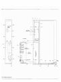
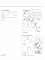
Figure 6-1. 8080A Mainframe Replaceable Parts
! ~Sl
=
=.
-~"------o- MP 27
- - - ---
t--
MP~
MP26
/
_J
I
\
I
I
I
REO / / / / / / / /VtO
r
-----
I - - C2,CR51
t-
~
--1
L!=;
J1
~
/
/
MP37
-
MP24
-Il'\
I
J
MP37
L
D Sl/MP5l1
MP52
/~
MP2S
MP23
------------------------------------------------------------------------6-5
Table 6>-2. Replaceable Parts
Moon 8OROA
INSTRUMENT HRIAI_ PRE FT x
F R'M-E
"4_p
RHE RENCF
OESIGNATOR
.
MP2-------------;;;/
Al
• A7
• A1
.4
AS
2
1
4
5
6
Cl
C2
- - - - - - - - - - - - - - M P )0
cJ
~--~--
MP8~_~
~ ~-~--/
-
----MP 32
050
C051
C052
CRn
---MP18
-MP 10
~-
MPJJ-~
-M?31
-MPJL
MP21-;-
-Mp 35
MPo
t----------- -- ---tAP 20
MP 22-
L-
M? 10
---MPIS
--MP'
MP3-
MP I 9 - - - - -
MP
11--------s::>
.
08080-66501
08080-66502
08080-6650'
08080-66504
080&0-66505
BO
80
90
80
0160-2208
0160-2208
0160-2708
C-F BOPF 300v
C-F _ J~OPf 300V
C-F BOPF 300V
AT-PWR sPl y
H-ANHOG SPl
AY-OtSTRIBUTR
Ay PWR SOlV
2140-0 0 16
lAMP IHC 0 5V .06A
2110-0007
2110-0303
FUSE
FUSE 2. FER
Fl
F1
,
MPl
MP2
MO,
10104
MPS
3 0403-0164
08016-04101
08016-04102
1 08080·00201
2 08080-00202
,.
GUIDE PC eO.BlK
COVER TOP
COVER 80TTOM
PANEL-FRONT LH
PANel-FRONT RH
MP6
MP7
10108
MP9
MP10
08080-00203
08080-60204
08080-60205
08080-00206
5001-1210
PANEl-OISTRI. Bo
PANEL AY-RE.R
pANEL AV-Of AR
PLATE-DIODES
.HGlE 8RACKET TO
MPH
MP17
MPB
08080-01203
08080-01101
08080-0120?
BUCKET RESISTOR
HEAT SIHK-PS
8RACKET-TOP
MP14
MPH
MP16
MPH
MP18
06080-04103
08080-04101
08080-04102
1460-1345
5001-0432
COVEll-PIIR SPl T
SUPPORT-PLUGIH 8
SUPPORT-PLUG IN T
TIL T STAND
SIDE 7
GUSSET
5001-0439
5020-8803
5020-8-804
5020-8836
5040-1124
HIM S1 DE 5.25
FRAME-FRONT
FRAME-REAR
CORNER STRUT 15
KNOB_PBTN POVER
5040~7023
PUSH ROO
BE ZEL-PB KNOB
ROO-POVU SW
SNAFT-SHORT
GUIDE POVER ROO
MP19
104020
101021
MP22
MP23
8
6
7
5
2
MP24
MP25
101026
"P27
MP2R
2
0
3
6
101029
MOJO
MP31
104033
101034
8
9
6
2
5040-7201
5040-7202
5040-7219
5040-7221
2 5060-9803
fOOT
TRIM STRIP-TOP
CAo, HANoLE-F RONT
FOOT REAR
STRAP.HANOLE
MP35
101036
MP37
MP38
HPlo
5060-9911
5060-9936
1400-0824
0360-0503
3 1200-0080
COVER SIDE
COVER UOE 151N
CABLE STUo
LUG SOLD BRS
INS 010 .531
104040
MP44
MP45
MP51
101052
0340-0844
08080-00597
08080-00601
4 00183-67701
4 1450-0404
INSULATOR COVER
ANGLE FILLER
SHIELD oW.R SOL T
BASE PILTlT
LENS PILOT LIGHT
MOn
08080-01102
HEAT SINK
1854-0589
1853-0251
1853-0251
1853-0251
1853-0251
XSTR
XsrR
XSTR
UTR
XSTR
0370-0914
08011-43701
08030 -43701
08080-03101
a
0
NoN SI
SI PNP
SI PHP
51 oNP
SI pNo
01
02
Q1
04
05
2
3
3
3
3
Rl
6 0811-3075
Sl
3101-2216
SW OPOT
vI
08080-61601
CBL AY CONN
1400·0090
2110-0565
2110-0566
2110-0')69
WASHER NEOpRENE
FUSEHOLo CAOfUL
FUS£HOloER
NUT NEX
MP 29
Figure 6-2. 808QA Mainframe Cabinet Parts
BO AY-PWR SPU
OTO RE Cl TN 3881
010 REeT IN 3881
OIO-TRW 50-41
010 OfCT IN 3881
MP 36
MP 18
OESCRloTlON
1901-0756
1901-0756
0 1901 -0792
1901-0756
OSl
------MPI3
PA~l
NUMBER
HI
KFI
HI
KFl
9
9
0
3
XOI
8 1200-0043
R-F 6.5K VW
INS XSTR MTG
6-6--------------------------------------------------------------------
Table 6-2. Replaceable Parts (cant'd)
41
080~0-66~01
REFERENCE
OE51GN&TOR
... -p PA,PT
Al
A1
Al
Al
01RO-26H
01.0-2633
01/.0-3?26
01·0-0059
0160-4709
.,
.,
6
6
5
4
4
41
41
41
41
01~0-345~
0160-3456
01RO-05S?
01RO-2636
01RO-2636
01RO-2636
0160-2636
C-F
C-F
C-F
C-F
C-F
C-F
C-F
C-F
C-F
C-F
2501lF 2S0V
250UF 250V
.01 OF 400V
100F 25V
nOOPF 20X
C53
(54
C55
C56
CH
01RO-0~82
C-F 560 UF 20VDC
C-f 560 IIF ZOVDC
C-F 560 UF 20VDC
C-F 270U F 40V
C-F 27011 F 40V
41
C58
5
0180-0~8?
C-F HOUF 40V
41
A1
A1
Al
Al
CAl
CA2
CA3
C.4
CR5
•
8
9
R
1901-1087
1901-10B7
1901-0460
1901-1087
1901-1087
OTO
010
DTO
010
010
Al
Al
Al
040
7 1901-0731
2 1901-1065
2 1901-1065
A1
A1
JI
Al
41
41
MPI
MP2
01
CR41
CA47
OHO-058?
~
1251-3708
1251-3708
H
PIIR
PWR
15v
PIIR
PIIR
RECl.6KV
RECT.6KV
150.A
RECT .MV
REeT .6KV
DIO-PWR 400V 1A
DTO-PIIR 400V H
Dl0-PIIR 400V 1A
1.SlIl TST • • 500
KHPER CAPAC ITOR
HTR NPN 51
XSTR SI 2N3439
KSTR sr NPN
.,.,
.,.,
R5
R35
o 0757-0657
0757-0857
5 0690-3931
5 0690-3931
o 0757-0352
R-F
R-F
R-F
R-F
P-F
Al
R36
R40
R41
R42
R43
3
5
4
o
7
41
A1
T1
12
9 08080-61102
R 08060-61101
HMO AY OA!YEA
xFMo AV
6 1902-3245
010 21.5Y 5% .4W
41
41
41
A1
A1
Al
040
041
82
R3
.4
Al
A1
A1
A1
XOI
X04,.
X041R
a
9 1205-0264
7 1205-0208
1205-0266
A2
A2
.2
A2
A2
A2
42
A2
02
A2
42
A2
82.5K 1% .SW
82.5K 1% .511
39Kl0% 111 CC
39Kl0% 111 CC
1S0K1% .511
HEAt SlNK
HT-SINK sEMrCON
HEAt SINK TO 3
80 AV-PIIR SPlY
bESCR rPTI 0"
C2]
0180-2435
0160-0168
01RO-0059
0160-0597
0160-4210
C-F
C-F
C-F
C-F
C-F
2200F 40V
.lUF10%PlAST
10UF 25V
1500PF 400V
.0UliF 20%
C24
C?5
c?6
cn
C29
0180-0197
01 RO-0119
0160-0597
0180-0791
0160-0597
C-F
C-F
C-F
Cor
C-F
2.2UF 20V
ll1F 25Y
1500PF 400Y
WF 35Y
1500PF 400V
0160-3533
0180-2338
01RO-0050
01RO-0050
01RO-0050
CAP
C-f
C-F
C-F
C-F
470PF 5%300V
650UF 13V
40UF 50v
40UF 50V
40UF ~Ov
C"
00
c?1
cn
01
C60
C62
C63
C/.4
C~5
CM
o
3
?
2
2
01RO-0116
0180-0116
CDNN POST 10.AlE
CONN POST 10.AlE
50 rc 14-CON
L60
L61
l6?
L63
l64
9100-3139
9100-3'39
9100-3139
9100-3139
9100-3139
COil
COlL
COIL
COIl
COIl
030
1854-0392
XSTR 51 2N 5088
0757-0727
0757-0280
0757-0280
0757-0467
0698-3161
R-t
R-F
R-F
R-F
R-F
Jl
J?
08
R18
R19
RlO
, R21
A2
A2
A2
A2
42
A2'
A2
A2
R22
R23
R24
Rl5
R26
.2
R27
R28
R29
830
A2
Rll
Rll
R33
A3~
R62
42
A2
Ul
A2
A2
A2
42
YRlO
YA21
YR30
YA'l2
,
3
3
R
9
2 0757-0479
R 0757-0409
, 0757-04H
n 0698-H45
o 2100-0567
INOUC
H'OUC
INOUC
TNOUC
INOUC
75U'"
75UH
750'"
75uH
75U'"
562 1% .2511
1Kn .12511
1KU .12511
121K 11
36.3Ka
R-F 392K lX 1/8W
.-F 274 11 .12511
P-F 365 11 .12S11
R-F 20.5k1%
R-VAR 2K lOX .511
5
6
6
9
,
0757-0290
0698-3259
2100-3210
0757-0442
0757-0280
P-F 6.19K1%
P-F 7.87KU
R-VAA 10K 101.5 ..
P-F 10Xa .1251/
A-F lK'n .12511 f
3
2
4
2
0698-3157
0698-3156
0757.0273
0757-0809
A-F
R-F
A-F
R-F
1826-0335
1820-1745
Ic LIN 511 PS ORI
rc .C140016CP
1902-3182
1902-0049
1902-0064
1902-3256
DID 12.1v 5X .411
orO-ZNR 6.19V 5X
010 7.5Y 5X .411
010 23.7V 5X .414
1200-0423
SKt IC 16-CON
u2
o
2
1
9
A2
C-F 6.8UF 35v TA
C-F 6.811F 35v T4
'3
A3
A3
A3
A3
'3
A3
A3
A3
'3
09
010
013
014
015
R1
R2
R3
A4
R5
'3
'3
A3
'3
'3
oJ
KSTR
KstR
XSTR
XS1R
XSTR
0757-0416
0757-0280
0757-;0422
2100-0554
0757-11281
O-F
R-F
R-F
R-V
R-F
5
3
1
5
5
0757-0Q2
0757~0438
0698-4020
0811-1200
0811-1200
R~F
R,9
R20
R21
R-F
R-F
R-F
R-F
909 1% ,125w
5.11KH
9.53K1X
.1 10% 011 PII
.1 lOX 011 PII
.22
R23
R24
R25
R26
1
5
Z
6
9
0757-0410
0698-4420
0698-4435
0757-0407
0698-4416
R-f
P-F
R-F
A-F
R-'
301 1% .12511
226 11 .125w
2.49K1X
200 1% .12511
169 1t .12511
8
o
4
5
2
0698-3136
0757-0401
0757-0273
2100-0554
0698-3700
R·F
R-F
R-F
R-V
P-F
17 .8K11:
100 1% .12511
3.0U1X
500 10% .511
71 ~ 1% .125w
All
., Z
A3
DESCRIPTION
A3
A3
43
43
A3
C1
C2
C4
00
C21
7 0180-0229
0180-0032
5 0180'-0061
8 0180-0197
9 0160-2055
C-f
C-F
C-F
C-F
C-F
But 10Y
l00r 12V
100ur 15Y
2.2UF lOY
.0lur 100V
A3
A3
A3
43
'3
C22
C50
C51
C52
C53
7
7
o
4
5
0180-0039
0180-0729
0180-0032
0160-4212
0180-0061
C-F
C-F
C-F
C-F
C-F
100UF 12Y
3~IIF 10V
10uF 12V
.068UF 20X
100l.lF 15v
.3
'3
A3
43
C70
C71
C72
C73
7
o
4
o
0180-0729
0180-0032
0160-47P
OHO-005S
C-F
C-F
C-F
Cor
330F 10V
10UF HY
.06RUf 20X
50ltF l5V
oJ
oJ
CR2
CR21
1901-0050
1901-1068
010 SII 80V 200 ••
010 sC"'OTTKY
.3
A3
J1
4 ~
J?
J~
A3
J4
1200-0R14
1200_0R14
1200-0814
1200-0R14
sn-xs fR
S"T-XHR
S<T-XSTR
SO-XSTO
A3
A~
n
n
l1
t?
6 9100-1788
6 9100-1766
18~4-02n
A3
A3
A]
'I.
'3
'3
'3
.3
'3
.3
.3
'3
18~4-0715
HTR
x <TR
XSTO
x<TR
51 2N'904
S I lN3904
51 2"3904
<T 2N3904
18~5-00H
XSTQ
~
1854-0715
1854-0715
A3
43
3-CONT
3-COIIT
'-CONT
J-CONT
A4
06080-66503
80 AY-ANAlOG SPl
oUCRIPTION
RH
A34
R35
R36
837
6 0757-0796
Q 0811-1668
9 0611-1666
o 0696-4037
o 0698-4037
B-'
R-'
A-F
R-F
8-'
82.5
1.5
1.S
46.4
46.4
A38
A40
850
R51
852
9
6
7
3
8
0757-1094
0696-3431
0757-0416
0757-0260
0698~3~58
R-F
R-F
B.'
R-F
A-r
1.47Kll
23,7 IX
511 1% .125"
Uti ,125 .. F
4.02K1 x
R53
A54
A55
l!56
A57
3
7
5
o
o
0811-0n9
0757-0424
21ll0-0H4
0757-0279
0757-0401
A-f
R-f
A-V
B-f
B-'
.H 5:1: ZV PII
1.1XU .12511
500 101 .511
3.16K11
100 U .12511
858
859
860
R70
R71
9
6
1
7
3
0757-0278
0696-3540
0757-0444
0757-0416
0757-0?80
8-E 1.18K1%
R-F n.4K1%
R·f 12 .1K1%
R~F 511 11 .12511
R-F 1Kl1 .1251/ F
872
A13
A74
875
R76
8 0698-3558
4 0811-1829
6 0757-0263
~ 2100':'0554
7 0757-0424
.-F
R-F
8-F
R-Y
R-F
500 10X .5W
1.1nx .125W
H7
878
A79
880
A81
o
8
1
8
]
0757-0401
0698-3152
0757-0444
0698-3540
0813-0040
R-F
.-F
A-F
R-F
8-F
100 1% .125W
3.48K 11
12.1KH
15.4K1%
20 51 511 PII
Ul
U2
u4
o
o
o
o
1820--0439
11120':'0439
1820-0439
1820-0439
IC-LIN VOL T
IC-LIN VOLT
Ic-l1~ vO~ T
IC-Lr~ vOLT
VRl
VRZO
5 1902-0084
5 1902-3096
U!
11 .5 ..
5X
2W
51 211
1%
11
4.02KU
.2~ lOX ]11
U1% .12511 F
REG
REG
AEG
REG
T ;nn9Qn
DID 6.81v 51 .41/
DID 5.23v 51 .4w
08080-66504
80 AV-OISTRI8UTP
oeSCAIPTiON
AEFERENCE
QEUGHA TOA
1251-0472
1251-0472
1251-0472
1251-0472
A4
J1
J2
J3
J4
J5
A4
Jl>
4 1251-0472
'4
J7
J8
J9
1251-0472
125l-0'll
R 1251-2034
A4
A4
A4
A4
A4
04
AS
1251-047l
4
4
060RO-6650S
AS
AS
(I
COliN
COliN
CONN
CONN
CONN
PC
PC
PC
PC
PC
12CONT
12CONT
1UONT
12COlll
12CONT
CONN
CONN
CONN
CONN
PC 12eONT
PC 12CONT
PC lUONT •
PC2X10.156D
AD ItY PwR $PlY
oESCR TPTION
REFERENC!
DESIGNAtOR
0160-3969
0160-4439
C-F
C-F
C-F
C-F
C-F
C6
0160-44]9
C-F 4700 PF
.s
II
.5
l2
9100-3396
9100-3139
COIL 2x4.", 2A
COl L 1 NOUC 75U'"
A5
A5
Al
R2
0686-1055
0612-0047
R-F '.5% .511 CC
R-r 5 5% 511
.5
AS
A5
A5
A3
'3
BD AY-ANAlOG SPL
a
511 1% .12511
lKH .12511 F
909 U .125 ..
500 10X .5W
2. 74K1%
19.6K 1%.125
14.7KU
3.01K1%
332 1% .511
A3
A3
08080-66~03
2N3904
2N3904
2N3904
2113904
2N3906'
46.4 11
.270 51 .SII'
2.40K1%
100 1% ,12511
3.65K1%
REFERENCE
OESrGNATOR
REHRENCE
UUGNA10R
SI
SI
S1
SI
SI
R-F
o-F
R-F
P-F
R-F
R8
R9
810
'3
A3
A3
43
7
,
5
5
4
1854-0215
1854-0215
1854-0215
1854-0215
1853-0036
o 0696-4037
1 0612-0040
2 0698-4435
a 0757-0401
9 0757-0434
R6
.7
.3
A3
REffRE"'CE
OlSIG .... TOR
A2
A2
A2
A2
A2
1KU .12511 F
,Tt1X .511 .F
1.5(1% .2S11
100 U .12511
1 5X 211 PII
0757-0280
0757-0159
0757-0736
0757-0401
0811-1666
08080-66~07
.2
.2
.2
CO N-POST 10F
CO N-POST 10F
0340-0469
08060-42301
6 1854-0749
5 1854-0079
5 1654-0780
.,
J4
1251-4084
1251-4084
1200-0424
C031
1000PF 1000V
1000PF lOOOv
HOUF 40V
560 UF 20voc
560 UF 20VOC
41
41
41
41
41
0'~0-2636
010 Sl SOY .02A
OIO-PIl. 400Y ,.
orO-PIIR 400V 1A
010 SI 50V .02A
con
OgCR rpTrON
NU"'9fR
C7
C8
cn
C40
C41
1901-0 0 44
1901-1065
'901-'065
1001-0044
C04
C05
80 H-PW. SPI, Y
Cl
n
C4
C5
5
9
6
6
7
0160-]96A
0160-4759
01~0-3969
.47UF lOX
• nUF 250V
.015uF 20!
.01 5UF 20~
4700 PF
r-------------------------------
SECTION 7
SERVICE
7-1
7-6
INTRODUCTION
7-2
This section contains the information to
service the HP Model 8080A. The information includes
theory of operation, troubleshooting, schematics
and component layouts.
7-3
The schematics and component layouts are
organized as 'Service Sheets' wh ich are identified by a
large number within a square in the lower corners. A
table relating these Service Sheets to board assemblies
is given in Table 7 -1. Schematic Diagram symbols are
given in Table 7-2.
Table 7-1. Index to Assemblies
Assembly
Service Sheet
A 1 Switching Board
A2 Driver/Filter Board
A3 Analog Supply Board
A4 Distribution Board
7-4
1
1
2
3
SAFETY CONSIDERATIONS
7-5
This section contains warnings and cautions
that must be followed for your protection and to avoid
damage to the equipment:
I
WARNING
I
Maintenance described herein is performed with power
supplied to the instrument, and protective covers removed.
Such maintenance should be performed only by service·
trained personnel who are aware of the hazards involved
(for example, fire and electrical shock). Where maintenance can be performed without power applied, the power
should be removed.
When servicing is completed, the After Service Safety
Check must be performed.
AFTER SERVICE SAFETY CHECK
7-7
Execute the following checks when servicing
is completed.
7-8
Disconnect power cord from line. Visually
inspect interior of instrument for any sign of abnormal
internally generated heat, such as discolored printed circuit boards or components, damaged insulation, or evidence of arcing. Determine cause and remedy.
7-9
Check cabinet/ground pin continuity in
accordance with IEC/VDE. Flex the power cord while
making the measurement to detect any intermittent
discontinuity. Check internal ground connections on
boards and frame. Also check resistance of any front
or rear panel ground terminals marked ~ .
7-10
Check cabinet/line isolation in accordance
with IEC/VDE. Replace any component which results in
a failure or refer to production Memo or Service Note
issued by product division for alternate action.
7-11
Check line fuse to verify that the proper
value is installed.
7-12
Check that safety covers are installed.
7-13
Check that all coaxial and flat cables inside
are properly connected. Check that all boards and the
heatsink on the chassis are properly connected. Verify
that the board clamp is fitted.
7-14
Inform Hewlett-Packard (internally, the
responsible product division) of any repeated failures
in the above tests or any other safety features.
7-15
SERVICE BLOCK
(THEORY/TROUBLESHOOTING)
7-16
The theory of operation and troubleshooting
information is provided in the form of Service Block i.e.
Service Block 1, located between Service Sheets 1. This
provides deta iled information on how to troub leshoot
the 8080A power supply without the prescence of high
voltage.
7-2
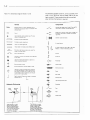
The following symbols conform, as far as possible, with
ANSI Y 32.2, IEEE No. 315and ANSI Y32.14 (for the
logic symbols). These standards should be consulted
when further informations is required.
Table 7-2. Schematic Diagram Notes (1 of 2)
Units
General
Components
ReSlstane. velutl$ are In ohms, capacitance val .... es to
NOfmallv open toggfe switch. C;rcles (0) ale uHd tor
the contacts to indicate a lock II',"" type Iwitch.
microfarad, and Inductance values In mlcrohor'lfies unless
otherwi$e noted !
PfO
Pen of
'*
Asterisk denotU
it
--
factory selected valve. The y;)lue
!hown is tl\e nominal value.
Spring return, 2,polition vander switch. Triengll!t ~
are IJsed for 11"1. tonlacu to Indicate a non·lockil\Q
type switCh.
2"POS.tion, 2·pole slide switch.
EndoJ,Ss front panel nomenclature.
---,
[ ---~
~
Encloses rear panel nOmenchlture.
Heavy line InOlcalel signal path.
.~
Heavy dashad line indicates pr.maty feedback path.
Wire colour cod•. S~me 3J resinor colour code. F Int
number is. Wife body colour.
w. ,e
Air cored inductor.
~.
II
JJ
Or plvg Ulied as link.
Ten point in it Circuit. POint may/may nOt be identifie<f
on P.C. bOard.
~
Used with 1fImmtr porentiOmeteu or capacitors 10
indicate scre"Ndfiver adjustment.
Direct conneclion 10 earth.
bead
-"U-
Ground connectiOn 10 Instrument cnauis
Of
Air cored transformer, The dot ~.J is used. when
neeeuary, to indicate innanlaneous polarity.
1r0t'l core
Fertite core
Fefrite bead
V8r3Ctor diode
frame.
Multi-junction diode
Used when a !'lumber Of cOmmon·return connectiom
are at the same polenlial. If thefe ,$ more than one
such SySlem to the s.amt circuit. numbers are ""rinen
.n the triangles so that all connectiOns wllh th. 5a1T"l&
potential have Ihe iame number.
Drode
Zener diode
I
Speciftc potential dlffeflnce w(ln respecr to a porentlal
fefefenCt!! level, ego
SChottky diode
+10 V
light Emining DiOde ILEO)
Schematic Referencing
Signal
Sch'n"Iotlc
number
numb.l
~
"
-1~
/
The", flferences on a Slinal
I• .wing a sch."....tic diagram
indicate tn8 signal destination .
The CifCI. containl the lignal
numbel and the &qua,.. contains
tilt numbel of th. schematic
to wnich th.t $ignel goal.
Photodiode
Fu..
------
Neon
6
Th." r.fe"nC8'J on a signal
I:mtering a sdlematic: ditgr.m
indicate the lignal origin.
The ci relt c:ontainl the .;gnal
number and dw square contain I
the numbel of the SCMmltie
to lNhic:h lhat fig nil originltln.
4l-
~
7-3
Table 7-2. Schematic Diagram Notes (2 of 2)
Terminals and Connectors
Logic Symbols
Soldered con"'eCllOn.
1
~
Example 01 IIJltd mall! "nd fe-mall! COnnector, ~llh
plug and 5ocke~ "I'\d contiC' dUtg",tofi.
e<).
aprn CQlIteIO'
P C
boa/d edge conneCtor and S(Jckel.
I
l-
~:=r
'
P
,I
,I
u:a""p1e of bUlkhead mOunted cOa.lal ~oc'Nel WIlt'.
hee coalillill plug and cable.
T I'1ree'l1,l Ii! delflc,.
Outpul .~ l'I'91'.... mpedance
when EN ., lafU.
,'re~oec·
l've 01 ,npuL Normal
OJ)f:ral,on when EN
11
I've'
F hp flOp
ell.ample 01 coalll,,1 cablt wIth ItrmlnoiHlon lolae,(!d
to
PC. board.
Cample ... I uncl.o")
Control hmClIon
Oependency
G-9aCI, '-clock
EN·3"",ate. R·' ..... ' IC
Contro' block
lOW>
S-Wt tQ high>'
1 (~) -covnc uQ Idown)
.... sh.fl
tdge-ttlQ9trtd.
>
R EG·r.gIHf'. SE L-wIOC lor
Analog Symbols
r---'-L_-A
CAl
8
082
Ol~. blOck
CNTR-counler, IDE)MUX·(delmull~pIU'(
OutPUI ~Dl!!nCls on A and G 1
~,
~
+
Cl,lflent SOurCe
-+-
W,red AND
conn~cllon
Wl1ed OR con.,ecllOI1
7-6------------------------+--------------------------..
08080 - 66505
I
I
LINE FILTER BOARD A5
I
LOCATION
OF 52
C5
I I
C6
I
,--------1
I
0
I
I
I
I
LOCATION OF
0
J1 ON
FRAME
0
I
L
[j [j ~D1
C2
I
R2
~
I-
11
C3
I
I ~-----------------------------'
I
I
I
-.J
1I
(3)
C8
I
I
C7
•
o
I
T2
•
-0
98
98
I
I
o
I
J
I
@ r
L---T-------------------------------~
@
(3)
CONNECT
TO
FOR TROUBLESHOOTING
WHEN USING EXTE RNAL POWER SUPPLY
DRIVER & FILTER BOARD A2
08080-66502
-1
07
097
-1
06
1l-1
~
C66
[55
~
C6
_'
~
~
C63
096
J2
rL....:
..J
1 2 3 4 5 5 7 B 9 10
J
05
L50
l_
095
095
05
092
02
SERVICE SHEET
1
1
e60
~
-1~C==:;62~
1
R52
o
0.
o
0
°
REMOVE WHITE/ORANGE WIRE
FOR TROUBLESHOOTING
,
-----------------------------------7-7
SERVICE BLOCK 1
POWER SUPPLY Al, A2, A3
THEORY OF OPERATION
General
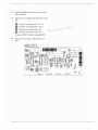
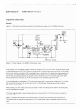
Figure 7-1 illustrates the operating principles of the switched power supply used in the B080A mainframe.
ANALOG
SUPPLY
Q\
STARTER
CIRCUIT
+
SENSE VOLTAGE
~
MIN, D. C. ADJUST
10 U1
\QLTAGE
ADJJST
COMPARATOR
9 PULSE WIDTH
MODULATOR
-
----
6
~
U2
MINIMll.1
DU~E
041
Y
3
OSCILLATOR
V
REF
16
SWITCHING
TRANSISTOR
FLOATING
GROUND
Figure 7-1. Block Diagram of the 8080A switched power supply
After power-on, the rectified line voltage is reduced by starter circuit, 01, to approx. 20 V, and fed as supply voltage
to the switching control A2U1. A2U1 then starts switching 041 via the minimum duty cycle circuit. The dc derived
from the line rectifier is chopped by 041, and stepped down by transformer T2 to supply the analog regulators after
rectification. The voltage induced in sense winding 93/3 is rectified by CR4 and now delivers the supply voltage
for U1 which was previously derived during power-on from the starter circu it 01. The sense voltage is also fed via
CR22 and R26 to the sense input of U1/10 and compared with the reference voltage from VR21.
Line voltage changes or load changes at T2 influence the sense voltage. Increasing sense voltage causes U1 to change
the duty cycle at its output pin 6, so that the "on time" of 041 decreases. Decreasing sense voltage increases
the "on time" of 041, via U1.
With increasing "on time" of 041, more energy is stored in T2 and more energy can be drawn by the analog supply,
and so load changes are regulated.
If the line voltage changes, the sense voltage changes too, and the energy for T2 is held constant by varying the
"on time" of 041.
NOTE: T2 separates the instrument from the main power. The primary part is referenced to floating ground.
The secondary part is referenced to chassis ground. For troubleshooting, a galvanic separated ac-source must be
used.
7-8 - - - - - - - - - - - - - - - - - - - - - - - - - - - - - - - - - - -
Voltage Selection and Line Rectifier
The line voltage is selected via 52. In the 115 V-position of 52, CR1/CR2 and CR4/CR5 are connected to charging
capacitors C7, C8 to form a voltage doubler.
When 52 is in 230 V position, diodes CR1, CR2, CR4 and CR5 are arranged as a bridge.
Start Circuit
The start circuit delivers power for the switching control circuits during the start phase (power-on), and when
the rectified feedback voltage decreases to approx. 19 V.
When power is switched on, base current for A 10 1 is supplied via R4 and R5, A1 VR2 holding the base voltage
at 21.5 V. The rectified line voltage, reduced by R1, 01 and CR3, supplies A2R8 via the switching control circuit
A2U1 until a feedback voltage is generated by T2 (windings 93 and 3).
When the normal supply operation is reached, the feedback voltage, rectified by A2CR5, is higher than the
voltage supplied from the start circuit. This decouples the start circuit by the "or" arrangement A1CR3 and A2CR4.
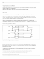
Minimum Duty Cycle Circuit (A2U2)
U1/6
-- - ---,
U2112
U2/11
~
_ _...+
..J
U2/10
Figure 7-2. Timing Diagram for Minimum Duty Cycle
Switching control A2U1 can vary its duty cycle at the output pin 6 from 20 % to 90 % (pin 6 is inverting output).
As the switching transistor A 1041 requires an "on time" between approx. 2 % and 50 %, the duty cycle delivered
from A2 U1 must be reduced.
The maximum duty cycle is determined by A2R28, and potentiometer A2R26 is used to adjust the correct duty
cycle for maximum load.
The minimum duty cycle is determined by a monoflop formed by A2U2, R32, R29, C31 and CR31.
The time determined by R32, R29 and C31 is substracted from the U1 output signal.
Figure 7-2 shows the principal timing conditions at U2.
--------------------------------------7-9
Driver Stage (A1040)
The switching signal derived from the minimum duty cycle circuit is inverted by A2030, and fed to the driver stage
A 1040. 040 switches the operating feedback voltage to transformer T 1, whose secondary wind ing is connected
to the base of switching transistor 041. A1CR40 and A1C40 protect A 1040 against negative spikes gnerated by
T1. T 1 separates the high voltage switching circu it 041 from the low vo Itage part.
Switching Circuit (A1041)
Transistor 041 switches the primary winding of the flyback transformer T2 to the rectified line voltage. Duri ng
the transistor on-time, current rises linearily and charges transformer T2.
When 041 cuts off, the T2 secondary wind ings become forward biased and energy is discharged from the transformer.
The voltage appearing at the collector of 041 is the sum of the rectified line voltage and back-transformed secondary
voltage, plus a voltage spike caused by the T2 primary stray-inductance. Capacitors C43 and C44, which are
referenced to floating ground via CR41 and CR42, are charged to the maximum voltage. When the 041 collector
voltage steps down, CR41 and CR42 become reverese biased and capacitors C43/C44 discharge via R45. During
this process part of the energy stored in C43/C44 is fed back to the main dc-source (C7/C8) which reduces the
power losses across R45.
r""""'"
Spike caused by primary stray inductance
rBack-transformed secondary voltage
1
Figure 7-3. 041 Collector Voltage
Rectified line voltage
7-10 - - - - - - - - - - - - - - - - - - - - - - - - - - - - - - - - - - -
Switching Control Circuit A2U1
The incoming voltage is stepped down and stabilized by VR20 to supply the switching control U1 (pins 1 and 16)
and the minimum duty cycle circuit U2/14.
The osci Ilator, a miller integrator, generates a sawtooth with a frequency of approx. 18 kHz determined by C22
and R2t. The output delivers a dc voltage proportional to the voltage difference at pins 9 and 10. Both signals,
the sawtooth from the miller integrator and the dc output from the comparator, are fed to the pulse width
modulator.
The pulse width modulator generates a rectangular output signal with a duty cycle, which is determined by the voltage
deviation at pin 10 to the reference voltage from VR27 at pin 9. Amplified in the output stage, the signal is fed
from pin 6 to the minimum duty cycle circuit U2.
R28 limits the max. duty cycle to approx. 50 %.
Resistor R18 between pin 9 and pin 10 and C29 reduces the loop gain to avoid regu lation instabi Ihies.
The sense voltage derived from the flyback transformer T2 is divided by resistor network R19, R25, R26 and R27.
Potentiometer R26 allows a voltage variation from approx. +5 V to +7 Vat the sense input pin 10 to adjust the
correct duty cycle at maximum load.
Soft Start and Cut-out Circuit
As can be seen in Figure 7-4, instructions derived from the protection circuits in U1 are fed to the soft-start
and cut-out circuit.
The soft-start and cut-out circuit forces the pulse width modulator to set the duty cycle immediately to zero
when an alarm is recognized. After a dead-time, which is determined by C25 and C22, the pulse modulator starts
slowly increasing the pulse width of the output signal.
To avoid in the case of a steady alarm the pulse width modualtor turning on and off continuously. capacitor C24
is charged step by step from the counting circuit. When C24 is charged to 5 V, the pulse modulator circuit is finally
switched off, and can be restarted only by switching off the power supply for the time C24 needs to discharge.
Overvoltage
The overvoltage protection circuit in U1 senses the voltage drop across R27 (pin 8), and compares it with the
reference voltage generated by VR21 (6.2 V). When the voltage at pin 8 exceeds 6.2 volt (reference voltage). a signal
is fed to the soft-start and cut-out circuit and activates cut-off and soft-start.
Overcurrent Protection
With the overcurrent protection circuit in Ul, the current through switching transistor 041 is sensed across A 1 R43.
The sense signal derived from A 1 R43 is fed to input pin 12 and divided by R24/R23. When the vo Itage at pin 12
exceeds approx. 660 m V (voltage drop across A 1 R43 is then approx. 1.97 V) the soft-start and cut-out
circuit is activated.
C23 filters the sense voltage at pin 12.
-----------------------------------7-11
SUPPLY
VOLTAGE
Low
Supply
Voltag'"
Internal
Supply
Protection
C22
Miller
t---o--~ Integratorl-+---.,
+
RJO
Output
Stage
to MIN DUTY
f--o>=-4~"CYCLE MONDflOP U2
I
I
I
I
I
VR32
23.6V
I
I
I
I
I
OVER CURRENT
SENSE FROM. -~-t5-'-----1~_--!?b-t--fr::~1
Al R43
...
I
I
I
I
I
I
I
I
I
I
L __
Figure 7-4. Switching Control Circuit (IC Block Diagram)
I
I
I
I
~FLOAnNG
__ __1
L--~====--
~
GROUND
7-12
Low Voltage Protection
Normal switching control circuit operation is assured with a supply voltage at U1 pins 1 and 16 down to
approx. 8 volt. If the supply voltage drops below 8 volt, the output signal is cut off. This protects the
switching transistor from overload.
Without this protection circuit, duty cycle would increase when the sense voltage goes down and the
switching transistor would be damaged.
Loop Fault Protection
Loop fault protection via U1 occurs when the feedback loop is open or shorted. Duty cycle is then cut
to zero. After the dead time, approx. 16 % duty cycle (determined by R20) is generated until the fault
is corrected. Then the duty cycle increases slowly to the normal condition. To prevent loop fault during
start under load, and to reduce the start time, VR30 delivers approx. 4.5 V to the sense input pin 10 of
U1 until enough feedback voltage is generated.
Analog Board A3
Voltages derived from the switched supply are post-regulated on the A3 analog board. Four adjustable
regulation circuits generate the required voltages for the system.
Each of them has a fold-back current limiting characteristic which is accomplished by resistors R8, R32,
R58 and R78.
Current is sensed by differential amplifiers and voltage is held constant by voltage regulators U1 and U4.
-----------------------------------7-13
TROUBLESHOOTING
The following information enables the service engineer to troubleshoot most of the 80BOA power supply
circuits without high voltages present.
Regulation and switching functions can be checked by driving the circuits with an external 25 V dc supply.
The 115 V/230 V ac mains supply is requ ired only when the starter circuit (A 101) has to be tested.
PROCEDURE
1.
Ensure that the power cord is not connected.
2.
Remove the white/orange wire of A 1T2 from the A 1 board position
3.
Solder a wire from
4.
Connect 25.0 V DC to
5.
Check voltages and waveforms as given for test points
®
to
CD
@ .
@
as shown on the A 1 component layout.
and
®
as shown on the A2 component layout.
~
to
~
.
NOTE: To check A2U1 regulation, vary the +25 V supply slightly. The duty cycle at A2U1 pin 6
should change. If A2U1 switches off, set power supply voltage back to 25 V, switch off and on to
start U1 again. After repair remove wire from
and @ and resolder white/orange
wire.
~
®
Starter Circuit Check
After power-on, the switch ing and regulation circuits are supplied via R 1, A 1Q 1 and A 1CR3 until A1041
starts switching, and the feedback voltage is rectified by A2CR22/CR5/CR4.
®
For the Starter Circuit Test, the black wire
high peak voltages at the collector of A 1041.
of A lT2 must be removed from the A 1 board to avoid
The +12 V for A2U1 is only supplied via R1, A 101, A 1CR3 and A2RB.
PROCEDURE
I
WARNING
I
High Voltage is present when performing this test.
1.
Ensure that the power cord is removed.
2.
Remove black wire
3.
Connect oscilloscope probe to A2U1 pin 6 (testpoint
4.
Using a VAR IAC apply power-supply voltage from mains.
5.
Check signal at
®
~
from the A 1 board.
.
~
l.
8080A TROUBL SHOOTIN
8080A TROUBLESHOOTING
5 V/OIV
~:':~4 .5
V 10 IV
+--l'--::-tt!!-I,~~l---[-~1~
. ..
10 V/DIV
5 V/DIV
SIGNAL AT A1Q41 COLLECTOR
WITH A1 R45 OPEN
CORRECT SIGNAL AT A1 R45
,
~:.,:r~ ..
10 V/DIV
"
\
..•• j ..•
...
.1
.
J
~::::;::L..,I 0
V
10 V/DIV
---.4--1-----1' 5
V/D IV
OV
SIGNAL AT A1R45 WITH A1C43
OR A1C44 OPEN
SIGNAL AT A1R45 WITH A1CR41
OR A1CR42 OPEN
5 V/OIV
TIME BASE SETTING: 1OJis/DIV
OSCILLOSCOPE TRIGGERED TO:
TIME BASE SETTE\lG: 10,us/DIV
"0
------------------------------------------------------------------------------7-15
PIO A2 DRIVER & FILTER BOARD
A1 SWITCHING BOARD
108080 ·665021
1080S0 - 665011
--I
--
PIO A2 DRIVER-&l
FILTER BOARD
:
108080- 56502)
MINIMUM
r----{~_R3_0J--o-----tl'_lR_3_1J__----l:.c::-Ii<'
T2
~
10K
DUTY CYCLE
3
CR 31
12
I J U2 ,r-11_
O~J.lK
8
U2
FLY BACK
TRANSFORMER
10
_=____
9
RJJ
IL.7K
C31
R29
L..3'OK
L70p
~
MIN. DUTY CYCLE
ADJUST
R3~O
rr
~
11"
OJO
92
STAGE
~
R40
IK
.
7
C53
560~
10
>-t-+-t---<~rl=h
OVERCURRENT SENSE
OJ
L
1$;1
~2
• 2.7~
1
r--""1:<.6--'-'.=15:..1""14'------'-'1.:..3--'-'.."12_--"-'llV----'-'1:<.0..J.=.9--,
:c
C29
'-,["VR21
6.2Y
Ul
~
5
~
6
R19
I.Sn
+'.2V
'I
B ny RVnLTA(;E
7
[IR2S
~
~
Qn~:
j~tO ~r
'cD
r
lK
I'---t-~
CR5
VOLT
~~~6
L-+-_---,-~--..J,__
JB:Ji<'
CR 22
.,J20.5K
VR32 L .,
2J.~V
)1.C22 4
J .cT1. 5n
6.8~
I
C55
550~
C60
I
I
J:R27
C26
6.19K
'F1.sn'l
r-
-
~
-
~
I
6
95
C56
270~
>---H-.+------~
270
C5L
TO -20V SUPPLY
La ~
~.j....-.4~--O.
_ _~)----f=-,-97
JD
~~
~!..
-
~--~
I
--I
~ ~ LOATING GROUND
.1 CHASSIS
A 5 LINE FI LT ER BOARD
--,
·
•
I FR~ME I
115V/230V
SUPPLY
ii'i
VOLTAGE
I
CONNECTIONS
' 1
[QffJ
Fl
NOTES;
02
CRL
1. THE ENCIRCLED POINTS 1 TO 6 RELATE TO
THE TROUBLESHOOTING PROCEDURE.
O'lQ0:.N=;---~t__----__I',.--<:>---~"!-1---o---o---..,......--i
51
2. ALL VOLTAGES AND WAVEFORMS ONLY VAllO
WITH EXTERNAL POWER SUPPLY AS DESCRIBED
IN THE TROUBLESHOOTING PROCEDURE.
5
I
5L
~. Fg.'L7~
I
~
I
.('
ISn
·~.in
:
W
XJ
fIiNEl
I
C2
__--.J
I
CABLE A2Wl
TO BOARD A3
ANALOG
SUPPLY
FRAME
WSOSO' 665051
GRO UNO
•
:
I
-_-_------:-+-::12~V,----+---1-----------------+------------{::2J---+--.-2J-.S-Y------l--7
---
SUPPLY
5.8~
I.
CRL
TO -5.2V
• C56
CR53
07
.............
ll>--..,....~_+_il-_r__t--,._-__LJ_T-*-"'f;::"---~--f__'}
""l
,
@
365
n~·,..lill1.,
C
21
•
rf:AME
(MP9)
CRL2
I
+2mV
+12Y
L60
CRL'
I:
1
C65
R3S
150K
i
C20
C21
VR20
O.lI'F; \O~F L'-, 12V
...J
6S0~
[Ji
r---t----t-----t
CSL
560~
SUPp\'Y
96
10
L
CRLO
10~
'7
4
+
CLO
: TO -lOV
40~
T1
•.
•
••
•
•
TO 'lOV SUPPLY
332
C5J
1Le-
6 U2
DRIVER
3.01K
+12Y
R52
o
Rl
1M
04
C5
l...7n
,
QI
,
·
CR 3
05
----_._~
•
J
I
ST_A_R_T_E_~_~
____
1
A1 SWITCHING BOARD
A2 DRIVER & FILTER BOARD
I
7-16------------------------~----------------------------------
ANALOG SUPPLY
BOARD A3 08080- 66503
J2
ABCOEFHJ
KL
""'--------, J 1
1
2
3
4
5
6
7
8
9
_10
-1L--_
R8 1
_
Q20 •
0
bee
EMITTER
o
BASE
SERVICE SHEET
COLLECTOR
o
OOQ3
bee
•
• • 04
bee
------'~
• • 0 05
bee
•
~
VIEWED
FROM TOP
2
\
\.
\
_ _ _ _ _ _ _ _ _ _ _ _ _ _ _ _ _ _ _ _ _ _ _ _ _ _ _ _ _ _ _ _ _ _ _ _ _ _ _ _ _ _ _ _ _ _ _ _ _ _ _ _ _ _- - - - - - - - - - - 7 - 1 7
1---:-c~:-:-;-::_:_:::_~::77::::::_:_;_;:;::::_;_~-- - - - - - - - - - - - - - - - - - - - - - - - - - - ,
A3 ANALOG SUPPLY BOARD 108080-555031
PIOAi-DRiVER
PIO AI.
DISTRIBUTION
BOARD
&FILTER BOAR!:
108080 - 55502)
i,~;;;~-=-ll I
¢
'I
------- ...l-.<I<lEJ11----r--l.--------t--.-----------..,----,r--r------j1
.-----
..l.,
fio' "
Ql
I
~,
108080 - 655041
~t 11-~--r-----.--t----"+,J!!,,-,Ii_7t•
L_'S:.o:-:
I
I
~):J.
LL-:_r=.:::"'-J
1
:
I
['
'"
:I
C.,
I I
, I
1
1
I
I
i
[::, ):l1< "
t):..
I
[ :.l..,
:
-------.!l..-<t1H--+-----4---+-C)---l--r-----I-------I---------l.-~-1---,-.l..---t1
~
0.71
1
~~",I' i
I
::'
I
'~
'"
I >0,
It,!
I
I
[ ",
'::'0L~
0,1
A19
.""
)71$
~
.. -r-c'~+- .~L._f-l--+i'""1"""'
$11'
j"
1'"
J
0'
I
1
roo
"'''
I
~
,
I
I
~
©
III
I
:=~~
U2
I
L'-f-'---l-'-----+"------11---+-...;.,.
~
J~~~
"'" ''''' +------+--~-~-_Hr,;)o"
[ ~':;~
-~
--1-----J----l-_+-----'-----l-----\tl,--+--"-~--+--y..,
m
:
I
if [
-:-1
E5l
: joiG
f-I-+-.,.-.'------'-----'1"'.UV,-;:,;Ti71
"
1~~t:!.~1
I
'I
-1
,1
L
~
I
I
0.01
........
I'! I
,IE-l---J
I
"4.~
ell
1.~PK
K~
."'-'''
"'1)1
........---
[
Mb" :.»;..--+-4I-l/--C"..::J'H-----l~
,o,---J..-,.."
lU:'
rl~1'
'"
100
;,==
=.,1
i
r--f'
=:j:,:::==:;--""nt~l
I I
I
'--1---.!1!-.
,
I IFRAM Ell
£!..
K1T.J"H----+--tX
r; >-~----f~gl--f./C~ L......_-_~J
S..]W
1~r-"""",,1-IH--+--+---'
V.s~K
".
t::~!f
,----:-1
!,
I
I i FRAME I I
,ill.
~r-----<'~>--f---------+--,------.~ 1-----1--LJ---r--;-------r-,..-----+7I J
R~I
I
LQ:.'~7
__
J
I
03r'
1.
I
I
(S1
"L~-=-
"
I
I
I
;~§r ~,'
I II
•
~""-- ~
I"-.
~
I
I
I
,
I
11
Il~~
7
n ('51
Il'il
de,,'
1,JJ2K
..
-l
.trl,~ '"
),.
I
. :
~
)
I
I
j
I
~5
L..--+---+--------t------I---t-i '"
,.m 1 ~~,::,
l
.,.,.
I
t~fJ~
'prJ
I
..
t~:1II
U3
'--+-'I-'-I-""CI'>:
I
1I
1
"
t :
-=--':J
I
I
St--
O~.~,
:
~,:,
1
I
l1
~lO'l1
..IDE ,"HO CIolOlI,f
I
+-_--r_----._--Jli;R~Mf~ --..---c"='r---...,.--.------.-"T---ri~ ...L
~' g' L~
1
I: I
lIlI"'I--o--I,,,-'--(,I?.L
,_4j._-+-
'lL
...
l
0;;;-'
1
I
"
0'
"
I
I
.ro
,
~'.iil
1=-
.........-o--r---<.l _J
OJ.
).,~bll:
~..,..;:..L1 ......._ ___l
---------
'WIllE e"HO (KOl<f
-l.
I
'"
L--+--+--------I------t---t-i
I
II
...
(1)
." "
,.,
I
I
I
I
'"
U4
"m
I
1
."
"'
_J..
I
100
~&~(~
."
11.11(
I
I
IU~
I
I
n..,
I
II
'"
y1'i.UI
\"IK
____'_
_+__
__::_;(~1
L
---"
-2'Q'i
I
I
I
I
2
A3 ANALOG SUPPLY BOARD
----------------------------------------------------------------------7-19
IPIG A3 AN~L.oG SUPPLY
(08080 - 66 5031
~
:
;
'~ __~
I
ABCDEFHJ
lFRi
KL
I
AI. IjisTRI BUT ION BOARD 108:S-0T"66504l
~
(RAME
NO
I
I
:
- 5.2 V _ _----Ir-=-97.=......f-------,O::.....:S'
o
2
I-
I
IX2
'~-----~vr------------'
~
/
I
I
I
I-
i-
IX3
IX4
I
6
5
3
I-
I
I
IX5
I
I
,I
I
I
7
I
I
I
IX6
I
I
I
LJ
8
---,
-I
I
IX7
I
LINE
LAMP
1
I
,~-----~vr----------'/
~
v
EIGHT IDENTICAL SOCKETS CARRYING
POWER SUPPLY CONNECTIONS
TO THE MAINFRAME MODULES
-5.2V -20V
.10V -IOV
VIEW OF PIN CONNECTIONS ON ONE OF
.....
. . _ - - THE ABOVE SOCKETS. VIEW IS FROM
THE REAR UNDERSIDE OF THE MAINFRAME
o
GND
3
A4 DISTRIBUTION BOARD
Flidl
HEWLETT
~~ PACKARD
MANUAL CHANGES
Manual for Model Number
Manual printed on
8080A
February 1982
Manual Part Number
08080-90002
Make all ERRATA corrections.
Check the following table for your instrument serial prefix/serial number
and make the listed changes to your manual.
~
New Item
Serial Prefix or
Serial Number
Manual
Changes
Serial Prefix or
Serial Number
Manual
Changes
ERRATA
2126GOO601
and above
1
2510G01041
2621G01251
2621G01301
2621G01491
and above
and above
and above
1-2
1-3
1-4
and above
2621G01536
2621G01611
2621G01656
and above
and above
1-5
1-6
1-7
1-8
JUne 1989
and above
Number of Pages:
7
Page
1
MODEL B080A
INDEX OF MANUAL CHANGES
MANUAL
CHANGE FRAME
ERRATA
MISCELLANEOUS
Section 5-17.
II
Al
A3
A2
A5
A4
para 2
II
19
Page 6-6,Table 6-2
Page 7-6,7-15,7-16
MP27, R45
Page 6-4.Figure 6-
MP2,3, 18 ,20,
MP21,22,31,
MP32,35
Figure 1-3
1
2
3
. .
..
.
.
.
. .
.
.
.
.
.
.
.
.
MP2,3,54,55,
MP56,57,
4
C71
5
C51
6
s1
7
RI'1
8
.
040
R35,37
P,age 2
MODEL 8080A
ERRATA:
In Section 5-17; para 19, on Component Layout A3 :
AddR81 in the same position as on page 7-16.
On Page 7-1$., the value of C24 should read
2.2~.
On Page 6-6. Table 6-2 add the following Replaceable Part Tables
15400A 1/4 BLANK PANEL
MPI
MP2
MP3
MP4
NUT HEX 2-56
FRONT-PANEL
ANGLE FILLER
PANEL SUB
WASH LOCK.08810
SCREW ~1ACH 4-40
SCREW MACH 6-32
0610-0001
08080-00297
08080-00597
08093-00202
2190-0112
2200-0770
2360-0111
~1P5
MP6
MP7
15401A 1/8 BLANK PANEL
MP1
MP2
MP3
MP4
MPS
MP6
MP7
0610-0001
08080-00298
08080-00597
08093-00202
2190-0112
2200-0770
2360-0111
NUT HEX 2-56
FRONT PANEL
ANGLE FILLER
PANEL SUB
WASH LOCK.088ID
SCREW MACH 4-40
SCREW MACH 6-32
15402A 1/8 FEEDTHROUGH PANEL
MP1
MP2
t~P3
vn-6 (blk)
MP5
MP6
MP7
FRONT PANEL
ANGLE FILLER
PANEL SUB
CONN BNC REAR MTG
NUT HEX
SCREW t~ACH 4-40
SCREW MACH 6-32
08080-00299
08080-00597
08093-00202
08080-61602
2950-0145
2200-0770
2360-0111
On Page 7-6, change the diagram of Line Filter Board AS to read:
blk
0
6
blu
6
blk
0
L1 is connected as shown on partial diagram.
Page 3
MODEL 8080A
ERRATA (Cont.)
In Section 5-17,
PROCEDURE
2.
POWER SUPPLY ADJUSTMENTS
para 2
should read :
WIth the modules in the 8080A check the power
supply voltages on B080A board A3 (Analog
Supply).
Testpoint
Adjust
Voltages
+10 V
-20 V
-10 V
A3R4
A3R75
A3R55
A3R31
+10V±10mV
-20 V ± 10 mV
-10 V ± 10 mV
-5.2 V ± 10 mV
-5.2 V
If DC voltages are incorrect remove plug-ins and using A2R26
adjust voltage at TP*, to -8.IV.
Reinstall pug-ins and recheck DC-voltages.
On
Page 6-5, Replaceable Parts List,
delete: MP 44
On
Table 1-1. Recornrended Test Equipnent, change to read:
Table 1-2. Specifications
ENVIRONMENTAL
Storage Temperature: -40 0 C to 75°C
Operating Temperature: DOC to 55°C
~
Humidity Range: 95 % RH, OOC to 40°C
~
POWER: 115/230 V rms +10 %, -22 %, 48-66 Hz, 200 V A
max.
Page 4
M)DEL
8080A
- (
MANUAL CHANGE 1
en Page 6-5, change the Table of Replaceable Parts to read:
Add:
Q1
MP27
5040-1148
SHAFT-SHORr
R45
0811-1225
R-FXD 1.8K 1% 12w
Page 6-4, Figure 6-1, 8080 Ma.infrarre Replaceable Parts:
'!he MP53 is added to MP7 and the R45 is added to MP53.
MANUAL CHANGE 2
IMPORI'ANT NCYm:
New part nunbers assigned to tie
follONing items since all threaded
holes or screws are nON METRIC!
On Figure 1-3. Front Handle/Rack M:llmting ~itons change
Option 907 to read:
Cption 908 to read:
Option 909 to read:
Kit No. 5061-9689
Kit No. 5061-9677
Kit No. 5061-9683
On P,age 6-5, change the Table of Replaceable Parts to read:
MP2
MP3
MP18
MP20
MP21
MP22
MP31
MP32
MP35
\.
08080-04111
5001-1232
5001-8232
5021-5803
5021-5804
5021-5836
5041-6819
5041-6820
5061-9511
COVER TOP
COVER B:JI'I(l1
GUSSET SIDE
FRAME FRNT 312.6
FRAME REAR 132.6
STRUT CRNR
CAP STP HNDL FNT
CAP STP HNDL RR
COVER SIDE 312.6
'
Page 5
M:>DEL S080A
MANUAL CHANGE 3
(
\
On Page 6-5, change the Table of Replaceable Parts to read:
MP2
08080~4104
MP3
08080~4105
MP54
MP55,57
MP56
ADD:
On Page 6-4,
8160-0375
8160-0428
0363-0125
COVER'IDP
COVER EarroM
GASKET
RFI ROUND STRIP
CCNI'ACI' FINGER
add:
lMPLEMENTATION FOR SERVICE
1. Part-No. 08080-04701 and 08080-04702 surface rust be conductable, not
anodized. (Supp:::>rt)
2. Gasket 8160-0375, MP 54, ~ 400MM long, nust be put in the gap be~
Supp:::>rt and Front-Frarre-casting to make a total electrical contact
of the Support to the casting.
3. Gasket 8160-0428, MP55 I has to be put onto the front side of both supports.
'These will be kept by both Front-Plates to fix it in horizontal position.
Snall pices of tape 0460-1336 will be used to fix the gasket vertical.
4. RF1-Strip 0363-0125, MP 56, has to be sticked on the sides of both FrontPanels, teeth directed inwards.
5. Put Gasket 8160-0428, MP57, into the profil of the side covers _(4X) •
6. Stick 0363-0125, MP58 I on 'Ibp and Bottom Cover near the fixing screw over
the full length.
7. All cutted Gasket-Ends has to be secured witz Silicone-Rubber 0470-0033.
MANUAL CHANGE 4
On Table 6-2., Replaceable Parts List, change to read:
A3 C71
0180~161
C-F'XD 3, 3UF 35V
MANUAL CHANGE 5
On Page
6-6, change the Table of Peplaceable Parts to read:
A3
A1
C51
041
0160-0161
1854-1183
C-FXD 3. 3UF 35V
TRS 81 PWR NPN
Page 6
,.
,.'. .
UJDEL 8080A
On Page 6-5, change the Table of Replaceable Parts to read:
51
3101-2958
SW-LrnE
On Page 6-6, change the Table of Replaceable Parts to read:
A1
040
1854-0090
XSTR 2N3503SI
MANUAL CHANGE 7
On Page 6-5, Replaceable Parts List,
ADD:
Rl'1
0837-0215
THE NEW THERMISIOR IS
m
THMS-5RG PI'CI'R
PLACE BEIWEEN THE AS FILTERBOARD
AND 'IRE FUSE:
MANUAL CHANGE 8
on
Page 6-6 ReplaceabJLe Parts List, change to read:
A1
Add:
R35
0757-0864
R-FXD 301K 1% .5W
R37
0757-0864-
R-FXD 301K1% .5W
R35 and R3 7 are piggy packed in paralell.
Page 7
SECTION 8
' - - - - - - - - - - - - - - - - - - - - - - - - - - - - - - BACKDATING
8-1
INTRODUCTION
8-2
This section contains backdating information
which adapts this manual to instruments with serial
numbers lower than that shown on the title page.
8-3
CHANGE SEQUENCE
8-4
Changes are listed in the serial number order
that they occurred in the manufacture of the instrument.
However, in adapting this manual to an instrument with
a particular serial number, apply the changes in reverse
order. That is, begin with the latest change and progress
to the earliest change that applies to the serial number
in question. Table 8-1 lists the serial numbers to which
each change applies.
NOTE: This manual applies to serial number 1604G00461
and onwards. For instruments with very early serial
numbers e.g. 1604G00103, an alternative method to
incorporating all the changes from this backdating section
in the schematics/component layouts at the end of this
manual, would be to use the schematics/component-;
layouts in the preliminary manual for purposes of documentation. In this way, a clearer overview of the "add"
and "delete" instructions in this section can be achieved.
Table 8-1. Backdating Changes
Instrument
Serial Number
Make Manual
Changes
1604G00102
1604G00103
1604GOO104 to -108
1604G00109
1604GOOll0
1604G00111 and -112
1604G00113
1604G00114
1604G00115
1604GOOl16 to -118
1604G00119
1604G00120
1604G00121 to -123
1604G00124 and -125
1604G00126
1604G00127
1604G00128
1604G00129
1604G00130 and -131
1604G00132
1604G00133 to -135
1604G00136 and -137
1604G00138 to -140
1604GOO 141 to -224
1604G00225to -228
1604G00229
1604G00230 to -290
1604G00291 to -320
1604G00321 to -340
16Q4G00341 to -390
1604G00391 to -460
4 to 10
1 to 3; 5 to 10
4 to 10
1 to 10
1t03;5to10
1 to 10
5 to 10
1 to 10
4 to 10
1 to 10
4 to 10
1 to 10
2 to 10
4 to 10
5 to 10
3 to 10
4 to 10
3 to 10
4 to 10
3 to 10
4 to 10
1 to 3; 5 to 10
4 to 10
5 to 10
6 to 10
5 to 10
6 to 10
7 to 10
8 to 10
9 and 10
10
CHANGE 1
Change A3 Parts List to read:
VR1
010 BKON 6.19 V
1902-0551
CHANGE 2
On Board A2 Parts List, make the following changes:
delete
change
change
add
delete
C29
C11
to
C27
to
C28
R18, R19
C-F 1500 pF
C-F 40f.J.F
C-F .1 J.1.F
C-F 40 J.1.F
R-F 1 K
0160--oS97
0180-00S0
0180-0269
0180-0050
0757--0280
CHANGE 3
Delete the following components from the Main Frame Parts List:
Cl, C2, C3
C-F 330 pF
0160-2208
Change the A2 Parts List to read:
Delete
Add
R26
R27
R28
R-VAR 5 K
R-F 5.62 K
R-F 20 K
2100-3252
0757-0200
0757--0449
VR32
C23
DIO-ZNR 23.7 V
C-F 3.3 J.1.F
1902-3256
0180-2141
from the A2 Parts List.
to the A3 Parts List.
CHANGE 4
Add the following components to the A1 Parts List:
CR43
VR44
VR45
VR46
010
010
010
010
PWR 1 KV
BKON 100 V
BKON 100 V
BKDN 100 V
1901--0732
1902-0175
1902-0175
1902-0175
Change A1 Parts List to read:
Q41
XSTR NPN
1854-0665
CHANGES
I
Delete the following components from the A1 Parts List:
CR2
CR4
CR5
010 PWR RECT
010 PWR RECT
010 PWR RECT
(
1901-1087
1901-1087
1901-1087
l
Change the A1 Parts List to read:
CRl
DIO FW BRDG 600 V
1901-0367
CHANGE 6
Change the Main Frame Parts List to read:
F1
F1
F1
2110-0465
2110-0467
2110-0470
CAP-FUSEHOLDER
NUT HEX
FUSEHOLDER BODY
CHANGE 7
Change Frame Parts List to read:
MP11
XF1
ANGEL FUSE
FUSEHOLDER B
08080-00502
2110-0564
KEEPER CAP
08080-42301
CHANGES
Delete
MP2
CHANGE 9
Change A2 Parts List to read:
R32
R-F14.7K
0698-3156
CHANGE 10
Change Frame Parts List to read:
Sl
3101-1720
SW PBTN DPDT
from A 1 Parts List.