1
SERVICE MANUAL
CODE: 00ZERA57VOSME
ER-A570 OPTION
SRN (IN-LINE) INTERFACE
MODEL ER-A6IN
RS-232 INTERFACE
MODEL ER-A5RS
CONTROL ROM
MODEL ER-A57R1
(For "V" version)
CONTENTS
I.
SRN (IN-LINE) SYSTEM FOR ER-A570 . . . . . . . . . . . . . . . . . . . . . . . . . . . . . . . . . 1-1
II. RS-232 SYSTEM FOR ER-A570 . . . . . . . . . . . . . . . . . . . . . . . . . . . . . . . . . . . . . . . 2-1
III. TEST FUNCTION FOR ER-A6IN AND ER-A5RS . . . . . . . . . . . . . . . . . . . . . . . . . . 3-1
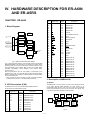
IV. HARDWARE DESCRIPTION FOR ER-A6IN AND ER-A5RS . . . . . . . . . . . . . . . . . 4-1
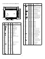
PARTS GUIDE
Parts marked with "! " is important for maintaining the safety of the set. Be sure to replace these parts with specified
ones for maintaining the safety and performance of the set.
SHARP CORPORATION
This document has been published to be used for
after sales service only.
The contents are subject to change without notice.
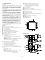
● Precautions
1. Downloading the data from the ER-02FD in the inline system
To download the data from the ER-02FD onto the ECR in the inline system, the following procedure
must be observed.
1) Download the data from the ER-02FD onto the ECR using the SRV #998.
2) Execute the SRV RESET operation.
3) Execute either the INLINE RAM CLEAR operation (#899) or the INLINE SET UP 1 JOB operation
(#895).
4) Check the SRV #970 to see if the ECR memory capacity exceeds the packaged RAM memory
capacity. If it does, add an optional RAM and follow the same procedure all over again from step 1).
CAUTION FOR BATTERY REPLACEMENT
(Danish)
ADVARSEL !
Lithiumbatteri – Eksplosionsfare ved fejlagtig håndtering.
Udskiftning må kun ske med batteri
af samme fabrikat og type.
Levér det brugte batteri tilbage til leverandoren.
(English)
Caution !
Danger of explosion if battery is incorrectly replaced.
Replace only with the same or equivalent type
recommended by the equipment manufacturer.
Discard used batteries according to manufacturer’s instructions.
(Finnish)
VAROITUS
Paristo voi räjähtää, jos se on virheellisesti asennettu.
Vaihda paristo ainoastaan laitevalmistajan suosittelemaan
tyyppiin. Hävitä käytetty paristo valmistajan ohjeiden
mukaisesti.
(French)
ATTENTION
Il y a danger d’explosion s’ il y a remplacement incorrect
de la batterie. Remplacer uniquement avec une batterie du
même type ou d’un type recommandé par le constructeur.
Mettre au rébut les batteries usagées conformément aux
instructions du fabricant.
(Swedish)
VARNING
Explosionsfare vid felaktigt batteribyte.
Använd samma batterityp eller en ekvivalent
typ som rekommenderas av apparattillverkaren.
Kassera använt batteri enligt fabrikantens
instruktion.
I. SRN (IN-LINE) SYSTEM FOR ER-A570
MODEL
ER-A6IN
ER-A57R1 (For ER-A570)
(OPTIONS FOR ER-A570)
CONTENTS
CHAPTER 1. ER-A570 SRN (IN-LINE) SYSTEM CONFIGURATION . . . . . . . . . .
1-2
CHAPTER 2. HARDWARE REQUIREMENTS . . . . . . . . . . . . . . . . . . . . . . . . . . . .
1-2
CHAPTER 3. TRANSMISSION SYSTEM SPECIFICATIONS . . . . . . . . . . . . . . . .
1-3
CHAPTER 4. FILE/DATA ALLOCATION IN THE IN-LINE SYSTEM . . . . . . . . . . .
1-6
CHAPTER 5. PROGRAM DATA UPDATING . . . . . . . . . . . . . . . . . . . . . . . . . . . . .
1-6
CHAPTER 6. SRV-MODE PROGRAMMING . . . . . . . . . . . . . . . . . . . . . . . . . . . . .
1-8
CHAPTER 7. PGM2 MODE PROGRAMMING . . . . . . . . . . . . . . . . . . . . . . . . . . .
1-14
CHAPTER 8. TROUBLESHOOTING JOBS . . . . . . . . . . . . . . . . . . . . . . . . . . . . .
1-16
CHAPTER 9. READING (X) AND RESETTING (Z) REPORTS . . . . . . . . . . . . . .
1-17
CHAPTER 10. SOFTWARE INSTALLATION PROCEDURE FOR
IN-LINE SYSTEM . . . . . . . . . . . . . . . . . . . . . . . . . . . . . . . . . . . . . .
1-19
1 1
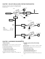
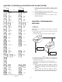
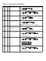
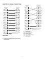
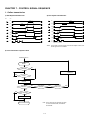
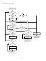
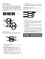
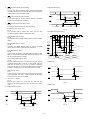
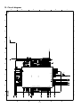
CHAPTER 1. ER-A570 SRN (IN-LINE) SYSTEM CONFIGURATION
The ER-A570 in-line system conforms to the SHARP Retail Network
that consists of a master and a maximum of 15 satellites (inclued the
one backup master).
ER-01MB/02MB
Master
HOST
ER-A5RS
Modem/NCU
ER-03DW
Drawer (max.3 units)
ER-A570
ER-01RA/02RA
ER-A6IN
ER-A57R1
ER-03RP or
ER-04RP
Backup master
Kitchin printer
ER-01MB/02MB
Sharp
Retail
Network
ER-A6IN
ER-A570
NOTE:
Master :
Satellite:
ER-03RP/04RP:
Satellite+ER-03RP/04RP:
1 unit
Max. 15 units
Max. 9 units
Max.15 units
ER-A57R1
ER-01RA/
ER-02RA
Satellites
ER-01MB/02MB
ER-A6IN
ER-A570
ER-A57R1
ER-01RA/
ER-02RA
Fig. 1-1
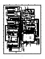
CHAPTER 2. HARDWARE REQUIREMENTS
1. Master System
2. Satellite system (inclued the backup
master)
The following optional units are required to complete the master
system configuration.
The following optional units are required to complete the Satellite
systems configuration.
The satellite may require additional RAM for allocating the IRC files.
The master may require additional RAM for allocating the IRC files.
1) ER-A6IN: SRN I/F control board
1) ER-A6IN: SRN I/F control board
2) ER-01RA: Option RAM chip (32KB)
ER-02RA: Option RAM chip (128KB)
ER-01MB: Option RAM board (Max. 512K bytes)
ER-02MB: Option RAM board (1M bytes)
2) ER-01RA: Option RAM chip (32KB)
ER-02RA: Option RAM chip (128KB)
ER-01MB: Option RAM board (Max. 512K bytes)
ER-02MB: Option RAM board (1M bytes)
3) ER-A57R1: Option device control ROM (1 chip)
• The ROM chip (ER-A57R1) is installed on the main PWB of ER-
3) ER-A57R1: Option device control ROM (1 chip)
• The ROM chip (ER-A57R1) is installed on the main PWB of ER-
A570.
A570.
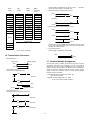
1 2
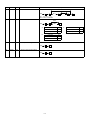
3. Components
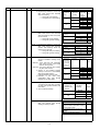
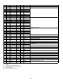
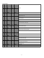
NO
MANE
PARTS CODE
Q’ty
1
PWB UNIT
CPWBX7317RC01
1
2
PWB BRACKET
LANGT7466RCZ Z
1
3
CONNECTOR BRACKET
LANGT7510RCZ Z
1
4
SCREW (FOR HOLDING OF THE PWB AND PWB BRACKET)
LX –BZ6665RCZZ
2
5
SCREW (FOR : PWB BRACKET AND PWB BRACKET, PWB BRACKET AND MAIN CHASSIS,
GND WIRE.)
LX–BZ6774R CZZ
6
WIRING TIE
LBNDJ2004SCZ Z
1
7
SPACER
PSPAN7039XCZZ
1
5
8
FERRITE CORE (FOR INTERNAL CABLE)
RCORF6666 RCZZ
1
9
INTERNAL CABLE
QCNW–6856RCZ Z
1
10
BNC-T CONNECTOR
QCNC–6811RC 0C
1
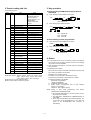
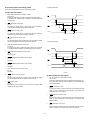
5. Maximum Length of Transmission
Cable
CHAPTER 3. TRANSMISSION
SYSTEM SPECIFICATIONS
1000m (3281 ft) . . . trunk cables + branch cables; however, branch
cable length is 10m (5m ✕ 2) for each terminal.
1. Transmission Method
1) Carrier sense multiple access with collision detect (CSMA/CD)
2) Single channel, half duplex
3) High level data link controller (HDLC)
6. Max Terminals
2. Transmission Medium
7. Physical Organization
1) Topology: Common Bus System
The branch cable is not included in the standard accessories of the
ER-A6IN. Please order with the following code.
16 Terminals max. (15 satellites, 1 master)
2) Coaxial cable RG-58/u
3. Transmission Speed
PARTS CODE
PRICE RANK
QCNW-6835RCZZ
BM
DESCRIPTION
Branch cable
480KBPS/1MBPS (Selectable) ... SRV mode JOB#922.
QCNW-6835RCZZ
4. Data Transfer Method
Packet-data transfer method
Data side of 1 paket is MAX. 270 Byte.
5m (16.4ft)
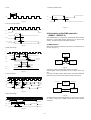
Fig. 3-1
Trunk cables
Tetminator
50Ω
Cable connector
R
R
Branch
cables
(5m x 2)
JJ conector
16.4ft.
x2
*Master
Satellite
Satellite
Satellite
Fig. 3-2 physical organization
*NOTE: The master can be located anywhere within the SRN (IRC) network configuration.
1 3
Satellite
5 Channel No.
Indicates that channel of the packet. (Channel 1 or Channel 2)
8. Packet Format
F
8 Bits
1 Opening flag (8 Bits) (01111110) (7E)
DA
8 Bits
2 Destination address (00-FEH)
(SRN Terminal Number)
SA
8 Bits
3 Source address (00-FEH)
TYPE
8 Bits
4 Packet type (DATA/ACK/RACK/NRDY)
CH NO
8 Bits
5 Channel No. (01H = CH1; 02H = CH2)
DLS
8 Bits
BCL
8 Bits
BCH
8 Bits
CRC
8 Bits
F
8 Bits
1) Unable to handle received data because the receiving side is
in the BUSY state.
2) Unable to handle received data because the receiving buffer is
full.
7 Number of data bytes
Indicates the number of bytes of data, which is a data, packet
status that will be converted into hexadecimal numbers before
transmission. Maximum number of bytes is 270.
6 Circuit status: Buffer full, RE-transmit, Unable
DATA
max.
270
bytes.
CRC
8 Bits
6 Circuit status
In the case of the NRDY packet, it indicates why the NRDY packet
was issued.
8 Data
Transfer data is contained in this field. Size of data is limited to a
maximum of 270 bytes. It can only exist in the data packet.
7 Dummy
9 CRC check code
This check code is used to detect any errors in the transmit data.
A CRC code is generated from the sending side to be sent to the
receiving side.
At the receiving side, the CRC check code is generated on the
basis of the same formula as the sending side to verify it against
the CRC check code receive.
8 Number of bytes at the data unit
Φ Closing flag (7E)
The closing flag is sent at the end of the packet. When the IRC
control circuit at the receiving side receives the flag, it terminates
the operation.
9 DATA
Number of data bytes (270 Bytes)
Φ CRC check code
9. Type of packet
Γ Closing flag (8 Bits) (01111110) (7E)
Two types of packet formats are available for the SHARP RETAIL
NETWORK. One is the data packet (the content of data is judged by
the host level). The other is the control packet which is responded to
by the controller level and has three types of packets: ACK packet,
RACK packet and NRDY (NOT READY) packet.
Fig. 3-3 Packet format
1 Opening flag (7E)
The open flag (7E) is sent at the beginning of each packet. As the
SRN control circuit (receiving side) receives the flag, it will start
the receiving operation.
NOTE: The packet begins with the open flag (8 Bits) and ends
with a closing flag (8 Bits).
2 Destination address (00H – FEH)
The destination address indicates where the packet is addressed
(receiving unit) too. The terminal number of each unit is converted
into a hexadecimal number to be used for the destination address.
3 Source Address (00H – FEH)
The source address indicates the sending unit (transmit unit). The
terminal number of each unit is converted into a hexadecimal
number to be used for the source address.
4 Types of packets
There are four types of packets each are used to indicate the type
of packet to be transferred.
00: DATA packet
(summary and preset data)
01: ACK packet
The acknowledging packet that is sent to the transmitting
side from the receiving side to indicate that the packet was
received properly.
02: RACK packet
The acknowledging packet that will be sent to the receiving
side to indicate that the ACK packet has been properly
received by the sending side.
03: NRDY packet
The acknowledge packet that is sent to the sending side to
indicate that it is not ready to receive data.
1 4
(1)
DATA packet: is used for sending and receiving data. Its contents are judged at the host level.
(2)
ACK packet: is a response sent from the sink station to the
source station by the link level (of DATA packet) when the DATA
packet is properly received.
(3)
NRDY (NOT READY) packet is a response packet of the link
level. It is used in case it is unable to receive in the host level or
no space is available in its receive buffer despite the the error
check CRC of the DATA packet is normal.
DATA
packet
ACK
packet
PACK
packet
NRDY
(Not ready)
packet
F
F
F
F
DA
DA
DA
DA
SA
SA
SA
SA
0
1
1
1
CH NO
CH NO
CH NO
CH NO
DLS
DLS
DLS
DLS
Communication is disabled due to full retry counts . . . "PW-OFF"
(power off) will be printed on the master unit.
4 Abnormal sequence-3 (when ACK is in error)
Data
X
ACK
(No ACK)
6ms
ACK
RACK
5 Abnormal sequence-4 (when RACK is in error)
BCL
0
0
0
BCH
0
0
0
CRC
CRC
CRC
CRC
CRC
CRC
F
F
F
DATA
Data
ACK-1
RACK
6ms
X
ACK-2
ACK-5
Control packet
CRC
Full ACK retry counts. If RACK were not detected after five retries
to send ACK, it assumes RACK to be in error, and so the receiving
operation terminates normally.
CRC
F
6 Abnormal sequence-5
(receiving side not enabled to receive data)
Fig. 3-4 Types of packets
Data
10. Transmission Procedure
NRDY
1 Normal sequence
[Sequence]
11. Terminal Number Assignment
[Receiving side]
Data
when the IRC option is installed, an IRC terminal number must also
be supplied. This number is in the range of 1 to 254. The number is
specified in the PGM 2 mode at installation time. It is necessary to
specify an number for each device connected to the IRC including the
master. It should be noted that the IRC terminal number and the
register number are not related. Section 10 of this manual indicates
how this number is specified.
ACK
RACK
2 Abnormal sequence-1
(when there is a single data error)
Data
X
• IRC terminal number (3 digits max.): *000 ∼ 254
*000: OFF line machine
15ms
(No ACK)
• Register number (4 digits max.): *0 ∼ 9999
*0: can not be used in the IRC operation.
Data
(Retry)
ACK
RACK
NOTE:
X
Indicates an error.
3 Abnormal sequence-2
(when there are six successive data errors)
Data
X
15ms
(No ACK)
Data
(Retry-1)
X
Data
(Retry-5)
X
(No ACK)
(No ACK)
15ms
1 5
CHAPTER 4. FILE/DATA ALLOCATION IN THE IN-LINE SYSTEM
Master
Satellite
∗ 1 ; In case of system report job disable on back-up master,
consolidation and receive files need not be created in back-up
master.
SRN
DEPT
TRAN
SACTION
PLU
SET
PLU
CLERK
HOURLY
DAILY
NET
EAN/
UPC
DYNAMIC
EAN/UPC
T.LOG
CUSTOMER
CASHIER
SIGN ON/OFF
CLERK
RCV BUFFER
Preset
totalizer
consolidation
receive
save
Preset
totalizer
consolidation
receive
save
Preset
totalizer
consolidation
receive
save
Preset
LINK
PLU
∗ 2 ; The clerk totalizer file only need to have one blocks.
DEPT
TRA N
SA CTION
Preset
totalizer
save
PLU
LINK
PLU
Preset
totalizer
save
Preset
totalizer
Preset
totalizer
Logging data
1. General
There are two ways of updating the preset data for the ER-A570
in-line system.
Totalizer
save
HOURLY
Totalizer
consolidation
receive
save
CHAPTER 5. PROGRAM DATA
UPDATING
Preset
CLERK
Totalizer
consolidation
receive
save
∗ 4 ; The sign on/off clerk file need not be created in case of
individual clerk system.
Preset
totalizer
save
SET
PLU
Preset
totalizer
consolidation
receive
save
∗ 3 ; The clerk consolidation/receive/save files need not be created
in case of floating clerk system.
Preset
totalizer
save
DAILY
NET
Totalizer
EAN/
UPC
Preset
DYNAMIC
EAN/UPC
Preset
1) To download the reset file of the master to a satellite after clearing
preset file of the slave.
This mode can be used at the time the machine is installation.
Logging data
T.LOG
Preset data
Totalizer
Preset
totalizer
consolidation
receive
save
KITCHEN
PRINTER
Preset
totalizer
save
CASHIER
Preset
edit buffer
KITCHEN
PRINTER
Preset data
Preset
edit buffer
Fig. 5-1
2) To download the preset file of the master to the preset file of a
slave without clearing the slave"s preset file. (Downloading file
with a job number in 5000)
RCV.
GLU
BUFFER
This mode can be used at the time of correcting preset data.
GLU
FILE
B.T.
BUFFER
Data process on the satellite to which the master preset file is
downloaded
GLU
BUFFER
B.T.
BUFFER
RESET
CLERK
Totalizer
receive
consolidation
RESET
CLERK
Totalizer
RESET
CASHIER
Totalizer
receive
consolidation
RESET
CASHIER
Totalizer
(in the ER-A570, the shaded section (
Fig. 4-1
(a)
When a preset file whose job number is 4000s is
downloaded, the contents of the corresponding file in the
satellite is zero cleared before saving the data received from
the master.
(b)
When a preset file whose job number is 5000s is
downloaded, the contents of the corresponding file in the
satellite is replaced by the preset file sent from the master.
GLU
BUFFER
) is not used.)
1 6
2. Down-Loading Job List
3. Key operation
List of Down load jobs
Mode
Job
SRV
800
PGM
Item
SRV parameter
1) Down-loading of PGM-mode program data on
DEPT/PLU
Note
(a)
Including the machine
parameter relating to
inline operations.
("#902, #920 d" is not
downloaded.)
PGM2 secret code
preset
845
Training text CLK No.
850
Free Key layout
4100
Dept preset
4119
Direct Dept/PLU key
4200
PLU/LINK/SET preset
with clearing function
4300
Transaction preset
with clearing function
Down-loading to all the satellites in the system
1 item
(JOB#)
NK2
X
X
NK3
TL
ALL
NK2: Register No.
(b)
Down-loading to the satellite specified
(JOB#)
NK1
X
ST
NK2
X
1 item
with clearing function
NK3
TL
NK1: Register No.
NK2: Start code
NK3: End code
4220
LINK PLU preset
with clearing function
4221
SET PLU preset
with clearing function
4400
Clerk preset
2) Down-loading of other program data
4600
Other preset
(a)
4610
Date, time
4614
Logo text
4644
Message text
4654
Guidance text
4700
TAX preset
4800
ONLINE preset
4950
IRC KP preset
4900
PGM preset relating to
inline operations
4999
All PGM preset
5100
Dept preset
without clearing function
5200
PLU/LINK/SET preset
without clearing function
5220
LINK PLU preset
without clearing function
5221
SET PLU preset
without clearing function
5300
Transaction preset
Down-loading to all the satellites in the system
(JOB#)
(b)
X
TL
Down-loading to the satellite specified
(JOB#)
X
NK1
ST
TL
NK1: Register No.
4. Others
1) If a transmission error occurs, the machine number of a satellite in
which the error has occured is printed In that case, the manager
retry function becomes available.
without clearing function
2) After transmission termination, the master prints the receipt/journal to that effect.
without clearing function
3) Broadcast communication
SRV mode down load job and PGM mode #4XXX (with clear job)
job is used by broadcast communication.
without clearing function
#4200 and #5200 don’t include stock data.
#4600 Other preset : Optional feature preset, VP preset, Hourly
report, Stack report, Secret code PGM1,
X1/Z1, X2/Z2, Auto key, PLU Level range.
#4400 exists in only clerk individual system.
#4200 include link PLU and set PLU presets.
Broadcast communication method:
The master is communicated to all satellites at a time.
The download of broardcast communication is as follows
a) Master downloads to all satellites.
(Broadcast communication)
<DISPLAY: SENDING>
b) All satellites receives the data.
c) Master checks communication error to each satellite.
(Normal cumminocation)
<DISPLAY : each register number>
NOTE: Setting of SRV mode programming
"BROADCAST COMMUNICATION"
JOB
#920-C
• When the ER-03RP/04RP is in the inline system, set up in
the following two methods*
1) Set JOB #920-C "BROADCAST COMMUNICATION" to
"NOTHING."
2) When performing broadcast downloading (#4XXX), turn
off the power of the ER-03RP/04RP, or turn off/on the
power of the ER-03RP/04RP after execution of
downloading.
1 7
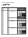
CHAPTER 6. SRV-MODE PROGRAMMING
0
(JOB#)
X
TL
ABCD
M: Master
S: Satellite
No.
1
Job#
#902 MRS = 0000
M/S
M/S
Item
Key sequence
902-A: 1. Choice of inline
1. Inline
No
Yes
2
#918 MRS = 0000
M/S
918-A: 1. Printing of text of a tied PLU in set
PLU
2. Direct non tendering finalization after
previous tender entry
3. Output of set PLU to KP
1. Printing of
text of a
tied PLU in
set PLU
2. Direct non
tendering
finalization
after
previous
tender
entry
Disable
Yes
Enable
Disable
No
Enable
902-A
0
1
3. Output of
set PLU to
KP
918-A
By tied PLU
0
Set PLU’s KP
1
By tied PLU
2
Set PLU’s KP
3
By tied PLU
4
Set PLU’s KP
5
By tied PLU
6
Set PLU’s KP
7
1. Red color printing on KP when
PLU’s unit price is zero
M/S
M/S
918-B: 1. Red color printing on KP when PLU’s
unit price is zero
918-C: 1. Printing of Z counter on Z1/Z2 report
2. Comulating orders in KP
3. Printing the DEPT./PLU text on KP in
double size character
No
Yes
1. Printing of
Z counter
on Z1/Z2
report
2. Comulating
orders in KP
Yes
Yes
No
Yes
No
No
M/S
918-D: 1. Tip paid includes cash tip
2. Clearing of tip totalizer at clerk Z1
report
3. Printing of tip totalizer on the clerk
report
1. Tip paid
includes
cash tip
2. Clearing
of tip
totalizer
at clerk
Z1 report
No
Yes
Yes
No
No
Yes
1 8
918-B
0
2
3. Printing
the
DEPT./PLU
text on KP
in double
size
character
918-C
No
0
Yes
1
No
2
Yes
3
No
4
Yes
5
No
6
Yes
7
3. Printing
of tip
totalizer
on the
clerk
report
918-D
No
0
Yes
1
No
2
Yes
3
No
4
Yes
5
No
6
Yes
7
No.
3
Job#
#920 MRS = 0000
M/S
S
Item
Key sequence
920-A: 1. Buck up master function
1. Buck up master function
Not
Exit
M/S
920-B: 1. System report and down load job is
executed in the buck up master
2. The GLU finalization is executed in
the setellite
3. The clerk system
1. System
report and
down load
job is
excuted in
the back
up master
2. The GLU
finalization
is
executed
in the
satellite
3. The clerk
system
920B
Enable
Disable
Disable
Enable
Enable
Disable
S
922-C: 1. Broad cast communication
2. PGM-mode programming
satellite
at
the
1. Broadcast
communication
Nothing
4
#922 MRS = 0008
M/S
Centralized
0
Individual
1
Centralized
2
Individual
3
Centralized
4
Individual
5
Centralized
6
Individual
7
2. PGM mode
programming at the
satellite
Exist
M/S
920-A
0
1
920-C
Disable
0
Enable
1
Disable
4
Enable
5
1.Machine assignment
920-D
Standalone
Satellite
Master
Backup master
0
1
2
3
920-D: 1. Machine assignment
922-A, B
922-C, D:
Not used. (Fixed at "00".)
1. SRN transmission speed and
carrier-off waiting time
1. Transmission
speed
480K BPS
1M BPS
5
#923 MRS = 0000
M/S
923-A, B, C, D:
6
#924 MRS = 0000
M/S
924-A: 1. Report printing when consolidation
daily and periodic cashier reading or
resetting
2. PLU save file
2. Carrier-off
waiting time
12.8 msec
3.2 msec
6.4 msec
9.6 msec
6.4 msec
1.6 msec
3.2 msec
4.8 msec
922-C,D
00
01
02
04
08
09
10
12
Not used. (Fixed at "0000")
1. Report printing when
consolidation daily and
periodic cashier
reading or resetting is
taken.
Printing of report on
individual register
Printing of both i.e.
reports on individual
machines and
consolidation report on
the entire system
1 9
2. PLU
save file
924-A
Not
0
Exist
1
Not
4
Exist
5
No.
6
Job#
#924 MRS = 0000
M/S
M/S
Item
Key sequence
924-B: 1. Save file except for PLU
2. Programming whether or not to lock
REG mode entries after individual
daily total resetting
1 Locking after clerk resetting
2 Locking after term clerk resetting
1. Save file
except for
PLU
2. Locking
after clerk
resetting
3. Locking
after term
clerk
resetting
Yes
Yes
0
No
1
Yes
2
No
3
Yes
4
No
5
Yes
6
No
7
Not
No
Yes
Exit
No
924-C: 1. Programming whether or not to lock
REG mode entries after individual
daily total resetting. When the system
has no save file
1 Locking after hourly resetting
2 Locking after general resetting
924-D: 1. Programming whether or not to lock
REG mode entries after individual
periodic total resetting. When the
system has no save file
1 Locking after daily net resetting
2 Locking after general resetting
7
#925 MRS = 0000
M/S
925-A: 1. Selection of the method of daily total
general consolidation resetting at the
master
Method-1: Those data that has individually
been reset and the current sales
data are reset together
Method-2: Only those data that has individually been reset is reset
2. Clearing of the individual resetting
memory at the time of consolidation
daily total general resetting
Individual resetting memory=IRM
3. Execution of Job #199 when
consolidation daily total general
resetting has not been taken.
925-B: 1. Any entry operation is inhibited until
Job #199 is executed after consolidation daily total general resetting has
been taken.
2. Various individal resetting.
1. Locking after hourly
resetting
No
1. Locking after hourly
resetting
No
1. Selection of
the method
of the daily
total general
consolidation
resetting at
the master
Yes
No
Yes
Method-2
No
1. Any entry
operation is
inhibited until
job#199
0
No
1
Yes
2
No
3
924-D
Yes
0
No
1
Yes
2
No
3
3. Execution of
Job#199
925-A
Method-1
No
1 10
2. Clearing of
the IRM
924-C
Yes
2. Locking after general
resetting
Yes
Yes
925-C: 1. Report printing when consolidation
daily and periodic total general
reading or resetting is taken.
2. Locking after general
resetting
Yes
924-B
Disable
0
Enable
1
Disable
2
Enable
3
Disable
4
Enable
5
Disable
6
Enable
7
2. Various
individual
resetting
925-B
Disable
0
Enable
1
Disable
2
Enable
3
1. Report printing
Both i. e. report on individual
machines and Consolidation report
on the entire system.
Consolidation report on the entire
system
Report on individual register
925-C
0
1
2
No.
7
Job#
#925 MRS = 0000
M/S
M/S
Item
Key sequence
925-D: 1. PLU stock control system
2. Resetting in the open store state.
1. PLU stock
control
system
Centralized
Individual
2. Resetting in
the open
store state
Disable
Enable
Disable
Enable
925-D
0
1
2
3
<<Detailed descriptions of the parameter for Job #925>>
925-A 1 Method of daily general resetting of the entire system at the master:
It is specified whether only those data that has individually been reset or that data and the
current sales data should be reset when resetting of the entire system is take.
Note here that if the machine is programmed to disable individual resetting (by B of
SRV-mode programming Job #925), not only individual resetting but also resetting of the
entire system cannot be achieved unless "Those data that has individually been reset and
the current sales data are reset together" has been selected.
2 Automatic clearing of the individual resetting memory at the time of consolidation daily
total general resetting No/Yes
The machine can be programmed to clear the individual resetting memory when general
Z1 resetting of the entire system is taken. If the memory is not cleared data is
accumulated each time individual resetting is taken until job #99 is executed.
3 Execution of Job #99 when consolidation daily total general resetting has not been taken
Enable/Disable:
Job #99 can be executed even if general Z1 resetting of the entire system is not taken.
925-B 4 Any entry operation is inhibited until Job #99 is executed after consolidation or individual
daily total general resetting has been taken No/Yes:
This parameter enables the master to restrict the resetting job at satellites.
5 Individual resetting Enable/Disable:
The master alone can be made capable of resetting by selecting "Disable".
When selecting "Enable", or "Disable", however, the selection of the resetting method
mentioned 1 above should well be noted.
925-C 6 Type of printing of daily total and periodic total general X/Z reports:
The following three types are available:
a) Printing of only X/Z reports on individual machines
b) Printing of a consolidation X/Z report only
c) Printing of X/Z reports on individual machines, followed by the printing of a
consolidation X/Z report
Note: This programming 1 - 4 is valid for the system that has the save file.
Reading of SRV-mode program data
925-D 7 PLU stock control in the inline system
a) Stock control in inline system is available in two types: individual and centralized
systems.
b) Centralized stock control system
Program data only stock is only stored in the master.
Stock data in each satellite must be zero before a stock entry is made.
When a consolidaton report is taken, stock data in respective satellites are
consolidated and is add to stock data in the master.
Then the sum is printed.
Stock data in each satellite is reset to zero at this time.
Notice) In this system, stock counter in each satellite is always negative.
So, Entry which makes the PLU stock counter negative must be Allowed
unconditionally. (SRV. JOB#906-A)
c) Individual control system
Program data on stock is stored in the master and stellites, respectively.
When a consolidation report is taken, stock data in the master and satellites is
consolidated and printed.
The consolidation does not affect the stock data in the master.
1 11
No.
8
Job#
#926 MRS=0004
M/S
M/S
Item
Key sequence
926-A: 1. Sending "last void data" on KP
2. Sending "past void data" on KP
1. Sending "last
void data" on
KP
2. Sending "past
void data" on
KP
926-A
Yes
0
No
1
Yes
2
No
3
Yes
No
M/S
926-B: 1. Program reset in PGM2 mode
2. Sending "refund data" on KP
1. Program
reset in
PGM2
mode
2. Sending
"refund
data" on KP
Disable
Enable
M/S
926-C:
1. Dept./PLU
text printing
Double
9
#931 MRS=0000
#937 MRS=0000
M/S
931: CONSOLIDATION Z1 COUNTER
937: CONSOLIDATION Z2 COUNTER
10
#897
M/S
Inline system in which kitchen printers alone are
connected.
• Function
a) In this inline system any inline job (consolidation, down-loading, UP-loading, etc) is inhibited.
b) SRV parameter JOB#922 is set to "0008" programming of the terminal number of the master.
K.P. preset file and K.P. edit buffer is created.
The above jobs, etc are performed.
c) The above system requires the following selection in programming JOB#920-D. Register
is standalone. =0
M/S
0
No
1
Yes
2
No
3
2. Check VP
format
Normal
#898
Yes
Not used (Fixed at "0")
926-D: 1. Dept./PLU text printing
2. Check VP
11
926-B
Inline resetting
• Function
This operation clears only the work memory
for inline operations.
The program memory for inline operations
re-mained uncharged even after the resetting
here is performed.
Inline communications can also be achieved.
1 12
926-D
Normal
0
Euro check
1
French check
2
German check
3
Normal
4
Euro check
5
French check
6
German check
7
X
931
XXXX
937
XXXX: Inital value for the counter.
897
X
TL
898
X
TL
TL
No.
12
13
Job#
#899
#895
M/S
M/S
M/S
Item
Key sequence
Clearing the memories for inline operations.
• Function
This operation clears all the inline program
data memory and work memory.
After carrying out this clearing operation, any
inline communication is inhibited until the
necessary data for inline operations are
re-programmed.
This function automatically create the inline
files by following SRV preset.
MASTER MACHINE : (SRV #920 D=2)
Consolidation file and the receive file is
created.
When clerk file is centraized, SIGN ON/OFF
CLERK file is created.
BACKUP MASTER MACHINE : (SRV #920
D=3)
RECEIVE GLU BUFFER is created.
When clerk file is centraized, SIGN ON/OFF
CLERK file is created.
When system report/downloading job is
possible on backup master, consolidation file
and the receive file is created.
All machine :
When the system has the save file, the save
file is created.
File area is shifted to secure the work memory
for inline operation.
The "in use" flag of the clerk program data file
is cleared. (at the master)
All records in the clerk program data file are
erased.
(at the satellite)
Set ip 1 job operation
899
X
Refer to CHAPTER 10.
1 13
TL
CHAPTER 7. PGM2 MODE PROGRAMMING
No.
Job#
M/S
Item
1.
#3610
M/S
• Terminal number
Key sequence
0
3610
TL
NK
X
NK: Terminal No. = 0 ~ 254
2.
#3611
M
• Master list (Generation)
3611
NK1
X
X
NK2
ST
TL
NK1: Terminal No. = 1 ~ 254
NK2: Register No. = 1 ~ 999999
3.
#3612
M
• Master list (Delection)
3612
NK
X
ST
TL
NK: Register No. = 1 ~ 999999
4.
#3616
M
• Terminal number of the quest
0
check file buck-up master.
3616
TL
NK
X
NK: Machine No. = 1 ~ 999999
NK = 0: When the back up master does not exist in the inline system.
MRS = 0
5.
#3631
M
• Decide whether to enable or
disable the manager retry
function when a transmission
error occurs
0
3631
TL
NK
X
NK:0 = Manager retry function ENABLE
1 = Manager retry function DISABLE
6.
#3650
M/S
MRS = 0
• Terminal number of K.P.
K.P.=Kitchine printer
3650
X
NK1
X
NK2
ST
TL
X
NK2
ST
TL
NK2
ST
TL
NK1: K.P. No. = 1 ~ 9
NK2: Terminal No. = 0 ~ 254
∗ NK2 = 0: When the K.P. deletion
7.
#3651
M/S
• Data transmission of K.P.
3651
X
NK1
NK1: K.P. No. = 1~9
NK2:
Data transmission
8.
#3653
M/S
NK2
Enable
0
Disable
1
• Second K.P. No.
3653
X
NK1
X
NK1: K.P. No. = 1 ~ 9
NK2: Second K.P. No. = 1 ~ 9
∗ NK2 = 0: When the non second K.P.
1 14
No.
Job#
M/S
9.
#3654
M/S
Item
Key sequence
• K.P. name
Space
3654
X
NK1
TEXT
X
ST
TL
NK 1: K.P. No. = 1~9
TEXT: Max. 12character
10.
#3655
M/S
• Print format for K.P.
0000
3655
X
A:
12.
#3610
#3650
M/S
M/S
TL
PLU/DEPT code
A
Amount
C
Print
0
Print
0
Skip
1
Skip
1
Unit price
B
Print
0
Skip
1
B:
11.
ABC
• Inline preset reading
3610
X
TL
3650
X
TL
• Kitchen printer preset reading
1 15
C:
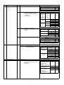
CHAPTER 8. TROUBLE SHOOTING JOBS
M : Master
S
: Satellite
BM : Backup master
No.
JOB#
1
#5810
2
ITEM
MODE
S/M
KEY SEQUENCE
Master declaration
PGM2
BM/M
5810
X
TL
#5820
Recover declaration
PGM2
BM/M
5820
X
TL
3
#5940
Clerk preset file in use flag foreed to clear
PGM2
M
5940
X
TL
4
#5990
All item sales data memory manual clear
PGM2
M/S
5990
X
TL
5
#5994
Clerk sales data memory manual clear
PGM2
M/S
5994
X
NK
X
TL
NK : Clerk No.
6
#5996
Hourly sales data memory manual clear
PGM2
M/S
5996
7
#5997
Daily net sales data memory manual clear
PGM2
M/S
5997
X
TL
8
#5700
Sign on clerk report
PGM2
M/S
5700
X
TL
1 16
TL
(4)
CHAPTER 9. READING (X) AND
RESETTING (Z) REPORTS
Syetem sales report for master/backup master
MODE ∗1
OP X/Z
REPORT NAME
X
Z
X1/Z1
∗3 DATA FOR
X2/Z2
X1
Z1
X2
Z2
JOB#
READING
GENERAL
Φ
Φ
Φ
Φ
1 x 00
—
(1)
Job #Ynm: Y = 1 when the master is in the X1/Z1 mode.
Y = 2 when the master is in the X2/Z2 mode.
DEPT/GROUP
Φ
Φ
1 x 10
—
(2)
Master consolidation report command entry sequence
IND. GROUP
Φ
Φ
1 x 12
GROUP No
(a)
To specify a range
GROUP TOTAL
Φ
1 x 13
—
NK1 : Machine number
NK2 : START number
NK3 : END number
PLU BY RANGE
Φ
Φ
Φ
Φ
1 x 20
PLU CODE
PLU BY DEPT
Φ
Φ
Φ
Φ
1 x 21
DPT CODE
GROUP No
X
Ynm
Enter system
X
NK1
Only 1 item
X
(b)
NK3
ST
NK2
Machine number
TL
To specify a department or group
NK1 : Machine number
NK2 : DEPT number
X
Ynm
Entire system
X
Z
NK1
ST
NK2
TL
Machine number
PLU IND. GR.
Φ
Φ
1 x 22
PLU GR. TL
Φ
Φ
1 x 23
—
PLU STOCK
Φ
1 x 24
PLU CODE
PLU ZERO SALES
Φ
Φ
1 x 27
ALL
PLU ZERO SALES
BY DEPT
Φ
Φ
1 x 27
DPT CODE
PLU MINIMUM
STOCK
Φ
1 x 28
ALL
TRANSACTION
Φ
TL-ID
Φ
COMMISSION
SALES
Φ
TAX
Φ
CHIFF
Φ
ALL CLERK
Φ
Φ
Φ
To specify nothing
Φ
Φ
NK1 : Machine number
Φ
Φ
Φ
Φ
HOURLY (ALL)
Φ
Φ
HOURLY (RANGE)
Φ
IND. CLERK
(c)
Φ
X
Entire system
X
Z
NK1
ST
TL
Machine number
Individual report command entry sequence
1 x 32
—
Φ
1 x 32
—
1 x 34
—
Φ
1 x 40
—
Φ
1 x 41
∗4
1 x 60
Φ
Φ
1 x 80
Φ
Φ
1 x 81
BALANCE
Φ
∗1
∗2
Φ
∗2
Φ
1 x 82
Φ
Φ
1 x 90 –
1 x 91
Φ
1 x 99
Φ
∗2
1 x 70
Φ
Φ
∗2
1 x 60
GLU BY CLERK
Reset clear
The same key operation as the standalone is required for entry
of an individual report JOB#.
Φ
GLU
STACKED REP
(3)
—
—
Φ
DAILY NET
Ynm
1 x 30
1 x 31
NOTE
X1 : Daily X report
Z1 : Daily Z report
X2 : Preriodic X report
Z2 : Periodic Z report
∗2
The time interval range, or PLU code range can be specified by
entering the start and end numbers according to the following
procedure. When specifying a single time interval, PLU code,
the start number has only to be entered.
XXXX
Start No.
X
XXXX
End No.
Stop of printing reports: These system reports do not execute this
specification.
∗3
When 1 is entered in the forth digit of a job code, Inline system
reports are printed.
Example:
∗4
1 17
System daily general report;
job code 1100
System periodic general report; job code 1200
In case of floating clerk system, this daily report can be printed
at any satellite.
(The periodic report can not be printed at any satellite.)
(5)
Individual report jobs for the master/backup master/satellite
MODE ∗1
OP X/Z
REPORT NAME
X
Z
GENERAL
X1/Z1
∗3 DATA FOR
X2/Z2
X1
Z1
X2
Z2
JOB#
READING
Φ
Φ
Φ
Φ
00
—
DEPT/GROUP
Φ
Φ
10
—
IND. GROUP
Φ
Φ
12
GROUP No
GROUP TOTAL
Φ
13
—
PLU BY RANGE
Φ
Φ
Φ
Φ
Φ
20
PLU CODE
PLU BY DEPT
Φ
Φ
Φ
Φ
21
DPT CODE
GROUP No
PLU IND. GR.
Φ
Φ
22
PLU GR. TL
Φ
Φ
23
—
PLU STOCK
Φ
24
PLU CODE
PLU ZERO SALES
Φ
Φ
27
ALL
PLU ZERO SALES
BY DEPT
Φ
Φ
27
DPT CODE
PLU MINIMUM
STOCK
Φ
28
ALL
TRANSACTION
Φ
TL-ID
Φ
COMMISSION
SALES
Φ
Φ
30
—
31
—
Φ
32
—
Φ
33
—
TAX
Φ
CHIFF
Φ
ALL CLERK
Φ
Φ
Φ
Φ
Φ
Φ
HOURLY (ALL)
Φ
Φ
HOURLY (RANGE)
Φ
Φ
IND. CLERK
Φ
—
Φ
40
—
∗4
Φ
41
—
∗4
60
Φ
Φ
Φ
80
Φ
Φ
81
Φ
Φ
∗1
∗2
∗2
82
Φ
90 – 91
Z1 : Daily Z report
X2 : Preriodic X report
Z2 : Periodic Z report
The time interval range, or PLU code range can be specified by
entering the start and end numbers according to the following
procedure. When specifying a single time interval, PLU code,
the start number has only to be entered.
XXXX
X
XXXX
End No.
When 2 is enterd in the third digit of a job code, periodic reports
are printed.
Example:
∗4
Φ
X1 : Daily X report
Start No.
∗3
Φ
Φ
*2
70
GLU
BALANCE
∗2
34
GLU BY CLERK
STACKED REP
∗2
60
Φ
DAILY NET
NOTE
Daily general report;
job code 100
Periodic general report; job code 200
In case of clerk centrized, this report can not be printed at master/backup master/satellites.
1 18
CHAPTER 10. SOFTWARE INSTALLATION PROCEDURE FOR IN-LINE SYSTEM
1. SATELLITE
SRV
1)
902 →
•
→ ⊗ → 1XXX → TL
; INLINE
2)
920 →
•
→ ⊗ → 1 → TL
; SATELLITE MACHINE.
3)
899 →
•
→ ⊗ → TL
; INLINE RAM CLEAR.
YES
PGM2
4)
2612 →
•
→ ⊗ → M-No. → TL
; OWN MACHINE NO.
5)
3610 →
•
→ ⊗ → T-No. → TL
; OWN TERMINAL NO.
2. MASTER
SRV
6)
902 →
•
→ ⊗ → 1XXX → TL
; INLINE
7)
920 →
•
→ ⊗ → 2 → TL
; MASTER MACHINE.
8)
Programs the other necessary SRV JOBs (#924,925)
9)
899 →
•
→ ⊗ → TL
YES
; INLINE RAM CLEAR
PGM
10)
2612 →
•
→ ⊗ → M-No. → TL
; OWN MACHINE NO.
11)
3610 →
•
→ ⊗ → T-No. → TL
; OWN TERMINAL NO.
12)
; MACHINE MASTER LIST
3611
T-No.
X
X
M-No.
13)
Programs the other necessary PGM JOBs.
14)
4900 →
•
ST
TL
→ ⊗ → TL
; DOWN LOADING (IN-LINE PARAMETER DATA)
(ALL PRESET DATA)
SRV
15)
800 →
•
→ ⊗ → TL
; DOWN LOADING (SRV PARAMETER)
16)
850 →
•
→ ⊗ → TL
; DOWN LOADING (KEYBOARD)
PGM
4999 →
17)
•
→ ⊗ → TL
; DOWN LOADING (ALL PGM PRESETS)
3. Set-up 1 job operation
1) Satellite (Jobs #902, #920, #899, and #3610 are auto-matically programmed.) must do PGM JOB#2612.
Terminal No.
of the satellite
TL
it self
2) Master (Jobs #902, #920, #899, #3610, #3611, and #4900 are automatically programmed.) must do PGM JOB#2612.
⊗
895
1
⊗
Terminal No.
of the satellite
X
ST
Terminal No.
Machine No.
ST
it self
3) Back-up master (Jobs #902, #920, #899 and #3610 are auto-matically programmed.) ,mast do PGM JOB#2612.
895
X
2
X
Terminal No.
of the satellite
TL
it self
4) Standalone (Jobs #902, #920 are automatically programmed.) must do PGM JOB#2612.
⊗
895
895 →
•
3
⊗
→ ⊗ → TL
1 19
TL
II. RS-232 SYSTEM FOR ER-A570
MODEL
ER-A5RS
ER-A57R1 (For ER-A570)
(OPTION FOR ER-A570)
CONTENTS
CHAPTER 1. GENERAL . . . . . . . . . . . . . . . . . . . . . . . . . . . . . . . . . . . . . . . . . . . . 2-2
CHAPTER 2. COMPONENTS . . . . . . . . . . . . . . . . . . . . . . . . . . . . . . . . . . . . . . . . 2-2
CHAPTER 3. SPECIFICATIONS OF RS-232 INTERFACE . . . . . . . . . . . . . . . . . . 2-2
CHAPTER 4. BLOCK DIAGRAM AND SYSTEM CONFIGURATION . . . . . . . . . . 2-3
CHAPTER 5. SIGNAL CONNECTION DIAGRAM . . . . . . . . . . . . . . . . . . . . . . . . . 2-3
CHAPTER 6. RS-232 PROTOCOL . . . . . . . . . . . . . . . . . . . . . . . . . . . . . . . . . . . . 2-5
CHAPTER 7. CONTROL SIGNAL SEQUENCE. . . . . . . . . . . . . . . . . . . . . . . . . . 2-12
CHAPTER 8. DATA BLOCK FORMAT. . . . . . . . . . . . . . . . . . . . . . . . . . . . . . . . . 2-15
CHAPTER 9. RS-232 APPLICATION. . . . . . . . . . . . . . . . . . . . . . . . . . . . . . . . . . 2-15
.
21
■ WHAT IS AN RS-232 INTERFACE?
• EIA (Electronics Industries Association) standard RS-232 is asso-
CHAPTER 3. SPECIFICATIONS OF
RS-232 INTERFACE
ciated with the transfer of binary serial data, control signals and
timing signals between modems and data terminals.
• The RS-232 interface is one of the devices generally used for the
1. Online interface
exchange of information between a computer and a peripheral
device.
• This interface (ER-A5RS) was designed to conform to the EIA
standard, but in particular it was designed for connection between
the ER-A570 and a data processing machine.
• It becomes necessary to set communication specifications of the
ER-A5RS (e.g. baud rate) matched to those of the data processing
machine, when the ER-A5RS is connected with a data processing
machine that is equipped with the RS-232 interface.
• The Dip switch on the ER-A5RS interface circuit board must be
used to choose the specifications.
• Refer to Section 3 "RS-232 Interface Specifications" for details of
a)
b)
c)
d)
Interface
Duplex type
Line configuration
Data rate
:
:
:
:
e)
f)
g)
h)
i)
Synchronizing mode
Parity check
Code
Bit sequence
Data format
:
:
:
:
:
communication specifications.
b1
b2
RS-232
Half-duplex / Full-duplex
Direct connection/Modem connection
19200, 9600, 4800, 2400, 1200, 600 and
300 bps
(Programable)
Asynchronous
Vertical parity check (odd)
ASCII
LSB first
1 start bit + 7 data bits + 1 parity +
1 stop bit
b3
b4
b5
b6
b7
P
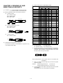
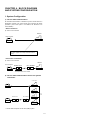
CHAPTER 1. GENERAL
Start-bit
This option (ER-A57R1 and ER-A5RS) is the RS-232 interface option
for the ER-A570 cash register. It enables the ER-A570 to perform
on-line data communications.
When this option is used for on-line data communications, the ERA570 can be connected to a host computer. Also, their connection
can be made via modems.
When this option is used together with a multiplexer (to be procured
in the market), it allows the host computer to be connected to more
than one ER-A570.
j) Protocol
k) Transmission line :
Cable
Connector
(ECR side)
Connector cover
Data rate
ER-A5RS
PARTS CODE
C PWB S 7 2 9 2 R C 0 1
L ANGT 7 4 6 6RC Z Z
Q’ty
1
1
L X – B Z 6 6 6 5RC Z Z
2
L X – B Z 6 7 7 4RC Z Z
3
XHBSD3 0 P 0 8 0 0 0
2
L BND J 2 0 0 4 SC Z Z
1
L H L DW6 8 1 4 R C Z Z
2
PSPAN7 0 3 9 XC Z Z
1
RCOR F 6 6 5 8 RC Z Z
2
Parity-bit Stop-bit
: Polling/selecting (Simple procedure)
: Shielded cable
: D-sub 9 pin (female type) connector
Inch pitch (4-40 UNC) lock screw
: Shielded cover
The table shows the relationship between the data rate and the recommended cable length.
CHAPTER 2. COMPONENTS
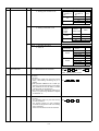
NO
NAME
1 PWB UNIT
2 BRACKET
SCREW (FOR PWB AND
3
BRACKET)
SCREW (FOR HOLDING OF
4 THE PWB BRACKET, AND
BRACKET TO BRACKET)
SCREW (FOR HOLDING OF
5
THE RS-232 CABLE CORE)
6 WIRING TIE
CLAMP
7
(FOR RS-232 CABLE)
8 SPACER
FERRITE CORE
9
(FOR EXTERNAL CABLE)
Data-bit
22
Recommended cable length
19,200 bps
3.75 meters
9,600 bps
7.5 meters
4,800 bps
15
meters
2,400 bps
30
meters
1,200 bps
60
meters
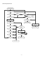
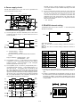
CHAPTER 4. BLOCK DIAGRAM
AND SYSTEM CONFIGURATION
1. System Configuration
1) On-line data communication
On-line data communication is allowed only when the ER-A570 is a
stand-alone machine or an in-line master. The protocol is the simple
procedure. (The on-line option is not usable if the ER-A570 is an
in-line satellite.)
1 Direct connection
a) One-to-one connection
Satellite
Host computer
ER-A570
The ER-A57R1 and ER-A5RS are Installed in ER-A570.
(The same applies to the sample connections shown
below.)
2 Connection via modems
a) One-to-one connection
Satellite
Host computer
MODEM NCU
NCU MODEM
ER-A570
To be procured in the market
2) On-line data communication and in-line system
connection
In-line master
OR
ER-A570
In-line master
ER-A570
In-line backup
master
MODEM NCU
NCU MODEM
in-line
system
ER-A570
In-line satellite
ER-A570
In-line satellite
∗ The ER-A6IN is required for the inline (SRN) system.
23
CHAPTER 5. SIGNAL CONNECTION
25PIN D-SUB
9PIN D-SUB
MODEM
TERMINAL
SD
2
3
SD
RD
3
2
RD
RTS
4
7
RTS
DCD
8
1
DCD
DTR
20
4
DTR
DSR
6
6
DSR
CTS
5
8
CTS
SG
7
5
SG
CI
22
9
CI
FG
1
25PIN D-SUB
9PIN D-SUB
HOST
SATELLITE
SD :
RD :
DTR :
DSR :
RTS :
DCD:
CTS :
FG :
FRAME GROUND is connected
to the shield of the cable.
DIAGRAM
1. Connection between the master (Host)
and Satellite
24
SD
2
3
SD
RD
3
2
RD
RTS
4
7
RTS
DCD
8
1
DCD
DTR
20
4
DTR
DSR
6
6
DSR
CTS
5
8
CTS
SG
7
5
SG
FG
1
FRAME GROUND is connected
to the shield of the cable.
TRANSMITTED DATA
RECEIVED DATA
DATA TERMINAL READY
DATA SET READY
REQUEST TO SEND
DATA CARRIER DETECTOR
CLEAR TO SEND
FRAME GROUND
2. Connection between the terminal and
MODEM
SD :
RD :
DTR :
DSR :
TRANSMITTED DATA
RECEIVED DATA
DATA TERMINAL READY
DATA SET READY
Host
Satellite
( 1 ) Inquines of the satellite.
Dummy
(3bytes)
( 2 ) Receives ENQ.
Check the terminal No.
to see if it is its own.
ENQ
Terminal No.
(6bytes)
( 4 ) Receives ACK.
ACK
( 3 ) Sends ACK.
( 5 ) Sends the text.block.
Start code
Text (parameter)
( 6 ) Receives text.
Checks the check sum,text
data,etc. And goes to (8)
if there is no error in them.
End code
Three types of
text block formats
are available
Text (FDS)
Text (DATA)
( 8 )' Sends NAK if any error
occurs.
NCK
( 7 ) Resends the text block if NAK is received.
Resends the text block up to two times.
Sends EOT and terminates the operation
with error if NAK is still received after the
second resending of text block.
( 8 ) Sends ACK.
ACK
( 9 ) Sends the next text if ACK is received and
sends EOT and terminates the operation if
data transfer is finaiized.
EOT
RTS :
DCD:
CTS :
CI :
FG :
REQUEST TO SEND
DATA CARRIER DETECTOR
CLEAR TO SEND
CALLING INDICATOR
FRAME GROUND
25
( 10 ) Terminates the operation if EOT
is received.
Host
Satellite
( 1 ) Inquines of the satellite.
Dummy
(3bytes)
Terminal No.
(6bytes)
( 2 ) Receives ENQ.
Checks the terminal No.
to see if it is its own.
ENQ
( 4 ) Receives ACK.
ACK
( 3 ) Sends ACK.
( 5 ) Sends the text.block.
Start code
Text (parameter)
( 6 ) Receives text.
Checks the check sum,text
data,etc. And goes to (8)
if there is no error in them.
End code
Text (DATA)
( 8 )' Sends NAK if any error
occurs.
NAK
( 7 ) Resends the text block if NAK is received.
Resends the text block up to two times.
Sends EOT and terminates the operation
with error if NAK is still received after the
second resending of text block.
( 8 ) Sends ACK.
ACK
( 9 ) Sends the next text if ACK is received and
sends EOT and waits for ENQ.
EOT
( 10 ) Terminates the operation if EOT
is received.
ENQ
ACK
Continued on the
next page
CHAPTER 6. RS-232 PROTOCOL
1. Basic protocol specification
1) Data transmission from the host to a satellite
26
Host
Satellite
Continued from the
preceding page.
( 12 ) Sends text corresponding
to the job code.
Start code
( 13 ) Receives text.
Checks the check sum, text lingth, text data, etc.
And goes to (15) if there is no error in them.
Sends NAK if any error occurs.
Text (parameter)
Text (DATA)
NAK
(When an error
occurs)
( 14 ) Resends text block if NAK is received.
Resends text up to two times,and
performs error handling if NAK is still
received after the second resending
of text block.
( 15 ) Sends ACK.
ACK
( 16 ) Sinds the next text if ACK is received,
and sends EOT and terminates the
operation if data transfer is finalized.
EOT
( 17 ) Terminates the operation if EOT is received.
Note : For the description of
each data block see section
4 (Text block formats)
2) Data transmission from satellite to the host
27
End code
Two types of
text block
formats are
available.
—
—
—
—
NAK
EOT
TEXT
TIME-UP
Time-up: One second after sending of ID ENQ.
Four seconds after sending of text.
Sends ID ENQ and goes to 1.
—
ACK
KEY ENTRY
—
0
Initial
ENQ
EVENT
STATE
1) Down-loading matrix for the host
2. Transmission control procedure matrix
—
—
—
Resends the text and then goes to 2.
If the host has resent the text two times,it sends EOT and
goes to 0.
(ERROR END)
The host goes to 0.
(ERROR END)
—
—
—
Resends the text and then goes to 2.
If the host has resent the text two times, it sends EOT and
goes to 0.
(ERROR END)
Sends text and goes to 2.
Sends EOT and then goes to 0.
(Normal end)
—
2
After sending text
Resends ID ENQ and then goes to 1.
If the host has resent ID ENQ two times,it sends EOT and
goes to 0.
(ERROR END)
Sends text and goes to 2.
—
1
After sending ID ENQ
—
—
—
—
NAK
EOT
TEXT
TIME-UP
—
—
Resends EOT and goes to 3.
If the host has resent the EOT two times, it goes to 0.
(ERROR END)
Time-up: Two second after sending of EOT.
KEY ENTRY
TIME-UP
TEXT
EOT
—
—
NAK
The host goes to 0
(ERROR END)
Sends ACK and goes to 4.
3
After sending EOT
ACK
ENQ
EVENT
STATE
Time-up: One second after sending of ID ENQ.
Four seconds after sending of text.
Sends ID ENQ and goes to 1.
—
ACK
KEY ENTRY
—
0
Initial
ENQ
EVENT
STATE
2) Up-loading matrix for the host
—
—
—
Sends EOT and goes to 3.
—
—
The host goes to 0.
(ERROR END)
Time-up is 7 seconds
—
The host checks the checks the text block, if the block is
correct, the host sends ACK and goes to 4.
If it is not correct, the host sends NAK and goes to 5.
If transmission cannot be continued, the host sends EOT
and goes to 0.
(ERROR END)
The host checks the text block, if the block is correct, the
host sends ACK and goes to 4.
If it is not correct, the host sends NAK and goes to 5.
If transmission cannot be continued, the host sends EOT
and goes to 0.
The host goes to 0.
(ERROR END)
Time-up is 7 seconds
The host goes to 0.
(ERROR END)
—
—
—
5
After sending NAK
—
Resends the text and then goes to 2.
If the host has resent the text two times, it goes to 0.
(ERROR END)
The host goes to 0.
(ERROR END)
Resends the text and then goes to 2.
If the host has resent the text two times, it goes to 0.
(ERROR END)
—
2
After sending text
After the host has received TEXT, goes to 0.
(Normal end)
After the host has received ENQ, goes to 0.(ERROR END)
—
—
After the host has received ENQ, resends ACK and goes to
4.
After the host has received TEXT, ignores the ENQ.
4
After sending ACK
—
Resends ID ENQ and then goes to 1.
If the host has resent ID ENQ two times, it goes to 0.
(ERROR END)
Sends text and goes to 2.
—
1
After sending ID ENQ
—
—
—
EOT
TEXT
TIME-UP
ACK
NAK
ID-ENQ
Initial
0
Satellite checks the terminal No.:If it is correct, satellite
sends ACK and goes to 1.
If it is not correct, Satellite ignores the ID-ENQ.
—
—
STATE
EVENT
3) Down-loading matrix for the sattelite
After sending ACK
1
Satellite checks the terminal No.:If it is correct, satellite
sends ACK and goes to 1.
If it is not correct, Satellite ignores the ID-ENQ.
—
—
After satellite has received TEXT, goes to 0.
(Normal end)
Before satellite has received TEXT, ignores the EOT
Satellite checks the text block, if the block is correct,
Satellite sends ACK and goes to 1.
If it is not correct, satellite sends NAK and goes to 2.
If transmission cannot be continued, satellite sends EOT
and goes to 0.
(ERROR END)
Satellite sends EOT, and goes to 0.
(ERROR END)
Time-up is 7 secondsThe host goes to 0.
Satellite checks the text block, if the block is correct,
Satellite sends ACK and goes to 1.
If it is not correct, satellite sends NAK and goes to 2.
If transmission cannot be continued, satellite sends EOT
and goes to 0.
(ERROR END)
The host goes to 0.
(ERROR END)
Time-up is 7 seconds
Satellite goes to 0.
(ERROR END)
—
—
—
After sending NAK
2
—
—
TEXT
TIME-UP
—
NAK
The host goes to 0.
(ERROR END)
Time-up is 7 seconds
Satellite checks the text block, if the block is correct,
satellite sends ACK and goes to 3.
If it is not correct, satellite sends NAK and goes to 2.
If transmission cannot be continued, satellite sends EOT
and goes to 0.
(ERROR END)
Time-up: Four seconds after sending of text.
Two second after sending of ENQ.
TIME-UP
TEXT
EOT
—
ACK
Satellite sends ENQ and goes to 4.
—
3
ID-ENQ
EVENT
After receiving text and sending ACK
—
EOT
STATE
—
—
NAK
Resends the ENQ and then goes to 4.
If satellite has resent the ENQ two times, sends EOT and
goes to 0.
(ERROR END)
—
Resends the ENQ and then goes to 4.
If Satellite has resent the ENQ two times, sends EOT and
goes to 0.
(ERROR END)
—
Satellite sends the text and goes to 5.
—
4
—
Resends the text and then goes to 5.
If satellite has resent the text two times, sends EOT and
goes to 0.
(ERROR END)
Satellite goes to 0.
(ERROR END)
Resends the text and then goes to 5.
If satellite has resent the text two times, sends EOT and
goes to 0.
(ERROR END)
Satellite sends the text and goes to 5, or sends the EOT
and goes to 0.
(Normal END)
—
5
After sending TEXT
Satellite goes to 0.
(ERROR END)
Time-up is 7 seconds
Satellite goes to 0.
(ERROR END)
Time-up is 7 seconds
After sending ENQ
Satellite checks the text block, if the block is correct,
Satellite sends ACK and goes to 3.
If it is not correct, Satellite sends NAK and goes to 2.
If transmission cannot be continued, satellite sends EOT
and goes to 0.
(ERROR END)
Satellite goes to 0.
(ERROR END)
—
—
—
2
After sending NAK
Satellite checks the text block, if the block is correct,
satellite sends ACK and goes to 3.
If it is not correct, Satellite sends NAK and goes to 2.
If transmission cannot be continued, satellite sends EOT
and goes to 0.
(ERROR END)
—
—
—
ID-ENQ
ACK
1
Satellite checks the terminal No.:If it is correct, satellite
sends ACK and goes to 1.
If it is not correct, satellite ignores the ID-ENQ.
After receiving ID-ENQ and sending ACK.
0
Initial
Satellite checks the terminal No.:If it is correct, satellite
sends ACK and goes to 1.
If it is not correct, satellite ignores the ID-ENQ.
EVENT
STATE
4) Up-loading matrix for the satellite
CHAPTER 7. CONTROL SIGNAL SEQUENCE
1. Online transmission
1) Half duplex transmission
DCE
2) Full duplex transmission
DCE
DTE
SD
DTE
SD
DATA
RD
DATA
RD
DATA
DATA
RTS
RTS
CTS
CTS
DSR
DSR
DCD
DCD
< 100ms
< 100ms
DTR
DTR
< 500ms
< 500ms
* CI
CI
*Note : In the direct connect mode, same as full duplex control, but the
CI signal is not controlled.
*Note: In the direct connect mode, same as full duplex control, but
the CI signal is not controlled.
3) Line connection sequence flow
STARTED BY P.C
INITIAL
CI SENSE ?
NO
YES
NO
ERROR : NO LINE
DTR OFF
CI ON ?
DTR ON
NO
DSR ON ?
NO
CI SENSE ?
NO
YES
TIME OUT ?
YES
30sec
YES
NO
FULL DUPLEX ?
YES
RTS ON
LINE ESTABLISHED
Note : The CI signal can be changed over when
so set in the PGM mode, and effective
at ECR side.
2 12
4) Transmission sequence flow
LINE ESTABLISHED
YES
FULL DUPLEX ?
NO
DCD OFF ?
YES
NO
YES
TIME OUT ?
5 sec
RTS ON
DSR ON ?
YES
FULL DUPLEX ?
YES
DCD ON ?
YES
NO
TIME OUT ?
30 sec
NO
CTS ON ?
TIME OUT ?
YES
NO
TXRDY ?
YES
YES
YES
7 sec
FULL
DUPLEX ?
DTR OFF
RTS OFF
YES
TRANSMIT ERROR
SEND 1 CHARACTER
YES
YES
RTS OFF
MORE TO
SEND ?
LINE ESTABLISHED
FULL DUPLEX ?
WAIT 100ms
RTS OFF
LINE ESTABLISHED
2 13
5) Receiving sequence flow
LINE ESTABLISHED
DSR ON ?
NO
YES
DCD ON ?
NO
NO
HALF
DUPLEX ?
NO
TIME OUT ?
30sec
YES
RXRDY ?
NO
YES
ID. ENQ ∞
ACK or
NAK 4 sec
TEXT 7 sec
NO
TIME OUT ?
YES
YES
SEND TEXT
READ 1 CHARACTER
NO
YES
EOT ?
YES
LINE ESTABLISHED
DTR OFF
RTS OFF
ENQ ?
YES
NO
ACK ?
YES
AFTER
RECEIVE
ER-OFF
COMMAND
RECEIVE ERROR
YES
END CODE
NAK ?
YES
DTR OFF
RTS OFF
YES
DSR OFF
YES
BUFFER FULL ?
YES
INITIAL
LINE ESTABL
2 14
NO
CHAPTER 8. DATA BLOCK FORMAT
Example
1
2
3
Memory image
02
5A
F0
1. Basic format
1
1) ID-ENQ :
10bytes
2
30h
Line image
32h
ENQ code (05h)
Terminal No. 000001-999999 (6 bytes)
EOT is set as dummy cahracters. (3 bytes)
2) ACK :
1 byte 06h
3) NAK :
1 byte 15h
4) EOT :
1 byte 04h
5) ENQ :
1 byte 05h
35h
3
41h
46h
30h
Transmission sequence
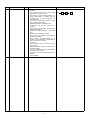
CHAPTER 9. RS-232 application
1. RS-232 preset
6) TEXT :
Data ASCII (max. 250 bytes)
Block consecutive No.
Start code
1) SRV programming
End code
Check sum
[JOB#945] MRS = 0000
The assignment of RS-232 channel by each devices.
Start code : This code may not be provided.
Null is impermissible.
0
945
End code : This code may not be provided.
Null or any same code as the start code is
not permissible.
945-A:
945-B:
945-C:
945-D:
When master reset is performed, the default is assumed:
Start code = 02h
End code = 0Dh
: 2 bytes hex number
Low-order 8-bit data of the complement of
2 for the sum of text data.
RAM data:
: Even number of data that is obtained by
dividing one byte of RAM data into highorder 4 bits and low-order 4 bits and converting them to ASCII codes shown in the
code conversion table.
Bit image
Hexadecimal
Channel No. for ONLINE = 0 to 7.
Not used. (Fixed at "0")
Not used. (Fixed at "0")
Not used. (Fixed at "0")
∗ Do not select the same channel number with two or more devices.
∗ Use the switches on the I/F board to set the channel No. for the I/F
board connector. (Refer to the RS-232 channel setting in IV.
HARDWARE DESCRIPTION FOR ER-A5RS.)
2) PGM programming
Job#
PGM-MODE programming for online operation
6110
Programming of the terminal number
6111
Programming of the modem control
6112
Programming of the transmission data rate (Bau
rate)
ASCII
6113
Programming of the start and end code.
6110
Online Preset reading
Code conversion table .
Print code (high-order or low-order 4 bits)
TL
∗ When channel No. is zero, system is nothing.
Block consecutive No. : This number starts with 30h and cycles
like this: 30h, 31h — 39h, 30h, 31h (Ring
counter system)
Check sum
ABCD
X
Line image
0000
0
30h
0001
1
31h
0010
2
32h
[JOB#6110] MRS = 000001
0011
3
33h
Programming of the terminal number
0100
4
34h
0101
5
35h
0110
6
36h
0111
7
37h
1000
8
38h
1001
9
39h
1010
A
41h
1011
B
42h
1100
C
43h
1101
D
44h
1110
E
45h
1111
F
46h
0
6110
X
NK
NK: Terminal No. = 0 to 999999
2 15
TL
[JOB#6111] MRS = 00
Porgramming of the modem control
0
6111
X
TL
AB
6111-A: 1. Sensing of the CI signal Yes/No
1. Sensing of the CI signal
6111-A
No
0
Yes
1
6111-B: 1. Duplex type
1. Duplex type
6111-B
Full duplex system
0
Half duplex system
1
[JOB#6112] MRS = 5
Programming of the transmission bau rate
0
6112
TL
A
X
6112-A: Transmission bau rate
Transmission bau rate
6112-A
300 bps
0
600 bps
1
1200 bps
2
2400 bps
3
4800 bps
4
9600 bps
5
19200 bps
6
[JOB#6113] MRS = 002013
Programming of the start and end code
0
6113
X
XXXYYY
TL
XXX: Start code = 02H (STX)
YYY: End code = 0DH (CR)
[JOB#6110]
Online preset reading
6110
X
TL
2 16
III. TEST FUNCTION FOR ER-A6IN AND ER-A5RS
CHAPTER 1. General
CHAPTER 4. Test Job & Code
This test program, is contained in the ER-A57R1 (option ROM), has
been developed for the purpose of confirming the operations of the
I/F board check conducted by the ER-A5RS and ER-A6IN mounted in
the ER-A570.
1 RS-232 I/F check
JOB & CODE
CHAPTER 2. Structure (RS-232 test
& inline test)
1 RS-232 test (RS-232 port test conducted by ER-A5RS
The following structure is required to execute RS-232 test program.
•
•
•
•
Contents
500
Channel check
501
RS-232 channel 1 check
502
RS-232 channel 2 check
503
RS-232 channel 3 check
504
RS-232 channel 4 check
505
RS-232 channel 5 check
506
RS-232 channel 6 check
507
RS-232 channel 7 check
2 Inline I/F check
ER-A570
JOB & CODE
Contents
ER-A5RS (I/F PWB Unit)
600
IRC TEST 1
Loopback connector for testing (UKOG-6705 RCZZ)
601
IRC TEST 2
ER-A57R1 (option control ROM)
602
IRC TEST 3
603
IRC TEST 4: DATA
(SATELLITE setting)
transmission
test
604
IRC TEST 5: DATA
(MASTER setting)
transmission
test
UKOG-6705RCZZ:
ER-A5RS: 2PCS
ER-A570
+ ER-A57R1
CHAPTER 5. Cautions
• Options should be installed with the power supply turned off.
• When setting the RS232C channels, avoid setting two or more
Diagram of the loopback connector
ports to the same channel. The ER-A570 allows installation of
max. two units of the ER-A5RS. In this case also, avoid setting two
ports of the ER-A5RS to the same channel. If not, the hardware
may be damaged.
• Concerning the inspection items whose display formats are not
1
CD
2
RD
3
TD
4
ER
5
6
GND DR
7
RS
8
CS
presented in this test function, nothing appears on the display
screen. (blank display)
9
CI
CHAPTER 6. RS-232 Test
2 Inline test
The following structure is required to execute the inline test program.
•
•
•
•
•
1. Channel check
ER-A570
1 Activation
The program is activated by JOB#500
SRV mode: 500 → TL
ER-A6IN (inline I/F PWB unit)
ER-A57R1 (option control ROM)
2 Contents to be tested
Information about connected RS-232 channel is printed.
Branch line (main line) cable (for transmission test)
Terminator (50Ω)
Πριντινγ
διγιτ
21
20
19
18
17
16
15
ΧΗ7 ΧΗ6 ΧΗ5 ΧΗ4 ΧΗ3 ΧΗ2 ΧΗ1
CHAPTER 3. Activation
3 2 1
5 0 0
CHn = 0 : Presence of channel
1 : Ansence of channel
This test program can be activated by inputting 3-digit number → TL
with the mode switch in the "SRV" position.
3 Confirmed content
Printed contents and the setting of channel changeover switch on
PWB are compared and confirmed.
3 1
4 Release
The program is terminated after the above contents are printed.
RS-232 channel setting (SW OFF: 1, SW ON: 0)
$FF.
Note) The above check should be made with the baud rate set at
9600BPS.
∗ Refer to the silk print on the I/F board.
Check 3 Timer check
Before making check 2 , set the corresponding timer at
10ms for RCVDT activation, and check to see that:
1) TRQ1 is not generated during the execution of check
2 .
2) TRQ1 is generated in 10msec. after check 2 is finished.
ER-A5RS CN2
SW1
Channel
5
4
0
0 Invalid
0
1 Channel 1
1
0 Channel 2
1
1 Channel 3
0
0 Channel 4
0
1 Channel 5
1
0 Channel 6
1
1 Channel 7
6
0
0
0
0
1
1
1
1
3
0
0
0
0
1
1
1
1
ER-A5RS CN1
SW1
Channel
2
1
0
0 Invalid
0
1 Channel 1
1
0 Channel 2
1
1 Channel 3
0
0 Channel 4
0
1 Channel 5
1
0 Channel 6
1
1 Channel 7
3 Contents to be checked
If an error occurs during the above checks, following error printouts occur. Even if an error occurs during check 1 , the test is
continued after the corresponding error print-out has occurred, but
if an error occurs during the execution of check 2 or 3 , the test
is terminated after the corresponding error print-out has occurred.
Note that when check 1 , 2 or 3 terminates, the termination
print-out occurs irrespective of any errors that have occurred during the check. (The program terminates normally only when no
error print-out has occurred.)
2. RS-232 Channel 1 ~ 7 check
1 Activation
The program is activated by JOB#501~507.
SRV mode: 501 → TL : Channel 1
ERROR
ERROR PRINT
E1-ER DR
ERn-DRn ERR
502 → TL : Channel 2
2
E2-ER CI
ERn-CIn ERR
503 → TL : Channel 3
3
E3-RS CD
RSn-CDn ERR
504 → TL : Channel 4
4
E4-RS CS
RSn-CSn ERR
505 → TL : Channel 5
5
E5-CI INT
Interruption error of CIn
506 → TL : Channel 6
6
E6-CD INT
Interruption error of CDn
7
E7-CS INT
Interruption error of CSn
8
E8-TXEMP
TXEMPn error
9
E9-TXEMP I
Interruption error of TXEMPn
10
E10-TXRDY
TXRDYn error
11
E11-TXRDY I
Interruption error of TXRDYn
E12-RCVRDY
RCVRDYn error
(Reception is impossible. TRQ1 has
occurred during execution of check
2 .)
E13-RCVRDY I
Interruption error of RCVRDY
E14-SD RD
SDn-RDn ERR
(Data error)
E15-SD RD
SDn-RDn ERR
(Data error, Flaming error)
E16-TIMER
TIMERn error
(TMRQn cannot be set
termination of check 2 .)
507 → TL : Channel 7
2 Contents to be tested
If the channel specified by JOB#CODE is not set, the machine
performs the mis-operation processing. When the channel is set,
the machine conducts the loop check concerning the channel
specified by JOB#CODE by using the loopback connector.
The following three items are checked:
12
1 Control signal check
2 Data transfer check
13
3 Timer check (RS-232 onboard timer)
14
Check 1 Control signal check (ERn-DRn•CIn, RSn-CDn•CSn loop
check)
OUTPUT
15
INPUT
ERn
RSn
DRn
CIn
CDn
CSn
OFF
OFF
OFF
OFF
OFF
OFF
OFF
ON
OFF
OFF
ON
ON
ON
OFF
ON
ON
OFF
OFF
ON
ON
ON
ON
ON
ON
16
17
E17-TIMER I
after
Interruption error of TRQ1
Errors that may occur during check 1 (control signal check): E1 ~ E7
Errors that may occur during check 2 (data transfer check): E8 ~
E15
Errors that may occur during check 3 (timer check): E12, E16 and
E17
The read check about the above INPUT items and interrupt check of
CS, CI and CD are performed.
Read check:
Contents
1
ER and RS are switched over in the order as
shown in the above table to confirm the logic of
DR, CI, CD and CS.If the read logic is different
from the one in the table, error print-outs occur.
4 Cancellation
The program automatically terminates when a check is finished.
Termination print-out:
Interrupt check: Allows the interruption of either of CS, CI and CD
one by one. (The mask is released.)
The interruption does not take place when each
signal is turned on. Or if the interruption occurs
when a signal is turned off, error print-outs occur.
50n
Each of the above checks should be made in four cycles.
Note) ERn control selector jumper switch on the I/F board must be
switched to the software control side.
Check 2 Data transfer check (SDn-RDn loop check)
In this check, transfer 256-byte loopback data of $00 ~
3 2
n :
1~7
b6: n unexpected interruption is made.
b7: An error occurs. (Always 1 when in error print)
CHAPTER 7. INLINE CHECK
δ Error print by diag 5 command
The table below shows the names of the signals to be checked
and their directions.
1. IRC TEST 1
1 Getting started
Get started with JOB #600.
SRV mode: 600
TL
2 Test content
The ROM and the RAM on the ER-A6IN are checked as well as
an interruption by CTC and carrier sense are checked. Also the
ADLC functions and send/receive DMA are checked by means of
the self loop function of ADLC (MC6854). In addition, the other
signals are checked.
Signal name
Direction
Power failure notice
Host → Controller
Power ON initializing
Host → Controller
Power ON continuation
Host → Controller
Power failure process end
Host ← Controller
CH1 received data present
Host ← Controller
CH2 received data present
Host ← Controller
E5-XXXXXXXX
(b7b6b5b4b3b2b1b0)
3 Check content
The end print is checked.
First the status of the number of resending is printed by the SRN
handler command (Diag 2), then diag 0, 1, and 5 commands are
executed. If any error occurs, an error print is made to show the
error status.
H>C
Check that the target bits in two kinds of status (ST1 and ST2)
obtained by diag 5 command are "0" for ST1 and "1" for ST2.
(The other bits should be masked.) In the other cases, the
error occurring bit is shown as "1" and the error print is made
in the above format. If the target bit is "0," it is normal.
ST1: Sense in the controller in non-active state of a signal in
the direction of host → controller.
ST2: Sense in the controller in active state of a signal in the
direction of host → controller.
α Print of the number of resending by diag 2 command
DATA RETRY CNT. = XXX
ACK
RETRY CNT. = YYY
(Νοτε) ΞΞΞ ανδ ΨΨΨ αρε ιν
δεχιµ αλνυµ βερσ. (000∼255)
B7:
B6:
B5:
B4:
B3:
B2:
B1:
B0:
β Error print by diag 0 command
Error status (0: Normal or not checked yet, 1: Abnormal)
E0-XXXXXXXX
(b7b6b5b4b3b2b1b0)
0 (Not used.)
Power failure notice
0 (Not used.)
0 (Not used.)
0 (Not used.)
0 (Not used.)
Power ON continuation
Power ON initializing
Similarly to the above procedure, the signals in the direction
from the controller to the host obtained by diag 5 command
are checked. If the target bit is "1," it shows defective operation, If "0," it is normal.
b0: RAM check error
b1: ROM sum check error
b2: CTC, CH2, or CH3 interruption (Timer interruption) is not
effective.
b3: Interruption with the carrier OFF is not effective, or the
mirror image with the carrier OFF shows the carrier ON.
b4: Transmission complete interruption (DMAC TC UP interruption) is not effective.
b5: A corrosion is generated.
b6: An expected interruption is made.
b7: An error occurs. (Always 1 in when in error print)
The error print in that case is made as shown below:
E5-XXXXXXXX
(b7b6b5b4b3b2b1b0)
B7:
B6:
B5:
B4:
B3:
B1:
B0:
(Note)
• When a RAM error occurs, the other checks are not performed.
• When a ROM sum check error occurs, the other checks
except for the RAM error check are not performed.
C>H
0 (Not used.)
0 (N0t used.)
0 (Not used.)
CH2 received data present
CH1 received data present
0 (Not used.)
0 (Not used.)
4 End
χ Error print by diag 1 command
The end print is made and the operation is terminated automatically.
Error status (0: Normal, 1: Abnormal)
600
E0-XXXXXXXX
(b7b6b5b4b3b2b1b0)
b0: Transmission complete interruption (DMAC TC UP interruption) is not effective.
b1: An underrun error occurs.
b2: An overrun error occurs.
b3: Abnormal data number transmitted by DMA
b4: Abnormal data number received by DMA
b5: Data transmitted by DMA are difference from data received by DMA.
3 3
2. IRC test 2 (FLAG send)
4. IRC test 4, 5 (Data transmission test)
1 Getting started
Get started with JOB #601.
This test is intended to perform data transmission test in an actually
configured system. The system to be tested is composed of one set
of master machine (set by JOB #604) and max. 15 sets of slave
machines (set by JOB #603).
SRV mode: 601
Note for starting the test:
TL
• When testing a set in which the IRC setting has been already
made, be sure to cancel the inline setting in the following procedure before performing this test.
2 Content
FLAG (7EH) is continuously transmitted. The following display is
given during the execution. (Execution of diag command 3)
To cancel the inline setting:
SRV mode: 902
∆ΟΤ−∆ΙΣΠΛΑΨ:
I
R C
F L A G
C K
X
0XXX
TL
S R V.
XXX: Set as required.
• When testing an already configured system, cancel the inline set-
3 Test check content
The FLAG to be transmitted is checked by the hardware.
ting of the set which are not to be tested in the above procedure or
disconnect their signal lines. (Disconnect the inner cable and the
joint connector.) If the test is executed without cancelling the inline
setting of a set which is not to be tested, the data in the set may be
destroyed.
601
• Cancel the inline setting of all the sets in the system before performing the transmission test (JOB #603, JOB #604) setting. Perform the satellite machine setting (JOB #603) before performing
the master machine setting (JOB #604).
4 Cancellation
To cancel this test, perform the SRV reset.
Note for terminating the test:
3. IRC test 3 (DATA send)
• After terminating the test of all the sets used in the test (by the
1 Getting started
Get started with JOB #602.
• For the set whose inline setting was cancelled before the test
SRV mode: 602
program resetting), perform setting of each set.
because its IRC setting had been made, perform the inline setting
in the following procedure. This test will not affect the other settings.
TL
To set the inline setting YES:
SRV mode: 902
2 Test content
Data of 256 byte in 00 - 0FFH are formed as one packet, and the
packets are continuously transmitted in the packet interval of 12.8
msec at 480 kbps. (Execution of diag command 4)
∆ΟΤ−∆ΙΣΠΛΑΨ:
I
R C
D A T A
C K
X
1XXX
TL
1 Satellite machine setting (JOB #603)
Starting
S R V.
SRV mode: 603
3 Check content
The data to be transmitted are checked by the hardware.
∆ΟΤ−∆ΙΣΠΛΑΨ:
TL
S L
:
0 0 0
S R V.
602
Test terminal No. input and test start
4 Cancellation
To cancel this test, perform the SRV reset.
XXX
TL
(XXX: 000 - 254)
XXX: Test slave machine terminal No.
∆ΟΤ−∆ΙΣΠΛΑΨ:
3 4
S L
:
X X X
S R V.
With the above procedure, setting and starting of the satellite
machine to be tested are finished, and the master machine is
ready for starting.
Data transmission with the master is performed and the sequence
number of received data is displayed on the display.
When using two or more satellite machines for testing, perform
the above procedure for every satellite machine to be tested. In
this case, avoid repetition of the terminal number.
c. The master receives the data and then checks the sequence
No. and 0AAH data.
If there are two or more satellite machines, steps a and b are
repeated. If all data sent from the satellite are normal, the
master increments the sequence No.
The above steps a through c are repeated.
Test data format (1 packet: 256 byte)
2 Master machine setting (JOB #604)
The master machine setting should be performed after the completion of the satellite machine setting. If the master machine is
started before starting the satellite machine, an transmission error
may occur.
ZZZZ : Sequence No. 2 byte (Integral number 4 digits)
AA
: Transmitted data (0AAH) x 254 byte
STARting
SRV mode: 604
254 255 256 (BYTE)
AA AA AA
1 2 3 4 5
ZZ ZZ AA AA AA
4 Error display
When an error occurs during the data transmission test, the following display is given and the error print is made.
To cancel the error, perform the program resetting (power
OFF/ON in the SRV mode).
TL
Error display:
∆ΟΤ−∆ΙΣΠΛΑΨ:
M A 0 0 0
:
S L 0 0 0
S R V.
∆ΟΤ−∆ΙΣΠΛΑΨ:
I
R C
E R R = X X
S R V.
Test terminal No. input and test start
XX: Error code
XXX
YYY
TL
ST
Error print
(Satellite side)
If there are two or more satellite machines, repeat
the procedure.
(XXX, YYY: 000 ~ 254)
XXX : Terminal No. of the master machine to be
tested
YYY : Terminal No. of the satellite machine to be
tested
Note: Do not use the same terminal No. to any of
the master and the satellite machines.
E-XX
(Master side)
E-XX YYY
M A X X X
:
S L Y Y Y
S R V.
With the above procedure, data transmission is started with the
satellite machine in standby state.
When data transmission is started, the sequence No, of transmitted data is displayed on the 7SEG DISPLAY of the master and the
satellite machines.
∆ΟΤ−∆ΙΣΠΛΑΨ:
Z
ZZZZ: Sequence No.
0000
Z
Z
604
ΨΨΨ: ΣΑτελλιτε τερµ ιναλ Νο.
ωηεν αν ερρορ οχχυρσ.
XX=
∆ΟΤ−∆ΙΣΠΛΑΨ:
603
Z
9999
3 Test content
a. A sequence No. of 2 byte and the format below composed of
0AAH data of 254 byte are transmitted from the master to the
satellite.
The sequence No. is displayed on the 7SEG DISPLAY of the
master.
b. The satellite returns the received data back to the master.
The sequence No. of the received data is displayed on the
7SEG DISPLAY of the satellite.
3 5
01: Abnormal command (except during transmitting)
02: No received data
03: Reception size YES
Received data remained
04: The remote station not ready (in transmitting)
The remote station is not ready for reception and returns back "NRDY."
05: Receiving side buffer full
The controller receiving buffer in the remote station is
full.
06: Resend error (in transmitting)
Retry over (5 times) without reply
07: Collision error (in transmitting)
When data transmitting collision occurs, retry over (16
times) after random time (0 - 255 ms).
08: Line busy time out
Transmission is not made because of transmission
between the other remote stations, and data transmitting wait time is out.
09: Reception size over (in receiving)
The reception buffer size is insufficient.
0A: Hhard error
Abnormal interface (no SRN interface or abnormal
SRN controller)
IV. HARDWARE DESCRIPTION FOR ER-A6IN
AND ER-A5RS
CHAPTER1. ER-A6IN
Pin
Signal name
Input/
Output
Description
11
VCC
—
+5V
12
D2
I/O
Data Bus D2
13
D7
I/O
Data Bus D7
14
D0
I/O
Data Bus D0
15
D1
I/O
Data Bus D1
16
INT
In
Interrupt
17
NMI
In
Non Maskable Interrupt
18
HALT
Out
HALT
19
MREQ
Out
Memory Request
20
IOREQ
Out
I/O Request
21
RD
Out
Read
22
WR
Out
Write
CARRIER
DETECTION
23
BUSAK
Out
24
WAIT
In
WAIT
MODULATOR
25
BUSRQ
In
Bus Request
26
RES
In
Reset
27
M1
Out
28
RFSH
Out
Refresh
29
GND
—
GND
30
A0
Out
Address Bus A0
31
A1
Out
Address Bus A1
Fig. 1 SRN controller board block diagram
32
A2
Out
Address Bus A2
Fig. 1 shows the block diagram of the controller board of the SHARP
RETAIL NETWORK. The Controller is connected to the system bus of
the host system as one of I/O. Inside of the controller consists of Z-80
CPU, transmission link controller, DMA control circuit, ROM, RAM,
modulator, demodulator, carrier detection circuit, collision detect
circuit and so on.
Data communications with the host system is performed by the
handshaking by byte. The controller side functions with DMA (Direct
Memory Access) and is capable of data transmission without waiting
for the host system side.
∗ OPC1 is used only as a bus buffer. (In order to provide compatibility between the host CPU in the ECR side and H8/510.)
33
A3
Out
Address Bus A3
34
A4
Out
Address Bus A4
35
A5
Out
Address Bus A5
36
A6
Out
Address Bus A6
37
A7
Out
Address Bus A7
38
A8
Out
Address Bus A8
39
A9
Out
Address Bus A9
40
A10
Out
Address Bus A10
1. Block Diagram
ROM
CLOCK
CIRCUIT
CPU: Z80
HOST SYSTEM
BUS
DB
DMA
CONTROLLER
DATA BUS
COLLISION
DETECTION
OPC1
CONT
RAM
CONTROL BUS
BUS BUFFER
EXTERNAL
CABLE
TRANSMISSION
LINK
CONTROLLER
DEMODULATOR
Bus acknowledge
M1 cycle
3. Description of MB62H149
1) Outline
2. CPU Description (Z-80)
The MB62H149 is a semi-custom LSI chip for the peripheral circuits
in the SRN (SHARP Retail Network), its main function is to
communicate data with the host CPU and control the peripheral
circuits and transmission control circuits of the Sub CPU (Z-80). Fig.
2. shows the general configuration of the functions:
For details on the CPU, see the Cash Register Basic Manual.
Pin Connections (C-MOS Version used)
Pin
Signal name
Input/
Output
Description
1
A11
Out
Address Bus A11
2
A12
Out
Address Bus A12
3
A13
Out
Address Bus A13
4
A14
Out
Address Bus A14
5
A15
Out
Address Bus A15
6
φ
In
CLK4 (MHz)
7
D4
I/O
Data Bus D4
8
D3
I/O
Data Bus D3
9
D5
I/O
Data Bus D5
10
D6
I/O
Data Bus D6
Line
DMAC
SUB-CPU
(Z-80)
TIMER
COUNTER
ADLC
HOST CPU
DATA HAND
SHAKING
CIRCUIT
PERIPHERAL
CIRCUIT
TRANSMISSION
CONTROL
CIRCUIT
MB62H149
Fig. 2
4 1
(c)
2) Internal functions
Clock dividing circuit
This block divides the blocks according to the CLK supplied from
outside to generate the clock for CPU, DMAC and CTC and the
E and transmission clock rate (480 KBPS or 1 MBPS selectable)
for the ADLC.
(1) Data handshaking circuit
Is used because data processing speeds vary and the timing of the
HOST CPU and SUB CPU do not synchronize, the MB62H149 is
used for data handshaking. When the data handshaking portion is
broken down, the system consists of a Write Signal from the HOST
CPU to the MB62H149, Read Signal from the MB62H149 of the SUB
CPU, Write Signal from the SUB CPU to the MB62H149 and Read
Signal from the MB62H149 of the HOST CPU, all of which from two
blocks as shown.
(3) Transmission control circuit
The transmission control circuit is divided into the modem unit, carrier
detect unit, collision detect unit.
ADLC TDY
ADLC RDX
HOST CPU
HOST CPU
Write
MB62H149
Read
MB62H149
Read
Write
SUB CPU
(HOST CPU TO SUB CPU)
SUB CPU
(FROM SUB CPU TO HOST CPU)
Collision detect
Carrier detect 1
(for data)
Fig. 3
Carrier detect 2
(for resronse)
HOST CPU
DATA BUS
(8bit)
HOST CPU
write register
(SUB CPU
read register)
SUB CPU
write register
(HOST CPU
read register)
HOST CPU address
and RD, WR
HOST CPU
address
decode
HOST CPU
write & SUB
CPU read
control unit
(DMA & CPU
access)
Collision
detect unit
Carrier
detect unit
(a)
Modem circuit
The transmission data input from the ADLC are PE modulated
(phase encoding modulation), the circuit to be output to the
transmission driver and the reception data input from the transmission receiver are demodulated and produced at the ADLC.
(b)
Collision detect circuit
The data transmitted from the home station is received and
detects a collision on the transmission line by means of an exclusive OR gate.
(c)
Carrier detect circuit
This circuit detects whether data is flowing on the transmission
line. It consists of a circuit which immediately senses a no data
status on the line. When data is not on the line the circuit
functions to sense an elapse of the fixed time rate. The
immediate sensing circuit is used for response testing and the
delayed sensing circuit is used for data testing.
The fixed time rate is selectable according to the transmission
speed as shown below via SRV-mode programming. Job #922.
HOST CPU · SUB CPU
& DMAC control
SUB CPU
write & HOST
CPU read control
unit (DMA &
CPU access)
(2) Peripheral circuit
The peripheral circuit consists of an I/O address generation unit on
the SUB CPU, block dividing circuit, and the wait signal control unit.
Transmission speed
CLK (16 MHz)
From transmission receiver
Fig. 6
SUB CPU
DATA BUS
(8bit)
Fig. 4
SUB CPU address
& RD, WR
To transmission driver
MODEM unit
SUB CPU address
decoding unit
I/O address
CPU & DMAC wait
signal control unit
Wait signal
Clock dividing
circuit
System clock
(4 MHz)
Fig. 5
(a)
I/O address generation circuit
A total of 11 I/O addresses are generated by A0, A1, A4, A5 and
RD and WR signals.
(b)
CPU and DMAC wait signal control unit
Clocks into the CPU (Z-80), SUB CPU and its peripheral LSI,
DMAC and CTC are operated respectively on 4 MHz.
While, the ADLC (MC68B54) (Advanced Data Link Control) is
operated by the E (Enable clock) of 2 MHz according to restrictions in terms of the hardware of the LSI.
It is necessary to synchronize the timing of the write and read in
the ADLC.
To control synchronization, timing, and input, the wait signal
goes into the CPU for CPU access and into the DMAC for DMA
access. This block is a circuit to generate such wait signal.
4 2
Delay time
1 MBPS
1.6m sec, 3.2m sec, 4.8m sec, 6.4m sec.
480 KBPS
3.2m sec, 6.4m sec, 9.6m sec, 12.8m sec.
3) Terminal Name and Description (MB62H149)
Pin
No.
Description
IO/WR
Sub
I/O
37
IO/RD
Sub
I/O
I/O read
20
38
AEN
Sub
In
Address enable from DMAC
39
AST
Sub
In
Address strobe from DMAC
40
TCS
Sub
In
Terminal count
41
14
17.9 ± 0.4
40
INDEX
80
25
0.8 ± 0.15
Terminal
name
In/
Out
36
65
Pin
No.
Host/
Sub
23.9 ± 0. 6
64
LEAD
1
NO
Terminal
name
24
0.35 ± 0.1
I/O write
41
DAK23
Sub
In
42
DRQRS
Sub
Out
DMA request read to sub
DMA acknowledge 2+3
43
DRQWS
Sub
Out
DMA request write to sub
44
RDH
Host
In
Read from Host
45
WRH
Host
In
write from Host
46
INTH
Host
Out
47
DAK
Host
In
48
TCH
Host
In
Terminal count from host
49
DRQWH
Host
Out
DMA request read to host
50
DRQWH
Host
Out
DMA request write to host
51
CS
Host
In
52
VSS
—
—
GND
53
—
—
—
N.U.
Interrupt to host
DMA acknowledge from host
Chip select from host
54
DB0
Host
I/O
Data bus
Fig. 7
55
DB1
Host
I/O
Data bus
Host/
Sub
In/
Out
56
DB2
Host
I/O
Data bus
57
DB3
Host
I/O
Data bus
Sub
In
Clock in (16 MHz)
58
DB4
Host
I/O
Data bus
—
—
N.U.
59
DB5
Host
I/O
Data bus
Description
1
CLK
2
—
3
IORQ
Sub
In
I/O request
60
DB6
Host
I/O
Data bus
4
MREQ
Sub
In
Memory request
61
DB7
Host
I/O
Data bus
5
RDS
Sub
In
Read from sub
62
AB0
Host
In
Address bus from host
6
WRS
Sub
In
Write from sub
63
—
—
—
N.U.
7
INTS
Sub
Out
Interrupt to sub
64
AB1
Host
In
Address bus from host
8
φ
Sub
Out
Clock out
65
COL
Sub
In
Collision detect signal
9
TM0
Sub
In
Timer 0
66
RDI
Sub
In
10
TM1
Sub
Out
Timer 1
67
TDI
Sub
Out
Receive data from receiver
Transmmit data to driver
11
MRD
Sub
Out
Memory read
68
RTS
Sub
In
12
VSS
—
—
GND
69
RXC
Sub
Out
Receive clock to ADLC
13
WAIT
Sub
Out
Wait signal
70
RXD
Sub
Out
Receive data to ADLC
14
A15
Sub
Out
Address bus for DMA
71
TXC
Sub
Out
Transmmit clock
16
A9
Sub
Out
72
TXD
Sub
In
Transmmit data
17
A8
Sub
Out
73
VDD
—
—
+5V
18
A5
Sub
In
74
E
Sub
In
Enable clock to ADLC
19
A4
Sub
In
75
IRQ
Sub
In
Interrupt request from ADLC
20
A1
Sub
In
76
LCS
Sub
Out
Link controller chip select
21
A0
Sub
In
77
—
—
—
N.U.
22
DAK01
Sub
In
DMA acknowledge 0+1
78
RS1
Sub
Out
Register select 1
23
—
—
—
N.U.
79
RS0
Sub
Out
Register select 0
24
MWR0
Sub
Out
Memory write
80
MSK
Sub
Out
Mask signal
25
D7
Sub
I/O
Data bus
26
D6
Sub
I/O
27
D5
Sub
I/O
28
D4
Sub
I/O
29
D3
Sub
I/O
30
D2
Sub
I/O
31
D1
Sub
I/O
32
D0
Sub
I/O
33
VDD
—
—
+5V
34
—
—
—
N.U.
35
RES
Host
In
Reset
4 3
Request to send
• HOST read timing.
4) Pin Assingment and timing Charts
Pin function will be described for the host and sub system.
(1) Host pin description
1
2
DB0—DB7 (data bus) Input/Output, 3-state
Pins 54—61
These lines (data bus) are use for hardware flag assignments:
8-bit data write, hardware flag recognition, and 8-bit data read
from the host.
CS
AB0, AB1
RDH (Read from host), Input
Pin 44
An active low signal which is used when the host reads the
hardware flag and 8-bit data through the data bus.
TAR
TRA
TRWS
RDH
TRDE
3
4
5
6
7
8
9
Φ
Γ
WRH (Write from sub), Input
Pin 45
An active low signal which is used when the host writes the
hardware flag and 8-bit data through the data bus.
TRDF
DB0-DB7
CS (Chip select from host), Input
Pin 51
An active low signal which is used when the host reads or writes
the hardware flag and 8-bit data through the data bus.
Fig. 8
• HOST write timing.
AB0, AB1(Address bus from host), Input
Pin 62, 64
An input signal used to select the register when the host reads
or writes the hardware flag and 8-bit data through the data bus.
CS
DAK (DMA Acknowledge from host), Input
Pin 47
Not used (+5v)
AB0, AB1
TAW
DRQRH (DMA Request read to haos), Output
Pin 49
Not used
TWA
TWWS
WRH
TDW
DRQWH (DMA request write to host), Output
Pin 50
Not used
TWD
DB0-DB7
TCH (Terminal count from host), Input
Pin 48
Not used
Fig. 9
INTH (Interrupt to host), Output
Pin 46
An active low signal which is used to inform the interrupt signal
that the controller has the information to read or write.
(2) Sub system pin description
RES (Reset), Input
Pin 35
Asynchronous reset signal from the host which is used to reset
registers within the controller.
4 4
1
D0 – D7 (Data bus) Input Output (3-state)
Pin 32 – 25
These lines (data bus) are used for hardware flag assignments:
8 bit data write, hardware flag recognition, and 8-bit data read
from the subsystem.
2
IORQ (I/O request), Input
Pin 3
An active low memory request input from the subsystem (Z-80A)
which is used to create I/O control signals in conjunciton with
RDS, WRS, A0, A1, A4 and A5.
3
MREQ (Memory request), Input
Pin 4
An active low memory request input from the subsystem (Z-80A)
which is used to create I/O control signals in conjunction with
RDS and WRS.
4
RDS (Read from sub), Input
Pin 5
Data read signal received from the subsystem (Z-80A) wihch is
used to create I/O and memory data read control signal.
5
WRS (Write from sub), Input
Pin 6
Data write signal received from the subsystem (Z-80A) which is
used to create I/O and memory data write control signal.
Λ
DRQRS (DMA request read to sub CPU), Output
Pin 42
An active low DMA request to the sub CPU to read data which is
normally connected to the DMA controller of the sub.
6
MRD (Memory read), Output
Pin 11
Memory data read control signal sent to the subsystem
(memory) which is created with MREQ and RDS.
Μ
DRQWS A request to write to sub CPU), Outut
Pin 43
An active low DMA request to the sub CPU to write data which is
normally connected to the DMA controller of the sub CPU.
7
MWRO (Memory write), Output
Pin 24
Memory data write control signal sent to the subsystem
(memory) which is created with MREQ and RDS.
Ν
TCS (Terminal count from sub), Input
Pin 40
An active high signal which the subsystem uses to inform that
the current DMA cycle is the final cycle.
8
IO/WR (I/O write), Input/Output (3-state)
Pin 36
I/O data write control signal sent to the subsystem (peripheral
I/O) which is created with IORQ And WRS.
During the DMA mode, it is received from the DMAC to create
the memory to I/O data transfer control signal.
Ο
INTS (Interrupt to sub), Input
Pin 17
An interrupt which the controller uses to inform the sub that it
has data to be read or written. This output is a half duty
oscillation signal when active.
9
Π
IO/RD (I/O read), Input/Output (3-state)
Pin 37
I/O data read control signal sent to the subsysystem (peripheral
I/O) which is created with IORQ and WRS. During the DMA
mode, it is received from the DMAC to create the I/O to memory
data transfer control signal.
WAIT (Wait signal), Output
Pin 13
This signal is used to provide synchronization for the DMAC and
the sub CPU with the link controller (ADLC) when transferring
data with the link controller (ADLC), that is, to wrtie a command
to the ADLC, to read status, and to write or read transmit or
receive data. This line is normally an input to the DMAC and sub
CPU WAIT (ready) line.
Φ
AO, A1, A4, A5 (Address bus from sub CPU), In
Pin 21, 20, 19, 18
An input signal used to create the selection signal which the sub
reads the hardware flag and subsystem (peripheral I/O) 8-bit
data through the data bus.
Θ
CLK (Clock input), Input
Pin 1
Basic frequency input which is used to derive system clock,
transmit/receive clock, and internal sync clock, [16MHz]
Ρ
φ (clock out), Output
Pin 8
A system clock output which the basic oscillation is divided by
four, Since the basic frequency is normally at 16MHz, the
system clock output is a 4MHz.
Σ
TXC (Transmit clock), Output (for SRN)
Pin 71
As the basic frequency is divided 1/16 or 1/32, it is supplied as
the transmit clock for the SRN system.
Choice of 1/16 and 1/32 is dependent on the sub CPU.
Τ
TXD (Transmit data from ADLC), Input (for SRN)
Pin 72
Transmit data from the link controller (ADLC).
Υ
TDI (Transmit data to driver), Output (for SRN)
Pin 67
Transmit data which TXD is phase encoded with the transmit
clock which is an input to the line driver of the SRN.
ς
RDI (Receiver data from receiver), Input (for SRN)
Pin 66
Phase encoded data from the other end via the line receiver of
the SRN.
Ω
RXD (Receive data to ADLC), Input (for SRN)
Pin 70
Receive data (RXD) output as the phase encoded data from the
other end received via the receiver are demodulated within the
controller to separate it into the receive data (RXD) and receive
clock, which is normally an input to the link controller (ADLC).
Ξ
RXC (Receive clock to ADLC), Output (for SRN)
Pin 69
An output of the receive clock (RXC) which is normally supplied
to the link controller (ADLC).
Γ
A8, A9, A10, A15 (Address bus for DMA), Output (3-state)
Pin 17, 16, 15, 14
Used to create the memory address information on the basis of
the information from the DMAC during the DMA cycle. The
output has 3-stats and retains a high impedance except during
the DMA cycle.
Η
AEN (Address enable from DMAC), In
Pin 38
An input from the DMAC which is used to enable the DMAC to
control by isolating the system address bus from the CPU
(Z-80A) during the DMA cycle.
That is, A8, A9, A10, and A15 are set to output condition from
their high impedance state.
Ι
ϑ
Κ
AST (Address strobe from DMAC), In
Pin 39
An input from the DMAC which is used to latch the information
from the DMAC Sent on the data bus with AST In the DMAC
cycle to create A8, A9, A10, and A15 address information.
DAK01 (DMA acknowledge 0+1), Input
Pin 22
The subsystem uses four DMA channels; one each for
transmitting and receiving of data (DAK0, DAK1), and for read
and write of received data (DAK2, DAK3), DAK01 is a logical OR
of DAK0 with DAK1 which is used for DMA control of
transmission data.
DAK23 (DMA acknowledge 2+3), Input
Pin 41
This signal is a logical OR of DAK2 and DAK3 and is used for
DMA control of transmission data.
4 5
Ψ
Ζ
• Sub CPU write timing
RTS (Request to send), Input (for SRN)
Pin 68
An input from the link controller (ADLC) which becomes active
low during transmission. The controller uses it for controlling the
collision detect circuit and modem circuit.
A0, A1, A4, A5
LCS (Link controller chip select), Output
Pin 76
A chip select signal for the link controller (ADLC) in which the
sub CPU synchronizes with the DMCA.
[
IORQ
TAI
WRS
TDWK
IRQ (Interrupt request from ADLC), Input
Pin 75
An Interrupt request from the link controller (ADLC).
∴
TIA
TWWK
TWDK
D0-D7
E (Enable clock to ADLC), Input
Pin 74
Link controller (ADLC) enable clock which the sub CPU
synchronizes with the DMAC for data read to write.
Fig. 11
• Sub DMA memory write timing
Φ
]
RS0 (Register select 0), Outpt
Pin 79
Command and status register select signal for the link controller
(ADLC).
⊥
T AE L
TDQ
AEN
TSTL
T ST T
AST
TAK
TA K
DAK01
DAK23
RS1 (Register select 1), Output
Pin 78
Command and status register select for the link controller
(ADLC) which is used in conjunction with RS0 above.
T DC L
TD CT
IO/RD
TWAG
T WA H
T LC G
_
TMWG
T MW H
MWR
TE OG
TEOH
E
COL (Collision detect signal), Input
Pin 65
To avoid collision on the line, the data sent, from this side are
compared with the data on the line. In other words, when the
data sent are equal to the on line, no collision is assumed
existing. If not equal, an occurrence of data collision is assumed.
This line is, therefore, the input of the data sent from this side.
α
T LC H
LCS
MSK (Mask signal), Output
Pin 80
Used to mask the signal to avoid DMA looping, except for other
than the data transmit/receive DMA request signal (input from
the link controller (ADLC), normally).
* LCSO remain high level
for DK2, 3
WAIT
Fig. 12
• MRD timing
MREQ
TM0 (Timer 0), Input
Pin 9
A clock of a given interval (100 msec) sent from the subsystem’s
timer and counter. It is used to create the carrier off wait signal
and back-off timer within the controller.
RDS
TMRG
TMRH
MRD
β
TM1 (Timer 1), Output
Pin 10
Back-off timer output is a clock pulse ten times the TM0
frequency (T1=10xT0), where T1 is TM 1 clock and T0 is a TM0
clock.
Fig. 13
• MWR timing
• Sub CPU read timing chart
MREQ
A0, A1, A4, A5
WRS
IORQ
TAI
TMWG
TIA
TRWK
MWR
RDS
TRDG
TRDH
D0-D7
Fig. 14
Fig. 10
4 6
TMWH
• CLK
• Collision generation time
TC
TWH
TWL
RDI
CLK
TCOL
TCOL
COL
Fig. 15
• A8, A9, A10, A15 timings
Φ
Fig. 20
AEN
4. Description of the DMA controller
(DMAC; µPD8257-2)
AST
TSDG
TSDH
The µPD8257 DMAC is a signal-chip, programmable DMA controller
designed to control DMA transfers between the I/O devices and
memory. The following outlines the DMAC operations:
D0-D7
TADG
A8, A9, A10, A15
1) DMA Opretion
Fig. 16
Data transfer between I/O devices and memory is normally done via
the CPU (see Fig. 21).
• MSK, RSO timings
Φ
DAK01
CPU
TTCG
T TC H
TCH
TDMH
TDMG
: Duringtransfer
MSK
: Transfer and
I/O device
Memory
LCS
T TR H
TTRG
RS0
Fig. 21
RS1
The memory contents are temporarily stored in the CPU’s
internal register before being written into an I/O device at the next
step.
In contrast, the DMA controller allows data to be directly transferred
between memory and I/O devices without the CPU (See Fig. 22).
Fig. 17
• TXC, TDI timings
Φ
TCTG
T CT H
Control signal
TXC
TTDG
DMA C
Control signal
TTDG
TXD
TCIG
TCIH
TDI
I/O device
Memory
Data
Fig. 18
• RXC, RXD timings
Fig. 22
RXWS
The DMAC (8257) permits data transfers only between memory and
I/O devices. (Some type of DMACs allow data transfer between
memories).
RXWL
RDI
T RX Y
T RX L
T RX H
RXC
TR DS U
T RD H
RXD
Fig. 19
4 7
2) Actual DMAC Operations
Address bus
Memory
Data bus
CP U
(Z-80)
4
BUSRQ
BUSAK
DMA C
(8257)
3
External
device
I/O device
4
DAK
2
DRQ 1
Fig. 23
Transfer from memory to I/O device
1 When the CPU wants to start a DMA cycle, it sets the number of
bytes to be transferred and the first address of the tansfer memory
area into the registers within the DMAC. The applicable I/O device
issues a DMA Request (DRQ) to the DMAC.
2 Receving the DRQ signal, the DMAC issues a BUSRQ (Bus Request) to the CPU to request for bus access control.
3 Upon receipt of the BUSRQ, the CPU floats both data and address buses and returns a BUSAK to the DMA as soon as it
completes the current instruction execution cycle.
Bus access control is now passed to the DMAC.
4 The DMAC creates as memory Chip Select signal from the address bus, and outputs the transfer data address and RD signal to
place the transfer data onto the data bus. At this point the DMAC
issues a DAK (DMA Acknowledge) to the I/O device to let to the
I/O device read the memory data on the data bus. The above
sequence is repeated until a single DMA cycle is completed.
*
On this board, DMA transfer is performed between the ADLC and
memory, and between memory and MB62H149.
The DAK01 (pin 37) and DAK23 (pin 41) of the MB62H149 are the
results of the logical OR of DAK0 with DAK1 and DAK2 with DAK3
of the DMAC, respectively. The DMAC’s DAK is controlled by the
MB62H149.
MB62H149
DMAC
DAK0
DAK1
DAK2
DAK3
25
22
24
14
41
15
DAK01
DAK23
8257
Fig. 24
DAK01 is used for the DMA cycle for data transfer, while DAK23 is
used for data transfer with the host processor.
4 8
3) DMAC (8257-2) Pin Functions
Pin No.
Signal name/in-out/Description
1
I/OR (I/O Read) – Active Low Input/output (3 state)
This pin functions as an input when is Slave mode. Application of a Low level to this pin reads the 8-bit status register
value or the upper/lower byte of the 16-bit DMA address register or 16-bit TC regsiter. When in the Master mode this pin
serves as a control output, which allows the device to receive data from an I/O device during the DMA write cycle.
2
I/OW (I/O Write) – Active Low input/output (3 state)
This pin function as an input when in Slave mode. Application of a Low level to this pin enables the data to be loaded
into the 8-bit mode set register or the upper/lower byte of the 16-bit DMA address register or TC register. When in the
Master mode this pin serves as a control output, which allows the device to write data into an I/O device.
3
MEMR (Memory Read) – Active Low output (3 state)
This pin is used to enable to be read from the addressed memory location during DMA read cycle. It is set to a high
impedance when in the Slave mode.
4
MEMW (Memory Write) – Active Low output (3 state)
This pin is used to enable data to be writen in to the addressed memory location during DMA write cycle. It is set to high
impedance when in the Slave mode.
5
MARK (Mark) – Output
This pin is used to indicate to the selected I/O device that the current DMA cycle is the 128th cycle as counted from the
preceding MARK.
A MARK always occurs at every 128 cycles as counted from the end of a data block. It occurs at every 128 cycle as
counted from the beginning of a data block only if the total number (n) of DMA cycles is an integral multiple of 128 (and
the value (n-1) is loaded in the TC register).
6
READY (Ready) – Input
If the low-speed memory used requires an extended memory cycle, appliyng an asynchronous Low level signal to this
pin causes the DMAC to place wait cycles on its internal state to extend the memory read/write cycle.
7
HLDA (Hold Acknowledge) – Input
This pin accepts an BUSAK signal returned from the CPU (Z-80) when the CPU acknowledges a hold request. The
signal indicates that the DMAC (µPD8257) has acquired bus access control. Once this signal is returned, the bus
outputs of the CPU are set to high impedance.
8
ADDSTB (Address Strobe) – Output
This pin is normally connected to the STB Input of the µPD8212 as a strobe, which is used to write the upper byte of
memory address from the data bus into the µPD8212 .
9
AEN (Address Enable) – Output
This pin is used to set the address and control bus outputs of the Z-80 CPU to high impedance if needed. It may also be
used to disable the system address bus by using the enable input of the address bus driver within the system. This is to
disable any response from non-DMA devices during the DMA cycle.
It may also be used to disconnect the µPD8257’s data bus from the system data bus, so that no special timing restriction
be required for the sytem bus when the µPD8257 wants to transfer the upper byte of DMA address through its data bus.
When the µPD8257 is used for I/O device configuration (in contrast to memory map configuration), this AEN output is
disabled so that an I/O device is not selected when a DMA address is pleaced on the address bus. An I/O device must
be selected bye the DMA acknowledge output to the four channels.
10
HRQ (Hold Request) – Output
This pin is used to request system bus access control. It is connected to the BUSRQ input of the Z-80 when only one
chip of µPD8257 is used in the system. When two or more chips are used, an additional priority encoder is required to
assign priority to the multiple HRQ signal lines.
11
CS (Chip Select) – Active Low input
When in the Slave mode, this pin enables the I/O Read or I/O Write input of the µPD8257 when the device is to be read
or written, respectively. When in the Master mode, the CS is automatically disabled to prevent the device itself from
being selected during DMA operation.
12
CLK (Clock) – Input
Clock in (4MHz)
13
RESET (Reset) – Input
This pin normally accepts an asynchronous Reset output from the CPU. The Reset signal resets all control signals and
places the device into the Slave mode. Once a Reset signal is received, the µPD8257 aborts its current operation
regardless of the device status and enters the Idle set (SI).
25, 24, 14, 15
DACK0-DACK3 (DMA Acknowledge) – Active Low output
These pins indicate to the I/O devices attached to the respective channels that the DMA cycle has been acknowledged.
19 – 16
DRQ0-DRQ3 (DMA Request) – Input
These Pins are independent, asynchronous DMA request channels used for I/O devices to request DMA cycle to the
µPD8257. DRQ3 has the lowest priority, while DRQ0 has the highest, as long as the Rotary Priority mode is not
selected. DRQn input is kept high until a DACKn is received. During the Multi DMA Cycle mode (Burst mode), DRQn is
kept high until the DACKn for the last cycle is received.
4 9
Pin No.
Signal name/in-out/Description
30 – 26
23 22, 21
DO-D7 (Data Bus) – Input/output (3 state)
When the µPD8257 is programmed by the CPU (Z-80), the data bus accepts the upper/Lower byte of DMA address and
TC register value output from the CPU, or 8-bit data to be loaded into the Mode Set register (Slave mode). When the
CPU wants to read the value of the DMA address register, TC register, or status register, the data bus is used to transfer
the pertinent data value to the CPU (Slave mode).
During the DMA cycle (when the µPD8257 is bus master), the data bus is used to transfer the upper byte of memory
address from a DMA address register to the µPD8212. This address byte is transferred at the beginning of a DMA cycle.
The data bus is subsequently used to transfer memory data in the remaining portion of the DMA cycle.
32 – 35
A0-A3 (Address Bus) – Input/output (3 state)
When in the Slave mode, these pins serve as inputs to select a register to be read or written. Hen in the Master mode,
these pins output the lower 4 bits of 16-bit memory address.
37 – 40
A4-A7 (Address Bus) – Output (3 state)
When in the Master mode, these pins output bits 4-7 of the 16-bit memory address. Hen in the Slave mode, these pins
are ser to high impedance.
36
TC (Terminal Count) – Output
The TC output Indicates to the currently selected I/O device that the current DMA cycle is the last cycle of the data block.
If the TC stop bit of the Mode Set register is set, the selected channel will be automatically disabled at the end of the
DMA cycle.
The TC signal is output when bit 14 of the TC register on the selected channel is reset to zero. The value (n-1) must be
loaded in the lower 14 bits of the TC register, where "n" is the number of DMA cycles to be executed.
5. Oscillator Circuit
The LSI system clocks and transfer clocks for the ER-52TR system
are obtained by dividing a single master clock. The master clock (16.0
MHz) is applied to the CLK pin (pin 1) of the MB62H149, where it is
divided into system clocks for the individual LSI chips. The resulting
clocks of φ(4MHz) and TXC (1 or 0.5 MHz) appear at pins 8 and 71,,
respectively.
EID2
16.0 [MHz]
01
CLK
MB62H149
TXC
Φ
X1
To ADLC (1 or 0.48 [MHz})
System CLK (4 [MHz])
Fig. 25
6. Serial/Parallel Conversion for Data
Transmission
1) General
Since a serial synchronous transmission scheme is used for SRN
communications, serial/parallel conversion is equired on the sen
d/receive data. The serial/parallel converter circuit uses an MC68B54
Advanced Data Link Controller (ADLC). The ADLC converts D0-D7
parallel data into serial data in synchronicity with the TXC signal (pin
5), and converts serial data (RXD) into parallel in synchronicity with
the RXC signal (pin 4).
4 10
Pin No.
Symbol
Pin name and function
1
VSS
Ground pin
2
RTS
This pin indicates that send data exists in the TxFIF0. If CR2b7 is set to one, this output is set to Low.
This pin is set to High when a Close flag has been transmitted after a frame is completed, an Abort is
transmitted, CR2b7 is reset in the Mark Idle state (RTS remains at Low if CR2b7 is reset to zero in any
state other than the Mark Idle state), or the RESET input is held at Low.
(Requeset Data Input)
Input/
Output
–
Out
3
RXD
Receiver Data input to accept received data.
(Receiver Data Input)
In
4
RXC
Receiver Clock input to accept a synchronization signal for the received data input.
(Receiver Clock Input)
In
5
TXC
Transmitter Clock input, used to synchronize the transmit data output.
When in the Loop mode (including Test mode), the signal at this pin must be in-phase with the RxC.
(Transmitter Clock Input)
In
6
TXD
TRansmit Data output.
(Transmit Data output)
Out
7
IRQ
Interrupt Request output. This pin is set Low if an interrupt occurred and the corresponding Enable bit
is set. It is set High when the cause of the interrupt is removed or the Enable bit is reset.
(Interrupt Request Output)
Out
RESET input. If a Low signal is applied to this pin, the RxReset (CR1b6) and TxReset (CR1b7) are set
to one, which resets the Rx and Tx circuits, respectively. The TxAbort (CR4b5), RTS (CR2b7), Loop
Mode (CR3b5), and Loop on Line/DTR (CR367) are reset to zero.
All initial status conditions are reset. The RTS and LOC/DTR output pins are set to High when the
corresponding control registers are reset, and the TxD output is placed in Mark Idle state.
While the RESET inputs is kept at Low, none of the control register bits mentioned above can be
updated. If the RESET input is set to High, the reset condition continues until CR1b6 and CR1b7 are
reset to zeros by software.
(RESET Input)
In
Chip Select input. Read/write access to the device is enabled only if this input is Low and the Enable
input is High.
(Chip Select Input)
In
8
9
RESET
CS
10
11
RS0
RS1
Register Select inputs. These inputs are used with the R/W input (CR1b0) to address a register within
the device for read/write access.
(Register Select Input)
In
12
R/W
Read/Write Control input used to indecate tha direction of the data flow.
The Data I/O buffer is placed in the Output mode if this input is High; it is placed in Input mode if this
Low.
(Read/Write Control Input)
In
Enable Clock input used to time the CS, RS0, RS1, and R/W inputs. Data read/write access to the
device is enabled only if this input is kept high.
This pin is also used for data transfer through the RxFIFO of TxFIFO.
(Enable Clock Input)
In
13
E
14
VCC
This pin accepts a +5V power supply.
(Voltage Source)
I/O
15 ∼22
D7 – D0
Bidirectional data bus used to transfer data with the system. It is a three-state bus except during Read
access.
(Data Bus)
I/O
Receive Data Service Request output. This pin reflects the value of ST1b0. A high state of this pin
indicates that the RxFIFO is in request for service.
When the RxFIFO is read, the RDSR outputs is reset to Low. (The RxFIFO here refers to the one
(CR2b1 = 0) or two (CR2b1 = 1) nearest to the data bus.)
When in the Preferred Status mode (CR2b0 = 1) , this pin is kept Low as long as the other status
condition exists.
(Receive Data Service Request Output)
Out
Transmitter Data Service Request output. This pin outputs the value of ST1b6 in any mode other than
the FC mode (CR2b3 = 1). A high state of this pin indicates that the TxFIFO requests service. When
data is written into the TxFIFO, the RDSR is reset to Low. (The TxFIFO here refers to the one (CR2b1
= 0) or two (CR2b1 = 1) nearest to the data bus.)
This pin is kept Low when the RESET pin is at an active Low. CTS pin is High, or CR1b7 is High.
When in the Preferred Status mode (CR2b0 = 1), this pin is also kept High if the Tx-Underrun condition
exists.
(Transmitter Data Service Request Output)
Out
Flag Detect output. This pin remains Low for a one-bit time interval (while Receiver Clock = RxC) after
the last flag bit is detected.
(Flag Detect Output)
Out
23
24
25
RDSR
TDSR
FD
4 11
Pin No.
26
28
27
Symbol
LOC/DTR
CTS
DCD
Pin name and function
Input/
Output
Loop On Line Control/Data Terminal Ready output. This pin functions as the DTR in any mode other
than Loop mode (CR3b5 = 0). It is set Low if CR3b7 is set to one, and is set High when the same bit is
set to zero.
When in the Loop mode (CR3b5 = 1), this pin functions as the LOC, which is used to control the
external loop interface hardware between On Loop and Off Loop.
If CR3b7 is set to zero, this pin is set High when RxD = 01111111 is detected, causing the hardware to
go into the On Loop. If CR3b7 is set to zero, this pin is set High when RxD = 11111111 is detected,
causing the hardware to return to the Off Loop.
If the RESET input is set Low, CR3b5 is set to zero (Non-Loop Mode), which sets CR3b7 to zero. As a
result, this pin issues a High level signal.
(Loop On Line Control/Data Terminal Ready Output)
Out
Clear to Send input. Setting this pin to High disables ST1b6 and related IRQ.
If SR1b4 is set and this pin is enabled, an IRQ is issued. Low-to-High transition at the CTS input is set
in SR1b4, which is cleared by CR2b6 or CR1b7.
(Clear to Send Input)
In
Loop On Line Control/Data Terminal Ready output. Setting this pin to High resets the Receiver register
and sets SR2b5, which causes an IRQ to be issued if enabled. Low-to-High transition at the DCD input
is set in ST2b5, which cleared by CR2b5 or CR1b6.
(Loop On Line Control/Data Terminal Ready Output)
In
4 12
of the following transistor (IC7) is set Low, it is turned off.
When hte RTS is set Low, transistor Q1 turned on through an inverter,
which applies a bese current to Q2, turnit it on. When Q2 and pins 10
and 9 of IC7 are turned on, the output transistors IC7 (pins 6 and 5)
are turned on. Since the output trasistors are common-emitter circuit,
data "1" is obtained at LINE.
3) Pin Configuration (top view)
VSS
RTS
RXD
RXC
TXC
TXD
IRQ
RESET
CS
RS0
RS1
R/W
E
VCC
1
2
3
4
5
6
7
8
9
10
11
12
13
14
28
27
26
25
24
23
22
21
20
19
18
17
16
15
CTS
DCD
DTR/LOC
FD
TDSR
RDSR
D0
D1
D2
D3
D4
D5
D6
D7
R20
Q2
+12V
R1
15
820
R3
1K
74HC04
5
4
R22
4
RTS
R10
220
IC7
Q1
560
6
SN75450BN
LINE
10
1
13
TDI
R24
12
7
11
IC7
220
SN75450 BN
9
GND
R25
470
+5V
Fig. 26
RTS
TDI
7. Modulator/Demodulatro circuit
Fig. 28
Phase encoding (PE) modulation is used for SRN communications.
The PE modulation has a changing point in the signal at the center of
the bit, the timing signal is regenerated from this signal, making the
modulation and demodulation simpler by providing continuous signals
for the DC conponents.
2) Receiver
The receiver provides the following two functions:
1) Data reception
2) Collision detection
Transmitter
Data
0
1
1
0
0
1
0
1
+12V
Transmit data
NRZ
+12V
R16
1K
RTS
PE
Q3
R15 3.9K
75115
13
14
COL
Fig. 27 PE Modulation
9
11
15
2
RDI
Serial send data applied from the ADLC to TXD (pin 72) of the
MB62H149 and the TXC synchronization signal is subject to PE
modulation. The resulting signal is output through TDI (pin 67) of the
MB62H149 to the transmission driver.
Received data is applied from the receiver to RDI (pin 66) of the
MB62H149, where it is demodulated into serial receive data and
synchronization clock. They are output to the ADLC through RXS (pin
70) and RXC (pin 69), respectively.
The modulator and demodulator are located within the MB62H149.
C32
VR1
3300P
R17
20K
1.5K
7
8
1
R23
LINE
1.2K
GND
+5V
12K
3 R28 4
15K
+5V
Fig. 16-29
1 Data reception
The 75115 is a dual-channel receiver containing two comparators.
One of the comparators is used to detect received data (RDI). The
data received from the line is applied to the negative input (pin 5)
of the comparator. The received data is also amplified by Q3,
integrated by R15 and C32, and voltage-divided by R17 and VR1
before being applied to the positive input (pin 7) of the same
comparator, This assures reliable identification of "0" and "1"
levels even if the received data signal is distorted due to a lond
line length.
8. Transmitter and Receiver Circuits
1) Transmitter
The modulated send data output through TDI (pin 67) of the
MB62H149 is controlled by the RTS (Request to Send) signal
transferred from the ADLC during transmission.
The TDI is NAND’ed with RTS, so that data transmission is disabled
when the RTS is high.
RTS is Low state during transmission and Transistor Q2 is turned ON.
When transmitting data "1", the output at pin 12 of the NAND gate
(IC7) is set Low. (the RTS is Low) Since pin 11
Note:
4 13
If Transistor Q1 is replaced for servicing, the VR1 requires
readjustment. See the section for adjustment.
2 Collision detection
The other comparator in the 75115 is used for collision detection.
The SRN communication uses only a single transmission line, and
the transmission line is connected to each terminal. Only one pair
of terminals can communicate with each other over the transmission line at a time. If the transmission line is busy, other terminals
must wait to transmit until the line becomes available. The line
busy condition is monitored by the collision detector. The line
signal is applied to the positive input (pin 9) of the comparator,
while the local send signal is applied to the negative input (pin 11)
of the same comparator, so that correct transmission can be monitored by comparing the line signal with the transmission signal. If
two terminals attempt transmission at the same time, data collision
will occur on te line, which results in the line signal being different
from the local transmission signal. Detecting this difference, the
collision detector outputs a COL signal to indicate it to the CPU.
11. ADJUSTMENT FOR SRN
(IN-LINE) INTERFACE BOARD
If transistor Q3 in the transmitter/receiver section has been replaced
or if the SRN level requires readjustment, the following alignment is
required:
1) Tools and Instruments Required
1 Oscilloscope (50MHz or better) . . . . . . . . . . . . . . . . . . . . . . . . . . 1
2 ER-A570 . . . . . . . . . . . . . . . . . . . . . . . . . . . . . . . . . . . . . . . . . . . 1
3 ER-A57R1 . . . . . . . . . . . . . . . . . . . . . . . . . . . . . . . . . . . . . . . . . . 1
2) Dummy Network Specifications
9. Collision detect circuit
The access system employs the carrier sense multiple access with
collision detect (CSMA/CD) with a BUS type topology. The access
system has no control station on the network and checks the space
area condition of the circuit according to the prosece is available.
Collision is detected sometimes due to the delay on the circuit or the
simulataneous data sending, but the collision is detected immediately
by the collision detect circuit and prevents the deterioration of the
transmission efficiency by ptoviding the backoff process (binary
exponential backoff). The carrier sence is detected by the two stages
of the dta packet and response packet to prevent the collision of the
response packet. This permits higher efficiency for heavy loads.
Collision detect circuit is located within the MB62H149 custom LSI.
R2
R1
C1
R1 100 Ω J (1/4W carbon)
R2 150 Ω J (1/4W carbon)
C1 0.01µ F (mylar firm)
Fig. 1 Dummy network
The oscillator should be connected to the points indicated by ⊕ and
∃ .
⊕: Connect the positive side of the oscillator.
∃ : Connect the negative side of the oscillator.
10. Carrier detect circuit
This circuit detects whether data is flowing on the transmission line. It
consists of a circuit which immediately senses a no data status on the
line.
Fig. 30
3) Connections
BNC connector
(QCNW-6856RCZZ)
Expansion PWB
(CKOG-6708RCZZ)
Main PWB
ER-A6IN
Base
MB62H149
65
COL
15
75115
LINE
Fig. 2
1 Attach the expansion PWB (CKOG–6708RCZZ) to the main PWB.
2 Attach the ER-A6IN to the expansion PWB. (Place a base under
the ER-A6IN to stabilize it.)
3 Attach the BNC connector (QCNW–6856RCZZ) to the ER-A6IN.
When data is not on the line the circuit functions to sense an elapse
of the fixed time rate the immediate sensing circuit is used for
response testing and the delayed sensing circuit is used for data
testing.
This circuit is located within MB62H149 custom LSI.
4) Alignment Procedure
1 When Using an Oscillator
a) Checking the 1MHz oscillator output
Using an oscilloscope check the 1MHz oscillator’s output waveform.
5V
0V
0.5µ S
0.5µ S
Fig. 3 1MHz oscillator output waveform
NOTE: The oscillator used should have an output impedance of
50Ω.
4 14
b) Connecting the oscillator and its adjustment
Key operations: MODE switch: SRV position
Connect a dummy network or branch-trunk network on to the output
of the ER-A6IN installed in the ER-A570, and connect the oscillator to
the dummy or branch-trunk network.
601
R2
R1
TL
iii) Checking transmitter terminals’ output waveform
Using an oscilloscope, check the transmitter terminal’s output
signal waveform.
OSC
C1
SRN connector
Fig. 4 Connection
1µ S
∗ Waveform adjustment
Adjust VR1 until the signal waveform as shown in Fig. 5 is obtained
across TP (pin 1 of the 75115) and GND pin.
Turning VR1 clockwise extends the interval of T1.
Fig. 8 Transmitter terminal’s output waveform
(at transmitter output)
At the receiver terminal, the transmitter terminal’s output
waveform is subject to attenuation and distortion due to the length
of the trunk cable (this depends on the characteristics of the cable
itself).
VOH
VOL
T1
1µ S
T2
3.8V
T1 = 580 to 620ms
T2 = 380 to 420ms
0.8V
Fig. 9 Example of distorted signal waveform at the receiver terminal
(RG58/U 400m)
Fig. 5 Receiver regeneration waveform (with dummy network)
With the receiver terminal adjust VR1 (5kΩ) on the ER-A6IN board
until the waveform as shown in Fig. 10 is obtained at TP (pin 1 of the
75115). (For the location of VR1, see Fig. 6 Board location of this
subsection).
Clockwise rotation of VR1 extends the High level pulse width of the
signal at TP (pin 1 of the 75115).
CPWBX7317RC01
Parts surface
TP
GND PIN
R3
1µ S
Fig. 10 Waveform at TP (pin 1 of the 75115 IC in the receiver
terminal)
VR1 IRCCN
MC68B54
1µ S
A
F1
5) Other Checks (These Checks should be
done After the Receive Level Adjustment
is Completed).
Fig. 6 Board location
2 When the Branch Trunk Network and Two
ECR’S are Available.
1 Line driver bias control circuit
a) Connecting terminals
Make sure that the voltage at the Α -side lead of the R3 resistor
(150Ω, 3W) shown in Fig. 6 is properly switched.
Both ends of the network must be terminated with a 50Ω terminator. If
only two active terminals are to be tested and left on the network,
disconnect all other terminals from the network. (In this case as well,
both ends of the trunk network must be terminated with 50Ω).
R50 Ω
Procedure:
i) Connect a terminating resistor or read network to the BNC connector, QCNW-6856RCZZ (Fig. 2).
R50 Ω
ii) Run the diagnostic program JOB#604, and make sure that the
voltage at point Α (in Fig. 6) is switched as shown in Fig. 10.
12V
0V
4.3ms
17ms
ER-A670/A650
Fig. 11 bias circuit switching waveform
ER-A670/A650
Key operation:
Fig. 7 Terminal connection
602
TL
b) Receive level adjustment
i) Turn on both the objective terminal of receive level adjustment
(receiver terminal) and the terminal which sends the adjusting
signal (transmitter terminal).
ii) Run the diagnostic program JOB#603 on the transmitter terminal
to send a flag.
iii) If the waveform as shown in Fig. 15 is not obtained, it is most
probable that transistor Q3 (2SA509) is defective.
2
4 15
For the other check items, refer to III. TEST FUNCTION.
1
2
3
4
DACK2
A
RDO
WRO
TRQ1
POFF
RSRQ
DB0~7
OPTCS
RES
SRCS
D0
X2
OPC1
ASTB
C24
C25
C26
75
76
77
78
79
103 x 3 SW
80
C56
D
19
DB7
25
26
AB4
AB5
CS
24
AB3
30
29
28
27
22
23
AB1
AB2
21
AB0
20
18
DB6
B
NC
D7
D6
D5
IC16
C
330P
C48
R40
R41
56 TRNEMP
D
R10
51 DRES
52
53 XOUT
54 ADSTB
R44
10K
10K x 5
AS
C22
103
(BACK)
10K R9
R43
R22 R42
R49
57 RCVRDY
55 BRK
R11
59 TRNRDY
RA2
READY
R48 TC
3
2
1
58 RCVDT
60 AS
61 DH0
62 DH1
63 DH2
64 DH3
66 DH4
65
D4
17
67 DH5
68 DH6
69 DH7
15
D3
D2
70 AB23
16
14
DB3
D1
DB5
13
DB2
DB4
12
DB1
71 AB22
11
9
DB0
73 AB20
72 AB21
8
10
74 AB19
6
AB6
1M
7
5
AB7
TCH
4
3
2
1
AB8
+5V
DMACS
33
TCH
10K
36
UCS
R14
22
VCC
39
GND
40
SRCS
R45
AENH 41
5
BREQ
99
34
AH1
AH1
43
AB10
BREQ
SREST 42
TRRQ
AB11
98
DAK
DAK
RDH
RDH
IORD
R4
AB0~23
AH0
AH0
37
WRH
WRH
38
SINT
SINT
IOWR 46
R5
AEN
R39
44
HRQ
10K
SREST
10K
47
AB18
10K
48
CI
6
+5V
AB14
88
89
+5V
85
C
TRRQ
49
RTS
ER-A6IN
100 AB9
31
AB12
97
32
CTS
DACK3
AB17
95
CS0
94
93
P0
DCD
82
B
96
35
AB13
R12
92
X1
91
X2
AB15
87
VCC
TXE
90
GND
AB16
HLDRD
86
45
83
TRV
81
HLDAK 50
R6
4 16
R22
10K
A
E
E
BACK
F
F
DH0~DH7
G
G
H
H
I
1/2
I
1
2
3
4
5
6
12. Circuit diagram
R46
1
2
3
4
5
GND (S)
A
SREST
RES
TCS
DAK23
3
13
12
HC00
12
5
6
C7
+5V
1
10M/16V
4
IC8
DMAC
SINT
DRWH
DRRH
TCH
DAK
RDT
CLK
CS
A7
A6
A5
A4
A3
A2
A1
A0
MRD
DAK1
DAK0
MWR
MLDRQ
MARK
HLDA
DRQ1
DRQ0
+
53
34
73
33
45
56
57
58
59
60
DM3
DM4
DM5
DM6
DM7
55
DM2
54
51
52
DM1
DM0
12V
0.1M 12
C6
44
DAK23 41
43
42
DRQ3
39
DRQ2
38
40
6
12
11
40
39
38
37
35
34
33
32
24
25
4
10
5
7
18
19
ASTB
AEN
TCS
µPD8257-2
RES
D7
D6
D5
D4
D3
D2
D1
D0
IO/WR
IO/RD
TC
AEN
ASTB
DRQ2
DRQ3
DACK3
DACK2
GND
VCC
DH0~7
B
RSCS
WRH
RDH
HC00
12
14
4
MC04
2
13
100P x 8
21
23
C41
C38
26
C42
C39
27
22
28
C43
C40
29
C44
30
2
1
36
9
8
17
16
15
14
20
C45
VRAM
11
D7
D6
D5
D4
D3
D2
D1
D0
14
2
1
VRAM
HC00
10
31
A7
A6
A5
A4
A3
A2
A1
A0
MRO
DB5
DB6
DB7
DB4
DB3
DB2
DB1
DB0
CS
NC
NC
WRH
RDH
DACK23
DRQWS
DRQRS
TCS
AEN
AST
4
5
9
10
30 D2
+5V
4
8
Φ (4M)
HC00
6
HC04
SRES
IO/RD
IO/WR
13
C
11
HC04
HC04
4
Φ (4MHz)
10
4
29 D3
16V 0.1µ
27 D5
10µ C46
61
12
DAKS
BUSRQ
BUSAR
2PIN
23PIN
63PIN
77PIN
IC5
M862H149
NC:
Φ (4M)
+5V
35
6
47
22
C11
32 D0
D0
31 D1
D1
DAK
28 D4
D2
TCH
48
D3
49
DRQRH
50
D4
DRQWH
25 D7
62
AB1
64
AH0
AB0
AH1
CDL
65
D5
26 D6
D6
Φ
66
INTH
46
D7
11 MRQ
MRQ
8
Φ
RDI
67
RES
D7
D5
D3
D0
D6
D4
D2
D1
13
10
9
7
8
12
15
14
25
23
29
11
MREQ
NM1
RES
A9
A8
A7
A6
A5
A4
A3
A2
A1
A0
A10
HALT
WR
RD
IOREQ
IC3
M1
INT
CPU
2
0.1µ
3
D
CLK (16MHz)
TM0
TM1
RTS
RXC
E
2
RTS
5
6
4
220P
13
7
9
11
10
26
28
1
14
HC08
9
C36
C34
C35
A9
RA4
A8
A7
R37
3
HC08
6
D7
D6
D5
D4
D3
IC2 D2
D1
D0
DCD
FDT
R/W
RES
TDSR
MC68854
RTS
RXC
RXD
TXC
TXD
E
IRQ
CS
RS1
RS0
LOC
CTS
VSS
VCC RDSR
ADCL
WRS R38
RDS
IORQ R31
MRQ
R32
10K x 5
22
21
20
19
17
26 R30
39
38
37
A6
A5
A3
A2
A1
A0
A4
36
220P
C1
A10
35 10K-8
R36
34 RA3
33
32
31
30
R34
10K
+5V
18
16
3K-8 10K-12
R35
27
40 R29
DAKS 1
TCS
TMPZ84C00P
VAIT
Φ
A15
A14
A13
A12
A11
RFSH
D7
D6
D5
D4
D3
D2
D1
D0
BUSRO
BUSAR
GND
VCC
Z-80
E
RXC
A1 19 A4
A4
18 A5
A5
17 A8
A8
16 A9
A9
15 A10
A10
14 A15
A15
3 IORQ
IOREQ
4 MRQ
MREQ
5 RDS
RDS
6 WRS
WRS
7
INTS
INTS
24 MWR
MWR
80 RDS
MSK
79 RS0
RS0
78 RS1
RS1
76 LCS
LCS
75 IRQ
IRQ
74 EC
E
72 TXD
TXD
71 TXC
TXC
RXD 70 RXD
20 A1
RA4 28
10K-5
1
A11
2
A12
3
A13
4
A14
5
A15
6
Φ
24
D7
D6
D5
D4
D3
D2
D1
D0
0.1µ
10µ/16V
+
C62
C2
WAIT
RA1
BR4
+5V
D
21 A0
330P
C
15
16
17
18
19
20
21
22
27
25
12
8
24
23
9
D7
D6
D5
D4
D3
D2
D1
D0
4
5
26
27
28
1
2
3
4
15
D2
D3
D4
D5
D6
D7
Φ
+5V
SRES
TDSR
RDSR
MRD
IO/WR
DRQ1 11
DRQ0 8
25
D1
6
11
13
12
D0
RDS
+5V
14
Z/T2
Z/T1
CLK1
CLK3
CLK0
CLK2
Z/T0
GND
VCC
6
2
1
3
F
TDI
RTS
HC04
4
MSK
4
RDSR
5
16.0MHz
VSS
X1
10
17
19
18
16
9
8
22
20
23
21
7
5
24
TDSR
0.1µ
C4
13
12
10
9
IOREQ
RES
CS1
Q1 VCC
HC08
9
HC08
9
Φ
D7
D6
D4 IC1 CE
D5
CS0
D3
D2
D1
D0
RD
IEO
IEI
INT
M1
TMP284C30P
Z-80 CTC
F
+5V
B
68
TDI
37
1
IO/RD
CLK
36
DAK01
TM0
9
IO/WR
TM1
13
WATI
RTS
10
A0
69
A
4
TMI
4
RTS
NU
3
+12V
74HC04
A1
A0
A6
INTS
+5V
0.1µ/12V
C3
+5V
1
28
1
27
22
19
18
17
16
15
13
12
11
12
470
R25
560
R22
+
47µ/35V
C9
MWR
MRD
D7
D6
D5
D4
D3
D2
D1
D0
0.1µ 14
C14
26
RDI
NU
NU
NU
RTS
CQL
2
1
12
10
6
13
14
15
560
D6
IC6
G
IC13
A9
A8
A7
A6
CE
A12
A11
A10
ROM
A5
A4
A3
Q1
1A
2A
1K
2B
1B
1RS
GND
11
5
4
8
16
3
7
9
R16
VR1
A9
A8
A7
A6
A5
A4
A3
A2
A1
A0
20
D3
50V
0.1M
Q3
0.1µ
C34
R23
R17
1.2K
15K
R28
+5V
+5V
H
1.5KG
R27 12K
+5V
3300P
C32
12K
R26
20K
3.9KG
C
R15
220P
A12
A11
CS2
8
HC00
FB1
3W
1S
R1
12
1000P
C47
10
9
NC
OE
WE
D7
D6
D5
VRAM
IC14
D4
D3
D2
D1
D0
GND
VDD
CS1
RAM
A10
A9
A8
A7
A6
A5
A4
A3
A2
A1
A0
C8
1
22
27
A15
D5
1SS353 x 2
D4
+5V
A12
24
25
3
4
5
6
7
8
9
10
A10 21
A9
A8
A7
A6
A5
A4
A3
A2
A1
A0
C49
2
23
26
19
18
17
16
15
13
12
11
14
28
20
D7
D6
D5
D4
D3
D2
D1
D0
FB2
1/2W
BZ
GND
51
R2
VRAM
100P
C19
H
SN75450BN
STPB54V
R19
D1
1K
10
C33
D2
2
23 A11
21 A10
24
25
3
4
5
6
7
8
9
10
SN75450BN 9
220 11
R24
150
1K
3W
R3
Q2
820
R21
R20
SRES
MWR
256 (512)
OE
D7
D6
D5
D4
D3
D2
D1
D0
GND
VCC
VCC
7S115
1YP
1YS
2RS
2RT
1RT
A1
A0
VPP/A15 A2
NC/A14
A13
A13
2STB 1STB
2YP
2YS
SN75450BN
R18
SN75450BN
3
NU
2 7
1
7
+5V
13
+
250mA
F1
+5V
16V
10µ
C13
G
1SS353 x 2
4 17
I
GND 2
LIN 1
0.1µ
C20
2/2
I
1
2
3
4
5
6
6
4
3
2
D
ER-A6IN
6
OPTCN1
5
C
B
A
OPTCN2
SIGNAL
SIGNAL
IRCCN
No. No.
SIGNAL
No.
SIGNAL
SIGNAL
No. No.
GND
1
35
GND
GND
1
36
GND
1
LIN
GND
2
36
GND
GND
2
37
GND
2
GND
RDO
3
37
(φ)
GND
3
38
GND
WRO
4
38
NU1
RDO
4
39
(φ)
+5V
5
39
BREQ
WRO
5
40
NU1
+5V
6
40
BACK
BREQ
6
41
+5V
A23
7
41
TRQ2
BACK
7
42
+5V
A22
8
42
TRQ1
A23
8
43
TRQ2
A21
9
43
EXINT1
A22
9
44
TRQ1
A20
10
44
EXINT0
A21
10
45
EXINT1
A19
11
45
TRRQ
A20
11
46
EXINT0
A18
12
46
RSRQ
A19
12
47
TRRQ
A17
13
47
RFSH
A18
13
48
RSRH
A16
14
48
IPLON
A17
14
49
RFSH
A15
15
49
D7
A16
15
50
IPLON
A14
16
50
D6
A15
16
51
D7
A13
17
51
D5
A14
17
52
D6
A12
18
52
D4
A13
18
53
D5
A11
19
53
D3
A12
19
54
D4
A10
20
54
D2
A11
20
55
D3
A9
21
55
D1
A10
21
56
D2
A8
22
56
D0
A9
22
57
D1
A7
23
57
POFF
A8
23
58
D0
A6
24
58
VRAM
A7
24
59
POFF
A5
25
59
(+12V)
A6
25
60
VRAM
A4
26
60
A3
A5
26
61
A3
+24V
27
61
+24V
A4
27
62
(+12V)
+24V
28
62
+24V
+24V
28
63
+24V
A1
29
63
A2
+24V
29
64
+24V
A0
30
64
RES
A1
30
65
A2
RESET
31
65
AS
A0
31
66
RES
OPTCS
32
66
NU2
RESET
32
67
AS
33
68
NU2
GNDP
33
67
GND
OPTCS
GNDP
34
68
GND
GNDP
34
69
GND
GNDP
35
70
GND
5
4
3
2
1
1
A
C
B
4 18
D
13. PWB layout
1 Parts side
4 19
2 Solder side
4 20
CHAPTER 2. ER-A5RS
3. Description of main LSI
1. General
3-1. OPC1 (F256004PJ)
1) General description
The ER-A5RS is composed of the following blocks:
The OPC1 is a gate array of integrated peripheral circuits of RS232/Simple IRC interface.
One chip of the OPC1 is equipped with four communication circuits.
(Three of them are for RS-232 only: UNIT 0 ~ 2, one is for selection
of simple IRC/RS-232: UNIT 3)
The ER-A5RS uses UNIT0 (RS-232 interface) and UNIT7 (RS-232
interface).
1) RS-232 receiver (75189A)
2) RS-232 driver (75188)
3) USART (MB89371A)
4) Gate array (OPC1: F256004PJ)
2. Block diagram
UNIT NO.
DCD1,2 CI1,2
RCVDT1,2 CTS1,2
AB0,1
CS1,CS2
R,W
DB0~7
INT ( )
RES
CLOK
A0~A5
RDO,WRO
OPTCS
D0~D7
RES,POFF
DSR1,2
RSRQ,TRQ1
CD1,2 CI1,2
RD1,2 CS1,2
RS-232
DTR1,2 TRNDT1,2
RTS1,2
+24V
Power
+12V
supply
circuit
-12V
Used.
UNIT1
RS-232
Used.
UNIT2
RS-232
Not used.
UNIT3
RS-232/Simple IRC
Not used.
DR1,2
RS-232
ER1,2 SD1,2
1 Timer function
Used for the timer between characters in data reception.
RS1,2
2 Address decode
USART chip select output and own select.
Driver
PX
ER-A5RS
RS-232
Reciever
Each UNIT of the OPC1 has the following functions:
USART
OPC1
Purpose
UNIT0
3 Interruption control
RSRQ, TRRQ output using outputs from USART (TRNRDY,
TRNEMP, RCVRDY, BRK) and RS-232 control signals (CI, CTS,
CD) as interruption factors.
(For the simple IRC, TRNEMP is excluded.)
INT ( ): TRNRDY1,2 RCVRDY1,2 TRNEMP1,2 BRK1,2
For RS-232
∗ RSRQ:
TRRQ(Not used): For simple IRC
4 Simple IRC send/receive control (UNIT3 only) : Not used
TRV
CTS0
CD0
SL00
SL01
SL02
SL10
SL11
82
81
80
79
78
77
76
TRRQ
83
USICH
84
GND
CTS2
X2
90
85
X1
91
CI2
SL31
92
86
SL32
93
87
SL20
94
VCC
SL21
95
CD2
RCVDT2
96
88
TRNRDY2
97
89
CI3/P2I
98
TRNEMP2
100
99
2) Pin configuration
CS3
1
75
SL12
CS2
2
74
RCVRDY2
TRNEMP3
3
73
RCVDT1
BRK3
4
72
RCVRDY1
TRANDY3
5
71
TRNRDY1
RCVRDY3
6
70
BRK1
RXDATA0
7
69
DB7
TRCK
8
68
DB6
RES
9
67
DB5
OPTCS
10
66
DB4
D0
11
65
GND
D1
12
64
DB3
D2
13
63
DB2
D3
14
62
DB1
GND
15
61
DB0
D4
16
60
TRNEMP1
D5
17
59
TRNRDY0
D6
18
58
RCVDT0
D7
19
57
RCVRDY0
RSRQ
20
56
TRNEMP0
A0
21
55
BRK0
A1
22
54
SL30
A2
23
53
XOUT
A3
24
52
SL22
A4
25
51
RES
45
46
47
48
49
50
CI1
CD1
CTS1
CI0
RTS0
PX
38
CD3/P0
44
37
W
RTS1
36
CS0
43
35
AB0
CTS3/P1
34
R
42
33
AB1
TXE
32
CS1
41
31
RDO
RCVDT3
30
WRO
40
29
TRQ2
39
28
TRQ1
VCC
27
GND
26
A5
POFF
OPC1
F256004PJ
4 21
D7
D6
D5
D4
D3
D2
D1
D0
WRO
RDO
RES
W
R
RES
AB1
AB0
A5
A4
A3
A2
A1
XOUT
TBCK
DB5
DB4
DB3
DB2
DB1
DB0
DB7
DB6
TO/FROM USART
X1
X2
RXDATA0
TXE
3) Block diagram
TCR0
Inline
cont
OCS
Data bus buffer
Timer0 control
RCVDT0
Timer0
TCR1
Read/write
control
Timer1 control
RCVDT1
Timer1
TCR2
Decorder
control
Timer2 control
RCVDT2
A0
Timer2
SL00
SL01
SL02
SL10
TCR3
Timer3 control
Chanel select control
SL11
SL12
SL20
SL21
SL22
SL30
SL31
SL32
TRV
RCVDT3
CHSL
Timer3
RTS1
RTS CNT
USICH
CS3
RTS0
CS2
CS1
CS0
RCVRDY3
RCVRDY2
Interrupt control
RCVRDY1
RCVRDY0
Power
supply
cont.
TRNEMP3
TRNEMP2
TRNEMP1
4 22
TRNRDY3
TRNRDY2
TRNRDY1
BRK3
TRNRDY0
BRK0
BRK1
CTS2
CTS3/P1
CTS1
CD3/P0
CTS0
CD2
CD0
CD1
CI2
CI3/P2I
CI0
CI1
TRQ2
TRRQ
TRQ1
RSRQ
POFF
PX
TRNEMP0
4) Pin description
OPC1 pin table
The signals marked with "-" at the end are LOW active signals. Example: "CS1-" = "CS1"
No.
Pin No.
1
80
SL00
Pin name
I/O
I
ICU
Pin
SL00
ER-A5RS
2
79
SL01
I
ICU
SL01
3
78
SL02
I
ICU
SL02
4
77
SL10
I
ICU
SL10
5
76
SL11
I
ICU
SL11
6
75
SL12
I
ICU
SL12
7
95
SL20
I
ICU
GND
8
96
SL21
I
ICU
GND
9
52
SL22
I
ICU
GND
10
54
SL30
I
ICU
GND
11
93
SL31
I
ICU
GND
Description
RS-232/UNIT0 channel select
RS-232/UNIT1 channel select
RS-232/UNIT2 channel select
RS-232/UNIT3 channel select
12
94
SL32
I
ICU
GND
13
36
CS0-
O
O
CS1-
14
32
CS1-
O
O
CS2-
15
2
CS2-
O
O
NC
16
1
CS3-
O
O
NC
RS-232/INLINE USART chip select
17
81
CD0-
I
IS
DCD1-
RS-232 control signal CD- input
18
46
CD1-
I
IS
DCD2GND
RS-232 USART chip select
19
88
CD2-
I
IS
20
38
CD3-/P0-
I
IS
GND
RS-232 CD-/INLINE P0-
21
82
CTS0-
I
IS
CTS1-
RS-232 control signal CTS- input
22
47
CTS1-
I
IS
CTS2-
23
86
CTS2-
I
IS
GND
24
43
CTS3-/P1-
I
IS
GND
RS-232 CTS-/INLINE P1-
25
48
CI0-
I
IS
CI1-
RS-232 control signal CI- input
26
45
CI1-
I
IS
CI2-
27
87
CI2-
I
IS
GND
28
99
CI3-/P2I
I
IS
GND
RS-232 CI-/INLINE P2I
29
55
BRK0
I
ISC
BRK1
RS-232 USART BREAK signal
30
70
BRK1
I
ISC
BRK2
31
27
POFF-
I
IS
POFF-
POFF signal (LOW: P-OFF, HIGH: P-ON)
32
4
BRK3
I
IS
GND
RS-232/INLINE USART BREAK signal
33
57
RCVRDY0
I
ISC
RCVRDY1
RS-232 USART RCVRDY signal
34
72
RCVRDY1
I
ISC
RCVRDY2
35
74
RCVRDY2
I
ISC
GND
36
6
RCVRDY3
I
IS
GND
RS-232/INLINE USART RCVRDY signal
37
59
TRNRDY0
I
ISC
TRNRDY1
RS-232 USART TRNRDY signal
38
71
TRNRDY1
I
ISC
TRNRDY2
39
98
TRNRDY2
I
ISC
GND
40
5
TRNRDY3
I
IS
GND
RS-232/INLINE USART TRNRDY signal
41
56
TRNEMP0
I
ISC
TRNEMP1
RS-232 USART TRNEMP signal
42
60
TRNEMP1
I
ISC
TRNEMP2
43
100
TRNEMP2
I
ISC
GND
44
3
TRNEMP3
I
IS
GND
RS-232/INLINE USART TRNEMP signal
45
58
RCVDT0
I
ISC
RCVDT1
RS-232 RCVDT signal (LOW: TIMER START)
46
73
RCVDT1
I
ISC
RCVDT2
47
97
RCVDT2
I
ISC
GND
48
41
RCVDT3
I
IS
GND
49
20
RSRQ-
O
3S
RSRQ-
RS-232 IRQ- signal
50
83
TRV-
I
ISC
+5V
INLINE YES/NO
51
7
RXDATA0
O
O
NC
INLINE RXDATA OUT
52
42
TXE
O
O
NC
INLINE TRNS ENABLE
RS-232/INLINE RCVDT signal
53
84
TRRQ-
O
3S
NC
INLINE IRQ- signal
54
28
TRQ1-
O
3S
TRQ1
TIMER IRQ signal (RS-232)
4 23
No.
Pin No.
55
29
TRQ2-
O
3S
NC
TIMER IRQ signal (INLINE)
56
11
D0
I/O
IOU
D0
DATA BUS (MAIN)
57
12
D1
I/O
IOU
D1
58
13
D2
I/O
IOU
D2
59
14
D3
I/O
IOU
D3
60
16
D4
I/O
IOU
D4
61
17
D5
I/O
IOU
D5
62
18
D6
I/O
IOU
D6
63
19
D7
I/O
IOU
D7
64
61
DB0
I/O
IOU
DB0
65
62
DB1
I/O
IOU
DB1
66
63
DB2
I/O
IOU
DB2
67
64
DB3
I/O
IOU
DB3
68
66
DB4
I/O
IOU
DB4
69
67
DB5
I/O
IOU
DB5
70
68
DB6
I/O
IOU
DB6
71
69
DB7
I/O
IOU
DB7
72
21
A0
I
I
A0
73
22
A1
I
I
A1
74
23
A2
I
I
A2
75
24
A3
I
I
A3
76
25
A4
I
I
A4
77
26
A5
I
I
A5
78
10
OPTCS-
I
I
OPTCS-
OPTION CHIP SELECT (from MAIN)
79
31
RDO-
I
I
RDO-
READ signal (from MAIN)
80
30
WRO-
I
I
WRO-
WRITE signal (from MAIN)
81
9
RES-
I
IS
RES-
RESET signal (from MAIN)
82
34
R-
O
O
R-
READ signal (To USART)
83
37
W-
O
O
W-
WRITE signal (To USART)
84
51
RES
O
O
RES
RESET signal (To USART)
85
92
X1
O
X1
Oscillation circuit
86
91
X2
I
87
53
XOUT
O
O
XOUT
88
8
TRCK
O
O
NC
T/R clock for 1CH USART
89
35
AB0
O
O
AB0
Address bus for USART
90
33
AB1
O
O
AB1
91
85
USICH
I
ISC
GND
UNIT3 USART 1CH/2CH select
92
50
PX
O
PX
Power source clock
93
39
VCC
94
89
VCC
+5V
95
15
GND
GND
96
40
GND
GND
97
65
GND
GND
98
90
GND
99
49
RTS0-
O
O
RTS1-
100
44
RTS1-
O
O
RTS2-
ICU
O
IS
ISC
3S
IOU
Pin name
I/O
Pin
ER-A5RS
Description
DATA BUS (USART)
ADDRESS BUS (MAIN)
X2
Clock for USART
+5V
GND
RS-232 control signal RTS- output
: CMOS level input (internal pullup resistor)
: Output
: TTL level input (internal schmit circuit)
: CMOS level input (internal schmit circuit)
: Three state output
: I/O port (internal pullup resistor)
4 24
● Operations in the advancement synchronization mode
3-2. USART (MB89371A)
• Detection of framing error, overrun error, parity error
• Transmission/reception buffer state acknowledgment
• Break characters detection
1) General
The MB89371A (Serial data transmitter/receiver, 2 units) is a versatile-use interface LSI for communication lines, which is equipped with
two sets of equivalent units of the MB89251A (serial data transmitter/receiver), the baud rate generating section, and the interruption
adjustment section.
It is positioned between the line Modem and the computer, and used
for serial/parallel conversion of data, data send/receive operation
check, and the synchronization mode selection according to the program assignment.
The transmitter section converts parallel data into serial data, and
adds the parity bit, the start bit, and the stop bit to them, and transmits them. In the synchronization mode, it transmits synchronization
characters during no transmission data period. In the advancement
synchronization mode, it allows selection of transmission clocks and
transmission baud rates.
The receiving section converts serial data into parallel data, and
checks parities to judge that data are properly transmitted.
In the synchronization mode, it detects synchronization characters
and makes synchronization of transmission/reception operations with
the transmitter side. In the advancement synchronization mode, it
allows selection of transmission clocks and reception baud rates.
The baud rate generating section generates clock pulse signals which
are used in transmission and reception and delivered through the
baud rate selecting section to the SDTR section.
It provides the loop back diagnostic function which crosses interface
lines of the Modem and loops transmission and reception signals,
facilitating the operation check.
● Error start bit detection
● IBM Bi-sync system operation allowed.
● Duplex buffer system in the transmission and the reception sections.
● Loop back diagnostic functions
● I/O signal level TTL compatible
● Compatible with standard microprocessor in connecting pins and
signal timing.
● Standard 42 pin plastic DIP, 48 pin plastic QFP
● +5V single power source
48
47
46
45
44
43
42
41
40
39
38
37
NC
GND
RCVDT1
DB3
DB2
OPEN
DB1
DB0
VCC
RCVCLK1
NC
DTR1
2) Pin configuration
DB4
DB5
DB6
DB7
TRNCLK1
W
CS1
RSLCT0
R
RCVRDY1
RSLCT1
CS2
Features
● Two independent channels of SDTR.
36
35
34
33
32
31
30
29
28
27
26
25
RTS1
DSR1
RST
CLOCK
TRNDT1
TRNEMP1/ST1-1
CTS1
SYNC/BRK1
TRNRDY1
RCVCLK2
DTR2
RTS2
13
14
15
16
17
18
19
20
21
22
23
24
● Built-in baud rate generator which allows setting for each channel
1
2
3
4
5
6
7
8
9
10
11
12
● External clock available
RCVDT2
NC
TRNCLK2
RCVRDY2
TRNRDY2
SYNC/BRK2
OPEN
CTS2
TRNEMP2/ST1-2
TRNDT2
DSR2
NC
● Internal clock output available.
● Maskable interruption generating circuit
● Two channels are assigned to different address spaces.
● Baud rate DC ~ 240K baud (with external clocks)
3) Block diagram
● Full duplex communication
● Program assignment in synchronization mode
DB0~DB7
• Data bit length: 5 - 8 bits
• Character synchronization system: Internal synchronization,
CS1,CS2
RSLCT0,RSLCT1
W,R
external synchronization
TRNRDY1
RCVRDY1
SYNC,BRK1
TRNEMP1
• Number of synchronized characters: Single character, double
characters
• Parity occurrence and check: parity valid/invalid
Address
decoder
Mode setting
register 1
SDTR1
Interruption
mask 1
Baud rate
setting
register 1
even parity, odd parity
Loop
back
control
1
Clock
control
1
TRNDT1
RTS1
DTR1
RCVDT1
CTS1
DSR1
TRNCLK1
RCVCLK1
● Operations in the synchronization mode
•
•
•
•
Overrun error and parity error detection
Transmit/receive buffer state acknowledgment
Baud rate
generator
Synchronization character detection
RST
Automatic insertion of synchronization character
● Program assignment function in the advancement synchronization
mode
TRNRDY2
RCVRDY2
SYNC/BRK2
TRNEMP2
• Data bit length: 5 ~ 8 bits
• Stop bit length: 1, 11⁄2, 2 bits
• Baud rate: Transmission clock, reception clock x 1, x 1/16, x
SDTR2
Mode setting
register 2
Interruption
mask 2
Loop
back
control
2
TRNDT2
RTS2
DTR2
RCVDT2
CTS2
DSR2
CLOCK
Baud rate
setting
register 2
1/64
Clock
control
2
• Parity occurrence and check: Parity valid, invalid
Even parity, odd parity
VCC
GND
4 25
TRNCLK2
RCVCLK2
4) Pin description
No.
Pin No.
1
1
DB4
Pin name
I/O
I/O
DB4
ER-A5RS
2
2
DB5
I/O
DB5
3
3
DB6
I/O
DB6
4
4
DB7
I/O
DB7
5
41
DB0
I/O
DB0
6
42
DB1
I/O
DB1
7
44
DB2
I/O
DB2
8
45
DB3
I/O
DB3
9
46
RCVDT1
I
RCVDT1
10
13
RCVDT2
I
RCVDT2
11
47
GND
–
GND
12
5
TRNCLK1-
I
GND
13
15
TRNCLK2-
I
GND
Data bus
RS-232 reception data signal
Data transmission clock
14
6
W-
I
W-
15
7
CS1-
I
CS1-
Write signal
16
12
CS2-
I
CS2-
17
8
RSLCT0
I
AB0
18
11
RSLCT1
I
AB1
19
9
R-
I
R-
20
10
RCVRDY1
O
RCVRDY1
21
16
RCVRDY2
O
RCVRDY2
22
28
TRNRDY1
O
TRNRDY1
23
17
TRNRDY2
O
TRNRDY2
24
29
BRK1
O
BRK1
25
18
BRK2
O
BRK2
26
30
CTS1-
I
(CTS1-)GND
27
20
CTS2-
I
(CTS2-)GND
28
31
TRNEMP1
O
TRNEMP1
29
21
TRNEMP2
O
TRNEMP2
30
14
NC
–
NC
31
24
NC
–
NC
32
38
NC
–
NC
33
48
NC
–
NC
34
19
OPEN
35
43
OPEN
36
32
TRNDT1
O
TRNDT1
37
22
TRNDT2
O
TRNDT2
38
35
DSR1-
I
DSR1-
39
23
DSR2-
I
DSR2-
40
36
RTS1-
O
NC
41
25
RTS2-
O
NC
42
37
DTR1-
O
DTR1-
43
26
DTR2-
O
DTR1-
44
39
RCVCLK1-
I
GND
45
27
RCVCLK2-
I
GND
46
33
CLOCK
I
CLOCK
Clock signal
47
34
RST
I
RES
RESET signal
48
40
VCC
–
+5V
+5V
RS-232 chip select
Address bus
Read signal
RS-232 data reception enable signal
RS-232 data transmission enable signal
Break code detection signal
RS-232 clear to send signal
RS-232 transmission buffer empty signal
NC
NC
RS-232 transmission data signal
RS-232 data set ready signal
Request to send signal
RS-232 data terminal ready signal
Data reception clock
4 26
Potential at point a changes according to a fluctuation in the
+12V output. Waveform at point a differs depending on the state
of +12V output.
4. Power supply circuit
The ER-A550 supplies +5V to +24V, and ±12V is generated from
+24V in the DC/DC convertor circuit.
+24V
ZD1
T1
RD27EB4
H6752RC
T800mA
100µ35V x 2
RD 33E B1
C51
ZD2
+
Q1
-12V
R18
+5V
+5V
1
D1
E352
IC9
2
2.2K
ZD3
RD5.1EL1
4
9393
c
16V
8
1
IC8
R22
4.3K
C50
10µ
+24V
R24
3
R17
2.7KG
C52
D3
50V
+12V
+
D2
+ C49
100µ
(4)
7
C
IC8
∗ IC9: Not used
2.2KG
- 2
3
+
a
b
R13
+ 6
5
-
B
C28 100K G
330P
R14
10KG
The pin 3 output of the IC9 chip at circuit Χ is at a high level
when the pin 1 input is at 5V. But, when it drops below 4.5V, the
line goes to the GND level. This causes Q1 to turn off so that
+12V and 12V are shut off. It is provided for prevention from
malfunction in the logic circuit when the +5V supply from malfunction in the logic circuit when the +5V supply from the ERA550 main frame drops.
R16
R15
10K
10K
5. ER-A5RS channel setting
A
The ER-A5RS ports can be set to channel 1 - 7 and invalid (inhibit)
with SW1 on the PWB.
9393
PX
Fig. 4-1
(1)
The PX signal from the OPC1 alternately turns on and off the
comparator output of IC 8 (pin 7), which causes Q1 to turn on
and off. (Circuit Α )
3.255µs
SW1
(1)
RSCN1
(0)
OPTCN1
T1
RSCN2
+5V
PX
GND
SW1 setting contents
SW1 1~3 are used for channel setting of RS-232 connector 1
(RSCN1).
SW1 4~6 are used for channel setting of RS-232 connector 2
(RSCN2).
+5V
Point c
Q1
ON,OFF
GND
OFF
ON
OFF
ON
OFF
Fig. 4-2
SW1
T1: Software starting: 26.04us
Normal operation: 13.02us
∗ After POFF cancel (Power ON), software start is made for
13.3ms.
Duty (Q1: ON/OFF) : Software strating: 12.5%
Noemalperation : 25%
(2)
(3)
The potential at point α is 4.8V when the output voltage is
+12V(About +11V). A load fluctuation causes the +12V output to
change. At point β of the comparators (+) side, a triangular
waveform appears as shown in Fig. 4-2.
The comparator (IC No. 8...Circuit Β ), the potential at point α
is compared with that of point β . If the potential at point α is
lower than point β , Q1 activating time is prolonged to raise
the output voltage (by increasing the duty cycle). On the contrary, if the potential at point α is higher, the transistor activating time is hortened to decrease the output voltage (by decreasing the duty cycle). As Q1 duties cycles are varied by detecting
the +12V output fluctuation in the comparator (Circuit Β ), the
output voltage is regulated at a constant level.
Point b
RSCN1
setting
6
5
4
RSCN2
setting
0
0
0
RS-232 invalid
0
0
0
RS-232 invalid
0
0
1
Channel 1
0
0
1
Channel 1
0
1
0
Channel 2
0
1
0
Channel 2
0
1
1
Channel 3
0
1
1
Channel 3
1
0
0
Channel 4
1
0
0
Channel 4
1
0
1
Channel 5
1
0
1
Channel 5
1
1
0
Channel 6
1
1
0
Channel 6
1
1
1
Channel 7
1
1
1
Channel 7
2) If RSCN of the ER-A5IN and the ER-A5RS connector are set to
the same channel, the buses compete and the operation cannot
be assured. In addition, it may break the hardware. Never set the
two to the same channel. Be sure to set them to different channels
or to set invalid.
CN2
CN1
4
3
4
3
2
1
O
F
F
5
5
6
+1.4V
GND
OFF
ON
OFF
ON
(a)
OFF
ON OFF
1
+4.8V
Point a +3V
*3
+1.4V
GND
0
Fig. 4-3
4 27
1
*2
2
*1
6
Point c
1
+5V
500mV
+4.8V
Point a
Point c
Q1
ON, OFF
2
Note
1) If RSCN1 port and RSCN2 port of the ER-A5RS are set to the
same channel, RSCN2 port becomes invalid and only RSCN1 is
valid.
+5V
GND
PX
SW1
3
1
2
3
4
A
RD
WR
D4
D5
D6
D7
RSRQ
A0
A1
A2
A3
A4
A5
POFF
TRQ1
RES
OPTCS
D0
D1
D2
D3
(C39)
B
WR
RES
OPTCS
D0
D1
D2
D3
GND
D4
D5
D6
D7
RSRQ
A0
A1
A2
A3
A4
A5
POFF
TRQ1
101 x6
1
2
3
4
5
6
7
NC
8
NC
9
(C2)
10
(C7)
11
12
13
14
15
16
17
18
19
20
21
22
23
24
25
26
27
28
(C19)
29
NC
30
(C40)
NC
NC
R1
1M
C
X1
9.83MHz
IC1
F256004PJ
+5V
5
CS1
AB1
R
AB0
CS0
W
CS2
AB1
R
AB0
CS1
W
10K x6
R7
R6
R5
R4
R2
R3
C27
C26
C25
C23
C22
C21
6
+5V
GND
VCC
ER-A5RS
VCC
GND
B
CTS1
DCD1
+5V
NC
100
99
98
97
96
95
94
93
92
91
90
89
88
87
86
85
84
83
82
81
NC
RES
XOUT
RCVDT1
RCVRDY1
TRNRDY1
BRK1
DB7
DB6
DB5
DB4
GND
DB3
DB2
DB1
DB0
TRNEMP1
TRNRDY0
RCVDT0
RCVRDY0
TRNEMP0
BRK0
SLO0
SLO1
SLO2
SLI0
SLI1
SLI2
C
80
79
78
77
76
75
74
73
72
71
70
69
68
67
66
65
64
63
62
61
60
59
58
57
56
55
54
53
52
51
RA3
RA2
10K-8
RA3
10K-6
SW1
D
R8
10K
R9
10K
RA5
10K-4
RES
BRK1
TRNE MP 1
RCVRDY1
TRNRDY1
RCVDT1
TRNEMP2
BRK2
TRNRDY2
RCVRDY2
RCVDT2
RC
103-6
D
C48
103
(C47)
331 x6
C11
C10
C9
C8
C33
C34
C46
C45
C44
C43
C29
C30
C31
C32
C15
C14
C13
C12
331 x4
1
2
3
4
5
6
AB1
AB0
E
1
2
3
4
5
6
7
8
9
10
11
12
E
DB4
DB5
DB6
DB7
TRNCLK1
W
CS1
RSLCT0
R
RCVRDY1
RSLCT1
CS2
MB89371A
IC
+24V
C50
10µ/16V
R22
4.3K
T800mA
D1
E352
ZD1
RD27EB4
F
+
+5V
1
3
IC9
2
C49
100µ50V
J8
F
Q1
J1
CI2
C70
102
J9
CTS2
C62
102
DCD2
DSR2
C68
102
(C67)
RCVDT2
TRNDT2
RTS2
DTR2
J3
CI1
C66
102
CTS1
C61
102
DCD1
DSR1
C63
102
(C65)
RCVDT1
TRNDT1
RTS1
DTR1
G
1
8
7
IC8
9393
-
G
+
-
6
5
R14
10KG
+
2
3
ZD2
+24V
IC8 4
9393
+5V
C52
+
C51
+
100µ/35V x2
RD33EB1
CTS1
R24
2.2K
D3
D2
36
NC
35
34 RES
33
32
31
30
29
28
27
26
25
NC
T1
H6752RC
RTS1
DSR1
RST
CLOCK
TRNDT1
TRNEMP1
CTS1
BRK1
TRNRDY1
RCVCLK2
DTR2
RTS2
ZD3
RD5.1EL1
CTS2
CTS0
CD0
RTS1
CI1
CD1
CTS1
CI0
RTS0
PX
31
32
33
34
35
36
37
38
39
40
41
42
43
44
45
46
47
48
49
50
RTS2
CI2
DCD2
CTS2
CI1
RTS1
101 x4
101 x4
RCVDT2
DTR1
48 NC
47
46
45
44
43
NC
42
41
40
+5V
39
38
NC
37
NC
GND
RCVDT1
DB3
DB2
OPEN
DB1
DB0
VCC
RCVCLK1
NC
NC
TRNCLK2
RCVRDY2
TRNRDY2
DRK2
OPEN
CTS2
TRNEMP2
TRNDT2
DSR2
NC
13
NC 14
15
16
17
18
19
NC
20
21
22
23
24
NC
A
6
8
IC3
9
IC3
2
4
6
IC5
4
2
9
10
12
13
R13
R15
10K
R16
10K
2
8
11
R20
C28 100KG
330P
2.2KG
R18
-12V
R17
2.7KG
+12V
2
75189A
9
3
12
10
100K
R12
R11
C17 3.3K
222
RA4
10
RA4
4
RA4
13
FL11
FL9
FL16
FL15
FL14
FL5
FL3
FL1
FL4
FL2
FL6
FL7
FL8
H
RA6
10
RA6
13
FB C
FB
FL12
FL13
100K -4
RA6
FL10
4
100K R21
R19
1.2K C37 3.3K
222
RA6
5
6
7
4
IC6
9
IC6
8
11
IC7 3
IC7
IC7
8
2
R10
1.2K
C69 5
102
IC6
3
1
6
8
12
5
75189A
11 IC6 13
J12
J11
12
75189A
9
3
75188
10
12
6
100K -4
RA4
5
7
11
11
IC4 3
IC4
IC4
75188
13
12
75189A
3 IC3 1
11
IC3
2
4
5
C64 5
102
IC5
11
13
J4
J
H
CI2
CD2
CS2
DR2
RD2
SD2
RS2
ER2
CI1
CD1
CS1
DR1
RD1
SD1
RS1
ER1
I
I
1
2
3
4
5
6
6. Circuit diagram
6
SIGNAL
4
3
2
D
ER-A5RS
6
OPTCN1
5
C
B
A
OPTCN2
No. No.
SIGNAL
RSCN1
SIGNAL
No. No.
GND
1
SIGNAL
No.
SIGNAL
5
GND
1
CD1
37
GND
2
RD1
38
GND
3
SD1
4
39
(φ)
4
ER1
WRO
5
40
NU1
5
GND
40
BACK
BREQ
6
41
+5V
6
DR1
7
41
TRQ2
BACK
7
42
+5V
7
RS1
8
42
TRQ1
A23
8
43
TRQ2
8
CS1
A21
9
43
EXINT1
A22
9
44
TRQ1
9
CI1
A20
10
44
EXINT0
A21
10
45
EXINT1
A19
11
45
TRRQ
A20
11
46
EXINT0
RSCN2
A18
12
46
RSRQ
A19
12
47
TRRQ
No.
A17
13
47
RFSH
A18
13
48
RSRQ
1
CD2
A16
14
48
IPLON
A17
14
49
RFSH
2
RD2
A15
15
49
D7
A16
15
50
IPLON
3
SD2
A14
16
50
D6
A15
16
51
D7
4
ER2
A13
17
51
D5
A14
17
52
D6
5
GND
A12
18
52
D4
A13
18
53
D5
6
DR2
A11
19
53
D3
A12
19
54
D4
7
RS2
A10
20
54
D2
A11
20
55
D3
8
CS2
A9
21
55
D1
A10
21
56
D2
9
CI2
A8
22
56
D0
A9
22
57
D1
A7
23
57
POFF
A8
23
58
D0
A6
24
58
VRAM
A7
24
59
POFF
A5
25
59
(+12V)
A6
25
60
VRAM
A4
26
60
A3
A5
26
61
A3
+24V
27
61
+24V
A4
27
62
(+12V)
+24V
28
62
+24V
+24V
28
63
+24V
A1
29
63
A2
+24V
29
64
+24V
A0
30
64
RES
A1
30
65
A2
RESET
31
65
AS
A0
31
66
RES
OPTCS
32
66
NU2
RESET
32
67
AS
GNDP
33
67
GND
OPTCS
33
68
NU2
GNDP
34
68
GND
GNDP
34
69
GND
GNDP
35
70
GND
1
35
GND
2
36
GND
GND
2
RDO
3
37
(φ)
GND
3
WRO
4
38
NU1
RDO
+5V
5
39
BREQ
+5V
6
A23
A22
GND
GND
36
4
SIGNAL
3
2
1
1
A
C
B
4 29
D
7. PWB layout
4 30