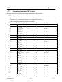
1
Geschäftsbereich
Meßtechnik
Servicehandbuch
SIGNALGENERATOR
R&S SML01
1090.3000.11
R&S SML02
1090.3000.12
R&S SML03
1090.3000.13
ENGLISH SERVICE MANUAL FOLLOWS FIRST COLOURED DEVIDER
Band 1
Servicehandbuch besteht aus 2 Bänden
Printed in the Federal
Republic of Germany
1090.3123.24-03
1
SML
Registerübersicht
Registerübersicht
Sicherheitshinweise
Qualitätszertifikat
Support-Center-Adresse
Liste der R&S-Niederlassungen
BAND 1
Grundunterlagen
Prüfen und Instandsetzen der Baugruppen
Mainboard ............................................................................................................................ Register 1
BAND 2
Prüfen und Instandsetzen der Baugruppen
Frontmodul .......................................................................................................................... Register 2
Eichleitung 1.1/2.2/3.3 GHz ................................................................................................ Register 3
Schaltnetzteil........................................................................................................................ Register 4
Referenzoszillator OXCO- Option SML-B1 ....................................................................... Register 5
Pulsmodulator - Option SML-B3 ........................................................................................ Register 6
Ausgangsteil......................................................................................................................... Register 7
1090.3123.24
RE
D-2
SML
Austausch von Baugruppen und Kabeln
Grundunterlagen
Dieses Kapitel enthält die Grundunterlagen für das SMV03-Grundgerät. Für die Bestellung von Ersatzteilen und Baugruppen wenden Sie sich bitte an unseren Ersatzteil-Schnelldienst oder an Ihre Rohde &
Schwarz-Servicestelle und beachten Sie die Hinweise im folgenden Abschnitt, "Austausch von Baugruppen und Kabeln".
Die Adresse unseres Ersatzteil-Schnelldienstes sowie eine Liste der Rohde & Schwarz-Vertretungen
befindet sich am Beginn dieses Servicehandbuchs.
Austausch von Baugruppen und Kabeln
Tabelle 1 am Ende dieses Abschnitts enthält eine Zusammenstellung der lieferbaren Netzkabel. Die für
die Bestellung notwendigen Identnummern von Ersatzteilen und Baugruppen sind aus den Schaltteillisten im vorliegenden Kapitel zu entnehmen.
Wichtiger Hinweis!
Beachten Sie beim Austausch einer Baugruppe bitte die Sicherheitshinweise und
die entsprechende Montageanleitung in Kapitel 3 dieses Servicehandbuchs!
Ersatzteilbestellung
Um Ersatzteile schnell und richtig liefern zu können, benötigen wir folgende Angaben:
• Sachnummer (siehe Schaltteillisten in diesem Kapitel)
• Benennung
• Kennziffer gemäß Schaltteilliste
• Stückzahl
• Gerätetyp, für den das Ersatzteil benötigt wird
• Ansprechpartner für eventuelle Rückfragen
Austauschbaugruppen
Austauschbaugruppen sind eine kostengünstige Alternative zu Originalbaugruppen. Es handelt sich
hier um keine neuen Baugruppen, sondern um reparierte und geprüfte Teile. Diese können
Gebrauchsspuren aufweisen, sie sind jedoch elektrisch und mechanisch neuen Baugruppen gleichwertig.
Ihre Rohde & Schwarz-Vertretung (bzw. Abteilung Zentralservice, Rohde & Schwarz München) informiert Sie gerne darüber, welche Baugruppen als Austauschbaugruppen lieferbar sind.
Bestellung und Lieferung von Austauschbaugruppen
Bei der Bestellung von Austauschbaugruppen werden dieselben Angaben benötigt wie für die normale Ersatzteilbestellung, jedoch mit der entsprechenden Variantenangabe bei der Sachnummer.
Rücknahme defekter Austauschbaugruppen
Defekte, reparierbare Baugruppen des Austauschprogramms werden innerhalb von 3 Monaten nach
Lieferung gegen Gutschrift eines Rückkaufwerts zurückgenommen.
Ausgeschlossen von der Rücknahme sind Teile, die nicht mehr aufarbeitbar sind, z. B. verbrannte,
angebrochene oder durch Reparaturversuche beschädigte Druckschaltungen, unvollständige Baugruppen, Teile mit schweren mechanischen Schäden.
1090.3000.24
1
D-1
Austausch von Baugruppen und Kabeln
SML
Senden Sie bitte die defekten Austauschbaugruppen mit einem Rückwarenbegleitschein und folgenden Angaben zurück:
• Sachnummer, Seriennummer und Bezeichnung des ausgebauten Teils
• möglichst genaue Fehlerbeschreibung
• Sachnummer, Seriennummer und Typ des Gerätes, aus dem die Baugruppe ausgebaut wurde
• Ausbaudatum
• Name des Technikers, der den Austausch vorgenommen hat
Ein Rückwarenbegleitschein wird mit jeder Austauschbaugruppe mitgeliefert.
Tabelle 1 Lieferbare Netzkabel
Sachnummer
Schutzkontaktstecker nach
Vorzugsweise verwendet in
DS 006.7013
BS1363: 1967’ entsprechend
IEC 83: 1975 Standard B2
Großbritannien
DS 006.7020
Typ 12 nach SEV-Vorschrift 1011.1059,
Normblatt S 24 507
Schweiz
DS 006.7036
Typ 498 / 13 nach US-Vorschrift UL 498,
bzw. IEC 83
USA / Kanada
DS 006.7107
Typ SAA3 10 A, 250 V,
nach AS C112-1964 Ap.
Australien
DS 0025.2365
DS 0099.1456
DIN 49 441, 10 A, 250 V, abgewinkelt
DIN 49 441, 10 A, 250 V, gerade
Europa (ohne Schweiz)
1090.3000.24
2
D-1
SML
Achtung!
Vor dem Entfernen der Rückwandfüße und dem Abziehen des Tubus das Gerät auf
die Frontgriffe stellen, um eine Beschädigung des Gerätes durch Herausrutschen zu
vermeiden.
Beim Aufstecken des Tubus darauf achten, daß keine Kabel eingeklemmt oder abgezogen werden.
1090.3000.24
3
D-1
Gehäuseaufbau nach der Bauweise 2000
SML
Gehäuseaufbau nach der Bauweise 2000
12
11
13
10
5
Chassis
9
8
7
6
4
1
2
3
Das Gehäuse besteht nach der BW 2000 im
wesentlichen aus dem gerätespezifischen
Chassis, einem Tubus [10], Gerätefüßen [7, 8,
12] und Frontgriffen [2].
Das gerätespezifische Gehäusechassis ist in
der Mitte der oberen Abbildung dargestellt. Es
setzt sich zusammen aus einem Frontrahmen
und einem Baugruppenträger mit Rückwanne.
Der Frontrahmen ist aus Aluminiumprofil gebogen, der Baugruppenträger ist als Blechbiegeteil geformt.
Die Nahtstellen zwischen den verschiedenen
Gehäuseteilen können je nach Bedarf
mit Dichtschnüren [6, 13] abgedichtet
werden.
Die Frontseite wird durch eine ebenfalls gerätespezifische Montagewanne [4] und eine
Fronthaube [1] komplettiert.
½ Zum Verschließen des Gerätes den Tubus von
der Rückseite über das Chassis schieben.
½ Den Tubus mit Hilfe der Rückwandfüße [12]
mit aufgesteckten Elastikpuffern anschrauben.
Die unteren Gerätefüße mit Antirutsch-Einsatz
[7, 8] sind fest mit dem Tubus verschraubt und
dienen gleichzeitig als Arretierung beim Übereinanderstapeln von Geräten.
1090.3000.24
4
D-1
Liste mechanischer Teile
SML
Liste mechanischer Teile
Der SML ist nach R&S-Bauweise 2000 aufgebaut.
Gehäusegröße:
2E 1/1 T450
Maße über alles:
87,6 mm x 465,1 mm x 495 mm
Zubehör:
19’’-Adapter ZZA-211, Stock no. 1096.3260.00
Lfd. Nr.
Anzahl
Bezeichnung
Sachnummer
1
1
Fronthaube SML01
Front panel SML02
Front panel SML03
1090.3275.00
1090.3269.00
1090.3252.00
2
2
Frontgriff
1096.1468.00
3
4
Schraube M4x12
1096.4780.00
4
1
Fronteinheiit
1104.1409.00
5
6
DIN 965 – M3x6 - A4 - PA
0396.8023.00
6
2m
HF-Dichtschnur O-Prof. 2,0 SI
0396.1035.00
7
4
Gerätefuß
1096.2506.00
8
2
Aufstelluß
1096.2529.00
9
1
Tragegriff seitlich
1096.2670.00
10
1
Tubus
1096.6901.00
11
4
Abdeckung
1096.2558.00
12
4
Rückwandfuß
1096.2487.00
13
m
HF-Dichtschnur FL 9,53x6,3
1096.4867.00
Die Lage der einzelnen Teile ist aus der Montagezeichnung ersichtlich.
1090.3000.24
5
D-1
Test and Measurement
Division
Service Manual
SIGNALGENERATOR
R&S SML01
1090.3000.11
R&S SML02
1090.3000.12
R&S SML03
1090.3000.13
Volume 1
Service manual consists of 2 volumes
Printed in the Federal
Republic of Germany
1090.3123.24
21
E-3
SML
Tabbed Divider Overview
Tabbed Divider Overview
Safety Instructions
Certificate of Quality
Support Center Address
List of R&S Representatives
VOLUME 1
Basic Documents
Testing and Repair of Modules
Mainboard............................................................................................................... Tabbed Divider 1
VOLUME 2
Testing and Repair of Modules
Front Assembly ...................................................................................................... Tabbed Divider 2
Attenuator ................................................................................................................. Tabbed Divider 3
Switching Power Supply ......................................................................................... Tabbed Divider 4
Reference Oscillator OXCO - Option SML-B1 ...................................................... Tabbed Divider 5
Pulse Modulator - Option SML-B3.......................................................................... Tabbed Divider 6
Output Unit ............................................................................................................... Tabbed Divider 7
1090.3123.24
RE
E-2
SML
Module and Cable Exchange
Basic Documents
This chapter contains the circuit documents for the SML basic unit. The circuit documents for the modules "IQ Analog/Digital Unit" (IQ Board) and „Differential Outputs“ are relegated to chapters 6 and 7,
respectively. Chapter 8 contains the basic documents for the module "Digital I/Q Outputs". To order
replacement parts and modules please contact our spare parts express service or your Rohde &
Schwarz service representative and note the hints given in the following section, "Module and Cable
Exchange".
The address of our spare parts express service and a list of Rohde & Schwarz representatives can be
found at the beginning of this service manual.
Module and Cable Exchange
Table 1 at the end of this section lists all power cables available. The stock numbers necessary for ordering replacement parts and modules can be found in the component lists further down.
Important Note!
When replacing a module please note the safety instructions and the repair instructions given in chapter 3 of this service manual.
Ordering replacement parts
To deliver replacement parts promptly and correctly we need the following indications:
• Stock number (see component lists in this chapter)
• Designation
• Component number according to component list
• Number of pieces
• Instrument type the replacement part belongs to
• Contact person for possible questions
Replaced modules
Replaced modules are an economic alternative for original modules. It should be kept in mind that
replaced modules are not new, but repaired and fully tested parts. They may have traces from use
but they are electrically and mechanically equivalent to new modules.
To find out which replaced modules are available, please refer to your Rohde & Schwarz representative (or to the central service division, Rohde & Schwarz Munich). The identification number is usually
the same as for the original module, but with a variant index .95, .96, .97 or .98.
Ordering and delivery of replaced modules
For ordering replaced modules, the same indications as for ordinary parts are required, however,
with the corresponding variant index appended to the stock number.
Taking back defective replacement modules
Defective modules of the replacement program which can be repaired are taken back within
3 months after delivery of the replaced module. A repurchasing value is credited.
Excluded are parts which can not be repaired, e.g. PCBs that are burnt, broken or damaged by repair
attempts, incomplete modules, parts which are heavily damaged mechanically.
1090.3000.24
1
E-1
Module and Cable Exchange
SML
The defective parts must be sent back with a returned accompanying document containing the
following information:
• Stock number, serial number and designation of the dismounted part,
• Precise description of the error,
• Stock number, serial number and designation of the instrument the part was dismounted from,
• Date of dismounting,
• Name of the technician who exchanged the part.
A returned accompanying document is provided with each replacement module.
Table 1
List of power cables available
Stock No.
Earthed-contact connector
Preferably used in
DS 006.7013
BS1363: 1967’ complying with
IEC 83: 1975 standard B2
Great Britain
DS 006.7020
Type 12 complying with SEV-regulation
1011.1059, standard sheet S 24 507
Switzerland
DS 006.7036
Type 498 / 13 complying with
US-regulation UL 498, or with IEC 83
USA / Canada
DS 006.7107
Type SAA3 10 A, 250 V,
complying with AS C112-1964 Ap.
Australia
DS 0025.2365
DS 0099.1456
DIN 49 441, 10 A, 250 V, angular
DIN 49 441, 10 A, 250 V, straight
Europe (except Switzerland)
1090.3000.24
2
E-1
SML
Module and Cable Exchange
Caution
Prior to removing the rear feet and taking off the enclosure, put unit onto front handles to avoid damages to the unit though slipping.
When mounting the tube take care not to damage or pull off cables.
1090.3000.24
3
E-1
Construction of the Casing According to Design 2000
SML
Construction of the Casing According to Design 2000
12
11
13
10
5
Chassis
9
8
7
6
4
1
2
3
The casing essentially consists of a devicespecific chassis, the panelling [10], instrument
feet [7, 8, 12] and front grips [2].
The device-specific chassis is shown in
the center of the figure above. It consists
of a front frame and a module support with
rear panel. The front frame is made
of a bended aluminum profile, the module
support is shaped out of a piece of sheet
metal.
strument from gliding, in particular if several
instruments are piled up.
The contact edges between the different parts
of the casing can be sealed by means of the RF
seals [6, 13] provided with the instrument.
The front side is completed by a devicespecific mounting panel [4] and a front
panel [1].
½ To close the casing, push the panelling over
the chassis starting on the rear side of the
instrument.
½ Screw on the panelling by means of the
rear-panel feet [12] equipped with elastic
buffers.
The lower instrument feet [7, 8] are tightly
screwed to the panelling. They prevent the in-
1090.3000.24
4
E-1
List of mechanical parts
SML
List of mechanical parts
The SML is constructed in accordance with R&S design 2000.
Size of the casing:
2E 1/1 T450
Overall dimension:
87,6 mm x 465,1 mm x 495 mm
Accessories:
19’’-Adapter ZZA-211, Stock no. 1096.3260.00
Current No.
No. of Parts
Designation
Stock No.
1
1
Front panel SML01
Front panel SML02
Front panel SML03
1090.3275.00
1090.3269.00
1090.3252.00
2
2
Front grip
1096.1468.00
3
4
Screw M4x12
1096.4780.00
4
1
Front Unit
1104.1409.00
5
6
DIN 965 – M3x6 - A4 - PA
0396.8023.00
6
2m
RF seal O-Prof. 2,0 SI
0396.1035.00
7
4
Instrument foot
1096.2506.00
8
2
Foot
1096.2529.00
9
1
Carrying handle, lateral
1096.2670.00
10
1
Panelling
1096.6901.00
11
4
Cover
1096.2558.00
12
4
Rear-panel foot
1096.2487.00
13
m
RF seal FL 9,53x6,35
1096.4867.00
The location of the individual parts can be obtained from the assembly drawing contained in the basic
documents of instrument.
1090.3000.24
5
E-1
Serviceunterlagen
Mainboard
1090.3500.02
ENGLISH SERVICE MANUAL FOLLOWS FIRST COLOURED DEVIDER
Printed in the Federal
Republic of Germany
1090.3500.00
1
D-1
SML
Mainboard
Inhaltsverzeichnis
1
1.1
MAINBOARD....................................................................................................... 1.1
Übersicht ................................................................................................................................. 1.1
1.2
Funktionsbeschreibung......................................................................................................... 1.3
1.2.1
Stromversorgung mit Sicherungsboard und Spannungsreglern ....................................... 1.3
1.2.2
Rechner............................................................................................................................. 1.4
1.2.2.1
CPU ............................................................................................................................... 1.4
1.2.2.2
Programm- und Datenspeicher ..................................................................................... 1.4
1.2.2.3
IEC-Bus und RS232 ...................................................................................................... 1.4
1.2.2.4
Tastatur, Drehgeber und Datenübertragung ................................................................. 1.4
1.2.2.5
Diagnose-ADC............................................................................................................... 1.5
1.2.2.6
PIO und Interrupts ......................................................................................................... 1.5
1.2.2.7
Anzeige und Kontrasteinstellung ................................................................................... 1.5
1.2.2.8
Schnittstellen Baugruppe............................................................................................... 1.5
1.2.2.9
Speicher für Fertigungsdaten ........................................................................................ 1.5
1.2.3
Synthesizer........................................................................................................................ 1.6
1.2.3.1
Referenz ........................................................................................................................ 1.6
1.2.3.2
Referenz-PLL................................................................................................................. 1.6
1.2.3.3
Step Synthesizer............................................................................................................ 1.7
1.2.3.4
DDS-Synthesizer ........................................................................................................... 1.7
1.2.3.5
Main Loop ...................................................................................................................... 1.8
1.2.3.6
Frequenzvervielfacher ................................................................................................... 1.8
1.2.3.7
FM/PHiM........................................................................................................................ 1.9
1.2.4
Ausgangsteil...................................................................................................................... 1.9
1.2.4.1
Pegelaufbereitung.......................................................................................................... 1.9
1.2.4.2
AM-Modulator und Level Preset .................................................................................. 1.10
1.2.4.3
Abstimmbare Oberwellenfilter ..................................................................................... 1.10
1.2.4.4
Abwärtsmischer mit Pegeldetektor .............................................................................. 1.11
1.2.4.5
Ausgangsverstärker mit Pegeldetektor ....................................................................... 1.12
1.2.5
Modulationsaufbereitung mit LF-Generator .................................................................... 1.13
1.2.5.1
Modulationsaufbereitung ............................................................................................. 1.13
1.2.5.2
LF-Generator ............................................................................................................... 1.13
1.3
Öffnen des Mainboards ....................................................................................................... 1.14
1.4
Spezielle Meßgeräte und Hilfsmittel ................................................................................... 1.15
1.5
Fehlersuche .......................................................................................................................... 1.16
1.5.1
Fehler auf dem Rechner/Fronteinheit ............................................................................. 1.16
1.5.2
Fehler Stromversorgung/Spannungszuführung .............................................................. 1.16
1.5.3
Angezeigte Fehler am Display......................................................................................... 1.17
1.5.3.1
Synchronisierfehler ...................................................................................................... 1.17
1.5.3.2
Kalibrierfehler............................................................................................................... 1.18
1.5.4
Fehler Ausgangssignal RF_OUT an X106 (Mainboard) ................................................. 1.19
1.5.4.1
Fehler im CW-Mode .................................................................................................... 1.19
1.5.4.2
Fehler bei FM/PHiM..................................................................................................... 1.20
1.5.4.3
Fehler bei AM .............................................................................................................. 1.20
1.5.5
Fehler Ausgangssignal LF an X114 (Mainboard)............................................................ 1.21
1090.3500.00
3
D-1
Mainboard
SML
1.6
Modulcheck Prüfen und Abgleichen .................................................................................. 1.22
1.6.1
Modulcheck ..................................................................................................................... 1.22
1.6.1.1
Modul „Supplies“ .......................................................................................................... 1.22
1.6.1.2
Modul „LF-Generator“ .................................................................................................. 1.23
1.6.1.3
Modul „Reference & Stepsynthesizer“ ......................................................................... 1.24
1.6.1.4
Modul „Main Synthesizer & Multiplier“ ......................................................................... 1.25
1.6.1.5
Modul „Output Unit 1“ .................................................................................................. 1.26
1.6.2
Prüfungen und Abgleiche ................................................................................................ 1.27
1.6.2.1
Prüfen des 800 MHz CRO........................................................................................... 1.27
1.6.2.2
Prüfen des Phasendetektors und der Regelschleife in der Referenz-PLL.................. 1.27
1.6.2.3
Abgleich des 800 MHz CRO........................................................................................ 1.28
1.6.2.4
Prüfen des VCO .......................................................................................................... 1.28
1.6.2.5
Prüfen des Phasendetektors und der Regelschleife in der Main Loop ....................... 1.28
1.6.2.6
Prüfen der Voreinstellspannung .................................................................................. 1.29
1.6.2.7
Prüfen des LF-Generators........................................................................................... 1.29
1.6.2.8
Prüfen der Modulationsaufbereitung ........................................................................... 1.30
1.6.2.9
Prüfen der Reglerumschaltungen................................................................................ 1.30
1.6.2.10 Prüfen der Pegelregelung mit Detektorlinearität ......................................................... 1.31
1.2.6.11 Prüfen der Lüfteransteuerung ..................................................................................... 1.31
1.7
Tabellen und Schnittstellen................................................................................................. 1.32
1.7.1
Liste der Diagnosemeßpunkte ........................................................................................ 1.45
1.7.2
Referenzspannungen ...................................................................................................... 1.45
1.7.3
Arbeitspunkte und HF-Pegel ........................................................................................... 1.45
1.7.3.1
Synthese...................................................................................................................... 1.45
1.7.3.2
Ausgangsteil ................................................................................................................ 1.45
1.7.4
Digitale Schnittstelle ........................................................................................................ 1.45
1.7.4.1
Schnittstelle HW Rechner............................................................................................ 1.45
1.7.4.2
Schnittstelle Frequenzeinstellung ................................................................................ 1.45
1.7.4.3
Schnittstelle Einstellung interne Register DDS-MOD .................................................. 1.45
1.7.4.4
Schnittstelle Ausgangsteil............................................................................................ 1.45
1.7.4.5
Modulationsaufbereitung und LF-Generator................................................................ 1.45
1.7.5
Externe Schnittstelle........................................................................................................ 1.45
1090.3500.00
4
D-1
SML
Mainboard
Index
A
M
Abwärtsmischer .......................................... 1.11
AC-Kopplung............................................... 1.13
AM-Frequenzgang ...................................... 1.20
AM-Hubeinstellung...................................... 1.13
AM-Modulator.............................................. 1.10
Arbeitspunkte .............................................. 1.34
Ausgangsteil.................................................. 1.9
Ausgangsverstärker .................................... 1.12
Meßgeräte ................................................... 1.15
Modulationsaufbereitung .................... 1.13, 1.30
Modulcheck ................................................. 1.22
B
Oberwellen .................................................. 1.19
Oberwellenfilter............................................ 1.10
N
Nebenlinien.................................................. 1.19
O
Blockschaltbild .............................................. 1.2
P
D
Pegelaufbereitung ......................................... 1.9
Pegeldetektor ..................................... 1.11, 1.12
Pegelfehler .......................................... 1.19, 1.21
Pegelkorrektur .............................................. 1.19
Pegelregelung ............................................. 1.31
Preset-Stellglied .......................................... 1.10
Prüfen und Abgleichen ................................ 1.22
Detektorlinearität ......................................... 1.31
Diagnosemeßpunkte................................... 1.32
Digitale Schnittstelle.................................... 1.37
E
Ein- und Ausbau der Baugruppe................. 1.14
Endstufe ...................................................... 1.12
Externe Schnittstellen ................................. 1.43
R
Rechner ......................................................... 1.4
Referenzspannung ............................... 1.3, 1.34
F
Fehlersuche ................................................ 1.16
FM/PhiM-Frequenzgang ............................. 1.20
Frequenzfehler ............................................ 1.21
S
Schalter ....................................................... 1.11
Service-Kit ................................................... 1.14
Service-Programm ............................. 1.16, 1.22
Servicestellung ............................................ 1.14
Sicherung ...................................................... 1.3
Sicherungsboard ........................................... 1.3
Steckbrücken ............................................... 1.22
Störhub ........................................................ 1.19
Synchronisierfehler...................................... 1.17
Synthesizer .................................................... 1.6
H
HF-Pegel ..................................................... 1.34
Hubfehler..................................................... 1.20
K
Kalibrierfehler .............................................. 1.18
Klirrfaktor..................................................... 1.20
L
T
LF-Generator...................................... 1.13, 1.29
Lüfter ........................................................... 1.16
Lüfteransteuerung ....................................... 1.31
Tiefpassfilter ................................................ 1.12
V
Versorgungsspannung .................................. 1.3
Verstärker......................... 1.10, 1.11, 1.12, 1.13
Z
Zweitonmodulation ...................................... 1.13
1090.3500.00
5
D-1
SML
Mainboard
1
Mainboard
1.1
Übersicht
Die Baugruppe Mainboard besteht aus den Funktionseinheiten Stromversorgung mit Sicherungsboard
und Spannungsreglern, Rechner mit Interface zu Baugruppen, Synthesizer, Ausgangsteil und Modulationsaufbereitung mit LF-Generator. Somit sind fast alle Schaltungsteile eines Signalgenerators auf
einer Baugruppe vereint.
Die Steckverbindungen zur Eichleitung und den Optionen sind auf dem Mainboard enthalten und führen
die notwendigen Leitungen zur Stromversorgung und Datenübertragung.
Das Mainboard befindet sich auf der Geräteoberseite des SML.
Der Synthesizer des SML läßt sich in die Funktionsmodule Reference, Reference Loop, Step Synthesizer, DDS-Synthesizer, Main Loop, Frequency Multiplier sowie Modulation FM/PM untergliedern. Diese
Funktionsmodule sind auf dem Blockschaltbild Blatt 3 mit gestrichelten Linien gekennzeichnet.
Als Referenz für das gesamte Mainboard steht ein interner 10 MHz VCTCXO zur Verfügung (optionell
ein sehr stabiler Quarzofen). Die Buchsen REF EXT IN sowie REF EXT OUT an der Geräterückseite
dienen zur Einspeisung einer externen 10 MHz-Referenz, bzw. liefern die interne Referenz (10 MHz)
nach außen.
Die interne oder wahlweise vom Benutzer eingespeiste externe Referenz dient als Vergleichsfrequenz
für die Reference Loop. In dieser wird ein keramischer Resonator bei 800 MHz auf die Referenzfrequenz synchronisiert. Deren Ausgangssignal dient als LO-Frequenz zur Erzeugung des unteren Frequenzbereiches von 9 kHz...76 MHz auf dem Ausgangsteil. Durch Frequenzteilung erhält man die beiden Frequenzen 100 und 200 MHz, die als Taktfrequenzen für die eigentliche Frequenzsynthese benötigt werden.
Auf dem Step Synthesizer werden durch Frequenzteilung und anschließende Mischung mit dem
200 MHz Signal weitere feste Frequenzen im Bereich von 187.5...266.666 MHz erzeugt. Ein abstimmbares Bandpassfilter am Ausgang des Mischers sorgt für eine ausreichende Unterdrückung der unerwünschten Mischprodukte.
Der DDS-Synthesizer beinhaltet einen DDS-Baustein mit 50 Bit Frequenzauflösung sowie einen D/AConverter zur Generierung des analogen Ausgangssignales von 15.02...27.06 MHz. Beide Bausteine
werden mit dem 100 MHz Signal der Reference Loop getaktet.
Das Ausgangssignal des DDS-Synthesizers dient als Referenzsignal für die Main Loop. Hier wird das
Signal eines abstimmbaren Oszillators von 201.75...269 MHz mit der Ausgangsfrequenz des Step Synthesizers abwärts gemischt und mit dem Referenzsignal verglichen. Eine Voreinstellspannung für den
VCO sorgt dafür, daß der VCO immer auf dem richtigen Seitenband der Mischung einschwingt. Die
Regelbandbreite der PLL beträgt ca. 80 kHz.
Mit Hilfe eines Step-Recovery-Vervielfachers wird das Ausgangssignal der Main Loop auf die Grundoktave von 605.25...1210.5 MHz vervielfacht. Ein abstimmbares Bandpassfilter sorgt für ausreichende
Selektion der gewünschten Ausgangsfrequenz. Die weiteren Frequenzoktaven von 76...605.25 MHz
werden durch Teilung (2,4 oder 8) generiert.
Das Ausgangsteil besteht aus den Komponenten Pegelaufbereitung, AM-Modulator und Preset, Oberwellenfilter, Abwärtsmischzweig mit Pegeldetektor und Ausgangsverstärker mit Pegeldetektor (siehe
Blockschaltbild Blatt 2).
Es erhält von der Synthese den Frequenzbereich von 76...1100 MHz sowie ein 800 MHz LO-Signal. Der
Frequenzbereich wird durch Abwärtsmischung mit dem 800 MHz Signal als LO nach unten auf 9 kHz
erweitert.
Der AM-Modulator mit den Ausgangsverstärkern erzeugt den gewünschten Pegelbereich (-10 dBm bis
ca. +23 dBm). Ein Pegeldetektor sorgt in Verbindung mit einer Pegelregelschleife für eine hohe, temperaturstabile Pegelgenauigkeit.
Die Pegelregelschleife hat eine Bandbreite von ca. 50 kHz und ermöglicht so eine analoge AM.
1090.3500.00
1.1
D-1
Mainboard
SML
Ein auf der Baugruppe befindlicher LF-Generator erzeugt ein Sinussignal im Frequenzbereich 0.1 Hz –
1 MHz, das für interne Modulationen verwendet werden kann. Dieses Signal wird außerdem nach außen
an die Fronplatte des SML (Buchse LF) geführt und kann im Pegel zwischen 1 mV und 4 V variiert werden (siehe Blockschaltbild Blatt 2).
Hinweis:
1090.3500.00
Ein Blockschaltbild befindet sich auf den Blättern 1-3 der Schaltplan-Unterlagen.
Die Bezeichnungen (z.B. SYN-K2) in den Stromlauf-Unterlagen geben die Namen der
Abschirmkammern an und dienen zur schnelleren Lokalisierung der Schaltungsteile auf
dem Mainboard (siehe Deckelbezeichnungen und Blatt 4).
1.2
D-1
SML
Mainboard
1.2
Funktionsbeschreibung
1.2.1
Stromversorgung mit Sicherungsboard und Spannungsreglern
Stromlauf Blatt 6, 7, 8, 27, 48
Die Versorgungsspannungen des Netzteils werden über das Sicherungsboard auf das Mainboard geführt, dort gesiebt und auf der gesamten Baugruppe verteilt. Sie sind auf dem Sicherungsboard mit
Schmelzsicherungen abgesichert (Blatt 7). Die Nennwerte der Sicherungen (F1 – F4) können den
Schaltplan-Unterlagen entnommen werden.
Weitere Spannungen für LC-Display (V15N_LCD), Rechnerversorgung (+3VR), Diagnose (-5VR), HFKomponenten (+8V_REFHF1/2, +5V_REFHF, ±10V_REFHF, +5V-SYNE, +3V_REFHF) und eine Referenzspannung (+10V_REF) werden auf dem Mainboard in verschiedenen Kammern mit Spannungsreglern erzeugt (Blatt 8, 27, 48).
Zur temperaturabhängigen Drehzahlregelung des Gerätelüfters ist eine Lüftersteuerungsschaltung vorhanden (Blatt 6).
1090.3500.00
1.3
D-1
Mainboard
1.2.2
Rechner
1.2.2.1
CPU
SML
Stromlaufblatt 9 und 8
Es wird der RISC-Prozessor 80960HD50 von Intel verwendet.
Adress- und Datenbus sind nicht gemultiplext. Die Busse zu den Speicherbausteinen sind ungepuffert
und maximal 32 Bit breit. Der Periferiebus wird gepuffert bei einer Breite von maximal 16 Bit. Der Adressbereich des Prozessors ist in 16 * 256 MByte-Blöcke aufgeteilt.
Im Prozessor ist ein Interruptcontroller integriert. Neben den internen Interrupts stehen 8 externe, maskierbare Interrupts und ein nicht maskierbarer Interrupt (NMI) zur Verfügung. Dieser wird vom Supervisor MAX793TCSE erzeugt, welcher die +3,3 V-Versorgung überwacht. Er erzeugt einen RESET-Puls
beim Hochlaufen der Versorgungsspannung. Fällt die Spannung unter den Schwellwert von 2,8 V, so
wird die Versorgung der SRAMs auf Batteriebetrieb umgeschaltet und die SRAMs werden in den Standby-Modus gebracht.
1.2.2.2
Programm- und Datenspeicher
Stromlaufblatt 11
Der Bootcode und die Firmware werden in 2 Flash-EPROMs gespeichert, wobei die Speichergröße 2
MB, 4 MB oder 8 MB betragen kann. Ein Update der Software ist über die RS232-Schnittstelle möglich.
Der batteriegepufferte Teil des RAMs wird von einem bzw. zwei SRAMs 256k x 16 Bit gebildet. Eine
Widerstandsbestückung läßt die Konfiguration auf 512 kByte oder 1 MByte zu. Für unterschiedliche
Modelle ist die Bestückung zusätzlicher Bausteine von weiteren 2 MByte möglich. Diese Bausteine sind
nicht batteriegepuffert.
1.2.2.3
IEC-Bus und RS232
Stromlaufblatt 12
Als IEC-Bus-Controller wird der Baustein TNT4882 verwendet. Die notwendigen Bus-Treiber sind im Baustein integriert. Seine Taktfrequenz beträgt 40 MHz. Der Baustein kann über das Signal RESET-P-IEC
zurückgesetzt werden.
Als RS232-Interface dient der Baustein TL16C550A. Die Pegelumsetzung von TTL-Pegel auf RS232Pegel erfolgt im Baustein LT1280. Die Baudrate wird von einem eigenen 3,6864 MHz-Taktgenerator
abgeleitet.
1.2.2.4
Tastatur, Drehgeber und Datenübertragung
Stromlaufblatt 13
Das Gate-Array Perif2 steuert die Tastatur und den Drehgeber. Es können Tastaturmatrizen von maximal 8 Reihen und 12 Spalten sowie der R&S-Standard-Drehgeber angeschlossen werden.
Die serielle Datenübertragung zum ADC, den Optionen und den auf dem Mainboard integrierten HFModulen wird über die serielle Schnittstelle des Perif2 hergestellt. Mit Hilfe der PIOs 0...4 können bis zu
23 zusätzliche Baugruppen angesprochen werden. Mit den Signalen SERDATA_N und SERCLK_N des
Perifs erfolgt die Datenübertragung zu den Schieberegistern auf den einzelnen Baugruppen. Der PIO5
erzeugt den Baugruppenstrobe (Write-Signal).
Zwei PIO-Leitungen PIO6 und 7 ermöglichen das Beschreiben und Lesen von EEPROMs für Baugruppenerkennung und Kalibrierdaten.
1090.3500.00
1.4
D-1
SML
1.2.2.5
Mainboard
Diagnose-ADC
Stromlaufblatt 14 und 15
Der Diagnose-ADC AD7710 arbeitet mit einer Auflösung von 24 Bit. Diagnosespannungen dürfen
±2,5 V nicht über- bzw. unterschreiten. Analoge Multiplexer 74LV4051 auf den verschiedenen Baugruppen legen genau einen Diagnosepunkt an die gemeinsame Meßleitung V_DIAG an.
Jeder Diagnosepunkt schreibt einen individuellen Spannungsteilungsfaktor, sowie eine definierte Wartezeit vor.
Im Baustein integriert ist ein digitales Tiefpassfilter, dessen Grenzfrequenz programmierbar ist.
1.2.2.6
PIO und Interrupts
Stromlaufblatt 16
Der Baustein D40 enthält 3*8Bit Input/Output-Ports, die die Ausgabe von Steuersignalen für die Diagnosemessung, IEC-Bus und Display sowie das Einlesen von Status- und Interrupt-Signalen ermöglichen.
Diese können an einem 8 Bit-Port vom Rechner abgefragt werden.
Für funktionelle Hardware sind insgesamt 12 Interrupts vorgesehen. Diese werden nur im Fall von
Hardwarefehlern oder im Overrangefall ausgelöst. Die Interruptmeldungen der funktionellen Hardware
werden zu einem Interrupt INT_HW_N zusammengefaßt und an die CPU weitergeleitet.
1.2.2.7
Anzeige und Kontrasteinstellung
Stromlaufblatt 8
Das verwendete LC-Display enthält einen eingebauten Controller und kann daher ohne spezielles Interface an den 8 Bit-Periferiebus angeschlossen werden.
Die Einstellung des Kontrastes erfolgt über die negative Versorgungsspannung VN15-LCD. Diese wird
vom programmierbaren Schaltregler MAX749CSA N3 aus +5 V erzeugt und kann über Software im
Bereich –5 V...-15 V variiert werden.
Mit dem Signal CFL_OFF wird die Displaybeleuchtung bedient. LCD_ON schaltet das Display ein.
REV_LCD aktiviert die invertierende Darstellung des Displays.
1.2.2.8
Schnittstellen Baugruppe
Stromlaufblatt 13
Die Ansteuerung der funktionellen Hardware erfolgt über eine serielle Schnittstelle. Dazu wird über die
PIO des Perifs zuerst das Modul (Baugruppe) angewählt (Signal MS_xx_N). Dieses Signal schaltet die
serielle Datenübertragung auf der Baugruppe frei. Mit den Signalen SERDATA_N und SERCLK_N des
Perifs erfolgt die Datenübertragung zu den Schieberegistern auf den einzelnen Baugruppen. Abgeschlossen wird die Übertragung mit dem Baugruppenstrobe, der über ein PIO des Perifs programmiert
wird.
1.2.2.9
Speicher für Fertigungsdaten
Stromlaufblatt 14
Zum Ablegen von individuellen Kalibrierdaten einer Baugruppe sowie der Kodierung von Änderungszustand, Variante und sonstigen Fertigungsdaten ist auf jeder Baugruppe ein EEPROM vorgesehen. Für
die Funktionsmodule des Mainboards (Rechner, Synthese, Modulationsaufbereitung und Ausgangsteil)
wird nur ein Baustein verwendet. Das Beschreiben und Lesen wird durch die Leitungen EECLK_N und
EEDATA ermöglicht, die über 2 PIOs des Perifs programmiert werden.
1090.3500.00
1.5
D-1
Mainboard
1.2.3
Synthesizer
1.2.3.1
Referenz
SML
Modul Reference auf Blockschaltbild 3
Stromlaufblatt 19 und 33
Die Referenzfrequenz beträgt für interne und externe Synchronisation 10 MHz. Im Betriebsmodus Referenz Intern dient das Ausgangssignal des internen 10 MHz-VCTCXO (B2) als Referenzsignal für den
Phasenvergleicher D39. Das Bit REF_ON schaltet den VTCXO (V35, V63) ein und gleichzeitig den
Signalpfad zum Phasendetektor durch (über D64).
Im Betriebsmodus Referenz Extern wird das 10 MHz-Eingangssignal auf CMOS-Pegel gewandelt und
über ein Tiefpassfilter an die Ausgangsbuchse EXT REF OUT weitergegeben (LOOP-THROUGH). Damit wird ein konstanter definierter Pegel am Ausgang erzeugt, es können problemlos weitere Geräte auf
diese Referenz synchronisiert werden. Statt des internen 10 MHz-Signals liegt nun das Signal von REF
EXT IN am Phasenvergleicher D39 an. Über das Bit REFEXT wird dieser Pfad eingeschaltet (D64).
Ist die Option SML-B1 bestückt, so wird diese statt des internen VCTCXOs als Referenzfrequenz verwendet. Das Bit OPT_ON (D64) schaltet das Signal vom Optionsquarz zum Phasenvergleicher D39 durch.
Bei interner Referenz wird das heruntergeteilte Signal PLL10 der Reference Loop auf den Ausgang REF
EXT OUT geschaltet. Es dient auch gleichzeitig dem LF-Generator als Taktfrequenz (Signal
LFGEN_CLK).
Zur Kalibrierung bzw. zum Abstimmen der internen Referenz (VCTCXO bzw. SML-B1) dient der 12 Bit
DA-Converter D74 (REFTUNE). Dieser erzeugt aus der 10 V-Referenzspannung des Mainboards eine
Tunespannung im Bereich von 0...10 V.
1.2.3.2
Referenz-PLL
Modul Reference Loop auf Blockschaltbild 3
Stromlaufblatt 19 – 22, 34
Der VCO der Referenz-PLL ist mit einem keramischen Resonator B1 aufgebaut, der mit Hilfe der Abstimmdiode V89 auf seine Sollfrequenz von 800 MHz nachgeregelt wird. Der Abgleich über den Trimmkondensator C224 dient zum Grobabgleich des Oszillators, damit die Regelschleife nicht den kompletten Toleranzbereich der verwendeten Bauteile mit ihrem Ziehbereich abdecken muß. Die Transistorstufe V71 entdämpft mit ihrer negativen Impedanz den Schwingkreis. Die Transistoren V37 sowie V64
prägen einen konstanten Strom in die Oszillatorschaltung ein. Über einen Trennverstärker N8 wird das
Oszillatorsignal ausgekoppelt und steht an der Buchse X109 für Meßzwecke oder als Referenzfrequenz
für weitere Optionen zur Verfügung.
Im Rückwärtszweig der PLL teilt der Frequenzteiler D14 das Oszillatorsignal zunächst auf 200 MHz. Die
Differenzverstärkerschaltung mit V73 und V74 wandelt dieses Signal auf CMOS-Pegel, die Frequenzteiler D69 und D115 teilen das Signal weiter herunter auf die Vergleichsfrequenz von 10 MHz.
Das heruntergeteilte Signal wird nun am Phasendetektor D39 mit dem 10 MHz-Signal der Referenz
verglichen. In der Betriebsart Referenz Extern stehen dem Benutzer zwei mögliche Regelbandbreiten
zur Verfügung. Bei der Regelbandbreite Slow wird der Pfad über den Regelverstärker N14 geschaltet
(Schalter D37, Signal REFSLOW_OFF = 0). Die Regelbandbreite beträgt hier ca. 10 Hz und regelt somit
mögliche Brumm- oder Störsignale des extern eingespeisten Referenzsignales aus. Die Standardregelschleife (N13, Signal REFFAST_OFF = 0) beträgt ca. 1 kHz. Dieses ist die optimale Regelbandbreite im
Bezug auf Phasenrauschen bei interner Referenz. Die Regelspannungen der beiden Regler werden
über die Fensterkomparatoren U4 bzw. U5 überwacht, die bei Ausrasten der Regelschleife eine Fehlermeldung (Reference PLL unlocked) erzeugen.
Das 800 MHz-Ausgangssignal des Moduls Reference PLL wird desweiteren über den HF-Verstärker V46
dem Downconverter auf dem Ausgangsteil als LO-Signal zur Verfügung gestellt (Signal DOWNCONV).
Das 200 MHz-Signal VCO200 der Referenz PLL wird über den Verstärker V75 ausgekoppelt (Signal
MIXER1). Über einen ohmschen Leistungsteiler verteilt sich hier das Signal auf zwei weitere Pfade.
Über V80 und den Differenzverstärker V77 und V78 wird das Signal auf CMOS-Pegel gewandelt und an
die zwei Frequenzteiler D13 und D70 geleitet. Auf dem anderen Pfad steht es dem Modul Step Synthesizer als LO-Signal zur Verfügung.
1090.3500.00
1.6
D-1
SML
1.2.3.3
Mainboard
Step Synthesizer
Modul Step Synthesizer Coarse Resolution auf Blockschaltbild 3
Stromlaufblatt 22-24, 33
Das Modul Step Synthesizer teilt zunächst das 200 MHz-Signal von der Reference Loop mit dem programmierbaren Frequenzteiler D70 auf 8.333....66.666 MHz (Signal MIX_DIG). Die Teilungsfaktoren
3...24 werden über die Bits MIXDIV<4:0> eingestellt. Hier kann es wahlweise noch durch zwei (D116)
geteilt oder direkt zu einem programmierbaren Dämpfungsglied weitergeführt werden. Dieses ist mit
Hilfe eines ohmschen Spannungsteilers realisiert, wobei die einzelnen Pfade über die Pin-Dioden V17,
V18, V209 und V212 geschaltet werden (Ansteuerbits ZFATT<1:0>). Es dient dazu, den Pegel für die
unterschiedlichen Frequenzen am IF-Port des Mischers konstant zu halten. Die Werte ZFATT zur Ansteuerung werden hierbei in einer Kalibrierroutine ermittelt (Kalibration IF-Filter).
Da für die Erzeugung der benötigten Stepfrequenz nicht nur die Grundwelle sondern wahlweise auch die
Oberwelle des geteilten Signals benötigt wird, dient ein Hochpassfilter bzw. ein Tiefpassfilter der weiteren Vorselektion. Bei bestimmten Teilerfrequenzen werden diese jedoch nicht benötigt. Die Bits
ZFPATH1-3 bestimmen den jeweils geschalteten Pfad. Über den Verstärker V230 gelangt das Signal
MIX_ANALOG zum IF-Port des Mischers B4. Ist keiner der drei Pfade geschaltet, wird eine Gleichspannung über L170 auf den IF-Port des Mischers gegeben (Bit ZF200_ON=1).
Dort wird das Signal mit dem 200 MHz-Signal des LO auf eine ZF-Frequenz von 187.5...266.666 MHz
hochgemischt. Bei ZF200_ON=1 (Gleichspannung auf MIX_ANALOG) wird das LO-Signal des Mischers
nicht unterdrückt, und man erhält dabei die Frequenz von 200 MHz am RF-Port des Mischers.
Am RF-Port des Mischers sorgen zwei abstimmbare Bandpassfilter für die notwendige Unterdrückung
der unerwünschten Mischprodukte. Die Filter werden dabei mit Hilfe der Abstimmdioden V214-V225
abgestimmt. Die Abstimmspannung wird mit Hilfe des DA-Converters U6 und des StromSpannungswandlers N12 erzeugt. Die HF-Verstärker V69, V213 und V202 entkoppeln die beiden in
Serie geschalteten Filter und sorgen für einen ausreichend hohen Pegel und somit ausreichenden Signal-Rauschabstand. Die jeweils benötigte Abstimmspannung ZFTUNE für die verschiedenen StepFrequenzen wird in der Kalibrierroutine IF-Filter ermittelt. Der Pegeldetektor V143 dient hierbei zur Pegelmessung am Ausgang der Bandpassfilter.
1.2.3.4
DDS-Synthesizer
Modul DDS-Synthesizer Fine Resolution auf Blockschaltbild 3
Stromlaufblatt 22, 27
Der Frequenzteiler D13 teilt das 200 MHz-Referenzsignal des Moduls Reference Loop wahlweise auf
100 oder 66 MHz (Bit DDSDIV). Dieses Signal (DDSCLK) dient dabei als Taktsignal für den DDSBaustein DDSMOD D56 sowie für den DA-Converter D63.
Der DDS-Baustein erzeugt hierbei mit einer internen Auflösung von 50 Bit die benötigte Ausgangsfrequenz von 15.02...27.06 MHz. Diese liegt als 14 Bit-Amplitudenwert (AW<19:6>) am Ausgang des Bausteins vor und wird mit Hilfe von D63 in ein analoges Ausgangssignal gewandelt. Das optimale Timing
zwischen Daten und Clock am DA-Converter wird mit Hilfe einer schaltbaren Delayline gewährleistet.
Die Bits Delay1-3 schalten hierbei die drei zur Verfügung stehenden Laufzeitpfade. Die optimalen Werte
für die beiden möglichen Taktfrequenzen von 66 oder 100 MHz sind im EEPROM abgelegt und können
von Baugruppe zu Baugruppe unterschiedlich sein.
Ein Tiefpassfilter am analogen Ausgang des DA-Converters sorgt für die notwendige Unterdrückung der
unerwünschten Aliasingfrequenzen (> 80 dB Sperrdämpfung). V39 sowie D126 wandeln das Analogsignal auf CMOS-Pegel.
Der DDS-Baustein beinhaltet des weiteren ein Ausgangsport OUTPORT<15:0>, an dem weitere Ansteuerbits für die Module DDS-Synthesizer sowie Main Loop anliegen, sowie ein Eingangsport
MOD<15:4>, an dem die digitalen Modulationsdaten (12 Bit) für FM und PhiM eingespeist werden.
Die Transistoren V156 und V235 sowie der Operationsverstärker N5 regeln die Versorgungsspannung
des DDS-Bausteins auf 5.25 V. Der Transistor V15 erzeugt die benötigte Versorgungsspannung von –
5 V für den DA-Converter.
1090.3500.00
1.7
D-1
Mainboard
1.2.3.5
SML
Main Loop
Modul Main Loop auf Blockschaltbild 3
Stromlaufblatt 25, 26, 28, 34
Die Main Loop erzeugt den Frequenzbereich von 201.75...269 MHz. Der Transistor V82 mit seiner negativen Impedanz an der Basis entdämpft den Schwingkreis, der über die Kapazitätsdioden V123-130
abgestimmt wird (Abstimmspannung TUNE_VCO). Die Transistoren V38, V65 sowie V199 dienen zur
Arbeitspunktstabilisierung des Oszillators. Die Auskopplung des HF-Signals erfolgt über die Basisstufe
mit V83.
Über einen nachfolgenden Widerstandsteiler wird das Signal auf zwei Pfade verteilt. HF-Mult ist hierbei
das Ausgangssignal zum Frequency Multiplier, LO_MIX2 ist das Signal im Rückwärtspfad der PLL und
dient als LO-Signal für den Mischer B3, der Stepfrequenz und Oszillatorsignal auf eine IF von
15.02...27.06 MHz abwärts mischt.
Die nachfolgende Frequenzweiche sorgt für eine ausreichende Unterdrückung der hochfrequenten
Mischprodukte sowie für eine gute Anpassung an den Mischer. V86 und V85 wandeln das Signal auf
CMOS-Pegel (P41). Der nachfolgende Frequenzteiler D72 teilt das Signal durch zwei (PH-DET), welches als Vergleichssignal für den integrierten Doppelphasendetektor D71 dient.
Je nach verwendetem Seitenband der Mischung können die vier Ausgangssignale des Phasendetektors
über D10 in ihrer Polarität eingestellt werden (Bit PD_INV). Der Summierverstärker N17 summiert die
Signale des Phasendetektors sowie einen fest eingespeisten Phasenoffset (über R365) und wandelt
diese in eine Spannung (Meßpunkt P42). Die Verstärkung des nachfolgenden PI-Reglers N19 läßt sich
zur Kompensation der Verstärkungsänderungen in der PLL, verursacht durch eine unterschiedliche
Oszillatorabstimmsteilheit, mit dem Analogmultiplexer D58 in 8 Stufen einstellen.
Der Schalttransistor V3 klemmt den Regler kurzzeitig auf 0 V-Ausgangsspannung bei bestimmten Frequenzwechseln. Der nachfolgende Operationsverstäker N18 summiert die Signale des PI-Reglers sowie
der PLL-Voreinstellspannung PLLTUNE. Diese wird benötigt, damit die PLL immer auf dem richtigen
Seitenband der Mischung einschwingt. Sie läßt sich über den Analogschalter D57 in 16 Stufen mit einer
Auflösung von ca. 1.25 V einstellen.
Über die FET-Schalter V5, V148 sowie V155 lassen sich nachfolgende Tiefpassfilter sowie ein LeadLag-Glied in ihrer Grenzfrequenz umschalten. Hiermit kann bei Frequenz- oder Phasenmodulation die
Schleifenbandbreite der PLL von ca. 80 kHz auf ca. 500 kHz umgestellt werden.
Die Schaltung mit N16 und V66 dient zur Arbeitspunktregelung des Phasendetektors.
Die Regelspannung an Meßpunkt P49 wird über einen Fensterkomparator U3 überwacht und führt bei
nicht eingerasteter Schleife zu einer Fehlermeldung („MAIN PLL UNLOCKED“).
1.2.3.6
Frequenzvervielfacher
Modul Frequency Multiplier auf Blockschaltbild 3
Stromlaufblatt 29-31, 33
Das Modul Frequency Multiplier vervielfacht das Ausgangssignal 201.75...269 MHz der Main Loop um
den Faktor 3...5 auf die Frequenzoktave von 605.25...1210.5 MHz mit Hilfe des Step-Recovery Vervielfachers V49. Die HF-Verstärker V47 und V70 sorgen für den notwendigen Pegel zu dessen Ansteuerung sowie für ausreichende Entkopplung zum VCO.
Zur Filterung der gewünschten Spektrallinie der Vervielfachung dient ein in drei Stufen aufgebautes
Bandpassfilter. Dieses läßt sich über die Abstimmspannung BPTUNE mit Hilfe von Kapazitätsdioden
(V91-V114) auf die gewünschte Durchlaßfrequenz einstellen. Die dazu benötigte Abstimmspannung
wird mit Hilfe des DA-Converters U2 und des Strom-Spannungswandlers N12 erzeugt. Die richtigen
Spannungswerte werden in einer Kalibrierroutine (Kalibration-MultiplierFilter) mit Hilfe einer Pegelmessung an V61 ermittelt.
Die integrierten HF-Verstärker N6, N11 sowie der diskret aufgebaute Verstärker V48 entkoppeln die
einzelnen Filterblöcke und sorgen für einen ausreichenden Pegel, der notwendig ist für einen ausreichenden Signal-Rauschabstand des Ausgangssignales HF-DIV.
Der Ausgangsfrequenzbereich von 76...605.25 MHz wird mittels Frequenzteilung durch zwei, vier und
acht (Bits DIVOUT>1:0>) mit Hilfe des integrierten Bausteines D68 erzeugt. Über Pindioden-Schalter
(V27 und V29) wird der direkte Pfad (Grundoktave) oder der Teilerpfad ausgewählt (Bit DIVOUT_ON).
Das Signal FSYN (76...1210.5 MHz) bildet die Schnittstelle zum Ausgangsteil.
1090.3500.00
1.8
D-1
SML
1.2.3.7
Mainboard
FM/PHiM
Modul Modulation FM / PM auf Blockschaltbild 3
Stromlaufblatt 32, 27
Im Abschnitt Modulationsaufbereitung (siehe Abschnitt 1.2.5) wird die Beschaltung der Modulationsmatrix näher beschrieben. Das analoge Modulationssignal wird mit Hilfe des 12 Bit-A/D-Converters D30 in
ein digitales Signal gewandelt (AD<15:4>). Das MSB wird dabei invertiert (D127), so daß die Daten zur
weiteren Verarbeitung im Zweierkomplement vorliegen. Die Abtastfrequenz des Wandlers liegt zwischen
8.333 und 25 MHz synchron zur Taktfrequenz des DDS-Synthesizers und wird durch Frequenzteilung
(Bits FMDIV<2:0>) über den Frequenzteiler D4 erzeugt. Dies ist notwendig, um unerwünschten Aliasingprodukten im Algorithmus ausweichen zu können. Sie dient auch zur Übernahme der Modulationsdaten (Signal FM_CLK) am DDS-Baustein D56. Das Bit FM_OFF schaltet den Clock des AD-Wandlers
ab. Das Bit FM_INVERS invertiert die Modulationsdaten bei Wechsel des Seitenbandes der Mischung in
der Main Loop.
Die eigentliche Hubeinstellung erfolgt rein digital und ist komplett im DDS-Baustein D56 implementiert.
Eine Modulation über den VCO ist auf Grund der hohen Bandbreite der Main Loop nicht mehr notwendig.
1.2.4
Ausgangsteil
1.2.4.1
Pegelaufbereitung
Modul RF-Pegel im Blockschaltbild 2
Stromlaufblatt 42 und 43
Das Modulationssignal der AM wird durch D105 mit dem eingestellten Hub multipliziert und auf die Referenzspannung des Pegels addiert (N29, Signal AM_REF). Diese Spannung wird anschließend mit
dem 12 Bit-Wandler D121 entsprechend dem eingestellten Pegel skaliert und dient als Pegelführungswert für die Pegelregelung (Signal REFAM, Meßpunkt P45, Diagnosepunkt 401 D_REFAM).
Die Auflösung beträgt bis ca. 5 dBm (Ausgangspegel an der Gerätebuchse) 0,01dB.
Der PI-Regler N31 kann mit den Schaltern D87/88/89 für unterschiedliche Regelbandbreiten und Betriebsmodi konfiguriert werden. Es kann zwischen 2 verschiedenen Regelbandbreiten gewählt werden
(Bit SLOW1_OFF). Im CW-Betrieb beträgt die Bandbreite ca. 4 kHz, bei AM etwa 50 kHz.
Das Signal KLEMM_N ermöglicht das Austasten des Pegels beim Frequenzwechsel bzw. bei Umschaltungen der Dämpfungsglieder auf der Eichleitung. Dieses Signal wird über eine Logikschaltung (D102 +
D96) aus den Bits LEV_OFF, BLANK_NORM, BLANK_ENA und dem Prozessorsignal BLANK_IN abgeleitet.
Das Bit MAX_POUT_N klemmt den Ausgangspegel auf ca. 16 dBm. Mit dem Bit MOD_OPU1G_N muß
dazu der Pegelführungswert vom Regler abgeklemmt werden.
Das Bit MOD_OPU2G_N schaltet den aufbereiteten Führungswert auf den Optionsstecker X131 und
steht dort für Baugruppen, die evtl. dem Mainboard nachgeschaltet werden, zur Verfügung.
ALC_OFF schaltet die Pegelregelung zwischen Regeln und Steuern um.
Mit den Bits DETOUT_OFF und DETMIX_OFF wird das Ausgangssignal des Pegeldetektors am Ausgang bzw. im Mischerpfad in die Pegelregelschleife als Meßgröße eingespeist.
Das Ausgangssignal des Pegelreglers (Signal AM_MOD, Steckbrücke X11, Diagnosepunkt 402
D_AMOD) dient als Abstimmspannung zur Steuerung des AM-Modulators (siehe Abschnitt 1.2.4.2) und
wird mit dem Komparator U7 auf Spannungen kleiner 10 V überwacht. Bei Überschreitung wird per Interrupt eine Fehlermeldung am Display ausgegeben (ERROR 110; „OUTPUT UNLEVELED; OPU1“).
1090.3500.00
1.9
D-1
Mainboard
1.2.4.2
SML
AM-Modulator und Level Preset
Modul Level Preset und AM-Modulator im Blockschaltbild 2
Stromlaufblatt 36 und 37
Das Ausgangssignal FSYN des Synthesizers gelangt über den Verstärker V173 auf das Preset-PegelStellglied V153. Ein zweiter Verstärker (V172) und ein weiteres Pegel-Stellglied (V19) erhöhen die Dynamik auf ca. 40 dB Stellbereich ohne dabei das Breitbandrauschen zu verschlechtern. Die Dämpfung
dieser Stellglieder wird durch die Stromverteilung im Differenzverstärker (V163 und V164) bestimmt.
Der 12 Bit-Wandler D107 mit OPAMP N30 erzeugt die Ansteuerspannung, die die Stromverteilung im
Differenzverstärker V163 und V164 steuert. Mit der temperaturkompensierten Stromquelle V162 wird
ein konstanter Strom für die Differenzverstärker erzeugt.
Das Preset-Pegelstellglied sorgt dafür, daß trotz Verstärkungsschwankungen von Synthese und Ausgangsteil der Amplitudenmodulator in seinem optimalen Arbeitspunkt betrieben werden kann. Die intern
über Firmware ablaufende Kalibrierung „Level Preset“ ermittelt die Einstellwerte des Presetstellgliedes.
Der Amplitudenmodulator V150/151/152 ist das Stellglied für die Pegelregelung. Er muß mit seiner Dynamik den Bereich der elektronischen Absenkung bis –15 dBm Ausgangspegel sicherstellen (kontinuierliche Pegelabsenkung ATT_FIXED). Die Stromverteilung im Differenzverstärker V160, V187 wird
durch das Signal AM_MOD (siehe Abschnitt 1.2.4.1) gesteuert. Als temperaturkompensierte Stromquelle für den Differenzverstärker dient V159.
Die Verstärker V171, V170 gleichen die Dämpfungen der Pegelstellglieder aus, um den SignalRauschabstand nicht zu sehr zu verschlechtern.
Eigenschaften
1.2.4.3
AM-Modulator:
Dynamik min. 55 dB
Geräteeinstellung: 100 MHz, -10 dBm
→ typ. Dämpfung: ca. 20 dB
Preset-Stellglied.
Dynamik min. 35 dB
Geräteeinstellung: 100 MHz, -10 dBm
→ typ. Dämpfung: je Stellglied ca. 15 dB
Verstärker BFG21W:
UCE = 3.9 V; IE = 60 mA
Verstärkung ca. 12 dB
Abstimmbare Oberwellenfilter
Modul Tunable Harmonic Filters im Blockschaltbild 2
Stromlaufblatt 38, 33 und 31
Die Oberwellen des Signals werden mit zwei abstimmbaren Tiefpassfiltern unterdrückt. Die Umschaltgrenze der beiden Filter liegt bei 255.25 MHz. Oberhalb von 650 MHz werden die Filter mittels eines
Bypass-Pfades umgangen (Bit OWFILT_ON).
Die Abstimmung der Filter erfolgt über Kapazitätsdioden (V115-V122 und V131-V142), die mit einer
gemeinsamen Spannung abgestimmt werden. Die Steuerspannung wird mit dem 8 Bit-D/A-Wandler U1
und dem OP-AMP N12 erzeugt (Signal OWTUNE, Diagnosepunkt 405 D_OWTUNE).
Die intern über Firmware ablaufende Kalibrierung „Harm Filter“ ermittelt die Einstellwerte des D/AWandlers.
Die Umschaltung der Filter erfolgt mit den Pin-Dioden V25, V31, V226 und V227 (Bit OW2_OW1).
Die Ansteuerspannung der Pin-Dioden wird mit N7 erzeugt.
1090.3500.00
1.10
D-1
SML
Mainboard
Eigenschaften
Filter 1:
Durchlaßgrenzfrequenz:
abstimmbar ca. 70 MHz...300 MHz
Sperrgrenzfrequenz (30 dB):
abstimmbar ca. 150 MHz...450 MHz
Durchgangsdämpfung
ca. 1.5 dB
Filter 2:
Durchlaßgrenzfrequenz:
Sperrgrenzfrequenz (30dB):
Durchgangsdämpfung
abstimmbar ca. 220 MHz...700 MHz
abstimmbar ca. 350 MHz...1200 MHz
ca. 1.5 dB
Abstimmspannung: OWTUNE: 0 V...21.3 V ± 5%
Umschalter
1.2.4.4
Durchgangsdämpfung
Ansteuerspannung (an N7)
ca. 0.5 dB
+8.8 V/-9.5 V
Abwärtsmischer mit Pegeldetektor
Modul Mixer und Lowpass 100 MHz im Blockschaltbild 2
Stromlaufblatt 39 und 40
Die GaAs-Schalter D101/100 schalten das Ausgangssignal der Oberwellenfilter entweder direkt auf den
Ausgangsverstärker oder auf den Abwärtsmischerpfad des Ausgangsteils. Die negativen Steuerspannungen der Schalter werden mit den Transistoren V193, V194, V165 und V166 erzeugt. Die Umschaltung erfolgt mit dem Bit MIX_OFF).
Am Mischer B5 wird der Frequenzbereich unter 76 MHz durch Abmischen mit dem 800 MHz-Signal
DOWNCONV der Referenz-PLL erzeugt. Nachfolgende Filter unterdrücken speziell den LO und andere
unerwünschte Mischprodukte über 80 MHz.
Mit den Powersplittern R1165, R1098, R1099 und R1015 wird ein Teil des Signals vor dem Mischer ausgekoppelt und einem Pegeldetektor (V179) zugeführt.
Der temperaturkompensierte und linearisierte Pegeldetektor V179 wird bei Ausgangsfrequenzen kleiner
5 MHz zur Pegelregelung verwendet. Die Logarithmierer N4 und der Verstärker N22 dienen zur Linearisierung der Ausgangsspannung des Detektors. Die Linearität des Detektors wird mit dem digitalen Potentiometer D97 abgeglichen (siehe auch Abschnitt 1.2.4.5). Die frequenzabhängigen Kalibrierwerte
werden bei der externen Pegelkorrektur ermittelt und im EEPROM der Baugruppe abgespeichert.
Der Verstärker V175 gleicht die Dämpfung des Mischerpfades aus.
Eigenschaften
1090.3500.00
Schalter D101/100:
Isolation:
min. 70 dB
Durchgangsdämpfung ca. 1 dB
Steuerspannungen:
0 V / -6 V
Mischer B5:
RF-Frequenz
IF-Frequenz
LO-Frequenz
Einfügedämpfung
Powersplitter:
Geräteeinstellung Frequenz: 5 MHz
Durchgangsdämpfung bei 805 MHz ca. 11 dB
Auskoppeldämpfung bei 805 MHz ca. 3 dB
Pegeldetektor:
Ausgangsspannung
0 V...5 V
Lineare Pegeldynamik ca. 30 dB
Verstärker V175:
UCE = 2.75 V; IE = 65 mA
Verstärkung ca. 20 dB (9 kHz...76 MHz)
1.11
800.009 MHz...876 MHz
9 kHz...76 MHz
800 MHz, 7 dBm
ca. 6 dB
D-1
Mainboard
1.2.4.5
SML
Ausgangsverstärker mit Pegeldetektor
Modul Output Stage und Level Detector im Blockschaltbild 2
Stromlaufblatt 39 und 41
Der 2-stufige Ausgangsverstärker hebt den Pegel auf etwa 15-23 dBm bei ca. 40 dBc Oberwellenabstand an. Die Vorstufe V174 ist mit einem bipolaren Transistor (BFG21W), die Endstufe V196 mit einem
GaAs-Transistor (HWL30) realisiert. Der Spannungsregler N31/V233 erzeugt die +10 V-OPUB-Versorgungsspannung für den Endstufentransistor V196.
Ein festes Tiefpassfilter am Ausgang der Endstufe unterdrückt die Oberwellen ab ca. 1.3 GHz.
Um eine möglichst kleine Einfügedämpfung durch den Ausgangsdetektor zu erhalten, ist dieser über
einen Widerstandsrichtkoppler R1353/1166/1146 angekoppelt.
Der temperaturkompensierte, linearisierte Ausgangsdetektor V200 wird bei Frequenzen größer 5 MHz
zur Pegelregelung verwendet. Die Logarithmierer N23/24 und der Verstärker N23 dienen zur Linearisierung der Ausgangsspannung des Detektors.
N27 erzeugt zusammen mit dem digitalen Potentiometer D97 eine variable Spannung, (Signal
V_DETTUNE, Diagnosepunkt 413 D_DETTUNE), die zum Ableich der Linearität der Detektoren dient.
Die frequenzabhängigen Kalibrierwerte werden bei der externen Pegelkorrektur ermittelt und im
EEPROM der Baugruppe abgespeichert.
Eigenschaften
1090.3500.00
Vorstufen-Verstärker V174:
UCE = 4 V; IE = 60 mA
Verstärkung ca. 12 dB
Endstufen-Verstärker V196:
UDS = 7.8 V; ID = 250 mA
Verstärkung ca. 10 dB
Ausgangstiefpaß:
Durchlaßgrenzfrequenz: 1.25 GHz
Sperrgrenzfrequenz (30 dB): 1.6 GHz
Widerstandsrichtkoppler:
Durchgangsdämpfung: ca. 3 dB
Pegeldetektor:
Ausgangsspannung: 0 V...5 V
lineare Pegeldynamik: ca. 30 dB
Tunespannung Detektor:
V_DETTUNE = 0 V...2.5 V
1.12
D-1
SML
Mainboard
1.2.5
Modulationsaufbereitung mit LF-Generator
1.2.5.1
Modulationsaufbereitung
Modul Modulation Source Control im Blockschaltbild 2
Stromlaufblatt 32, 42 und 45
Die Modulationsaufbereitung besteht aus zwei getrennten Pfaden für AM und FM/ϕM.
Das extern an X114 eingespeiste Modulationssignal kann mit dem Umschalter D85 wahlweise AC- (über C627) oder DC-gekoppelt werden.
Die Umschaltung zwischen interner, externer oder Zweitonmodulation erfolgt mit den Umschaltern D26,
D85 und D86.
Bei Zweiton-FM/ϕM-Modulation wird mit dem Schalter D26 die Amplitude des Modulations-Summensignals halbiert.
Die Umschaltung zwischen FM, AM oder simultaner Modulation erfolgt mit den Umschaltern D26, D85
und D86.
Die AM-Hubeinstellung erfolgt mit dem 12 Bit-Wandler D105. Das Ausgangssignal des Hubteilers wird
mit N29 auf den Pegelreferenzwert (5 V) addiert.
Bei FM/ϕM-Bandwidth = Standard (ca. 100 kHz) wird mit dem Umschalter D16 sowie R814 und C804
das Modulationssignal vorverzerrt, um den PLL-Frequenzgang zu kompensieren.
Die intern über Firmware ablaufende Kalibrierung „FM Offset“ kompensiert DC-Offsetspannungen, die
auf dem Modulationspfad bis zum AD-Wandler entstehen.
Eigenschaften
1.2.5.2
AM-Pfad:
Bandbreite:
Verstärkung:
DC – 500 kHz
5 (bei 100% AM)
FM/ϕM-Pfad:
Bandbreite:
Verstärkung:
DC – 500 kHz
1.5
AC-Kopplung:
untere Grenzfrequenz: ca. 1 Hz
LF-Generator
Modul LF-Generator im Blockschaltbild 2
Stromlaufblatt 44
Der LF-Generator liefert eine sowohl im Pegel als auch in der Frequenz einstellbare Sinusspannung bis
max. 1 MHz, die von einem integrierten DDS-Baustein (D94) erzeugt wird. Die Taktfrequenz beträgt
10 MHz und wird von der Referenzschleife abgeleitet. Der Baustein beinhaltet den D/A-Wandler zum
Erzeugen des Analogsignals. Nachfolgende Tiefpässe befreien das Ausgangssignal von Oberwellen
und Taktfrequenz.
Die Versorgungsspannung des LF-Generators (+3V-LFGEN) wird mit dem Transistor V229 erzeugt.
Die Verstärker N26 erzeugen ein Ausgangssignal (LF_INT), das für die internen Modulationen (AM und
FM/ϕM) verwendet wird. Dieser Pegel wird mit dem digitalen Potentiometer D97 auf 1VSpitze abgeglichen
(Kalibrierung LFGen Level).
Mit dem D/A-Wandler D103 und nachfolgenden Verstärkern N25 kann das Ausgangssignal an X114
(LF) im Pegel zwischen 1 mV und 4 V variiert werden.
1090.3500.00
1.13
D-1
Mainboard
1.3
SML
Ausbau des Mainboards
Achtung!
Befolgen Sie bitte genau die Anweisungen der folgenden Abschnitte, damit eine Beschädigung des Gerätes oder eine Gefährdung von Personen vermieden wird. Beachten Sie bitte auch die allgemeinen Sicherheitshinweise am Anfang dieses Handbuchs.
Hinweis:
Die Baugruppe muß zum Abgleichen nicht ausgebaut oder geöffnet werden!
Kalibrierungen, die mit geöffnetem Mainboard durchgeführt werden, können unter Umständen die Daten des Gerätes verschlechtern. Sie sollten auf jeden Fall
beim vollständig montierten und warmgelaufenen Gerät nochmals durchgeführt
werden.
Der Rechnerteil auf dem Mainboard besitzt keinen Schirmdeckel.
Zum Ein- und Ausbau der Baugruppe verfahren Sie wie folgt:
Öffnen des Gerätes
½
Das Gerät hochkant auf die beiden Griffe stellen und die vier
Schrauben in den Gerätefüßen lösen.
Die Gerätefüße lassen sich nun entfernen.
½
Den Gehäusetubus vorsichtig nach oben abziehen.
Gerät ist nun offen.
Baugruppe ausbauen und
öffnen
½
Alle Steckverbindungen auf der Baugruppe lösen.
½
HF-Kabel von X106 abschrauben.
½
Die Befestigungsschrauben, die das Mainboard mit der Rückseite
des Geräterahmens verbinden, lösen.
½
Die Befestigungsschrauben (Kreuzschlitz) vom Mainboard lösen.
Baugruppe kann jetzt schräg nach oben herausgezogen werden.
Baugruppe einbauen
1090.3500.00
½
Die Schirmdeckel der Baugruppe können nun abgeschraubt werden.
½
Mit Hilfe des im Service-Kit enthaltenen Netzteilverlängerungskabels kann die Baugruppe zur Fehlersuche in der sogenannten
Servicestellung betrieben werden. Dazu sind die Steckverbindungen zur Fronteinheit wieder zu stecken, die Baugruppe kann anschließend senkrecht in die im Rahmen vorgesehenen HalteSchlitze gesteckt werden.
½
Schritte in umgekehrter Reihenfolge wie oben beschrieben ausführen.
1.14
D-1
SML
1.4
Mainboard
Spezielle Meßgeräte und Hilfsmittel
Die in der folgenden Tabelle aufgelisteten Geräte sind zum Prüfen und zum Abgleich des Mainboards
erforderlich.
Tabelle 1-1 Mainboard – spezielle Hilfsmittel
Pos.
Geräteart
Erforderliche Eigenschaften
Geeignetes
R&S-Gerät
Bestell-Nr.
Anwendung
1
Digitalmultimeter DC
1 mV...100 V
0,1 mA...1 A
R6552
R6552
alle DC-Messungen
AC-Messung bei
LF-Generator
2
DC/AC-Voltmeter
DC – 1 MHz
URE3
0350.5315.03
alle AC-Messungen
bis 1 MHz
3
Frequenzzähler
1 MHz ... 100 MHz
4
Oszilloskop
DC-100 MHz, 2 Kanäle
Tektronix
TDS220
5
RF-Spektrumanalysator
9 kHz...1.1 GHz
FSEA20
FSIQ3
FSP
1065.6000.20
1119.5005.03
1093.4495.03
Ausgangsfrequenz
Ausgangspegel
Nebenlinien
6
Modulationsanalysator
100 kHz...1100 MHz, AM,
FM, PhiM, Stereocoder,
Stereodecoder, Klirrfaktormesser, Bewertungsfilter ITU-R, ITU-T
FMB mit Option
FMA-B1,
FMA-B2,
FMA-B3,
FMA-B4
856.5005.52
855.2002.52
855.0000.52
856.0003.52
855.6008.52
Modulationsmessungen
7
Leistungsmesser
9 kHz...1.1 GHz
NRVD mit
NRV-Z51
857.8008.02
857.9004.02
Pegelkorrektur
8
HF-Tastkopf mit DCBlocker
9 kHz...1.1 GHz
Fehlersuche im
HF-Pfad
9
Mikrocontroller
Industriestandard-PC mit
IEC625-Schnittstelle
(IEC-Bus)
Serviceprogramm
Pegelkorrektur
10
IEC-Bus-Kabel
Verbindung nach IEC625
11
Service-Kit
1090.3500.00
Abgleich VCTCXO
1.15
LF-Generator
Modulationsaufbereitung
PCK
0292.2013.10
1006.3008.03
Serviceprogramm
Pegelkorrektur
SML-Z2
1090.5203.02
Fehlersuche
D-1
Mainboard
1.5
SML
Fehlersuche
Die DC-Spannungen an den im Schaltplan mit D_XXXXXXX bezeichneten Testpunkten (z.B.
D_PLL800F) können im Display des SML angezeigt werden. Hierzu wird im Untermenü Utilities/Diag/Tpoint die Testpunkt-Anzeige aktiviert und der gewünschte Diagnosepunkt (siehe Tabelle
Diagnosepunkte) eingegeben.
Ein vollständiger Test aller auf der Baugruppe Mainboard vorhandenen Testpunkte kann mit Hilfe des
Service-Programms SML_SERV.EXE durchgeführt werden. Eventuell auftretende Fehler können somit
sehr schnell und einfach lokalisiert werden.
1.5.1
Fehler auf dem Rechner/Fronteinheit
Das Display zeigt
nichts an
Möglicherweise ist die Kontrasteinstellung extrem eingestellt.
½
Gerät mit gedrückter PRESET-Taste einschalten.
ACHTUNG: Alle intern ablaufenden Kalibrierungen müssen daraufhin
erneuert werden.
Display-Beleuchtung
funktioniert nicht
½
½
½
Steckverbindung zur Display-Beleuchtung prüfen (X116).
Spannungsversorgung für die Display-Beleuchtung prüfen.
Display defekt.
Steuerrechner ohne
Funktion
½
½
Versorgungsspannungen prüfen (siehe Tabelle 1-5 Referenzspannungen)
Taktsignale prüfen
P9
40 MHz 5 V
P7
5 MHz 3 V
P12 25 MHz 5 V
Steckverbindung zum Display prüfen (X117).
Bootsektor im Flash-EPROM fehlt (kann nur im R&S-Werk erneuert
werden).
½
½
1.5.2
Fehler Stromversorgung/Spannungszuführung
Gerätelüfter funktioniert nicht
½
½
½
Fehler bei Versorgungsspannung bzw. ½
Referenzspannungen ½
1090.3500.00
Versorgungskabel des Lüfters zu Stecker X100 überprüfen
Lüfteransteuerung (V12, V238) nach Abschnitt 1.6.2.11 überprüfen
Sicherungen (F1–F4) auf Sicherungsboard überprüfen (Stromlaufblatt 7)
Modulcheck nach Abschnitt 1.6.1.1 durchführen
Spannungen nach Tabelle Abschnitt 1.7.2 überprüfen
1.16
D-1
SML
1.5.3
Mainboard
Angezeigte Fehler am Display
Vor der eigentlichen Fehlersuche am Mainboard muß sichergestellt sein, daß alle Versorgungsspannungen ordnungsgemäß anliegen, desweiteren muß per Diagnosemessung überprüft sein, daß alle
Referenzspannungen anliegen. Dazu sind die Diagnosepunkte D_+10VREFHF, D_-10VREFHF,
D_5VREFHF, D_+5V-SYNE, D_8VHF1 und D_8VHF2 der Reihe nach auf ihre Sollpegel zu überprüfen
(siehe Tabelle Abschnitt 1.7.2 oder Modulcheck nach Abschnitt 1.6.1.1).
1.5.3.1
Synchronisierfehler
Synchronisierfehler der Referenz-PLL und der Main-PLL des Synthesizers sowie der Pegelregelschleife
auf dem Ausgangsteil werden am Display mit entsprechenden Fehlermeldungen angezeigt. Ist ein Fehler an der Referenz-PLL, so kann dies auch zu einem Ausrasten der Main-PLL führen. Das gleiche gilt
für den Fehlerfall an der Main-PLL. Ein Ausrasten hier kann zu fehlendem HF-Signal und damit zu einem Ausrasten der Pegelregelung führen.
Fehlermeldung „Reference PLL unlocked“
Fehler tritt ausschließlich bei Referenz Extern auf:
½
Sicherstellen, daß das extern eingespeiste Signal in Frequenz und
Pegel dem Datenblattwert entspricht.
½
Signalpfad V34 bis D81überprüfen, ob 10 MHz-Signal anliegt
(Stromlaufblatt 19).
Fehler tritt auch bei Referenz Intern auf:
Fehlermeldung
PLL unlocked“
„Main
Fehlermeldung “Output unleveled; OPU1“
1090.3500.00
½
Modulcheck nach Abschnitt 1.6.1.3 durchführen.
½
Überprüfen der Fensterkomparatoren U4 bzw. U5 (Stromlaufblatt 34)
nach Tabelle 1-7.
½
Modulcheck nach Abschnitt 1.6.1.3 durchführen.
½
Überprüfen des Fensterkomparators U3 nach Tabelle 1-7 (Stromlaufblatt 34).
½
Sicherstellen, daß obige Fehlermeldungen nicht vorhanden sind.
½
Sicherstellen, daß keine internen Kalibrierungen fehlen.
½
Modulcheck nach Abschnitt 1.6.1.5.
½
Überprüfen Fensterkomparator U7 (Stromlaufblatt 42).
1.17
D-1
Mainboard
1.5.3.2
SML
Kalibrierfehler
Zunächst muß sichergestellt werden, daß das Ausgangssignal 200 MHz der Referenz-PLL ordnungsgemäß zur Verfügung steht (Signal VCO 200). Dies ist Voraussetzung für sämtliche Kalibrierungen des
Synthesizers.
Fehlermeldung:“ERROR! ½
Press any key to go on !“
bei der Kalibrierung IFFilter
Modulcheck nach Abschnitt 1.6.1.3 durchführen.
Fehlermeldung:“ERROR! ½
Press any key to go on !“ ½
bei der Kalibrierung Main
Loop
Kalibrierung IF-Filter ausführen.
Modulcheck nach 1.6.1.4 durchführen
Fehlermeldung:“ERROR! ½
Press any key to go on !“
½
bei
der
Kalibrierung
MULT-Filter
½
Kalibrierung IF-Filter ausführen
Fehlermeldung:“ERROR! ½
Press any key to go on !“
½
bei
der
Kalibrierung
Harm-Filter
Kalibrierung IF-Filter, Main Loop und Mult Filter ausführen
Fehlermeldung:“ERROR! ½
Press any key to go on !“
½
bei der Kalibrierung Level
Preset
Kalibrierung IF-Filter, Main Loop, Mult Filter und Harm Filter ausführen
Fehlermeldung:“ERROR! ½
Press any key to go on !“
bei
der
Kalibrierung
LFGen Level
Modulcheck nach 1.6.1.2 durchführen
Fehlermeldung:“ERROR! ½
Press any key to go on !“
½
bei der Kalibrierung FMOffset
Kalibrierung LFGen Level ausführen
1090.3500.00
Kalibrierung Main Loop ausführen
Modulcheck nach 1.6.1.4 durchführen
Modulcheck nach 1.6.1.4 und 1.6.1.5 durchführen
Modulcheck nach 1.6.1.4 und 1.6.1.5 durchführen
Modulcheck nach 1.6.1.2 durchführen
1.18
D-1
SML
1.5.4
Mainboard
Fehler Ausgangssignal RF_OUT an X106 (Mainboard)
Die nun folgende Fehlerbeschreibung ist nur relevant, wenn keinerlei Fehler am Display angezeigt werden, bzw. wenn alle Kalibrierungen ordnungsgemäß ausgeführt sind. Ansonsten ist die Fehlersuche
beim entsprechend aufgeführten Kapitel durchzuführen.
1.5.4.1
Fehler im CW-Mode
Kein Pegel oder Fehler
im Ausgangspegel
Störhub zu groß (keine
Nebenlinien)
Es ist zu beachten, daß der Pegel an der Buchse X106 auf Grund der
Einfügedämpfung der Eichleitung ca. 4-6 dB höher ist, als er im Display
angezeigt wird (gilt nur für eingestellte Pegel > 5 dBm).
½
Sicherstellen, daß Pegelkorrektur nicht abgeschaltet ist (Menü
Utilities:Calib:Level) bzw. User Correction (Menü Level:Ucor) aktiviert ist.
½
Modulcheck nach Abschnitt 1.6.1.5 durchführen.
½
Pegelregelung und Detektorlinearität nach Abschnitt 1.6.2.10 prüfen.
Nachprüfen, ob das Referenzsignal bei 800 MHz ebenfalls zu hohen
Störhub hat. Hierzu Signal an X109 (OUT800) messen.
wenn Störhub zu groß:
½
Modulcheck nach Abschnitt 1.6.1.3 durchführen.
Wenn Störhub in Ordnung:
Nebenlinien >-70 dBc
für Ablagefrequenzen
> 10 kHz zum Träger
½
Modulcheck nach Abschnitt 1.6.1.4 durchführen.
½
Spannungsregelung Phasendetektor N16/V66 und Spannungsregelung DDS-Baustein N5/V156/V235 nach Tabelle 1-7 überprüfen
(Stromlaufblatt 27, 28).
½
Arbeitspunkt VCO V82, V83 in Main-PLL nach Tabelle 1-7 überprüfen
(Stromlaufblatt 25).
Feststellen, ob Nebenlinien nur bei bestimmten Frequenzen auftreten.
Hierzu Frequenz um 1 kHz verstimmen, und Ablagefrequenz der Nebenlinie neu messen.
Ablagefrequenz der Nebenlinie bleibt gleich:
½
Modulcheck nach Abschnitt 1.6.1.3 durchführen.
½
Arbeitspunkt CRO800 überprüfen (Stromlaufblatt 20).
Ablagefrequenz der Nebenlinie verschiebt sich:
½ Modulcheck nach Abschnitt 1.6.1.4 durchführen.
½ Spannungsregelung Phasendetektor N16/V66 und Spannungsregelung DDS-Baustein N5/V156/V235 nach Tabelle 1-7 überprüfen
(Stromlaufblatt 27,28).
½ Phasendetektoroffset von –8.9 ± 0.2 V an Knoten R364/R365 überprüfen (Stromlaufblatt 28).
Oberwellenabstand
kleiner 30 dBc
½
½
Modulcheck nach Abschnitt 1.6.1.5 durchführen.
Arbeitspunkt von Verstärker V174 und V196 nach Tabelle 1-8 überprüfen.
Ausgangsfrequenz zwischen 9 kHz und 76 MHz:
½ Arbeitspunkt von Verstärker V175 nach Tabelle 1-8 überprüfen.
Ausgangsfrequenz zwischen 76 MHz und 650 MHz:
½ Kalibrierung Harm Filter durchführen.
1090.3500.00
1.19
D-1
Mainboard
1.5.4.2
SML
Fehler bei FM/PHiM
Hubfehler bei FM oder
PhiM
½
Modulcheck nach Abschnitt 1.6.1.2 durchführen.
Überprüfen, ob Clocksignal an Pin1/D30 anliegt (Stromlaufblatt 32).
Falls nicht:
½ Signalpfad von Eingang D4 bis Ausgang D73 nach Tabelle 1-7 überprüfen (Stromlaufblatt 32).
Klirrfaktor bei FM oder
PhiM zu groß
½
Modulcheck nach Abschnitt 1.6.1.2 durchführen.
½
Überprüfen der benötigten Mittenspannung (2 ± 0.15 V an D30/Pin23)
für den AD-Wandler (Stromlaufblatt 32).
FM/PhiMFrequenzgang
Toleranz
Fehler tritt auf bei Modulationsbandbreite Standard:
½ Überprüfen der Umschaltung zur Vorverzerrung (Schalter D16: ON
sowie Versorgungsspannungen nach Stromlaufblatt 32).
außer
Fehler tritt auf bei Modulationsbandbreite Wide:
½ Überprüfen der Umschaltung zur Vorverzerrung (Schalter D16: OFF
sowie Versorgungsspannungen nach Stromlaufblatt 32).
½
1.5.4.3
Überprüfen der Umschaltung des Schleifenfilters (Bit BWSLOW_ON
auf 0 V an Pin 2 der Schalter V148, V5, V155, Stromlaufblatt 28).
Fehler bei AM
Hubfehler bei AM
Fehler nur bei AM mit internem LF-Generator:
½ Kalibrierung LFGen Level durchführen.
½ Modulcheck nach Abschnitt 1.6.1.2 durchführen.
Fehler bei AM intern und extern:
½ Kalibrierung Level Preset durchführen.
½ Modulcheck nach Abschnitt 1.6.1.2 durchführen.
½ Modulcheck nach Abschnitt 1.6.1.5 durchführen.
½ Pegelregelung und Detektorlinearität nach Abschnitt 1.6.2.10 prüfen.
Klirrfaktor bei AM zu
groß
Fehler nur bei AM mit internem LF-Generator:
½ Klirrfaktor des LF-Generators an LF (X114) prüfen.
Fehler bei AM intern und extern:
½ Kalibrierung Level Preset durchführen.
½ Modulcheck nach Abschnitt 1.6.1.2 durchführen.
½ Modulcheck nach Abschnitt 1.6.1.5 durchführen.
½ Pegelregelung und Detektorlinearität nach Abschnitt 1.6.2.10 prüfen.
AM-Frequenzgang außer
Toleranz
Fehler nur bei AM mit internem LF-Generator:
½ Frequenzgang des LF-Generators an LF (X114) prüfen.
Fehler bei AM intern und extern:
½ Kalibrierung Level Preset durchführen
½ Modulcheck nach Abschnitt 1.6.1.2 durchführen
½ Modulcheck nach Abschnitt 1.6.1.5 durchführen
½ Umschaltung auf breite Regelschleife prüfen, wenn AM eingeschaltet
wird. R1334 und C708 werden über R1267 und D89 auf Masse gelegt, die Verbindung zu N31 Pin2 wird aufgetrennt. Dazu D89 Pin1 =
3.3 V und D89 Pin16 = 0 V (Schalter D89 Stromlaufblatt 42).
1090.3500.00
1.20
D-1
SML
1.5.5
Mainboard
Fehler Ausgangssignal LF an X114 (Mainboard)
Frequenzfehler
Pegelfehler
1090.3500.00
Referenz-Clock fehlerhaft:
½
Signal LFGEN_CLK auf 10 MHz, 3.3 V-Rechteck-Signal überprüfen
(siehe Stromlaufblatt 44).
½
Kalibrierung LFGen Level durchführen.
½
Modulcheck nach Abschnitt 1.6.1.2 durchführen.
1.21
D-1
Mainboard
1.6
SML
Modulcheck Prüfen und Abgleichen
Die Lage der Steckbrücken und Meßpunkte kann aus der Bestückungszeichnung (siehe SchaltplanUnterlagen) entnommen werden. Das Abgleichelement C224 ist am Baugruppendeckel gekennzeichnet.
Zur Prüfung der einzelnen Module ist das Serviceprogramm SML_SERV.EXE notwendig. Hiermit kann
eine umfangreiche Prüfung der Baugruppe erfolgen. Dazu kann im Menüpunkt „Check“ das Prüfen einer
einzelnen Komponente (Supplies, LF-Generator, Reference & Step Synthesizer, Main Synthesizer &
Multiplier, Output Unit 1) oder der gesamten Baugruppe (ALL) ausgewählt werden. Im Block-Diagramm
werden nun alle Komponenten, die außer Toleranz liegen, durch rote Markierungen gekennzeichnet. Die
genaue Auflistung aller Meßwerte kann im „Report“-Fenster angezeigt werden. Im Menü Directmode
kann man einzelne Ansteuerbits der verschiedenen Module auf dem Mainboard einstellen um damit eine
gezielte Prüfung einzelner Komponenten durchzuführen.
Alle aufgeführten Meßwerte ohne Toleranzangaben sind als Richtwerte zu verstehen. Spannungsangaben ohne weitere Bezeichnung bedeuten DC-Spannungen. Zu Beginn eines jeden Abgleiches bzw.
jeder Meßprozedur ist die Baugruppe, soweit nicht anders erwähnt, in den Presetzustand zu setzen.
1.6.1
Modulcheck
Zum Test der einzelnen Module wird nun das Serviceprogramm gestartet und ein Check der einzelnen
Module ausgeführt. Mit Hilfe des Errorreports kann man sehen, welche Testpunkte außer Toleranz sind.
Unten aufgelistete Tabellen zeigen nun, um welchen Fehler es sich handeln könnte.
Die Fehler sollten in der angegebenen Reihenfolge (siehe Tabelle) behoben werden, da die weiter unten
genannten Fehler auch Folgefehler der oberen sein können.
1.6.1.1
Modul „Supplies“
Testpunkt außer
Toleranz:
Stromlaufblatt
Fehlersuche
D_OFFSETCPU
14
Dient nur zur Offsetmessung der Baugruppe
D_OFFSETSYN
34
Dient nur zur Offsetmessung der Baugruppe
D_VA24P
7
½
Überprüfen der Sicherung F3
D_VA12P
7
½
Überprüfen der Sicherung F1
D_VA12N
7
½
Überprüfen der Sicherung F2
D_VA5N
8
½
-5 V Spannungsregler N2 überprüfen
D_VLCD
8
½
Überprüfen der Kontrastspannung
D_REF10
15
½
+10 V Spannungsregler G2, N1 überprüfen
D_+10VREFHF
48
D_-10VREFHF
1090.3500.00
48
½
½
½
½
10 V Referenzspannung an N33 Pin 5 überprüfen
+10 V Spannungsregler N33, V228 überprüfen
10 V Referenzspannung an R1575 prüfen
-10 V Spannungsregler N33, V232 überprüfen
1.22
D-1
SML
Mainboard
Testpunkt außer
Toleranz:
Stromlaufblatt
D_8VHF1
48
D_8VHF2
48
D_5VREFHF
48
D_+5V-SYNE
1.6.1.2
27
Fehlersuche
½
½
7.95 V ± 3% Referenzspannung an N21 Pin10 prüfen
½
½
7.95 V ± 3% Referenzspannung an N21 Pin5 prüfen
½
½
5.18 V ± 3% Referenzspannung an N21 Pin 12 prüfen
½
½
8 V Spannungsregler N21, V146 überprüfen
8 V Spannungsregler N21, V234 überprüfen
5 V Spannungsregler N21, V144 überprüfen
10 V Referenzspannung an R1543 überprüfen
Spannungsregelung 5 V mit N5, V156 und V235 überprüfen
Modul „LF-Generator“
Toleranz:
Testpunkt außer
Stromlaufblatt
D_LFINT
44
½
LF Generator nach Abschnitt 1.6.2.7 prüfen
D_LFGEN
44
½
LF Generator nach Abschnitt 1.6.2.7 prüfen
D_AMANLG
42
½
Modulationsaufbereitung nach Abschnitt 1.6.2.8 prüfen
D_FMANLG
32
½
Modulationsaufbereitung nach Abschnitt 1.6.2.8 prüfen
1090.3500.00
Fehlersuche
1.23
D-1
Mainboard
1.6.1.3
SML
Modul „Reference & Stepsynthesizer“
Testpunkt außer
Toleranz:
Stromlaufblatt
Fehlersuche
D_OFFSETSYN
34
Dient nur zur Offsetmessung der Baugruppe
D_REFTUNE
33
½
D_REF10
19
DA-Wandler D74 mit Operationsverstärker N12 überprüfen (Spannungsversorgung nach Stromlauf)
Ohne SML-B1:
½ Ausgangssignal B2 und Signalpfad V33 bis D81 überprüfen (10 MHz-Signal)
Mit SML-B1:
½ Eingangssignal OPTREF und Signalpfad D64 bis D81 überprüfen (10 MHz-Signal)
½
½
D_REF800
20
Prüfen des 800 MHz-CRO nach Abschnitt 1.6.2.1
Überprüfen HF-Verstärker N8 nach Tabelle 1-6
D_REF200
20-21
Nur falls D_REF800 in Toleranz:
½ HF-Signalpfad und Arbeitspunkte von D14 bis D69 nach Tabelle 1-6 überprüfen
D_VCO10
21, 19
Nur falls D_REF200 in Toleranz:
½ Am Ausgang Frequenzteiler D69 und D115 mit Tastkopf und Oszilloskop 20 bzw.
10 MHz-CMOS Signal nachmessen
½ CMOS-Signal 10 MHz im weiteren HF-Pfad D53 und D81 bis P39 überprüfen
D_PLL800F
D_PLL800S
19 - 21
Ist nur D_PLL800F außer Toleranz (D_PLL800S in Toleranz) bzw. umgekehrt:
Prüfung Phasendetektor und Regelschleife nach Abschnitt 1.6.2.2
½
Beide Meßpunkte außer Toleranz:
Prüfen des 800 MHz-CRO nach Abschnitt 1.6.2.1
½
½
½
Prüfen des Phasendetektors und der Regelschleife der Referenz-PLL nach
Abschnitt 1.6.2.2
Abgleich des 800 MHz-CRO nach Abschnitt 1.6.2.3 ausführen
D_LO800
20, 40
Nur falls D_REF800 in Toleranz:
½ HF-Verstärker V46 nach Tabelle 1-6 überprüfen
D_LO200
21,22
Nur falls D_REF200 in Toleranz:
½ HF-Signalpfad und Arbeitspunkte V75 bis V76 nach Tabelle 1-6 überprüfen
D_DDSCLK
22
D_ZFTUNE
33
DA-Wandler U6 mit Operationsverstärker N12 überprüfen (Spannungsversorgungen
nach Stromlauf)
D_MIX10_50
22,23
Nur falls D_DDSCLK in Toleranz:
½ CMOS-Signal 15.384 MHz nach Frequenzteiler D70 überprüfen
½ CMOS-Signal 15.384 MHz nach D99 und D120 überprüfen
½ HF-Signalpfad von Ausgang D99 bis Signal MIX_ANALOG nach Tabelle 1-6
überprüfen
D_MIX200-250
24
1090.3500.00
Nur falls D_LO200 in Toleranz:
HF-Signalpfad und Arbeitspunkte V80 bis Eingang D13 nach Tabelle 1-6 überprüfen
½ CMOS-Signal 100 MHz nach Frequenzteiler D13 überprüfen
½
Nur falls D_ZFTUNE in Toleranz:
HF-Signalpfad und Arbeitspunkte von Signal ZFFILTER bis Signal RF_MIX2 nach
Tabelle 1-6 überprüfen
½
1.24
D-1
SML
1.6.1.4
Mainboard
Modul „Main Synthesizer & Multiplier“
Bei der Prüfung bzw. Fehlersuche wird vorausgesetzt, daß beim Modul „Reference & Step Synthesizer“
keine Diagnosepunkte außer Toleranz sind.
Fehlersuche
Testpunkt außer
Toleranz:
Stromlaufblatt
D_+5VSYNE
27
½
½
D_DDSCLK
22
Siehe Abschnitt 1.6.1.3
D_REFPD
27
D_VCO
25, 28
D_MAINPLL
28
D_VCOPD
25, 26
Nur falls D_DDSCLK sowie D_+5VSYNE in Toleranz:
Überprüfen, ob das Taktsignal von 100 MHz an D56/Pin25 und D63/Pin15 anliegt
Überprüfen der negativen Spannungsversorgung für D63 (Meßpunkt P2: -5.3 ± 0.3 V)
Überprüfen, ob DDS-Baustein D56 Ausgangssignale liefert (CMOS Taktsignale an
AW<19:6>)
½ Analoger Signalpfad von D63 bis D126 nach Tabelle 1-6 überprüfen
½
½
½
½
½
28
½
29
Prüfen der Voreinstellspannung nach Abschnitt 1.6.2.6
Prüfen des IF-Signals nach dem Mischer (Meßpunkt P41, Frequenz ca. 20 MHz)
CMOS-Signal der halben IF-Frequenz nach D72 nachmessen
Nur falls D_REFPD in Toleranz:
½ VCO nach Abschnitt 1.6.2.4 überprüfen
½
D_PULSELEV
VCO nach Abschnitt 1.6.2.4 überprüfen
Nur falls D_VCO, D_MAINPLL in Toleranz:
½ Prüfen des HF-Signalpfades und der Arbeitspunkte von V84-V203 auf dem LO-Pfad
nach Tabelle 1-6
½
½
D_MAINPI
10 V-Referenzspannung an R1543 überprüfen
Spannungsregelung 5 V mit N5, V156 und V235 nach Tabelle 1-7 überprüfen
Prüfen des Phasendetektors und der Regelschleife der Main-PLL nach
Abschnitt 1.6.2.5
Prüfen der Voreinstellspannung nach Abschnitt 1.6.2.6
Nur falls D_MAINPI in Toleranz:
½
HF-Signalpfad und Arbeitspunkte V47 bis V70 nach Tabelle 1-6 überprüfen
D_BPTUNE
33
DA-Wandler U6 mit Operationsverstärker N12 überprüfen (Versorgungsspannungen nach
Stromlauf)
D_HFBP
29, 30
Nur falls D_BPTUNE und D_PULSELEV in Toleranz:
D_FSYN
½
31
HF-Signal und Arbeitspunkte über das dreistufige Bandpassfilter überprüfen (von V92
bis Signal HF_DIV) nach Tabelle 1-6
Nur falls D_HFBP in Toleranz:
Testpunkt nur für Frequenzen < 605.25 MHz außer Toleranz:
½
Prüfen des HF-Signalpfades und der Arbeitspunkte über den Teilerpfad (Pinschalter V27
bis V29 sowie D68 bis N10) nach Tabellen 1-6 und 1-8
Testpunkt nur für Frequenzen > 605.25 MHz außer Toleranz:
½
1090.3500.00
Prüfen des HF-Signalpfades über den direkten Pfad (nur Pinschalter V27 bis V29)
nach Tabelle 1-6 und Tabelle 1-8
1.25
D-1
Mainboard
1.6.1.5
SML
Modul „Output Unit 1“
Bei der Prüfung bzw. Fehlersuche wird vorausgesetzt, daß bei keinem anderen Modul ein Diagnosepunkt außer Toleranz ist.
Testpunkt außer
Toleranz:
Stromlaufblatt
D_LEVPRES bei
DAC-Function Test
43
½
D_REFAM
42+43
½
D_OWTUNE bei DAC- 33
Function Test
Fehlersuche
DA-Wandler D107 mit Operationsverstärker N30 überprüfen
N29 Pin7 auf 5 V ± 0.5% überprüfen und Level DA-Wandler D121 mit N30
überprüfen
½
DA-Wandler U1 mit Operationsverstärker N12 überprüfen
D_DETTUNE
41
½
Potentiometer D97 mit Operationsverstärker N27 überprüfen
D_AMOD bei ALC
Switching Test
42
½
Prüfen der Reglerumschaltung nach Abschnitt 1.6.2.9
D_MOD
36, 37
½
½
D_SWITCH
37, 38
½
½
½
½
D_MIX
39, 40
½
½
½
D_VDETMIX
40
D_VDETOUT
39, 41
½
½
½
½
Prüfen der Arbeitspunkte von V173, V172, V171 nach Tabelle 1-8
Prüfen des HF-Signalpfades über Verstärker V173, V172, V171 und des
Presetstellgliedes V153 und V19 nach Tabelle 1-8
Prüfen des Arbeitspunktes von V170 nach Tabelle 1-8
Prüfen des HF-Signalpfades über Pinschalter V226, V227 für Frequenzen größer
650 MHz
Prüfen des HF-Signalpfades über Pinschalter V31, V32, V26 und V25 sowie über
Oberwellenfilter2 für Frequenzen zwischen 256 MHz und 650 MHz
Prüfen des HF-Signalpfades über Pinschalter V31 und V25 sowie Oberwellenfilter1 für Frequenzen zwischen 77 MHz und 255 MHz
Prüfen des HF-Signalpfades über Umschalter D101 bis zum Mischer B5 nach
Tabelle 1-8
Prüfen des Arbeitspunktes von V175 nach Tabelle 1-8
Prüfen des IF-Signalpfades über V175 nach Tabelle 1-8
Prüfen der OP-Amps N4 und N22
Prüfen der Arbeitspunkte von V174 und V196 nach Tabelle 1-8
Prüfen des HF-Signalpfades über Umschalter D101, D100, V174 und V196 nach
Tabelle 1-8
Prüfen der OP-Amps N24 und N23
D_OWTUNE bei
Cal. test Harm
Es wird geprüft, ob die Kalibrierwerte innerhalb eines typischen Bereichs liegen
½ Kalibrierung HarmFilter durchführen
D_VDETOUT bei
Cal. test Harm
Es wird geprüft, ob sich die Filterflanke der Oberwellenfilter verstellen läßt
D_LEVPRES bei
Cal. test LPR
Es wird geprüft, ob die Kalibrierwerte innerhalb eines typischen Bereichs liegen
½ Kalibrierung LevelPreset durchführen
D_AMOD bei
Cal. test LPR
Es wird geprüft ob der AM-Modulator im typischen Arbeitspunkt ist
½ Kalibrierung LevelPreset durchführen.
D_AMOD bei Cal. test
LPR SLOW_OFF1/2
Die Umschaltung zwischen schneller und langsamer AM-Regelschleife wird geprüft.
½ Reglerumschaltung nach Abschnitt 1.6.2.9 prüfen
1090.3500.00
1.26
D-1
SML
Mainboard
1.6.2
Prüfungen und Abgleiche
1.6.2.1
Prüfen des 800 MHz-CRO
Hierzu Stromlaufblatt 19/20
Es wird die Funktion sowie der Abstimmbereich des Oszillators überprüft.
Vorbereitung
½
½
½
Prüfen
½
1.6.2.2
Steckbrücke X18 ziehen und Netzgerät (0...20 V) an X18.2 und
X18.3 anschließen
Spektrumanalysator an X109 anschließen, Einstellung CF
800 MHz, Span 10 MHz, REF LEVEL 10 dBm
Abstimmspannung auf 11 V einstellen und nachprüfen,ob Oszillator
bei 800 ± 1 MHz schwingt, ansonsten Trimmer C224 so abstimmen, daß Oszillator in gewünschtem Bereich schwingt
Abstimmspannung von 0...20 V variieren, der Oszillator muß ohne
Aussetzer oder Rauschüberhöhungen innerhalb des Bereichs
800 MHz ± 5 MHz schwingen
Prüfen des Phasendetektors und der Regelschleife in der Referenz-PLL
Hierzu Stromlaufblatt 19
Eine exakte Überprüfung des integralen Regelverstärkers bei einer geöffneten Regelschleife ist nicht
möglich, eswird daher nur auf grobe Funktionalität überprüft. Es wird nachfolgend nur die Überprüfung
der Standardregelschleife aufgeführt. Zur Überprüfung der langsamen Regelschleife kann über das
Serviceprogramm im Menü Direct Mode (FRE) das Bit REFFAST_OFF auf 1 gesetzt werden. Die Prüfung bleibt dann identisch.
Vorbereitung
½
½
Siehe Vorbereitung bei „Prüfen des 800 MHz CRO“
Sicherstellen, daß das Referenzsignal 10 MHz anliegt (CMOSSpannung an P39)
Prüfen
½
Abstimmspannung so einstellen, daß der Oszillator deutlich unterhalb 800 MHz schwingt (Abstimmspannung = 0 V). An C385 kann
mit dem Tastkopf des Oszilloskopes nun eine abfallende Sägezahnspannung beobachtet werden. In den integralen Regler fließt
nun ein negativer Eigangsstrom, der dazu führt, daß die Ausgangsspannung des Reglers auf ca 21..24 V ansteigt. Diese Spannung
kann an X18.1 nachgemessen werden.
Abstimmspannung nun so einstellen, daß der Oszillator deutlich
oberhalb 800 MHz schwingt (Abstimmspannung = 20 V). An C386
kann mit dem Tastkopf des Oszilloskopes nun eine ansteigende
Sägezahnspannung beobachtet werden. In den integralen Regler
fließt ein positiver Eigangsstrom, der dazu führt, daß die Ausgangsspannung des Reglers nun auf seine untere Spannungsgrenze abfällt. Die Spannung von ca. - 3 V kann an X18.1 nachgemessen werden.
Steckbrücke X18 wieder stecken
½
½
1090.3500.00
1.27
D-1
Mainboard
1.6.2.3
SML
Abgleich des 800 MHz-CRO
Hierzu Stromlaufblatt 19/20
Der Oszillator wird nun auf eine mittlere Abstimmspannung abgeglichen.
Vorbereitung
½
½
½
Abgleich
1.6.2.4
Sicherstellen, daß Oszillator– sowie Referenzsignal ordnungsgemäß anliegen. Hierzu Diagnosepunkte D_VCO10 und D_REF10 überprüfen nach Tabelle 1-3.
Diagnosepunkt D_PLL800F einschalten.
C224 verstimmen, bis gemessene Spannung 11 ± 1 V beträgt, der
Abgleich kann ohne Baugruppendeckel erfolgen.
Prüfen des VCO
Hierzu Stromlaufblatt 28/25
Es werden die Funktion sowie der Abstimmbereich des Oszillators der Main-PLL überprüft.
Vorbereitung
½
½
½
Prüfen
½
½
½
1.6.2.5
HF-Signalpfad bei Signal HF-MULT auftrennen (C305 auslöten) und
Meßkabel anlöten bzw. mit HF-Tastkopf an dieser Stelle messen.
Steckbrücke X20 ziehen und Netzgerät (0...22 V) an X20.2 und
X20.3 anschließen.
Abstimmspannung von 0...22 V variieren, Oszillator muß ohne Aussetzer / Rauschüberhöhungen im Bereich 180 bis 290 MHz schwingen.
Bei der minimalen Nutzfrequenz von 201.75 MHz muß die Abstimmspannung im Bereich 1.5...4.5 V liegen.
Bei der maximalen Nutzfrequenz von 269 MHz muß die Abstimmspannung im Bereich 14...20 V liegen.
Der Pegel an Signal HF-MULT muß im Bereich 4 bis 10 dBm liegen.
Prüfen des Phasendetektors und der Regelschleife in der Main Loop
Hierzu Stromlaufblatt 28
Eine exakte Überprüfung des integralen Regelverstärkers bei einer geöffneten Regelschleife ist nicht
möglich, es wird daher nur auf grobe Funktionalität überprüft.
Vorbereitung
½
½
Prüfen
½
½
½
1090.3500.00
Steckbrücke X20 ziehen und Netzgerät (0...20 V) an X20.2 und
X20.3 anschließen.
Sicherstellen, daß das Referenzsignal (Signal PHASEDET)
20.5128 MHz anliegt (CMOS-Pegel).
Abstimmspannung so einstellen, daß der Oszillator ca. 1 – 5 MHz
unterhalb von 266 MHz schwingt. An C242 kann mit dem Tastkopf
des Oszilloskopes nun eine abfallende Sägezahnspannung beobachtet werden. In den integralen Regler fließt nun ein negativer
Eingangsstrom, der dazu führt, daß die Ausgangsspannung des
Reglers auf ca 4...6 V ansteigt. Diese Spannung kann an P49
nachgemessen werden.
Abstimmspannung so einstellen, daß der Oszillator ca. 1 - 5 MHz
oberhalb von 266 MHz schwingt. An C259 kann mit dem Tastkopf
des Oszilloskopes nun eine ansteigende Sägezahnspannung beobachtet werden. In den integralen Regler fließt ein positiver Eingangsstrom, der dazu führt, daß die Ausgangsspannung des Reglers
nun auf seine untere Spannungsgrenze abfällt. Die Spannung von
ca. -4...-6 V kann an P49 nachgemessen werden.
Steckbrücke X20 wieder bestücken.
1.28
D-1
SML
1.6.2.6
Mainboard
Prüfen der Voreinstellspannung
Hierzu Stromlaufblatt 28
Vorbereitung
½
½
½
Prüfen
½
½
½
1.6.2.7
Steckbrücke X19 ziehen und auf X19.2 und X19.3 stecken (R1236
auf Masse).
HF-Signalpfad bei Signal HF-MULT auftrennen (C305 auslöten) und
Meßkabel anlöten bzw. mit HF-Tastkopf an dieser Stelle messen.
Mit Hilfe des Serviceprogrammes im Menü Direct Mode (SYN) das
Einstellbit PLLTUNE von 15 bis 0 einstellen und Oszillatorsignal
dabei betrachten.
Der Oszillator verändert seine Schwingfrequenz bei jeder Stufe um
ca. 2.5...10 MHz und deckt dabei den Frequenzbereich
201.75...269 MHz ab.
Steckbrücke X19 wieder zurückstecken.
C305 wieder einlöten.
Prüfen des LF-Generators
Hierzu Stromlaufblatt 44
Vorbereitung
Geräteeinstellung:
Prüfen
½
½
½
½
½
LF Output:State on
LF Output:Voltage 1 V
LF Output:LFGenFreq 1 kHz
Pegel an N26 Pin 7 mit AC-Voltmeter auf 1 kHz 0.99 Vs ± 4% prüfen.
Pegel an N26 Pin 1 mit AC-Voltmeter auf 1 kHz 1 Vs± 0.5% prüfen.
Spannungsteiler R1076, R1307 überprüfen.
Pegel an N25 Pin 7 auf 1 kHz 250 mVs ± 0.5% prüfen.
Pegel an N25 Pin1 auf 1 kHz 1 Vs ± 1% prüfen.
LF-Generator-Frequenz bis 100 kHz durchwobbeln.
½ Frequenzgang an X114.1 auf kleiner 0.5 dB prüfen.
½ Klirrfaktor an X114.1 auf kleiner 0.1% prüfen.
LF-Generator-Frequenz bis 1 MHz durchwobbeln.
½ Frequenzgang an X114.1 bis 500kHz auf kleiner 0.5 dB, bis 1 MHz
auf kleiner 3 dB prüfen.
1090.3500.00
1.29
D-1
Mainboard
1.6.2.8
SML
Prüfen der Modulationsaufbereitung
Hierzu Stromlaufblatt 32, 42, 45
Vorbereitung
Geräteeinstellung: Modulation:AM:AM Depth 80%
Modulation:AM:AM Source LFGen
Modulation:AM:LFGenFreq 1kHz
Modulation:FM:FM Source LFGen
LF Output:State on
-
X114 Pin1 LF mit X114 Pin6 MOD verbinden.
Pegel an N32 Pin7 auf 1 kHz 1 Vs ± 1% prüfen.
Pegel an N27 Pin1 auf 1 kHz 5 VS ± 1.5% prüfen.
Pegel an P46 auf 4 VS ± 1.5% prüfen.
Pegel an N28 Pin1 auf 1 kHz 2 Vs ± 1% prüfen.
Pegel an N28 Pin7 auf 1 kHz 1.5 Vs ± 1% und –2 V ± 1.5% DC
prüfen.
- Geräteeinstellung: Modulation:AM:AM Source Ext.
½ Pegel an P46 auf 4 VS ± 1.5% prüfen.
- Geräteeinstellung: LF Output:LFGenFreq 500 kHz.
½ Frequenzgang an P46 auf kleiner 0.5 dB prüfen.
½ Frequenzgang an N28 Pin7 auf kleiner 2 dB prüfen (typ. 1dB).
½
½
½
½
½
Prüfen
1.6.2.9
-
Prüfen der Reglerumschaltungen
Hierzu Stromlaufblatt 42
Vorbereitung
-
Folgendes Bitmuster per Serviceprogramm im Direct Mode (OPU1)
einstellen:
RFLEV = 4095
ALC_ON = 0
DETOUT_OFF = 1
DETMIX_OFF = 1
Prüfen
½
DC-Spannung an X11 auf 5 V ± 3% prüfen.
Bit MODOPU1G_N = 1 und MODOPU2G_N = 0 setzen.
DC-Spannung an X11 auf 0 V ± 10 mv prüfen.
Bit MAX_POUT_N = 0 setzen.
DC-Spannung an X11 auf 1.61 V ± 5% prüfen.
Bit LEV_OFF = 1 setzen.
DC-Spannung an X11 auf -0.6 V ± 0.1 V prüfen.
Bit BLANK_ENA = 1 und BLANK_NORM = 1 setzen.
DC-Spannung an X11 auf 1.61 V ± 5%
½
½
½
½
1090.3500.00
1.30
D-1
SML
1.6.2.10
Mainboard
Prüfen der Pegelregelung mit Detektorlinearität
Hierzu Stromlaufblatt 40, 41
Vorbereitung
Einstellungen: Frequenz = 9 kHz, 5 MHz, 5.1 MHz, 1100 MHz
Pegel = 10 dBm
Level:Level:AttenuatorMode Fixed
Leistungsmesser am Geräteausgang bzw. über 6 dB Dämpfungsglied
an X106 anschließen.
½
½
Prüfen
½
½
½
Pegel-Bezugswert über der Frequenz aufnehmen.
Diagnosepunkt D_VDETMIX (9kHz – 5 MHz) bzw. D_VDETOUT
(5.1 MHz – 1.1 GHz) messen und Bezugswerte aufnehmen.
Am SML jetzt den Pegel in 5 dB-Schritten reduzieren.
Diagnosespannung D_VDETMIX bzw. D_VDETOUT auf jeweils
Bezugswert – Pegelabsenkung (-5 dB = Faktor 0.5623) prüfen. Die
Abweichungen sollten kleiner 0.1 dB sein.
Pegel am Leistungsmesser ablesen.
Folgende Pegelabweichungen sollen nicht überschritten werden:
Absenkung in dB ATT FIXED
Toleranz in dB
5
0.4
10
0.6
15
1.2
20
3.0
Bei zu großen Pegelabweichungen Pegelkorrekturprogramm starten.
½ Powermeter mit NRV-Z51 an SML-Ausgangsbuchse anschließen,
IEC-Bus-Verbindung zum Steuerrechner herstellen und Level Correction im Programm SML_SERV.EXE (Menü Calibrate:External->)
starten.
Hinweis: Das Mainboard muß dazu komplett eingebaut und ca.
15 min warmgelaufen sein. Es dürfen keine Fehlermeldungen angezeigt werden.
1.6.2.11
Prüfen der Lüfteransteuerung
Vorbereitung
Zum Prüfen der Lüftersteuerung muß das Mainboard ausgebaut und in
der Servicestellung (hochkant mit Netzteilverlängerung) betrieben werden. Am Stecker X100 muß zwischen Pin1 und Pin2 ein Lastwiderstand von 100 Ω 1 W angebracht werden.
Prüfen
Spannung an V12/V238 Pin1 (Basis) auf 19.5 V ± 1 V prüfen.
(Temperatur von R1654 ca. 30° C).
Diese Spannung ist von der Temperatur des R1654 abhängig und
sollte bei Abkühlung desR1654 mittels Kältespray nicht größer als 21 V
werden.
½ Spannung an X100 Pin2 auf 10 V ± 2.5 V prüfen (Temperatur von
R1654 ca. 30° C).
Diese Spannung ist von der Temperatur des R1654 abhängig, sie sollte
bei Abkühlung des R1654 mit Kältespray nicht kleiner als 6 V werden.
½ Lastwiderstand 100 Ω wieder entfernen.
1090.3500.00
½
1.31
D-1
Mainboard
SML
1.7
Tabellen und Schnittstellen
1.7.1
Liste der Diagnosemeßpunkte
Tabelle 1-2 Diagnosepunkte Rechner und Versorgungsspannungen:
Diagnosepunkt
Meßpunkt
Min./V
Max./V
Einstellung
000 D_OFFSETCPU
Masseoffset CPU
-0.01
0.01
Preset
001 D_VA24P
Versorgungsspannung +24 V
23
25
Preset
002 D_VA12P
Versorgungsspannung +12 V
11.5
12.5
Preset
003 D_VA12N
Versorgungsspannung –12 V
-11.5
-12.5
Preset
004 D_OFFSETCPU
Masseoffset CPU
-0.01
0.01
Preset
005 D_VA5N
Versorgungsspannung –5 V
-4.7
-5.3
Preset
006 D_VLCD
Versorgung LCD
-4.5
-13.6
Utilities:Display Contrast
0...63
007 D_REF10
Referenz 10V
9.7
10.3
Preset
Tabelle 1-3 Diagnosepunkte Synthese:
Diagnosepunkt
Meßpunkt
Min./V
Max./V
Einstellung
200 D_OFFSETSYN
Offsetmessung HF-Teil
- 0.01
0.01
Preset
201 D_PLL800F
VCO Abstimmspannung Referenzloop fast
4
16
Preset
202 D_PLL800S
VCO Abstimmspannung Referenzloop
slow
4
16
Utilities:Ref Osc:Source Ext
Ref Loop Narrow
(Wartezeit: > 30 s !,
Signal 10 MHz an REFEXT
IN anschließen)
203 D_REF10
REF 10 MHz für Referenzloop
1
2.8
Preset
204 D_VCO10
VCO 10 MHz für Referenzloop
1
2.8
Preset
205 D_REF800
VCO 800 MHz Ausgangspegel
0.15
0.6
Preset
206 D_REF200
REF 200 MHz in Referenzloop
0.5
2
Preset
207 D_ZFTUNE
Abstimmspannung Bandpass ZF
8
14
Preset
208 D_LO200
LO-Pegel Stepsynthese Mischer1
0.1
0.4
Preset
209 D_MIX10-50
IF-Pegel Stepsynthese Mischer1
0.5
2
Preset
210 D_MIX200-250
RF-Pegel Stepsynthese Mischer2
0.15
0.6
Preset
211 D_MAINPI
Pegel Loopfilter in Main-PLL
-2
2
Preset
212 D_MAINPLL
VCO Abstimmspannung in Main-PLL
13
20
Preset
213 D_REFPD
Pegel REF am Phasen-Detektor in Main- 1.5
PLL
2.8
Preset
214 D_VCOPD
Pegel VCO am Phasen-Detektor in Main- 1.5
PLL
2.8
Preset
215 D_VCO
Ausgangspegel VCO in Main-PLL
0.5
1.5
Preset
216 D_PULSELEV
Pegel SRD-Pulse
0.2
0.8
Preset
217 D_HFBP
Pegel nach Bandpassfilter Vervielfacher
0.2
1
Preset
218 D_FSYN
Pegel Ausgangsfrequenz SYN
0.03
0.2
Preset
1090.3500.00
1.32
D-1
SML
Mainboard
Diagnosepunkt
Meßpunkt
Min./V
Max./V
Einstellung
219 D_BPTUNE
Abstimmspannung Bandpass SRD
5
9
Preset
220 D_LFINT
Pegel LF-Generator
Spannung periodisch zwischen den
Grenzen
-1
1
LFOutput:State on
:LFGenFreq 0.1Hz
221 D_REFTUNE
Abstimmspannung 10 MHz-Referenz
4.75
5.25
Utilities:Ref Osc:Adjustment
State On
Frequency Adjustment 2048
222 D_DDSCLK
Pegel Referenzclock DDS-MOD
1.5
2.8
Preset
223 frei
Tabelle 1-4 Diagnosepunkte Ausgangsteil und Modulationsaufbereitung:
Diagnosepunkt
Meßpunkt
Min/V
Max/V
Einstellung
400 D_LEVPRES
Abstimmspannung Preset-Stellglied
0.1
1.5
Preset
401 D_REFAM
AM-Referenzsignal
-2.5
-1
Preset
402 D_AMOD
Abstimmspannung AM-Modulator
0.3
1.2
Preset
403 D_LFGEN
Ausgangspegel LF-Generator
-4
Spannung periodisch zwischen den Grenzen
4
LFOutput:State on
:Voltage 4 V
:LFGenFreq 0.1Hz
404 D_8VHF1
Versorgungsspannung für die HF-Stufen
7.55
8.35
405 D_OWTUNE
Abstimmspannung Oberwellenfilter
2
6
407 D_8VHF2
Versorgungsspannung für die HF-Stufen
7.55
8.35
408 D_VDETOUT
Ausgangsdetektor Endverstärker
1
2
Preset
409 D_MOD
Pegel vor dem AM-Modulator
-1.5
-0.3
Preset
410 D_SWITCH
Pegel nach dem AM-Modulator
-0.5
-0.01
Preset
411 D_MIX
Pegel im IF-Zweig des Abwärtsmischers
-1
-0.05
Preset
406 frei
Frequenz 70 MHz
Pegel –10dBm
412 D_VDETMIX
Detektorspannung Mischerzweig
0.8
1.8
Freqeunz 4 MHz
413 D_DETTUNE
Abstimmspannung Linearitätsabgleich
Pegeldetektoren
0.01
2.5
Preset
414 D_AMANLG
Analoges Modulationssignal AM
-5
Spannung periodisch zwischen den Grenzen
5
Modulation:AM:AMDepth 100%
:AM Source LFGen
:LFGenFreq 0.1Hz
Pegel –10dBm
415 D_TEMP
Temperaturmesstelle 10 mV/°C
0.01
0.8
416 D_+10VREFHF
Referenz DC-Spannung +10 V
9.7
10.3
417 D_-10VREFHF
Referenz DC-Spannung –10 V
-10.3
-9.7
418 D_5VREFHF
Versorgungsspannung +5V
4.9
5.5
419 D_FMANLG
Analoges Modulationssignal FM
Spannung periodisch zwischen den
Grenzen
0.5
3.5
Modulation:FM:FMSource LFGen
:LFGenFreq 0.1Hz
420 D_LO800
Pegel des 800 MHz-LO-Signals
-0.4
-0.05
Preset
421 D_+5V-SYNE
Versorgungsspannung für DDS
5.1
5.8
422 Frei
423 Frei
1090.3500.00
1.33
D-1
Mainboard
1.7.2
SML
Referenzspannungen
Tabelle 1-5 Referenzspannungen
Spannung
Meßpunkt
Min/V
Max/V
+12VR
X2 Pin 3
11.5
12.5
7
-12VR
X2 Pin 4
-11.5
-12.5
7
+24VR
X2 Pin 5
24
25
7
+5VR
X2 Pin 2
4.8
5.15
7
-5VR
X2 Pin 1
-5.1
-4.9
8
+3VR
P6
3.15
3.45
8
V15N_LCD
P5
-13.7
-4.4
8
+10V_REF
P30
+5V-SYNE
C292
5.1
5.4
27
+3V-LFGEN
V229 Emitter
3.1
3.5
35
-2VDIAG
R780
-2.5
-2.1
35
+10V-OPUB
V233 Emitter
9.7
10.3
39
+10V_REFHF
V228 Emitter
9.9
10.1
48
-10V_REFHF
V232 Emitter
-10.1
-9.9
48
+8V_REFHF1
V146 Emitter
7.7
8.2
48
+8V_REFHF2
V234 Emitter
7.7
8.2
48
+5V_REFHF
C251
5
5.35
48
+3V_REFHF
V145 Emitter
3.45
3.65
48
1090.3500.00
Stromlaufblatt
15
1.34
D-1
SML
Mainboard
1.7.3
Arbeitspunkte und HF-Pegel
Die angegebenen Einstellungen müssen ausgehend vom Preset Zustand des Gerätes vorgenommen
werden.
1.7.3.1
Synthese
Die Pegel der hier aufgelisteten Meßpunkte sollten mit einem Tastkopf mit ausreichend großem
Vorwiderstand (> 1 kΩ) gemessen werden. Es ist auf eine kurze Massevervindung zu achten.
Tabelle 1-6 Arbeitspunkte und Pegel von HF-Verstärkern:
Bauteil
Arbeitspunkt
Eingangspegel in
dBm
Ausgangspegel in
dBm
Meßfrequenz
N8
5 ± 1.1 V (Pin 3)
25 ± 10 mA
5 ± 1.1 V (Pin 3)
18 ± 7 mA
Uce: 4.5 ± 0.5 V
28 ± 10 mA
Uce: 5.4 ± 0.6 V
22 ± 8 mA
Uce: 5.4 ± 0.6 V
22 ± 8 mA
Uce: 3.6 ± 0.5 V
50 ± 10 mA
Uce: 5.4 ± 0.6 V
22 ± 8 mA
Uce: 5.4 ± 0.6 V
22 ± 8 mA
Uce: 3.6 ± 0.5 V
50 ± 10 mA
Uce: 3.6 ± 0.5 V
52 ± 10 mA
Uce: 7.2 ± 0.6 V
80 ± 20 mA
Uce: 5.4 ± 0.6 V
22 ± 8 mA
Uce: 5.4 ± 0.6 V
22 ± 8 mA
Uce: 5.4 ± 0.6 V
22 ± 8 mA
Uce: 5.4 ± 0.6 V
22 ± 8 mA
Uce: 5.4 ± 0.6 V
22 ± 8 mA
Uce: 1.8 ± 0.4 V
25 ± 8 mA
Uce: 2.5 ± 0.6 V
18 ± 5 mA
Uce: 3.5 ± 0.5 V
58 ± 12 mA
Uce: 7.5 ± 1 V
94 ± 15 mA
3.5 ± 0.7 V (Pin 3)
30 ± 6 mA
3.5 ± 0.7 V (Pin 3)
55 ± 9 mA
3±3
10 ± 4
800 MHz
3±4
8±5
800 MHz
3±4
11 ± 5
800 MHz
-3 ± 4
8±5
200 MHz
-10 ± 4
3±5
200 MHz
3±5
16 ± 5
200 MHz
-2 ± 5
5±5
200 MHz
-6 ± 5
5±5
200 MHz
5±5
15 ± 5
200 MHz
-17 ± 6
-1 ± 6
46.153 MHz
-12 ± 6
4±6
246.153 MHz
-12 ± 6
0±6
246.153 MHz
-6 ± 6
3±6
246.153 MHz
-2 ± 3
8±4
266.666 MHz
0±4
7±4
266.666 MHz
-17 ± 6
7±6
20.512 MHz
6±6
CMOS
20.512 MHz
-4 ± 3
CMOS
20.512 MHz
7±3
15 ± 4
266.666 MHz
11 ± 4
17 ± 5
266.666 MHz
-1 ± 4
8±5
800 MHz
1±5
10 ± 6
800 MHz
N9
V46
V75
V72
V74, V73
V76
V80
V77, V78
V230
V69
V213
V202
V84
V203
V86
V85
V39
V47
V70
N6
N11
1090.3500.00
1.35
D-1
Mainboard
SML
Bauteil
Arbeitspunkt
Eingangspegel in
dBm
Ausgangspegel in
dBm
Meßfrequenz
V48
Uce: 3.8 ± 0.5 V
35 ± 8 mA
5 ± 1.1 V (Pin 3)
18 ± 7 mA
0±6
12 ± 6
800 MHz
-6 ± 3
0±4
100 MHz
N10
Tabelle 1-7 Referenzspannungen, DC-Arbeitspunkte und digitale Signale:
Funktion
Bauteil
Arbeitspunkt/Signal
800 MHz CRO
V71
Uce: 5.3 ± 0.4 V
Ic: 48 ± 6 mA
Main VCO
V82
Uce: 4.8 ± 0.4 V
Ic: 40 ± 6 mA
Main VCO
V83
Uce: 3.8 ± 0.4 V
Ic: 40 ± 6 mA
Spannungsversorgung
Phasendetektor Main Loop
N16 / Pin3
V66
5 ± 0.1 V
Uce: 5 ± 0.5 V
Ic: 15 ± 5 mA
Spannungsversorgung
DDS-Synthesizer
N5 / Pin3
V235, V156
5.29 ± 0.1 V
Uce: 2.5 ± 0.5 V
Ic: 280 ± 50 mA
Clockaufbereitung FM und
Dithering
D4 / Pin 12
Pin 13
D106 / Pin 3
Pin 6
Pin 11
D117 / Pin 3
Pin 5
CMOS 25 MHz
CMOS 12.5 MHz
CMOS 12.5 MHz
CMOS 12.5 MHz
CMOS 6.25 MHz
CMOS 12.5 MHz
CMOS 6.25 MHz
Fensterkomparatoren für
Interrupts
U5 / Pin 5 und
U4 / Pin3
U5 / Pin 3 und
U4 / Pin 6
U3 / Pin 3
U3 / Pin 6
1.85 ± 0.05 V
1090.3500.00
1.36
0.055 ± 0.005 V
0.7 ± 0.05 V
-0.7 ± 0.05 V
D-1
SML
Mainboard
1.7.3.2
Ausgangsteil
Die Bauteile sind in der Reihenfolge, wie sie im HF-Pfad liegen, in der Tabelle aufgeführt.
Tabelle 1-8 Arbeitspunkte und HF-Pegel Ausgangsteil:
Bauteil
Arbeitspunkt
Eingangspegel in Ausgangspegel in Einstellung
dBm
dBm
V173
UCE = 3.9V ± 0.3V
I = 60mA ± 7 mA
3 ± 5dB
14 ± 6dB
Frequenz = 1.1 GHz
Preset1 V153
I = 20µA...500 µA
14 ± 6dB
5 ± 5dB
Frequenz = 1.1 GHz
V172
UCE = 3.9V ± 0.3 V
I = 60mA ± 7mA
5 ± 5dB
16 ± 5dB
Frequenz = 1.1 GHz
Preset2 V19
I = 20µA...500 µA
16 ± 5dB
7 ± 4dB
Frequenz = 1.1 GHz
V171
UCE = 3.9V ± 0.3V
I = 60mA ± 7 mA
7 ± 4dB
16 ± 4dB
Frequenz = 1.1 GHz
AM-Modulator
V150 – V152
I = 20µA...100 µA
16 ± 4dB
1 ± 4dB
Frequenz = 1.1 GHz
V170
UCE = 3.9V ± 0.3V
I = 60mA ± 7 mA
1 ± 4dB
11 ± 4dB
Frequenz = 1.1 GHz
B5
LO-Pegel
9dBm ± 2dB
RF-Pegel
-9 ± 4dB
IF-Pegel
Frequenz = 75 MHz
V175
UCE = 3.9V ± 0.3V
I = 60 mA ± 7 mA
-15 ± 4dB
5 ± 4dB
Frequenz =75 MHz
V174
UCE = 3.9V ± 0.3V
I = 60 mA ± 7mA
2 ± 3dB
12 ± 3dB
Frequenz = 1.1 GHz
V196
UDS = 7.8V ± 0.3 V
(UGS ca. -1.6 V)
I = 250mA ± 20mA
10 ± 3dB
20 ± 3dB
Frequenz = 1.1 GHz
1090.3500.00
1.37
-15 ± 4dB
D-1
Mainboard
1.7.4
SML
Digitale Schnittstelle
In den folgenden Tabellen sind die Einstellbits für die Grundeinstellung des Gerätes (Presetzustand)
aufgeführt. Die Einstellung der Bits kann größtenteils an den Schieberegisterausgängen nachgemessen
werden. Die Pinbelegung kann den Stromlaufunterlagen entnommen werden.
Die Einstellungen an den DA-Wandlern sind gerätespezifisch und können deshalb hier nicht angegeben
werden.
1.7.4.1
Schnittstelle HW Rechner
Byte
Bit
Bezeichnung
Funktion
2
7
6
5
4
3
2
1
0
RESET_1
EXT_ON
RADC_RSYN
-
Signal für Mod07
Signal für Mod07
Empfangsdaten ADC oder Synthese
7
6
5
4
3
2
1
0
INT_RST
DIAG_ENA
DIAG2
DIAG1
DIAG0
Rücksetzen des HW-Interruptmelders
Einschalten Diagnosemultiplexer
Adresse Diagnosepunkt
1
1.7.4.2
Preseteinstellung
Schnittstelle Frequenzeinstellung
Byte
Bit
Bezeichnung
1
7
6
5
4
3
2
1
0
REFTUNE12
REFTUNE11
REFTUNE10
REFTUNE9
Funktion
Bemerkung
Abstimmspannung für internen
VCTCXO oder optionellen OCXO
0...10 V
MSB
Daten liegen im internen EEPROM
8
7
6
5
4
3
2
1
0
1090.3500.00
REFTUNE8
REFTUNE7
REFTUNE6
REFTUNE5
REFTUNE4
REFTUNE3
REFTUNE2
REFTUNE1
LSB
1.38
D-1
SML
Mainboard
Byte
Bit
Bezeichnung
Funktion
Bemerkung
7
7
6
5
4
3
2
1
0
ZFFILT7
ZFFILT6
ZFFILT5
ZFFILT4
ZFFILT3
ZFFILT2
ZFFILT1
ZFFILT0
Abstimmspannung für abstimmbares
Bandpassfilter der Stepsynthese
187.5...266.66 MHz
0... 21V
MSB
6
7
6
5
4
3
2
1
0
OWFILT7
OWFILT6
OWFILT5
OWFILT4
OWFILT3
OWFILT2
OWFILT1
OWFILT0
Abstimmspannung für abstimmbare
MSB
Oberwellenfilter im Teilerbereich
Filter1: 76...255 MHz
Filter2: 255...605.25 MHz
0...21V
Daten liegen im SRAM
lineare Interpolation zwischen den Frequenzstützpunkten
LSB
5
7
6
5
4
3
2
1
0
BPFILT7
BPFILT6
BPFILT5
BPFILT4
BPFILT3
BPFILT2
BPFILT1
BPFILT0
Abstimmspannung für abstimmbare
Bandpassfilter im Frequenzbereich
605.25...1100 MHz
0...21V
Daten liegen im SRAM
7
6
RESET_DDS
DDSDIV
5
READ_DDS
Reset für DDS-MOD
Teilerumschaltung Referenzclock
DDS-MOD
Lesestrobe für DDS-MOD
4
OW2_OW1
Wahl Oberwellenfilter Ausgang Teiler
3
OWFILT_ON
Einchalten Pfad Oberwellenfilter1/2
2
1
0
ZFPATH3
ZFPATH2
ZFPATH1
Hochpassfilterbank für 1.ZF-Frequenz
7
6
5
4
3
2
1
0
FMDIV2
FMDIV1
FMDIV0
MIXDIV4
MIXDIV3
MIXDIV2
MIXDIV1
MIXDIV0
Teilerfaktor für Abtastfrequenz A/D-Wandler
FM/PM, Bereich 0...5
4
3
1090.3500.00
Daten liegen im SRAM
Lineare Interpolation zwischen den Frequenzstützpunkten
LSB
MSB
lineare Interpolation zwischen den Frequenzstützpunkten
LSB
1 = Reset
0 = 100 MHz,
1= 66.66 MHz
1 = Lesen (FM-OffsetKalibrierung)
0: OW1: 76...255 MHz
1:OW2:255...605.25 MHz
1: OW-Filterpfad ein
(76...605.25 MHz)
Hochpassfilter
Tiefpassfilter
Direkter Pfad
MSB
LSB
Teilungsfaktoren für Mischfrequenzen an Mi- MSB
scher1
benötigte Teilungsfaktoren: 3...24 für Frequenzen 8.33...66.66 MHz
LSB
1.39
D-1
Mainboard
SML
Byte
Bit
Bezeichnung
Funktion
Bemerkung
2
7
6
5
4
ZF200_ON
ZFATT1
ZFATT0
MIX10_ON
3
REFFAST_OFF
Umschaltung Attenuator vor Mischer 1
Attenuatorstellung für Mischfrequenz vor
Mischer 1 (0...3)
Einschalten Festteiler durch 2 vor Mischer 1
Umschaltung Regelbandbreite in 800 MHz
Referenz-PLL
Umschalter für externe Referenz
2
REFEXT
1
OPT_ON
0
REF_ON
1= DC (200 MHz)
MSB
LSB
1: Festteiler 2 ein
0: Festteiler 2 aus
0=Regelbandbreite 1 kHz
1=Regelbandbreite 10 Hz
1=REFEXT
0=REFINT
1 = Pfad OCXO ein
0 = Pfad OCXO aus
1 = VCTCXO ein
0 = VCTCXO aus
7
LFWR_OFF
6
RDDDS_OFF
5
4
3
2
1
0
SYNDIAG_ENA3
SYNDIAG_ENA2
SYNDIAG_ENA1
SYNDMUX2
SYNDMUX1
SYNDMUX0
1
1.7.4.3
OCXO -Pfad Ein/Aus
VCTCXO (Standard 10 MHz) Ein/Aus
Write-Signal am LF-Generator sperren
Leseclock DDS-MOD
Diagnosemultiplexer 1...3
Ein/Aus
Diagnosemultiplexer Pfad 0...7
1: Write gesperrt
0: Leseclock ein
1:Leseclock aus
(FM-Offset-Kalibrierung)
1 = MUX ein
0 = MUX aus
MSB
LSB
Schnittstelle Einstellung interne Register DDS-MOD
Die Nachricht für einen Schreibzugriff setzt sich aus einer 8Bit-Adresse und maximal einem 64 BitDatenwort zusammen:
D<63:0>: Controll-Register-Information, maximal 64 Bit
A<7:4>: Basis-Adresse des DDS-MOD, statisch eingestellt, Adresse = 0
A<3:0>: Sub-Adresse zur Adressierung der internen Control-Register und externen Schieberegister
Da die Einstellbits der internen Kontrollregister nicht zugänglich sind werden nur die Bits der Ausgabeports beschrieben. Die internen Bits dienen hauptsächlich der Feinfrequenzeinstellung sowie der Einstellung des FM/PhiM-Hubes
Beschreibung der Ausgangsports DDS-MOD (OUTPORT)
D56
Bit
Bezeichnung
Funktion
15
14
13
12
DELAY2
DELAY1
DELAY0
PD_INV
Delayline 1,2 oder 3 für Clock D/A-Converter
Line 2 ein
Line 1 ein
Invertieren der Polarität in der MAIN LOOP, Line 0 ein
ergibt sich aus RF-Algorithmus
Bandbreitenumschaltung der MAIN LOOP
11
BWSLOW_ON
Polaritätsumschaltung FM/PM
1:slow im CW-Mode
wird bei Frequenzwechseln dynamisch auf 1 0:fast (Bandwith Wide bei
gesetzt
FM/PhiM)
Abschaltung für Sampl.Takt A/D-Wandler
1090.3500.00
Bemerkung
1.40
D-1
SML
Mainboard
D56
Bit
Bezeichnung
10
9
FM_INVERS
FRE_CHANGE
0: normal, 1:invers
8
FM_OFF
0: Takt ein (FM/PhiM)
1: Takt aus (CW)
7
6
5
4
PLL-TUNE3
PLL-TUNE2
PLL-TUNE1
PLL-TUNE0
3
2
1
0
1.7.4.4
PLLGAIN2
PLLGAIN1
PLLGAIN0
Funktion
Bemerkung
Voreinstellspannung für VCO in MAIN LOOP
Einstellung ergibt sich aus RF-Algorithmus
MSB
LSB
Umschaltung Schleifenverstärkung
(Regelbandbreite) in MAIN LOOP
Einstellung ergibt sich aus RF-Algorithmus
MSB
LSB
Schnittstelle Ausgangsteil Einstellungen
Byte
Bit
Bezeichnung
Funktion
Preseteinstellung
7
7
6
5
4
3
2
1
0
------------------------------------------------POTSELECT1
POTSELECT0
DIGPOT7
DIGPOT6
DIGPOT5
DIGOPT4
----------------------------------------------------------------------------------------------0
Auswahl Potiregister
Einstellung Digitales Poti
0
1
MSB DIGPOT
7
6
5
4
3
2
1
0
DIGPOT3
DIGPOT2
DIGPOT1
DIGPOT0
AM11
AM10
AM9
AM8
Einstellung Digitales Poti
Modulationsgrad AM
LSB DIGPOT
MSB AM
7
6
5
4
3
2
1
0
7
6
5
4
3
2
1
0
AM7
AM6
AM5
AM4
AM3
AM2
AM1
AM0
PRES11
PRES10
PRES9
PRES8
PRES7
PRES6
PRES5
PRES4
Modulationsgrad AM
PRESET-Einstellung
LSB AM
MSB PRESET
6
5
4
1090.3500.00
1.41
D-1
Mainboard
SML
Byte
Bit
Bezeichnung
Funktion
Preseteinstellung
3
7
6
5
4
3
2
1
0
PRES3
PRES2
PRES1
PRES0
RFLEV11
RFLEV10
RFLEV9
RFLEV8
PRESET-Einstellung
Pegel-Einstellung HF
LSB PRESET
MSB HF-Level
2
7
6
5
4
3
2
1
0
RFLEV7
RFLEV6
RFLEV5
RFLEV4
RFLEV3
RFLEV2
RFLEV1
RFLEV0
Pegel-Einstellung HF
LSB HF-Level
1
7
6
5
4
3
2
1
0
DIVOUT_ON
DIVOUT2
DIVOUT1
DIVOUT0
BLANK_ENA
MOD_OPU2G_N
MOD_OPU1G_N
BLANK_NORM
Ausgangsteiler ein/aus
Teilungsfaktoren für 2N –Teiler im Teilerbereich
1
0
1
0
0
1
0
0
7
6
5
4
3
2
1
0
MIX_OFF
LEV_OFF
MAX_POUT_N
SLOW2_OFF
SLOW1_OFF
DETMIX_OFF
DETOUT_OFF
ALC_ON
0
1090.3500.00
Enable für BLANK-Signal
Pegelführungswert zum X131
Pegelführungswert zum OPU1
BLANK mit normaler Polarität
Ausgangsfrequenz > 76 MHz
HF-Pegel austasten
HF-Pegel auf ca. 13 dBm geklemmt
Zeitkonstante 2 im AM-Mod.-Pfad
Zeitkonstante 1 im AM-Mod.-Pfad
Pegeldetektor im Mischerzweigs
Ausgangsdetektor
automatische Pegelkontrolle
1.42
1
0
1
1
0
1
0
1
D-1
SML
Mainboard
1.7.4.5
Schnittstelle Modulationsaufbereitung und LF-Generator
Einstellungen
Byte
Bit
Bezeichnung
Funktion
8
7
6
5
4
3
2
1
0
----------------------------------------LFFREQ0
LFFREQ1
LFFREQ2
LFFREQ3
------------------------------------------------------------------------------------------------------------------------------------------------------------------------Freq0
Frequenz LF_GEN
Freq1
Freq2
Freq3
7
7
6
5
4
3
2
1
0
LFFREQ4
LFFREQ5
LFFREQ6
LFFREQ7
LFFREQ8
LFFREQ9
LFFREQ10
LFFREQ11
Freq4
Freq5
Freq6
Freq7
Freq8
Freq9
Freq10
Freq11
6
7
6
5
4
3
2
1
0
7
6
5
4
3
2
1
0
LFFREQ12
LFFREQ13
LFFREQ14
LFFREQ15
LFFREQ16
LFFREQ17
LFFREQ18
LFFREQ19
LFFREQ20
LFFREQ21
LFFREQ22
LFFREQ23
LFFREQ24
LFFREQ25
LFFREQ26
LFFREQ27
Freq12
Freq13
Freq14
Freq15
Freq16
Freq17
Freq18
Freq19
7
6
5
4
3
2
1
0
7
6
5
4
3
2
1
0
LFFREQ28
LFFREQ29
LFFREQ30
LFFREQ31
CTRL
CTRL
POW_DOWN
PHASE0
Freq28
Freq29
Freq30
Freq31
Control = 0 !
Control = 0 !
Power-Down
Phase0
Phasenverschiebung
MSB Freqeunz
0
0
1
LSB Phase
PHASE1
PHASE2
PHASE3
PHASE4
GEN_LEV11
GEN_LEV10
GEN_LEV9
GEN_LEV8
Phase1
Phase2
Phase3
Phase4
Ausgangspegel des LF-Generators
MSB Phase
MSB LFGEN-Level
5
4
3
1090.3500.00
Preseteinstellung
LSB Frequenz
Freq20
Freq21
Freq22
Freq23
Freq24
Freq25
Freq26
Freq27
1.43
D-1
Mainboard
SML
Byte
Bit
Bezeichnung
2
7
6
5
4
3
2
1
0
7
6
5
4
3
2
1
0
7
6
5
4
3
2
1
0
GEN_LEV7
GEN_LEV6
GEN_LEV5
GEN_LEV4
GEN_LEV3
GEN_LEV2
GEN_LEV1
GEN_LEV0
MOD_CTRL_OFF
FMEXT_N
AMEXT_N
FMINT_N
AMINT_N
FM_GAIN
AM_GAIN
DC_AC
RES_LF
---------------DMUX3_ON
DMUX2_ON
DMUX1_ON
DIAG2_OPU
DIAG1_OPU
DIAG0_OPU
1
0
1090.3500.00
Funktion
Preseteinstellung
Ausgangspegel des LF-Generators
Aussteuerungs-Überwachung
FM-Modulation extern aus
AM-Modulation extern aus
FM-Modulation intern aus
AM-Modulation intern aus
Verstärkung FM-Pfad
Verstärkung AM-Pfad
ext. Modulation, Kopplung DC / AC
RESET für LF-Generator
-------------------------------------------Diagnosemultiplexter 3 Ein / Aus
Diagnosemultiplexer 2 Ein / Aus
Diagnosemultiplexer 1 Ein / Aus
Diagnosemultiplexer Pfad 0...7
LSB LFGEN-Level
0
1
1
1
1
1
1
1
0
frei
0
0
0
0
0
0
1.44
D-1
SML
1.7.5
Signal
Name
Mainboard
Externe Schnittstelle
R
A
Wertebereich
PT
Beschreibung
Bild
Nr.
Anschlußpunkt
Bemerkung
ZUM LÜFTER / to fan
FAN
O
P
Masse
O
P
+12 V, max. 170 mA
X100.2
Versorgung Lüfter
X100.1
X100.3
Code
X100.4
n.c.
ZUR RÜCKWANNE / to rearpanel
EXT_REF_OUT
O
A
10 MHz, >0.5V, 50Ω
D
X101
Referenzfrequenz
EXT_REF_IN
I
A
10 MHz, 0.5...2V, 50Ω
D
X102
Referenzfreuenz
X-AXIS
O
A
0...10 V
P
X103
Analogsignal X-Achse
not fitted
TRIGGER
I
D
HCT-Pegel
P
X105
Sweeptrigger-signal
model component
O
A
9 kHz...1200 MHz
E
X106
HF-Buchse
X108
Referenz von OCXO
X109
800 MHz Referenz
HF-Connector
RFOUT
-20...+19 dBm, 50Ω
REF OCX
I
A
10 MHz, LVT-Pegel
OUT800
O
A
800 MHz, 0dBm
B
D
RS232-Pegel
X111.1...9
Serielle Schnittstelle
B
D
HCT-Pegel
X112.1...24
IEC-Bus, IEC625
D
SCHNITTSTELLE / Interface RS232:
RS232
SCHNITTSTELLE
/ Interface IEC-BUS:
IEEE488
model component
SERBUS
Masse
A
X113.1
RESET_P
O
D
TTL-Pegel
X113.2
Reset_1
O
D
TTL-Pegel
X113.3
Masse
A
X113.4
EXT_ON
X113.5
SERB_DATA
X113.6
SERB_CLK
X113.7
Masse
A
X113.8
V_DIAG
BB_CN
Masse
X113.9
O
A
0.1...2 Vss
A
X113.10
Rückmischsignal
X113.11
SERB_SYNC
1090.3500.00
Reset für ext. SerbusMaster
X113.12
1.45
D-1
Mainboard
Signal
Name
SML
R
A
Wertebereich
PT
Beschreibung
SERB_INT
Bild
Nr.
Anschlußpunkt
Bemerkung
X113.13
Masse
A
X113.14
EXT_OK
X113.15
FRONTEINHEIT / frontassembly
LF_GEN
O
A
Masse
O
A
0.1 Hz...1 MHz
0...±4 VS
E
DC...100 kHz
0...±1 VS
X114.1
Ausgang LF-Signal
X114.2
Masse LF-Signal
X114.3
Code
X114.4
n.c.
X114.6
Eingang Modulation
X114.5
Masse Modulation
MOD
I
A
Masse
I
A
V12-P
I
P
+12 V (±3%)
P
X115.A1...A6
Versorgung +12 V
V12-N
I
P
-12 V (±3%)
P
X115.B1/B2
Versorgung -12 V
Masse
I
P
V24-P
I
P
Masse
I
P
V5-P
I
P
Masse
I
P
X115.D5/D6
+12V-Supply
O
P
X116.1
Masse
O
P
X116.2
CFL_OFF
O
D
Connector to FUSE BOARD
X115.B3...B6
+24 V (+10%,-5%)
P
X115.C1/C2
Versorgung +24 V
X115.C3...C6
+5V (±2%)
P
X115.D1...D4
Versorgung +5 V
Display Beleuchtung
/ Display illumination
HCT-Pegel
Versorgung
LCD-Beleuchtung
X116.3
Beleuchtung ein/aus
X116.4/5
Verbindung
X116.6
Code
LC-Display
Masse
O
D
+5V-Supply
O
P
5V
X117.2
Versorgung digital
LCD
VO_LCD
O
P
-5...-15 V
X117.3
Versorgung LCD
BLE-PER-N
O
D
TTL-Pegel
X117.4
WR_PER_N
O
D
TTL-Pegel
X117.5
Periferie Schreiben
RD_PER_N
O
D
TTL-Pegel
X117.6
Periferie Lesen
D0...7-PER
O
D
TTL-Pegel
X117.7...14
Daten Periferie
CS_LCD_N
O
D
TTL-Pegel
X117.15
Chip Select
RESET_N
O
D
TTL-Pegel
X117.16
Reset
V15N_LCD
O
P
-5...-15 V
X117.17
Versorgung LCD
1090.3500.00
X117.1
1.46
D-1
SML
Signal
Name
Mainboard
R
A
Wertebereich
Beschreibung
PT
Bild
Nr.
Anschlußpunkt
Bemerkung
LCD_ON
O
D
TTL-Pegel
X117.18
Ein/Aus
FONT_LCD
O
D
TTL-Pegel
X117.19
Wahl Fonts
REV_LCD
O
D
TTL-Pegel
X117.20
Reversebetrieb
X118.1...3/8
n. c.
ZUM DREHGEBER / to knob
RMK1
I
D
TTL-Pegel
X118.4
Signal Drehgeber
+5 VR
O
P
5V
X118.5/7
Versorgung digital
Masse
O
P
RMK2
I
D
TTL-Pegel
X118.9
Signal Drehgeber
KNOBAX
I
D
TTL-Pegel
X118.10
Signal Drehgeber
COL6...0
I
D
TTL-Pegel
X119.1...7
Tastatur Matrix
Spalten
ROW6...0
I
D
TTL-Pegel
X119.8...14
Tastatur Matrix
Reihen
Masse
O
P
X130.1
+24VM
O
P
X130.2
Masse
O
P
X130.3
+12VM
O
P
X130.4
Masse
O
P
X130.5
-12VM
O
P
X130.6
Masse
O
P
X130.7
+5 VM
O
P
X130.8
Masse
O
P
X130.9
+3VM
O
P
X130.10
Versorgung+3.3 V
MS_ATTEN_N
O
D
TTL-Pegel
X130.11
Modul_Select
Att2 oder Att3
STROBE_N
O
D
TTL-Pegel
X130.12
Strobe
SERDATA_N
O
D
TTL-Pegel
X130.13
Daten seriell
EEDATA
B
D
TTL-Pegel
X130.14
Daten EEPROM
SERCLK_N
O
D
TTL-Pegel
X130.15
Clock seriell
EECLK_N
O
D
TTL-Pegel
X130.16
Clock EEPROM
MI_OVERL
I
D
TTL-Pegel
X130.17
Interrupt Überspannung
V_DIAG
I
A
-2,5...+2,5 V
X130.18
Diagnose-spannung
TTL-Pegel
X130.19
Interrupt Temperatur
X130.20
n.c.
X118.6
ZUR TASTATUR / to keyboard
ZUR EICHLEITUNG 2.2 / 3.3 GHZ
/ to Attenuator
MI_TEMP
1090.3500.00
1.47
Versorgung +24 V
Versorgung +12 V
Versorgung –12 V
Versorgung +5 V
D-1
Mainboard
Signal
Name
SML
R
A
Wertebereich
PT
Beschreibung
Bild
Nr.
Anschlußpunkt
Bemerkung
ZUM AUSGANGSTEIL 3.3GHZ &
I/Q-Modulator/ to Output stage &
I/Q-Mod.
Masse
O
P
X131.1
+24VM
O
P
X131.2
Masse
O
P
X131.3
+12VM
O
P
X131.4
Masse
O
P
X131.5
-12VM
O
P
X131.6
Masse
O
P
X131.7
+5 VM
O
P
X131.8
Masse
O
P
X131.9
+3VM
O
P
X131.10
Versorgung +3,3 V
MS_OPU3_N
O
D
TTL-Pegel
X131.11
Modul_Select
OPU3
STROBE_N
O
D
TTL-Pegel
X131.12
Strobe
SERDATA_N
O
D
TTL-Pegel
X131.13
Daten seriell
EEDATA
B
D
TTL-Pegel
X131.14
Daten EEPROM
SERCLK_N
O
D
TTL-Pegel
X131.15
Clock seriell
EECLK_N
O
D
TTL-Pegel
X131.16
Clock EEPROM
MI_ALC2
I
D
TTL-Pegel
X131.17
Interrupt Pegelregelung
V_DIAG
I
A
-2,5...+2,5 V
X131.18
Diagnosespannung
BLANK
O
D
TTL-Pegel
X131.19
Blank-Signal
LEV_EXT
O
A
0...-5 V
X131.20
Führungswert
Pegel+AM
X131.21
Modul_Select
E
DC...50 kHz
MS_IQMOD_1N
O
D
TTL-Pegel
Versorgung +24 V
Versorgung +12 V
Versorgung –12 V
Versorgung +5 V
IQMOD_1
MS_IQMOD_2N
O
D
TTL-Pegel
X131.22
Modul_Select
IQMOD_2
-12VM
O
P
X131.23
Versorgung –12 V
BB_CN
I
A
X131.24
Rückmischsignal
+12VM
O
P
X131.25
Versorgung +12 V
+12VM
O
P
X131.26
Versorgung +12 V
Masse
O
P
X132.1
+24VM
O
P
X132.2
Masse
O
P
X132.3
+12VM
O
P
X132.4
Masse
O
P
X132.5
0.1...2 Vss
ZUM OPTIONSQUARZ
/ to Reference OCXO
1090.3500.00
1.48
Versorgung +24 V
Versorgung +12 V
D-1
SML
Signal
Name
Mainboard
R
A
Wertebereich
PT
Beschreibung
Bild
Nr.
Anschlußpunkt
Bemerkung
-12VM
O
P
X132.6
Versorgung -12 V
Masse
O
P
X132.7
+5 VM
O
P
X132.8
Masse
O
P
X132.9
+3VM
O
P
X132.10
Versorgung+3.3V
MS_OPTREF_N
O
D
TTL-Pegel
X132.11
Modul_Select
Referenzosz.
STROBE_N
O
D
TTL-Pegel
X132.12
Strobe
SERDATA_N
O
D
TTL-Pegel
X132.13
Daten seriell
EEDATA
B
D
TTL-Pegel
X132.14
Daten EEPROM
SERCLK_N
O
D
TTL-Pegel
X132.15
Clock seriell
EECLK_N
O
D
TTL-Pegel
X132.16
Clock EEPROM
MI_OPTREF
I
D
TTL-Pegel
X132.17
Interrupt
OVEN COLD
V_DIAG
I
A
-2,5...+2,5 V
X132.18
Diagnose-
Versorgung +5 V
spannung
OPTTUNE
O
A
0...10V
E
X132.19
n.c.
X132.20
Abstimmspng. OCXO
model component
VIA ADAPTERPLATINE ZUM
SFL-CODER
Masse
O
P
X133.1
+24VM
O
P
X133.2
Masse
O
P
X133.3
+12VM
O
P
X133.4
Masse
O
P
X133.5
-12VM
O
P
X133.6
Masse
O
P
X133.7
+5 VM
O
P
X133.8
Masse
O
P
X133.9
+3VM
O
P
X133.10
Versorgung +3,3 V
MS_X133_N
O
D
TTL-Pegel
X133.11
Modul_Select
STROBE_N
O
D
TTL-Pegel
X133.12
Strobe
SERDATA_N
O
D
TTL-Pegel
X133.13
Daten seriell
EEDATA
B
D
TTL-Pegel
X133.14
Daten EEPROM
SERCLK_N
O
D
TTL-Pegel
X133.15
Clock seriell
EECLK_N
O
D
TTL-Pegel
X133.16
Clock EEPROM
MI_3
I
D
TTL_Pegel
X133.17
Interrupt
V_DIAG
I
A
-2,5...+2,5 V
X133.18
Diagnosespannung
MS14_N
O
D
TTL_Pegel
X133.19
Modul_Select
Reserve
1090.3500.00
1.49
Versorgung +24 V
Versorgung +12 V
Versorgung –12 V
Versorgung +5 V
D-1
Mainboard
Signal
Name
SML
R
A
Wertebereich
Beschreibung
PT
Bild
Nr.
Anschlußpunkt
Bemerkung
X133.20
n.c.
RESET_P
O
D
TTL-Pegel
X133.21
Reset
SERB_CLK
O
D
TTL-Pegel
X133.22
Clock von ext.
Serbus-Master
SERB_DATA
B
D
TTL-Pegel
X133.23
ser. Daten von/zu ext.
Serbus-Master
SERB_INT
I
D
Schmitt-Trigger
X133.24
Interrupt von ext.
Serbusdekoder
SERB_SYNC
O
D
Schmitt-Trigger
X133.25
Sync-Leitung con ext.
Serbus-Master
Masse
O
P
X133.26
Masse
O
P
X134.1
+24VM
O
P
X134.2
Masse
O
P
X134.3
+12VM
O
P
X134.4
Masse
O
P
X134.5
-12VM
O
P
X134.6
Masse
O
P
X134.7
+5 VM
O
P
X134.8
Masse
O
P
X134.9
+3VM
O
P
X134.10
Versorgung +3.3 V
MS_PULS_N
O
D
TTL-Pegel
X134.11
Modul_Select
Pulsmod/gen
STROBE_N
O
D
TTL-Pegel
X134.12
Strobe
SERDATA_N
O
D
TTL-Pegel
X134.13
Daten seriell
EEDATA
B
D
TTL-Pegel
X134.14
Daten EEPROM
SERCLK_N
O
D
TTL-Pegel
X134.15
Clock seriell
EECLK_N
O
D
TTL-Pegel
X134.16
Clock EEPROM
V_DIAG
I
A
-2,5 V...+2,5 V
X134.18
DiagnoseSpannung
X134.17/19/20
n.c.
ZUM / to PULSMOD
Versorgung +12 V
Versorgung –12 V
Versorgung +5 V
not fitted
RESERVE FÜR WEITERE OPTION
Masse
O
P
X135.1
+24VM
O
P
X135.2
Masse
O
P
X135.3
+12VM
O
P
X135.4
Masse
O
P
X135.5
-12VM
O
P
X135.6
Masse
O
P
X135.7
+5 VM
O
P
X135.8
Masse
O
P
X135.9
1090.3500.00
Versorgung +24 V
1.50
Versorgung +24 V
Versorgung +12 V
Versorgung –12 V
Versorgung +5 V
D-1
SML
Signal
Name
Mainboard
R
A
Wertebereich
Beschreibung
+3VM
O
P
MS_X135_N
O
D
STROBE_N
O
SERDATA_N
PT
Bild
Nr.
Anschlußpunkt
Bemerkung
X135.10
Versorgung +3.3 V
TTL-Pegel
X135.11
Modul_Select
Reserve
D
TTL-Pegel
X135.12
Strobe
O
D
TTL-Pegel
X135.13
Daten seriell
EEDATA
B
D
TTL-Pegel
X135.14
Daten EEPROM
SERCLK_N
O
D
TTL-Pegel
X135.15
Clock seriell
EECLK_N
O
D
TTL-Pegel
X135.16
Clock EEPROM
X135.17
n.c.
V_DIAG
I
A
-2,5...+2,5 V
X135.18
Diagnose-spannung
MS13_N
O
D
TTL-Pegel
X135.19
Modul_Select
Reserve
MI_1
I
D
TTL-Pegel
X135.20
Interrupt
Reserve
model component
WEITERE OPTION ODER
BAUGRUPPE MIT
SERBUS-DEKODER
Masse
O
P
X136.1
+24VM
O
P
X136.2
Masse
O
P
X136.3
+12VM
O
P
X136.4
Masse
O
P
X136.5
-12VM
O
P
X136.6
Masse
O
P
X136.7
+5 VM
O
P
X136.8
Masse
O
P
X136.9
+3VM
O
P
X136.10
Versorgung +3.3 V
MS11_N
O
D
TTL-Pegel
X136.11
Modul Select
Reserve
RESET_P
O
D
TTL-Pegel
X136.12
Reset für ext.
Serbus-Master
SERB_CLK
O
D
TTL-Pegel
X136.13
Clock von ext. Serbus-Master
SERB_DATA
B
D
TTL-Pegel
X136.14
ser. Daten von / zu
ext. Serbus-Master
SERB_INT
I
D
Schmitt-Trigger
X136.15
Interrupt von ext.
Serbusdekoder
SERB_SYNC
O
D
Schmitt-Trigger
X136.16
Sync-Leitung con ext.
Serbus-Master
STROBE_N
O
D
TTL-Pegel
X136.17
Strobe
SERDATA_N
O
D
TTL-Pegel
X136.18
Da Reserve
Masse
O
D
1090.3500.00
Versorgung +24 V
Versorgung +12 V
Versorgung –12 V
Versorgung +5 V
X136.19
1.51
D-1
Mainboard
Signal
Name
SML
R
A
Wertebereich
Beschreibung
PT
Bild
Nr.
Anschlußpunkt
Bemerkung
SERCLK_N
O
D
TTL-Pegel
X136.20
Clock seriell
Reserve
EEDATA
B
D
TTL-Pegel
X136.21
Daten EEPROM
Reserve
Masse
O
D
EECLK_N
O
D
TTL-Pegel
X136.23
Clock EEPROM
Reserve
V_DIAG
I
A
-2,5...+2,5 V
X136.24
Diagnosespannung
MS12_N
O
D
TTL-Pegel
X136.25
Modul Select
Reserve
MI_2
I
D
TTL-Pegel
X136.26
Interrupt Reserve
X136.22
model component
AUFSATZ PLATINE MIT
SERBUS-MASTER
RESET_P
O
D
TTL-Pegel
X137.1
Reset für ext.
Serbus-Master
CS_SERB_N
O
D
TTL-Pegel
X137.2
Chip-Select für ext.
Serbus-Master
RD_PER_N
O
D
TTL-Pegel
X137.3
Readsignal Periferie
WR_PER_N
O
D
TTL-Pegel
X137.4
Lesesignal Periferie
A1...5-PER
O
D
TTL-Pegel
X137.5...9
Adresse Periferie
D0...D15-PER
B
D
TTL-Pegel
X137.10...25
Daten Periferie
INT_SERB_N
I
D
TTL-Pegel
X137.26
Interrupt von ext.
Serbus-Master
SERB_CLK
I
D
TTL-Pegel
X137.27
Clock von ext.
Serbus-Master
SERB_DATA
B
D
TTL-Pegel
X137.28
Daten von / zu ext.
Serbus-Master
SERB_INT
O
D
Schmitt-Trigger
X137.29
Interrupt zu ext.
Serbus-Master
SERB_SYNC
I
D
Schmitt-Trigger
X137.30
Sync-Leitung von ext.
Serbus-Master
Masse
I
D
X137.31/32
+5 VR
O
P
X137.33/34
+5 V Versorgung für
ext. Serbus-Master
RF_UNMOD
O
A
X190
not fitted
RF_MOD1
I
A
X191
not fitted
RF_MOD2
I
A
X192
not fitted
not fitted
ICE-ADAPTER
ICE-Adapter
I
DP
X300.1...208
O
1090.3500.00
1.52
nur für Labor- und
Testzwecke
D-1
SML
Mainboard
Sicherungsboard/ Fuse Board (1090.3523)
Signal
Name
R
A
Wertebereich
PT
Beschreibung
Bild
Nr.
Anschlußpunkt
Bemerkung
ZUM / to MAINBOARD
V12P
O
P
+12 V (±3%)
X125.A1...A6
Versorgungsspannung
V12N
O
P
-12 V (±3%)
X125.B1/B2
Versorgungsspannung
Masse
O
P
V24P
O
P
Masse
O
P
V5P
O
P
Masse
O
P
+5 V
I
P
Masse
I
P
+24 V
I
P
Masse
I
P
-12V
I
P
Masse
I
P
+12V
I
P
X125.B3...B6
+24 V (+10%, -5%)
X125.C1/C2
Versorgungsspannung
X125.C3...C6
+5 V (±2%)
X125.D1...D4
Versorgungsspannung
X125.D5/D6
VOM NETZTEIL / from Power Supply
Eintrag in der Spalte R (Richtung):
+5 V (±2%)
X126.1/2
X126.3/4
+24 V (+10%, -5%)
X126.5
Versorgungsspannung vom
Netzteil
X126.6
-12V (±3%)
X126.7
Versorgungsspannung vom
Netzteil
X126.8/9
+12V (±3%)
X126.10
O = Ausgang
I = Eingang
Eintrag in der Spalte A (Art):
A = Analog
D = Digital
P = Power
Eintrag in der Spalte PT:
(Prüf- und Trimmplan)
P = Prüfwert
T = Trimmwert
D = Typprüfwert
1090.3500.00
Versorgungsspannung vom
Netzteil
1.53
Versorgungsspannung vom
Netzteil
B = Bidirektional
E = Einstellwert
D-1
Service Documents
Mainboard
1090.3500.02
Printed in the Federal
Republic of Germany
1090.3500.00
1
E-1
SML
Mainboard
Contents
1
1.1
MAINBOARD....................................................................................................... 1.1
Overview.................................................................................................................................. 1.1
1.2
Function Description.............................................................................................................. 1.3
1.2.1
Current Supply with Fuse Board and Voltage Regulators ................................................. 1.3
1.2.2
Computer........................................................................................................................... 1.4
1.2.2.1
CPU ............................................................................................................................... 1.4
1.2.2.2
Program and Data Memory ........................................................................................... 1.4
1.2.2.3
IEC Bus and RS232....................................................................................................... 1.4
1.2.2.4
Keyboard, Knob and Data Transfer ............................................................................... 1.4
1.2.2.5
Diagnostic ADC ............................................................................................................. 1.5
1.2.2.6
PIO and Interrupts ......................................................................................................... 1.5
1.2.2.7
Display and Contrast Setting ......................................................................................... 1.5
1.2.2.8
Interfaces Module .......................................................................................................... 1.5
1.2.2.9
Memory for Production Data.......................................................................................... 1.5
1.2.3
Synthesizer........................................................................................................................ 1.6
1.2.3.1
Reference ...................................................................................................................... 1.6
1.2.3.2
Reference PLL............................................................................................................... 1.6
1.2.3.3
Step Synthesizer............................................................................................................ 1.7
1.2.3.4
DDS Synthesizer............................................................................................................ 1.7
1.2.3.5
Main Loop ...................................................................................................................... 1.8
1.2.3.6
Frequency Multiplier....................................................................................................... 1.8
1.2.3.7
FM/PHiM........................................................................................................................ 1.9
1.2.4
Output Unit ........................................................................................................................ 1.9
1.2.4.1
Level Conditioning ......................................................................................................... 1.9
1.2.4.2
AM Modulator and Level Preset .................................................................................. 1.10
1.2.4.3
Tunable Harmonic Filters ............................................................................................ 1.10
1.2.4.4
Down Converter with Level Detector ........................................................................... 1.11
1.2.4.5
Output Amplifier with Level Detector ........................................................................... 1.12
1.2.5
Modulation Conditioning with LF Generator .................................................................... 1.13
1.2.5.1
Modulation Conditioning .............................................................................................. 1.13
1.2.5.2
LF Generator ............................................................................................................... 1.13
1.3
Removing the Mainboard .................................................................................................... 1.14
1.4
Special Measuring Instruments and Accessories............................................................. 1.15
1.5
Troubleshooting ................................................................................................................... 1.16
1.5.1
Error on the Computing Unit/Front Unit........................................................................... 1.16
1.5.2
Error Current Supply/Voltage Supply .............................................................................. 1.16
1.5.3
Errors Indicated on Display ............................................................................................. 1.17
1.5.3.1
Synchronizing Errors.................................................................................................... 1.17
1.5.3.2
Calibration Error........................................................................................................... 1.18
1.5.4
Error Output Signal RF_OUT at X106 (Mainboard) ........................................................ 1.19
1.5.4.1
Error in CW Mode........................................................................................................ 1.19
1.5.4.2
Error with FM/PHiM ..................................................................................................... 1.20
1.5.4.3
Error with AM ............................................................................................................... 1.20
1.5.5
Error Output Signal LF at X114 (Mainboard)................................................................... 1.21
1090.3500.00
3
E-1
SML
Mainboard
1.6
Checking the Modules, Testing and Adjustment .............................................................. 1.22
1.6.1
Checking the Modules..................................................................................................... 1.22
1.6.1.1
Module “Supplies“ ........................................................................................................ 1.22
1.6.1.2
Module “LF Generator“ ................................................................................................ 1.23
1.6.1.3
Module “Reference & Step Synthesizer“...................................................................... 1.24
1.6.1.4
Module „Main Synthesizer & Multiplier“ ....................................................................... 1.25
1.6.1.5
Module “Output Unit 1“ ................................................................................................ 1.26
1.6.2
Testing and Adjustments................................................................................................. 1.27
1.6.2.1
Testing the 800-MHz CRO........................................................................................ 1.27
1.6.2.2
Testing the Phase Detector and the Control Loop in the Reference PLL................. 1.27
1.6.2.3
Adjusting the 800-MHz CRO..................................................................................... 1.28
1.6.2.4
Testing the VCO ....................................................................................................... 1.28
1.6.2.5
Testing the Phase Detector and Control Loop in the Main Loop .............................. 1.28
1.6.2.6
Testing the Presetting Voltage.................................................................................. 1.29
1.6.2.7
Testing the LF Generator.......................................................................................... 1.29
1.6.2.8
Testing the Modulation Conditioning......................................................................... 1.30
1.6.2.9
Testing the Controller Switchovers ........................................................................... 1.30
1.6.2.10
Testing the Level Control with Detector Linearity.................................................... 1.31
1.6.2.11
Testing the Fan Control.......................................................................................... 1.31
1.7
Tables and Interfaces........................................................................................................... 1.32
1.7.1
List of Diagnostic Test Points .......................................................................................... 1.32
1.7.2
Reference Voltages......................................................................................................... 1.34
1.7.3
Operating Points and RF Levels ..................................................................................... 1.35
1.7.3.1
Synthesis ..................................................................................................................... 1.35
1.7.3.2
Output Unit................................................................................................................... 1.37
1.7.4
Digital Interface ............................................................................................................... 1.38
1.7.4.1
Interface HW Controller ............................................................................................... 1.38
1.7.4.2
Interface Frequency Setting......................................................................................... 1.38
1.7.4.3
Interface Setting Internal Registers DDS-MOD ........................................................... 1.40
1.7.4.4
Interface Output Unit Settings...................................................................................... 1.41
1.7.4.5
Interface Modulation Conditioning and LF Generator Settings.................................... 1.43
1.7.5
External Interface ............................................................................................................ 1.45
1090.3500.00
4
E-1
SML
Mainboard
Index
A
AC coupling ............................................... 1.12
AM frequency response ............................ 1.19
AM Modulator .............................................. 1.9
Amplifier ........................... 1.9, 1.10, 1.11, 1.12
L
Level conditioning ........................................ 1.8
Level Control ............................................. 1.30
level correction .......................................... 1.18
Level detector ................................... 1.10, 1.11
Level error ........................................ 1.18, 1.20
LF Generator .................................... 1.12, 1.29
Lowpass filter ............................................ 1.11
B
Block diagram ............................................. 1.1
C
Calibration error ........................................ 1.17
Checking the modules .............................. 1.21
Computer .................................................... 1.3
M
Measuring Instruments .............................. 1.14
Modulation conditioning ............................. 1.12
Modulation Conditioning ............................ 1.29
D
Detector Linearity ...................................... 1.30
Deviation error ........................................... 1.19
Diagnostic Test Points ..................... 1.32, 1.34
Digital Interface ........................................... .38
Distortion factor ......................................... 1.19
Down Converter ........................................ 1.10
O
Operating points ........................................ 1.35
Output Amplifier ......................................... 1.11
Output stage .............................................. 1.11
Output unit ................................................... 1.8
E
P
External interfaces .................................... 1.45
Preset controller .......................................... 1.9
F
R
Fan ............................................................ 1.15
Fan Control ............................................... 1.31
FM/PhiM frequency response ................... 1.19
Frequency error ......................................... 1.20
Fuse ............................................................ 1.2
Fuse board .................................................. 1.2
Reference voltage ....................................... 1.2
Removal and replacement of the board .... 1.13
Residual FM .............................................. 1.18
RF level ..................................................... 1.35
S
H
Service kit .................................................. 1.13
Service position ......................................... 1.13
Service program ............................... 1.15, 1.21
Spurious .................................................... 1.18
Spurious AM setting .................................. 1.12
Supply voltage ............................................... .2
Switches .................................................... 1.10
Synchronizing errors .................................. 1.16
Synthesizer .................................................. 1.5
Harmonic filters ........................................... 1.9
Harmonics ................................................. 1.18
J
Jumper ...................................................... 1.21
T
Testing and Adjustment ............................. 1.21
Troubleshooting ......................................... 1.15
Two-tone modulation ................................. 1.12
1090.3500.00
5
E-1
SML
Mainboard
1
Mainboard
1.1
Overview
The Mainboard consists of the functional units current supply with fuse board and voltage regulators,
controller with interface to modules, synthesizer, output unit and modulation conditioning with LF
generator. Thus, almost all circuit components of a signal generator are accommodated on one module.
The plug-in connections to the attenuator and the options are to be found on the mainboard and include
the necessary lines for current supply and data transfer. The mainboard is located on the upper side of
the SML.
The synthesizer of the SML can be divided into the functional modules Reference, Reference Loop, Step
Synthesizer, DDS Synthesizer, Main Loop, Frequency Multiplier and Modulation FM/PM. These functional
modules are marked by dashed lines on the block diagram sheet 3.
An internal 10-MHz VCTCXO is available as reference for the entire mainboard (optionally a highly stable
crystal oven). The connectors REF EXT IN and REF EXT OUT at the rear of the instrument permit to
feed in an external 10-MHz reference or provide the internal reference (10 MHz) externally.
The internal reference or the external reference that can be fed in by the user as an option is used as
reference frequency for the Reference Loop. There, a ceramic resonator is synchronized to the reference
frequency at 800 MHz. Its output signal is used as LO frequency for generation of the lower frequency
range of 9 kHz to 76 MHz on the output unit. By means of frequency division, the two frequencies 100
and 200 MHz are obtained, which are required as clock frequencies for the frequency synthesis proper.
On the Step Synthesizer, further fixed frequencies in the range from 187.5 to 266.666 MHz are generated
by means of frequency division and subsequent conversion with the 200-MHz signal. A tunable bandpass
filter at the output of the mixer ensures sufficient suppression of unwanted mixer products.
The DDS Synthesizer includes a DDS component with 50-bit frequency resolution as well as a D/A
converter for generation of the analog output signal of 15.02 to 27.06 MHz. Both components are clocked
with the 100-MHz signal of the Reference Loop.
The output signal of the DDS Synthesizer serves as reference signal for the Main Loop. There, the signal
of a tunable oscillator of 201.75 to 269 MHz is down-converted with the output frequency of the Step
Synthesizer and compared with the reference signal. A presetting voltage for the VCO makes sure that
the VCO always resonates to the correct sideband of the conversion. The control bandwidth of the PLL is
approx. 80 kHz.
Using a step-recovery multiplier, the output signal of the Main Loop is multiplied to the fundamental
octave of 605.25 to 1210.5 MHz. A tunable bandpass filter ensures sufficient selection of the desired
output frequency. The further frequency octaves of 76 to 605.25 MHz are generated by division (2,4 or 8).
The output unit consists of the components level conditioning, AM modulator and preset, harmonics filter,
down-conversion path with level detector and output amplifier with level detector. (see block diagram
sheet 2)
It obtains the frequency range 76 to 1100MHz as well as a 800-MHz LO signal from the synthesis. The
frequency range is expanded down to 9 kHz by down-conversion with the 800-MHz signal as LO.
The AM modulator with the output amplifiers generates the desired level range (-10dBm to approx.
+23dBm). A level detector in conjunction with a level control loop ensures a high, temperature-stable level
accuracy.
The level control loop features a bandwidth of approx. 50 kHz and thus enables an analog AM.
1090.3500.00
1.1
E-1
Mainboard
SML
An LF generator accommodated on the board generates a sine-wave signal in the frequency range
0.1 Hz to 1 MHz that can be used for internal modulations. This signal is also routed outwards to the front
panel of the SML (connector LF) and can be varied in its level between 1 mV and 4 V. (see block diagram
sheet 2)
Note:
1090.3500.00
A block diagram is to be found on sheets 1-3 of the connection
diagram. The designations (e.g. SYN-K2) in the connection diagram indicate the names
of the shielding chambers and permit faster localization of the circuit components on the
mainboard. (see cover designations and sheet 4)
1.2
E-1
SML
Mainboard
1.2
Function Description
1.2.1
Current Supply with Fuse Board and Voltage
Regulators
Circuit diagram sheet 6, 7, 8, 27, 48
The supply voltages of the power supply are taken via the fuse board to the mainboard, where they are
filtered and distributed on the entire board. They are protected by fuses on the fuse board (sheet 7). The
rated values of the fuses (F1 – F4) can be obtained from the connection diagram.
Further voltages for LCD (V15N_LCD), controller supply (+3VR), diagnostic (-5 VR), RF components (+8
V_REFHF1/2, +5 V_REFHF, ±10 V_REFHF, +5 V-SYNE, +3 V_REFHF) and a reference voltage (+10
V_REF) are generated on the mainboard in various chambers with voltage regulators. (Sheet 8, 27, 48)
For temperature-dependent speed control of the fan, a fan control circuit is provided. (sheet 6)
1090.3500.00
1.3
E-1
Mainboard
1.2.2
Computer
1.2.2.1
CPU
SML
Circuit diagram sheet 9 and 8
The RISC processor 80960HD50 from Intel is used.
Address and data bus are not multiplexed. The buses to the memory devices are not buffered and
feature a width of maximally 32 bits. The peripheral bus are backed up with a width of maximally 16 bits.
The address area of the processor is divided up into 16 * 256 Mbyte blocks
An interrupt controller is integrated in the processor. In addition to the internal interrupts, 8 external,
maskable interrupts and a non-maskable interrupt (NMI) are provided. The latter is generated by the
supervisor MAX793TCSE that monitors the 3.3-V supply. It generates a RESET pulse when the supply
voltage starts up. If the voltage falls below a threshold of 2.8 V, the supply of the SRAMs is switched to
battery mode and the SRAMs are set to standby mode.
1.2.2.2
Program and Data Memory
Circuit diagram sheet 11
The boot code and the firmware are stored in 2 flash EPROMs with a possible storage capacity of 2MB,
4MB or 8MB. A software update is possible via the RS232 interface.
The part of the RAM with battery backup consists of one or two SRAMs 256k x 16bits. Fitting resistors
allows for the configuration 512kBytes or 1MByte. To obtain different models, additional components of
another 2 Mbytes can be fitted. These components feature no battery backup.
1.2.2.3
IEC Bus and RS232
Circuit diagram sheet 12
The TNT4882 component is used as IEC-bus controller. The required bus drivers are integrated in this
component. Its clock frequency is 40 MHz. The component can be reset via the signal RESET-P-IEC.
The TL16C550A component is used as RS232 interface. The level conversion from TTL level to RS232
level is effected in the LT1280 component. The baud rate is derived from an extra 3.6864-MHz clock
generator.
1.2.2.4
Keyboard, Knob and Data Transfer
Circuit diagram sheet 13
The gate array Perif2 controls the keyboard and the knob. Keyboard matrices of maximally 8 rows and
12 columns as well as the R&S standard knob can be connected.
The serial data transfer to the ADC, the options and the RF modules integrated on the mainboard is
established via the serial interface of the Perif2. Using the PIOs 0 to 4, up to 23 additional modules can
be addressed. Using the signals SERDATA_N and SERCLK_N of the Perif, the data transmission to the
shift registers on the individual modules is made. The PIO5 generates the module strobe (Write signal).
Two PIO lines PIO6 and 7 permit writing to and reading of EEPROMs for module identification and
calibration data.
1090.3500.00
1.4
E-1
SML
1.2.2.5
Mainboard
Diagnostic ADC
Circuit diagram 14 and 15
The diagnostic ADC AD7710 uses a resolution of 24 bits. Diagnostic voltages must not exceed or fall
below ±2.5 V. Analog multiplexers 74LV4051 on the various modules apply exactly one diagnostic point
to the common measuring line V_DIAG.
Each diagnostic point prescribes an individual voltage division factor and a defined waiting time.
A digital lowpass filter with a programmable cutoff frequency is integrated in the chip.
1.2.2.6
PIO and Interrupts
Circuit diagram sheet 16
The device D40 contains 3*8Bit Input/Output Ports that enable the output of control signals for the
diagnostic measurement, IEC bus and display as well as reading in of status and interrupt signals. They
can be polled by the computer at an 8-bit port.
A total of 12 interrupts is provided for the functional hardware. The interrupts are only triggered in the
case of hardware errors or overrange. The interrupt messages of the functional hardware are combined
to interrupt INT_HW_N and passed on to the CPU.
1.2.2.7
Display and Contrast Setting
Circuit diagram sheet 8
The LCD used contains an integrated controller and can therefore be connected to the 8-bit peripheral
bus without the need for a special interface.
The contrast setting is possible via the negative supply voltage VN15-LCD. This is generated from +5 V
by the programmable switching regulator MAX749CSA N3 and can be varied in the range from –5 V to 15 V via the software.
The signal CFL_OFF is used to operate the display illumination. LCD_ON switches on the display.
REV_LCD activates inverse display.
1.2.2.8
Interfaces Module
Circuit diagram sheet 13
The functional hardware is controlled via a serial interface. For this purpose, the module is addressed first
via the PIO of the Perif (Signal MS_xx_N). This signal enables the serial data transfer on the module. The
signals SERDATA_N and SERCLK_N of the Perif permit the data transfer to the shift registers on the
individual modules. The transfer is terminated with the module strobe, which is programmed via a PIO of
the Perif.
1.2.2.9
Memory for Production Data
Circuit diagram sheet 14
An EEPROM is provided on each module for storing individual calibration data and coding of revision,
version and other production data. For the functional modules of the mainboard (computer, synthesizer,
modulation conditioning and output unit), only one device is used. Writing and reading is enabled by the
lines EECLK_N and EEDATA, which are programmed via 2 PIOs of the Perif.
1090.3500.00
1.5
E-1
Mainboard
1.2.3
Synthesizer
1.2.3.1
Reference
SML
Module Reference on block diagram 3
Circuit diagram sheet 19 and 33
The reference frequency is 10 MHz for internal and external synchronization. In the operating mode
Reference Internal, the output signal of the internal 10-MHz VCTCXO (B2) is used as reference signal for
the phase comparator D39. The bit REF_ON switches on the VTCXO (V35, V63) and simultaneously
connects the signal path through to the phase detector (via D64).
In the operating mode Reference External, the 10-MHz input signal is converted to CMOS level and
passed on via a lowpass filter to the output connector EXT REF OUT (LOOP-THROUGH). Thus, a
constant defined level is generated at the output, and further devices can be synchronized to this
reference without problems. Instead of the internal 10-MHz signal, the signal of REF EXT IN is now
applied to phase comparator D39. This path is cut in via bit REFEXT (D64).
If fitted, the option SML-B1 is used as reference frequency instead of the internal VCTCXO. The bit
OPT_ON (D64) connects the signal from the reference OCXO to phase comparator D39.
With internal reference, the down-divided signal PLL10 of the Reference Loop is connected to the output
REF EXT OUT. Is is simultaneously used as clock frequency by the LF generator (signal LFGEN_CLK).
For calibration or tuning of the internal reference (VCTCXO or SML-B1), the 12-bit DA converter D74
(REFTUNE) is used. It generates a tuning voltage in the range from 0 to 10 V from the 10-V reference
voltage of the mainboard.
1.2.3.2
Reference PLL
Module Reference Loop on block diagram 3
Circuit diagram sheet 19 – 22, 34
The VCO of the reference PLL includes a ceramic resonator B1, which is adjusted to its nominal
frequency of 800 MHz using tuning diode V89. The adjustment via trimming capacitor C224 serves for
coarse adjustment of the oscillator so that the control loop does not have to cover the complete tolerance
range of the components used with its tuning range. With its negative impedance, the transistor stage
V71 reduces damping of the oscillator circuit. Transistors V37 and V64 impress a constant current in the
oscillator circuit. The oscillator signal is decoupled via buffer amplifier N8 and provided at connector X109
for measuring purposes or as reference frequency for further options.
In the reverse path of the PLL, the frequency divider D14 first divides the oscillator signal to 200 MHz.
The differential amplifier circuit with V73 and V74 converts this signal to CMOS level and the frequency
dividers D69 and D115 divide the signal further down to the reference frequency of 10 MHz.
This signal is then compared with the 10-MHz reference signal at phase detector D39. In the operating
mode Reference External, two possible control bandwidths are available to the user. In the case of
control bandwidth Slow, the path is connected via control amplifier N14 (switch D37, signal
REFSLOW_OFF = 0). The control bandwidth is approx. 10 Hz and thus corrects possible hum or
spurious signals of the externally applied reference signal. The standard control loop (N13, signal
REFFAST_OFF = 0) is approx. 1 kHz. This is the optimal control bandwidth regarding phase noise with
internal reference. The control voltages of the two controllers are monitored via window comparators U4
or U5, which produce an error message (Reference PLL unlocked) when the PLL is unlocked.
The 800-MHz output signal of the Reference PLL module is then provided as LO signal via RF amplifier
V46 to the down converter on the output unit (signal DOWNCONV).
The 200-MHz signal VCO200 of the reference PLL is decoupled via amplifier V75 (signal MIXER1). Via
an ohmic power divider, the signal is then divided up between two further paths. Via V80 and differential
amplifiers V77 and V78, the signal is converted to CMOS level and routed to the two frequency dividers
D13 and D70. On the other path, it is supplied to the Step Synthesizer module as LO signal.
1090.3500.00
1.6
E-1
SML
1.2.3.3
Mainboard
Step Synthesizer
Module Step Synthesizer Coarse Resolution on block diagram sheet 3 (Circuit diagram sheet 22-24, 33)
The Step Synthesizer module first divides the 200-MHz signal from the Reference Loop to 8.333 to
66.666 MHz (signal MIX_DIG) using the programmable frequency divider D70. The division factors 3 to
24 are set via the bits MIXDIV<4:0>. There, the signal can either be divided by two (D116) or directly
passed on to a programmable attenuator pad. This is implemented by means of an ohmic voltage divider,
the individual paths being switched via pin diodes V17, V18, V209 and V212 (control bits ZFATT<1:0>).
Its purpose is to maintain a constant level for the different frequencies at the IF port of the mixer. The
values ZFATT for the control are determined in a calibration routine (calibration IF filter).
Since, for generation of the required step frequency, not only the fundamental but, as an option, also the
harmonic of the divided signal is required, a highpass filter or lowpass filter is used for further
preselection. However, they are not required at certain divider frequencies. The bits ZFPATH1-3
determine the currently activated path. Via amplifier V230, the signal MIX_ANALOG is taken to the IF port
of mixer B4. If none of the three paths is activated, a dc voltage is applied via L170 to the IF port of the
mixer (bit ZF200_ON=1).
There, the signal is up-converted with the 200-MHz signal of the LO to an IF frequency of 187.5 to
266.666 MHz. With ZF200_ON=1 (DC voltage at MIX_ANALOG), the LO signal of the mixer is not
suppressed and a frequency of 200 MHz is obtained at the RF port of the mixer.
Two tunable bandpass filters at the RF port of the mixer ensure the necessary suppression of unwanted
mixer products. The filters are tuned using tuning diodes V214-V225. The tuning voltage is generated
using the DA converter U6 and the current-voltage converter N12. The RF amplifiers V69, V213 and
V202 decouple the two series-connected filters and ensure a sufficiently high level and thus a sufficient
S/N ratio. The required tuning voltage ZFTUNE for each of the various step frequencies is determined in
the calibration routine IF filter. The level detector V143 serves for level measurement at the output of the
bandpass filters.
1.2.3.4
DDS Synthesizer
Module DDS Synthesizer Fine Resolution on block diagram sheet 3 (Circuit diagram sheet 22, 27)
The frequency divider D13 divides the 200-MHz reference signal of the Reference Loop module to either
100 or 66 MHz (Bit DDSDIV). This signal (DDSCLK) is used as clock signal for the DDS component
DDSMOD D56 as well as for DA converter D63.
The DDS component generates the required output frequency of 15.02 to 27.06 MHz with an internal
resolution of 50 bits. It is provided at the output of the component as a 14-bit amplitude value (AW<19:6>)
and is converted into an analog output signal using D63. Optimal timing between data and clock at the
DA converter is ensured by means of a switchable delay line. The bits Delay1-3 switch the three available
delay paths. The optimal values for the two possible clock frequencies of 660 and 100 MHz are stored in
the EEPROM and may vary from module to module.
A lowpass filter at the analog output of the DA converter ensures the necessary suppression of unwanted
aliasing frequencies (> 80 dB stopband attenuation). V39 and D126 convert the analog signal to CMOS
level.
Furthermore, the DDS component includes an output port OUTPORT<15:0>, where further control bits
for the modules DDS Synthesizer and Main Loop are applied and an input port MOD<15:4>, where the
digital modulation data (12 bits) for FM and PhiM are fed in.
Transistors V156 and V235 as well as operational amplifier N5 adjust the supply voltage of the DDS
component to 5.25 V. Transistor V15 generates the required supply voltage of –5 V for the DA converter.
1090.3500.00
1.7
E-1
Mainboard
1.2.3.5
SML
Main Loop
Module Main Loop on Block diagram sheet 3 (Circuit diagram sheet 25, 26, 28, 34)
The Main Loop generates the frequency range from 201.75 to 269 MHz. Transistor V82 with its negative
impedance at the base reduces damping of the oscillator circuit that is tuned via tuning diodes V123-130
(tuning voltage TUNE_VCO). Transistors V38, V65 and V199 are used to stabilize the operating point of
the oscillator. The RF signal is decoupled via the basic stage with V83.
A subsequent ohmic divider is used to split up the signal into two paths. HF-Mult is the output signal to
the Frequency Multiplier, LO_MIX2 is the signal in the reverse path of the PLL and is used as LO signal
for mixer B3, which down-converts step frequency and oscillator signal to an IF of 15.02 to 27.06 MHz.
The following diplexer ensures sufficient suppression of high-frequency mixer products as well as good
matching to the mixer. V86 and V85 convert the signal to CMOS level (P41). The subsequent frequency
divider D72 divides the signal by two (PH-DET) that serves as reference signal for the integrated doublephase detector D71.
Depending on the sideband of the conversion used, four output signals of the phase detector can be set
in their polarity via D10 (Bit PD_INV). Summing amplifier N17 sums up the signals of the phase detector
as well as a fixed phase offset applied (via R365) and converts them into a voltage (test point P42). The
gain of the subsequent PI-controller N19 can be set in 8 steps using analog multiplexer D58 for
compensation of the gain variations in the PLL that are caused by a different oscillator tuning slope.
Switching transistor V3 briefly clamps the controller to a 0-V output voltage at certain frequency changes.
The subsequent operational amplifier N18 adds up the signals of the PI-controller and of the PLL
presetting voltage PLLTUNE. This voltage permits the PLL to lock on the proper sideband of conversion.
It can be set via analog switch D57 in 16 steps with a resolution of approx. 1.25 V.
Via FET switches V5, V148 and V155, the subsequent lowpass filters and a lead-lag section can be
switched over in their cut-off frequency. Thus, with frequency or phase modulation, the loop bandwidth of
the PLL of approx. 80 kHz can be changed to approx. 500 kHz.
The circuit with N16 and V66 is used for operating point control of the phase detector.
The control voltage at test point P49 is monitored via window comparator U3 and will cause an error
message in the case of an unlocked loop („MAIN PLL UNLOCKED“).
1.2.3.6
Frequency Multiplier
Module Frequency Multiplier block diagram sheet 3 (Circuit diagram sheet 29-31, 33)
The Frequency Multiplier module multiplies the output signal 201.75 to 269 MHz of the Main Loop by a
factor of 3 to 5 to obtain a frequency octave of 605.25 to 1210.5 MHz using the step-recovery multiplier
V49. RF amplifiers V47 and V70 provide the level required for its control as well as sufficient decoupling
to the VCO.
For filtering the desired spectral line of the multiplication, a bandpass filter consisting of three stages is
used. It can be set to the desired passband frequency via tuning voltage BPTUNE by means of tuning
diodes (V91-V114). The tuning voltage required for this purpose is generated by means of the DA
converter U2 and the current-voltage converter N12. The correct voltage values are determined in a
calibration routine (calibration multiplier filter) by means of a level measurement at V61.
The integrated RF amplifiers N6, N11 as well as amplifier V48 that is of discrete design decouple the
individual filter blocks and provide a sufficient level that is required for a sufficient S/N ratio of the output
signal HF-DIV.
The output frequency range of 76 to 605.25 MHz is generated by means of frequency division by two, four
and eight (bits DIVOUT>1:0>) using the IC D68. Pin diode switches (V27 and V29) are used to select the
direct path (fundamental octave) or the divider path (Bit DIVOUT_ON).
The signal FSYN (76 to 1210.5 MHz) constitutes the interface to the output unit.
1090.3500.00
1.8
E-1
SML
1.2.3.7
Mainboard
FM/PHiM
Module Modulation FM / PM on block diagram 3 (Circuit diagram sheet 32, 27)
In the section Modulation conditioning (1.2.5) the connection of the modulation matrix is described in
greater detail. The analog modulation signal is converted into a digital signal using the 12-bit A/D
converter D30 (AD<15:4>). The MSB is inverted (D127) so that the data are provided in the two’s
complement for further processing. The sampling frequency of the converter lies between 8.333 and 25
MHz, synchronous to the clock frequency of the DDS synthesizer and is generated by frequency division
(Bits FMDIV<2:0>) via frequency divider D4. This is necessary to avoid unwanted aliasing products in the
algorithm. It also serves for transferring the modulation data (signal FM_CLK) at the DDS component
D56. The bit FM_OFF switches off the AD converter clock. The bit FM_INVERS inverts the modulation
data when the sideband of the conversion is changed in the Main Loop.
The deviation setting proper is purely digital and is completely implemented in the DDS component D56.
A modulation via the VCO is no longer necessary due to the high bandwidth of the Main Loop.
1.2.4
Output Unit
1.2.4.1
Level Conditioning
Module RF level in block diagram 2
Circuit diagram sheets 42 and 43.
The modulation signal of the AM is multiplied with the set deviation by D105 and added to the reference
voltage of the level (N29, signal AM_REF). This voltage is subsequently scaled with the 12-bit converter
D121 according to the set level and is used as command value for the level control. (Signal REFAM, test
point P45, diagnostic point 401 D_REFAM)
The resolution is up to approx. 5dBm (output level at instrument connector) 0.01dB.
PI-controller N31 can be configured for various control bandwidths and operating modes using switches
D87/88/89. It is possible to select between 2 different control bandwidths (bit SLOW1_OFF). In CW
mode, the bandwidth is approx. 4 kHz, with AM about 50 kHz.
The signal KLEMM_N permits to blank the level when changing the frequency or switching over the
attenuator pads on the attenuator. This signal is derived via a logic circuit (D102 + D96) from the bits
LEV_OFF, BLANK_NORM, BLANK_ENA and the processor signal BLANK_IN.
The bit MAX_POUT_N clamps the output level to approx. 16dBm. To this end, the level command value
must be declamped from the controller with bit MOD_OPU1G_N.
Bit MOD_OPU2G_N switches the conditioned command value to the optional connector X131 and is
available there for modules that might be connected after the mainboard.
ALC_OFF switches off automatic level control.
Using the bits DETOUT_OFF and DETMIX_OFF the output signal of the level detector is fed into the PLL
as measured variable at the output or in the mixer path.
The output signal of the level controller (signal AM_MOD, jumper X11, diagnostic point 402 D_AMOD) is
used as tuning voltage for control of the AM modulator (see 1.2.4.2) and is checked for voltages smaller
than 10 V using comparator U7. If this threshold is exceeded, an error message is output on the display
via interrupt. (ERROR 110; „OUTPUT UNLEVELED; OPU1“).
1090.3500.00
1.9
E-1
Mainboard
1.2.4.2
SML
AM Modulator and Level Preset
Module Level Preset and AM Modulator in block diagram 2
Circuit diagram sheets 36 and 37
The output signal FSYN of the synthesizer is taken via amplifier V173 to the preset level controller V153.
A second amplifier (V172) and a further level controller (V19) increase the dynamic range to approx.
40dB without deteriorating the broadband noise. The attenuation of these controllers is determined by the
current distribution in the differential amplifier (V163 and V164).
The 12-bit converter D107 with OPAMP N30 generates the control voltage that controls the current
distribution in differential amplifier V163 and V164. The temperature-compensated current source V162 is
used to generate a constant current for the differential amplifier.
The preset level controller makes sure that the amplitude modulator can be operated in its optimal
operating point in spite of gain variations of synthesis and output unit. The Level Preset calibration that is
run internally via firmware determines the setting values of the preset controller.
The amplitude modulator V150/151/152 is the controller for the level control. With its dynamic range, it
must provide the range of electronic level attenuation down to an output level of –15dBm (continuous
level reduction ATT_FIXED). The current distribution in differential amplifier V160, V187 is controlled by
the signal AM_MOD (see 1.2.4.1). V159 serves as temperature-compensated current source for the
differential amplifier.
Amplifiers V171, V170 compensate the attenuations of the level controllers in order not to deteriorate the
S/N ratio too much.
Characteristics
1.2.4.3
AM modulator:
Dynamic range min. 55 dB
Instrument setting: 100 MHz, -10 dBm
→ typ. attenuation: approx. 20 dB
Preset controller:
Dynamic range min. 35 dB
Instrument setting: 100 MHz, -10 dBm
→ typ. attenuation: approx. 15 dB for each controller
Amplifier BFG21W:
UCE = 3.9 V; IE = 60 mA
Gain approx. 12 dB
Tunable Harmonic Filters
Module Tunable Harmonic Filters in block diagram 2
Circuit diagram 38, 33 and 31
The harmonics of the signal are suppressed by means of two tunable lowpass filters. The switchover
frequency of the two filters is at 255.25 MHz. Above 650 MHz, the filters are by-passed (bit OWFILT_ON).
The filters are tuned via tuning diodes (V115-V122 and V131-V142) that are tuned with a common
voltage. The control voltage is generated using 8-bit D/A converter U1 and OP-AMP N12. (Signal
OWTUNE, diagnostic point 405 D_OWTUNE)
The “Harm Filter” calibration that is run internally via the firmware determines the setting values of the
D/A converter.
The filters are switched over using pin diodes V25, V31, V226 and V227 (bit OW2_OW1).
The control voltage of the pin diodes is generated by means of N7.
1090.3500.00
1.10
E-1
SML
Mainboard
Characteristics
Filter 1:
Pass frequency:
tunable approx. 70 MHz to 300 MHz
Stop frequency (30dB):
tunable approx. 150 MHz to 450 MHz
Insertion loss
approx. 1.5dB
Filter 2:
MHz
Pass frequency:
tunable approx. 220 MHz to 700
Stop frequency (30dB):
Insertion loss
tunable appr. 350 MHz to 1200 MHz
approx. 1.5 dB
Tuning voltage: OWTUNE: 0V to 21.3V ± 5%
Switch:
1.2.4.4
Insertion loss:
approx. 0.5 dB
Control voltage (at N7) +8.8 V/-9.5 V
Down Converter with Level Detector
Module Mixer and Lowpass 100 MHz in block diagram 2
Circuit diagram sheet 39 and 40o
The GaAs switches D101/100 connect the output signal of the harmonic filters either directly to the
output amplifier or to the down-conversion path of the output unit. The negative control voltages of the
switches are generated using transistors V193, V194, V165 and V166. Switchover is made by bit
MIX_OFF)
The frequency range below 76 MHz is generated at mixer B5 by down conversion with the 800-MHz
signal DOWNCONV of the reference PLL. Subsequent filters suppress the LO in particular and other
unwanted mixture products above 80 MHz.
Using the power splitter R1165, R1098, R1099 and R1015, part of the signal is decoupled before the
mixer and taken to a level detector (V179).
The temperature-compensated and linearized level detector V179 is used for level control at output
frequencies below 5 MHz. Logarithmic amplifier N4 and amplifier N22 are used to linearize the output
voltage of the detector. The linearity of the detector is adjusted using the digital potentiometer D97 (see
also 1.2.4.5). The frequency-dependent calibration values are determined in the external level correction
and stored in the EEPROM of the module.
The amplifier V175 compensates for the attenuation of the mixer path.
Characteristics
Switch D101/100:
Insulation:
min. 70 dB
Insertion loss approx. 1 dB
Control voltages:
0 V / -6
Mixer B5:
RF frequency
IF frequency
LO frequency
Insertion loss
Power splitter:
Instrument setting frequency: 5 MHz
Insertion loss at 805 MHz approx. 11 dB
Coupling attenuation at 805 MHz approx. 3 dB
Level detector:
Output voltage 0 V to 5 V
800.009 MHz to 876 MHz
9 kHz to 76 MHz
800 MHz, 7 dBm
approx. 6 dB
Linear level dynamic range
Amplifier V175:
1090.3500.00
approx. 30 dB
UCE = 2.75 V; IE = 65 mA
Gain approx. 20 dB (9 kHz to 76 MHz)
1.11
E-1
Mainboard
1.2.4.5
SML
Output Amplifier with Level Detector
Module Output Stage and Level Detector in block diagram 2
Circuit diagram sheet 39 and 41
The 2-stage output amplifier boosts the level to about 15-23dBm with approx. 40dBc harmonics
suppression. Preliminary stage V174 is implemented with a bipolar transistor (BFG21W), the output stage
V196 with a GaAs transistor (HWL30). Voltage regulator N31/V233 generates the +10V-OPUB supply
voltage for the output stage transistor V196.
A fixed lowpass filter at the output of the output stage suppresses the harmonics from approx. 1.3 GHz.
The output detector is coupled via a resistive coupler R1353/1166/1146 in order to obtain a possibly small
insertion loss.
The temperature-compensated, linearized output detector V200 is used for level control at frequencies
above 5 MHz. Logarithmic amplifiers N23/24 and amplifier N23 are used for linearization of the output
voltage of the detector.
In conjunction with the digital potentiometer D97, N27 generates a variable voltage (signal V_DETTUNE,
diagnostic point 413 D_DETTUNE) that is used for adjusting the linearity of the detectors.
The frequency-dependent calibration values are determined in the external level correction and stored in
the EEPROM of the module.
Characteristics
1090.3500.00
Pre-stage amplifier V174:
UCE = 4V; IE = 60 mA
Gain approx. 12 dB
Output stage amplifier V196:
UDS = 7.8V; ID = 250 mA
Gain approx. 10 dB
Output lowpass:
Pass frequency: 1.25 GHz
Stop frequency (30dB): 1.6 GHz
Resistive coupler:
Insertion loss: approx. 3 dB
Level detector:
Output voltage: 0 V to 5 V
linear level dynamic range: ca. 30 dB
Tuning voltage detector:
V_DETTUNE = 0 V to 2.5 V
1.12
E-1
SML
Mainboard
1.2.5
Modulation Conditioning with LF Generator
1.2.5.1
Modulation Conditioning
Module Modulation Source Control in block diagram 2
Circuit diagram sheet 32, 42 and 45
The modulation conditioning consists of two separate paths for AM and FM/ϕM.
The modulation signal externally applied at X114 can optionally be AC-coupled (via C627) or DC-coupled
using changeover switch D85.
For switching over between internal, external or two-tone modulation switches D26, D85 and D86 are
used.
In the case of two-tone FM/ϕM modulation, the amplitude of the modulation sum signal is halved using
switch D26.
For switching over between FM, AM or simultaneous modulation, the switches D26, D85 ad D86 are
used.
The spurious AM setting is made using the 12-bit converter D105. The output signal of the deviation
divider is added to the level reference value (5 V) using N29.
With FM/ϕM-Bandwith = Standard (approx. 100 kHz), the switch D16 as well as R814 and C804 are used
to pre-distort the modulation signal in order to correct the PLL frequency response.
The “FM Offset” calibration that is run internally via the firmware compensates the DC offset voltages that
are produced on the modulation path to the AD converter.
Characteristics
1.2.5.2
AM path:
Bandwidth:
Gain:
DC to 500 kHz
5 (with 100% AM)
FM/ϕM path:
Bandwidth:
Gain:
DC to 500 kHz
1.5
AC coupling:
lower cutoff frequency: approx. 1 Hz
LF Generator
Module LF-Generator in block diagram 2
Circuit diagram sheet 44
The LF generator supplies a sine-wave voltage of max. 1 MHz that can be set both in terms of level and
frequency and is generated by a DDS component (D94). The clock frequency of 10 MHz is derived from
the reference loop. The component includes the D/A converter for generation of the analog signal.
Subsequent lowpass filters remove harmonics and clock frequency from the output signal.
The supply voltage of the LF generator (+3V-LFGEN) is generated by transistor V229.
The amplifiers N26 generate an output signal (LF_INT) that is used for the internal modulations (AM and
FM/ϕM). This level is adjusted to 1 Vpeak using the digital potentiometer D97. (calibration LFGen Level)
Using the D/A converter D103 and the subsequent amplifiers N25, the output signal at X114 (LF) can be
varied in its level between 1 mV and 4 V.
1090.3500.00
1.13
E-1
Mainboard
1.3
SML
Removing the Mainboard
Caution!
Make sure to observe the instructions given in the following in order not to cause
damage to the instrument or endanger anybody. Please also note the general safety
instructions at the beginning of this manual.
Note:
For adjustment, the module need not be removed or opened!
Calibrations carried out with open mainboard might cause the instrument data to
deteriorate. They should be repeated when the instrument has been fully mounted
and warmed up.
The computing unit on the mainboard features no screening cover.
For removal and replacement of the board proceed as follows:
Opening the instrument
½
Put the instrument on end on the two handles and loosen the four
screws in the instrument feet.
The instrument feet can be removed now.
½
Carefully lift off the instrument tube.
The instrument is open now.
Removing and opening the ½
board
½
Loosen all plug-in connections on the board.
Unscrew RF cable from X106
½
Loosen the fixing screws fastening the mainboard to the rear of
the instrument frame.
½
Loosen the fixing screws (Phillips) from the mainboard.
The module can be lifted out at an angle.
Replacing the board
1090.3500.00
½
The screening covers of the module can be unscrewed now.
½
Using the power supply extension cable supplied with the service
kit, the board can be operated in the so-called service position for
troubleshooting. To this end, restore the plug-in connections to
the front unit; the board can then be inserted vertically into the
slots provided in the frame.
½
Proceed in the reverse order to the procedure described above.
1.14
E-1
SML
Mainboard
1.4
Special Measuring Instruments and Accessories
The instruments listed in the following table are required for testing and adjustment of the mainboard.
Table 1-1
Mainboard – special accessories
Item
Type of instrument
Specifications
Appropriate
R&S device
Order No.
Use
1
Digital multimeter DC
1 mV to 100 V
0.1 mA to 1 A
R6552
R6552
all DC
measurements
AC measurement
with LF generator
2
DC/AC voltmeter
DC to 1 MHz
URE3
0350.5315.03
all AC
measurements up
to 1 MHz
3
Frequency counter
1 MHz to 100 MHz
4
Oscilloscope
DC-100 MHz, 2 channels
Tektronix
TDS220
5
RF spectrum analyzer
9 kHz to 1.1GHz
FSEA20
FSIQ3
FSP
1065.6000.20
1119.5005.03
1093.4495.03
Output frequency
Output level
Spurious
6
Modulation analyzer
100 kHz to 1100 MHz, AM,
FM, PhiM, stereo coder,
stereo decoder, distortion
meter, weighting filter
ITU-R, ITU-T
FMB with option
FMA-B1,
FMA-B2,
FMA-B3,
FMA-B4
856.5005.52
855.2002.52
855.0000.52
856.0003.52
855.6008.52
Modulation
measurements
7
Power meter
9 kHz to 1.1 GHz
NRVD with
NRV-Z51
857.8008.02
857.9004.02
Level correction
8
RF probe with DC
blocker
9 kHz to 1.1 GHz
Troubleshooting in
the RF path
9
Micro-controller
Industrial-standard PC
with IEC625 interface
(IEC bus)
Service program
level correction
10
IEC-bus cable
Connection to IEC625
11
Service kit
1090.3500.00
Adjustment
VCTCXO
1.15
LF generator
modulation
conditioning
PCK
0292.2013.10
1006.3008.03
Service program
Level correction
SML-Z2
1090.5203.02
Troubleshooting
E-1
Mainboard
1.5
SML
Troubleshooting
The DC voltages at the test points (e.g. D_PLL800F) marked with D_XXXXXXX in the connection
diagram can be indicated in the SML display. For this purpose activate the test point display in the
submenu Utilities/Diag/Tpoint and enter the desired diagnostic point (see Table diagnostic points).
Complete testing of all test points provided on the mainboard is possible using the service program
SML_SERV.EXE. Possible faults can thus be located very fast and easily.
1.5.1
Error on the Computing Unit/Front Unit
Display does not
indicate anything
The contrast may be set to extreme values.
½
Switch on the instrument with the PRESET key depressed.
CAUTION: All calibrations that are run internally must be repeated then.
Display illumination
does not work
½
½
½
Check plug-in connection to display illumination. (X116)
Check voltage supply for display illumination.
Display defective.
Controller without
function
½
½
Check supply voltages (see Table 1-5 Reference voltages)
Check clock signals
P9
40 MHz 5 V
P7
5 MHz 3 V
P12
25 MHz 5 V
Check plug-in connection to display (X117)
Boot sector in flash EPROM missing (can only be repaired in the factory)
½
½
1.5.2
Error Current Supply/Voltage Supply
Instrument fan does
not function
½
½
Check supply cable from fan to connector X100
Check fan control (V12, V238) according to 1.6.2.11
Fault in supply
voltage or reference
voltages
½
½
½
Check fuses (F1–F4) on fuse board (circuit diagram sheet 7)
Check the module according to 1.6.1.1
Check voltages according to the table of section 1.7.2
1090.3500.00
1.16
E-1
SML
1.5.3
Mainboard
Errors Indicated on Display
Before starting troubleshooting on the mainboard, make sure that all supply voltages are applied properly,
besides perform a diagnostic measurement to check that all reference voltages are applied. For this
purpose, check diagnostic points D_+10VREFHF, D_-10VREFHF, D_5VREFHF, D_+5V-SYNE,
D_8VHF1, D_8VHF2 for their nominal level one after the other (see Table in section 1.7.2 or check
module according to 1.6.1.1).
1.5.3.1
Synchronizing Errors
Synchronizing errors of the reference PLL and main PLL of the synthesizer and level control loop on the
output unit are indicated on the display with respective error messages. If there is a fault in the reference
PLL, this may also cause unlocking of the main PLL. The same is true in the case of a fault in the main
PLL. Unlocking may cause a missing RF signal and thus unlocking of the level control.
Error message
„Reference PLL
unlocked“
Error occurs only with Reference External:
½
Make sure that the externally applied signal corresponds to the data
sheet with respect to frequency and level.
½
Check signal path from V34 to D81 to determine whether 10-MHz
signal is applied (circuit diagram sheet 19)
Error also occurs with Reference Internal:
Error message „Main
PLL unlocked“
Error message
“Output unleveled;
OPU1“
1090.3500.00
½
Check module according to 1.6.1.3
½
Check window comparators U4 or U5 (circuit diagram sheet 34)
according to Table 1-7
½
Check module according to 1.6.1.3
½
Check window comparator U3 according to Table 1-7
(circuit diagram sheet 34)
½
Make sure that the above error messages are not output
½
Make sure that no internal calibrations are missing
½
Check module according to 1.6.1.5
½
Check window comparator U7 (circuit diagram sheet 42)
1.17
E-1
Mainboard
1.5.3.2
SML
Calibration Error
First make sure that the 200-MHz output signal of the reference PLL is provided properly (signal VCO
200). This is a prerequisite for all the calibrations of the Synthesizer.
Error message:“ERROR!
Press any key to go on !“
during calibration IF filter
½
Error message:“ERROR!
½
Press any key to go on !“
during calibration Main ½
Loop
Error message:“ERROR!
½
Press any key to go on !“
during calibration MULT- ½
filter
½
Error message:“ERROR!
½
Press any key to go on !“
during calibration Harm- ½
filter
Error message:“ERROR!
½
Press any key to go on !“
during calibration Level ½
Preset
Error message:“ERROR!
½
Press any key to go on !“
during calibration LFGen
Level
Error message:“ERROR!
½
Press any key to go on !“
during calibration FM ½
offset
1090.3500.00
Check module according to 1.6.1.3
Perform calibration IF filter
Check module according to 1.6.1.4
Perform calibration IF filter
Perform calibration Main Loop
Check module according to 1.6.1.4
Perform calibration IF filter, Main Loop und Mult Filter
Check module according to 1.6.1.4 and 1.6.1.5
Perform calibration IF-Filter, Main Loop, Mult Filter and Harm Filter
Check module according to 1.6.1.4 and 1.6.1.5
Check module according to 1.6.1.2
Perform calibration LFGen Level
Check module according to 1.6.1.2
1.18
E-1
SML
1.5.4
Mainboard
Error Output Signal RF_OUT at X106 (Mainboard)
The following error description is only relevant if no errors are indicated on the display at all and if all
calibrations have been carried out properly. Otherwise, refer to the respective section for troubleshooting.
1.5.4.1
Error in CW Mode
No level or error in
output level
Residual FM too big
(no spurious)
Note that due to the insertion less of the attenuator, the level at connector
X106 is approx. 4 to 6 dB higher than indicated in the display (is only true
for levels set > 5 dBm).
½
Make sure that level correction is not switched off
(menu Utilities:Calib:Level) or User Correction (menu Level:Ucor)
is activated
½
Check module according to 1.6.1.5
½
Check level control and detector linearity according to 1.6.2.10
Check whether the reference signal also features an excessive residual FM
at 800 MHz. For this purpose, measure signal at X109 (OUT800),
If residual FM is too big:
½ Check module according to 1.6.1.3
If residual FM is okay:
Spurious >-70 dBc for
offset frequencies
> 10 kHz from carrier
½
Check module according to 1.6.1.4
½
Check voltage control phase detector N16/V66 and voltage control
DDS device N5/V156/V235 according to Table 1-7
circuit diagram sheet 27,28)
½
Check operating point VCO V82, V83 in main PLL according
to Table 1-7 (circuit diagram sheet 25)
Determine whether spurious only occur at certain frequencies. To this end,
detune frequency by 1 kHz and measure the offset frequency of the
spurious again.
Offset frequency of spurious remains the same:
½
Check module according to 1.6.1.3
½
Check operating point CRO800 (circuit diagram sheet 20)
Offset frequency of spurious is shifted:
Harmonics
suppression smaller
than 30 dBc
½
Check module according to 1.6.1.4
½
Check voltage control phase detector N16/V66 and voltage control
DDS component N5/V156/V235 according to Table 1-7
(circuit diagram sheet 27,28)
½
Check phase detector offset of –8.9 ± 0.2 V at node R364/R365
(circuit diagram sheet 28)
½
Check module according to 1.6.1.5
½
Check operating point of amplifiers V174 and V196 according
to Table 1-8
Output frequency between 9 kHz and 76 MHz
½ Check operating point of amplifier V175 according to Table 1-8
Output frequency between 76 MHz and 650 MHz
½
1090.3500.00
Perform calibration Harm Filter
1.19
E-1
Mainboard
1.5.4.2
SML
Error with FM/PHiM
Deviation error with
FM or PhiM
½
Check module according to 1.6.1.2
Check whether clock signal is applied at pin1/D30 (circuit diagram sheet 32)
If not:
½
Check signal path from input D4 to output D73 according to Table 1-7
(circuit diagram sheet 32)
Distortion factor too
big at FM or PhiM
½
Check module according to 1.6.1.2
½
Check the required center voltage (2 ± 0.15 V at D30/pin23) for the AD
converter (circuit diagram sheet 32)
FM/PhiM frequency
response out of
tolerance
This error occurs with modulation bandwidth Standard:
½
Check switchover for pre-distortion (switch D16: ON as well as supply
voltages according to circuit diagram sheet 32)
Error occurs with modulation bandwidth Wide:
½ Check switchover for pre-distortion (switch D16: OFF as well as supply
voltages according to circuit diagram sheet 32)
½ Check switchover of loop filter (Bit BWSLOW_ON to 0V at pin 2 of
switches V148, V5, V155, circuit diagram sheet 28)
1.5.4.3
Error with AM
Deviation error
with AM
Error only with AM with internal LF generator:
½ Perform calibration LFGenLevel
½ Check module according to 1.6.1.2
Error with AM internal and external:
½ Perform calibration Level Preset
½ Check module according to 1.6.1.2
½ Check module according to 1.6.1.5
½ Check level control and detector linearity according to 1.6.2.10
Distortion factor too
big with AM
Error only with AM with internal LF generator:
½
Check distortion factor of LF generator at LF (X114)
Error with AM internal and external:
½ Perform calibration Level Preset
½ Check module according to 1.6.1.2
½ Check module according to 1.6.1.5
½ Check level control and detector linearity according to 1.6.2.10
AM frequency
response out of
tolerance
1090.3500.00
½
Error only with AM with internal LF generator:
½
Check frequency response of LF generator at LF (X114)
Error with AM internal and external:
½ Perform calibration Level Preset
½ Check module according to 1.6.1.2
½ Check module according to 1.6.1.5
½ Check switchover to wide control loop when AM is switched on. R1334
and C708 are grounded via R1267 and D89 and the connection to N31
pin2 is opened. To this end, D89 Pin1 = 3.3V and D89 Pin16 = 0V
(switch D89 circuit diagram sheet 42)
1.20
E-1
SML
1.5.5
Mainboard
Error Output Signal LF at X114 (Mainboard)
Frequency Error
Level error
1090.3500.00
Reference clock faulty
½
Check signal LFGEN_CLK for 10 MHz, 3.3 V squarewave signal
(see circuit diagram sheet 44)
½
Perform calibration LFGenLevel
½
Check module according to 1.6.1.2
1.21
E-1
Mainboard
1.6
SML
Checking the Modules, Testing and Adjustment
The position of the jumpers and test points can be obtained from the component location plan (see
connection diagram). Trimmer C224 is marked on the module cover.
For checking the individual modules the service program SML_SERV.EXE is required. It permits
comprehensive testing of the module. Menu item “Check“ permits to test an individual component
(Supplies, LF-Generator, Reference & Step Synthesizer, Main Synthesizer & Multiplier, Output Unit 1) or
the complete module (ALL). In the block diagram, all the components that are out of tolerance are marked
by red color. The detailed list of all measured values can be displayed in the “Report“ window. The menu
Directmode permits to set individual control bits of the different modules on the Mainboard in order to
perform a specific test of individual components.
All measured values listed without tolerance are meant to be understood as rough values. Voltage values
without further designation are DC voltages.
Prior to each adjustment or test procedure, set the board to the preset status unless otherwise specified.
1.6.1
Checking the Modules
For testing the individual modules, the service program is started and the individual modules are
checked. The error report indicates the test points that are out of tolerance. Tables listed below will then
indicate the error that might be involved.
The errors should be eliminated in the order given in the table, since errors mentioned further down might
result from those above.
1.6.1.1
Module “Supplies“
Test point out of
tolerance
Circuit
diagram
sheet
Troubleshooting
D_OFFSETCPU
14
Only serves for offset measurement of the board
D_OFFSETSYN
34
Only serves for offset measurement of the board
D_VA24P
7
½
Check fuse F3
D_VA12P
7
½
Check fuse F1
D_VA12N
7
½
Checking fuse F2
D_VA5N
8
½
Check –5-V voltage regulator N2
D_VLCD
8
½
Check contrast voltage
D_REF10
15
½
Check +10-V voltage regulator G2, N1
D_+10VREFHF
48
½
½
D_-10VREFHF
1090.3500.00
48
½
½
Check 10-V reference voltage at N33 pin 5
Check +10-V voltage regulator N33, V228
Check 10-V reference voltage at R1575
Check –10-V voltage regulator N33, V232
1.22
E-1
SML
Mainboard
Test point out of
tolerance
Circuit
diagram
sheet
Troubleshooting
D_8VHF1
48
½
½
Check 7.95 V ± 3% reference voltage at N21 Pin10
½
½
Check 7.95 V ± 3% reference voltage at N21 Pin5
½
½
5.18V ± 3% reference voltage at N21 Pin 12
D_8VHF2
48
D_5 VREFHF
48
D_+5 V-SYNE
1.6.1.2
27
½
½
Check 8-V voltage regulator N21, V146
Check 8-V voltage regulator N21, V234
Check 5-V voltage regulator N21, V144
Check 10-V reference voltage at R1543
Check voltage control 5 V with N5, V156 and V235
Module “LF Generator“
Test point out of
tolerance
Circuit
diagram
sheet
Troubleshooting
D_LFINT
44
½
Check LF generator according to 1.6.2.7
D_LFGEN
44
½
Check LF generator according to 1.6.2.7
D_AMANLG
42
½
Check modulation conditioning according to 1.6.2.8
D_FMANLG
32
½
Check modulation conditioning according to 1.6.2.8
1090.3500.00
1.23
E-1
Mainboard
1.6.1.3
SML
Module “Reference & Step Synthesizer“
Test point out of
tolerance
Circuit
diagram
sheet
Troubleshooting
D_OFFSETSYN
34
Serves only for offset measurement of the board
D_REFTUNE
33
½
D_REF10
19
Without SML-B1:
½
Check DA converter D74 with operational amplifier N12 (voltage supply according
to circuit diagram)
Check output signal B2 as well as signal path from V33 to D81 (10- MHz signal)
With SML-B1:
½
D_REF800
D_REF200
D_VCO10
20
20-21
21, 19
½
½
19 to 21
½
Check RF amplifier N8 according to Table 1-6
Check RF signal path and operating points from D14 to D69 according
to Table 1-6
Only if D_REF200 in tolerance:
½
Measure again 20 or 10-MHz CMOS signal at output frequency divider D69 and
D115 using probe and oscilloscope
Check 10-MHz CMOS signal in the further RF path D53 and D81 until P39
If only D_PLL800F is out of tolerance (D_PLL800S in tolerance) or vice versa:
½
D_PLL800S
Check 800-MHz CRO according to 1.6.2.1
Only if D_REF800 in tolerance:
½
D_PLL800F
Check input signal OPTREF as well as signal path from D64 to D81
(10-MHz signal)
Check phase detector and control loop according to 1.6.2.2
Both test points out of tolerance:
½
½
½
D_LO800
D_LO200
D_DDSCLK
20, 40
21, 22
22
Check the 800-MHz CRO according to 1.6.2.1
Check the phase detector and control loop of the reference PLL according
to 1.6.2.2
Adjust the 800-MHz CRO according to 1.6.2.3
Only if D_REF800 in tolerance:
½
Check RF amplifier V46 according to Table 1-6
Only if D_REF200 in tolerance:
½
Check RF signal path and operating points V75 to V76 according to Table 1-6
Only if D_LO200 in tolerance:
½
½
Check RF signal path and operating points V80 to the input D13 according
to Table 1-6
Check 100-MHz CMOS signal after frequency divider D13
D_ZFTUNE
33
Check DA converter U6 using operational amplifier N12 (voltage supplies according to
circuit diagram)
D_MIX10_50
22,23
Only if D_DDSCLK in tolerance:
D_MIX200-250
1090.3500.00
24
½
½
½
Check CMOS signal 15.384 MHz after frequency divider D70
Check CMOS signal 15.384 MHz after D99 and D120
Check RF signal path from output D99 to signal MIX_ANALOG according
to Table 1-6
Only if D_ZFTUNE in tolerance:
½
Check RF signal path and operating points from signal ZFFILTER to signal
RF_MIX2 according to Table 1-6
1.24
E-1
SML
1.6.1.4
Mainboard
Module „Main Synthesizer & Multiplier“
Testing and troubleshooting assumes that no diagnostic points of module “Reference & Step Synthesizer“
are out of tolerance.
Test point out of
tolerance
Circuit
diagram
sheet
D_+5 VSYNE
27
D_REFPD
Troubleshooting
½
½
Check 10-V reference voltage at R1543
Check voltage control 5 V with N5, V156 and V235 according to Table 1-7
22
See 1.6.1.3
27
Only if D_DDSCLK and D_+5 VSYNE are in tolerance:
½
½
½
½
Check whether the 100-MHz clock signal is applied at D56/Pin25 and D63/Pin15
Check the negative voltage supply for D63 (Test point P2: -5.3 ± 0.3 V)
Check whether the DDS component D56 supplies output signals (CMOS clock signals
at AW<19:6>)
Check analog signal path from D63 to D126 according to Table 1-6
D_VCO
25, 28
½
Check VCO according to 1.6.2.4
D_MAINPLL
28
½
Check the presetting voltage according to 1.6.2.6
D_VCOPD
25, 26
Only if D_VCO, D_MAINPLL in tolerance:
½
½
½
D_MAINPI
D_PULSELEV
28
29
D_BPTUNE
33
D_HFBP
29, 30
D_FSYN
31
Check the RF signal path and the operating points of V84-V203 on the LO path
according to Table 1-6
Check the IF signal after the mixer (test point P41, frequency approx. 20 MHz)
Measure again the CMOS signal of half the IF frequency after D72
Only if D_REFPD in tolerance:
½
½
½
Check VCO according to 1.6.2.4
Check phase detector and control loop of main PLL according to 1.6.2.5
Check presetting voltage according to 1.6.2.6
Only if D_MAINPI in tolerance:
½
Check RF signal path and operating points V47 to V70 according to Table 1-6
Check DA converter U6 using operational amplifier N12 (supply voltages according to
circuit diagram)
Only if D_BPTUNE and D_PULSELEV in tolerance:
½
Check RF signal and operating points via the three-stage bandpass filter (from V92 to
signal HF_DIV) according to Table 1-6
Only if D_HFBP in tolerance:
Test point only for frequencies < 605.25 MHz out of tolerance:
½
Check the RF signal path and the operating points via the divider path (pin switch V27
to V29 as well as D68 to N10) according to Table 1-6 and 1-8
Test point only for frequencies > 605.25 MHz out of tolerance:
½
1090.3500.00
Check the RF signal path via the direct path (only pin switches V27 to V29) according
to Table 1-6 and Table 1-8
1.25
E-1
Mainboard
1.6.1.5
SML
Module “Output Unit 1“
Testing or troubleshooting assumes that no diagnostic point is out of tolerance with any other module.
Test point out of
tolerance
Circuit
diagram
sheet
Troubleshooting
D_LEVPRES with
DAC function tet
43
½
Check DA converter D107 using operational amplifier N30
D_REFAM
42+43
½
Check N29 Pin7 for 5 V ± 0.5% and level DA converter D121 using N30
D_OWTUNE with DAC
function test
33
½
Check DA converter U1 using operational amplifier N12
D_DETTUNE
41
½
Check potentiometer D97 using operational amplifier N27
D_AMOD with ALC
switching test
42
½
Check controller switchover according to 1.6.2.9
D_MOD
36, 37
½
½
D_SWITCH
37, 38
½
½
½
½
D_MIX
39, 40
½
½
Check the operating points of V173, V172 and V171 according to Table 1-8
Check the RF signal path via amplifiers V173, V172, V171 and the preset
controller of V153 and V19 according to Table 1-8
Check the operating point of V170 according to Table 1-8
Check the RF signal path via pin switches V226, V227 for frequencies above
650 MHz
Check the RF signal path via pin switches V31, V32, V26 and V25 and via
harmonics filter 2 for frequencies between 256 MHz and 650 MHz
Check the RF signal path via pin switches V31 and V25 and harmonics filter1 for
frequencies between 77 MHz and 255 MHz
Check the RF signal path via switch D101 to mixer B5 according to Table 1-8
Check the operating point of V175 according to Table 1-8
½
Check the IF signal path V175 according to Table 1-8
Check the OP amps N4 and N22
D_VDETMIX
40
½
D_VDETOUT
39, 41
½
½
½
Check the operating points of V174 and V196 according to Table 1-8
Check the RF signal path via switches D101, D100, V174 and V196 to Table 1-8
Check the OP amps N24 and N23
D_OWTUNE with
Cal. test Harm
Check whether the calibration values are within a typical range.
D_VDETOUT with
Cal. test Harm
Check whether the filter edge of the harmonics filter can be varied.
D_LEVPRES with
Cal. test LPR
Check whether the calibration values are within a typical range.
½
½
Perform calibration HarmFilter
Perform calibration LevelPreset
D_AMOD with
Cal. test LPR
Check whether the AM modulator is in the typical operating point
D_AMOD with
Cal. test LPR
SLOW_OFF1/2
Check the switchover between fast and slow AM control loop
1090.3500.00
½
½
Perform calibration LevelPreset
Check controller switchover according to section 1.6.2.9
1.26
E-1
SML
Mainboard
1.6.2
Testing and Adjustments
1.6.2.1
Testing the 800-MHz CRO
See circuit diagram sheet 19/20
Both the function and the tuning range of the oscillator are checked
Preparation
Testing
1.6.2.2
½
Pull jumper X18 and connect power supply (0 to 20 V) to X18.2 and
X18.3.
½
Connect spectrum analyzer to X109, setting CF 800 MHz, Span 10
MHz, REF LEVEL 10 dBm
½
Set tuning voltage to 11 V and check whether oscillator oscillates at
800 ± 1 MHz, otherwise adjust trimmer C224 such that the
oscillator oscillates in the desired range.
½
Vary the tuning voltage from 0 to 20 V, the oscillator must oscillate
within the range 800 MHz ± 5 MHz without drop-outs or excessive
noise.
Testing the Phase Detector and the Control Loop in the Reference PLL
See circuit diagram sheet 19
Exact testing of the integral control amplifier with open control loop is not possible, which is why only a
coarse function test is made. In the following, only the standard control loop is tested. For checking the
slow control loop, bit REFFAST_OFF can be set to 1 via the service program in the menu Direct Mode
(FRE). In this case, the test remains the same.
Preparation
Testing
1090.3500.00
½
See preparation for „Testing the 800-MHz CRO“
½
Make sure that the 10-MHz reference signal is applied (CMOS
voltage at P39)
½
Set tuning voltage such that oscillator oscillates clearly below 800
MHz (tuning voltage = 0V). A falling sawtooth voltage can now be
seen at C385 using the oscilloscope probe. A negative input
current flows into the integral controller, causing the output voltage
of the controller to increase to approx. 21 to 24 V. This voltage can
be measured at X18.1.
½
Set the tuning voltage such that the oscillator oscillates clearly
above 800 MHz (tuning voltage = 20V). A rising sawtooth voltage
can now be seen at C386 using the oscilloscope probe. A positive
input voltage flows into the integral controller, causing the output
voltage of the controller to fall to its lower voltage limit. A voltage of
approx. -3 V can be measured at X18.1.
½
Insert jumper X18 again.
1.27
E-1
Mainboard
1.6.2.3
SML
Adjusting the 800-MHz CRO
See circuit diagram 19/20
The oscillator is now adjusted to an average tuning voltage.
½
Preparation
½
½
Adjustment
1.6.2.4
Make sure that the oscillator and reference signal are applied
properly. For this purpose, check diagnostic points D_VCO10 and
D_REF10 according to Table 1-3.
Switch on diagnostic point D_PLL800F
Detune C224 until the measured voltage is 11 ± 1 V, the
adjustment is possible without module cover.
Testing the VCO
See circuit diagram sheet 28/25
Both the function and the tuning range of the oscillator of the main PLL are checked.
Preparation
Testing
½
Open the RF signal path at signal HF-MULT (unsolder C305) and
solder test cable to it or use RF probe to measure at this place
½
Pull jumper X20 and connect power supply unit (0 to 22 V) at X20.2
and X20.3
½
Vary tuning voltage from 0 to 22 V, the oscillator must oscillate in the
range from 180 to 290 MHz without dropout or excessive noise.
At the minimum useful frequency of 201.75 MHz, the tuning voltage
must range from 1.5 to 4.5 V
½
1.6.2.5
½
At the maximum useful frequency of 269 MHz, the tuning voltage
must range from 14 to 20 V
½
The level at signal HF-MULT must lie in the range from 4 to 10 dBm.
Testing the Phase Detector and Control Loop in the Main Loop
See circuit diagram sheet 28
Exact testing of the integral control amplifier is not possible with open control loop, which is why only a
coarse function test is made.
Preparation
½
½
Testing
½
½
½
1090.3500.00
Pull jumper X20 and connect power supply (0 to 20 V) to X20.2 and
X20.3
Make sure that the reference signal (Signal PHASEDET) 20.5128
MHz is applied (CMOS level)
Set the tuning voltage such that oscillator oscillates approx. 1 to 5
MHz below 266 MHz. A falling sawtooth voltage can now be observed
at C242 using the oscilloscope probe. A negative input current flows
into the integral controller, causing the output voltage of the controller
to increase to approx. 4 to 6 V. This voltage can be measured at P49.
Set the tuning voltage such that oscillator oscillates approx. 1 to 5
MHz above 266 MHz. A rising sawtooth voltage can now be seen at
C259 using the probe of the oscilloscope. A positive input current
flows into the integral controller, causing the output voltage of the
controller to fall to its lower voltage limit. A voltage of approx. -4 to -6
V can be measured at P49.
Insert jumper X20 again.
1.28
E-1
SML
1.6.2.6
Mainboard
Testing the Presetting Voltage
See circuit diagram sheet 28
Preparation
Testing
1.6.2.7
½
Pull jumper X19 and insert at X19.2 and X19.3 (R1236 to ground)
½
Open RF signal path at signal HF-MULT (unsolder C305) and
solder test cable to it or use RF probe to measure at this position.
½
Use the service program in the menu Direct Mode (SYN) to set
setting bit PLLTUNE from 15 to 0 and observe oscillator signal.
½
The oscillator varies its oscillating frequency by approx. 2.5 to 10
MHz at each step, thus covering the frequency range from 201.75
to 269 MHz.
½
Insert jumper X19 again.
½
Resolder C305.
Testing the LF Generator
See circuit diagram sheet 44
Preparation
Instrument setting:
Testing
½
Check level at N26 pin 7 for 1 kHz 0.99 Vp ± 4% using AC voltmeter
½
Check level at N26 pin 1 for 1 kHz 1 Vp± 0.5% using AC voltmeter
½
Check voltage divider R1076, R1307
½
Check level at N25 pin 7 for 1 kHz 250 mVp ± 0.5%
½
Check level at N25 pin1 for 1 kHz 1Vp ± 1%
LF Output:State on
LF Output:Voltage 1V
LF Output:LFGenFreq 1 kHz
Sweep through LF generator frequency to 100 kHz
½
Check frequency response at X114.1 for smaller than 0.5 dB
½
Check distortion factor at X114.1 for smaller than 0.1%
Sweep through LF generator frequency to 1 MHz
½
1090.3500.00
Check frequency response at X114.1 up to 500 kHz for smaller
than 0.5 dB, up to 1 MHz for smaller than 3 dB
1.29
E-1
Mainboard
1.6.2.8
SML
Testing the Modulation Conditioning
See circuit diagram sheets 32, 42, 45
Preparation
Testing
-
Instrument setting: Modulation:AM:AM Depth 80%
Modulation:AM:AM Source LFGen
Modulation:AM:LFGenFreq 1 kHz
Modulation:FM:FM Source LFGen
LF Output:State on
-
Connect X114 pin1 LF to X114 pin6 MOD
½
Check level at N32 pin7 for 1 kHz 1 Vp ± 1%
½
Check level at N27 pin1 for 1 kHz 5 Vp ± 1.5%
½
Check level at P46 for 4 Vp ± 1.5%
½
Check level at N28 pin1 for 1 kHz 2 Vp ± 1%
½
Check level at N28 pin7 for 1 kHz 1.5 Vp ± 1% and –2 V ± 1.5% DC
Instrument setting:
½
Check level at P46 for 4 Vp ± 1.5%
Instrument setting:
1.6.2.9
Modulation:AM:AM Source Ext
LF Output:LFGenFreq 500 kHz
½
Check frequency response at P46 for smaller than 0.5 dB
½
Check frequency response at N28 pin7 for smaller than 2 dB
(typ. 1 dB)
Testing the Controller Switchovers
See circuit diagram sheet 42
Preparation
-
Set the following bit pattern in direct mode via the service program
(OPU1)
RFLEV = 4095
ALC_ON = 0
DETOUT_OFF = 1
DETMIX_OFF = 1
Testing
½
Check DC voltage at X11 for 5 V ± 3%
Set bit MODOPU1G_N = 1 and MODOPU2G_N = 0
½
Check DC voltage at X11 for 0 V ± 10 mV
Set bit MAX_POUT_N = 0
½
Check DC voltage at X11 for 1.61 V ± 5%.
Set bit LEV_OFF = 1
½
Check DC voltage at X11 for -0.6 V ± 0.1V
Set bit BLANK_ENA = 1 and BLANK_NORM = 1
½
1090.3500.00
Check DC voltage at X11 for 1.61 V ± 5%
1.30
E-1
SML
1.6.2.10
Mainboard
Testing the Level Control with Detector Linearity
See circuit diagram sheets 40, 41
Settings:
Preparation
Frequency = 9 kHz, 5 MHz, 5.1 MHz, 1100 MHz
Level = 10 dBm
Level:Level:AttenuatorMode Fixed
Connect power meter to instrument output or to X106 via 6dB
attenuator pad.
½
½
Testing
½
½
½
Record level reference value versus frequency
Measure diagnostic point D_VDETMIX (9 kHz to 5 MHz) or
D_VDETOUT (5.1 MHz – 1.1 GHz) and record reference values
Reduce level in 5-dB steps on the SML.
Check diagnostic voltage D_VDETMIX or
D_VDETOUT for
reference value – level reduction (-5 dB = factor 0.5623). The
deviations should be smaller than 0.1 dB.
Read off level on power meter
The following level deviations should not be exceeded:
Reduction in dB ATT FIXED
Tolerance in dB
5
0.4
10
0.6
15
1.2
20
3.0
Start level correction program in the case of excessive level deviations
½
Connect power meter with NRV-Z51 to SML output connector,
establish IEC-bus connection to controller and start level correction
in the program SML_SERV.EXE (Menu Calibrate:External->).
Note:
1.6.2.11
The mainboard must have been mounted
completely and warmed up for approx. 15 min.
Error messages must not be displayed.
Testing the Fan Control
Preparation
For testing the fan control, the mainboard must be removed and
operated in the service position (upright with power supply extension).
A ballast resistance of 100Ω 1W must be connected to connector X100
between pin 1 and pin 2.
Testing
½
Check voltage at V12/V238 pin1 (base) for 19.5V ± 1 V.
(Temperature of R1654 approx. 30°C)
This voltage depends on the temperature of R1654 and should not
exceed 21 V when cooling R1654 with ice spray.
½
Check voltage at X100 pin2 for 10 V ± 2.5 V. (Temperature of
R1654 approx. 30°C)
This voltage depends on the temperature of R1654 and should not fall
below 6 V when cooling R1654 with ice spray.
½
1090.3500.00
Remove ballast resistance of 100 Ω again.
1.31
E-1
Mainboard
SML
1.7
Tables and Interfaces
1.7.1
List of Diagnostic Test Points
Table 1-2 Diagnostic points computer and supply voltages:
Diagnostic point
Test point
Min./V
Max./V
Setting
000 D_OFFSETCPU
Ground offset CPU
-0.01
0.01
Preset
001 D_VA24P
Supply voltage +24 V
23
25
Preset
002 D_VA12P
Supply voltage +12 V
11.5
12.5
Preset
003 D_VA12N
Supply voltage –12 V
-11.5
-12.5
Preset
004 D_OFFSETCPU
Ground offset CPU
-0.01
0.01
Preset
005 D_VA5N
Supply voltage –5 V
-4.7
-5.3
Preset
006 D_VLCD
Supply LCD
-4.5
-13.6
Utilities:Display Contrast
0 to 63
007 D_REF10
Reference 10V
9.7
10.3
Preset
Table 1-3 Diagnostic points synthesis:
Diagnostic point
Test point
Min./V
Max./V
Setting
200 D_OFFSETSYN
Offset measurement RF unit
- 0.01
0.01
Preset
201 D_PLL800F
VCO Tuning voltage reference loop fast
4
16
Preset
202 D_PLL800S
VCO Tuning voltage reference loop slow
4
16
Utilities:Ref Osc:Source Ext
Ref Loop Narrow
(wait time: > 30 s !,
Connect signal 10 MHz to
REFEXT IN)
203 D_REF10
REF 10 MHz for reference loop
1
2.8
Preset
204 D_VCO10
VCO 10 MHz for reference loop
1
2.8
Preset
205 D_REF800
VCO 800 MHz output level
0.15
0.6
Preset
206 D_REF200
REF 200 MHz in reference loop
0.5
2
Preset
207 D_ZFTUNE
Tuning voltage bandpass IF
8
14
Preset
208 D_LO200
LO level step synthesis mixer1
0.1
0.4
Preset
209 D_MIX10-50
IF level step synthesis mixer1
0.5
2
Preset
210 D_MIX200-250
RF level step synthesis mixer 2
0.15
0.6
Preset
211 D_MAINPI
Level Loop filter in main PLL
-2
2
Preset
212 D_MAINPLL
VCO tuning voltage in main PLL
13
20
Preset
213 D_REFPD
Level REF at phase detector in main PLL
1.5
2.8
Preset
214 D_VCOPD
Level VCO at phase detector in main PLL
1.5
2.8
Preset
215 D_VCO
Output level VCO in main PLL
0.5
1.5
Preset
216 D_PULSELEV
Level SRD pulse
0.2
0.8
Preset
217 D_HFBP
Level after bandpass filter multiplier
0.2
1
Preset
218 D_FSYN
Level output frequency SYN
0.03
0.2
Preset
1090.3500.00
1.32
E-1
SML
Mainboard
Diagnostic point
Test point
Min./V
Max./V
Setting
219 D_BPTUNE
Tuning voltage bandpass SRD
5
9
Preset
220 D_LFINT
Level LF generator
Voltage periodic between the limits
-1
1
LFOutput:State on
:LFGenFreq 0.1Hz
221 D_REFTUNE
Tuning voltage 10-MHz reference
4.75
5.25
Utilities:Ref Osc:Adjustment
State On
Frequency Adjustment 2048
222 D_DDSCLK
Level reference clock DDS-MOD
1.5
2.8
Preset
223 unused
Table 1-4 Diagnostic points output unit and modulation conditioning:
Diagnostic point
Test point
Min/V
Max/V
Setting
400 D_LEVPRES
Tuning voltage Preset controller
0.1
1.5
Preset
401 D_REFAM
AM reference signal
-2.5
-1
Preset
402 D_AMOD
Tuning voltage AM modulator
0.3
1.2
Preset
403 D_LFGEN
Output level LF generator
Voltage periodically between the limits
-4
4
LFOutput:State on
:Voltage 4 V
:LFGenFreq 0.1Hz
404 D_8VHF1
Supply voltage for RF stages
7.55
8.35
405 D_OWTUNE
Tuning voltage harmonics filter
2
6
407 D_8VHF2
Supply voltage for RF stages
7.55
8.35
408 D_VDETOUT
Output detector final amplifier
1
2
Preset
409 D_MOD
Level before AM modulator
-1.5
-0.3
Preset
410 D_SWITCH
Level after AM modulator
-0.5
-0.01
Preset
411 D_MIX
Level in IF path of down-converter
-1
-0.05
Frequency 70 MHz
Preset
406 frei
Level –10 dBm
412 D_VDETMIX
Detector voltage mixer path
0.8
1.8
Frequency 4 MHz
Level –10 dBm
413 D_DETTUNE
Tuning voltage linearity adjustment level
detectors
0.01
2.5
Preset
414 D_AMANLG
Analog modulation signal AM
voltage periodical between the limits
-5
5
Modulation:AM:AMDepth 100%
:AM Source LFGen
:LFGenFreq 0.1Hz
415 D_TEMP
Temperature test point 10 mV/°C
0.01
0.8
416 D_+10VREFHF
Reference DC voltage +10 V
9.7
10.3
417 D_-10VREFHF
Reference DC voltage –10 V
-10.3
-9.7
418 D_5VREFHF
Supply voltage +5V
4.9
5.5
419 D_FMANLG
Analog modulation signal FM
Voltage periodically between the limits
0.5
3.5
Modulation:FM:FMSource LFGen
:LFGenFreq 0.1Hz
Preset
420 D_LO800
Level of 800-MHz LO signal
-0.4
-0.05
421 D_+5V-SYNE
Supply voltage for DDS
5.1
5.8
422 Unused
423 Unused
1090.3500.00
1.33
E-1
Mainboard
1.7.2
SML
Reference Voltages
Table 1-5 Reference voltages
Voltage
Test point
Min/V
Max/V
+12VR
X2 Pin 3
11.5
12.5
Circuit diagram
sheet
7
-12VR
X2 Pin 4
-11.5
-12.5
7
+24VR
X2 Pin 5
24
25
7
+5VR
X2 Pin 2
4.8
5.15
7
-5VR
X2 Pin 1
-5.1
-4.9
8
+3VR
P6
3.15
3.45
8
V15N_LCD
P5
-13.7
-4.4
8
+10V_REF
P30
+5V-SYNE
C292
5.1
5.4
27
+3V-LFGEN
V229 Emitter
3.1
3.5
35
-2VDIAG
R780
-2.5
-2.1
35
+10V-OPUB
V233 Emitter
9.7
10.3
39
+10V_REFHF
V228 Emitter
9.9
10.1
48
-10V_REFHF
V232 Emitter
-10.1
-9.9
48
+8V_REFHF1
V146 Emitter
7.7
8.2
48
+8V_REFHF2
V234 Emitter
7.7
8.2
48
+5V_REFHF
C251
5
5.35
48
+3V_REFHF
V145 Emitter
3.45
3.65
48
1090.3500.00
15
1.34
E-1
SML
Mainboard
1.7.3
Operating Points and RF Levels
The given settings must be performed with the instrument in the Preset status.
1.7.3.1
Synthesis
The levels of the test points listed here should be measured using a probe with sufficient series
resistance (> 1 kΩ). Make sure that there is a short ground connection.
Table 1-6 Operating points and levels of RF amplifiers:
Component
Operating point
Input level in dBm
Output level in dBm Test frequency
N8
5 ± 1.1 V (Pin 3)
25 ± 10 mA
5 ± 1.1 V (Pin 3)
18 ± 7 mA
Uce: 4.5 ± 0.5 V
28 ± 10 mA
Uce: 5.4 ± 0.6 V
22 ± 8 mA
Uce: 5.4 ± 0.6 V
22 ± 8 mA
Uce: 3.6 ± 0.5 V
50 ± 10 mA
Uce: 5.4 ± 0.6 V
22 ± 8 mA
Uce: 5.4 ± 0.6 V
22 ± 8 mA
Uce: 3.6 ± 0.5 V
50 ± 10 mA
Uce: 3.6 ± 0.5 V
52 ± 10 mA
Uce: 7.2 ± 0.6 V
80 ± 20 mA
Uce: 5.4 ± 0.6 V
22 ± 8 mA
Uce: 5.4 ± 0.6 V
22 ± 8 mA
Uce: 5.4 ± 0.6 V
22 ± 8 mA
Uce: 5.4 ± 0.6 V
22 ± 8 mA
Uce: 5.4 ± 0.6 V
22 ± 8 mA
Uce: 1.8 ± 0.4 V
25 ± 8 mA
Uce: 2.5 ± 0.6 V
18 ± 5 mA
Uce: 3.5 ± 0.5 V
58 ± 12 mA
Uce: 7.5 ± 1 V
94 ± 15 mA
3.5 ± 0.7 V (Pin 3)
30 ± 6 mA
3.5 ± 0.7 V (Pin 3)
55 ± 9 mA
3±3
10 ± 4
800 MHz
3±4
8±5
800 MHz
3±4
11 ± 5
800 MHz
-3 ± 4
8±5
200 MHz
-10 ± 4
3±5
200 MHz
3±5
16 ± 5
200 MHz
-2 ± 5
5±5
200 MHz
-6 ± 5
5±5
200 MHz
5±5
15 ± 5
200 MHz
-17 ± 6
-1 ± 6
46.153 MHz
-12 ± 6
4±6
246.153 MHz
-12 ± 6
0±6
246.153 MHz
-6 ± 6
3±6
246.153 MHz
-2 ± 3
8±4
266.666 MHz
0±4
7±4
266.666 MHz
-17 ± 6
7±6
20.512 MHz
6±6
CMOS
20.512 MHz
-4 ± 3
CMOS
20.512 MHz
7±3
15 ± 4
266.666 MHz
11 ± 4
17 ± 5
266.666 MHz
-1 ± 4
8±5
800 MHz
1±5
10 ± 6
800 MHz
N9
V46
V75
V72
V74, V73
V76
V80
V77, V78
V230
V69
V213
V202
V84
V203
V86
V85
V39
V47
V70
N6
N11
1090.3500.00
1.35
E-1
Mainboard
Component
SML
Operating point
Input level in dBm
Output level in dBm
Test frequency
V48
Uce: 3.8 ± 0.5 V
35 ± 8 mA
0±6
12 ± 6
800 MHz
N10
5 ± 1.1 V (Pin 3)
18 ± 7 mA
-6 ± 3
0±4
100 MHz
Table 1-7 Reference voltages, DC operating points and digital signals
Function
Component
Operating point/signal
800 MHz CRO
V71
Uce: 5.3 ± 0.4 V
Ic: 48 ± 6 mA
Main VCO
V82
Uce: 4.8 ± 0.4 V
Ic: 40 ± 6 mA
Main VCO
V83
Uce: 3.8 ± 0.4 V
Ic: 40 ± 6 mA
Voltage supply
Phase detector Main Loop
N16 / Pin3
V66
5 ± 0.1 V
Uce: 5 ± 0.5 V
Ic: 15 ± 5 mA
Voltage supply
DDS synthesizer
N5 / Pin3
V235, V156
5.29 ± 0.1 V
Uce: 2.5 ± 0.5 V
Ic: 280 ± 50 mA
Clock conditioning FM and
Dithering
D4 / Pin 12
Pin 13
D106 / Pin 3
Pin 6
Pin 11
D117 / Pin 3
Pin 5
CMOS 25 MHz
CMOS 12.5 MHz
CMOS 12.5 MHz
CMOS 12.5 MHz
CMOS 6.25 MHz
CMOS 12.5 MHz
CMOS 6.25 MHz
Window comparators for
interrupts
U5 / Pin 5 and
U4 / Pin3
U5 / Pin 3 and
U4 / Pin 6
U3 / Pin 3
U3 / Pin 6
1.85 ± 0.05 V
1090.3500.00
1.36
0.055 ± 0.005 V
0.7 ± 0.05 V
-0.7 ± 0.05 V
E-1
SML
Mainboard
1.7.3.2
Output Unit
The components are listed in the table in the order in which they are to found in the path.
Table 1-8 Operating points and RF level output unit:
Component
Operating point
Input level in dBm
Output level in
dBm
Setting
V173
UCE = 3.9V ± 0.3V
I = 60mA ± 7 mA
3 ± 5dB
14 ± 6dB
Frequency = 1.1 GHz
Preset1 V153
I = 20µA to 500 µA
14 ± 6dB
5 ± 5dB
Frequency = 1.1 GHz
V172
UCE = 3.9V ± 0.3 V
I = 60mA ± 7mA
5 ± 5dB
16 ± 5dB
Frequency = 1.1 GHz
Preset2 V19
I = 20µA to 500 µA
16 ± 5dB
7 ± 4dB
Frequency = 1.1 GHz
V171
UCE = 3.9V ± 0.3V
I = 60mA ± 7 mA
7 ± 4dB
16 ± 4dB
Frequency = 1.1 GHz
AM-Modulator
V150 – V152
I = 20µA to 100 µA
16 ± 4dB
1 ± 4dB
Frequency = 1.1 GHz
V170
UCE = 3.9V ± 0.3V
I = 60mA ± 7 mA
1 ± 4dB
11 ± 4dB
Frequency = 1.1 GHz
B5
LO level
9dBm ± 2dB
RF level
-9 ± 4dB
IF level
Frequency = 75 MHz
V175
UCE = 3.9V ± 0.3V
I = 60 mA ± 7 mA
-15 ± 4dB
5 ± 4dB
Frequency =75 MHz
V174
UCE = 3.9V ± 0.3V
I = 60 mA ± 7mA
2 ± 3dB
12 ± 3dB
Frequency = 1.1 GHz
V196
UDS = 7.8V ± 0.3 V
(UGS ca. -1.6 V)
I = 250mA ± 20mA
10 ± 3dB
20 ± 3dB
Frequency = 1.1 GHz
1090.3500.00
1.37
-15 ± 4dB
E-1
Mainboard
1.7.4
SML
Digital Interface
The following tables list the setting bits for the default setting (preset status) of the instrument. The
setting of the bits can to a large extent be measured at the shift register outputs. The pin assignment can
be obtained from the circuit diagrams.
The settings on the DA converters are device-specific and, therefore, cannot be indicated here.
1.7.4.1
Interface HW Controller
Byte
Bit
Designation
Function
2
7
6
5
4
3
2
1
0
RESET_1
EXT_ON
RADC_RSYN
-
Signal for Mod07
Signal for Mod07
Receive data ADC or Synthesis
7
6
5
4
3
2
1
0
INT_RST
DIAG_ENA
DIAG2
DIAG1
DIAG0
Reset of HW interrupt alarm
Switch-on diagnostic multiplexer
Address diagnostic point
1
1.7.4.2
Preset setting
Interface Frequency Setting
Byte
Bit
Designation
1
7
6
5
4
3
2
1
0
REFTUNE12
REFTUNE11
REFTUNE10
REFTUNE9
Function
Remark
Tuning voltage for internal
VCTCXO or optional OCXO
0 to 10 V
MSB
Data lies in the internal EEPROM
8
7
6
5
4
3
2
1
0
1090.3500.00
REFTUNE8
REFTUNE7
REFTUNE6
REFTUNE5
REFTUNE4
REFTUNE3
REFTUNE2
REFTUNE1
LSB
1.38
E-1
SML
Mainboard
Byte
Bit
Designation
Function
Remark
7
7
6
5
4
3
2
1
0
ZFFILT7
ZFFILT6
ZFFILT5
ZFFILT4
ZFFILT3
ZFFILT2
ZFFILT1
ZFFILT0
Tuning voltage for tunable
bandpass filters of step synthesis
187.5 to 266.66 MHz
0 to 21V
MSB
6
7
6
5
4
3
2
1
0
OWFILT7
OWFILT6
OWFILT5
OWFILT4
OWFILT3
OWFILT2
OWFILT1
OWFILT0
Tuning voltage for tunable
MSB
harmonic filters in the divider range
Filter 1: 76 to 255 MHz
Filter 2: 255 to 605.25 MHz
0 to 21V
Data lies in the SRAM
linear interpolation between the frequency
sampling points
LSB
5
7
6
5
4
3
2
1
0
BPFILT7
BPFILT6
BPFILT5
BPFILT4
BPFILT3
BPFILT2
BPFILT1
BPFILT0
Tuning voltage for tunable
bandpass filters in the frequency range
605.25 to 1100 MHz
0 to 21V
Data lies in the SRAM
7
6
RESET_DDS
DDSDIV
5
READ_DDS
Reset for DDS-MOD
Divider switchover reference clock
DDS-MOD
Read strobe for DDS-MOD
4
OW2_OW1
Selection harmonic filter output divider
3
OWFILT_ON
Switch-on path harmonic filter1/2
2
1
0
ZFPATH3
ZFPATH2
ZFPATH1
Highpass filter bank for 1st IF frequency
7
6
5
4
3
2
1
0
FMDIV2
FMDIV1
FMDIV0
MIXDIV4
MIXDIV3
MIXDIV2
MIXDIV1
MIXDIV0
Divider factor for sampling frequency A/D
converter FM/PM, Range 0 to 5
4
3
1090.3500.00
Data lies in the SRAM
Linear interpolation between the frequency
sampling points
LSB
MSB
linear interpolation between the frequency
sampling points
LSB
1 = Reset
0 = 100 MHz,
1= 66.66 MHz
1 = Read (FM offset
calibration)
0: OW1: 76 to 255 MHz
1:OW2:255 to 605.25 MHz
1: OW Filter path on
(76 to 605.25 MHz)
Highpass filter
Lowpass filter
Direct path
MSB
LSB
Division factors for mixer frequencies at mixer1 MSB
required division factors: 3 to 24 for frequencies
8.33 to 66.66 MHz
LSB
1.39
E-1
Mainboard
SML
Byte
Bit
Designation
Function
Remark
2
7
6
5
4
ZF200_ON
ZFATT1
ZFATT0
MIX10_ON
3
REFFAST_OFF
Switchover Attenuator before mixer1
Attenuator setting for mixer frequency before
mixer1 (0 to 3)
Switch-on fixed divider by 2 before mixer 1
Switchover control bandwidth in 800 MHz
reference PLL
Switch for external reference
2
REFEXT
1
OPT_ON
0
REF_ON
1= DC (200 MHz)
MSB
LSB
1: fixed divider 2 on
0: fixed divider 2 off
0=control bandwidth 1 kHz
1=control bandwidth 10 Hz
1=REFEXT
0=REFINT
1 = Path OCXO on
0 = Path OCXO off
1 = VCTCXO on
0 = VCTCXO off
7
LFWR_OFF
6
RDDDS_OFF
5
4
3
2
1
0
SYNDIAG_ENA3
SYNDIAG_ENA2
SYNDIAG_ENA1
SYNDMUX2
SYNDMUX1
SYNDMUX0
1
1.7.4.3
OCXO path on/off
VCTCXO (Standard 10 MHz) on/off
Disable write signal at LF generator
Read clock DDS-MOD
Diagnostic multiplexer 1 to 3
On/off
Diagnostic multiplexer path 0 to 7
1: Write disabled
0: Read clock on
1:Read clock off (FM-offset
calibration)
1 = MUX on
0 = MUX off
MSB
LSB
Interface Setting Internal Registers DDS-MOD
The message for a write access consists of an 8-bit address and maximally one 64-bit data word:
D<63:0>: Control-register information, maximal 64 bits
A<7:4>: Basic address of DDS-MOD, set statically, address = 0
A<3:0>: Sub address for addressing the internal control registers and external shift registers
Since the setting bits of the internal control registers are not accessible, only the bits of the output ports
are written to. The internal bits are mainly used for fine frequency setting and setting of residual FM/PhiM.
Description of output ports DDS-MOD (OUTPORT)
D56
Bit
Designation
Function
Remark
15
14
13
12
DELAY2
DELAY1
DELAY0
PD_INV
Delay line 1,2 or 3 for Clock D/A converter
11
BWSLOW_ON
Polarity switchover FM/PM
is dynamically set to 1 on frequency changes
Line 2 on
Line 1 on
Inversion of polarity in MAIN LOOP, results Line 0 on
from RF algorithm
Bandwidth switching of MAIN LOOP
Switch-off for sampl.clock A/D converter
1090.3500.00
1.40
1:slow in CW mode
0:fast (Bandwidth Wide with
FM/PhiM)
0:normal, 1:inverse
E-1
SML
Mainboard
D56
Bit
Designation
10
9
FM_INVERS
FRE_CHANGE
8
FM_OFF
7
6
5
4
PLL-TUNE3
PLL-TUNE2
PLL-TUNE1
PLL-TUNE0
3
2
1
0
PLLGAIN2
PLLGAIN1
PLLGAIN0
1.7.4.4
Function
Remark
0: Clock on (FM/PhiM)
1: Clock off (CW)
Presetting voltage for VCO in MAIN LOOP
Setting results from RF algorithm
MSB
LSB
Switchover loop gain (control bandwidth) in
MAIN LOOP
Setting results from RF algorithm
MSB
LSB
Interface Output Unit Settings
Byte
Bit
Designation
Function
Preset setting
7
7
6
5
4
3
2
1
0
------------------------------------------------POTSELECT1
POTSELECT0
DIGPOT7
DIGPOT6
DIGPOT5
DIGOPT4
----------------------------------------------------------------------------------------------0
Selection potentiometer register
Setting digital potentiometer
0
1
MSB DIGPOT
7
6
5
4
3
2
1
0
DIGPOT3
DIGPOT2
DIGPOT1
DIGPOT0
AM11
AM10
AM9
AM8
Setting digital potentiometer
Modulation depth AM
LSB DIGPOT
MSB AM
5
7
6
5
4
3
2
1
0
AM7
AM6
AM5
AM4
AM3
AM2
AM1
AM0
Modulation depth AM
LSB AM
4
7
6
5
4
3
2
1
0
PRES11
PRES10
PRES9
PRES8
PRES7
PRES6
PRES5
PRES4
PRESET setting
MSB PRESET
6
1090.3500.00
1.41
E-1
Mainboard
SML
Byte
Bit
Designation
Function
Preset setting
3
7
6
5
4
3
2
1
0
PRES3
PRES2
PRES1
PRES0
RFLEV11
RFLEV10
RFLEV9
RFLEV8
PRESET setting
Level setting RF
LSB PRESET
MSB RF level
2
7
6
5
4
3
2
1
0
RFLEV7
RFLEV6
RFLEV5
RFLEV4
RFLEV3
RFLEV2
RFLEV1
RFLEV0
Level setting RF
LSB RF level
1
7
6
5
4
3
2
1
0
DIVOUT_ON
DIVOUT2
DIVOUT1
DIVOUT0
BLANK_ENA
MOD_OPU2G_N
MOD_OPU1G_N
BLANK_NORM
Output divider on/off
Division factors for 2N –divider in divider range
1
0
1
0
0
1
0
0
7
6
5
4
3
2
1
0
MIX_OFF
LEV_OFF
MAX_POUT_N
SLOW2_OFF
SLOW1_OFF
DETMIX_OFF
DETOUT_OFF
ALC_ON
Output frequency > 76 MHz
Blanl RF level
RF level clamped to approx. 13 dBm
Time constant 2 in AM mod. path
Time constant 1 in AM mod. path
Level detector in mixer path
Output detector
Automatic level control
0
1090.3500.00
Enable for BLANK signal
Level command value to X131
Level command value to OPU1
BLANK with normal polarity
1.42
1
0
1
1
0
1
0
1
E-1
SML
Mainboard
1.7.4.5
Interface Modulation Conditioning and LF Generator Settings
Byte
Bit
Designation
Function
8
7
6
5
4
3
2
1
0
----------------------------------------LFFREQ0
LFFREQ1
LFFREQ2
LFFREQ3
------------------------------------------------------------------------------------------------------------------------------------------------------------------------Freq0
Frequency LF_GEN
Freq1
Freq2
Freq3
7
7
6
5
4
3
2
1
0
LFFREQ4
LFFREQ5
LFFREQ6
LFFREQ7
LFFREQ8
LFFREQ9
LFFREQ10
LFFREQ11
Freq4
Freq5
Freq6
Freq7
Freq8
Freq9
Freq10
Freq11
6
7
6
5
4
3
2
1
0
LFFREQ12
LFFREQ13
LFFREQ14
LFFREQ15
LFFREQ16
LFFREQ17
LFFREQ18
LFFREQ19
Freq12
Freq13
Freq14
Freq15
Freq16
Freq17
Freq18
Freq19
5
7
6
5
4
3
2
1
0
LFFREQ20
LFFREQ21
LFFREQ22
LFFREQ23
LFFREQ24
LFFREQ25
LFFREQ26
LFFREQ27
Freq20
Freq21
Freq22
Freq23
Freq24
Freq25
Freq26
Freq27
4
7
6
5
4
3
2
Freq28
Freq29
Freq30
1
0
LFFREQ28
LFFREQ29
LFFREQ30
LFFREQ31
CTRL
CTRL
POW_DOWN
PHASE0
Freq31
Control = 0 !
Control = 0 !
Power-Down
Phase0
phase shift
MSB frequency
0
0
1
LSB phase
6
5
4
3
2
1
0
PHASE1
PHASE2
PHASE3
PHASE4
GEN_LEV11
GEN_LEV10
GEN_LEV9
GEN_LEV8
Phase1
Phase2
Phase3
Phase4
Output level of LF generator
MSB Phase
MSB LFGEN Level
3
7
1090.3500.00
Preset setting
1.43
LSB Frequency
E-1
Mainboard
SML
Byte
Bit
Designation
Function
Preset setting
2
7
6
5
4
3
2
1
0
GEN_LEV7
GEN_LEV6
GEN_LEV5
GEN_LEV4
GEN_LEV3
GEN_LEV2
GEN_LEV1
GEN_LEV0
Output level of LF generator
LSB LFGEN level
1
7
6
5
4
3
2
1
0
MOD_CTRL_OFF
FMEXT_N
AMEXT_N
FMINT_N
AMINT_N
FM_GAIN
AM_GAIN
DC_AC
Modulation control
FM modulation external off
AM modulation external off
FM modulation internal off
AM modulation internal off
Gain FM path
Gain AM path
ext. modulation, coupling DC / AC
0
1
1
1
1
1
1
1
0
7
6
5
4
3
2
1
0
RES_LF
---------------DMUX3_ON
DMUX2_ON
DMUX1_ON
DIAG2_OPU
DIAG1_OPU
DIAG0_OPU
RESET for LF generator
-------------------------------------------Diagnostic multiplexer 3 On / off
Diagnostic multiplexer 2 on / off
Diagnostic multiplexer 1 on / off
Diagnostic multiplexer path 0 to 7
0
unused
0
0
0
0
0
0
1090.3500.00
1.44
E-1
SML
Mainboard
1.7.5
Signal
Name
External Interface
R
A
Value range
PT
Description
Fig.
No.
Terminal
Remark
ZUM LÜFTER / to fan
FAN
O
P
Ground
O
P
+12 V, max. 170 mA
X100.2
Supply fan
X100.1
X100.3
Code
X100.4
n.c.
ZUR RÜCKWANNE / to rearpanel
EXT_REF_OUT
O
A
10 MHz, >0.5V, 50Ω
D
X101
Reference frequency
EXT_REF_IN
I
A
10 MHz, 0.5 to2V, D
50Ω
X102
Reference frequency
X-AXIS
O
A
0 to 10 V
X103
Analog signal X-axis
P
not fitted
TRIGGER
I
D
HCT level
P
X105
Sweep trigger signal
model component
O
A
9 kHz to 1200 MHz
E
X106
RF connector
X108
Reference of OCXO
X109
800-MHz reference
RF Connector
RFOUT
-20 to +19 dBm, 50Ω
REF OCX
I
A
10 MHz, LVT level
OUT800
O
A
800 MHz, 0dBm
B
D
RS232 level
X111.1 to 9
Serial interface
B
D
HCT level
X112.1 to 24
IEC bus, IEC625
D
SCHNITTSTELLE / Interface RS232:
RS232
SCHNITTSTELLE / Interface IECBUS:
IEEE488
model component
SERBUS
Ground
A
X113.1
RESET_P
O
D
TTL level
X113.2
Reset_1
O
D
TTL level
X113.3
Ground
A
X113.4
EXT_ON
X113.5
SERB_DATA
X113.6
SERB_CLK
X113.7
Ground
A
X113.8
V_DIAG
BB_CN
Ground
X113.9
O
A
0.1 to 2 Vpp
A
X113.10
Reconversion signal
X113.11
SERB_SYNC
1090.3500.00
Reset for ext. Serbus
master
X113.12
1.45
E-1
Mainboard
Signal
Name
SML
R
A
Value range
PT
Description
SERB_INT
Fig.
No.
Terminal
Remark
X113.13
Ground
A
X113.14
EXT_OK
X113.15
FRONTEINHEIT / frontassembly
LF_GEN
O
A
Ground
O
A
0.1 Hz to 1 MHz
0 to ±4 Vp
E
DC to 100 kHz
0 to ±1 Vp
X114.1
Output LF signal
X114.2
Ground LF signal
X114.3
Code
X114.4
n.c.
X114.6
Input modulation
X114.5
Ground modulation
MOD
I
A
Ground
I
A
V12-P
I
P
+12 V (±3%)
P
X115.A1 to A6
Supply +12 V
V12-N
I
P
-12 V (±3%)
P
X115.B1/B2
Supply -12 V
Ground
I
P
V24-P
I
P
Ground
I
P
V5-P
I
P
Ground
I
P
X115.D5/D6
+12-V supply
O
P
X116.1
Ground
O
P
X116.2
CFL_OFF
O
D
Connector to FUSE BOARD
X115.B3 to B6
+24 V (+10%,-5%)
P
X115.C1/C2
Supply +24 V
X115.C3 to C6
+5V (±2%)
P
X115.D1 to D4
Supply +5 V
Display Beleuchtung/
Display illumination
HCT level
Supply
LCD illumination
X116.3
Illumination on/off
X116.4/5
Connection
X116.6
Code
LC-Display
Ground
O
D
+5-V supply
O
P
5V
X117.2
Supply digital LCD
VO_LCD
O
P
-5 to -15 V
X117.3
Supply LCD
BLE-PER-N
O
D
TTL level
X117.4
WR_PER_N
O
D
TTL level
X117.5
Peripheral writing
RD_PER_N
O
D
TTL level
X117.6
Peripheral reading
D0 to 7-PER
O
D
TTL
X117.7 to 14
Peripheral data
CS_LCD_N
O
D
TTL level
X117.15
Chip Select
RESET_N
O
D
TTL level
X117.16
Reset
V15N_LCD
O
P
-5 to -15 V
X117.17
Supply LCD
1090.3500.00
X117.1
1.46
E-1
SML
Signal
Name
Mainboard
R
A
Value range
Description
PT
Fig.
No.
Terminal
Remark
LCD_ON
O
D
TTL level
X117.18
On/off
FONT_LCD
O
D
TTL level
X117.19
Selection Fonts
REV_LCD
O
D
TTL level
X117.20
Reverse mode
X118.1 to 3/8
n.c.
ZUM DREHGEBER / to knob
RMK1
I
D
TTL level
X118.4
Signal knob
+5 VR
O
P
5V
X118.5/7
Supply digital
Ground
O
P
RMK2
I
D
TTL level
X118.9
Signal knob
KNOBAX
I
D
TTL level
X118.10
Signal knob
COL6 to 0
I
D
TTL level
X119.1 to 7
Keyboard matrix
columns
ROW6 to 0
I
D
TTL level
X119.8 to 14
Keyboard matrix
rows
Ground
O
P
X130.1
+24VM
O
P
X130.2
Ground
O
P
X130.3
+12VM
O
P
X130.4
Ground
O
P
X130.5
-12VM
O
P
X130.6
Ground
O
P
X130.7
+5 VM
O
P
X130.8
Ground
O
P
X130.9
+3VM
O
P
X130.10
Supply+3.3 V
MS_ATTEN_N
O
D
TTL level
X130.11
Modul_Select
Att2 or Att3
STROBE_N
O
D
TTL level
X130.12
Strobe
SERDATA_N
O
D
TTL level
X130.13
Data serial
EEDATA
B
D
TTL level
X130.14
Data EEPROM
SERCLK_N
O
D
TTL level
X130.15
Clock serial
EECLK_N
O
D
TTL level
X130.16
Clock EEPROM
MI_OVERL
I
D
TTL level
X130.17
Interrupt overvoltage
V_DIAG
I
A
-2.5 to +2.5 V
X130.18
Diagnostic voltage
TTL level
X130.19
Interrupt temperature
X130.20
n.c.
X118.6
ZUR TASTATUR / to keyboard
ZUR EICHLEITUNG 2.2 / 3.3 GHZ /
to Attenuator
MI_TEMP
1090.3500.00
1.47
Supply +24 V
Supply +12 V
Supply –12 V
Supply +5 V
E-1
Mainboard
Signal
Name
SML
R
A
Value range
PT
Description
Fig.
No.
Terminal
Remark
ZUM AUSGANGSTEIL 3.3GHZ &
I/Q-Modulator/ to Output stage &
I/Q-Mod.
Ground
O
P
X131.1
+24VM
O
P
X131.2
Ground
O
P
X131.3
+12VM
O
P
X131.4
Ground
O
P
X131.5
-12VM
O
P
X131.6
Ground
O
P
X131.7
+5 VM
O
P
X131.8
Ground
O
P
X131.9
+3VM
O
P
X131.10
Supply +3 to V
MS_OPU3_N
O
D
TTL level
X131.11
Modul_Select
OPU3
STROBE_N
O
D
TTL level
X131.12
Strobe
SERDATA_N
O
D
TTL level
X131.13
Data serial
EEDATA
B
D
TTL level
X131.14
Data EEPROM
SERCLK_N
O
D
TTL level
X131.15
Clock serial
EECLK_N
O
D
TTL level
X131.16
Clock EEPROM
MI_ALC2
I
D
TTL level
X131.17
Interrupt level control
V_DIAG
I
A
-2.5 to +2.5 V
X131.18
Diagnostic voltage
BLANK
O
D
TTL level
X131.19
Blank signal
LEV_EXT
O
A
0 to –5 V
X131.20
Reference value
Pegel+AM
X131.21
Modul_Select
E
DC to 50 kHz
MS_IQMOD_1N
O
D
TTL level
Supply +24 V
Supply +12 V
Supply –12 V
Supply +5 V
IQMOD_1
MS_IQMOD_2N
O
D
TTL level
X131.22
Modul_Select
IQMOD_2
-12VM
O
P
X131.23
0.1 to 2 Vpp
Supply –12 V
BB_CN
I
A
X131.24
Reconversion signal
+12VM
O
P
X131.25
Supply +12 V
+12VM
O
P
X131.26
Supply +12 V
Ground
O
P
X132.1
+24VM
O
P
X132.2
Ground
O
P
X132.3
+12VM
O
P
X132.4
Ground
O
P
X132.5
ZUM OPTIONSQUARZ / to
Reference OCXO
1090.3500.00
1.48
Supply +24 V
Supply +12 V
E-1
SML
Signal
Name
Mainboard
R
A
Value range
PT
Description
Fig.
No.
Terminal
Remark
-12VM
O
P
X132.6
Ground
O
P
X132.7
+5 VM
O
P
X132.8
Ground
O
P
X132.9
+3VM
O
P
X132.10
Supply+3.3V
MS_OPTREF_N
O
D
TTL level
X132.11
Modul_Select
Reference oscillator
STROBE_N
O
D
TTL level
X132.12
Strobe
SERDATA_N
O
D
TTL level
X132.13
Data serial
EEDATA
B
D
TTL level
X132.14
Data EEPROM
SERCLK_N
O
D
TTL level
X132.15
Clock serial
EECLK_N
O
D
TTL level
X132.16
Clock EEPROM
MI_OPTREF
I
D
TTL level
X132.17
Interrupt
OVEN COLD
V_DIAG
I
A
-2.5 to +2.5 V
X132.18
Diagnostic voltage
X132.19
n.c.
X132.20
Tuning voltage.
OCXO
OPTTUNE
O
A
0 to 10V
E
Supply -12 V
Supply +5 V
model component
VIA ADAPTER BOARD TO FLCODER
Ground
O
P
X133.1
+24VM
O
P
X133.2
Ground
O
P
X133.3
+12VM
O
P
X133.4
Ground
O
P
X133.5
-12VM
O
P
X133.6
Ground
O
P
X133.7
+5 VM
O
P
X133.8
Ground
O
P
X133.9
+3VM
O
P
X133.10
Supply +3,3 V
MS_X133_N
O
D
TTL level
X133.11
Modul_Select
STROBE_N
O
D
TTL level
X133.12
Strobe
SERDATA_N
O
D
TTL level
X133.13
Data serial
EEDATA
B
D
TTL level
X133.14
Daten EEPROM
SERCLK_N
O
D
TTL level
X133.15
Clock serial
EECLK_N
O
D
TTL level
X133.16
Clock EEPROM
MI_3
I
D
TTL level
X133.17
Interrupt
V_DIAG
I
A
-2.5 to +2.5 V
X133.18
Diagnostic voltage
MS14_N
O
D
TTL level
X133.19
Modul_Select
Reserve
1090.3500.00
1.49
Supply +24 V
Supply +12 V
Supply –12 V
Supply +5 V
E-1
Mainboard
Signal
Name
SML
R
A
Value range
Description
RESET_P
O
D
TTL level
PT
Fig.
No.
Terminal
Remark
X133.21
Reset
X133.20
n.c.
SERB_CLK
O
D
TTL level
X133.22
Clock from ext.
Serbus master
SERB_DATA
B
D
TTL level
X133.23
ser. Data from/to
ext. Serbus master
SERB_INT
I
D
Schmitt trigger
X133.24
Interrupt from ext.
Serbus decoder
SERB_SYNC
O
D
Schmitt trigger
X133.25
Sync line from ext.
Serbus master
Ground
O
P
X133.26
Ground
O
P
X134.1
+24VM
O
P
X134.2
Ground
O
P
X134.3
+12VM
O
P
X134.4
Ground
O
P
X134.5
-12VM
O
P
X134.6
Ground
O
P
X134.7
+5 VM
O
P
X134.8
Ground
O
P
X134.9
+3VM
O
P
X134.10
Supply+3.3 V
MS_PULS_N
O
D
TTL level
X134.11
Modul_Select
Pulsmod/gen
STROBE_N
O
D
TTL level
X134.12
Strobe
SERDATA_N
O
D
TTL level
X134.13
Data serial
EEDATA
B
D
TTL level
X134.14
Data EEPROM
SERCLK_N
O
D
TTL level
X134.15
Clock serial
EECLK_N
O
D
TTL level
X134.16
Clock EEPROM
V_DIAG
I
A
-2.5 V to +2.5 V
X134.18
Diagnostic
voltage
X134.17/19/20
n.c.
ZUM / to PULSMOD
Supply+12 V
Supply –12 V
Supply +5 V
not fitted
RESERVE FOR FURTHER OPTION
Ground
O
P
X135.1
+24VM
O
P
X135.2
Ground
O
P
X135.3
+12VM
O
P
X135.4
Ground
O
P
X135.5
-12VM
O
P
X135.6
Ground
O
P
X135.7
+5 VM
O
P
X135.8
Ground
O
P
X135.9
1090.3500.00
Supply+24 V
1.50
Supply+24 V
Supply+12 V
Supply –12 V
Supply +5 V
E-1
SML
Signal
Name
Mainboard
R
A
Value range
Description
+3VM
O
P
MS_X135_N
O
D
STROBE_N
O
SERDATA_N
PT
Fig.
No.
Terminal
Remark
X135.10
Supply+3.3 V
TTL level
X135.11
Modul_Select
Reserve
D
TTL level
X135.12
Strobe
O
D
TTL level
X135.13
Data serial
EEDATA
B
D
TTL level
X135.14
Data EEPROM
SERCLK_N
O
D
TTL level
X135.15
Clock serial
EECLK_N
O
D
TTL level
X135.16
Clock EEPROM
X135.17
n.c.
V_DIAG
I
A
-2.5 to +2.5 V
X135.18
Diagnostic voltage
MS13_N
O
D
TTL level
X135.19
Modul_Select
Reserve
MI_1
I
D
TTL level
X135.20
Interrupt
Reserve
model component
FURTHER OPTION OR BOARD
WITH SERBUS DECODER
Ground
O
P
X136.1
+24VM
O
P
X136.2
Ground
O
P
X136.3
+12VM
O
P
X136.4
Ground
O
P
X136.5
-12VM
O
P
X136.6
Ground
O
P
X136.7
+5 VM
O
P
X136.8
Ground
O
P
X136.9
+3VM
O
P
X136.10
Supply +3.3 V
MS11_N
O
D
X136.11
Modul Select
TTL level
Supply +24 V
Supply +12 V
Supply –12 V
Supply +5 V
Reserve
RESET_P
O
D
TTL level
X136.12
Reset for ext.
Serbus master
SERB_CLK
O
D
TTL level
X136.13
Clock from ext.
Serbus master
SERB_DATA
B
D
TTL level
X136.14
ser. Data from/to ext.
Serbus master
SERB_INT
I
D
Schmitt trigger
X136.15
Interrupt from ext.
Serbus decoder
SERB_SYNC
O
D
Schmitt trigger
X136.16
Sync line from ext.
Serbus master
STROBE_N
O
D
TTL level
X136.17
Strobe
SERDATA_N
O
D
TTL level
X136.18
Da
Reserve
Ground
O
D
1090.3500.00
X136.19
1.51
E-1
Mainboard
Signal
Name
SML
R
A
Value range
Description
+3VM
O
P
MS_X135_N
O
D
STROBE_N
O
SERCLK_N
PT
Fig.
No.
Terminal
Remark
X135.10
Supply+3.3 V
TTL level
X135.11
Modul_Select
Reserve
D
TTL level
X135.12
Strobe
O
D
TTL level
X136.20
Clock seriell
Reserve
EEDATA
B
D
TTL level
X136.21
Daten EEPROM
Reserve
Ground
O
D
EECLK_N
O
D
TTL level
X136.23
Clock EEPROM
Reserve
V_DIAG
I
A
-2.5to +2.5 V
X136.24
Diagnoseis voltage
MS12_N
O
D
TTL level
X136.25
Modul Select
Reserve
MI_2
I
D
TTL level
X136.26
Interrupt Reserve
X136.22
model component
PLUG-ON BOARD WITH SERBUS
MASTER
RESET_P
O
D
TTL level
X137.1
Reset fo ext. Serbus
master
CS_SERB_N
O
D
TTL level
X137.2
Chip-Select for ext.
Serbus master
RD_PER_N
O
D
TTL level
X137.3
Read signal
peripheral
WR_PER_N
O
D
TTL level
X137.4
Write signal
peripheral
A1 to 5-PER
O
D
TTL level
X137.5 to 9
Address peripheral
D0 to D15-PER
B
D
TTL level
X137.10 to 25
Data peripheral
INT_SERB_N
I
D
TTL level
X137.26
Interrupt from ext.
Serbus master
SERB_CLK
I
D
TTL level
X137.27
Clock from ext.
Serbus master
SERB_DATA
B
D
TTL level
X137.28
Data from/to ext.
Serbus master
SERB_INT
O
D
Schmitt trigger
X137.29
Interrupt to ext.
Serbus master
SERB_SYNC
I
D
Schmitt-Trigger
X137.30
Sync line from ext.
Serbus master
Ground
I
D
X137.31/32
+5 VR
O
P
X137.33/34
+5 V supply for ext.
Serbus master
RF_UNMOD
O
A
X190
not fitted
RF_MOD1
I
A
X191
not fitted
RF_MOD2
I
A
X192
not fitted
not fitted
ICE ADAPTER
ICE Adapter
I
DP
X300.1 to 208
O
1090.3500.00
1.52
only for lab and test
purposes
E-1
SML
Mainboard
Sicherungsboard / Fuse Board (1090.3523)
Signal
Name
R
A
Value range
PT
Description
Fig.
No.
Terminal
Remark
ZUM / to MAINBOARD
V12P
O
P
+12 V (±3%)
X125.A1 to A6
Supply voltage
V12N
O
P
-12 V (±3%)
X125.B1/B2
Supply voltage
Ground
O
P
V24P
O
P
Ground
O
P
V5P
O
P
Ground
O
P
+5 V
I
P
Ground
I
P
+24 V
I
P
Ground
I
P
-12V
I
P
Ground
I
P
+12V
I
P
X125.B3 to B6
+24 V (+10%, -5%)
X125.C1/C2
Supply voltage
X125.C3 to C6
+5 V (±2%)
X125.D1 to D4
Supply voltage
X125.D5/D6
VOM NETZTEIL / from Power Supply
Entry in column R (direction):
+5 V (±2%)
X126.1/2
Supply voltage from
power supply
X126.3/4
+24 V (+10%, -5%)
X126.5
Supply voltage from
power supply
X126.6
-12V (±3%)
X126.7
Supply voltage from
power supply
X126.8/9
+12V (±3%)
O = Output
I = Input
X126.10
Supply voltage from
power supply
B = Bidirectional
Entry in column A (type):
A = Analog
D = Digital
P = Power
Entry in column PT:
(Test and trim plan)
P = Test value
T = Trim value
D = Type test value E = setting value
1090.3500.00
1.53
E-1