1
STEREO POWERAMPLIFIER
SPEGI?,
KCU
(DrrroNEER'
CONTENTS
1.
S P E C | F | C A T | O N. .S. . .
2.
F R O N TP A N E LF A C I L I T I E S
3.
CoNNECTIOD
NIAGRAM
4.
5.
6.
CIRCUITDESCRIPTION
4.1 PowerAmplifier
4.2 PeakLevelMeter Circuit
4.3 ProtectionCircuit ,
4.4 Surge
C u r r e nS
t u p p r e s sCoirr c u i t.
B L O C KD I A G R A M . . .
ADJUSTINGPROCEDURES
6 . 1 l d l eC u r r e nAt d i u s t m e n t
6.2 Current Limiter SensitivityAdiustment
6.3 MeterAmplifierAdjustment
7.
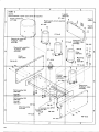
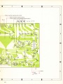
D|SASSEMBLY
8.
P A R T SL O C A T T O N S
9.
EXPLODEDVIEWS
10.
SCHEMATICDIAGRAMS,P.C. BOARDPATTERNSAND
PARTSLIST
Parts ..
andMiscellaneous
Diagram
10.1 Schematic
(AWR-093)
10.2 PowerSupplyCircuitAssembly
10.3 PowerAmplifierAssembly(AWH-045)
10.4 MeterAmplifierAssembly(AWM-0811
3
... ... ..
4
.. .......
5
'........
6
7
8
10
......
11
13
....'...
. . . . 14
15
......
... .. . 16
........
20
23
.......
.... '...
.. -. '.
..''
30
33
37
42
11. PACKING
...... ...
47
12. PARTSLISTOFEXPLODEDVIEWS.
.........48
EiPEC.E
1. SPECIFICAT|ONS
Semiconductors
Transistors
D i o d e .s.
...........55
...........75
PowerAmplifier
C a s c a d eddi f f e r e n t i aAl m p l i f i e r ,
.......
Push-pulldrive,Triple push-pull,direct coupledOCL.
ContinuousPowerOutout
from 20 Hertz to 20,000 Hertz
(Both channelsdriven) . . . . . . 250 watts per channel(g ohms)
Total Harmonic Distortion at20 Hertz to 20.000 Hertz
Circuitry.
(Continuous
ratedpoweroutput)
o.1%
( 1 2 5w a t t sp e rc h a n n p
eo
l w eor u t p u t , 8
o h m s ). . . . . . . . . O . O 5 %
(1 wattperchannel
poweroutput,8ohms) . . . . . . . , . . . 0.Q5o/o
lntermodulation
Distortion
( C o n t i n u or ua st e d ' p o woeurt p u t )
.........
- O."lo/o
( 1 2 5w a t t sp e rc h a n n eplo w eor u t p u tS
, o h m s .). . . - . . . . 0 . 0 5 %
(1 watt perchannel
poweroutput,8 ohms) .
. . .O.O5%
FrequencyResponse.
5 Hertzto 80,000HertzlldB
Input(Sensitivity/lmpedance)
.
. . . . . . 2Vl50kohms
Output
Speaker..
. 4ohmstoSohms
D a m p i nFga c t o(r2 0H e r t zt o 2 0 , 0 0 0H e r t zS, o h m s ). . . , . . .
50
Hum andNoise(lHF, short-circuited,
A network). . . . . . .110d8
Miscellaneous
PowerRequirements
. . AC 120V60 Hertz
P o w eCr o n s u m o t i o
. .n. . . .
.,.. 500watts
Dimensions
. . . . . . 4 8 0 ( W ) x 1 8 6 . 5 ( Hx)4 4 5 ( D m
) m
1 9 - 5 / 1 x6 7 x 1 3 - 3 1 1 6 i n
Weight: Without Package.
24.3kg;54lb
FurnishedParts
ConnectionCord with Pin Plugs
Operatinglnstuctions
NOTE:
Specificdtiotrt and the design subject to possible mod,fication
without notice due to improuements.
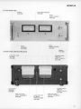
2. FRONT PANEL FACILITIES
P E A KL E V E LM E T E R S
Whenspeakersystemsof 8O nominal impedanceareconnected,theseprovidedirect readoutof the output power
in Watts.
NOTE:
Speohersyotemimpedanceuariesoccording to frequency.
To obtoin o preciae medsurcmentof the output poue\
remoue Spedhercon\ectiotrs ond connect 8a dumtuy
loodsocro4i the SPEAKERStermindls-
POWERSWI CH
S'et to ON to energizethe SPEC-2.Output will not be
obtaineduntil the PRoTEcTIoN indicatorlamp Soesout.
This effect is due to the internalmuting circuit and does
not indicatemalfunction.
METERZEROPOINTADJUSTMENT
PROTECTION
INDICATOR
The lamp lights when the protection circuit functions.
lf the lamp stays on during operation, turn off the
POWER switch and check as describedin the section
"Protection Circuit Operation". After identifying and
correctingthe sourceof difficulty, if the lamp still fails
to extinguish, contact a Pioneer Authorized Service
Center,
INPUTLEVEL CONTROLS(LEFT & RIGHT)
Adjust LEFT and RIGHT controls according to the
output level (voltage)of the pre-amplifierconnectedto
the SPEC-2 INPUT (L & R) jacks. Control positions
correspondto 2V at MAX (fully clockwise),4V at center
of rotation, and d at MIN (fully counter-ciockwise)
Normallyset thesecontrolsto MAX (2V).
. lf the minimum output voltageof the employedpreamplifier doesnot reach2V. set the controlsto MAX
(2V). In this casethe effectiveoutput indicatedin the
specificationswill not be obtained (for example 1/4
of the specifiedoutput can be attained with a preamplifieroutput voltageof 1V).
sPEC-e
3. CONNECTIONDIAGRAM
TAPE DECK
STEREOTURNTABLE
-i
. ,
' \ . .1, , I
,
r ,
; rl tO C i O q1 o
STEREOPRE-AMPLIFIER(e.s.PioneerSPEC-1)
SPEAKERS IMPEDANCE swilch
S€t to malch the nominal imDedance of the spoaker syst€ms employed with the SPEC-2. Be sure
to turn otf the po!!€r before
c h e n g i n gt h i s s w i t c h s e t t i n g .
For about 6 to 12 seconds 6tter
changing the position o{ the
IMPEDANCE swirch the PROTECTION lamp lights and sound
is not obtained from the speaksr
systems. This is du6 to the builtin muting circuit,
R I G H TC H A N N E L
L E F TC H A N N E L
SPEAKERSYSTEMS
4. CIRCUIT DESCRIPTION
4 . 1 P O W E RA M P L I F I E R
The SPEC-2 is a high power design, employing a
cascoded differential amplifier first stage, push-pull
drive, and darlington triple push-pull circuit with
all stagesdirect coupled (OCL).
The circuit diagram is shown in Fig. 2. Q1 and Q2
form the differntial amplifier. The input signal is
applied to Q1 and NFB from the output stage
applied to Q2 base. These two transistors are connected in common base circuits with Q3 and Q4,
forming a cascode amplifier. Since the common
emitter circuit (Q1 & Q2) load becomes the input
of the following common base circuit stage, load
impedance is low and stable amplification can be
achieved.
Q3 and Q4 outputs drive Q5 and Q6 in opposite
phase. The Qb output via Q7 is applied to the
current mirror circuit formed by D2 and Q8, where
the phase is again inverted. Q6 and Q8 outputs
thus become signals of the same phase and perform
a pre-driver function.
The cunent mirror circuit is depicted in Fig. 1.
Current flowing through R2 and Q8 becomesequal
to that flowing through Rl and D2. In other words,
since R1 and R2 are equal, and the characteristics
of. D2 and Q8 base-emitter are also equal, the
current +BL reaching point A (in Fig. 1) through
R1 and D2 is equal to that reaching the same point
through R2 and Q8 base-emitter. This becomes
equivalent to having Q5 output directly driving
Q8.
By adopting this current mirror circuit, when
muting relay RLb is OFF Q8 is cut off, Q10 - Q20
are switched OFF in succession, and operation
stops. The reversed phases of Q8 and Q6 outputs
cause them to cancel each other, reducing pop
noise and muting relay switching noise.
Q13 and Q14 in the following driver stage drive
the power transistors by direct coupling. The final
stage is a high output design with three power
transistors for each channel coupled in parallel.
This parallel coupling permits comparatively large
current (Ic) to be employed through each transistor, plus selection of an operating point with
good linearity and high amplification (hfe).
+Bl
ll:t2
- llrirel
tu
€
Fig. 1 CurrentMirror Circuit
IIIPUTH
Fig. 2 PowerAmplifier Circuit
SPEC-p
Current Limiter Circuit
The current limiter circuit, shown in Fig. 2, consists
of Q9 - qLz. If an overcurrent flows in the power
transistors, due to low load (less than 4S2) or load
shorting, this circuit utilizes the voltage drop
produced in the power transistor emitter resistance
to limit the input voltage. Q9 - Q12 are normally
OFF, but if for some rea.sonan overcurrent occurs
in the power transistors, the voltage drop component of the power transistor emitter resistance
increases. This voltage is divided and used to bias
the bases of Q9 and Q11, switching them ON.
Q9 and Ql1 make Q10 and Q12 conductive,
limiting the signal voltages applied to the basis of
Q13 and Q14.
VR2 and VR3 in this circuit set the current limiting value, while TH1 and TH2 are for temperature
compensation. RLG is a selector switch for changing the current limiting value at 4O load.
4.2 PEAK LEVEL METER CIRCUIT
Logarithmic indication is required in order to
provide a broad indicating range in a single meter,
without the need for range selection by the user.
With respect to an 8O load, approximately 50dB
logarithmic compression is performed to allow
meter indication in the range of 0.01 - 500W.
As shown in Fig. 3, the circuit is divided into
positive and negative sides. Each side consists of
logarithmic compression, peak value holding and
voltage to current converter circuits. In addition
there is a cunent resultant circuits, common to
both sides. The positive side circuit operation is
described here.
A portion of the pov/er amplifier output signal is
compressed by the logarithmic compression circuit,
which utilizes the exponential function properties
of diodes. Figs. 4 and 5 illustrate the operating
principle and input-output response. The compressed signal is then rectified and retained for a
suitable length of time by the peak holding circuit,
which employs a simple diode and capacitor construction. Holding time is determined by ttre time
constant of C1 and R1.
The holding circuit voltage is then applied to the
voltage-current converter, where it is converted
into a current value and amplified. The current
afterwards passes through the current resultant
circuit and drives the meter.
The current resultant circuit applies the larger
current of the positive and negative sides to the
.meter for operation.
o
E
o
e
I\
I EL
+
f
Inprtvoltagc(lC)
Fig. 4 EquivalentCircuit of the LogarithmicCompression
e
4
=
current
Yoltage
Conv
erter
PostTtvt
stDE
Peak
logarithmic r alue
holding
ion
ress
comp
e
e
€
o
E
lC inputvoltage
Fig. 5 Input-outputResponse
- P o s i t i vpee a kc u r r e n t
--' llegatiYe
pealcurrent
It0lltvtst0t
Fig. 3 PeakLevelMeterCircuit
7
4 . 3 P R O T E C T I O NC I R C U I T
The main purpose of the protection circuit is to
protect the equipment and give an indication in
the event of malfunction, incorrect operation,
faulty connections, or other causes.
The block diagram of the protection circuit functions is shown in Fig. 6. The following description
is in reference to the dia$am.
RL2, RLg and RL6 are for changing the transformer secondary taps when the impedance switch
is selected and determining the value of the current
control circuit in the power amplifier. They are
thus not directly related to the protectiorr function.
Zener diodes D2 and DB fix the operating potentials of Q29 and Q30, and the difference in their
starting points prevent misoperation.
Relay and Lamp Drivers
q27 - Q30 form the relay drive circuit (see Fig. 7).
while Q31 drives the lamp. In normal operation,
reverse bias is applied to Q27, maintaining it in
the cut off state. When an abnormality is detected
by the DC balance or temperature detector, current
flows through R1. Q27 base potential falls rapidly
and it switches ON. This causes forward bias
voltage to be applied to Q28, turning Q28 ON.
Potential at point B drops, turning off Q29 and
Q30. With Q29 OFF, current to relay RL5 is cut
off, tuming Q31 (lamp drive) ON and lighting the
protection lamp. Q30 cuts off the current to RL4
and RL2 (when impedance switch is at 8Q; when
at 4Q, RL4, RL6 and RL3).
Becauseof RL4 off, output circuit of the power
amplifier becomes open, and the stagesbeyond the
predriver are stopped operation completely by
RL5.
Power Switch ON Muting
This circuit also includes a delaying function when
the power switch is set to ON. The delay time is
determined by R8 and C1 in the Q29 and Q30
basecircuits.
Immediately after the power switch is turned ON,
-B1 and -B2,
Q27 and Q28 are reverse biased by
and switched OFF. Point B potential from'+B3
passes through R8 and rises as Cl charges. The
rise time is determined by the time constant of
C1 and R8. When the potential exceeds D3
(zener diode) zener voltage, Q30 is switched ON
and current flows in the relay circuit connected
to Q30.
In the same manner, when the potential at point
B exceeds D2 zener voltage, Q29 is switched ON
and current flows in RL5. Correct voltage is thus
applied to the power amplifier.
Fig. 6 Block Diagramof the ProtectionCircuit
SPEG.El
Power Switch OFF Muting
Since +B3 normally passes from R7 to R6 and
flows to -B.2, Q28 base is maintained at cut off
potential. When the power switch is tumed OFF,
-B2 immediately ceases,since its time constant is
smaller than +83. Consequently, +83 passes
through Dl and is applied to Q28 base, tuming
Q28 ON. Point B potential then falls rapidly,
tuming Q27 and Q30 OFF.
lmpedanceSelectorMuting
When the impedance selector switch (S1) is
changed from 8Sl to 4Sl, uncharged capacitor C2
is introduced into the - 82 circuit, temporarily
reducing -B2 voltage. This causes Q28 to switch
ON, C1 to be discharged, and Q29 & Q30 to be
switched OFF.
Although Q28 switches OFF again, Q29 and Q30
continue in the OFF condition for severalseconds
while C1 is charging.
Temperature Detector
The temperature detector employs positive coefficient thermistors (posistors). These are temperature
sensitive elements possessinga positive temperature
response, rapidly increasing in resistance when a
certain temperature is exceeded (see Figs. 8 & 9).
The posistors (TH3 & TH4) are mounted on the
power transistor. If some abnormality increa.ses
the temperature to the posistor operating point,
their resistance rapidly increases, reducing the
potential at point C. This allows DB to conduct,
so that the potential at point D drops and Q27
switches ON.
q
4
o
,2
o
4
point
A
-Tem0erature
t ("
Response
Fig. 8 Posistor-temperature
Fig. 9 TemperatureDetector Circuit
DC BalanceDetector
Q25 and Q26 make up a differential amplifier,
as shown in Fig. 10. The inputs (bases) of these
transistors are connected to the left and right
power amplifier. If for some reason the DC
balance of the power stage is upset, a potential
difference arises in the differential amplifier input
signal, unbalancing q25 and Q26 collector currents.
When one of the collector potentials becomes
lower than Q27 base potential, this base potential
is dissipated through D1 or D2, q27 switches ON,
and relay and lamp drives operate.
r- ----Poror
amplilicr
ir - - - - - - - - J
itcll
I
I
I
L-
--:E---..i
Fig. 10 DC BalanceDetectorCircuit
CIRCUITS
4.4 SURGECURRENTSUPPRESSOR
power
is
used
in the
A toroidal core
transformer
possessing
compactness and
SPEG2, which while
a large handling capacity, also exhibits extremely
low intemal resistance. In combination with the
four 15,000pF electrolytic capacitors forming the
power supply, surge current accompanying power
switch operation can reach a maximum of 3004.
The power supply can therefore be damaged unless
protective measuresare taken.
The main sources of surge current generation are
power transformer excitation current and power
supply electrolytic capacitor charging current.
Two surge suppressor circuits are employed in the
SPEC-2, one each in the primary and secondary
power transformer circuits. These circuits are
shown in Fig. 11.
Power transformer excitation current is handled
by the relay surge suppressor circuit at the
primary side. When the power switch is turned
ON, the current passes through R2 & D1 and
charges C1, therefore it does not flow through the
relay drive coil immediately, and RLl remains
OFF. The transformer excitation current flows
through R1 during this interval. After. C1 is
completely charged, current flows in the RL1
+83 drive coil switching it ON, and R1 is shorted.
The surge suppressor circuit in the
secondary side of the power transformer is designed to handle the
electrolytic capacitor charging curandlanp
Relay
rent. When the power switch is
drivors
turned ON, RL2 and RLB remain
OFF due to protection circuit operation. Consequently, the current
passes through R3 and R4, gradually charging the electrolytic capacitors through a bridge type rectifier
circuit. RL2 or RLB is switched ON
when charging has been completed,
gving the normal operating mode.
By employing these circuits, surge
+Bl
+
current is limited to approximately
t lectrolytic
40 A.
t
ito
catac
tlectrolytic
capacitor
-Bl
Fig. 11 SurgeCurrentSuppressor
Circuit
10
5. BLOCK DIAGRAM
LEFT
I
TNPUT I
etl
u*,il-
Li
_ -- --_\
P O W EA
RM P L I F I E R
Qlr
I
PROTECT
LANP
PROTECTION
CIRCUIT
t
RIGHT
INPUT
@9_l
-----r
: l--u*t
powER AMPLTFTER
( same as Lelt, cirannel,,)
RIGHTCHANNEL
f*l
'l
ll
Irl
I
tl
LE--
44
sPEC-e
t-
METER
ANPLIFIER
PEAK LEVEL
M E T ER
OUTPUT
L EFT
1
AC LINE
S W I T C H E: S
Sr : P0WER 0N*_0EF
I|'lPEDANCE
Sz . SPEAKER
8.0* 4Q,
:
POTENTIOMETERS
VRr: LEFT LEVELC0NTR0L
C0I{TR0L
VR2: RIGHTLEVEL
TPUT
@+
RIGH
6\\
t--
I
-
MLE T E RA l l P L t F t E R !
aRrcHT CHANNE
(Sarneas Left, channeL)
|
+
PEAKLEVEL
METER
;
RELAYS
RL1: PRIMARY
SURGE
CURRENT
CONTROL
:
RL2,
RLs SECSNDARY
CURRENT
SURGE
CONTROL
ANDVOLTAGE
SELECTOR
RLn: P0WERSUPPLY
CUT_
OFF RELAY
RL5: MUTING
RELAY
R h ' C U R R E NLTI M { T E R
SENSITIVITY
CONTROL
t<
6. ADJUSTING PROCEDURES
Since the same configuration is used for both left
and right channels of the SPEC-2 power amplifier
assembly, the following adjustments apply to both
channels.
6.1 IDLE CURRENTADJUSTMENT
1 ) Connect as shown in Fig. 12.
2 ) Set LEFT LEVEL and RIGHT LEVEL controls on the front panel to minimum (fully
counter-clockwise).
3 ) Set POWER switch to ON. After I or 2
minutes adjust VR1 to give an indication of
30mV on the voltmeter.
4 ) After the po\Merhas been ON for 30 minutes,
readjust VRl for 30mV indication on the
voltmeter.
Poweramplifierassembly
Fig. 12 ConnectionDiagramfor ldle CurrentAdjustment
13
6.2 CURRENT LIMITER SENSITIVITY
ADJUSTMENT
Note:
The high output power of the SPEC-2 requires a
dummy load of 4O and more than 200W. If a
200W dummy load is not available, connect two
8S}, 100W loads in parallel.
1 ) Connect as shown in Fig. 14.
2 ) Set SPEC-2 impedance selector switch to 8O
(even though a 4O dummy load is used).
3 ) While the voltmeter indicated 30V/(40 ), adjust
VR2 to just distorted point the upper half of
the waveform.
In the same manner, adjust VR3 to just distorted point the lower half with 28.3V/(44).
VR3
F i g . 1 3 T h e P o s i t i o no f V R 2 a n d V R 3
Voltmeter
Osilloscope
ooo
/ | ilPur
la
AF signalgenerator
Fig. 14 ConnectionDiagramfor CurrentLimiter SensitivityAdjustment
Waveform
SPEG.E!
6.3 M E T E R A M P L I F I E R A D J U S T M E N T
1 ) Connect as shown in Fig. 16.
2 ) Adjust input level to give an indication of
44.7V on the voltmeter.
3 ) At this time, adjust VR1 (left channel; VR2
is for right channel) for OdB (250W) indication
on the LEVEL meter.
Meteramplifierassembly
VR2
VRl
F i s .1 5 The Positionof VR 1 a n d V R 2
Voltmeter
SPEC-2
r
RIGHT .----.
I NPUT
IA
R
a
AF.S
'J-'
att\
Fig. 16 ConnectionDiagramfor MeterAmplifier Adjustment
15
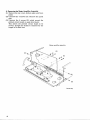
7. DISASSEMBLY
1. Removingthe Top Cover
Remove t],:.eL2 screws (A) to detach the top
cover.
(A)
E
(A)
(A)
Y
9
A)
I
g
@
-\
,a/-*rutez&tt"-..^
?soo
""*€:
i
"€a*...
(A)
ToP cover
n *""'-€(A,-.""",:'i,*u*
.--
2. Removingthe Bottom Plate
Removethe 13 screws(B) to detachthe bottom
plate.
sPEC-e
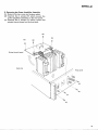
3. Removingthe Front Panel
(1) Remove all control knobs by pulling them
out.
(2) Remove the LEFT LEVEL and RIGHT
LEVEL shaft nuts and washers.
(3) Remove the 4 screws (C) on each side of the
main body. The front panel is ready for
removal.
'--=-
Front panel
-..---- . -'-
)
,/.
7
j @(c)
M a i nb o d y
Washer
17
4. Removingthe Meter Amplifier Assembly
(1) Remove the top cover, bottom plate and front
panel.
(2) Unscrew the 4 screws (D). Remove the panel
stay.
(3) Unscrew the 4 screws (E) which mount the
printed circuit board on peak level meter.
This allows the printed circuit board to be
moved, though the distance is limited by the
length of lts lead wire.
Meteramplifier assembly
Panelstay
SFEC.A
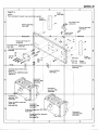
5. Removingthe Power Amplifier Assembly
(1) Remove the top cover and bottom plate.
(2) Unscrew the 4 screws (F) which mount the
power amplifier assembly on the rear panel.
(3) Unscrew the 4 screws (G) which mount the
printed circuit board on the heat sink.
Printedcircuit board
Heatsink
19
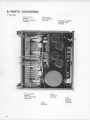
8. PARTS LOCATIONS
1. Top View
Poweramplifier
assembly
{ R I G H TC H A N N E L )
AWH-045
Powersupply
circuit assembly
AWR.093
Electrolytic capacitor
r 5,00&F100v
ACH-052
Poweramplitier
assembly
(LEFTCHANNEL}
AWH-045
Power
transformer
ArT-245
Oiode
KBH2504
Meter
amplifier
assembly
AWM.081
siPEc-e
2. Front PanelView
Handle
ANK,O84
Front panel assembly
ANB,358
Kn o b
( L E F TL E V E L )
AAB,097
'm
8:
&E
Knob
( RI G H T L E V EL )
AAB-097
Knob
(POWER)
AAD-109
H a n dl e
ANK.O84
3. Front View with PanelRemoved
Lamp(bartype)
8V 0.3A
AEL-058
Variableresistor
100ko-B
( L E F TL E V E L )
ACV-009
Leverswitch
(POWER)
ASK.OSO
Peaklevelmeter
( L EF T C H A N N E L )
AAW,O51
Lamp with wire
8V 50mA
( P R O T E C T T O) N
AEL-O42
Variableresistor
100kf,-B
( RI GH T L E VEL )
ACV-009
Peaklevelmeter
( RI G H TC H A N N E
L)
AAW.O51
4. RearView
Input terminal
AKB.O13
Output terminal(A)
AKE.02O
Spacer
AEB.O75
Spacer
AEB.075
Qround
terminal
A K E . O 1 9 Slideswitch
(IMPEDANCE)
ASH.014
Output terminal(B)
AKE.O21
3
ir
9. EXPLODEDVIFWS
NOTE:
ili
Partsindicatedin greentype cannothtisupplied.
BM.3x8*,
BM.3x8
rTW.3d
Top cover
ANE.097
PM.4x10
d
BM.3xg
rTw.30
@''
@.
-(9-
PM.4x10
PART 1
:ii!i:.ii1iitiiil,i,r::.iiirf
{ii'i!.!tir.1
PM.3x8
iri
[email protected] :
Front panelassembly
ANB.358
Handle
ANK-084
@
illliliJtlirj.l$;t;:1}?;i!,Y,
1i1r1;tl,iii!:il
Knob(POWER)
AAD.109
Knob
( L E F T L E V E L ,R I G H TL EV E L )
AAB-097
PM.3x8
@^
F W ' 3 @ x0 . 5 1
N u t M 9 Spacer9dx1t
8 7 1 - 0 0 4 M45-086
3
sIrEc-e
PART 3
S*e page 27
i ,r..",
*'b
P M . 4 x1 0
BM'3x8
RT.4x16
Foot assembly
AEC.178
Foot assembly
AEC-178
RT'4x16
itTW30
R T ' 4 x1 6
PART 1
NOTE:
..
t.'1
,i::,
Metpf amplifier assembly
AWM-081
Partsindicatedin greentype cannottb supplied.
A
Relay
ASR.O15
P M . 4 x8
A
PL socket
AKK-OO2
r.. ,i
.
-i .' -:iii:i:r
ii i-:.fl.ira:
orw.ao'
RT'3x6
(bartype)
Lamp
8V,..PL
AEL-058
N.3d
B
B
:ffi qgf.l:,.,,,,i,,
r,:,,
c
D
c
R u b b e rh o l d e r
AEB-051
Lampwith wire 8V, 50mA
AEL.O42
D
3
25
3
PART 2
.,1
Fus6.2A
AEK;103
RT'4x8 "i
NOTE:
ti'r
Partsindicatedin greentype cannotbe supplied.
Powertransformer
ATT-249.
Powersupplycircuit assembly
AWR-093
T'4x8
A
F u s e1
AEK-1I
':.:i.!,:itlii:!'1.:i.i..!1j,..:1i.i-1:.:t:;i,|:'it,r'.:.i,.tft:itjiri:rl:lilsi
I
Electrolyticcapaci
15,000pF,
100V
ACH-052
Electrolytic
B
15,000pF
ACH-052
RT.4x8
B
Diode
KBH-2504
RT.4x16
PM'4x10
Ceramic
0 . 0 1 p F ,1
ACG-00!
c
c
RT
Electrolytic
15,0001rF,
t00V
ACH-052
SpringwasherM6
ABE-026
Nut M6
SpringwasherMG
ABE.026
Nut M6
ABN.O17
sw.30
M o u n t i n gp i l l a r
ALA.O21
D
TerminalstriP (4P)
1
PM.3x8
D
PM.4x10
RT.3x6
26
siPEC-e
PART 3
,lil
NOTE:
Partsindicatedin greentype cannotbe supplied.
A
A
power cord
ACp
A D G- 0 1 3
Groundterminal
AKE.O19
Output terminal(A)
AKE.O2O
Terminal9o.16 Output terminal(B)
AKE_021
AEC-252
Terminalboardheld metal
B I M4e-052
ry''
-
BM.3x8
Screw
ABA.O89
OTW'4d Spacer
wN.4O AEB-075
,,tttinBUi$i;il.rh;l.i'.:,i:
AKB-013
Terminalboardheld metal
M49-014
S l i d es w i t c h( I M P E D A N C E )
ASH-014
t
L
c
Sonnector
i$sembly (6P)
6DX-020
c
Connector
assembly(5P)
ADX-O22
Connector
assembly(3P)
ADX.O23
Poweramplifierassembly
AWH.O45
(Seepage28)
D
conn$to,
(6P)
assernhly
ADXS21
Connectora*sembly(3P)
ADX-024 ,!i
PoweF.ampl
if ier assembly
AWH€45
(Seep$se28)
lr
D
Connector
assembly(5P)
ADX-O22
POWER
A M P L I F I E RASSEMBLY
NOTE:
Partsindicatedin greent ype cannot be supplied
A
A
.t'..ii.:.:t,lt':',,::.,r'.:f i::rti..iii rr,i: .i11:.:..:.,.r:rii...:.ljt::ri.lf,iL:,:llt!r.il!tr...,.,ft,...ii.:,:
Powertransistor
2SC1586
BM.3x10
Powertransistor
2SA909
Toggle nut
AEC-225
P M . 3 x1 6
B
B
R T . 3 x8
Varistor
,STV4H I
,
Insulatingwafer
BM.3x8
x:c-076
c
c
Transistorsocket
AKH-OO1
BM.3x8
'
Contactstrip (3P)
AKM-018
'
BM'3x8
D
2e
' :1.l' ', '.
Contactstrip (6P)
AKM.O2O
B M . 3 x8
i:','.
,"Contactstrip (5P)
AKM.O19
D
sPEC-e
NOMENCLATURE
OF SCREWS.
WASHERS
AND NUTS
The fou owing symbols stand for screws, washersand nutsasshownin explodedview.
Symbol
RT
Do.cription
Shspe
E r a z i e rh e a d t a p p i n g s c r e w
EW
PT
Pan head tapping screw
fF-
BT
Binding head tapping screw
ft-.
u--
CT
Countersunkhead tapping screw
t-
TT
Truss head tapping screw
ocT
Oval countersunk head tapping
Countersunk head machine
vt-:t
Dsscriprion
E type
\D
SW
Spring lock washer
Washer faced nut
Outernal toothed lock washer
#l
sc
Slotted set screw {Cone point)
e=D
Slotted set screw (Flar ooinr)
cEr
F
r
HS
AM
Binding head machinoscrew
G=
ocw
Oval countersunk head wood
CW
Countersunkhead wood screw
PSF
Pan head scr6w with flat washe.
@fl
oTw
Truss head machine screw
Panhead screw with spring
lock washer and flat washer
I
@il
Tt!!
PSB
\\,
Internal toothed lock washer
Oval countersunk head
Pan head screw with sprjng
A4
og
N
octv
PSA
Shape
oil
@
Panhead machinescrew
CM
Symbol
Hexagon socket headless set
@@
Round head wood screw
EXAMPLE
-::::";::1,,
L
PM' 3x8
Symbol
hr
F W ' 9 @1
x'
T-
th;skns55in mm ( I )
- diameterin mm ( d )
Symbol
-11'
/At
{( )l
d
I
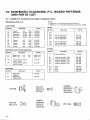
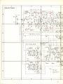
1O.SCHEMATICDIAGRAMS,P.C. BOARDPATTERNS
AND PARTSLIST
10.1 SCHEMATICDIAGRAMAND MISCELLANEOUS
PARTS
NOTE:
. Copocitors:in pF unlessotherwisenoted p:pF
. fiesrsao/s.
in a, AW unlessotheruisenoted h:hf]-,M:Ma
Miscellaneous
PartsList
CAPACITORS
D€scription
Symbol
Parl No.
FUSES
Symbol
c1
c2
c3
c4
Csramic
Electrolytic
Electrolytic
Electrolvtic
El€ctrolytic
0.01
15.000
15,OOO
15,000
15,000
150V
|OoV
IOoV
1oOV
l00V
ACG-003
ACH-052
ACH-052
ACH-052
ACH-052
c6
c7
Ceramic
Ceramic
Ceramic
Ceramic
Ceramic
0.O1
O.Ol
O.O1
O.O1
0.01
150V
15OV
15OV
150V
'l50V
ACG-001
ACG-001
ACG-001
ACG-001
ACG-003
c9
c10
D€scription
FUl
FU2
FU3
FU4
FU5
Fuse2A (Secondary)
Fuse2A (Secondary)
Fuse1A (Secondary)
A EK-103
AE K.103
AEK.106
FU6
FU1
FU8
Fuse1A (Secondary)
Fuse24 {Secondary)
Fuse12A (Primaryl
AE K"106
AEK-103
AEK-301
OTHERS
R E S I S T O RA
SN D P O T E N T I O M E T E B S
D€rcription
Symbol
Symbol
R1
Ds3cription
Metaloxid6
Metaloxide
VR2
4.7k
4.7k
Variableresistor1ook-B
( L E F TL E V E L )
Variableresistor100k-B
( R I G H TL E V E L }
Description
s1
Psrt No,
Part No.
3W
3W
RS3P472K
R53P472K
ACV-009
ACV-009
SWITCHES
Symbol
Part No.
Part No.
T1
Powertransformer
PL1
PL2
PL3
PL4
PL5
Lamp with wire
Lamp (bar typel
Lamp lbar lype)
Lamp (bar rypel
Lamp (bar typel
RL1
RL4
D1
D2
Relay
8V,
8V,
8V,
8V,
8V,
ATT.249
sOmA
0.3A
0.3A
0.3A
0.3A
AEL.U2
AEL-O58
AE L-O58
AEL.O58
AE L-O58
ASR-015
ASR-016
KBH-2504
st801-02
Diode
Diode
ASK-O80
(POWER)
Slide switch
(IMPEDANCE)
ASH-014
Bt
g7Y-ct
2sA733
r--r
2SC94S
2sA7s8 E itsE,
-82
25A725
ffiirE"
2SC1312 U)-B
2SA909
(2s8600A)
rlPl\ c
2sc1586[ \l 5,t(2SD555A)
2sA872AA--B
4J-;
2S8507
2SB63OA
2 S D 3 13
2SD61OA
\\sl
|lF}r
l/11
lr{
-
c U'-'-l'>B
l$=%
@?
2sc1384
SchematicDiagram
nNe Ass) AwH- 04$
PO$/ER
0 r , o "2 S A ? 3 x3t
0r.Qe, Qrz
2SCt58S'xi
'+
2SD6l0A
| tr\/trt
INPI.JT
LCF
I
CONTROL
@
TI
t;
rt
c?60P C3
16sn, |
.1;=
2
l
r0
os,q'o2SC945
xz
20v
,'9
tH
o,,Dr,Ds,os,Dr,Dro
lS24?3 xs
R r^
&:22
POWERN1P ASSy AWH- 045
rER AtlP Assy Awll-081
:Fil-,u
orDgzlS24?3x3t
6
or,Qr,Qr,Qr2SC13l2,c E
d
flss2.'lK
r'nt:ilrlir:,+il::.]
iriir.t
;i:ri, rj:, :nji.:.iir!
e:,er,0s,0c
2SA?25'+
RrlK(2'\i)
.:i+
6
i
0,,l524?3
Drs
0n*
j
wZiS?
ll'.25850
N O T E S:
SWIT C H E S
S r : P 0 $ / E RS W I T C H
0N + oFF
ST,
S P E A K E RI I ' I P E D A N C E
8(}-4Q
RELAY
RLr
R L rr
RL+
RLs
3
3'l
sPEC-e
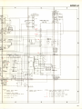
ri
Cl58*xi
LEFT
PO9{ER$'mY ASSy
AWR- 093
---
RIqHT
9N 050
kto^s
A
A
t6T
rs:
i$
Rs.??
AC r20V
50-60Hr
RELAYS
RLI PRII'4ARY
SURGECURRENT
CONTROL
RELAY
RLz.3SECONOARY
SURGECURRENT
RELAYS
CONTROL
ANO VOLTAGE
SELECTOR
R L + O U T P U TC U T - O F F R E L A Y
RLr
LIilITORSENSITIVITY
c'URRENT
CONTROLRELAY
' SIGNAL v0tTAGENECESSARYFOR OBTAINING
(lKHz)'
250fv,/6Q oUTPUTPOWER
l-l]
v
(
: DC VOLTASE AT NO INPUT SIGNAL.
::i;l
v)
: OC VOLTA$S AT 25OfV/EQ OUTPUTPOWER
AT NO INPUT SIGNAL,
DC CURREN.T'
RLs NUTING RELAY
32
(AWR.Og3I
10.2 FOWERSUPPLYCIRCUITASSEMBLY
Powertransformer(REO)
Power transformer {R ED}
Powertransformer(OR)
Por,vertransformer(OR)
Cz- Cs
15,000/1(xh4
Rr,Rz
4.7ksl(3W)
Power amplifier assembly-No.21
Meter amplif ier assembly-No.23
Power amplif ier ass€mbly-No.5
Meter amplif ier assembly-No.7
Powertransformer(GRN)
transformer (GRN)
transformer(BLK)
transformer(GRY)
transformer
transformer(BLU)
ramps
8V 0.3Ax4
Meter amplif ier assembly-No.5
amplitier assembly-No.5
amplif ier assembly-No.7
amplif ier ass6mbly-No.
(R CH.)
amplifierass€mbly-No.6
Power amplifier 6embty-No.6 (L CH.)
amplifier ass€mbly-No.10
amplifier ass€mbly-No.11
sPEC-e
PartsList of PowerSupply Circuit Assembly(AWR-093)
CAPACITORS
Symbol
c1
Psrt No.
De3cription
Ceramic
C€ramic
Ceramic
Ceramic
C6ramic
o.01
o.o'l
0.01
0.01
0.01
150V
150V
150V
150V
150V
ACG-O04-0
ACG-004-0
acG-00+o
ACG-004-0
ACG-004-0
c6
c7
c8
c9
cl0
C€ramic
C€ramic
Ceramic
0.01
0.01
0.ol
150V
150V
150V
ACG-OO4-0
ACG-O04-0
cl1
c12
Efoctrolytic
Electrolytic
47O
1000
35V
35V
cEA 471P35€5C
cEA 102P35-85C
c4
t:::"""
RESISTORS
Symbol
D€.cription
R1
20
20
Prrt No"
201,
2w,t
ACN-00S0
ACN-005-0
SEMICONDUCTORS
Sytnbol
Oe.cription
Pr.l No,
ol
D2
D3
D4
Diod€
Diode
Diode
Diode
Diode
stB0l-04
st 801-o4
srB01-04
stB0l-04
sl Bot-02
D6
Diods
Diode
Diode
Diode
Diod€
slBol-o2
srB01-02
slaol-o2
stB0l-02
stB01-o2
o7
DA
D9
D10
OTHERS
qmbol
RL1
RL2
Ds.cription
Rolsy
Rolay
Part No.
ASR-013-O
ASR-O13-0
(AWH.I!4sI
IO.3 POWER
AMPLIFIERASSEMBLY
Meter amplif i€r assembly'No.24
Polwr supplycircuits€mb|y.Nos.23,24,25
Pn-Cr3 25A909
(221
MEtsramplifier asembly-No.21
(R CH.)
Poweramplifierass€mbly.No.7
Meteramplitierassembly-No.
18 ( 191
Powersrpply circuitassembly-N06.
32,31,34
smplif ier ass€mbly-No.7
PourersupplycircuitNernbly-No.28
Meter amplifisr assembly-No.
15( 16)
Metor amplif ier assembly-No.23
Power supply circuit ass€mbly-N
06.19,20,21
0*- 0,r 25C1586
VRr
100k-B
siPEc-e
=
A
A
f
d
c{
G
0'u
(M9)s'0
&-lffi
(o
.^6
jitn
mU
(/.tS)Sn
jg
-(\l
fr
-rC)
@(v
d F
t--F
B
r
i*
tlt
$l
(M?l)Offuu
r
<n
<\l
!o
l3
(D
/+
=
.'4i
-
d-
c
t ' 06 l
c
+c?
td
<a>
-
=
a
t
s-
-at)
O-.o
.t>
)001t'u
F
9A/ol
riil;*ri:l;
?E
di+
cl
0i0tu
uL:t iE/-ZZel
4
o
N
o
(o
ct
t
o
*'$
o
F
fr
=
vsttu"'
ct
dI;
r
a
.J'
(!
t_
Y
ry
N
D
"EE
N
C-l
E*
G'
.;<
-^./t
tlzz'u
l*
y8:tsu
y0 ilzu
)1,9
e
sg
e
o9o'o''
(?)
r
sr
cl
ct)
D
5c\r
39
PartsList of PowerAmplifier Assembly(AWH-045)
CAPACITORS
Symbol
Symbol
Description
c1
c2
c3
c4
Efectrolytic
C€ramic
Ceramic
Electrolytic
Electrolytic
4.7
68p
47p
10
10
35V
sOV
50V
35V
35V
cszA 4R7M35
ccDsL 680K50
ccDSL470K50
cEA t00P50
cEA r00P35
c6
Efectrolytic
Ceramic
tulylar
lvlylar
Ceramic
22
4p
0.1
0.1
47Op
35V
50V
20OV
200V
500V
cEA 220P35
ccDsl o40K 50
coMA 104K200
coMA 104K200
CKDYB471K5OO
470p
500v
"'
:.:?L'.1""
O.O47
22p
820p
47Op
l50V
50V
50V
50
ACG-OO9-O
CKDYB 220 50
CKDYB 821K 50
C K D Y B4 7 1 K 5 0
c8
c9
c10
ct1
:::T::
c13
cl4
c15
cl6
c18
Ceramic
C6ramic
Ceramic
Ceramic
R E S I S T O RA
SN D P O T E N T I O M E T E R S
R1
2.2M
'110k
R3
R4
2.2k
15k
1.8k
R6
r.8k
33k
't5k
RDY.PS 225J
R D % P S1 1 4 J
RD%PS222J
RD7.PS153J
ROlr'rPSF122J
4.7k
4.7k
ROIZPSF122J
RD7.PS333J
RDz.PS153J
RS2P472K
ROy.PS472J
R11
R12
R13
R14
Rt5
100
100
100
100
R D % P M Fl O I J
R D % P M F1 0 1 J
RD/,PMF 101J
R D % P M F1 0 1 J
R16
Rt7
R18
R19
R20
22
R8
R9
R10
R21
823
F24
't10k
22
22
ao%PsF 22oJ
RDT.PSF22OJ
BDT.PSF114J
BD%PSF 220.J
RD7.PSF 22OJ
1ook
100k
22Ok
22Ok
47
RD7.PS1O1J
R D % P S1 0 1 J
AD%PSF 221J
RO%PSF 221
RD7.PS47OJ
RD'/.PS470J
RD%PMF 471J
RDT,PMF471J
RD7.PS331J
RD%PS331J
40
Part No,
R31
R32
R33
R34
R35
C6rbon film
Carbon film
C€rbon film
C€rbon film
Carbon film
27
27
10
10
10
RD%PS27OJ
RD%PS27OJ
RDY.PS1OOJ
RDY.PSl OOJ
RD%PS1OOJ
R36
R37
R38
R39
R40
Carbon lilm
Carbon film
Carbon tilm
10
10
10
0.5
5W
5W
RD%PS1OOJ
RD%PSl OOJ
RD%PSI OOJ
RTSB ORSK
RTsB OR5K
R41
R42
R43
R44
R45
Wirewound
Wirewound
Wirewound
Wirewound
Metaloxide
0.5
0.5
0.5
0.5
lk
5W
5W
5W
5W
3W
RTsB OR5K
RTsB OR5K
RT5B OR5K
RTsB ORSK
RS3P102K
R46
R47
848
R51
Wir6wound
Wirewound
Carbonfilm
Carbonfilm
2.2
1O
910
1.3k
vll
5W
RT2B 2R2K
RTSB 1OOK
R D % P S9 ' I 1 J
RDY.PS'I32J
vR2
VR3
Semi-fixed
Semi-fixed
S6mi-fixEd
470-B
100-B
100"8
ACP-051.o
ACP-050-0
ACP-050-0
SEMICONDUCTORS
Symbol
o1
Doscription
Part No.
Transistor
Transistor
Transistor
Transistor
Transistor
2SA798-Gor F
2SA872A-D or E
2SA872A-Dor E
2SD61oA-Ror S, O
2SD6'l0A-Ror S, O
Transistor
Trantastor
Transistor
Transistor
Transistor
2SD61OA-R
or S, O
2SB63OA-Ror S, O
2SA733-R
25C945-R
25C945-R
014
Transistor
Transistor
Transistor
Tlansistor
015
Transistor
25A733-R
25061oA-Ror S, O
2SB630A-Ror S, O
2SC1586-0or R
25D555A-R or S
2SC1586-0or R
25D555A-R or S
o16
Transistor
o17
Transistor
018
Transistor
019
Transistor
o3
04
o5
06
Q7
08
o9
010
Carbonfilm
.Carbonfilm
Carbonlilm
Carbonfilrn
Carbonfilm
D6scription
Part No.
011
012
or3
2SC1586-0or R
2SD555A-Ror S
2SA909-Oor R
2S8600A-R or S
2SA909-Oor R
2SB60OA-Ror S
2SA909-Oor R
2S860OA-Ror S
€tPEC-P
D€scription
Symbol
Part No.
o1
D3
Zenerdiode
Diode
04
D5
Diode
Diode
BZ 340
1S2473
(1S1555)
STV3H-Y
1S2473
(1S1555)
152473
{1S1555)
stB0l -04
stB01-04
D6
o7
D8
Diode
Diode
o9
Diod€
152413
{1S1555}
1S2473
(1515551
Dl1
Diode
STV4H
Thl
Th2
Th3
Thermistor
Thermistor
P.T.C.thermistor
TH101-2
TH101-2
AEX-O44
010
OTHERS
Symbol
D.3criplion
P.rl No.
L1
AF chokecoil
ATH-012-0
RLl
RL2
Reod relay
Reodrelay
ASR-017-0
ASR-005-C
10.4 METERAMPLIFIERASSEMBLY(NWM.O8l}
OO
N
A
t-
(|YlD00ereu
Jyl . 9c/01
<?
(?
i-k$
(\l
c
a
5
F.o==
o
I
(M%)visc/01
r
o
ro
m
(t,
ql
cD
6r,
31.') r
-1r)
o
a,
(\l
*
G
(n
raN
GO
.4
CLl.
Jlo
N
=
cl
t
=
<i
+t
9t /Za DtJ
>.Ll
ro
(\l
(?
t!*,
T
<0
o
N
a
N
+=
6l
(t)
/
=
,= P E
al
c7*
co
<f)
?
8;
s*
2
. O
(J
::(n
-Gl
-
t
<
' ,
9
yOgirsu
+N
sr/]Lvt,
B
T
!n
c)
U'
c-l
--
sc/zlst)
{
q)
A
,o
zzesu
B
t0'0zLJ
(Mzll)vq
r
0su
So
'-
- r_\-
CJ
.tO
x
(?
|l
$
r
o
I
o
.f
<\r
o(.,d-3
d t+r
({
I
@
(t,
U,
N
o
,..: ,r{til:
x
GT
r
P(!-)
tfj
#t
J \ t t a
dF
-(J
1'-t_
I
-2 ur
g -00rzu^
c
0:,!' ^' l A
v
X
i
._
c
i
5tosl scu
st
s: cr
s2
K)
C)
ct,
cr
s
c!.
U'
6r
ystrzu
g.
ct
a
o";
q
a
ct
C'
c:
ygtzzu
j
€
N
c-)
r
=
D
S
E
4?
F$
o<\l
I .t,
rl
c-
+
CT
D
Peakle\relmeter
(R chl
{ia"!i;
tff
t.
r, -+*---.-------<',
,,, *
E
*"
l''
:':'l
i{
15
Poweramplifierassembly-No.8
(L CH.)
8s,
Poweramplifierassembly-No.8
{R CH.)
amplifierassembly-No.2
l
4f,
Powersupplycircuitassembly-Nos.
19.20,21
amplifierassembly-No.
t6
Power supply circuit assembly-Nos.
23, 24, 25
Powersupplycirbuit assembly-No.31
8r,
Power supply circuit assembly-No.30<---'------------ Su-"
4f,,
(R CH.)
Poweramplifierassembly-No.4
Poweramplifierassembty-No.4
{L CH.}
Power amplif ier assembly-No.l9
Poweramplifierassembly-No.19
{R CH.
43
E|FEC-P
Peaklar6l meter
(L ch)
Powertransformer(WHT)
Power transformer {BRN}
Power supply circuit assembly-No.35
supplycircuit assembly-Nos.32,33,34
Poweramplif ier assembly-No.5
Powersupplycircuitassembly-No.27
Powersupply circuit assembly.No.26
rNo.19(L CH.)
r ( RC H . )
PartsList of MeterAmplifier Assembly(AWM-081
)
CAPACITORS
Symbol
c1
Description
Pert No.
Sylhbol
P€rt No.
Electrolytic
Electrolytic
Electrolytic
Electrolytic
Electrolytic
1
1
1
1
220
25V
25V
25V
25V
6V
cszA 010M 25
cszA 0't0M 25
cszA or0M 25
cszA 01otvr25
cEA 221P 6
R27
R2a
R29
R30
Carbonfilm
Carbonfilm
Carbonfilm
Carbonfilm
Carbonfilm
3.3k
3.3k
3.3k
3.3k
3.3k
RD%PS332J
RDY.PS332J
RDY.PS332J
RD/.PS 332J
RD7.PS332J
c1
c8
c9
cl0
Efectrolytic
Efectrolytic
Efectrolytic
Efectrolytic
Efoctrolytic
22O
220
22O
47O
47O
6V
6V
6V
6V
cEA
cEA
cEA
cEA
cEA
221P 6
221P 6
221P 6
4 7 1 P6
4 7 1 P6
R31
R32
R33
R34
R35
Carbonfilm
Carbonfilm
Carbonfilm
Carbonfilm
Carbonfilm
3.3k
3.3k
150
150
150
RD/.PS332J
RDY.PS332J
R D % P S1 5 1 J
RDY.PS
151J
RDI.PS151J
c11
c12
cl3
c14
cl5
Efectrolytic
Ceramic
Ceramic
Ef€ctrolytic
Efectrolylic
47O
0.O1
O.01
22
22
16V
50v
50v
35V
35V
c E A 4 7 1 P1 6
cKoYB 103K 50
CKDYB 1O3K50
cEA 220P 35
cEA 220P 35
R36
R37
R38
R39
R40
Carbonfilm
l50
:?':::1"'
CarbonIilm
Carbonfilm
330
33O
RD'/.PS33I J
RO%PS331J
cl6
Electrolytic
Electrolytic
10
10
35V
35V
cEA r 00P 35
cEA 100P 35
c18
c19
c20
c21
:: "..
10
10
10
160V
35V
35V
ACH-313-O
cEA 100P35
cEA t00P 35
R41
R42
R43
R44
R45
Carbonlilm
Carbonfilm
Carbonlilm
Carbontilm
Carbontilm
4.7k
1.5k
6.8k
6.8k
100
RO%PS472J
RD/.PS152J
RD%PS682J
RD%PS682J
R O % P S1 0 1 J
R46
F47
R48
R49
R50
Carbontilm
Carbonfilm
Carbonfilrn
Carbonfilm
Carbonfilrn
100
8.2k
150k
4.7k
15k
R D % P S1 0 1 J
RDy.PS822J
RD%PS154J
RD%Ps 472J
RDY.PS153J
R51
R52
R53
R54
Carbontilm
Carbontilm
Carbonlilm
Carbonfilm
CarbonIilm
15k
'lsk
22
150k
4.7k
RD/.PS |53J
RO%PS153J
RD%PS22OJ
RD7.PS154J
RD%PS 472J
R56
R57
R58
R59
R60
Carbontilm
Carbonfilm
Carbonfilm
Carbonfilm
Carbontilm
2.7k
2.2k
47k
4.7k
15k
RO%?S272J
RD%PS222J
RDY.PS473J
RO%PS472J
RD%PM.I53J
R61
R62
R63
R64
R65
Carbon{ilm
Carbontilm
Metaloxide
Carbonfilm
Carbonfilm
15k
Ik
330
1k
22
R66
R67
R68
R69
R70
Carbonfilm
Wirewound
Metaloxide
Carbontilm
Carbonfilm
22
4.7
1k
47O
47O
VR1
VR2
Semi-fixed
Semi-tixed
100-B
100-B
c4
Electrolytic
Electrolytic
R E S I S T O RA
SN D P O T E N T I O M E T E R S
Symbol
D€scription
P6rt No.
2W
2W
RS2P't02J
RS2P102J
RD%PS473J
RD%PS473J
RD%PS822J
M6tal oxide
Metal oxide
Carbon film
Carbon film
Carbon film
1k
lk
47k
47k
8.2k
R8
R9
Rr0
Carbon film
Carbon film
Carbon film
Carbon film
Carbon filrn
8.2k
8.2k
8.2k
'l
OO
10O
RD%PS822J
RD%PSA22J
RD%PS822J
R D % P S1 0 1 J
R D y . P S1 0 1 J
R1l
F12
R13
Rl4
R15
Carbon film
C€rbon film
Carbon film
Carbon film
Carbon film
10O
1O0
27
27
27
RD'/.PS101J
R D % P S1 0 1 J
RD%PS27OJ
RD7.PS27OJ
RD/.PS27OJ
R16
R17
R18
R19
R20
Carbon film
Carbon film
Carbon film
Carbon film
C€rbon film
2'l
4.7M
4.7M
4,1M
4.7M
RD'/.PS270J
RDl.PS475J
RD%PS475J
RD7.PS475J
RDY.PS475J
R21
R22
R23
R24
R25
Carbon film
Carbon film
Carbon film
Carbon film
Carbon film
15k
15k
15k
15k
3.3k
RDI.PS 153J
RDY.PS153J
RD7.PS153J
RD7.PS153J
RD7.PS332J
R3
R4
45
De.cription
hw
vzw
1AW
vd
1AW
5W
2W
RDY2PM
153J
RD7,PM1O2J
RS2P331J
RD%PM1O2J
RD%PS22OJ
RD%PS22OJ
RT5B 4R7K
RS2P102J
RD%PS471J
RD7.PS471J
ACP-O50-O
ACP-050-0
SEMICONDUCTORS
Symbol
o1
a2
o3
I
Fert No.
Transistor
T€nsistor
Transistor
Transistor
Transistor
2SC13't
2-G
25A725-G
2SA725-G
2SA725-G
o7
08
09
010
Traosistor
Transistor
Transiator
Transistor
Transistor
25A725-G
2SC1312-G
2SC13't
2-G
2SC1312-G
2SC1312-G
011
o12
013
014
015
Transistor
Tranaistor
Transistor
Transirtor
Transistor
2SA733-Oor R
2SC1384-Ror S
2SC945-Oor R
2SC138+S
2SC138+Ror S
o16
017
Transistor
Transistor
2SD313-Dor E
2SB5O7-Dor E
D1
D2
D3
D4
D5
Diode
Diod6
Diode
Diode
Diode
152473
152473
152473
1S2473
1S2473
D6
D7
D8
D9
Dto
Diode
Diod€
Diod6
Diodo
Diode
152473
152473
152473
1S2473
152473
D11
D12
D13
D14
t)15
Oiode
Diode
Diode
Diode
Diode
152473
1S2473
1S2473
152473
1s2473
Dl6
017
D18
D'tI
o20
Diode
Oiode
Oiode
Oiod6
Diode
152473
1s2473
152473
1s2473
D21
o22
D23
D24
Diode
Diode
Diode
Diode
Diode
1S2473
1s2473
152473
1s2473
'ts2473
D26
D27
D28
o29
D30
Diode
Diodo
Diode
Diode
Oiode
1S2473
152473
152473
1s2473
152473
D31
o32
D33
Diode
Diode
Zenor diode
152473
1s2473
wz't 00
04
46
Doscription
'ts2473
Symbol
Derciption
Psn No,
D34
Zener diode
Diode
w2061
152473
D36
037
D38
D39
D40
Diode
Diode
Zaner diod6
Zene. diode
Diode
st 801-02
slB0l-02
w2150
wz't 50
1S2473
D41
D42
D43
D44
D45
Zener diode
Zan6r diode
Diode
Diode
Diods
wzl57
w2157
s rB01-o4
152473
s rBol-o4
SPEC.El
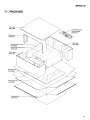
11. PACKING
Top pad
AHA-09O
Connectingcord
with pin plug
ADE-013
Panelcover
AHB-027
Polyethylenecover
AHG.O29
Operatinginstructions
ARB.153
Front pad
AHA.O91
Bottom
AHA.096
Insidepacking
AHC.023
Packingcase
AHD.272
Rearpad
AHA-092
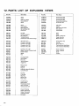
12. PARTS LIST OF EXPLODEDVIEWS
Par$ No.
Paats Namo
Parts No.
Parts Name
AAB.O97
AAD,1(D
AAW.Os1
ABA.O33
ABA-O8A
Knob
Knob
PeakLevelMeter
ScrewM2.6x4
Screw
AKM.OlA
AKM.O19
AKM-O2O
ALA-021
AN 8,358
ContactStrip (3P)
Contact Strip l5P)
ContactStrip (6P)
Chassis
MountingPillar
Front PanelAss.
ABA-089
ABA.O9O
ABA-097
ABE.026
ABN.OO9
Screw
Screw M4x8
MountingPillar
SpringWasherM6
Union Nut
ANE,O97
ANK.O84
ARB.153
ASH414
ASK-080
Top Cover
Handle
OperatingInstruction
SlideSvltitch
LeverSwitch
ABN-Ot7
ACG-OO1
ACH-052
ACV-009
ADE.O13
Nut M6
CeramicCapacitor
Ele, Capacitor
VariableResistor
ConnectionCord{with Pin Plug)
ASR-015
ASR-016
ATT-249
AWH{45
AWM{81
Relay
Relay
PowerTranstorm€r
ADG.O13
ADX.02O
ADX-O2l
ADX-O22
ADX-023
AC Pow6rCord
connector Ass.(6P)
ConnectorAss, (6P)
ConnectorAss. l5P)
ConnectorAss. (3P)
AWR-O93
871-OO4
M4s-086
M49{14
M49-052
Pow€rSupply Ass.
Nut Mg
Spacergmmx1t
ADX-024
AEa,oo'l
AEB.O51
AEB.075
AEC-036
ConnectorAss. {3P)
Washer{lnternal Toothed Lock}
RubberHolder
Spacer
Clip
25A909
2SB1586
KBH25O4
STV4H
PowerTransistor
AEC-076
AEC-079
AEC-178
AEC-222
AEC-225
I n s u l a t i n gW a { e r
Terminal Board
Togqle Nut
AEC-236
AEK-103
AEK.106
A€L-O42
AEL-OsA
Plastic Board
Fuse2A
AHA-O9O
AHA-091
AHA-OS2
AHA.096
AHB.O27
Top Pad
Front Pad
Rear P6d
Bottom Pad
Panel Cover
AHC-O23
AHO-272
AHG-O29
AKB-013
AKC-031
Insid6Packing
Packing Cas€
Polyelhylene Cover
Input Terminal
T€rminal strip (4P)
AKE-O19
AKE.O2O
AKE-O21
AKH-OO'I
AKK-OO2
Ground Terminal
Oueut T6rminal A
Output Terminal B
Transistor Socket
PL Socket
Larnp with Wire (8V 50mA)
Lamp 8V 0.3A
TerminalBoardHeldMetal
TerminalBoardHeldMetal
Diode
PIONEEFI
ELECTFI(fNIC
GOFIFOFIATION
Megueo-ku, Tokyo
T53. Japan
4-'1, Meguno l-Chome,
U.Ei. PIONEEFI
ELECTFIC'NICS
CCIF:PG'FIATIGIN
-A.
75 oxfo.cl
D.rwe. Moonach e, New Jel.sev o7o74,u.
( EIJFIC,PE! N.V.
PIG'NEEFI
ELECTFIG,NIC
Ele g,ur
t -, t-dg-.-' --, *eg no. 9, 2OJO A.rwp.o.
FIONEEFI
ELECTFICINICA
AUATFIALIA
PTY. LTc,.
Alst.a
ia
1 7A 184 Boundanv
troad, B.aes de, Vicconi6 3'l95,
o S E P T ,1 9 7 5
Printedin Japan