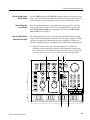
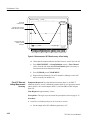
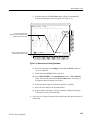
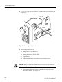
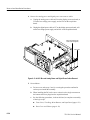
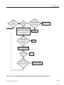
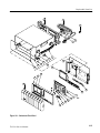
1
Service Manual
TLS 216
Logic Scope
070-8831-02
This document applies for firmware version 1.00
and above.
Warning
The servicing instructions are for use by qualified
personnel only. To avoid personal injury, do not
perform any servicing unless you are qualified to
do so. Refer to the Safety Summary prior to
performing service.
Copyright Tektronix, Inc. All rights reserved. Licensed software products are owned by Tektronix or its suppliers and
are protected by United States copyright laws and international treaty provisions.
Use, duplication, or disclosure by the Government is subject to restrictions as set forth in subparagraph (c)(1)(ii) of the
Rights in Technical Data and Computer Software clause at DFARS 252.227-7013, or subparagraphs (c)(1) and (2) of the
Commercial Computer Software – Restricted Rights clause at FAR 52.227-19, as applicable.
Tektronix products are covered by U.S. and foreign patents, issued and pending. Information in this publication supercedes
that in all previously published material. Specifications and price change privileges reserved.
Printed in the U.S.A.
Tektronix, Inc., P.O. Box 1000, Wilsonville, OR 97070–1000
TEKTRONIX and TEK are registered trademarks of Tektronix, Inc.
BusForm, GURU, and QUICKCLIP are trademarks of Tektronix, Inc.
TLS 216 WARRANTY
Tektronix warrants that this product will be free from defects in materials and workmanship for a period of three (3) years
from the date of shipment. If any such product proves defective during this warranty period, Tektronix, at its option, either
will repair the defective product without charge for parts and labor, or will provide a replacement in exchange for the
defective product.
In order to obtain service under this warranty, Customer must notify Tektronix of the defect before the expiration of the
warranty period and make suitable arrangements for the performance of service. Customer shall be responsible for
packaging and shipping the defective product to the service center designated by Tektronix, with shipping charges prepaid.
Tektronix shall pay for the return of the product to Customer if the shipment is to a location within the country in which the
Tektronix service center is located. Customer shall be responsible for paying all shipping charges, duties, taxes, and any
other charges for products returned to any other locations.
This warranty shall not apply to any defect, failure or damage caused by improper use or improper or inadequate
maintenance and care. Tektronix shall not be obligated to furnish service under this warranty a) to repair damage resulting
from attempts by personnel other than Tektronix representatives to install, repair or service the product; b) to repair
damage resulting from improper use or connection to incompatible equipment; or c) to service a product that has been
modified or integrated with other products when the effect of such modification or integration increases the time or
difficulty of servicing the product.
THIS WARRANTY IS GIVEN BY TEKTRONIX WITH RESPECT TO THIS PRODUCT IN LIEU OF ANY
OTHER WARRANTIES, EXPRESSED OR IMPLIED. TEKTRONIX AND ITS VENDORS DISCLAIM ANY
IMPLIED WARRANTIES OF MERCHANTABILITY OR FITNESS FOR A PARTICULAR PURPOSE.
TEKTRONIX’ RESPONSIBILITY TO REPAIR OR REPLACE DEFECTIVE PRODUCTS IS THE SOLE AND
EXCLUSIVE REMEDY PROVIDED TO THE CUSTOMER FOR BREACH OF THIS WARRANTY. TEKTRONIX
AND ITS VENDORS WILL NOT BE LIABLE FOR ANY INDIRECT, SPECIAL, INCIDENTAL, OR
CONSEQUENTIAL DAMAGES IRRESPECTIVE OF WHETHER TEKTRONIX OR THE VENDOR HAS
ADVANCE NOTICE OF THE POSSIBILITY OF SUCH DAMAGES.
P6240 WARRANTY
Tektronix warrants that this product will be free from defects in materials and workmanship for a period of one (1) year
from the date of shipment. If any such product proves defective during this warranty period, Tektronix, at its option, either
will repair the defective product without charge for parts and labor, or will provide a replacement in exchange for the
defective product.
In order to obtain service under this warranty, Customer must notify Tektronix of the defect before the expiration of the
warranty period and make suitable arrangements for the performance of service. Customer shall be responsible for
packaging and shipping the defective product to the service center designated by Tektronix, with shipping charges prepaid.
Tektronix shall pay for the return of the product to Customer if the shipment is to a location within the country in which the
Tektronix service center is located. Customer shall be responsible for paying all shipping charges, duties, taxes, and any
other charges for products returned to any other locations.
This warranty shall not apply to any defect, failure or damage caused by improper use or improper or inadequate
maintenance and care. Tektronix shall not be obligated to furnish service under this warranty a) to repair damage resulting
from attempts by personnel other than Tektronix representatives to install, repair or service the product; b) to repair
damage resulting from improper use or connection to incompatible equipment; or c) to service a product that has been
modified or integrated with other products when the effect of such modification or integration increases the time or
difficulty of servicing the product.
THIS WARRANTY IS GIVEN BY TEKTRONIX WITH RESPECT TO THIS PRODUCT IN LIEU OF ANY
OTHER WARRANTIES, EXPRESSED OR IMPLIED. TEKTRONIX AND ITS VENDORS DISCLAIM ANY
IMPLIED WARRANTIES OF MERCHANTABILITY OR FITNESS FOR A PARTICULAR PURPOSE.
TEKTRONIX’ RESPONSIBILITY TO REPAIR OR REPLACE DEFECTIVE PRODUCTS IS THE SOLE AND
EXCLUSIVE REMEDY PROVIDED TO THE CUSTOMER FOR BREACH OF THIS WARRANTY. TEKTRONIX
AND ITS VENDORS WILL NOT BE LIABLE FOR ANY INDIRECT, SPECIAL, INCIDENTAL, OR
CONSEQUENTIAL DAMAGES IRRESPECTIVE OF WHETHER TEKTRONIX OR THE VENDOR HAS
ADVANCE NOTICE OF THE POSSIBILITY OF SUCH DAMAGES.
Table of Contents
List of Figures . . . . . . . . . . . . . . . . . . . . . . . . . . . . . . . . . . . . . . . . . . . . .
List of Tables . . . . . . . . . . . . . . . . . . . . . . . . . . . . . . . . . . . . . . . . . . . . . .
Service Safety Summary . . . . . . . . . . . . . . . . . . . . . . . . . . . . . . . . . . . . .
Preface . . . . . . . . . . . . . . . . . . . . . . . . . . . . . . . . . . . . . . . . . . . . . . . . . . .
vi
ix
xi
xiii
Manual Structure . . . . . . . . . . . . . . . . . . . . . . . . . . . . . . . . . . . . . . . . . . . . . . . . .
Conventions . . . . . . . . . . . . . . . . . . . . . . . . . . . . . . . . . . . . . . . . . . . . . . . . . . . . .
Modules . . . . . . . . . . . . . . . . . . . . . . . . . . . . . . . . . . . . . . . . . . . . . . . . . . . . .
Safety . . . . . . . . . . . . . . . . . . . . . . . . . . . . . . . . . . . . . . . . . . . . . . . . . . . . . .
Symbols . . . . . . . . . . . . . . . . . . . . . . . . . . . . . . . . . . . . . . . . . . . . . . . . . . . . .
Operating Instructions . . . . . . . . . . . . . . . . . . . . . . . . . . . . . . . . . . . . . . . . . .
Related Manuals . . . . . . . . . . . . . . . . . . . . . . . . . . . . . . . . . . . . . . . . . . . . . . . . . .
xiii
xiv
xiv
xiv
xiv
xiv
xv
Introduction . . . . . . . . . . . . . . . . . . . . . . . . . . . . . . . . . . . . . . . . . . . . . . .
xvii
Before Servicing . . . . . . . . . . . . . . . . . . . . . . . . . . . . . . . . . . . . . . . . . . . . . . . . . .
Strategy for Servicing . . . . . . . . . . . . . . . . . . . . . . . . . . . . . . . . . . . . . . . . . . . . .
Tektronix Service . . . . . . . . . . . . . . . . . . . . . . . . . . . . . . . . . . . . . . . . . . . . . . . . .
Warranty Repair Service . . . . . . . . . . . . . . . . . . . . . . . . . . . . . . . . . . . . . . . .
Repair or Calibration Service . . . . . . . . . . . . . . . . . . . . . . . . . . . . . . . . . . . .
Self Service . . . . . . . . . . . . . . . . . . . . . . . . . . . . . . . . . . . . . . . . . . . . . . . . . .
xvii
xvii
xviii
xviii
xviii
xix
Product Description . . . . . . . . . . . . . . . . . . . . . . . . . . . . . . . . . . . . . . . . .
Warranted Characteristics . . . . . . . . . . . . . . . . . . . . . . . . . . . . . . . . . . .
Typical Characteristics . . . . . . . . . . . . . . . . . . . . . . . . . . . . . . . . . . . . . .
Nominal Traits . . . . . . . . . . . . . . . . . . . . . . . . . . . . . . . . . . . . . . . . . . . . .
1–1
1–3
1–9
1–13
Installation . . . . . . . . . . . . . . . . . . . . . . . . . . . . . . . . . . . . . . . . . . . . . . . .
2–1
Supplying Operating Power . . . . . . . . . . . . . . . . . . . . . . . . . . . . . . . . . . . . . . . . .
Power Cord Information . . . . . . . . . . . . . . . . . . . . . . . . . . . . . . . . . . . . . . . .
Operating Voltage . . . . . . . . . . . . . . . . . . . . . . . . . . . . . . . . . . . . . . . . . . . . .
Memory Backup Power . . . . . . . . . . . . . . . . . . . . . . . . . . . . . . . . . . . . . . . .
Operating Environment . . . . . . . . . . . . . . . . . . . . . . . . . . . . . . . . . . . . . . . . . . . .
Operating Temperature . . . . . . . . . . . . . . . . . . . . . . . . . . . . . . . . . . . . . . . . .
Ventilation Requirements . . . . . . . . . . . . . . . . . . . . . . . . . . . . . . . . . . . . . . .
Applying and Interrupting Power . . . . . . . . . . . . . . . . . . . . . . . . . . . . . . . . . . . .
Power On . . . . . . . . . . . . . . . . . . . . . . . . . . . . . . . . . . . . . . . . . . . . . . . . . . .
Power Off . . . . . . . . . . . . . . . . . . . . . . . . . . . . . . . . . . . . . . . . . . . . . . . . . . .
Repackaging Instructions . . . . . . . . . . . . . . . . . . . . . . . . . . . . . . . . . . . . . . . . . . .
2–1
2–2
2–3
2–4
2–4
2–4
2–4
2–4
2–4
2–5
2–5
General Operating Instructions . . . . . . . . . . . . . . . . . . . . . . . . . . . . . . .
2–7
Screen Layout . . . . . . . . . . . . . . . . . . . . . . . . . . . . . . . . . . . . . . . . . . . . . . . . . . . .
Basic Procedures . . . . . . . . . . . . . . . . . . . . . . . . . . . . . . . . . . . . . . . . . . . . . . . . .
2–7
2–7
Specification
Operating Information
TLS 216 Service Manual
i
Table of Contents
How to Power On . . . . . . . . . . . . . . . . . . . . . . . . . . . . . . . . . . . . . . . . . . . . .
How to Use Help . . . . . . . . . . . . . . . . . . . . . . . . . . . . . . . . . . . . . . . . . . . . . .
How to Display Logic Scope Status . . . . . . . . . . . . . . . . . . . . . . . . . . . . . . .
How to Reset the Logic Scope . . . . . . . . . . . . . . . . . . . . . . . . . . . . . . . . . . .
How to Set Functions from the Front Panel . . . . . . . . . . . . . . . . . . . . . . . . .
How to Set Functions from Menus . . . . . . . . . . . . . . . . . . . . . . . . . . . . . . . .
How to Set Complex Functions . . . . . . . . . . . . . . . . . . . . . . . . . . . . . . . . . .
2–7
2–8
2–9
2–9
2–9
2–10
2–11
Operating Instructions for Waveform Groups . . . . . . . . . . . . . . . . . . .
2–15
Vertical Readout . . . . . . . . . . . . . . . . . . . . . . . . . . . . . . . . . . . . . . . . . . . . . . . . . .
How to Adjust the Vertical Setup . . . . . . . . . . . . . . . . . . . . . . . . . . . . . . . . . . . . .
To Scale and Position Waveform Groups . . . . . . . . . . . . . . . . . . . . . . . . . . .
To Set Up from the Vertical Controls Menu . . . . . . . . . . . . . . . . . . . . . . . . .
How to Select Groups and Channels . . . . . . . . . . . . . . . . . . . . . . . . . . . . . . . . . .
To Select a Group . . . . . . . . . . . . . . . . . . . . . . . . . . . . . . . . . . . . . . . . . . . . .
To Select a Channel . . . . . . . . . . . . . . . . . . . . . . . . . . . . . . . . . . . . . . . . . . .
To Remove a Group from the Display . . . . . . . . . . . . . . . . . . . . . . . . . . . . .
How to Create a Waveform Group . . . . . . . . . . . . . . . . . . . . . . . . . . . . . . . . . . . .
To Define a Group . . . . . . . . . . . . . . . . . . . . . . . . . . . . . . . . . . . . . . . . . . . .
To Delete a Group . . . . . . . . . . . . . . . . . . . . . . . . . . . . . . . . . . . . . . . . . . . . .
How to Choose the Group Display Mode . . . . . . . . . . . . . . . . . . . . . . . . . . . . . .
To Select a Group Mode . . . . . . . . . . . . . . . . . . . . . . . . . . . . . . . . . . . . . . . .
To Display Only the Selected Channel . . . . . . . . . . . . . . . . . . . . . . . . . . . . .
To Define Group Thresholds and Height . . . . . . . . . . . . . . . . . . . . . . . . . . .
To Remove a Group from the Display . . . . . . . . . . . . . . . . . . . . . . . . . . . . .
To Find More Information . . . . . . . . . . . . . . . . . . . . . . . . . . . . . . . . . . . . . . . . . .
2–15
2–16
2–17
2–17
2–18
2–18
2–19
2–19
2–20
2–21
2–21
2–22
2–23
2–23
2–24
2–24
2–24
Circuit Description . . . . . . . . . . . . . . . . . . . . . . . . . . . . . . . . . . . . . . . . .
3–1
Logic Conventions . . . . . . . . . . . . . . . . . . . . . . . . . . . . . . . . . . . . . . . . . . . . . . . .
Module Overview . . . . . . . . . . . . . . . . . . . . . . . . . . . . . . . . . . . . . . . . . . . . . . . . .
3–1
3–1
Theory of Operation
Performance Verification
ii
Introduction . . . . . . . . . . . . . . . . . . . . . . . . . . . . . . . . . . . . . . . . . . . . . . .
4–1
Option 1S . . . . . . . . . . . . . . . . . . . . . . . . . . . . . . . . . . . . . . . . . . . . . . . . . . . . . . .
Operating Information . . . . . . . . . . . . . . . . . . . . . . . . . . . . . . . . . . . . . . . . . . . . .
Conventions . . . . . . . . . . . . . . . . . . . . . . . . . . . . . . . . . . . . . . . . . . . . . . . . . . . . .
4–1
4–2
4–2
Brief Procedures . . . . . . . . . . . . . . . . . . . . . . . . . . . . . . . . . . . . . . . . . . .
4–5
Self Tests . . . . . . . . . . . . . . . . . . . . . . . . . . . . . . . . . . . . . . . . . . . . . . . . . . . . . . .
Verify Internal Adjustment, Self Calibration, and Diagnostics . . . . . . . . . .
Verify Probe Function and Calibration . . . . . . . . . . . . . . . . . . . . . . . . . . . . .
Functional Tests . . . . . . . . . . . . . . . . . . . . . . . . . . . . . . . . . . . . . . . . . . . . . . . . . .
Verify All Input Channels . . . . . . . . . . . . . . . . . . . . . . . . . . . . . . . . . . . . . . .
Verify the Time Base . . . . . . . . . . . . . . . . . . . . . . . . . . . . . . . . . . . . . . . . . . .
Verify the Main and Delayed Trigger Systems . . . . . . . . . . . . . . . . . . . . . . .
Verify the File System . . . . . . . . . . . . . . . . . . . . . . . . . . . . . . . . . . . . . . . . . .
4–5
4–5
4–6
4–7
4–8
4–10
4–11
4–13
Performance Tests . . . . . . . . . . . . . . . . . . . . . . . . . . . . . . . . . . . . . . . . . .
4–15
Prerequisites . . . . . . . . . . . . . . . . . . . . . . . . . . . . . . . . . . . . . . . . . . . . . . . . .
Equipment Required . . . . . . . . . . . . . . . . . . . . . . . . . . . . . . . . . . . . . . . . . . .
Test Record . . . . . . . . . . . . . . . . . . . . . . . . . . . . . . . . . . . . . . . . . . . . . . . . . .
Preparation: Clear Probe Calibrations . . . . . . . . . . . . . . . . . . . . . . . . . . . . . . . . .
4–15
4–15
4–16
4–24
TLS 216 Service Manual
Table of Contents
Signal Acquisition System Checks . . . . . . . . . . . . . . . . . . . . . . . . . . . . . . . . . . .
Check Accuracy of Offset (Zero Setting) . . . . . . . . . . . . . . . . . . . . . . . . . . .
Check DC Gain and Voltage Measurement Accuracy . . . . . . . . . . . . . . . . .
Check Analog Bandwidth . . . . . . . . . . . . . . . . . . . . . . . . . . . . . . . . . . . . . . .
Check Delay Between Channels . . . . . . . . . . . . . . . . . . . . . . . . . . . . . . . . . .
Time Base System Check . . . . . . . . . . . . . . . . . . . . . . . . . . . . . . . . . . . . . . . . . . .
Check Accuracy for Long-Term Sample Rate, Delay Time, and Delta Time
Measurements . . . . . . . . . . . . . . . . . . . . . . . . . . . . . . . . . . . . . . . . .
Trigger System Checks . . . . . . . . . . . . . . . . . . . . . . . . . . . . . . . . . . . . . . . . . . . .
Check Accuracy for Logic Triggering . . . . . . . . . . . . . . . . . . . . . . . . . . . . .
Check Accuracy, Trigger Threshold . . . . . . . . . . . . . . . . . . . . . . . . . . . . . . .
Sensitivity, Edge Trigger . . . . . . . . . . . . . . . . . . . . . . . . . . . . . . . . . . . . . . . .
Output Signal Checks . . . . . . . . . . . . . . . . . . . . . . . . . . . . . . . . . . . . . . . . . . . . . .
Check Outputs — Probe Compensator . . . . . . . . . . . . . . . . . . . . . . . . . . . . .
Check Outputs — Main and Delayed Trigger . . . . . . . . . . . . . . . . . . . . . . .
4–25
4–25
4–26
4–31
4–34
4–36
4–36
4–39
4–39
4–43
4–45
4–51
4–51
4–53
Adjustment Procedures
Adjustment Procedures . . . . . . . . . . . . . . . . . . . . . . . . . . . . . . . . . . . . .
5–1
Requirements for Performance . . . . . . . . . . . . . . . . . . . . . . . . . . . . . . . . . . . . . .
Personnel . . . . . . . . . . . . . . . . . . . . . . . . . . . . . . . . . . . . . . . . . . . . . . . . . . . .
Warm-Up Period . . . . . . . . . . . . . . . . . . . . . . . . . . . . . . . . . . . . . . . . . . . . . .
Access . . . . . . . . . . . . . . . . . . . . . . . . . . . . . . . . . . . . . . . . . . . . . . . . . . . . . .
System . . . . . . . . . . . . . . . . . . . . . . . . . . . . . . . . . . . . . . . . . . . . . . . . . . . . . .
Optional Peripherals . . . . . . . . . . . . . . . . . . . . . . . . . . . . . . . . . . . . . . . . . . .
Test Equipment . . . . . . . . . . . . . . . . . . . . . . . . . . . . . . . . . . . . . . . . . . . . . . .
Usage . . . . . . . . . . . . . . . . . . . . . . . . . . . . . . . . . . . . . . . . . . . . . . . . . . . . . . . . . .
Performing the Adjustments . . . . . . . . . . . . . . . . . . . . . . . . . . . . . . . . . . . . .
Complete Adjustment . . . . . . . . . . . . . . . . . . . . . . . . . . . . . . . . . . . . . . . . . .
Individual Adjustments . . . . . . . . . . . . . . . . . . . . . . . . . . . . . . . . . . . . . . . . .
Partial Adjustment . . . . . . . . . . . . . . . . . . . . . . . . . . . . . . . . . . . . . . . . . . . .
Adjustment After Repair . . . . . . . . . . . . . . . . . . . . . . . . . . . . . . . . . . . . . . . .
Adjustment Dependencies . . . . . . . . . . . . . . . . . . . . . . . . . . . . . . . . . . . . . .
Equipment Required . . . . . . . . . . . . . . . . . . . . . . . . . . . . . . . . . . . . . . . . . . . . . . .
Adjustment Instructions . . . . . . . . . . . . . . . . . . . . . . . . . . . . . . . . . . . . . . . . . . . .
Hardware Installation . . . . . . . . . . . . . . . . . . . . . . . . . . . . . . . . . . . . . . . . . .
Software Installation . . . . . . . . . . . . . . . . . . . . . . . . . . . . . . . . . . . . . . . . . . .
Software-Based Adjustments . . . . . . . . . . . . . . . . . . . . . . . . . . . . . . . . . . . .
Display Assembly Adjustment . . . . . . . . . . . . . . . . . . . . . . . . . . . . . . . . . . . . . . .
Rotation, Brightness, and Contrast Adjustment . . . . . . . . . . . . . . . . . . . . . .
5–1
5–1
5–1
5–1
5–2
5–2
5–2
5–2
5–2
5–3
5–3
5–3
5–3
5–4
5–4
5–6
5–6
5–6
5–7
5–9
5–9
Maintenance Information . . . . . . . . . . . . . . . . . . . . . . . . . . . . . . . . . . . .
6–1
Procedures Not In This Section . . . . . . . . . . . . . . . . . . . . . . . . . . . . . . . . . . . . . .
Preventing ESD . . . . . . . . . . . . . . . . . . . . . . . . . . . . . . . . . . . . . . . . . . . . . . . . . .
Precautions . . . . . . . . . . . . . . . . . . . . . . . . . . . . . . . . . . . . . . . . . . . . . . . . . .
Susceptibility to ESD . . . . . . . . . . . . . . . . . . . . . . . . . . . . . . . . . . . . . . . . . .
6–1
6–2
6–2
6–2
Inspection and Cleaning . . . . . . . . . . . . . . . . . . . . . . . . . . . . . . . . . . . . .
6–5
General Care . . . . . . . . . . . . . . . . . . . . . . . . . . . . . . . . . . . . . . . . . . . . . . . . . . . . .
Inspection and Cleaning Procedures . . . . . . . . . . . . . . . . . . . . . . . . . . . . . . . . . .
6–5
6–5
Maintenance
TLS 216 Service Manual
iii
Table of Contents
Inspection — Exterior . . . . . . . . . . . . . . . . . . . . . . . . . . . . . . . . . . . . . . . . . .
Cleaning Procedure — Exterior . . . . . . . . . . . . . . . . . . . . . . . . . . . . . . . . . .
Inspection — Interior . . . . . . . . . . . . . . . . . . . . . . . . . . . . . . . . . . . . . . . . . .
Cleaning Procedure — Interior . . . . . . . . . . . . . . . . . . . . . . . . . . . . . . . . . . .
Lubrication . . . . . . . . . . . . . . . . . . . . . . . . . . . . . . . . . . . . . . . . . . . . . . . . . .
6–5
6–6
6–6
6–7
6–8
Removal and Installation Procedures . . . . . . . . . . . . . . . . . . . . . . . . . .
6–9
Preparation — Please Read . . . . . . . . . . . . . . . . . . . . . . . . . . . . . . . . . . . . . . . . .
List of Modules . . . . . . . . . . . . . . . . . . . . . . . . . . . . . . . . . . . . . . . . . . . . . . .
General Instructions . . . . . . . . . . . . . . . . . . . . . . . . . . . . . . . . . . . . . . . . . . .
Summary of Procedures . . . . . . . . . . . . . . . . . . . . . . . . . . . . . . . . . . . . . . . .
Equipment Required . . . . . . . . . . . . . . . . . . . . . . . . . . . . . . . . . . . . . . . . . . .
Access Procedure . . . . . . . . . . . . . . . . . . . . . . . . . . . . . . . . . . . . . . . . . . . . . . . . .
Procedures for External Modules . . . . . . . . . . . . . . . . . . . . . . . . . . . . . . . . . . . . .
Front-Panel Knobs . . . . . . . . . . . . . . . . . . . . . . . . . . . . . . . . . . . . . . . . . . . .
Line Fuse and Line Cord . . . . . . . . . . . . . . . . . . . . . . . . . . . . . . . . . . . . . . . .
EMI Gaskets . . . . . . . . . . . . . . . . . . . . . . . . . . . . . . . . . . . . . . . . . . . . . . . . .
Rear Cover and Cabinet . . . . . . . . . . . . . . . . . . . . . . . . . . . . . . . . . . . . . . . .
Front Cover, Trim Ring, Menu Buttons, and Input Panel . . . . . . . . . . . . . . .
A12 Front-Panel Assembly and Probe Calibrator . . . . . . . . . . . . . . . . . . . .
Display-Frame Assembly . . . . . . . . . . . . . . . . . . . . . . . . . . . . . . . . . . . . . . .
Cabinet Modules . . . . . . . . . . . . . . . . . . . . . . . . . . . . . . . . . . . . . . . . . . . . . .
Procedures for Outer-Chassis Modules . . . . . . . . . . . . . . . . . . . . . . . . . . . . . . . .
Input Cable Assembly . . . . . . . . . . . . . . . . . . . . . . . . . . . . . . . . . . . . . . . . . .
Probe Flex Circuit Replacement . . . . . . . . . . . . . . . . . . . . . . . . . . . . . . . . . .
Fan . . . . . . . . . . . . . . . . . . . . . . . . . . . . . . . . . . . . . . . . . . . . . . . . . . . . . . . . .
A14 D1 Bus and Analog-Power and Digital-Power Cables . . . . . . . . . . . . .
A23 SerPar Assembly . . . . . . . . . . . . . . . . . . . . . . . . . . . . . . . . . . . . . . . . . .
A11 Processor/Display Board . . . . . . . . . . . . . . . . . . . . . . . . . . . . . . . . . . . .
Top Cover and Board Brackets . . . . . . . . . . . . . . . . . . . . . . . . . . . . . . . . . . .
Rear-Panel Cables . . . . . . . . . . . . . . . . . . . . . . . . . . . . . . . . . . . . . . . . . . . . .
A10 Acquisition Board . . . . . . . . . . . . . . . . . . . . . . . . . . . . . . . . . . . . . . . . .
Floppy Disk . . . . . . . . . . . . . . . . . . . . . . . . . . . . . . . . . . . . . . . . . . . . . . . . . .
Rear Chassis . . . . . . . . . . . . . . . . . . . . . . . . . . . . . . . . . . . . . . . . . . . . . . . . .
Procedures for Inner-Chassis Modules . . . . . . . . . . . . . . . . . . . . . . . . . . . . . . . .
A16 Low Voltage Power Supply . . . . . . . . . . . . . . . . . . . . . . . . . . . . . . . . . .
A30 Display Assembly and Supply Fuse . . . . . . . . . . . . . . . . . . . . . . . . . . .
Front Subpanel . . . . . . . . . . . . . . . . . . . . . . . . . . . . . . . . . . . . . . . . . . . . . . .
Main Chassis . . . . . . . . . . . . . . . . . . . . . . . . . . . . . . . . . . . . . . . . . . . . . . . . .
Disassembly for Cleaning . . . . . . . . . . . . . . . . . . . . . . . . . . . . . . . . . . . . . . . . . .
6–9
6–10
6–10
6–10
6–11
6–14
6–15
6–16
6–17
6–19
6–19
6–21
6–23
6–26
6–26
6–29
6–29
6–31
6–33
6–33
6–35
6–37
6–39
6–40
6–41
6–42
6–45
6–46
6–47
6–48
6–52
6–54
6–54
Troubleshooting . . . . . . . . . . . . . . . . . . . . . . . . . . . . . . . . . . . . . . . . . . . .
6–57
Diagnostics . . . . . . . . . . . . . . . . . . . . . . . . . . . . . . . . . . . . . . . . . . . . . . . . . . . . . .
Firmware Updates . . . . . . . . . . . . . . . . . . . . . . . . . . . . . . . . . . . . . . . . . . . . . . . .
Troubleshooting Procedures . . . . . . . . . . . . . . . . . . . . . . . . . . . . . . . . . . . . . . . . .
6–57
6–58
6–59
Options and Accessories . . . . . . . . . . . . . . . . . . . . . . . . . . . . . . . . . . . . .
7–1
Options . . . . . . . . . . . . . . . . . . . . . . . . . . . . . . . . . . . . . . . . . . . . . . . . . . . . . . . . .
7–1
Options
iv
TLS 216 Service Manual
Table of Contents
Options A1–A5: International Power Cords . . . . . . . . . . . . . . . . . . . . . . . . .
Option B1: Service Manual . . . . . . . . . . . . . . . . . . . . . . . . . . . . . . . . . . . . .
Option 1B: Coaxial Adapter Set . . . . . . . . . . . . . . . . . . . . . . . . . . . . . . . . . .
Option 1K: K420 Instrument Cart . . . . . . . . . . . . . . . . . . . . . . . . . . . . . . . .
Warranty-Plus Service Options . . . . . . . . . . . . . . . . . . . . . . . . . . . . . . . . . . .
Option 1P: HC100 4 Pen Plotter . . . . . . . . . . . . . . . . . . . . . . . . . . . . . . . . . .
Option 1R: Rackmounted Logic Scope . . . . . . . . . . . . . . . . . . . . . . . . . . . .
Option 2P: Phaser 200e Color Printer . . . . . . . . . . . . . . . . . . . . . . . . . . . . . .
Option 9C: Certificate of Calibration and Test Data Report . . . . . . . . . . . . .
Standard Accessories . . . . . . . . . . . . . . . . . . . . . . . . . . . . . . . . . . . . . . . . . . . . . .
Optional Accessories . . . . . . . . . . . . . . . . . . . . . . . . . . . . . . . . . . . . . . . . . . . . . .
Accessory Software . . . . . . . . . . . . . . . . . . . . . . . . . . . . . . . . . . . . . . . . . . .
Warranty Information . . . . . . . . . . . . . . . . . . . . . . . . . . . . . . . . . . . . . . . . . .
7–1
7–1
7–1
7–1
7–1
7–2
7–2
7–2
7–2
7–2
7–3
7–4
7–4
Electrical Parts List . . . . . . . . . . . . . . . . . . . . . . . . . . . . . . . . . . . . . . . . .
8–1
Diagrams . . . . . . . . . . . . . . . . . . . . . . . . . . . . . . . . . . . . . . . . . . . . . . . . .
9–1
Symbols . . . . . . . . . . . . . . . . . . . . . . . . . . . . . . . . . . . . . . . . . . . . . . . . . . . . . . . .
9–1
Electrical Parts List
Diagrams
Mechanical Parts List
TLS 216 Service Manual
Replaceable Parts List . . . . . . . . . . . . . . . . . . . . . . . . . . . . . . . . . . . . . . .
10–1
Parts Ordering Information . . . . . . . . . . . . . . . . . . . . . . . . . . . . . . . . . . . . . . . . .
Using the Replaceable Parts List . . . . . . . . . . . . . . . . . . . . . . . . . . . . . . . . . . . . .
10–1
10–2
v
Table of Contents
List of Figures
Figure 2–1: Map of Display Functions . . . . . . . . . . . . . . . . . . . . . . . . .
Figure 2–2: Vertical Readout Displaying Two Group Readouts . . . . .
Figure 2–3: The Vertical Readout and Vertical Controls Menu . . . . .
Figure 2–4: Groups — Valid and Invalid . . . . . . . . . . . . . . . . . . . . . . .
Figure 2–5: Display Modes . . . . . . . . . . . . . . . . . . . . . . . . . . . . . . . . . . .
Figure 4–1: Map of Display Functions . . . . . . . . . . . . . . . . . . . . . . . . .
Figure 4–2: Verifying Adjustments and Signal-Path
Compensation . . . . . . . . . . . . . . . . . . . . . . . . . . . . . . . . . . . . . . . . . .
Figure 4–3: Test Hookup for Functional Tests . . . . . . . . . . . . . . . . . . .
Figure 4–4: Square Wave Calibration and DC Baseline Signals . . . .
Figure 4–5: Measurement of DC Offset Accuracy at Zero Setting . . .
Figure 4–6: Test Hookup for DC Gain and Accuracy Tests . . . . . . . .
Figure 4–7: Measurement of DC Gain Accuracy . . . . . . . . . . . . . . . . .
Figure 4–8: Measurement of DC Accuracy . . . . . . . . . . . . . . . . . . . . . .
Figure 4–9: Test Hookup for Analog Bandwidth Test . . . . . . . . . . . . .
Figure 4–10: Measurement of Analog Bandwidth . . . . . . . . . . . . . . . .
Figure 4–11: Test Hookup for Channel Delay Test . . . . . . . . . . . . . . . .
Figure 4–12: Measurement of Channel Delay . . . . . . . . . . . . . . . . . . .
Figure 4–13: Test Hookup for Time Base System Check . . . . . . . . . . .
Figure 4–14: Measurement of Accuracy — Long-Term and
Delay Time . . . . . . . . . . . . . . . . . . . . . . . . . . . . . . . . . . . . . . . . . . . . .
Figure 4–15: Test Hookup for Logic Trigger Check . . . . . . . . . . . . . .
Figure 4–16: Test Hookup for Trigger Threshold Check . . . . . . . . . .
Figure 4–17: Measurement of Trigger-Level Accuracy . . . . . . . . . . . .
Figure 4–18: Test Hookup for Main Edge Trigger Sensitivity
Checks . . . . . . . . . . . . . . . . . . . . . . . . . . . . . . . . . . . . . . . . . . . . . . . .
Figure 4–19: Measurement of Trigger Sensitivity . . . . . . . . . . . . . . . .
Figure 4–20: Test Hookup for AUX TRIGGER Input Sensitivity
Check . . . . . . . . . . . . . . . . . . . . . . . . . . . . . . . . . . . . . . . . . . . . . . . . .
Figure 4–21: Test Hookup for Probe Compensator Check . . . . . . . . .
Figure 4–22: Measurement of Probe Compensator Limits . . . . . . . . .
Figure 4–23: Test Hookup for Main Trigger Output Check . . . . . . . .
Figure 4–24: Measurement of Main Trigger Output Limits . . . . . . . .
Figure 5–1: Accessing the Protection Switch . . . . . . . . . . . . . . . . . . . .
Figure 5–2: Five and Ten Percent Luminance Patches . . . . . . . . . . . .
Figure 6–1: External Modules . . . . . . . . . . . . . . . . . . . . . . . . . . . . . . . .
vi
2–8
2–15
2–17
2–20
2–22
4–3
4–6
4–8
4–9
4–26
4–27
4–28
4–30
4–32
4–33
4–34
4–35
4–37
4–38
4–40
4–43
4–45
4–46
4–48
4–49
4–51
4–52
4–53
4–54
5–8
5–10
6–12
TLS 216 Service Manual
Table of Contents
Figure 6–2: Outer-Chassis Modules . . . . . . . . . . . . . . . . . . . . . . . . . . .
Figure 6–3: Inner-Chassis Modules . . . . . . . . . . . . . . . . . . . . . . . . . . . .
Figure 6–4: Knob Removal . . . . . . . . . . . . . . . . . . . . . . . . . . . . . . . . . . .
Figure 6–5: Line Fuse and Line Cord Removal . . . . . . . . . . . . . . . . . .
Figure 6–6: Rear Cover and Cabinet Removal . . . . . . . . . . . . . . . . . .
Figure 6–7: Front Cover, Trim Ring, Menu Buttons, and Input Panel
Removal (Front Cover not Shown) . . . . . . . . . . . . . . . . . . . . . . . . .
Figure 6–8: A12 Front-Panel Assembly Removal . . . . . . . . . . . . . . . . .
Figure 6–9: Disassembly of Front-Panel Assembly . . . . . . . . . . . . . . .
Figure 6–10: Cabinet Modules Removal . . . . . . . . . . . . . . . . . . . . . . . .
Figure 6–11: Input Cable Assembly Routing . . . . . . . . . . . . . . . . . . . .
Figure 6–12: Cable Tie Removal for New Installations . . . . . . . . . . . .
Figure 6–13: A14 D1 Bus and Analog-Power and Digital-Power Cables
Removal . . . . . . . . . . . . . . . . . . . . . . . . . . . . . . . . . . . . . . . . . . . . . . .
Figure 6–14: Circuit Board Assembly Removal . . . . . . . . . . . . . . . . . .
Figure 6–15: Remove Circuit Board From Assembly . . . . . . . . . . . . .
Figure 6–16: A11 Processor/Display Removal . . . . . . . . . . . . . . . . . . .
Figure 6–17: Board Bracket Removal . . . . . . . . . . . . . . . . . . . . . . . . . .
Figure 6–18: A10 Acquisition Board Removal . . . . . . . . . . . . . . . . . . .
Figure 6–19: Floppy Disk Removal . . . . . . . . . . . . . . . . . . . . . . . . . . . .
Figure 6–20: Rear Chassis Removal . . . . . . . . . . . . . . . . . . . . . . . . . . .
Figure 6–21: A16 Low Voltage Power Supply Removal . . . . . . . . . . .
Figure 6–22: Display Assembly Removal . . . . . . . . . . . . . . . . . . . . . . .
Figure 6–23: Display-Driver Board Removal . . . . . . . . . . . . . . . . . . . .
Figure 6–24: Front Subpanel Removal . . . . . . . . . . . . . . . . . . . . . . . . .
Figure 6–25: Accessing the Protection Switch . . . . . . . . . . . . . . . . . . .
Figure 6–26: Primary Troubleshooting Procedure . . . . . . . . . . . . . . .
Figure 6–27: Module Isolation Troubleshooting Procedure . . . . . . . .
Figure 6–28: Power Supply Voltage Measurement Locations . . . . . . .
Figure 6–29: A16 Low Voltage Power Supply Module Isolation
Troubleshooting Procedure . . . . . . . . . . . . . . . . . . . . . . . . . . . . . . .
Figure 6–30: Display Troubleshooting Procedure . . . . . . . . . . . . . . . .
Figure 6–31: Horizontal and Vertical Sync Signals . . . . . . . . . . . . . . .
Figure 6–32: A Video Signal with White, Black, and Blanking Levels
Figure 6–33: Processor/Acquisition Troubleshooting Procedure . . . .
Figure 6–34: Processor/Front Panel Troubleshooting Procedure . . . .
Figure 6–35: Acquisition Troubleshooting Procedure . . . . . . . . . . . . .
Figure 6–36: Acquisition Troubleshooting Procedure (Cont.) . . . . . .
TLS 216 Service Manual
6–13
6–14
6–17
6–18
6–21
6–22
6–24
6–25
6–28
6–30
6–31
6–34
6–35
6–36
6–38
6–39
6–42
6–44
6–46
6–48
6–50
6–51
6–53
6–58
6–60
6–62
6–63
6–64
6–66
6–67
6–67
6–68
6–69
6–70
6–71
vii
Table of Contents
Figure 6–37: A11 DRAM Processor/Display Module
(View of Right Side) . . . . . . . . . . . . . . . . . . . . . . . . . . . . . . . . . . . . .
Figure 6–38: A11 DRAM Processor/Display Module
(View of Upper Left Corner) . . . . . . . . . . . . . . . . . . . . . . . . . . . . . .
Figure 6–39: A11 DRAM Processor/Display Module
(View of Lower Left Corner) . . . . . . . . . . . . . . . . . . . . . . . . . . . . . .
Figure 9–1: TLS 216 Block Diagram . . . . . . . . . . . . . . . . . . . . . . . . . . .
Figure 9–2: TLS 216 Interconnect Diagram . . . . . . . . . . . . . . . . . . . . .
Figure 10–1: Cabinet and Front Panel . . . . . . . . . . . . . . . . . . . . . . . . .
Figure 10–2: Outer-Chassis Modules . . . . . . . . . . . . . . . . . . . . . . . . . .
Figure 10–3: Inner-Chassis Modules . . . . . . . . . . . . . . . . . . . . . . . . . . .
Figure 10–4: Floppy Disk . . . . . . . . . . . . . . . . . . . . . . . . . . . . . . . . . . . .
Figure 10–5: Cabling . . . . . . . . . . . . . . . . . . . . . . . . . . . . . . . . . . . . . . . .
Figure 10–6: Accessories . . . . . . . . . . . . . . . . . . . . . . . . . . . . . . . . . . . . .
viii
6–72
6–73
6–74
9–2
9–4
10–5
10–7
10–8
10–9
10–11
10–12
TLS 216 Service Manual
Table of Contents
List of Tables
Table 1–1: Warranted Characteristics: Input System . . . . . . . . . . . .
Table 1–2: Warranted Characteristics: Signal Acquisition System . .
Table 1–3: Warranted Characteristics: Time Base System . . . . . . . .
Table 1–4: Warranted Characteristics: Triggering System . . . . . . . .
Table 1–5: Warranted Characteristics: Output Ports and Power
Distribution System . . . . . . . . . . . . . . . . . . . . . . . . . . . . . . . . . . . . .
Table 1–6: Warranted Characteristics: Environmental . . . . . . . . . . .
Table 1–7: Typical Characteristics: Input System . . . . . . . . . . . . . . . .
Table 1–8: Typical Characteristics: Signal Acquisition System . . . . .
Table 1–9: Typical Characteristics: Triggering System . . . . . . . . . . .
Table 1–10: Typical Characteristics: Display and Data Handling
Systems . . . . . . . . . . . . . . . . . . . . . . . . . . . . . . . . . . . . . . . . . . . . . . .
Table 1–11: Typical Characteristics: Operating Environment . . . . .
Table 1–12: Nominal Traits: Input System . . . . . . . . . . . . . . . . . . . . .
Table 1–13: Nominal Traits: Signal Acquisition System . . . . . . . . . . .
Table 1–14: Nominal Traits: Time Base System . . . . . . . . . . . . . . . . .
Table 1–15: Nominal Traits: Triggering System . . . . . . . . . . . . . . . . .
Table 1–16: Nominal Traits: Display System . . . . . . . . . . . . . . . . . . . .
Table 1–17: Nominal Traits: GPIB Interface and Output Ports . . . .
Table 1–18: Nominal Traits: Fuse Rating . . . . . . . . . . . . . . . . . . . . . . .
Table 1–19: Nominal Traits: Mechanical . . . . . . . . . . . . . . . . . . . . . . .
Table 2–1: Power-Cord Conductor Identification . . . . . . . . . . . . . . . .
Table 2–2: Power Cord Identification . . . . . . . . . . . . . . . . . . . . . . . . .
Table 2–3: Effects of Corrupted Data . . . . . . . . . . . . . . . . . . . . . . . . . .
Table 4–1: Test Equipment . . . . . . . . . . . . . . . . . . . . . . . . . . . . . . . . . .
Table 4–2: DC Accuracy . . . . . . . . . . . . . . . . . . . . . . . . . . . . . . . . . . . .
Table 4–3: Settings For Logic Trigger Accuracy Checks . . . . . . . . . .
Table 5–1: Calibration Tests . . . . . . . . . . . . . . . . . . . . . . . . . . . . . . . . .
Table 5–2: Adjustments Required for Module Replaced . . . . . . . . . .
Table 5–3: Adjustments and Dependencies . . . . . . . . . . . . . . . . . . . . .
Table 5–4: Test Equipment, Fixtures, and Supplies . . . . . . . . . . . . . .
Table 5–5: GPIB Board Configuration . . . . . . . . . . . . . . . . . . . . . . . . .
Table 6–1: Relative Susceptibility to Static-Discharge Damage . . . . .
Table 6–2: External Inspection Check List . . . . . . . . . . . . . . . . . . . . .
Table 6–3: Internal Inspection Check List . . . . . . . . . . . . . . . . . . . . . .
TLS 216 Service Manual
1–3
1–3
1–5
1–5
1–6
1–6
1–9
1–9
1–10
1–10
1–11
1–13
1–13
1–14
1–14
1–14
1–14
1–15
1–15
2–2
2–3
2–5
4–15
4–30
4–40
5–3
5–4
5–4
5–4
5–6
6–2
6–6
6–6
ix
Table of Contents
Table 6–4: Tools Required for Module Removal . . . . . . . . . . . . . . . . .
Table 6–5: Normal Supply Voltages (Measured on J26 and J27 on the
A11 DRAM Processor/Display Module) . . . . . . . . . . . . . . . . . . . .
Table 6–6: No-Load Supply Voltages (Measured on J5 and J6 on the
A16 Low Voltage Power Supply Module) . . . . . . . . . . . . . . . . . . .
Table 7–1: International Power Cords . . . . . . . . . . . . . . . . . . . . . . . . .
Table 7–2: Standard Accessories . . . . . . . . . . . . . . . . . . . . . . . . . . . . . .
Table 7–3: Optional Accessories . . . . . . . . . . . . . . . . . . . . . . . . . . . . . .
Table 7–4: Accessory Software . . . . . . . . . . . . . . . . . . . . . . . . . . . . . . .
x
6–11
6–63
6–63
7–1
7–2
7–3
7–4
TLS 216 Service Manual
Service Safety Summary
Only qualified personnel should perform service procedures. Read this Service
Safety Summary and the General Safety Summary before performing any service
procedures.
Do Not Service Alone
Do not perform internal service or adjustments of this product unless another
person capable of rendering first aid and resuscitation is present.
Disconnect Power
To avoid electric shock, disconnect the main power by means of the power cord
or, if provided, the power switch.
Use Caution When
Servicing the CRT
To avoid electric shock or injury, use extreme caution when handling the CRT.
Only qualified personnel familiar with CRT servicing procedures and precautions
should remove or install the CRT.
CRTs retain hazardous voltages for long periods of time after power is turned off.
Before attempting any servicing, discharge the CRT by shorting the anode to
chassis ground. When discharging the CRT, connect the discharge path to ground
and then the anode. Rough handling may cause the CRT to implode. Do not nick
or scratch the glass or subject it to undue pressure when removing or installing it.
When handling the CRT, wear safety goggles and heavy gloves for protection.
Use Care When Servicing
With Power On
Dangerous voltages or currents may exist in this product. Disconnect power,
remove battery (if applicable), and disconnect test leads before removing
protective panels, soldering, or replacing components.
To avoid electric shock, do not touch exposed connections.
X-Radiation
TLS 216 Service Manual
To avoid x-radiation exposure, do not modify or otherwise alter the high-voltage
circuitry or the CRT enclosure. X-ray emissions generated within this product
have been sufficiently shielded.
xi
Service Safety Summary
xii
TLS 216 Service Manual
Preface
This is the Service Manual for the TLS 216 Logic Scope. Before using this
manual to service the logic scope, please read all topics in this preface. Also,
read the introduction that follows this preface, as it describes the strategy
(module replacement) used to service this product.
Manual Structure
This manual is divided into sections, such as Specifications and Theory of
Operation. Further, it is divided into subsections, such as Product Description
and Removal and Installation Procedures.
The following is a brief description of each manual section.
TLS 216 Service Manual
H
Specifications — contains a product description of the logic scope and
tables of the characteristics and descriptions that apply to it.
H
Operating Information — includes installation and operating instructions
at the level needed to safely power on and service this logic scope. Instructions for shipment of the logic scope are also found in this section.
H
Theory of Operation — contains circuit descriptions that support general
service and fault isolation.
H
Performance Verification — contains a collection of procedures for
confirming that this logic scope functions properly and meets warranted
limits.
H
Adjustment Procedures — contains a collection of procedures for adjusting
this Logic Scope to meet warranted limits.
H
Maintenance — contains information and procedures for doing preventive
and corrective maintenance of this logic scope. Instructions for cleaning, for
module removal and installation, and for fault isolation to a module are
found here.
H
Options — contains information on servicing any of the factory-installed
options that may be present in your logic scope.
H
Electrical Parts List — contains a statement referring you to Replaceable
Parts, where both electrical and mechanical modules are listed. See below.
H
Diagrams — contains a block diagram and an interconnection diagram
useful for isolating failed modules.
xiii
Preface
H
Mechanical Parts List — includes a table of all replaceable modules, their
descriptions, and their Tektronix part numbers.
Conventions
This manual uses certain conventions which you should become familiar with
before doing service.
Modules
Safety
Symbols
This manual refers to any replaceable component, assembly, or part of this logic
scope generically as a module. In general, a module is an assembly, like a circuit
board, rather than a component, like a resistor or an integrated circuit. Sometimes a single component is a module; for example, each chassis part of the logic
scope is a module.
Symbols and terms related to safety appear in the Safety Summary found at the
beginning of this manual.
Besides the symbols related to safety, this manual uses the following symbols:
STOP. The STOP label appears with information that must be read in order to
correctly do service and to avoid incorrectly using or applying service procedures.
The clock icon labels procedure steps which require a pause to wait for the logic
scope to complete some operation before you can continue.
Various icons such as the example icon at the left are used in procedures to help
identify certain readouts and menu functions on screen.
Operating Instructions
xiv
Throughout this manual, you will find various procedures which contain steps of
instructions for you to perform. To keep those instructions clear and consistent,
this manual uses the following conventions:
H
Names of front-panel controls and menu labels appear in boldface print.
H
Names also appear in the same case (initial capitals, all uppercase, etc.) in
the manual as is used on the logic scope front panel and menus. Front panel
names are all upper case letters, for example, GROUP MENU and
GROUP 1.
H
Instruction steps are numbered. The number is omitted if there is only one
step.
TLS 216 Service Manual
Preface
H
When steps require that you make a sequence of selections using front-panel
controls and menu buttons, an arrow ( ➞ ) marks each transition between a
front panel button and a menu, or between menus. Also, whether a name is a
main menu or side menu item is clearly indicated: Press HORIZONTAL
MENU ➞ Record Length (main) ➞ 500 points in 10 divs (side) ➞
Trigger Position (main) ➞ Set to 20% (side).
Using the convention just described results in instructions that are graphically
intuitive and simplifies procedures. For example, the instruction just given
replaces these five steps:
1. Press the front-panel button HORIZONTAL MENU.
2. Press the main menu button Record Length.
3. Press the side menu button 500 points in 10 divs.
4. Press the main menu button Trigger Position
5. Press the side menu button Set to 20%
Sometimes you may have to make a selection from a popup menu: Press
TRIGGER MENU ➞ Type (main) ➞ Edge (pop-up). In this example, you
repeatedly press the main menu button Type until Edge is highlighted in the
pop-up menu.
Related Manuals
The following documents are related to the use or service of the logic scope.
The TLS 216 User Manual contains a tutorial to quickly show you how to
operate the logic scope and an in depth discussion of how to more completely
use its features. Applications are also discussed.
The TLS 216 Programmer Manual (Tektronix part number 070-8835-00)
describes using a computer to control the logic scope through the GPIB interface.
The TLS 216 Reference (Tektronix part number 070-8833-00) gives you a quick
overview of how to operate your logic scope.
TLS 216 Service Manual
xv
Preface
xvi
TLS 216 Service Manual
Introduction
This introduction describes what you should do before attempting servicing of
the TLS 216 Logic Scope, outlines the strategy for servicing that this manual
supports, and lists service that you can obtain from Tektronix.
Before Servicing
This manual is for servicing the TLS 216 Logic Scope. To prevent injury to
yourself or damage to the logic scope, do the following before you attempt
service:
H
Be sure you are a qualified service person;
H
Read the Safety Summary and Preface found at the beginning of this manual;
H
Read Strategy for Servicing, below, and Installation in Section 2.
When using this manual for servicing, be sure to heed all warnings, cautions, and
notes.
When performing any procedure, be sure to read any introduction it may provide.
These introductions provide information needed to do the service safely,
correctly, and efficiently.
Strategy for Servicing
NOTE. Throughout this manual, any field-replaceable component, assembly, or
part of this logic scope is referred to generically as a module.
This manual contains all the information needed for periodic maintenance of the
logic scope. (Examples of such information are procedures for checking
performance and for readjustment.) Further, it contains all information for
corrective maintenance down to the module level. This means that the procedures, diagrams, and other troubleshooting aids help isolate failures to a specific
module, rather than to components of that module. Once a failure is isolated,
replace the module with a fresh unit obtained from the factory.
All modules are listed in Section 10, Mechanical Parts List. To isolate a failure
to a module, use the fault isolation procedures found in Section 6, Maintenance
Information. To remove and replace any failed module, follow the instructions in
Removal and Installation Procedures, also found in Section 6.
TLS 216 Service Manual
xvii
Introduction
Tektronix Service
Tektronix provides service to cover repair under warranty as well as other
services that may provide a cost-effective answer to your service needs.
Whether providing warranty repair service or any of the other services listed
below, Tektronix service technicians, trained on Tektronix products, are best
equipped to service your logic scope. Tektronix technicians are appraised of the
latest information on improvements to the product as well as the latest new
options to the product.
Warranty Repair Service
Repair or Calibration
Service
Tektronix warrants this product for three years from date of purchase, excluding
probes for which the warranty is one year. (The warranties appear following the
title page and copyright page near the front of this manual.) Tektronix technicians provide warranty service at most Tektronix service locations worldwide.
Your Tektronix product catalog lists all service locations worldwide.
The following services may be purchased to tailor repair and/or calibration of
your TLS 216 Logic Scope to fit your requirements.
Option 9C. When you order your TLS 216 Logic Scope with Option 9C, it is
shipped with a Certificate of Calibration and Test Data Report. This certificate
provides traceability to the National Institute of Standards and Technology
(NIST). It certifies procedures used to calibrate the logic scope comply with
U. S. Military Standard 45662A.
At-Depot Service. Tektronix offers several standard-priced adjustment (calibration) and repair services:
H
A single repair and/or adjustment.
H
Calibrations using equipment and procedures that meet the traceability
standards specific to the local area.
H
Annual maintenance agreements that provide for either calibration and repair
or calibration only of the logic scope.
Of these services, the annual maintenance agreement offers a particularly
cost-effective approach to service for many owners of the TLS 216 Logic Scope.
Such agreements can be purchased to span several years.
On-Site Service. The annual maintenance agreement can be purchased with
on-site service, with repair and calibration done at your facility. This service
reduces the time your logic scope is out of service when calibration or repair is
required.
xviii
TLS 216 Service Manual
Introduction
Self Service
Tektronix supports repair to the module level by providing Module Exchange
and Module Repair and Return.
Module Exchange. This service reduces down time for repair by allowing you to
exchange most modules for remanufactured ones. Tektronix ships you an
updated and tested exchange module from the Beaverton, Oregon service center,
typically within 24 hours. Each module comes with a 90-day service warranty.
Module Repair and Return. This service returns to you within 10 days the same
module that you shipped to Tektronix. The module shipped is repaired, tested,
and returned to you from the Beaverton, Oregon service center. It is not updated
to match current modules of the same type. Again, each module comes with a
90-day service warranty.
For More Information. Contact your local Tektronix service center or sales
engineer for more information on any of the repair or adjustment services just
described.
TLS 216 Service Manual
xix
Introduction
xx
TLS 216 Service Manual
Performance Verification
Product Description
The Tektronix TLS 216 Logic Scope is a superb tool for analyzing and debugging digital circuits. Its performance addresses the needs of digital designers and
troubleshooters of such circuits with the following features:
TLS 216 Service Manual
H
sixteen channels, equipped with sixteen 2.5 pF FET probes, for acquiring
waveforms from digital circuits
H
three display modes — displays analog waveforms, digital BusForms, and
dual-threshold timing diagrams
H
four threshold level presets based on four logic families, TTL, CMOS,
+ECL, and –ECL, for deriving digital levels for BusFormTM and timing
diagram displays
H
five trigger types — Edge, Pulse, Pattern, State, and Sequence
H
500 MHz maximum bandwidth, a 2 Gigasamples/second maximum
digitizing rate, eight-bit digitizers, and up to a 2,000-sample record length
per channel
H
full GPIB software programmability and hardcopy output using GPIB,
RS-232, or Centronics ports
H
complete measurement and documentation capability
H
intuitive operation using graphic icons and the more familiar and traditional
horizontal and vertical knobs
H
on-line help at the touch of a button
1–1
Product Description
1–2
TLS 216 Service Manual
Warranted Characteristics
This subsection lists the various warranted characteristics that describe the
TLS 216, including both electrical and environmental characteristics.
Warranted characteristics are quantifiable performance limits that are warranted.
NOTE. In these tables, those warranted characteristics that are checked (either
directly or indirectly) in the Performance Verification, found in Section 1, appear
in boldface type under the column Name.
Performance Conditions
The electrical characteristics found in these tables of warranted characteristics
apply when the TLS 216 has been adjusted at an ambient temperature between
+20_ C and +30_ C, has had a warm-up period of at least 20 minutes, and is
operating at an ambient temperature between +4_ C and +50_ C (unless
otherwise noted), and has passed both the signal path compensation and probe
calibration routines.
Table 1–1: Warranted Characteristics: Input System
Name
Description
Input Resistance with Coaxial Adapter
50 ±1%
Input Resistance with P6240 Probe
1 M ±15% at DC
Input Dynamic Range with Coaxial Adapter
±5 V (DC + Peak AC).
Input Dynamic Range with P6240 Probe
+15 V to –12 V (DC + Peak AC).
Maximum Input Voltage with Coaxial Adapter
±5 V (DC + Peak AC).
Maximum Input Voltage with P6240 Probe
±25 V (DC + Peak AC).
Maximum Input Voltage (Instrument Front Panel)
±5 V (DC + Peak AC).
Table 1–2: Warranted Characteristics: Signal Acquisition System
Name
Description
DC Gain Accuracy with P6240 Probe
±1.5% for time base settings of 50 mV/Div to 2 V/Div.
DC Gain Accuracy with Coaxial Adapter
±4.0% for time base settings of 50 mV/Div to 2 V/Div.
TLS 216 Service Manual
1–3
Warranted Characteristics
Table 1–2: Warranted Characteristics: Signal Acquisition System (Cont.)
Name
Description
DC Voltage Measurement Accuracy, Averaged, with
Coaxial Adapter
For an average of 16 waveforms:
±(4.0% × | reading – Offset | + Offset Accuracy +
(0.06 Div x V/Div))
Delta Volts between any two averages of 16 waveforms
acquired under the same setup and ambient conditions:
±(4.0% × | reading | + (0.1 Divs x V/Div) + 0.3 mV)
DC Voltage Measurement Accuracy, Averaged, with
P6240 Probe
For an average of 16 waveforms:
±(1.5% × | reading – Offset | + Offset Accuracy +
(0.06 Div x V/Div))
Delta Volts between any two averages of 16 waveforms
acquired under the same setup and ambient conditions:
±(1.5% × | reading | + (0.1 Divs x V/Div) + 0.3 mV)
DC Voltage Measurement Accuracy, Not Averaged, with
Coaxial Adapter
Any sample:
±(4.0% × | reading – Offset | + Offset Accuracy +
(0.13 Divs x V/Div) + 0.6 mV)
Delta Volts between any two samples acquired under the same
setup and ambient conditions:
±(4.0% × | reading | + (0.26 Divs x V/Div) + 1.2 mV)
DC Voltage Measurement Accuracy, Not Averaged, with
P6240 Probe
Any sample:
±(1.5% × | reading – Offset | + Offset Accuracy +
(0.13 Divs x V/Div) + 0.6 mV)
Delta Volts between any two samples acquired under the same
setup and ambient conditions:
±(1.5% × | reading | + (0.26 Divs x V/Div) + 1.2 mV)
Offset Accuracy
Analog Bandwidth with P6240 Probe or Coaxial Adapter
Delay Between Channels with Coaxial Adapter
1–4
V/Div Setting
Offset Accuracy
50 mV/Div to 499 mV/Div
2% of offset ± .3 Divs x V/Div
500 mV/Div to 2 V/Div
2% of offset ± .2 Divs x V/Div
Limits given for an ambient temperature range of 0_ C to +30_ C.
Derate upper bandwidth frequencies by 5.0 MHz for each _ C
above +30_ C.
V/Div Setting
Bandwidth
200 mV/Div to 2 V/Div
DC to 500 MHz
100 mV/Div to 199 mV/Div
DC to 450 MHz
50 mV/Div to 99.9 mV/Div
DC to 350 MHz
200 ps for any two channels with equal V/Div settings.
TLS 216 Service Manual
Warranted Characteristics
Table 1–2: Warranted Characteristics: Signal Acquisition System (Cont.)
Name
Description
Delay Between Channels with P6240 Probe
v500 ps for any two channels with equal V/Div settings.
Cross Talk (Channel Isolation)
w100:1 at 100 MHz and w30:1 at the rated bandwidth for the
sensitivity rating of the channel, for any two channels having equal
V/Div settings.
Table 1–3: Warranted Characteristics: Time Base System
Name
Description
Sample Rate and Delay Time Accuracy
"100 ppm over any interval w1 ms.
Seconds/Div Time Base Accuracy
"100 ppm over any interval w1 ms.
Delta Time Measurement Accuracy
Conditions
Time Measurement Accuracy
Single shot sample mode, ±(1 WI1 + 100 ppm × | Reading | +
20 MHz Bandwidth selected 1.1 ns)
Repetitive, w8 averages,
bandwidth selected
1
±(1 WI1 + 100 ppm × | Reading | +
180 ps)
The Waveform Interval (WI) is the time between the samples in the waveform record.
Table 1–4: Warranted Characteristics: Triggering System
Name
Description
Edge Trigger Accuracy
Any channel: 0.50 Divs from DC to 50 MHz, increasing to 3.0 Divs
at 500 MHz.
Pulse-, Sequence-, or Pattern-Type Trigger Time Accuracy
(Single Channel)
Width or Limit Setting
Trigger Time Accuracy
2.4 ns to 35 ns
±(5% of setting + 0.5 ns)
35 ns to 1 ms
±(10% of setting + 0.5 ns)
1.02 ms to 1 s
±(.01% of setting +50 ns)
Width or Limit Setting
Trigger Time Accuracy
2.4 ns to 35 ns
±(5% of setting + 2.5 ns)
35 ns to 1 ms
±(10% of setting + 2.5 ns)
1.02 ms to 1 s
±(.01% of setting +50 ns)
Pulse-, Sequence-, or Pattern-Type Trigger Time Accuracy
(Multiple Channels)
Pulse-, Sequence-, or Pattern-Type Trigger Minimum Time Interval
500 ps.
Edge-Type Trigger Minimum Pulse Width
800 ps.
Pulse-Type Trigger Rearm Time
2.5 ns.
Pulse-Type Trigger Minimum Pulse Width
2.0 ns.
Pattern-Type Trigger Minimum Pattern Width
4.0 ns.
TLS 216 Service Manual
1–5
Warranted Characteristics
Table 1–4: Warranted Characteristics: Triggering System (Cont.)
Name
Description
Pattern-Type Trigger Rearm Time
4.5 ns.
Sequence-Type Trigger Rearm Time
4.5 ns.
Sequence-Type Trigger Minimum Pulse Width
4.0 ns.
State-Type Trigger Setup and Hold Times
Setup: 4.0 ns; hold time: 4.0 ns.
Trigger Threshold Accuracy
±2% of (threshold setting – offset setting) + 0.2 Divs +
offset accuracy
Auxiliary Trigger Input Sensitivity
DC to 50 MHz input frequency with VIN(HI) = 2.0 V and
VIN(LO) = 0.8 V.
Table 1–5: Warranted Characteristics: Output Ports and Power Distribution System
Name
Description
Main and Delayed Trigger Output Logic Levels
Logic-High (VOUT(HI)): 2.5 V open circuit, 1.0 V into a 50 load to ground.
Logic-Low (VOUT(LO)): 0.7 V into a load of 4 mA; 0.25 V
into a 50 load to ground.
Source Voltage
90 to 250 VACRMS, continuous range.
Source Frequency
47 Hz to 440 Hz.
Power Consumption
350 W.
Probe Compensator Output Voltage and Frequency
Output voltage: 0.5 V (base to top) ±2% into a 50 load;
frequency: 1 kHz ±5%.
Table 1–6: Warranted Characteristics: Environmental
Name
Description
Temperature
(Operating and Nonoperating)
Operating: +4_ C to +50_ C.
Electrostatic Discharge Susceptibility
Up to 8 kV with no change to control settings, or impairment of
normal operation; up to 15 kV with no damage that prevents
recovery of normal operation by the user.
1–6
Nonoperating: –22_ C to +60_ C
TLS 216 Service Manual
Warranted Characteristics
Table 1–6: Warranted Characteristics: Environmental (Cont.)
Name
Description
Emissions
The instrument meets or exceeds the EMC requirements of the
following standards:
Vfg. 243/1991 Amended per Vfg. 46/1992
FCC Code of Federal Regulations, 47 CFR, Part 15,
Subpart B, Class A
Third Party Certification
UL: 1244, Ninth Edition
CSA: C22.2 No. 231-M89
TLS 216 Service Manual
1–7
Warranted Characteristics
1–8
TLS 216 Service Manual
Typical Characteristics
This subsection contains tables that list the various typical characteristics that
describe the TLS 216 Logic Scope.
Typical characteristics describe typical or average performance. Typical
characteristics are not warranted.
Table 1–7: Typical Characteristics: Input System
Name
Description
Input Resistance (Instrument Front Panel)
75 W ±1% at DC
Probe Input Capacitance
2.5 pF maximum.
Table 1–8: Typical Characteristics: Signal Acquisition System
Name
Description
Effective Bits
For a 9-division (peak-to-peak) sine wave output:
Output Frequency
2 GS/s Sample Rate
98 MHz
5.5 bits
245 MHz
5.0 bits
490 MHz
4.5 bits
Input Current
60 mA at an ambient temperature 30_ C.
Step Response Rise Time
V/Div Setting
Rise Time
50 mV/Div to 99.9 mV/Div
1.0 ns
100 mV/Div to 199 mV/Div
900 ps
200 mV/Div to 2 V/Div
800 ps
Step Response Settling Time with Coaxial Adapter
TLS 216 Service Manual
V/Div
Setting
±Step
Response
Settling Error at
20 ns
100 ns
50 mV/Div to
99.9 mV/Div
5.0 V
0.5% 0.2% 0.1%
100 mV/Div to 5.0 V
199 mV/Div
1.0% 0.5% 0.2%
200 mV/Div to 5.0 V
2 V/Div
1.0% 0.5% 0.2%
20 ms
1–9
Typical Characteristics
Table 1–9: Typical Characteristics: Triggering System
1
Name
Description
Trigger Position Accuracy (All Types)
Acquisition Mode
Accuracy
Sample or Average
±(1 WI1 + 1.5 ns)
Envelope
±(2 WI1 + 1.5 ns)
Edge-Type Trigger Jitter
0.5 ns peak-to-peak for 100 records.
Pulse-, Pattern-, State-, or Sequence-Type Trigger Sensitivity
1.0 Div from DC to 200 MHz, with a minimum slew rate of
25 Divs/ms at the trigger level threshold.
Pulse-, Pattern-, or Sequence-Type Trigger Time Range and
Resolution
Range: 2.4 ns to 1 s.
Time Range
Time Resolution
2.4 ns to 10 ns
0.2 ns
10.5 ns to 20 ns
0.5 ns
21 ns to 50 ns
1 ns
52 ns to 100 ns
2 ns
104 ns to 200 ns
4 ns
210 ns to 500 ns
10 ns
520 ns to 1 s
20 ns
Trigger Holdoff Range
0.5 ns to 10 s.
“Set Trigger Level to 50%” Minimum Operable Frequency
50 Hz.
Delayed Trigger Time Range
16.5 ns to 250 ns at 10 ms or faster; 15.152 ns to 250 s at 25 ms
or slower.
Delayed Trigger Events Range
2 to 10 million events.
Auxiliary Trigger Input Logic Levels
VIN(HI) = 2.0 V and VIN(LO) = 0.8 V.
Auxiliary Trigger Input Characteristics
Input is TTL compatible.
The Waveform Interval (WI) is the time between the samples in the waveform record.
Table 1–10: Typical Characteristics: Display and Data Handling Systems
Name
Description
Video Display Resolution
640 pixels horizontally by 480 pixels vertically in a display area of
12.8 cm (5.04 in.) horizontally by 9.6 cm (3.78 in.) vertically.
Nonvolatile Memory Capacity
Reference waveforms (4), stored setups (10), and calibration
constants are retained in nonvolatile memory.
Nonvolatile Memory Retention Time
5 years.
Floppy Disk Drive
3.5” floppy disk, 1.44 Mbyte, DOS 4.0 format for storing
waveforms, hard copies, and instrument setups.
1–10
TLS 216 Service Manual
Typical Characteristics
Table 1–11: Typical Characteristics: Operating Environment
Name
Description
Humidity
(Operating and Nonoperating)
Nonoperating:
to 90% relative humidity from –22_ C to +40_ C
to 50% relative humidity from –22_ C to +50_ C
Operating:
to 80% relative humidity from +4_ C to +29_ C
to 20% relative humidity from +4_ C to +50_ C
Altitude
(Operating and Nonoperating)
Operating: to 4570 m (15,000 ft.).
Nonoperating: to 12190 m (40,000 ft.).
Random Vibration
(Operating and Nonoperating)
Operating: 0.31 gRMS from 5 to 500 Hz, 10 minutes each axis
TLS 216 Service Manual
Nonoperating: 3.04 gRMS from 5 to 500 Hz, 10 minutes each axis.
1–11
Typical Characteristics
1–12
TLS 216 Service Manual
Nominal Traits
This subsection contains a collection of tables that list the various nominal traits
that describe the TLS 216, including both electrical and mechanical traits.
Nominal traits are described using simple statements of fact such as “16, all
identical” for the trait “Input Channels, Number of,” rather than in terms of
limits that are performance requirements.
Table 1–12: Nominal Traits: Input System
Name
Description
Input Probe Type
Tektronix P6240 only.
Input Coaxial Adapter Type
Tektronix part number 013–0282–00.
Probe Input Coupling
DC.
Input Probe Connector Type
Amp Inc. Amplimite coax Mix, Amp part number 750019–1.
Mates with Amp part number 750020–1.
Table 1–13: Nominal Traits: Signal Acquisition System
Name
Description
Input Channels, Number of
16, all identical; identified as Ch1, Ch2,... Ch16.
Input Coupling
DC only.
Samplers, Number of
16, all identical; one per channel.
Digitized Bits, Number of
8 bits.
V/Div Gain Sensitivity Settings
50 mV/Div to 2 V/Div in a 1–2–5 sequence.
V/Div Fine Gain Range and Resolution
Range: adjustable between the V/Div step gain setting and the
next lower step gain setting.
Resolution: 1% of the lower step gain setting.
Offset Voltage Range and Resolution
Range: +15 V to –12 V. Resolution: 5 mV.
Position Range
±5 divisions.
Position Accuracy
0.1 divisions.
Analog Bandwidth Selections
20 MHz and FULL (500 MHz) bandwidth.
TLS 216 Service Manual
1–13
Nominal Traits
Table 1–14: Nominal Traits: Time Base System
1
Name
Description
Seconds/Division Range
0.5 ns/div to 5 s/div.
Seconds/Division Step Settings
0.5 ns/Div to 5 s/div in a 1–2.5–5 sequence.
Sample-Rate Range, Real-Time1
10 Samples/s to 2 GS/s on 16 channels simultaneously.
Sample-Rate Range, Interpolated1
5 GSamples/s to 100 GSamples/s.
Record Length Selection
500 samples, 1000 samples, 2000 samples.
The range of real-time rates, expressed in samples/second, at which a digitizer samples signals at its inputs and stores the
samples in memory to produce a record of time-sequential samples.
Table 1–15: Nominal Traits: Triggering System
Name
Description
Trigger Threshold Range and Resolution
(Any Trigger Source)
Range: ±10 Divs; Resolution: 0.02 Divs.
Line Trigger Level
0 V. Triggers at all 0 volt crossings regardless of whether positive
going or negative going.
Table 1–16: Nominal Traits: Display System
Name
Description
Contrast Ratio
> 100:1.
Waveform Display Graticule
Single Graticule: 401 × 501 pixels, 8 ×10 divisions, where
divisions are 1 cm by 1 cm
Waveform Display Color Scale
16 colors in infinite persistence and variable persistence display
styles.
Table 1–17: Nominal Traits: GPIB Interface and Output Ports
Name
Description
Video Output, VGA
DB-15 rear panel video connector, noninterlaced; levels comply
with ANSI Standard R5343A.
GPIB Interface
GPIB interface complies with IEEE Std 488-1987.
RS-232 Interface
RS-232 interface complies with EIA/TIA 574.
Centronics Interface
Centronics interface complies with Centronics interface standard
C332-44 Feb 1977, REV A.
1–14
TLS 216 Service Manual
Nominal Traits
Table 1–18: Nominal Traits: Fuse Rating
Name
Description
Fuse Rating
Either of two fuses may be used.
0.25I × 1.25I (UL 198.6, 3AG): 6 A FAST, 250 V.
5 mm × 20 mm (IEC 127): 5A (T), 250 V.
Table 1–19: Nominal Traits: Mechanical
Name
Description
Weight
12.3 kg (29 lbs) with front cover.
24.7 kg (54 lbs), when packaged for shipment.
Dimensions
Height: 193 mm (7.6 in) with the feet installed.
Width: 445 mm (17.5 in), with handle.
Depth: 434 mm (17.1 in), with front cover installed.
Cooling Method
Forced-air circulation with no air filter.
Finish Type
Tektronix Blue vinyl-clad material on an aluminum cabinet.
Construction Material
Chassis parts constructed of aluminum alloy; front panel
constructed of plastic laminate; circuit boards constructed of glass
laminate. Cabinet is aluminum and is clad in Tek Blue vinyl
material.
Weight of Rackmounted Instrument and Rackmount Conversion
Kit
2.3 kg (5 lbs) for the rackmount conversion kit only; 3.6 kg (8 lbs)
when packaged for shipment.
12.3 kg (29 lbs) plus weight of rackmount parts for the rackmounted instrument (Option 1R).
20.5 kg (54 lbs) when the rackmounted instrument is packaged for
domestic shipment.
Dimensions of Rackmount Instrument
Height: 178 mm (7 in).
Width: 483 mm (19 in).
Depth: 559 mm (22 in).
TLS 216 Service Manual
1–15
Nominal Traits
1–16
TLS 216 Service Manual
Installation
This section contains the information needed to operate the TLS 216 Logic
Scope when servicing it. The following topics are included:
H
Installation details how to put the logic scope into service. It covers power
requirements, power connection, and operating environment. It also details
considerations for applying, interrupting, and removing power and provides
instructions for repackaging the logic scope for shipment.
H
General Operating Instructions describe how to turn on the logic scope and
how to make basic operational settings from the front panel. It also covers
operation of the on-board Help and Status features.
H
Operating Instructions for Waveform Groups briefly describe basic
principles for creating waveform groups and how to control them. (The logic
scope displays a waveform only as part of a waveform group.)
Supplying Operating Power
CAUTION. Read all information and heed all cautions in this section before
connecting the logic scope to a power source.
CAUTION. AC POWER SOURCE AND CONNECTION. The logic scope operates
from a single-phase power source. It has a three-wire power cord and two-pole,
three-terminal grounding type plug. The voltage to ground (earth) from either
pole of the power source must not exceed the maximum rated operating voltage,
250 volts.
Before making connection to the power source, be sure the logic scope has a
suitable two-pole, three-terminal grounding-type plug.
GROUNDING. This logic scope is safety Class 1 equipment (IEC designation).
All accessible conductive parts are directly connected through the grounding
conductor of the power cord to the grounded (earthing) contact of the power
plug.
TLS 216 Service Manual
2–1
Installation
CAUTION. The power input plug must be inserted only in a mating receptacle
with a grounding contact where earth ground has been verified by a qualified
service person. Do not defeat the grounding connection. Any interruption of the
grounding connection can create an electric shock hazard.
For electric shock protection, the grounding connection must be made before
making connection to the input or output terminals of the logic scope.
Power Cord Information
A power cord with appropriate plug configuration is supplied with each logic
scope. Table 2–1 gives the color-coding of the conductors in the power cord. If
you require a power cord other than the one supplied, refer to Table 2–2, Power
Cord Identification.
Table 2–1: Power-Cord Conductor Identification
2–2
Conductor
Color
Alternate Color
Ungrounded (Line)
Brown
Black
Grounded (Neutral)
Light Blue
White
Grounded (Earthing)
Green/Yellow
Green
TLS 216 Service Manual
Installation
Table 2–2: Power Cord Identification
Plug Configuration
Operating Voltage
TLS 216 Service Manual
Normal Usage
Option Number
North America
115 V
Standard
Europe
230 V
A1
United Kingdom
230 V
A2
Australia
230 V
A3
North America
230 V
A4
Switzerland
230 V
A5
This logic scope operates with any line voltage from 90–250 VACRMS with any
line frequency from 47–63 Hz. There are two fuses, either of which may be used
throughout the line voltage and frequency ranges. (The two fuses are not totally
interchangeable as each requires a different fuse cap.)
2–3
Installation
Memory Backup Power
Memory modules with on-board batteries allow the logic scope to retain some
types of data upon loss of the AC power source. The stored adjustment
constants, saved front-panel settings, current front-panel settings (logic scope
status), and waveforms saved in memory are retained.
The on-board batteries of the memory modules have a shelf life of about five
years. Partial or total loss of stored settings upon power on may indicate that the
memory modules need to be replaced.
Operating Environment
The following environmental requirements are provided to ensure proper
operation and long logic scope life.
Operating Temperature
Ventilation Requirements
The logic scope can be operated where the ambient air temperature is between
4_ C and +50_ C and can be stored in ambient temperatures from –22_ C to
+60_ C. After storage at temperatures outside the operating limits, allow the
chassis to stabilize at a safe operating temperature before applying power.
The logic scope is cooled by air drawn in and exhausted through its cabinet side
panels by an internal fan. To ensure proper cooling of the logic scope, allow at
least two inches clearance on both sides and 3/4 inch on the bottom of the logic
scope. (The feet on the bottom of the logic scope provide the required clearance
when set on flat surfaces.) The top of the logic scope does not require ventilation
clearance.
CAUTION. If air flow is restricted, the internal power supply of the logic scope
may temporarily shut down.
Applying and Interrupting Power
Consider the following information when you power on or power off the logic
scope, or when power is interrupted due to an external power failure.
Power On
2–4
Upon power on, the logic scope runs its power-on self check. If it passes, the
logic scope displays a “passed” status message and a prompt to press CLEAR
MENU to continue. If it fails, the logic scope displays a diagnostic log that
identifies the area(s) that failed and a prompt to press CLEAR MENU to
TLS 216 Service Manual
Installation
continue. See Section 6, Maintenance, for information on diagnostics and fault
isolation.
Power Off
CAUTION. DO NOT power off the logic scope when either running a signal path
compensation or when doing any of the adjustments described in Section 5,
Adjustment Procedures. To do so might result in the loss of internally stored
adjustment constants.
In general, do not power off the logic scope when doing operations that affect the
data types listed in Table 2–3. Wait for the logic scope to finish the operation
when doing adjustments, saving waveforms, or saving setups.
Improper power off or unexpected loss of power to the logic scope can result in
the following corruptions of non-volatile RAM (NVRAM). The following table
describes the messages displayed when power is restored after an abnormal
power off.
Table 2–3: Effects of Corrupted Data
Corrupted Data Type
Results
Adjustment Constants:
Signal Path Compensation
A signal path compensation is required.
Voltage Reference
A voltage reference adjustment is required
(Section 5).
Frequency Response
A frequency response adjustment is required
(Section 5).
Error Log
Errors logged are lost.
Reference Waveforms
Waveform Lost.
Saved Setups
Setup Lost.
Repackaging Instructions
Use a corrugated cardboard shipping carton having a test strength of at least 275
pounds and with an inside dimension at least six inches greater than the logic
scope dimensions.
If the logic scope is being shipped to a Tektronix Service Center, enclose the
following information: the owner’s address, name and phone number of a contact
person, type and serial number of the logic scope, reason for returning, and a
complete description of the service required.
TLS 216 Service Manual
2–5
Installation
Seal the shipping carton with an industrial stapler or strapping tape.
Mark the address of the Tektronix Service Center and also your own return
address on the shipping carton in two prominent locations.
2–6
TLS 216 Service Manual
General Operating Instructions
This section describes how to turn on the TLS 216 Logic Scope and how to
make basic operational settings from the front panel. It also covers operation of
the onboard Help and Status features.
Before doing service, read these general operating instructions for servicing the
logic scope. They prepare you to follow the operating instructions contained in
the service procedures of this manual, such as the front-panel setup instructions
required to do the Performance Verification in Section 4 or the Adjustments in
Section 5.
NOTE. These instructions are at the level appropriate for servicing the logic
scope. The complete operator instructions are found in the TLS 216 User
Manual.
NOTE. Unlike a conventional digitizing oscilloscope, the logic scope displays the
waveform it acquires as groups instead of as individual waveforms. For
instructions on using groups, see Operating Instructions for Waveform Groups
on page 2–15.
Screen Layout
See Figure 2–1 to become familiar with the basic layout of the logic scope
display and the components within that display.
Basic Procedures
Read the following procedures to learn how to power on the logic scope and how
to use its front panel controls and menus to set logic scope functions.
How to Power On
TLS 216 Service Manual
Push the principal power switch found on the rear panel of the logic scope to the
on (1) position, then push the ON/STBY (standby) switch to toggle the Logic
Scope into operation.
2–7
General Operating Instructions
CAUTION. The principal power switch at the rear panel is the true power
disconnect switch. When connected to a power source and when the principal
power switch is on, the internal power supplies and much of the other circuitry
of the logic scope are energized REGARDLESS of the setting of the ON/STBY
switch. The ON/STBY (standby) switch simply toggles operation on and off.
How to Use Help
To enter help mode, push the HELP front-panel button. Front-panel knobs and
buttons now display information about their function when turned or pushed.
Push HELP again to exit help mode.
To get help information on a menu item, display the menu desired (if you are in
help mode, exit help first). Push HELP. Now the menu buttons display
information about their function when pushed.
Brief status information.
Position of waveform record relative to the display screen.
General purpose knob readout.
Graticule and waveform
groups
Side menu area.
Readouts for measurements move
here when CLEAR MENU is pressed.
Group reference indicator
Vertical group, horizontal
scale, and trigger type
readouts.
Pop-up menu
Main menu display area.
Readouts in lower graticule area move here when CLEAR MENU is pressed.
Figure 2–1: Map of Display Functions
2–8
TLS 216 Service Manual
General Operating Instructions
How to Display Logic
Scope Status
How to Reset the
Logic Scope
How to Set Functions
from the Front Panel
Push the SHIFT, and then the STATUS front-panel buttons to display the status
menu. You will find menu selections that display messages that reflect the state
of the acquisition system, the eight waveform groups, and the trigger system.
Before beginning maintenance, you might want to set the controls of the logic
scope to their factory defaults. To do so, press the SETUP front-panel button,
press Recall Factory Setup in the main menu, and then press OK Confirm
Factory Init in the side menu.
The following functions can be set using the front-panel knobs without accessing
menus: vertical scale and position, horizontal scale and position, trigger level (Edge
and Pulse type trigger only), and run/stop waveform acquisition. To adjust these
functions, reset the logic scope as described above, and then do the following steps:
1. Input the waveform source(s) to the input channels (7). (Numbers in
parentheses call out front-panel controls in the illustrations accompanying
these instructions.) The channels must be defined to be part of a logic scope
waveform group (see How to Create a Waveform Group on page 2–20).
1
2
3
4
8
7
6
TLS 216 Service Manual
5
2–9
General Operating Instructions
2. Select the group containing the waveform source(s) using the group buttons (8).
3. Locate the front-panel control and adjust the function to be set:
How to Set Functions
from Menus
H
To adjust vertical position and scale of the selected group, rotate the vertical
position and scale knobs (1). (The logic scope must be in Analog display
mode to vertically size waveforms on screen; see To Select a Group Mode on
page 2–23.)
H
To adjust horizontal position and scale of the selected group, rotate the
horizontal position and scale knobs (2).
H
To stop the logic scope from actively acquiring waveforms, press the button
RUN/STOP (3). Press RUN/STOP again to toggle to actively acquiring.
H
To adjust trigger level (edge and pulse trigger type settings only), rotate the
THRESHOLD knob (6) or press the SET LEVEL TO 50% button (6). Level
adjustment occurs on the trigger source selected in the trigger menu.
H
To force a triggering of an acquisition, press FORCE TRIGGER (5).
All other functions must be set using menus. To set such functions, do the
following steps:
1. Press the button corresponding to the function to be set. (Push SHIFT (4)
before pressing the button if the function to be set is highlighted in blue on
the front panel.)
2. Push the front-panel button that corresponds to the menu containing the
function. A main menu (14) for selecting among related functions appears.
Example: Push TRIGGER MENU.
Note the two labels: the top label is a function to choose from; the bottom
label tells you the current setting for that function. Type is currently set to
Edge.
3. Select a function from the main menu using the main-menu buttons (12). A
side menu for selecting among that the available settings for that function
appears. Example: Push Source (13).
4. Select the setting for the function from the side menu (9) using the sidemenu buttons (11). Example: Push AC (10).
2–10
TLS 216 Service Manual
General Operating Instructions
9
10
11
14
13
12
How to Set Complex
Functions
A few functions require more than just two levels (main and side) of menus to
completely specify their settings. In such cases, either the main menu “pops up”
a menu to supply additional choices or the side menu displays a field that can be
varied to set parameters.
To set a function that uses a pop-up menu, do the following steps:
1. Push a main-menu button to pop up a menu (18) of subfunctions. Note the
upward pointing arrow or triangle in the main menu button. This triangle
indicates that a pop-up menu appears when the main button is pushed.
Example: Push Type (17).
Note the pop-up menu for Type is set to Edge. All the main-menu buttons to
the right of the pop-up menu are labeled with subfunctions of Edge.
2. Pushing the button that popped up the menu (17) toggles through the pop-up
menu choices. Example: Repeatedly push Type to toggle through the pop-up
menu. Notice the other main-menu button labels change accordingly.
3. Complete the setting of the desired mode by selecting from the main menu
and the side menu that results. Example: Push Mode & Holdoff (16), and
then push Normal (15).
TLS 216 Service Manual
2–11
General Operating Instructions
15
18
Indicates a pop menu
17
16
To adjust a function setting appearing in a side menu field, do the following
steps: (The examples of possible menu selections in the substeps that follow
assume you’ve pushed TRIGGER MENU and set Type to Edge.)
1. Push a main menu button that displays a side menu with a menu item(s) that
contains a field (readout) that can be varied. Example: Push Threshold (21).
2. Push the side-menu button labeled with the menu item containing the field to
select it for setting. Example: Push Threshold (19).
3. Use the general purpose knob (20) to adjust the field to the trigger level to
the setting desired. Example: Turn the knob to –200 mV. Alternately, you
could set the level using the keypad. Example: Enter –200, press SHIFT,
then press m to set the threshold to –200 mV.
2–12
TLS 216 Service Manual
General Operating Instructions
19
20
21
— The general purpose knob is
used to control many logic scope functions, such as cursor positioning, display
intensities, delay time, gated measurements, number of events, trigger position,
holdoff, offset, and variable persistence.
In all cases, the menus are used to select the function to which the general
purpose knob is assigned. The following attributes apply to this knob:
TLS 216 Service Manual
H
Depending on the function it is assigned to control, the general purpose knob
may vary numerical readouts, position objects (cursors) on screen, or select
between icon-label settings that show up in side-menu labels.
H
The general purpose knob has a readout area at the upper right corner of the
screen. (See Figure 2–1 on page 2–8.) This readout always reflects the
name and value of the function that the general purpose knob is currently
controlling.
H
Whenever the general purpose knob assignment is changed, a knob icon
appears immediately to the right of the general purpose knob readout to
notify you of the assignment change. The icon is removed as soon as you use
the general purpose knob to change the value of the function it is assigned to.
H
Whenever the menu is removed, the general purpose knob is not assigned
and doesn’t control any function. (An exception is the cursor function. If
cursors are turned on, removing the menu leaves the knob assigned to
2–13
General Operating Instructions
control the cursors until reassigned by selecting another menu and function
that uses the knob.)
H
When the SHIFT button is lit, the general purpose knob becomes a coarse
adjustment. When the SHIFT button is not lit, the general purpose knob
becomes a fine adjustment.
H
The general purpose knob also has a SELECT button. This button is used to
toggle the knob between the control of either of the two cursors displayed
when H-bar or V-bar cursors are turned on in the cursor menu.
— Using the techniques described for using
menus, you can access and change functions in the display menu and utilities
menu. In the Display menu, you can set the following functions:
H
Color: waveforms, readouts, graticule.
H
Intensity: waveforms, readouts, graticule, etc.
H
Style of waveform display(s): vectors or dots, intensified or non-intensified
samples, and infinite or variable persistence.
H
Graticule format: type.
H
Waveform interpolation filter and readout options.
From the Utility menu, you can configure the GPIB port (talk/listen, address,
etc.) and access internal routines for self diagnostics and self compensation.
Instructions for setting up communication over the GPIB are found in Section 5,
Adjustment Procedures.
2–14
TLS 216 Service Manual
Operating Instructions for Waveform Groups
The TLS 216 Logic Scope receives input signals through its channels, but only
displays those signals if the channels receiving them are assigned to waveform
groups. This section briefly describes basic principles for creating waveform
groups and how to control them.
NOTE. These instructions are at the level appropriate for servicing the logic
scope. The complete operator instructions are found in the TLS 216 User
Manual.
NOTE. These instructions do not cover the basic principles of operating the
front-panel interface. For those instructions, see General Operating Instructions
on page 2–7.
Vertical Readout
To determine the composition (first and last channel) of any group displayed,
check the Vertical Readout at the bottom of the display. (See Figure 2–2.)
Selected Group
A Group Readout
First Channel
Group Label
Last Channel
Volts/Div or Group Mode
Figure 2–2: Vertical Readout Displaying Two Group Readouts
TLS 216 Service Manual
2–15
Operating Instructions for Waveform Groups
The Vertical Readout includes group readouts. Each group readout lists each
group by number and indicates its last and first channel. In addition, the Vertical
Readout:
H
displays only groups that are defined.
H
displays the label of the selected group in reverse video. (See Figure 2–2.)
H
displays OFF in the group readout for any group that is turned off in its
Display Mode menu.
H
displays the volts/division setting next to the group label of groups that are
set to Analog mode with all channels in the group displayed. If set to Analog
mode with only the selected channel displayed, the word Select replaces the
volts/division readout. (See Choosing a Group Display Mode, which begins
on page 2–22 for information about group modes.)
H
displays the display mode, Bus or Timing, next to the group label of groups
set to BusForm or Timing Diagram modes.
H
displays the contents of the group by listing the last and the first channel it
contains.
H
displays only one of the two “pages” of live (as opposed to reference) groups
at a time: Group 1 through Group 4 or Group 5 through Group 8, whichever
page contains the currently selected group.
H
displays the reference group currently selected in the Group More menu. (If
MORE is lighted, the live group readouts are removed from the Vertical
Readout.)
How to Adjust the Vertical Setup
To effectively use the vertical controls, consider how they operate with regard to
the group display mode (group display modes are described on page 2–22):
2–16
H
The vertical position, bandwidth, and offset controls operate directly on the
selected group regardless of its display mode: Analog, BusForm, or Timing
Diagram.
H
The Vertical SCALE knob adjusts the vertical size of a group displayed in
Analog mode on screen.
H
Although the Vertical SCALE knob adjusts the scale used by the acquisition
hardware regardless of the group display mode, it does not alter the vertical
size on screen of a group displayed in either BusForm or Timing Diagram
mode. You set the vertical size directly in divisions of difference between the
logic HIGH and LOW values that these two modes display.
TLS 216 Service Manual
Operating Instructions for Waveform Groups
To Scale and Position
Waveform Groups
To adjust the vertical scale and position of the selected waveform group, use the
following procedure:
1. To vertically scale the selected waveform group, turn the Vertical SCALE
knob. Changing the vertical scale changes the volts per division setting to
vertically expand or contract all waveforms in the group. (This knob controls
the vertical size of the selected group only if its group display mode is
Analog. See page 2–24 for sizing groups set to other modes.)
2. To vertically position the selected group, turn the Vertical POSITION knob.
This knob controls only the selected group and operates independently of the
display mode.
NOTE. The instructions in the remainder of this section make use of the
convention for procedure steps described in the preface to this manual (see
Conventions on page xiv).
To Set Up from the
Vertical Controls Menu
To access the Vertical Controls menu, press GROUP MENU ➞ Vertical
Controls (main). (See Figure 2–3.)
Group Reference Indicator
of the Selected Group
Group Reference Indicator
of an Unselected Group
Vertical Readout,
Group 1 Selected
Figure 2–3: The Vertical Readout and Vertical Controls Menu
TLS 216 Service Manual
2–17
Operating Instructions for Waveform Groups
Use this menu to set vertical offset and bandwidth (full or limited) of the selected
group. You can also change the vertical position to a specific number of divisions
from center screen from this menu instead of using the Vertical POSITION knob.
How to Select Groups and Channels
The logic scope applies the control changes you make, such as vertical bandwidth, offset, position, and scale, to the selected group. To make these changes
to a group, or to define a group (choose the channels the group contains, its
display mode, and so on), you must first select it.
To Select a Group
To select a live waveform group (one that can acquire waveforms as opposed to a
reference waveform group that can only store and display them) do the following
steps.
1. Press any of group selection buttons GROUP 1 through GROUP 4 on the
right side of the display to select any one of groups 1 – 4.
2. Press SHIFT and repeat step 1 to select any one of groups 5 – 8. Note that
the labels GROUP 5 through GROUP 8 are shifted functions of the
GROUP 1 through GROUP 4 buttons.
When selecting groups, note the following operating characteristics:
2–18
H
The logic scope highlights the selected group. It also displays its group
reference indicator (left of the graticule) and its group readout label in
reverse video. (See Figure 2–3.)
H
The logic scope creates the group automatically if you select a group not yet
defined. It creates it using the first channel not allocated to another group. It
displays it using Analog display mode.
H
The logic scope displays all groups except those undefined (deleted) or those
which have their display mode set to Off. (See page 2–19 to learn how to
remove and return a group from the display.)
H
The logic scope ignores attempts to select undefined groups when the
defined groups have used up all 16 channels.
H
The logic scope lights the LED above the button you press. The LED lights
regardless of whether you select a shifted group (5 – 8) or one that is not
shifted (1 – 4). Therefore, if you are not sure which group is selected, look at
the group readout. It always indicates the selected group.
H
The logic scope does not depend on the selected group to determine its
trigger source. You define the trigger source independently in the Main
Trigger menu or Delayed Trigger menu.
TLS 216 Service Manual
Operating Instructions for Waveform Groups
To select a reference waveform group (as opposed to a live waveform group), do
the following steps.
1. Press the MORE group selection button. The More Group menu will appear.
2. Press Reference Group (main). Select from Ref1 (side) through Ref4 (side).
NOTE. If references are empty (appear shaded in the Select Ref menu), you
cannot display them. If a reference group is turned off in its Display Mode menu,
selecting it switches its display mode to Analog, so it is automatically displayed.
To Select a Channel
The logic scope also applies a limited number of control changes based on the
selected channel in the selected group. For example, Autoset, which automatically adjusts control settings based on the signals at its input channels, uses the
selected channel to determine the logic scope control setup. Also Measure, the
automatic measure feature, takes most automatic measurements on the selected
channel.
To designate one channel as the selected channel within the selected group,
perform the following steps.
1. Select a live or reference group as previously described.
2. Press Group Definition (main) ➞ Selected Channel (side). Use the general
purpose knob or key pad to designate the selected channel in the group.
To Remove a Group from
the Display
To remove a group from display, do the following steps.
1. Press the group selection button (GROUP 1 through GROUP 8) to select
the group you want to remove from the display.
2. Press the GROUP OFF button to remove the currently selected group.
To display a group that is turned off, turn it on in the group mode menu:
Press GROUP MENU ➞ Group Definition (main) ➞ Analog, Bus, or Timing
Diagram (side).
NOTE. Turning a group off does not make its channels available for including in
other groups. Turning off a group that includes a channel providing a trigger
source does not turn that channel off as a trigger source. Turning off a group
does remove any automated measurements of channels in that group.
TLS 216 Service Manual
2–19
Operating Instructions for Waveform Groups
How to Create a Waveform Group
The logic scope operates on channels and the waveforms they acquire only as
individual groups. To perform even basic operations on any waveform, such as
displaying, vertically positioning, and vertically scaling it, you must first know
how to include it in a group.
To more fully understand what a group is, consider its characteristics.
Groups contain one or up to sixteen channels. You must assign a channel to a
group for it to be displayed. See Figure 2–4.
Groups use only contiguous channels. For example, a group can contain
channels 5 through 10, but not channels 5 through 8 plus 10.
Groups cannot share channels. For example if Group 1 contains channel 10, no
other group can include channel 10.
Groups are the objects you display, vertically scale, and vertically position. You
can adjust a single channel like a group if you make it the only channel in a
group and adjust that group.
Groups can be displayed in any of three display modes: Analog, BusForm, or
Timing Diagram.
CH 1
CH 2
Groups can have multiple channels (up to 16)
CH 3
CH 4
CH 5
CH 6
Groups can have one channel
CH 7
CH 8
CH 9
CH 10
CH 11
Groups cannot share channels
CH 12
CH 13
CH 14
CH 15
CH 16
Figure 2–4: Groups — Valid and Invalid
2–20
TLS 216 Service Manual
Operating Instructions for Waveform Groups
To Define a Group
To define a waveform group, you select the group, specify the channels it
contains, and designate one of the channels as the selected channel. To do so,
perform the following steps.
1. Press any of group selection buttons GROUP 1 through GROUP 4 on the
right side of the display. Or press SHIFT, and then press any of group
selection buttons GROUP 5 through GROUP 8. (The MORE selection
button allows you to select internally stored Ref groups of saved waveforms
for display.)
2. Press Group Definition (main) ➞ First Channel (side). Use the key pad to
select the first channel in the group.
3. Press Last Channel (side). Use the key pad to select the last channel in the
group.
4. Press Selected Channel (side). Use the key pad to designate the selected
channel in the group.
Several operating characteristics can be observed when you perform the steps
just listed:
H
Selecting a group not yet defined creates the group using a single channel.
The logic scope uses the lowest numbered channel not yet assigned to a
group.
H
When defining a first channel or last channel, the logic scope ignores the
input of any channels belonging to another group.
H
Attempting to increase the first channel to a higher numbered channel than
that set for last channel sets both the first and last channels to the higher
numbered channel. This operation results in a single channel group.
H
Attempting to decrease the last channel to a lower numbered channel than
that set for first channel sets both the first and last channels to the lower
numbered channel. This operation results in a single channel group.
You can also increment the first, last, and selected channels by repeatedly
pressing their menu button in the side menu after selection.
To Delete a Group
To delete a group, do the following steps:
1. Press the group selection button (GROUP 1 through GROUP 8) to select
the group you want to delete.
2. Press Group Definition (main) ➞ Delete Group (side). The logic scope
takes the following actions:
TLS 216 Service Manual
H
Removes the group and its vertical readout from the display.
H
Removes any automated measurements on channels in the group.
2–21
Operating Instructions for Waveform Groups
H
Releases all channels in the group so that they are available for including in
existing groups or new groups you create.
NOTE. Channels selected as trigger sources in the trigger menus continue to be
the trigger source regardless of whether it belongs to a group that is displayed,
turned off, or deleted (belongs to no group at all).
How to Choose the Group Display Mode
The logic scope displays the waveform groups you define in your choice of three
display modes: Analog, BusForm, and Timing Diagram.
Analog displays each waveform in the group as the analog of its input signal. All
waveforms in the group have superimposed ground references. (See Figure 2–5.)
The logic scope scales Analog groups vertically on screen when you use the
Vertical SCALE knob. Also, the group reference indicator for the group (left side
of screen) points to the ground reference level for the group in Analog mode if
vertical offset is set to zero.
Analog mode is the only group display mode that can be switched between a
display of all the channels in a group and display of a single channel in a group.
Analog Mode
(Indicator Points To Ground)
BusForm Mode
(Indicator Points To Midlevel)
Timing Diagram Mode
(Indicator Points To Midlevel of
the Last Channel)
Figure 2–5: Display Modes
2–22
TLS 216 Service Manual
Operating Instructions for Waveform Groups
BusForm displays each waveform in the group as one or more of three digital
logic levels defined as HIGH, LOW, or indefinite (between HIGH and LOW).
The level of each waveform displayed depends on how the instantaneous level of
its input signal compares with two threshold levels that you define.
As with Analog mode, all waveforms in the group have superimposed ground
references. (The group reference indicator points to the midlevel for the group
instead of the ground level.) However, in BusForm mode the logic scope does
not display waveform height in volts/division but as a number of divisions that
you specify between the HIGH and LOW levels (group height).
Timing Diagram displays each waveform in the group as one or more of three
digital logic levels like BusForm. However, unlike BusForm, the logic scope
vertically offsets the ground reference of each waveform, so that the waveforms
are separated vertically on screen. (The group reference indicator points to the
midlevel of the last channel (highest numbered) included in the group.)
OFF removes the display of all waveforms in the group. Only the waveforms are
turned off; the group reference indicator, trigger position, and trigger bar
indicators remain on screen. You can select, position, and scale a group
regardless of whether it is on or off.
To Select a Group Mode
To select a group display mode, do the following steps:
1. Press any of group selection buttons GROUP 1 through GROUP 4 on the
right side of the display. Or press SHIFT, and then press any of group
selection buttons GROUP 5 through GROUP 8. (The MORE button allows
you to select internally stored Ref waveform groups for display and
manipulation.)
The selected group is indicated by the lighted LED above each button.
2. Press GROUP MENU ➞ Display (main) ➞ Analog, Bus, Timing
Diagram, or OFF (side). (See Figure 2–5.)
To Display Only the
Selected Channel
For groups displayed in Analog mode, you can remove the display of all but the
selected channel. To toggle between a display of all the channels in a group and a
display of only the selected channel, do the following steps:
1. Press GROUP MENU ➞ Display (main) ➞ Analog (side).
2. Press Analog (side) again to toggle between the All and Select settings.
Note that the logic scope replaces the volt/division setting with the word
Select when you toggle to that setting.
TLS 216 Service Manual
2–23
Operating Instructions for Waveform Groups
To Define Group
Thresholds and Height
If displaying waveform groups in BusForm or Timing Diagram display mode,
you must set the display thresholds and group height. To set these parameters for
the currently selected group, do the following steps:
1. Press GROUP MENU ➞ Display Thresholds (main).
2. Press Vhigh, min and use the general purpose knob or keypad to set the
voltage level the waveform group must exceed to be displayed as a HIGH.
3. Press Vlow, max and use the general purpose knob or keypad to set the
voltage level the waveform group must not exceed to be displayed as a
LOW.
4. Press Display Thresholds (main) ➞ Height in Divs (side) and use the
keypad to set the height of all waveforms in the currently selected group.
NOTE. Although the Vertical Scale knob does not size BusForm and Timing
Diagram mode groups on screen, you should set it to a level that displays your
digital waveforms properly. For example, if your waveforms are clipped in
Analog mode, they will be clipped in BusForm and Timing Diagram modes as
well (“Clipping” appears on screen). Adjust the Vertical Scale knob until
clipping stops.
To Remove a Group from
the Display
To remove the display of a group, do the following step:
Select the group and press the GROUP OFF button. (Alternately, you could set
the display mode to Off in the Display Mode menu.)
Removing the display of a group also removes from the display any automated
measurements being made on any waveforms in that group.
To Find More Information
For the complete operator instructions for the logic scope, see the TLS 216 User
Manual.
For general operating instructions on operating front-panel controls and menus,
see General Operating Instructions on page 2–7 of this section.
For a general description of the logic scope, see Product Description in Section 1
of this manual.
For general instructions for operating the internal diagnostic routines of the logic
scope, see on General Operating Instructions page 2–7.
2–24
TLS 216 Service Manual
Theory of Operation
Circuit Description
This section describes the electrical operation of the TLS 216 Logic Scope using
the major circuit blocks or modules.
This section has two main parts:
H
Logic Conventions describes how logic functions are discussed and
represented in this manual.
H
Module Overview describes circuit operation from a functional-circuit block
perspective.
Logic Conventions
The TLS 216 Logic Scope contains many digital logic circuits. This manual
refers to these circuits with standard logic symbols and terms. Unless otherwise
stated, all logic functions are described using the positive-logic convention: the
more positive of the two logic levels is the high (1) state, and the more negative
level is the low (0) state. Signal states may also be described as “true” meaning
their active state or “false” meaning their non-active state. The specific voltages
that constitute a high or low state vary among the electronic devices.
Active-low signals are indicated by a tilde prefixed to the signal name (~RESET). Signal names are considered to be either active-high, active-low, or to
have both active-high and active-low states.
Module Overview
This module overview describes the basic operation of each functional circuit
block as shown in Figure 9-2.
General
The Tektronix TLS 216 Logic Scope is a 16-channel instrument. Each channel
provides a calibrated vertical scale factor. All of the 16 channels can be
simultaneously acquired at the maximum digitizing rate of 2 GSamples/sec.
Input Signal Path
A signal enters the logic scope through a probe attached to a logic scope input
connector on the A10 Acquisition board.
Acquisition System — The acquisition system provides 50 inputs and, under
control of the processor system, attenuation of input signals. It attenuates/amplifies the input signals, samples them, converts them to digital signals, and
TLS 216 Service Manual
3–1
Circuit Description
controls the acquisition process under direction of the processor system. The
acquisition system includes the trigger, acquisition timing, and acquisition mode
generation and control circuitry.
D1 Bus — The acquisition system passes the digital values representing the
acquired waveform through the A14 D1 Bus to the A11 DRAM Processor/Display board. This happens after a waveform acquisition is complete if the digital
signal processor in the processor system requests the waveform.
Processor System — The processor system contains a 68020 microprocessor
that controls the entire instrument. It includes the firmware. It also includes a
GPIB interface. You can reprogram the firmware from a remote controller using
the GPIB and an external software package.
The processor also includes a digital signal processor. This signal processor
processes each waveform as directed by the system processor. Waveforms and
any text to be displayed are passed on to the display system. The A11 DRAM
Processor/Display board contains both the processor and display systems.
Display System — Text and waveforms are processed by different parts of the
display circuitry. The display system sends the text and waveform information to
the tube assembly as a video signal. The display system also generates and sends
vertical (VSYNC) and horizontal (HSYNC) sync signals to the tube assembly. A
VGA-compatible video output is at the rear of the TLS 216.
Voltage Controlled
Oscillator (VCO)
Master clocks for the acquisition system are generated by the circuitry on the
A10 Acquisition board. The circuitry makes up a phased locked loop. The master
clock is divided down by the A10 Acquisition circuitry under control of the
processor system.
Tube Assembly
All information (waveforms, text, graticules, and pictographs) is displayed by
the A30/31/32 Display system. The A30 Display Driver board generates the high
voltages necessary to drive the display tube. It also contains the video amplifier,
horizontal oscillator, and the vertical and horizontal yoke driver circuitry.
Front Panel
The processor system sends instructions to and receives information from the
Front Panel Processor on the A12 Front Panel board. The Front Panel Processor
reads the front-panel switches and potentiometers. Any changes in their settings
are reported to the processor system. The Front Panel Processor also turns the
LEDs on and off and generates the bell signal.
Front-panel menu switches are also read by the Front Panel Processor. The
processor sends any changes in menu selections to the processor system. The
3–2
TLS 216 Service Manual
Circuit Description
ON/STBY switch is one of the menu switches. However, it is not read by the
Front Panel Processor, but passes through the A12 Front Panel board and the
A11 DRAM Processor/Display board to the low voltage power supply.
The front panel also generates the probe compensation signals SIGNAL
and GND.
Rear Panel
The GPIB connector provides access to stored waveforms, and allows external
control of the logic scope.
You can output hardcopies to the GPIB, RS-232 and Centronics ports.
Low Voltage Power Supply
The low voltage power supply is a switching power converter with active power
factor control. It supplies power to all of the circuitry in the logic scope.
The principal POWER switch, located on the rear panel, controls all power to
the logic scope including the Low Voltage Power Supply. The ON/STBY switch,
located on the front panel, also controls all of the power to the logic scope except
for part of the circuitry in the Low Voltage Power Supply.
The power supply sends a power fail (~PF) warning to the processor system if
the power is going down.
Fan
TLS 216 Service Manual
The fan provides forced air cooling for the logic scope. It connects to +25 V
from the Low Voltage Power Supply by way of the A11 DRAM Processor/Display module.
3–3
Circuit Description
3–4
TLS 216 Service Manual
Introduction
The entire performance verification procedure includes both the Brief Procedures
and the Performance Tests, found later in this section. You may not need to
perform all of these procedures, depending on what you want to accomplish.
H
To rapidly confirm that the logic scope functions and was adjusted properly,
just do the procedures under Self Tests, which begin on page 4–5.
Advantages: These procedures are short, require no external signal sources,
and perform extensive functional and accuracy testing to provide high
confidence that the logic scope will perform properly. You can use them as a
quick check before making a series of important measurements.
Time Required: Approximately 55 minutes.
H
To further check functionality, first do the Self Tests just mentioned; then do
the procedures under Functional Tests that begin on page 4–7.
Advantages: These procedures require minimal additional time to perform,
require no additional equipment other than the standard-accessory probes and
a floppy disk, and more completely test the internal hardware of the logic
scope. You can use them to quickly verify that the primary features of the
logic scope are operational.
Time Required: Approximately 45 minutes.
H
If you desire a more extensive confirmation of performance, do the
Performance Tests, beginning on page 4–15, after doing the Functional and
Self Tests just referenced.
Advantages: These procedures add direct and indirect checking of warranted
specifications. They require more time to perform and suitable test equipment. (See Equipment Required beginning on page 4–15.)
Time Required: Approximately 11 hours, 35 minutes.
Option 1S
If you ordered this product as an Option 1S, you must obtain a complete set (16)
of probes to do a complete performance verification. (Option 1S substitutes Coax
Adapters for the probes normally shipped.) Alternately, you may choose to adapt
the procedures as follows:
1. Perform the procedure Self Tests on page 4–5, skipping the test Verify Probe
Function and Calibration on page 4–6.
TLS 216 Service Manual
4–1
Introduction
2. Skip all of the procedure Functional Tests except for the test Verify the File
System on page 4–13.
3. If you desire a more extensive confirmation of performance, do the
procedure Performance Tests. When doing the Performance Tests, you must
also skip the test Check Outputs — Probe Compensator on page 4–51, since
that check requires a probe.
Operating Information
If you are not familiar with operating this logic scope, read the TLS 216
Reference or the TLS 216 User Manual. These manuals contain instructions that
will acquaint you with the use of the front-panel controls and the menu system.
Conventions
Throughout these procedures the following conventions apply.
H
Each test procedure uses the following general format.
Title of Test
Equipment Required
Time Required
Prerequisites
Procedure
H
Each procedure consists of as many steps and substeps as required to do the
test. Steps and substeps are sequenced as follows:
1. First Step
a. First Substep
b. Second Substep
2. Second Step
H
4–2
Refer to Figure 4–1: “Main menu” refers to the menu that labels the seven
menu buttons under the display; “side menu” refers to the menu that labels
the five menu buttons to the right of the display. “Pop-up menu” refers to a
menu that pops up when a main-menu button is pressed.
TLS 216 Service Manual
Introduction
H
Brief Status
Information
Instructions for making a menu selection will follow this format: FRONT
PANEL BUTTON ➞ Pop-Up (if necessary) ➞ Main Menu Button ➞
Side Menu Button. For example, “Press TRIGGER MENU ➞ Type: Edge
(pop-up) ➞ Source (main) ➞ AC (side).”
Position of Waveform
Record Relative to
the Screen and Display
General Purpose
Knob Readout
Side menu area.
Readouts for
measurements move
here when CLEAR
MENU is pressed.
Graticule and Waveforms
Waveform Reference
Symbols: Ground Levels
and Waveform Sources
Vertical Scale, Horizontal
Scale, and Trigger Level
Readouts
Pop-up Menu
Main menu display area. Readouts
in lower graticule area move here
when CLEAR MENU is pressed.
Figure 4–1: Map of Display Functions
TLS 216 Service Manual
4–3
Introduction
4–4
TLS 216 Service Manual
Brief Procedures
The Self Tests use internal routines to confirm basic functionality and proper
adjustment. The standard-accessory probes are the only equipment required.
The Functional Tests use the probe-calibration output at the front panel as a
test-signal source to further verify that the logic scope functions properly. The
standard accessory probes and a floppy disk are the only equipment required.
Self Tests
These procedures use internal routines to verify that the logic scope functions
and was adjusted properly.
Verify Internal Adjustment,
Self Calibration, and
Diagnostics
Equipment Required: None.
Time Required: Approximately 40 minutes after warm-up period.
Prerequisites: Power on the logic scope and allow a 20 minute warm-up before
doing this procedure.
Procedure:
1. Verify that internal diagnostics pass:
a. Press SHIFT; then press UTILITY ➞ System: Diag/Err (pop-up) ➞
Area: All (pop-up).
b. Disconnect all input signals and probes from all sixteen channels.
c. Press Execute (main) ➞ OK Confirm Run Test (side).
d. Wait. The internal diagnostics do an exhaustive verification of proper
logic scope function. This verification will take up to two minutes. At
some time during the wait, a “clock” icon (shown at left) may appear on
screen. When the logic scope finishes the verification, the resulting
status will appear on the screen.
e. Verify that no failures occur.
f.
Press SHIFT; then press UTILITY ➞ System: Cal (pop-up).
g. Verify that the word Pass appears in the main menu under the Voltage
Reference, Frequency Response, and Pulse Trigger menu labels
(See Figure 4–2.)
TLS 216 Service Manual
4–5
Brief Procedures
First, the CAL menu
is displayed.
Second, a signal path
compensation is run and is verified.
Third, the adjustment
sections are verified.
Figure 4–2: Verifying Adjustments and Signal-Path Compensation
h. Press Signal Path (main) ➞ OK Compensate Signal Paths (side).
i.
Wait. Signal-path compensation runs in about 16 minutes. While it
progresses, a “clock” icon (shown at left) is displayed on screen.
j.
Verify that the word Pass appears under Signal Path in the main menu.
(See Figure 4–2.)
2. Return to regular service: Press CLEAR MENU to exit the system menus.
Verify Probe Function and
Calibration
Equipment Required: Sixteen P6240 probes.
Time Required: Approximately 15 minutes.
STOP. If your logic scope was ordered configured as Option 1S, it was shipped
without the 16 probes included with the standard configured logic scope. You
must have the probes to do the following steps and may wish to skip verification
of probe function. Read the information under Option 1S on page 4–1 before
continuing.
4–6
TLS 216 Service Manual
Brief Procedures
Procedure:
1. Connect the probes and preset the instrument controls:
a. Connect 16 P6240 probes to the logic scope (one to each channel).
b. Connect each probe tip to a PROBE CALIBRATION output terminal
(order is not important); ensure correct orientation of each probe (ground
pins on the bottom).
c. Press save/recall SETUP ➞ Recall Factory Setup (main) ➞ Ok
Confirm Factory Init (side).
2. Run the probe calibration routine on all probes:
a. Press GROUP MENU ➞ Group Definition (main) ➞ Last Channel
(side). Use the numeric keypad to set the last channel to 16.
b. Press the main menu button Cal Probes; then press the side menu button
OK Compensate Probes.
c. Wait. Calibration of all 16 probes will take about 4 minutes.
d. Verify that no failures occur. If a failure occurs, consult the error log
[SHIFT – UTILITY ➞ System: Diag/Err (pop-up) ➞ Error Log
(main)] to pinpoint the faulty probe.
3. Return to regular service: Press CLEAR MENU to exit the system menus
and disconnect the probes.
Functional Tests
The purpose of these procedures is to confirm that the logic scope functions
properly. The only equipment required is two standard-accessory probes and a
3.5I, 720 K or 1.44 Mbyte floppy disk.
STOP. These procedures verify functions; that is, they verify that the logic scope
features operate. They DO NOT verify that they operate within limits.
Therefore, when the procedure calls for you to verify that a signal appears on
screen “that is about five divisions in amplitude” or “has a period of about six
horizontal divisions,” etc., do NOT interpret the quantities given as limits. To
check operation within limits, proceed to the Performance Tests, which begin on
page 4–15.
DO NOT make changes to the front-panel settings that are not called out in the
procedures. Each verification procedure will require you to set the logic scope to
certain default settings before verifying functions. If you make changes to these
TLS 216 Service Manual
4–7
Brief Procedures
settings other than those called out in the procedure you may obtain invalid
results. In this case, just redo the procedure from step 1.
STOP. If your logic scope was ordered configured as Option 1S, it was shipped
without the 16 probes included with the standard configured logic scope. You
must have the probes to do the following steps and may wish skip all the function
tests except the last. Read the information under Option 1S on page 4–1 before
continuing.
Verify All Input Channels
Equipment Required: Two P6240 probes.
Time Required: Approximately 30 minutes.
Prerequisites: None.
Procedure:
1. Install the test hookup and preset the logic scope controls:
P6240
(Not
Connected Yet)
P6240
Figure 4–3: Test Hookup for Functional Tests
a. Install one probe on channel 1. Connect the probe tip to a PROBE
CALIBRATION signal output on the front panel. Connect the probe tip
of a second probe to a PROBE CALIBRATION signal output, but do
not install it yet.
b. Press save/recall SETUP ➞ Recall Factory Setup (main) ➞ Ok
Confirm Factory Init (side).
4–8
TLS 216 Service Manual
Brief Procedures
c. Press GROUP MENU ➞ Cal Probes (main) ➞ OK Initialize Probes
(side).
d. Set the vertical SCALE to 500 mV.
e. Press SET LEVEL TO 50%.
f.
Press GROUP MENU ➞ Group Definition (main) ➞ Last Channel
(side). Use the numeric keypad to set the last channel to 16.
2. Verify that all input channels operate: Do the following substeps — test
channel 1 first and then proceed to the other channels.
a. Confirm that the following statements are true for the selected channel.
H
A square-wave probe-calibration signal about one division in
amplitude is on screen. (See Figure 4–4.)
Selected Channel Shows a
Square-Wave Signal
Other Channels Show DC Baseline
Figure 4–4: Square Wave Calibration and DC Baseline Signals
TLS 216 Service Manual
H
The vertical POSITION knob moves all signals up and down the
screen when rotated.
H
Turning the vertical SCALE knob counterclockwise decreases the
amplitude of the waveform on screen (this may untrigger the signal),
turning the knob clockwise increases the amplitude, and returning
the knob to 500 mV returns the amplitude to about one division.
4–9
Brief Procedures
b. Press SHIFT; then press ACQUIRE MENU. Use the side menu to
select, in turn, each of the three acquisition modes and confirm that the
following statements are true. Refer to the icons at the left of each
statement as you confirm those statements.
H
Sample mode displays an actively acquiring waveform on screen.
(Note that there is noise present on the peaks of the square wave.)
H
Envelope mode displays an actively acquiring waveform on screen
with the noise displayed.
H
Average mode displays an actively acquiring waveform on screen
with the noise reduced. Now return the instrument to Sample mode.
c. Install the second probe (mentioned in step 1a) on the next channel in
numeric sequence. Leave the first probe installed on channel 1.
d. Press GROUP MENU ➞ Group Definition (main) ➞ Selected
Channel (side). Press the side menu button Selected Channel again if
necessary to increment the selected channel to the next channel to be
tested.
e. Press SET LEVEL TO 50% as necessary to trigger the signal.
f.
Repeat substeps a through d until you have verified all sixteen input
channels.
3. Remove the test hookup: Disconnect the probes from the channel inputs and
the probe calibration terminals.
Verify the Time Base
Equipment Required: One P6240 probe.
Time Required: Approximately 5 minutes.
Prerequisites: None.
Procedure:
1. Install the test hookup and preset the logic scope controls:
a. Install the probe on channel 1. Connect the probe tip to the PROBE
CALIBRATION signal on the front panel. (See Figure 4–3 on
page 4–8.)
b. Press save/recall SETUP ➞ Recall Factory Setup (main) ➞ Ok
Confirm Factory Init (side).
c. Press SET LEVEL TO 50%.
d. Set the vertical SCALE to 500 mV.
4–10
TLS 216 Service Manual
Brief Procedures
e. Set the horizontal SCALE to 250 ms.
f.
Press CLEAR MENU to remove the menus from the screen.
2. Verify that the time base operates: Confirm the following statements.
a. One period of the square-wave probe-calibration signal is about four
horizontal divisions on screen.
b. Rotating the horizontal SCALE knob clockwise expands the waveform
on screen (more horizontal divisions per waveform period), counterclockwise rotation contracts it, and returning the horizontal scale to
250 ms returns the period to about four divisions.
c. The horizontal POSITION knob positions the signal left and right on
screen when rotated.
3. Remove the test hookup: Disconnect the probe from the channel input and
the probe-calibration terminals.
Verify the Main and
Delayed Trigger Systems
Equipment Required: One P6240 probe.
Time Required: Approximately 5 minutes.
Prerequisites: None.
Procedure:
1. Install the test hookup and preset the logic scope controls:
a. Install the probe on channel 1. Connect the probe tip to the PROBE
CALIBRATION signal on the front panel. (See Figure 4–3 on
page 4–8.)
b. Press save/recall SETUP ➞ Recall Factory Setup (main) ➞ Ok
Confirm Factory Init (side).
c. Press SET LEVEL TO 50%.
d. Set the vertical SCALE to 200 mV.
e. Set the horizontal SCALE for the M (main) time base to 250 ms.
f.
Press TRIGGER MENU ➞ Mode & Holdoff (main) ➞ Normal (side).
2. Verify that the main trigger system operates: Confirm that the following
statements are true.
a. The trigger Threshold readout in the main menu changes with the
trigger THRESHOLD knob.
TLS 216 Service Manual
4–11
Brief Procedures
b. The trigger THRESHOLD knob can trigger and untrigger the squarewave signal as you rotate it. (Leave the signal untriggered.)
c. Pressing SET LEVEL TO 50% triggers the signal that you just left
untriggered. (Leave the signal triggered.)
3. Verify that the delayed trigger system operates:
a. Press HORIZONTAL MENU ➞ Time Base (main) ➞ Delayed
Triggerable (side).
b. Press the side-menu button Delayed Only.
c. Set the horizontal SCALE for the D (delayed) time base to 250 ms.
d. Press SHIFT; then press DELAYED TRIG ➞ Threshold (main) ➞
Threshold (side).
e. Confirm that the following statements are true:
f.
H
The trigger Threshold readouts in the main and side menus change
as you turn the general purpose knob.
H
The general purpose knob can trigger and untrigger the square-wave
signal as you rotate it. (Leave the signal untriggered.)
H
Pressing SET LEVEL TO 50% triggers the signal that you just left
untriggered. (Leave the signal triggered.)
Press the main-menu button Delay by Time.
g. Use the keypad to enter a delay time of 1 second.
h. Verify that the trigger READY indicator on the front panel flashes about
once every second as the waveform is updated on screen.
4. Verify main and delayed triggering for the logic triggers:
a. Press HORIZONTAL MENU ➞ Time Base (main) ➞ Main Only
(side).
b. Press TRIGGER MENU ➞ Type: Pattern (pop-up).
c. Verify that the screen shows a triggered square-wave signal.
d. Press HORIZONTAL MENU ➞ Time Base (main) ➞ Delayed Only
(side).
e. Verify that the trigger READY indicator on the front panel flashes about
once every second as the waveform is updated on screen.
5. Remove the test hookup: Disconnect the standard-accessory probe from the
channel input and the probe calibration terminals.
4–12
TLS 216 Service Manual
Brief Procedures
Verify the File System
Equipment Required: One 720 K or 1.44 Mbyte, 3.5I DOS compatible disk
(formatted).
Time Required: Approximately 5 minutes.
Prerequisites: None.
Procedure:
1. Preset the logic scope controls:
a. Insert the disk in the disk drive to the left of the monitor.
b. Press save/recall SETUP ➞ Recall Factory Setup (main) ➞ Ok
Confirm Factory Init (side).
c. Set the horizontal SCALE to 250 ms (one click clockwise). Notice the
horizontal readout now displays 250 ms at the bottom of the screen.
2. Verify the file system works:
a. Press save/recall SETUP ➞ Save Current Setup (main) ➞ To File
(side).
b. Turn the general purpose knob to select the file to save. Choose
TEK?????.SET. With this choice, you will save a file starting with TEK,
then containing 5-numbers, and a .SET extension. For example, the first
time you run this on a blank, formatted disk or on the Example Programs
Disk, the logic scope will assign the name TEK00000.SET to your file.
If you ran the procedure again, the logic scope would increment the
name and call the file TEK00001.SET.
c. Press the side-menu button Save To Selected File.
d. Set the horizontal SCALE to 500 ms, and then use the vertical POSITION knob to place the channel 1 baseline trace two divisions above
center screen.
e. Press Recall Saved Setup (main) ➞ From File (side).
f.
Turn the general purpose knob to select the file to recall. For example, if
you followed the instructions above and used a blank disk, you had the
logic scope assign the name TEK00000.SET to your file.
g. Press the side-menu button Recall From Selected File.
h. Verify that the logic scope retrieved the saved setup from the disk. Do
this by noting that the horizontal SCALE again reads 250 ms and the
channel 1 baseline waveform is again vertically positioned near center
screens as when you saved the setup.
3. Remove the test hookup: Remove the disk from the disk drive.
TLS 216 Service Manual
4–13
Brief Procedures
4–14
TLS 216 Service Manual
Performance Tests
This section contains a collection of procedures for checking that the TLS 216
performs as warranted.
The procedures appear in four logical groupings: Signal Acquisition System
Checks, Time Base System Checks, Triggering System Checks, and Output Signal
Checks. They check (either directly or indirectly) all the characteristics that are
designated as checked in the Specifications. (The characteristics that are checked
appear in boldface type under Warranted Characteristics beginning on page
1–3.)
Prerequisites
The tests in this subsection comprise an extensive, valid confirmation of
performance and functionality given the following prerequisites:
H
The cabinet must be installed on the logic scope.
H
You must have performed and passed the procedures under Self Tests, found
on page 4–5, and those under Functional Tests, found on page 4–7.
H
You must have performed Preparation: Clear Probe Calibrations, found on
page 4–24.
H
The logic scope must have been last adjusted at an ambient temperature
between +20_ C and +30_ C, must have been operating for a warm-up
period of at least 20 minutes, and must be operating at an ambient temperature between 4_ C and +50_ C. (The warm-up requirement is usually met by
completing the Self Tests and Functional Tests.)
Read General Instructions and Conventions that start on page 4–1 before
performing these procedures.
Equipment Required
These procedures use external, traceable signal sources to directly check
warranted characteristics. Table 4–1 shows the required equipment list.
Table 4–1: Test Equipment
Item Number and Description
Minimum Requirements
Example
Purpose
1.
Attenuator,10X (three required)
Ratio: 10X; impedance 50 ;
connectors: female BNC input, male
BNC output
Tektronix part number
011–0059–02
Signal Attenuation
2.
Attenuator, 2X
Ratio: 2X; impedance 50 ; connectors: female BNC input, male BNC
output
Tektronix part number
011–0069–02
Signal Attenuation
TLS 216 Service Manual
4–15
Performance Tests
Table 4–1: Test Equipment (Cont.)
Item Number and Description
1
Minimum Requirements
Example
Purpose
3.
Terminator, 50 W
Impedance 50 W; connectors:
female BNC input, male BNC output
Tektronix part number
011–0049–01
Signal Termination for
Channel Delay Test
4.
Cable, Precision 50 W Coaxial
(three required)
50 W, 36 in, male to male BNC
connectors
Tektronix part number
012–0482–00
Signal Interconnection
5.
Connector, Dual-Banana (two
required)
Female BNC to dual banana
Tektronix part number
103–0090–00
Various Accuracy Tests
6.
Connector, BNC “T”
Male BNC to dual female BNC
Tektronix part number
103–0030–00
Checking Trigger Sensitivity
7.
Coupler, Dual-Input
Female BNC to dual male BNC
Tektronix part number
067–0525–02
Checking Delay Between
Channels
8.
Generator, Calibration
Variable amplitude to ±104 V;
accuracy to 0.1%
Data Precision 8200
Checking DC Offset, Gain,
and Measurement Accuracy
9.
Generator, Leveled Sine Wave,
Medium-Frequency
200 kHz to 250 MHz; Variable
amplitude from 5 mV to 4 Vp-p into
50 W
Tektronix SG 503 Leveled
Sine Wave Generator
Checking Trigger Sensitivity at low frequencies
10. Generator, Leveled Sine Wave,
High-Frequency
250 MHz to 500 MHz; Variable
amplitude from 500 mV to 4 Vp-p into
50 W; 6 MHz reference
Tektronix SG 504 Leveled
Sine Wave Generator with
a TM 500 Series Power
Module with SG 504 Output Head
Checking Analog Bandwidth and Trigger Sensitivity at high frequencies
11. Generator, Time Mark
Variable marker frequency from 10
ms to 10 ns; accuracy within 2 ppm
Tektronix TG 501A Time
Mark Generator
Checking Sample-Rate
and Delay-time Accuracy
12. P6240 Probes, which are a
Standard Accessory to this
product1
P6240 probes
Tektronix part number
P6240
Signal Interconnection
13. Adapter, Coaxial
(two required)
Logic Scope channel input to female
SMA adapter
Tektronix part number
013–0282–00
Signal Interconnection
14. Adapter, SMA to BNC
(two required)
Male SMA to female BNC
Tektronix part number
015–0554–00
Signal Interconnection
If your logic scope was ordered configured as Option 1S, it was shipped without the 16 probes included with the standard
configured logic scope. Read the information under Option 1S on page 4–1 before continuing.
Test Record
4–16
Photocopy the next 7 pages and use them to record the performance test results
for your instrument.
TLS 216 Service Manual
Performance Tests
TLS 216 Test Record
Instrument Serial Number:
Temperature:
Date of Calibration:
Performance Test
Certificate Number:
RH %:
Technician:
Minimum
Incoming
Outgoing
Maximum
Offset Accuracy (Zero Setting)
CH1 Offset
–60 mV
__________
__________
+60 mV
CH2 Offset
–60 mV
__________
__________
+60 mV
CH3 Offset
–60 mV
__________
__________
+60 mV
CH4 Offset
–60 mV
__________
__________
+60 mV
CH5 Offset
–60 mV
__________
__________
+60 mV
CH6 Offset
–60 mV
__________
__________
+60 mV
CH7 Offset
–60 mV
__________
__________
+60 mV
CH8 Offset
–60 mV
__________
__________
+60 mV
CH9 Offset
–60 mV
__________
__________
+60 mV
CH10 Offset
–60 mV
__________
__________
+60 mV
CH11 Offset
–60 mV
__________
__________
+60 mV
CH12 Offset
–60 mV
__________
__________
+60 mV
CH13 Offset
–60 mV
__________
__________
+60 mV
CH14 Offset
–60 mV
__________
__________
+60 mV
CH15 Offset
–60 mV
__________
__________
+60 mV
CH16 Offset
–60 mV
__________
__________
+60 mV
DC Gain
CH1
: Reading
+480 mV
__________
__________
+520 mV
CH2
: Reading
+480 mV
__________
__________
+520 mV
CH3
: Reading
+480 mV
__________
__________
+520 mV
CH4
: Reading
+480 mV
__________
__________
+520 mV
CH5
: Reading
+480 mV
__________
__________
+520 mV
CH6
: Reading
+480 mV
__________
__________
+520 mV
CH7
: Reading
+480 mV
__________
__________
+520 mV
CH8
: Reading
+480 mV
__________
__________
+520 mV
CH9
: Reading
+480 mV
__________
__________
+520 mV
CH10
: Reading
+480 mV
__________
__________
+520 mV
CH11
: Reading
+480 mV
__________
__________
+520 mV
CH12
: Reading
+480 mV
__________
__________
+520 mV
CH13
: Reading
+480 mV
__________
__________
+520 mV
CH14
: Reading
+480 mV
__________
__________
+520 mV
TLS 216 Service Manual
4–17
Performance Tests
TLS 216 Test Record (Cont.)
Instrument Serial Number:
Temperature:
Date of Calibration:
Performance Test
Certificate Number:
RH %:
Technician:
Minimum
Incoming
Outgoing
Maximum
DC Gain
CH15
: Reading
+480 mV
__________
__________
+520 mV
CH16
: Reading
+480 mV
__________
__________
+520 mV
DC Accuracy
4–18
CH1
+2.7 V Offset
–2.7 V Offset
+2.898 V
–2.898 V
__________
__________
__________
__________
+3.102 V
–3.102 V
CH2
+2.7 V Offset
–2.7 V Offset
+2.898 V
–2.898 V
__________
__________
__________
__________
+3.102 V
–3.102 V
CH3
+2.7 V Offset
–2.7 V Offset
+2.898 V
–2.898 V
__________
__________
__________
__________
+3.102 V
–3.102 V
CH4
+2.7 V Offset
–2.7 V Offset
+2.898 V
–2.898 V
__________
__________
__________
__________
+3.102 V
–3.102 V
CH5
+2.7 V Offset
–2.7 V Offset
+2.898 V
–2.898 V
__________
__________
__________
__________
+3.102 V
–3.102 V
CH6
+2.7 V Offset
–2.7 V Offset
+2.898 V
–2.898 V
__________
__________
__________
__________
+3.102 V
–3.102 V
CH7
+2.7 V Offset
–2.7 V Offset
+2.898 V
–2.898 V
__________
__________
__________
__________
+3.102 V
–3.102 V
CH8
+2.7 V Offset
–2.7 V Offset
+2.898 V
–2.898 V
__________
__________
__________
__________
+3.102 V
–3.102 V
CH9
+2.7 V Offset
–2.7 V Offset
+2.898 V
–2.898 V
__________
__________
__________
__________
+3.102 V
–3.102 V
CH10
+2.7 V Offset
–2.7 V Offset
+2.898 V
–2.898 V
__________
__________
__________
__________
+3.102 V
–3.102 V
CH11
+2.7 V Offset
–2.7 V Offset
+2.898 V
–2.898 V
__________
__________
__________
__________
+3.102 V
–3.102 V
CH12
+2.7 V Offset
–2.7 V Offset
+2.898 V
–2.898 V
__________
__________
__________
__________
+3.102 V
–3.102 V
CH13
+2.7 V Offset
–2.7 V Offset
+2.898 V
–2.898 V
__________
__________
__________
__________
+3.102 V
–3.102 V
CH14
+2.7 V Offset
–2.7 V Offset
+2.898 V
–2.898 V
__________
__________
__________
__________
+3.102 V
–3.102 V
CH15
+2.7 V Offset
–2.7 V Offset
+2.898 V
–2.898 V
__________
__________
__________
__________
+3.102 V
–3.102 V
CH16
+2.7 V Offset
–2.7 V Offset
+2.898 V
–2.898 V
__________
__________
__________
__________
+3.102 V
–3.102 V
TLS 216 Service Manual
Performance Tests
TLS 216 Test Record (Cont.)
Instrument Serial Number:
Temperature:
Date of Calibration:
Performance Test
Certificate Number:
RH %:
Technician:
Minimum
Incoming
Outgoing
Maximum
Analog Bandwidth
CH1 Pk-Pk Reading
848 mV
__________
__________
N/A
CH2 Pk-Pk Reading
848 mV
__________
__________
N/A
CH3 Pk-Pk Reading
848 mV
__________
__________
N/A
CH4 Pk-Pk Reading
848 mV
__________
__________
N/A
CH5 Pk-Pk Reading
848 mV
__________
__________
N/A
CH6 Pk-Pk Reading
848 mV
__________
__________
N/A
CH7 Pk-Pk Reading
848 mV
__________
__________
N/A
CH8 Pk-Pk Reading
848 mV
__________
__________
N/A
CH9 Pk-Pk Reading
848 mV
__________
__________
N/A
CH10 Pk-Pk Reading
848 mV
__________
__________
N/A
CH11 Pk-Pk Reading
848 mV
__________
__________
N/A
CH12 Pk-Pk Reading
848 mV
__________
__________
N/A
CH13 Pk-Pk Reading
848 mV
__________
__________
N/A
CH14 Pk-Pk Reading
848 mV
__________
__________
N/A
CH15 Pk-Pk Reading
848 mV
__________
__________
N/A
CH16 Pk-Pk Reading
848 mV
__________
__________
N/A
Delay Between Channels
CH1 and CH2
N/A
__________
__________
200 ps
CH1 and CH3
N/A
__________
__________
200 ps
CH1 and CH4
N/A
__________
__________
200 ps
CH1 and CH5
N/A
__________
__________
200 ps
CH1 and CH6
N/A
__________
__________
200 ps
CH1 and CH7
N/A
__________
__________
200 ps
CH1 and CH8
N/A
__________
__________
200 ps
CH1 and CH9
N/A
__________
__________
200 ps
CH1 and CH10
N/A
__________
__________
200 ps
CH1 and CH11
N/A
__________
__________
200 ps
CH1 and CH12
N/A
__________
__________
200 ps
CH1 and CH13
N/A
__________
__________
200 ps
CH1 and CH14
N/A
__________
__________
200 ps
TLS 216 Service Manual
4–19
Performance Tests
TLS 216 Test Record (Cont.)
Instrument Serial Number:
Temperature:
Date of Calibration:
Performance Test
Certificate Number:
RH %:
Technician:
Minimum
Incoming
Outgoing
Maximum
Delay Between Channels
CH1 and CH15
N/A
__________
__________
200 ps
CH1 and CH16
N/A
__________
__________
200 ps
Long Term Sample Rate
CH1
–4.0 Div
__________
__________
+4.0 Div
CH5
–4.0 Div
__________
__________
+4.0 Div
CH9
–4.0 Div
__________
__________
+4.0 Div
CH13
–4.0 Div
__________
__________
+4.0 Div
Delta Time
C1 Per Reading
19.760 ns
__________
__________
20.240 ns
C5 Per Reading
19.760 ns
__________
__________
20.240 ns
C9 Per Reading
19.760 ns
__________
__________
20.240 ns
C13 Per Reading
19.760 ns
__________
__________
20.240 ns
Logic Triggering
Pulse-Glitch (Main)
Generator Readings At:
10 ns
250 ns
2.5 ms
56.2 MHz
2.27 MHz
244 kHz
__________
__________
__________
__________
__________
__________
N/A
N/A
N/A
56.2 MHz
2.27 MHz
244 kHz
__________
__________
__________
__________
__________
__________
N/A
N/A
N/A
56.2 MHz
2.27 MHz
244 kHz
__________
__________
__________
__________
__________
__________
N/A
N/A
N/A
56.2 MHz
2.27 MHz
244 kHz
__________
__________
__________
__________
__________
__________
N/A
N/A
N/A
Pulse-Width (Main)
Generator Readings At:
10 ns
250 ns
2.5 ms
Pulse-Glitch (Delayed)
Generator Readings At:
10 ns
250 ns
2.5 ms
Pulse-Width (Delayed)
Generator Readings At:
10 ns
250 ns
2.5 ms
4–20
TLS 216 Service Manual
Performance Tests
TLS 216 Test Record (Cont.)
Instrument Serial Number:
Temperature:
Date of Calibration:
Performance Test
Certificate Number:
RH %:
Technician:
Minimum
Incoming
Outgoing
Maximum
Logic Triggering
Sequence (Main)
Generator Readings
2.27 MHz
__________
__________
N/A
Sequence (Delayed)
Generator Readings
2.27 MHz
__________
__________
N/A
__________
__________
3.46 V
3.46 V
Trigger Threshold
Threshold Readings
Positive Slope
Negative Slope
2.54 V
2.54 V
__________
__________
Edge Trigger
CH1 (50 MHz)
Positive Slope
Negative Slope
Stable Trigger
Stable Trigger
__________
__________
__________
__________
N/A
N/A
CH2 (50 MHz)
Positive Slope
Negative Slope
Stable Trigger
Stable Trigger
__________
__________
__________
__________
N/A
N/A
CH3 (50 MHz)
Positive Slope
Negative Slope
Stable Trigger
Stable Trigger
__________
__________
__________
__________
N/A
N/A
CH4 (50 MHz)
Positive Slope
Negative Slope
Stable Trigger
Stable Trigger
__________
__________
__________
__________
N/A
N/A
CH5 (50 MHz)
Positive Slope
Negative Slope
Stable Trigger
Stable Trigger
__________
__________
__________
__________
N/A
N/A
CH6 (50 MHz)
Positive Slope
Negative Slope
Stable Trigger
Stable Trigger
__________
__________
__________
__________
N/A
N/A
CH7 (50 MHz)
Positive Slope
Negative Slope
Stable Trigger
Stable Trigger
__________
__________
__________
__________
N/A
N/A
CH8 (50 MHz)
Positive Slope
Negative Slope
Stable Trigger
Stable Trigger
__________
__________
__________
__________
N/A
N/A
CH9 (50 MHz)
Positive Slope
Negative Slope
Stable Trigger
Stable Trigger
__________
__________
__________
__________
N/A
N/A
TLS 216 Service Manual
4–21
Performance Tests
TLS 216 Test Record (Cont.)
Instrument Serial Number:
Temperature:
Date of Calibration:
Performance Test
Certificate Number:
RH %:
Technician:
Minimum
Incoming
Outgoing
Maximum
Edge Trigger
4–22
CH10 (50 MHz)
Positive Slope
Negative Slope
Stable Trigger
Stable Trigger
__________
__________
__________
__________
N/A
N/A
CH11 (50 MHz)
Positive Slope
Negative Slope
Stable Trigger
Stable Trigger
__________
__________
__________
__________
N/A
N/A
CH12 (50 MHz)
Positive Slope
Negative Slope
Stable Trigger
Stable Trigger
__________
__________
__________
__________
N/A
N/A
CH13 (50 MHz)
Positive Slope
Negative Slope
Stable Trigger
Stable Trigger
__________
__________
__________
__________
N/A
N/A
CH14 (50 MHz)
Positive Slope
Negative Slope
Stable Trigger
Stable Trigger
__________
__________
__________
__________
N/A
N/A
CH15 (50 MHz)
Positive Slope
Negative Slope
Stable Trigger
Stable Trigger
__________
__________
__________
__________
N/A
N/A
CH16 (50 MHz)
Positive Slope
Negative Slope
Stable Trigger
Stable Trigger
__________
__________
__________
__________
N/A
N/A
AUX Trigger Input
Positive Slope
Negative Slope
Stable Trigger
Stable Trigger
__________
__________
__________
__________
N/A
N/A
CH1 (500 MHz)
Positive Slope
Negative Slope
Stable Trigger
Stable Trigger
__________
__________
__________
__________
N/A
N/A
CH2 (500 MHz)
Positive Slope
Negative Slope
Stable Trigger
Stable Trigger
__________
__________
__________
__________
N/A
N/A
CH3 (500 MHz)
Positive Slope
Negative Slope
Stable Trigger
Stable Trigger
__________
__________
__________
__________
N/A
N/A
CH4 (500 MHz)
Positive Slope
Negative Slope
Stable Trigger
Stable Trigger
__________
__________
__________
__________
N/A
N/A
CH5 (500 MHz)
Positive Slope
Negative Slope
Stable Trigger
Stable Trigger
__________
__________
__________
__________
N/A
N/A
TLS 216 Service Manual
Performance Tests
TLS 216 Test Record (Cont.)
Instrument Serial Number:
Temperature:
Date of Calibration:
Performance Test
Certificate Number:
RH %:
Technician:
Minimum
Incoming
Outgoing
Maximum
Edge Trigger
CH6 (500 MHz)
Positive Slope
Negative Slope
Stable Trigger
Stable Trigger
__________
__________
__________
__________
N/A
N/A
CH7 (500 MHz)
Positive Slope
Negative Slope
Stable Trigger
Stable Trigger
__________
__________
__________
__________
N/A
N/A
CH8 (500 MHz)
Positive Slope
Negative Slope
Stable Trigger
Stable Trigger
__________
__________
__________
__________
N/A
N/A
CH9 (500 MHz)
Positive Slope
Negative Slope
Stable Trigger
Stable Trigger
__________
__________
__________
__________
N/A
N/A
CH10 (500 MHz)
Positive Slope
Negative Slope
Stable Trigger
Stable Trigger
__________
__________
__________
__________
N/A
N/A
CH11 (500 MHz)
Positive Slope
Negative Slope
Stable Trigger
Stable Trigger
__________
__________
__________
__________
N/A
N/A
CH12 (500 MHz)
Positive Slope
Negative Slope
Stable Trigger
Stable Trigger
__________
__________
__________
__________
N/A
N/A
CH13 (500 MHz)
Positive Slope
Negative Slope
Stable Trigger
Stable Trigger
__________
__________
__________
__________
N/A
N/A
CH14 (500 MHz)
Positive Slope
Negative Slope
Stable Trigger
Stable Trigger
__________
__________
__________
__________
N/A
N/A
CH15 (500 MHz)
Positive Slope
Negative Slope
Stable Trigger
Stable Trigger
__________
__________
__________
__________
N/A
N/A
CH16 (500 MHz)
Positive Slope
Negative Slope
Stable Trigger
Stable Trigger
__________
__________
__________
__________
N/A
N/A
Output Signal Checks
Probe Calibrator Output
Voltage
Frequency
Main Trigger Output
490 mV
950 Hz
High ≥1.0 V
__________
__________
__________
__________
__________
__________
510 mV
1050 Hz
Low ≤0.25 V
Delayed Trigger Output
High ≥1.0 V
__________
__________
Low ≤0.25 V
TLS 216 Service Manual
4–23
Performance Tests
Preparation: Clear Probe Calibrations
Before performing any of the performance checks that follow, you must initialize
all channels to remove any previously stored probe calibrations. To do so,
perform the following procedure.
Equipment Required: None.
Time Required: Approximately 5 minutes.
Procedure:
1. Create a 16-channel group:
a. Disconnect any input signals and probes from the front panel.
b. Press save/recall SETUP ➞ Recall Factory Setup (main) ➞ OK
Confirm Factory Init (side).
c. Press GROUP MENU ➞ Group Definition (main) ➞ Last Channel
(side). Use the numeric keypad to set the last channel to 16.
2. Run the probe initialization routine on all probes: Press the main menu
button Cal Probes; then press the side menu button OK Initialize Probes.
NOTE. Ignore the message that appears on screen that instructs you to connect
probes; installation of probes is only required when compensation of probes is to
be performed.
3. Return to regular service: Press CLEAR MENU to exit the system menus.
4–24
TLS 216 Service Manual
Performance Tests
Signal Acquisition System Checks
These procedures check (either directly or indirectly) those characteristics that
relate to the signal-acquisition system and are listed as checked under Warranted
Characteristics in the Specifications section.
Check Accuracy of Offset
(Zero Setting)
Equipment Required: None.
Time Required: Approximately 20 minutes.
Prerequisites: The logic scope must meet the prerequisites listed on page 4–15.
1. Preset the instrument controls:
a. Disconnect any input signals from all channels.
b. Press save/recall SETUP ➞ Recall Factory Setup (main) ➞ OK
Confirm Factory Init (side).
c. Set the horizontal SCALE to 1 ms.
d. Press SHIFT; then press ACQUIRE MENU ➞ Mode (main) ➞
Average 16 (side).
e. Press DISPLAY ➞ Graticule (main) ➞ Frame (side).
f.
Press CURSOR ➞ Function (main) ➞ H Bars (side).
g. Press CLEAR MENU.
2. Confirm input channels are within limits for offset accuracy at zero offset:
Do the following substeps — test channel 1 first and then proceed to the rest
of the channels.
a. Set the vertical SCALE setting to 200 mV.
b. Rotate the general purpose knob to superimpose the active cursor over
the baseline DC test level. (Ignore the other cursor.)
c. Read the measurement results at the absolute (@:) cursor readout (see
Figure 4–5).
TLS 216 Service Manual
4–25
Performance Tests
Ignore the
inactive cursor.
Align the active cursor to
the DC baseline (no input).
Then read the offset
relative to ground
reference.
Figure 4–5: Measurement of DC Offset Accuracy at Zero Setting
d. Check that the readout indicates an offset between +60 mV and –60 mV.
e. Press GROUP MENU ➞ Group Definition (main) ➞ First Channel
(side). Press the side menu button First Channel again if necessary to
increment to the next channel to be tested.
f.
Press CURSOR; press CLEAR MENU.
g. Repeat substeps b through f for all 16 channels. (Substeps e and f will
not be necessary for channel 16.)
Check DC Gain and
Voltage Measurement
Accuracy
Equipment Required: Two dual-banana connectors (Item 5), one BNC T
connector (Item 6), one DC calibration generator (Item 8), two precision coaxial
cables (Item 4), one coaxial adapter (Item 13), and one SMA to BNC adapter
(Item 14).
Time Required: Approximately 3 hours.
Prerequisites: The logic scope must meet the prerequisites listed on page 4–15.
Procedure:
1. Install the test hookup and preset the instrument controls:
a. Set the output of the DC calibration generator to 0 V.
4–26
TLS 216 Service Manual
Performance Tests
b. Connect the output of the DC calibration generator through a dual-banana connector followed by a 50 precision coaxial cable to one side of
a BNC T connector. See Figure 4–6.
c. Connect the Sense output of the generator through a second dual-banana
connector followed by a 50 precision coaxial cable to the other side of
the BNC T connector. Now connect the BNC T connector to channel 1
through the SMA to BNC adapter and a coaxial adapter. See Figure 4–6.
DC Calibrator
Output Sense
HI
LO
Dual Banana
to BNC
Adapters
Coaxial Adapter
SMA to BNC
Adapter
BNC T Connector
Figure 4–6: Test Hookup for DC Gain and Accuracy Tests
d. Press save/recall SETUP ➞ Recall Factory Setup (main) ➞ OK
Confirm Factory Init (side).
e. Set the vertical SCALE to 100 mV.
f.
Press SHIFT; then press ACQUIRE MENU ➞ Mode (main) ➞
Average 16 (side).
g. Press DISPLAY ➞ Graticule (main) ➞ Frame (side).
h. Press CURSOR ➞ Function (main) ➞ H Bars (side).
2. Confirm input channels are within limits for DC gain accuracy: Do the
following substeps — test channel 1 first, then proceed on to the other
channels.
a. Press GROUP MENU ➞ Vertical Controls (main) ➞ Offset (side). Use
the keypad to set offset to 250 mV. (Press 250, then press SHIFT m, and
then press ENTER.)
b. Set the generator output to 0 V.
c. Press CLEAR MENU. Use the general purpose knob to precisely align
the active cursor to the DC baseline level on screen.
TLS 216 Service Manual
4–27
Performance Tests
d. Set the generator output to 500 mV.
e. Press SELECT. Use the general purpose knob to precisely align the
alternate cursor to the 500 mV DC test level on screen.
f.
Read the measurement results from the delta () readout, not the
absolute (@:) readout. (See Figure 4–7.) Check that the : readout on
screen is between 480 mV and 520 mV
First, align a cursor to the
DC baseline (no input).
Second, align the other
cursor to the DC test
level that you input.
Third, read the results of
the DDC measurement
here.
Figure 4–7: Measurement of DC Gain Accuracy
g. Press GROUP MENU ➞ Group Definition (main) ➞ First Channel
(side). Press the side menu button First Channel again if necessary to
increment to the next channel to be tested.
h. Set the generator output to 0 V.
i.
Move the test hookup to the channel you select.
j.
Repeat substeps c through i for all 16 channels. (Substeps g through i
will not be necessary for channel 16.)
3. Reestablish the initial test setup:
a. Set the generator output to 0 V.
b. Move the test hookup back to channel 1.
4–28
TLS 216 Service Manual
Performance Tests
c. Press save/recall SETUP ➞ Recall Factory Setup (main) ➞ OK
Confirm Factory Init (side).
d. Press SHIFT; then press ACQUIRE MENU ➞ Mode (main) ➞
Average 16 (side).
e. Press DISPLAY ➞ Graticule (main) ➞ Frame (side).
4. Confirm input channels are within limits for DC accuracy: Do the following
substeps — test channel 1 first, then proceed on to the other channels.
a. Set the vertical SCALE to 100 mV.
b. Press GROUP MENU ➞ Vertical Controls (main) ➞ Offset (side). Use
the keypad to set vertical offset to +2.7 V. The baseline level will move
off screen.
c. Set the generator to +3 V. The DC test level should appear on screen. (If
it doesn’t return, the DC accuracy check has failed for the current
channel.)
d. Press MEASURE ➞ Select Measrmnt for Ch x (main).
e. Press the side-menu button more until the menu label Mean appears in
the side menu (its icon is shown at the left). Press the side-menu button
Mean.
f.
TLS 216 Service Manual
Press CLEAR MENU. Read the measurement results at the Mean
measurement readout. See Figure 4–8.
4–29
Performance Tests
First set the offset. The baseline trace
moves vertically off screen.
Second, input a DC level equal to the
offset plus 3 divisions.
Third, turn on the Measurement called
mean and read the results here.
Figure 4–8: Measurement of DC Accuracy
g. Check that the Mean measurement readout is within the limits listed in
Table 4–2.
Table 4–2: DC Accuracy
Scale Setting
Offset Setting
Generator Setting
Accuracy Limits
100 mV
+2.7 V
+3 V
+2.898 V to +3.102 V
–2.7 V
–3 V
–2.898 V to –3.102 V
h. Press GROUP MENU ➞ Group Definition (main) ➞ First Channel
(side). Press the side menu button First Channel again if necessary to
increment to the next channel to be tested.
i.
Move the test hookup to the selected channel.
j.
Repeat substeps d through i for all 16 channels. (Substeps h and i will
not be necessary for channel 16.)
k. Repeat substeps b and c, reversing the polarity of the offset and
generator settings as is listed in Table 4–2.
l.
4–30
Move the test hookup back to channel 1.
TLS 216 Service Manual
Performance Tests
m. Press GROUP MENU ➞ Group Definition (main) ➞ Last Channel
(side). Use the numeric keypad to set the last channel to 1.
n. Repeat substeps d through i for all 16 channels. (Substeps h and i will
not be necessary for channel 16.)
5. Disconnect the hookup:
a. Set the generator output to 0 V.
b. Disconnect the test hookup at the input connector of channel 16.
Check Analog Bandwidth
Equipment Required: One high-frequency leveled sine wave generator and its
leveling head (Item 10), one coaxial adapter (Item 13), one SMA to BNC adapter
(Item 14).
Time Required: Approximately 1 hour and 25 minutes.
Prerequisites: The logic scope must meet the prerequisites listed on page 4–15.
Procedure:
1. Install the test hookup and preset the instrument controls:
a. Press save/recall SETUP ➞ Recall Factory Setup (main) ➞ OK
Confirm Factory Init (side).
b. Set the horizontal SCALE to 50 ns.
c. Press MEASURE ➞ High-Low Setup (main) ➞ Min-Max (side).
d. Connect, through its leveling head, an SMA to BNC adapter, and a
coaxial adapter, the sine wave output of a high-frequency leveled sine
wave generator to channel 1. Set the output of the generator to a
reference frequency of 6 MHz. See Figure 4–9.
TLS 216 Service Manual
4–31
Performance Tests
High
Frequency
Sine Wave
Generator
Output
Coaxial Adapter
SMA to BNC
Adapter
Leveling Head
Figure 4–9: Test Hookup for Analog Bandwidth Test
2. Confirm the input channels are within limits for analog bandwidth: Do the
following substeps — test channel 1 first, then proceed on to the other
channels.
a. Set the vertical SCALE to 200 mV.
b. Press TRIGGER MENU ➞ Source (main) ➞ Channel (side). Use the
keypad to specify the selected channel as the trigger source.
c. Press MEASURE ➞ Select Measrmnt for Ch x (main).
d. Press the side-menu button more until the menu label Pk-Pk appears in
the side menu (its icon is shown at the left). Press the side-menu button
Pk-Pk.
e. Repeatedly press the side-menu button –more– until Frequency appears
in the side menu (its icon is shown at the left). Press the side-menu
button Frequency.
f.
Press CLEAR MENU.
g. Set the generator output so the C1 Pk-Pk readout equals 1.2 V. Press
SET LEVEL TO 50% as necessary to trigger a stable display and
ensure an accurate setting.
h. Set the frequency of the generator, as shown on screen, to approximately
500 MHz.
i.
4–32
Set the horizontal SCALE to 1 ns. If necessary, adjust the generator until
the output frequency is 500 MHz. Press SHIFT; then press ACQUIRE
MENU ➞ Mode (main) ➞ Average 16 (side).
TLS 216 Service Manual
Performance Tests
j.
Read the results at the C1 Pk-Pk readout, which will automatically
measure the amplitude of the test signal. See Figure 4–10.
First, increase the reference
frequency to the test frequency; then
decrease the horizontal scale.
Second, read the results from the
readout of measurement Pk-Pk.
Figure 4–10: Measurement of Analog Bandwidth
k. Press the side menu button Sample. Check that the Pk-Pk readout on
screen is 848 mV.
l.
Set the horizontal SCALE back to the 50 ns.
m. Press GROUP MENU ➞ Group Definition (main) ➞ First Channel
(side). Press the side menu button First Channel again if necessary to
increment to the next channel to be tested.
n. Set the generator output to a reference frequency of 6 MHz.
o. Move the test hookup to the selected channel.
p. Repeat substeps b through o for all 16 channels. (Substeps l through o
will not be necessary for channel 16.)
3. Disconnect the hookup: Disconnect the test hookup at the input connector of
channel 16.
TLS 216 Service Manual
4–33
Performance Tests
Check Delay Between
Channels
Equipment Required: One medium-frequency leveled sine wave generator
(Item 9), one precision coaxial cable (Item 4), one 50 terminator (Item 3), one
dual-input coupler (Item 7), two coaxial adapters (Item 13), and two SMA to
BNC adapters (Item 14).
Time Required: Approximately 1 hour.
Prerequisites: The logic scope must meet the prerequisites listed on page 4–15.
STOP. DO NOT use the vertical position knob to reposition any channel while
doing this check. To do so invalidates the test.
Procedure:
1. Install the test hookup and preset the instrument controls:
a. Press save/recall SETUP ➞ Recall Factory Setup (main) ➞ OK
Confirm Factory Init (side).
b. Set the horizontal SCALE to 500 ps.
c. Press SHIFT; then press ACQUIRE MENU ➞ Mode (main) ➞
Average 16 (side).
d. Press GROUP 2.
e. Connect, through a 50 precision coaxial cable followed by a 50 termination, the output of a medium-frequency sine wave generator to a
dual-input coupler. See Figure 4–11.
f.
Connect the coupler to channels 1 and 2 through two coaxial adapters
and two SMA to BNC adapters. See Figure 4–11.
2. Confirm all channels are within limits for channel delay:
a. Set the generator frequency to 250 MHz and the amplitude for about two
divisions in channel 1.
b. Locate the point on the rising edge of the left-most waveform where it
crosses the center horizontal graticule line. This is the time reference
point for this waveform. Note the corresponding time reference point for
the right-most waveform. See Figure 4–12.
c. Press CURSOR ➞ Function (main) ➞ V Bars (side).
d. Press CLEAR MENU.
4–34
TLS 216 Service Manual
Performance Tests
Medium
Frequency
Sine Wave
Generator
Output
Coaxial
Adapters
SMA to BNC
Adapters
50 Terminator
Dual Input Coupler
Figure 4–11: Test Hookup for Channel Delay Test
First, display the live/reference
waveforms for channels. Note their
overlapping ground reference indicators.
Second, identify the time reference points
of those waveforms.
Third, turn on the cursor and align the V
bar cursors to the time reference points.
Fourth, read the results here.
Figure 4–12: Measurement of Channel Delay
e. Rotate the General Purpose knob to align one cursor to the time
reference point of the left-most waveform edge and the other cursor to
the time reference point of the right-most waveform edge. (Press
SELECT to switch between the two cursors.) See Figure 4–12.
TLS 216 Service Manual
4–35
Performance Tests
f.
Read the measurement results at the : cursor readout, not the @:
readout on screen.
g. Check that the cursor readout on screen is 200 ps.
h. Leaving one half of the test hookup installed on channel 1, move the
other half to the next channel in sequence (for example, from channel 2
to channel 3).
i.
Press GROUP MENU ➞ Group Definition (main) ➞ First Channel
(side) to increment First Channel to next channel to be checked. Press
the side menu button First Channel again if necessary to increment the
first channel.
j.
Repeat substeps c through i until you have checked all 16 channels
(substeps h and i will not be necessary for channel 16).
3. Disconnect the hookup: Disconnect the hookup at the input connectors of
channels 1 and 16.
Time Base System Check
This procedure checks (either directly or indirectly) those characteristics that
relate to the Main and Delayed time base system and are listed as checked under
Warranted Characteristics in the Specifications section.
Check Accuracy for
Long-Term Sample Rate,
Delay Time, and Delta
Time Measurements
Equipment Required: One time-mark generator (Item 11), one 50 precision
coaxial cable (Item 4), one coaxial adapter (Item 13), and one SMA to BNC
adapter (Item 14).
Time Required: Approximately 40 minutes.
Prerequisites: The logic scope must meet the prerequisites listed on page 4–15.
Procedure:
1. Install the test hookup and preset the instrument controls:
a. Connect, through a 50 precision coaxial cable, a coaxial adapter, and
an SMA to BNC adapter, the time-mark output of a time-mark generator
to channel 1. Set the output of the generator for 10 ms markers. See
Figure 4–13.
4–36
TLS 216 Service Manual
Performance Tests
Time-Mark
Generator
Output
Coaxial Adapter
SMA to BNC
Adapter
Figure 4–13: Test Hookup for Time Base System Check
b. Press save/recall SETUP ➞ Recall Factory Setup (main) ➞ OK
Confirm Factory Init (side).
c. Set the vertical SCALE to 500 mV.
d. Press SET LEVEL TO 50%.
e. Use the vertical POSITION knob to center the test signal on screen.
f.
Press TRIGGER MENU ➞ Mode & Holdoff (main) ➞ Normal (side).
g. Press HORIZONTAL MENU ➞ Record Length (main) ➞ 1000
Points in 20divs (main).
h. Press the main-menu button Trigger Position. Press the side-menu
button Set to 20%.
i.
Press SHIFT; then press ACQUIRE MENU. Press the main-menu
button Mode; then press the side-menu button Average 16.
j.
Press MEASURE ➞ High-Low Setup (main) ➞ Min-Max (side).
2. Confirm Main and Delayed time bases are within limits for accuracies:
a. Set the horizontal SCALE of the Main time base to 1 ms. Press SET
LEVEL TO 50% as necessary to trigger the signal.
b. Adjust the horizontal POSITION so the trigger T is aligned to the
center vertical graticule line.
c. Press HORIZONTAL MENU ➞ Time Base (main) ➞ Delayed Only
(side) ➞ Delayed Runs After Main (side).
d. Set the horizontal SCALE of the D (delayed) time base to 250 ns.
TLS 216 Service Manual
4–37
Performance Tests
e. Use the keypad to set delayed time to 10 ms. (Press 10, then SHIFT,
then m followed by ENTER.) Press SET LEVEL TO 50% as
necessary to trigger the signal.
f.
Check that the rising edge of the marker crosses the center horizontal
graticule line at a point within ±4.0 divisions of center graticule (see
Figure 4–14).
First, align the trigger T to the
center graticule line.
Second, the horizontal modes
are set.
Third, the horizontal scale for D
time base is set and a 10 ms delay
is entered.
Fourth, the waveforms rising edge is checked
to be within 4.0 horizontal divisions on the
center horizontal graticule line.
Figure 4–14: Measurement of Accuracy — Long-Term and Delay Time
g. Press the side-menu button Main Only. Set the horizontal SCALE to
2.5 ns.
h. Set the output of the generator for 20 ns markers.
i.
Press SET LEVEL TO 50%.
j.
Press MEASURE ➞ Select Measrmnt for Ch x. Press the sidemenu button –more–, until Period appears in the side menu. Press
Period.
k. Press CLEAR MENU.
l.
Check that the readout for C1 Per is within 19.760 ns to 20.240 ns.
m. Move the test hookup to the first channel in the next bank (5, 9, or 13).
4–38
TLS 216 Service Manual
Performance Tests
n. Press GROUP MENU ➞ Group Definition (main). Press the side menu
button First Channel four times. (The channel with the test hookup
connected should become the first channel.)
o. Press TRIGGER MENU ➞ Source (main) ➞ Channel (side). Use the
numeric keypad to set the trigger source to the selected channel.
p. Set the generator output back to 10 ms markers.
q. Press HORIZONTAL MENU.
r. Repeat substeps a through q until you have checked channels 1, 5, 9, and
13. (Substeps m through q will be unnecessary for channel 13.)
3. Disconnect the hookup: Disconnect the test hookup at the input connector of
channel 13.
Trigger System Checks
These procedures check (either directly or indirectly) those characteristics that
relate to the Main and Delayed trigger systems and are listed as checked under
Warranted Characteristics in the Specifications section.
Check Accuracy for Logic
Triggering
Equipment Required: One medium-frequency leveled sine wave generator
(Item 9), one 10X attenuator (Item 1), one precision coaxial cable (Item 4), one
coaxial adapter (Item 13), and one SMA to BNC adapter (Item 14).
Time Required: Approximately 1 hour and 35 minutes.
Prerequisites: See page 4–15.
Procedure:
1. Install the test hookup and preset the instrument controls:
a. Press save/recall SETUP ➞ Recall Factory Setup (main) ➞ OK
Confirm Factory Init (side).
b. Set the horizontal SCALE to 10 ns.
c. Set the vertical SCALE to 100 mV.
d. Connect the output of a medium-frequency leveled sine wave generator
to channel 1 through a 50 precision coaxial cable, a 10X attenuator, an
SMA to BNC adapter, and a coaxial adapter. See Figure 4–15.
TLS 216 Service Manual
4–39
Performance Tests
MediumFrequency
Sine Wave
Generator
Output
Coaxial Adapter
SMA to BNC
Adapter
10X Attenuator
Figure 4–15: Test Hookup for Logic Trigger Check
e. Press MEASURE ➞ Select Measurement for Ch x (main).
f.
Repeatedly press the side-menu button –more– until Frequency appears
in the side menu. Press Frequency.
g. Press High-Low Setup (main) ➞ Min-Max (side).
2. Confirm the trigger system is within time-accuracy limits for main,
nonsequence logic triggering:
a. Set the output of the sine wave generator for a 84.7 MHz, four-division
sine wave on screen. Press SET LEVEL TO 50%.
b. Press TRIGGER MENU ➞ Mode & Holdoff (main) ➞ Normal (side).
c. Press Type: Pulse (pop-up) ➞ Trig When (main).
d. Press the side menu button Width. See Table 4–3. Use the numeric
keypad to enter the width dictated by the current time base setting. (Use
the number in the “Upper Limit or Width Setting” column).
Table 4–3: Settings For Logic Trigger Accuracy Checks
4–40
Time Base Setting
Upper Limit or
Width Setting
Initial Generator
Setting
Low Frequency
Limit
10 ns
8 ns
84.7 MHz
56.2 MHz
250 ns
200 ns
3.13 MHz
2.27 MHz
2.5 ms
2 ms
263 kHz
244 kHz
TLS 216 Service Manual
Performance Tests
e. Slowly decrease the output frequency until the TRIG’D LED on the
front panel turns off. The READY LED should be lit.
f.
Check that the C1 Freq readout is greater than the “Low Frequency
Limit” listed in Table 4–3.
g. Set the generator output frequency to the next “Initial Generator Setting”
listed in Table 4–3. Set the time base accordingly.
h. Repeat substeps d through g until you have checked all the time base
settings listed in Table 4–3.
i.
Set the generator output frequency back to 84.7 MHz; set the horizontal
SCALE to 10 ns.
j.
Press the main menu button Class. Press it again to select pulse-width
triggering.
k. Press the side-menu button Upper Limit. Use the numeric keypad to
enter the upper limit dictated by the current time base setting. (See
Table 4–3).
l.
Slowly decrease the output frequency until the signal becomes untriggered (the TRIG’D LED turns off).
m. Check that the C1 Freq readout is greater than the “Low Frequency
Limit” listed in Table 4–3.
n. Set the generator output frequency to the next “Initial Generator Setting”
listed in Table 4–3. Set the time base accordingly.
o. Repeat substeps k through n until you have checked all the time base
settings listed in Table 4–3.
p. Press the side menu button Upper Limit; use the numeric keypad to set
the upper limit to 3 ms. Press Class: Glitch (pop-up) ➞ Width (side);
use the numeric keypad to set the width to 3 ms.
3. Confirm the trigger system is within time-accuracy limits for delayed,
nonsequence logic triggering:
a. Set the output of the sine wave generator to 84.7 MHz.
b. Press HORIZONTAL MENU ➞ Time Base (main) ➞ Delayed Only
(side); press the side menu button Delayed Triggerable.
c. Set the horizontal SCALE of the delayed time base to 10 ns
d. Press SHIFT – DELAYED TRIG.
TLS 216 Service Manual
4–41
Performance Tests
e. Repeat steps 2c through 2o. When performing step 2e, ignore the
front–panel LEDs. Instead decrease the output frequency until the word
D TRIG? appears at the top center of the screen.
4. Confirm the trigger system is within time-accuracy limits for main and
delayed sequence triggering:
a. Press save/recall SETUP ➞ Recall Factory Setup (main) ➞ OK
Confirm Factory Init (side).
b. Press TRIGGER MENU ➞ Mode & Holdoff (main) ➞ Normal (side).
c. Press MEASURE ➞ Select Measurement for Ch x (main).
d. Repeatedly press the side-menu button –more– until Frequency appears
in the side menu. Press Frequency.
e. Set the output of the sine wave generator to 3.13 MHz; set the horizontal
SCALE to 250 ns.
f.
Set the vertical SCALE to 100 mV.
g. Press TRIGGER MENU ➞ Type: Sequence (pop-up).
h. Press the main menu button Define End Pattern, then press the side
menu button Ch Index. Use the numeric keypad to set the channel index
to 2.
i.
Press the side menu button Set to Don’t Care; then press the side menu
button Set to Low.
j.
Press the main menu button Sequence Trig When; then press the side
menu button Time. Use the numeric keypad to set the time to 200 ns.
k. Press the side menu button < Time.
l.
Slowly decrease the generator output frequency until the signal becomes
untriggered (the TRIG’D LED turns off).
m. Check that the C1 Freq readout is greater than 2.27 MHz.
n. Press the side menu button Time; set the time to 1 ms. Press HORIZONTAL MENU ➞ Time Base (main) ➞ Delayed Only (side); press
the side menu button Delayed Triggerable.
o. Press SHIFT – DELAYED TRIG.
p. Repeat substeps e through m for the delayed trigger.
5. Disconnect the hookup: Disconnect the cable from the generator output at
the input connector of channel 1.
4–42
TLS 216 Service Manual
Performance Tests
Check Accuracy, Trigger
Threshold
Equipment Required: One DC calibration generator (Item 8), one BNC T
connector (Item 6), two precision coaxial cables (Item 4), one coaxial adapter
(Item 13), one SMA to BNC adapter (Item 14), and two dual banana connectors
(Item 5).
Time Required: Approximately 5 minutes.
Prerequisites: The logic scope must meet the prerequisites listed on page 4–15.
It must also pass the Signal Acquisition System Checks beginning on page 4–25.
Procedure:
1. Install the test hookup and preset the instrument controls:
a. Set the output of the DC calibration generator to 0 volts.
b. Connect the output of the DC calibration generator through a dual-banana connector followed by a 50 precision coaxial cable to one side of
a BNC T connector. (See Figure 4–16)
DC Calibrator
Output
Sense
HI
LO
Dual Banana to
BNC Adapter
Coaxial Adapter
SMA to BNC
Adapter
BNC T Connector
Figure 4–16: Test Hookup for Trigger Threshold Check
c. Connect the Sense output of the generator, through a second dual-banana
connector followed by a 50 precision coaxial cable, to the other side
of the BNC T connector.
d. Connect the BNC T connector to channel 1 through a coaxial adapter
and an SMA to BNC adapter.
e. Press save/recall SETUP ➞ Recall Factory Setup (main) ➞ OK
Confirm Factory Init (side).
TLS 216 Service Manual
4–43
Performance Tests
2. Confirm Main trigger system is within limits for trigger threshold accuracy:
a. Press GROUP MENU ➞ Vertical Controls (main) ➞ Vertical Position
(side). Use the keypad to set vertical position to –3 divisions. The
baseline level will move down three divisions.
b. Press the side menu button Offset. Use the keypad to set vertical offset
to +3 volts. The baseline level will move off screen.
c. Set the standard output of the DC calibration generator to +3 volts. The
DC test level will appear on screen.
d. Press SET LEVEL TO 50%.
e. Press TRIGGER MENU.
f.
4–44
Check that the Threshold readout in the main menu is between 2.54 V
and 3.46 V. See Figure 4–17.
TLS 216 Service Manual
Performance Tests
First, set vertical offset to maximum and
vertical position to –3 divisions. Note the
ground reference indicator is bounded
on screen (baseline is off-screen).
Second, set input equal to the offset to
return the DC level to the screen.
Third, push SET LEVEL TO 50%
and check the results in the main
menu under “Threshold.”
Figure 4–17: Measurement of Trigger-Level Accuracy
g. Press the main-menu button Slope; then press the side-menu button for
negative slope. (See icon at left.)
h. Press SET LEVEL TO 50%.
i.
Check that the Threshold readout in the main menu is between 2.54 V
to 3.46 V.
3. Disconnect the hookup:
a. Set the output of the DC calibration generator to 0 volts.
b. Disconnect the cable from the generator output at the input connector of
channel 1.
Sensitivity, Edge Trigger
Equipment Required: One medium-frequency leveled sine wave generator
(Item 9), one high-frequency leveled sine wave generator (Item 10), two
precision 50 W coaxial cables (Item 4), one 10X attenuator (Item 1), one BNC T
connector (Item 6), one 2X attenuator (Item 2), one coaxial adapter (Item 13),
and one SMA to BNC adapter (Item 14).
Time Required: Approximately 3 hours and 15 minutes.
Prerequisites: The logic scope must meet the prerequisites listed on page 4–15.
It must also pass the Signal Acquisition System Checks beginning on page 4–25.
TLS 216 Service Manual
4–45
Performance Tests
Procedure:
1. Install the test hookup and preset the instrument controls:
a. Press save/recall SETUP ➞ Recall Factory Setup (main) ➞ OK
Confirm Factory Init (side).
b. Set the horizontal SCALE for the M (main) time base to 25 ns.
c. Set the vertical SCALE to 200 mV.
d. Press TRIGGER MENU ➞ Mode & Holdoff (main) ➞ Normal (side).
e. Press SHIFT; then press ACQUIRE MENU ➞ Mode (main) ➞
Average 16 (side).
f.
Press MEASURE ➞ High-Low Setup (main) ➞ Min-Max (side).
g. Connect the signal output of a medium-frequency sine wave generator to
channel 1 through a 50 coaxial cable, a coaxial adapter, and an SMA
to BNC adapter. See Figure 4–18.
MediumFrequency
Sine Wave
Generator
Output
Coaxial Adapter
SMA to BNC
Adapter
Figure 4–18: Test Hookup for Main Edge Trigger Sensitivity Checks
2. Confirm Main trigger system is within sensitivity limits (50 MHz):
a. Set the generator frequency to 50 MHz.
b. Press MEASURE ➞ Select Measrmnt for Ch x.
c. Press the side-menu button –more– until Amplitude appears in the side
menu (its icon is shown at the left). Press the side-menu button
Amplitude.
d. Press SET LEVEL TO 50%.
4–46
TLS 216 Service Manual
Performance Tests
e. Press CLEAR MENU.
f.
Adjust the generator output until the C1 Amplitude readout indicates
the amplitude is 1.000 V. (Readout may fluctuate around 1.000 V.)
g. Disconnect the precision 50 W coaxial cable from the SMA to BNC
adapter and reconnect it through a 10X attenuator.
h. Press TRIGGER MENU ➞ Slope (main).
i.
Press SET LEVEL TO 50%. Check that the instrument obtains a stable
trigger for the test waveform on both the positive and negative slopes.
See Figure 4–19. (Use the side menu to switch between trigger slopes;
use the THRESHOLD knob to stabilize the trigger if required.)
j.
Disconnect the test hookup, remove the 10X attenuator, and reconnect it
to the next channel in numeric sequence.
k. Press GROUP MENU ➞ Group Definition (main) ➞ First Channel
(side). Press the side menu button First Channel again if necessary to
increment the first (and selected) channel.
l.
Press TRIGGER MENU ➞ Source (main) ➞ Channel (side). Use the
numeric keypad to enter the next channel in sequence.
m. Repeat substeps b through l for all sixteen channels. (Substeps j through
l will be unnecessary for channel 16.)
n. Leave the Main trigger system triggered on the positive slope of the
waveform before continuing to the next step.
TLS 216 Service Manual
4–47
Performance Tests
First, set a signal with an
amplitude at the minimum trigger
sensitivity.
Second, check for a stable
trigger at both the positive and
negative slope settings.
Figure 4–19: Measurement of Trigger Sensitivity
3. Confirm the AUX Trigger input:
a. Remove the 10X attenuator from the hookup. Connect a BNC-T
connector to the AUX TRIGGER input on the rear panel. Connect one
side of the T connector to the generator through a 50 coaxial cable;
connect the other side of the T connector to channel 1 through a 50 coaxial cable, an SMA to BNC adapter, and a coaxial adapter. See
Figure 4–20.
4–48
TLS 216 Service Manual
Performance Tests
To BNC-T connector on AUX
Trigger Input on Rear Panel
MediumFrequency
Sine Wave
Generator
Output
Coaxial Adapter
From BNC-T
connector on
AUX Trigger
Input
SMA to BNC
Adapter
Figure 4–20: Test Hookup for AUX TRIGGER Input Sensitivity Check
b. Press GROUP MENU ➞ Group Definition (main) ➞ First Channel
(side). Use the numeric keypad to set the first channel to 1.
c. Press GROUP MENU ➞ Group Definition (main) ➞ Last Channel
(side). Use the numeric keypad to set the last channel to 1.
d. Set the vertical SCALE to 1 V.
e. Press TRIGGER MENU ➞ Source (main) ➞ Channel (side). Use the
numeric keypad to set the channel index to 1. Press SET LEVEL to
50%.
f.
Press MEASURE ➞ Select Measrmnt for Ch x (main).
g. Press the side-menu button –more– until Amplitude appears in the side
menu (its icon is shown at the left). Press the side-menu button
Amplitude.
h. Set the generator frequency to 25 MHz; adjust the generator output until
the C1 Amplitude readout indicates the amplitude is 4 V. (Readout may
fluctuate around 4 V.)
TLS 216 Service Manual
i.
Press TRIGGER MENU ➞ Source (main) ➞ Auxiliary (side).
j.
Press SET LEVEL TO 50%. Check that the instrument obtains a stable
trigger for the test waveform on both the positive and negative slopes.
Press the main-menu button Slope; then use the side menu to switch
between trigger slopes. Use the general purpose knob to stabilize the
trigger if required.
4–49
Performance Tests
k. Leave the Main trigger system triggered on the positive slope of the
waveform.
l.
Press the main-menu button Source; then press the side-menu button
CH 1.
4. Confirm that the Main trigger system is within sensitivity limits (500 MHz):
a. Disconnect the hookup. Connect, through its leveling head, a coaxial
adapter, and an SMA to BNC adapter, the signal output of a high-frequency leveled sine wave generator to channel 1.
b. Set the horizontal SCALE to 500 ps for the M (Main) time base.
c. Set the vertical SCALE to 200 mV.
d. Set the generator frequency to 500 MHz; press SET LEVEL TO 50%.
e. Set the test signal amplitude for about six divisions on screen. Now fine
adjust the generator output until the C1 Amplitude readout indicates the
amplitude is 1.2 V. (Readout may fluctuate around 1.2 V.)
f.
Disconnect the high frequency sine wave generator from the SMA to
BNC adapter and reconnect it through a 2X attenuator.
g. Press TRIGGER MENU ➞ Slope (main).
h. Check that the instrument obtains a stable trigger for the test waveform
on both the positive and negative slopes. (Use the side menu to switch
between trigger slopes; use the THRESHOLD knob to stabilize the
trigger if required.)
i.
Disconnect the test hookup and move it to the next channel in numeric
sequence.
j.
Press GROUP MENU ➞ Group Definition (main) ➞ First Channel
(side). Press the side menu button First Channel again if necessary to
increment to the next channel to be tested.
k. Press TRIGGER MENU ➞ Source (main) ➞ Channel (side). Use the
numeric keypad to enter the next channel in sequence.
l.
Press MEASURE ➞ Select Measrmnt for Ch x.
m. Press the side-menu button –more– until Amplitude appears in the side
menu (its icon is shown at the left). Press the side-menu button
Amplitude.
n. Repeat substeps g through m for all sixteen channels. (Substeps i
through m will be unnecessary for channel 16.)
5. Disconnect the test hookup at the channel 16 input.
4–50
TLS 216 Service Manual
Performance Tests
Output Signal Checks
These procedures check those characteristics of the output signals that are listed
as checked under Warranted Characteristics in the Specifications section.
Check Outputs — Probe
Compensator
Equipment Required: One P6240 probe.
Time Required: Approximately 5 minutes.
Prerequisites: The logic scope must meet the prerequisites listed on page 4–15.
It must also pass the Signal Acquisition System Checks beginning on page 4–25.
STOP. If your logic scope was ordered configured as Option 1S, it was shipped
without the 16 probes included with the standard configured logic scope. You
must have one probe to check the probe compensator output and may wish skip
this test. Read the information under Option 1S on page 4–1 before continuing.
Procedure:
1. Install the test hookup and preset the logic scope controls:
a. Install one probe on channel 1. Connect the probe tip to a PROBE
CALIBRATION signal output on the front panel. (See Figure 4–21.)
P6240
Figure 4–21: Test Hookup for Probe Compensator Check
b. Press save/recall SETUP ➞ Recall Factory Setup (main) ➞ Ok
Confirm Factory Init (side).
c. Set the vertical SCALE to 200 mV.
TLS 216 Service Manual
4–51
Performance Tests
d. Press SHIFT; then press ACQUIRE MENU ➞ Mode (main) ➞
Average (side). Use the keypad to set the number of averages to 64.
2. Confirm Probe Compensator output voltage is within limits:
a. Press MEASURE ➞ Select Measurement for Ch x (main).
b. Repeatedly press the side-menu button –more– until Pk–Pk appears in
the side menu. Press Pk–Pk.
c. Repeatedly press the side-menu button –more– until Frequency appears
in the side menu. Press Frequency. (See Figure 4–22.)
First, turn on the
Pk–Pk and
Frequency
measurements.
Second, read the
measurement
results here.
Figure 4–22: Measurement of Probe Compensator Limits
d. Check that the C1 Pk–Pk readout is between 490 and 510 mV.
e. Check that the C1 Freq readout is between 950 and 1050 Hz.
3. Disconnect the probe from the channel 1 input.
4–52
TLS 216 Service Manual
Performance Tests
Check Outputs — Main
and Delayed Trigger
Equipment Required: One precision coaxial cable (Item 4), one coaxial adapter
(Item 13), one SMA to BNC adapter (Item 14).
Time Required: Approximately 10 minutes.
Prerequisites: The logic scope must meet the prerequisites listed on page 4–15.
It must also pass the Signal Acquisition System Checks beginning on page 4–25.
Procedure:
1. Install the test hookup and preset the instrument controls:
a. Connect the MAIN TRIGGER OUTPUT at the rear panel to channel 1
through a 50 W precision cable, a coaxial adapter, and an SMA to BNC
adapter (see Figure 4–23).
To Main
Trigger Out
Coaxial Adapter
SMA to BNC
Adapter
Figure 4–23: Test Hookup for Main Trigger Output Check
b. Press save/recall SETUP ➞ Recall Factory Setup (main) ➞ OK
Confirm Factory Init (side).
c. Set the horizontal SCALE to 250 ms.
d. Press SHIFT; then press ACQUIRE MENU ➞ Mode (main) ➞
Average (side). Use the keypad to set the number of averages to 64.
2. Confirm Main and Delayed Trigger outputs are within limits for logic levels:
a. Use the vertical POSITION knob to center the display on screen.
b. Press MEASURE ➞ Select Measurement for Ch 1 (main).
c. Repeatedly press the side-menu button –more– until High and Low
appear in the side menu (their icons are shown at the left). Press both
side-menu buttons High and Low. (See Figure 4–24.)
TLS 216 Service Manual
4–53
Performance Tests
First, turn on the
measurements
High and Low.
Second, read the
measurement
results here.
Figure 4–24: Measurement of Main Trigger Output Limits
d. Check that the C1 High readout is 1.0 V and that the C1 Low readout
is 0.25 V.
e. Move the precision 50 cable from the MAIN TRIGGER OUTPUT
BNC to the DELAYED TRIGGER OUTPUT BNC.
f.
Check that the C1 High readout is 1.0 volt and that the C1 Low
readout 0.25 volts.
3. Disconnect the cables from the channel 1 input and the rear panel output.
4–54
TLS 216 Service Manual
Adjustment Procedures
Adjustment Procedures
This section contains information needed to adjust your TLS 216 Logic Scope.
Description. The Adjustment Procedures are divided into six subsections:
H
General information about adjusting the TLS 216 Logic Scope.
H
A list of equipment required to perform the adjustments.
H
The written procedures for installing and using the TLS 216 Adjustment
Software.
H
The TLS 216 Adjustment Software included with this manual. The material
found in the subsections listed above should be read before using the
adjustment software.
H
A written procedure for manually adjusting the display assembly.
Purpose. This procedure is used to return the logic scope to conformance with its
Warranted Characteristics as listed in Section 1, Specification. It can also be
used to optimize the performance of the logic scope.
Adjustment Interval. As a general rule, these adjustments should be done every
2000 hours of operation or once a year if the logic scope is used infrequently.
Requirements for Performance
Before you do this procedure, you need to address the following requirements.
Personnel
Warm-Up Period
Access
TLS 216 Service Manual
This procedure is only to be performed by trained service technicians.
This logic scope requires a 20 minute warm-up time in a 20_ C to 30_ C
environment before it is adjusted. Adjustments done before the operating
temperature has stabilized may cause errors in performance.
Except when adjusting the display assembly, the cabinet is not removed. Instead,
you enable the internal adjustment constants of the logic scope to be written.
Two small holes in the chassis allow service personnel to insert a tool and push a
switch to enable or disable the writing of new adjustment constants to non-volatile RAM.
5–1
Adjustment Procedures
The procedure that follows will tell you how and when to enable and disable the
writing of adjustment constants. Be sure to disable the switch when you have
finished adjusting the logic scope.
System
The following computer and peripherals are required to adjust this logic scope.
Computer. An IBMR PCt or a strict compatible is required. The system must
also be equipped as follows:
Optional Peripherals
Test Equipment
H
Eight MHz clock speed or faster.
H
DOS 3.2 or higher.
H
640K Resident RAM with 580 K Available RAM.
H
A hard drive.
H
A high-density floppy drive: 3.5 inch (1.44 M) or 5.25 inch (1.2 M).
H
A GPIB board — National InstrumentsR GPIB-PCII, GPIB-PCIIA or
GPIB-PCII/IIA. (A PC-GPIB Package that includes the PCII/IIA is
available — Tektronix part number S3FG210).
H
Suitable keyboard and monitor.
Installation of a math coprocessor in your system is strongly recommended to
decrease the time required to adjust the logic scope.
The equipment list, starting on page 5–4, lists all test equipment required to
adjust this logic scope.
Usage
The following topics cover what is required of you when adjusting the logic
scope and what is done by the software. Also, the performance of individual
adjustments is discussed.
Performing the
Adjustments
5–2
When using the adjustment software, you will not be required to manually adjust
any circuits. As you run the calibration tests, the software adjusts the circuits
using external standards you provide in response to prompts on the computer
screen. Your role, then, is to provide those test signals and to prompt the
computer to continue.
TLS 216 Service Manual
Adjustment Procedures
Complete Adjustment
A complete adjustment is the performance of all adjustments on the TLS 216
Adjustment Software in sequence.
Throughout this section, “complete adjustment” is used as just defined.
Individual Adjustments
The adjustment software contains three classes of adjustments as shown in
Table 5–1. Each class contains one or more individual calibration tests (CATS)
and an internal compensation routine (SPC). The TLS 216 Adjustment Software
provides you with instructions for running each of the tests.
All these software-based adjustments are made internally by the adjustment
software, and all adjustments can be done without removal of the logic scope
cabinet.
Signal Path Compensation (SPC). This internal routine is not an adjustment. It is a
temperature compensation routine that compensates for the current operating
temperature to optimize logic scope performance.
Table 5–1: Calibration Tests
Partial Adjustment
Adjustment After Repair
TLS 216 Service Manual
Class of Adjustment
CATS Tests
Voltage Reference
CVR_CAL
SPC
Frequency Response
SPC
HF CAL
Pulse Trigger
SPC
TRIG_POS_CAL
The adjustment software will allow you to make individual adjustments.
However, usually all adjustments are made unless you are adjusting circuits in
the course of troubleshooting the logic scope. Read the information under
Complete Adjustment, Adjustment After Repair, and Adjustment Dependencies
before doing an individual adjustment.
After the removal and replacement of a module due to electrical failure, you
must either do a complete adjustment or no adjustment is required, depending on
the module replaced. See Table 5–2.
5–3
Adjustment Procedures
Table 5–2: Adjustments Required for Module Replaced
Module Replaced
Adjustment Required
Acquisition Board
Complete Adjustment
Front Panel Assembly
None Required
Low Voltage Power Supply
Complete Adjustment
Processor Board
Complete Adjustment1
Display Assembly
Display Adjustment Only
1
Adjustment Dependencies
If a firmware upgrade is done, a complete adjustment is required.
Some adjustments depend on successful prior completion of other adjustments.
For example, all the CATS tests associated with the Voltage Reference Adjustment class must be passed before any other adjustments can be successfully
completed. The following table lists the adjustments and their dependencies.
Table 5–3: Adjustments and Dependencies
Class of Adjustment
Prior Completion Requirements
Voltage Reference Adjustment
None
Frequency Response Adjustment
Voltage Reference (SPC and all tests)
Pulse Trigger Adjustment
Voltage Reference (SPC and all tests)
Display Adjustment
None
Equipment Required
The test equipment required to adjust the TLS 216 Logic Scope is listed here.
Table 5–4: Test Equipment, Fixtures, and Supplies
Item Number and
Description
Minimum Requirements
Example
Purpose
1. Adjustment Tool
Less than 1/8 inch diameter
and over 2 inches long
Tektronix part number
003–0675–00
Software-based Adjustments
(used as a probe) and Manual Adjustments
2. Attenuator, 10X
(Two required)
Ratio: 10X; impedance
50 ; connectors: female
BNC input, male BNC output
Tektronix part number
011–0059–02
Software-based Adjustments
5–4
TLS 216 Service Manual
Adjustment Procedures
Table 5–4: Test Equipment, Fixtures, and Supplies (Cont.)
Item Number and
Description
Minimum Requirements
Example
Purpose
3. Attenuator, 2X
Ratio: 2X; impedance 50 ;
connectors: female BNC input, male BNC output
Tektronix part number
011–0069–02
Software-based Adjustments
4. Cable GPIB
IEEE Std 488.1–1987/
IEEE Std 488.2–1987
Tektronix part number
002–0991–01
Software-based Adjustments
Tektronix part number
067–0525–02
Software-based Adjustments
5. Coupler, Dual-Input
6. Cable, Precision
Coaxial
50 , 36 in, male to male
BNC connectors
Tektronix part number
012–0482–00
Software-based Adjustments
7. Connector, DualBanana
Female BNC to dual
banana
Tektronix part number
103–0090–00
Software-based Adjustments
8. Generator, Calibration
High Amplitude pulse with
variable amplitude of at least
60 V.
Tektronix PG 506A1 Calibration Generator
Probe Adjustment
9. Generator, DC
Calibration
Variable amplitude to ±104 V; Data Precision 8200
accuracy to 0.1%
10. Generator, Leveled
200 kHz to 250 MHz;
Tektronix SG 5031 or
Sine Wave, Medium-Fre- Variable amplitude from 5 mV SG5030 Leveled Sine Wave
quency
to 4 Vp-p into 50 ; flatness Generator
3 %; harmonic content: 2nd
harmonic down –30 dB from
fundamental; all others down
–40 dB
Software-based Adjustments
Software-based Adjustments
Tektronix SG 5041 Leveled
Software-based Adjustments
Sine Wave Generator with its
leveling head or a Tektronix
SG 50301 Programmable
Leveled Sine Wave Generator with its leveling head
11. Generator, Leveled Sine
Wave, High-Frequency
250 MHz to 500 MHz;
Variable amplitude from 0.5 V
to 4 Vp-p into 50 ; 6 MHz
reference; harmonic content:
2nd harmonic down –25 dB
from fundamental; all others
down –40 dB
12. Magnifier, 6X
Standard Tool
13. Photometer
0.1 to 200 Footlamberts
Tektronix J16 Photometer
Contrast Adjustment
with J6503 Luminance Probe
14. Fixture,Cal Adapter
Zero Loss; P6240 to BNC
Tektronix part number
067–0232–xx
1
Brightness and Focus Adjustment
Software-based Adjustments
Requires a TM 500 or TM5000 Series Power Module Mainframe.
TLS 216 Service Manual
5–5
Adjustment Procedures
Adjustment Instructions
The following instructions will guide you through installing the software on your
system, setting up the logic scope for adjustment, and starting the adjustment of
the logic scope by the software.
Hardware Installation
1. Install the proper GPIB card (see System on page 5–2): Use the manual
accompanying your GPIB card to install and configure that card.
2. Configure the GPIB card:
a. This software is designed to be compatible with cards configured for
PCII and PCIIA operation. The following table lists the default card
settings.
b. If these settings conflict with your hardware setup, see your GPIB card
manual for alternate settings.
c. If you have more than one GPIB card installed, this adjustment software
assumes the first card (referenced 0). See your GPIB card manual for
information on how to determine which card is your “0” card.
Table 5–5: GPIB Board Configuration1
Board Settings
GPIB-PCII
GPIB-PCIIA
Base I/O Address (hex)
2B8
2E1
Interrupt Line
7
7
DMA Channel
1
1
1
Systems using the combination card (GPIB-PCII/IIA) can be configured as either a
GPIB-PCII or a GPIB-PCIIA.
Software Installation
STOP. ALWAYS use this installation procedure when installing this software on a
new computer. This installation program uses parameters you supply (see step 2,
substep a) to create a custom start-up file on your hard disk directory. After
installation, you will be instructed to run this start-up batch file whenever you
do software-based adjustments, so it can configure your computer properly
before it runs the adjustment program. Do not simply copy the software files
from one computer to another, since the start-up batch file you copy may not
match the computer you copy it to.
5–6
TLS 216 Service Manual
Adjustment Procedures
1. Create a working disk: Using the proper DOS commands, copy the TLS 216
Adjustment Software disk to a working disk.
2. Install the software to hard disk:
a. Install your working disk in a floppy drive and type install. You will be
asked to specify the hard disk on which to install the adjustment
software. You will also be prompted to specify several GPIB-card
configuration parameters.
b. The adjustment software will be installed in a directory called
TLS216.ADJ on your hard drive. Be sure to read the files readme and
release.nts in that directory before you continue.
3. Store your installation disk: Remove your installation disk and store in a
secure place.
Software-Based
Adjustments
Equipment Required: All items that are listed for “Software-based Adjustments” under “Purpose” in Table 5–4 starting on page 5–4.
1. Hook up the logic scope:
a. Connect the GPIB cable (Item 4) to the GPIB port at the computer rear
panel. (When multiple GPIB cards are installed, connect to the GPIB0
card.)
b. Connect the GPIB cable (Item 4) to the GPIB port at the logic scope rear
panel.
c. Power on the logic scope.
2. Set up the logic scope:
a. Press SHIFT; then press UTILITY.
b. Repeatedly press the main-menu button System until I/O is highlighted
in the pop-up menu.
c. Press the side-menu button TALK/LISTEN.
d. Use the keypad to set any address between 0 and 29.
3. Enable the adjustment constants to be written:
a. Locate the two small access holes on the right side of the logic scope
cabinet near the front.
b. Insert the adjustment tool (Item 1) in the hole nearest the front of the
logic scope about 1/2 inch to engage the rocker switch.
c. Push to rock the switch to its unprotected (enabled) position.
TLS 216 Service Manual
5–7
Adjustment Procedures
4. Let the logic scope warm up: Allow a 20 minute warm-up period before you
begin step 5.
Protected
Unprotected
Figure 5–1: Accessing the Protection Switch
5. Start the adjustment software:
a. Change drives to your hard drive.
b. Change directories to TLS 216.ADJ.
c. Type ADJ216.
d. Follow the instructions as prompted on your computer screen.
6. When adjustment has been completed:
CAUTION. Be sure to disable the NVRAM Protection switch as instructed below
to protect the adjustment constants against alteration.
a. Locate the two small access holes on the right side of the logic scope
cabinet near the front. (See Figure 5–1.)
5–8
TLS 216 Service Manual
Adjustment Procedures
b. Insert the adjustment tool (Item 1) in the hole nearest the rear of the
logic scope about 1/2 inch to engage the rocker switch.
c. Push to rock the switch to its protected (disabled) position.
Display Assembly Adjustment
STOP. It is not necessary to do this procedure to perform a complete adjustment.
Only use this procedure to adjust the display assembly if it has been repaired or
if brightness and contrast have become unsatisfactory.
Rotation, Brightness, and
Contrast Adjustment
Equipment Required: One 6X magnifier (Item 12) and one J16 Photometer
with a J6503 Luminance Probe (Item 11).
Procedure:
1. Access the inside of the logic scope: See Removal and Installation Procedures in Section 6 to remove the cabinet.
2. Adjust the display rotation
a. Display the Composite test pattern:
H
Leave the logic scope powered off.
H
Set the DIP switch, located near the front of the A11 DRAM Processor/
Display, as follows:
Switch No.
1
2
3
4
5
Open
Closed
TLS 216 Service Manual
X
X
X
X
6
7
X
X
X
8
X
H
Power on the logic scope.
H
Press SHIFT; then press UTILITY.
H
Repeatedly press the main-menu button System until Diag/Err is
highlighted in the pop-up menu.
H
Repeatedly press the main-menu button Area until Display is
highlighted in the pop-up menu.
H
Repeatedly press the side-menu button –more– until Composite
appears in the side menu. Push Composite.
5–9
Adjustment Procedures
H
Press the main-menu button EXECUTE; then press the side-menu
button Ok Confirm Run Test.
b. Make the adjustment: Adjust R401 (TRACE ROTATION) to minimize
the display’s tilt. Use the frame around the display as a reference. R401
is the second adjustment from the fan.
3. Adjust the display brightness:
H
Locate R403 (BRIGHTNESS). It is one of the adjustments on the
left side of the instrument located just ahead of the fan. It is the
fourth adjustment from the fan.
H
Observe the luminance patches using a 6X magnifier.
H
Adjust R403 (BRIGHTNESS) until the background raster lines in
the 5% luminance patch (see Figure 5–2) just disappear, while the
lines in the 10% luminance patch are just visible, when both are
viewed through the magnifier.
10% Patch
5% Patch
Figure 5–2: Five and Ten Percent Luminance Patches
5–10
TLS 216 Service Manual
Adjustment Procedures
4. Adjust the display contrast:
a. Display the White Field test pattern:
H
Press the center main-menu button to display the main-menu.
H
Press the main-menu button Tests.
H
Repeatedly press the side-menu button –more– until White Field
appears in the side menu. Push White Field.
H
Press the main-menu button EXECUTE; then press the side-menu
button Ok Confirm Run Test.
b. Make the contrast adjustment:
H
Locate R404. It is one of the adjustments on the left side of the
instrument located just ahead of the fan. It is the fifth adjustment
from the fan.
H
Monitor the luminance at center screen using a J16 photometer and a
luminance probe.
H
Adjust R404 (CONTRAST) for a reading of 40 foot lamberts.
NOTE. The adjustments for contrast and brightness interact with each other.
5. Restore the logic scope to normal operation:
a. Restore the dip switch to the settings that follow:
Switch No.
1
2
3
4
5
6
7
8
X
X
X
X
X
X
X
X
Open
Closed
b. Power off the logic scope.
c. See Removal and Installation Procedures in Section 6 to reinstall the
cabinet and other modules removed in step 1.
TLS 216 Service Manual
5–11
Adjustment Procedures
5–12
TLS 216 Service Manual
Maintenance
Maintenance Information
This section contains the information needed to do periodic and corrective
maintenance on the TLS 216 Logic Scope. The following topics are included.
Maintenance Information provides this introduction plus general information on
preventing damage to internal modules when doing maintenance.
Inspection and Cleaning provides information and procedures for inspecting the
logic scope and cleaning its external and internal modules.
Removal and Installation Procedures provide instructions for the removal of
defective modules and replacement of new or repaired modules. Also included is
a procedure for disassembly of the logic scope for cleaning.
Troubleshooting provides information for isolating failed modules. Included are
instructions for operating the internal diagnostic routines of the logic scope and
troubleshooting trees. Most of the trees make use of these internal diagnostic
routines to speed fault isolation to a module.
Procedures Not In This Section
The following sections contain information/procedures related to maintenance.
Operating Information, beginning on page 2–1, covers instructions useful when
operating the logic scope in order to troubleshoot it. It also details the service
strategy and lists options for obtaining maintenance service and for replacing
failed modules.
Theory of Operation, beginning on page 3–1, contains a circuit description at the
module, or block, level.
Performance Verification, beginning on page 4–1, contains procedures that may
be useful in isolating problems to modules by testing logic scope performance.
Adjustment Procedures, beginning on page 5–1, addresses after repair adjustment
and the interval between periodic adjustments. It contains a procedure for
adjusting the internal circuits of the logic scope.
Diagrams, beginning on page 9–1, contains a block diagram using individual
modules as blocks and an interconnection diagram showing connections between
the modules.
Replaceable Parts List, beginning on page 10–1, lists all field replaceable
modules by part number.
TLS 216 Service Manual
6–1
Maintenance Information
Preventing ESD
CAUTION. Static discharge can damage any semiconductor component in this
logic scope.
Precautions
When performing any service which requires internal access to the logic scope,
adhere to the following precautions to avoid damaging internal modules and their
components due to electrostatic discharge (ESD).
1. Minimize handling of static-sensitive modules.
2. Transport and store static-sensitive modules in their static protected
containers or on a metal rail. Label any package that contains static-sensitive
modules.
3. Discharge the static voltage from your body by wearing a grounded antistatic
wrist strap while handling these modules. Do service of static-sensitive
modules only at a static-free work station.
4. Nothing capable of generating or holding a static charge should be allowed
on the work station surface.
5. Handle circuit boards by the edges when possible.
6. Do not slide the modules over any surface.
7. Avoid handling modules in areas that have a floor or work-surface covering
capable of generating a static charge.
Susceptibility to ESD
Table 6–1 lists the relative susceptibility of various classes of semiconductors.
Static voltages of 1 kV to 30 kV are common in unprotected environments.
Table 6–1: Relative Susceptibility to Static-Discharge Damage
Semiconductor Classes
6–2
Relative Susceptibility
Levels1
MOS or CMOS microcircuits or discrete circuits, or linear
microcircuits with MOS inputs (most sensitive)
1
Schottky signal diodes
3
Schottky TTL
4
High-frequency bipolar transistors
5
JFET
6
Linear microcircuits
7
TLS 216 Service Manual
Maintenance Information
Table 6–1: Relative Susceptibility to Static-Discharge Damage (Cont.)
Semiconductor Classes
Relative Susceptibility
Levels1
Low-power Schottky TTL
8
TTL (least sensitive)
9
1
TLS 216 Service Manual
Voltage equivalent for levels (voltage discharged from a 100 pF capacitor through
resistance of 100 ):
1 = 100 to 500 V
5 = 400 to 600 V
2 = 200 to 500 V
6 = 600 to 800 V
3 = 250 V
7 = 400 to 1000 V (est.)
4 = 500 V
8 = 900 V
9 = 1200 V
6–3
Maintenance Information
6–4
TLS 216 Service Manual
Inspection and Cleaning
This section describes how to inspect for dirt and damage on, and how to clean
the exterior and interior of the TLS 216 Logic Scope. Inspection and cleaning are
done as preventive maintenance. Preventive maintenance, when done regularly,
may prevent logic scope malfunction and enhance its reliability.
Preventive maintenance consists of visually inspecting and cleaning the logic
scope and using general care when operating it.
How often to do maintenance depends on the severity of the environment in
which the logic scope is used. A proper time to perform preventive maintenance
is just before logic scope adjustment.
General Care
The cabinet helps keep dust out of the logic scope and should normally be in
place when operating the logic scope. The logic scope front cover protects the
front panel and display from dust and damage. Install it when storing or
transporting the logic scope.
Inspection and Cleaning Procedures
Inspect and clean the logic scope as often as operating conditions require. The
collection of dirt on components inside can cause them to overheat and
breakdown. (Dirt acts as an insulating blanket, preventing efficient heat
dissipation.) Dirt also provides an electrical conduction path that could cause a
failure, especially under high-humidity conditions.
CAUTION. Avoid the use of chemical cleaning agents which might damage the
plastics used in this logic scope. Use only deionized water when cleaning the
menu buttons or front-panel buttons. Use a 75% isopropyl alcohol solution as a
cleaner and rinse with deionized water. Before using any other type of cleaner,
consult your Tektronix Service Center or representative.
Inspection — Exterior
TLS 216 Service Manual
Inspect the outside of the logic scope for damage, wear, and missing parts, using
Table 6–2 as a guide. Any logic scope that appears to have been dropped or
otherwise abused should be checked thoroughly to verify correct operation and
performance. Immediately repair defects that could cause personal injury or lead
to further damage to the logic scope.
6–5
Inspection and Cleaning
Table 6–2: External Inspection Check List
Item
Inspect For
Repair Action
Cabinet, front panel, and
cover
Cracks, scratches, deformations, damaged
hardware or gaskets.
Replace defective module.
Front-panel knobs
Missing, damaged, or loose knobs.
Repair or replace missing or defective knobs.
Connectors
Broken shells, cracked insulation, and deformed
contacts. Dirt in connectors.
Replace defective modules. Clear or wash out dirt.
Carrying handle, flip stand,
cabinet feet.
Correct operation.
Replace defective module.
Accessories
Missing items or parts of items, bent pins, broken or
frayed cables, and damaged connectors.
Replace damaged or missing items, frayed cables,
and defective modules.
Cleaning Procedure —
Exterior
Clean the outside of the logic scope as needed, using the following procedure.
CAUTION. To prevent getting moisture inside the logic scope during external
cleaning, use only enough liquid to dampen the cloth or applicator.
1. Remove loose dust on the outside of the logic scope with a lint free cloth.
2. Remove remaining dirt with a lint free cloth dampened in a general purpose
detergent-and-water solution. Do not use abrasive cleaners.
3. Clean the light filter protecting the monitor screen with a lint-free cloth
dampened with either isopropyl alcohol or, preferably, a gentle, general
purpose detergent-and-water solution.
Inspection — Interior
To access the inside of the logic scope for inspection and cleaning, refer to the
Removal and Installation Procedures in this section.
Inspect the internal portions of the logic scope for damage and wear, using Table
6–3 as a guide. Defects found should be repaired immediately.
If any electrical module is replaced, check Table 5–2 in Section 5 to see if it is
necessary to adjust the logic scope.
Table 6–3: Internal Inspection Check List
Item
Inspect For
Repair Action
Circuit boards
Loose, broken, or corroded solder connections.
Burned circuit boards. Burned, broken, or cracked
circuit-run plating.
Remove failed module and replace with a fresh
module.
Resistors
Burned, cracked, broken, blistered condition.
Remove failed module and replace with a fresh
module.
6–6
TLS 216 Service Manual
Inspection and Cleaning
Table 6–3: Internal Inspection Check List (Cont.)
Item
Inspect For
Repair Action
Solder connections
Cold solder or rosin joints.
Resolder joint and clean with isopropyl alcohol.
Capacitors
Damaged or leaking cases. Corroded solder on
leads or terminals.
Remove damaged module and replace with a fresh
module from the factory.
Semiconductors
Loosely inserted in sockets. Distorted pins.
Firmly seat loose semiconductors. Remove devices
that have distorted pins. Carefully straighten pins
(as required to fit the socket), using long-nose
pliers, and reinsert firmly. Ensure that straightening
action does not crack pins, causing them to break
off.
Wiring and cables
Loose plugs or connectors. Burned, broken, or
frayed wiring.
Firmly seat connectors. Repair or replace modules
with defective wires or cables.
Chassis
Dents, deformations, and damaged hardware.
Straighten, repair, or replace defective hardware.
Cleaning Procedure —
Interior
Clean the inside of the logic scope as needed using the following procedure.
NOTE. If, after doing steps 1 and 2, a module is clean upon inspection, skip the
remaining steps.
1. Blow off dust with dry, low-pressure, deionized air (approximately 9 psi).
2. Remove any remaining dust with a lint free cloth dampened in isopropyl
alcohol (75% solution) and rinse with warm deionized water. (A cottontipped applicator is useful for cleaning in narrow spaces and on circuit
boards.)
CAUTION. To prevent damage from electrical arcing, ensure that circuit boards and
components are dry before applying power to the logic scope.
3. If steps 1 and 2 do not remove all the dust or dirt, the logic scope may be
spray washed using a solution of 75% isopropyl alcohol by doing steps 4
through 8.
4. Gain access to the parts to be cleaned by removing easily accessible shields
and panels (see “Removal and Installation Procedures”).
5. Spray wash dirty parts with the isopropyl alcohol and wait 60 seconds for the
majority of the alcohol to evaporate.
6. Use hot (120_ F to 140_ F) deionized water to thoroughly rinse them.
7. Dry all parts with low-pressure, deionized air.
TLS 216 Service Manual
6–7
Inspection and Cleaning
8. Dry all components and assemblies in an oven or drying compartment using
low-temperature (125_ F to 150_ F) circulating air.
Lubrication
6–8
There is no periodic lubrication required for this logic scope.
TLS 216 Service Manual
Removal and Installation Procedures
This section contains procedures for removal and installation of all mechanical
and electrical modules. Any electrical or mechanical module, assembly, or part
listed in Section 10 of this manual is a module.
Preparation — Please Read
WARNING. Before doing this or any other procedure in this manual, read the
Safety Summary found at the beginning of this manual. Also, to prevent possible
injury to service personnel or damage to the logic scope components, read
Before Servicing in the introduction, Supplying Operating Power in Section 2, and
Preventing ESD in this section.
This section contains the following technical information:
H
This preparatory information that you need to properly do the procedures
that follow.
H
List of tools required to remove all modules.
H
Three module locator diagrams for finding the External Modules (see Figure
6–1), Outer-Chassis Modules (see Figure 6–2), and Inner-Chassis Modules
(see Figure 6–3) in this logic scope.
H
Procedures for removal and reinstallation of the electrical and mechanical
modules.
H
A disassembly procedure for removal of all the major modules from the
logic scope at one time and for reassembly of those modules into the logic
scope. Such a complete disassembly is normally only done in order to
completely clean the logic scope. (Instructions for doing the actual cleaning
are found under Inspection and Cleaning at the beginning of this section.)
WARNING. Before doing any procedure in this section, disconnect the power cord
from the line voltage source. Failure to do so could cause serious injury or
death.
TLS 216 Service Manual
6–9
Removal and Installation Procedures
List of Modules
General Instructions
Section 10 lists all modules.
READ THE GENERAL INSTRUCTIONS THAT FOLLOW BEFORE REMOVING A MODULE.
First read over the Summary of Procedures that follows to understand how the
procedures are grouped. Then read Equipment Required for a list of the tools
needed to remove and install modules in this logic scope.
If you are disassembling this logic scope for cleaning, go to the procedure
Disassembly for Cleaning (page 6–54).
If you are removing a module for service, begin by doing the procedure Access
Procedure (page 6–14). By following the instructions in that procedure, you
remove the module to be serviced while removing the minimum number of
additional modules.
Summary of Procedures
The procedures are described in the order in which they appear in this section. In
addition, you can look up any procedure for removal and reinstallation of any
module in the Table of Contents of this manual.
H
The Access Procedure on page 6–14 first directs you to the procedure(s) (if
any) that are required to access the module to be serviced, and then it directs
you to the procedure to remove that module.
H
Procedures for External Modules, beginning on page 6–15, are procedures
for removing modules the removal of which do not require internal access to
the logic scope.
H
Procedures for Outer-Chassis Modules, beginning on page 6–29, are
procedures for removing modules the removal of which require access
internal to the instrument but external to the chassis.
H
Procedures for Inner-Chassis Modules , beginning on page 6–46, are
procedures for removing modules the removal of which require access
internal to the logic scope and internal to the chassis.
H
Disassembly for Cleaning , beginning on page 6–54, is a procedure, based
on the removal procedures just described, that removes all modules for
cleaning. Instructions for cleaning are found in Inspection and Cleaning,
which begins this section.
NOTE. Read the cleaning procedure before disassembling the logic scope for
cleaning.
6–10
TLS 216 Service Manual
Removal and Installation Procedures
Equipment Required
Most modules in this logic scope can be removed with a screwdriver handle
mounted with a size T-15, TorxR screwdriver tip. Use this tool whenever a
procedure step instructs you to remove or install a screw unless a different size
screwdriver is specified in that step. All equipment required to remove and
reinstall each module is listed in the first step of its procedure.
Table 6–4: Tools Required for Module Removal
TLS 216 Service Manual
Item
No.
Name
Description
Tektronix
Part Number
1
Screwdriver handle
Accepts TorxR-driver bits
003–0301–00
2
T-15 Torx tip
TorxR-driver bit for T-15 size screw
heads
003–0966–00
3
T-20 Torx tip
TorxR-driver bit for T-20 size screw
heads
003–0866–00
4
T-20 Torx tip
Special Tool: Narrow TorxR-driver
bit for T-20 size screw heads (Fan
removal only)
003–1457–01
5
Flat-bladed
screwdriver
Standard tool; screwdriver for
removing standard-headed screws
6
Needle-Nose Pliers
Standard tool
7
Nutdriver, 14 inch
Standard tool
8
Retaining Ring Pliers
Standard tool; 1-1/8 inch minimum
throw
9
Angle-Tip Tweezers
Standard tool
10
Pliers
Standard tool
6–11
Removal and Installation Procedures
Rear Cover
Cabinet
Fuse Cap
Line Fuse
Line Cord
EMI Gasket
Handle
Handle Cap
Foot
Foot Pad
EMI Gasket
Display Frame
Flip Stand
Front Panel Knobs
Menu Buttons
Input Panel
Probe Flex
Cover
A12 Front Panel Assembly
Probe Calibrator Cover
Trim Ring
Front Cover
Figure 6–1: External Modules
6–12
TLS 216 Service Manual
Removal and Installation Procedures
Disk Cable
Fan
Floppy Disk
Drive
A11 DRAM
Processor/Display
Board
Drive
Shield
A23 SerPar Board
Board
Bracket
Top
Cover
Rear
Chassis
Drive
Bracket
A14 D1 Bus
Analog and
Digital Power
Cables
A10 Acquisition Board
Cable
Tie Down
Input Cable Assembly
Probe Flex Circuit
Figure 6–2: Outer-Chassis Modules
TLS 216 Service Manual
6–13
Removal and Installation Procedures
A30 Display
Assembly
A16 Power Supply
Main Chassis
Figure 6–3: Inner-Chassis Modules
Access Procedure
Begin with this procedure when you have identified a module to be removed for
service and have read General Instructions found earlier in this section.
1. Locate module to be removed:
a. Find the module to be removed in the module locator diagrams, Figures
6–1 through 6–3.
b. Once the module is found, note from the title of the figure whether the
module is an external, outer-chassis mounted, or inner-chassis mounted
part.
2. If the module is externally mounted, no internal access is required; remove
the module: Find and do the procedure whose title matches the name of the
module to be removed under Procedures for External Modules (page 6–15).
6–14
TLS 216 Service Manual
Removal and Installation Procedures
3. If the module is an outer- or inner-chassis module, access the inside of the
instrument:
a. First do the procedure Line Fuse and Line Cord; then do the procedure
Rear Cover and Cabinet. Both are found under Procedures for External
Modules immediately following this procedure.
b. After completing those procedures, return to this procedure and continue
with step 4.
4. If the module is an outer-chassis module, remove it:
a. If removing the display-frame assembly, first do the procedure Front
Cover, Trim Ring, Menu Buttons, and Input Panel, found under
Procedures for External Modules (page 6–15).
b. Find and do the procedure whose title matches the name of the module
to be removed under Procedures for Outer-Chassis Modules, on page
6–29.
5. If the module is an inner-chassis module, access the inner-chassis:
a. If removing the display tube, display-driver board, or the front subpanel,
first do the procedure Front Cover, Trim Ring, Menu Buttons, and Input
Panel, found under Procedures for External Modules. Also remove the
display-frame assembly found under Procedures for External Modules,
on page 6–15.
b. Also, if removing the front subpanel, do A12 Front-Panel Assembly also
found under Procedures for External Modules.
c. Do, in the order listed, the three procedures A14 D1 Bus and AnalogPower and Digital-Power Cables, A11 Processor/Display Board and Top
Cover found under Procedures for Outer-Chassis Modules, page 6–29.
d. Find and do the procedure whose title matches the name of the module
to be removed under Procedures for Inner-Chassis Modules, page 6–46.
6. Reinstall all modules removed: Read the instructions found at the end of the
procedure that removes the module to be serviced — they will guide you in
reinstalling all modules removed.
Procedures for External Modules
Do the Access Procedure (page 6–14) before doing any procedure in this
collection. The procedures found here, listed in order presented, follow.
TLS 216 Service Manual
H
Front-Panel Knobs
H
Line Fuse and Line Cord
6–15
Removal and Installation Procedures
H
EMI Gaskets
H
Rear Cover and Cabinet
H
Front Cover, Trim Ring, Menu Buttons, and Input Panel
H
A12 Front-Panel Assembly
H
Display Frame
H
Cabinet Modules
Front-Panel Knobs
1. Assemble equipment and locate modules to be removed: Have an angled-tip
tweezers (Item 9) handy. Find the knob(s) to be removed on the front panel.
2. Orient the logic scope: Set the logic scope so its bottom is down on the work
surface and its front is facing you.
3. Remove the knob(s): Grasp any knob you wish to remove and pull it straight
out from the front panel slightly to create some clearance between the base
of the knob and the front panel. Insert the tweezers between the knob and
front panel and use them to remove the knob.
4. Reinstallation: To reinstall, align knob to shaft and push it in until it snaps.
6–16
TLS 216 Service Manual
Removal and Installation Procedures
When reinstalling the
knobs, note there are three
sizes. Be sure to reinstall
the proper size knob in the
proper location.
Figure 6–4: Knob Removal
Line Fuse and Line Cord
1. Assemble equipment and locate modules to be removed: Have a flat-bladed
screwdriver (Item 5) handy. Locate the line fuse and line cord in the locator
diagram External Modules, Figure 6–1.
2. Orient the logic scope: Set the logic scope so its bottom is down on the work
surface and its rear is facing you. If you are servicing the line fuse, do the
next step; if you are servicing the line cord, skip to step 4.
TLS 216 Service Manual
6–17
Removal and Installation Procedures
3. Remove line fuse: Find the fuse cap on the rear panel. (See Figure 6–5.)
Now, remove the fuse cap by turning it counter-clockwise using a flat-bladed
screwdriver, and remove the line fuse. Reverse procedure to reinstall.
4. Remove line cord: Find the line cord on the rear cover. (See Figure 6–5.)
Now, remove the line-cord retaining clamp by first unplugging the line cord
from its receptacle. Next, grasp both the line cord and the retaining clamp
and rotate it 90 degrees counter-clockwise. Pull the line cord and clamp
away to complete the removal. Reverse procedure to reinstall.
5. Reinstallation: Do in reverse steps 3 and 4 to reinstall the line cord and then
the line fuse.
1 Unplug
2 Rotate
3 Pull
Line Fuse
Fuse Cap
Figure 6–5: Line Fuse and Line Cord Removal
6–18
TLS 216 Service Manual
Removal and Installation Procedures
EMI Gaskets
See Rear Cover and Cabinet procedure that follows.
Rear Cover and Cabinet
1. Assemble equipment and locate modules to be removed:
a. Have handy a screwdriver with a size T-20 TorxR tip (Items 1 and 4).
b. Make sure the logic scope’s front cover is installed; if it’s not, install it
by snapping its edges over the trim ring.
c. Locate the rear cover and cabinet in the locator diagram External
Modules, Figure 6–1.
2. Orient the logic scope: Set the logic scope so its face is down with its front
cover on the work surface and its bottom facing you.
3. Disconnect the line cord: Unplug the line cord from its receptacle at the rear
cover.
4. Remove rear cover: Remove the four screws securing the rear cover to the
logic scope. Lift off the rear cover.
5. Remove the cabinet:
a. At the rear of the cabinet, grasp its left and right edges.
b. Pull upward to slide the cabinet off the logic scope. Take care not to bind
or snag the cabinet on the logic scope’s internal cabling as you remove
it.
STOP. DO NOT do steps 6 through 8 to remove the EMI gasket(s) unless they
must be replaced due to damage. If you are not replacing those gaskets, skip to
step 9.
When reinstalling EMI gaskets and/or the logic scope cabinet, carefully
follow the instructions given. Unless they are performed properly, the
logic scope may not meet its emissions requirements (EMI).
6. Assemble equipment and locate modules to be removed:
a. Have handy a pair of needle-nose pliers (Item 6).
b. Locate the modules to be removed in the locator diagram External
Modules, Figure 6–1.
7. Remove the EMI gaskets:
a. Look for the point where the ends of the gasket touch in the channel at
the rear edge of the cabinet.
TLS 216 Service Manual
6–19
Removal and Installation Procedures
b. Use a pair of needle-nose pliers to pry up one of the ends.
c. Grasp the EMI gasket, and gently pull it out of the its channel.
d. Repeat substeps a through c to remove the gasket from its channel on the
front casting.
8. Reinstallation of EMI gaskets: Press each EMI gasket back into its groove at
the rear edge of the cabinet or front casting. Make sure the ends of the gasket
touch, but do not overlap, when installing. (Cut off excess length if required
to prevent overlap.)
9. Reinstallation of cabinet and rear cover:
a. Do in reverse order steps 3 and 4 to reinstall the cabinet.
b. Take care not to bind or snag the cabinet on internal cabling; redress
cables as necessary.
c. When sliding the cabinet on, be sure that the front edge of the cabinet
aligns with the groove containing the EMI shield on the front casting.
d. Be sure that the ridge around the rear chassis slides into the groove
containing a second EMI cable on the rear of the cabinet.
e. When reinstalling the four screws at the rear panel, tighten them to
16 foot-lbs torque.
f.
6–20
See the procedure Line Fuse and Line Cord to reinstall the line cord,
which completes the logic scope reassembly.
TLS 216 Service Manual
Removal and Installation Procedures
Figure 6–6: Rear Cover and Cabinet Removal
Front Cover, Trim Ring,
Menu Buttons, and Input
Panel
TLS 216 Service Manual
1. Assemble equipment and locate modules to be removed: No tools are needed.
Locate the modules to be removed in the locator diagram External Modules,
Figure 6–1.
6–21
Removal and Installation Procedures
2. Orient the logic scope: Set the logic scope so its rear is down on the work
surface and its bottom is facing you.
3. Remove the front cover: Grasp the front cover by its left and right edges and
snap it off of the front subpanel. (When reinstalling, align and snap back on.)
Trim Ring: when removing the trim ring,
grasp its back edge and vigorously flex it
upward before pulling it forward.
Menu Buttons
Input Panel
Figure 6–7: Front Cover, Trim Ring, Menu Buttons, and Input Panel Removal (Front
Cover not Shown)
STOP. DO NOT touch the carbon contact points on the menu buttons installed in
the trim ring. Also, do not touch the contacts on the flex circuit exposed when
you remove the trim ring.
6–22
TLS 216 Service Manual
Removal and Installation Procedures
4. Remove the trim ring: Grasp the trim ring by its top edge and pry it up and
lift it forward to snap it off of the front subpanel. If servicing the menu
buttons, lift them out of the trim ring. (When reinstalling, reinsert the menu
buttons, align the trim ring to the front subpanel and press it back on.)
STOP. DO NOT touch the contacts on the flex circuit exposed when you remove
the input panel in the step that follows.
5. Remove the input panel: Gently pry, using your fingers, the snap-off/snap-on
input panel away from the front subpanel to remove it. (When reinstalling,
use your hands to press it back on.)
6. Reinstallation: Do in reverse steps 3–5 to reinstall the input panel, menu
buttons, trim ring, and the front cover, following the reinstallation
instructions found in each step.
A12 Front-Panel Assembly
and Probe Calibrator
NOTE. This procedure includes removal and reinstallation instructions for the
front panel and front panel buttons. Unless either of those modules are being
serviced, do not do step 5, “Further disassembly of front-panel assembly.”
1. Assemble equipment and locate modules to be removed:
a. Have handy a screwdriver with a size T-15 TorxR tip (Items 1 and 2).
b. Locate the modules to be removed in the locator diagram External
Modules, Figure 6–1.
c. Do the procedure Front Cover, Trim Ring, Menu Buttons, and Input
Panel, steps 1–5, immediately preceding this procedure.
2. Orient the logic scope: Set the logic scope so its bottom is down on the work
surface and its front is facing you.
3. Remove the front-panel assembly:
a. Lift the front-panel assembly out of the front subpanel until you can
reach the interconnect cable connecting it to the processor/display board.
b. Disconnect that cable at J2 of the processor/display board. Disconnect
the flex-board connector at P3 of the front-panel assembly. (The flex
board is part of the display-frame assembly.)
c. Finally, lift the front-panel assembly out of the front subpanel to
complete the removal.
TLS 216 Service Manual
6–23
Removal and Installation Procedures
Front-Panel Assembly
P3
To J2 of A11 DRAM
Processor/DisplayBoard
Figure 6–8: A12 Front-Panel Assembly Removal
4. Remove the probe calibrator: If the probe calibrator is to be serviced,
remove the two nuts securing it to the front panel assembly. See Figure 6–9.
5. Further disassembly of front-panel assembly: If the front panel or the
front-panel buttons are to be serviced, do the following substeps:
a. Remove the front-panel control knobs from the front-panel assembly
using the method described in Front-Panel Knobs on page 6–16.
b. Remove the eight screws mounting the front-panel board to the front
panel.
c. Now hand disassemble the front-panel assembly components using
Figure 6–9 as a guide. Reverse procedure to reassemble, using the same
Figure 6–9 as a guide.
6–24
TLS 216 Service Manual
Removal and Installation Procedures
Figure 6–9: Disassembly of Front-Panel Assembly
6. Reinstallation:
a. If the front-panel assembly was further disassembled in step 5, then
reverse substeps 5a–5c to reassemble, using Figure 6–9 as a guide.
b. If the probe calibrator was removed, reinstall it using Figure 6–9 as a
guide. Be sure to align the calibrator cover flush to the front panel before
installing the two nuts removed in step 4.
c. Then do step 3, reversing the procedure outlined in each substep. Last,
reinstall the trim ring and, if desired, the front cover, referring to the
procedure Front Cover, Trim Ring, Menu Buttons, and Input Panel (page
6–21).
TLS 216 Service Manual
6–25
Removal and Installation Procedures
Display-Frame Assembly
1. Assemble equipment and locate modules to be removed: Have handy a
screwdriver with a size T-15 TorxR (Items 1 and 2). Locate the modules to
be removed in the locator diagram External Modules, Figure 6–1,
page 6–12.
2. Orient the logic scope: Set the logic scope so its bottom is down on the work
surface and its front is facing you.
3. Remove the display-frame assembly:
a. Do the procedure Front Cover, Trim Ring, Menu Buttons, and Input
Panel (page 6–21) to remove the front cover and trim ring.
b. Lift the front-panel assembly out of the front subpanel until you can
reach J2 on the front-panel assembly. Disconnect the flex cable coming
from the display-frame assembly at J39 of the front-panel assembly.
c. Remove the three screws securing the display-frame assembly to the
front subpanel and remove that assembly.
4. Reinstallation:
a. Do, in reverse order, substeps 3b–3c, reversing each step to reinstall the
display-frame assembly. Then see the procedure Front Cover, Trim Ring,
Menu Buttons, and Input Panel (page 6–21) to complete reassembly of
the logic scope.
Cabinet Modules
1. Assemble equipment and locate modules to be removed: Have handy a pair
of needle-nose pliers (Item 6). Locate the modules to be removed in the
locator diagram External Modules (see Figure 6–1).
2. Orient the logic scope: Set the logic scope so the left side is down on the
work surface and its handle is facing upwards.
3. Remove the handle:
a. Insert the tips of a pair on needle-nose pliers (Item 6) into the hole of
either handle cap. Push and hold to depress the handle release (see
Figure 6–10).
b. While holding the handle release depressed, pull the handle out of the
slot in the handle cap. Repeat procedure to remove the handle from the
other handle cap (see Figure 6–10).
c. Reverse procedure to reinstall.
6–26
TLS 216 Service Manual
Removal and Installation Procedures
4. Remove the handle caps:
a. Insert the retaining ring pliers (Item 8) into the opening created in the
handle cap when you removed the handle.
b. While using the pliers to expand the handle cap outward, grasp it and
snap it off.
c. Repeat procedure to remove the remaining cap as needed; push the
cap(s) back on to reinstall.
5. Remove the flip stand: Grasp the flip stand by both sides near where it joins
each flip stand foot. Now compress the flip stand until the flip stand ends
clear the flip stand feet to complete the removal (see Figure 6–10).
6. Remove the flip stand foot (or feet):
a. Do Rear Cover and Cabinet procedure (page 6–19) to gain access to the
inside of the cabinet.
b. Working from inside the cabinet, push the two retainers to release the
flip stand foot you wish to remove and lift it away from the outside of
the cabinet (see Figure 6–10).
c. Repeat procedure to remove as many of the remaining feet as needed;
insert the two retainers back in their slots in the cabinet and snap into
place any flip stand foot removed.
7. Reinstallation: If any flip stand feet were removed, reinstall as directed in
step 6c; then see Rear Cover and Cabinet procedure (page 6–19) to reinstall
the rear cover and cabinet. Do in reverse order steps 3 and 5, reversing each
step, to reinstall the flip stand, then the handle caps (if removed), then the
handle.
TLS 216 Service Manual
6–27
Removal and Installation Procedures
Push down to flex handle
and flatten against cabinet;
then pull it out.
Handle Cap
Removal
Handle Removal
Flip Stand
Removal
Foot Removal
Figure 6–10: Cabinet Modules Removal
6–28
TLS 216 Service Manual
Removal and Installation Procedures
Procedures for Outer-Chassis Modules
Do the Access Procedure (page 6–14) before doing any procedure in this
collection. The procedures found here, listed in order presented, follow.
H
Input Cable Assembly
H
Probe Flex Circuit Replacement
H
Fan
H
A14 D1 Bus and Analog-Power and Digital-Power Cables
H
A23 SerPar Board
H
A11 Processor/Display Board
H
Top Cover and Board Brackets
H
Rear-Panel Cables
H
A10 Acquisition Board
H
Floppy Disk Drive
H
Rear Chassis
Input Cable Assembly
1. Assemble equipment and locate modules to be removed:
a. Have handy a screwdriver with a size T-15 TorxR tip (Items 1 and 2).
b. Locate the modules to be removed in the locator diagram Outer-Chassis
Modules, Figure 6–2, page 6–13.
2. Orient the logic scope: Set the logic scope so its top is down on the work
surface and its front is facing you.
3. Remove the Input Cable Assembly:
a. Unplug each of the 16 interconnect cables that connect to each of the 16
channel inputs from its jack on the Acquisition board. See Figure 6–11.
b. Now, remove the five screws you exposed when you removed the input
panel (removed during the access procedure).
c. Complete the removal by lifting the Input Cable Assembly out of the
front subpanel. Reverse the procedure to reinstall. Be careful to plug
each cable into its correct jack — Figure 6–11 shows the correct
orientation.
TLS 216 Service Manual
6–29
Removal and Installation Procedures
Fan
Group 4
13
14
Group 3
Group 2
Group 1
9
5
1
10
6
2
7
16
Channel
Numbers
1
5
2
3
15
9
6
7
4
Group 1
12
13
10
11
8
Group 2
11
8
4
3
Front
14
15
12
Group 3
16
Group 4
Figure 6–11: Input Cable Assembly Routing
4. Reinstallation: Do the following substeps to reinstall the input cable
assembly:
a. If replacing the input cable assembly with a new unit from the factory,
cut the three cable ties as shown in Figure 6–12. Do not cut any of the
cable ties that gather the cables into bundles.
b. Do in reverse order substeps 3a–3c, reversing the removal instructions in
each substep to reinstall the assembly. Be sure to connect each numbered
channel to the jack labeled with the same number (see Figure 6–11).
6–30
TLS 216 Service Manual
Removal and Installation Procedures
c. Then see the following procedures, in the order listed, to complete
reassembly of the logic scope.
H
Front Cover, Trim Ring, Menu Buttons, and Input Panel (page 6–16)
H
Rear Cover and Cabinet (page 6–19)
Cut and Remove
Input Cable Assembly
Figure 6–12: Cable Tie Removal for New Installations
Probe Flex Circuit
Replacement
STOP. Do not perform the following procedure unless you are replacing a failed
or damaged probe flex circuit with a fresh unit from the factory. (Removal of the
circuit is likely to destroy it.) If such is not the case, skip this procedure.
1. Assemble equipment and locate modules to be removed:
a. Have handy a screwdriver with a size T-15 TorxR tip (Items 1 and 2).
b. Locate the modules to be removed in the locator diagram Outer-Chassis
Modules, Figure 6–2, page 6–13.
2. Orient the logic scope: Set the logic scope so its top is down on the work
surface and its front is facing you.
3. Partially remove the Input Cable Assembly:
a. Working from the front, remove the five screws mounting the input cable
assembly to the front subpanel. (The heads of these screws were exposed
TLS 216 Service Manual
6–31
Removal and Installation Procedures
when you removed the input panel, which was removed during the
access procedure.)
b. Lift the Input Cable Assembly out of the front subpanel (do not unplug
the assembly from the A10 Acquisition Board) and route it out of the
way. Reverse the procedure to reinstall.
4. Remove the probe flex circuit to be replaced:
a. Unplug it from J103 on the A10 Acquisition Board
b. Pull the probe flex circuit away from the front subpanel. (It is held on by
its sticky backing.)
c. Route the non-connector end of the flex circuit from the front through
the front subpanel to complete removal.
5. Clean the front subpanel:
a. Use a lint free cloth dampened in isopropyl alcohol to thoroughly clean
from the surface area on the front subpanel upon which the probe flex
circuit mounts. Remove as much adhesive as possible. (A small amount
of adhesive from the flex circuit you removed will be left on the front of
the chassis. This is normal.)
b. Using a second lint free cloth dampened with deionized water, wipe the
mounting surface of the front subpanel. Let dry.
6. Reinstall the Input Cable Assembly: Do in reverse order substeps 3a and 3b.
STOP. DO NOT touch the contacts on the probe flex circuit with your bare
fingers. You should wear clean cloth gloves that are free of lint when installing
the probe flex circuit on the front chassis.
7. Install the new probe flex circuit:
a. Route the non-connector end of the probe flex circuit from the rear of the
subpanel through to the front.
b. Plug in the connector end to J103 on the A10 Acquisition Board.
c. Peel the adhesive backing to expose the adhesive back of the probe flex
circuit.
d. Carefully align the two holes in flex circuit to the corresponding pins
that protrude through the front subpanel (from the input cable assembly).
e. Maintain alignment while pressing along the entire front surface of the
flex circuit to ensure adhesion to the front subpanel.
6–32
TLS 216 Service Manual
Removal and Installation Procedures
H
Clean the surface of the probe flex circuit just installed using isopropyl
alcohol and a clean, lint-free cloth.
8. Reassemble the logic scope: See the following procedures, in the order
listed, to complete reassembly of the logic scope.
H
Front Cover, Trim Ring, Menu Buttons, and Input Panel (page 6–21)
H
Rear Cover and Cabinet (page 6–19)
Fan
1. Assemble equipment and locate module to be removed: Have handy a
screwdriver with a size T-20 TorxR tip (Items 1 and 4). Locate the fan in the
locator diagram Outer-Chassis Modules, Figure 6–2, page 6–13.
2. Orient the logic scope: Set the logic scope so its bottom is down on the work
surface and its left side is facing you.
3. Disconnect the fan from processor/display board: Unplug the fan’s power
cable from J20.
4. Remove the fan: Remove the two screws securing the fan to the main chassis
and lift the fan away from the chassis.
5. Reinstallation: Do in reverse order steps 3 and 4, reversing the removal
instructions in each step to reinstall the assembly. See the procedure Rear
Cover and Cabinet (page 6–19) to complete reassembly of the logic scope.
A14 D1 Bus and
Analog-Power and
Digital-Power Cables
1. Assemble equipment and locate modules to be removed: Have handy a
screwdriver with a size T-15 TorxR tip (Items 1 and 2). Find the modules to
be removed in the locator diagram Outer-Chassis Modules, Figure 6–2, on
page 6–13.
2. Orient the logic scope: Set the logic scope so its left side is down on the
work surface and its front is facing you.
3. Remove the D1 bus: Grasp the D1 bus and pull it up from the logic scope to
unplug it from its two plug-in connectors. (J28 is the connector on the
processor/display board; J100 is on the acquisition board.) Reverse these
removal instructions to reinstall. See Figure 6–13.
TLS 216 Service Manual
6–33
Removal and Installation Procedures
4. Remove the analog-power and digital-power interconnect cables:
a. Unplug the analog-power cable at J26 on the display processor board, at
J5 on the low-voltage power supply, and at J700 on the acquisition
board.
b. Unplug the digital-power cable at J27 on the display processor board, at J6
on the low-voltage power supply, and at J101 on the acquisition board.
Analog and Digital Power
Cables (Interchangeable)
A14 D1 Bus
Figure 6–13: A14 D1 Bus and Analog-Power and Digital-Power Cables Removal
5. Reinstallation:
a. Do in reverse order steps 3 and 4, reversing the procedure outlined in
each step to reinstall the assembly.
b. When installing the D1 bus be sure to orient it so the single connector at
the bottom of the bus plugs into the acquisition board.
c. See the following procedures, in the order listed, to complete reassembly
of the logic scope.
6–34
H
Front Cover, Trim Ring, Menu Buttons, and Input Panel (page 6–21)
H
Rear Cover and Cabinet (page 6–19)
TLS 216 Service Manual
Removal and Installation Procedures
A23 SerPar Assembly
1. Assemble equipment and locate module to be removed:
H
Have handy a screwdriver with a size T-20 TorxR tip (Items 1 and 4)
and one 316 inch nutdriver.
H
Locate the A23 SerPar Board in the locator diagram Outer-Chassis
Modules, Figure 6–2, page 6–13.
2. Remove circuit board assembly:
a. Using a screwdriver with size T-20 TorxR tip, remove the two screws
(number 4 in Figure 6–14) securing the rear plate of the circuit board
assembly.
3
4
2
1
Figure 6–14: Circuit Board Assembly Removal
TLS 216 Service Manual
6–35
Removal and Installation Procedures
b. Disconnect the cable connector (number 2) from the processor-display
circuit board connector (number 1).
c. Pull out the A23 SerPar Board assembly (number 3) from the rear of the
logic scope.
3. Remove circuit board from assembly:
a. Using a 3/16-inch nutdriver, remove the four lock connectors (number 3
in Figure 6–15) securing the circuit board to the rear plate.
b. Separate the circuit board with attached cable (number 1), from the rear
plate with attached brackets (number 2).
2
3
1
Figure 6–15: Remove Circuit Board From Assembly
4. Reinstallation::
a. Do in reverse order substeps 3a and 3b of this procedure.
b. Reinstall the A23 SerPar Board assembly in the logic scope. Do in
reverse substeps 2a through 2c of this procedure.
c. See the following procedures, in the order listed, to complete reassembly
of the logic scope:
6–36
H
Front Cover, Trim Ring, Menu Buttons, and Input Panel
(page 6–21).
H
Rear Cover and Cabinet (page 6–19).
TLS 216 Service Manual
Removal and Installation Procedures
d. To ensure the A23 SerPar Board is working correctly, perform the
power-up short diagnostics procedure described on page 6–57.
A11 Processor/Display
Board
1. Assemble equipment and locate modules to be removed
a. Have handy a screwdriver with a size T-20 TorxR tip (Items 1 and 4).
b. Locate the modules to be removed in the locator diagram Outer-Chassis
Modules, Figure 6–2, page 6–13.
c. Do the procedure A14 D1 Bus and Analog-Power and Digital-Power
Cables on page 6–33 to remove those interconnect cables.
2. Orient the logic scope: Set the logic scope so its bottom is down on the work
surface and its rear is facing you.
3. Disconnect the fan from processor/display board: Unplug the fan’s power
cable from J20.
4. Remove the processor/display board: Use Figure 6–16 as a guide while
doing the following substeps:
a. Working from the rear panel, remove the two screws mounting the
support bracket in the rear panel. Then lift it out from the rear panel.
b. Unplug the interconnect cable from the GPIB connector on the rear
cover at J35 of the processor/display board. Disconnect the bus cable at
J5. Unplug J62 video signal connector, J51 Monitor VGA connector, J37
RS232/Centronics connector, and J38 floppy drive connector.
c. Grasp the board by its right and left sides and pull it towards the rear of
the logic scope. This will disconnect the processor/display board from
the eight board mounts securing the board above the top cover.
d. Lift the board up away from the logic scope chassis to complete the
removal.
5. Reinstallation:
a. Do, in reverse order, steps 3 through 4 reversing the removal instructions
of each step to reinstall the processor/display board.
b. See the procedures A14 D1 Bus and Analog-Power and Digital-Power
Cables (page 6–33), A23 SerPar Board (page 6–35) and Rear Cover and
Cabinet (page 6–19) to complete reassembly of the logic scope.
TLS 216 Service Manual
6–37
Removal and Installation Procedures
First, unplug the cables at
J38 and J35.
J35
J5
J51
J38
J37
J62
J2
Second, slide the A11 DRAM
Processor/Display board to
the rear to release it from the
board mounts; then lift up to
complete removal.
Figure 6–16: A11 Processor/Display Removal
6–38
TLS 216 Service Manual
Removal and Installation Procedures
Top Cover and Board
Brackets
1. Assemble equipment and locate modules to be removed:
a. Have handy a screwdriver with a size T-15 TorxR tip (Items 1 and 2)
and, if removing any board mount, a flat-bladed screwdriver (Item 5).
b. Locate the modules to be removed in the locator diagram Outer-Chassis
Modules, Figure 6–2, page 6–13.
c. Do the procedures A14 D1 Bus and Analog-Power and Digital-Power
Cables (page 6–33) and A11 Processor/Display Board (page 6–37) to
remove those modules.
2. Orient the logic scope: Set the logic scope so its bottom is down on the work
surface and its front is facing you.
3. Remove the top cover: Remove the 12 screws securing the top cover to the
main chassis, then slide it back until its front edge clears the retainers in the
front subpanel. Lift the top cover away to complete removal.
4. Remove the board mount(s): From the top side of the top cover, use the
flat-bladed screwdriver to pry up the retainer lug until it clears the slot in the
front cover. While holding the lug clear of the slot, push the mount towards
the rear until it releases. See Figure 6–17. (When reinstalling, be sure to
align the lug properly and be sure it snaps into its slot.)
Figure 6–17: Board Bracket Removal
TLS 216 Service Manual
6–39
Removal and Installation Procedures
5. Reinstallation:
a. Do in reverse order steps 3 and 4, reversing the procedure outlined in
each step to reinstall the assembly. Then see the following procedures, in
the order listed, to complete reassembly of the logic scope.
H
A11 Processor/Display Board (page 6–37)
H
A14 D1 Bus and Analog-Power and Digital-Power Cables
(page 6–33)
H
A23 SerPar Board (page 6–35)
H
Front Cover, Trim Ring, Menu Buttons, and Input Panel (page 6–21)
H
Rear Cover and Cabinet (page 6–19)
Rear-Panel Cables
1. Assemble equipment and locate modules to be removed: Have handy a pair
of needle nose pliers (Item 6) and a 1/4 inch nut driver (Item 7).
2. If removing the GPIB cable, do the following substeps:
a. Unplug the GPIB cable from its jack (J35) of the processor/display
board.
b. Working from the rear panel and using the 1/4 inch nut driver, unscrew
the two hex-headed mounting posts that secure the cable to the rear
chassis.
c. Working from inside the logic scope, lift the cable out of the rear chassis.
3. If removing any cable connected to the rear panel BNC connectors, do the
following:
a. Do the procedure A10 Acquisition Board, on page 6–41.
b. Using a pair of needle nose pliers, reach between the main chassis and
the rear chassis and unplug the cable to be removed.
c. Lift it away from the logic scope to remove it.
4. Reinstallation: Reverse substeps in steps 2 and 3 to reinstall any cables
removed. The routing of each rear cable removed in step 2 is shown in
Figure 6–18 on page 6–42. See the procedure A10 Acquisition Board to
reinstall the acquisition board if it was removed.
6–40
TLS 216 Service Manual
Removal and Installation Procedures
A10 Acquisition Board
1. Assemble equipment and locate modules to be removed:
a. Have handy a screwdriver with a size T-15 TorxR tip (Items 1 and 2).
b. Locate the modules to be removed in the locator diagram Outer-Chassis
Modules, Figure 6–2, page 6–13.
c. Do the procedure A14 D1 Bus and Analog-Power and Digital-Power
Cables (page 6–33) to remove the D1 bus and the interconnect cables.
d. Do the procedure Input Cable Assembly (page 6–29) to disconnect the 16
input cables from the acquisition board. Do not remove the input cable
assembly from the front subpanel.
2. Orient the logic scope: Set the logic scope so its top is down on the work
surface and its front is facing you.
3. Remove the Acquisition Board: Use Figure 6–18 as a guide.
a. Disconnect the cables from AUX TRIGGER INPUT (at J600), MAIN
TRIGGER OUT (at J300), DELAYED TRIGGER OUT (at J301).
b. Remove the two screws used to secure the noise reduction shield to the
rear chassis.
c. Remove the eight screws that mount the acquisition board to the main
chassis and lift the board away from the main chassis to complete
removal.
4. Reinstallation: Do, in reverse order, substeps 3a–3c reversing each step to
reinstall the acquisition board. Then see the following procedures, in the
order listed, to complete reassembly of the logic scope:
TLS 216 Service Manual
H
A14 D1 Bus and Analog-Power and Digital-Power Cables (page 6–33).
H
Input Cable Assembly (page 6–29).
H
Front Cover, Trim Ring, Menu Buttons, and Input Panel (page 6–21).
H
Rear Cover and Cabinet (page 6–19).
6–41
Removal and Installation Procedures
MAIN TRIGGER
OUTPUT
AUX TRIGGER
INPUT
DELAYED TRIGGER
OUTPUT
Figure 6–18: A10 Acquisition Board Removal
Floppy Disk Drive
1. Assemble equipment and locate modules to be removed:
a. Have handy a screwdriver with a size T-15 TorxR tip (Items 1 and 2)
and a screwdriver with a small Phillips head.
b. Locate the modules to be removed in the locator diagram Outer-Chassis
Modules, Figure 6–2, page 6–13.
2. Orient the logic scope: Set the logic scope so its top is down on the work
surface and its front is facing you.
6–42
TLS 216 Service Manual
Removal and Installation Procedures
3. Remove the Floppy Disk: Use Figure 6–19 as a guide.
a. Unplug the J38 disk cable connector (ribbon interconnect cable) that
connects the disk drive to the A11 Processor/Display board.
b. You can either remove the disk drive by itself or the drive with its disk
bracket. To remove the drive and the disk bracket skip to step c. To
remove the drive by itself, unscrew the 2 retaining Phillips screens on
the sides of the disk. Then pull out the disk.
c. To remove the disk drive and the disk bracket together, remove the two
T15 torque screws holding the bracket to the chassis. Then remove the
disk and the brackets as a unit.
TLS 216 Service Manual
6–43
Removal and Installation Procedures
Disk Cable
Floppy Disk
Drive
Drive
Shield
Drive
Bracket
Figure 6–19: Floppy Disk Removal
4. Reinstallation: Do, in reverse order, substeps 3c then 3a or 3b then 3a to
reinstall the floppy disk. Then see the following procedures, in the order
listed, to complete reassembly of the logic scope:
6–44
H
Front Cover, Trim Ring, Menu Buttons, and Input Panel (page 6–21).
H
Rear Cover and Cabinet (page 6–19).
TLS 216 Service Manual
Removal and Installation Procedures
Rear Chassis
1. Assemble equipment and locate modules to be removed:
a. Have handy a screwdriver with a size T-15 TorxR tip (Items 1 and 2)
and a T-20 TorxR tip (Item 4).
b. Locate the modules to be removed in the locator diagram Outer-Chassis
Modules, Figure 6–2, page 6–13.
c. Install the front cover if it is not already installed.
2. Orient the logic scope: Set the logic scope so its bottom is down on the work
surface and its rear is facing you.
3. Remove the rear chassis: Use Figure 6–20 as a guide when doing the
following substeps:
a. Unplug the GPIB interconnect cable at J32 of the processor/display
board.
b. Remove the 6 screws securing the rear chassis to the main chassis and
the two screws securing it to the low-voltage power-supply shield.
c. Lift the rear chassis up slightly to access the cables connected to it.
Disconnect those cables from AUX TRIGGER INPUT (at J600), MAIN
TRIGGER OUT (at J300), DELAYED TRIGGER OUT (at J301), all
found on the acquisition board.
4. Reinstallation: Do, in reverse order, substeps 3a–3c, reversing each step to
reinstall the rear chassis. Then see the following procedures, in the order
listed, to complete reassembly of the logic scope.
TLS 216 Service Manual
H
A14 D1 Bus and Analog-Power and Digital-Power Cables (page 6–33)
H
Rear Cover and Cabinet (page 6–19)
6–45
Removal and Installation Procedures
DELAY TRIGGER to J301
MAIN TRIGGER to J300
AUXILIARY TRIGGER to J600
EMI GASKET
Figure 6–20: Rear Chassis Removal
Procedures for Inner-Chassis Modules
You should have completed the Access Procedure (page 6–14) before doing any
of the procedures for the Inner-Chassis modules. The procedures are presented in
the following order:
6–46
H
A16 Low Voltage Power Supply
H
A30 Display Assembly and Supply Fuse
H
Front Subpanel
H
Main Chassis
TLS 216 Service Manual
Removal and Installation Procedures
A16 Low Voltage Power
Supply
1. Assemble equipment and locate modules to be removed: Have handy a
screwdriver with a size T-15 TorxR tip (Items 1 and 2). Locate the modules
to be removed in the locator diagram Inner-Chassis Modules, Figure 6–2,
page 6–13.
2. Orient the logic scope: Set the logic scope so its bottom is down on the work
surface and its rear is facing you.
3. Remove the low-voltage power supply:
CAUTION. If any RTV Silicon is removed from the logic scope, it must be
replaced in order to maintain the warranted characteristics for random
vibration.
a. Working from the rear of the logic scope, remove the two screws
securing the low-voltage power supply to the rear chassis. See Figure 6–21.
b. Now, working from the top of the logic scope, remove the seven screws,
indicated in Figure 6–21, that mount the supply to the main chassis.
c. Grasp the supply at the points indicated in the same figure and lift the
board up out of the logic scope to complete removal.
4. Reinstallation: Do, in reverse order, substeps 3a through 3c reversing each
step to reinstall the low-voltage power supply. Then see the following
procedures to complete the reassembly:
TLS 216 Service Manual
H
Top Cover and Board Brackets (page 6–39)
H
A11 Processor/Display Board (page 6–37)
H
A14 D1 Bus and Analog-Power and Digital-Power Cables (page 6–33)
H
Rear Cover and Cabinet (page 6–19)
6–47
Removal and Installation Procedures
Rotate the edge of the board upward
as indicated to clear the lip of the main
chassis when lifting this board out.
Figure 6–21: A16 Low Voltage Power Supply Removal
A30 Display Assembly
and Supply Fuse
NOTE. The display and the display-driver board are a single module and must be
removed and replaced as such. They are listed as a single module in the
Replaceable Parts List.
1. Assemble equipment and locate modules to be removed: Have handy a
screwdriver with a size T-15 TorxR tip (Items 1 and 2). Locate the modules
to be removed in the locator diagram Inner-Chassis Modules, Figure 6–2,
page 6–13.
6–48
TLS 216 Service Manual
Removal and Installation Procedures
2. Orient the logic scope: Set the logic scope so its bottom is down on the work
surface and its rear is facing you.
3. Remove the high-voltage fuse: If you are servicing this fuse, remove the fuse
from its fuse holder on the display-driver board. Reverse the procedure to
reinstall.
WARNING. Display tube handling: Use care when handling a display tube. If you
break a display tube it may implode, scattering glass fragments with high
velocity and possibly injuring you. Wear protective clothing, including safety
glasses (preferably a full-face shield). Avoiding striking the display tube with or
against any object.
Display tube storage: Store the display tube face down in a protected location,
placing it on a soft, nonabrasive surface to prevent scratching the face plate.
4. Remove the display tube: Take the precautions outlined in the warning
above. Reference Figure 6–22 while doing the following substeps.
a. Unplug the display tube connector from the back of the display tube and
the display tube yoke connector from the display circuit board (J340).
b. Remove the two screws that secure the band circling the front of display
tube to the front subpanel. Carefully guide display tube forward to
partially remove it from the front subpanel and to access the anode lead
connected to the display tube.
WARNING. High-voltage is present on the anode lead. Before unplugging the
anode in the following substep, you must discharge it: ground a flat-bladed
screwdriver (Item 5) with an insulated handle to the chassis through a suitable
grounding strap. Next, probe under the insulating cap of the anode lead and
touch the lead’s metal conductor to discharge. Repeat. After unplugging the
anode in substep d, touch its metal conductor to the chassis for a few minutes to
further ensure discharge.
c. Discharge the anode lead as described in the immediately proceeding
WARNING, unplug it from the display tube, and discharge that lead
(again see WARNING).
d. Be sure you have read the WARNING on display tube handling and
storage found at the start of this display tube removal procedure. Then
pull the display tube out through the front subpanel to complete removal.
Store as directed in the WARNING message.
TLS 216 Service Manual
6–49
Removal and Installation Procedures
J305
J350
J170
J570
Figure 6–22: Display Assembly Removal
5. Remove the display-driver board: Use Figure 6–23 as a guide.
CAUTION. If any RTV Silicon is removed from the logic scope, it must be
replaced in order to maintain the warranted characteristics for random
vibration.
a. Remove the six screws that mount the display-driver board to the main
chassis.
b. Now, grasp the display-driver board at the points indicated and move the
board forward about an inch to clear the retainer built into the left side of
the main chassis.
c. Once the retainer is cleared, work from the front and top to tilt the board
so its right edge is up and its left side is down and lift it out of the top of
the logic scope’s main chassis.
6–50
TLS 216 Service Manual
Removal and Installation Procedures
Move circuit board
forward to clear
main chassis
Figure 6–23: Display-Driver Board Removal
6. Reinstallation:
a. Do, in reverse order, substeps 5a–5c, reversing each step to reinstall
Display-Driver board.
b. Do, in reverse order, substeps 4a–4d, reversing each step to reinstall the
display tube if removed.
c. See step 3 to reinstall the supply fuse if it was removed.
d. See the following procedures, in order, to complete reassembly of the
logic scope:
TLS 216 Service Manual
H
Top Cover and Board Brackets (top cover only) on page 6–39
H
A11 Processor/Display Board (page 6–37)
6–51
Removal and Installation Procedures
H
A14 D1 Bus and Analog-Power and Digital-Power Cables
(page 6–33)
H
Display-Frame Assembly (page 6–48)
H
Front Cover, Trim Ring, Menu Buttons, and Input Panel (page 6–21)
H
Rear Cover and Cabinet (page 6–19) (completes reassembly)
Front Subpanel
1. Assemble equipment and locate modules to be removed:
a. Have handy a screwdriver with a size T-15 TorxR tip (Items 1 and 2).
b. Do the procedure A30 Display Assembly and Supply Fuse (page 6–48).
Do not remove the display-driver board.
c. Locate the modules to be removed in the locator diagram Inner-Chassis
Modules, Figure 6–2, page 6–13.
2. Orient the logic scope: Set the logic scope so its rear is down on the work
surface and its bottom is facing you.
3. Partially remove the Input Cable Assembly:
a. Working from the front, remove the five screws mounting the input cable
assembly to the front subpanel. (The heads of these screws were exposed
when you removed the input panel, which was removed during the
access procedure.)
b. Lift the Input Cable Assembly out of the front subpanel (do not unplug
the assembly from the A10 Acquisition Board) and route it out of the
way. Reverse the procedure to reinstall.
4. Remove the front subpanel: Remove the six screws securing the front
subpanel to the main chassis. (See Figure 6–24 for screw locations.) Lift the
front subpanel up away from the main chassis to complete the removal.
5. Reinstallation: Do the following substeps to reinstall the front subpanel and
reassemble the remainder of the logic scope:
a. Align the front subpanel to the main chassis, taking care to ensure that
the main chassis slips into its alignment slot on the front subpanel (see
magnified view, Figure 6–24.) Then reinstall the six screws removed in
step 4.
b. Reverse steps 3a and 3b to reinstall the input cable assembly.
c. See the procedure A30 Display Assembly and Supply Fuse (page 6–48)
to reinstall the display-frame assembly and display tube.
6–52
TLS 216 Service Manual
Removal and Installation Procedures
d. See the following procedures, in the order listed, for instructions for
reinstalling the remaining modules.
H
A12 Front-Panel Assembly and A13 Firmface Board
H
Top Cover and Board Brackets (page 6–39)
H
A11 Processor/Display Board (page 6–37)
H
A14 D1 Bus and Analog-Power and Digital-Power Cables
(page 6–33)
H
Front Cover, Trim Ring, Menu Buttons, and Input Panel (page 6–21)
H
Rear Cover and Cabinet (page 6–19)
Figure 6–24: Front Subpanel Removal
TLS 216 Service Manual
6–53
Removal and Installation Procedures
Main Chassis
Additional Modules Removed: All.
1. Remove the main chassis: Since the removal of the main chassis requires the
removal of virtually all modules, do the procedure Disassembly for Cleaning
that follows. While doing Disassembly for Cleaning, you will remove the
front-panel assembly. Ignore the instructions to disassemble that assembly.
2. Reinstallation: See reinstallation instructions in Disassembly for Cleaning.
Disassembly for Cleaning
This procedure is for disassembly of the TLS 216 Logic Scope into its individual
modules so they can be cleaned. For the cleaning instructions, see Inspection and
Cleaning, which begins this section.
1. Assemble equipment and locate modules to be removed:
a. Have handy a screwdriver with a size T-15 TorxR tip (Items 1 and 2), a
T-20 TorxR tip (Item 4), a flat-bladed screwdriver (Item 5), and a pair of
angle-tip tweezers (Item 9).
b. Familiarize yourself with the modules illustrated in Figures 6–1, 6–2,
and 6–3.
2. Remove external modules: Do in order the following procedures. They are
found under Procedures for External Modules which starts on page 6–15.
a. Line Fuse and Line Cord (page 6–17)
b. Rear Cover and Cabinet (page 6–19)
c. Front Cover, Trim Ring, Menu Buttons, and Input Panel (page 6–21)
d. Front Subpanel (page 6–52) and Display-Frame Assembly (page 6–48)
3. Remove the outer-chassis modules: Do in order the following procedures.
They are found under Procedures for Outer-Chassis Modules which start on
page 6–29.
a. Fan (page 6–33)
b. A14 D1 Bus and Analog-Power and Digital-Power Cables (page 6–33)
c. A23 SerPar Board (page 6–35)
d. A11 Processor/Display Board (page 6–37)
e. Top Cover and Board Brackets (page 6–39)
f.
6–54
Input Cable Assembly (page 6–29)
TLS 216 Service Manual
Removal and Installation Procedures
g. A10 Acquisition Board (page 6–41)
4. Remove the inner-chassis modules: Do in order the following procedures.
They are found under Procedures for Inner-Chassis Modules which start on
page 6–46.
a. A16 Low Voltage Power Supply (page 6–47)
b. A30 Display Assembly and Supply Fuse (page 6–48)
5. Disassemble the chassis:
a. Set the assembly so its bottom is down on the work surface and its front
is facing you.
b. Remove the six screws securing the front subpanel to the main chassis.
(See Figure 6–24 for screw location.)
c. Lift the front subpanel up away from the main chassis.
d. Now remove the six screws securing the rear chassis to the main chassis
and separate the two chassis. (See Figure 6–20 for screw location.)
6. Reassembly: Do the following substeps:
a. Reassemble the chassis: Align the rear chassis to the main chassis and
reinstall the five screws removed in step 5d; align the front subpanel to
the main chassis and reinstall the six screws removed in step 5b.
NOTE. The following substeps refer you to procedures for installing each module
removed. When reinstalling the modules, ignore any instructions that require
connecting a cable or bus to a module that you have not yet installed. The
necessary connections will be made when you install the missing module later.
b. Reinstall the inner-chassis modules: Do in the order listed the following
procedures. When doing these procedures, do their steps in reverse order.
These procedures are found under Procedures for Inner-Chassis Modules
which start on page 6–46.
H
A30 Display Assembly and Supply Fuse (page 6–48)
H
A16 Low Voltage Power Supply (page 6–47)
c. Reinstall the outer-chassis modules: Do in the order listed the following
procedures. When doing these procedures, do their steps in reverse order.
These procedures are found under Procedures for Outer-Chassis
Modules which start on page 6–29.
H
TLS 216 Service Manual
Input Cable Assembly (page 6–29)
6–55
Removal and Installation Procedures
H
Top Cover and Board Brackets (page 6–39)
H
A11 Processor/Display Board (page 6–37)
H
A23 SerPar Board (page 6–35)
H
A14 D1 Bus and Analog-Power and Digital-Power Cables
(page 6–33)
H
Fan (page 6–33)
H
A10 Acquisition Board (page 6–41)
d. Reinstall external modules: Do in the order listed the following
procedures. When doing these procedures, do the steps in reverse order.
These procedures are found under Procedures for External Modules
which starts on page 6–15.
6–56
H
Front Subpanel (page 6–52)
H
Display-Frame Assembly (page 6–48)
H
Front Cover, Trim Ring, Menu Buttons, and Input Panel (page 6–21)
H
Rear Cover and Cabinet (page 6–19)
H
Line Fuse and Line Cord (page 6–17)
TLS 216 Service Manual
Troubleshooting
This section contains information and procedures designed to help you isolate
faulty modules in the TLS 216 Logic Scope. If a module needs to be replaced,
follow the Removal and Installation Procedures located in this section.
Diagnostics
The logic scope has two levels of internal diagnostics that focus on verifying,
adjusting, and if need be, isolating faulty modules.
Both levels of internal diagnostics report any bad modules and/or interfaces. If a
bad module and/or interface is found, use the troubleshooting procedures in this
section to determine which module needs to be replaced.
The two levels of diagnostics are the short confidence set and the extended set
that tests the logic scope circuitry in-depth and takes more time. At power-on,
the logic scope automatically executes the short set. The extended set is optional
and is executed by using the following procedure:
STOP. To perform the following procedure AS WELL AS THOSE THAT
FOLLOW in this section, the extended diagnostics must be enabled. To ensure
that they are, check S3 on dip switch S1001. S1001 is located near the front edge
of the A11 Processor/Display board. Set S3 to the closed position to enable the
diagnostics.
Prerequisites: Power on the logic scope and allow a 20 minute warm-up before
doing this procedure.
1. Display the System diagnostics menu:
a. Press SHIFT; then press UTILITY.
b. Repeatedly press the main-menu button System until Diag/Err is
highlighted in the pop-up menu.
2. Run the System Diagnostics: Press the main-menu button Execute; then
press the side-menu button OK Confirm Run Test.
3. Wait: The internal diagnostics do an exhaustive verification of proper logic
scope function. This verification will take about two minutes. When
finished, the logic scope will display a report of any bad modules and/or
interfaces.
TLS 216 Service Manual
6–57
Troubleshooting
Firmware Updates
The TLS 216 Firmware updates are easy to do. Simply install the Firmware
disks on your PC and follow the instructions in the README file located on the
first disk.
NOTE. You must set the Protection switch to the unprotected position before
updating the Firmware. Figure 6–25 shows how to set the switch. After loading
the Firmware, be sure you set the switch back to the protected position and cycle
power.
If you want to order a Firmware update, see Optional Accessories, Mechanical
Parts List in Section 10 for the part number.
Protected
Unprotected
Figure 6–25: Accessing the Protection Switch
6–58
TLS 216 Service Manual
Troubleshooting
Troubleshooting Procedures
Use the procedures that follow to aid in isolating failures to a module. Be sure to
read Diagnostics on page 6–57. You may also find the block and interconnect
diagrams located in Section 9 helpful when troubleshooting this product.
TLS 216 Service Manual
6–59
Troubleshooting
1Note: Diagnostic switch number 3 on S1001
Press on the principal
power switch on the back
of the logic scope.1
Can you
hear the fan
whirling?
must be closed before beginning this procedure. See Diagnostics on page 6–57.
Press
the ON/STBY
button. Can you
hear the fan
now?
No
Yes
No
Power off and remove the cover using
the Rear Cover and Cabinet removal
procedure. Check all the cables coming
out of the Low Voltage Power Supply,
and the cabling between modules. Be
sure every cable is attached securely.
Yes
When
the logic scope
powers on, do the frontpanel lights come on and
then go off about
30 seconds
later?
Perform the A16 Low Voltage
Power Supply Module
Isolation troubleshooting
procedure.
No
Perform the
Processor/Front Panel troubleshooting procedure.
Does the
system power
on now?
Yes
No
There is something
wrong with the ON/STBY
button. Perform the
Processor/Front Panel
troubleshooting
procedure.
Yes
Does
the display seem
to be working
at all?
No
Yes
Is the
display readable
and stable?
No
Yes
Does
the logic scope
respond correctly when
the front-panel buttons
are pushed?
No
Perform the
Processor/Front Panel troubleshooting procedure.
Yes
Perform the A16 Low Voltage
Power Supply Module
Isolation troubleshooting procedure.
Yes
Does
the logic scope
power on, all the
diagnostics pass, but
sometime later powers
down on its
own?
No
Did
you find the faulty
module?
No
Replace the
A10 Acquisition
module.
Yes
Done.
Perform the Module Isolation
troubleshooting procedure.
Figure 6–26: Primary Troubleshooting Procedure
6–60
TLS 216 Service Manual
Troubleshooting
Power
on again and
observe the LED
(DS1). Does it
display
.E?
Power
on again and
observe the LED
(DS1). Does it
only display
.8?
No
Yes
Is
there ~0 V on
J26 Pin 4? (See
Figure 6–37.)
No
Yes
Replace the A16
Low Voltage Power
Supply module.
No
No
Power off the logic
scope and remove its
cabinet using the Rear
Cover and Cabinet removal procedure. On
the A11 DRAM
Processor/Display
module, set S1001’s
eighth switch to the
open position.
Is
there~0 V
on J28, Pin 100?
(See Figure
6–37.)
No
Replace the
A11 DRAM
Processor/Display
module.
Yes
Is there
5.1 V on
J27 pin 17?
(See Figure
6–37.)
Yes
Replace the
A11 DRAM
Processor/Display
module.2
No
Perform the A16 Low Voltage
Power Supply Module
Isolation troubleshooting
procedure.2
Yes
Replace the
A10 Acquisition
module.
No
Does DS1
first flash .8, then
display a sequence of
hex numbers from 1–e
with no period
preceding
them?
Yes
Perform the Display
troubleshooting
procedure.2
No
Does
DS1 flash .8,
Yes
then display the sequence
of hex numbers
pausing to
flash .c?
Press S1002 on the
A11 DRAM
Processor/Display
module towards the
back of the logic
scope and cycle
power.2
No
Does
DS1 flash .8,
then display the sequence
of hex numbers
pausing to
flash .d?
No
Replace the
A11 DRAM
Processor/Display
module.2
Yes
2Note: Set all the switches on S1001 back to
the closed position and cycle power before
performing another procedure.
Replace the A11 DRAM
Processor/Display module.2
Note: The replacement module may not have
the correct firmware loaded. See page 6–58
for details on firmware updates.
Figure 6–26: Primary Troubleshooting Procedure (Cont.)
TLS 216 Service Manual
6–61
Troubleshooting
This procedure assumes
that the logic scope is up and
running and you can read the
display.
Power off and remove the cover using the Rear Cover and
Cabinet removal procedure.
Check all the cables coming
out of the Low Voltage Power
Supply and the cabling between modules. Be sure every
cable is attached securely.
Regardless
of other failures,
did the Processor fail but
the Acq/Proc Interface
and FP/Proc Interface
pass?
Select the extended diagnostics menu and
run all the test suites (Diagnostics on page
6–57 explains how to do this).
Note: Diagnostic switch number 3 on S1001
must be closed before beginning this procedure. See Diagnostics on page 6–57.
Are
any failures
reported?
No
The logic scope is
ok.
Yes
Yes
No
Did the
Processor
pass but something
else fail?
No
Perform the Processor Acquisition and Processor/Front Panel
troubleshooting procedures.
Yes
Could
you locate a faulty
module using these
procedures?
No
Replace the A11 DRAM
Processor/Display module.
Yes
Done.
Did
the Front
Panel and/or FP/
Proc Interface tests
fail?
Yes
Did the
FP/Proc Interface
tests
fail?
No
Of the two, the Front Panel
test must have failed. Replace
the A12 Front Panel module.
Yes
No
Are there
any failures with the
Acquisition and/or its
interfaces?
Perform the Processor/Front
Panel troubleshooting procedure.
No
The logic scope should be ok. Run
the extended diagnostics
(Diagnostics on page 6–57 explains
how to do this) and verify that all the
modules pass.
Yes
Regardless
Yes
of other failures, did
the Acq/Proc Interface
test fail?
Perform the
Processor Acquisition
troubleshooting procedure.
No
Perform the Acquisition troubleshooting procedure.
Figure 6–27: Module Isolation Troubleshooting Procedure
6–62
TLS 216 Service Manual
Troubleshooting
Table 6–5: Normal Supply Voltages (Measured on J26 and J27 on the A11 DRAM
Processor/Display Module; see 6–37 on page 6–72)
Supply
Lower Limit
Upper Limit
+5.1 VA (J27 pin 5)
+5.0 V
+5.2 V
+5.1 VB (J27 pin 17)
+5.0 V
+5.2 V
+25 V (J27 pin 1)
+23.5 V
+27.5 V
+5 V (J26 pin 39)
+4.9 V
+5.1 V
–5.1 V (J26 pin 17)
–4.9 V
–5.2 V
+15 V (J26 pin 11)
+14.7 V
+15.3 V
–15 V (J26 pin 7)
–14.7 V
–15.3 V
Ground (J26 or J27 pin 15)
Table 6–6: No-Load Supply Voltages (Measured on J5 and J6 on the A16 Low
Voltage Power Supply Module)
Supply
Lower Limit
Upper Limit
+5.1 VA (J6 pin 5)
+4.95 V
+5.25 V
+5.1 VB (J6 pin 17)
+4.95 V
+5.25 V
+25 V (J6 pin 1)
+23.5 V
+27.5 V
+5 V (J5 pin 39)
+0.59 V
+0.81 V
–5.1 V (J5 pin 17)
–0.39 V
–0.61 V
+15 V (J5 pin 11)
+1.05 V
+1.75 V
–15 V (J5 pin 7)
–1.05 V
–1.75 V
Ground (J5 or J6 pin 15)
J6
A16 Low Voltage Power Supply Module
J5
1
39
1
39
Figure 6–28: Power Supply Voltage Measurement Locations
TLS 216 Service Manual
6–63
Troubleshooting
Use this procedure to determine if an logic
scope problem is caused by the Low Voltage
Power Supply. Connect the logic scope to the
correct power source. Turn on the principal
power switch.
Does
the logic scope
power on, all the
diagnostics pass, but sometime
later it powers off
on its own?
Yes
The logic scope may have powered off because it over-heated.
Wait 5 minutes and power on
the logic scope.
No
Are
the front-panel
lights
on?
Turn off the principal power switch. Disconnect
the line cord from its power source. Remove the
logic scope rear cover and cabinet using the
Rear Cover and Cabinet removal procedure.
Connect the logic scope to the correct power
source. Turn on the principal power switch.
Yes
No
Press
the ON/STBY
button. Are the
front-panel
lights on?
Check the power supply voltages on
J26 and J27 on the A11 DRAM Processor/Display module (see Table 6–5 and
Figure 6–37). If necessary, temporarily
short pins 3 and 5 of J26 to toggle the
On/Standby Control circuit.
Yes
No
Is fuse
blown?
Are
the voltages
ok?
No
No
Yes
Replace
fuse. Does fuse
blow
again?
Turn off the power switch.
Disconnect the line cord
from its power source.
Replace the Low Voltage
Power Supply.
Yes
No
Does the
logic scope
work?
Yes
Yes
Done.
Turn off the principal power switch.
Remove the two power cables from
the right side of the logic scope. Turn
on the principal power switch.
Without a power supply load, check
the power supply voltages on the A17
Main LV Power Supply module (see
Table 6–6 and Figure 6–28). If necessary, temporarily short pins 3 and 5 of
J5 to toggle the On/Standby Control
circuit.
No
Are
the voltages
ok?
No
Yes
The Low Voltage
Power Supply is ok.
Perform the Primary
troubleshooting
procedure.
Figure 6–29: A16 Low Voltage Power Supply Module Isolation Troubleshooting Procedure
6–64
TLS 216 Service Manual
Troubleshooting
Does
it power on
normally and
pass all the
diagnostics?
Yes
Is
the fan
working?
Does the
logic scope have
adequate ventilation (as
specified in Section 2
Operating Information
on page 2–4)?
Yes
No
No
Replace the A10
Acquisition module.
No
Turn off the principal power switch.
Disconnect the line cord from its
power source. Remove the logic
scope rear cover and cabinet using
the Rear Cover and Cabinet
removal procedure.
Is the
fan’s connector
securely attached to
J20 on the A11 DRAM
Processor/Display module?
(See Figure
6–38.)
Yes
Create adequate
ventilation.
No
Connect
the fan.
Yes
Unplug the fan, power on the
logic scope and probe J20.
Is
Yes
there 25 V
across the pins
of J20?
Replace
the fan.
No
Is
there 25 V
across J27 pins 1
and 3 on the A11 DRAM
Processor/Display module?
(See Figure 6–37.)
Yes
Replace the A11 DRAM
Processor/Display module.
No
Figure 6–29: A16 Low Voltage Power Supply Module Isolation Troubleshooting Procedure (Cont.)
TLS 216 Service Manual
6–65
Troubleshooting
This procedure helps you
determine whether the display
or the A11 DRAM Processor/
Display module is bad.
Is
the display
legible but the
horizontal and/or
vertical sync do not
look ok?
Do
J18 pins 1 and 2
on the A11 DRAM Processor/Display module
(see Figure 6–39) have
signals similar to
Figure 6–31?
Yes
Yes
Replace the A30
Display Assembly.
No
No
Power the logic scope off and disconnect the cable from J5 on the A11
DRAM Processor/Display module (see
Figure 6–39) then power back on.
Are
J5 pins 1 and 2 at
+25 V and J5 pins 3
and 4 at +5.1 V?
Yes
Does
J62 pin 1
on the A11 DRAM Processor/Display module
(see Figure 6–39) have a
video signal with the
same levels as
Figure 6–32?
Yes
No
On the A11 DRAM Processor/Display
module probe J27, but DO NOT REMOVE the cable from the connector.
The voltages will change if the A11
DRAM Processor/Display is not
connected to the power supply.
Are J27 pin 1
at +25 V and J27
pin 17 at +5.1 V? (See
Figure 6–37.)
No
Yes
Replace the A11 DRAM
Processor/Display module.
No
Perform the Low Voltage
Power Supply troubleshooting procedure.
Figure 6–30: Display Troubleshooting Procedure
6–66
TLS 216 Service Manual
Troubleshooting
J18 pin 1 (Horizontal Sync)
J18 pin 2 (Vertical Sync)
Figure 6–31: Horizontal and Vertical Sync Signals
White Level
J62 pin 1 (Video)
Black Levels
Blanking Levels
Figure 6–32: A Video Signal with White, Black, and Blanking Levels
TLS 216 Service Manual
6–67
Troubleshooting
This procedure helps
you determine whether the
A10 Acquisition or the A11 DRAM
Processor/Display module is bad.
Replace the A14 D1 Bus module. Be
sure you connect the A14 D1 Bus
module correctly (the silkscreen on
the module will help you correctly
orient the module).
Select the extended diagnostics
menu and run all the test suites (the
discussion of the Diagnostics on
page 6-57 explains how to do this).
Do the
Yes
Processor/Acq tests
pass now?
Done.
No
There is a problem in the communication link between the A10 Acquisition
and the A11 DRAM Processor/Display
module. The A10 Acquisition most likely failed, so replace this module. Run
the Extended Diagnostics again.
Do the
Processor/Acq tests
pass now?
Yes
Done.
No
Replace the A11 DRAM
Processor/Display module.
Figure 6–33: Processor/Acquisition Troubleshooting Procedure
6–68
TLS 216 Service Manual
Troubleshooting
This procedure helps you determine if the
A11 DRAM Processor/Display or the A12
Front Panel module is bad.
Is the cable
from the A11 DRAM
Processor/Display module to
the A12 Front Panel module
securely
connected?
No
Connect the cable and then
perform the Primary troubleshooting procedure.
Yes
Is the
ON/STBY
button working
correctly?
Does
the resistance
between these two
pins dramatically decrease when the ON/
STBY button
is toggled?
On the A11 DRAM
No Processor/Display
module probe J26
pins 3 and 5 with an
ohm meter (see Figure 6–37).
No
Power off and remove the
cable from J2 on the A11
DRAM Processor/Display
module. Probe P2 pins 10
and 8 with an ohm meter.
Yes
Yes
Power off the logic scope, remove
the cable from J2 of the A11 DRAM
Processor/Display module (see
Figure 6–37), and power back on.
Replace the Low Voltage
Power Supply.
Does
the resistance
between these two
pins dramatically decrease
when the ON/STBY
button is
toggled?
Yes
No
Is
there a
3.125 MHz clock
on J2 pin 25?
Replace the A12
Front Panel module.
No
Yes
Probe J2
pin 2, 6, 7, 11, 16.
Are these pins –15 V,
+15 V, +5 V, –5 .1 V, and
+5.1 V
respectively?
No
Probe J26 and J27 but DO NOT REMOVE the cables from the connector
(see Figure 6–37). The voltages will
change if the A11 DRAM Processor/
Display module is not connected to
the power supply. Probe J26 pins 7,
11, 17, and 35, and J27 pin 17.
Yes
No
Yes
There must be a problem with the communication link between the A11 DRAM
Processor/Display and the A12 Front
Panel. The A12 Front Panel module has
most likely failed. Replace this module.
Are
these pins
–15 V, +15 V, –5.1 V,
+5 V, and +5.1 V
respectively?
Does
the Front Panel
work correctly
now?
Perform the Low Voltage
Power Supply troubleshooting procedure.
No
Yes
Replace the A11 DRAM
Processor/Display module.
Done.
Figure 6–34: Processor/Front Panel Troubleshooting Procedure
TLS 216 Service Manual
6–69
Troubleshooting
Perform Signal Path Calibration
and initialize setup using the Recall
Factory Setup menu item.
Probe
Compensation signal
available at all 16
outputs?
Use an oscilloscope to verify that probe
calibration signals of 0.5V and
1 kHz at the PROBE CALIBRATION
outputs on the front panel.
Yes
No
Remove the Probe Calibrator
(see procedure page 6–23).
Probe
calibration signal
available at SIG terminal
on A12 Front-Panel
Assembly?
No
After ensuring proper power to
the A12 Front-Panel Assembly,
replace A12 Front Panel
Assembly. See processor/front
panel procedure on page 6–69.
Yes
Replace the Probe
Calibrator.
Attach a probe to the PROBE CALIBRATION
signal located on the front panel. Connect the
probe to the Channel 1 input on the front panel
and set Group 1 to display Channel 1. Set
trigger type to edge and trigger source to
Channel 1. Press Set Level to 50%.
Do
all channels
display the correct
triggered
trace?
Yes
No
Does
channel display a
triggered waveform
with an amplitude of
approximately
500 mV?
No
Note problems with
channel and continue
until all channels
have been tested.
Are
there symptoms
to indicate acquisition
board still has
faults?
No
Yes
Done.
Yes
Repeat procedure for all 16 channels – set
Group 1 to display channel under test and
trigger source to the displayed channel.
Have all
channels been
tested?
No Test next
channel.
Yes
Figure 6–35: Acquisition Troubleshooting Procedure
6–70
TLS 216 Service Manual
Troubleshooting
Are
all 16 channels
showing
faults?
Pulse–Pattern logic trigger modes
performance verification test.
Check probe for proper
operation and make
sure probe power flex
board is connected to
acquisition board.
Check that all
connections to acquisition
board are made properly.
Set trigger type to Pulse – Width
and set upper limit to 600 mSec
and set lower limit to 2 mSec.
Press Set Level to 50%.
Are all
16 channels still
showing
faults?
State logic trigger mode
performance verification test.
Set trigger type to State and clock
source to Ch 1. Define pattern as
Ch 1 Hi, all other pattern bits X
(don’t care). Press Set Level to 50%.
Set trigger type to Sequence –
Range and define Start Pattern as
Ch 1 Hi and End Pattern as Ch 1
Lo, the rest X. Set upper range
limit to 600 mSec and lower limit to
2 mSec. Press Set level to 50%.
Does
Channel display a
triggered waveform for all
three trigger
types?
Problem with one or more
channels showing faults –
check input connections;
correct as needed.
Yes
Attach a probe to the PROBE
CALIBRATION signal located on the
front of the Logic Scope. Connect the
probe to channel one on the front panel
and set Group 1 to display channel 1.
Sequence logic trigger mode
performance verification test.
No
Yes
Perform the low voltage
power supply
troubleshooting procedure.
No
Perform Signal Path
Compensation. Perform
the complete adjustment
procedure found in
Section 5 and recheck
Acquisition Module
using this procedure.
No
Yes
Done.
Yes
Are all
16 channels still
showing
faults?
Replace the
A10 Acquisition Module.
No
Are all
channels
OK?
No
Yes
If Low voltage or acquisition
module was replaced,
Perform Signal Path
Compensation and the
complete adjustment
procedure found in Section 5.
Done.
Figure 6–36: Acquisition Troubleshooting Procedure (Cont.)
TLS 216 Service Manual
6–71
Troubleshooting
Only probe points specified in the procedures. You can cause catastrophic
damage if you attempt to probe other points.
U2000
J28
Pin 100
U1331
Pin 1
U2001
J27
Pin 17
Pin 3
Pin 3
Pin 4
Pin 5
J2
S1002
J30
J26
U1097
Figure 6–37: A11 DRAM Processor/Display Module (View of Right Side)
6–72
TLS 216 Service Manual
Troubleshooting
J35
J20
U174
Figure 6–38: A11 DRAM Processor/Display Module (View of Upper Left Corner)
TLS 216 Service Manual
6–73
Troubleshooting
Y3
J5
U190
J62
J18
Figure 6–39: A11 DRAM Processor/Display Module (View of Lower Left Corner)
6–74
TLS 216 Service Manual
Options
Options and Accessories
This section describes the various options as well as the standard and optional
accessories that are available for the TLS Logic Scope.
Options
The following options are available:
Options A1–A5:
International Power Cords
Besides the standard North American, 110 V, 60 Hz power cord, Tektronix ships
any of five alternate power cord configurations with the logic scope when
ordered by the customer.
Table 7–1: International Power Cords
Option B1: Service Manual
Option
Power Cord
A1
Universal European — 220 V, 50 Hz
A2
UK — 240 V, 50 Hz
A3
Australian — 240 V, 50 Hz
A4
North American — 240 V, 60 Hz
A5
Switzerland — 220 V, 50 Hz
When Option B1 is ordered, Tektronix ships a service manual with the logic
scope.
Option 1B: Coaxial
Adapter Set
With this option, Tektronix ships a set of 16 coaxial adapters. These adapters
replace the standard P6240 probes and provide a 50 SMA connection to the
instrument.
Option 1K: K420
Instrument Cart
With this option, Tektronix ships the K420 Instrument Cart. The cart can help
you transport the logic scope around many lab environments.
Warranty-Plus Service
Options
The following options add to the services available with the standard warranty.
(The standard warranty appears following the title page in this manual.)
H
TLS 216 Service Manual
Option M2. When Option M2 is ordered, Tektronix adds two years of repair
service to the standard warranty.
7–1
Options and Accessories
Option 1P: HC100 4 Pen
Plotter
Option 1R: Rackmounted
Logic Scope
H
Option M3. When Option M3 is ordered, Tektronix adds four logic scope
calibrations (one per year in the second through fifth years of service) to the
Option M2 service.
H
Option M8. When Option M8 is ordered, Tektronix adds four logic scope
calibrations (one per year in the second through fifth years of service) to the
standard warranty.
With this option, Tektronix ships a four-color plotter designed to make waveform
plots directly from the logic scope without requiring an external controller. It
handles A4 and US letter size media.
Tektronix ships the Logic Scope, when ordered with Option 1R, configured for
installation in a 19 inch wide instrument rack. Customers with instruments not
configured for rackmounting can order a rackmount kit (016-1236-00 for field
conversions).
Instructions for rackmounting the Logic Scope are shipped with the option 1R.
Option 2P: Phaser 200e
Color Printer
Option 9C: Certificate of
Calibration and Test Data
Report
With this option, Tektronix ships a Tektronix Phaser 200e, 300 dpi, thermal
transfer, color printer. It handles letter or A4 size Tektronix thermal paper and
transparencies. It can handle laser copy (plain) paper with the ColorCoat Transfer
Roll.
Tektronix ships a Certificate of Calibration which states this instrument meets or
exceeds all warranted specifications and has been calibrated using standards and
instruments whose accuracies are traceable to the National Institute of Standards
and Technology, an accepted value of a natural physical constant or a ratio
calibration technique. The calibration is in compliance with US MILSTD-45662A. This option also includes a test data report for the instrument.
Standard Accessories
The following standard accessories are included with the logic scope:
Table 7–2: Standard Accessories
7–2
Accessory
Part Number
User Manual
070-8834-00
Programmer Manual
070-8835-00
Reference
070-8833-00
TLS 216 Service Manual
Options and Accessories
Table 7–2: Standard Accessories (Cont.)
Optional Accessories
Accessory
Part Number
Performance Verification and Specifications Technical
Reference
070-8832-00
Front Cover
200-3696-00
U.S. Power Cord
161-0230-01
Probes, 2.5 pf FET (Qty. 16)
P6240 (single unit)
Y-Leadset (Qty. 2 pkgs. of 10) (Used with probe)
020-2008-00
SMT KlipChip (Qty. 3 pkgs. of 12) (Used with probe)
020-1386-01
One-to-Two Adapter (Qty. 2) (Used with probe)
013-0280-00
Hand-Held Adapter (Qty. 2) (Used with probe)
013-0281-00
Marker Tags (Qty. 3) (Used with probe)
334-8632-00
Eight-Cable Loom (Qty. 6) (Used with probe)
352-1039-01
Logic Scope to Coax Adapter (Qty. 2)
013-0282-00
You can also order the following optional accessories:
Table 7–3: Optional Accessories
TLS 216 Service Manual
Accessory
Part Number
TLS Service Manual
070-8831-00
Plotter (GPIB and Centronics Standard)
HC100
Instrument Cart
K420
Rack Mount Kit (for field conversion)
016-1236-00
Oscilloscope Camera
C9
Oscilloscope Camera Adapter
016-1154-00
Soft-Sided Carrying Case
016-0909-01
Transit Case
016-1135-00
GPIB Cable (1 meter)
012-0991-01
GPIB Cable (2 meter)
012-0991-00
Logic Scope to Coax Adapter
013-0282-00
FlexLead Adapter (Used with probe)
PJ25x25
16-Pin SOIC Adapter (Used with probe)
013-0242-00
24-Pin DIP Adapter (Used with probe)
003-0823-00
68-Pin PLCC Adapter (Used with probe)
013-0250-00
7–3
Options and Accessories
Accessory Software
The following optional accessories are Tektronix software products recommended for use with your logic scope:
Table 7–4: Accessory Software
Warranty Information
7–4
Software
Part Number
EZ-Test Program Generator
S45F030
Wavewriter: AWG and waveform creation
S3FT400
TekTMS: Test management system
S3FT001
LabWindows
S3FG910
Check for the full warranty statements for this product, the probes, and the
products listed above on the page or pages immediately following the title and
copyright pages in the manual for each product.
TLS 216 Service Manual
Electrical Parts List
Electrical Parts List
The modules that make up this instrument are often a combination of mechanical
and electrical subparts. Therefore, all replaceable modules are listed in under
Replaceable Parts List which begins on page 10–1. Refer to that list for locating
all replaceable parts and their part numbers when using this manual.
TLS 216 Service Manual
8–1
Electrical Parts List
8–2
TLS 216 Service Manual
Diagrams
Diagrams
This section contains the interconnection diagram and the block diagram for the
TLS 216 Logic Scope.
Symbols
Graphic symbols and class designation letters are based on ANSI Standard
Y32.2–1975. Abbreviations are based on ANSI Y1.1–1972.
Logic symbology is based on ANSI/IEEE Std 91–1984 in terms of positive
logic. Logic symbols depict the logic function performed and can differ from the
manufacturer’s data.
The tilde (~) preceding a signal name indicates that the signal performs its
intended function when in the low state.
Other standards used in the preparation of diagrams by Tektronix, Inc. are:
TLS 216 Service Manual
H
Tektronix Standard 062–2476 Symbols and Practices for Schematic Drafting
H
ANSI Y14.159–1971 Interconnection Diagrams
H
ANSI Y32.16–1975 Reference Designations for Electronic Equipment
H
MIL–HDBK–63038–1A Military Standard Technical Manual Writing
Handbook
9–1
Diagrams
1
CH1_A
2
CH2_A
3
CH3_A
4
CH4_A
5
CH1_B
6
CH2_B
7
CH3_B
8
CH4_B
12
TIME
INTERPOLATOR
FLOPPY
DRIVER
12
A10A1
TIME
INTERPOLATOR
100
9
CH1_C
10
CH2_C
11
CH3_C
MENU
SWITCHES
12
CH4_C
A12
A14 D1 BUS
FRONT PANEL
10
FRONT PANEL
SWITCHES
FRONT PANEL
LEDS
13
CH1_D
FRONT PANEL
POTS
14
CH2_D
15
CH3_D
16
CH4_D
SIGNAL
GROUND
16 PINS
PROBE
COMPENSATION
16 PINS
A12A1
PROBE
CALIBRATOR
A12
FRONT PANEL
2
6
PROBE
POWER
FLEX
ACQUISITION
SYSTEM
ON/STBY
LOW VOLTAGE POWER SUPPLY
~PF
A10
ACQUISITION
A17 MAIN LV POWER SUPPLY
A18 MAIN CONVERTER CONTROL
A19 POWER FACTOR CONTROL
50
ANALOG POWER
TO ALL CIRCUITS
40
DIGITAL POWER
TO ALL CIRCUITS
Figure 9–1: TLS 216 Block Diagram
9–2
TLS 216 Service Manual
Diagrams
2
AUX TRIGGER
INPUT
2
MAIN TRIGGER
OUTPUT
2
DELAYED TRIGGER
OUTPUT
26
26
2
A23
SERPAR
BOARD
FAN
100
26
GPIB
IEEE STD 488 PORT
PROCESSOR
SYSTEM
25
ON/STBY
15
VGA
REAR PANEL
68020
BUS
D2
BUS
CRT_ANODE
VERT_YOKE
~FSYNC
/VIDEO
DISPLAY
SYSTEM
~VSYNC
A30
DISPLAY
DRIVER
BOARD
VIDEO
GRID1,2
FOCUS
A32
VIDEO
BOARD
6
V1000
~HSYNC
HORIZ_YOKE
~FSYNC
/VIDEO
12
A11
DRAM PROCESSOR
/DISPLAY BOARD
LCS_CLK
A31
SHUTTER DRIVER
BOARD
Figure 9–1: TLS 216 Block Diagram (Cont.)
TLS 216 Service Manual
9–3
Diagrams
P2
26 PINS
26
FRONT PANEL
SWITCHES
MENU
SWITCHES
10
CH2_A
J1400
J2100
6
J75
16 PINS PD3
SIGNAL
CH2_B
J2300
16 PINS PD4
GROUND
CH3_B
J2400
8
PD1
A12 FRONT PANEL
BOARD
CH1_C
CH2_C
12 PINS
J3300
12
12 PINS
J3400
TIME
INTERPOLATOR
BOARD
CH4_C
J4100
13
CH1_D
J4200
14
CH2_D
J4300
15
CH4_D
2
P103
6 PINS
12
7 PINS
P8
7
J4
P102
50
12 PINS
P6
12
J7
2
D1 BUS
P100
100 PINS
J100
–5.1V
100 PINS
J102
J101
40 PINS
P1
NC
P28
100
100
100
100 PINS
100 PINS
J2
J5
FILTER
DIGITAL POWER
40 PINS
J6
A10 ACQUISITION BOARD
P5
ANALOG POWER
50 PINS
J1
A14
2 +5V
50 PINS
P101
40
FLOPPY DRIVER
J103
6 PINS
2
PROBE POWER
FLEX
12 PINS
P4
26
CH3_D
J4400
16
A19
POWER FACTOR
CONTROL BOARD
P402
CH3_C
12
A18
MAIN CONVERTER
CONTROL BOARD
P401
12 PINS
J402
J3200
11
12
12 PINS
J3100
10
PROBE
CALIBRATOR
BOARD
J401
CH4_B
9
PD2
P2
CH1_B
J2200
7
PROBE
COMP
J301
CH4_A
5
FLEX
J300
CH3_A
4
10 PINS
AUXTRIG
J1300
3
P3
J600
CH1_A
J1200
2
FRONT PANEL
KNOBS
J3
J1100
1
P26
50
40
40
40
P27
P6
A17 MAIN LV POWER SUPPLY BOARD
Figure 9–2: TLS 216 Interconnect Diagram
9–4
TLS 216 Service Manual
Diagrams
REAR PANEL
AUX TRIGGER
INPUT
MAIN TRIGGER
OUTPUT
DELAYED TRIGGER
OUTPUT
P35
J35
26 PINS
J2
26 PINS
J51
26
P51
GPIB
IEEE STD 488 PORT
15
16 PINS
VGA
A23
J37
P37
SERPAR BOARD
P1
25 PINS
CENTRONICS COMPATIBLE
26
26 PINS
P2
9 PINS
J40
P40
20
20 PINS
RS–232
CARTRIDGE CONSOLE
SERVICE PORT
P38
CRT_ANODE
26 PINS
J5
P5
16 PINS
J390
16
VERT_YOKE
J170
16 PINS
J50
J62
J400
P62
J285
2 PINS
J60
J70
J280
J150
J300
J28
J20
100 PINS
J455
2
P20
J501
2 PINS
J500–1
J500–2
J500–3
J500–4
J500–5
6 J530
V1000
FAN
J30
J26
26 PINS
J90
J555
J100
J550
A32
NC
VIDEO BOARD
J305
40 PINS
J39
J27
100 PINS
40 PINS
HORIZ_YOKE
NC
PROCESSOR/
A11 DRAM
DISPLAY BOARD
J52
2 PINS
J85
4 PINS
DRIVER
A30 DISPLAY
BOARD
2
4
J505
2 PINS
J560
4 PINS
J570
12
12 PINS
A31 SHUTTER DRIVER
BOARD
Figure 9–1: TLS 216 Interconnect Diagram (Cont.)
TLS 216 Service Manual
9–5
Diagrams
9–6
TLS 216 Service Manual
Mechanical Parts List
Replaceable Parts List
This section contains a list of the modules that are replaceable for the
TLS 216 Logic Scope. Use this list to identify and order replacement parts.
Parts Ordering Information
Replacement parts are available from or through your local Tektronix, Inc.
service center or representative.
Changes to Tektronix instruments are sometimes made to accommodate
improved components as they become available and to give you the benefit of
the latest circuit improvements. Therefore, when ordering parts, it is important
to include the following information in your order:
H
Part number
H
Instrument type or model number
H
Instrument serial number
H
Instrument modification number, if applicable
If a part you order has been replaced with a different or improved part, your local
Tektronix service center or representative will contact you concerning any
change in the part number.
Change information, if any, is located at the rear of this manual.
Module Replacement
TLS 216 Service Manual
The logic scope is serviced by module replacement. There are three options you
should consider:
H
Module Exchange. In some cases you may exchange your module for a
remanufactured module. These modules cost significantly less than new
modules and meet the same factory specifications. For more information
about the module exchange program, call 1–800–TEKWIDE, ext. 6630.
H
Module Repair. You may ship your module to us for repair, after which we
will return it to you.
H
New Modules. You may purchase new replacement modules in the same
way as other replacement parts.
10–1
Replaceable Parts List
Using the Replaceable Parts List
The tabular information in the Replaceable Parts List is arranged for quick
retrieval. Understanding the structure and features of the list will help you find
the all the information you need for ordering replacement parts.
Item Names
In the Replaceable Parts List, an Item Name is separated from the description by
a colon (:). Because of space limitations, an Item Name may sometimes appear
as incomplete. For further Item Name identification, U.S. Federal Cataloging
Handbook H6-1 can be used where possible.
Indentation System
This parts list is indented to show the relationship between items. The following
example is of the indentation system used in the Description column:
1 2 3 4 5
Name & Description
Assembly and/or Component
Attaching parts for Assembly and/or Component
(END ATTACHING PARTS)
Detail Part of Assembly and/or Component
Attaching parts for Detail Part
(END ATTACHING PARTS)
Parts of Detail Part
Attaching parts for Parts of Detail Part
(END ATTACHING PARTS)
Attaching parts always appear at the same indentation as the item it mounts,
while the detail parts are indented to the right. Indented items are part of, and
included with, the next higher indentation. Attaching parts must be purchased
separately, unless otherwise specified.
Abbreviations
10–2
Abbreviations conform to American National Standards Institute (ANSI)
standard Y1.1
TLS 216 Service Manual
Replaceable Parts List
CROSS INDEX – MFR. CODE NUMBER TO MANUFACTURER
Mfr.
Code
Manufacturer
Address
City, State, Zip Code
S3109
FELLER
72 VERONICA AVE UNIT 4
SUMMERSET NJ 08873
S3629
SCHURTER AG H
C/O PANEL COMPONENTS CORP
2015 SECOND STREET
BERKELEY CA 94170
TK0IK
MODERN METALS
UNIT A/K, 5/F GOLD KING IND.
BLDG NO. 35–41 TAI LIN ROAD
KWAI–CHUNG N.T. HONG KONG
TK0488
CURRAN COIL SPRING INC
635 NW 16TH
PORTLAND OR 97209–2206
TK0588
UNIVERSAL PRECISION PRODUCTS
1775 NW 216TH
HILLSBORO OR 97123
TK1163
POLYCAST INC
9898 SW TIGARD ST
TIGARD OR 97223
TK1465
BEAVERTON PARTS MFG CO
1800 NW 216TH AVE
HILLSBORO OR 97124–6629
TK1499
AMLAN INC
97 THORNWOOD RD
STAMFORD CT 06903–2617
TK1899
MINNESOTA MINING AND MFG CO
5400 RT B PO BOX 1228
COLUMBIA MO 65205
TK2162
DERBY MFG
24350 STATE ROAD 23 SOUTH
SOUTH BEND IN 46614–9696
TK2193
PHOTO AND SOUND
820 NW 18TH AVENUE
PORTLAND OR 97209
TK2248
WESTERN MICRO TECHNOLOGY
1800 NW 169TH PL SUITE B–300
BEAVERTON OR 97006
TK2338
ACC MATERIALS
ED SNYDER BLDG 38–302
BEAVERTON OR 97077
TK2432
UNION ELECTRIC
15/F #1, FU–SHING N. ROAD
TAIPEI, TAIWAN ROC
TK2469
UNITREK CORPORATION
3000 LEWIS & CLARK WAY SUITE #2
VANCOUVER WA 98601
TK2500
SOLECTEK ACCESSORIES CORP
6370 NANCY RIDGE DR
SUITE 109
SAN DIEGO CA 92121
0JR05
TRIQUEST CORP
3000 LEWIS AND CLARK HWY
VANCOUVER WA 98661–2999
0J9P9
GEROME MFG CO INC
PO BOX 737 403 NORTH MAIN
NEWBERG OR 97132
0KB01
STAUFFER SUPPLY
810 SE SHERMAN
PORTLAND OR 97214
0KB05
NORTH STAR NAMEPLATE
1281–S NE 25TH
HILLSBORO OR 97124
00779
AMP INC
2800 FULLING MILL
PO BOX 3608
HARRISBURG PA 17105
07416
NELSON NAME PLATE CO
3191 CASITAS
LOS ANGELES CA 90039–2410
1DM20
PARLEX CORPORATION
LAMINATED CABLE DIV
7 INDUSTRIAL WAY
SALEM, NH 03079
1JJ96
KAM ELECTRIC CO
11866 SLATER AVE NE
KIRKLAND WA 98034
2W733
COOPER INDUSTRIES INC
BELDEN DIVISION
2200 US HIGHWAY 27 SOUTH
PO BOX 1980
RICHMOND IN 47375–0010
22526
BERG ELECTRONICS INC (DUPONT)
857 OLD TRAIL RD
ETTERS PA 17319
24931
SPECIALTY CONNECTOR CO INC
2100 EARLYWOOD DR
PO BOX 547
FRANKLIN IN 46131
30817
INSTRUMENT SPECIALTIES CO INC
EXIT 53 RT 80 BOX A
DELAWARE WATER GAP PA 18327
34416
PARSONS MFG CORP
1055 OBRIAN DR
MENLO PARK CA 94025–1408
5Y921
COMAIR ROTRON, A KLI COMPANY
2675 CUSTOMHOUSE COURT
SAN YSIDRO CA 92173
50356
TEAC AMERICA INC
7733 TELEGRAPH RD PO BOX 750
MONTEBELLO, CA 90640–6537
53387
MINNESOTA MINING MFG CO
PO BOX 2963
AUSTIN TX 78769–2963
75915
LITTELFUSE INC SUB TRACOR INC
800 E NORTHWEST HWY
DES PLAINES IL 60016–3049
80009
TEKTRONIX INC
14150 SW KARL BRAUN DR PO BOX 500
BEAVERTON OR 97077–0001
TLS 216 Service Manual
10–3
Replaceable Parts List
Fig. &
Index No.
Tektronix
Part No.
Serial No.
Effective Dscont
Mfr.
Code
Qty
12345 Name & Description
200–3695–03
1
REAR COVER ASSY:W/LABEL
80009
200369503
–2
161–0230–01
1
CABLE ASSY,PWR,:3,18 AWG,92 L,SVT,TAN
(STANDARD ACCESSORY)
TK2432
ORDER BY DESC
–3
343–1213–00
1
CLAMP,PWR CORD:POLYMIDE
(STANDARD ACCESSORY)
TK1163
ORDER BY DESC
–4
200–2264–00
1
S3629
FEK 031 1666
200–2265–00
1
CAP,FUSEHOLDER:3AG FUSES
(AMERICAN)
CAP,FUSEHOLDER:5 X 20MM FUSES
(EUROPEAN)
S3629
FEK 031.1663
159–0013–00
1
75915
312006
159–0210–00
1
FUSE,CARTRIDGE:3AG,6A,250V,FAST BLOW
(AMERICAN)
FUSE,CARTRIDGE:DIN 5 X 20MM,5AMP,250VSLOW BLOW
(EUROPEAN)
S3629
TYPE FST 034–31
–6
650–3039–00
1
CABINET ASSY:
0J9P9
650–3039–00
–7
367–0247–01
1
HANDLE,CARRYING:11.54 L,W/CLIP
80009
367024701
–8
200–2191–00
2
CAP,RETAINER:PLASTIC
0JR05
ORDER BY DESC
–9
437–0443–00
1
CABINET,SCOPE:ALUMINUM
0J9P9
407–0443–00
–10
348–1110–02
4
FOOT,CABINET:
80009
348111002
–11
348–1254–01
4
PAD,FOOT:TEK BLACK,SANTOPRENE
80009
348125401
–12
348–0875–00
1
FLIPSTAND,CAB.:
TK0488
ORDER BY DESC
–13
348–1109–01
2
GASKET,SHIELD:45.0 L
80009
348110901
–14
200–3696–01
1
COVER,FRONT:PLASTIC
(STANDARD ACCESSORY)
80009
200369601
–15
101–0142–00
1
TRIM,DECORATIVE:FRONT
TK1163
ORDER BY DESC
–16
334–8580–00
1
MARKER,IDENT:MKD TLS216
0KB05
334–8580–00
–17
214–4287–00
1
ACTUATOR:ELASTOMER MAT,FRONT PANEL,RUBBER
TK0IK
ORDER BY DESC
–18
650–2927–00
1
REPLACEABLE AS:DISPLAY FRAME WITH FLEX
80009
650292700
–19
334–8560–00
1
MARKER,IDENT:MARKED FLEX
07416
334–8560–00
–20
386–6405–00
1
PANEL,INPUT:POLYCARBONATE
TK1163
386–6405–00
–21
377–0579–00
5
INSERT,KNOB:PLASTIC
TK1163
ORDER BY DESC
–22
210–0457–00
2
NUT,PL,ASSEM WA:6–32 X 0.312,STL CD PL
0KB01
ORDER BY DESC
–23
614–0901–00
1
FRONT PNL ASSY:
(A12)
80009
614090100
–24
366–2170–00
1
KNOB:DIMPLED GPK,1.7 DIA
TK1163
ORDER BY DESC
–25
366–2111–00
3
KNOB:SMALL,FLUTED
TK1163
ORDER BY DESC
–26
200–4128–00
1
CALIBRATOR
TK1163
ORDER BY DESC
–27
366–2114–00
2
KNOB:LARGE,DETENTED
TK1163
ORDER BY DESC
10–1–1
–5
10–4
Mfr. Part No.
TLS 216 Service Manual
Replaceable Parts List
1
2
3
4
5
7
8
9
13
10
11
12
6
18
13
17
16
15
14
19
20
21
22
23
A12
24
25
26
27
Figure 10–1: Cabinet and Front Panel
TLS 216 Service Manual
10–5
Replaceable Parts List
Fig. &
Index No.
10–2–1
Tektronix
Part No.
212–0189–00
Serial No.
Effective Dscont
Qty
12345 Name & Description
4
SCREW,MACHINE:8–32 X 0.500,PAN HEAD,TORX
Mfr.
Code
Mfr. Part No.
0KB01
ORDER BY DESC
–2
119–5044–00
1
FAN,DC:TUBE AXIAL;20–28V,0.275A,5W
5Y921
JQ24F4V/031349
–3
671–2413–00
1
CIRCUIT BD ASSY:COLOR PROCESSOR DISPLAY
(A11)
80009
671241300
–4
441–1902–01
1
CHASSIS,SCOPE:REAR
0J9P9
ORDER BY DESC
–5
334–8617–00
1
MARKER,IDENT:REAR,BNC,VGA,CONN IDENT
07416
334–8617–00
–6
131–1315–01
3
CONN,RF JACK:BNC/PNL,;50 OHM,FEMALE,STR,PELTOLA
24931
28JR306–1
–7
407–3825–00
2
BRACKET,CKT BD:PLASTIC,REAR
TK1163
ORDER BY DESC
–8
386–6182–00
1
PLATE,REAR:ALUMINUM,RS232/CENTRONIC
0J9P9
386–6182–00
–9
211–0730–00
2
SCREW,ASSEM WSHR:6–32 X 0.375,PNH,STL CD PL
0KB01
ORDER BY DESC
–10
131–0890–01
4
CONN,HARDWARE:DSUB,JACK SCREW;4–40 X 0.312L
00779
205818–2
–11
348–1300–00
2
SHLD,GSKT,ELEK:3.165 L,CLIP ON
30817
0098–0564–09–03
–12
671–2437–00
1
CIRCUIT BD ASSY:RS232/CENTRONIC
(A23 SerPar)
80009
671243700
–13
671–2846–00
1
CIRCUIT BD ASSY:D1 BUS
(A14)
80009
671284600
–14
174–3146–00
1
CA ASSY,SP:COAXIAL,;RFD/KIT,16.75 OHM,RG197,12.0 L
80009
174314600
–15
259–0100–00
1
FLEX CIRCUIT:PROBE
80009
259010000
–16
672–2552–02
1
CIRCUIT BD ASSY:ACQUISITION,TESTED
(A10)
80009
672255202
–17
407–3878–00
6
BRACKET,CKT BD:PLASTIC
TK1163
ORDER BY DESC
–18
407–3877–00
2
BRACKET,CKT BD:PLASTIC
TK1163
ORDER BY DESC
–19
441–1901–01
1
CHASSIS,SCOPE:TOP
0J9P9
ORDER BY DESC
10–6
TLS 216 Service Manual
Replaceable Parts List
9
10
9
8
2
6
A11
3
7
5
4
1
11
7
12
A23
19
18
17
13 A14
A10
16
14
15
Figure 10–2: Outer-Chassis Modules
TLS 216 Service Manual
10–7
Replaceable Parts List
Fig. &
Index No.
Tektronix
Part No.
Serial No.
Effective Dscont
Mfr.
Code
Qty
12345 Name & Description
640–0077–02
1
DISPLAY MODULE:COLUMBIA FULL COLOR
(A30)
80009
640–0077–02
–2
407–4099–00
1
BRKT,PWR SPLY:LVPS,POLYCARBONATE
80009
407409900
–3
348–1300–00
2
SHLD,GSKT,ELEK:3.165 L,CLIP ON
30817
0098–0564–09–03
–4
620–0063–00
1
POWER SUPPLY:90–275 VAC,45 TO 440 HERTZ, 400 W
(A16)
80009
620006300
–5
441–2017–01
1
CHASSIS,SCOPE:MAIN W/SHIELD
0J9P9
ORDER BY DESC
–6
386–6403–00
1
SUBPANEL,FRONT:
TK1465
386–6403–00
10–3–1
Mfr. Part No.
2
A30
1
3
4
A16
5
6
Figure 10–3: Inner-Chassis Modules
10–8
TLS 216 Service Manual
Replaceable Parts List
Fig. &
Index No.
Tektronix
Part No.
Serial No.
Effective Dscont
Mfr.
Code
Qty
12345 Name & Description
407–4460–xx
1
BRKT,DISK DRIVE:ALUMINUM
0J9P9
407–4230–00
–2
211–0840–00
2
SCREW,MACHINE:M2.6 X 0.45MM PITCH X 4.0 L
0KB01
.26C4MXPHY
–3
211–0730–00
2
SCREW,ASSEM WSHR:6–32 X 0.375,PNH,STL CD PL
0KB01
ORDER BY DESC
–4
174–2964–00
1
WIRE,ELECTRICAL:FLAT FLEX,JUMPER;26 COND,300V
1DM20
1.00MM–26–7–B
–5
276–0849–00
1
CORE,EM:EMI SUPPRESS,RBN CABLE
1JJ96
BFS33.5X8X6.5
–6
407–4230–00
1
BRKT,DISK DRIVE:ALUMINUM
0J9P9
407–4230–00
–7
337–3935–00
1
SHLD,DISK DRIVE:
0JR05
337–3935–00
–8
119–5677–01
1
DISK DRIVE:FLOPPY,3.5 INCH;2MB,0.5 INH DSDD
50356
119–5677–01
–9
105–1081–xx
211–0866–xx
1
1
FLOPPY DISK DRIVE BRACKET ADAPTER
SCREW PHIL M2.5X10 PHIL PNH BRZN
TK1163
0KB01
105–1081–xx
211–0866–xx
10–4–1
Mfr. Part No.
9
2
4
1
3
5
8
7
6
Figure 10–4: Floppy Disk
TLS 216 Service Manual
10–9
Replaceable Parts List
Fig. &
Index No.
Tektronix
Part No.
Serial No.
Effective Dscont
Mfr.
Code
Qty
12345 Name & Description
174–1525–00
1
CA ASSY,SP,ELEC:2 X 8–13,28 AWG,VIDEO/MONITOR BUS
–2
174–2031–00
3
CABLE ASSY,RF:50 OHM COAX,6.5 L,W/BLUE JKT
TK2338
174–2031–00
–3
174–2349–00
1
CABLE ASSY:7.0 L,2,2 COND,RIBBON,LDI,1X2,0.1 CTR
TK2469
ORDER BY DESC
–4
174–1524–01
1
CA ASSY,SP:RIBBON,GPIB;IDC,24,28 AWG,4.0 L,24 POS
TK2469
ORDER BY DESC
–5
129–1439–00
2
SPACER,POST:0.17 L,4–40 BRS,0.25 RND
TK0588
ORDER BY DESC
–6
174–2975–00
1
CA ASSY,SP,ELEC:16, 28 AWG, FLAT, 4.0L 15 POS
80009
174297500
–7
346–0266–00
1
STRAP,CABLE:PLASTIC
0KB05
346–0266–00
–8
174–1519–00
1
CA ASSY,SP:RIBBON,;IDC,40,28 AWG,5.4 L,2X20,0.1 CTR
TK1899
ORDER BY DESC
–9
174–2973–00
1
CA ASSY,SP:RIBBON,;IDC,40,28 AWG,1.4 L 2X25,0.1 CTR
53387
ORDER BY DESC
–10
174–1728–00
1
CA ASSY,SP:RIBBON,;IDC,26,28 AWG,6.0 L,2X13,0.1 CTR
53387
ORDER BY DESC
–11
343–0549–00
3
STRAP,TIEDOWN,E:0.098 W X 4.0 L,ZYTEL
TK1499
HW–047
10–5–1
10–10
TK2469
Mfr. Part No.
ORDER BY DESC
TLS 216 Service Manual
Replaceable Parts List
3
4
2
5
6
1
7
8
9
10
11
Figure 10–5: Cabling
TLS 216 Service Manual
10–11
Replaceable Parts List
Fig. &
Index No.
Tektronix
Part No.
Serial No.
Effective Dscont
Qty
Mfr.
Code
12345 Name & Description
Mfr. Part No.
STANDARD ACCESSORIES
10–6–1
161–0104–05
1
CA ASSY,PWR:3,1.0MM SQ,250V/10A,2.5 M,RTANG
(OPTION A3–AUSTRALIAN)
S3109
SAA/3–OD3CCFC3X
–2
161–0104–06
1
CA ASSY,PWR:3,1.0MM SQ,250V/10A,2.5 METER,RTANG
(OPTION A1–EUROPEAN)
S3109
VIIGSOPO–HO5VVF
–3
161–0104–07
1
CA ASSY,PWR:3,1.0MM SQ,240V/10A,2.5 METER,RTANG
(OPTION A2–UNITED KINGDOM)
S3109
ORDER BY DESC
–4
161–0104–08
1
CA ASSY,PWR:3,18 AWG,250/10A,98 INCH L,RTANG
(OPTION A4–NORTH AMERICAN)
2W733
ORDER BY DESC
–5
161–0167–00
1
CA ASSY,PWR:3,0.75MM SQ,250V/10A,2.5 M,RTANG
(OPTION A5–SWITZERLAND)
S3109
ORDER BY DESC
343–0170–00
1
RTNR,CA TO CA:U/W 0.25 OD CABLES
(OPTIONS A1,A2,A3,A4,A5)
0JR05
ORDER BY DESC
–––––––––––
1
ACCESSORY PKG:16 EA,P6240,ACTIVE PROBEW/ACCY
070–8832–00
1
MANUAL,TECH:PERF VERIFICATION /SPECIFICATION
80009
070883200
070–8833–00
1
MANUAL,TECH:REFERENCE
80009
070883300
070–8834–00
1
MANUAL,TECH:USER
80009
070883400
070–8835–00
1
MANUAL,TECH:PROGRAMMERS
80009
070883500
1
2
3
4
5
Figure 10–6: Accessories
10–12
TLS 216 Service Manual
Replaceable Parts List
Fig. &
Index No.
Tektronix
Part No.
Serial No.
Effective Dscont
Qty
12345 Name & Description
Mfr.
Code
Mfr. Part No.
OPTIONAL ACCESSORIES
003–1457–01
1
BIT,TORX DRIVER:MODIFY THE T–20,TORX
TK1465
003–1457–01
003–1487–00
1
FIXTURE:CRT ALIGNMENT
80009
003148700
012–0991–00
1
CABLE,INTCON:SHLD CMPST,GPIB;CRC,12 TW PR,24
22526
81190–020
012–0991–01
1
CABLE,GPIB:LOW EMI,1 METER
00779
553577–2
012–1250–00
1
CABLE,INTCON:SHLD CMPST,PARALLEL CENTRONICS
TK2193
CACC 3049
012–1298–00
1
CABLE,INTCON:RS232C DB25M–DB9F SERIAL NULL
TK2500
C294–9
012–1388–00
1
CABLE ASSEMBLY:OSCILLOSCOPE SECURITY, 6 FT
80009
012138800
013–0282–00
1
ADAPTER,PROBE:50 TO 75 OHM ADAPTER
80009
013028200
016–0909–01
1
CASE,CARRYING:SOFTSIDED FOR 3002C,P,R,25PIN
TK2162
0587
016–1135–00
1
CASE,CARRYING:26 X 22 X 15,HARD TRANS W/WHEELS
34416
2622RW–7T–7B
016–1145–00
1
HOOD ASSEMBLY:
80009
016114500
016–1236–00
1
MOUNTING KIT:RACK MOUNT KIT
80009
016123600
063–1645–00
1
SOFTWARE PKG:FIELD ADJ,VER 1–3.5 AND 1–5.25 DISK
80009
063164500
070–8831–xx
1
MANUAL,TECH:SERVICE
80009
0708831xx
103–0340–00
1
ADAPTER,FLEX:FLEX CKT,25 CONTACT,0.025 PITCH
80009
103034000
067–0232–00
1
FIXTURE,CAL ADAPTER,ZERO LOSS;P6240
80009
067023200
TLS 216 Service Manual
10–13
Replaceable Parts List
10–14
TLS 216 Service Manual