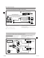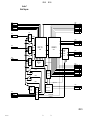
1
3CCD COLOR VIDEO CAMERA DXC-390 DXC-390P SERVICE MANUAL 1st Edition ! WARNING This manual is intended for qualified service personnel only. To reduce the risk of electric shock, fire or injury, do not perform any servicing other than that contained in the operating instructions unless you are qualified to do so. Refer all servicing to qualified service personnel. ! WARNUNG Die Anleitung ist nur für qualifiziertes Fachpersonal bestimmt. Alle Wartungsarbeiten dürfen nur von qualifiziertem Fachpersonal ausgeführt werden. Um die Gefahr eines elektrischen Schlages, Feuergefahr und Verletzungen zu vermeiden, sind bei Wartungsarbeiten strikt die Angaben in der Anleitung zu befolgen. Andere als die angegeben Wartungsarbeiten dürfen nur von Personen ausgeführt werden, die eine spezielle Befähigung dazu besitzen. ! AVERTISSEMENT Ce manual est destiné uniquement aux personnes compétentes en charge de l’entretien. Afin de réduire les risques de décharge électrique, d’incendie ou de blessure n’effectuer que les réparations indiquées dans le mode d’emploi à moins d’être qualifié pour en effectuer d’autres. Pour toute réparation faire appel à une personne compétente uniquement. DXC-390/390P Table of Contents Manual Structure Purpose of this manual ........................................................................................ 3 (E) Related manuals ................................................................................................... 3 (E) 1. Operating Instructions 2. Service Overview 2-1. 2-2. 2-3. 2-4. 2-5. Board location ....................................................................................... 2-1 (E) Removal of cabinet ............................................................................... 2-1 (E) Removal of CCD block ......................................................................... 2-2 (E) How to use an extension board ............................................................. 2-2 (E) Input/output signals of connectors ........................................................ 2-4 (E) 3. Circuit Operation Description 3-1. 3-2. 3-3. 3-4. 3-5. VA-193 Board ....................................................................................... 3-1 (E) DP-313 Board ........................................................................................ 3-1 (E) EN-142 Board ....................................................................................... 3-2 (E) SG-265 Board ........................................................................................ 3-3 (E) MB-875 Board ...................................................................................... 3-4 (E) 4. Electrical Alignment 4-1. 4-2. Preparation ............................................................................................ 4-1 (E) 4-1-1. Adjustment Fixture and Measurement Equipment .............. 4-1 (E) 4-1-2. Equipment Connection ......................................................... 4-1 (E) 4-1-3. Description of Side Panel Sheet Switches ........................... 4-2 (E) 4-1-4. Super Reset (data initialization) ........................................... 4-2 (E) Adjustment ............................................................................................ 4-2 (E) 4-2-1. VCO Adjustment 0(original oscillator adjustment) ............. 4-2 (E) 4-2-2. Built-in Color Bars Adjustment (adjustment from DSP) ..... 4-2 (E) 4-2-3. CCD OUT Adjustment ......................................................... 4-3 (E) 5. Spare Parts 5-1. 5-2. DXC-390/390P Notes on Repair Parts .................................................................................. 5-1 Exploded View ............................................................................................ 5-2 1 (E) 5-3. 5-4. Electrical Parts List ..................................................................................... 5-4 Packing Materials & Supplied Accessories .............................................. 5-20 6. Semiconductor Pin Assignments index ............................................................................................................ 6-1 IC ................................................................................................................. 6-3 7. Block Diagrams DP-313 ........................................................................................................ 7-1 EN-142 ........................................................................................................ 7-2 MB-875 ....................................................................................................... 7-3 SG-265 ........................................................................................................ 7-4 VA-193 ........................................................................................................ 7-5 8. Schematic Diagrams Frame ........................................................................................................... 8-2 CN-1938 ...................................................................................................... 8-4 PA-236 ........................................................................................................ 8-5 DP-313 ........................................................................................................ 8-6 EN-142 ........................................................................................................ 8-8 SG-265 (1/2) .............................................................................................. 8-10 SG-265 (2/2) .............................................................................................. 8-12 VA-193 (1/2) ............................................................................................. 8-14 VA-193 (2/2) ............................................................................................. 8-15 MB-875 (1/3) ............................................................................................ 8-16 MB-875 (2/3) ............................................................................................ 8-17 MB-875 (3/3) ............................................................................................ 8-18 9. Board Layouts CN-1938 ...................................................................................................... 9-1 PA-236 ........................................................................................................ 9-1 DP-313 ........................................................................................................ 9-2 EN-142 ........................................................................................................ 9-3 MB-875 ....................................................................................................... 9-4 SG-265 ........................................................................................................ 9-5 VA-193 ........................................................................................................ 9-6 2 (E) DXC-390/390P Manual Structure Purpose of this manual This manual is the Service Manual of the 3CCD color video camera DXC-390/390P. This manual contains the operating instructions, service overview, functions, electrical alignment, spare parts, semiconductor pin assignments, block diagrams, schematic diagrams and board layouts. Related manuals In addition to this Service Manual, the following manuals are provided for this unit. . Operation Manual (Supplied with the DXC-390/390P) This manual is required for the proper operation and application of this unit. Part of the Operation Manual is included also in this Service Manual, in Section 1, “Operating Instructions” . Part number: 3-203-786-11 . “Semiconductor Pin Assignments” CD-ROM (Available on request) This “Semiconductor Pin Assignments” CD-ROM allows you to search for semiconductors used in Communication System Solutions Network Company equipment. Semiconductors that cannot be searched for on this CD-ROM are listed in the service manual for the corresponding unit. The service manual contains a complete list of all semiconductors and their ID Nos., and thus should be used together with the CD-ROM. Part number: 9-968-546-XX DXC-390/390P 3 (E) Section 1 Operating Instructions This section is extracted from operation manual. 3-203-786-11(1) DXC-390/390P 3CCD Color Video Camera Instructions for Use GB (DXC-390P only) DXC-390 DXC-390P 2000 Sony Corporation DXC-390/390P 1-1 (E) English Owner’s Record The model and serial numbers are located at the bottom. Record these numbers in the spaces provided below. Refer to these numbers whenever you call upon your Sony dealer regarding this product. Model No. Serial No. WARNING To prevent fire or shock hazard, do not expose the unit to rain or moisture. To avoid electrical shock, do not open the cabinet. Refer servicing to qualified personnel only. For the customers in the U.S.A. This equipment has been tested and found to comply with the limits for a Class A digital device, pursuant to Part 15 of the FCC Rules. These limits are designed to provide reasonable protection against harmful interference when the equipment is operated in a commercial environment. This equipment generates, uses, and can radiate radio frequency energy and, if not installed and used in accordance with the instruction manual, may cause harmful interference to radio communications. Operation of this equipment in a residential area is likely to cause harmful interference in which case the user will be required to correct the interference at his own expense. You are cautioned that any changes or modifications not expressly approved in this manual could void your authority to operate this equipment. The shielded interface cable recommended in this manual must be used with this equipment in order to comply with the limits for digital device pursuant to Subpart B of Part 15 of FCC Rules. For the customers in Europe (for DXC-390P only) This product with the CE marking complies with the EMC Directive (89/336/EEC) issued by the Commission of the European Community. Compliance with this directive implies conformity to the following European standards: • EN55103-1: Electromagnetic Interference (Emission) • EN55103-2: Electromagnetic Susceptibility (Immunity) This product is intended for use in the following Electromagnetic Environment(s): E1 (residential), E2 (commercial and light industrial), E3 (urban outdoors) and E4 (controlled EMC environment, ex. TV studio) 2 (GB) Important safeguards/notices for use in the medical environments 1. All the equipments connected to this unit shall be certified according to Standard IEC60601-1, IEC60950, IEC60065 or other IEC/ISO Standards applicable to the equipments. 2. When this unit is used together with other equipment in the patient area*, the equipment shall be either powered by an isolation transformer or connected via an additional protective earth terminal to system ground unless it is certified according to Standard IEC60601-1. m 1. 5 R Caution When you dispose of the unit or accessories, you must obey the law in the relative area or country and the regulation in the relative hospital. GB English * Patient Area 4. This equipment generates, uses, and can radiate frequency energy. If it is not installed and used in accordance with the instruction manual, it may cause interference to other equipment. If this unit causes interference (which can be determined by unplugging the power cord from the unit), try these measures: Relocate the unit with respect to the susceptible equipment. Plug this unit and the susceptible equipment into different branch circuit. Consult your dealer. (According to Standard EN60601-1-2 and CISPR11, Class B, Group 1) 3. The leakage current could increase when connected to other equipment. 3 (GB) 1-2 (E) DXC-390/390P Table of Contents Chapter 1 Overview Chapter 3 Installation and Connections Features .................................................................... 6 Location and Functions of Parts and Controls ..... 8 Front Panel/Top Panel/Bottom Panel ..................... 8 Right Side Panel (Control Panel) ........................... 9 Rear Panel ............................................................ 11 Chapter 2 Operation Adjusting snd Setting with Menus ....................... 12 Menu Configuration ............................................. 12 Operation through Menus .................................... 14 Function of Menus ............................................... 16 Initial Setting of the Menus ................................. 31 Shooting .................................................................. 32 Adjusting the Flange Focal Length ...................... 32 Basic Shooting Procedure .................................... 35 Adjusting the Iris, Focus and Zoom ..................... 36 Adjusting the Black Balance ................................ 38 Adjusting the White Balance ............................... 39 Adjusting the Picture Tone in a Multi-Camera System ............................................................ 41 4 (GB) Installation .............................................................. 42 Applicable Lens ................................................... 42 Mounting the Lens ............................................... 43 Mounting a Microscope Adaptor ......................... 45 Mounting on a Tripod .......................................... 45 Mounting to a Wall or Ceiling ............................. 45 Basic System Connection ..................................... 47 Connecting to Video Equipment with Composite Video Input Connectors .................................. 48 Connecting to Video Equipment with RGB or S-Video Inputs ................................................ 50 Connecting Two or More Cameras—Multi-Camera System ............................................................ 51 Connecting to a Remote Control Unit .................. 52 Operating the Camera with the RM-C950 Remote Control Unit ................................................... 53 Connecting to a Computer .................................... 54 Connections for Long Exposure Shooting .......... 55 Connections for Shooting Using a Flash ............. 56 Table of Contents Chapter 4 Appendix Precautions ............................................................. Typical CCD Phenomena ....................................... List of Messages .................................................... Specifications ......................................................... Optional Accessories ............................................ 57 58 59 60 64 Table of Contents DXC-390/390P 5 (GB) 1-3 (E) Chapter Chapter 1 Overview 1 Features High-quality images TM1) • The high density 1/3 type, three-chip Exwave HAD CCD2), containing some 380,000 (DXC-390) or 430,000 (DXC-390P) effective picture elements (pixels), offers superior picture quality: 800 TV lines of high horizontal resolution, high sensitivity of F8 at 2,000 lx, an excellent signal-to-noise ratio of 62 dB (DXC-390) or 61 dB (DXC390P) and a low smear level. • The adoption of the LSI digital signal processing technology reproduces a finer, more detailed picture. • DynaLatitude processing enables you to adjust contrast finely according to the luminance signal level of each picture element. • The DCC+ (Dynamic Contrast Control plus) function minimizes the phenomena whereby the whole screen turns white or a part of the image becomes colorless when shooting a very bright object. • The Partial Enhance function enables you to adjust the sharpness and tint of only a specified color. Wide Range of Exposure Control The AGC (Auto Gain Control) function and CCD IRISTM3) function automatically adjust a wide range of incoming light levels. When the lighting condition is poor, the AGC function automatically increases the gain up to 16 times. When incoming light is excessive, the CCD IRIS function automatically adjusts shutter speed to cut exposure to the ........................................................................................................................................................................................................................................................... 1) Exwave HADTM: Exwave Hole-Accumulated Diode 2) CCD: Charge-Coupled Device “Exwave HADTM” is a trademark of Sony Corporation. 3) “CCD IRISTM” is a trademark of Sony Corporation. 6 (GB) Chapter 1 Overview RS-232C interface The camera can be controlled from a computer via the RS232C interface. For details, contact your authorized Sony dealer. Chapter 1 equivalent of up to 10 aperture stops. When using the video camera in a fixed location or for a microscope system, the AGC, CCD IRIS and auto-iris controls automatically adjust a wide range of incoming light levels. The desired AE window can be set by using the AE AREA MANUAL function. Compact and lightweight Wide range of electronic shutter modes The wide range of speeds for the electronic shutter minimizes blurring in fast-moving objects and produces acceptably bright still images of objects shot in poor light. • Flickerless mode: This mode allows you to obtain flickerless images shot even under fluorescent light. • Clear scan mode: This mode reduces horizontal bands appearing in computer displays when shooting the display with the conventional video camera. The camera is compact (56 × 50 × 128 mm (2 1/4 × 2 × 5 1/8 inches)) and very light (approx. 370 g (13 oz)), allowing easy installation even where space is a problem. Following are some sample applications: • As a permanent fixture in theaters, concert halls, etc. • As a bird’s-eye view camera for special events • As a video conference system camera • As a camera for microscopes • As a rooftop weather-monitoring camera • As a laboratory monitor camera Versatile use with external equipment • The video camera is equipped with three types of outputs: composite, Y/C and RGB outputs. The camera offers a high-quality picture on a connected monitor or VCR. • The camera can be remotely controlled with the RM-C950 remote control unit (not supplied). Chapter 1 Overview 1-4 (E) 7 (GB) DXC-390/390P Location and Functions of Parts and Controls Front Panel/Top Panel/Bottom Panel 1 Lens Mount (C-mount) Attach a C-mount lens or microscope adaptor. Chapter 1 Note Be sure to use a lens whose projected part from the lens mount surface is less than 4.3 mm. Mounting the lens with a projected part greater than 4.3 mm may damage the internal mechanism of the camera. 1 Lens mount 2 Screw holes (M3) 2 Screw holes Use these holes (M3, depth: 4 mm (3/16 inches)) to attach the supplied tripod adaptor to the camera for mounting the camera on a wall, ceiling or tripod. For how to install the tripod adaptor, see “Mounting on a Tripod” on page 45. 2 Screw holes (M3) 8 (GB) Chapter 1 Overview Right Side Panel (Control Panel) 2 V/BLACK button 3 b/ WHITE button 4 BARS button 5 ENTER button 6 v button Chapter 1 1 MENU button 1 MENU button Displays the MAIN menu on a monitor screen. Press again to exit the menu. When a setting menu is displayed, press this button to return to the MAIN menu. For menu operations, see “Operation through Menus” on page 14. 2 V/BLACK (black balance) button While the menu is displayed: Moves the menu cursor upward. Also use this button for an AE window setting, etc. While the normal screen is displayed: Activates the automatic black balance adjustment. 3 b/ WHITE (white balance) button While the menu is displayed: Increases the setting value or changes the setting. Also use this button for an AE window setting, etc. While the normal screen is displayed: Activates the automatic white balance adjustment when MODE is set to AWB in WHITE BALANCE menu. 7 B/FILE SELECT button 8 FLANGE BACK (flange focal length) adjustment ring Chapter 1 Overview DXC-390/390P 9 (GB) 1-5 (E) Location and Functions of Parts and Controls Chapter 1 4 BARS (color bars output) button Outputs the color bar signal. Press again to revert to video signal output. For monitor adjustment, contact your authorized Sony dealer. 5 ENTER button Selects a setting menu in the MAIN menu. Also use this button for an AE window setting, etc. 6 v button Moves the menu cursor downward. Also use this button for an AE window setting, etc. 7 B/FILE SELECT button While the menu is displayed: Decreases the setting value or changes the setting. Also use this button for an AE window setting, etc. While the normal screen is displayed: Switches the user preset file between A and B. 8 FLANGE BACK (flange focal length) adjustment ring Adjusts the flange focal length of a lens which is not equipped with this function. For details on flange focal length adjustment, see “Adjusting the Flange Focal Length” on page 32. 10 (GB) Chapter 1 Overview DC IN/VBS (DC input/video signal output) connector (12-pin) Connects to the CMA-D2/D2MD/D2CE/D2MDCE camera adaptor. Inputs the DC power and outputs the video signal. 2 1 MENU LOCK ON/OFF switch DC IN/VBS 2 connector 3 TRIG IN connector 4 LENS connector 5 VIDEO OUT TRIG IN 3 TRIG IN connector (BNC type) Connects to a commercially available slave unit by converting to BNC type in strobe mode. connector 4 LENS connector (6-pin) Connects to a lens control cable when attaching the zoom lens especially designed for this camera. VIDEO OUT DC IN/VBS Chapter 1 1 MENU LOCK ON/OFF switch When this switch is set to ON, the menu is not displayed on the screen even if you press the MENU button. Rear Panel LENS MENU LOCK OFF 5 VIDEO OUT connector (BNC type) Outputs a composite video signal. ON RGB/SYNC REMOTE 6 REMOTE 7 connector 6 REMOTE connector (mini DIN 8-pin) Connects to the RM-C950 remote control unit (not supplied). RGB/SYNC connector RGB/SYNC connector (D-sub 9-pin) 7 Outputs RGB signals and their respective sync signals. Use the CCXC-9DB/CCXC-9DD/CCMC-9DS connecting cable for the connections. Chapter 1 Overview 1-6 (E) 11 (GB) DXC-390/390P Chapter Operation 2 Chapter 2 Adjusting and Setting with Menus Camera operational settings can be changed through simple adjustment of the settings on the on-screen menus. Settings can be adjusted to get the best possible results for the given shooting conditions or to enhance the image with special effects. About on-screen menus This section explains how to read the on-screen menu before starting menu operation. MAIN menu Menu Configuration 1 Before starting menu operation, make sure that the MENU LOCK ON/OFF switch on the rear panel is set to OFF. To display a menu, press the MENU button on the right side panel. The MAIN menu is displayed on the monitor screen. The setting menu will be displayed by selecting the desired setting menu item with the V or v button and pressing the ENTER button. 12 (GB) 2 <MAIN> >EXPOSURE CONTRAST WHITE BALANCE ENHANCER GENERAL SYSTEM SCENE FILE Select ENTER Next [A] 3 MENU Exit 4 Chapter 2 Operation 4 Operational message Indicates how to operate the currently displayed menu. Setting menu <EXPOSURE> >GAIN STEP SHUTTER 6 LENS IRIS AE LEVEL AE AREA Select [A] STEP 0dB OFF 3 REMOTE AUTO 7 5 Setting menu Indicates the currently selected setting menu. + _ 0 MULTI MENU Back 4 1 Cursor Selects a setting menu or setting item. Move the cursor up or down using the V or v button. 6 Setting items Indicates the items that can be adjusted in each setting menu. Select the item by moving the cursor beside it with the V or v button. Chapter 2 5 1 7 Set values The currently set values are displayed. Change the values using the B or b button. 2 Setting menu items When you select the desired item with the V or v button and press the ENTER button, the setting menu for adjustment and setting is displayed. 3 User preset file You can store two types of preset adjustments into files A and B. Indicates the currently selected preset file (A or B). Chapter 2 Operation DXC-390/390P 13 (GB) 1-7 (E) Adjusting and Setting with Menus Menu operation procedure Operation through Menus To change the settings on the menu, proceed as follows. Menu operation buttons Chapter 2 1 Operate the menu with the buttons on the right side panel. MENU button B button V button b button MENU 2,3 MENU 2 BLACK FILE SELECT ENTER BLACK FILE SELECT BARS WHITE BARS WHITE ENTER 4 v button ENTER button 1 The following table shows the functions of the buttons. Press the MENU button. The MAIN menu appears. Cursor Button Function MENU Displays the MAIN menu. V button v button B button b button Moves the cursor upward. <MAIN> >EXPOSURE CONTRAST WHITE BALANCE ENHANCER GENERAL SYSTEM SCENE FILE Moves the cursor downward. Changes the setting/decreases the value. Changes the setting/increases the value. Select 14 (GB) 2 Setting menu ENTER Next MENU Exit Chapter 2 Operation Move the cursor to the menu item to be set by pressing the V or v button, then press the ENTER button. The setting menu is displayed. LENS IRIS AE LEVEL AE AREA Select [A] STEP 0dB OFF Setting item REMOTE AUTO + _ 0 MULTI <EXPOSURE> GAIN STEP >SHUTTER Select Change the value by pressing the B or b button. Holding down the button changes the value quickly. <EXPOSURE> GAIN STEP >SHUTTER SPEED LENS IRIS AE LEVEL AE AREA Select [A] STEP 0dB STEP OFF REMOTE AUTO + _ 0 MULTI MENU Back MENU Back Move the cursor to the item to be adjusted by pressing the V or v button. LENS IRIS AE LEVEL AE AREA 4 Chapter 2 <EXPOSURE> >GAIN STEP SHUTTER 3 [A] [A] STEP 0dB OFF REMOTE AUTO + _ 0 MULTI MENU Back To reset to the initial set value Select the item to be reset, then press the B and b buttons simultaneously. For the initial set value on each item, see “Initial Setting of the Menus” on page 31. Set value To return to the normal screen Press the MENU button while the MAIN menu is displayed. While each setting menu is displayed, press the MENU button to return to the MAIN menu, then press it again to return to the normal screen. Chapter 2 Operation 1-8 (E) 15 (GB) DXC-390/390P Adjusting and Setting with Menus GAIN Adjusts the video gain. Function of Menus EXPOSURE menu Chapter 2 Selection Function STEP Sets the video gain to the desired level. Use this setting for shooting in an extremely dark place where even fully opening the lens iris still does not produce an acceptably bright image. The gain level can be set in the range from 0 to 24 dB in units of 1 dB. AGC Automatic gain control. Automatically adjusts the gain according to the brightness of the object to be shot. This setting is useful for shooting when lighting conditions may change. You can select the maximum gain level to be adjusted to 6, 12, 18 or 24 dB with the LIMIT setting. HYPER Increases the video gain to about 30 dB. This setting is useful when the lighting condition is very dark. Adjusts the items relating to exposure, such as gain and shutter mode. <EXPOSURE> >GAIN STEP SHUTTER [A] STEP 0dB OFF LENS IRIS AE LEVEL AE AREA Select REMOTE AUTO + _ 0 MULTI MENU Back Setting items on the EXPOSURE menu Setting item Contents of setting Ref. page GAIN Adjusts video gain. 16 Sets gain level. 16 SHUTTER Sets the modes for the electronic shutter. 16 LENS Sets the iris mode. 18 IRIS Adjusts the iris automatically or manually. 19 AE LEVEL Finely adjusts the focusing point of auto exposure adjustment. 19 AE AREA Sets the AE window in AGC, CCD IRIS or auto iris adjustment mode. 19 STEP 16 (GB) SHUTTER (electronic shutter) Selects the electronic shutter modes. This function enables you to obtain blur-free images of fastmoving objects and acceptably bright still images of objects shot in poor lighting conditions. Chapter 2 Operation Selection Function Selection Function OFF Any electronic shutter mode does not function. VARIABLE STEP Sets the shutter speed to any of 15 steps in longexposure mode and 11 steps in high-speed mode. Use for fine adjustment of the video output level in long exposure mode (low-speed mode) or in clear scan mode (high-speed mode). Long exposure mode You can set the SPEED value in units of 1 frame. For example, if you set to 50 frames (about 1.7 seconds), the video signal produced during this set time is output in the form of one complete frame at intervals of about 1.7 seconds. These pictures, which contain 50 frames of video information, are much brighter than normal one-frame images. This mode is useful for shooting a poorly illuminated object in a dark place. Chapter 2 Select SPEED and set the shutter speed from among the following values: Long-exposure mode: 0.1, 0.2, 0.3, 0.5, 1.0, 1.5, 2.0, 2.5, 3.0, 3.5, 4.0, 5.0, 6.0, 7.0, and 8.0 sec. To set the speed, display OFF by pressing the B and b buttons simultaneously, then select the desired value by pressing the b button. Each press changes the speed in the order as shown above. High-speed mode: FL (flickerless), 1/125, 1/250, 1/500, 1/1000, 1/2000, 1/4000, 1/10000, 1/20000, 1/40000, 1/100000 To set the speed, display OFF by pressing the B and b buttons simultaneously, then select the desired value by pressing the B button. Each press changes the speed in the order as shown above. When using the camera in a 50 Hz lighting area (DXC-390) or in a 60 Hz lighting area (DXC-390P), the FL setting offers flickerless images even under fluorescent light. To set the shutter speed 1 Display OFF by pressing the B and b buttons simultaneously. 2 Select the SPEED value by pressing the b button. Each time you press the button, the value changes in units of 1 frame. To convert the value into the shutter speed Example: When the value is set to 5 frames 5 × 1/30 = 0.1666 seconds (DXC-390) 5 × 1/25 = 0.2000 seconds (DXC-390P) Notes • Do not use AGC, CCD-IRIS, ATW, DCC+ and DYNALATITUDE functions in long exposure mode. • When you set the shutter speed to 1 second or higher, set the gain level to 0 dB. (Continued) Chapter 2 Operation DXC-390/390P 17 (GB) 1-9 (E) Adjusting and Setting with Menus Function Selection Function VARIABLE (Continued) Clear scan mode You can set the shutter speed in units of 1H (horizontal scanning time: 63.56 µs for DXC-390, 64.00 µs for DXC-390P). Select SPEED, then select the value from 1/525H to 262/525H (DXC-390) or 1/625H to 312/625H (DXC390P). This mode can be used for shooting computer displays with reduced horizontal bands appearing across the display screen. CCD-IRIS (Continued) For example, this function is useful for microscope applications. When shooting with a microscope not equipped with the auto-iris lens, the luminance level that is just right for the human eye is often too bright for the video camera. When CCD-IRIS is selected, the electronic shutter automatically decreases excessive incident light to an appropriate level for the video camera. This function is also useful for cutting out excessive incident light that is not cut out by the auto-iris lens in scenes containing very bright patches (such as snow, or sea water reflecting sunlight). You can select the highest limit value of the variable range of the shutter speed. Select LIMIT, then set the speed to 1/250, 1/500, 1/1000, 1/2000, 1/4000, 1/10000, 1/20000,1/40000 or 1/100000. Chapter 2 Selection To set the shutter speed 1 Display OFF by pressing the B and b buttons simultaneously. 2 Select the SPEED value by pressing the b button while observing the noise on the monitor screen so that you can obtain the image with minimum noise. Each time you press the button, the value changes in units of 1H. To convert the value into the shutter speed Example: When the value is set to 250H DXC-390: 250 × 63.56 µs (1H) + 34.9 µs (constant) = 15924.9 µs = Approx. 0.016 seconds DXC-390P: 250 × 64.00 µs (1H) + 35.0 µs (constant) = 16035.0 µs = Approx. 0.016 seconds Automatically adjusts the luminance level for optimum output level. When incoming light is excessive, this function automatically adjusts the shutter speed to cut exposure equivalent to up to 10 aperture stops. CCD-IRIS 18 (GB) Note You cannot use CCD-IRIS mode when using a lens that automatically adjusts the iris control according to the video signal input. LENS Selects the iris mode. Selection Function VIDEO Select when you use a lens that automatically adjusts the iris according to the input video signal. Select AE LEVEL, then adjust the auto exposure focusing point in the range from –127 to +127. REMOTE Select when you use a lens that adjusts the iris according to the DC power supplied. Selection Function Chapter 2 Operation Selection Function AE LEVEL Sets auto exposure focusing point in the range from –127 to +127. AE AREA Sets the AE (Auto Exposure) window when the camera is set to AGC, CCD IRIS or auto-iris control mode. MULTI: Divides the screen into 9 sections and adjusts auto exposure according to the luminance level in each section. Normally set to this position. LARGE, MID, SPOT and SLIT: Displays the following AE windows and adjusts auto exposure according to the luminance level in each area. LARGE AE AREA MANUAL: Sets the AE window with the desired size (Continued) and position on the screen. Follow the steps below. 1 Select MANUAL and press the ENTER button. Cross cursor Chapter 2 IRIS Appears when you set LENS to REMOTE. Selects how to adjust the iris. You can select AUTO or MANUAL. AUTO: Adjusts the iris automatically. MANUAL: Adjusts the iris with the IRIS control on the RM-C950 remote control unit. Set Top-Left Point Move Cross Cursor MENU Cancel ENTER Next 2 Move the cross cursor appearing at the left top corner with the B, b, V or v button to set the upper and left side size, then press the ENTER button. Set Bottom-Right Point Move Cross Cursor MENU Cancel ENTER Next BARS Back MID SLIT SPOT Cross cursor (Continued) Chapter 2 Operation 1-10 (E) 19 (GB) DXC-390/390P Adjusting and Setting with Menus CONTRAST menu Function AE AREA (Continued) 3 Move the cross cursor appearing at the right bottom corner with the B, b, V or v button to set the lower and right side size, then press the ENTER button. Chapter 2 Selection Adjusts the contrast of the image. <CONTRAST> [A] >EFFECT MANUAL KNEE POINT MID + _ 0 BLACK STRETCH GAMMA ON + _ 0 LEVEL + _ 0 MASTER PEDESTAL + _ 0 R. PEDESTAL + _ 0 B. PEDESTAL Move Window Move Cross Cursor MENU Cancel ENTER Fix BARS Back 4 Move the AE window to the desired position with the B, b, V or v button, then press the ENTER button. Note To cancel the setting before completing the procedure, press the MENU button. AE SPEED Sets auto exposure focusing speed in AGC, CCD IRIS or auto-iris control mode. Selects from MID (normal speed), FAST (fast speed) and SLOW (slow speed). Note If lens hunting occurs, adjust with AE SPEED. AE DETECT Selects the detection method of the luminance level of the selected AE window. AVERAGE: Selects to detect the average luminance level of the whole AE window. PEAK: Selects to detect the part with the highest luminance level. 20 (GB) Select MENU Back Setting items in the CONTRAST menu Setting item Contents of setting Ref. page EFFECT Adjusts the picture contrast in accordance with the incident luminance level. 21 KNEE POINT Sets the knee point. 21 BLACK STRETCH Adjusts the luminance of a dark portion of the screen. 21 Activates gamma compensation. 21 Adjusts the gamma level. 21 Sets the pedestal level of the output signal. 21 Finely adjust the pedestal level. 22 GAMMA LEVEL MASTER PEDESTAL R./B. PEDESTAL Chapter 2 Operation EFFECT Selects the setting suitable for the incident luminance levels. GAMMA Activates gamma compensation. Function Selection Function MANUAL Selects KNEE POINT setting or BLACK STRETCH. OFF Outputs the video signal linearly without gamma compensation. Use this setting when you want to produce images for image processing or image analysis. ON Compensates the reproduction characteristics of a cathode-ray tube of a monitor to produce naturaltone image. Select LEVEL, then adjust so that you can obtain natural-tone image. Adjustable range is from –10 to +10. KNEE POINT Sets the knee point according to the incoming light levels. OFF: Knee processing does not function. HIGH: Sets the knee point to the highest level. MID: Normally, select this position. LOW: Sets the knee point to the lowest level. BLACK STRETCH Adjusts the luminance of the dark portion of the screen. You can set the value within the range from –10 to +10. The higher the setting, the brighter the screen. DCC+ When shooting a very bright object, the whole screen may white out or a part of the image may be colorless. This setting minimizes these phenomena. DYNALATITUDE Adjusts the contrast according to the luminance level of each picture element. The setting is useful for shooting scenes mixed with bright and dark parts. You can set the level within the range from –10 to +10. MASTER PEDESTAL The pedestal levels of the G, B and R output signals can be adjusted simultaneously. Adjusts the darkness level of the black part of the image. Use this function to bring out details in heavily shaded areas. The adjustable range is from –127 to +127. Normally set to ±0. Use of a waveform monitor allows easier adjustment. (Continued) Chapter 2 Operation DXC-390/390P Chapter 2 Selection 21 (GB) 1-11 (E) Adjusting and Setting with Menus Adjusting direction Effect WHITE BALANCE menu + The whole screen becomes whiter. Adjusts the white balance. – The whole screen becomes blacker. Chapter 2 <WHITE BALANCE> >MODE R. PAINT B. PAINT R. (red) PEDESTAL, B. (blue) PEDESTAL Use these items to finely adjust the pedestal level of each color. Adjust while watching the monitor screen. The items can be finely adjusted within the range from –127 to +127. Select [A] AWB + _ 0 + _ 0 MENU Back Setting items in the WHITE BALANCE menu 22 (GB) Setting item Contents of setting Ref. page Selects the white balance modes. MODE R./B. PAINT Finely adjusts the white balance (AWB, ATW). 23 23 Chapter 2 Operation MODE Selects the white balance modes. Function AWB Adjusts the white balance atutomatically (auto white balance). When this item is selected, R. PAINT and B. PAINT are displayed. Use these items for fine adjustment. Adjust them while watching the monitor screen. R. PAINT: Finely adjusts the red in the range from –100 to +100. B. PAINT: Finely adjusts the blue in the range from –100 to +100. For details, see “Adjusting the White Balance” on page 39. ATW NORMAL or ATW WIDE Activates auto-tracing white balance. This mode is suitable for shooting when the light source changes. The white balance is automatically adjusted as the color temperature changes. Normally, set to ATW NORMAL. The ATW WIDE setting can cope with a wider range of color temperature changes. When these items are selected, R. PAINT, B. PAINT, AREA and SPEED are displayed. Use these items for fine adjustment. Adjust them while watching the monitor screen. The adjusted values are stored in memory other than AWB values. R. PAINT: Finely adjusts the red in the range from –10 to +10. B. PAINT: Finely adjusts the blue in the range from –10 to +10. Function ATW AREA: A detecting window appears on the monitor NORMAL screen. Normally set to NORMAL to detect the or ATW average luminance level on the whole screen. If WIDE you want to display the desired window, set to (Continued) MANUAL and follow the steps below. 1 Press the ENTER button. 2 Move the left top cross cursor with the B, b, V or v button to set the upper and left side size, and press the ENTER button. 3 Move the right bottom cross cursor with the B, b, V or v button to set the lower and right side size, and press the ENTER button. 4 Move the window to the desired position on the screen with the B, b, V or v button, and press the ENTER button. SPEED: Sets the focusing speed. You can select SLOW (slow speed), MID (normal speed) or FAST (fast speed). MANUAL Use for manual adjustment of white balance. When this item is selected, R. GAIN and B. GAIN are displayed. Adjust them while watching the monitor screen. R. GAIN: Finely adjusts the red gain in the range from –127 to +127. B. GAIN: Finely adjusts the blue gain in the range from –127 to +127. 3200K Selects for indoor shooting. (Color temperature: 3200K) 5600K Selects for outdoor shooting. (Color temperature: 5600K) Chapter 2 Operation 1-12 (E) Chapter 2 Selection Selection 23 (GB) DXC-390/390P Adjusting and Setting with Menus ENHANCER menu Adjusts the sharpness of the image outline and the color tone (hue). Chapter 2 <ENHANCER> [A] >DETAIL ON + _ 0 LEVEL FREQUENCY MID LINEAR MATRIX ON MODE STANDARD TARGET COLOR Select MENU Back Setting item Contents of setting Ref. page DETAIL Enables or disables to adjust the sharpness of the image outline. 24 Adjusts the sharpness of the image outline. 24 FREQUENCY Adjusts the sharpness of the detailed image outline. 24 LINEAR MATRIX Enables or disables processing of a 25 color matrix. MODE Finely adjusts the color tone. TARGET COLOR Specifies the color for DETAIL or LINEAR MATRIX adjustments. 24 (GB) Function ON Enables adjustment of the sharpness of the image outline. OFF Disables adjustment of the sharpness of the image outline. Selection Function LEVEL Adjusts the level in the range from –127 to +127. The lower level decreases the sharpness of the image outline and makes the image softer. The higher level increases the sharpness of the image outline and makes the image sharper. FREQUENCY Selects the frequency level with which the image outline is adjusted from LOW (lower frequency level), MID (middle frequency level) or HIGH (higher frequency level). Higher setting provides a sharper outline of detailed images. 25 25 Chapter 2 Operation LINEAR MATRIX Processes an image with a color matrix to change the chroma saturation and hue in order to reproduce natural color. Function ON Corrects the color to reproduce natural color. OFF Color correction does not function. Use when you want to process the image. When you set LINEAR MATRIX to ON, MODE is displayed. You can adjust the color suitable for an object. When you set MODE to MANUAL, R. PAINT, G. PAINT and B. PAINT appear. Selection Function STANDARD Normally, select this setting. R ENHANCE Enhances the red. B ENHANCE Enhances the blue. G ENHANCE Enhances the green. Adjusts each color finely. R. PAINT: Finely adjusts the red in the range from –30 to +30. G. PAINT: Finely adjusts the green in the range from –30 to +30. B. PAINT: Finely adjusts the blue in the range from –30 to +30. TARGET COLOR Select when adjusting DETAIL or LINEAR MATRIX for a specific color. Selection Function ALL Adjusts DETAIL or LINEAR MATRIX for the whole image. Normally, set to this position. IN Adjusts DETAIL or LINEAR MATRIX for a specific color. With the RANGE setting you can finely adjust the area in the range from –10 to +10. OUT Adjusts DETAIL or LINEAR MATRIX for colors other than a specified one. How to specify a color 1 2 Select IN or OUT and press the ENTER button. Move the cross cursor ( ) appearing in the center of the screen to the desired color with the B, b, V or v button so that the cross cursor square covers the desired color, then press the ENTER button. When you select IN, you can adjust the color indicated by the cross cursor ( ). When you select OUT, you can adjust colors other than that with the cross cursor. Chapter 2 Operation DXC-390/390P Chapter 2 Selection MANUAL Selection When you set DETAIL to ON, LEVEL and FREQUENCY are displayed. Adjust the sharpness of the image outline in accordance with your shooting purpose and your taste. ALL Setting items in the ENHANCER menu LEVEL DETAIL Enables or disables adjustment of the sharpness of the image outline. 25 (GB) 1-13 (E) Adjusting and Setting with Menus CCD MODE Selects the CCD read-out mode. GENERAL menu Sets the general items. Chapter 2 <GENERAL> >CCD MODE SHADING COMP. TRIGGER [A] FIELD OFF Function FIELD Accumulates charges in field units. Use to shoot a moving object. FRAME Accumulates charges in frame units. Provides the image with the highest possible vertical resolution. Use to shoot a still object. OFF NEGA OFF FLICKER CANCELLER OFF Select Selection SHADING COMP. (Shading compensation) Eliminates green or magenta color which may appear at the top or bottom of the screen, when the camera is used with an optical instrument. MENU Back Setting items in the GENERAL menu Selection Function Color elimination does not function. If green or magenta color appears at the top or bottom of the screen when the camera is attached to a microscope, etc., select this setting. Setting item Contents of setting Ref. page OFF CCD MODE Selects the CCD read-out mode. 26 ON SHADING COMP. Eliminates color at the top and bottom of the screen. 26 TRIGGER Sets the polarity when connecting a slave unit to synchronize with a stroboscope. 27 NEGA Reverses the output image to negative. 27 Reduces flicker when SHUTTER is set FLICKER CANCELLER to CCD IRIS or OFF. 26 (GB) 27 When SHADING COMP. is set to ON, LEVEL is displayed. Adjust while watching the screen so that the color is eliminated. Adjustable range is from –127 to +127. Adjusting Effect direction + Green at the top and magenta at the bottom will be eliminated. – Magenta at the top and green at the bottom will be eliminated. Chapter 2 Operation TRIGGER Set when you use a slave unit connected to the TRIG IN connector and synchronize the camera with a stroboscope. Function OFF Select when you do not connect a slave unit. ON Select when you connect a slave unit. Select POLARITY, and set it to the same polarity as the input pulse signal. : Falling edge : Rising edge Sets the items relating to the system of the camera and selection of output signals. <SYSTEM> >BAUD RATE D-SUB VIDEO D-SUB SYNC Selection Function OFF Outputs the image normally. ON Outputs the image reversed to negative/positive. FLICKER CANCELLER When using the camera in a 50 Hz lighting area (DXC-390) or in a 60 Hz lighting area (DXC-390P), you can obtain images with less flicker under fluorescent light even when SHUTTER is set to CCD IRIS or OFF. Set this item to OFF when you want to set NEGA to ON. Selection Function OFF Disables the FLICKER CANCELLER function. ON Reduces flicker. [A] 9600 VBS C.SYNC RGB SYNC 12P CONNECTOR NEGA Reverses the output image to negative/positive. Select Chapter 2 Selection SYSTEM menu G IN MENU Back Setting items in the SYSTEM menu Setting item Contents of setting Ref. page BAUD RATE Selects the baud rate. 28 D-SUB VIDEO Switches the video signal output from the RGB/SYNC connector (Dsub 9-pin). 28 D-SUB SYNC Switches the sync signal output from the RGB/SYNC connector (Dsub 9-pin). 28 RGB SYNC Adds a sync signal to the RGB output. 28 12P Switches the input and output of the CONNECTOR DC IN/VBS connector and selects the output signal. 29 (Continued) Chapter 2 Operation 1-14 (E) 27 (GB) DXC-390/390P Adjusting and Setting with Menus Chapter 2 Setting item Contents of setting Ref. page (VBS lock) H. PHASE* SC. PHASE ROUGH* SC. PHASE FINE* Adjusts the horizontal phase and SC (subcarrier) phase during external synchronization (with VBS signal input). 29 (HD/VD lock) H. PHASE* 30 Adjusts the horizontal phase during external synchronization (with HD/VD signal input). D-SUB SYNC Switches the sync signal output from the connector (D-sub 9-pin) at the rear panel. Selection Function C.SYNC Outputs the composite sync signal. WEN Outputs the WEN signal. When connecting peripheral equipment, the signal is used as trigger pulse output to the equipment. Select the polarity of the WEN signal with the POLARITY setting. : Negative : Positive * Displayed only when an external sync signal is input. BAUD RATE Switches the baud rate of the REMOTE connector at the rear panel. Sets to any of 19200, 9600, 4800, 2400 and 1200. Normally, set to 9600 when the RM-C950 remote control connector. unit is connected to the REMOTE D-SUB VIDEO Switches the video signal output from the connector (D-sub 9-pin) at the rear panel. Selection Function VBS Outputs VBS signal. Y/C Outputs Y/C signal. 28 (GB) RGB/SYNC RGB/SYNC RGB SYNC Adds a sync signal to the G signal or R, G and B signals output from the RGB/SYNC connector. Selection Function OFF No sync signal is added to an output signal. G Adds a sync signal to the G signal output from the RGB/SYNC connector. RGB Adds sync signals added to the G, B and R signals RGB/SYNC connector. output from the Chapter 2 Operation 12P CONNECTOR Switches the input and output of the DC IN/VBS connector (12-pin). Selects the output signal from this connector when OUT is selected. Function IN Functions as the input connector. OUT Functions as the output connector. Select the output signal with the SIGNAL setting. HD/VD: Outputs the HD/VD signal. C. SYNC: Outputs the composite sync signal. Chapter 2 Selection HD/VD lock Appears only when an external reference sync signal (HD/ VD signal) is input. Adjusts the horizontal phase to synchronize the camera operation with the reference signal. Select H.PHASE, then adjust the level within the range from –20 to +127. VBS lock Appears only when an external reference sync signal (VBS signal) is input. Adjusts the horizontal phase and SC (subcarrier) phase to synchronize the camera operation with the reference signal. Selection Function H.PHASE Adjusts the horizontal phase within the range from –20 to +127. SC.PHASE Roughly adjusts the subcarrier phase by setting to 0° or 180°. ROUGH SC.PHASE Finely adjusts the subcarrier phase within the range from –127 to +127. FINE Chapter 2 Operation DXC-390/390P 29 (GB) 1-15 (E) Adjusting and Setting with Menus FILE SELECT Selects the file A or B. SCENE FILE menu Chapter 2 Sets the preset menu settings. The camera has two memory files (A or B) for storing the menu settings. You can store a different type of setting into each file, and switch to the file most suitable for the shooting conditions quickly. The currently selected memory file is shown in the upper right corner of the on-screen menu. LOAD Sets the setting to be stored into the file which you select with FILE SELECT, and stores the setting. Selection Type of setting STANDARD Suitable for a camera used as a permanent fixture. MICROSCOPESuitable for a camera for a microscope. <SCENE FILE> >FILE SELECT LOAD [A] A FULL AUTO Automatically adjusts settings. STROBE Suitable for stroboscopic shooting. FILE B (or A) When copying the settings between two files. Storing the setting Select MENU Back Setting items in the SCENE FILE menu Setting item Ref. page Contents of setting FILE SELECT Selects the file into which you store the setting. Selects the type of setting to be stored, and loads it. LOAD 30 (GB) 1 Select A or B into which the setting is stored in the FILE SELECT setting. 2 3 Press the V or v button to select LOAD. 30 30 4 Press the B or b button to select the desired setting to be stored, and press the ENTER button. “Overwrite OK?” appears. Press the ENTER button. If you do not want to store the setting, press the MENU button. Chapter 2 Operation Setting menu Initial Setting of the Menus Setting item Initial setting WHITE BALANCE MODE Setting menu EXPOSURE Setting item GAIN STEP SHUTTER STEP LENS IRIS CONTRAST Initial setting ENHANCER AWB R. PAINT ±0 B. PAINT ±0 DETAIL ON STEP LEVEL ±0 0 dB FREQUENCY MID OFF LINEAR MATRIX REMOTE MANUAL ON MODE OFF GENERAL STANDARD TARGET COLOR ALL CCD MODE FIELD OFF AE LEVEL ±0 SHADING COMP. AE AREA MULTI TRIGGER OFF MANUAL NEGA OFF KNEE POINT MID FLICKER CANCELLER OFF BLACK STRETCH ±0 EFFECT GAMMA BAUD RATE 9600 ON D-SUB VIDEO VBS C.SYNC SYSTEM ±0 D-SUB SYNC MASTER PEDESTAL ±0 RGB SYNC G R. PEDESTAL ±0 12P CONNECTOR IN B. PEDESTAL ±0 H. PHASE* ±0 LEVEL Chapter 2 If you want to reset the settings and values to the initial settings, press the B and b buttons simultaneously. SC PHASE ROUGH* 0° SC PHASE FINE* ±0 * Displayed only when an external sync signal is input. Chapter 2 Operation 1-16 (E) 31 (GB) DXC-390/390P Shooting Adjusting the Flange Focal Length Chapter 2 This section explains how to adjust the flange focal length (distance from the lens mounting plane to an object). Adjustment method varies with the lens you use. When you use the VCL-610WEA zoom lens 1 Desired shooting distance to the object or about 3 m (10 feet) 6 Object, such as letters, fine patterns, etc., on which you can observe the focus condition distinctly 2 4 RM-C950 remote control unit 32 (GB) The following is an example of flange focal length adjustment using the RM-C950 remote control unit. Adjust it using the FLANGE BACK (flange focal length) adjustment ring on the camera. Note Be sure to set the iris fully open before adjusting the flange focal length. 1 Point the camera to an object at the desired shooting distance or about 3 m (10 feet) away. 2 Set the IRIS AUTO/MANUAL knob to MANUAL, and turn the IRIS knob to OPEN as far as it goes. 3 Turn the ZOOM knob to TELE (telephoto) as far as it goes. 4 Adjust the focus on the object used in step 1 by turning the FOCUS knob. 5 Turn the ZOOM knob to WIDE (wide-angle) as far as it goes. 6 Adjust the focus on the object used in step 1 by turning the FLANGE BACK (flange focal length) adjustment ring on the camera. 7 Repeat steps 3 to 6 until you achieve sharp focus both in the telephoto and wide-angle positions. 3, 5 Now the flange focal length adjustment is completed. You do not need to readjust the flange focal length unless you replace the lens. Chapter 2 Operation When you use the VCL-614WEA zoom lens You do not need to use the FLANGE BACK (flange focal length) adjustment ring on the camera. Desired shooting distance to the object or about 3 m (10 feet) 1 2 5, 6 3 1 3 4 Turn the iris ring to 1.4 (open). 5 Turn the ZOOM ring clockwise to align 5.5 (wideangle) with the white line, then turn the F.f adjustment ring by holding the F.f fixing screw to adjust the focus on the object used in step 1. Turn the ZOOM ring counterclockwise to align 77 (telephoto) with the white line, then adjust the focus on the object. 4, 5, 8 6 2, 9 Object, such as letters, fine patterns, etc., on which you can observe the focus condition distinctly OPERATION MODE FOCUS MyA ZOOM MyA IRIS MyA 7 8 FOCUS ZOOM IRIS Point the camera to an object at the desired shooting distance or about 3 m (10 feet) away. Set the FOCUS, ZOOM, IRIS M/A switches on the lens to M (Manual) position using a pointed object. 9 Chapter 2 6 Note Be sure to set the iris fully open before adjusting the flange focal length. Turn the fixing screw for the F.f adjustment ring counterclockwise to loosen it. Repeat steps 5 and 6 until you achieve sharp focus both in the telephoto and wide-angle positions. Turn the fixing screw for the F.f adjustment ring clockwise to tighten it firmly. Set the FOCUS, ZOOM, IRIS M/A switches on the lens to A (Auto) position. Now the flange focal length adjustment is completed. You do not need to readjust the flange focal length unless you replace the lens. Chapter 2 Operation DXC-390/390P 33 (GB) 1-17 (E) Shooting When you use a zoom lens not equipped with the flange focal length adjustment function Chapter 2 1 Set the iris fully open if the lens is equipped with the iris ring. If you use the auto iris lens, illuminate the object appropriately so that the iris is open. 2 Point the camera to an object at the desired shooting distance or about 3 m (10 feet) away. 3 Turn the zoom ring to TELE (telephoto) as far as it goes. 4 Adjust the focus on the object used in step 2 by turning the focus lens on the lens. 5 Turn the zoom ring to WIDE (wide-angle) as far as it goes. 6 Adjust the focus on the object used in step 2 by turning the FLANGE BACK (flange focal length) adjustment ring on the camera. Do not turn the focus ring on the lens during adjustment. 7 Repeat steps 3 to 6 until you achieve sharp focus both in the telephoto and wide-angle positions. Adjust the flange focal length using the FLANGE BACK (flange focal length) adjustment ring on the camera. Desired shooting distance to the object or about 3 m (10 feet) 1, 3, 4, 5 2 6 Object, such as letters, fine patterns, etc., on which you can observe the focus condition distinctly Now the flange focal length adjustment is completed. You do not need to readjust the flange focal length unless you replace the lens. 34 (GB) Chapter 2 Operation Basic Shooting Procedure 3 4, 5 Turn on the power of the camera and all connected devices. 2 3 Illuminate an object with proper lighting. 4 Adjust the white balance. For details, see “Adjusting the White Balance” on page 39. 5 Adjust the settings as required. For details, see “Adjusting And Setting with Menus” on page 12. 6 Start shooting. Point the camera at the object and adjust the iris, focus and zoom. For details, see “Adjusting the Iris, Focus And Zoom” on pages 36 to 37. Chapter 2 Operation 1-18 (E) Chapter 2 2 1 35 (GB) DXC-390/390P Shooting Adjusting the Iris, Focus and Zoom Chapter 2 The following is an example of the iris, focus and zoom adjustments using the RM-C950 remote control unit. For details, refer to the Operating Instructions supplied with the RM-C950. When you use the VCL-610WEA zoom lens Adjusting the iris automatically Set the IRIS AUTO/MANUAL switch on the RM-C950 to AUTO. Note You cannot adjust the iris manually with the VCL610WEA. Adjusting the focus Adjust the focus by turning the FOCUS knob on the RMC950. Zooming Turn the ZOOM knob on the RM-C950 as required. IRIS AUTO/MANUAL select switch IRIS knob FOCUS knob RM-C950 36 (GB) ZOOM knob Chapter 2 Operation When you use the VCL-614WEA zoom lens Adjusting the iris Set the IRIS M/A select switch on the lens to A (Auto), and the IRIS AUTO/MANUAL switch on the remote control unit to MANUAL. 2 Adjust the iris by turning the IRIS knob on the remote control unit. Chapter 2 1 Adjusting the focus OPERATION MODE FOCUS MyA ZOOM MyA IRIS MyA FOCUS ZOOM 1 Set the FOCUS M/A select switch on the lens to A (Auto). 2 Adjust the focus by turning the FOCUS knob on the remote control unit. Zooming IRIS IRIS AUTO/ MANUAL switch FOCUS/ZOOM/IRIS M/A select switch IRIS knob FOCUS knob 1 Set the ZOOM M/A select switch on the lens to A (Auto). 2 Turn the ZOOM knob on the remote control unit. Note RM-C950 ZOOM knob When adjusting the iris, focus and zoom manually using the rings on the lens, make sure to set the IRIS, FOCUS and ZOOM M/A select switches to M (Manual) before operating the iris, focus and zoom. Manual operations with the switch set to A may cause damage to the lens. Chapter 2 Operation DXC-390/390P 37 (GB) 1-19 (E) Shooting Operation procedure Adjusting the Black Balance Chapter 2 Be sure to adjust the black balance when you use the camera for the first time, or after you have not used it for a long period of time, or if there is a sudden change in the temperature. 1 If any menu is displayed on the screen, press the MENU button to remove it. 2 If a color bar signal is displayed on the screen, press the BARS button to remove it. 3 Press the BLACK button. The lens iris control is automatically closed, and the black balance is adjusted. If you use a manual-iris lens, close the iris then press the BLACK button. While adjusting, the bars are displayed. When the adjustment is completed, the message “BLACK: OK” appears on the screen. The adjusted black level is stored in the memory and remains even after the power is turned off. 2 3 MENU 1 BLACK FILE SELECT BARS WHITE ENTER Black balance adjustment errors If the black balance adjustment is not successful, the message “BLACK: NG” appears on the screen. If this happens, take the necessary measures and perform steps 1 through 3 again. For details, see “List of Messages” on page 59. 38 (GB) Chapter 2 Operation Operation procedure Adjusting the White Balance 1 2 Press the MENU button to display the MAIN menu. Select the WHITE BALANCE menu, and set MODE to AWB. <WHITE BALANCE> >MODE R. PAINT B. PAINT 2 1, 3 MENU 7 2 BARS button BLACK FILE SELECT Select BARS WHITE [A] AWB + _ 0 + _ 0 Chapter 2 Each time the lighting condition changes, be sure to adjust the white balance so that optimum color reproduction is obtained. MENU Back For menu operation, see “Operation through Menus (Menu operation procedure)” on page 14. ENTER 3 4 Press the MENU button twice to remove the menu. Display the camera image on the monitor screen. Note If a color bar signal is displayed on the screen, press the BARS button to turn it off. 5 Set the lens iris control as follows: When using an auto-iris lens: Set to auto-iris control. When using a manual-iris lens: Set to an appropriate iris opening value. (Continued) Chapter 2 Operation 1-20 (E) 39 (GB) DXC-390/390P Shooting 6 Place a white object (white pattern, white cloth, etc.) in the same light as that falling on the object to be shot, then zoom in on the white object to fill the screen as follows. 7 Chapter 2 35% of screen height The white object must fill a rectangle of 15% of this size. screen (Avoid very width bright highlights within the rectangle.) 15% of screen width 10% of screen height The white object can be a white wall near the object to be shot. Press the WHITE button. During adjustment the bars appear. The message “WHITE: OK” appears on the screen when the adjustment is done. The adjusted white level is automatically stored in memory and remains even if the camera’s power is turned off. To shoot under the same conditions, the stored white balance is recalled by setting MODE to AWB in the WHITE BALANCE menu. White balance adjustment errors If the auto white balance adjustment is not successful, an error message appears on the screen. If this happens, take the necessary measures and perform steps 1 through 7 again. For more details, see “List of Messages” on page 59. Notes • Do not include highly reflective objects in the picture. • Always shoot the image under suitable lighting conditions. WHITE: NG XXXXX Error message 40 (GB) Chapter 2 Operation Adjusting the Picture Tone in a MultiCamera System Connecting the cameras to video equipment with phase indication capability When connecting to a special-effects generator, a chromakey unit, or other video equipment with phase indication capability, the basic adjustment procedure is as follows: DXC-390/390P 1 Turn on the phase indication capability of the connected video equipment. 2 Adjust the horizontal phase using the menu. Select H. PHASE from the SYSTEM menu. For more details, see “Operation through Menu” on page 14. 3 Adjust the subcarrier phase using the menu. Select SC. PHASE from the SYSTEM menu. First adjust the subcarrier phase roughly with SC. PHASE ROUGH by setting to between 0° and 180°, then adjust it finely using SC. PHASE FINE. For more details, refer to the instruction manual of the connected video equipment with phase indication capability. Use one of the cameras as a reference camera and adjust the other cameras to the reference camera one by one. Chapter 2 When configuring a multi-camera system, adjust all cameras to prevent camera-to-camera variations in picture tone. Before making the adjustments outlined below, input the same sync signal to all cameras. For connections, see “Connecting Two or More Cameras – Multi Camera System” on page 51. Connecting the cameras to video equipment without phase indication capability 1 Adjust the horizontal phase. Select H. PHASE from the SYSTEM menu, and adjust so that the reference video signal and the output signal have the same horizontal sync phase. Use a waveform monitor or an oscilloscope to check the phase. 2 Adjust the subcarrier phase. Select SC. PHASE from the SYSTEM menu. First adjust the subcarrier phase roughly with SC. PHASE ROUGH by setting to between 0° and 180°, then adjust it finely using SC. PHASE FINE so that the reference video signal and the output video signal have the same subcarrier phase. Use a vectorscope or the wiping function of a special-effects generator to display the images of both the reference camera and the camera to be adjusted simultaneously on the screen. Chapter 2 Operation 41 (GB) 1-21 (E) Chapter Installation and Connections 3 Chapter 3 Installation Note Applicable Lens C-mount lenses with the following lens mount surface can be attached to the camera. Be sure to use a lens whose projected part from the lens mount surface is less than 4.3 mm. Mounting the lens with a projected part greater than 4.3 mm may damage the internal mechanism of the camera. Lens mount surface 4.3 mm or less 42 (GB) Chapter 3 Installation and Connections Mounting the Lens 1 2 Remove the mount caps of the camera and lens. 3 Connect the lens control cable to the LENS connector on the camera. Mounting the VCL-610WEA Zoom Lens To adjust the position of the lens After fixing the lens to the camera, rotate the lens further clockwise. When the lens mount is slipped, rotate the lens in the desired direction. Chapter 3 Lens control cable Align the threaded portion of the lens mount with that of the camera mount, and slowly rotate the lens clockwise to fix to the camera. 3 2 2 1 1 Chapter 3 Installation and Connections 1-22 (E) 43 (GB) DXC-390/390P Installation Mounting the VCL-614WEA Zoom Lens 1 2 Remove the mount caps of the camera and lens. 3 Connect the lens control cable to the LENS connector on the camera. Lens control cable Chapter 3 3 2 2 1 1 Align the threaded portion of the lens mount with that of the camera mount, and turn the mount lock ring clockwise as far as it goes to fix the lens to the camera. To adjust the position of the lens After tightening the mount lock ring, loosen it by turning it counterclockwise by approximately 90º. Then rotate the lens to adjust the position, and tighten the mount lock ring securely. Mounting C-mount lens other than the VCL610WEA and VCL-614WEA other Also refer to the instruction manual supplied with the lens. 1 2 Remove the mount caps of the camera and lens. Align the threaded portion of the lens mount with that of the camera mount, and slowly rotate the lens clockwise to fit to the camera. To adjust the position of the lens Refer to the instruction manual supplied with the lens. 44 (GB) Chapter 3 Installation and Connections Mounting a Microscope Adaptor Following is an example of attaching the tripod adaptor to the bottom panel of the camera. You can also attach the tripod adaptor to the top panel of the camera. e.g. Attaching on the bottom panel Chapter 3 To attach the camera to a microscope, an operating microscope, etc., it is necessary to mount an appropriate adaptor. The method for mounting the adaptor is the same as for the lens. For details, refer to the instruction manual for each adaptor. Attaching the supplied tripod adaptor Mounting on a Tripod Install the supplied tripod adaptor using the three screw holes (M3) on the top or bottom panel. Then attach the tripod to the adaptor using the following mounting screws: M3 screws Tripod adaptor U1/4”, 20 UNC 4 = 4.5 mm ± 0.2 mm (ISO standard) Mounting to a Wall or Ceiling Attach the camera with the tripod adaptor to the mounting bracket or suspension bracket using the appropriate screws (U1/4”, 20 UNC) that fit the tripod holes of the adaptor. (Continued) Chapter 3 Installation and Connections DXC-390/390P 45 (GB) 1-23 (E) Installation Reference dimensions for attaching a tripod Bottom 40 (1 5/8) Top ∅5 Hole (depth: 5 (7/32)) 9 14 ( /16) 13 45.5 (1 /16) ∅5 Hole (depth: 5 ( /32)) 7 14 (9/16) Chapter 3 18 (23/32) 23.5 (15/16) Tripod screw (depth: 7 (9/32)) Unit: mm (inches) Tripod screw (depth: 7 (9/32)) Side 32.5 (1 5/16) 32.6 (1 5/16) Tripod adaptor Tripod adaptor Unit: mm (inches) 46 (GB) Chapter 3 Installation and Connections Basic System Connection To supply power to the camera, use the CMA-D2/D2MD/ D2CE/D2MDCE camera adaptor. Note on connections Be sure to turn off the power supply for all equipment before making any connections. Chapter 3 There are two methods for connecting the camera and the camera adaptor. • Using the CCDC cable which only supplies power to the camera (For connecting method, see page 48.) • Using the CCMC cable which supplies power to the camera and transmits video signals to the camera adaptor (For connecting method, see page 49.) Note on use of camera adaptors Be sure to use one camera adaptor for each DXC-390/390P unit. Although the camera adaptor has two CAMERA connectors (4-pin and 12-pin), the power consumption of the camera is such that two camera units cannot be connected at the same time. The camera adaptor you can use with your camera varies with the signal systems and uses. EIA standard, NTSC color system CCIR standard, PAL color system Medical CMA-D2MD CMA-D2MDCE Non-medical CMA-D2 CMA-D2CE System Use Chapter 3 Installation and Connections 1-24 (E) 47 (GB) DXC-390/390P Basic System Connection Connecting to Video Equipment with Composite Video Input Connectors Connecting using the CCDC cable Chapter 3 75-ohm coaxial cable Composite video input (VIDEO IN) Video monitor, VCR, etc. DXC-390/390P VIDEO OUT VIDEO OUT DC IN/VBS TRIG IN 1 2 LENS Set the MODE selector to the “1” position. MENU LOCK OFF CMA-D2/D2MD/D2CE/ D2MDCE camera adaptor ON RGB/SYNC REMOTE Power cord CAMERA (4-pin) DC IN/VBS CCDC-5/10/25/50A/100A cable Setup using a CCDC cable (for supplying power only) 48 (GB) Chapter 3 Installation and Connections Connecting using a CCMC cable Composite video input (VIDEO IN) Chapter 3 Video monitor, VCR, etc. 75-ohm coaxial cable DXC-390/390P VIDEO OUT DC IN/VBS TRIG IN VIDEO OUT LENS MENU LOCK OFF CMA-D2/D2MD/D2CE/ D2MDCE camera adaptor Power cord ON RGB/SYNC REMOTE CAMERA (12-pin) DC IN/VBS 1 2 Set the MODE selector to the “1” position. CCMC-12P02/05/10/25 cable Setup using a CCMC cable (for supplying power to camera and video signals to the camera adapter) Chapter 3 Installation and Connections DXC-390/390P 49 (GB) 1-25 (E) Basic System Connection Connecting to Video Equipment with RGB or S-Video Inputs 1 2 Set the MODE selector CMA-D2/D2MD/D2CE/ to the “1” position. D2MDCE camera adaptor Chapter 3 CCDC-5/10/25/50A/100A cable or CCMC-12P02/05/10/25 cable* Power cord CAMERA (4-pin or 12-pin) DC IN/VBS DXC-390/390P Camera cable: CCXC-9DB (D-sub 9-pin y BNC connectors), or CCMC-9DS (Dsub 9-pin y BNC, S-video connectors) TRIG IN B input Sync input1) LENS MENU LOCK OFF G input VIDEO OUT DC IN/VBS ON RGB/SYNC RGB monitor, image processor, etc. R input REMOTE RGB/SYNC Composite video (BNC) or S-video input (4-pin)2) Computer, image processor etc. or Camera cable CCXC-9DD (D-sub 9-pin y D-sub 9-pin) RGB/SYNC input *If a CCMC cable is used, the S-video signal is also output from the S-video output of the CMA-D2/D2MD/D2CE/D2MDCE. 1) When using a video monitor without a sync signal input connector, the camera can be set to output a sync signal with the G signal or RGB signals. For details, see “SYSTEM menu” on page 27. 50 (GB) 2) This setup is for connecting to a composite video (VBS) connector. To output separated Y/C signals to the S-video input of video equipment, use a CCMC-9DS camera cable. For details on switching camera output between VBS (composite video) and Y/C, see “SYSTEM menu” on page 27. Chapter 3 Installation and Connections Connecting Two or More Cameras—Multi-Camera System connectors on each camera adaptor (see below). • Adjust the subcarrier and horizontal synchronization phases for all cameras. For more details, see “Adjusting the Picture Tone in a Multi-Camera System” on page 41. Notes on multi-camera system 75-ohm coaxial cable 1 2 Set the MODE selector to the “1” position. Sync signal generator Sync (VBS or BS) output DXC-390/390P VIDEO OUT VIDEO OUT DC IN/VBS TRIG IN Chapter 3 Perform the following to prevent flicker when switching between two or more cameras connected to a video switcher: • Supply the same sync signal to the GENLOCK IN CMA-D2/D2MD/ D2CE/D2MDCE camera adaptor GENLOCK IN LENS MENU LOCK OFF ON RGB/SYNC VBS OUT VIDEO IN CAMERA (12-pin) REMOTE DC IN/VBS CCMC-12P02/05/10/25 cable Switcher, etc. VIDEO IN Power cord VBS OUT 75-ohm coaxial cable 1 2 Set the MODE selector to the “1” position. VIDEO DXC-390/390P OUT VIDEO OUT DC IN/VBS TRIG IN GENLOCK IN CMA-D2/D2MD/ D2CE/D2MDCE camera adaptor LENS MENU LOCK OFF Video monitor, VTR, etc. ON RGB/SYNC REMOTE CAMERA (12-pin) Power cord DC IN/VBS CCMC-12P02/05/10/25 cable Chapter 3 Installation and Connections 1-26 (E) 51 (GB) DXC-390/390P Connecting to a Remote Control Unit You can connect the RM-C950 remote control unit. 75-ohm coaxial cable Chapter 3 VIDEO OUT RM-C950 remote control unit DXC-390/390P VIDEO OUT DC IN/VBS TRIG IN Set the MODE selector to the “1” position. 1 LENS CAMERA MENU LOCK OFF Video monitor, VCR, etc. Composite video input 2 ON RGB/SYNC REMOTE CMA-D2/D2MD/ D2CE/D2MDCE camera adaptor Camera cable (supplied with RM-C950) DC IN/ VBS REMOTE Power cord CCDC cable: CAMERA (4-pin) CCMC cable: CAMERA (12-pin) CCDC-5/10/25/50A/100A cable or CCMC-12P02/05/10/25 cable 52 (GB) Chapter 3 Installation and Connections Operating the Camera with the RMC950 Remote Control Unit GAIN 2 GAIN Use to change the variable range of gain levels to 0–24 dB. FUNCTION J BLACK Use to start the auto black balance adjustment. Chapter 3 When the RM-C950 remote control unit is used with this camera, the names and functions of the PRINT, FLASH, LONG EXPOSURE and FUNCTION buttons and the GAIN control change as follows, in accordance with the functions of the camera. Function Buttons/control Button/control on the RM-C950 names when used with the camera Attaching the supplied name sheet Functions of the PRINT, FLASH, LONG EXPOSURE and FUNCTION buttons and GAIN control on the RM-C950 Function Buttons/control Button/control on the RM-C950 names when used with the camera PRINT ENTER Use when displaying the setting menu selected in the MAIN menu, or use to set the AE window, etc. manually in the menus. FLASH FILE SELECT Use to switch a preset file between A and B. LONG EXPOSURE Jj SHUTTER SPEED Use to set the shutter speed without displaying the menu when SHUTTER is set to STEP or VARIABLE in the menu. The sheet for the button names when the camera is used with the remote control unit is supplied with the camera. Attach the name sheet to the control panel of the RM-C950. 1 Before attaching, clean the control panel of the RMC950. 2 Peel off the adhesive sheet at the back of the name sheet and attach the name sheet to the panel. Chapter 3 Installation and Connections DXC-390/390P 53 (GB) 1-27 (E) Connecting to a Computer Video input connector Chapter 3 Video monitor, VCR, etc. Set the MODE selector to the “1” position. 1 2 VIDEO OUT DXC-390/390P CMA-D2/D2MD/D2CE/ D2MDCE camera adaptor VIDEO OUT DC IN/VBS TRIG IN LENS MENU LOCK OFF ON RGB/SYNC Serial interface connector REMOTE REMOTE Connecting cable1) CAMERA (4-pin or 12-pin) DC IN/VBS Computer Power cord CCDC-5/10/25/50A/100A cable or CCMC-12P02/05/10/25 cable System for controlling the camera with a computer using an RS-232C command For more details on RS-232C protocols and cables for connection to a computer, contact your authorized Sony dealer. 1) Use the shielded connecting cable for connecting to a computer. 54 (GB) Chapter 3 Installation and Connections Connections for Long Exposure Shooting 1 2 Set the MODE selector to the “1” position. Video monitor, VCR, etc. Video input connector Chapter 3 CMA-D2/D2MD/D2CE/ D2MDCE camera adaptor Power cord CAMERA (4-pin or 12-pin) Image processor or frame memory unit DXC-390/390P DC IN/VBS VIDEO OUT DC IN/VBS TRIG IN CCDC-5/10/25/50A/100A cable or CCMC-12P02/05/10/25 cable LENS MENU LOCK OFF Video input connector ON RGB/SYNC REMOTE RGB/SYNC Video output connector External control connector CCMC-9DSMN/CCMC-9DS/ CCXC-9DB camera cable System for shooting using long exposure in VARIABLE mode for electronic shutter Note When shooting with long exposure, set D-SUB SYNC to WEN and RGB SYNC to G (or RGB) in the SYSTEM menu (page 28). Chapter 3 Installation and Connections 1-28 (E) 55 (GB) DXC-390/390P Connections for Shooting Using a Flash Flash CMA-D2/D2MD/D2CE/ D2MDCE camera adaptor Synchronization cable Slave unit Chapter 3 DXC-390/ 390P Video input connector VIDEO OUT DC IN/VBS TRIG IN 1 2 Power cord Set the MODE selector to the “1” position. DC IN/ VBS LENS MENU LOCK TRIG IN OFF ON RGB/SYNC REMOTE Video monitor, VCR, etc. CAMERA (4-pin or 12-pin) RGB/SYNC Remote connector Image processor Video output connector Video input connector CCMC-9DSMN/CCMC-9DS/ CCXC-9DB camera cable CCDC-5/10/25/50A/100A cable or CCMC-12P02/05/10/25 cable Note When connecting a flash unit, set TRIGGER to ON in the GENERAL menu (page 27) and D-SUB SYNC to WEN in the SYSTEM menu (page 28). 56 (GB) Chapter 3 Installation and Connections Chapter Appendix 4 Chapter 4 Precautions Operating or storage location Transportation Operating or storing the camera in the following locations may cause damage to the camera: • Extremely hot or cold places (Operating temperature: –5°C to +45°C [23°F to 113°F]) • Exposed in direct sunlight for a long time, or close to heating equipment (e.g., near heaters) • Close to sources of strong magnetism • Close to sources of powerful electromagnetic radiation, such as radios or TV transmitters • Locations subject to strong vibration or shock When transporting the camera, repack it as originally packed at the factory or in materials equal in quality. Ventilation Cleaning • Use a blower to remove dust from the lens or optical filter. • Use a soft, dry cloth to clean the external surfaces of the camera. Stubborn stains can be removed using a soft cloth dampened with a small quantity of detergent solution, then wipe dry. • Do not use volatile solvents such as alcohol, benzene or thinners as they may damage the surface finishes. To prevent heat buildup, do not block air circulation around the camera. Chapter 4 Appendix DXC-390/390P 57 (GB) 1-29 (E) Typical CCD Phenomena Aliasing Vertical smear Blemishes A “smear” may appear to extend vertically from very bright subjects, as shown below. A CCD image sensor consists of an array of individual picture elements (pixels). A malfunctioning sensor element will show up as a single pixel blemish in the image. This is generally not a problem. Chapter 4 The following phenomena may appear on the monitor screen while you are using the DXC-390/390P color video camera. These phenomena stem from the high sensitivity of the CCD image sensors, and do not indicate a fault within the camera. When shooting fine stripes, straight lines or similar patterns, the lines may become slightly jagged. Pale vertical smear White speckles Video monitor screen Very bright subject (such as an electric lamp, fluorescent lamp, sunlight, or strong reflected light) When you shoot a poorly illuminated object at a high temperature, small white dots may appear all over the entire screen image. This phenomenon is common to CCD imaging elements using an interline transfer system, and is caused when electric charge induced by infrared radiation deep within the photo sensor is transferred to the resistors. 58 (GB) Chapter 4 Appendix List of Messages The following messages may appear on the screen. Take the necessary measures shown below. Messages while adjusting the white balance automatically Meaning/remedies WHITE: OK Automatic white balance adjustment has succeeded. WHITE: NG LEVEL LOW The video level of the image is too low. • Increase the illumination. • Widen the iris opening. • Increase the video gain. Take the measures above, then press the WHITE button. WHITE: NG LEVEL HIGH The video level of the image is too high. • Remove any brightly illuminated objects. • Decrease the illumination. • Close the iris opening. • Decrease the video gain. Take the measures above, then press the WHITE button. WHITE: NG TEMP LOW Color temperature is too low. Change the color temperature of the object to the appropriate level. Message Meaning/remedies WHITE: NG TEMP HIGH Color temperature is too high. Change the color temperature of the object to the appropriate level. WHITE: NG TRY AGAIN The camera has failed to adjust the white balance. Add white part to the object shot. Take the measures above, then try again. If the message appears even if you repeat adjustment, the camera needs to be checked. Consult your authorized Sony dealer. Messages while adjusting the black balance automatically Message Meaning/remedies BLACK: OK Automatic black balance adjustment has succeeded. BLACK: NG IRIS close? The camera has failed to adjust the black balance. Close the iris opening, than press the BLACK button. Chapter 4 Appendix 1-30 (E) Chapter 4 Message Messages while adjusting the white balance automatically (continued) 59 (GB) DXC-390/390P Specifications Image system/optical system Functions/performance Image device Horizontal resolution 800 TV lines Sensitivity 2000 lux (F8, 3,200K) Signal-to-noise ratio DXC-390: 62 dB DXC-390P: 61 dB Gain control AGC: Automatic Gain Control STEP: 0–24 dB (in units of 1 dB) HYPER White balance AWB: R. PAINT, B. PAINT MANUAL: R. GAIN, B. GAIN ATW: R. PAINT, B. PAINT 3200K 5600K Electronic shutter speed Adjustable in the range from 1/100000 to about 8.0 sec. (adjustable with CCD IRIS) Linear matrix ON/OFF switchable Gamma compensation ON/OFF switchable Charge accumulation mode Switchable between field and frame mode 1/3 type CCD, interline transfer type Effective picture elements DXC-390: 768 (horizontal) × 494 (vertical) DXC-390P: 752 (horizontal) × 582 (vertical) Lens mount C-mount Chapter 4 Video system Synchronization Internal/external synchronization (VBS, HD/ VD), switched automatically Signal format DXC-390: NTSC standard format (EIA standard) DXC-390P: PAL standard format (CCIR stnadard) Scanning DXC-390: 525 lines, 2:1 interlace DXC-390P: 625 lines, 2:1 interlace Scanning frequency DXC-390: 15.734 kHz (horizontal), 59.94 Hz (vertical) DXC-390P: 15.625 kHz (horizontal), 50.00 Hz (vertical) 60 (GB) Chapter 4 Appendix Inputs/outputs General Power supply 12 V DC Power consumption Approx. 7.6 W Operating temperature –5°C to +45°C (23°F to +113°F) Storage and transport temperature –20°C to +60°C (–4°F to +140°F) Operating humidity 20% to 80% (free of condensation) Storage and transport humidity 20% to 90% (free of condensation) Dimensions 56 × 50 × 128 mm (2 1/4 × 2 × 5 1/8 inches) (w/h/d) (not including the projecting parts) Mass Approx. 370 g (13 oz) Supplied accessories Lens mount cap (1) Tripod adaptor (1) Name sheet for the buttons on the RM-C950 (1) Instructions for Use (1) Warranty card (1) (DXC-390 only) Sales companies’ guide (1) (DXC-390P only) Chapter 4 Video input/output signals Composite video: 1 Vp-p (75 ohms) R/G/B: 1.0 Vp-p (75 ohms at R/G/B on Sync) Y: 1 Vp-p (75 ohms) Y/C: 1 Vp-p, same level as VBS chroma, 75 ohms SYNC: 2 Vp-p, 75 ohms External sync input VBS/BS, HD/VD (VBS 1 Vp-p or Burst 0.3 Vp-p, SYNC 0.3 Vp-p or HD/VD 4.0 Vp-p, 75 ohms) Input/output connectors VIDEO OUT: BNC, 75 ohms, unbalanced DC IN/VBS: 12-pin REMOTE: mini DIN 18-pin TRIG IN: BNC, TTL RGB/SYNC: D-sub 9-pin LENS: 6-pin connector for the zoom lens especially designed for this camera (Continued) Chapter 4 Appendix DXC-390/390P 61 (GB) 1-31 (E) Specifications Medical specifications Demensions Front 56 (2 1/4) 28 (1 1/8) 50 (2) 28 (1 1/8) Design and specifications are subject to change without notice. 25 (1) 25 (1) Chapter 4 Protection against electric shock Class I Protection against harmful ingress of water Ordinary Degree of safety in the presence of flammable anesthetics or oxygen Not suitable for use in the presence of flammable anesthetics or oxygen Mode of operation Continuous C-mount Side 140.7 (5 5/8) 12.7 (1/2) 50 (2) 128 (5 1/8) Unit: mm (inches) 62 (GB) Chapter 4 Appendix Top 40 (1 5/8) 25 (1) 16.5 (21/32) Chapter 4 Screw hole (M3, depth: 4 (3/16)) Bottom 40 (1 5/8) 25 (1) 11 (7/16) Screw hole (M3, depth: 4 (3/16)) Unit: mm (inches) Chapter 4 Appendix 1-32 (E) 63 (GB) DXC-390/390P Optional Accessories Lenses Power supply cable VCL-614WEA zoom lens (14 ×, f = 5.5 – 77 mm) VCL-610WEA zoom lens (10 ×, f = 6.5 – 65 mm) CCDC series (length: 5 m [16 ft], 10 m [32 ft], or 25 m [82 ft]) CCDCA series (length: 50 m [164 ft], or 100 m [328 ft]) CCMC series (length: 2 m [7 ft], 5 m [16 ft], 10 m [32 ft], or 25 m [82 ft]) Camera adaptor Chapter 4 CMA-D2 camera adaptor (for NTSC format) CMA-D2MD camera adaptor (for NTSC format, medical use) CMA-D2CE camera adaptor (for PAL format) CMA-D2MDCE camera adaptor (for PAL format, medical use) Remote control unit Camera cable CCXC-9DB (D-sub y BNC × 5) CCXC-9DD (D-sub y D-sub) CCMC-9DS (D-sub y BNC × 4, S-video connector) CCMC-9DSMN (D-sub y BNC × 3, phono jack, S-video connector) RM-C950 remote control unit (connecting cable supplied) 64 (GB) Chapter 4 Appendix Chapter 4 Printed in Japan Chapter 4 Appendix DXC-390/390P 65 (GB) 1-33 (E) Section 2 Service Overviw 2-1. Board location 2-2. Removal of cabinet EN-142/142P board 1. Remove the seven screws (P2 x 3) and then remove the upper case. 2. Remove the two screws (P2 x 3) and then remove the stay. 3. Remove the two screws (P2 x 3) and then remove the rear panel. Remove the flat cable from the rear panel. 4. Loosen the three screws (B3 x 8) and then remove the tripod adaptor. (These screws cannot be removed because of stoppers.) 5. Remove the CCD block, referring to the Section2-3. “Removal of CCD block”. 6. Remove the flat cable from the SG-265/265P board. 7. Remove the four screws (P2 x 3) on the MB-875/875P board and then remove the lower case. SG-265/265P board DP-313/313P board CN-1938 board VA-193/193P board MB-875/875P board PA-236 board P2 x 3 n Do not damage the flat cable. Upper case *4 Rear panel P2 x 3 SG-265/265P board *4 *1 VA-193/193P board P2 x 3 P2 x 3 *3 P2 x 3 P2 x 3 Flat cable MB-875/875P board *2 Stay Flat cable *3 *2 Lower case *1 P2 x 3 CCD block B3 x 8 B3 x 8 DXC-390/390P Tripod adaptor 2-1 (E) 2-3. Removal of CCD block 2-4. How to use an extension board 1. Remove the upper case and stay, referring to the Section 2-2. “ Removal of cabinet ”. 2. Remove the flat cable from the VA-193/193P board. Extension boards are not in use for adjustment. These are in use for check of VA-193/193P, DP-313/313P, EN-142/142P, SG-265/265P boards. Extension board . EX-747 . EX-748 . EX-749 . EX-750 : J-6432-130-A : J-6432-140-A : J-6432-150-A : J-6432-160-A . In cases of the VA-193/193P board VA-193/193P board VA-193/193P board Flat cable 3. Loosen the three screws (B3 x 8) and then remove the tripod adaptor. (These screws cannot be removed because of stoppers.) 4. Remove the two screws and draw the CCD block. 5. Remove the flat cable from the MB-875/875P board and then remove the CCD block. n . Do not damage the flat cable. . Pay carefull attention not to give the stress in the PA-236 board and prism block, since it may cause damage them. Flat cable Extension board EX-747 Extension board EX-748 . In cases of the DP-313/313P board CCD block DP-313/313P board MB-875/875P board Lower case Extension board EX-749 Extension board EX-750 +P2 x 3 B3 x 8 B3 x 8 2-2 (E) Tripod adaptor DXC-390/390P . In cases of the EN-142/142P board EN-142/142P board Extension board EX-747 Extension board EX-748 . In cases of the SG-265/265P board SG-265/265P board Extension board EX-749 Extension board EX-750 DXC-390/390P 2-3 (E) 2-5. Input/output signals of connectors REMOTE 8 VIDEO OUT DC IN/VBS 5 TRIG IN 6 7 4 LENS 3 1 2 (External view) MENU LOCK OFF ON RGB/SYNC REMOTE connector (8-pin) REMOTE Pin No. DXC-390/390P REAR PANEL LENS 6 1 4 3 Signal 1 HSK output 2 HSK input 3 TXD__ 4 GND 5 RXD__ 6 TXD_+ 7 UNREG_+ 8 RXD_+ 2 5 RGB/SYNC 4 5 9 2 3 8 7 1 6 (External view) (External view) RGB/SYNC connector (D-sub 9-pin) LENS connector (6-pin) Pin No. Pin No. Signal 1 Focus control 2 Zoom control 3 GND 4 Iris close 5 Iris control/video (signal) +12V 6 Signal 1 VBS output (GND) 2 RGB output (GND) 3 R/VBS output 4 G/Y output 5 B/C output 6 VBS/Y output 7 SYNC/WEN output (signal) 8 SYNC output (GND) 9 _/C output DC IN/VBS connector (12-pin) Pin No. DC IN/VBS 1 1 2 9 8 10 11 3 12 4 7 6 5 (External view) 2-4 (E) External sync mode Internal sync mode HD/VD VBS GND GND GND 2 +12V +12V +12V 3 VBS/Y output (GND) VBS/Y output (GND) VBS/Y output (GND) 4 VBS/Y output (signal) VBS/Y output (signal) VBS/Y output (signal) 5 EXT HD input (GND) _ HD output (GND) 6 EXT HD input (signal) _ _/HD output (signal) 7 EXT VD input (signal) EXT VBS input (signal) SYNC/VD output (signal) 8 _/C output (GND) _/C output (GND) _/C output (GND) 9 _/C output (signal) _/C output (signal) _/C output (signal) 10 GND GND GND 11 +12V +12V +12V 12 EXT VD input (GND) EXT VBS input (GND) SYNC/VD output (GND) DXC-390/390P Section 3 Circuit Operation Description 3-1. VA-193 Board The VA-193 board consists of the circuit blocks described below. . S/H, AGC Circuit and Pre-amplifier (Main circuit : CXA1757R) . Processing circuit . Shading correcting circuit . Signal generator circuit for lens control (3) Shading Compensation Circuit V-periodic delta wave is generated, it uses the voltage for VCA gain control, so that shading compensation function is realized. The generated delta wave is adjusted so that the wave center will be around the center on the screen. The delta wave slant, central adjustment value, offset adjustment value and delta wave generating on/off are set in IC903 and IC906. (1) S/H, AGC Circuit and Pre-amplifier (Main circuit : CXA1757R) In CXA1757R (IC901), RGB signal that is input from the PA-236 board, is separated signal using correlative double sampling processing. There is sampling-hold by input XSHD and XSHP sampling pulses, is processed. The separated signal is amplified by a AGC amplifier. This AGC amplifier can control gain by voltage. This voltage is input from IC902, is changed by every gain mode. The signal that is through the AGC amplifier, is input to the pre-amplifier circuit. In the pre-amplifier, gives a gain to R-channel and B-channel signals, suppresses sensitive uneven between RGB. After that, is output from IC901 via blanking process and clamp circuit. The black output level is approximately 1.8V. (4) Lens Control Signal Generator circuit Signals for controlled lens iris, focus and zoom are generated. About iris, the signals for video servo and DC control are alternated (IC913). The video servo signal makes the Y-signal from the RGB signal of previous AGC in IC901 and is input to VCA (IC907) via gain amplifier and clamp circuit. This VCA sets a gain according to convergence level from IC903. The control signal for DC control, that is set voltage in IC903, is output after adjusted gain. The voltage range of the signal is approximately from 2.5 V to 7.5 V. The ZOOM and FOCUS control signals are the same set voltage in IC903, are output after adjusted gain. The voltage range is the same approximately from 2.5 V to 7.5 V. A voltage of IC903 is controlled from a microprocessor, and then a lens is controlled. (2) Processing Circuit The RGB signal that is output from IC901 eliminates the 14 MHz component by the trap filter after through the buffer. After that, it is input to the white-balance amplifier (from IC910 to IC912). This amplifier can be controlled a gain by a voltage (VCA), VCA gain of R-channel and B-channel is controlled by a voltage giving from IC906 and the whitebalance processing is performed. And VCA of G-channel is given the signal for compensation from the shading compensation circuit, it is performed compensation by controlling a gain of Gchannel. The signal after performing white-balance, after through a pre-knee circuit and a white-clip circuit, is clamped OPB part by the feedback clamp circuit (from IC915 to IC918) to approximately 2.1 Vdc, is output to the DP-313 board. DXC-390/390P 3-2. DP-313 Board The DP-313 board consists of the circuit blocks described below. . A/D converter circuit for video signal . Around CXD9117R . CXD9087R and its surrounding circuits . D/A converter circuit for video signal . Clock phase control circuit 3-1 (E) (1) A/D converter circuit for video signal The analog signal (RGB) that is processed every kind at the VA-193 board, is converted to 10-bit digital signal at CXD2310AR (from IC401 to IC403). Sampling frequency is 14 MHz. The top reference voltage (approximately 4V) and bottom reference voltage (approximately 2V) that are the standard voltage, are set in IC406 (D/A converter), are input via buffer (IC411). Also, calibration pulse for IC401, IC402 and IC403 is input after mixing inside between generated in hard ware (around IC420) and generated in software via IC406. (2) CXD9117R and its surrounding circuit The digital converted RGB signals are input to CXD9117R (IC404), digital signal processing performs. The IC inside setting is performs by the serial communication (BUSY, PRN-CS, SDI-3, SDO-3 and SCLK-3) from a microprocessor. Also, a data communication with EEROM (IC405) is controlled by CXD9117R. (3) CXD9087R and its surrounding circuit 10-bit digital signal after processing in CXD9117R is input to CXD9087R, performs digital signal processing. The IC inside setting is performed by the serial communication (CS, SDCK and SDA0-SDA3) from a microprocessor. The output signal is Y and color differential signal (Y, CR and CB, every 10-bit). Also, AHD and AVD that are output at the same time, are sent to the MB-875 board and ECK is sent to the SG265 board. (4) D/A converter circuit for video signal Y, CR and CB (every 10-bit) that are output from CXD9087R, are input to CXD2307R and are converted to analog signals. The clock frequency for conversion is 28 MHz. And, an output amplitude can be set independently Y, CR and CB by setting a reference voltage from IC406. 3-3. EN-142 Board The EN-142 board generates the composite signal (VBS and Y/C) by the encoder IC from Y, CR (R-Y) and CB (BY) that are output from the DP-313 board. In the another system, RGB signals are also generated by the discrete circuit. These output signals are output through the driver circuits. . Encode (IC704) The color differential signals (Y, R-Y and B-Y) are input to IC704, then encode, VBS and Y/C signals are generated. The input Y signal gain is performed at gain control amplifier in IC704, and also the input R-Y and B-Ysignals gain are performed at GCA in IC703. Each level setting (Y, SYNC, BURST, SETUP and White-clip) is performed by IC701. The title signal from the DP-313 board can be also mixed to a final output signal of IC704 turning the S701 switch on. . RGB generator circuit RGB signals are made from color differential signals (Y, R-Y and B-Y) output the DP-313 board. SYNC addition independently controls ON/OFF for R/B and G. . Video signal driver circuit VBS, Y, C, R, G and B signals output via 75-ohm driver circuit. HD, VD, C, SYNC and WEN signals also output via driver circuit. Also, HD line and VD line using both input and output are change-controlled by two-way buffer IC712. (5) Clock phase control circuit 14 MHz and 28 MHz clock pulses that is input from the MB-875 board, are performed phase adjustment and are output via buffer to each IC (A/D converter for video circuit, CXD9117R, CXD9087R and D/A converter for video circuit). For CXD9117R and CXD9087R, 3.3 V amplitude is output after converted from 5 V amplitude. 3-2 (E) DXC-390/390P 3-4. SG-265 Board The microprocessor communicates a data with each board, and controls a camera. And, by external sync circuit around the Gen.Lock IC, sync mode is discriminated and sync source signal is separated. These construct 4fsc clock PLL. . Microprocessor IC107 (uPD70F3017) This is 32-bit RISC microprocessor of a flash type. The clock frequency uses 17 MHz (X101). Program write terminal is common use with the communication terminal (UART), a change connection performs between software rewrite in IC102 and normal communication. IC101 is EEPROM stored camera setting data. . External sync signal (VBS and HD/VD) Sync mode is discriminated by a input sync source signal from external. SYNC and BURST are separated from its signal and input to IC230, compare phase with the internal HD and SC signals. In the VBS external sync mode, 4fsc clock signal is synchronized in SC-PLL whichever NTSC and PAL systems. In the HD/VD external sync mode, it is synchronized only PAL system. In the internal sync mode and HD/VD external sync mode of NTSC system, PLL is not consisted, VCXO is generated by a fixed voltage. HD and SC phase on those external sync mode are adjusted. And, a sync source signal is changed amplitude to 5 Vp-p after through buffer and separated. . Character generator block The clock uses 7 MHz that is divided 14 MHz to half in IC103. The character and Key signal are made in IC111, are input to CXD9087R. . External communication block One is RS232C, communicates with external through driver circuit (IC112). Another is CCU protocol, takes on sending in Q102 and receiving in Q101. . Iris value converter block In the exclusive lens for DXC-390, an iris value gets as voltage. Its voltage is adapted for a dynamic range of A/D converter of the microprocessor in IC115, is taken the microprocessor. . Sync signal generator (IC231) Each kind sync signal (HD, VD, FLD, LALT, BF and OBLK) is output. DXC-390/390P 3-3 (E) 3-5. MB-875 Board The MB-875 board is installed the oscillator circuit for master clock, the timing generator for the CCD driving pulse, the IC generated detection boundary and the DC-DC converter. . 28 MHz oscillating circuit This circuit consists of the P-COMP (HD phase comparative output) signal and PLL in VCO. When the internal sync and VBS external sync, it iscrystal type VCO, HD and VD. When the external sync, it is generated 28 MHz of the master clock in the LC type VCO oscillator. Both oscillator circuits do not operate simultaneously. The oscillator clock improves the duty ratio in IC635, IC636 and its around circuit. . Timing generator (IC611) 28 MHz and AHD/AVD from the DP-313 board are input, each pulse for driving the CCD is generated. . V1, V2, V3 and V4 Vertical transfer pulse . H1 and H2 Horizontal transfer pulse . VSUB Electric charge sweep out pulse . RG Reset gate pulse The transfer pulse is sent via H-driver circuit (IC612) and V-driver circuit (IC601, IC604 and IC607) to the PA board, the sample and hold pulse are sent to the VA-193 board. . CXD9115AR (IC606) The window signal for detection frame is generated. H-Window and V-Window signals are mixed in IC628 and IC629, are output to the DP-313 board. A CCD accumulative time is realized according to a trigger input. . DC-DC converter (DD601) The voltages of +15V, +9V, +5V (A), +5V (D), +3.3V and _7.5V are generated from the external input power supply UNREG (+), so that supply to each board. Independently, UNREG (+) is passed through a filter, it is supplied as UNREG (LENS). 3-4 (E) DXC-390/390P Section 4 Electrical Alignment 4-1. Preparation 4-1-1. Adjustment Fixture and Measurement Equipment J-6029-140-B 4-1-2. Equipment Connection Video camera DXC-390/390P Pattern box PTB-500 VIDEO OUT DC IN/VBS . Light source for adjustment chart Power supply from 90 to 240VAC TRIG IN LENS MENU LOCK OFF ON RGB/SYNC REMOTE Camera adaptor CMA-D2/D2CE J-6026-130-B Waveform monitor (WFM) Grayscale chart . For video level adjustment, etc. Vectorscope Termination (75Z) Color monitor Commercially Available Products . Vectorscope . Waveform monitor . Frequency counter . Signal generator . Digital voltmeter . Color monitor . Lens (C-mount type and manual iris type) Termination (75Z) DXC390/390P 4-1 (E) 4-2. Adjustment 4-1-3. Description of Side Panel Sheet Switches 4-2-1. VCO Adjustment (original oscillator adjustment) Adj. no. is selected by the arrow t (up) or the arrow T(down). Data is adjusted by the arrow R(up) or the arrowr(down). Equipment Preparation BLACK MENU FILE SELECT WHITE BARS ENTER : Monitor screen : Input the VBS OUT on a camera to the EXT IN on a signal generator. Input the SC output on a signal generator to a frequency counter. Adjustment Procedure : Adjust Adj61 (NTSC) or Adj14 (PAL) so that the SC frequency becomes the specification. : 3.579545 MHz ± 5 Hz (NTSC) Specification : 4.433618 MHz ± 5 Hz (PAL) Side Panel Sheet Switch 4-2-2. Built-in Color Bars Adjustment (adjustment from DSP) 4-1-4. Super Reset (data initialization) 1.Pressing the S101 switch on the SG-265 board and turn the power on. 2. After fifteen seconds, the initial data is written and the picture appears. 3. Turn the S102 switch on the SG-265 to the ADJ side (down side). 4. The ADJ picture is displayed. Monitor Screen Equipment Preparation : Waveform monitor and vectorscope : Press the BARS button to the built-in color bars side. . R/G/B OUT Adjustment Adjust Adj31 so that the white level becomes the specification A. . R OUT Adjustment Adjust Adj32 so that the waveform becomes the specification B. . B OUT Adjustment Adjust Adj33 so that the waveform becomes the specification C. Specification : A=75 IRE ±1 IRE (NTSC) 700 mV ± 7 mV (PAL) B : The waveform becomes flat. C : The waveform becomes flat. DXC-390 Adj no. XX data. XX A B, C Adjust number XX is shown data XX. G B R DXC-390P A B, C G 4-2 (E) B R DXC-390/390P . VBS OUT Adjustment Adjustment Procedure . Adjust Adj72 and Adj73 so that the chroma level becomes the specification D. . Adjust Adj74 so that the burst level becomes the specification E. . Adjust Adj75 so that the set up level becomes the specification F. . Adjust Adj76 so that the Y level becomes the specification G. . Adjust Adj77 so that the SYNC level becomes the specification H. Specification : D : Adjust each color spot within the frame on a vectorscope. E = 40 IRE ± 1 IRE (NTSC) 300 mV ± 7 mV (PAL) F = 0 IRE (NTSC) 0 mV (PAL) G = 75 IRE ± 1 IRE (NTSC) 700 mV ± 7 mV (PAL) H = 40 IRE ± 1 IRE (NTSC) 300 mV ± 7 mV (PAL) DXC-390 G F E H DXC-390P 4-2-3. CCD OUT Adjustment Equipment: Waveform monitor and vectorscope Adjustment Procedure 1. Press the BARS button, the built-in color bars will be OFF. 2. Shut the lens iris. 3. Turn the S102 switch on the SG-265 board to the OPE side (up side). . Pedestal Adjustment 4. Press the BLACK button ( R ). 5. Confirm the specification A. Specification : A : Confirm that BLACK OK is displayed. . Pre-white Balance Adjustment 6. Shoot the grayscale chart, adjust the VBS OUT level by the lens iris to approximately 80 % level. 7. Turn the S102 switch on the SG-265 board to the ADJ side (down side). 8. Press the MENU button to show the DSP ADJ display. 9. Make settings the DSP Adj549 to the data01. 10. Turn the S102 switch on the SG-265 board to the OPE side (up side). 11. Press the WHITE button (t). 12. Confirm the specification B. Specification : B : Confirm that PRE WB OK is displayed. 13. Turn the S102 switch on the SG-265 board to the ADJ side (down side). 14. Return the DSP Adj549 to the data00. 15. Press the MENU button to show the ADJ display. . Target Color Setting 16. Make settings the Adj98 data to 004. 17. Make settings the Adj99 data to 002. 18. Make settings the Adj100 data to 024. 19. Turn the S102 switch on the SG-265 board to the OPE side (up side). G F E H DXC390/390P 4-3 (E) Section 5 Spare Parts 5-1. Notes on Repair Parts 5-1. 1. Safety Related Components Warning w Components marked ! are critical to safe operation. Therefore, specified parts should be used in the case of replacement. 2. Standardization of Parts Some repair parts supplied by Sony differ from those used for the unit. These are because of parts commonality and improvement. Parts list has the present standardized repair parts. 3. Stock of Parts Parts marked with “o” at SP (Supply Code) column of the spare parts list may not be stocked. Therefore, the delivery date will be delayed. 4. Harness Harnesses with no part number are not registered as spare parts. In need of repair, get components shown in the list and repair using them. DXC-390/390P 5-1 5-2. Exploded View 26 12 18 26 15 20 18 26 *1 16 17 26 14 25 23 7 1 3 4 5 8 24 26 *2 26 21 6 26 2 22 13 *2 10 26 19 *1 9 27 11 28 5-2 DXC-390/390P NO. Part No. SP Description 1 2 3 4 A-8325-284-A A-8325-287-A A-8325-288-A A-8325-289-A A-8325-309-A o o o o o PANEL ASSY,REAR MOUNTED CIRCUIT MOUNTED CIRCUIT MOUNTED CIRCUIT MOUNTED CIRCUIT BOARD,PA-236 BOARD,VA-193 BOARD,DP-313[for UC,J] BOARD,DP-313P[for CE] 5 A-8325-290-A A-8325-310-A A-8325-292-A A-8325-312-A A-8325-293-A o o o o o MOUNTED MOUNTED MOUNTED MOUNTED MOUNTED BOARD,EN-142[for UC,J] BOARD,EN-142P[for CE] BOARD,MB-875[for UC,J] BOARD,MB-875P[for CE] BOARD,CN-1938 10 A-8325-909-A A-8325-910-A A-8326-195-A A-8326-196-A X-3605-837-1 o o s s o MOUNTED CIRCUIT BOARD,SG-265[for UC,J] MOUNTED CIRCUIT BOARD,SG-265P[for CE] CHU COMPLETE ASSY[for UC,J] CHU COMPLETE ASSY[for CE] GUIDE ASSY, ADJUSTER SCREW 11 12 13 14 15 X-3605-838-1 X-3605-839-1 X-3605-840-1 X-3605-841-1 1-562-222-21 s o o o s ADAPTOR ASSY,TRIPOD CASE ASSY,UPPER CASE ASSY,LOWER STAY ASSY RECEPTACLE,CONNECTOR 6P[LENS] 16 17 18 19 20 1-562-381-00 1-580-090-11 1-580-724-21 1-771-944-11 1-774-806-11 s s s s s CONNECTOR,ROUND TYPE 12P[DC IN/VBS] SOCKET,D-SUB CONNECTOR 9P[RGB/SYNC] CONNECTOR,BNC[VIDEO OUT, TRIG IN] SWITCH,SHEET CONNECTOR,ROUND TYPE(8PIN)[REMOTE] 21 22 23 24 25 1-792-595-11 2-042-385-00 3-626-695-01 3-626-707-01 3-737-536-03 s s o o o CABLE,FLEXIBLE FLAT(30 CORE) CAP,C MOUNT PANEL,REAR RUBBER(10X60X4) LUG,GROUND,CONNECTOR 26 27 28 3-968-729-81 s SCREW (M2),LOCK ACE,P2(+P2X3) 7-623-923-11 s WASHER 2.6, NYLON 7-682-548-04 s SCREW +B3X8 6 7 8 9 DXC-390/390P CIRCUIT CIRCUIT CIRCUIT CIRCUIT CIRCUIT 5-3 5-3. Electrical Parts List ------------CN-1938 BOARD ------------Ref. No. or Q'ty Part No. (CN-1938 BOARD) Ref. No. or Q'ty Part No. SP Description 1pc A-8325-293-A o MOUNTED CIRCUIT BOARD, CN-1938 C001 C002 C003 C004 C005 1-164-858-11 1-164-858-11 1-164-858-11 1-164-858-11 1-164-858-11 s s s s s CAPACITOR,CERAMIC CAPACITOR,CERAMIC CAPACITOR,CERAMIC CAPACITOR,CERAMIC CAPACITOR,CERAMIC C006 C007 C008 C009 C010 1-164-858-11 1-164-858-11 1-107-820-11 1-164-858-11 1-107-820-11 s s s s s CAPACITOR,CERAMIC 22PF/16V 1005 CAPACITOR,CERAMIC 22PF/16V 1005 CAPACITOR,CHIP CERAMIC 0.1MF F CAPACITOR,CERAMIC 22PF/16V 1005 CAPACITOR,CHIP CERAMIC 0.1MF F C011 C012 C013 C014 C015 1-164-882-11 1-164-858-11 1-164-858-11 1-164-858-11 1-164-882-11 s s s s s CAPACITOR,CERAMIC CAPACITOR,CERAMIC CAPACITOR,CERAMIC CAPACITOR,CERAMIC CAPACITOR,CERAMIC C016 C017 C018 C019 C020 1-164-939-11 1-164-939-11 1-164-882-11 1-164-882-11 1-164-858-11 s s s s s CAPACITOR,CHIP CERAMIC 2200PF CAPACITOR,CHIP CERAMIC 2200PF CAPACITOR,CERAMIC 220PF/16V CH CAPACITOR,CERAMIC 220PF/16V CH CAPACITOR,CERAMIC 22PF/16V 1005 C021 C022 C023 C024 C025 1-164-943-11 1-107-820-11 1-107-820-11 1-107-820-11 1-164-870-11 s s s s s CAPACITOR,CHIP CAPACITOR,CHIP CAPACITOR,CHIP CAPACITOR,CHIP CAPACITOR,CHIP C026 C027 C028 C029 C030 1-164-870-11 1-107-820-11 1-164-878-11 1-164-858-11 1-164-858-11 s s s s s CAPACITOR,CHIP CERAMIC 68PF/16 CAPACITOR,CHIP CERAMIC 0.1MF F CAPACITOR,CHIP CERAMIC 150PF CAPACITOR,CERAMIC 22PF/16V 1005 CAPACITOR,CERAMIC 22PF/16V 1005 C031 C032 C033 1-164-858-11 s CAPACITOR,CERAMIC 22PF/16V 1005 1-164-858-11 s CAPACITOR,CERAMIC 22PF/16V 1005 1-164-882-11 s CAPACITOR,CERAMIC 220PF/16V CH CN007 1-573-370-21 s CONNECTOR,FFC/FPC 30P D001 8-719-510-30 s DIODE D2FL20 F001 22PF/16V 22PF/16V 22PF/16V 22PF/16V 22PF/16V L014 L015 L016 1-410-981-31 s CHIP INDUCTOR 0.1UH (2012) 1-410-981-31 s CHIP INDUCTOR 0.1UH (2012) 1-410-981-31 s CHIP INDUCTOR 0.1UH (2012) R001 R002 R003 R004 1-218-665-11 1-218-665-11 1-218-665-11 1-218-665-11 S001 1-571-738-11 s SWITCH,SLIDE (2-2-2) s s s s RESISTOR,CHIP RESISTOR,CHIP RESISTOR,CHIP RESISTOR,CHIP 75 75 75 75 1/16W 1/16W 1/16W 1/16W (1608) (1608) (1608) (1608) 220PF/16V CH 22PF/16V 1005 22PF/16V 1005 22PF/16V 1005 220PF/16V CH CERAMIC CERAMIC CERAMIC CERAMIC CERAMIC 0.01MF 0.1MF F 0.1MF F 0.1MF F 68PF/16 ! 1-533-483-11 s FUSE CHIP 1.6A/125V (6125) FB003 FB004 FB005 FB006 1-500-215-11 1-500-215-11 1-500-215-11 1-500-215-11 FL001 1-234-066-11 s FILTER, CHIP EMI L001 L002 L003 L004 L005 1-410-981-31 1-410-981-31 1-410-981-31 1-410-981-31 1-410-981-31 s s s s s CHIP CHIP CHIP CHIP CHIP INDUCTOR INDUCTOR INDUCTOR INDUCTOR INDUCTOR 0.1UH 0.1UH 0.1UH 0.1UH 0.1UH (2012) (2012) (2012) (2012) (2012) L006 L007 L008 L009 L010 1-410-981-31 1-410-981-31 1-410-981-31 1-410-981-31 1-410-981-31 s s s s s CHIP CHIP CHIP CHIP CHIP INDUCTOR INDUCTOR INDUCTOR INDUCTOR INDUCTOR 0.1UH 0.1UH 0.1UH 0.1UH 0.1UH (2012) (2012) (2012) (2012) (2012) L011 L012 L013 1-410-981-31 s CHIP INDUCTOR 0.1UH (2012) 1-410-981-31 s CHIP INDUCTOR 0.1UH (2012) 1-410-981-31 s CHIP INDUCTOR 0.1UH (2012) 5-4 1005 1005 1005 1005 1005 SP Description s s s s BEAD, BEAD, BEAD, BEAD, FERRITE FERRITE FERRITE FERRITE (CHIP) (CHIP) (CHIP) (CHIP) DXC-390/390P -----------DP-313 BOARD -----------Ref. No. or Q'ty Part No. (DP-313 BOARD) Ref. No. or Q'ty Part No. SP Description SP Description A-8325-289-A o MOUNTED CIRCUIT BOARD, DP-313 [for UC,J] A-8325-309-A o MOUNTED CIRCUIT BOARD, DP-313P [for CE] C474 C475 C476 C477 C478 1-107-820-11 1-107-820-11 1-104-851-11 1-107-820-11 1-107-820-11 C401 C402 C403 C404 C405 1-104-851-11 1-107-820-11 1-113-985-11 1-107-820-11 1-104-851-11 s s s s s CAPACITOR,TANTALUM 10MF/10V CAPACITOR,CHIP CERAMIC 0.1MF F CAPACITOR,TANTALUM 10MF/20V CAPACITOR,CHIP CERAMIC 0.1MF F CAPACITOR,TANTALUM 10MF/10V C479 C480 C482 1-107-820-11 s CAPACITOR,CHIP CERAMIC 0.1MF F 1-107-820-11 s CAPACITOR,CHIP CERAMIC 0.1MF F 1-104-851-11 s CAPACITOR,TANTALUM 10MF/10V CN401 1-794-307-11 o CONNECTOR,BOARD TO BOARD C406 C407 C408 C409 C410 1-107-820-11 1-107-820-11 1-107-820-11 1-107-820-11 1-107-820-11 s s s s s CAPACITOR,CHIP CAPACITOR,CHIP CAPACITOR,CHIP CAPACITOR,CHIP CAPACITOR,CHIP IC401 IC402 IC403 IC404 IC405 8-752-376-32 8-752-376-32 8-752-376-32 8-759-661-32 8-759-662-10 s s s o s IC IC IC IC IC CXD2310AR CXD2310AR CXD2310AR CXD9117R AT28BV64-30TC C411 C412 C413 C414 C415 1-135-210-11 1-135-210-11 1-107-820-11 1-107-820-11 1-107-820-11 s s s s s CAPACITOR,TANTALUM 4.7MF/10V CAPACITOR,TANTALUM 4.7MF/10V CAPACITOR,CHIP CERAMIC 0.1MF F CAPACITOR,CHIP CERAMIC 0.1MF F CAPACITOR,CHIP CERAMIC 0.1MF F IC406 IC409 IC410 IC411 IC414 8-759-064-36 8-759-661-30 8-752-363-60 8-759-669-45 8-759-531-92 s o s s s IC IC IC IC IC MB88346BPFV CXD9087R CXD2307R-T4 TL062CPWR-12 TC7WH04FU(TE12R) C416 C417 C418 C422 C425 1-107-820-11 1-107-820-11 1-104-851-11 1-107-820-11 1-104-851-11 s s s s s CAPACITOR,CHIP CERAMIC 0.1MF F CAPACITOR,CHIP CERAMIC 0.1MF F CAPACITOR,TANTALUM 10MF/10V CAPACITOR,CHIP CERAMIC 0.1MF F CAPACITOR,TANTALUM 10MF/10V IC415 IC416 IC420 IC421 IC423 8-759-523-95 8-759-491-46 8-759-101-12 8-759-058-62 8-759-523-81 s s s s s IC IC IC IC IC TC74VHC74FT(EL) TC74VHCT04AFT(EL) UPC311G2 TC7S08FU-TE85R TC74VHC08FT(EL) C427 C428 C433 C434 C435 1-107-820-11 1-104-851-11 1-164-937-11 1-164-937-11 1-107-820-11 s s s s s CAPACITOR,CHIP CERAMIC 0.1MF F CAPACITOR,TANTALUM 10MF/10V CAPACITOR,CHIP CERAMIC 1000PF CAPACITOR,CHIP CERAMIC 1000PF CAPACITOR,CHIP CERAMIC 0.1MF F L401 L402 L403 L404 L405 1-412-029-11 1-412-029-11 1-412-029-11 1-412-029-11 1-412-029-11 s s s s s CHIP CHIP CHIP CHIP CHIP C437 C439 C440 C441 C442 1-164-937-11 1-107-820-11 1-135-259-11 1-107-820-11 1-135-259-11 s s s s s CAPACITOR,CHIP CERAMIC 1000PF CAPACITOR,CHIP CERAMIC 0.1MF F CAPACITOR,TANTALUM 10MF/6.3V F CAPACITOR,CHIP CERAMIC 0.1MF F CAPACITOR,TANTALUM 10MF/6.3V F L406 L407 L408 1-412-028-11 s CHIP INDUCTOR 4.7UH (3225) 1-412-029-11 s CHIP INDUCTOR 10UH (3225) 1-412-029-11 s CHIP INDUCTOR 10UH (3225) C443 C444 C445 C446 C447 1-107-820-11 1-135-259-11 1-107-820-11 1-107-820-11 1-125-839-11 s s s s s CAPACITOR,CHIP CERAMIC 0.1MF CAPACITOR,TANTALUM 10MF/6.3V CAPACITOR,CHIP CERAMIC 0.1MF CAPACITOR,CHIP CERAMIC 0.1MF CAPACITOR,TANTALUM 47MF/6.3V Q401 Q402 8-729-117-32 s TRANSISTOR 2SC4177 8-729-117-16 s TRANSISTOR 2SA1611M6 C448 C451 C452 C453 C454 1-125-839-11 1-107-820-11 1-135-259-11 1-107-820-11 1-135-208-11 s s s s s CAPACITOR,TANTALUM 47MF/6.3V CAPACITOR,CHIP CERAMIC 0.1MF F CAPACITOR,TANTALUM 10MF/6.3V F CAPACITOR,CHIP CERAMIC 0.1MF F CAPACITOR,TANTALUM 1MF/10V R403 R404 R405 R408 R409 1-219-600-11 1-219-598-11 1-218-945-11 1-218-929-11 1-218-945-11 s s s s s RESISTOR,CHIP RESISTOR,CHIP RESISTOR,CHIP RESISTOR,CHIP RESISTOR,CHIP 56K 1/16W(1005) 47K 1/16W(1005) 220 1/16W(1005) 10 1/16W (1005) 220 1/16W(1005) C456 C457 C459 C460 C461 1-107-820-11 1-107-820-11 1-107-820-11 1-107-820-11 1-125-839-11 s s s s s CAPACITOR,CHIP CERAMIC 0.1MF CAPACITOR,CHIP CERAMIC 0.1MF CAPACITOR,CHIP CERAMIC 0.1MF CAPACITOR,CHIP CERAMIC 0.1MF CAPACITOR,TANTALUM 47MF/6.3V R410 R411 R412 R415 R416 1-218-929-11 1-218-945-11 1-218-929-11 1-218-989-11 1-218-989-11 s s s s s RESISTOR,CHIP RESISTOR,CHIP RESISTOR,CHIP RESISTOR,CHIP RESISTOR,CHIP 10 1/16W (1005) 220 1/16W(1005) 10 1/16W (1005) 1M 1/16W (1005) 1M 1/16W (1005) C462 C463 C464 C465 C468 1-125-839-11 1-125-839-11 1-125-839-11 1-107-820-11 1-107-820-11 s s s s s CAPACITOR,TANTALUM 47MF/6.3V CAPACITOR,TANTALUM 47MF/6.3V CAPACITOR,TANTALUM 47MF/6.3V CAPACITOR,CHIP CERAMIC 0.1MF F CAPACITOR,CHIP CERAMIC 0.1MF F R417 R418 R419 R422 R423 1-218-941-11 1-218-941-11 1-218-990-11 1-218-990-11 1-218-990-11 s s s s s RESISTOR,CHIP RESISTOR,CHIP RESISTOR,CHIP RESISTOR,CHIP RESISTOR,CHIP 100 1/16W (1005) 100 1/16W (1005) 0 1/16W (1005) 0 1/16W (1005) 0 1/16W (1005) C469 C470 C471 C472 C473 1-104-851-11 1-107-820-11 1-107-820-11 1-107-820-11 1-107-820-11 s s s s s CAPACITOR,TANTALUM 10MF/10V CAPACITOR,CHIP CERAMIC 0.1MF CAPACITOR,CHIP CERAMIC 0.1MF CAPACITOR,CHIP CERAMIC 0.1MF CAPACITOR,CHIP CERAMIC 0.1MF R425 R426 R427 R428 R429 1-218-990-11 1-218-949-11 1-218-989-11 1-218-989-11 1-218-989-11 s s s s s RESISTOR,CHIP RESISTOR,CHIP RESISTOR,CHIP RESISTOR,CHIP RESISTOR,CHIP 0 1/16W (1005) 470 1/16W 1M 1/16W (1005) 1M 1/16W (1005) 1M 1/16W (1005) R430 R442 R443 1-218-941-11 s RESISTOR,CHIP 100 1/16W (1005) 1-218-990-11 s RESISTOR,CHIP 0 1/16W (1005) 1-218-965-11 s RESISTOR,CHIP 10K 1/16W [for CE] 1pc 1pc DXC-390/390P CERAMIC CERAMIC CERAMIC CERAMIC CERAMIC 0.1MF 0.1MF 0.1MF 0.1MF 0.1MF F F F F F F F F F F F F F F F F F s s s s s CAPACITOR,CHIP CERAMIC 0.1MF CAPACITOR,CHIP CERAMIC 0.1MF CAPACITOR,TANTALUM 10MF/10V CAPACITOR,CHIP CERAMIC 0.1MF CAPACITOR,CHIP CERAMIC 0.1MF INDUCTOR INDUCTOR INDUCTOR INDUCTOR INDUCTOR 10UH 10UH 10UH 10UH 10UH F F F F (3225) (3225) (3225) (3225) (3225) 5-5 (DP-313 BOARD) (DP-313 BOARD) Ref. No. or Q'ty Part No. Ref. No. or Q'ty Part No. SP Description SP Description R444 R446 R458 R459 R462 1-218-965-11 1-218-965-11 1-218-965-11 1-218-965-11 1-218-965-11 s s s s s RESISTOR,CHIP RESISTOR,CHIP RESISTOR,CHIP RESISTOR,CHIP RESISTOR,CHIP 10K 10K 10K 10K 10K 1/16W [for UC,J] 1/16W 1/16W 1/16W 1/16W R555 R556 R557 R558 R559 1-218-990-11 1-218-953-11 1-218-953-11 1-218-941-11 1-218-941-11 s s s s s RESISTOR,CHIP RESISTOR,CHIP RESISTOR,CHIP RESISTOR,CHIP RESISTOR,CHIP 0 1/16W (1005) 1K 1/16W 1K 1/16W 100 1/16W (1005) 100 1/16W (1005) R463 R465 R476 R477 R478 1-218-965-11 1-218-941-11 1-218-941-11 1-218-941-11 1-218-965-11 s s s s s RESISTOR,CHIP RESISTOR,CHIP RESISTOR,CHIP RESISTOR,CHIP RESISTOR,CHIP 10K 100 100 100 10K 1/16W 1/16W (1005) 1/16W (1005) 1/16W (1005) 1/16W R560 R561 R562 R563 R564 1-218-941-11 1-218-971-11 1-218-965-11 1-218-971-11 1-218-965-11 s s s s s RESISTOR,CHIP RESISTOR,CHIP RESISTOR,CHIP RESISTOR,CHIP RESISTOR,CHIP 100 33K 10K 33K 10K R479 R480 R487 R488 R489 1-218-957-11 1-218-959-11 1-218-941-11 1-218-965-11 1-218-941-11 s s s s s RESISTOR,CHIP RESISTOR,CHIP RESISTOR,CHIP RESISTOR,CHIP RESISTOR,CHIP 2.2K 1/16W(1608) 3.3K 1/16W 100 1/16W (1005) 10K 1/16W 100 1/16W (1005) R567 R568 R569 R570 R571 1-218-941-11 1-218-941-11 1-218-990-11 1-218-941-11 1-218-965-11 s s s s s RESISTOR,CHIP RESISTOR,CHIP RESISTOR,CHIP RESISTOR,CHIP RESISTOR,CHIP 100 1/16W (1005) 100 1/16W (1005) 0 1/16W (1005) 100 1/16W (1005) 10K 1/16W R490 R491 R492 R494 R497 1-218-990-11 1-218-990-11 1-218-953-11 1-218-941-11 1-218-941-11 s s s s s RESISTOR,CHIP RESISTOR,CHIP RESISTOR,CHIP RESISTOR,CHIP RESISTOR,CHIP 0 1/16W (1005) 0 1/16W (1005) 1K 1/16W 100 1/16W (1005) 100 1/16W (1005) R572 R575 R576 R577 R578 1-218-965-11 1-218-941-11 1-218-941-11 1-218-941-11 1-218-941-11 s s s s s RESISTOR,CHIP RESISTOR,CHIP RESISTOR,CHIP RESISTOR,CHIP RESISTOR,CHIP 10K 100 100 100 100 R498 R500 R501 R502 R503 1-218-941-11 1-218-941-11 1-218-941-11 1-218-953-11 1-218-953-11 s s s s s RESISTOR,CHIP RESISTOR,CHIP RESISTOR,CHIP RESISTOR,CHIP RESISTOR,CHIP 100 1/16W (1005) 100 1/16W (1005) 100 1/16W (1005) 1K 1/16W 1K 1/16W R581 R582 R583 R584 R585 1-218-990-11 1-216-864-11 1-216-864-11 1-216-864-11 1-216-864-11 s s s s s RESISTOR,CHIP RESISTOR,CHIP RESISTOR,CHIP RESISTOR,CHIP RESISTOR,CHIP 0 0 0 0 0 R504 R505 R506 R509 R510 1-218-953-11 1-218-953-11 1-218-953-11 1-218-953-11 1-218-953-11 s s s s s RESISTOR,CHIP RESISTOR,CHIP RESISTOR,CHIP RESISTOR,CHIP RESISTOR,CHIP 1K 1K 1K 1K 1K R586 R587 R588 R589 R590 1-216-864-11 1-216-864-11 1-216-864-11 1-216-864-11 1-218-965-11 s s s s s RESISTOR,CHIP RESISTOR,CHIP RESISTOR,CHIP RESISTOR,CHIP RESISTOR,CHIP 0 1/16W (1608) 0 1/16W (1608) 0 1/16W (1608) 0 1/16W (1608) 10K 1/16W R511 R513 R514 R516 R517 1-218-965-11 1-218-965-11 1-218-965-11 1-218-953-11 1-218-977-11 s s s s s RESISTOR,CHIP RESISTOR,CHIP RESISTOR,CHIP RESISTOR,CHIP RESISTOR,CHIP 10K 1/16W 10K 1/16W 10K 1/16W 1K 1/16W 100K 1/16W(1005) R592 R593 R594 R595 R596 1-218-965-11 1-218-965-11 1-218-990-11 1-218-990-11 1-218-990-11 s s s s s RESISTOR,CHIP RESISTOR,CHIP RESISTOR,CHIP RESISTOR,CHIP RESISTOR,CHIP 10K 1/16W 10K 1/16W 0 1/16W (1005) 0 1/16W (1005) 0 1/16W (1005) R518 R519 R522 R524 R531 1-218-977-11 1-218-990-11 1-218-965-11 1-218-965-11 1-218-990-11 s s s s s RESISTOR,CHIP RESISTOR,CHIP RESISTOR,CHIP RESISTOR,CHIP RESISTOR,CHIP 100K 1/16W(1005) 0 1/16W (1005) 10K 1/16W 10K 1/16W 0 1/16W (1005) R597 1-216-864-11 s RESISTOR,CHIP 0 1/16W (1608) R532 R535 R536 R537 R538 1-218-965-11 1-218-990-11 1-218-990-11 1-218-959-11 1-218-959-11 s s s s s RESISTOR,CHIP RESISTOR,CHIP RESISTOR,CHIP RESISTOR,CHIP RESISTOR,CHIP 10K 1/16W 0 1/16W (1005) 0 1/16W (1005) 3.3K 1/16W 3.3K 1/16W TP401 TP402 TP403 TP404 TP405 1-535-757-11 1-535-757-11 1-535-757-11 1-535-757-11 1-535-757-11 R539 R540 R541 R542 R543 1-218-959-11 1-218-945-11 1-218-945-11 1-218-945-11 1-208-719-11 s s s s s RESISTOR,CHIP RESISTOR,CHIP RESISTOR,CHIP RESISTOR,CHIP RESISTOR,CHIP 3.3K 1/16W 220 1/16W(1005) 220 1/16W(1005) 220 1/16W(1005) 33K 1/16W (1005) R544 R545 R546 R547 R548 1-208-719-11 1-208-719-11 1-208-721-11 1-208-715-11 1-208-715-11 s s s s s RESISTOR,CHIP RESISTOR,CHIP RESISTOR,CHIP RESISTOR,CHIP RESISTOR,CHIP 33K 33K 39K 22K 22K 1/16W 1/16W 1/16W 1/16W 1/16W (1005) (1005) (1005) (1005) (1005) R549 R550 R551 R552 1-208-715-11 1-208-721-11 1-208-721-11 1-218-941-11 s s s s RESISTOR,CHIP RESISTOR,CHIP RESISTOR,CHIP RESISTOR,CHIP 22K 39K 39K 100 1/16W 1/16W 1/16W 1/16W (1005) (1005) (1005) (1005) 5-6 1/16W 1/16W 1/16W 1/16W 1/16W s s s s s CHIP, CHIP, CHIP, CHIP, CHIP, CHECKER CHECKER CHECKER CHECKER CHECKER 1/16W (1005) 1/16W (1005) 1/16W 1/16W (1005) 1/16W 1/16W (1005) 1/16W (1005) 1/16W (1005) 1/16W (1005) 1/16W 1/16W 1/16W 1/16W 1/16W (1005) (1608) (1608) (1608) (1608) (CONNECTOR) (CONNECTOR) (CONNECTOR) (CONNECTOR) (CONNECTOR) DXC-390/390P -----------EN-142 BOARD -----------Ref. No. or Q'ty Part No. 1pc (EN-142 BOARD) Ref. No. or Q'ty Part No. SP Description 1pc A-8325-290-A o MOUNTED CIRCUIT BOARD, EN-142 [for UC,J] A-8325-310-A o MOUNTED CIRCUIT BOARD, EN-142P [for CE] C701 C702 C703 C704 C705 1-113-642-11 1-107-820-11 1-107-820-11 1-107-820-11 1-107-820-11 s s s s s CAPACITOR,TANTALUM 47MF/10V CAPACITOR,CHIP CERAMIC 0.1MF CAPACITOR,CHIP CERAMIC 0.1MF CAPACITOR,CHIP CERAMIC 0.1MF CAPACITOR,CHIP CERAMIC 0.1MF C706 C707 C708 C709 C710 1-107-820-11 1-107-820-11 1-164-844-11 1-164-844-11 1-164-844-11 s s s s s CAPACITOR,CHIP CAPACITOR,CHIP CAPACITOR,CHIP CAPACITOR,CHIP CAPACITOR,CHIP C711 C712 C713 C714 C715 1-164-380-11 1-104-851-11 1-164-380-11 1-104-851-11 1-164-380-11 s s s s s CAPACITOR,CERAMIC 51PF CH (M-) CAPACITOR,TANTALUM 10MF/10V CAPACITOR,CERAMIC 51PF CH (M-) CAPACITOR,TANTALUM 10MF/10V CAPACITOR,CERAMIC 51PF CH (M-) C716 C717 C718 C719 C720 1-104-851-11 1-164-852-11 1-104-851-11 1-107-820-11 1-113-682-11 s s s s s CAPACITOR,TANTALUM 10MF/10V CAPACITOR,CHIP CERAMIC 12PF/16V CAPACITOR,TANTALUM 10MF/10V CAPACITOR,CHIP CERAMIC 0.1MF F CAPACITOR,TANTALUM 33MF/10V C721 C722 C723 C724 C725 1-107-820-11 1-107-820-11 1-107-820-11 1-113-682-11 1-135-259-11 s s s s s CAPACITOR,CHIP CERAMIC 0.1MF CAPACITOR,CHIP CERAMIC 0.1MF CAPACITOR,CHIP CERAMIC 0.1MF CAPACITOR,TANTALUM 33MF/10V CAPACITOR,TANTALUM 10MF/6.3V C726 C727 C728 C729 C730 1-107-820-11 1-164-848-11 1-164-845-11 1-107-820-11 1-107-685-11 s s s s s CAPACITOR,CHIP CERAMIC 0.1MF F CAPACITOR,CERAMIC 8PF/16V(1005) CAPACITOR,CERAMIC 5PF/16V(1005) CAPACITOR,CHIP CERAMIC 0.1MF F CAPACITOR,TANTALUM 15MF/6.3V C731 C732 C733 C734 C735 1-107-820-11 1-107-685-11 1-107-820-11 1-107-820-11 1-107-820-11 s s s s s CAPACITOR,CHIP CERAMIC 0.1MF CAPACITOR,TANTALUM 15MF/6.3V CAPACITOR,CHIP CERAMIC 0.1MF CAPACITOR,CHIP CERAMIC 0.1MF CAPACITOR,CHIP CERAMIC 0.1MF C736 C737 C738 C739 C740 1-107-820-11 1-107-820-11 1-104-912-11 1-104-912-11 1-104-852-11 s s s s s CAPACITOR,CHIP CERAMIC 0.1MF F CAPACITOR,CHIP CERAMIC 0.1MF F CAPACITOR,TANTALUM 3.3MF/16V CAPACITOR,TANTALUM 3.3MF/16V CAPACITOR,TANTALUM 22MF/10V C741 C742 C744 C745 C746 1-107-820-11 1-104-912-11 1-107-820-11 1-164-848-11 1-104-912-11 s s s s s CAPACITOR,CHIP CERAMIC 0.1MF F CAPACITOR,TANTALUM 3.3MF/16V CAPACITOR,CHIP CERAMIC 0.1MF F CAPACITOR,CERAMIC 8PF/16V(1005) CAPACITOR,TANTALUM 3.3MF/16V C747 C748 C749 C750 C751 1-104-852-11 1-107-820-11 1-164-848-11 1-107-820-11 1-107-820-11 s s s s s CAPACITOR,TANTALUM 22MF/10V CAPACITOR,CHIP CERAMIC 0.1MF F CAPACITOR,CERAMIC 8PF/16V(1005) CAPACITOR,CHIP CERAMIC 0.1MF F CAPACITOR,CHIP CERAMIC 0.1MF F C752 C753 C754 C755 C756 1-107-820-11 1-107-820-11 1-107-820-11 1-107-820-11 1-107-820-11 s s s s s CAPACITOR,CHIP CAPACITOR,CHIP CAPACITOR,CHIP CAPACITOR,CHIP CAPACITOR,CHIP DXC-390/390P CERAMIC CERAMIC 4PF/16V 4PF/16V 4PF/16V CERAMIC CERAMIC CERAMIC CERAMIC CERAMIC F F F F 0.1MF F 0.1MF F (1005) (1005) (1005) 0.1MF 0.1MF 0.1MF 0.1MF 0.1MF F F F F SP Description C757 C758 C759 C760 C761 1-107-820-11 1-107-820-11 1-164-874-11 1-104-912-11 1-164-852-11 s s s s s CAPACITOR,CHIP CERAMIC 0.1MF F CAPACITOR,CHIP CERAMIC 0.1MF F CAPACITOR,CHIP CERAMIC 100PF CAPACITOR,TANTALUM 3.3MF/16V CAPACITOR,CHIP CERAMIC 12PF/16V C762 C763 C764 C765 C767 1-164-848-11 1-107-820-11 1-107-820-11 1-107-820-11 1-107-820-11 s s s s s CAPACITOR,CERAMIC 8PF/16V(1005) CAPACITOR,CHIP CERAMIC 0.1MF F CAPACITOR,CHIP CERAMIC 0.1MF F CAPACITOR,CHIP CERAMIC 0.1MF F CAPACITOR,CHIP CERAMIC 0.1MF F C768 C769 C770 C771 C772 1-104-852-11 1-107-820-11 1-107-820-11 1-104-752-11 1-104-752-11 s s s s s CAPACITOR,TANTALUM 22MF/10V CAPACITOR,CHIP CERAMIC 0.1MF F CAPACITOR,CHIP CERAMIC 0.1MF F CAPACITOR,TANTALUM 33MF/6.3V CAPACITOR,TANTALUM 33MF/6.3V C773 C774 C775 C776 C777 1-104-752-11 1-104-752-11 1-104-752-11 1-113-682-11 1-104-752-11 s s s s s CAPACITOR,TANTALUM CAPACITOR,TANTALUM CAPACITOR,TANTALUM CAPACITOR,TANTALUM CAPACITOR,TANTALUM C778 C779 C780 C781 C782 1-107-820-11 1-113-682-11 1-107-820-11 1-113-682-11 1-113-682-11 s s s s s CAPACITOR,CHIP CERAMIC 0.1MF F CAPACITOR,TANTALUM 33MF/10V CAPACITOR,CHIP CERAMIC 0.1MF F CAPACITOR,TANTALUM 33MF/10V CAPACITOR,TANTALUM 33MF/10V C783 C784 C785 C786 C787 1-107-820-11 1-107-820-11 1-104-851-11 1-104-851-11 1-104-851-11 s s s s s CAPACITOR,CHIP CERAMIC 0.1MF F CAPACITOR,CHIP CERAMIC 0.1MF F CAPACITOR,TANTALUM 10MF/10V CAPACITOR,TANTALUM 10MF/10V CAPACITOR,TANTALUM 10MF/10V C789 C790 C791 C792 C793 1-113-642-11 1-164-874-11 1-107-820-11 1-104-851-11 1-107-820-11 s s s s s CAPACITOR,TANTALUM 47MF/10V CAPACITOR,CHIP CERAMIC 100PF CAPACITOR,CHIP CERAMIC 0.1MF F CAPACITOR,TANTALUM 10MF/10V CAPACITOR,CHIP CERAMIC 0.1MF F C794 C795 C796 C797 C798 1-104-851-11 1-107-820-11 1-104-851-11 1-104-851-11 1-104-851-11 s s s s s CAPACITOR,TANTALUM 10MF/10V CAPACITOR,CHIP CERAMIC 0.1MF F CAPACITOR,TANTALUM 10MF/10V CAPACITOR,TANTALUM 10MF/10V CAPACITOR,TANTALUM 10MF/10V C799 C800 C801 C802 C803 1-104-851-11 1-104-851-11 1-107-820-11 1-104-851-11 1-107-820-11 s s s s s CAPACITOR,TANTALUM 10MF/10V CAPACITOR,TANTALUM 10MF/10V CAPACITOR,CHIP CERAMIC 0.1MF F CAPACITOR,TANTALUM 10MF/10V CAPACITOR,CHIP CERAMIC 0.1MF F C804 C805 C806 1-107-820-11 s CAPACITOR,CHIP CERAMIC 0.1MF F 1-164-882-11 s CAPACITOR,CERAMIC 220PF/16V CH 1-164-882-11 s CAPACITOR,CERAMIC 220PF/16V CH CN701 1-794-204-11 o CONNECTOR,BOARD TO BOARD DL701 1-411-935-11 s DELAY LINE FL701 FL702 FL703 FL704 1-234-503-11 1-234-503-11 1-234-503-11 1-234-178-11 33MF/6.3V 33MF/6.3V 33MF/6.3V 33MF/10V 33MF/6.3V F F F F F F F F F s s s s FILTER, FILTER, FILTER, FILTER, FL704 LOW PASS (14MHZ) LOW PASS (14MHZ) LOW PASS (14MHZ) BAND PASS (3.58MHZ) [for UC,J] 1-234-150-11 s FILTER, BAND PASS 4.48MHZ [for CE] IC3 8-759-523-02 s IC TC74HC4053AFT(EL) 5-7 (EN-142 BOARD) (EN-142 BOARD) Ref. No. or Q'ty Part No. Ref. No. or Q'ty Part No. SP Description IC4 IC701 IC702 IC703 IC704 8-759-523-02 8-759-064-36 8-759-058-62 8-759-196-69 8-752-056-59 s s s s s IC IC IC IC IC TC74HC4053AFT(EL) MB88346BPFV TC7S08FU-TE85R BA7655AF-E2 CXA1592R IC705 IC706 IC707 IC708 IC709 8-759-064-36 8-759-082-61 8-759-082-61 8-759-392-35 8-759-392-33 s s s s s IC IC IC IC IC MB88346BPFV TC4W53FU TC4W53FU LT1361CS8-E2 LT1362CS-E2 IC710 IC711 IC712 IC844 IC848 8-759-392-33 8-759-058-62 8-759-435-08 8-759-485-79 8-759-082-58 s s s s s IC IC IC IC IC LT1362CS-E2 TC7S08FU-TE85R MAX314CSE-TE2 TC7SET08FU(TE85L) TC7W08FU IC849 8-759-485-79 s IC TC7SET08FU(TE85L) L701 L702 L704 L705 1-412-030-11 1-412-030-11 1-412-030-11 1-412-030-11 s s s s INDUCTOR,CHIP INDUCTOR,CHIP INDUCTOR,CHIP INDUCTOR,CHIP Q701 Q702 Q703 Q704 Q705 8-729-117-16 8-729-117-16 8-729-117-16 8-729-117-16 8-729-117-16 s s s s s TRANSISTOR TRANSISTOR TRANSISTOR TRANSISTOR TRANSISTOR 2SA1611M6 2SA1611M6 2SA1611M6 2SA1611M6 2SA1611M6 Q706 Q707 Q708 Q709 Q710 8-729-117-16 8-729-117-32 8-729-926-19 8-729-117-32 8-729-402-19 s s s s s TRANSISTOR TRANSISTOR TRANSISTOR TRANSISTOR TRANSISTOR 2SA1611M6 2SC4177 2SC4103-Q 2SC4177 XN6501 Q711 Q712 Q713 Q714 Q715 8-729-117-32 8-729-122-63 8-729-117-32 8-729-402-19 8-729-122-63 s s s s s TRANSISTOR TRANSISTOR TRANSISTOR TRANSISTOR TRANSISTOR 2SC4177 2SA1226-E4 2SC4177 XN6501 2SA1226-E4 Q716 Q717 Q718 Q719 Q720 8-729-117-32 8-729-402-19 8-729-122-63 8-729-117-32 8-729-926-19 s s s s s TRANSISTOR TRANSISTOR TRANSISTOR TRANSISTOR TRANSISTOR 2SC4177 XN6501 2SA1226-E4 2SC4177 2SC4103-Q Q721 Q722 Q723 Q724 Q725 8-729-117-32 8-729-117-16 8-729-117-16 8-729-117-16 8-729-117-16 s s s s s TRANSISTOR TRANSISTOR TRANSISTOR TRANSISTOR TRANSISTOR 2SC4177 2SA1611M6 2SA1611M6 2SA1611M6 2SA1611M6 Q726 Q727 Q728 Q729 Q730 8-729-117-16 8-729-117-16 8-729-117-16 8-729-117-16 8-729-117-16 s s s s s TRANSISTOR TRANSISTOR TRANSISTOR TRANSISTOR TRANSISTOR 2SA1611M6 2SA1611M6 2SA1611M6 2SA1611M6 2SA1611M6 Q731 Q732 Q733 Q734 Q735 8-729-117-32 8-729-117-32 8-729-117-32 8-729-117-32 8-729-117-32 s s s s s TRANSISTOR TRANSISTOR TRANSISTOR TRANSISTOR TRANSISTOR 2SC4177 2SC4177 2SC4177 2SC4177 2SC4177 Q736 Q737 Q738 8-729-117-32 s TRANSISTOR 2SC4177 8-729-117-32 s TRANSISTOR 2SC4177 8-729-117-32 s TRANSISTOR 2SC4177 5-8 22UH 22UH 22UH 22UH (3225) (3225) (3225) (3225) SP Description Q739 8-729-117-32 s TRANSISTOR 2SC4177 R701 R702 R703 R704 R705 1-218-990-11 1-218-990-11 1-218-990-11 1-218-945-11 1-218-945-11 s s s s s RESISTOR,CHIP RESISTOR,CHIP RESISTOR,CHIP RESISTOR,CHIP RESISTOR,CHIP 0 1/16W (1005) 0 1/16W (1005) 0 1/16W (1005) 220 1/16W(1005) 220 1/16W(1005) R706 R707 R708 R709 R710 1-218-945-11 1-218-961-11 1-218-961-11 1-218-961-11 1-218-955-11 s s s s s RESISTOR,CHIP RESISTOR,CHIP RESISTOR,CHIP RESISTOR,CHIP RESISTOR,CHIP 220 1/16W(1005) 4.7K 1/16W 4.7K 1/16W 4.7K 1/16W 1.5K 1/16W R711 R712 R713 R714 R715 1-218-955-11 1-218-955-11 1-218-961-11 1-218-957-11 1-218-957-11 s s s s s RESISTOR,CHIP RESISTOR,CHIP RESISTOR,CHIP RESISTOR,CHIP RESISTOR,CHIP 1.5K 1.5K 4.7K 2.2K 2.2K R716 R717 R718 R719 R720 1-218-960-11 1-218-961-11 1-218-953-11 1-218-953-11 1-208-688-11 s s s s s RESISTOR,CHIP RESISTOR,CHIP RESISTOR,CHIP RESISTOR,CHIP RESISTOR,CHIP 3.9K 1/16W 4.7K 1/16W 1K 1/16W 1K 1/16W 1.6K 1/16W 1005 R721 R722 R723 R724 R725 1-220-881-11 1-208-691-11 1-208-861-81 1-208-687-11 1-208-699-11 s s s s s RESISTOR,CHIP RESISTOR,CHIP RESISTOR,CHIP RESISTOR,CHIP RESISTOR,CHIP 30 1/16W (1005) 2.2K 1/16W(1005) 82 1/16W (1005) 1.5K 1/16W (1005) 4.7K 1/16W(1005) R726 R727 R728 R729 R730 1-218-990-11 1-208-683-11 1-208-683-11 1-218-990-11 1-218-969-11 s s s s s RESISTOR,CHIP RESISTOR,CHIP RESISTOR,CHIP RESISTOR,CHIP RESISTOR,CHIP 0 1/16W (1005) 1K 1/16W (1005) 1K 1/16W (1005) 0 1/16W (1005) 22K 1/16W (1608) R731 R732 R733 R734 R735 1-218-969-11 1-218-959-11 1-218-953-11 1-208-899-11 1-208-699-11 s s s s s RESISTOR,CHIP RESISTOR,CHIP RESISTOR,CHIP RESISTOR,CHIP RESISTOR,CHIP 22K 1/16W (1608) 3.3K 1/16W 1K 1/16W 3.3K 1/16W(1005) 4.7K 1/16W(1005) R736 R737 R738 R739 R740 1-218-990-11 1-208-899-11 1-220-168-11 1-208-691-11 1-218-990-11 s s s s s RESISTOR,CHIP RESISTOR,CHIP RESISTOR,CHIP RESISTOR,CHIP RESISTOR,CHIP 0 1/16W (1005) 3.3K 1/16W(1005) 62 1/16W 2.2K 1/16W(1005) 0 1/16W (1005) R741 R742 R743 R744 R745 1-208-687-11 1-208-699-11 1-218-990-11 1-208-683-11 1-208-899-11 s s s s s RESISTOR,CHIP RESISTOR,CHIP RESISTOR,CHIP RESISTOR,CHIP RESISTOR,CHIP 1.5K 1/16W (1005) 4.7K 1/16W(1005) 0 1/16W (1005) 1K 1/16W (1005) 3.3K 1/16W(1005) R746 R747 R748 R749 1-208-862-11 1-218-953-11 1-208-899-11 1-218-990-11 s s s s RESISTOR,CHIP RESISTOR,CHIP RESISTOR,CHIP RESISTOR,CHIP R750 91 1/16W(1005) 1K 1/16W [for CE] 3.3K 1/16W(1608) 0 1/16W (1005) [for UC,J] 1-208-699-11 s RESISTOR,CHIP 4.7K 1/16W(1005) R751 R752 R753 R754 R755 1-208-671-11 1-218-864-11 1-218-990-11 1-208-671-11 1-218-864-11 s s s s s RESISTOR,CHIP RESISTOR,CHIP RESISTOR,CHIP RESISTOR,CHIP RESISTOR,CHIP R756 1-218-990-11 s RESISTOR,CHIP 0 1/16W (1005) 1/16W 1/16W 1/16W 1/16W(1608) 1/16W(1608) 330 1/16W (1005) 5.1K 1/16W(1608) 0 1/16W (1005) 330 1/16W (1005) 5.1K 1/16W(1608) DXC-390/390P (EN-142 BOARD) (EN-142 BOARD) Ref. No. or Q'ty Part No. R757 R758 R759 R760 R761 Ref. No. or Q'ty Part No. 1-208-688-11 1-208-663-11 1-218-953-11 1-218-990-11 SP Description s s s s RESISTOR,CHIP RESISTOR,CHIP RESISTOR,CHIP RESISTOR,CHIP 1.6K 1/16W 1005 150 1/16W (1005) 1K 1/16W 0 1/16W (1005) [for CE] 1-218-990-11 s RESISTOR,CHIP 0 1/16W (1005) [for UC,J] SP Description R815 R816 R817 R818 R819 1-208-675-11 1-208-679-11 1-208-679-11 1-218-990-11 1-208-679-11 s s s s s RESISTOR,CHIP RESISTOR,CHIP RESISTOR,CHIP RESISTOR,CHIP RESISTOR,CHIP 470 1/16W (1005) 680 1/16W (1005) 680 1/16W (1005) 0 1/16W (1005) 680 1/16W (1005) R820 R821 R822 R823 R824 1-208-679-11 1-208-679-11 1-218-990-11 1-208-679-11 1-218-990-11 s s s s s RESISTOR,CHIP RESISTOR,CHIP RESISTOR,CHIP RESISTOR,CHIP RESISTOR,CHIP 680 1/16W (1005) 680 1/16W (1005) 0 1/16W (1005) 680 1/16W (1005) 0 1/16W (1005) R825 R826 R827 R828 R829 1-218-990-11 1-218-990-11 1-218-990-11 1-208-668-11 1-218-990-11 s s s s s RESISTOR,CHIP RESISTOR,CHIP RESISTOR,CHIP RESISTOR,CHIP RESISTOR,CHIP 0 1/16W (1005) 0 1/16W (1005) 0 1/16W (1005) 240 1/16W(1005) 0 1/16W (1005) R830 R831 R832 R833 R834 1-208-679-11 1-208-679-11 1-208-679-11 1-218-951-11 1-218-951-11 s s s s s RESISTOR,CHIP RESISTOR,CHIP RESISTOR,CHIP RESISTOR,CHIP RESISTOR,CHIP 680 680 680 680 680 R835 R836 R837 R838 R839 1-218-951-11 1-208-679-11 1-208-679-11 1-218-951-11 1-218-665-11 s s s s s RESISTOR,CHIP RESISTOR,CHIP RESISTOR,CHIP RESISTOR,CHIP RESISTOR,CHIP 680 1/16W 680 1/16W (1005) 680 1/16W (1005) 680 1/16W 75 1/16W (1608) R840 R841 R842 R843 R844 1-218-665-11 1-218-665-11 1-218-665-11 1-218-951-11 1-218-951-11 s s s s s RESISTOR,CHIP RESISTOR,CHIP RESISTOR,CHIP RESISTOR,CHIP RESISTOR,CHIP 75 1/16W (1608) 75 1/16W (1608) 75 1/16W (1608) 680 1/16W 680 1/16W R845 R846 R847 R848 R849 1-218-666-11 1-218-666-11 1-218-666-11 1-218-666-11 1-218-672-11 s s s s s RESISTOR,CHIP RESISTOR,CHIP RESISTOR,CHIP RESISTOR,CHIP RESISTOR,CHIP 82 1/16W (1608) 82 1/16W (1608) 82 1/16W (1608) 82 1/16W (1608) 150 1/16W(1608) R850 R851 R852 R853 R854 1-218-672-11 1-218-941-11 1-208-643-11 1-208-643-11 1-218-962-11 s s s s s RESISTOR,CHIP RESISTOR,CHIP RESISTOR,CHIP RESISTOR,CHIP RESISTOR,CHIP 150 1/16W(1608) 100 1/16W (1005) 22 1/16W (1005) 22 1/16W (1005) 5.6K 1/16W R855 R856 R857 R858 R859 1-218-962-11 1-218-962-11 1-218-948-11 1-208-707-11 1-218-990-11 s s s s s RESISTOR,CHIP RESISTOR,CHIP RESISTOR,CHIP RESISTOR,CHIP RESISTOR,CHIP 5.6K 1/16W 5.6K 1/16W 390 1/16W (1005) 10K 1/16W (1005) 0 1/16W (1005) S701 1-771-795-11 s SWITCH, SLIDE R762 R763 R764 R765 R766 1-208-674-11 1-208-683-11 1-208-687-11 1-208-699-11 1-208-689-11 s s s s s RESISTOR,CHIP RESISTOR,CHIP RESISTOR,CHIP RESISTOR,CHIP RESISTOR,CHIP 430 1/16W (1005) 1K 1/16W (1005) 1.5K 1/16W (1005) 4.7K 1/16W(1005) 1.8K 1/16W(1005) R767 R768 R770 R771 R772 1-208-652-11 1-208-683-11 1-218-953-11 1-208-899-11 1-220-179-11 s s s s s RESISTOR,CHIP RESISTOR,CHIP RESISTOR,CHIP RESISTOR,CHIP RESISTOR,CHIP 51 1/16W (1005) 1K 1/16W (1005) 1K 1/16W 3.3K 1/16W(1005) 510 1/16W(1005) R773 R774 R775 R776 R777 1-208-661-11 1-218-953-11 1-208-899-11 1-208-699-11 1-218-967-11 s s s s s RESISTOR,CHIP RESISTOR,CHIP RESISTOR,CHIP RESISTOR,CHIP RESISTOR,CHIP 120 1/16W (1005) 1K 1/16W 3.3K 1/16W(1005) 4.7K 1/16W(1005) 15K 1/16W (1608) R778 R779 R780 R781 R782 1-218-953-11 1-208-701-11 1-218-965-11 1-208-671-11 1-208-689-11 s s s s s RESISTOR,CHIP RESISTOR,CHIP RESISTOR,CHIP RESISTOR,CHIP RESISTOR,CHIP 1K 1/16W 5.6K 1/16W(1005) 10K 1/16W 330 1/16W (1005) 1.8K 1/16W(1005) R783 R784 R785 R786 R787 1-208-671-11 1-208-691-11 1-208-697-11 1-208-699-11 1-218-959-11 s s s s s RESISTOR,CHIP RESISTOR,CHIP RESISTOR,CHIP RESISTOR,CHIP RESISTOR,CHIP 330 1/16W (1005) 2.2K 1/16W(1005) 3.9K 1/16W(1005) 4.7K 1/16W(1005) 3.3K 1/16W R788 R789 R790 R791 R792 1-218-959-11 1-218-959-11 1-218-959-11 1-218-959-11 1-218-959-11 s s s s s RESISTOR,CHIP RESISTOR,CHIP RESISTOR,CHIP RESISTOR,CHIP RESISTOR,CHIP 3.3K 3.3K 3.3K 3.3K 3.3K R793 R794 R795 R796 R797 1-218-959-11 1-218-959-11 1-218-959-11 1-218-965-11 1-218-959-11 s s s s s RESISTOR,CHIP RESISTOR,CHIP RESISTOR,CHIP RESISTOR,CHIP RESISTOR,CHIP 3.3K 1/16W 3.3K 1/16W 3.3K 1/16W 10K 1/16W 3.3K 1/16W R798 R799 R800 R801 R802 1-218-959-11 1-218-959-11 1-218-959-11 1-218-959-11 1-218-971-11 s s s s s RESISTOR,CHIP RESISTOR,CHIP RESISTOR,CHIP RESISTOR,CHIP RESISTOR,CHIP 3.3K 1/16W 3.3K 1/16W 3.3K 1/16W 3.3K 1/16W 33K 1/16W (1005) R803 R804 R805 R806 R807 1-218-971-11 1-218-971-11 1-218-971-11 1-218-971-11 1-218-959-11 s s s s s RESISTOR,CHIP RESISTOR,CHIP RESISTOR,CHIP RESISTOR,CHIP RESISTOR,CHIP 33K 1/16W (1005) 33K 1/16W (1005) 33K 1/16W (1005) 33K 1/16W (1005) 3.3K 1/16W TP701 TP702 TP703 TP704 TP705 1-535-757-11 1-535-757-11 1-535-757-11 1-535-757-11 1-535-757-11 R808 R809 R810 R811 R812 1-208-899-11 1-208-691-11 1-218-971-11 1-208-899-11 1-208-691-11 s s s s s RESISTOR,CHIP RESISTOR,CHIP RESISTOR,CHIP RESISTOR,CHIP RESISTOR,CHIP 3.3K 1/16W(1005) 2.2K 1/16W(1005) 33K 1/16W (1005) 3.3K 1/16W(1005) 2.2K 1/16W(1005) TP706 1-535-757-11 s CHIP, CHECKER (CONNECTOR) R813 R814 1-208-899-11 s RESISTOR,CHIP 3.3K 1/16W(1006) 1-208-691-11 s RESISTOR,CHIP 2.2K 1/16W(1005) DXC-390/390P 1/16W 1/16W 1/16W 1/16W 1/16W s s s s s CHIP, CHIP, CHIP, CHIP, CHIP, CHECKER CHECKER CHECKER CHECKER CHECKER 1/16W (1005) 1/16W (1005) 1/16W (1005) 1/16W 1/16W (CONNECTOR) (CONNECTOR) (CONNECTOR) (CONNECTOR) (CONNECTOR) 5-9 -----------MB-875 BOARD -----------Ref. No. or Q'ty Part No. 1pc (MB-875 BOARD) Ref. No. or Q'ty Part No. SP Description 1pc A-8325-292-A o MOUNTED CIRCUIT BOARD, MB-875 [for UC,J] A-8325-312-A o MOUNTED CIRCUIT BOARD, MB-875P [for CE] C601 C602 C603 C604 C605 1-113-981-11 1-107-820-11 1-104-920-11 1-164-156-11 1-164-874-11 s s s s s CAPACITOR,TANTALUM 22MF/20V CAPACITOR,CHIP CERAMIC 0.1MF F CAPACITOR,TANTALUM 4.7MF/35V CAPACITOR,CERAMIC 0.1MF/25V F CAPACITOR,CHIP CERAMIC 100PF C606 C607 C608 C609 C610 1-104-851-11 1-164-156-11 1-107-820-11 1-104-914-11 1-107-820-11 s s s s s CAPACITOR,TANTALUM 10MF/10V CAPACITOR,CERAMIC 0.1MF/25V F CAPACITOR,CHIP CERAMIC 0.1MF F CAPACITOR,CHIP TANTALUM 22MF/16V CAPACITOR,CHIP CERAMIC 0.1MF F C611 C612 C613 C614 C615 1-107-820-11 1-113-682-11 1-135-149-21 1-107-820-11 1-104-852-11 s s s s s CAPACITOR,CHIP CERAMIC 0.1MF F CAPACITOR,TANTALUM 33MF/10V CAPACITOR,TANTALUM 2.2MF/10V CAPACITOR,CHIP CERAMIC 0.1MF F CAPACITOR,TANTALUM 22MF/10V C616 C617 C618 C619 C620 1-113-682-11 1-113-981-11 1-107-820-11 1-135-210-11 1-104-920-11 s s s s s CAPACITOR,TANTALUM 33MF/10V CAPACITOR,TANTALUM 22MF/20V CAPACITOR,CHIP CERAMIC 0.1MF F CAPACITOR,TANTALUM 4.7MF/10V CAPACITOR,TANTALUM 4.7MF/35V C621 C622 C623 C625 C626 1-164-156-11 1-104-851-11 1-164-156-11 1-107-820-11 1-107-820-11 s s s s s CAPACITOR,CERAMIC 0.1MF/25V F CAPACITOR,TANTALUM 10MF/10V CAPACITOR,CERAMIC 0.1MF/25V F CAPACITOR,CHIP CERAMIC 0.1MF F CAPACITOR,CHIP CERAMIC 0.1MF F C627 C628 C629 C630 C631 1-107-820-11 1-107-820-11 1-107-820-11 1-164-937-11 1-164-937-11 s s s s s CAPACITOR,CHIP CAPACITOR,CHIP CAPACITOR,CHIP CAPACITOR,CHIP CAPACITOR,CHIP C632 C633 C634 C635 C636 1-107-820-11 1-107-820-11 1-107-820-11 1-113-981-11 1-107-820-11 s s s s s CAPACITOR,CHIP CERAMIC 0.1MF CAPACITOR,CHIP CERAMIC 0.1MF CAPACITOR,CHIP CERAMIC 0.1MF CAPACITOR,TANTALUM 22MF/20V CAPACITOR,CHIP CERAMIC 0.1MF F F F C637 C638 C639 C640 C641 1-107-820-11 1-107-820-11 1-107-820-11 1-107-820-11 1-104-920-11 s s s s s CAPACITOR,CHIP CERAMIC 0.1MF CAPACITOR,CHIP CERAMIC 0.1MF CAPACITOR,CHIP CERAMIC 0.1MF CAPACITOR,CHIP CERAMIC 0.1MF CAPACITOR,TANTALUM 4.7MF/35V F F F F C642 C643 C644 C645 C649 1-164-156-11 1-164-156-11 1-107-820-11 1-164-860-11 1-164-858-11 s s s s s CAPACITOR,CERAMIC 0.1MF/25V F CAPACITOR,CERAMIC 0.1MF/25V F CAPACITOR,CHIP CERAMIC 0.1MF F CAPACITOR,CHIP CERAMIC 27PF/16V CAPACITOR,CERAMIC 22PF/16V 1005 C650 C651 C652 C653 C654 1-164-858-11 1-164-156-11 1-110-398-11 1-113-642-11 1-107-820-11 s s s s s CAPACITOR,CERAMIC 22PF/16V 1005 CAPACITOR,CERAMIC 0.1MF/25V F CAPACITOR,TANTALUM 15MF/35V CAPACITOR,TANTALUM 47MF/10V CAPACITOR,CHIP CERAMIC 0.1MF F C655 C656 C657 C658 C659 1-164-156-11 1-110-398-11 1-115-709-11 1-164-156-11 1-164-156-11 s s s s s CAPACITOR,CERAMIC 0.1MF/25V F CAPACITOR,TANTALUM 15MF/35V CAPACITOR,ELECT 680MF / 6.3V CAPACITOR,CERAMIC 0.1MF/25V F CAPACITOR,CERAMIC 0.1MF/25V F 5-10 CERAMIC CERAMIC CERAMIC CERAMIC CERAMIC 0.1MF F 0.1MF F 0.1MF F 1000PF 1000PF SP Description C660 C661 C662 C663 C664 1-113-682-11 1-115-705-11 1-113-682-11 1-113-682-11 1-164-156-11 s s s s s CAPACITOR,TANTALUM 33MF/10V CAPACITOR,ELECT 150MF / 6.3V CAPACITOR,TANTALUM 33MF/10V CAPACITOR,TANTALUM 33MF/10V CAPACITOR,CERAMIC 0.1MF/25V F C665 C666 C667 C669 C670 1-115-778-11 1-164-156-11 1-113-981-11 1-115-757-11 1-113-981-11 s s s s s CAPACITOR,ELECT 82MF/25V(105C) CAPACITOR,CERAMIC 0.1MF/25V F CAPACITOR,TANTALUM 22MF/20V CAPACITOR,ELECT 330MF/16V(105C) CAPACITOR,TANTALUM 22MF/20V C671 C672 C673 C674 C675 1-164-156-11 1-104-852-11 1-110-398-11 1-113-981-11 1-107-820-11 s s s s s CAPACITOR,CERAMIC 0.1MF/25V F CAPACITOR,TANTALUM 22MF/10V CAPACITOR,TANTALUM 15MF/35V CAPACITOR,TANTALUM 22MF/20V CAPACITOR,CHIP CERAMIC 0.1MF F C676 C677 C678 C679 C680 1-162-970-11 1-113-981-11 1-110-398-11 1-164-943-11 1-162-966-11 s s s s s CAPACITOR,CERAMIC 0.01MF/25V B CAPACITOR,TANTALUM 22MF/20V CAPACITOR,TANTALUM 15MF/35V CAPACITOR,CHIP CERAMIC 0.01MF CAPACITOR,CERAMIC 2200PF/50V B C681 C682 C683 C684 C685 1-104-851-11 1-104-910-11 1-107-820-11 1-164-943-11 1-164-856-11 s s s s s CAPACITOR,TANTALUM 10MF/10V CAPACITOR,TANTALUM 15MF/10V CAPACITOR,CHIP CERAMIC 0.1MF F CAPACITOR,CHIP CERAMIC 0.01MF CAPACITOR,CERAMIC 18PF/16V CH C686 C687 C689 C690 C691 1-164-856-11 1-164-866-11 1-107-820-11 1-104-851-11 1-164-843-11 s s s s s CAPACITOR,CERAMIC 18PF/16V CH CAPACITOR,CHIP CERAMIC 47PF/16V CAPACITOR,CHIP CERAMIC 0.1MF F CAPACITOR,TANTALUM 10MF/10V CAPACITOR,CHIP CERAMIC 3PF/16V C694 C695 C696 1-107-820-11 s CAPACITOR,CHIP CERAMIC 0.1MF F 1-107-820-11 s CAPACITOR,CHIP CERAMIC 0.1MF F 1-107-820-11 s CAPACITOR,CHIP CERAMIC 0.1MF F CN601 CN602 CN603 CN604 CN605 1-750-360-21 1-794-306-11 1-770-677-11 1-794-306-11 1-770-677-11 CN606 1-766-360-21 s CONNECTOR,FFC/FPC (LIF) 30P D601 D602 D603 D604 D605 8-719-059-51 8-719-059-51 8-719-059-51 8-719-420-77 8-719-420-77 D606 8-719-974-98 s DIODE HVM17-01(VARI-CAP) DD601 1-476-017-11 s CONVERTER UNIT, DC-DC IC601 IC602 IC603 IC604 IC606 8-752-372-14 8-759-064-36 8-759-082-61 8-752-372-14 8-759-661-31 s s s s s IC IC IC IC IC CXD1267AN MB88346BPFV TC4W53FU CXD1267AN CXD9115AR IC607 IC608 IC609 IC611 IC612 8-752-372-14 8-759-058-58 8-759-058-58 8-752-351-03 8-759-491-46 s s s s s IC IC IC IC IC CXD1267AN TC7S04FU-TE85R TC7S04FU-TE85R CXD1256AR TC74VHCT04AFT(EL) s o o o o CONNECTOR,FFC/FPC (ZIF) 24P CONNECTOR,BOARD TO BOARD 70P CONNECTOR,BOARD TO BOARD 50P CONNECTOR,BOARD TO BOARD 70P CONNECTOR,BOARD TO BOARD 50P F s s s s s DIODE DIODE DIODE DIODE DIODE MA3J142E0LSO MA3J142E0LSO MA3J142E0LSO MA724 MA724 DXC-390/390P (MB-875 BOARD) (MB-875 BOARD) Ref. No. or Q'ty Part No. Ref. No. or Q'ty Part No. SP Description SP Description IC614 IC615 IC616 IC619 IC621 8-759-257-96 8-759-195-81 8-759-058-62 8-759-566-06 8-759-447-77 s s s s s IC IC IC IC IC TC7S14FU(TE85R) TC7S86FU TC7S08FU-TE85R TC7WH08FU(TE12R) TC7WH74FU(TR12R) R630 R632 R633 R635 R637 1-218-965-11 1-218-953-11 1-218-953-11 1-218-990-11 1-218-990-11 s s s s s RESISTOR,CHIP RESISTOR,CHIP RESISTOR,CHIP RESISTOR,CHIP RESISTOR,CHIP 10K 1/16W 1K 1/16W 1K 1/16W 0 1/16W (1005) 0 1/16W (1005) IC625 IC627 IC628 IC629 IC630 8-759-082-59 8-759-058-64 8-759-196-97 8-759-196-97 8-759-196-96 s s s s s IC IC IC IC IC TC7W32FU TC7S32FU-TE85R TC7SH32FU(TE85R) TC7SH32FU(TE85R) TC7SH08FU(TE85R) R638 R639 R640 R641 R642 1-218-989-11 1-218-989-11 1-218-990-11 1-218-950-11 1-218-941-11 s s s s s RESISTOR,CHIP RESISTOR,CHIP RESISTOR,CHIP RESISTOR,CHIP RESISTOR,CHIP 1M 1/16W (1005) 1M 1/16W (1005) 0 1/16W (1005) 560 1/16W 100 1/16W (1005) IC631 IC632 IC633 IC634 IC635 8-759-196-97 8-759-524-19 8-759-058-54 8-759-058-54 8-759-271-86 s s s s s IC IC IC IC IC TC7SH32FU(TE85R) TC74VHC164FT(EL) TC7S00FU-TE85R TC7S00FU-TE85R TC7SH04FU R643 R644 R646 R647 R648 1-208-643-11 1-218-990-11 1-218-941-11 1-218-941-11 1-218-990-11 s s s s s RESISTOR,CHIP RESISTOR,CHIP RESISTOR,CHIP RESISTOR,CHIP RESISTOR,CHIP 22 1/16W (1005) 0 1/16W (1005) 100 1/16W (1005) 100 1/16W (1005) 0 1/16W (1005) IC636 8-759-271-86 s IC TC7SH04FU L601 L602 L603 L604 L605 1-412-030-11 1-412-030-11 1-412-030-11 1-412-030-11 1-412-030-11 s s s s s INDUCTOR,CHIP INDUCTOR,CHIP INDUCTOR,CHIP INDUCTOR,CHIP INDUCTOR,CHIP R649 R650 R651 R652 R653 1-218-941-11 1-218-941-11 1-218-941-11 1-218-945-11 1-218-945-11 s s s s s RESISTOR,CHIP RESISTOR,CHIP RESISTOR,CHIP RESISTOR,CHIP RESISTOR,CHIP 100 100 100 220 220 R654 R658 L606 L607 L608 L609 L610 1-412-026-11 1-424-673-11 1-424-673-11 1-424-673-11 1-424-673-11 s s s s s INDUCTOR,CHIP 1UH (3225) COIL, CHOKE 4.7UH COIL, CHOKE 4.7UH COIL, CHOKE 4.7UH COIL, CHOKE 4.7UH R660 R661 1-218-953-11 s RESISTOR,CHIP 1K 1/16W 1-218-990-11 s RESISTOR,CHIP 0 1/16W (1005) [for CE] 1-218-990-11 s RESISTOR,CHIP 0 1/16W (1005) [for UC,J] 1-218-990-11 s RESISTOR,CHIP 0 1/16W (1005) 1-216-798-11 s RESISTOR,CHIP 12 1/16W 1608 L611 L612 L613 L614 L615 1-424-673-11 1-424-673-11 1-424-673-11 1-424-673-11 1-412-030-11 s s s s s COIL, CHOKE 4.7UH COIL, CHOKE 4.7UH COIL, CHOKE 4.7UH COIL, CHOKE 4.7UH INDUCTOR,CHIP 22UH (3225) R662 R663 R664 R665 R666 1-216-798-11 1-216-798-11 1-216-798-11 1-218-990-11 1-218-965-11 s s s s s RESISTOR,CHIP RESISTOR,CHIP RESISTOR,CHIP RESISTOR,CHIP RESISTOR,CHIP 12 1/16W 1608 12 1/16W 1608 12 1/16W 1608 0 1/16W (1005) 10K 1/16W L616 L617 L618 1-412-177-11 s MICRO INDUCTOR 1-412-030-11 s INDUCTOR,CHIP 22UH (3225) 1-412-030-11 s INDUCTOR,CHIP 22UH (3225) Q602 Q603 8-729-141-53 s TRANSISTOR 2SK94-X2X3X4 8-729-117-16 s TRANSISTOR 2SA1611M6 R667 R668 R669 R670 R671 1-218-965-11 1-218-965-11 1-218-965-11 1-218-953-11 1-218-957-11 s s s s s RESISTOR,CHIP RESISTOR,CHIP RESISTOR,CHIP RESISTOR,CHIP RESISTOR,CHIP 10K 1/16W 10K 1/16W 10K 1/16W 1K 1/16W 2.2K 1/16W(1608) R601 R602 R605 R606 R608 1-218-990-11 1-218-941-11 1-218-975-11 1-218-965-11 1-218-990-11 s s s s s RESISTOR,CHIP RESISTOR,CHIP RESISTOR,CHIP RESISTOR,CHIP RESISTOR,CHIP 0 1/16W (1005) 100 1/16W (1005) 68K 1/16W(1608) 10K 1/16W 0 1/16W (1005) R672 R673 R674 R676 R677 1-218-977-11 1-218-989-11 1-218-990-11 1-218-990-11 1-218-990-11 s s s s s RESISTOR,CHIP RESISTOR,CHIP RESISTOR,CHIP RESISTOR,CHIP RESISTOR,CHIP 100K 1/16W(1005) 1M 1/16W (1005) 0 1/16W (1005) 0 1/16W (1005) 0 1/16W (1005) R609 R610 R611 R612 R613 1-218-953-11 1-218-965-11 1-218-990-11 1-218-961-11 1-218-990-11 s s s s s RESISTOR,CHIP RESISTOR,CHIP RESISTOR,CHIP RESISTOR,CHIP RESISTOR,CHIP 1K 1/16W 10K 1/16W 0 1/16W (1005) 4.7K 1/16W 0 1/16W (1005) R678 R679 R680 R681 R682 1-218-990-11 1-218-941-11 1-218-990-11 1-218-990-11 1-218-990-11 s s s s s RESISTOR,CHIP RESISTOR,CHIP RESISTOR,CHIP RESISTOR,CHIP RESISTOR,CHIP 0 1/16W (1005) 100 1/16W (1005) 0 1/16W (1005) 0 1/16W (1005) 0 1/16W (1005) R614 R616 R617 R619 R621 1-218-941-11 1-218-969-11 1-218-969-11 1-218-941-11 1-218-990-11 s s s s s RESISTOR,CHIP RESISTOR,CHIP RESISTOR,CHIP RESISTOR,CHIP RESISTOR,CHIP 100 1/16W (1005) 22K 1/16W (1608) 22K 1/16W (1608) 100 1/16W (1005) 0 1/16W (1005) R683 R684 R685 R686 R687 1-218-990-11 1-218-990-11 1-218-990-11 1-218-990-11 1-218-990-11 s s s s s RESISTOR,CHIP RESISTOR,CHIP RESISTOR,CHIP RESISTOR,CHIP RESISTOR,CHIP 0 0 0 0 0 1/16W 1/16W 1/16W 1/16W 1/16W (1005) (1005) (1005) (1005) (1005) R624 R625 R626 R627 R628 1-218-941-11 1-218-941-11 1-218-941-11 1-218-965-11 1-218-965-11 s s s s s RESISTOR,CHIP RESISTOR,CHIP RESISTOR,CHIP RESISTOR,CHIP RESISTOR,CHIP 100 100 100 10K 10K R688 R689 R690 R691 R692 1-218-990-11 1-218-990-11 1-218-990-11 1-218-990-11 1-218-990-11 s s s s s RESISTOR,CHIP RESISTOR,CHIP RESISTOR,CHIP RESISTOR,CHIP RESISTOR,CHIP 0 0 0 0 0 1/16W 1/16W 1/16W 1/16W 1/16W (1005) (1005) (1005) (1005) (1005) R693 1-218-965-11 s RESISTOR,CHIP 10K 1/16W R629 1-218-941-11 s RESISTOR,CHIP 100 1/16W (1005) DXC-390/390P 22UH 22UH 22UH 22UH 22UH (3225) (3225) (3225) (3225) (3225) 1/16W 1/16W 1/16W 1/16W 1/16W R659 (1005) (1005) (1005) [for CE] [for UC,J] 1/16W (1005) 1/16W (1005) 1/16W (1005) 1/16W(1005) 1/16W(1005) 5-11 (MB-875 BOARD) Ref. No. or Q'ty Part No. SP Description -----------PA-236 BOARD -----------Ref. No. or Q'ty Part No. SP Description TP601 1-535-757-11 s CHIP, CHECKER (CONNECTOR) 1pc A-8325-287-A o MOUNTED CIRCUIT BOARD, PA-236 X601 X601 1-767-618-11 s OSCILLATOR, CRYSTAL [for UC,J] 1-767-620-11 s OSCILLATOR, CRYSTAL [for CE] C101 C102 C104 C105 C106 1-107-826-11 1-107-826-11 1-104-823-11 1-162-970-11 1-107-826-11 s s s s s CAPACITOR,CHIP CERAMIC 0.1MF CAPACITOR,CHIP CERAMIC 0.1MF CAPACITOR,CHIP TANTALUM 47MF/16V CAPACITOR,CERAMIC 0.01MF/25V B CAPACITOR,CHIP CERAMIC 0.1MF C107 C108 C201 C202 C204 1-104-478-11 1-162-970-11 1-107-826-11 1-107-826-11 1-104-823-11 s s s s s CAPACITOR,TANTALUM 10MF/35V CAPACITOR,CERAMIC 0.01MF/25V B CAPACITOR,CHIP CERAMIC 0.1MF CAPACITOR,CHIP CERAMIC 0.1MF CAPACITOR,CHIP TANTALUM 47MF/16V C205 C206 C207 C208 C301 1-162-970-11 1-107-826-11 1-104-478-11 1-162-970-11 1-107-826-11 s s s s s CAPACITOR,CERAMIC 0.01MF/25V B CAPACITOR,CHIP CERAMIC 0.1MF CAPACITOR,TANTALUM 10MF/35V CAPACITOR,CERAMIC 0.01MF/25V B CAPACITOR,CHIP CERAMIC 0.1MF C302 C304 C305 C306 C307 1-107-826-11 1-104-823-11 1-162-970-11 1-107-826-11 1-104-478-11 s s s s s CAPACITOR,CHIP CERAMIC 0.1MF CAPACITOR,CHIP TANTALUM 47MF/16V CAPACITOR,CERAMIC 0.01MF/25V B CAPACITOR,CHIP CERAMIC 0.1MF CAPACITOR,TANTALUM 10MF/35V C308 1-162-970-11 s CAPACITOR,CERAMIC 0.01MF/25V B Q101 Q201 Q301 8-729-117-32 s TRANSISTOR 2SC4177 8-729-117-32 s TRANSISTOR 2SC4177 8-729-117-32 s TRANSISTOR 2SC4177 R101 R102 R103 R201 R202 1-216-857-11 1-216-809-11 1-216-830-11 1-216-857-11 1-216-809-11 s s s s s RESISTOR,CHIP RESISTOR,CHIP RESISTOR,CHIP RESISTOR,CHIP RESISTOR,CHIP 1M 1/16W 1608 100 1/16W 1608 5.6K 1/16W 1608 1M 1/16W 1608 100 1/16W 1608 R203 R301 R302 R303 1-216-830-11 1-216-857-11 1-216-809-11 1-216-830-11 s s s s RESISTOR,CHIP RESISTOR,CHIP RESISTOR,CHIP RESISTOR,CHIP 5.6K 1/16W 1608 1M 1/16W 1608 100 1/16W 1608 5.6K 1/16W 1608 5-12 DXC-390/390P -----------SG-265 BOARD -----------Ref. No. or Q'ty Part No. 1pc (SG-265 BOARD) Ref. No. or Q'ty Part No. SP Description 1pc A-8325-909-A o MOUNTED CIRCUIT BOARD, SG-265 [for UC,J] A-8325-910-A o MOUNTED CIRCUIT BOARD, SG-265P [for CE] C101 C102 C104 C106 C107 1-107-820-11 1-107-820-11 1-107-820-11 1-113-642-11 1-164-943-11 s s s s s CAPACITOR,CHIP CERAMIC 0.1MF F CAPACITOR,CHIP CERAMIC 0.1MF F CAPACITOR,CHIP CERAMIC 0.1MF F CAPACITOR,TANTALUM 47MF/10V CAPACITOR,CHIP CERAMIC 0.01MF C108 C109 C110 C111 C112 1-107-820-11 1-104-852-11 1-164-852-11 1-164-852-11 1-135-259-11 s s s s s CAPACITOR,CHIP CERAMIC 0.1MF F CAPACITOR,TANTALUM 22MF/10V CAPACITOR,CHIP CERAMIC 12PF/16V CAPACITOR,CHIP CERAMIC 12PF/16V CAPACITOR,TANTALUM 10MF/6.3V F C113 C114 C115 C116 C117 1-107-820-11 1-107-820-11 1-107-820-11 1-113-642-11 1-107-820-11 s s s s s CAPACITOR,CHIP CERAMIC 0.1MF CAPACITOR,CHIP CERAMIC 0.1MF CAPACITOR,CHIP CERAMIC 0.1MF CAPACITOR,TANTALUM 47MF/10V CAPACITOR,CHIP CERAMIC 0.1MF C120 C121 C122 C123 C124 1-164-874-11 1-164-874-11 1-107-820-11 1-113-642-11 1-104-851-11 s s s s s CAPACITOR,CHIP CERAMIC 100PF CAPACITOR,CHIP CERAMIC 100PF CAPACITOR,CHIP CERAMIC 0.1MF F CAPACITOR,TANTALUM 47MF/10V CAPACITOR,TANTALUM 10MF/10V C125 C126 C127 C128 C129 1-107-820-11 1-135-070-00 1-104-851-11 1-164-943-11 1-104-851-11 s s s s s CAPACITOR,CHIP CERAMIC 0.1MF F CAPACITOR,TANTALUM 0.1MF/35V CAPACITOR,TANTALUM 10MF/10V CAPACITOR,CHIP CERAMIC 0.01MF CAPACITOR,TANTALUM 10MF/10V C130 C131 C132 C133 C134 1-135-177-21 1-135-070-00 1-135-070-00 1-135-070-00 1-164-943-11 s s s s s CAPACITOR,TANTALUM 1MF/25V CAPACITOR,TANTALUM 0.1MF/35V CAPACITOR,TANTALUM 0.1MF/35V CAPACITOR,TANTALUM 0.1MF/35V CAPACITOR,CHIP CERAMIC 0.01MF C135 C136 C137 C138 C139 1-164-937-11 1-107-820-11 1-104-852-11 1-113-642-11 1-107-820-11 s s s s s CAPACITOR,CHIP CERAMIC 1000PF CAPACITOR,CHIP CERAMIC 0.1MF F CAPACITOR,TANTALUM 22MF/10V CAPACITOR,TANTALUM 47MF/10V CAPACITOR,CHIP CERAMIC 0.1MF F C140 C141 C142 C143 C144 1-107-820-11 1-107-820-11 1-104-852-11 1-107-820-11 1-107-820-11 s s s s s CAPACITOR,CHIP CERAMIC 0.1MF CAPACITOR,CHIP CERAMIC 0.1MF CAPACITOR,TANTALUM 22MF/10V CAPACITOR,CHIP CERAMIC 0.1MF CAPACITOR,CHIP CERAMIC 0.1MF C145 C146 C148 C149 C150 1-104-852-11 1-107-820-11 1-107-820-11 1-107-820-11 1-107-820-11 s s s s s CAPACITOR,TANTALUM 22MF/10V CAPACITOR,CHIP CERAMIC 0.1MF CAPACITOR,CHIP CERAMIC 0.1MF CAPACITOR,CHIP CERAMIC 0.1MF CAPACITOR,CHIP CERAMIC 0.1MF F F F F C151 C152 C153 C154 C155 1-107-820-11 1-107-820-11 1-107-820-11 1-107-820-11 1-107-820-11 s s s s s CAPACITOR,CHIP CAPACITOR,CHIP CAPACITOR,CHIP CAPACITOR,CHIP CAPACITOR,CHIP F F F F F C156 C230 C231 C232 C233 1-107-820-11 1-164-943-11 1-113-642-11 1-107-820-11 1-164-943-11 s s s s s CAPACITOR,CHIP CERAMIC 0.1MF F CAPACITOR,CHIP CERAMIC 0.01MF CAPACITOR,TANTALUM 47MF/10V CAPACITOR,CHIP CERAMIC 0.1MF F CAPACITOR,CHIP CERAMIC 0.01MF DXC-390/390P CERAMIC CERAMIC CERAMIC CERAMIC CERAMIC 0.1MF 0.1MF 0.1MF 0.1MF 0.1MF F F F F F F F F SP Description C234 C235 C236 C237 C238 1-164-943-11 1-113-642-11 1-107-820-11 1-164-874-11 1-164-858-11 s s s s s CAPACITOR,CHIP CERAMIC 0.01MF CAPACITOR,TANTALUM 47MF/10V CAPACITOR,CHIP CERAMIC 0.1MF F CAPACITOR,CHIP CERAMIC 100PF CAPACITOR,CERAMIC 22PF/16V 1005 C239 C240 C241 C242 C243 1-107-820-11 1-107-820-11 1-164-866-11 1-164-866-11 1-104-851-11 s s s s s CAPACITOR,CHIP CERAMIC 0.1MF F CAPACITOR,CHIP CERAMIC 0.1MF F CAPACITOR,CHIP CERAMIC 47PF/16V CAPACITOR,CHIP CERAMIC 47PF/16V CAPACITOR,TANTALUM 10MF/10V C244 C245 C246 C247 C248 1-164-874-11 1-164-874-11 1-104-851-11 1-104-851-11 1-113-682-11 s s s s s CAPACITOR,CHIP CERAMIC 100PF CAPACITOR,CHIP CERAMIC 100PF CAPACITOR,TANTALUM 10MF/10V CAPACITOR,TANTALUM 10MF/10V CAPACITOR,TANTALUM 33MF/10V C249 C250 C251 C252 C253 1-113-682-11 1-107-820-11 1-164-858-11 1-135-333-11 1-107-820-11 s s s s s CAPACITOR,TANTALUM 33MF/10V CAPACITOR,CHIP CERAMIC 0.1MF F CAPACITOR,CERAMIC 22PF/16V 1005 CAPACITOR,TANTALUM 1MF/16V CAPACITOR,CHIP CERAMIC 0.1MF F C254 C255 C256 C257 C258 1-164-739-11 1-107-820-11 1-135-070-00 1-107-820-11 1-107-820-11 s s s s s CAPACITOR,CERAMIC 560PF (1608) CAPACITOR,CHIP CERAMIC 0.1MF F CAPACITOR,TANTALUM 0.1MF/35V CAPACITOR,CHIP CERAMIC 0.1MF F CAPACITOR,CHIP CERAMIC 0.1MF F C259 C260 C261 C262 C263 1-107-820-11 1-107-819-11 1-104-851-11 1-104-852-11 1-164-943-11 s s s s s CAPACITOR,CHIP CERAMIC 0.1MF F CAPACITOR,CERAMIC 22000PF/16V(1005) CAPACITOR,TANTALUM 10MF/10V CAPACITOR,TANTALUM 22MF/10V CAPACITOR,CHIP CERAMIC 0.01MF C264 C265 C266 C267 C268 1-107-820-11 1-107-820-11 1-104-913-11 1-135-210-11 1-107-689-21 s s s s s CAPACITOR,CHIP CERAMIC 0.1MF F CAPACITOR,CHIP CERAMIC 0.1MF F CAPACITOR,CHIP TANTALUM 10MF/16V CAPACITOR,TANTALUM 4.7MF/10V CAPACITOR,TANTALUM 1MF/35V C269 C270 C271 C272 C273 1-164-943-11 1-164-943-11 1-107-820-11 1-164-864-11 1-107-820-11 s s s s s CAPACITOR,CHIP CAPACITOR,CHIP CAPACITOR,CHIP CAPACITOR,CHIP CAPACITOR,CHIP CERAMIC CERAMIC CERAMIC CERAMIC CERAMIC C274 C275 C276 C277 1-164-866-11 1-164-943-11 1-107-820-11 1-164-870-11 s s s s CAPACITOR,CHIP CAPACITOR,CHIP CAPACITOR,CHIP CAPACITOR,CHIP CERAMIC CERAMIC CERAMIC CERAMIC C278 C279 C280 C281 C282 1-104-913-11 1-104-913-11 1-104-913-11 1-104-913-11 1-164-858-11 s s s s s CAPACITOR,CHIP TANTALUM 10MF/16V CAPACITOR,CHIP TANTALUM 10MF/16V CAPACITOR,CHIP TANTALUM 10MF/16V CAPACITOR,CHIP TANTALUM 10MF/16V CAPACITOR,CERAMIC 22PF/16V 1005 C283 C284 C285 C286 C287 1-104-851-11 1-107-820-11 1-107-820-11 1-107-820-11 1-164-943-11 s s s s s CAPACITOR,TANTALUM 10MF/10V CAPACITOR,CHIP CERAMIC 0.1MF F CAPACITOR,CHIP CERAMIC 0.1MF F CAPACITOR,CHIP CERAMIC 0.1MF F CAPACITOR,CHIP CERAMIC 0.01MF C288 C289 1-107-820-11 s CAPACITOR,CHIP CERAMIC 0.1MF F 1-107-820-11 s CAPACITOR,CHIP CERAMIC 0.1MF F C277 0.01MF 0.01MF 0.1MF F 39PF/16V 0.1MF F 47PF/16V 0.01MF 0.1MF F 68PF/16V [for UC,J] 1-164-862-11 s CAPACITOR,CHIP CERAMIC 33PF/16V [for CE] 5-13 (SG-265 BOARD) (SG-265 BOARD) Ref. No. or Q'ty Part No. Ref. No. or Q'ty Part No. SP Description SP Description C290 C291 C292 C293 C294 1-104-913-11 1-113-981-11 1-104-851-11 1-107-820-11 1-164-858-11 s s s s s CAPACITOR,CHIP TANTALUM 10MF/16V CAPACITOR,TANTALUM 22MF/20V CAPACITOR,TANTALUM 10MF/10V CAPACITOR,CHIP CERAMIC 0.1MF F CAPACITOR,CERAMIC 22PF/16V 1005 IC238 IC239 IC240 IC241 IC242 8-759-101-12 8-759-195-81 8-759-058-62 8-759-058-58 8-759-702-08 s s s s s IC IC IC IC IC UPC311G2 TC7S86FU TC7S08FU-TE85R TC7S04FU-TE85R NJM360M C295 C296 C297 C298 C299 1-164-943-11 1-107-820-11 1-164-854-11 1-107-820-11 1-107-820-11 s s s s s CAPACITOR,CHIP CERAMIC 0.01MF CAPACITOR,CHIP CERAMIC 0.1MF F CAPACITOR,CERAMIC 15PF/16V CH CAPACITOR,CHIP CERAMIC 0.1MF F CAPACITOR,CHIP CERAMIC 0.1MF F IC243 IC244 IC245 IC246 IC247 8-759-523-02 8-759-523-04 8-759-669-45 8-759-523-02 8-759-510-71 s s s s s IC IC IC IC IC TC74HC4053AFT(EL) TC74HC4538AFT TL062CPWR-12 TC74HC4053AFT(EL) BA10358F-E2 C300 C301 C302 C303 C304 1-104-852-11 1-113-682-11 1-104-913-11 1-104-913-11 1-107-820-11 s s s s s CAPACITOR,TANTALUM 22MF/10V CAPACITOR,TANTALUM 33MF/10V CAPACITOR,CHIP TANTALUM 10MF/16V CAPACITOR,CHIP TANTALUM 10MF/16V CAPACITOR,CHIP CERAMIC 0.1MF F IC248 IC249 8-759-523-97 s IC TC74VHC123AFT(EL) 8-759-058-62 s IC TC7S08FU-TE85R C305 C306 C307 C308 C309 1-107-820-11 1-107-820-11 1-113-985-11 1-164-856-11 1-104-851-11 s s s s s CAPACITOR,CHIP CERAMIC 0.1MF F CAPACITOR,CHIP CERAMIC 0.1MF F CAPACITOR,TANTALUM 10MF/20V CAPACITOR,CERAMIC 18PF/16V CH CAPACITOR,TANTALUM 10MF/10V L101 L102 L103 L104 L230 1-412-030-11 1-412-030-11 1-412-030-11 1-412-030-11 1-412-957-11 L231 L232 C310 C311 C312 C313 C314 1-113-991-11 1-164-943-11 1-164-856-11 1-164-856-11 1-164-882-11 s s s s s CAPACITOR,TANTALUM 33MF/16V CAPACITOR,CHIP CERAMIC 0.01MF CAPACITOR,CERAMIC 18PF/16V CH CAPACITOR,CERAMIC 18PF/16V CH CAPACITOR,CERAMIC 220PF/16V CH L233 L234 1-412-031-11 s INDUCTOR,CHIP 47UH (3225) 1-410-656-11 s INDUCTOR,CHIP 150UH (3225) [for UC,J] 1-410-393-11 s INDUCTOR,CHIP 100UH (3225) [for CE] 1-412-030-11 s INDUCTOR,CHIP 22UH (3225) 1-412-030-11 s INDUCTOR,CHIP 22UH (3225) L235 1-412-030-11 s INDUCTOR,CHIP 22UH (3225) CN101 CN102 CN103 1-774-710-41 o CONNECTOR,BOARD TO BOARD 20P 1-766-210-21 s HOUSING, CONNECTOR 8P 1-794-307-11 o CONNECTOR, BOARD TO BOARD D101 D230 D231 D232 8-719-073-01 8-719-059-51 8-719-059-52 8-719-059-51 s s s s DIODE DIODE DIODE DIODE MA111-(K8).S0 MA3J142E0LSO MA3J14300LSO MA3J142E0LSO Q101 Q102 Q103 Q104 Q230 8-729-117-32 8-729-117-32 8-729-117-32 8-729-104-25 8-729-117-16 s s s s s TRANSISTOR TRANSISTOR TRANSISTOR TRANSISTOR TRANSISTOR 2SC4177 2SC4177 2SC4177 2SB804-AV 2SA1611M6 FB101 FB102 FB103 FB104 FB105 1-500-215-11 1-500-215-11 1-500-215-11 1-500-215-11 1-500-215-11 s s s s s BEAD, BEAD, BEAD, BEAD, BEAD, FERRITE FERRITE FERRITE FERRITE FERRITE Q231 Q232 Q233 Q234 Q235 8-729-117-16 8-729-117-32 8-729-402-84 8-729-403-29 8-729-402-19 s s s s s TRANSISTOR TRANSISTOR TRANSISTOR TRANSISTOR TRANSISTOR 2SA1611M6 2SC4177 XN4601 XN6435 XN6501 FB106 FB107 1-500-215-11 s BEAD, FERRITE (CHIP) 1-500-215-11 s BEAD, FERRITE (CHIP) Q236 Q237 Q238 Q239 Q240 8-729-117-16 8-729-403-29 8-729-402-84 8-729-402-19 8-729-117-16 s s s s s TRANSISTOR TRANSISTOR TRANSISTOR TRANSISTOR TRANSISTOR 2SA1611M6 XN6435 XN4601 [for UC,J] XN6501 2SA1611M6 IC101 IC102 IC103 IC106 IC107 8-759-589-29 8-759-082-61 8-759-083-94 8-759-524-50 8-759-663-37 s s s s s IC IC IC IC IC X24645S8I-2.7T2 TC4W53FU TC7W74FU TC74VHC541FT(EL) UPD70F3017AYGC-8EU Q241 8-729-117-32 s TRANSISTOR 2SC4177 IC108 IC109 IC111 IC112 IC113 8-759-490-41 8-759-548-91 8-759-662-75 8-759-441-99 8-759-058-58 s s s s s IC IC IC IC IC TC74VHCT541AFT(EL) S-80830ALUP-EAT-T2 UPD6466GS-541-E2 MAX3232CSE-TE2 TC7S04FU-TE85R R101 R102 R103 R106 R107 1-218-990-11 1-218-990-11 1-218-965-11 1-218-953-11 1-218-965-11 s s s s s RESISTOR,CHIP RESISTOR,CHIP RESISTOR,CHIP RESISTOR,CHIP RESISTOR,CHIP 0 1/16W (1005) 0 1/16W (1005) 10K 1/16W 1K 1/16W 10K 1/16W IC115 IC230 IC231 IC232 IC233 8-759-198-34 8-752-335-47 8-752-341-58 8-759-058-58 8-759-524-19 s s s s s IC IC IC IC IC TA75S558F CXD1216M CXD1217Q TC7S04FU-TE85R TC74VHC164FT(EL) R108 R109 R110 R111 R112 1-218-953-11 1-218-965-11 1-218-965-11 1-218-965-11 1-218-965-11 s s s s s RESISTOR,CHIP RESISTOR,CHIP RESISTOR,CHIP RESISTOR,CHIP RESISTOR,CHIP 1K 1/16W 10K 1/16W 10K 1/16W 10K 1/16W 10K 1/16W IC234 IC235 IC236 IC237 8-759-058-58 8-759-058-58 8-759-064-36 8-759-058-62 s s s s IC IC IC IC TC7S04FU-TE85R TC7S04FU-TE85R MB88346BPFV TC7S08FU-TE85R R113 R114 R115 R116 R117 1-218-965-11 1-218-965-11 1-218-965-11 1-218-965-11 1-218-965-11 s s s s s RESISTOR,CHIP RESISTOR,CHIP RESISTOR,CHIP RESISTOR,CHIP RESISTOR,CHIP 10K 10K 10K 10K 10K R118 1-218-965-11 s RESISTOR,CHIP 10K 1/16W 5-14 (CHIP) (CHIP) (CHIP) (CHIP) (CHIP) L232 s s s s s INDUCTOR,CHIP INDUCTOR,CHIP INDUCTOR,CHIP INDUCTOR,CHIP INDUCTOR,33UH 22UH (3225) 22UH (3225) 22UH (3225) 22UH (3225) (2520) 1/16W 1/16W 1/16W 1/16W 1/16W DXC-390/390P (SG-265 BOARD) (SG-265 BOARD) Ref. No. or Q'ty Part No. Ref. No. or Q'ty Part No. SP Description SP Description R119 R120 R121 R122 R123 1-218-965-11 1-218-965-11 1-218-965-11 1-218-953-11 1-218-953-11 s s s s s RESISTOR,CHIP RESISTOR,CHIP RESISTOR,CHIP RESISTOR,CHIP RESISTOR,CHIP 10K 1/16W 10K 1/16W 10K 1/16W 1K 1/16W [for CE] 1K 1/16W [for UC,J] R183 R184 R185 R186 R187 1-218-953-11 1-208-707-11 1-208-703-11 1-218-941-11 1-218-941-11 s s s s s RESISTOR,CHIP RESISTOR,CHIP RESISTOR,CHIP RESISTOR,CHIP RESISTOR,CHIP 1K 1/16W 10K 1/16W (1005) 6.8K 1/16W(1005) 100 1/16W (1005) 100 1/16W (1005) R124 R125 R126 R127 R128 1-218-971-11 1-218-965-11 1-218-965-11 1-218-965-11 1-218-990-11 s s s s s RESISTOR,CHIP RESISTOR,CHIP RESISTOR,CHIP RESISTOR,CHIP RESISTOR,CHIP 33K 1/16W (1005) 10K 1/16W 10K 1/16W 10K 1/16W 0 1/16W (1005) R188 R230 R231 R232 R233 1-218-941-11 1-218-941-11 1-218-941-11 1-218-953-11 1-218-953-11 s s s s s RESISTOR,CHIP RESISTOR,CHIP RESISTOR,CHIP RESISTOR,CHIP RESISTOR,CHIP 100 1/16W (1005) 100 1/16W (1005) 100 1/16W (1005) 1K 1/16W [for CE] 1K 1/16W [for UC,J] R129 R130 R131 R133 R134 1-218-965-11 1-218-990-11 1-218-953-11 1-218-965-11 1-218-990-11 s s s s s RESISTOR,CHIP RESISTOR,CHIP RESISTOR,CHIP RESISTOR,CHIP RESISTOR,CHIP 10K 1/16W 0 1/16W (1005) 1K 1/16W 10K 1/16W 0 1/16W (1005) R234 R235 R236 R237 R238 1-218-941-11 1-218-965-11 1-218-965-11 1-218-953-11 1-218-953-11 s s s s s RESISTOR,CHIP RESISTOR,CHIP RESISTOR,CHIP RESISTOR,CHIP RESISTOR,CHIP 100 1/16W (1005) 10K 1/16W [for UC,J] 10K 1/16W [for CE] 1K 1/16W 1K 1/16W [for CE] R135 R136 R137 R138 R139 1-218-969-11 1-218-953-11 1-218-965-11 1-218-965-11 1-218-965-11 s s s s s RESISTOR,CHIP RESISTOR,CHIP RESISTOR,CHIP RESISTOR,CHIP RESISTOR,CHIP 22K 1/16W (1608) 1K 1/16W 10K 1/16W 10K 1/16W 10K 1/16W R239 1-216-833-11 s RESISTOR,CHIP 10K 1/16W (1608) [for UC,J] 1-218-953-11 s RESISTOR,CHIP 1K 1/16W [for CE] 1-218-953-11 s RESISTOR,CHIP 1K 1/16W 1-218-965-11 s RESISTOR,CHIP 10K 1/16W [for CE] 1-218-965-11 s RESISTOR,CHIP 10K 1/16W [for UC,J] R141 R142 R143 R144 R145 1-218-973-11 1-218-953-11 1-218-973-11 1-218-965-11 1-218-965-11 s s s s s RESISTOR,CHIP RESISTOR,CHIP RESISTOR,CHIP RESISTOR,CHIP RESISTOR,CHIP 47K 1/16W (1005) 1K 1/16W 47K 1/16W (1005) 10K 1/16W 10K 1/16W R146 R147 R148 R149 R150 1-218-965-11 1-218-990-11 1-218-965-11 1-218-965-11 1-218-990-11 s s s s s RESISTOR,CHIP RESISTOR,CHIP RESISTOR,CHIP RESISTOR,CHIP RESISTOR,CHIP 10K 1/16W 0 1/16W (1005) 10K 1/16W 10K 1/16W 0 1/16W (1005) R151 R152 R153 R154 R155 1-218-990-11 1-218-990-11 1-218-965-11 1-218-965-11 1-218-969-11 s s s s s RESISTOR,CHIP RESISTOR,CHIP RESISTOR,CHIP RESISTOR,CHIP RESISTOR,CHIP 0 1/16W (1005) 0 1/16W (1005) 10K 1/16W 10K 1/16W 22K 1/16W (1608) R156 R157 R158 R159 R160 1-218-965-11 1-218-953-11 1-218-960-11 1-218-965-11 1-218-965-11 s s s s s RESISTOR,CHIP RESISTOR,CHIP RESISTOR,CHIP RESISTOR,CHIP RESISTOR,CHIP 10K 1/16W 1K 1/16W 3.9K 1/16W 10K 1/16W 10K 1/16W R161 R162 R163 R164 R165 1-218-962-11 1-218-965-11 1-208-713-11 1-208-697-11 1-218-965-11 s s s s s RESISTOR,CHIP RESISTOR,CHIP RESISTOR,CHIP RESISTOR,CHIP RESISTOR,CHIP 5.6K 1/16W 10K 1/16W 18K 1/16W (1005) 3.9K 1/16W(1005) 10K 1/16W R166 R167 R168 R169 R170 1-218-965-11 1-208-697-11 1-208-713-11 1-208-707-11 1-208-707-11 s s s s s RESISTOR,CHIP RESISTOR,CHIP RESISTOR,CHIP RESISTOR,CHIP RESISTOR,CHIP 10K 1/16W 3.9K 1/16W(1005) 18K 1/16W (1005) 10K 1/16W (1005) 10K 1/16W (1005) R171 R172 R173 R174 R175 1-208-707-11 1-218-990-11 1-218-965-11 1-218-965-11 1-218-965-11 s s s s s RESISTOR,CHIP RESISTOR,CHIP RESISTOR,CHIP RESISTOR,CHIP RESISTOR,CHIP 10K 1/16W (1005) 0 1/16W (1005) 10K 1/16W 10K 1/16W 10K 1/16W R176 R177 R178 R180 1-218-965-11 1-218-965-11 1-218-965-11 1-218-965-11 s s s s RESISTOR,CHIP RESISTOR,CHIP RESISTOR,CHIP RESISTOR,CHIP 10K 10K 10K 10K DXC-390/390P 1/16W 1/16W 1/16W 1/16W R240 R241 R242 R243 R244 R245 R248 R249 1-218-953-11 s RESISTOR,CHIP 1K 1/16W 1-218-990-11 s RESISTOR,CHIP 0 1/16W (1005) [for CE] 1-218-990-11 s RESISTOR,CHIP 0 1/16W (1005) [for UC,J] 1-218-967-11 s RESISTOR,CHIP 15K 1/16W (1608) 1-218-947-11 s RESISTOR,CHIP 330 1/16W R250 R251 R252 R253 R254 1-218-977-11 1-218-941-11 1-218-941-11 1-218-967-11 1-218-967-11 s s s s s RESISTOR,CHIP RESISTOR,CHIP RESISTOR,CHIP RESISTOR,CHIP RESISTOR,CHIP 100K 1/16W(1005) 100 1/16W (1005) 100 1/16W (1005) 15K 1/16W (1608) 15K 1/16W (1608) R255 R256 R257 R258 R259 1-218-975-11 1-218-981-11 1-218-975-11 1-218-981-11 1-218-961-11 s s s s s RESISTOR,CHIP RESISTOR,CHIP RESISTOR,CHIP RESISTOR,CHIP RESISTOR,CHIP 68K 1/16W(1608) 220K 1/16W(1005) 68K 1/16W(1608) 220K 1/16W(1005) 4.7K 1/16W R260 R261 R262 R263 R264 1-218-954-11 1-218-941-11 1-218-970-11 1-218-971-11 1-218-941-11 s s s s s RESISTOR,CHIP RESISTOR,CHIP RESISTOR,CHIP RESISTOR,CHIP RESISTOR,CHIP 1.2K 1/16W 100 1/16W (1005) 27K 1/16W (1005) 33K 1/16W (1005) 100 1/16W (1005) R265 R266 R267 R268 R269 1-218-953-11 1-218-953-11 1-218-947-11 1-218-953-11 1-208-899-11 s s s s s RESISTOR,CHIP RESISTOR,CHIP RESISTOR,CHIP RESISTOR,CHIP RESISTOR,CHIP 1K 1/16W [for UC,J] 1K 1/16W [for CE] 330 1/16W 1K 1/16W [for UC,J] 3.3K 1/16W(1005) R270 R271 R272 R273 R274 1-218-941-11 1-219-606-11 1-218-953-11 1-208-707-11 1-208-692-11 s s s s s RESISTOR,CHIP RESISTOR,CHIP RESISTOR,CHIP RESISTOR,CHIP RESISTOR,CHIP 100 1/16W (1005) 100K 1/16W(1005) 1K 1/16W 10K 1/16W (1005) 2.4K 1/16W(1005) R275 R276 R277 R278 R280 1-208-707-11 1-208-699-11 1-208-707-11 1-218-989-11 1-218-953-11 s s s s s RESISTOR,CHIP RESISTOR,CHIP RESISTOR,CHIP RESISTOR,CHIP RESISTOR,CHIP 10K 1/16W (1005) 4.7K 1/16W(1005) 10K 1/16W (1005) 1M 1/16W (1005) 1K 1/16W R281 1-218-980-11 s RESISTOR CHIP 180K 1/16W(1005) R247 5-15 (SG-265 BOARD) (SG-265 BOARD) Ref. No. or Q'ty Part No. Ref. No. or Q'ty Part No. SP Description SP Description R282 R283 R284 R285 R286 1-208-703-11 1-218-957-11 1-218-953-11 1-218-953-11 1-208-922-11 s s s s s RESISTOR,CHIP RESISTOR,CHIP RESISTOR,CHIP RESISTOR,CHIP RESISTOR,CHIP 6.8K 1/16W(1005) 2.2K 1/16W(1608) 1K 1/16W 1K 1/16W 30K 1/16W (1005) R341 R342 R343 R344 R345 1-218-969-11 1-208-899-11 1-218-969-11 1-218-969-11 1-208-689-11 s s s s s RESISTOR,CHIP RESISTOR,CHIP RESISTOR,CHIP RESISTOR,CHIP RESISTOR,CHIP 22K 1/16W (1608) 3.3K 1/16W(1005) 22K 1/16W (1608) 22K 1/16W (1608) 1.8K 1/16W(1005) R287 R288 R289 R290 R291 1-218-970-11 1-218-953-11 1-218-953-11 1-208-701-11 1-208-702-11 s s s s s RESISTOR,CHIP RESISTOR,CHIP RESISTOR,CHIP RESISTOR,CHIP RESISTOR,CHIP 27K 1/16W (1005) 1K 1/16W 1K 1/16W 5.6K 1/16W(1005) 6.2K 1/16W(1005) R346 R347 R348 R349 1-218-941-11 1-218-965-11 1-218-954-11 1-218-990-11 s s s s RESISTOR,CHIP RESISTOR,CHIP RESISTOR,CHIP RESISTOR,CHIP 100 1/16W (1005) 10K 1/16W 1.2K 1/16W 0 1/16W (1005) R292 R293 R294 R295 R296 1-218-977-11 1-218-959-11 1-218-957-11 1-218-965-11 1-208-703-11 s s s s s RESISTOR,CHIP RESISTOR,CHIP RESISTOR,CHIP RESISTOR,CHIP RESISTOR,CHIP 100K 1/16W(1005) 3.3K 1/16W 2.2K 1/16W(1608) 10K 1/16W 6.8K 1/16W(1005) S101 S102 1-572-473-11 s SWITCH, TACTIL 1-771-795-11 s SWITCH, SLIDE R297 R298 R299 R300 R301 1-218-941-11 1-208-707-11 1-218-953-11 1-218-955-11 1-218-953-11 s s s s s RESISTOR,CHIP RESISTOR,CHIP RESISTOR,CHIP RESISTOR,CHIP RESISTOR,CHIP 100 1/16W (1005) 10K 1/16W (1005) 1K 1/16W 1.5K 1/16W 1K 1/16W TP105 TP106 TP107 TP230 TP231 1-535-757-11 1-535-757-11 1-535-757-11 1-535-757-11 1-535-757-11 TP232 TP233 TP234 1-535-757-11 s CHIP, CHECKER (CONNECTOR) 1-535-757-11 s CHIP, CHECKER (CONNECTOR) 1-535-757-11 s CHIP, CHECKER (CONNECTOR) R302 R303 R304 R305 R306 1-218-961-11 1-218-957-11 1-218-965-11 1-219-606-11 1-218-941-11 s s s s s RESISTOR,CHIP RESISTOR,CHIP RESISTOR,CHIP RESISTOR,CHIP RESISTOR,CHIP 4.7K 1/16W 2.2K 1/16W(1608) 10K 1/16W 100K 1/16W(1005) 100 1/16W (1005) X101 X230 X230 1-781-839-11 s VIBRATOR, CRYSTAL 1-767-617-11 s OSCILLATOR, CRYSTAL [for UC,J] 1-767-619-11 s OSCILLATOR, CRYSTAL [for CE] R307 R308 R310 R311 R312 1-208-715-11 1-218-969-11 1-218-959-11 1-208-707-11 1-208-719-11 s s s s s RESISTOR,CHIP RESISTOR,CHIP RESISTOR,CHIP RESISTOR,CHIP RESISTOR,CHIP 22K 1/16W (1005) 22K 1/16W (1608) 3.3K 1/16W 10K 1/16W (1005) 33K 1/16W (1005) R313 R314 R315 R316 1-208-715-11 1-218-980-11 1-218-965-11 1-218-973-11 s s s s RESISTOR,CHIP RESISTOR,CHIP RESISTOR,CHIP RESISTOR,CHIP R317 22K 1/16W (1005) 180K 1/16W(1005) 10K 1/16W 47K 1/16W (1005) [for UC,J] 1-218-965-11 s RESISTOR,CHIP 10K 1/16W R318 R319 R320 R321 R321 1-218-954-11 1-218-965-11 1-218-958-11 1-218-955-11 1-218-959-11 s s s s s RESISTOR,CHIP RESISTOR,CHIP RESISTOR,CHIP RESISTOR,CHIP RESISTOR,CHIP 1.2K 1/16W 10K 1/16W [for UC,J] 2.7K 1/16W(1005) 1.5K 1/16W [for UC,J] 3.3K 1/16W [for CE] R322 R323 R324 R325 R326 1-218-941-11 1-218-965-11 1-218-965-11 1-218-969-11 1-218-953-11 s s s s s RESISTOR,CHIP RESISTOR,CHIP RESISTOR,CHIP RESISTOR,CHIP RESISTOR,CHIP 100 1/16W (1005) 10K 1/16W [for UC,J] 10K 1/16W 22K 1/16W (1608) 1K 1/16W R327 R328 R329 R330 R331 1-218-943-11 1-218-957-11 1-218-959-11 1-218-954-11 1-218-947-11 s s s s s RESISTOR,CHIP RESISTOR,CHIP RESISTOR,CHIP RESISTOR,CHIP RESISTOR,CHIP 150 1/16W [for CE] 2.2K 1/16W(1608) 3.3K 1/16W 1.2K 1/16W 330 1/16W R333 R334 R335 R336 R337 1-218-968-11 1-218-961-11 1-218-953-11 1-218-953-11 1-218-957-11 s s s s s RESISTOR,CHIP RESISTOR,CHIP RESISTOR,CHIP RESISTOR,CHIP RESISTOR,CHIP 18K 1/16W 4.7K 1/16W 1K 1/16W 1K 1/16W 2.2K 1/16W(1608) R338 R339 R340 1-218-848-11 s RESISTOR,CHIP 1.1K 1/16W(1608) 1-218-977-11 s RESISTOR,CHIP 100K 1/16W(1005) 1-218-969-11 s RESISTOR,CHIP 22K 1/16W (1608) 5-16 s s s s s CHIP, CHIP, CHIP, CHIP, CHIP, CHECKER CHECKER CHECKER CHECKER CHECKER (CONNECTOR) (CONNECTOR) (CONNECTOR) (CONNECTOR) (CONNECTOR) DXC-390/390P -----------VA-193 BOARD -----------Ref. No. or Q'ty Part No. (VA-193 BOARD) Ref. No. or Q'ty Part No. SP Description 1pc A-8325-288-A o MOUNTED CIRCUIT BOARD, VA-193 C901 C902 C903 C904 C905 1-107-820-11 1-113-642-11 1-107-820-11 1-107-820-11 1-135-333-11 s s s s s CAPACITOR,CHIP CERAMIC 0.1MF F CAPACITOR,TANTALUM 47MF/10V CAPACITOR,CHIP CERAMIC 0.1MF F CAPACITOR,CHIP CERAMIC 0.1MF F CAPACITOR,TANTALUM 1MF/16V C906 C907 C908 C909 C910 1-135-333-11 1-135-333-11 1-135-333-11 1-135-333-11 1-135-333-11 s s s s s CAPACITOR,TANTALUM CAPACITOR,TANTALUM CAPACITOR,TANTALUM CAPACITOR,TANTALUM CAPACITOR,TANTALUM C911 C912 C913 C914 C915 1-164-943-11 1-104-851-11 1-104-851-11 1-107-820-11 1-164-937-11 s s s s s CAPACITOR,CHIP CERAMIC 0.01MF CAPACITOR,TANTALUM 10MF/10V CAPACITOR,TANTALUM 10MF/10V CAPACITOR,CHIP CERAMIC 0.1MF F CAPACITOR,CHIP CERAMIC 1000PF C916 C917 C918 C919 C920 1-107-820-11 1-107-820-11 1-107-820-11 1-104-851-11 1-104-851-11 s s s s s CAPACITOR,CHIP CERAMIC 0.1MF F CAPACITOR,CHIP CERAMIC 0.1MF F CAPACITOR,CHIP CERAMIC 0.1MF F CAPACITOR,TANTALUM 10MF/10V CAPACITOR,TANTALUM 10MF/10V C921 C922 C923 C924 C925 1-107-820-11 1-104-851-11 1-107-820-11 1-104-851-11 1-107-820-11 s s s s s CAPACITOR,CHIP CERAMIC 0.1MF F CAPACITOR,TANTALUM 10MF/10V CAPACITOR,CHIP CERAMIC 0.1MF F CAPACITOR,TANTALUM 10MF/10V CAPACITOR,CHIP CERAMIC 0.1MF F C926 C927 C928 C929 C930 1-104-851-11 1-107-820-11 1-135-070-00 1-135-070-00 1-135-070-00 s s s s s CAPACITOR,TANTALUM 10MF/10V CAPACITOR,CHIP CERAMIC 0.1MF F CAPACITOR,TANTALUM 0.1MF/35V CAPACITOR,TANTALUM 0.1MF/35V CAPACITOR,TANTALUM 0.1MF/35V C931 C932 C933 C934 C935 1-135-181-21 1-135-181-21 1-135-181-21 1-104-851-11 1-104-851-11 s s s s s CAPACITOR,TANTALUM CAPACITOR,TANTALUM CAPACITOR,TANTALUM CAPACITOR,TANTALUM CAPACITOR,TANTALUM C936 C938 C939 C940 C941 1-107-820-11 1-107-686-11 1-110-569-11 1-164-874-11 1-104-752-11 s s s s s CAPACITOR,CHIP CERAMIC 0.1MF F CAPACITOR,CHIP TANTALUM 4.7MF/16V CAPACITOR,CHIP TANTALUM 47MF/6.3V CAPACITOR,CHIP CERAMIC 100PF CAPACITOR,TANTALUM 33MF/6.3V C943 C944 C946 C947 C949 1-104-851-11 1-107-820-11 1-104-851-11 1-107-820-11 1-104-851-11 s s s s s CAPACITOR,TANTALUM 10MF/10V CAPACITOR,CHIP CERAMIC 0.1MF F CAPACITOR,TANTALUM 10MF/10V CAPACITOR,CHIP CERAMIC 0.1MF F CAPACITOR,TANTALUM 10MF/10V C950 C951 C952 C953 C954 1-107-820-11 1-164-874-11 1-107-820-11 1-104-851-11 1-104-851-11 s s s s s CAPACITOR,CHIP CERAMIC 0.1MF F CAPACITOR,CHIP CERAMIC 100PF CAPACITOR,CHIP CERAMIC 0.1MF F CAPACITOR,TANTALUM 10MF/10V CAPACITOR,TANTALUM 10MF/10V C955 C956 C957 C958 C959 1-107-820-11 1-104-851-11 1-107-820-11 1-135-259-11 1-107-820-11 s s s s s CAPACITOR,CHIP CERAMIC 0.1MF CAPACITOR,TANTALUM 10MF/10V CAPACITOR,CHIP CERAMIC 0.1MF CAPACITOR,TANTALUM 10MF/6.3V CAPACITOR,CHIP CERAMIC 0.1MF C960 C961 1-135-259-11 s CAPACITOR,TANTALUM 10MF/6.3V F 1-107-820-11 s CAPACITOR,CHIP CERAMIC 0.1MF F DXC-390/390P 1MF/16V 1MF/16V 1MF/16V 1MF/16V 1MF/16V 4.7MF/6.3V 4.7MF/6.3V 4.7MF/6.3V 10MF/10V 10MF/10V F F F F SP Description C962 C963 C964 C965 C966 1-113-985-11 1-113-985-11 1-113-985-11 1-104-851-11 1-113-985-11 s s s s s CAPACITOR,TANTALUM CAPACITOR,TANTALUM CAPACITOR,TANTALUM CAPACITOR,TANTALUM CAPACITOR,TANTALUM 10MF/20V 10MF/20V 10MF/20V 10MF/10V 10MF/20V C967 C968 C969 C970 C971 1-113-985-11 1-107-820-11 1-107-820-11 1-107-820-11 1-107-820-11 s s s s s CAPACITOR,TANTALUM 10MF/20V CAPACITOR,CHIP CERAMIC 0.1MF CAPACITOR,CHIP CERAMIC 0.1MF CAPACITOR,CHIP CERAMIC 0.1MF CAPACITOR,CHIP CERAMIC 0.1MF C973 C974 C975 C976 C977 1-107-820-11 1-104-851-11 1-104-851-11 1-104-851-11 1-104-851-11 s s s s s CAPACITOR,CHIP CERAMIC 0.1MF F CAPACITOR,TANTALUM 10MF/10V CAPACITOR,TANTALUM 10MF/10V CAPACITOR,TANTALUM 10MF/10V CAPACITOR,TANTALUM 10MF/10V C978 C979 C980 C981 C982 1-104-851-11 1-104-851-11 1-135-210-11 1-135-210-11 1-135-208-11 s s s s s CAPACITOR,TANTALUM CAPACITOR,TANTALUM CAPACITOR,TANTALUM CAPACITOR,TANTALUM CAPACITOR,TANTALUM C983 C984 C985 C986 C987 1-107-820-11 1-107-820-11 1-135-210-11 1-135-210-11 1-135-208-11 s s s s s CAPACITOR,CHIP CERAMIC 0.1MF F CAPACITOR,CHIP CERAMIC 0.1MF F CAPACITOR,TANTALUM 4.7MF/10V CAPACITOR,TANTALUM 4.7MF/10V CAPACITOR,TANTALUM 1MF/10V C988 C989 C990 C991 C992 1-135-210-11 1-135-210-11 1-135-208-11 1-104-851-11 1-135-333-11 s s s s s CAPACITOR,TANTALUM CAPACITOR,TANTALUM CAPACITOR,TANTALUM CAPACITOR,TANTALUM CAPACITOR,TANTALUM C993 C994 C995 C996 C997 1-135-333-11 1-135-333-11 1-104-851-11 1-107-820-11 1-104-851-11 s s s s s CAPACITOR,TANTALUM 1MF/16V CAPACITOR,TANTALUM 1MF/16V CAPACITOR,TANTALUM 10MF/10V CAPACITOR,CHIP CERAMIC 0.1MF F CAPACITOR,TANTALUM 10MF/10V C998 C999 C1000 C1001 C1002 1-107-820-11 1-107-820-11 1-107-820-11 1-104-851-11 1-113-985-11 s s s s s CAPACITOR,CHIP CERAMIC 0.1MF F CAPACITOR,CHIP CERAMIC 0.1MF F CAPACITOR,CHIP CERAMIC 0.1MF F CAPACITOR,TANTALUM 10MF/10V CAPACITOR,TANTALUM 10MF/20V C1003 C1004 C1005 C1006 C1007 1-113-642-11 1-107-820-11 1-113-985-11 1-107-820-11 1-104-851-11 s s s s s CAPACITOR,TANTALUM 47MF/10V CAPACITOR,CHIP CERAMIC 0.1MF F CAPACITOR,TANTALUM 10MF/20V CAPACITOR,CHIP CERAMIC 0.1MF F CAPACITOR,TANTALUM 10MF/10V C1008 C1009 C1010 C1011 C1012 1-107-820-11 1-113-985-11 1-107-820-11 1-104-851-11 1-107-820-11 s s s s s CAPACITOR,CHIP CERAMIC 0.1MF F CAPACITOR,TANTALUM 10MF/20V CAPACITOR,CHIP CERAMIC 0.1MF F CAPACITOR,TANTALUM 10MF/10V CAPACITOR,CHIP CERAMIC 0.1MF F C1013 C1014 C1015 C1016 C1017 1-113-985-11 1-107-820-11 1-104-851-11 1-107-820-11 1-104-851-11 s s s s s CAPACITOR,TANTALUM 10MF/20V CAPACITOR,CHIP CERAMIC 0.1MF F CAPACITOR,TANTALUM 10MF/10V CAPACITOR,CHIP CERAMIC 0.1MF F CAPACITOR,TANTALUM 10MF/10V C1018 C1019 C1020 C1025 1-107-820-11 1-104-851-11 1-107-820-11 1-107-820-11 s s s s CAPACITOR,CHIP CERAMIC 0.1MF F CAPACITOR,TANTALUM 10MF/10V CAPACITOR,CHIP CERAMIC 0.1MF F CAPACITOR,CHIP CERAMIC 0.1MF F F F F F 10MF/10V 10MF/10V 4.7MF/10V 4.7MF/10V 1MF/10V 4.7MF/10V 4.7MF/10V 1MF/10V 10MF/10V 1MF/16V 5-17 (VA-193 BOARD) (VA-193 BOARD) Ref. No. or Q'ty Part No. Ref. No. or Q'ty Part No. SP Description SP Description Q915 Q916 Q917 Q918 Q919 8-729-402-84 8-729-402-84 8-729-402-84 8-729-402-84 8-729-402-84 s s s s s TRANSISTOR TRANSISTOR TRANSISTOR TRANSISTOR TRANSISTOR XN4601 XN4601 XN4601 XN4601 XN4601 Q920 Q921 Q922 Q923 Q924 8-729-402-84 8-729-402-84 8-729-117-32 8-729-402-84 8-729-117-32 s s s s s TRANSISTOR TRANSISTOR TRANSISTOR TRANSISTOR TRANSISTOR XN4601 XN4601 2SC4177 XN4601 2SC4177 1-164-874-11 s CAPACITOR,CHIP CERAMIC 100PF 1-164-874-11 s CAPACITOR,CHIP CERAMIC 100PF 1-164-874-11 s CAPACITOR,CHIP CERAMIC 100PF Q925 Q926 8-729-402-84 s TRANSISTOR XN4601 8-729-117-32 s TRANSISTOR 2SC4177 CN901 CN902 1-794-204-11 o CONNECTOR,BOARD TO BOARD 1-691-346-11 s CONNECTOR,FFC/FPC 8P D901 8-719-421-69 s DIODE MA133 R901 R902 R903 R904 R905 1-218-990-11 1-218-990-11 1-218-990-11 1-218-990-11 1-218-990-11 s s s s s RESISTOR,CHIP RESISTOR,CHIP RESISTOR,CHIP RESISTOR,CHIP RESISTOR,CHIP 0 0 0 0 0 1/16W 1/16W 1/16W 1/16W 1/16W (1005) (1005) (1005) (1005) (1005) FL901 FL902 FL903 1-234-504-11 s FILTER, TRAP (14.3MHZ) 1-234-504-11 s FILTER, TRAP (14.3MHZ) 1-234-504-11 s FILTER, TRAP (14.3MHZ) IC901 IC902 IC903 IC904 IC905 8-752-064-37 8-759-064-36 8-759-064-36 8-759-669-45 8-759-076-06 s s s s s IC IC IC IC IC CXA1757R MB88346BPFV MB88346BPFV TL062CPWR-12 TL064CPW R906 R907 R908 R909 R910 1-218-990-11 1-218-990-11 1-218-990-11 1-218-990-11 1-218-990-11 s s s s s RESISTOR,CHIP RESISTOR,CHIP RESISTOR,CHIP RESISTOR,CHIP RESISTOR,CHIP 0 0 0 0 0 1/16W 1/16W 1/16W 1/16W 1/16W (1005) (1005) (1005) (1005) (1005) IC906 IC907 IC908 IC909 IC910 8-759-064-36 8-759-196-69 8-759-082-61 8-759-058-58 8-759-661-29 s s s s s IC IC IC IC IC MB88346BPFV BA7655AF-E2 TC4W53FU TC7S04FU-TE85R LT1251CS-E2 R911 R912 R913 R914 R915 1-218-990-11 1-218-990-11 1-218-990-11 1-218-971-11 1-218-971-11 s s s s s RESISTOR,CHIP RESISTOR,CHIP RESISTOR,CHIP RESISTOR,CHIP RESISTOR,CHIP 0 1/16W (1005) 0 1/16W (1005) 0 1/16W (1005) 33K 1/16W (1005) 33K 1/16W (1005) IC911 IC912 IC913 IC914 IC915 8-759-661-29 8-759-661-29 8-759-082-61 8-759-700-95 8-759-062-66 s s s s s IC IC IC IC IC LT1251CS-E2 LT1251CS-E2 TC4W53FU NJM1496M TC7S66F R916 R917 R918 R919 R920 1-218-990-11 1-208-719-11 1-208-715-11 1-218-965-11 1-218-965-11 s s s s s RESISTOR,CHIP RESISTOR,CHIP RESISTOR,CHIP RESISTOR,CHIP RESISTOR,CHIP 0 1/16W (1005) 33K 1/16W (1005) 22K 1/16W (1005) 10K 1/16W 10K 1/16W IC916 IC917 IC918 IC919 IC920 8-759-062-66 8-759-062-66 8-759-076-06 8-759-082-61 8-759-058-62 s s s s s IC IC IC IC IC TC7S66F TC7S66F TL064CPW TC4W53FU TC7S08FU-TE85R R921 R922 R923 R924 R925 1-218-957-11 1-218-957-11 1-218-957-11 1-218-937-11 1-218-937-11 s s s s s RESISTOR,CHIP RESISTOR,CHIP RESISTOR,CHIP RESISTOR,CHIP RESISTOR,CHIP 2.2K 1/16W(1608) 2.2K 1/16W(1608) 2.2K 1/16W(1608) 47 1/16W 47 1/16W L901 L902 L903 L904 1-412-030-11 1-412-030-11 1-412-030-11 1-412-030-11 s s s s INDUCTOR,CHIP INDUCTOR,CHIP INDUCTOR,CHIP INDUCTOR,CHIP R926 R927 R928 R929 R930 1-218-937-11 1-218-955-11 1-218-957-11 1-218-957-11 1-218-953-11 s s s s s RESISTOR,CHIP RESISTOR,CHIP RESISTOR,CHIP RESISTOR,CHIP RESISTOR,CHIP 47 1/16W 1.5K 1/16W 2.2K 1/16W(1608) 2.2K 1/16W(1608) 1K 1/16W Q901 Q902 Q903 Q904 Q905 8-729-117-32 8-729-117-32 8-729-117-32 8-729-117-32 8-729-117-16 s s s s s TRANSISTOR TRANSISTOR TRANSISTOR TRANSISTOR TRANSISTOR 2SC4177 2SC4177 2SC4177 2SC4177 2SA1611M6 R931 R932 R933 R934 R935 1-218-957-11 1-218-957-11 1-218-953-11 1-218-957-11 1-218-953-11 s s s s s RESISTOR,CHIP RESISTOR,CHIP RESISTOR,CHIP RESISTOR,CHIP RESISTOR,CHIP 2.2K 1/16W(1608) 2.2K 1/16W(1608) 1K 1/16W 2.2K 1/16W(1608) 1K 1/16W Q906 Q907 Q908 Q909 Q910 8-729-117-16 8-729-117-16 8-729-117-16 8-729-117-32 8-729-117-32 s s s s s TRANSISTOR TRANSISTOR TRANSISTOR TRANSISTOR TRANSISTOR 2SA1611M6 2SA1611M6 2SA1611M6 2SC4177 2SC4177 R936 R937 R938 R939 R940 1-218-957-11 1-218-953-11 1-218-990-11 1-218-990-11 1-208-719-11 s s s s s RESISTOR,CHIP RESISTOR,CHIP RESISTOR,CHIP RESISTOR,CHIP RESISTOR,CHIP 2.2K 1/16W(1608) 1K 1/16W 0 1/16W (1005) 0 1/16W (1005) 33K 1/16W (1005) Q911 Q912 Q913 Q914 8-729-117-32 8-729-117-32 8-729-402-84 8-729-117-32 s s s s TRANSISTOR TRANSISTOR TRANSISTOR TRANSISTOR 2SC4177 2SC4177 XN4601 2SC4177 R941 R942 R943 R944 1-208-719-11 1-218-959-11 1-218-961-11 1-218-953-11 s s s s RESISTOR,CHIP RESISTOR,CHIP RESISTOR,CHIP RESISTOR,CHIP 33K 1/16W (1005) 3.3K 1/16W 4.7K 1/16W 1K 1/16W C1026 C1027 C1028 C1029 C1030 1-104-852-11 1-104-851-11 1-104-851-11 1-104-851-11 1-104-851-11 s s s s s CAPACITOR,TANTALUM CAPACITOR,TANTALUM CAPACITOR,TANTALUM CAPACITOR,TANTALUM CAPACITOR,TANTALUM C1031 C1032 C1033 C1034 C1035 1-107-820-11 1-104-851-11 1-107-820-11 1-104-851-11 1-107-820-11 s s s s s CAPACITOR,CHIP CERAMIC 0.1MF F CAPACITOR,TANTALUM 10MF/10V CAPACITOR,CHIP CERAMIC 0.1MF F CAPACITOR,TANTALUM 10MF/10V CAPACITOR,CHIP CERAMIC 0.1MF F C1036 C1037 C1038 5-18 22UH 22UH 22UH 22UH 22MF/10V 10MF/10V 10MF/10V 10MF/10V 10MF/10V (3225) (3225) (3225) (3225) DXC-390/390P (VA-193 BOARD) (VA-193 BOARD) Ref. No. or Q'ty Part No. Ref. No. or Q'ty Part No. SP Description SP Description R947 R948 R949 R950 R951 1-218-957-11 1-218-972-11 1-218-957-11 1-218-972-11 1-218-957-11 s s s s s RESISTOR,CHIP RESISTOR,CHIP RESISTOR,CHIP RESISTOR,CHIP RESISTOR,CHIP 2.2K 1/16W(1608) 39K 1/16W (1005) 2.2K 1/16W(1608) 39K 1/16W (1005) 2.2K 1/16W(1608) R1006 R1007 R1008 R1009 R1010 1-208-713-11 1-220-196-11 1-219-600-11 1-218-970-11 1-218-959-11 s s s s s RESISTOR,CHIP RESISTOR,CHIP RESISTOR,CHIP RESISTOR,CHIP RESISTOR,CHIP 18K 1/16W (1005) 13K 1/16W (1005) 56K 1/16W (1005) 27K 1/16W (1005) 3.3K 1/16W R952 R953 R954 R955 R956 1-218-959-11 1-218-953-11 1-218-961-11 1-218-965-11 1-218-953-11 s s s s s RESISTOR,CHIP RESISTOR,CHIP RESISTOR,CHIP RESISTOR,CHIP RESISTOR,CHIP 3.3K 1/16W 1K 1/16W 4.7K 1/16W 10K 1/16W 1K 1/16W R1011 R1012 R1013 R1014 R1015 1-208-643-11 1-218-947-11 1-218-957-11 1-218-959-11 1-208-643-11 s s s s s RESISTOR,CHIP RESISTOR,CHIP RESISTOR,CHIP RESISTOR,CHIP RESISTOR,CHIP 22 1/16W (1005) 330 1/16W 2.2K 1/16W(1608) 3.3K 1/16W 22 1/16W (1005) R957 R958 R959 R960 R961 1-218-958-11 1-218-955-11 1-218-945-11 1-218-951-11 1-218-965-11 s s s s s RESISTOR,CHIP RESISTOR,CHIP RESISTOR,CHIP RESISTOR,CHIP RESISTOR,CHIP 2.7K 1/16W(1005) 1.5K 1/16W 220 1/16W(1005) 680 1/16W 10K 1/16W R1016 R1017 R1018 R1019 R1020 1-218-947-11 1-218-957-11 1-218-947-11 1-218-959-11 1-208-643-11 s s s s s RESISTOR,CHIP RESISTOR,CHIP RESISTOR,CHIP RESISTOR,CHIP RESISTOR,CHIP 330 1/16W 2.2K 1/16W(1608) 330 1/16W 3.3K 1/16W 22 1/16W (1005) R962 R963 R964 R965 R966 1-218-953-11 1-218-958-11 1-218-955-11 1-218-945-11 1-218-951-11 s s s s s RESISTOR,CHIP RESISTOR,CHIP RESISTOR,CHIP RESISTOR,CHIP RESISTOR,CHIP 1K 1/16W 2.7K 1/16W(1005) 1.5K 1/16W 220 1/16W(1005) 680 1/16W R1021 R1022 R1023 R1024 R1025 1-218-957-11 1-218-961-11 1-218-954-11 1-218-962-11 1-218-961-11 s s s s s RESISTOR,CHIP RESISTOR,CHIP RESISTOR,CHIP RESISTOR,CHIP RESISTOR,CHIP 2.2K 4.7K 1.2K 5.6K 4.7K R967 R968 R969 R970 R971 1-218-965-11 1-218-953-11 1-218-958-11 1-218-951-11 1-218-955-11 s s s s s RESISTOR,CHIP RESISTOR,CHIP RESISTOR,CHIP RESISTOR,CHIP RESISTOR,CHIP 10K 1/16W 1K 1/16W 2.7K 1/16W(1005) 680 1/16 1.5K 1/16W R1026 R1027 R1028 R1029 R1030 1-208-713-11 1-220-196-11 1-219-600-11 1-218-970-11 1-218-990-11 s s s s s RESISTOR,CHIP RESISTOR,CHIP RESISTOR,CHIP RESISTOR,CHIP RESISTOR,CHIP 18K 1/16W (1005) 13K 1/16W (1005) 56K 1/16W(1005) 27K 1/16W (1005) 0 1/16W (1005) R972 R973 R974 R975 R976 1-218-945-11 1-219-605-11 1-208-719-11 1-208-719-11 1-218-953-11 s s s s s RESISTOR,CHIP RESISTOR,CHIP RESISTOR,CHIP RESISTOR,CHIP RESISTOR,CHIP 220 1/16W(1005) 91K 1/16W(1005) 33K 1/16W (1005) 33K 1/16W (1005) 1K 1/16W R1031 R1032 R1033 R1034 R1035 1-218-990-11 1-218-990-11 1-208-713-11 1-219-600-11 1-218-970-11 s s s s s RESISTOR,CHIP RESISTOR,CHIP RESISTOR,CHIP RESISTOR,CHIP RESISTOR,CHIP 0 1/16W (1005) 0 1/16W (1005) 18K 1/16W (1005) 56K 1/16W (1005) 27K 1/16W (1005) R977 R978 R979 R980 R981 1-218-953-11 1-218-953-11 1-218-990-11 1-218-947-11 1-218-953-11 s s s s s RESISTOR,CHIP RESISTOR,CHIP RESISTOR,CHIP RESISTOR,CHIP RESISTOR,CHIP 1K 1/16W 1K 1/16W 0 1/16W (1005) 330 1/16W 1K 1/16W R1036 R1037 R1038 R1039 R1040 1-220-196-11 1-208-899-11 1-208-691-11 1-208-719-11 1-218-990-11 s s s s s RESISTOR,CHIP RESISTOR,CHIP RESISTOR,CHIP RESISTOR,CHIP RESISTOR,CHIP 13K 1/16W (1005) 3.3K 1/16W(1005) 2.2K 1/16W(1005) 33K 1/16W (1005) 0 1/16W (1005) R982 R983 R984 R985 R986 1-218-953-11 1-218-953-11 1-218-990-11 1-218-947-11 1-218-953-11 s s s s s RESISTOR,CHIP RESISTOR,CHIP RESISTOR,CHIP RESISTOR,CHIP RESISTOR,CHIP 1K 1/16W 1K 1/16W 0 1/16W (1005) 330 1/16W 1K 1/16W R1041 R1042 R1043 R1044 R1045 1-218-990-11 1-208-899-11 1-208-691-11 1-208-719-11 1-208-899-11 s s s s s RESISTOR,CHIP RESISTOR,CHIP RESISTOR,CHIP RESISTOR,CHIP RESISTOR,CHIP 0 1/16W (1005) 3.3K 1/16W(1005) 2.2K 1/16W(1005) 33K 1/16W (1005) 3.3K 1/16W(1005) R987 R988 R989 R990 R991 1-218-953-11 1-218-953-11 1-218-947-11 1-218-990-11 1-219-598-11 s s s s s RESISTOR,CHIP RESISTOR,CHIP RESISTOR,CHIP RESISTOR,CHIP RESISTOR,CHIP 1K 1/16W 1K 1/16W 330 1/16W 0 1/16W (1005) 47K 1/16W(1005) R1046 R1047 R1048 R1049 R1050 1-208-719-11 1-218-990-11 1-208-691-11 1-218-965-11 1-218-965-11 s s s s s RESISTOR,CHIP RESISTOR,CHIP RESISTOR,CHIP RESISTOR,CHIP RESISTOR,CHIP 33K 1/16W (1005) 0 1/16W (1005) 2.2K 1/16W(1005) 10K 1/16W 10K 1/16W R992 R993 R994 R995 R996 1-218-970-11 1-218-947-11 1-218-990-11 1-218-947-11 1-218-990-11 s s s s s RESISTOR,CHIP RESISTOR,CHIP RESISTOR,CHIP RESISTOR,CHIP RESISTOR,CHIP 27K 1/16W (1005) 330 1/16W 0 1/16W (1005) 330 1/16W 0 1/16W (1005) R1051 R1053 R1057 R1058 R1059 1-218-990-11 1-218-990-11 1-218-864-11 1-218-864-11 1-218-864-11 s s s s s RESISTOR,CHIP RESISTOR,CHIP RESISTOR,CHIP RESISTOR,CHIP RESISTOR,CHIP 0 1/16W (1005) 0 1/16W (1005) 5.1K 1/16W(1608) 5.1K 1/16W(1608) 5.1K 1/16W(1608) R997 R998 R999 R1000 R1001 1-218-947-11 1-218-990-11 1-218-967-11 1-218-954-11 1-218-953-11 s s s s s RESISTOR,CHIP RESISTOR,CHIP RESISTOR,CHIP RESISTOR,CHIP RESISTOR,CHIP 330 1/16W 0 1/16W (1005) 15K 1/16W (1608) 1.2K 1/16W 1K 1/16W R1060 R1061 R1062 1-218-864-11 s RESISTOR,CHIP 5.1K 1/16W(1608) 1-218-864-11 s RESISTOR,CHIP 5.1K 1/16W(1608) 1-218-864-11 s RESISTOR,CHIP 5.1K 1/16W(1608) R1002 R1003 R1004 R1005 1-218-953-11 1-218-973-11 1-218-966-11 1-218-967-11 s s s s RESISTOR,CHIP RESISTOR,CHIP RESISTOR,CHIP RESISTOR,CHIP 1K 1/16W 47K 1/16W (1005) 12K 1/16W 15K 1/16W (1608) TP901 TP902 TP903 TP904 TP905 1-535-757-11 1-535-757-11 1-535-757-11 1-535-757-11 1-535-757-11 DXC-390/390P s s s s s CHIP, CHIP, CHIP, CHIP, CHIP, CHECKER CHECKER CHECKER CHECKER CHECKER 1/16W(1608) 1/16W 1/16W 1/16W 1/16W (CONNECTOR) (CONNECTOR) (CONNECTOR) (CONNECTOR) (CONNECTOR) 5-19 5-4. Packing Materials & Supplied Accessories (VA-193 BOARD) Ref. No. or Q'ty Part No. Ref. No. or Q'ty Part No. SP Description TP906 TP907 TP908 TP909 TP910 1-535-757-11 1-535-757-11 1-535-757-11 1-535-757-11 1-535-757-11 (CONNECTOR) (CONNECTOR) (CONNECTOR) (CONNECTOR) (CONNECTOR) 1pc 1pc 1pc 1pc 3pcs 3-203-786-01 3-203-786-11 3-626-916-01 X-3605-838-1 7-623-923-11 TP911 TP912 1-535-757-11 s CHIP, CHECKER (CONNECTOR) 1-535-757-11 s CHIP, CHECKER (CONNECTOR) 3pcs 7-682-548-04 s SCREW +B3X8(EP-FE/CU,NI,CR) ----FRAME ----Ref. No. or Q'ty Part No. s s s s s 1pc 1pc 1pc 2pcs 1pc 1pc 1pc 5-20 CHIP, CHIP, CHIP, CHIP, CHIP, CHECKER CHECKER CHECKER CHECKER CHECKER SP Description s s o s s MANUAL, INSTRUCTION [for J] MANUAL, INSTRUCTION [for UC,CE] SEAL FOR REMOTE CONTROL ADAPTOR ASSY,TRIPOD WASHER PLASTIC (2.6X0.3) 1-562-222-21 1-562-381-00 1-580-090-11 1-580-724-21 1-771-944-11 1-774-806-11 1-792-595-11 SP Description s s s s s s s RECEPTACLE,CONNECTOR 6P CONNECTOR (RECEPTACLE) 12P SOCKET, D-SUB CONNECTOR 9P CONNECTOR, BNC SWITCH, SHEET CONNECTOR, ROUND TYPE CABLE, FLEXIBLE FLAT (30 CORE) DXC-390/390P Index Section 6 Semiconductor Pin Assignments The following describes the semiconductor types used in this unit. For semiconductors marked with page numbers in the index, refer to the corresponding pages in this section. However, in some cases incompatible types are also listed, therefore, when a part is to be replaced, also refer to the Spare Parts section. In addition, for semiconductors with ID Nos., refer to the separate CD-ROM titled “Semiconductor Pin Assignments” (Sony Part No. 9-968-546-xx) that allows searching for parts by semiconductor type or ID No. The semiconductors in the manual or on the CD-ROM are listed by equivalent types. Thus the external view or the index mark indication may differ from the actual type. Pin assignments and block diagrams are based on the IC manufacturer’s data book. DIODE Page or ID No. D2FL20 ............................................................................ DC007-01 D2FL20U-TA .................................................................... DC007-01 HVM17-01 ........................................................................ DC001-03 HVM17-01-TL .................................................................. DC001-03 MA111-(K8).S0 ................................................................ DC008-01 MA111-TX ........................................................................ DC008-01 MA133 .............................................................................. DC001-01 MA133-TX ........................................................................ DC001-01 MA3J142E0LSO .............................................................. DC001-03 MA3J14300LSO ............................................................... DC001-01 MA724 .............................................................................. DC004-03 MA724-TX ........................................................................ DC004-03 DXC-390/390P TRANSISTOR Page or ID No. 2SA1226-E4 ..................................................................... TC001-01 2SA1226-T1E4 ................................................................ TC001-01 2SA1611-M6 .................................................................... TC001-01 2SA1611-T1M6 ................................................................ TC001-01 2SB804-AV ...................................................................... TC002-01 2SB804-T1AVAU ............................................................. TC002-01 2SC4103-Q ...................................................................... TC001-02 2SC4103T106-Q .............................................................. TC001-02 2SC4177-L6 ..................................................................... TC001-02 2SC4177-T1L5L6 ............................................................. TC001-02 2SK94-T1X2X3X4 ............................................................ TC001-05 2SK94-X2X3X4 ................................................................ TC001-05 XN4601 ............................................................................ TC006-06 XN4601-TW ..................................................................... TC006-06 XN6435 ............................................................................ TC006-01 XN6435-TW ..................................................................... TC006-01 XN6501 ............................................................................ TC006-02 XN6501-TW ..................................................................... TC006-02 6-1 Index IC Page or ID No. AT28BV64-30TC ................................................... AT28C64B-15TC BA10358F-E2 ..................................................................... RC4558 BA7655AF-E2 ................................................................. BA7655AF CXA1592R ..................................................................... CXA1392R CXA1592R-TH ............................................................... CXA1392R CXA1757R-T6 ............................................................................. 6-3 CXD1216M .................................................................... CXD1216M CXD1216M-TH .............................................................. CXD1216M CXD1217Q ..................................................................... CXD1217Q CXD1217Q-T4 ............................................................... CXD1217Q CXD1256AR ............................................................................... 6-4 CXD1256AR-T6 .......................................................................... 6-4 CXD1267AN-T4 ............................................................. CXD1267N CXD2307R-T6 ............................................................... CXD2307R CXD2310AR-T4 ............................................................. CXD2310R ICX258AL-1 ................................................................................ 6-5 ICX259AL-1 ................................................................................ 6-5 LT1251CS-E2 ............................................................................. 6-5 LT1361CS8-E2 ................................................................... RC4558 LT1362CS-E2 ................................................................. LT1359CS MAX314CSE-TE2 ....................................................... MAX314CSE MAX3232CSE-TE2 ........................................... MAX3232CSE-TE2 MB88346BPFV .......................................................... MB88346APF MB88346BPFV-EF .................................................... MB88346APF IC Page or ID No. TC7SET08FU(TE85R) ...................................................... TC7S08F TC7SH04FU ..................................................................... TC7S04F TC7SH04FU-TE85R ......................................................... TC7S04F TC7SH08FU-TE85R ......................................................... TC7S08F TC7SH32FU-TE85R ......................................................... TC7S32F TC7W08FU ...................................................................... TC7W08F TC7W08FU(TE12R) ........................................................ TC7W08F TC7W32FU ................................................................... TC7W32FU TC7W32FU(TE12R) ..................................................... TC7W32FU TC7W74FU ................................................................... TC7W74FU TC7W74FU(TE12R) ..................................................... TC7W74FU TC7WH04FU(TE12R) ...................................................... TC7W04F TC7WH08FU(TE12R) ...................................................... TC7W08F TC7WH74FU(TE12R) ................................................... TC7W74FU TC7WH74FU(TR12R) ................................................... TC7W74FU TL062CPW ......................................................................... RC4558 TL062CPWR ....................................................................... RC4558 TL064CPW ................................................................ XRA10324AF TL064CPW-E05 ......................................................... XRA10324AF UPC311G2 ....................................................................... UPC311C UPC311G2-E2 ................................................................. UPC311C UPC358G2-E2 .................................................................... RC4558 UPD6466GS-541-E2 ...................................... UPD6466GS-502-E2 X24645S8I-2.7T2 ....................................................... TC74HC574P NJM1496M ....................................................................... MC1496P NJM1496M-TE2 ............................................................... MC1496P NJM360M ............................................................................ LM360N NJM360M-TE2 .................................................................... LM360N S-80830ALUP-EAT-T2 ............................................ S-8054ALR-LN TA75S558F ..................................................................... TA75S01F TA75S558F(TE85R) ....................................................... TA75S01F TC4W53FU ................................................................... TC4W53FU TC4W53FU(TE12R) ..................................................... TC4W53FU TC74HC4053AFT(EL) ............................................ MC74HC4053F TC74HC4538AFT(EL) ............................................ MC74HC4538N TC74VHC04FT(EL) ..................................................... TC74HC04P TC74VHC08FT(EL) ..................................................... TC74HC08P TC74VHC123AFT(EL) ............................................... TC74HC123P TC74VHC164FT(EL) ................................................. TC74HC164P TC74VHC541FT(EL) ................................................ MC74HC541N TC74VHC74FT(EL) ..................................................... TC74HC74P TC74VHCT541AFT(EL) ............................................ MC74HC541N TC74VHCT574F(EL) ................................................. TC74HC574P TC7S00FU(TE85R) .......................................................... TC7S00F TC7S04FU(TE85R) .......................................................... TC7S04F TC7S08FU(TE85R) .......................................................... TC7S08F TC7S14FU(TE85R) ....................................................... TC7S14FU TC7S32FU(TE85R) .......................................................... TC7S32F TC7S66F ......................................................................... SC14S66F TC7S66F(TE85R) ........................................................... SC14S66F TC7S86FU ..................................................................... TC7S86FU TC7S86FU(TE85R) ....................................................... TC7S86FU 6-2 DXC-390/390P IC [|IC|] CXA1757R-T6 (SONY) HEAD AMP FOR MULTI CCD DIGITAL CAMERA 48 47 46 45 44 43 42 41 40 39 38 37 36 35 34 33 —TOP VIEW— 32 31 30 29 28 27 26 25 24 23 22 21 20 19 18 17 1 2 3 4 5 6 7 8 9 10 11 12 13 14 15 16 49 50 51 52 53 54 55 56 57 58 59 60 61 62 63 64 PIN NO. I/O SIGNAL PIN NO. I/O SIGNAL PIN NO. I/O SIGNAL PIN NO. I/O SIGNAL 1 2 3 4 5 6 7 8 9 10 11 12 13 14 15 16 I I I — I — — I — — I — — O O I AGCMAX AGCCONT CSHI NC WCCONT NC NC IOUTCONT GND GND VRBCONT VCC VCC VRB VRT OFFSET 17 18 19 20 21 22 23 24 25 26 27 28 29 30 31 32 — — O O O O O O — — I I I I I — GND GND BCLP BOUT GCLP GOUT RCLP ROUT VCC VCC CLPCB CLPCG CLPCR BGAIN RGAIN GND 33 34 35 36 37 38 39 40 41 42 43 44 45 46 47 48 — — — — — — — I I I I I I — I I BTP2 GTP2 RTP2 BTP1 GTP1 RTP1 GND BDIN BPIN GDIN GPIN RDIN RPIN VCC XSHD XSHP 49 50 51 52 53 54 55 56 57 58 59 60 61 62 63 64 I I I I I I I — I I — I I I I — CLPDM PLTG PLTP PLTCR1 PLTCR2 PLTCB1 PLTCB2 VCC PLTT PLTB GND XRS CLPBL PBLK CLPOB VCC INPUTS AGCCONT AGCMAX BDIN BGAIN BPIN CLPBL CLPCB CLPCG CLPCR CLPDM CLPOB CSHI GDIN GPIN IOUTCONT OFFSET PBLK PLTB PLTCB1 PLTCB2 PLTCR1 PLTCR2 PLTG PLTP PLTT RDIN RGAIN RPIN VRBCONT WCCONT XRS XSHD XSHP : : : : : : : : : : : : : : : : : : : : : : : : : : : : : : : : : AGC GAIN CONTROL MAX AGC GAIN CONTROL B CHANNEL CCD SIGNAL B GAIN CONTROL B CHANNEL CCD SIGNAL CLAMP PULSE AGC CLAMP AGC CLAMP AGC CLAMP CLAMP PULSE CLAMP PULSE A/D S/H SLEW RATE CONTROL G CHANNEL CCD SIGNAL G CHANNEL CCD SIGNAL INPUT CLAMP SIGNAL CONTROL CLAMP SIGNAL VOLTAGE CONTROL PREBLANKING PULSE AGC GAIN MATCHING PULSE AGC GAIN MATCHING CAPACITOR AGC GAIN MATCHING CAPACITOR AGC GAIN MATCHING CAPACITOR AGC GAIN MATCHING CAPACITOR AGC GAIN MATCHING PULSE AGC GAIN MATCHING PULSE AGC GAIN MATCHING PULSE R CHANNEL CCD SIGNAL R GAIN CONTROL R CHANNEL CCD SIGNAL VRB CONTROL WHITE CLIP VOLTAGE CONTROL S/H PULSE (A/D CONVERTER) S/H PULSE S/H PULSE OUTPUTS BCLP BOUT GCLP GOUT RCLP ROUT VRB VRT : : : : : : : : B SIGNAL CLAMP B SIGNAL G SIGNAL CLAMP G SIGMAL R SIGNAL CLAMP R SIGNAL A/D REFERENCE VOLTAGE A/D REFERENCE VOLTAGE OTHERS BTP1 BTP2 GTP1 GTP2 RTP1 RTP2 NC : : : : : : : B CHANNEL CDS SIGNAL TEST POINT B CHANNEL AGC SIGNAL TEST POINT G CHANNEL CDS SIGNAL TEST POINT G CHANNEL AGC SIGNAL TEST POINT R CHANNEL CDS SIGNAL TEST POINT R CHANNEL AGC SIGNAL TEST POINT NO CONNECTION 38 37 36 35 34 33 BGAIN BDIN, BPIN RTP1 GTP1 BTP1 RTP2 GTP2 BTP2 30 40, 41 CORRELATED DOUBLE SAMPLING AGC PRE AMP WHITE CLIP SAMPLE HOLD BLK DRIVER WHITE CLIP SAMPLE HOLD BLK DRIVER WHITE CLIP SAMPLE HOLD BLK DRIVER 20 BOUT CLP GDIN, GPIN 42, 43 CORRELATED DOUBLE SAMPLING AGC PRE AMP 22 GOUT CLP RDIN, RPIN XSHD, XSHP, CLPDM 44, 45 CORRELATED DOUBLE SAMPLING AGC PLTG, PLTP 50, 51 57, 58 PILOT PLTT, PLTB AGCMAX, AGCCONT RGAIN CLPOB WCCONT CSHI, XRS PBLK CLPLB IOUTCONT, OFFSET VRBCONT PRE AMP 24 ROUT CLP 47, 48, 49 GAIN CONTROL 1, 2 CLP 23 CLP 21 CLP 19 RCLP GCLP 31 63 5 BCLP 3, 60 62 61 8, 16 11 DXC-390/390P REF BOTTOM 14 REF TOP 15 VRB VRT 6-3 IC CXD1256AR (SONY) INPUTS CK D1 D2 D3 D4 ED0 - ED2 EF GM HD HTSG OSCI PS SMD1, SMD2 VD TIMING GENERATOR FOR CCD CAMERA 48 47 46 45 44 43 42 41 40 39 38 37 36 35 34 33 —TOP VIEW— 32 31 30 29 28 27 26 25 24 23 22 21 20 19 18 17 OUTPUTS A0 - A5 BFG CK CL CLP1, CLP4 DL1, DL2 H1, H2 ID LH1 MCK OSCO PBLK RG SG1, SG2 SH1, SH2 SHD, SHD SHP, SHP SP1, SP2 1 2 3 4 5 6 7 8 9 10 11 12 13 14 15 16 49 50 51 52 53 54 55 56 57 58 59 60 61 62 63 64 PIN NO. I/O SIGNAL 1 2 3 4 5 6 7 8 9 10 11 12 13 14 15 16 O I I I I I I — I O I I I I O O OSCO OSCI EF ED0 ED1 ED2 SMD1 GND SMD2 VD HD CL CK CK SP1, SP2 SIGNAL O O O O — O O — — O O — O O O O A3 A0 A1 A2 GND RG LH1 VCC VCC H1 H2 GND VD INITIALIZE 59 HD INITIALIZE 57 VCT BFG CLP1, CLP4 CLP2, CLP3 PBLK SIGNAL O O O I O O O — O O O O O O O O V3 SG2 V4 TEST2 MCK SHP SHD GND SP1 SP2 SH1 SH2 DL1 DL2 BFG CLP1 PIN NO. I/O SIGNAL 49 50 51 52 53 54 55 56 57 58 59 60 61 62 63 64 I/O I/O O O O O I — O I I I I I O I CLP2 CLP3 CLP4 PBLK ID WEN GM VCC CL PS HD VD HTSG TEST MODE SET 64 41, 42 HIGH PULSE GENERATOR CIRCUIT DRIVER SUB V1 - V4 VCT WEN CK 3 ADR. COUNT 55 1 H ROM V ROM ROG ROM LATCH LATCH LATCH GATE GATE : : : : : : : : : : : : : : : : : : : : : : (NOT IN USE) ENCODER/CHROMA MODULATOR PULSE NTSC (1820 fH)/PAL (1816 fH) CLOCK NTSC (910 fH)/PAL (908 fH) CLOCK CLAMP PULSE CLOCK FOR DELAY LINE CCD HORIZONTAL REGISTER DRIVE CLOCK LINE IDENTIFICATION CLOCK FOR LAST CCD VERTICAL REGISTER NTSC (910 fH)/PAL (908 fH) CLOCK INVERTER FOR OSCILLATOR BLANKING CLEANING PULSE RESET GATE PULSE CCD ELECTRIC CHARGE READ OUT PULSE SELECTION DATA S/H PULSE PRE-CHARGE LEVEL S/H PULSE COLOR SEPARATION S/H PULSE CCD ELECTRIC CHARGE SUBSTRATE PULSE CCD VERTICAL REGISTER DRIVE CLOCK (NOT IN USE) WRITE ENABLE OTHER TEST, TEST2 : TEST CK 15 - 20 ADR. COUNT NTSC (1820 fH)/PAL (1816 fH) CLOCK NORMALLY FIX TO “LOW” LEVEL COLOR/BW SELECT FIELD/FRAME SELECT NTSC (EIA) /PAL (CCIR) SELECT SHUTTER SPEED SETTING (NOT IN USE) ANALOG PROCESSING/DIGITAL PROCESSING HORIZONTAL SYNC XSG1, XSG2 CONTROL INVERTER FOR OSCILLATOR SHUTTER SPEED SELECT (SERIAL/PARALLEL) SHUTTER MODE SETTING VERTICAL SYNC INPUT/OUTPUT CLP2, CLP3 : CLAMP PULSE 11 - 14 1/2 2 D1 - D4 EF A0 - A5 GM OSCO OSCI GATE 22 37 38 LH1 I/O 33 34 35 36 37 38 39 40 41 42 43 44 45 46 47 48 ADR. COUNT SHP 39 SHD H1, H2 SUB V2 V1 SG1 PIN NO. 63 SH1 44 SH2 45, 46 DL1, DL2 RG D1 D2 D3 D4 A5 A4 I/O 17 18 19 20 21 22 23 24 25 26 27 28 29 30 31 32 60 43 MCK VCT PIN NO. : : : : : : : : : : : : : : CONTROL 61 30, 31, 33, 35 26, 27 32, 34 23 GATE 10 47 COUNTER SHUT ROM DECODER 4-6 7, 9 58 48, 51 HTSG V1 - V4 SG1, SG2 ED0 - ED2 SMD1, SMD2 PS 49, 50 52 DECODE 53 ID 6-4 DXC-390/390P IC ICX258AL (SONY) ICX259AL (SONY) LT1251CS (LINEAR TECH) VIDEO FADER AND DC GAIN CONTROL AMPLIFIER —TOP VIEW— 1/3-INCH CCD IMAGE BLOCK —TOP VIEW— V4 1 IN1 1 FB1 2 3 16 H2 V3 2 14 IN2 + _ + _ 13 FB2 CONTROL 15 H1 12 VFS V2 3 14 NC VC V1 4 13 RG IC 4 11 IFS GND 5 12 VL + _ + _ RC 5 10 RFS NC 6 11 SUB NC 7 10 GND NULL 6 9 VCC 9 VDD GND 7 8 VOUT VOUT 8 INPUTS H1, H2 : : RG : SUB : VL V1 - V4 : HORIZONTAL REGISTER TRANSFER CLOCK RESET GATE CLOCK OVERFLOW DRAIN PROTECTION TRANSISTOR BIAS VERTICAL REGISTER TRANSFER CLOCK OUTPUT VOUT : SIGNAL OUTPUT OTHER NC : NO CONNECTION RG V1 V2 V3 V4 SUB 13 4 3 VERTICAL SHIFT REGISTER 2 1 11 HORIZONTAL SHIFT REGISTER H1 H2 VL OUTPUT AMP 8 VOUT 15 16 12 DXC-390/390P 6-5 DP-313 DP-313 Section 7 Block Diagrams CN401 49 NIC-BUSY 47 NIC-CS 45 SDI-3 43 SDO-3 41 SCLK-3 IC401 CN401 55 GCH VIDEO A/D CONV . G VIDEO A/D CXD9117R R(10bit) CXD9087R R IC404 CONV . IC409 B(10bit) Y CR B CB VIDEO A/D ADR I/O WE OE RDY 14M EEPROM CONV . 54 56 38 VIDEO D/A CONV. CN401 Y CR CB 16 12 8 CN401 WDISPLAYB WDISPLAY CDTAR DTAR VD HD TTLB TTL SRST 48 46 44 42 28 26 32 30 52 CN401 14M 28M 66 64 28M 14M IC405 14MHz CLOCK IC411(1/2) AD VRT + 5V to 3.3V TRANSFER IC411(2/2) IC423 AD VRB + IC421 AD RST 28MHz CLOCK CLOCK CN401 35 EVR03-CS 37 SDATA-5 39 SCLK-5 CN401 AVD_5 AHD ECK IC410 IC403 CN701 63 BCH 50 21 23 25 27 29 31 G(10bit) IC402 CN401 59 RCH CN401 OBLK CS-DSP SDCK SDA3 SDA2 SDA1 SDA0 RESET PULSE GEN. IC420 PHASE RECT . D /A IC415(2/3), IC416 CO NV. FLD/FRM CONT OUTPUT ENABLE IC406 Y,CR,CB REF. DP-313 DXC-390/390P 7-1 7-1 EN-142 CN701 9 LALT 15 INTSC 8 BF 414 FSC 7 OBLK CLP4 5 IC844 (2/2) S701 IC849 (1/2) DL701 Q701,704 FL701 LPF BUFF CN701 32 CR FL703 Q703,706 LPF BUFF CN701 24 EVR07-CS 21 SCLK-5 22 SDATA-5 CN701 TTL 20 CN701 TTLB 19 Driver CN701 VBS 37 Driver CN701 VBS/Y 38 Driver CN701 _ /C 42 Driver CN701 R/VBS 41 Driver CN701 G/Y 46 Driver CN701 B/C 45 CN701 EXT HD 17 CN701 HDIN/HDOUT 33 IC704 CN701 Y 28 CN701 27 CB EN-142 FL702 Q702,705 LPF BUFF IC701 CXA1592R DL GND IC708 VBS IC3 AMP IC703 1/3 Y ENCODER IC4 AMP C 2/3 B-Y GAIN FL704 R-Y GAIN 3/3 BPF BURST LEVEL D/A CONV +5V SETUP LEVEL Y LEVEL 1/3 SYNC LEVEL SYNC WC LEVEL Y R-Y R/B SYNC B-Y R/B SYNC 2/3 Q710,712,713 Q714,715,716 IC709 B B-CALC Q717,718,719 G SYNC R R-CALC CMA IC705 G G-CALC D/A CONV CN701 23 EVR01-CS CN701 11 HD CN701 12 VD CN701 10 SYNC VBS Y/C HD/VD IN/OUT SYNC/WEN VD/SYNC IC712 1/5 2/5 IC711 Driver 3/5 IC707 Driver IC710 IC706 CN701 6 WEN Driver CN701 VDIN/VDOUT CN701 EXT VBS/VD 18 CN701 SYNC/WEN 31 34 4/5 EN-142 7-2 7-2 DXC-390/390P MB-875 IC629(1/2) CN604 46 WDISPLAY MIX W2_DISP MIX W2_BLK IC606 W0_H W2_OE CP_OE WIN_OE W0_V WEPH W1_H WECHANGE CP_BLK IC619(1/3,2/3) CN604 42 DTAR 44 CDTAR CN602 SDATA-5 SCLK-5 KIS-CS KIS-STB EVR06-CS CP_DISP IC628(1/2) CN604 48 WDISPLAYB MB-875 MIX W1_V CXD9115AR IC602 D/A CONV FILTER WEPOL WE_NORM CN602 39 KIC-FLFR 62 RESRT5 DD601 WENTG CN606 11 TRIGGER CN605 + 15V + 9V CN604 + 9V CN602 + 9V CN605 + 5V(A) CN604 + 5V(A) CN603 + 5V(A) CN604 + 5V(D) CN602 + 5V(D) CN604 + 3.3V CN602 + 3.3V RECT 14M XSUBT IC632 DL XV2K XV4K XSG1T XSG2T CN605 15 XSHP CN605 16 XSHD CN605 19 XRS DXC-390/390P CN603 WEN 6 CN606 UNREG(LENS) 23 CN606 24,25,26 UNREG(+) 28,29,30 UNREG(G) DC-DC CONVERTER IC614(1/2),615(1/2),616(1/2) CN601 V1(B) 1 2 V2(B) V3(B) 3 V4(B) 4 H2(B) 5 H1(B) 6 RG(B) 7 8 VSUB(B) V1(G) 9 10 V2(G) 11 V3(G) 12 V4(G) H2(G) 13 14 H1(G) 15 RG(G) 16 VSUB(G) 17 V1(R) 18 V2(R) V3(R) 19 V4(R) 20 H2(R) 21 H1(R) 22 23 RG(R) 24 VSUB(R) 20 19 33 34 16 IC630,631 MIX XV2 XV4 XSG1 XSG2 IC607 V3(R),V4(R), V Dr (R) VSUB(R) XV1,XV3 XSUB 28 M ADJ IC611 V1(G),V2(G), IC604 V3(G),V4(G), V Dr (G) VSUB(G) V1(B),V2(B), IC601 V3(B),V4(B), V Dr (B) VSUB(B) H1,H2 H1(R),H2(R) H Dr (R) IC612 H1(G),H2(G) H Dr (G) H1(B),H2(B) TIMING PULSE GEN. IC608 IC609 H Dr (B) RG(R),RG(G),RG(B) IC636 DL RECT IC625(1/3) RECT IC621 IC634 28MHzVCO (LC) IC633,D606 7-3 7-3 Q602 LPF IC635 28M RECT IC603 X601,IC627,Q603 IC625(2/3) DL 28MHzVCO (X'tal ) CN605 _ 7.5V _ 5V CN604 _ 5V CN603 _ 5V CN602 _ 5V CN602 TG-CS FLD HD CN604 14 M AHD AVD-5 CN605 PBLK CN605 CLPOB CN605 CLPDM CN603 CLP4 CN604 28 M CN602 P-COMT CN602 VOC_CONT 12,14 48,50 53 52 31,32 6,57 1,2,3,4 2,4,62 2,4 1,3,5,51 1,3 11,13 39,41 67,69 47-50 68,70 32 59 58 66 56 54 21 22 23 5 64 60 63 LPF CN602 HDDET MB-875 64 SG-265 SG-265 IC243(1/3) CN103 P-COMT CN103 VCO_CONT N:1k P:NM IC243(2/3) IC230 N: NTSC (DXC-390) P: PAL (DXC-390P) NM: NO MOUNT HCOMOUT SYNC IN IC231 IC246 (3/3) 4FSCOUT CXD1216M LALTR LALTR N:NM P:1k CLOUT N:10k P:NM VR GENLOCK DRIVER CXD1217Q IC239,247, 248(3/3),242 GND IC243(3/3) VRI IC237 SYNC GEN. SC PHASE CONTROL & SC 0/180 SELECTOR IC245(1/2) INT_SC EXT_SC IC246 (2/3) LPF VCO IC246 (1/3) 63 +5V N:NM P:1k HCOMOUT EXT INT/EXT INT_HD 60 4FSCIN X230 CN103 4 FSC 44 CN103 INTSC 53 CN103 FLD LALT BF OBLK SYNC HD VD 59 57 56 54 55 58 61 CN103 EXT_VBS/VD 51 IC232 CN103 47 ECK CLIN OFH H PHASE GEN. IC244(2/3),245(2/2) IC238,241,Q241,240,239 Q237,236,235,234,233 EXT_SC EXT_SYNC SYNC/SC SEPARATOR SC FREQ H PHASE IC236 EXT_VD RECT IC233,234,Q230,232 EXT_HD CN103 64 HDDET 0/PAI SC PHASE D/A CONV IC232,244(1/3) RECT CN103 IRIS-CLOSE ADBIAS1 IC115 CN103 SCLK-5 SDATA-5 EVR02-CS IC107 CN103 EXT_HD HD DETECTOR 46 19 20 48 IC235,249,Q231 SG-265 7-4 7-4 DXC-390/390P VA-193 VA-193 IC 909(1/2) CN901 22 CLPOPB IC905(4/4) ZOOM IC 920(1/2) CN901 21 PBLK 20 CLPBL 19 XRS 23 CLPDM 15 X SHP 16 X SHD AMP CN901 ZOOM 35 AMP CN901 FOCUS 34 CN901 IRIS 33 CN901 R VA 42 CN901 G VA 43 CN901 B VA 46 IRIS OPEN FOCUS R CDS OUT G CDS OUT Q914(1/3),IC907(2/3) IC908 YMTX AMP CLAMP VCA B CDS OUT Q901,Q902, Q903,Q904,Q905 IC905(1/4) Y GAIN CONT Q909 IRIS GND AMP IC905(2/4) CN902 R PA 1 R Q906 FL 901 BUF 14M TRAP FILTER IC905(3/4) IC913 Q910, IC910 VCA Y/DC SELECT Q915, Q916 Q921,Q922 IC 915 PRE KNEE WHITE CLIP S/H CMP IC 918(1/4) CXD1757R CN902 G PA 6 G Q907 FL 902 BUF 14M TRAP FILTER Q911, IC911 Q917, Q918 Q923,Q924 IC 916 VCA PRE KNEE WHITE CLIP S/H S/H, AGC CN902 B PA 8 CMP IC 918(4/4) B IC 901 Q908 FL 903 BUF 14M TRAP FILTER Q912, IC912 Q919, Q920 Q925,Q926 IC 917 VCA PRE KNEE WHITE CLIP S/H CMP CN901 27 EVR04-CS AGC CONT D/A CONV. IC902 R GAIN B GAIN D/A CONV. IC 918(3/4) CLAMP LEVEL CONT OFF SET CENTER SET IC906 G SHADE IRIS OPEN CN901 28 EVR05-CS CN901 25 SCLK-5 26 SDATA-5 29 EVR08-CS WB CONT D/A CONV. IC903 CN901 30 AVD_5 PRE KNEE LEVEL CONT WHITE CLIP LEVEL CONT BIAS SHADING COMP. PULSE GEN. MIX LEVEL , CENTER POINT RECT. IC904,IC919,Q913 DXC-390/390P VA-193 IC914 7-5 7-5 Section 8 Schematic Diagrams 1 2 3 4 5 8-1 DXC-390/390P A B C D 8-1 E F G H A B C 8-2 D E F -5V -5V -5V -5V G/Y B/C GND(A) -/C GND(A) GND(A) GND(A) R/VBS GND(A) VBS VBS/Y VDIN/VDOUT GND(A) -7.5V +15V X SHP X SHD GND(A) GND(A) XRS CLPBL PBLK CLPOPB CLPDM GND(A) SCLK-5 12 13 14 15 16 17 18 19 20 21 22 23 24 25 12 13 14 15 16 17 18 19 20 21 22 23 24 25 26 +15V -7.5V +15V GND(A) SCLK-5 SDATA-5 XSHP XSHD 41 41 42 -5V RCH GCH GND(A) GND(A) +9V 50 48 48 49 47 47 50 GND(A) +9V 46 49 GND(A) B VA 45 46 43 +9V BCH GND(A) G/Y -5V -5V -5V -5V 43 +9V GND(A) GND(A) GND(A) GND(A) B/C 45 40 40 R VA G VA GND(A) 39 39 GND(A) GND(A) GND(A) R/VBS -/C 44 38 38 NC -5V 42 NC NC -5V GND(A) -5V 37 VBS VBS/Y 44 ZOOM GND(A) 36 30 37 30 29 36 28 28 FOCUS FOCUS_CONT ZOOM_CONT GND(A) NC EVR08-CS AVD_5 35 GND(A) GND(A) HD_IN/HD_OUT VD_IN/VD_OUT SYNC/WEN CR GND(A) 34 27 35 SDATA-5 EVR04-CS EVR05-CS 26 27 33 EVR04-CS EVR05-CS PBLK CLPOB CLPDM XRS CLPBL GND(A) GND(A) NC NC GND(A) GND(A) GND(A) GND(A) GND(A) GND(A) GND(A) -7.5V +15V GND(A) 11 NC -7.5V GND(A) GND(A) NC GND(A) GND(A) GND(A) GND(A) GND(A) 11 CN901 1 2 3 4 5 6 7 8 9 10 CN605 34 H1(R) 33 RG(R) VSUB(R) +5V(A) +5V(A) IRIS V3(R) V4(R) H2(R) 32 H1(G) 32 RG(G) VSUB(G) V1(R) V2(R) +5V(A) IRIS_CONT/VIDEO MB-875 EVR08-CS AVD_5 VSUB(B) V1(G) 31 V4(B) H2(B) H1(B) RG(B) 29 V2(B) V3(B) 31 V1(B) +5V(A) Y GND(A) NC CB CN601 HDIN/HDOUT SYNC/WEN CR Y GND(A) GND(A) CB NC NC V4(G) H2(G) EVR07-CS NC V2(G) SCLK-5 23 V3(G) SDATA-5 EVR01-CS 21 B PA SDATA-5 EVR01-CS EVR07-CS 20 8 TTLB TTL 24 19 7 TTLB TTL SCLK-5 22 VSUB(R) 17 7 8 G PA GND GND(A) EXT_HD EXT_VBS/VD H1(R) RG(R) 16 6 GND(A) EXT HD EXT VBS/VD 18 15 GND 6 4FSC INTSC V2(R) V3(R) V4(R) H2(R) 14 5 4FSC INTSC 13 +15V 5 GND(A) 12 -7.5V 4 HD VD V4(G) H2(G) H1(G) RG(G) VSUB(G) V1(R) 3 SYNC 3 11 3 4 LALT RG(B) VSUB(B) V1(G) V2(G) V3(G) 1 2 3 4 5 6 7 8 9 10 11 12 13 14 15 16 17 18 19 20 21 22 23 24 -7.5V OBLK BF V2(B) V3(B) V4(B) H2(B) H1(B) 1 2 3 4 5 6 7 8 9 10 R PA GND CLP4 WEN CN101 2 +5V(A) V1(B) 1 2 3 4 5 6 7 8 9 10 GND(A) 2 +5V(A) +5V(A) +5V(A) PA(B) 2 GND(A) CN603 GND 1 SYNC HD VD 1 2 3 4 5 6 7 8 9 10 11 12 13 14 15 16 17 18 19 20 21 22 23 24 25 26 27 28 29 30 31 32 33 34 35 36 37 38 39 40 41 42 43 44 45 46 47 48 49 50 PA-236 +15V GND PA(G) 1 BF 4 1 2 3 4 5 6 7 8 9 10 11 12 13 14 15 16 17 18 19 20 21 22 23 24 25 26 27 28 29 30 31 32 33 34 35 36 37 38 39 40 41 42 43 44 45 46 47 48 49 50 CN102 LALT CN701 1 PA(R) GND +5V(A) CLP4 WEN OBLK +5V(A) +5V(A) +5V(A) Frame Frame CN902 VA-193 EN-142 5 8-2 DXC-390/390P G H A B C DXC-390/390P D 8-3 8 6 7 3 4 5 2 1 20 19 18 14 15 16 17 12 13 9 10 11 7 8 4 5 6 2 3 1 NC GND ENTER_SW DOWN_SW LEFT_SW RIGHT_SW UP_SW BARS_SW MENU_SW CN102 BARS L/D SW ENTER TCK_IN TMS_IN R/U SW SENSE_JIG MENU PRESET TX232_OUT RX232_IN +3.3V_OUT GND OPE/ADJ RESET TXD RXD GND VPP_IN CN101 SG-265 GND(A) -5V -5V TRIG 14M GND(A) VCO_CONT HDDET VD RESET5 P-COMP BF LALT HD FLD OBLK SYNC +9V INTSC EXT_VBS/VD GND(D) EVR09-CS ECK EXT_HD 4FSC GND(D) CLOSE TTLB PROTECT WB_AE TTL BECOL PKDET WRGBCH1 KIC-STB SRST WRGBCH0 KIC-CS SDCK CS-DSP TG-CS SDA3 SDA0 SDA1 SDA2 SDO-3 SCLK-3 SDI-3 NIC_BUSY NIS_CS SDATA-5 EVR08-CS SCLK-5 EVR07-CS EVR06-CS EVR04-CS EVR05-CS EVR03-CS HSK_O EVR01-CS TX_DATA HSK_I RX_DATA CMA_DATA UNREG(+) +3.3V +5V(D) PW_CONT +3.3V +5V(D) CN103 1 2 3 4 5 6 7 8 9 10 11 12 13 14 15 16 17 18 19 20 21 22 23 24 25 26 27 28 29 30 31 32 33 34 35 36 37 38 39 40 41 42 43 44 45 46 47 48 49 50 51 52 53 54 55 56 57 58 59 60 61 62 63 64 65 66 67 68 69 70 11 12 13 14 15 16 17 18 19 20 21 22 23 24 25 26 27 28 29 30 31 32 33 34 35 36 37 38 39 40 41 42 43 44 45 46 47 48 49 50 51 52 53 54 55 56 57 58 59 60 61 62 63 64 65 66 67 68 69 70 CN005 1 2 3 4 5 6 7 8 9 10 CN602 -5V GND(A) -5V GND(A) 14M VCO_CONT HDDET TRIGGER VD RESET5 FLD P-COMP LALT HD SYNC BF INTSC OBLK EXT_VBS/VD +9V GND(D) EVR09-CS GND(D) IRIS_CLOSE ECK EXT_HD PROTECT 4FSC WB_AE TTL TTLB KIC_FLFR KIC-STB SRST WRGBCH0 WRGBCH1 BECOL KIC-CS CS-DSP TG-CS SDA3 SDCK SDA1 SDA2 SDI-3 SDA0 NIS-CS SDO-3 SCLK-3 NIC-BUSY EVR08-CS SCLK-5 SDATA-5 EVR07-CS EVR05-CS EVR06-CS EVR03-CS EVR04-CS HSK_O EVR01-CS RX_DATA TX_DATA HSK_I CMA_DATA UNREG(+) +3.3V +5V(D) PW_CONT +3.3V +5V(D) CN604 GND(D) GND(D) -5V -5V 14M BCH 28M GND(A) +5V(D) RCH CLPDSP GND(A) +5V(A) PBLKDSP GCH AHD +9V AVD_5 OBLK +3.3V SRST NIC-CS WDISPLAYB NIC-BUSY SDI-3 WDISPLAY CDTAR SCLK-3 DTAR SDO-3 GND(D) SCLK-5 SDATA-5 ECK EVR03-CS GND(D) NC NC TTLB TTL SDA0 SDA1 HD SDA2 VD SDA3 SDCK BECOL NC GND(A) WRGBCH1 SBLK CS-DSP WRGBCH0 Y WB_AE GND(A) NC GND(A) GND(D) CR GND(D) GND(D) CB +5V(D) +3.3V +5V(A) +5V(D) +3.3V +3.3V 70 69 68 67 66 65 64 63 62 61 60 59 58 57 56 55 54 53 52 51 50 49 48 47 46 45 44 43 42 41 40 39 38 37 36 35 34 33 32 31 30 29 28 27 26 25 24 23 22 21 20 19 18 17 16 15 14 13 12 11 1 2 3 4 5 6 7 8 9 10 +3.3V Y WRGBCH0 GND(A) WRGBCH1 SBLK CS-DSP NC SDCK BECOL SDA3 HD SDA2 VD SDA1 TTL SDA0 TTLB NC NC EVR03-CS GND(D) SDATA-5 ECK SCLK-5 GND(D) SCLK-3 DTAR SDO-3 CDTAR SDI-3 WDISPLAY PRN-CS WDISPLAYB BUSY OBLK +3.3V SRST 17 19 20 22 24 25 26 28 30 32 33 35 37 40 42 45 47 50 +5V(A) PBLKDSP RCH CLPDSP GND(A) +5V(D) BCH 28M GND(A) 14M -5V GND(D) -5V GND(D) 54 57 59 61 65 66 69 70 68 67 64 63 62 60 58 56 55 +9V AVD GCH AHD 53 52 51 49 48 46 44 43 41 39 38 36 34 31 29 27 23 21 18 16 15 14 CR GND(D) GND(A) GND(D) CB +3.3V +5V(A) GND(D) +5V(D) +5V(D) +3.3V WB_AE GND(A) NC CN401 13 CN002 12 11 1 2 3 4 5 6 7 8 9 10 Frame Frame DP-313 1 CN-1938 FLAT CABLE 30P CN606 MB-875 VBS/Y VBS -/C E CN007 FOCUS_CONT 1 1 FOCUS CONT SYNC/VD_X 7 ZOOM_CONT IRIS_CLOSE IRIS_CONT/VIDEO 2 3 4 2 ZOOM CONT IRIS CLOSE IRIS CONT/VIDEO -/C_G -/C_X UNREG_G 8 9 10 HSK_O GND R/VBS 16 G/Y 17 B/C GND 18 19 SYNC/WEN VD_IN/VD_OUT 20 21 HD_IN/HD_OUT UNREG(LENS) 22 UNREG(+) UNREG(+) UNREG(+) 24 25 26 PROTECT UNREG(G) 27 28 UNREG(G) UNREG(G) 29 30 3 4 5 5 HSK_O UNREG_+ 11 HSK_I 6 6 HSK_I SYNC/VD_G 12 TX_DATA 7 7 TXDATA RX_DATA CMA_DATA 8 9 8 RXDATA CMADATA PW_CONT 10 TRIGGER 11 12 10 11 12 13 14 15 16 17 18 19 20 21 22 23 24 25 26 27 28 29 30 9 13 14 15 23 F HD IN/HD OUT UNREG(LENS) TO SHEET SWITCH G UNREG_G 1 UNREG_+ 2 VBS/Y_G 3 VBS/Y_X -/HD_G -/HD_X 4 5 6 PW CONT CN003 TRIGGER VBS/Y VBS/Y/C_G R/G/B_G 1 2 VBS -/C R/VBS_X G/Y_X 3 4 GND R/VBS B/C_X VBS/Y/_X 5 6 G/Y SYNC/WEN_OUT_X 7 B/C GND SYNC_G -/C_X 8 9 UNREG(+) UNREG(+) UNREG(+) HSK_O HSK_I TXD_1 2 3 PROTECT UNREG(G) UNREG_G RXD_4 5 UNREG(G) UNREG(G) TXD_+ UNREG_+ RXD_+ 6 7 8 FOCUS CONT 1 ZOOM CONT UNREG(G) 2 3 IRIS CLOSE IRIS CONT/VIDEO UNREG(+) 4 5 6 DC IN /VBS CN001 VIDEO OUT CN006 TRIG IN 2 RGB /SYNC 3 SYNC/WEN VD IN/VD OUT CN004 REMOTE LENS 4 5 SERVICE Frame GS-SKX-1150_FRAME_001_102 8-3 H CN-1938 1 CN007 (30/30) CN007 (29/30) CN007 (28/30) 30 UNREG(G) 29 UNREG(G) 28 UNREG(G) CN007 (26/30) CN007 (25/30) CN007 (24/30) 26 UNREG(+) 25 UNREG(+) 24 UNREG(+) CN007 (22/30) 22 HD IN/HD OUT CN007 (21/30) 21 VD IN/VD OUT CN-1938 ! D001 D2FL20U-TA F001 1.6A L007 0.1uH L008 0.1uH C008 0.1uF C009 22pF C012 22pF CN001 L002 0.1uH CN007 (13/30) 13 VIDEO OUT VBS C016 0.0022uF CN002 C017 0.0022uF R003 75 RN-C 2 CN007 (19/30) CN007 (15/30) 1 2 3 VBS/Y_X _/HD_G 4 5 _/HD_X SYNC/VD_X 6 7 _/C_G _/C_X 8 9 UNREG_G UNREG_+ SYNC/VD_G 10 11 12 L001 0.1uH C002 22pF 19 15 UNREG_G UNREG_+ VBS/Y_G GND C004 22pF GND DC IN/VBS FL001 13 CN007 (12/30) CN007 (14/30) CN007 (16/30) CN007 (17/30) CN007 (18/30) CN007 (20/30) 12 14 16 17 18 20 2 4 6 8 1 VBS/Y 3 _/C 5 R/VBS G/Y B/C 7 10 12 9 11 SYNC/WEN CN003 R001 75 RN-C L005 L003 0.1uH L004 L006 0.1uH 0.1uH VBS/Y/C_G 1 R/G/B_G R/VBS_X 2 0.1uH 14 G/Y_X B/C_X 3 4 5 VBS/Y/_X SYNC/WEN_OUT_X 6 7 SYNC_G 8 9 3 _/C_X R004 75 RN-C C001 22pF C003 22pF C005 22pF C007 22pF L009 0.1uH C013 22pF C006 22pF R002 75 RN-C RGB/SYNC L010 0.1uH C014 22pF L011 0.1uH CN004 CN007 (5/30) CN007 (6/30) 4 CN007 (7/30) CN007 (8/30) CN007 (9/30) 5 6 7 8 9 FB001 NM HSK_O FB002 NM HSK_I TXDATA RXDATA FB003 FB004 FB005 CMADATA FB006 CN007 (10/30) 10 PW CONT C010 0.1uF C023 0.1 C024 0.1 C025 68pF C026 68pF C027 0.1 HSK_O 1 HSK_I TXD__ UNREG_G 2 3 4 RXD__ TXD_+ UNREG_+ 5 6 7 RXD_+ 9 10 11 12 C028 150pF REMOTE 8 CN005 CN007 (1/30) CN007 (2/30) 1 2 FOCUS CONT ZOOM CONT CN007 (3/30) CN007 (4/30) 3 IRIS CLOSE IRIS CONT/VIDEO CN007 (23/30) 4 23 L012 L013 0.1uH L014 0.1uH L015 0.1uH FOCUS CONT ZOOM CONT 0.1uH 5 C015 220pF C018 220pF C019 220pF C029 22pF C022 0.1uF L016 0.1uH CN007 (11/30) 11 UNREG(G) 3 IRIS CLOSE IRIS CONT/VIDEO 4 5 UNREG(+) 6 UNREG(LENS) C011 220pF C030 22pF C031 22pF C032 22pF CN006 TRIG IN TRIGGER S001 2 3 5 1 27 PROTECT C021 0.01uF 4 8-4 B C D PROTECT ON/OFF 6 G1 7 A LENS C033 220pF C020 22pF CN007 (27/30) 1 2 8-4 8 NM: NO MOUNT CN-1938 GS-SKX-1150_CN-1938_011_001 DXC-390/390P E F G H PA-236 B 5 C101 0.1uF 1 C102 0.1uF 4 3 4 V1(B) V2(B) 3 V3(B) 4 5 6 7 8 9 10 11 12 13 14 15 16 17 18 19 20 21 22 23 24 V4(B) H2(B) H1(B) RG(B) VSUB(B) V1(G) V2(G) V3(G) V4(G) H2(G) H1(G) RG(G) VSUB(G) V1(R) V2(R) V3(R) V4(R) H2(R) H1(R) RG(R) VSUB(R) 15 16 B1 7 8 1 2 R102 100 1 C104 47uF 16V C105 0.01uF H1 CSUB H2 GND1 5 GND2 10 14 C106 0.1uF C107 10uF 35V TA R103 5.6k C108 0.01uF (FLEXIBLE) C103 NM 3 4 R101 1M 8 7 6 5 1 2 3 4 8 7 6 G 5 6 1 5 1 2 3 4 B2 1 2 V1 V2 2 V3 1 V4 3 (FLEXIBLE) 9 11 VDD 8 SUB VOUT 13 12 RG VL 2 CN101 Q101 2SC4177-T1L5L6 # IC101 ICX258AL-1 (N) ICX259AL-1 (P) 6 PA-236 C201 0.1uF 7 8 8 7 6 15 H1 16 H2 GND1 5 5 6 5 4 3 2 1 2 R202 100 C204 47uF 16V 4 V1 3 V2 2 V3 1 V4 2 3 4 7 PA(G) Q201 2SC4177-T1L5L6 9 11 VDD 8 SUB VOUT 13 12 RG VL C202 0.1uF 8 GND GND +15V _7.5V GND PA(R) # IC201 ICX258AL-1 (N) ICX259AL-1 (P) CN102 PA(B) 3 C205 0.01uF CSUB 14 C206 0.1uF GND2 10 C207 10uF 35V R203 5.6k (N) : NTSC (DXC-390) UC, J (P) : PAL (DXC-390P) CE NM : NO MOUNT C208 0.01uF C203 NM B3 R201 1M R C301 0.1uF 4 # IC301 ICX258AL-1 (N) ICX259AL-1 (P) 9 VDD 8 11 VOUT SUB 12 13 VL RG 5 6 1 Q301 2SC4177-T1L5L6 C302 0.1uF 4 3 V2 2 V3 1 V4 7 8 15 16 C304 47uF 16V V1 2 3 4 R302 100 C305 0.01uF H1 CSUB H2 GND1 5 GND2 10 14 C306 0.1uF C307 10uF 35V R303 5.6k 5 C308 0.01uF C303 NM R301 1M PA-236 GS-SKX-1150_PA-236_011_001 8-5 DXC-390/390P A B C D 8-5 E F G H DP-313 +5V(D) +5V(D) +5V(D) CN401 (50/70) 50 OBLK IC422 +3.3V # R443 # R444 NM (N) 10k(N) 10k(P) NM(P) C417 0.1uF R404 47k RN-C 3 + Q402 2SA1611-T1M6 IC411 (2/2) TL062CPWR 8 TP401 1 2 _ R557 1k 4 C410 0.1uF R405 220 R406 NM RN-C CN401 (67/70) 67 -5V CN401 (69/70) 69 -5V L403 10uH R407 NM RN-C C403 10uF 20V C402 0.1uF C404 0.1uF C411 4.7uF 10V C412 4.7uF 10V 1 D0 13 TO 38 AT 14 TIN 42 TS 37 TSTR G9 G8 G7 G4 G3 G6 G5 G2 G1 G4 1 VDD1 2 GD9 3 GD8 4 GD7 5 GD6 6 GD5 7 GD4 8 GD3 9 GD2 10 GD1 11 GD0 12 VDD2 13 GND1 14 RD9 15 RD8 16 RD7 17 RD6 18 RD5 19 RD4 20 RD3 21 RD2 22 RD1 23 RD0 24 GND2 25 VDD3 26 BD9 27 BD8 28 BD7 29 BD6 30 BD5 31 BD4 32 BD3 33 BD2 34 BD1 35 BD0 36 VDD4 R594 0 G3 G2 G0 G1 G0 R595 0 R9 R8 40 31 NC1 32 NC2 33 NC3 C405 10uF 10V G7 G6 G5 R7 R6 NC4 46 NC5 47 NC6 R5 R4 R3 R2 R1 27 55 A/D R558 100 R408 10 CN401 (55/70) IC401 CXD2310AR-T4 AVSS1 28 AVSS2 36 AVSS3 43 AVSS4 44 AVSS5 6 DVSS1 16 DVSS2 48 DVSS3 2 G9 G8 GCH R0 C425 10uF 10V C441 0.1uF C442 10uF 6.3V B7 B6 R559 100 R409 220 GND(A) GND(A) GND(A) GND(A) CN401 (65/70) 65 GND(A) DVDD2 AVDD3 DVDD1 AVDD2 CE C414 0.1uF 31 32 R8 R7 R6 B3 R5 R4 B0 B2 B1 R3 R2 R1 R0 NC3 27 28 36 43 44 6 16 48 A12 A11 R597 0 A10 R582 0 A9 A8 R583 0 R584 R585 0 0 (1608) R586 0 C443 0.1uF C428 10uF 10V R587 R588 0 0 (1608) (1608) (1608) R589 0 (1608) A6 A5 C444 10uF 6.3V A4 A3 A2 A1 VRT1 30 VRT2 39 VIN 34 VRB1 35 VRB2 41 63 BCH C415 0.1uF C416 0.1uF R411 220 IC421 TC7S08FU(TE85R) IC420 UPC311G2-E2 R560 100 D8 IC403 CXD2310AR-T4 CAL 17 SEL 15 RESET 20 LINV 21 MINV 19 TESTMODE 22 CLK 23 24 DVDD2 D9 A/D OE CE 5 BAL2 6 B VCC GND 3 Y 4 31 NC1 32 NC2 33 NC3 NC4 NC5 NC6 66 14M CN401 (64/70) 64 28M (1608) CL412 40 46 47 27 B7 B6 B5 E2 E3 6 WE 8 RDY/BSY GND 7 GND(D) 9 11 GND(D) GND(D) CN401 (40/70) 36 40 GND(D) GND(D) CN401 (68/70) 68 GND(D) CN401 (70/70) 70 GND(D) CN401 (11/70) CN401 (36/70) A D 100 (N) : NTSC (DXC-390) UC, (P) : PAL (DXC-390P) CE NM : NO MOUNT G9 G8 G7 G6 G5 G4 G3 G2 G1 G0 R9 R8 R7 R6 R5 R4 R3 R2 R1 R0 B9 B8 B7 B6 B5 B4 B3 B2 B1 B0 35 (35/70) CN401 SDATA-5 SCLK-5 37 39 (37/70) (39/70) CN401 D4 D3 D2 CN401 IC406 MB88346BPFV-EF CS3 11 D1 D0 17 14 2 1 15 3 16 DI VCC DO AO1 AO2 AO3 LD AO4 AO5 CLK AO6 18 ADVRT 19 2 FLD/FRM ADVRB 3 4 5 6 7 8 10 R590 10k R593 10k C451 0.1uF C452 10uF 6.3V C454 1uF 10V C453 0.1uF 1 AO9 VDD AO10 VSS AO11 AO12 GND 20 DAVRY DAVRR DAVRB 9 12 OE 13 R479 2.2k R480 3.3k ADRST AD CLOCK IC415 (3/3) TC74VHC74FT(EL) IC415 (1/3) TC74VHC74FT(EL) IC416 (4/6) TC74VHC04FT(EL) 14 C406 VCC 0.1uF GND 3 D PR IC415 (2/3) TC74VHC74FT(EL) C435 0.1uF IC416 (1/6) TC74VHC04FT(EL) R415 1M 4 2 Q CK Q CLR 1 13 5 C407 0.1uF 6 9 8 R418 100 R419 0 12 R416 1M C R552 B0 IC416 (5/6) TC74VHC04FT(EL) B 100 EVR03-CS B1 C401 10uF 10V 8-6 3 B3 B2 R417 100 11 10 12 11 R420 NM D PR Q CK Q CLR 13 9 R421 NM R426 470 R425 0 8 C433 0.001uF 1 C432 NM 2 C436 NM R423 NM IC416 (6/6) TC74VHC04FT(EL) C434 0.001uF 3 C437 0.001uF 5 9 8 10 4 IC416 (2/6) TC74VHC04FT(EL) C481 NM CK1 IC416 (3/6) TC74VHC04FT(EL) R429 1M C438 NM R555 0 7 R427 1M R422 0 IC423 (3/5) TC74VHC08FT(EL) R428 1M 14 10 R423 0 CN401 (9/70) D7 D6 D5 AO7 AO8 1 21 C408 0.1uF CN401 (7/70) 1 2 CE OE E1 B4 7 CN401 (66/70) (1608) (1608) (1608) B9 B8 27 28 36 43 44 6 16 48 L402 10uH 5 11 10 D7 9 D6 8 D5 5 D4 4 D3 3 D2 2 D1 1 D0 13 TO 38 AT 14 TIN 42 TS 37 TSTR DVSS2 5 A AVSS5 DVSS1 1 1 AVSS4 4 2 AVSS3 V+ OUT IN2 7 AVSS1 AVSS2 R563 33k IN1 BAL1 3 C482 10uF 10V R564 10k 8 2 GND R562 10k V- R561 33k 12 100 R477 GND 4 CL411 7 9 VCC 26 A12 IO7 2 25 A11 IO6 28 24 A10 IO5 3 23 A9 IO4 4 22 A8 IO3 10 20 A7 IO2 11 19 A6 IO1 12 18 A5 IO0 13 A4 14 A3 15 A2 16 A1 17 A0 A0 DVSS3 29 R412 10 AVDD3 DVDD1 AVDD1 4 AVDD2 18 25 26 7 45 CN401 (63/70) 2 IC405 AT28BV64-30TC A7 C427 0.1uF R476 (2/2) NM VCC CL408 BUS4 40 NC4 46 NC5 47 NC6 NC1 NC2 AVSS1 AVSS2 33 11 D8 10 D7 9 D6 8 D5 5 D4 4 D3 3 D2 2 D1 1 D0 13 TO 38 AT 14 TIN 42 TS 37 TSTR DVSS2 CN401 (18/70) CN401 (61/70) 10 14 18 61 CN401 (14/70) AVSS5 DVSS1 CN401 (10/70) A/D R9 A12 A11 C413 0.1uF 3 B5 B4 12 D9 BUS2 RCH AVSS4 59 30 VRT2 39 VIN 34 VRB1 35 IC402 VRB2 CXD2310AR-T4 41 CAL 17 SEL 15 RESET 20 LINV 21 MINV 19 TESTMODE 22 CLK 23 OE 24 AVSS3 CN401 (59/70) VRT1 DVSS3 R410 10 AVDD1 18 25 26 7 45 29 R596 0 B9 B8 37 C422 0.1uF 3 108 VDD10 107 GO9 106 GO8 105 GO7 104 GO6 103 GO5 102 GO4 101 GO3 100 GO2 99 GO1 98 GO0 97 VDD9 96 GND10 95 RO9 94 RO8 93 RO7 92 RO6 91 RO5 90 RO4 89 RO3 88 RO2 87 RO1 86 RO0 85 VDD8 84 GND9 83 BO9 82 BO8 81 BO7 80 BO6 79 BO5 78 BO4 77 BO3 76 BO2 75 BO1 74 BO0 73 VDD7 IC404 CXD9117R E3 ADVRB 12 11 D8 10 D7 9 D6 8 D5 5 D4 4 D3 3 D2 2 D1 C483 NM E1 E2 C409 0.1uF D9 D0 VRT1 30 VRT2 39 VIN 34 VRB1 35 VRB2 41 CAL 17 SEL 15 RESET 20 LINV 21 MINV 19 TESTMODE 22 CLK 23 OE 24 CE TP402 D1 R556 1k 7 6 _ D4 + 29 D3 5 D2 18 25 26 7 45 IC411 (1/2) TL062CPWR R402 NM RN-C A7 A6 A5 R401 NM RN-C A9 A8 R403 56k RN-C 8 5 C448 47uF 6.3V C447 47uF 6.3V C446 0.1uF A10 ADVRT CL407 C445 0.1uF 144 GND16 143 GND15 142 CLKI 141 VDD12 140 XRESET 139 SOT 138 SCK 137 SIN 136 AMC 135 SMC 134 NC2 133 PROGRESS 132 HDVS 131 NT/PAL 130 FRAME 129 CKDIV 128 CUR_LVL1 127 CUR_LVL0 126 BLINK1 125 BLINK0 124 GND14 123 FLDO 122 VBLKO 121 HBLKO 120 CBLKI/FLDI 119 VDI/VBLKI 118 HDI/HBLKI 117 GND13 116 VDD11 115 BUSY 114 SI 113 SO 112 XSCK 111 XCE 110 GND12 109 GND11 3 4 5 R570 100 GND3 GND4 39 AD12 40 AD11 41 AD10 42 AD9 43 AD8 44 AD7 45 AD6 46 AD5 47 AD4 48 AD3 49 AD2 50 AD1 51 AD0 52 GND5 53 VDD5 54 D7 55 D6 56 D5 57 D4 58 D3 59 D2 60 D1 61 D0 62 VDD6 63 GND6 64 EEP_RDY 65 EEP_XWE 66 EEP_XOE 67 NC1 68 TST2 69 TST1 70 TST0 71 GND7 72 GND8 SDO-3 SCLK-3 CK Q CLR 6 R581 0 R569 0 Q 38 SDI-3 43 41 R465 100 R462 10k PR D CL410 C440 10uF 6.3V BUS1 CN401 (41/70) 45 DVDD2 CN401 (45/70) CN401 (43/70) BUSY PRN_CS C439 0.1uF Q401 2SC4177-T1L5L6 1 2 AVDD2 CN401 (47/70) 49 47 +9V AVDD3 DVDD1 CN401 (49/70) 53 L406 4.7uH L405 10uH AVDD1 CN401 (53/70) C418 10uF 10V L404 10uH L401 10uH R463 10k R461 NM R430 100 R442 0 R567 100 R568 100 R464 NM IC422 7 2 1 R446 R458 R460 10k 10k NM D7 +3.3V +3.3V D6 D5 +3.3V 5 51 A0 3 CN401 (5/70) CN401 (51/70) A1 1 CN401 (3/70) A2 CN401 (1/70) R445 R457 R459 NM NM 10k A4 A3 1 (1/2) NM B1 1 2 4 62 4 3 5 CN401 (2/70) CN401 (4/70) CN401 (62/70) DP-313 6 CK1D DA CLOCK 8-6 DXC-390/390P E F G H DP-313 R573 NM WRGBCH0 WRGBCH1 BECOL R574 NM B1 B0 172 173 174 175 12 6 5 B1H11 GND7 BIH10 B1H9 Y0 Y1 B1H8 Y2 B1H7 B1H6 Y3 Y4 B1H5 B1H4 B1H3 Y5 SOT SIN B1H0 GND20 3 2 68 67 CR6 CR7 63 62 61 60 59 YB CL406 58 57 YB1 56 55 YB2 YB3 54 53 52 YB4 YB5 R488 10k R489 100 VCC GND 7 1 2 VCC GND 4 5 63 CB2 CB3 64 1 CB5 CB9 CB10 CR2 CR3 CR9 CR10 YB2 YB4 YB5 NM NM NM NM NM NM 100 YB3 R501 R528 R529 R530 R527 R525 R526 YB6 YB7 YB8 SDA0 SDA2 SDA1 SDA3 CS SDCK SDA0 YB10 VRR RO RO GO D/A BO BO ROR VGR ROG VGG ROB 0.1uF SDA0 GO IC410 CXD2307R-T6 C471 C470 0.1uF R516 1k C469 10uF 10V VRB VRG 34 29 30 35 VGB 42 C477 0.1uF 41 C478 0.1uF 40 C479 0.1uF TP403 50 51 R540 220 TP404 R541 220 TP405 54 55 58 59 R542 220 43 C472 0.1uF R543 33k RN-C R547 22k RN-C C473 0.1uF R544 33k RN-C R548 22k RN-C 44 45 47 R545 33k RN-C C474 0.1uF CDTAR SRST (8/70) CN401 CR 12 (12/70) CN401 Y 16 (16/70) CN401 NC NC 15 33 (15/70) (33/70) NC 34 (34/70) CN401 CN401 SDCK CS-DSP (23/70) (21/70) CN401 CN401 SDA3 23 21 25 SDA2 27 CN401 CN401 CN401 CN401 4 CN401 48 37 38 39 36 49 C475 0.1uF R546 39k RN-C C476 10uF 10V R550 39k RN-C R551 39k RN-C WDISPLAY DTAR 46 42 (46/70) CN401 (42/70) CN401 VD HD 28 26 (28/70) CN401 (26/70) CN401 TTLB 32 TTL 30 (32/70) CN401 (30/70) CN401 CDTAR 44 52 (44/70) CN401 (52/70) CN401 IC424 DAVRY DAVRB 1 BH 2 3 4 (2/2) 5 6 NM 5 TTLB TTL 8 R549 22k RN-C DAVRR R578 100 WDISPLAY DTAR CB 46 GND(A) R577 100 3 BF 6 SDA1 5 R505 R506 1k 1k SDA2 SDA1 CS SDA3 SDA2 CS SDA3 SDCK 1k 1k 1k R504 R502 R503 2 3 4 SDCK YB9 1 R0 R1 R7 7 R8 8 R9 9 G0 10 G1 11 G2 12 G3 13 G4 14 G5 15 G6 16 G7 17 G8 18 G9 19 B0 20 B1 21 B2 22 B3 23 B4 24 B5 25 B6 26 B7 27 B8 28 B9 YB1 100 100 100 C485 NM R2 2 R3 3 R4 4 R5 5 R6 6 CB4 IC423 (5/5) TC74VHC08FT(EL) R497 R498 R500 L408 10uH 62 31 32 33 52 53 56 57 60 61 CB1 CR8 100 CN401 CN401 C486 NM CR6 CR7 R494 (20/70) IC414 (3/4) TC7WH04FU(TE12R) CR5 1k (58/70) C484 NM L407 10uH 51 50 C465 0.1uF R492 58 20 R536 0 R533 NM C468 0.1uF CR4 R576 100 PBLKDSP SBLK R535 0 IC414 (4/4) TC7WH04FU(TE12R) CR1 BE CN401 7 8 C467 NM 14 R487 100 6 R532 10k 3 R534 NM IC414 (2/4) TC7WH04FU(TE12R) R531 0 CB8 R515 NM (48/70) IC414 (1/4) TC7WH04FU(TE12R) CR8 CR9 CR10 CB6 CB7 R514 10k 48 CR3 CR4 CR5 66 65 64 SMC 49 AMC 48 SCK 47 GND6 46 GND5 45 B1H2 B1H1 C458 NM WDISPLAYB 1 92 91 VF9 90 VDD10 89 VDD9 93 GND8 GND21 CN401 CN401 VF8 GND19 1 4 R478 10k VF7 CR9 CR10 R490 0 R491 0 IC423 (2/5) TC74VHC08FT(EL) 11 13 NC3 R0H0 GND18 IC423 (1/5) TC74VHC08FT(EL) IC423 (4/5) 1 3 TC74VHC08FT(EL) 2 TESTADV R0H1 CR6 CR7 CR8 CL403 C455 NM CR3 CR4 CR5 R0H3 R0H2 VDD1 VDD2 176 (22/70) (13/70) CR AVDD1 170 171 22 13 CR1 CR2 AVDD3 AVDD2 B2 IC409 CXD9087R CL405 71 70 69 AVSS2 167 168 169 B4 B3 CR1 CR2 AVDD4 165 166 164 DSP IRB AVSS1 B7 B6 B5 CN401 CN401 NC WB_AE 2 IRG 163 CN401 (19/70) (24/70) CB9 CB10 BCK B9 B8 (17/70) 73 72 IRR 161 162 17 19 24 3.3k 3.3k 160 VDD8 VDD7 CR0 3.3k B CB9 CB10 R0H11 R0H10 R0H9 CB6 CB7 CB8 76 75 74 R538 R539 158 159 GND16 GND17 R0H6 R0H5 R0H4 WRGBCH0 WRGBCH1 BECOL (57/70) CN401 CB4 CB5 R537 R0 CB7 CB8 78 77 GCK 155 156 157 G0H1 G0H0 CB3 AVDD6 AVDD5 153 154 R3 R2 R1 CB4 CB5 CB6 CB1 CB2 81 80 79 VB R5 R4 G0H4 G0H3 G0H2 R0H8 R0H7 6 57 CL404 83 82 DVDD RCK 150 151 152 CB2 CB3 CE R8 R7 R6 (6/70) CN401 +5V(A) +5V(A) CB Y7 41 Y6 42 NC1 43 VDD5 44 VDD6 R9 148 149 G0H6 G0H5 86 85 84 YB6 R GND9 CB0 CB1 Y9 Y8 145 146 147 G0H9 G0H8 G0H7 88 87 40 G0 PBLK SBLK 39 143 144 5 5 GND11 GND10 YB7 140 141 142 WB_AE WDISPLAYB YB8 G4 G3 G2 G1 R524 10k YB10 YB9 138 139 R522 10k SDCK CS 17 SDA3 18 SDA2 19 SDA1 20 SDA0 21 VDD3 22 VDD4 23 GND2 24 GND3 25 TEST 26 ADDONOFF 27 HREF 28 AHD 29 AVD 30 CHARB 31 CHAR 32 HDLC 33 SKTN 34 CLP1 35 ECK 36 GND4 37 Y10 38 G6 G5 R508 NM 3 G0H11 G0H10 HD 9 VD 10 TTL 11 TTLB 12 DTAR 13 CDTAR 14 WINDOW 15 G7 135 136 137 G9 G8 GND14 GND15 CK1 4 CK1D 5 GND1 6 SRST 7 OE 8 133 134 G R513 10k 1 2 2 3 R575 100 CL409 C464 47uF 6.3V R512 NM 116 TEST3 115 NTEST2 114 NTEST1 113 BUNRI 112 GND13 111 GND12 110 VDD12 109 VDD11 108 SDCKCNT 107 NC2 106 SIOS 105 WRGBCH0 104 WRGBCH1 103 BECOL 102 PKDET 101 WB_AE 100 VF0 99 VF1 98 VF2 97 VF3 96 VF4 95 VF5 94 VF6 C463 47uF 6.3V 123 122 C462 47uF 6.3V 132 VDD14 131 VDD13 130 SKTN1 129 NC9 128 NC8 127 NC7 126 NC6 125 NC5 124 NC4 C461 47uF 6.3V R511 10k 16 C460 0.1uF C459 0.1uF R493 NM 121 WINDOWB 120 TTL2 119 TTL1 118 TEST1 117 TEST2 C457 0.1uF C456 0.1uF R572 10k R571 10k R592 10k 1 DVSS BLK R591 NM R507 NM DP-313 SRST R518 100k R517 100k R509 1k R510 1k C480 0.1uF VCC GND 3 ECK IC424 (1/2) 1 NM 2 CLP1 4 ECK 38 (38/70) CN401 CLPDSP 60 (60/70) CN401 AVD 54 (54/70) CN401 56 (56/70) CN401 R519 0 AVD AHD AHD SDA1 29 (25/70) (27/70) (29/70) SDA0 31 (31/70) 5 DP-313 GS-SKX-1150_DP-313_011_101 8-7 DXC-390/390P A B C D 8-7 E F G H EN-142 (28/50) 2 3 4 +5V(A) +5V(A) +5V(A) +5V(A) Y C701 47uF 10V CN701 CN701 (29/50) (13/50) 29 13 Q711 2SC4177-T1L5L6 Q709 2SC4177-T1L5L6 Q708 2SC4103T106-Q Q707 2SC4177-T1L5L6 (2/2) IC844 TC7SET08FU(TE85R) C785 10uF 10V C702 0.1uF C708 4pF R707 FL701 4.7k 1 LPF 2 IN OUT GND 3 R710 1.5k R730 22k R714 2.2k R718 1k C717 12pF C711 51pF (1608) R716 3.9k R713 4.7k R704 220 RN-C GND(A) GND(A) C703 0.1uF 1 IN DL 2 OUT GND 3 R733 1k R731 22k 5 C748 0.1uF C725 10uF 6.3V R719 1k R717 4.7k 27 CB C786 10uF 10V CN701 (30/50) 30 C704 0.1uF C709 4pF FL702 1 LPF 2 IN OUT GND 3 C713 51pF (1608) Q705 2SA1611-T1M6 R708 4.7k R711 1.5k IC701 MB88346BPFV-EF C714 10uF 10V 11 15 Q706 2SA1611-T1M6 Q703 2SA1611-T1M6 (32/50) 3 R703 0 32 CR FL703 1 IN R709 4.7k LPF 2 OUT GND 3 16 R712 1.5k 10 1 C787 10uF 10V C706 0.1uF C707 0.1uF CN701 (21/50) CN701 (22/50) CN701 CN701 (24/50) (23/50) 21 22 24 23 C710 4pF C715 51pF (1608) R706 220 RN-C DI VCC DO AO1 AO2 LD AO3 AO4 AO5 AO6 AO7 CLK CS7 AO8 AO9 VDD AO10 AO11 VSS AO12 GND 20 18 19 2 3 4 5 6 R854 5.6k R-Y 16V 41 42 43 44 C741 0.1uF 45 46 47 1 C730 15uF 6.3V R855 5.6k YTBLK NOISESLICE IN1 3 VCC OUT1 1 CTL1 IN2 6 OUT2 5 C729 0.1uF 2 3 4 5 6 7 8 C735 0.1uF C731 0.1uF R780 10k 1 3 ON 20 19 C789 47uF 10V 18 17 1k R759 16 15 14 1 13 IN (N) : NTSC (DXC-390) UC, J (P) : PAL (DXC-390P) CE NM : NO MOUNT BPF 2 OUT GND R774 # FL704 3 1k 3.58M (N) 4.43M (P) C759 100pF # R761 0 (N) NM (P) C763 0.1uF R858 10k RN-C # R760 NM (N) 0 (P) C790 100pF R851 100 R770 1k # R747 NM (N) 1k (P) # R749 0 (N) NM(P) C740 22uF 10V SYNC OFF 2 C755 0.1uF C746 3.3uF 6.3V CTL2 GND S701 R857 390 RN-C 23 22 21 9 10 11 12 C744 0.1uF 4 SETUP Y CSY CSAGC MODE BLEVEL BY_IN B_YCLP TP703 7 AVCC COUT CLP4 CLP2 C742 3.3uF 16V C736 0.1uF CHROMA DGND CIN IC704 CXA1592R-TH C760 3.3uF 6.3V 24 WCLEVEL SETUPCLP YOUT VOUT YL_YHCLP YL_YHIN AGND 2 IC849 (1/2) TC7SET08FU(TE85R) YHCLP YHIN 48 8 B-Y BURST C788 NM WC 9 12 13 R/B SYNC G SYNC C719 0.1uF Q739 2SC4177-T1L5L6 C721 0.1uF C722 0.1uF C723 0.1uF C752 0.1uF C726 0.1uF C753 0.1uF C754 0.1uF C758 0.1uF R856 5.6k SCLK-5 SDATA-5 EVR07-CS EVR01-CS Q713 2SC4177-T1L5L6 Q712 2SA1226-T1E4 Q710 XN6501-TW R724 1.5k RN-C C797 10uF 10V R741 1.5k RN-C C733 0.1uF C720 33uF 10V 1 1 43 6 3 6 5 2 2 5 4 R720 1.6k RN-C R722 2.2k RN-C R721 30 RN-C R723 82 RN-C R729 0 1 1 43 6 3 6 5 2 2 C727 8pF R734 3.3k RN-C R735 4.7k RN-C R727 1k RN-C C724 33uF 10V 5 4 R737 3.3k RN-C R739 2.2k RN-C R738 62 RN-C R740 0 CN701 CN701 (14/50) (7/50) 8 14 7 CN701 CN701 (19/50) (20/50) 19 20 CN701 (5/50) 5 R745 3.3k RN-C Q720 2SC4103T106-Q 1 1 43 6 3 6 5 2 2 R748 3.3k RN-C R750 4.7k RN-C R744 1k RN-C 5 4 R757 1.6k RN-C R762 430 RN-C R758 150 RN-C R763 1k RN-C R765 4.7k RN-C R768 1k RN-C R784 2.2k RN-C R773 120 RN-C R782 1.8k RN-C C761 12pF R766 1.8k RN-C R771 3.3k RN-C R767 51 RN-C R772 510 RN-C Q721 2SC4177-T1L5L6 C764 0.1uF C762 8pF C745 8pF R742 4.7k RN-C Q719 2SC4177-T1L5L6 Q718 2SA1226-T1E4 C799 10uF 10V TP705 R746 91 RN-C R743 0 LALT INTSC BF 4FSC OBLK TTLB TTL CLP4 9 15 R764 1.5k RN-C C756 0.1uF C734 0.1uF R775 3.3k RN-C R776 4.7k RN-C C766 NM C757 0.1uF R-Y B-Y Y TP706 R783 330 RN-C R785 3.9k RN-C R786 4.7k RN-C C765 0.1uF R-Y B-Y Y IC848 (3/3) TC7W08FU(TE12R) IC702 TC7S08FU(TE85R) R751 330 RN-C C747 22uF 10V 8 VCC GND 4 5 (15/50) (8/50) C749 8pF R726 0 R725 4.7k RN-C (9/50) CN701 CN701 Q717 XN6501-TW C798 10uF 10V TP704 R728 1k RN-C CN701 Q716 2SC4177-T1L5L6 Q715 2SA1226-T1E4 Q714 XN6501-TW C728 5pF 4 3 1 7 8 C718 10uF 10V C716 10uF 10V 16V 3.3uF IC703 BA7655AF-E2 C732 15uF 6.3V 17 14 CN701 Q738 2SC4177-T1L5L6 Q737 2SC4177-T1L5L6 2 C705 0.1uF 3.3uF C739 TP702 R705 220 RN-C GND(A) C738 38 39 40 R_YIN R_YCLP (27/50) R702 0 GND R778 1k 36 35 34 33 32 31 30 29 28 27 26 25 37 5 VCC 2 4 C737 0.1uF Q702 2SA1611-T1M6 1 4 VCC GND 3 C750 0.1uF R732 3.3k C712 10uF 10V 2 (1/2) IC844 TC7SET08FU(TE85R) R777 15k DL701 TP701 CN701 IC849 (2/2) TC7SET08FU(TE85R) R715 2.2k R701 0 28 Q704 2SA1611-T1M6 Q701 2SA1611-T1M6 L702 22uH SYNCLEVEL SYNC CN701 1 CBLK CTBLK (2/50) (3/50) (4/50) SHPOUT YLEVEL (1/50) CN701 CN701 CN701 L701 22uH FADERMODE FADERSIG SETUPLEVEL CN701 47 _5V _5V _5V _5V FSCOUT BFG BF (47/50) 49 48 NC1 NC2 CN701 50 SHPCLP1 DLD SHPCLP2 (49/50) (48/50) SHPLEVEL DLE (50/50) CN701 CN701 DVCC 4FSCIN LALT 1 CN701 EN-142 5 2 A 1 B VCC 4 Y C751 0.1uF R754 330 RN-C R752 5.1k RN-C R736 0 C805 220pF GND 3 R755 5.1k RN-C R753 0 R779 5.6k RN-C R781 330 RN-C R756 0 5 6 1 3 IC848 (2/3) TC7W08FU(TE12R) CN701 (10/50) 10 7 R859 0 IC848 (1/3) TC7W08FU(TE12R) SYNC 8-8 A 2 C806 220pF B C D 8-8 DXC-390/390P E F G H EN-142 EN-142 L705 22uH Q731 2SC4177-T1L5L6 L704 22uH Q736 2SC4177-T1L5L6 IC708 LT1361CS8-E2 R787 3.3k R788 3.3k R789 3.3k R791 3.3k VBS C791 0.1uF Q726 2SA1611-T1M6 Q724 2SA1611-T1M6 Q723 2SA1611-T1M6 2 0 1 1 10 SEL COM 3 C777 33uF 6.3V 15 +INA 2 5 V+ 6 C792 10uF 10V OUTA -INA +INB -INB OUTB R807 3.3k R802 33k C779 33uF 10V B R810 33k C793 0.1uF C794 10uF 10V Q725 2SA1611-T1M6 Q727 2SA1611-T1M6 COM 4 2 R798 3.3k 5 R803 33k 16 VCC 12 0 13 1 11 SEL 6 INH GND 8 Q728 2SA1611-T1M6 Q733 2SC4177-T1L5L6 COM 2 0 1 1 10 SEL Q729 2SA1611-T1M6 R799 3.3k 15 C776 33uF 10V B +INB OUTB OUTC 11 -INC 14 +IND OUTD -IND 3 9 Q730 2SA1611-T1M6 C770 0.1uF 0 1 SEL COM GND(A) 16 R/VBS 41 G/Y 46 -/C 42 B/C 45 GND(A) GND(A) GND(A) GND(A) 39 40 CN701 (37/50) CN701 (16/50) CN701 (41/50) CN701 (46/50) CN701 (42/50) CN701 (45/50) CN701 (39/50) (40/50) 1 R836 680 RN-C R840 75 (1608) RN-C 1 R820 680 RN-C R825 0 7 R821 680 RN-C R826 0 10 R816 680 RN-C R827 0 16 R817 680 RN-C R841 75 (1608) RN-C R842 75 (1608) RN-C 2 R822 0 V- C782 33uF 10V B C778 0.1uF C784 0.1uF R823 680 RN-C R830 680 RN-C R832 680 RN-C R837 680 RN-C 43 44 CN701 CN701 CN701 (43/50) (44/50) Q734 2SC4177-T1L5L6 3 C774 33uF 6.3V R805 33k IC4 (3/3) TC74HC4053AFT(EL) 16 12 VCC 14 0 COM 13 1 11 SEL 6 INH GND VEE 8 7 Q735 2SC4177-T1L5L6 5 OUTA -INA IC4 (2/3) TC74HC4053AFT(EL) R796 10k 37 (38/50) 13 R804 33k R800 3.3k C769 0.1uF R795 3.3k VBS CN701 C773 33uF 6.3V VEE 7 COM 38 14 IC4 (1/3) TC74HC4053AFT(EL) R794 3.3k +INA V+ 6 -INB 12 +INC 15 R793 3.3k C796 10uF 10V R831 680 RN-C C783 0.1uF 4 3 C772 33uF 6.3V IC3 (3/3) TC74HC4053AFT(EL) C795 0.1uF VBS/Y RN-C IC709 LT1362CS-E2 IC3 (2/3) TC74HC4053AFT(EL) 5 0 3 1 9 SEL R829 0 C781 33uF 10V B C780 0.1uF Q732 2SC4177-T1L5L6 R792 3.3k 7 R819 680 RN-C R839 75 (1608) 4 R797 3.3k R790 3.3k R828 240 RN-C V- C771 33uF 6.3V Q722 2SA1611-T1M6 1 R815 470 RN-C 8 IC3 (1/3) TC74HC4053AFT(EL) 4 C775 33uF 6.3V R801 3.3k R806 33k IC705 MB88346BPFV-EF IC707 TC4W53FU(TE12R) IC706 TC4W53FU(TE12R) IC711 (1/2) TC7S08FU(TE85R) (2/2) IC711 TC7S08FU(TE85R) 15 16 10 1 DI VCC AO1 DO AO2 LD AO3 AO4 AO5 CLK AO6 CS1 AO7 AO8 AO9 VDD VSS AO10 AO11 AO12 GND 20 18 19 CMA 2 VBS Y/C 2 3 4 8 7 C767 0.1uF A 4 3 C800 10uF 10V 8 5 6 5 6 7 4 1 R813 3.3k RN-C VDD C801 0.1uF VEE VSS INH 3 4 2 R811 3.3k RN-C 11 14 13 8 6 7 A VDD 1 VEE VSS INH 3 4 2 15 R808 3.3k RN-C R812 2.2k RN-C R809 2.2k RN-C V+ R814 2.2k RN-C OUTA OUTB 6 -INB 12 +INC 9 12 5 +INA 2 -INA 5 +INB 1 C768 22uF 10V IC712 (1/5) MAX314CSE-TE2 2 OUTC R824 0 IC712 (2/5) MAX314CSE-TE2 (3/5) IC712 MAX314CSE-TE2 1 7 R834 680 R848 82 10 R835 680 RN-C(1608) R849 150 RN-C(1608) 14 15 R852 22 10 R853 22 OUTD +IND -IND 16 EXT HD 17 HDIN/HDOUT 33 VDIN/VDOUT 34 EXT VBS/VD SYNC/WEN 31 GND(A) GND(A) 35 36 WEN VD HD 6 12 CN701 (17/50) CN701 (33/50) CN701 (34/50) CN701 CN701 (18/50) CN701 (35/50) CN701 (36/50) CN701 CN701 (6/50) (12/50) CN701 (11/50) CN701 (25/50) CN701 (26/50) 16 11 9 IC712 (4/5) MAX314CSE-TE2 6 7 8 R850 150 -INC RN-C(1608) 18 (31/50) 12 13 V13 R818 0 R846 82 RN-C(1608) R847 82 RN-C(1608) R833 680 4 1 R845 82 RN-C(1608) 5 VCC GND 3 11 17 14 3 IC710 LT1362CS-E2 R838 680 R843 680 R844 680 IC712 (5/5) MAX314CSE-TE2 VL GND 5 C802 10uF 10V C804 0.1uF 4 C803 0.1uF NC NC 5 11 25 26 EN-142 GS-SKX-1150_EN-142_011_101 8-9 DXC-390/390P A B C D 8-9 E F G H SG-265 (1/2) SG-265 (1/2) 4 3 1 B3 ope/48J IRIS-CLOSE IC115 TA75S558F(TE85R) R105 NM R183 1k CLOSE ADBIAS1 C146 0.1uF C101 0.1uF R142 1k 6 10k 10k R112 R113 10k 10k R114 R115 10k 10k R116 R117 R118 10k 10k 10k 1 2 7 8 7 6 3 4 5 5 4 6 7 8 3 P72/ANI2 P75/ANI5 P74/ANI4 P73/ANI3 P77/ANI7 P76/ANI6 P81/ANI9 P80/ANI8 P00/NMI P82/ANI10 P83/ANI11 P01/INTP0 P02/INTP1 P04/INTP3 P03/INTP2 P05/INTP4/ADTRG P07/INTP6 P06/INTP5/RTPTRG P11/SO0 P10/SI0/SDA P12/SCK0/SCL P44/AD4 P107/RTP7/A12 P110/A1 2 IC107 UPD70F3017AYGC-8EU R147 0 C120 100pF C121 100pF C122 0.1uF C123 3 2 47uF 10V 6 5 4 3 2 1 9 1 1 2 R148 10k 15 14 13 12 11 R149 51 10k P43/AD3 EVR01-CS R110 R111 P40/AD0 P41/AD1 P42/AD2 12 10k P95/HLDAK P96/HLDRQ CN103 (12/70) R109 P93/DSTB/RD P94/ASTB EVR04-CS EVR03-CS EVR02-CS ADJ 75 P71/ANI1 74 P70/ANI0 73 AVREF 72 AVSS 71 AVDD 70 P65/AD21 69 P64/AD20 68 P63/AD19 67 P62/AD18 66 P61/AD17 65 P60/AD16 64 P57/AD15 63 P56/AD14 62 P55/AD13 61 P54/AD12 60 P53/AD11 59 P52/AD10 58 P51/AD9 57 P50/AD8 56 BVSS 55 BVDD 54 P47/AD7 53 P46/AD6 52 P45/AD5 P92/R/W/WRH 6 C106 C107 47uF 0.01uF 10V P91/UBEN 5 P90/LBEN/WRL R104 0 NM P21/SO2 2 P22/SCK2 3 P23/RXD1 4 P24/TXD1 5 P25/ASCK1 6 VDD1 7 VSS1 8 P26/TI2/TO2 9 P27/TI3/TO3 10 P30/TI00 11 P31/TI01 12 P32/TI10 13 P33/TI11 14 P34/TO0/A13 15 P35/TO1/A14 16 P36/TI4/TO4/A15 17 P37/TI5/TO5 18 VPP 19 P100/RTP0/A5 20 P101/RTP1/A6 21 P102/RTP2/A7 22 P103/RTP3/A8 23 P104/RTP4/A9 24 P105/RTP5/A10 25 P106/RTP6/A11 1 C104 0.1uF C102 0.1uF 2 P120/WAIT 4 CLKOUT 14 13 2/2 Super reset 1 3 5 1 X1 VSS2 CN103 (13/70) CN103 (15/70) CN103 (14/70) C114 0.1uF C115 0.1uF C150 0.1uF X2 EVR07-CS EVR06-CS EVR05-CS 10k XT2 VDD2 EVR08-CS 10k R126 1 2 VEE VSS INH B1 17 16 15 R125 TP107 1 2 18 R139 10k S102 S101 OPE 100 99 98 97 96 95 94 93 92 91 90 89 88 87 86 85 84 83 82 81 80 79 78 77 76 8 IC102 TC4W53FU(TE12R) CN103 (18/70) CN103 (17/70) CN103 (16/70) R138 10k 1 VDD 3 3 R136 1k TP106 9 2 R107 10k 7 R103 10k C149 0.1uF R143 47k 2 2 5 R102 0 3 4 8 TP105 6 A R101 0 C148 0.1uF C147 NM R141 47k 4 R185 6.8k RN-C R108 1k R106 1k 8 3 VCC 5 S2 SDA 2 S1 7 WP 1 6 SCL NC VSS 4 2 5 IN+ 3 IN2 IC101 X24645S8I-2.7T2 R135 22k R134 0 RESET P114/XT1 2/2 1 R184 10k RN-C P113/A4 46 P14/SO1/TXD0 P13/SI1/RXD0 (46/70) P20/SI2 P15/SCK1/ASCK0 CN103 R131 1k P111/A2 P112/A3 2/2 26 27 28 29 30 31 32 33 34 35 36 37 38 39 40 41 42 43 44 45 46 47 48 49 50 1 (N) : NTSC (DXC-390) UC, J (P) : PAL (DXC-390P) CE NM : NO MOUNT R119 R144 10k 10k R120 R121 R177 # R122 10k 10k NM (N), 1K (P) # R123 1k (N), NM (P) R145 R146 (1/2) C116 NM IC114 4 2 3 R128 0 R130 0 R179 NM 4 VCC GND 5 3 6 7 R133 10k 2 4 X101 17.000MHz D101 MA111-TX 1 C112 10uF 6.3V 7 6 2 3 2 1 C113 0.1uF Q CLR GND 6 4 Y1 8 6 7 5 4 3 2 20 11 12 13 14 15 16 17 18 11 12 13 14 15 16 17 18 3 9 VCC Vcc 10 20 G2 19 1 2 Y8 Y7 3 A3 A2 A1 1 4 Y2 10 5 Y4 Y3 7 8 PR VCC 5 Q 6 C140 0.1uF IC103 TC7W74FU(TE12R) B2 2/2 2/2 SDATA-5 IC108 TC74VHCT541AFT(EL) IC106 TC74VHC541FT(EL) SCLK-5 SYSTEM RESET OUT 8 9 1 D 7 2 2 9 8 A7 A6 A5 A4 19 HDDET Y1 HDDET Y2 INT/EXT C109 22uF 10V A3 A2 A1 C108 0.1uF A8 64 R178 10k R129 10k FLD Y6 Y5 CN103 (64/70) R127 10k R124 33k G1 2/2 2/2 2/2 VD 14M TRIG G2 66 65 HD GND VD GND 5 HD 2/2 3 1 8 C111 12pF R176 10k Y8 Y7 CN103 (66/70) CN103 (65/70) 2/2 R175 10k 2 4 5 C110 12pF B9 R174 10k VDD OUT VSS 8 R173 10k RESET5 SDATA-5 SCLK-5 8-10 A 0.1uF IC109 S-80830ALUP-EAT-T2 5 Y4 Y3 KIC-STB EVR09-CS Y6 Y5 34 50 47uF 10V 1 A7 A6 A5 A4 CN103 (50/70) TG-CS KIC-CS C117 A8 CN103 (33/70) CN103 (34/70) 32 33 (2/2) G1 CN103 (32/70) NM 10k R137 10k R180 10k IC114 10k 10k B C D 62 (62/70) CN103 20 19 (20/70) CN103 (19/70) CN103 8-10 DXC-390/390P E F G H SG-265 (1/2) SG-265 (1/2) PROTECT 43 (43/70) CN103 NIC_BUSY 21 NIC_CS SDO-3 SCLK-3 22 23 (21/70) (22/70) (23/70) CN103 CN103 24 25 (24/70) (25/70) 26 (26/70) 27 28 29 (27/70) 1 B4 B6 B5 B8 1 L102 22uH 2 2 C142 22uF 10V B7 1 3 1 2 3 4 5 6 7 8 9 11 12 13 14 15 SDI-3 SDA0 SDA1 SDA2 SDA3 SDCK CS-DSP TTL 30 31 (28/70) (29/70) (30/70) (31/70) CN103 CN103 CN103 CN103 CN103 CN103 CN103 CN103 CN103 CN103 TTLB SRST 41 42 35 (41/70) (42/70) (35/70) CN103 WRGBCH0 WRGBCH1 36 37 (36/70) CN103 38 39 (37/70) (38/70) (39/70) CN103 BECOL PKDET WB_AE 40 (40/70) CN103 UNREG(+) 7 (7/70) CN103 +3.3V 1 +3.3V 3 (1/70) (3/70) CN103 CN103 CN103 2 CN103 CN103 Q104 2SB804-T1AVAU R169 10k RN-C 1 R170 10k RN-C 2 3 C125 0.1uF 5 5 1 R150 0 2 A R156 10k R157 1k 8 C128 0.01uF A C130 1uF 25V A 7 3 4 R153 10k R155 22k C135 0.001uF R159 10k Q103 2SC4177-T1L5L6 R167 3.9k RN-C R164 3.9k RN-C C156 0.1uF R168 18k RN-C CN102 FB101 FB102 FB103 FB104 C155 0.1uF FB105 FB106 FB107 R188 100 6 R160 10k R186 100 R187 100 R166 10k R171 10k RN-C C154 0.1uF C153 0.1uF R165 10k R158 3.9k C151 0.1uF Q101 2SC4177-T1L5L6 1 2 UP_SW LEFT_SW 3 4 RIGHT_SW 5 ENTER_SW 6 DOWN_SW GND 7 8 3 C139 0.1uF A 14 7 13 1 8 3 2 C1V+ 9 GND 12 10 C1+ 11 4 15 1 4 C2V- IC112 MAX3232CSE-TE2 A 16 SERVICE CONNECTOR NC GND VPP_IN C131 0.1uF A 35V R2OUT C126 0.1uF 35V MENU_SW BARS_SW C138 47uF 10V 5 6 10 C2+ R151 0 C134 0.01uF 1 C152 0.1uF 5 R161 5.6k 2 2 3 C129 10uF 10V R2IN 14 13 Y GND 15 12 11 4 7 T2IN 9 8 16 17 18 R1OUT 9 VDD DATA VR 6 VG CMDCT 1 VB CLK 2 VBLK CS 4 VC1 PCL 9 BLK1 TEST 20 HSYNC VC2 19 VSYNC BLK2 8 OSCI 7 OSCO GND R1IN 1 3 T2OUT 2 R162 10k Q102 2SC4177-T1L5L6 R154 10k VCC R152 0 VCC T1OUT T1IN C124 10uF 10V R163 18k RN-C IC113 TC7S04FU(TE85R) IC111 UPD6466GS-541-E2 L103 22uH 5 C141 0.1uF A C132 0.1uF 35V 6 C133 0.1uF 35V A D GND C127 10uF 10V 3 2 6 5 CN101 1 2 3 RESET TXD 4 5 RXD GND OPE/ADJ 6 7 8 MENU PRESET TX232_OUT 9 10 11 RX232-IN +3.3V_OUT SENSE_JIG 12 13 14 TCK_IN 15 TMS_IN R/U SW 16 17 L/D SW 18 ENTER BARS 19 20 CMA_DATA 6 5 4 C143 0.1uF R172 0 PW_CONT RX_DATA TX_DATA L104 22uH C144 0.1uF C136 0.1uF C145 22uF 10V (6/70) (5/70) (8/70) 8 CN103 HSK_I 9 10 HSK_O 11 +5V(D) +5V(D) 2 (2/70) CN103 +5V(D) 4 (4/70) CN103 GND(D) GND(D) GND(D) 45 (45/70) 49 (49/70) CN103 CN103 (10/70) (11/70) CN103 2/2 2/2 GND(A) 67 (67/70) CN103 GND(A) 69 (69/70) CN103 -5V -5V 68 (68/70) (70/70) CN103 70 C137 22uF 10V L101 22uH (9/70) CN103 CN103 CN103 CN103 -5V 5 CN103 2/2 SG-265 (1/2) GS-SKX-1150_SG-265_011_101 8-11 DXC-390/390P A B C D 8-11 E F G H SG-265 (2/2) SG-265 (2/2) IC243 (1/3) TC74HC4053AFT(EL) 1 CN103 (60/70) 60 14 P-COMP COM 16 VCC 12 0 13 1 11 SEL 6 INH GND 8 VEE 7 IC231 CXD1217Q-T4 IC230 CXD1216M-TH C231 47uF 10V # R235 10k (N) NM (P) IC243 (2/3) TC74HC4053AFT(EL) 0 COM 1 1 10 SEL R234 100 15 R347 10k 2 VDD 10 HCOMIN 9 HCOMOUT 16 # R236 NM (N) 10k (P) 28 8 4FSCINVDD 4FSCOUT 14 TEST 24 CLOUT CLIN 19 OSC MODE1 20 MODE2 HCOMOUT 18 EXT OFLD1 13 LALTRI OFLD 21 HRI OLALT 29 VRI OBF/COLB OBLK IC243 (3/3) TC74HC4053AFT(EL) 17 SYNCIN 11 INT/EXT 8 VR 7 5 MODE1 HR 3 6 MODE2 14 CLOCK NC1 13 NC2 VSS C236 0.1uF # R242 NM (N) 10k(P) # R240 NM (N) 1k (P) R237 1k 20 15 HDIN TGC 1 18 ISCIN 4 ESCINSCCOMOUT 12 LALTIN 19 LALTR 2 2 C235 47uF 10V C232 0.1uF # R238 NM(N) 1k (P) 5 4 0 COM 3 1 9 SEL R241 1k # R243 10k (N) NM (P) C233 0.01uF 22 30 3 5 31 4 2 R349 0 1 2 OSYNC 10 OVD 6 SG OHD 26 OFH 15 O2FH VSS R244 12 1k # R239 10k (N) NM (P) C230 0.01uF 7 23 17 C234 0.01uF R249 330 R350 NM C314 C238 220pF 22pF # R232 NM (N) 1k (P) 1/2 3 CN103 (58/70) IRIS-CLOSE 58 HD 1/2 HD 1/2 VD CN103 (61/70) # R233 1k (N) NM (P) 61 R230 100 R231 100 VD B11 1/2 SCLK-5 1/2 SDATA-5 1/2 SCLK-5 SDATA-5 63 VCO_CONT CN103 (47/70) CN103 (56/70) CN103 (59/70) 47 56 59 CN103 (57/70) 57 ECK BF FLD LALT 1/2 1/2 IC234 TC7S04FU(TE85R) IC233 TC74VHC164FT(EL) EVR02-CS CN103 (63/70) Q232 2SC4177-T1L5L6 Q230 2SA1611-T1M6 R255 68k FLD INT/EXT 3 4 5 6 4 10 11 R246 NM 12 13 # R247 0 (N) NM (P) IC232 TC7S04FU(TE85R) TP230 14 # R245 NM(N) 0 (P) 1 VCC QA A QB C243 10uF 10V 5 R251 100 2 B R262 27k 4 QC QD Y A 2 3 QF QG CK QH CLR GND 8 9 C239 0.1uF 7 R253 15k C241 47pF IC244 (1/3) TC74HC4538AFT(EL) R256 220k R260 1.2k C244 100pF C245 100pF 7 VCC 5 4 Y A GND 3 2 Q 5 CN103 (51/70) CN103 (48/70) 51 48 B 5 R252 100 5 4 CD VCC 4 Y A 2 GND 3 3 GND 3 IC249 (2/2) TC7S08FU(TE85R) C242 47pF C240 0.1uF 2 R254 15k R258 220k R261 100 R250 100k 1 EXT_VBS/VD EXT_HD 8-12 A TP231 1 T1 VCC 4 HDDET C247 10uF 10V R259 4.7k IC249 (1/2) TC7S08FU(TE85R) 1/2 R264 100 R257 68k C237 100pF 2 R263 33k Q231 2SA1611-T1M6 IC235 TC7S04FU(TE85R) R248 15k 5 C249 33uF 10V GND QE 6 T2 Q C248 33uF 10V C246 10uF 10V VCC C D 8-12 DXC-390/390P E F G H SG-265 (2/2) IC244 (3/3) TC74HC4538AFT(EL) IC244 (2/3) TC74HC4538AFT(EL) C254 560pF (1608) VCC GND C250 0.1uF R269 3.3k RN-C 12 CD 8 Q 1 R274 2.4k RN-C R270 100 RN-C T2 10 Q 11 IC240 TC7S08FU(TE85R) IC245 (2/2) TL062CPWR 14 15 T1 R267 330 16 SG-265 (2/2) C264 0.1uF 3 R271 100k 9 8 + 1 2 _ 5 2 C260 0.022uF 4 13 1 C251 22pF R273 10k RN-C C256 0.1uF 35V R275 10k RN-C C259 0.1uF VCC A B C262 22uF 10V R284 1k 4 Y GND 3 4FSC 44 (44/70) CN103 OBLK SYNC 54 55 (54/70) (55/70) CN103 CN103 R289 1k # R265 1k (N) NM (P) B10 IC246 (3/3) TC74HC4053AFT(EL) # R266 NM(N) 1k (P) # R268 1k (N) NM (P) 1 5 4 0 COM 3 1 9 SEL 2 ADBIAS1 IC236 MB88346BPFV-EF SDATA-5 17 14 15 16 SCLK-5 10 1 C252 1uF 16V C253 0.1uF DI DO VCC AO1 AO2 AO3 LD CLK AO4 AO5 AO6 CS2 AO7 AO8 VDD VSS AO9 AO10 AO11 AO12 GND 20 18 O/FAI 19 2 SC FREQ 2 3 4 5 1 A B 5 VCC Y 13 R293 3.3k # R316 47k (N) NM (P) 4 1 1 6 3 6 3 4 4 5 2 XN4601-TW (N) GND 3 NM D230 MA3J142E0LSO 3 1 H PHASE SC PHASE IC246 (2/3) TC74HC4053AFT(EL) 2 R279 NM 2 1 10 0 1 COM 5 R290 5.6k RN-C SEL + R296 6.8k RN-C R304 10k 7 R298 10k RN-C C268 1uF 35V C270 0.01uF R294 2.2k C275 0.01uF L231 47uH # X230 14.31818MHz (N) 17.734475MZ (P) C295 0.01uF 16 VCC 14 COM 6 _ C278 10uF 16V (P) R307 22k RN-C IC245 (1/2) TL062CPWR R285 1k 15 R280 1k 3 L 12 0 H 13 1 11 SEL 6 INH GND VEE 8 7 2 C280 10uF 16V R309 NM C283 10uF 10V 1 R317 10k 1 1 VC Fout (N) : NTSC (DXC-390) UC, J (P) : PAL (DXC-390P) CE NM : NO MOUNT R332 NM 14 4 Vdd 3 8 Vss 2 7 C284 0.1uF C289 0.1uF 3 C292 10uF 10V IC246 (1/3) TC74HC4053AFT(EL) D231 MA3J14300LSO TP234 TP232 IC238 UPC311G2-E2 Q233 XN4601-TW Q235 XN6501-TW Q234 XN6435-TW Q237 XN6435-TW IC241 TC7S04FU(TE85R) Q239 XN6501-TW Q240 2SA1611-T1M6 D232 MA3J142E0LSO L233 22uH Q241 2SC4177-T1L5L6 R282 6.8k RN-C R302 4.7k 6 3 V+ IN1 6 5 1 V_ GND BAL1 OUT BAL2 7 IN2 2 3 1 1 C263 0.01uF 6 3 4 3 6 3 R278 R281 1M 180k 4 4 4 C281 10uF 16V 5 2 1 1 C285 0.1uF Y C267 4.7uF 10V R292 100k R291 6.2k RN-C C274 47pF # C277 68pF (N) 33pF (P) C261 10uF 10V R286 30k RN-C IC247 (1/2) UPC358G2-E2 3 + 2 _ TP233 5 4 Y VCC GND A B 8 C276 0.1uF 1 R299 1k C303 10uF 16V R338 1.1k RN-C C297 15pF 2 R345 1.8k RN-C 1 4 C313 18p R301 1k R303 2.2k 6 5 # L232 150uH (N) 100uH (P) Q236 2SA1611-T1M6 R300 1.5k R297 100 6 3 4 5 CN103 3 R320 2.7k R325 22k C291 22uF 20V IC247 (2/2) UPC358G2-E2 C266 10uF 16V 4 3 C287 0.01uF IC239 TC7S86FU(TE85R) C258 0.1uF 4 3 1 1 R336 1k 2 A L230 33uH C265 0.1uF 2 2 R333 18k (52/70) GND 3 R283 2.2k R310 3.3k R330 1.2k 54 5 VCC R324 10k 5 6 2 2 R306 100 RN-C 6 5 # R321 1.5k (N) 3.3K (P) R318 1.2k R305 100k RN-C 4 5 6 3 5 2 4 C257 0.1uF 4 3 2 2 C271 0.1uF 6 3 R348 1.2k 1 1 5 4 1 1 R288 1k R277 10k RN-C 8 C272 39pF 6 5 2 2 R314 180k 52 1/2 R311 10k RN-C C282 22pF R312 33k RN-C IC248 (3/3) TC74VHC123AFT(EL) 4 C273 0.1uF 6 _ R331 330 R334 4.7k 7 R322 100 R326 1k R328 2.2k R337 2.2k C312 18p R339 100k C301 33uF 10V R342 3.3k RN-C C304 0.1uF C307 10uF 20V C309 10uF 10V IC242 NJM360M-TE2 (1/3) IC248 TC74VHC123AFT(EL) 5 + R329 3.3k C293 0.1uF C296 0.1uF R335 1k R340 22k R343 22k C310 33uF 16V C294 22pF C288 0.1uF C311 0.01uF C298 0.1uF 16 2 6 7 5 CR Q 1 R295 10k 3 12 Q VCC GND C 9 C286 0.1uF R315 10k 8 10 4 CLR 11 (2/3) IC248 TC74VHC123AFT(EL) R287 27k C269 0.01uF C279 10uF 16V R313 22k RN-C 14 15 13 CR Q Q 8 R276 4.7k RN-C +9V +5V(D) L234 22uH C302 10uF 16V 7 OUT+ 3 +V IN+ CLR OUTGND IN-V 3 C 1 2 6 C306 0.1uF 2 R346 100 INTSC 53 (53/70) CN103 5 4 R272 1k 5 C255 0.1uF 2 # R327 NM (N) 150 (P) # R323 10k (N) NM (P) 5 2 # Q238 6 7 8 9 12 # R319 10k (N) NM (P) R308 22k IC237 TC7S08FU(TE85R) 11 1/2 C299 0.1uF C290 10uF 16V C300 22uF 10V R341 22k R344 22k C305 0.1uF C308 18p GND(D) 1/2 -5V 1/2 L235 22uH SG-265 (2/2) GS-SKX-1150_SG-265_011_102 8-13 DXC-390/390P A B C D 8-13 E F G H VA-193 (1/2) VA-193 (1/2) 1 2/2 110 2/2 109 108 107 2/2 2/2 2/2 106 2/2 2/2 105 104 2/2 2/2 103 R903 2 R1051 0 1 5 R_WHT 3 5 6 7 8 C1003 47uF 10V RTP2 GTP2 BTP2 GTP1 BTP1 BDIN RTP1 GND1 GDIN BPIN RDIN GPIN RPIN 4 25 24 2 C929 0.1uF 35V C930 0.1uF 35V TP907 4.7uF 6.3V 4.7uF 6.3V R925 47 R933 1k R1049 10k C944 0.1uF C942 NM 4 R959 220 R946 39k 5 R947 2.2k C943 10uF 10V C952 0.1uF R926 47 V+ R916 0 C919 10uF 10V 2 FB1 R957 2.7k C1031 0.1uF R976 1k R958 1.5k 13 C1005 10uF 20V Q907 2SA1611-T1M6 14 R961 10k C921 0.1uF R934 2.2k 7 C911 0.01uF C922 10uF 10V 1 IN R935 1k 6 5 3 IC902 MB88346BPFV-EF R962 1k Q911 2SC4177-T1L5L6 FL902 BPF 2 OUT GND 3 R1059 5.1k RN-C C947 0.1uF C945 NM C923 0.1uF R965 220 R948 39k R917 33k RN-C R949 2.2k C946 10uF 10V IN2 FB1 3 VC 4 IC 12 VFS 11 IFS 5 RC 10 RFS R1060 5.1k RN-C FB2 NULL 2 19 2 4 3 4 5 6 7 R918 22k RN-C 8 9 12 C904 C912 0.1uF 10uF 10V C915 0.001uF C913 C914 10uF 0.1uF 10V CN901 (24/50) 24 CN901 (25/50) CN901 (27/50) CN901 (26/50) 25 SCLK-5 27 26 EVR04_CS SDATA-5 R919 10k R920 10k C917 0.1uF 2/2 AO4 LD AO5 AO6 CLK AO7 AO8 AO9 AO10 17 AO11 AO12 VSS GND 20 36 4 4 36 + 8 5 R993 330 R994 0 + 7 C968 0.1uF C981 4.7uF 10V C954 10uF 10V 6 C1010 0.1uF C1028 10uF 10V 9 15 1 Q908 2SA1611-T1M6 16 Q912 2SC4177-T1L5L6 R936 2.2k 10 TP909 1 8 1 R937 1k FL903 BPF 2 IN OUT GND 3 R968 1k R1050 10k R1061 5.1k RN-C C950 0.1uF 1 R972 220 R950 39k 2 14 R967 10k R951 2.2k C949 10uF 10V C955 0.1uF IN1 VOUT IN2 FB1 3 VC 4 IC 12 VFS 11 IFS 5 RC 10 RFS R1062 5.1k RN-C C1034 10uF 10V V+ FB2 Q918 XN4601-TW Q923 XN4601-TW 3 6 3 11 25 25 6 3 11 25 6 R1015 22 4 V- NULL R983 1k R984 0 4 4 3 6 4 4 3 6 4 3 6 1 R985 330 R995 330 R996 0 C963 10uF 20V R1017 2.2k R1016 330 C975 10uF 10V C983 0.1uF C969 0.1uF 3 2 C985 4.7uF 10V 11 GND 5 2/2 118 2/2 2/2 119 BUS3 BUS4 2/2 121 2/2 2/2 122 123 2/2 2/2 (39/50) (41/50) CN901 CN901 G VA GND(A) 43 (43/50) CN901 44 (44/50) CN901 R1041 0 1 + 3 C986 4.7uF 10V 4 R1044 33k RN-C R1042 3.3k RN-C C987 1uF 10V R1031 0 C976 10uF 10V Q919 XN4601-TW 2 3 R988 1k C993 1uF 16V G_FB_CLP R1043 2.2k RN-C C984 0.1uF 6 Q920 XN4601-TW 3 11 25 25 6 Q925 XN4601-TW 3 11 25 6 Q926 2SC4177-T1L5L6 IC917 TC7S66F(TE85R) IC918 (3/4) TL064CPW-E05 TP906 11 25 25 4 R986 1k C1013 10uF 20V R987 1k C1014 0.1uF R990 0 4 36 4 4 25 4 36 4 36 14 2 + R997 330 R998 0 R1021 2.2k R1018 330 C964 10uF 20V C988 4.7uF 10V R1032 0 C970 0.1uF GND 5 3 _ 13 R989 330 C989 4.7uF 10V 4 R1045 3.3k RN-C C990 1uF 10V R1047 0 1 C994 1uF 16V R1046 33k RN-C B VA GND(A) 46 45 (46/50) CN901 (45/50) CN901 GND(A) GND(A) 47 49 (47/50) (49/50) CN901 CN901 B_FB_CLP R1048 2.2k RN-C C1016 0.1uF 124 125 2/2 128 R1020 22 12 C1029 10uF 10V C1015 10uF 10V 39 41 TP905 25 _ 2 R969 2.7k 6 -5V -5V IC916 TC7S66F(TE85R) IC918 (4/4) TL064CPW-E05 R1019 3.3k C956 10uF 10V CN901 R_FB_CLP 11 25 25 Q924 2SC4177-T1L5L6 C1012 0.1uF R971 1.5k CN901 (40/50) R1038 2.2k RN-C 7 2/2 R1039 33k RN-C C992 1uF 16V 42 40 (42/50) GND(A) R VA 4 R1014 3.3k 13 R970 680 7 C1035 0.1uF 8 2/2 R1040 0 1 R1037 3.3k RN-C C982 1uF 10V R1030 0 GND 5 3 _ 6 C980 4.7uF 10V R1013 2.2k R1012 330 2 B_WHT CS4 VDD 4 2/2 TP904 25 IC912 LT1251CS-E2 14 33k 33k 116 117 5 DO C948 NM 2/2 2/2 DI AO2 AO3 C918 0.1uF GND(A) R914 R915 13 VCC R980 330 R981 1k C1009 10uF 20V B_PRE_KNEE C903 0.1uF AO1 BUS3 C916 0.1uF 4 2/2 2/2 114 115 IC915 TC7S66F(TE85R) 11 4 11 18 IRIS_OPEN 36 Q917 XN4601-TW R982 1k R964 1.5k 13 C1011 10uF 10V C1033 0.1uF 6 IC918 (1/4) TL064CPW-E05 112 113 L902 22uH R963 2.7k 7 C1032 10uF 10V 4 8 R966 680 V- 3 25 25 G_PRE_KNEE 6 VOUT 11 Q922 2SC4177-T1L5L6 IC918 (2/4) TL064CPW-E05 C1008 0.1uF IC911 LT1251CS-E2 V+ 6 25 R1011 22 _ 9 9 IN1 3 Q921 XN4601-TW C962 10uF 20V R979 0 G_WHT 1 11 25 4 R978 1k C1006 0.1uF C1027 10uF 10V C1007 10uF 10V 6 25 R977 1k R960 680 C953 10uF 10V 3 Q916 XN4601-TW 10 3 TP908 L904 22uH 8 VOUT IN2 Q915 XN4601-TW VC FB2 4 IC 12 VFS 11 IFS R1057 5.1k RN-C 5 RC 10 6 RFS NULL VR1058 5.1k 7 RN-C C1030 10uF 10V 8 C933 4.7uF 6.3V 14 IN1 9 10 11 12 13 14 15 16 C901 0.1uF C902 47uF 10V FL901 BPF 2 OUT GND 3 IN R924 47 C932 R956 1k 3 1 4 R955 10k Q910 2SC4177-T1L5L6 R932 2.2k 1 0.1uF 35V C931 9 1 Q906 2SA1611-T1M6 C928 R1010 3.3k IC910 LT1251CS-E2 10uF 10V 3 2 VRT OFFSET 0 R1054 NM 26 23 RCLP 22 GOUT 21 GCLP 20 BOUT 19 BCLP 18 GND6 17 GND4 C920 R907 VRB PBLK CLPOPB 0 0 0 ROUT VCC7 VCC4 (22/50) 21 22 R904 R905 R906 VCC6 VRBCONT CN901 XRS CLPBL 0 GND7 (21/50) 19 20 0 R913 IC901 CXA1757R-T6 GND3 CN901 (20/50) R912 32 GND5 31 RGAIN 30 BGAIN 29 CLPCR 28 CLPCG 27 CLPCB VCC5 AGCMAX AGCCONT (19/50) 0 NC3 IOUTCONT 0 0 NC2 0 R909 R910 49 CLPDM 50 PLTG 51 PLTP 52 PLTCR1 53 PLTCR2 54 PLTCB1 55 PLTCB2 56 VCC2 57 PLTT 58 PLTB 59 GND2 60 XRS 61 CLPBL 62 PBLK 63 CLPOB 64 VCC3 VCC1 XSHP XSHD R908 111 C1004 0.1uF 48 47 46 45 44 43 42 41 40 39 38 37 36 35 34 33 R911 CN901 CN901 4 C1025 0.1uF +5V(A) +5V(A) 32 2 2/2 IC920 (2/2) TC7S08FU(TE85R) NM 3 WCCONT 31 IC921 (1/2) C1026 22uF 10V L901 22uH CN901 (31/50) CN901 (32/50) C910 1uF 16V B_CLIP R1052 NM 0 C909 1uF 16V C908 1uF 16V GND X SHP CLPDM C907 1uF 16V R_CLIP R902 0 1uF 16V C906 1uF 16V NC1 23 X SHD CSHI 15 CN901 (23/50) 16 G_CLIP R901 0 CN901 (16/50) CN901 (15/50) R_PRE_KNEE TP911 TP912 C905 VCC 102 101 2/2 127 126 2/2 BUS1 2/2 2/2 BUS4 120 NM: NO MOUNT VA-193 (1/2) GS-SKX-1150_VA-193_011_101 8-14 A B C D 8-14 DXC-390/390P E F G H VA-193 (2/2) VA-193 (2/2) 1 TP901 Q902 2SC4177-T1L5L6 +15V R PA GND 3 4 -7.5V +15V 5 6 GND G PA 7 GND 8 B PA 17 18 C934 10uF 10V R942 3.3k R929 2.2k TP910 104 1/2 8 5 6 7 + 7 C951 100pF R945 10k 5 C958 10uF 6.3V VDD 1 VEE VSS INH 3 1 2 4 IN 3 C960 10uF 6.3V 7 CTL IN C995 10uF 10V C996 0.1uF R921 2.2k R922 2.2k R923 2.2k C935 10uF 10V C937 NM C936 0.1uF R931 2.2k 5 R943 4.7k 2 4 R953 1k C940 100pF C961 0.1uF C959 0.1uF R954 4.7k 1 VCC GND A 6 7 C967 10uF 20V 8 6 VDD R1027 13k 3 4 2 4 R1009 27k RN-C C974 10uF 10V C997 10uF 10V C998 0.1uF 1/2 101 1/2 111 119 1/2 BUS3 1/2 IC919 TC4W53FU(TE12R) +5V(A) CN901 (29/50) 29 1/2 EVR08-CS 117 15 16 10 1 VCC AO1 AO2 AO3 AO4 AO5 LD CLK AO6 AO7 CS8 AO8 AO9 VDD AO10 AO11 VSS AO12 GND 20 18 19 R_WHT B_WHT 2 3 4 R_WHT2 5 6 7 8 9 12 R939 0 G_WHT B_WHT2 R_PRE_KNEE BUS4 1/2 120 121 1/2 1/2 30 AVD_5 IC904 (2/2) TL062CPWR G_PRE_KNEE B_PRE_KNEE R_CLIP G_CLIP 3 + B_CLIP 1/2 1/2 1/2 124 123 C999 0.1uF C1002 10uF 20V C1001 10uF 10V 8 11 1 1/2 122 A VDD 1 1 4 R941 33k RN-C 5 2 63 VEE VSS INH 4 2 44 C939 47uF 6.3V R1000 1.2k R973 91k RN-C R1003 47k R991 47k RN-C 4 8 6 _ + R974 33k RN-C 5 R975 33k RN-C R1004 12k 7 R1002 1k R1001 1k 1 C957 0.1uF D901 MA133-TX 3 C938 4.7uF 16V R999 15k C965 10uF 10V 63 52 2 28 EVR05-CS 15 16 1 36 113 1/2 114 112 1/2 1/2 C971 0.1uF 10 IC904 (1/2) TL062CPWR IN- C1018 0.1uF R992 27k C972 NM C973 0.1uF R1005 15k C977 10uF 10V C1022 NM C1024 NM C978 10uF 10V R1055 NM R1056 NM R1023 1.2k 3 GAN2 6 OUT+ OUT- (36/50) CN901 R1022 4.7k 37 (37/50) NC 38 (38/50) CN901 CN901 +9V +9V 48 50 (48/50) (50/50) CN901 CN901 L903 22uH 128 R1025 4.7k 12 NC 127 126 VCC LD CLK AO3 AO4 AO5 AO6 AO7 AO8 AO9 VDD AO10 AO11 VSS AO12 GND 20 18 19 2 3 4 5 6 1/2 CINV- BIAS 5 R1024 5.6k C1019 10V 10uF GND(A) GND(A) 1 2 (1/50) CN901 (2/50) CN901 GND(A) GND(A) 3 4 5 (3/50) CN901 (4/50) CN901 (5/50) CN901 6 7 (6/50) CN901 (7/50) CN901 8 9 10 (8/50) CN901 (9/50) CN901 (10/50) CN901 GND(A) GND(A) GND(A) C1020 0.1uF OFF_SET CENTER_SET G_SHAD R_FB_CLP G_FB_CLP B_FB_CLP 7 8 9 12 13 BUS2 YGAIN1 YGAIN2 Y/DC IRIS FOCUS ZOOM 5 IC906 MB88346BPFV-EF GND(A) VA-193 (2/2) GS-SKX-1150_VA-193_011_102 8-15 DXC-390/390P A B 4 1/2 BUS1 AO1 AO2 1/2 1/2 CIN+ 14 C1017 10uF 10V R952 3.3k 2 GAN1 IN+ IC914 NJM1496M-TE2 C1023 NM NC CS5 10 2 GND(A) NC 11 CN901 (28/50) CN901 35 C1037 C1038 100pF 100pF C1000 0.1uF C927 0.1uF DI DO (35/50) ZOOM 125 C1021 NM Q913 XN4601-TW 2 _ R938 0 BIAS 13 6 7 3 C926 10uF 10V 17 14 CN901 GND(A) R1034 56k RN-C R1028 56k RN-C R1008 56k RN-C R1035 27k RN-C C991 10uF 10V 8 5 R940 33k RN-C IC903 MB88346BPFV-EF CN901 (30/50) (34/50) 1/2 R1036 13k RN-C C1036 100pF R1029 27k RN-C C979 10uF 10V 11 DI DO 34 115 3 118 116 1 11 R1053 0 C925 0.1uF 1/2 FOCUS 4 2 _ 4 IC920 (1/2) TC7S08FU(TE85R) 17 14 + R1033 18k RN-C VEE VSS INH C924 10uF 10V 1/2 TP903 1 IC907 (3/3) BA7655AF-E2 IC909 (1/2) TC7S04FU(TE85R) IC921 (2/2) 2 14 13 _ R1007 13k RN-C 8 5 C966 10uF 20V CTL 2 VCC GND 3 + R1026 18k RN-C 9 _ A CN901 12 8 3 3 (33/50) TP902 10 GND C941 33uF 6.3V 6 _ 5 103 105 106 107 108 109 110 1/2 1/2 5 R944 1k R930 1k 102 1/2 1/2 R1006 18k RN-C IC909 (2/2) TC7S04FU(TE85R) GND(A) GND(A) 1/2 1/2 IC907 (2/3) BA7655AF-E2 VCC NM 1/2 1/2 IC907 (1/3) BA7655AF-E2 Q914 2SC4177-T1L5L6 Q909 2SC4177-T1L5L6 YGAIN2 CN901 (17/50) CN901 (18/50) R928 2.2k R927 1.5k 2 Q904 2SC4177-T1L5L6 + CN902 1 Q905 2SA1611-T1M6 Q903 2SC4177-T1L5L6 33 ZOOM 14 Q901 2SC4177-T1L5L6 +15V FOCUS -7.5V IRIS -7.5V 13 12 IRIS IC905 (4/4) TL064CPW-E05 IC905 (3/4) TL064CPW-E05 IC905 (2/4) TL064CPW-E05 IC913 TC4W53FU(TE12R) Y/DC 11 IC908 TC4W53FU(TE12R) YGAIN1 CN901 (11/50) CN901 (13/50) CN901 (12/50) CN901 (14/50) IC905 (1/4) TL064CPW-E05 C D 8-15 E F G H MB-875 (1/3) MB-875 (1/3) 1 R661 12 (1608) 3/3 C665 82uF 25V L601 22uH 1/3, 3/3 3/3 UNREG(+) 3/3 UNREG(G) +15V D601 MA3J142E0LSO DCIN 4 XSHT 6 XV1 7 XSG1 5 XV2 8 XV3 9 XSG2 10 XV4 16 VL 7 2 3 8 4 2 5 9 C602 0.1uF C601 22uF 20V R601 0 VH GND 13 C623 0.1uF (1608) 3 C621 0.1uF (1608) IC604 CXD1267AN-T4 18 DCOUT D602 MA3J142E0LSO C620 4.7uF 35V B 2 3 1 2 C607 0.1uF (1608) C604 0.1uF (1608) IC601 CXD1267AN-T4 17 VSHT 14 V1 15 V2 12 V3 11 V4 20 CPP1 19 CPP2 1 CPP3 11 7 13 12 2 3 14 8 4 15 2 3 DCIN 4 XSHT 6 XV1 7 XSG1 5 XV2 XV3 9 XSG2 10 XV4 16 VL VH C610 0.1uF C617 22uF 20V R613 0 C618 0.1uF GND 13 D603 MA3J142E0LSO C641 4.7uF 35V IC607 CXD1267AN-T4 TP601 17 VSHT 14 V1 15 V2 12 V3 11 V4 20 CPP1 19 CPP2 1 CPP3 6 7 8 7 2 3 9 10 8 4 5 C642 0.1uF (1608) 2 3 DCIN 4 XSHT 6 XV1 7 XSG1 5 18 XV2 XV3 9 XSG2 10 XV4 16 VL VH C625 0.1uF R640 0 C635 22uF 20V C637 0.1uF GND 13 3 2/3, 3/3 GND 3/3 1/3,3/3 3/3 +9V _7.5V _5V 1/3,3/3 +15V 18 1 17 VSHT 14 V1 15 V2 12 V3 11 V4 20 CPP1 19 CPP2 1 CPP3 +3.3V 3 2 C651 0.1uF (1608) B5 C652 15uF 35V C657 680uF 6.3V C655 0.1uF (1608) C656 15uF 35V C658 0.1uF (1608) C659 0.1uF (1608) C660 33uF 10V 4 5 C644 0.1uF B4 15 5 VCC GND 3 GND 3 GND 3 IC614 (1/2) TC7S14FU(TE85R) 2 4 5 IC616 (1/2) TC7S08FU(TE85R) 1 2 4 TRIGGER Q601 C605 100pF 2/3 2/3 +5V(D) R621 R677 9 L602 22uH 49 R678 1 0 0 0 R665 R666 112 C612 33uF 10V 103 C614 0.1uF R667 R611 6 0 0 10k 10k B6 TEST2 XV4 1 2 3 4 5 6 7 8 32 VSS4 31 WE_NORM 30 TRIG 29 WEPOL 28 WECHANGE 27 VDD2 26 WEPH 25 WENTG 24 WIN_OE 23 VSS3 22 CP_OE 21 W2_OE 20 W1_OE 19 W0_OE 18 PAL_NTS 17 IC606 CXD9115AR SIN SCK B5 C695 0.1uF HSUB B6 64 2/3 2/3 W2_BLK CP_DISP 50 CP_BLK 51 XV2K 52 XSUBT 53 WEN 54 XV4K 55 XSG1T 56 VSS7 57 VDD4 58 XSG2T 59 XV2 60 TEST0 61 TEST1 62 63 W0_H XSUB GATE R692 0 R604 NM 8 1 IC619 (3/3) TC7WH08FU(TE12R) IC619 (2/3) TC7WH08FU(TE12R) 2 R630 10k R637 0 R635 0 R629 R626 KIC-CS KIC-STB 100 R624 100 101 102 1 3 2 4 1 3 +5V(D) R625 100 R619 11 L611 L612 L613 4.7uH 4.7uH 4.7uH L614 4.7uH 4 DC-DC CONV. -5.0V -7.5V GND2 9 GND1 8 1/3,3/3 3/3 3/3 IC632 TC74VHC164FT(EL) GND 3 GND 3 14 1 VCC IC630 (1/2) TC7SH08FU-TE85R 2 1 2 IC631 (1/2) TC7SH32FU-TE85R 4 VCC GND 3 GND VCC QA B QB QC A QD 2 1 8 QE QF CK QG CLR QH GND 7 3 4 5 6 10 11 C629 0.1uF 12 13 0 WDISPLAYB 3/3 109 2/3 WDISPLAY 3/3 C696 0.1uF 3 R690 0 IC629 (2/2) TC7SH32FU-TE85R L618 22uH +3.3V 1/3, 3/3 CDTAR 3/3 DTAR 3/3 108 2/3 0 R688 0 C627 0.1uF C628 0.1uF C632 0.1uF C634 0.1uF R693 10k C639 0.1uF C638 0.1uF C694 0.1uF C697 NM C698 NM C699 NM C700 NM B7 111 110 100 SCLK-5 2/3 C677 22uF 20V 3 3 2 3/3 RESET5 C674 22uF 20V UNREG_GND2 5 3/3 2/3 4 4 HD 3/3 C671 0.1uF (1608) UNREG_GND1 8 SDATA-5 FLD 4.7uH 1 2 6 3/3 KIC_FLFR L610 UNREG1 UNREG2 5 +5V_A 6 +5V_D 7 +3.3V 7 3 6 3/3 3/3 4.7uH 4.7uH +9V 9 10 11 12 13 14 15 16 104 3/3 3/3 5 VCC R687 7 5 # R628 10k (N) NM (P) R679 5 C670 22uF 20V TC7WH08FU(TE12R) IC619 (1/3) VCC GND 4 # R627 NM (N) 10k (P) 2/3 5 4 IC629 (1/2) TC7SH32FU-TE85R 48 47 46 45 44 43 42 41 40 39 38 37 36 35 34 33 R602 100 L608 L609 +15V XSG2 XRST XFLD_FRM 1/3, 3/3 C616 33uF 10V 4 1 8 4 2 4 R689 4 1 2 1 WEN 2 5 7 1 2 R605 68k R603 NM NM 3/3 DD601 13 12 9 W1_V W1_H W0_BLK W0_DISP W0_V 3/3 VSUB(R) C679 0.01uF (1608) C669 330uF 16V IC628 (2/2) TC7SH32FU-TE85R TC7SH32FU-TE85R (1/2) IC628 (1/2) IC615 TC7S86FU(TE85R) 2 3/3 C664 0.1uF (1608) C666 0.1uF (1608) C667 22uF 20V 0 TGVD VSS2 FLD SGHD XSG1 V3(R) V4(R) 5 VCC VSS6 VSS5 W1_DISP V1(R) V2(R) 6 3 VCC SYSCK VDD1 TGHD VSUB(G) R686 5 9 10 W2_H W1_BLK VDD3 3/3 3/3 3/3 V4(G) C662 33uF 10V 5 VCC 4 W2_DISP W2_V 3/3 3/3 V2(G) V3(G) C663 33uF 10V IC631 (2/2) TC7SH32FU-TE85R IC630 (2/2) TC7SH08FU-TE85R IC616 (2/2) TC7S08FU(TE85R) CS STROBE VSS1 3 3/3 3/3 3/3 8 7 IC615 (2/2) TC7S86FU(TE85R) TRIG_ON/OFF 3/3 VSUB(B) V1(G) IC614 (2/2) TC7S14FU(TE85R) 11 TRIG_CONT 3/3 B4 B5 5 V4(B) C678 15uF 35V D605 MA724-TX 3 3/3 C661 150uF 6.3V B5 V3(B) L607 4.7uH C676 0.01uF (1608) HD_IN/HD_OUT VD_IN/VD_OUT B5 B4 3/3 R664 12 (1608) D604 MA724-TX 13 12 14 C680 0.0022uF (1608) +5V(A) +5V(D) 3/3 1/3, 3/3 1/3, 3/3 1 R DCOUT 8 9 2 C643 0.1uF (1608) 3 G DCOUT 8 5 9 1 2 L605 22uH V1(B) V2(B) R663 12 (1608) C673 15uF 35V _7.5V 3/3 3/3 R662 12 (1608) 10 C603 4.7uF 35V 1/3, 3/3 L606 1uH UNREG(LENS) R680 0 100 106 2/3 2/3 107 2/3 105 R691 0 (N) : NTSC (DXC-390) UC, J (P) : PAL (DXC-390P) CE NM : NO MOUNT 100 2/3 2/3 2/3 MB-875 (1/3) GS-SKX-1150_MB-875_011_101 8-16 A B C D 8-16 DXC-390/390P E F G H MB-875 (2/3) MB-875 (2/3) 1 IC621 (1/2) TC7WH74FU(TE12R) IC621 (2/2) TC7WH74FU(TE12R) 7 VCC GND 4 XSHP 1 XSHD XSHD CLPDM PBLK 104 B3 18 19 TRIG_CONT TRIG_ON/OFF 1/3 B6 B7 1/3 4 5 2 B7 2 3 6 7 8 4 5 6 9 12 7 13 AO1 AO2 VCC DI DO AO3 AO4 AO5 AO6 AO7 AO8 AO9 AO10 AO11 LD CLK 17 14 15 AO12 VSS GND 20 1/3, 3/3 GND 1/3 1/3 102 101 3/3 2 R672 100k R671 2.2k 1 10 1 2 C682 15uF 10V 3 C683 0.1uF R676 0 C685 18pF L616 2.2uH 4 R633 1k C631 0.001uF 4 R641 560 R639 1M 2 5 VCC VCC GND GND 3 3 C636 C640 0.1uF 0.1uF IC636 (1/2) TC7SH04FU-TE85R # X601 28.63636MHz (N) (P) 28.375MHz B5 VCC CLPOB 4 2 A IC625 (1/3) TC7W32FU(TE12R) 3 7 XSHD IC625 (2/3) TC7W32FU(TE12R) 5 VCC GND 3 5 VCC GND 3 CL602 2 1 R643 22 6 5 C645 27pF R644 0 IC609 TC7S04FU(TE85R) CLPDM R653 220 R654 1k 2 R648 0 VCC GND 3 PBLK R651 5 VCC 4 Y A R646 100 2 GND R647 100 3 C647 NM C687 47pF C689 0.1uF VCO_CONT R649 100 100 100 50 CLP2 CLP3 51 CLP4 52 PBLK 53 ID 54 WEN 55 GM 56 VDD3 57 CL 58 PS 59 HD 60 VD 61 HTSG 62 TEST 63 XCK 64 CK 1 CS TG IC611 CXD1256AR-T6 2 3 4 5 6 7 8 32 XSG1 31 XV1 30 XV2 29 XSUB 28 VSS2 27 H2 26 H1 25 VDD2 24 VDD1 23 LH1 22 RG 21 VEE 20 A2 19 A1 18 A0 17 A3 CL601 R681 0 C653 47uF 10V R682 0 3/3 H2(B) H1(B) H2(G) 3/3 3/3 3/3 3/3 3/3 3/3 2 C692 NM 3/3 14M 3/3 3/3 3/3 AHD AVD_5 TG-CS CLP4 108 H1(R) RH2 BH1 GH2 BH2 RH1 GH1 IC612 TC74VHC04FT(EL) C672 22uF 10V BRG R683 0 IC613 NM R660 0 # R659 0 (N) NM (P) 28M 1 C654 0.1uF # R658 NM (N) 0 (P) 3/3 14 VCC 2 1A 1Y 3 4 2A 2Y 5 6 3A 3Y 9 8 4A 4Y 11 10 5A 5Y 13 12 6A 6Y GND C693 7 NM 2 1 9 10 11 12 13 14 15 16 C690 10uF 10V IC627 (2/2) TC7S32FU(TE85R) 3/3 C648 NM 1/3 H1(G) H2(R) RH1 48 47 46 45 44 43 42 41 40 39 38 37 36 35 34 33 49 1 C646 NM C691 3pF C686 18p R652 220 C650 22pF R650 5 BH1 GH2 GH1 RH2 2 GND XSHP 4 1 Y XSG2 XV3 Vss 2 5 BH2 4 C649 22pF TEST2 XV4 Fout VC 4 5 L617 D606 HVM17-01-TL EVR06-CS 2 3 22uH IC633 (2/2) TC7S00FU(TE85R) IC634 (2/2) TC7S00FU(TE85R) R673 1M R674 0 4 1 C633 0.1uF 3 4 1 C684 0.01uF 3 (1/2) IC634 TC7S00FU(TE85R) (1/2) IC633 TC7S00FU(TE85R) R670 1k VEE VSS INH C619 4.7uF 10V R617 22k 2 1 16 IC602 MB88346BPFV-EF 7 R612 4.7k IC627 (1/2) TC7S32FU(TE85R) CS6 VDD C615 22uF 10V C608 0.1uF 11 8 C613 2.2uF 10V 1 1M VCC GND 4 A5 A4 C606 10uF 10V C611 0.1uF VDD C630 R638 0.001uF 2 IC608 TC7S04FU(TE85R) D3 D4 C609 22uF 16V 6 C626 0.1uF 4 Vdd IC635 (1/2) TC7SH04FU-TE85R XSP1 VSS3 28M VCO R610 10k 8 5 A C681 10uF 10V R632 1k XSHD XSHP MCK R606 10k R614 100 C622 10uF 10V XVCT D1 D2 P-COMP R616 22k VSS1 SMD2 S B8 R609 1k B5 CLPBL 6 8 L604 22uH 3/3 B5 6 IC625 (3/3) TC7W32FU(TE12R) 112 1/3 1/3 1/3 1/3 B2 R669 10k 109 111 110 C668 NM 14 VCC 1 1Y 1A 2 1B 4 2A 2Y 5 2B 9 3A 3Y 10 3B 12 4A 4Y 13 4B GND 7 3 6 8 11 C675 0.1uF R684 0 B1 IC603 TC4W53FU(TE12R) Q602 2SK94-T1X2X3X4 L603 22uH IC635 (2/2) TC7SH04FU-TE85R IC636 (2/2) TC7SH04FU-TE85R L615 22uH 1/3 1/3 2 1 Q603 2SA1611-T1M6 R668 10k HDDET 3/3 1/3 106 105 B8 R642 100 FLD/FRAM 107 XDL2 XDL1 CLPDM PBLK CK CLR 6 2 XSH2 XSH1 XSP2 XSHP XSHD Q CLPOB XSHP D ED1 ED2 SMD1 CLPOB 3 8 PR Q CLP1 BFG XRS 3/3 3/3 3/3 3/3 3/3 1/3 5 R608 0 EF ED0 3/3 R607 NM OSCO OSCI 103 1/3 GRG RRG RG(B) RG(G) RG(R) 3/3 3/3 3/3 3 RRG GRG R685 0 BRG 3/3 1/3 (N) : NTSC (DXC-390) UC, J (P) : PAL (DXC-390P) CE NM : NO MOUNT 4 5 MB-875 (2/3) GS-SKX-1150_MB-875_011_102 8-17 DXC-390/390P A B C D 8-17 E F G H MB-875 (3/3) 58 FLD HD 57 LALT 56 BF SYNC 55 54 53 51 +9V EXT_VBS/VD 50 EVR09-CS 49 GND(D) EXT_HD 52 48 47 46 45 44 43 42 41 40 39 TTLB TTL WB_AE KIC_FLFR BECOL WRGBCH1 36 WRGBCH0 35 SRST 34 KIC-STB KIC-CS 33 32 TG-CS 31 30 CS-DSP SDCK 29 SDA3 28 27 SDA2 SDA1 26 SDA0 25 SDI-3 SCLK-3 SDO-3 24 23 22 21 NIC-CS NIC-BUSY 1 2 3 4 5 6 7 8 9 10 11 12 13 14 15 16 17 18 19 20 21 22 23 70 69 68 67 DP-313 GND(D) -5V GND(D) -5V 66 14M 65 GND(A) 28M 64 63 BCH +5V(D) LALT SYNC HD 62 VD GND(A) 59 4FSC INTSC GND(A) 57 EXT_HD 54 EXT_VBS/VD TTLB 53 TTL SCLK-5 SDATA-5 EVR01-CS 51 EVR07-CS NC 47 NC 45 CB 44 SDI-3 CDTAR Y GND(A) GND(A) 43 SDO-3 42 DTAR SCLK-3 SYNC/WEN 40 CR 39 HD_IN/HD_OUT VD_IN/VD_OUT GND(A) GND(A) 38 ECK 37 SDATA-5 36 GND(D) EVR03-CS 61 GND(A) 60 CLPDSP RCH 58 56 55 52 PBLKDSP +5V(A) AHD GCH AVD_5 +9V SRST +3.3V 50 OBLK 49 NIC-BUSY WDISPLAYB 48 46 41 35 NIC-CS WDISPLAY GND(D) SCLK-5 VBS 34 VBS/Y GND(A) 33 32 NC NC TTLB GND(A) 31 SDA0 R/VBS -/C GND(A) 30 TTL 29 SDA1 28 GND(A) 27 VD SDA2 HD B/C 26 G/Y -5V 25 SDA3 24 -5V 23 BECOL SDCK -5V -5V 22 21 NC CS-DSP SDATA-5 SCLK-5 EVR08-CS EVR07-CS 20 16 13 EVR06-CS EVR05-CS EVR04-CS EVR03-CS 12 EVR01-CS 12 CR 11 HSK_O HSK_I 11 GND(D) 10 GND(A) 9 8 TX_DATA RX_DATA GND(D) CB 7 UNREG(+) 6 CMA_DATA 5 PW_CONT 4 2 +5V(D) +3.3V +5V(D) 1 +3.3V NC GND(A) WB_AE FOCUS_CONT IRIS_CLOSE ZOOM_CONT IRIS_CONT/VIDEO HSK_I HSK_O RX_DATA TX_DATA CMA_DATA TRIGGER PW_CONT VBS/Y -/C VBS R/VBS GND GND B/C G/Y UNREG(LENS) HD_IN/HD_OUT VD_IN/VD_OUT SYNC/WEN UNREG(+) UNREG(+) 7 6 5 3 2 1 2 3 4 5 6 7 8 9 10 11 12 13 14 15 16 17 18 19 20 21 22 4 1 CN606 1 2 3 4 5 6 7 8 9 10 11 12 13 14 15 16 17 18 19 20 21 22 23 24 25 26 27 28 29 30 31 32 33 34 35 36 37 38 39 40 41 42 43 44 45 46 47 48 49 50 VA-193 GND(A) GND(A) GND(A) GND(A) GND(A) GND(A) GND(A) GND(A) NC NC -7.5V +15V -7.5V +15V XSHP XSHD GND(A) GND(A) XRS CLPBL PBLK CLPOB CLPDM GND(A) SCLK-5 SDATA-5 EVR04-CS EVR05-CS EVR08-CS AVD_5 +5V(A) +5V(A) IRIS_CONT/VIDEO FOCUS_CONT ZOOM_CONT GND(A) NC NC -5V GND(A) -5V RCH GCH GND(A) GND(A) BCH GND(A) +9V GND(A) +9V GND(A) WRGBCH0 Y 14 8 CN-1938 23 3 24 9 25 10 CN605 SBLK WRGBCH1 15 13 PROTECT 14 UNREG(+) 15 17 26 16 18 27 17 19 28 18 UNREG(G) UNREG(G) UNREG(G) 19 29 20 5 GND(D) 4FSC PROTECT 37 38 4 ECK IRIS_CLOSE 30 3 OBLK INTSC H2(B) V4(B) V3(B) V2(B) V1(B) 59 H1(B) P-COMP VSUB(B) RG(B) 60 V2(G) V1(G) 61 VCO_CONT RESET5 VD 62 V4(G) V3(G) 63 RG(G) H1(G) H2(G) HDDET CLP4 WEN OBLK BF V1(R) VSUB(G) 64 CN601 PA-236 +5V(A) V2(R) 65 GND(A) 14M TRIGGER 66 +5V(A) +5V(A) +5V(A) V4(R) V3(R) 67 1 2 3 4 5 6 7 8 9 10 11 12 13 14 15 16 17 18 19 20 21 22 23 24 25 26 27 28 29 30 31 32 33 34 35 36 37 38 39 40 41 42 43 44 45 46 47 48 49 50 H1(R) H2(R) GND(A) -5V CN604 24 -5V 69 EN-142 CN603 RG(R) 70 68 2 SG-265 VSUB(R) CN602 1 MB-875 (3/3) GND(D) +5V(A) +3.3V +5V(D) +3.3V +5V(D) +3.3V MB-875 (3/3) GS-SKX-1150_MB-875_011_103 8-18 A B C D 8-18 DXC-390/390P E F G H CN-1938, PA-236 CN-1938, PA-236 Section 9 Board Layouts DXC-390/390P CN-1938 -A side- CN-1938 -B side- SUFFIX: -11 SUFFIX: -11 CN-1938 -A side- CN-1938 -B side- SUFFIX: -11 SUFFIX: -11 9-1 9-1 PA-236 -A side- PA-236 -B side- SUFFIX: -11 SUFFIX: -11 PA-236 -A side- PA-236 -B side- SUFFIX: -11 SUFFIX: -11 DP-313 DP-313 DP-313 -A SIDE- DP-313 -B SIDE- SUFFIX: -11 SUFFIX: -11 DP-313 -A SIDE- DP-313 -B SIDE- SUFFIX: -11 SUFFIX: -11 9-2 9-2 DXC-390/390P EN-142 DXC-390/390P EN-142 EN-142 -A SIDE- EN-142 -B SIDE- SUFFIX: -11 SUFFIX: -11 EN-142 -A SIDE- EN-142 -B SIDE- SUFFIX: -11 SUFFIX: -11 9-3 9-3 MB-875 MB-875 MB-875 -A SIDESUFFIX: -11 MB-875 -B SIDESUFFIX: -11 MB-875 -A SIDE- MB-875 -B SIDE- SUFFIX: -11 SUFFIX: -11 9-4 9-4 DXC-390/390P SG-265 DXC-390/390P SG-265 SG-265 -A SIDE- SG-265 -B SIDE- SUFFIX: -11 SUFFIX: -11 SG-265 -A SIDE- SG-265 -B SIDE- SUFFIX: -11 SUFFIX: -11 9-5 9-5 VA-193 VA-193 VA-193 -A SIDE- VA-193 -B SIDE- SUFFIX: -11 SUFFIX: -11 VA-193 -A SIDE- VA-193 -B SIDE- SUFFIX: -11 SUFFIX: -11 9-6 9-6 DXC-390/390P DXC-390 (J, UC) DXC-390P (CE) J, E 9-955-208-01 Sony Corporation Communication System Solutions Network Company Printed in Japan 2000. 4 26 ©2000