1
\, .,
.
.
\
FILE NO.bfX---’q~
‘.
\
=-wqusr
Manual
Service
Mini
Component
System
DC-D5(AU)
—
~
(NZ)
,.. ,
.“...”,..
.“
., ,.
,. . ..
1’
PRODUCT
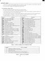
~:.:::,Contents
129
Specification
...... ... .. ... .. .. . .. ..... .. . . .
System Connection
Laser Beam Safety
CD Mechanism
CD Service
... .. ... .. . . . . . .. .... .. . .
Precaution
. . . .. .. .... .. . .
Removal
Mode
... ... . . .. .. ... ... . .
1
Exploded
1
2
Parts List (CD
3
CODE
No.
05 (AU)
. .... .. .... ..
20
. . . . .. ... .. .......
21
Mechanism)
... ....
22
Parts List (Tape Deck Mechanism)
.. . .. ......
Schematic Diagram (CD) . . . . . . . . . . . . . . . . . . . .
23
24
Exploded
View(CD
418
Mechanism)
Mechanism)
View (Tape
Deck
.. .... ... .. . . . .. ...... .. . .
7
CD Adjustmen{
.... .... ... . .. . . .. ..... .. . .Tape Deck A~ustment
.. .. .. . . . . .. .... ... . .
9
11
Wiring
Schematic
Diagram (Tuner)
.. . . . .... .. .. .....
Tape
12
Schematic
Diagram (Front)
. .. . .... ... .. .....
30
Switch...
. . . . ...... .. ..
. ... .. .. . . . . ....... .. . .
13
13
Schematic Diagram (Power Amp) . . . . . . . . . . . . .
Wiring IXagram (Main Amp & G. Equalizer)
...
32
34
. .... ... . . . . .. . ...... . . .
13
Schematic Diagram (Tape Deck Amp)
... .....
Wiring Diagram (Tape Deck Amp) . . . . . . . . . . . .
36
37
Deck Replacement
Operating the Reset
Parts List (Remocon)
Parts List(Speaker)
lCVoltage
Exploded
Table
. .. .. . . . .. ...... .. .
of CD....
View (Cabinet
. . . . ....... . .. .
& Chassis)
... .. . .. .
Parts List . . . . . . . . . . . . . . . . . . . . . . . . . . . . . . . .
This Service manual is consistof
“RB-D5”,
”DC-D5U-,
14
Diagram (CD&Front)
15
lC Block
16
LCD
Diagram
Block
Diagram
. . . . . . . . . . . . ..-
26
28
. . .. .. .. .. . .. ..... ... ....
38
.. .. . ... . . ..... ... .....
44
”SX-D5”.
REFERENCE
No.
SM580235
\ ‘.
SPECIFICATION
DC-D5U MINI SHELF SYSTEM
Amplifier section
Output power . . . . . . . . . . . .
Graphic equalizer control
.
Input . . . . . . . . . . . . . . . . . .. . .
outputs
..................
........................
Tuner section
Frequency range . . . . . . . . . .
...... .... . ........
5 W x 2 (a~~ ohms, 10% distortion)
f 10dB (300 i+Z, lkHz, 10k Hz)
PHONO : 2.5 mV/50 kohms
SPEAKERS:
4 ohms
PHONES :8-32 ohms
Approx.
CD player section
Channels . . . . . . . . . . . . . . . . .
Sampling frequency . . . . . . .
Pickup . . . . . . . . . . . . . . . . . . .
Frequency response . . . . . . .
Wow and flutter
.........
2-channel stereo
44.1 kHz
Optical 3-beam semiconductor
20-20,000
Hz
8elow measurable limits
AC: 230-240 V, 50 HZ
50 w
270 (W) x 285 (H) x 186 (D) mm
3.8 kg
RW05 WIRELESS
REMOTE CONTROLLER
2 “AA” batteries
Power requirements
......
41(W) x 175(H) x 18(D) mm
Chmensions(approx.)
......
63 g (without batteries)
Weight(approx.)
..........
FM :87.5108 MHz
AM:522-1710k
Hz
Cassette deck section
Track system . . . . . . . . . . . . .
Frequency response . . . . . . .
Signal to noise ratio . . . . . .
Wow and flutter
.........
Fast forward /
rewind time . . . . . . . . .
SYSTEM
Gemeral
Power requirements
......
Power consumption . . . . . . .
......
Dirmerrsions(approx.)
W@@ht(approx.)
..........
5X=5
SPEAKER
SYSTEM
Type . . . . . . . . . . . . . . . . . . . . .
Umk’t used . . . . . . . . . . . . . . . .
4-track, 2-channel stereo
80-13,500
Hz
50 dB
0.15 ?4. (WRMS)
Maxim urn power~andling capacity . . . . . .
Nominal impedance . . . . . .
Oirmensions(approx.)
. . . ...’
Weight(approx.)
..........
110 sec. (C-60) .
2 way bass reflex
woofer : 12cm cone type
Tweeter : piezo electric
10 W (peak)
4ohrns
“
180(W) x 285(H) x
1.4 kg (per speaker)
191 (D) mm
laser
... -.
. .-
Specification
subject to change without notice.
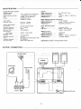
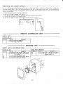
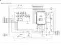
CONNECTION
.
...-.
---
--
.
xii!$$”’’””’””’”-
FM otidoor’a6f161
““
- Rch
. -.
:
.-
.-.
. . . ,-.,, . ... ..... . .. .-, =
-. ,,,.
speaker
..7...-,
TurMable
Earth
lead
L ch speaker
.,
“= .-
e
Q
output
leads
AM loop aerial
FM indoor aerial
=
1
I II
,...”..
.,.
A --l
!
I
i-l
SJ
To an AC outlet
\
.. ..
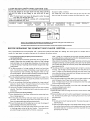
LASER BEAM SAFEti
PRECAUTIONS
(CD)
I Do
not look straight
at the laser beam from the pickup
and do I
point the beam
at your fingers
or any other
part of your
body.
‘.
Note: The Iaser beam must never be allowed to enter the eyes
since this may damage the eyes.
Power must never
be supplied
to a pickup with a damaged
laser
not
I
Structural
I
output part (objective
This
Safety
Interlock
model has a disc chuck lever and top lid. This
lever and top lid prevent to expose the laser beam for
disc chuck
users.
lens, etc.).
I
INVISIBLE
LASER
RADIATION
I
EXPOSURE
OUTPUT
POWER
TO
:
BEAM
0.6 mW
IS
DANGEROUS
MAX
m
1
., .,
.
-l
L-.
CLASS
WAVELENGTH
:
790
1-
LASER
PRODUCT
I
nm
I
t2#Wl10N
- USE OFCON7ROLS
ORADJU.Sl’14ENlS
ORPERFORMANCE
OFPROCEDURES
01’t+133
TNANTNoSE SPECIFIEDIN lHE
-OPERATING
INSRNJC710NS
UAYRESULTINNAZ4RDOUS
RADLATION
EXPOSURE.
❑YANYONE
EXCEPTPROPERLY
OUAUFIED
PERSONNEL
YHECOMPACT
DISCPLAYERSHOULO
NOTBEAOWSTED
ORREPAIREO
BEFORE
REPAIRINGTHE
Many semiconductors
COMPACT
..
(ICS and transistors)
DISC PLAYER
and a pickup (with a bui!t-in
SECTION
laser diode) for
reading
the
music signals
on compact discs b
means of a laser beam are used as the parts in the compact disc player section.
1) Precautions
(particularly
~
for handling
the ICS)
The pickup and
the pickup
semiconductors
(particularly
maged if they come into contact
static electricity.
and semiconductors
Note: Under no circumstances must be the grounding bands be
grounded wit%out a resistor (with a 1M ohms resistance) since doing so involves the risk of electric shocks.
the ICS) may be da-
Since static in the clothes of the repair personnel will not be dis-
with a source of high voltage
Do not bring them; therefore,
charged by wearing
into contact with
parts.
..
... -
of a large number of optical and precision
Do not store or repair it, therefore,
@ The pickup, which is a single integrated part, is kept in a conductive bag. Use this bag to convey the pickup from one place to an-
in any location with a
high temperature,
high humidity,
high magnetic fields
dust concentration.
(Since the pickup contains a powerful magnet.
other.
or higtr
like these can cause the printed circuit board to
crack or malfunctioning
@Do
3) Precautions with laser beam
~
to occur.
@ The pickup isa single integrated partwhich
its adjustment
Note:
points and set screws must not
4) Cleaning the lens surface
during
handling
instruments,
Cover the work
tools and repair equipment
must be
bench where the repair work will
be
@ Ground the metal part of the soldering
iron in order to safeguard
bands around their wrists
to discharge static picked up by their bodies.
grounded through a resistor
Notes:
Do not use too much isopropyl alcohol: the excessmay seep in
side the pickup.
@ The lens is held in place by a very feeble support spring. There
against leakage of electricity from the heater.
must wear grounding
the plastic lens.
~
done with a grounded electrically conductive sheet.
@ Repair personnel
@ Remove stubborn dirt with a cotton swab dipped in isopropyl alto.
hoi. Do not use any other type of cleaning fluid since it may mark
the unit being repaired.
@ All measuring
Blow off dust on the lens using the kind of air brush which is used
for cameras.
@ When replacing any of the parts, disconnect the power plug from
grounded.
output part (objective lens, etc.).
has been very precisely
~
static
The laser beam must never be allowed to enter the eyes
@ Power must never be supplied to a pickup with a damaged laser
be touched.
2) How to prevent
at the laser beam from the pickup and do not
since this may damage the eyes.
The performance of such a pickup may
deteriorate gradually and cause malfunctioning.
adjusted. Therefore,
DO not look straight
point the beam at your fingers or any other part of your body.
not use a pickup which has been subjected to strong external
pressure or to an impact.
from static which may
is not placed on top of the bag.
not apply strong external pressure to the pickup or subject it to
impact. Actions
In order to avoid damage resulting
occur when the pickup is removed from the bag, make sure that it
it must not be brought near any magnetized objects.)
@Do
bands, every care must be taken
the clothes to touch the pickup and semiconductors
,.,
(particularly the ICS).
voltage static.
@ The pickup consists
grounding
not to allow
or into the vicinity of anything which has been charged with high
These
bands are
fore, when cleaning the lens, avoid applying any more force b)
the cotton swab than is necessary since this may bend the sup
port spring out of shape.
(with a 1M ohms resistance).
-2-
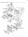
CD MECHANISM
REMOV~L
1) Preparations
1) Do not apply
force to the pickup when
unnecessary
circuit sections.
2) Do
not
unnecessary
apply
Unnecessary
\
(do not
force
force may break theteeth
3) In the descriptions
which follow,
pull
or
onthetray
handling
push
it
it.
Care should
forcefully)
to
be taken
remove
the
not even to touch the lens or drive
disc tray
from
its
inside
position.
gear (CM6).
the numbers in the parentheses
after the parts are reference
numbers
in the exploded views.
Refer to these views.
2)
and installing
Removing
DISC TRAY
the disc tray
REPLACEMENT
1) Remove the stop screw (Y 1) of the disc tray (31). (~)
2) Pull the disc tray
(31) all the way forward
tray drive gear (CM 12) clockwise.
by turning
SECOND TOOTH
the
OF TRAY
MOVE GEAR
(@)
Do not take hold of the disc tray (31) and pull it
Note:
out by force.
3) Push the catch on the disc tray (31) in the direction
by the arrow,
4) To install
and draw out the disc tray (31).
the disc tray, turn
tion of the arrow
shown
(@)
the gear (CM12) in the direc-
as far as it will go.
(@)
39
5) Align the disc tray (31 ) with the mechanism chassis (CM39).
Adjusting
6) Push
second tooth of the tray move gear (CM3).
the disc tray
with the tray
drive
7) Secure it with
(31 ) toward
gear
(CM12)
the rear, ‘and
as shown
(@)
interlock
in Fig.@
it
.
the screw (Y I ) which was removed in step 1).
,’,
3)
Disassembling
the
(1) Removing the
pickup
mechanism
block
:” .-
(31).
(Refer to steps
1) Remove, the disc tray
...
-..,.the. .. section
. .. . ,. ent”itled”
.
.
.“Removing
. .
.
.1), 2) and 3) of
in~alling
the
.
.
.. , tray-”), by, z~. !,,... r,
-,, -..,,
,- ,<
2) Turn the tray drive gear (CM 12) ‘counterclockwise (~),
move the pickup in the direction
and
of arrow
(@)
disc
~ TRAY
MOVE GEAR (CM3)
(CM13).
drive
(@)
5) Now remove the pick rack gears (CM16 and CM19).
R will
gears
not
be possible
(CM16
to remove
and CM19)
unless
the
the
pick
rack
pickup
has
been moved all the way in the direction
of arrow
(@).
pickup block can now
be removed
by taking
out the
screw (CM51) and spring coil (CM49).
If the timing
“X-
gear (CM23) is in the state shown
in the figure
shown by
on the right,
. .
..
..’
-,
TRAy
GEAR (CM6)
;-AR
\
gear (CM12) and washer
Note:
.
..’
, .-,
,,.
and
(@)
4) Remove the screw (CM1 1), and also remove the tray
6) The
.-
.,
as far as it
will go.
3) Remove the spring wire (CM44) with tweezers.
Note:
.-,.
,.
by
put it in the state
“O”.
-3-
“ (CM23)
.. . ..
‘“
.
MECHANISM REMOVAL
(2) Replacing
and
(CD)
lubricating
the
pickup
1) Pull out the two pickup rails (CN(143) from the chassis (CM50).
2) The pickup (CM52) can now be ‘&moved
once the two
pick-
up rails (CM43) have been taken out.
3) When
two
the pickup has
pickup rails
been
(CM43)
replaced,
cleanly
474B) around the entire
be sure
to wipe
the
and apply grease (FLOIL
circumference
c
G-
of the rails and along
FIX BY THE
CEMEDINE
#575
their entire length.
CM9
4) Pass the two
pickup
rails
(CM43)
through
the
new
pickup
(CM52), insert them into the chassis (CM50), and fix them
in
Notes:
a.
When
applying
the
grease to adhere
b.
moving
or
do
not
allow
any
by the do;s
in the figure)
0@
of
is damaged in the process of re-
inserting
the
two
pickup
rails
(CM43)
..-
from or into the chassis (CM50), wipe the damaged
area with
a cloth
dipped
in alcohol (normal
ane), and bond it together
!,
5
0
to any other parts.
If a part (indicated
the chassis (CM50)
.. .
,.,,.., .,
...
grease,
0
00
place at an angle of 45° as shown in the figure.
hex-
CM50
FLOIL
(G-47LB)
0
BREAK
using a bonding agent
(Cemedine #575).
\,.
(3) Replacing
the loading/sled
motor
‘ ~‘‘ .
1) The loading/sled motor (CM38) can be removed
chassis (cM39)
once- the
from
screw. (CM.24) securing the
SHkFT
the
motor
(CM38) is removed.
2) Mount the new loading/sled
(CM39) using the screw
motor
(CM38) onto the chassis
(CM24).
the Ioadingk ;Ied motor’s operation
Checking
1) As shown in the figure, connect an ammeter and a DC pow-
(4)
er supply
open
to the
loading/sled
and end switches
motor
(CM38),
and set the tray
to the “’off” [open] positions.
2) Check that the pickup (CM52) moves smoothly
ping
from
the
ward
its outer
plied
from
3) The
inner
circumference
circumference
Check that
the
without
compact
a DC 0.6V
voltage
stop-
disc tois ap-
the DC power supply.
disc tray is housed
a DC 4V
when
of
voltage
the
inside and the gear (CM9) slips when
is applied
ammeter
from
indicates
the
DC power
120mA
supply.
or more at this
time.
——
ATTACHMENT
OF MOTOR
ANGLE
.:gal:
@“~
,-_-_-TRAY OPEN I
E?tD SWITCH
al :~
Utu
L-.-------
.
\.
MECHANISM
4)
REMOVAL
Check points
lubrication
(CD)
for CD mechanism
assembly and
(3)
(1) Lubricating
and mounting the tray slide\ ~
1) Apply grease (FLOIL G-474B) to the area indicated by the diagonal in the figure;
2) When inserting
it is installed
the tray slide (CM15),
vis-a-vis
the
set the
base/tray
timing
position
where
gear (CM20)
as
Installing
the
base up/down slide and timing
1) Move the base upldown slide (CM 14) in the direction of the
arrow
0,
and set the
gears at the positions
shown
in the
figure.
2) Insert the timing
gear (CM23), and mount it using the screw
(CM21).
3) Turn the timing
shown in the figure.
gear
(CM23) counterclockwise.
gear
y
GEAR
TIMING
BASE UP/ DOWN
*~~JJ14
,/’
ql+i@$
SCREW
““-
Hook the gear
gear (CM23).
J -.0
@
(2)
Installing
1) Move
the
the
tray
tray
. .,,,,
.
spring
(CM22)
.:
GEAR TENSlON
onto the timing
‘
SPRING
x“ ~1’
gear
slide
(CM15)
2) Engage the gear section
inner
(CM21)
@
tension
~~
1
i
gear of the tray
in the direction of the arrow ~.
of the tray
gear
(CM6)
slide (CM15) with
at the
center
line,
the
as
shown in the figure.
3) Align the tray move gear (CM3) with
the position
(0)
of the
hole in the outer gear of the tray
gear (CM6) and engage
the tray move gear (CM3), as shown
in the figure.
@
El
TRAY
SLIDE
L
-
GEAR
3)
m’oNsp
..
.
MECHANISM
(4)
.,
REMOVAL
Lubricating
the
base
(CD)
(5)
lever
Apply grease (FLOIL G-474 B}tothe,
Lu&icating
the
the lower
of
2) Apply
I
( ;jj$
gear
and
clutch
gear
around the entire circumference
area).
grease (G-333)
outer
3)
sled
G-474B)
gear of the pickup sled gear (CM12), as shown
in the figure
CEM~Dl;5E
pickup
grease (FLOIL
1) Apply
~< area in the figure.
around the entire
circumference of the
clutch gear (CM9).
Apply
grease
clutch
gear
(FLOIL
G-474B)
(CM9) where
to
it
the
makes
~~
Part
of
contact with
the
outer
the
inner
clutch gear (CM8).
PICKUP
SLED
GEAR
8
&
,<;., ,..
:,. .
:L.
FLOIL
(G-474B)
m
Q
CLUTCH’ INNER
,-.-,.,
.,,. .. ....
GEAR”’
CM8
$J?
I
,+~>
rJL
:R(35-
l\
I
‘T’, ,(
1- ..
,>J&’
,:. . .
. .
.,
_..
.’....
..-.
Arranging
and
securing
in the ~gure,
the
. CLUTCH cM9 .-.
. .
.. .. .. fi#. *rll CF. m
Uulcn
Ucfin
,.
-.
.
,..
.
at
a position
motor
(CM4B) through
switch)
..-
movement.
(CM38) and sensor
the leads with
switch
the lug (CM41),
check that
2) if no problems arise in the @ check, secure the points
,..
-. \\
I
,, \\--
T
““
”----”---
-<
‘
‘--
“--
“-
:.
-.
lzzl
FLOIL(G-474B)
-BE
NOT
pin (a)
of the compact disc, and pass the
of the chassis (CM39).
(CM26) by passing
the pickup (CM52)
shown
circumference
them
through
moves smoothly
in the figure
usin9
point
x
o
.,
. .
NOTE
THE
LUG
CUk.HION
PORTION
-6-
the leads from the load-
(b) in the chassis (CM39).
the leads interfering
a bonding a9ent (Cemedine X575).
m
SLACK
Arrange
without
TO CN101 COPCB
. .
&-
——
on the innermost
(micro
securing
.:
leads
set the pickup (CM52)
ingkled
.....
4
-,,
,J.
._
%
leads from the pickup (CM52) and spindle
motor
.:.
lkL
.
.
,’
,. .
1) As shown
@
<...-..
—.
—
~.~.~
J‘“-”””
...“,_p“?”
,...
_.-aq
~
mij+jii
CEMEDINE
(6)
,
m
//l-
‘.
–~M12
After
with
its
SERVICE
\ ‘
MODE
,.
Specifications
To enter any service mode, first
simulta eously press the CD MEMORY and BAND (TUNER) keys on the unit. This accesses the ser7
Now press one ofj~he buttons on the unit to enter a service mode. As the service mode entry state is dis-
vice mode entry state.
continued after 1 second elapses, the system will
enter a service mode only if the next key is pressed within
one second.
I. Checking the key input signal connections
- Enter this mode by pressing the ME MORY(TUNER) key during the service mode entry state.
. The entire LCD goes out once this
. [n this
(i.e. the lit portions
gradually increase).
. Press the FM MODE (TUNER)
I
mode is entered.
mode, as keys on the unit are pressed segments
I
KEY
on the LCD corresponding
key to exit this mode and return to the normal
DISPLAY
I
I
to each key on a one-to-one basis come on
(Refer to Table 1.)
KEY
I
mode.
DISPLAY
I
KEY
II
DISPLAY
I
1
DIGIT
BAND
DIGIT
MEMORY
I REPEAT
1 : ~
!
2 :
I
I@
] FM MODE
I REPEAT
7:+
PIAYI PAUSE
-
RANDOM
RANDOM
STOP
TIME
EDIT
..-
EDIT
TUNING
UP
DIGIT 4:
~
SKIP/SEARCH
Ml
FADE
TUNING
DOWN
DIGIT 5:
~
SKIP/SEARCH
M
TRACK
PRESET UP
SIDE A
-
CD MEMORY
PROG.
-.
IDIGIT
II POWER
OPEN/CLOSE
INTRO
PRESET DOWN
SIDE B
... .
,,
..
@ : Releases the
mode and returns the set to the normal
key checking
TABLE I : CORRESPONDING
12
INTRO f /~q
RANDOM ‘GJ4-l
mode.
KEYS AND DISPLAYS IN THE KEY iHECKING
MODE
34567
~
/
FI’+1’12
//-//-/,
/-//-/ kHz SIDEA
L~AM-/ /“I~!/:
/-//-/
m
~HZ
TRACT
REPEAT STEREO AUTO MONO FADETIME EDIT
WEB
D
FIGURE 1 : LCD ( LIQUID CRYSTAL DISPLAY)
2. Checking LCD connections
. Enter this mode by pressing the REPEAT key during the service mode entry state. (See note.)
. The entire LCD goes out once this
mode is entered.
. In this mode, all segment of the LCD lights each time the REPEAT
. Press the FM MODE key to exit this mode and return
3. CD tracking
balance adjusting
key is pressed.
to the normal
mode.
mode
. Enter this mode by pressing the PLAYIPAUSE
key during the service mode entry state.
. If the power is off when this mode is entered, the power automatically
. In this
mode, the tracking
balance adjustment
state
(tracking
closed.
-7-
is off)
comes on.
is automatically
entered
after
the tray
I
is completely
SERVICE
MODE
In this
PLAY
mode,
the
key in this
Turning
off the
Enter
this
If the
power
In this
In this
the
This
mode
by pressing
when
mode,
the
this
displays
like
is released
❑o
❑ j
I ~
those
used,
LCD track
shown
If the display
when
key during
are
the
the service
the
power
displays
like
number
in Table
I FOCUS search
has been bequn
20
21
22
23
Both
CLV and tracking
are ON
is turned
those
shown
has been completed
search
off
represent
action
or press
CD operations
of CD occurred
the
FM
MODE
(success,
failure)
-
(internal
(external
Spindle
Pickup
I 3-
1 Spindle
(pickup
braking
return
direction)
direction)
return)
has been completed
is in progress
readinq
has been comoleted
L-point
access has been begun
L-point
access (REV64
12
13
L-point
access (FWD64
L-point
access (REV16
qq
L-point
access (FWD16
Is
L-point
access (REV1
access has been completed
Pause
(REV16
I Pause
(REVI
I Pause
(trace)
track
track
access has begun
~1
access (high-speed
access has begun)
I
9
is in progress
I Music
access (hiqh-speed
access is in proqress)
g~
P
Music
access (high-speed
access has been completed)
gq
Music
access (high-speed
access has been completed)
access
access has been completed)
96
Music
access (REV64
is in progress
gy
Music
access (FWD64
Sz
Playing
is in progress
99
99
Music
access (REV16
TOC reading
is in proqress
(skip
return
operation)
has been begun
is in progress
5-
TABLE 2 : DISPLAYS
[
DURING
NUMBER
1
2
13
I
Music
Playing
60
I
I
51
61
1
Iumo)
95
reading
jump)
jump)
Music
F
has begun
TOC
track
ium D)
Playing
I Rewinding
jump)
jump)
gn
have been
Focusing
is not possible
The
subcode
! Toc
cannot
4
The
focus
5
The
subcode
is not input
in focus
during
lost while
is not Input
track
access (FWD16
access (final
OF CD ERROR
track
track
Music
track
jump)
jump)
jump)
jump)
stage)
MODE
I
search.
disc startup.
I
be read
was
(high-speed
Music
THE CD OPERATION
STATE
the servo
while
was
the servo
on (during
-8-
playing,
is on (during
TABLE 3 : DISPLAY
in
failure)
jump)
track
~n
I
track
is in progress
return
appear
jump)
track
track
Music
~
track
(success,
mI
and pickup
than
has begun
I pause (FWD16
I =
J
displayed)
has begun
completed
Fast forwarding
different
is no display.
ql
❑ f-1
is in progress
is in progress
braking
other
Ill
BEI
is [n progress
normally
reading
L-point
return
than
TOC
Pausing
return
CD operations
TOC
Ho
qp
the
OPERATION
16
Pickup
different
DISPLAY
is In progress
Pickup
represent
not the errors,
closing
braking
Pressing
key.
Tray
31
Yll
2 (which
has begun
3U
I
In Table
closing
closing
playing.
state.
Tray
Tray
during
display.
is in progress
are ON
Spindle
key
comes on.
Ei
CLV and tracking
z-
MEMORY
mode.
Lz
Both
] Focus search
the
to begin.
mode entry
OPERATION
kick
by pressing
playing
automatically
3 (which
is “O” when
power
has been begun
05
I
can be entered
and causes
balance adjusting
is entered,
Focus search
! Spindle
❑6
❑-
STOP
in the
DISPLAY
I
CD tracking
mode
CD function
appear
LCD digit 5 display.
mode
the
state
servo
mode
is off when
displayed)
adjustment
on the tracking
releases
display
mode,
normally
balance
turns
power
4. CD operation
.
tracking
state
etc.).
playing,
etc.).
OF CD ERRORS
CD ADJUSTMENT
Electrical
Adjustment
So far
we
have
player
handling,
disassembly
notes
of
instructions
Preparations
presented
the
before
explanations
prior
to
unit.
repair,
sure
Be
making
regarding
handling
to
compact
disc
Measuring
pickup
and
(l) Test
the
carefully
read
for Adjustments
instruments
disc.:
(2) Oscilloscope
these
or Memory
any adjustments.
(3) Dlgltal
adjustments
equipment
b. Use a 10:1
c. Test
1.
Initial
can be using
corresponds
probe
for
disc is subject
the
to that
equipment
of the above
observing
signals
change without
produced
listed
by other
drivers
manufactures
(Sony)
: SS5711
(1 OMHZ
scope : DSS6521
voltmeter
(4) Screw
Notes : a. The
and tools
YEDS18
(Input
Impedance
(no metallic)
provided
or dual phenomenon)
(Storage
for
that
scope)
IM ohm or more)
adjustments
the
performance
of
that
models.
on the oscilloscope
and storage
scope
notice.
set
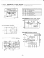
Set the
SVR11
at its initial
position
of adjustment
controls
as shown
in figure
below.
SVRI 1
INITIAL SET
PICKUP
FFC 13P
rRESET
(–L—’)
SWITCH
(MECHANICAL
CENTER)
%i+~
,Pl
,F,y
CNI13L
/!!
S1301
TRACKING
BALANCE ADJ
TP2 FE-J,’,
TP3 TEJ/
TP4 VC—
@l
1C101
SVR1l
o
1C103
0
FROM AMP —
~N,07
I
LJ
FROM POWER
I
CN102
—~CN105
C
MECHA
MOTOR
C=
MECHA
SWITCH
E
[7?
CN103
‘Upp”<
TO FRONT
2.
Tracking
Balance
Adjustment
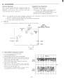
1. Connect the oscilloscope
2. Turn
3.
Load the test disc.And
Press
the
BAND
(Tuner)
same
time.
Soon
within
to TP3(TE),
TP4(VC).
Press
mode (Tracking
the
6. Adjust
form
relative
* If this
motor
set the function
button
after,
a second. (See service
*Service
5.
(SVRI 1)
on the power of the unit.
4.
the
PCB
PLAY/PAUSE
SVRI
of
1 so that
TP3
on
the
adjustment
press
PLAY
button
/ PAUSE
mode)
I
I
i
500PS
I
L4——L—4=—— L-4––!-–-.4–-J
at
I
I
button
TP1
(RF)
mode)
entry
button.
the
TE (Tracking
oscilloscope
right
is imperfect,
sending
the
I
position.
balance adjustment
to OV. (See figure
(pickup
toCD
and CD MEMORY
motor),
is
Error)
signal
vertically
wave-
Ov
symmetrical
side )
become
Inferior
run
away
the
sled
playabilky
TP3
(TE)
-9-
-o1-
H2KIS
44 HWIV21S
W
(31)
&dl
Ao
AO
(dtJ)
i dl
“s
“b
E
‘z
.,
nmusnrav
ao
‘‘
ADJUSTMENT
1.
Azimuth
OF TAPE
Adjustment
.
Be sure
to clean the
.
Be sure
both
.
Be sure
both cannel’s
.
After
completion
DECK
A
(l).
~.
Load a test
Q.
Press
@.
Use a + tip
the
muth
DECK
~.
2.
waveform
tape (VTT-703
PLAY
button.
to make
any adjustment.
level (Using
the
phase
a dual-channel
oscilloscope),
matching.
use the thread lock (TB-1401B)
etc. : 10kHz)
to secure
the
procedure
the
the
left
screw
and
phase during
for
right
normal
normal
azi-
outputs
are
playback.
for
deck B.
Adjustment
TEST
DECK
,
TAPE
DECK
A
TAPE
SVR
1
Normal
1. For
making
2.
Adjustment
3.
Confirm
the
moved
from
1
MTT-I
REMARKS
COUNTER
1
1
2995-3005
1 IN
Memorize
HZ
adjustment
should
-40-
of step 1, set the
be made at the
indication
SVR
of the
tape
on the TAPE
For adjustment,
use the screwdriver
For
check,
Parts
speed
is TCW-21
short
the
speed
1) and confirm
that
portion
for
with
Isolated
points
the
speed
ts record
made with
C-60 blank
B
on counter.
is
in
-40-70
Confirm
HZ
that
against
cassette
tape.
after
adjustment
has been
made and adjusting
driver
has been
re-
P. C. Board.
tip from
(High-SPEED)
grip.
to chassis
ground
Hz
on the
TAPE
against
DECK A.
Location
SHORT
/
+ B1
/
L
03907
TAPE
speed
DECK
DECK A.
the speed of DECK B is in -40-70
(H1
tape
of
of the tape.
2 second
AMPLIFIER
test
70Hz
DECK B mechanism
ending
DECK
5.
high
the
3000Hz
B
4.
Tape
3.
DECK
Normal
:
screws.
in deck A.
SVRO1
Notes
adjustment
B
SPEED
2
azimuth
playback)
to turn
so that
at the same
,
1
attempting
are same for
(normal
screwdriver
Speed
STEP
before
and 2) are the same
of the adjustment,
adjustment
Repeat
Tape
heads
channels(l
maximized
(2).
DECK
T
Lw
u
SPEED)
CN304
SPEED
TA-R-.
@
D
TA-L
+
--L
SVRO1
HI. S.—
B
c1
-11-
f
I
DECK
AMPLIFIER
P. C. Board,
(Test
.,,. . ...
.,
‘.
REPLACEMENT
4.
Torque
OF’TAPE
30-60
F.FWD
55-120
gr.cm
REW
55-120
gr.cm
Replacement
Driving
PLAY :TW-2111
REW:Torque
F.FWD / REW : TW-2231
PLAY
TAPE
BACK TENSION
TA~E-UP TORQUE
\
PLAY : TW-2111
Test cassette.
2.0-
gr.cm
E
—..HEAD
—..—
Gage
Cr4
WHITE
REC/PLAY HEAD
)
/-8
F------
EARTH
PLAY
!!
..-..
...“...:4
HEAD
X74
. ..
RED
EARTH
M
u
>
6.
!,
,
,-
Replacement
..
-12-
power cassette:
> 60g
4.5 gr.cm
.
I.
TENSION
TW-2412
of Head
I
..
MECHANISM
Measurements
ITEM
5.
DECK
WHITE
OPERATING
This
THE
unit is provided with
RESET
a reset switch on the rear panel. The
tions which controls the CD, TUNER,
when the CD, TUNER,
following
SWITCH
TAPE
the step below.
TAPE
DECK and et~ operation
1
Keep the RESET
(The backed up electrolytic
the microprocessor
capacitor is discharged by keeping the RESET
switch depress.)
switch
in the each see-
and initialize
the microprocessor
outlet.
Reconnect the AC power cord to the power outlet.
4)
Press the CD, TUNER,
DECK and etc. operations,
and check their
operation.
m--
.:..
.-
PARTS
LIST
REMOCON (RB-D5)
Ref.
No.
Part
No.
614
614
252
235
Description
1373
9433
Dm.mmmmmammmm.-
PARTS
ASSY, REMOCON
LID, BATTERY
mmm.mmmmmm.
LIST & EXPLODED
mm.
SPEAKER
S1
S2
S51
S52
Parl No.
614 248 0052
(419
002 0206)
614 248 0045
614 251 5860
614 022 8755
UNIT
mm.-maa.mm.-Dm--D
m.mm.9m.-m.-m----
VIEW
SPEAKER (SX-D5)
Ref. No.
.,..
is not acknowledged even
60 seconds.
3).
TAPE
to initialize
press the RESET
switch depressed for
buttons
serves
is to be serviced or key input
are pressed,
1). Disconnect the AC power cord from the power
2).
reset switch
DECK and etc block. If the unit
FIXING PARTS (SPEAKER)
Description
ASSY, CABINET,
PIEZO
BUZZER
Ref.
FRONT (WITH
FOR TWEETER
SPEAKER)
ASSY, CABINET,
REAR
SPEAKER, D12 5W 4fl,
WI RE, LEAD, SPEAKER
wooFER
,/
,/’6’)
SY 1
SY2
No.
Part
411
411
Description
No.
021
020
4906
8905
SCR S-TPG
BIN
3X20,CABINET
SCR S-TPG BIN+FLG
WOOFER SPEAKER
3X20,
m“z
---Sti’z
----
o
61”Z
-----
Lcz
w
----
----
0
----
----
0
Z9
f9
-
----
-
:;o--
L9
Zo “o
----8Z”Z
<v
9P
so 1
so., - --;
0
--
10”0
0
0
Z1 .0
Os”z
Gb.z
lb
8b
Soul
---S0”1
LE
ZE
o
---El ‘b
z6”17
----0
66”b
----86”b
09
Z1 “o
---Z1 .0
bb
-----
-----
o
0
o
Sti’z
-----Sb”Z
6S
09 z
‘ “-;9~-”
0
----
tz”z
----Oz”z
-----
----
o
Zo “o
----
86”b
Ls
8S
-
-----
0s z
0
0
-----
o
0
o
----
-t7L
98 b
S8”b
0
89’1
-
18’b
_— —-S8b
bS
Ss z
0s’2
---~s.z - - ;~-z-6f
ok
00s
---10”s
-----
o
6bZ
—-8bZ
0
0
o
----S8’ti
----
6b’Z
Gf.z
-----
o
- --o---
Zs
-----
Z9’Z
Zo ‘o
---0
-----
6S”0
OE”O
0
15
. -----
0s
60 “Z
----
S$
9E
. -----
00s
Ls’z
----Zs z
80”z
0
Z9”Z
o
-----
00”s
0
81”z
----81 ‘Z
b
Os”z
---0s’2
6b
Os’z
---—-
EE
-----
9b”0
9b’O
LL
81
Sz”z
-s;’:
----
o
------------
apow
apow
ON
Aeld
dois
U!d 6U!JRaW
?pOW
CIPOW
keld
dol$
ON U!d 6U]1nWaW
apOW Aqd
----------apow dois
ON
------------
Uld fiu!mwaw
apow
apow
0
1
z
f
------------
Os’z
1+
Sb Z
---Sb’Z
61
Oz
‘
s
9
bO’O
0
Es
19”0
-----
0
10 s
----10’s
lZ
Zz
EZ
--
L
8
Lc
8$
----
0
Vz
C9 “z
---8SZ
6
01
55
9s
-----
6f”l
Lb
-----
0
SiZ
9Z
Ob’1
---0
0
0
LL
Z1
0s”2
m
0
-----
0
LZ
8Z
0
---L6”b
El
9S’b
Eti
------
0
6Z
OE
Z[ “z
El “b
~, .b - - ; /-z-b~
GL
91
Ae[d
do$s
ON U!d fiu!m$eaw
3N198D1
----
Z8”b
---ZE
----
L6”P’
---8*
----
S8”b
---w
0
-----
S8”b
98P
-----
o
----
----
L6”ti
/!6’t
-----
----
10”0
-----
0
o
09
60’0
-----
SP
9b
0
----
19
Z9
f9
L6”b
Lb
18b
-----
o
0
----6S
-----
-----
P8”P
-----
98”b
-----
o
98 b
LS
85
-----
9Z
b8’b
-----
lL
Z1
-----
10”0
lb
Zb
$b
f9”b
----Lz
8Z
b8b
-----
Ei
S8b
----
S8”b
m
b8”b
-----
6Z
OE
1s
-----
--*---P1
S1
91
bL “b
---——
Sz
-----
01
00 ‘z
98”b
---95
0
----—
Ob
bf “b
---Vz
fs”z
----
6
-----
o
--
5’s
0
----
0
—-bS
-----
6f
o
-— --Ez
S8 b
-----
0
98”0
----
S8 b
b8”b
98”b
-----
Es
-----
0
o
_— --lZ
o
—-s
--
9
-----
0
0
Zo”s
----
-----
08”b
. .— —-61
0
_— -E
Zo’s
---6*
o
0s
-----
z8”t7
-----
28 b
bf
s:
9E
-----
Oz
-----
b
Zo”s
1s
Zs
Zo”s
.--—
—
1S
8C
----
Zz
----
L
8
EE
o
-----
0
---L1
81
ZL “b
.-- —-
b8”b
----z
1
V0131
apow do~s
-----------ON U!d fiu!m$eaw
apow dois
----------ON Utd fiulmseaw
-----------ON
apOW
dols
U!d fiuumeaw
apOW dois
-- —----—--ON Uld fiu!jnseaw
Z1
lsLadfl
EOKN
: mlj
uo!jenunfj
-----
81 ‘O
---91
-----
----
-----
----
-----
o
lf”f
------
br”9
----
-----
bl
o
El
l&-”f
—— --(1
lcf
-----
LZ
8Z
01”0
S1
-----
-----
lf”f
Os”z
Sz
9Z
19”Z
_— -01
ii
-----
ts”z
lSZ
_— -Vz
!-8
--
6
-----
Is”z
Ez
9b”L
—— --Zz
fo”s
-----
-R?-L
9
9b”L
----
lS”Z
-----
lZ
189
---—s
-----
Oz
-----
lS’Z
[S’z
-----
lf”f
---——
L1
lf”f
8t
61
6b’Z
----
b
-----
Z(’C
f
zf”L—-1
--
z
apow dois
—-------
---ON
------------
U!d fiupnseaw
apow
mjj
qj
8s.1 - -;;,--
----
Zos
-----
10”s
----18”Z
qj
ml j
>Illj
------
.-
OSb
—--
>qj
ml~
-----
LS.z
09
>n/j
--57.:-
8S’1
--——
Zs z
ml j
1 00”S1
mjj
00 ‘s
=.
0
..
. .
m[j
c.
0
0
I
.,.
c.
q
qj
----if
j
---lS”Z
z
9Z
I
,..
~s.z --o~.;- -
o
Os”z
----
-----
>qj
mlj
-—
-ff “z
m\j
ml j
----
~z.l
lz”l
0
f6 b
xv j
-----
>qj
----
o
i
qj
----,6.1
o
--;
--
JPOW
-
---Z1 “)
0
I
)
20131
Aeld
----------apow dol$
ON
S9
99
XII j
>qj
------------
U!d 6U!JnWJW
apow
apow
Aeld
dots
apow
hid
-----------
apOW dol$
Os’z
Os’z
I
---Zb’Z
n
U!d 6U!JII$QWJ
Ae[d
apOW
----------apow
t
do>$
i
U!d 6u!Jnseaw
ON
o
-:--
I
aPOIN Aeld
---:---_---
?pOW do]$
0
t
1
z
I
ON Uld 6upnseaw
mlj
-----
mlj
------
6b’Z
qj
—— -Os’z
I
‘: ______
8b’Z
o
f
I
ON
ff
Pf
qj
mlj
---lSZ
m14
Li
81
6L
I
I
6b
0s
mJj
-—
10’S
xud
_— L---bS Z
b
-----
0
1S
Z5
Zo”s
I
ml j
—— -ls”z
Oz
m{~
‘“
lS”Z
Sf
9f
>n\j
I
—----/s.z
t
s
I
L9
89
>nlj
-— --8S”Z
Es
xqj
---------
I
lE
8$
>nlj
—----
m,.,.
--
i
iz
Zz
I
>nld
817”Z
9
mlj
>n/j
----“-;b; -” 9bl
69
OL
>n\j
----ff “z
m! j
————
0
6s
>n\j
---
fz
1
----
L
8
--——
[s z
Z9”Z
lSZ
1 b“Z.
Vz
I
Os”z
—--
--
Os”z
-----
0
lL
ZL
Zo”s
—---10”s
80”0
r----l----l--W
.“
k“
-----
o
Sz
I
mld
>n/j
.— ---
Os’z
6
OL
bS
~s
9s
m[j
ml j
m[j
o
L..
I
qj
>nlj
----S1 “z
>nJj
-----
Os.z - - ;s-z--
[S”z
LL
Zt
o
-----
bZ’1
fL
m{j
-
LS
8S
6S
qj
----
-----
Ob”b
0
ml j
----98”f
V1
SL
9L
mlj
>njj
OO.s - - j;s--
i9
mJj
o
---------,--—————
————
ml j
----
flub
----
----8bZ
lSZ
LZ
8Z
mlj
mlj
----
-----
LL
8L
61
qj
----
0
>n\j
r
.L
9i7
ml j
----6ti”Z
6Z
of
mlj
----6b”Z
fl
w
dol$
ON U!,j 6u!Jnseaw
d496Z9V9
89L
---6S’1
08
o
----
o
Z9
$9
b9
3n/d
------,blb
Lb
8t7
----
0
1:
ZE
>n/j
---Lo’z
*1
St
91
ON
I
U!d fiu!jnseaw
1
WOl Z6V_l 1013 I
. . ..
.
i
VIEW (CABINET
Y15-J
:+.. . .
. ..
..+.
,,
-,
,./
. ..
/“
3536
-
m’34
.
4/
-,,
16’:J9
‘\
‘.
.\
\\
-15-
v
PARTS
LIST
PRODUCT SAFETY NOTICE
Each precaution
In this
and the schematic
fied
nated
~,
diagram
use only
in the
CAUTION:
Regular
should
in this
type
available
be followed
designate
replacement
list
insulated
: Not
N.S.P
the
parts
are acceptably
manual
from
components
parts
manual.
designated,
as service
and
circuit
before
capacitors
servicing.
are
safety
or parts
Leakage-current
the supply
resistors
during
in which
not
or
with
Components
identified
with
can be of special
significance.
the
of resistance,
same
resistance
ratings
measurements
returning
the
product
listed.
To know
must
to the
those
the
IEC symbol
When
wattage
be made
~
replacing
to
in the
parts
a component
or voltage
determine
that
that
list
identi-
are
desig-
exposed
parts
customer.
values,
refer
to the
schematic
diagram.
parts.
PACKING
Ref.
No.
Part
614
614
614
614
614
614
614
614
No.
254
248
248
228
232
176
236
231
Description
6826
0601
0618
0331
3366
3170
0132
6832
INNER
Ref.
CARTON
PAD,TOP
L.R.
SHEET,SET
INNER
POLY
Part
Description
No.
614
195
6978
42
412
003
1708
43
614
246
5745
44
614
051
9785
614
129
2496
614
125
6443
614
212
8343
L.R.
PAD,BOTTOM
SHEET,SP
No.
41
BOX
POLYE
COVER,INST
M.
COVER,REMOCON
LABEL,SAFETY,CLASS
l,LASER
RUBBER CUSHION,
CD MECHANISM,FLOAT
SCREW,SPECIAL,CO
MECHA,FIX
SHIELO,POWER
TRANSFORMER
LUG,EARTH
FIXER,LEAD
RETAINER
CUSHION,DECK
MECHA LEAD FIX
LABEL,SAFETY,PICKUP,LASER
ACCESSORIES
Ref.
No.
Part
614
&614
614
614
No.
251
8335
250 6578
234
232
FIXING
Description
5511
6671
Ref.
INSTRUCTION
MANUAL
POWER CORO,AC
LOOP ANTENNA,AM
ANTENNA,FM
:ABINET
Ref.
No.
3
4
5
6
7
8
9
10
11
12
13
14
15
16
17
18
19
20
No.
251
251
248
248
248
239
213
248
248
248
248
248
248
248
248
248
248
248
248
003
7628
7680
0069
0076
0182
0405
3019
0397
0335
0328
0311
0304
0298
0281
0274
0267
0250
0243
0236
2804
ASSY,CABINET,
FRONT
ASSY,CABINET,REAR
ASSY,LID,CASSETTE,DECK
A
ASSY,LIO,CASSETTE,DECK
B
ESCUTCHEON,CO
TRAY,FRONT
KN08,ROTARY,BALANCE
KNOB,SLIDE,
FUNCTION
BUTTON,DUBB,BASS
BUTTON,DECK
B,REC
BUTTON,DECK
B,PLAY
BUTTON,DECK
B,REW
BUTTON,DECK
B,FWD
BUTTON,OECK
B,STOP/EJECT
BUTTON,DECK
B,PAUSE
BUTTON,DECK
A,PLAY
8UTTON,DECK
A,REW
BUTTON,DECK
A,FWD
BUTTON,OECK
A,STOP/EJECT
BUTTON,DECK
A,PAUSE
SCREW,SPECIAL.PHONO
GND
1694
0410
1516
0465
8199
0427
1744
3927
1502
9346
TABLE,LOADING,CO
TRAY
MOUNT-M,CO
MECHA,FIX
WINOOW,LEO
COVER
Description
No.
SCR S-TPG
BIN 3X20,
CABINET/REAR
SCR S-TPG
BIN 3X1O,
PHONO.SP
TERMINAL
SCR S-TPG
BIN 3X1O,
AC SOCKET
SCR S-TPG
BIN 3X1O,BRACKET
FOR CD MECHANISM
FIXING
SCR S-TPG
PAN 2X3,
REC SPRING
PLATE
SCR S-TPG
PAN 2X4,
DECK MECHA/BRACKET-E
SCR S-TPG
PAN 2.6X4,
DECK MECHA EARTH
TRAY
SCR S-TPG
PAN 2X8,CD
SCR S-TPG
BIN 2X8,
CD ESCUTCHEON
411
021
4906
Y02
411
021
3701
Y03
411
021
3701
411
021
3701
411
025
1901
Y12
411
028
2905
Y13
411
028
5500
Y14
411
022
8408
Y15
411
021
1202
Y16
411
021
3503
SCR
S-TPG
BIN 3X1O,CD PCB
Y17
411
021
3503
SCR
S-TPG
BIN
3X1O,
BIN
3X1O,
I
Description
No.
Part
Yol
Y04
Part
614
614
614
614
614
614
614
614
614
614
614
614
614
614
614
614
614
614
614
412
1
2
PARTS
Yll
FRONT
Y18
411
021
3503
SCR
PCB
S-TPG
GRAPHIC
Y19
411
021
3503
Y20
411
020
8905
SCR
S-TPG
EQUALIZER
BIN
PCB
3X1O,
MECHA BUTTON/BRACKET-E
SCR
DECK
Y21
411
020
9100
SCR
S-TPG
81N
3X1O,
MECHANISM
S-TPG
BRZ+FLG
3X12,P.T.
1
:HASSIS
Ref.
31
32
33
34
35
36
37
38
39
40
No.
Part
614
614
614
614
614
614
614
614
614
614
Description
No.
238
248
248
248
244
248
225
237
238
216
LECTRICAL
Ref.
No.
Part
~423
016
9407
614
251
3279
53
614
253
8463
54
614
251
1404
55
614
251
1411
56
d614
614
256
238
4820
7146
57
1
-16
f
Description
No.
52
51
SPRING,WIRE,CASSETTE,OPEN
ASSY,GEAR,LIO
CASSETTE
MOUNT-M,GEAR
SUPPORT
BRACKET-M,MECHA
8UTTON
BRACKET-E,DECK
MECHA,SIOE
BRACKET-E,DECK
MECHA,TOP
SPRING,PLATE,REC
PARTS
FUSE 250V
0.25A,F901
ASSY,CONNECTOR-S,6P,MECHA
ASSY,CONNECTOR-S,4P,
R/P HEAO
ASSY,CONNECTOR-S,3P,P
HEAD
ASSY,CONNECTOR-S,
2P,E
HEAD
POWER TRANSFORMER,PT401
PLUG,4P
WITH LEAO,MOTOR
., .,.
PARTS
Ref. No.
Part
614
614
~614
~614
p.
c.
BOARD
No.
ASsY
Description
256
232
4769
6404
ASSY , PCB , TUNER/AMP
TERMINAL,GROUND,
PHONO
229
203
8107
7362
HEAT
HEAT
411
614
403
021
228
106
6405
4704
1603
C4000
~403 200 0205
C4009
C4743
fh403
403
200
200
0205
6900
C4744
403 058 6008
C4843
C4844
C4934
CF201
CF202
CF203
CN201
CN202
403 200
403 058
403 200
614 231
614 231
614 246
614 254
614 249
614 252
614 227
614 017
614 017
614 017
614 017
614 017
614017
614 035
614 017
614 248
407 007
::401
CN403
CN404
CN405
CN406
CN407
CN408
CN41O
CN411
CN412
D2101
or
or
D2102
or
:;103
D2104
D2105
or
or
D2106
Or
;;107
or
or
D4001
D4002
D4003
D4004
D4005
SINK,FOR
6900
6008
6900
0199
0199
0832
6673
0617
7962
0004
2539
2638
2614
2553
2119
2546
2702
8685
1738
9904
407 012 5809
407 012 4406
407
007
9904
407 012 4406
407
407
407
407
407
407
407
407
407
407
407
407
~407
~407
012
157
157
007
012
012
007
012
012
007
012
012
008
008
5809
8109
8109
9904
5809
4406
9904
4406
5809
9904
4406
5809
0801
0801
~407
~407
A407
008 0801
008 0801
004 9105
DIODE GP-15
DIODE GFJ-15
DIODE DSF1OC
004
DIODE
D4006
A407
A407 004 9105 OIODE
D4008
D4920
or
D4921
A407
407
407
407
407
407
407
407
407
407
407
407
D4922
or
04923
or
D4930
or
D4931
004
012
007
007
012
007
012
007
012
012
007
007
9105
9105
4406
9904
9904
4406
9904
4406
9904
4406
4406
9904
9904
DIODE
DIOOE
OIODE
DIODE
DIODE
DIODE
DIODE
DIODE
DIODE
DIOOE
DIODE
DIODE
DSF1OC
DSF1OC
DSF1OC
1SS133
GMAO1
GMAOI
1SS133
GMAO1
1SS133
GMAO1
1SS133
1SS133
GMAOI
GMAOI
Ref.
No
or
D4932
or
IC401
SINK,FOR IC404
BIN
3X6,FOR
IC40:
SCR S-TPG
BIN
3X8,FOR
IC401
FILTER,LC,FM,BPF
lU Q 50V
NP-ELECT
ELECT 2200U
M 35V
ELECT 2200Ll
M 35V
1000U M 16V
ELECT
POLYESTER
0.15U
M 50V
1000U M 16V
ELECT
POLYESTER
(3.15U
M 50V
1000U M 16V
ELECT
FILTER,FM,CERAMIC*1O.7MHZ
FILTER,FM,CERAMIC,1O,7MHZ
FILTER,XTAL,FM,1O.7MHZ
ASSY,CONNECTOR-S,8P,
FRONT
TERMINAL,FMIAM
ANT
TERMINAL,FM/AM
ANT
SOCKET,9P,T0
G.EQ
PLUG,2P,T0
DECK
PLUG,12P,TCJ
DECK
PLUG,1OP,TO
CD
PLUG,4P.TO
co
PLUG,4P,T0
POWER SUPPLY
PLUG,3P,T0
FRONT
SOCKET;2P,RCA
TYPE;VIDEO””
TERMINAL,4P,SPEAKER
OUT
JACK,PHONES
‘“
GMAO1
DIODE
DIODE
1SS176”
DIODE
1SS133
GMAO1
DIODE
DIODE
1SS133
DIODE
1SS176
VARACTOR
DIODE
SVC211-B
VARACTOR
.DIOOE SVC211-B
GMAO1
DIODE
DIODE
1SS176
DIODE
1SS133
DIOOE
GMAOl -’DIODE
1SS133
DIOOE
1SS175
GMAO1
DIODE
DIODE
1SS133
DIODE
1SS176
DIODE
Gp-15
DIODE
GP-15
D4007
or
““”’” i
,----
411 021 6405 SCR S-TPG
BPF21
C2146
.
LIST
MAIN (TUNER/AMPLIFIER)
71
. .
IC201
IC202
IC203
IC401
IC402
IC404
IC405
IC409
ICP1O
ICP1l
L2101
L2102
L2103
L2104
Q2101
Q2102
Q2103
Q2104
Q2105
Q2106
Q2107
Q2108
or
Q2109
Or...
Q211O
Q2111
Q4730
or.
Q4732
or
Q4830
or
24832
or
?4920
or
J4921
Dr
24930
~r
94931
>r
24944
?2127
?2128
?4929
34000
S.4003
;4004
r2101
ru201
iR401
(2101
>r
(2102
CD MAIN
Part
Description
012
007
012
049
293
066
295
053
4406
9904
4406
2103
8708
7600
7402
0409
~409
~409
409
027
027
016
1005
1005
7902
~614
~614
614
614
614
614
405
405
405
405
405
405
405
405
405
405
405
405
405
405
405
405
405
405
405
405
405
405
405
405
405
405
405
405
405
405
A401
L?1401
A401
614
614
614
614
614
614
614
614
614
205
205
229
248
028
028
012
018
067
125
125
125
125
012
020
012
020
067
067
020
012
020
012
020
012
020
012
020
012
020
012
020
012
020
012
125
025
025
012
019
247
247
248
249
248
234
240
246
2921
2921
9692
0557
6731
6748
5904
7902
0800
4900
4900
4900
4900
2002
7204
2002
7204
0800
0800
7204
2002
7204
2002
7204
2002
7204
2002
7204
2002
7204
2002
7204
2002
7204
2002
4900
7409
7409
4503
1677
6840
6840
4432
0778
1752
0486
1118
0870
P.C.
m
-17-
No.
407
407
407
409
409
409
~409
409
DIODE
1SS133
DIODE
GMAO1
DIODE
1SS133
IC TA7358P
IC LA1830-AUD
IC LM7001
IC TA8229K
IC TC9153AP
IC L780S12
IC L780S12
IC LA3161
IC PROTECTOR
ICP-N38
IC PROTECTOR
ICP-N38
INDUCTOR,AIR,FM
ANT COIL
INOUCTOR,AIR,FM
OSC COIL
FILTER,8.2UH
FILTER,1OUH
TR 2SC1923-Y
TR 2SC380TM-O
TR RN2207
TR RN1208
TR RN1208
TR RN1208
TR RN1208
TR 2SC1815-GR
TR 2SC945A-K
TR 2SC1815-GR
TR 2SC945A-K
. . . .. ... . .. . ..TR RN2207
TR RN2207
TR 2SC945A-K
-‘:
TR 2SC1815-GR...
. .
:
.
TR 2SC945A-K
TR 2SC1815-GR
TR 2SC945A-K
TR 2SC1815-GR
TR 2SC945A-K
‘“
TR 2SC1815-GR
TR 2SC945A-K
TR 2SC1815-GR
TR 2SC945A-K
rR 2SC1815-GR
TR 2SC945A-K
rR 2SC1815-GR
I’R 2SC945A-K
[R 2SC1815-GR
[R RN1208
:ARBON
220
JA,l/6W
:ARBON
220
JA l/6W
:ARBON
IOU JA l/4W
3WITCH,FUNCTION
3WITCH,BASSX
3WITCH,BEAT
‘ILTER,AM,IF,CERAMIC
[UNER,AM,BLOCK
COIL
/R,ROTARY,100K
OHM,BALANCE
IESONATCIR,7.2MHZ,FOR
IC202
?ESONATOR,7.2MHZ,FOR
IC202
?ESONATOR,FM
MPX VCO
BOARD\ASSY
. ...
. . :“...
“.
.:
:“
.
..:.”.
-.-,,
,
EE!ELd
“’:
PARTS
Ref.
Part
No.
C1302
C1321
C1605
No.
CN101
CN102
CN103
CN104
CN105
CN106
403
403
403
614
614
614
614
614
614
196
196
196
227
017
017
017
254
208
4102
9602
4102
7706
2553
2546
2553
6666
2379
CN107
614
254
6680
D1301
D1311
D1312
D1313
D1314
D1601
D1602
IC101
IC102
IC103
IC104
IC105
IC106
or
or
ICPO1
ICP02
L1301
L1401
Q101
Q102
Q105
Q106
Q107
Q108
0109
0111
Q112
Q113
Q114
Q115
Q116
Q121
Q122
407
407
407
012
012
012
4406
4406
4406
~407
407
053
012
6704
4406
~407
407
409
409
410
409
409
053
012
245
267
167
262
285
8302
4406
4802
8109
3309
6209
0307
~409
~409
~409
~614
~614
614
614
405
405
026 8500
057 6407
169 7804
205 2891
2349106
028 4133
028 4133
006
1905
405
405
405
405
405
405
405
405
405
405
405
405
405
011
011
000
000
011
011
006
011
006
006
011
006
000
000
8609
8609
3400
3400
8609
8609
1905
8609
1905
1905
8609
1905
4407
4407
Q131
Q132
405
~405
009
077
5207
9008
or
~405
614
614
023
221
250
3005
8327
7414
Xlol
614
231
2667
X102
614
215
5561
S1301
SVR1l
TAPE DECK AMPLIFIER P.C.
Ref. No.
73
C3911
C3917
CN301
CN302
[CN303
Part
I
614
403
403
614
614
614
ELECT
1000U
M 6,3V
DL-ELECT
0.047F
Z 5.5V
ELECT
1000U
M 6.3V
SOCKET,13P*PICK-UP
PLUG,4P,CD
MECHA,MOTOR
PLUG,3P,CD
MECHA,SWITCH
PLUG,4P,TEST
PIN,TP1-TP4
ASSY,CONNECTOR-S,4P,T0
MAIN
SOCKET,1OP(BOARD
TO BOARD),
TO FRONT
ASSY,CONNECTOR-S,
1OP,
TO MAIN
DIODE
1SS133
DIOOE
1SS133
DIODE
1SS133
ZENER DIODE
MTZ5.6B
OIOOE
1SS133
ZENER DIODE
MTZ8.2A
DIOOE
1SS133
IC LA921OM
IC BA6296FP
IC UPD75112GF-796-3BE
IC LC7861NE
IC TDA1311T
IC L78M05
IC UPC78M05H
IC NJM78M05FA
IC PROTECTOR
ICP-N15
IC:PROTECTOR
21CP-N05
FILTER,CHOKE,1OUH
FILTER,CHOKE,1OUH
TR 2SA933S-S
TR 2SC1740S-S
TR 2SC17-40S-S
TR DTC114TS
TR DTC114TS
TR 2SC1740S-S
TR 2SC1740S-S
TR 2SA933S-S
TR 2SC1740S-S
TR 2SA933S-S
TR 2SA933S-S
TR 2SC1740S-S
TR 2SACT33S-S
TR DTC124ES
TR DTC124ES
TR 2SB927-S
TR TIP29B
TR 2SD330-E
SWITCH,TACT,RESET
POTENTIOMETER,1OK
OHM(B),
TRACKING
BALANCE
RESONATOR,
16.93MHZ,
FOR
IC104
RESONATOR,CERAMIC,
4.19MHZ,F
OR ICI03
BOARD ASSY
Description
No.
248
059
062
017
017
254
Ref.
Description
1332
0708
1105
2546
2553
6642
ASSY,PCB,DECK
POLYESTER
0.018u
M 50V
POLYESTER
0.047U
M 50V
PLUG,3P,P
HEAO
PLUG,4P,R/P
HEAO
ASSY,CONNECTOR-S,2P,T0
MAIN
-18-
No.
Part
Description
No.
CN304
614
254
6697
CN305
CN306
614
614
614
614
407
407
407
407
017
020
223
017
012
007
012
007
2577
6562
9223
2539
4406
9904
4406
9904
:;307
D3905
or
03906
::907
or
IC301
L3901
Q3702
Q3802
Q3902
;:912
;:916
;:920
;:921
or
S3001
SVRO 1
‘RONTP.
Ref.
No.
ASSY,CCINNECTORTO MAIM
PLUG,6P.MECHA
SOCKET,4P,T0
SOCKET,4P,T0
PLUG,2P*E-HEAD
DIOOE
1SS133
DIODE
G&lAOl
OIODE
1SS133
DIODE
GMAOl
S,12P,
MOTOR
MOTOR
407 012 4406 DIOOE 1SS133
407 007 9904 DIODE GMAO1
409
614
405
405
405
405
405
405
405
405
405
405
405
405
614
614
251
251
000
000
005
001
020
012
020
012
020
012
013
012
243
250
1000
1688
3103
3103
2002
7001
7204
2002
7204
2002
7402
2002
1301
7403
3256
7384
IC TA8189N
TRANS,OSC
TR DTC114ES
TR DTC114ES
TR 2SA733-P
TR 2SA1015-GR
TR 2SC945A-K
TR 2SC1815-GR
TR 2SC945A-K
TR 2SC1815-GR
TR 2SC945A-P
TR 2SC1815-GR
TR 2SC2120-Y
TR 2SC-2001-K
SWITCH,SLIDE,R/P
SEMI-FIXED
V.R,2K
TAPE SPEED..
-
OHM(B),
~~
C. BOARD ASSY
Part
Description
No.
74
614
614
614
614
614
256
248
248
248
217
4752
0434
0120
0441
8935
CN251
CN252
614
614
017
254
3871
6659
CN253
614
208
2287
D2501
D2504
or
or
IC251
L2501
LCDO1
PL251
PL252
408
407
407
407
410
614
614
614
614
006
007
012
012
167
028
248
046
046
3702’
9904
4406
5809
3408
6861
0564
0094
0094
Q2501
405 001 0200
S2501
S2502
S2503
S2504
S2505
S2506
S2507
S2508
S2509
S251O
S2511
S2512
614 220
614 220
614 220
614 220
614 220
614 220
614 220
614\220
614 !320
614 220
614 220
614 220
5631
5631
5631
5631
5631
5631
5631
5631
5631
5631
5631
5631
. ‘\
ASSY,PCB,FRONT
MOUNT-M,LCO
COVER,LCD
SHEET,LCII
SWITCH,OPTO
CONNECTOR,
IR RECEIVE(REMOCON)
PLUG,8P*FRONT-MAIN(TUNER)
ASSY,CONNECTOR-S,3P,
FRONT-MAIti(POWER
AMP)
PLUG,1OP(BOARD
TO BOARD),
TO CO
LED SLZ-190B-05,STAND-BY
DIODE
GMAO1
DIODE
1SS133
OIODE
1SS176
IC UP075306GF-257-3B9
FILTER,
1OOUH,RIPPLE
CANCEL
LCD(LIQUIiJ
CRYSTAL
OISPLAY)
LAMP,12v
O.lA
O.lA
LAMP,12V
TR RN1202
SWITCH,TACT,BANO
SWITCH,TACT,TU/MEMO
SWITCH,TACT,FM/MODE
SWITCH,TACT,TUNING
UP
SWITCH,TACT,TUNING
DOWN
SWITCH,.TACT,PRESET
UP
SWITCH,TACT,REPEAT
SWITCH,TACT,CD/MEMO
SWITCH,TACT,PLAY/PAUSE
SWITCH,TACT,STOP
SWITCH,TACT,F.F
SWITCH,TACT,REW
PARTS
Ref.
LIST
Part
No.
S2513
S2514
S2515
S2516
S2517
S2518
X2501
Description
No.
614
614
614
614
614
614
614
220
220
220
220
220
220
215
5631
5631
5631
5631
5631
5631
5561
SWITCH,TACT,OPEN/CLOSE
SWITCH,TACT,PRESET
SWITCH,TACT,POUER
SWITCH,TACT,RANDOM
SWITCH,TACT,EOIT
SWITCH,TACT,IPJTRO
RESONATOR,CERAMIC,4.
FOR IC2501
DOWN
19MHZ*
iRAPHIC EOUALIZER P. C. BOARD ASSY
Ref.
. .. . .
Part
No.
614
614
407
407
407
407
408
256
226
012
007
012
007
018
4776
9961
4406
9904
4406
9904
9501
D4972
408
018
9501
D4973
408
018
9501
D4974
408
018
9501
D4975
408
018
9501
D4980
or
D4981
or
IC403
Q4760
407
407
407
407
409
405
405
405
405
405
405
405
405
614
614
614
614
614
012
007
012
007
020
012
020
012
020
012
020
012
020
220
220
240
240
240
4406
9904
4406
9904
2900
2002
7204
2002
7204
2002
7204
2002
7204
5631
5631
9893
9693
9893
;;761
::860
.. :.
.....
.....
..:..-.:
....
,.. . .
. .
Description
No.
75
CN409
D4761
or
D4861
or
D4971
::861
or
S4001
S4002
VR401
VR402
VR403
‘OVERSUPPLY
Ref.
No.
1
76
L
CN420
;:421
P.C.
Part
~614
~614
~614
614
614
A614
SWITCH,TACT,~L
SWITCH,TACT,VWVR,SLIDE,50K
VR,SLIDE,50K
VR,SLIDE,50K
..
. ..$.
‘
“
.,. ..
““
>
..
UP
DOWN
13HM(B),300HZ
OHM(B),IKHz
CJHM(B),1OKHZ
BOA
D ASSY
4783
4839
4540
9223
6562
2203
ASSY,PCB.POWER
SUPPLY
ASSY,COMWECTCJR-S,4P,T0
HOLDER,FUSE,FOR
F901
SOCKET,4P,T0
MAIN
SOCKET,4P,T0
MAIN
SOCKET,ZP,AC
Description
No.
256
254
208
223
020
251
ASSY,PCB,G.EQ
PLUG,9P,T0
MAIN
DIODE
1SS133
GMAO1
OIODE
DIODE
1SS133
DIODE
GMAO1
LED SLZ-181C-26-AB,
VOL POSITION
1
LED SLZ-181C-26-AB,
VOL POSITION
2
LED SLZ-lfllC-26-AB,
VOL POSITION
3
LED SLZ-181C-26-AB,
VOL POSITION
4
LED SLZ-181C-26-AB,
VOL POSITION
5
DIODE
1SS133
DIODE-GMAQ1
DIODE
1SS133
~, ~ .’..
DIODE
Gt4AOl
IC LB1433N
‘
TR 2SC1815-GR
TR:2SC945A-K
,
TR 2SC1815-GR
TR 2SC945A-K
TR 2SC1815-GR
TR 2SC945A-K
TR 2SC1815-GR
TR 2%c945A-K
MAIM
‘\
-19-
..”
.. :. .,’
II
A
Li
I I
f%Eszw3
l-’
‘ ‘ilbn
@!!$@l
“–OIW?,
II
..... ----...
PARTS
LIST (CD
:D MECHANISM
Ref. No.
Part
MECt+~,NISM)
(PM-DAD
CMO1
411
119
8908
CM02
CM03
CM04
411
614
411
087
224
119
4704
2056
8908
CM05
CM06
CM07
411
614
411
087
224
152
4704
2049
4301
CM08
CM09
614
614
614
412
411
237
238
243
031
152
9172
4794
6455
2104
4301
614
614
412
224
241
045
1998
4651
4101
:;10
CM1l
CM12
;;13
EX2$i/
SP)
Ref.
Description
No.
CM14
CM15
CM16
CM17
CM18
CM19
CM20
CM21
CM22
CM23
CM24
614
614
614
412
233
224
224
031
6311
2094
2018
2104
614
614
614
412
614
614
411
225
224
224
031
242
237
044
0884
2001
2032
2104
8665
8304
7205
CM25
CM26
CM27
CM28
614
614
614
411
018
018
202
020
9223
9223
5277.
9803
CM29
CM30
CM31
614
614
411
224
243
022
1967
2594
7807
SCREW S-TPG
PAN 2X14,
GEAR FIX~,t
WASHER V ?X6X0.4,GEAR
FIX
GEAR,TRAY
MOVE
SCREW S-TPG PAN 2X14,
GEAR FIX
WASHER V 2X6X0.4,GEAR
FIX
GEAR,TRAY
SCREW S-TPG
PAN PCS 1.7X6,
GEAR FIX
ASSY,GEAR,CLUTCH
INNER
GEAR,CLllTCH
OUTER
GEAR,CLUTCH
OUTER
SCREW,SPECIAL,SLIDE
FIX
SCREW S-TPG
PAN PCS 1.7X6,
GEAR FIX
GEAR,PICKUP
SLED
GEAR,PICKUP
SLED
WASHER,SPECIAL,
PICKUP
GEAR FIX
SLIDE,BASE
UP/DOWN
SLIDE,TRAY
GEAR,PICKUP
RACK UPPER
SCREW,SPECIAL,GEAR
FIX
SPRING,COMP,RACK
BACK
GEAR,PICKUP
RACK LOWER
TIMING
GEAR,BASE/TRAY
Part
Description
No.
BRACKET-M,TRAY
GUIOE(L)
SCREW S-TPG
PAN 2X6,
BRACKET
FIX
BRACKET-M,TRAY
GUIDE(R)
LEVER,BASE
SPRING,COMP,BASE
LEVER MOVE
SCREW S-TPG
BRZ+FLG
3X8,
LEVER
FIX
ASSY,MOTOR,LOADING/SLED
CHASSIS,LOADING
CHASSIS,LOAOING
SCREW,SPECIAL,
BOSS REINFORCEMENT
LUG,WIRE
DRESS
SCREW S-TPG
BIN 3X6,
LUG FIX
SHAFT,PICKUP
RAIL
SPRING,WIRE,PICKUP
BACK
SPRING,TENS,BASE
PULL UP
ASSY,CHASSIS,BASE,
WITH SPINDOLE
MOTOR + TURNTABLE,SERVICE
ONLY
SCREW S-TPG
BRZ+FLG
3X6,
614
411
224
022
3176
7807
CM34
CM35
CM36
CM37
614
614
614
411
224
233
226
020
3183
6304
5536
9902
CM38
CM39
614
614
614
412
225
241
242
031
4B20
5764
6641
2104
CM42
614
411
129
021
9136
5705
CM43
CM44
CM49
CM50
614
614
614
614
230
229
228
247
0411
4529
5084
1950
CM51
411
020
9803
CM52
614
239
1303
or
614
231
6047
CM53
CM54
614
614
251
246
6522
2959
or
614 2.462966
CM55
614
or
614’246
. ..<.,,
CM56
CM57
412
014
2600
LIMIT/TRAY
OPEN
JASHER,SPECIAL,GEAR
614
125
6528
OJSHION,MOTOR
;;40
CM41
..-
SCREW,SPECIAL,GEARFIX
SPRING,TENS,GEARTENSION
GEAR,TIMING
SCREW PAN+SW 2X4,
SLEO MOTOR FIX
SWITCH,LIMIT
SWITCH,TRAY
OPEN
SPRING
PLATE,CHUCKING
SCREW S-TPG
BRZ+FLG
BASE CHASSIS
FIX
BRACKET-M,CHUCKING
ASSY,PULLEY
SCREW S-TPG
PAN 2X6,
BRACKET
FIX
No.
CM32
CM33
3X6,
-21-
246
2973
2980
‘-.~~,.
CHUCK BRACKET
FIX
PICKUP,LASER,PLASTIC,
(SF-PIPS)
PICKUP,LASER,ALUMINUM,
(SF-90PS)
CORD,13P,PICKUP
ASSY,CONNECTOR-S,4P,
SPINDLE/SLED
MOTOR
4SSY,CONNECTOR-S,4P,
SPINDLE/SLED
MOTOR
RSSY,CONNECTOR-S,3P,
LIMIT/TRAY
OPEN SWITCH
4SSY,CONNECTOR-S,3P,
SWITCH
FIX
LEAD
FIX
.. ..
-Ez
-
\
H1uv3 OV3H’9111
U3A31 X31X AVld’1103’5N11jdS
s Uvllo)’ssoa
V BV1103 Yd “lV133dS’li3M2S
V X31X AVld’LL3A31
8 )31X AVld ‘I13A31
dOIS’4V31’H311ftS
C“oxs”cxz
AIOd’1V1J3dS’
83 HSVfl
S“OX8” CXS*” I
AIOd’1V133dS’
N3HSVR
t“ox8”txz”
I
AIOd’1V133dS’
ti3HSVR
sz”oxo”txz”
I
NOIAN 49’1V123dS” U3HSVl!
9XZ NVd 9dl-S
3111 HR33S
LXZ HlflW1ZV”lV133dS’
/43KlS
CXZ ON18 +’lV133dS’/t3U2S
8xZ dl13 -+’ lV133dS’H3U2S
V )230’9XZ
+’lV133dS’163U3S
lNIddVl
V)Jj’WV3’lVI03dS’M3H3S
Zlo
Szo
9Z0
t’00
LZO
9Z0
~oo.s
Sozz
60LI
IOLC
O09ti
10s1
Clo
0005
9Z0
8081
9Z0
90SZ
L?OZb19
1S1 t18
6ZI *19
’300 21*
6tl
*I9
091 *18
‘S61 tJ19
9120
8SLt
r890
1018
6198
9L91
tZPV
I Oflfz
9Z0
ZIP
ZIP
ZI*
Zlt
11?
21*
Zlt
Zlt
21*
zl~
.ONVed
I
w!$d!nsaa
NIddVl
VH3WV3’ lV133dS’,W.43S
SXZ IIN19 3111 d
‘7 V133dS’P13U3S
bXZ 3111 3+ ’lV123dS’F13U3S
9 X330’ A134VS 33 LI’L13A31
3AILlCl 3dV1’UOIOW’ASSV
3SVM3’)113N5VW’ 0V3H
AVld/33H’3113NYdW’
0V3H
AV7d”3113NEIVW’ 0V3H
X3 Vd’31Vld
!JNIb’dS
3011S 133 C3’U3A31
NO11VH131A IINV’NOIHSn3
NIvw’3twlos’l13a
uV1103 W’ lV133dS ‘,WU3S
NOIOW’ Li388n8 ‘NOIHSIYI
UO1OW’13YWL8
80SN3S’83A31
dn 3YV1’133U’ASSV
AlddllS’133tl’ASSV
NOISN31 >3V9’dW03’9N18dS
0UVM804 1SV4 ‘LIV39
wv3’tlv39
31Vld UV39’U3A31 ‘ASSV
UV39’.3JVld ‘ 9NILldS
9 x130’ YsIo 733 HMA74’ASSV
V X330’XSIO
733 H$IA13 ‘ASSV
lUVf!LIOJ/3SN3A3 ti’ 3UVnbS’1139
lLlVf1803/3SU3A3H ‘A371nd’ ASSV
5NISN3S’U3A31
., . ,.
V WUV”U3170!3 H3NId
‘ U3A31 ‘ ASSV
HlnfiIZV’l
IOJ 9N18dS
a S1330
‘OV3H 3SVLi3”’110)’ 5NIUdS
,A.
(S) N3A31
NOllnU AVld”l I03’9NIUdS
1081NO3 NIVW”3!31R’9NIUdS
(d)13NVd ”3UIR”9NI!4dS
73NVd 0V3H’13X3VU9
v X330’3SV8
OV3H’301n3
3dV1’13Y2VU8
8 X330’ 13NVd 0V3H’3017S
V X330’ 13NVd 0V3H’3011S
AV7d’JV31’H211fM
S L13A31 NOllf18’ 3UIft’5NILldS
0 >330
‘NOlll18
33 U’3!JIM’9N18dS
U3ddOlS AVld/33ti’SSOS
X31X 133P3 ‘83A31
13A31 dOIS/AVld ‘3 UIh”!JNIUdS
)401VIU3V 133r3’3UIfl’9NIUdS
tSINVH23W 3dV1’SISSVH2’ASSV
V U3A31 NOllnE’ 3HIFl’3NI!4dS
L13ddOlS 3SllVd ‘ SS09
!43A31 3SnVd’1102’5NIUdS
3SnVd’U3A31
10UNO3
3SnVd’ 381A’5NIHdS
Nolln9
3snvd ‘ U3A31
NOllnE dOIS “u3A31
NOlll18 44 ‘ U3A31
Nollna
arn8 ‘ U3A31
NOllnE AVld’83A31
NOlln13 33/1’ U3A31
96W1
S6W1
t 6W1
Z6W1
Z6W1
16w1
88W1
I
ON
98w1
t’8Wl
C8W1
Z8W1
6LW1
8LN1
LLW1
9Lw1
SLW1
PLW1
UOlVn12V NO1lIM HSnd ‘ 3011s
Molvnm
iimms’3011s
IV13W 3SVE” SISSVH2 9nS’ ASSV
uqd!,asaa
,~a~
(dS J NISa-WJ
Oocz 9Z0
zIt
*I9
*19
tT9
b19
ti19
9P I
OTZ
IIZ
PZO
251
1115
ZZ89
tt’69
&69 I
89ZI
P19
t19
919
b19
1S1
z~I
OIZ
961
SOLt
66ZI
Z$bc
OL1’O
919
151
0609
OIZ
1~1
Zoct
Z91,!
9Z0
9Z0
Otil
bfz
IZO
TZZ
TZZ
151
Soz
9ZI
SCI
9Z0
921
ZZI
s61
tOZ
t’OZ
80Z
PCI
tcI
OLO
1S1
890
961
561
690
otiI
Tozz
tooz
80S1
6Z60
Igz8
LLZO
LLZO
66Z8
FIS’I
8k89
LZlb
L061
It89
CSS6
!=60’2
IOL’3
S69S
1SS0
9t’06
‘Z906
9160
ZTt8
IL81
1610
L80S
CLZZ
b191
SOt I
9L90
6C91
Z8ZT
SLZI
OLLZ
19ZI
6990
98TL
OZCO
9*21
rIto
1!50
!=ZSO
LTSO
9~S0
00$0
OZII
LEII
8SZ’S
A
ZST
6ZT
O!JI
2S1
Z51
L90
Z91
6ZI
TSI
80Z
ZSJ
80Z
961
961
961
961
961
6CI
6rl
L90
zIt
ZI*
PT9
ti19
819
b19
b19
ti19
ti19
t19
t19
Zlti
!=19
*I9
P19
?19
b19
b19
919
*I9
P19
*I9
*19
t19
*T9
t19
*I9
*I9
*T9
!=19
!=19
*I9
b19
PT9
?19
*19
P19
t19
b19
P19
*I9
b19
!=19
t19
bT9
tT9
b19
t19
919
~
~
~
.
Oml lle.4
VVSlNVH13klJ
bLtll
tLWl
ZLW1
69W1
89wl
L 9Pil
99W1
S9W1
b9ml
Z9W1
09W1
6SKL1
LSW1
9SW1
Sswl
Cswl
Z9W1
15W1
Oswl
6*w1
LVHI
9*W1
S*W1
O*W1
Ctwl
Obwl
6twl
8CW1
6S!41
,-—
C7N1- . = .
@
S8WlOwil
*
0
Sswl
ttwl
ttwl
If W1
Otwl
6ZW1
8ZW1
:.
/’wl-%g=%$?#&$Jim&
,.,.,...
.
c%
LZW1
9ZW1
9ZW1
Czwl
Zzwl
Z9W1
w\
I Zwl
Ozwl
61W1
LIW1
91W1
SIVI1
*IW1
Elwl
Zlwl
IIW1
Olwl
60W1
80N1
L OWl
90W1
SOIU
b owl
cowl
Zowl
I owl
, ‘ ,
4&i
~~=
,
I
42%ZW1
:’zw’
sEwl-
,,.
ON .Jan
a 3dVl
Y:
~.. —..
I
_..
—--—---
I
—
I
IT-I. . . . .
.-—--—--—-
I —1=====
_.. —
—..
—
-— Jkwl
--—--
.,
5
—
—
c
-
—--—
I
! !!.
II
II
.. —-.
--—
111~11
--—
m’-
mg~
—-—-“=$
--....——.———
l!m
—--
_-.
n
?W,
-- y___
I
%0
I
1
--m------------------------;#u.
t
I
--—--—---
,!”
.
r
.@
.;:2
,,
_-—-..
_----L.
k?
t
e
!
I
I
I
,’
i
.“,
,..,
I
I
h)
.4
,,.
1
., ..,,
I
f
m
t
Id &J
I
ML
I
‘“’---i
“Q40
b dot-----1
-1
i
‘a
m=kl
----J
II
!11
-------------------------------------
———
a
J__:f-!...~+
~~:
--------------ZOZN3
E
L
1
.-
—
—
—
*
T–
a!
—
—
—
,
1
I
I
—
711
/
I
m
N
I
I
co
I
(w
,.
I
I
(u
I
I
0
w
>
,,-”
—
I
%?’
II
I
I
I
I
a
—
—
—
!J=--l-
1
I
~:
lK
R25z=3IK
R2S2S
‘3???6
,,
.
/“
,’
,.
k
—
TIT
HHI’
:--
‘Q;
-t-:Ll
-’ -’ -’ -’:--
,.
R2 2
?
I
—
DIAGRAM (POWER AMPLIFIER)
--”—-
~
1 !
1 1
1
..
L
T
I
..
,.
I
F
I
I
r
—
!-:-—-—-.
I
ac%
lcAm
1[213!
,.,J0.7,2.
Z
4151617
/.9
o ..64
-—----
10 c*WA
18
Ga7J /./J
‘
..
I
I
‘=4-257-T
1
—.—
.—
-
.
5--~-
~
!.
‘.
,.
11111 ‘-—-- —-—.
II
---- .,..n-—
i
H
nrw=l
1111
,
r
,
..C7.
,“
.
.
-
.,R77
I
‘OF.m
H
2.,
9..
5.5
IC 402
,.,
5.6
5.X
s..
TC 9153AP
, ... .
0
‘“”I :+31
-—
1!22
Ill
.~
uLuLuLuL.!-u-l-
#n%’77
Il. I‘
_
hIOO1-D4004
GP-15
ADAOOS-DdC08
DSF IOC
L
_.--l
..
I
>
. .
..-I ..
—..___ .*....
Lb
~
.
;C!l!3
b
n
G)
cOCN3
I
w
I
!
,
I
-1-1
1 I
I
.
,
..-.
.
,,W,
6818V1
I
Il%!
IOE31
I
d
r--i *u
II
H3-8
H3-U
I
I
w
m
.,
IC BLOCK
ICIOI
1
I
PIN
SECTION)
VEE
3
E
1/0
FUNCTION
i
NC
I
II
I &,
-.. r,.
--,...;-Iwull
Lu8i11e
LLlu1fi
I
/l?
-,
I
PIN NAME
NI
r
,.s
42
-5V
I
No.
IV Convert
Input
(from
Photo
Diode
E)
1/0
FUIKTlON
. ..
I
I
Non
JP-
1
43
JP +
I
+
of
Input
Track
of
F
I
IV Convert Input (from Photo diode F)
44
THLD
I
Hold of Output
FN
I
IV Converter
45
TG L
I
Tracking
46
TOFF
I
47
TES
o
I-ICI
,, IL”
n
FZD
o
6
FO
o
IV Converter Output
7
TEAO
o
Tracking
8
VREF2
I
~-------lelelt!ll
9
10
VREF3
I
Reference
TESI
I
Test
11
ATSC
I
+
12
ATSC-
1
-
Input
of
Anti
13
TPA
+
I
- Input
of
Tracking
14
TPA-
1
15
TPAO
o
I
TOFS
I
I
Error
Le
Amplifier
,,..!*--Vulklye
L
Voitage
3
Output
,
Input
Input of Anti
Shock Detect Amplifier
Shock
Detect
+ Input of Tracking
Trackin~
I Inout
“’*-”+
WLIL~UL
I
Tracking
I
Add the Track Jump Pulse
Servo Hold Switch
o
1~
JPo
SLEQ
I
21
TDO
o
Tracking
22
FDO
o
Focus Actuator
23
FD-
1
24
FSW
I
25
NC
FEAO
I
1 0
I
I
28
FD +
I
29
SPO
o
30
21
-,
sPo<Pnfs
.?---
r-l
32
---
VEE
,--
34
SL-
1
35
SL +
I
55
36
37
38
bLUU
I
Vcc
SLSW
DEFO
39
2FREQ
40
DRF
ICI02
1
1
I
u
I
o
I
o
Tracking
I
Input
- Input of CLV Error
53
S L(Colo
—EFMO
Al
n,
I
,tnn
I
v Uu
Servo
Siqnai
Detect S Carve of Focus Error
+
I
Input
of
CLV
Amnlifior
Error
I
I
EFMO (RF) Signal
I
I
I
EFMO (RF) Signal
I
I
Signal
Off the Focus Servo
For
Amplifier
Slice Level Control Amplifier
I
Output
, Cir
7.”
57
PDO
I
+ Input of VCO Control
..
. .Amnlifier
. ~...._.
58
PDO-
1
- Input of VCO Control
Amplifier
VCO Control Amplifier
59
Vcoc
I
Input for Sled Servo Equalizer
60
Vcoo
o
w,
Output
,
..-.
.
1
..er
Input for Focus Actuator Coil Driver
63
LASER
I
Laser Control Signal
Focus Servo Switch
64
66/60
1“
Select of DSP LC786611
Non Connection
65
NC
66
DF2
1. I Input for Defect Pulse width
Control
67
DF1
I
.. . .
[ Incwt for Defect Pulse width
. . .control
““
,,, +
Amolifier
OUtDUt
Input for Spindle
Is
i
*
I ..
if
J
. . . . . . . m—.-.a~
ivio~or
- Input
urlver
1
I
—.A
uuIpuI
of Sled Motor Driver
j
Defect Signal Output
Input for VCO
BA6296FP (Dual
Motor
: High
& Actuator
Level
I
-38–
I
1
I
GND
C.rc
nrr
-----r_7R61
, “~,..t
I T.-,-b
, ,cz\A
Detect Timing
ll~+a,-+
Timinn
“c.=-.
,,, ,.! ,0=
Focus Detect Timing
Ground
i
--
O
RF SUM Amplifier
9
u
IV Converter Output
Output
LDO
o)
75
LDS
I
I Laser Diode ON
,
I Input of Auto Laser Power Control
I
I Input of Auto Laser Power Control
I
LDC
I
+ 5V
VDD
FINl-
1
IV Convert Input (From
Photo Diode A+ C)
79
FIN2
I
IV Convert Input (From
Photo Diode B + D)
I
Reference
VREF1
1
I
74
80
Coil Driver)
“
RF SUM
I
“-’
I Non Connection
PH
,
“:’’’’--’-
~ 78
I
ON
73
1>
~~ 76
1 77
Sled Servo Switch
Servo
71
72
+ Input of Sled Motor Driver
Focusing
Du
Drl
70
Motor Driver
DrivPr
sninrile Motor
-r.,,--.------..-.C)utnut
--.r-.
t
I -5V
SIea
I
co
u>
““
I
I
I + Input of Focus Error Amplifier
Lutl
IVC1
-.L1ua&ul
+ Input of Focus 2-’”’-’-c-:’ WI
‘-:”-- a. .. . . ..
CLV Error Amplifier UU1pILJL
“-- ‘d”
.
CLK
I Focus Error
Clock
b“..
62
Coil Driver Outcmt
I
Vco output
Coil Driver Output
I +5V
I
the
1
+
Servo
I Detect Track Signal
Track Jumo Pulse Am Dtifier CXJtDUt
Actuator
Off
Error
I
30
THDS
FE+
II
For
Trackinq
CLVCLV
Amplifier
VolGage of Tracking
FOCS
52
Pulse
Gain Low
51
cc
TD +
20
I
I
Jump Pulse Amplifier
50
54
cc
. .
Pulse Amplifier
Pulse Amp’’”-)Illrcr
=.
..-.
Trackina
GIISeI
for
Amplifier
Pulse Amplifier
18
I
*“
49
17
26
/lQ
II
input
Jurmp
Track
5
Input
.
Connection
- Input
4
27
I
NAME
2
16
I
(CD
LA9210M (Servo Signal Processor)
No.
\
DIAGRAM
Voltage
1
I
I
I
ii
IC BLOCK
ICI03
PIN No.
SIGNAL
1
2
3
4
5
6
7
8
9
10
11
12
13
14
15
16
17
CD MUTE
P CON
VIDEO
TUNER
TAPE
CD
RSET
x2
xl
CRECL P
POWER
PLAY P
STOP
PULL UP
SYNCRO
VOL UP
VOL DOWN
18
19
20
A MUTE
STANDBY
P CON 2
26
27
28
29
Vss
SUB BUSY
V CHK
30
WRQ
IR
31
FUNC
32
33
I
t
(CD
Processor for CD & Tape Deck)
1/0
DESCRIPTION
PORT NAME
NAME
P41
P42
P53
P52
P51
P50
RESET
Xo
xl
P63
P62
P61
P60
P73
P72
P71
P70
P83
P82
P81
Control Signal of CD Muting
Power Control Signal (POWER ON)
VIDEO Position Siqnal of Function Switch
TUNER Position Signal of Function Switch
TAPE Position Signal of Function Switch
CD Position Signal of Function Switch
System Reset
X’tal 0ut(4.19
MHz)
X’tal In (4.19 MHz)
Editorship of REC is in progress
Power ON Signal
PLAY Siqnal
STOP Signal
STAN DBY (Stoppage Failure of Electricity) Signal
Synchronous Operation Siqnal
Volume Up Signal
Volume Down Signal
Vss
P13
P12
PI 1
Plo
Ground
Busy Signal In from Sub Micro Processor (For Tuner)
Detection Siqnal for Stoppage Failure of Electricity
DSP (Diqital Siqnal Processor) Interface [Sub Q Request]
Infrared Ray Receiving
(Remocon)
Signal
Control Siqnal of Analoque Audio Muting
Control Signal of STANDBY
LED
Power Control 2 Siqnal (POWER ON)
-
:
:
:
:
:
High
Hiqh
High
High
High
ACTIVE
ACTIVE
ACTIVE
ACTIVE
:
:
:
:
High
LOW
LOW
LOW
ACTWE
: High
o
o
o
o
o
o
I
o
I
o
o
o
o
o
o
o
o
o
o
o
..I
I
I
I
I
KEY2
PTH02
Key
Input
Siqnal
I
KEY1
PTHO1
Key
Input
Signal
I
34
KEYO
PTHOO
Key
Input
Siqna[
I
35
PC
THLD
K!,-
TIO
THLD
IVL
TIl
,,1
&lo+
,.”.
37
38
..
SLED OUT
NC
-, -,.,.,
P23
P22
m-.
IN
an
I RWr_
lP2rl
nl
Y,
42
43
44
I .y
mnlvu.IT
I .“-,
ma
AC
-74
,
Ilc
.“
i ‘PEN
VI
SW
LIMIT
NC
SW
47
48
flo
->
50
J1
52
--,
33
54
55
56
57
.0
;;
-w
ISI-.
P02 /s0
PO1 /SCK
Poo / INT4
COIN
CQCK
DRF
Al
r
,.s
I
, rdr
IREC SW
,“.-
ntrlrr
II uln
LL
I NC
=.> .-,
UAL
JtL
1
I
I NC
1 --.
I UKV
r145
I
, ... ,--
IVIU I t
D1?2
,,4-.
I P132
n?zl~
I .IJ!
I P130
m.. ?
HI SEL
VIDEO SEL
NC
NC
,,mm
Vuu
PI>?
.,-e
I P122
I P121
I P120
P142
P141
P140
NC
,,nm
““”
DSP RESET
I ATT
I SHIFT
I
b4
I L,4 I Cll
1 Y4L
-.,
.- -,,
.,.
.
I“..=”,Ica.-l [ L! K\/\
./.
,
---
I P30
I P43
-.-
o
---
Outer Direction Signal for SLED Motor
Not Used (Ground)
,- L-.-_,
n:---A:A n Signal for SLED Motor
I DSP (Diaital Sianal Processor) Interface [Command Latch]
I m<P
---- (Dimital----- Sirrnal
~. .. . .Proce,
. --- Jsor) Interface [Sub Q Data]
DSP (Digital Signal Processor) Interface [Command Data]
DSP (Digital Signal Processor) Interface [Clock]
DRF Siqnal
1
Not
--------
I I<wi
o
o
I
o
o
I
..-
(VITD)
,.
__,
I
I
---
I Switch Detectiol I Signal for Open End of CD Tray
Switch Detection Siqnal for Limit of Pickup
Not Used (Ground)
I
Nnt
..-.
..-
I----ICQ,-! (Grn[lnd)
,-----
for
REC of TAPE
I Switch Detectio! I Siqnal
l?!, n u,,=~.,v,,
ni. c,,-+i r,” “f
,-.. TAPE (Edge Detection)
, ,,”,,
I Not Used (VDD)
.:---t
--I ~-,--.
>Wel-1.
>Iyrlal
tul
DAC(Diqital
to
Deck Mechanism
“!
ACTIVE
[
I
---
: Hiqh
Analogue Converter)
Select Signal for , High-speed Access
A
~. ~unkln
Select Signal of wmc
.,=-w
—,,
Not Used (VDD)
—
Not Connection (Vmm~
❑ ,-.,.?-. c,, r.nl,,
L 5V
.“..
=4
,“~~!y
.
I
I
1
I mAc, m:_, ._,
I UJK
\Wgl
Ldl
.-
w
Analogue
COnVerter) lnterfaCe [Latch]
.\
--7--[
”!.”
—
I Reset Control Si qnal for DSP (Diqital Signal Processor)
] DAC (Dtqltal to Analogue Converter) Interface [Data]
I DAC (Diqital to Analoque Converter) Interface [Clock]
I r5z
62
63
I
I
Siqnal
I Not Used (Open)
1
‘“A’-cignal
for CD
Unlvc
Ivlullrly
.2
I ‘n’”r
1
I
Signal
1 P33
t ,---] P31
61
--
Switch
ACTWE
ACTIVE
ACTIVE
ACTIVE
ACTIVE
Function
c,
...’
SECTION)
(Micro
PTH03
au
.. . .. ..
DIAGRAM
uPD75112GF-796-3BE
.
1
----o
o
o
o
o
‘“”’: i
IC BLOCK
DIAGRAM
(CD
SECTION)
,.. .
ICI 04 LC7861 NE (Digital
No
?
1
2
3
4
5
PIN
LK
$
TEST 1
I
AO
o
Al
I
PDO
o
Vss
For TEST.
GNO
output
This signal
EFMO
O
output
8
i- EFMIN
9
TEST2
10
CLV +
11
CLW
12
VIP
13
FOCS
.
1
I
o
0
21
22
23
24
25
26
27
28
29
30
0
for
0
of
0
0
FST
Antiphase
HFL -
PCK
O
40
ROM OUT
C2FLCK
C2F
0
For output
43
00uT
0
Output
CLV rough
l-2Vp.P
Phase control
Output
Sewo.
time
This signal use SLICE LEVEL
is non connection.
Servo time
‘H-
time
: Output
tf =
-H-
: Output-L-
: Lens pull
Up with
generate,
with
slowly
than
it reset output
command
& JP_. It jump
with
of track
the
jump,
prescribed
command
~E
countec
: ‘H”
stop the
Focus
of FOCS. For lead-in
it oscillate
number
of track jump,
TEST3
I
For TEST. Normal
0..
Compfy
prescribed
of
kick
Pulse,
of track (1.4,16.64).
it oscillate
kick
Pulse,
from
Output
Comply with- command
,P + ~ ,p-. ,t jump
the
Voo
number
of track (1,4.16,64).
EFM wgnal
durin
SE
JP + & JP_. N jump
For adustment
of
For TEST. Normal
EMPH
O
Output
DFOFF
I
ON/ OFF Switchin
is ‘H-
the
prescribed
reduction
Ume
time.
Out
CO. ROM
For
output
of
signal
that
Comply
with
CO-ROM
For
output
of
signal
that
Comply
with
CO-ROM
that
Comply
with
CD-ROM
of signal
of OIGITAL
Synchronizing
signal
monitor
46
Pw
SFSY is Synchronizing
47
SFSY
0
0
4a
SBCK
lb-t=
51
I
0
eighth
CO-ROM
OUT
For correction
of wb-code
of Cl,
block.
C2, single,
double.
signal of sub-code
send to SBCK then
& frame.
Clock of
read out the sub-code of P. 0, R, S,
T, U, V, &W.
Output
Oata
of Synchronizing
sub-code
signal (7.35KHz)
Q pass the
CRC check then
WRQ do ‘H-.
It
I
detect
at external,
~.
RWC set the
kick
Pulse,
of track (1,4.16.64).
lt&E-
I
Turn
I
Dataof
Oata
“H-
by” send with
on the
LASER
58
16M
59
~
<~~y
4M
~;
Power
SQOUT
El=
57
read
out from
by Micro
SQOUT by send the
Processor then
Synchronizing
Supply time
want
o
0
0
0
Thn
output
16M
Outp;t(16.9344MHz)
I
For TEST. Normal
recess. Sound on function.
Filter.
with
0
it
C~command
let
data.
4ht
Output
This output
at the
can control
: Once “L-
LBS first time
at Serial
: M / L set the “L..
Control
from
Micro
Processor
at Serial Control
from
Micro
Processor
(4.2336MHz)
can control
time
Chip select Terminal.
is non connection.
This terminal
‘-L-
: LC7866
is active
I
(Internal
de-emphasis
Oi ital
Comply
0
M non connection.
it need
of
that
I
it oscillate
number
with
of signal
EFLG
in 1 frame)
of track jump,
Comply
For output
command
is non connection.
command
that
SBSY
o
is non connection.
of signal
I
+ 5V
with
time
For output
45
= SYNC of
of track jump. it oscillate kick Pulse.
prescribed number Of track (1,4.16,64).
time
Hold
For TEST. Normal
44
o
detected
(Latch
O
I
CK2
42
THLO
TEST4
39
41
O
DEMo
LRSY
Sampling
CONTROL.
.0..
o
38
for
Hold
of signal to DAC, Signal of Latch & L / R select, Signal
CONTROL.
..TGL
JK
DFIN
Output
OISC MOTOR
.TOFF.
.
37
select, Signal
of signal to OAC, Signal of Latch & L / R select, Signal
OISC MOTOR
3
FSEQ-
0
DAC. Signal of Latch & L/R
Hold
Sampling
for
of
1
o
DACLK
Sampling
Output
for
Hold
of signal to
for
HF signal
1
TES
36
of EFMO.
FDCUS
770
JPt.
limiter.
use SLICE LEVEL CONTROL.
SYNC (FS of truth)
20
Output
Output
I
0
amplitude
JP + & JF’_. It “ump the
19
0
of signal to DAC. Signal of Latch & L / R select, Signal
Output
Output
Comply
18
Antiphase
use SLICE LEVEL CONTROL.
through
For TEST. Normal
JP+
17
limiter.
CONTROL.
Compfy
16
amplitude
for Sampling
0
0
0
0
0
This signal
Inputting
15
DFOUT
35
through
DESCRIPTION
o
0
=0
Positive
14.
is non connection.
Inputfrom “VCOoutputin LA921O.(8.6436MHz)
Phasecomparison
outputof VCOandEFM signaL
=.
7
time
Normal
o
1/
If o
NAME
Negative
6
Signal Processor)
ut ‘H-
: Filter OFF
-m-
.,.
-.
1
43218
Resistor
: Pull OOwn)
I
Connection
Terminal
of crystal oscillation (16.9344MHz)
o
Connection
Terminal
of crystal oscillation (16.9344MHz)
I
s
:gy
92328612.5
.
,.
$+~i=%=
CLV.10
~v-,,
V.P
146)1481
P. sea
(A.
)
(.7)
sOsY =Sr
COCK
1=
Rwc
DIGITAL
SEPVO
12
=~c$lu.cl
—
—
54
[01?4
mm
CI C2 [RUM
WTECT
& Ccf=lcl
Cmwll?m
C1.v
SERW
-A-R
51
—
2
L=”
15
29
57
58
59
6?
FLAG
IC BLOCK
DIAGRAM
ICI05 TDA1311A(~
(C43 & TUNER
(Stereo
Continuous
SECTION)
Calibration
Digital to analog (D /A)
m
1
5
w
Convefier)
FUNCTION
NO.
PIN NAME
1/0
1
2
3
4
BCK
Ws
DATA
GND
I
I
I
-
Word Select Input
Data Input
Ground
5
VOD
-
SupPly
6
VO L
o
Left Channel Output
I
7
NCl
VOR
8
I
Bit Clock Input
Voltage
-
I Not
O
I Right Channel Output
Connected
vm
ICI06
NJM78M05FA
(3-Terminal
Voltage
Regulator)
1
.
.
,.
IC201 TA7358 (FM RX Front
End)
.
-. .wrc.
..-
-
-’-”i~”
‘“ ““ ‘-
. ..
.
““.:‘“ “’—..-...
.— .-.
‘“
..
=-
IC203 LM7001 (PLL Frequency
n2
Synthesizer)
@
I ml
IF%?
IC202 LA1830-AUD
(IF & PLL MPX Demodulator
System For AM & FM)
FMIN
(
NUN
(
I WI
PRccRAw&E
DIvIDER
Iwoz
Ivss
941FT
-41-
REGI_
IAT04
,..
IC BLOCK
DIAGRAM
(TAPE
IC301 TA8189N (Dual Pre-Amplifier
DECK
& MAIN
AMPLIFIER
SECTION)
IC402 TC9153AP (Electronic
System
For Tape Deck)
NF
Pre
OUT
Metal
OUT
TapeAl
law B vcc
Rec
CW
CG
I NH
%
%0
NF
Volume)
u! (
0s(
)050
ch21B
Rec IN
)R-OUT
L- CUT
ch2/A
ALC
1
CK
)R-IN7
L- [N
chl 1A
GND
7 BIT
chl /8
Rec
w
NF
Metal
MIX
Pm
OUT our
GND1
MIN
Rec
OUT
OUT
LATCH
IN
I
cm
NF
CR
A-W
-.
,,
....
. .,
c=
) A-GNO
)R-IN2
L-IN
IC401 TA8229K (Power
Amplifier)
VCC2
Vcc
6011
+LATCH
I
A
a
6
8.S.1
5
C4_IT-1
Ch-1
+
NF 1
BIAS
RIPPLE [
TERMINAL
L
IC404” 405 L780SI 2 (5-Terminal
a
CIRCUIT
THERMAL CUT -OFF
PROTECTIGf4
~
IN-2
)R-WT
L-CUT
IN- I
(
Voltage
Regulator)
‘i
~
POWER
GNO
NF2 (
I
I
PRE
GM I
~W2
IC403 LBI 433N (LED Level Meter
IC409 LA3161 (2-Channel
Driver)
Pre-Amplifier)
Vcc
~&
T
Giil
‘\\
~
OUTPUT
~
OUTPUT
2
IC BLOCK
DIAGRAM (FRONT
IC251 pPD75306GF-257-3B9
I PIN
No.
1
L
2
3
4
5
10
11
12
13
14
15
16
17
18
19
20
21
22
23
24
25
26
27
28
29
SIGNALNAME
I
I
I
Es
POWER
MUTE
NC
NC
NU
SCK
NU
SI
NU
NU
NU
45
46
NU
NC
a7
M r-
-.
lw.-
P51
P52
P53
Poo / INT4
PO1 /SCK
P02/SO/SBO
I Po3~i/sBl
PIO/lNTO
P1l/lNTl
P12/lNT2
P13/Tlo
P20 / PTIOO
P>l
I
49
50
51
52
53
54
55
56
57
58
59
I x2
I
60
61
62
63
64
65
SEEK (Not Used)
AM IF (Not Used)
NX ADJ (Not Used)
MONO
DO
J
I CL
}
.
P50
,GG,
DESCRIPTION
I
of
of
of
of
of
Liquid
Liquid
Liquid
Liquid
Liquir!
Crystal
Crystal
Crystal
Cry$tal
Crystal
I
I
Display
Display
Display
Display
Display
pOVVer SUPply for Drive of LiqU;~ .,”
tid
Power Supply for Drive of Liqu.AM Step Selection
V5<
!
Processor)
I
Not Used (Open)
Not Used (Open)
Not Used (Open)
Not Used (Open)
Not Used (Open)
Not Used (Open)
Not Used (Open)
ACTIVE
Auto Tuning Signal
Not Used (Open)
I Not Used (OEten
I Not Used (OE~en)
Common of LLiquid Crystal Display
Common of Liquid Cryystal Oisplay
Common of Liquid Crystal Display
Common of Liquid Crystal Display
I Bias of Liquid Crystal Display
Power Supply for Drive of Liquid Crystal Displa
~“
P40
P41
P42
P43
Micro
I
I Seqment
I Seqment
Seqment
Seqment
Segment
v,
V,c,
VI~,
E=
43
44
PORT NAME
S21
S22
S23
S24/BPO
S25/BPl
S26/BP2
S27/BP3
S28/BP4
S29/BP5
S30/BP6
S31 /BP7
COMO
COM1
COM2
COM3
I BIAS
E
30
31
32
33
34
35
36
37
38
39
40
41
42
& LCD Driving
S12
S13
S14
S15
S16
SEG13
SEG14
“SEG15
SEG16
SEG17
NC
NC
NC
NC
NC
NC
NC
AUTO
NC
NC
NC
COM O
COM 1
COM 2
COM 3
[ BIAS
VLCO
VLC1
VLC2
STEP(Not Used)
ST
(Not Used)
SD
Not Used
I NU
Vss
(Tuner
SECTION)
STEREO Signal
STATION
DETECTION
Not Used (Ground)
Ground
Tuner Power Siqnal
T(lner Muto Sirinal
Siqnal
Lty>Lcl,
~..,..-I
“I>plczy
h:.~t=.~
Crvctal
~.,..-.
flisnlav
-.-F.-J
9kHz (VDD)fl
P23 / BUZ
P30 / LCDCL
P31 /SYNC
P32
P33
Vnn
NU
NC
NC
xl
XT 1
XT2
NC
xl
Xo
P60 / KRO
P61 /KR1
P62/KR2
P63 /KR3
P701KR4
P71/KR5
ACTIVE
ACTIVE
ACTIVE
ACTIVE
: LOW LEVEL
: LOW LEVEL
I
I
I
1
I
VI ~~
0
,,
I
I
TUNE”R (V<$)
TUNE R(V~~)
I
I
I
I
TUNE R(V<<)
.
VS5
GROUND
TUNER
o
o
TUNER
I
I
l— 1- 1
I
0
1
I
I
I
I
[
I
Wide (HIGH) /Narrow
(LOW)
I
Serial Bus Busy Siqnal Out to CID Micro Processor
or Ground)
Initial (Destination) Set for User = Country
I
—
or Ground)
Initial (Destination) Set for User = Country
—
Initial (Destination) Set for Userr = Country (Open or Ground)
SE1T (Open)/ NOT (V~$)
Select Signal for FM Auto Mute
Power Supply + 5V
Not Used (Ground)
OSC X’tal Terminal for Sub System Clock
Not Used (Open)
OSC X’tal Terminal for Sub System Clock
Non Connection
X’tal In. Main System Clock (4.194304 MHz)
X’tal Oufl=Main System Clock (4.1 94304 MHz)
ON (Open) I OFF (V$$)
Select Signal for Auto Tuning Mode
SET (Open) I NOT (V<C,)
Select Signal for AM IF
NOR (Open) IADJ (V~$)
Select Signal for NX Adj. Mode
ACTIVE : HIGH LEVEL
Compulsion Monaural
O
o
I
I
,
o
I
I
I
I
j
I
I
o
I
i
1
o
1- 0
o
‘..
.-. .
o
o
o
o
o
o
OPEN
OPEN
OPEN
OPEN
OPEN
OPEN
OPEN
OPEN
OPEN
OPEN
OPEN
LCD
LCD
o
Data Siqnal from LM7001
~ Data Signal from LM7001
CONNECT
LCD
LCD
LCD
LCD
LCD
1
-43-
t
R
Not Used (Open)
Not Used (OpIIen
Not Used (Ground)
Serial Clock Signal from CD Micro Processor
Not Used (Ground)
g-serial
Dataiiij
from CD Micro Processor
Not Used (Ground)
Not Used (Ground)
Not Used (Ground)
Not Used (Ground)
_
Select Siqnal for AM Signal Type
I
o
o
o
o
o
o
0
OkHz (VSS)
: LOW LEVEL
: LOW LEVEL
,>L
BUSY
so
S1
S2
FM MUTE
VDD
: HIGH LEVEL
1/0
I
OPEN
OPEN
v~~
CD pCON
v<,
CD ~CON
V<5
V<$
V5<
V55
OPEN
OPEN
1
I
-----
CD ~CON
V5<
OPEN
v<<
v<<
+ 5V
V,f
OPEN
OPEN
X’TAL
X’TAL
V$s
v<<
OPEN
TUNER
TUNER
TUNER
1
I
I
;
.,.
‘“ ““”m
. . . . . . :....’....”.
.
IC BLOCK
NO:,.
--1+
DIAGRAM
‘:::’COM.. 1
..:-. ,NTRO .
COM.
(FRbNT
2
SECTION)
.,. ,
COM. 3
COM. 4..
NO..
RANDOM”
PROG.
REPEAT”
12
‘“”” :
COM.
1
COM. 2
.
‘
COM. 3
FADE --
COM. 4
TIME
2
If
lg
le
Id
13
6f
6g
6e
6d
3
la
lb
lC
ST
14
6a
6b
6C
EDIT
15
4f
7g
7e
7d
4
2f
2g
2e
2d
5
2a
2b
2C
TRACK
16
7a
7b
7C
6
FM
MW
LW
AM
17
kHz
MHz
SIDE A
7
1
2
3b. c
3g
18
COM. 1
8
4h
4g
4e
4d
19
9
4a
4b
4C
AUTO
20
10
Sf
Sg
Se
5d
11
5a
5b
SC
MONO
-44-
21
SIDE B
COM. 2
COM. 3
COM. 4
,.
MEMO
..
.
.,.
.-
...
.
,,
/
Siqw
0
SANYO
Osaka,
Jun. /’94505O
NS
printed
in Japan
Electric Co., Ltd.
Japan