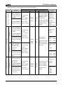
1
TC-580 Service Manual
Contents
Introduction...................................................................................................................... 1
Safety Information ........................................................................................................... 1
Radio Overview................................................................................................................ 2
Software Specifications .................................................................................................. 5
Circuit Description ........................................................................................................ 13
CPU Pins ........................................................................................................................ 21
TC-580 Parts List 1 ........................................................................................................ 25
Adjustment Description ................................................................................................ 40
Troubleshooting Flow Chart ......................................................................................... 50
Disassembly and Assembly for Repair........................................................................ 53
Exploded View ............................................................................................................... 56
TC-580 Parts List 2 ........................................................................................................ 57
Packing........................................................................................................................... 59
TC-580 PCB View ........................................................................................................... 60
TC-580 Level Diagram ................................................................................................... 62
TC-580 Block Diagram................................................................................................... 63
TC-580 Schematic Diagram .......................................................................................... 64
Specifications ................................................................................................................ 69
TC-580 Service Manual
Introduction
Manual Scope
This manual is intended for use by experienced technicians familiar with similar types of communication
equipment. It contains all service information required for the equipment and is current as of the
publication date.
Safety Information
The following safety precautions shall always be observed during operation, service and repair of this
equipment.
◇ This radio shall be serviced by qualified technicians only.
◇ Only use HYT supplied or approved batteries and chargers.
◇ To avoid electromagnetic interference and/or compatibility conflicts, turn off your radio in any
area where posted notices instruct you to do so. Turn off your radio before boarding an aircraft.
Any use of the radio must be in accordance with airline regulations or crew instructions.
◇ For vehicles with an air bag, do not place a radio in the area over an air bag or in the air bag
deployment area.
◇ Turn off your radio prior to entering any area with explosive and flammable materials.
◇ Do not charge or replace your battery in a location with explosive and flammable materials.
◇ Turn off your radio before entering a blasting area.
◇ Do not use any portable radio that has a damaged antenna. If a damaged antenna comes into
contact with your skin, a minor burn may result.
◇ Do not expose the radio to direct sunlight for a long time, nor place it close to a heating source.
◇ During transmission, hold the radio in a vertical position with its microphone 2.5 to 5.0
centimeters (1-2 inches) away from your lips, and keep the antenna at least 2.5 centimeters
(approximately 1 inch) away from your head. If you wear a portable radio on your body, ensure
that the antenna is at least 2.5 centimeters (approximately 1 inch) away from your body when
transmitting.
1
TC-580 Service Manual
Radio Overview
(1) Strap Hole
(2) Antenna
(3) PTT
(Push-to-Talk) Key
(4)SK1
(programmable)
(5)SK2 (programmable)
(6) LCD Display
(7) Function Keypad
(8) LED Indicator
(9) TK (programmable)
(10)Radio On-Off/Volume
Control Knob
(11) Microphone
(12) Speaker
(13) Accessory Jack
Cover
(14) Numeric Keypad
(15) Battery Latch
(16) Accessory
Jack
(17) Belt Clip
(18) Battery
(19) Charging Piece
﹡Function Keypad
y
OK key: to access a menu or to select an option.
y
DN key: to switch channels downwards during non-menu operation or to scroll options
downwards during menu operation.
y
UP key: to switch channels upwards during non-menu operation or to scroll options upwards
during menu operation.
y
C key: to return to the previous menu. Long press this key to return to the main menu.
2
TC-580 Service Manual
OK key
DN key
UP key
C key
﹡Numeric Keypad
Used to enter information for programming the radio.
y
y
-
: Used to enter numbers or characters.
: Used to enter decimal points or characters. Press OK first and then
immediately to
lock/unlock the keypad.
y
: Used to enter characters.
﹡LED Indicator
Status indications and alert tones are shown in the table below:
Operations/Functions
LED Indications and Alert Tones
To enter Wired Clone mode:
Turn on the source radio with
SK1
held
down
for
approximately 2 seconds,
and turn on the target radio
directly.
Wired Clone
Status of the source radio in
Wired Clone mode
(After the target radio is
turned on and the cloning
cable is connected, press
PTT of the source radio to
begin cloning.)
Status of the target radio in
Wired Clone mode
The LED on the source radio flashes red once
upon power-on.
The LED glows red during cloning process.
The LED flashes orange upon cloning errors.
(Press OK, and then the orange LED goes out.
Press PTT to restart cloning.)
The LED solidly glows orange once cloning is
completed.
The LED glows green during cloning process.
The green LED goes out once cloning is
completed.
3
TC-580 Service Manual
Power On (to enter User Mode)
The LED flashes green once and the power-on
alert tone sounds.
Low Battery Alert
The LED flashes red, and a low-pitched tone
sounds every 10 (programmable) seconds.
Transmitting
The LED glows red during transmitting.
When TOT timer expires, the radio sounds beep
tones continuously.
A TOT pre-alert tone sounds before the TOT timer
expires.
Receiving
The LED glows green during receiving.
Scanning
The LED flashes green during scanning.
Scan Start Alert (programmable by the dealer):
one beep is heard.
Scan End Alert (programmable by your dealer):
two continuous beeps are heard.
Writing/Reading
The LED glows red when reading data.
The LED glows green when writing data.
When a call is transmitted (within the Auto
Reset Time)
The LED solidly glows orange.
When a call is received
The LED rapidly flashes orange.
When an individual call is received (within
the Auto Reset Time)
The orange LED gives indication by means of
double flash.
When a group call is received (within the
Auto Reset Time)
The LED flashes orange.
Adjusting TX items
The LED solidly glows red.
Adjusting RX items
The LED solidly glows green.
4
TC-580 Service Manual
Software Specifications
Description of Features
1.
256 available channels
2.
32 available zones
3.
High /Low power switchable
4.
5 selectable VOX sensitivity levels
5.
Channel Scan
6.
Bandwidth Switch
7.
Home Channel
8.
Time-out Timer (TOT)
9.
Busy Channel Lockout (transmission prohibited in busy status)
10. 9 selectable squelch levels
11. Monitor
12. Compandor
13. Scrambler
14. Whisper
15. CTCSS/CDCSS Encode & Decode (CTCSS Tail Revert of 180/120 degrees, supporting
non-standard CTCSS/CDCSS)
16. DTMF Decode
17. Manual Frequency Input
18. Keypad Lock
19. Menu Edit
20. Channel Set Mode
21. Channel Alias Display
22. Reverse Display
23. Incoming-call Display
24. PC Programming
25. Wired Clone
26. Manual Adjust
27. Battery Strength Indicator
5
TC-580 Service Manual
28. Low Battery Alert
29. Battery Save
30. Power-on Password
31. Reset: to restore factory settings
32. Emergency Alarm
33. Software Update
Description of Modes
User Mode
It is a conventional communication mode. After the radio is turned on, it enters the User mode.
PC Programming Mode
The radio in User mode enters PC Programming mode through specific protocol based communication
with the programming software. In this mode, radio functions and adjustment parameters can be set
through the programming software (including User Version and Factory Version).
Reset Mode
You can restore the settings, which may affect normal operation, to factory defaults in this mode. The
factory default settings include radio parameters, as well as 8 channel frequencies and other
channel-related parameters.
If your radio is programmed with this function, you can enable it by pressing PTT, SK1 and SK2 for 2
seconds while powering on the radio.
Channel Set Mode
You can edit parameters on the current channel through menu operation and keypad input. Once the
Channel Set mode is entered, you can select and edit parameters like TX/RX frequency,
CTCSS/CDCSS, channel spacing, power level and so on, through the menu. Such settings are mainly
made through the menu. Some of these parameters can only be selected from the drop-down list (like
Wide/Narrow channel spacing, and High/Low power level) and some can be input through numeric
keys (like TX/RX frequency).
Press and hold down PTT and SK2 for 2 seconds while powering on the radio to enter the Channel Set
mode. See the structure illustrated below:
6
TC-580 Service Manual
After the Channel Set mode is entered, you will be required to input the channel number for further
menu operation.
Level-1 Menu
(Displayed
Content)
CH n
RX Freq
Level-2 Menu
(Displayed
Content)
RX Freq
350.00000
Description for Level-2 Menu
Displays the RX frequency. Press OK to edit.
7
TC-580 Service Manual
CH n
TX Freq
CH n
Option Items
CH n
RX CTC/CDC
CH n
TX CTC/CDC
TX Freq
350.00000
Displays the TX frequency. Press OK to edit.
Option Items
CH Space
Sets the spacing of the current channel.
Option Items
Power Level
Sets the power level of the current channel.
Option Items
Whisper
Sets the whisper feature on the current channel.
Option Items
Compandor
Sets the compandor feature on the current
channel.
Option Items
Scrambler
Sets the scrambler feature on the current
channel.
RX CTC/CDC
CTC/CDC None
Sets not to receive CTCSS/CDCSS on the
current channel.
RX CTC/CDC
CTC
Displays the RX CTCSS on the current channel.
RX CTC/CDC
Normal CDC
Displays the RX CDCSS on the current channel.
RX CTC/CDC
Invert CDC
Displays the RX CDCSS on the current channel.
TX CTC/CDC
CTC/CDC None
Sets not to transmit CTCSS/CDCSS on the
current channel.
TX CTC/CDC
CTC
Displays the TX CTCSS on the current channel.
TX CTC/CDC
Normal CDC
Displays the TX CDCSS on the current channel.
TX CTC/CDC
Invert CDC
Displays the TX CDCSS on the current channel.
Press OK to edit it.
Press OK to edit it.
Press OK to edit it.
Press OK to edit it.
Press OK to edit it.
Press OK to edit it.
Wired Clone Mode
1.
Description
Wired Clone mode is an independent mode. To access other modes, you must restart the radio.
Wired Clone mode includes Clone mode and Factory Clone mode.
1) Clone Mode:
Connect two radios using a cloning cable. Then press and hold down SK1 for 2 seconds while
powering the source radio on, and the radio enters Clone mode. The target radio can be directly
turned on to enter the mode. In this mode, data stored in EEPROM of the source radio will be cloned
to EEPROM of the target radio. The data transferred only covers channel data and common
parameters, excluding adjustment data, version and serial No. of the model.
2) Factory Clone Mode:
8
TC-580 Service Manual
Connect two radios using a clone cable. Then hold down SK1 for 2 seconds while powering the
source radio on, and the radio enters Clone mode; press the SK2 afterwards to switch to Factory
Clone mode. The target radio can be directly turned on to enter the Clone mode. The data transferred
covers all data in EEPROM other than serial No, with flag of manual adjustment switch included.
2.
Process
Process of Wired Clone:
1) The LED flashes red once after the source radio enters Wired Clone mode. Press PTT to begin to
clone data to the target radio.
2) During cloning, LED of the source radio solidly glows red, and LED of the target radio solidly glows
green. When cloning ends, LED of the source radio solidly glows orange, while LED of the target
radio goes out, and the target radio restarts automatically to prepare for a further clone.
3) If any abnormal situation occurs during cloning, the source radio will stop cloning and its orange
LED will flash, indicating both radios are ready for another cloning operation.
4) When cloning ends, the source radio goes back to standby status no matter whether the cloning is
successful. Press PTT again to begin another cloning operation.
Manual Tune Mode
Press and hold down PTT and SK1 on the radio for 2 seconds while powering it on, and the radio
enters Manual Tune mode. (Note: This operation is subject to the option Manual Tune Mode in the
programming software. If this option is unchecked, the radio can not enter this mode, which helps avoid
change of parameters and degradation of radio performance caused by user’s misoperations.)
Keep this option unchecked after values are well adjusted from factory, to avoid any unexpected
change of values. And re-adjust the values upon your further requirement. These values will remain in
other modes.
See the tuning items illustrated below:
9
TC-580 Service Manual
10
TC-580 Service Manual
1. To enter the Manual Tune mode
Hold down PTT and SK1 for 2 seconds while powering on the radio. Then the LCD displays
"Tuning Mode”, indicating that the Manual Tune mode has been entered. At this time, release the
keys.
2. To switch the tuning item
After the tuning mode is entered, switch the tuning item using UP or DN key. The LCD displays the
tuning item accordingly. The LED solidly glows red for the TX group items and glows green for the
RX group items.
3. To adjust the value
At a certain frequency, short press SK1 to increase the value in the step of 1; hold down the key to
increase the value continuously in steps of 1.
At a certain frequency, short press SK2 to decrease the value in the step of 1; hold down the key to
decrease the value continuously in steps of 1.
4. To save the value
After the value is set, press UP or DN to switch the frequency, or press OK to save the value.
5. To enter the selected item
Use UP or DN key to choose your desired tuning items, and press OK to enter the item.
6. To return to the previous menu
Short press C to return to the previous menu; and long press C to return to the first level menu.
7. Measures on special items
TX group items: Including the VOX Level 1-5 and TX Low Voltage Threshold. These tuning items
are related to AD sampling. Short press SK1 or SK2 after entering the above
items, to activate AD sampling (including calculation) once. Press UP or DN to
switch the frequency and press OK to save the current AD sampling value. If
neither of SK1 or SK2 is pressed, the tuning value will not be updated, and AD
sampling will not be activated.
Rx Group Items: Including the SQL On 1, SQL On 5, SQL On 9, SQL Off 1, SQL Off 5, SQL Off 9
and Rx Low Voltage Threshold. These tuning items are related to AD sampling.
Short press SK1 or SK2 after entering the above items, to activate AD sampling
(including calculation) once. Press UP or DN to switch the frequency and press
11
TC-580 Service Manual
OK to save the current AD sampling value. If neither of SK1 or SK2 is pressed,
the tuning value will not be updated, and AD sampling will not be activated.
8. Description of key-press
Short press: indicates to press the key for shorter than 1 second;
Long press: indicates to press the key for 1 second or more.
12
TC-580 Service Manual
Circuit Description
General Realization Method
TX Section: The audio signal from MIC is amplitude limited and amplified by U203. After that, the
signal feeds to the AGC circuit and then to the baseband processor U202 in AK2347, where the signal
is filtered, compressed, pre-emphasized and amplitude limited. The signal from AK2347 goes to VCO
for frequency modulation (the PLL system is composed of U101, Q100 and Q101). After modulated
onto the RF carrier, the signal is processed by the buffer amplifiers Q104 and Q106. Then the signal
passes through the TX/RX switch D401, and goes to the front-stage power amplifier for
pre-amplification. After that, the signal is further amplified by the driver amplifier Q402, for obtaining the
power to drive the final-stage amplifier. After the signal is amplified by the final-stage amplifier (Q403),
the signal with required power is generated. Then it passes through the TX/RX switch D403, and feeds
to the low-pass filter circuit. Finally, the signal is transmitted via the antenna after high-order harmonics
are removed (The TX/RX switch circuit is composed of D401, D511, D403, D501 and D502).)
RX Section: The RF signal from the antenna passes through the low-pass filter, and then feeds to the
bandpass filter (composed of D514, D515 and D516) to filter out undesired out-of-band interference
signal. Then the desired RF signal enters the high-frequency low-noise amplifier Q501, where it is
amplified. The amplified signal goes to the bandpass filter (composed of D509, D510 and D513) to filter
out out-of-band interference signal again. The desired RF signal is mixed with the first local oscillator
signal from VCO at Q502. The newly generated signal is processed by the crystal filter (Z1, Z2 or
XF501) to generate the first IF signal.
After amplified at Q505, the first IF signal goes to the IF
modulator (U201), where it is mixed with the second local oscillator signal from X101 to generate the
second IF signal (it is filtered by CF201). Then U201 demodulates the second IF signal, and outputs
audio signal, which is divided into two flows and sent to the baseband processor U202 in AK2347. One
flow of audio signal is amplified, and then goes to the low-pass filter to filter out high-frequency audio
signal (CTCSS/CDCSS signal is kept). The CTCSS/CDCSS signal is sent to MCU (U611) for decoding.
The other flow of audio signal is filtered, de-emphasized and expanded, and then is sent to the audio
amplifier (U205), where the audio power of the signal is amplified to drive the speaker directly.
Power Supply Section: The 7.4V battery voltage goes to the LDO IC (U601), and generates 5V DC
voltage, which is divided into two flows. One flow is converted into 4.5V voltage via the dual LDO IC
(U602) (under the control of MCU, one flow (4.5T) supplies power for the TX circuit; one flow (V_SAVE)
13
TC-580 Service Manual
supplies power for VCO; under the control of 4.5T, V_SAVE is converted to 4.5R via Q604); the other
flow goes to the dual LDO IC (U603), and generates two flows of 3V voltage (3M1 and 3M2), supplying
power for MCU/LCD and PLL/U202(AK2347) respectively.
Signaling Encoding: MCU (U611) generates two flows of CTCSS/CDCSS. One flow is output via the RC
network, and is sent to VCO together with the audio signal for modulation. The other flow goes through
the RC network to modulate the PLL reference frequency oscillator. The signal amplitude of the two
flows can be adjusted separately.
Realization Methods of Basic Functional Modules
1 HF Section
1) Block Diagram of PLL Circuit:
PLL System
CTC/DCS
LD
PLL_CLK
PLL_DATA
PLL_EN
VRCR
TCXO 21.25M
T/R
Q103
T/R
U101
Synthesizer
MB15E03
Loop Filter
V_R
Q101
RX
VCO
Ripple
Restraint
TX/RX
VCO_BUF
2SC5108
BUF_AMP
2SC5108
TX
Q104
Q106
MIXER
CTC/DCS
V_T
Figure 1.1
Q100
TX
VCO
Block Diagram of PLL and VCO
The PLL circuit generates RF carrier signal for TX and the first local oscillator signal for
RX.
PLL: The step frequency of the PLL circuit is 5.0KHz, 6.25KHz, 10.0KHz or 12.5KHz. In U101, the
21.25MHz reference oscillator signal is divided into 5.0KHz, 6.25 KHz, 10.0 KHz or 12.5 KHz
reference frequencies via a fixed counter in PLL. The signal output from the VCO (TX VCO/RX
VCO) is processed by the buffer amplifier Q104, and then enters PLL, where it is further processed
by the variable frequency-divider. Then the signal is compared with the reference frequency in the
phase detector (PD) of PLL. The signal from PD passes through a low-pass filter, and then is sent
to the varactors of VCO so as to control its output frequency.
14
TC-580 Service Manual
VCO: There is a TX VCO and a RX VCO. In TX mode, PLL generates a control voltage via
the phase detector and the low-pass filter (LOOP FILTER) to control the varactor, making
TX VCO generate the RF carrier signal consistent with the preset frequency of MCU. The
modulation signal from U202 (AK2347) and MCU is modulated onto the RF carrier via
D108. Then the signal is processed by the buffer amplifier, and is sent to the RF power
amplifier circuit for power amplification. In RX mode, RX PLL generates a control voltage
via the phase detector and the low-pass filter (LOOP FILTER) to control the varactor,
making RX VCO generate the first local oscillator signal consistent with the preset
frequency of MCU. Then the signal is mixed with the received RF signal at Q502, and the
first IF signal is therefore generated.
Unlock Detector: If the LD pin of U101 is at low level, unlock status is valid. When this
status is detected by the microprocessor, neither transmission nor reception can be made,
and the unlock alarm sounds.
2) Block Diagram of The RF Power Amplifier Circuit:
VCO_BUF
2SC5108
VCO_OUT
Q104
BUF_AMP
2SC5108
TX/RX
PLL_RF_IN
Q106
PRE_AMP
2SC4988
Q401
DRV_AMP
RD01
Q402
Q403
ANT
ANT_SW
1st Lo
APC
Figure 1.2
Final_AMP
RQA0002
APC
Harmonic_LPF
TX/RX
Block Diagram of TX RF Circuit
The modulated carrier signal is processed by the front-stage amplifier Q401 and by the
driver amplifier Q402, for obtaining the power to drive the final-stage amplifier. Then the
RF signal is further amplified by the final-stage amplifier Q403, for obtaining required
power. The amplified RF signal passes through D403, and goes to the LC low-pass filter
circuit (LPF). Finally the signal is transmitted via the antenna after high-order harmonics
are removed in LPF.
The APC circuit is composed of U401, Q405 and Q404. U401 controls the bias voltage at
the gates of Q402 and Q403, so as to control the TX current and to further regulate power.
15
TC-580 Service Manual
3) Block Diagram of RX Low-noise Amplifier and The First Mixer Circuit:
ANT
ANT_SW
Harmonic_LPF
XF501
Crystal Filter
21.7M
Varactor
Tuned Filter
Varactor
Tuned Filter
Q503
Q501
Figure 1.3
LNA
AT41511
TU
Q502
MIXER
3SK318
TU
IF_AMP
2SC5108
1ST LO
TX/RX
Block Diagram of RX RF Circuit
Desired and undesired RF signals received via the antenna feed to the band-pass filter to
filter out undesired out-of-band interference signal. Then the desired RF signal is
amplified by the high-frequency low-noise amplifier Q501. Afterwards, the amplified signal
goes through the bandpass filter again to filter out undesired out-of-band interference
signal. The desired RF signal is mixed with the first local oscillator signal from VCO at Q502.
The MCU outputs through APC/TU pin a voltage, which controls the central frequency of
the electrically tunable bandpass filter.
2. IF Processing and Audio Demodulation
Narrow Band
Ceramic Filter 2nd
Crystal Filter
LO
Z1,Z2 or XF501
IF_AMP
2SC5108
RSSI
21.7M
MIX OUT
Detector
U201
TA31136
AF_DET
Q503
N-DET
Figure 1.4
Block Diagram of IF Processing
16
TC-580 Service Manual
The newly generated signal at Q501 is processed by the crystal filter (Z1, Z2 or XF501) to generate the
first IF signal (21.7MHz). After amplified by Q505, this IF signal enters the IF demodulator U201, where
it will be mixed with the second local oscillator signal to generate the second IF signal (450KHz). Then
U201 demodulates this second IF signal and outputs an audio signal which will be sent to AK2347.
3. MCU Control, Signal Processing and Audio Power Amplification
Circuit diagram of this section is shown as below:
ALARM
PTT
SK1
SK2
BEEP
LCD
CSTN
KEY PAD
4*4
E2PROM
PLL_CLK
PLL_DATA
PLL_EN
TTS_DET
LED_GREEN
LED RED
TTS_IN
CTC/DCS_DET
DTMF_DET
APC/TU
U611
CPU
CTC_IN
DTMF_IN
SAVE
W/N
TX/RX
STM32F100
DTMF/TTS
T/R
DTMF/TTS_OUT
Noise Detect
Reset
Xin
Xout
APA_EN
CTC/DCS_OUT
VRCR
CTC/DCS
RSSI
VOX
LED_GREEN
LED_RED
APC/TU
SAVE
W/N
TX/RX
T/R
RSSI
N-DET
VOX_DET
TXD
RXD
VRCR
9.8304M
APA_EN
VDD
R2
R
AK2347
Figure 1.5
POWER_CTRL
C2
C
Block Diagram of MCU Control Circuit
1) MCU Control Circuit
MCU control circuit is composed of MCU, EEPROM, keys and etc. This section has the
following functions: to initialize data of the radio and save data to EEPROM; to check the
battery voltage and signals from external keys, LD and VOX-DET, and make responses; to
transmit required data to PLL; to switch and control RX/TX status based on the input PTT
signal; to switch the squelch circuit on or off based on the input signaling decode signal
and squelch level signal; to control circuits of high/low power switch, audio power
amplification, VCO power supply, RX power supply and TX power supply; (for
programming) to communicate with PC via RXD/TXD, and transmit data to or receive data
from PC.
17
TC-580 Service Manual
2) Signal Processing Circuit
VOX_AMP
VOX
CTC/DCS
VOX_DET
MOD_VCO
U203
NJM2904
Audio & Sub-Audio Processor
AGC
DTMF/TTS
MIC
MIC_AMP
TDA2822
U202
AK2347
AF_DET
U205
S201
Speaker
CTC/DCS_DET
DTMF_DET
APA_EN
Q205
OPTIONAL
U204 NJM2904
BEEP
TTS_DET
Figure 1.6
a.
Block Diagram of Baseband Processing
TX Baseband Processing
The modulation signal from MIC is amplitude limited and amplified by U204. Afterwards, the signal
feeds to the AGC circuit and then to the baseband processor U202 in AK2347, where it is filtered,
compressed, pre-emphasized and amplitude limited. Then the modulated signal enters VCO for
direct frequency modulation.
b.
Rx Baseband Processing
The DEMOD signal derived from IF demodulation has two flows after entering U202 in AK2347.
One flow of audio signal is amplified, and then goes to the low-pass filter to filter out high-frequency
audio signal and to reserve the CTCSS/CDCSS signal; then the reserved CTCSS/CDCSS signal is
sent to MCU (U611) for decoding. The other flow of audio signal is filtered, de-emphasized and
expanded, and then is sent to the audio power amplifier (U205).
c.
Audio Power Amplification
The audio signal output from U202 in AK2347 goes through the volume control switch, and it is then
amplified by the audio power amplifier (U205) to drive the speaker directly.
18
TC-580 Service Manual
4. Power Supply Processing
Block diagram of power supply circuit is shown as below:
Power Supply
5V
U601
XC6201P
U603
XC6401FF
LCD_3M1
MCU_3M1
AK2347_3M2
PLL_3M2
7.4V
U602
XC6401FF
POWER_CTRL
Figure 1.7
VR_4.5V
VP_4.5V
VT_4.5V
VCO_4.5V
Block Diagram of Power Supply Circuit
Power Supply Section: The 7.4V battery voltage goes to the LDO U601 and generates a 5V DC voltage,
which is divided into two flows. One flow is converted into a 4.5V DC voltage via the dual LCO IC (U602)
and supplies the TX, RX and VCO circuits. The other flow goes through U603 and generates a 3V
voltage to supply the MCU, EEPROM, LCD, PLL, and U202 (AK2347) etc.
5. Keypad and LCD
Figure 1.8
Diagram of LCD and Keypad
19
TC-580 Service Manual
Figure 1.9
Block Diagram of Display Circuit
The radio adopts a LCD of 128*32 pixels, and a keypad of 16 keys which includes 4 function keys and
12 numeric keys. The display circuit is composed of MCU (U611), LCD module, 16-key keypad, LED
and other components. The backlight enable pin LCD_BL is controlled by MCU. When it is set to H, the
backlight will be turned on.
20
TC-580 Service Manual
CPU Pins
Pin
No.
Port
Pin Name
I/O
Function
Controls the LCD backlight.
1
PE2
LCD_BLT
O
2
PE3
Reserved
O
Reserved
3
PE4
EXT_PTT
I
PTT key on the earpiece (valid at high level)
4
PE5
VSAVE_CTR
L
O
5
PE6
TX_CTRL
O
H: On.
Controls the power in Battery Save mode.
H: On; L: Off.
Controls the TX power.
H: On; L: Off.
Provides a power-off protection interface
6
VABT
(temporarily not valid); however, a 100nF ceramic
capacitor is required to be connected to VDD.
7
PC13-ANTI_TAMP
Reserved
O
Reserved
8
PC14-OSC32_IN
Reserved
O
Reserved
9
PC15-OSC32_OUT
Reserved
O
Reserved
10
VSS_5
GND
11
VDD_5
VCC
12
OSC_IN
OSC_IN
I
For 9.8304MHz main crystal oscillator
13
OSC_OUT
OSC_OUT
O
Green LED
14
NRST
RESET
I
Reset pin (valid at low level)
15
PC0/ADC_IN10
RSSI_DET
AD
Detects signal strength.
16
PC1/ADC_IN11
Reserved
O
Reserved
17
PC2/ADC_IN12
VOX_DET
AD
Provides VOX detection (to detect voice signals)
18
PC3/ADC_IN13
CTC_DCS_IN
AD
Inputs CTCSS/CDCSS
19
VSSA
Analog ground
20
VREF-
Must be connected to VSSA.
21
VREF+
ADC reference voltage
22
VDDA
VDDA
23
PA0_WKUP/USART
2_CTS/ADC_IN0/TI
M2_CH1_ETR
CTC_DCS_V
CO
P
W
M
Outputs CTCSS/CDCSS to VCO.
24
PA1/USART2_RTS/
ADC_IN1/TIM2_CH2
CTC_DCS_P
LL
P
W
M
Outputs CTCSS/CDCSS to PLL.
25
PA2/USART2_TX/A
DC_IN2/TIM2_CH3
BEEP_OUT
P
W
M
Outputs audio signals of BEEP.
26
PA3/USART2_RX/A
DC_IN3/TIM2_CH4
DTMFO/TTS
O/MSKO
P
W
M
27
VSS_4
GND
28
VDD_4
VCC
Outputs DTMF, 2-TONE, MSK and Emergency
tone.
21
TC-580 Service Manual
29
PA4/DAC_OUT1/SPI
1_NSS/USART2_CK
/ADC_IN4
APC/TU
DA
For automatic power control/ tune voltage
30
PA5/SPI1_SCK/DAC
_OUT2/ADC_IN5
VRCR
DA
Adjusts tolerance of carrier frequencies.
31
PA6/SPI1_MISO/AD
C_IN6/TIM3_CH1
BEEP_MUTE
O
32
PA7/SPI1_MOSI/AD
C_IN7/TIM3_CH2
Reserved
O
Reserved
33
PC4/ADC_IN14
SQL_DET
AD
Detects carrier signals.
34
PC5/ADC_IN15
BAT_DET
AD
Detects battery voltage.
35
PB0/ADC_IN8/TIM3
_CH3
DTMFI/MSKI
AD
Input pin for DTMF/MSK decoding
36
PB1/ADC_IN9/TIM3
_CH4
Reserved
O
Reserved
37
PB2 / BOOT1
BOOT1
I
Input the low level.
38
PE7
Reserved
O
Reserved
39
PE8
PTT
I
PTT key (valid at low level)
40
PE9
SK1
I
41
PE10
SK2
I
42
PE11
TK
I
Emergency Key (valid at low level)
43
PE12
PLL_EN
O
MB15E03SL PLL ENABLE
44
PE13
LD
I
Detects PLL circuit unlock (H: Lock; L: Unlock).
45
PE14
AK2347_CSN
O
Enables Ak2347 serial data.
46
PE15
MIC_CTRL
O
Switches the MIC on or off (H: Off; L: On).
47
PB10/I2C2_SCL/US
ART3_TX
Reserved
O
Reserved
48
PB11/I2C2_SDA/US
ART3_RX
Reserved
O
Reserved
49
VSS_1
GND
50
VDD_1
VCC
51
PB12/SPI2_NSS
/I2C2_SMBAl/USAR
T3_CK
Reserved
O
Reserved
52
PB13/SPI2_SCK
/USART3_CTS
LCD_SCL
O
Serial Port: inputs LCD Clock.
53
PB14/SPI2_MISO
/USART3_RTS
Reserved
O
Reserved
54
PB15/SPI2_MOSI
LCD_SDI
O
Serial Port: inputs LCD serial data.
55
PD8
OPT_SEL_2
O
Reserved
56
PD9
OPT_SEL_1
I
Detects external earpiece (valid at high level).
57
PD10
APA_EN
O
Controls the power for audio PA (H: On; L: Off).
Controls the TX modulation circuit for BEEP (L:
Off; H: On).
Programmable function key (SK1) (valid at low
level)
Programmable function key (SK2) (valid at low
level)
22
TC-580 Service Manual
Clock signal for MB15E03SL PLL clock/ AK2347
58
PD11
COM_SCLK
O
59
PD12
COM_DATA
O
60
PD13
GLED
O
Green LED (H: On)
61
PD14
RLED
O
Red LED (H: On)
62
PD15
LCD_RS
O
Displays data or options.
63
PC6
LCD_RSTB
O
64
PC7
T/R
O
Controls the RF TX/RX switch (H: RX; L: TX).
65
PC8
EEP_SCLK
I/O
EEPROM Clock
66
PC9
EEP_SDA
I/O
EEPROM Data
67
PA8/USART1_CK
/MCO
Reserved
O
Reserved
68
PA9/USART1_TX/
UART1_TX
O
UART TxD
69
PA10/USART1_RX
UART1_RX
I
UART RxD
70
PA11
USART1_CTS
/
Reserved
O
Reserved
71
PA12
USART1_RTS/
/
Reserved
O
Reserved
72
PA13/JTMS/SWDIO
73
Not connected
74
VSS_2
GND
75
VDD_2
VCC
76
PA14/JTCK/SWCLK
JTCK/SWCLK
Can not remain open during adjustment.
77
PA15/JTDI
JTDI
Can not remain open during adjustment.
78
PC10
KEY_IN4
I
79
PC11
KEY_IN3
I
80
PC12
KEY_IN2
I
81
PD0
KEY_IN1
I
82
PD1
KEY_OUT4
O
83
PD2/TIM3_ETR
KEY_OUT3
O
84
PD3
KEY_OUT2
O
85
PD4
KEY_OUT1
O
86
PD5
Reserved
O
87
PD6
Reserved
Reserved
88
PD7
Reserved
Reserved
89
PB3/JTDO/TRACES
WO
JTDO
Can not remain open during adjustment.
90
PB4/JNTRST
JNTRST
Can not remain open during adjustment.
91
PB5/I2C1_SMBAl
Reserved
Reserved
92
PB6/I2C1_SCL/TIM4
_CH1
Reserved
Reserved
93
PB7/I2C1_SDA/TIM
4_CH2
TTSI
clock.
Data cable for MB15E03SL PLL data/ AK2347
data.
Reset Input Pin
When RSTB is set to L, initialization begins.
JTMS/SWDIO
Can not remain open during adjustment.
Input pin for key matrix scan
Output pin for key matrix scan
Reserved
TRG
23
Inputs 2-Tone.
TC-580 Service Manual
94
BOOT0
BOOT0
I
95
PB8/TIM4_CH3
Reserved
Reserved
96
PB9/TIM4_CH4
Reserved
Reserved
97
PE0/TIM4_ETR
Reserved
Reserved
98
PE1
W/N
99
VSS_3
GND
100
VDD_3
VCC
Input the low level.
Controls the channel spacing between wide and
O
narrow (L: Narrow; H: Wide.).
24
TC-580 Service Manual
TC-580 Parts List 1
TC-580 (350-390MHz) Parts List 1
No.
Part No.
Description
1 41005801000C0 PCB Board FR4 6L 4P 108.29*46.31*1.20mm C (RoHS)
Qty. Ref No. Print No.
1
PCB
2
3801045030130 Ceramic Filter 450KHz±6.0KHz 450F (RoHS)
1
CF201
T2H
3
3099080398000 Chip Resistor 1206 0.39Ω J 1/4W (RoHS)
1
R429
B3C
4
3099080398000 Chip Resistor 1206 0.39Ω J 1/4W (RoHS)
1
R430
B3C
5
3099080398000 Chip Resistor 1206 0.39Ω J 1/4W (RoHS)
1
R431
B3C
6
3001052790000 Chip Resistor 0402 2.7Ω J 1/16W (RoHS)
1
R506
T4D
7
3001054790000 Chip Resistor 0402 4.7Ω J 1/16W (RoHS)
1
R269
B2B
8
3001054790000 Chip Resistor 0402 4.7Ω J 1/16W (RoHS)
1
R271
B1B
9
3001051000020 Chip Resistor 0402 10Ω F 1/16W (RoHS)
1
R121
T5F
10
3001051000020 Chip Resistor 0402 10Ω F 1/16W (RoHS)
1
R126
T4F
11
3001051000020 Chip Resistor 0402 10Ω F 1/16W (RoHS)
1
R133
T3E
12
3001051000020 Chip Resistor 0402 10Ω F 1/16W (RoHS)
1
R237
B2A
13
3001051000020 Chip Resistor 0402 10Ω F 1/16W (RoHS)
1
R251
T2H
14
3001051000020 Chip Resistor 0402 10Ω F 1/16W (RoHS)
1
R268
B2B
15
3001051000020 Chip Resistor 0402 10Ω F 1/16W (RoHS)
1
R404
T5E
16
3001054700000 Chip Resistor 0402 47Ω J 1/16W (RoHS)
1
R407
T5D
17
3001054700000 Chip Resistor 0402 47Ω J 1/16W (RoHS)
1
R411
T5C
18
3001056810000 Chip Resistor 0402 680Ω J 1/16W (RoHS)
1
R644
B4D
19
3001056810000 Chip Resistor 0402 680Ω J 1/16W (RoHS)
1
R649
B4D
20
3001055600000 Chip Resistor 0402 56Ω J 1/16W (RoHS)
1
R106
T4F
21
3001055100020 Chip Resistor 0402 51Ω J 1/16W (RoHS)
1
R107
T4F
22
3001051010000 Chip Resistor 0402 100Ω J 1/16W (RoHS)
1
R112
T4E
23
3001051010000 Chip Resistor 0402 100Ω J 1/16W (RoHS)
1
R514
T1E
24
3001055110000 Chip Resistor 0402 510Ω J 1/16W (RoHS)
1
R518
T4D
25
3001051010000 Chip Resistor 0402 100Ω J 1/16W (RoHS)
1
R521
T1E
26
3001051010000 Chip Resistor 0402 100Ω J 1/16W (RoHS)
1
R535
T1G
27
3001051010000 Chip Resistor 0402 100Ω J 1/16W (RoHS)
1
R643
B3C
28
3001051010000 Chip Resistor 0402 100Ω J 1/16W (RoHS)
1
R670
B4D
29
3001061010000 Chip Resistor 0603 100Ω J 1/10W (RoHS)
1
R415
T3B
30
3001051510000 Chip Resistor 0402 150Ω J 1/16W (RoHS)
1
R131
T3E
31
3001062710000 Chip Resistor 0603 270Ω J 1/10W (RoHS)
1
R706
B3A
32
3001053310010 Chip Resistor 0402 330Ω J 1/16W (RoHS)
1
R405
T4E
33
3001053310010 Chip Resistor 0402 330Ω J 1/16W (RoHS)
1
R513
T1E
34
3001063910000 Chip Resistor 0603 390Ω J 1/10W (RoHS)
1
R729
B2E
35
3001063910000 Chip Resistor 0603 390Ω J 1/10W (RoHS)
1
R730
B2E
36
3001063910000 Chip Resistor 0603 390Ω J 1/10W (RoHS)
1
R731
B1E
37
3001055620000 Chip Resistor 0402 5.6KJ 1/16W (RoHS)
1
R200
B1A
38
3001055610000 Chip Resistor 0402 560Ω J 1/16W (RoHS)
1
R100
T4G
39
3001055610000 Chip Resistor 0402 560Ω J 1/16W (RoHS)
1
R516
T1F
40
3001055610000 Chip Resistor 0402 560Ω J 1/16W (RoHS)
1
R517
T1G
41
3001056810000 Chip Resistor 0402 680Ω J 1/16W (RoHS)
1
R632
B2A
42
3001058210000 Chip Resistor 0402 820Ω J 1/16W (RoHS)
1
R402
T4E
43
3101051030020 Chip Capacitor 0.01UF K 25V 0402 (RoHS)
1
C243
T2G
25
TC-580 Service Manual
44
3101051030020 Chip Capacitor 0.01UF K 25V 0402 (RoHS)
1
C262
B1A
45
3101051030020 Chip Capacitor 0.01UF K 25V 0402 (RoHS)
1
C276
B1A
46
3101051030020 Chip Capacitor 0.01UF K 25V 0402 (RoHS)
1
C414
T4B
47
3101051030020 Chip Capacitor 0.01UF K 25V 0402 (RoHS)
1
C439
B4C
48
3101051030020 Chip Capacitor 0.01UF K 25V 0402 (RoHS)
1
C538
T1E
49
3101051030020 Chip Capacitor 0.01UF K 25V 0402 (RoHS)
1
C539
T1E
50
3101051030020 Chip Capacitor 0.01UF K 25V 0402 (RoHS)
1
C543
T1F
51
3101051030020 Chip Capacitor 0.01UF K 25V 0402 (RoHS)
1
C547
T1G
52
3101051030020 Chip Capacitor 0.01UF K 25V 0402 (RoHS)
1
C558
T1G
53
3101051030020 Chip Capacitor 0.01UF K 25V 0402 (RoHS)
1
C623
B2D
54
3101051030020 Chip Capacitor 0.01UF K 25V 0402 (RoHS)
1
C673
B2D
55
3101051030020 Chip Capacitor 0.01UF K 25V 0402 (RoHS)
1
C678
B2D
56
3101051030020 Chip Capacitor 0.01UF K 25V 0402 (RoHS)
1
C681
B2C
57
3101051030020 Chip Capacitor 0.01UF K 25V 0402 (RoHS)
1
C684
B2C
58
3101051030020 Chip Capacitor 0.01UF K 25V 0402 (RoHS)
1
C686
B3C
59
3101052230000 Chip Capacitor 0402 0.022UF K 16V (RoHS)
1
C157
T5H
60
3101051050000 Chip Capacitor 0402 1UF K 16V (RoHS)
1
C266
T3G
61
3101052230000 Chip Capacitor 0402 0.022UF K 16V (RoHS)
1
C672
B1D
62
3101052230000 Chip Capacitor 0402 0.022UF K 16V (RoHS)
1
C676
B1D
63
3101052230000 Chip Capacitor 0402 0.022UF K 16V (RoHS)
1
C707
B3A
64
3101072240000 Chip Capacitor 0.22UF K 25V 0805 (RoHS)
1
C102
T3G
65
3101053330000 Chip Capacitor 0402 0.033UF K 16V (RoHS)
1
C158
T5H
66
3101053330000 Chip Capacitor 0402 0.033UF K 16V (RoHS)
1
C273
T3I
67
3101053330000 Chip Capacitor 0402 0.033UF K 16V (RoHS)
1
C274
T4I
68
3101051040060 Chip Capacitor 0.1UF K 16V 0402 (RoHS)
1
C118
T5F
69
3101051040060 Chip Capacitor 0.1UF K 16V 0402 (RoHS)
1
C119
T4F
70
3101051040060 Chip Capacitor 0.1UF K 16V 0402 (RoHS)
1
C133
T4G
71
3101051040060 Chip Capacitor 0.1UF K 16V 0402 (RoHS)
1
C141
T4H
72
3101051040060 Chip Capacitor 0.1UF K 16V 0402 (RoHS)
1
C145
T5H
73
3101051040060 Chip Capacitor 0.1UF K 16V 0402 (RoHS)
1
C151
T5F
74
3101051040060 Chip Capacitor 0.1UF K 16V 0402 (RoHS)
1
C172
T3F
75
3101051040060 Chip Capacitor 0.1UF K 16V 0402 (RoHS)
1
C207
T3I
76
3101051040060 Chip Capacitor 0.1UF K 16V 0402 (RoHS)
1
C210
T2I
77
3101051040060 Chip Capacitor 0.1UF K 16V 0402 (RoHS)
1
C211
T2I
78
3101051040060 Chip Capacitor 0.1UF K 16V 0402 (RoHS)
1
C216
B1E
79
3101051040060 Chip Capacitor 0.1UF K 16V 0402 (RoHS)
1
C222
T2I
80
3101051040060 Chip Capacitor 0.1UF K 16V 0402 (RoHS)
1
C242
T2G
81
3101051040060 Chip Capacitor 0.1UF K 16V 0402 (RoHS)
1
C252
T2H
82
3101051040060 Chip Capacitor 0.1UF K 16V 0402 (RoHS)
1
C257
B2B
83
3101051040060 Chip Capacitor 0.1UF K 16V 0402 (RoHS)
1
C259
B2B
84
3101051040060 Chip Capacitor 0.1UF K 16V 0402 (RoHS)
1
C261
B2B
85
3101051040060 Chip Capacitor 0.1UF K 16V 0402 (RoHS)
1
C264
T3H
86
3101051040060 Chip Capacitor 0.1UF K 16V 0402 (RoHS)
1
C269
B2C
87
3101051040060 Chip Capacitor 0.1UF K 16V 0402 (RoHS)
1
C272
B1B
88
3101051040060 Chip Capacitor 0.1UF K 16V 0402 (RoHS)
1
C277
B2E
89
3101051040060 Chip Capacitor 0.1UF K 16V 0402 (RoHS)
1
C280
T2H
90
3101051040060 Chip Capacitor 0.1UF K 16V 0402 (RoHS)
1
C281
T2H
26
TC-580 Service Manual
91
3101051040060 Chip Capacitor 0.1UF K 16V 0402 (RoHS)
1
C407
T5D
92
3101051040060 Chip Capacitor 0.1UF K 16V 0402 (RoHS)
1
C413
T4B
93
3101051040060 Chip Capacitor 0.1UF K 16V 0402 (RoHS)
1
C435
B4D
94
3101051040060 Chip Capacitor 0.1UF K 16V 0402 (RoHS)
1
C440
B4C
95
3101051040060 Chip Capacitor 0.1UF K 16V 0402 (RoHS)
1
C514
T4D
96
3101051040060 Chip Capacitor 0.1UF K 16V 0402 (RoHS)
1
C520
T4D
97
3101051040060 Chip Capacitor 0.1UF K 16V 0402 (RoHS)
1
C535
T1E
98
3101051040060 Chip Capacitor 0.1UF K 16V 0402 (RoHS)
1
C603
T2A
99
3101051040060 Chip Capacitor 0.1UF K 16V 0402 (RoHS)
1
C624
B5D
100 3101051040060 Chip Capacitor 0.1UF K 16V 0402 (RoHS)
1
C674
B2D
101 3101051040060 Chip Capacitor 0.1UF K 16V 0402 (RoHS)
1
C679
B2C
102 3101051040060 Chip Capacitor 0.1UF K 16V 0402 (RoHS)
1
C682
B2C
103 3104071040010 Tantalum Capacitor 0.1UF M 20V -55~+125℃ P (RoHS)
1
C100
T4G
104 3101050590020 Chip Capacitor 0402 0.5PF B 50V (RoHS)
1
C109
T5F
105 3101050590020 Chip Capacitor 0402 0.5PF B 50V (RoHS)
1
C116
T4F
106 3101050590020 Chip Capacitor 0402 0.5PF B 50V (RoHS)
1
C117
T4F
107 3001050000000 Chip Resistor 0402 0Ω J 1/16W (RoHS)
1
C412
T5D
108 3001050000000 Chip Resistor 0402 0Ω J 1/16W (RoHS)
1
R104
T3G
109 3001050000000 Chip Resistor 0402 0Ω J 1/16W (RoHS)
1
R220
T2I
110 3001050000000 Chip Resistor 0402 0Ω J 1/16W (RoHS)
1
R283
T3G
111 3001050000000 Chip Resistor 0402 0Ω J 1/16W (RoHS)
1
R406
T5E
112 3001050000000 Chip Resistor 0402 0Ω J 1/16W (RoHS)
1
R642
B2C
113 3001050000000 Chip Resistor 0402 0Ω J 1/16W (RoHS)
1
R712
B3A
114 3001060000000 Chip Resistor 0603 0Ω J 1/10W (RoHS)
1
R410
T5C
115 3001051220000 Chip Resistor 0402 1.2KΩ J 1/16W (RoHS)
1
R102
T4G
116 3001051020000 Chip Resistor 0402 1KΩ J 1/16W (RoHS)
1
R275
B2A
117 3001051520010 Chip Resistor 0402 1.5KΩ F 1/16W (RoHS)
1
R403
T4E
118 3001051520010 Chip Resistor 0402 1.5KΩ F 1/16W (RoHS)
1
R532
T2G
119 3001051820000 Chip Resistor 0402 1.8KΩ J 1/16W (RoHS)
1
R246
T1G
120 3001051820000 Chip Resistor 0402 1.8KΩ J 1/16W (RoHS)
1
R408
T5D
121 3101051020010 Chip Capacitor 1000PF K 50V 0402 (RoHS)
1
C103
T3F
122 3101051020010 Chip Capacitor 1000PF K 50V 0402 (RoHS)
1
C104
T3F
123 3101051020010 Chip Capacitor 1000PF K 50V 0402 (RoHS)
1
C120
T5F
124 3101051020010 Chip Capacitor 1000PF K 50V 0402 (RoHS)
1
C134
T4G
125 3101051020010 Chip Capacitor 1000PF K 50V 0402 (RoHS)
1
C139
T4H
126 3101051020010 Chip Capacitor 1000PF K 50V 0402 (RoHS)
1
C146
T5G
127 3101051020010 Chip Capacitor 1000PF K 50V 0402 (RoHS)
1
C148
T5G
128 3101051020010 Chip Capacitor 1000PF K 50V 0402 (RoHS)
1
C152
T5E
129 3101051020010 Chip Capacitor 1000PF K 50V 0402 (RoHS)
1
C154
T4E
130 3101051020010 Chip Capacitor 1000PF K 50V 0402 (RoHS)
1
C209
T3I
131 3101051020010 Chip Capacitor 1000PF K 50V 0402 (RoHS)
1
C213
B2E
132 3101051020010 Chip Capacitor 1000PF K 50V 0402 (RoHS)
1
C221
T2I
133 3101051020010 Chip Capacitor 1000PF K 50V 0402 (RoHS)
1
C223
T3I
134 3101051020010 Chip Capacitor 1000PF K 50V 0402 (RoHS)
1
C237
B1A
135 3101054710010 Chip Capacitor 470PF K 50V 0402 (RoHS)
1
C238
T3H
136 3101051020010 Chip Capacitor 1000PF K 50V 0402 (RoHS)
1
C256
B2A
137 3101051020010 Chip Capacitor 1000PF K 50V 0402 (RoHS)
1
C260
B2B
27
TC-580 Service Manual
138 3101051020010 Chip Capacitor 1000PF K 50V 0402 (RoHS)
1
C282
T3G
139 3101051020010 Chip Capacitor 1000PF K 50V 0402 (RoHS)
1
C404
T5D
140 3101051020010 Chip Capacitor 1000PF K 50V 0402 (RoHS)
1
C411
T5C
141 3101051020010 Chip Capacitor 1000PF K 50V 0402 (RoHS)
1
C443
B4D
142 3101051020010 Chip Capacitor 1000PF K 50V 0402 (RoHS)
1
C505
T3B
143 3101051020010 Chip Capacitor 1000PF K 50V 0402 (RoHS)
1
C522
T3D
144 3101051020010 Chip Capacitor 1000PF K 50V 0402 (RoHS)
1
C527
T2E
145 3101051020010 Chip Capacitor 1000PF K 50V 0402 (RoHS)
1
C557
T2G
146 3101051020010 Chip Capacitor 1000PF K 50V 0402 (RoHS)
1
C559
T2G
147 3101051020010 Chip Capacitor 1000PF K 50V 0402 (RoHS)
1
C621
T2A
148 3101051020010 Chip Capacitor 1000PF K 50V 0402 (RoHS)
1
C634
B2A
149 3101051020010 Chip Capacitor 1000PF K 50V 0402 (RoHS)
1
C635
B2A
150 3101051020010 Chip Capacitor 1000PF K 50V 0402 (RoHS)
1
C727
T1D
151 3001051040000 Chip Resistor 0402 100KΩ F 1/16W (RoHS)
1
R105
T3G
152 3001051040000 Chip Resistor 0402 100KΩ F 1/16W (RoHS)
1
R122
T5F
153 3001051040000 Chip Resistor 0402 100KΩ F 1/16W (RoHS)
1
R124
T5F
154 3001051040000 Chip Resistor 0402 100KΩ F 1/16W (RoHS)
1
R212
T3I
155 3001051040000 Chip Resistor 0402 100KΩ F 1/16W (RoHS)
1
R226
T3I
156 3001051040000 Chip Resistor 0402 100KΩ F 1/16W (RoHS)
1
R235
T3I
157 3001051040000 Chip Resistor 0402 100KΩ F 1/16W (RoHS)
1
R502
T3B
158 3001051040000 Chip Resistor 0402 100KΩ F 1/16W (RoHS)
1
R507
T3D
159 3001051040000 Chip Resistor 0402 100KΩ F 1/16W (RoHS)
1
R508
T3D
160 3001051040000 Chip Resistor 0402 100KΩ F 1/16W (RoHS)
1
R509
T1E
161 3001051040000 Chip Resistor 0402 100KΩ F 1/16W (RoHS)
1
R511
T1E
162 3001051040000 Chip Resistor 0402 100KΩ F 1/16W (RoHS)
1
R522
T3B
163 3001051040000 Chip Resistor 0402 100KΩ F 1/16W (RoHS)
1
R523
T2D
164 3001051040000 Chip Resistor 0402 100KΩ F 1/16W (RoHS)
1
R525
T3B
165 3001051040000 Chip Resistor 0402 100KΩ F 1/16W (RoHS)
1
R609
T1B
166 3001051040000 Chip Resistor 0402 100KΩ F 1/16W (RoHS)
1
R636
B1D
167 3001051040000 Chip Resistor 0402 100KΩ F 1/16W (RoHS)
1
R656
B2D
168 3001051040000 Chip Resistor 0402 100KΩ F 1/16W (RoHS)
1
R668
T2B
169 3001051040000 Chip Resistor 0402 100KΩ F 1/16W (RoHS)
1
R672
B4C
170 3001051040000 Chip Resistor 0402 100KΩ F 1/16W (RoHS)
1
R679
B4C
171 3001051040000 Chip Resistor 0402 100KΩ F 1/16W (RoHS)
1
R685
B4C
172 3101051010030 Chip Capacitor 100PF J 50V 0402 (RoHS)
1
C135
T4H
173 3101051010030 Chip Capacitor 100PF J 50V 0402 (RoHS)
1
C136
T4H
174 3101051010030 Chip Capacitor 100PF J 50V 0402 (RoHS)
1
C137
T4H
175 3101051010030 Chip Capacitor 100PF J 50V 0402 (RoHS)
1
C138
T4G
176 3101051010030 Chip Capacitor 100PF J 50V 0402 (RoHS)
1
C513
T4D
177 3101051010030 Chip Capacitor 100PF J 50V 0402 (RoHS)
1
C703
B4A
178 3101051010030 Chip Capacitor 100PF J 50V 0402 (RoHS)
1
C704
B4A
179 3101051010030 Chip Capacitor 100PF J 50V 0402 (RoHS)
1
C705
B3A
180 3101051010030 Chip Capacitor 100PF J 50V 0402 (RoHS)
1
C706
B3A
181 3101051010030 Chip Capacitor 100PF J 50V 0402 (RoHS)
1
C708
B3E
182 3101051010030 Chip Capacitor 100PF J 50V 0402 (RoHS)
1
C709
B4G
183 3101051010030 Chip Capacitor 100PF J 50V 0402 (RoHS)
1
C710
B3G
184 3101051010030 Chip Capacitor 100PF J 50V 0402 (RoHS)
1
C711
B1G
28
TC-580 Service Manual
185 3101051010030 Chip Capacitor 100PF J 50V 0402 (RoHS)
1
C712
B5E
186 3101051010030 Chip Capacitor 100PF J 50V 0402 (RoHS)
1
C713
B1F
187 3101051010030 Chip Capacitor 100PF J 50V 0402 (RoHS)
1
C714
B4F
188 3101051010030 Chip Capacitor 100PF J 50V 0402 (RoHS)
1
C715
B3E
189 3101051010030 Chip Capacitor 100PF J 50V 0402 (RoHS)
1
C716
B5B
190 3101051010030 Chip Capacitor 100PF J 50V 0402 (RoHS)
1
C717
B5B
191 3101051010030 Chip Capacitor 100PF J 50V 0402 (RoHS)
1
C718
B5B
192 3001051030000 Chip Resistor 0402 10KΩ J 1/16W (RoHS)
1
R101
T5G
193 3001051030000 Chip Resistor 0402 10KΩ J 1/16W (RoHS)
1
R115
T5H
194 3001051030000 Chip Resistor 0402 10KΩ J 1/16W (RoHS)
1
R116
T5H
195 3001051030000 Chip Resistor 0402 10KΩ J 1/16W (RoHS)
1
R117
T5H
196 3001051530000 Chip Resistor 0402 15KΩ J 1/16W (RoHS)
1
R209
T2I
197 3001051030000 Chip Resistor 0402 10KΩ J 1/16W (RoHS)
1
R224
T3I
198 3001051030000 Chip Resistor 0402 10KΩ J 1/16W (RoHS)
1
R273
T1H
199 3001054720000 Chip Resistor 0402 4.7KΩ J 1/16W (RoHS)
1
R276
B2A
200 3001051030000 Chip Resistor 0402 10KΩ J 1/16W (RoHS)
1
R277
T3H
201 3001051030000 Chip Resistor 0402 10KΩ J 1/16W (RoHS)
1
R279
T3H
202 3001051030000 Chip Resistor 0402 10KΩ J 1/16W (RoHS)
1
R401
T3E
203 3001051030000 Chip Resistor 0402 10KΩ J 1/16W (RoHS)
1
R418
B5D
204 3001051030000 Chip Resistor 0402 10KΩ J 1/16W (RoHS)
1
R519
T2E
205 3001051030000 Chip Resistor 0402 10KΩ J 1/16W (RoHS)
1
R601
B2C
206 3001051030000 Chip Resistor 0402 10KΩ J 1/16W (RoHS)
1
R602
B2C
207 3001051030000 Chip Resistor 0402 10KΩ J 1/16W (RoHS)
1
R666
B3E
208 3001051030000 Chip Resistor 0402 10KΩ J 1/16W (RoHS)
1
R667
B3C
209 3001051030000 Chip Resistor 0402 10KΩ J 1/16W (RoHS)
1
R676
B2D
210 3001051060000 Chip Resistor 10M J 1/16W 0402 (RoHS)
1
R716
B3A
211 3215006100010 Chip Inductor 10nH J 600mA 0.12Ω 0603 (RoHS)
1
L413
T5D
212 3101051000020 Chip Capacitor 10PF J 50V 0402 (RoHS)
1
C105
T4G
213 3101051000020 Chip Capacitor 10PF J 50V 0402 (RoHS)
1
C147
T5G
214 3101051000020 Chip Capacitor 10PF J 50V 0402 (RoHS)
1
C149
T5G
215 3101061000000 Chip Capacitor 0603 10PF J 50V (RoHS)
1
C111
T4F
1
TC101
T4F
1
TC102
T3F
1
C230
T4I
219 3104071060070 Tantalum Capacitor 10UF M 10V -55~+125℃ P (RoHS)
1
C251
T2G
220 3104071060070 Tantalum Capacitor 10UF M 10V -55~+125℃ P (RoHS)
1
C627
B2D
221 3104081060120 Tantalum Capacitor 10UF M 16V -55~+125℃ S (RoHS)
1
C258
B2B
222 3104081060120 Tantalum Capacitor 10UF M 16V -55~+125℃ S (RoHS)
1
C441
B4C
223 3001051240000 Chip Resistor 0402 120KΩ J 1/16W (RoHS)
1
R108
T4H
224 3001051240000 Chip Resistor 0402 120KΩ J 1/16W (RoHS)
1
R123
T4E
Trimmer Capacitor 10pF ±2.5pF 55V -25~+85℃ SMD
216 3102992000040
(RoHS)
Trimmer Capacitor 10pF ±2.5pF 55V -25~+85℃ SMD
217 3102992000040
(RoHS)
218 3104071060070 Tantalum Capacitor 10UF M 10V -55~+125℃ P (RoHS)
225 3001058230000 Chip Resistor 0402 82KΩ J 1/16W (RoHS)
1
R222
T2I
226 3001051240000 Chip Resistor 0402 120KΩ J 1/16W (RoHS)
1
R285
B2C
227 3001051230000 Chip Resistor 0402 12KΩ J 1/16W (RoHS)
1
R503
T4D
228 3101050900000 Chip Capacitor 0402 9PF J 50V (RoHS)
1
C503
T3B
229 3101050400010 Chip Capacitor 0402 4PF J 50V (RoHS)
1
C506
T3C
230 3101050900000 Chip Capacitor 0402 9PF J 50V (RoHS)
1
C511
T3B
29
TC-580 Service Manual
231 3101061200000 Chip Capacitor 0603 12PF J 50V (RoHS)
1
C451
T4B
232 3001051540000 Chip Resistor 0402 150KΩ F 1/16W (RoHS)
1
R211
T2I
233 3001052240000 Chip Resistor 0402 220KΩ F 1/16W (RoHS)
1
R249
T2H
234 3001051540000 Chip Resistor 0402 150KΩ F 1/16W (RoHS)
1
R510
T1E
235 3001051540000 Chip Resistor 0402 150KΩ F 1/16W (RoHS)
1
R512
T1E
236 3001061540010 Chip Resistor 0603 150KΩ D 1/10W (RoHS)
1
R419
B5D
237 3001061540010 Chip Resistor 0603 150KΩ D 1/10W (RoHS)
1
R420
B5C
238 3001061540010 Chip Resistor 0603 150KΩ D 1/10W (RoHS)
1
R421
B5D
239 3001061540010 Chip Resistor 0603 150KΩ D 1/10W (RoHS)
1
R422
B5D
240 3001061540010 Chip Resistor 0603 150KΩ D 1/10W (RoHS)
1
R423
B5D
241 3001061540010 Chip Resistor 0603 150KΩ D 1/10W (RoHS)
1
R432
B5C
242 3210106680000 Chip Inductor 68nH K 340mA -40~+85℃ 0603(RoHS)
1
L506
T4D
243 3001051530000 Chip Resistor 0402 15KΩ J 1/16W (RoHS)
1
R234
T2I
244 3001051530000 Chip Resistor 0402 15KΩ J 1/16W (RoHS)
1
R530
T1G
245 3101051500020 Chip Capacitor 15PF J 50V 0402 (RoHS)
1
C519
T3E
246 3001051830000 Chip Resistor 0402 18KΩ J 1/16W (RoHS)
1
R207
T2I
247 3001051830000 Chip Resistor 0402 18KΩ J 1/16W (RoHS)
1
R208
T2I
248 3210305180000 Chip Inductor 18nH J 300mA -55~+125℃ 0402 (RoHS)
1
L113
T3F
249 3101050700010 Chip Capacitor 7PF J 50V 0402 (RoHS)
1
C517
T4E
250 3001051020000 Chip Resistor 0402 1KΩ F 1/16W (RoHS)
1
R103
T4G
251 3001051020000 Chip Resistor 0402 1KΩ F 1/16W (RoHS)
1
R127
T5F
252 3001051020000 Chip Resistor 0402 1KΩ F 1/16W (RoHS)
1
R202
B1C
253 3001051010000 Chip Resistor 0402 100Ω F 1/16W (RoHS)
1
R210
T2I
254 3001051020000 Chip Resistor 0402 1KΩ F 1/16W (RoHS)
1
R215
T1H
255 3001051020000 Chip Resistor 0402 1KΩ F 1/16W (RoHS)
1
R216
T1H
256 3001051020000 Chip Resistor 0402 1KΩ F 1/16W (RoHS)
1
R221
B1E
257 3001051020000 Chip Resistor 0402 1KΩ F 1/16W (RoHS)
1
R267
B2A
258 3001051020000 Chip Resistor 0402 1KΩ F 1/16W (RoHS)
1
R286
B2A
259 3001051020000 Chip Resistor 0402 1KΩ F 1/16W (RoHS)
1
R287
B2C
260 3001051020000 Chip Resistor 0402 1KΩ F 1/16W (RoHS)
1
R647
B1D
261 3001051020000 Chip Resistor 0402 1KΩ F 1/16W (RoHS)
1
R648
B2C
262 3001051020000 Chip Resistor 0402 1KΩ F 1/16W (RoHS)
1
R651
B3C
263 3001051020000 Chip Resistor 0402 1KΩ F 1/16W (RoHS)
1
R655
B3C
264 3001051020000 Chip Resistor 0402 1KΩ F 1/16W (RoHS)
1
R701
T1D
265 3001051020000 Chip Resistor 0402 1KΩ F 1/16W (RoHS)
1
R710
B4A
266 3001051020000 Chip Resistor 0402 1KΩ F 1/16W (RoHS)
1
R711
B4A
267 3001051020000 Chip Resistor 0402 1KΩ F 1/16W (RoHS)
1
R713
B3A
268 3001051020000 Chip Resistor 0402 1KΩ F 1/16W (RoHS)
1
R720
T2D
269 3001051020000 Chip Resistor 0402 1KΩ F 1/16W (RoHS)
1
R721
B3E
270 3001051020000 Chip Resistor 0402 1KΩ F 1/16W (RoHS)
1
R722
B4G
271 3001051020000 Chip Resistor 0402 1KΩ F 1/16W (RoHS)
1
R723
B3G
272 3001051020000 Chip Resistor 0402 1KΩ F 1/16W (RoHS)
1
R724
B1G
273 3001051020000 Chip Resistor 0402 1KΩ F 1/16W (RoHS)
1
R725
B4E
274 3001051020000 Chip Resistor 0402 1KΩ F 1/16W (RoHS)
1
R726
B2F
275 3001051020000 Chip Resistor 0402 1KΩ F 1/16W (RoHS)
1
R728
B3F
276 3001051020000 Chip Resistor 0402 1KΩ F 1/16W (RoHS)
1
R732
B3E
277 3001061020010 Chip Resistor 0603 1KΩ J 1/10W (RoHS)
1
R526
B1E
30
TC-580 Service Manual
278 3005051020010 Integrated Resistor 1K J 1/16W -55~+125℃ 4*0402 (RoHS)
1
RN101
T4H
279 3005051020010 Integrated Resistor 1K J 1/16W -55~+125℃ 4*0402 (RoHS)
1
RN202
T4I
280 3001051050000 Chip Resistor 0402 1MΩ F 1/16W (RoHS)
1
R206
T3I
281 3001051050000 Chip Resistor 0402 1MΩ F 1/16W (RoHS)
1
R233
B1A
282 3001051050000 Chip Resistor 0402 1MΩ F 1/16W (RoHS)
1
R242
T3H
283 3001051050000 Chip Resistor 0402 1MΩ F 1/16W (RoHS)
1
R417
B4D
284 3001051050000 Chip Resistor 0402 1MΩ F 1/16W (RoHS)
1
R424
B4D
285 3001051050000 Chip Resistor 0402 1MΩ F 1/16W (RoHS)
1
R426
B3C
286 3001051050000 Chip Resistor 0402 1MΩ F 1/16W (RoHS)
1
R433
B4D
287 3001051050000 Chip Resistor 0402 1MΩ F 1/16W (RoHS)
1
R616
B2D
288 3304010100180 Varactor 10V 10-45PF 4.3 -55~125℃ SC-79 (RoHS)
1
D104
T4G
289 3304010100180 Varactor 10V 10-45PF 4.3 -55~125℃ SC-79 (RoHS)
1
D105
T4F
290 3304010100180 Varactor 10V 10-45PF 4.3 -55~125℃ SC-79 (RoHS)
1
D106
T3F
291 3304010100180 Varactor 10V 10-45PF 4.3 -55~125℃ SC-79 (RoHS)
1
D107
T3F
292 3101051050000 Chip Capacitor 1UF K 6.3V 0402 (RoHS)
1
C202
B1A
293 3101051050000 Chip Capacitor 1UF K 6.3V 0402 (RoHS)
1
C203
T2I
294 3101051050000 Chip Capacitor 1UF K 6.3V 0402 (RoHS)
1
C205
T2I
295 3101051050000 Chip Capacitor 1UF K 6.3V 0402 (RoHS)
1
C214
T3I
296 3101051050000 Chip Capacitor 1UF K 6.3V 0402 (RoHS)
1
C215
T3I
297 3101051050000 Chip Capacitor 1UF K 6.3V 0402 (RoHS)
1
C217
T1I
298 3101051050000 Chip Capacitor 1UF K 6.3V 0402 (RoHS)
1
C218
T1I
299 3101051050000 Chip Capacitor 1UF K 6.3V 0402 (RoHS)
1
C229
T4I
300 3101053330000 Chip Capacitor 0.033UF K 6.3V 0402 (RoHS)
1
C236
T3H
301 3101051050000 Chip Capacitor 1UF K 6.3V 0402 (RoHS)
1
C270
B1A
302 3101051050000 Chip Capacitor 1UF K 6.3V 0402 (RoHS)
1
C279
T3I
303 3101051050000 Chip Capacitor 1UF K 6.3V 0402 (RoHS)
1
C446
B3C
304 3101051050000 Chip Capacitor 1UF K 6.3V 0402 (RoHS)
1
C604
T1B
305 3101051050000 Chip Capacitor 1UF K 6.3V 0402 (RoHS)
1
C670
B2D
306 3101051050000 Chip Capacitor 1UF K 6.3V 0402 (RoHS)
1
C685
B3C
307 3101051050000 Chip Capacitor 1UF K 6.3V 0402 (RoHS)
1
C687
B3C
308 3101051050000 Chip Capacitor 1UF K 6.3V 0402 (RoHS)
1
C688
B3C
309 3101051050000 Chip Capacitor 1UF K 6.3V 0402 (RoHS)
1
C689
B4C
310 3101051050000 Chip Capacitor 1UF K 6.3V 0402 (RoHS)
1
C690
B4E
311 3101051050000 Chip Capacitor 1UF K 6.3V 0402 (RoHS)
1
C696
B2C
312 3101051050000 Chip Capacitor 1UF K 6.3V 0402 (RoHS)
1
C719
B3A
313 3101061050020 Chip Capacitor 1UF K 25V 0603 (RoHS)
1
C219
T1I
314 3101051020010 Chip Capacitor 1000P K 6.3V 0402 (RoHS)
1
C235
B1D
315 3101061050020 Chip Capacitor 1UF K 25V 0603 (RoHS)
1
C220
T1H
316 3104071050070 Tantalum Capacitor 1UF M 16V -55~+125℃ P (RoHS)
1
C433
B5D
317 3213306102000 Chip Inductor 1uH K 25mA 0.6Ω -25~+85℃ 0603 (RoHS)
1
L116
T5H
318 3213306102000 Chip Inductor 1uH K 25mA 0.6Ω -25~+85℃ 0603 (RoHS)
1
L117
T5G
319 3213306102000 Chip Inductor 1uH K 25mA 0.6Ω -25~+85℃ 0603 (RoHS)
1
L201
T2I
320 3213212102000 Chip Inductor 1uH J 245mA 1.1Ω -40~+105℃ 1008 (RoHS)
1
L404
T5D
321 3213212102000 Chip Inductor 1uH J 245mA 1.1Ω -40~+105℃ 1008 (RoHS)
1
L412
B4B
322 3213212102000 Chip Inductor 1uH J 245mA 1.1Ω -40~+105℃ 1008 (RoHS)
1
L511
T1E
323 3213212102000 Chip Inductor 1uH J 245mA 1.1Ω -40~+105℃ 1008 (RoHS)
1
L513
T1E
324 3001052220010 Chip Resistor 0402 2.2KΩ F 1/16W (RoHS)
1
R201
B1A
31
TC-580 Service Manual
325 3001052220010 Chip Resistor 0402 2.2KΩ F 1/16W (RoHS)
1
R204
B1E
326 3001052220010 Chip Resistor 0402 2.2KΩ F 1/16W (RoHS)
1
R250
T3G
327 3001052220010 Chip Resistor 0402 2.2KΩ F 1/16W (RoHS)
1
R629
B2A
328 3101062250000 Chip Capacitor 2.2UF K 10V 0603 (RoHS)
1
C240
T1G
329 3101062250000 Chip Capacitor 2.2UF K 10V 0603 (RoHS)
1
C605
T1B
330 3101062250000 Chip Capacitor 2.2UF K 10V 0603 (RoHS)
1
C606
T1B
331 3101062250000 Chip Capacitor 2.2UF K 10V 0603 (RoHS)
1
C607
T1B
332 3101062250000 Chip Capacitor 2.2UF K 10V 0603 (RoHS)
1
C608
T2B
333 3101062250000 Chip Capacitor 2.2UF K 10V 0603 (RoHS)
1
C609
T2B
334 3101062250000 Chip Capacitor 2.2UF K 10V 0603 (RoHS)
1
C612
T1B
335 3104072250060 Tantalum Capacitor 2.2UF M 10V -55~+125℃ P (RoHS)
1
C132
T4G
336 3104072250060 Tantalum Capacitor 2.2UF M 10V -55~+125℃ P (RoHS)
1
C140
T4H
337 3104072250060 Tantalum Capacitor 2.2UF M 10V -55~+125℃ P (RoHS)
1
C225
T2I
338 3104072250060 Tantalum Capacitor 2.2UF M 10V -55~+125℃ P (RoHS)
1
C227
T3I
339 3104242250000 Tantalum Capacitor 2.2UF K 16V -55~+125℃ A (RoHS)
1
C101
T4G
340 3001052720000 Chip Resistor 0402 2.7KΩ J 1/16W (RoHS)
1
R272
B1D
341 3001051820000 Chip Resistor 0402 1.8KΩ J 1/16W (RoHS)
1
R515
T1E
342 3101052000020 Chip Capacitor 20PF J 50V 0402 (RoHS)
1
C523
T2D
343 3101052000020 Chip Capacitor 20PF J 50V 0402 (RoHS)
1
C528
T3D
344 3101052000020 Chip Capacitor 20PF J 50V 0402 (RoHS)
1
C549
T3D
345 3101052000020 Chip Capacitor 20PF J 50V 0402 (RoHS)
1
C552
T3B
346 3101052000020 Chip Capacitor 20PF J 50V 0402 (RoHS)
1
C553
T3B
347 3101052000020 Chip Capacitor 20PF J 50V 0402 (RoHS)
1
C617
B2D
348 3101052000020 Chip Capacitor 20PF J 50V 0402 (RoHS)
1
C619
B2D
349 3701212540040 Crystal Oscillator 21.25MHz 2.5ppm 3V -30-+75℃ (RoHS)
1
X101
T5G
350 3101052220010 Chip Capacitor 2200pF K 50V 0402 (RoHS)
1
C233
T3I
351 3001052240000 Chip Resistor 0402 220KΩ J 1/16W (RoHS)
1
R639
B1D
352 3001052240000 Chip Resistor 0402 220KΩ J 1/16W (RoHS)
1
R645
B3C
353 3001052240000 Chip Resistor 0402 220KΩ J 1/16W (RoHS)
1
R657
B3C
354 3001052740000 Chip Resistor 0402 270KΩ J 1/16W (RoHS)
1
R635
B1D
355 3212106221000 Chip Inductor 220nH J 300mA -55~+125℃ 0603(RoHS)
1
L103
T4F
356 3212106221000 Chip Inductor 220nH J 300mA -55~+125℃ 0603(RoHS)
1
L104
T3F
357 3212106221000 Chip Inductor 220nH J 300mA -55~+125℃ 0603(RoHS)
1
L109
T5F
358 3212106221000 Chip Inductor 220nH J 300mA -55~+125℃ 0603(RoHS)
1
L110
T3F
359 3210107221000 Chip Inductor 220nH J 240mA -40~+85℃ 0805 (RoHS)
1
L407
T3B
360 3101052210020 Chip Capacitor 220PF J 50V 0402 (RoHS)
1
C263
B1C
361 3101052210020 Chip Capacitor 220PF J 50V 0402 (RoHS)
1
C275
B1B
362 3101052210020 Chip Capacitor 220PF J 50V 0402 (RoHS)
1
C508
T4C
363 3101052210020 Chip Capacitor 220PF J 50V 0402 (RoHS)
1
C510
T4D
364 3101052210020 Chip Capacitor 220PF J 50V 0402 (RoHS)
1
C542
T2E
365 3101062210000 Chip Capacitor 0603 220PF J 50V (RoHS)
1
C421
T3B
366 3101062210000 Chip Capacitor 0603 220PF J 50V (RoHS)
1
C423
T3A
367 3101062210000 Chip Capacitor 0603 220PF J 50V (RoHS)
1
C430
T4A
368 3101062210000 Chip Capacitor 0603 220PF J 50V (RoHS)
1
C459
T3A
369 3221507221000 Bead 220Ω 100MHz 2000mA -55~+125℃ 0805 (RoHS)
1
L405
T4C
370 3001052230010 Chip Resistor 0402 22KΩ J 1/16W (RoHS)
1
R409
T5D
371 3001052230010 Chip Resistor 0402 22KΩ J 1/16W (RoHS)
1
R677
B2A
32
TC-580 Service Manual
372 3001052230010 Chip Resistor 0402 22KΩ J 1/16W (RoHS)
1
R678
B2A
373 3210305220000 Chip Inductor 22nH J 300mA -55~+125℃ 0402 (RoHS)
1
L510
T2E
374 3210306220000 Chip Inductor 22nH J 300mA -40~+85℃ 0603 (RoHS)
1
L401
T4E
375 3101052200010 Chip Capacitor 22PF J 50V 0402 (RoHS)
1
C206
T3I
376 3101052200010 Chip Capacitor 22PF J 50V 0402 (RoHS)
1
C212
T2I
377 3101052200010 Chip Capacitor 22PF J 50V 0402 (RoHS)
1
C224
T3I
378 3101052200010 Chip Capacitor 22PF J 50V 0402 (RoHS)
1
C226
T3H
379 3101052200010 Chip Capacitor 22PF J 50V 0402 (RoHS)
1
C265
T5H
380 3101052200010 Chip Capacitor 22PF J 50V 0402 (RoHS)
1
C271
T4H
381 3101082260020 Chip Capacitor 22UF M 10V 1206 (RoHS)
1
C255
B2B
382 3104082260060 Tantalum Capacitor 22UF K 10V -55~+125℃ A (RoHS)
1
C602
T1B
383 3101052400010 Chip Capacitor 0402 24PF J 50V J (RoHS)
1
C541
T1E
384 3101052710000 Chip Capacitor 0402 270PF J 50V (RoHS)
1
C409
T5D
385 3001052730000 Chip Resistor 0402 27KΩ J 1/16W (RoHS)
1
R227
T4H
386 3001052730000 Chip Resistor 0402 27KΩ J 1/16W (RoHS)
1
R228
T3I
387 3001051530000 Chip Resistor 0402 15KΩ J 1/16W (RoHS)
1
R241
T3H
388 3210305270000 Chip Inductor 27nH J 300mA -55~+125℃ 0402(RoHS)
1
L507
T4E
389 3101051100010 Chip Capacitor 11PF J 50V 0402 (RoHS)
1
C524
T2E
390 3101062700010 Chip Capacitor 27PF J 50V 0603 (RoHS)
1
C454
T4B
391 3101050200010 Chip Capacitor 0402 2PF B 50V (RoHS)
1
C502
T3B
392 3101050200010 Chip Capacitor 0402 2PF B 50V (RoHS)
1
C530
T2E
393 3101050200010 Chip Capacitor 0402 2PF B 50V (RoHS)
1
C531
T2E
394 3101050200010 Chip Capacitor 0402 2PF B 50V (RoHS)
1
C532
T2E
395 3101050200010 Chip Capacitor 0402 2PF B 50V (RoHS)
1
C544
T2F
396 3101050200010 Chip Capacitor 0402 2PF B 50V (RoHS)
1
C546
T1G
397 3101060200010 Chip Capacitor 0603 2PF B 50V (RoHS)
1
C452
T4B
398 3101060200010 Chip Capacitor 0603 2PF B 50V (RoHS)
1
C455
T4A
399 3101060200010 Chip Capacitor 0603 2PF B 50V (RoHS)
1
C456
T4A
400 3401001000080 PNP Transistor 15V 800mA -55~150℃ SC-59 (RoHS)
1
Q701
T2D
401 3401001000490 PNP Transistor 50V 150mA -55~125℃ SSM (RoHS)
1
Q202
B2E
402 3411001000000 PNP Transistor 50V 150mA -55~150℃ SOT-523 (RoHS)
1
Q204
T1H
403 3403003000060 NPN Transistor 50V 150mA -55~150℃ SC-75A (RoHS)
1
Q702
T1D
404 3406001000090 NPN Transistor 9V 100mA -65~150℃ UPAK (RoHS)
1
Q401
T5E
405 3401002000990 NPN Transistor 10V 30mA -55~125℃ SSM (RoHS)
1
Q104
T4F
406 3401002000990 NPN Transistor 10V 30mA -55~125℃ SSM (RoHS)
1
Q106
T3E
407 3401002000990 NPN Transistor 10V 30mA -55~125℃ SSM (RoHS)
1
Q505
T1G
408 3411002000020 NPN Transistor 50V 150mA -55~150℃ SOT-523 (RoHS)
1
Q105
T4E
409 3411002000020 NPN Transistor 50V 150mA -55~150℃ SOT-523 (RoHS)
1
Q203
T1H
410 3503010000010 P-MOSFET VDS:-30V ID:-100mA VGS(th):-1.9V (RoHS)
1
Q102
T5F
411 3503010000010 P-MOSFET VDS:-30V ID:-100mA VGS(th):-1.9V (RoHS)
1
Q604
T1B
412 3503020000030 N-MOSFET VDS:30V ID:100mA VGS(th):3.0V (RoHS)
1
Q201
B1A
413 3503020000030 N-MOSFET VDS:30V ID:100mA VGS(th):3.0V (RoHS)
1
Q207
B4D
414 3503020000030 N-MOSFET VDS:30V ID:100mA VGS(th):3.0V (RoHS)
1
Q208
B2C
415 3499000000140 N-JFET VGS:15V VGSoff:-1.4V IDSS:50mA (RoHS)
1
Q100
T4F
416 3499000000140 N-JFET VGS:15V VGSoff:-1.4V IDSS:50mA (RoHS)
1
Q101
T3F
417 3001053320000 Chip Resistor 0402 3.3KΩ J 1/16W (RoHS)
1
R129
T4E
418 3001053320000 Chip Resistor 0402 3.3KΩ J 1/16W (RoHS)
1
R130
T3E
33
TC-580 Service Manual
419 3001053320000 Chip Resistor 0402 3.3KΩ J 1/16W (RoHS)
1
R134
T3E
420 3001053320000 Chip Resistor 0402 3.3KΩ J 1/16W (RoHS)
1
R135
T3E
421 3001053320000 Chip Resistor 0402 3.3KΩ J 1/16W (RoHS)
1
R231
T2G
422 3001053320000 Chip Resistor 0402 3.3KΩ J 1/16W (RoHS)
1
R245
T1G
423 3001053320000 Chip Resistor 0402 3.3KΩ J 1/16W (RoHS)
1
R247
T2G
424 3213306332000 Chip Inductor 3.3uH K 15mA -25~+85℃ 0603 (RoHS)
1
L101
T4G
425 3213306332000 Chip Inductor 3.3uH K 15mA -25~+85℃ 0603 (RoHS)
1
L102
T3G
426 3213306332000 Chip Inductor 3.3uH K 15mA -25~+85℃ 0603 (RoHS)
1
L107
T4F
427 3213306332000 Chip Inductor 3.3uH K 15mA -25~+85℃ 0603 (RoHS)
1
L108
T4F
428 3702368630020 Crystal 3.6864MHz 50~100ppm 8~20pF -40~125℃ (RoHS)
1
X203
T5H
429 3101063690000 Chip Capacitor 0603 3.6PF B 50V (RoHS)
1
C112
T5F
430 3001053340000 Chip Resistor 0402 330KΩ J 1/16W (RoHS)
1
R223
T3I
431 3001053340000 Chip Resistor 0402 330KΩ J 1/16W (RoHS)
1
R425
B4D
432 3101053310020 Chip Capacitor 0402 330PF K 50V (RoHS)
1
C512
T4D
433 3001053330010 Chip Resistor 0402 33KΩ J 1/16W (RoHS)
1
R280
T3H
434 3001053330010 Chip Resistor 0402 33KΩ J 1/16W (RoHS)
1
R413
T5D
435 3210108330000 Chip Inductor 33nH J 530mA -40~+85℃ 1206 (RoHS)
1
L105
T5F
436 3210305220000 Chip Inductor 22nH J 300mA -55~+125℃ 0402 (RoHS)
1
L125
T3E
437 3210306330000 Chip Inductor 33nH J 300mA -40~+85℃ 0603 (RoHS)
1
L509
T2E
438 3101053300000 Chip Capacitor 0402 33PF J 50V (RoHS)
1
C228
T3H
439 3101053300000 Chip Capacitor 0402 33PF J 50V (RoHS)
1
C234
T3I
440 3101053300000 Chip Capacitor 0402 33PF J 50V (RoHS)
1
C246
T2G
441 3210108390000 Chip Inductor 39nH J 490mA -40~+85℃ 1206 (RoHS)
1
L106
T3F
442 3210305220000 Chip Inductor 22nH J 300mA -55~+125℃ 0402 (RoHS)
1
L111
T4E
443 3101050300000 Chip Capacitor 0402 3PF B 50V (RoHS)
1
C128
T3F
444 3101050300000 Chip Capacitor 0402 3PF B 50V (RoHS)
1
C501
T3B
445 3501020000030 N-MOSFET VDS:6V ID:20mA VGS(th):0.7V (RoHS)
1
Q502
T1E
446 3231351630000 Air-core Inductor E2-0.35*1.6*3TR (RoHS)
1
L409
T3A
447 3001054320000 Chip Resistor 0402 4.3KΩ J 1/16W (RoHS)
1
R505
T3D
448 3001054720000 Chip Resistor 0402 4.7KΩ J 1/16W (RoHS)
1
R120
T5E
449 3001054720000 Chip Resistor 0402 4.7KΩ J 1/16W (RoHS)
1
R203
B1A
450 3001054720000 Chip Resistor 0402 4.7KΩ J 1/16W (RoHS)
1
R265
T4I
451 3001054720000 Chip Resistor 0402 4.7KΩ J 1/16W (RoHS)
1
R266
B2C
452 3001054720000 Chip Resistor 0402 4.7KΩ J 1/16W (RoHS)
1
R428
B3C
453 3001054720000 Chip Resistor 0402 4.7KΩ J 1/16W (RoHS)
1
R603
B2C
454 3001054730000 Chip Resistor 0402 47KΩ J 1/16W (RoHS)
1
R630
B4D
455 3001054730000 Chip Resistor 0402 47KΩ J 1/16W (RoHS)
1
R631
B4D
456 3001054720000 Chip Resistor 0402 4.7KΩ J 1/16W (RoHS)
1
R637
B1D
457 3001054720000 Chip Resistor 0402 4.7KΩ J 1/16W (RoHS)
1
R638
B2D
458 3001054720000 Chip Resistor 0402 4.7KΩ J 1/16W (RoHS)
1
R640
B1D
459 3001054720000 Chip Resistor 0402 4.7KΩ J 1/16W (RoHS)
1
R641
B2D
460 3001054720000 Chip Resistor 0402 4.7KΩ J 1/16W (RoHS)
1
R652
B3C
461 3001054720000 Chip Resistor 0402 4.7KΩ J 1/16W (RoHS)
1
R654
B3C
462 3001054720000 Chip Resistor 0402 4.7KΩ J 1/16W (RoHS)
1
R697
B2C
463 3001054720000 Chip Resistor 0402 4.7KΩ J 1/16W (RoHS)
1
R698
B2C
464 3001054720000 Chip Resistor 0402 4.7KΩ J 1/16W (RoHS)
1
R735
T2D
465 3101064790010 Chip Capacitor 0603 4.7PF B 50V (RoHS)
1
C428
T4A
34
TC-580 Service Manual
466 3101074750000 Chip Capacitor 4.7UF K 16V 0805 (RoHS)
1
C143
T5H
467 3101074750000 Chip Capacitor 4.7UF K 16V 0805 (RoHS)
1
C268
T3G
468 3104074750070 Tantalum Capacitor 4.7UF M 10V -55~+125℃ P (RoHS)
1
C122
T5F
469 3104074750070 Tantalum Capacitor 4.7UF M 10V -55~+125℃ P (RoHS)
1
C153
T5E
470 3104074750070 Tantalum Capacitor 4.7UF M 10V -55~+125℃ P (RoHS)
1
C200
B1B
471 3101054720000 Chip Capacitor 4700PF K 50V 0402 (RoHS)
1
C680
B2C
472 3101054720000 Chip Capacitor 4700PF K 50V 0402 (RoHS)
1
C683
B2C
473 3001054740000 Chip Resistor 0402 470KΩ J 1/16W (RoHS)
1
R240
T3H
474 3101054710010 Chip Capacitor 0402 470PF K 50V (RoHS)
1
C114
T5F
475 3101054710010 Chip Capacitor 0402 470PF K 50V (RoHS)
1
C115
T3F
476 3101054710010 Chip Capacitor 0402 470PF K 50V (RoHS)
1
C123
T5F
477 3101054710010 Chip Capacitor 0402 470PF K 50V (RoHS)
1
C124
T4E
478 3101054710010 Chip Capacitor 0402 470PF K 50V (RoHS)
1
C131
T3F
479 3101054710010 Chip Capacitor 0402 470PF K 50V (RoHS)
1
C144
T5H
480 3101054710010 Chip Capacitor 0402 470PF K 50V (RoHS)
1
C150
T5F
481 3101054710010 Chip Capacitor 0402 470PF K 50V (RoHS)
1
C171
T3E
482 3101054710010 Chip Capacitor 0402 470PF K 50V (RoHS)
1
C173
T3F
483 3101054710010 Chip Capacitor 0402 470PF K 50V (RoHS)
1
C201
B1B
484 3101054710010 Chip Capacitor 0402 470PF K 50V (RoHS)
1
C208
T1H
485 3101054710010 Chip Capacitor 0402 470PF K 50V (RoHS)
1
C231
T1H
486 3101054710010 Chip Capacitor 0402 470PF K 50V (RoHS)
1
C232
B2C
487 3101054710010 Chip Capacitor 0402 470PF K 50V (RoHS)
1
C245
T2H
488 3101054710010 Chip Capacitor 0402 470PF K 50V (RoHS)
1
C247
T3G
489 3101054710010 Chip Capacitor 0402 470PF K 50V (RoHS)
1
C248
T3G
490 3101054710010 Chip Capacitor 0402 470PF K 50V (RoHS)
1
C249
T3H
491 3101054710010 Chip Capacitor 0402 470PF K 50V (RoHS)
1
C402
T5E
492 3101054710010 Chip Capacitor 0402 470PF K 50V (RoHS)
1
C403
T4E
493 3101054710010 Chip Capacitor 0402 470PF K 50V (RoHS)
1
C408
T5C
494 3101054710010 Chip Capacitor 0402 470PF K 50V (RoHS)
1
C415
T4B
495 3101054710010 Chip Capacitor 0402 470PF K 50V (RoHS)
1
C422
T3B
496 3101054710010 Chip Capacitor 0402 470PF K 50V (RoHS)
1
C432
B5D
497 3101054710010 Chip Capacitor 0402 470PF K 50V (RoHS)
1
C434
B4D
498 3101054710010 Chip Capacitor 0402 470PF K 50V (RoHS)
1
C436
B4D
499 3101054710010 Chip Capacitor 0402 470PF K 50V (RoHS)
1
C437
B5D
500 3101054710010 Chip Capacitor 0402 470PF K 50V (RoHS)
1
C438
B5D
501 3101054710010 Chip Capacitor 0402 470PF K 50V (RoHS)
1
C442
B4D
502 3101054710010 Chip Capacitor 0402 470PF K 50V (RoHS)
1
C518
T4D
503 3101054710010 Chip Capacitor 0402 470PF K 50V (RoHS)
1
C534
T2E
504 3101054710010 Chip Capacitor 0402 470PF K 50V (RoHS)
1
C536
T1E
505 3101054710010 Chip Capacitor 0402 470PF K 50V (RoHS)
1
C537
T1E
506 3101054710010 Chip Capacitor 0402 470PF K 50V (RoHS)
1
C540
T1E
507 3101054710010 Chip Capacitor 0402 470PF K 50V (RoHS)
1
C613
T1B
508 3101054710010 Chip Capacitor 0402 470PF K 50V (RoHS)
1
C657
B3A
509 3101054710010 Chip Capacitor 0402 470PF K 50V (RoHS)
1
C675
B4C
510 3101054710010 Chip Capacitor 0402 470PF K 50V (RoHS)
1
C677
B2D
511 3101054710010 Chip Capacitor 0402 470PF K 50V (RoHS)
1
C701
T1D
512 3101054710010 Chip Capacitor 0402 470PF K 50V (RoHS)
1
C702
B3A
35
TC-580 Service Manual
513 3001054730000 Chip Resistor 0402 47KΩ J 1/16W (RoHS)
1
R109
T5H
514 3001054730000 Chip Resistor 0402 47KΩ J 1/16W (RoHS)
1
R110
T5H
515 3001054730000 Chip Resistor 0402 47KΩ J 1/16W (RoHS)
1
R114
T5F
516 3001054730000 Chip Resistor 0402 47KΩ J 1/16W (RoHS)
1
R125
T5F
517 3001054730000 Chip Resistor 0402 47KΩ J 1/16W (RoHS)
1
R137
T5F
518 3001054730000 Chip Resistor 0402 47KΩ J 1/16W (RoHS)
1
R213
B1A
519 3001054730000 Chip Resistor 0402 47KΩ J 1/16W (RoHS)
1
R229
B2E
520 3001054730000 Chip Resistor 0402 47KΩ J 1/16W (RoHS)
1
R270
B2A
521 3001054730000 Chip Resistor 0402 47KΩ J 1/16W (RoHS)
1
R414
T5D
522 3001054730000 Chip Resistor 0402 47KΩ J 1/16W (RoHS)
1
R653
B3C
523 3001054730000 Chip Resistor 0402 47KΩ J 1/16W (RoHS)
1
R673
T1B
524 3001054730000 Chip Resistor 0402 47KΩ J 1/16W (RoHS)
1
R674
T1B
525 3001054730000 Chip Resistor 0402 47KΩ J 1/16W (RoHS)
1
R702
T2D
526 3001054730000 Chip Resistor 0402 47KΩ J 1/16W (RoHS)
1
R727
B5B
527 3001054730000 Chip Resistor 0402 47KΩ J 1/16W (RoHS)
1
R733
B5B
528 3001054730000 Chip Resistor 0402 47KΩ J 1/16W (RoHS)
1
R734
B5B
529 3101054700010 Chip Capacitor 47PF J 50V 0402 (RoHS)
1
C410
T5D
530 3101051200020 Chip Capacitor 0402 12PF B 50V (RoHS)
1
C504
T3B
531 3101051590000 Chip Capacitor 0402 1.5PF B 50V (RoHS)
1
C515
T4E
532 3101060400010 Chip Capacitor 0603 4PF B 50V (RoHS)
1
C424
T3A
533 3101060400010 Chip Capacitor 0603 4PF B 50V (RoHS)
1
C426
T3A
534 3101060400010 Chip Capacitor 0603 4PF B 50V (RoHS)
1
C429
T4A
535 3231351640000 Air-core Inductor E2-0.35*1.6*4TL (RoHS)
1
L410
T3A
536 3231351640000 Air-core Inductor E2-0.35*1.6*4TL (RoHS)
1
L411
T4A
537 3231351640000 Air-core Inductor E2-0.35*1.6*4TL (RoHS)
1
L501
T3B
538 3001055620000 Chip Resistor 0402 5.6KΩ J 1/16W (RoHS)
1
R132
T3F
539 3001055130010 Chip Resistor 0402 51KΩ J 1/16W (RoHS)
1
R225
T3I
540 3001055130010 Chip Resistor 0402 51KΩ J 1/16W (RoHS)
1
R236
T3I
541 3101055610000 Chip Capacitor 0402 560PF K 50V (RoHS)
1
C254
T3H
542 3001055630000 Chip Resistor 0402 56KΩ J 1/16W (RoHS)
1
R219
B2E
543 3001055630000 Chip Resistor 0402 56KΩ J 1/16W (RoHS)
1
R412
T5D
544 3001055630000 Chip Resistor 0402 56KΩ J 1/16W (RoHS)
1
R531
T2G
545 3101055600000 Chip Capacitor 0402 56PF J 50V (RoHS)
1
C250
T2H
546 3101055600000 Chip Capacitor 0402 56PF J 50V (RoHS)
1
C406
T5D
547 3101050900010 Chip Capacitor 0402 9PF B 50V (RoHS)
1
C107
T4G
548 3101050500010 Chip Capacitor 0402 5PF B 50V (RoHS)
1
C129
T3F
549 3101050500010 Chip Capacitor 0402 5PF B 50V (RoHS)
1
C130
T3F
550 3101050500010 Chip Capacitor 0402 5PF B 50V (RoHS)
1
C529
T2E
551 3101050500010 Chip Capacitor 0402 5PF B 50V (RoHS)
1
C533
T2E
552 3101060500010 Chip Capacitor 0603 5PF B 50V (RoHS)
1
C155
T3F
553 3231351650000 Air-core Inductor E2-0.35*1.6*5TL (RoHS)
1
L515
T2E
554 3231351650000 Air-core Inductor E2-0.35*1.6*5TL (RoHS)
1
L517
T3D
555 3231351650000 Air-core Inductor E2-0.35*1.6*5TL (RoHS)
1
L518
T3E
556 3231351650000 Air-core Inductor E2-0.35*1.6*5TL (RoHS)
1
L519
T3C
557 3231351650000 Air-core Inductor E2-0.35*1.6*5TL (RoHS)
1
L520
T3C
558 3001056820000 Chip Resistor 0402 6.8KΩ J 1/16W (RoHS)
1
R504
T4D
559 3221507600000 Bead 60Ω 100MHz 3000mA -55~+125℃ 0805 (RoHS)
1
L406
T4C
36
TC-580 Service Manual
560 3221507600000 Bead 60Ω 100MHz 3000mA -55~+125℃ 0805 (RoHS)
1
L606
T2A
561 3001070000000 Chip Resistor 0805 0Ω J 1/8W -55~+155℃ (RoHS)
1
L608
T1B
562 3221506601000 Bead 600Ω 100MHz 500mA -55~+125℃ 0603 (RoHS)
1
L100
T3G
563 3221506601000 Bead 600Ω 100MHz 500mA -55~+125℃ 0603 (RoHS)
1
L114
T4G
564 3221506601000 Bead 600Ω 100MHz 500mA -55~+125℃ 0603 (RoHS)
1
L115
T4H
565 3221506601000 Bead 600Ω 100MHz 500mA -55~+125℃ 0603 (RoHS)
1
L118
T4F
566 3221506601000 Bead 600Ω 100MHz 500mA -55~+125℃ 0603 (RoHS)
1
L208
T3I
567 3221506601000 Bead 600Ω 100MHz 500mA -55~+125℃ 0603 (RoHS)
1
L209
T4H
568 3221506601000 Bead 600Ω 100MHz 500mA -55~+125℃ 0603 (RoHS)
1
L402
T4E
569 3221506601000 Bead 600Ω 100MHz 500mA -55~+125℃ 0603 (RoHS)
1
L604
T2B
570 3221506601000 Bead 600Ω 100MHz 500mA -55~+125℃ 0603 (RoHS)
1
L605
T2B
571 3221506601000 Bead 600Ω 100MHz 500mA -55~+125℃ 0603 (RoHS)
1
L607
B1D
572 3221506601000 Bead 600Ω 100MHz 500mA -55~+125℃ 0603 (RoHS)
1
L610
B3C
573 3221506601000 Bead 600Ω 100MHz 500mA -55~+125℃ 0603 (RoHS)
1
L611
B5D
574 3221506601000 Bead 600Ω 100MHz 500mA -55~+125℃ 0603 (RoHS)
1
L616
T1B
575 3221506601000 Bead 600Ω 100MHz 500mA -55~+125℃ 0603 (RoHS)
1
L701
B3A
576 3221506601000 Bead 600Ω 100MHz 500mA -55~+125℃ 0603 (RoHS)
1
L703
T1D
577 3001056830000 Chip Resistor 0402 68KΩ J 1/16W (RoHS)
1
R113
T5H
578 3210306680000 Chip Inductor 68nH J 300mA -40~+85℃ 0603 (RoHS)
1
L414
T3A
579 3101050600010 Chip Capacitor 6PF B 50V 0402 (RoHS)
1
C174
T3E
580 3101060600010 Chip Capacitor 6PF B 50V 0603 (RoHS)
1
C110
T5F
581 5205000001000 Battery Connector Black PA9T/Brass 00 (RoHS)
1
G1
T3D
582 3101050400010 Chip Capacitor 4PF B 50V 0402 (RoHS)
1
C521
T3E
583 3101050200010 Chip Capacitor 2PF B 50V 0402 (RoHS)
1
C526
T3E
584 3101051000020 Chip Capacitor 10PF B 50V 0402 (RoHS)
1
C551
T3D
585 3101060700020 Chip Capacitor 0603 7PF B 50V (RoHS)
1
C156
T3F
586 3101060700020 Chip Capacitor 0603 7PF B 50V (RoHS)
1
C425
T3A
587 3101060700020 Chip Capacitor 0603 7PF B 50V (RoHS)
1
C427
T3A
588 3001058220000 Chip Resistor 0402 8.2KΩ J 1/16W (RoHS)
1
R416
B5D
589 3001056830000 Chip Resistor 0402 68KΩ J 1/16W (RoHS)
1
R230
T3I
590 3001058230000 Chip Resistor 0402 82KΩ J 1/16W (RoHS)
1
R238
T3H
591 3001058230000 Chip Resistor 0402 82KΩ J 1/16W (RoHS)
1
R239
T3H
592 3001058230000 Chip Resistor 0402 82KΩ J 1/16W (RoHS)
1
R248
T2G
593 3101058200000 Chip Capacitor 82PF J 50V 0402 (RoHS)
1
C244
T2G
594 3101051200020 Chip Capacitor 0402 12PF B 50V (RoHS)
1
C108
T3F
595 3101051000020 Chip Capacitor 0402 10PF B 50V (RoHS)
1
C507
T3C
596 3101060800010 Chip Capacitor 0603 8PF B 50V (RoHS)
1
C113
T4F
597 3231351680000 Air-core Inductor E2-0.35*1.6*8TR (RoHS)
1
L416
T4C
598 3701098340010 Crystal 9.8304MHz ±30ppm 20pF -30℃~+75℃ (RoHS)
1
X602
B1D
599 3001059130000 Chip Resistor 0402 91KΩ F 1/16W (RoHS)
1
R214
B2E
600 3001059130000 Chip Resistor 0402 91KΩ F 1/16W (RoHS)
1
R232
B1A
601 3101050900000 Chip Capacitor 0402 9PF B 50V (RoHS)
1
C106
T3F
602 3101050900000 Chip Capacitor 0402 9PF B 50V (RoHS)
1
C126
T4F
603 3101053300000 Chip Capacitor 0402 33PF B 50V (RoHS)
1
C127
T3F
604 3101050900000 Chip Capacitor 0402 9PF B 50V (RoHS)
1
C170
T3F
605 3101050900000 Chip Capacitor 0402 9PF B 50V (RoHS)
1
C241
T1G
606 3101050900000 Chip Capacitor 0402 9PF B 50V (RoHS)
1
C401
T4E
37
TC-580 Service Manual
607 3101050900000 Chip Capacitor 0402 9PF B 50V (RoHS)
1
C405
T5D
608 3001050000000 Chip Resistor 0402 0Ω J 1/16W (RoHS)
1
C525
T2E
609 3101050900000 Chip Capacitor 0402 9PF B 50V (RoHS)
1
C548
T2F
610 3101060900010 Chip Capacitor 0603 9PF B 50V (RoHS)
1
C450
T5C
611 3101060900010 Chip Capacitor 0603 9PF B 50V (RoHS)
1
C453
T5B
Baseband Processor 2.7~3.3V -40~+85℃ VSOP-24 A
(RoHS)
613 4399090000000 Key Switch PT036-D1S (RoHS)
1
U202
T3H
1
S633
B3A
614 3418001000010 NPN Transistor 10V 50mA -65~150℃ SOT-143 (RoHS)
1
Q501
T4D
615 3304040200000 Varactor VR:30V 19.7pF/1VR 2.1pF/28VR (RoHS)
1
D108
T5F
616 3612022000000 Memory EEPROM 256K 1.8~5.5V -40~85℃ (RoHS)
1
U622
B4E
617 3403007000020 BRT Vce:50V VIoff:0.3V VIon:1.4V (RoHS)
1
Q404
B5D
618 3403008000010 BRT Vce:50V VIoff:0.5V VIon:3V (RoHS)
1
Q205
B2A
619 3403008000010 BRT Vce:50V VIoff:0.5V VIon:3V (RoHS)
1
Q405
B5D
620 3399990000080 Zener Diode 6.8V -55~125℃ SOD-523 (RoHS)
1
D210
B1C
621 3399990000080 Zener Diode 6.8V -55~125℃ SOD-523 (RoHS)
1
D220
B1B
622 3399990000080 Zener Diode 6.8V -55~125℃ SOD-523 (RoHS)
1
D250
B2A
623 3399990000080 Zener Diode 6.8V -55~125℃ SOD-523 (RoHS)
1
D251
B4C
624 3399990000080 Zener Diode 6.8V -55~125℃ SOD-523 (RoHS)
1
D252
B3A
625 3399990000080 Zener Diode 6.8V -55~125℃ SOD-523 (RoHS)
1
D402
B5D
626 3499000000180 PNP Transistor 12V 2.5A -55~150℃ SOT23 (RoHS)
1
Q206
B2B
627 3304060300050 Varactor VR:15V 16.4pF/1VR 5.5pF/4VR (RoHS)
1
D509
T2D
628 3304060300050 Varactor VR:15V 16.4pF/1VR 5.5pF/4VR (RoHS)
1
D510
T2D
629 3304060300050 Varactor VR:15V 16.4pF/1VR 5.5pF/4VR (RoHS)
1
D513
T3D
630 3304060300050 Varactor VR:15V 16.4pF/1VR 5.5pF/4VR (RoHS)
1
D514
T3B
631 3304060300050 Varactor VR:15V 16.4pF/1VR 5.5pF/4VR (RoHS)
1
D515
T3B
632 5206010200020 FFC Connector 10pin 0.5mm -30℃~+85℃ (RoHS)
1
J701
B3A
633 3399990000260 Rectifier Diode 10V 15mA 380mV/1mA -55~125℃ (RoHS)
1
D505
T4C
634 3307110100080 LED Super Green 2.2V -40~85℃ (RoHS)
1
D603
B2F
635 3307110100080 LED Super Green 2.2V -40~85℃ (RoHS)
1
D604
B4G
636 3307110100080 LED Super Green 2.2V -40~85℃ (RoHS)
1
D605
B2G
637 3307110100080 LED Super Green 2.2V -40~85℃ (RoHS)
1
D606
B4F
638 3307110100080 LED Super Green 2.2V -40~85℃ (RoHS)
1
D607
B4H
612 3613034000000
639 3307110100080 LED Super Green 2.2V -40~85℃ (RoHS)
1
D608
B2H
640 3307110100080 LED Super Green 2.2V -40~85℃ (RoHS)
1
D610
B2A
641 3303020100080 LED 35V -25~85℃ (RoHS)
1
D401
T3E
642 3303020100080 LED 35V -25~85℃ (RoHS)
1
D501
T3B
643 3303020100080 LED 35V -25~85℃ (RoHS)
1
D502
T3B
644 3303020100080 LED 35V -25~85℃ (RoHS)
1
D511
T3E
645 3303020100020 LED 80V -55~150℃ (RoHS)
1
D109
T5E
646 3303020100020 LED 80V -55~150℃ (RoHS)
1
D206
T1H
647 3303030800040 LED 35V -55~125℃ (RoHS)
1
D403
T3B
648 3604007000000 PLL IC 1.2GHZ -40~+85℃ BCC-16 (RoHS)
1
U101
T4G
649 3605008005070 Operational Amplifier 3~32V -40~+85℃ (RoHS)
1
U203
T2I
650 3605008005070 Operational Amplifier 3~32V -40~+85℃ (RoHS)
1
U401
B5D
651 3307110100070 LED Super Red 1.85V -40~85℃ (RoHS)
1
D609
B2A
652 3303030300000 Schottky Barrier Diode 40V -40~125℃ (RoHS)
1
D201
T3I
653 3303030300000 Schottky Barrier Diode 40V -40~125℃ (RoHS)
1
D202
T1I
38
TC-580 Service Manual
654 3303030300000 Schottky Barrier Diode 40V -40~125℃ (RoHS)
1
D203
T1H
655 3504990000010 PA MOSFET VDS:30V ID:600mA VGS(th):1.8V (RoHS)
1
Q402
T5D
656 3504990000040 PA MOSFET 10uA 25V 10uA 7.2V 7W 150℃ (RoHS)
1
Q403
T5C
657 3610017000070 MCU 32Bit 3V 7.3728MHz -40~80℃ (RoHS)
1
U611
B3D
658 3603002005440 IF Processor 455MHz -30~+85℃ SSOP-16 (RoHS)
1
U201
T2G
659 3605017005540 Operational Amplifier 1.8~15V -40~150℃ (RoHS)
1
U205
B2B
660 3302030500020 Zener Diode 18V 150℃ SOD-323 (RoHS)
Compound Transistor PNP+NPN -50V/50V HFE:68/68
661 3499000000150
(RoHS)
Compound Transistor PNP+NPN -50V/50V HFE:68/68
662 3499000000150
(RoHS)
663 3403009000010 Compound Transistor NPN*2 50V -55~150℃ (RoHS)
1
D207
T2C
1
Q103
T5F
1
Q210
T1G
1
Q621
B2A
664 3608015000060 Power Management IC LDO 5V -40~+85℃ (RoHS)
Power Management IC LDO 3.0V&3.0V -40~+85℃
665 3608015000040
(RoHS)
Power Management IC LDO 4.5V&4.5V -40~+85℃
666 3608015000050
(RoHS)
667 6201836000000 Antenna Spring Plate T0.20mm 00 (RoHS)
1
U601
T2B
1
U603
T2B
1
U602
T1B
1
ANT1
T5B
1
Q621
B2A
1
U601
T2B
1
U603
1
U602
1
ANT1
668
669
670
671
672
3403009000010 Compound Transistor NPN*2 50V -55~150℃ (RoHS)
3608015000060 Power management IC LDO 5V -40~+85℃ (RoHS)
Power management IC LDO 3.0V&3.0V -40~+85℃
3608015000040 (RoHS)
Power management IC LDO 4.5V&4.5V -40~+85℃
3608015000050 (RoHS)
6201836000000 Antenna Spring Plate T0.20mm 00 (RoHS)
39
T2B
T1B
T5B
TC-580 Service Manual
Adjustment Description
Required Test Instruments
Radio communication test set (HP8921)
1 set
10V/3A regulated DC power supply
1 set
Digital voltmeter
1 set
Ammeter
1 set
Preparation
Place the board to be tested on the test fixture (please ensure good connection between each test point
and the fixture), and connect the board to a power supply.
Tuning Procedures
1. Operations before Tuning
1)
PCB Tuning:
Before the PCB arrives each work station for specification inspection, programs must be
downloaded and EEPROM must be initialized by the profiles (downloading with a test
framework/ initializing via programming software or through wired clone). If any adjustment is
required, apply a programming cable to enter the adjustment mode for PC programming or
manual adjustment.
2)
Radio Tuning:
1) Manual Tuning: Hold down PTT and SK1 for 2 seconds while powering on the radio. Then
the LCD displays “Tuning Mode”. After the keys are released, press OK, and then press
UP/DN to select your desired tuning item. To enter this item, press OK again. To return to the
previous menu, press C. The LED solidly glows red for TX group items and green for RX
group items. Follow the operation instructions to tune each item.
2) Automatic Tuning: Connect a programming cable to the radio for real-time tuning through
PC.
3)
Wired Clone:
1) Connect two radios using a cloning cable. Then hold down SK1 for 2 seconds while
powering the source radio on, and the radio enters Clone mode, with red LED flashing once.
The target radio can be directly turned on to enter the mode.
2) Press SK2 in Clone mode to switch to Factory Clone mode, with red LED flashing twice.
40
TC-580 Service Manual
(Note: The Factory Clone Mode option must be checked through the programming software.)
3) Press PTT to begin cloning. During cloning, LED of the source radio glows red, while LED
of the target radio glows green. Upon completion of cloning, LED of the source radio solidly
glows orange. If any error occurs during cloning, LED of the source radio flashes orange.
Press OK to return to Clone mode upon either cloning success or failure.
4) You can clone the data to multiple target radios in the same way.
2. Description of Tuning Items
TC-580 Tuning Items
Channel
Wide Band
Tunable Frequency
Narrow Band
Freq.
Freq.
Freq
Freq.
Freq.
Freq.
Freq.
Freq.
Freq.
Freq.
1
2
.3
4
5
1
2
3
4
5
TX Section
1
Preset Power
Y
2
Frequency Tolerance
Y
3
TX Low Power
Y
Y
Y
Y
Y
4
TX High Power
Y
Y
Y
Y
Y
5
CDCSS Balance
Y
Y
Y
Y
Y
6
CDCSS Deviation
Y
Y
Y
Y
Y
Y
Y
Y
Y
Y
7
CTCSS L Deviation
Y
Y
Y
Y
Y
Y
Y
Y
Y
Y
8
CTCSS M Deviation
Y
Y
Y
Y
Y
Y
Y
Y
Y
Y
9
CTCSS H Deviation
Y
Y
Y
Y
Y
Y
Y
Y
Y
Y
10
DTMF Deviation
Y
Y
Y
Y
Y
Y
Y
Y
Y
Y
Y
Y
Y
Y
Y
Y
Y
VOX Gain 1
Y
VOX Gain 2
Y
VOX Gain 3
Y
VOX Gain 4
Y
VOX Gain 5
Y
VOX
11
Gain
12
13
TX Low Voltage
Y
Threshold
Max. Deviation of TX
Audio
Y
Y
Y
41
TC-580 Service Manual
RX Section
14
SQL Level 1 ON
Y
Y
Y
Y
Y
Y
Y
Y
Y
Y
15
SQL Level 5 ON
Y
Y
Y
Y
Y
Y
Y
Y
Y
Y
16
SQL Level 9 ON
Y
Y
Y
Y
Y
Y
Y
Y
Y
Y
17
SQL Level 1 OFF
Y
Y
Y
Y
Y
Y
Y
Y
Y
Y
18
SQL Level 5 OFF
Y
Y
Y
Y
Y
Y
Y
Y
Y
Y
19
SQL Level 9 OFF
Y
Y
Y
Y
Y
Y
Y
Y
Y
Y
Y
Y
RX Low Voltage
20
Y
Threshold
21
Max. RX Volume
22
Bandpass Filter
Y
Y
Y
Y
Note: Y indicates frequencies that can be tuned, and the rest are blank
channels not available for tuning.
1)
Entry into a tuning item
Hold down PTT and SK1 for 2 seconds while powering on the radio. Then the LCD displays
“Tuning Mode”. Press OK to enter the item. (Please note that TX Item is the default item.) And use
UP/DN to switch between TX Item and RX Item. After the item is selected, press OK to enter
submenu under this item. Press OK to enter the desired tuning item or press C to return to the
previous menu.
2)
Wide/Narrow Bandwidth Switch and Frequency Switch in a Tuning Item
After an item is entered, press UP/DN to switch the frequency or wide/narrow bandwidth. Press OK
to save and return to the previous menu upon completion of tuning.
3)
Value Tuning
Short press SK1 under certain bandwidth and certain tuning item to decrease the tuning value in
the step of 1; hold down the key to decrease the value continuously in steps of 1. The tuning value
will remain unchanged once it reaches the allowed minimum value.
Short press SK2 under certain bandwidth and certain tuning item to increase the tuning value in the
step of 1; hold down the key to increase the value continuously in steps of 1. The tuning value will
remain unchanged once it reaches the allowed maximum value.
4)
Measures on special items
SQL On 5, SQL Off 5 and RX Low Voltage Threshold: These tuning items are related to AD
42
TC-580 Service Manual
sampling. Press SK1 or SK2 after entering the above items, to activate AD sampling (including
calculation) once. Press OK to save the current AD sampling value and exit. If neither of SK1 or
SK2 is pressed, the tuning value will not be updated, and AD sampling will not be activated.
5)
Description of key-press
Please refer to “Software Specifications →Description of Modes → Manual Tune Mode →
Description of key-press” on page 12.
6)
Tuning Items
TX group items: include the Preset Power, Frequency Tolerance, TX Low Power, TX High Power,
CDCSS Balance, CDCSS Deviation, CTCSS Deviation (low), CTCSS Deviation
(Medium), CTCSS Deviation (high), DTMF Deviation, TX Low Voltage
Threshold and Max. Deviation of TX Audio tuned in tuning mode via software,
and VCO Lock Voltage tuned out of the tuning mode via hardware.
Rx Group Items: include the Squelch, RX Low Voltage Threshold, Max. RX Volume and RX
Bandpass Filter tuned in tuning mode, and VCO Lock Voltage tuned out of the
tuning mode.
3. Specific Operations and Requirements
1)
Tuning out of the mode
Note: CH1, CH2 and CH3 must be preset as wide bandwidth with low, medium and high frequency
respectively and CH4, CH5 and CH6 as narrow bandwidth with low, medium and high frequency
respectively. Make sure the antenna or load is connected before adjustment.
Tuning of TX/RX VCO Voltage
Item
Condition
Test
Test Instrument
Adjustment
Test point
Part
CH3 and press
VCO
PTT to transmit.
Lock
Voltage
ceramic tuning tool until
the lock voltage meets
TC101
4.0V±0.2V
the requirements.
Set the channel to
CH1 and press
PTT to transmit.
Digital
Voltmeter
Check
≥0.5V
CV
Adjust TC102 with
Rx
Set the channel to
ceramic tuning tool until
VCO
CH3.
the lock voltage meets
TC102
Lock
Voltage
/ Remarks
Adjust TC101 with
Set the channel to
TX
Method
Specifications
Set the channel to
the requirements.
Check
CH1.
43
4.0V±0.2V
≥0.5V
TC-580 Service Manual
2)
Tuning in the mode
Note: Make sure the antenna or load is connected before adjustment.
TX group items: go to tune TX items under TX Item menu.
Item
Condition
Switch to and
Preset
enter Pre Power,
Power
and set to WFP3.
Frequency
Tolerance
Switch to and
enter Freq Offset,
and set to WFP3.
Test
Adjustment
Test Instrument
Test point
Communication
Antenna
Test Set
Connector
Communication
Antenna
Test Set
Connector
Part
Press
SK1/
SK2
Press
SK1/
SK2
Method
Specifications
/ Remarks
Press SK1/SK2 to tune
the TX preset power
value, and press OK to
1.0W
save and exit.
Press SK1/SK2 to tune
the TX carrier frequency
tolerance, and press OK
<300Hz
to save and exit.
Switch to and
enter TX Power
High Power
TX Power
H. WFP1 at low
UHF:
frequency is set
Press SK1/SK2 to tune
4.0W±0.2W
by default.
the TX power, and press
I≤1.4A
Short press
OK to save and exit
UP/DN to switch
upon completion of all
VHF/245MHz
the frequency
settings.
: 4.5W~5.0W
I≤1.5A
(refer to the
tunable
frequencies).
Switch to and
enter TX Power L.
Communication
Test Set /
Ammeter
Antenna
Connector
Press
SK1/
SK2
Low Power
WFP1 at low
frequency is set
Press SK1/SK2 to tune
by default.
the TX power, and press
Short press
OK to save and exit
UP/DN to switch
upon completion of all
the frequency
settings.
(refer to the
tunable
frequencies).
Switch to and
enter CDC
Blance. WFP1 at
CDCSS
Balance
low frequency is
set by default.
Short press
Press SK1/SK2 to tune
Communication
Test Set
Antenna
BPF:
Connector
<20Hz~300Hz
Press
SK1/
SK2
the CDCSS waveform,
and press OK to save
and exit upon
completion of all
settings.
UP/DN to switch
the frequency.
44
1W±0.3W
I≤1.0A
TC-580 Service Manual
Wide Band
CDC Dev. WFP1 at
low frequency is set
by default.
Short press UP/DN to
switch the frequency.
Tune WFP5 in CDC
Narrow Band
CDCSS Deviation
Switch to and enter
Dev, and then press
UP to enter NFP1 at
Press SK1/SK2 to
Communication
Test Set
BPF:
<20Hz~300Hz
Antenna
Connector
Press
SK1/
SK2
AF Genl Lvl: off
700±50Hz
tune the CDCSS
deviation, and press
OK to save and exit
upon completion of
all settings.
low frequency.
450±50Hz
Short press UP/DN to
switch the frequency.
Switch to and enter
CTC Dev L. WFP1 at
Low Frequency
low frequency is set
by default.
Short press UP/DN to
switch the frequency.
Tune WFP5 in CTC
Dev L, and then press
UP to enter NFP1 at
low frequency.
Switch to and enter
CTC Dev M. WFP1 at
Medium Frequency
by default.
Short press UP/DN to
switch the frequency.
Tune WFP5 in CTC
Dev M, and then
press UP to enter
Communication
Press SK1/SK2 to
Test Set
tune the CTCSS
BPF:
Antenna
<20Hz~300Hz
Connector
AF Genl Lvl:
off
Press
SK1/
SK2
deviation, and press
OK to save and exit
upon completion of
all settings.
NFP1 at low
frequency.
Switch to and enter
CTC Dev H. WFP1 at
low frequency is set
High Frequency
CTCSS Deviation
low frequency is set
by default.
Short press UP/DN to
switch the frequency.
Tune WFP5 in CTC
Dev H, and then press
UP to enter NFP1 at
low frequency.
45
Wide band:
700±50Hz
Narrow
band:
450±50Hz
TC-580 Service Manual
DTMF Deviation
Wide Band
Switch to and enter
low frequency is set
by default.
Short press UP/DN to
switch the frequency.
Band
Tune WFP5 in DTMF
Narrow
Press SK1/SK2
DTMF Dev. WFP1 at
Dev, and then press
to tune the
DTMF
Communication
Test Set
BPF:
Antenna
<20Hz~15KHz
Press
deviation, and
SK1/
press OK to
SK2
save and exit
AF Genl Lvl: off
3±0.1kHz
upon
completion of all
UP to enter NFP at
1.8±0.1kHz
settings.
low frequency.
Max. Modulation Frequency Deviation
Wide Band
Switch to and enter
TX Max Dev. WFP1 at
low frequency is set
by default.
Short press UP/DN to
Narrow Band
switch the frequency.
Tune WFP5 in TX
Max Dev, and then
press UP to enter
Press SK1/SK2
Communication
Test Set
BPF:
<20Hz~15KHz
AF Genl Lvl:
3.9KHz~4.1KHz
to tune the
Antenna
Press
Earpiece
SK1/
Socket
SK2
120mV
audio deviation,
and press OK to
save and exit
upon
completion of all
settings.
NFP1 at low
1.9KHz~2.1KHz
frequency.
Switch to VOX Gain
Press SK1/SK2
VOX Gain
and press OK to enter
its menu. Select VOX
Communication
Gain1 and enter, and
Test Set
set to WFP3.
BPF:
In the menu of VOX
<20Hz~15KHz
Gain, press UP/DN to
AF Genl Lvl:
switch among items
1.5mV
to begin
sampling. Press
Antenna
Press
OK to save and
Earpiece
SK1/
return to the
Socket
SK2
previous menu
upon
completion of
from VOX Gain1 to
sampling.
VOX Gain5.
VOX Gain1:
7.0mV
VOX Gain2:
4.0mV
VOX Gain3:
3.0mV
VOX Gain4:
2.5mV
VOX Gain5:
1.5mV
A. 6.4~6.6V: the
TX Low Voltage Threshold
alert tone sounds
to indicate
Switch to and enter
TX Low Batt, and set
to WFP3.
Power
Digital Voltmeter
Supply
port
Check the
transmission
value, adjust the
inhibition upon
Power
output voltage
press of PTT.
Supply
and inspect the
B. ≤6.2V: the alert
emergency
tone will sound to
level.
indicate
transmission
inhibition if PTT is
held down.
46
TC-580 Service Manual
RX group items: go to tune RX items under RX Item menu.
Items
Condition
Test
Test Instrument
Adjustment
Test point
Part
(Bandpass)
Switch to and enter
BPF Tune. WFP1 at
low frequency is set
RX Sensitivity
by default.
Communication
waveform and press
Test Set
SK1/SK2 to adjust
MOD: 1KHz
Short press UP/DN to
DEV: 3.0KHz
switch the frequency.
Filter: 0.3~3KHz
Antenna
Press
Earpiece
SK1/
Socket
SK2
Remarks
Method
Check the bandpass
SSG: -119dBm
Specifications /
the BPF Tune
waveform. Press OK
to save and exit upon
completion of all
settings.
Adjust the
volume to an
appropriate
value before
tuning, so that
the output
amplitude is not
limited.
SINAD: ≥12dB
Switch to and enter
Squelch Open
Wide Band
SQL Open5. WFP1 at
low frequency is set
Communication
by default.
Test Set
Short press UP/DN to
SSG: -121dB
switch the frequency.
MOD: 1KHz
Refer to method of
DEV: 3KHz
SQL Open5 for that of
Filter: 0.3~3KHz
(Level 5):
-121dB
SQL Open1 and SQL
Antenna
Press
Open9.
Earpiece
SK1/
Tune WFP5 in SQL
Socket
SK2
Open5, and then
Narrow Band
Squelch level
press DN to enter
NFP1 at low
frequency.
Refer to method of
SQL Open5 for that of
SQL Open1 and SQL
Tune the SSG
Squelch Level:
output signal to
Level 1: -124dB
squelch level. Press
Level 9: -117dB
OK to save and exit
upon completion of
all settings.
Communication
Test Set
Squelch Level
(5):
-120dB
SSG: -120dB
MOD: 1KHz
DEV: 1.5KHz
Squelch Level:
Filter: 0.3~3KHz
Level 1: -123dB
Level 9: -116dB
Open9.
Switch to and enter
SQL Close5. WFP1
set by default.
Wide Band
Squelch Close
at low frequency is
Short press UP/DN to
switch the frequency.
Squelch level
Tune the SSG output (Level 5):
Communication
Test Set
SSG: -123dBm
MOD: 1KHz
Refer to method of
DEV: 3KHz
SQLClose 5 for that
Filter: 0.3~3KHz
Antenna
Press
Earpiece
SK1/
Socket
SK2
signal to squelch
level. Press OK to
save and exit upon
completion of all
settings.
of SQL Close 1 and
-123dB
Squelch Level:
Level 1:
-126dB
Level 9:
SQL Close 9.
-119dB
47
TC-580 Service Manual
Tune WFP5 in SQL
Squelch level
Narrow Band
Squelch Close
Close5, and then press
UP to enter NFP1 at
Communication
low frequency.
Test Set
(Level 5):
-122dB
SSG: -122dBm
Refer to method of
MOD: 1KHz
SQLClose 5 for that of
DEV: 1.5KHz
SQL Close 1 and SQL
Filter: 0.3~3KHz
Antenna
Press
Earpiece
SK1/
Socket
SK2
Refer to the
Squelch
above.
Level:
Level 1:
-125dB
Level 9:
Close 9.
Max. RX Volume
RX Low Voltage Threshold
-118dB
Check the value,
adjust the output
Power
Switch to Rx Low Batt,
Digital Voltmeter
and set to WFP3.
Supply
Port
voltage and
7.0~7.2V: the
red LED
Power
inspect the
Supply
emergency level
(red LED flashes
and alert tone
flashes and
alert tone
sounds.
sounds).
Communication
Press SK1/SK2 to
Test Set
tune the maximum
SSG: -47dBm
Switch to Rx Max Dev,
MOD: 1KHz
and set to WFP3.
Antenna
Press
Earpiece
SK1/
Socket
SK2
DEV: 3KHz
Filter: 0.3~3KHz
1.3~1.5W
volume, Press OK
to save and exit
(2.28~2.45V)
upon completion
of all settings.
Appendix 1: Reference Value for TC-580U Source Radio
Wide Band
Tuning Item
Freq. 1
Narrow Band
Freq.
Freq.
Freq.
Freq.
Freq.
Freq.
Freq.
Freq.
Freq.
2
3
4
5
1
2
3
4
5
TX Item Section
Preset Power
167
Frequency Tolerance
608
TX Low Power
176
167
167
170
159
TX High Power
400
397
389
390
387
CDCSS Balance
89
91
110
113
89
CDCSS Deviation
101
101
117
115
115
57
61
71
73
68
CTCSS L Deviation
152
163
136
169
171
96
104
85
106
110
CTCSS M Deviation
139
151
175
170
162
89
97
110
111
101
CTCSS H Deviation
151
155
173
169
174
94
98
109
109
109
DTMF Deviation
94
96
102
102
112
55
55
59
62
63
TX Low Voltage
202
Threshold
48
TC-580 Service Manual
VOX
Gain
VOX Gain1
71
VOX Gain2
32
VOX Gain3
20
VOX Gain4
14
VOX Gain5
4
Max Deviation of TX
16
17
18
19
22
16
17
18
20
22
Audio
Rx Item Section
SQL Level 1 ON
78
69
65
67
65
82
72
68
66
70
SQL Level 5 ON
61
50
44
44
47
64
55
48
48
48
SQL Level 9 ON
32
23
19
20
21
38
26
23
23
24
SQL Level 1 OFF
85
78
76
75
79
91
84
79
80
79
SQL Level 5 OFF
72
63
59
58
61
75
66
59
62
61
SQL Level 9 OFF
46
35
31
33
31
51
39
34
33
36
536
631
RX Low Voltage
200
Threshold
Max. RX Volume
33
Bandpass Filter
210
320
429
Note: The value is subject to that of the source radio.
Appendix 2: Reference Value for TC-580 Battery Strength
Detection in TX status
Green LED glows (70%-100%)
>7.46V
Duration: 18 minutes
Orange LED glows (50%-70%)
7.15V - 7.35V
Duration: 12 minutes
Red LED glows (30%-50%)
7.00V - 7.15V
Duration: 12 minutes
Red LED flashes (<30%)
6.20V - 7.00V
Duration: 18 minutes
Red LED flashes and Alert tone sounds
5.80V - 6.20V
Radio is powered off.
<5.80V
Detection in Rx and Standby status (or press the Battery Strength Indicator key)
Green LED glows (70%-100%)
>7.55V
Duration: 18 minutes
Orange LED glows (50%-70%)
7.35V -7.55V
Duration: 12 minutes
Red LED glows (30%-50%)
7.00V - 7.35V
Duration: 20 minutes
Red LED flashes (<30%)
6.50V - 7.00V
Duration: 18 minutes
Red LED flashes and low battery
alert tone sounds every ten
5.80V - 6.50V
seconds.
49
TC-580 Service Manual
Troubleshooting Flow Chart
TX Section
Start
Low TX Power
No Sound during
transmission
LED fails to
glow/flash
No transmission
Normal TX
power supply?
No
Replace D609
Check the TX
power
Yes
Check the audio path
(MIC, D108)
LED of D609
glows red?
No
No
TX VCO locked?
Yes
Replace D609
Check TX path
Check antenna
connection
Check Q402, Q403
and Q404
50
Check the APC
circuit
Check TX VCO
TC-580 Service Manual
RX Section
51
TC-580 Service Manual
MCU Section
Start
Normal power-on alert
tone and LCD display?
Normal power-on
alert tone and LCD
display
Keys work
normally?
No
Normal power-on
alert tone but no
LCD Display
No power-on alert
tone but normal
LCD display
LCD works
normally?
Speaker works
normally?
No
Yes
Yes
Key dome
works normally?
No power-on alert
tone and no LCD
display
No
Yes
Replace
LCD
Replace
speaker
MCU
operating voltage
VCC works
normally?
Yes
No
Yes
Other
controlling pins
work normally?
Yes
No
Yes
MCU
works
normally
MCU works
normally?
No
Replace
dome
Re-download the
program or replace
MCU
52
No
Check
power
supply
circuit
TC-580 Service Manual
Disassembly and Assembly for Repair
Disassembly
1. Power off the radio at first, and then remove the belt clip, battery and antenna one by one;
2. Disassemble the Chassis in the following steps:
1) Remove the volume control knob in direction of ① as shown in Figure 1;
2) Remove the nut fixing the volume control knob with sleeves in direction of ②;
3) Remove the nut fixing the antenna connector with sleeves in direction of ③;
4) Remove the screw fixing the antenna connector with a screwdriver in direction of ④;
5) Remove the antenna connector with sleeves in direction of ⑤;
6) Remove two screws fixing the chassis with a screwdriver in direction of ⑥;
7) Lift the bottom of aluminum chassis in direction of ⑦, and pull the chassis in direction of
⑧ to take it out;
8) Remove the rear cover in direction of ⑨;
(Note: Pull the chassis gently and carefully; otherwise, the speaker cable may get broken.)
1
2
9
8
3
5
6
6
7
4
Figure 1
3. Disassemble the PCB in the following steps:
1) Detach two speaker cables from the main PCB with an electric iron, and unsolder the keypad
PCB;
2) Remove the bracket for accessory jack in direction of ① as shown in Figure 2;
3) Remove nine self-tapping screws from the main PCB with a screwdriver in direction of ②, and
remove the main PCB in direction of ③.
4) Remove the two screws from the keypad PCB with a screwdriver in direction of ④, and remove
the keypad PCB in direction of ⑤.
53
TC-580 Service Manual
1
2
2
2
2
2
2
2
2
2
3
4
5
4
Figure 2
Assembly
1. Assemble the PCB in the following steps:
1) Place the main PCB onto the aluminum chassis in direction of ① as shown in Figure 3, and use
nine screws to secure it in direction of ②.
2) Attach the keypad PCB to one side of the chassis in direction of ③, and secure it with two
screws in direction of ④.
3) Install the bracket for accessory jack in direction of ⑤.
4) Solder the keypad PCB to main PCB with an electric iron;
5
2
2
2
2
2
2
2
2
2
1
4
3
4
Figure 3
54
TC-580 Service Manual
2. Assemble the Chassis in the following steps:
1) Solder two speaker cables to the chassis with an electric iron;
2) Attach the rear cover in direction of ⑨;
3) Insert the chassis into the front case in direction of ②, and then press the bottom of the chassis;
(Note: Place the waterproof ring in its place. And do not place the speaker cables over the
LCD.)
4) Secure the chassis with two screws in direction of ④.
5) Install the antenna connector with sleeves in direction of ⑤.
6) Secure the antenna connector with a screw using a screwdriver in direction of ⑥.
7) Secure the antenna connector with a nut using sleeves in direction of ⑦.
8) Attach a nut for the volume control knob with sleeves in direction of ⑧.
9) Install the volume control knob in direction of ⑨.
9
8
1
2
7
3
5
4
4
Figure 4
3. Then install the antenna, battery and belt clip one by one.
55
6
TC-580 Service Manual
Exploded View
45
44
1
43
2
3
42
4
41
5
6
7
8
40
9
10
11
12
13
39
14
38
15
16
37
17
18
19
36
20
35
21
22
23
34
24
25
26
33
27
28
32
29
30
31
56
TC-580 Service Manual
TC-580 Parts List 2
No.
Material No.
Description
1
6100459000000
Top key
1
2
6201739000000
Inner lining for knob
1
3
6001018000000
Volume control knob
1
4
7209002500000
Antenna nut
1
5
6100487000000
Antenna O_Ring
1
6
4400100033000
SMA RF connector
1
7
7102004000200
Machine screw
1
8
6000842100000
Plastic PTT key
1
9
6100367000000
Silicone rubber PTT key
1
10
7400234000000
Speaker felt
1
11
5001210000430
Speaker
1
12
5130000000050
Black/White LCD
1
13
7101904020200
Self-tapping screw
9
14
7500339000000
FPC sponge
1
15
7500242000000
FPCB sponge cushion
1
16
5206010200020
FPC connector
1
17
6100334000000
O-ring for encoder switch
1
18
4302020000040
Volume switch
1
19
NC
Main PCB
1
20
6201836000000
Spring plate for antenna
1
21
7500114000000
Heat sink pad
1
22
5205000001000
Battery connector
1
23
6100314000000
Waterproof ring for battery connector
1
24
6300064000000
Aluminum chassis
1
25
410058002000A
0
Keypad PCB
1
26
7300037000000
Metal dome for PTT key
1
27
7102005000000
Machine screw
2
28
7103006004000
Machine screw
2
29
6100376000000
Waterproof O-ring for radio unit
1
30
6001046000000
Rear cover
1
31
7102009000100
Machine screw
2
32
7400279000000
Waterproof PC sheet for aluminum chassis
1
33
7500338000000
Sponge Pad for Crystal
1
34
5205004000020
Accessory jack
1
35
5205005000040
Accessory jack
1
36
6000852000000
Bracket for accessory jack
1
37
5002220000070
Microphone
1
38
7300036000000
Metal dome for numeric key
1
39
6100366000000
Numeric Key
1
40
6001090000000
Ultrasonic front case (with the fixing nut for antenna)
1
41
6000749000000
Accessory jack cover
1
57
Qty. (PCS)
TC-580 Service Manual
42
7500324000000
MIC washer
1
43
7400055000000
MIC net
1
44
6000745000000
Light guide
1
45
7206002200200
Nut for volume switch
1
58
TC-580 Service Manual
Packing
59
TC-580 PCB View
Top Layer
60
TC-580 PCB View
Bottom Layer
61
5
4
3
2
1
TC-580 Level Diagram
D
Rx Section
D
-120dBm
-122dBm
-104dBm
-108dBm
-98dBm
-103dBm
-80dBm
110mVrms
150mVrms
0.8W
C514
C557
ANT
C543
LPF
BPF
C423
BPF
C510
Speaker
XF501
C527
Q501
AT-41511
U201
C547
C268
U202
C236
U205
B2
1
2
Q505
2SC5108
Q502
3SK318
+
-
2nd Local
-24dBm
1st Local
-10dBm
RF
IF
AF
Each of the levels plotted from RF to the first IF is the level that can provide a 12dB SINAD for an SSG signal through a 470pFb coupling capacitor.When AF ouput is adjusted to 0.5W, adjust the frequency deviation of 1KHz AF
C
C
level to 3KHz (Wide), 1.5KHz (Narrow).
Tx Section
12mVrms
160mVrms
125mVrms
-45dBm
-26dBm
-5dBm
4dBm
17dBm
38dBm
36dBm
C409
C174
U203
C203
MIC1
C222
U202
C109
C279
Q100
2SK508NV
LPF
D403
C170
C116
Q104
mic
D108
BB179
B
ANT
C405
Q106
2SC5108
2SC5108
AF
Q401
2SC4988
Q402
RD01MUS1
Q403
RQA0002DNS
MA2Z077
B
RF
AF and RF levels are measured at high impedance.
A
A
62
5
4
3
2
1
1
TC-580
Block
Diagram
TC-580
原理框图
TC-580
BLOCK
DIAGRAM
PLL System
CTC/DCS
Power Supply
VRCR
5V
U601
XC6201P
D
U603
XC6401FF
LCD_3M1
MCU_3M1
AK2347_3M2
PLL_3M2
LD
PLL_CLK
PLL_DATA
PLL_EN
TCXO 21.25M
T/R
U602
XC6401FF
POWER_CTRL
Q103
T/R
VR_4.5V
VP_4.5V
VT_4.5V
VCO_4.5V
Loop Filter
Q101
RX
VCO
Ripple
Restraint
V_T
CTC/DCS
Q104
BUF_AMP
2SC5108
PRE_AMP
2SC4988
Q106
Q401
VOX_DET
DRV_AMP
RD01
Q402
Final_AMP
RQA0002
Q403
ANT
ANT_SW
Q100
TX
VCO
VOX_AMP
VOX
VCO_BUF
2SC5108
V_R
TX/RX
U101
Synthesizer
MB15E03
7.4V
D
APC
APC
Harmonic_LPF
TX/RX
DTMF/TTS
C
AGC
Ceramic Filter
Narrow Band
U203
NJM2904
Audio & Sub-Audio Processor
MIC
IF_AMP
2SC5108
XF501
Crystal Filter
21.7M
Varactor
Tuned Filter
C
Varactor
Tuned Filter
RSSI
Q502
MIXER
3SK318
N-DET
U205
LNA
AT41511
TU
U202
AK2347
Q501
TU
MIC_AMP
TDA2822
Q503
U201
TA31136
Detector
S201
Speaker
ALARM
PTT
SK1
SK2
BEEP
LCD
CSTN
E2PROM
PLL_CLK
OPTIONAL
U204 NJM2904
LED RED
APC/TU
U611
CPU
CTC_IN
DTMF_IN
SAVE
W/N
TX/RX
STM32F100
DTMF/TTS
T/R
DTMF/TTS_OUT
Xin
Reset
Noise Detect
Xout
CTC/DCS_OUT
APA_EN
CTC/DCS
VRCR
RSSI
VOX
LED_GREEN
1
LED_GREEN
TTS_IN
B
LCD&KEYPAD
PLL_EN
1
BEEP
PLL_DATA
2
Q205
B
2
APA_EN
KEY PAD
4*4
LED_RED
APC/TU
SAVE
W/N
TX/RX
T/R
RSSI
N-DET
VOX_DET
TXD
RXD
A
VRCR
9.8304M
APA_EN
A
POWER_CTRL
R1
VDD
R
AK2347
C1
C
HYT Science&technology Co.Ltd.
Model Name:
Part Name:
63
1
File No.:
Prepare:
TC-580
Page:
BLOCK DIAGRAM
Date:
HYT-RD-BLD-CD-
Check:
1
of
1
Wednesday, June 24, 2009
Rev:
Approve:
1.0
5
4
3
2
1
TC-580 Schematic Diagram (AF&IF)
R282
NC
CTC_IN
R242
1M
51K
3M2
22P
1
2
R285
L209
R227
27K
120K
1
3
0.1U
C274
0.033U
4.7K
R286
R230
C279
Q205
DTC114EE
C215
1U
8
IN-
7
IN+ VCC
2
6
2IN+ O2
3
5
2IN- GND
4
C262
0.01U
5M
1
4.5R
AA+
4
1K
B OUT
B-
7
6
+B-
B+
V-
R206
1M
5
C209
1000P
5
100R
1U
L201
1uH
C221
1000p
OPT_SEL
R202
C263
220P
D210
EDZ6.8B
C219
1U
RB706F-40
4.5R
C200
2SC5343
C208
470P
R252
TTSI
NC(1K)
R254
3
2
R216
1K
mic
+
B
X1
5M
5.6K
R259
NC(100K)
NC(0.1U)
C292
1
R260
LTWC450F
1
Q204
2SA1980E
1
+
R258
NC(10K)
R257
NC(100K)
R255
NC(1M)
R256
NC(10K)
64
8
2
AK_FILTERO
NC(0.1U)
R263
NC(22K)
NC(4.7K)
C295
C296
NC(0.01U)
A OUT
V+
NC(150K)
3
CF201
C231
470P
NC(0.01U)
1U
C220
1U
C290
2
1
C218
220K
D203
RB706F-40
1
2
R249
R250
2.2K
J4
MICJACK
2
1
R201
2.2K
R200
2
1
1
R261
NC(10K)
R264
NC(22K)
A
7
6
B OUT
B- B
+
5
B+
-
+AA+
R262
NC(100K)
NC(5600P)
C248
C249
470P
R272
2.7K
TP200
C293
1
2
R253
NC(10K)
470P
UART_RX
1K
2
4
3
1
C201
470P
Q203
1K
2
1U
TP609
2.2K
4.7U/10V
1
3
R248
82K
C277
0.1U
R204
4.7K
3
R215
2
C281
0.1U
4
0.1U
C203
R220
0
1
C217
C247
470P
15K
R210
R214
91K
C213
R232
91K
C235
1000p
EXT_PTT
47K
MA2S111
D202
C246
33P
C211
R203
C205
1U
2
9
QUAD
FIL IN
FIL OUT
10K
C282
1000P
R209
D206
R273
R284
NC
R208
18K
8
0.1U
7
R247
3.3K
AF OUT
12
C244
11
82P
10
R283
0R
1
2
C280
0.1U
3
R281
NC(10K)
56P
IF OUT
RSSI
470P
10
C251
10U/10V
DEC
IF IN
2nd_LO
C250
6
C252
5
14
15
16
13
N-DET
VCC
MIX OUT
3
4
N-REC
GND
MIX IN
OSC IN
OSC OUT
2
1
C245
3.3K
C216
0.1U
C202
1U
C268
4.7U
R245
C243
0.01U
U201
TA31136FN
R251
Q210
UMC4N
4
C242
0.1U
R246
1.8K
C210
0.1U
C276
0.01U
R229
3
R219
56K
1
R274
t 2
1
RT1
NC(68K)
NC(THERMISTOR)
R244
NC(820K)
C278
NC
R233
1M
R234
15K
C241
9P
Q201
2SK1824
2
C206
22P
R207
18K
3.3K
CD202
2
1000P
8
1
C240
2.2U
2
3
R231
SQL_DET
2
3
R211
150K
C212
22P
Q202
2SA1832
R221
A
-+
D231
NC
C259
0.1U
C272
0.1U
C
J5
PJ-D3027D
D230
NC
R269
4.7
5M
R213
47K
V+
A OUT
R271
4.7
+
-
1
3
4
2
5
C257
0.1U
L208
601s
C207
0.1U
1
2
R268
10
1
O1
U205
TDA2822D
1
U203
NJM2904V
RSSI
IF_IN
A
C258
10U/16V
3
D201
RB706F-40
1
C214
3
2
1U
1U
68k
B
C256
1000P
C230
10U/10V
R212
100K
C255
22U
2
1K
MOD
DTMF/TTSO
VBAT
APA_EN
VOX_DET
W/N
MIC_CTRL
AF_OUT
R267
1K
8
7
6
5
C275
220P
Speaker
C260
1000P
Q206
FMMT717
R270
47K
RN202
1K*4
1
2
3
4
COM_DATA
COM_CLK
AK_CSN
UART_TX
D220
EDZ6.8B
C261
0.1U
Q208
2SK1824
C269
R265
D250
EDZ6.8B
V_BAT
R237
10
R226
100K
R228
27K
R276
4.7K
C273
0.033U
601s
C229
1U
1
C233
2200P
R235
100K
TP608
SW-VOLUME
3
C271
3
C291
NC(4.7U/10V)
C
0.1U
R236
C234
33P
U202
AK2347
1
X203
3.6864M
82K
D207
UDZS18B
C298
NC(1000P)
2
1
22P
2
C265
C222
C232
470P
R275
1K
2
3
A
2
R279
10K
10K
1
2
3
4
5
6
7
8
9
10
11
12
RXIN
AGNDIN
RXINO
AGND
FILTERO
TXINO
RXOUT
TXIN
DINO
EXTIN
DIN
EXTINO
RSAOUT
LIMLV
TSAOUT
MOD
VDD
VSS
XOUT
SDATA
XIN
SCLK
TEST
CSN
R222
C270
1U
S201
V-
U204
NC(NJM2904V)
4
1
24
23
22
21
20
19
18
17
16
15
14
13
C228
R277 33P
10K
G1
7.5V
1
33K
1000P
2
R280
560P
BEEP_MUTE
1K
1
C254
C223
C224 330K
22P
R224
R287
R278
NC
V_7.5
2
470K
D205
NC(EDZ6.8B)
5
4
82K
1U
C227
2.2U/10V
C237
1000P
51K
R223
22P
R240
BEEP
15K
R225
C225
2.2U/10V
C226
R239
C266
AF_OUT
0.033UF
R238
82K
C238
470P
2
C264
0.1U
D
R266
4.7K
R241
C236
DTMF
2
AK_FILTERO
1
D
C294
NC(1000P)
5
4
3
2
1
TC-580 Schematic Diagram (KEY&LCD)
J701
LCD
D
1
2
3
4
5
6
7
8
9
10
1
2
3
4
5
6
7
8
9
10
D
3M1
L701
601s
R706
601s
270
R702
C702
470P
C727
1000P
47K
R720
1K
D252
EDZ6.8B
C719
1U
R710
LCD_BL
1K
C
LCD_RS
Q702
2SC4617
C701
470P
LCD_SCL
LCD_SDI
R735
4.7K
1K
R711
1K
R712
0R
R713
1K
C
C703
100P
S623
2
1
2
1
2
S628
1
S630
S629
2
1
2
S631
1
2
1
D605
LED
D608
LED
D607
LED
2
D606
LED
B
D604
LED
1 2
1
S627
2
2
S626
1 2
1
S625
1
1
2
D603
LED
S624
390
1
S622
R731
2
2
1 2
1
1
JP703
CON5
2
2
S621
S620
1
C707
0.022U
S619
2
390
1
1
R730
2
S618
2
R729
1
1
S617
2
390
S616
1
C706
100P
C705
100P
C704
100P
10M
LCD_RSTB
R701
R716
C614
1U
L703
NC
V_BAT
R717
Q701
2SA1362
1
2
3
4
5
1
1
1
SK2
2
SK1
2
PTT
2
2
B
R721
1K
R722
1K
R723
1K
KEY_OUT1
KEY_OUT2
KEY_OUT3
R724
1K
R725
1K
R726
1K
R728
1K
A
R732
1K
C714
100P
C715
100P
C713
100P
C712
100P
C711
100P
C710
100P
C709
100P
KEY_OUT4
KEY_IN1
KEY_IN2
KEY_IN3
A
KEY_IN4
C708
100P
65
5
4
3
2
1
5
4
3
2
1
TC-580 Schematic Diagram (MCU&POWER)
R656
CTC_IN
D
100K
C677
470P
KEY_OUT1
KEY_OUT2
KEY_OUT3
KEY_OUT4
KEY_IN1
KEY_IN2
KEY_IN3
KEY_IN4
TTSI
601s
C623
0.01U
R635
270K
4.7K
C672
0.022U
T/R
LCD_RSTB
LCD_RS
LCD_SDI
LCD_SCL
V_BAT
TP610
1
R643
1U
100
DTMF
100
C716
100P
C718
100P
2
4
2
5
47K
47K
R630
1
C613
470P
C675
470P
C612
2.2U
EN1 Vout1
Vin
VSS
EN2 Vout2
R653
TP611
47K
C608
2.2U
U603
XC6401FF37MRN
L605
C609
2.2U
66
3M1
601s
601s
3M2
C657
470P
S633
ALARM
L616
C606
2.2U
2
L604
6
5
4
R609
C607
2.2U
1
2
3
4.5R
601s
C605
2.2U
U602
XC6401FF55MRN
47K
R674
R673
47K
C603
0.1U
Q604
2SJ243 3
V_SAVE
100K
5
NC Vout
100K
C602
22U/10V
C604
1U
6
5
4
1
4
47K
R734
47K
47K
C717
100P
0R
EN1 Vout1
Vin
VSS
EN2 Vout2
2
R670
VSAVE_CTRL
1
2
3
L608
1
JP702
CON4
1
2
3
4
R733
TP103
TP104
R668
3M1
R727
R685
100K
22K
5M
U601
XC6209E502PR
C621
TP102
R679
R677
22K
B
4.5T
1000P
L606
600s
VBAT
100K
R631
L611
R678
C686
0.01U
VIN
C687 4.7K
1U
VSS
4.7K
V_BAT
R672
Q621
UMG3N
AK_CSN
PLL_LD
PLL_EN
CE
R652
2
R654
3
C688
1U
100K
4
3
2
1
GND
A2
A1
A0
R651
1K
VRCR
A
SDA
SCL
WP
VCC
C624
0.1U
1K
BEEP_MUTE
V_BAT
5
6
7
8
R649
680
R655
SQL_DET
MIC_CTRL
APC/TU
U622
CAT24C256
R644
680
D610
G_LED
D609
R_LED
3
BEEP
4.7K
C685
601s
R667
10K
10K
C683
4700P
C634
1000P
2
C682
0.1U
C681
0.01U
C696
1U
3M1
1
4.7K
R603
TP607
10K
R698
C680
4700P
R602
C635
1000P
C689
1U
220K
4.7K
R601
R657
0R
R697
C
COM_DATA
COM_CLK
APA_EN
OPT_SEL
220K
R642
0.1U
4.7K
C678
0.01U
C684
C679
B
R648
1K
3M1
0.01U
DTMF/TTSO
C627
1K
10U/10V
4.7K
C676
0.022U
4.7K
R647
R641
R640
CTC_PLL
C673
0.01U
STM32F100(100P)
26
27
28
29
30
31
32
33
34
35
36
37
38
39
40
41
42
43
44
45
46
47
48
49
50
100K
R638
L607
601s
R637
220K
C671
NC
R639
MOD
R636
R645
C
R676
10K
TP605
680
C619
20P
U611
75
74
73
72
71
70
69
68
67
66
65
64
63
62
61
60
59
58
57
56
55
54
53
52
51
D251
EDZ6.8B
R632
C670
1U
VDD_2
VSS_2
NC
JTMS
Reserved
Reserved
UART_RX
UART_TX
Reserved
EEP_SDA
EEP_SCLK
T/R
LCD_RSTB
LCD_RS
RLED
GLED
COM_DATA
COM_SCLK
APA_EN
OPT_SEL1
OPT_SEL2
LC D_SDI
Reserved
LCD_SCL
Reserved
UART_RX
UART_TX
1
C674
0.1U
1M
R616
9.8304MHz
2
X602
1
C617
20P
LCD_BLT
Reserved
EXT_PTT
VSAVE_CTRL
TX_CTRL
VBAT
Reserved
Reserved
Reserved
VSS_5
VDD_5
OSC_IN
OSC_OUT
RESET
RSSI_DET
Reserved
VOX_DET
CTC/DCS_IN
VSSA
VREFVREF+
VDDA
CTC_V
CTC_P
BEEP
C690
1U
D
3M1
2.2K
VDD_3
VSS_3
W/N
Reserved
Reserved
Reserved
BOOT0
TTSI
Reserved
Reserved
JNTRST
JTDO
Reserved
Reserved
Reserved
KEY_OUT1
KEY_OUT2
KEY_OUT3
KEY_OUT4
KEY_IN1
KEY_IN2
KEY_IN3
KEY_IN4
JTDI
JTCK
L610
DTMF/TTS/MSKO
VSS_4
VDD_4
APC/TU
VRCR
BEEP_MUTE
Reserved
SQL_DET
BAT_DET
DTMFI/MSKI
Reserved
BOOT1
Reserved
PTT
SK1
SK2
TK
PLL_EN
LD
AK2347_CSN
MIC_CTRL
Reserved
Reserved
VSS_1
VDD_1
1
2
3
4
5
6
7
8
9
10
11
12
13
14
15
16
17
18
19
20
21
22
23
24
25
TP604
TP603
RSSI
LCD_BL
VOX_DET
EXT_PTT
TP601
100
99
98
97
96
95
94
93
92
91
90
89
88
87
86
85
84
83
82
81
80
79
78
77
76
R666
10K
W/N
TP602
R629
TP606
A
5
4
3
2
1
TC-580 Schematic Diagram (RF)
220P
L409
L410
3T
4T
C425
7P
L407
1uH
1
4T
C501
3P
C415
470P
C502
2P
2
C414
0.01U
C431
NC
L501
R415
100
C413
0.1U
L411
4T
C428
4.7P
C427
7P
D
L412
C430
4P
220nH
2P
2P
C456
NC
C455
2P
C447
27P
C452
NC
C454
12P
C448
9P
C451
NC
C453
9P
C449
C450
C429
4P
C422
470P
R413
33K
L405
221SG
L402
601s
C426
4P
1
2
R409
22K
C411
1000P
C424
220P
D502
MA2S077
R412
56K
C404
1000P
R414
47K
C423
4.5T
2
R404
10
C408
470P
L406
C402
470P
C407
0.1U
2
1SS356
D501
MA2S077
C403
470P
3
R402
820
R411
0R
R407
47
D403
1
220P
Q403
RD07
1
ANTENNA
8T
C410
47P
L404
1uH
L416
Q402
RD01
1
600s
C412
NC
C421
270P
3
10nH
2
22nH
330
56P
R408
1.8K
2
Q401
2SC4988
1
C405
9P
0
0R
C459
C409
R410
1.5K
L413
47
9P
C406
3
R406
L401
R403
R405
D
C401
L414
NC
TP400
V_BAT
R429
0.39
2
R430
0.39
R431
D401
MA2S077
2
1
R419
0.39
R432
6P
2
C533
1
C531
2P
R422
R423
150K
150K
C534
470P
7
C436
4
5
C173
470P
C530
2P
4.5R
470P
R424
Q207
3 2SK1824 1
R428
APC/TU
1M
Q405
DTC114EE
C442
470P
10
C
D402
EDZ6.8B
C443
1000P
+ -6
3
4.7K
R433
1M
R425
330K
1
R133
8
2- +
2
V_SAVE
C172
0.1U
1
C433
1U/10V
Q404
DTA114YE
R418
10K
3
R131
150
C171
470P
R519
10K
L125
22nH
U401
NJM2904V
C438
470P
150K
R135
3.3K
R134
3.3K
150K
470P
R421
C532
2P
L510
R132
5.6K
150K
C437
5P
MA2S077
9P
R130
3.3K
R420
150K
22nH
C174
Q106
2SC5108
C170
VCO_OUT
D511
C432
470P
R416
8.2K
C434
470P
C435
0.1U
1
C439
0.01U
1M
C440
0.1U
2
C
C441
10U/16V
R417
R401
10K
C529
5P
R426
1M
C446
1U
4.5T
R518
Z2
21.7M
C548
9P
67
R525
100K
C505
1000P
9P
C510
220P
1
D505
C507
10P
D514
HVC350B
2
C504
12P
D516
NC
2
L505
NC
C509
NC
L520
5T
L519
5T
20P
R504
6.8K
C503
C553
R506
2.7
4P
1
C515
1.5P
C506
220P
D515
HVC350B
2
C519
15P
C508
20p
1
Q501
AT-41511
NC
C549
20P
R503
12K
1
C551
10P
R505
4.3K
0.1U
C552
C514
C516
4
2
C528
20P
R522
100K
R502
100K
C513
100P
27nH
1
R513
330
R509
100K
C523
20P
C511
9P
HVC350B
C539
0.01U
R511
100K
L518
5T
2
C524
11P
L517
5T
D513
220P
L515
5T
HVC350B
Q502
3SK318
L508
NC
2
2
1
3
Z1
21.7M
1
C542
3
2
4P
C512
330P
R524
NG
L507
C517
7P
2P
1
C540
470P
TP501
2
0R
R526
1K
C545
NC(12P)
3
1000P
L506
68nH
C522
1000P
C521
C526
D509
C544
2P
A
1uH
C541
24P
5
C546
2P
C525
2
0.01U
C527
R507
100K
C520
0.1U
3
L511
R508
100K
R523
100K
R510
150K
1
R530
15K
560
R512
150K
D510
C558
0.01U
R516 C543
R521
100
L509
R535
100
1
C537
470P
C518
470P
33nH
IN
XF501
NC
Cap
Out
560
R515
1.8K
B
510
C535
0.1U
1
4
6
0.01U
R517
Cap
C547
GND
GND
C557
1000P
Q505
2SC5108
C538
0.01U
L513
1uH
IF_IN
C536
470P
4
C559
1000P
2
R531
56K
3
R532
1.5K
R514
100
HVC350B
4.5R
HSM88AS
B
L504
NC
A
5
4
3
2
1
TC-580 Schematic Diagram (VCO&PLL)
D
D
V_SAVE
3
1
2nd_LO
Q105
2SC5343
L118
2
601s
C151
0.1U
R120
4.7K
D109
MA2S111
C152
1000P
C154
1000P
2
C150
470P
1
3M2
L116
1uH
C146
3
OUT
C103
1000P
TC101
10P
L115
601s
C140
2.2U/10V
R108
120K
C141
0.1U
C122
NC
4.7U/10V
1K
R102
1.2K
0R
601s
C102
0.22U/20V
C106
C104
1000P
601s
2
L104
220nH
1
D106
D103
NC
2
C132
2.2U/10V
1
3.3U
L114
C133
0.1U
1
L102
5M
9P
1SV325
D102
NC
L106
39N
C115
470P
C119
0.1U
3
10
R127
2
T/R
1K
5
5P
Q101
2SK508NV
1
2
0.5P
C156
7P
TC102
10P
B
1
C117
R112
100
L108
3.3U
C108
12P
1
NC(MA2S077)
5
6
7
8
C123
470P
C155
D107
1
47K
Q103
UMC4N
4
L100
1SV325
D111
NC(MA2S077)
1
2
R104
220nH
R126
3
R103
560
D112
R125
R123
C111
10P
120K
R107
51R
L111
22nH
C124
470P
R129
3.3K
2
R100
2
2
C121
NC
R105
100K
10K
C134
1000P
R124
100K
R111
2
1
2
3
4
5
6
7
8
R101
C101
OSCin OSCout
R
Vp
P
VCC
LD/Fout
Do
ZC
GND
PS
Xfin
LE
fin
DATA
CLOCK
U101
MB15E03SLPV1
4
3
2
1
C120
1000P
TP101
2.2U/16V
C139
1000P
VSAVE_CTRL
PLL_EN
COM_DATA
COM_CLK
L107
3.3U
R114
47K
MOD
C100
PLL_LD
RN101
1K*4
D108
BB179
L110
16
15
14
13
12
11
10
9
C
R122
100K
C113
8P
R137
47K
0.1U/20V
B
C110
6P
R106
56
1
L103
220nH
1
D101
NC
C116
3
2
1
3.3U
3M2
R110
47K
C142
NC
Q102
2SJ243 1
C118
0.1U
2
4.7U
3
0.5P
C109
0.5P
C107
9P
1SV325
47K
CTC_PLL
C148
1000P
C114
470P
2
C143
2
R109
L101
33N
10P
1SV325
2
D100
NC
C158
0.033U
C157
0.022U
D104
10K
1
10K
1
10K
VRCR
10
3.6P
Q100
2SK508NV
1
2
L105
C105
X101
21.25M
D105
R117
R121
C112
C149
10P
C147
10P
GND
4
R116
1
C
R115
VCONT VCC
R113
68K
L109
220nH
1uH
1000P
C145
0.1U
2
C144
470P
C153
4.7U/10V
L117
C126
VCO_OUT
C135
100P
C136
100P
C137
100P
9P
C138
100P
L112
NC
Q104
2SC5108
L113
A
18nH
C131
C128
3P
470P
C130
5P
A
C127
33P
C129
5P
68
TC-580 Service Manual
Specifications
General Specifications
Frequency Range
VHF: 136-174 MHz
245 MHz
UHF: 350-390 MHz
400-470 MHz
Channel Capacity
256
Channel Spacing
25 /12.5 KHz
Operating Voltage
7.4V DC
Battery
1100mAh Li-Ion Battery
Battery Life (5-5-90 Duty Cycle)
Above 8 Hours
Operating Temperature
-25℃~+60℃
Dimensions (H×W×D)
(with battery, without antenna)
450-520 MHz
127mm*59mm*35mm
Weight (with antenna & battery)
250g
Frequency Stability
±2.5ppm
Receiver
Sensitivity
≤0.25/0.28μV
Selectivity
70/50dB
Intermodulation
60dB
Spurious Response Rejection
70dB
Rated Audio Power Output
1W
Rated Audio Distortion
≤5%
Transmitter
RF Power Output
Spurious and Harmonics
VHF: 4.5-5.0W/1.0±0.3W
UHF: 4.0±0.3W/1.0±0.3W
-36dBm<1GHz
-30dBm>1GHz
Modulation Limiting
≤5KHz/2.5KHz
FM Noise
≥40/35dB
Modulation Distortion
≤5%
All Specifications are tested according to TIA/EIA-603, and subject to change without notice due to
continuous development.
HYT endeavors to achieve the accuracy and completeness of this manual, but no warranty of accuracy or reliability is
given. All the specifications and designs are subject to change without notice due to continuous technology development.
Changes which may occur after publication are highlighted by Revision History contained in Service Manual.
No part of this manual may be copied, reproduced, translated, stored in a retrievable system, distributed, or transmitted
in any form or by any means, electronic or mechanical, for any purpose without the express written permission of HYT.
69