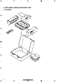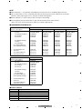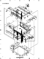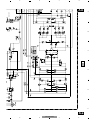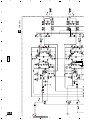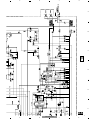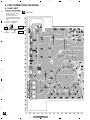
1
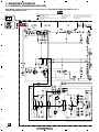
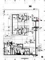
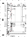
Service
Manual
ORDER NO.
CRT3369
GM-5100T/XU/EW
BRIDGEABLE TWO-CHANNEL POWER AMPLIFIER
GM-5100T
GM-5100T
/XU/EW
/XU/UC
GM-5100T
GM-5100T
GM-510T
/XU/ES
/XU/CN
/XU/UC
For details, refer to "Important check points for good servicing".
PIONEER CORPORATION
4-1, Meguro 1-Chome, Meguro-ku, Tokyo 153-8654, Japan
PIONEER ELECTRONICS (USA) INC. P.O.Box 1760, Long Beach, CA 90801-1760 U.S.A.
PIONEER EUROPE NV Haven 1087 Keetberglaan 1, 9120 Melsele, Belgium
PIONEER ELECTRONICS ASIACENTRE PTE.LTD. 253 Alexandra Road, #04-01, Singapore 159936
C PIONEER CORPORATION 2004
K-ZZB. DEC. 2004 Printed in Japan
1
A
2
3
4
SAFETY INFORMATION
CAUTION
This service manual is intended for qualified service technicians; it is not meant for the casual do-it-yourselfer.
Qualified technicians have the necessary test equipment and tools, and have been trained to properly and safely repair
complex products such as those covered by this manual.
Improperly performed repairs can adversely affect the safety and reliability of the product and may void the warranty.
If you are not qualified to perform the repair of this product properly and safely, you should not risk trying to do so
and refer the repair to a qualified service technician.
B
WARNING
This product contains lead in solder and certain electrical parts contain chemicals which are known to the state of
California to cause cancer, birth defects or other reproductive harm.
Health & Safety Code Section 25249.6 - Proposition 65
- Service Precaution
You should conform to the regulations governing the product (safety, radio and noise, and other regulations),
and should keep the safety during servicing by following the safety instructions described in this manual.
C
D
E
F
2
GM-5100T/XU/EW
1
2
3
4
5
6
7
8
[Important Check Points for Good Servicing]
A
In this manual, procedures that must be performed during repairs are marked with the below symbol.
Please be sure to confirm and follow these procedures.
1. Product safety
Please conform to product regulations (such as safety and radiation regulations), and maintain a safe servicing environment by
following the safety instructions described in this manual.
1 Use specified parts for repair.
Use genuine parts. Be sure to use important parts for safety.
2 Do not perform modifications without proper instructions.
Please follow the specified safety methods when modification(addition/change of parts) is required due to interferences such as
radio/TV interference and foreign noise.
B
3 Make sure the soldering of repaired locations is properly performed.
When you solder while repairing, please be sure that there are no cold solder and other debris.
Soldering should be finished with the proper quantity. (Refer to the example)
4 Make sure the screws are tightly fastened.
Please be sure that all screws are fastened, and that there are no loose screws.
5 Make sure each connectors are correctly inserted.
Please be sure that all connectors are inserted, and that there are no imperfect insertion.
6 Make sure the wiring cables are set to their original state.
C
Please replace the wiring and cables to the original state after repairs.
In addition, be sure that there are no pinched wires, etc.
7 Make sure screws and soldering scraps do not remain inside the product.
Please check that neither solder debris nor screws remain inside the product.
8 There should be no semi-broken wires, scratches, melting, etc. on the coating of the power cord.
Damaged power cords may lead to fire accidents, so please be sure that there are no damages.
If you find a damaged power cord, please exchange it with a suitable one.
9 There should be no spark traces or similar marks on the power plug.
D
When spark traces or similar marks are found on the power supply plug, please check the connection and advise on secure
connections and suitable usage. Please exchange the power cord if necessary.
0 Safe environment should be secured during servicing.
When you perform repairs, please pay attention to static electricity, furniture, household articles, etc. in order to prevent injuries.
Please pay attention to your surroundings and repair safely.
2. Adjustments
To keep the original performance of the products, optimum adjustments and confirmation of characteristics within specification.
Adjustments should be performed in accordance with the procedures/instructions described in this manual.
3. Lubricants, Glues, and Replacement parts
E
Use grease and adhesives that are equal to the specified substance.
Make sure the proper amount is applied.
4. Cleaning
For parts that require cleaning, such as optical pickups, tape deck heads, lenses and mirrors used in projection monitors, proper
cleaning should be performed to restore their performances.
5. Shipping mode and Shipping screws
To protect products from damages or failures during transit, the shipping mode should be set or the shipping screws should be
installed before shipment. Please be sure to follow this method especially if it is specified in this manual.
3
GM-5100T/XU/EW
5
6
F
7
8
1
A
2
3
4
CONTENTS
SAFETY INFORMATION............................................2
1. SPECIFICATIONS .......................................................5
2. EXPLODED VIEWS AND PARTS LIST ......................6
2.1 PACKING..............................................................6
2.2 EXTERIOR ............................................................8
3. SCHEMATIC DIAGRAM...........................................10
3.1 SCHEMATIC DIAGRAM(GUIDE PAGE) ............10
4. PCB CONNECTION DIAGRAM................................18
4.1 AMP UNIT..........................................................18
B
5. ELECTRICAL PARTS LIST........................................22
6. ADJUSTMENT .........................................................25
7. GENERAL INFORMATION.......................................26
7.1 DIAGNOSIS .......................................................26
7.1.1 DISASSEMBLY.........................................26
7.1.2 CONNECTOR FUNCTION DESCRIPTION ......28
8. OPERATIONS ...........................................................29
C
D
E
F
4
GM-5100T/XU/EW
1
2
3
4
5
6
7
8
1. SPECIFICATIONS
A
Power source .......................................................................................................... 14.4 V DC (10.8 — 15.1 V allowable)
Grounding system .......................................................................................................................................... Negative type
Current consumption .................................................................................................... 30.0 A (at continuous power, 4 Ω)
Backup current ................................................................................................................................................ 3 mA or less
Average current drawn* ...................................................................................................... 10.0 A (4 Ω for two channels)
19.0 A (4 Ω for one channel)
Fuse ........................................................................................................................................................................ 30 A × 2
Dimensions ...................................................................................................................... 300 (W) × 60 (H) × 327 (D) mm
Weight .................................................................................................................... 4.7 kg (Leads for wiring not included)
Maximum power output .............................................................................................. 250 W × 2 (4 Ω) / 760 W × 1 (4 Ω)
Continuous power output .......................................................... 125 W × 2 (at 14.4 V, 4 Ω, 20 Hz — 20 kHz 0.2% THD)
380 W × 1 (at 14.4 V, 4 Ω, 20 Hz — 20 kHz 0.8% THD)
190 W × 2 (at 14.4 V, 2 Ω, 20 Hz — 20 kHz 0.8% THD)
Continuous power output (DIN power) ............................ 175 W × 2 (4 Ω) / 520 W × 1 (4 Ω) (DIN45324, +B=14.4 V)
Load impedance .......................................................................................................................... 4 Ω (2 — 8 Ω allowable)
(Bridge connection: 4 — 8 Ω allowable)
Frequency response ........................................................................................................ 10 Hz — 50 kHz (+0 dB, –1 dB)
Signal-to-noise ratio ...................................................................................................................... 95 dB (IEC-A network)
Distortion ........................................................................................................................................ 0.015 % (10 W, 1 kHz)
Separation ...................................................................................................................................................... 70 dB (1 kHz)
Low pass filter .............................................................................................................................. Cut off frequency: 80 Hz
Cut off slope: –12 dB/oct
Bass Boost .............................................................................................................................................. Frequency: 50 Hz
Level: 0/6/12 dB
Gain control .................................................................................................................................. RCA: 200 mV — 6.5 V
Speaker: 0.8 — 26 V
Maximum input level / impedance ...................................................................................................... RCA: 6.5 V / 22 kΩ
Speaker: 26 V / 40 kΩ
B
C
Note:
• Specifications and the design are subject to possible modification without notice due to improvements.
*Average current drawn
• The average current drawn is nearly the maximum current drawn by this unit when an audio signal is input. Use this value when
working out total current drawn by multiple power amplifiers.
D
E
F
5
GM-5100T/XU/EW
5
6
7
8
1
A
2
3
4
3
4
2. EXPLODED VIEWS AND PARTS LIST
2.1 PACKING
9
1
3
2
B
6
5
4
C
5
D
7
8
E
F
6
GM-5100T/XU/EW
1
2
6
5
8
7
NOTE:
A
- Parts marked by “*” are generally unavailable because they are not in our Master Spare Parts List.
- The > mark found on some component parts indicates the importance of the safety factor of the part.
Therefore, when replacing, be sure to use parts of identical designation.
- Screws adjacent to ∇ mark on the product are used for disassembly.
- For the applying amount of lubricants or glue, follow the instructions in this manual.
( In the case of no amount instructions, apply as you think it appropriate.)
- PACKING SECTION PARTS LIST
Description
Screw Assy
Screw
Polyethylene Sheet
Cord Assy
Protector
GM-5100T/XU/EW
CEA4835
BYC40P180FZK
CNM4338
CDE7736
CHP2911
Part No.
GM-5100T/XU/UC
GM-5100T/XU/ES
CEA4835
CEA4835
BYC40P180FZK
BYC40P180FZK
CNM4338
CNM4338
CDE7736
CDE7736
CHP2911
CHP2911
GM-5100T/XU/CN
CEA4835
BYC40P180FZK
CNM4338
CDE7736
CHP2911
6
7
8
9-1
9-2
Polyethylene Bag
Carton
Contain Box
Owner’s Manual
Polyethylene Bag
CEG1317
CHG5360
CHL5360
CRD3915
CEG1116
CEG1351
CHG5362
CHL5362
CRD3916
CEG1116
CEG1317
CHG5361
CHL5361
CRD3918
CEG1116
CEG1317
CHG5465
CHL5465
CRB2041
CEG1116
9-3
9-4
9-5
9-6
Warranty Card
Card
Owner’s Manual
Caution Card
CRY1157
Not used
Not used
Not used
Not used
ARY1048
Not used
Not used
Not used
Not used
CRD3919
Not used
ARY7046
Not used
Not used
Not used
Description
Screw Assy
Screw
Polyethylene Sheet
Cord Assy
Protector
Part No.
GM-510T/XU/UC
CEA4835
BYC40P180FZK
CNM4338
CDE7736
CHP2911
6
7
8
9-1
9-2
Polyethylene Bag
Carton
Contain Box
Owner’s Manual
Polyethylene Bag
CEG1351
CHG5363
CHL5363
CRD3917
CEG1116
9-3
9-4
9-5
9-6
Warranty Card
Card
Owner’s Manual
Caution Card
Not used
ARY1048
Not used
CRP1324
Mark No.
1
2
*
3
4
5
*
*
*
Mark No.
1
2
*
3
4
5
*
*
*
B
C
D
E
- Owner's Manual
Part No.
CRD3915
CRD3916
CRD3917
CRD3918
CRD3919
CRB2041
Language
English, Spanish, German, French, Italian, Dutch
English, French, Spanish
English, French, Spanish
English, Spanish
Arabic, Portuguese(B)
Traditional Chinese
F
7
GM-5100T/XU/EW
5
6
7
8
1
2
3
2.2 EXTERIOR
4
44
43
42
A
7
36
6
11
7
40
37
B
45
2
37
41
12
12
12
13
4
2
10
2
31
4
2
3
32
C
34
21
32
15
33
16
20
3
15
15
33
14
15
A
3
32
15
33
32
30
15
29
D
24
23
15
14
32 15
25
26
3
33
22
22
18
39
35
32
27
3
2
4
2
19
4
3
2
E
17
28
4
5
2
1
2
1
9
8
1
1
5
F
5
1
5
8
1
38
5
GM-5100T/XU/EW
1
2
3
4
6
5
7
8
- EXTERIOR SECTION PARTS LIST
Mark No. Description
*
A
Part No.
Mark No. Description
Part No.
1
2
3
4
5
Screw
Screw
Screw
Screw
Screw
BBZ30P060FTC
BBZ30P080FZK
BBZ30P100FZK
BBZ30P120FTC
BSZ30P050FZK
26
27
28
29
30
Buss Bar
Buss Bar
Buss Bar
Spacer
Sub Heat Sink
CND2470
CND2472
CND2729
CNM9570
CNR1778
6
7
8
9
10
Badge
Screw
Case
Panel
Panel
See Contrast table(2)
CBA1810
CNB3071
See Contrast table(2)
See Contrast table(2)
31
32
33
34
35
Sub Heat Sink
Screw
Screw
Screw
Terminal(CN850)
CNR1779
IMS30P050FZK
PPZ30P100FSN
PPZ30P100FZK
VNF1084
11
12
13
14
15
Heat Sink
Spacer
Amp Unit
Screw
Screw
See Contrast table(2)
CNV8256
See Contrast table(2)
BBZ30P060FZK
BBZ30P080FZK
36
37
38
> 39
40
Lighting Conductor Unit
Screw
Screw
Fuse(FU100,101)(30A)
Sheet
CXC4334
IBZ30P060FTC
PPZ30P100FZK
CEK1330
CNM9571
16
17
18
19
20
Pin Jack(CN111)
Terminal(CN853)
Terminal(CN855)
Terminal(CN856)
Socket(CN801)
See Contrast table(2)
See Contrast table(2)
See Contrast table(2)
See Contrast table(2)
CKM1463
Screw
Seal
Holder
Nut
Washer
See Contrast table(2)
See Contrast table(2)
See Contrast table(2)
See Contrast table(2)
See Contrast table(2)
21
22
23
24
25
Holder
Terminal
Buss Bar
Buss Bar
Buss Bar
CND2456
CND2458
CND2467
CND2468
CND2469
*
41
42
43
44
45
B
C
D
E
F
9
GM-5100T/XU/EW
5
6
7
8
1
A
2
3
4
(2) CONTRAST TABLE
GM-5100T/XU/EW, GM-5100T/XU/UC, GM-5100T/XU/ES, GM-5100T/XU/CN and GM-510T/XU/UC are constructed the
same except for the following:
Part No.
Mark No. Description
GM-5100T/XU/EW
GM-5100T/XU/UC
GM-5100T/XU/ES GM-5100T/XU/CN
*
6 Badge
CAH1919
CAH1919
CAH1916
CAH1916
9 Panel
CNB3111
CNB3111
CNB3053
CNB3053
10 Panel
CNB3123
CNB3056
CNB3055
CNB3055
11 Heat Sink
CNR1788
CNR1788
CNR1764
CNR1764
13 Amp Unit
CWH1267
CWH1268
CWH1268
CWH1268
B
*
16
17
18
19
41
Pin Jack(CN111)
Terminal(CN853)
Terminal(CN855)
Terminal(CN856)
Screw
CKB1069
CKE1054
CKE1056
CKE1056
Not used
CKB1068
CKE1055
CKE1057
CKE1057
Not used
CKB1068
CKE1055
CKE1057
CKE1057
Not used
CKB1068
CKE1055
CKE1057
CKE1057
Not used
42
43
44
45
Seal
Holder
Nut
Washer
Not used
Not used
Not used
Not used
Not used
Not used
Not used
Not used
Not used
Not used
Not used
Not used
Not used
Not used
Not used
Not used
C
Mark No. Description
*
6 Badge
9 Panel
10 Panel
11 Heat Sink
13 Amp Unit
D
*
Part No.
GM-510T/XU/UC
CAH1919
CNB3111
CNB3113
CNR1797
CWH1268
16
17
18
19
41
Pin Jack(CN111)
Terminal(CN853)
Terminal(CN855)
Terminal(CN856)
Screw
CKB1068
CKE1055
CKE1057
CKE1057
BMZ40P200FZK
42
43
44
45
Seal
Holder
Nut
Washer
CAN3984
CNV8522
NB40FZK
WB40FZK
E
F
10
GM-5100T/XU/EW
1
2
3
4
5
6
7
8
A
B
C
D
E
F
11
GM-5100T/XU/EW
5
6
7
8
1
2
3
4
3. SCHEMATIC DIAGRAM
3.1 SCHEMATIC DIAGRAM(GUIDE PAGE)
Note: When ordering service parts, be sure to refer to " EXPLODED VIEWS AND PARTS LIST" or
"ELECTRICAL PARTS LIST".
A-a
A
A-a
A-a
A-a
A-b
A-b
A-b
NOTE :
Symbol indicates a resistor.
No differentiation is made between chip resistors and
discrete resistors.
Symbol indicates a capacitor.
No differentiation is made between chip capacitors and
discrete capacitors.
Large size
SCH diagram
Decimal points for resistor
and capacitor fixed values
are expressed as :
2.2 ← 2R2
0.022 ← R022
The > mark found on some component parts indica
the importance of the safety factor of the part.
Therefore, when replacing, be sure to use parts of
identical designation.
Guide page
0dB
Detailed page
0dB
0dB
+18.3dBs
-1.7dB ~
-32.1dB
0dB or +12dB or +6
-13.8dBs
+18.3dBs
B
+18.5dBs
(BB ON
INPUT MAX)
BASS BO
GAIN
C
BASS B
GAIN
D
E
F
A
12
GM-5100T/XU/EW
1
2
3
4
6
5
8
7
A-b
cates
A
A
AMP UNIT
+6dB
-1.8dBs
B
-3.1dBs
+38.5dBs
BOOST
DTC643TU
C
DTC643TU
BOOST
D
E
>
>
F
A
13
GM-5100T/XU/EW
5
6
7
8
+18.5dBs
(BB ON
INPUT MAX)
E
0dB
D
1
+18.3dBs
0dB
14
2
GAIN
-13.8dBs
2
BASS BOOST
BASS BOOST
-1.8dBs
0dB or +12dB or +6dB
A-b
+18.3dBs
-1.7dB ~
-32.1dB
The > mark found on some component parts indicates
the importance of the safety factor of the part.
Therefore, when replacing, be sure to use parts of
identical designation.
B
0dB
C
Decimal points for resistor
and capacitor fixed values
are expressed as :
2.2 ← 2R2
0.022 ← R022
A
NOTE :
Symbol indicates a resistor.
No differentiation is made between chip resistors and
discrete resistors.
Symbol indicates a capacitor.
No differentiation is made between chip capacitors and
discrete capacitors.
A-a A-b
1
3
3
4
1
F
A-a
GM-5100T/XU/EW
4
6
5
3
4
A-b
A
GAIN
BASS BOOST
2
8
7
B
A-a A-b
C
D
E
F
A-a
15
GM-5100T/XU/EW
5
6
7
8
1
+38.5dBs
AMP UNIT
2
A-b
16
2
DTC643TU
DTC643TU
-3.1dBs
A
B
8dBs
A-a A-b
1
3
3
4
A
C
D
E
F
1
GM-5100T/XU/EW
4
6
5
8
7
>
>
A
B
A-a A-b
C
D
E
F
2
3
4
A-b
17
GM-5100T/XU/EW
5
6
7
8
1
2
3
4
4. PCB CONNECTION DIAGRAM
4.1 AMP UNIT
NOTE FOR PCB DIAGRAMS
A
1.The parts mounted on this PCB
include all necessary parts for
several destination.
For further information for
respective destinations, be sure
to check with the schematic diagram.
2.Viewpoint of PCB diagrams
A
AMP UNIT
Capacitor
Connector
SIDE A
B
Chip Part
P.C.Board
SIDE B
SPEAKER
OUTPUT
SPEAKER
OUTPUT
C
POWER
SUPPLY
D
E
3
2
1
3
2
1
3
2
1
3
2
1
3
F
A
18
GM-5100T/XU/EW
1
2
3
4
2
1
3
2
1
5
6
8
7
SIDE A
A
B
BASS BOOST
GAIN
C
LPF/OFF
D
Rch
L-
Lch
L+
E
SPEAKER
INPUT
R-
2
R+
1
F
A
19
GM-5100T/XU/EW
5
6
7
8
1
A
2
A
3
4
3
4
AMP UNIT
B
C
D
Lch
E
Rch
L+
L-
R+
R-
F
A
20
GM-5100T/XU/EW
1
2
5
6
7
8
A
SIDE B
B
C
D
E
F
A
21
GM-5100T/XU/EW
5
6
7
8
1
A
B
2
3
5. ELECTRICAL PARTS LIST
NOTE:
Parts whose parts numbers are omitted are subject to being not supplied.
The part numbers shown below indicate chip components.
Chip Resistor
RS1/_S___J,RS1/__S___J
Chip Capacitor (except for CQS.....)
CKS....., CCS....., CSZS.....
The > mark found on some component parts indicatesthe importance of the safety factor of the part.
Therefore, when replacing, be sure to use parts of identical designation.
Meaning of the figures and others in the parentheses in the parts list.
Example) IC 301 is on the point (face A, 91 of x-axis, and 111 of y-axis) of the corresponding
PC board.
IC 301 (A, 91, 111) IC NJM2068V
=====Circuit Symbol and No.===Part Name
--- -----------------------------------------------
A
Part No.
-------------------------
Unit Number : CWH1267(EW)
Unit Number : CWH1268(UC,ES,CN)
Unit Name
: Amp Unit
MISCELLANEOUS
C
D
E
F
4
IC
IC
IC
IC
IC
111
112
141
171
172
(B,294,54) IC
(B,275,81) IC
(B,283,106) IC
(B,287,189) IC
(B,297,186) IC
NJM2068MD
NJM2068MD
NJM4558MD
NJM4558MD
NJM4558MD
IC
IC
Q
Q
Q
651
901
201
202
203
(A,168,99) IC
(B,159,67) IC
(B,249,140) Transistor
(B,252,137) Transistor
(B,251,131) Transistor
PA2027A
UPC494GS
DTC643TU
DTC643TU
DTA124EU
Q
Q
Q
Q
Q
551
552
553
554
555
(B,221,90) Transistor
(B,220,140) Transistor
(B,227,92) Transistor
(B,215,143) Transistor
(B,225,85) Transistor
2SA1163
2SA1163
2SA1163
2SA1163
2SC2713
Q
Q
Q
Q
Q
556
557
558
559
560
(B,218,131) Transistor
(B,220,83) Transistor
(B,211,135) Transistor
(B,216,79) Transistor
(B,209,150) Transistor
2SC2713
2SC2713
2SC2713
2SC2713
2SC2713
Q
Q
Q
Q
Q
561
562
563
564
565
(B,230,76) Transistor
(B,242,157) Transistor
(B,223,75) Transistor
(B,223,154) Transistor
(A,230,38) Transistor
2SA1163
2SA1163
2SC2713
2SC2713
2SD1684
Q
Q
Q
Q
Q
566
571
572
581
582
(A,219,201) Transistor
(B,244,74) Transistor
(B,219,124) Transistor
(A,243,65) Transistor
(A,241,166) Transistor
2SD1684
2SC2713
2SC2713
2SC3421
2SC3421
Q
Q
Q
Q
Q
583
584
585
586
587
(A,276,39) Transistor
(A,250,200) Transistor
(A,254,39) Transistor
(A,228,200) Transistor
(A,211,66) Transistor
2SC4388
2SC4388
2SC4388
2SC4388
2SA1358
Q
Q
Q
Q
Q
588
589
590
591
592
(A,209,157) Transistor
(A,221,39) Transistor
(A,173,200) Transistor
(A,199,39) Transistor
(A,195,200) Transistor
2SA1358
2SA1673
2SA1673
2SA1673
2SA1673
Q
Q
Q
Q
Q
660
661
662
670
671
(A,158,77) Transistor
(B,154,110) Transistor
(B,151,121) Transistor
(B,269,113) Transistor
(B,266,113) Transistor
2SB1243
2SA1576A
2SC4081
2SA1576A
2SC4081
22
=====Circuit Symbol and No.===Part Name
--- -----------------------------------------------
Part No.
-------------------------
Q
Q
Q
Q
Q
672
673
674
691
692
(B,267,105) Transistor
(B,260,114) Transistor
(B,263,97) Transistor
(B,176,89) Transistor
(B,175,97) Transistor
2SC4081
2SC4081
2SA1576A
DTC114TU
DTA114EU
Q
Q
Q
Q
Q
931
932
933
934
941
(B,148,55) Transistor
(B,155,44) Transistor
(B,143,50) Transistor
(B,146,38) Transistor
(A,91,36) Transistor
2SD1766
2SD1766
2SB1188
2SB1188
FKV550N
Q
Q
Q
Q
Q
942
943
944
945
946
(A,136,36) Transistor
(A,76,36) Transistor
(A,121,36) Transistor
(A,61,36) Transistor
(A,106,36) Transistor
FKV550N
FKV550N
FKV550N
FKV550N
FKV550N
Q
Q
Q
Q
Q
951
952
981
991
992
(A,129,203) Transistor
(A,109,203) Transistor
(B,138,70) Transistor
(B,140,86) Transistor
(B,144,85) Transistor
2SD2395
2SB1566
2SA1576A
2SC4081
DTC114TU
D
D
D
D
D
161
162
553
554
555
(A,307,69) Diode
(A,292,89) Diode
(B,212,77) Diode
(B,232,149) Diode
(B,210,77) Diode
ERA15-02VH
ERA15-02VH
MA111
MA111
MA111
D
D
D
D
D
556
557
558
601
658
(B,235,148) Diode
(B,248,74) Diode
(B,226,124) Diode
(A,258,121) LED
(B,166,36) Diode
MA111
MA111
MA111
UB3803X
DAN202U
D
D
D
D
D
661
664
665
670
681
(B,171,77) Diode
(B,140,117) Diode
(A,48,102) Diode
(B,263,113) Diode
(A,157,108) Diode
MA111
UDZS7R5(B)
RM4Z-LFJ4
MA111
ERA15-02VH
D
D
D
D
D
682
951
952
957
958
(A,162,111) Diode
(B,145,195) Diode
(B,123,195) Diode
(A,89,203) Diode
(A,70,203) Diode
ERA15-02VH
UDZS16(B)
UDZS16(B)
FML22S
FML22R
D
D
D
L
L
991
992
993
601
951
(A,125,187) Diode
(A,122,186) Diode
(B,142,81) Diode
(A,60,72) Choke Coil 50µH
(A,69,166) Choke Coil 320µH
ERA92-02VH
ERA92-02VH
MA111
CTH1323
CTH1326
L
T
TH
TH
TH
952
901
901
902
903
(A,41,166) Choke Coil 320µH
(A,101,86) Transformer
(A,151,37) Thermistor
(A,149,202) Thermistor
(A,128,105) Thermistor
CTH1326
CTT1122
CCX1013
CCX1013
CCX1064
GM-5100T/XU/EW
1
2
3
4
6
5
=====Circuit Symbol and No.===Part Name
--- -----------------------------------------------
7
8
Part No.
-------------------------
=====Circuit Symbol and No.===Part Name
--- -----------------------------------------------
Part No.
-------------------------
S
S
S
VR
> FU
151
171
901
201
100
(A,314,101) Switch(LPF/OFF)
(A,314,181) Switch(BASS BOOST)
(A,9,200) Switch(BFC)
(A,311,154) Volume 10kΩ(A)(GAIN)
(A,20,45) Fuse 30A
CSH1021
CSH1029
HSH-156
CCS1241
CEK1330
R
R
R
R
R
563
564
565
566
567
(B,222,87)
(B,216,139)
(B,212,89)
(B,226,129)
(B,210,89)
RS1/16S681J
RS1/16S681J
RS1/16S361J
RS1/16S361J
RS1/16S433J
> FU
AR
AR
101
101
102
(A,20,68) Fuse 30A
(B,315,81) Surge Protector
(B,310,92) Surge Protector
CEK1330
RCCA-201Q31UA-PI
RCCA-201Q31UA-PI
R
R
R
R
R
568
569
570
571
572
(B,223,129)
(B,211,82)
(B,210,146)
(B,236,75)
(B,228,154)
RS1/16S433J
RS1/16S681J
RS1/16S681J
RS1/16S223J
RS1/16S223J
RS1/16S471J
RS1/16S471J
RS1/16S223J
RS1/16S223J
RS1/16S102J
R
R
R
R
R
573
574
575
576
577
(B,232,43)
(B,219,197)
(A,234,73)
(A,235,157)
(B,222,68)
RS1/16S820J
RS1/16S820J
RD1/4PU101J
RD1/4PU101J
RS1/16S681J
RESISTORS
R
R
R
R
R
111
112
113
114
117
(B,295,72)
(B,283,91)
(B,295,62)
(B,275,88)
(B,292,61)
R
R
R
R
R
118
121
122
123
125
(B,270,82)
(B,296,46)
(B,273,73)
(B,296,44)
(B,292,44)
10kΩ
10kΩ
10kΩ
10kΩ
RS1/16S102J
CCN1152
CCN1152
CCN1152
CCN1152
R
R
R
R
R
578
579
580
581
582
(B,218,155)
(B,226,74)
(B,221,147)
(B,235,70)
(B,240,161)
RS1/16S681J
RS1/16S181J
RS1/16S181J
RS1/16S100J
RS1/16S100J
R
R
R
R
R
126
127
131
134
152
(B,287,83) 10kΩ
(B,291,64) 10kΩ
(B,276,70) 10kΩ
(B,276,73) 10kΩ
(B,288,100)
CCN1152
CCN1152
CCN1152
CCN1152
RS1/16S103J
R
R
R
R
R
583
584
585
586
587
(B,220,69)
(B,218,153)
(A,282,34)
(A,246,205)
(A,258,34)
RS1/16S100J
RS1/16S100J
RD1/2PM100J
RD1/2PM100J
RD1/2PM100J
R
R
R
R
R
154
157
159
171
172
(B,287,100)
(B,283,116)
(B,281,116)
(B,285,184)
(B,295,180)
RS1/16S103J
RS1/16S103J
RS1/16S103J
RS1/16S222J
RS1/16S222J
R
R
R
R
R
588
589
590
591
592
(A,225,205)
(B,237,34)
(B,211,205)
(A,204,34)
(A,190,205)
RD1/2PM100J
RS1/16S221J
RS1/16S221J
RD1/2PM100J
RD1/2PM100J
R
R
R
R
R
173
174
175
176
177
(B,287,179)
(B,299,180)
(B,289,184)
(B,302,183)
(B,316,181)
RS1/16S101J
RS1/16S182J
RS1/16S182J
RS1/16S221J
RS1/16S121J
R
R
R
R
R
593
594
595
596
597
(A,225,34)
(A,169,205)
(A,265,54) 1Ω
(A,261,195) 1Ω
(A,243,54) 1Ω
RD1/2PM100J
RD1/2PM100J
CCN1151
CCN1151
CCN1151
R
R
R
R
R
178
179
180
181
182
(B,302,185)
(B,317,185)
(B,302,186)
(B,318,185)
(B,293,191)
RS1/16S132J
RS1/16S122J
RS1/16S104J
RS1/16S104J
RS1/16S273J
R
R
R
R
R
598
599
600
601
602
(A,240,195) 1Ω
(A,210,45) 1Ω
(A,184,186) 1Ω
(A,188,45) 1Ω
(A,206,186) 1Ω
CCN1151
CCN1151
CCN1151
CCN1151
CCN1151
R
R
R
R
R
184
185
189
198
201
(B,300,192)
(B,288,196)
(B,284,198)
(B,280,100)
(B,250,143)
RS1/16S331J
RS1/16S331J
RS1/16S273J
RS1/16S0R0J
RS1/16S0R0J
R
R
R
R
R
621
622
623
624
625
(A,168,70)
(A,165,75)
(B,175,86)
(B,151,85)
(A,155,88)
RD1/4PU101J
RD1/4PU472J
RS1/16S563J
RS1/16S221J
RD1/4PU152J
R
R
R
R
R
202
203
204
206
207
(B,252,134)
(B,285,176)
(B,297,177)
(B,268,168)
(B,273,164)
RS1/16S0R0J
RS1/16S560J
RS1/16S560J
RS1/16S222J
RS1/16S222J
R
R
R
R
R
630
631
632
633
634
(A,163,86)
(A,162,80)
(B,163,118)
(B,171,106)
(B,163,116)
RD1/4PU271J
RD1/4PU271J
RS1/16S223J
RS1/16S223J
RS1/16S223J
R
R
R
R
R
505
506
507
508
509
(B,260,38)
(B,265,202)
(B,237,38)
(B,243,202)
(B,248,80)
RS1/16S682J
RS1/16S682J
RS1/16S682J
RS1/16S682J
RS1/16S564J
R
R
R
R
R
640
641
642
644
645
(B,156,102)
(B,150,109)
(B,136,110)
(B,154,106)
(B,150,118)
RS1/16S472J
RS1/16S682J
RS1/16S682J
RS1/16S103J
RS1/16S222J
R
R
R
R
R
510
511
512
513
514
(B,226,126)
(B,241,75)
(B,222,125)
(A,13,204)
(A,27,143)
RS1/16S564J
RS1/16S473J
RS1/16S473J
RD1/2PM100J
RD1/2PM100J
R
R
R
R
R
646
647
648
649
650
(B,150,116)
(B,146,117)
(B,145,119)
(B,143,122)
(A,44,82)
RS1/16S472J
RS1/16S103J
RS1/16S103J
RS1/16S473J
RD1/4PU222J
R
R
R
R
R
551
552
555
556
557
(B,230,43)
(B,222,197)
(B,236,90)
(B,228,136)
(B,236,92)
RS1/16S182J
RS1/16S182J
RS1/16S103J
RS1/16S103J
RS1/16S473J
R
R
R
R
R
666
670
671
672
673
(B,39,79)
(B,270,118)
(B,267,117)
(A,263,107)
(B,269,99)
RS1/16S1R0J
RS1/16S104J
RS1/16S472J
RD1/4PU103J
RS1/16S562J
R
R
R
R
R
558
559
560
561
562
(B,226,133)
(B,231,92)
(B,225,143)
(B,233,92)
(B,225,145)
RS1/16S473J
RS1/16S331J
RS1/16S331J
RS1/16S331J
RS1/16S331J
R
R
R
R
R
674
675
676
831
832
(B,253,113)
(B,251,113)
(A,266,100)
(A,304,66)
(A,307,65)
RS1/16S472J
RS1/16S222J
RD1/4PU221J
RD1/4PU683J
RD1/4PU683J
5
6
7
8
A
B
C
D
E
F
23
GM-5100T/XU/EW
1
A
B
C
D
E
2
3
4
=====Circuit Symbol and No.===Part Name
--- -----------------------------------------------
Part No.
-------------------------
=====Circuit Symbol and No.===Part Name
--- -----------------------------------------------
Part No.
-------------------------
R
R
R
R
R
901
921
922
923
924
(B,141,65)
(B,140,49)
(B,140,45)
(A,148,50)
(A,159,34)
RS1/16S124J
RS1/16S472J
RS1/16S472J
RD1/4PU332J
RD1/4PU332J
C
C
C
C
C
554
555
556
559
560
(B,227,133)
(B,218,87)
(B,212,139)
(A,210,94)
(A,230,128)
CCSRCH680J50
CKSRYB471K50
CKSRYB471K50
CEAT221M10
CEAT221M10
R
R
R
R
R
931
932
933
934
935
(A,95,41)
(A,142,34)
(A,81,41)
(A,125,41)
(A,65,41)
RD1/2PM121J
RD1/2PM121J
RD1/2PM121J
RD1/2PM121J
RD1/2PM121J
C
C
C
C
C
561
562
563
564
565
(B,208,89)
(B,223,130)
(B,228,73)
(B,244,161)
(A,231,68)
CCSRCH150J50
CCSRCH150J50
CCSRCH470J50
CCSRCH470J50
CFTNA223J50
R
R
R
R
R
936
941
942
951
952
(A,112,41)
(A,73,68)
(A,125,57)
(A,139,200)
(A,112,193)
RD1/2PM121J
RD1/2PM220J
RD1/2PM220J
RD1/4PU103J
RD1/4PU103J
C
C
C
C
C
566
567
568
569
570
(A,218,160)
(A,38,206)
(A,27,158)
(A,32,209)
(A,27,147)
CFTNA223J50
CFTNA333J50
CFTNA333J50
CQHA102J2A
CQHA102J2A
R
R
R
R
R
953
954
961
966
970
(A,143,201)
(A,119,204)
(A,116,112)
(B,126,77)
(A,165,202)
RD1/2PM470J
RD1/2PM470J
RD1/2PM220J
RS1/16S153J
RD1/2PM182J
C
C
C
C
C
571
572
573
574
575
(B,239,70)
(B,245,164)
(B,217,69)
(B,215,154)
(B,239,66)
CCSRCH220J50
CCSRCH220J50
CCSRCH220J50
CCSRCH220J50
CCSRCH220J50
R
R
R
R
R
973
974
975
976
977
(B,152,63)
(B,162,42)
(B,162,45)
(B,162,44)
(B,161,37)
RS1/16S103J
RS1/16S472J
RS1/16S472J
RS1/16S472J
RS1/16S272J
C
C
C
C
C
576
577
578
581
582
(B,245,166)
(B,219,66)
(B,213,156)
(A,280,47)
(A,269,198)
CCSRCH220J50
CCSRCH220J50
CCSRCH220J50
CFTNA103J50
CFTNA103J50
R
R
R
R
R
978
979
980
981
982
(B,169,38)
(B,169,41)
(B,141,68)
(B,149,77)
(B,147,73)
RS1/16S272J
RS1/16S272J
RS1/16S105J
RS1/16S153J
RS1/16S102J
C
C
C
C
C
650
651
652
653
666
(A,136,89)
(A,174,80)
(A,171,117)
(A,159,120)
(B,254,120)
CEAT220M25
CEAT471M16
CFTNA103J50
CFTNA103J50
CKSQYB104K50
R
R
R
R
R
983
984
985
986
987
(B,142,76)
(B,141,76)
(B,142,71)
(B,141,71)
(B,132,88)
RS1/16S473J
RS1/16S202J
RS1/16S101J
RS1/16S223J
RS1/16S103J
C
C
C
C
C
671
672
673
674
675
(A,175,105)
(A,171,121)
(A,143,112)
(A,142,106)
(A,167,104)
CEAT101M16
CFTNA103J50
CEAT100M50
CEAT100M50
CFTNA103J50
R
R
R
R
991
992
993
998
(A,140,188)
(A,126,183)
(B,139,82)
(B,270,124)
RD1/2PM391J
RD1/2PM391J
RS1/16S222J
RS1/16S102J
C
C
C
C
C
676
677
681
691
831
(A,134,122)
(A,26,89)
(A,271,121)
(A,179,97)
(A,311,41)
CFTNA103J50
CFTNA224J50
CEANP221M10
CEAT220M25
CEAT100M50
C
C
C
C
C
832
903
941
942
943
(A,302,41)
(A,149,70)
(A,67,101) 3900µF/16V
(A,67,84) 3900µF/16V
(A,70,53)
CEAT100M50
CEAT2R2M50
CCH1644(P35)
CCH1644(P35)
CQHA472J2A
C
C
C
C
C
944
951
952
953
954
(A,129,52)
(A,150,196)
(A,123,202)
(A,158,197)
(A,128,194)
CQHA472J2A
CQHA102J2A
CQHA102J2A
CEAT470M16
CEAT470M16
C
C
C
C
C
955
956
957
958
959
(A,134,194)
(A,114,198)
(A,63,135) 2200µF/50V
(A,43,135) 2200µF/50V
(A,63,156) 2200µF/50V
CEAT470M25
CEAT470M25
CCH1647(P35)
CCH1647(P35)
CCH1647(P35)
C
C
C
C
C
960
962
970
971
972
(A,43,155) 2200µF/50V
(A,110,125)
(A,173,64)
(A,132,67)
(A,168,67)
CCH1647(P35)
CQHA102J2A
CFTNA103J50
CFTNA564J50
CEAT101M16
C
C
C
C
C
973
974
975
980
991
(A,151,77)
(A,144,75)
(A,133,77)
(A,144,56)
(A,146,182)
CQHA102J2A
CEAT221M16
CEANP470M16
CFTNA103J50
CEAT471M50(P45)
CAPACITORS
C
C
C
C
C
111
112
113
114
121
(B,297,65)
(B,283,89)
(A,299,64)
(A,280,92)
(A,284,71)
CKSRYB471K50
CKSRYB471K50
CEAT100M50
CEAT100M50
CFTNA223J50
C
C
C
C
C
122
123
124
125
126
(A,284,75)
(B,290,64)
(B,287,81)
(A,287,66)
(A,284,79)
CFTNA223J50
CCSRCH470J50
CCSRCH470J50
CFTNA103J50
CFTNA103J50
C
C
C
C
C
127
128
151
152
153
(B,292,46)
(B,273,75)
(A,283,120)
(A,303,94)
(A,288,105)
CCSRCH470J50
CCSRCH470J50
CFTNA274J50
CFTNA274J50
CFTNA154J50
C
C
C
C
C
154
171
172
173
181
(A,301,100)
(A,289,176)
(A,300,177)
(A,311,205)
(A,299,203)
CFTNA154J50
CFTNA273J50
CFTNA273J50
CEANP4R7M50
CFTNA224J50
C
C
C
C
C
182
184
551
552
553
(A,300,197)
(A,316,202)
(A,239,87)
(A,233,139)
(B,236,93)
CFTNA224J50
CEANP4R7M50
CEAT101M16
CEAT101M16
CCSRCH680J50
F
24
GM-5100T/XU/EW
1
2
3
4
5
6
7
=====Circuit Symbol and No.===Part Name
--- -----------------------------------------------
Part No.
-------------------------
C
C
C
C
CEAT471M50(P45)
CQHA102J2A
CQHA102J2A
CKSRYB224K16
992
993
994
999
(A,121,180)
(A,136,176)
(A,130,176)
(B,249,129)
8
A
6. ADJUSTMENT
There is no information to be shown in this chapter.
B
C
D
E
F
25
GM-5100T/XU/EW
5
6
7
8
1
2
3
4
7. GENERAL INFORMATION
7.1 DIAGNOSIS
7.1.1 DISASSEMBLY
A
Removing the Case (Fig. 1)
Case
1 Remove three black screws (M3 x 10).
2 Remove six white screws (M3 x 6).
3 Remove four black screws (M3 x 5).
B
2
Caution)
When you disassemble/re-assemble the Product
with it placed upside down, take care not to
damage the top surface.
The Product uses several different types of
screws. Take care not to confuse them during
re-assembly.
2
2
3
3
1
1
1
3
2
2
3
2
C
Fig. 1
Removing the Panel (Fig. 2)
Panel for the RCA side
Panels are used for two sides individually, one
for the RCA side and the other for the Power
Terminal side.
1
1
1
1
Panel for the RCA side
D
1 Remove six black screws (M3 x 8).
2
2
1
2
1
RCA Terminal
(CN111)
Remove two black screws (M3 x 5).
(They are used to secure the RCA Holder.)
Panel for the Power Terminal side
3 Remove six black screws (M3 x 8).
E
Panel for the Power Terminal side
3
3
3
3
3
F
3
Fig. 2
26
GM-5100T/XU/EW
1
2
3
4
5
6
8
7
Amp Unit
Removing the Amp Unit (Fig. 3)
Heat Sink
A
1 Remove six black screws (M3 x 10).
1
2 Remove six white screws (M3 x 12).
3
A Screw holes in the PCB are printed with
numbers 1 to 12.
1
1
2
2
2
Remove screws in numerical order.
Re-assembly takes the reverse order of
disassembly.
Caution)
The Amp Unit is adhered on the Heat Sink with
silicon grease. This means forcibly removing the
Amp Unit from the Heat Sink may break the
PCB.
2
2
2
3
1
1
1
Remove all of the twelve screws. Then,
remove the two black screws (M3 x 5).
Tighten screws whose length is M3 x 8 or
more into the two screw holes so as to
raise the Amp Unit above the Heat Sink.
Then, remove the Amp Unit.
(Since screw threads differ, 1 and 2 screws cannot be used.)
A
3
B
C
Fig. 3
Caution when re-assembling the Amp Unit and the Heat Sink
Be aware that the RCA Terminal may break
unless the Amp Unit and the Heat Sink are
assem-bled following the correct procedures
given below.
RCA Holder
RCA Terminal
(CN111)
Amp Unit
1) Secure the RCA-side Panel on the Heat Sink
with screws. (Fig. 2)
D
2) Place the Amp Unit on the Heat Sink aligning
with two studs. (Fig. 4)
3) Move the Amp Unit until the RCA Holder on
the Amp Unit comes in contact with the inside
of the Panel. (Fig. 4)
Move the Amp Unit
Caution in steps 2) and 3)
When you place the Amp Unit on the Heat Sink,
you will find no positioning marks to determine
the direction of two panels. To position them
correctly, the Amp Unit needs to be moved to
the place where it comes in contact with the
RCA-side panel.
If you do not position them, an excessive force
can be applied to the RCA Terminal. This may
result in breakage.
E
Heat Sink
4) Secure the RCA-side Panel and the RCA
Holder with screws. (Fig. 2)
5) Secure the Amp Unit on the Heat Sink with
screws. (Fig. 3)
Panel for the
RCA side
Stud
Stud
6) Secure the Panel for the Power Terminal side
in place with screws. (Fig. 2)
27
GM-5100T/XU/EW
5
6
F
Fig. 4
7
8
1
2
3
4
7.1.2 CONNECTOR FUNCTION DESCRIPTION (GM-5100T/XU/EW)
A
B
C
D
E
F
28
GM-5100T/XU/EW
1
2
3
4
5
6
7
Bass boost level control can boost the
level around the frequency selected by
the bass boost frequency control switch
from 0, 6, and 12 dB.
The power indicator lights when the
power is switched on.
Power Indicator
8. OPERATIONS (GM-5100T/XU/EW)
Full range
Subwoofer
Full range
Very Low Frequency range
LPF (right)
OFF (left)
Speaker
Type
Audio frequency range
to be output
LPF Select
Switch
Connect a subwoofer.
Remarks
Set the LPF select switch as follows according to the type of speaker that is connected to the
speaker output connector and the car stereo system:
LPF (Low-Pass Filter) Select Switch
If you hear a beat while listening to an MW/LW
broadcast with your car stereo, change the BFC
switch using a small standard tip screwdriver.
BFC (Beat Frequency Control) Switch
6
Bass Boost Level Control Switch
• When using with an RCA equipped car
stereo (standard output of 500 mV), set to
the NORMAL position. When using with
an RCA equipped Pioneer car stereo with
max. output of 4 V or more, adjust level to
match the car stereo output level.
• If you hear too much noise when using the
speaker input terminals, turn the gain
control counter-clockwise.
If the sound level is too low, even when
the volume of the car stereo used along
with this power amplifier is turned up,
turn gain control on the front of the
power amplifier clockwise. If the sound
distorts when the volume is turned up,
turn the gain control counter-clockwise.
Gain Control
5
7
8
A
B
C
D
E
F
GM-5100T/XU/EW
8
29