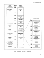
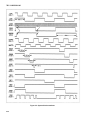
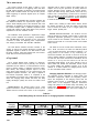
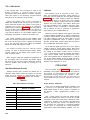
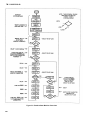
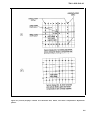
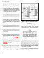
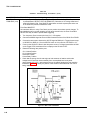
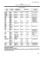
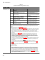
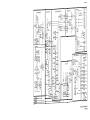
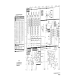
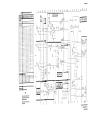
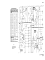
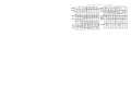
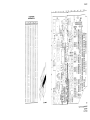
1
ARMY TM 11-6625-3241-40
MARINE CORPS TM 09045B-40/2
TECHNICAL MANUAL
GENERAL SUPPORT
MAINTENANCE MANUAL
FOR
OSCILLOSCOPE OS-291/G
(TEKTRONIX MODEL 2430A)
(NSN 6625-01-258-0022)
Distribution is authorized to Department of Defense and DOD
contractors only for official use or for administration or
operational purposes. This determination was made on 27
August, 1988. Other requests for this document will be referred
to Commander, US Army Communications-Electronics
Command and Fort Monmouth, ATTN: AMSEL-LC-LM-LT,
Fort Monmouth, NJ 07703-5000.
DESTRUCTION NOTICE – Destroy by any method that will
prevent disclosure of contents or reconstruction of the
document.
HEADQUARTERS, DEPARTMENT OF THE ARMY
1 MARCH 1991
ARMY TM 11-6625-3241-40
MARINE CORPS TM 09045B-40/2
(This manual includes copyright material reproduced by permission of TEKTRONIX, Inc.)
Technical Manual
No. 11-6625-3241-40
Technical Manual
No. 09045B-40/2
DEPARTMENT OF THE ARMY
AND HEADQUARTERS, MARINE CORPS
Washington, DC, 1 March 1991
GENERAL SUPPORT MAINTENANCE MANUAL
FOR
OSCILLOSCOPE OS-291/G
(TEKTRONIX MODEL 2430A)
(NSN 6625-01-258-0022)
You can help improve this manual. If you find any mistakes or if you know of a
way to improve the procedures, please let us know. Mail your letter, DA Form
2028 (Recommended Changes to Publications and Blank Forms), or DA Form
2028-2 located in the back of this manual direct to: Commander, U.S. Army
Fort
Communication-Electronics Command, ATTN: AMSEL–LC-LM–LT,
Monmouth, New Jersey 07703-5000. Marine Corps units, submit NAVMC 10772
(Recommended Changes to Technical Publications) to: Commanding General,
Marine Corps Logistics Base (Code 850) Albany, Georgia 31704-5000. In either
case, a reply will be furnished to you.
This manual is an authentication of the manufacturer’s commercial literature which, through usage,
has been found to cover the data required to operate and maintain this equipment. Since the manual
was not prepared in accordance with military specifications, the format has not been structured to
consider levels of maintenance.
i/(ii blank)
TM 11-6625-3241-40
TABLE OF CONTENTS
Page
SECTION 0
SECTION 1
SECTION 2
SECTION 3
INTRODUCTION . . . . . . . . . . . . . . . . . . . . . . . . . . . . . . . . . . . . . . . .. . . . . . . . . . .. .
0-1
Scope . . . . . . . . . . . . . . . . . . . . . . . . . . . . . . . . . . . . . . . . . . . . . . . . . . . . .
0-1
Consolidated Index of Army Publications and Blank Forms . . . . . . . . . . . . . . . . . .
0-1
Maintenance Forms, Records, and Reports . . . . . . . . . . . . . . . . . . . . . . . . . . . . . . .
0-1
Reporting Equipment improvement Recommendations (EIR) . . . . . . . . . . . . . . . .
0-1
Administrative Storage . . . . . . . . . . . . . . . . . . . . . . . . . . . . . . . . . . . . . . . . . . . . . . . . .
0-1
Destruction of Army Electronics Materiel to Prevent Enemy Use . . . . . . . . . . . . . .
0-1
SPECIFICATION . . . . . . . . . . . . . . . . . . . . . . . . . . . . . . . . . . . . . . . . . . . . . . . . . . . . . .
1-1
Introduction . . . . . . . . . . . . . . . . . . . . . . . . . . . . . . . . . . . . . . . . . . . . . . . . . . . . . . . . . . . .
1-1
Vertical System . . . . . . . . . . . . . . . . . . . . . . . . . . . . . . . . . . . . . . . . . . . . . . . . . . . . . . . . . .
1-1
Horizontal System . . . . . . . . . . . . . . . . . . . . . . . . . .. . . . . . . . . . . . . . . . . . . . . .
1-1
Trigger System . . . . . . . . . . . . . . . . . . . . . . . . . . . . . . . . . . . . . . . . . . . . . . . . . . . . . . . . . . .
1-1
Cursor Measurements . . . . . . . . . . . . . . . . . . . . . . . . . . . . . . . . . . . . . . . . . . . . . . . . . .
1-2
Waveform Acquisition . . . . . . . . . . . . . . . . . . . . . . . . . . . . . . . . . . . . . . . . . . . . . . . . . .
1-2
Storage and I/O . . . . . . . . . . . . . . . . . . . . . . . . . . . . . . . . . .... . . . . . . . . . . . . . . . . . . .
1-3
Extended Features . . . . . . . . . . . . . . . . . . . . . . . . . . . . . . .. . . . . . . . . . . . . . . . . . . . . . .
1-3
Performance Conditions . . . . . . . . . . . . . . . . . . . . . . . . . . . . . . . . . . . . . . . . . . . . . . . .
1-3
Recommended Adjustments Schedule . . . . . . . . . . . . . . . . . . . . . . . . . . . . . . . . . . .
1-3
PREPARATION FOR USE . . . . . . . . . . . . . . . . . . . . . . . . . . . . . . . . . . . . . . . . . . . . . . . . . . . . . . . .
2-1
Safety . . . . . . . . . . . . . . . . . . . . . . . . . . . . . . . . . . . . . . . . . . . . . . . . . . . . . . . . . . . . . . . .
2-1
Line Voltage Selection . . . . . . . . . . . . . . . . . . . . . . . . . . . . . . . . . . . . . . . . . . . . . . . . . .
2-1
Line Fuse . . . . . . . . . . . . . . . . . . . . . . . . . . . . . . . . . . . ... . . . . . . . . . . . . . . . . . . . . . . . .
2-2
Power Cord . . . . . . . . . . . . . . . . . . . . . . . . . . . . . . . . . . . . . . . . . . . . . . . . . . . . . . . . . . . . . . . . .
2-2
Instrument Cooling . . . . . . . . . . . . . . . . . . . . . . . . . . . . . . . . . . . . . . . . . . . . . . . . . . . . .
2-2
Start-up . . . . . . . . . . . . . . . . . . . . . . . . . . . . . . . . . . .. . . . . . . . . . . . . . . . . . . . . . . . . . . . . .
2-2
Power-down . . . . . . . . . . . . . . . . . . . . . . . . . . . . . . . . . . . . . . . . . . . . . . . . . . . . . . . . . . . . . .
2-3
Repackaging For Shipment . . . . . . . . . . . . . . . . . . . . . . . . . . . . . . . . . . . . . . . . . . . . .
2-3
THEORY OF OPERATION . . . . . . . . . . . . . . . . . . . . . . . . . . . . . . . . . . . . . . . . . . . . . .
3-1
Section Organization . . . . . . . . . . . . . . . . . . . . . . . . . . . . . . . . . . . . . . . . . . . . . . . .
3-1
integrated Circuit Descriptions. . . . . . . . . . . . . . . . . . . . . . . . . . . . . . . . . . . . . . . .
3-1
Simplified Block Diagram Description . . . . . . . . . . . . . . . . . . . . . . . . . . . . . . . . . . . .
3-2
Detailed Block Diagram Description . . . . . . . . . . . . . . . . . . . . . . . . . . . . . . . . . . . . .
3-8
introduction . . . . . . . . . . . . . . . . . . . . . . . . . . . . . . . . . . . . . . . . . . . . . . . . . . . . . . . . . .
3-8
input Signal Conditioning and Analog Sampling . . . . . . . . . . . . . . . . . . . . . . . . .
3-8
Acquisition Process and Control . . . . . . . . . . . . . . . . . . . . . . . . . . . . . . . . . . . . . . .
3-9
iii
TM 11-6625-3241-40
TABLE
OF
CONTENTS–CONT
Page
SECTION 3
THEORY OF OPERATION-CONT
Detailed Block Diagram Description–CONT
SECTION 4
iv
Data Clocking to Acquisition Memory . . . . . . . . . . . . . . . . . . . . . . . . . . . . . . . . . . .
3-10
Analog Data Conditioning and A/D Conversion . . . . . . . . . . . . . . . . . . . . . . . . . . .
3-11
Acquisition Processing and Display . . . . . . . . . . . . . . . . . . . . . . . . . . . . . . . . . . . .
3-12
Detailed Circuit Description . . . . . . . . . . . . . . . . . . . . . . . . . . . . . . . . . . . . . . . . . . . . . .
3-14
System Processor . . . . . . . . . . . . . . . . . . . . . . . . . . . . . . . . . . . . . . . . . . . . . . . . . .
3-14
Waveform Processor System., . . . . . . . . . . . . . . . . . . . . . . . . . . . . . . . . . . . . . . . .
3-21
Front Panel Processor . . . . . . . . . . . . . . . . . . . . . . . . . . . . . . . . . . . . . . . . . . . . . . . .
3-26
Front Panel . . . . . . . . . . . . . . . . . . . . . . . . . . . . . . . . . . . . . . . . . . . . . . . . . . . . . . . . .
3-28
System DAC And Acquisition Control Registers . . . . . . . . . . . . . . . . . . . . . . . . . . .
3-29
System DAC (Cont) and Auxiliary Front Panel . . . . . . . . . . . . . . . . . . . . . . . . . . . .
3-31
System Clocks . . . . . . . . . . . . . . . . . . . . . . . . . . . . . . . . . . . . . . . . . . . . . . . . . . . . . .
3-32
Time Base Controller and Acquisition Memory . . . . . . . . . . . . . . . . . . . . . . . . . . .
3-36
Attenuators and Preamps . . . . . . . . . . . . . . . . . . . . . . . . . . . . . . . . . . . . . . . . . . . . .
3-40
Peak Detectors and CCD/Clock Drivers . . . . . . . . . . . . . . . . . . . . . . . . . . . . . . . . .
3-42
Triggers and Phase Clocks . . . . . . . . . . . . . . . . . . . . . . . . . . . . . . . . . . . . . . . . . . . .
3-47
Jitter Correction Ramps . . . . . . . . . . . . . . . . . . . . . . . . . . . . . . . . . . . . . . . . . . . . . . .
3-52
Trigger Holdoff, Jitter Counters, and Calibrator . . . . . . . . . . . . . . . . . . . . . . . . . . .
3-53
CCD Output . . . . . . . . . . . . . . . . . . . . . . . . . . . . . . . . . . . . . . . . . . . . . . . . . . . . . . . . .
3-56
A/D Converter and Acquisition Latches . . . . . . . . . . . . . . . . . . . . . . . . . . . . . . . . . .
3-57
Display and Attributes Memory . . . . . . . . . . . . . . . . . . . . . . . . . . . . . . . . . . . . . . . .
3-59
Display Control . . . . . . . . . . . . . . . . . . . . . . . . . . . . . . . . . . . . . . . . . . . . . . . . . . . . . .
3-61
Display Output . . . . . . . . . . . . . . . . . . . . . . . . . . . . . . . . . . . . . . . . . . . . . . . . . . . . . .
3-67
High-Voltage Supply and CRT . . . . . . . . . . . . . . . . . . . . . . . . . . . . . . . . . . . . . . . . .
3-70
System l/O . . . . . . . . . . . . . . . . . . . . . . . . . . . . . . . . . . . . . . . . . . . . . . . . . . . . . . . . .
3-74
Low-Voltage Power Supply . . . . . . . . . . . . . . . . . . . . . . . . . . . . . . . . . . . . . . . . . . . .
3-77
Low-Voltage Regulators . . . . . . . . . . . . . . . . . . . . . . . . . . . . . . . . . . . . . . . . . . . . . .
3-82
PERFORMANCE CHECK AND FUNCTIONAL VERIFICATION PROCEDURE .
4-1
Introduction . . . . . . . . . . . . . . . . . . . . . . . . . . . . . . . . . . . . . . . . . . . . . . . . . . . . . . . . . . . .
4-1
Preparation . . . . . . . . . . . . . . . . . . . . . . . . . . . . . . . . . . . . . . . . . . . . . . . . . . . . . . . . .
4-1
Initial Setup . . . . . . . . . . . . . . . . . . . . . . . . . . . . . . . . . . . . . . . . . . . . . . . . . . . . . . . . .
4-3
Vertical System . . . . . . . . . . . . . . . . . . . . . . . . . . . . ... . . . . . . . . . . . . . . . . . . . . . . . . .
4-5
Triggering Systems . . . . . . . . . . . . . . . . . . . . . . . . . . . . . . . . . . . . . . . . . . . . . . . . . . . . .
4-14
Horizontal System . . . . . . . . . . . . . . . . . . . . . . . . . . . . . . . . . . . . . . . . . . . . . . . . . . . . . .
4-21
Additional Verifications and Checks . . . . . . . . . . . . . . . . . . . . . . . . . . . . . . . . . . . . . .
4-24
TM 11-6625-3241-40
TABLE OF CONTENTS–CONT
Page
SECTION 5
SECTION 6
ADJUSTMENT PROCEDURE . . . . . . . . . . . . . . . . . . . . . . . . . . . . . . . . . . . . . . . . . . .
5-1
Introduction . . . . . . . . . . . . . . . . . . . . . . . . . . . . . . . . . . . . . . . . . . . . . . . . . . . . . . . . . . .
5-1
Calibration Sequence and Partial Procedures . . . . . . . . . . . . . . . . . . . . . . . . . . .
5-1
Warm-up Time Requirements . . . . . . . . . . . . . . . . . . . . . . . . . . . . . . . . . . . . . . . . .
5-1
Preservation of lnstrument Calibration . . . . . . . . . . . . . . . . . . . . . . . . . . . . . . . . . .
5-2
Internal Adjustments . . . . . . . . . . . . . . . . . . . . . . . . . . . . . . . . . . . . . . . . . . . . . . . . . . .
5-3
Self Calibration . . . . . . . . . . . . . . . . . . . . . . . . . . . . . . . . . . . . . . . . . . . . . . . . . . . . . . . .
5-10
MAINTENANCE . . . . . . . . . . . . . . . . . . . . . . . . . . . . . . . . . . . . . . . . . . . . . . . . . . . . . . .
6-1
Instrument Calibration . . . . . . . . . . . . . . . . . . . . . . . . . . . . . . . . . . . . . . . . . . . . . . .
6-1
National Bureau of Standards Traceability . . . . . . . . . . . . . . . . . . . . . . . . . . . . . .
6-2
Voiding Calibration . . . . . . . . . . . . . . . . . . . . . . . . . . . . . . . . . . . . . . . . . . . . . . . . . .
6-2
Static-sensitive Components.. . . . . . . . . . . . . . . . . . . . . . . . . . . . . . . . . . . . . . . . . . .
6-3
Preventive Maintenance . . . . . . . . . . . . . . . . . . . . . . . . . . . . . . . . . . . . . . . . . . . . . . . .
6-4
Introduction . . . . . . . . . . . . . . . . . . . . . . . . . . . . . . . . . . . . . . . . . . . . . . . . . . . . . . . .
6-4
General Care . . . . . . . . . . . . . . . . . . . . . . . . . . . . . . . . . . . . . . . . . . . . . . . . . . . . . . .
6-4
inspection and Cleaning . . . . . . . . . . . . . . . . . . . . . . . . . . . . . . . . . . . . . . . . . . . . .
6-4
Lubrication . . . . . . . . . . . . . . . . . . . . . . . . . . . . . . . . . . . . . . . . . . . . . . . . . . . . . . . . .
6-6
Semiconductor Checks . . . . . . . . . . . . . . . . . . . . . . . . . . . . . . . . . . . . . . . . . . . . . .
6-6
Periodic Readjustment . . . . . . . . . . . . . . . . . . . . . . . . . . . . . . . . . . . . . . . . . . . . . . .
6-6
Troubleshooting . . . . . . . . . . . . . . . . . . . . . . . . . . . . . . . . . . . . . . . . . . . . . . . . . . . . . . .
6-7
Introduction . . . . . . . . . . . . . . . . . . . . . . . . . . . . . . . . . . . . . . . . . . . . . . . . . . . . . . . .
6-7
Troubleshooting Aids . . . . . . . . . . . . . . . . . . . . . . . . . . . . . . . . . . . . . . . . . . . . . . . .
6-7
Troubleshooting Equipment . . . . . . . . . . . . . . . . . . . . . . . . . . . . . . . . . . . . . . . . . . .
6-8
Troubleshooting Techniques.. . . . . . . . . . . . . . . . . . . . . . . . . . . . . . . . . . . . . . . . .
6-8
Corrective Maintenance . . . . . . . . . . . . . . . . . . . . . . . . . . . . . . . . . . . . . . . . . . . . . . . .
6-11
Introduction . . . . . . . . . . . . . . . . . . . . . . . . . . . . . . . . . . . . . . . . . . . . . . . . . . . . . . . .
6-11
Maintenance Precautions . . . . . . . . . . . . . . . . . . . . . . . . . . . . . . . . . . . . . . . . . . . .
6-11
Selectable Components . . . . . . . . . . . . . . . . . . . . . . . . . . . . . . . . . . . . . . . . . . . . .
6-11
Maintenance Aids . . . . . . . . . . . . . . . . . . . . . . . . . . . . . . . . . . . . . . . . . . . . . . . . . . .
6-11
Interconnections . . . . . . . . . . . . . . . . . . . . . . . . . . . . . . . . . . . . . . . . . . . . . . . . . . . .
6-11
Transistors and integrated Circuits . . . . . . . . . . . . . . . . . . . . . . . . . . . . . . . . . . . .
6-13
Soldering Techniques . . . . . . . . . . . . . . . . . . . . . . . . . . . . . . . . . . . . . . . . . . . . . . . .
6-13
Removal and Replacement Procedure . . . . . . . . . . . . . . . . . . . . . . . . . . . . . . . . . .
6-14
v
TM 11-6625-3241-40
TABLE OF CONTENTS-CONT
SECTION 6
MAINTENANCE-CONT
Internal Diagnostics and Calibration Routines . . . . . . . . . . . . . . . . . . . . . . . . . . . . . .
6-23
Introduction . . . . . . . . . . . . . . . . . . . . . . . . . . . . . . . . . . . . . . . . . . . . . . . . . . . . . . . . .
6-23
Overview . . . . . . . . . . . . . . . . . . . . . . . . . . . . . . . . . . . . . . . . . . . . . . . . . . . . . . . . . . .
6-23
Calibration Routines . . . . . . . . . . . . . . . . . . . . . . . . . . . . . . . . . . . . . . . . . . . . . . . . .
6-23
Diagnostic Routines . . . . . . . . . . . . . . . . . . . . . . . . . . . . . . . . . . . . . . . . . . . . . . . . . .
6-25
Diagnostics Operation via the GPIB lnterface . . . . . . . . . . . . . . . . . . . . . . . . . . . .
6-31
Diagnostic Procedures . . . . . . . . . . . . . . . . . . . . . . . . . . . . . . . . . . . . . . . . . . . . . . .
6-32
Front Panel Settings for lnit Panel . . . . . . . . . . . . . . . . . . . . . . . . . . . . . . . . . . . . . . . . .
6-97
APPENDIX A REFERENCES . . . . . . . . . . . . . . . . . . . . . . . . . . . . . . . . . . . . . . . . . . . . . . . . . . . . . . . . .
A-1
APPENDIX B EXPENDABLE SUPPLIES AND MATERIALS LIST . . . . . . . . . . . . . . . . . . . . . . . . .
B-1
INDEX . . . . . . . . . . . . . . . . . . . . . . . . . . . . . . . . . . . . . . . . . . . . . . . . . . . . . . . . . . . . . . . . . . . . . . . . . . . . . .
Index-1
vi
TM 11-6625-3241-40
LIST OF ILLUSTRATIONS
Number
Title
Page
1-1
Oscilloscope OS-291/G . . . . . . . . . . . . . . . . . . . . . . . . . . . . . . . . . . . . . . . . . . . . . .
1-0
2-1
LINE VOLTAGE SELECTOR, line fuse, and power cord receptacle . . . . . . . . .
2-1
3-1
Oscilloscope OS-291/G simplified block diagram . . . . . . . . . . . . . . . . . . . . . . .
3-3
3-2
Simplified Memory Map of the OS-291/G . . . . . . . . . . . . . . . . . . . . . . . . . . . . . . .
3-17
3-3
System Clock waveforms . . . . . . . . . . . . . . . . . . . . . . . . . . . . . . . . . . . . . . . . . . . . .
3-34
3-4
Simplified Peak Detector block diagram . . . . . . . . . . . . . . . . . . . . . . . . . . . . . . .
3-43
3-5
Simplified CCD architecture . . . . . . . . . . . . . . . . . . . . . . . . . . . . . . . . . . . . . . . . . .
3-46
3-6
Trigger Logic Array Control Data Byte . . . . . . . . . . . . . . . . . . . . . . . . . . . . . . . . . .
3-49
3-7
Jitter correction waveforms . . . . . . . . . . . . . . . . . . . . . . . . . . . . . . . . . . . . . . . . . . .
3-53
3-8
Readout State Machine flow chart . . . . . . . . . . . . . . . . . . . . . . . . . . . . . . . . . . . . .
3-66
3-9
Vertical Vector Generator . . . . . . . . . . . . . . . . . . . . . . . . . . . . . . . . . . . . . . . . . . . . .
3-68
3-10
DC Restorer . . . . . . . . . . . . . . . . . . . . . . . . . . . . . . . . . . . . .. . . . . . . . . . . . . . . . . . . .
3-72
3-11
GPIB data flow diagram . . . . . . . . . . . . . . . . . . . . . . . . . . . . . . . . . . . . . . . . . . . . . .
3-75
3-12
GPIB three-wire handshake state diagram . . . . . . . . . . . . . . . . . . . . . . . . . . . . . .
3-76
3-13
PWM Regulator and lnverter. . . . . . . . . . . . . . . . . . . . . . . . . . . . . . . . . . . . . . . . . .
3-79
3-14
PWM switching waveforms . . . . . . . . . . . . . . . . . . . . . . . . . . . . . . . . . . . . . . . . . . .
3-80
5-1
Adjustment locations for Displays 4 through 6 . . . . . . . . . . . . . . . . . . . . . . . . . . .
5-4
5-2
Display 5–Vertical and Horizontal Gain, Offset, and Vector
Compensation adjustments pattern . . . . . . . . . . . . . . . . . . . . . . . . . . . . . . . . . . . .
5-5
5-3
Integrator Time adjustment pattern . . . . . . . . . . . . . . . . . . . . . . . . . . . . . . . . . . . .
5-6
6-1
Multipin connector . . . . . . . . . . . . . . . . . . . . . . . . . . . . . . . . . . . . . . . . . . . . . . . . . . .
6-8
6-2
Circuit Board Location. . . . . . . . . . . . . . . . . . . . . . . . . . . . . . . . . . . . . . . . . . . . . . .
6-15
6-3
Installation sequence for installing the CRT frame screws. . . . . . . . . . . . . . . . .
6-21
6-4
Trigger LED binary coding for diagnostic tests. . . . . . . . . . . . . . . . . . . . . . . . . . .
6-26
6-5
Main EXT DIAG menu . . . . . . . . . . . . . . . . . . . . . . . . . . . . . . . . . . . . . . . . . . . . . . .
6-27
6-6
Initial Troubleshooting Chart.... . . . . . . . . . . . . . . . . . . . . . . . . . . . . . . . . . . . . . .
6-33
6-7
Mux Test waveforms . . . . . . . . . . . . . . . . . . . . . . . . . . . . . . . . . . . . . . . . . . . . . . . . . .
6-38
6-8
Typical Register test waveforms. . . . . . . . . . . . . . . . . . . . . . . . . . . . . . . . . . . . . . .
6-51
6-9
Front Panel Microprocessor diagnostics test. . . . . . . . . . . . . . . . . . . . . . . . . . . .
6-74
6-10
System Processor data bit D7 in the Bus isolate mode. . . . . . . . . . . . . . . . . . .
6-95
FO-1
Block Diagram . . . . . . . . . . . . . . . . . . . . . . . . . . . . . . . . . . . . . . . . . . . . . . . . . . . . .
FP-1
FO-2
Circuit Board Interconnection Diagram . . . . . . . . . . . . . . . . . . . . . . . . . . . . . . . . .
FP-5
FO-3
Chassis Parts, Test Equipment, and Setups for Test Waveforms
and Voltage Measurements . . . . . . . . . . . . . . . . . . . . . . . . . . . . . . . . . . . . . . . . . . .
FP-9
vii
TM 11-6625-3241-40
LIST OF ILLUSTRATIONS–CONT
Number
Title
Page
FO-4
A12 Processor Board Component Locator . . . . . . . . . . . . . . . . . . . . . . . . . . . . . .
FP-11
FO-5
System Processor Schematic . . . . . . . . . . . . . . . . . . . . . . . . . . . . . . . . . . . . . . . .
FP-15
FO-6
Waveform Processor Schematic . . . . . . . . . . . . . . . . . . . . . . . . . . . . . . . . . . . . . .
FP-19
FO-7
A13 Side Board Component Locator . . . . . . . . . . . . . . . . . . . . . . . . . . . . . . . . . . .
FP-23
FO-8
Front Panel Processor Schematic . . . . . . . . . . . . . . . . . . . . . . . . . . . . . . . . . . . . .
FP-25
FO-9
A14 Front Panel Board and A18 Scale Illumination Board Component
Locator . . . . . . . . . . . . . . . . . . . . . . . . . . . . . . . . . . . . . . . . . . . . . . . . . . . . . . . . . . . .
FP-29
FO-10
Front Panel Schematic . . . . . . . . . . . . . . . . . . . . . . . . . . . . . . . . . . . . . . . . . . . . . . .
FP-31
FO-11
A10 Main Board Component Locator . . . . . . . . . . . . . . . . . . . . . . . . . . . . . . . . . .
FP-35
FO-12
Acquisition Control Registers and System DAC Schematic . . . . . . . . . . . . . . .
FP-41
FO-13
Auxiliary Front Panel and System DAC Schematic . . . . . . . . . . . . . . . . . . . . . . .
FP-45
FO-14
All Time Base/Display Board Component Locator . . . . . . . . . . . . . . . . . . . . . .
FP-49
FO-15
System Clocks Schematic . . . . . . . . . . . . . . . . . . . . . . . . . . . . . . . . . . . . . . . . . . .
FP-53
FO-16
Time Base Controller and Acquisition Memory Schematic . . . . . . . . . . . . . . . .
FP-57
FO-17
Attenuators and Preamps Schematic . . . . . . . . . . . . . . . . . . . . . . . . . . . . . . . . . .
FP-61
FO-18
Peak Detectors and CCD/Clock Drivers Schematic . . . . . . . . . . . . . . . . . . . . . .
FP-65
FO-19
Triggers and Phase Clocks Schematic . . . . . . . . . . . . . . . . . . . . . . . . . . . . . . . . .
FP-69
FO-20
Jitter Correction Ramps Schematic . . . . . . . . . . . . . . . . . . . . . . . . . . . . . . . . . . . .
FP-73
FO-21
Trigger Holdoff, Jitter Counters and Calibrator Schematic . . . . . . . . . . . . . . .
FP-77
FO-22
CCD Output Schematic . . . . . . . . . . . . . . . . . . . . . . . . . . . . . . . . . . . . . . . . . . . . . .
FP-81
FO-23
A/D Converter and Acquisition Latches Schematic . . . . . . . . . . . . . . . . . . . . . .
FP-85
FO-24
Display and Attributes Memory Schematic . . . . . . . . . . . . . . . . . . . . . . . . . . . . .
FP-89
FO-25
Display Control Schematic . . . . . . . . . . . . . . . . . . . . . . . . . . . . . . . . . . . . . . . . . . .
FP-93
FO-26
Display Output Schematic . . . . . . . . . . . . . . . . . . . . . . . . . . . . . . . . . . . . . . . . . . .
FP-97
FO-27
A17 High Voltage Board Component Locator . . . . . . . . . . . . . . . . . . . . . . . . . . .
FP-103
FO-28
High Voltage Supply and CRT Schematic . . . . . . . . . . . . . . . . . . . . . . . . . . . . . .
FP-105
FO-29
System l/O Schematic . . . . . . . . . . . . . . . . . . . . . . . . . . . . . . . . . . . . . . . . . . . . . . . .
FP-109
FO-30
A16 Low Voltage Power Supply Board Component Locator . . . . . . . . . . . . . .
FP-113
FO-31
Low Voltage Power Supply Schematic . . . . . . . . . . . . . . . . . . . . . . . . . . . . . . . . .
FP-115
FO-32
Low Voltage Regulators Schematic . . . . . . . . . . . . . . . . . . . . . . . . . . . . . . . . . . . .
FP-121
FO-33
Power Supply Troubleshooting . . . . . . . . . . . . . . . . . . . . . . . . . . . . . . . . . . . . . . .
FP-125
FO-34
Display Troubleshooting . . . . . . . . . . . . . . . . . . . . . . . . . . . . . . . . . . . . . . . . . . . . .
FP-127
FO-35
System Clock Troubleshooting . . . . . . . . . . . . . . . . . . . . . . . . . . . . . . . . . . . . . . .
FP-129
viii
TM 11-6625-3241-40
LIST OF TABLES
Number Title
Page
1-1
Electrical, Environmental, and Mechanical Characteristics . . . . . . . . . . . . . . .
1-4
3-1
Host Memory-Mapped I/O . . . . . . . . . . . . . . . . . . . . . . . . . . . . . . . . . . . . . . . . . . . .
3-19
3-2
Processor Control Register Functions . . . . . . . . . . . . . . . . . . . . . . . . . . . . . . . . . .
3-20
3-3
Processor Miscellaneous Output Register (PMISCOUT) Functions . . . . . . . .
3-20
3-4
Waveform Processor Address Decoding . . . . . . . . . . . . . . . . . . . . . . . . . . . . . . .
3-24
3-5
Trigger Logic ArrayAddresses (6080h-6087h) . . . . . . . . . . . . . . . . . . . . . . . . . .
3-48
3-6
REF4/5 Frequency for Each SEC/DIV Setting . . . . . . . . . . . . . . . . . . . . . . . . . . . .
3-50
3-7
Phase Clock Array Control Lines (CC3 through CCO) . . . . . . . . . . . . . . . . . . . . .
3-51
3-8
Holdoff Delay Range for Current Source vs Charging Capacitor
Combinations . . . . . . . . . . . . . . . . . . . . . . . . . . . . . . . . . . . . . . . . . . . . . . . . . . . . . . .
3-54
3-9
Side Board Address Decoding.. . . . . . . . . . . . . . . . . . . . . . . . . . . . . . . . . . . . . . .
3-56
4-1
Cross Reference for Test Equipment . . . . . . . . . . . . . . . . . . . . . . . . . . . . . . . . . . .
4-2
4-2
Accuracy Limits CH 1 and CH 2 CURSOR VOLTS Readout and A and
B TRIGGER Readouts . . . . . . . . . . . . . . . . . . . . . . . . . . . . . . . . . . . . . . . . . . . . . . . .
4-8
4-3
Minimum Display Level for CH 1 or CH 2 Triggering (in divisions) . . . . . . . . . .
4-15
4-4
Minimum Signal Level for EXT1 or EXT 2 Triggering (in millivolts) . . . . . . . . . . .
4-17
6-1
Relative Susceptibility to Static-Discharge Damage . . . . . . . . . . . . . . . . . . . . .
6-3
6-2
External Inspection Checklist. . . . . . . . . . . . . . . . . . . . . . . . . . . . . . . . . . . . . . . .
6-4
6-3
Internal Inspection Checklist.. . . . . . . . . . . . . . . . . . . . . . . . . . . . . . . . . . . . . . . .
6-5
6-4
Power Supply Voltage and Ripple Limits . . . . . . . . . . . . . . . . . . . . . . . . . . . . . . .
6-10
6-5
Maintenance Aids . . . . . . . . . . . . . . . . . . . . . . . . . . . . . . . . . . . . . . . . . . . . . . . . . . .
6-12
6-6
OS-291/G Troubleshooting Procedures . . . . . . . . . . . . . . . . . . . . . . . . . . . . . . . .
6-34
6-7
lNIT PANEL State . . . . . . . . . . . . . . . . . . . . . . . . . . . . . . . . . . . . . . . . . . . . . . . . . . . .
6-97
ix/(x blank)
TM 11-6625-3241-40
Section 0
INTRODUCTION
SCOPE
This manual contains instructions for the General
Support Maintenance of the Oscilloscope OS-291/G.
Throughout this manual, the oscilloscope is referred to as
the instrument, the Tektronix 2430A, or the OS-291/G.
CONSOLIDATED INDEX OF ARMY
PUBLICATIONS AND BLANK FORMS
Refer to the latest issue of DA PAM 25-30 to determine
whether there are new additions, changes, or additional
publications pertaining to this equipment.
MAINTENANCE FORMS, RECORDS,
AND REPORTS
a. Report of Maintenance and Unsatisfactory Equiprnent. Department of the Army forms and procedures
used for equipment maintenance will be those prescribed
by DA PAM 738-750 as contained in Maintenance Management Update. Marine Corps maintains forms and
procedures as prescribed by TM4700-15/1.
b. Report of Item and Packaging Deficiencies. Fill out
and forward SF 364 (Report of Discrepancy (ROD)) as
prescribed in AR 735-11-2/DLAR 4140.55/SECNAVlNST
4355.18/AFR 400-54/MCO 4430.3J.
c. Transportation Discrepancy Report (TDR) (SF 361).
Fill out and forward Transportation Discrepancy Report
(TDR) (SF 361) as prescribed in AR 55-37/NAVSUPINST
4610.33C/AFR 75-18/MCO P4610.19D DLAR 4500.15.
REPORTING EQUIPMENT
IMPROVEMENT RECOMMENDATIONS
(EIR)
a. Army. If your OS-291/G needs improvement, let us
know. Send us an EIR. You, the user, are the only one who
can tell us what you don’t like about your equipment. Let
us know why you don’t like the design or performance.
Put it on an SF 368 (Product Quality Deficiency Report).
Mail it to us at: Commander, US Army Communications
Electronics Command and Fort Monmouth, ATTN: AMSEL-PA-MA-D, Fort Monmouth, New Jersey 07703-5000.
We’ll send you a reply.
b. Marine Corps Users. QDR shall be reported on
SF 368 in accordance with MCO P4855.10, Product
Quality Deficiency Report Manual. Submit to Commanding General, Marine Corps Logistics Base (Code 856),
Albany, Georgia 31704-5000.
ADMINISTRATIVE STORAGE
Administrative storage of equipment issued to and
used by Army activities will have preventive maintenance
performed in accordance with PMCS charts before
storing. When removing the equipment from administrative storage the PMCS should be performed to ensure
operational readiness.
DESTRUCTION OF ARMY
ELECTRONICS MATERIEL
TO PREVENT ENEMY USE
Destruction of Army electronics materiel to prevent
enemy use shall be in accordance with TM 750-244-2.
0-1
TM 11-6625-3241-40
Figure 1-1. Oscilloscope OS-291/G.
1-0
TM 11-6625-3241-40
Section 1
SPECIFICATION
INTRODUCTION
The Tektronix 2430A Digital Oscilloscope is a portable, dual-channel instrument with a maximum digitizing
rate of 100 Megasamples per second. The scope is
capable of simultaneous acquisition of Channel 1 and
Channel 2 input signals. It has a real-time useful storage
bandwidth of 40 MHz for single-event acquisitions, with
an equivalent-time bandwidth of 150 MHz when repetitive acquisitions are acquired. Since both channels are
acquired simultaneously, the XY display is available to
full bandwidth.
The instrument is microprocessor controlled and
menu driven, displaying at the top of the screen alphanumeric CRT readouts of the vertical and horizontal scale
factors, trigger levels, trigger sources and cursor measurements. Menus, displayed at the bottom of the CRT
display, are used by the operator to select the operating
mode.
A user makes decisions as to what operation and
mode setup the instrument must have to make the
measurement wanted and then selects the proper functions using a combination of front-panel buttons and the
displayed menu.
Five menu buttons mounted on the CRT bezel are
used to make selections from the entry choices displayed. The top line of the menu display usually contains
the menu title, and the bottom line Iabels the buttons with
the control functions they select. The selection is made
(indicated by an underscoring of the menu label in the
display) when the bezel button below the selected
function is pressed. The menus, system operating
modes, and auxiliary functions are described in chapter
2 of the Operators and Unit Maintenance manual.
VERTICAL SYSTEM
The two vertical channels have calibrated deflection
factors from 2 mV to 5 V per division in a 1-2-5 sequence
of 14 steps. Use of coded probes having attenuation
factors of 1X, 10X, 100X, and 1000X extends the minimum sensitivity to 5,000 V per division (with the 1000X
probe) and the maximum sensitivity to 200 µV per
division (using a 1X probe in SAVE or AVERAGE
expanded mode).
VOLTS/DIV readouts are automatically switched to
display a correct scale factor when properly coded
probes are attached. Each channel can be separately
inverted. ADD and MULT are display functions provided
by the processor system.
In SAVE mode, the waveforms maybe both horizontally and vertically repositioned, expanded horizontally
and verticalIy, added to each other, or multiplied together for either XY or YT displays.
Horizontal display modes of A, A INTEN, and B
Delayed are available. The time base has 28 calibrated
SEC/DIV settings in a 1-2-5 sequence from 5 ns per
division to 5 s per division. An External Clock mode is
provided that accepts clocking signals from 1 MHz to
100 MHz.
The B Trace and the intensified zone on the A INTEN
Trace may be delayed by time with respect to the A
trigger, and a DELAY by EVENTS function permits the A
display to be delayed by a selected number of B Trigger
events. In the case of DELAY by EVENTS, the B Trigger
SOURCE, COUPLING, SLOPE, and LEVEL controls
define the nature of the signal needed to produce events
Triggering. The number of events required to satisfy the
delay may beset from 1 to 65,536, with a resolution of one
event. The DELTA DELAY feature produces two independently settable delayed B Traces in DELAY by TIME.
TRIGGER SYSTEM
The trigger system of the scope provides many
features for selecting and processing a signal used in
triggering the acquisition system. The conventional
features of SOURCE selection, Trigger LEVEL control,
Trigger SLOPE, Trigger MODE, and CPLG (coupling)
include enhancements not normally found in a conventional oscilloscope.
The choices of VERT, CH1 or CH2, EXT1 or EXT2,
LINE, and A*B or WORD (16-bit data word recognition)
are available as SOURCE selections for triggering A
Horizontal Mode acquisitions. These sources for trigger
signals provide a wide range of applications involving
specialized triggering requirements. Except for A*B (A
AND B) and LINE (power-source frequency), the same
Trigger SOURCE selections are available for triggering B
1-1
TM 11-6625-3241-40
acquisitions. The selected trigger signal is conditioned
by the choice of input CPLG (coupling). These coupling
selections are AC, DC, HF REJECT, LF REJECT, and
NOISE REJECT. LEVEL control provides a settable
amplitude (with CRT readout) at which triggering will
occur, and SLOPE control determines on which slope of
the triggering signal (plus or minus) the acquisition
is triggered.
Trigger MODE choices are AUTO LEVEL, AUTO/
ROLL, NORM (normal), and SINGLE SEQ (single sequence), for the A and A INTENSIFIED Modes, and
Triggerable After Delay and Runs After Delay, for the B
Mode. AUTO LEVEL provides for automatic leveling on
the applied trigger signal. AUTO MODE produces an
auto trigger in the event a trigger signal is either not
received or not within the Iimits needed to produce a
triggering event. When triggering conditions are met, a
normal triggered display results. At SEC/DIV settings of
100 ms per division and longer, the AUTO MODE
switches to ROLL. in ROLL MODE, the display is
continually updated and trigger signals are disregarded.
NORM (normal) trigger MODE requires that all triggering requirements are met before an acquisition will take
place. SINGLE SEQ (single sequence) MODE is a
variation of the conventional single-shot displays found
on many previous oscilloscopes. In SINGLE SEQ, a
single complete acquisition is done on all called-up
VERTICAL MODES. Since an acquisition depends on the
acquisition mode in effect, many of the scope operating
features are altered in SINGLE SEQ.
The user has a choice of trigger points within the
acquired waveform record by selecting the amount of
pretrigger data displayed. The trigger location in the
record is selectable from a choice of five pretrigger
lengths beginning atone-eighth of the record length and
increasing to seven-eighths of the record length. A
record trigger position is independently selectable for
both A and B acquisitions. Additional trigger positions in
the record are selectable via the GPIB interface commands.
CURSOR MEASUREMENTS
Time and Voltage cursors are provided for making
parametric measurements on the displayed waveforms.
Time may be measured either between the cursor
positions (DELTA TIME) or between a selected cursor
and the trigger point of an acquired waveform (ABSOLUTE). Time cursor readouts are scaled in seconds,
degrees, or percentage values. The l/TIME cursors may
be scaled in hertz (Hz), degrees, or percentage.
Voltage cursor measurements on a waveform display
can be selected to read either the voltage difference
1-2
between the cursor positions or the absolute voltage
position of a selected cursor with respect to ground. The
volts measurement readouts may be scaled in units of
volts, decibels (dB), or percent. The Voltage cursors and
Time cursors may also be coupled to track together
(V@T and SLOPE) and assigned to a particular
waveform for ease in making peak-to-peak and slope
waveform measurements. The units for V@T may be
volts, percent, or dB; SLOPE may have units of slope
(VOLTS/SEC), percent (VOLTS/VOLT), or dB.
WAVEFORM ACQUISITION
Waveforms may be acquired in different modes,
depending on the measurement requirements. The
acquisition modes of NORMAL, ENVELOPE, and
AVG (averaging) provide the user with a wide range of
measurement adaptability. NORMAL mode provides a
continuous acquisition producing a “live” waveform
display similar to that seen with an analog oscilloscope.
AVG (averaging) mode is especially useful for improving
the signal-to-noise ratio of the displayed waveform.
Small amplitude signals masked by noise become easily
visible for making measurements and analysis by averaging from 2 to 256 acquisitions for removing uncorreIated noise.
Equivalent-time sampling, used for NORMAL and AVG
acquisition of recurring periodic signals, extends the
useful storage bandwidth to 150 MHz when the REPETITIVE mode is on. Randomly acquired data points taken
from aperiodic signal are used to fill the complete record
of the signal waveform display. Depending on the
SEC/DIV setting, as few as 10 samples (at 5 ns/DIV) or as
many as 409 (at 200 ns/DIV) samples maybe obtained on
each trigger event. The user sees the waveform display
build up as dots until the entire 1024 data point record is
filled.
ENVELOPE mode saves the maximum and minimum
data-point values over a selected number of acquisitions
from 1 to 256 plus CONT (continuous). The display
presents a visual image of the amount of change
(envelope) that occurs to a waveshape during the
accumulated acquisitions. Frequency, phase, amplitude, and position changes are easily identified when
acquiring in ENVELOPE mode. The glitch-catching
capability of ENVELOPE mode can capture single-event
pulses as narrow as 2 ns at the slowest SEC/DIV setting
of 5 seconds per division.
Horizontally, the record length of acquired waveforms
is 1024 data points (512 max/min pairs in ENVELOPE
mode), of which 500 make up a one-screen display (50
data points per division for 10 divisions). The entire
record may be viewed by using the Horizontal POSITION
control to position any portion of the record within the
viewing area.
TM 11-6625-3241-40
STORAGE AND I/0
Acquired waveforms may be saved in any of four REF
(reference) waveform nonvolatile memories. Any or all of
the saved reference waveforms may be displayed for
comparison with the waveforms being currently acquired. The source and destination of waveforms to be
saved may be user designated. Assignment can be made
to save either channel 1 or channel 2 (or the results of an
addition or multiplication of the two channels) to any REF
memory or to move a stored reference from one REF
memory to another. Reference waveforms may also be
written into a REF memory location via the GPIB
interface.
The scope is fully controllable and capable of sending
and receiving waveforms via the standard equipped
GPIB interface. This feature makes the instrument ideal
for making automated measurements in a production or
research and development environment that calls for
repetitive data taking. Self-calibration and self-diagnostic features built into the scope to aid in fault detection
and servicing are also accessible via commands sent
from the GPIB controller.
Another standard feature is the DEVICES setting for
GPIB Interface control. This feature allows the user to
output waveforms (and other on-screen information) to
either a HP@ Graphics Printer or Plotter from the scope
front-panel, providing a way to obtain hard-copies of
acquired waveforms without putting the scope into a
system controller environment.
EXTENDED FEATURES
There are several other features incorporated into this
instrument designed to make it more usable, namely, the
HELP, AUTOsetup, MEASURE, and AutoStep Sequencer features.
HELP: The HELP function can be used to display
operational information about any front-panel control.
When HELP mode is in effect, manipulating almost any
front-panel control causes the scope to display
information about that control. When HELP is first
invoked, an introduction to HELP is displayed on screen.
MEASURE automatically extracts
MEASURE:
parameters from signal input to the scope. In the
SNAPSHOT mode, 20 different waveform parameters
are extracted and displayed for a single acquisition. In
the continuous extraction mode, up to four parameters
are extracted continuously as the instrument continues
to acquire.
AutoStep Sequencer (PRGM): With AutoStep, the
user can save single front-panel setups or sequences of
setups and associated flow control and Input/Output
actions for later recall. If MEASURE and/or OUTPUT are
saved as part of these setups they can be used for
automatic parameter extraction and data printout. 100 to
800 front-panel setups (depending on complexity) can
be stored in one or more sequences.
The descriptions of these four features are found in
Chapter 2 of the Operators and Unit Maintenance manual
for this instrument.
For part numbers and further information about
standard accessories and a list of the optional accessories, refer to the Unit, Direct Support, and General
Support Repair Parts and Special Tools List for Oscilloscope OS-291/G.
PERFORMANCE CONDITIONS
Electrical, environmental, and mechanical characteristics are listed in Table 1-1.
Electrical characteristics apply when the scope has
been calibrated at an ambient temperature between
+ 20±°C and + 30°C, has had a warmup period of at least
20 minutes and is operating at an ambient temperature
between -15°C and + 55°C (unless otherwise noted).
The scope meets the environmental requirements of
MIL-T-28800C for Type Ill, Class 3, Style D equipment,
with the humidity and temperature requirements defined
in paragraphs 3.9.2.2, 3.9.2.3, and 3.9.2.4.
RECOMMENDED ADJUSTMENTS
SCHEDULE
For optimum performance to specification, the internal SELF CAL should be done:
AUTOsetup: The AUTOsetup function is used to
automatically setup the scope for a viewable display
based on the input signal. The user can specify the
waveform characteristic the display is optimized for
(front-edge, period, etc.) from a menu displayed upon
executing AUTOsetup.
a. If the operating temperature is changed by more
than 50°C since the last SELF CAL was performed.
b. Immediately before making measurements requiring the highest degree of accuracy.
1-3
TM 11-6625-3241-40
Table 1-1
Electrical, Environmental, and Mechanical Characteristics
Performance Requirements
Characteristics
WEIGHT AND DIMENSIONS
1
Weight
28.1 Ibs (12.8 kg).
Length
18.86 in (479 mm).
Width
13.0 in (330 mm).
Height
6.3 in (160 mm).
1
1
POWER REQUIREMENT
1
115 VAC operation
90 to 132 VAC.
230 VAC operation
180 to 250 VAC.
1
48 to 440 Hz.
Frequency
Power
1
1300 VA maximum.
1
5 amp, 250 V.
Fuse
1
1
ENVIRONMENTAL
Operating temperature range
Storage temperature range
15° to 131°F (-15° to +55°C).
1
-80° to 185°F (-62° to + 85°C).
Relative humidity
30° to 55°C
Operating
altitude
Storage altitude
Vibration
Shock
1
Performance Requirement not checked in the manual.
1-4
95% maximum.
1
1
0 to 15,000 ft (4,500 meters).
0 to 50,000 ft (15,000 meters).
1
4g.
150g. 1
1
1
TM 11-6625-3241-40
Table 1-1
Electrical, Environmental, and Mechanical Characteristics (cont)
Performance Requirements
Characteristics
TRIGGER
Minimum Amplitude and Frequency for AUTO LEVEL
Trigger and for Triggering on Auto Setup
≥ 5 mV at ≥ 50 Hz.
Minimum P-P Signal Amplitude for Stable Triggering
from CH 1, CH 2, or ADD
A Trigger
DC Coupled
0.35 division from DC to 50 MHz, increasing to 1.0 division
at 150 MHz; 1.5 divisions at 150 MHz in ADD mode.
NOISE REJ Coupled
1.2 divisions or less from DC to 50 MHz, increasing to
3 division at 150 MHz; 4.5 divisions at 150 MHz in ADD
mode.
AC Coupled
0.35 division from 60 Hz to 50 MHz; increasing to 1.0
division at 150 MHz, 1.5 divisions at 150 MHz in ADD
mode. Attenuates signals below 60 Hz.
HF REJ Coupled
0.50 division from DC to 30 kHz. Attenuates signals above
30 kHz.
LF REJ Coupled
0.50 division from 80 kHz to 50 MHz; increasing to
1.0 division at 150 MHz; 1.5 divisions at 150 MHz in ADD
mode. Attenuates signals below 80 kHz.
B Trigger
Multiply all A Trigger specifications by two.
A*B Selected
Multiply all A Trigger specifications by two.
Minimum P-P Signal Amplitude for Stable Triggering
from EXT TRIG 1 or EXT TRIG 2 Source
A Trigger
EXT Gain = 1
DC Coupled
17.5 mV from DC to 50 MHz, increasing to 50 mV at
150 MHz.
NOISE REJ Coupled
60 mV or less from DC to 50 MHz; increasing to 150 mV at
150 MHz.
AC Coupled
17.5 mV from 60 Hz to 50 MHz; increasing to 50 mV at
150 MHz, Attenuates signals below 60 Hz.
HF REJ Coupled
25 mV from DC to 30 kHz.
LF REJ Coupled
25 mV from 80 kHz to 50 MHz; increasing to 50 mV at
150 MHz.
EXT Gain = ÷ 5
1
Amplitudes are five times those specified for
Ext Gain = 1.
B Trigger
Multiply all A Trigger amplitude specifications by two.
A*B Selected
Multiply all A Trigger amplitude specifications by two.
Performance Requirement not checked in the manual.
1-5
TM 11-6625-3241-40
Table 1-1
Electrical, Environrmental and Mechanical Characteristics (cont)
Performance Requirements
Characteristics
TRiGGER (cont)
Maximum P-P Signal Rejected by NOiSE REJ
Coupling Signals within the Vertical Bandwidth
CH 1 or CH 2 Source
0.4 division or greater for VOLTS/DIV settings of 10 mV
and higher. Maximum noise rejected is reduced at 2 mV
per divsion and 5 mV per division.
EXT TRIG 1 or EXT TRIG 2 Source
20 mV or greater when Ext Trig Gain = 1.100 mV or greater
when Ext Trig Gain = ÷ 5.
EXT TRIG 1 and EXT TRIG 2 inputs
1
Capacitance
1 Megohm ± 1%
1
15 pF ± 3 pF.
Maximum input Voltage
400 V (DC + peak AC); 800 V p-p AC at 10 kHz or less.
Resistance
1
LEVEL Control Range
CH 1 or CH 2 Source
EXT GAIN = 1
EXT GAIN = ÷5
± 18 divisions times the VOLTS/DIV setting.
1
± 0.9 V.
1
± 4.5 V.
1
LEVEL Readout Accuracy (for triggering signals with
transition times greater than 20 ns)
CH 1 or CH 2 Source
DC Coupled
+ 15°C to + 35°C
Within ± [3% of setting + 3% of p-p signal + (0.2 division
x VOLTS/DIV setting) + 0.5 mV + (0.5 mV x probe
attenuation factor)].
-15°C to + 55°C
Add (1.5 mV x probe attenuation) to + 15°C to (excluding
+ 15°C to + 35°C) + 35°C specification. 1
NOISE REJ Coupled
Add ± (0.6 division x VOLTS/DiV setting) to DC Coupled
specifications.
EXT TRIG 1 or EXT TRIG 2 Source
EXT GAIN = 1
1
1-6
DC Coupled
Within ± [3% of setting + 4% of p-p signal + 10 mV +
(0.5 mV x probe attenuation factor)].
NOISE REJ Coupled
Add ± 3O mV to DC Coupled specifications.
Performance Requirement not checked in the manual.
TM 11-6625-3241-40
Table 1-1
Electrical, Environmental, and Mechanical Characteristics (cont)
Performance Requirements
Characteristics
TRIGGER (cont)
EXT TRIG 1 or EXTTRIG 2 Source (cont)
EXT GAIN = ÷ 5
DC Coupled
Within ± [3% of setting + 4% of p-p signal + 50 mV + (0.5
mV x probe attenuation factor)].
NOISE REJ Coupled
Add ± 150 mV to DC Coupled specifications.
1
1
1
Max. Holdoff
Min. Holdoff
A SEC/DIV
Variable A Trigger Holdoff
5 ns
10 ns
20 ns
50 ns
100 ns
200 ns
2-4 µs
500 ns
5-10 µs
1 µs
2 µs
5 µs
10-20 µs
20-40 µs
50-100 µs
100- 150 µs
Ioµs
20 µs
50 µs
0.1-0.2 ms
0.2 -0.4 ms
0.5-1.0 ms
1 - 1.5 ms
100 µs
200 µs
500 µs
1-2 ms
2-4 ms
5-10 ms
10-15 ms
1 ms
2 ms
5 ms
10-20 ms
20-40 ms
50-100 ms
90-150 ms
10 ms
20 ms
50 ms
0.1-0.2 s
0.2-0.4 s
0.5-1.0 s
0.9 - 1.5 s
100 ms
200 ms
1-2 s
2-4 s
500 ms
1s
2s
5s
SLOPE Selection
9-15 µs
9 -15 s
5-10 s
Conforms to trigger-source waveform and AC-powersource waveform.
Trigger Position Jitter (p-p)
SEC/DIV 0.5 ps per Division or Greater
A and B Triggered Sweeps
B RUNS AFTER Delay
SEC/DIV 0.2 µs per Division or Less
1
1
0.04 times the SEC/DIV setting.
1
0.08 times the SEC/DIV setting.
(0.04 x SEC/DIV setting) + 200 ps.
1
Performance Requirement not checked in the manual.
1-7
TM 11-6625-3241-40
Table 1-1
Electrical, Environmental, and Mechanical Characteristics (cont)
Performance Requirements
Characteristics
Resolution
Record Length
Acquisition SYSTEM - CH 1 AND CH 2 (cont)
1
8 bits
1
1024 samples
Sample Rate
10 samples per second to 100 megasamples per second
(5 s per division to 500 ns per division).
Sensitivity
Range
80 µV per DL to 0.2 V per DL in a 1-2-5 sequence of 11
steps (2 mV per division to 5 V per division).
Accuracy
Normal and Average Modes
Within ± (2% + 1 DL) at any VOLTS/DIV setting for a
signal 1 kHz or less contained within ± 75 DL (±3
divisions) of center when an Autocal has been performed
within ± 15°C of the operating temperature. Measured on a
four- or five-division signal with VOLTS or V@T cursors;
UNITS set to delta volts
Envelope Mode
Add 1% to Normal Mode specifications.
Variable Range
Continuously variable between VOLTS/DIV settings.
Extends sensitivity to 0.5 V per DL or greater, 12.5 V per
division or greater.
Bandwidth
1
Normal and Average Mode; Repeat off;
SEC/DIV at 0.5 µs or Faster
DC to 40 MHz.
Normal and Average Modes with Repeat On or
Continuous Envelope Mode; SEC/DIV at 0.2 µs or
Faster (-3 dB Bandwidth)
DC to 150 MHz.
AC Coupled Lower -3 dB Point
1X Probe
10 Hz or less.
10X Probe
1 Hz or less.
Step Response, Repeat and Average On:
Average Set to 16
Rise Time
1
Performance Requirement not checked in the manual.
1-8
2.3 ns or less.
1
TM 11-6625-3241-40
Table 1-1
Electrical, Environmental, and Mechanical Characteristics (cont)
Performance Requirements
Characteristics
ACQUISITION SYSTEM - CH1 AND CH2 (cont)
Envelope Mode Pulse Response
Minimum Single Pulse Width for 50% or Greater
Amplitude Capture at 85% or Greater Confidence
2 ns.
Minimum Single Pulse Width for Guaranteed 50%
or Greater Amplitude Capture
4 ns.
Minimum Single Pulse Width for Guaranteed 80%
or Greater Amplitude Capture
8 ns.
Channel Isolation
Acquired CH 2 Signal Delay with Respect to CH 1
Signal at Full Bandwidth
1
1
1
100:1 or greater attenuation of the deselected channel at
100 MHz; 50:1 or greater attenuation at 150 MHz for a
10-division input signal from 5 mV/div to 500 mV/div; 50:1
or greater attenuation @ 100 MHz for 2 mV/div with equal
VOLTS/DIV settings on both channels.
1
±250 ps.
Input R and C (1 Megohm)
Resistance
Capacitance
1
1 Megohm ±0.5%.
1
15 pF ± 2 pF.
Input R (50 ohms)
Resistance
VSWR (DC to 150 MHz)
Maximum Input Voltage
1
50 ohms ±1%.
1
1.3:1 or better.
NOTE
Changing Front Panel settings before the scope
has recovered from a 50 Overload condition
may cause the scope to “lock up.” If the scope
locks up, remove the cause of the overload and
press the POWER switch off and then on.
5 V rms: 0.5 Ω− sec for any one-second interval for
instantaneous voltages from 5 V to 50 V.
Maximum Input Voltage
Input Coupling Set to DC, AC, or GND
Common-Mode Rejection Ratio (CMRR); ADD Mode
with either Channel Inverted
400 V (DC + peak AC); 800 V p-p AC at 10 kHz or less.
1
At least 10:1 at 50 MHz for common-mode signals of 10
divisions or less with VARIABLE VOLTS/DIV adjusted for
best CMRR at 50 kHz.
POSITION
1
Range
± (9.3 to 10.4) div., at 50 mV per division with INVERT off,
when Self Cal has been done with ± 5°C of the operating
temperature.
Gain Match Between NORMAL and SAVE
±3 DLs for positions within 55 divisions from center.
Performance Requirement not checked in the manual.
1-9
TM 11-6625-3241-40
Table 1-1
Electrical, Environmental, and Mechanical Characteristics (cont)
Performance Requirements
Characteristics
ACQUISITION SYSTEM - CH 1 AND CH 2 (cont)
Low-Frequency
Linearity
Normal or Average Mode
3 DLs or less compression or expansion of a two-division,
center-screen signal when positioned anywhere within the
acquisition window.
20 MHz Bandwidth Limiter
-3 dB Bandwidth
13 MHz to 24 MHz.
50 MHz Bandwidth Limiter
-3 dB Bandwidth
Rise Time
40 MHz to 55 MHz.
1
6.3 ns to 8.7 ns.
TIME BASE
Sample Rate Accuracy
Average Over 100 or More Samples
±0.0015%
1
External Clock
Repetition Rate
1
Minimum
1 MHz.
Maximum
100 MHz.
Events Count
Events Maximum Repetition Rate
1
1 to 65,536.
1
100 MHz.
1
Signal Levels Required for EXT Clock or EVENTS
CH 1 or CH 2 SOURCE
1
DC Coupled
0.7 division from DC to 20 MHz; increasing to 2.0 divisions
at 100 MHz; 3.0 divisions at 100 MHz in ADD mode.’
NOISE REJ Coupled
2.4 divisions or Iess from DC to 20 MHz; increasing to 6.0
divisions at 100 MHz; 9.0 divisions at 100 MHz in ADD
mode. 1
AC Coupled
0.7 division from 60 Hz to 20 MHz; increasing to
2.0 divisions at 100 MHz; 3.0 divisions at 100 MHz in ADD
mode. Attenuates signals below 60 Hz. 1
HF REJ Coupled
1.0 division from DC to 30 kHz. Attenuates signals above
30 kHz. 1
LF REJ Coupled
1.0 division from 80 kHz to 20 MHz; increasing to
2.0 divisions at 100 MHz; 3.0 divisions at 100 MHz in ADD
mode. Attenuates signals below 80 kHz. 1
Performance Requirement not checked in the manual.
1-10
TM 11-6625-3241-40
Table 1-1
Electrical, Environmental, and Mechanical Characteristics (cont)
Performance Requirements
Characteristics
TIME BASE (cont)
Signal Levels Required for EXT Clock or EVENTS
(cont)
EXT TRIG 1 or EXT TRIG 2 Source
Ext Gain = 1
DC Coupled
35 mV from DC to 20 MHz; increasing to 100 mV at
100 MHz. 1
NOISE REJ Coupled
120 mV or less from DC to 20 MHz; increasing to 300 mV at
100 MHz. 1
AC Coupled
35 mV from 60 Hz to 20 MHz; increasing to 100 mV at
100 MHz. Attenuates signals below 60 HZ. 1
1
50 mV from DC to 30 kHz. Attenuates signals above
30 kHz.
HF REJ Coupled
LF REJ Coupled
50 mV from 80 kHz to 20 MHz; increasing to 100 mV at
100 MHz. Attenuates signals below 80 kHz.
1
Amplitudes are five times those specified for Ext Gain= 1.
Ext Gain = ÷ 5
Delay Time Range
B RUNS AFTER DELAY
(0.04 X B SEC/DIV) to (65,536 x 0.04 X B SEC/DIV) or
1.3107 ms, whichever is greater.
B TRIGGERABLE AFTER DELAY
SEC/DIV 500 ns and faster
20 ns to 1.3107 ms.
SEC/DIV 1 µs and slower
(0.04 X B SEC/DIV) to (65536 X 0.04 X B SEC/DIV).
Delay Time Resolution
B RUNS AFTER DELAY
(0.04 x B SEC/DIV).
B TRIGGERABLE AFTER DELAY
SEC/DIV 500 ns and faster
20 ns.
SEC/DIV 1 µs and slower
(0.04 x B SEC/DIV).
Delay Time Accuracy
Same as the sample rate accuracy.
NONVOLATILE MEMORY
Front-Panel Setting, Waveform Data, Sequencer,
and Calibration Data Retention Time
Greater than 3 years.
Proprietary Data Removal From Memory
Executing a TEKSECURE Erase Memory deletes all saved
waveforms, settings, and sequences stored in memory. To
further ensure that no proprietary data remains stored, all
RAM, except those locations storing calibration constants,
status/results, and the clock, are cleared. The scope is left
with the default front-panel setup that you get by doing an
INIT front panel.
‘Performance Requirement not checked in the manual.
1-11
TM 11-6625-3241-40
Table 1-1
Electrical, Environmental, and Mechanical Characteristics (cont)
Characteristics
Performance Requirements
SIGNAL OUTPUTS
CALIBRATOR
CALIBRATOR output amplitudes at 5 MHz are at least 50%
1
of output amplitudes at 1 ms SEC/DIV setting.
Voltage (with A SEC/DIV switch set to 1 ms)
1
1 Megohm Load
0.4 V ±1%
50 ohm Load
0.2V ± 1.5%.
Current (short circuit load with A SEC/DIV switch
set to 1 ms)
Repetition Period:
8 mA ± 1.5%. 1
A SEC/DIV
1
Setting
Performance Requirement not checked in the manual.
1-12
Calibrator 1
Frequency
Calibrator
1
Period
Div/ 1
Cycle
5 ns
10 ns
20 ns
50 ns
100 ns
200 ns
5 MHz
200 ns
40
20
10
4
2
1
500 ns
1 µs
500 kHz
2 µs
4
2
5 µs
10 µs
20 ks
50 kHz
20 µs
4
2
1
50 µs
100 µs
200 µs
5 kHz
200 µs
4
2
1
500 µs
1 ms
2 ms
500 Hz
2 ms
4
2
1
20 ms
4
2
1
0.4
0.2
0.1
0.04
0.02
0.01
0.004
5 ms
10 ms
20 ms
50 ms
100 ms
200 ms
500 ms
1s
2s
5s
1
1
50 Hz
TM 11-6625-3241-40
Table 1-1
Electrical, Environmental, and Mechanical Characteristics (cont)
Performance Requirements
Characteristics
SIGNAL OUTPUTS (cont)
CALIBRATION (cent)
Accuracy
Symmetry
± 0.0015%
1
Duration of high portion of output cycle is 50% of output
period ± (lesser of 500 ns or 25% of period). 1
CH 2 SIGNAL OUTPUT
Output Voltage
Offset
-3 dB Bandwidth
20 mV per division ± 10% into 1 Megohm
10 mV per division ±10% into 50 ohms.
± 10 mv into 50 ohms when DC balance has been
performed within ± 5°C of the operating temperature.
DC to greater than 50 MHz.
A TRIGGER, RECORD TRIGGER, and WORD
RECOGNIZE Output
Logic Polarity
Negative true. Trigger occurrence indicated by a HI to LO
transition.
Output Voltage HI
1
Load of 400 VA or Less
2.5 V to 3.5 V.
50 ohm Load to Ground
0.45 V or greater.
1
Output Voltage LO
1
Load of 4 mA or Less
0.5 V or less.
50 ohm Load to Ground
0.15 V or less.
SEQUENCE OUT, STEP COMPLETE Outputs
Logic Polarity
1
Negative true. HI to LO transition indicates the event
occurred.
Output Voltage HI
1
Load of 400 µA or less
2.5 V to 3.5 V.
50 ohm Load to Ground
0.45 V or greater.
1
Output Voltage LO
T1
Load of 4 mA or less
0.5 V or less
50 ohm Load to Ground
0.15 V or less.
SEQUENCE IN Input
Logic Polarity
1
Negative true. HI to LO transition restarts a paused
sequence.
1
High-Level Input Current
20 µA maximum at Vin = 2.7 V.
Low-Level Input Current
-0.4 mA maximum at Vin = 0.4 V.
High-Level Input Voltage
2.0 V minimum.
Low-Level Input Voltage
0.8 V maximum.l
1
1
Absolute Maximum Ratings
1
Vin max
+7.0V.
Vin min
-0.5 V.
1
1
Performance Requirement not checked in the manual.
1-13
TM 11-6625-3241-40
Table 1-1
Electrical, Environmental, and Mechanical Characteristics (cont)
Performance Requirements
Characteristics
DISPLAY
Graticule
Phosphor
Nominal Accelerating Potential
80 mm times 100 mm (8 x 10 divisions).
1
P31.
1
16 kV.
1
Waveform and Cursor Display, Vertical Resolution
Electrical
One part in 1024 (10 bit). Calibrated for 100 points per
divisional
Gain Accuracy
Graticule indication of voltage cursor difference is within
1% of CRT cursor readout value, measured over center 6
divisions.
Centering; Vectors OFF
Within ± 0.1 division.
Offset with Vectors ON
Less than 0.05 division.
Linearity
Less than 0.1 division difference between graticule
indication and CRT cursor readout when active volts
cursor is positioned anywhere on screen and inactive
1
cursor is at center screen.
Vector Response
NORMAL Mode
Step Aberration
+ 4%, -4%, 4% p-p.
Fill
Edges of filled regions match reference lines within
±0.1 division.
ENVELOPE Mode
Fill
Less than 1% change in p-p amplitude of a 6-division,
filled ENVELOPE waveform when switching vectors ON
and OFF.
Waveform and Cursor Display, Horizontal Resolution
1
Electrical
One part in 1024 (10 bit). Calibrated for 100 points per
division. 1
Gain Accuracy
Graticule indication at time cursor difference is within 1%
of CRT cursor readout value, measured over center 6
divisions.
Centering; Vectors OFF
Within ±0.1 division.
Offset with Vectors ON
Less than 0.05 division.
Linearity
Less than 0.1 division difference between graticule
indication and CRT cursor readout when active time cursor
is positioned anywhere along center horizontal graticule
line and inactive cursor is at center screen. 1
Performance Requirement not checked in the manual.
1-14
TM 11-6625-3241-40
Section 2
PREPARATION FOR USE
SAFETY
This section tells how to prepare for and to proceed with
the initial start-up of the Tektronix OS-291 Digital Oscilloscope.
Refer to the Safety information at the front of this manual.
Before connecting the oscilloscope to a power source, read
both this section and the Safety information at the front of
this manual.
This instrument may be damaged if operated
with the LINE VOLTAGE SELECTOR switch set for
the wrong applied AC input-source voltage or if
the wrong line fuse is installed.
LINE VOLTAGE
SELECTION
The scope operates from either a 115 V or 230 V nominal
AC power-input source having a line frequency ranging from
48 Hz to 440 Hz. Before connecting the power cord to a
power-input source, verify that the LINE VOLTAGE SELECTOR switch, located on the rear panel (see Fig. 2-1), is set for
the correct nominal AC input-source voltage. To convert the
instrument for operation from one line-voltage range to the
other, move the LINE VOLTAGE SELECTOR switch to the
correct nominal AC source-voltage setting. The detachable
power cord may have to be changed to match the particular
power-source outlet.
Figure 2-1. LINE VOLTAGE SELECTOR, line fuse, and power cord receptacle.
2-1
TM 11-6625-3241-40
LINE FUSE
To verify the proper value of the instrument’s power-input fuse, perform the following procedure:
a.
Press in the fuse-holder cap and release it with a
slight counterclockwise rotation.
b. Pull the cap (with the attached fuse inside) out of
the fuse holder.
c. Verify proper fuse value.
d. Install the proper fuse and reinstall the fuse-holder cap.
POWER CORD
This instrument has a detachable three-wire power
cord with a three-contact plug for connection to both the
power source and protective ground. The power cord is
secured to the rear panel by a cord-set securing clamp.
The protective ground contact on the plug connects
(through the power cord protective grounding conductor) to the accessible metal parts of the instrument. For
protection against electrical shock, insert this plug into a
power-source outlet that has a properly grounded protective-ground contact.
INSTRUMENT COOLING
To prevent instrument damage from overheated components, adequate internal airflow must be maintained.
Before turning on the power, first verify that air-intake
holes on the bottom and side of the cabinet and the fan
exhaust holes are free of any obstruction to airflow. The
scope has a thermal cutout that will activate if overheating occurs. The scope shuts down immediately with no
attempt to save waveforms or front-panel conditions if a
cutout happens. Power will be disabled to the scope until
the thermal cutout cools down, at which time the
power-on sequence is redone. The resulting loss of the
last front-panel and waveform data will cause the
power-on self test to fail and is indicated to the user by a
failed CKSUM-NVRAM test (number 6000 in the main
EXTENDED DIAGNOSTICS menu). The cause of the
overheating must be corrected before attempting prolonged operation of the scope. Pressing the MENU
OFF/EXTENDED FUNCTIONS button exits the EXTENDED DIAGNOSTICS mode to the normal operating
mode.
2-2
START-UP
This instrument automatically performs power-up tests
each time the instrument is turned on. These tests provide the
highest possible confidence level that the instrument is fully
functional. If no faults are encountered, the instrument will
enter the Scope mode in either the ACQUIRE or SAVE
Storage mode, depending on the mode in effect when it was
powered off.
If tests are failed, the scope displays the Extended
Diagnostics menu. If the failure is in the range of
1000-5300 and the message “HARDWARE PROBLEM SEE SERVICE MANUAL” is displayed with the menu, see
“Diagnostics” in Section 6 for more information. If the
failure is in 1000-5300 range, but “RUN SELF CAL WHEN
WARMED UP” is displayed, the SELF CAL procedure
should be executed from the EXTENDED FUNCTIONS
menu (wait for the NOT WARMED UP message to
disappear from the SELF CAL menu). If failures persist
after the SELF CAL is run (the “HARDWARE PROBLEM –
SEE SERVICE MANUAL” message will be displayed),
see “Diagnostics” in Section 6 for more information.
Failure of a test in the range of 7000 to 9300 may not
indicate a fatal scope fault. Several conditions can occur
that wiII cause a non-fatal failure of the tests. The scope
will display “RUN SELF CAL WHEN WARMED UP” to
indicate a SELF CAL should be performed. If SELF CAL
does not clear the failure (“HARDWARE PROBLEM –
SEE SERVICE MANUAL” is displayed), the scope may
still be usable for your immediate measurement purposes. For example, if the problem area is in CH 2, CH 1
may still be used with full confidence of making accurate
measurements. Press the MENU OFF/EXTENDED
FUNCTIONS button to exit EXTENDED DIAGNOSTICS
and enter Scope mode.
NOTE
The SELF CAL procedure is detailed in
Section 5 of this manual. Refer to Section 6 of
this manual for information on the power-up
tests and the procedures to follow in the
event of a failed power-up test.
A fatal fault in the operating system will cause the
scope to abort. No displays are possible, and the user is
notified of an abort situation only by the flashing of the
Trigger LED indicators (if that is possible). Cycling the
power off then back on may clear the problem, but a
failure of this magnitude usually requires the scope to be
referred to a qualified service person for checkout and
repairs. Persistent or recurring failures of the power-on or
self-diagnostic test should be brought to the attention of
a qualified service person at the first opportunity.
TM 11-6625-3241-40
POWER-DOWN
NOTE
POWER INTERRUPTION TO THE INSTRMENT WHEN THE SELF-CALIBRATION ROUTINE IS EXECUTING INVALIDATES THE
INSTRUMENT CALIBRATION CONSTANTS.
Upon such an interruption, the instrument
sets an internal flag denoting that SELF CAL
was running at shutdown. When power is
reestablished, the scope will display ‘RUN
SELF CAL WHEN WARMED UP.” When the
“NOT WARMED UP” message disappears
from the SELF CAL menu, the user MUST
perform a SELF CAL to escape the EXT DIAG
menu (the ~ menu button MUST be used to
access the SELF CAL menu–see Section 6
for more information). If failures persist after
the SELF CAL is performed, refer the
instrument to qualified service personnel.
For a normal power-off from the scope mode, an
orderly power-down sequence retains the SAVE and
SAVEREF waveforms, the current front-panel control
settings, and any stored front-panel settings. If a power-off or transient power fluctuation occurs during SELF
CAL, or EXTENDED CALIBRATION, or the instrument
shuts down at any time due to overheating, the normal
power-down sequence is not executed. The result is loss
of stored calibration constants or last front-panel control
settings (or both) and a failure of the next power-on
self-test (6000-6400 range). If Front Panel, sequencer, or
stored waveform information was lost, the error will clear
itself on the next power-down/power-up cycle. If calibration constants were lost the instrument will display
information indicating if calibration is needed.
If power is momentarily interrupted, starting the
power-off sequence, but is reestablished before the
sequence completes, the scope will redo the power-on
procedure. If the scope is in the middle of a waveform
acquisition when power interruption occurs, the
waveform data will not be saved, and the invalid
waveform data display will be seen when power-on has
completed. Press ACQUIRE to restart the acquisition
and obtain valid waveform data.
REPACKAGING FOR SHIPMENT
It is recommended that the original carton and
packing material be saved in the event it is necessary for
the instrument to be reshipped using a commercial
transport carrier. If the original materials are unfit or not
available, then repackage the instrument using the
following procedure.
a.
Use a corrugated cardboard shipping carton
having a test strength of at least 275 pounds and
with an inside dimension at least six inches
greater than the instrument dimensions.
b. Completely wrap the instrument with polyethylene sheeting or equivalent to protect the outside
finish and prevent entry of harmful substances
into the instrument.
c.
Cushion instrument on all sides using three
inches of padding material or urethane foam,
tightly packed between the carton and the instrument.
d. Seal the shipping carton with an industrial stapler
or strapping tape.
2-3/(2-4 blank)
TM 11-6625-3241-40
Section 3
THEORY OF OPERATION
SECTION ORGANIZATION
This section of the manual is divided into three
subsections, with each subsection increasing in detail.
The first subsection is the “Simplified Block Diagram
Description” which contains a general summary of
instrument operation by foldout. A simplified block
diagram accompanies the text. Subsection two is the
“Detailed Block Diagram Description” which discusses
the circuit functions in greater detail and provides a more
in-depth look at the acquisition system. A detailed block
diagram is located in the foldout pages at the rear of this
manual. Generally, both block diagram descriptions
follow the signal-flow path as much as possible and not
the schematic foldout number order as Is done in the
“Detailed Circuit Description.”
Subsection three is the “Detailed Circuit Description”
which discusses the circuitry shown in the schematic
diagram foldouts, also located at the rear of this manual.
The foldout number associated with each description is
identified in the text and is shown on the block diagrams.
For best understanding of the circuit being described,
refer to the appropriate foldout and the block diagrams.
The order of discussion in the circuit descriptions follows
the foldout number order.
INTEGRATED CIRCUIT DESCRIPTIONS
Digital logic circuits perform most of the functions
within the instrument. Functions and operation of the
logic circuits are shown using logic symbols and terms.
Most logic functions are described using the positive-logic convention. Positive logic is a notation system in which
the more positive of the two logic levels is the HI (or 1)
state; the more negative level is the LO (or O) state.
Voltages that constitute a HI or a LO state vary between
specific devices. Refer to the device manufacturer’s data
book for specific electrical characteristics or logical
operation of common parts.
The functioning of linear integrated circuit devices in
this section is discussed using waveforms or other
techniques such as voltage measurements and simplified diagrams, where required, to illustrate their operation.
3-1
TM 11-6625-3241-40
SIMPLIFIED BLOCK DIAGRAM DESCRIPTION
This discussion is of the block diagram shown in
Figure 3-1.
the Peak Detector outputs and match it to the control gain
level set by the System Processor. That DC level sets the
CCD signal gain.
Attenuators and Preamplifiers (fig. FO-17)
ATTENUATORS. The Attenuators are settable to 1X,
10X, or 100X attenuation, to reduce the input signal level
to within the dynamic range of the Preamplifiers. Input
coupling for the signal to the Attenuators may be either
AC or DC with 1 MW termination or DC with 500
termination. Attenuator and coupling switching are
controlled
the
System
Processor
by
using
register-activated magnetic- latch switches.
PREAMPLIFIERS.
T h e Preamplifiers provide
switchable gain setting and buffering of the attenuated
input signal. Single-ended input signals are converted to
double-ended (differential) output signals. Variable
Vertical Mode gain, vertical position, and DC Balance are
controlled by input signals to the Preamplifiers. The
System Processor-controlled gain in combination with
the switchable attenuator settings allow the complete
range of available VOLTS/DIV switch settings from 2 mV
to 5 V to be obtained. Trigger pickoffs provide a sample of
the input signal to the trigger system for use as a
triggering signal source.
Peak Detectors and CCD/Clock Drivers
(fig. FO-18)
PEAK DETECTORS. Additional buffering of the signal
to the CCDS is provided by the Peak Detectors for all
acquisition modes. The bandwidth of the input amplifiers
of the Peak Detectors is switchable for FULL, 50 MHz, and
20 MHz bandwidths. In Envelope acquisition mode, dual
min-max Peak Detectors detect and hold the minimum
and maximum peak signal amplitudes that occur
between sampling clocks. Those min and max signal
values are then applied to the CCDs for sampling. Control
data from the System Processor controls the bandwidth
selection, and peak detector clock signals multiplex the
signal samples from the Peak Detectors to the CCDS. A
calibration signal input is provided to the Peak Detectors
for use in automatic calibration and diagnostic testing of
the acquisition system.
Common-mode adjust circuitry on the output of the
Peak Detectors is used to control the overall gain of the
Peak Detector/CCD acquisition subsystem. Using digital
signals to the DAC system, analog voltages are generated
that set the gain of the Common-mode adjust amplifiers.
These amplifiers monitor the DC common-mode level of
3-2
CCD/CLOCK DRIVERS. The CCDs are fast analog
shift registers that can hold more that enough samples to
fill the complete waveform record of 1024 samples per
channel. The extra samples are used to account for the
uncertainty of the trigger point location in the 32 samples
stored In the input register. Once a trigger occurs, the
samples not needed to fill the waveform records are
basically discarded. For fast signals, waveform samples
are stored very rapidly and then shifted out at a rate that
can be handled by the A/D Converter. When the sample
rate is slow enough to allow direct conversion of the input
samples, a Short Pipeline mode is used to shift samples
directly through the CCD registers. The Clock Driver
portion of the devices produces the phase clocks that
shift the analog data through the CCD registers. Other
clocks used to sample the signal and transfer the samples
into and out of the CCD arrays are generated in the CCD
Phase Clock and System Clock circuits (fig. FO-19 and
FO-15, respectively).
CCD Output (fig. FO-22)
The differential signals from both sides and both
channels of the CCD arrays are combined and multiplexed onto a single data line to the A/D Converter. The
output clocking is referenced to the sample and phase
clocks to maintain the correct data timing relationships of
the samples. Waveform data samples are therefore stored
in the correct Acquisition Memory locations after being
digitized.
A/D Converter and Acquisition Latches (fig.
FO-23)
A/D CONVERTER. The combined samples of analog
signals are converted to eight-bit data bytes by the A/D
Converter. In Envelope Mode, the data bytes are applied
to two magnitude comparators, along with the previous
maximum and minimum data bytes to determine if it is
greater in magnitude than the last maximum or minimum.
If a new data byte is greater, the new data byte is latched
into the Acquisition Latches; otherwise, latching does not
occur. Clocking to direct the signals into the Acquisition
Latches comes from the System Clock circuit and is
referenced to the Output Clocks to maintain the correct
data input to the magnitude comparators for making the
Envelope min-max comparisons.
TM 11-6625-3241-40
Figure 3-1. Oscilloscope OS-291/G simplified block diagram.
3-3
TM 11-6625-3241-40
ACQUISITION LATCHES. For Normal and Average
acquisitions, the data bytes are passed directly through
the Acquisition Latches to the Acquisition Memory where
they are stored temporarily before transfer to Waveform
Processor Data Bus and the Waveform Processor Save
Memory. The Envelope acquisition waveform bytes in the
Acquisition Latches are the maximum and minimum data
point values that occurred in the sampling interval. When
the SEC/DIV setting reaches the maximum sampling rate,
only one min-max pair is present during a sampling
interval; and, in mat case, the Envelope data byte
comparisons are done by a firmware routine as the data is
transferred from the Save Memory to the Display Memory.
Time Base Controller and Acquisition Memory
(fig. FO-16)
ACQUISITION MEMORY. Digitized waveform data
bytes are transferred from the Acquisition Latches to the
Acquisition Memory under control of the Time Base
Controller. The data is temporarily stored here before
moving to the Waveform Processor Save Memory under
control of the Waveform Processor.
TIME BASE CONTROLLER. The Time Base Controller,
under direction of the System Processor, monitors and
controls the acquisition functions. When the pretrigger
samples are obtained, the digitization process is started.
Samples are counted to store the correct number in the
Acquisition Memory, and the trigger point is properly
located in the waveform record. Among the various tasks
done by the Time Base Controller, Clock signals
generated by the Time Base Controller provide the
acquisition rate, the calibrator frequency, and enable the
Trigger circuitry to accept a trigger after the pretrigger
data is acquired.
Waveform Processor (fig. FO-6)
The Waveform Processor performs the high-speed
data-handling operations required to produce and update the CRT displays. Waveform data is transferred from
the Acquisition Memory to a “Save” Memory in the
Waveform Processor work space. Waveforms may be
digitally added, multiplied, or averaged, as part of the
display processing that the Waveform Processor does
before transferring the data to the Display Memory. The
Save Memory is kept alive during periods of power-off.
This holds the Save waveforms, the reference waveforms
and/or front-panel setups for up to three years. The
Waveform Processor memory space and all devices on
the Waveform Processor address bus are addressable by
the System Processor via the Bus Connect circuitry for 1/0
operations.
The Bus Connect circuitry includes logic gating that
arbitrates when the Waveform Processor memory space
(RAM) and addressable devices are under control of the
System Processor. The System Processor may gain
3-4
control by a BUSREQUEST to which the Waveform
Processor issues a BUSGRANT signal; or if the Waveform
Processor is held reset, the System Processor issues a
BUSTAKE signal. The BUSTAKE is used when the System
Processor writes a waveform display task list into the
Waveform Processor Command RAM space. When the
reset is then removed from the Waveform Processor, it
does all the waveform data processing tasks given to it to
do by the System Processor without further need of
System Processor action.
Display and Attributes Memory (fig. FO-24)
The 512 data points to be displayed out of the 1024
data-point record are transferred to the Display Memory
from the Waveform Processor Save Memory after any
required processing such as adding, subtracting, multiplying, or interpolating is done. Subsequent refreshes of
the display are then continually made from data stored in
the Display Memory, and that memory is only updated as
necessary to display different waveforms or portions of
the waveform record (a new horizontal position or new
waveform called up for display). The Attributes Memory
holds all the VOLTS/DIV and SEC/DIV scale factors for
each of the waveforms displayed. Readouts of that data
are also displayed on the CRT.
Display Control (fig. FO-25)
The Display Control System controls the display of the
waveforms and readouts. Data bytes stored in the Display
Memory are read out and D-to-A converted into vertical
and horizontal current signals used to generate the
waveform dots and readout characters. State-machine
circuitry under control of the System Processor performs
all the display tasks assigned including control of the
Z-Axis. The System Processor and the Waveform Processor are therefore free to carry on with other functions until
it becomes necessary to make a display change (such as
a menu or display mode change or a waveform data
update). Display state-machine clocks are generated
from the Time Base Controller 5 MHz clock signal.
Display Output (fig. FO-26)
Horizontal and vertical signal current from the Display
Controller are converted into the deflection voltage
signals used to drive the CRT deflection plates by the
Display Output circuitry. Vector generation circuitry
provides a choice of either connected waveform dots
(vectors on) or a dots-only waveform display. Display
switching circuitry connects the correct deflection signals to the vertical and horizontal output amplifier for YT
(vertical signal versus time), XY (horizontal signal versus
vertical signal), or readout data. Dynamic offset correction of the vertical and horizontal output amplifiers is
provided that minimizes trace shift due to intensity
changes.
TM 11-6625-3241-40
System Processor (fig. FO-5)
The System Processor, under program direction, controls all the functions of the scope and coordinates the
functions of the two other microprocessors (the Front
Panel Processor and the Waveform Processor). The
System Processor has a 16-bit address bus and a
separate 8-bit data bus. No multiplexing of the data bus is
required. Addresses are decoded to access the
memory-mapped devices on the data bus, and control
signals generated by the System Processor control
communication between the Processor and the bus
devices. An extensive interrupt circuit enables devices on
the bus to request servicing when necessary to get new
instructions or take other action. A power-up reset circuit
permits an orderly power-on and power-off sequence of
the System Processor.
Permanent programming used to control the Operating
System resides in the System ROM. The System ROM
contains one 16 K by 8-bit memory device and four 64 K
by 8-bit memory devices for a total of 272 K of memory. A
page-switching scheme is used to permit the System
Processor to access all the available memory addresses
of ROM.
System RAM consists of a single 32 K by 8-bit memory
device. Data needing short-term storage (data used for
performing various control functions) as well as data
needing long-term storage (calibration constants, the
front-panel setup at power down, etc.) are stored in this
nonvolatile RAM. The data in this memory is maintained
during power off.
NOTE
Although all the data in this memory device is
backed up and is, therefore, nonvolatile, that
part of the System RAM reserved for data that
NEEDS to be backed up is referred to as
NVRAM throughout this section. Parts of
System RAM that do NOT NEED backing up
are referred to as volatile RAM or just RAM.
Front Panel Processor (fig. FO-8)
The Front Panel Processor is a special-purpose device
used to respond to switch and control changes. When a
control changes, the Front Panel Processor informs the
System Processor so that the operating state may be
altered to match the requested change. Potentiometer
controls are digitized to provide the necessary change
data to the System Processor. The System Processor
notes the control that changed, the amount and direction
of change (if a pot), and sends out the necessary
commands to make the change. New settings are updated in the nonvolatile RAM so that they will be available
in the event of a power-off. On a power-on, the Front Panel
Processor receives instructions as to how the switches
are to be interpreted and then begins scanning the front
panel, watching for a control to change. The System
Processor is then free to carry on with other functions.
Front Panel (fig. FO-1O) and Auxiliary Front
Panel (fig. FO-13)
All the buttons and knobs of the Front Panel and
Auxiliary Front Panel are “soft” controls and do not
directly activate a circuit function. This fact allows the
switch functions and menu labels to be changed (especially the bezel buttons of the Auxiliary Front Panel which
are used to make menu selections) as necessary. Buttons
may be defined by the System Processor to be push-push
on-off, momentary contact, continuous, or toggle
switches. Control changes are monitored by the Front
Panel Processor. Potentiometer controls are digitized;
and when a change occurs, the amount and direction of
change is sent to the System Processor to make the
appropriate operational changes. Push buttons that are
pressed are interpreted as to what type of switch action
occurred (from the switch-type definition list) and that
information is sent to the System Processor to make the
appropriate operational changes.
Ail the buttons and knobs Iocated to the right of the CRT
(facing the scope) are monitored via circuitry of the Front
Panel. The Auxiliary Front Panel contains the circuitry
required to monitor the bezel buttons (menu selection
buttons), the push buttons, and the INTENSITY knob (all
located directly beneath the CRT). Probe coding for the
vertical-channel and external-trigger BNC connectors
and the 50 Ω overload circuits for CH 1 and CH 2 are also
monitored via the Auxiliary Front Panel circuitry.
System DAC (fig. FO-12 and FO-13)
The System DAC is used in normal operation to set the
various analog control voltages throughout the instrument. Such things as preamplifier gain, vertical position
and centering, trigger levels, holdoff time, common-mode adjust, scale illumination, intensity of the
various CRT displays, and CCD position offsets are all
controlled by the System Processor via the System DAC.
Digital values representing the analog voltage levels
required for the various controls are written to the
digital-to-analog converter (DAC) input registers where
they are converted to analog voltage levels at the inputs to
the Sample-and-Hold circuits. The Sample-and-Hold
circuits maintain a fixed output voltage to the controlled
circuit between updates by the System Processor.
For calibration and diagnostic purposes, the System
DAC is used to send known voltage levels to various
circuits. Those levels may then be adjusted to remove
offsets and set gain levels to achieve analog calibration
or to test the gains and offsets for diagnostic purposes.
3-5
TM 11-6625-3241-40
Acquisition Control Registers (fig. FO-12)
The Acquisition Control Registers are the digital
control interface between the System Processor and the
switchable acquisition circuitry. Switching data is written
to the Registers to control the setup of the Peak Detectors,
the A/B Trigger Generator, the Trigger Logic Array, and
the Phase Clock Array. Additional decoding circuitry
produces clocking signals used to load controlling data
into the Attenuator Register, the CH 1 and CH 2 Preamplifiers, and the A/B Trigger Generator.
Triggers and Phase Clocks (fig. FO-19)
TRIGGERS. The Trigger circuits detect when a trigger
meeting the setup conditions occurs. Triggering signals
are selectable by the A/B Trigger Generator from a choice
of the following sources: CH 1, CH 2, EXT 1, EXT 2, and
LINE. The Trigger Logic Array makes possible the further
choices of WORD Trigger (WDTTL), or A and B Trigger.
Upon receiving a valid trigger, the acquisition in progress
is allowed to complete. Conditions for triggering, such as
Level, Slope, Coupling, and Mode, are determined by the
A/B Trigger Generator. Other triggering conditions such
as delay by time, delay by events, and A and B Triggerare
decided by the Trigger Logic Array which produces the
output gates signaling a trigger event. The System
Processor sets up the operating modes for the A/B Trigger
Generator and the Trigger Logic Array via the Acquisition
Control Registers (fig. FO-12). Control signals to the
Jitter Correction Ramps (RAMP and RAMP) are generated
by the Trigger Logic Array to start measuring the time
between the sample clock and the trigger event. That time
difference is used to correctly place the samples when
repetitive sampling is used.
CCD PHASE CLOCKS. The CCD Clocks (used to
move data into and out of the CCDs), the Peak Detector
Clocks, the ramp-switching signals to the Jitter
Correction Ramp circuits, and the trigger location bits
(needed to place the trigger position with respect to the
waveform data) are all generated by the Phase Clock
Array. A master clock signal of either 200 MHz or 250 MHz
is generated by the Phase-Locked Loop circuit and
voltage-controlled oscillator. The master clock frequency
needed is determined by the sampling rate at a particular
SEC/DIV switch setting. Frequency dividers in the Phase
Clock Array reduce the master clock frequency to the
lower rates of the output clocks as determined by the
System Processor via the Acquisition Control Registers
(fig. FO-12).
triggers (repetitive sampling). Two ramp generators are
used, so two time measurements are made. The System
Processor will determine which measurement is the one
actually used. The RAMP and RAMP signals from the
Trigger circuits control the start and stop of the ramp
signals while the SLRMP1 and SLRMP2 signals control
switching between the fast-charging current source and
slow-discharging current source. Since the SLRMP signals are related to the sample clock, the amount of charge
stored from the fast-charging current source before
switching to the slow ramp occurs is a measure of the time
difference between the trigger and the sample clock. The
Jitter Counters start counting when the SLRMP signal
switches to the slow ramp, and they are stopped when a
comparator circuit determines that the ramp level has
discharged to a fixed reference Ievel.
Trigger Holdoff and Jitter Counters (fig. FO-21)
TRIGGER HOLDOFF. The A Trigger Holdoff circuit
prevents the A/B Trigger Generator (fig. FO-19) from
recognizing a new trigger event for a certain amount of
delay time after an acquisition has been completed. The
delay allows all of the data handling of the acquired
samples to be completed before starting a new waveform
acquisition. Minimum holdoff time is dictated by the
SEC/DIV switch setting. A front-panel HOLDOFF control
permits the user to increase the holdoff time as an aid in
improving triggering stability on certain signals.
JITTER COUNTERS. The Jitter Counters (one for
RAMP1 and one for RAMP2) start counting the 8 MHz
clock when a START signal is received from the Jitter
Counter Ramps switching circuit. That start occurs at the
beginning of the slow ramp discharge. When the level of
the slow ramp decreases to the fixed reference level, a
STOP signal generated by a comparator in the Jitter
Counter Ramps circuit halts the count. The 8-bit count
bytes held in the Jitter Counters are then read by the
System Processor via address-selected bus buffers as
two measures of the time difference between the trigger
point and the sample clock. Since the timing between the
two ramps is not identical (but both times are referenced),
one measurement may have been made with better slope
characteristics than the other (over a more linear portion
of the discharge curve). The count producing the least
ambiguity is used by the System Processor to correctly
position the waveform samples in the memory when
repetitive sampling is done.
Calibrator (fig. FO-21)
Jitter Correction Ramps (fig. FO-20)
The Jitter Correction Ramps work in conjunction with
the Jitter Counters to detect and measure the time
difference between a trigger event (that occurs randomly)
and the sample clock. That time difference is used to
correctly place sampled data points into the waveform
record when those samples are acquired on different
3-6
The Calibrator circuitry shapes the CALCLK signal
from the Time Base Controller to produce a signal with a
faster rise and fall time and very precise amplitude.
Frequency of the Calibrator signals changes (within
limits) as the SEC/DIV switch changes. Signal amplitude
is 400 mV (starting from zero), and the effective output
impedance is 50 Ω.
TM 11-6625-3241-40
System Clocks (fig. FO-15)
The System Clocks circuitry produces the fixed-frequency clock signals used throughout the scope. A
40 MHz crystal-controlled oscillator circuit produces the
master clock signal that is divided down to provide the
various system clocks that are needed. Some of the
special clocks generated are the CCD Data Clocks, used
primarily to switch the analog signal samples from the
CCDs to the input of the A/D Converter and switch the
converted data bytes to the Acquisition Latches. The
reference frequency (either 4 MHz or 5 MHz) to the Phase
Clock Array in the CCD Clock circuitry (fig. FO-19) is also
selected by the System Clocks circuitry. A Secondary
Clock Generator state-machine circuit produces three
clocking signals to the Waveform Processor to control the
activity of that device.
High Voltage Supply and CRT (fig. FO-28)
The High Voltage Supply and CRT circuitry provides
the auxiliary voltages needed by the CRT to produce a
display. Focus, intensity, trace rotation, astigmatism,
geometry, Y-Axis alignment, heater, and cathode-to-anode accelerating voltage are all provided by the
various circuits included. These circuits are: the High
Voltage Oscillator, the High Voltage Regulator, the +61 V
Supply, the Cathode Supply, the Anode Multiplier, the DC
Restorer, the Focus and Z-Axis Amplifiers, the Auto Focus
Buffer, and the various CRT adjustment potentiometers.
System I/0 (fig. FO-29)
The System I/0 circuits provide the interfaces between
the scope and external devices that may be connected.
Included in the interfaces is a standard general-purpose
interface bus (GPIB) that permits two-way communication between the System Processor and a GPIB controller
or other IEEE 488-1980 compatible GPIB devices. The
GPIB interface permits waveforms, front-panel setups,
and other commands or messages to be both sent and
received by the scope,
NOTE
The optional Word Recognize Probe is not
issued with the OS-291/G.
A second interface is the Word Trigger circuitry used to
control the word recognition patterns of the optional Word
Recognize probe. All firmware and hardware (including
connectors) required for use of the Word Recognize
probe is supplied as standard equipment. A trigger
produced by the probe (VVDTTL) may be internally
selected to trigger the scope, and it may be supplied to an
external device via the WORD TRIG OUT connector on the
rear panel.
Three BNC connectors comprise a third interface
which is used to help control the AutoStep Sequencer.
SEQUENCE IN is an input that accepts TTL-compatible
signals for starting a sequence and stepping a paused
sequence. SEQUENCE OUT is an output that issues a
TTL-compatible signal upon the completion of a sequence. STEP COMPLETE is an output that issues a
TTL-compatible signal to indicate when a step in sequence is complete. For all three inputs/outputs, the
negative edge of the TTL signal triggers/signals the
event.
An audible alarm bell is provided to give the user
warning of events that may require attention. GPIB errors
are typical events that produce the warning bell so that a
user may take notice of the error event. Another instance
that causes the warning bell is an attempted call-up of an
invalid operating condition from either the front panel or
the GPIB. Typically, warning and error messages are also
displayed on the CRT to aid the user in determining the
nature of the problem.
Low Voltage Power Supply (fig. FO-31)
The majority of the low voltages required to power the
scope are produced by a high-efficiency, switching
power supply. Input AC power of either 115 V or 230 V
within the frequency range of 48 Hz to 400 Hz is rectified
and used to drive a switching circuit at a frequency of
about 50 kHz. A smaller power transformer is possible
with the higher frequency switching, and much more
efficient power transfer is possible. Regulation of the
power to the switching transformer is controlled by a
pulse-width modulator (PWM) using feedback from one
of the rectifier transformer outputs. The PWM controls the
on-time of the switching transistors that deliver energy to
the transformer primary winding. If the feedback voltage
is too low, more energy is supplied by turning on the
switching transistors longer. Automatic overvoltage and
overcurrent sensing circuits shut down the switching if
either type of overload occurs. The AC input has an
interference filter, primary line fusing, and a thermal
cutout that shuts down the power supply in the event of
overheating.
Low Voltage Regulators (fig. FO-32)
The Low Voltage Regulators remove AC noise and
ripple from the rectified output voltages from the power
transformer. Each regulator automatically current limits
the output and prevents the current from exceeding the
normal power limits. This limiting prevents further possible damage to the power supply or other scope circuitry.
Each of the power supply regulators controls its output
voltage level by comparing the output to a known voltage
reference level. To maintain stable and well-regulated
output voltages, highly stable reference voltages are
developed for making the comparisons.
3-7
TM 11-6625-3241-40
DETAILED BLOCK DIAGRAM DESCRIPTION
INTRODUCTION
This description of the Detailed Block Diagram (found
in the “FO” section of this manual) provides an overview
of the operation of many of the circuits and their
functions. The emphasis is on the acquisition system,
and a “signal flow” approach is used as much as
possible. No attempt is made in this discussion to
specifically cover all the circuitry shown on the block
diagram, though most is covered in general as it relates to
those areas described in detail. The components discussed for each schematic diagram are generally outlined in functional blocks on their corresponding schematic diagram. These “function blocks” also appear on
the “Detailed Block Diagram” within outlined areas that
correspond to the schematic diagrams. Refer to both the
Detailed Block Diagram and the Schematic Diagrams as
needed while reading the following description.
INPUT SIGNAL CONDITIONING AND
ANALOG SAMPLING
Signals applied to the CH 1 and CH 2 input connectors
are coupled to their respective attenuators. The CH 1 and
CH 2 attenuators (fig. FO-17) are settable for 1X, 10X, and
100X attenuation, with input-coupling mode choices of
AC, DC, and GND. Input termination resistance of either
1 ΜΩ or 50 Ω is selectable with the DC input coupling
choice. The attenuation factor, input coupling mode, and
input termination settings for each input are controlled by
the System Processor (fig. FO-5) through the Attenuator
Control Register (fig, FO-17), based on the Front Panel
control settings chosen by the user.
common-mode rejection ratio. Input ports used to control
the DC Balance, the Variable VOLTS/DIV gain, and the
Vertical Position are provided in the Preamp stages.
Analog control voltages to these inputs are developed by
the System DAC and routed to the Preamps via the DAC
MUX/O Sample-and-Hold circuit (fig. FO-12). Trigger
pickoff circuits in each Preamp provide a sample of the
vertical signal that may be selected by the Trigger
circuitry as the trigger signal source.
The differential output signals from the Preamps are
applied to their corresponding Peak Detector. Input
amplifiers within the CH 1 and CH 2 Peak Detectors (fig.
FO-18) buffer the applied signals and provide a constant
input resistance of about 75 Ω to those signals. The
buffered signals are then either amplified further or “peak
detected” and amplified, depending on the acquisition
mode setting.
The System Processor controls the operating mode of
the Peak Detectors via control data writes to the Acquisition Control Registers (fig. FO-12). Some of the resulting
digital outputs drive control inputs on the Peak Detectors,
while others control the enabling and disabling of the
Peak Detector clock signals from the CCD
(charge-coupled device) Phase Clock Generator (fig.
FO-19). The effect of this combined action depends on
the acquisition mode selected. For NORMAL and AVG
(average) acquisition modes, the peak-detect function of
the Peak Detectors is disabled and the input signals are
only amplified for application to the CCDS. For ENVELOPE mode, however, the peak-detect portion of the
internal circuitry is enabled and the maximum and
minimum signal amplitude levels that occur during a
sampling interval are detected. Those maximum and
minimum values are then amplified and passed on to
the CCDS.
The attenuated CH 1 and CH 2 signals are buffered by
their respective Preamps (fig. FO-17) before they are
passed on to the Peak Detectors. Preamplifier gain is
controlled by the System Processor using a serial control-data line via the Miscellaneous Register (fig. FO-5)
and the DAC MUX (digital-to-analog converter multiplexer) Select circuit. Serial data is clocked into the internal
register of the Preamps via the Control Register Clock
Decoder (fig. FO-12). As with the attenuator settings, the
gain-setting data output by the System Processor depends on the user-selected Front Panel control settings.
The range of attenuation settings coupled with the
gain-control settings of the Preamps allows the complete
range of available VOLTS/DIV switch settings (from 2 mV
to 5 V) to be obtained.
Other inputs to the Peak Detectors control the input
amplifier Bandwidth Limit setting (FULL, 50 MHz, or
20 MHz) and provide for the application of the calibration
signal used for instrument calibration and self diagnostics. Calibration voltage levels applied to the Peak
Detectors are generated by the System Processor via the
System DAC (fig. FO-12), DAC MUX 3, and the Cal Ampl
circuit (fig. FO-13). The System Processor selects between either the normal signal inputs or the calibration
signal inputs using data written to the Acquisition Control
Registers. The bandwidth of the input amplifiers of the
Peak Detectors is also controlled via the Acquisition
Control Registers, based on the user-selected Bandwidth
Limit setting.
In addition to signal gain and input signal buffering, the
Preamps convert the single-ended input signal to a
double-ended differential output signal that improves the
The signal-sampling process of CCDs (fig. FO-18)
requires that two differential-signal pairs be available
from each Peak Detector. Each CCD will use one or both
3-8
TM 11-6625-3241-40
output pairs as input signals, depending on the analog
sampling mode. Briefly, the FISO (fast-in, slow-out)
sampling mode requires 1056 samples to be shifted into
each CCD. Half of the samples for a channel (528) are
shifted into one side of one CCD, and the other half are
shifted into the second side of the same CCD. The first
pair of differential outputs are shifted into a pair of
internal registers in one half of the CCD on the same
phase of the sample clock. The second pair of differential
output signals are identical to the first pair. This second
pair is shifted into the two internal registers of the second
half of the CCD on the opposite phase of the same sample
clock used to shift in the first pair of output signals. This
method of sampling produces a maximum sampling rate
of 100 megasamples per second using a 50 MHz clock
frequency. A second sampling method, called the
“Short-Pipeline” mode, uses only half of each CCD and
samples only one of the output signal pairs from the Peak
Detectors. FISO and Short-Pipeline analog sampling
modes are both discussed later in this description and in
the “Time Base Controller and Acquisition Memory”
portion of the Detalied Circuit Description.
Each differential output signal pair from the Peak
Detectors is monitored by a separate Common-Mode
Adjust circuit. These Common-Mode Adjust circuits (fig.
FO-18) compare the common-mode voltage against the
common-mode adjust voltage output by the System DAC.
The common-mode adjust voltage is set by the System
Processor to control the overall gain of the CCDs based
on calibration constants stored in the System Processor
nonvolatile RAM (fig. FO-5) as the result of a self
calibration.
The common-mode adjusted signal pairs (two per
Peak Detector) are applied to their corresponding sides
of the CCDs. There, they are analog sampled. The
process consists of converting the analog voltages into
individual charged “packets” having a charge directly
related to the voltage amplitude of the signal sample.
At SEC/DIV settings of 50 µs and faster, the signals are
sampled at a faster rate than the maximum conversion
rate of the A/D Converter. This mode is the “fast-in,
slow-out” (FISO) sampling mode. When enough samples
have been stored in the parallel register array of the CCDs
to fill a waveform record after a trigger event, sampling
stops (fast-in). The stored analog samples are then
clocked out of the CCD arrays at a rate that the A/D
Converter can handle (hence, slow-out). For SEC/DIV
settings slower than 50 µs, the Short-Pipeline sampling
mode is used. In Short-Pipeline, the acquisition rates are
slower than the maximum digitizing rate of the A/D
Converter. Samples are taken at a constant rate in
Short-Pipeline mode, but to account for the slower
acquisition rates needed for each successively slower
SEC/DIV setting (from 100 µs to 5 s), samples that are not
needed are ignored. Short-Pipeline mode is so named
because the samples do not fill all of the parallel registers
within the CCDs, but take a “short” serial path through the
CCDs (see the “Detailed Circuit Description” for more
information).
Analog samples are continually clocked into the CCDs
by the output clocks of the CCD Phase Clock Array until a
valid trigger is recognized by the Acquisition System. The
Time Base Controller (fig. FO-16) provides the reference
frequency to the CCD Phase Clock Array via the Reference Frequency Selector and the Phase-Locked Loop
circuit (fig. FO-19). Dividers in the CCD Phase Clock
Array synthesize the clocking frequencies needed for
saving the acquisition at the different SEC/DIV settings.
The Time Base Controller also controls the acquisition
mode (FISO, Short-Pipeline, or ROLL) and the storing of
acquired samples into the Acquisition Memory.
At this point in the sampling process the Time Base
Controller is waiting for a triggering gate from the Trigger
System to complete the acquisition (see “Acquisition
Process and Control). Extra pretrigger samples acquired while waiting for a trigger will either be flushed out
of the output wells of the CCDs (FISO mode) or converted
and stored in the circular Acquisition Memory (fig.
FO-16), but not moved to the Save Memory (Short-Pipeline mode). The exception to this is ROLL mode; a trigger
event is not required for ROLL acquisitions. Digitized
data is moved through the Acquisition System to continually update the display with each waveform data point acquired.
ACQUISITION PROCESS AND
CONTROL
To do a waveform acquisition, the System Processor
addresses the internal instruction registers within the
Time Base Controller and then writes the setup data into
the registers. The setup data defines the acquisition
mode (FISO, Short-Pipeline, or ROLL), the time base
clocking rate (for the SEC/DIV setting), the trigger
position, and other instructions for how an acquisition is
to be made.
Once the setup data is in the Time Base Controller
instruction registers, the System Processor generates a
strobe that starts the acquisition and turns control of the
Acquisition System over to the Time Base Controller. The
Time Base Controller then begins monitoring the CCD
Phase Clocks to determine when an adequate number of
analog samples are in the CCDs to fill the pretrigger
requirements. When those samples have been obtained,
the Time Base Controller enables the Trigger Logic Array
(fig. FO-19) to accept a trigger and begins looking for a
triggering gate from the Trigger Logic Array (via the CCD
Phase Clock Array). This waiting period is the continuous
analog sampling state for the CCDs referred to at the end
3-9
TM 11-6625-3241-40
of the “Input Signal Conditioning and Analog Sampling”
discussion.
With the Trigger System enabled, the A/B Trigger
Generator (fig. FO-19) monitors the selected source for a
signal that meets the analog triggering criteria. Source
selection and triggering criteria are controlled by serial
data writes from the System Processor (via the Data MUX
Select circuit) based on the Front Panel settings selected
by the user. When the analog triggering conditions are
met, the A/B Trigger Generator gates the Trigger Logic
Array. Once enabled, the Trigger Logic Array monitors
other triggering criteria (Trigger Mode, Delay Time
setting, Hold Off timing, etc.) to determine the actual
“Record” trigger point in the waveform data record. The
System Processor writes data control bits defining the
Trigger Logic Array operating mode to the internal
registers of the Trigger Logic Array via the Acquisition
Control Registers.
When the Trigger Logic Array determines that the
additional triggering conditions are also met, the Time
Base Controller is gated (via the CCD Phase Clock Array),
and the post-trigger samples are taken (if required) to
finish the acquisition. How the acquisition is completed
after the trigger point is determined, depends on the
analog sampling mode in effect.
FISO Mode
For FISO mode, the CH 1 and CH 2 CCDs must each
hold 1024 samples (plus some extra samples used in
locating the correct trigger point), After the trigger event,
the Time Base Controller counts a sampling clock from
the CCD Phase Clock Generator to determine when
enough post-trigger samples have been shifted into the
CCDs to finish the acquisition. When the record is filled,
the analog sampling process is stopped by disabling the
sampling clocks output by the CCD Phase Clock Generator. Converting the stored analog information into digital
data and saving it into the Acquisition Memory is then
started. Both the “conversion” and “save” aspects of the
acquisition process are discussed in “Analog Data Conditioning and A/D Conversion” and “Acquisition Processing and Display. ”
Short-Pipeline Mode
For Short-Pipeline acquisitions, each CCD can contain
only 37 samples before the “pipe” is full. This means that
samples must be continuously shifted through the digitizing process and into Acquisition memory as the samples
are being taken. Since the pretrigger and post-trigger
distribution of the data in the acquisition record is not
defined until a trigger occurs, converted data is continually stored in the Acquisition Memory. if the Acquisition
Memory space should become filled before a trigger
occurs, newly acquired data will simply displace the old
3-10
in a circular manner (oldest data replaced first). After a
trigger, the Time Base Controller counts another sampling clock to determine when enough samples have
been moved into the Acquisition Memory to satisfy the
post-trigger requirements and then turns the Acquisition
Memory space over to the Waveform Processor. The
Waveform Processor transfers the samples into the Save
Memory for eventual display.
DATA CLOCKING TO
ACQUISITION MEMORY
FISO Mode
In FISO mode, the Time Base Controller signals the
CCD Phase Clock Array (U470, fig. FO-19) to begin
clocking waveform samples out of the CCDs. The Time
Base Controller monitors the Trigger Location signals
from the CCD Phase Clock Array to determine precisely
where in the acquisition the trigger occurred. When the
samples not needed to fill the 1024-point waveform
record have been clocked out so that only the samples
properly positioned around the trigger point remain in the
CCD, the Time Base Controller enables the save acquisition clocking to begin moving the digitized samples from
the A/D Converter into the Acquisition Memory, thus
saving the waveform record. (See “Detailed Circuit
Description” for more trigger point location information.)
To do a waveform save, the Time Base Controller is
selected to control writing into the Acquisition Memory
via the Memory Mode Control circuit (fig. FO-16). The
SAVEACQ clock circuitry is then enabled to pass a 2 MHz
clock signal (D24XPC) from the CCD Data Clock circuit
(fig. FO-15) to do the memory writes at the FISO rate.
The memory write clock also increments the Acquisition Memory Address Counter to provide the address for
writing the next data point into the Acquisition Memory.
The address is latched into the Record-End Latch during
each memory write so that the beginning of the acquisition record can be determined when the Acquisition
Memory is accessed later.
As the samples are being moved into the Acquisition
Memory, the Time Base Controller monitors clocks from
the CCD Data Clock circuit to determine when the 1024
digitized samples (per each channel) are saved. The
Time Base Controller then stops writing to the Acquisition
Memory by disabling the write clock and switches control
of the memory to the Waveform Processor (again, via the
Memory Mode Control circuit). The Time Base Controller
then strobes the Waveform Processor (fig. FO-6) to signal
that the acquisition is complete and the waveform data is
available for processing and display.
Short-Pipeline Mode
For Short-Pipeline mode, the Time Base Controller
generates an enabling clock that controls the 2 MHz write
TM 11-6625-3241-40
clock to the Acquisition Memory. The correct enabling
rate of the SAVEACQ write clock for the selected SEC/D IV
setting is synthesized within the Time Base Controller,
using a CCD Data Clock input to obtain the base
frequency. This enabling clock turns on the controlling
gate circuit to pass only two SAVEACQ clocks (via the
Mode Control Circuit) to write to the Acquisition Memory,
saving one digitized data point per channel (two in
Envelope Mode–one max and one min per channel).
Then the synthesized clock from the Time Base Controller
disables the SAVEACQ clock for a certain number of
clock cycles. Specifically, the number of ungated clock
cycles equals the SEC/DIV setting divided by 50 µs, i.e.,
four clock cycles at a SEC/DIV setting of 200 µs. Therefore, the samples saved in the Acquisition Memory in
Short-Pipeline mode produce a constant 50 samples per
horizontal division when displayed, regardless of the
SEC/DIV setting.
2. While the output level of the first CH 1 Sample-and-Hold is gated to the A/D Converter, a CCD
Output Sample clock gates the outputs of the CH 2
Single-Ended Amplifiers to their corresponding
CH 2 Sample-and-Hold circuits. Both the first
CH 1 Sample-and-Hold outputs and the inputs to
the CH 2 Sample-and-Hold circuit are then ungated, and the first CH 2 Sample-and-Hold output
circuit is gated onto pass its held signal level to the
A/D Converter.
3. The first CH 2 output is then ungated, and the
second CH 1 Sample-and-Hold output and the
second CH 2 Sample-and-Hold output are gated
on in succession to couple their held levels to the
A/D Converter. This multiplexing process continues until 512 samples from both sides of the two
CCDs have been converted.
NOTE
The remainder of the Short-Pipeline save operation is
similar to a FISO save. The Acquisition Memory Address
Counter is incremented by the clock that writes data to the
memory as in FISO, but at the synthesized rate rather than
at the 2 MHz FISO rate. As in FISO, the Trigger Location
information is used to determine the trigger point location. Enough samples are saved into memory after the
trigger point is found to fill the post-trigger requirements
before turning control over to the Waveform Processor.
ANALOG DATA CONDITIONING
AND A/D CONVERSION
Both pairs of the differential output signals from the
CH 1 and CH 2 CCDs are applied to the inputs of the
corresponding pairs of Single-Ending Amplifiers (fig.
FO-22). Each amplifier converts the differential signal
clocked to its inputs to a single-ended output signal. That
signal is used to drive the input of a corresponding
Sample-and-Hold circuit (also shown on fig. FO-22).
The CCD Data Clocks and the CCD Output Sample
Clocks (fig. FO-15) control the timing between when the
signals are coupled to their corresponding Sample-and-Hold circuits and when the Sample-and-Hold
circuit outputs are coupled to the single analog input of
the A/D Converter (fig. FO-23). Briefly for FISO mode, the
timing is as follows:
1. A CCD Output Sample clock gates the outputs of
both CH 1 Single-Ended Amplifiers to the input of
their associated Sample-and-Hold circuit. There,
the input Ievels are sampled, and the gating is then
disabled to hold the sampled level on the Hold
capacitors. One of the CH 1 Sample-and-Hold
output circuits is then gated on to pass the sample
level to the A/D Converter for digitization.
The samples are clocked through each side of
the CCD at a 500 kHz rate, resulting in an
output sampling rate of 1 MHz per channel.
Also note that the 4-to-1 gating of the two
channels and their respective outputs results
in a 2 MHz time-multiplexed (4-to-1) signal to
the A/D Converter,
For Short-Pipeline sampling mode, the gating for the
inputs to the Sample-and-Hold circuits is the same as in
FISO mode. However, since only one side of each CCD is
used per channel, only one pair of differential outputs
(per CCD) and the corresponding Single-Ended Amplifier and Sample-and-Hold circuits transfers valid
waveform samples to the A/D Converter. The Short-Pipeline mode save-acquisition clocking ensures that only the
valid converted data is saved (see “Short-Pipeline Mode”
in “Acquisition Process and Control”). Observe, however,
that the signal to the A/D Converter is still a 2 MHz
time-muitiplexed signal, but with invalid data half of the
time. Since the invalid data is, in effect, discarded by the
Short-Pipeline Mode save-acquisition clocking, the A/D
Converter continues to operate at a constant 2 MHz
conversion rate as in FISO mode.
The time-multiplexed signal is applied to the input of
the A/D Converter circuit for digitization. The System
Clocks circuit (fig. FO-15) provides a 2 MHz clock to the
converter, for a 2 MHz data-conversion rate of the input
signal. The resulting digital output byte is applied in four
8-bit bytes to the Acquisition Latches (fig. FO-23).
For Normal and Average Acquisition Modes, data is
clocked into the Acquisition Latches by the same 2 MHz
clock used by the A/D Converter. Enabling of the outputs
of the Acquisition Latches is controlled by the CCD Data
clocks in a sequence that ensures that the data clocked
out from the enabled latch corresponds to the CCD side
and Sample-and-Hold circuit that provided it. The 8-bit
3-11
TM 11-6625-3241-40
sample bytes are then saved in Acquisition memory in the
same order they were obtained. This “structured” method
for saving acquisitions keeps the data in the correct time
sequence for display.
For Envelope Mode, the Time Base Controller disables
continuous gating of the 2 MHz clock to the Acquisition
Latches. This action turns over the gating of that clock to
the Envelope Min-Max Comparators (fig. FO-23). With the
2 MHz clock ungated, the CCD Data Clocks will continue
to control the enabling of the outputs of the acquisition
latches as described, but the new data bytes are not
continually clocked into the latches. The result is that
only the data bytes clocked in by the Envelope Min-Max
Comparators are sequentially clocked to the Envelope
Data bus in the following order: CH 1 max, CH 2 max,
CH 1 rein, CH 2 min. This is the same order in which the
analog samples are clocked into the A/D Converter.
The output of the A/D Converter is fed to the Envelope
Min-Max Comparators (fig. FO-23). The outputs of the
Acquisition Latches are also fed back to those comparators. Due to the previously described timing action of
the CCD Data Clocks, the newly digitized minimum or
maximum value from the Peak Detectors (see “Input
Signal Conditioning and Analog Sampling”) is compared
to the last value latched into the Acquisition Latch that
corresponds to the new point. If the newly acquired point
is outside the previous minor max value, the appropriate
Envelope Min-Max Comparator gates the 2 MHz clock,
and the new data byte is latched into the corresponding
acquisition latch.
ACQUISITION PROCESSING
AND DISPLAY
Data Transfer to SAVE Memory
Once the 1024 digitized signal bytes per channel are in
Acquisition Memory, the Time Base Controller ungates
the SAVEACQ clock and switches the Memory Mode
Control circuit to the Waveform Processor. It also signals
the Waveform Processor, via the Display Status Buffer
(fig. FO-6), that the acquisition is complete. The
Waveform Processor can then access the Acquisition
Memory.
When the Waveform Processor reads the acquisition
done (ACQDN) signal from the Time Base Controller, it
writes an address (via the Address Latch) which is
decoded by the Register Address Decoding circuit (fig.
FO-6). The decoded address signals the Record-End
Latch (fig. FO-16) to enable its contents (the last addressed memory Iocation for the stored acquisition) to the
Waveform Processor data bus to be read to determine the
location of the last record byte stored. The Waveform
Processor then uses that location to determine the
location of any byte in Acquisition Memory.
3-12
The Waveform Processor outputs (via its Address
Latch) addresses to the Address Counter for Acquisition
Memory. The Address Counter is held in its load mode by
the Waveform Processor (via the Memory Mode Control
circuit), passing the address through to Acquisition
Memory. The Waveform Processor enables the Acquisition Memory and provides the clocks (via the Memory
Mode Control circuit) to move stored data out to the
Waveform Data bus via the Data Bus buffer. This data is
written either into the Waveform Save Memory or into an
internal register of the Waveform Processor for processing, depending on the display requirements.
Most transfers from Acquisition Memory are straight
out of Acquisition Memory, through the Waveform Data
Buffer, and into a corresponding memory location in
Waveform Save Memory. However, the Waveform Processor sometimes disables the Waveform Data Buffer and
reads the data directly into its own internal register via the
Data Bus Buffer. The Waveform Processor then processes it according to tasks assigned by the System
Processor, using routines stored in its own ROM. For
instance, in Envelope mode the Waveform Processor will
read (into a second internal register) the corresponding
byte stored in Waveform Save Memory from the previous
acquisition. If the new byte, stored in the first internal
register, is determined to be a new max or min value, the
Waveform Processor uses it to replace the previous value
in Waveform Save Memory.
It should be noted that the Waveform Save Memory is a
paged RAM memory. The Waveform Processor uses a
paged address scheme to load waveform data into one of
six possible sections, depending on the source (CH 1 or
CH 2) or the destination (REF1, REF2, etc) of the
waveform. Observe also that the Waveform Save Memory
RAMs are nonvolatile, allowing for preservation of the
waveform data stored in each of the six sections. Seethe
“Detailed Circuit Description” for more information concerning the structuring of the Waveform Save Memory.
Data Transfer to Display Memory
Once an acquisition is stored in the Waveform Save
Memory, it must be moved to the proper locations in
Display Memory, from where it is converted back to an
analog signal for display. The Waveform Processor
updates each section of Display Memory at the proper
time, based on internal routines stored in Waveform
Processor ROM and timing supplied by the Secondary
Clocks via the Waveform Processor Clock and BusGrant
Decoding circuit. The Waveform Processor also writes
attribute changes (such as changes in horizontal position) to the Display Memory (when assigned the task by
the System Processor).
The Waveform Processor addresses (in parallel) both
the Waveform Save Memory and the Display RAMs via the
Address Multiplexer (fig. FO-25). The System Processor
gates the address through to the Display Memory (the
TM 11-6625-3241-40
Vertical, Horizontal, and Attribute RAMs on fig. FO-24) via
the Display Control Register (fig. FO-25). The Waveform
Processor then clocks the data out of its memory into the
appropriate Display RAM.
currents are analog in nature, but reflect the ±256-bit
resolution of the DACs. Therefore, the current outputs are
a series of discrete analog levels (or steps, if the current is
varying), each level corresponding to the 8-bit byte
applied to the DAC.
Data Transfer to Display DACS
When the System Processor initiates the display of the
data stored in Display Memory, it writes (via its data bus)
the starting address of that data to the Display Counter
(fig. FO-25). It also outputs an address that latches, via
the Register Select Circuit, the starting address into the
Display Counter. Simultaneously, data from the System
Processor initiates, via the Display Control Register (fig.
FO-25), a strobe to the Display State Machine. The
Display State Machine then signals the Address Multiplexer, gating the address(es) output by the Display
Counter through to Display Memory (fig. FO-24), and
begins to gate a clock from the Display Clocks circuit to
the Display Counter. The Display Counter increments for
each (display) clock cycle, accessing successive addresses in Display Memory as the System Processor
clocks the data out of Display Memory.
The System Processor uses data writes to the
Mode-Control Register (fig. FO-25) to select which
portion of the Display Memory (Vertical, Horizontal, or
Attribute) or which register (Volts Cursors or Time
Cursors) is selected for output to the Vertical or Horizontal
DACs. The System Processor also uses the Mode-Control
Register to select, via the Horizontal Data Buffers,
whether the waveform data in the Horizontal RAM is
applied to the Horizontal or Vertical DAC, allowing either
YT or XY displays.
It should be noted that the incrementing addresses
supplied via the address latch are also applied to the
Ramp Buffer. Since each incremental address corresponds directly to the data byte it addresses, and since
the output of the Ramp Buffer (fig. FO-24) will be
converted to a staircase waveform by the Horizontal DAC,
the addresses can provide the horizontal deflection (or
“ramp”) necessary for YT displays.
Data Display
Data, waveform or other, is converted to two complementary output currents by each Display DAC. These
The differential current outputs from the Horizontal
and Vertical DACs are converted to single-ended voltages at the input to the Display Output circuitry. Those
voltages then drive either the corresponding Horizontal
and Vertical Vector Generators (fig. FO-26) for vector
displays or the Horizontal and Vertical Output Amplifiers
directly for dot displays.
The Vector Generators consist of a High-Current
Difference Amplifier, a Sample-and-Hold circuit, and an
Integrator to produce the vectors that connect the sample
points in the display. Signals for vectored displays are
continuously sampled and held, and integrated. The
input voltage integrated is the difference between the
voltage level of the sample presently being held and the
intergrated level of the sample immediately preceding it.
This action allows a smooth transition between the
individual steps for a continuous display.
A Display Mode Switcher selects between the Vector
Generator signals, a dots-only signal or an envelope
display signal. With Envelope mode selected, the signal
is passed through an RC integrator that produces vectors
between the min-max data points of the Envelope Mode
display.
The System Processor, based on Front Panel settings,
selects the display mode for the Vertical and Horizontal
Vector Generators. The selected input, either Vector, Dot,
Envelope, or Readout inputs, from each Vector Generator
is coupled through to its corresponding Vertical or
Horizontal Output circuit (fig. FO-26). There they are
amplified and converted from single-ended to double-ended, to drive the Vertical or Horizontal plates of the CRT
(fig. FO-28). Both Vertical and Horizontal Output circuits
have voltage offset and gain adjustments and are compensated for "spot wobble" (variations in beam placement on the CRT screen with variations in beam intensity)
by the Intensity circuit (fig. FO-13) via the Spot-Wobble
Correction circuit.
3-13
TM 11-6625-3241-40
DETAILED CIRCUIT DESCRIPTION
SYSTEM PROCESSOR
coincident with the latching of the data read into Processor U640.
The System Processor (fig. FO-5) is the control center
of all operations in the scope. It consists of an 8-bit
microprocessor, an 8-bit data bus, a 16-bit address bus, a
prioritizing interrupt system, hardware address decoding, nonvolatile RAM space, and 272 K of bank-switched
ROM.
The System Processor circuitry also coordinates the
functions of the two other microprocessors in the scope,
the Waveform Processor and the Front Panel Processor.
The ~signal is derived from an inverted version of the
Processor R~signal (via U572C) with a buffered Processor Q signal (via U880D) NANDed by U844B. The output
of this NAND-gate is a signal with a falling edge that
indicates the start of a write cycle to the addressed device
and arising edge that latches data from the Processor into
the addressed device. The Q signal is used here instead
of HVMA (as was used to generate ~) to produce a data
hold time of more than 100 ns as needed by the oscilloscope Time Base Controller circuitry.
System Processor
Data Bus Buffer
System Processor U640 executes instructions stored
in the System ROM in order to initiate and control the
various functions of this scope. Internally, the microprocessor has 16-bit data paths; externally it has an 8-bit data
bus for communication and a separate 16-bit address
bus. No address/data bus demultiplexing is necessary.
The Processor is driven by an external 8 MHz clock that is
divided by four internally for a 2 MHz cycle rate. The
number of cycles per instruction varies from a minimum
of 2 to a maximum of 20, with the average being about 4
cycles per instruction. The Processor executes, on the
average, 1/2 million instructions per second.
Data Bus Buffer U650 provides buffering of the data
bus lines. It is bidirectional to enable two-way communication between the System Processor and the data bus. In
normal operation, jumper J126 will connect the chip-enable pin to ground, and the buffer is enabled to transfer
data. The direction of the transfer is controlled by the R~
signal from the System Processor via inverting buffer
U572C.
System Processor U640 generates three signals used
to control the communication activities of external circuitry. Of these signals, E and Q are for timing purposes. The
rising edge of Q signals that the address on the bus is
valid; data to the Processor is latched on the falling edge
of E. The third signal generated is the R/W signal. It is
valid the same time the address is valid, and its state (LO
or Hl) determines whether an addressed device is written
to or read from.
The E signal (U640 pin 34) and the Q signal (U640
pin 35) are ORed together by U840D to generate the
HVMA (Host Valid Memory Address) signal. When HVMA
at U840D pin 11 is Hl, the address on the bus is valid.
Once the external circuitry receives a valid address
signal, it proceeds with the specified memory access.
The signals used to enable and time these accesses are
~ (read) and ~ (write).
The~signal is derived from U844A, which NANDs the
HVMA signal with the Processor R~ signal. Inverting
buffer U572C provides added driving power to the R~
signal, and inverting buffer U866D reinverts it back to its
original polarity before it is applied to NAND-gate U844A.
The output of U844A is the ~ signal, whose falling edge
indicates the start of a read cycle. The rising edge of ~ is
3-14
Moving test jumper J126 to its KERNEL position
disables buffer U650 and forces it to its tri-state (high-impedance output) mode. The pull-up and pull-down
resistors on the data bus lines, R742, R746, and R744,
place an instruction byte on the Processor data bus that
causes the Processor to repeatedly increment the addresses placed on its address bus lines through their
entire range. This procedure is a troubleshooting aid that
exercises a good portion of the address-decoding and
chip-select circuitry.
Address Buffers
Address Buffers U632 and U730 provide buffering of
the System Processor address lines to the various
addressable devices. The buffer chips are permanently
enabled and provide both current buffering and electrical
isolation for the address lines. Test point TP840 is
provided as a source of an oscilloscope trigger signal
when checking the incrementing address lines in the
forced KERNEL troubleshooting mode described in the
“Data Bus Buffer” description.
System ROM
The System ROM (read-only memory) stores the
commands and data used by System Processor U640 to
execute its control functions. The System ROM is made
up of one 16 K by 8-bit memory device, U670, that
contains the System Processor operating system, and
four page-switched, 64 K by 8-bit memory devices, U680,
TM 11-6625-3241-40
U682, U690, and U692, used for storage of all the
additional operating routines. This gives a total of 272 K
of ROM space. Each ROM is individually enabled by the
ROM Select circuitry, and the addressed data will only
appear on the system data bus when the ~ (read) signal
goes LO. Since Processor U640 has the capability to
address only 64 K locations and has to address other
things besides ROM, the System ROM is split into 17
pages. Address decoders U890A, U890B, and part of PC
Register U860 select the page of ROM to be read from to
allow the System Processor to access the entire 272 K
ROM space.
Immediately after the power-up reset ends, Processor
U640 automatically tries to fetch the reset vector (the
location of the first program instruction) from locations
FFFE(hex) and FFFF(hex) in its address space. Anytime
the System Processor tries to access memory, the HVMA
(host valid memory address) signal from U840D will be HI
during the time the address is guaranteed to be valid.
Addresses FFFE and FFFF have bits AE and AF (the two
MSBS of the address bus) set Hl; therefore, with the HVMA
signal Hl, NAND-gate U870D outputs a LO that enables
U890A, and a -select output is obtained from U890A
for both addresses. The ROM I applied to the chip-enable
input of ROM U670, along with the LO ~ applied to its
output enable, outputs the two 8-bit data bytes from
location FFFE and location FFFF onto the system data
bus via bus transceiver U660. The address contained in
these bytes directs the Processor to the start of its
program, and the program is started.
When the Processor needs information from one of the
other System ROMs, it writes four bits of select data into
register U860. Of these bits, PAGE-BIT0 and PAGE-BIT1,
applied to 1-of-4 Decoder U890B, select which ROM chip
of ROMO is enabled. PAGE-BIT2 and PAGE-BIT3 are the
most significant bits of the ROM addresses and determine which page of the enabled ROM is addressed.
3. After at least 100 ms (time is determined by the 10 µF
capacitor C938 and the 200 KW resistor R936), the
voltage on C938 triggers an internal comparator in the
Reset Controller and the Reset Controller removes the
reset at pin 37 of the System Processor by switching
RESET HI.
The Power-Up Reset continues to monitor the power
supply voltage at its SENSE input. This voltage is divided
by an internal voltage divider and continuously compared against an internal voltage reference. if the power
supply drops below operating limits for some reason, the
Reset Controller drives RESET LO to reset the System
Processor, and at the same time, it discharges C938. The
normal power-up sequence previously described can
then occur when/if the power supply comes back within limits.
in a normal power-down sequence, the System Processor is notified in advance that power is going down via the
non-maskable interrupt PWRUP Processor from the Power Up circuit (fig. FO-32). The power supply remains up
for a minimum of 10 ms after PWRUP is issued, and the
System Processor uses the time to calculate and save
calibration constants, front-panel settings, and other
information needed when repowered up. Once these
“housekeeping chores” are completed, the System Processor sets the PWRDOWN bit HI at pin 15 of U760, which
pulls the RESI N (reset in) input of the Reset Controller LO
through inverter U254E. This forces the Reset Controller
to reset the System Processor as previously discussed.
NOTE
If, for some reason, the System Processor
does not set PWRDOWN to trigger the reset,
the Reset Controller does so when the power
supply monitored at the SENSE input falls
below operating limits (see previous discussion).
Power-Up Reset
The Power-Up Reset circuit holds the System Processor U640 reset for 100 ms after instrument power up to
make sure that all instrument power supplies are operating property. This delay ensures that the System Processor begins the operating program with all electrical
components in valid (defined) states after the instrument
is turned on.
The Power-Up Reset circuit consists of Texas instruments TL7705@ Reset Controller IC U942 and some RC
timing components. When the instrument is first powered
up, the Reset Controller’s RESET output is LO, holding
the System Processor reset at pin 37. The Reset Controller then monitors the power supply voltage at its SENSE
input at pin 7. When the supply voltage at this input
reaches operating tolerance, the Reset controller allows
an internal current source to begin charging C938 at pin
Interrupt Logic
The interrupt Logic circuit provides a means by which
other sub-systems may interrupt the normal program
execution being done by the Processor to request
service. Three levels of interrupts are available in Processor U640. The ~ (nonmaskable interrupt) that occurs at
power-down has priority over the other two interrupt
Ievels. If either of the other interrupts is present at the
same time as the ~, the Processor gives preference to
the NM I and immediately branches to the power-down
routine. The power-down routine performs the operations
necessary for an orderly shut-down of the scope. A
cyclical-redundancy checksum of the data stored in
Nonvolatile RAM is calculated and stored back into that
RAM. On power-up, that checksum is used to verify the
validity of the parameters and settings stored in the
Nonvolatile RAM. To prevent a possible 500 overload of
3-15
TM 11-6625-3241-40
the Channel 1 or Channel 2 input circuitry during times
that the instrument is off, part of the power-down routine
is to make certain that input coupling is set to a
high-impedance state.
The next interrupt in priority after the ml is the FIRQ
(fast-interrupt request). It is produced by flip-flop U894A
in response to a 2 ms clock signal from the Time Base
circuit (fig. FO-16). The 2 ms clock sets the FIRQ line LO
every 2 ms to signal Processor U640 that it is time to do
the time-critical tasks like updating the DAC System.
When the fast-interrupt request has been serviced, the
Processor clears the FIRQ latched into U894A by outputting address 6012h. This address is decoded by 1-of-8
Decoder U884 to generate a CLRFIRQ (clear fast-interrupt request) signal that resets flip-flop U894A. Servicing
of a fast-interrupt request differs from other interrupt
requests in that the contents of only two Processor
registers are pushed to an internal stack (instead of all the
Processor registers), allowing the Processor to respond
faster.
The lowest priority is given to the combined signal
forming the ~ (interrupt request). This interrupt allows
various sub-systems to get attention from the System
Processor. NOR-gate U850B outputs a LO when any of the
five conditions occur. Inputs to NOR-gate U850B are
from: the GPIB (General Purpose Interface Bus), the
Display circuitry, the Front Panel, the Waveform Processor, and the Trigger System. Of these, the latter three
interrupts may be masked off (disabled) by the Processor
by writing LO mask bits into register U760 which are then
applied to AND-gates U880A, U880B, and U880C. A LO
input to one input of an AND-gate holds the associated
output pin LO and prevents an interrupt signal from being
gated through to NOR-gate U850B. The Waveform Processor may mask the Display System interrupt (DISDN)
from the System Processor by placing a LO on pin 5
(MDISDN) of AND-gate U580B from register U550 (fig.
FO-6). The Waveform Processor thereby can gain first
access to the Display System if it needs to do display
updates before the System Processor sees that the
Display System is finished with its last task. When the
Waveform Processor is done, it writes the MDISDN
interrupt HI to let the System Processor know that it is
finished with the Display System and the Display System
is ready to be restarted.
When an ~ interrupt is detected, the Processor
executes a read of location 6010h which is the address of
Interrupt Register U654 (an octal buffer). That address is
decoded by 1-of-8 Decoder U884 to set INTREG LO and
enable U654. The enabled buffer passes the status of the
various interrupt lines at its inputs to the data bus for the
Processor to read. From the status bits read, the Processor determines which circuit caused the interrupt and
branches to that circuit’s interrupt service routine. If more
than one interrupt is pending, the System Processor IRQ
interrupt handling routine decides which one needs to be
3-16
(or can be) handled first. The order in which it handles
these interrupts depends on the current activity of the
System Processor.
Besides interrupt status, three other status bits are read
from the Interrupt Register. These are the DCOK (DC ok)
signal from the power supply (checked during the
calibration routine register checks), BUSGRANT fromthe
Waveform Processor, and FPDNRD. DCOK signifies that
the various power supply voltages are within proper
limits; BUSGRANT indicates that the Waveform Processor has relinquished bus control in its operating space
and that those addresses are now mapped into the
System Processor address space. FPDNRD indicates
that the Front Panel Processor has read the data sent to it
from the System Processor.
System Address Decode Circuit
The System Address Decode circuit uses several of the
system address bits, along with other control signals, to
connect the System Data Bus (via the Memory Buffer) to
System RAM and ROM (called System Memory, collectively) for those addresses that map to those memories. It
also isolates the System Data Bus from System Memory
when the System Processor output addresses that map to
other memory devices or certain input/output registers.
Some control signals are routed from this decode circuit
to other circuits and are used to decode enables for those
circuits.
MEMORY BUFFER. U660, a bi-directional buffer,
connects or isolates the System Data Bus from System
Memory depending on whether enabled or disabled by
the output of AN D-gate U580A. Direction of data transfer
is controlled by the ~ (write) line from the system
processor. When devices other than System ROM or
System RAM are addressed, the buffer outputs are
switched to a high-impedance state to isolate the memory
devices from the data bus.
MEMORY MAP. Figure 3-2 is a memory map showing
the different memory areas and the address blocks they
occupy on the System Processor and the Waveform
Processor Data Bus. Addresses output by the System
Processor and/or the Waveform Processor access the
memory indicated in the address block depending on
how those addresses are decoded. Refer to Figure 3-2 as
the address blocks are discussed (both here and later for
the Waveform Procesor RAM).
As indicated by the memory map, addresses from
0000h-7FFFh are overlapping addresses; that is, if they
are originated by the System Processor, they may map to
(access) memory locations or registers connected to
either the System Data Bus or the Waveform Processor
Data bus. If they are originated by the Waveform Processor, they access the memories indicated on the Waveform
Processor Bus. The following description of the address
TM 11-6625-3241-40
Figure 3-2. Simplified Memory Map of the OS-291/G.
3-17
TM 11-6625-3241-40
decoding is for System Processor addresses and how the
System Address Circuit outputs control signals to the
Memory Buffer and to the address decoding circuit for the
Waveform Processor (fig. FO-6). For information on how
the Waveform Processor’s address decoding circuitry
uses these signals, see “Waveform Processor Operation”
in this section,
ADDRESSES 8000h-FFFFh. All addresses from
8000h-FFFFh have AF set HI. This HI is inverted (via
U866C) and routed to U580A. With the inverted AF bit
holding the input of AND-gate U580A LO, the output of the
gate holds the Memory Buffer U660 enabled (LO). As
shown in the memory map, all addresses in this range are
System ROM accesses and require System Data Bus
connection to the System Memory Data Bus. Locations
8000h-FFFFh are not used to address any other memory
devices outside System memory (decoding for the paged
System ROM was discussed under “System ROM” in
this section).
ADDRESSES 0000h-7FFFh. All addresses in this
range have the AF bit set LO. With AF LO, the inverted AF
signal holds a HI at one input to the dual-input AND-gate
U580A. The output of this AND-gate (and the enabling of
U660) is then controlled by the output of OR-gate U332A.
When the System Processor wants these address
ranges to map to the Waveform Processor Data Bus (i.e.,
wants the System Data Bus and the Waveform Data Bus
connected), it either asserts BUSREQ to the Waveform
Processor to receive BUSGRANT, or it asserts BUSTAKE
to force BUSGRANT. BUSGRANT at the input of OR-GATE
U250D forces a HI to the input of AND-gate U862B. If this
is not a MAIN or MAIN2 memory access, MAIN and MAIN2
from 1-of-8 Decoder U668 are both HI and U862B output
is driven HI by the BUSGRANT. This HI is coupled through
U332A and U580A to disable the U660 Memory Buffer and
disconnect the System Data Bus from System Memory.
MAIN and MAIN2 are routed to decoding circuitry and
used to connect the System Data Bus to the Waveform
Data Bus (see “System Processor Access” under
“Waveform Processor System” in this section).
If either of the host RAM enables MAIN or MAlN2 are LO,
the 1-of-8 decoder U668 has decoded address lines AC,
AD, and AE to determine that the addresses range from
4000h-4FFFh or from 7000h-7FFFh. In these address
ranges, the LO host RAM enable holds off the BUSGRANT-forced HI at the output of U250D from driving the
output of AND-gate U862B HI. If the System Processor is
accessing these locations in Waveform Processor RAM, it
asserts WPRAM HI (Waveform Processor RAM) at the
input to OR-gate U332A. This HI is coupled through
U332A and AND-gate U580 to disable U660 regardless of
BUSGRANT, MAIN and MAIN2. BUSGRANT and WPRAM
3-18
are routed to decoding circuitry to connect the System
DATA Bus to the Waveform Data Bus.
If the System Processor is NOT accessing Waveform
Processor RAM for the 4000h-4FFFh or 7000h-7FFFh
address space, WPRAM is disabled LO. With either MAIN
or MAIN2 enabled LO, the output of U862B is driven LO.
This LO lets OR-gate U332A, and then AND-gate U580A,
switch LO and enables Memory Buffer U660 to connect
the System Data Bus to the System Memorv Bus. The
MAIN and MAIN2 memories are then accessed.
If the System Processor is NOT accessing Waveform
Processor RAM or a MAIN-section of System RAM,
BUSGRANT and WPRAM are NOT asserted HI and MAIN
and MAIN2 are not asserted LO. In this case, the output of
four-input AND-gate U862A controls the enabling/disabling of the Memory Buffer. U862A combines with
AND-gate U432B to form a five-input AND-gate function,
with outputs YO-Y3 and Y5 connected to the five inputs. If
the address is in the range of 0000h-4FFFh or
5000h-5FFFh, 1-of-8 decoder U668 decodes a LO output
to one of the five ANDed Inputs. U862A outputs a LO
which is ORed (by U250D) with the disabled BUSGRANT
(LO) to hold off AND-gate U862B. The LO at the output of
U862B is passed through U332A (WPRAM is LO) and
U580A to enable the Memory Buffer and connect the
System Data Bus to the System Memory. The LO output of
U322A, m, also enables the System RAM for this
Miscellaneous RAM access.
ADDRESSES 6000h-6FFFh. Addresses in this range
either access devices on the Waveform Processor bus or
directly access devices on the System Data Bus. If the
address is in this range, U668 decodes Y6, _ LO.
Since Y6 is LO, all other outputs, including those
driving the five inputs to AND-function U862A/U432B, are
HI. With the five inputs to AND-function U862A/U432B ail
Hl, its output is HI to U862. With the remaining two
decoder outputs U862B, MAIN and MAIN2, set Hl,
AND-gate U862B outputs a HI that holds the Memory
Buffer disabled for ALL HMMIO accesses. HMMIO is
inverted via U866B and is routed, along with address bits
A3 and A4, to decoding circuitry (fig. FO-6) to determine
when the System Data Bus connects to the Waveform
Data Bus for HMMIO accesses.
Host Memory-Mapped I/O
To permit the System Processor to control the hardware
functions of the scope, several control registers have
been assigned to unique addresses within the Processor
address space (memory-mapped). These registers appear as blocks of read-only, write-only, or read-write
memory to the System Processor. The data bits handled
by these registers control specific hardware functions,
and the commands written will not violate any hardware
restrictions.
TM 11-6625-3241-40
Table 3-1
Host Memory-Mapped I/O
W/R
A1
A0
LO
LO
LO
INTREG (read Interrupt Register)
LO
LO
HI
PMISCIN (Processor miscellaneous inputs)
LO
HI
LO
CLRFIRQ (clears FIRQ flip-flop)1
LO
HI
HI
NC
Output Signal
HI
LO
LO
PCREG (write Processor Control Register)
HI
LO
HI
PMISCOUT (write Misc Register)
HI
HI
LO
TVREG (not used)
HI
HI
HI
WDREG (write Word Probe and GPIB LED Register)
1To clear the Fast-Interrupt Request, the processor does a read of the assigned address even through an actual register does not
exist. The decoded output performs the reset function and no data is transferred.
As mentioned in “System Address Decode Circuit,” the
block of addresses from 6000h to 6FFFh corresponds to
the host memory-mapped input/output (HMMIO) block.
Addresses within this block are decoded to produce a LO
HMMIO signal to 1-of-8 Decoder U884 and Octal buffer
U830. The three MSBS of the I/O address block and the
HVMA (host valid memory address) are decoded by
1-of-8 decoder U668 to decode the I/O addresses between 6000h and 6FFFh.
One-of-eight Decoder U884 uses the HMMIO line and
address bits A3 and A4 as enabling signals. Address lines
AO and A1 and the R/W line from the processor (via
inverter U572C), select one of the eight outputs of U884 to
go LO when the Decoder is enabled. Table 3-1 shows the
registers accessed by this decoding.
Inverting buffer U830, enabled by HMMIO for I/O
operations, applies the inverted middle bits of the
address bus to various functional modules as selects.
The firmware routines will allow only one of these select
bits to be set LO at a time. In the selected circuit, further
address decoding is enabled. Figure 3-2 illustrates the
System Processor address memory map and shows the
blocks assigned for memory-mapped I/O. Each of the
memory-mapped I/O blocks consists of 16 consecutive
addresses from 6000h to 7000h with various functions
assigned to specific addresses. These functions include
clocks, chip enables, and circuit enables. Each is
explained in the descriptions of the circuits they affect.
The System RAM consists of a single memory device. It
is nonvolatile RAM, that is, data is maintained when
power is off. The Processor U640 controls the direction of
data flow via the WR (write) and RD (read) control lines.
NOTE
Although all the data in this memory device is
backed up and is, therefore, nonvolatile, that
part of the System RAM reserved for data that
NEEDS to be backed up (such as the calibration constants and front-panel settings) is
referred to as NVRAM throughout this section.
Parts of System RAM that do NOT NEED
backing up are referred to as volatile RAM or
just RAM.
The chip-select circuit for System RAM U664 consists
of Q842, Q960, CR944, and associated components. With
instrument power off, no bias current for Q960 is available, and the transistor is off.
System RAM
When instrument power is applied the normal power
supplies provide bias currents for the chip-select string
between U332A and U664. As the power supplies are
coming up, operations on the address bus are undefined,
which could cause U332A to try to enable U664. To
prevent this, the RESET signal from the Power-Up Reset
stage is applied to the base circuit of Q960 through diode
CR944. This LO keeps the transistor biased off until the
power-up RESET signal returns Hl; at which time the data
on the address bus is stable.
The System RAM provides temporary storage of data
used in execution of the various control functions of the
System Processor. In addition, long-term power-off storage of system-calibration constants and front-panel
settings is provided, allowing the instrument to power on
in the same state it was in when it was turned off.
With normal power on, when OR-gate U332A decodes
a System RAM access, its output goes LO to turn off Q842.
R956 then pulls up on the base of Q960, turning that
transistor on and pulling the chip-select pin of U664 LO to
enable the System RAM. The RAM enable is removed
when the output of U332A goes Hl, turning Q842 back on
3-19
TM 11-6625-3241-40
and robbing the base current from Q960. With Q960 off,
R764 pulls the chip-select input of U664 HI to disable the
RAM.
Misc Registers
The Mist Registers allow the System Processor to
initiate and control various processes by writing control
words to two address-decoded locations. The Mist
Registers also contain an address-decoded buffer used
to read certain bits of instrument status.
The RESET line holds all of the outputs of Processor
Control Register U860 LO until the Power-Up Reset goes
HI, ensuring that the functions controlled by the register
outputs start in known states. To load U860 the System
Processor writes data to location 6014h, generating an
address-decoded PCREG clock. This rising edge of the
PCREG clock when the clock returns HI causes the data
on the data bus to be written into the register. Table 3-2
illustrates the select functions of the register output bits.
Operation of U760, the Processor Miscellaneous Output Register (PMISCOUT), is similar to U860 just described. Data is written into the register with the PMISCOUT (processor miscellaneous outputs) clock when
address 60 15h is decoded by U884. Table 3-3 explains
register functions.
The Processor Miscellaneous Input buffer (PMISCIN),
U854, at address 6011h, allows the System Processor to
monitor the activities of various other circuits. By reading
the data byte from location 6011h, the System Processor
can check for the presence of a Word-Trigger probe and
for Waveform Processor and Front Panel Processor
interrupts. For diagnostic routines and self-check, correct operation of registers U760, U860, and U754 is
verified by writing known values to the diagnostic bits
(DIAG0, DIAG1, and DIAG2) then reading them back. If
both Hi’s and LO’s can be written to and read from these
diagnostic locations, fairly high confidence may be
placed in the addressing and selection of the registers
and their data paths.
Table 3-2
Processor Control Register Functions
Bit
Output Name
0
1
PAGE-BIT0
PAGE-BIT1
ROM enable selection signals for Bank-Switched System ROM.
2
3
PAGE-BIT2
PAGE-BIT3
Select a page in Bank-Switched System ROM.
4
WPRESET
Resets Waveform Processor.
5
WPKERNEL
6
BUSREQ
System Processor requests to take control of the Waveform Processor busses.
7
BUSTAKE
System Processor takes control of the Waveform Processor address and data busses.
8
I
DIAGO
Output Function
Places the Waveform Processor in KERNEL mode for diagnostics.
I Diagnostic bit 0- verifies that data can be written to the register.
Table 3-3
Processor Miscellaneous Output Register
(PMISCOUT) Functions
Bit
Output Name
0
MWPDN
1
MSYNTRIG
2
MFPINT
3
STEP COMP
4
SEQOUT
6
BELL
3-20
Output Functions
Masks off (disables) Waveform Processor Done interrupt.
Masks off Synchronous Trigger interrupt.
Masks off Front-Panel interrupt.
Indicates the AutoStep Sequencer has completed a sequence step.
Indicates the AutoStep Sequencer has completed a sequence.
Indicates an event occurred which normally rings instrument’s internal warning bell.
TM 11-6625-3241-40
WAVEFORM PROCESSOR SYSTEM
looks in Command RAM at a vectored location to find the
first task in the task list.
The Waveform Processor System (fig. FO-6) performs
the high-speed data-handling operations needed to
produce and update displays of acquired data points on
the CRT including averaging, enveloping, adding, multiplying, and interpolation of the waveform data. It accepts
task information from the System Processor and then
carries out the assigned tasks without further need of the
System Processor. When that task list has been completed, it sends an interrupt to the System Processor to
inform it that another list of tasks can be accepted.
The first instruction in the task list tells the Waveform
Processor what is to be done. The Processor then
switches to the routine in ROM to get the instructions that
do that job. Part of that routine might be to get the
arguments for the task. When the arguments are in place,
the Waveform Processor then finishes the task routine.
When done with the first task, the Waveform Processor
looks at the task list for the next task. it keeps doing the
commands and arguments for each task until the entire
task list is done. The last task of every task list is the WPDN
task (Waveform Processor Done). Upon receiving that
task, the Waveform Processor sets the WPDN bit to the
System Processor Interrupt circuit HI, informing the
System Processor that it is finished. it then enters a "loop
forever” state to wait for its next set of instructions. When
the System Processor checks the interrupt register and
finds WPDN Hl, it resets the Waveform Processor and
writes a new list of tasks to the Waveform Processor
Command RAM.
The Waveform Processor memory space is accessible
by the System Processor, allowing the System Processor
to send commands to the Waveform Processor and to
read any desired result or data location especially for the
GPIB I/O functions.
Waveform Processor
Waveform Processor U470 is a specially designed,
high-speed microprocessor with a 16-bit multiplexed
data and address bus and separate 12-bit instruction-address and 16-bit instruction-data busses. The Waveform
Processor is clocked at 2.5 MHz and executes one
instruction each clock cycle. Internally the Waveform
Processor uses a 32-bit wide instruction word. Therefore,
to enable it to obtain a complete instruction for execution
with each Processor cycle, instructions are “double-prefetched.” Two 16-bit halves of the instruction are fetched
from the instruction bus with each cycle at a 5 MHz rate,
so that the instruction words are 32 bits wide.
Initially, with power-on, WPRESET (Waveform Processor reset) from Processor Controlled Register U860 (fig.
FO-5) will be LO, holding the processor reset via U270C.
This reset remains in effect until the System Processor
writes a HI bit to the WPRESET output of U860 to remove
the reset and enable the Waveform Processor. The
System Processor also holds the Waveform Processor
reset while it is updating the command list in RAM of the
next task that the Waveform Processor is to perform. This
reset occurs at the completion of each set of tasks given to
the Waveform Processor and is released when the new
task list is in place in the Waveform Processor Command
RAM, U440.
Upon release of WPRESET, the Waveform Processor
fetches the first two 16-bit words from its instruction
ROMs, U480 and U490, at a 5 MHz rate and forms them
into a 32-bit instruction word. Waveform Processor U470
then executes the first instruction and at the same time it
“prefetches” the next 32-bit word from the instruction
ROM (the next instruction). The Waveform Processor
continues fetching instructions to carry out its internal
initialization routine until that is completed, and it then
WAVEFORM PROCESSOR OPERATION. When the
Waveform Processor gains control of the waveform bus, it
sequentially moves the 1024 data points for each channel
(512 min/max pairs in envelope) from the Acquisition
Memory (fig. FO-16) to the Save Memory (U350). When
the Waveform Processor does a display update, it selects
the required data points needed for each waveform
display requested (according to the mode selected) from
Save Memory and moves them to the Display Memory
(fig. FO-24). At the end of the display update, DISDN
(display done) from the Display Control (fig. FO-25) goes
HI to interrupt the Waveform Processor (and the System
Processor if the Waveform Processor is also done and
permits the signaL to be gated to the System Processor via
AND-gate U580B, fig. FO-5). This teIIs the Waveform
Processor that the current dispIay cycIe has completed
and the next update to DispIay Memory maybe started.
When in ENVELOPE acquisition mode with more than
one acquisition accumulation to be displayed, the data
bytes stored in Save Memory are not automatically
overwritten with each acquisition. As the data bytes are
being transferred from Acquisition Memory to Save
Memory, they are compared by the Waveform Processor.
if the new data byte does not exceed the current maximum
or minimum vaIue in the Save Memory location that it is
being compared with, that Save Memory location is not
overwritten (until the enveIope acquisition is reset to start
a new accumuIation).
In AVG acquisition mode, data from the Acquisition
Memory is averaged with the waveform data in the Save
Memory, and the Save Memory is then rewritten with the
averaged waveform data. Waveform adds, multiplies,
expansions, and interpolations are performed by the
Waveform Processor on the Save Memory data prior to
transfer to the Display Memory for display.
3-21
TM 11-6625-3241-40
WAVEFORM PROCESSOR ADDRESS ENABLING.
The 2.5 MHz System Clock signal CLK1 from Clock
Divider U710 (fig. FO-15) is inverted by U866E and ORed
with the skewed 2.5 MHz CLK3 signal by OR-gate U264B.
The timing of this ORed signal is such that the output of
U264B goes HI when the address on the input pins of
Waveform Address Registers U562 and U364 is
guaranteed to be valid. Inverter U270B inverts the output
from the OR-gate (WVMA – waveform valid-memory
address), and when that output again goes LO, the rising
edge of the inverted WVMA signal on the clock input of the
Waveform Address Registers latches the 16-bit address
from the Waveform Processor into the registers.
the processor from data bus buffers U360 and U560 or
written to the WD (waveform data) bus via U360, a
bidirectional data bus buffer. To read data into the
processor, the HI R/W (read-write) signal is applied to
NAND-gate U870C where it is NANDed with CLK1. During
the half period that CLK1 is HI (CLK1 is LO), the gated
output from U870C i S the WRD (waveform processor
read) in its LO (asserted) state. The LO is applied to the
direction-enabling input of bidirectional buffer U360 via
U542B. This LO enables U360 for a read from the WD
(waveform data) bus, and the addressed 8-bit word on the
WD bus is applied to the center eight lines of the
processor 16-bit address/data bus.
ADDRESS LATCH. U366, a dual 4-to-1 multiplexer,
and Address Latches U364 and U562 couple a modified
version of the 16-bit address output by the Waveform
Processor (DADO-DADF) to the Waveform Processor
Address Bus (WAO-WAF). Addresses latched to the
Waveform Processor Address Bus remain on that bus for
the entire Waveform Processor cycle.
The four least significant bits (LSB) and the four most
significant bits (MSB) of the data applied to the WD bus
come from buffer U560, which is enabled via U250B and
U250A for processor reads. The four LSBS are always LO
(guard bits), while the four MSBS will be set to the same
level as the WD7 bit (sign-extended) of the center eight
bits. This placement of the 8-bit data in the center of the
16-bit bus provides a reasonable tradeoff between dynamic range (12 bits) and guard bits (4 bits).
Due to its architecture, the Waveform Processor outputs different address blocks than those required to
access the various memories on the Waveform Processor
Data Bus (see fig. 3-2). U366 selects either address bit
DADC or DADB for output to address WAB of the
Waveform Processor Data Bus, depending on the condition of its three most-significant address bits, DADC,
DADE, and DADF. AND-gate U276B detects when these
bits are all HI and outputs a HI to the “A” select input of the
multiplexer. With the “B” select input held HI for all
Waveform Processor accesses by BUSCONNECT, U366
routes DADB to address bit WB via address latch U562.
If any of the three most-significant Waveform Processor address bits are low, DADC is coupled to address bit
WB. This action translates the addresses output by the
Waveform Processor to those required on the Waveform
Processor Bus.
If BUSCONNECT is LO, the access is a System
Processor access and BUSGRANT is HI, BUSGRANT
disables the Address Latches and the decoding action of
U366 does not affect the address on the Waveform
Processor Bus. BUSGRANT is inverted via U254B enabling the BUS Connect Address Buffers to connect the
System Address Bus to the Waveform Processor Bus.
Test point TP562 on address line WAA provides a
trigger source for an external test oscilloscope when
examining address waveforms in the Waveform Processor KERNEL mode. As the KERNEL mode exercises
address lines WA0-WAA, WAA is used as the trigger point.
WAVEFORM
READ/WRITE
PROCESSOR
ENABLING. Once latched, the address is removed from
the bus and, depending on whether Processor U470 is
supposed to be reading or writing, data will be read into
3-22
To write data out of the Waveform Processor to the WD
bus, the WRD level applied to the direction-enabling pin
of U360 will be HI. The center eight bits of the Waveform
Processor data bus will then be buffered onto the WD
(waveform data) bus by U360 and written to the currently
addressed location. During writes to the WD bus, the HI
level of WRD disables buffer U560, via U250B and U250A,
to isolate it from the Waveform Processor address/data
bus.
SYSTEM PROCESSOR ACCESS. When the System
Processor needs to do an access in the Waveform
Processor address space, it checks its software copy of
PCREG to see if the Waveform Processor is reset. If it is not
reset, the System Processor asserts BUSREQ (bus
request) to the Waveform Processor and waits until the
Processor outputs a BUSACK (bus
Waveform
acknowledge) to OR-gate U332D. The output of U332D is
the BUSGRANT signal that, when Hl, disables the
Waveform Processor data buffers, address registers, and
memory control lines.
When Waveform Processor U470 is being held reset
(inactive) and cannot possibly respond to a BUSREQ, the
System Processor instead asserts BUSTAKE to OR-gate
U332D when it needs to take control of the Waveform
Processor address space. The System Processor can
also assert BUSTAKE during diagnostics in the event of a
Waveform Processor failure to release the bus after a
BUSREQ is given.
With BUSGRANT asserted Hl, the inverted BUSGRANT, BUSGRANT, is output by inverter U254B and
enables Bus Connect Address Buffers U262, U260, and
U =564. The enabled buffers connect the System Processor
address bus and control signal lines to their counterparts
from the Waveform Processor. The Bus Connect Data
TM11-6625-3241-40
Buffer U552, a bidirectional device, is then enabled and
directed by control signals from the System Processor for
data transfers to and from the Waveform Processor data
bus.
Decoding circuitry uses the signals WPRAM, MAIN,
MAIN2, and HMMIO; System-Address bits A3, A4, and AF;
and BUSTAKE/BUSGRANT to determine when to enable
U552 and connect the System Data Bus to the Waveform
Data Bus. The addresses that produce accesses to the
Waveform RAM (and require U552 to be enabled) are
shown on the memory map, Figure 3-2. (Also, see
“System Address Decode,” appearing earlier in this section.)
The Bus Connect Data Buffer is enabled when the
output of the dual-input AND-gate U432D steps HI and the
output of U254D steps LO. With BUSGRANT asserted Hl,
the output state of U850A depends on the state of its other
input which is controlled by the output of OR-gate
U850A. Any HI on U850A’s inputs drives its output LO.
This LO output holds the output of U432D LO and U552
disabled Hl via U254D.
One input to U850A is BUSGRANT. Since BUSGRANT
is Hi, BUSGRANT is LO a few nanoseconds after BUSGRANT enables. While Hi, BUSGRANT holds U850A’s
output LO, preventing transients from enabling the Bus
Connect Data Buffer. After the few nanoseconds BUSGRANT has no effect on decoder operation.
If the address-bit AF is Hl at the input to NOR-gate
U850A, the address on the System Address Bus is
between 8000h-FFFFh. These addresses map only to
System ROM; therefore, the access cannot be a
Waveform Processor access. The HI AF-bit at the input to
U850A holds its output LO and, via inverter U254D, the
Bus Connect Data Buffer is disabled.
If either MAlN MAIN2 is LO, the System Processor is
accessing the 4000h-4FFFh or 7000h-7FFFh address
space, and WPRAM determines if the access is to the
Waveform RAM space. if WPRAM is disabled LO at the
inputs to OR gates U840A and U840B, one of the outputs
of those gates will be LO, depending on which signal,
MAlN or MAlN2, is also LO. The LO output will be inverted
Hl by either U254C or U254F, and the output of NOR-gate
U850A will be LO. Again via inverter U254D, the Bus
Connect Data Buffer is disabled.
lf WPRAM is enabled Hi, the outputs of both U840A and
U840B are HI and are inverted LO by U254F and U254C,
respectively. Since this is not a System ROM (AF-bit) or a
HMMlO access, the rest of the inputs of U850A will be LO
and the output of U850A will go Hl. The Bus Connect Data
Buffer will be enabled by the LO at the output of inverter
U254A.
if HMMIO is Hl at the input to U874B, the access is for
the 6000h-6FFFh address space. Whether or not the
access connects the System Processor to the Waveform
Data Bus depends on System Address Bits A3 and A4.
For 6000h-6FFFh addresses in the eight upper ranges
(6018h-601Fh, 6038h-603Fh, etc.), both bits are Hi; for
the eight lower address ranges (6000h-6017h,
6020h-6037h, etc.), at least one of the bits will be LO. With
one or both of the A3 and A4 bits LO at NAND-gate U874D,
its output must be Hi. This Hl is coupled to one input of
NAND-gate U874B (the other input of U874B is held Hl by
HMMIO) and its output is forced LO. This output is
connected to the input of U874A, an inverter-configured
NAND-gate, and holds the output of the device and the
input to NOR-gate U850A Hl. The Bus Connect Data
Buffer is held disabled as previously described.
lf both A3 and A4 are Hl, NAND-gate U874D’s output
goes LO. This LO drives the output of NAND-gate U874B
Hl and the output of U874A LO. With the other inputs to
U850A LO, its output goes Hl and enables the Bus
Connect Buffer via U254D.
To summarize, the conditions that must be present for
the decoding circuitry to produce an enable to the Bus
Connect Data Buffer are:
a.
BUSGRANT LO – Waveform Processor has relinquished the busses;
b.
MAlN and MAlN2 Hl–This is not a “System RAM”
Main Memory access;
c.
Address bit AF is LO–This is not a ‘System ROM”
access, and either:
1.
HMMlO is LO–The address is not a System
Processor memory-mapped l/O location, or
2. lt is a memory-mapped l/O location and address
bits A3 and A4 are Hl (the address is within the top
eight l/O address ranges of the System Processor).
Addresses residing in the System Processor memory
space should not access the Waveform Processor
memory space, and are thus excluded from access by
U850A and the associated input logic gates. Addresses
not excluded will cause a System Processor access into
the Waveform Processor memory space.
Waveform Processor ROM
The Waveform Processor ROM consists of two
8 K by 8-bit ROM devices connected in parallel to form
an 8 K by 16-bit storage memory for Waveform Processor
waveform data handling commands. The Waveform
Processor “double-fetches” data from this ROM space by
reading in two 16-bit bytes of command data during each
Waveform Processor clock cycle. This method of reading
3-23
TM 11-6625-3241-40
the commands makes the Waveform Processor command
memory space look like a 4 K by 32-bit ROM. The 32-bit
instruction word formed by the two fetches adequately
defines any Waveform Processor operation and allows
the Waveform Processor to execute one instruction for
each 2.5 MHz clock cycle.
through all the addresses of its lA bus. This KERNEL
mode allows the Waveform Processor address bus and
address decoding to be exercised for troubleshooting
and diagnostic purposes
Waveform Processor Address Decoding
The chip-select pins of Waveform Processor ROMs,
U480 and U490, are both connected to a + 5 V supply
through R376. During normal operation, Waveform KERNEL jumper (P128) is installed, and the chip selects of
both ROMs are shorted to ground and are constantly
enabled.
The addresses of instructions to be read are determined by the 12 instruction-address bits output from the
Waveform Processor and by the state of the 5 MHz clock.
The 12 address bits from U470 are the most significant
address bits for any given instruction. The 5 MHz clock
applied to ROM address inputs A0 through delay line
DL580 and associated components delays the least
significant address bit enough to provide the needed
data-hold time. The state of the 5 MHz clock will be LO to
access the first 16 bits of an instruction word. The state of
the A0 address line then goes Hl, and the second half of
the 32-bit instruction is obtained from the next higher
memory location. This address selection scheme is the
“double-fetch” of instruction data mentioned previously
in the Waveform Processor description.
Removing jumper P128 disables the Waveform ROMs
and places their outputs into the high-impedance state.
The pull-up and pull-down resistors within resistor packs
R474 and R590 place a “NOP” (no-operation) instruction
byte on the instruction bus. A NOP Processor command
causes the Waveform Processor to increment through the
first 12 bits of its address range on the 16-bit DAD bus and
The Waveform Processor Address Decoding circuit
monitors the Waveform Processor address bus to develop
the appropriate enabling signals to the memory or I/O
device that is to be accessed.
Block decoding is done by 1 of 8 decoder U570, which
uses address lines WAC-WAF to separate the addresses
below 32K into eight 4K blocks. Decoder U570 is enabled
when a valid address (WVMA Hl) below 32K (address bit
WAF LO) is placed on the memory address bus by either
the Waveform Processor or the System Processor. The
next three lower address lines (WAE, WAD, and WAC)
determine which one of the eight outputs of the Decoder
will be selected. Table 3-4 illustrates this address decoding.
ADDRESSES 0000h-1FFFh. Accesses in this 8K block
are mapped to U350, the Save RAM (Waveform Processor
RAM). U570, a 1-of-8 decoder, outputs a LO at either Y0 or
Y1 for all addresses within this block and Hls on Y2-Y7. A
LO at either YO or Y1 causes AND-gate U580C
(functioning as a negative-logic OR gate) to output a LO
SAVE enable. This LO is inverted twice via Q244 and
Q332 and holds the chip-select input of Save RAM U350
enabled LO. Since this address block is the only block
that accesses the SAVE memory, when other address
blocks are decoded by U570 (in the descriptions to
follow), YO and Y1 are HI and U350 disabled via Q244 and
Q332.
Table 3-4
Waveform Processor Address Decoding
ADDRESS BlTS
OUTPUT SlGNAL (Active LO)
WAE
WAD
WAC
LO
LO
LO
(Y0 or Y1) SAVE from NAND-gate
LO
LO
HI
U580C to enable the SAVE memory.
LO
HI
LO
(Y2) DISP– Selects display memory.
LO
HI
HI
(Y3) DATT – Selects attribute memory,
HI
LO
LO
(Y4) ACQ– Selects acquisition memory.
HI
LO
HI
(Y5) WPCMDN/COEFF– Selects either the command or the coefficient memory.
HI
HI
LO
(Y6) WMMIO – Enables Waveform Processor memory-mapped l/O Decoder U540.
HI
HI
HI
(Y7) WPRAM2– Decoded to enable waveform processor RAM U440.
3-24
TM 11-6625-3241-40
NOTE
The chip-select circuit between the SAVE
output of U580C and RAM U350 is identical to
that for the System Processor RAM (U664,
fig. FO-5). The circuit determines chip selection during normal operation and isolates the
Save RAM chip-select input when power is off.
Writing to or reading from any of the Waveform
Processor RAM space is done via bidirectional Bus Buffer
U352. When Save RAM U350 is selected by the SAVE line
going LO, U352 is also enabled via AND-gate U580D. The
state of the WWR (waveform write) control line determines
the direction of the data transfer.
ADDRESSES 2000h-4FFFh and 6000h-6FFFh.
Addresses in these ranges select either Y2 (DISP),
(DATT), Y4 (ACQ), or Y6 (WHMMIO). DISP, DATT, and
ACQ are used to select the Display and Display Attribute
Memories (fig. FO-24) and the Acquisition Memory (fig.
(Waveform
WMMIO
respectively.
FO-16)
Memory-Mapped I/O) is used to select the Register
Decoding Circuitry.
With the output of U580C HI for all accesses in this
group, Y0 and Y1 hold Save RAM U350 disabled (see
“ADDRESSES 0000h-1FFFh” discussion). The HI SAVE
also holds the input to U580D Hl; the other input to U580D
is held HI by the output of U432A. The output of U432A is
HI because one of its inputs is held HI by Y5 and the other
held HI by Y7 (via OR-gate U132C). The Hls at both inputs
to U580D hold the Waveform Data Buffer disabled for all
accesses in this group.
When WMMIO (6000h-6FFFh) is decoded LO, decoder
U540 is enabled. U540 operates similarly to U570 and
uses address lines WA0-WA4 to produce its various I/O
enabling outputs. Address bits WA3 and WA4 are used as
chip selects and cause the output of U540 to fall into the
eight locations immediately above those of Decoder
U884 (fig. FO-5) for System Processor memory-mapped
I/O.
The outputs of U540 allow the accessing processor to
read the display status (SSREG), to read the two-byte
address of the last-acquired point (RDMAR0 and
RDMAR1), or to latch the present interrupt status (COMREG). (See the “Display Status Register” and “Interrupt
Latch” descriptions for further explanation.)
A D D R E S S E S 5 0 0 0 h - 5 F F F h . This 4 K block of
addresses is decoded as an access to the Waveform
Processor Coefficient-Temp Memory in RAM U440. With a
5XXXh address, U570 decodes WPCMDN COEPF LO and
sets its other 7 outputs Ht. The LO at the input to AND-gate
U432A holds its output LO, and this LO holds U440
enabled for access. (The HI SAVE disables U350 as
previously described).
The LO at the output of U432A is also coupled to the
input of U580D. With a LO at the input to this AND-gate, its
output is LO and U352, the Waveform Data Buffer, is
enabled to connect the Waveform Data Bus to the
Waveform Processor RAM.
ADDRESSES 7000h-7FFFh. Addresses in this range
select WPRAM. Assuming BUSGRANT and WPRAM are
both LO at the inputs to XOR-gate U130A, both inputs to
OR-gate U132D are LO and its output is also LO. This LO
forces the output of U432A LO and enables RAM U440.
The same LO also enables the Waveform Data Buffer via
U580D to connect the Waveform Data Bus to the
Waveform Processor RAM.
The System Processor can also access this address
bus by asserting BUSGRANT and WPRAM Hl. The two HI
inputs to XOR-gate U130A produce a LO at its output. The
Waveform Data Buffer and the Waveform RAM are
enabled as was just described for the Waveform Processor access for this address group. BUSGRANT disables
the Address Latches for the Waveform Processor and is
inverted to enable the Bus Connect Circuitry to connect
the System Address Bus to the Waveform Address Bus.
The Bus Connect Data Buffer is enabled to connect the
System Data Bus to the Waveform Data Bus.
Waveform Processor RAM
The Waveform Processor RAM is used for storage and
manipulation of waveform-display data. The RAM space
is divided up into four memories consisting of the
8 K by 8-bit “Save Memory” RAM space, the 2 K by 8-bit
“Command-temp” RAM space, the 2 K by 8-bit “Coefficient” RAM space, and the “Interpolation” RAM space.
The 8 K by 8-bit Save Memory, U350, is where the
Waveform Processor places acquired waveform data that
should be retained with power off. Waveforms stored in
the Save RAM are retained for up to three years at room
temperature with the power off. The waveforms stored in
Save Memory U350 are maintained when the power is off.
The 8 K by 8-bit RAM, U350, is where the Command-Temp, Coefficient, and Interpolation RAM spaces
reside. The Waveform Processor uses the Command-Temp RAM space for storage of commands to the
Waveform Processor from the System Processor and for
temporary scratch-pad storage of display calculations in
process. The Coefficient RAM space is used only for
further scratch-pad storage. Interpolation RAM is used
for storing interpolation calculation used for the MEASURE feature of this scope.
Reading from and writing to the Waveform Processor
RAM selected by the Address Decode circuit are controlled by the WRD (waveform read) and WWR (waveform
write) signals respectively.
As was true for the chip-select circuitry for System
ROM, undefined operations on the address bus can
3-25
TM 11-6625-3241-40
cause the chip-select circuit to enable U350 as the power
supplies are brought up at power-on. To prevent this, the
RESET signal from the Power-Up Reset stage is applied to
the base circuit of Q332 through diode CR244. This LO
keeps the transistor biased off and U350 disabled until
the power-up RESET signal returns Hl; at which time the
data on the address bus is stable.
Waveform Data Buffer
The Waveform Data Buffer U352 allows data transfers
to and from the Waveform Processor RAM to take place.
The buffer is enabled by U580D when any of the
Waveform Processor RAM locations are addressed.
Buffer direction is determined by the WWR level.
FRONT PANEL PROCESSOR
The Front Panel Processor (fig. FO-8) monitors the
settings of the pots and switches of the Front Panel (fig.
FO-10) and the Auxiliary Front Panel (fig. FO-13). The
Front Panel Processor allows quick system response to
changes in front-panel settings without excessive use of
time by the System Processor. The Front Panel Processor
system consists of a microprocessor integrated circuit
with a built-in RAM, ROM, and A/D converter (for digitizing the potentiometer wiper voltages); the handshake
logic between the System Processor and the Front Panel
Processor (to synchronize data transfer between processors); and the data bus interface to provide the actual data
transfers between busses.
Front Panel Processor
Display Status Buffer
Display Status Buffer U542A allows the controlling
processor (System Processor or Waveform Processor) to
read the status of the Display System operations. The
address-decoded SSREG (sub-system status register)
line from Decoder U540 enables buffer U542A to place
the DISDN (display done) and ACQDN (acquisition done)
signals on the WD bus where they may be read. These
status bits are used by the reading Processor to determine when to execute the next phase of a display or
acquisition sequence.
Interrupt Latch
The Interrupt Latch (U550) allows the Waveform Processor operations to interrupt the System Processor for
servicing and, when servicing is completed, allows the
System Processor to reset the interrupt.
To write data into the latch, the controlling Processor
address location 6019h, causing the COMREG line from
U540 to enable U550. Data from the WD bus is written into
the latch on the rising edge of the WWR pulse. The Q
output from pin 2 (MDISDN) of the latch is applied to
AND-gate U580B (fig. FO-5) where it either masks the
DISDN (display done) interrupt from the System Processor when it occurs or lets the interrupt pass. Masking the
DISDN interrupt from the System Processor permits the
Waveform Processor to have first access to the Display
System for display updates before the System Processor
sees that the Display System is finished with its last task.
The next bit is unused. The Q output bit on pin 10 is the
WPDN (waveform processor done) interrupt and provides
the Waveform Processor with a way of telling the System
Processor that it is done with its assigned task and is
ready to accept another. The output bit on pin 10 is
applied to Display Status Buffer U542A and is used for
write-readback verification of U550 and U542A during the
self-check and other diagnostic routines.
3-26
Front Panel Processor U700 does the reading of the
front-panel pots and switches. It continuously scans the
front-panel control settings and compares them against
the values stored in its internal RAM. When a change is
detected, the Front Panel Processor issues an interrupt to
the System Processor. The System Processor then handles the interrupt and reads the changed data from the
Front Panel Processor to update its control-setting values. The Front Panel Processor also updates the current
value list stored in its RAM for further use.
Front Panel Processor U700 is externally clocked by
the 4 MHz system clock applied to the external clock
input (EXTAL). Initially, the LO state of FPRESET on the
INT 2 input (pin 18) will clear all the internal registers of the
Front Panel Processor. When FPRESET goes Hl, the
Processor executes the power-up self-test instructions
stored in ROM space within the Processor integrated
circuit. When the self test has completed, the Front Panel
Processor sends the diagnostic result byte to the System
Processor and branches to its main program. The main
program routine sets up the data direction for the various
port lines, sets the AN0-AN3 (analog inputs 0-3) to their
analog input mode, and receives the eight front-panel
configuration bytes from the System Processor that
define the manner in which the various front-panel
switches and pots operate. It then begins scanning the
front-panel pots and switches for their initial settings.
After the initial values are determined and stored, the
Front Panel Processor sends those coded values back to
the System Processor in an 11-byte message (10 data
bytes plus an end-of-message byte) to update the
front-panel information held by the System Processor. It
then begins scanning the front-panel controls for
changes from the currently stored front-panel values.
To read front-panel pot settings, the internal A/D
converter of the Front Panel Processor performs an 8-bit,
successive-approximation conversion of the analog levels applied to the AN0 and AN2 inputs by a selected
potentiometer. These analog input signals come from
TM 11-6625-3241-40
8-input analog multiplexer U902 on the Front Panel (fig.
FO-10) and U600 on the Auxiliary Front Panel (fig. FO-13).
A specific pot to be read is selected by the multiplexer
under control of the MUXSEL0, MUXSEL1, MUXSEL2,
and MUXINH (multiplexer inhibit) output lines from the
Front Panel Processor. These select signals, in combination with the selected A/D (AN0 or AN2) input, define the
pot being read.
To read the front-panel switches, the Front Panel
Processor first sets one of the front-panel switch-matrix
rows LO, using the MUXSEL0-MUXSEL2 outputs. It then
sets its S/L (shift/load) output on pin 29 LO. The LO does
a parallel load of the switch-closure data into shift
registers U904 (fig. FO-10) and U700 (fig. FO-13). The
shift/load line is then set HI (shift mode), and eight shift
clocks (SHCLK) are generated to move the switch-closure data serially onto the SW OUT (front-panel switch
data out) or the SW OUT A (auxiliary front-panel switch
data out) lines, where it is read by the Front Panel
Processor. This cycle is then repeated for the seven
remaining rows of the matrix to read all the switches.
When the Front Panel Processor detects a change in
either a switch or a pot setting from its currently stored
values, it places a code identifying which control setting
changed on its PA0-PA7 outputs, and it then sets the
WRTOHOST (write to host) signal HI to clock Handshake
Logic flip-flop U861B. The resulting HI on the Q output of
the flip-flop is the front-panel interrupt (FPINT) to the
System Processor, telling it that the front-panel settings
have been changed.
The System Processor handles the interrupt by reading
the byte from the Front Panel Processor; and then, via the
Handshake Logic, it resets flip-flop U861B to remove the
interrupt and set HOSTDNRD (host done reading) Hl.
This signals the Front Panel Processor that the System
Processor has read the code identifying the changed
control. The Front Panel Processor then places the new
control-setting value on its output bus and reasserts the
front-panel interrupt using the WRTOHOST line to again
clock flip-flop U861B.
The System Processor then reads the changed-data
bytes for the identified control(s) (either three bytes or five
bytes depending on whether one or two control changes
are being sent) and reasserts HOSTDNRD. Changes of up
to two controls are remembered by Front Panel Processor
U700 so that if the System Processor is busy, the control
changes are not lost whiIe the Front Panel Processor is
waiting to make the transfers. If more than two controls
are changed before the System Processor has time to
read the changes, the oldest change is written over and
lost.
The WRTOFP (write to front-panel processor) input to
U700 at pin 3 is set LO (via the Handshake Logic) when the
System Processor wants to input data to the Front Panel
Processor. The Front Panel Processor then reads one byte
of data from the System Processor in a manner similar to
that just described for transfers from the Front Panel
Processor to the System Processor. This mode allows the
System Processor to change the current control configuration list stored in the limited RAM space of the Front
Panel Processor. This list defines how the operation of
pots and switches is to be interpreted (for example,
momentary contact or toggle switches).
Jumper J155, connected to the PC 7 and PD7 inputs, is
used to enable diagnostic test routines that verify functionality of U700. The test routines may also be used to
troubleshoot the Front Panel Processor system. These
tests are explained in the Diagnostics portion of the
“Maintenance” section of this manual.
Handshake Logic
The Handshake Logic circuit, formed by NOR-gates
U862A, B, C, and D and flip-flops U861A and B, controls
and synchronizes data transfers between the System
Processor and the Front Panel Processor.
Data transfers between the two processors are initiated
by interrupts that signal the destination processor that
service is requested. When the Front Panel Processor has
changed-value data to give to the System Processor, it
will place the data bytes to be given to the System
Processor on its PA 0- P A 7 (port A– bits 0 through 7)
outputs. It then asserts WRTOHOST (write to host) Hl,
clocking the FPINT (front-panel interrupt) at the Q output
of U861B HI.
Depending on what the System Processor is doing, it
may either service the interrupt request immediately, or it
may wait for time to be available. When it responds to the
interrupt, it does a read of the Front Panel “register”
address 6209h. The decoded FPREG signal from Side
Board Address Decoder U781 (fig. FO-21) allows
OR-gates U862B and U862C to pass the WR or RD
signals. For a read, both input pins to U862B are LO,
causing the output of U862A to go LO. This enables buffer
U751, placing the data from the Front Panel Processor on
the System Processor data bus (FPO-FP7) and, at the
same time, resets flip-flop U861B. Resetting U861B
removes the front-panel interrupt and sets HOSTDNRD
(host done reading) to U700 Hl.
When the System Processor needs to write to the Front
Panel Processor, it writes data to address 6209h. This
latches data from the System Processor data bus into
register U742. The enable to U742 is via U862C. The latch
enable also resets the Q output of flip-flop U861A LO via
U862D to produce the WRTOFP (write to front-panel)
interrupt to U700. Latching data into U742 immediately
frees the System Processor to resume other tasks, since it
doesn’t have to wait for the Front Panel Processor to
service the interrupt.
3-27
TM 11-6625-3241-40
When U700 services the interrupt by the System
Processor, it sets FPRD (front-panel reading) LO and
enables the latched data in register U742 onto the Front
Panel data bus. It then reads the data into its internal
registers and asserts FPDNRD (front-panel done reading). FPDNRD going HI clocks the FPDNRD status bit
from flip-flop U861A pin 6 HI to signal the System
Processor that it is done reading the byte and removes the
WRTOFP interrupt present on U861A pin 5. Each data
byte transfer from the System Processor to the Front Panel
Processor and vice versa is done using the two handshake routines just described.
Trigger Status Indicators
The Front Panel Trigger Status Indicators provide
visual information regarding trigger slope and trigger
status to the user. Data written to LED Register U741 from
the System Processor turns on the LED that reflects the
current trigger status. A LO output from U741 turns on the
associated LED. The LED Register is enabled by a System
Processor write to address 6208h. Side Board Address
Decoder U781 (fig. FO-21) produces the decoded LEDREG signal that enables data at the input pins to be
latched when the WR clock goes Hl.
FRONT PANEL
The Front Panel is the operator’s interface for controlling the user-selectable oscilloscope functions.
All of the Front Panel controls (fig. FO-10) are “soft”
controls in that they are not connected directly into the
signal path. Therefore, associated circuits are not influenced by the physical parameters (such as capacitance, resistance, and inductance) of the controls. In
addition, converting the analog output levels of the
potentiometers to digital equivalent values allows the
System Processor and the Front Panel Processor to
handle the data in ways that enhance control operation.
The variables defining the current settings of the
control pots and the front-panel switches are stored and
continually updated in Nonvolatile RAM U664 (fig. FO-5)
by the System Processor. The data remains stored when
the oscilloscope is turned off so that when the scope is
turned on again the System Processor returns to the same
front-panel setup that was present when the scope was
turned off.
Front-Panel Switch Scanner
The Front Panel switches are arranged in an electrical
array of eight rows and six columns. Switches are placed
at row-column intersections, and when a switch is closed,
one of the row lines is connected to one of the column
lines through an isolation diode. Checking for switch
conditions (open or closed) is done by setting a single
3-28
row line LO and then sequentially checking the six
columns to determine if a LO is present on any of the
column lines. After each column line in a row is checked,
the current row line is reset HI and the next row line is set
LO to check the next six columns. A complete check of the
front-panel switches consists of setting all eight row lines
LO in order and performing a six-column scan for each
column to check for a LO.
A row is selected for checking by the Front Panel
Processor (U700, fig. FO-8) when it switches the MUXSEL
lines (0-2) applied to multiplexer U903 to set a row line LO.
To check the columns, the processor pulses its S/L
(shift/load) select line to shift register U904 first LO and
then Hl. This causes a parallel load of the six column-line
bits (plus the seventh and eighth bits tied HI by R934) into
the shift register. The processor then generates eight shift
clocks (SHCLK) to U904, serially shifting the switch data
out on the SWOUT (switch data out) line. The serial data
bits are applied to the PBO input (pin 25) of the Front Panel
Processor to be checked. Any LO bits in the column-line
data tell the Processor that a switch is closed. Since the
Front Panel Processor knows which row line it set LO, it
can determine from the position of the LO bits in the serial
data string which of the switches are closed.
In addition to the front-panel push-button and continuous-rotation switches connected in the switch array, there
is a rate switch associated with the Horizontal Position,
the CH 1 Vertical Position, the CH 2 Vertical Position, and
the Cursor Position potentiometers. These switches are
normally closed in the center positioning range of the
associated pot. When the pot is rotated in either direction
out of this range, the rate switch opens. The open switch
signals the Front Panel Processor that the associated
control function has changed from normal (absolute)
positioning to a faster, rate-change positioning mode.
Rotating the pot still further into the rate region causes the
associated on-screen display position to change at a still
faster rate. When the pot position is returned to its center
range (rate switch closed), further positioning of the
associated display occurs from where the rate function
positioning left off.
Front-Panel Pot Scanner
The Pot Scanning circuitry, working together with the
A/D converter internal to Front Panel Processor U700,
produces digital values for the wiper voltages of the
front-panel potentiometers and for the voltages monitored by the auxiliary front-panel circuitry. Analog multiplexer U902 selects which of the eight front-panel pots
are read. (Trigger Level control R902 and Holdoff control
R901 are continuous-rotation potentiometers made up of
two separate resistive elements each.) Analog multiplexer U600 (fig. FO-13) selects the auxiliary front-panel
value to be read.
Three MUXSEL control lines to multiplexer U902 and
U600 select the pot or value to be read. The analog
TM 11-6625-3241-40
voltage level at the wiper of the pot selected by U902 is
output at pin 3 (AOUT0) and is applied to the Front Panel
Processor at pin 21 (analog input ANO). Analog voltages
selected by multiplexer U600 are applied to analog input
AN2. The voltage levels at these inputs are digitized, and
the amount and direction of changes from the previously
stored values are calculated. Changed values are stored
in the internal RAM of U700 for comparison during future
scans, and the change data is then relayed to the System
Processor. That change data is used by the System
Processor to update its current control settings and pot
values list and to update the front-panel variables in
Nonvoiatile RAM U664.
SYSTEM DAC AND ACQUISITION
CONTROL REGISTERS
The Acquisition Control Registers and System DAC
circuitry (fig. FO-12) is used to set various analog
reference voltages throughout the instrument and controls such things as preamplifier gain, vertical position
and centering, trigger levels, holdoff time, common-mode rejection, graticule illumination, and CCD
offsets.
The System DAC portion of the circuitry consists of a
data latch that stores the digital value to be converted, a
D/A converter that does the actual conversion, a multiplexer system to route the resulting analog voltage to the
proper control circuit, and a sample-and-hold system
that stores the analog levels between updates. Much of
the multiplexing and sample-and-hold circuitry is shown
in fig. FO-13, Auxiliary Front Panel and System DAC.
The
Control
to set
System
other portion of fig. FO-12 is the Acquisition
Registers circuitry, used by the System Processor
up the acquisition and triggering modes. The
DAC portion is described first.
D-to-A Converter
The D-to-A Converter stage, U860, converts the digital
value written into registers U850 and U851 by the System
Processor into two complementary output currents.
(Complementary in this case means that the sum of the
two currents equals a predefine value.) The digital data
bits to be converted are serially clocked into the shift
register from data bus line D7 (via U280). Sixteen data bits
are sequentially placed on data bus line D7 and clocked
into the shift register on the rising edges of 16 WR pulses
(clock is via U280A and U280B). As the bits are being
loaded into the registers, the DAC output current does not
correspond to any useful value, but the multiplexer used
to direct that output to the following stages are not
enabled during loading. After all 16 bits have been
clocked into the register, the inputs to DAC U860 will beat
their proper Ievels and the DAC outputs will be valid
levels. One of the multiplexer may then be enabled by
the System Processor using the DAC MUX enables via
register U272.
Only the first 12 bits (DACO through DAC11) of the 16
bits loaded into the registers are used for conversion
data. The next three higher bits are used as 1-of-8 select
bits to the four analog multipiexers that route the DAC
output voltage to the proper Sample-and-Hold circuit.
And finally, the MSB of shift register U851 is used in a
write-readback operation that allows the operation of
registers U850 and U851 to be checked by the System
Processor during self checks and diagnostics.
The magnitude (range) of the DAC output currents is
set by the voltages applied to pins 14 and 15 of U860.
Pin 15 VREF is tied to ground through R761. The reference
voltage to pin 14 is applied via a voltage divider (R760
and R860) between the + 10 VREF supply and the output of
the DAC Gain Sample-and-Hold, U660. The System
Processor enables self-calibration of the gain of U860 via
this Sample-and-Hold circuit. Gain changes are explained in the discussion of the DAC Gain circuit.
DAC l-to-E CONVERTER. This circuit changes the
differential output currents from DAC U860 into a
single-ended output voltage that is routed to a selected
Sample-and-Hold circuit via one of the analog
multiplexers.
The output currents from DAC U860 develop a voltage
drop across the resistive networks at the inputs to
operational amplifier U661C. The equivalent input impedance at both inputs is approximately 200 Ω; so, when
both currents are equal (middle range of the DAC), the
output voltage of operational amplifier U661C will be
close to 0V. An offset current is added to the non-inverting
input node via R666 to precisely set the midrange value to
0 V. The gain of U661C is set by the ratio of R663 to R664,
and the (calibrated) output voltage ranges from -1.36 V to
+ 1.36 V.
DAC OFFSET. The DAC Offset level is self-adjusting
and is updated via DAC Offset Sample-and-Hold U650
each time the DAC System cycles through its DAC
channels to update its control Ievels.
At the beginning of each DAC-update cycle, the
System Processor writes 0800h to DAC input shift
registers U850 and U851; this corresponds to 0 V (center
of the DAC range). The DAC output currents representing
0 V are converted by the DAC l-to-E Converter U661 C to a
voltage that is applied to U650 via multiplexer U651. Any
deviation from the desired 0 V level causes the output of
U650 (configured as an inverting integrator) to shift
slightly. This applies an offsetting voltage to DAC l-to-E
Converter U661C via R666 and R665 to bring its output
level back to precisely 0 V.
3-29
TM 11-6625-3241-40
Capacitor C655 holds the offset level constant between
update cycles (every 64 ms) to keep the proper offset for
the entire DAC cycle. By updating the offset every 64
milliseconds, offset variations that would otherwise
occur overtime and temperature changes are eliminated.
D A C G A I N . The DAC Gain is set during each
DAC-update cycle immediately after DAC Offset is set
and keeps DAC gain constant with time and temperature
changes.
To set the DAC Gain, the System Processor loads
0F59h into DAC input registers U850 and U851 and routes
the resulting output voltage to DAC Gain Sample-and-Hold U660 via multiplexer U651 pin 2. A digital
input of 0F59h to the DAC is supposed to produce an
output of + 1.25 V from U661 C. The resulting DAC output
is compared to a + 1.25 V reference by operational
amplifier U660. Any deviation from the correct + 1.25 V
level produces a gain-correction voltage applied to the
DAC via R760. Capacitor C662 maintains the correction
voltage between DAC update cycles.
DAC Multiplexer Select
The Multiplexer Select circuit, composed of addressable latch U272 and the associated decoding gates,
provides the enabling signal that selects one of the four
1-of-8 multipiexers to route the DAC output voltage to the
Sample-and-Hold circuits. Data applied to the D input of
U272 from data bus bit D7 (via U280D) is latched to the
addressed output pin as determined by the logic levels on
the A, B, and C select lines (A0 through A2). The input data
is written to the addressed output on the falling edge of
the enable signal at pin 14 (via U280A and U280C). The
logic state written to the output remains latched when the
enable signal returns Hl. The states of the unaddressed
outputs remain unchanged. To enable the latch,
NOR-gate U280A (functioning as a negative-logic
NAND-gate) needs the DACSEL (DAC select) line LO to
produce a HI output. That HI is inverted by U280C to
enable the Multiplexer Select register to be written into.
That same LO DACSEL is applied to NOR-gate U280D to
enable it to pass the data on the D7 line to the D input of
U272 and to the DAC input register, formed by U850
and U851.
Multiplexer U651, when enabled by Multiplexer Select
Latch U272, routes the analog output voltage from DAC
l-to-E Converter U661C to one of eight Sample-and-Hold
circuits, depending on the output specified by the logic
states on the its select inputs. Selection is determined by
three bits clocked into DAC Register U851 as described in
the preceding D/A Converter discussion. One of three
other multiplexers, shown in fig. FO-13, may be enabled
instead of U651 to pass the DAC output to one of the
Sample-and-Hold circuits on their outputs (also shown in
fig. FO-13).
3-30
DAC MUX 0 Sample-and-Hold
The eight Sample-and-Hold circuits shown on fig.
FO-12 (formed by U641A through U641D, U650, U660,
U661A, U661B and their associated components) store
and buffer the analog voltage levels directed to them by
multiplexer U651. Each of the operational-amplifier circuits selectable by U651 (except the DAC Offset and DAC
Gain operational amplifiers, U650 and U660 respectively)
has a hold capacitor on one input that is charged up to the
DAC output voltage level through the selected multiplexer channel. When the multiplexer channel is then deselected, the capacitor holds the voltage at a fixed level so
that the associated Sample-and-Hold circuit provides a
steady voltage Ievel to the circuit it controls. Voltage gain
of the Sample-and-Hold operational amplifiers range
from more than 4.5 in the CH 1 and CH 2 Gain-Cal circuits
down to 2 in the Jit 1 Gain and Jit 2 Gain amplifiers and
down to about 1 for the CH 1 and CH 2-BAL voltage
followers. The Jitter Gain circuits (formed by U661A and
U661 B) produce a negative 5 V DC offset voltage at their
output pins as their gain-setting resistors are referenced
to the + 5 V supply. The DAC Offset and DAC Gain
Sample-and-Hold circuit operations are described in the
previous D/A Converter discussion.
Acquisition Control Registers
Mode control of the analog acquisition system and
trigger circuitry is controlled by the System Processor via
shift registers and a decoder. The System Processor,
through its address decoding circuitry, enables Decoder
U271 to produce a shift register clock at one of its eight
outputs. These clock signals are used to move serial data
from the ACD (acquisition control data) line, U272 pin 5,
into one of the various Acquisition Control Registers, of
which three are shown in fig. FO-12. They are Peak
Detector Control Register U530, Gate Array Control
Register U270, and Trigger Source Control Register
U140. Other registers clocked are the Channel 1 and
Channel 2 Control Registers (U510 and U220 on fig.
FO-17), the internal control registers of the CH 1 and
CH 2 Preamplifiers (U420 and U320 on fig. FO-17), and
the internal control registers in the A/B Trigger Generator
(U150, fig. FO-19).
The ACD line is shared by all the Acquisition Control
Registers; the selected clock determines which register
will be loaded with the data being written by the System
Processor. Decoder U271 is enabled when the ACQSEL
and WR lines are LO and address line A3 is Hl. Address
lines A0, A1, A2 determine which of the output lines
produces the clock signal. A data bit present on the ACD
line (previously written to latch U272 in a DAC write cycle)
is loaded into the clocked register on the rising edge of
the WR signal as U271 becomes unenabled and its
selected LO output goes Hl. Each bit to be loaded must be
successively written to U272 then moved into a register
by the output clock from 271.
TM 11-6625-3241-40
AUXILIARY SYSTEM DAC-CONT
AND FRONT PANEL
The DAC multiplexing and sample-and-hold circuits
included in fig. FO-13 operate similarly to those described in the System DAC Acquisition Control Register
(fig. FO-12) discussion. The analog voltage output from
the DAC l-to-E Converter is routed through one of the
three additional multiplexer (shown in fig. FO-13) to
several types of hold circuits.
DAC Multiplexers
DAC Multiplexer U821, U830, and U831 route the
analog output voltage from DAC l-to-E Converter U661C
(fig. FO-12) to the various Sample-and-Hold circuits.
Operation of each multiplexer is identical to that of
Multiplexer U651, previously described in the System
DAC Acquisition Control Register circuit discussion.
Each multiplexer is individually enabled by a bit from
Multiplexer Select Latch U272, and signal routing
through the enabled device is controlled by the three
select bits applied to it from the three most significant bit
outputs of DAC Register U851.
Sample-and-Hold
A separate Sample-and-Hold circuit is associated with
each of the multiplexer outputs. An analog voltage routed
from the DAC l-to-E Converter through the selected
multiplexer channel charges up the hold capacitor at the
input of an operational amplifier in the selected Sample-and-Hold circuit. When that multiplexer channel is
deselected, the voltage level is held on the capacitor
because of the high-impedance discharge paths presented by the multiplexer output and the operational
amplifier input. The individual operational amplifiers are
configured as buffers with voltage gains varying from
-0.47 to + 10, depending on the requirements of the
function that is being controlled. The CH 1 and CH 2
Position Sample-and-Hold circuits also provide a DC
offset of their output levels to properly bias the inputs they
drive.
Graticuie lllumination. The Graticule illumination
circuit, composed of U820A, U520G, and associated
components, sets the brightness of the three lamps used
to light up the graticule lines etched on the CRT faceplate.
Operational amplifier U820A is configured as an
inverting integrator. inverting buffer U520G may be
thought of simply as an open-collector transistor following operational amplifier U820A. The circuit appears this
way because of the negative feedback around U820A and
voltage divider R824-R825 keeps U520G in its linear
operating range. Gain around the loop (11) is set by the
ratio of R822 to R823 plus 1. The DAC control voltage
applied to pin 2 of U820A causes the integrator output to
slowly ramp in the opposite direction. This output is
inverted by U520G, and it sets the current in the graticule
lamps. Between DAC-updates no integration takes place,
and the charge held on C822 holds the output of the
inverting buffer, and thereby the graticule lighting,
constant.
Cal Amp
The Cal Amp (U610) operates in a manner similar to the
Sample-and-Hold circuits just described. It is used to
supply test signals to the CAL inputs of the CH 1 and CH 2
Peak Detectors (U440 and U340, fig. FO-18) for Self
Calibration of the acquisition system. The test signal
level, stored on capacitor C733, is applied to the input of
an amplifier internal to U610 which has dual-differential
outputs. The complementary-current outputs for each
channel are approximately 6 mA x 1.25 mA.
Z-AXIS Control
The Z-Axis Control stage consists of Q810, U811,
U810A, U810B, five-transistor array U812, and associated components. Multiplexer U811 selects one of three
intensity-control
voltages – normal, intensified, or
readout (output from Sample-and-Hold buffers U820B,
U820C, or U820D) and routes it to a current source
composed of U810A, U810B, and Q810. The amount of
current passed by Q810 controls the display intensity.
The transistors in array U812 form an automatic gain
compensation circuit for Z-Axis Amplifier U227 (fig.
FO-28).
Selecting an input to pass through multiplexer U811 is
done by two active input signals, BRIGHTZ and RO. (The
third select input is a permanent LO, so only one of the first
four inputs can be selected.) For normal-intensity
waveform displays, all select bits will be LO to select
input 0 to switch through U811. if the waveform display
should be intensified at any time, the BRlGHTZ input will
go Hl, selecting input 1. When readout is to be displayed,
the RO input will go HI, selecting either input 3 or input 4,
depending on the setting of the BRIGHTZ bit. Since
inputs 3 and 4 are both connected to the INT-RO (readout
intensity) control voltage level, the readout displays are
not intensified.
The selected intensity control voltage is applied to
U810B, configured as an inverting buffer with again of -1.
The output voltage is offset -4.06 V by the voltage divider
at pins 3 and 5 of U810 (R814and R815) and resistor R816
at pin 6. The resulting inverted and shifted output is
converted to a current by R812 and applied to the emitter
of Q810.
The circuitry of operational amplifier U810A and
transistor Q810 is arranged so that the transistor is on with
its emitter held at -2.7 V. The -2.7 V level at the emitter is
set by the bias on input pin 3 of operational amplifier
3-31
TM 11-6625-3241-40
U810A. The voltage developed at the output of U810B
causes a current to flow in R812 and sets the current drive
level for the Z-Axis circuit (fig. FO-28). This Z-INT drive
current supplied via U812E from pin 14 may vary from
0 mA to 4 mA (-1.36 V to + 1.36 V respectively at the
output pin of multiplexer U811).
When the intensity of the selected display is at
minimum, the output control voltage from multiplexer
U811 will be below -1.36 V. This causes the output of
U810B to go to approximately -2.7 V, reducing the emitter
current to Q810 to approximately zero. Diode CR810
limits the reverse-bias voltage across the base-emitter
junction of Q810 to about 0.6 V and protects the
base-emitter junction from excessive voltage.
Automatic compensation of the Z-Axis Amplifier gain is
carried out in five-transistor array U812. Transistors
U812B and U812C form the bias network for U812D,
one-half of the Z-Drive compensation amplifier. Biasing
for the other transistor of the differential pair is supplied
by U812A, R817, and a resistor internal to the Z-Axis
Amplifier that is tied to the + 5 VD supply. The differential
amplifier pair is biased so that the total current is divided
between the two sides. The resistance value of the
internal resistor in the Z-Axis Amplifier is an indication of
the gain of that device. Changes in that value that occur
between different Z-Axis Amplifiers shift the biasing level
of U812E to either increase or decrease the share of the
total current through that transistor by a small amount,
The change in current is in the appropriate direction to
make the display intensity of different instruments comparable with exactly the same intensity control settings.
Capacitor C817 bypasses high-frequency noise present
on the ZGAIN signal line.
The SPOTWOB (spot wobble) signal line, at the output
of Operational Amplifier U810B, picks off the various
intensity levels. Those levels are used in the Horizontal
and Vertical Output Amplifiers (fig. FO-26) to dynamically correct intensity-related position shifts on the CRT
(described in the Display Output circuitry discussion).
Auxiliary Front Panel
code applied to its select inputs. The selected signal may
be one of the four probe-coding voltages (developed by
the voltage divider formed by the encoding resistance of
the probe attached to the input connectors and the
associated pull-up resistor within R601), the CH1 OVL
(overload) or CH2 OVL levels (used to indicate when an
excessive voltage is applied to the input connector), or
one of the two, 180 degree out-of-phase wipers on the
Intensity control (a continuous-rotation pot).
Auxiliary Switch Register U700 performs a parallel
load of the status of all of its input bits whenever the Front
Panel Processor puts out a SHCLK (shift clock) with the
S/L (shift/load) select input of the register set LO. Once
loaded, the S/L input is set Hl, and the eight bits of
switch-closure data are clocked out to the Front Panel
Processor on the SWOUTA (switch data out-auxiliary
Front Panel) line with eight more clocks applied to the
clock input of the Auxiliary Switch Register. Switches
read include the five menu select switches on the lower
edge of the CRT bezel, the Intensity Control SELECT
switch, the STATUS switch, and the MENU OFF (MENU
OFF/EXTENDED FUNCTIONS) switch.
SYSTEM CLOCKS
The System Clocks circuitry (fig. FO-15) produces the
fixed-frequency System clocks signals used throughout
the oscilloscope. These clocks are developed from a
40 MHz master clock frequency, and they are used to
drive state machines that produce other special-purpose
clocks that control the waveform acquisition processes.
Master Clock Generator
The Master Clock circuit produces 20 MHz and 8 MHz
clocks (C20M and C8M) by dividing down the output from
the 40 MHz crystal oscillator circuit, Y611. The oscillator
circuit drives both the divide-by-two flip-flop (U612A) and
the divide-by-five circuit (flip-flops U612B, U615A, and
U615B) in parallel via inverter U513A. The 20 MHz clock
is obtained from flip-flop U612A. With its Set, Clear, J, and
K inputs all held permanently Hl, the flip-flop toggles on
each negative-going 40 MHz clock edge to divide the
input clock frequency by two.
The Auxiliary Front Panel circuitry provides a means of
reading the front-panel bezel push buttons, located
directly below the CRT, as well as several analog voltages
associated with the front-panel BNC input connectors.
The circuit consist of analog multiplexer U600 (used to
route the various analog voltages to the A/D converter),
parallel-loading shift register U700 (used to relay
switch-closure data to the Front Panel Processor, shown
in fig. FO-8), and associated components.
The divide-by-five circuit is a state machine formed by
J-K flip-flops U612B, U615A, and U615B. With the two
feedback signals to the J and K inputs of U612B, the
flip-flop chain sets logic levels on the J and K inputs of
U615B that allows its Q output to change states only every
five 40 MHz input clocks to produce the 8 MHz clock.
Analog multiplexer U600 routes one of the eight input
levels to the A/D converter internal to Front Panel
Processor U700 (fig. FO-8), depending on the three-bit
The Secondary Clock Generator circuit further divides
the 20 MHz clock to produce other system clock rates.
The flip-flops within U710, along with logic gates U711A,
3-32
Secondary Clock Generator
TM 11-6625-3241-40
U711B, U711C, and U712B, produce 10 MHz,5 MHz,and
2.5 MHz clocks.
Flip-flop U710D and exclusive-OR gate U711C generate the 2.5 MHz clock (CLK3A) that is delayed 3/8 of a
cycle (150 ns) with respect to the 2.5 MHz clock at the 3Q
output (CLK1A). CLK1A, CLK2A, and CLK3A are used for
control-clock generation in the Waveform Processor
system (fig. FO-6). The 10 MHz clock output at TP133 is
provided as a trigger signal when troubleshooting the
Waveform Processor system with a logic analyzer or test
oscilloscope.
The CLK1A, CLK2A, and CLK3A clocks are buffered by
U712A, U712C, and U712D to the Waveform Processor.
Buffering these clocks ensures that a fault on the buffered
side will not halt operation of the Secondary Clock
Generator circuit. Series-damping resistors R713, R715,
and R716 reduce ringing in the interconnection cable.
The 5 MHz clock is applied to multiplexer U722A, where it
is available for selection (along with the 4MHz clock) as
the reference signal to Phase-Locked Loop circuit (U381,
fig. FO-19). The 5 MHz clock is also used in the Display
Control circuitry, fig. FO-25.
Minimum-Delay
Clock
The Minimum-Delay Clock circuit produces a 1 MHz
clock (2XPC) whose transitions nearly coincide with
those of the 20 MHz clock. The requirements of the clock
timing dictate that the delay between a rising edge of the
20 MHz clock (C20M2 on U720A pin 3) and the 2 MHz
TTL4C (TTL-compatible phase 4 clock, originating from
Phase Clock Array U470–fig. FO-19) transitions be less
than 50 ns. Since the propagation delay (2 XPC-to-TTL4C
delay) through the Phase-Clock Array is a significant
portion of the 50 ns allowed, the phase of the 2XPC
(two-times CCD “C” register clock rate) clock relative to
the 20 MHz clock must be optimized for minimum delay.
To obtain minimum delay, U622, U523B, and their
associated logic gating are configured as a divide-by-20
counter whose output is synchronized to the 20 MHz
clock (plus propagation delay through U523B), Counter
U622 and NAND-gate U620C provide division by ten,
producing a 2 MHz clock (4XPC) at pin 11 of U622. This
clock is inverted by U513F and is used in the A/D
Converter and Acquisition Latches circuit (fig. FO-23).
The uninvested 4XPC clock is used as the SR (shift right)
data input for shift register U642 to produce two delayed
4XPC clocks (D14XPC and DZ4XPC).
After one run through the counting cycle at power-on,
any unknown counter states in divide-by-ten counter
U622 are resolved, and the circuit counts in the following
manner: If the circuit does not start in the Load condition,
it will be in the Count mode (a HI on pin 9 from the output
of NAND-gate U620C) and the 20 MHz clocks cause the
counter output to increment until it reaches 1100 (binary).
At this point the output of U620C will go LO, causing the
counter to load the count 0011 (binary) from its inputs with
the next clock. Once the counter is loaded, the output of
U620C will return Hl, and normal counting from a known
state commences. When the counter reaches 1100 again,
the load-count sequence will be repeated, requiring ten
20 MHz clocks to complete the cycle.
AND-gate U623C watches the three lowest bits of the
counter outputs (Q A , QB , and Qc). The output of U623C
(pin 8) will be HI during the “7” state (0111 binary) of each
10-count cycle and will stay Hl for one 20 MHz clock cycle
(50 ns). This HI is applied to the K input and the J input
(via OR-gate U522B) of flip-flop U523B. With the K and J
inputs both Hl, the flip-f lop toggles when the next 20 MHz
clock arrives. Assuming the Q output of the flip-flop was
LO, toggling to a HI applies a HI to the J input via OR-gate
U522B. When the output of U623C returns LO (next
20 MHz clock), the J and K input states of the flip-flop will
keep the Q output HI with subsequent 20 MHz clocks.
The Q output of U523B will stay HI until the next seven
(0111) state from AND-gate U623C arrives, at which time
the J and K inputs are again set Hl. On the rising edge of
the next 20 MHz clock the Q output of flip-flop U523B
toggles LO. When the 50 ns pulse from U623C returns LO,
the J and K input states will both be LO, and further
20 MHz clocks are prevented from changing the Q output
state of the flip-flop. The output remains LO until the next
HI state from U623C starts the divide sequence over
again. Note that transitions of the 1 MHz signal (2XPC) at
pin 9 of U523B are delayed from the C20M (20 MHz clock)
clock rising-edge transitions by only the propagation
delay through the flip-flop (about 7 ns).
CCD Output-Sample Clocks
The CCD (charge-couple devices) Output-Sample
Clocks stage controls signal transfers from the CH1 and
CH2 CCD/Clock Drivers to the external CCD Output
circuitry. It consists of a state machine synchronized to
the 20 MHz clock (and thus the CCD events) and produces clocks to: (1) move sampled data out of the CH1
CCD/Clock Driver, (2) move sampled data out of the CH2
CCD/Clock Driver, (3) reset both the CH1 and CH2
CCD/Clock Driver output-charge wells in preparation for
the next transfer, and (4) phase-lock the CCD-Data
Clocks. Fig. 3-3 illustrates the timing of these clocks and
other clocks in the System Clocks circuitry; it may be of
use in following the discussion of circuit operation.
When acquired samples are to be shifted out of the CH1
and CH2 CCD/Clock Driver, the TTL version of the
Phase-Clock 04 output TTL4C from Phase Clock Array
U470) will be toggling at 500 kHz. Transitions of the
TTL4C clock are desynchronized to the 20 MHz clock
(C20M2) by flip-flop U720A to correct the phase between
the TTL4C clock and the state machine outputs. This
3-33
TM 11-6625-3241-40
Figure 3-3. System Clock waveforms.
3-34
TM 11-6625-3241-40
correction closely synchronizes charge transfers within
the CCD (relative to the 2XPC clock) with the signal
transfers out of the CCD.
When the SYNC4C (synchronized phase-4 clock) is LO
(pin 5 of flip-flop U720A), the LOAD signal applied to shift
registers U730 and U830 (via AND-gate U623B and
inverter U513E) will be Hl. This Hl, along with the HI
SYNC4C signal from pin 6 of flip-flop U720A, causes both
shift registers to do a parallel load of the fixed logic levels
applied to their D input pins. The levels loaded set the
OS1 (sample CH1-CCD outputs), OS2 (sample CH2-CCD
outputs), and the RST (reset CCD output wells) outputs
from U730, and the SYNC (sync data clocks) output from
U830 all Hl. The HI RST level applied back to U621 and the
HI output from NAND-gate U620B will be loaded into
counter U621 as 0101 binary because of the LO LOAD
output of U623B applied to the CT/LD input Pin. This state
then stays as is for the remainder of the LO state of the
SYNC4C signal.
250 ns as for OS1 and OS2), after which time the next load
of U621 will occur. At the end of the reset time, both RST
and the DA output of U620B are both LO, so counter U621
loads to 0000 binary. On the same 20 MHz clock, the LO
RST level present on the SR data input of U830 is shifted
right to the QA SYNC) output. This state (with SYNC LO)
lasts one clock cycle (50 ns) only, because Qc is still LO,
causing LOAD to go HI and, therefore, causing the shift
register to again shift right, resulting in SYNC going HI.
On the next 20 MHz clock pulse, the TTL4C input is LO,
causing SYNC4C to go LO on the clock edge. This starts
the whole process over, and it is repeated until all
samples have been moved out of the CC D/Clock Drivers.
AND-gates U731A, U731B, and U731C buffer the
outputs of counter U730 and ensure that the counter and
the clock circuit will keep running even if a short occurs
on the buffered OSAM1, OSAM2, or RESET lines.
CCD Data Clocks
When the SYNC4C output of flip-flop U720A returns Hl,
counter U621 is enabled by the HI from AND-gate U623B
to count for two, 20 MHz clock cycles (150 ns), reaching
the count of 0111 binary, The next clock toggles the Qc
output of U621 LO (count goes to 1000 binary), and the
LOAD output from AND-gate U623B is forced LO. The Hl
LOAD signal output obtained from inverter U513E, along
with the LO SYNC4C from flip-flop U720A pin 6, sets up
shift registers U730 and U830 to shift right. The next
20 MHz clock (250 ns after the 2XPC clock toggled) shifts
a LO to the OS1 output of U730 (pin 14) and loads a binary
0100 into counter U621 (since the output of NAND-gate
U620B is now LO). The fixed HI applied to the SR data
input of U730 is shifted to the QA output.
After 0100 is loaded into counter U621, the LOAD
output of U623B returns HI (since pin 12 of U621 has been
set HI by the inputs loaded into the counter). This once
again produces a LO LOAD output from inverter U513E
and prevents U730 and U830 from shifting. Counter U621
counts three cycles of the 20 MHz clock (200 ns), reaching count 0111. The next 20 MHz clock toggles the Q C
output of U621 LO and sets the LOAD line LO once again,
enabling shift registers U730 and U830. The next clock
(250 ns) shifts the previously loaded LO from the OS1
output right to the OS2 output of U730 and moves a HI
from the SR data input into the OS1 output. At the same
time, counter U621 is reloaded to 0100 binary to again
restart its count.
A similar 250 ns cycle occurs for the OS2 LO state,
ending with the LO being shifted to the QD output of U730.
However, when the load is done to U621 this time, the OS2
output to NAND-gate U620B is LO, and counter U621 is
loaded with 0101 binary (the D A input from U620B is HI).
Since U621 now needs one less clock to count to 0111,
RST (and thus RESET remains LO for 200 ns (rather than
The CCD Data Clocks DS11, DS13, DS21, and DS23,
generated by counter U721, shift register U831, and the
associated logic gating, are responsible for multiplexing
the four CCD/Clock Driver output levels (CH 1 CCD01,
CH 1 CCD03, CH 2 CCD01, and CH 2 CCD03) onto the
CCD DATA line for digitization by the A/D Converter.
Figure 3-3 (shown previously) illustrates timing of
the stage.
When the SYNC output from U830 pin 15 goes LO (for
50 ns at the end of the TTL4C cycle), the outputs of
NAND-gate U620A and inverter U513D go Hl, and the
output of AND-gate U623A goes LO. This places counter
U721 and shift register U831 in their parallel load mode,
and the next 20 MHz clock rising edge (start of next
TTL4C) loads in the fixed logic levels at their D inputs. The
data bits (1000 binary) loaded into shift register U831 set
the DS23 (data select CH2 phase-3) output bit (pin 15) Hl,
with all other output bits LO. The LO DS23 output from
inverter U832D is applied to Q880 (fig. FO-22) to switch
the CCD output data from the CH2 CCD array phase-3
output onto the CCD DATA line, where it is applied to A/D
Converter U560 (fig. FO-23).
That same 20 MHz clock loads counter U721 with 0111
binary and clocks SYNC from pin 15 of U830 HI, With
SYNC Hl, shift register U831 is in hold mode, and counter
U721 is enabled to count via AND-gate U623A. Counter
U721 increments from the beginning count of 0111 to
0000 (nine, 20 MHz clocks –450 ns), at which time the
SHIFT output from OR-gate U522A goes LO. This sets up
shift register U831 (via U620A) to shift and via U623A
places U721 in load mode, The next 20 MHz clock (at
500 ns) shiftsa new LO from the SR data input of U831 into
the QA output and shifts the Hl from the Q A output to the QB
output (DS11). Counter U721 is also reloaded with 0111
binary for the next count cycle.
3-35
TM 11-6625-3241-40
Similar 500 ns count cycles shift the HI bit to each
output of shift register U831 in succession until, during
the last 50 ns of the HI state of the DS13 signal (U831
pin 15), SYNC goes LO again. The LO sets up U721 and
U831 to load on the next 20 MHz clock. The next clock
(concurrent with TTL4C going LO) loads both U721 and
U831 and starts the cycle over again. The arrival of the
SYNC signal ensures that the presetting load of U721 and
U831 always occurs concurrently with TTL4C going LO.
The four data-select clocks (and their inverted outputs)
are thereby synchronized to CCD/Clock Driver output cycles.
The DS21 signal is also applied to a circuit formed by
flip-flop U720B and exclusive-OR gate U711D. One input
of U711D is held permanently HI so the gate acts as an
inverter for the DS21 signal on the other input. When the
DS21 logic level goes Hl, the output of U711D goes LO
and flip-flop U720B become set with the Q output (pin 9)
Hl. At the end of the HI logic level, the DS21 signal goes
LO, but the Q output remains HI until the next rising edge
of the D14XPC clock (4XPC delayed by one 20 MHz clock
cycle) clocks the LO on the D input through the flip-flop.
This circuit action has the effect of stretching the DS21
signal by 50 ns. The resulting DDS21 signal is applied to
Time Base Controller U670 (fig. FO-16).
The delayed D14XPC and Dz4XPC clocks are produced
by using the 4XPC clock as the data source for the
shift-right input to register U162 and clocking that data
right to the shift register outputs with the 20 MHz clock
(C20M1). The first output signal (QA is delayed from the
input clock by 50 ns and the second (Qc) by 150 ns.
D 2XPC is applied to NAND-gate U650B (fig. FO-16) for
use in controlling the timing of the SAVEACQ signal to the
Acquisition Memory. The time delay ensures that the data
written to Memory has stabilized at the output of the
A/D Converter.
Reference Frequency Selector
The PLL (phase-locked loop) Reference Frequency
Selector, U722A, selects either a 4 MHz or a 5 MHz clock
signal as the reference frequency to the Phase-Locked
Loop (PLL) circuit (U381, fig. FO-19). The Phase-Clock
Oscillator in the PLL circuit runs at 50 times the selected
reference frequency, so sampling clocks to Phase Clock
Array U470 are generated at a rate of either 200 MHz or
250 MHz. The two choices of signal frequencies provide
the correct input frequency to the internal dividers of the
Phase Clock Array needed to generate the clocks for each
SEC/DIV setting sample rate.
Flip-flop U523A is configured as a divide-by-two
circuit that divides the 8 MHz (C8M) clock to produce a
4MHz clock at its Q output (pin 6). The SEL4/5 (select
4 MHz/5 MHz) signal on pin 14 of U722A selects whether
this 4 MHz clock or the 5 MHz clock from U710 will appear
at the REF4/5 output pin. The signal inputs to the
3-36
multiplexer are connected so that when SEL4/5 is Hl, the
5 MHz clock is selected; when it is LO, the 4 MHz clock is
selected. The 4MHz signal is inverted by U832F and
applied to the Front-Panel Processor (U700, fig. FO-8) as
the clocking frequency.
TIME BASE CONTROLLER AND
ACQUISITION MEMORY
Time Base Controller (U670, fig. FO-16) and its associated gating circuitry generates the control signals and
clocks to cause acquisitions in the various modes to
occur. It keeps track of how the acquisition is progressing, starts the digitization of the samples by the A/D
Converter when the correct number of data points have
been acquired, and moves the digitized samples to
Acquisition Memory (U600). The Acquisition Memory
provides temporary storage of the converted data to
permit the Waveform Processor to access the data as it is
needed to update the display.
Time Base Controller
Time Base Controller U670 monitors and controls the
various acquisition functions. Two different operating
modes of the CCD (charge-coupled devices) must be
controlled by U670; these are the FISO mode (fast-in,
slow-out) and the Short-Pipe mode (slow-in, slow-out).
FISO mode is used at sweep speeds faster than 100 ms/
div when the analog sampling must occur at the fastest
possible rate. The Short-Pipe mode is used for lower
frequency signals when the A/D conversion rate is much
faster than the signals being sampled.
The major Time Base Controller functions in FISO
(fast-in, slow-out) mode are:
a.
Ensure that enough samples are in the CCD/Clock
Driver “B” register to fill the “pretrigger” requirements.
b.
Ensure that the proper number of “post-trigger”
samples are moved into the “B” register after
triggering occurs.
c.
Discard the proper number of unneeded samples
at the start of “slow-out” conversion.
d.
Ensure that exactly 1024 samples are moved to the
Acquisition Memory during the “slow-out” conversion process.
Major functions in Short-Pipe mode are:
a. Ensure that valid data has made it through the
“short-pipe” path of the CCD/Clock Driver.
TM 11-6625-3241-40
b.
Synthesize the proper sample rate called for by the
SEC/DIV setting.
c.
Ensure that enough samples have been saved in
the Acquisition Memory to fill pretrigger requirements before enabling the Triggers.
d.
Ensure that the proper number of post-trigger
samples are stored into the Acquisition Memory
after the trigger event.
The instruction registers within Time Base Controller
U670 are enabled when TBSEL from the System Processor is LO. A register is selected for writing to or reading
from by address lines A0, A1, and A2. Setup data from the
System Processor data bus is buffered to the selected
register via bidirectional buffer U641 and written into the
selected internal register by the WR (write) signal applied
to pin 14. Acquisition mode, SEC/DlV setting, trigger
position, and several other functions are controlled by the
System Processor via the commands written to the
instruction registers within U670. Status data and register
contents may be read out of the Time Base Controller
registers by the System Processor in a similar manner
using the RD (read) signal to reverse the data paths in
buffer U641 and the internal circuitry of U670.
The FlSO (fast-in, slow-out, pin 36), ROLL (pin 2),
SEL4/5 (select reference –4 MHz/5 MHz, pin 28), and
ENVL (envelope, pin 39) outputs are set indirectly by
System Processor writes to the internal control registers
at the start of each acquisition cycle. Control signals are
then output by an internal state machine of the Time Base
Controller to dynamically control the acquisition circuitry
in the required mode and signal acquisition rate (set by a
combination of FlSO and SEL4/5). Writing to these
“register” locations also allows the System Processor to
generate several strobes for internal latching and control
functions.
A state machine internal to Time Base Controller U670
runs the acquisition process from start to finish, When ail
internal registers are properly loaded, the System Processor writes to location 6022h, generating a strobe that
switches acquisition control to the Time Base Controller.
This starts the acquisition system, and samples are taken
in the defined mode. For FlSO operations, the following
occurs.
A counter internal to U670 begins counting TTL1B (TTL
version-Phase 1B) clocks to determine when at least
enough samples have been transferred into the “B”
register of the CCD/Clock Drivers to fill “pretrigger”
requirements. Samples will then continue to be placed in
the B register, but no output samples will be saved until
the record trigger occurs. (All 1054 locations in the two
sides of 16 by 33 bit register will fill if a record trigger does
not occur before that many samples have been taken.)
Each TTL1B clock represents 32 analog samples (two
16-sample sides) transferred into the CCD/Clock Drivers
B register. When the proper number of pretrigger samples
have been loaded, U670 will set its EPTHO (end of
pretrigger holdoff) line Hl. This signal enables Trigger
Logic Array U370 (FO 19), and the state machine in Time
Base Controller U670 starts watching the SYNTRiG
(synchronized trigger) input (pin 30) from the Phase
Clock Array (U470, fig. FO-19) for the “record” trigger. in
the meantime, the Trigger Logic Array will be counting
delay clocks (DELCLK) to fulfill any specified delay
requirements before a record trigger is permitted to
be generated.
When the delay requirements are met, the SYNTRIG is
allowed to occur when a trigger event occurs. The counter
then watches TTL1B to determine when the proper
number of post-trigger samples have been moved to the B
register to fill the post-trigger requirements, then it sets
SO (slow-out, pin 38) Hl. This stops the sampling process
and starts A/D conversion of the analog samples stored in
the CCD/Clock Driver B register.
Since the trigger event can occur at any one of the 32
analog samples that are taken between each TTL1B
clock, and since the Time Base Controller only keeps
track of the number of pretrigger and post-trigger samples in terms of these 32-sample records, there are
usually some samples at the beginning of those in the
CCD/Clock Driver B register that are extra. When the
analog samples are serially moved out of the CCD/Clock
Driver for digitization, these extra samples must be
ignored in order to maintain proper trigger location within
the complete record. The Phase Clock Array (U470)
knows where the record trigger occurred relative to the
TTL1B pulse (1-of-32 position) and sends this information
to U670 on the TL0-TL4 (trigger location bits 0 through 4)
lines. This trigger-location number is loaded into the
counter and, as the samples are moved out of the
CCD/Clock Driver, that number of samples is essentially
discarded. Those samples are A/D converted but will not
be stored because U650B is not yet enabled to gate the
SAVEACQ signal used to write the data into the Acquisition Memory.
Once the extra samples have been counted, the
ACQUiRE output is set HI, enabling U650B. Since the
instrument is in FISO mode, the output of U512C will be Hl
and the SAVEACQ signal used to save waveform data into
the Acquisition Memory (via U501) is controlled by the
output of U642 (fig. FO-15). This input to NAND-gate
U650B is a delayed version of the 4XPC (2 MHz) clock
(D24XPC). The 150 ns delay provided ensures that the
A/D Converter output byte has settled before being
written to the Acquisition Memory.
When the Time Base Controller is in control of writing
data to the Acquisition Memory, the SAVEACQ clock is
routed through U501 of the Memory Mode Control logic
and becomes the WE (write enable) clock used to write
waveform data into Acquisition Memory U600. That data
is obtained from the Acquisition Latches (fig. FO-23) via
3-37
TM 11-6625-3241-40
buffer U613. The WE signal is also used to increment the
memory Address Counter (U300, U400, and U401) the
result being that digitized samples from the Acquisition
Latches are saved interleaved in consecutive memory
locations. Each address is latched into the Record-End
Latch (U502 and U601) as the data-write ends, so that the
address of the last-stored sample is always available.
This information is used as a pointer when generating
waveform displays.
As the digitized samples are moved to Acquisition
Memory, an internal counter in Time Base Controller U670
watches the DS21 and DS23 clocks (pins 6 and 17) to
determine when 1024 points (or 512 max/min pairs in
Envelope mode) from each CCD/Clock Driver (CH 1 and
CH 2) have been stored. When 2048 samples have been
saved, the Time Base Controller will set ACQUIRE
(pin 24) LO, disabling memory saves, and it will set its
ACQDN (acquisition done) status line (pin 25) Hl. The
Waveform Processor (U470, fig. FO-6) then takes over for
transfer of the acquired waveforms to the Waveform
Processor Save Memory.
When the Waveform Processor (U470, fig. FO-6) reads
the HI ACQDN status via U542 (fig. FO-6), it reads the
address of the last-saved point from the Record-End
Latch (U502 and U601). Since the Acquisition Memory
addresses are circular (incrementing the Address Counter from its last address back to the first address), it knows
the record begins at the next address. With TB2MEM LO,
the ACQ signal is routed through Mode Logic Switch
U501 to become the WP2MEM signal. The ACQ signal
going LO from the Waveform Processor via address
decoder U570 enables data buffer U610 to permit the
Waveform Processor to access the waveform data stored
in the Acquisition Memory (see “Waveform Processor
System” description).
SHORT-PIPE OPERATION. Short-Pipe operation is
similar to FISO in the way mode and setup data are loaded
and the way the internal counter is used to keep track of
various events. The major differences are: Short-Pipe
mode moves input samples directly from the CCD/Clock
Driver “A” register input, down the first “B” register
channel and out of the CCD/Clock Driver through the “C”
register. Short-Pipe mode must also synthesize the
sample clock rate.
To synthesize the sample rate for the Short-Pipe mode,
FISO (from U670 pin 36) is set LO by the System
Processor, thereby enabling the CE2B/N (clock enable
2B divided by N) input to U512C. The CE2B/N clock
(along with the D 24XPC clock) then controls saving the
waveform data into the Acquisition Memory. In Short-Pipe
mode, CCD sampling occurs at a continuous 1 MHz rate,
but due to SEC/DIV setting data written to an internal
counter in U670, the synthesized CE2B/N clock will only
allow every “Nth” point to be saved in Acquisition memory
to produce only 50 data points per division in the display.
3-38
Samples between the saved Nth points are ignored. The
synthesized CE2B/N clock will only enable U650B long
enough to save either two or four points and is dependent
on the sweep-rate division factor written to the internal
counter. This allows effective sample rates down to 1
sample every 2 ms (100 ms/div) to reachieved. The SDC
(slow-delay clock, U670– pin 29) runs at this effective
sample rate and allows the Trigger circuits to count delay
periods in terms of sample intervals.
Since CCD/Clock Driver samples are moved directly
from the input to the output via the first B register and
since stored samples may occur at a rate different than
the sample rate, pretrigger and post-trigger counting is
done relative to samples actually stored into the Acquisition Memory. When enough valid pretrigger points have
been saved, EPTHO enables the Triggers. Data is saved
in bursts of two points (four points in ENVELOPE acquisition mode), one for CH 1 and one for CH 2, at the
synthesized rate. When the trigger event occurs, the
Trigger location bits are set relative to the synthesized
clock and allow a data correction algorithm to correct
already-acquired data points relative to the trigger event.
Post-trigger sampling occurs at the defined rate, and
since A/D converted data already is stored in Acquisition
Memory, ACQDN is set. Waveform data bytes are moved
to the Save Memory by the Waveform Processor and
control is given back to the System Processor.
LOAD LATCHES FLIP-FLOP. In Envelope Mode, Load
Latches flip-flop U651A puts out a signal at the beginning
of each envelope sampling interval that is HI for four
acquisition cycles. That HI LOAD LATCHES signal loads
the first four acquired data points (two min-max pairs) into
the Acquisition Latches to be used for min-max
comparison to the following waveform samples in that
Envelope sampling interval.
The Set input of U651A is HI during Envelope, the
output of the flip-flop is controlled by the DS23 clock and
the CE2B/N clock (on the D input). The CE2B/N clock is a
divided down DS23 clock, with the division factor depending on the SEC/DIV setting. The division factor
determines how many waveform samples will be compared for new max and new min during each envelope
sampling interval. Only the maximum and minimum
waveform data point values that occur during the envelope sampling interval are transferred to the Acquisition
Memory.
For non-envelope acquisitions, ENVL is LO. The Set
input of flip-flop U651A is therefore asserted, and U651A
will be held in the Set state with the Q output (LOAD
LATCHES) held Hl, That constant HI signal applied to the
Acquisition Latch Switches circuitry causes each data
point acquired to be loaded into the Acquisition Latches
and transferred into Acquisition Memory.
TM 11-6625-3241-40
ROLL LOGIC. In ROLL mode the display is constantly
being updated as new data points are available. A means
is provided to tell the Waveform Processor when new data
points are available. An interrupt to the Waveform
Processor is generated by the Roll Logic flip-flop, U651B,
When the ACQUIRE signal from Time Base Controller
U670 goes Hl, new waveform data points are acquired.
The HI state of that signal is clocked to the Q output of
flip-flop U651B on the rising edge of the CE2B/N signal;
the same signal that causes the sample data to be saved
into the Acquisition Memory in Short-Pipe mode. The
PTAVAIL signal at the Q output is an interrupt to the
Waveform Processor. When the Waveform Processor
services the interrupt request, it sets PTACK (point
acknowledge) LO via U500B and U500C to reset the
flip-flop in preparation for the next new data points. The
saved points are also moved to the Save Memory and then
to the Display Memory for a display update.
In NORMAL mode, the ROLL signal is LO, and
NAND-gate U500B outputs a continuous logic HI that
holds the Roll Logic flip-flop in the Reset state (with the Q
output LO).
Memory Mode Control
The Memory Mode Control circuit is made up primarily
of Mode Selector Switch U501, a quad 2-to-1 multiplexer
that switches control signals between those of Time Base
Controller U670 and those of the Waveform Processor.
Selection is done by the TB2MEM signal from AND-gate
U731D pin 11.
The WE (write enable) output from Mode Selector
Switch U501, pin 12, controls both writing into the
Acquisition Memory and incrementing of the Address
Counter. With TB2MEM set LO, the WWR (Waveform
Processor write) signal gated through OR-gate U512D to
the 4A input (pin 13) of U501 controls writing to the
Acquisition Memory. The OE (output enable) derived
from the Waveform Processor WRD (Waveform Processor
read signal), controls the output of Acquisition Memory
data. It is asserted LO only when the Waveform Processor
is trying to read Acquisition Memory locations.
With TB2MEM Hl, the SAVEACQ signal from
NAND-gate U650B, is selected as the WE signal, and the
OE is set HI to disable the Acquisition Memory from
outputting data. Data buffer U613 is enabled by the LO
level of the EOE signal from pin 7 of the Mode Select
Switch to connect the envelope logic latch bus to the
input bus of the Acquisition Memory.
When the Waveform Processor wants to access the
Acquisition Memory, it will set the ACQ line LO to enable
its control signals to the inputs of Mode Logic Switch
U501 and wait for the ACQUIRE signal from Time Base
Controller U670 (fig. FO-16) to go LO (indicating that the
Time Base Controller is finished acquiring). When AC-
QUIRE goes LO, the output of AND-gate U731D
(TB2MEM) goes LO and the Mode Selector Switch selects
the Waveform Processor signals to control the Acquisition Memory. The LO TB2MEM signal also sets the
Address Counters to their Load state, and the counter
outputs then follow the WA0-WAA (Waveform Processor
address bits 0-A) lines, giving direct access to Acquisition Memory data locations by the Waveform Processor.
Address Counter
The Address Counter increments the Acquisition
Memory address as each point is saved. Each write into
Acquisition Memory ends with the WE (write enable)
signal going Hl, clocking the counter to address the next
sequential Acquisition Memory location.
The TB2MEM signal from AND-gate U731D controls
the mode of the Address Counter (composed of binary
counters U300, U400, and U401). When the the TB2MEM
signal goes LO, the counters become “transparent. ” This
connects the Waveform Processor address bus to the
address inputs of the Acquisition Memory so that the
Address Counter output follows the WAO-WAA (Waveform
Processor address bits 0-A) lines. When the TB2MEM
signal is Hl, the Time Base Controller is in control of the
Acquisition Memory, and the counter will be in its count
mode as the acquired signals are being stored into the
Acquisition Memory.
Acquisition Memory
Acquisition Memory U600 is a random-access memory
device (RAM) that provides temporary storage of acquired data points before they are moved into Save
Memory. Analog waveform samples from the CH 1 and
CH 2 CCD/Clock Drivers are digitized and moved into
Acquisition Memory under control of the Time Base
Controller (fig. FO-16), alternating CH 1 data with CH 2
data. The Waveform Processor reads the data out of
Acquisition Memory via buffer U610, unscrambles it, and
moves it to proper Save Memory locations.
MEMORY INPUT BUFFER. Memory Input Buffer U613
applies the time-multiplexed waveform data bytes from
the Acquisition Latches to the data inputs of the
Acquisition Memory inputs at all times except when the
Waveform Processor is accessing the Memory. Inverter
U620D inverts the most-significant bit of the sample data
so that range center of the A/D Converter output
corresponds to 00h (center screen value), thereby
creating bipolar data referenced to center screen.
Record-End Latch
The Record End Latch composed of U502 and U601
continually latches the address of the last Acquisition
memory location that was written. The latch is clocked on
the rising edge of the WE clock (from the SAVEACQ signal
or the Waveform Processor WWR signal via Mode Logic
3-39
TM 11-6625-3241-40
Switch U501) and provides the Waveform Processor with
the last address written (the end of the record for a full
acquisition) by the Time Base Controller or read by the
Waveform Processor. Since the Acquisition Memory
addresses are circular, the start of a FISO record will
always be the Record End address plus one. In
Short-Pipe mode, the Waveform Processor will read
those (two for normal, four for envelope) points immediately preceding (and including) the Record End address.
The latched address (plus the trigger location data) is
placed on the Waveform Processor data bus by asserting
RDMAR0 and RDMAR1 (read memory address) lines.
Two-to-one multiplexer U722B applies either trigger-location bit 4 (TL4) or the Time Base Controller
TBTRIG (time base triggered) status bit to latch U502,
depending on whether FISO or Short-Pipe mode is called
for. The TBTRIG bit used in Short-Pipe mode tells the
Waveform Processor when the Time Base Controller
detected Record Triggering.
ATTENUATORS AND PREAMPS
The Attenuators and Preamps circuitry (fig. FO-17)
allows the operator to select the vertical deflection
factors. The Front Panel Processor monitors the VOLTS/
DIV switches and VOLTS/DIV VAR controls and passes
changes to the settings to the System Processor which
then digitally switches the attenuators and sets the
Preamplifier gains accordingly. Vertical Couplings are
similarly controlled.
variable gain factors of the CH1 Preamp, are used to
obtain the complete range of vertical deflection factors.
The 50 Ω termination resistor has a thermal sensor
associated with it that produces a DC voltage (CH 1 OVL)
proportional to the input power. Should the input power
exceed the normal safe operating level for the 50 Ω DC
input, the output voltage from the thermal sensor will
exceed the normal operating limit. The amplitude of this
DC level is periodically checked by the Front Panel
Processor to detect if an overload condition is present. If
an overload occurs, the System Processor switches the
input coupling to the 1 ΜΩ position to prevent damage to
the attenuator, and the error message “50 Ω OVERLOAD”
is displayed on the CRT. At power-off, the input coupling
is automatically switched to the 1 ΜΩ position to prevent
an unmonitored overload condition from accidently
occurring.
Compensating capacitor C414 is manually adjusted at
the time of calibration to normalize input capacitance of
the preamplifier to the attenuator.
A probe-coding ring around the BNC input connector
passes probe-coding information (a resistance value to
ground) to the Front Panel Processor for detection of
probe attenuation factors. The readout scale factors are
then set to reflect the attenuation factor of the attached probe.
Attenuator Control Registers
An input signal from the Channel 1 input connector is
routed through an attenuator network by four pairs of
magnetic-latch relay contacts. The position of the relays
is set by data placed into Attenuator Control Register
U511 by the System Processor. Relay buffers U510 and
U520A and ATTEN CLK circuitry, U520D, Q620, and Q621
provide the necessary drive current to the relay coils.
The Attenuator Control Registers, composed of shift
registers U511 and U221, allow the System Processor to
control the settings of the input coupling and attenuation
factors. To set the input coupling mode and attenuation
factors for Channel 1 and Channel 2, a series of eight
16-bit control words are serially clocked into U221 and
U511 (eight bits in each register). Each control word is
used to set the position of one of the eight attenuator and
coupling relays (four relays are in each attenuator
assembly). Each control word will have only the bit
corresponding to the specific relay contact to be closed
set Hl. Relay buffers U510 and U520A (for Channel 1) and
U220 and U520B (for Channel 2) are open-collector
drivers that invert the polarities of all bits. This results in a
LO being applied to only the coil lead associated with the
contact to be closed; all other coil leads are held Hl.
Four input coupling modes (1 ΜΩ AC, GND, 1 ΜΩ DC,
and 50 Ω DC) and three attenuation factors (1X, 10X, and
100X) may be selected by closing different combinations
of relay contacts. The relay contacts are magnetically
latched and, once set, remain in position until new
attenuator settings are loaded into the Attenuator Control
Register and clocked by the ATTEN CLK circuitry. (See
the “Attenuator Control Register” description for a discussion of the relay-latching procedure.) The three
attenuation factors, along with the programmable and
ATTENUATOR CLK CIRCUIT. To set a relay once the
control word is loaded, the System Processor generates
an ATTN CLK (attenuator clock) to U520D pin 4 via R530
and C530. The strobe pulses the output of U520D LO for a
short time. This output pulse attempts to turn on both
Q620 and Q621 (relay drivers) via their identical
base-bias networks. Due to the lower level from the turned
on Darlington relay buffer (coupled through the
associated coil diode and either CR610 or CR622 to one
of the bias networks), one transistor will turn on harder as
Channel 1 and Channel 2 Attenuators
The Channel 1 and Channel 2 Attenuators are identical in operation, with corresponding circuitry in each
channel performing the same function. Therefore, only
the Channel 1 circuitry is described.
3-40
TM 11-6625-3241-40
the ATTN CLK pulse begins to forward bias the
transistors. The more positive collector voltage of the
transistor turning on harder is fed through the bias diode
(again either CR610 or CR622) to further turn off the
opposite transistor. This action results in one transistor
being fully on and the other one being fully off. The
saturated transistor supplies a current path through the
two stacked relay coils to the LO output of either U221 or
U511 to close the selected contacts. Once set, the
magnetic-latch feature will hold the relay set to this
position until opposing data is clocked into the
Attenuator Control Registers and strobed into the relay.
All coil leads for the remaining relays are set Hl, and only
the selected relay will be set.
To set the seven remaining attenuator and coupling
relays, the sequence just described is repeated seven
more times. Whenever the System Processor is informed
by the Front Panel Processor that the attenuation factor or
input coupling has changed, the entire relay-setting
procedure is repeated for all eight relays.
The MSB (most-significant bit) of the Attenuator Control Registers, ATD15, is routed back to the System
Processor via CR287 and U380A (fig. FO-12), allowing
diagnostic readback of the register contents.
CH1 Preamp
CH 1 Preamp U420 converts the single-ended input
signal from the CH1 Attenuator to a differential output
signal used to drive the CH1 Peak Detector (U440, fig.
FO-18). The device provides amplification in predefine
increments, depending on the control data written to it
from the System Processor. The CH1 Preamp also has
provisions for signal inversion, variable gain, vertical
positioning, trigger signal pickoff, and balance control.
The Channel 1 vertical input signal is applied to pin A
of CH1 Preamp U420 via C1005, R1005, and R1015.
Resistor R1015 is a damping resistor, and the two series
diodes to the -8 V supply, CR410 and CR411, protect the
input from excessive negative voltages. The differential
signal outputs (+ OUT and -OUT) sink 12 mA of common-mode current from the CH1 Peak Detector inputs
and drive those 75 Ω inputs with a 0.25 mA per division
output signal.
Control data from the System Processor is clocked into
the internal control register of U420 via pin 22 (CD) by the
clock signal applied to pin 23 CC). This data causes the
CH1 Preamp either to multiply the normalized gain
(5 mV/div) by 2.5 or 1 or to divide the normalized gain by
2, 4, or 10. The resulting sensitivities are 2 mV/div,
5 mV/div, 10 mV/div, 20 mV/div, and 50 mV/div respectively.
Three analog control voltages set by the System DAC
circuitry (fig. FO-12 and fig. FO-13) modify the differen-
tial output signal at pins 9 and 10 of the CH1 Preamp.
CH1-BAL (Channel 1 Balance) is applied to U420 pin 2
from the sample-and-hold circuit formed by U641B and
C648 (fig. FO-12). This signal is a DC-offset level determined during the auto-calibration procedure. The offset
value is stored as a calibration constant in nonvolatile
memory and, like the other System DAC outputs, is
updated approximately every 64 ms, holding the CH1
Preamp in a DC-balanced condition.
The voltage level of the CH1-PA-POS (Channel 1
Preamplifier Position) signal, from the circuit which
includes U630A and U630B (fig. FO-13), vertically positions the channel 1 trace. When the CH1 Vertical Position
control on the Front Panel is turned, the Front Panel
Processor detects the change and reports it to the System
Processor. The System Processor incorporates the
change and causes subsequent System DAC updates to
reflect the new value in the analog voltage level of the
CH1-PA-POS signal.
A user may change the Channel 1 variable gain by
pressing the CH1 VARIABLE button and pressing the
appropriate menu choice buttons. The Front Panel
Processor detects these switch closures and reports
them to the System Processor. The System Processor
modifies the memory value that is sent to the DAC System
to reflect the user-defined variable gain factor in the
CH1-GAIN-CAL signal. The memory value that is modified is the calibrated value derived at the time of
instrument self-calibration and stored in nonvolatile
memory. Selecting the CAL menu choice, removes the
variable gain modification and returns the calibrated gain
setting.
A pickoff amplifier internal to U420 conditions the
trigger signal and provides the proper signal level at
pin 15 to drive the A/B Trigger Generator (fig. FO-19). The
pickoff point for the trigger signal is prior to the addition of
the vertical-position offset, so the position of the signal on
the CRT has no effect on the trigger operation. However,
the pickoff point is after the balance and variable gain
have been added to the signal, so both of these functions
affect trigger operation.
Common-mode signals are rejected from the trigger
signal by the circuitry composed of operational amplifier
U230B and associated components. The inverting input
of U230B (pin 6) is connected to the common-mode point
between + PICK (pin 12) and -PICK (pin 15) of U420. Any
common-mode signals present are inverted and applied
to a common-mode point between R133 and R235 to
cancel the signals from the differential output. A filter
network composed of LR421 and a built-in circuit board
capacitor reduces trigger noise susceptibility.
The drain voltage for the input FET of the CH1 Preamp
is provided by the circuit composed of VR420, R512,
R515, and R516. Resistors R516 and R515 are part of the
self-calibration circuitry and are used to match the gain of
3-41
TM 11-6625-3241-40
the CH1-BAL signal (pin 2) with that of the output of the
attenuator.
CH2 Preamp
PEAK DETECTORS AND
CCD/CLOCK DRIVERS
Operation of CH2 Preamp U320 is nearly identical to
that of the CH1 Preamp just described. The exception is
that the signal obtained from the pickoff reverse-termination return (pin 11) is used to drive the rear-panel CH 2
SIGNAL OUTPUT connector.
The Peak Detectors and CCD/Clock Drivers (fig.
FO-18) form what is essentially a very fast analog shift
register. Waveform samples from each Preamp (U320 and
U420, fig. FO-17) are loaded into the shift register array at
a selected sample rate up to 10 ns per division and
clocked out at a slower fixed rate for digitization by the
A/D Converter (fig. FO-23).
The amplified + PRTR signal from U320 pin 11 provides an accurate representation of the Channel 2 signal
at the rear-panel CH 2 SIGNAL OUTPUT connector. The
+ PRTR pickoff signal is applied to the emitter of Q240B
via a voltage divider formed by R234, R241, and R240.
Transistor Q240B, configured as a diode, provides thermal compensation for the bias voltage of Q240A and
reduces DC level shifts with varying temperature. Emitter-follower Q240A provides the drive and impedance
matching to the CH 2 SIGNAL OUTPUT connector and
removes the diode drop added by Q240B. Clamp diodes
CR140 and CR141 protect Q240A should a drive signal be
accidentally applied to the CH 2 SIGNAL OUTPUT connector.
Peak Detectors U340 and U440 are hybrid devices
having two modes of operation: “track” and “peak
detect. ”For NORMAL and AVG (average) acquisition
modes, the Peak Detectors track the input signal and
provide signal gain from the Preamps to the CCD/Clock
Drivers. in the peak detect mode used for ENVELOPE
acquisitions, the Peak Detectors detect and hold the most
positive and the most negative amplitude value of the
input signal that occurs during each sampling interval.
The peak values are ampiified as in the NORMAL and AVG
modes and applied to the input registers of the CCD/
Clock Drivers in such a manner as to produce a composite waveform of the most positive and most negative
waveform amplitudes.
External Trigger Preamp
The functions provided by External Trigger Preamp
U100 are similar to those provided by the CH1 and CH2
Preamps. The single-ended EXT TRIG 1 and EXT TRIG 2
input signals are buffered by U100 and routed to A/B
Trigger Generator U150 (fig. FO-19) where they are
available for selection as the trigger source for either the
A or B trigger signal.
External trigger signal sensitivities may be set by the
user to allow triggering ranges of either ± 0.9 V (EXT ± 1)
or ±4.5 V (EXT ÷5). Larger applied voltages on the
external trigger inputs will exceed the control ranges of
the Trigger System, The logic levels of control bits
applied to U100 pin 30 (GA3) and pin 31 (GA4) from
Source Select Control Register U140 (fig. FO-12) set the
gain of the EXT TRIG 1 and EXT TRIG 2 Preamps
respectively.
DC offsets in the output signal due to any tracking
differences between the + 5 V and the -5 V supply to
U100 are reduced by the Tracking-Regulator circuit
composed of U120, Q110, and associated components,
Operational amplifier U120 and Q110 is configured so
that the output voltage at the emitter of Q110 follows the
-5 V supply applied to R210. This tracking arrangement
ensures that the supply voltages are of equal magnitude
to minimize DC offsets in the output signals.
3-42
CCD/Clock Drivers U350 and U450 are hybrid devices
containing a charge-coupled device (CCD) integrated
circuit and a Clock Driver integrated circuit. The
charge-coupled devices are very fast analog shift registers. Differential signal levels applied to the inputs of the
CCD from the Peak Detectors are sequentially clocked
into the CCD registers at the processor-selected sample
rate as determined by the SEC/DIV switch setting.
Movement of the analog samples through the CCD is
controlled by the Clock Driver circuitry of the devices.
Shifting the samples out of the CCD to be digitized in
done with the combined clocking action of the internal
Clock Drivers and the clock signals supplied externally to
the CCD via Q450, Q460, Q550, Q551, and Q560. All
control logic for the CCD/Clock Drivers, with the excep
tion of the RESET signal from the System Clocks (fig.
FO-15), is derived from Phase Clock Array U470 (fig.
FO-19).
Signal samples from both vertical channels are continuously loaded into and shifted through the CCD until a
trigger event occurs. The Time Base ControIler (U670, fig.
FO-16) then allows a specific number of further analog
samples to be shifted into the CCD depending on the
number of post-trigger samples needed to fill the
waveform record. That number is determined by the TRIG
POSITION setting for the acquisition. When the necessary samples have been loaded into the CCD, sampling is
halted. The differential analog samples stored in the CCD
are then shifted out of the CCD to the CCD Output
circuitry (fig. FO-22) where they are conditioned and
multiplexed to the A/D Converter to be digitized.
TM 11-6625-3241-40
Figure 3-4. Simplified Peak Detector block diagram.
3-43
TM 11-6625-3241-40
CH1 and CH2 Peak Detectors
The Peak Detectors provide peak detection, gain, and
buffering of the CH 1 and CH 2 signals. Peak detect is
enabled for ENVELOPE mode acquisitions only, but
signal buffering is provided for all modes. Operation of
both Peak Detectors is the same; therefore, the description is limited to the CH 1 circuitry. A simplified block
diagram of the Peak Detector is shown in Figure 3-4.
Two user-selectable bandwidth limiters provide
bandwidth reductions to either 20 MHz or 50 MHz for the
signal through the Peak Detectors. Fifty megahertz
bandwidth is adjusted by C431 for CH 1. The input stage
of the Peak Detector is where bandwidth limiting is
switched. Three bandwidth-select bits (FULL, 50 MHz,
and 20 MHz) applied from the Peak Detector Control
register (U530, fig. FO-12) control the bandwidth. Only
one control bit at a time is set Hl, and that bit controls the
input amplifier bandwidth accordingly.
The differential signal from the CH 1 Preamp is applied
to the CH 1 Peak Detector (U440) on input pins 4 and 6. In
ENVELOPE acquisition mode, two sets of two fast-peak
detectors following the input stage are used to permit
continuous peak detection of negative and positive peaks
of the input signal. While the PDA fast-peak detector is
peak detecting the positive peak, the PDB peak detector
is holding the last peak or resetting and vice versa (see
table in fig. 3-4). Each of fast-peak detectors is followed
by a slow-peak detector to increase the peak-hold time to
the CCD input register. The outputs of the positive peak
detectors are multiplexed to the differential OUT1 pins
(pins 26 and 28) while the outputs of the negative peak
detectors are multiplexed to the differential OUT3 pins
(pins 33 and 35).
For NORMAL and AVERAGE acquisition modes, the
Peak Detector operates in the track mode. To track the
input signal and supply buffering only to the input signal,
pin 21 (PD) is set HI and pin 22 (SLOW/FAST) is set LO,
and the differential peak-detector clock signals (PD1 and
PD2) are held at fixed levels (PD1 LO and PD2 Hl). These
control state levels set up one of the fast-peak detectors in
the positive- and negative-peak detectors to follow the
input signal in the track mode. The differential outputs at
OUT1 and 0UT3 follow the input signal at a signal level of
400 mV/division with a DC common-mode voltage of
about 9 V. The CCD/Clock Driver SIG1 and SIG3 inputs
are high impedance, so output loading of the Peak
Detectors is provided by the Common-Mode Adjust
circuits (discussed later).
Peak detect mode for ENVELOPE acquisitions is
turned on by setting PD LO at pin 21 and SLOW/FAST HI
at pin 22 of Peak Detector U440. The differential ECL
peak-detector clock signals (PD1 and PD2) toggle under
control of the Phase Clock Array (U470, fig. FO-19) to
control the internal peak detector switching and multi-
3-44
plexing of the positive and negative peaks to the OUT1
and OUT3 stages. The table in Figure 3-4 shows timing of
the peak detector clocks and illustrates how alternate
peaks are applied to the SIG1 and SIG3 inputs of
the CCD.
DC offsets between the internal peak detectors of U440
are nulled out by voltage levels applied from the DAC
MUX 3 SAMPLE AND HOLD (fig. FO-13) to pins 27 and 34.
Bias current for the input stage of U440 is set by R430 on
pin 47, and output stage bias is set by R440 on pin 32.
The + CH1 CAL and - CH1 CAL inputs at pins 8 and 10
are identical to the signal inputs, but they are used only
for the application of test signals during calibration or
diagnostic testing. Selection of the inputs is controlled by
the CAL/SIG signal. The test signals applied to pins 8 and
10 from the System DAC are used for testing and
calibrating the Peak Detectors, the CCD/Clock Drivers,
the CCD Output circuits, and the A/D Converter.
Common-Mode Adjust
The Common-Mode Adjust circuits (U540A and B,
Q540, Q640, and associated components) allow varying,
under control of the System Processor, the common-mode voltage levels at the output of the CH 1 Peak
Detector. (Similar circuitry performs the same task for the
CH 2 Peak Detector.) Adjusting these DC levels changes
the gain of the CCD and is done during self-calibration to
control the overall gain of the Peak Detector-CCD subsystem. The CH 1 –OUT1 Common-Mode Adjust circuit is
described; the remaining Common-Mode Adjust circuits
operate identically.
The OUT1 + and OUT1-common voltage is level
shifted and attenuated, then applied to U540A pin 3.
Operational amplifier U540A compares the common-mode level with the attenuated CM11 level from the
System DAC. The output of U540A drives Q640 to supply
more or less current to the collector circuit thus raising or
lowering the voltage on pin 25 of U440. Common-mode
current is drawn by pins 26 and 28 via R540C and R450D
to complete the feedback loop to the operational amplifier. Additional current is drawn by VCC1 (pin 25), part of
which is supplied via R651 to reduce the stress on Q640.
Emitter resistor R647 provides protection to Q640 against
excessive current demand in the event of a short or
overload. Resistors R647 and R651 also limit the voltage
gain of Q640 to stabilize the feedback loop of the
Common-Mode Adjust circuit.
Charge-Coupled Devices (CCD)
The CCD portion of the CH1 and CH2 CCD/CIock
Driver hybrids are MOS-type integrated circuits that
function as very fast analog shift registers, A signal
applied to the input is sampled by being converted to
charge packets. These charge packets are then shifted
through the CCD registers by MOS-circuit gating at
TM 11-6625-3241-40
intervals determined by the clock rates applied by the
Clock Driver integrated circuit portion of the hybrid. The
internal arrangement of the CCD analog shift registers
and the total amount of storage space permits the input
signal to be sampled at a high clock rate when necessary
for the higher frequency signals. The charge packet
samples are temporarily stored and then shifted out of the
CCD at a much slower rate than the sampling rate. This
type of operation is called Fast-In-Slow-Out (FISO) and is
used at SEC/DIV settings of 50 ms and faster. At SEC/DIV
settings of 100 ms and slower, the CCD runs with a
constant clock rate of 500 kHz in a mode called Short
Pipeline (discussed later).
A simplified diagram of one-half of one CCD is shown
in Figure 3-5. The half shown, the SIG1 side or Side 1, is
nearly Identical to the SIG3 side (Side 3) of the CCD. Each
side provides temporary storage of 528 analog samples
for a total storage of 1056 samples of a single channel.
The extra samples above that needed for the 1024-byte
waveform record are needed for proper clock switching
between the Fast-In and Slow-Out portions of the FISO
cycle. The CCD has a Serial-Parallel-Serial (S-P-S)
architecture. Each side has a 16 sample serial input ‘A”
register, a 16 x 33 sample parallel storage “B” register,
and a 16-sample serial output “C” register. Two such SPS
sections are shown in Figure 3-5.
All the registers require four-phase gate clocking to
move the sample charge packets through the CCD.
Hence, there are four “A” register clocks, four “B” register
clocks, and four “C” register clocks. There is also a
Transfer In (Tl) clock to shift samples from the serial A
register into the B register and a Transfer Out (TO) clock to
move them from the B register to the C register. The
RESET clock discharges the output wells between output
sample intervals so that charge does not accumulate at
the input to the source-follower output amplifier. The
SAM1 Sample clock samples the analog input signal at
the side one inputs. Sampling occurs on the falling edge
of SAM1, and the charge packet representing the instantaneous analog signal value is initially formed under the
first “1A” gate (the first gate that is driven by the A register
Phase 1 clock).
An extra input gate is added to Side 3, the other side of
the CH 1 CCD (not shown in fig. 3-5) to accept the Side 3
charge packets and permit their movement through the
CCD to be synchronized with the Side 1 samples. The
SAM3 Sample clock (opposite in polarity to the SAM1
Sample clock) performs the sampling function of the
SIG3 signal. This sampling scheme doubles the effective
sample rate of the CCD, Thus, the 100 megasample per
second sampling rate is achieved with 50 MHz “A
register clocks. All register gates are driven with bipolar
square-wave signals of + 5 V to -5 V, The RESET clock
signal also switches between + 5 V and -5 V, but it is HI
for only 200 ns of the total 2 µ period.
In FISO mode, 16 samples are shifted down the serial
input A register at a clock period equal to 0.04 times the
SEC/DIV setting. On every sixteenth clock cycle, the
positive 02A clock pulse is replaced by a single positive
pulse that moves all the charge packets into a transfer-in
register at the head of the B register. The A register is then
empty and ready to accept new serial-in samples. The B
register clocks run at 1/16 the speed of the A register
clock rate so that the A register will be filled prior to each
B register clock. In this way, the B register is filled with
samples that are moved in parallel through the CCD.
During this Fast-in portion of the input cycle, unneeded
charges that arrive at the output C register due to the way
that the input signal is continually sampled (until a trigger
occurs) are emptied from the CCD through the output
diffusion (OD1). When the Time Base Controller determines that the proper number of samples have been
stored in the CCD after the trigger occurs, the mode
changes to Slow-Out. The C register and RESET clocks
then toggle at a constant 500 kHz rate to shift samples out
of the CCD to be digitized.
The Short Pipe mode of the CCD is in effect at SEC/DIV
settings of 100 ps and slower. The CCD is operated at a
continuous 500 kHz rate. Samples are shifted serially
through the CCD via one B register channel only. The TI
clock toggles continuously to move the sample charge
packets from the first A register position into the active B
register channel, shown in Figure 3-5 as the Short-Pipe
(slow-in, slow-out) path.
The output diffusions for sides 1 and 3 (OD1 and OD3)
are independently driven from the System DAC. Varying
the voltages on these nodes varies the gain of the CCD.
These adjustments are used in conjunction with the
Common-Mode Adjustments to calibrate the gains of the
Peak Detector and CCD/Clock Driver subsystem. Gain
increases with increasing OD voltage and decreasing
Common-mode voltage; therefore, the calibration firmware moves these voltages in opposite directions to
effect calibration.
Clock Drivers
The Clock Driver integrated circuits internal to the CH1
and CH2 CCD/Clock Driver hybrids develop the four “A
register clocks, the four “B” register clocks, the two
sample clocks, and the transfer input (Tl) clock for the
CCD. The high-speed Sample A Register and TI drivers
are differential class A drivers through thick-film load
resistors on the hybrid. The B Register drivers are slower
with active pull-up and pull-down totem-pole outputs
similar to conventional TTL driver outputs.
The 1A and 3A high-speed clocks are accessible at
probe pins 21 and 20 of the hybrid devices. These pins
(P1A and P3A) are isolated from the actual CCD gates by
internal 875 Ω series resistors. Terminate the signals into
3-45
TM 11-6625-3241-40
Figure 3-5. Simplified CCD architecture.
3-46
TM 11-6625-3241-40
50 Ωσ to view them. Using the standard 10 ΜΩ probe will
cause the signals to have a displayed rise time of about
30 ns; the actual rise time internally is about 2 ns.
The CH1 CCD bias current for the high-speed drivers is
set by the feedback circuit of U360A and Q375. The
drivers are biased by injecting current into the IS input
(pin 29). Increasing the current makes the LO level of the
high-speed clocks more negative; decreasing the current
raises the LO level. The HI level of the clocks is always
within a few hundred millivolts of the +5 V supply to the
hybrid. For controlling the negative clock level, the
common-mode level of the 1A and 3A clocks at the P1A
and P3A outputs is applied to the input of U360A. This
level is compared to the midpoint between the + 5 V and
-5 V supplies. Operational amplifier U360A drives the
base of Q375 to a level such that the current injected into
IS sets the common-mode level of P1A and P3A equal to
the voltage at pin 5 of U360A (the voltage supply midpoint
value). Since the HI clock levels at P1A and P3A are
approximately at the + 5 V supply level, the LO levels of
the clocks then are set to approximately the -5 V supply
level. Bias stability is thereby maintained over temperature and component variations.
Each Clock Driver integrated circuit has only two B
register drivers. Therefore, the B register drive task is
shared between the two CCD/Clock Driver hybrids. The
Clock Drivers in U450 drive the 1B and 3B gates of both
CCDs, and the ones in U350 drive the 2B and 4B gates of
both CCDs (see fig. FO-18). The Transfer Out (TO) gate
timing has to match the 4B gate timing; therefore, the TO
gate inputs of each CCD are tied to the 4B gate signal
through R345.
Since the B register drivers have totem-pole outputs
with emitter-followers for pull-ups, their HI state outputs
are reduced from the + 5 V supply by approximately 1 V.
Resistors R466, R465, R366, and R365 reduce the
transient current flow into the B register gates when the B
drivers change state.
Resistor array R470 provides proper termination for the
ECL logic inputs to the CH 1 Clock Drivers.
“C” CLOCK DRIVERS. These are external clock
drivers consisting of Q450, Q550, Q460, Q560, and
associated components. They provide the necessary
-5 V to + 5 V clock swings for the CCD “C” register gates.
Each driver is simply an inverting buffer which accepts
TTL inputs from the Phase Clock Array. During the Fast-in
portion of the FISO acquisition cycle, the outputs of all
four drivers are held HI by the Phase Clock Array. During
the Slow-Out portion of the cycle, and at SEC/DlV
settings of 100 µ S and slower, the C Clock Drivers toggle
at a 500 kHz rate in the normal four-phase sequence.
RESET DRIVER. This driver consisting of Q551 is
identical to the C Clock Driver states. It takes the RESET
signal input from U731C in the System Clocks circuitry
(fig. FO-15). Like the C Clock Drivers, the Reset Driver is
driven HI during Fast-in and toggles at other times. The
Reset Driver output is held HI for only 200 ns of the 2 µ s
clock period.
-2 V Supply
A -2 V supply needed to terminate all of the high-speed
ECL signals on the Main circuit board is formed by U580B
and Q580. The circuit is a simple series-pass regulator
with R585 and R586 developing the -2 V reference for
operational amplifier U580B from the -5 V supply. Feedback is through R587. Collector load resistors R486,
R487, and R488 limit the power dissipation of Q580 and
protect it from possible short circuits of the -2 V supply.
TRIGGERS AND PHASE CLOCKS
In this scope, the acquisition system continuously
acquires input samples. When the user-specified number
of “pretrigger” samples have been moved into the CCDs,
the trigger system is allowed to recognize trigger events.
Sampling of the signal input to the CCDs continues (with
new samples pushing out old samples) until a trigger
occurs. After the trigger, the number of “post-trigger”
samples needed to fill the waveform record are moved
into the CCDs and sampling is stopped. The acquired
samples are then moved out of the CCDs, digitized,
stored to memory, and displayed. The acquisition system
then begins again to fill the “pretrigger window” for the
next acquisition; and, when that has been done, the
trigger system is enabled to Iook for the next trigger event.
The trigger circuits (fig. FO-19) detect when the
user-defined triggering conditions are met and then allow
the acquisition to be completed. When the triggering
signal limits defined by the user for slope, level, and
variable holdoff are detected by the A/B Trigger Generator, the resulting trigger output is applied to Trigger Logic
Array U370, where triggering conditions of delay mode,
delay time or delay events count, and optional trigger
sources are taken into consideration. The Trigger Logic
Array outputs several trigger-recognition and acquisition-control signals that cause the acquisition system to
finish the “post-trigger” portion of the acquisition.
The Phase Locked Loop and CCD Phase Clock Generator circuits (fig. FO-19) control sampling and shifting
operations of the CCD/Clock Drivers. The Phase Locked
Loop synthesizes the 200/250 MHz sample clock driving
the Phase Clock Array. The Phase Clock Array uses this
“master” clock to generate other CCD clocks in accordance with mode data written to it from the System Processor.
3-47
TM 11-6625-3241-40
A/B Trigger Generator
The A/B Trigger Generator circuit, composed Of U150
and associated components, provides for selection and
analog-type trigger detection from five input signals for
each of the A and B triggers. These are the CH 1 and CH 2
vertical inputs, the EXT 1 and EXT 2 trigger inputs, and
the line-trigger input (A trigger only). Two multiplexer
internal to U150 select one of these signals as the trigger
source for A Trigger and one (excluding the LINE signal)
for B—Trigger. Source
selection depends on the states of
—
the SR0A, SR1A, and SR2A (source select – A trigger)
lines for the A Trigger and on SR0B, SR1B, and SR2B for B
Trigger. The appropriate select bits are written into
register U140 by the System Processor whenever the
operator makes a triggering condition change using the
trigger source menus.
Control data from the System Processor defining
trigger mode, trigger coupling, and trigger slope are
clocked serially (one bit at a time) from the CD (control
data) line into two storage registers internal to U150.
Clocking the CCM (control clock A) line moves the setup
data to the A control register, while clocking CCD moves
data to the B control register. When the control data has
been loaded, each trigger circuit begins comparing its
selected input signal to the user-defined trigger level for
that trigger channel.
addresses between 6080h and 6087h to enable the
address inputs (A0, A1, and A2). The choice of eight
addresses between 6080h and 6087h provides for different operating requirements of the Trigger Logic Array.
Depending on the address written to, one of the
following actions may occur:
a.
Mode control data may be loaded into the internal
mode register.
b.
The internal events and delay counter low-byte or
high-byte of the number of events to be counted or
delay may be loaded.
c.
Various strobes used for internal control of the
Trigger Logic Array may be generated.
Table 3-5 shows the action taken for each address
selected.
Table 3-5
Trigger Logic Array Addresses
(6080h-6087h)
Address Bits
Circuit Operation
Initiated
When the defined triggering criteria are met for either A
or B, the associated trigger outputs (TGM, TGM for A
Trigger; TGD, TGD for B Trigger) will go to their asserted
(true) states. The exception is when the A Trigger holdoff
has not finished (ATHO is still HI), When the holdoff ends,
however, the next trigger event on the selected A Trigger
input will assert the A Trigger output gates.
A2
A1
A0
0
0
0
Restart Acquisition
0
0
1
Force Manual Trigger
0
1
0
Load Mode Control Data from
M0-M7
0
1
1
Latch Delay Counter Low-Byte
from M0-M7
Each differential trigger gate is inverted and current
buffered by a pair of differential transistors that allow
quick response to the trigger edges by Trigger Logic
Array U370.
1
0
0
Latch Delay Counter High-Byte
from M0-M7
0
1
Load Delay Counter from Delay
Latches
1
1
0
Not Used
1
1
1
Reset All Latches
Trigger Logic Array
The Trigger Logic Array circuit consists primarily of
Trigger Logic Array U370, The Trigger Logic Array
provides final trigger-source selection; trigger-point delays, delayed either by a specified amount of time or by a
specified number of events; and ramp-control signals to
the Jitter-Correction Ramps circuitry for resolving trigger-point ambiguities. The Trigger Logic Array also
produces the trigger and external clock signals necessary to control operations of the CCD Phase Clock
Generator circuit.
The three enable inputs to U370, E1B (A3), E2B (WR),
and E3B (ACQSEL), are all set LO whenever writing to
3-48
1
I
As previously mentioned, U370 provides final trigger-mode and source selection, dependent on data
written from the System Processor to a control register
within U370 at address 6082h. The mode control data
byte loaded from the M0-M7 input bus is built by the
System Processor and applied to the M0-M7 (mode)
inputs from serial-input register U270 (fig. FO-12) via the
GAD0-GAD7 bus lines. The data byte defines the A
Trigger source, B Trigger source, Record Trigger source,
Jitter Trigger source, and whether a single event or
multiple events are needed to produce a trigger. Bit
definition is shown in Figure 3-6.
TM 11-6625-3241-40
Figure 3-6. Trigger Logic Array Control Data Byte.
After the control data byte is loaded and the acquisition
is restarted, Trigger Logic Array U370 waits for EPTHO
(end of pretrigger holdoff) to go HI at pin 28, indicating
that the acquisition system has sampled the pretrigger
points and is ready to complete the acquisition. With
EPTHO set Hl, the trigger logic begins watching the
trigger source (as defined by the control data byte),
waiting for a trigger event to occur.
Operation of the Trigger Logic Array is very sequential
in the way it functions in the various trigger modes. An
example is illustrated in the sequence of events for B
RUNS AFTER trigger mode.
1. The System Processor loads the “delay count” and
“control mode” registers, then starts the acquisition (indicated by setting RSTACQ HI at TP370).
2.
The Trigger Logic Array watches for EPTHO at
pin 28 to go Hl; signaling that the defined number
of pretrigger points have been sampled.
3.
With EPTHO Hl, the Trigger Logic Array watches
MTG and MTG (main trigger gate) for an A trigger
event to start the delay counter. When a trigger
occurs, JTRIG (jitter trigger) is generated, starting
the jitter-correction circuits (via the RAMP and
RAMP signals).
4.
The defined delay count is decremented to zero by
the DELCLK (delay clock) signal on pin 67 from
Phase Clock Array U470. If the mode were A
Delayed by B Events, the B Trigger events would
be used to decrement the delay counter.
3-49
TM 11-6625-3241-40
5.
6.
In this example, when the internal Delay count
reaches 0, an R TRIG OUT (record trigger) is
generated for B RUNS AFTER. R TRIG OUT is the
“record trigger” point on the displayed waveform.
If the mode were B TRIG AFTER, the Trigger Logic
Array would begin watching for a B Trigger to occur
on the DTG and DTG input pins (Delay Trigger Gate).
Time Base Controller U670 (fig. FO-16) counts the
post-trigger samples as they are acquired. When
the required count is reached to complete the
acquisition, it resets EPTHO to LO and further
triggers from the Trigger Logic Array are prevented
from being generated.
The Time Base Controller then starts moving digitized
samples to the Acquisition Memory and, when finished,
tells the System Processor that the acquisition is done.
The System Processor may then restart the whole process again for the next acquisition by writing appropriate
data to the various trigger registers.
In external clock mode, the differential EXTCK and
EXTCK (external clock) signals to the CCC Phase Clock
Generator circuit replace the normal master-clock
(MCLK) signal and allows the B trigger events to be used
as the events delay source.
The A TRIG and R TRIG outputs from Q287 and Q288
are TTL-buffered versions of the corresponding trigger
signals and are routed to rear-panel BNC connectors.
Phase Locked Loop
The Phase Locked Loop circuit synthesizes the
200/250 MHz clock used by the Acquisition System. lt
consists of Phase/Frequency Detector U381, amplifier
U580A, a voltage-tuned tank circuit, and a divide-by-50
counter internal to Phase Clock Array U470. The tank-circuit resonant frequency is set by the value of voltage-controlled capacitor CR580. The resulting clock is divided by
50 by the counter and is applied to the phase-frequency
detector U381 on the FIV4 line. The FIV4 signal is
compared to the reference clock REF4/5, and any phase
or frequency error appears at the output of U381 as
variable width pulses. These pulses are integrated by
U580A to produce a DC voltage that represents the phase
difference (fast or slow) and magnitude of error between
the REF4/5 clock and the divided down master clock. This
is the frequency-control voltage and varies the capacitance of varactor diode CR580, part of the tank circuit
formed by the circuit board delay line and CR580. The
tank is tuned by the control voltage so that the master
clock frequency is precisely 50 times the reference
frequency, Depending on the user-defined sweep rate
and acquisition mode, the reference (REF4/5) will be
either 4 MHz or 5 MHz, resulting in a 200 MHz or 250 MHz
master clock (see Table 3-6).
3-50
Table 3-6
REF4/5 Frequency for Each SEC/DIV Setting
SEC/DIV
Setting
REF4/5
Frequency
Phase Clock
Array Clock
Frequency
EXT CLK
Don’t Care
EXT CLK
4 MHZ
200 MHz
1 jLs
4MHZ
200 MHz
2 ~s
5 MHz
250 MHz
5 ps
4MHZ
200 MHz
10 J.LS
5MHZ
250 MHz
20 ps
5MHZ
250 MHz
500 ns and
faster
50 ys
Don’t Care
1 MHz
100 p
Don’t Care
1 MHz
CCD Phase Clock Generator
The CCD Phase Clock Generator generates properly
phased and frequency-related clocks that control most of
the Acquisition system. These functions include moving
samples into the CCDs, shifting within the CCDs, jitter-correction control, peak-detection control, and trigger-delay clock generation. These clocks are derived
from the 200/250 MHz master clock generated by the
internal oscillator and the Phase Locked Loop circuit.
Two operating modes exist for the CCDs; FISO (fast-in,
slow-out) and Short-Pipe. The CCD Phase Clock Generator is set up to generate proper clocking signals for either
mode by loading data into Gate Array Control Register
U270 (fig. FO-12). This data is applied to U470 on the
CC0-CC3 (chip control 0-3) lines and on the PDOFF (peak
detector off) line. The PD OFF line enables/disables the
peak-detector output lines (PD1, PD1, PD2, and PD2) and
thus peak detection mode (see that description). The
CCO-CC3 inputs control operating mode and clock
selection as shown in Table 3-7.
FISO MODE. As explained in the CCD description,
each CCD is made up of two identical differential
channels using a serial-parallel-serial (SPS) structure.
Samples are moved into and shifted within the CCD using
properly phased, overlapping clocks. Figure 3-5 shows a
basic CCD structure (see CCD description, fig. FO-18).
Depending on whether the Side 1 channel or Side 3
channel is being acquired, the corresponding sample
gate will go Hi. This moves the present level of the input
signal into the input well of the CCD. Before the sample
gate returns LO, the 01A (phase 1-A register) clock goes
HI and the charge is shared by the adjacent cells (input
and 01). When the sample gate returns LO, all charge
moves to the 01 cell. The 02A clock then goes HI and
TM 11-6625-3241-40
charge is distributed into both the 01 and 02 cells. When
01 returns LO, all charge will move into the 02 cell. Similar
shifts occur using the 03A and 04A clocks until 01 occurs
again, completing the cycle.
Ramp (fig. FO-20) and start the RAMP1 and RAMP2 Jitter
Counters (fig. FO-21) on opposite edges of the master
clock. See those descriptions for further information on
trigger-jitter correction.
Table 3-7
Depending on trigger mode, the RTRIG (record trigger)
line will be asserted some time after JTRIG occurs. RTRIG
is synchronized to the B-register clock and is output to the
Time Base Controller on the SYNTRIG (synchronous
trigger) line, telling it to start counting post-trigger
samples. The RTRIG also Ioads a register internal to U470
with the present sample count to locate the trigger event
(explained later). When the Time Base Controller has
completed the post-trigger count, it will set SO (slow out)
Hl, switching the Phase Clock Array mode from “Fast In”
to “Slow Out” mode. The various phase clocks are now
derived from the 1 MHz 2XPC clock (from the Time Base
Controller) instead of the 200/250 MHz master clock, and
samples are shifted out of the CCD at the A/D conversion rate.
Phase Clock Array Control Lines (CC3 through CC0)
When 16 samples have been acquired in the A register,
the TI (transfer into B) clock moves all 16 samples from
the 01A cells in parallel into the B register. The four
phases of the B clocks shift samples down the 16 parallel
B registers in a manner similar to that just described for
the A register but at 1/16th the rate. The TTL1B clock
(TTL-version of B clock 01) is output to the Time Base
Controller and allows it to keep track of how many
samples have been acquired (in multiples of 32). This
allows the Time Base Controller to know when the proper
number of pretrigger points have been acquired and
when to enable the Trigger Logic Array.
Once enabled, the Trigger Logic Array begins counting
its predefine delay while samples continue to be
acquired. The DELCLK (delay clock) output to the Trigger
Logic Array runs at one-half the sample-clock rate,
allowing the Trigger Logic Array to complete any defined
delay. When delay is done, the JTRIG and RTRIG signals
may be generated. When the JTRIG occurs, the RAMP
and RAMP signals from the Trigger Logic Array start the
Jitter-Correction Ramps. The JTRIG signal to U470
causes the TLO (trigger location-bit 0) bit to latch the
phase (Hl or LO) of the master clock, defining which half
of the cycle the trigger event occurred. The internal
slow-ramp logic circuitry of U470 becomes enabled and,
on the next two edges of the master clock, asserts the two
pairs of slow-ramp (SLRMP) outputs. These outputs
reverse the charge direction of the Jitter-Correction
Outputs TL0-TL4 (trigger location bits 0 through 4)
define the trigger location within ± 1/2 of a sample
interval and allow the extra samples taken at the beginning and end of the CCD sample array contents to be
discarded. Defining and discarding these samples is
done because the trigger event may occur at any of 32
locations within the two A registers. Outputs TL1-TL4
locate the trigger at one of these 32 sample positions,
allowing samples before the start of the waveform to be
discarded. Output TL0 defines trigger position within the
sample interval to either half of the interval (phase 1 side
or phase 3 side) by sampling the phase of the master
clock when the trigger occurred.
SHORT-PIPE MODE. A second acquisition mode,
Short-Pipe mode, is used at SEC/DIV settings 100 ~s/div
and slower. In Short-Pipe mode, the 02A clock that
transfers samples down the input (A) register is disabled;
and instead, the TI (transfer into B array) clock shifts
samples straight down the first register of the B array to
the output well. Sampling occurs at 1 MHz in Short-Pipe
mode (500 kHz each side of the CCD) as the various
phase clocks are derived from the 2XPC clock. Trigger
delays are generated at the SDC (slow-delay clock) rate
since Short-Pipe mode connects the DELCLK output to
the SDC input. Since sampling is occurring at a 1 MHz
rate and the SEC/DIV is set so that a sample rate slower
than this is required, some of the samples must be
discarded. The discrepancy is resolved by the Time Base
Controller by counting and discarding the proper number
of samples between those it allows to be saved. This
allows effective sample rates much lower than the actual
1 MHz rate and, by routing the SDC signal to DELCLK,
allows the trigger delays to be counted in terms of
effective sample events.
In FISO mode, the TTL1B (TTL-level phase 1B) signal
runs at 1/16 of the A-register clock rate and is used by the
Time Base Controller to keep track of how many FISO
3-51
TM 11-6625-3241-40
samples have been taken. Each TTL1 B clock indicates
that 16 sample intervals have occurred. In Short-Pipe
mode, the TTL1 B clock runs at the A-register clock rate.
By using the TTL1 B count and the TL0-TL4 data, the Time
Base Controller (U670, fig. FO-16) can precisely determine when the acquisition is finished.
TTL4C is a TTL version of the phase 4 clock for the C
(output) register and runs at all times except during
RESET. This is one of the signals required by the System
Clock Generators for producing correctly timed Output
Sample Clocks to the CCD Output circuitry (fig. FO-22)
and the RESET clock to the CCD.
JITTER CORRECTION RAMPS
The Jitter Correction Ramps located on fig. FO-20 are
a portion of two dual-ramp timing circuits used to detect
and measure the time difference between a trigger event
and the sample clock. This information is needed when
doing acquisitions at SEC/DIV settings greater that
500 ns to correctly place the data points obtained on
different trigger events. The Ramp1 and Ramp2 Jitter
Counters are located on fig. FO-21.
Ramp1 and Ramp2
Operation of the RAMP1 and RAMP2 circuits are
identical; therefore, only the RAMP1 circuit will be
described. Both ramps are initiated by the same trigger
event, but they are switched to their slow-discharge mode
on opposite edges of the sample clock. By switching on
opposite edges, the trigger point has two distinct references which define the trigger point, allowing the System
Processor to detect and correct for metastable states of
the trigger recognition logic.
This charge current is switched through either Q491 or
Q492, depending on whether the ramp should be ramping
down slowly or ramping up quickly. When waiting for a
trigger to occur, the SLRMP1 (slow-ramp 1) will be LO,
turning Q491 on. Charging current from Q491, which
would normally charge integration capacitor C491 (and
the 50 pF circuit-board capacitor), is shunted to -5 V by
Q490, which is turned on by a HI RAMP (fast ramp) signal
applied to its base.
RAMP CLAMPING. The clamping circuit made up of
U590B, CR490, and associated components holds the
ramp summing-node voltage (collector of Q490) at 0 V
while the circuit is waiting for a trigger to occur (signaled
when RAMP and RAMP go to their true states). The
summing-node voltage is applied to U590B on pin 6
where it is compared to the 0 V clamp level (ground) on
pin 5. When the summing node attempts to go below
ground while Q490 is on, U590B will conduct more to
maintain the balance at the input pins, thereby clamping
the summing node at 0 V via R592 and CR490.
Transistor Q380 and its associated components clamp
the positive peaks of both ramps at + 3.2 V via CR491.
This clamping takes place at SEC/DIV settings slower
than 500 ns/div because the SLRMP signal doesn’t occur
soon enough after the RAMP signal starts the ramp to
reverse the ramp slope before the + 3.2 V level
is reached.
RAMP SWITCHING. When Trigger Logic Array U370
(fig. FO-20) detects that a trigger event has occurred, it
sets the RAMP and RAMP signals to their active (true)
states. The LO RAMP signal turns Q490 off to allow the
integration capacitor to begin a fast charge, and the HI
RAMP signal turns Q392 on to reverse bias CR490 and
remove the clamp circuit from the summing node.
The charging current now linearly charges C491 and
the circuit board capacitance positive (holding STOP1
LO through U490) until the proper edge of the next sample
clock occurs (see fig. 3-7) .This switches the SLRMP1 and
SLRMP1 signals to their true states, turning off Q491 and
turning Q492 on.
The ramp generator consists of a constant current
source used to rapidly charge an integration capacitor
when the trigger event occurs and a second current
source used to discharge the capacitor (more slowly)
after the proper edge of the sample clock occurs. The
fast-charge time is the actual time from the trigger event
to the appropriate sample-clock edge. The time it takes
the slow-discharge mode to discharge C491 gives a
numerical representation (count) of how high the ramp
level reached when C491 was fast charging; and therefore, the time of the fast ramp.
With Q492 on, the charging current is routed through
R497, producing a HI START1 signal and enabling the
RAMP1 Jitter Counter circuit (fig. FO-21). Since Q491 is
now off, C491 begins the slow-ramp discharge through
Q495 and R493. When the voltage held on C491 crosses
the switching threshold of U490, STOP1 is switched HI to
turn off the RAMP1 Jitter Counter at the proper count.
Fast charging rate is determined by the constant
current source formed by U590A, Q493, and associated
components. The charging current is nominally 20 mA
through R590 and Q493. The voltage drop across R590
balances the + 7.5 V reference at pin 2 of U590A and
keeps Q493 turned on just enough to maintain the
balance at the operational amplifier inputs.
At the time of calibration, the JIT1 GAIN (jitter gain–
ramp 1) value is set to the base of the discharge current
source transistor, Q495, so that the ratio between charging rate and discharging rate is 1250:1 (approximately
20 mA from the charging current source to approximately
16 µ A discharge current from Q495). The slow discharge
time of C491 allows the RAMP1 Jitter Counter to convert
3-52
TM 11-6625-3241-40
the peak amplitude of RAMP1 (dependent on the time that
C491 was allowed to fast charge) into a count relating
trigger-event position to the sample-clock edge.
After the Jitter Counter has been read, the RAMP,
RAMP, SLRMP1, and SLRMP1 signals will be reset to their
inactive states. This again clamps the summing-node
voltage at 0 V and reapplies the charging current to the
node in preparation for the next trigger event.
error in their slow-ramp starting times (due to metastable
switching of the SLRMP1 and SLRMP2 signals) there will
always be a chance of error present in the trigger-position
count. The count from both ramps is checked, and the
value closest to the nominal midrange count will be used
by the System Processor when placing the repetitively
sampled data points. If both counts are in error, that
acquisition is discarded.
TRIGGER HOLDOFF, JITTER
RAMP2. As mentioned earlier, the RAMP2 circuit is
running simultaneously, referenced to the opposite edge
of the sample clock. RAMP2 produces a count defining
the trigger point relative to the opposite edge of the
sample clock. Since both ramps have a possibility of an
COUNTERS, AND CALIBRATOR
Circuitry shown in fig. FO-21 performs a variety
of functions.
Figure 3-7. Jitter correction waveforms.
3-53
TM 11-6625-3241-40
The Trigger Holdoff circuits allow a delay to occur
between the occurrence of a triggering event and when
the A/B Trigger Generator is allowed to recognize another
trigger event. Variable Holdoff can help the user prevent
double triggering on aperiodic signals (such as complex
digital words).
The RAMP1 and RAMP2 Jitter Counters measure the
time difference between the asynchronous trigger event
and the actual sampling point of the waveform data. That
information is needed by the System Processor to place
the random samples taken in REPET acquisition mode
correctly with respect to data points taken in the previous
acquisitions to fill the waveform record.
The Calibrator circuit generates a square-wave output
having precise amplitude and frequency characteristics.
The CALIBRATOR signal provided at the front-panel
connector is useful for adjusting probe compensation
and verifying VOLTS/DIV and SEC/DIV calibration.
The Side Board Address Decoder included in the
circuitry is used by the System Processor to enable the
appropriate register or buffer on the Side board to read
the Jitter Counters, select the Holdoff Time, and communicate with the Front Panel Processor.
A Trig Holdoff
The A Trigger Holdoff circuit consists of a trigger-enabled, constant current source (actually one of three
selectable sources added to a small permanent source)
used to linearly charge a capacitor (one-of-two selectable values). The resulting integrator output is a linear
ramp whose slope depends on the current-source and
integration-capacitor selection. The ramp is applied to
the Holdoff Comparator where it is compared to the
user-definable (front-panel pot) holdoff-reference level.
When the charging ramp crosses that level, the ramp
rapidly discharges (resets) and ends the holdoff condition.
Holdoff Select. The Holdoff Select circuit, under
System Processor control, determines which of the
Holdoff Current Sources and which of the integration
capacitors will be used to produce the holdoff ramp. Its
outputs are set by the processor by writing data into
Holdoff Register U762, residing at address 620Ch.
Output bits HO0 through HO2 (holdoff control bits 0-2)
enable their corresponding current-source transistor
when Hl. Bit H03 is used for selection of the integration
capacitor. The FPRESET bit allows the System Processor
to reset the Front Panel Processor (fig. FO-8).
Buffer U761, residing at read location 602Ch, allows
the System Processor to check the holdoff circuit setup
and to monitor the status of the A Trigger (ATG) and
trigger holdoff (ATHO) bits.
Holdoff Current Sources. The Holdoff Current
Sources provide the constant currents used to charge the
integration capacitors (producing a linear ramp). The
circuit consists of four transistor current sources, three of
which may be turned on or off under control of the Holdoff
Select circuit.
The bases of the four current-source transistors, Q761,
Q771, Q772, and Q773, are held one diode-drop below
+ 5 V by CR772 and R773. This results in precisely + 5 V
being present on the emitter of any conducting current-source transistor, The amount of current is set by the
value of emitter resistor(s) .Transistor Q773 will always be
on while the other three current-source transistors can be
turned on or off by the HO control bit via the the
associated emitter diodes. A LO at the cathode of one of
these diodes will disable the associated current source
by reverse biasing the transistor junction; a HI at the
cathode of a diode enables the charging-current source
via the associated emitter resistor.
Charging Capacitor Selection. The Charging Capacitor Selection circuit composed of Q783, Q782, and
associated components, selects the integrating capacitance. The magnitude of the charging current from the
selected current source, in combination with the capacitance value, of the integration capacitor, determines
charge rate (slope) of the holdoff ramp; and thereby, the
holdoff time. Table 3-8 illustrates the holdoff time as a
function of the selected current source and charging capacitor.
Table 3-8
Holdoff Delay Range for Current Source vs Charging Capacitor Combinations
Hoidoff Deiay Range
Charging
Capacitor
1000 pF
1.1 ~F
3-54
90.0 pA
Current Source
909 @
Current Source
10ns-100ns
I
lops -loo~s
I
9.09 PA
Current Source
100ns-lys
lys-lo~s
100 Vs-lms
lms-10ms
827 @
Current Source
10ms-100ms
TM 11-6625-3241-40
Charging current is stored on capacitor C882 when
holdoff intervals less than or equal to 10 ps are desired.
For longer holdoff periods, capacitor C881 and C885 are
placed in parallel with C882 by turning Q782 on. Transistor Q782 turns on when HO3 (holdoff select 3) is LO,
turning Q783 off. This pulls the gate of Q782 high and
turns it on, placing the parallel combination of C881 and
C885 in parallel with C882. Due to the relative capacitance ratios (1000:1), C881 is the dominant integrating
element in the three-capacitor parallel combination.
Holdoff-Ramp Comparators. Two Holdoff-Ramp
Comparators, U871 and U881, watch the holdoff ramp.
Comparator U871 compares the ramp level to the
user-defined reference level while U871 compares it to a
predefine “end-of-holdoff” level.
Initially, a HI on the Q output of Holdoff Logic flip-flop
U872A keeps Q781 turned on. The integration capacitors
are discharged, and all the charging current is being
shunted away from the capacitors through Q781. The
user-definable holdoff reference applied to U871 pin 2
via R863 will always be more positive than this discharged level, so the output of U871 applied to the
Holdoff Logic will be Hl. This removes the reset from the
Holdoff Logic flip-flop U872A and enables the occurrence of a trigger event (ATG going Hl) to clock it.
When a trigger event occurs, discharge transistor
Q781 turns off, allowing the selected integrating capacitors to charge. When the charging ramp reaches the
user-defined HOREF (holdoff reference) level, the output
of ramp comparator U871 will go LO. This resets flip-flop
U872A of the Holdoff Logic which, in turn, turns Q781
back on.
The low-impedance path through Q781 discharges the
integration capacitor very rapidly. When this discharging
ramp crosses the -4.6V level (defined by R887 and R888),
the output of U881 will go LO, resetting the Holdoff Logic
circuit. This ends the holdoff pulse and allows the next
trigger to be accepted.
Transistor Q781 remains on until the next trigger event,
at which time the cycle repeats itself. Propagation delays
through the Analog Trigger and the Record Trigger
devices ensure that the discharging ramp will always
reach the -5 V level before another trigger event can start
the next holdoff ramp.
Holdoff Logic. The Holdoff Logic initiates and controls
the holdoff ramp and produces the holdoff pulse controlling the delay between one trigger event and the next. it
starts the holdoff ramp when a trigger event is detected,
begins ramp discharge when the user-defined HOREF
level is reached, and ends the holdoff pulse when the
ramp crosses the “end-of-holdoff” level.
Initially, the Set and Reset inputs of U872A will be Hl,
allowing the flip-flop to watch the ATG (analog trigger)
line for a trigger event. While it is waiting, its Q output will
be Hl, keeping Q781 on and the integration capacitors
discharged.
When an ATG occurs, the HI level at the input of the
flip-flop is clocked to the Q output while the Q output goes
LO. This LO turns Q781 off and allows the selected current
source(s) to charge the capacitors. At the same time, the
LO is applied to pin 10 of U872B, forcing its Q output Hl.
This is the ATHO (analog trigger holdoff) signal and
indicates that an analog trigger has occurred. This signal
is applied to A/B Trigger Generator U150 (fig. FO-19) to
prevent it from recognizing another trigger until the
holdoff time ends.
As the charging ramp reaches the user-defined
(front-panel Holdoff pot) reference level, the output from
comparator U871 will go LO. This CROSS (reference
crossing) level is applied to U872A and resets the
flip-flop. The Q output, now Hl, turns Q781 on and begins
discharging the ramp at a rapid rate. The HI Q output from
U872A removes the Set level from U872B and allows the
ENDHO (end of holdoff) level from U881 to reset the
ATHO level LO when the discharging ramp reaches
-4.6 V.
As mentioned earlier, propagation delays in the A/B
Trigger Generator and the Trigger Logic Array ensure that
another trigger (ATG) will not occur until Q781 has
discharged the integration capacitors fully to -5 V. This
ensures that holdoff ramps always start from a known
point, and thus maintains holdoff stability.
The width of the ATHO pulse represents the time from
which one analog trigger event was accepted to when the
next trigger event is allowed (next acquisition record). By
varying this time (front-panel Holdoff control) the displayed waveform may be adjusted to exclude undesired
trigger events (which may cause display instability).
RAMP1 and RAMP2 Jitter Counters
The RAMP1 and RAMP2 Jitter Counters convert the
discharge time of their associated Jitter Ramps to binary
numbers relating trigger-event positions to the edges of
the sample clock. Since operation of both Jitter Counters
is identical, only the RAMP1 Jitter Counter will be
described.
The RAMP1 Jitter Counter is an eight-bit counter that is
started and stopped by signals from the RAMP1 Jitter
circuit. It counts the 8 MHz clock pulses over the interval
when the Jitter Ramp is discharging, thus converting the
peak value of the ramp to a binary number. Since that
value is directly proportional to the time difference
between a trigger event and the next sample-clock edge,
the number derived by the counter gives a precise time
measurement of where the trigger occurred with respect
3-55
TM 11-6625-3241-40
to the sampled data. That information is used by the
System Processor to correctly place the random-sampled data points obtained in REPET acquisition
mode with respect to the previously acquired random
data points as the waveform record is filled.
Initially, the RAMP1 Jitter Counter (composed of
U852A and U852B) is held reset by the HI from pin 6 of
U841A. When the START1 (start counter 1) input goes HI
(signaling start of the slow discharge of integration
capacitor C491, located on fig. FO-20), the rising edge of
the next 8 MHz clock pulse will enable the counter by
clocking the Q output of U841A LO. The Q output of the
“stop” flip-flop U841B is LO and enables U851B to pass
falling-edge clock pulses to U852A at an 8 MHz rate.
The counter increments until the Jitter RAMP1 circuit
detects the discharge threshold has been crossed. When
this occurs, STOP1 (stop counter 1) applied to U841B will
go Hl. The next rising edge of the 8 MHz clock disables
U851B via U841B and stops the counter.
The System Processor may then read the counter
contents via U752 at address-decoded location 620Eh.
Counter contents for the RAMP2 Jitter Counter may be
read at location 620Fh.
When the jitter ramps are reinitiated (in preparation for
the next trigger event), the START1 and STOP1 signals
will return LO. The next rising edge of the 8 MHz clock will
reset the RAMP1 Jitter Counter by clocking pin 6 of
U841A HI.
Side Board Address Decoder
Address Decoder U781 monitors the address bus to
determine when various buffers and registers on the Side
board are to be enabled for communication with the
System Processor. Table 3-9 illustrates this decoding.
Table 3-9
Side Board Address Decoding
Address (hex)
3-56
Seiects or Enabies
6208
LED Register
6209
Front-Panel Register
620A
No connection
620B
No connection
620C
Write/Read Holdoff Register
620D
Set Holdoff Flip-Flop
620E
Read RAMP1 Jitter Counter
620F
Read RAMP2 Jitter Counter
Calibrator
The Calibrator circuit is composed of U731, U831,
Q831, and associated components. Output frequency is
set by the CALCLK signal from the Time Base Controller
(fig. FO-16). The output frequency follows the SEC/DIV
setting from 50 ns/div to 20 ms/div and is set to display
from 2.5 to 10 calibrator cycles across the ten graticule
divisions over those settings. This feature allows quick
and easy verification of the acquisition time base rates.
The Calibrator circuitry is essentially a voltage regulator
that is switched off and on, producing a square-wave
output signal at the CALIBRATOR loop.
When the CALCLK (calibrator clock) signal, at the base
of U831D (applied via R885) is LO, U831C (configured as
a diode) is forward biased. This shunts bias current away
from Q831, keeping it turned off. When Q831 is off, the
front-panel CALIBRATOR output is pulled to ground
potential, through R831, thereby setting the lower limit of
the CALIBRATOR square-wave signal.
As the CALCLK signal goes from LO to Hl, the base of
U831D is pulled Hl, reverse biasing U831C. Bias current
for Q831 now flows through R834 and R835, turning it on.
The voltage at the emitter of Q831 rises to a level of
+ 2.4 V, determined by the voltage regulator composed of
U731, U831A, U831B, Q831, and associated components. This regulated level is divided down to + 400 mV
p-p, by the resistive divider formed by R832 and R831,
and applied to the front-panel CALIBRATOR loop at an
effective output impedance of 50 Ω.
CCD OUTPUT
The CCD Output circuits (fig. FO-22) convert the two
differential output signals from each CCD into single-ended signals for subsequent A/D conversion. The
single-ended analog voltages are applied to Sampie-and-Hold circuits where they are held until the
time-multiplexed A/D Converter digitizes the stored
samples.
Single-Ending
Amplifiers
There are four identical Single-Ending Amplifiers used
to convert the four differential CCD array outputs to
single-ended signals for A/D conversion. Operation of
the Channel 1 –Side 1 Single-Ending Amplifier is described.
Side 1 signal outputs from U450 are applied through
R876A and R876B to the bases of U775A and U775B.
Transistors U775A and U775B form a differential transconductance amplifier that provides high-impedance
loading of the CCD array outputs. The collectors of the
two transistors are connected to operational amplifier
U770A which is configured as a differential-input,
single-ended output transresistance amplifier. The con-
TM 11-6625-3241-40
nection of R771 to the + 7.5 V supply causes the output of
U770A to be level shifted to + 7.5 V. The resulting output
at pin 1 of U770A is a level-shifted, attenuated, single-ended replica of the differential CCD array output signal
with most common-mode interference removed.
CH 1 and CH 2 Sample-and-Hold Amplifiers and
Multiplexer
The CH 1 and CH 2 Sample-and-Hold Amplifiers and
Multiplexer allow a single A/D Converter to digitize all
the analog samples from both CCDS by time-multiplexing
the output samples to the single converter. The four
Sample-and-Hold circuits are identical; and, for brevity,
only the CH 1 –Side 1 circuitry will be described.
The output from U770A is applied directly to sampling
switch U560A, an enhancement-mode MOS-FET device.
The switch gate is controlled via Q660 by the OSAM1
(Output Sample from Channel 1) logic signal, and is
closed when the data being shifted out of the CCD is
stable. When OSAM1 is LO, the switch is on, and hold
capacitor C561 charges to the signal level of U770A.
When OSAM1 is Hl, the switch is off, and C561 holds its
voltage level. Figure 3-3 (shown previously in the “System Clocks” description) shows the timing of OSAM1 and
OSAM2 during the Slow-Out and Short-Pipe modes of
CCD operation. During Fast-In mode, OSAM1 and
OSAM2 are both held LO.
The level stored on Hold capacitor C561 is buffered by
operational amplifier U770B. The operational amplifier,
along with Q771, converts the applied input sample
voltage to output current.
Selection of the CH 1 –Side 1 current signal to be
digitized by the A/D Converter is controlled by the DS11
(Data Select-Channel 1 –Side 1) line. As shown in
Figure 3-3, only one of the four DS signals will be LO at
any time. A LO DS11 signal applied to the base of Q770
will turn that transistor off. The other transistor of CH 1
(Q870) and both of the CH 2 transistors (Q780 and Q880)
are onto shunt their associated signal currents to ground.
Each of the four shunting transistors will be turned off in
sequence to allow its associated signal current to pass to
the CCD DATA node via a series common-base transistor
(Q772 for Channel 1 –Side 1). The resulting CCD DATA
signal is a time-multiplexed combination of all four CCD
output channels (two from CH 1 and two from CH 2).
Auxiliary Supplies
The Auxiliary Supplies circuit, composed of U861A,
U861B, U861C, U861D, and associated components,
provides operating voltages used by the CCD Output
circuitry. The voltage level of the A2D REF (-0.5 V
analog-to-digital reference) is determined by the current
through R861 from operational amplifier U861C and is set
by the resistive divider string formed by R762, R763, and
R764 from the + 10 VREF supply. The other voltage outputs
( + 7.5 V and + 9 V RA and + 9 VRB ) are set by the various
taps on the resistive voltage divider and buffered by
operational amplifiers.
A/D CONVERTER
AND ACQUISITION LATCHES
The A/D Converter and Acquisition latches (fig. FO-23)
circuit consists of eight-bit A/D Converter U560, eight-bit
Envelope Min-Max Comparator U740 and U732 (for
ENVELOPE acquisitions), Acquisition Latches U631,
U632, U630 and U640, and latch switching circuitry to
direct and latch the acquired data point values.
A/D Converter
A/D Converter U560 is an 8-bit flash converter that
digitizes the analog samples from the CCDs at an overall
conversion rate of 2 MHz.
The A2D REF voltage (-0.5 V) is amplified and inverted
by U880 to produce the 1.5 V reference voltage used by
the A/D Converter. Noise and ripple are filtered from the
amplified reference voltage by L770, C560, and C776.
The negative side of the reference is tied to ground;
therefore, input voltage for conversion may range from
0 V to 1.5 V. The time-multiplexed CCD Data signal
current develops a voltage across R880 that is offset by
the A2D REF and then amplified and inverted by U780 to
produce an input signal to the A/D Converter within the
0 V to + 1.5 V range needed. The amplified signal is
applied to the analog input of U560 after being filtered by
L780 and C770.
The input sample is converted on the falling edge of
D 24XPC, a 2 MHz clock signal. A valid data byte representing the analog input voltage appears on the A/D
Converter output approximately 20 ns later. That data
byte is applied to the 8-bit Magnitude Comparator formed
by U740 and U732, with the four LSB going to U740 and
the four MSB of the byte going to U742.
Envelope Min-Max Comparator
Precise current matching of the Side 1 and Side 3
signal offsets is achieved by setting the DAC-generated
CENTER 1 voltage at the time of calibration. Similar offset
matching for CH 2 is done with the CENTER 2 signal.
For ENVELOPE Mode acquisitions, glitch-catching at
the slow SEC/DIV settings is done by the Envelope
Min-Max Comparator circuit formed by four-bit comparators U740 and U732. At SEC/DIV settings slower than
3-57
TM 11-6625-3241-40
50 ms, analog Peak Detectors U440 and U340 provide
more samples than needed to fill the required 50 data
points (25 min-max pairs) per division, so not all are
saved. During each envelope sampling interval (1/50 of
the SEC/DIV setting at 50 ps and slower), the Envelope
Min-Max Comparator compares every Peak Detector
min/max value from A/D Converter U560 to the
last-latched maximum or minimum byte to determine
which sample will be saved. If the new byte value is
greater than the latched byte value, the MAX output of
Comparator U732 (pin 5) will go Hl; if less than the
latched value, MIN at pin 7 will go Hl. If the A/D output
value is equal to the latched value, both connected
outputs of Magnitude Comparator U732 will remain LO.
The final min byte and max byte obtained from each
channel during an envelope sampling interval are saved
to the Acquisition Memory as part of the envelope
waveform record.
Since the input to the A/D Converter is time multiplexed
between CH 1 maximum, CH 2 maximum, CH 1 minimum, and CH 2 minimum values from the Peak Detectors,
the latched data applied to the Envelope Min-Max
Comparator from the Max/Min Latches must also be time
multiplexed to maintain the correct relationship for
making the comparisons (CH 1 maximum against CH 1
maximum, CH 1 minimum against CH 1 minimum, etc.).
The necessary time multiplexing is done by the Envelope
Latching Logic circuitry.
ENVELOPE MODE ACQUISITIONS. In ENVELOPE
MODE, the LOAD LATCHES signal input to U512A and
U512B (from the Time Base Controller, fig. FO-16) forces
each clock flip-flop in turn to clock the A/D Converter
output data byte into its associated latch by holding their
D inputs HI during the first four data point conversions in
each envelope sampling interval. These first four
samples (one byte in each Acquisition Latch) initialize the
min/max data in the latches for comparison to the
remaining data samples that occur in the envelope
sampling interval.
The Acquisition Latch Switches multiplex the latched
CH 1 and CH 2 maximum and minimum data bytes to the
inputs of the Envelope Min-Max Comparator so that each
digitized sample from the A/D Converter is compared to
the correct previous sample (CH 1 Min to the previous
CH 1 Min, etc.). It also provides the proper enabling and
clocking to direct a new maximum or minimum data bytes
into the correct Acquisition Latch.
As in NORMAL Mode acquisitions, output enabling of
the four latches is controlled by the DS11, DS13, DS21,
and DS23 data select lines. The Q outputs of the flip-flops
control output enabling of the four latches, causing the
Acquisition Latch corresponding with the selected CCD
output (CH 1 or CH 2, maximum or minimum) to apply the
previously latched data byte to the inputs of the Envelope
Min-Max Comparator. A/D Converter output data is thus
always being compared to the proper maximum or
minimum data value.
Acquisition Latch Switches
NORMAL MODE ACQUISITIONS. In non-envelope
mode, the LOAD LATCHES signal from the Time Base
Controller remains in its HI state. With LOAD LATCHES HI
at one of the inputs of OR-gates U512A and U512B, the
MIN and MAX signals from the Envelope Min-Max
Comparators are ignored, and the outputs from the gates
are held Hl. This causes each sample from the A/D
Converter to be clocked directly through the Acquisition
Latches.
Output enabling of the four Acquisition Latches is
controlled by the DS11, DS13, DS21, and DS23 data
select lines, which also control the multiplexing of the
CCD analog samples to A/D Converter U560. The states
of these select Iines, only one of which maybe Hl at a time,
are latched into the four flip-f lops of U520 and U521 by the
20 MHz system clock (C20M1). The Q outputs of the
flip-flops control output enabling of the four Acquisition
Latches. One at a time, their outputs are enabled to apply
the acquired data point to the output bus for transfer to the
Acquisition Memory input buffer (U613, fig. FO-16). Four
hundred nanoseconds after one of the Acquisition
Latches has been enabled, the rising edge of the 4XPC
signal clocks the HI state present on the D inputs of the
flip-flops of U510 and U511 to the Q output of the enabled
flip-flop. That rising edge then clocks the data byte from
the A/D Converter through the enabled Acquisition Latch
to the input buffer of the Acquisition Memory.
3-58
When the Envelope Min-Max Comparator detects that
the A/D Converter output byte value is either above or
below the latched byte value, the MAX or MIN output of
U732 will go HI respectively. The HI is passed through
U512A (MIN) or U512B (MAX) to the D inputs of flip-flops
U510 and U511. Since the A/D Converter output byte
value could represent any of the four CCD array channels,
the data select lines that determine what sample is
currently being output from the CCDs are applied to the
reset inputs of U510 (A and B) and U511 (A and B). Only
that clocking flip-flop corresponding to the selected data
sample is enabled by a HI data select line; all others
remain in the RESET state.
When the 4XPC (2 MHz) clock occurs, the enabled
clocking flip-flop transfers the level at its D input to its Q
output. If that level is a HI (a new max has been found), the
current A/D Converter output data byte (the new max) will
be latched into the associated Max Latch (either U632 or
U631, depending on whether it is CH 1 or CH 2 data),
where it then becomes the new comparison level. MIN
clocks are produced by U510B and U511A in a similar
fashion, latching the new MIN values into either U640
or U630.
Acquisition Latches
During Envelope Mode, the Acquisition Latches perform as Min-Max latches (U631 and U632 Max; U630 and
TM 11-6625-3241-40
U640 Min) to hold the maximum and minimum data point
values being compared during the sampling interval.
These values are compared to each newly converted
waveform sample to determine when new maximums or
minimums occur, Output enabling and data latching are
controlled by the Acquisition Latch Switches as previously described.
DISPLAY AND ATTRIBUTES MEMORY
If the Waveform Processor needs to read data from the
Vertical RAM, it outputs an address within the 8 K to 10 K
address space of the RAM. This address block is decoded
by U323B to enable both the Vertical RAM (via U421A)
and bus transceiver U322. Since the Waveform Processor
is trying to read data, its WRD (waveform processor read)
line will be set LO. This enables the RAM outputs via
U323C and U421B and causes buffer U322 to direct the
data onto the Waveform Processor data bus.
Horizontal RAM
The Display and Attributes Memory (fig. FO-24) is
where the Waveform Processor stores waveform and
readout data that is to be displayed on the CRT. Digital-to-Analog converters (DAC), under control of the
Display Control circuits, convert this stored data to the
vertical- and horizontal-deflection signal currents that
drive the Display Output amplifiers.
Vertical RAM
Vertical RAM U431 stores the vertical-deflection data
for four 512-point waveforms. Data points to be displayed
are written from the Save Memory into the RAM by the
Waveform Processor (fig. FO-6) on the WD bus (waveform
data bus) via bus transceiver U322. The stored waveform
display bytes are read sequentially out of the Vertical
RAM in blocks under control of the Display Counter (fig.
FO-25) and applied to Vertical DAC U142 to produce the
analog vertical deflection signal of the displayed
waveform.
To write data into the Vertical RAM, the Waveform
Processor puts the data byte to be written onto its WD bus
and sets its WRD (waveform read) bit Hl. This HI enables
bus transceiver U322, and the vertical data is applied to
l/O (in/out) pins of the RAM. At the same time, the DISP
signal is address decoded LO (from decoder U570, fig.
FO-6) for addresses between 8 K and 12 K, and the WAB
address bit applied to U323B selects the Vertical RAM
U431 via U421A. When the Waveform Processor generates its write pulse (WWR), it is transmitted through U422A
and U422D, writing data into the Vertical RAM. This
process occurs for each data byte (point) of waveform
information.
To display the stored data points, the System Processor loads the starting address of the data block to be
displayed into the Display Counter and selects the
Display Counter to address the Vertical RAM (via the
Address Multiplexer). The System Processor also sets the
YON (vertical display on) bit applied to U421A and
U421B LO, selecting the Vertical RAM and enabling its
outputs. As the Display Counter increments, the selected
block of data is sequentially clocked out onto the DY bus
(vertical-display data bus) and applied to Vertical DAC
U142 to produce the vertical deflection signal current to
the Vertical Output Amplifiers.
Operation of Horizontal RAM U440 is identical to that of
the Vertical RAM just described. The Horizontal RAM chip
select CSX) is gated through U323D for addresses
between 10 K and 12 K when DISP is LO. Data that may be
stored in the Horizontal RAM includes two 512-point
waveforms and 1 K by 8 of readout information. During a
waveform display, the data output from the Horizontal
RAM may be routed to either the Vertical DAC or
Horizontal DAC, providing for either two more YT displays
or two XY displays.
Attributes RAM
Attributes RAM U430 contains 4 K by 1 points of data
that tell the Z-Axis system (using the BRIGHTZ signal)
whether or not a data point read from either the Vertical
RAM or the Horizontal RAM should be intensified. Operation of the RAM is similar to that just described for the
Vertical and Horizontal RAMs except that the data path is
only one bit wide.
The write enable of the Attribute RAM (WRA) is gated by
U422C between 12 K and 14 K when DATT is LO from
decoder U570 (fig. FO-25). WRA going LO enables the
data from bit WD7 of the data bus to be written to the
addressed location. Gate U422A prevents the WWR clock
from being gated to U422C if the Display Counter is
selected (Waveform Processor not in control of the
address bus).
To read attribute data out of the RAM, the Waveform
Processor sets WRD LO. This LO, along with the address-decoded DATT (attribute data) line, enables buffer
U423A and places the addressed output bit from the DO
output of U430 onto bit WD7 of the data bus.
When displaying data from either (or both) the Vertical
RAM or Horizontal RAM (the addresses applied to all
three RAM chips are the same), the attribute data for each
data point will be applied to the Z-Axis circuit to determine
the intensity of each point. A HI bit from the DO output of
U430 will intensify the displayed point.
Horizontal Data Buffers
The Horizontal Data Buffers, U320 and U321, are used
to route the data from the Horizontal RAM to either the
Horizontal DAC or the Vertical DAC, depending on the
type of display being produced.
3-59
TM 11-6625-3241-40
For normal waveform displays, vertical deflection data
may come from either the Vertical or the Horizontal RAM.
To route data from the Horizontal RAM to the Vertical DAC,
the outputs of the Vertical RAM will be disabled (OEY), the
outputs of the Horizontal RAM will be enabled (OEX goes
LO), and buffer U320 will be enabled (XTOVERT goes
LO). These three signals are all controlled by the System
Processor by writing bits XON and XTOVERT HI into Mode
Control Register U541 (fig. FO-25) and writing a LO to the
YON output of the register. Now, data addressed in the
Horizontal RAM is applied to the Vertical DAC to produce
vertical waveform deflections.
For XY displays, Mode-Control bits XON, YON, and XY
are set HI while XTOVERT is set LO. This applies
addressed data from the Vertical RAM to the Vertical DAC
and applies the addressed data from the Horizontal RAM
to the Horizontal DAC via now-enabled buffer U321. A
waveform versus waveform (XY) display results.
During readout displays, both U320 and U321 will be
disabled, along with the Vertical RAM. Since the readout
character-code data is stored in the Horizontal RAM, it will
be enabled. Character-code data from the Horizontal
RAM is output to the Readout State Machine, where it is
converted to the appropriate horizontal- and vertical-deflection codes.
Readout Buffers
Readout buffers U240 and U140 direct the ten least
significant bits (LSB) from the Display Counter to the
Horizontal DAC and the Vertical DAC during readout
displays. The buffers are enabled by a LO RO signal at
their enable inputs.
Four of these bits, Q6-Q9, are applied to the four most
significant bits (MSB) of the Vertical DAC input through
U140A and are used to select one of the 16 available
readout lines for the selected character to be displayed on.
The six LSBS are applied to the six MSBS of the
Horizontal DAC and are used to select one of the 64
possible character positions on the selected readout line.
Since a maximum of only 40 characters will actually be
displayed on any given line, the gain of the Horizontal
Output amplifier increases when readout is being displayed. The center 40 character positions then fill the
display horizontally. This action is more fully explained in
the Horizontal Output amplifier description.
Ramp Buffers
Ramp Buffers U130 and U140 apply the ten LSBS of the
Display Counter address (via Address Multiplexer U210,
U212, and U221 on fig. FO-25) to the Horizontal DAC
during YT waveform (non-XY) displays. Since the Display
Counter address is merely incrementing for waveform
3-60
displays, a horizontal ramp results at the Horizontal DAC
outputs. Each sequentially acquired data point is thus
displayed at its corresponding horizontal (time-dependent) address on the CRT. The buffers are enabled by the
COUNTEN (counter enable) bit from the Mode-Control
Register.
Volts Cursor Register
Volts Cursor Register U241 is an address-decoded
memory location where the System Processor writes the
eight MSBS of the vertical-position data for volts-cursor
displays. Data written into this register, along with two
bits written into the Misc Reg U540, define the vertical
position of the Volts-cursor. Since volts-cursor displays
have two cursors, the processor alternately writes the
position data for each cursor into the registers just before
it is displayed. Data is written into the register on the
rising edge of the address-decoded VCURS clock pulse.
Volts-cursor displays are a special type of “waveform”
display wherein the vertical deflection data from the
Vertical RAM is disabled (by turning off the RAM chip
select), and the data bits in Volts Cursor Register U241
(and the DYO-DY1 bits from the Mist Reg U540, fig.
FO-25) are applied to Vertical DAC U142 instead. Cursor
display is automatically selected by the Z-Axis logic when
neither WFM nor RO are asserted (not a waveform display
and not a readout display). To start the display, the
System Processor asserts the START bit in the Display
Control Register as it would for a waveform display,
starting the Display State Machine. The result is a
horizontal line displayed on the screen at the level set by
the data from the Volts Cursor Register. When displaying
cursors on a waveform, the two LSBS from the Mist Reg
are set to 0, decreasing the resolution from 1024 Ievels to
256 levels.
Time Cursor Register
Time Cursor Register U441 provides a function similar
to the Volts Cursor Register. Time-cursor data is written to
the register from the System Processor on the rising edge
of the address-decoded TCURS clock (time-cursor
clock). This data is applied to Horizontal DAC U250
(along with the DX0-DX1 bits from the Mist Reg) to define
the horizontal position of the cursor. A software ramp
previously written into Vertical RAM U431 is applied to
Vertical DAC U142 as the Display State Machine runs
(started in the same way as the volts-cursor display).
For “directed-beam” cursors, such as the”+” made up
of individual microprocessor-directed points displayed
on screen, both cursor registers are enabled after the
System Processor writes one dot of XY position data into
the registers. To display the addressed point, the processor sets the HZON (host z-axis on) bit in the Mist Reg LO,
then Hl. The processor then calculates the next point of
the “+,” writes the position data to the cursor registers,
TM 11-6625-3241-40
enables the registers, and sets HZON LO to display that
point. This cycle continues until the entire “+” is drawn.
Vertical DAC
Vertical DAC U142 generates complementary vertical-deflection currents used to drive the vertical deflection system from the digital data applied to its inputs. The
data that appears at the DAC inputs is selected by the
microprocessor via the Mode-Control Register and determines what type of display will be generated. The
exclusive-OR gate U350A inverts bit DY9 during
“non-readout” displays to create “bipolar” data relative to
the vertical (graticule) center of the CRT.
Horizontal DAC
Operation of Horizontal DAC U250 is identical to that of
the Vertical DAC and produces the horizontal-deflection
signal currents that drive the Horizontal Output amplifier.
Diagnostic Buffers
The Diagnostic Buffers, U141 (vertical) and U243
(horizontal), allow the System Processor to monitor the
data being applied to the Vertical DAC and Horizontal
DAC respectively. By forcing known data patterns
through the various data paths and observing the data
arriving at the DAC inputs, the diagnostic routines can
verify functionality of much of the display system hardware. The buffers are enabled during diagnostics via the
address-decoded Register Select logic.
DISPLAY CONTROL
The Display Control circuitry (fig. FO-25) produces the
CRT waveform and readout displays from data stored in
the Display RAM. The data, originally stored by the
Waveform Processor or the System Processor, is read out
of the RAM and is used to produce the individual dots that
make up both waveform and readout displays. The
Display Control circuitry has two “state machines” for
converting the stored data into the horizontal and vertical
deflections that produce the waveform dots and
readout characters.
For YT waveform displays, the Display State Machine
generates 512 Iinearly spaced points across the face of
the CRT (horizontally). Each of these points may be
displayed at any of 256 vertical positions on the CRT. For
XY displays, each of the 512 points that make up a
waveform may be placed anywhere on the screen in a 256
by 256 matrix.
For readout displays, the face of the CRT is vertically
divided into 16 character lines each having 40 horizontal
character positions on the line. Each of these character
positions corresponds to a specific location in the
readout memory space (stored in the Horizontal RAM). To
display the readout, the Readout State Machine sequentially reads through the readout memory and displays the
required character at the corresponding (memorymapped) location on the CRT screen. Each displayed
character consists of a sequence of individual dots
produced by the Readout State Machine.
Each of these display types is controlled and initiated
by the System Processor. The acquired waveform data
points are written into the Display and Attributes Memory
by the Waveform Processor and the readout data is
written in by the System Processor. Display of this stored
data is controlled by the System Processor through data
latched into the several display registers. The data
written to the registers determines what type of display
should be produced, how long (number of data points) it
should be, and when it should start.
Register Select
The Register Select stage, composed of U550 and
U450D (along with the System Processor address decoding), address decodes the three LSBS of the System
Processor address bus to enable any of eight display
“registers” for a read or write. These registers control
such things as display mode (how the stored data is
displayed, either XY or YT), which waveforms are displayed, and whether or not cursors and readout are to be
displayed.
The enable inputs for U550 are controlled by the
System Processor. The DISPSEL (display select) is an
address-decoded signal produced on the Processor
board when any of the display memory addresses are
output by the System Processor. Negative OR gate U450D
provides an enable to U550 whenever the System Processor is trying to read or write. Address bit A3 provides the
final enable when it is Hl.
Once enabled, the three lowest address bits are used to
select one of the eight outputs from U550. These outputs,
when LO, enable or load one of the eight display registers.
Enabling of these individual registers is explained in
more detail in the specific register descriptions.
Mode Control Register
Mode Control Register U541 and associated gating
circuits composed of U340, U442, U423B, and U350C,
control the operating modes of the various display
state machines.
Data from the processor data bus is written into data
latch U541 when the MODECON (mode control) bit from
U550 returns HI (after the PWRUP reset goes Hl). These
latched bits are used as enables to other portions of the
display circuitry and control the overall function of the
display.
3-61
TM 11-6625-3241-40
NAND gates U340C and U340D do not allow the YON
and and enables (controlling the vertical and horizontal
RAMs respectively) unless the display counter is running
(PRESTART + DISPLAY is Hi). Exclusive-OR gate U350C
and tristate buffer U423B are used to enable horizontal-deflection bit DX1 only when the time cursor is being
displayed (both RO and COUNTEN are LO). The remaining bits from the mode-control register are NANDed with
the DISP (display running) signal and only affect their
associated functions while the Display State Machine is
running.
Buffer U542 provides a way for the System Processor to
read back the data written to the Mode Control Register
U541.
Display Control Register
The operation of Display Control Register U530 is
similar to that just described for the Mode Control
Register. When enabled (by DISCO N), data from the data
bus is written into U530 on the rising edge of the System
Processor WR (write) clock. These data bits determine
how many data points are displayed, whether the display
is to be read from memory in envelope mode (ENV), and
whether the intensity of each dot should be bright or dim
(DOTS).
The buffer U531 provides a way for the System
Processor to read back the contents of the Display
Control Register.
Misc Reg
Operation of the Mist Reg is identical to that of the
Display Control Register just described. The output bits
control miscellaneous circuit functions. The function of
each bit is explained in the description of the associated
circuitry.
Buffer U540 allows the System Processor to read back
the contents of the Mist Reg.
Display Clocks
The state machines of the Display System run on
clocks derived from the 5 MHz clock of the Time Base
Controller circuit (fig. FO-16). The Display Clocks circuit
provides the signal frequency division and gating Iogic to
properly condition clocks for the Dispiay System circuitry.
The 5 MHz clock signal from the Time Base Controller
circuit is buffered and inverted by U413C and is used to
drive the Readout State Machine.
3-62
The 5 MHz clock is also applied to the counter made up
of decade counters U410A and U410B, producing several
intermediate clocks at their outputs. The 1 MHz 2QC
clock, the 500 kHz 2QA clock, and the 250 kHz clock from
U410B are gated together by U411A and produce the
SAMPLE clock, having a LO duty cycle of 12.5%.
Buffer U413A inverts the 250 kHz clock used for the
Z-Axis and Display State Machines.
Gates U411C, U412C, and U412D make up a
clock-steering circuit that selects the source for clocks to
the counters, depending on display mode. When displaying waveforms, readout, or cursors, the DISPLAY bit
applied to U411C is Hl. The RO and RO signals, applied to
U412C and U412D respectively, do clock selection
depending on whether readout or waveform data is to be
displayed.
For waveform displays, RO applied to U412C is LO,
holding its output to U411C Hl. This Hl, along with the HI
DISPLAY bit, enables U411C, and the output of U411C
follows the 250 kHz signal applied to U412D (since RO is
Hi). For readout displays, RO and RO are HI and LO
respectively. This holds the output of U412D Hl, and the
output of U411C follows the CLKRAM (clock RAM) signal
from the Readout State Machine. To completely disable
the Display Counter clocks, the Display State Machine
sets the DISPLAY bit applied to U411C LO.
Display Counter
The Display Counter stage, made up of U211, U220,
and U222, generates the sequential addressing that the
Display and Readout State Machines use to read the
stored waveform and character data out of the Display
and Attributes Memory. Depending on the type of information to be read from RAM (waveform or readout),
clocks to the counter are selected by logic to produce
waveform and readout displays at the proper refresh
rates.
To display stored data, the System Processor writes the
eight MSBS of the 12-bit starting RAM address into U211
and U220 over the data busby generating a LO LDCOUNT
from the Register Select stage. The 4 LSBS of the address
(all LO) are also loaded at the same time into U222. The
counter then starts counting at the selected rate. When
the count in U222 reaches 15, its RCO (ripple-carry
output) goes LO for the last half of the clock cycle and
enables U220. Due to a two-gate propagation delay
through U222 to the RCO output, U220 will still be
enabled on the rising edge of the next clock. This clocks
U220, which is then disabled until U222 counts another 16
clocks. Counting continues, and eventually the RCO
output of U220 enables U211, causing it to increment in a
TM 11-6625-3241-40
similar fashion. Counting continues until the Display
State Machine determines that the desired display is
complete, at which time it shuts off clocks to the counter.
The outputs of the counterchange synchronously and
are applied to the Address Multiplexer stage, which
selects between these counter outputs and the microprocessor address bus for Display and Attributes Memory
addresses. The MAX output from U222 (occurring on
count 15) is used in the Readout State Machine.
Address Multiplexer
The Address Multiplexer stage, under control of the
Display State Machine, selects the address source for the
various display RAMs from either the Waveform Processor address bus or the Display Counter.
When the Waveform Processor is writing acquired data
into the display RAMs (Horizontal or Vertical), the Display
State Machine selects the Waveform Processor address
bus (WA0-WAB) as the source for RAM addresses by
setting the COUNTSEL (counter select) line LO. When
displaying the stored data, COUNTSEL is Hl, and the
outputs from the Display Counter are routed to the various
RAM address lines.
Exclusive-OR gate U350B is used to invert counter bit
DCO when displaying envelope data (ENV is Hl). This
causes data pairs (max-min) to be read out in reverse
(relative to how they were stored) and produces an
envelope display that always starts with a MIN point.
Display State Machine
The Display State Machine determines when display of
stored data should start and stop, depending on other
conditions in the Display System.
To start a display, the System Processor writes a HI for
the START bit into Display Control Register U530. This HI
is applied to the D input of flip-flop U415A and clocked to
its Q output on the falling edge of the 250 kHz clock
(rising edge of the 250 kHz clock). This latched STARTDIS bit (Hl) is then applied to the D input of U414A and to
pin 9 of U313. Since the Display Counter has not reached
its final value (this is the starting point), the output level of
the three lower AND gates within U313 are LO, thereby
enabling the output AND gate (it has inverting inputs).
With the previous display cycle finished (as it is for this
discussion), the DISDN (display done) bit applied to
pin 10 of U313 is also HI, The 250 kHz clock applied to
this enabled AND gate causes the output of U313 to go HI
on the falling edge to clock the HI STARTDIS bit to the Q
output of U414A. This latched signal is the DISPLAY bit
that enables the Display Counter clocks (via U411C).
The DISPLAY bit is delayed slightly by the propagation
delays of the START bit through the flip-flops and gates.
Therefore, the PRESTART bit is written HI to cause the
output of U323A to be HI until the DISPLAY bit is latched
into flip-flop U414A. The HI PRESTART + DISPLAY bit
from U323A selects the counter outputs to address the
Display and Attributes Memory (via the Address Multiplexer stage). After the DISPLAY bit is latched into U414A,
the System Processor sets the START and PRESTART
bits from the Display Control Register LO. The LO START
bit is clocked to the Q output of U415A, disabling the
250 kHz clocks through U313 to U414A, and the LO
PRESTART bit allows the DISPLAY signal to control
OR-gate U323A.
With the DISPLAY bit to U411C set Hl, clocks from
either U412C or U412D clock the Display Counter. Which
one does the clocking depends on whether the data to be
displayed is readout or waveform information. If readout
information is being displayed, the RO bit (from the Mode
Control Register) applied to U412D will be LO, disabling
the 250 kHz clock (output of U412D is held Hl). At the
same time, RO applied to U412C is Hl, enabling the
CLKRAM (clock RAM) signal from the Readout State
Machine to clock the address counters.
If waveform data is to be displayed, RO from the Mode
Control Register is HI and RO is LO. The LO RO level
applied to U412C closes the CLKRAM path (output of
U412C is held Hl) while the HI RO level applied to U412D
opens the 250 kHz clock path through U412D and U411C.
The two display-control bits, STOP 512 and STOP 1024,
applied to U313 determine how many data bytes are read
from the selected display RAM (Horizontal, Vertical, and
Attribute) before stopping the current display cycle. Only
one of these two bits is HI at any time. The outputs of the
unselected AND gates within U313 are LO, and along with
the LO caused by the LO STARTDIS bit, enable the output
gate of U313. The selected AND gate watches its
appropriate counter bit and, on the falling edge of the bit,
causes a clock at the output of U313. This clocks the now
LO STARTDIS bit to the Q output of U414A, disabling
U411C (and thus clocks to the Display Counter), and
resets the DISDN at the Q output HI in preparation for the
next display cycle.
The DISDN signal is also sent to the System Processor
Interrupt Logic to tell it when the currently assigned
display task is complete. When the processor detects the
HI DISDN, it writes data out to the display register to start
the next display cycle. The System Processor, knowing
how much waveform and readout data needs to be
displayed, does the writing at a rate that keeps the overall
display-refresh rate constant.
Displaying a single waveform requires 512 data points
be read from RAM, so STOP 512 is set Hl. A two-waveform
display or a single-waveform envelope display will
require STOP 1024 to be Hl. Readout displays may also
consist of up to 16 lines of readout, in which case
3-63
TM 11-6625-3241-40
STOP 1024 would be set. This is further explained in the
Readout State Machine description.
The STOPDIS bit applied to the reset inputs of U414A
and U415A provides the System Processor with a way to
stop any display in process.
Z-AXIS Logic
The Z-Axis Logic determines when to turn the display
beam on or off for each of the various display modes.
These displays are readout, waveform, cursor-normal,
cursor-dashed,
and diagnostic (processor-forced)
Z-Axis on.
To enable readout or waveform displays, the Display
State Machine sets its DISPLAY output Hl. This enables
U415B, U414B, and U312C.
During readout displays, the RZON (readout Z-Axis on)
signal from the Readout State Machine is LO for each
point that should be turned on and HI when the display
should be blanked. The Ievel of this signal is sampled by
U415B at a 5 MHz rate. The Q output of U415B controls
the Z-Axis through U450B and U223C, and since it is
synchronized to the 5 MHz clock used to clock the
Readout State Machine, the intensity of each dot is not
the same.
For waveform displays, the DOTS bit from Display
Control Register U530 will be set Hl by the System
Processor. This Hl, along with the Hl DISPLAY signal from
the Display State Machine, enables U312C. As long as a
waveform display is taking place, the 250 kHz clock turns
the display dots on and off with a 50% duty cycle via
U312C and U223C. When the Display State Machine
determines that the waveform display is over, it sets its
DISPLAY bit LO, disabling U312C. For nonwaveform
displays, the DOTS bit is LO, also disabling U312C.
For cursor displays, the Hl DlSPLAY signal enables D
flip-flop U414B, and the 250 kHz clock begins clocking
the data from the output of U312B to the Q output of
U414B. Since a cursor display is neither a waveform nor a
readout display, the DOTS signal applied to inverter
U413D is LO while the RO signal applied to NAND-gate
U312B is Hl. This enables U312B, and the output of
U412A then controls the D input signal to flip-flop U414B.
That signal is clocked to the Q output and applied to
U223C to control the Z-Axis signal ZON.
When displaying the inactive cursor (the one not
selected for control by the cursor pot), the ACTlVELC
(active line cursor) bit from the Mist Register to pin 2 of
U412A is set LO. This causes the output of U412A to be Hl,
and the Z-Axis remains on as long as that particular cursor
is being displayed.
3-64
When the other (active) cursor is to be displayed, the
System Processor sets the ACTIVELC bit Hl. The output of
U412A is then dependent on the DC3 signal from the
Display Counter. The DC3 signal has a 50% duty cycle
and changes states every eight characters (for cursors,
the character is a single dot), so the resultant cursor
display appears as a dashed line,
The HZON (host Z-Axis on) bit applied to U450B from
the Mist Register (U540) allows the System Processor to
turn the Z-Axis on during diagnostics and allows verification of Z-Axis functionality. When set LO, HZON produces
a LO at the output of U450B output, and thus at the ZON
(Z-Axis on) output of U223C. This keeps the Z-Axis turned
on until the HZON bit is reset HI by the processor.
Readout State Machine
The Readout State Machine produces the alphanumeric readout on the CRT from character-code data stored in
the Horizontal RAM. For readout displays, the face of the
CRT is vertically divided into 16 character lines each
having 40 horizontal character positions on the line. Each
of these character positions corresponds to a specific
location in the readout memory space (stored in the
Horizontal RAM). To display the readout, the Readout
State Machine sequentially reads through the readout
memory and displays the required character at the
corresponding (memory-mapped) location on the CRT
screen. Each displayed character consists of a sequence
of individual dots produced by the Readout State Machine.
Since the position of the character on the screen is
related directly to the RAM location, the LSBS of the
Display Counter are used to position the character on the
CRT screen. The six LSBs of the counter are applied to the
Horizontal DAC and select 1-of-64 character locations on
a line (only the center 40 are displayed) and the next four
LSBS are applied to the Vertical DAC to select 1-of-16
display lines.
Once this rough positioning is done, the Readout State
Machine displays a sequence of dots that make up the
addressed character, each dot being positioned relative
to the rough display position.
Character codes, sequentially read from the Horizontal
RAM, are applied to seven address lines of a character
ROM (U420). These select the block of dot-position data
within the ROM corresponding to that character code.
Five more address bits are generated by an incrementing
Dot Counter (U416B and U416A) and sequentially clock
the XY dot-position data from the selected ROM block.
The horizontal and vertical dot-position data is applied to
the Horizontal and Vertical DACs and is used to deflect
the CRT beam relative to the selected on-screen character position.
TM 11-6625-3241-40
The operation of the Readout State Machine is ROM
based; it proceeds through a sequence of states based on
data loaded from a ROM.
Initially, when power is first applied, both the PWRUP
(power up) and DISPLAY signals applied to U450A are LO.
These states cause a LO at the reset input of presettable
counter U231 that resets its output count to zero. The
reset state will remain until the instrument power comes
up (PWRUP goes Hl) and the System Processor determines that a display should be produced (it starts the
Display State Machine and DISPLAY goes Hl).
With the reset removed, presettable counter U231 is
enabled to either count (up) or do a parallel load from the
four MSBS output from the addressed location within
U232 on the next rising edge of the 5 MHz clock. The
COUNT/LOAD select line from the data selector U230
determines whether counting or loading will occur.
The LOAD/DECIDE bit output from the addressed ROM
location within U232 is applied to the enable input of U230
and determines whether the COUNT/LOAD line is forced
LO (U230 disabled by LOAD/DECIDE being Hl) or
whether one of the decision inputs is selected (via select
inputs A, B and C of U230). When the LOAD/DECIDE bit
from U232 is LO, it indicates that the state machine is at a
decision point as to whether counter U231 should count
or load (instead of just automatically loading the next
state). The condition tested to make this decision is
selected by the select inputs to U230 and are as follows:
a.
DO– RO (readout) goes HI when a readout display
should start.
b.
D2 – AND gate U233A watches for the 12th character address (11).
c.
D3– EOCH (end of character) goes LO on the last
character dot and causes the next state to be
loaded.
d.
D4– EOL (end of line X9 bit U440, diagram 16)
goes HI when readout line is over.
e.
D5 – AND gate U223B watches for the 64th character address (63) to indicate that the next character
is the beginning of a new line.
ROM U330, addressed in parallel with U232, outputs
three bits unique to the state selected and is used to clock
the dot counter (U416B and U416A), clock the Display
Counter, and to turn on the Z-Axis for readout dots.
The flow chart in Figure 3-8 illustrates operation of the
Readout State Machine.
As the state machine runs, the counter outputs of U231
(the “current-state”) are first reset to state “0.” The data
output from the 04-07 (outputs 4-7) Iines of U232 contain
the “next-state” data, 01-03 (outputs 1-3) hold the select
data for the data selector U230, and output 00 (output 0)
is the LOAD/DECIDE bit. In addition, the outputs from
U330, used to turn on the Z-Axis if appropriate (RZON),
increment the character ROM dot counter U416B-U416A
(CKDOTCTC), and clock the Display Counter (CLKRAM)
to address the next character, are now at their state 0
condition (all Hl).
The COUNT/LOAD signal from U232 determines what
action counter U231 takes when the next 5 MHz clock
occurs. If LO, the data from outputs 04-07 of U232 is
loaded to the counter outputs; if Hl, the counter increments.
The LOAD/DECIDE line, along with the three channel-select inputs to U230, gives the state machine the
ability to determine when certain events have occurred.
When the LOAD/DECIDE bit from ROM U232 is Hl,
indicating that no decisions need be made in the present
state, data selector U230 is disabled and the COUNT/
LOAD output to U231 are forced LO. On the next 5 MHz
clock, the “next-state” data from U232 (outputs 04-07) is
merely loaded into counter U231.
If the “present-state” data output from U232 has the
LOAD/DECIDE bit set LO, indicating that some circuit
condition needs to be tested to determine what to do next,
data selector U230 is enabled. The three data bits (01
through 03) from U232 define which condition needs to
be tested and selects one of the D inputs of U230 to route
to U231 via the COUNT/LOAD line. Whether or not the
condition being tested for is present at the selected D
input determines whether counter U231 counts or loads.
To go from state “0” to state “1,“ data from U232 is
loaded into U231.
The state 1 data from U232 has the LOAD/DECIDE
signal set LO, and the next three bits select input DO of
U230 to watch. This is the RO (readout) line, and it is set HI
by the System Processor when it wants to start a readout
display. If RO is LO (don’t start yet), COUNT/LOAD is also
LO and the “next-state” data from U232 is loaded into
counter U231. For state 1, the next-state data is also 1, so
the state machine just cycles in state 1 until RO goes Hl.
When RO goes Hl, the COUNT/LOAD line follows and
the next 5 MHz clock increments the counter to state “2.”
State 2 has the LOAD/DECIDE bit set Hi, so the next clock
merely loads the next-state data (which happens to be 3)
into U231.
State “3” clocks the Display and Attributes Memory
(using CLKRAM from U330), enables U230, and selects
its D2 input. AND gate U223A, producing the D2 input
level, monitors the Display Counter address lines, looking for address 11. Address 11 corresponds to the twelfth
3-65
TM 11-6625-3241-40
Figure 3-8. Readout State Machine flow chart.
3-66
TM 11-6625-3241-40
character (remember character 0) and the first character
displayed on the CRT. (See Display Output description
for further explanation.) If address 11 has not been
encountered yet, the next-state data from U232 will be
loaded into U231.
This next-state data is 2. Returning to state 2 resets the
CLKRAM bit from U330 HI so the next state 3 will clock the
Display Counter again. This loop between states 2 and 3
continues to clock the Display Counter until U223A
detects address 11. When this occurs, COUNT/LOAD
goes Hl and the next 5 MHz clock increments the state
to “4.”
State “4” resets CLKRAM HI and disables U230. The
next clock loads state “5,” a 200 ns delay, into U231. The
next clock loads state “6.”
State “6” data from U232 enables U230 and selects its
D3 input. This is the EOCH (end of character) bit from the
character ROM U420 and will only be LO for the last dot of
any given character. As long as EOCH is HI (not the last
dot), U231 will increment to state “7” on the next clock.
State 7 disables U230, terminating the test condition.
State “8” is loaded from state 7 and turns on the Z-Axis
via RZON (readout Z-Axis on) from U330. States “9” and
“A” (hex) are sequentially loaded from the previous state
and also have RZON asserted. These three cycles in
sequence turn the Z-Axis on for 600 ns for each readout
dot to be displayed.
State “B” is loaded from state “A” and does two things.
It turns RZON off (Hi) and sets CKDOTCTC (clock dot
counter) LO, incrementing the dot counter made up of
U416B and U416A. This addresses the next byte of XY
deflection data within U420 in preparation for the next dot
display cycle.
The next 5 MHz clock loads state 5 from state B and
resets the CKDOTCTC from U330 Hl. State 6 is next
loaded from state 5 and is once again checking for EOCH
(described earlier).
If EOCH is set LO this time (signaling the last dot),
counter U231 will be loaded to state “D” (instead of
clocked to state 7 as described earlier). State D clocks the
Display Counter via CLKRAM, enables U230 and selects
its D4 input. This input monitors the EOL signal (X9 bit)
from the Horizontal RAM which will beset HI when the last
character of a given line of readout information has been
displayed. When EOL (end of line) is detected, U231
increments to state “E.” If it is not detected, state 4 will be
reloaded from state D data and the next character will be
displayed as described before.
State “E" resets the CLKRAM signal from U330 and
disables U230. The next 5 MHz clock Ioads state “F” from
state E data.
State “F” data clocks the Display Counter via CLKRAM,
enables U230 and selects its D5 input. AND gate U223B
watches for Display Counter address 63; i.e., the 64th
character. If the 64th character is not detected, state E is
loaded from the state F data, resetting CLKRAM HI in
preparation for the next state F and the associated
CLKRAM pulse. The looping between states E and F
continues to increment the Display Counter until U223B
detects address 63 (the 64th character).
The 64th character is significant in that the next
character is the start of the next line. When address 63 is
detected, U231 is clocked from state F to state 0. The
routine is now back to where it started, and the next line
may be displayed in a similar manner.
DISPLAY OUTPUT
The Display Output circuits (fig. FO-26) convert the
current outputs from the Horizontal and Vertical digital-to-analog converters (DACs) to the voltage Ievels
used to drive the CRT defection plates. The Display
Output circuit includes a vector-generation function that
allows the individual dots of a waveform display to be
translated into smooth lines connecting the waveform
points (vectors on). A Display Mode switching circuit
under control of the System Processor selects which type
of signal is applied to the output amplifiers for the various
display types (envelope, dots, vectors, or readout).
Vertical and Horizontal input Buffers
Operation of the Vertical and Horizontal Input Buffers
is identical; so for brevity, only the Vertical Input Buffer
circuit operation is described.
The Vertical input Buffer, JFET operational amplifier
U170 and its associated components, translates the
complementary output currents from the Vertical DAC
(U142, fig. FO-24) to an output voltage. Complementary,
in this case, means that the sum of the currents is a fixed
value; if one current increases, the other decreases by the
same amount.
Current from the Vertical DAC output connected to
pin 3 of U170 develops a voltage across R163. This
voltage causes the output of U170 to move in the same
direction until the feedback current through R164 applies
an equal voltage to pin 2 of U170. The output voltage of
the input Buffer at pin 6 is the (signed) sum of voltages
across R163 (+) and R164 (-). The gain of the stage is 1 V
per mA (differential).
Vertical and Horizontal Vector Generators
Operation of the Vertical and Horizontal Vector Generators is similar. For brevity, only the Vertical Vector
Generator is described in detail, and the differences in
the two Vector Generators pointed out. Each Vector
3-67
TM 11-6625-3241-40
Generator consists of a High-Current Difference Amplifier, a Sample-and-Hold circuit, and an Integrator circuit
that transforms the step voltages output from the Sample-and-Hold circuit to smooth transitions (vectors). See
Figure 3-9 for a simplified diagram.
The step transitions from Vertical Input Buffer U 170 are
applied to the High-Current Difference Amplifier, made
up of U281, Q182, Q181, and associated components,
through R172. Initially (before the first integration occurs), input pin 3 of U281 is referenced to ground through
R161; deviation from this ground reference seen at the
other input (pin 2) causes the output (pin 6) of U281 to
move in the opposite direction. This voltage change is
applied to the base of Q181 (via R145) and to the base of
Q182 (via series diodes CR193 and CR194 from R145).
These transistors are biased in their linear region and act
as emitter followers for the signals at their bases. Two
series diodes between the bases of the transistors
separate the base voltages by 1.2 V, so the emitters of
both transistors are at about the same potential. Negative
feedback from the amplifier output (junction of
R194-R196) is via R280. The resistance ratio of R280 to
R172 sets the voltage gain of the amplifier at -1.
Capacitor C281, from the output of U281 back to the input
at R172, provides a fast feedback path to smooth
transition spikes.
Sample Switch U270B, Hold Capacitor C260, and
Voltage Follower U280 form a sample-and-hold circuit.
The output of the High-Current Difference Amplifier at the
junction of R194 and R196 is allowed enough time to
settle to its new level before the 250 kHz SAMPLE pulse
goes LO. At that time, the output of the Difference
Amplifier is applied to the input of Voltage Follower
U280A, and C260 is charged rapidly to that output voltage
level. The SAMPLE pulse returns Hl, and the BX output of
the data selector goes to its high-impedance state to start
the hold time. Voltage Follower U280 has high-impedante FET inputs; therefore, Hold Capacitor C260 discharges very little during the hold time.
The output of Voltage Follower U280 is held at the
voltage level across C260; that level causes some value of
current to flow through the series combination of R620
and R162 to the input of Integrator U282 (pin 2, the
inverting input). The output of Integrator U282 at pin 6
ramps Iinearly for the duration of the hold cycle. (Actually,
it ramps for almost the whole cycle, since the charge on
Hold Capacitor C260 reaches the final level slightly
before the sample switch is opened to start the hold time.)
The time constants of the integrating network composed
of R162 and of the series combination of R601 and C180 in
parallel with R603 and C470 are such that the output of
Integrator U282 reaches the new point position just as the
next SAMPLE gate to U270B occurs. (A step change of 1 V
at the input causes a ramp of -1/4 V per ms (or -1 V over
the 4 ms cycle hold time.)
Figure 3-9. Vertical Vector Generator.
3-68
TM 11-6625-3241-40
The feedback of this “new” point position to U281
through R160 modifies the reference at pin 3 of Difference Amplifier U281 (new reference is one-half the output
voltage at U282 pin 6). The next voltage from Input Buffer
U170 is applied to the input (pin 2 of U281) of the
Difference Amplifier which now amplifies the difference
between the present point position on screen (represented by the voltage at pin 3 of U281A) and the new
position (applied to pin 2 of U281A). This difference
voltage is sampled and stored on Hold Capacitor C260
where it sets a new current level through R162 and R620
from the output of Voltage Follower U280 to the input
(pin 2) of Integrator U282A.
This cycle just described of comparing the old position
to the new one, sampling the difference, and ramping to
the new position continues for each point of a vector
waveform display.
The adjustment associated with Voltage Follower U280
is INT ADJ potentiometer R620. This pot (the integrator
adjustment) is used to compensate for charge current
introduced from analog switch U270B. A corresponding
adjustment is not present in the Horizontal Vector Generator circuit. A VECTOR COMP adjustment is present in
both the Vertical and Horizontal Integrator circuits. The
pots (R276 vertical and R376 horizontal) are used to
adjust for minimum vertical and horizontal offset between
the vector and dot displays.
Mode Select
The Mode Select Switch consists of data selector
U290A (horizontal) and U290B (vertical). The switches
route the various X-Axis and Y-Axis signal sources to the
Horizontal and Vertical Output amplifiers. The select
signals to U290 coming from Mist Reg U540 (fig. FO-25)
allow the System Processor to switch to the various
display modes (Envelope, vectors, dots, and readout).
The System Processor does this by writing control bits to
the 1Q and 2Q output of Display Register U540 (AMP1 and
AMP0 respectively) which are applied to select input
SELB (pin 9) of U290B and to SELA (pin 10) of U290A.
An envelope waveform display is produced by selecting the X0 and Y0 inputs of U290 to be switched to the
Vertical and Horizontal Output amplifiers. The signal
applied to the Horizontal Output amplifier for YT displays
is the incrementing count from the Display Counter, and it
moves the electron beam horizontally across the face of
the CRT. In the Vertical circuitry, a sample-and-hold
circuit formed by Data Selector U270A and Hold Capacitor C912 bypasses the Vertical Vector Generator circuitry.
The 250 kHz signal driving the data selector, derived from
the same Clock Divider circuit that supplies the SAMPLE
signal (U410A and B, fig. FO-25), is delayed slightly by
the RC combination of R607 and C900. The delay allows
the analog signal at the output of the Vertical DAC to settle
before the sample from Vertical Input Buffer amplifier
U170 is taken. The voltage on C912 is applied to the RC
integrator made up of R165 and C166 to produce a
min-max envelope with shaded vectors between the
successive dots.
To produce a vector display of a waveform, the System
Processor selects the X1 and Y1 inputs of U290. This
routes the outputs from the Vertical and Horizontal Vector
Generators (previously described) to the Horizontal and
Vertical Output amplifiers.
For non-vector waveform displays, the X2 and Y2
inputs are routed to the outputs of U290. These signal
lines, V DOTS and H DOTS, come directly from the output
of the Vertical and Horizontal Input Buffers (U170 and
U370B), bypassing the Vertical and Horizontal Vector
Generators. Since the data applied to the Horizontal DAC
in YT mode is from the incrementing Display Counter, the
Y-Axis vertical deflections are displayed versus a linear
X-Axis ramp (horizontal time axis). If XY mode is in effect,
the data applied to the Horizontal DAC is the digitized
waveform data used to provide the X-Axis deflection
signal. In either YT mode with vectors off or XY mode, a
dot waveform display is seen on the CRT.
To display readout, the H READOUT and V READOUT
signals at the Y3 and X3 inputs are switched to the outputs
of U290. The resistive divider formed by R171 and R282
slightly decreases the amplitude of the signal from the
Vertical DAC to ensure that all the Readout vertical data
points are limited to eight vertical graticule divisions and
will appear on screen. Operational amplifier U392B and
its associated resistors perform the opposite function on
the H READOUT signal from the Horizontal DAC, increasing the gain of that signal. This horizontal expansion
causes the center 40 characters of a displayed readout
line (out of a possible 64) to horizontally fill the screen.
(See the Readout State Machine description for further
details.)
Horizontal and Vertical Output
Operation and circuitry of the Horizontal and Vertical
Output are nearly identical. Therefore, only the Horizontal Output circuit operation is described.
The selected horizontal signal from U290A is applied to
operational amplifier U392A configured with a variable
gain set by R586. (The corresponding buffer in the
Vertical Output has a slightly different variable gain
range.) Operational amplifier U392D is an inverting
amplifier having a gain of about two. Horizontal offset is
adjusted with R587.
The output of U392D drives the negative horizontal-deflection plate (H-) of the CRT and operational amplifier
U392C. Operational amplifier U392C is configured as an
inverting buffer with unity gain, and its output drives the
positive horizontal-deflection plate (H +).
3-69
TM 11-6625-3241-40
Spot-Wobble Correction
The Spot-Wobble Correction circuit provides a dynamic correction of spot-shift on the CRT caused by signal
intensity changes (CRT electron-beam current changes).
Correction is accomplished by injecting offsetting currents that vary Iinearly with beam-current changes into
the Vertical and Horizontal Output.
The beam-current control voltage is inverted by U460A
and applied to one end of R583 and R584 while the other
end of both potentiometers is connected to the noninverted control signal. Each potentiometer is adjusted
over this “differential” range to minimize the associated
spot wobble while viewing a special calibration display
provided with the Extended Calibration function.
HIGH-VOLTAGE SUPPLY AND CRT
The High-Voltage Supply and CRT circuit (fig. FO-28)
provides the voltage levels and control circuitry for
operation of the cathode-ray tube (CRT). The circuitry
consists of the HV Oscillator, the HV Regulator, the + 60 V
Supply, the Cathode Supply, the Anode Multiplier, the DC
Restorer, Focus and Z-Axis Amplifiers, the Auto Focus
buffer, the CRT, and the various CRT Control Voltage
Circuitry.
HV Oscillator
The HV Oscillator transforms power obtained from the
-15 V unregulated supply into the various AC levels
necessary for the operation of the CRT circuitry. The
circuit consists primarily of transformer T525 and switching transistor Q628 connected in a power oscillator
configuration. Sinusoidal Iow-voltage oscillations setup
in the primary winding of T525 are raised by transformer
action to high-voltage levels in the secondary windings.
These AC secondary voltages are applied to the +60 V
Supply, the DC Restorer, the Cathode Supply, and the
Anode Multiplier circuits that provide the necessary CRT
operating potentials.
Oscillation occurs due to the positive feedback from
the primary winding (pin 4 to pin 5) to the smaller
base-drive winding (pin 3 to pin 6) used to provide base
drive to switching transistor Q628. The frequency of
oscillation is approximately 50 kHz and is determined
primarily by the parallel resonance frequency of the
transformer.
OSCILLATION START UP. Initially, when power is
applied, the HV Regulator circuit detects that the CRT
cathode voltage is too positive and pulls pin 3 of
transformer T525 negative. The negative Ievel is applied
to the base of switching transistor Q628 through the
transformer winding and forward biases it, Charge begins
to flow in the primary winding through the transistor
3-70
collector circuit and produces a magnetic field around
the transformer primary winding. The increasing
magnetic field induces an in-phase voltage in the
base-drive winding that further supports the base-emitter
voltage bias of the transistor. This in-phase feedback
causes Q628 to remain on and continue supplying energy
to the parallel resonant circuit formed by the winding
inductance and interwinding capacitance of the
transformer. As the primary voltage peaks, then begins
failing, the induced magnetic field begins to decay. This
decreases the base-drive voltage through the
base-connected winding and begins to turn Q628 off.
As Q628 turns off, the magnetic field around the
primary winding continues to collapse, and a voltage of
opposite polarity is induced in the base-drive winding.
This turns the switching transistor completely off. Once
again, as the magnetic field builds and then reverses, the
voltage induced in the base-drive winding changes
direction, forward biasing Q628. At that point, the primary
winding current starts increasing again, and the switching transistor is again turned on hard by the feedback
supplied to the base-drive winding. This sequence of
events occurs repetitively as the circuit continues to
oscillate.
The oscillating magnetic field couples power from the
primary winding into the secondary windings of the
transformer. The amplitudes of the voltages induced in
the secondary windings are a function of the turns ratios
of the transformer windings.
HV Regulator
The HV Regulator consists of U1686 and associated
components. It monitors the CRT Cathode Supply voltage and varies the bias point of the switching transistor in
the HV Oscillator to hold the Cathode Supply voltage at
the nominal level. Since the output voltages at the other
secondary winding taps are related by turns ratios to the
Cathode Supply voltage, all voltages are held in regulation.
When the Cathode Supply voltage is at the proper level
(-1900 V), the current through R263 and the 19 Mfl
resistor internal to High-Voltage Module CR565 holds the
voltage developed across C260 at 0 V. This is the
balanced condition and sets the output of integrator
U168B at a level providing correct base drive for Q628 to
hold the secondary voltages at their proper levels.
If the Cathode Supply voltage Ievel tends too positive,
a slightly positive voltage will develop across C260. This
voltage causes the output of integrator U168B to move
negative. The negative shift charges capacitor C617 to a
different level around which the induced feedback voltage at the base-drive winding will swing. The added
negative bias causes Q628 to turn on earlier in the
oscillation cycle, delivering more energy per cycle to the
resonant transformer. The increased energy in the reso-
TM 11-6625-3241-40
nant circuit increases the secondary voltages until the
Cathode Supply voltage returns to the balanced condition (0 V across C260). Opposite action occurs should the
Cathode Supply voltage tend too negative.
+60 Volt Supply
The +60 Volt Supply circuit provides power to several
other circuits on the High-Voltage board. Diode CR411
provides half-wave rectification of the first-tap voltage
from the secondary of T525 and stores that charge on
C216 and C218. Transistor Q215 and the associated
components form a series pass regulator. Diode CR315
protects the base-emitter junction of Q215 should a
failure reverse-bias the junction. Transistors Q216 and
Q217 along with divider R218 and R219, and other
associated components form an error amplifier to control
the series pass regulator.
Cathode Supply
The Cathode Supply circuit is composed of a voltage-doubler and an RC filter network contained within
High-Voltage Module CR565. This supply produces the
-1900 V accelerating potential to the CRT cathode and
the -900 V slot lens voltage. The -1900 V supply is
monitored by the HV Regulator to maintain the regulation
of all voltages from the HV Oscillator.
The alternating voltage from pin 10 of transformer
T525 (950 V peak) is applied to a conventional voltage-doubler circuit at pin 7 of the High Voltage Module.
On the positive half cycle, the input capacitor of the
voltage doubler (0.006 µF) is charged to -950 V through
the forward-biased diode connected to ground at pin 9 of
the module. The following negative half cycle adds its AC
component (-950 V peak) to this stored DC value and
produces a total peak voltage of -1900 V across the
capacitor. This charges the 0.006 µF storage capacitor
(connected across the two doubler diodes) through the
second diode (now the forward-biased diode) to -1900 V.
Two RC filters follow the voltage doubler to smooth out the
AC ripple. A resistive voltage divider across the output of
the filter network provides the -900 V slot lens potential.
Anode Multiplier
The Anode Multiplier circuit (also contained in
High-Voltage Module CR565) uses voltage multiplication
to produce the + 14 kV CRT anode potential. Circuit
operation is similar to that of the voltage-doubler circuit of
the Cathode Supply.
The first negative half cycle charges the 0.001 µF input
capacitor (connected to pin 8 of the High Voltage Module) to a positive peak value of + 2.33 kV. The following
positive half cycle adds its positive peak amplitude to the
voltage stored on the input capacitor and boosts the
charge on the second capacitor of the multiplier (and
those following) to +4.66 kV. Following cycles continue
to boost up succeeding capacitors to values +2.33 kV
higher than the preceding capacitor until all six capacitors are fully charged. This places the output of the last
capacitor in the multiplier at + 14 kV above ground
potential. Once the multiplier reaches operating potential, succeeding cycles replenish charge drawn from the
Anode Multiplier by the CRT beam. The 1 Mfl resistor in
series with the output protects the multiplier by limiting
the anode current to a safe value.
Focus Amplifier
The Focus Amplifier, in conjunction with the auto-focus
circuitry, provides optimum focus of the CRT beam for all
settings of the front-panel INTENSITY control. The Focus
Amplifier itself consists of two shunt-feedback amplifiers
composed of Q145, Q152, and their associated components. The outputs of these amplifiers set the operating
points of a horizontally converging quadrapole lens and a
vertically converging quadrapole lens within the CRT.
The convergence strength of each lens is dependent on
the electric field set up between the lens elements.
Since the bases of Q145 and Q152 are held at constant
voltages set by their emitter potentials, changing the
position of the wiper arms of the ASTIG and FOCUS pots
changes the current in the base resistors, R261 and R145.
This changes the feedback currents in R245 and R246
and produces different output levels from the Focus
Amplifiers; that in turn, changes the convergence characteristic of the quadrapole lenses.
Initially, at the time of adjustment, the FOCUS and
ASTIG potentiometers are set for optimum focus of the
CRT beam at low intensity. After that initial adjustment,
the ASTIG pot normally remains as set, and the FOCUS
control is positioned by the user as required when
viewing the displays. When using the FOCUS control,
transistor Q152 is controlled as described above; however, an additional current is also supplied to the base node
of Q145 from the FOCUS pot through R262. This additional current varies the base-drive current to Q145 and
provides tracking between the two lenses as the FOCUS
control is adjusted during use of the instrument.
Auto Focus
The convergence strengths of the quadrapole lenses
also dynamically track changes in the display intensity.
The VQ signal, applied to the CRT at pins 5 and 6, is
linearly related to the VZ (intensity) signal driving the CRT
control grid, and increases the strength of the lenses at
higher CRT beam currents. (A higher beam current
requires a stronger lens to cause an equal convergence of
the beam.) The emitter follower Q500 buffers the VZ
signal (offset 15 V by VR316) to the first and second
quadrapole lenses. A linear relationship (as opposed to
the “ideal” exponential relationship) between the Z-Axis
drive (VZ) and quadrapole voltage (VQ) provides ade-
3-71
TM 11-6625-3241-40
quate dynamic focusing for low to medium Z-Axis drive.
The High-Drive Focus adjustment R400 sets the attenuation factor at the output of buffer Q500. Capacitors C409
and C295 compensate for the capacitive loading of the
quadrapole elements.
Z-AXIS Amplifier
The high-voltage, high-speed transresistance amplifier U227 produces VZ, the Z-Axis drive signal. The
amplifier has two signal inputs: ZINT–acurrent input that
determines the output voltage VZ, and ZON–a TTL
gating signal that causes VZ to go to its lowest value
(approximately 8 V) when HI, Capacitor C139 supplies
current to U227 during VZ transitions, R137 is a current
limiter, and C234 is a bootstrap capacitor to speed up
VZ edges.
DC Restorer
The DC Restorer provides CRT control-grid bias and
couples both the DC and the low-frequency components
of the Z-Axis drive signal to the CRT control grid. This
circuit allows the Z-Axis Amplifier to control the display
intensity by coupling the low-voltage Z-Axis drive signal
(VZ) to the elevated CRT control grid potential (about
-1.9 kV). Refer to Figure 3-10 for the following description.
The DC Restorer circuit operates by clipping an AC
voltage waveform at the grid bias and the Z-Axis drive
levels. The shaped AC waveform is then coupled to the
CRT control grid through a coupling capacitor that
restores the DC components of the signal.
Figure 3-10. DC Restorer.
3-72
TM 11-6625-3241-40
GRID BIAS LEVEL. An AC drive voltage of
approximately 300 V peak-to-peak is applied to the DC
Restorer circuit from pin 7 of transformer T525. The
negative half-cycle of the sinusoidal waveform is clipped
by CR541, and the positive half-cycle (150 V peak) is
applied to the junction of CR442, CR644, and R546 via
R643 and R543. Transistors Q640 and Q641, and
associated components form a voltage clamp circuit that
limits the positive swing of the AC waveform at
the junction.
Transistor Q640 is configured as a shunt-feedback
amplifier with R645, C639, and R639 as the feedback
elements. The feedback current through R645 develops a
voltage across the resistor that is positive with respect to
ground on the base of the transistor. The value of this
additive voltage plus the diode drop across CR644 sets
the clamping threshold. Grid Bias potentiometer R100
varies the voltage across base resistor divider R642 and
R644 and thus sets the feedback current through R645.
When the amplitude of the AC waveform is below the
clamping threshold, diode CR644 will be reverse biased
and the AC waveform will be unclamped. As the amplitude of the AC waveform at the junction of CR442 and
CR644 exceeds the voltage of C638, diode CR644
becomes forward biased, and the AC waveform is
clamped at that level. Any current greater than that
required to maintain the clamp voltage will be shunted to
ground by transistor Q640.
Z-AXIS DRIVE LEVEL. The variable Z-Axis signal (VZ)
establishes the lower clamping level of the AC waveform
applied to the High Voltage Module. When the amplitude
of the waveform drops below the Z-Axis signal level,
CR442 becomes forward biased, and the AC waveform is
clamped to the Z-Axis signal level. The VZ level may vary
between + 8 V and +50 V, depending on the setting of
the front-panel INTENSITY control.
The AC waveform, now carrying both the grid-bias
information and the Z-Axis drive information, is applied to
a DC Restorer circuit in the High-Voltage Module where it
is lowered to the voltage level of the CRT control grid
(approximately -2 kV).
DC RESTORATION. The DC Restorer circuit in the
High-Voltage Module is referenced to the CRT cathode
voltage via a connection within CR565. Capacitor C
(labeling shown in fig. 3-10), connected to pin 15 of
CR565, initially charges to a level determined by the
difference between the Z-Axis signal level and the CRT
cathode potential. The Z-Axis signal sets the level on the
positive plate of capacitor C through R443, CR442, and
R546; the level on the negative plate is set by the CRT
cathode voltage through resistor E and diode A.
Capacitor D is charged to a similar DC level through
resistor F and R442.
When the AC waveform applied to pin 15 begins its
transition from the lower clamped level (set by the Z-Axis
signal) towards the upper clamped level (set by the Grid
Bias potentiometer), the charge on capacitor C increases. The additional charge is proportional to the
voltage difference between the two clamped voltage
levels.
When the AC waveform begins its transition from the
upper clamped level back to the lower clamped level,
diode A becomes reverse biased. Diode B becomes
forward biased, and an additional charge proportional to
the negative excursion of the AC waveform (difference
between the upper clamped level and the lower clamped
level) is added to capacitor D through diode B and
resistor G. The amount of charge added to capacitor D
depends on the setting of the front-panel INTENSITY
control, as it sets the lower clamping level of the AC
waveform. This added charge determines the potential of
the control grid with respect to the CRT cathode.
The potential difference between the control grid and
the cathode controls the electron-beam current (the
display intensity). With no Z-Axis signal applied (lNTENSITY control off), capacitor D will be charged to its
maximum negative value since the difference between
the two clamped voltage levels is at its maximum value.
This is the minimum intensity condition and reflects the
setting of the Grid Bias potentiometer. During calibration,
the Grid Bias pot is adjusted so that the difference
between the upper clamping level (set by the Grid Bias
pot) and the ‘no signal” level of the Z-Axis drive signal
(VZ) produces a control grid bias that barely shuts off the
CRT electron beam.
As the INTENSITY control is advanced, the amplitude
of the square-wave Z-Axis signal increases accordingly.
This increased signal amplitude decreases the difference between the upper and lower clamped levels of the
AC waveform, and less charge is added to capacitor D.
The decreased voltage across capacitor D decreases the
potential difference between the control grid and the
cathode, and more CRT beam current is present. increased beam current increases the CRT display intensity.
During the periods that capacitor C is charging and
discharging, the control grid voltage is held stable by the
long-time-constant discharge path of capacitor D
through resistor F. Any charge removed from capacitor D
during the positive transitions of the AC waveform will be
replaced on the negative transitions.
The fast-rise and fast-fall transitions of the Z-Axis
signal are coupled to the CRT control grid through
capacitor D. This AC-coupled fast-path signal sends the
CRT electron beam to the new intensity level, then the
slower DC Restorer path “catches up” to handle the DC
and low-frequency components of the Z-Axis drive signal.
3-73
TM 11-6625-3241-40
Neon lamps DS490 and DS491 prevent arcing inside
the CRT by preventing the control grid and cathode from
becoming too widely separated in voltage.
CRT Control Voltages
The CRT Control Voltages circuitry produce the voltages and current levels necessary for the CRT to operate.
Operational amplifier U168B, transistor Q269, and associated components form an Edge-Focus circuit that
establishes the voltages for the elements of the third
quadrapole lens. The positive lens element is set to its
operating potential by Edge Focus adjustment pot R300
(via R393). This voltage is also divided by R278 and R277
and applied to the noninverting input of U168B to control
the voltage on the other element of the third lens.
The operational amplifier and transistor of the
Edge-Focus circuit are arranged as a feedback amplifier
with R279 and R179 setting the stage gain. Gain of the
amplifier is equal to the attenuation factor of divider
network R278 and R277; so, total overalI gain of the stage
from the wiper of R300 to the collector of Q269 is equal to
unity. The offset voltage between lens elements is set by
the ratio of R279 and R179 and the + 10 V reference
applied to R179. This arrangement causes the two
voltages applied to the third quadrapole lens to track
each other over the entire range of Edge Focus adjustment R300.
Other adjustable level-setting circuits include Y-Axis
Alignment pot R305, used to rotate the beam alignment
after vertical deflection. This adjustment controls the
amount of current through the Y-Axis alignment coil
around the neck of the CRT and is set to produce precise
perpendicular alignment between the X- and Y-Axis
deflections. The TRACE ROTATION adjustment pot,
R1077, is a front-panel control. The effect of the adjustment is similar to the Y-Axis Alignment pot, but when
adjusted, it rotates both the X-Axis and the Y-Axis
deflections on the face of the CRT. A final adjustable
level-setting control is the Geometry pot R200, adjusted
to optimize display geometry.
SYSTEM I/O
The System I/O circuits (fig. FO-29) provide methods
of getting various types of signals or voltages into and out
of the scope. These include a GPIB interface, an interface
to the AutoStep Sequencer, Word-Trigger interface, an
audio bell, and the probe-power connectors used to
supply power to active probes.
GPIB
The GPIB interface provides an electrical interface
adherent to the IEEE 488-1980 Standard using protocols
3-74
defined in the Tektronix GPIB Codes and Formats Standard.
GPIB data transfers are done under control of U630, a
GPIB Controller integrated circuit. The controller automatically produces proper handshaking and data direction control. Data is transferred to and from the GPIB bus
through bidirectional buffer U624. Handshaking signals
are transferred to and from the GPIB bus via the handshaking bidirectional buffer, U720. Data transfers between the GPIB Controller and the System Processor are
through bidirectional buffer U532.
When power is first applied, the GPIBRESET signal
from register U754 holds GPIB Controller U630 in its reset
state. The System Processor then removes the reset and
begins to initialize the Internal registers of the GPIB
Controller. To write data into the registers, the System
Processor writes data to the memory-mapped addresses
between 6800h and 6807h. These addresses produce a
LO GPIBSEL and a LO address bit A3 applied to U332B
and enable the GPIB Controller. Data is written to the
internal register defined by address bits A0-A2.
The GPIB Controller is now initialized and begins
watching the handshake lines on the GPIB bus, looking
for a data transfer to be initiated by another GPIB device
on the bus. Data transfer may also be initiated by the
System Processor by writing data into the GPIB Controller data register. In either case, activity on the GPIB bus
follows the sequences presented in Figures 3-11
and 3-12.
When data has been read into the controller from the
GPIB bus, the GPIBINT (GPIB interrupt) request is
asserted, telling the System Processor that GPIB data is
available. To receive the data, the System Processor
reads the GPIB Controller internal data register, automatically resetting the interrupt request.
Status of the GPIB operations is displayed on the three
front-panel GPIB Status LEDs. These LEDs are turned on
or off by the System Processor by writing three control
bits into GPIB Status Register U754.
Sequencer Output
The Sequencer Output circuit drives two output BNC
connectors and accepts input from a third BNC connector. The outputs/input are called SEQUENCE OUT, STEP
COMPLETE, and SEQUENCE lN, respectively. SEQUENCE OUT steps LO (TTL level) to indicate when a
sequence completes execution; STEP COMPLETE steps
LO to indicate when a step in a sequence completes. A
TTL step from HI to LO (or grounding the input) to
SEQUENCE IN restarts a temporarily halted sequence.
TM 11-6625-3241-40
Figure 3-11. GPIB data flow diagram.
3-75
TM 11-6625-3241-40
Figure 3-12. GPIB three-wire handshake state diagram.
The System Processor controls the SEQUENCE OUT
and STEP COMPLETE output levels via Mist Register
U760 (fig. FO-5). When a sequence and/or step is
complete, the System Processor sets SEQOUT and/or
STEP COMP HI out of the Mist Register.
SEQOUT is coupled to Q104 via R300, a 1 kfl resistor.
A TTL HI voltage level, dropped across the R330 and the
base/emitter of Q104, is great enough to saturate Q104
and provides a LO SEQUENCE OUT at J1903. When
SEQOUT is LO, Q104 is off. SEQUENCE OUT at J1903 is
pulled up to about +3 V via R108. (The +5 V supply is
zener-regulated by R105 and VR105 to provide the + 3 V
collector supplies for Q104 and Q107.)
The circuit action of Q107 and its surrounding circuitry
is identical to the Q104 stage with STEP COMP driving the
base of Q107 via R108 to provide STEP COMPLETE at
J1904. CR104/CR107 provide output protection for
Q104/Q107.
After setting SEQINCS LO, the System Processor next
asserts WR LO. This LO drives the output of OR-gate
U250C LO to RESET the Q output of D-type Flip-Flop
U894B LO. NEXT, RD is asserted LO (WR goes Hl) to drive
the output of OR-gate U132A LO. This LO enables the
upper-four buffers of the Octal Buffer U120. With the
Q-output of Flip-Flop U894B connected to the input of
one of the enabled buffers, that reset-forced LO obtained
at WR is coupled to the DO line of the System Processor
Data Bus. The System Processor monitors the DO bit as
long as RD and SEQINCS are asserted.
The input to inverter U424E is normally pulled up to
+ 5 V by R120. This HI is inverted LO by U424E and routed
to the positive-triggered clock input of Flip-Flop U894B.
if, during the time RD is asserted, SEQUENCE IN steps
LO at J1905, it drives the clock input of U894B HI and the
+ 5 V hardwired to the D-input of the flip-flop latches to
the Q output. With the Quad Buffer still enabled by RD, the
System Processor reads the transition via data bit DO and
restarts the temporarily-halted sequence.
Word Trigger and GPIB Status
To read the SEQUENCE IN at J1905, the System
Processor periodically sets SEQINCS (Sequence In Chip
Select) LO via register U884 (fig. FO-5). SEQINCS is
routed to one input of OR-gates U250C and U132A; the
other input of OR-gate U250C is connected to the System
Processor WR (write) line, and the other input of U132A is
connected to the System Processor RD line. With SEQINCS LO, the WR and/or RD can drive the output of their
respective OR-gate LO, when they are asserted.
3-76
NOTE
The Word Trigger Probe is not supplied with
the OS-291/G.
The Word Trigger circuit provides interface and control
of the external Word Trigger Probe. Two bits from Control
Register U754 are used to set the recognition mode of the
TM 11-6625-3241-40
Word Trigger Probe. Forty bits of serial data are applied to
the W DATA (word data) line and clocked into the serial
shift register in the word probe by toggling the W CLOCK
(word clock) line. Once loaded, the Word Trigger Probe
outputs a trigger pulse each time (and as long as) the set
conditions are met.
Since LS498 is inductive, the current decay portion of
its cycle (Q594 off) tends to force pin 1 of the speaker
above the + 5 VD supply level. Diode CR594 becomes
forward biased in this case and shunts the decay current
back to the + 5 V Dsupply, protecting transistor Q594 from
overvoltage conditions.
The WDTTL output is applied to the trigger circuits
where, if selected as the trigger source, it produces a
scope trigger event. The trigger signal is buffered to the
rear panel by U844D, Q720, and the associated components. Output levels are TTL compatible, with the maximum HI level being set by R716 and VR717. Output
impedances are 47 U LO and 227 ~ HI. Diode CR722,
zener VR717, and resistors R717 and R718 provide
protection of the output circuit should an out-of-range
voltage be applied to the output connector.
As long as the BELL line remains Hl, the speaker
produces an approximate 2 kHz tone. In practice, the
System Processor sets the BELL line HI for a short time
(±4 ins), turning Q588 on, starting the tone and rapidly
charging C590. When BELL returns LO, C590 gradually
discharges through R594. As the capacitor discharges,
bias on Q592, and thus current through the speaker is
reduced, causing the sound to gradually fade out in a
pleasing “bell-like” tone.
Probe Power
The remaining inputs and outputs of Control Register
U754 are used to control the GPIB Status LEDs and to
reset GPIB Controller U630.
NOTE
Probes powered by the Probe Power circuit
are not supplied with the OS-291/G.
Bell
The Bell circuit allows the scope to produce an audio
tone to draw the operator’s attention to certain warning
and error conditions. The circuit consists of a free-running oscillator whose signal is gated through the output
speaker.
The Probe Power outputs on the rear panel provide
access to three of the instrument power-supply voltages
and may be used to power approved voltage- and
current-probe accessories.
LOW-VOLTAGE POWER SUPPLY
The oscillator consists of timer U274, configured as an
astable multivibrator (oscillator), and output transistor
Q594, used to buffer the oscillator output. Current flowing
in R274 and R276 charges C372 up until it crosses the
trigger level at pin 2 of U274. This sets the output applied
to the base of Q594 LO, turning the transistor off, and sets
the discharge output at pin 7 to ground potential. Capacitor C372 now discharges through R276 until the threshold
level at pin 6 is reached, at which time the output at pin 3
goes HI and the discharge pin goes to a high-impedance
state. Capacitor C372 begins to charge through R274 and
R276 again, completing the cycle. The cycle continues as
long as instrument power is applied, alternately turning
Q594 off and on with an approximate 50% duty cycle.
The BELL line from the Misc Register (U760, fig. FO-5)
is used to gate this oscillator signal through the speaker
to produce the audio output. As long as BELL is LO,
transistors Q596, Q558, and Q592 are off, and current is
cut off to speaker LS498.
When BELL goes Hl, transistor Q596 turns on, which in
turn, turns on Q588. With Q588 on, the base of Darlington
transistor Q592 is pulled HI, Now, whenever the oscillator
transistor Q594 is on, proper biasing conditions for Q592
are established and current flows from the + 5 V D supply
to ground through Darlington Q592, the speaker LS498,
and transistor Q594. When Q594 turns off, current flow is
interrupted until the oscillator turns Q594 back on.
The low voltages required by the scope are produced
by a high-efficiency, switching power supply (fig. FO-31).
This type of supply directly rectifies and stores charge
from the AC line supply; then the stored charge is
switched through a special transformer at a high rate,
generating the various supply voltages.
AC Power Input
LINE SWITCHING AND LINE RECTIFIER. AC line
voltages of either 115 V or 230 V may provide the primary
power for the instrument, depending on the setting of the
LINE VOLTAGE SELECTOR switch S1000 (located on the
instrument rear panel). POWER Switch S1350 applies the
selected
line voltage to the power supply
rectifier (CR510).
With the selector switch in the 115 V position, the
rectifier and storage capacitors C105 and C305 operate
as a full-wave voltage doubler. When operating in this
configuration, each capacitor is charged on opposite half
cycles of the AC input, and the voltages across the two
capacitors in series approximates the peak-to-peak
values of the source voltage. For 230 V operation, switch
S1000 connects the rectifier as a conventional bridge
rectifier. Both capacitors charge on both input half
cycles, and the voltage across C105 and C305 in series
approximates the peak value of the rectified source
3-77
TM 11-6625-3241-40
voltage. For either configuration (with proper line voltage), the DC voltage supplied to the power supply
inverter is the same.
SURGE PROTECTION. Thermistors RT717 and RT805
limit the surge current when the power supply is first
turned on. As current warms the thermistors, their
resistances decrease and have little effect on circuit
operation. Spark-gap electrodes E609 and E616 are
surge voltage protectors. If excessive source voltage is
applied to the Instrument, the spark-gaps conduct, and
the extra current quickly exceeds the rating of F1000. The
fuse then opens to protect the power supply.
EMI FILTER. A sealed line filter, FL1000, is packaged
with the line cord connector. It is effective in reducing
noise with frequency components at and beyond 1 MHz.
A differential mode filter is made up of R809, C816, R815,
L715, L709, R808, R713, and C706 and is effective in
reducing switch-mode noise up to 1 MHz. Resistor R1OOO
ensures that the capacitors in the line filter become
discharged a short time after removal of the line cord so
as to not present a shock hazard at the line cord
A combination common-mode and
connector.
differential-mode filter is made up of T117, R217, R117,
C219, C225, and C328. The line-rectification
energy-storage capacitors (C105 and C305) also aid in
the operation of this filter circuit. Resistors R410 and R401
bleed charge from the line-rectification capacitors to
guarantee that they are discharged within a definite time
after power is removed (turned off).
THERMAL SWITCH. Thermal Switch S1020 opens if
the temperature of the power supply heatsink becomes
abnormally high. High temperatures may indicate
blocked ventilation holes or failed components. Opening
the switch removes AC-line power from the supply to
prevent any further damage from occurring. When the
heatsink cools to its normal limits, the switch recloses.
Opening of S1020 immediately shuts off the power
supply, and the System Processor does not perform its
normal shutdown routine. Waveforms and front-panel
settings are not saved on a thermal shutdown.
Control Power Supply
The control circuits for the power supply require a
separate power supply circuit to operate. This independent power source is made up of Q148, Q240, Q836, and
associated components.
Initially, when instrument power is applied, the positive
plate of capacitor C244 is charged toward the value of the
positive rectified-line voltage through R223. The voltage
at the base of Q148 follows at a level determined by the
voltage divider composed of R436, R244, CR239, R240,
R640, Q836 and the load resistance placed on the supply.
When the voltage across C244 reaches about +27 V, the
base voltage of Q148 reaches + 12.6 V and Q148 turns
3-78
on, saturating Q240. The +27 V on the emitter of Q240
appears at its collector and establishes the positive
voltage supply for the + 12 V regulator stage formed by
Q836, VR929, R240, and R640. With Q240 on, R244 is
placed in parallel with R436 and both Q148 and Q240
remain saturated.
The +27 V level begins to drain down as the +12 V
Regulator draws charge from C244. If the main power
supply doesn’t start (and thus recharge C244 via T335
and CR245) by the time the voltage across C244 reaches
about + 14 V, Q240 turns off. With Q240 off, resistor R244
pulls the base of Q148 low and turns it off also. (Capacitor
C244 would only discharge low enough to turn off the
transistors under a fault condition.) In this event, C244
would then charge again to +27 V, and the start sequence would repeat. Normally, the main power converter is delivering adequate power before the + 14 V level is
reached, and the current drawn through T335 via Q421
and Q423 induces a current in the secondary winding of
T335 that charges C244 positive via diode CR245. The
turns ratio of T335 sets the secondary voltage to approximately + 17 V and, as long as the supply is being properly
regulated, C244 is charged to that level and held there.
Preregulator
The power converter consists of a buck-type switching
Preregulator, producing width-regulated voltage pulses
that are filtered to produce a preregulated DC current,
and an Inverter stage that chops this preregulated current
into AC to drive a power transformer. The transformer has
output windings that provide multiple unregulated DC
voltages after rectification has taken place. The main
Preregulator components are Q421, Q423, CR426, C328,
T335, T620, and U233. The fundamental Inverter components are Q521, Q721, T639, and U829B (see fig. 3-13).
PREREGULATOR
CONTROL
CIRCUIT.
The
Preregulator control circuit monitors the drive voltage
reflected from the secondary to the primary of the Inverter
output transformer T639 and holds it at the level that
produces proper supply voltages at each of the
secondary windings.
The Preregulator control circuit consists primarily of
control IC U233, gate drive transformer T620, and the
associated bias and feedback circuit elements. The
voltage at the primary center tap of T639 is attenuated and
applied to the voltage-sense input of control IC U233.
This IC varies the “on time” of a series switch, depending
on whether the sensed voltage is too high or too low.
Transistors Q421 and Q423 form this “series switch, ” and
are each active during alternate switching cycles. The
on-time duty cycle of the series switch is inversely
proportional to the rectified line voltage on C328. In
normal operation, the series switch is on about one-half of
the time. When the series switch is off, current to T639 is
through CR426.
TM 11-6625-3241-40
Figure 3-13. PWM Regulator and Inverter.
PREREGULATOR START-UP. As the supply for the
Preregulator control IC is established, an internal
oscillator begins to run. The oscillator generates a
repetitive triangular wave (as shown in fig. 3-14) at a
frequency determined primarily by R228 and C227 (with
R227 having a minor effect since it controls the discharge
time of timing capacitor C227).
As the control power supply turns on, a 50 µA current
source internal to U233 begins to charge capacitor C128
positive. This charging level, applied to one of the
negative inputs of the PWM comparator, allows drive
pulses of greater and greater duty cycle to be generated.
These pulses drive the series switching transistors (Q421
and Q423), and their slow progression from narrow to
wide causes the various secondary supplies to gradually
build up to their final operating Ievels. This slow buildup
prevents a turn-on current surge that would cause the
current-limit circuitry to shut down the supply.
PREREGULATION. Once the initial charging at
power-up is accomplished (as just described), the
voltage-sensing circuitry begins controlling the inverter
switching action. The voltage level at the primary center
tap of T639 is divided by sense string R146-R144, and the
resulting voltage is applied to the error amplifier internal
to U233 at pin 1. The + 5.1 V reference generated by
U233 is applied to pin 2 of U233, the other input of the
error amplifier. if the sensed level at pin 1 is Iower than the
reference level at pin 2 (as it always is for the first few
switching cycles), the output of the error amplifier is high.
This high level is applied to a negative input of the PWM
comparator; the other negative input is applied from the
soft-start capacitor (described previously).
3-79
TM 11-6625-3241-40
Figure 3-14. PWM switching waveforms.
The lower of the two negative input levels determines
the actual negative comparison point of the PWM comparator; and this level determines the point at which the
positive-going ramp, applied to the positive input,
switches the PWM comparator to initiate the off state of
the PWM switch. The PWM series switch is turned on at the
beginning of each clock cycle; turn-off occurs when the
positive-going ramp crosses the threshold level of the
PWM comparator. The lower the level at the controlling
(negative) input, the shorter the PWM switch “on time. ”
Depending on the output level sensed, the duty cycle of
the drive signal changes (sensed level rises or falls with
respect to the triangular waveform applied to the positive
PWM comparator input) to hold the secondary supplies at
their proper levels.
3-80
Optoisolator U155 and resistor R145 form a control
network that allows a voltage sensed at the FEEDBACK
input to slightly alter the voltage-sense reference applied
to pin 1 of U233. The FEEDBACK signal is generated by
the + 5 V Inverter Feedback amplifier (U189B, fig. FO-32)
and indirectly related to the Ievel of the + 5 VD supp!y line.
If the FEEDBACK signal goes above its nominal level
( + 5 VD is too low), base drive to the shunt transistor (in
optoisolator U155) increases. This increase causes additional current to be shunted around R144 (via R145 and
phototransistor of U155) and changes the ratio of the
sensing divider. The voltage at the center tap of T639 must
increase to balance out the changed sense ratio and
maintain balance in the error amplifier. Since the output of
the error amplifier controls the current to the primary
TM 11-6625-3241-40
winding of the output transformer, and since the error
amplifier sensing depends on a balanced condition, the
voltage at the transformer primary increases.
With a higher current applied to the transformer
primary, higher voltages appear across the secondary
windings of T639 with each cycle. This causes the
secondary voltages to return to their nominal levels. As
the + 5 VD line returns to its nominal level, base drive to
the shunt transistor stabilizes at a level that keeps the
sensed + 5 V D level in regulation. Should the FEEDBACK
signal level tend too high, opposite control responses
occur. Further information about the FEEDBACK signal is
given in the + 5 V Inverter Feedback description.
Inverter
The Inverter circuit alternately switches current
through each leg of the primary winding of output
transformer T639. The circuit is made up of Q521, Q721,
U840D, U829B, and associated components.
A clock pulse from U233 is applied to a TTL-CMOS
level shifting buffer (U840D) at the beginning of every
switching cycle. The level-shifted clock pulse at the
output of U840 clocks U829B, a CMOS D-type flip-flop
(configured to toggle with each clock). The Inverter
switch transistors, Q521 and Q721, are alternately turned
on and off by the flip-flop outputs and are connected to
opposite ends of the primary winding of the output
transformer. Driving the inverter switches in alternate
fashion produces AC currents in the secondary windings
of the output transformer that are rectified, providing the
various unregulated DC supply voltages.
Primary Fault Sensing
Primary current, primary regulated voltage, and primary unregulated voltage are monitored by circuitry to
prevent catastrophic failure. Should conditions arise that
cause an excessive primary current or an excessive
primary regulated voltage, limiting occurs. The excessive
primary current and primary regulated voltage functions
share much common circuitry, while the low unregulated
primary voltage circuitry is entirely independent of the
first two fault-sensing circuits.
PRIMARY OVER-CURRENT SENSING. The primary
current of T639 through R727 produces a voltage signal
that is filtered by R728 and C728 to remove
high-frequency switching spikes. The filtered signal is
applied to the inverting input of U840C. The noninverting
input of the comparator is set at a level defined by the
+ 5.1 V reference from U233 and voltage divider
R935-R836. If an excessive-current condition exists (to
the point that the inverting input of U840C goes more
positive than the noninverting input), the comparator
output goes low. The open-collector output of the
comparator is “wire-ORed n with the open-collector
output of the regulated primary over-voltage comparator
(U840B) and drives U840A, connected as an inverting
buffer. Buffer U840A drives the clock input of a CMOS
flip-flop in U829, configured as a monostable flip-flop,
used to shut down supply operation.
PRIMARY OVER-VOLTAGE SENSING. The regulated
primary voltage is sensed by the voltage divider
R129-R128, with C528 providing low-pass filtering to
remove high-f requency switching spikes. The attenuated
signal is applied to comparator U840B at the inverting
input, while the noninverting input is connected to the
+5. 1 V reference from U233. Should the regulated
primary voltage become high enough to raise the
inverting input of the comparator more positive than the
noninverting input, the comparator output goes to a low
level. As previously stated, the output of this comparator
is wire-O Red to the output of U840C and drives an
inverting clock buffer U840A. This buffer in turn drives the
clock input of the monostable flip-flop circuit used to shut
down supply operation.
SHUTDOWN TIMER. The Shutdown Timer ensures
that the preregulator series switch remains off long
enough for energy stored in C128 (the soft-start
capacitor) and C244 (the Control Power Supply
energy-storage capacitor) to drain down via normal
circuit loading should an over-current or over-voltage
fault occur. Shutdown of the series switch (Q421 and
Q423) occurs when the S/D (shutdown) input (pin 10) of
U233 goes high. The Shutdown Timer, made up of U829A,
R824, C829, R934, CR730, and CR824, controls
this input.
Prior to being clocked, U829A (configured as a monostable flip-flop) is in a reset state with its Q output set
low. This is the normal operating mode and allows the
series switch to be controlled by the regulating functions
of U233. Capacitor C829 charges to the Control Power
Supply voltage via R824 and CR824 (diode CR824 shunts
R932 when charging C829 to provide a relatively fast
charging path). When the flip-flop is clocked (indicating
fault-sense from the voltage- or current-sense circuits),
the Q output goes high and C829 begins to discharge.
With Q high, CR824 becomes reverse biased so that
discharge of C829 is through R932, providing a relatively
slow discharge compared to the charging time. This
ensures that the Q output of U829A is held high long
enough for soft-start capacitor C128 and Control Power
Supply capacitor C244 to fully discharge.
The high Q output of U829A, connected to the S/D
(shutdown) input to U233, turns off the PWM switch (Q421
and Q423) immediately and keeps it off until Q returns low
(when the Control Power Supply decays and turns U829
off). However, the PWM clock continues to run and the
Inverter switches (Q521 and Q721) continue to operate.
Since the PWM switch is not operating, energy is not
transferred to the Control Power Supply via T335, and
C244 discharges below the minimum voltage level required by the Control Power Supply circuit (through the
normal circuit load). When this minimum level is reached,
3-81
TM 11-6625-3241-40
the Control Power Supply regulator disconnects from
C244, interrupting the power to the control circuitry and
stopping the Inverter switches.
Monostable U829A is designed to remain active long
enough for the Control Power Supply to decay and
disconnect. The disconnect level is approximately half of
the Control Power Supply voltage and, once disconnected, supply voltage is reestablished in 0.5 to 2
seconds. The time it takes C244 to charge from the
“disconnect threshold” to the Control Power Supply
“turn-on threshold” is the dominate factor in determining
the power supply restarting time when recovering from an
over-current or over-voltage fault condition.
Capacitor C829 is once again charged through R824
and CR824 with a relatively short time constant, allowing
U829A to be triggered again (if the fault persists) by the
time the Control Power Supply restarts.
Line Up
The Line Up circuit, composed of U834B, U265, and
associated components, senses the level of the rectified
line voltage and relays its status through the POWER UP
circuit to the System Processor. The signal from voltage
divider R325-R835 is low-pass filtered by C835 and is
applied to the inverting input of comparator U834B. The
noninverting input of the comparator is referenced to the
+5. 1 V reference from U233. The output of the comparator drives the light-emitting diode of optoisolator
U265, so whenever the rectified line-input voltage is
below the normal operating level (approximately
+ 178 V), the light-emitting diode (LED) is off. With the
LED off, the output phototransistor of U265 is biased off.
At instrument turn-on, after the rectified line voltage
comes up, the Control Power Supply begins supplying
power to the control circuitry. At that time, the output of
comparator U834 goes LO at pin 7 to turn on the LED in
optoisolator U265. This action biases on the output
transistor of the optoisolator and switches the LINE UP
signal HI. Through the PWRUP signal circuitry, a HI LINE
UP signal tells the System Processor that ample line
voltage is available for normal instrument operation.
When instrument power is turned off, the rectified line
voltage begins dropping. At about 178 V, comparator
U834 switches off the LED in U264, and the LINE UP
signal goes LO. A LO output tells the System Processor
that power is dropping, and the Processor begins shutting the instrument down in an orderly fashion before the
secondary voltages go out of regulation.
tion of the input line signal to the Trigger stage that is
isolated from the power-line environment.
Since resistors R516 and R518 are large compared to
the impedance of the primary winding in T415, the
transformer operates in a current-driven mode. The
secondary winding of T415 is connected to a transresistance amplifier stage consisting of U170A, C483, and
R483. This amplifier presents a very low impedance to the
output of the transformer and maintains the integrity of the
line voltage signal representation. Capacitor C483 provides a negative-feedback path to high frequencies
(relative to 60 Hz) and reduces noise on the line-frequency signal. The output of the transresistance amplifier
drives the oscilloscope trigger circuitry.
Secondary Rectifiers
The Rectifiers convert the alternating currents from the
secondary windings of the Inverter output transformer to
the various unregulated DC voltages required by the
instrument. Rectification is done by conventional diode
rectifier circuits, and filtering is done by conventional LC
net works.
LOW-VOLTAGE
REGULATORS
The Low-Voltage Regulators (fig. FO-32) remove AC
voltage noise and ripple from the various unregulated DC
supply voltages. Each regulator output is automatically
current limited if the output current exceeds the requirements of a normally functioning instrument. This limiting
prevents any further component damage.
+10 and -5 V References
Each of the power supply regulators controls its
respective output by comparing the output voltage to a
known reference level. in order to maintain a stable
supply voltage, the reference voltage must itself be highly
stable. The circuit composed of U180, U170B, U900, and
associated components produces the two reference
levels used by the regulator circuits.
Resistor R566 and capacitor C664 form an RC filter
network that smooths the unregulated + 15 VA supply
before it is applied to voltage-reference IC U180. The
+ 10 V output from pin 6 of U180 feeds a low-pass filter
composed of R900 and C900. The output of this filter in
turn feeds unity-gain buffer amplifier U900, the output of
which is the source of the + 10 V reference used by the
various positive regulators. Low-pass filter R900-C900
provides filtering for the IC voltage reference and provides for a well-defined voltage rise of the + 10 VREF
voltage at power-up.
Line Trigger PO
The Line Trigger PO circuit, made up of T415, U170A,
and the associated components, provides a representa-
3-82
Operational amplifier U170B and its associated components make up a -5 V Reference circuit used as the
reference for the negative regulators. It is configured as
TM 11-6625-3241-40
an inverting amplifier with a gain of 1/2 and converts the
+ 10 VREF input to a precision -5 V REF output.
(preventing component damage in case of a failure on the
+ 15 V supply line).
+15 V Regulator
The over-current limiting circuit is of foldback design
and is performed by operational amplifier U470A and its
associated components. Under normal current demand
conditions, the output of U470A is Hl, keeping diode
CR465 reverse biased. If the regulator output current
exceeds approximately 1.3 A (as it might if a component
fails), the voltage drop across R473 (added onto the+ 8 V
output voltage) causes the inverting input of U470A to
exceed the + 8 V level at the noninverting input, and the
output at pin 1 will go LO. This forward biases diode
CR465 and reduces the forward bias on Q465 and thereby
decreases the bias current to Q479. This in turn reduces
the regulator output current through Q479 to decrease the
output voltage. As the output voltage drops (applied to
U470A pin 3), the output current required to cause
limiting also decreases, causing both voltage and current
to drop to low values as Q465 becomes biased off.
The + 15 V Regulator uses three-terminal regulator
U579 and operational amplifier U570A (arranged as the
voltage sensor) to achieve regulation of the + 15 V
supply. The three-terminal regulator holds its output
voltage on pin 2 at 1.25 V more positive than the reference input level applied to pin 1. The voltage at the
reference pin is established by current in diode CR575
and is controlled by voltage sensor U570A.
Resistors R576 and R575 at the regulator output divide
the +15 V level down for comparison to the +10 V
reference applied to pin 3 of operational amplifier U570A.
At initial power up, when the input voltage at pin 2 (from
the divider) is lower than the + 10 V reference, the output
of amplifier U570A is high, and the output voltage is
allowed to rise. As the regulator output reaches + 15 V,
the amplifier begins sinking current away from the
reference pin of the three-terminal regulator via diode
CR575. This sets the voltage on the reference pin at its
nominal level and holds the output at + 15 V.
Current Iimiting for the +15 V supply is provided by the
internal circuitry of the three-terminal regulator. Diodes
CR576 and CR583 protect U570A from transient voltage reversals.
+ 8 V Regulator
The + 8 V Regulator is composed of Q465, Q479,
U470A, U470B, and the associated components. The
circuit regulates the voltage and Iimits the supply current.
Initially, as power is applied, the voltage at pin 6 of
U470B via R476 is lower than the + 8 V reference level
applied to pin 5 via divider R465 and R466. The output of
U470B is forced Hl, reverse biasing diode CR466. With
CR466 (and CR465) off, all the current through R565 is
supplied as base current to Q465, turning it on. This turns
on the pass transistor Q479 at maximum current. This
current charges up the various loads on the supply line
and the output level moves positive.
As the regulator output rises toward + 8 V, this positive-going voltage is applied to the inverting input of
U470B through R476. When the output voltage reaches
+ 8 V, the inverting input equals the reference at the
noninverting input set by R465 and R466. Then, the
output at pin 7 of U470B goes negative, forward biasing
diode CR466 and shunting base-drive current away from
Q465. This reduces the currents through Q465 and Q479
to levels that maintain a + 8 V output. Since base drive
source for Q465 is the + 15 V supply, via R565, proper
relative polarity between the two supplies is assured
Pin 2 of U470A is pulled down through R477 to the -8 VA
supply so that the output of the foldback circuit becomes
immediately HI at power-on. This initial HI holds CR465
biased off thereby preventing a false overcurrent sense
and subsequent Iatchup at start-up as the + 8 V regulated
output seen on pin 3 of U470A rises from 0 V to its normal
operating level.
+ 5 V Regulator
Regulation of the + 5 V supply is provided by a circuit
similar to that of the + 8 V Regulator. As long as the
relative polarity between the + 8 V supply and the + 5 V
supply is maintained, base drive to Q870 is supplied
through R864. The current through Q870 provides base
drive for the series-pass transistor Q879.
When voltage-sense amplifier U870B detects that the
+ 5 V remote-sense voltage has reached + 5 V, it begins
shunting base-drive current away from Q870 via diode
CR866 and holds the output voltage constant.
Current limiting for the +5 V supply is done by U870A
and associated components. Under normal current demand conditions, the output of U870A is high and diode
CR865 is reverse biased. However, should the current
through current-sense resistor R873 reach approximately
3 amperes, the voltage developed across R873 (added to
the regulated + 5 V output) raises the voltage at pin 2 of
U870A (via divider R876 and R875) to a level equal to that
at pin 3. This causes the output of U870A to go low,
forward biasing CR865. Base drive current is then
shunted away from Q870, and the output current in Q879
is reduced. Resistor R874 allows the supply to maintain
regulation with the remote-sense line disconnected.
Resistors R875 and R877 provide enough initial current to
the load to prevent an excessive-current Iatchup of U470A
as the power comes up.
3-83
TM 11-6625-3241-40
-15 V Regulator
Operation of the -15 V Regulator, composed of U679,
U570B and their associated components, is similar to that
of the + 15 V Regulator already described. The regulator
is referenced to -5 V to allow sensing of the negative
output level. Zener diode VR870 allows operational
amplifier U570B to operate in its active region. Capacitor
C873 is a speed-up capacitor that allows the regulator to
respond more quickly to current surges and other transients and provides filtering of zener noise produced
by VR870.
-8 V Regulator
Operation of the -8 V regulator is nearly identical to
that of the + 8 V Regulator, except that it is referenced to
-5 V to allow sensing of negative voltages. Zener diode
VR380 allows operational amplifiers U270A and U270B to
operate in their linear regions.
The -8 V Sense input provides for remote sensing of the
supply Ievel on the Main board where regulation is the
most critical. Since the -8 V level is remotely sensed, the
IR drop caused by the impedance in the supply bus lines
going to the main board and a small series resistor in the
line (R121 on the Main board) causes the actual output
Ievel from the supply regulator to be closer to -8.4 V. (This
is the voltage actually required by some of the -8 V load
circuits.) Resistor R388 allows the supply to maintain
regulation with the remote sense line disconnected.
Current limiting of the combined -8 V and -8.3 V supplies
occurs at about 3 amperes.
-5 V Regulator
Operation of the -5 V Regulator is similar to that of the
+ 5 V Regulator. Current limiting of the -5 V supply
occurs at about 3.1 amperes.
+ 5 V Preregulator Feedback
Operational amplifier U189 and associated components are configured as a frequency-compensated voltage-sensing network. The circuit monitors the + 5 V
digital power supply line from the rectifiers and provides
feedback to the Preregulator Control IC (U233) via
optoisoiator U155 (both on fig. FO-31). The feedback is
used to trim the + 5 VD level by controlling the Preregulator. The FEEDBACK signal slightly varies the voltage to
the Inverter output transformer and holds the output of the
5 V secondary windings at an optimum level. Output
levels of the other secondary windings are related by
3-84
turns ratio to the + 5 VD level and are also held at their
optimum levels. This technique minimizes power losses
in the series-pass transistors and increases regulator
reliability.
Power-Up
The Power-Up circuit, composed of U189A, Q295 and
the associated components, provides buffering and level
shifting of the LINE UP signal to the System Processor.
Operational amplifier U189A is configured as a comparator referenced to + 10 V REF. When adequate power-line input voltage is available, the LINE UP signal will
be HI. The output of the comparator will be LO, turning off
transistor Q295. This results in a HI PWRUP signal to the
System Processor, indicating that the power supplies are
stable. When adequate power-line voltage is not available, the LINE UP signal from the Preregulator circuit
goes LO, the output Ievel of U189A goes HI and turns
Q295 on, resulting in a LO PWRUP signal to the System
Processor. This indicates that the various supply voltages
may go out of regulation in about 10 ms.
Capacitor C1 95 provides a negative-feedback path for
high-frequency signals and stabilizes operation of
U189A.
DC OK Sense
The output of the DC OK Sense circuit is checked by
the System Processor after it receives the PWRUP signal
to verify that power supply voltages are within tolerance.
By itself, the resistive summing network made up of
R794, R795, R797, R686, R688 and R796 would produce a
voltage near 0 V if all supplies were within tolerance. This
voltage may vary ±0.19 V, depending on slight variations
in the individual supply output levels. The current in
resistor R396 is, however, added into the summing node
and shifts its operating point approximately 0.19 V
positive.
The resulting voltage is compared to ground by
comparator U395B and to +0.37 V by comparator
U395A, establishing the tolerance window. Both
open-collector outputs of the comparator are off, and the
DCOK signal is Hl, as long as the summing-node voltage
falls within this window. Should the summing-node
voltage exceed either limit, the associated comparator
turns on its output transistor and pulls the DCOK signal
LO, indicating that at least one of the power supplies is not
operating properly.
TM 11-6625-3241-40
Section 4
PERFORMANCE CHECK AND
FUNCTIONAL VERIFICATION
PROCEDURE
NOTE
Perform the SELF-CAL procedure before doing this procedure. The Self Calibration procedure is part of
Section 5 of this manual.
INTRODUCTION
Use this procedure to verify proper operation of
instrument controls and to check the instrument’s performance against the requirements listed in Section 1.
This procedure verifies instrument function and may be
used to determine need for readjustment (all internal
adjustments should be referred to qualified service
personnel). These checks may also be used as an
acceptance test.
Do not remove this instrument’s cabinet to perform this
procedure. All checks are made using the operator-accessible front- and rear-panel controls and connectors.
Within the procedure, there are steps that verify proper
operation of instrument controls or functions that are not
specified as Performance Requirements in Section 1.
These steps use the word “VERIFY” when indicating the
characteristic for which to test. The functions tested by
these steps ARE NOT Performance Requirements and
should not be interpreted as such. Steps to check
Performance Requirements use the word “CHECK, ”
rather than “VERIFY.”
PREPARATION
THIS PROCEDURE ASSUMES THAT OPERATORS
ARE SUFFICIENTLY ACQUAINTED WITH INSTRUMENT
OPERATION TO SET IT UP AS DIRECTED IN THE
PROCEDURE STEPS. Refer to the Operators and Unit
Maintenance Manual if instructions for obtaining the
various operation modes of this instrument are needed.
Test equipment items 1 through 20 listed in Table 4-1
are required to perform this procedure. The specific
pieces of equipment required to perform the checks
within each subsection are listed at the beginning of that
subsection. The item numbers in parentheses next to
each piece of equipment refer to the numbered equipment list of Table 4-1. Items 21 and 22 are used for
instrument calibration only (see the Adjustment Procedure – Section 5).
Before performing this procedure, ensure that the LINE
VOLTAGE SELECTOR switch is set for the AC power
source being used (see “Preparation for Use” in Section 2
of this manual). Connect the instrument to be checked
and the test equipment to an appropriate power source.
Turn the instrument on and ensure that no error message
is displayed on the CRT. If an error message is present,
have the instrument repaired by a qualified service
technician before performing this procedure.
This procedure is divided into subsections (VERTICAL
SYSTEM, TRIGGERING SYSTEM, etc.), and further into
steps (Verify CH 1 and CH 250 Q Overload Protection,
etc.). This arrangement allows verification of the functionality of the instrument’s individual sections, as well as
its conformance to individual specifications, without
requiring performance of the entire procedure. Any
number of steps (in any order) can be performed as long
as ALL the parts of a step are performed in sequence and
in their entirety.
BEFORE PERFORMING THE REMAINDER OF THIS
PROCEDURE, DO THE “INITIAL SETUP” AT THE BEGINNING OF THE PROCEDURE STEPS. The Initial Setup is a
procedure for setting up and storing a complete
front-panel setup that can be recalled, When performing
almost any step in this procedure, the first part (part a)
requires that this stored front-panel setup be recalled and
specifies the changes (if any) to be made to that setup.
Make ONLY those changes specified; do not change any
4-1
TM 11-6625-3241-40
“Select” means to press the appropriate front paneI
button to obtain the stipulated menu on the CRT screen.
“Set,” when preceded by a menu selection, indicates the
stipulated menu function should be turned on or off by
pressing the appropriate menu button. The function will
appear underlined in the menu when turned on, not
underlined when turned off. Control settings not listed do
not affect the procedure.
other control settings (including vertical and horizontal
position settings).
NOTE
This instrument must be powered up for at
least 20 minutes before performance requirements can be checked.
Table 4-1
Cross Reference for Test Equipment
Description
Suggested
U.S. Army Equivalent
TEKTRONIX SG 5031
Bal. 6126M
2. Calibration Generator
TEKTRONIX PG 506
1
Bal. 6126M
3. Time-Mark Generator
TEKTRONIX TG 5011
Bal. 6126M
1. Leveled Sine-Wave Generator
1
4. Function Generator
TEKTRONIX FG 502
5. Power Supply
TEKTRONIX PS 503A1
MIS-30526
1
6. Digital Voltmeter (DMM)
TEKTRONIX DM 501A
TEK DM 501A
7. GPIB Controller
TEKTRONIX 2402A Tekmate with DSO
Utility Software (S37UT01).
F3702A1
8. GPIB Cable
TEKTRONIX Part Number 012-0630-03
9. Coaxial Cable (2 required)
TEKTRONIX Part Number 012-0057-01
10. Precision Coaxial Cable
TEKTRONIX Part Number 012-0482-00 Bal. 6126M
11. Termination
TEKTRONIX Part Number 011 -0049-01 011-0049-01
12. 10X Attenuator (2 required)
TEKTRONIX Part Number 011-0059-02
13. 5X Attenuator
TEKTRONIX Part Number 011-0060-02
14. 2X Attenuator
TEKTRONIX Part Number 011-0069-02
15. 10X Probe (supplied with
instrument)
TEKTRONIX P6131
TEK P6131
16. 1X Probe
TEKTRONIX P6101A
TEK P6101A
17. Dual-Input Coupler
TEKTRONIX Part Number 067-0525-01
067-0525-02
18. BNC Female-to-Dual Banana
Adapter (2 required)
TEKTRONIX Part Number 103-0090-00
7907592
19. Sine-Wave Oscillator
TEKTRONIX SG 502 1
20. Pulse Generator
TEKTRONIX PG 5021
21. Alignment Tool
TEKTRONIX Part Number 003-0675-00
22. Normalizer
TEKTRONIX Part Number 067-0537-00
‘Requires a Tektronix TM 500 Series Power-Module Mainframe.
4-2
012-0057-01
7916146
TM 11-6625-3241-40
3.
INITIAL SETUP
a.
Select PRGM.
g.
Push:
INIT PANEL
Select: TRIGGER MODE
AUTO . . . . . . . . . . . . . . . . . ..On
Set:
In part h, Trigger Mode is set back to AUTO
LEVEL. (AUTO LEVEL was initially turned off to
make the front-panel changes in parts a
through g faster to set.) Throughout the
remainder of this Performance Check procedure, the scope is switched to AUTO LEVEL
when the initial setup is recalled, providing
automatic triggering of displays. If preferred,
you can switch to AUTO and use INIT @50%
and/or the TRIGGER LEVEL control to trigger
manually. When AUTO is the required mode
for a procedure (such as for checking the
Trigger Level Readout accuracy, etc.) AUTO
is specified in that procedure. Occasionally,
AUTO LEVEL may fail to find a stable trigger if
you connect the triggering signal to the front
panel between auto-level cycles; if so, push
INIT @50% to obtain the triggered display.
Select: CH 1 COUPLING/lNVERT
Set:
50 Ω ON/OFF . . . . . . . .... ON
Select: CH 2 COUPLING/lNVERT
Set:
50 Ω ON/OFF . . . . . . . . . ..ON
ASEC/DIV . . . . . . . . . . . . . . 500 µs
Set:
Select the A/B TRIG button to enable the B Trigger System.
c.
Select TRIGGER MODE to display B TRIG mode
menu and set TRIG AFTER on. Select the A/B TRIG
button to return to the A Trigger System.
d.
Select STORAGE ACQUIRE and set REPETON/OFF
ON. Repeatedly press the menu button labeled AVG
until a “16” appears above the AVG. Repeatedly
press the ENVELOPE button until a “16” appears
above ENVELOPE. Set NORMAL back on.
e.
Select PRGM to display the AUTOSTEP SEQUENCER menu. Press SAVE in the main menu to display
the SAVE Sequence menu.
f.
h. Pushing the menu button saves the label for the
sequence and displays the message “SETUP CONTROLS, PUSH PRGM TO CONTINUE.” Select TRIGGER MODE and set AUTO LEVEL back on. DO NOT
CHANGE ANY OTHER FRONT PANEL SETTING AT
THIS TIME. Do not select any actions. instead, save
the current front-panel setup by doing the following:
1.
2. When the letter for the first character of the label
is displayed, push CURSOR < > to move to the
next character. Repeat step 1 to select the letter
for the next character of the label.
Push the front-panel button PRGM.This will bring
up the action selection menu.
2. Do not select any actions. Push the menu button
labeled SAVE SEQ to store the sequence under
the Iabel “FPNL. ”
Use the arrows under ROLL-CHARS to create a label
(use FPNL) for the front-panel setup outlined herein
steps 1-3:
1. Select the first character for the label. Use the
arrow-labeled buttons to select the first letter for
the sequence label. Press the J. button to step
forward in the alphabet and digits (0-9) and the T
button to step backwards. Holding down the
buttons moves through the characters continuously; a single press moves forward or backward
one character. (There is a “blank space” character between the digit 9 and letter A.)
Push the menu button labeled SAVE when the label
is complete.
NOTE
Select: VERTICAL MODE
Set:
CH2 . . . . . . . . . . . . . . . . . . ..0n
b.
Repeat last step until “FPNL” is spelled out. (Any
character can be returned to for editing by
continually pushing the CURSOR < > button,
since it reverses the selection order after the first
and sixth character is selected.)
i.
Later in this procedure, when instructed to recall the
“Initial Front-Panel Setup,” perform the following
steps:
1.
Push PRGM to display the main SEQUENCER
menu.
2.
Push RECALL in the main menu to display the
menu used for retailing the front-panel Setup.
3.
Use the arrow-labeled buttons to move the
underline to the label “FPNL. ”
4.
Push RECALL and the front-panel settings will
change to those settings that were stored
for FPNL.
4-3
TM 11-6625-3241-40
NOTE
j.
Remember this four-step procedure for recalling FPNL.
The following steps turn the Trigger Point
indicator (a small “T” displayed on
waveforms) and the BELL on for use in this
procedure. These functions cannot be stored
in the front-panel setup, but remain in effect
until changed by the operator. Leave these
functions turned on for the remainder of
this procedure.
4-4
Press the MENU OFF/EXTENDED FUNCTIONS button twice to display the EXTENDED FUNCTION
menu. Press the menu button labeled SYSTEM
(menu will change).
k. Press the menu button labeled MISC (menu will
change). Set TRIG T ON/OFF and BELL ON/OFFto
ON for the displayed menu.
l.
Press MENU OFF/EXTENDED FUNCTIONS to exit
the extended functions.
TM 11-6625-3241-40
VERTICAL SYSTEM
NOTE
Before performing the steps in this subsection, perform the INITIAL FRONT PANEL CONTROL SETUP at the
beginning of this procedure.
Equipment Required (see table 4-1)
5X Attenuator (Item 13)
2X Attenuator (Item 14)
1X Probe (Item 16)
Dual-Input Coupler (Item 17)
BNC Female-to-Dual Banana Adapter (Item 18)
Leveled Sine-Wave Generator (Item 1)
Calibration Generator (Item 2)
Power Supply (Item 5)
Coaxial Cable (Item 9)
Precision Coaxial Cable (Item 10)
10X Attenuator (Item 12)
1. Verify CH 1 and CH 250 Q OVERLOAD
Protection.
NOTE
Changing Front Panel settings before the
scope has recovered from a 500 Overload
condition may cause the scope to “’lock up. ” If
the scope locks up, remove the cause of the
overload and press the POWER switch off and
then on.
e.
Adjust the Power Supply output level until the CH 1
trace rises to 1 division above the center graticule
line (5 V).
f.
Select CH 1 COUPLING/lNVERT and set 50 ~
ONIOFF to ON.
g.
VERIFY– For a period of 1 minute, the readout
display does not indicate any overload condition (50
Ω OVERLOAD).
h.
Set 50 ~ ON/0FF to OFFandthe CH 1 VOLTS/DlV to
5 V.
Recall the Initial Front-Panel Setup, labeled “FPNL”
(see step i in “INITIAL SETUP” at the start of this
procedure). Make the following changes to the
front-panel setup:
Set:
To prevent damage to the input circuitry when
in 50 Q DC coupling mode, the 20 V Power
Supply should be turned off immediately if
automatic OVERLOAD switching does not
occur within 15 seconds after applying the
power source and setting the 50 Q coupling
on in part j.
CH 1 VOLTS/DIV . . . . . . . . . 1V
CH 2 VOLTS/DIV . . . . . . . . . 1V
Select: VERTICAL MODE
Set:
CH2 . . . . . . . . . . . . . . . . . . Off
Select: CH 1 COUPLING/lNVERT
Set:
50 W ON/OFF . . . . . . . . . .. OFF
i.
Select: CH 2 COUPLING/lNVERT
Set:
50 W ON/OFF . . . . . . . . . .. OFF
b.
Connect the Power Supply (Power Supply should be
turned off) to the CH 10R X input connector via a BNC
Female-to-Dual Banana adapter and a Coaxial
Cable.
c.
Using the CH 1 VERTICAL POSITION control, align
the trace to the bottom graticule line.
d.
Turn on the Power Supply.
Increase the Power Supply output level until the CH 1
trace rises to the center graticule line (+20 V).
NOTE
When setting 50 Q ON/0FF to ON, note that
the Power Supply has adequate current
outputs to keep the voltage level at +20 V.
j.
Set 50 Ω ON/OFF to ON.
k.
VERIFY –Approximately 10 seconds (no longer than
15 seconds) after CH 1 50 Ω ON/OFF is set to ON,the
readout display indicates “50 Ω OVERLOAD” and the
CH 1 COUPLING switches to GND.
4-5
TM 11-6625-3241-40
1.
Turn the Power Supply off.
g.
m. Disconnect the Power Supply.
n.
VERIFY–The readout display no longer indicates
“50 ~ OVERLOAD” and the CH 1 COUPLING/lNVERT menu indicates DC on.
p.
Select VERTICAL MODE and set CH 1 off and
CH 2 on.
q.
Repeat b through o using CH 2 control settings and
input to verify 50 ~ OVERLOAD protection for CH 2.
2.
Check CH 1 and CH 2 AC/DC/GND
COUPLING/lNVERT Modes.
a.
Recall the Initial Front-Panel Setup, labeled “FPNL”
(see step i in "lNITIAL SETUP” at the start of this
procedure). Make the following changes to the
front-panel setup:
Set:
h.
CHECK – Display for a square wave which steps
positive (upwards) approximately 0.5 division from
the center horizontal graticule line. VERIFY–That
CH 1 COUPLING automatically switched from AC on
to DC on.
i.
Set INVERT ON/OFF to ON (an inverted arrow
appears left of the CH 1 scale factor readout.
j.
CHECK – Displayed square wave now steps downwards from the center horizontal graticule line and is
approximately 0.5 division in amplitude.
k.
Select VERTICAL MODE and set CH 2 on and CH 1
off. Select CH 2 COUPLING/INVERT to display that
menu.
l.
Move the 1X Probe from the CH 1 input connector to
the CH 2 input connector.
m. Repeat parts c through j using the CH 2 input
and controls.
Select: CH 2 COUPLING/INVERT
Set:
50 Ω ON/OFF . . . . . . . . . . . OFF
GND . . . . . . . . . . . . . . . . . . . On
n.
Select: CH 1 COUPLING/INVERT
Set:
50 Ω ON/OFF . . . . . . . . . . . OFF
GND . . . . . . . . . . . . . . . . . . . On
Set:
A SEC/DIV . . . . . . . . . . . . . . 5 ms
3. Check CH 1 and CH 2 VOLTS/DIV Display and
Readout Accuracies. Check the A and B
TRIGGER LEVEL Readout Accuracies.
b.
Connect the Calibrator output signal to the CH 1
OR X input connector using a 1X probe.
c.
Set the CH 1 COUPLING/INVERT menu to DC on. (A
GND symbol disappears next to the CH 1 scale factor
readout in upper left-hand corner of CRT.)
d.
CHECK – Display for a square wave which steps
positive (upwards) approximately 2 divisions from
the center horizontal graticule line.
e.
Set CH 1 COUPLING to AC (a sine wave symbol
appears next to the CH 1 scale factor readout).
4-6
Amplitudes are less than 1 division (200 mV)
for checks h and j since the 1X probe’s
resistance is significant when compared to
the 50 inputs of the scope.
CH 1 VOLTS/DiV . . . . . . . . . 200 mV
CH 2 VOLTS/DlV . . . . . . . . . 200 mV
Select: VERTICAL MODE
Set:
CH2 . . . . . . . . . . . . . . . . . . . Off
f.
NOTE
Clear the 50 ~ OVERLOAD condition by setting CH 1
COUPLING to DC.
o.
Set 50 Q ON/OFF to ON (the sine wave symbol is
replaced by an ohm symbol next to the CH 1 scale
factor readout).
CHECK – Display for a tilted square wave of approximately 2 divisions (average) amplitude centered
vertically around the center horizontal graticule line.
a.
Disconnect the test setup.
Retail the initial Front-Panel Setup, labeled “FPNL”
(see step i in “INITIAL SETUP” at the start of this
procedure). Make the following changes to the
front-panel setup:
Select: VERTICAL MODE
Set:
CH2 . . . . . . . . . . . . . . . . . . .. Off
Select: CH 1 COUPLING/lNVERT
Set:
50 Ω ON/OFF . . . . . . . . . . .. OFF
Select: CH 2 COUPLING/lNVERT
Set:
50 Ω ON/OFF . . . . . . . . . . .. OFF
Select: BANDWIDTH
Set:
20 MHz . . . . . . . . . . . . . . . ..On
Select: TRIGGER MODE
Set:
AUTO . . . . . . . . . . . . . . . . . ..On
TM 11-6625-3241-40
b. Connect the Calibration Generator’s STD AMPLlTUDE output to the CH 1 OR X input connector via a
Coaxial Cable. Do not use a Termination.
12. CHECK –That the voltage reading displayed is
within the limits given in Table 4-2 under the
CURSOR VOLTS Readout Accuracy-ENVELOPE
MODE column.
c. CHECK– CH 1 and CH 2 VOLTS/DIV and TRIGGER
LEVEL readout accuracies as follows:
13. Set the ACQUIRE menu back to NORMAL on.
1. Set VOLTS/DIV control to the first position listed
in Table 4-2.
14. Set the TRIGGER LEVEL control at the most
positive voltage that produces a barely triggered, jittering display for the positive (+)
setting for the slope switch.
2. Set the Calibration Generator STD AMPLITUDE
output level to the corresponding Standard
Amplitude Out level in Table 4-2. Use the TRIGGER LEVEL control as necessary to obtain a
stable display.
15. CHECK –The A Trigger Level readings (upper-right corner of display) are within the limits
listed in the (+) Peak column under Limits-DC
Coupling in Table 4-2.
NOTE
To properly verify TRIGGER LEVEL readout
accuracy, the Calibration Generator’s output
must have rising and falling transition times
(10% to 90%) > 20 ns. No overshoot should
appear on the waveform.
3.
Verify that the Calibration Generator output
meets the requirements noted above.
4.
Use the VERTICAL POSITION control to set the
bottom of the signal 3 divisions below
graticule center.
Select CURSOR FUNCTION and set VOLTS on.
Using the CURSOR/DELAY control, align the
selected cursor (segmented) with the bottom of
the displayed waveform.
7.
PUSH the CURSOR SELECT button to select the
other cursor (it will change from solid to segmented).
8.
Use the CURSOR/DELAY control to align this
cursor to the top of the waveform. Take care to
use the same reference points (top edge, bottom
edge, or center) of the waveform and cursor as in
subpart 6.
9.
CHECK–That the voltage reading displayed by
the cursor readout is within the limits given in
Table 4-2 under the CURSOR VOLTS Readout
Accuracy-NORMAL MODE column.
10. Select STORAGE ACQUIRE and set ENVELOPE on.
11. Using the CURSOR/DELAY control, readjust the
cursors as necessary to align them to the top or
bottom (discount noise) of the waveform. Press
CURSOR SELECT as needed to toggle between
the two cursors.
16. Set the TRIGGER LEVEL control at the most
negative voltage that produces a barely triggered, jittering display for negative (-) setting for
the slope switch.
17. CHECK –The A Trigger Level readings are within
the limits listed in the (-) Peak column under
Limits-DC Coupling in Table 4-2.
18. Set the TRIGGER LEVEL control for a stable display.
19. Press the A/B TRIG button to set the B Trigger
System on.
20. Set HORIZ MODE to B.
21. Set the TRIGGER LEVEL control at the most
positive voltage that produces a barely triggered, jittering display for the positive (+)
setting for the slope switch.
22. CHECK –That the B Trigger Level readings
(upper-right corner of display) are ‘within the
limits listed in the (+) Peak column under
Limits-DC Coupling in Table 4-2.
23. Set the TRIGGER LEVEL control at the most
negative voltage that produces a barely triggered, jittering display for negative (-) setting for
the slope switch.
24. CHECK – That the B Trigger Level readings are
within the limits listed in the (-) Peak column
under Limits-DC Coupling in Table 4-2.
25. Set the HORIZ MODE to A.
26. Press the A/B TRIG button to set the A Trigger
System on.
27. Set the VOLTS/DIV control to the next position
listed in Table 4-2.
28. Set the Calibration Generator STD AMPLITUDE
output level to the corresponding Standard
Amplitude Out level in Table 4-2.
4-7
TM 11-6625-3241-40
Table 4-2
Accuracy Limits CH 1 and CH 2 CURSOR VOLTS Readout
and A and B TRIGGER Readouts
VOLTS/
DIV
Control
Standard
Amplitude
Out
CURSOR VOLTS Readout Accuracy
TRIGGER LEVEL Readout
NORMAL MODE
ENVELOPE MODE
(2% + 0.04 div)
(3% + 0.04 div)
+ Peak
-Peak
Limits-DC Coupling
1
10 mV
9.72 mV to 10.28 mV
9.62 mV to 10.38 mV
8.5 mV to 11.5 mV
±1.2 mV
1
20 mV
19.40 mV to 20.60 mV
19.20 mV to 20.80 mV
17.2 mV to 22.8 mV
± 2.2 mV
10 mV
50 mV
48.60 mV to 51.40 mV
48.10 mV to 51.90 mV
44.4 mV to 55.6 mV
± 4.0 mV
20 mV
0.1 V
97.20 mV to 102.80 mV
96.20 mV to 103.80 mV
89.6 mV to 110.4 mV
± 7.2 mV
50 mV
0.2 V
194.00 mV to 206.00 mV
192.00 mV to 208.00 mV
178.0 mV to 222.0 mV
± 16.0 mV
100 mV
0.5 V
486.00 mV to 514.00 mV
481.00 mV to 519.00 mV
448.0 mV to 552.0 mV
± 36.0 mV
200 mV
1V
972.00 mV to 1.03 V
962.00 mV to 1.04 V
896.0 mV to 1.1 V
±72.0 mV
500 mV
2V
1.94 V to 2.06 V
1.92 V to 2.08 V
1.8 V to 2.2 V
± 160.0 mV
1V
5V
4.86 V to 5.14 V
4.81 V to 5.19 V
4.5 V to 5.5 V
± 360.0 mV
2V
10 V
9.72 V to 10.28 V
9.62 V to 10.38 V
9.0 V to 11.0 V
±710.0 mV
5V
20 V
19.40 V to 20.60 V
19.20 V to 20.80 V
17.8 V to 22.2 V
±1.6 V
2 mV
5 mV
29. Use the VERTICAL POSITION control to set the
bottom of the signal 3 divisions below
graticule center.
37. Press the A/B TRIG button to set the A Trigger
System on (the A COUPLING menu will be
displayed). Set A COUPLING to DC on.
30. Repeat subparts 6 through 29 for each VOLTS/
DIV Control setting listed in Table 4-2. Skip
subparts 26 through 29 when checking the last
VOLTS/DIV Control setting in the table.
38. Set HORIZONTAL MODE to A.
31. Press A/B TRIG to set the B Trigger System on.
Select TRIGGER CPLG and set REJECT
NOISE on.
32. Press A/B TRIG to set the A Trigger System on
(the A TRIG CPLG menu will be displayed). Set
REJECT NOISE on.
33. Set the CH 1 VOLTS/DIV control to 50 mV.
34. Set the Calibration Generator’s STD AMPLlTUDE output level to 0.2 V.
35. Repeat subparts 14 through 24, using 147 mV to
253 mV as the limits to check against in subparts
15 and 22 and +47 mV to -47 mV as the Iimits for
subparts 17 and 24.
36. Set the B COUPLING mode back to DC on
(B TRIGGER CPLG menu is still displayed from
subpart 24).
4-8
39. Set the CH 1 VOLTS/DIV control to 1 V and the
Calibration Generator’s output level to 5 V.
40. Select CH 1 VARIABLE and press and hold down
the menu button labeled “J” until the displayed
waveform no longer decreases in amplitude.
41. CHECK–That the amplitude of the displayed
waveform is two divisions or less. VERIFY–That
a” > “ symbol appears immediately Ieft of the CH
1 scale factor readout.
42. VERIFY–That the amplitude of the displayed
waveform increases when the menu button labeled “t” is pushed.
43. Press CAL. VERIFY–That the waveform has
returned to its original amplitude and that the
“ > “ symbol is no longer displayed.
44. Select CH 1 COUPLING/l INVERTand set INVERT
ON/OFFto ON.
TM 11-6625-3241-40
45. Using the VERTICAL POSITION control, set the
bottom of the waveform 3 divisions below
graticule center.
4.
Check LF Linearity.
a.
Recall the Initial Front-Panel Setup, labeled “FPNL”
(see step i in “INITIAL SETUP” at the start of this
procedure). Make the following changes to the
front-panel setup:
46. Repeat subparts 6 through 9 to check INVERT
accuracy.
47. Return INVERT ON/OFF to OFF.
Select: VERTICAL MODE
Set:
CH2 . . . . . . . . . . . . . . . . . .. Off
48. Select VERTICAL MODE and set CH 2 on and
CH 1 off. Move the Coaxial Cable to the CH 2 OR
Y input connector.
Select: CH 1 COUPLING/lNVERT
Set:
50 Ω ON/OFF . . . . . . . . . .. OFF
49. Repeat subparts 1 through 48 (skipping 5) to
check the functions and accuracies for CH 2.
Select: CH 2 COUPLING/lNVERT
Set:
50 Ω ON/OFF . . . . . . . . . .. OFF
50. Select TRIGGER MODE and set AUTO LEVEL on.
b.
51. Remove the Coaxial Cable from the CH 2 OR Y
input connector and connect the 5 V standard
amplitude signal to CH 1 OR X and CH 2 OR Y
input connector through a Dual-Input Coupler.
Connect the Calibration Generator’s STD AMPLlTUDE output to the CH 1 OR X input connector via a
Coaxial Cable. Do not use a Termination.
c.
Set the Calibration Generator’s STD AMPLITUDE
output level to 0.2 V.
52. Using the CH 2 VERTICAL POSITION control, set
the bottom of the CH 2 waveform 1.5 divisions
below graticule center.
d.
Use the CH 1 POSITION control to center the
waveform vertically around the center horizontal
graticule line.
53. Select VERTICAL MODE and set CH 1 on. Use the
CH 1 VERTICAL POSITION to superimpose the
CH 1 waveform exactly over the CH 2 waveform.
e.
Use the generator’s VARIABLE control to adjust the
waveform for exactly 2 vertical divisions on screen
(discount trace width).
f.
Use the CH 1 POSITION control to align the top of the
waveform to the top horizontal graticule line.
g.
CHECK –That the amplitude of the displayed
waveform is between 1.88 and 2.12 divisions.
h.
Use the CH 1 POSITION control to align the bottom of
the waveform to the bottom horizontal graticule line.
i.
CHECK –That the amplitude of the displayed
waveform is between 1.88 and 2.12 divisions.
j.
Select STORAGE ACQUIRE and set ENVELOPE on.
k.
Repeat parts d through i to check the LF Linearity for
the ENVELOPE mode. Discount the noise and the
envelope “fill” when performing parts g and i and use
1.84 and 2.16 divisions as Iimits for those parts.
l.
Set the STORAGE ACQUIRE mode back to NORMAL
on.
54. Set CH 1 and CH 2 VOLT/DIV controls to 2 V. Set
CH 1 and CH 2 off and ADD on.
55. Align the cursors to the top and bottom of the
displayed waveform as in subparts 6 through 8.
56. CHECK–That the cursor readout indicates
about 10 V.
57. Set CH 1 and CH 2 VOLTS/DIV back to 1 V and set
MULT on (ADD will be turned off).
58. Align the cursors to the top and bottom of the
displayed waveform as in subparts 6 through 8.
59. CHECK –That the cursor readout indicates
about 25 V2.
d. Set MULT off and CH 1 on.
e.
Precisely align one voltage cursor to the graticule
line 3 divisions above graticule center and the other
cursor to the line 3 divisions below graticule center.
f.
CHECK–That the voltage reading displayed is within 1% of 6.00 Volts (5.94 to 6.06).
g.
Disconnect the test setup.
m. Move the Coaxial Cable from the CH 1 OR X input
connector to the CH 2 OR Y input connector.
n.
Select VERTICAL MODE and set CH 2 on and CH 1
off.
o.
Repeat parts d through k to check CH 2 using CH 2
control settings and menus.
4-9
TM 11-6625-3241-40
p.
ASEC/DIV . . . . . . . . . . . . .. 200 ns
Disconnect the test setup.
Select: VERTICAL MODE
CH2 . . . . . . . . . . . . . . . . . . .. Off
Set:
5. Check CH 1 and CH 2 Position Range.
a.
Recall the Initial Front-Panel Setup, labeled “FPNL”
(see step i in "INITIAL SETUP" at the start of this
procedure). Make the following changes to the
front-panel setup:
Set:
CH1 VOLTS/DIV . . . . . . . . . 20 mV
CH2 VOLT/DIV . . . . . . . . . . 20 mV
A SEC/DIV . . . . . . . . . . . . . . 10 ms
Select: VERTICAL MODE
CH2 . . . . . . . . . . . . . . . . . . . Off
Set:
b.
Connect a 50 kHz reference frequency signal from
the Leveled Sine-Wave Generator to the CH 1 OR X
input connector via a Coaxial Cable and a 5X
Attenuator.
b.
Connect the output of the Leveled Sine-Wave Generator to the CH 1 OR X input connector via a Precision
Coaxial Cable, a 10X Attenuator, and a 2X Attenuator.
c.
Set the Leveled Sine-Wave Generator output level for
a 6-division display at the 3 MHz reference frequency, then change the output frequency to 150 MHz.
d.
Set A SEC/DIV to 5 ns.
e.
CHECK–The display amplitude is 4.2 divisions
or greater.
f.
Return the A SEC/DIV to 200 ns and set the CH 1
VOLT/DiV control to the next higher setting.
g.
Repeat parts c through f for all CH 1 VOLTS/DIV
settings through 500 mV, removing and/or adding
10X, 5X, and 2X Attenuators as necessary to allow
adjusting the Leveled Sine-Wave Generator output
Ievel to 6 divisions.
c.
Adjust the Leveled Sine-Wave Generator’s output
Ievel for a 4-division display on screen.
d.
Remove the 5X Attenuator and connect the Coaxial
Cable directly to the CH 1 OR X input connector.
h.
Return A SEC/DIV to 200 ns.
e.
Rotate the CH 1 POSITION control full clockwise and
hold until the waveform no longer moves up screen.
i.
Select VERTICAL MODE and set CH 2 on and
CH 1 off.
f.
CHECK –That the bottom of the waveform is within
+0.4 to -0.7 division of the center horizontal
graticule line.
j.
Repeat parts b through g to check CH 2 bandwidth,
substituting CH 2 controls and input connector.
g..
Rotate the CH 1 POSITION control full counter-clockwise and hold until the waveform no longer moves
down screen.
k.
Set A SEC/DIV to 10 µs.
l.
Set the Leveled Sine-Wave Generator to a 50-kHz
reference frequency and adjust the output level for a
6-division display (change 10X, 5X, and 2X Attenuators as required).
h.
CHECK -That the top of the waveform is within +0.7
to -0.4 division of the center horizontal graticule line.
i.
Reinstall the 5X Attenuator and move the Coaxial
Cable to the CH 2 OR Y input connector.
j.
Select VERTICAL MODE and set CH 2 on and
CH 1 off.
k.
Repeat parts c through h to check CH 2’s position
range, using the CH 2 input connector and controls.
6.
Check CH 1 and CH 2 Bandwidth and
Bandwidth Limit (20 MHz and 50 MHz).
a.
Retail the Initial Front-Panel Setup, labeled “FPNL”
(see step i in “INITIAL SETUP” at the start of this
procedure). Make the following changes to the
front-panel setup:
Set:
4-10
CH1 VOLTS/DIV . . . . . . . . . 2 mV
CH2 VOLTS/DlV . . . . . . . . . 2 mV
m. Select VERTICAL BANDWIDTH and set to 20 MHz on.
Set the A SEC/DIV to 20 ns.
n.
Increase the Leveled Sine-Wave Generator’s output
frequency until the display amplitude is 4.2 divisions.
o.
CHECK –That the Leveled Sine-Wave Generator’s
output frequency is from 13 MHz to 24 MHz.
p.
Set the VERTICAL BANDWIDTH to 50 MHz on and
increase the Leveled Sine-Wave Generator’s output
frequency until the display amplitude is 4.2 divisions.
q.
CHECK –That the Leveled Sine-Wave Generator’s
output frequency is from 40 MHz to 55 MHz.
r.
Set the VERTICAL BANDWIDTH to FULL. Move the
Precision Coaxial Cable from the CH 2 OR Y input
connector to the CH 1 OR X input connector.
s.
Select VERTICAL MODE and set CH 1 on.
TM 11-6625-3241-40
t.
Repeat parts k through q to check bandwidth limit for
CH 1.
u.
Disconnect the test setup.
7.
Check Common Mode Rejection Ratio
(CMRR).
a.
e.
Select VERTICAL MODE and set CH 1 off.
f.
Select CH 2 VARIABLE only and, using the menu
buttons under the arrow symbols, adjust for minimum
ADD display amplitude.
g.
Set the A SEC/DIV to 20 ns.
h.
Set the Leveled Sine-Wave Generator’s output frequencyto 50 MHz.
i.
Using the CURSOR/DELAY control, align the movable cursor (segmented) to the top of the ADD
waveform.
h.
Press CURSOR/SELECT to enable the alternate cursor.
k.
Use the CURSOR/DELAY control to align this cursor
to the bottom of the ADD waveform. Take care to use
the same reference points (top edge, bottom edge, or
center) of the waveform and cursor as in part i.
Select: TRIGGER SOURCE
Set:
CHAN 1/2 . . . . . . . . . . . . ...1
l.
CHECK –That the cursor readout (upper right corner
of display) indicates 50.0 mV or less.
Select: CURSOR FUNCTION
VOLTS . . . . . . . . . . . . . . . . ..On
Set:
m. Set the Leveled Sine-Wave Generator’s output frequency back to 50 kHz.
Recall the Initial Front-Panel Setup, labeled “FPNL”
(see step i in “INITIAL SETUP” at the start of this
procedure). Make the following changes to the
front-panel setup:
Set:
ASEC/DIV . . . . . . . . . . . . . . 10 µs
Select: VERTICAL MODE
Set:
CH2 . . . . . . . . . . . . . . . . . . ..Off
ADD . . . . . . . . . . . . . . . . . . ..On
Select: CH 1 COUPLING/lNVERT
INVERT ONIOFF . . . . . . . ..ON
Set:
Menu displayed:
ATTACH CURSORS TO:
Set:
ADD . . . . . . . . . . . . . . . . . . ..On
Select: STORAGE ACQUIRE
AVG . . . . . . . . . . . . . . . . . . ..On
Set:
NOTE
When the Initial Front Panel Setup is recalled
in part a, the CH 1 and CH 2 traces will be
centered vertically. DO NOT adjust the CH 1 or
CH 2 POSITION controls during the remainder
of this CMRR check to avoid exceeding the
dynamic range of the CH 1 andlor CH 2
Vertical systems. If the controls are accidently
adjusted, go back to part a and repeat this
check.
b.
Connect a 50 kHz reference frequency signal from
the Leveled Sine-Wave Generator to the CH 1 OR X
and CH 2 OR Y input connectors via a Coaxial Cable
and a Dual-Input Coupler.
c.
Set the Leveled Sine-Wave Generator output level for
a 5-division display of the reference signal on CH 1.
d.
Set the CH 1 and CH 2 VOLT/DIV controls to 50 mV.
n.
Set the VARIABLE menu back to CAL and return the A
TIME/DIV control to 10 µs.
o.
Select CH 1 COUPLING/lNVERT and set INVERT
ONIOFF to OFF.
p.
Select CH 2 COUPLING/lNVERT and set INVERT
ONIOFF to ON.
q.
Repeat parts f through I to check CMRR with CH 2
inverted. Be sure to use the CH 2 VARIABLE for part f
(cursor readout will be in DIV instead of V units if CH 1
VARIABLE is used).
r.
Remove the test setup.
8.
Check Channel Isolation.
a.
Recall the Initial Front-Panel Setup, labeled “FPNL”
(see step i in “INITIAL SETUP” at the start of this
procedure). Make the following changes to the
front-panel setup:
Set:
ASEC/DIV . . . . . . . . . . . . ..5 ns
Select: CURSOR FUNCTION
Set:
VOLT . . . . .. On . . . . . . . . . ..On
(The ATTACH CURSOR menu will be displayed).
4-11
TM 11-6625-3241-40
NOTE
When the Initial Front Panel Setup is recalled
in part a, the CH 1 and CH 2 traces will be
centered vertically. DO NOT adjust the CH 1 or
CH 2 POSITION controls during the remainder
of this Channel Isolation check to avoid
exceeding the dynamic range of the CH 1
andlor CH 2 Vertical systems. If the controls
are accidently adjusted, go back to part a and
repeat this check.
b.
c.
9.
Check the CH 2 Output Voltage Accuracy and
Bandwidth.
a.
Recall the Initial Front-Panel Setup, labeled “FPNL”
(see step i in “INITIAL SETUP” at the start of this
procedure). Make the following changes to the
front-panel setup:
Set:
CH 1 VOLTS/DIV . . . . . . . ..20 mV
Select: CH 2 COUPLING/lNVERT
Set:
50 Ω ONIOFF . . . . . . . . . . .. OFF
Select: TRIGGER SOURCE
Set:
CHAN 1/2 . . . . . . . . . . . . ...2
Connect the Leveled Sine-Wave Generator to the
CH 1 OR X input connector via a Coaxial Cable.
Select: CURSOR FUNCTION
Set:
VOLTS . . . . . . . . . . . . . . . . ..On
Set the Leveled Sine-Wave Generator frequency to
100 MHz and adjust the output level for a 5-division
display.
Menu displayed: ATTACH CURSORS TO
Set:
CH1 . . . . . . . . . . . . . . . . . . ..On
d.
Set the CH 1 and CH 2 VOLTS/DIV controls to 50 mV.
b.
e.
Using the CURSOR/DELAY control, align the movable cursor (segmented) to the top of the CH 2
waveform.
Connect the Calibration Generator’s STD AMPLlTUDE output to the CH 2 OR Y input connector via a
Coaxial Cable. Do not use a Termination.
c.
Set the Calibration Generator STD AMPLITUDE
output level to 0.5 V.
f.
Press CURSOR/SELECT to enable the alternate cursor.
d.
Use the CH 2 VERTICAL POSITION control to align
the bottom of the displayed waveform to the graticule
line three divisions below graticule center.
g.
Use the CURSOR/DELAY control to align this cursor
to the bottom of the CH 2 waveform. Take care to use
the same reference points (top edge, bottom edge, or
center) of the waveform and cursor as in part e.
e.
Use the Calibration Generator’s VARIABLE AMPLlTUDE control to adjust the CH 2 display for precisely
5 divisions amplitude.
f.
h.
CHECK –That the cursor readout (upper right corner
of display) indicates 5.00 mV or less.
Connect the CH 2 SIGNAL OUTPUT connector (on
the rear panel) to the CH 1 OR X input connector via a
Coaxial Cable. Do not use a Termination.
i.
Change the CH 1 VOLTS/DIV control to 100 mV,
increase the Leveled Sine-Wave Generator frequency to 150 MHz, and readjust the output level for a
5-division display. Return the CH 1 VOLTS/DIV control to 50 mV.
g.
Select VERTICAL MODE and set CH 2 off.
h.
Use the CH 1 VERTICAL POSITION control to align
the bottom of the displayed waveform to the graticule
line three divisions below graticule center.
i.
Using the CURSOR/DELAY control, align the movable cursor (segmented) to the top of the CH 1
waveform.
j.
Press CURSOR/SELECT to enable the alternate cursor.
k.
Use the CURSOR/DELAY control to align this cursor
to the bottom of the CH 1 waveform. Take care to use
the same reference points (top edge, bottom edge, or
center) of the waveform and cursor as in part i.
l.
CHECK–That the cursor readout (upper right corner
of display) indicates 45.00 to 55.00 mV.
j.
Repeat parts e through h (using 10.00 mV as the limit
for part h) to check 150 MHz Channel Isolation.
k.
Move the Coaxial Cable to CH 2 OR Y input connector.
l.
Select TRIGGER SOURCE and set CHAN 1I 2 to 2.
m. Return both VOLTS/DIV controls to 100 mV.
n.
Repeat parts c through j using the cursors to measure
the CH 1 waveform instead of CH 2’s. Use the CH 2
VOLTS/DIV control instead of CH 1‘s for part i.
o.
Disconnect the test setup.
4-12
m. Select CH 1 COUPLING/lNVERT and set 50 Q
ONIOFF to OFF.
TM 11-6625-3241-40
b.
Press the front-panel button labeled SELECT.
c.
o. CHECK–That the cursor readout indicates 90.00 to
110.00 mV. Set 50 Ω ONIOFFbackto ON.
Set VECTORS ON/0FF to OFF for the displayed menu.
d.
p. Disconnect the Coaxial Cable from the Calibration
Generator’s output and connect it to the output of a
Leveled Sine-Wave Generator.
CHECK–That the CH 1 trace is no more than 0.1
division above or below the center horizontal
graticule line.
e.
Select CURSOR FUNCTION and set TIME on. Note
that one cursor is displayed 4 divisions left, one 4
divisions right of the center graticule line. Do NOT
adjust the placement of the time cursors displayed.
f.
CHECK–That each cursor is within ±0.1 division of
the vertical graticule line at which it is located.
g.
Press the menu button labeled TIME to turn off
the cursors.
h.
Connect the STD AMPL OUTPUT of a Calibration
Generator to the CH 1 OR X input connector via a
Coaxial Cable.
i.
Set the AMPLITUDE control of the Calibration Generator for a 0.2 V setting.
j.
Select STORAGE ACQUIRE and set AVG on.
k.
Press the front-panel button labeled SELECT (next to
the INTENSITY control).
l.
Toggle the VECTORS ON/OFF button for the displayed menu, between the ON/OFF settings while
making the check in the following part.
n. Align the cursors to the displayed waveform as in
parts i and k.
q. Select CH 2 COUPLING/lNVERT and set 50 Ω
ONIOFF to ON.
r.
Set the A SEC/DIV control to 200 ns.
s. Set the Leveled Sine-Wave Generator output level for
a 6-division display at the 3 MHz reference frequency, then change the output frequency to 50 MHz.
Adjust the CH 1 VERTICAL POSITION control as
required to view the display.
t.
Set the A SEC/DIV control to 5 ns.
u. CHECK–The display amplitude is 4.2 divisions or
greater.
v.
Disconnect the Coaxial Cable from the CH 2 input.
w. Select CH 1 COUPLING/lNVERTand set GND on. Set
the A SEC/DIV control to 500 µs.
x.
Use the CH 1 VERTICAL POSITION control to align
the grounded trace to the center horizontal graticule
line.
m. CHECK–That the display shifts no more than
±0.05 division while performing part 1.
y. Set the CH 1 VOLTS/DIV to 5 mV and the CH 1
COUPLING to DC.
n.
Disconnect the Calibration Generator from CH 1 ORX
input connector.
z.
o.
Select PRGM and press the menu button labeled
INIT PANEL.
p.
Select TRIGGER MODE and set AUTO on.
q.
Select STORAGE ACQUIRE and set ENVELOPE on.
Repeatedly press the ENVELOPE menu button until
CONT (Continuous) appears above the label.
r.
Use the CH 1 VERTICAL POSITION control to move
the displayed trace up 3 divisions and down 3
divisions to create a 6-division “filled” envelope on
screen.
s.
Press the SELECT button (next to the INTENSITY
control).
t.
CHECK– For no more than a 0.06-division change in
amplitude between the “filled” envelope and the
non-filled envelope as VECTORS ONIOFF is
switched between the ON and OFF settings for the
displayed menu.
VERIFY–That the trace is within ±2 divisions of the
center graticule line.
aa. Disconnect the test setup.
10. Check Display Versus Graticule Centering and
Dot Versus Vector Display Offset. Check
VECTOR Response for NORMAL and
ENVELOPE Acquisition modes.
a.
Recall the Initial Front-Panel Setup, labeled “FPNL”
(see step i in “INITIAL SETUP” at the start of this
procedure). Make the following changes to the
front-panel setup:
Select: VERTICAL MODE
CH2 . . . . . . . . . . . . . . . . . . ..0ff
Set:
Select: CH 1 COUPLING/lNVERT
Set:
50 Ω ON/OFF . . . . . . . . . .. OFF
4-13
TM 11-6625-3241-40
TRIGGERING SYSTEMS
NOTE
The CH 1 and CH 2 Trigger Level Readout Accuracies are checked in the Vertical Systems subsection.
In this procedure, a “stable trigger-refers to a consistent trigger; that is, one that results in a uniform, regular
display triggered on the selected slope ( ± ). A stably-triggered display should NOT have the trigger point
switch between opposite slopes on the waveform, nor should it “roll” across the screen, as successive
acquisitions occur. At TIME/DIVsettings of 2 ms/DIVand faster, the TRIG ‘D LED is constantly lit if the display is
stably triggered (note that, for Tables 4-3 and 4-4, the LED will flash for the 10 mslDIV checks).
Equipment Required (see table 4-1)
I
I
Leveled Sine-Wave Generator (Item 1)
Time-Mark Generator (Item 3)
Function Generator (Item 4)
Coaxial Cable (Item 9)
1. Check A and B Internal Source Trigger
Sensitivity.
Termination (Item 11)
5X Attenuation (Item 13)
10X Probe (Item 15)
Dual-Input Coupler (Item 17)
b.
Connect the sine-wave output of the appropriate
generator through a Coaxial Cable and a Termination
to the CH 1 OR X input connector. Use the Function
Generator (item 4) for Test Frequencies below
50 MHz; use the Leveled Sine-wave Generator (item
1) for Test Frequencies 50 MHz and higher.
c.
Adjust the generator’s output frequency to the first
Test Frequency setting specified in Table 4-3.
d.
Set the SEC/DIV control to the setting used with the
Test Frequency.
e.
Set the output amplitude of the specified Test Frequency to the level given in Table 4-3 for the A Trigger
System with DC Trigger Coupling.
NOTE
This step checks the CH 1 trigger source for
ail trigger coupling settings for both A and B
Horizontal Modes. The other sources are
checked for DC coupling only. Normally,
checking all coupling modes for one trigger
source is adequate since all the sources
share common coupling circuitry; other
sources need only be checked in the DC
trigger coupling setting to verify their signal
paths. However, if a source’s trigger sensitivity is very near the limits specified in Table 4-3,
this procedure will specify additional checks
for the other trigger coupling settings.
a.
NOTE
When amplitudes of less than 1 division are
required, adjust the generator for 10X the
specified amplitude with the CH 1 VOLTIDIV
set to 100 mV and change the setting to 1 V
before making the checks. For amplitudes >
to 1 division, simply adjust for the required
amplitude with the VOLT/DIV set to 100 mV.
Recall the Initial Front-Panel Setup, labeled “FPNL”
(see step i in “INITIAL SETUP” at the start of this
procedure). Make the following changes to
the front-panel setup:
Select: VERTICAL MODE
Set:
CH2 . . . . . . . . . . . . . . . . . . . Off
Select: CH 1 COUPLING/lNVERT
Set:
50 Ω ON/OFF . . . . . . . . . . . OFF
f.
Select TRIGGER CPLG to display the A COUPLING menu.
Select: CH 2 COUPLING/lNVERT
Set:
50 Ω ON/OFF . . . . . . . . . . . OFF
NOTE
Select: TRIGGER MODE
AUTO . . . . . . . . . . . . . . . . . . ON
Set:
When checking for triggers in parts g and h,
use the TRIGGER LEVEL control to trigger (or
to attempt to trigger) on the waveform.
4-14
TM 11-6625-3241-40
Table 4-3
Minimum Display Level for CH 1 or CH 2 Triggering
(in divisions)
Trigger
System
Test
Frequency
TRIGGER COUPLING
SEC/DIV
Setting
A
60 Hz
10 ms
0.35
0.35
NOISE REJ
a
B
60 Hz
10 ms
0.70
0.70
a
a
A
30 kHz
20 ms
0.35
0.35
a
0.5
DC
AC
HF REJ
a
LF REJ
(0.70)b
a
B
30 kHz
20 µs
0.70
0.70
a
A
80 kHz
10 µs
0.35
0.35
a
1.0
a
0.70
a
a
B
A
80 kHz
50 MHz
10 µs
20 ns
B
50 MHz
A
150 MHz
C
B
150 MHz
C
5 ns
A
150 MHzC
5 ns
B
C
20 ns
5 ns
0.70
0.35
0.35
0.70
0.70
1.0
1
2.0
2.0
(0.35) b
a
0.5
1.0
(1.2)
b
0.5
(2.4)
b
1.0
(3.0)
b
1.0
6.0
(6.0)
b
2.0
4.5
a
1.5
9.0
a
3.0
1.2
2.4
3.0
ADD Vertical Mode
150 MHz
5 ns
1.5
1.5
3.0
3.0
a
Not necessary to check.
Not triggered at the specified amplitude.
C
At frequencies above 100 MHZ, it may be necessary to adjust the LEVEL control for a Stable trigger and to make the display visible.
b
g. CHECK–For a stable, triggered display on both +
and - slopes for all TRIGGER COUPLING settings
that are specified at the present Test Frequency.
h. CHECK– For no stable trigger (display free-runs) for
any TRIGGER COUPLING setting specifying the
footnote “Not Triggered at specified amplitude. ”
i.
j.
k.
Change the generator output amplitude as necessary
and repeat parts g through h for any Trigger Coupling
setting specifying a different Minimum Display Level
for triggering other than the initial setting for that row.
(For example, NOISE, HF, and LF settings usually–
but not always –require different amplitudes than the
initial setting.)
Set the generator’s output to the next Test Frequency
in Table 4-3.
Repeat parts d through j (skip part f) to check A
Triggers for each test frequency setting in Table 4-3.
Change generators (as specified in part b) as needed
to obtain the test frequency required. Return the
TRIGGER COUPLING menu to DC when completed.
l.
Select VERTICAL MODE and set CH 1 off and
CH 2 on.
m. Repeat parts b through k to check CH 2 triggers,
using CH 2 control settings and input connector. Skip
parts f, h, and i and check only for DC trigger coupling
in part g if the DC trigger sensitivity is NOT near the
specified limits; otherwise, check as for CH 1.
n.
Select VERTICAL MODE and set ADD on and
CH 2 off.
o.
Repeat parts b through k to check ADD triggers,
using CH 2 control settings and input connector. Skip
parts h and i and check only for DC trigger coupling in
part g if the DC trigger sensitivity is NOT near the
specified limits; otherwise, check as for CH 1.
p.
Select VERTICAL MODE and set ADD off and
CH 1 on.
q.
Set TRIGGER CPLG back to DC and set the HORlZONTAL MODE to B.
r.
Press A/B TRIG to select the B Trigger System (the B
COUPLING menu will be displayed).
4-15
TM 11-6625-3241-40
s.
Repeat part b through o to check B triggers, using the
TRIGGER LEVEL control to trigger the display. Use
the generator amplitude settings specified in the
Trigger System-B rows of Table 4-3.
b.
Connect the sine wave output of the appropriate
generator through a Coaxial Cable, a 5X Attenuator, a
Termination (install Termination between the 5X
Attenuator and the Dual-Input Coupler) and a
Dual-Input Coupler to the CH 1 OR X and the EXT
TRIG 1 input connectors. Use the Function Generator
(item 4) for Test Frequencies below 50 MHz; use the
Leveled Sine-Wave Generator (item 1) for test Frequencies 50 MHz and higher.
c.
Select TRIGGER SOURCE and push the EXT menu
button. Set A EXT SOURCE 1/2 to 1.
d.
Press the A/B TRIG button to select the B Trigger
System (the B TRIG SOURCE menu will be displayed). Push the EXT menu button and set B EXT
SOURCE 1I2 to 1. Press the A/B TRIG button to return
to the A Trigger System.
e.
Adjust the generator’s output frequency to the first
Test Frequency setting specified in Table 4-4.
f.
Set the A SEC/DIV control to the setting used with that
Test Frequency.
g.
Set the CH 1 VOLTS/DIV control to the setting used
with that Test Frequency setting.
h.
Select TRIGGER CPLG to display the A COUPLING menu.
NOTE
When checking 50 MHz and 150 MHz Triggers
for the B TRIGGER SYSTEM, the REPET mode
acquisitions can require a long time to
complete. When setting the B SEC/DIV control
for those TEST FREQUENCIES, set the Horizontal MODE to A and set the A SECIDIV
control to the SEC/DIV setting specified in the
table. This adjustment will set BOTH A and B
Acquisition Systems to the specified SECIDIV
setting and reduce the time required to
complete the B REPET acquisition sequence.
Set the HORIZONTAL MODE back to 5.
t.
Disconnect the test setup.
2. Check Trigger Sensitivity for A and B
External Sources.
NOTE
This step checks the trigger sensitivity of the
external sources for the DC trigger coupling
setting only. Normally, checking all coupling
modes for one trigger source (checked in
step 1 of this subsection) is adequate since all
the sources share common coupling circuitry; other sources need on/y be checked in the
DC trigger coupling setting to verify their
signal paths. However, if a source’s trigger
sensitivity is very near the limits specifed in
Table 4-4, this procedure will specify additional checks for the other trigger coupling
settings.
a.
NOTE
The Minimum Signal Levels for Triggering for
EXT TRIG ÷ 5 are 5X the /eve/s that are listed
in Table 4-4. This procedure obtains the 5X
levels by removing a 5X Attenuator from the
test setup after setting the generator’s output
level as specified in Table 4-4.
i.
Recall the Initial Front-Panel Setup, labeled “FPNL”
(see step i in “INITIAL SETUP” at the start of this
procedure). Make the following changes to the
front-panel setup:
NOTE
When checking for triggers in part/, use the
TRIGGER LEVEL control to trigger (or to
attempt to trigger) on the waveform.
Select: VERTICAL MODE
Set:
CH2 . . . . . . . . . . . . . . . . . . . Off
Select: CH 1 COUPLING/lNVERT
Set:
50 Ω ON/OFF . . . . . . . . . . . OFF
Select: CH 2 COUPLING/lNVERT
Set:
50 Ω ON/OFF . . . . . . . . . . . OFF
j.
CHECK – For a stable, triggered display at the DC
trigger coupling setting. Press TRIGGER SLOPE to
check for both + and - slopes.
k.
Remove the 5X Attenuator from the test setup and
reconnect the setup.
l.
Set CH 1 VOLTS/DIV for an on-screen display.
Select: TRIGGER MODE
Set:
AUTO . . . . . . . . . . . . . . . . . . ON
4-16
Set the output amplitude of the specified Test Frequency to the level given in Table 4-4 for the A Trigger
System with DC Trigger Coupling.
TM 11-6625-3241-40
Table 4-4
Minimum Signal Level for EXT1 or EXT2 Triggering
(in millivolts)
a
Not necessary to check.
Not triggered at specified amplitude.
At frequencies above 100 MHz, it maybe necessary to adjust the LEVEL control for a stable trigger and to make the display visible.
b
C
m. Select TRIGGER SOURCE and push the EXT menu
button. Set A and B EXT GAIN to EXT 1÷5 on in the
menu displayed.
s.
Move the leg of the Dual-Input-Connector connected
to the EXT 1 input to the EXT 2 input.
n.
Select TRIGGER CPLG and repeat part j to check A
EXT 1÷5 coupling.
t.
Select TRIGGER SOURCE and push the EXT menu
button. Set the A EXT SOURCE 1I2 TO 2. Select
TRIGGER COUPLING.
o.
If trigger sensitivity was near the specified limits for
the EXT 1 or EXT 1÷5 sources with the trigger
coupling set to DC on, repeat parts i through n for all
other coupling settings in that test frequency row,
changing the trigger coupling settings and generator
amplitude as required.
u.
Repeat parts e through r to check the EXT 2 trigger
source, setting EXT 2÷5 and EXT 2 in parts m and q,
respectively.
v.
Select TRIGGER SOURCE and set VERT on (the
VERT source will ensure that the A Acquisition
System is stably triggered – required for the following B Trigger checks).
w.
Press A/B TRIG to select the B Trigger System and set
the HORIZONTAL MODE to B.
x.
Repeat parts b to u to check B Trigger System
sensitivity. Use generator amplitude levels in the
TRIGGER SYSTEM – B rows for checking the B
Trigger sensitivity.
Set the generator’s output to the next Test Frequency
in Table 4-4.
Select TRIGGER SOURCE and push the EXT menu
button. Set A and B EXT GAIN back to EXT 1 in the
menu displayed. Reinstall the 5X Attenuator in the
test setup.
r.
Repeat parts f through q to check the trigger sensitivity for each test frequency in Table 4-4. Use the
Function Generator for frequencies below 50 MHz;
use a Leveled Sine-Wave Generator for frequencies
equal to or above 50 MHz.
4-17
TM 11-6625-3241-40
NOTE
When checking 50 MHz and 150 MHz Triggers
for the B TRIGGER SYSTEM, the REPET mode
acquisitions can require a long time to
complete. When setting the B SEC/DIV control
for those TEST FREQUENCIES, set the HORIZONTAL MODE to A and set the A SEC/DIV
control to the SEC/DIV setting specified in the
table. This adjustment will set BOTH A and B
Acquisition Systems to the specified SEC/DIV
setting and reduce the time necessary to
complete the B REPET acquisition sequence.
Set the HORIZONTAL MODE back to B.
h.
VERIFY–That for Trigger Level Readout settings of
approximately < 0 V the display is stably triggered
with the Trigger indicator (a small “T”) approximately
centered vertically on the waveform.
i.
VERIFY –That for Trigger Level settings between
approximately 0 V and 200 mV the display is stably
triggered and the Trigger Indicator moves along the
upper-positive going slope of the waveform.
j.
VERIFY–That for settings greater (more positive)
than approximately 200 mV the display is not triggered (free-runs). Press A/B TRIG to select the B
Trigger System and set SLOPE to - (negative).
k.
Press A/B TRIG to select the A Trigger System and set
SLOPE to - (negative).
l.
VERIFY–That for Trigger Level Readout settings of
> approximately 0 V or more the display is stably
triggered with the Trigger indicator approximately
centered verticalIy on the waveform.
Disconnect the test setup.
y.
3. Check A*B Trigger Source.
a.
Recall the Initial Front-Panel Setup, labeled “FPNL”
(see step i in “INITIAL SETUP” at the start of this
procedure). Make the following changes to the
front-panel setup:
Set:
ASEC/DIV . . . . . . . . . . . . . . l o p s
m. VERIFY–That for Trigger Level settings between
approximately 0 mV and -200 mV the display is stably
triggered and the Trigger indicator moves along the
lower-negative going slope of the waveform.
n.
VERIFY–That for settings which are less (more
negative) than approximately 200 mV the display is
not triggered (free-runs).
o.
Set the A Trigger Level Readout for a reading of 0.0 V
and SLOPE to + (positive).
Select: TRIGGER MODE
AUTO . . . . . . . . . . . . . . . . . . On
Set:
Select: TRIGGER SOURCE
A* BIWORD . . . . . . . . . . . . . A*B
Set:
Press:
A/B TRIG to display the B TRIG SOURCE
menu.
p.
Press A/B TRIG to select the B Trigger System and set
SLOPE to + (positive).
Set:
CHAN 1/2 . . . . . ......... 2
q.
Repeat parts h through o to verify the B Trigger
System as a source for the A*B composite trigger. Do
NOT change the HORIZONTAL MODE to B. Note that
the Trigger Level Readout will indicate B Trigger
Level settings for parts h through o and that performance of part j will select the A Trigger System, while
part k will select the B Trigger System.
r.
Disconnect the test setup.
b.
Ensure that the B Trigger Level Readout is set to 0.0 V.
Adjust if necessary using the TRIGGER LEVEL
control.
c.
Press the A/B TRIG button to select the A Trigger System.
d.
Select VERTICAL MODE and set CH 2 off.
e.
Connect the output of a Leveled Sine-wave Generator
through a Coaxial Cable and a Dual-Input Coupler to
the CH 1 OR X and CH 2 OR Y input connectors. Do
not use a Termination.
f.
g.
4-18
Set the generator’s frequency to 50 kHz and its
amplitude for a 4-division display.
Use the TRIGGER LEVEL control to adjust the A
Trigger Level Readout while performing parts h
through n.
4. Verify the Normal and Single Sequence
Trigger Functions.
a.
Recall the Initial Front-Panel Setup, labeled “FPNL”
(see step i in “INITIAL SETUP” at the start of this
procedure). Make the following changes to the
front-panel setup:
Select: VERTICAL MODE
Set:
CH2 . . . . . . . . . . . . . . . . . . ..0ff
ASEC/DIV . . . . . . . . . . . . . . 10 µs
Set:
TM 11-6625-3241-40
h.
Press the A/B TRIG button to select the B Trigger
System (the B COUPLING menu will be displayed)
and set the HORIZONTAL MODE to B.
Set the generator’s frequency and amplitude for a
50 kHz, 4-division display.
i.
Set the B COUPLING menu to NOISE REJECT on.
d.
Select TRIGGER MODE and set NORMAL on.
j.
e.
Using the TRIGGER LEVEL control, VERIFY that the
display can be triggered on the positive going slope
of the AC waveform for the + (plus) selection of the
SLOPE button and on the negative going slope for the
- (minus) selection of the SLOPE button.
CHECK –That the display cannot be stably triggered
with the TRIGGER LEVEL control for either positive or
negative setting of the SLOPE button.
k.
Set the B COUPLING menu to DC on and disconnect
the test setup.
6.
Check Slope Selection and Verify Line
Trigger.
a.
Recall the Initial Front-Panel Setup, labeled “FPNL”
(see step i in “INITIAL SETUP” at the start of this
procedure). Make the following changes to the
front-panel setup:
b.
Connect the Leveled Sine-wave Generator output to
CH 1 OR X input connector through a Coaxial Cable.
c.
f.
VERIFY–That for TRIGGER LEVEL settings outside
the range of the display (approximately ±200 mV),
the acquisition stops and the waveform is saved
on screen.
g.
Trigger the display and set SINGLE SEQUENCE on.
h.
VERIFY–That for each press of the STORAGE
ACQUIRE button, a waveform is acquired and saved
on screen.
i.
Select: VERTICAL MODE
CH2 . . . . . . . . . . . . . . . . . ..0ff
Set:
Select: CH 1 COUPLING/lNVERT
50 Ω ONIOFF . . . . . . . . . .. OFF
Set:
CH 1 VOLTS/DlV . . . . . . . ..5 V
Set:
ASEC/DIV . . . . . . . . . . . . ..5 ms
Disconnect the test setup.
5. Check Trigger Noise Rejection.
a.
Select: TRIGGER SOURCE
LINE . . . . . . . . . . . . . . . . . ..On
Set:
Recall the Initial Front-Panel Setup, labeled “FPNL”
(see step i in “INITIAL SETUP” at the start of this
procedure). Make the following changes to the
front-panel setup:
DO NOT connect the 10X Probe ground lead
to the AC (line) power source when performing this step.
Select: VERTICAL MODE
Set:
CH2 . . . . . . . . . . . . . . . . . . .. Off
ASEC/DIV . . . . . . . . . . . . . . 10 µs
Set:
b.
Connect the sine wave output of the Function Generator through a Coaxial Cable to the CH 1 OR X input
connector.
c.
Set the Function Generator’s frequency to 50 kHz and
its amplitude for a 4-division display.
d.
Change the CH 1 VOLTS/DIVto 1 V (yields a 0.4-division display).
e.
Select TRIGGER COUPLING and set NOISE REJECT
on.
b.
Connect a 10X Probe to the CH 1 input connector and
connect the 10X Probe tip to an AC (line) source.
c.
Using the TRIGGER LEVEL control, VERIFY that the
display can be triggered on the positive going slope
of the AC waveform for the + (plus) selection of the
SLOPE button and on the negative going slope for the
- (minus) selection of the SLOPE button.
NOTE
f.
CHECK– For a non-triggered, free-running display
for both the + (positive) and - (negative) settings of
the SLOPE button.
g.
Set the A COUPLING menu back to DC on.
The Trigger Point Indicator, a small “T” riding
on the displayed waveform, indicates the
point on which the instrument is triggered for
the displayed waveform.
d.
Disconnect the test setup.
4-19
TM 11-6625-3241-40
h.
Recall the Initial Front-Panel Setup, labeled “FPNL”
(see step i in “INITIAL SETUP” at the start of this
procedure). Make the following changes to the
front-panel setup:
Use the HORIZONTAL POSITION control to position
the time marker with superimposed Trigger Point
Indicator to the extreme left graticule line.
i.
Set the TRIGGER POSITION menu to ½ and verify
that the Trigger Point Indicator moves to a time
marker that is approximately at center screen.
Select: VERTICAL MODE
Set:
CH 2 . . . . . . . . . . . . . . . . . . . Off
Set:
CH 1 VOLTS/DIV . . . . . . . . . IV
j.
Use the HORIZONTAL POSITION control to position
the time marker with superimposed Trigger Point
Indicator to the extreme left graticule line.
Connect the MARKER out signal of the Time Mark
Generator to the CH 1 OR X input connector through
a coaxial cable.
k.
Set the TRIGGER POSITION menu to ¾ and verify
that the Trigger Point Indicator moves to a time
marker that is approximately at center screen.
l.
Set the TRIGGER POSITION menu to 7/8 and verify
that the Trigger Point Indicator is positioned on a time
marker approximately 2.5 divisions to the right of the
center graticule line.
7. Verify A and B Trigger Position Function.
a.
b.
c.
Set the Time Mark Generator’s marker period to 1 ms.
d.
Position the start of the display to the extreme left
graticule line using the HORIZONTAL POSITION
control.
e.
Select TRIG POSITION and set 1/8 on.
f.
VERIFY–That the Trigger Point Indicator (a “T”
symbol) is positioned on a time marker approximately 2.5 divisions to the right of the extreme left
graticule line.
g.
Set the TRIGGER POSITION menu to ¼ and verify
that the Trigger Point Indicator moves to a time
marker that is approximately at center screen.
4-20
m. Press A/B TRIG to select the B Trigger System and set
the HORIZONTAL mode to B. Use the TRIGGER
LEVEL control to trigger the display as required.
n.
Repeat parts d through k to check the B TRIGGER
POSITION function.
o.
Disconnect the test setup.
TM 11-6625-3241-40
HORIZONTAL SYSTEM
Equipment Required (see table 4-1)
Precision Coaxial Cable (Item 10)
Termination (Item 11)
Time-Mark Generator (Item 3)
Coaxial Cable (2 required) (Item 9)
1. Check Cursor Readout Accuracies for the A
and B Acquisition Systems.
a.
Recall the Initial Front-Panel Setup, labeled “FPNL’
(see step i in “INITIAL SETUP” at the start of this
procedure). Make the following changes to the
front-panel setup:
Select: CURSOR FUNCTION
TIME . . . . . . . . . . . . . . . . . ..On
Set:
b.
c.
Use the CURSOR/DELAY control to align the movable cursor (it will have more dots than the alternate cursor) to the third graticule line to the left of
center screen.
Press CURSOR SELECT to enable the alternate cursor.
d.
Use the CURSOR/DELAY control to align cursor to
the third graticule line to the right of center screen.
e.
CHECK–That the Cursor Time Readout indicates
2.9700 to 3.0300 ms.
f.
Set the HORIZONTAL MODE to B.
g.
CHECK–That the Cursor Time Readout indicates
2.9700 to 3.0300 ms.
2. Verify the Sample Rate of the A and B
Acquisition Systems and Check the
Horizontal Display Accuracy.
a.
Recall the Initial Front-Panel Setup, labeled “FPNL”
(see step i in “INITIAL SETUP” at the start of this
procedure). Make the following changes to the
front-panel setup:
Select: VERTICAL MODE
Set:
CH2 . . . . . . . . . . . . . . . . . . ..Off
CH1 VOLTS/DIV . . . . . . . ..500 mV
Set:
ASEC/DIV . . . . . . . . . . . . ..500 ns
b.
Connect the MARKER OUT signal of a Time Mark
Generator to the CH 1 OR X input connector through
a Coaxial Cable. Do not use a Termination.
c.
Set the Time Mark Generator’s marker period to 0.5
µs.
d.
Push I NIT @ 50% to set the A Trigger level.
e.
VERIFY–That one time marker per horizontal division is displayed.
f.
CHECK–That the spacing between the time markers
nearest the third and ninth vertical graticule lines is 6
divisions, ±0.06 division.
g.
Press A/B TRIG to select the B triggers.
h.
Set HORIZONTAL MODE to B and set the B SEC/DIV
control to 500 ns.
i.
Push I NIT @ 50% to set the B trigger level.
j.
VERIFY–That one marker per horizontal division
is displayed.
k.
CHECK –That the spacing between the time markers
nearest the third and ninth vertical graticule lines is 6
divisions, ±0.06 division.
l.
Rotate the A and B SEC/DIV control counter-clockwise one position to set both acquisition systems one
speed slower.
m. Set the Time Mark Generator’s marker period to
match the acquisition rate set in the last part.
n.
VERIFY–That one marker per horizontal graticule
line is displayed.
0.
CHECK –That the spacing between the time markers
nearest the third and ninth vertical graticule lines is 6
divisions, ±0.06 division.
p.
Set HORIZONTAL MODE to A.
q.
VERIFY–That one marker per horizontal division
is displayed.
r.
CHECK–That the spacing between the time markers
nearest the third and ninth vertical graticule lines is 6
divisions, ±0.06 division.
4-21
TM 11-6625-3241-40
s.
Set HORIZONTAL MODE to B.
t.
Repeat parts k through r to verify all A and B
acquisition rate settings down to 500 ms.
u.
Disconnect the test setup.
3. Verify the DELAY TIME and A DELAY TIME
Functions, Check A DELAY TIME
Resolution, and Check Accuracy of the
Time-Base Reference (using the ADELAY
TIME function).
a.
Recall the Initial Front-Panel Setup, labeled “FPNL”
(see step i in “INITIAL SETUP” at the start of this
procedure). Make the following changes to the
front-panel setup:
Select: VERTICAL MODE
Set:
CH 2 . . . . . . . . . . . . . . . . . . . Off
Set:
CH 1 VOLTS/DIV . . . . . . . . . 500 mV
ASEC/DIV . . . . . . . . . . . . . . 20 µs
HORIZONTAL MODE . . . . . A INTEN
BSEC/DIV . . . . . . . . . . . . . . 500 ns
A/B TRIG . . . . . . . . . . . . . . . B
b.
j.
Use the CURSOR/DELAY control to adjust the DELAY
TIME Readout for a reading of 20.00 µs (the intensified zone will be aligned to the time marker 3
divisions left of center screen).
k.
Press the A TIME ON/OFF menu button to set
A TIME ON.
l.
Using the CURSOR/DELAY control, adjust the
A DELAY TIME Readout for a reading of 120.00 µS.
m. VERIFY–That the A DELAY intensified zone is on the
marker 3 divisions right of center screen.
n.
Slightly rotate the CURSOR/DELAY control to increase the A DELAY TIME reading the least
amount possible.
o.
CHECK –That the readout can be advanced in
increments at least as small as 0.02 µs.
p.
Rotate the CURSOR/DELAY control to set the
A DELAY TIME readout to 500 µs.
q.
Set the HORIZONTAL MODE to B, then set the
B SEC DIV control to 5 ns.
r.
Use the HORIZONTAL POSITION control to align the
two Trigger Point Indicators to the center vertical
graticule line.
s.
CHECK–That the two time markers displayed are
not horizontally separated by more than 1.5 divisions
at the points where their rising edges cross the center
horizontal graticule line.
t.
Disconnect the test setup.
Select TRIGGER MODE and set RUNS AFTER on. Set
A/B TRIG to A.
c.
d.
Use the HORIZONTAL POSITION control to align the
Trigger Point Indicator (a small “T” on the displayed
trace) to the vertical graticule line 3 divisions left of
center screen.
Connect the MARKER OUT signal of a Time Mark
Generator to the CH 1 OR X input connector through
a Coaxial Cable. Do not use a Termination.
e.
Set the Time Mark Generator’s marker period to 20
µs. Vertically position the bottom of the CH 1 display
to 1 division below center screen.
f.
Select DELAY TIME and use the CURSOR/DELAY
control to adjust the DELAY TIME Readout for a
reading of 120.00 µs.
g.
VERIFY–That the intensified zone is on the time
marker that is 3 divisions right of center screen.
h.
Set the HORIZONTAL MODE to B. VERIFY–the
B Trigger Point Indicator is on the rising edge of the
displayed time marker.
i.
4-22
Set the HORIZONTAL MODE to A INTEN and use the
HORIZONTAL POSITION control to position the A
Trigger Point Indicator to the graticule line 4 divisions
left of center screen.
4. Verify the DELAY EVENTS function.
a.
Recall the Initial Front-Panel Setup, labeled “FPNL”
(see step i in “INITIAL SETUP” at the start of this
procedure). Make the following changes to the
front-panel setup:
Select: CH 2 COUPLING/lNVERT
Set:
50 Ω ONIOFF . . . . . . . . . . .. OFF
CH 1 VOLTS/DIV . . . . . . . ..1 V
Set:
CH 2 VOLTS/DlV . . . . . . . ..2 V
ASEC/DIV . . . . . . . . . . . . ..5 ms
A/B TRIG . . . . . . . . . . . . . . ..B
b.
Select TRIGGER MODE and set RUNS AFTER on. Set
A/B TRIG to A.
c.
Connect the MARKER OUT signal of a Time Mark
Generator to the CH 1 OR X input connector through
a Coaxial Cable. Do not use a Termination.
d.
Set the Time Mark Generator’s marker period to 5 ms.
TM 11-6625-3241-40
e.
Connect the A TRIGGER OUTPUT (TTL) output at the
scope’s rear panel to the CH 2 OR Y input connector
with a Coaxial Cable. Do not use a Termination.
m. Use the HORIZONTAL POSITION control to align the
Trigger Point Indicators to the graticule line 3 divisions right of center screen.
f.
Use the VERTICAL POSITION controls to position the
CH 1 and CH 2 displays for easy viewing.
n. Set the HORIZONTAL MODE to A.
g.
Select TRIGGER SOURCE and push the EXT menu
button. Set A AND B EXT GAIN to EXT1÷5.
h.
Press the A/B TRIG button to select the B Trigger.
i.
Select TRIGGER SOURCE and push the EXT menu
button. Set B EXT SOURCE 1/ 2 to 1. Press the A/B
TRIG button to return to the A Trigger.
Connect the output of a Leveled Sine-Wave Generator to the EXT TRIG 1 input via a Precision Coaxial
Cable and a Termination.
k.
Set the Leveled Sine-Wave Generator’s amplitude to
3 V and its frequency to 2 MHz.
l.
Set the HORIZONTAL MODE to B and set the
B SEC/DIV control to 50 µs.
o. Select DELAY EVENTS and set EVENTS ON/OFF to
ON. Use the CURSOR/DELAY control to set the
EVENTS COUNT to 60001 B TRIGS (60,001).
p. VERIFY–That the falling edge of the A Trigger signal
displayed in CH 2 is 3 divisions left of center screen.
q. Set the HORIZONTAL MODE to B.
Select: TRIGGER SOURCE
Set:
CHAN 1/2 . . . . . . . . . . . . ...1
Select: DELAY EVENTS
r.
VERIFY–That the rising edge of the displayed time
marker can be aligned to the Trigger Point Indicator
approximately 3 divisions right of center screen
using the CURSOR/DELAY control.
s.
Disconnect test setup.
4-23
TM 11-6625-3241-40
ADDITIONAL VERIFICATIONS AND CHECKS
Equipment Required (see table 4-1)
10X Attenuator (Qty 2) (Item 12)
1X Probe (Item 16)
Dual-input Coupler (17)
BNC Female-to-Dual Banana Adapter (Item 18)
Sine-Wave Oscillator (Item 19)
Pulse Generator (Item 20)
Calibration Generator (Item 2)
Digital Voltmeter (DMM) (Item 6)
GPIB Controller (Item 7)
GPIB Cable (Item 8)
Coaxial Cable (Qty 2) (Item 9)
Termination (Item 11)
1. Check Gain Match Between NORMAL and
Save Acquisition Modes.
a.
2. Verify the Cursor Units and Functions.
NOTE
Recall the Initial Front-Panel Setup, labeled “FPNL”
(see step i in “INITIAL SETUP” at the start of this
procedure). Make the following changes to the
front-panel setup:
Select: CH 1 COUPLING/lNVERT
Set:
50 Ω 20N/0FF . . . . . . . . . . . OFF
This check VERIFIES the functionality of the
cursors. The accuracy of the cursor readout is
checked in the Vertical and Horizontal Systems subsections of this procedure.
a.
Select: STORAGE ACQUIRE
AVG . . . . . . . . . . . . . . . . . ..On
Set:
Select: VERTICAL MODE
Set:
CH2 . . . . . . . . . . . . . . . . . . .. Off
Select: VERTICAL MODE
Set:
CH2 . . . . . . . . . . . . . . . . . . . Off
b.
Select: CH 1 COUPLING/lNVERT
Set:
50 Ω ONIOFF . . .. OFF.. . .. OFF
Connect the Calibration Generator’s STD AMPLlTUDE output to the CH 1 OR X input connector
through a coaxial cable. Do not use a termination. Set
the Calibration Generator’s output level to 0.5 V and
center the displayed square wave on screen.
c.
Select CURSOR FUNCTION and set VOLTS on.
d.
Using the CURSOR/DELAY control, align the enabled cursor (segmented) to the top of the displayed
square wave.
Recall the Initial Front-Panel Setup, labeled “FPNL”
(see step i in “INITIAL SETUP” at the start of this
procedure). Make the following changes to the
front-panel setup:
Select: TRIGGER MODE
Set:
AUTO . . . . . . . . . . . . . . . . . ..On
Select: CURSOR FUNCTION
Set:
TIME . . . . . . . . . . . . . . . . . ..On
b.
Use the CURSOR DELAY control to align the enabled
time cursor to the vertical graticule line 2 divisions
left of center screen.
c.
Press the CURSOR SELECT button to enable the
alternate cursor (realign the Trigger Point Indicator
(small “T”) to center screen if necessary) and align it
to the graticule line 2 divisions right of center screen.
e.
Press CURSOR SELECT to enable the alternate
cursor (it will change from solid to segmented). Align
the cursor to the bottom of the square wave.
f.
Note the CURSOR VOLTS readout value.
d.
g.
Select STORAGE SAVE to save the display. Realign
the cursors to the saved square wave if required.
VERIFY–That the cursor readout indicates approximately 2.00 ms.
e.
Select CURSOR UNITS and set /ABS to ABS.
VERIFY–That the cursor readout indicates approximately 1.00 ms.
f.
Return AIABS to
and set DEGREES on. Press the
NEW REF menu button.
h.
CHECK–That the CURSOR VOLTS readout value is
within 12 mV of the value noted in part f.
i.
Disconnect the test setup.
4-24
TM 11-6625-3241-40
g.
VERIFY –That the cursor readout indicates approximately 360.00° and that TIME CURSOR REF =
indicates approximately 2.00 ms.
3. Verify STORAGE SAVE Functions.
Set
IABS to ABS. VERIFY –That the cursor readout
indicates approximately 180.00°.
Recall the Initial Front-Panel Setup, labeled “FPNL”
(see step i in “INITIAL SETUP” at the start of this
procedure). Make the following changes to the
front-panel setup:
Set % on. VERIFY – That the cursor readout indicates
approximately 50.00%.
Select: TRIGGER MODE
AUTO . . . . . . . . . . . . . . . . ..On
Set:
Set SEC on and
I ABS to A.
a.
b.
Use the VERTICAL POSITION controls to position the
CH 1 trace 2 divisions above graticule center and the
CH 2 trace 2 divisions below graticule center.
c.
Select VERTICAL MODE and set ADD on (ADD trace
will beat graticule center).
d.
Select STORAGE SAVE and press the menu button
labeled CH 1 (the menu will change from SAVEREF
SOURCE to SAVEREF DESTINATION).
e.
Press the menu button labeled REF1 (the menu will
change back to SAVEREF SOURCE). Press CH 2,
REF2, ADD, REF3, REF, REF1, and REF4 in that order
(menu will change for each button push) to store
CH 2 in REF2, ADD in REF3, and REF1 in REF4.
f.
Select VERTICAL MODE and set CH 1, CH 2, and
ADD off.
g.
Select STORAGE DISPLAY REF and press the REF1,
REF2, and REF3 buttons. VERIFY–That the REF1
trace is displayed 2 divisions above, the REF2 trace 2
divisions below, and the REF3 trace at center screen.
h.
Press the HORIZ POS REF menu button (menu will
change) and set REF1 P on for the displayed menu.
VERIFY–That the HORIZONTAL POSITION control
can position the REF1 P trace horizontally. Repeat
verification for REF2 and REF3.
Select CURSOR FUNCTION and set l/TIME on.
VERIFY–That the cursor readout indicates approximately 500.00 Hz.
l.
Set VOLTS on. Select CURSOR UNITS and set dB on.
m. Use the CURSOR DELAY control to align one volt
cursor to the graticule line 2 divisions above center
screen and the other volt cursor to the line 2 divisions
below center screen. Use the CURSOR SELECT
button to toggle between cursors.
n.
Press the NEW REF menu button. VERIFY–That the
cursor readout indicates 0.0 dB.
o.
Align the enabled cursor to the center horizontal
graticule line. VERIFY–That the cursor readout
indicates approximately -6.00 dB.
p.
Connect the CALIBRATOR signal to the CH 1 OR X
input connector through a 1X Probe.
q.
Vertically center the display (do not position horizontally). Use the TRIGGER LEVEL control to trigger
the display.
r.
Set the CURSOR UNITS menu to VOLTS and select
the CURSOR FUNCTION menu. Set V@T on.
s.
Position one time cursor to 1 division left of center
screen; position the other time cursor to 1 division
right of center screen. VERIFY–That the cursor
readout indicates approximately 400.00 mV.
i.
Set REF HPOS REF/LOCK to LOCK. VERIFY–That
the HORIZONTAL POSITION control now positions
all displayed REF traces simultaneously.
t.
Set the CURSOR FUNCTION menu to SLOPE. VERlFY –That the cursor readout indicates approximately
400.00 V/s.
j.
u.
Disconnect test setup.
Press the STORAGE DISPLAY REF menu button to
return to that menu. Set REF1 off and REF4 on.
VERIFY–That the REF4 trace replaces the REF1
trace.
4-25
TM 11-6625-324-40
4. Verify Auto Setup.
e.
Vertically position the waveform so that the
ground-reference indicator (“+”) is 2 divisions below the center horizontal graticule line. Then set the
CH 1 VOLTS/DIV to 20 mV, so that the waveform is no
longer contained vertically on screen.
f.
Push the front-panel button labeled AUTO to do an
Auto Setup on the input waveform for CH 1.
g.
VERIFY–That the scope displays the Auto Setup
menu and the message “AUTOSETUP WORKING:
PLEASE WAIT” as it acquires information about the
CH 1 waveform.
h.
VERIFY–That the Auto Setup mode is VIEW (from the
recalled front-panel setup).
i.
VERIFY (after the message is removed) –That the
ground-reference indicator for the waveform (“ +”) is
approximately aligned to the horizontal graticule line
at center screen, and that the entire waveform is
contained vertically within the graticule area. (The
trigger point indicator, a small “T” riding on the
waveform, should be approximately at horizontal
center screen.)
j.
Vertically reposition the ground-reference indicator
to 2 divisions below the center horizontal graticule
line, then return the CH 1 VOLTS/DIV to 20 mV (same
set up as part e).
k.
Select VERTICAL MODE and set CH 2 on. Then,
disconnect the test setup at CH 1 and reconnect the
Pulse Generator to both CH 1 OR X and CH 2 OR Y
input connectors through the Coaxial Cable, followed by the 10X Attenuator, followed by a Dual-Input
Coupler.
l.
Now, position the ground-reference indicator for
CH 2 to 2 divisions above the center horizontal
graticule line; then set CH 2 VOLTS/DIV to 20 mV.
NOTE
In this step, certain parts will require that you
do an Auto Setup on a waveform to verify
specific, although approximate, values for
amplitude and time-related waveform characteristics. These values are specific to the
waveform that Auto Setup was performed on,
which was deliberately chosen due to its
amplitude, DC offset, and timing characteristics. Therefore, do NOT expect Auto Setup to
return the same values for waveforms with
different characteristics. Waveforms with different characteristics may require changes to
the VOLTS/DIV and SEC/DIV settings in Auto
Setup to size the waveform on screen, thereby
yielding different amplitudes, periods, pulse
widths, etc. on screen.
a.
Recall the Initial Front-Panel Setup, labeled “FPNL”
(see step i in “INITIAL SETUP’ at the start of this
procedure). Make the following changes to the
front-panel setup:
Set:
ASEC/DIV . . . . . . . . . . . . . 20 µs
Select: VERTICAL MODE
CH 2 . . . . . . . . . . . . . . . . . . . Off
Set:
b. Connect the output of the Pulse Generator (item 20)
to the CH 1 OR X input connector through a Coaxial
Cable, followed by a 10X Attenuator.
c. Set the Pulse Generator’s output for a 500 mV pk-pk
amplitude with the peak levels ±250 mV around the
ground-reference indicator. (The ground-reference
indicator is a small “+” at the left side of the screen).
d. Set the Pulse Generator period for 100 µs (5 divisions) and the pulse duration (positive duration) for
approximately 25 µs (1.25 divisions).
NOTE
At this point, you should have a rectangular
waveform with a 25% duty cycle (1/4 of the
time Hi, 3/4 of the time LO) centered vertically
on screen. (That is, its peaks should be
equidistant from the center horizontal
graticule line while its ground-reference indicator (“+”) should be aligned to that same
line.
4-26
m. Push AUTO. VERIFY–That the scope scales both the
CH 1 and CH 2 waveforms so that the CH 1 waveform
is contained within the top half of the screen and the
CH 2 waveform is contained within the bottom half.
(Slightly adjust the vertical position knobs to see
which is the CH 1 waveform and which is the CH 2
waveform.)
n.
Select Auto Setup and set PERIOD on. VERIFY–That
the menu entry RES HI/LO appears with the setting
LO selected.
o.
Disconnect the test setup at CH 1 OR X and CH 2 OR
Y input connector, remove the Dual-Input Coupler
from the setup, and reconnect the setup to the CH 1
OR X input connector. (Same connection as in part
b.)
TM 11-6625-3241-40
p.
Select VERTICAL MODE and set CH 2 off.
q.
Push the AUTO button. VERIFY–That between 1 and
2 cycles of the waveform are displayed on screen,
with the amplitude contained within about &2.25
divisions of center. (The amplitude is about 2.5
divisions for this particular input waveform.) The
trigger-point indicator is near the beginning of the
20-division waveform record, and the Trigger SLOPE
is positive (“+“).
r.
Set RES HI I LO to HI in the Auto Setup menu.
s.
Push AUTO. VERIFY–That the waveform is displayed with higher vertical resolution (more amplitude than in part q, about 5 divisions for this
particular input waveform) and that the amplitude is
contained vertically on screen. Also verify that about
1-2 cycles is included in the ENTIRE 20-division
waveform record. Use the HORIZONTAL POSITION
control to view the entire waveform. The trigger-point
indicator is near the beginning of the record; the
Trigger SLOPE is positive (“+ “).
t.
u.
Set RES HI I LO to LO and set PULSE on in the Auto
Setup menu.
Push AUTO. VERIFY –That the positive ¼-cycle of
the waveform (that is, the pulse) is displayed on
screen and that the amplitude is contained vertically
within approximately ±2.25 divisions of center
screen. (The amplitude is about 2.5 divisions for this
particular input waveform.) The trigger-point indicator is near the beginning of the 20-division waveform
record, and the Trigger SLOPE is positive (“+“).
v.
Set the A SEC/DIV to 20 µS , then set the Pulse
Generator to produces COMPLEMENT pulse; that is,
one with a negative 1/4-cycle pulse duration.
w.
Push AUTO. VERIFY–That the negative ¼-cycle of
the waveform (in this case the pulse is negative-going) is displayed on screen and that the amplitude is
contained vertically within approximately *2.25
divisions of center screen. (The amplitude is about
2.5 divisions for this particular input waveform.) The
trigger point indicator is near the beginning of the
record; the Trigger SLOPE is negative (“-”).
x.
Set the RES HllLO to HI.
y.
Push AUTO. VERIFY– That the negative ¼cycle of
the waveform is displayed over about 10 of the 20
divisions in the waveform record, with the amplitude
contained vertically on screen. (The amplitude is
about 5 divisions for this particular input.) The trigger
point indicator is near the beginning of the record; the
Trigger SLOPE is negative (“-”).
z.
Set the RES HllLO to LO and EDGE
aa. Push AUTO. VERIFY-That the rising (positive-going) edge of the waveform is displayed on screen with
the trigger-point indicator at center screen.
(Waveform amplitude is about 2.5 divisions for this
particular input waveform).
ab. Set EDGE
ac. Push AUTO. VERIFY–That the falling (negative-going) edge of the waveform is displayed on screen with
the trigger-point at center screen. (The amplitude is
about 2.5 divisions for this particular input
waveform).
ad. Set the RES HIILO to HI.
ae. Push AUTO. VERIFY–That the falling (negative-going) edge of the waveform is displayed over about 10
of the 20 divisions in the waveform record with the
same triggering as for RES LO setting. (The amplitude is about 5 divisions for this particular input
waveform.)
af. Disconnect the test setup.
5. Verify MEASURE for SNAPSHOT and
Continuous-Update Modes.
a.
Recall the Initial Front-Panel Setup, labeled “FPNL”
(see step i in “INITIAL SETUP” at the start of this
procedure). Make the following changes to the
front-panel setup:
Select: VERTICAL MODE
Set:
CH 2 . . . . . . . . . . . . . . . . . ..Off
Select: CH 1 COUPLING INVERT
Set:
50 Ω ON/OFF . . . . . . . . . .. Off
Select: CH 2 COUPLING INVERT
Set:
50 Ω ON/OFF . . . . . .... ..Off
b. Connect the STD OUTPUT of the Calibration Generator to the CH 1 OR X and CH 2 OR Y input connectors
via a Coaxial Cable and a Dual-Input Coupler.
c. Set the output of the generator to 0.5 V.
d. Push AUTO to do an AUTO setup on the CH 1
waveform. Since AUTO setup executed in VIEW
mode, there should be several cycles of the square
wave displayed on screen.
e. Set PERIOD on in the Auto Setup menu. Push AUTO.
f.
Push MEASURE (next to PRGM, which is right of
AUTO) to display that menu.
g. Select SETUP in the menu. Set METHOD to HISTand
MARK ON/OFF to ON.
4-27
TM 11-6625-3241-40
h.
Push MEASURE again and select SNAPSHOT. VERlFY–That the SNAPSHOT menu is displaying values
for 20 parameters approximately agreeing with the
expected values. For instance, P-P (peak-to-peak)
and TOP should be about 500 mV, and DUTY (duty
cycle) should be about 50%.
x.
Use the CURSOR/DELAY and SELECT controls to
bracket slightly more than one cycle (3 EDGES) of the
waveform. All 4 parameters should be as verified in
part q.
y.
Disconnect the test setup.
i.
Set the Calibration Generator to 0.2 V.
6. Verify Operation of the Auto Step Sequencer.
j.
Push lNIT@50% to set the A Trigger level.
a.
k.
Push menu item AGAIN. VERIFY – That SNAPSHOT
readout updates the parameters (P-P and TOP are
now about 200 mV).
l.
Select: TRIGGER MODE
AUTO . . . . . . . . . . . . . . . . ..On
Set:
Select VERTICAL MODE and set CH 2 on. Set the
CH 2 VOLT/DIVto the same setting as CH 1.
Select: VERTICAL MODE
CH 2 . . . . . . . . . . . . . . . . . .. Off
Set:
Set:
ASEC/DIV . . . . . . . . . . . . ..50 ms
m. Push MEASURE and select SNAPSHOT. Push TARGET CH 2 in the menu displayed.
n.
VERIFY–That the parameter values are now displayed for CH 2 (screens read “SNAPSHOT OF
CH 2“).
o.
Select VERTICAL MODE and set CH 2 off.
p.
Push MEASURE and set WINDOW ONIOFF to ON.
q.
Select MEAS TYPE in the menu and use the direction
arrows in the displayed menu to move the underline
to PK-PK and press the ON button to display the
parameter. Repeat for BASE, FREQ, and PERIOD.
VERIFY–That as each is turned on the value displayed approximately agrees with the expected
values (200 mV, 0V, 1 kHz, and 1 ms, respectively).
r.
VERIFY–That two X’s (MARKs) bracket one cycle of
the squarewave to indicate where FREQ and PERIOD
are being measured (MARKs are displayed for time
measurements only).
s.
Push CURSOR FUNCTION and set TIME on in the
menu displayed.
t.
Use the CURSOR/DELAY knob to adjust the active
cursor to the center of one positive ½-cycle of the
waveform.
u.
Push CURSOR SELECT to select the alternate cursor.
Adjust it to the center of the following negative 1/2-cycle of the waveform.
v.
VERIFY–That the BASE and PK-PK values displayed
are still approximately correct, but the values for
FREQ and PERIOD are replaced with the message
“NEED 3 EDGES”.
w.
4-28
Adjust the active cursor to the same 1/2-cycle as the
other cursor. VERIFY–That the PK-PK value drops to
approximately O V.
Recall the Initial Front-Panel Setup, labeled “FPNL”
(see step i in “INITIAL SETUP” at the start of this
procedure). Make the following changes to the
front-panel setup:
b.
Press the PRGM front-panel button. VERIFY –The
AUTOSTEP SEQUENCER menu is displayed.
c.
Press the SAVE menu button. This calls up a
sub-menu for labeling the front-panel setup with a 1-6
character name so it can be recalled later.
d.
VERIFY–That a sequence can be labeled and that
label saved by doing the following:
Use the arrows under ROLL-CHARS to create a label (use
TEST 1) for the front-panel setup as outlined here in steps
1-3:
1.
Select the first character for the label. Use the
arrow-labeled buttons to select the first letter for
the sequence label. Press the J button to step
forward in the alphabet and digits (0-9) and the T
button to step backwards. Holding down the
buttons moves through the characters continuously; a single press moves forward or backward
one character. (There is a “blank space” character between the digit 9 and letter A.)
2.
When you have displayed the letter for the first
character of the label, push CURSOR <> to
move to the next character, Repeat part 1 to
select the letter for the next character of your label.
3.
Repeat the last step until “TEST 1” is spelled out.
(You can return to any character by continually
pushing CURSOR <>, since it reverses the
selection order after the first and sixth character
is selected.)
e.
Push menu button labeled SAVE when the label
is complete.
f.
VERIFY–That, when SAVE is pushed, the scope
displays a message indicating “SEQUENCE TEST 1
STEP 1“ and the remaining memory in percent.
.
TM 11-6625-3241-40
g.
Position the CH 1 trace to the graticule line 3 divisions
above graticule center. Push PRGM to advance to
sequencer step 1 actions.
VERIFY–That the SET STEP ACTIONS for Step 1 is
displayed.
Use the arrow buttons to move the underline to the
“ < N >” following the ACTION called REPEAT. Push
YIN to toggle the action to Y (“Y” stands for Yes or
On).
v.
Push PRGM (front-panel button). VERIFY–That the
BELL rings and the setup stored as step 2 is
displayed. The CH 1 trace should be located 1
division above graticule center.
w. Push PRGM. VERIFY–That the BELL rings and the
setup stored as step 3 is displayed. The CH 1 trace
should be located 1 division below graticule center.
x.
Push PRGM. VERIFY–That the BELL rings and the
setup stored as step 4 is displayed. The CH 1 trace
should be located 3 divisions below graticule center.
Now move the underline to the ACTION called BELL,
and turn BELL on (set to Y). Using the same procedure, turn PAUSE on also.
y.
Push PRGM. VERIFY–That the BELL rings and the
sequence loops back to display step 1 of the
sequence.
k.
Push NEXT STEP. VERIFY –That the on-screen message indicates STEP 2.
l.
Position the CH 1 trace to the graticule line 1 division
above graticule center. Push PRGM to advance to
sequencer step 2 actions.
z. Connect the STEP COMPLETE output BNC (located
on rear panel) to the banana plug inputs of a Digital
Voltmeter (DMM) via a Coaxial Cable and a BNC
Female-to-Dual Banana Adapter. When connecting
the BNC Female-to-Dual Banana Adapter to the
DMM, put the side with the bump marked “GND” to
the LOW or (-) input jack.
m. VERIFY–That REPEAT, PAUSE, and BELL are the
only actions on.
aa. Set the DMM to the 20 DC VOLTS range. CHECK–
That the DMM reading is< 0.5 V.
n.
Push YIN to turn REPEAT off. Push NEXT STEP.
o.
The message should now say STEP 3. Position the
CH 1 trace to the graticule line 1 division below
graticule center. Push PRGM to advance to sequencer step 3 actions.
ab. Push PRGM to advance to sequence step 2.
CHECK–That the DMM reading momentarily jumps
to a level > 2.5 V and < 3.5 V before returning to the
level measured in subpart aa.
VERIFY–that PAUSE and BELL are the only actions
on. Push NEXT STEP to advance to sequencer step 4.
Position the CH 1 trace to the graticule line 3 divisions
below graticule center. Push PRGM to advance to
sequencer step 4 actions. PAUSE and BELL should
be the only action on.
r.
s.
Push SAVE SEQ to save the sequence. VERIFY–
That the main AUTOSTEP SEQUENCER menu is
returned and the message “SEQUENCE SAVED” is
displayed.
Push RECALL to display the menu for recalling
sequences. VERIFY–That TEST1 appears in the list
of CURRENT SEQUENCES.
t.
Use the arrow buttons to move the underline (select)
TEST1.
u.
Push RECALL. VERIFY–That the BELL rings and the
setup stored as step 1 is displayed. The CH 1 trace
should be located 3 divisions above graticule center.
ac. Move the Coaxial Cable from the STEP COMPLETE
output to the SEQUENCE OUT output BNC.
CHECK–That the DMM reading is > 2.5 V and
< 3.5 V.
ad. Push PRGM once to advance to sequence step 3. Wait
until step 3 is loaded and then push PRGM again to
advance to step 4.
ae. CHECK – That the DMM reading is < 0.5 V.
af. Disconnect the coaxial cable from the SEQUENCE
OUT output BNC.
ag. Connect the square wave output of a generator (such
as Item 19) capable of outputting nominal TTL levels
to the SEQUENCE IN input BNC via a Coaxial Cable.
Set the output frequency of the generator to 10 Hz.
ah. VERIFY–That the scope continuously Ioops through
sequencer steps 1 to 4 in response to the generator
input.
ai. Disconnect the Coaxial Cable from the SEQUENCE
IN BNC.
aj. Push EXIT. VERIFY–That the RECALL menu is
returned.
4-29
TM 11-6625-3241-40
ak. Push EXIT. VERIFY-That the main AUTOSTEP SEQUENCER menu is returned.
7.
GPIB Functionality Verification.
q.
insert a bootable DSO Utility Software disk in drive A
of the 2402A (software included with 2402A).
r.
Turn on the 2402A Tekmate. After about 30 seconds
the DSO SHELL menu should appear on the oscilloscope’s screen.
s.
Push SELECT to select RUN APPLICATIONS.
t.
Push SELECT to select DSOAPF.EXE. (Notice the
disk drive light will be lit as the program is being
loaded, this will take about 30 seconds.)
u.
Push SELECT to run the DATA TRANSFERS application.
v.
Press the menu button labeled NEXT until the
asterisk is beside the SAVE DSO SETUP TO DISK
selection.
w.
Push SELECT to run this application.
x.
Push SELECT to activate a TRANSFER PANEL SETUPTO DISK operation. (Notice the disk drive light will
be lit as the front panel setup is saved to the disk,
when the operation is complete the file name that the
front panel was saved to will be displayed in the
bottom left of the oscilloscope’s screen.)
NOTE
Verification of Step 7 assumes a TEKTRONIX
2402A Tekmate Controller will be used for
verifying GPIB Functionally.
a.
b.
Recall the initial Front-Panel Setup, labeled “FPNL"
(see step i in “INITIAL SETUP” at the start of this
procedure). Make the following changes to the
front-panel setup:
Push SETUP OUTPUT (the button to the lower right of
SEC/DIV control) and press the menu button labeled
SETUP (menu will change).
c.
Press the OUTPUT SETUP menu button labeled
MODE to display that menu.
d.
Set T/L on. VERIFY–That the ADDR light is off.
e.
Set L/ONLY on. VERIFY–That the ADDR light is on.
f.
Set T/ONLY on. VERIFY -That the ADDR light remains on.
y.
Push PRGM (the button located below the AI B
SEC/DIV knob).
g.
Push SETUP OUTPUT and press the menu button
labeled SETUP.
z.
Note the settings the scope is set to for step af. Select
the INIT PANEL menu button.
h.
Press the OUTPUT SETUP menu button labeled
MODE to display that menu.
i.
Set T/L on.
j.
Push SETUP OUTPUT and press the menu button
labeled SETUP.
k.
Press the menu button labeled ADDR to select
that menu.
1.
Press the menu button labeled T or ~ to set the GPIB
ADDRESS to 1. The t increments the address and the
J. decrements it.
m. Push SETUP OUTPUT and press the menu button
labeled SETUP.
n.
Press the menu button labeled TERM.
o.
Set EOI on.
p.
Connect the 2402A Tekmate to the oscilloscope’s
rear-panel GPIB CONNECTOR using the GPIB
cable.
4-30
aa. Push SAVE (the button located in the top right of the
front panel).
ab. Push MENU OFF (the button located next to the
power switch). (Notice the TRANSFER PARAMETERS menu returns.)
ac. Press the menu button labeled CANCEL to return the
TRANSFER Operations menu.
ad. Press the menu button labeled NEXT until the
asterisk is next to the RESTORE DSO SETUP FROM
DISK menu item.
ae. Push SELECT to run this application.
af. Push SELECT to TRANSFER to the scope the front
panel setup saved in step x. (Notice the light on the
disk drive is lit as the Front Panel is being transferred.
The scope should be set up as it was before
initialization of the front panel in step z.)
ag. Disconnect the test setup.
TM 11-6625-3241-40
8. Check A TRIGGER and RECORD TRIGGER
Outputs for Logic Polarity and Minimum
HI/LO (50-f’l loads).
Recall the Initial Front-Panel Setup, labeled “FPNU"
(see step i in “INITIAL SETUP” at the start of this
procedure). Make the following changes to the
front-panel setup:
m. Repeat parts h through k, aligning the cursor to the
CH 2 waveform instead of the CH 1.
n.
Disconnect the test setups.
9.
Verify Teksecure Erase Memory Function.
Select: CH 1 COUPLING/lNVERT
Set:
50 Ω ON/OFF . . . . . . . . . .. OFF
PERFORMANCE OF THIS STEP (9) IS OPTIONAL. If performed, it will erase from sequencer
memory the Initial Setup established and
stored at the beginning of this procedure. Any
reference
stored
other
sequences,
waveforms, and waveforms saved on screen
will be irretrievably lost.
Select: CH 2 COUPLING/lNVERT
Set:
50 Ω ONIOFF . . . . . . . . . .. OFF
CH 1 VOLTS/DIV . . . . . . . ..200 mV
set:
CH 2 VOLTS/DIV . . . . . . . ..200 mV
Select: TRIGGER SOURCE
LINE . . . . . . . . . . . . . . . . . . ..On
Set:
b.
Connect the RECORD TRIGGER OUTPUT (rear
panel) to the CH 1 input connector via a Coaxial
Cable and a Termination.
c.
Connect the TRIGGER OUTPUT (rear panel) to the
CH 2 input connector via a Coaxial Cable and a
Termination.
This step uses the front panel to verify that the
Teksecure Erase Memory feature erases sequencer and
reference memories, as well as any waveforms currently
saved on screen. It also verifies that the current front-panel setup is changed to the default values normally
established when an INIT PANEL is performed.
a.
Using the CH 1 and CH 2 VERTICAL POSITION
controls, position the CH 1 waveform to the top-half
of the screen and the CH 2 to the bottom-half for easy
viewing.
e.
CHECK –That both of the waveforms are displayed
with their falling edges aligned to the Trigger Point
Indicator (a small “T” riding on each waveform).
f.
Select CURSORS FUNCTION and set VOLTS ON.
g.
Select CURSOR UNITS and set
h.
Use the CURSOR/DELAY control to align the Voltage
cursor to the top flat portion of the CH 1 waveform.
Select: TRIGGER MODE
AUTO . . . . . . . . . . . . . . . . ..On
Set:
Select: VERTICAL MODE
CH 2 . . . . . . . . . . . . . . . . . .. Off
Set:
Set:
CH 1 VOLTS/DlV . . . . . . . ..5 V
A SEC/DIV . . . . . . . . . . . . . . 100 µs
b.
Save CH 1 trace in REF memory 1: Position the CH 1
trace to the graticule line 3 divisions above center
screen, then push STORAGE SAVE to display the
SAVEREF SOURCE menu. Now push CH 1 in the
menu and, when the menu changes, push REF1.
c.
Reposition CH 1 trace and save in REF memory 2:
Position the CH 1 trace to the graticule line 1 division
above center screen. Now push CH 1 and, when the
menu changes, push REF2.
d.
Reposition CH 1 trace and save in REF memory 3:
Position the CH 1 trace to the graticule line 1 division
below center screen. Now push CH 1 and, when the
menu changes, push REF3.
e.
Reposition CH 1 trace and save in REF memory 4:
Position the CH 1 trace to the graticule line 3 divisions
below center screen. Now push CH 1 and, when the
menu changes, push REF4.
IABS to ABS.
i.
CHECK –That the Cursor Readout indicates a voltage > 450 mV.
j.
Align the Voltage cursor to the bottom flat portion of
the CH 1 waveform.
k.
CHECK –That the Cursor Readout indicates a voltage < 150 mV.
1.
Press the CURSOR FUNCTION button twice to
display the Attach Cursors menu and set CH 2 on for
the displayed menu.
Recall the Initial Front-Panel Setup, labeled “FPNL”
(see Step i in “INITIAL SETUP” at the start of this
procedure).
4-31
TM 11-6625-3241-40
f.
Reposition CH 1 trace and display REF memories
1-4: Push ACQUIRE and move the “live” CH 1 trace to
the bottom of the graticule. Push DISPLAY REF, and
then set REF1 through REF4 on to display the saved
CH 1 traces. Five traces should now be displayed.
NOTE
Even if the Erase Memory status is determined
successfully, the failure that resulted in the
SELF TEST failure should be serviced. After
completing this procedure, run the Self Calibration procedure, followed by the Self Diagnostics procedure. (See Sections 5 and 6 of
this manual for instructions on how to perform
these procedures). If both are not successful,
refer the instrument to qualified service
personnel.
g. Display Teksecure Erase Memory menu: Push the
front-panel button labeled “MENU OFF/EXTENDED
FUNCTIONS” twice to display the Extended Functions menu. Next, push SYSTEM and, when the menu
changes, push PANEL. Now push the TEKSECURE
ERASE MEMORY to display that menu.
NOTE
j.
VERIFY– Internal memory status: After the SELF
TEST is completed, confirm that the message
ERASED appears immediately following the TEKSECURE ERASE MEMORY STATUS caption, as well as
after each of the captions for the individual blocks of
RAM memory. If FAlLED appears after any caption,
perform parts g and h again to reexecute an Erase
Memory. If status is still FAlLED, this verification fails
and the instrument should be referred to qualified
service personnel for repair.
k.
VERIFY – Front-panel and screen status: Confirm
that CH 1 is set to 100 mV (was set to 5 V in part a) and
that the A SEC/DIV is set to 1 ms (was set to 100 µs in
part a). Confirm that the four traces that were saved in
and displayed from REF memories 1-4 are no longer
displayed, and that the “live” CH 1 trace is displayed
at or near center screen.
l.
VERIFY– Reference Memory status: Push DISPLAY
REF. Confirm that the status “EMPTY” is displayed
above the REF 1-4 labels in that menu. Now use the
menu buttons to first display and then remove each
REF memory. Confirm that each memory displays an
invalid “waveform;” that is, a horizontal line at center
screen that is broken by (alternates with) full-screen
fill areas.
If the SELF TEST fails and causes the Extended Diagnostics menu to be displayed,
continue with part i of this procedure. Otherwise, skip to part j to verify the memory status.
h. Execute Teksecure Erase Memory: Push ERASE. The
instrument screen will blank momentarily and then
the message “RUNNING SELF TEST” will appear.
i.
Failure of the SELF TEST that runs when Erase
Memory is executed – even for reasons not related to
internal RAM memory blocks – causes the Extended
Diagnostics menu to be displayed, rather than the
Teksecure Status menu. If this is not the case,
continue this procedure at part j. If the Extended
Diagnostics menu is displayed, do the following:
4-32
1.
Push the MENU OFF/EXTENDED FUNCTIONS
button once to force display of the Teksecure
Status menu.
2.
Perform part j and determine the Erase Memory
status as instructed.
3.
If status is determined ERASED, continue this
procedure at part k; otherwise, perform part g
again to access the Teksecure Erase Memory
menu, and push ERASE to execute another Erase
Memory. Then, if the Erase Memory Status menu
is not already displayed, push the MENU OFF/
EXTENDED FUNCTIONS button once to force
the display of the Teksecure Status menu. Now
perform part j, and, if the status is not ERASED,
refer the instrument to qualified service personnel for repair.
m. VERIFY– Sequencer Memory Status: Push PRGM to
display the AUTOSTEP SEQUENCER menu; then
push RECALL to switch to the menu for recalling
sequences. Confirm that the label FPNL (the label for
the Initial Setup sequence), is no longer listed for
recall. Further, confirm that no other sequences are
listed for recall.
Confirmation of parts j through m constitutes a verification of the Teksecure Erase Memory feature.
TM 11-6625-3241-40
Section 5
ADJUSTMENT PROCEDURE
INTRODUCTION
IMPORTANT– PLEASE READ BEFORE USING THIS PROCEDURE
This procedure is used to return the instrument to
conformance with its “Performance Requirements” as
listed in the Specification (Section 1). It can also be used
to optimize the performance of the instrument. As a
general rule, these adjustments should be performed
every 2000 hours of operation or once a year if used
infrequently.
The Adjustment Procedure consists of two subsections. The first subsection is “Internal Adjustments.”
Step 1 of this subsection, ‘Display Adjustments, ” uses
display test patterns generated internally by the instrument. Steps 2 through 5 require external generators to
provide signals for the test displays. In all steps of
“Internal Adjustments” internal controls must be adjusted (cabinet removal is required). An internal jumper
must also be pulled off to enable the menu choices for the
Extended Calibration menu. This menu must be enabled
to perform “Display Adjustments”.
The second subsection is “Self Calibration.” SELF
CAL is a fully automatic procedure initiated by the user
from the front panel. No external signals or internal
adjustments are required, and beyond starting the
procedure, no further action is needed for the user to do
a SELF CAL. The instrument cabinet must be installed to
obtain a proper SELF CAL, and the Self Calibration
subsection must be done and passed before going onto
the third subsection of the Adjustment Procedure.
CALIBRATION SEQUENCE AND
PARTIAL PROCEDURES
To completely calibrate this instrument, all steps of
this procedure should be performed, completely and in
sequence. Individual steps in the Internal Adjustments
subsection can be omitted if a complete calibration is not
needed. Individual substeps (parts) in “Display Adjustments” (Internal Adjustments subsection) can be
skipped by advancing to the next display.
While a Self Calibration must be performed before
doing the External Adjustments, it can also be performed
any time the instrument is installed in its cabinet,
optimizing the instrument’s performance for the existing
environment. The internal jumper removed for performance of the Internal Adjustments does not affect Self Calibration.
WARM-UP TIME REQUIREMENTS
This oscilloscope requires adequate warm-up time in
a 20°C to 30°C environment before performing the
calibration routines and adjustments in this procedure.
Calibration performed before the operating temperature
has stabilized may cause an erroneous calibration. The
adjustment procedure indicates the duration of the
warm-up periods and the points in the procedure at
which they should be allowed.
5-1
TM 11-6625-3241-40
PRESERVATION OF
INSTRUMENT CALIBRATION
The Internal Adjustments requires enabling the EXTENDED CALIBRATION menu. Since the internal calibration constants stored can be altered by the user if the
EXTENDED CALIBRATION menu is enabled, this menu
is disabled by the installation of an internal jumper.
REINSTALLATION OF THE INTERNAL JUMPER TO
5-2
PREVENT INADVERTENT ALTERING OF INTERNAL
CALIBRATION CONSTANTS BY USERS IS RECOMMENDED. Performance of a Self Calibration only, without performance of the internal adjustments subsection,
does not require the removal of the jumper or cabinet.
NOTE
The Extended Calibration menu can also be
accessed via the GPIB (General Purpose
Interface Bus).
TM 11-6625-3241-40
INTERNAL ADJUSTMENTS
Equipment Required (see table 4-1)
Leveled Sine-Wave Generator (Item 1)
Calibration Generator (Item 2)
Coaxial Cable (Item 9)
Precision Coaxial Cable (Item 10)
Termination (Item 11)
1.
Display Adjustments.
a.
Remove the cabinet from the instrument (see “Removal and Replacement Procedure” in the Maintenance section of this manual). Remove jumper J156
from P156 on the Side Board (on right side of
instrument near the rear).
10X Attenuator (Item 12)
Dual-Input Coupler (Item 17)
Alignment Tool (Item 21)
Normalizer (Item 22)
f.
Press the menu button labeled ADJUSTS (Display 1
will appear).
g.
ADJUST–The ASTIG and FOCUS front panel controls for best definition of the displayed dot.
h.
Press any menu button to advance to Display 2.
NOTE
Operation (for more than a few minutes) of
the scope without its cabinet installed requires that cooling be provided for the
components on the A 10-Main Board. Use a
small fan to direct air across the finned
heatsinks on that board. The fan used should
have the same airflow capability as the fan
used in the scope. The CFM (cubic feet per
minute) specification for the instrument’s fan
is 35 CFM at O H 20 (essentially, open air). Do
NOT remove the fan from the scope for use in
cooling the A 10-Main Board, as critical
components in other sections of the instrument may overheat.
b.
c.
Connect the instrument to a suitable power source
and power it ON. Allow a 10 minute warm up before
performing the rest of this subsection.
Press the MENU OFF/EXTENDED FUNCTIONS button once or twice (two presses are necessary if any
menu is presently displayed, one press if no menu is
displayed) to display the EXT FUNCT Functions
menu.
d.
Press the menu button labeled CAL/DIAG (menu will
change).
e.
Press the menu button labeled EXT CAL to display
the EXT CAL menu.
All adjustment controls associated with Displays 2 and 3 that are not designated front
panel controls are located between the fan
and the high-voltage shield on the A17-High
Voltage Board of the instrument.
i.
ADJUST– R100 (Grid Bias control) as necessary to
display two dots. Continue to adjust R100 just until
one dot disappears, leaving the other dot displayed.
j.
Press any menu button to advance to Display 3.
k.
ADJUST–The ASTIG and FOCUS front panel controls and R300 (Edge Focus control) for most uniform
focus over the entire displayed pattern.
l.
ADJUST–The TRACE ROTATION front panel control to align the horizontal lines of the displayed
pattern parallel to the horizontal graticule lines.
m. ADJUST– R305 (the Y-AXIS Alignment control) to
align the vertical lines of the displayed pattern
parallel to the vertical graticule lines.
n.
REPEAT– Parts I and m to obtain best overall
alignment.
o.
ADJUST– R200 (Geometry control) for the least
curvature overall of the display lines at the vertical
and horizontal edges of the CRT screen.
p.
ADJUST– R300 (Edge Focus control) for best focus
along the edges of the CRT screen.
5-3
TM 11-6625-3241-40
Figure 5-1. Adjustment locations for Displays 4 through 6.
q.
Set the intensity control (front panel) for maximum brightness of the display, ADJUST –R400
(High Drive Focus) for best overall focus of the
displayed pattern.
r.
Return the INTENSITY control to approximately the
same setting in effect prior to part p and repeat parts
p and q for best focus compromise between the two
intensity settings.
s.
Press any menu button to advance to Display 4. Note
that all adjustment controls associated with this
display are located on the top circuit board near the
rear of the instrument (see Figure 5-1).
t.
ADJUST –R583 VERT WOB (Vertical Spot-wobble
control) and R584 HOR WOB (Horizontal
Spot-wobble control) for maximum overall definition
of the displayed dot pattern (only one dot visible at
each graticule line intersection where a dot is
displayed).
NOTE
When the Spot-wobble compensation is
bad/y out of adjustment, three dots will be
visible at each of the 33 dot locations.
ADJUST– R583 or R584 to align the dots in
either a vertically or horizontally oriented
line, then use the other control to adjust for
only one dot at each dot location (all three
dots superimposed).
5-4
u.
Press any menu button to advance to Display 5. Note
that all adjustment controls associated with this
display are located on the top circuit board near the
rear of the instrument (see Figure 5-1).
NOTE
The display generated by performing parts is
composed of a “rectangle” of dots, a small
“cross” of 5 dots, and a large “cross” of 2
vectors. Calibration for this display consists
of aligning the small cross to the large one
(parts v and w), then aligning both crosses to
the center graticule lines (parts x and y), and
finally, adjusting the horizontal sides of the
rectangle for 6 divisions of separation and
the vertical sides for 8 divisions of separation
(parts z and aa). See Figure 5-2 (a and b).
TM 11-6625-3241-40
Figure 5-2. (a and b). Display 5 –Vertical and Horizontal Gain, Offset, and Vector Compensation adjustments
pattern.
5-5
TM 11-6625-3241-40
v.
ADJUST –R276 Vert Vector Comp (Vertical Vector
Compensation control) to align the 3 vertically
oriented dots of the small cross pattern to the
vertical vector of the large cross pattern.
w.
ADJUST– R376 Horiz Vector Comp (Horizontal Vector Compensation control) to align the 3 horizontally
oriented dots of the small cross pattern to the
horizontal vector of the large cross pattern.
x.
ADJUST –R585 Vert Offset (Vertical Offset control)
to precisely align the horizontal vector of the displayed pattern to the center horizontal graticule line.
y.
ADJUST –R587 Horiz Offset (Horizontal Offset control) to precisely align the vertical vector of the
displayed pattern to the center vertical graticule
line.
/
ADJUST FOR BEST
FRONT CORNER
Figure 5-3. Integrator Time adjustment pattern.
IMPORTANT
z.
ADJUST– R580 Vert Gain (Vertical Gain Control) to
space the horizontal sides of the rectangle exactly 6
divisions apart.
aa. ADJUST –R586 Horiz Gain (Horizontal Gain control)
to space the vertical sides of the rectangle exactly 8
divisions apart.
ab. Press any menu button to advance to Display 6. Note
that the adjustment control associated with this
display is located on the top circuit board near the
left rear corner of the instrument (see fig. 5-1).
ac. ADJUST– R620 Int Adj (Integrator Time control) for
best front corner (minimum roll-up or roll-off) of the
high-frequency (filled) portion of the display. See
Figure 5-3 for further detail.
ad. Skip to Step 2, “Sample Skew and Delay Match
Adjustment, ” unless the instrument did not meet the
LF linearity requirements as specified in the Performance Check and Functional Verification Procedure. If the remaining subparts (ae through ak) are
not to be performed, reinstall J156 now.
5-6
READ THE FOLLOWING NOTE BEFORE
CONTINUING WITH THIS PROCEDURE
NOTE
The, CCD gain adjustments (R768, R769,
R877, & R688) called out in the following
steps should only be performed if the instrument did not meet the LF linearity specifications as checked in the Performance Check
and Functional Verification Procedure.
These adjustments were preset at the factory
to their optimum setting and further adjustment may result in reduced instrument performance.
If it is determined that the CCD gains need to be
adjusted, jumper J156 will need to be removed and a
COLD START of the instrument done to preset the CM 11,
CM13, CM21, and CM23 DAC values to 1400. Once the
instrument is cold started and the CCD gain adjustments
made, the “Self Calibration n subsection of this procedure must be performed after the remaining adjustments
in this subsection are completed.
ae. Push the MENU OFF/EXTENDED FUNCTIONS button twice to display the EXT FUNCT menu on screen.
Push SPECIAL to display that menu.
TM 11-6625-3241-40
af. Push the menu button labeled COLD START to cold
start the instrument.
ag. Perform subparts c through e of step 1 to redisplay
the EXT CAL menu. Push ADJUSTS seven times to
advance through the displays to the CH 1 CCD gain
adjust display (screen will display “ADJUST
CH 1...”).
b. Connect the output of the Leveled Sine-Wave Generator to the CH 1 OR X and CH 2 OR Y input
connectors via a Precision Coaxial Cable and a
Dual-Input Coupler.
c. Set the Leveled Sine-Wave Generator output level for
a 6-division display at a frequency of 1 MHz, then
change the output frequency to 100 MHz.
NOTE
ah. Adjust the Channel 1 CCD gains (R768 and R769) for
approximately four-divisions of each display.
Part a sets the A SEC/DIV control to an
acquisition rate (500 ns) lower than required
to properly display the 100-MHz sine wave
set in part c. Part d requires that the Leveled
Sine-Wave Generator output frequency be
varied slightiy (about ± 100 kHz) to create an
“aliased” display. The aliased sine wave
appears as if untriggered and as if its
frequency is much lower than 100-MHz sine
wave set in part c. Vary the Leveled SineWave Generator output frequency in part d
until only one or two cycles of the untriggered
sine wave are displayed. Use a Leveled
Sine-Wave Generator with a highly stable
frequency output, such as the TEKTRONIX
SG 503.
NOTE
The R768 and R769 for Channel 1 and R877
and R688 for CH 2 CCL) gains are found on the
left-rear corner of the A10-Main Board.
ai. Press any menu button to advance to the Channel 2
CCD gain adjust display.
aj. Adjust the Channel 2 CCD gains (R877 and R688) for
approximately four-divisions of each display.
ak. Recheck the LF linearity as described in the Performance Check procedure to see if the instrument now
meets specifications. If the instrument passes this
check, continue with this Adjustment Procedure. If
LF linearity still fails, decrease the CCD gains of the
failing channel by approximately one minor division
and recheck Iinearit y.
NOTE
For best instrument performance, keep the
CCD gains adjusted as close to 4 divisions as
possible while meeting the LF linearity
checks.
2. Sample Skew and Delay Match Adjustment.
a.
d. Vary the Leveled Sine-Wave Generator output frequency slightly (if required) to alias the display as
outlined in the previous NOTE. Now, to reduce the
“jitter” of the display, select TRIGGER MODE, set to
AUTO in the menu, and then adjust the TRIGGER
LEVEL control for the maximum TRIGGER LEVEL
readout (here, 1.80 V).
e. ADJUST –SAM-SKEW1 (R475), located just forward
of the smaller, finned heat sink near the center-rear
edge of the Main board, for best definition (least
width or fuzziness) of the rising and falling portions
of the sine wave. Adjust for best compromise
between the definition of the rising and falling
portions of the sine wave.
If a menu is displayed press the MENU OFF/EXTENDED FUNCTIONS button to remove it from the
screen. Press the PRGM front-panel button, then
press the I NIT PANEL menu button. Do NOT change
the CH 1 and CH 2 VERTICAL POSITION throughout
this check. Make the following changes to the front
panel setup:
Set:
NOTE
When performing part e, h, and i, it may be
helpful to toggle between STORAGE ACQUIRE (while making the adjustment) and
SAVE (while checking for best adjustment)
modes.
A SEC/DIV . . . . . . . . . . . . ..500 ns
Select: CH 1 COUPLING INVERT
Set:
50 Q ONIOFF . . . . . . . . . ..ON
Select: CH 2 COUPLING INVERT
Set:
50 ONIOFF . . . . . . . . . ..ON
f.
ADJUST –C353 and C354, located between U440
and U450 on the main board, for the best definition
(least separation or fuzziness) on the top and bottom
of the sine wave.
g. Select VERTICAL MODE and set CH 2 on and
CH 1 off.
5-7
TM 11-6625-3241-40
h.
ADJUST–SAM-SKEW2 (R458), located near
SAM-SKEW1 (R475), for best definition (least width
or fuzziness) of the rising and falling portions of the
sine wave. Adjust for best compromise between the
definition of the rising and falling portions of the sine
wave.
i.
ADJUST –C351 and C352, located between U340
and U350 on the main board, for the best definition
(least separation or fuzziness) on the top and bottom
of the sine wave.
j.
Select VERTICAL MODE and set CH 1 on and CH 2
off. Repeat Step e, if necessary, to achieve definition
of the rising and falling portions of the sine wave.
k.
Select VERTICAL MODE and set CH 1 and CH 2 both
on. Select BANDWIDTH and set SMOOTH to ON in
the menu.
1.
ADJUST– DLY-MATCH (C356), located just forward
of the SAM-SKEW2 (R458), for minimum separation
of the CH 1 and CH 2 sine waves at the points they
cross the center horizontal graticule line. Select
BANDWIDTH and set SMOOTH back to OFF when
finished.
d.
Push MENU OFF/EXTENDED FUNCTIONS twice;
then SPECIAL; then CCD ADJ. “CCD-GAIN-CORR
ONIOFF” will be displayed in the menu. Push the
menu button labeled by the downward-pointing
arrow once to display the CCD-CTE-CORR menu
entry; then rotate the INTENSITY knob until
CCD-CTE-Correction is OFF (underline will move
to OFF).
e.
ADJUST–CTE1 (R865) for minimum amplitude of
the high-frequency “spikes” on the top and bottom
flat portions of the pulse. (These spikes are negative
going on the top flat portion, and positive going on
the bottom portion, of the pulse.) Compromise the
adjustment for minimum spike amplitude on both the
top and bottom portions of the pulse. (R865 is
located near the middle of the rear edge of the
Al O-Main Board, just forward of U863.)
f.
Select VERTICAL MODE and set CH 2 on and
CH 1 off.
g.
Repeat part e, adjusting CTE2 (R864) instead of
CTE1. (R864 is located near the middle of the rear
edge of the Al O-Main Board, just toward the rear
from U862 and U863.)
h.
Repeat part d, turning CCD-CTE-CORR back to ON
instead of OFF.
m. Select VERTICAL MODE and set CH 1 on and CH 2
off. Repeat steps e through I to fine tune the
sample-skew and delay-match adjustments.
n.
NOTE
Part i that follows requires that the Self-Calibration procedure found later in this section
be performed. Performing a SELF CAL here
stores internal calibration constants adequate to ensure the remainder of the adjustments in this subsection (“internal Calibration”) are valid. it is still necessary to perform
the Self-Calibration procedure at the “usual”
time, that is, after finishing the lnternal-Calibration.
Disconnect the test setup.
3. CH 1 and CH 2 Charge-Transfer Efficiency
(R865 and R864).
a.
If a menu is displayed, press the MENU OFF/EXTENDED FUNCTIONS button to remove it from the
screen. Select SETUP PRGM and press the menu
button labeled INIT PANEL. Make the following
changes to the front panel setup:
Set:
i.
Do a SELF CAL: Skip to, and perform, the procedure
found under SELF CALIBRATION in this section;
however, do not install the instrument cabinet before
performing the procedure.
j.
Disconnect the test setup.
4.
CH 1 and CH 2 Input Capacitance
Adjustment (C414 and C31 1).
a.
If a menu is displayed, press the MENU OFF/EXTENDED FUNCTIONS button to remove it from the
screen. Select SETUP PRGM and press the menu
button labeled INIT PANEL. Make the following
changes to the front panel setup:
A SEC/DIV . . . . . . . . . . . . . . 500ns
Select: CH 1 COUPLING INVERT
Set:
50 ONIOFF . . . . . . . . . . ON
Select: CH 2 COUPLING INVERT
Set:
50
ONIOFF . . . . . . . . . . . ON
b.
c.
5-8
Connect the FAST RISE output of a Calibration
Generator to the CH 1 OR X and CH 2 OR Y input
connectors through a Coaxial Cable and a Dual-l nput Coupler.
Set the Calibration Generator output for a 6-division
display at a frequency of approximately 10kHz in CH
1. Vertically center the display on screen.
Set:
A SEC/DIV . . . . . . . . . . . . . . 100µs
TM 11-6625-3241-40
5. 50 MHz Bandwidth Limit Filter Adjustment
b.
Connect the HIGH AMPLITUDE output of the Calibration Generator to the CH 1 OR X input connector
via a Precision Coaxial Cable, a Termination, and an
adjustable Normalizer.
c.
Set the Calibration Generator output level for a 6
division display at a frequency of 1 kHz.
d.
a.
If a menu is displayed, press the MENU OFF/EXTENDED FUNCTIONS button to remove it from the
screen. Select SETUP PRGM and press the menu
button labeled INIT PANEL. Make the following
changes to the front panel setup:
Set:
A SEC/DIV . . . . . . . . . . . . . ..50ns
CH 1 VOLTS/DIV . . . . . . . ..10mV
Select: BANDWIDTH
50 MHz . . . . . . . . . . . . . . . ..On
Set:
Set the Normalizer for a square front corner over
approximately the first 40 µs (0.4 division) of the
positive portion of the waveform.
Select:
Set:
Select:
Set:
CH 1 COUPLING/lNVERT
50
ONIOFF . . . . . . . . . . ..ON
e.
Change the CH 1 VOLTS/DIV control to 50 mV and
adjust the Calibration Generator amplitude for a
6 division display.
f.
ADJUST –C414 (near the front edge of the A10-Main
Board) for the same waveform front corner as noted
in part d.
b.
Connect the positive-going, FAST RISE output of the
Calibration Generator to the CH 1 OR X input
connector input via a Precision Coaxial Cable and a
10X Attenuator.
g.
Repeat parts c through f until no change is observed
in the waveform front corner between the 50 mV and
100 mV settings for the CH 1 VOLTS/DIV control.
c.
Set the Calibration Generator output level for a
5 division display at a frequency of 100 kHz.
d.
ADJUST –C431 for as flat a response as possible.
This capacitor is located on the A10-Main Board.
e.
Move the test setup to the CH 2 OR Y input connector.
f.
Select VERTICAL MODE and set CH 2 on and
CH 1 off.
g.
Set CH 2 VOLTS/DIV to 10 mV.
h.
Repeat parts c and d, adjusting C235 for part d.
i.
Disconnect the test setup.
h.
i.
Move the input signal to CH 2 OR Y input connector.
Select VERTICAL MODE and set CH 2 on and
CH 1 off.
Repeat parts c through g to adjust the CH 2 input
capacitance, adjusting C311 in part f and using the
CH 2 VOLTS/DIV control for parts e and g.
Disconnect the test setup.
STORAGE ACQUIRE
REPET ONIOFF . . . . . . . . ..ON
AVG . . . . . . . . . . . . . . . . . . ..On
5-9
TM 11-6625-3241-40
SELF CALIBRATION
Equipment Required
None
Self Calibration
NOTE
After successful completion of the automatic
calibration routine, “RUNNING” will disappear from the CRT screen and “PASS” will be
displayed above the SELF CAL menu button
label. Press the MENU OFF/EXTENDED
FUNCTIONS button to return the instrument
to control settings in effect before the Se/f
Calibration was initiated. If the automatic
calibration routine is NOT successful (errors
are detected), the EXTENDED D/AGNOST/CS
menu will be displayed with accompanying
error messages. Perform the following parts
only if the instrument fails the Self Calibration; otherwise, Self Calibration has been
completed.
a. Turn the instrument POWER ON and allow a 10 minute warm-up period. Note that the instrument’s
cabinet should be in place when performing this
subsection of this procedure. (If an internal Calibration was performed and J156 removed, reinstall
J156 prior to reinstalling the cabinet.)
b. Press the MENU OFF/EXTENDED FUNCTIONS button once or twice (two presses are necessary if any
menu is presently displayed, one press if no menu is
displayed) to display the Extended Functions menu.
c.
Press the menu button labeled CAL/DIAG (menu will
change).
e.
Press the MENU OFF/EXTENDED FUNCTIONS button to turn off the EXTENDED DIAGNOSTICS menu.
d. Press the menu button labeled SELF CAL. “RUNNING” will be displayed in the lower right corner of
the CRT screen for approximately 10 seconds as the
instrument performs its automatic calibration routine.
f.
Repeat parts b through d. If the instrument displays
the EXTENDED DIAGNOSTICS menu again, refer
the instrument to qualified personnel for servicing;
otherwise, Self Calibration has been successfully
completed.
5-10
TM 11-6625-3241-40
Section 6
MAINTENANCE
This section contains useful information on the calibration of the scope and for conducting preventive maintenance,
troubleshooting, and corrective maintenance on the Oscilloscope OS-Z91/G. Circuit board removal procedures are included in
the “Corrective Maintenance” subsection. An extensive diagnostics procedures table (Table 6-6) is provided in the “Internal
Diagnostics and Calibration Routines” subsection at the back of this section.
INSTRUMENT CALIBRATION
trigger system. No adjustments are required for the time base
or horizontal subsystems.
The OS-291/G is designed to provide as near total
automatic calibration as practical. Automatic procedures
minimize manufacturing and end-user costs associated with
calibration and enhance the accuracy of the instrument
during use.
Maximum instrument accuracy can be assured by doing a
SELF CAL just before making critical measurements. Continued accuracy is maintained by running SELF CAL whenever
the operating temperature has changed more than five
degrees Celsius since the last SELF CAL.
Instead of the usual numerous manual potentiometer
“tweaks” that require extensive servicing, the scope makes
wide use of digital calibration techniques. The extensive
digital-to-analog (DAC) subsystem of the scope and the
built-in computer firmware are used to calculate and adjust
more than 100 voltages that control gain, offset, and other
parameters of circuit operation affecting accuracy. The
automatic SELF CAL uses no external test equipment and
takes less than 10 seconds to complete. The ease of use of
SELF CAL allows it to be done at any time to assure the user
of an accurate measurement in the present testing environment.
Extended Calibration
Semiautomatic calibration of the vertical attenuators (ATTEN) and external trigger amplifiers (TRIGGER) is supported
by this level of calibration. The technician must supply the DC
voltage levels required for calibration to the input connectors,
and the scope then performs the actual calibration of the gain
of the vertical input attenuators and gain and offset of the
external trigger amplifier using the supplied DC voltages.
During the ATTEN calibration, the accuracy of the internal
10 V Calibration Reference is verified against the standard
amplitude voltage applied to the attenuators.
Adjustments that remain for the Display System and the
charge-coupled device (CCD) output amplifiers and those
requiring external standard test signals are not automatic, but
they are aided by the built-in programming. The scope
supplies the test signals for the Display System and CCD
output amplifier adjustments and does the actual calibration
of the vertical attenuators and trigger amplifiers once the
standard voltage calibration signals are provided.
The EXT CAL routines also provide the automatic REPET
calibration and the display signals for the manual ADJUSTS
needed for the Display System and CCD output amplifier
calibrations. REPET calibration adjusts the timing of the jitter
correction ramps. The jitter correction ramps are used to
measure the time between the randomly acquired samples
and the trigger point. That time difference is used to place the
waveform samples correctly with respect to the trigger point
in the repetitive acquisition mode waveform record.
Calibration Levels
Manual Adjustments
Calibration of the scope occurs at several levels. These
levels are the fully automatic SELF CAL, the semiautomatic
EXTENDED CAL, the manual adjustments, and dynamic
calibration.
Self Calibration
Almost all of the measurement systems within the
OS-291/G are calibrated with the SELF CAL procedure.
These automatic adjustments include the gain and offset
settings for the vertical acquisition system and the internal
Adjustments made by the technician involving access to
the internal portions of the scope are limited to the Display
System, the CRT adjustments, the CCD output amplifier
gains, the attenuator input capacitance, the 50 MHz bandwidth limiter, and the CCD sampling clock skew. These
adjustments are made during factory calibration and should
not require readjustment during normal operation. Replacement of parts during repair of the instrument that affect these
calibrations will, however, require readjustment of the affected circuitry. The ADJUSTS calibration routine in the
EXTENDED CALIBRATION procedures provides display
patterns and brief instructions for the technician to follow in
6-1
TM 11-6625-3241-40
calibrating the Display System and CCD output amplifier
gains.
Traceability is maintained for subsequent performances of
SELF CAL by referencing all calibration calculations to the
traceable internal voltage reference.
Dynamic Adjustments
As the scope operates, continuous adjustments are made
to correct for minor offsets in the acquisition system and jitter
correction ramp timing. The dynamic adjustments are totally
automatic and require no user action.
Recommended Adjustment Intervals
The recommended interval for doing the Extended Calibration ATTEN and external TRIGGER calibrations is every
2000 hours, or once a year if the instrument is used
infrequent y. Readjustment of the Display System and rerunning the REPET calibration step will not normally be needed
unless parts are replaced that affect those calibrations. It is
NOT necessary to re-perform any portion of the Extended
Calibration to maintain maximum measurement accuracy
over the specified operating temperature range of the
instrument.
NATIONAL BUREAU OF STANDARDS
TRACEABILITY
Traceability to the National Bureau of Standards (NBS)
requires that the stated accuracy of an instrument has been
established through calibration with equipment whose accuracies have been established either directly or indirectly by
NBS certified references.
Instrument traceability is established in the Extended
Calibration routine by calibrating the attenuators (ATTEN)
and external trigger amplifiers (TRIGGER) with an NBS
traceable voltage reference. As the fine gain adjustment of the
attenuators is made, the relative accuracy of the internal 10 V
Calibration Reference is also checked by normalizing it to the
external voltage source provided by the technician. If the fine
gain of the attenuators requires an adjustment of more than
approximately 2%, the ATTEN calibration fails. Barring
component problems, a failure indicates either that the
internal reference is faulty or that the applied voltage is not a
valid standard reference voltage.
Passing the ATTEN calibration step using an NBS traceable voltage standard ensures that the internal, nonadjustable
10 V Calibration Reference is also traceable. Subsequently
passing the SELF CAL procedure (which uses the traceable
10 V Calibration Reference to provide the calibration voltages) then makes the scope an NBS traceable instrument.
6-2
VOIDING CALIBRATION
Factory calibration is done using NBS traceable sources.
An internal jumper installed at the time of calibration prevents
the user from inadvertently running the EXT CAL routines and
voiding the traceable calibration of the instrument. Removing
the jumper and attempting to do the ATTEN and TRIGGER
calibration without an accurate standard amplitude voltage
source will result in a failed calibration. In the case of a failure,
the stored constants for the attenuator gain calibration are not
replaced; therefore, the previous degree of accuracy is
maintained by the instrument. However, a FAIL label remains
displayed over the affected EXT CAL menu choice, and the
scope will fall subsequent power-on tests and enter Extended
Diagnostics (EXT DIAG) until the calibration is passed.
Power-on or Self Diagnostics (SELF DIAG) tests that detect
a system, subsystem, or device failure that may affect
instrument calibration are noted by a FAIL label on the test
along with the calibration status of UNCALD in the EXT DIAG
menu display. Calibration failures are of two types: soft errors
caused by gain or offset parameter drifts beyond tolerance–
usually caused by a large change in operating temperature
since the last SELF CAL was done, or hard failures caused by
component problems that prevent calibration.
Soft Errors
These errors appear as a loss of SELF CAL and are noted
by the UNCALD label appearing above the SELF CAL choice
in the main CAL/DIAG menu. Running the SELF CAL routine
and obtaining a PASS status clears up any soft calibration
errors and revalidates the instrument calibration.
Hard Failures
A hard failure affecting calibration may also be
indicated by the loss of SELF CAL, but running the SELF
CAL routine does not produce a PASS status for SELF
CAL or any failed test in EXT DIAG. Loss of ATTEN or
external TRIGGER calibration is noted by the UNCALD
label appearing above those choices in the EXT CAL
menu. A loss of calibration for either ATTEN or TRIGGER
indicates a possible nonvolatile memory failure. in either
case, instrument calibration should be considered void,
and the scope must be referred to a qualified service
person for servicing.
TM 11-6625-3241-40
STATIC-SENSITIVE COMPONENTS
The following precautions apply when performing any
maintenance involving internal access to the instrument.
When performing maintenance, observe the following
precautions to avoid component damage:
1.
Static discharge can damage any semiconductor component in this instrument.
This instrument contains electrical components that
are susceptible to damage from static discharge.
Table 6-1 lists the relative susceptibility of various
classes of semiconductors. Static voltages of 1 kV to
30 kV are common in unprotected environments.
Table 6-1
Relative Susceptibilty to Static-Discharge Damage
Semiconductor Classes
Relative
Susceptibility
Levels 1
MOS or CMOS microcircuits or discretes, or linear microcircuits with MOS
inputs (Most Sensitive)
1
ECL
2
Schottky signal diodes
3
Schottky TTL
High-frequency bipolar transistors
JFET
14
5
6
7
Linear microcircuits
Low-power Schottky TTL
8
TTL(Least Sensitive)
9
1
Voltage equivalent for levels (voltage discharged from a 100
pF capacitor through a resistance of 100
1=100 to 500 V
2= 200 to 500 V
3=250 V
4=500 V
Minimize handling of static-sensitive components.
2. Transport and store static-sensitive components
or assemblies in their original containers or on a
metal rail. Label any package that contains static-sensitive components or assemblies.
3.
Discharge the static voltage from your body by
wearing a grounded antistatic wrist strap while
handling these components. Servicing static-sensitive components or assemblies should be
performed only at a static-free work station by
qualified service personnel.
4.
Nothing capable of generating or holding a static
charge should be allowed on the work station
surface.
5.
Keep the component leads shorted together
whenever possible.
6.
Pick up components by their bodies, never by
their leads.
7.
Do not slide the components over any surface.
8. Avoid handling components in areas that have a
floor or work-surface covering capable of generating a static charge.
9.
Use a soldering iron that is connected to earth
ground.
10. Use only approved antistatic, vacuum-type resoldering tools for component removal.
6= 600 to 800 V
7=400 to 1000 V (est)
8=900V
9=1200V
5= 400 to 600 V
6-3
TM 11-6625-3241-40
PREVENTIVE MAINTENANCE
result in instrument failure, especially under high-humidity conditions.
INTRODUCTION
Preventive maintenance consists of cleaning, visual
inspection, and checking instrument performance.
When performed regularly, it may prevent instrument
malfunction and enhance instrument reliability. The
severity of the environment in which the instrument is
used determines the required frequency of maintenance. An appropriate time to perform preventive maintenance is just before instrument adjustment.
Avoid the use of chemical cleaning agents
which might damage the plastics used in this
instrument. Use a nonresidue-type cleaner,
preferably isopropyl alcohol or a solution of
1% general purpose detergent with 99%
water. Before using any other type of cleaner,
consult your Tektronix Service Center or
representative.
GENERAL CARE
The cabinet minimizes accumulation of dust inside
the instrument and should normally be in place when
operating the oscilloscope. The instrument’s front cover
protects the Front Panel and CRT from dust and damage.
It should be installed whenever the instrument is stored
or transported.
Exterior
INSPECTION AND CLEANING
inspection. Inspect the external portions of the
instrument for damage, wear, and missing parts; use
Table 6-2 as a guide. Instruments that appear to have
been dropped or otherwise abused should be checked
thoroughly to verify correct operation and performance.
Repair deficiencies that could cause personal injury or
lead to further damage to the instrument immediately.
The scope should be visually inspected and cleaned
as often as operating conditions require. Accumulation
of dirt in the instrument can cause overheating and
component breakdown. Dirt on components acts as an
insulating blanket, preventing efficient heat dissipation.
It also provides an electrical conduction path that could
To prevent getting moisture inside the instrument during external cleaning, use only
enough liquid to dampen the cloth or applicator.
Table 6-2
External Inspection Check List
item
Inspect For
Repair Action
Cabinet, Front Panel,
and Cover
Cracks, scratches, deformations, damaged
hardware or gaskets.
Replace defective components.
Front-panel Controls
Missing, damaged, or loose knobs, buttons,
and controls.
Repair or replace missing or defective
items.
Connectors
Broken shells, cracked insulation, and
deformed contacts. Dirt in connectors.
Replace defective parts. Clear or wash out
dirt.
Carrying Handle
Accessories
6-4
Correct operation,
Missing items or parts of items, bent pins,
broken or frayed cables and damaged
connectors.
Replace defective parts.
Replace damaged or missing items, frayed
cables, and defective parts.
TM 11-6625-3241-40
Table 6-3
Internal Inspection Check List
Item
Repair Action
Inspect For
Clean solder corrosion with isopropyl
alcohol. Resolder defective connections.
Determine cause of burned items and
repair. Repair defective circuit runs.
Resistors
Loose, broken, or corroded solder
connections. Burned circuit boards.
Burned, broken, or cracked circuit-run
plating.
—
Burned, cracked, broken, blistered.
Solder Connections
Cold solder or rosin joints.
Resolder joint and clean with isopropyl
alcohol.
Capacitors
Damaged or leaking cases. Corroded
solder on leads or terminals.
Replace defective capacitors. Clean solder
connections and flush with isopropyl
alcohol.
Semiconductors
Loosely inserted in sockets. Distorted pins.
Firmly seat loose semiconductors. Remove
devices having distorted pins. Carefully
straighten pins (as required to fit the
socket), using long-nose pliers, and
reinsert firmly. Ensure that straightening
action does not crack pins, causing them to
break off.
Wiring and Cables
Loose plugs or connectors. Burned,
broken, or frayed wiring.
Dents, deformations, and damaged
hardware.
Firmly seat connectors. Repair or replace
defective wires or cables.
Circuit Boards
Chassis
CLEANING. Loose dust on the outside of the
instrument can be removed with a lint free cloth. Dirt that
remains can be removed with a lint free cloth dampened
in a general purpose detergent-and-water solution. Do
not use abrasive cleaners.
Two plastic light filters, one blue and one clear, are
provided with the oscilloscope. Clean the light filters and
the CRT face with a lint-free cloth dampened with either
isopropyl alcohol or a general purpose detergent-and-water solution.
Replace defective resistors. Check for
cause of burned component and repair as
necessary.
Straighten, repair, or replace defective
hardware.
overheating be corrected to prevent recurrence of the
damage.
If any electrical component is replaced, conduct a
Performance Check for the affected circuit and for other
closely related circuits (see Section 4). If repair or
replacement work is done on any of the power supplies,
verify that the affected power supply meets the voltage
and ripple tolerance requirements under Specification in
Section 1 of this manual.
Interior
To access the inside of the instrument for inspection
and cleaning, refer to the “Removal and Replacement
Procedure” in the “Corrective Maintenance” part of this
section.
To prevent damage from electrical arcing,
ensure that circuit boards and components
are dry before applying power to the instrument,
INSPECTION. Inspect the internal portions of the
OS-291/G for damage and wear, using Table 6-3 as a
guide. Deficiencies found should be repaired
immediately. The corrective procedure for most visible
defects is obvious; however, particular care must be
taken if heat-damaged components are found.
Overheating usually indicates other trouble in the
instrument; it is important, therefore, that the cause of
CLEANING. To clean the interior, blow off dust with
dry, low-pressure air (approximately 9 psi). Remove any
remaining dust with a lint free cloth dampened in a
general purpose detergent-and-water solution. A
cotton-tipped applicator is useful for cleaning in narrow
spaces and on circuit boards. If these methods do not
remove all the dust or dirt, the instrument may be spray
6-5
TM 11-6625-3241-40
washed using a solution of 5% general purpose
detergent and 95 0/0 water as follows:
LUBRICATION
There is no periodic lubrication required for this
instrument.
Exceptions to the following cleaning procedure are the CH 1 and CH 2 Attenuator
assemblies. Clean these assemblies only
with isopropyl alcohol as described in Step 4
of the cleaning procedure. In addition, all
other Front Panel controls are sealed and
require no maintenance.
1.
Gain access to the parts to be cleaned by
removing easily accessible shields and panels
(see “Removal and Replacement Procedure”).
2. Spray wash dirty parts with the detergent-and-water solution; then use clean water to thoroughly
rinse them.
3.
Dry all parts with low-pressure air.
4,
Clean switches with isopropyl alcohol and wait 60
seconds for the majority of the alcohol to evaporate. Then complete drying with low-pressure air.
5.
6-6
Dry all components and assemblies in an oven or
drying compartment using low-temperature
(125°F to 150°F) circulating air.
SEMICONDUCTOR CHECKS
Periodic checks of the transistors and other semiconductors in the oscilloscope are not recommended. The
best check of semiconductor performance is actual
operation in the instrument.
PERIODIC READJUSTMENT
Complete Performance Check and Adjustment procedures are given in Sections 4 and 5. The Performance
Check Procedure can also be helpful in localizing
certain troubles in the instrument. In some cases, minor
problems may be revealed or corrected by readjustment.
To ensure accurate measurements, check the performance of this instrument every 2000 hours of operation, or if used infrequently, once each year. In addition,
replacement of components may necessitate readjustment of the affected circuits.
TM 11-6625-3241-40
TROUBLESHOOTING
INTRODUCTION
Preventive maintenance performed on a regular basis
should reveal most potential problems before an instrument malfunctions. However, should troubleshooting be
required, the following information is provided to facilitate location of a fault. In addition, the material presented
in the “Theory of Operation” and “Foldouts” sections of
this manual may be helpful while troubleshooting.
TROUBLESHOOTING AIDS
Diagnostic Firmware
The operating firmware in this instrument contains
diagnostic routines that aid in locating malfunctions.
When instrument power is applied, power-up tests are
performed to verify proper operation of the instrument. If
a failure is detected, this information is passed on to the
operator in the form of a CRT readout error message. The
failure information directs the troubleshooter to the area
of failing circuitry. If the failure is such that the processor
can still execute the diagnostic routines, the user can
call up specific tests to further check the failing circuitry.
The specific diagnostic routines are explained later in
this section.
Schematic Diagrams
Complete schematic diagrams are located on foldout
pages in the “Foldouts” section. Heavy black lines that
enclose portions of the circuitry represent the circuit
board on which the enclosed circuitry is mounted. The
assembly number and name of the circuit board are
shown near the edge of the diagram.
Functional blocks on schematic diagrams are also
outlined with a wide black line. Components within the
outlined area perform the function designated by the
block label. The “Simplified Block Diagram Description”
and the “Detailed Block Diagram Description” in the
“Theory of Operation” uses these functional block
names when describing circuit operation, aiding in
cross-referencing between the two circuit descriptions
and the schematic diagrams.
Component numbers and electrical values of components in this instrument are shown on the schematic
diagrams. Important voltages and waveform reference
numbers (enclosed in hexagonally-shaped boxes) are
also shown on each schematic diagram. Waveform
illustrations are located adjacent to or on a sheet
following their respective schematic diagram.
Circuit Board Illustrations
Circuit board illustrations showing the physical location of each component are provided for use in conjunction with each schematic diagram. Each board illustration is found in the “Foldouts” section at the rear of this
manual.
The locations of waveform test points are marked on
the circuit board illustrations with hexagonally outlined
numbers corresponding to the waveform numbers on
both the schematic diagram and the waveform illustrations.
Circuit Board Locations
The placement of each circuit board in the instrument
is shown with a board location illustration (see fig. 6-2).
Additional board locator illustrations can be found in the
foldout section along with each circuit board illustration.
Circuit Board Interconnections
A circuit board interconnection diagram is provided in
the “Foldouts” section to aid in tracing a signal path or
power source between boards. All wire, plug, and jack
numbers are shown along with their associated wire or
pin numbers.
Power Distribution
Power distribution is traceable through the schematic
diagrams in the “Foldouts” section. The low-voltage
power supplies originate on the Power Supply board and
are schematically illustrated in fig. FO-31 and FO-32.
The high-voltage and +61 V power supplies, originating
on the High Voltage board, are shown in fig. FO-28. Any
power supply can be tracked back to its schematic
diagram and forward to other circuitry illustrated on
different schematic diagrams.
Power is distributed to the different circuit boards
through interconnect assemblies consisting of one or
more connectors. The schematic diagrams showing
these assemblies (or partial assemblies) provide the
interconnecting assembly (wire, plug, and/or jack)
numbers, as well as the number for the individual pins or
wires distributing the supplies. By referencing the
numbers for the assembly and its connector wire(s), the
schematic diagram showing that section of the power
distribution path immediately preceding the section
illustrated (on a given schematic diagram) can be
determined.
If power is carried to another interconnect assembly
and on to another circuit board, that distribution is
6-7
TM 11-6625-3241-40
shown. The other interconnect assembly and conductors are labeled as previously described, except that an
individual connector number indicates the schematic
diagram showing the succeeding distribution path section rather than the preceding section. This method
allows the tracing of power distribution either up the path
toward the originating supply, or away (further down the
distribution path) from that supply.
Multipin Connectors
Multipin connector orientation is indexed by two
triangles; one on the holder and one on the circuit board.
Slot numbers are usually molded into the holder. When a
connection is made to circuit board pins, ensure that the
index on the holder is aligned with the index on the circuit
board (see fig. 6-1).
In some cases, the schematic diagram showing an
interconnect assembly carrying power to a circuit board
may not illustrate all of that circuit board. Arrows pointing
to foldout numbers indicate other schematic diagrams
(illustrating other parts of the circuit board) where the
supplies are routed. Further, any schematic diagram
showing a partial circuit board will indicate the number
of the foldout where the interconnect assembly(ies)
routing power supplies to that board is illustrated. This
method allows tracing power distribution back to an
interconnect assembly, at which point further distribution tracing can occur.
As a further aid to power supply distribution, the
“Foldouts” section contains an interconnect diagram.
This diagram shows all of the interconnections between
the various circuit board assemblies, including the
power supplies. This diagram can also be an aid in power
distribution tracing.
Grid Coordinate System
Each schematic diagram and circuit board illustration
has a grid border along its left and top edges. A table
located adjacent to each diagram lists the grid coordinates of each component shown on that diagram. To aid
in physically locating components on the circuit board,
this table also lists the grid coordinates of each component on the circuit board illustration.
Near each circuit board illustration is an alphanumeric
listing of all components mounted on that board. The
second column in each listing identifies the foldout in
which each component can be found. These component-locator tables are especially useful when more than
one foldout is associated with a particular circuit board.
Troubleshooting Flowcharts
The troubleshooting flowcharts contained in the foldout section at the rear of this manual are to be used in
conjunction with the Extended Diagnostics in Table
6-6 (at the back of this section) as an aid in locating
malfunctioning circuitry. To use the flowcharts, begin
with the Initial Troubleshooting Chart shown in Figure
6-6. This chart will help identify problem areas and will
direct you to the appropriate procedures for further
troubleshooting.
6-8
Figure 6-1. Multipin connector.
TROUBLESHOOTING EQUIPMENT
The equipment listed in Table 4-1 of this manual, or
equivalent equipment, may be useful when troubleshooting this instrument.
TROUBLESHOOTING
TECHNIQUES
in the following list of troubleshooting procedures, the
first two steps use diagnostic aids inherent in the
instrument’s operating firmware. These buiit-in tests can
iocate many circuit faults to aid in isolating the problem
circuitry. The next four procedures are check steps that
ensure proper control settings, connections, operation,
and adjustment. if the trouble is not located by these
checks, the remaining steps will aid in locating the
defective component. When the defective component is
located, replace it using the appropriate replacement procedure given under “Corrective Maintenance”
in this section.
TM 11-6625-3241-40
Before using any test equipment to make
measurements on static-sensitive, current-sensitive, or voltage-sensitive components or assemblies, ensure that any voltage
or current supplied by the test equipment
does not exceed the limits of the component
to be tested.
1. Power-up Tests
This scope performs automatic verification of the
instrument. If a failure occurs, refer to the “Internal
Diagnostics and Calibration Routinesn discussion later
in this section for interpreting the failure.
If a problem is found, the associated troubleshooting
procedure may be used to isolate the problem. The
troubleshooting procedures are found in Table 6-6. See
Figure 6-6 for the Initial Troubleshooting Chart.
2. Diagnostic Test Routines.
The instrument firmware contains diagnostic routines
that may be selected by the user from the Front Panel to
further clarify the nature of a suspected failure. The
desired test is selected using the MENU buttons after
entering the Extended Diagnostics Mode. Entry into the
Diagnostic Mode and its uses are explained in the
“Internal Diagnostics and Calibration Routines” discussion later in this section.
3. Check Control Settings
Incorrect control settings can give a false indication of
instrument malfunction. If there is any question about the
correct function or operation of any control, refer to
either the “Operating Information” in Section 2 of this
manual or to the Operators Manual.
4. Check Associated Equipment
Before proceeding, ensure that any equipment used
with the scope is operating correctly. Verify that input
signals are properly connected and that the interconnetting cables are not defective. Check that the AC-power-source voltage to all equipment is correct.
5. Visual Check
To avoid electrical shock, disconnect the
instrument from the AC power source before
making a visual inspection of the internal
circuitry.
Perform a visual inspection. This check may reveal
broken connections or wires, damaged components,
semiconductors not firmly mounted, damaged circuit
boards, or other clues to the cause of an instrument
malfunction.
6. Check instrument Performance and
Adjustment
Check the performance of those areas where trouble
appears to exist. The trouble condition observed maybe
the result of a lack of calibration. Complete Performance
Check and Adjustment procedures are given in Sections
4 and 5 of this manual respectively.
7. Isolate Troubie to a Circuit
To isolate problems to a particular area, use any
symptoms noticed to help locate the trouble. Refer to the
OS-291/G Troubleshooting Procedures (Table 6-6) in the
“Internal Diagnostics and Calibration Routines” discussion in this section as an aid in locating a faulty circuit.
8. Check Power Supplies
For safety reasons, an isolation transformer
must be connected whenever troubleshooting in the Preregulator and Inverter Power
Supply sections of the instrument.
When trouble symptoms appear in more than one
circuit, first check the power supplies; then check the
affected circuits by taking voltage and waveform readings. Check first for the correct output voltage of each
individual supply; then measure AC ripple to check that
it is within the Peak-to-Peak Ripple specification. Table
6-4 lists the power supply voltage level and ripple limits
for each supply.
These voltages are measured between the power
supply test points (most of which are located on the Side
Board near the Front Panel Processor board) and
ground. Voltage ripple amplitudes must be measured
using an oscilloscope. Before measuring AC ripple, set
the STORAGE ACQUIRE mode of the OS-291/G to SAVE.
Use a 1X probe having as short aground lead as possible
to minimize stray pickup. The oscilloscope used to
measure ripple must be bandwidth limited to 20 MHz.
Use of a higher bandwidth oscilloscope without 20 MHz
bandwidth limiting will result in higher readings.
If the power-supply voltages and ripple are within the
listed ranges in Table 6-4, the supply can be assumed to
be working correctly. If the supply is not within specified
ranges, the fault may or may not be located in the power
supply circuitry. A defective component elsewhere in the
6-9
TM 11-6625-3241-40
instrument can create the appearance of a power-supply
problem and may also affect the operation of other
circuits. Use the Power Supply Control Troubleshooting
chart in the “Foldouts” section to aid in locating the
problem.
Table 6-4
Power Supply Voltage and Ripple Limits’
NOTE
Voltages and waveforms indicated on the
schematic diagrams are not absolute and
may vary slightly between instruments. To
establish operating conditions similar to
those used to obtain these readings, set up
the Test scope and the OS-291/G under test
as indicated near the waveform illustrations
for a schematic diagram.
11. Check Individual Components
To avoid electric shock, always disconnect
the instrument from the AC power source
before removing or replacing components.
To accurately check components, it is often necessary
to remove or partially disconnect the component from
the circuit board, in order to isolate it from surrounding
circuitry. Partial specifications (resistor tolerance, transistor type, etc.) for most components can be found by
referencing the component designation number in the
Unit, Direct Support, and General Support Repair Parts
and Special Tools List for Oscilloscope OS-291/G.
9. Check Circuit Board Interconnections
After the trouble has been isolated to a particular
circuit, again check for loose or broken connections,
improperly seated semiconductors, and heat-damaged
components.
10. Check Voltages and Waveforms
Often the defective component can be located by
checking circuit voltages or waveforms. Typical voltages
are listed on the schematic diagrams. Waveforms indicated on the schematic diagrams by hexagonally outlined numbers are shown adjacent to the schematic
diagrams. Waveform test points are shown on the circuit
board illustrations.
6-10
When checking semiconductors, observe
the static-sensitivity precautions located at
the beginning of this section.
12. Repair and Adjust the Circuit
if any defective parts are located, follow the replacement procedures given under “Corrective Maintenance”
in this section. After any electrical component has been
replaced, the performance of that circuit and any other
closely related circuit should be checked. if work has
been done on the power supplies, a complete check of
the regulated voltages should be done to verify that the
supply voltages are in tolerance. A check of the Display
ADJUSTS calibration and a SELF CAL should verify that
the instrument meets Performance Requirements if the
voltages are all correct.
TM 11-6625-3241-40
CORRECTIVE MAINTENANCE
INTRODUCTION
Corrective maintenance consists of component replacement and instrument repair. This part of the manual
describes special techniques and procedures required
to replace components in this instrument. If it is necessary to ship your instrument to a Tektronix Service Center
for repair or service, refer to the “Repackaging for
Shipment” information in Section 2 of this manual.
same components associated with CH 2 (U100, U340,
and U350, respectively) are changed. Upon changing
any of those components, the vertical performance
checks associated with the affected channel should be
made. If the bandwidth and rise time performance
requirements are met and the front-corner aberrations
are within approximately ±6% and 6% peak-to-peak,
the resistor associated with the affected channel should
not be changed. if these conditions are not met, selecting the resistor changes circuit response as follows:
MAINTENANCE PRECAUTIONS
1. increasing the resistance reduces the front-corner aberrations while decreasing bandwidth and
rise time.
To reduce the possibility of personal injury or instrument damage, observe the following precautions:
2. Decreasing the resistance increases bandwidth
and rise time while increasing front-corner aberrations.
Disconnect the instrument from the AC-power
source before removing or installing components.
3. The change in front-corner aberrations for changing the resistor is less than or equal to 1%.
1.
2. Verify that the line-rectifier filter capacitors are
discharged prior to performing any servicing.
3.
Use care not to interconnect instrument grounds
which may be at different potentials (cross
grounding).
4. When soldering on circuit boards or small insulated wires, use only a 15-watt, pencil-type soldering iron.
5.
Use an isolation transformer to supply power to
the OS-291/G if removing the shield-and troubleshooting in the power supply.
SELECTABLE COMPONENTS
Two components in this instrument are selectable to
obtain optimum circuit operation. Value selection of
these components is done during the initial factory
adjustment procedure. Further selection is not usually
necessary for subsequent adjustments unless a component has been changed that affects circuitry for which a
selected component has been specifically chosen,
Specifically, the selected components are R1015 and
R1016. These components are located on the A10 Main
board and the schematic diagram is on fig. FO-17.
R1015 may need selecting if the CH 1 Preamp (U420),
Peak Detector (U440), and/or CCD/Clock Driver (U450)
are changed. Selection of R1016 may be required if the
Do not increase the value of the resistor to the point at
which the bandwidth and rise-time performance requirements are not met; the ± 6%, 6% peak-to-peak guideline
is maintenance information only, not a performance
requirement. The bandwidth, rise time, and aberrations
should be measured with the affected channel set to
200 mV per division.
MAINTENANCE AIDS
The maintenance aids listed in Table 6-5 include items
required for performing most of the maintenance procedures in this instrument. Equivalent products may be
substituted for the examples given, provided their characteristics are similar.
INTERCONNECTIONS
Interconnections in this instrument are made with pins
soldered onto the circuit boards. Several types of mating
connectors are used for the interconnecting pins. The
following information provides the replacement procedures for the various types of connectors.
End-Lead Pin Connector's
Pin connectors used to connect the wires to the
interconnect pins are factory assembled. They consist of
machine-inserted pin connectors mounted in plastic
holders. If the connectors are faulty, the entire wire
assembly should be replaced.
6-11
TM 11-6625-3241-40
Table 6-5
Maintenance Aids
6-12
TM 11-6625-3241-40
Multipin Connectors
When pin connectors are grouped together and
mounted in a plastic holder, they are removed, reinstalled, or replaced as a unit. If any individual wire or
connector in the assembly is faulty, the entire cable
assembly should be replaced. To provide correct orientation of a multipin connector, an index arrow is stamped
on the circuit board, and either a matching arrow is
molded into or the numeral 1 is marked on the plastic
housing as a matching index. Be sure these index marks
are aligned with each other when the multipin connector
is reinstalled.
TRANSISTORS AND
INTEGRATED CIRCUITS
Transistors and integrated circuits should not be
replaced unless they are actually defective. If removed
from their sockets or unsoldered from the circuit board
during routine maintenance, return them to their original
board locations. Unnecessary replacement or transposing of semiconductor devices may affect the adjustment
of the instrument. When a semiconductor is replaced,
check the performance of any circuit that may be
affected.
Any replacement component should be of the original
type or a direct replacement. Bend transistor leads to fit
their circuit board holes, and cut the leads to the same
length as the original component.
After replacing a power transistor, check that
the collector is not shorted to the chassis
before applying power to the instrument.
The chassis-mounted power supply transistor is insulated from the chassis by a heat-transferring mounting
block. Reinstall the mounting block and bushings when
replacing these transistors. Use a thin layer of heat-transferring compound between the insulating block and
chassis when reinstalling the block.
To remove socketed dual-in-line packaged (DIP)
integrated circuits, pull slowly and evenly on both ends
of the device. Avoid disengaging one end of the integrated circuit from the socket before the other, since this
may damage the pins.
To remove a soldered DIP IC when it is going to be
replaced, clip all the leads of the device and remove the
leads from the circuit board one at a time. If the device
must be removed intact for possible reinstallation, do not
heat adjacent conductors consecutively. Apply heat to
pins at alternate sides and ends of the IC as solder is
removed. Allow a moment for the circuit board to cool
before proceeding to the next pin.
SOLDERING TECHNIQUES
The reliability and accuracy of this instrument can be
maintained only if proper soldering techniques are used
to remove or replace parts. General soldering techniques, which apply to maintenance of any precision
electronic equipment, should be used when working on
this instrument.
To avoid an electric-shock hazard, observe
the following precautions before attempting
any soldering: turn the instrument off, disconnect it from the AC power source, and
wait at least three minutes for the line-rectifier filter capacitors to discharge.
Use rosin-core wire solder containing 63% tin and
37% lead. Contact your local Tektronix Field Office or
representative to obtain the names of approved solder
types.
When soldering on circuit boards or small insulated
wires, use only a 15-watt, pencil-type soldering iron. A
higher wattage soldering iron may cause etched circuit
conductors to separate from the board base material and
melt the insulation on small wires. Always keep the
soldering-iron tip properly tinned to ensure best heat
transfer from the iron tip to the solder joint. Apply only
enough solder to make a firm joint. After soldering, clean
the area around the solder connection with isopropyl
alcohol and allow it to air dry.
6-13
TM 11-6625-3241-40
Only an experienced maintenance person,
proficient in the use of vacuum resoldering
equipment should attempt repair of any
circuit board in this instrument. Many integrated circuits are static sensitive and may
be damaged by solder extractors that generate static charges. Perform work involving
static-sensitive devices only at a static-free
work station while wearing a grounded antistatic wrist strap. Use only an antistatic
vacuum solder extractor approved by a
Tektronix Service Center.
Excessive heat can cause the etched circuit
conductors to separate from the circuit
board. Never allow the solder extractor tip to
remain at one place on the board for more
than three seconds. Solder wick, spring-actuated or squeeze-bulb solder suckers, and
heat blocks (for resoldering multipin components) must not be used. Damage caused by
poor soldering techniques can void the
instrument warranty.
3.
Attempts to unsolder, remove, and resolder
leads from the component side of a circuit
board may cause damage to the reverse side
of the circuit board.
The following techniques should be used to replace a
component on a circuit board:
1. Touch the vacuum solder extractor to the lead at
the solder connection. Never place the iron
directly on the board; doing so may damage the
board.
NOTE
Some components are difficult to remove
from the circuit board due to a bend placed in
the component leads during machine insertion. To make removal of machine-inserted
components easier, straighten the component leads on the reverse side of the circuit
board.
2. When removing a multipin component, especially
an IC, do not heat adjacent pins consecutively.
Apply heat to the pins at alternate sides and ends
of the IC as solder is removed. Allow a moment for
the circuit board to cool before proceeding to the
next pin.
6-14
Bend the leads of the replacement component to
fit the holes in the circuit board. If the component
is replaced while the board is installed in the
instrument, cut the leads so they protrude only a
small amount through the reverse side of the
circuit board. Excess lead length may cause
shorting to other conductive parts.
4. Insert the leads into the holes of the board so that
the replacement component is positioned the
same as the original component. Most components should be firmly seated against the circuit
board.
5. Touch the soldering iron to the connection and
apply enough solder to make a firm solder joint.
Do not move the component while the solder
hardens.
6.
Cut off any excess lead protruding through the
circuit board (if not clipped to the correct length in
part 3).
7. Clean the area around the solder connection with
isopropyl alcohol. Be careful not to remove any of
the printed information from the circuit board.
REMOVAL AND REPLACEMENT
PROCEDURE
Read these instructions completely before attempting
any corrective maintenance.
To avoid electric shock, disconnect the
instrument from the AC power source before
removing or replacing any component or
assembly.
The exploded view drawing in the Unit, Direct SUPport, and General Support Repair Parts and Special
TM 11-6625-3241-40
Tools List for Oscilloscope OS-291/G may be helpful
during the removal and Installation of individual components or subassemblies. Figure 6-2 illustrates the locations of the circuit boards referred to in this procedure.
Individual circuit boards are illustrated in the “Foldouts”
section of this manual; those illustrations are useful in
location of the components referred to in this procedure.
As a further aid in component location, this procedure
specifies the location of most of the components to be
disconnected. The component side of a circuit board is
referred to as the “top” side of the board; the edge
nearest the Front Panel is the front edge. The remaining
sides and edges follow from this orientation.
1. Cabinet Removal
a. Disconnect the power cord from any AC power
source.
b. Disconnect the power cord from its receptacle at
the instrument’s Rear Panel.
c. Grasp the power cord plug (female end), rotate the
power cord retainer 1/4 turn, and pull it to remove
the cord from the Rear panel.
d. Grasp the handle hubs (at right and left side of the
instrument) and pull outward. Rotate the hubs to
position the front of the handle away from the front
of the instrument.
e. Install the protective Front Cover over the Front
Panel. Push on the cover to lock the cover’s side
tabs around the Front Panel’s trim band.
f. Set the instrument so it rests on the Front Cover.
Figure 6-2. Circuit Board Location.
6-15
TM 11-6625-3241-40
g. Remove the four screws inside the four rear feet at
the instrument’s back panel.
Dangerous potentials exist at several points
throughout this instrument. If it is operated
with the cabinet removed, do not touch
exposed connections or components. Some
transistors may have elevated case voltages.
Disconnect the AC power source from the
instrument and verify that the line-rectifier
filter capacitors have discharged before
cleaning the instrument or replacing parts
(see label on the Low Voltage Power Supply
cover).
h. Grasp the handle hubs (at right and left sides of
the instrument) and pull outward. While holding
the hubs outward, pull straight up from the rear of
the cabinet to remove the cabinet from the
instrument.
c.
d. Disconnect the ribbon cable connector at J141 of
the Main board. J141 is located at the lower
right-rear corner of the instrument.
e.
Disconnect the ribbon cable connector at J121 of
the Timebase/Display board. J 121 is located at
the right-rear corner of the board, under the ribbon
cable disconnected in part d.
f.
Disconnect PI 17 and P148 from J117 and J148.
J117 and J148 are located on the Timebase/Display board, at the right-rear corner and center-rear edge, respectively.
g. Remove the three mounting screws securing the
Timebase/Display board to the Center chassis
and Power Supply.
h.
Using a 7/32 inch nutdriver, rotate the three black
plastic retaining latches counterclockwise ¼ turn
to unlock them. The two retaining latches are
located near the left-front and left-rear corners of
the Timebase/Display board.
i.
Grasp the left edge of the Timebase/Display
board and rotate it (and the Top chassis) upward
about 45 degrees. While supporting the Top
chassis, disconnect the ribbon cable connector at
J131 (left-front corner of the Timebase/Display
board) and the flex cable at J125 (right-rear corner
of the Processor board on the underside of the Top
chassis).
j.
Continue to rotate the Top chassis until it is at a
90° angle to the top of the instrument.
k.
Rotate the black retaining latch (center-left edge
of the Timebase/Display board) ‘/4 turn counterclockwise to release the board from the Top
chassis.
1.
Grasp the left edge of the board and pull it slightly
away from the To-p chassis until it clears the head
of the retaining latch unlocked in part k. Pull upon
the board until the right edge of the board slips out
of the four channel notches on the Top chassis.
Reverse parts a through h to install the cabinet,
The line-rectifier capacitors normally retain a
charge for several minutes after the instrument is powered off and can remain charged
for a longer period if a bleeder resistor or
other power supply problem occurs. Before
beginning any cleaning or work on the
internal circuitry of the instrument, discharge
the capacitors by connecting a shorting
strap in series with a 1 k , 5 watt resistor
across the capacitors. To do this, the Low
Voltage Power Supply assembly must be
visible for the following parts are located on
this board. Connect one end of the shorting
straplresistor combination to upper-most
terminal of S 1020 (the terminal connected
through a wire to W310). Connect the other
end to pin 11 of T117 (the pin protruding from
the side of the transformer, near its right-rear
corner). Measure across those two connections with a voltmeter to ensure the capacitors are discharged.
2. Timebase/Display Board Removal
a. Perform Step 1 to remove the cabinet.
b. Set the instrument on a flat, smooth surface, with
its underside facing down and the Front Panel
facing forward.
6-16
Disconnect the ribbon-cable connector from J100
of the Timebase/Display board. J 100 is located at
the right-front corner of the Timebase/Display
board.
Reverse parts a through I to install the board to the Top
chassis and to secure the Top chassis to the Center
chassis. Take care to fit the right edge of the board to the
four channel notches when installing the board on the
Top chassis.
TM 11-6625-3241-40
3. Processor Board Removal
a.
Perform Step 1 to remove the cabinet.
b. Set the instrument on a flat, smooth surface, with
its underside facing down and the Front Panel
facing forward.
c.
d.
e.
f.
Remove the three mounting screws securing the
Timebase/Display board to the Center chassis
and Power Supply.
Using a 7/32 inch nutdriver, rotate the two black
retaining latches counterclockwise 1/4 turn to
unlock them. The two retaining latches are located near the left-front and left-rear corners of
the Timebase/Display board.
Grasp the left edge of the Timebase/DispIay
board and rotate it (and the Top chassis) upward
about 45 degrees. While supporting the Top
chassis, disconnect the ribbon cable connector at
J 131 (left-front corner of the Timebase/Display
board) and the flex cable at J125 (right rear corner
of the Processor board on the underside of the Top
chassis).
Continue to rotate the Top chassis until it is at a
180 degree angle to the top of the instrument. The
top of the Processor board is now exposed.
4. Front Panel Board Removal
a.
b. Set the instrument on a flat, smooth surface, with
its underside facing down and the Front Panel
facing forward.
c.
Pull straight out on the lNTENSITYcontrol knob to
remove it from its shaft.
d.
Using a small, flat-bladed screwdriver, gently pry
loose and remove the top trim cover.
e.
Remove the four screws exposed by part d.
f.
Turn the instrument over to expose the bottom of
the trim ring and remove the two screws securing
the front feet to the instrument. Remove the feet
from the trim ring.
g.
Remove the two remaining screws securing the
trim ring.
h. Grasp the edges of the trim ring and pull forward to
remove it from the Front casting.
i.
Turn the instrument over so its top side is up.
j.
Remove the three mounting screws securing the
Timebase/Display board to the Center chassis.
k.
Using a 7/32 inch nutdriver, rotate the three black
retaining latches counterclockwise 1/4 turn to
unlock them. The two retaining latches are located near the left-front and left-rear corners of
the Timebase/Display board.
l.
Grasp the left edge of the Timebase/Display
board and rotate it (and the Top chassis) upward
about 45 degrees. While supporting the Top
chassis, disconnect the flex cable at J125
(right-rear corner of the Processor board on the
underside of the Top chassis).
g. Disconnect the ribbon-cable connector from J 103
and the flex cable connector from J207 of the
Processor board. J103 and J207 are located at the
left-front corner of the board.
h. Disconnect the ribbon cable connectors at J181
and J 120 of the Processor board. J 181 and J120
are located at the left rear corner of the board.
i.
j.
Rotate the black retaining latch (center-right edge
of the Processor board) 1/4 turn counterclockwise
to release the board from the Top chassis.
Grasp the right edge of the board and pull it
slightly away from the Top chassis until it clears
the head of the retaining latch unlocked in part i.
Pull upon the board until the left edge of the board
slips out of the four channel notches on the Top
chassis. Fifth channel notch needs attention
when reassembling.
Reverse parts a through j to install the board on the Top
chassis and to secure the Top chassis to the Center
chassis. Take care to fit the edge of the board to the four
channel notches when installing it on the Top chassis.
Perform Step 1 to remove the cabinet from the
instrument.
m. Continue to rotate the Top chassis until it is at a
180 degree angle to the top of the instrument.
n.
Disconnect the ribbon cable connector from J 166
on the Low Voltage Power Supply board and push
it towards the rear of the instrument. J166 is
located at the left-front section of the board near
the front corner of the Center chassis.
o.
Disconnect the ribbon cable connector from J150
at the front of the Side board.
p. Remove the anode lead from its retainer and
position it away from the lower square hole in the
Main chassis. Take care not to separate the male
end of that lead from the female end.
6-17
TM 11-6625-3241-40
q. Disconnect the ribbon cable connector from J152
of the Main board. J 152 is located in front of the
High Voltage shield, at the lower left side of the
instrument.
g. Disconnect the cable connector from J 107, located near the right-rear corner of the board, and
from J 106, located near center-front edge of the
board.
r. Carefully route the connectors disconnected in
parts o and q to the inside of the instrument.
h. Remove the screw securing the end of the Power
switch’s extension shaft to the Front casting.
s. Gently push the backside of the Front Panel
Control assembly until it is removed from the Front
casting.
i.
t.
To remove the Front Panel Control board from the
Front Panel, perform the following subparts:
1.
NOTE
Using a 1/16 inch allen wrench, remove the
CH 1 and CH 2 VOLTS/DIV control knobs, as
well as the A and B SEC/DIV control knob.
When installing the extension shaft to the
Power switch, push the small shaft to put the
switch in the IN position. Insert the shaft into
the Front casting, align the extension shaft to
the small shaft, and push the button end of
the switch until the two shafts are coupled.
2. Pull straight out on the remaining six control
knobs to remove them from their shafts.
3. Turn the Front Panel face down and remove
the four mounting screws from the Front Panel
Control board. Separate the Front Panel from
the board.
Grasp the large extension shaft near where it joins
to the small shaft of the power switch and pull it
upwards from the Main board to disconnect it. Lift
up and back (towards the rear of the instrument) to
remove the extension shaft from the Front casting.
j . Using a 7/32 inch nutdriver, rotate the seven black
retaining latches ¼ turn counterclockwise to
release them.
Reverse parts a through t to assemble the Front Panel
assembly and install it on the instrument. Take care to
align the GPIB Status indicators to their holes in the trim
ring when installing that band.
k.
Disconnect the flex cable connector from J114
and the two retaining latches. J114 is located in
left-rear corner of the board.
1.
Remove the two mounting screws securing the
Main board to the Main chassis.
5. Main Board Removal
m. Lift the board up from the instrument and back
from the Front casting to complete the board
removal.
a.
Perform Step 1 to remove the cabinet from the instrument.
b. Perform parts b through h of Step 4 to remove the
Front Panel trim ring.
c.
d.
e.
f.
6-18
Pull the Front Panel assembly forward until it is
clear of the Front casting and the face of the Front
casting is accessible (it is not necessary to
disconnect the cables connecting the assembly
to the main instrument).
Remove the six screws securing the Main board to
the Front casting. The screws are located on the
face of the casting and are adjacent to the four
BNC connectors.
Disconnect the two flex cable connectors at J 104
and J 108, and the ribbon cable connector at J 105.
J104, J105, and J108 are located near the
right-front corner of the board.
Disconnect the three ribbon cable connectors
from J111, J113 (TV Trigger option only), and J141
at the left edge of the board.
Reverse parts a through m to install the Main board.
When positioning the Main board over the retaining
latches, first position the board with the three center
latches. Secure those latches into place. Next, secure
the three latches to the right rear of the instrument and
then the left front latch.
6. Side Board Removal
a.
Perform Step 1 to remove the cabinet from the instrument.
b. Set the instrument on a flat, smooth surface with
the Side board facing up and the Front Panel
facing forward.
c.
Disconnect the ribbon cable connectors from
J111 and J141 of the Main board.
d
Disconnect the ribbon cable connectors from
J 100 of the Timebase/Display board and J103 of
the Processor board. The two connectors are
attached to the same ribbon cable.
TM 11-6625-3241-40
e.
f.
Disconnect the ribbon cable connectors from
J121 of the Timebase/Display board and J 120 of
the Processor board. The two connectors are
attached to the same ribbon cable.
Disconnect the ribbon cable connector from J 150
of the Side board.
c.
d. Disconnect the CRT lead (male end) from the High
Voltage Module lead.
e.
g. Perform parts j through I of Step 4 to access the
inside of the instrument.
h. Disconnect the ribbon cable connector from J 102
at the right front corner of the Low Voltage Power
Supply board and route the cable to the outside of
the instrument.
i.
Rotate the Top chassis back to the normal (installed) position. Using a 7/32 inch nutdriver, rotate
the two retaining latches 1/4 turn clockwise to
temporarily secure it to the instrument.
j.
Rotate the black retaining latch (near the front of
the Side board) 1/4 turn counterclockwise to
unlock it.
k . Remove the mounting screw (center of the Side
board) securing the Side board to the Main
chassis.
1.
Lift the front of the Side board up until it clears the
retaining latch and then pull the board forward,
until it clears the channel notch at its rear edge, to
complete the removal.
a. Perform Step 1 to remove the cabinet from the instrument.
b. Set the instrument on a flat, smooth surface with
the High Voltage Supply board facing up and the
Front Panel facing forward.
The CRT anode lead may retain a high-voltage charge after the instrument is powered
off. To avoid electrical shock, ground the CRT
anode lead to the metal chassis after disconnetting the plug. Reconnect and disconnect
the anode-lead plug several times, grounding the anode lead to chassis ground each
time it is disconnected to fully dissipate the
charge.
Remove the single screw securing the High
Voltage Power Supply and lift the High Voltage
shield off.
The five mounting posts on the side of the
High Voltage module (U565) may retain a
high-voltage charge after the instrument is
Powered off. To avoid electrical shock,
discharge these posts to the metal chassis
through an appropriate shorting strap.
f.
Discharge the five posts on the side of the High
Voltage Module to the metal chassis.
g. Disconnect the cable connectors from J172 and
J173, located at the front edge of the board, and
from J162 and J176, located the rear edge of the
board.
h.
Disconnect the remaining ribbon connector from
J105 on the Main board.
i.
Pry outward on either one of two retaining latches
securing the fan on its mounting posts. As the
latch clears the edge of the fan, pull the fan
outward and away from the instrument to remove.
The latches are located at opposite corners; one
at the bottom corner nearest the rear, the other at
the top corner nearest the front, of the instrument.
j.
Perform parts j through I of Step 4 to access the
inside of the instrument.
k.
Disconnect the CRT connector from the back of
the CRT.
1.
Rotate the two black retaining latches (near the
front- and rear-left corners of the High Voltage
Power Supply board) 1/4 turn counterclockwise to
unlock them.
Reverse parts a through I to install the Side board in
the instrument. Take care to fit the rear edge of the board
to the channel notch when reinstalling to the chassis.
7. High Voltage Board Removal
Remove the anode lead from the retainer that
secures it to the Main chassis.
m. While holding its nut (located between the CRT
shield and the adjacent Main chassis) stationary,
remove the mounting post (near the center of the
board) securing the High Voltage Power Supply
board to the Main chassis.
n.
Lift the left edge of the board up to clear the
retaining latches. Pull the board to the left, until its
right edge clears the two channel notches, to
complete the removal.
6-19
TM 11-6625-3241-40
Reverse parts a through n to install the High Voltage
Power Supply board. Take care to fit the left edge of the
board to the channel notches when reinstalling the
board.
8. Low Voltage Power Supply Assembly
Removal
a.
b.
Perform Step 1 to remove the cabinet from the instrument.
Disconnect the ribbon cable connector at J113 of
the Main board to access the mounting screw at
the center of the Side board. Remove that screw.
c.
Remove the mounting screw at the center of the
Side board.
d.
Disconnect the ribbon cable connector at J148 of
the Timebase/Display board.
e.
Perform parts j through i of Step 4 to access the
inside of the instrument.
f.
Disconnect the ribbon cable connectors at J102
(right front corner of the Low Voltage Power
Supply Supply board) and J166 (left front corner
of the same board).
m. Using a 7/32 inch nutdriver, rotate the two black
retaining latches (near the left and right front
corners of the Low Voltage Power Supply board)
‘/4 turn counterclockwise to unlock them. Repeat
for the two latches located near the middle of the
right and left edges of the board.
n. Remove the mounting screw securing the Low
Voltage Power Supply assembly to the Main
chassis. The screw is located near the right-front
corner of the board.
o. Carefully route the disconnected cables away
from the top side of the Low Voltage Power Supply
assembly.
p.
Grasp the front of the Low Voltage Power Supply
bracket and lift up until the Low Voltage Power
Supply board is ciear of the retaining latches
Unlocked in part m.
q,
Pull the board towards the front of the instrument
(until its rear edge clears the two channel notches)
while lifting upwards to complete the removal of
the assembly.
Reverse parts a through q to assemble the Low Voltage
Power Supply assembly and secure it to the instrument.
Take care to fit the board to the channel notches when
reinstalling the board.
9. Cathode Ray Tube Removal
g. Disconnect the flex cable connector from J207 at
the left front corner of the Processor board.
h.
Remove the six screws and two extension posts
securing the Low Voltage Power Supply cover
(hereafter referred to as “the cover” for the
remainder of this step) to the Low Voltage Power
Supply bracket.
i.
Remove the screw securing the cover to the
Center chassis.
j.
Remove the two screws securing the cover to the
Rear chassis. One screw is located immediately
below the GPI B Connector, the other immediately
below the PLOTTER X OUTPUT BNC.
k.
Lift the cover off the Low Voltage Power Supply
bracket to remove.
a.
Perform Step 1 to remove the cabinet from the instrument.
i.
Disconnect the four cable connectors from P30,
P60, P70, and P80 (located near the rear of the Low
Voltage Power Supply board). Note the color
coding of P30 and P60 cables to guide in reconnection of same.
b.
Perform parts c through i of Step 4 to remove the
trim band from the instrument.
c.
Remove the implosion shield from the CRT faceplate.
6-20
Use care when handling a CRT Breakage of
the CRT may cause high-velocity scattering
of glass fragments (implosion). Protective
clothing and safety glasses (preferably a
full-face shield) should be worn. Avoid striking the CRT on any object which may cause it
to crack or implode. When storing a CRT
p/ace it in a protective carton of set it face
down on a smooth surface in a protected
location. When stored face down, it should
be placed on a soft, nonabrasive surface to
prevent the CRT face p/ate from being
scratched.
TM 11-6625-3241-40
d. Remove the anode lead from the retainer that
secures it to the Main chassis.
The CRT anode lead may retain a hjgh-voltage charge after the instrument is powered
off. To avoid electrical shock, ground the CRT
anode lead to the metal chassis after disconnecting the plug. Reconnect and disconnect
the anode-load plug several times, grounding the anode lead to chassis ground each
time it is disconnected to fully dissipate the
charge.
e. Disconnect the CRT anode lead (male end) from
the high-voltage module lead. Discharge the CRT
anode lead by grounding its tip to the metal
chassis.
f. Disconnect the cable from J172 at the right-front
corner of the High Voltage Power Supply board.
g. Perform parts j through I of Step 4 to access the
inside of the instrument.
h. Disconnect the CRT connector from the back of
the CRT.
i.
Disconnect the single cable from the CRT (accessed through a hole in the top of the CRT
shield).
j.
Disconnect the ribbon cable at J148 of the
Timebase/Display board.
k.
Disconnect the flex cable at J104 of the Main
board.
1.
Remove the eight screws (two at each corner)
securing the CRT frame to the Front casting.
m. Remove the CRT frame from the Front casting.
Guide the flex cable disconnected in part k
through its slot in the Front casting while removing
the CRT frame.
n. Grasp the face of the CRT and pull it forward, while
guiding the CRT anode lead and the other cable
(disconnected in part f) through their holes in the
CRT shield. It maybe necessary to reposition the
ribbon cable (disconnected in part j) as the
removal of the CRT is completed.
Reverse parts a through n to install the CRT. When
installing the CRT frame (removed in part m) to the
casting, referto Figure 6-3 for the method of installation.
10. Menu Switch Removal
a. Perform Step 1 to remove the cabinet from the instrument.
b. Disconnect the flex cable at J104 of the Main
board.
c. Perform parts c through i of Step 4 to remove the
trim band from the instrument.
Figure 6-3. installation sequence for installing the CRT frame screws.
6-21
TM 11-6625-3241-40
d. Perform parts through m of Step 9 to remove the
CRT frame from the instrument.
d.
Insert the tip of a screwdriver through the hole in
the Low Voltage Power Supply board that is
directly above the Attenuator to be removed.
Remove the screw securing the rear of the Attenuator to the Main Board.
e.
Rotate the Timebase/Display board to its mounting position and temporarily secure it by rotating
the two black retaining lugs 1/2 turn clockwise to
lock them. The two retaining latches are located
near the left-front and left-rear corners of the
Timebase/Display board.
f.
Remove the two screws securing the rear Attenuator shield to the heatsink. Remove the small
shield.
e. Carefully pull the adhesive-backed switch from
the front of the CRT frame.
f. Pull the switch through the hole in the CRT frame
to complete the removal.
Reverse parts a through f to install the Menu switch to
the CRT frame and the frame to the instrument. Use care
to align the switch to the locating studs on the CRT frame
when pressing the switch back on the frame.
11. Scale Illumination Board Removal
a.
Perform Step 1 to remove the cabinet from the instrument.
b. Perform parts b through e of Step 10.
c.
Disconnect the Scale Illumination board cable
from J106 (located near the front edge of the Main
board).
d. Remove the Scale Illumination board and the
attached light reflector while guiding the cable
(disconnected in part b) through its hole in the
Front casting.
e. Separate the Scale Illumination board from the
light reflector to complete the disassembly.
Reverse parts a through e to install the Scale Illumination board to the instrument.
g. Unsolder the two Attenuator output leads from the
variable-capacitor lead and the resistor-capacitor
pair lead exposed in part f.
h.
Unplug the multipin connector from the Main
board (at P147 for the CH 1 and P146 for the CH 2
Attenuator).
i.
Remove the two screws (one is immediately lower
left and the other upper right of the associated
input BNC connector) securing the Attenuators to
the Front casting.
j . Remove the two screws securing the small bar to
the bottom of the Front casting,
k.
Grasp the front end of the Attenuator assembly by
its BNC connector and the rear end by the rear
edge of the Attenuator shield.
l.
b. Perform parts b through s of Step 4 to access the
inside of the instrument, skipping parts n, p, and
q. When performing part r of Step 4, route the
cable disconnected in part o.
Gently lift the Attenuator straight up from the Main
board until the Attenuator pins clear their Main
board plugs underneath the Attenuator assembly.
Lift the rear of the Attenuator assembly up and
towards the rear of the instrument until the
Attenuator clears the braided shield cable
mounted in the Front casting.
Insert the tip of a short screwdriver through the
large slot in the Front casting (above and right of
the associated input BNC connector). Remove the
screw securing the front of the Attenuator to the
Main board.
Reverse parts b through I to reinstall the Attenuator.
When performing part b, reverse parts b throughs of Step
4 to reinstall the Front Panel and secure the Timebase/
Display board and Front Panel assembly to the instrument.
12. Attenuator Removal Procedure
a.
c.
6-22
Perform Step 1 to remove the cabinet from the instrument.
TM 11-6625-3241-40
INTERNAL DIAGNOSTICS
AND CALIBRATION ROUTINES
INTRODUCTION
This subsection describes function and operation of
the internal diagnostics and calibration routines. Where
calibration routines make use of internal diagnostics, the
interaction is explained. Status and other messages
resulting from running the diagnostics or calibration
routines are also detailed, and special conditions, such
as the impact of power loss while certain diagnostic or
calibration routines are running, are discussed.
In addition to the diagnostics and calibration routines,
the Special Diagnostic menu and the features it accesses are also covered, including how they relate to the
internal diagnostic routines. Information on how to run
the diagnostics from the GPIB interface is included,
followed by a table of Diagnostic/Troubleshooting procedures for this instrument.
OVERVIEW
This instrument supports two types of internal diagnostic tests and calibration routines. Self Calibration
(SELF CAL) and Extended Calibration (EXT CAL) calibrate the analog subsystems of the scope to meet
specified performance requirements. Any detected
faults in the control system and/or in the seif-calibrating
hardware resuit in a “FAIL” message that labels the failed
calibration type (SELF or EXT). Both SELF CAL and EXT
CAL make use of some of the diagnostic routines that
comprise the Extended Diagnostics.
Self Diagnostics (SELF DIAG) and Extended Diagnostics (EXT DIAG) are the two types of diagnostic routines
used to detect and isolate system operation faults in this
instrument. The tests are based on a muiti-level scheme.
First the highest system level, the kernel, is tested and
then lower-level subsystems are progressively tested.
Each lower-level subsystem tested follows a higher-level
system that tested good. When the SELF DIAG detect a
system fault, it isolates the fault to one of the upper-level
subsystems immediately above the kernel. EXT DIAG
can then be used to isolate the failure to lower-levei
subsystems and to test those subsystems, down to the
lowest possible level.
in addition to the calibration and diagnostic routines
just mentioned, there are the “Special” diagnostic
features, useful for instrument troubleshooting, and
Service Routines which are usually used with the
Extended Diagnostics to isolate instrument failures.
CALIBRATION ROUTINES
SELF CAL
When the system runs the Self Calibration routine, it
generates test voltages to the Peak Detectors via the Cal
Amplifier and DAC system. These voltage are used to set
the gains, offsets and/or centering, and balance of the
CCD Samplers, Peak Detectors, and Preamplifiers. The
system uses iterative calculations to modify these voltages until converged solutions are reached; these
converged solutions become the calibration constants
stored in NVRAM (nonvolatile RAM) and are used to
maintain calibration.
When SELF CAL is run, there is some interaction
between the calibration routines for the different analog
circuits calibrated. This interaction is minimized by
using calibration constants obtained from the last SELF
CAL run as starting values for calculating the new
calibration constants when anew SELF CAL is run. if you
are running a SELF CAL after a “COLD START” (see
“Special Diagnostics” in this section), the previous
calibration constants are discarded; therefore, the SELF
CAL tests are done twice to assure a converged solution.
(The time required to perform the SELF CAL procedure
from a COLD START is, therefore, obviously longer than
the normal SELF CAL.)
SELF CAL can be run from the front-panel using the
EXTENDED FUNCTIONS menu or by the GPIB routines
for automatically calibrating the internal analog systems. SELF CAL routines take about 10 seconds and
calibrate most of the analog system. A SELF CAL maybe
performed by the user at any time (scope should be
warmed up). Recommended times are: when the ambient operating temperature changes by a significant
amount since the last SELF CAL was run (see Level
7000-9000 Tests under “Diagnostic Test and Calibration
Failures”); and before a measurement is made which
requires the highest possible level of accuracy.
EXT CAL
Extended Calibration (EXT CAL) is an interactive
procedure that requires the calibrator to apply standard
voltages to the Vertical and External trigger inputs as
part of the procedure. EXT CAL uses the test voltages to
automatically set the correct Attenuator gain through the
Preamplifiers and the Trigger circuitry offset and gain.
The internal 10-V Calibration Reference is verified
against the applied DC test voltage standard as part of
the ATTENUATOR calibration.
6-23
TM 11-6625-3241-40
The ADJUSTS routines generate test waveforms or
voltage levels that are used by the calibrator to set the
vertical and horizontal gain and offset for the CRT drive
signal and the CCD output amplifier gains. These display
adjustments also include edge focus, geometry, CRT
bias, and other adjustments to optimize the CRTdisplay.
(No two CRTs are exactly alike; therefore, these tests
must be user-interactive.)
Pushing SELF CAL runs the previously described
routine that calibrates this scope’s analog subsystems. If
the SELF CAL is successful, the PASS status is displayed
above the SELF CAL button label in the CAL/DIAG menu.
Failing SELF CAL causes the scope to enter the EXT
DIAG menu (see fig. 6-5). if the CAL/DIAG menu is
recalled, the FAIL status is displayed.
Pushing EXT CAL displays the EXT CAL menu:
The Repetitive calibration sets the slope of two
internal timing ramps that are part of the feedback
system used in locating points of repetitively-acquired
data. Repetitive calibration is a COARSE adjustment
and should only be run after a COLD START has been
executed. A continuous FINE adjustment occurs during
instrument operation to keep the calibration adjusted
properly.
Other manual adjustments requiring calibration are
the 50 MHz bandwidth limit, and the CCD clock sample skew.
Extended Calibration via the GPIB allows greater
choice as to which part of the analog systems is
calibrated. For instance, when the TRIGGER calibration
is run from the EXT CAL menu, four gain and four offset
adjustments are made for both the A and B Trigger
systems. Any of these eight adjustments can be individually run from the GPIB. Each test in the EXT DIAG menu
that runs as a result of executing EXT CAL has an EXT
CAL adjustment associated with it and the adjustment
can be run, individually or with other adjustments, from
the GPIB. See the LEVEL 7000-9000 test information
under “Diagnostic Test and Calibration Failures” for the
test levels that run when EXT CAL is executed.
<status>
ATTEN
<status >
TRIGGER
< status>
REPET
ADJUSTS 1
Pushing any of the four left-most menu buttons begins
execution of the semi-automatic calibration routine
corresponding to the button label. Pressing the up-arrow
button returns to the CAL/DIAG menu level. The correct
DC test voltages must be input to complete the ATTEN
and TRIGGER calibration.
EXT CAL routines can be aborted at any time by
pressing the MENU OFF/EXTENDED FUNCTIONS button, but once a calibration routine (except ADJUSTS) is
started, it must be successfully completed or the status
will be FAIL.
NOTE
Extended Calibration is considered a service
function; therefore, the EXT CAL menus are
normally disabled to make them unusable by
the scope operator. The cabinet must be
removed and jumper J156 must be removed
(fig. F0-21, sheet 2) to enable the menus.
Disabling is done to prevent accidental loss
of calibration by scope operators.
Calibration Operation
The steps and equipment needed to completely
calibrate this instrument are found in Section 5, “Adjustments Procedure.” Further information is found at the
beginning of this section under “Instrument Calibration.”
CAL/DIAG menu. All calibration routines are
accessed by selecting CAL/DIAG from the EXTENDED
FUNCTION menu (they can also be run via the GPIB).
The EXTENDED FUNCTIONS menu is selected by the
MENU/EXTENDED FUNCTIONS button when no other
menus are displayed. Pressing the bezel button under
the CAL/DIAG menu label produces the following menu
display:
<status>
SELF
CAL
6-24
<status>
EXT
CAL
<status>
SELF
DIAG
<warm-up-msg>
EXT
DIAG
The “<status>” message above the CAL labels
indicates the results of the last test run for the calibration
type above which it appears in the CAL/DIAG menu.
When a failure occurs, “ <status>” is NOT immediately
updated; rather, a new test must be run to determine
current status:
a.
During SELF CAL, some of the tests under levels
7000-9000 of the Extended Diagnostics are run.
The scope enters the EXT DIAG menu in the event
of a failure of these sublevel tests and indicates
the level failed. Since the tests pertaining to SELF
CAL are run, the status label for SELF CAL is
updated when a SELF CAL is performed.
b. For internal component failures that would cause
EXT CAL to fail, the status is updated when EXT
CAL is run, either from the front-panel or GPIB, or
upon instrument power on.
TM 11-6625-3241-40
For. calibration, <status > can be:
UNCALD
instrument has not been calibrated
FAIL
hardware errors were detected during
calibration (calibration may not be valid).
PASS
the instrument was successfully calibrated.
“ < warm-up-msg > .“ The actual message displayed
is the warning “NOT WARMED UP.” This message is
displayed for approximately ten minutes after power-on
to warn that calibration of the instrument during this
period is not recommended.
The “NOT WARMED UP” message is displayed after
every power-on, even if the scope is turned off and then
right back on. In this case, calibration maybe performed
one minute after completion of the power-on routine.
NOTE
Running an EXT CAL for ATTEN andlor TRIG
calibration without inputting the correct DC
voltage levels causes the “FAIL” message to
appear above the ATTEN andlor TRIG menu
labels but does NOT change the ATTEN
andlor TRIGGER calibration. See the LEVEL
test
information
7000-9000
under
‘Diagnostic Test and Calibration Failures “for
the test levels that run when EXT CAL is
executed.
DIAGNOSTIC ROUTINES
The two main types of internal diagnostic routines are
Self Diagnostics (SELF DIAG) and Extended Diagnostics (EXT DIAG). Both types can be executed from scope
menus. The Self Diagnostics, as well as those subtests
below the 7000-9000 level that run when EXT CAL is
executed, are a subset of the Extended Diagnostics.
EXT DIAG
The Extended Diagnostics include all of the automatic
test routines internal to the scope. Although the EXT
DIAG are run when SELF DIAG runs, the individual tests
can be performed at several levels from the EXT DIAG
menu and its submenus (see “Diagnostics Operation”).
EXT DIAG. The Extended Diagnostics are set up in a
multi-level structure, the hierarchy of which is:
0000
Top Level of the Extended Diagnostics.
When run, the Self Diagnostics are done
(see “Self Diagnostics” in this section).
1000-9000
Second level (first level under top level).
When any of these nine levels run, all
sublevel tests below the running second
level are done. All eight of these second
level tests (and their sublevel tests) run
when level 0000 is executed (executing
level 0000 runs the Self Diagnostics).
x 100 - x900
Third Level, where x is the most significant digit of the second level test the
third level is under. When run, any
sublevel tests are also run.
xy10-xy90
Fourth Level, where x indicates the
second level and y the third level test the
fourth level is under.
CAPABILITY OF EXT DIAG. The hierarchical
structure just detailed allows selective testing and fault
isolation/location of instrument subsystems from the
highest to the lowest levels. The second levels are those
subsystems immediately below the kernel and levels
three and four are progressively lower subsystems of
those sub-kernel systems. Status (FAIL, PASS, or blank
for not tested) appears at the top and second levels in the
EXT DIAG menu if Self-Diagnostics are run; lower levels
must be selected and run to determine individual status
of lower subsystems.
Any individual test selected can be made to loop to
isolate signal path problems with external test and
measurement equipment, once the area of failure has
been determined by the automatic tests.
Any of the Extended Diagnostics tests may be accessed either individually or in selected groups using the
EXT DIAG control menu. The tests use internal feedback
and the digitizing capabilities of the instrument to
minimize the need for applying external signals or for
using external test equipment to troubleshoot. Testing of
a failed area down to the lowest functional level possible
(in some cases to the failed component) provides
direction for further troubleshooting with service routines and/or conventional methods. Troubleshooting a
failure may be based on assumptions made possible by
running selected tests to verify good circuit blocks,
thereby eliminating those blocks from consideration as a
failed area.
SECOND LEVEL TEST DESCRIPTIONS. When the
second-level (1000-9000) test is run, the following
systems are tested:
Test 1000
System ROM is checked to validate
memory operation.
Test 2000
Read/Write and Addressing tests are
performed on registers.
Test 3000
System RAM is checked for
write-read capability to all addresses.
6-25
TM 11-6625-3241-40
Test 4000
Front panel processor is checked.
Test 5000
Waveform processor is checked.
Test 6000
Checksums of NVRAMS are done to
validate the stored calibration constantsand waveform data.
Test 7000-9000 Calibrated analog circuits are tested
to see if they willpass with the present
calibration constants.
It is important to realize that, although status of the
tests is indicated at the sublevels immediately below the
kernel (1000, 2000, etc.), the tests are also run at any
lower levels (3rd, 4th, etc.) in order to check out the
indicated circuits. The only exceptions are as follows:
1.
2.
3.
Levels 3700 and 3800 may only be executed from
EXT DIAG and then only if internal jumper J156 is
removed (fig. FO-21, sheet 2).
CKSUM-NVRAM tests at level 6000 are only
executed at power-on. When selected from EXT
DIAG, only the flag status is changed.
The ATTENUATOR test at the 8700 level, the EXT
TRIG OFFSET and GAIN tests (9114-17,9124-27,
9213-16, 9223-26), and the REPET test (9300) are
not run when Self Diagnostics are run. None of
these tests run from the EXT DIAG menu. These
tests are run when EXT CAL is run for ATTEN,
TRIG, and/or REPET respectively.
SELF DIAG
The Self-Diagnostic routine runs the 1000-9000 level
tests from the Extended Diagnostics. As mentioned,
these diagnostic routines test the function of all subsystems immediately below the kernel level (the kernel
being the “highest” level) and the lower-level systems
below each subsystem. The tests of subsystems immediately below the kernel are shown as levels 1000-9000
when the EXT DIAG menu is displayed (see fig. 6-5). See
the descriptions under “Second-Level Tests” for details
on the circuits tested.
BINARY CODE FOR FAlLED TESTS. In most cases,
the EXT DIAG menu is the major tool in determining
causes of internal failures. In the case of a failure that
keeps the scope from displaying its EXT DIAG menu, the
TRIGGER LEDs flash a binary code that indicates the
FIRST test that failed.
As Self-Diagnostic tests run, the Trigger LEDs flash
indicating that the self tests are being run. In a normal
sequence with no failures, the tests run quickly, and the
length of time that an LED is lighted is short. If a failure
occurs, the Trigger LEDs flash a binary code of the FIRST
failed test (see fig. 6-4 for the binary codes of the LEDs).
6-26
Figure 6-4. Trigger LED binary coding for diagnostic
tests.
This failure display is important, since it can be the only
troubleshooting clue available if the scope cannot
display the extended diagnostics menu.
For example, if test 2130 should fail, the following
sequence of LED flashes occur to indicate the failed test
number:
1.
All the LEDs are lit at the start of Self Diagnostic
routine to verify they can be turned on.
2.
The LED’s flash, indicating that tests are being
run.
3. When the test failure occurs, all the Trigger LEDs
are lighted and held on momentarily, indicating a
failure has been found.
4.
For the first number of the failed test, the READY
LED turns on for a binary 2 (the failed test is in the
2000 level); all the LEDs are then turned on to
delimit the first digit of the failed test from the
second digit to follow.
5. The second number of the test number (one) is
shown by turning on the TRIG’D LED for the binary
code for 1, then all the LEDs are again turned on as
the code digit delimiter.
6. The third number of the failed test (three) is shown
by turning on both the TRIG’D and the READY
LEDs. Their binary values are summed (1 + 2) to
obtain the third number of the failed test (three),
and all the LEDs are again lit to separate the digits.
7. The fourth and final number of the failed testis O,
and all the LEDs light to identify the end of the
failed test code.
8. After flashing out the coded number of the first
failed test, the diagnostics continue on with the
remaining tests, if they can be run. Any additional
failures found will NOT be flashed on the Trigger
LEDs.
TM 11-6625-3241-40
regardless of what caused the SELF DIAG to run. The
EXT DIAG menu is exited by pressing the MENU
OFF/EXTENDED FUNCTIONS front-panel button.
Diagnostic MENUS. Since the diagnostics
routines are layered into a multi-level, hierarchical
structure, the diagnostic menus are also layered this
way. In each menu, there is one higher level test
displayed, along with several equal sublevels. The
menus are used to either run the higher (top) level test or
to select a menu for one of the sublevels displayed. The
selected sublevel test can then be run as the top level of
the submenu selected. Examination of the EXT DIAG
menu should illustrate the structure.
Figure 6-5. Main EXT DIAG menu.
If you miss the code the first time (as is usual unless
you are expecting a failure), Self Diagnostics must be run
again. If a failure prevents display of the EXTDIAG menu,
you must turn off the scope and turn it back on again to
rerun the tests. It takes a little practice to read the failure
codes from the LEDs.
If it can, the scope displays the Extended Diagnostics
menu if a failure is found (or if the Self Diagnostics were
run from that menu). The display of test selections in the
Extended Diagnostics menu is a hierarchically structured set of tests in lists containing the test numbers, test
names, and last status of the test results. If the test has
not been run since the last COLD START, no status will be
displayed. If an upper level test in the set (such as REG)
is run, all tests in the REG test hierarchy will be done and
labeled with a PASS or FAIL status. Menu operation is
covered in “Diagnostics Operation. ”
Diagnostics Operation
Diagnostics can be run from the Front Panel or via the
GPIB. The Self-Diagnostics are also executed when the
instrument is powered up. For both the Self and Extended Diagnostics, Front Panel access is from the same
CAL/DIAG menu used to access the calibration features.
Pushing EXT DIAG displays the main Extended Diagnostics menu (see fig. 6-5). In this menu, the top level test
is listed as “EXTENDED-DIAGNOSTICS” and its level
number is “0000. ” The status at the time the test was last
run is also indicated on the display line. All the other tests
listed are one level below this level (1000-9000) and are
indented to indicate their subordinance. The bottom
three lines appear in this main menu and all submenus
for use in selecting and running tests.
UP/DOWN ARROWS. The up-arrow and down-arrow
buttons move an underscore pointer through the
displayed list of diagnostic tests. Moving the pointer to a
diagnostic below the top-level test line and then pressing
the RUN/SEL button selects a submenu of tests available
at the next level down with that diagnostic. Moving the
pointer up above the top-level test line returns to the next
level of hierarchy in the menu (if not in the main Extended
Diagnostic menu; at the top –test 0000). When in the
main Extended Diagnostic menu, pressing the up-arrow
button returns the CAL/DIAG menu).
A press of RUN/SEL with the pointer at the top line (top
level) causes all the tests at and below that diagnostic
level to be run. An individual test can be selected by
using the arrow keys to move the pointer to the desired
test, then pressing the RUN/SEL button twice (once to
select it, and once to run it). The cumulative result of any
test run will be displayed on test completion at the right of
the title line. This will be either PASS, FAIL, or blank if an
attempt was made to run a non-automatic test.
NOTE
A diagnostics
Pushing SELF DIAG or powering up the scope causes
the Self Diagnostics to run. These routines take about
30 seconds. First the TRIGGER status LED’s flash as
previously described. Then, if all tests are passed, the
scope displays the main EXT DIAG menu if SELF DIAG
was run from that menu, or returns to scope mode if SELF
DIAG was run due to power-on. If passed when run from
the CAL/DIAG menu, the scope returns to that menu and
indicates the PASS status above the SELF DIAG button
label. Failure of a test always returns the EXT DIAG menu
name in the Extended
not testable. The asterisk indicates either
that the test is run only during an EXT CAL or
run at power-on SELF DIAG only. The
PASSIFAIL status is the result of the last EXT
CAL or the last power-on check. A FAIL label
on an asterisked test is accompanied by the
“RUN SELF CAL THEN RUN EXT CAL”
diagnostic message above the bezel button
labels. An UNCALD label also appears above
6-27
TM 11-6625-3241-40
the uncalibrated selection of the EXT CAL
selection in the CAL DIAG menu.
MODE. The MODE button rolls through four mode
choices for running the selected test. The choices are
RUN ONCE, RUN CONTINUOUS, RUN UNTIL FAIL, and
RUN UNTI L PASS. The last two modes are continuous
modes until the required condition is met.
If RUN Continuous is chosen before starting the
selected test, it will be continually executed until the
HALT button is pressed. RUN UNTIL PASS and RUN
UNTIL FAIL modes may also be stopped using the HALT
button. if an asterisked test (not presently testable) is
selected, the mode switches to RUN ONCE and RUN
ONCE, and the test does not run.
NOTE
If one of the continuous MODES is chosen,
pressing the HALT button will stop the test AS
LONG AS THE HALT LABEL IS SOLIDLY
DISPLAYED above the button. If level 4000 is
run, the display will be flashing and the HALT
button is ignored (instrument must be powered down, and then up, to stop execution).
HALT. Pressing HALT causes all diagnostic test
activity to stop at the finish of the current test in progress.
It is especially used to bait a test running in a continuous mode.
Remember that, when using any Extended Diagnostic
menus, the top (defauit) level test in the menu is the only
one that can be run from the menu displayed. For
example, moving the pointer to underline “3000 SYS
RAM” in the main menu and pressing RUN/SEL selects
(displays) the System RAM submenu with 3000 SYS RAM
underlined and at the top Ievel. Pressing RUN/SEL runs
the 3000 level test. Moving to, say, “3500 A11U440” (a
sublevel in the displayed menu) and pressing RUN/SEL
selects another Iower-level submenu where the 3500
Ievel test is the top level. This process can be continued
until the lowest levels are reached.
STATUS. The status for the test at the time the last test
is run appears next to the test names. For diagnostics
<status> can be:
(blank)
test has not been executed.
FAIL
test failed on last attempt.
PASS
test passed on last attempt.
The <status> appearing on the test lines requires
some interpretation. The < status> for the top-level test
for any EXT DIAG menu can be one of three states as
indicated above. PASS means ALL the sublevel tests
THAT RUN when the top Ievel is run passed; FAIL means
6-28
at least ONE of the sublevel tests THAT RUN faiied. if the
operator has entered an EXT DIAG menu and not yet run
the top level test, the status is blank.
For any sublevel test displayed belowthe top level in a
menu, <status> is FAIL if any test in the submenus
below that test was failed the last time it was run, whether
or riot it normally runs when the test in question runs (it is
PASS if ail are passed). In the case of a failed EXT CAL
test, the upper-level tests which the failed test ran under
will have FAI L status in the menus in which they appear
as sublevei tests.
To illustrate the difference in interpretation just described, if the ATTENUATOR test, level 8700, failed at the
last time the EXT CAL was run, SELF DIAG (Ievel 0000)
will pass if run because SELF and EXT DIAG do not run
EXT CAL tests. However, level 8000 in the EXT DIAG
menu will have FAIL status, since one of the submenus
under level 8000 has FAIL status. If level 8000 is
underlined and RUN/SEL used to select and then run the
level 8000 test, it will pass, again because the 8700 EXT
CAL test is not run.
To summarize, the top level status applies to all the
tests that run under it, if the top level is run, or is blank if
not run. Status on a sublevel test in menus applies to all
tests in the submenus that fail under that sublevel test in
the menu hierarchy, whether actually accessing and
running the sublevel test would run those tests or not.
NOTE
The status for sublevel tests in the EXT DIAG
menus can also be blank. Blank status
indicates that the results of the tests below
the sublevels is unknown, such as when a
COLD START has been performed.
Diagnostic Test and Calibration Failures
Failures of the diagnostic tests run as a result of
executing Extended Diagnostics or Self Diagnostics, as
well as those run due to performance of SELF CAL or EXT
CAL, are now discussed. Some tests are run only under
special circumstances (such as only as the result of
running an Extended Calibration or when an internal
jumper is removed). The circumstances are described as
the individual levels are discussed.
LEVELS 1000-5000. Tests in the 1000-5000 levels are
hardware tests that run when Extended Diagnostics or
Self Diagnostics are run. if the instrument fails a
1000-5000 level test, the instrument displays the
message “HARDWARE PROBLEM-SEE SERVICE
MANUAL” in the Extended Diagnostics menu. The
second level test that failed will be indicated by the FAIL
status on the test line. This message remains displayed
until POWER-ON Self Diagnostics pass. Running and
TM 11-6625-3241-40
passing the failed test, either from the Extended
Diagnostic menu or via running Self Diagnostics from the
CAL/DIAG menu, does not remove the message.
Hardware failures should be referred to qualified service
personnel.
Test levels 3700 and 3800 test the RAM devices that
store the internal calibration constants. Loss of power
while these tests run can result in the loss of these
constants. To prevent such loss, this instrument will only
run those tests if an internal jumper, J156 (see fig. FO-21,
sheet 2), is removed before the tests are run. Run these
tests only if necessary; this would normally be if a 6000
NVRAM failure has occurred and testing of device
functionality is desired. In the event calibration constants are lost, SELF CAL and any calibrations labeled
“FAIL” or “UNCAL” must be performed.
LEVEL 6000 Tests. The LEVEL 6000 diagnostics test
the calibration constants, last front-panel setup,
waveform, and Sequencer data stored in NVRAM. (This
test is only run at power on for Self Diagnostics, unless
J156 is removed, then it can be run from Self Diagnostics
or Extended Diagnostics, no matter how initiated).
Failure of a 6000 subset diagnostic test indicates a
checksum failure of the stored data in the nonvolatile
RAM. If test 6100 fails, tests 6200 and 6300 in the subset
are not done.
The causes of a failure in the 6100-6300 bracket may
be non-fatal to continued instrument operation, and
normal (or near-normal) operation may be recovered by
the user (also see “COLD START” under “Special
Diagnostics” in this section).
a.
LEVEL 6100. If the calibration constants are lost,
this test will fail and the instrument will do a
“COLD START. ” The Extended Diagnostic menu
will be entered and the message “RUN SELF CAL
THEN RUN EXT CAL” will be displayed in that
menu. Service personnel should perform the self
calibration routine, plus the ATTEN, TRIGGER,
and REPET Extended Calibrations. Unexplained
loss of calibration constants indicates need for
corrective maintenance.
b. LEVEL 6200. Loss of the stored power-off
front-panel settings (failure of FP-LAST test 6200)
causes the scope to do an INIT PANEL on
power-up (see Table 6-7 for the INIT settings).
Recovery of normal operation is done by pressing
MENU OFF/EXTENDED FUNCTIONS to exit EXTENDED DIAGNOSTICS and resetting the
front-panel controls to the required settings for
the measurement to be made. The “FAIL” condition for test 6200 will be reset to PASS and the
scope will not enter EXTENDED DIAGNOSTICS
on the next power-up if permanent failure of the
memory has not occurred.
c.
LEVEL 6300-6400. Checksum failures of these
levels indicate that waveform data and/or scaling
information, or front-panel setups stored as sequences, are invalid. This may have occurred due
to a memory failure or battery backup failure, or
due to loss of power during the time the information was stored. Scope may be usable; recovery of
operation is as for level 6200, above. The “FAIL"
condition for test 6200 will be reset to PASS and
the scope will not enter EXTENDED DIAGNOSTICS on the next power-up if permanent failure of
the memory has not occurred.
LEVEL 7000-9000 Tests. Test failures at this level can
be due to hardware or other causes.
A FAIL status (or PASS, for that matter) of the
ATTENUATOR test (8700 level), the EXT TRIG OFFSET(9114-17 and 9124-27 levels) and/or GAIN tests
(9213-16 and 9223-26 levels), and/or the REPET test
(9300 level) are the result of the test(s) run at the time an
Extended Calibration of the affected area(s) was last
performed. These tests are not run when Self Diagnostics are run and are followed by an asterisk “*” after their
test name to indicate this. (Neither can these tests be run
from the EXT DIAG menu; however, since the FAIL status
at the second level (8000 and/or 9000) might or might not
be the result of the sublevel Extended Calibration test,
the EXT DIAG can be used to determine if it was an EXT
CAL test that failed.)
Although these tests are not run at the Self-Diagnostic
level, a failed status will result in the instrument displaying the Extended Diagnostics menu when the Self
Diagnostics are run at power-on (Self-Diagnostics can
PASS, however, since these tests are NOT actually run).
The message “RUN SELF CAL THEN RUN EXT CAL” will
be displayed in the menu. The message can only be
removed by running the Extended Calibration for the
failed test (either ATTEN, TRIG, or REPET). Extended
Calibration is a service function and should be referred
to qualified service personnel.
NOTE
In the case of an invalid standard voltage
being applied during the ATTEN or TRIG
Extended Calibrations, this instrument does
not change its calibration and its accuracy is
unchanged. The previously described conditions for a failed Extended Calibration are
exhibited, however, and a valid Extended
Calibration is required to remove the message from the Extended Calibration menu.
The remaining tests that run below the 7000-9000 level
are executed when either a SELF CAL is performed or
Self Diagnostics or Extended Diagnostics are run. (When
run due to a SELF CAL, the system flags these appropriate tests as failed if a converging solution cannot be
6-29
TM 11-6625-3241-40
found; when run due to performing Self Diagnostics or
Extended Diagnostics, the system widens the limit
values stored as calibration constants and tests if
converging solutions could be found and a SELF CAL
passed if it was run.) Failure of these tests causes the
second level status to fail for the affected area and, if Self
Diagnostics was run because of power on, the EXT DIAG
menu is displayed indicating the failed status. The
Extended Diagnostics can then be used to determine if
the failed test is SELF CAL or EXT CAL related.
If the failure is not an EXT CAL related test(s), a
hardware failure can still not be assumed unless SELF
CAL is performed and a failure occurs in the same test or
tests. Failure may only indicate that calibration is
inaccurate for the current ambient temperature. This is
because the tests are run somewhat differently when
they are run as a result of running Self Diagnostics or
Extended Diagnostics than when they are run as a result
of running a SELF CAL, as was just mentioned.
When SELF CAL runs, the old values are modified and
new values are calculated for the calibration constants;
these new values are stored and then used to run the
tests. One of the criteria for modifying these constants is
ambient temperature.
When the tests are run due to Self Diagnostics or
Extended Diagnostics, the old values are NOT modified.
If the ambient temperature has changed sufficiently to
affect calibration, the tests run may not be able to
converge to the correct limits (even though they are
wider than those of SELF CAL). This indicates that a
SELF CAL should be done to move the calibration
constant values to the new “in-calibration” limits to
compensate for the present instrument conditions,
whereupon the SELF DIAG test should pass. Failure to
pass the SELF CAL procedure as outlined in Section 5 of
this manual indicates a probable hardware failure and
this instrument should be referred to qualified service personnel.
NOTE
If power is lost while SELF CAL is running, the
calibration constants are invalidated. Normally, invalidating the constants causes the
instrument to do a COLD START to replace
the invalidated constants with nominal
values. If power interruption during SELF CAL
causes the invalidation, however, the scope
locks itself into the EXT DIAG menus and can
only be exited by pressing the “up arrow”
button. Pressing this button locks the scope
into the CAL/DIAG menu, where the user
must execute a SELF CAL. before the menu
can be exited. Running the SELF CAL
validates and preserves the calibration constants.
6-30
Special Diagnostics
The Special Diagnostic Features menu is accessed by
EXTENDED FUNCTIONS. The features in this menu are
normally disabled to prevent operators (non-service
personnel) from operating them, and, if the SPECIAL
menu button is pressed, the message “DISABLED –SEE
MANUAL” is displayed. If J156 (fig. FO-21, sheet 2) is
removed, “WARNING: SERVICE ONLY–SEE MANUAL”
is displayed in the SPECIAL menu and the menu is
enabled to allow the features to be used for servicing the
scope.
COLD START. COLD START eliminates all the
previous calibration constants and restores them to
known nominal values. A COLD START is especially
useful for removing scrambled data from the NVRAM and
is needed to permit a valid SELF CAL (and subsequent
testing) to be performed if the data scrambled is the
instrument’s calibration constants. After a COLD START,
a SELF CAL and the Attenuator, TRIGGER, and REPET
EXT CAL must be performed to return the instrument to
its previous state.
A COLD START can be initiated in three ways. One,
J156 can be removed and the SPECIAL Diagnostics
menu can be used to COLD START the scope as an aid in
servicing it. Second, a COLD START is done upon
power-up if the Battery Status circuitry fails, or if the
NVRAM is replaced. Third, if the internal calibration
constants are corrupted, the instrument fails test level
6100 and, the next time it’s powered up and the Self
Diagnostics are run, a COLD START is performed. (The
only exception is when the instrument detects that an
interruption of power during SELF CAL caused the
constants to become corrupted – see NOTE under LEVEL 7000-9000 Tests earlier in this subsection.) The latter
two COLD STARTS described here can occur whether
J156 is installed or removed.
After a COLD START, the instrument displays the EXT
DIAG menu, where the test level numbers, test names,
and last status of the test results is displayed. If the test
has not been run since the last “COLD START,” no status
will be displayed. If an upper level test in the set (such as
REG) is run, all tests in the REG test hierarchy will be
done and labeled with a PASS or FAIL status. Menu
operation is covered in “Diagnostics Operation. ”
FORCE DAC. Pressing this menu button accesses a
menu that lets service personnel vary selected
adjustment constants to aid in troubleshooting certain
internal circuits. It is especially useful for facilitating
troubleshooting of the digital-to-analog converter
circuitry and all the output sample-and-hold circuits of
the DAC System. The routines in Table 6-6 indicate how
this feature is used.
TM 11-6625-3241-40
CAL PATH ONIOFF. When ON, the calibration signal
path to the Peak Detectors is closed. If large offset errors
have driven the display off-screen, switching CAL PATH
ON eliminates the Attenuators and Preamplifiers from
the input signal path and places the calibration reference
level on the display. If that brings the display back on
screen, the offset problem may be isolated to the
Attenuators or Preamplifiers; if not, then the problem
may be in the Peak Detectors or CCDS.
Service Routines
The Service Routines are menu, GPIB interface, or
jumper initiated routines for exercising the hardware,
usually in a looping mode, that allow a service person to
troubleshoot an internal fault using external testing and
measuring equipment. Where possible, the Extended
Diagnostics routines are used for looping to allow access
to them from both the front-panel EXTENDED FUNCTIONS
menu and the GPIB interface.
Jumper-initiated tests include Kernel Mode for the
System Processor and the Waveform Processor, Waveform Processor Bus Control Mode, Bus Isolate Mode,
System Microprocessor Chip Select test, Resets for the
System Microprocessor and the Waveform Microprocessor, a Front Panel Microprocessor internal diagnostics
test, and a Front Panel Multiplexer test. A description of
these tests and how they are used is included in the
Extended Diagnostics section of Table 6-6.
Troubleshooting routines (written by a system programmer) that systematically exercise specific firmware
or hardware functions can be implemented via the GPIB
interface. This type of external testing provides a tool for
troubleshooting the scope that may be changed as
needed by controller programming.
Use of the Service Routines provides service personnel with signals and procedures that enable fault isolation and restoration of an instrument to a functional level
that is supported by the Extended Diagnostics and/or
other routines.
DIAGNOSTICS OPERATION
VIA THE GPIB INTERFACE
Operation of any of the four Cal/Diagnostic modes is
selected by using the key words SELFCal, EXTCal,
SELFDiag, or EXT Diag as arguments with the TEST Type
command via a GPIB controller. The selected TEST Type
will start when the EXEcute command is received.
SELF CAL
If TESTType SEL FCal is selected, the Self Calibration
portion of the test sequence will run in its entirety when
the EXEcute command is received. A service request
(SRQ) will be issued when the sequence is finished if the
OPC mask is on. The status byte received by the
controller will indicate if the test completed either with
error or with no error.
If an error occurs during SELFCal, it is reported to the
controller when the ERR or? query is issued to the
instrument. ERR or? returns a string of error numbers (up
to nine) resulting from the last EXEcute command, These
numbers will be the highest order in the hierarchy of the
SELF CAL routine; so, to locate the exact test that failed
in the tree, the TESTNum must beset to a lower level and
the ERRor? query reissued until the lowest detection
level of the failure is reached. The ERRor? query returns
O if no errors have occurred. This method of failure
location is used for errors generated by any of the
calibration or diagnostics sequences.
EXT CAL
The EXTCAL TESTType allows specifying the calibration sequence (TESTNum) to be performed. The calibration routine specified may be any steps or sub-steps of
the EXT CAL or SELF CAL routines. The user is responsible for assuring that any externally required test equipment has been connected and programmed and that
pauses in the procedure to make manual adjustments or
equipment changes are terminated via a menu button
push or a GPIB STEp command to advance to the next
step in the sequence. The external calibration sequence
numbers to be used as the numerical argument for
TESTNum are listed in Table 6-6. The valid test numbers
for Calibration are 7000 to 9300 in the table. Error
handling is the same as in SELFCal.
SELF DIAG
When Self Diagnostics is called via the GPIB, completion and/or failure will cause an SRQ to be issued by the
instrument. The status bytes returned on a poll indicate a
successful completion or failure of the Self Diagnostics
sequence. Errors can then be queried via the GPIB and
traced to the lowest level of the Extended Diagnostics in
the same manner as from the front-panel. Failure of Self
Diagnostics when run from the GPIB does not put the
instrument into the Extended Diagnostics menu as it
does when run from the Front Panel.
EXT DIAG
TESTType EXT Diag allows a specific TESTNum to be
selected for execution upon receiving an EXEcute
command. Error handling and reporting is the same as in
SELFCal. Looping a test is done by issuing the LOOP
command prior to the EXEcute command, and the HALt
command stops the looping test.
6-31
TM 11-6625-3241-40
DIAGNOSTIC PROCEDURES
The various tests resident in the scope are organized
into a tree structure with a test number designating each
node. The root node is 0000. A summary of the way in
which the tests are performed and the type of test made
follows the test number and test name in Table 6-6.
NOTE
FAIL and PASS flags in the Extended Diagnostics menu show the results of the last test run.
If a defective device that has previously
caused a FAIL flag to be set is replaced, the
test must be run again to obtain a PASS
indication in the menu.
6-32
These troubleshooting procedures are broken down
into several types. The Troubleshooting Procedures of
Table 6-6 provide a description of the tests made, and in
many cases, the troubleshooting procedure used in case
of a test failure. Other areas of the scope require more
extensive troubleshooting trees. These areas are: the
Low Voltage Power Supply, the Display System, and the
System Clocks. Troubleshooting trees are located in the
“Foldouts” section of this manual. Some of the troubleshooting procedures are very general in that they don’t
lead the troubleshooter directly to a specific faulty
component or components. In those cases, it is up to the
troubleshooter to analyze the information obtained from
the tests made to determine the actual fault. Figure
6-6 is a flow chart that shows the initial troubleshooting
steps as an aid in determining whereto start.
TM 11-6625-3241-40
Figure 6-6. Initial Troubleshooting Chart.
6-33
TM 11-6625-3241-40
Table 6-6
OS-291/G Troubleshooting
Procedures
1. INITIAL INDICATIONS
TESTS FOR
LIFE
1.
Are TRIGGER LEDs flashing? If all lights are flashing, suspect Waveform Processor ROM
U480 or U490 (fig. FO-6, sheet 2) or their selects.
2. Is there activity from GPIB LEDs during turn on? If the three LEDs above the CRT (LOCK,
SRQ, and ADDR) all light then go through a binary counting pattern (test number 2170),
the diagnostics are working, and the instrument is alive. Go to Procedure 2.
3. After 30 seconds of turn-on, press MENU OFF and cycle the SLOPE switch. If the + and
- Slope LEDs light alternately, the System Processor is alive, and the operating system is
active. Go to Procedure 2.
4.
Did the attenuator relays click? If the relays clicked, the power-on self tests were running.
5. If any of the signs-of-life occurred, then assume that there is some “life in the box” and go
to Procedure 2; otherwise, go to Procedure 8.
2. CRT DISPLAY CHECK
1.
If the menus are normal (can focus, adjust intensity, etc.), then go to Procedure 3.
2. If there are no displays then go to Procedure 5.
3. If there is a display, but the display is incorrect (no intensity control, out of focus, etc.), a
dot only, a vertical or horizontal streak, then it is an analog problem. Go to Procedure 6.
4.
If portions of the readout are missing or wrapped over, but the power-on test runs, the
front-panel controls and the EXT DIAG menus may still be useful. Attempt to use the
diagnostics to determine the failed tests. Also, read the binary code of the first failed test
that is flashed by the Trigger LEDS during the power-on sequence. Use that information
as a starting point for troubleshooting, using the steps indicated for the failed test in
Procedure 7, “EXTENDED DIAGNOSTICS. ” The most probable cause of a failure of this
type is a bus problem or bad IC on a bus causing a stuck bit in Display circuitry of the
Time Base/Display board (fig. FO-24 and FO-26). The busses to suspect are the ones
connected to the IC indicated by the failed test.
3. POWER-ON DIAGNOSTICS
NOTE
This is not selectable, it executes at power-on.
1.
Ifall the power-on tests pass, go to Procedure 4. If not, then go to Procedure 7.
4. OPERATIONAL PROBLEMS (not detectable by diagnostics)
NO SIGNAL
ACQUISITIONS
Phase Clock Array Outputs U470 (fig. FO-19) (A10 Main board)
1.
Check U470 (Phase Clock Array) (pins 13, 14, 15, and 16) for output clocks.
2. If no outputs, the problem is probably U470 or the input circuit to U470 (pins 65 and 67);
i.e., CR580 or C580.
3. If U470 is replaced and outputs are obtained, do the following test: turn the OS-291/G to
the setting 5 ns/div, REPET ON, NORMAL acquisition. Apply a 30 MHz sine-wave into
CH 1. Watch the waveform as it is created on screen. Make sure no misplaced samples
occur 20 ns after they should (this will be obvious by the appearance of spikes on the
screen within about one minute). If this happens, replace Phase Clock Array again until
the problem goes away.
4.
6-34
If the Phase Clock Array is working, the problem is in the Time Base. See the SYSTEM
CLOCK TROUBLESHOOTING chart located in the "Foldouts” section of this manual.
TM 11-6625-3241-40
Table 6-6
OS-291/G Troubleshooting Procedures (cont)
4. OPERATIONAL
TIMING ERROR AT
50 ms/div
AND FASTER
PROBLEMS (not detectable by diagnostics) (cont)
Phase-Locked Loop Circuit (fig. FO-19)
1.
Check the 4 MHz input to U381 pin 6. If there is no 4 MHz clock at TP174 then go to the
SYSTEM CLOCK TROUBLESHOOTING chart (located in the “Foldouts” section) and
troubleshoot the System Clocks.
NOTE
Use the CURSOR function of 1ITIME to measure the frequency. The cursor position
difference will read out directly in frequency.
2.
Check U381 pin 9 for 4 MHz if SEC/DIV is 50 µs, and 5 MHz if SEC/DIV is 20 µs.
Frequency too low at pin 9:
a. Check that U381 pin 3 has negative pulses and that the voltage at U381 pin 12 is positive
with respect to U381 pin 3. The VCO CTL voltage at TP581 can be as high as + 12 V.
Frequency too high at pin 9:
b. Check that U381 pin 12 is ramping negative with respect to U381 pin 3 (average not
absolute) and TP581 can be as negative as -0.6 V.
c.
MISSING DATA
POINTS IN REPET
If these conditions are not true, the problem is probably Phase/Frequency Detector
U381 or amplifier U580.
Jitter Correction Circuit (fig. FO-18, FO-20, and FO-21)
On the scope under test, select REPET acquisition mode, AUTO LEVEL, VERT trigger, DC
Trigger COUPLING, and set the SEC/DIV setting to 5 ns. Then select ACQUIRE and connect a
probe from the CH 1 input to TP345 (found above U450, the CH 1 CCD, on the A10 Main
board).
If there are bands of missing data points every two divisions, or only a few data points are
placed every two divisions or the waveforms are distorted, the problem maybe in the Jitter
Correction circuitry.
The Jitter Correction circuit has both analog and digital circuits. First check the digital
portion to insure that it is working. If that is ok, then assume that the problem is in the analog
portion of the Jitter Correction circuit.
However, if the Jitter Correction circuit is found to be working correctly and the waveforms
are still distorted (specifically spikes), then the problem may be with the Phase Clock Array
outputs U470. To check U470, see NO SIGNAL ACQUISITIONS previously discussed in this
able.
Digital Section Troubleshooting:
1. Check that START 1 and START 2 are present at U841 pin 2 and U842 pin 2 (fig. FO-21)
respectively and that they are coincident.
a. Test the collector of Q492 and Q391 (fig. FO-20) for the START pulses.
If missing:
b. Check for SLRMP1 and SLRMP at the bases of Q492 and Q491.
c. Check for SLRMP2 and SLRMP2 at the bases of Q391 and U390.
d. Check for RAMP and RAMP at the bases of Q392 and Q490.
If any gating signals are absent, backtrack to U470 and/or U370 (fig. FO-19) and locate
the defective component.
6-35
TM 11-6625-3241-40
Table 6-6
OS-291/G Troubleshooting Procedures (cont)
4. OPERATIONAL
MISSING DATA
POINTS IN REPET
(cont)
PROBLEMS (not detectable by diagnostics) (cont)
2.
Check that STOP 1 and STOP 2 are present at U841 pin 12 and U842 pin 12. These signals
are not coincident and should be jittering with respect to one another.
If missing, backtrack to U490 and/or U390 (fig. FO-20) to locate the defective component.
3.
While triggering on the START1 pulse, check for gated signal (by STOP1) at U852 pin 1.
Check at U853 pin 1 for gated signal while triggering on the START2 pulse. If either gated
signal is missing, check the gating components to locate the problem.
4.
While triggering on the START1 pulse, check for activity (fast to slow) at the Jitter
Counter (U852 and U853) outputs (pins 3, 4, 5, 6, 11, 10, 9, and 8). Observe that each
output pin on the ICs should be switching slower than the preceding one as the counters
count down, Replace the counter if found defective.
5.
Check that the inputs to U752 are gated to the outputs of U752. The only time they are the
same is if both pins 1 and 19 are low. If a WORD trigger probe is not available, the
following setup may be used making use of the A and B Trigger Mode to obtain coincident triggering.
HORIZONTAL
A and B SEC/DIV
MODE
500 ns
B
VERTICAL
MODE
COUPLING
VOLTS/DIV
POSITION
CH 1 and CH 2
DC
2V
Traces to graticule center
TRIGGER
A TRIGGER SOURCE
A LEVEL
SLOPE
MODE
B TRIGGER SOURCE
MODE
EXT1 A*B
500 mV
- (minus)
NORMAL
EXT2
TRIG AFTER; EXT CLK OFF
Now connect the EXT1 to U752 pin 1 and EXT2 to U752 pin 19. The input-output pairs
may now be checked, and they should compare at the “T” of the trigger point.
Analog Section Troubleshooting:
1. Connect a probe from CH 1 of the scope under test to test point TP345 on its A 10 Main
board. Select REPET, set the scope under test to 5 ns/div and obtain a stable trigger.
2. Set the test scope to 500 µs/div.
With the test scope:
3. Make sure that the signal at the collector of Q491 and Q390 stabilizes at about 800 mV.
This is the baseline stabilization circuit. The waveforms shown adjacent to the schematic
diagrams in the “Foldouts” section are useful to make waveform comparisons.
4. Check for a fast ramp that corresponds to RAMP and RAMP from U370. This ramp should
rise from the stabilization level to a maximum and start down at the same time that the
START1 (or START2) pulse steps high, and that the STOP1 (or STOP2) pulse steps high
when the descending ramp crosses O V. If not, troubleshoot the circuitry to determine the
problem. These ramps should be linear both in rise and fall times.
6-36
TM 11-6625-3241-40
Table 6-6
OS-291/G Troubleshooting Procedures (cont)
4. OPERATIONAL
GPIB
PROBLEMS (not detectable by diagnostics) (cont)
GPIB Test for Activity (fig. FO-29)
1.
Press the OUTPUT menu button, then SETUP, then MODE. Select L/ONLY and see if the
ADDR LED is on. Select T/Land see if the ADDR LED is off. Select T/ONLY and see if the
ADDR LED is on again.
2. If the LEDs follow the above, GPIB IC U630 is at least responding to the System Processor, and the problem is probably in GPIB Bus Buffers U720 or U624.
3. If the LEDs do not follow the above pattern, troubleshoot bidirectional buffer U532 or
U630 (assuming the LEDs do the O through 7 binary count during REG test section of EXT
DIAG).
FRONT PANEL
PROBLEMS
Front Panel and Auxiliary Front Panel (fig. FO-10 and FO-13)
If there is a Front Panel problem and the Extended Diagnostics have not detected anything,
the problem is not in the Front Panel Processor or its handshake logic with the System Processor.
On the Front Panel Microprocessor (U700), do the following checks:
NOTE
When probing around the Front Panel Processor circuitry, it is possible to cause bad
data to be written to the System Microprocessorandlor the Front Panel Microprocessor
by inadvertent grounding of pins or accidental shorting of pins together. If this should
occur, many trouble symptoms may be present. To cure these symptoms, turn off the
OS-291/G and turn it back on again. This rewrites all RAM space in the System and Front
Panel Microprocessors with correct operating data.
1.
Check pins 26,27,28,29,30, and 15 for active output signal switching. These signals are
all asynchronous, so a stable display pattern is not possible (without going to SAVE
mode on the test scope).
2.
If the signals checked in Step 1 are active, go to Step 3. If these signals are not actively
switching, perform the Front Panel MUXTEST to check that the Processor drives the
MUXSEL signal lines in a tight looping routine. In the MUXTEST, only the MUXSEL signal
output lines are being driven. No output will be seen on the S/L or SHCLK lines (pins 29
and 30 respectively).
3.
Check pin 24 for active AOUTO return signal from the Front Panel pots.
4.
If the return signal line is active, go
voltage levels from the Front Panel
8-to-1 multiplexer). Problems with a
Scanner may be checked out using
5.
Check pin 25 for active return signal from the Front Panel Switches.
6.
If the SW/OUT signal line is active, the Switch Scanner circuitry is working. If it is not
active, troubleshoot 1-of-8 decoder U903 and serial shift register U904 for correct
operation.
7.
Check pin 22 (AOUT2) for an active return signal from the Auxiliary Front Panel INTENSlTY pot and Front Panel BNC connectors. Individual signal voltage levels maybe checked
using the Front Panel MUXTEST if the signal line is active. If switching levels are not
present on the AOUT2 signal line, troubleshoot 8-to-1 multiplexer U600.
to Step 5. If it is not active, showing the different
pots, troubleshoot Front Panel Pot Scanner U902 (an
single pot output rather that a total failure of the Pot
the MUXTEST mentioned in Step 2.
6-37
TM 11-6625-3241-40
Table 6-6
OS-291/G Troubleshooting Procedures (cont)
4. OPERATIONAL PROBLEMS (not detectable by diagnostics) (cont)
FRONT PANEL
PROBLEMS (cont)
8. Check pin 9 (SWOUTA) for an active signal when one of the Auxiliary Front Panel buttons
is pressed (bezel, SELECT, STATUS, MENU OFF). Otherwise, a HI is being shifted out of
serial shift register U700. If the SWOUTA signal does not show a square pulse when one
of the buttons is pressed, troubleshoot U700.
Front Panel MUXTEST
An intermittent failure or noisy Front Panel pot can produce inconsistent control changes. To
test individual pots for smooth operation and full range control limits, the Front Panel MUX
SELECT test may be used to provide stable triggering.
1.
Turn the power off and connect pins 2 and 3 of J 155 together.
2.
Ground the MUXINH signal at the end of R815 nearest the front of the OS-291/G to DGND.
3.
Connect the test scope to observe the AOUTO signal at R800 pin 8. Trigger the test scope
on MUXSEL2 at R800 pin 4. Set the SEC/DIV switch to 100 µs and the VOLTS/DIV to 2 V.
4.
Power on the OS-291/G. When it does the power-on test, it will signal a test failure of 4300
on the Trigger LEDS, and there will be no display on the OS-291/G CRT.
5.
Rotate the following rate position pots:
CH 1 Vertical Position
CH 2 Vertical Position
Horizontal Position
Cursor/Delay Position
6.
Check that the pots go into the rate region at both extremes of rotation and that the
voltage level for each pot moves smoothly from one amplitude level to the other
(approximately 0.5 V to 5 V total range) as the pot is rotated. Seethe Mux Test waveform
illustrations (fig. 6-7) to identify the portion of the waveform associated with the control
being rotated.
Figure 6-7. Mux Test waveforms.
6-38
M 11-6625-3241-40
Table 6-6
OS-291/G Troubleshooting Procedures (cont)
4. OPERATIONAL PROBLEMS (not detectable by diagnostics) (cont)
FRONT PANEL
PROBLEMS (cont)
Rotate the following infinite rotation pots:
7.
Trigger Level Control
Hold off Control
8.
Check that both sides of the pot have equal output range (approximately O V to 5 V) and
that the voltage level for each side of each pot moves smoothly from one extreme to the
other as the pot is rotated through the continuous range (not its end-switching region).
9.
Connect the test scope to observe the AOUT2 signal at R809. This signal is from the
Auxiliary Front Panel circuitry.
10. Momentarily short the shell of each of BNC input connectors to its coded-probe-switching ring and observe that the voltage level for that connector goes from 5 V to O V.
11. Rotate the infinite INTENSITY pot and check for smooth voltage level changes on both
sides of the pot (from approximately O V to 5 V).
12. The two remaining analog levels are the CH 1 and CH 250
are approximately 3 V each.
BELL
PROBLEM
overloads. Check that they
Bell Circuit (fig. FO-29)
Remove the word trigger probe, then:
1. Connect a probe to the emitter of Q592. Then select the B TRIGGER SOURCE menu and
press the BEZEL switch for WORD. The voltage should go close to + 4 V with about a 1 V
p-p, 2 kHz square wave superimposed upon it (peak of 5 V).
If the 4 V DC is not present, check the signal path back to U760 pin 16. If the 2 kHz is
missing, check back to the oscillator circuit U274.
CALIBRATOR
PROBLEMS
Calibrator (fig. FO-16 and FO-21)
NOTE
Make sure that you have not made the mistake of viewing the Calibrator signal output
with a 10 M
probe and have the channel in 50
input termination.
The calibrator circuit can be split into two parts. The source of the signal (CALCLK input at
W122 pin 2) (fig. FO-21, sheet 2) and the analog output stage.
1.
Check for a 3 V square-wave signal at U831 B pin4 (fig. FO-21, sheet 2). If not present, the
problem is in U831, U731, Q831, or one of the parts in that output amplifier circuit.
a. Check: U831 pin 8 for a signal.
b. Check U831 pin 2 for +2.4 V.
c. Check U831 pin 1 for +5.1 V.
d. Check base of Q831 is the same as the emitter of Q831.
2. Check for a 3 V square wave at U680A pin 18 (fig. FO-16, sheet 2). If present, the problem
is a defective cable connection from A11 to A13 boards.
3. Check for a square-wave signal at U680A pin 2. If present, replace U680.
4.
Replace U670.
6-39
TM 11-6625-3241-40
Table 6-6
OS-291/G Troubleshooting Procedures (cont)
4. OPERATIONAL PROBLEMS (not detectable by diagnostics) (cont)
WORD TRIGGER
Word Trigger (fig. FO-29)
1.
Make sure the Word Trigger probe connector is properly installed (connector is on the
OS-291/G Rear Panel).
2. Select TRIG POSITlON to 1/8, SEC/DIV to 100 µs, and VOLTS/DIV to 2 V. Probe U754 pin
5 for clock pulses. If not present, verify U754 pin 1 (RESET) is HI and U754 pin 11 has
clock pulses. Replace U754 if the signals at pins 1 and 11 are ok.
3. Verify that the flex connector at the back of the A12 board is installed correctly. If ok, then
the WORD RECOGNIZE probe is possibly defective. Try the probe on another OS-291/G
to verify its operation.
DAC SYSTEM
FAILURE
DAC System (fig. FO-12 and FO-13)
Symptoms are CCD and Peak Detectors gain fails SELF CAL, and Trig Level fails SELF CAL.
1.
Check TP650 (fig. FO-12, sheet 2) on the A10 Main board for 0 V.
2.
Check TP660 (fig. FO-12, sheet 2) on the A10 Main board for + 1.25 V.
3.
If the test point voltages are good, the DAC SYSTEM is operating normally to this point.
Troubleshoot the DAC multiplexer (U831, U821, and U830) (fig. FO-13) and the
individual DAC output ports (fig. FO-12).
4.
If the levels at TP650 and TP660 are bad, check DAC multiplexer U651, the DAC Inputs
(U860 pins 1 through 12), and current-to-voltage converter U661 (fig. FO-12, sheets 1
and 2). U661 should have an output of 32 DC levels, switching from one to the next each
2 ms, and then repeating. The maximum output level is ± 1.36 V. This output signal
should be present at the input to each of the DAC multiplexer (pin 3), and each
multiplexer output pin should have a steady DC voltage level present.
5.
Check that only one DAC MUX enable at a time from U272 is LO.
6.
Use the Force DAC Test to check suspected output ports for correct control range.
Force DAC Test:
1.
Press the SPECIAL menu choice under Extended Functions and then press FORCE DAC.
NOTE
The SPECIAL menu choices are normally disabled to the user and press of the SPECIAL
menu button calls up the display “DISABLED – SEE MANUAL”. To enable the choices for
servicing, the cabinet must be removed and JumperJ156 (EXT CAL DIS on fig. FO-21)
must be removed.
2. The first and second bezel buttons are used to select through the DAC values to be
tested. The INTENSITY control sets the values.
3. Test suspected DAC circuits for correct voltage limits over the control range using the
test points and values given in the following Force DAC Ranges table.
6-40
TM 11-6625-3241-40
Table 6-6
OS-291/G Troubleshooting Procedures (cont)
Force DAC Ranges
6-41
TM 11-6625-3241-40
Table 6-6
OS-291/G Troubleshooting Procedures (cont)
4. OPERATIONAL PROBLEMS (not detectable by diagnostics) (cont)
HOLDOFF
PROBLEMS
Trigger Holdoff Circuitry (fig. FO-21 )
Run Extended Diagnostic test 2600 for the SIDE-BOARD registers U761 and U762. If that
fails, troubleshoot the indicated failure.
If not, troubleshoot the Trigger Holdoff circuitry.
1.
Check the emitter voltages for logical Hi/LO as follows:
SEC/DIV
500 ns
1 µs
10 µs
Q761
HI
LO
LO
Q71
LO
HI
LO
Q772
LO
LO
HI
Q783
-15V
-15V
+5V
If these levels are not correct, suspect the corresponding emitter diode, or the transistor
emitter-base junctions as being defective. Observe that Q783 has no emitter diode, so
suspect the transistor itself or Q782.
Some triggering failures are an indication of possible problems with the ATHO (A trigger
holdoff signal). If ATHO is stuck Hl, no triggers will be permitted by A/B Trigger Logic
Array U150; if stuck LO, the triggering will be unstable.
2. Check the signals around flip-flop U872 for proper action of that device (see the test
waveforms illustrations associated with the circuit adjacent to fig. FO-21).
Test scope: Select ENVELOPE 1 and AUTO TRIGGER MODE. Scope under test: Select
5 ns/div, trigger on the CAL signal, and set HOLDOFF to minimum.
SEQUENCER
OUTPUT
PROBLEMS
Sequencer Output circuitry (fig. FO-29)
SEQUENCE OUT doesn’t switch LO at the end of a sequence or back HI when the sequence
is exited after completion:
1.
Create a sequence with one step and no PAUSE. The Front Panel setup is arbitrary for the
step (see Operators and Unit Maintenance Manual for operating the Sequencer).
2. RECALL the sequence. Check that Q104’s collector is HI before the sequence is recalled,
switches LO at the end of a sequence, and switches back HI when the sequence is exited
(see Operators and Unit Maintenance Manual for operating the Sequencer).
If the collector of Q104 switches properly, the problem is an open component in the
R104-J125/P125-Flex Cable-J
1903 path.
3. If collector doesn’t switch, either the transistor, its collector supply, or its base drive is
bad (CR104 may also be shorted). Isolate base drive to Q104 via R300 to determine
whether drive or output circuitry is bad. The driving signal comes from 1/0 register block
of fig. FO-5.
STEP OUT doesn’t switch LO at the end of a sequence step or back HI at the start of the next
sequence step:
1.
Create a sequence containing at least two steps. The front panel setup is arbitrary for
both steps, but set PAUSE on in the ACTIONS menu associated with the first step (see
Operators and Unit Maintenance Manual for operating the Sequencer).
2. Check that Q107’s collector switches LO at the end of a step (should stay LO at end of
PAUSE’d step 1) and back HI when the sequence is restarted (push PRGM).
6-42
TM 11-6625-3241-40
Table 6-6
OS-291/G Troubleshooting Procedures (cont)
4. OPERATIONAL PROBLEMS (not detectable by diagnostlcs) (cont)
SEQUENCER
OUTPUT
PROBLEMS (cent)
If the collector switches properly, the problem is an open component in the
R107-J125/P125-Flex Cable-J1904 path.
3. If collector doesn’t switch, either the transistor, its collector supply, or its base drive is
bad (CR107 may also be shorted). Isolate base drive to Q107 via R108 to determine
whether the drive or output circuitry is bad.
The drive signal comes from l/O register block of fig. FO-5.
5. GPIB CAPABILITY AVAILABLE FOR EXTENDED DIAGNOSTICS
Extended Diagnostics test may be run via the GPIB interface to track down failed devices
when the Front Panel is locked up due to a front-panel failure or when there is no display
visible. The importance of this is that the initial step of locating all problem areas is simplified
when the OS-291/G can do it itself.
1. If the hardware and software are available to interface a OS-291/G to a GPIB controller,
then run the Extended Diagnostics test. Troubleshoot any failed diagnostics test as
indicated in Procedure 7 of this table.
2. If GPIB interface is not available, go to Procedure 6 to troubleshoot the display problem.
6. DISPLAY TROUBLESHOOTING
INTENSITY
No Intensity (HV Supply and CRT, fig. FO-28)
If there is no GPIB capability, troubleshooting is going to be more difficult if no display is
available. The steps in this table address the analog problems not detectable by the
Extended Diagnostics in any case. Digital failures of the Display System are covered in the
troubleshooting tables in the “Foldouts” section at the back of this manual.
1.
Press STATUS to set READOUT level.
A High Voltage probe is required to measure the grid, cathode, and anode voltage of
the CRT.
2.
If no display is present, check the CRT intensity grid voltage (V1000 pin 3), the grid bias
adjust, the CRT cathode and heater circuits, and the CRT anode HV.
3.
If no voltages are present, troubleshoot the HV power supply. The -15 V Unreg supply is
fused by F961 (fig. FO-32, sheet 2) which will be open if a component failure in the HV
power supply caused excessive loading.
4.
If CRT voltages are good, and still no intensity, turn off the OS-291/G and check the CRT
heater for continuity from pins 1 to 14 (fig. FO-28). If open, change the CRT.
5.
Does intensity vary with the Grid Bias Adjust? If not, troubleshoot the DC Restorer circuit.
If it does, check the signal from U227 at pin 13 (fig. FO-19, sheet 2).
6.
Check input to U227 (ZON, pin 3), If input ok, check supply voltages to U227. If all ok,
change U227.
7.
If ZON not present, troubleshoot the Z-Axis Logic circuitry, U223C and input gates and
signals (fig. FO-25, sheet 2).
8.
If all ok in the CRT and Z-Axis circuitry, go to the “NO DISPLAY” tree located on the
DISPLAY TROUBLESHOOTING foldout in the "Foldouts” section of this manual. Also,
check that the Power-on Self Test completes without hanging. (See “SYSTEM
MICROPROCESSOR HALTS IN POWER-UP TEST” following “No Intensity Control” of
this Procedure.)
6-43
TM 11-6625-3241-40
Table 6-6
OS-291/G Troubleshooting Procedures (cont)
6. DISPLAY TROUBLESHOOTING
INTENSITY (cont)
SYSTEM MICROPROCESSOR
HALTS IN
POWER-UPTEST
No Intensity Control:
1.
Check signal output of U227 at pin 13. Is the waveform correct (see waveform 145 on fig.
FO-28, sheet 2), and does its amplitude vary with the DISP INTENSITY control? If yes,
then check the signal path components to the junction of CR442 and R546 for continuity.
2.
If the signal at U227 pin 13 does not vary with the DISP INTENSITY control, check CR135
for open or short.
3.
Check the ZINT signal on pin 2 of U227. Does it vary correctly with the DISP INTENSITY
control? If yes, suspect U227. If no, then use the Force DAC Test (see “DAC SYSTEM
FAILURE” in Procedure 4 of this table) to verify the INTENSITY pot and the DAC SYSTEM.
4.
If the INTENSITY pot changes the DAC settings in the Force DAC Test, the pot and
pot-scanning circuitry are ok; if not, troubleshoot the Front Panel.
5.
Check the suspected DAC outputs at the points indicated in the Force DAC Test table
(Force DAC Ranges). If DAC outputs are ok, troubleshoot Intensity multiplexer U811 (fig.
FO-13, sheet 2) and its select signals, and the Z-axis signal amplifiers (U810 and U812).
Troubleshoot DAC circuit if the DAC outputs are bad (see the “DAC SYSTEM FAILURE”
troubleshooting in Procedure 4 of this table).
6.
Check the DISDN signal at U414A pin 6 and the PRESTART + DISPLAY signa at U323A
pin 3 for correct operation (fig. FO-25, sheet 1). If not correct, troubleshoot the Readout
State Machine (see the “NO DISPLAY” tree located on the DISPLAY TROUBLESHOOTING foldout in the "Foldouts” section).
Test 3000 –TRIG and READY LEDs on or Test 6000 – READY and ARM LEDs on, and the
OS-291/G Self Test has halted.
Problem is probably in the Display State Machine circuitry (fig. FO-25) or the DISDN signal
path to the System Processor Interrupt circuit.
1.
Check that the DISDN signal is correct at U414 pin 6 (waveform illustration 126 on fig.
FO-25); if not, troubleshoot the Display State Machine (seethe “NO DISPLAY” tree
located on the DISPLAY TROUBLESHOOTING foldout in the “Foldouts” section for
typical Display State Machine waveforms).
2. If the DISDN signal is ok, check the DISDN signal path to U580B pin 4 (fig. FO-5, sheet 2)
for continuity.
Test 8000 – plus ( + ) LED on and Self Test has halted and “Running Self Test” message is
displayed, but nothing else is occurring:
1.
Check the ACQDN signal at U670 pin 25 (fig. FO-16) (Time Base Controller).
Test 8000–plus ( + ) LED on and Self Test has baited and no display is seen:
1.
6-44
Check operation of the Readout State Machine (fig. FO-25).
TM 11-6625-3241-40
Table 6-6
OS-291/G Troubleshooting Procedures (cont)
6. DISPLAY TROUBLESHOOTING
FOCUS
If all the focus voltages and adjustments are correct in the following checks and proper
focusing cannot be attained, suspect a defective CRT. Check all the CRT voltages and EXT
CAL Display ADJUSTS for the CRT to verify their accuracy before changing a suspected CRT.
No Focus at Any Intensity:
1.
Check the ASTIG adjustment (fig. FO-28).
2.
Check junction of R262 and R145 for a voltage swing of O to 15 V as the FOCUS control is
adjusted from one extreme to the other. If not correct, troubleshoot potentiometer,
connectors between the potentiometer and the junction, and the + 15 V supply to the
FOCUS potentiometer.
3.
Check at the collector of Q152 for a voltage swing of -175 V to -115 V as the FOCUS
potentiometer is adjusted from one extreme to the other.
4.
Check for -300 Vat the junction of R248 and R247. If not correct, check CR611, CR610,
C618 and the 150 V PK AC supply at the junction of C618 and C640.
A HV probe is required for the following step.
5.
Check the CRT’s intensity grid, cathode, and anode voltages for correct levels. If not
correct, troubleshoot faulty circuit.
Poor Focus at High Intensity:
1. Check the HIGH DRIVE FOCUS adjustment (R400).
2. Check the wiper of R400 for a varying voltage as the DISP INTENSITY control is
increased to high intensity levels. If not correct, check Q500, CR500 and VR316 for shorts
or opens.
3. If the output of R400 tracks the display intensity changes, check R395, R297, C295,
and P174.
Poor Edge Focus:
1.
Check the EDGE FOCUS adjustment.
2. Check the collector of Q269 for a voltage swing of -131.8 V to -111.8 V as the EDGE
FOCUS pot is adjusted from one extreme to the other. Check the wiper of R300 for a
voltage swing of O V to +50 V as the pot is adjusted from one extreme to the other. If not
correct, check the pot and the +61 V supply.
DEFLECTION
PROBLEM
Display Output (fig. FO-26)
Vertical Deflection Bad (Horizontal stripe only) or Horizontal Deflection Bad (Vertical
stripe only).
1.
Press PRGM and then press the fifth menu selection button to do a PANEL INIT.
2. Connect the CALIBRATOR output signal to the CH 1 BNC using one of the supplied 10X
coded probes. Set the OS-291/G VOLTS/DIV setting to 200 mV. Press SAVE on the
OS-291/G, then MENU OFF.
3. Trigger the test scope on the ZON signal at U223C pin 8 (fig. FO-25, sheet 2). Set the test
scope Trigger Coupling to HF Reject and Slope to - (minus).
6-45
TM 11-6625-3241-40
Table 6-6
OS-291/G Troubleshooting Procedures (cont)
6. DISPLAY TROUBLESHOOTING
DEFLECTION
PROBLEM (cont)
4.
Use the test scope to compare the circuit signals at the points indicated in the schematic
diagram on fig. FO-26, sheets 1 and 2, to the corresponding waveform illustrations
located adjacent to the foldout. (The HOLDOFF control will be of some use in obtaining a
stable display if using an analog scope. If using a OS-291/G as the test scope, press
SAVE to obtain a stable display, if necessary, for viewing.)
5.
Troubleshoot as necessary if incorrect waveforms are found. If none of the waveforms are
correct, problem is either U 170 or bad input from the Vertical Display DAC, (U142) for
bad vertical deflection. For bad horizontal deflection, problem is either U370B or bad
input from the Horizontal Display DAC, U250. If bad input signals, troubleshoot the
Display and Attributes Memory and Display DACS (fig. FO-24). Seethe “Distorted
Display” tree located on the DISPLAY TROUBLESHOOTING foldout in the “Foldouts”
section.
6.
If the waveform at U 170 pin 6 is correct (or U370B pin 7 for the horizontal signal), but not
correct at the integrator output, check that the sample switch (U270B) is getting the
SAMPLE drive signal. Troubleshoot the Vertical or Horizontal vector generator circuitry.
7.
IS display switching correctly for dots, envelope, vector, and readout displays? If not,
check multiplexer U290 and select signals (AMP0 and AMP1).
7. EXTENDED DIAGNOSTICS
If unfamiliar with the use or operation of the extended diagnostics routines of this scope, the
calibration and diagnostics and information supplied in the “INTERNAL DIAGNOSTICS AND
CALIBRATION ROUTINES” subsection of this section may prove very useful.
0000
EXTENDED
DIAGNOSTICS
Running extended diagnostics at this level runs all tests. It is equivalent to SELF DIAG in the
CAL/DIAG menu. A failed testis indicated by a FAIL label in the main Extended Diagnostics
menu. Go to the Iower testing levels of a failed test to isolate the failure.
1000
SYS-ROM
System ROM U670, U680, U682, U690, and U692 (fig. FO-5)
Testing Method:
Run from this level, all ROM tests are selected in turn, or an individual test numbers
1100-1500 may be selected and run.
These tests compute the cyclic redundant word for the contents of the ROM. The resulting
value is compared to the stored value of the first word of the ROM (the previously computed
CRCC). A correct match indicates a good ROM.
If marked FAIL in the main Extended Diagnostic menu, go to the next level and run the test to
determine the failed ROM or ROMs.
TEST NUMBER 1100: Test number 1 100 tests U670, a 16 K X 8 ROM that contains the
scope operating system. There are no sublevel tests for test number 1100.
TEST NUMBER 1200-1500: Test numbers 1200 -1500 test the remaining four 64 K x 8
ROMs comprising the remainder of the System ROM memory, with numbers 1200, 1300,
1400, and 1500 testing U680 (ROM0.0), U682 (ROM0.1), U690 (ROM0.2), and U692
(ROM0.3), respectively. There are four sublevels to each test 1200-1500. This is because
each ROM device is divided into four pages (16 Kbytes each) with each pages selectable
by 2 address-page bits. Each sublevel test (1210-1240, 1310-1340, etc.) tests one of the
four pages for a device.
For tests 1200-1500, the sublevel test number and the numerical suffix in the test label
indicate the page and ROM device the test is run on. For instance, the sublevel test “1320
ROM0.1 -5” is run on page 5 of 16 possible pages, where page 5 is part of ROM0.1
(U682).
6-46
TM 11-6625-3241-40
Table 6-6
OS-291/G Troubleshooting Procedures (cont)
7. EXTENDED DIAGNOSTICS (cont)
1000
SYS-ROM (cont)
The System Processor drives the System Address Decode circuitry to select the device and
page from the System ROM. U890B provide the ROM0.0-3 chip select signals for selecting
the ROM device accessed, and, if the ROM selected is one of the four paged ROMs, U860
supplies the page-selecting address bits, PAGE- BIT2 and PAGE-BIT3. Using test 1320 again
as an example, U890B sets ROM0.0 LO to select ROM0.1 (U682), and U860 sets Page Bits 3
and 2 to LO (0) and HI (1), respectively, to select the second address page within the ROM
device (the second page of that device is the 5th page of the 16 pages available for System
ROM).
NOTE
The page number associated with the sublevel test labels are based on viewing the
16-page memory as having the following sequence: the first four pages (pages 0-3) are
located in the first four 16 kbyte address spaces of ROM0.0-ROM0.3, respectively; the
second four pages (4-7) in the second four 16 kbyte address spaces, respectively; etc.
That is why, in the previous example, the label for test level 1320 is “ROM0. 1-5” where
‘-5 “indicates the fifth page. Page 5 is the fifth page for the entire paged-System ROM; it
is the second page (or 16 kbyte memory space) for U682.
Troubleshooting Procedure:
1. A failed ROM test indicates a defective ROM. Check that the correct ROMs are installed in
the correct sockets.
Check out the supply voltages and the chip select to a failed ROM to verify them.
2. A failure of most or all paged ROM indicates a paging chip select problem. The last
condition is probably not detectable as the System Microprocessor is unable to obtain its
operating instructions from the ROM. The System Microprocessor Kernel test (given in
Procedure 8) maybe used to check that the microprocessor is operating and to check the
chip-select addressing circuitry for correct operation.
1100ROM1
Base page ROM, A12U670
1210 ROMO.O-
1st quarter of A12U680 (page 0)
1220 ROM0.0-4
2nd quarter of A1 2U680 (page 4)
1230 ROMO.O-8
3rd quarter of A12U680 (page 8)
1240 ROM0.0-C
4th quarter of A12U680 (page C)
1310 ROM0.1-1
1st quarter of A12U682 (page 1)
1310 ROM0.1-5
2nd quarter of A12U682 (page 5)
1310 ROM0.1-9
3rd quarter of A12U682 (page 9)
1310 ROM0.1-D
4th quarter of A12U682 (page D)
1410 ROM0.2-2
1st quarter of A12U690 (page 2)
1410 ROM0.2-6
2nd quarter of A12U690 (page 6)
1410 ROM0.2-A
3rd quarter of A12U690 (page A)
1410 ROM0.2-E
4th quarter of A12U690 (page E)
1510 ROM0.3-3
1st quarter of A12U692 (page 3)
1510 ROM0.3-7
2nd quarter of 12U692 (page 7)
1510 ROMO.3-B
3rd quarter of A12U692 (page B) * Not used
1510 ROM0.3-F
4th quarter of A12U692 (page F) * Not used
6-47
TM 11-5625-3241-40
Table 6-6
OS-291/G Troubleshooting Procedures (cont)
7. EXTENDED DIAGNOSTICS (cont)
2000
REG
Registers Testing
Testing Method:
From this level, all register tests are selected in turn. Individual tests maybe executed by
selecting test numbers 2100 through 2600. If marked FAIL in the main Extended Diagnostics
menu, move the cursor to the 2000 level test and rerun to find next lower failure level in the
Registers tests.
All register names have the convention of assuming the name given to the schematicdesignated chip-select line for that register (i.e., MISC is the name of the chip select on the
time base/display board to registers U532 and U540).
The register tests are organized by circuit board. Where possible, a set of four bit patterns
have been used. The register tests have the capability of testing for stuck bits (both high and
low) for each data line as well as testing each data line for interconnecting shorts to other
data lines.
If all bit patterns of a test fail, check for a defective chip select, a defective IC in the
chip-select path, or possibly the part under test is defective. If at least one bit pattern passes,
use the “which bit changed” method of isolating which bit(s) have the problem.
2100
PROCESSOR
System Microprocessor Register Tests – A12 Processor circuit board
Testing Method:
The processor board has nine register tests. These are organized from the System
Microprocessor outward for increasing confidence. One should always check multiple
failures from top to bottom, investigating each in turn.
2110
DIAGO
Page Control Register (PCREG) U860 (fig. FO-55)
Testing Method:
Sets PCREG (bit D7) = 0 and tests for = 0 (stuck at one). Sets PCREG (bit D7) = 1 and tests
for = 1 (stuck at zero). If both tests pass, the result flag is set to PASS; otherwise, it is set
to FAIL.
If test = FAIL then look for failure using the following steps:
1. On the test scope, connect CH 1 to J125 pin 15. Select Slope, + (plus); Trigger Source,
CH 1; Trigger Level, 1 V; CH 1 and CH 2 input coupling, DC; CH 1 and CH 2 VOLTS/DIV,
2 V. This step provides a positive, TTL-level trigger strobe (or pulse) for validation of the
signal being tested while a test is running. The test scope setup will be used in each of
the Registers troubleshooting procedures.
Now using CH 2 probe:
6-48
2.
Run test 2110 in CONTINUOUS mode and check forelock activity at U860 pin 11 (clocks
on LO-to-Hi transition close to the end of the trigger strobe pulse); if not, troubleshoot its
clocking circuitry (U884, U862, and U866).
3.
Check that U860 pin 19 clocks from LO-to-Hi and remains HI after the trigger strobe pulse
returns to LO. If not, replace U860.
4.
Test for a chip select at U854 pins 1 and 19 (LO enables). If not correct, troubleshoot
System Address Decode circuitry (U884, U862, and U866).
5.
While selected, check that U854 pin 11 is set to the state of U860 pin 19. If DIAG0 failed
and the chip selects to U854 and the signal to U854 pin 11 are ok; then U854 is probably
defective.
TM 11-6625-3241-40
Table 6-6
OS-291/G Troubleshooting Procedures (cont)
7. EXTENDED DIAGNOSTICS (cont)
2120
DCOK U654
interrupt Register U654 (fig. FO-5, sheet 2) and DCOK logic circuitry U395 and associated
components (fig. FO-32)
Testing Method:
The power supply sends a TTL signal to the interrupt register to inform the System Microprocessor of the logic AND of the power supply voltages. DCOK tests INTREG (bit 7). if = 1, the
test result = PASS; otherwise, the result = FAIL.
Troubleshooting Procedure:
if test = FAIL then look for failure using the following steps:
1. Setup the test scope as per Step 1 of the 2110 troubleshooting procedure.
Now using CH 2 probe:
2. Run test 2120 in Continuous MODE and check for INTREG chip select on pins 1 and
19 of interrupt Register U654. if not present, troubleshoot the System Address Decode
circuitry (U884, U862, U866A, U870B, and associated components) for proper inputs and
outputs.
3. While the testis running, test U654 pin 17 for steady-state HI value. If HI and DCOK fails,
then replace U654. if LO, then check the power supply voltages and the DCOK AND
circuit. if supply voltages are not correct, troubleshoot the low-voltage power supply and
regulators; if voltages are correct, troubleshoot A16U395 and associated components
(fig. FO-32).
2130
BUSTAKE
Page Control Register U860 (fig. FO-5, sheet 2), OR-gate U332D (fig. FO-6, sheet 1), and interrupt Register U654 (fig. FO-5, sheet 1).
Testing Method:
To test for stuck at 1, PCREG U860 is written the pattern X00XXXXX to clear BUS REQUEST and
BUSTAKE bits. Then INTREG (bit 6) is tested for = 0, and the PASS/FAIL results are set accordingly.
The PCREG is set for a BUSTAKE (X1XXXXXX ). This time the INTREG (bit 6) should = 1. The
result is set to FAIL if the test fails.
Troubleshooting Procedure:
if test = FAIL then look for failure using the following steps:
1. Setup the test scope as per Step 1 of the 2110 troubleshooting procedure.
Now using the CH 2 probe:
2. Run test 2130 in Continuous MODE and check for INTREG chip select at U654 pin 1
and 19. if not present, troubleshoot the System Address Decode circuitry (U884, U862,
U866A, U870B, and associated components) for proper inputs and outputs.
3. Check that BUSTAKE on PCREG U860 pin 16 has LO-to-Hi and Hi-to-LO transitions on
alternate PCREG chip selects. if not, suspect problem with U860.
4. Check INTREG U654 pin 15 for a LO-to-Hi transition when BUSTAKE on PCREG U860 pin
16 is set from LO-to-Hi; if not, then check U332D (fig. FO-6, sheet 1) for correct gating.
6-49
TM 11-6625-3241-40
Table 6-6
OS-291/G Troubleshooting Procedures (cont)
7. EXTENDED DIAGNOSTICS (cont)
2140
DIAG1
Processor Miscellaneous Out and Processor Miscellaneous In Registers (U750 and U854)
Diagnostic Bit 1 (fig. FO-5)
Testing Method:
This is the first test for the PMISCOUT and PMISCIN registers. The byte to PMISCOUT U760 is
set to 00000000 and PMISCIN (bit 4) is tested for = 0. The test result flag is set PASS or FAIL.
PMISCOUT is then set to 10000000 and PM ISCIN (bit 4) is again tested. If the test fails, the
test result is set to FAIL.
Troubleshooting Procedure:
If test = FAIL then look for failure using the following steps:
1. Set up the test scope as per Step 1 of the 2110 troubleshooting procedure.
Now using the CH 2 probe:
2. Run test 2140 in CONTINUOUS MODE and check for chip select at U760 pin 11. If not
present, troubleshoot the System Address Decode circuitry (U884, U862, U866A, U870B,
and associated components) for proper inputs and outputs.
3. Test U760 pin 19 for a LO-to-Hi transition between chip selects. If missing, replace U760;
if ok, suspect U854.
2150
COMREG
Interrupt Latch (COMREG) U550 and Display Status Register (SSREG) U542 (fig. FO-6)
Testing Method:
A BUSTAKE is executed (previously tested) and the 4Q output of U550 pin 15 is set LO.
SSREG U542 bits 0 and 1 (pins 16 and 18) are then tested to see if they are LO, and the test
results are set accordingly.
NOTE
The inputs of U542 pins 2 and 4 are wired together
Pin 15 of U550 is then set HI and SSREG bits O and 1 are tested for H1. If the test fails, the test result
is set to FAIL.
Troubleshooting Procedure:
If test = FAIL then look for failure using the following steps:
1. Setup the test scope as per Step 1 of the 2110 troubleshooting procedure.
Now using CH 2 probe:
2. Run test 2150 in CONTINUOUS mode and check that U550 (COMREG, pin 1) is set LO
during the period that the clock line to U550 (WWR, pin 9) has a LO-to-Hi transition. This
may be done by saving the COMREG signal in REF1 and displaying it at the same time as
the clock pulse on U550 pin 9 is acquired. If these signals are not coincident, then
troubleshoot the cause and correct the problem. See Figure 6-8 for typical register
test waveforms.
3. Check that U550 pin 15 has a LO-to-Hi transition after the second clock pulse goes
LO-to-Hi. If no transition, change U550; if ok, check chip enable of U542 (SSREG, pin 1)
to be LO after WRR on U550 pin 9 goes LO-to-Hi. If ok, then suspect U550. if the enable is
defective, troubleshoot and correct the problem.
6-50
TM 11-6625-3241-40
Table 6-6
OS-291/G Troubleshootlng Procedures (cont)
7. EXTENDED DIAGNOSTICS (cont)
2150
COMREG (cont)
Figure 6-8. Typical Register test waveforms.
2160
WPDN
Waveform Processor Done U550 (fig. FO-6)
Testing Method:
A BUSTAKE is executed (previously tested) and pin 10 of Interrupt Latch U550 is set LO. Then
pin 14 (bit 2) of PMISCIN register U854 (fig. FO-5, sheet 2) is tested for a LO, and the test results are set accordingly.
Then pin 10 of U550 is set Hl, and U854 pin 14 is tested for a Ht. If test fails, the test result is
set to FAIL.
Troubleshooting Procedure:
If test = FAIL then look for failure using the following steps:
1. Setup the test scope as per Step 1 of the 2110 troubleshooting procedure.
Now using CH 2 probe:
2. Run test 2160 in CONTINUOUS mode and check that U550 (COMREG, pin 1) is set LO
during the period that the clock to U550 (WRR, pin 9) has a LO-to-Hi transition. This may
be done by saving the COMREG signal in REF1 and displaying while acquiring the clock
pulse on U550 pin 9. If these signals are not coincident, then troubleshoot the cause.
3. Check that U550 pin 10 has a Hi-to-LO transition on the first enable and a LO-to-Hi
transition after the second clock pulse goes LO-to-Hi. If bad, change U550; if good,
check chip enable at U854 pins 1 and 19 is LO after U550 pin 10 goes from LO-to-Hi. If
ok, then suspect U854. If the enable is defective, troubleshoot and correct the problem.
6-51
TM 11-6625-3241-40
Table 6-6
OS-291/G Troubleshooting Procedures (cont)
7. EXTENDED DIAGNOSTICS (cont)
2170
DIAG2
Diagnostic Bit 2 Word Trigger Register U754 (fig. FO-29)
Testing Method:
WDREG U754 (DIAG2, pin 19) is set to 0xxxxxxx and PMISCIN U854 (bit D6, pin 5) (fig. FO-5)
is tested for 0. The test result is to PASS or FAIL accordingly.
WDREG U754 (DIAG2, pin 19) is then set to 1XXXXXXX and PMISCIN U854 (bit D6, pin 5) is
tested for 1. if the test fails, the test result is set to FAIL.
WDREG also drives the GPIB LEDS on the Front Panel. Bit patterns xxxxxOOO to XXXXX111 are
sent in a binary sequence with a 50 ms delay between patterns. The register is then reset to
entry values.
Troubleshooting Procedure:
if test = FAlL then look for failure using the following steps:
1. Setup the test scope as per Step 1 of the 2110 troubleshooting procedure.
Now using CH 2 probe:
2. Check that U754 (RESET, pin 1) is HI.
3. Run test 2170 in Continuous mode and check the clock line to A12U754 at pin 11 for
LO-to-Hi transitions. Since this is the register that provides the strobe to WORD TRIG,
there should be four clock pulses, one at each end of the trigger strobe and two under it.
if not, troubleshoot the clock source to isolate the problem.
4. Test that U754 pin 19 has a LO-to-Hi transition on the third strobe. if there is no LO-to-Hi
transition, replace U754. if there is, then test A12U854 pin 15 for the same signal as at
U759 pin 19. if present, replace U854; if not, find the open.
2190
MWPDN
Miscellaneous Register U760 (fig. FO-5)
Testing Method:
A BUSTAKE is executed (previously tested), interrupt Latch bit D2 is set true (WPDN) and
PMISCOUT Register U760 pin 2 (the mask for WPDN), is set to 0.
INTREG U654 (bit DO, pin 18) is tested for 0 and the test result is set accordingly.
PMISCOUT U760 (bit DO, pin 2) is set to 1 which should unmask the WPDN that is already set
true. INTREG (bit 0) is tested for 1. If test fails, the test result is set to FAIL.
Troubleshooting Procedure:
if test = FAIL then look for failure using the following steps:
1. Setup the test scope as per Step 1 of the 2110 troubleshooting procedure.
Now using the CH 2 probe:
2. Run test 2190 in Continuous mode and check that U550 (COMREG, pin 1) (fig. FO-6,
sheet 2) is set LO during the period that the clock line U550 pin 9 has a LO-to-Hi
transition. This may be done by saving the COMREG signal in REF1 (if using a OS-291/G
as the test scope) and displaying it while acquiring the clock pulse on U550 pin 9. if these
signals are not coincident, then troubleshoot the cause.
3. Check that U550 pin 2 has a LO-to-HI transition on the second clock pulse. If bad, change
U550. if ok, store in REF1 and display it while testing output of U880B pin 6 (fig. FO-5,
sheet 2). If ok then replace U654; if not, check the inputs to U880A on pins 4 and 5, and if
those are ok, replace U880.
6-52
TM 11-6625-3241-40
Table 6-6
OS-291/G Troubleshooting Procedures (cont)
7. EXTENDED DIAGNOSTICS (cont)
2200
TB-DSP
Display Control Registers (fig. FO-25)
Testing Method:
Running the test from this level will test all the Display Control registers. These tests will
Utilize four bit patterns to detect faults. If marked FAIL at this level, go to the lower levels in the
menu to test for the failed register. The four bit patterns sent in each of the register tests are as
foIlows:
Test 1 – 10100101 is sent to the input latch and read back via the output buffer. Test result
is set to fail if not a match.
Test 2– 01001011 is sent and read back. Test result is set to fail if not a match.
Test 3– 10010110 is sent and read back. Test result is set to fail if not a match.
Test 4–00101 101 is sent and read back. Test result is set to fail if not a match.
NOTE
DISCON (bit 0) will not change, as it has the Main board diagnostics as its input.
2210
MISC
Misc Registers U532 and U540 (fig. FO-25)
Testing Method:
The MISC register is two components; latch U532 and read-back buffer U540. The test result
s set to PASS and the test is done; any failure sets it to FAIL.
f run from this level, all four tests are selected in turn. One may execute any single test by
selecting 2211 to 2214. The test involves writing four unique patterns (see test 2200) to U532
and reading them back from U540. The four patterns test for all stuck-at(s) and for lines
shorted to other lines. By knowing which test fails and the bit pattern, one may easily
determine a bus problem by observing which bits are the same in the failed tests.
Troubleshooting Procedure:
If test = FAIL for all tests, then look for failure using the following steps:
1. Setup the test scope as per Step 1 of the 2110 troubleshooting procedure.
Now using the CH 2 probe:
2. Run test 2210 in Continuous Mode and check U532 pin 1 for to be LO during the
time of the trigger strobe. If not, troubleshoot the Register Select circuitry (U550 and
U450D) for proper operation.
3. Check U532 pin 19 for clock pulse activity (RD strobe from System Microprocessor).
4. if 1 and 2 above are ok, then select a pattern test and check that the data lines are the
same states as the pattern; i.e., 10100101 would have the D7 pin = 1, D6 pin = 0, etc.
NOTE
Must select test mode of RUN ONCE for stability.
If ok, repeat steps 2 and 3 for U540, and replace U540 if steps 2 and 3 pass.
6-53
TM 11-6625-3241-40
Table 6-6
OS-291/G Troubleshooting Procedures (cont)
7. EXTENDED DIAGNOSTICS (cont)
2220
MODECON
Mode Control Register U541 and U542 (fig. FO-25)
Testing Method:
The MO DECON register is two components, latch U541 and read-back buffer U542. The test
result is set to PASS, any failure sets it to FAIL.
If run from this level, all four tests are selected in turn. One may execute any one test by
selecting 2221 to 2224. The test involves writing four unique patterns (see test 2200) to U541
and reading them back from U542. The four patterns test for all stuck-at(s) and for lines
shorted to other lines. By knowing which test fails and the bit pattern, one may easily
determine a bus problem by observing which bits are the same in the failed tests.
Troubleshooting Procedure:
If test = FAIL for all test then look for failure using the following steps:
1. Setup the test scope as per Step 1 of the 2110 troubleshooting procedure.
Now using the CH 2 probe:
2. Check U541 pin 1 for PWRUP = Hl; if not, troubleshoot Power Up circuitry (fig. FO-32).
3. Run test 2220 in CONTINUOUS mode and check U541 pin 11 for clock pulse MODECON
activity.
NOTE
First clock pulse is the write to U541, the second is the read from U542.
4. If 2 and 3 above are ok, then select a pattern test and check that the data lines are the
same states as the pattern; i.e., 10100101 would have the D7 pin = 1, D6 pin = 0, etc. If
ok, replace U542.
2230
DISCON
Display Control Register U530 and U531 (fig. FO-25)
Testing Method:
The DISCON (display control) register is two components, latch U530 and read-back buffer
U531. The test result is set to PASS, any failure sets it to FAIL.
If run from this level, all four tests are selected in turn, or one may execute anyone test by
selecting 2231 to 2234. The test involves writing four unique patterns (see test 2200) to U530
and reading them back from U531. The four patterns test for all stuck-at(s) and for lines
shorted to other lines. By knowing which test fails and the bit pattern, one may easily
determine a bus problem by observing which bits are the same in the failed tests.
NOTE
The readback bit (bit 0) is the Main board diagnostic bit and will not be tested.
6-54
TM 11-6625-3241-40
Table 6-6
OS-291/G Troubleshooting Procedures (cont)
7. EXTENDED DIAGNOSTICS (cont)
Troubleshooting Procedure:
2230
DISCON (cont)
If test = FAIL for all test then look for failure using the following steps:
1. Set up the test scope as per Step 1 of the 2110 troubleshooting procedure.
Using the CH 2 probe:
2. Run test 2230 in CONTINUOUS mode and check U530 pin 1 for DISCON = LO during the
time of the trigger strobe. If not, troubleshoot the Register Select circuit (U550 and
U450D) for proper operation.
3. Check U530 pin 11 for clock pulse activity (WR strobe from System Microprocessor).
4. If 2 and 3 above are ok, then select a pattern test and check that the data lines are the
same states as the pattern; i.e., 10100101 would have the D7 pin = 1, D6 pin = 0, etc. If
ok, replace U531.
2300
TB-DSP
Display Memory Bus Registers:
Running this test will test all the Display bus registers. There are seven tests in this section.
The first two write a pattern to one register and read back from another as in the previous secion.
The next three tests deal with the “Q” bus of the display state machine and require strobing of
data and shifting of bits for readout.
The remaining two tests use initialized data in U441 and U440 (display and readout memory
will be written with our standard four patterns in the first four bites of each memory).
If marked FAIL in the Extended Diagnostic menu, go to the next lower level of diagnostics and
run those tests to determine the problem register.
2310
VCURS
Volts Cursors Register U241 (fig. FO-24) Testing Method:
The Volts Cursors Register test checks two components; latch U241 readback is via
Diagnostic Buffer U141. The test result is set to PASS, any failure sets it to FAIL.
If run from this level, all four tests are selected in turn, or one may execute anyone test by
selecting 2311 to 2314. The test involves writing four unique patterns (see test 2200) to U241
and reading them back from U141. The four patterns test for all stuck-at(s) and for lines
shorted to other lines. By knowing which test fails and the bit pattern, one may easily
determine a bus problem by observing which bits are the same in the failed tests.
Troubleshooting Procedure:
If test = FAIL for all tests then look for failure using the following steps:
1. Check U241 pin 1 to be LO (VCURSEN).
2. Check VCURS clock to U241 at pin 11 for activity (save to REF1 and display for timing).
3. Select one pattern and check each output relative to the REF1 clock pulse for the proper
level for that bit/pattern. If incorrect, replace U241.
4. Check U141 pins 1 and 19 for the YDIAG pulse after the clock pulse to U241. If ok,
replace U141. If not present, replace U550 (fig. FO-25, sheet 2).
6-55
TM 11-6625-3241-40
Table 6-6
OS-291/G Troubleshooting Procedures (cont)
7. EXTENDED DIAGNOSTICS (cont)
2320
TCURS
Time Cursor Register U441 (fig. FO-24)
Testing Method:
The TCURS test checks two ICs; U441 is a latch and the read back is Diagnostic Buffer U243.
The test result is set to PASS, any failure sets it to FAIL.
If run from this level, all four tests are selected in turn, or one may execute anyone test by
selecting 2321 to 2324. The test involves writing four unique patterns (see test 2200) to U441
and reading them back from U243. The four patterns test for all stuck-at(s) and for lines
shorted to other lines. By knowing which test fails and the bit pattern, one may easily
determine a bus problem by observing which bits are the same in the failed tests.
Troubleshooting Procedure:
If test = FAIL for all test then look for failure using the following steps:
1. Check U441 pin 1 to be LO (TCURSEN).
2. Check U441 (TCURS, pin 11) for clock activity (save to REF1 and display for timing).
3. Select one pattern and check each output relative to the REF1 clock pulse for the proper
level for that bit/pattern. If incorrect, replace U441.
4. Check U243 pins 1 and 19 for the XDIAG pulse after clock pulse to U441. If ok, replace
U243; if not present, replace U550 (fig. FO-25, sheet 1).
2330
U130
Ramp Buffer U130 (fig. FO-24)
Testing Method:
If run from this level, all four tests are selected in turn, or one may execute anyone test by
selecting 2331 to 2334.
This test requires the Display State Machine to be operative. There is no “good” way to
ensure that it is functional, and there have been no previous tests to help to find that out.
Therefore, if this test fails, it could be for several reasons other than U130. If the power-on Self
Test starts to run but halts at test level 3000 or test level 6000 (as indicated by the lighted
Trigger LEDs), the problem maybe in the Display State Machine circuit (fig. FO-25) or the
DISDN signal path to the System Processor Interrupt circuit. Use the Display Troubleshooting
Chart to troubleshoot the Display State Machine and check that the DISDN signal at U414
pin 5 is correct.
Initialization:
DISCON = 01100000. Significant bits are b2, b5, b6, and b7 (STOPDIS, enable “Q” bus,
not ENV mode).
MODECON = 00001000. Significant bit is b3 (U140 lower half).
MISC = 00100000. Significant bit is b5 (ZAXIS OFF).
The test result = PASS.
6-56
TM 11-6625-3241-40
Table 6-6
OS-291/G Troubleshooting Procedures (cont)
7. EXTENDED DIAGNOSTICS (cont)
2330
U130 (cont)
The test is to load a pattern into the display counters, U220 and U211, with the LDCOUNT
strobe (data loaded to U222 is fixed). Their outputs are selected by U221, U212, U210 holding
U414A in the reset mode and not PRESTART. Since the STOPDiS line is LO, the display
counters are selected as the source to the Q bus (U210, U212, U221). The inputs to U 130 are
the bits Q1 ..Q5 where Q1..Q3 = 0. and Q4, Q5 are the b0, b1 data of pattern. To read back
properly, shift the pattern left 3 bits and use only the lower 5 bits of XDIAG (U243).
Test 1. 10100101 is loaded and read back via U243. Test result is set to fail if not a match
on bits O through 5.
Test 2. 01001011 is loaded and read back via U243. Test result is set to fail if not a match
on bits O through 5.
Test 3. 10010110 is loaded and read back via U243. Test result is set to fail if not a match
on bits O through 5.
Test 4. 00101101 is loaded and read back via U243. Test result is set to fail if not a match
on bits O through 5.
Troubleshooting Procedure:
NOTE
Q0 through Q3 = 0. Q4 through Q11 map to D0 through D7; i.e., Q4 = d3. By knowing
which test FAILs and the bit pattern one may easily determine the problem bit(s) (Iook for
the bit column in the failed tests that are the same).
if 2 or 3 tests fail, then there is a bus problem of some sort and they must be examined. If all
four tests FAIL, then the problem can be in several locations.
1.
LDCOUNT might not be strobing the data into Display Counters U220 and/or U21 1 (fig.
FO-25, sheet 1).
2. U414A may not be resetting, or U323 pin 3 might be HI due to a failure.
3. Address Multiplexer U221, U212, and U210 may not be operating properly.
4. Ramp Buffer U130 (fig. FO-24, sheet 2) may be defective.
Set up the test scope as in Step 1 of the 2110 troubleshooting procedure.
Now using the CH 2 probe:
1.
Run test 2230 in Continuous mode and verify the LDCOUNT strobe pulse at pin 11 of U222,
U220, and U211.
2. Verify that after LDCOUNT strobe, that the outputs of U222, U220, and U211 are stable
and of the correct level for the test selected.
3. Verify that U323 pin 3 is LO.
4. Verify the outputs of U221, U212, and U210 are stable and correct after the LDCOUNT
strobe to the previous bus.
5. Verify the chip enable to U130 pins 1 and 15 is LO. if ok to here, replace U130.
6-57
TM 11-6625-3241-40
Table 6-6
OS-291/G Troubleshooting Procedures (cont)
7. EXTENDED DIAGNOSTICS (cont)
2340
U140
Readout Buffer U140 (fig. FO-24, sheet 2)
Testing Method:
If run from this level, all four tests are selected in turn, or one may execute anyone test by selecting 2341 to 2344.
This test requires the Display State Machine to be operative. There is no “good” way to ensure that it is functional and there have been no previous tests. Therefore, if this test fails, it
could be for several reasons other than U140.
Initialization:
DISCON = 01100000. Significant bits are b2, b5, b6, and b7 (STOPDIS, enable “Q” bus,
not ENVELOPE mode).
MODECON = 00001000. Significant bit is b3 (U140 lower half).
MISC = 00100000. Significant bit is b5 (ZAXIS OFF).
The test result = PASS.
The test is to load a pattern into the display counters, U220 and U211, with the LDCOUNT
strobe. The counter outputs are switched to the Q bus through U221, U212, U210 by holding
U414A in the reset mode (PRESTART + DISPLAY is LO). The inputs to U140 (lower half) are
the bits Q6 through Q8 where Q1 through Q3 = O. Q4 and Q5 are the b0 and b1 data of the
pattern. To read back properly, one shifts the pattern left 3 bits and use bits 4,5, and 6 of
XDIAG (U243); the test result is set to FAIL if the test fails.
Test 1. 10100101 is loaded and read back via U243. Test result is set to fail if not a match
on bits 0 through 5.
Test 2. 01001011 is loaded and read back via U243. Test result is set to fail if not a match
on bits 0 through 5.
Test 3. 10010110 is loaded and read back via U243. Test result is set to fail if not a match
on bits 0 through 5.
Test 4. 00101101 is loaded and read back via U243. Test result is set to fail if not a match
on bits 0 through 5.
Then MODECON is set to 00010000 to select the top half of U 140 and the pattern is shifted
left 2 bits. YDIAG (U141) bits 4,5,6, and 7 are tested, and the test result is set to FAIL if the
test fails.
Test 1. 10100101 is loaded and read back via U141. Test result is set to FAIL if not a
match on bits 0 through 5.
Test 2. 01001011 is loaded and read back via U141. Test result is set to FAIL if not a
match on bits 0 through 5.
Test 3. 10010110 is loaded and read back via U141. Test result is set to FAIL if not a
match on bits 0 through 5.
Test 4. 00101101 is loaded and read back via U141. Test result is set to FAIL if not a
match on bits 0 through 5.
6-58
TM 11-6625-3241-40
Table 6-6
OS-291/G Troubleshooting Procedures (cont)
7. EXTENDED DIAGNOSTICS (cont)
NOTE
2340
U140 (cont)
Q0 through Q4 = 0. Q4 through Q11 map to DO to D7. i.e., Q7 = D3. By knowing which
test FAILs and the bit pattern one may easily determine the problem bit(s) (Iook for the bit
column in the failed tests that are the same).
If 2 or 3 tests fail, then there is a bus problem of some sort, and the busses must be examined.
fall four tests FAIL, then the problem can be in several locations.
1.
LDCOUNT might not be strobing the data into U220 and/or U21 1 Display Counters (fig.
FO-25, sheet 1).
2. Flip-flop U414A may not be resetting, or OR-gate U323 pin 3 might be HI due to a failure.
3. The busses into or out of Address Multiplexer U221, U212, U210 may not be operating
properly.
4. Readout Buffer U140 may be defective.
Troubleshooting Procedure:
Set up the test scope as in Step 1 of the 2110 troubleshooting procedure.
Now using the CH 2 probe:
1.
Run test 2340 and verify the LDCOUNT strobe pulse at pin 11 of U222, U220, and U211.
2. Verify that after LDCOUNT strobe, that the outputs of Address Multiplexer U222, U220,
U211 are stable and of the correct level for the test selected.
3. Verify that U323 pin 3 is LO.
4. Verify the outputs of U221, U212, and U210 are stable and correct after the LDCOUNT
strobe to the previous bus.
5. Verify the RO chip enable to U 140 pin 1 is HI for about half of the Trigger strobe positive
period, and then that it goes LO and stays LO for the remaining time. This LO selects
inputs Q6 through Q9 of U140.
6. Verify the COUNTEN chip enable to U140 pin 19 has a Hi-to-LO transition; then, before
the time that U140 pin 1 goes LO, U140 pin 19 goes HI. While U140 pin 19 is LO, inputs
Q6, Q7, Q8 are selected. If ok to here, replace U140.
6-59
TM 11-6625-3241-40
Table 6-6
OS-291/G Troubleshooting Procedures (cont)
7. EXTENDED DIAGNOSTICS (cont)
2350
U240
Readout Buffer U240 (fig. FO-24, sheet 2)
Testing Method:
If run from this level, all four tests are selected in turn, or one may execute any one test by se
Iecting 2351 to 2354.
This test requires the display state machine to be operative. There is no “good” way to ensure
that it is functional, and there have been no previous tests to help find that out. Therefore, if
this test fails, it could be for several reasons other than U240.
Initialization:
DISCON = 01100000. Significant bits are b2, b5, b6, and b7 (STOPDIS, enable “Q” bus,
not ENV mode).
MODECON = 00010000. Significant bit is b3 (U240).
MISC = 00100000. Significant bit is b5 (ZAXIS OFF).
The test result = PASS.
The test is to load a pattern into the display counters, U220 and U211, with the LDCO UNT
strobe. The counter outputs are switched to the Q bus through U221, U212, U210 by holding
U414A in the reset mode (PRESTART + DISPLAY is LO). The inputs to U240 are the bits Q0
through Q5 where Q0 through Q3 = 0. Q4 and Q5 are the b0, b1 data of pattern. To read back
properly, one shifts the pattern left 6 bits and uses bits 6 and 7 of XDIAG (U243); the test result
is set to FAIL if the test fails.
Test 1. 10100101 is loaded and read back via U243. Test result is set to fail if not a match on
bits 0 through 5.
Test 2. 01001011 is loaded and read back via U243. Test result is set to fail if not a match on
bits 0 through 5.
Test 3. 10010110 is loaded and read back via U243. Test result is set to fail if not a match on
bits 0 through 5.
Test 4. 00101101 is loaded and read back via U243. Test result is set to FAIL if not a match on
bits O through 5.
NOTE
Q0 through Q3 = 0, and Q4 through Q11 map to D0 to D7. i.e., Q7 = 03. By knowing
which test FAILs and the bit pattern, one may easily determine the problem bit(s) (look
for the bit column in the failed tests that are the same).
If 2 or 3 tests fail, then there is a bus problem of some sort that must be examined. If all four
tests FAIL, then the problem can be in several locations.
1.
LDCOUNT might not be strobing the data into U220 and/or U211.
2. Flip-flop U414A may not be resetting, or U323 pin 3 might be HI due to a failure.
3. Address Multiplexer U221, U212, and U210 may not be operating properly.
4.
6-60
Readout Buffer U240 maybe defective.
TM 11-6625-3241-40
Table 6-6
OS-291/G Troubleshooting Procedures (cont)
7. EXTENDED DIAGNOSTICS (cont)
2350
U240 (cont)
Troubleshooting Procedure:
Set up the test scope as in Step 1 of the 2110 troubleshooting procedure.
Now using the CH 2 probe:
1. Run test 2350 in Continuous mode and verify the LDCOUNT strobe pulse at pin 11 of
U222, U220, and U211.
2. Verify that after LDCOUNT strobe, the outputs of Address Multiplexer U222, U220, U211
are stable and of the correct level for the test selected.
3. Verify that U323A pin 3 is LO.
4. Verify the outputs of U221, U212, and U210 are stable and correct after the LDCOUNT
strobe to the previous bus.
5. Verify the RO chip enable to U240 pins 1 and 15 is LO. if ok to here, replace U240.
2360
U322
Vertical Buffer U322 (fig. FO-24, sheet 1)
Testing Method:
if run from this Ievel, all four tests are selected in turn, or one may execute any one test by selecting 2361 to 2364. The contents of the first four bytes of U322 have been written and will
now be tested against the values that were thought to be written, any failure to match will
cause that test to fail. U322 is decoded by reading address 2000h.
Set test result = PASS.
if contents of 2000h not equal to 10100101, then test result = FAIL.
if contents of 2001 h not equal to 01001011, then test result = FAIL.
if contents of 2002h not equal to 10010110, then test result = FAIL.
if contents of 2003h not equal to 00101101, then test result = FAIL.
Troubleshooting Procedure:
Set up the test scope as in Step 1 of the 2110 troubleshooting procedure.
Using the CH 2 probe:
1.
Run test 2360 in Continuous mode and check U322 pin 19 for a negative strobe YSEL
at 10 µs from the LO-to-Hi transition of the trigger pulse. if not present, troubleshoot U323
and the inputs to it.
2.
Check for activity on the WRD signal line of U322 pin 1; if no activity, check for open back
to U564 (fig. FO-6, sheet 1).
3.
Check that the data pattern for the test is correct at the input and output pins of U322. The
data is stable during the YSEL strobe on pin 19, and the data bit level must be read in
coincidence with it as other activity is also taking place on the WD bus. A Word Recognize probe would be useful to make these checks, but it is not necessary.
4.
If the input and output data patterns of U322 do not match, replace U322. if they match
each other, but are not correct, suspect a problem with Vertical RAM U431. Run test 2361
through test 2364 to see if all patterns fail. if all do not fail, troubleshoot for a bad bit of the
failing test or tests.
5.
Check pin 20 (DEY) and pin 18 (CSY) of U431 for a negative strobe coincident with the
YSEL strobe. If either is not present, troubleshoot U421 and the input signals to it.
6-61
TM 11-6625-3241-40
Table 6-6
OS-291/G Troubleshooting Procedures (cont)
7. EXTENDED DIAGNOSTICS (cont)
2360
U322 (cont)
6. Check that pin 21 of U431 (WE) is HI during the HI portion of the trigger strobe (displayed
on CH 1 of the test scope). The data writes of the test patterns occur during the LO
portion of the trigger strobe, and that activity can be seen. If the WE signal is not correct,
troubleshoot U422 and the input signals to it.
7.
2370
U314
Replace U431.
Horizontal Buffer (fig. FO-24)
Testing Method:
If run from this level, all four tests are selected in turn, or one may execute anyone test by
selecting 2371 to 2374. The contents of the first four bytes of U314 have been written and will
now be tested against the values that were thought to be written, any failure to match will
cause that test to fail. U314 is decoded by reading address 2800h.
Set test result = PASS.
If contents of 2800h not equal to 10100101, then test result = FAIL.
If contents of 2801 h not equal to 01001011, then test result= FAIL.
If contents of 2802h not equal to 10010110, then test result= FAIL.
Troubleshooting Procedure:
Set up the test scope as in Step 1 of the 2110 troubleshooting procedure.
Using the CH 2 probe:
2400
TB-DSP
1.
Run test 2370 in CONTINUOUS mode and check U314 pin 19 for a negative strobe XSEL
at 10 µs from the LO-to-Hi transition of the trigger pulse. If not present, troubleshoot U323
and the inputs to it.
2.
Check for activity on the WRD signal line of U314 pin 1; if no activity, check for open back
to U564 (fig. FO-6, sheet 1).
3.
Check that the data pattern for the test is correct at the input and output pins of U314. The
data is stable during the XSEL strobe on pin 19, and the data bit level must be read in
coincidence with it, as other activity is also taking place on the WD bus.
4.
If the input and output data patterns of U314 do not match, replace U314. If they match
each other, but are not correct, suspect a problem with Horizontal RAM U431. Run test
2371 through test 2374 to see if all patterns fail. If all do not fail, troubleshoot for a bad bit
of the failing test or tests. A Word Recognize probe would be useful for making these
checks but is not necessary.
5.
Check pin 20 (DEX) and pin 18 (CSX) of U440 for a negative strobe coincident with the
XSEL strobe. If either is not present, troubleshoot U421 and the input signals to it.
6.
Check that pin 21 of U440 (WE) is HI during the HI portion of the trigger strobe (displayed
on CH 1 of the test scope). The data writes of the test patterns occur during the LO
portion of the trigger strobe, and that activity can be seen. If the WE signal is not correct,
troubleshoot U422 and the input signals to it.
7.
Replace U440.
Running the test at this level will execute the Time Base Controller (U670) tests for Short-Pipe
(S1SO) and FISO modes.
The test causes Time Base Controller U670 to simulate all the necessary states to get an
acquisition in Short-Pipe and FISO modes.
6-62
TM 11-6625-3241-40
Table 6-6
OS-291/G Troubleshooting Procedures (cont)
7. EXTENDED DIAGNOSTICS (cont)
2410
U670 FISO
Time Base Controller U670 (fig. FO-16, sheet 1 )
Running the test executes the Time Base Controller in FISO mode.
Troubleshooting Procedure:
Set up the test scope as in Step 1 of the 2110 troubleshooting procedure.
Now using the CH 2 probe:
2420
U670 SISO
1.
Run test 2410 in the Continuous mode. Set the Sec/Div setting of the test scope to 1
µs and connect the CH 2 probe to pin 19 of bidirectional buffer U641 TBSEL); save CH 2
into REF1 and Display REF1.
2.
Position CH 2 down to allow room to display the signal and connect the CH 2 probe to
U641 pin 1; save CH 2 into REF2 and Display REF2. The LO TBSEL pulse should be
coincident to a HI RD pulse; if not, then troubleshoot the TBSEL or the RD signal line.
3.
Position CH 2 down to allow room to display the signal and probe U641 pin 11 through
18. While the REF1 signal= is LO and REF2 signal RD is Hi, compare the results to
01100101 where U641 pin 11 is D7 and U641 pin 18 is D0. if they do not compare, replace
U641.
4.
Test the output of U670 pin 26 for a square wave with a period of about 200 µs. If not
correct, replace U670.
5.
if present, test for the square wave at U680 pin 16; replace U680 if TIMER signal is
missing.
6.
if all checks were ok, suspect U542 (fig. FO-6).
Time Base Controller U670 (fig. FO-16, sheet 1)
Troubleshooting Procedure:
Set up the test scope as in Step 1 of the 2110 troubleshooting procedure and run test 2420 in
the Continuous mode on the scope under test.
Now using the CH 2 probe:
1.
Position the trigger strobe (CH 1) near the top of the CRT and connect the CH 2 probe to
pin 19 of U641 (TBSEL). Adjust the Sec/Div setting of the test scope to 1 µs. Verify that
there is a negative TBSEL pulse during the positive trigger strobe. Save the CH 2
waveform in REF1 and display REF1.
2. Position the CH 2 display down to allow room for another display and connect the CH 2
probe to U641 pin 1. Save CH 2 into REF2 and display REF2. The TBSEL pulse should be
coincident to a HI RD pulse; if not, then troubleshoot the chip selector signal line.
3. Position the CH 2 display down to allow room and probe U641 pin 11 through 18 while
REF1 signal is LO and REF2 signal is HI. Compare the results to 01000000 where U641
pin 11 is D7 and U641 pin 18 is DO. If they do not compare, replace U641.
4. Test the output of U670 at pin 26 for a square wave signal (TIMER) with a period of about
200 µs; if not present, replace U670.
5. If present, test for the square wave at U680 pin 16 and replace U680 if missing.
6. If all checks were ok, suspect U542 (fig. FO-6).
6-63
TM 11-6625-3241-40
Table 6-6
OS-291/G Troubleshooting Procedures (cont)
7. EXTENDED DIAGNOSTICS (cont)
2500
MAIN
The Main board has five shift-register tests. These are in two groups. The first group includes
Gate Array U270, Peak-Detector U530, Attenuators U511 and U221 (acting as one 16-bit
register), Trig U140. The second group has the System-DAC U850 and U851 (acting as one
16-bit register).
From this level, the initialization and all five tests are selected in turn. An individual test may
be run by selecting test numbers 2510 to 2560.
There is one diagnostic bit for readout off the Main board and that is the logic-AND of the
MSB of all the shift registers. The shift registers are preset to 10100101, or
1010010110100101 and the diagnostic bit is tested to see if a ”1” is being readout for the
MSB. if the diagnostic bit is not = 1, then either one of the registers is not loading or the
diagnostic bit is stuck. In any event, no further meaningful data is possible, so the test stops.
if initialization is successful, each bit is shifted out, register by register, and compared
against what it should be by shifting the initial pattern and comparing the MSB. After any
register is tested, it is reinitialized so the next register maybe tested. DISCON (input = U531
pin 18, output = U531 pin 17) is the diagnostic bit from the Main board.
2510 INIT
SHIFT REGS
Acquisition Control Shift Registers U270 (Gate Array), U530 (Peak Detector), U140 (Trig Control), DAC input Shift Register U850/U851 (fig. FO-12), and Attenuator Shift Register
U221/U511 (fig. FO-17)
Testing Method:
For this test to pass, the MSB of the five output registers above must be high. If one of the registers didn’t have the correct pattern strobed in, the test fails.
Troubleshooting Procedure:
Set up the test scope as in Step 1 of the 2110 troubleshooting procedure.
Run test 2510 in CONTINUOUS mode.
Using the CH 2 probe:
2520
ATTEN
1.
Check U380A pin 3 (fig. FO-12, sheet 1 ) for a HI level during the HI period of the trigger
strobe. If ok, then check for the same signal at U531 pin 18 (fig. FO-25, sheet 1). If correct
and test is failing, replace U531 and run SELF DIAG.
2.
Check U380A pins 1 and 2. if both are HI during the trigger strobe HI and pin 3 does not
follow, then replace U380. If neither pin 1 nor 2 is Hi, then suspect DAC Select Multiplexer U272 or its input gating.
3.
If U380A pin 2 is LO, then run test 2560 and troubleshoot using the procedure given for
that number.
4.
If U380A pin 1 is LO, then find which cathode of the input diodes (CR185, CR186, CR287,
or CR288) is LO. Run the test number for the suspected Shift Register and check the
inputs (clocks, data, and power) to it (look at the information given with the test number
for the troubleshooting procedure for each Shift Register). If they are all ok, replace the
suspected Shift Register; if not, troubleshoot the bad input.
Attenuator Shift Registers U221/U511 (fig. FO-17, sheets 1 and 2)
Testing Method:
For this test, the MSB of U511 pin 13 will be compared with what the MSB should be with each
shift of the register. If one of the bits differs from the loaded-in pattern, the test fails.
6-64
TM 11-6625-3241-40
Table 6-6
OS-291/G Troubleshooting Procedures (cont)
7. EXTENDED DIAGNOSTICS (cont)
2520
ATTEN (cont)
Troubleshooting Procedure:
Set up the test scope as in Step 1 of the 2110 troubleshooting procedure.
NOTE
For the following, set the Trigger Position of the test scope to 3/4. If using an analog
scope for testing, use the appropriate holdoff and trigger level to view the signals
of interest.
Run test 2520 in Continuous mode. Using the CH 2 probe:
1. Check U511 pin 9 and U221 pin 9 for + 5 V (registers not held reset). if not + 5 V, then
repair.
2. Check Shift Register U221 at pin 8 for activity (ATT SR CLOCK line). if clock is missing,
troubleshoot Control Register Clock Decoder U271 (fig. FO-12, sheet 1).
3. Check U221 pins 1 and 2 for activity (ACD line is the data input). if ACD missing,
troubleshoot the signal path to and gating on the inputs of DAC Multiplexer Select
register U272 (fig. FO-12, sheet 1).
4. Check U221 pin 13 for activity; replace U221 if inactive.
5. if checks good to this point and the test still fails, replace U511.
2530
PEAK DETECTOR
Acquisition Control Register U530 (fig. FO-12, sheet 1 )
Testing Method:
For this test, the MSB of U530 pin 13 will be compared with what the MSB should be with each
shift of the register. if one of the bits differs from the loaded-in pattern, the test fails.
Troubleshooting Procedure:
Set up the test scope as in Step 1 of the 2110 troubleshooting procedure.
NOTE
For the following, set the Trigger Position of the test scope to 3/4. If using an analog
scope for testing, use the appropriate holdoff and trigger level to view the signals of
interest.
Run test 2530 in Continuous mode. Using the CH 2 probe:
1. Check U530 pin 9 for a HI level. if LO, then check R531 and source of + 5 V.
2. Check U530 pin 8 for activity (PD SR CLK signal line); if inactive, repair.
3. Check U530 pins 1 and 2 for activity (ACD line is the data input). Repair if inactive.
4.
if all inputs are good, replace U530.
6-65
TM 11-6625-3241-40
Table 6-6
OS-291/G Troubleshooting Procedures (cont)
7. EXTENDED DIAGNOSTICS (cont)
2540
GATE ARRAY
Acquisition Control Register U270 (fig. FO-12, sheet 1)
Testing Method:
For this test, the MSB of U270 pin 13 will be compared with what the MSB should be with each shift
of the register. if one of the bits differs from the loaded-in pattern, the test fails.
troubleshooting Procedure:
Set up the test scope as in Step 1 of the 2110 troubleshooting procedure.
NOTE
For the following, set the Trigger Position of the test scope to 3/4. If using an analog
scope for testing, use the appropriate holdoff and trigger level to view the signals of
interest.
Run test 2540 in Continuous mode. Using the CH 2 probe:
1. Check U270 pin 9 for a HI level. if not +5 V, check R269 and source of the + 5 V.
2. Check U270 pin 8 for activity (GA SR CLK signal line); if inactive, repair.
3. Check U270 pins 1 and 2 for activity (ACD line is the data input); repair if inactive.
4. If all inputs are good, replace U270.
2550
TRIG
Acquisition Control Register U140 (fig. FO-12, sheet 1)
Testing Method:
For this test, the MSB of U140 pin 13 will be compared with what the MSB should be with each
shift of the register. if one of the bits differs from the loaded-in pattern, the test fails.
Troubleshooting Procedure:
Set up the test scope as in Step 1 of the 2110 troubleshooting procedure.
NOTE
For the following, set the Trigger Position of the test scope to 3/4. If using an analog
scope for testing, use the appropriate holdoff and trigger level to view the signals of
interest.
Run test 2550 in CONTINUOUS mode. Using the CH 2 probe:
1.
Check U140 pin 9 for a HI level. if not +5 V, check R142 and source of the +5 V.
2. Check U140 pin 8 for activity (TRIG CONT CLK line). if inactive, repair.
3. Check U140 pins 1 and 2 for activity (ACD line is the data input); repair if inactive.
4. if all inputs are good, replace U140.
6-66
TM 11-6625-3241-40
Table 6-6
OS-291/G Troubleshooting Procedures (cont)
7. EXTENDED DIAGNOSTICS (Cont)
2560
SYSTEM DAC
DAC Input Shift Registers A10U850/A10U851 (fig. FO-12, sheet 2)
Testing Method:
For this test, the MSB of U851 pin 13 will be compared with what the MSB should be with each
shift of the register. If one of the bits differs from the loaded-in pattern, the test fails.
Troubleshooting Procedure:
Set up the test scope as in Step 1 of the 2110 troubleshooting procedure.
NOTE
For the following, set the Trigger Position of the test scope to 3/4. If using an analog
scope for testing, use the appropriate holdoff and trigger level to view the signals of
interest.
Run test 2560 in the CONTINUOUS mode. Using the CH 2 probe:
1. Check U850 pin 9 and U851 pin 9 for HI level. If not + 5 V, check R850 and source of the
+5V.
2. Check U850 pin 8 and U851 pin 8 for clock activity. If clocks are inactive, then:
a. Check U280B pin 5 to have a LO gate present; replace U272 if pin 5 is stuck either HI or
LO.
b. Check U280B pin 6 for clocking signals during the HI period of the trigger strobe.
c.
Replace U280 if not gating correctly; troubleshoot clock signals if not present.
3. Check the data input to U850 at pins 1 and 2. The signal should be a train of pulses during
the HI period of the trigger strobe. If the data input signal is not present, test signals
around U280D and correct.
4. Check U850 pin 13 that the first 8-bits of the 16-bit pattern comes out as the second is
shifted into U850 at pins 1 and 2. (A Sec/Div setting of 0.5 ms on the test scope is good
for viewing the data pattern, and the latched data on pin 13 is much easier to view than
the input data pulses). If the data is not shifting through U850, then replace U850.
5. If the data is coming through U850, check U851 pins 1 and 2 to verify that it is ok there.
Check pin 13 of U851 for a data pattern of 1010010110100101. (Each bit is approximately
0.2 ms wide, so a 0.4 ms wide pulse is two bits.)
6. Replace U851 if not shifting the signal through.
6-67
TM 11-6625-3241-40
Table 6-6
OS-291/G Troubleshooting Procedures (cont)
7. EXTENDED DIAGNOSTICS (cont)
2600
SIDEU761/U762
Holdoff Register U762 (fig. FO-21, sheet 2)
Testing Method:
From this level, all four tests are selected in turn. individual test maybe called by selecting
test numbers 2610 to 2640. The test involves writing 4 unique patterns to U762 and reading
them back from U761. The four patterns test for all stuck-at(s) and for lines shorted to other
lines. By knowing which test FAILs and the bit pattern, one may easily determine a bus probIem by observing which bits are the same in the failed tests.
The HOREG register is two integrated circuits; U762 is a latch and the read back is U761. If all
tests pass, the test result is set to PASS; any failure sets it to FAIL.
NOTE
Bit 3 of the test patterns is not allowed to be set LO as it would reset the GPIB chip and we
cannot restart it from the diagnostic routines.
Test 1. 10101101 is sent to U762 and read back via U761. Test result is set to FAIL if not a
match
Test 2. 01001011 is sent to U762 and read back via U761. Test result is set to FAIL if not a
match.
Test 3. 10011110 is sent to U762 and read back via U761. Test result is set to FAIL if not a
match.
Test 4. 00101101 is sent to U762 and read back via U761. Test result is set to FAIL if not a
match.
Troubleshooting Procedure:
If the failure occurs for all tests:
Set up the test scope as in Step 1 of the 2110 troubleshooting procedure.
Now using CH 2 probe:
1.
Check that U762 (H OREG, pin 1) is LO about 12 µs after the trigger strobe. If_ is
absent, test the inputs of U781. Replace U781 if the inputs are ok; if not ok, troubleshoot
that problem.
2. Check that U762 (WR clock, pin 9) has a LO-to-Hi transition during the enable time. (Save
enable in REF1 and display it while looking at the clock.) Clock line is the write line; if
missing, suspect open run or connection.
3. Check the outputs U762 (pins 15, 12, 10,7, and 5) for the proper levels for the pattern that
is being looped on. Replace U762 if incorrect.
4. Check U761 pin 1 to be enabled after the clock to U762 pin 9. if present, then the problem
is possibly U762.
6-68
TM 11-6625-3241-40
Table 6-6
OS-291/G Troubleshooting Procedures (cont)
7. EXTENDED DIAGNOSTICS (cont)
3000
SYS-RAM
All RAM tests are non-destructive. The Display RAM is tested first, and, if found good, the
contents of the other RAMs are stored in the Display RAM as they are tested. The contents are
returned after the test is complete.
From this level (3000), all eight RAM tests are selected in turn. An individual RAM test maybe
run by selecting test levels 3100 to 3800.
NOTE
An internal jumper, J156 (A13 Side board), must be removed before test levels 3700 and
3800 maybe run. If the jumper is removed and test levels 3700 and 3800 are run, loss of
power during while they are running can result in loss of internal calibration constants.
In that event, a partial recalibration is required (see information regarding power loss
while running SELF CAL under "Diagnostics Test and Calibration Failures” in this
section). Run these tests only if necessary.
31OOA11U431
3200A11U440
3300A12U350
3400A11U430
3500A11U600
3600A12U440
3700A12U664
3800A12U664
Each RAM test (Ievels 3100-3800) is comprised of the four following subparts:
A logic one is shifted left through a field of logic zeros while incrementing the address (the
“-” TRIGGER SLOPE LED is lit).
A logic one is shifted right through a field of logic zeros while decrementing the address (the
“+” TRiGGER SLOPE LED is lit).
A logic zero is shifted left through a field of logic ones while incrementing address (the “-”
TRIGGER SLOPE LED is lit).
A logic zero is shifted right through a field of zeros while decrementing the address (the”+”
TRiGGER SLOPE LED is lit).
Running level 3000 causes all four parts of the test to be performed on all 8 RAMs (sublevels
3100-3800), while running an individual sublevel test causes the four-part test to be performed on the corresponding RAM device.
Running a sublevel test from 3X10 to 3X40 (where X = 1-8) runs the part (out of four parts)
0S” runs the test that shifts logic 0 left in a
Indicated by the test label (for instance, “3340 1
field of logic ones for an incrementing address on U350).
3100
A11U431
RAM U431 (fig. FO-24, sheet 1)
troubleshooting Procedure:
f test = FAIL then look for failure and correct using the following steps:
Using the CH 1 probe:
1.
Run test 3110 in Continuous mode and check for activity on the chip select line to
U431 (CSY, pin 18). if active, trigger the test scope on the signal. if no chip select, work
backwards and find problem.
6-69
TM 11-6625-3241-40
Table 6-6
OS-291/G Troubleshooting Procedures (cont)
7. EXTENDED DIAGNOSTICS (cont)
3100
A11U431 (cont)
Using the CH 2 probe:
2. Check for activity on the write enable line to U431 (WE, pin 21) and note that it is LO at the
same time as the chip select line. If no signal present, work backwards and find the
problem.
3. Check for activity on the output enable line to U431 (OEY, pin 20). If none, work backwards and find the problem.
4. Check the data I/0 pins of U431 (pins 9, 10, 11, 13, 14, 15, 16, and 17) for activity when
test 3100 is selected. If no activity when OEY (output enable) is LO (pin stuck HI or LO),
then suspect U322; otherwise suspect U431.
3200
A11U440
RAM U440 (fig. FO-24, sheet 2)
Troubleshooting Procedure:
If test = FAIL then look for failure and correct using the following steps:
Run test 3210 in CONTINUOUS mode.
Using the CH 1 probe:
1.
Check for activity on the chip select line U440 (CSX, pin 18) and trigger the scope on the
CH 1 signal. If none, work backwards and find the problem.
Using the CH 2 probe:
2. Check for activity on the write enable line U440 pin 21, and note that it is LO at the same
time as the chip select line. If none, work backwards and find the problem.
3. Check for activity on the output enable line U440 pin 20. If none, work backwards and
find the problem.
4. Check the data I/0 pins of U440 (pins 9, 10, 11, 13, 14, 15, 16, and 17) for activity when
test 3210 is selected. If no activity (stuck HI or LO) when output enable is LO, then
suspect U314; otherwise suspect U440.
3300
A12U350
RAM U350 (fig. FO-6, sheet 2)
Troubleshooting Procedure:
If test = FAIL then look for failure and correct, using the following steps:
Select test 3310 and RUN CONTINUOUSLY.
Using the CH 1 probe:
1.
Check for activity on the chip select line to U350 pin 20, and trigger the scope on the
signal if active. If no chip select, work backwards through the chip select circuitry and
find the problem.
2. Check for activity on the write enable line to U350 (WRR, pin 27) and note that it is LO at
the same time as the chip select line. If no activity, work backwards and find the problem.
3. Check for activity on the output enable line to U350 (WRD, pin 22). If no activity, work
backwards and find the problem.
4. Check the data I/0 pins of U350 (pins 9, 10, 11, 13, 14, 15, 16, and 17) for activity when
test 3400 is selected. If no activity (stuck HI or LO) when output enable is LO, then
suspect buffer U352; otherwise suspect U350.
6-70
TM 11-6625-3241-40
Table 6-6
OS-291/G Troubleshooting Procedures (cont)
7. EXTENDED DIAGNOSTICS (cont)
3400
A11U430
RAM U430 (fig. FO-24, sheet 2)
Troubleshooting Procedure:
if test = FAIL then look for failure and correct using the following steps:
Run test 3410 in Continuous mode.
Using CH 1 probe:
1.
Check the write enable to U430 (WRA, pin 8) for activity and trigger on the signal if active. if no
activity, troubleshoot OR gate U422A and U422C and their input signals. Check that pin 10 is
LO; if not, repair.
Using the CH 2 probe:
2. Check for activity at the data input to U430 (DI, pin 11) is timed with the enable pulse. if no
signal, suspect U423A or U422B.
3. if the checks in Steps 1 and 2 are ok, replace U430.
3500
A11U600
ACQUIRE RAM U600 (fig. FO-16, sheet 1)
Troubleshooting Procedure:
If test = FAIL then look for failure and correct, using the following steps:
Run test 3510 in Continuous mode.
1.
Check for LO on chip select line U600 pin 18. Repair if not LO.
2. Check for activity on the write enable line to U600 (WE, pin 21). If no activity, work
backwards and find the problem.
3. Check for activity on the output enable line to U600 (OE, pin 20). if no activity, work
backwards and find the problem.
4. Check the data I/O pins of U600 (pins 9, 10, 11, 13, 14, 15, 16, and 17) for activity when
test 3500 is selected. if no activity (stuck HI or LO) when the output enable is LO, then
suspect buffer U610; otherwise suspect U600.
3600
A12U440
CMD/TMP RAM U440 (fig. FO-6, sheet 2)
NOTE
If tests 3300 through 3600 all fail, the most /ike/y faults are: a stuck data line to U352, a bad select
signal to U352, or Waveform Data Buffer U352 itself.
Troubleshooting Procedure:
If test = FAIL then look for failure and correct, using the following steps:
Run test 3610 in the Continuous mode.
Using the CH 1 probe:
1.
Check for activity on the chip select line to U440 pin 20, and trigger the scope on the signal if
active. if no activity, work backwards through U250C and find the problem.
Using the CH 2 probe:
2. Check the data I/O pins of U440 (pins 11, 12, 13, 15, 16, 17, 18, and 19) for activity. If no activity
when output enable is LO, then suspect U440; otherwise check U352.
6-71
TM 11-6625-3241-40
Table 6-6
OS-291/G Troubleshooting Procedures (cont)
7. EXTENDED DIAGNOSTICS (cont)
3700 or 3800
A12U664
SYSTEM RAM U664 (fig. FO-5, sheet 1)
NOTE
The test of RAM device U644 is divided into two test /eve/s, 3700 and 3800. The sections
of U644 that maybe accessed depend on the condition of the B3USREQ output of U860.
With BUSREQ set HI, the 8 Kby 8 memory space corresponding to addresses 7000H to
8FFFH is the only space available; with BUSREQ set LO, the 24 K by 8 memory space
corresponding to addresses 0000H to 5FFFH are both available. Leve/ 3700 tests the
7000H to 8FFFHblock while level 3800 tests the 0000H-5FFFblock resulting in the entire
32 K by 8 RAM being tested. The Troubleshooting Procedure that follows applies to both
test levels.
troubleshooting Procedure:
NOTE
if the System Ram data bus, chip selects, or output enable lines are defective, the
System Microprocessor cannot run the the diagnostics testing. Therefore, if test
3700/3800 fails, the most likely problem is U664. If the diagnostics tests do not run, the
Kernel test will have to be used to isolate a system bus or address decoding problem. An
NVRAM failure due to stored data being scrambled requires a “COLD START” to reload
the NVRAM with correct nominal values. The COLD START should be followed by a SELF
CAL and then an EXTENDED CAL of ATTEN, TRIGGERS, and REPET to return it to a
completely calibrated state.
If test = FAIL, look for failure and correct using the following steps:
Run test 3710 or 3810 in CONTINUOUS mode.
Using the CH 1 probe:
1.
Check for a LO on pin 20. If it is Hi, check back to the source of the problem starting
with Q960.
Using the CH 2 probe:
2. Check for activity on the write enable line pin 27.
3. Check for activity on the output enable line pin 22.
4. Check the data I/0 pins (pins 11, 12, 13, 15, 16, 17, 18, 19) for activity.
5. Check the data 1/0 pins (pins 11, 12, 13, 14, 15, 16, 17, 18) of U660 for activity. If not
active, check its write enable and output enable lines (pins 1 and 19).
6-72
TM 11-6625-3241-40
Table 6-6
OS-291/G Troubleshooting Procedures (cont)
7. EXTENDED DIAGNOSTICS (cont)
4000
FPP
Front Panel Microprocessor U700 (fig. FO-8)
Testing Method:
The Front Panel Processor test first sets all test results to NULL. Any failure to complete all the
tests will result in a locked front panel. Depending on the nature of the failure, the Trigger
LEDS maybe latched in the first number of the test level that failed, the failure code maybe
flashed out on the LEDs (if it is the first failed test), or it may make it through the diagnostic,
but with the FPP test marked FAIL. That information will help to isolate which circuitry maybe
defective and gives the starting point in troubleshooting a failure. It will be necessary to turn
off the scope and turn it back on again to repeat the diagnostic testing from the front panel;
however, testing may be done using GPIB diagnostic test commands.
The Front Panel Microprocessor internal diagnostics require that the Microprocessor be reset. Therefore, the structure of the FPP tests is such that the Microprocessor is initialized
when completed. This requires that ALL of the tests be run in order. Therefore, ail tests will be
run even though it appears that only a sub-test is being executed.
Test Steps:
4100
U861 pin 9 should be reset to its LO state via U862B and U862A.
4200
U861 pin 6 should be reset to its HI state via U862C and U862D.
4300
U861 (WR TO HOST, pin 11) should clock pin 9 Hi.
4400
U700 (Front Panel Microprocessor) checks its internal RAM, ROM, Timer, and A/D.
Any failure will set the test result to FAIL.
4500
U861 (FPDNRD, pin 3) should clock pin 6 LO.
.
U742 and U751. Four bit patterns are written to the FPP and echoed back. If these are
not returned properly, the test result = FAIL.
4600
Troubleshooting Procedure:
Failure of one of the Front Panel Microprocessor tests maybe indicated only by flashing out
the failed test number on the Trigger LEDs, but if the diagnostic testing can continue past the
failure, the Extended Diagnostic menu will be seen with the FPP test marked FAIL. The usual
result of a Front Panel Microprocessor failure is a locked up Front Panel (the buttons and pots
will not be functional). To rerun the diagnostic testing from the front panel to check the Trigger LEDs for the failed test number, it is necessary to turn off then turn back on the scope.
Troubleshooting Front Panel Microprocessor U700:
1.
Check pin 5 for the 4 MHz clock.
2. Check pin 4 for +5 V, pin 1 for ground.
3. Check pins 8, 14, 16, 17, 19,31, and 32 for +5 V and pins 6,7, and 20 for ground.
4. Perform the Front Panel Processor test if all the checks in steps 1,2, and 3 were ok. If not,
troubleshoot any problem area found by the checks.
Front Panel Processor Test:
1.
Turn off power and short pins 1 and 2 of J155 together. (The pins must remain shorted
together during power-on.) This places the Front Panel Microprocessor in the continuous
self-diagnostic mode (Test 4400). Connect a test scope to view the signal present on pin
14 of U700.
2. Turn the power back on and observe the signal at pin 14. See test waveform illustration of
Figure 6-9 for correct waveshape and timing.
6-73
TM 11-6625-3241-40
Table 6-6
OS-291/G Troubleshooting Procedures (cont)
7. EXTENDED DIAGNOSTICS (cont)
.
4000
FPP (cont)
Figure 6-9. Front Panel Microprocessor diagnostics test.
1. If the test waveform is not present and the supply voltage, the ground, and the clock are
correct, change the Front Panel Microprocessor, U700; it is possibly defective.
f the Front Panel Microprocessor checks out ok, turn off the power and remove the jumper
connected for the preceding Front Panel diagnostic test. Turn the scope back on and perform
he following circuit checks for any of the Front Panel tests that failed when running the Exended Diagnostics via the GPI B. Use the circuit checks to isolate the problem in the associated circuitry. IF THE FPP Diagnostics TEST FAILED, THE ONLY WAY TO RUN THESE
TESTS WILL BE VIA GPIB, AS THE FRONT PANEL WILL NOT RESPOND TO BUTTON PRESSES. To gain access to the scope via the GPIB when the EXT DIAG menu is being displayed, a
MENU OFF command must be sent to exit extended diagnostics.
NOTE
Since the Front Panel Microprocessor is being reset in this test, there is no way to HALTif
one chooses a CONTINUOUS loop mode and runs the tests from the Front Panel.
However, to allow access to these features for any possible troubleshooting, looping
has not been disabled. ONCE A TESTIS INVOKED IN CONTINUOUS MODE, A POWER
OFF/ON CYCLE MUST BE USED TO EXIT FROM THE FRONT PANEL. Via the GPIB, the
tests may be started and halted by sending the appropriate commands.
Set up the test scope as in Step 1 of the 2110 troubleshooting procedure.
Run tests 4100 through 4600 in Continuous mode. Use the CH 2 probe for the following
checks while the specific test is selected and running.
4100 U861 (FPINT, pin 9):
1. Check U862A pin 1 for 0.2 µs negative strobe during the HI period of the trigger strobe. if
not present, replace U862.
2. Check U861 pin 9 for a Hi-to-LO transition. if not occurring, replace U861.
4200 U861 (FPDNRD, pin 6):
1. Check U861 pin 1 for a negative strobe during the HI period of the trigger strobe. if not
present, replace U862.
2. Check U861 pin 6 for a LO-to-Hi transition from the strobe at U861 pin 1. if occurring,
replace U861.
6-74
TM 11-6625-3241-40
Table 6-6
OS-291/G Troubleshooting Procedures (cont)
7. EXTENDED DIAGNOSTICS (cont)
4000
FPP (cont)
4300 U700 (WR TO HOST, pin 12):
1.
Check that U861 pin 9 has a HI pulse. If not, select 50 ms/div and ENVELOPE acquisition
mode on the test scope; then, run test 4000 for the scope under test. At pin 12 of U700,
check for a strobe occurring near the falling edge of the trigger strobe. If the strobe is ok,
replace U861. If missing, test for 4 MHz at U700 pin 5 and replace U700 if the 4 MHz
clock is ok.
If the 4 MHz clock is missing, troubleshoot the clock source. Restore the prior test scope setup as for test 2110 (a good use for the AutoStep Sequencer if using a OS-291/G as the test
scope.)
4400 DIAG BYTE U700:
1. Check that the enable pulse to U751 (pins 1 and 19) is present and save to REF1. If not
present, check for an open between U862A pin 1 and U751 pins 1 and 19.
2. Display REF1 and probe U751 (pins 18, 16, 14, and 12). These should all be LO during
the time U751 is enabled. If not LO, it indicates either a problem in U700 or an invalid dc
voltage level at one of the U700 inputs. If one of these four diagnostic bits is HI and the
supply pins, etc., are ok, replace U700.
4500 U700 (FPDNRD, pin 13):
1. Select the 1/2 TRIG POSITION and set the Sec/Div setting to 1 ms on the test scope.
Check for the FPDNRD clock pulse to U861 at pin 3 (leads the trigger strobe rising edge
about 120 µs). If missing, replace U700.
2. Check for LO at U861 pin 6; replace U861 if pin 6 is H1.
3. Check A12U654 pin 13 for LO. Replace A12U654 if pin 13 is LO and test is failing.
4600 U742/U751 :
1. Check for a pattern of 10100101 at U742 (pins 19, 16, 15, 12, 9,6,5, and 2) at the rising
edge of the trigger strobe (Word Recognize Probe is useful for this check). If not, and
U742 pin 11 is LO, then replace U742. If U742 pin 11 is Hl, replace U700.
2. Check the enable pulse at U751 pins 1 and 19. Save and move to REF1.
3. Display REF1 and check for a 10100101 pattern coincident with the enable pulse at U751
pins 17, 15, 13,11,8,6,4, and 2. If not ok, replace U700.
4. Display REF1 and check for a 10100101 pattern coincident with the enable pulse at U751
(pins 3,5,7,9,12,14,16, and 18). If not ok, replace U751.
4700
BATT STATUS
Battery Status (fig. FO-5, sheet 1)
Testing Method:
There is no hardware exercised for this test. The operating system is informed by the Front
Panel Processor if the Battery Status voltage is either high or low. The “test” is to read a
memory location where the System Processor has stored the status after checking with the
FPP If the status is unknown, the result is NULL. If the test “passes,” it means that it is not
defective in that direction.
6-75
TM 11-6625-3241-40
Table 6-6
OS-291/G Troubleshooting Procedures (cont)
7. EXTENDED DIAGNOSTICS (cont)
4700
BATT STATUS
(cont)
Troubleshooting Procedure:
4710 HIGH:
Either the voltage is really high or the detection circuitry is defective.
1.
Check for + 5 Vat pin 3 of U940A.
2. If ok, test for the same voltage at U700 pin 21 (fig. FO-8). if ok there, replace U700. if
voltage is wrong at pin 21, backtrack to the problem component (suspect U940).
4720 LOW:
Either the voltage is low or the detecting circuit is defective.
1.
Check for + 5 Vat pin 3 of U940A.
2. If ok, test for the same voltage at U700 pin 21 (fig. FO-8). if ok there, replace U700. if
voltage is wrong at pin 21, backtrack to the problem component (suspect U940).
5000
WP U470
Waveform Microprocessor U470 (fig. FO-6)
Testing Method:
The nature of these tests is such that all tests must be executed in order and may not be
individually executed. Therefore, any attempt to execute one test will result in all tests being
executed.
The Waveform Processor test first sets all test results to NULL. Any failures will be fatal in
terms of instrument operation; however, the last test that was executed will be set FAIL and
should help in diagnosing the cause of the problem.
The Waveform Processor command memory has been checked out by this time as well as the
bus structure that permits the System Processor to control the Waveform Processor bus.
5100
RUN-TASK
Testing Method:
Loads a task into Command Memory U440 and tells the Waveform Microprocessor to execute
it. A 30 ms timeout is executed; and then, INTREG (bit 0) is tested for WPDN. if it has not been
set, the task did not execute and terminate properly. if 5100 fails, it could be the Waveform
Processor code ROMs, or the Waveform Microprocessor itself (U470), In any event, the Waveform Processor Kernel tests will need to be run to diagnose the source of the problem.
Troubleshooting Procedure:
Use the Waveform Processor Kernel test in Procedure 8 to troubleshoot for a Processor fault
or a fault on the Waveform Microprocessor address or data bus.
6-76
TM 11-6625-3241-40
Table 6-6
OS-291/G Troubleshooting Procedures (cont)
7. EXTENDED DIAGNOSTICS (cont)
5200
BUSGRANT
Testing Method:
This test executes a bus request by setting bit D5 (pin 14) of PCREG U860 (fig. FO-5, sheet 2)
Hl, delaying 10 ms, and checking bit D6 of INTREG (Interrupt Register) U654 to see if a BUSGRANT has occurred.
Troubleshooting Procedure:
Set up the test scope as in Step 1 of the 2110 troubleshooting procedure.
Run test 5200 in CONTINUOUS mode. Using the CH 2 Probe:
1. Check U860 pin 15 for LO-to-Hi transition. If not occurring, replace U860.
2. Check U332D pin 13 (fig. FO-6, sheet 1) for LO-to-Hi transition. If not occurring, replace
Waveform Microprocessor U470.
3. Check U332D pin 11 for LO-to-Hi transition. If not gating, replace OR-gate U332.
5300
VERSION-CHK
Waveform Processor ROM U480 and U490 (fig. FO-6, sheet 2)
Testing Method:
The version number in the header is preset to “?” and is filled in by this test. If the test fails,
the “?” will remain in the header for further indication of an error. A Waveform Microprocessor
reset causes the Waveform Microprocessor to read the version number bytes of the Waveform
Microprocessor code. If the version number is incorrect, the Waveform Microprocessor code
is incompatible with the System Microprocessor code and may not execute properly.
Troubleshooting Procedure:
If test 5300 fails, replace Waveform Processor ROMs U480 and/or U490 with the correct ones
for the version of System Microprocessor code being used.
6000
CK SUM-NVRAM
Nonvolatile RAM Checksum U664 (fig. FO-5, sheet 1)
Testing Method:
Some of the CRCCs (check sums) are computed at power-down and will be valid only at
power-up. Therefore, executing tests 5000 through 5003 will only display the flags that
resulted from power-up diagnostics.
NOTE
FAIL and PASS flags in the Extended Diagnostics menu show the results of the last test
run. If a defective device that has previously caused a FAIL flag to be set is replaced, the
test must be run again to obtain a PASS indication in the menu.
When the instrument is SELF CALIBRATED, a CRCC is calculated and stored for the
Calibration Constants in NVRAM.
When power-down is executed, the values of the front panel variables have a CRCC
calculated and stored.
When a waveform is saved, the CRCC is calculated for the waveform and headers and saved.
On power-up, all of these are recalculated and compared to the stored CRCC word. If they do
not agree, that test fails.
6-77
TM 11-6625-3241-40
Table 6-6
OS-291/G Troubleshooting Procedures (cont)
7. EXTENDED DIAGNOSTICS (cont)
6100
CAL CONSTANTS
Calibration Constants
Troubleshooting Procedure:
If FAIL, the calibration constants have been lost and a COLD START is executed. The instrument must be recalibrated to return to calibrated operation after a COLD START.
A failure of 6100 is serious to the normal operation of the OS-291/G, and the cause of the failure should be found and corrected to prevent reoccurrence.
1. Check the components that connect the + 5 V to the NVRAM at power-off and power-on
respectively.
2. Test several times by cycling the power after the instrument has completed its self
testing. If the test continues to fail, check the PWRUP line to U640 pin 2, and ensure that it
is reset LO when the power line voltage drops below the minimum line voltage. If this line
does not go LO soon enough, the power-down routines will not calculate the current
check sums before the power is completely lost.
6200
FPLAST
Front Panel Control Settings
Troubleshooting Procedure:
If the last front panel settings have been lost, the instrument will be set up in the I NIT PANEL
configuration in the AutoStep Sequence menu (push PRGM).
If this event is due to a component failure, the RAM test (3700 and/or 3800) or BATT STATUS
test (4700) should also have failed. Check NVRAM device U664 and associated circuitry or
the Battery Status circuit as appropriate.
6300
WFM HEADERS
Waveform Data
Troubleshooting Procedure:
The reference waveform memories will be declared EMPTY if the WFM HEADERS do not
check correctly. These waveforms are stored in A12U350. Therefore, if the problem is due to
failed components, the RAM test (3300) or BATT STATUS (4700) should have failed.
7000
CCD
CCD/CLOCK DRIVERS U350 (CH 2) and U450 (CH 1) (fig. FO-18, sheets 1 and 2)
Testing Method:
These tests, if passed, indicate that the hardware is functional.
IF A SELF DIAG OR EXTENDED DIAG TEST FAILS, ONE CANNOT ASSUME THE HARDWARE IS DEFECTIVE UNLESS THE SAME TEST FAILS A SELF CAL. The reason that SELF
CAL must be run to assure a hardware failure is that SELF CAL computes new values of the
constants for each test and uses them in the subsequent tests; whereas, diagnostic tests use
previously stored constants for making the tests. If those stored values are not valid for the
present operating temperature of the scope, the test may not be able to converge to a solution.
The CCD has two classes of adjustments, centering and gain. In addition, several CCD parameters are measured and stored for use in Dynamic Calibration. Centering must be performed in all four acquisition modes because of offset differences in the different paths. Gain
is performed in Short-Pipeline and FISO modes.
6-78
TM 11-6625-3241-40
Table 6-6
OS-291/G Troubleshooting Procedures (cont)
7. EXTENDED DIAGNOSTICS (cont)
7000
CCD (cont)
Failure of Tests in 7300 and 7400
Troubleshooting Procedure:
The CCDS area good suspect if any of the 7000 series diagnostic tests failed, especially in
the 7300 and 7400 subsets. The Extended Diagnostics menu should be examined to determine if the problem is in only one or in both of the channels. If both channels fail:
1.
Check the CCD clocks. To determine if a clock problem is internal or external to the
CCD/Clock Driver hybrid, compare the collector voltages of Q450, Q460, Q550, and
Q560 to Waveform illustration 67 (associated with fig. FO-18). if any of the clock
waveforms are different, check the base of the associated transistor(s). If the base
voltage is switching correctly, change the defective transistor. If not switching, trace
back to the clock source from U470, the Phase Clock Array (fig. FO-19), and check there.
If the clocks are not correct there, change U470.
2.
If the clocks are running correctly at the collectors of Q450, Q460, Q550, and Q560,
check to see if pins 2,3,5,6, and 7 of R470 are switching correctly (compare pins 2,3,4,
and 5 to waveforms 68 through 71 on fig. FO-18). If not switching correctly, check the
outputs of U470 for correct clock. If not present there, troubleshoot the Phase Clock Array
(U470); if ok there, find the open.
3.
If the clocks seem to be functioning normally to this point, check the shared clock signals
at TP345, R366, R465, and R466. If these points are not switching, change the CCD/
Clock Drivers (U350 and U450).
If a single channel fails:
1. Change the associated CCD/Clock Driver. if the problem is not corrected, troubleshoot
the CCD Output circuitry.
NOTE
If any CCD or Peak Detector is changed, do not run a SELF CAL until the CCD OUTPUT
Gain has been set using the EXT CAL ADJUSTS, test pattern number 6. Adjust the X 2
division gain for the changed channel both Side 1 and Side 2 according to the
directions given in the display.
Failure of tests in 7100 or 7200
The CCD output stage is a probable area for failure if a SELF CAL fails any of the 7100 or 7200
tests. Check these tests to see which channel did not pass, then perform the following steps.
CCD Output Troubleshooting Procedure (fig. FO-22):
NOTE
Channel 1 components are reference (Channel 2 components are in parentheses).
1.
Input the OS-291/G calibrator signal to the channel that is not operating properly. if
neither is working, start with CH 1. CH 1 components will be referenced, with the CH 2
circuit numbers given in parentheses. Set the bad channel to 100 mV/div, DC coupled,
with 50 termination off. Adjust the screen waveform so the ground dot on the scope
under test is 2 divisions below center screen if possible. Set the input coupling of the
other channel to ground. Turn the A SEC/DIV to 5 µs.
6-79
TM 11-6625-3241-40
Table 6-6
OS-291/G Troubleshooting Procedures (cont)
7. EXTENDED DIAGNOSTICS (cont)
7000
CCD (cont)
7300
EFFICIENCY
2.
Verify that pins 1 and 5 (the CCD outputs) of R876 (R886) look similar to waveform
illustration 104 (fig. FO-22), with center screen being + 5 V. if these waveforms do not
appear, troubleshoot the CCD/Clock Drivers. Verify that pins 3 and 7 of R876 (R886)
resemble waveform 105. Again, if this waveform does not appear, go to the CCD/Clock
Driver troubleshooting.
3.
Examine pin 1 of U770A and U870A (U780A and U880A). The input waveform should
have an offset of + 7.5 V, which is center screen in waveform illustration 106. If this
waveform does not look right, check the parts in this section for failures.
4.
Compare pins 1 and 8 of U560 (pins 9 and 16 for channel 2) to waveform 107. If this
waveform does not appear, check to see that pins 3 and 6 of U560 are switching between
O and +15 V. if they are, then the switch (U560) is bad. if they are not switching, check to
see if the base of Q660 (Q670) is switching between 0.5 V and O V. If it is, the transistor is
bad. If it is not, trace OSAM1 (OSAM2) back to the Al 1 Time Base board.
5.
Observe the voltage at pin 7 of U770 and U870 (U780 and U880). it should be similar to
waveform 110, except that an offset of up to ± 1.3 V may appear. If this is not the result,
check the + 9 V and the centering voltage (7.5 V ± 1.3 V). If the voltages are correct,
check U770 and its associated transistors and other components for failure.
6.
Check the collectors of Q770 and Q870 (Q780 and Q880). These should look like
waveform 109, where center screen corresponds to ground. if they do not, make sure the
bases are switching on and off. if they are switching and a collector is not, check the
transistor for a collector-to-emitter short. If not switching on the base, trace the associated DS signal back to the A11 Time Base board. The timing relationships of the OSAM
and the DS signals are shown in waveform illustrations 45 through 51 of the System
Clocks (fig. FO-15).
CCD/CLOCK DRIVERS U350 and U450 (fig. FO-18, sheets 1 and 2)
Testing Method:
This test measures the transfer efficiency of the CCD by comparing the gain of columns 2 and
16 of the CCD B register arrays. To do this, a ± 4 division input is applied to the Peak Detector
calibration inputs and acquired. Efficiency loss and apparent offset for the gain are both
calculated and stored for use in dynamic data correction. Efficiency loss of more than 6 0/0 will
cause an error to be flagged. Testing is performed at two SEC/DIV settings (2 µs and 500 ns)
on all four CCD channels.
Troubleshooting Procedure:
If all other tests are ok, the most probable cause of failure is a defective CCD; replace the
failed CCD.
7400
PDOFFSET
PEAK DETECTORS U340 (CH 2) and U440 (CH 1) (fig. FO-18, sheets 1 and 2)
Testing Method:
This test is to check the match of the offsets of the two paths through the peak detectors. A O V
cat signal input (DAC value = 2048) is acquired and the A and B peak detector and D and C
peak detector pairs (see Figure 3-5 in Section 3 of this manual) are matched by iteratively
adjusting the appropriate PDOS (peak-detector offset) DACs and re-measuring the
difference until offsets are matched. If matching cannot be accomplished within 1/2 DL for
calibration or 1 DL for diagnostics, the test terminates due to acquisition count, and the test
result is set to FAIL; otherwise, it passes.
6-80
TM 11-6625-3241-40
Table 6-6
OS-291/G Troubleshooting Procedures (cont)
7. EXTENDED DIAGNOSTICS (cont)
7400
PDOFFSET (cont)
The SPECIAL menu choices under Extended Functions provide a diagnostic switch to divide
the signal acquisition path. CAL PATH ONI0FF turns on or off the calibration signal path to
the Peak Detectors. It is a useful diagnostics device in the event that large offset errors have
driven the display off-screen. Switching CAL PATH ON eliminates the Attenuators and
Preamplifiers from the input signal path and places the calibration reference level on the
display. If that brings the display back on screen, then the offset problem maybe isolated to
the Attenuators or Preamplifiers; if not, then the problem maybe in the Peak Detectors or
CCDS. With CAL PATH ON, the FORCE DAC test maybe used to check the operation of the
Peak Detectors and CCDS using the CURS (CAL) adjustment.
Troubleshooting Procedure:
1. Do a COLD START and use the Force DAC Test in Procedure 4 to determine if the DAC
system can control the PD-OFFSET voltages (PD11, PD13, PD21, and PD23) correctly. If
not, troubleshoot the DAC system.
2. If the DAC system is functioning normally, the most probable cause of a failure is a faulty
Peak Detector. Replace the Peak Detector of the failing channel.
NOTE
If any CCD or Peak Defector/s changed, do not run a SELF CAL until the CCD OUTPUT
Gain has been set using the EXT CAL ADJUSTS, test pattern number 6. Adjust the
X 2 division gain for the changed channel, Side 1 and Side 2, according to the
directions given in the display.
8000
PA
Preamplifiers U320 (CH 2) and U420 (CH 1) (fig. FO-17, sheets 1 and 2)
Testing Method:
The PA tests, if passed, indicate that the analog acquisition circuitry is functional.
IF A SELF DIAG OR EXTENDED DIAGTEST FAILS, ONE CANNOT ASSUME THE
HARDWARE IS DEFECTIVE UNLESS THE SAME TEST FAILS A SELF CAL. The reason that
SELF CAL must be run to assure a hardware failure is that SELF CAL computes new values of
the constants for each test and uses them in the subsequent tests; whereas, diagnostic tests
use previously stored constants for making the tests. If those stored values are not valid for
the present operating temperature of the scope, the test may not be able to converge to a
solution.
The Preamplifier has constants for Position Offset, Position Gain, Balance, Normal and Invert
Gain, and Max Variable Gain. There is some interaction between adjustments. This effect is
addressed by always using the previously stored constants in any setup and executing SELF
CAL twice from a COLD START to assure an iterative solution of the calibration constants.
Troubleshooting Procedure:
1.
If SELF CAL fails, the calibration constants will most likely not be close enough to an
operationally good value for the portions of the Preamp that work to function properly. Do
a COLD START to replace the stored calibration constants with nominal values.
NOTE
After a COLD START the scope will need partial recalibration after it is repaired to return
it to correct adjustment.
2. If the 8000 level is flagged FAIL, there will be failure at one or more of the lower level tests.
This is the case because one failure that misbiases the Preamp can cause several SELF
CAL tests to fail.
6-81
TM 11-6625-3241-40
Table 6-6
OS-291/G Troubleshooting Procedures (cont)
7. EXTENDED DIAGNOSTICS (cont)
8000
PA (cont)
3.
After doing a COLD START, use the Force DAC Test (see DAC System Failure, in
Procedure 4) to determine if the DAC system can control the Preamp DAC voltages
correctly for the tests that are flagged FAIL. Troubleshoot the DAC system for those DAC
outputs showing no or improper control.
4.
Check that the Preamp is responding to the DAC control voltage being changed. These
are respectively for CH 1 and CH 2:
1POS and 2POS to pin 17 for position input.
CH1G and CH2G to pin 18 for gain control.
CH1B and CH2B to pin 2 for balance.
The check is setup by first doing a COLD START (to again set the calibration constants
to known values), and then applying a 4-division signal to the CH 1 and CH 2 vertical
inputs (or to the bad channel if only one is bad). Observe the signal on the crt, if possible;
otherwise, use a test scope to probe the vertical signal path to check for correct
response. Since the Preamp outputs are not accessible, use the output of the Peak
Detectors (U440 and U340, fig. FO-18) to verify the signal through the Preamp. The side 3
Peak Detector output for CH 1 maybe checked on R441 and R540; and for the CH 2
side 3 output, check at R244 and R341.
Use either the Front Panel Controls or the Force DAC Test to check the VARIABLE GAIN
and VERTICAL POSITiON. Balance may be varied only using the Force DAC function.
Varying the channel balance should appear as a DC offset change to the vertical signal
level. Prior to making any adjustments after a COLD START (either with the Front Panel
controls or the Force DAC function), the signal at the output of the Peak Detectors should
have a + 8.7 V DC level with an AC signal (replica of the input signal) of approximately
0.5 V peak-to-peak.
6-82
5.
The Preamplifier operating mode is set by a serial data word sent from the System
Microprocessor. The CD input, pin 22 (U420 and U320, fig. FO-17), is the serial data
input. A TTL level logic swing shoulid be present on this line whenever the Attenuators,
Preamps, or A/B Trigger Generator operating modes are being set up. if there are no FAIL
flags under these major test categories, the CD circuitry is most likely functioning
properly. The CC input, pin 23, is the control clock input, and it should have a TTL level
logic swing on it only when the particular hybrid, in this case the Preamp hybrid, is being
set up. Check that this line is high initially and pulses LO eight times for each Preamp
load cycle. (The eight pulses maybe separated into several groups of pulses.)
6.
The Preamps have bypassed and decoupled voltage supplies. Check that the bypassing
components in series with the power supplies are not open. Also check that the DC bias
voltages at the Preamps are approximately the levels indicated on the schematic
diagram.
7.
If a Preamp hybrid itself is suspected of being defective and the other channel is fully
functional, swap Preamp hybrids between channels to see if the problem moves to the
other channel. If so, replace the defective Preamp. if not, check the hybrid mount
connections of the defective channel for corrosion or contamination that maybe causing
a poor contact.
TM 11-6625-3241-40
Table 6-6
OS-291/G Troubleshooting Procedures (cont)
7. EXTENDED DIAGNOSTICS (cont)
8100
POSITION
OFFSET
Acquisition System Position Offset
Testing Method:
Position Offset is calculated at 50 mV per division only. Position offset must be performed for
all four acquisition modes to compensate for the common mode offsets in the CCD arrays
that are not corrected by CCD centering. After the hardware is set up and the CCD constants
set for the particular mode of operation, the Preamplifier is balanced by executing the
balance routine, but only changing the DAC settings – not the cal constants. This assures an
accurate position measurement.
The Position Offset is then calculated by acquiring aground level signal and comparing the
Acquisition Memory value to what a ground acquisition should be (center screen is 00h). If
the value is not within 1/2 DL for calibration or 1 DL for diagnostics, the position DAC outputs
(CH1-PA-POS and/or CH2-PA-POS) are adjusted to compensate. When the acquisition is
within limits, the test result is set to PASS. If the position offset cannot be adjusted to within
specification, the acquisition count for an abort is taken, and the test result is set to FAIL.
Troubleshooting Procedure (refer to test 8000 for more information):
8200
POSITION
GAIN
1.
Check that the decoupling network, R420/C423 or R222/C222 is functional.
2.
Use the Force DAC Test (see DAC System Failure, in Procedure 4) to determine if the
CH1-PA-POS and/or CH2-PA-POS voltages are being controlled by the DAC System. If
not, troubleshoot the DAC System.
3.
Use the SPECIAL menu choice of CAL PATH ON to determine whether the offset error is
prior to the Peak Detectors or after. Troubleshoot in the appropriate direction to locate the
source of the offset error.
4.
Check that the bypassing components in series with the power supplies are not open.
Also check that the DC bias voltages at the Preamp are approximately the levels
indicated on the schematic diagram.
5.
If a Preamp hybrid itself is suspected of being defective and the other channel is fully
functional, swap Preamp hybrids between channels to see if the problem moves to the
other channel. If so, replace the defective Preamp. If not, check the hybrid mount
connections of the defective channel for corrosion or contamination that maybe causing
a poor contact.
6.
Swap Peak Detector hybrids between channels to see if the problem channel reverses. If
so, replace the faulty Peak Detector.
Preamplifier Position Gain U420 and U320 (fig. FO-17, sheets 1 and 2)
Testing Method:
Position Gain is calculated at 50 mV per division only, using the stored Position Offset
calibration constant. The DAC counts corresponding to + 4 divisions of Position Offset are
added to the Position Offset constant and an acquisition is made. After storing the results, a
corresponding 4-division acquisition is made, and the two values of acquisition memory are
checked for eight divisions of change in the calibration limits. The Position Gain constant is
then calculated as a result of the data taken and stored as a Position Gain calibration
constant. A Position Gain constant more than 20 0/0 different from the nominally expected
value will cause the test to fail.
NOTE
POSITION GAIN is not an iterative calibration as the gain is directly calculated.
6-83
TM 11-6625-3241-40
Table 6-6
OS-291/G Troubleshooting Procedures (cont)
7. EXTENDED DIAGNOSTICS (cont)
8200
POSITION
GAIN (cont)
8300
PREAMP
BAIANCE
Troubleshooting Procedure (refer to test 8000 for more information):
1.
Check that the decoupling network, R420/C423 or R222/C222 is functional.
2.
Use the Force DAC Test to determine if the CH1-PA-POS and/or CH2-PA-POS voltages
are being controlled by the DAC System. If not, troubleshoot the DAC System.
3.
Check that the bypassing components in series with the power supplies are not open.
Also check that the DC bias voltages at the Preamp are approximately the levels
indicated on the schematic diagram.
4.
If a Preamp hybrid itself is suspected to be defective and the other channel is fully
functional, swap Preamp hybrids between channels to see if the problem moves to the
other channel. If so, replace the defective Preamp. If not, check the hybrid mount
connections of the defective channel for corrosion or contamination that maybe causing
a poor contact.
5.
Swap Peak Detector hybrids between channels to see if the problem channel reverses. If
so, replace the faulty Peak Detector.
Preamplifier Balance U420 and U320 (fig. FO-17, sheets 1 and 2)
Testing Method:
Balance is performed in all five Preamplifier ranges, and on both channels simultaneously.
Balance is calculated by first taking a ground acquisition in non-invert. Then an acquisition is
made in INVERT, and a new balance DAC voltage is calculated that will keep the trace shift
between non-invert and INVERT within limits for calibration or diagnostics. This is done until
balance is within specification or until the maximum number of acquisitions has been
reached. If the result is within specification prior to acquisition abort, the test result is set to
PASS; otherwise, it is set to FAIL.
Balance Test Limits:
Range
Cai limit
Diag limit
50 mV
1/2 DL
1 DL
20 mV
1/2 DL
1 DL
10mV
1 DL
2 DL
5 mV
1 DL
2 DL
2 mV
2 DL
4 DL
Troubleshooting Procedure (refer to test 8000 for more information):
6-84
1.
Check that the biasing network associated with the balance input, pin 2, and pins 4,20,
and 25 is functional and that the voltage levels are approximately those indicated on the
schematic diagram.
2.
Use the Force DAC Test (see DAC System Failure, in Procedure 4) to determine if the
CH1 BAL and/or CH2BAL voltages are being controlled by the DAC System. If not,
troubleshoot the DAC System.
3.
Check that the bypassing components in series with the power supplies are not open.
Also check that the DC bias voltages at the Preamp are approximately the levels
indicated on the schematic diagram.
4.
If a Preamp hybrid itself is suspected of being defective and the other channel is fully
functional, swap Preamp hybrids between channels to see if the problem moves to the
other channel. If so, replace the defective Preamp. If not, check the hybrid mount
connections of the defective channel for corrosion or contamination that maybe causing
a poor contact.
5.
Swap Peak Detector hybrids between channels to see if the problem channel reverses. if
so, replace the faulty Peak Detector.
TM 11-6625-3241-40
Table 6-6
OS-291/G Troubleshooting Procedures (cont)
7. EXTENDED DIAGNOSTICS (cont)
8400
PREAMP GAIN and
8500 PREAMP
INVERT GAIN
Testing Method:
During calibration, gain constants are computed by using the Balance control to position
+2.5 and -2.5 divisions and computing the next gain DAC value until the result is set to be
within specifications. For diagnostics, the swing is reduced to ± 1.5 divisions to allow for
thermal drifts that occur due to temperature changes between power off and power on. The
effects of thermal drift are especially noticeable at high vertical sensitivities. Limits are 1 DL
for calibration and 2 DL for diagnostics. Gain is done for all five Preamplifier ranges in both
normal and invert modes. Both Preamplifier channels are tested simultaneously. Since the
transfer function of the gain control is nonlinear, correction is done iteratively either until the
gain is within specifications or until the maximum number of acquisitions allowed for the test
has been reached. If the result is found prior to a test abort, the test result is set to PASS;
otherwise, it is set to FAIL.
Troubleshooting Procedure (refer to test 8000 for more information):
1. COLD START and use the Force DAC test to check that the DAC system is controlling the
CH1-GAIN-CAL and CH2-GAIN-CAL voltages correctly. If not ok, troubleshoot the DAC
system.
2. Check that the bypassing components in series with the power supplies are not open.
Also check that the DC bias voltages at the Preamp are approximately the levels
indicated on the schematic diagram.
3. If a Preamp hybrid itself is suspected of being defective and the other channel is fully
functional, swap Preamp hybrids between channels to see if the problem moves to the
other channel. If so, replace the defective Preamp. If not, check the hybrid mount
connections of the defective channel for corrosion or contamination that maybe causing
a poor contact.
4. Swap Peak Detector hybrids between channels to see if the problem channel reverses. If
so, replace the faulty Peak Detector.
8600
PREAMP
VAR MAX
Testing Method:
In this test, the change in Preamplifier control (which will yield an attenuation of 2.75 from the
Calibrated VOLTS/DIV setting) is measured on both channels at 50 mV per division in normal
mode. This is done by re-performing the 50 mV non-inverted gain test seeking a value of
+2.5 divided by +2.75 (+0.91) division and -2.5 divided by -2.75 (-0.91) division on the
output. The difference between the resulting gain control DAC setting and the gain control
DAC calibration constant is the Var Max value. Inability to achieve an attenuation factor of
2.75 is a test failure.
Troubleshooting Procedure (refer to test 8000 for more information):
See the Troubleshooting Procedure for tests 8400 and 8500.
6-85
TM 11-6625-3241-40
Table 6-6
OS-291/G Troubleshooting Procedures (cont)
7. EXTENDED DIAGNOSTICS (cont)
8700
ATTENUATORS
Channel 1 and Channel 2 Attenuators AT400 and AT300 (fig. FO-17, sheets 1 and 2)
Testing Method:
THIS TEST IS ONLY PERFORMED USING EXTENDED Calibration. With the Preamplifier
set to 50 mV non-inverted, the Preamplifier gain test is repeated interactively using standard
DC test voltages applied to the CH 1 and CH 2 inputs. By adjusting the Preamplifier balance
o give 2 divisions, the output is swung between 2 (input grounded), and + 2 (input set to
0.2 V per div), divisions. The gain control DAC is adjusted to achieve an output within
specifications. The difference between the resulting control DAC setting and the gain
calibration constant measured at 50 mV per division (non-inverted) is the attenuator gain
constant. if a solution cannot be found, or if the resulting solution is more than a 2 0/0 gain
error, the test result is set to FAIL. if the test fails, an attenuator gain of O (nominal) is stored for
he calibration constant under the assumption that the test setup maybe in error. The testis
repeated for all three vertical attenuators (1X, 10X, and 100X) using input test voltages of
0.2 V DC, 2 V DC, and 20 V DC.
Troubleshooting Procedure:
1.
Check that the correct test voltages are used for the ATTEN calibration step.
2.
Check that one audible click is heard when changing the VOLTS/DIV setting between
50 mV and 100 mV (10X attenuation) and between 500 mV and 1 V (100X attenuation).
Also check that one audible click is heard when changing the Vertical input coupling
between DC and AC, and when turning the 50 input ON and OFF. Several clicks will
normally be heard when switching in and out of GND Coupling.
3.
If one and only one audible click was heard for each of the first four Front Panel changes
above, then the circuitry that drives the four mag latch relays in each attenuator is
functioning properly by switching the individual relays to the opposite latched position
(the audible click).
4.
Connect the output of a Standard Amplitude Generator to the vertical input of the failing
channel using a coaxial cable with no terminator. Set the Standard Amplitude Generator
output and the VOLTS/DIV setting on the scope to the values given in the following table
and check the signal path between the Attenuator and the Preamplifier input of the failed
channel. With a 10X probe on the test scope, view the signal at the Preamp input pin. Use
NOISE REJ Trigger Coupling and 20 MHz Bandwidth on the test scope to clear up the
trace noise and obtain a stable trigger. If only one channel is bad, the other channel of the
scope may be used to view the signal. The signal amplitude out of the Attenuator and into
the Preamp should be approximately 50 mV peak-to-peak for each attenuator setting in
the three ranges. A possible, but unlikely, source of a failure that is not in the signal path
between the Attenuator and the Preamp is a shorted capacitor (C414 or C311) connecting to the Attenuator.
ATTENUATOR CHECK
5.
6-86
Signai In
VOLTS/DIV
Signal Out
50 mV
2 mV to 50 mV
50 mV
0.5 V
100 mV to 500 mV
50 mV
5V
1V to 5 V
50 mV
If one channel shows PASS flags on all the ATTEN tests, swap the Preamps between
channels to determine if the Preamplifier inputs are ok. if that swaps the problem, replace
the faulty Preamp. If the problem remains in the same channel, replace the defective
Attenuator.
TM 11-6625-3241-40
Table 6-6
OS-291/G Troubleshooting Procedures (cont)
7. EXTENDED DIAGNOSTICS (cont)
8700
ATTENUATORS
(cont)
6. if none or only some audible clicks were heard, and assuming the Attenuator Register
and Preamplifier tests passed the Power On SELF TEST or a subsequent EXTENDED
Diagnostic test, troubleshoot the magnetic latch buffers (U510 and U220) and the
latching circuitry (Q620, Q621, U520, and associated components) on fig. FO-17.
7. Check the ATTEN CLK line for the presence of a signal at the times when an audible click
should be heard.
8. Shift Registers U221 and U511 are assumed functional with proper input signals if there
is a PASS flag present at the 2520 Ievel of the Extended Diagnostics menu after performing the EXT DIAG diagnostics test. Otherwise, troubleshoot the Shift Registers for the
source of failure.
9000
TRIGGERS
A/B Trigger Generator U150 (fig. FO-19)
Testing Method:
The Triggers tests, if passed, indicate that the analog trigger circuitry is functional.
IF A SELF Diagnostic OR EXTENDED Diagnostic TEST FAILS, ONE CANNOT ASSUME
THE HARDWARE IS DEFECTIVE UNLESS THE SAME TEST FAILS A SELF CAL. The reason
that SELF CAL must be run to assure a hardware failure is that SELF CAL computes new
values of the constants for each test and uses them in the subsequent tests. Whereas,
diagnostic tests use previously stored constants for making the tests. If those stored values
are not valid for the present operating temperature of the scope, the test may not be able to
converge to a solution.
Triggers have constants for offset and gain. The value of Level DAC output that caused the
trigger to change state is assumed to be the upper hysteresis level in plus slope and the lower
hysteresis Ievel in negative slope.
NOTE
TRIGGER MODE is set to A and B to program ATG out put to be the AND of A and B trlggers.
Thus ATG may be tested as an Indlcatlon that triggering has occurred. This requires that
BOTH A AND B TRIGGERS MUST BE FUNCTIONAL TO GET EITHER TEST RESULT TO
PASS.
Troubleshooting Procedure:
External and internal Trigger Path (common circuitry):
1. For this test to result in a PASS flag, several major circuit blocks must work correctly.
Common to both the external trigger signal path and the internal trigger signal path is
A/B Trigger Generator U150 (fig. FO-19) with the following related input signals:
a. ATHO (A Trigger Hold off) from the Trigger Hold off circuit (U872B, fig. FO-21,
sheet 2) to A/B Trigger Generator U150 through a level shifting resistor string of R225
and R134. The level at U150 pin 15 is less than + 3.3 V for logic LO and greater than
+4.0 V for logic HI. The input must be logic HI for a trigger output to occur. if the
ATHO signal is not correct, see the “HOLDOFF PROBLEMS” in Procedure 4.
b. A TRIG LEVEL and B TRIG LEVEL from the DAC System (fig. FO-13, sheets 1 and 2)
via U640A (A TRIG LEVEL) and U640D (B TRIG LEVEL) and filter networks
R250/C250 or R162/C160 is another. These voltage levels should be adjustable from
-1.3 V to + 1.3 V using the FORCE DAC function.
6-87
TM 11-6625-3241-40
Table 6-6
OS-291/G Troubleshooting Procedures (cont)
7. EXTENDED DIAGNOSTICS (cont)
c. ACD (Acquisition Control Data), A TRIG CLOCK, and B TRIG CLOCK are the signals
that load the internal shift register of U150 with MODE, CPLG, and SLOPE requirements for the trigger signal. These lines should have TTL level voltage swings, and
the A TRIG CLOCK clock and B TRIG CLOCK signal lines should only have transitions when the associated A or B Trigger MODE, CPLG, or SLOPE are changed. The
ACD data line (U150 pin 36) should be checked for the presence of voltage transitions.
9000
TRIGGERS (cont)
d. Six SR data lines set up the A TRIG SOURCE and B TRIG SOURCE selections. Shift
Register U 140 (fig. FO-12, sheet 1) provides these signals, and it is tested by test
2510 of the Extended Diagnostics. The signals are assumed correct for a PASS flag
at that diagnostic level. If a FAIL flag is present, follow the Troubleshooting Procedure under that diagnostic level.
2 . High speed ECL level shift stages, Q250 and Q251 for MAIN GATE and Q150 and Q151
for DELAY GATE, are common paths for both Internal and External trigger sources. These
stages should have an ECL input swing of less than +3.4 V for logic LO and greater than
+4.0 V for logic HI. The output swing should be greater than -1.6 V for logic LO and less
than -1.1 V for logic HI.
3 . Trigger Logic Array U370 (fig. FO-19) is also common to both the external and internal
trigger signal paths. Related signal inputs that must be correct are:
a.
EPTHO (End Pretrigger Holdoff) from Timebase Controller U670 (fig. FO-16) via
buffer U680E. EPTHO must be TTL high for a trigger to occur. If that is not occurring,
see the SYSTEM CLOCK TROUBLESHOOTING chart in the “Foldouts” section at the
back of this manual.
b. WR, ACQSEL, A0-A3, and GAD0-GAD7 are the digital control and data lines. These
signals are tested by test number 2510 of the Extended Diagnostics and, if a PASS
flag is present, are assumed to be correct. Otherwise refer to that diagnostics
troubleshooting procedure for a failure of 2510.
4.
The ATG path from Trigger Logic Array U370 to data bus bit DO is also a common path.
The AND “logic function of the A Trigger Gate and the B Trigger Gate is performed within
Trigger Logic Array U370. The path from A/B Trigger Gate inputs, through a logic ANDing
gate, to the Trigger Logic Array Output (pin 63, ATG) is asynchronous and direct, delayed
only by the propagation delay of the internal logic gate structures. The ATG signal has a
TTL voltage level swing. The ATG output signal path is through R368 and W110 to buffer
U851 C (fig. FO-21, sheet 2) and then through tristate buffer U761 to the DO bit of the
System Microprocessor data bus. This path through buffer U761 is not tested by test
2000 (Register Tests) of Extended Diagnostics, so it must be verified from U370 through
U761 to be operational. ATG also clocks Trigger Holdoff flip-flop U872A.
EXTERNAL TRIGGER PATH – EXCLUSIVE:
5. EXTERNAL TRIGGER PREAMP U100 (fig. FO-17, sheet 2) is only in the External Trigger
Signal path. It should be verified to be functional if FAIL flags appear only at Extended
Diagnostics levels with EXT labels.
a. There are only two mode control bits that setup U 100. These bits are assumed to be
correct if level 2510 of Extended Diagnostics shows a PASS flag. These two bits set
up the 1X or 5X attenuation for each EXT TRIG channel.
b. Q110, U 120, and associated circuitry produce a + 5 V source that tracks the
instrument’s -5 V source. The voltage level at U 100 pins 17 and 44 should be verified
to be + 5 V. The decoupled -5 V power supply voltage at pin 7 of U100 must be
present for this circuit and for the circuit of U100 to function properly.
6-88
TM 11-6625-3241-40
Table 6-6
OS-291/G Troubleshooting Procedures (cont)
7. EXTENDED DIAGNOSTICS (cont)
9000
TRIGGERS (cont)
c. The voltage at U100 pins 25 and 36 should be verified to be + 5 V to test for defective
decoupling components (L210/C211 and L120/C112).
INTERNAL TRIGGER PATH – EXCLUSIVE:
6. CH 1 and CH 2 PREAMPS U420 and U320, U230A, U230B, and associated components
(fig. FO-17) supply the Internal CH 1 TRIG and CH 2 TRIG signals, and should be verified
for functionality if FAIL flags appear only on Extended Diagnostics levels with CH 1 or
CH 2 labels.
9100
TRIGGER
OFFSET
a.
Operational Amplifiers U230B and U230A and associated components form common
mode level trimming amplifiers for the CH 1 and CH 2 ± PICK outputs respectively.
Since the CH 1 and CH 2 trigger signals originate from the -PICK outputs of the
CH 1/CH 2 PREAMPs (U420 and U320), improper operation of these bias trimming
amplifiers will result in a diagnostic FAIL flag. When operating properly, the
arithmetic average of the + PICK and -PICK bias voltages should beat or very near
O V. If this is not the case, the amplifier circuitry needs to be repaired. (Note that the
two circuits interact with each other.)
b.
If a channel PREAMP is suspected of having a defective -PICK output and the other
channel shows no Diagnostics FAIL flags, swap PREAMPs to see if the problem
moves to the other channel. If it does, replace the defective PREAMP.
Trigger Signal Offset
Testing Method:
A ground signal is provided to the trigger from the CH 1 or CH 2 pickoff (internal triggers) or
from an external source (EXT1, EXT2 external triggers). This is done by grounding the
attenuator or by providing a short at the EXT TRIG inputs.
The trigger level DAC is moved in two binary searches to determine where the upper and
lower hysteresis levels are while holding the “other” trigger level in such a state that should
be “triggered. ” The constant is then set to the hysteresis level that represents the triggering
point for the desired slope at zero input. The test is repeated for both A and B triggers for all
input paths. For EXT TRIG inputs, levels are measured for both the 1X and 5X (attenuated by a
factor of five) amplifier ranges. An additional offset for the trigger slope is obtained by
measuring the trigger in minus (-) slope with a CH 1 input and computing the difference
between the obtained value and that measured in plus ( + ) slope.
troubleshooting Procedure:
1. Run test 9100 in CONTINUOUS mode.
2. Starting with the signal path for ATG at pin 2 of U761 (fig. FO-21, sheet 2), work backwards toward the trigger signal source using a test oscilloscope to check that the proper
signals are present with the proper bias levels and voltage swings.
3. Use the troubleshooting comments under 9000 level as a guide.
4. ATG signal should be present at TTL level voltage swings.
5. MAIN and DELAY GATE signals to Trigger Logic Array U370 (fig. FO-19) should be
present at ECL voltage level swings.
6. A TRIG LEVEL and B TRIG LEVEL signals, at pins 13 and 37 of U150 respectively, should
have several levels: ± 1 V swings, ± 0,5 V swings, and voltage swing levels that
approach a final level of gain iteratively as the binary search is done.
6-89
TM 11-6625-3241-40
Table 6-6
OS-291/G Troubleshooting Procedures (cont)
7. EXTENDED DIAGNOSTICS (cont)
9100
TRIGGER
OFFSET (cont)
7. CH 1 and CH 2 TRIGGER signals should be at or near 0 V. (LR421/LR220 can be open
and not cause a FAIL flag to appear at this diagnostic test level since this test only
requires CH 1/CH 2 trigger signal to be near O V, which is the case with these
components open. (However, a FAIL flag will appear at the 9200 diagnostic level.)
8. EXT1 and EXT2 TRIG signals are provided externally, and the external signal paths to the
Trigger Source Select function within A/B Trigger Generator U150 are not tested by
running test 9200 CONTINUOUS Mode. If FAIL flags only appear at EXT diagnostic
levels, the EXT source inputs of U 150 are most likely functional, and the problem is either
External Trigger Preamp U100 and related bias circuitry, or the BNC and R1001/R1003
signal path from the Front Panel.
9200
TRIGGER GAIN
Trigger Signal Gain
Testing Method:
Trigger gain is measured for both A and B triggers and for CH 1 and CH 2 inputs. Trigger gain
is set by positioning the input signal to + 2 divisions using the CH 1 and CH 2 Preamplifier
balance control. The trigger level is then determined by binary search using the same routine
which is used for trigger offset. The same is done for -2 divisions. These results are then used
to compute the trigger gain.
Trigger Gain for the External Triggers is done in Extended Calibration of the TRIGGER
circuits. A ground signal and externally supplied DC voltages are used to get a four division
level swing in both Ext Trig Preamp gain ranges. If gain cannot be measured, an error is
flagged. On the External Triggers, a nominal gain value is stored if the test fails, on the
assumption that the external setup may be faulty. The test(s) that failed will be marked FAIL in
the Extended Diagnostic menu.
Troubleshooting Procedure:
6-90
1.
Run test 9200 in CONTINUOUS mode.
2.
Starting with the signal path for ATG at pin 2 of U761 (fig. FO-21, sheet 2), work backwards toward the trigger signal source using a test oscilloscope to check that the proper
signals are present with the proper bias levels and voltage swings.
3.
Use the troubleshooting comments under 9000 level as a guide.
4.
The ATG signal should be present at TTL level voltage swings.
5.
MAIN and DELAY GATE signals to Trigger Logic Array U370 (fig. FO-19) should be
present at ECL voltage level swings.
6.
A TRIG LEVEL and B TRIG LEVEL signals, at pins 13 and 37 of U150 respectively, should
have several levels: ± 1V swings, ± 0.5 V swings, and voltage swing levels that
approach a final level of gain iteratively as the binary search is done.
7.
CH 1 and CH 2 TRIGGER signals, at pins 6 and 8 of U150 respectively, should have two
levels separated by 100 mV centered approximately around 0 V. LR421 or LR220 (fig.
FO-17) could be open and cause a FAIL flag to appear only at this diagnostic test level
while the 9100 TRIGGER OFFSET level shows a PASS flag since that test only requires
CH 1/CH 2 trigger signal to be near 0 V, which is the case with these components open.)
8.
EXT1 and EXT2 TRIG signals are provided externally and this signal path to the Trigger
Source Select function within A/B Trigger Generator U 150 is not tested by running test
9200 in CONTINUOUS mode. If FAIL flags only appear at EXT diagnostic levels, the EXT
source inputs of U150 are most likely functional and the problem is either External
Trigger Preamp U100 and related bias circuitry, or the BNC and R1001, R1003 signal path
from the Front Panel.
TM 11-6625-3241-40
Table 6-6
OS-291/G Troubleshooting Procedures (cont)
7. EXTENDED DIAGNOSTICS (cont)
9300
REPET
This routine is not a test. Enough samples are acquired to calibrate the Jitter Correction Gain
in Extended Calibration.
Troubleshooting Procedure:
1. Use the Jitter Correction Troubleshooting procedure to locate the source of the failure.
8. DEAD START
POWER
SUPPLIES
LV POWER SUPPLY (fig. FO-31) and LV REGULATORS (fig. FO-32)
1. Test for proper voltages on the A13 Side board (see fig. FO-8 for schematic diagram).
Check +15 V(TP812), +10 V (TP811), +8 V(TP814), +5 V (TP821), +5 VDF (TP825),
-15 V (TP813), -8 V Sense (TP815), -8.3 V (TP823), and -5 V (TP822) for proper levels. If
any of the voltages are incorrect, troubleshoot the bad supply. The + 5 VD supply is fused
by F269 (fig. FO-31, sheet 2) and the -15 V Unreg supply to the HV Oscillator is fused by
F961 (fig. FO-32, sheet 2). Both of these fuses are located under ribbon cables attaching
to the power supply board and are hidden from view until the cables are disconnected.
See the POWER SUPPLY CONTROL TROUBLESHOOTING chart for the Low Voltage Power
Supply located in the “Foldouts” section of this manual.
If troubleshooting the Low Voltage Power Supply with the AC power connected, use of
an isolation transformer is necessary to prevent damage to equipment and possible
personal injury due to electrical shock.
2. Check that PWRUP signal on U640 pin 2 (fig. FO-5, sheet 2) is HI and that the RESET
signal on U640 pin 37 is HI after the power on. if not, troubleshoot the Power Up circuitry
(fig. FO-32) and Power Up Reset circuitry (fig. FO-5).
PROCESSOR
CLOCKS
System Clocks (fig.FO-15)
1. Check System Microprocessor U640 pin 38 (fig. FO-5) for 8 MHz. if not there, check
System Clocks for the defective component(s) (fig. FO-15).
2. Check Front Panel Microprocessor U700 at pin 5 (fig. FO-8, sheet 2) for the 4 MHz clock.
if not there, check System Clocks for the defective clock circuit (fig. FO-15).
3. Repair clocks. Go to the SYSTEM CLOCK TROUBLESHOOTING chart (located in the
“Foldouts” section of this manual).
4. if clocks are working, and the scope still gives no signs of life, use the System Processor
Kernel Test to verify operation of the System Processor addressing and chip select
circuitry.
SYSTEM
PROCESSOR
System Microprocessor Aborts on Start Up or While Operating
There is some internal consistency checking that can result in an “abort” of the operating
routines. The abort routine loops endlessly, blinking the Trigger LEDs on and off in an abort
code. On an abort, the Trigger LEDs are flashed three times, then an abort code is displayed
in binary with the TRIG’D LED being the LSB of the code (see fig. 6-4), and the cycle is then
repeated continually.
The abort codes and possibie causes of an abort are shown in the following table:
6-91
TM 11-6625-3241-40
Table 6-6
OS-291/G Troubleshooting Procedures (cont)
8. DEAD START
SYSTEM
PROCESSOR (cont)
Meaning
Possible Cause
1
Abort code initialized to this value at
power-on
Bad ROM/RAM. Firmware bug.
2
Unknown code received from Front
Panel Processor.
3
Too many bytes received from Front
Panel Processor.
Front Panel Processor data path to
System Processor bad.
Front Panel Processor data path to
System Processor bad or handshake
logic bad.
4
Software interrupt 2 or Software
Interrupt 3 instruction executed.1
Bad ROM/RAM. Firmware bug.
5
GPIB terminator value for query
response scrambled.
Bad ROM/RAM. Firmware bug.
(May require a COLD START.)
6
GPIB event code to be reported is
unknown.
Bad ROM/RAM. Firmware bug.
(May require a COLD START.)
7
GPIB delimiter found by scanner has
changed and is invalid.
Bad ROM/RAM. Firmware bug.
(May require a COLD START.)
CODE
1
SW12 and SW13 are not used in the software instructions. If executed, they were not valid instructions.
Use the System Processor Kernel Test to verify the ability of the System Microprocessor to
function.
System Microprocessor U640 (fig. FO-5) Kernel Test:
1.
With the power off, move jumper J126 (fig. FO-5, sheet 2) from pins 1 and 2 to pins 2 and
3 of P126. This disables the System Processor Data Bus Driver, and allows the data bus
lines to be pulled up and down to a single byte instruction. The instruction (CLRB)
continually fetches and executes the CLRB instruction to step through the entire 64 K o
addresses.
2.
Move jumper J 127 (fig. FO-6, sheet 1) (Waveform Processor Bus control) from the
NORMAL position (pins 1 and 2 connected) to the BUSTAKE position (pins 2 and 4
connected). This places the Waveform Processor Bus under control of the System
Processor. In this mode, the basic operation of the System Processor can be checked,
and all the address decoding circuitry can be verified.
3.
Connect CH 1 of a test scope to TP840 (fig. FO-5, sheet 2). Display that signal and use it
as a trigger source for the test scope. This point is the AF address bit (the MSB) of the
address bus.
4.
Turn the power on and check that the RESET signal on U942 pin 5 is Hl; if not,
troubleshoot the Power Up Reset circuitry (fig. FO-5) and the Power Up circuitry (fig.
FO-32).
5.
Adjust the test scope to view the AF signal. It should be a TTL level square wave with a
50 0/0 duty cycle.
Using the CH 2 probe:
6. Check each address line in order (from AF to A0) for a valid TTL level signal, with each
lower address line having a frequency of exactly twice the frequency as the address
above it. Any loss of the 50 0/0 duty cycle and/or distortion indicates a shorted address
line. Check both the input and output pins of Address Buffers U730 and U632 to verify
that they are working correctly, and to determine if address lines are shorted after the
buffers. Waveform illustrations 6, 7, 8, 9, 10, and 11 adjacent to fig. FO-5 maybe used to
compare against the observed waveforms.
6-92
TM 11-6625-3241-40
Table 6-6
OS-291/G Troubleshooting Procedures (cont)
8. DEAD START
7. lf a fault is found, if may be necessary to isolate the System Processor address bus from
SYSTEM
PROCESSOR (cont)
the Waveform Processor address bus to determine what circuitry is causing the problem.
See the BUS ISOLATE and the WAVEFORM PROCESSOR KERNEL MODE procedures
following the System Processor Chip-Select Test.
System Processor Chip-Select Test:
1.
From the Kernel mode, momentarily short the pins of J 129 (fig. FO-5, sheet 2) together to
reset the processor. This forces ROM0.0 to be switched in. Set the test scope to 10 ms/div
to view one whole cycle of the AF period, and set the Trigger Slope so that AF is shown LO
during the first half of the display. While AF is LO, addresses from 0000h to 7FFFh are
being executed; while Hl, addresses from 8000h to FFFFh are executed.
2. Move jumper J127 (fig. FO-6, sheet 1) to connect pins 2 and 4. This causes the “BUSTAKE” condition so that the System Processor has access to the Waveform Processor
memory space. In this mode, most of the processing system can be verified.
Using the CH 2 probe:
3. Look for a LO chip-select signal, at the point designated in the following table, that
occurs during the correct portion of the AF waveform period. Waveform ilIustrations 20,
21,22,23,24, and 25, may be used as comparison waveforms for the chip selects output
from Address Decoder U570 (fig. FO-6).
Chip
Select
Test
Point
Bus
Address
Range(hex)
SAVE
U580-8
WP
0000-1FFF
DISP
U570-13
WP
2000-2FFF
DATT
U570-12
WP
3000-3FFF
ACQ
U570-11
WP
4000-4FFF
CMD/TEMP
U250-8
WP
5000-57FF
COEFF
U250- 11
WP
5800-5FFF
HMMIO
U870-6
BOTH
6000-6FFF
NVRAM
U840-6
SYS
7000-77FF
SYSRAM
U840-3
SYS
7800-7FFF
ROM0.0
U890-4
SYS
8000-BFFF
ROM1
U890-5
SYS
C000-FFF
Position Within
the AF Period
4. Check the host memory mapped I/0 selects at the outputs of U830 [fig. FO-5, sheet 2) to
verify that selects are generated and only-during the time HMMIO is LO.
5. With the power off, check that no two of the select outputs are shorted together. If
shorted, troubleshoot the cause and repair.
NOTE
If the problem is that one of the selects is not being generated, the SELF TEST will be
able to determine that a group of registers fail. However, if two or more of the selectlines
are shorted together, any addressed devices will try to respond at the same time and
bus contention will occur. The result is that the normal SELF TEST diagnostics testing
won ‘t work.
6-93
TM 11-6625-3241-40
Table 6-6
OS-291/G Troubleshooting Procedures (cont)
8. DEAD START
6. Check each of the System Microprocessor data bus lines (D7-DO) on the outputs of Data
SYSTEM
PROCESSOR (cont)
Bus Buffer U650. Look for open bus lines (no activity) and hung bus lines (stuck HI or
LO). if a fault is found, it will be necessary to determine if it is on the System Bus or the
Waveform Processor bus. Use the BUS ISOLATE MODE to assist in checking for a fault
location.
BUS ISOLATE MODE
6-94
1.
Move jumper J127 (fig. FO-6, sheet 1) to the BUS ISOLATE position (pins 2 and 4
connected). This electrically disconnects the Waveform Processor bus from the System
Processor bus to isolate the different parts of the processing system from each other.
2.
Recheck the faulty data bus line to determine if it is still faulty (problem on the System
Processor data bus) or the fault is gone (problem on the Waveform Processor data bus).
3.
Check that no data bus activity is occurring during the Waveform Processor address
space (see fig. 6-10 to compare against). Faulty address decoding can cause response
from an incorrectly addressed device.
4.
Check that the data bus is at the “float” level during periods of inactivity (waiting for a
response from devices that are on the Waveform Processor bus). A HI or a LO in the idle
period indicates a stuck data bus.
5.
if no faults are found on the System Processor data bus, the problem data line maybe on
the Waveform Processor bus. Use the Waveform Processor Kernel mode to check for
faults while the busses are isolated.
TM 11-6625-3241-40
Table 6-6
OS-291/G Troubleshooting Procedures (cont)
8. DEAD START
SYSTEM
PROCESSOR (cont)
Figure 6-10. System Processor data bit D7 in the Bus Isolate mode.
WAVEFORM
PROCESSOR
Waveform Processor Kernel Mode
This mode is used when a fault has been found on either the System Processor data bus or the Sysem Processor address bus while in the BUS CONNECT mode or when SELF TEST 5100 (RUN
TASK) fails in the Extended Diagnostics menu.
1. Turn off the power and place the processor system in the BUS ISOLATE mode (seethe
preceding steps).
2. Remove jumper J128 (Waveform Processor Kernel Mode) and jumper J 184 (Waveform
Processor Reset Release) (fig. FO-6, sheet 1). Both are located on the A12 Processor board near
Waveform Microprocessor U470.
3. With the power on in the Kernel mode, the Instruction Data Bus lines are pulled up or pulled
down in a command that causes the U470 to address every instruction in its memory sequentially and continually. Instruction address bus lines and data address bus lines can be checked for
activity. All the Instruction address bus lines and the data address bus lines with the exception of
the top five (WAA through WAE) increment with the periods shown in the following tables. WAA
through WAE will be fixed random values because page switching of the memory is not done
and is not set to any known state in the Kernel test.
6-95
TM 11-6625-3241-40
Table 6-6
OS-291/G Troubleshooting Procedures (cont)
8. DEAD START
WAVEFORM
PROCESSOR (cont)
Waveform Processor Instruction Bus
Address Lines
Waveform Processor Data Bus
Address Lines
Signal
Location
Period
Signal
Location
Period
IA9
TP580
409.6 µs
WAB
U562-9
1.6384 µs
IA8
U490-22
204.8 µs
WAA
TP562
819.2 µs
IA7
U490-23
102.4 µS
WA9
U562-5
409.6 µs
IA6
U490-1
51.2 µs
WA8
U562-2
204.8 µs
IA5
U490-2
25.6 µs
WA7
U364-19
102.4 µs
IA4
U490-3
12.8 µs
WA6
U364-16
51.2 µs
IA3
U490-4
6.4 µs
WA5
U364-15
25.2 µs
IA2
U490-5
3.2 µs
WA4
U364-12
12.8 µs
IA1
U490-6
1.6 µs
WA3
U364-9
6.4 µs
IA0
U490-7
800 ns
WA2
U364-6
3.2 µs
CLK2D
U490-8
200 ns
WA1
U364-5
1.6 µs
WA0
U364-2
800 ns
4. The lnstruction Memory Datelines into the Waveform Microprocessor can also be
checked to determine if any of the lines are shorted or open. Check against the schematic to see which lines (IDO through IDF) are normally pulled up or normally pulled down for
the Kernel test.
6-96
TM 11-6625-3241-40
FRONT PANEL SETTINGS FOR INIT PANEL
Table 6-7 lists the Front Panel settings which are returned when INIT PANEL is executed from the AutoStep
menu (PRGM).
Table 6-7
INIT PANEL State (cont)
Table 6-7
INIT PANEL State
GPIB SETUP (OUTPUT)
AUTOSET Controls
VIEW
LO
Mode
Resolution
CURSOR Controls
CURSOR/DELAY Knob
CURSOR FUNCTION
VOLTS UNITS
TIME UNITS
SLOPE UNITS
CURSOR Mode
ATTACH CURSORS TO:
XAxis Cursor Position
YAxis Cursor Position
TIME Cursor Position
VOLTS Ref Value
TIME Ref Value
SLOPE Ref Value
CURSOR POSITION
All off
VOLTS
SEC
VOLTS/SEC
CH 1
±3 divisions
±3 divisions
±4 divisions
1.0V
1.0SEC
l.0V/SEC
DELAY Controls
DELAY by EVENTS
TIME
DELAY TIME
DELAY Time
DELAY EVENTS Count
OFF
OFF
40 µs
0.0
1
DEVICES/SETUP (OUTPUT)
DEVICES
HPGL PLOTTER
THINKJET PRINTER
SETUP
Print SETTINGS
Print TEXT
Print GRAT
Print WFM
PGSIZE
OFF
ON
DEBUG
LONG
LOCK
PATH
RQS Mask
OPC Mask
CER Mask
EXR Mask
EXW Mask
INR Mask
USER Mask
PID Mask
DEVDEP Mask
Data Encoding (ENCDG)
Data Target
Data Source
FASTXMIT
FASTXMIT Encoding (ENCDG)
CURVE ONLY
START
STOP
LEVEL
HYSTERESIS
DIRECTION
SETUP ATTRIBUTE
SETUP FORCE
T
OFF
ON
LLO
ON
ON
ON
ON
ON
ON
ON
OFF
OFF
ON
BINARY
REF 1
CH 1
OFF
BINARY
OFF
256
512
0
5
PLUS
0
OFF
OFF
ON
ON
ON
ON
US
6-97
TM 11-6625-3241-40
Table 6-7
INIT PANEL State (cont)
Table 6-7
INIT PANEL State (cont)
HORIZONTAL Mode Controls
TRIGGER Controls
MODE
A SEC/DIV
EXT CLK Expansion
Factor
EXT CLK
POSITION Waveform
POSITION Reference
POSITION set to
POSITION REF mode
A
1 ms
A/B TRIG set for
A TRIG MODE
B TRIG MODE
A
AUTO LEVEL
RUNS AFTER
1
OFF
LIVE
REF 1
Midscreen
INDependent
SOURCE (both)
COUPLING (both)
SLOPE (both)
TRIG POSITION
LEVEL (both)
EXT GAIN (both)
HOLDOFF
CH 1
DC
+ (plus)
1/2 (512)
0.0
INTENSITY Controls
SELECT
READOUT Intensity
DISP Intensity
GRAT Illum
INTENS Level
VECTORS
DISP
50%
40%
0%
80%
ON
MEASURE Controls
MARK
DISPLAY
WINDOW
METHOD
LEVEL (units)
LEVEL (settings)
PROXIMAL
MESIAL
MESIAL2
DISTAL
TARGET
OFF
OFF
OFF
MI N/MAX
%
10%/0.4V
50%/1 .3 V
50%/1 .3 V
90%/2.4 V
CH 1
STORAGE Mode Controls
STORAGE Mode
ACQUIRE Mode
REPET
AVG Number
ENVELOPE Number
SAVE ON
REF1 through REF4
6-98
SAVE
NORMAL
OFF
2
1
OFF
OFF
÷1
Minimum
VERTICAL MODE Controls
CH 1
VOLTS/DIV (both)
VARIABLE (both)
COUPLING (both)
50 Ω (both)
INVERT (both)
POSITION set to
Display Mode
BANDWIDTH
SMOOTH
ON
100 mv
CAL
DC
OFF
OFF
Mid screen
YT
FULL
OFF
WORD RECOGNIZE (SET WORD)
Word Match
RADIX
CLOCK
Don’t care (all x)
HEX
ASYNC
TM 11-6625-3241-40
Appendix A
REFERENCES
SCOPE
This appendix lists all forms, field manuals, technical manuals, and miscellaneous publications referenced in this
manual.
Equipment inspection and Maintenance Worksheet . . . . . . . . . . . . . . . . . . . . . . . . . . . . . . . . . . . . . . . . . . . .. DA Form 24O4
Product Quality Deficiency Report . . . . . . . . . . . . . . . . . . . . . . . . . . . . . . . . . . . . . . . . . . . . . . . . . . . . . . . . . . . . . Form SF 368
Recommended Changes to Equipment Technical Manuals . . . . . . . . . . . . . . . . . . . . . . . . . . . . . . . . . . . . . DA Form 2028-2
Recommended Changes to Publications and Blank Forms . . . . . . . . . . . . . . . . . . . . . . . . . . . . . . . . . . . . . .. DA Form 2028
Report of Discrepancy (ROD) . . . . . . . . . . . . . . . . . . . . . . . . . . . . . . . . . . . . . . . . . . . . . . . . . . . . . . . . . . . . . . . . .. Form SF 364
Transportation Discrepancy Report . . . . . . . . . . . . . . . . . . . . . . . . . . . . . . . . . . . . . . . . . . . . . . . . . . . . . . . . . . .. Form SF 361
TECHNICAL MANUALS
Operator’s and Unit Maintenance Manual for Oscilloscope OS-291/G . . . . . . . . . . . . . . . . . . . . .. TM 11-6625-3241 -12
Procedures for Destruction of Electronics Materiel to Prevent Enemy Use
(Electronics Command) . . . . . . . . . . . . . . . . . . . . . . . . . . . . . . . . . . . . . . . . . . . . . . . . . . . . . . . . . . . . . . . . . . . . . TM 750-244-2
Unit, Direct Support, and General Support Repair Parts and Special Tools List
for Oscilloscope OS-291/G . . . . . . . . . . . . . . . . . . . . . . . . . . . . . . . . . . . . . . . . . . . . . . . . . . . . . . . . . . TM 11-6625-3241-24P
MISCELLANEOUS
Abbreviations for Use on Drawings, Specifications Standards and in Technical Documents . . . . . . . . . .. MIL-STD-12
Common Table of Allowances . . . . . . . . . . . . . . . . . . . . . . . . . . . . . . . . . . . . . . . . . . . . . . . . . . . . . . . . . . . . . . . . .. CTA 50-970
Consolidated lndex of Army Publications and Blank Forms . . . . . . . . . . . . . . . . . . . . . . . . . . . . . . . . . . . . . . DA Pam 25-30
First Aid for Soldiers . . . . . . . . . . . . . . . . . . . . . . . . . . . . . . . . . . . . . . . . . . . . . . . . . . . . . . . . . . . . . . . . . . . . . . . . . . . .. FM 21-11
Safety Precautions for Maintenance of Electrical/Electronic Equipment . . . . . . . . . . . . . . . . . . . . . . . . . . . . . . . . TB 385-4
The Army Maintenance Management System (TAMMS) . . . . . . . . . . . . . . . . . . . . . . . . . . . . . . . . . . . . . . . DA Pam 738-750
A-1/(A-2 blank)
TM 11-6625-3241-40
Appendix B
EXPENDABLE SUPPLIES AND
MATERIALS LIST
INTRODUCTION
C
O
F
H
SCOPE
This appendix lists expendable supplies and materials
you will need to operate and maintain the Oscilloscope
OS-291/G. These items are authorized to you by CTA
50-970, Expendable Items (except Medical, Class V,
Repair Parts, and Heraldic Items).
EXPLANATION OF COLUMNS
a. Column (1) - Item Number. This number is
assigned to the entry in the listing and is referenced in the narrative instructions to identify the
material.
b. Column (2) - Level. This column identifies the
lowest level of maintenance that requires the listed
item. Enter as applicable:
c.
– Operator/Crew
– Unit Maintenance
– Direct Support Maintenance
– General Support Maintenance
Column (3) - National Stock Number. This is the
National Stock Number assigned to the item; use it
to request or requisition the item.
d. Column (4) - Description. Indicates the Federal
item name and, if required, a description to identify
the item. The last line for each item indicates the
Federal Supply Code for Manufacturer (FSCM) (in
parentheses) followed by the part number.
e.
Column (5) - Unit of Measure (U/M). Indicates the
measure used in performing the actual maintenance function. This measure is expressed by a
two-character alphabetical abbreviation (e.g., ea,
in, pr). If the unit of measure differs from the unit of
issue, requisition the lowest unit of issue that will
satisfy your requirements.
EXPENDABLE SUPPLIES AND MATERIALS
(1)
(2)
(3)
(4)
(5)
Item No.
Level
National Stock Number
Description
U/M
1
C
8305-00-267-3015
Cloth, Cheesecloth, Cotton,
Lintless, CCC-C-440, Type ii,
Class 2 (81349)
yd
2
C
7930-00-068-1669
Detergent, General Purpose
oz
3
C
6810-00-753-4993
Alcohol, isopropyl, 8 oz. can,
MIL-A-10428, Grade A (81349)
oz
4
H
Solder, Rosin Core, 63% Tin,
37% Lead
lb
5
H
Solder, 3% Silver
lb
6
H
Applicator, Cotton Tipped, 6 inch
ea
B-1/(B-2 blank)
TM 11-6625-3241-40
INDEX
Subject
Page
A
Accuracy
Cursor Readout . . . . . . . . . . . . . . . . . . . . . . . . . . . . . . . . . . . . . . . . . . . . . . . . . . . . . . . . . . . . . . . . . . . . . . . . . . . . . . . . . 4-21
Cursor Volts Readout . . . . . . . . . . . . . . . . . . . . . . . . . . . . . . . . . . . . . . . . . . . . . . . . . . . . . . . . . . . . . . . . . . . . . . . . . . . ...4-8
Horizontal Display . . . . . . . . . . . . . . . . . . . . . . . . . . . . . . . . . . . . . . . . . . . . . . . . . . . . . . . . . . . . . . . . . . . . . . . . . . . . . . . 4-21
Output Voltage . . . . . . . . . . . . . . . . . . . . . . . . . . . . . . . . . . . . . . . . . . . . . . . . . . . . . . . . . . . . . . . . . . . . . . . . . . . . . . . . . . 4-12
Readout . . . . . . . . . . . . . . . . . . . . . . . . . . . . . . . . . . . . . . . . . . . . . . . . . . . . . . . . . . . . . . . . . . . . . . . . . . . . . . . . . . . . . . . ...4-6
Time Base Reference . . . . . . . . . . . . . . . . . . . . . . . . . . . . . . . . . . . . . . . . . . . . . . . . . . . . . . . . . . . . . . . . . . . . . . . . . . . . 4-22
Trigger Level . . . . . . . . . . . . . . . . . . . . . . . . . . . . . . . . . . . . . . . . . . . . . . . . . . . . . . . . . . . . . . . . . . . . . . . . . . . . . . . . . . . ...4-6
Trigger Level Readout . . . . . . . . . . . . . . . . . . . . . . . . . . . . . . . . . . . . . . . . . . . . . . . . . . . . . . . . . . . . . . . . . . . . . . . . . . . ...4-8
Volts/Div Display . . . . . . . . . . . . . . . . . . . . . . . . . . . . . . . . . . . . . . . . . . . . . . . . . . . . . . . . . . . . . . . . . . . . . . . . . . . . . . . ...4-6
Acquisition
Average Mode . . . . . . . . . . . . . . . . . . . . . . . . . . . . . . . . . . . . . . . . . . . . . . . . . . . . . . . . . . . . . . . . . . . . . . . . . . . . . . . . . . 3-21
Control Register. . . . . . . . . . . . . . . . . . . . . . . . . . . . . . . . . . . . . . . . . . . . . . . . . . . . . . . . . . . . . . . . . . . . . . . . . . . . . . . . . 6-66
Control Register Clock Decoder . . . . . . . . . . . . . . . . . . . . . . . . . . . . . . . . . . . . . . . . . . . . . . . . . . . . . . . . . . . . . . . . ..FP-41
Control Registers . . . . . . . . . . . . . . . . . . . . . . . . . . . . . . . . . . . . . . . . . . . . . . . . . . . . . . . . . . . . . . ...3-6,3-29, 3-30, FP-41
Control Registers Block Diagram . . . . . . . . . . . . . . . . . . . . . . . . . . . . . . . . . . . . . . . . . . . . . . . . . . . . . . . . . . . . . . . . ..FP-l
Control Shift Registers . . . . . . . . . . . . . . . . . . . . . . . . . . . . . . . . . . . . . . . . . . . . . . . . . . . . . . . . . . .. 6-64
Data Transfer . . . . . . . . . . . . . . . . . . . . . . . . . . . . . . . . . . . . . . . . . . . . . . . . . . . . . . . . . . . . . . . . . . . . . . . . . . . . . . . . ...3-12
Description of Process . . . . . . . . . . . . . . . . . . . . . . . . . . . . . . . . . . . . . . . . . . . . . . . . . . . . . . . . . . . . . . . . . . . ..3-9
ENVELOPE . . . . . . . . . . . . . . . . . . . . . . . . . . . . . . . . . . . . . . . . . . . . . . . . . . . . . . . . . . . . . . . . . . . . . . . . . . . . . . . . . . . . . 3-57
Envelope Mode . . . . . . . . . . . . . . . . . . . . . . . . . . . . . . . . . . . . . . . . . . . . . . . . . . . . . . . . . . . . . . . . . . . . . . . . . . . . . . ...3-21
FISO Mode . . . . . . . . . . . . . . . . . . . . . . . . . . . . . . . . . . . . . . . . . . . . . . . . . . . . . . . . . . . . . . . . . . . . . . . . . . . . . . . . 6-62,6-63
Gain Matching . . . . . . . . . . . . . . . . . . . . . . . . . . . . . . . . . . . . . . . . . . . . . . . . . . . . . . . . . . . . . . . . . . . . . . . . . . . . . . . . . . 4-24
Latch Switches . . . . . . . . . . . . . . . . . . . . . . . . . . . . . . . . . . . . . . . . . . . . . . . . . . . . . . . . . . . . . . . . . . . . . . . . . . ..3-58, FP-85
Latches . . . . . . . . . . . . . . . . . . . . . . . . . . . . . . . . . . . . . . . . . . . . . . . . . . . . . . . . . . . . . . . . . . . . . . ...3-2,3-57, 3-59, FP-85
Latches Block Diagram . . . . . . . . . . . . . . . . . . . . . . . . . . . . . . . . . . . . . . . . . . . . . . . . . . . . . . . . . . . . . . . . . . . . . . . . ..FP-1
Memory . . . . . . . . . . . . . . . . . . . . . . . . . . . . . . . . . . . . . . . . . . . . . . . . . . . . . . . . . . . . . . . . . ...3-4,3-10,3-39. 6-71, FP-57
Memory Block Diagram . . . . . . . . . . . . . . . . . . . . . . . . . . . . . . . . . . . . . . . . . . . . . . . . . . . . . . . . . . . . . . . . . . . . . . . . ..FP-1
Position Offset . . . . . . . . . . . . . . . . . . . . . . . . . . . . . . . . . . . . . . . . . . . . . . . . . . . . . . . . . . . . . . . . .. ........ . . . . . . . 6-67
Processing . . . . . . . . . . . . . . . . . . . . . . . . . . . . . . . . . . . . . . . . . . . . . . . . . . . . . . . . . . . . . . . . . . . . . . . . . . . . . . . . . . . . . 3-12
Sample Rate . . . . . . . . . . . . . . . . . . . . . . . . . . . . . . . . . . . . . . . . . . . . . . . . . . . . . . . . . . . . . . . . . . . . . . . . . . . . . . ...4-21
Short-Pipe Mode . . . . . . . . . . . . . . . . . . . . . . . . . . . . . . . . . . . . . . . . . . . . . . . . . . . . . . . . . . . . . . . . . . . . . . . . . . . 6-62, 6-63
System Characteristics . . . . . . . . . . . . . . . . . . . . . . . . . . . . . . . . . . . . . . . . . . . . . . . . . . . . . . . . . . . . . . .1-8
Troubleshooting . . . . . . . . . . . . . . . . . . . . . . . . . . . . . . . . . . . . . . . . . . . . . . . . . . . . . . . . . . . . . . . . . . . . . . . . . . . 6-34
Troubleshooting Waveforms.. . . . . . . . . . . . . . . . . . . . . . . . . . . . . . . . . . . . . . . . . . . . . . . . . . . . . . . . . . . . .. FP-59. FP-87
Waveform . . . . . . . . . . . . . . . . . . . . . . . . . . . . . . . . . . . . . . . . . . . . . . . . . . . . . . . . . . . . . . . . . . . . . . . . . . . . . . . . ... . ..1-2
Address
Buffers . . . . . . . . . . . . . . . . . . . . . . . . . . . . . . . . . . . . . . . . . . . . . . . . . . . . . . . . . . . . . . . . . . . . . . . . . . . . . . . . . . . . . . . . . 3-14
Bus Connect Buffer . . . . . . . . . . . . . . . . . . . . . . . . . . . . . . . . . . . . . . . . . . . . . . . . . . . . . . . . . . . . . . . . . . . . . . . . . . . ..FP-19
Counter . . . . . . . . . . . . . . . . . . . . . . . . . . . . . . . . . . . . . . . . . . . . . . . . . . . . . . . . . . . . . . . . . . . . . . . . . . . . . . . . . . . . .. FP-59
Decoder for System . . . . . . . . . . . . . . . . . . . . . . . . . . . . . . . . . . . . . . . . . . . . . . . . . . . . . . . . . . . . . . . . . . . . . . . . . . . . . . 3-16
Decoder for the Side Board.... . . . . . . . . . . . . . . . . . . . . . . . . . . . . . . . . . . . . . . . . . . . . . . . . . . . . . . . . . . . .. FP-77
Decoding for Registers . . . . . . . . . . . . . . . . . . . . . . . . . . . . . . . . . . . . . . . . . . . . . . . . . . . . . . . . . . . . . . . . . . . . . . . .. FP-21
Decoding for Waveform Processor . . . . . . . . . . . . . . . . . . . . . . . . . . . . . . . . . . . . . . . . . . . . . . . . . . . . . . . . . . . . . . . . . 3-24
Latch . . . . . . . . . . . . . . . . . . . . . . . . . . . . . . . . . . . . . . . . . . . . . . . . . . . . . . . . . . . . . . . . . . . . . . . . . . . . . . . . . ...3-22, FP-19
Multiplexer . . . . . . . . . . . . . . . . . . . . . . . . . . . . . . . . . . . . . . . . . . . . . . . . . . . . . . . . . . . . . . . . . . . . . . . . . . . . ..FP-93
Multiplexer for Display . . . . . . . . . . . . . . . . . . . . . . . . . . . . . . . . . . . . . . . . . . . . . . . . . . . . . . . . . . . . . . . . . . . . . 3-63
Adjustments
After Repair . . . . . . . . . . . . . . . . . . . . . . . . . . . . . . . . . . . . . . . . . . . . . . . . . . . . . . . . . . . . . . . . . . . . . . . . . . . . ... 6-10
Astigmatism . . . . . . . . . . . . . . . . . . . . . . . . . . . . . . . . . . . . . . . . . . . . . . . . . . . . . . . . . . . . . . . . . . . . . . . . . . . . 3-71,5-336-45
Bandwidth Limit Filter (C431) . . . . . . . . . . . . . . . . . . . . . . . . . . . . . . . . . . . . . . . . . . . . . . . . . . . . . . . FP-35, FP-39, FP-65
C351 . . . . . . . . . . . . . . . . . . . . . . . . . . . . . . . . . . . . . . . . . . . . . . . . . . . . . . . . . . . . . . . . . . . . . . . . . . . . . . . .. ....5-8, FP-67
C352 . . . . . . . . . . . . . . . . . . . . . . . . . . . . . . . . . . . . . . . . . . . . . . . . . . . . . . . . . . . . . . . . . . . . . . . . . . . . . . . .. .. ..5-8, FP-67
Index-1
-6625-3241-40
Subject
Adjustments – CONT
C353 . . . . . . . . . . . . . . . . . . . . . . . . . . . . . . . . . . . . . . . . . . . . . . . . . . . . . . . . . . . . . . . . . . . . . . . . . . . . . . . . . . . . . .5-7, FP-65
C354 . . . . . . . . . . . . . . . . . . . . . . . . . . . . . . . . . . . . . . . . . . . . . . . . . . . . . . . . . . . . . . . . . . . . . . . . . . . . . . . . . . . . ..5-7, FP-65
Channel 1 Bandwidth Limit Filter (C431) . . . . . . . . . . . . . . . . . . . . . . . . . . . . . . . . . . . . . . . . . . . . . . . . . . . . . . . . . . ...5-9
Channel 1 CCD Gain (R768 and R769) . . . . . . . . . . . . . . . . . . . . . . . . . . . . . . . . . . . . . . . . . . .. 5-7, FP-37, FP-39, FP-81
Channel 1 lnput Capacitance (C414) . . . . . . . . . . . . . . . . . . . . . . . . . . . . . . . . . . . . . . . . . . . .. 5-9, FP-35, FP-39, FP-61
Channel 2 Bandwidth Limit Filter (C235) . . . . . . . . . . . . . . . . . . . . . . . . . . . . . . . . . . . . . . . . . . . . . . . . . . . . ..,5-9, FP-67
Channel 2 CCD Gain (R877 and R688) . . . . . . . . . . . . . . . . . . . . . . . . . . . . . . . . . . . . . . . . . . .. 5-7, FP-37, FP-39, FP-83
Channel 2 Input Capacitance (C311) . . . . . . . . . . . . . . . . . . . . . . . . . . . . . . . . . . . . . . . . . . . ..5-9, FP-35, FP-39, FP-63
Charge Transfer Efficiency1 (R865) . . . . . . . . . . . . . . . . . . . . . . . . . . . . . . . . . . . . . . . . . . . . . . . . . . . ..5-8, FP-37, FP-65
Charge ransfer Efficiency 2 (R864) . . . . . . . . . . . . . . . . . . . . . . . . . . . . . . . . . . . . . . . . . . . . .. 5-8, FP-37, FP-39, FP-67
Common Mode . . . . . . . . . . . . . . . . . . . . . . . . . . . . . . . . . . . . . . . . . . . . . . . . . . . . . . . . . . . . . . . . . . . . . . . . . . . . . . . ..FP-65
Computer Aided . . . . . . . . . . . . . . . . . . . . . . . . . . . . . . . . . . . . . . . . . . . . . . . . . . . . . . . . . . . . . . . . . . . . . . . . . . . . . . . . . . 6-1
Constants . . . . . . . . . . . . . . . . . . . . . . . . . . . . . . . . . . . . . . . . . . . . . . . . . . . . . . . . . . . . . . . . . . . . . . . . . . . . . . . . . . . . ...6-30
Delay Match (C356) . . . . . . . . . . . . . . . . . . . . . . . . . . . . . . . . . . . . . . . . . . . . . . . . . . . . . . . . . . ..5-8, FP-35, FP-39, FP-67
Display .................. . . . . . . . . . . . . . . . . . . . . . . . . . . . . . . . . . . . . . . . . . . . . . . . . . . . . . . . . . . . . . 5-1, 5-3-5-7
Dynamic . . . . . . . . . . . . . . . . . . . . . . . . . . . . . . . . . . . . . . . . . . . . . . . . . . . . . . . . . . . . . . . . . . . . . . . . . . . . . . . . . . . . . . ...6-2
Edge Focus (R300) . . . . . . . . . . . . . . . . . . . . . . . . . . . . . . . . . . . . . . . . . . . . . . . . . . . . . . . 3-74, 5-3, 6-45, FP-103, FP-1C)5
Focus . . . . . . . . . . . . . . . . . . . . . . . . . . . . . . . . . . . . . . . . . . . . . . . . . . . . . . . . . . . . . . . . . . . . . . . . . . . . . . . . . . . ...3-71,5-3
Geometry (R200) . . . . . . . . . . . . . . . . . . . . . . . . . . . . . . . . . . . . . . . . . . . . . . . . . . . . . . . . . . . .. 3-74, 5-3, FP-103, FP-105
Grid Bias (R100) . . . . . . . . . . . . . . . . . . . . . . . . . . . . . . . . . . . . . . . . . . . . . . . . . . . . . . . .. 3-72, 3-73,5-3, FP-103, FP-107
High Drive Focus (R400) . . . . . . . . . . . . . . . . . . . . . . . . . . . . . . . . . . . . . . . . . . . . . . . . . . 3-72, 5-3, 6-45, FP-103, FP-1O7
Horizontal Gain (R586) . . . . . . . . . . . . . . . . . . . . . . . . . . . . . . . . . . . . . . . . . . . . . . . . . . . . . . . . . . .3-69, 5-6, FP-49, FP-99
Horizonta Offset (R587) . . . . . . . . . . . . . . . . . . . . . . . . . . . . . . . . . . . . . . . . . . . . . . . . . . . . . . . . . . . . ...5-6, FP-51, FP-99
Horizontal Spot Wobble (R584). . . . . . . . . . . . . . . . . . . . . . . . . . . . . . . . . . . . . . . . . . . .. 3-70, 5-4, FP-49, FP-51, FP-97
Horizontal Vector Compensation (R376) . . . . . . . . . . . . . . . . . . . . . . . . . . . . . . . . . . . . . . . . . . . .3-69, 5-6, FP-49, FP-99
lntegrator Time (R620) . . . . . . . . . . . . . . . . . . . . . . . . . . . . . . . . . . . . . . . . . . . . . . . . . . . . . . . . . . .3-69, 5-6, FP-49, FP-97
Internal . . . . . . . . . . . . . . . . . . . . . . . . . . . . . . . . . . . . . . . . . . . . . . . . . . . . . . . . . . . . . . . . . . . . . . . . . . . ...5-1,5-3-5-9,6-1
Location . . . . . . . . . . . . . . . . . . . . . . . . . . . . . . . . . . . . . . . . . . . . . . . . . . . . . . . . . . . . . . . . . . . . . . . . . . . . . . . . . . . . . . ...5-4
Sample Skew 1 (R475) . . . . . . . . . . . . . . . . . . . . . . . . . . . . . . . . . . . . . . . . . . . . . . . . . . . . . . . . . . . . . . . ..5-7, FP-35, FP-69
Sample Skew 2 (R458) . . . . . . . . . . . . . . . . . . . . . . . . . . . . . . . . . . . . . . . . . . . . . . . . . . . . . . . . . . . . . . ...5-8, FP-35, FP-69
Schedule for . . . . . . . . . . . . . . . . . . . . . . . . . . . . . . . . . . . . . . . . . . . . . . . . . . . . . . . . . . . . . . . . . . . . . . . . . . . . . . . . . 1-3,6-2
Trace Rotation . . . . . . . . . . . . . . . . . . . . . . . . . . . . . . . . . . . . . . . . . . . . . . . . . . . . . . . . . . . . . . . . . . . . . . . . . . . . ...3-74,5-3
Vertical Gain (R580) . . . . . . . . . . . . . . . . . . . . . . . . . . . . . . . . . . . . . . . . . . . . . . . . . . . . . . . . . . ..5-6, FP-49, FP-51, FP-97
See also Adjustment for Horizontal Gain (R586)
Vertical Offset (R585) . . . . . . . . . . . . . . . . . . . . . . . . . . . . . . . . . . . . . . . . . . . . . . . . . . . . . . . . . . 5-6, FP-49, FP-51, FP-97
Vertical Spot Wobble (R583) . . . . . . . . . . . . . . . . . . . . . . . . . . . . . . . . . . . . . . . . . . . . . .. 3-70,5-4, FP-49, FP-51, FP-97
Vertical Vector Compensation (R276) . . . . . . . . . . . . . . . . . . . . . . . . . . . . . . . . . . . . . . .. 3-6, FP-49, 5-6, FP-49, FP-97
Y-Axis Alignment (R305) . . . . . . . . . . . . . . . . . . . . . . . . . . . . . . . . . . . . . . . . . . . . . . . . . . . . . . . 3-74, 5-3, FP-103, FP-1O5
Analog
Data Conditioning . . . . . . . . . . . . . . . . . . . . . . . . . . . . . . . . . . . . . . . . . . . . . . . . . . . . . . . . . . . . . . . . . . . . . . . . . . . . . . . 3-11
Sampling . . . . . . . . . . . . . . . . . . . . . . . . . . . . . . . . . . . . . . . . . . . . . . . . . . . . . . . . . . . . . . . . . . . . . . . . . . . . . . . . . . . . . . . . 3-8
Troubleshooting . . . . . . . . . . . . . . . . . . . . . . . . . . . . . . . . . . . . . . . . . . . . . . . . . . . . . . . . . . . . . . . . . . . . . . . . . . . . . . . . . 6-36
Analog-to-Digital (A/D) Converter . . . . . . . . . . . . . . . . . . . . . . . . . . . . . . . . . . . . . . . .. .. . . . . . . . . . . . 3-2,3-11,3-57, FP-85
Block Diagram . . . . . . . . . . . . . . . . . . . . . . . . . . . . . . . . . . . . . . . . . . . . . . . . . . . . . . . . . . . . . . . . . . . . . . . . . . . . . . . . . . FP-1
Astigmatism Control . . . . . . . . . . . . . . . . . . . . . . . . . . . . . . . . . . . . . . . . . . . . . . . . . . . . . . . . . . . . . . . . . . . . . . . . . . . . . .. FP-105
See also Adjustments
Attenuator . . . . . . . . . . . . . . . . . . . . . . . . . . . . . . . . . . . . . . . . . . . . . . . . . . . . . . . . . . . . . . . . . . . . . . . . . . . . . . . . . . . . . .3-2,3-40
Block Diagram . . . . . . . . . . . . . . . . . . . . . . . . . . . . . . . . . . . . . . . . . . . . . . . . . . . . . . . . . . . . . . . . . . . . . . . . . . . . . . . . . . FP-1
Channel 1 . . . . . . . . . . . . . . . . . . . . . . . . . . . . . . . . . . . . . . . . . . . . . . . . . . . . . . . . . . . . . . . . . . . . . . . . . . . . . . . . . . . . ..FP-61
Channel 2 . . . . . . . . . . . . . . . . . . . . . . . . . . . . . . . . . . . . . . . . . . . . . . . . . . . . . . . . . . . . . . . . . . . . . . . . . . . . . . . . . . . . ..FP-63
Clock . . . . . . . . . . . . . . . . . . . . . . . . . . . . . . . . . . . . . . . . . . . . . . . . . . . . . . . . . . . . . . . . . . . . . . . . . . . . . . . . . . . . . . . . . .3-40
Control Registers . . . . . . . . . . . . . . . . . . . . . . . . . . . . . . . . . . . . . . . . . . . . . . . . . . . . . . . . . . . . . . . . . . . . . . . . ..3-40, FP-61
Gain Self Calibration . . . . . . . . . . . . . . . . . . . . . . . . . . . . . . . . . . . . . . . . . . . . . . . . . . . . . . . . . . . . . . . . . . . . . . . . . . . . . 5-10
Interconnection . . . . . . . . . . . . . . . . . . . . . . . . . . . . . . . . . . . . . . . . . . . . . . . . . . . . . . . . . . . . . . . . . . . . . . . . . . . . . . . . . FP-7
Removal . . . . . . . . . . . . . . . . . . . . . . . . . . . . . . . . . . . . . . . . . . . . . . . . . . . . . . . . . . . . . . . . . . . . . . . . . . . . . . . . . . . . . . . . 6-22
Shift Register . . . . . . . . . . . . . . . . . . . . . . . . . . . . . . . . . . . . . . . . . . . . . . . . . . . . . . . . . . . . . . . . . . . . . . . . . . . . . . . . . ..6-64
Shift Registers . . . . . . . . . . . . . . . . . . . . . . . . . . . . . . . . . . . . . . . . . . . . . . . . . . . . . . . . . . . . . . . . . . . . . . . . . . . . . . . . . . 6-64
Troubleshooting . . . . . . . . . . . . . . . . . . . . . . . . . . . . . . . . . . . . . . . . . . . . . . . . . . . . . . . . . . . . . . . . . . . . . . . . . . . . 6-64,6-70
Index-2
TM 11-6625-3241-40
Subject
Page
Attributes
Memory . . . . . . . . . . . . . . . . . . . . . . . . . . . . . . . . . . . . . . . . . . . . . . . . . . . . . . . . . . . . . . . . . . .3-4
RAM . . . . . . . . . . . . . . . . . . . . . . . . . . . . . . . . . . . . . . . . . . . . . . . . . . . . . . . . . . . . . . . . . . . . . . . . . . . . . . . . . . . . . . . . ..FP-91
Audio Tone . . . . . . . . . . . . . . . . . . . . . . . . . . . . . . . . . . . . . . . . . . . . . . . . . . . . . . . . . . . . . . . . . . . . ... 3-77
See also Bell
Auto Step Sequencer . . . . . . . . . . . . . . . . . . . . . . . . . . . . . . . . . . . . . . . . . . . . . . . . . . . . . . . . . . . . . . . . . . . . . . . . . . . . . . . . 4-28
Bandwidth . . . . . . . . . . . . . . . . . . . . . . . . . . . . . . . . . . . . . . . . . . . . . . . . . . . . . . . . . . . . . . . . . . . . . . . . . . . . . . . . . . . . . . . . . 4-10
Limit . . . . . . . . . . . . . . . . . . . . . . . . . . . . . . . . . . . . . . . . . . . . . . . . . . . . . . . . . . . . . . . . . . . . . . . . . . . . . . . . .4-10, 5-9
Output Voltage . . . . . . . . . . . . . . . . . . . . . . . . . . . . . . . . . . . . . . . . . . . . . . . . . . . . . . . . . .. . . . . .. . . . . . . . . . 4-12
Battery
Status. . . . . . . . . . . . . . . . . . . . . . . . . . . . . . . . . . . . . . . . . . . . . . . . . . . . . . . . . . . . . . . . . . . . . . . . . . . . . . . . . . . . 6-75, FP-15
Status Circuit Failure . . . . . . . . . . . . . . . . . . . . . . . . . . . . . . . . . . . . . . . . . . . . . . . . . . . . . . . . . . . . . . . . . . . . . . . . . . . . 6-30
Bell . . . . . . . . . . . . . . . . . . . . . . . . . . . . . . . . . . . . . . . . . . . . . . . . . . . . . . . . . . . . . . . . . . . . . . . . . . . . . . . . . . . . . . . ..3-77, FP-109
Troubleshooting . . . . . . . . . . . . . . . . . . . . . . . . . . . . . . . . . . . . . . . . . . . . . . . . . . . . . . . . . . . . . . . . . . . . . . . . . . . . . . . . . 6-39
Troubleshooting Waveforms . . . . . . . . . . . . . . . . . . . . . . . . . . . . . . . . . . . . . . . . . . . . . . . . . . . . . . . . . . . . . . . . . . .. FP-111
Block Diagram.. . . . . . . . . . . . . . . . . . . . . . . . . . . . . . . . . . . . . . . . . . . . . . . . . . . . . . . . . . . . . . . . . . . . . . . . . . . . 3-3, FP-1 , FP-3
Detailed Description . . . . . . . . . . . . . . . . . . . . . . . . . . . . . . . . . . . . . . . . . . . . . . . . . . . . . . . . . . . . . . . . . . . . . . . . . . . . ...3-8
Bus Connect Data Buffer . . . . . . . . . . . . . . . . . . . . . . . . . . . . . . . . . . . . . . . . . . . . . . . . . . . . . . . . . . . . . . . . . . . . . . . . . . ..FP-19
Bus Isolation . . . . . . . . . . . . . . . . . . . . . . . . . . . . . . . . . . . . . . . . . . . . . . . . . . . . . . . . . . . . . . . . . . . . . . . . . . . . . . . . . . . . . . . 6-65
Busgrant . . . . . . . . . . . . . . . . . . . . . . . . . . . . . . . . . . . . . . . . . . . . . . . . . . . . . . . . . . . . . . . . . . . . . . . . . . . . . . . . . . . . . . . . . . . 6-61
Decoder . . . . . . . . . . . . . . . . . . . . . . . . . . . . . . . . . . . . . . . . . . . . . . . . . . . . . . . . . . . . . . . . . . . . . . . . . . . . . . . . . . . . . ..FP-19
Bustake . . . . . . . . . . . . . . . . . . . . . . . . . . . . . . . . . . . . . . . . . . . . . . . . . . . . . . . . . . . . . . . . . . . . . . . . . . . . . . . . . . . . . . . . . . . . 6-49
C
Cabinet
Cleaning . . . . . . . . . . . . . . . . . . . . . . . . . . . . . . . . . . . . . . . . . . . . . . . . . . . . . . . . . . . . . . . .. . . . . . . . . . . 6-5
Removal . . . . . . . . . . . . . . . . . . . . . . . . . . . . . . . . . . . . . . . . . . . . . . . . . . . . . . . . . . . . . . . . . . . . . . . . . . . . . . . . . . . ...6-15
Calibration . . . . . . . . . . . . . . . . . . . . . . . . . . . . . . . . . . . . . . . . . . . . . . . . . . . . . . . . . . . . . . . . . . . . . . . . ..................6-1
Amplifier . . . . . . . . . . . . . . . . . . . . . . . . . . . . . . . . . . . . . . . . . . . . . . . . . . . . . . . . . . . . . . . . . . . . . . . . . . . . . . . . . . . . ..FP-47
Amplifier for Self Calbration... . . . . . . . . . . . . . . . . . . . . . . . . . . . . . . . . . . . . . . . . . . . . . . . . . . . . . . . . . . . . . . . . . . . 3-31
Cal/Diag Menu . . . . . . . . . . . . . . . . . . . . . . . . . . . . . . . . . . . . . . . . . . . . . . . . . . . . . . . . . . . . . . . . . . . . . . . . . . . . . . . . .. 6-24
Constants . . . . . . . . . . . . . . . . . . . . . . . . . . . . . . . . . . . . . . . . . . . . . . . . . . . . . . . . . . . . . . . . . . . . . . . . . ... . . . . . . . . . 6-62
Ext Cal Menu . . . . . . . . . . . . . . . . . . . . . . . . . . . . . . . . . . . . . . . . . . . . . . . . . . . . . . . . . . . . . . . . . . . . . . . . . . . . . . . . . . . . 6-24
Extended . . . . . . . . . . . . . . . . . . . . . . . . . . . . . . . . . . . . . . . . . . . . . . . . . . . . . . . . . . . . . . . . . . . ........ . . . . . . . . . 6-1,6-23
Failures . . . . . . . . . . . . . . . . . . . . . . . . . . . . . . . . . . . . . . . . . . . . . . . . . . . . . . . . . . . . . . . . . . . . . . . . . . . . . . . . . . . ..6-2, 6-28
Levels . . . . . . . . . . . . . . . . . . . . . . . . . . . . . . . . . . . . . . . . . . . . . . . . . . . . . . . . . . . . . . . . . . . . . . . . . . . . . . . . . . . . . . . . ...6-1
Overview of operation . . . . . ... . . . . . . . . . . . . . . . . . . . . . . . . . . . . . . . . . . . . . . . . . . . . . . . . . . . . . . . . . . . . . . . . . . . 6-24
Peak Detector . . . . . . . . . . . . . . . . . . . . . . . . . . . . . . . . . . . . . . . . . . . . . . . . . . . . . . . . . . . . . . . . . . . . . . . . . . ........ 6-31
Preserving . . . . . . . . . . . . . . . . . . . . . . . . . . . . . . . . . . . . . . . . . . . . . . . . . . . . . . . . . . . . . . . . . . . . . . . . . . . . . . . . . . . . . ..5-2
Routines . . . . . . . . . . . . . . . . . . . . . . . . . . . . . . . . . . . . . . . . . . . . . . . . . . . . . . . . . . . . . . . . ........ . . . . . . . . . . . . . . . 6-23
Self. See Adjustments
Self Cal . . . . . . . . . . . . . . . . . . . . . . . . . . . . . . . . . . . . . . . . . . . . . . . . . . . . . . . . . . . . . . . . . . ........ . . . . . . 5-10,6-1,6-23
See also GPIB
Sequence . . . . . . . . . . . . . . . . . . . . . . . . . . . . . . . . . . . . . . . . . . . . . . . . . . . . . . . . . . . . . . . . . . . . . . . . . . . . . . . . . . . . . . . . 5-1
Soft Errors . . . . . . . . . . . . . . . . . . . . . . . . . . . . . . . . . . . . . . . . . . . . . . . . . . . . . . . . . . . . . . . . . . . . . . . . . . . . . . . . . . . . . ...6-2
Trouble Conditions . . . . . . . . . . . . . . . . . . . . . . . . . . . . . . . . . . . . . . . . . . . . . . . . . . . . . . . . . . . . . . . . . . . . . . . . . . . . . . . . 6-9
Voiding . . . . . . . . . . . . . . . . . . . . . . . . . . . . . . . . . . . . . . . . . . . . . . . . . . . . . . . . . . . . . . . . . . . . . . . . . . . . . . . . . ...... 6-2
Index-3
TM 11-6625-3241-40
Subject
Page
Calibrator . . . . . . . . . . . . . . . . . . . . . . . . . . . . . . . . . . . . . . . . . . . . . . . . . . . . . . . . . . . . . . . . . . . . . . . . . . . . . ...3-6, 3-56, FP-79
Troubleshooting . . . . . . . . . . . . . . . . . . . . . . . . . . . . . . . . . . . . . . . . . . . . . . . . . . . . . . . . . . . . . . . . . . . . . . . . . . . . . . . ..6-39
Troubleshooting Waveforms . . . . . . . . . . . . . . . . . . . . . . . . . . . . . . . . . . . . . . . . . . . . . . . . . . . . . . . . . . . . . . . . . . . ..FP-79
Cathode . . . . . . . . . . . . . . . . . . . . . . . . . . . . . . . . . . . . . . . . . . . . . . . . . . . . . . . . . . . . . . . . . . . . . . . . . . . . . . . . . . . . . . . . .. FP-107
See also CRT
CCD . . . . . . . . . . . . . . . . . . . . . . . . . . . . . . . . . . . . . . . . . . . . . . . . . . . . . . . . . . . . . . . . . . . . . . . . . . . . . . ...3-2,3-42, 3-44,3-56
Amplifiers . . . . . . . . . . . . . . . . . . . . . . . . . . . . . . . . . . . . . . . . . . . . . . . . . . . . . . . . . . . . . . . . . . . . . . . . . . . . . . . . . . . ...3-56
Clock Drivers Block Diagram. . . . . . . . . . . . . . . . . . . . . . . . . . . . . . . . . . . . . . . . . . . . . . . . . . . . . . . . . . . . . . . . . . . . ..FP-1
Clocks . . . . . . . . . . . . . . . . . . . . . . . . . . . . . . . . . . . . . . . . . . . . . . . . . . . . . . . . . . . . . . . . . . . . . . . . . . . . . . . . . . . . . . . . ..3-6
Multiplexers . . . . . . . . . . . . . . . . . . . . . . . . . . . . . . . . . . . . . . . . . . . . . . . . . . . . . . . . . . . . . . . . . . . . . . . . . . . . . . . . . . ...3-57
output . . . . . . . . . . . . . . . . . . . . . . . . . . . . . . . . . . . . . . . . . . . . . . . . . . . . . . . . . . . . . . . . . . . . . . . . . . . . . . . . . . . . . . . ..3-56
Output Block Diagram . . . . . . . . . . . . . . . . . . . . . . . . . . . . . . . . . . . . . . . . . . . . . . . . . . . . . . . . . . . . . . . . . . . . . . . . . . ..FP-1
Sample and Hold . . . . . . . . . . . . . . . . . . . . . . . . . . . . . . . . . . . . . . . . . . . . . . . . . . . . . . . . . . . . . . . . . . . . . . . . FP-81, FP-83
Single-Ending Amplifiers . . . . . . . . . . . . . . . . . . . . . . . . . . . . . . . . . . . . . . . . . . . . . . . . . . . . . . . . . . . . . . . . . FP-81, FP-83
Transfer Efficiency . . . . . . . . . . . . . . . . . . . . . . . . . . . . . . . . . . . . . . . . . . . . . . . . . . . . . . . . . . . . . . . . . . . . . . . . . . . . ...6-64
Troubleshooting . . . . . . . . . . . . . . . . . . . . . . . . . . . . . . . . . . . . . . . . . . . . . . . . . . . . . . . . . . . . . . . . . . . . . . . . . . . . . . ...6-62
Troubleshooting Waveforms . . . . . . . . . . . . . . . . . . . . . . . . . . . . . . . . . . . . . . . . . . . . . . . . . . . . . . . . . . . . . . . . . . . ..FP-83
Channel Isolation.......... . . . . . . . . . . . . . . . . . . . . . . . . . . . . . . . . . . . . . . . . . . . . . . . . . . . . . . . . . . . . . . . . . . . . . . ...4-11
Chassis Parts
Component Location . . . . . . . . . . . . . . . . . . . . . . . . . . . . . . . . . . . . . . . . . . . FP-15, FP-41, FP-45, FP-53, FP-57, FP-61,
. . . . . . . . . . . . . . . . . . . . . . . . . . . . . . . . . . . . . . . . . . . . . . . . . . . . . . . . . . . . FP-65, FP-69, FP-73, FP-77, FP-81 , FP-85,
. . . . . . . . . . . . . . . . . . . . . . . . . . . . . . . . . . . . . . . . . . . . . . . . . . . . . . . . . . FP-89, FP-97,FP-105, FP-109, FP-115,FP-121
Schematic Cross Reference.. . . . . . . . . . . . . . . . . . . . . . . . . . . . . . . . . . . . . . . . . . . . . . . . . . . . . . . . . . . . . . . . . . . . ..FP-9
Chip Select . . . . . . . . . . . . . . . . . . . . . . . . . . . . . . . . . . . . . . . . . . . . . . . . . . . . . . . . . . . . . . . . . . . . . . . . . . . . . . . . . . . . 3-19,3-24
Circuit Board
Interconnection . . . . . . . . . . . . . . . . . . . . . . . . . . . . . . . . . . . . . . . . . . . . . . . . . . . . . . . . . . . . . . . . . . . . . ..6-10, FP-5, FP-7
Locations . . . . . . . . . . . . . . . . . . . . . . . . . . . . . . . . . . . . . . . . . . . . . . . . . . . . . . . . . . . . . . . . . . . . . . . . . . . . . . . ..6-15, FP-11
Cleaning . . . . . . . . . . . . . . . . . . . . . . . . . . . . . . . . . . . . . . . . . . . . . . . . . . . . . . . . . . . . . . . . . . . . . . . . . . . . . . . . . . . . . . . . . ...6-4
Clocks
Attenuator . . . . . . . . . . . . . . . . . . . . . . . . . . . . . . . . . . . . . . . . . . . . . . . . . . . . . . . . . . . . . . . . . . . . . . . . . . . . . . . . . . . ...3-40
C Drivers . . . . . . . . . . . . . . . . . . . . . . . . . . . . . . . . . . . . . . . . . . . . . . . . . . . . . . . . . . . . . . . . . . . . . . . . . . . . . . . . . . . . ..FP-65
CCD . . . . . . . . . . . . . . . . . . . . . . . . . . . . . . . . . . . . . . . . . . . . . . . . . . . . . . . . . . . . . . . . . . . . . . . . . . . . . . . . . . . . . . . . . ...3-6
CCD Data . . . . . . . . . . . . . . . . . . . . . . . . . . . . . . . . . . . . . . . . . . . . . . . . . . . . . . . . . . . . . . . . . . . . . . . . . . . . . . . . .3-35, FP-53
CCD Driver Troubleshooting Waveforms . . . . . . . . . . . . . . . . . . . . . . . . . . . . . . . . . . . . . . . . . . . . . . . . . . . . . . . . . . .FP-67
CCD Output Sample . . . . . . . . . . . . . . . . . . . . . . . . . . . . . . . . . . . . . . . . . . . . . . . . . . . . . . . . . . . . . . . . . . . . . . . . . . ..FP-55
CCD Output-Sample . . . . . . . . . . . . . . . . . . . . . . . . . . . . . . . . . . . . . . . . . . . . . . . . . . . . . . . . . . . . . . . . . . . . . . . . . . ...3-33
CCD Phase . . . . . . . . . . . . . . . . . . . . . . . . . . . . . . . . . . . . . . . . . . . . . . . . . . . . . . . . . . . . . . . . . . . . . . . . . . . . . ..3-50, FP-69
CCD Phase Troubleshooting Waveforms . . . . . . . . . . . . . . . . . . . . . . . . . . . . . . . . . . . . . . . . . . . . . . . . . . . . . . . . . . ..FP-71
Display . . . . . . . . . . . . . . . . . . . . . . . . . . . . . . . . . . . . . . . . . . . . . . . . . . . . . . . . . . . . . . . . . . . . . . . . . . . . . . . . . ..3-62, FP-93
Driver for Channel 1 CCD . . . . . . . . . . . . . . . . . . . . . . . . . . . . . . . . . . . . . . . . . . . . . . . . . . . . . . . . . . . . . . . . . . . . . . ..FP-65
Driver for Channel 2 CCD . . . . . . . . . . . . . . . . . . . . . . . . . . . . . . . . . . . . . . . . . . . . . . . . . . . . . . . . . . . . . . . . . . . . . . ..FP-67
Driver Troubleshooting . . . . . . . . . . . . . . . . . . . . . . . . . . . . . . . . . . . . . . . . . . . . . . . . . . . . . . . . . . . . . . . . . . . . . . . . ...6-62
Drivers . . . . . . . . . . . . . . . . . . . . . . . . . . . . . . . . . . . . . . . . . . . . . . . . . . . . . . . . . . . . . . . . . . . . . . . . . . . . . . . . 3-2, 3-42,3-45
Master for System . . . . . . . . . . . . . . . . . . . . . . . . . . . . . . . . . . . . . . . . . . . . . . . . . . . . . . . . . . . . . . . . . . . . . . . . . . . . ...3-32
Master Generator . . . . . . . . . . . . . . . . . . . . . . . . . . . . . . . . . . . . . . . . . . . . . . . . . . . . . . . . . . . . . . . . . . . . . . . . . . . . . ..FP-53
Minimum Delay . . . . . . . . . . . . . . . . . . . . . . . . . . . . . . . . . . . . . . . . . . . . . . . . . . . . . . . . . . . . . . . . . . . . . . . . . . . . . . . ..FP-53
Minimum-Delay . . . . . . . . . . . . . . . . . . . . . . . . . . . . . . . . . . . . . . . . . . . . . . . . . . . . . . . . . . . . . . . . . . . . . . . . . . . . . . ...3-33
Phase . . . . . . . . . . . . . . . . . . . . . . . . . . . . . . . . . . . . . . . . . . . . . . . . . . . . . . . . . . . . . . . . . . . . . . . . . . . . . . . . . . . ..6-34, FP-1
Phase Clocks . . . . . . . . . . . . . . . . . . . . . . . . . . . . . . . . . . . . . . . . . . . . . . . . . . . . . . . . . . . . . . . . . . . . . . . . . . . . . . . . ...3-47
Reference Frequency . . . . . . . . . . . . . . . . . . . . . . . . . . . . . . . . . . . . . . . . . . . . . . . . . . . . . . . . . . . . . . . . . . . . . . . . . ..FP-53
Reference Frequency for System . . . . . . . . . . . . . . . . . . . . . . . . . . . . . . . . . . . . . . . . . . . . . . . . . . . . . . . . . . . . . . . ...3-36
Secondary . . . . . . . . . . . . . . . . . . . . . . . . . . . . . . . . . . . . . . . . . . . . . . . . . . . . . . . . . . . . . . . . . . . . . . . . . . . . . . . . . . . ..FP-55
Secondary for System . . . . . . . . . . . . . . . . . . . . . . . . . . . . . . . . . . . . . . . . . . . . . . . . . . . . . . . . . . . . . . . . . . . . . . . . . ...3-32
System . . . . . . . . . . . . . . . . . . . . . . . . . . . . . . . . . . . . . . . . . . . . . . . . . . . . . . . . . . . . . . . . . . . . . . . . ...3-7, 3-32, 6-62, FP-1
System Troubleshooting . . . . . . . . . . . . . . . . . . . . . . . . . . . . . . . . . . . . . . . . . . . . . . . . . . . . . . . . . . . . . . . . . . . . . . .. FP-129
Troubleshooting Waveforms . . . . . . . . . . . . . . . . . . . . . . . . . . . . . . . . . . . . . . . . . . . . . . . . . . . . . . . . . . . . . . . . . . . ..FP-55
Waveform Processor . . . . . . . . . . . . . . . . . . . . . . . . . . . . . . . . . . . . . . . . . . . . . . . . . . . . . . . . . . . . . . . . . . . . . . . . . . ..FP-19
Index-4
TM 11-6625-3241-40
Subject
Page
Cold Start . . . . . . . . . . . . . . . . . . . . . . . . . . . . . . . . . . . . . . . . . . . . . . . . . . . . . . . . . . . . . . . . . . . . . . . . . . . . . . . . . . . . . . .5-6,6-30
Common Mode, Adjust . . . . . . . . . . . . . . . . . . . . . . . . . . . . . . . . . . . . . . . . . . . . . . . . . . . . . . . . . . . . . . . . . . . . . . . . . . . . ..FP-65
Common Mode Rejection Ratio (CMRR) . . . . . . . . . . . . . . . . . . . . . . . . . . . . . . . . . . . . . . . . . . . . . . . . . . . . . . . . . . . . . . . . 4-11
Component Testing . . . . . . . . . . . . . . . . . . . . . . . . . . . . . . . . . . . . . . . . . . . . . . . . . . . . . . . . . . . . . . . . . . . . . . . . . . . . . . . . . 6-10
Connectors
End-Lead Pin . . . . . . . . . . . . . . . . . . . . . . . . . . . . . . . . . . . . . . . . . . . . . . . . . . . . . . . . . . . . . . . . . . . . . . . . . . . . . . . . . . . 6-11
Muitipin . . . . . . . . . . . . . . . . . . . . . . . . . . . . . . . . . . . . . . . . . . . . . . . . . . . . . . . . . . . . . . . . . . . . . . . . . . . . . . . . . . . . . 6-8,6-13
Control Settings . . . . . . . . . . . . . . . . . . . . . . . . . . . . . . . . . . . . . . . . . . . . . . . . . . . . . . . . . . . . . . . . . . . . . . . . . . . . . . . . . . . ...6-9
Coupling/Invert . . . . . . . . . . . . . . . . . . . . . . . . . . . . . . . . . . . . . . . . . . . . . . . . . . . . . . . . . . . . . . . . . . . . . . . . . . . . . . . . . . . . . . . 4-6
CRT . . . . . . . . . . . . . . . . . . . . . . . . . . . . . . . . . . . . . . . . . . . . . . . . . . . . . . . . . . . . . . . . . . . . . . . . . . . .. 3-7,3-70, FP-105, FP-107
Anode . . . . . . . . . . . . . . . . . . . . . . . . . . . . . . . . . . . . . . . . . . . . . . . . . . . . . . . . . . . . . . . . . . . . . . . . . . . . . . . . . . 3-71, FP-105
Cathode Supply . . . . . . . . . . . . . . . . . . . . . . . . . . . . . . . . . . . . . . . . . . . . . . . . . . . . . . . . . . . . . . . . . . . . . . . . . . . . . . . FP-107
Control . . . . . . . . . . . . . . . . . . . . . . . . . . . . . . . . . . . . . . . . . . . . . . . . . . . . . . . . . . . . . . . . . . . . . . . . . . . . . . . . . . . . . . . . . 3-74
Control Interconnection . . . . . . . . . . . . . . . . . . . . . . . . . . . . . . . . . . . . . . . . . . . . . . . . . . . . . . . . . . . . . . . . . . . . . . . . ..FP-7
ControL Voltages . . . . . . . . . . . . . . . . . . . . . . . . . . . . . . . . . . . . . . . . . . . . . . . . . . . . . . . . . . . . . . . . . . . . . . . . . . . . .. FP-105
interconnection . . . . . . . . . . . . . . . . . . . . . . . . . . . . . . . . . . . . . . . . . . . . . . . . . . . . . . . . . . . . . . . . . . . . . . . . . . . . . . . . . FP-5
Removal . . . . . . . . . . . . . . . . . . . . . . . . . . . . . . . . . . . . . . . . . . . . . . . . . . . . . . . . . . . . . . . . . . . . . . . . . . . . . . . . . . 6-20 – 6-21
Troubleshooting . . . . . . . . . . . . . . . . . . . . . . . . . . . . . . . . . . . . . . . . . . . . . . . . . . . . . . . . . . . . . . . . . . . . . . . . . . . . 6-43,6-45
Cursor
Control . . . . . . . . . . . . . . . . . . . . . . . . . . . . . . . . . . . . . . . . . . . . . . . . . . . . . . . . . . . . . . . . . . . . . . . . . . . . . . . . . . . . . . . . FP-31
Functions . . . . . . . . . . . . . . . . . . . . . . . . . . . . . . . . . . . . . . . . . . . . . . . . . . . . . . . . . . . . . . . . . . . . . . . . . . . . . . . . . . . . . . 4-24
Measurements . . . . . . . . . . . . . . . . . . . . . . . . . . . . . . . . . . . . . . . . . . . . . . . . . . . . . . . . . . . . . . . . . . . . . . . . . . . . . . . . . . . . 1-2
Readout Accuracy . . . . . . . . . . . . . . . . . . . . . . . . . . . . . . . . . . . . . . . . . . . . . . . . . . . . . . . . . . . . . . . . . . . . . . . . . . . . . . . 4-21
Register . . . . . . . . . . . . . . . . . . . . . . . . . . . . . . . . . . . . . . . . . . . . . . . . . . . . . . . . . . . . . . . . . . . . . . . . . . . . . . . . . . . . . . . . 3-60
Time . . . . . . . . . . . . . . . . . . . . . . . . . . . . . . . . . . . . . . . . . . . . . . . . . . . . . . . . . . . . . . . . . . . . . . . . . . . . . . . . . . . . . . . . . . . 3-60
Time Register . . . . . . . . . . . . . . . . . . . . . . . . . . . . . . . . . . . . . . . . . . . . . . . . . . . . . . . . . . . . . . . . . . . . . . . . . . . . . . . . . . . 6-56
Time Registers . . . . . . . . . . . . . . . . . . . . . . . . . . . . . . . . . . . . . . . . . . . . . . . . . . . . . . . . . . . . . . . . . . . . . . . . . . . . . . . ..FP-91
Units . . . . . . . . . . . . . . . . . . . . . . . . . . . . . . . . . . . . . . . . . . . . . . . . . . . . . . . . . . . . . . . . . . . . . . . . . . . . . . . . . . . . . . . . . . . 4-24
Volt Register . . . . . . . . . . . . . . . . . . . . . . . . . . . . . . . . . . . . . . . . . . . . . . . . . . . . . . . . . . . . . . . . . . . . . . . . . . . . ..6-55, FP-89
Volts . . . . . . . . . . . . . . . . . . . . . . . . . . . . . . . . . . . . . . . . . . . . . . . . . . . . . . . . . . . . . . . . . . . . . . . . . . . . . . . . . . . . . . . . . . . 3-60
Volts Readout Accuracy . . . . . . . . . . . . . . . . . . . . . . . . . . . . . . . . . . . . . . . . . . . . . . . . . . . . . . . . . . . . . . . . . . . . . . . . . ...4-8
D
Data
Displaying . . . . . . . . . . . . . . . . . . . . . . . . . . . . . . . . . . . . . . . . . . . . . . . . . . . . . . . . . . . . . . . . . . . . . . . . . . . . . . . . . . . . . . 3-13
Missing . . . . . . . . . . . . . . . . . . . . . . . . . . . . . . . . . . . . . . . . . . . . . . . . . . . . . . . . . . . . . . . . . . . . . . . . . . . . . . . . . . . . . . . . 6-35
Transfer . . . . . . . . . . . . . . . . . . . . . . . . . . . . . . . . . . . . . . . . . . . . . . . . . . . . . . . . . . . . . . . . . . . . . . . . . . . . . . 3-12,3-13,3-27
Data Buffer
Bus Connect.. . . . . . . . . . . . . . . . . . . . . . . . . . . . . . . . . . . . . . . . . . . . . . . . . . . . . . . . . . . . . . . . . . . . . . . . . . . . . . . . . . . 3-23
Waveform . . . . . . . . . . . . . . . . . . . . . . . . . . . . . . . . . . . . . . . . . . . . . . . . . . . . . . . . . . . . . . . . . . . . . . . . . . . . . . . . . . . . . 3-26
Data Bus
Buffer . . . . . . . . . . . . . . . . . . . . . . . . . . . . . . . . . . . . . . . . . . . . . . . . . . . . . . . . . . . . . . . . . . . . . . . . . . . . . . . . . . . . 3-14, FP-17
Buffers . . . . . . . . . . . . . . . . . . . . . . . . . . . . . . . . . . . . . . . . . . . . . . . . . . . . . . . . . . . . . . . . . . . . . . . . . . . . . . . . . . . . . . . . FP-19
DC Restorer . . . . . . . . . . . . . . . . . . . . . . . . . . . . . . . . . . . . . . . . . . . . . . . . . . . . . . . . . . . . . . . . . . . . . . . . . . . . . . . ..3-72, FP-105
See also High Voltage Supply
DCOK . . . . . . . . . . . . . . . . . . . . . . . . . . . . . . . . . . . . . . . . . . . . . . . . . . . . . . . . . . . . . . . . . . . . . . . . . . . . . . . . . . . . . . . . ... . 6-49
Dead instrument . . . . . . . . . . . . . . . . . . . . . . . . . . . . . . . . . . . . . . . . . . . . . . . . . . . . . . . . . . . . . . . . . . . . . . . . . . . . . . . . . . . . 6-62
Deflection Troubleshooting.... . . . . . . . . . . . . . . . . . . . . . . . . . . . . . . . . . . . . . . . . . . . . . . . . . . . . . . . . . . . . . . . . . . . . . . . 6-45
Delay
Control . . . . . . . . . . . . . . . . . . . . . . . . . . . . . . . . . . . . . . . . . . . . . . . . . . . . . . . . . . . . . . . . . . . . . . . . . . . . . . . . . . . . . . . . FP-31
Events . . . . . . . . . . . . . . . . . . . . . . . . . . . . . . . . . . . . . . . . . . . . . . . . . . . . . . . . . . . . . . . . . . . . . . . . . . . . . . . . . . . . . . . . . 4-22
Time . . . . . . . . . . . . . . . . . . . . . . . . . . . . . . . . . . . . . . . . . . . . . . . . . . . . . . . . . . . . . . . . . . . . . . . . . . . . . . . . . . . . . . . . . . . 4-22
Delta Delay Time . . . . . . . . . . . . . . . . . . . . . . . . . . . . . . . . . . . . . . . . . . . . . . . . . . . . . . . . . . . . . . . . . . . . . . . . . . . . . . . . . . . . 4-22
Resolution . . . . . . . . . . . . . . . . . . . . . . . . . . . . . . . . . . . . . . . . . . . . . . . . . . . . . . . . . . . . . . . . . . . . . . . . . . . . . . . . . . . . . . 4-22
Destruction . . . . . . . . . . . . . . . . . . . . . . . . . . . . . . . . . . . . . . . . . . . . . . . . . . . . . . . . . . . . . . . . . . . . . . . . . . . . . . . . . . . . . . . . ...0-1
Index-5
TM 11-6625-3241-40
Subject
Page
Diagnostic
Buffers . . . . . . . . . . . . . . . . . . . . . . . . . . . . . . . . . . . . . . . . . . . . . . . . . . . . . . . . . . . . . . . . . . . . . . . . . . . . . . . . . ..3-61, FP-89
Capability . . . . . . . . . . . . . . . . . . . . . . . . . . . . . . . . . . . . . . . . . . . . . . . . . . . . . . . . . . . . . . . . . . . . . . . . . . . . . . . . . . . . . . 6-25
Coding . . . . . . . . . . . . . . . . . . . . . . . . . . . . . . . . . . . . . . . . . . . . . . . . . . . . . . . . . . . . . . . . . . . . . . . . . . . . . . . . . . . . . . ...6-26
Diagnostic–CONT
Cold Start . . . . . . . . . . . . . . . . . . . . . . . . . . . . . . . . . . . . . . . . . . . . . . . . . . . . . . . . . . . . . . . . . . . . . . . . . . . . . . . . . . . . ...6-30
DAC Tests . . . . . . . . . . . . . . . . . . . . . . . . . . . . . . . . . . . . . . . . . . . . . . . . . . . . . . . . . . . . . . . . . . . . . . . . . . . . . . . . . . . . ..6-40
Display Tests . . . . . . . . . . . . . . . . . . . . . . . . . . . . . . . . . . . . . . . . . . . . . . . . . . . . . . . . . . . . . . . . . . . . . . . . . . . . . . . . . ...6-34
Ext Diag Menu . . . . . . . . . . . . . . . . . . . . . . . . . . . . . . . . . . . . . . . . . . . . . . . . . . . . . . . . . . . . . . . . . . . . . . . . . . . . . . 6-25,6-27
Extended . . . . . . . . . . . . . . . . . . . . . . . . . . . . . . . . . . . . . . . . . . . . . . . . . . . . . . . . . . . . . . . . . . . . . . . . . . . . . . . . . . . . ...6-25
Failure Code Levels ........ . . . . . . . . . . . . . . . . . . . . . . . . . . . . . . . . . . . . . . . . . . . . . . . . . . . . . . . . . . . . . ..6-28–6-30
Front Panel Operation . . . . . . . . . . . . . . . . . . . . . . . . . . . . . . . . . . . . . . . . . . . . . . . . . . . . . . . . . . . . . . . . . . . . ..6-27–6-31
GPIB Operation . . . . . . . . . . . . . . . . . . . . . . . . . . . . . . . . . . . . . . . . . . . . . . . . . . . . . . . . . . . . . . . . . . . . . . . . . . . . . . . . . . 6-31
Hierarchy . . . . . . . . . . . . . . . . . . . . . . . . . . . . . . . . . . . . . . . . . . . . . . . . . . . . . . . . . . . . . . . . . . . . . . . . . . . . . . . . . . . . ...6-25
Initial Indications . . . . . . . . . . . . . . . . . . . . . . . . . . . . . . . . . . . . . . . . . . . . . . . . . . . . . . . . . . . . . . . . . . . . . . . . . . . . . ...6-34
Internal . . . . . . . . . . . . . . . . . . . . . . . . . . . . . . . . . . . . . . . . . . . . . . . . . . . . . . . . . . . . . . . . . . . . . . . . . . . . . . . . . ..6-23–6-33
Menus . . . . . . . . . . . . . . . . . . . . . . . . . . . . . . . . . . . . . . . . . . . . . . . . . . . . . . . . . . . . . . . . . . . . . . . . . . . . . . . . . . . . . . . ...6-27
Power-On Tests . . . . . . . . . . . . . . . . . . . . . . . . . . . . . . . . . . . . . . . . . . . . . . . . . . . . . . . . . . . . . . . . . . . . . . . . . . . . . . . ...6-34
Procedures . . . . . . . . . . . . . . . . . . . . . . . . . . . . . . . . . . . . . . . . . . . . . . . . . . . . . . . . . . . . . . . . . . . . . . . . . . . . . ..6-32–6-33
Self . . . . . . . . . . . . . . . . . . . . . . . . . . . . . . . . . . . . . . . . . . . . . . . . . . . . . . . . . . . . . . . . . . . . . . . . . . . . . . . . . . . . . . . . . ...6-26
Service Routines . . . . . . . . . . . . . . . . . . . . . . . . . . . . . . . . . . . . . . . . . . . . . . . . . . . . . . . . . . . . . . . . . . . . . . . . . . . . . ...6-31
Special Routines . . . . . . . . . . . . . . . . . . . . . . . . . . . . . . . . . . . . . . . . . . . . . . . . . . . . . . . . . . . . . . . . . . . . . . . . . . . . . ...6-30
Status . . . . . . . . . . . . . . . . . . . . . . . . . . . . . . . . . . . . . . . . . . . . . . . . ... . . . . . . . . . . . . . . . . . . . . . . . . . . . . . . . . . . . . . . 6-28
Test Failures . . . . . . . . . . . . . . . . . . . . . . . . . . . . . . . . . . . . . . . . . . . . . . . . . . . . . . . . . . . . . . . . . . . . . . . . . . . . . . . . . ...6-28
Test Routines . . . . . . . . . . . . . . . . . . . . . . . . . . . . . . . . . . . . . . . . . . . . . . . . . . . . . . . . . . . . . . . . . . . . . . . . . . . . . . . . . . ...6-9
Types of Routines . . . . . . . . . . . . . . . . . . . . . . . . . . . . . . . . . . . . . . . . . . . . . . . . . . . . . . . . . . . . . . . . . . . . . . . . . . . . . ...6-25
Digital-to-Analog Converter (DAC) . . . . . . . . . . . . . . . . . . . . . . . . . . . . . . . . . . . . . . . . . . . . . . . . . . . ...3-5,3-29, 6-1, FP-43
Adjustment Constants . . . . . . . . . . . . . . . . . . . . . . . . . . . . . . . . . . . . . . . . . . . . . . . . . . . . . . . . . . . . . . . . . . . . . . . . . ...6-30
Block Diagram . . . . . . . . . . . . . . . . . . . . . . . . . . . . . . . . . . . . . . . . . . . . . . . . . . . . . . . . . . . . . . . . . . . . . . . . . . . . . . . . . . FP-1
Display . . . . . . . . . . . . . . . . . . . . . . . . . . . . . . . . . . . . . . . . . . . . . . . . . . . . . . . . . . . . . . . . . . . . . . . . . . . . . . . . . . . . . . ...3-13
Horizontal . . . . . . . . . . . . . . . . . . . . . . . . . . . . . . . . . . . . . . . . . . . . . . . . . . . . . . . . . . . . . . . . . . . . . . . . . . . . . . . . . . . ..FP-91
I-to-E Converter . . . . . . . . . . . . . . . . . . . . . . . . . . . . . . . . . . . . . . . . . . . . . . . . . . . . . . . . . . . . . . . . . . . . . . . . . . . . . . ...3-29
Input Shift Register ....... . . . . . . . . . . . . . . . . . . . . . . . . . . . . . . . . . . . . . . . . . . . . . . . . . . . . . . . . . . . . . . . . . 6-64,6-67
Multiplexer (MUX) . . . . . . . . . . . . . . . . . . . . . . . . . . . . . . . . . . . . . . . . . . . . . . . . . . . . . . . . . . . . . . . . . . . . . . . . . . 3-30,3-31
Multiplexer (MUX) 0 Sample and Hold . . . . . . . . . . . . . . . . . . . . . . . . . . . . . . . . . . . . . . . . . . . . . . . . . . . . . . . . . . . ..FP-41
Multiplexer (MUX) 1 Sample and Hold . . . . . . . . . . . . . . . . . . . . . . . . . . . . . . . . . . . . . . . . . . . . . . . . . . . . . . . . . . . ..FP-45
Multiplexer (MUX) 2 Sample and Hold . . . . . . . . . . . . . . . . . . . . . . . . . . . . . . . . . . . . . . . . . . . . . . . . . . . . . . . . . . . ..FP-45
Multiplexer (MUX) 3 Sample and Hold . . . . . . . . . . . . . . . . . . . . . . . . . . . . . . . . . . . . . . . . . . . . . . . . . . . . . . . . . . . . . FP-47
Multiplexer Select . . . . . . . . . . . . . . . . . . . . . . . . . . . . . . . . . . . . . . . . . . . . . . . . . . . . . . . . . . . . . . ... . . . . . . . 3-30, FP-41
Offset . . . . . . . . . . . . . . . . . . . . . . . . . . . . . . . . . . . . . . . . . . . . . . . . . . . . . . . . . . . . . . . . . . . . . . . . . . . . . . . . . . . . . . . . . . 3-29
System Gain . . . . . . . . . . . . . . . . . . . . . . . . . . . . . . . . . . . . . . . . . . . . . . . . . . . . . . . . . . . . . . . . . . . . . . . . . . . . . . . . . . . . 3-30
Troubleshooting, . . . . . . . . . . . . . . . . . . . . . . . . . . . . . . . . . . . . . . . . . . . . . . . . . . . . . . . . . . . . . . . . . . . . . . . . . . . . . ...6-40
Troubleshooting Waveforms . . . . . . . . . . . . . . . . . . . . . . . . . . . . . . . . . . . . . . . . . . . . . . . . . . . . . . . . . . . . . . FP-43, FP-91
Vertical . . . . . . . . . . . . . . . . . . . . . . . . . . . . . . . . . . . . . . . . . . . . . . . . . . . . . . . . . . . . . . . . . . . . . . . . . . . . . . . . . . . . . . . . FP-89
Display . . . . . . . . . . . . . . . . . . . . . . . . . . . . . . . . . . . . . . . . . . . . . . . . . . . . . . . . . . . . . . . . . . . . . . . . . . . . . . . . . . . . . . . . . . ...3-12
Address . . . . . . . . . . . . . . . . . . . . . . . . . . . . . . . . . . . . . . . . . . . . . . . . . . . . . . . . . . . . . . . . . . . . . . . . . . . . . . . . . . . . . . . FP-93
Address Multiplexer . . . . . . . . . . . . . . . . . . . . . . . . . . . . . . . . . . . . . . . . . . . . . . . . . . . . . . . . . . . . . . . . . . . . . . . . . . . ...3-63
Adjustments . . . . . . . . . . . . . . . . . . . . . . . . . . . . . . . . . . . . . . . . . . . . . . . . . . . . . . . . . . . . . . . . . . . . . . . . . . . . 5-1,5-3–5-7
Centering . . . . . . . . . . . . . . . . . . . . . . . . . . . . . . . . . . . . . . . . . . . . . . . . . . . . . . . . . . . . . . . . . . . . . . . . . . . . . . . . . . . . ...4-13
Characteristics . . . . . . . . . . . . . . . . . . . . . . . . . . . . . . . . . . . . . . . . . . . . . . . . . . . . . . . . . . . . . . . . . . . . . . . . . . . . . . . ...1-14
Clocks . . . . . . . . . . . . . . . . . . . . . . . . . . . . . . . . . . . . . . . . . . . . . . . . . . . . . . . . . . . . . . . . . . . . . . . . . . . . . . . . . . . . . . ..FP-93
Control . . . . . . . . . . . . . . . . . . . . . . . . . . . . . . . . . . . . . . . . . . . . . . . . . . . . . . . . . . . . . . . . . . . . . . . . . . . . 3-61, FP-93, FP-95
Control Block Diagram . . . . . . . . . . . . . . . . . . . . . . . . . . . . . . . . . . . . . . . . . . . . . . . . . . . . . . . . . . . . . . . . . . . . . . . . . . . FP-3
Control Register . . . . . . . . . . . . . . . . . . . . . . . . . . . . . . . . . . . . . . . . . . . . . . . . . . . . . . . . . . . . . . . . . . . . . . . . . . . . . . ..FP-93
Control Register Troubleshooting . . . . . . . . . . . . . . . . . . . . . . . . . . . . . . . . . . . . . . . . . . . . . . . . . . . . . . . . . . . .. 6-53,6-54
Controller . . . . . . . . . . . . . . . . . . . . . . . . . . . . . . . . . . . . . . . . . . . . . . . . . . . . . . . . . . . . . . . . . . . . . . . . . . . . . . . . . . . . . ...3-4
Counter . . . . . . . . . . . . . . . . . . . . . . . . . . . . . . . . . . . . . . . . . . . . . . . . . . . . . . . . . . . . . . . . . . . . . . . . . . . . . . . . . .3-62, FP-93
DAC . . . . . . . . . . . . . . . . . . . . . . . . . . . . . . . . . . . . . . . . . . . . . . . . . . . . . . . . . . . . . . . . . . . . . . . . . . . . . . . . . . . . . . . . . ...3-13
Diagnostic Test . . . . . . . . . . . . . . . . . . . . . . . . . . . . . . . . . . . . . . . . . . . . . . . . . . . . . . . . . . . . . . . . . . . . . . . . . . . . . . . ...6-34
Distortion . . . . . . . . . . . . . . . . . . . . . . . . . . . . . . . . . . . . . . . . . . . . . . . . . . . . . . . . . . . . . . . . . . . . . . . . . . . . . . . . . . . .. FP-127
Index-6
TM 11-6625-3241-40
Page
Subject
Display –CONT
Dot . . . . . . . . . . . . . . . . . . . . . . . . . . . . . . . . . . . . . . . . . . . . . . . .. . . . . . . . . . . . . . . . . . . . 4-13
Horizontal Accuracy . . . . . . . . . . . . . . . . . . . . . . . . . . . . . . . . . . . . . . . . .. 4-21
M e m o r y
.
.
.
.
.
.
.
.
.
.
.
.
.
.
.
.
.
.
.
.
.
.
.
.
.
.
.
.
.
.
.
.
.
.
.
.
.
.
.
.
.
.
.
.
.
. . . 3 - 4 ,
3 - 1 2
Memory Block Diagram . . . . . . . . . . . . . . . . . . . ... . . . . . . . . . . . . . . . . . . .... .. FP-3
Memory Troubleshooting . . . . . . . . . . . . . . . . . . . . . . . . . . . ....... . . . . . . ... ... 6-55
Missing . . . . . . . . . . . . . . . . . . . . . . . . . . . . . . . . . . . . . . . . . . . . . . . . . . . . . . . . . . . . . . . . . . . . . . FP-127
Mode . . . . . . . . . . . . . . . . . . . . . . . . . . . . . . . . . . . . . . . . . . . ..... .. ........ .... . ... .3-61
Mode Control . . . . . . . . . . . . . . . . . . . . . . . . . . . . . . . . . . . .. ..... .. .. . ... ... .... FP-95
output . . . . . . . . . . . . . . . . . . . . . . . . .. . . . . . . . . . . . . . ..3-4, 3-67, FP-97, FP- 99
Output Block Diagram . . . . . . . . . . . . . . . . . . . . . . . . . . . . . . . ..... . .. FP-3
Ramp Buffers . . . . . . . . . . . . . . . . . . . . . . . . . . . . . . . . . . . . . . . ...3-60
Register Select . . . . . . . . . . . . . . . . . . . . . . . . . . . . . . . . . . . . . . . . . 3-61, FP-93
Spot Wobble Correction . . . . . . . . . . . . . . . . . . . . . . . . . . . . . . . . . . . . . . . . . . . . . . . . . . . . . . . . . . . . . . . . . . . . . . . .. FP-97
State Machine . . . . . . . . . . . . . . . . . . . . . . . . . . . . . . . . . . . . . . 3-63,FP-93
State Machine Troubleshooting. . . . . . . . . . . . . . . . . . . . . . . . . . . . . . . . . . . . . . . . . . . . . . . . . . . . . . . . . . . . . . . . . . . 6-44
Status Buffer . . . . . . . . . . . . . . . . . . . . . . . . . . . . . . . . . . . . . . . . . . . . . . .3-26, FP-21
Status Register . . . . . . . . . . . . . . . . . . . . . . . . . . . . . . . . . . . ........ . 6-50
Troubleshooting . . . . . . . . . . . . . . . . . . . . . . . . . . . . . . . .. . . ....6-43, FP-127
Troubleshooting Output Circuit . . . . . . . . . . . . . . . . . . . . . . . . . . . . . . . . . . . . . . . . . . . . . . . . . . . . . . . . 6-45
Troubleshooting Waveforms.. . . . . . . . . . . . . . . . . . . . . . . . . . . . . . . . FP-95,FP-101, FP-111
Vector . . . . . . . . . . . . . . . . . . . . . . . . . . . . . . . . . . . . . . . . . . . . . . 3-69, 4-13
Volts/Div Accuracy . . . . . . . . . . . . . . . . . . . . . . . . . . . . . . . . . ...... ... .4-6
E
Electrostatic Discharge . . . . . . . . . . . . . . . . . . . . . . . . . . . . . . . . . . . . . . . . . . C
Precautions . . . . . . . . . . . . . . . . . . . . . . . . . . . . . . . . . . . . . . . . . . .... .6-3
Relative Susceptibility . . . . . . . . . . . . . . . . . . . . . . . . . . . . . . . . . . . . . . . . . . . . . . . . 6-3
Envelope Max-Min Comparator . . . . . . . . . . . . . . . . . . . . . . . . . . . . . . . . . . . . . . . . . . . .. FP-85
Environmental Characteristics . . . . . . . . . . . . . . . . . . . . . . . . . . . . . . . . . . . . 1-4
Equipment
Cleaning . . . . . . . . . . . . . . . . . . . . . . . . . . . . . . . . . . . . . . . . . . . .. .. .. 6-4
Cold Starting . . . . . . . . . . . . . . . . . . . . . . . . . . . . . . . . . . . . . ....... . . . . . . . . . . . . . . . . ... . . . . . . . . . . . . . 5-6
Cooling . . . . . . . . . . . . . . . . . . . . . . . . . . . . . . . . . . . . . . . . . . ...2-2
Cross-Reference . . . . . . . . . . . . . . . . . . . . . . . . . . . . . . . . . . . . . .... .4-2
Dimensions . . . . . . . . . . . . . . . . . . . . . . . . . . . . . . . . . . . . . . . . . . . . .. . . . . . . . . . . . . . . . . .. 1-4
Exterior . . . . . . . . . . . . . . . . . . . . . . . . . . . . . . . . . . . . . . ..6-4
Inspection . . . . . . . . . . . . . . . . . . . . . . . . . . . . . . . . . . . . . . . . . . . . . . . . .6-4
Interior . . . . . . . . . . . . . . . . . . . . . . . . . . . . . . . . . . . . . . . . . . . . . . ..6-5
Test . . . . . . . . . . . . . . . . . . . . . . . . . . . . . . . . . . . . . . . . . . . . . . . . . . . . .4-1
Troubleshooting . . . . . . . . . . . . . . . . . . . . . . . . . . . . . . . . . . . . . . . . . . . . FP-9
Weight . . . . . . . . . . . . . . . . . . . . . . . . . . . . . . . . . . . . . . . . . . . . . . . . . . .1-4
Extended Calibration . . . . . . . . . . . . . . . . . . . . . . . . . . . . . . . . . . . . . . . . . . . . . . .........6-1
See also Calibration
Extended Diagnostics
See also Diagnostic
0000–Run All Test outines. . . . . . . . . . . . . . . . . . . . . . . . . . . . . . . . .. . . . . .. 6-46
1000–System ROM Test . . . . . . . . . . . . . . . . . . . . . . . . . . . . . . . . . . . . . . . . . . .. 6-46
1100–ROM Base Page Test . . . . . . . . . . . . . . . . . . . . . . . . . . . . . . . . . . . . . . . . . . .. 6-47
1210–ROM Page 0Test . . . . . . . . . . . . . . . . . . . . . . . . . . . . . . ..... . . . 6-47
1220-ROM Page 4 Test . . . . . . . . . . . . . . . . . . . . . . . . . . . . . . . . . . . . . . . . . . . . .. 6-47
1230–ROM Page 4 Test . . . . . . . . . . . . . . . . . . . . . . . . . . . . . . . . . . . . . 6-47
1240–ROM Page C Test . . . . . . . . . . . . . . . . . . . . . . . . . . . . . . . . . . . . . . . . . . . . . . . .. 6-47
1310–ROM Page 1 Test . . . . . . . . . . . . . . . . . . . . . . . . . . . . . . . . . . . . .. . . . . . . . . .. 6-47
1310–ROM Page 5 Test . . . . . . . . . . . . . . . . . . . . . . . . . . . . . . . . . . . . . . .. . . .. 6-47
1310–ROM Page 9 Test . . . . . . . . . . . . . . . . . . . . . . . . . . . . . . . . . . . . . . .. . . . .. 6-47
1310–ROM Page D Test . . . . . . . . . . . . . . . . . . . . . . . . . . . . . . . . . . . . . . . . . .... . . . . . . . . . 6-47
1410–ROM Page 2 . . . . . . . . . . . . . . . . . . . . . . . . . . . . . . . . . . . . . . . . . . . . . . . . . . . . . . . 6-47
Index-7
TM 11-6625-3241-40
Subject
Page
Extended Diagnostics – CONT
1410– ROM Page 6 Test . . . . . . . . . . . . . . . . . . . . . . . . . . . . . . . . . . . . . . . . . . . . . . . . . . . . . . . . . . . . . . . . . . . . . . . ...6-47
1410–ROM Page A Test . . . . . . . . . . . . . . . . . . . . . . . . . . . . . . . . . . . . . . . . . . . . . . . . . . . . . . . . . . . . .. . . . . . . . . . . . 6-47
1410–ROM Page E Test . . . . . . . . . . . . . . . . . . . . . . . . . . . . . . . . . . . . . . . . . . . . . . . . . . . . . . . . . . . . . . . . . . . . . . . . . . 6-47
1510–ROM Page 3 Test . . . . . . . . . . . . . . . . . . . . . . . . . . . . . . . . . . . . . . . . . . . . . . . . . . . . . . . . . . . . . . . . . . . . . . . ...6-47
1510–ROM Page 7 Test . . . . . . . . . . . . . . . . . . . . . . . . . . . . . . . . . . . . . . . . . . . . . . . . . . . . . . . . . . . . . . . . . . . . . . . . . . 6-47
.
1510–ROM Page B Test . . . . . . . . . . . . . . . . . . . . . . . . . . . . . . . . . . . . . . . . . . .. . . . . . . . . . . . . . . . . . . . . . . . . . . . . 6-47
1510–ROM Page F Test . . . . . . . . . . . . . . . . . . . . . . . . . . . . . . . . . . . . . . . . . . . . . . . . . . . . . . . . . . . . . . . . . . . . . . . ...6-47
2000–Register Tests . . . . . . . . . . . . . . . . . . . . . . . . . . . . . . . . . . . . . . . . . . . . . . . . . . . . . . . . . . . . . . . . . . . . . . . . . . ...6-48
2100–System Process or Register Tests . . . . . . . . . . . . . . . . . . . . . . . . . . . . . . . . . . . . . . . . . . . . . . . . . . . . . . . . . ...6-48
2110–Page Control Register Tests . . . . . . . . . . . . . . . . . . . . . . . . . . . . . . . . . . . . . . . . . . . . . . . . . . . . . . . . . . . . . . ...6-48
2120–lnterrupt Register Tests . . . . . . . . . . . . . . . . . . . . . . . . . . . . . . . . . . . . . . . . . . . . . . . . . . . . . . . . . . . . . . . . . ...6-49
2130–Page Control Register Tests . . . . . . . . . . . . . . . . . . . . . . . . . . . . . . . . . . . . . . . . . . . . . . . . . . . . . . . . . . . . . . . . . 6-49
2140–System Processor Miscellaneous Registers Tests . . . . . . . . . . . . . . . . . . . . . . . . . . . . . . . . . . . . . . . . . . . . . 6-50
2150–interrupt Latch and Display Status Register Tests . . . . . . . . . . . . . . . . . . . . . . . . . . . . . . . . . . . . ..... . . . . 6-50
2160–Waveform Processor Tests . . . . . . . . . . . . . . . . . . . . . . . . . . . . . . . . . . . . . . . . . . . . . . . . . . . . . . . . . . . . . . . . . . 6-51
2170–Word Trigger Register Tests . . . . . . . . . . . . . . . . . . . . . . . . . . . . . . . . . . . . . . . . . . . . . . . . . . . . . . . . . . . . . . . . . 6-52
2190–Miscellaneous Register Tests . . . . . . . . . . . . . . . . . . . . . . . . . . . . . . . . . . . . . . . . . . . . . . . . . . . . . . . . . . . . ...6-52
2200–Display Control Registers Tests . . . . . . . . . . . . . . . . . . . . . . . . . . . . . . . . . . . . . . . . . . . . . . . . . . . . . . . . . . ...6-53
2210–Miscellaneous Registers Tests . . . . . . . . . . . . . . . . . . . . . . . . . . . . . . . . . . . .. . . . . . . . . . . . . . . . . . . . . . . . . . 6-53
2220–Mode Control Register Tests . . . . . . . . . . . . . . . . . . . . . . . . . . . . . . . . . . . . . . . . . . . . . . . . . . . . . . . . . . . . . ...6-54
2230–Mode Control Register Tests . . . . . . . . . . . . . . . . . . . . . . . . . . . . . . . . . . . . . . . . . . . . . . . . . . . . . . . . . . . . . ...6-54
2300–Display Memory Bus Registers Tests . . . . . . . . . . . . . . . . . . . . . . . . . . . . . . . . . . . . . . . . . . . . . . . . . . . . . . ...6-55
2310–Volts Cursors Registers Tests . . . . . . . . . . . . . . . . . . . . . . . . . . . . . . . . . . . . . . . . . . . . . . . . . . . . . . . . . . . . ...6-55
2320–Time Cursor Register Tests . . . . . . . . . . . . . . . . . . . . . . . . . . . . . . . .. . . . . . . . . . . . . . . . . . . . . . . . . . . . . . . . . 6-56
2330–Ramp Buffer Tests . . . . . . . . . . . . . . . . . . . . . . . . . . . . . . . . . . . . . . . . . . . . . . . . . . . . . . . . . . . . . . . . . . . . . . ...6-56
2340–Readout Buffer Tests. . . . . . . . . . . . . . . . . . . . . . . . . . . . . . . . . . . . . . . . . . . . . . . . . . . . . . . . . . . . . . . . . . . . ...6-58
2350–Readout Buffer Tests. . . . . . . . . . . . . . . . . . . . . . . . . . . . . . . . . . . . . . . . . . . . . . . . . . . . . . . . . . . . . . . . . . . . ...6-60
2360–Vertical Buffer Tests . . . . . . . . . . . . . . . . . . . . . . . . . . . . . . . . . . . . . . . . . . . . . . . . . . . . . . . . . . . . . . . . . . . . . . . 6-61
2370–Horizontal Buffer Tests . . . . . . . . . . . . . . . . . . . . . . . . . . . . . . . . . . . . . . . . . . . . . . . . . . . . . . . . . . . . . . . . . . ...6-62
2400–Time Base Controller Tests . . . . . . . . . . . . . . . . . . . . . . . . . . . . . . . . . . . . . . . . . . . . . . . . . . . . . . . . . . . . . . ...6-62
2410–Time Base Controller Tests . . . . . . . . . . . . . . . . . . . . . . . . . . . . . . . . . . . . . . . . . . . . . . . . . . . . . . . . . . . . . . ...6-63
2420–Time Base Controller Tests . . . . . . . . . . . . . . . . . . . . . . . . . . . . . . . . . . . . . . . . . . . . . . . . . . . . . . . . . . . . . . ...6-63
2500–Main Board Shift Registers Tests . . . . . . . . . . . . . . . . . . . . . . . . . . . . . . . . . . . . . . . . . . . . . . . . . . . . . . . . . . . . 6-64
2510–lnitial Shift Registers Tests . . . . . . . . . . . . . . . . . . . . . . . . . . . . . . . . . . . . . . . . . . . . . . . . . . . . . . . . . . . . . . . . . 6-64
2520–Attenuator Shift Register Tests . . . . . . . . . . . . . . . . . . . . . . . . . . . . . . . . . . . . . . . . . . . . . . . . . . . . . . . . . . . ...6-64
2530–Acquisition Control Register Tests . . . . . . . . . . . . . . . . . . . . . . . . . . . . . . . . . . . . . . . . . . . . . . . . . . . . . . . . . . . 6-65
2540–Acquisition Control Register Tests . . . . . . . . . . . . . . . . . . . . . . . . . . . . . .. . . . . . . . . . . . . . . . . . . . . . . . . . . . . 6-66
2550–Acquisition Control Register Tests . . . . . . . . . . . . . . . . . . . . . . . . . . . . . . . . . . . . . . . . . . . . . . . . . . . . . . . . ...6-66
2560–System DAC Tests . . . . . . . . . . . . . . . . . . . . . . . . . . . . . . . . . . . . . . . . . . . . . . . . . . . . . . . . . . . . . . . . . . . . . . . . . 6-67
2600–Holdoff Register Tests . . . . . . . . . . . . . . . . . . . . . . . . . . . . . . . . . . . . . . . . . . . . . . . . . . . . . . . . . . . . . . . . . . ...6-68
3000–System RAM Tests . . . . . . . . . . . . . . . . . . . . . . . . . . . . . . . . . . . . . . . . . . . . . . . . . . . . . . . . . . . . . . . . . . . . . . ...6-69
3100–System RAM Tests . . . . . . . . . . . . . . . . . . . . . . . . . . . . . . . . . . . . . . . . . . . . . . . . . . . . . . . . . . . . . . . . . . . . . . ...6-69
3200–System Ram Tests.... . . . . . . . . . . . . . . . . . . . . . . . . . . . . . . . . . . . . . . . . . . . . . . . . . . . . . . . . . . . . . . . . . . ...6-70
3300–System RAM Tests . . . . . . . . . . . . . . . . . . . . . . . . . . . . . . . . . . . . . . . . . . . . . . . . . . . . . . . . . . . . . . . . . . . . . . ...6-70
3400–System RAM Tests . . . . . . . . . . . . . . . . . . . . . . . . . . . . . . . . . . . . . . . . . . . . . . . . . . . . . . . . . . . . . . . . . . . . . . ...6-71
3500–Acquisition RAM Tests . . . . . . . . . . . . . . . . . . . . . . . . . . . . . . . . . . . . . . . . . . . . . . . . . . . . . . . . . . . . . . . . . . . . . 6-71
3600–Command/Temporary RAM Tests . . . . . . . . . . . . . . . . . . . . . . . . . . . . . . . . . . . . . . . . . . . . . . . . . . . . . . . . . ...6-71
3700–System RAM Tests.... . . . . . . . . . . . . . . . . . . . . . . . . . . . . . . . . . . . . . . . . . . . . . . . . . . . . . . . . . . . . . . . . . . ...6-72
3800–System RAM Tests . . . . . . . . . . . . . . . . . . . . . . . . . . . . . . . . . . . . . . . . . . . . . . . . . . . . . . . . . . . . . . . . . . . . . . ...6-72
4000–Front Panel Microprocessor Tests . . . . . . . . . . . . . . . . . . . . . . . . . . . . . . . . . . . . . . . . . . . . . . . . . . . . . . . . ...6-73
4700–Battery Status Tests . . . . . . . . . . . . . . . . . . . . . . . . . . . . . . . . . . . . . . . . . . . . . . . . . . . . . . . . . . . . . . . . . . . . . ...6-75
5000–Waveform Processor Tests . . . . . . . . . . . . . . . . . . . . . . . . . . . . . . . . . . . . . . . . . . . . . . . . . . . . . . . . . . . . . . . ...6-76
5100–Waveform Processor Run Task Tests . . . . . . . . . . . . . . . . . . . . . . . . . . . . . . . . . . . . . . . . . . . . . . . . . . . . . . ...6-76
5200–Busgrant Tests . . . . . . . . . . . . . . . . . . . . . . . . . . . . . . . . . . . . . . . . . . . . . . . . . . . . . . . . . . . . . . . . . . . . . . . . . ...6-61
5300–Waveform Processor ROM Version Tests . . . . . . . . . . . . . . . . . . . . . . . . . . . . . . . . . . . . . . . . . . . . . . . . . . . ...6-61
6000– Nonvolatile RAM Checksum Tests . . . . . . . . . . . . . . . . . . . . . . . . . . . . . . . . . . . . . . . . . . . . . . . . . . . . . . . . ...6-61
6100–Calibration Constants. . . . . . . . . . . . . . . . . . . . . . . . . . . . . . . . . . . . . . . . . . . . . . . . . . . . . . . . . . . . . . . . . . . ...6-62
6200– Front Panel Control Setting Tests . . . . . . . . . . . . . . . . . . . . . . . . . . . . . . . . . . . . . . . . . . . . . . . . . . . . . . . . . ...6-62
6300–Waveform Data Header Tests . . . . . . . . . . . . . . . . . . . . . . . . . . . . . . . . . . . . . . . . . . . . . . . . . . . . . . . . . . . . . ...6-62
7000–CCD and Clock Drivers Tests . . . . . . . . . . . . . . . . . . . . . . . . . . . . . . . . . . . . . . . . . . . . . . . . . . . . . . . . . . . . ...6-62
Index-8
TM 11-6625-3241-40
Page
Subject
Extended Diagnostics – CONT
7300–CCD and Clock Drivers Transfer Efficiency Tests . . . . . . . . . . . . . . . . . . . . . . . . . . . . . . . . . . . . . . . . . . . . . .
7400–Peak Detector Tests . . . . . . . . . . . . . . . . . . . . . . . . . . . . . . . . . . . . . . . . ..
8000–Preamplifier Tests . . . . . . . . . . . . . . . . . . . . . . . . . . . . . . . . . . . . . ...
8100–Acquisition System Position Offset Tests . . . . . . . . . . . . . . . . . . . . . . . . . . . . . . . . . . . . . . . . . . . . . . . . . . . . .
8200–Preamplifier Position Gain . . . . . . . . . . . . . . . . . . . . . . . . . . . . . . . . . . . . . . . . . . . . . . . . . . . . . . . . . . . . . . . . .
8300–Preamplifier Balance Tests . . . . . . . . . . . . . . . . . . . . . . . . . . . . . . . . . . . . . . . . . . . . . . . . . . . . . . . . . . . . . . . . .
8400–Preamplifier Gain and invert Gain Tests . . . . . . . . . . . . . . . . . . . . . . . . . . . . . . . . . . . . . . . . . . . . . . . . . . . . . .
8600–Preamplifier Gain Variation Tests . . . . . . . . . . . . . . . . . . . . . . . . . . . . . . . . . . . . . . . . . . . . . . . . . . . . . . . . . . . .
8700–Attenuator Tests . . . . . . . . . . . . . . . . . . . . . . . . . . . . . . . . . . . . . . . ...
9000–Trigger Generator Tests. . . . . . . . . . . . . . . . . . . . . . . . . . . . . . . . . ..
9100–Trigger Offset Tests . . . . . . . . . . . . . . . . . . . . . . . . . . . . . . . . . . . . .. ..
9200–Trigger Gain Tests . . . . . . . . . . . . . . . . . . . . . . . . . . . . . . . . . . . . . ..
9300–Jitter Correction Samples . . . . . . . . . . . . . . . . . . . . . . . . . . . . . . . . . . . . . . . . . . . . . . . . . . . . . . . . . . . . . . . . . .
6-64
6-64
6-65
6-67
6-67
6-68
6-69
6-69
6-70
6-71
6-73
6-74
6-62
F
Fan . . . . . . . . . . . . . . . . . . . . . . . . . . . . . . . . . . . . . . . . . . . . . . . . . . . . . . .FP-107
Interconnection . . . . . . . . . . . . . . . . . . . . . . . . . . . . . . . . . . . . . . . . . . . . . . . . .. FP-5
Features, Extended . . . . . . . . . . . . . . . . . . . . . . . . . . . . . . . . . . . . . . . . . . . . .. 1-3
FISO . . . . . . . . . . . . . . . . . . . . . . . . . . . . . . . . . . . . . . . . . . . . . . . . . . . . . . . . . . . . 3-50
See also Time Base
Flex Front . . . . . . . . . . . . . . . . . . . . . . . . . . . . . . . . . . . . . . . . . . . . . . . . . . . . . . FP-7, FP-45,FP-105
Flex Rear . . . . . . . . . . . . . . . . . . . . . . . . . . . . . . . . . . . . . . . . . . . . . . . . . . . . . . . .. FP-5
Focus
Amplifier . . . . . . . . . . . . . . . . . . . . . . . . . . . . . . . . . . . . . . . . . . . . . . . . . .. 3-71, FP-105
Auto . . . . . . . . . . . . . . . . . . . . . . . . . . . . . . . . . . . . . . . . . . . . . . . . . . . . .3-71, FP-107
Troubleshooting . . . . . . . . . . . . . . . . . . . . . . . . . . . . . . . . . . . . . . . . . . . . . . . . .. 6-45
Focus Control . . . . . . . . . . . . . . . . . . . . . . . . . . . . . . . . . . . . . . . . . . . . . . . . . . FP-105
See also Adjustments
Forms . . . . . . . . . . . . . . . . . . . . . . . . . . . . . . . . . . . . . . . . . . . . . . . . . . . . . . . .0-1
Front Panel . . . . . . . . . . . . . . . . . . . . . . . . . . . . . . . . . . . . . . . . . . . . . . . . . . . 3-5, 3-28
Auxiliary . . . . . . . . . . . . . . . . . . . . . . . . . . . . . . . . . . . . . . . . . . . . . . . . . . 3-5, 3-31, 3-32,6-37,FP-45
Block Diagram . . . . . . . . . . . . . . . . . . . . . . . . . . . . . . . . . . . . . . . . . . . . . . . . 6-62 Control Settings . . . . . . . . . . . . . . . . . . . . . . . . . . . . . . . . . . . . . . . . . . . 6-62
lnital (lNIT) State . . . . . . . . . . . . . . . . . . . . . . . . . . . . . . . . . . . . . . . . . ... 6-68
Lock-Up . . . . . . . . . . . . . . . . . . . . . . . . . . . . . . . . . . . . . . . . . . . . . . . . . . . . . 4-5
Microprocessor . . . . . . . . . . . . . . . . . . . . . . . . . . . . . . . . . . . . . . . . . . . . . . . 6-73, FP-25
Multiplexer Test (MUXTEST) . . . . . . . . . . . . . . . . . . . . . . . . . . . . . . . . . . . . . . . . . . . . . . . . . . . .. 6-38
Pot Scanner . . . . . . . . . . . . . . . . . . . . . . . . . . . . . . . . . . . . . . . . . . . . . . . . .3-28, FP-31
Pots . . . . . . . . . . . . . . . . . . . . . . . . . . . . . . . . . . . . . . . . . . . . . . . . . . . ...FP- 31
Switch Scanner . . . . . . . . . . . . . . . . . . . . . . . . . . . . . . . . . . . . . . . . . . . . . . . . . 3-28,FP-33
Switches . . . . . . . . . . . . . . . . . . . . . . . . . . . . . . . . . . . . . . . . . . . . . . . . 3-27, FP-31
Troubleshooting . . . . . . . . . . . . . . . . . . . . . . . . . . . . . . . . . . . . . . . . . . . . . . . . 6-37
Front Panel Board
Board Location . . . . . . . . . . . . . . . . . . . . . . . . . . . . . . . . . . . . . . . . . . . . . . . . FP-29
Component Location . . . . . . . . . . . . . . . . . . . . . . . . . . . . . . . . . . . . . . . . . . . . . FP-29, FP-31
Interconnection . . . . . . . . . . . . . . . . . . . . . . . . . . . . . . . . . . . . ... . . . . . . . .FP-5
Removal . . . . . . . . . . . . . . . . . . . . . . . . . . . . . . . . . . . . . . . . . . . . . . . . . . . . 6-17, 6-18
Schematic Cross Reference.. . . . . . . . . . . . . . . . . . . . . . . . . . . . . . . . . . . . FP-29
Front Panel Processor . . . . . . . . . . . . . . . . . . . . . . . . . . . . . . . . . . . . . . . . . . . . . . . . . . . . . . . . . . . . . . . . . . . . . . . . . . . . . . . . . .3-5, 3-26
Handshake Logic . . . . . . . . .
l/O Bus . . . . . . . . . . . . . . . . .
Schematic . . . . . . . . . . . .
Troubleshooting Waveforms. . . . .
.
.
.
.
.
.
.
.
. . . . . . . . . . . . . . . . . .
. . . . . . . . . . . . . . . . . . . . . .
. . . . . . . . . . . . . . . . .
. . . . . . . . . . . . . . . . . . . .
.
.
.
.
.
.
.
.
. . . . . . . . . . .FP-27
. . . . . . . . . . . . ..FP-25
. . . . . . . . . ...FP-25
. . . . . . . . . . . ..FP-27
Index-9
TM 11-6625-3241-40
Subject
G
Gain Matching, Acquisition Mode . . . . . . . . . . . . . . . . . . . . . . . . . . . . . . . . . . . . . . . . . . . . . . . . . . . . . . . . . . . . . . . . . . ...4-24
Gate Array . . . . . . . . . . . . . . . . . . . . . . . . . . . . . . . . . . . . . . . . . . . . . . . . . . . . . . . . . . . . . . . . . . . . . . . . . . . . . . . . . . . . . 6-64,6-66
GPIB . . . . . . . . . . . . . . . . . . . . . . . . . . . . . . . . . . . . . . . . . . . . . . . . . . . . . . . . . . . . . . . . . . . . . . . . . . . . . . . . ...3-74,4-30, FP-111
Bus Interconnection . . . . . . . . . . . . . . . . . . . . . . . . . . . . . . . . . . . . . . . . . . . . . . . . . . . . . . . . . . . . . . . . . . . . . . . . . . . . FP-5
Diagnostic Operation . . . . . . . . . . . . . . . . . . . . . . . . . . . . . . . . . . . . . . . . . . . . . . . . . . . . . . . . . . . . . . . . . . . . . . . . . . . . 6-31
Extended Diagnostic (EXT DIAG) Command . . . . . . . . . . . . . . . . . . . . . .. . . . . . . . . . . . . . . . . . . . . . . . . . . . . . . . . . 6-31
Extended Diagnostics . . . . . . . . . . . . . . . . . . . . . . . . . . . . . . . . . . . . . . . . . . . . . . . . . . . . . . . . . . . . . . . . . . . . . . . . . . . . 6-43
External Calibration (EXT CAL) Command . . . . . . . . . . . . . . . . . . . . . . . . . . . . . . . . . . . . . . . . . . . . . . . . . . . . . . . . . 6-31
LED Flex . . . . . . . . . . . . . . . . . . . . . . . . . . . . . . . . . . . . . . . . . . . . . . . . . . . . . . . . . . . . . . . . . . . . . . . . . . . . . . . . FP-7, FP-111
Self Cal . . . . . . . . . . . . . . . . . . . . . . . . . . . . . . . . . . . . . . . . . . . . . . . . . . . . . . . . . . . . . . . . . . . . . . . . . . . . . . . . . . . . . . . . . 6-31
Self Diagnostic (SELF DIAG) Command . . . . . . . . . . . . . . . . . . . . . . . . . . . . . . . . . . . . . . . . . . . . . . . . . . . . . . . . . . . 6-31
Status . . . . . . . . . . . . . . . . . . . . . . . . . . . . . . . . . . . . . . . . .. . . . . . . . . . . . . . . . . . . . . . . . . . . . . . . . . . . . . . . . . 3-76, FP-111
Troubleshooting . . . . . . . . . . . . . . . . . . . . . . . . . . . . . . . . . . . . . . . . . . . . . . . . . . . . . . . . . . . . . . . . . . . . . . . . . . . . . . . . . 6-37
TroubleShooting Waveforms . . . . . . . . . . . . . . . . . . . . . . . . . . . . . . . . . . . . . . . . . . . . . . . . . . . . . . . . . . . . . . . . . . . . FP-111
Graticule
Centering . . . . . . . . . . . . . . . . . . . . . . . . . . . . . . . . . . . . . . . . . . . . . . . . . . . . . . . . . . . . . . . . . . . . . . . . . . . . . . . . . . . . . . . 4-13
Illumination . . . . . . . . . . . . . . . . . . . . . . . . . . . . . . . . . . . . . . . . . . . . . . . . . . . . . . . . . . . . . . . . . . . . . . . . . . . . . . . 3-31, FP-45
Grid Bias . . . . . . . . . . . . . . . . . . . . . . . . . . . . . . . . . . . . . . . . . . . . . . . . . . . . . . . . . . . . . . . . . . . . . . . . . . . . . . . . . . . . . . . . . . . 3-73
See also Adjustments
Grid Coordinates, Diagram . . . . . . . . . . . . . . . . . . . . . . . . . . . . . . . . . . . . . . . . . . . . . . . . . . . . . . . . . . . . . . . . . . . . . . . . . . . . 6-8
H
Handshake Logic . . . . . . . . . . . . . . . . . . . . . . . . . . . . . . . . . . . . . . . . . . . . . . . . . . . . . . . . . . . . . . . . . . . . . . . . . . . . . . . . . . . . 3-27
High Voltage . . . . . . . . . . . . . . . . . . . . . . . . . . . . . . . . . . . . . . . . . . . . . . . . . . . . . . . . . . . . . . . . . . . . . . . . . . . . . . . . . . . . . . . . . . . B
Oscillator . . . . . . . . . . . . . . . . . . . . . . . . . . . . . . . . . . . . . . . . . . . . . . . . . . . . . . . . . . . . . . . . . . . . . . . . . . . . . . . . . . . . . FP-107
Regulator . . . . . . . . . . . . . . . . . . . . . . . . . . . . . . . . . . . . . . . . . . . . . . . . . . . . . . . . . . . . . . . . . . . . . . . . . . . . . . . . . . . . . FP-105
High Voltage Board
Board Location . . . . . . . . . . . . . . . . . . . . . . . . . . . . . . . . . . . . . . . . . . . . . . . . . . . . . . . . . . . . . . . . . . . . . . . . . . . . . . . . FP-103
Component Location . . . . . . . . . . . . . . . . . . . . . . . . . . . . . . . . . . . . . . . . . . . . . . . . . . . . . . . . . . . . . . . . . . . FP-103, FP-105
Interconnection . . . . . . . . . . . . . . . . . . . . . . . . . . . . . . . . . . . . . . . . . . . . . . . . . . . . . . . . . . . . . . . . . . . . . . . . . . . . FP-5, FP-7
Removal . . . . . . . . . . . . . . . . . . . . . . . . . . . . . . . . . . . . . . . . . . . . . . . . . . . . . . . . . . . . . . . . . . . . . . . . . . . . . . . . . . . , . . . 6-19
Schematic Cross Reference . . . . . . . . . . . . . . . . . . . . . . . . . . . . . . . . . . . . . . . . . . . . . . . . . . . . . . . . . . . . . . . . . . . . . FP-103
Troubleshooting Waveforms . . . . . . . . . . . . . . . . . . . . . . . . . . . . . . . .. . . . . . . . . . . . . . . . . . . . . . . . . . . . . . . . . . . . FP-107
High Voltage Supply . . . . . . . . . . . . . . . . . . . . . . . .. . . . . . . . . . . . . . . . . . . . . . . . . . . . . . . . . . . . . . . . . . . . . . . . . . . . 3-7,3-70
+60Volt . . . . . . . . . . . . . . . . . . . . . . . . . . . . . . . . . . . . . . . . . . . . . . . . . . . . . . . . . . . . . . . . . . . . . . . . . . . . . . . . . . . . . . . . 3-71
Anode Multiplier . . . . . . . . . . . . . .. . . . . . . . . . . . . . . . . . . . . . . . . . . . . . . . . . . . . . . . . . . . . . . . . . . . . . . . . . . . . . . . . . . 3-71
Block Diagram . . . . . . . . . . . . . . . . . . . . . . . . . . . . . . . . . . . . . . . . . . . . . . . . . . . . . . . . . . . . . . . . . . . . . . . . . . . . . . . . . . FP-3
Cathode . . . . . . . . . . . . . . . . . . . . . . . . . . . . . . . . . . . . . . . . . . . . . . . . . . . . . . . . . . . . . . . . . . . . . . . . . . . . . . . . . . . . . . . . 3-71
DC Restorer . . . . . . . . . . . . . . . . . . . . . . . . . . . . . . . . . . . . . . . . . . . . . . . . . . . . . . . . . . . . . . . . . . . . . . . . . . . . . . 3-72, FP-105
Oscillator . . . . . . . . . . . . . . . . . . . . . . . . . . . . . . . . . . . . . . . . . . . . . . . . . . . . . . . . . . . . . . . . . . . . . . . . . . . . . . . . . . . . . . . 3-70
Regulator . . . . . . . . . . . . . . . . . . . . . . . . . . . . . . . . . . . . . . . . . . . . . . . . . . . . . . . . . . . . . . . . . . . . . . . . . . . . . . . . . . . . . . . 3-70
Troubleshooting . . . . . . . . . . . . . . . . . . . . . . . . . . . . . . . . . . . . . . . . . . . . . . . . . . . . . . . . . . . . . . . . . . . . . . . . . . . . . . . . . 6-43
Holdoff . . . . . . . . . . . . . . . . . . . . . . . . . . . . . . . . . . . . . . . . . . . . . . . . . . . . . . . . . . . . . . . . . . . . . . . . . . . . . . . . . . . . . . . . . 3-6,3-54
See also Trigger
A Trigger . . . . . . . . . . . . . . . . . . . . . . . . . . . . . . . . . . . . . . . . . . . . . . . . . . . . . . . . . . . . . . . . . . . . . . . . . . . . . . . . . . . . . . . . 3-54
Current Sources . . . . . . . . . . . . . . . . . . . . . . . . . . . . . . . . . . . . . . . . . . . . . . . . . . . . . . . . . . . . . . . . . . . . . . . . . . . . . . . . . 3-54
Delay Range . . . . . . . . . . . . . . . . . . . . . . . . . . . . . . . . . . . . . . . . . . . . . . . . . . . . . . . . . . . . . . . . . . . . . . . . . . . . . . . . . . . . 3-54
Logic . . . . . . . . . . . . . . . . . . . . . . . . . . . . . . . . . . . . . . . . . . . . . . . . . . . . . . . . . . . . . . . . . . . . . . . . . . . . . . . . . . . . . . . . . . . 3-55
Ramp Comparators . . . . . . . . . . . . . . . . . . . . . . . . . . . . . . . . . . . . . . . . . . . . . . . . . . . . . . . . . . . . . . . . . . . . . . . . . . . ...3-55
Register . . . . . . . . . . . . . . . . . . . . . . . . . . . . . . . . . . . . . . . . . . . . . . . . . . . . . . . . . . . . . . . . . . . . . . . . . . . . . . . . . . . . . . . . 6-68
Select . . . . . . . . . . . . . . . . . . . . . . . . . . . . . . . . . . . . . . . . . . . . . . . . . . . . . . . . . . . . . . . . . . . . . . . . . . . . . . . . . . . . . . . ...3-54
Troubleshooting . . . . . . . . . . . . . . . . . . . . . . . . . . . . . . . . . . . . . . . . . . . . . . . . . . . . . . . . . . . . . . . . . . . . . . . . . . . . . . . . . 6-42
Variable . . . . . . . . . . . . . . . . . . . . . . . . . . . . . . . . . . . . . . . . . . . . . . . . . . . . . . . . . . . . . . . . . . . . . . . . . . . . . . . . . . . . . ...3-54
Index-10
TM 11-6625-3241-40
Subject
Page
Horizontal
Buffer . . . . . . . . . . . . . . . . . . . . . . . . . . . . . . . . . . . . . . . . . . . . . . . . . . . . . . . . . . . . . . . . . . . . . . . . . . . . . . . . . . . . 6-62, FP-89
Data Buffers . . . . . . . . . . . . . . . . . . . . . . . . . . . . . . . . . . . . . . . . . . . . . . . . . . . . . . . . . . . . . . . . . . . . . . . . . . . . . . . . . . . . 3-59
Digital-to-Analog Converter (DAC) . . . . . . . . . . . . . . . . . . . . . . . . . . . . . . . . . . . . . . . . . . . . . . . . . . . . . . . . . . 3-61, FP-91
See also Digital-to-Analog Converter (DAC)
Display Accuracy . . . . . . . . . . . . . . . . . . . . . . . . . . . . . . . . . . . . . . . . . . . . . . . . . . . . . . . . . . . . . . . . . . . . . . . . . . . . . . . 4-21
Input Buffers . . . . . . . . . . . . . . . . . . . . . . . . . . . . . . . . . . . . . . . . . . . . . . . . . . . . . . . . . . . . . . . . . . . . . . . . . . . . . . . . . . . . 3-67
Mode . . . . . . . . . . . . . . . . . . . . . . . . . . . . . . . . . . . . . . . . . . . . . . . . . . . . . . . . . . . . . . . . . . . . . . . . . . . . . . . . . . . . . . . . . . 3-69
output . . . . . . . . . . . . . . . . . . . . . . . . . . . . . . . . . . . . . . . . . . . . . . . . . . . . . . . . . . . . . . . . . . . . . . . . . . . . . . . . . . . 3-69, FP-99
Position Control . . . . . . . . . . . . . . . . . . . . . . . . . . . . . . . . . . . . . . . . . . . . . . . . . . . . . . . . . . . . . . . . . . . . . . . . . . . . . . . . FP-31
RAM . . . . . . . . . . . . . . . . . . . . . . . . . . . . . . . . . . . . . . . . . . . . . . . . . . . . . . . . . . . . . . . . . . . . . . . . . . . . . . . . . . . . . . . . . . FP-89
System . . . . . . . . . . . . . . . . . . . . . . . . . . . . . . . . . . . . . . . . . . . . . . . . . . . . . . . . . . . . . . . . . . . . . . . . . . . . . . . . . . . . . . . . . . . 1-1
System Checks . . . . . . . . . . . . . . . . . . . . . . . . . . . . . . . . . . . . . . . . . . . . . . . . . . . . . . . . . . . . . . . . . . . . . . . . . . . . 4-21 –4-23
Vector Generator . . . . . . . . . . . . . . . . . . . . . . . . . . . . . . . . . . . . . . . . . . . . . . . . . . . . . . . . . . . . . . . . . . . . . . . . . . 3-67, FP-99
Input
Channel 1 . . . . . . . . . . . . . . . . . . . . . . . . . . . . . . . . . . . . . . . . . . . . . . . . . . . . . . . . . . . . . . . . . . . . . . . . . . . . . . . . . . . . . FP-61
Channel 2 . . . . . . . . . . . . . . . . . . . . . . . . . . . . . . . . . . . . . . . . . . . . . . . . . . . . . . . . . . . . . . . . . . . . . . . . . . . . . . . . . . . . . FP-63
Line . . . . . . . . . . . . . . . . . . . . . . . . . . . . . . . . . . . . . . . . . . . . . . . . . . . . . . . . . . . . . . . . . . . . . . . . . . . . . . . . . . . . . . . . . FP-115
Sequence . . . . . . . . . . . . . . . . . . . . . . . . . . . . . . . . . . . . . . . . . . . . . . . . . . . . . . . . . . . . . . . . . . . . . . . . . . . . . . . . . . . . FP-109
Signal Conditioning . . . . . . . . . . . . . . . . . . . . . . . . . . . . . . . . . . . . . . . . . . . . . . . . . . . . . . . . . . . . . . . . . . . . . . . . . . . . . . . 3-8
X . . . . . . . . . . . . . . . . . . . . . . . . . . . . . . . . . . . . . . . . . . . . . . . . . . . . . . . . . . . . . . . . . . . . . . . . . . . . . . . . . . . . . . . . . . . . . FP-61
Y . . . . . . . . . . . . . . . . . . . . . . . . . . . . . . . . . . . . . . . . . . . . . . . . . . . . . . . . . . . . . . . . . . . . . . . . . . . . . . . . . . . . . . . . . . . . . FP-63
Inspection. . . . . . . . . . . . . . . . . . . . . . . . . . . . . . . . . . . . . . . . . . . . . . . . . . . . . . . . . . . . . . . . . . . . . . . . . . . . . . . . . . . . . . . . 6-4,6-9
Integrated Circuits . . . . . . . . . . . . . . . . . . . . . . . . . . . . . . . . . . . . . . . . . . . . . . . . . . . . . . . . . . . . . . . . . . . . . . . . . . . . . . . . . . 6-13
Descriptions . . . . . . . . . . . . . . . . . . . . . . . . . . . . . . . . . . . . . . . . . . . . . . . . . . . . . . . . . . . . . . . . . . . . . . . . . . . . . . . . . . . . . . 3-1
Dual In-Line Package (DIP) . . . . . . . . . . . . . . . . . . . . . . . . . . . . . . . . . . . . . . . . . . . . . . . . . . . . . . . . . . . . . . . . . . . . . . . 6-13
Intensity
Control . . . . . . . . . . . . . . . . . . . . . . . . . . . . . . . . . . . . . . . . . . . . . . . . . . . . . . . . . . . . . . . . . . . . . . . . . . . . . . . . . . . . . . . . FP-45
Troubleshooting . . . . . . . . . . . . . . . . . . . . . . . . . . . . . . . . . . . . . . . . . . . . . . . . . . . . . . . . . . . . . . . . . . . . . . . . . . . . . . . . . 6-43
Interconnection . . . . . . . . . . . . . . . . . . . . . . . . . . . . . . . . . . . . . . . . . . . . . . . . . . . . . . . . . . . . . . . . . . . . . . . . . . . 6-11, FP-5, FP-7
Interrupt Latch . . . . . . . . . . . . . . . . . . . . . . . . . . . . . . . . . . . . . . . . . . . . . . . . . . . . . . . . . . . . . . . . . . . . . . . . . . . . . . . . . . . . . . 3-26
Troubleshooting. . . . . . . . . . . . . . . . . . . . . . . . . . . . . . . . . . . . . . . . . . . . . . . . . . . . . . . . . . . . . . . . . . . . . . . . . . . . . . . . . 6-50
Interrupt Logic . . . . . . . . . . . . . . . . . . . . . . . . . . . . . . . . . . . . . . . . . . . . . . . . . . . . . . . . . . . . . . . . . . . . . . . . . . . . . . . . 3-15, FP-17
Interrupt Register Troubleshooting. . . . . . . . . . . . . . . . . . . . . . . . . . . . . . . . . . . . . . . . . . . . . . . . . . . . . . . . . . . . . . . . . . . . 6-49
Inverter . . . . . . . . . . . . . . . . . . . . . . . . . . . . . . . . . . . . . . . . . . . . . . . . . . . . . . . . . . . . . . . . . . . . . . . . . . . . . . . . . . . . . 3-81, FP-117
See also Power Supply
J
Jitter
Correction . . . . . . . . . . . . . . . . . . . . . . . . . . . . . . . . . . . . . . . . . . . . . . . . . . . . . . . . . . . . . . . . . . . . . . . . . . . . . . . . . 3-53,6-62
Correction Ramps . . . . . . . . . . . . . . . . . . . . . . . . . . . . . . . . . . . . . . . . . . . . . . . . . . . . . . . . . . . . . . . 3-6,3-52, FP-73, FP-75
Correction Ramps Block Diagram . . . . . . . . . . . . . . . . . . . . . . . . . . . . . . . . . . . . . . . . . . . . . . . . . . . . . . . . . . . . . . . . . FP-1
Counters . . . . . . . . . . . . . . . . . . . . . . . . . . . . . . . . . . . . . . . . . . . . . . . . . . . . . . . . . . . . . . . . . . . . . . . 3-6,3-55, FP-77, FP-79
Counters Block Diagram . . . . . . . . . . . . . . . . . . . . . . . . . . . . . . . . . . . . . . . . . . . . . . . . . . . . . . . . . . . . . . . . . . . . . . . . . FP-1
Current Source . . . . . . . . . . . . . . . . . . . . . . . . . . . . . . . . . . . . . . . . . . . . . . . . . . . . . . . . . . . . . . . . . . . . . . . . . . . . . . . . . FP-73
Ramp Clamping . . . . . . . . . . . . . . . . . . . . . . . . . . . . . . . . . . . . . . . . . . . . . . . . . . . . . . . . . . . . . . . . . . . . . . . . . . . . . . . . . 3-52
Ramp Switching . . . . . . . . . . . . . . . . . . . . . . . . . . . . . . . . . . . . . . . . . . . . . . . . . . . . . . . . . . . . . . . . . . . . . . . . . . . . . . . . . 3-52
Switching . . . . . . . . . . . . . . . . . . . . . . . . . . . . . . . . . . . . . . . . . . . . . . . . . . . . . . . . . . . . . . . . . . . . . . . . . . . . . .. FP-73, FP-75
Troubleshooting. . . . . . . . . . . . . . . . . . . . . . . . . . . . . . . . . . . . . . . . . . . . . . . . . . . . . . . . . . . . . . . . . . . . . . . . . . . . . . . . . 6-35
Troubleshooting Waveforms . . . . . . . . . . . . . . . . . . . . . . . . . . . . . . . . . . . . . . . . . . . . . . . . . . . . . . . . . . . . . . . FP-75, FP-79
Index-11
TM 11-6625-3241-40
Subject
L
Line
Filter . . . . . . . . . . . . . . . . . . . . . . . . . . . . . . . . . . . . . . . . . . . . . . . . . . . . . . . . . . . . . . . . . . . . . . . . . . . . . . . . . . . . . . . . ...3-78
Filter Interconnection . . . . . . . . . . . . . . . . . . . . . . . . . . . . . . . . . . . . . . . . . . . . . . . . . . . . . . . . . . . . . . . . . . . . . . . . . . ..FP-7
Fuse . . . . . . . . . . . . . . . . . . . . . . . . . . . . . . . . . . . . . . . . . . . . . . . . . . . . . . . . . . . . . . . . . . . . . . . . . . . . . . . . . . . . . . . . . ...2-2
Rectifier . . . . . . . . . . . . . . . . . . . . . . . . . . . . . . . . . . . . . . . . . . . . . . . . . . . . . . . . . . . . . . . . . . . . . . . . . . . . . . . . . . . . . ...3-77
Switching . . . . . . . . . . . . . . . . . . . . . . . . . . . . . . . . . . . . . . . . . . . . . . . . . . . . . . . . . . . . . . . . . . . . . . . . . . . . . . . . . . . . ...3-77
Trigger . . . . . . . . . . . . . . . . . . . . . . . . . . . . . . . . . . . . . . . . . . . . . . . . . . . . . . . . . . . . . . . . . . . . . . . . . . . .. 3-82,4-19, FP-115
Up . . . . . . . . . . . . . . . . . . . . . . . . . . . . . . . . . . . . . . . . . . . . . . . . . . . . . . . . . . . . . . . . . . . . . . . . . . . . . . . . . . . ...3-82, FP-115
Voltage Selection . . . . . . . . .. . . . . . . . . . . . . . . . . . . . . . . . . . . . . . . . . . . . . . . . . . . . . . . . . . . . . . . . . . . . . . . . . . . . ... 2-1
Voltage Selector . . . . . . . . ... . . . . . . . . . . . . . . . . . . . . . . . . .. . . . . . . . . . . . . . . . . . . . . . . . . . . . . . . . . . . . . 4-1, FP-115
Voltage Selector Interconnection . . . . . . . . . . . . . . . . . . . . . . . . . . . ... . . . . . . . . . . . . . . . . . . . . . . . . . . . . . . . . . . FP-7
Linearity . . . . . . . . . . . . . . . . . . . . . . . . . . . . . . . . . . . . . . . . . . . . . . . . . . . . . . . . . . . . . . . . . . . . . . . . . . . . . . . . . . . . . . . . . 4-9, 5-6
Low Voltage Power Supply . . . . . . . . . . . . . . . . . . . . . . . . . . . . . . . . . . . . . . . . . . . . . . . . . . . . . . . . . . . . . . . . . . . . . . . . . . . . . 3-7
See also Power Supply and Low Voltage Power Supply Board
Block Diagram . . . . . . . . . . . . . . . . . . . . . . . . . . . . . . . . . . . . . . . . . . . . . . . . . . . . . . . . . . . . . . . . . . . . . . . . . . . . . . . . . . FP-3
Low Voltage Power Supply Board
Board Location . . . . . . . . . . . . . . . . . . . . . . . . . . . . . . . . . . . . . . . . . . . . . . . . . . . . . . . . . . . . . . . . . . . . . . . . . . . . . . . . FP-113
Component Location . . . . . . . . . . . . . . . . . . . . . . . . . . . . . . . . . . . . . . . . . . . . . . . . . . . . . . . . . . . . FP-113, FP-115, FP-121
Interconnection . . . . . . . . . . . . . . . . . . . . . . . . . . . . . . . . . . . . . . . . . . . . . . . . . . . . . . . . . . . . . . . . . . . . . . . . . . . . . . . . . FP-7
Removal . . . . . . . . . . . . . . . . . . . . . . . . . . . . . . . . . . . . . . . . . . . . . . . . . . . . . . . . . . . . . . . . . . . . . . . . . . . . . . . . . . . . . . . . 6-20
Schematic Cross Reference . . . . . . . . . . . . . . . . . . . . . . . . . . . . . . . . . . . . . . . . . . . . . . . . . . . . . . . . . . . . . . . . . . . . . FP-113
Main Board
Board Location . . . . . . . . . . . . . . . . . . . . . . . . . . . . . . . . . . . . . . . . . . . . . . . . . . . . . . . . . . . . . . . . . . . . . . . . . . . . . . . . . FP-39
FP-35, FP-37, FP-41, FP-45, FP-61,
Component Location . . . . . . . . . . . . . . . . . . . . . . . . . . . . . . . . . . . . . . . . . . .
. . . . . . . . . . . . . . . . . . . . . . . . . . . . . . . . . . . . . . . . . . . . . . . . . . . . . . . . . . . . . FP-65, FP-69, FP-73, FP-77, FP-81, FP-105
Interconnection . . . . . . . . . . . . . . . . . . . . . . . . . . . . . . . . . . . . . . . . . . . . . . . . . . . . . . . . . . . . . . . . . . . . . . . . . . . . FP-5, FP-7
Removal . . . . . . . . . . . . . . . . . . . . . . . . . . . . . . . . . . . . . . . . . . . . . . . . . . . . . . . . . . . . . . . . . . . . . . . . . . . . . . . . . . . . . . . . 6-18
Schematic Cross Reference.. . . . . . . . . . . . . . . . . . . . . . . . . . . . . . . . . . . . . . . . . . . . . . . . . . . . . . . . . . . . . . . . . . . . . FP-39
Shift Registers . . . . . . . . . . . . . . . . . . . . . . . . . . . . . . . . . . . . . . . . . . . . . . . . . . . . . . . . . . . . . . . . . . . . . . . . . . . . . . . . . . 6-64
Maintenance
Aids . . . . . . . . . . . . . . . . . . . . . . . . . . . . . . . . . . . . . . . . . . . . . . . . . . . . . . . . . . . . . . . . . . . . . . . . . . . . . . . . . . . . . . . . 6-11,6-12
Corrective . . . . . . . . . . . . . . . . . . . . . . . . . . .. . . . . . . . . .. .. . . .. . . . . . . . . . . . . . . . . . . . . . . . . . . . . . . . . . 6-11 – 6-22
Precautions . . . . . . . . . . . . . . . . . . . . . . . . . . . . . . . . . . . . . . . . . . . . . . . . . . . . . . . . . . . . . . . . . . . . . . . . . . . . . . . . . . . . . 6-11
Preventive . . . . . . . . . . . . . . . . . . . . . . . . . . . . . . . . . . ......... . . . . . . . . . . . . . . . . . . . . . . . . . . . . . . . . . . . . . . 6-4-6-6
Measure
Continuous-Update . . . . . . . . . . . . . . . . . . . . . . . . . . . . . . . . . . . . . . . . . . . . . . . . . . . . . . . . . . . . . . . . . . . . . . . . . . . . . . 4-27
Snapshot . . . . . . . . . . . . . . . . . . . . . . . . . . . . . . . . . . . . . . . . . . . . . . . . . . . . . . . . . . . . . . . . . . . . . . . . . . . . . . . . . . . . . . . 4-27
Memory
Acquisition . . . . . . . . . . . . . . . . . . . . . . . . . . . . . . . . . . . . . . . . . . . . . . . . . . . . . . . . . . . . 3-4,3-10,3-21, 3-39, FP-1 , FP-57
Acquisition RAM . . . . . . . . . . . . . . . . . . . . . . . . . . . . . . . . . . . . . . . . . . . . . . . . . . . . . . . . . . . . . . . . . . . . . . . . . . . . . . . . . 6-71
Attributes . . . . . . . . . . . . . . . . . . . . . . . . . . . . . . . . . . . . . . . . . . . . . . . . . . . . . . . . . . . . . . . . . . . . . . . . . . . . . . . . . . . 3-4, FP-3
Attributes RAM . . . . . . . . . . . . . . . . . . . . . . . . . . . . . . . . . . . . . . . . . . . . . . . . . . . . . . . . . . . . . . . . . . . . . . . . . . . . 3-59, FP-91
Buffer . . . . . . . . . . . . . . . . . . . . . . . . . . . . . . . . . . . . . . . . . . . . . . . . . . . . . . . . . . . . . . . . . . . . . . . . . . . . . . . . . . . . 3-16, FP-15
Command/Temporary RAM . . . . . . . . . . . . . . . . . . . . . . . . . . . . . . . . . . . . . . . . . . . . . . . . . . . . . . . . . . . . . . . . . . . . . . . 6-71
Display . . . . . . . . . . . . . . . . . . . . . . . . . . . . . . . . . . . . . . . . . . . . . . . . . . . . . . . . . . . . . . . . . . . . . . . . . . . . . . . . 3-4,3-12, FP-3
Erase . . . . . . . . . . . . . . . . . . . . . . . . . . . . . . . . . . . . . . . . . . . . . . . . . . . . . . . . . . . . . . . . . . . . . . . . . . . . . . . . . . . . . . . . . . . 4-31
Horizontal RAM . . . . . . . . . . . . . . . . . . . . . . . . . . . . . . . . . . . . . . . . . . . . . . . . . . . . . . . . . . . . . . . . . . . . . . . . . . . . 3-59, FP-89
Map, . . . . . . . . . . . . . . . . . . . . . . . . . . . . . . . . . . . . . . . . . . . . . . . . . . . . . . . . . . . . . . . . . . . . . . . . . . . . . . . . . . . . . . . . . . . 3-16
Mapped I/O . . . . . . . . . . . . . . . . . . . . . . . . . . . . . . . . . . . . . . . . . . . . . . . . . . . . . . . . . . . . . . . . . . . . . . . . . . . . . . . . . . . . . 3-18
Mode Control . . . . . . . . . . . . . . . . . . . . . . . . . . . . . . . . . . . . . . . . . . . . . . . . . . . . . . . . . . . . . . . . . . . . . . ,. . . . . . 3-39, FP-57
1-11,6-61
Nonvolatile RAM . . . . . . . . . . . . . . . . . . . . . . . . . . . . . . . . . . . . . . . . . . . . . . . . . . . . . . . . . . . . . . . . . . . . . .
RAM . . . . . . . . . . . . . . . . . . . . . . . . . . . . . . . . . . . . . . . . . . . . . . . . . . . . . . . . . . . . . . . . . . . . . . . . . . . . . . . . 6-69,6-70, FP-15
ROM . . . . . . . . . . . . . . . . . . . . . . . . . . . . . . . . . . . . . . . . . . . . . . . . . . . . . . . . . . . . . . . . . . . . . . . . . . . . . . . . . . . . . . . . . . FP-15
Index-12
TM 11-6625-3241-40
Subject
Page
Memory –CONT
Save . . . . . . . . . . . . . . . . . . . . . . . . . . . . . . . . . . . . . . . . . . . . . . . . . . . . . . . . . . . . . . . . . . . . . . . . . . . . . . . . . . . . . . 3-12,3-21
System RAM . . . . . . . . . . . . . . . . . . . . . . . . . . . . . . . . . . . . . . . . . . . . . . . . . . . . . . . . . . . . . . . . 3-19,6-69,6-70,6-71, 6-72
System ROM . . . . . . . . . . . . . . . . . . . . . . . . . . . . . . . . . . . . . . . . . . . . . . . . . . . . . . . . . . . . . . . . . . . . . . . . . . . . . . . . . . . . . 3-14
Vertical RAM . . . . . . . . . . . . . . . . . . . . . . . . . . . . . . . . . . . . . . . . . . . . . . . . . . . . . . . . . . . . . . . . . . . . . . . . . . . . . . 3-59, FP-89
Waveform Processor . . . . . . . . . . . . . . . . . . . . . . . . . . . . . . . . . . .. .. . . . .. . . . . . . . . . . . . . . . . . . . . . . . . . . . . . . . . 3-25
Waveform Processor ROM . . . . . . . . . . . . . . . . . . . . . . . . . . . . . . . . . . . . . . . . . . . . . . . . . . . . . . . . . . . . . -23, 6-61, FP-21
Menu Switch
interconnection . . . . . . . . . . . . . . . . . . . . . . . . . . . . . . . . . . . . . . . . . . .. . . . . . . . . . . . . . . . . . . . . . . . . . . . . . . . . .. FP-5
Removal . . . . . . . . . . . . . . . . . . . . . . . . . . . . . . . . . . . . . . . . . . . . . . . . . . . . . . . . . . . . . . . . . . . . . . . . . . . . . . . . . . . . . . . 6-21
Miscellaneous Register Troubieshooting . . . . . . . . . . . . . . . . . . . . . . . . . . . . . . . . . . . . . . . . . . . . . . . . . . . . . . . . . . 6-52,6-53
Mode Control Register Troubieshooting . . . . . . . . . . . . . . . . . . . . . . . . . . . . . . . . . . . . . . . . . . . . . . . . . . . . . . . . . . . . . . . . 6-54
N
NVRAM (Nonvolatile RAM). See Memory
O
output
Bandwidth . . . . . . . . . . . . . . . . . . . . . . . . . . . . . . . . . . . . . . . . . . . . . . . . . . . . . . . . . . . . . . . . . . . . . . . . . . . . . . . . . . . . . . 4-12
Calibrator . . . . . . . . . . . . . . . . . . . . . . . . . . . . . . . . . . . . . . . . . . . . . . . . . . . . . . . . . . . . . . . . . . . . . . . . . . . . . . . . . . . FP-79
Sequence . . . . . . . . . . . . . . . . . . . . . . . . . . . . . . . . . . . . . . . . . . . . . . . . . . . . . . . . . . . . . . . . . . . . . . . . . . . . . . . 3-74, FP-109
Signal . . . . . . . . . . . . . . . . . . . . . . . . . . . . . . . . . . . . . . . . . . .. . . . . . . . . . . . . . . . . . . . . . . . . . . . . . . . . . . . . . . . 1-12, FP-63
Step Complete . . . . . . . . . . . . . . . . . . . . . . . . . . . . . . . . . . . . . . . . . . . . . . . . . . . . . . . . . . . . . . . . . . . . . . . . . . . . . . .. FP-109
Voltage Accuracy . . . . . . . . . . . . . . . . . . . . . . . . . . . . . . . . . . . . . . . . . . . . . . . . . . . . . . . . . . . . . . . . . . . . .. . . . . . . 4-12
Word Recognizer . . . . . . . . . . . . . . . . . . . . . . . . . . . . . . . . . . . . . . . . . . . . . . . . . . . . . . . . . . . . . . . . . . . . . . . . . . . . .. FP-109
Overload Protection . . . . . . . . . . . . . . . . . . . . . . . . . . . . . . . . . . . . . . . . . . . . . . . . . . . . . . . . . . . . . . . . . . . . . . . . . . . . . . . . ...4-5
P
Page Control Register (PCREG) Troubleshooting . . . . . . . . . . . . . . . . . . . . . . . . . . . . . . . . . . . . . . . . . . . . . . . . . . 6-48,6-49
Peak Detector . . . . . . . . . . . . . . . . . . . . . . . . . . . . . . . . . . . . . . . . . . . . . . . . . . . . . . . . . . . . . . . . . . . . . . . . . 3-2,3-42,3-43,6-64
Block Diagram . . . . . . . . . . . . . . . . . . . . . . . . . . . . . . . . . . . . . . . . . . . . . . . . . . . . . . . . . . . . . . . . . . . . . . . . . . . . . . . . . . FP-1
Calibration . . . . . . . . . . . . . . .. . . . . . . . . . . . . . . . . . . . . . . . . . . . . . . . . . . . . . . . . . . . . . . . . . . . . . . . . . . . . . . . . . . . . . 6-31
Channel 1 . . . . . . . . . . . . . . . . . . . . . . . . . . . . . . . . . . . . . . . . . . . . . . . . . . . . . . . . . . . . . . . . . . . . . . . . . . . . . . . . . . . . . FP-65
Channel 2 . . . . . . . . . . . . . . . . . . . . . . . . . . . . . . . . . . . . . . . . . . . . . . . . . . . . . . . . . . . . . . . . . . . . . . . . . . . . . . . . . . . . . FP-67
Common Mode . . . . . . . . . . . . . . . . . . . . . . . . . . . . . . . . . . . . . . . . . . . . . . . . . . . . . . . . . . . . . . . . . . . . . . . . . . . . . . . . . . 3-44
Troubleshooting . . . . . . . . . . . . . . . . . . . . . . . . . . . . . . . . . . . . . . . . . . . . . . . . . . . . . . . . . . . . . . . . . . . . . . . . . . , . 6-65,6-64
Performance
Checks . . . . . . . . . . . . . . . . . . . . . . . . . . . . . . . . . . . . . . . . . . . . . . . . . . . . . . . . . . . . . . . . . . . . . . . . . . . . . . . . . . . . . . . 4-1,6-9
Conditions . . . . . . . . . . . . . . . . . . . . . . . . . . . . . . . . . . . . . . . . . . . . . . . . . . . . . . . . . . . . . . . . . . . . . . . . . . . . . . . . . . . . . . . 1-3
Phase Clocks Block Diagram . . . . . . . . . . . .. . . . . . . . . . . . . . . . . . . . . . . . . . . . . . . . . . . . . . . . . . . . . . . . . . . . . . . . . . . . . FP-1
Phase Locked Loop . . . . . . . . . . . . . . . . . . . . . . . . . . . . . . . . . . . . . . . . . . . . . . . . . . . . . . . . . . . . . . . . . . . . . . . . . . . 3-50, FP-69
Troubleshooting . . . . . . . . . . . . . . . . . . . . . . . . . . . . . . . . . . . . . . . . . . . . . . . . . . . . . . . . . . . . . . . . . . . . . . . . . . . . . . . . . 6-35
Troubleshooting Waveforms.. . . . . . . . . . . . . . . . . . . . . . . . . . . . . . . . . . . . . . . . . . . . . . . . . . . . . . . . . . . . . . . . . . . . FP-71
Position, Trigger . . . . . . . . . . . . . . . . . . . . . . . . . . . . . . . . . . . . . . . . . . . . . . . . . . . . . . . . . . . . . . . . . . . . . . . . . . . . . . . . . . . . 4-20
Power
AC lnput . . . . . . . . . . . . . . . . . . . . . . . . . . . . . . . . . . . . . . . . . . . . . . . . . . . . . . . . . . . . . . . . . . . . . . . . . . . . . . . . . 3-77, FP-115
AC Source . . . . . . . . . . . . . . . . . . . . . . . . . . . . . . . . . . . . . . . . . . . . . . . . . . . . . . . . . . . . . . . . . . . . . . . . . . . . . . . . . . . . . . . . 4-1
Cord . . . . . . . . . . . . . . . . . . . . . . . . . . . . . . . . . . . . . . . . . . . . . . . . . . . . . . . . . . . . . . . . . . . . . . . . . . . . . . . . . . . . . . . . . . . . . 2-2
Distribution . . . . . . . . . . . . . . . . . . . . . . . . . . . . . . . . . . . . . . . . . . . . . . . . . . . . . . . . . . . . . . . . . . . . . . . . . . . . . . . . . . . . . . . 6-7
Requirements . . . . . . . . . . . . . . . . . . . . . . . . . . . . . . . . . . . . . . . . . . . . . . . . . . . . . . . . . . . . . . . . . . . . . . . . . . . . . . . . . . . . . 1-4
Index-13
TM 11-6625-3241-40
Subject
Power Supply
See also Low Voltage Power Supply
+60 Volts . . . . . . . . . . . . . . . . . . . . . . . . . . . . . . . . . . . . . . . . . . . . . . . . . . . . . . . . . . . . . . . . . . . . . . . . . . . . . . . . . . . . . FP-107
-2volts . . . . . . . . . . . . . . . . . . . . . . . . . . . . . . . . . . . . . . . . . . . . . . . . . . . . . . . . . . . . . . . . . . . . . . . . . . . . . . . . . . . . . . . FP-67
Auxiliary . . . . . . . . . . . . . . . . . . . . . . . . . . . . . . . . . . . . . . . . . . . . . . . . . . . . . . . . . . . . . . . . . . . . . . . . . . . . . . . . ..3-57, FP-81
Checks . . . . . . . . . . . . . . . . . . . . . . . . . . . . . . . . . . . . . . . . . . . . . . . . . . . . . . . . . . . . . . . . . . . . . . . . . . . . . . . . . . . . . . . ...6-9
Control . . . . . . . . . . . . . . . . . . . . . . . . . . . . . . . . . . . . . . . . . . . . . . . . . . . . . . . . . . . . . . . . . . . . . . . . . . . . . . . . ..3-78, FP-117
Fault Sensing . . . . . . . . . . . . . . . . . . . . . . . . . . . . . . . . . . . . . . . . . . . . . . . . . . . . . . . . . . . . . . . . . . . . . . . . . . . . . . . .. FP-117
Inverter . . . . . . . . . . . . . . . . . . . . . .. . . . . . . . . . . . . . . . . . .. . . . . . . . . . . . . . . .. . . . . . . . . . . . . . . . . . . . . . . . . . FP-117
Low Voltage Regulators . . . . . . . . . . . . . . . . . . . . . . . . . . . . . . . . . . . . . . . . . . . . . . . . . . . . . . . . . . . . . . . . . . . . . . .. FP-121
Preregulator . . . . . . . . . . . . . . . . . . . . . . . . . . . . . . . . . . . . . . . . . . . . . . . . . . . . . . . . . . . . . . . . . . . . . . . . . . ...3-79, FP-115
Rectifiers . . . . . . . . . . . . . . . . . . . . . . . . . . . . . . . . . . . . . . . . . . . . . . . . . . . . . . . . . . . . . . . . . . . . . . . . . . . . . . . . 3-82, FP-117
References . . . . . . . . . . . . . . . . . . . . . . . . . . . . . . . . . . . . . . . . . . . . . . . . . . . . . . . . . . . . . . . . . . . . . . . . . . . FP-121, FP-123
Regulators . . . . . . . . . . . . . . . . . . . . . . . . . . . . . . . . . . . . . . . . . . . . . . . . . . . . . . . . . . . . . . . . . . . . . . . . . . . . . . . . . . . ...3-82
Ripple . . . . . . . . . . . . . . . . . . . . . . . . . . . . . . . . . . . . . . . . . . . . . . . . . . . . . . . . . . . . . . . . . . . . . . . . . . . . . . . . . . . . . . . . . . 6-10
Sense . . . . . . . . . . . . . . . . . . . . . . . . . . . . . . . . . . . . . . . . . . . . . . . . . . . . . . . . . . . . . . . . . . . . . . . . . . . . . . . . . . . . . . . . FP-121
Troubleshooting . . . . . . . . . . . . . . . . . . . . . . . . . . . . . . . . . . . . . . . . . . . . . . . . . . . . . . . . . . . . . . . . . . . . . . . . . . 6-62, FP-125
Troubleshooting Waveforms . . . . . . . . . . . . . . . . . . . . . . . . . . . . . . . . . . . . . . . . . . . . . . . . . . . . . . . . . . . . . . . . . . . FP-119
Voltage Limits . . . . . . . . . . . . . . . . . . . . . . . . . . . . . . . . . . . . . . . . . . . . . . . . . . . . . . . . . . . . . . . . . . . . . . . . . . . . . . . . . . . 6-10
Power-Down . . . . . . . . . . . . . . . . . . . . . . . . . . . . . . . . . . . . . . . . . . . . . . . . . . . . . . . . . . . . . . . . . . . . . . . . . . . . . . . . . . . . . . . . . 2-3
Sequence . . . . . . . . . . . . . . . . . . . . . . . . . . . . . . . . . . . . . . . . . . . . . . . . . . . . . . . . . . . . . . . . . . . . . . . . . . . . . . . . . . . . . . . 3-15
Power-On Diagnostic Tests . . . . . . . . . . . . . . . . . . . . . . . . . . . . . . . . . . . . . . . . . . . . . . . . . . . . . . . . . . . . . . . . . . . . . . . . . . . 6-34
Power-Up . . . . . . . . . . . . . . . . . . . . . . . . . . . . . . . . . . . . . . . . . . . . . . . . . . . . . . . . . . . . . . . . . . . . . . . . . . . . . . . . . . . . 3-84, FP-123
Processor (PWRUP) . . .. ....... . . . . . . . . . . . . . . . . . . . . . . . . . . . . . . . . . . . . . . . . . . . . . . . . . . . . . . . . . . . . . . . . . . 3-15
Reset . . . . . . . . . . . . . . . . . . . . . . . . . . . . . . . . . . . . . . . . . . . . . . . . . . . . . . . . . . . . . . . . . . . . . . . . . . . . . . . . . . . ..3-15, FP-15
Tests . . . . . . . . . . . . . . . . . . . . . . . . . . . . . . . . . . . . . . . . . . . . . . . . . . . . . . . . . . . . . . . . . . . . . . . . . . . . . . . . . . . . . . . . . . . . 6-9
Preamplifier . . . . . . . . . . . . . . . . . . . . . . . . . . . . . . . . . . . . . . . . . . . . . . . . . . . . . . . . . . . . . . . . . . . . . . . . . . . . . . . . . . . .3-2,3-40
Balance . . . . . . . . . . . . . . . . . . . . . . . . . . . . . . . . . . . . . . . . . . . . . . . . . . . . . . . . . . . . . . . . . . . . . . . . . . . . . . . . . . . . . . . . 6-68
Block Diagram . . . . . . . . . . . . . . . . . . . . . . . . . . . . . . . . . . . . . . . . . . . . . . . . . . . . . . . . . . . . . . . . . . . . . . . . . . . . . . . . . . FP-1
Channel . . . . . . . . . . . . . . . . . . . . . . . . . . . . . . . . . . . . . . . . . . . . . . . . . . . . . . . . . . . . . . . . . . . . . . . . . . . . . . . . .3-41, FP-61
Channe12 . . . . . . . . . . . . . . . . . . . . . . . . . . . . . . . . . . . . . . . . . . . . . . . . . . . . . . . . . . . . . . . . . . . . . . . . . . . . . . . ..3-42, FP-63
External Trigger . . . . . . . . . . . . . . . . . . . . . . . . . . . . . . . . . . . . . . . . . . . . . . . . . . . . . . . . . . . . . . . . . . . . . . . . . . . 3-42, FP-63
Gain . . . . . . . . . . . . . . . . . . . . . . . . . . . . . . . . . . . . . . . . . . . . . . . . . . . . . . . . . . . . . . . . . . . . . . . . . . . . . . . . . . . . . . . . . . . 6-69
Gain Variation . . . . . . . . . . . . . . . . . . . . . . . . . . . . . . . . . . . . . . . . . . . . . . . . . . . . . . . . . . . . . . . . . . . . . . . . . . . . . . . . . . . 6-69
Position Gain.. . . . . . . . . . . . . . . . . . . . . . . . . . . . . . . . . . . . . . . . . . . . . . . . . . . . . . . . . . . . . . . . . . . . . . . . . . . . . . . . . . . 6-67
Troubleshooting . . . . . . . . . . . . . . . . . . . . . . . . . . . . . . . . . . . . . . . . . . . . . . . . . . . . . . . . . . . . . . . . . . . . . . . . . . . . . . . . . 6-65
Preregulator. See Power Supply
Probe Power . . . . . . . . . . . . . . . . . . . . . . . . . . . . . . . . . . . . . . . . . . . . . . . . . . . . . . . . . ...... . . . . . . . . . . . 3-77, FP-5, FP-109
Processor Board
Board Location . . . . . . . . . . . . . . . . . . . . . . . . . . . . . . . . . . . . . . . . . . . . . . . . . . . . . . . . . . . . . . . . . . . . . . . . . . . . . . . . . FP-11
Component Location . . . . . . . . . . . . . . . . . . . . . . . . . . . . . . . . . . . . . . . . . . . . . . . . . FP-11, FP-13, FP-15, FP-19, FP-109
Interconnection . . . . . . . . . . . . . . . . . . . . . . . . . . . . . . . . . . . . . . . . . . . . . . . . . . . . . . . . . . . . . . . . . . . . . . . . . . . FP-5, FP-7
Removal . . . . . . . . . . . . . . . . . . . . . . . . . . . . . . . . . . . . . . . . . . . . . . . . . . . . . . . . . . . . . . . . . . . . . . . . . . . . . . . . . . . . . . . . 6-17
Schematic Cross Reference.. . . . . . . . . . . . . . . . . . . . . . . . . . . . . . . . . . . . . . . . . . . . . . . . . . . . . . . . . . . . . . . . . . . ..FP-11
R
RAM
Attributes . . . . . . . . . . . . . . . . . . . . . . . . . . . . . . . . . . . . . . . . . . . . . . . . . . . . . . . . . . . . . . . . . . . . . . . . . . . . . . . . . . . . . . FP-91
Command/Temporary . . . . . . . . . . . . . . . . . . . . . . . . . . . . . . . . . . . . . . . . . . . . . . . . . . . . . . . . . . . . . . . . . . . . . . . . . ...6-71
Horizontal . . . . . . . . . . . . . . . . . . . . . . . . . . . . . . . . . . . . . . . . . . . . . . . . . . . . . . . . . . . . . . . . . . . . . . . . . . . . . . . . . . . . . FP-89
Nonvolatile . . . . . . . . . . . . . . . . . . . . . . . . . . . . . . . . . . . . . . . . . . . . . . . . . . . . . . . . . . . . . . . . . . . . . . . . . . . . . . . . . . . . . 6-61
System . . . . . . . . ... . . . . . . . . . . . . . . . . . . . . . . . . . . . . . . . . . . . . . . . . . . . . . . . . . . . . . . . . . 3-19,6-69,6-70,6-71, 6-72
Vertical . . . . . . . . . . . . . . . . . . . . . . . . . . . . . . . . . . . . . . . . . . . . . . . . . . . . . . . . . . . . . . . . . . . . . . . . . . . . . . . . . . . . . . . . FP-89
Waveform Processor . . . . . . . . . . . . . . . . . . . . . . . . . . . . . . . . . . . . . . . . . . . . . . . . . . . . . . . . . . . . . . . . . . . . . . . . . . . . . 3-25
Ramp Buffers . . . . . . . . . . . . . . . . . . . . . . . . . . . . . . . . . . . . . . . . . . . . . . . . . . . . . . . . . . . . . . . . . . . . . . . . . . . . . . . . . 6-56, FP-91
Index-14
TM 11-6625-3241-40
Subject
Page
Readout
Buffers . . . . . . . . . . . . . . . . . . . . . . . . . . . . . . . . . . . . . . . . . . . . . . . . . . . . . . . . . . . . . . . . . . . . . . . . . 3-60,6-58,6-60, FP-91
Cursor Accuracy . . . . . . . . . . . . . . . . . . . . . . . . . . . . . . . . . . . . . . . . . . . . . . . . . . . . . . . . . . . . . . . . . . . .... . . . . . . . 4-21
State Machine . . . . . . . . . . . . . . . . . . . . . . . . . . . . . . . . . . . . . . . . . . . . . . . . . . . . . . . . . . . . . . . . . . . . . .. 3-64, 3-66, FP-95
Volts/Div Accuracy . . . . . . . . . . . . . . . . . . . . . . . . . . . . . . . . . . . . . . . . . . . . . . . . . . . . . . . . . . . . . . . . . . . . . . . . . . . . . ...4-6
Rear Panel Interconnection . . . . . . . . . . . . . . . . . . . . . . . . . . . . . . . . . . . . . . . . . . . . . . . . . . . . . . . . . . . . . . . . . . . . . . . . . ..FP-5
Record-End Latch . . . . . . . . . . . . . . . . . . . . . . . . . . . . . . . . . . . . . . . . . . . . . . . . . . . . . . . . . . . . . . . . . . . . . . . . . . . . . . . ..FP-59
Rectifiers . . . . . . . . . . . . . . . . . . . . . . . . . . . . . . . . . . . . . . . . . . . . . . . . . . . . . . . . . . . . . . . . . . . . . . . . . . . . . . . . ...3-82, FP-117
Sees/soPowerSupply
Regulators . . . . . . . . . . . . . . . . . . . . . . . . . . . . . . . . . . . . . . . . . . . . . . . . . . . . . . . . . . . . . . . . . . . . . . . . . . . . . . . . . . . . . . . . . 3-82
Sees/soPowerSupply
Block Diagram . . . . . . . . . . . . . . . . . . . . . . . . . . . . . . . . . . . . . . . . . . . . . . . . . . . . . . . . . . . . . . . . . . . . . . . . . . . . . . . . . . FP-3
High Voltage . . . . . . . . . . . . . . . . . . . . . . . . . . . . . . . . . . . . . . . . . . . . . . . . . . . . . . . . . . . . . . . . . . . . . . . . . . . . . . . . . . FP-105
Low Voltage . . . . . . . . . . . . . . . . . . . . . . . . . . . . . . . . . . . . . . . . . . . . . . . . . . . . . . . . . . . . . . . . . . . . . . . . . . . . . . . . . . . ...3-7
Troubleshooting . . . . . . . . . . . . . . . . . . . . . . . . . . . . . . . . . . . . . . . . . . . . . . . . . . . . . . . . . . . . . . . . . . . . . . . . . . . . . . . . . 6-62
Removal Procedure . . . . . . . . . . . . . . . . . . . . . . . . . . . . . . . . . . . . . . . . . . . . . . . . . . . . . . . . . . . . . . . . . . . . . . . . . . ..6-14–6-22
Repair . . . . . . . . . . . . . . . . . . . . . . . . . . . . . . . . . . . . . . . . . . . . . . . . . . . . . . . . . . . . .... . . . . . . . . . . . . . . . . . . . . . . . 6-10,6-11
Replacement Procedure . . . . . . . . . . . . . . . . . . . . . . . . . . . . . . . . . . . . . . . . . . . . . . . . . . . . . . . . . . . . . . . . . . . . . . ..6-14–6-22
Reset Driver . . . . . . . . . . . . . . . . . . . . . . . . . . . . . . . . . . . . . . . . . . . . . . . . . . . . . . . . . . . . . . . . . . . . . . . . . . . . . . . . . . . . . . . FP-65
Roll Logic . . . . . . . . . . . . . . . . . . . . . . . . . . . . . . . . . . . . . . . . . . . . . . . . . . . . . . . . . . . . . . . . . . . . . . . . . . . . . . . . . . . . . . . . . FP-57
ROM
System . . . . . . . . . . . . . . . . . . . . . . . . . . . . . . . . . . . . . . . . . . . . . . . . . . . . . . . . . . . . . . . . . . . . . . . . . . . . . . . . . . . . . . . . . 3-14
Waveform Processor . . . . . . . . . . . . . . . . . . . . . . . . . . . . . . . . . . . . . . . . . . . . . . . . . . . . . . . . . . . . . . . . . . . . . . . . 3-23,6-61
S
Safety . . . . . . . . . . . . . . . . . . . . . . . . . . . . . . . . . . . . . . . . . . . . . . . . . . . . . . . . . . . . . . . . . . . . . . . . . . . . . . . . . . . . . . . . . . ..A.2-1
Sample and Hold . . . . . . . . . . . . . . . . . . . . . . . . . . . . . . . . . . . . . . . . . . . . . . . . . . . . . . . . . . . . . . . . . . . . . . . . . . . . . . . . . . . . 3-31
Scale lllumination . . . . . . . . . . . . . . . . . . . . . . . . . . . . . . . . . . . . . . ..... . . . . . . . . . . . . . . . . . . . . . . . . . . . . . . . . . . . . . . FP-45
See also Graticule Illumination
Scale lllumination Board
Board Location . . . . . . . . . . . . . . . . . . . . . . . . . . . . . . . . . . . . . . . . . . . . . . . . . . . . . . . . . . . . . . . . . . . . . . . . . . . . . . . ..FP-29
Component Location . . . . . . . . . . . . . . . . . . . . . . . . . . . . . . . . . . . . . . . . . . . . . . . . . . . . . . . . . . . . . . . . . . . .. FP-29, FP-45
Interconnection . . . . . . . . . . . . . . . . . . . . . . . . . . . . . . . . . . . . . . . . . . . . . . . . . . . . . . . . . . . . . . . . . . . . . . . . . . . . . . . ..FP-5
Removal . . . . . . . . . . . . . . . . . . . . . . . . . . . . . . . . . . . . . . . . . . . . . . . . . . . . . . . . . . . . . . . . . . . . . . . . . . . . . . . . . . . . . . . 6-22
Schematic Cross Reference.. . . . . . . . . . . . . . . . . . . . . . . . . . . . . . . . . . . . . . . . . . . . . . . . . . . . . . . . . . . . . . . . . . ..FP-29
Self Calibration. See Calibration
Sequencer Troubleshooting . . . . . . . . . . . . . . . . . . . . . . . . . . . . . . . . . . . . . . . . . . . . . . . . . . . . . . . . . . . . . . . . . . . . . . . . . . 6-42
Setup
Auto . . . . . . . . . . . . . . . . . . . . . . . . . . . . . . . . . . . . . . . . . . . . . . . . . . . . . . . . . . . . . . . . . . . . . . . . . . . . . . . . . . . . . . . . . . . 4-26
Initial . . . . . .. . . . . . . . . . . . . . . . . . . . . . . . . . . . . . . . . . . . . . . . . . . . . . . . . . . . . . . . . . . . . . . . . . . . . . . . . . . . . . . . .4-1, 4-3
Shipment . . . . . . . . . . . . . . . . . . . . . . . . . . . . . . . . . . . . . . . . . . . . . . . . . . . . . . . . . . . . . . . . . . . . . . . . . . . . . . . . . . . . . . . . . . ..2-3
Short-Pipe. See Time Base
Side Board
Address Decoder . . . . . . . . . . . . . . . . . . . . . . . . . . . . . . . . . . . . . . . . . . . . . . . . . . . . . . . . . . . . . . . . . . . . . . . . . . . . . . . . 3-56
Board Location . . . . . . . . . . . . . . . . . . . . . . . . . . . . . . . . . . . . . . . . . . . . . . . . . . . . . . . . . . . . . . . . . . . . . . . . . . . . . . . ..FP-23
Component Location . . . . . . . . . . . . . . . . . . . . . . . . . . . . . . . . . . . . . . . . . . . . . . . . . . . . . . . . . . . . . . FP-23, FP-25, FP-77
Interconnection . . . . . . . . . . . . . . . . . . . . . . . . . . . . . . . . . . . . . . . . . . . . . . . . . . . . . . . . . . . . . . . . . . . . . . . . . . .. FP-5, FP-7
Removal . . . . . . . . . . . . . . . . . . . . . . . . . . . . . . . . . . . . . . . . . . . . . . . . . . . . . . . . . . . . . . . . . . . . . . . . . . . . . . . . ..6-18–6-19
Schematic Cross Reference . . . . . . . . . . . . . . . . . . . . . . . . . . . . . . . . . . . . . . . . . . . . . . . . . . . . . . . . . . . . . . . . . . . ..FP-23
Slope, Trigger . . . . . . . . . . . . . . . . . . . . . . . . . . . . . . . . . . . . . . . . . . . . . . . . . . . . . . . . . . . . . . . . . . . . . . . . . . . . . . . . . . . ...4-19
Soldering . . . . . . . . . . . . . . . . . . . . . . . . . . . . . . . . . . . . . . . . . . . . . . . . . . . . . . . . . . . . . . . . . . . . . . . . . . . . . . . . . . . ..6-13–6-14
Speaker . . . . . . . . . . . . . . . . . . . . . . . . . . . . . . . . . . . . . . . . . . . . . . . . . . . . . . . . . . . . . . . . . . . . . . . . . . . . . . . . . . . . . . . . .. FP-109
See also Bell
Index-15
TM 11-6625-3241-40
Subject
Page
Spot Wobble Correction . . . . . . . . . . . . . . . . . . . . . . . . . . . . . . . . . . . . . . . . . . . . . . . . . . . . . . . . . . . . . . . . . . . . . . . . . . . ..FP-97
See also Adjustments
Start-Up . . . . . . . . . . . . . . . . . . . . . . . . . . . . . . . . . . . . . . . . . . . . . . . . . . . . . . . . . . . . . . . . . . . . . . . . . . . . . . . . . . . . . . . . . . ...2-2
Static Sensitivity. See Electrostatic Discharge
Storage
Administrative . . . . . . . . . . . . . . . . . . . . . . . . . . . . . . . . . . . . . . . . . . . . . . . . . . . . . . . . . . . . . . . . . . . . . . . . . . . . . . . . . . . . 0-1
Save Functions. See Memory
Waveform . . . . . . . . . . . . . . . . . . . . . . . . . . . . . . . . . . . . . . . . . . . . . . . . . . . . . . . . . . . . . . . . . .. ...... . . . . . . . . . . . . . . 1-3
System
Address Buffers . . . . . . . . . . . . . . . . . . . . . . . . . . . . . . . . . . . . . . . . . . . . . . . . . . . . . . . . . . . . . . . . . . . . . . . . . . . . . . .FP-17
Address Decode . . . . . . . . . . . . . . . . . . . . . . . . . . . . . . . . . . . . . . . . . . . . . . . . . . . . . . . . . . . . . . . . . . . . . . . . . . . . . . . . FP-17
Clocks . . . . . . . . . . . . . . . . . . . . . . . . . . . . . . . . . . . . . . . . . . . . . . . . . . . . . . . . . . . . . . . . . . . . . . . . . . . . . ...3-7,3-32, 6-62
Clocks Block Diagram . . . . . . . . . . . . . . . . . . . . . . . . . . . . . . . . . . . . . . . . . . . . . . . . . . . . . . . . . . . . . . . . . . . . . . . . . . ..FP-1
Clocks Schematic . . . . . . . . . . . . . . . . . . . . . . . . . . . . . . . . . . . . . . . . . . . . . . . . . . . . . . . . . . . . . . . . . . . . . . . . . . . . . . FP-53
DAC Block Diagram . . . . . . . . . . . . . . . . . . . . . . . . . . . . . . . . . . . . . . . . . . . . . . . . . . . . . . . . . . . . . . . . . . . . . . . . . . . . . . FP-1
Digital-to-Analog Converter (DAC). . . . . . . . . . . . . . . . . . . . . . . . . . . . . . . . . . . . . . . . . . . . . . . . . . . . . . . . . . . . . 3-5,6-64
See also Digital-to-Analog Converter
I/O . . . . . . . . . . . . . . . . . . . . . . . . . . . . . . . . . . . . . . . . . . . . . . . . . . . . . . . . . . . . . . . . . . . . . . . . . . . . . . . . . . . . . . . . . 3-7,3-74
l/O Block Diagram . . . . . . . . . . . . . . . . . . . . . . . . . . . . . . . . . . . . . . . . . . . . . . . . . . . . . . . . . . . . . . . . . . . . . . . . . . . . . . . FP-3
l/O Register . . . . . . . . . . . . . . . . . . . . . . . . . . . . . . . . . . . . . . . . . . . . . . . . . . . . . . . . . . . . . . . . . . . . . . . . . . . . . . . . . . ..FP-17
Microprocessor . . . . . . . . . . . . . . . . . . . . . . . . . . . . . . . . . . . . . . . . . . . . . . . . . . . . . . . . . . . . . . . . . . . . . . . . . ..6-62, FP-15
Microprocessor Troubleshooting . . . . . . . . . . . . . . . . . . . . . . . . . . . . . . . . . . . . . . . . . . . . . . . . . . . . . . . . . . . . . . . . . . 6-44
RAM . . . . . . . . . . . . . . . . . . . . . . . . . . . . . . . . . . . . . . . . . . . . . . . . . . . . . . . . . . . . . . . . . . . . . . . . . . . . . . . . . . ...3-19, FP-15
ROM . . . . . . . . . . . . . . . . . . . . . . . . . . . . . . . . . . . . . . . . . . . . . . . . . . . . . . . . . . . . . . . . . . . . . . . . . . . . . . . . . . . . . 3-14, FP-15
Sequencer . . . . . . . . . . . . . . . . . . . . . . . . . . . . . . . . . . . . . . . . . . . . . . . . . . . . . . . . . . . . . . . . . . . . . . . . . . . . . . . . . . .. FP-109
System Processor . . . . . . . . . . . . . . . . . . . . . . . . . . . . . . . . . . . . . . . . . . . . . . . . . . . . . . . . . . . . . . . . . . . . . . . . . . 3-5,3-13,3-14
Block Diagram . . . . . . . . . . . . . . . . . . . . . . . . . . . . . . . . . . . . . . . . . . . . . . . . . . . . . . . . . . . . . . . . . . . . . . . . . . . . . . . . . . FP-1
Control Register . . . . . . . . . . . . . . . . . . . . . . . . . . . . . . . . . . . . . . . . . . . . . . . . . . . . . . . . . . . . . . . . . . . . . . . . . . . . . . ...3-20
Miscellaneous Registers . . . . . . . . . . . . . . . . . . . . . . . . . . . . . . . . . . . . . . . . . . . . . . . . . . . . . . . . . . . . . . . . . . . . . . . ...6-50
Output Register . . . . . . . . . . . . . . . . . . . . . . . . . . . . . . . . . . . . . . . . . . . . . . . . . . . . . . . . . . . . . . . . . . . . . . . . . . . . . . . . . 3-20
Schematic . . . . . . . . . . . . . . . . . . . . . . . . . . . . . . . . . . . . . . . . . . . . . . . . . . . . . . . . . . . . . . . . . . . . . . . . . . . . . . . . . . . ..FP-15
Troubleshooting . . . . . . . . . . . . . . . . . . . . . . . . . . . . . . . . . . . . . . . . . . . . . . . . . . . . . . . . . . . . . . . . . . . . . . . 6-48,6-50,6-62
Troubleshooting Waveforms . . . . . . . . . . . . . . . . . . . . . . . . . . . . . . . . . . . . . . . . . . . . . . . . . . . . . . . . . . . . . . . . . . . ..FP-17
T
Temperature
Ambient . . . . . . . . . . . . . . . . . . . . . . . . . . . . . . . . . . . . . . . . . . . . . . . . . . . . . . . . . . . . . . . . . . . . . . . . . . . . . . . . . . . . . . . . . 1-3
Warmup . . . . . . . . . . . . . . . . . . . . . . . . . . . . . . . . . . . . . . . . . . . . . . . . . . . . . . . . . . . . . . . . . . . . . . . . . . . . . . . . . . . . . 1-3, 5-1
Test Signals . . . . . . . . . . . . . . . . . . . . . . . . . . . . . . . . . . . . . . . . . . . . . . . . . . . . . . . . . . . . . . . . . . . . . . . . . . . . . . . . . . . . . . . ...6-1
Thermal Shutdown . . . . . . . . . . . . . . . . . . . . . . . . . . . . . . . . . . . . . . . . . . . . . . . . . . . . . . . . . . . . . . . . . . . . . . . . . . . . . . . ...3-78
Time Base . . . . . . . . . . . . . . . . . . . . . . . . . . . . . . . . . . . . . . . . . . . . . . . . . . . . . . . . . . . . . . . . . . . . . . . . . . . . . . . . . . . . . . . ...1-10
Controller . . . . . . . . . . . . . . . . . . . . . . . . . . . . . . . . . . . . . . . . . . . . . . . . . . . . . . . . . . . . . . . . . . . . . 3-4,3-9,3-36,6-62,6-63
Controller Block Diagram . . . . . . . . . . . . . . . . . . . . . . . . . . . . . . . . . . . . . . . . . . . . . . . . . . . . . . . . . . . . . . . . . . . . . . . ..FP-1
Controller Schematic . . . . . . . . . . . . . . . . . . . . . . . . . . . . . . . . . . . . . . . . . . . . . . . . . . . . . . . . . . . . . . . . . . . . . . . . . . ..FP-57
FISO Mode . . . . . . . . . . . . . . . . . . . . . . . . . . . . . . . . . . . . . . . . . . . . . . . . . . . . . . . . . . . . . . . . . . . . . . . . . . . . . . . . . 3-10,3-36
Reference Accuracy . . . . . . . . . . . . . . . . . . . . . . . . . . . . . . . . . . . . . . . . . . . . . . . . . . . . . . . . . . . . . . . . . . . . . . . . . . ...4-22
Short-Pipe Mode . . . . . . . . . . . . . . . . . . . . . . . . . . . . . . . . . . . . . . . . . . . . . . . . . . . . . . . . . . . . . . . . . . . . . . 3-10, 3-37,3-38
Troubleshooting Waveforms . . . . . . . . . . . . . . . . . . . . . . . . . . . . . . . . . . . . . . . . . . . . . . . . . . . . . . . . . . . . . . . . . . . ..FP-59
Time Base/Display Board
Board Location . . . . . . . . . . . . . . . . . . . . . . . . . . . . . . . . . . . . . . . . . . . . . . . . . . . . . . . . . . . . . . . . . . . . . . . . . . . . . . . ..FP-49
Component Location . . . . . . . . . . . . . . . . . . . . . . . . . . . . . . . . . . . . . . . . . . . . . . . . . . . . . . .. FP-49, FP-51, FP-53, FP-57,
. . . . . . . . . . . . . . . . . . . . . . . . . . . . . . . . . . . . . . . . . . . . . . . . . . . . . . . . . . . . . . . . . . . . . . . . . . . . . . . . . . FP-85, FP-89, FP-97
Interconnection . . . . . . . . . . . . . . . . . . . . . . . . . . . . . . . . . . . . . . . . . . . . . . . . . . . . . . . . . . . . . . . . . . . . . . . . . . . FP-5, FP-7
Removal . . . . . . . . . . . . . . . . . . . . . . . . . . . . . . . . . . . . . . . . . . . . . . . . . . . . . . . . . . . . . . . . . . . . . . . . . . . . . . . . . . . . . ...6-16
Schematic Cross Reference.. . . . . . . . . . . . . . . . . . . . . . . . . . . . . . . . . . . . . . . . . . . . . . . . . . . . . . . . . . . . . . . . . . . ..FP-49
Index-16
TM 11-6625-3241-40
Subject
Page
Timing
Error . . . . . . . . . . . . . . . . . . . . . . . . . . . . . . . . . . . . . . . . . . . . . . . . . . . . . . . . . . . . . . . . . . . . . . . . . . . . . . . . . . . . . . . . . . . 6-35
Troubleshooting . . . . . . . . . . . . . . . . . . . . . . . . . . . . . . . . . . . . . . . . . . . . . . . . . . . . . . . . . . . . . . . . . . . . . . . . . . . . . . . . . 6-35
Trace Rotation Control . . . . . . . . . . . . . . . . . . . . . . . . . . . . . . . . . . . . . . . . . . . . . . . . . . . . . . . . . . . . . . . . . . . . . . . . . . . .. FP-105
See also Adjustments
Traceability, NBS . . . . . . . . . . . . . . . . . . . . . . . . . . . . . . . . . . . . . . . . . . . . . . . . . . . . . . . . . . . . . . . . . . . . . . . . . . . . . . . . . . ...6-2
Transistors . . . . . . . . . . . . . . . . . . . . . . . . . . . . . . . . . . . . . . . . . . . . . . . . . . . . . . . . . . . . . . . . . . . . . . . . . . . . . . . . . . . . . . . . . 6-13
Trigger . . . . . . . . . . . . . . . . . . . . . . . . . . . . . . . . . . . . . . . . . . . . . . . . . . . . . . . . . . . . . . . . . . . . . . . . . . . . . . . . . . . . . . . . . .3-6,3-47
Block Diagram . . . . . . . . . . . . . . . . . . . . . . . . . . . . . . . . . . . . . . . . . . . . . . . . . . . . . . . . . . . . . . . . . . . . . . . . . . . . . . . . ..FP-1
Characteristics . . . . . . . . . . . . . . . . . . . . . . . . . . . . . . . . . . . . . . . . . . . . . . . . . . . . . . . . . . . . . . . . . . . . . . . . . . . . . . . . . ...1-5
Control . . . . . . . . . . . . . . . . . . . . . . . . . . . . . . . . . . . . . . . . . . . . . . . . . . . . . . . . . . . . . . . . . . . . . . . . . . . . . . . . . . . . . . . . . 6-64
Display Level . . . . . . . . . . . . . . . . . . . . . . . . . . . . . . . . . . . . . . . . . . . . . . . . . . . . . . . . . . . . . . . . . . . . . . . . . . . . . . . . . . . 4-15
External Inputs . . . . . . . . . . . . . . . . . . . . . . . . . . . . . . . . . . . . . . . . . . . . . . . . . . . . . . . . . . . . . . . . . . . . . . . . . . . . . . . ..FP-63
External Path Diagnostic Tests. . . . . . . . . . . . . . . . . . . . . . . . . . . . . . . . . . . . . . . . . . . . . . . . . . . . . . . . . . . . . . . . . . . . 6-72
External Signal Level . . . . . . . . . . . . . . . . . . . . . . . . . . . . . . . . . . . . . . . . . . . . . . . . . . . . . . . . . . . . . . . . . . . . . . . . . . . . 4-17
Functions . . . . . . . . . . . . . . . . . . . . . . . . . . . . . . . . . . . . . . . . . . . . . . . . . . . . . . . . . . . . . . . . . . . . . . . . . . . . . . . . . . . . . . 4-18
Generator . . . . . . . . . . . . . . . . . . . . . . . . . . . . . . . . . . . . . . . . . . . . . . . . . . . . . . . . . . . . . . . . . . . . . . . . . . . . . . . .3-48, FP-71
Holdoff . . . . . . . . . . . . . . . . . . . . . . . . . . . . . . . . . . . . . . . . . . . . . . . . . . . . . . . . . . . . . . . . . . . . . . . . . . . . . . . . . 6-68, FP-79
See also Holdoff
Holdoff Block Diagram . . . . . . . . . . . . . . . . . . . . . . . . . . . . . . . . . . . . . . . . . . . . . . . . . . . . . . . . . . . . . . . . . . . . . . . . . ..FP-1
Holdoff Control . . . . . . . . . . . . . . . . . . . . . . . . . . . . . . . . . . . . . . . . . . . . . . . . . . . . . . . . . . . . . . . . . . . . . . . . . . . . . . ..FP-31
Holdoff Troubleshooting . . . . . . . . . . . . . . . . . . . . . . . . . . . . . . . . . . . . . . . . . . . . . . . . . . . . . . . . . . . . . . . . . . . . . . . . . 6-42
Internal Path Diagnostic Tests. . . . . . . . . . . . . . . . . . . . . . . . . . . . . . . . . . . . . . . . . . . . . . . . . . . . . . . . . . . . . . . . . . . . . 6-73
LED . . . . . . . . . . . . . . . . . . . . . . . . . . . . . . . . . . . . . . . . . . . . . . . . . . . . . . . . . . . . . . . . . . . . . . . . . . . . . . . . . . . . ..6-26, FP-33
Level . . . . . . . . . . . . . . . . . . . . . . . . . . . . . . . . . . . . . . . . . . . . . . . . . . . . . . . . . . . . . . . . . . . . . . . . . . . . . . . . . . . . . . . . . . ...4-6
Level Control . . . . . . . . . . . . . . . . . . . . . . . . . . . . . . . . . . . . . . . . . . . . . . . . . . . . . . . . . . . . . . . . . . . . . . . . . . . . . . . . ..FP-31
Level Readout Accuracy . . . . . . . . . . . . . . . . . . . . . . . . . . . . . . . . . . . . . . . . . . . . . . . . . . . . . . . . . . . . . . . . . . . . . . . . ...4-8
Line . . . . . . . . . . . . . . . . . . . . . . . . . . . . . . . . . . . . . . . . . . . . . . . . . . . . . . . . . . . . . . . . . . . . . . . . . . . . ...3-82,4-19, FP-115
Logic Array . . . . . . . . . . . . . . . . . . . . . . . . . . . . . . . . . . . . . . . . . . . . . . . . . . . . . . . . . . . . . . . . . . . . . . . . . . . . . ..3-48, FP-71
Position . . . . . . . . . . . . . . . . . . . . . . . . . . . . . . . . . . . . . . . . . . . . . . . . . . . . . . . . . . . . . . . . . . . . . . . . . . . . . . . . . . . . . . . . 4-20
Preamplifier for External input . . . . . . . . . . . . . . . . . . . . . . . . . . . . . . . . . . . . . . . . . . . . . . . . . . . . . . . . . . . . . . . . . . . . 3-42
Self Calibration . . . . . . . . . . . . . . . . . . . . . . . . . . . . . . . . . . . . . . . . . . . . . . . . . . . . . . . . . . . . . . . . . . . . . . . . . . . . . . ...5-10
Sensitivity . . . . . . . . . . . . . . . . . . . . . . . . . . . . . . . . . . . . . . . . . . . . . . . . . . . . . . . . . . . . . . . . . . . . . . . . . . . . . . . . . 4-14, -16
Shift Register . . . . . . . . . . . . . . . . . . . . . . . . . . . . . . . . . . . . . . . . . . . . . . . . . . . . . . . . . . . . . . . . . . . . . . . . . . . . . . . . . . . 6-64
Signal Gain . . . . . . . . . . . . . . . . . . . . . . . . . . . . . . . . . . . . . . . . . . . . . . . . . . . . . . . . . . . . . . . . . . . . . . . . . . . . . . . . . . . . . 6-74
Signal Offset . . . . . . . . . . . . . . . . . . . . . . . . . . . . . . . . . . . . . . . . . . . . . . . . . . . . . . . . . . . . . . . . . . . . . . . . . . . . . . . . . . . . 6-73
Slope . . . . . . . . . . . . . . . . . . . . . . . . . . . . . . . . . . . . . . . . . . . . . . . . . . . . . . . . . . . . . . . . . . . . . . . . . . . . . . . . . . . . . . . . . . 4-19
Source.. . . . . . . . . . . . . . . . . . . . . . . . . . . . . . . . . . ...... . . . . . . . . . . . . . . . . . . . . . . . . . . . . . . . . . . . . . . . . . . . . . . . 4-18
Status Indicators . . . . . . . . . . . . . . . . . . . . . . . . . . . . . . . . . . . . . . . . . . . . . . . . . . . . . . . . . . . . . . . . . . . . . . . . . . . . . . . . 3-28
Status LED Register . . . . . . . . . . . . . . . . . . . . . . . . . . . . . . . . . . . . . . . . . . . . . . . . . . . . . . . . . . . . . . . . . . . . . . . . . . ..FP-25
System . . . . . . . . . . . . . . . . . . . . . . . . . . . . . . . . . . . . . . . . . . . . . . . . . . . . . . . . . . . . . . . . . . . . . . . . . . . . . . . . . . . . . . . . ...1-1
System Checks . . . . . . . . . . . . . . . . . . . . . . . . . . . . . . . . . . . . . . . . . . . . . . . . . . . . . . . . . . . . . . . . . . . . . . . . . . ..4-14–4-20
Troubleshooting . . . . . . . . . . . . . . . . . . . . . . . . . . . . . . . . . . . . . . . . . . . . . . . . . . . . . . . . . . . . . . . . . . . . . . . . . . . . 6-66,6-71
Troubleshooting Waveforms.. . . . . . . . . . . . . . . . . . . . . . . . . . . . . . . . . . . . . . . . . . . . . . . . . . . . . . . . . . . . .. FP-71, FP-79
Word . . . . . . . . . . . . . . . . . . . . . . . . . . . . . . . . . . . . . . . . . . . . . . . . . . . . . . . . . . . . . . . . . . . . . . . . . . . . . . . . . . ..3-76, FP-109
Troubleshooting . . . . . . . . . . . . . . . . . . . . . . . . . . . . . . . . . . . . . . . . . . . . . . . . . . . . . . . . . . . . . . . . . . . . . . . . . . . . . . ..6-7–6-10
Acquisition . . . . . . . . . . . . . . . . . . . . . . . . . . . . . . . . . . . . . . . . . . . . . . . . . . . . . . . . . . . . . . . . . . . . . . . . . . . . . . . . . . . . . 6-34
Aids . . . . . . . . . . . . . . . . . . . . . . . . . . . . . . . . . . . . . . . . . . . . . . . . . . . . . . . . . . . . . . . . . . . . . . . . . . . . . . . . . . . . . . . . . . ...6-7
Analog . . . . . . . . . . . . . . . . . . . . . . . . . . . . . . . . . . . . . . . . . . . . . . . . . . . . . . . . . . . . . . . . . . . . . . . . . . . . . . . . . . . . . . . . . 6-36
DC Voltages . . . . . . . . . . . . . . . . . . . . . . . . . . . . . . . . . . . . . . . . . . . . . . . . . . . . . . . . . . . . . . . . . . . . . . . . . . . . . . . . . . ..FP-9
Dead Instrument . . . . . . . . . . . . . . . . . . . . . . . . . . . . . . . . . . . . . . . . . . . . . . . . . . . . . . . . . . . . . . . . . . . . . . . . . . . . . ...6-62
Flowcharts . . . . . . . . . . . . . . . . . . . . . . . . . . . . . . . . . . . . . . . . . . . . . . . . . . . . . . . . . . . . . . ..6-8, FP-125, FP-127, FP-129
Initial Procedure . . . . . . . . . . . . . . . . . . . . . . . . . . . . . . . . . . . . . . . . . . . . . . . . . . . . . . . . . . . . . . . . . . . . . . . . . . . . . . . . 6-33
Operational Problems . . . . . . . . . . . . . . . . . . . . . . . . . . . . . . . . . . . . . . . . . . . . . . . . . . . . . . . . . . . . . . . . . . . . . . . . . . . . 6-34
Procedures . . . . . . . . . . . . . . . . . . . . . . . . . . . . . . . . . . . . . . . . . . . . . . . . . . . . . . . . . . . . . . . . . . . . . . . . . . . . . . . . . . . . . 6-32
Recommended Equipment . . . . . . . . . . . . . . . . . . . . . . . . . . . . . . . . . . . . . . . . . . . . . . . . . . . . . . . . . . . . . . . . . . . . . ..FP-9
Techniques . . . . . . . . . . . . . . . . . . . . . . . . . . . . . . . . . . . . . . . . . . . . . . . . . . . . . . . . . . . . . . . . . . . . . . . . . . . . . . . . . . . . ...6-8
Voltages . . . . . . . . . . . . . . . . . . . . . . . . . . . . . . . . . . . . . . . . . . . . . . . . . . . . . . . . . . . . . . . . . . . . . . . . . . . . . . . . . . . . . . . . 6-10
Waveforms . . . . . . . . . . . . . . . . . . . . . . . . . . . . . . . . . . . . . . . . . . . . . . . . . . . . . . . . . . . . . . . . . . . . . . . . . . . . . . ..6-10, FP-9
Index-17
TM 11-6625-3241-40
Subject
V
Vector
Display . . . . . . . . . . . . . . . . . . . . . . . . . . . . . . . . . . . . . . . . . . . . . . . . . . . . . . . . . . . . . . . . . . . . . . . . . . . . . . . . . . . . . . ...4-13
Response . . . . . . . . . . . . . . . . . . . . . . . . . . . . . . . . . . . . . . . . . . . . . . . . . . . . . . . . . . . . . . . . . . . . . . . . . . . . . . . . . . . . ...4-13
Vector Generator, . . . . . . . . . . . . . . . . . . . . . . . . . . . . . . . . . . . . . . . . . . . . . . . . . . . . . . . . . . . . . . . . . . . . . . 3-13, FP-97, FP-99
Horizontal . . . . . . . . . . . . . . . . . . . . . . . . . . . . . . . . . . . . . . . . . . . . . . . . . . . . . . . . . . . . . . . . . . . . . . . . . . . . . . . . . . . . . . 3-67
Vertical . . . . . . . . . . . . . . . . . . . . . . . . . . . . . . . . . . . . . . . . . . . . . . . . . . . . . . . . . . . . . . . . . . . . . . . . . . . . . . . . . . . . . . ...3-67
Vertical
Buffer . . . . . . . . . . . . . . . . . . . . . . . . . . . . . . . . . . . . . . . . . . . . . . . . . . . . . . . . . . . . . . . . . . . . . . . . . . . . . . . . . . . . 6-61, FP-89
Channel Isolation . . . . . . . . . . . . . . . . . . . . . . . . . . . . . . . . . . . . . . . . . . . . . . . . . . . . . . . . . . . . . . . . . . . . . . . . . . . . . ...4-11
Digital-to-Analog Converter (DAC) . . . . . . . . . . . . . . . . . . . . . . . . . . . . . . . . . . . . . . . . . . . . . . . . . . . . . . . . . . .3-61, FP-89
See also Digita 140-Analog Converter (DAC)
Input Buffers . . . . . . . . . . . . . . . . . . . . . . . . . . . . . . . . . . . . . . . . . . . . . . . . . . . . . . . . . . . . . . . . . . . . . . . . . . . . . . . . . ...3-67
Low Frequency Linearity . . . . . . . . . . . . . . . . . . . . . . . . . . . . . . . . . . . . . . . . . . . . . . . . . . . . . . . . . . . . . . . . . . . . . . . 4-9,5-6
Mode . . . . . . . . . . . . . . . . . . . . . . . . . . . . . . . . . . . . . . . . . . . . . . . . . . . . . . . . . . . . . . . . . . . . . . . . . . . . . . . . . . . . . . . . ...3-69
Output . . . . . . . . . . . . . . . . . . . . . . . . . . . . . . . . . . . . . . . . . . . . . . . . . . . . . . . . . . . . . . . . . . . . . . . . . . . . . . . . ...3-69, FP-97
Position Control . . . . . . . . . . . . . . . . . . . . . . . . . . . . . . . . . . . . . . . . . . . . . . . . . . . . . . . . . . . . . . . . . . . . . . . . . . . . . . ..FP-31
Position Range . . . . . . . . . . . . . . . . . . . . . . . . . . . . . . . . . . . . . . . . . . . . . . . . . . . . . . . . . . . . . . . . . . . . . . . . . . . . . . . . . . 4-10
RAM . . . . . . . . . . . . . . . . . . . . . . . . . . . . . . . . . . . . . . . . . . . . . . . . . . . . . . . . . . . . . . . . . . . . . . . . . . . . . . . . . . . . . . . . . . FP-89
System . . . . . . . . . . . . . . . . . . . . . . . . . . . . . . . . . . . . . . . . . . . . . . . . . . . . . . . . . . . . . . . . . . . . . . . . . . . . . . . . . . . . . . . . . . 1-1
System Checks . . . . . . . . . . . . . . . . . . . . . . . . . . . . . . . . . . . . . . . . . . . . . . . . . . . . . . . . . . . . . . . . . . . . . . . . . . . ..4-5–4-13
Vector Generator . . . . . . . . . . . . . . . . . . . . . . . . . . . . . . . . . . . . . . . . . . . . . . . . . . . . . . . . . . . . . . . . . . . . . . . ...3-67, FP-97
Voltages, Setups for Troubleshooting . . . . . . . . . . . . . . . . . . . . . . . . . . . . . . . . . . . . . . . . . . . . . . . . . . . . . . . . . . . . . . . . ..FP-9
Volts/Div, Control . . . . . . . . . . . . . . . . . . . . . . . . . . . . . . . . . . . . . . . . . . . . . . . . . . . . . . . . . . . . . . . . . . . . . . . . . . . . . . . . . ..FP-33
Volts/Div Control . . . . . . . . . . . . . . . . . . . . . . . . . . . . . . . . . . . . . . . . . . . . . . . . . . . . . . . . . . . . . . . . . . . . . . . . . . . . . . . . . ..FP-31
W
Warmup for Adjustment . . . . . . . . . . . . . . . . . . . . . . . . . . . . . . . . . . . . . . . . . . . . . . . . . . . . . . . . . . . . . . . . . . . . . . . . . . . . . . . 5-1
Waveform
Acquisition . . . . . . . . . . . . . . . . . . . . . . . . . . . . . . . . . . . . . . . . . . . . . . . . . . . . . . . . . . . . . . . . . . . . . . . . . . . . . . . . . . . . . . 1-2
Data . . . . . . . . . . . . . . . . . . . . . . . . . . . . . . . . . . . . . . . . . . . . . . . . . . . . . . . . . . . . . . . . . . . . . . . . . . . . . . . . . . . . . . . . ...6-62
Data Buffer . . . . . . . . . . . . . . . . . . . . . . . . . . . . . . . . . . . . . . . . . . . . . . . . . . . . . . . . . . . . . . . . . . . . . . . . . . . . . . . . . . . . .3-26
Processor. See Waveform Processor
Test Setups for Troubleshooting . . . . . . . . . . . . . . . . . . . . . . . . . . . . . . . . . . . . . . . . . . . . . . . . . . . . . . . . . . . . . . . . . ..FP-9
Troubleshooting . . . . . . . . . . . . . . . . . . . . . . . . . . . . . . . . . . . . . . . . . . . . . . . . . . . . . . . . . . . . . . . . . . . . . . . . . . . . . . ...6-10
Waveform Processor .. ..... . . . . . . . . . . . . . . . . . . . . . . . . . . . . . . . . . . . . . . . . . . . . . . . . . . . . . . . . . . . . . . . . 3-4,3-12,3-21
Address . . . . . . . . . . . . . . . . . . . . . . . . . . . . . . . . . . . . . . . . . . . . . . . . . . . . . . . . . . . . . . . . . . . . . . . . . . . . . . . . . . . . . . . . 3-22
Address Decoding . . . . . . . . . . . . . . . . . . . . . . . . . . . . . . . . . . . . . . . . . . . . . . . . . . . . . . . . . . . . . . . . . . . . . . . ..3-24, FP-21
Block Diagram . . . . . . . . . . . . . . . . . . . . . . . . . . . . . . . . . . . . . . . . . . . . . . . . . . . . . . . . . . . . . . . . . . . . . . . . . . . . . . . . ..FP-3
Clock . . . . . . . . . . . . . . . . . . . . . . . . . . . . . . . . . . . . . . . . . . . . . . . . . . . . . . . . . . . . . . . . . . . . . . . . . . . . . . . . . . . . . . . . .FP-19
Kernel Mode . . . . . . . . . . . . . . . . . . . . . . . . . . . . . . . . . . . . . . . . . . . . . . . . . . . . . . . . . . . . . . . . . . . . . . . . . . . . . . . . . . . . 6-66
Microprocessor . . . . . . . . . . . . . . . . . . . . . . . . . . . . . . . . . . . . . . . . . . . . . . . . . . . . . . . . . . . . . . . . . . . . . . . . . . . . . . ..FP-21
RAM . . . . . . . . . . . . . . . . . . . . . . . . . . . . . . . . . . . . . . . . . . . . . . . . . . . . . . . . . . . . . . . . . . . . . . . . . . . . . . . . . . . . . . . . . ..3-25
Read/Write Enable . . . . . . . . . . . . . . . . . . . . . . . . . . . . . . . . . . . . . . . . . . . . . . . . . . . . . . . . . . . . . . . . . . . . . . . . . . . . . . . 3-22
ROM . . . . . . . . . . . . . . . . . . . . . . . . . . . . . . . . . . . . . . . . . . . . . . . . . . . . . . . . . . . . . . . . . . . . . . . . . . . . . ...3-23, 6-61, FP-21
Troubleshooting . . . . . . . . . . . . . . . . . . . . . . . . . . . . . . . . . . . . . . . . . . . . . . . . . . . . . . . . . . . . . . . . . . . . . . . 6-51, 6-76,6-66
Troubleshooting Waveforms . . . . . . . . . . . . . . . . . . . . . . . . . . . . . . . . . . . . . . . . . . . . . . . . . . . . . . . . . . . . . . . . . . . ..FP-21
Word
Recognize . . . . . . . . . . . . . . . . . . . . . . . . . . . . . . . . . . . . . . . . . . . . . . . . . . . . . . . . . . . . . . . . . . . . . . . . . . . . . . . . . .. FP-109
Recognizer input interconnection . . . . . . . . . . . . . . . . . . . . . . . . . . . . . . . . . . . . . . . . . . . . . . . . . . . . . . . . . . . . . . . ..FP-5
Trigger . . . . . . . . . . . . . . . . . . . . . . . . . . . . . . . . . . . . . . . . . . . . . . . . . . . . . . . . . . . . . . . . . . . . . . . . . . . . . . . . . . . . . .. FP-109
Trigger Troubleshooting . . . . . . . . . . . . . . . . . . . . . . . . . . . . . . . . . . . . . . . . . . . . . . . . . . . . . . . . . . . . . . . . . . . . . 6-40,6-52
Index-18
TM 11-6625-3241-40
Page
Subject
Z
Z-Axis
Amplifier . . . . . . . . . . . . . . . . . . . . . . . . . . . . . . . . . . . . . . . . . . . . . . . . . . . . . . . . . . . . . . . . . . . . . . . . . . . . . . . . 3-72, FP-107
Control . . . . . . . . . . . . . . . . . . . . . . . . . . . . . . . . . . . . . . . . . . . . . . . . . . . . . . . . . . . . . . . . . . . . . . . . . . . . . . . . . . . 3-31, FP-47
Drive . . . . . . . . . . . . . . . . . . . . . . . . . . . . . . . . . . . . . . . . . . . . . . . . . . . . . . . . . . . . . . . . . . . . . . . . . . . . . . . . . . . . . . . . . . . 3-73
Logic . . . . . . . . . . . . . . . . . . . . . . . . . . . . . . . . . . . . . . . . . . . . . . . . . . . . . . . . . . . . . . . . . . . . . . . . . . . . . . . . . . . .3-64, FP-95
.
Index-1 9/(Index-20 blank)
By Order of the Secretary of the Army:
CARL E. VUONO
General, United States Army
Chief of Stuff
Official:
PATRICIA P. HICKERSON
Colonel, United States Army
The Adjutant General
By Order of the Marine Corps:
H. E. REESE
Deputy for Support
Marine Corps Research
Development and Acquisition
Command
DISTRIBUTION:
To be distributed in accordance with DA Form 12-36-E,
block 9137, Direct Support/General Support Maintenance
requirements for TM 11-6625-324140.
✩ U.S. GOVERNMENT PRINTING OFFICE:
1991--512-085/40114
TM 11-6625-3241-40
Figure FO-11. A10 Main Board Component Locator (Sheet 2 of 3).
FP-37/(FP-38 blank)
TM 11-6625-3241-40
FO-19
FO-11
FO-18
FO-26
FO-18
FO-15
FO-18
FO-12
FO-18
FO-12
FO-18
FO-17
FO-20
FO-11
FO-12 FO-13 FO-17 FO-18 FO-20 FO-21 FO-22
FO-28
FO-18
FO-13
page C
Figure FO-19. Triggers and Phase Clocks Schematic (Sheet 1 of 2).
FP-69/(FP-70 blank)
TM 11-6625-3241-40
FO-30
FO-28
FO-26
FO-29
FO-31
FO-8
FO-29
FO-31
FO-8
FO-28
FO-29
FO-8
FO-31
FO-5
FO-28
FO-31
FO-30
FO-26
FO-8
FO-8
Figure FO-32. Low Voltage Regulators Schematic (Sheet 1 of 2).
FP-121/(FP-122 blank)
PIN:
052443-000