1
-
-
- ---:=- - _ ._-
~
.
- -
- _ . -
.. .
-._
- - -
-
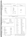
MODEL 301
OSCILLOSCOPE
P Y 4 A J
FABIO TEIXEIRA MAGAL HA~
c
s
M
N
E LEe T R ON I C S, INC.
manufacturers of precision electronic instruments
166 San Lazaro Avenue
Sunnyvale, Calif. 94086
\
.
WARRANTY
•f
CUSHMAN ELECTRONICS, INC. WARRANTS EACH OF THE INSTRUMENTS OF THEIR
MANUFACTURE TO BE FREE FROM DEFECTS IN MATERIAL AND WORKMANSHIP
FOR A PERIOD OF ONE YEAR FROM THE DATE OF ORIGINAL PURCHASE . THE
FOREGOING
IS
IN
LIEU
OF
ANY
OTHER
WARRANTY,
EXPRESS, IMPLIED
OR
STATUTORY.
THE
COMPANY, UNDER THEIR LIBERAL WARRANTY, WILL REPAIR
OR REPLACE ANY INSTRUMENT FOUND DEFECTIVE .
THIS WARRANTY MAY NOT APPLY · TO INSTRUMENTS
OF THE COMPANY, HAVE BEEN ALTERED OR MISUSED
WHICH ,
IN
THE
OPINION
This manual is intended to give the user a comprehensive knowledge of the instrument and its
operation or repair . In the event of trouble, study the manual carefully Most instrument malfunctions
can be corrected by the user with a minimum of lo st usage time .
For assistance or information of any kind, contact the fa ctory . Give full d e tails of the nature of your
problem and include the model and serial number of the instrument.
Should it appear that the instrume nt needs to be returned to the fa ctory for servi ce or recalibrat ion ,
let us know. Shipp ing instru ctions w ill be promptly given to you. There w ill be no charge for repair on
instruments within the one year warranty other th an transportat ion costs after 90 days of ownership .
Estimates of charg es for non-warranty or any other serv ice w ill be supplied by th e factory upon request
before work is begun and such work will be done on an actual co st ba sis only.
CLAIM FOR DAMAGE IN SHIPMENT
Your instrument should be inspected and tested as soon as it is received . The instrument is insured
for safe delivery. If the instrument is damaged in any way or fails to ope rate properly . file a claim with the
carrier or , if insured separately, with the insurance company.
We sincerely pledge our im m ediate and Iullest cooperation
to all users of our precision electronic instruments.
PLEASE ADVISE US IF WE CAN ASSIST YOU IN ANY MANNER
CUSHMAN ELECTRONICS, INC.
166 San Lazaro Avenue
Dial Area Code 408 - REgent 9 -6760
Sunnyvale, California
P Y 4 A J
! ABID
TEIXEIRA MAGALHAFS
i,
CONTENTS
Pag e
SECTION 1.
GENERAL DESCRIPTION
SECTION 2 .
OPERATING INSTRUCTIONS
2 .1
2.2
2.3
. SECTION 3 .
2- 1
.
2-1
.
2- 1
Genera l
Vertical Amp lif ier Boa rd
Horizontal Amp lifie r Boa rd . .
High -Vo lta ge Po w er Suppl y Board .
Low -Volta ge Po w er Suppl y Boa rd
.
. 3-1
.3-1
. 3-1
· . 3- 3
. 3 -3
.
MAINTENANCE
4.1
4 .2
SECTION 5 .
General · ·
Devia tion Mea surem ent s
Low -Frequency Phas e Compa rison
CIRCUIT D ESCRIPTION
3 .1
3.2
3 .3
3.4
3.5
SECTION 4.
1 -1
Calib rat ion Adj ustme nt s
4. 1.1 Vert ica l Ad ju stm ents .
4 .1 .2 Verti cal Gain .
4 . 1.3 CRT Bal ance
4 . 1.4 Horizo nta l Ga in .
Typi cal Volt ages and W avefo rm s .. .
.
. 4-1
4-1
4 -1
4-2
· . 4- 2
...... 4 - 2
SCH EMATICS AND PARTS' LOCATIONS
5 .1
52
5.3
Refer en ce Designato rs
Abb rev iat io ns .
Schem at ics. Part s Lists . and Pict orials
5 -1
5 -1
5 -2
ILLUSTRATIONS
2 -1
Oscill o scope Front Panel
3-1
3-2
Overa ll Block Diagr am
.
Horizonta l Amp lif ier Bo ard. Block Diagram
4-1
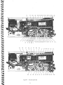
4 -2
Mo del 301 Oscill os cop e, Left-Sid e View o f Int erior ... .
M ode l 3 01 Oscil los cop e. Right -Si de View o f Int er ior .
5 -1
M odeI301(FP) . . . . . . . .
.
.
High Volt age Power Suppl y
Low Vo ltage Power Supply
.............
.
Vert ical Amplif ier (A 3l . .
.
Horiz ontal Ampl ifi er and Swe ep (A4) .
.........
5 -2
5 -3
5 -4
5 -5
__ __ 2 - 1
. . . 3 -2
. 3- 3
. .. . 4 - 1
4 -2
.
_.
.
.
.
.
5 -2
5 -5
5 -7
5 -9
5 -1 2
.
TAB LES
1- 1
Model 3 01 Specif icati ons
.
1 -1
4-1
4-2
4 -3
4 -4
4 -5
4 -6
Hig h -Vo ltage Supply Board Vo ltage Chart .. . .
tow-vonace Po w er Supply Board Volta ge Cha rt .
CRT Voltage Chart
Vertica l Am plif ier Board . Vo ltage Chart
.
Hor izont al Am pl if ier Bo ard. Volt age Chart
Hor izontal Arnplilrer Bo ard W averorm s
4 -3
4 -3
__ 4 - 3
. 4-3
· . 4 -4
4 -4
"
.
_
.
.
.
.
,
,
•
t
••
••
••
••
••
••
••
••
••
••
••
••
••
.
,•
.
••
••
.
•.
,.
"...
SECTION 1
GENERAL DESCRIPTION
The Model 301 Oscilloscope is designed for use with
the Cushman Models CE-3 and CE-7 FM Communica
tions Monitors, The Oscilloscope enables the
user to
visually examine the exact modulation delivered by the
transmitter. Any
abnormal
conditions
such
as unbal
anced modulation , pulses from the power supply , un
usual
clipping ,
and
other
problems
are
immediately
apparent so that appropriate repairs can be made . The
Model 301 has an automatic sync circuit to lock on and
precisely
display
waveforms. Vertical
display
is
cali
brated to show deviation on anyone of three ranges:
± 1.5, ± 5, and ± 15 kHz ,
Front panel switches permit an external vertical sig
nal input while using the internal sweep . External signals
may also be connected to the horizontal input. Thus, the
oscilloscope can be used independently of the monitor
ing function for routine testing , trouble shooting , dis
playing Lissajous patterns, etc.
Figure 2·'
Oscilloscope Front Panel
± 5% full scale in three ranges :
Dev iat ion A ccuracy
± 1.5 kHz, 5.0 kHz, 15 .0 kHz
External Inputs
Vertical and Horizontal
External Vertical Sens itivity
300 millivolts for full-scale
External Frequen cy Response (3 db )
30 kHz
Table 1-1.
Model301 Specifications
1-1
SECTION 2
OPERATING INSTRUCTIONS
2.1
2.2
General
The Model 301 Oscilloscope Plug -In has the stand
ard oscilloscope front-panel controls. most of which are
self-explanatory . (See Figure 2-1 .) A focus control. in
tensity control. and astigmatism control are provided to
ensure a clean trace on the face of the CRT. Vertical
and horizontal position controls are provided to position
the d isplay and set the display with respect to the zero
referen ce line on the scope graticule when the CE-3
function switch is In the CAL. position.
The lever switch directly below the CRT is a range
switch for vertical display of deviation and is directly
calibrated in ± 1.5 . ±5. and ± 15 kHz of deviation .
The scope circuit is de-coupled and the displayed de
viation will shift up or down if the transmitter under
test is off frequency .
Separate external inputs to the vertical or horizontal
am pli fie rs which drive the CRT are provided. Separate
O9gle switches permit selection of either internal or ex
te rna l signals in conjun ction with the external input
co ecto rs
e Model 301 sweep speeds can be adjusted with a
s . eep-speed switch and vernier control ; it is normally
sce ssarv to adjust the sweep speed to lock the audio
efor m being di splayed. The Model 301 incorporates
a to m at ic sync control which provides instant lo ck
any signal ex ceeding one d ivision in peak-to-peak
itude . A n external-vertical-gain control permits
atio n of sig nals applied to the external vertical
Operation of the Model 301 Oscilloscope with the
Model CE-3 or Model CE-7 to measure frequency devi
ation is described in the Monitor Manual.
2.3
a. generate an IF/Audio signal in the CE-3 or CE-7
that has a frequency of 10 times. 100 time s. or 1000
t imes that of the signal with which it is to be compared .
b. Set up the correct dividing ratio on the Model 308 .
c. Feed the Monitor output through the Model 308 to
the HORIZ. INPUT connector of the Model 301 .
d . Feed the si gnal to be compared to the VERT . IN
PUT connector of the Model 301
odel 301
Oscilloscope is removed by turning
rear panel of the monitor
ntercloc wise. When the locking shaft has been d is
_aged from the plug-in. pushing the knob inward
ause the plug-in connector to separate . The Model
j can the n be easily removed .
•
Low -Freguency Phase Comparison
The Model 301 can be used to compare the phase of
tone-operated squelch devices (such as the Vibra
sender) by using the Oscilloscope in conjunction with
the Model 308 Decade Frequency Divider. as follows :
e. Adjust the Monitor output frequency for the slow
est moving Lissajous patte rn on the Model 301 .
3 ge slotted knob on the
_
Deviation Measurements
o
ro long ed display of a bright spot or trace may
n the face of the CRT. Avoid this condition if
ssib !e, Use the CRT at half brightness to pro
lo ng the life of the CRT .
• High voltages are used in the Model 301 Oscillo
scope and the plug-in must not be removed or
replaced with the power sw i tch on . It is recom
mended that the power switch be turned off for 30
seconds before the Model 301 Oscilloscope Plug
In is removed to allow discharge of all high-voltage
capacitors .
2 -I
SECTION 3
CIRCUIT DESCRIPTION
General
K 1. wh ich is energized in these particular combina
tions of switch pos itions. The gain of the vertical am
plifiers is controlled by the deviation range switch.
which connects different calibrating resistances for the
1.5 -.5 -. and 15 -kHz ranges into the circu it.
it s of the Mod el 301 Osc illoscope are on
s- the Vertical Amp lifier board. th e Horizon
e
board.. the Low -Voltage Power Supply
2
the High-Voltage Power Supp ly board . The
c supply is fused (2 /10 amp S. B) at the plug
ce pt acl e J 3 . in th e monitor.
3.2
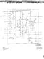
Vertical Amplifier Board
Figure 5-4 is the schematic diagram of the Vertical
Amplifier board . Transistors 01 th rough 06 comprise
a three-stage differential amplifier that drives the vert i
cle deflecti on plates of the CRT. The base of 01 is
biased to about +3 .2 volt s. by the Monitor di scrim ina
tor circuit when the VE RT. IN PUT sw itch is in the INT .
position. or by voltage divider R3 and R4 when the
swi t ch is in the EXT. position . The bia s on the base of
02 is var ied around +32 volts by the VERT . POS. po
tent iometer (R5) to move the CRT trace up or down .
The vertical amplifier is designed to have the proper
gain to produce full-scale vertical deflection of the CRT
when the signal from the Monitor 2nd I.F . and Discrim
inator board corresponds to a dev iation of ± 15 kHz .
for the 1.5-kHz and 5-kHz deviation ranges . the nega
tive feedback resi stors in the emitter circuits of 05 and
06 are shunted by appropriate res istances (R30 + R32
for the 1.5-kHz cange and R29 + R31 for the 5 -kHz
rangel to increase the amplifier gain by the right
amou nt to provide the correct vert ical deflection for
those ranges. Variable resistors R32 and R31 provide a
means for calibrating the two ranges.
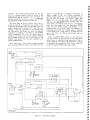
Fig ure 3-1 is th e overa ll block d iagram . The power
supply circuits and the usual cathode-ray tube controls
(A STIGM A TISM . FOCUS . and INTENSITY) are not
shown in the intere st of simplic ity. The CRT sweep can
be either externa l or interna l. The externa l sweep is ap
plied through the front-pan el HORIZ. INPUT BNC con
nector when the associated sw itch is in the EXT. pos i
tion . When the swit ch is in the INT po sition . the swe ep
comes from the internal sweep generator. The int ernal
sweep period is selectable by a four-position switch
and a vernier control from less than 0 .5 millise conds to
more than 50 mi llisecond s. and is synchron ized w ith
th e vertical input. A blanking signal is fed through an
amplif ier on the High -Voltage Power Supply board to
th e cathod e of the CRT to blank the return trace . The
hor izontal pos ition of the CRT trace is adjustab le wi th
the HORIZ. POS . control . which determines the dc
olt age on the horizontal defl ect ion pla te s.
The input to the CRT vert ical deflect ion plate s can be
a ext ern al signal (when the VERT . IN PUT sw itch is in
t e EXT. pos ition ) or it can co me from the 2nd I.F. and
iscrim i nator board of th e CE-3 or CE-7 (when the
ERT INPUT switch is in the INT . position ) In the
I T. posit ion . the oscilloscope displays the modulation
de iati o n of the signal bein g monitored by the CE·3 or
CE- 7 . In addition . afte r the oscilloscope trace has been
ce ntered vertically by the VERT. POS. control while the
. or is in the CAL . mode . the Mon it or can be
5 . e ed to the FREO.-DEV . MEASURE mode and the
ito red transm itter 's center-frequency error is rep
esented by the d isplacement of th e trace from the
cen te r line . Thus . the Model 301 Oscilloscope can
sed to indi cate fre que ncy er ror as w ell as FM
Transistor 07 is the sync amplifier . Its i nput come s
from one of the CRT vertical deflect ion pl ates . and its
out put is fed to the trigger circuit on the Horizontal
Amplifier board .
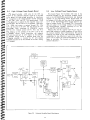
3.3
Horizontal Amplifier Board
On th is board are the int ern al sweep generator for
the CRT and the amplifiers to drive the horizontal de
flection plates of the CRT from either the internal
sweep or an e xternal ho rizo ntal input. Refer to the block
diagram (Figure 3 ·2) and the schematic diagram (Fig
ure 5-5)
a ion.
vert ical signal inp ut is dc- amplified and applied
of th e vertica l deflect ion plates through revers relay K 1. Input to the other vert ical deflection plate
c ampli fier de voltage from the VERT POS. potenti
ste r. For most sett ings of the CE-3 frequency sel ec
it c es. the LO freq uency is 10 MHz lower than
ialed -in frequency. When this is the case. relay
is deenergized and its co nt act s fe ed the vert ical in
• si qnal to the vertical deflection plates in such a way
5 0 cause an upward def lection of the CRT trace for
rease in the frequency of the monitored signal.
~ _ ·er. when the 1st-di git frequency selector swi t ch
po sition 0 or 1 wh ile the 2nd ·d igit switch is in
_ '.- n 2 or 3. the CE-3 LO frequency is 10 MHz
th an the dialed-in f requency. This would cause
_ be am to deflect downward for an increa se in signal
oencv if it wer e not for the reversing act ion of rel ay
Assume that the HORIZ. INPUT switch is in the
INT. position . the SWEEP switch is in the 10-msec
position. and that there is no sync input. With no sync
input. the output of Schmitt Trigger 01 /02 is essen
tially ground potentia l: therefore. resistor R12
is
shu nted by approx imately 10 kilohms (R 13 ' plus R39).
This lowered resistance demands more current than the
co nstant-current source (06) can supply to keep re
generative switch 03 /04 on hence it turn s off. When
the regenerative switch turns off. timing capacitor C6
starts charging
linearly from
the
constant -current
Source . When C6 charges to the threshold level of the
regenerati ve switch . the switch closes and discharges
C6 . After C6 discharges. the shu nt across R12 again
causes the regenerative switch to turn off. and C6 re
charges. Thus. a sawtooth waveform is generated at
th e top plate (in the block diagraml of C6 . This sweep
3- 1
signal is converted to a rectangular waveshape by
Schmitt Trigger Q 1/ Q2 . and is further converted to
posit ive tr igger pulses by the circuit consisting of C2 .
R9 . and CR 1. The output of the Schmitt Trigger also
charges C9 to a pos itive voltage ; this voltage back
biases CR5 . thus removing shunt resistors R13 and
R39 from the regenerative switch circuit. The regener
at ive switch can now be turned off only by a positive
pulse from the trigger circuit . The regenerative switch
stays off until timing capacitor C6 ch arges to the
threshold level of the switch . When this happens . C6
discharges. and canno t start charging again to produce
a new sweep until a trigger pulse is received from the
sy nc cir cuit. Thu s. the sweep is synchronized with the
vertical input.
waveform is Jed through emitter follower Q7 and one
half of a differential am plifier (Q9 i Q 11) to one of the
hor izontal deflection plates . The othe r horizontal de
flection plate is fed by the other half of the differential
amplifier (Q 1O/Q 12 ). the input to whi ch is a d c volt
age adjusta ble by HORIZ POS pot ent iome ter R7
The bottom plate of timing capaci to r C6 is not re
turned to ground as is co nven tiona l. but instead. is fed
a portion_pf the potential from the top plate of the ca
pac itor through emitter fol lowers Q7 and Q8 . This
changes the effective capacitan ce of C6 and therefore
the timing period . The amount by which the effective
capacitance is changed is co nt rolled by the SWEEP
vernier potentiometer . R6. Thu s. the sweep period is
determined not only by the tim ing capacitor selected
by the SWEEP sw itch . but also by the setting of the
SWEEP -vern ier control (t he red knob concentri c with
the black SWEEP sw itch)
When the HORIZ INPUT switch is in the EXT. posi
tion. th e junction of R 12 and CR5 in the regene rative
switch circuit is grounded to stop generation of the in
ternal sawtooth . The gain of the differential amplifier
is adjustable by potentiometer. R38 . wh ich varies the
amount of negat ive feedback i n the output stage .
Now assume that a sync sig nal is be ing received
from the vertical-deflecti o n input of the CRT. This sync
r----------------------l
q BOARD
I
"': R I ZO ~'r :"~ ':' V ;l ..
t:
:::
( XT
H ORIZ.
cr
I
I
.o.MPL
A
---+
TR I GGE R
I s _cc-
CIR CUIT
( ' ~ R O -: "
I
I
I
I
I
J
.....
L
___ ___
- - - - ---CC- l l
I
I
I
HQ RI Z
AM P L
B
______ J
~r 1:
1"
I
I
_" OR' Z
I
pas I
r
~-----------------,
AMP L lf l(~ 8 0 AQ :
I
.: =- :.:. .
ITCJ
0;-
'~ J V (' nd : F
i:
s: ~
EJ
I
I
I
I
I
I
I
I
I
I
I
: " ,:
zv z
-
v , 1\,:. ...OR
1'2 0 v
I
I
I
I
,-
I
I
-=
B
-----
I VER T POS I
0 I
12v
.¥'
A M PLI FI ER
r -
co" vOLT AGE -
l
L + : R SUPP LY BOA R D
I
R( v( RSING
I
...... ~( L :'; """"
r-r
I
I
?
?~,
,
L __
_____ J
I
I
I
I
I
I
-g
Iv
I
I
..J
~ §]
-
.-:
.-
...
GND r ROM 1\ 1 8 2 n d
DI GIT
I
I
I
I
ll.M P Lr F I (~
I
8 L A N K:'\jG
L
_______ -.J
I
V( R TICA L
L __ ______
I
A
I
I
I
.o.~P ll F I £ R
~
I
SU P PL Y S OAR D
I
I
'o( R T I C A L
I
I
I
I
I
8
-"7'G "-=- vOLT AGE- -,
I PYrR
I
I
SWITCHES
Figure 3- 1
Overal l Block Diagram
Low -Voltage Power Supply Board
High -Voltage Power Supply Board
3.4
This boa rd (Figure 5-3) furn i shes 240 vo lts to th e
hor izonta l am plif ie r o n the Ho rizonta l A mp lif ier board .
and to th e ASTIGMATISM potentiometer and blanking
ampl ifier on the High -Volta ge Po we r Supply boa rd . A n
ac voltaqe of 245 volt s rms from one of the seconda ries
of Tl on the High-Voltag e Power Supp ly boa rd is ap
p lied to bridge rect if ie r CR1 throu gh CR4 . The po sit ive
320-volt output of the bri d ge rectifier is fed th rough
th e em itter -follower regulator . consi sti ng of 01 . R2 .
CR5 . and CR6. to the board conn ector .
Resisto rs R3 and R5. tog ether w ith R4 . are the col
lector load resisto rs of vert ical amplifiers 05 and 06 o n
the Verti cal Amplifier board . Pot ent iometer R4 perm its
changin g the values of the load resistances slightly to
compensate fo r any differen ce in gain of the two tran
sistors and to adjust th e el ectri cal displacement of the
beam to mid -scale . The fun ction of relay K 1 is ex
pl ained in Section 3 .1 .
bo ard fur nishes - 120 0 vo lts for the CRT. As
ho n In th e sche mat ic d iagra m . Fig ure 5 - 2 . th e 920
t s acro ss th e high -vo lta ge seconda ry of transform er
IS ap plied to th e vo ltag e-doubler rec t if ier con sisti ng
C 1. CR1 . CR2 . and C2 . Th e appr oxi m at ely -2 10 0
, s ac ro ss C2 is redu ced by the regulato r circu it co n
's o, _ of R1. R2 . R3 . and V 1 to a regul at ed -1200 vo lt s.
- 12 0 0 vo lt output is appli ed th roug h R9 . lOO k
• to the g rid of the CRT . and also across the volt e-d iv id er ch ain co nsi sting of INT EN SITY cont ro l
- 2 . Rll . FOCUS co ntrol CH -Rl . R12 . and R13 .
po tent ial on the cathode of the CRT is set by the
,
E SITY co n tro l. wh ich determ in es the negative
' as on the grid (pi n 2) with respect to the cathode :
additio n. during retra ce a negative pulse from the
ri zo nt al amplifier is inverted by Oland appl ied
... a ug capacit o r C4 to the cat hode of the CRT. cutt in g
oH he beam
BL AN KINGl
EM ITTE R
f OLL OWER
OS
r----------------------------l.
II 7 ~?~~2 ...------,
1
I
CO,.S TANT
C U ~ ~E N T
S O ~ ~C E
0 6
,--
....
"
c __
I
' ...._· 1
~h
0 3/ 0 4
QI / 0 2
RI3
~ 39
CR S
..1£B
I .....
I ......
RI 2
_I~.7 /~6
1: J
[Q}]
R38
B
0 10 / 012
ISWEEP I
fEEOBA CK
.
~ E MI TT ER I.....'-----t.~
f OLLOwE R
OB
..
ISW E EP I
VERNI ER
CH- R 6
-=
Horizontal Amplifier Board. Block D iagram
3-3
GAIN
HOR , Z
AM PL .
SWI TCH
SW 3
Figure 3 -2
~H ORIZ
C5
1 '"
1--_--1~
09 /0 11
1
I SW4
REGEN
SWITC H
T RI GGER >-.L~...-I
AM: L
I
~:
07
S.
HOR I Z
[@] )~
COUPLI NG
. . - j E' " TTER
~ f OL Lo w ER
SCHM I T T
BL ANKI NG
OUTPU T
SWEEP
OUTPU T
TO HORtZ
OEf L PLA TES
I
SECTION 4
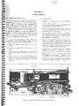
MAINTENANCE
ration Adjustment
4.1.2
~ :l six internal adjustments in the
Vertical Gain.
Model 301
Con t rols for these adjustments are Io
n i n Figures 4-1 and 4-2 . The adjuste ce pt the horizontal gain adjustment) are
t e Model 301 plugged into the CE-3 or CE-7
·0
and operating . The controls .shown in Figure
ca n be reached by remov ing the left-hand CE-3 or
CE- 7 cover. as described in the maintenance section
o f t e Monitor Manual. The only test equipment re
qui red is an unmodulated transmitter operating on any
frequency covered by the Monitor. Unless otherwise
stated, the controls mentio ned in the following proce
dures are on the Model 301 Oscilloscope.
'a. " Dial-in " the frequency of the
used for the test.
4,1,1 Vertical Amplifier Balance. Before making any
adjustments of the vertical deviation ranges. the verti
cal amplifier balance should be checked as follows :
e. With the deviation range switch set to ± 15 kHz .
offset the " dialed · in " frequency 15 kHz high and
low from the FCC assigned frequency . The scope
trace should shift up and down by 15 kHz .. If ad
justment is required, use the ± 15-kHz potenti
ometer ; the n recheck the transm itter frequency.
"""".......~"-""''V''' .
a. Place the
posit ion .
Monitor
b. Set the front-panel
pos it ion .
function
switch
VERT . POS
in
the
control to
transmitter being
b. In the CA L. pos ition of the Monitor funct ion
switch. adjust the CA L. control for a zero or mid
scale reading on the FREQUENCY meter .
c. Set the front-panel deviation range switch to
± 1.5 kHz and adjust the VERT . POS . control so the
trace is on the ' '0" reference line.
d . Set the Monitor function switch to the FREQ.
DEV . MEAS. pos ition. Key the transmitter and ad
just it " righ t on frequency "on the ± 1.5 -kHz
FREQUENCY error meter range.
CAL.
mid
f . Repeat step e. on the ±5-kHz deviation range by
offsetting the "d ialed-in " frequency by 5 kHz .
Ad just th e ±5-kHz potentiometer if necessary.
c . Set the front -panel range swit ch to the ± 15 -kHz
posit ion and note the position. of the trace on the
CRT.
g. Repeat step e. on the ± 1.5 ·kHz deviation range
by offsetting the " dialed-in" frequency by 1.0
kHz . Adjust the ± 1.5-kHz potent iometer if necessary.
d . Switch to the ± 1.5-kHz range and adjust the po
sition of the trace to the same po int noted above ,
u sing the vertical _ ampl ifier balance control (see
FIg ure 4-1).
h. Recheck the vertical amplifier balance adjustment
by repeating steps a. through d . of Section 4.1 .1.
±5
C.RT. BALANCE
kHz
:::. :-=).
·L~~o~ :. ·
VERT. AMP
! 1.5 kHz
Figure 4-1.
BALANCE
Model 301 Oscilloscope. Left-Side View of Interior
.( -1
tiS kHz
I
I
,
~
4.2
4 .1.3 CRT Balance. If the trace is not on the zero ref
ence line after adjusting the vertical ampl if ier balance
control. adjust the CRT balance control until the trace ' is
on the zero reference tine . (See Figure 4-1 for location
of the CRT balance controt .) This control centers the
range of the front-panel VE RT. POS. contro l.
Typical Voltages and Waveforms
Tables 4-' through 4-6 give typ ical data for the four
Oscilloscope boards and the CRT. Test conditions are
as follows unless otherwise stated :
Line Voltage
Control Settings:
FOCUS
INTENSITY
EXT. VERT. GAIN
ASTIGMATISM
VERT. POS
HORrZ . POS.
Deviation Range
SWEEP Range
SWEEP Vernier
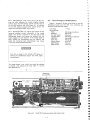
4:1.4
Horizontal Gain. An internal gain contro l on the
hor izontal amplifier permits adjustment of the sweep
length. This control is located on the right side of the
Oscilloscope plug -in and cannot be reached with the
scope plugged into the Monitor. If the sweep length is
short. remove the Oscilloscope from the Mon itor and
adjust the horizontal gain potentiometer (see Figure
4·2) in the counterc lockwise direction .
, 15 vac
Mid -range or optimum
M id-range
M inimum
Mid-Range or optimum
Mid-range
M id-range
±'5 kHz
50 msec
Fully ccw.
~
•
•
•
Turn the ac power to the monitor 0 FF before re
moving the Oscilloscope plug- in and wh ile replac
ing the plug- in .
The sweep length is not critica l. but should be adjusted
to provide a full sweep of the trace when it is on the
zero reference line .
o
HORIZONTAL
GAl N CONTROL
Figure 4-2 .
Model 301 Oscilloscope, Right -S ide View of Interior
4- 2
..
INa vertical input; INTE NSITY co ntrol max cloc kwise )
HO RIZ. INPU T Switch
in INT . Po sition
HORI Z. INPUT Switch
in EXT. Position
Transformer
HV Seconda ry
920 vac
-
- 1125 vdc
-
CR1 Anode
- 2180 vdc
-
C2
-1 200 vdc
· 1200 vdc
V1 Cathode
VI Anode
0.24 vdc
0.25 vdc
9.0 vdc
10.0 vdc
~9 .6V
01 Base (del
__. ;
(ac)
-
O.Bv
40 vdc
9.5 vdc
01 Collector (dc)
JLJ
(ac)
Table 4 -1 .
--
150v
16v
High -Vo lt age Power Supply Board
Voltage Chart
(Wit h 032 -vac. I - kH z. 3 .2- vdc inpu t ; 15 - kH z range )
Inp ut to Bridge Rectifie r
2 4 5 va c
Cl
3 0 0 ± 5 vdc
0 .7 vac
01 Base
240 ± 10 vd c
Test Po int T P 1
240 ± 10 vd c
Table 4 -2 .
01 Base
32 vdc
0 .90v POp ac
01 Collecto r
74 vdc
1.5v Pop ac
0 2 Base
3.2 vd c
Ov Pop ac
02 Co llector
7 4 vdc
08 7v Pop ac
Low -V oltag e Power Supply Board
Com mo n # 1
Voltage Chart
03 Emitt er
84 vdc
0 4 Emitt er
84 vdc
Comm on # 2
10. 7 vdc
Ov Pop ac (ap pr ox .)
05 Base
- 1.2 vdc
5 .2v Pop ac
05 Co llector
12 5 vdc
80v Pop ac
0 6 Base
- 1.2 vdc
4 .2 v Po p ac
06 Collecto r
125 vdc
77v Pop ac
Common # 3
- 8 .8 vdc
OV Pop ac Iapp ro x.)
07 Base
14 vdc
1.0v p op (cl ipped) ac
07 Collect or
8.0 vdc
12 .0v Pop (clipped) ac
Filament ;
Pin 12
Pin 1
Grid ; Pin 2
- 12 00vdc
- 1200 vd c
. - 1200 vdc
Cathod e ; Pin 3
- 1160 vd c
Focus ; Pin 4
- 840 vdc
Vert ical Plat es;
Pin 6
+125vd c
7
+ 12 5 vdc
Pin
A stigm at ism ; Pin 8
+ 125vdc
Ho rizon ta l Plat es;
Pin
9
Pin 10
Table 4 -3 .
- 3.6 vdc
Ov p -p ac (appro x .)
+125vd c
+ 125 vdc
(Ab ov e readings depend on sett ings of all po ten tiome te rsl
Table 4 -4.
CRT Voltage Chart
4-3
Vertical Amplifier Board . Voltage Chart
l
Vertical Signal;
HOR IZ. INPUT Sw itch
inINT . Pos ition;
SWEEP Switch at 10 msec;
SWEEP Ve rnier Max . CCW
No Vertical Signa l;
HORIZ . INPUT Switch
in EXT. Position
.-
ovdc
01 Base
01 Collector
02 Base
0-2 Col lector
03 Base
03 Col lector
C9
06 Emitter
06 Colle ctor
08 Em itter
05 Emitter
09 Base
09 Co llector
010 Base
010 Collector
Commo n #1
a11 Collector
0 12 Co llector
Comm on #2
-4.9 vdc
6.8 vdc
0.60 vdc
6.5 vdc
9,6 vdc
o 16 vdc
6.0 vdc
14.2 vdc
7.0 vdc
0.70 vdc
9.2 vdc
0.5 vdc
-4.0 vdc
0.7 vdc
-4.0 vdc
+ 3 7 vdc
125 vdc
135 vdc
-7.8 vdc
11.7 vdc
1.0 vdc
0.50 vdc
10,6 vdc
ovdc
0.40 vdc
14.2 vdc
118 vdc
0,95 vdc
10.0 vdc
0.5 vdc
-4.0 vdc
0.7 vdc
-4.0 vdc
+37 vdc
128 vdc
134 vdc
-7.8 vdc
I
!
I
I
Table 4 · 5 .
Horizontal Amplifier Board , Voltage Chart
I
I
Q2
Ql
i
!
B
C
B
C
Q6
Q3
I
Q8
0
::;;::~
on
Q 12
C
C
CJ
::;;::~
E
B
C
~I O . 2
/1+ .8
C
E
E
B
I
~
I
z
Q 10
Q9
Q5
C
I
B
C
0
o
~
..
I
8
i N+ o .
;I
- II
U+n
14
11
+0 .4
+.:
o
U+
+.5
1.4
°
-
Vl:::
y
O.9
-8
rm lA N3.6
9.4
0 .8
1O
•
0. 2
- 4.8
Numbers o n wavefo rms ind icat e voltages with resp ect to ground .
B
Base ; C
Col lector ; E
Emitter.
=
=
=
Table 4 -6.
Horizontal Amplifier Board Waveforms
,0
11.' 3.7
-4 .4
.0
22O
200
55
40
1A N
,0
~
.:.
~~
SECTION' 5
SCHEMATICS AND PARTS' LOCATIONS
e re nee Designators
assembly
H
henries
IF
intermedi ate frequency
incandescent
in ternal
Incd
INT
board
capacitor
k
Lin
diode
device signaling (lamp)
logari thmic
LPF
m
low pass filter
milli - 10 -3
M
meg - 10 .6
misc. electronic part
FIL
filter
J
K
jack
L
inductor , RF, choke
M
CH
meter
chassis
FP
front panel
RP
rear panel
P
plug
Q
transistor
R
resis tor
Hz
R
hertz
therm istor
N RFR
rel ay
linear
Log
E
fuse
kilo - 1000
MF LM
meta l film
MFR
manufacturer
Minat
minia ture
Mom
My
momentary
" m ylar "
N
NC
nano (10' 9)
N/ C
N/O
NP O
norm all y closed
not connected
no rma lly op en
negative pos it ive zero
not recom mended fo r field
replacem ent
SW
sw it ch
P
peak
T
transform er
PC
printed cir cuit
TB
p
terminal board
pF
picofarads - 10- 12 farad s
test point
PIV
peak inver se vo ltage
V
X
vacuum & display tubes -
P/O
part of
crystal
silicon con troll ed rectifier
Poly
Porc
polystyrene or polye ster
porcelain
speake r
Pos
positio ntsl
Pot
potentiometer
PI P
peak-to -peak
amperes
Rect
rectif ier
automa tic frequen cy control
rad io frequency
amp lif ie r
RF
S oB
b andpass
Sem i
sem icondu ctor
coun te r-cl ockw ise
Si
silicon
ceramic
Ta
tantalum
coeffic ient
Tog
togg le
SCR
S
5.2
A .p
C
pI
Abbreviations
slow -blow
com mo n
Tol
tol erance
co mposition
Trim
trimmer
conne cto r
TYP
clo ckwise
Jl
typ ica l
mi cro - 10 . 6
V
volts
deposited carbo n
Var
variable
electrolytic
VDCW
d c working vol ts
E cap
en capsu lated
WI
w ith
EXT
ex ternal
W
watt s
r
farads
ww
w irewo und
germanium
W/ O
w ith out
T
C
ep C
E ec ro
e
.
0
cathode -ray tube
g round(ed)
5 -1
c
[:
5.3
[I
Schematics, Parts Lists and Pictorials
l
On the following pages schematics. parts lists and pictorials are grouped
schematic,parts list,and pictorial of a given PC board are found on adjacent pages.
according
to
subassembly.
Thus.
[:
1
j
[~
1
TI
R2
RI
SWI
R3
R4
SW3
R7
R5
SW2
R6
JI
J2
SW4
Figure 5-1.
Model 301 (FP)
5-2
~- """
C assis Components
DESCRIPTION
EF.
CIE STOCK NO.
MFR.
RESISTORS
Rl
R2
R3
R4
R5
Pot .. cornp.
Pot. cornp.
Pot. cornp.
Pot .. cornp.
Pot. cornp.
1 megohm. 1/2W
500k ohm. 1/2W
lOOk ohm. 1/2W
500k ohm.1/2W
100 ohm. 1/2 W
R6
R7
Pot .. cornp. 10k ohm. 112 W
Pot. cornp. 1k ohm. 1/2 W
1203-0027
1203-0026
1203-0025
1203-0026
1203-0023
Allen-Bradley
Allen- Bradley
Allen-Bradley
Allen- Bradley
Allen-Bradley
P/01851-0024
1203-0024
CTS
Allen-Bradley
1851-0016
1850-0007
P/01851-0024
1850-0007
Centra lab
Alco
CTS
Alco
2536-00
Kings
2605-0011
Cinch
SWITCHES
SWl
SW2
SW3
SW4
Lever. 1P3 pos
Toggle. 3P2 pos
Rotary. 1P4 pos
Toggle. 3P2 pos
JACKS
Jl
J2
J3
Connector
SameasJl
Tube socket. 12 pin
PLUGS
Pl
Connector. 24 pin. male
2535-0019
TRANSFORMERS
Tl
Power Transformer
1575-0007
Basler
KNOBS
Knob.
Knob.
Knob.
Knob.
Knob.
Knob.
Knob.
Knob.
FOCUS
INTENSITY
EXT. VERT. GAIN
ASTIGMATISM
VERT. POS
HOR POS
SWEEP. inner
SWEEP. outer
7/16 in dia Black
7/16 in dia Black
7/16 in dia Black
7/16 in dia Black
5/8 in dia Black
5/8 in dia Black
3/4 in dia Red
1 in dia Black
2780-0019
2780-0019
2780-0019
2780-0019
2780-0017
2780-0017
2780-0009
2780-0007
King-Kasch
King-Kasch
King-Kasch
King-Kasch
King-Kasch
King-Kasch
King- Kasch
King-Kasch
1270-0019
RCA
4941-004
Cushman
TUBES
CRT. 3Pl A. 3-inch flat faceplate
MISCELLANEOUS
Graticule. CRT.
5-3
1 - ';;-;;;;-- -
I~
~o,
:1 _
, - - - --- - - - - - - - - - - - - -- - - -- - - -- --- -- - -- - - - - - 1
I
I
I
LCd-=t
_ ___ Ji
I
I
C E3
1'l'lT£ Ns ITY
R2
I,ocusl [
I Mr G
l~
~, - I
I
I
~K
I
I
~ .... .." ..~ :~ ., ~ ....... ~
RI
I..S Tl C.. ...TlS N I
Rot
'I '
:>
tn
~O O,l(
T y UH
I
G" I~ I
RJ I OOIt
' T'·'~
, I
I
I l? ~
I
-e-
II
I
I
_
'~I®©®©
~;'~~=r--~(',' - ------- -- - ---
I
I
A-'
- 1200v POW'ER SUPPLY
I
'"
...,
~ ~l--- --~~~ ~ ~ ~ ~ ~ ~-~~~~~~~---n -n --~
~.
I
I
HQA IZOHlAl. AWP\. If I[ R
a
II
"'
I VE RT . Pas.1
'00
0 1 ffi!
S w( [ P
I.
IITP
f'
L"-'
[ill
f.,
sw,
~
R 7 1.11'
I HORII .
PO S.1
~
G
10 .-: F/6
l]ill!]
$W4
§:!J
~)
[ill)
OED
[gD
sw'
j 5\11' H F' I
1 '
sw,
I
. . .. . .
0.' . .. ... u
' __" -.)''''
., 0'·.._•."""."
·v.-, ••
~
..
, ~. ,
. .......
~
.... _ .. ,..
·_'."
··.-."
" "0
..
I> • •
, .~,~
• · .. .• ·.', ..:..0. ·' ...
"~", '
' . ''' ~
, '''''''''' ....
... '" ....".0
O I~ I
W I R ING
~OO£L ~O'
-..1" 0
...
D! A.C R I\ W
OSOL LOS COP{
I v ( FlT
INPU T
.. . ... . . .. ..... '
. , ,_
.. _,
""" " -'- 1
.- ---..,
JO
to" ' ,,-,,"' ' _ . ~ C '-"""" ' '' IOo-:'' ' 00(
. .. . ~ 0 • • _ .... , ~'
'""" D ' 0 . 1M' QIl"I o .. .
. "0 . \ .-) . 10
>" Q
I
..-----.
,
n
o(Ooo • • 0
.. · " · O)oo o,..j,I O"_u •
00 ' 004..... ... QoO. ' U - . . D
, "-t .. , . _
..---,
(. . -
..
~
r---l
~
TP
TP
16
15
R5 0 1
RII
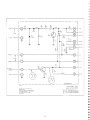
Figure 5-2 .
R8
High Voltage Power Supply (A 1)
Chass is A -l . Hig h Voltage Pow er Suppl y. PC Boa rd 0074
CKT. REF.
DESCR IPTIO N
CIE STOCK NO .
MFR .
CAPACITORS
Cl
C2
C3
C4
Me talized Film . 0 .047 J.lF ± 10%. 2500V
Meta lized Film. 0047 J.lF ± 10%. 2500V
Cer. 47 pF ± 20%. 3000V
M yla r, 0.4 7 J.lF. ± 20 %, 1400V
10 0 8 -0 0 3 0
10 0 8 : 0 0 30
10 0 5 -00 4 5
1008 -0044
Sprague
Sp rague
Centralab
TRW
1281 -0029
1281 -0 0 2 9
Varo
Varo
1271 - 0004
RCA
DIODES
CRl
CR2
sr VB-40
si. VB-40
TRANSISTORS
Ql
Si.2N34 ':; Q
Rl
R2
R3
R4
R5
Com p o560k ohm ± 5%. 1W
Comp , 560 k oh m ± 5%. 1W
Com p o560k o hm ± 5%. 1W
Comp o1k oh m ± 5%. 1/ 4 W
Comp , 5.6k ohm ±5%, 1/4W
10 68- 564 5
10 68 -5 64 5
10 68 - 564 5
10 6 6- 10 2 5
10 66 - 5625
Allen - Bradley
A llen-B rad ley
A lle n- Brad ley
Al len- Brad ley
A lle n- Brad ley
R6
R7
R8
R9
R10
Com p, 2M ohm ±5%, 1/4 W
Com p.150koh m ±5%. 1/4 W
Com po2M ohm ±5%. 1/4W
Compo lOO k oh m ± 5%. 1/4W
Com p, 680kohm ±5%. 1/4W
106 6 - 20 5 5
10 6 6 - 154 5
1066 - 20 5 5
10 6 6·1 0 4 5
10 66· 68 4 5
A lle n- Bradley
A llen- Brad ley
A llen-Bra dley
A llen-B rad ley
Alle n- Bradley
Rll
R12
R13
Comp o1.5M ohm ±5%. 1/4W
Com po2 .2M ohm ± 5%.l W
Com p.2 .7Mohm ±5%,lW
1066 ·1555
106 8 · 22 55
1068 ·2755
Alle n- Bradle y
A llen -Brad ley
Alle n- Brad ley
1281 ·0017
Victoree n
RESISTORS
TUBES
Vl
Regulator , 1200V ± 1.5%. GV3~
5·5
.1
I
,-------------- I
TI R ED
r
920 VAC
TI RED
~;
1
~( 0)(
-2 100V
I
I
,RO M
A4 - T P
- 1200 V
FP·RZ- 5
VI
i
/0
I
I
I
I
I
0 2
(2
v a - -<0
.0 4 7
Fp· RZ· 2
GV 3 S
~I
0
6 8 0 K
I
I
~\ 1
~FP-~ -'
~®--+FHI- 3
~8
2 .0
MEG
Tp
5
~6
2.0
MEG
IP
I
I
I
I
F '-~ I- l
J5 -1
8
~--A 1
~
}--
J3 - 12
I
QI
I
2N
J3 -3
3440
I
S2
I
P I-24
IW
v s -.0
I
BL ANK ING
RJ
56 0 <
IW
J3· Z
I
t
Rl
5 60 <
0 1
~
6 .5 v AC
IW
I
---J
I
I
1
I
L
_
AZ -TPI
PC
___
BD 007-4
__ -.-JI
5- 1 - 69
- 120 0 V
P OWER
SU P PLY
MODEL 3 01 O SC I LLOSCO PE
, IIl S.loTCAS 1 , ...
~ ' ''~ . ~H
~
(A "" ~( vcn c
c. ... ..c , ' O " ~ \lA. 'Jt S.,..
)
. " :I1.i ~ ' O Iil S
.. O.. ... S.I.i..
~I SS
01 ..
" l l vo, ' . Gl Al. e
O' .. lll .... H " C' l O
..c.s
11"4 1$ :' ''''''N ~ ' S '''T E ''O~O FOil flo'! OP(II "I'O "l .NO
c £ Q' (LiS.. ..... " ( l EC fR O" 'CS lOul ''''! ""
'-l .. , .. -
.-t
.. . ' &( TOII.' S (a C'~D ...... ....'.
s
coP't'r. c.- " ·.,.,a 15 " ( 1..$ .. ... ... .. u.ec t eo-ocs I,,"'
.. .. dS. <:. O· .. ( M I$( "'0 ' ( 0
v " lI.Jl s ' v , · V.. l( U O· .. { f1 , ~! "'O' l O
~·
", NO
cc ~, ... IS$
wrr .. ~
,;
.·
:;r
",R
rsc -, : ~ -,~
TO I E UHQ Q T"E RW'S ! 0 '" A( P Fl.O OUC EO
Ir [ -,
(0 "'5( "11
FR OM
cvs .......'"
£LE e
•
.-•
~
,
•
5 -6
R5 _ - --+'::rt
=
=--
-
-
R4
R 3 - - --=
FP-R2
01
TPI
TP4
CRI
FP -R3
TPIO
CR2
TPI2
CR3
TP~
CR4
CI
RI
R2
CR6
CR5
Figure 5 -3.
Low Voltage Power Supply (A2l
C. assis A -2 . Low Voltage Power Supply. PC Bd 0083
CIE STOCK NO.
DESCRIPTION
CKT. REF.
MFR .
CAPACITORS
Cl
Electro . 20 J.tF. 450V
1010 -0004
Sprague
1281 -00 30
1281 -0030
1281 -Q030
1281-0030
1281-0022
1281 -0022
General
General
General
General
Solitron
Solitron
1313 -0002
Parelco
1271-0004
RCA
1066 -6845
1069-2735
1076-0008
1200-0014
1076 -0008
Allen -Bradley
Allen -Bradley
Electra
Allen-Bradley
Electra
DIODES
CRl
CR2
CR3
CR4
CR5
CR6
Si. 1N-5062
st 1N-5062
st. 1N-5062
si. 1N-5062
si. Zener . 120V.
--
1.5R120B
Si.Zener. 120V. 1.5R120B
Electric
Electric
Electric
Electric
RELAYS
Kl
12 VDC. DPDT
TRANSISTORS
Q1
Si. NPN . 2N3440
RESISTORS
Rl
R2
R3
R4
R5
Compo 680kohm ±5%. 1/4W
Compo 27k ohm ± 5%. 2W
M Film . 88.7k ohm ± 1%. 1W
Pot. cornp. 25k ohm . 1/2W
M Film . 88.7k ohm ±1 %.1W
5 -7
[~
TI ORANGE
l
---..---+--{
~,:":,:,,,:,,_---...- - - -- - --
TI ORANGE
..L.._-+_-{
AJ -T P 10
- - - - - -+- -{
J 3- 6
------+--{
-+_ _ ...J
AJ - TP 8
J-----jf-- TO A4 - TP2 1
...- - - 1 - TO AI-"PI 3
_ - - - ( T'p
RJ
88 .7 K !. ' ,"",
''''
+ _ -{ T:
AJ - TP9
JJ - 7
}
~
CRT BAL.
}-- - - - - l-
. '- 24
....- - - - --1--
- - - - -+--{
R5
88.H:i '"
A3- TP I
....- - - - - - - A3-TPI5
I ".
A4 -T P 7
SW2 - 6
..- - - - - -+-
- - - - -+--{
KI
A4 - TP 26
CH-R6 - 3
., - 2 1 - - - - - - . , . . - - {
I
I
fP-R J
F P·R 2
INT ENSITY
lOOK
EXT v ERT
I
L
5 - I - 69
I " 1'I1'l 10 0llS . I" • .
soo
I
K
GAIN
A3
AJ
AI
1 P I4
TP 2
T P~
J3 -4
AI
TP7
J 3- 8
~d
AI
AI
AI
1 P6
TPIO
TP 2
'1", y " ~ u t , ''' 00' W''S u'' d SS
) ,.. OUCTO "" ·""'\V I S ·"
,:;... · .". ",. .. ( .,/'Soo"' ..... I. t :-. : .. ..\ ""'
co"
Ol" l lh ll S( /ItOTlO
, ""•...co , o..s·"' .... ~v ( s ,.. ~ . u....1 ss.o r H ~ .....S(
~~
f
Io()T' 0
~
O
, ~ ·\
.. . . ... ,
u"LI ISO ' Ht R••"U OOO t l O
• · _' CTO. " " ... e f IO "''''''u{
s
o.. r"'Gl . 1"'O'~ "' "IO(. v .. \.t SS
5- 8
. .. ,I .. ;;.I;. , . •
~r
.. r
,
I .. ;:
0- [ . .... ( .. ... :;
01 \. ........ .. . .. 1. 1 : ' _. .... .(\ 1~ .. " " I " 1
TO II \J'J.I_ :' 1 ~ ( . "· S I O• • I . · ~I O
'II '" ' .0'" 0 ..".. .. .. .. ' \ I(
"o((
.. .. 0 ,'I
I.v ·. , (.~
Oh ' U I. 'S( " OU O
· 24 0 V POWER SUP PLY
MODEL 30 1 OSC I LLOSCOPE
.... ,' U ..
If<':.
CI
CG
R23
R2 1
R29
R30 R32
RIG
RI 7
R I3 ~3 1
RIO C2
R4
C4
RG
R2
TP I
TP2
07
RI
C6
TP5
TP3
Figure 5 -4.
RiG
TPG
TP4
TP7
TP9
TP6
06
TPI I
Vert ic al Ampl ifier (A 3)
TPIO
04
05
01
03
TPI2
TP I3
TP I4
0 2 TP I9 TP20 TPI6 TP I7
TPI5
TPI6
~----- -
---
r
.1
Chassis A-3 . Vertical Amplifier. PC Board 0071 D
CKT. REF.
DESCRIPTION
C/E STOCK NO
MFR .
CAPACITORS
C1
C2
C3
C4
C5
Poly. 0.22 tL F ± 10 %. 400V
Electro . 1 tLF. 25V
Electro . 100 tLF. 25V
Electro . 100 tL F. 12V
Poly. 0.01 tL~ ± 10%. 200V
1008-0042
1013-0004
1013-0003
1013-0011
1008-0043
Sprague
Sprague
Sprague
Sprague
Sprague
C6
C7
C8
Electro. 1 tLF. 25V
Electro. 1 tLF. 25V
Electro. 15 J.LF. 6V
1013-0004
1013 -0004
1013-0009
Sprague
Sprague
Sprague
'I
TRANSISTORS
01
02
03
04
05
st. NPN . 2N3565
Si. NPN. 2N3565
Si, PNP. 21\J4249
st. PNP. 2 N4249
s i NPN. 2N3440
1272-0017
1272-0017
1272-0024
1272-0024
1271-0004
Fairchild
Fairchild
Fairchild
Fairch ild
RCA
06
si. NPN. 2N3440
Si. NPN . 2N3565
1271-0004
1272-0017
RCA
Fairchild
Q7
RESISTORS
4
R1
R2
R3
R4
R5
Cornp . 100 ohm ± 5%, 1/4W
Compo 1000hm ±5%, 1/4W
M Film, 294k ohm ± 1%. 1/4W
M Film , 61 .9kohm ±1%, 1/4W
M Film , 2.43k oh m ± 1%, 1/4W
1066-1015
1066-1015
1075-0028
1075-0018
1075-0019
Allen- Bradley
Alle n· Bradley
Electra
Electra
Electr a
•4
R6
R7
R8
R9
Rl0
M Film . 4750hm ± 1%. 1/4W
M Film , 10k ohm ± 1%. 1/4W
Pot. . cornp . 1OOk ohm. 112W
M Film. 10k ohm ± 1%. 1/4W
M Film . 5 .62k ohm ± 1%,1 / 4 W
1075-0023
1075-0009
1200 -0015
1075 -0009
1075-0013
Electra
Electra
Allen-Br adley
Electr a
Electra
,
Rll
R12
R13
R14
R15
M
M
M
M
M
Film. 5 .62k ohm ± 1%. 1/4W
Film. 10k ohm ±1 %, 1/4W
Film. 3.4k ohm ± 1%. 1/4W
Film, 2.43k ohm ± 1%. 1/4W
Film.l.43kohm ±1%.1/4W
1075-00 13
1075-0009
1075-0020
1075-0019
1075-0021
Electra
Electra
Electra
Electra
Electra
R16
R17
R18
R19
R20
M Film. 5.62k ohm ± 1%. 1/4W
Pot.. cornp . 1k ohm. 112W
M Film . 5.62k ohm ± 1%. 1/4W
M Film . 1.43k ohm ± 1%. 1/4W
M Film . 1k ohm ± 1%. 112W
1075-0013
1200-0012
1075-0013
1075-0021
1076-0007
Electra
Alle n-Bradley
Electra
Electr a
Electra
R21
R22
R23
R24
R25
M Film . 5.62k ohm ± 1%, 1/4W
M Film . 5.62k ohm ± 1%. 1/4W
Comp o1M ohm ±5%. 1/4W
Compo 470 ohm ±5%. 1/4W
Compo 330k ohm ± 5%. 1/4W
1075-0013
1075-0013
1066-1055
1066-4715
1066-3345
Electra
Electra
A lle n- Bradley
A llen- Bradley
Allen- Bradley
R26
R27
R28
R29
R30
R31
R32
Comp.47kohm ±5%.1/4W
Camp . 4.7k ohm ±5%, 1/4W
Comp o470 ohm ±5%. 1/4W
M Film . 2 .21 k ohm ± 1%.1 14 W
M Film . 562 ohm ± 1%. 1/2W
Pot.. co mp. l 0 k ohm. 1/ 2W
Pot., cornp . 1k ohm . 1/2W
1066-4735
1066-4725
1066-4715
1075-0010
1076 -0006
1200 -0013
1200-0012
Allen-Bradley
Allen-Bradley
Al len -Bradley
Electra
Electra
Allen-Bradley
Allen - Bradley
5 -10
4
•
~
~
•
•
•
•
'I
•
•
•
"
•
•
•
•
".
~
I
• ZOV FROM PI - 13
I
CH- R3- 3
-
. + le .BV
(
I
JI
(
(e)
(
R3
Z94K
1%
R9
10K
I D/o
l
~ 47
R Z4
0
RI4
Z.43K
1%
CI
.ZZ
VeI2 T . ~'Kf rJ
'\\~\
C7 E
1.0
+I O.7V
~
I
+ IZ5 V
TP
10
)
I
AZ-TP8
+7.4 V
C1i-R 3 -Z
I
A Z-TPIZ
I
(e)
R4
61.9 K
1%
(
• -5.ZV
=(
I
SWZ -7
SWZ- 8
I
(
A Z -TP IZ
I
(
05
Z N 344 0
IN SOCKET
~
Z N35 6 5
R7
10K
1%
~
RIO
5.6 ZK
I 'Y.
RZ3
I
I
CH-R5-3
~
ca - ns
- IZ V FR OM PI-14
I
-l
L
5 -1 - 69
I
0
1 /.
- 8 .8 V
C5
3 .6 V
RI3
3.40K
1%
RI8
5 .6Z K
R8
l OOK
15K HZ
CAL
r
33 0 K
)
IZVP/P
TO A4-TPI7
'8 V
RZO
IK
AMP .
8A L .
(
_..
CH- R5 - Z
t
{EG
ZI
5.6Z K
1°/.
'"
AZ -T P6
"j:
I/ Z W
5.6Z K
I 'Y.
• 3.ZV
{
®
'1J
"'
~
3
"
:::!= C4
•
1
+7.4V
RIZ
10K
I 'Y.
I
(
Tn
L-':";';M;~-","{'v--'------\
Tn
I
+IZ5 V
RZ9
II.ZV
SWZ -Z
R3 1
5 KHZ CAL
??IKl o;.. 10 K
~' OO
R3 0
56Z
R 3Z
1% rl2 W
IK
I
SWI-Z
1.5K HZ CAL
- - PC
- BD
0071 D
VE RT ICA L AMPLI FI ER
MODEL 301 OSCILLOSCOPE
•
1l ( ~ ,'i> 'OIQ $
I I.... .,... v "', U {::; ' N O.. ""S U.... t SS
OT.. t ll w'SE NOH O
] CA.....C I IO ~S VA LU ES
J
•
~
, NO' lrl (l R$ V....lU I~
•
U"Il£SS 0 1.. ( 1l.....'H "IOTE0
.. "UNI ( SS O l>·I'h.. ' ~1 N O I( O
"'()L"l,~ )\.1<,
OR
II<.:UNL
l ~ :'
1%6 8 "
'.. G ,5,
( V~ .......'"
, .. , ( ..
I l{ CTIION,CS INC
O{ O ' Dill , ,.,[ 00'1" ...,, 0 '"
,v.o
.......''''l { N NCl o r (U S.. ....... IL IClI<O" 'l~ I OV' '' '' ' "' l
"' ''I 1I ' ~ N or
10 '" u \t n Ol .. I ..... ' ~1 U" "IP" f.lrJl If II I
""'H[,Ul
' '''' hI .. ... ~ ll t' ItO ",A,LI!i
A \, Vlll ! ,0., ,1 ",
o r .. \ .. .. ' )1 «on u
cop," !'l,e.. ,
,,,'s
'p.j IJ'
'N
..... , fI IN
r"(),..IL';.,NC
CU" ·, t ,.. r '"0''' U-""'''''''p.j Ill !
\
:
e' ..
..
1
.
.1,. •
~ 4
M.
iC
\4
.-- - ~
~-
-
-----.
.---.
4. 4. 1
•
til
r--t
.---.
i4. te 111 ttl
..-.;1l
~
.----,
t1Il .... It
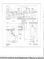
-4. Horizontal Amplifier and Sweep. PC Board 0072E
DESCRIPTION
CKT REF.
C/E STOCK NO.
MFR .
f
CAPACITORS
C1
C2
C3
C4
C5
Electro. 1J.l F. 25V
-Mica . 1000 pF ±5%. 100V
Electro . 100J.lF . 25V
Electro. 100 J.lF. 12V
Metalized Mylar. 1.0 J.lF ± 10%. 100V
1013 -0004
1002-0015
1013-0003
1013-0011
1008-0033
Sprague
Elmenco
Sprague
Sprague
TRW
C6
C7
C8
C9
C10
Poly. 0.2:2J.lF ± 10 %. 400V
Poly. 0.039 J.l F ± 10%. 100V
Poly. 0.01 J.l F ± 10%. 200V
Electro . 15J.lF. 25V
Poly. 0.22 J.l F ± 10%. 400V
1008-0042
1008 -0045
1008 -0043
1013 -0005
1008-0042
Sprague
Sprague
Sprague
Sprague
Sprague
Sylvania
Sylvania
Sylvan ia
Sylvania
Sylvania
DIODES
CRl
CR2
CR3
CR4
CR5
st
st. 1N3064
1281-0013
1281-0013
1281-0013
1281 -0013
1281 -0013
CR6
Si.1N3064
1281 -0013
Sylvania
1272-0017
1272-0017
1272-0024
1272-0017
1272 -0017
Fairchild
Fairchild
Fairchild
Fairchild
Fairchild
Fairchild
Fairchild
Fairchild
Fairchild
Fairchild
'I N3064
si 1N3064
s.. 1N3064
si 1N3064
TRANSISTORS
01
02
03
04
05
Si. NPN. 2N3565
si NPN. 2N3565
si PNP. 2N4249
Si. NPN . 2N3565
si NPN. 2N3565
06
07
08
09
010
si. PNP. 2N4249
si PNP. 2N4249
1272-0024
1272 -0017
1272-0024
1272-0024
1272-0024
011
012
s. NPN. 2N3440
s. NPN. 2N3440
1271-0004
1271-0004
RCA
RCA
s i NPN. 2N3565
si PNP. 2N4249
Si. PNP. 2N4249
RESISTORS
Rl
R2
R3
R4
R5
Comp , 33kohm ±5%. 1/4W
Compo 2 .2k ohm ±5%. 1/4W
Compo 22 ohm ± 5%. 1/4W
Compo 3.9k ohm ± 5%. 1/4W
Compo '1 k ohm ±5%. 1/4W
1066-3335
1066-2225
1066-2205
1066-3925
1066-1025
Allen -Bradley
Allen -Bradley
Allen -Bradley
Allen -Bradley
Allen- Bradley
R6
R7
R8
R9
Rl0
Comp o2 .2k ohm ±5%. 1/4W
Comp o1000hm ±5%, 1/ 4W
Compo 100 ohm ±5%. 1/4W
Cornp. 33kohm ±5%,1 /4W
Comp o8 .2k ohm ±5%. 1/4W
1066-2225
1066 -1015
10 66-1015
10 66-3335
1066 -8225
All en-Bradley
Allen -Bradley
Allen - Bradley
Allen -Bradley
Allen-Bradley
Rll
R12
R13
Comp.12kohm ±5%.1 /4W
Compo 33k ohm ±5%, 1/4W
Compo 47k ohm ±5%. 1/4W
Comp o1k ohm ±5%. 1/4W
Compo 10k ohm ±5%. 1/4W
1066-1235
1066-3335
1066-4725
1066-1025
1066 -1035
Allen - Bradely
Allen-Bradley
Allen-Bradley
All en-Bradley
Allen- Bradley
R14
R15
5 ·13
,
.
....
Chass is A -4 . Hor izontal Ampl if ier and Sw eep . PC Board 0072E. cont inu ed
DESCR IPTION
CKT.
I
C/E STOCK NO .
MFR .
R16
R17
R18
R19
R20
Comp o22k ohm ±5%. 1/4W
Com po22k ohm ±5%. 1/4W
Com p.68kohm ±5%. 1/4W
Compo1.8k ohm ± 5_"('0. 1/4 W
Comp o10koh m ±5%. 1/4W
1066 -2235
1066 -2235
10 6 6 - 6 8 3 5
10 6 6 - 18 2 5
1066 -1035
A llen - Bradley
A lle n-Br adley
Alle n-B rad ley
A ll en- Brad ley
Allen - Bradley
R21
R22
R23
R24
R25
Compo100kohm ±5%. 1/4W
Comp o10k ohm ±5%. 1/4W
M Film .93 .1kohm ±1 %.1 /4W ·
M Film .61 .9kohm ±1 %.1 /4W
M Film . 8.45kohm ±1 %. 1/4W
1066 -1045
1066 -1035
1075 -0029
1075 -0018
1075 -0031
All en- Bradl ey
All en- Bradl ey
Electra
Electra
Electra
R26
R27
R28
R29
R30
M
M
M
M
M
Film . 10k ohm ± .1 %. 1/4W
Film . 10k ohm ±1 %. 1/4W
Film . 3.4kohm ±1 %. 1/4W
Film . 3.4k ohm ± 1%. 1/4W
Film . 10k ohm ± 1%. 1/4W
1075-0009
1075-0009
1075-0020
1075 -0020
1075 -0009
Electra
Electra
Electra
Electra
Electra
R31
R32
R33
R34
R35
M
M
M
M
M
Film. 5.62k ohm ± 1%. 1/4W
Fil m. 1.43koh m ±1 %. 1/4 W
Film. 10 0 k ohm ± l %.lW
Fil m . 2.43k ohm ± 1%. 1/4W
Film . 2.43kohm ±1 %. 1/ 4 W
1075 -0013
1075 -0021
1076 -0009
1075-00 19
10 7 5 -0 0 19
Electra
Electra
Electra
Electra
Electra
R36
R37
R38
R39
M Film . 10m· oh m ± 1%. 1W
M Film . 887 ohm ± 1%. 1/4W
Pot.. corn p . 10 k ohm . 1/2W
Compo4 .7k ohm ± 5%. 1/4W
10 76 -0 0 0 9
10 7 5 -0 0 2 2
1200-00 13
10 6 6 -4 72 5
Elect ra
Elec tra
Alle n- Bradley
Al len- Bradley
o
5 ·14
_\~\ ·~ ·I\
I I :~ V
!'HOM
1'1-11
N
I'I\ClM
/\.\ - '1'1"1
IlIV
,' ,ll JM
SW1 - ~
S WJ- ~
S W 3 -:,
: ;W:J ,,~
.
,,,, ., "" W ~ -'I !th2L
.S W J ·· !
SW ~ - ' I
)2
I
TP
TP
II
C5
1.0
R7
100
11'
16
C8
.0 1
RI6
22 K
+ 14.2 V
:..L C 3
10 0
'1
R 17
22K
I%
R2 0
10 K
RI9
1.8 K
,.
I
I
I
I
011
2 N 34 4 0
R2 3
93.1 K
1 0/ 0
)9
~N4249
C IO
.2 2
R 26
10K
1 'Yo
I
I
R 27
10 K
1'1'0
R34
2 43K
1'1'0
f 37
66 7
10/0
- 7. 8 V
I
R32
R24
61. 9 K
1 '1'0
9 ,6 Y
R28
3 .4 K
1'1'0
..3. 7 V
I
I
I
R21
10 0 K
,IW
\r--
., 2.0 V
'18.1 V
TRIGG ER
J20 Y
R33
10 0 K
H ORIZONTAL
AM PLI FI ER
SWE EP
GENERATO R
S C H MITT
I
TP
13
CI
1.0
Aa 1' 1' \
I
R25
6.4 5 K
1%
R3 5
2 .4 3 K
I
1.43 K
I 'Y
o
R2 9
3 .4 K
1 0/ 0
R38
10 K
R2 2
10 K
" HORI Z.
GAIN"
I
I
01 0
2 N4 2 4 9
C9
CR2
I N30 6 4
RI 3
4 .7K
CR3
IN3 064
~-
; 6. 5 Y
__ ___ _
__ _
__ _
__ _
__ 1
r:».
I
RII
12 ~
_
r
----.....-.
R3 0
10 K
I o/~
I
I
1
IIL AN I-JNC
D RIVER
J.O.7 V
R3 1
562 K
1 0/ 0
'0 0
R8
100
L
- 12 V
TP
14
I
.) . 1 · 6 9
I
TP
TP
TP
8
15
I W
9
I'
J
TP
19
PC flO 007 2 E
-r-----I
HORl l O NTh L I\ MPlIFl r n
1\ 2 - T I' I Z
I "' I :;' I ~ ' O MS " ..... . :.... V Al UI S IN O " "' S UNll S1>
Oll'l ~R WIS ~ NOH D
1 CAPACITQ A$ - II AlU[ S ,"' .. 1 U NLESS OTHERWI SE N0 1 [0
) " " OUCTQRS- V ALU ES IN
'-' ''' LESS O TH (I'lWI Sf ", 0 1 (0
• • ' ...C TQ Il V S El EC f[ O
I. U(
') All \lOL1"'C. E Il lA O ' ''' C.S AM( QC \.J..,\ I $S
O , .. (M ""'~ "'O Tt O
RI 4
IK
· t~\
%,
---vv
C4
, 9.2 v
R36
10 0 K
I
11. 2 V
+
,oa
0 12
2 N344 0
AND SWEEP
BLA N KI NG
TO A I - T P 14
SW 4- 2
CO P V RIGH T 196 8 11'" ( USHU A... ELE CT RONI CS, IN C
r~" s Q R A WI"I C 1$ ''> lfNDED fO~ lM E OPE AA !' ::),> " N O
M A, N T[ N " NCf O~ CUS... MM" [ LEC TRO N' CS f OU, » \ ' ( ,>r
.... 0 , <;, »m 10 81 V SEO O I M[ R W'S( Oill iIl ( PAo n u Cf O
....'1 .. , 1" 1 ..... ' ll t H C(JN!>' ''' I '1'10'" ( US... ... . .. ll t C
l " U" ' l ::' , ~ C
- 12V
FRO M
P I- 14
FP - R7 - 3
FP-R 7 - 2
FP- R7-1
]3 -9
A2 -T P12
a
<r:': o~
O~
~o ~
o~
""'"
v
~
o~
('v
~
- --_. - -
)
)
I
\
I
Ii
V
~
I
I
~ 1r:l
<,
(
I
<...i)
8
l
~
-