1
Order Number: MCUK990801C8
GD90 Personal Cellular Telephone
Handheld Portable
EB-GD90
Specification
900 MHz
Frequency range
1800 MHz
Tx: 890 - 915 MHz
Rx: 935 - 960 MHz
Tx/Rx frequency separation
Tx: 1710 - 1785 MHz
Rx: 1805 - 1880 MHz
45 MHz
95 MHz
RF channel bandwidth
200 kHz
Number of RF channels
Speech coding
124
374
Full rate/Half rate/Enhanced
Full rate
Operating temperature
Full rate/Half rate
-10°C to +55°C
Type
Class 4 Handheld
Class 1 Handheld
RF Output Power
2 W maximum
1 W maximum
Modulation
GMSK (BT = 0.3)
Connection
8 ch/TDMA
Voice digitizing
13 kbps RPE-LTP / 13 kps ACLEP / 5.6 kps CELP / VSLEP
Transmission speed
270.3 kbps
Diversity
Frequency hopping
Signal Reception
Double superheterodyne
Intermediate Frequency
282MHz and 45MHz
Antenna Terminal Impedance
50 Ω
Antenna VSWR
<2.1 : 1
Dimensions
Height: 118 mm
Width: 42 mm
Depth: 16.5 mm
Volume
84.5 cc
Weight
88 g
Display
Graphical chip on glass liquid crystal, Alphanumeric 16 x 3
characters, 5 icons and 6 x 1 characters
Illumination
Green:
4 LEDs for the LCD
8 LEDs for the keyboards
1 LED Incoming call
Red:
1 LED Charging indicator
Keypad
17 keys, Navigation key
SIM
Plug-in type only
External DC Supply Voltage
3.6 V
Battery
3.6 V
Standby Battery Life
DRX 9
95 hrs maximum
Conversation Battery Life
PL 7, DTX 50%
200 minutes
Unless stated these specifications are with Battery Pack (EB-BSD90) fitted.
Battery life figures are dependent on network conditions.
WARNING
This service information is designed for experienced repair technicians only and is not designed for use by the general public. It does not contain warnings or
cautions to advise non-technical individuals of potential dangers in attempting to service a product.
Products powered by electricity should be serviced or repaired only by experienced professional technicians. Any attempt to service or repair the product or
products dealt with in this service manual by anyone else could result in serious injury or death.
Issue 1
Revision 0
This Service Manual is copyright and issued on the strict understanding that it is not to be reproduced, copied, or disclosed to
any third party, either in whole or part, without the prior written consent of Matsushita Communication Industrial UK Ltd.
Every care has been taken to ensure that the contents of this manual give an accurate representation of the equipment.
However, Matsushita Communication Industrial UK Ltd. accepts no responsibility for inaccuracies which may occur and
reserves the right to make changes to specification or design without prior notice.
The information contained in this manual and all rights in any designs disclosed therein, are and remain the exclusive property
of Matsushita Communication Industrial UK Ltd.
Other patents applying to material contained in this publication:
BULL CP8 PATENTS
Comments or correspondence concerning this manual should be addressed to:
Customer Support Department,
Matsushita Communication Industrial UK Ltd.,
Colthrop,Thatcham,
Berkshire. RG19 4ZD.
ENGLAND
© 1999 Matsushita Communication Industrial UK Ltd.
Issue 1
Revision 0
– ii –
MCUK990801C8
Service Manual
WARNINGS AND CAUTIONS
WARNING
The equipment described in this manual contains polarized capacitors utilising liquid electrolyte. These devices are entirely
safe provided that neither a short-circuit nor a reverse polarity connection is made across the capacitor terminals.
FAILURE TO OBSERVE THIS WARNING COULD RESULT IN DAMAGE TO THE EQUIPMENT OR, AT WORST,
POSSIBLE INJURY TO PERSONNEL RESULTING FROM ELECTRIC SHOCK OR THE AFFECTED CAPACITOR
EXPLODING. EXTREME CARE MUST BE EXERCISED AT ALL TIMES WHEN HANDLING THESE DEVICES.
Caution
The equipment described in this manual contains electrostatic sensitive devices (ESDs). Damage can occur to these
devices if the appropriate handling procedure is not adhered to.
ESD Handling precautions
A working area where ESDs may be safely handled without undue risk of damage from electrostatic discharge, must be
available. The area must be equipped as follows:
Working Surfaces - All working surfaces must have a dissipative bench mat, SAFE for use with live equipment, connected via
a 1M2 resistor (usually built into the lead) to a common ground point.
Wrist Strap - A quick release skin contact device with a flexible cord, which has a built in safety resistor of between 5k2 and
1M2 shall be used. The flexible cord must be attached to a dissipative earth point.
Containers - All containers and storage must be of the conductive type.
Batteries
This equipment may contain an internal battery in addition to the external battery packs. These batteries are recyclable and
should be disposed of in accordance with local legislation. They must not be incinerated, or disposed of as ordinary rubbish.
MCUK990801C8
Service Manual
– iii –
Issue 1
Revision 0
This page is left intentionally blank.
Issue 1
Revision 0
– iv –
MCUK990801C8
Service Manual
CONTENTS
1 INTRODUCTION
1.1
1.2
1.3
2
Purpose of this Manual . . . . . . . . . . . . . . . . . . . . . . . . . . 1
Structure of the Manual . . . . . . . . . . . . . . . . . . . . . . . . . . 1
Servicing Responsibilities . . . . . . . . . . . . . . . . . . . . . . . . 1
GENERAL DESCRIPTION
2.1
2.2
General . . . . . . . . . . . . . . . . . . . . . . . . . . . . . . . . . . . . . . 3
Handportable Main Kit . . . . . . . . . . . . . . . . . . . . . . . . . . 3
3 OPERATING INSTRUCTIONS
3.1
3.2
3.3
3.4
3.5
3.6
3.7
3.8
3.9
3.10
3.11
3.12
3.13
3.14
3.15
3.16
General . . . . . . . . . . . . . . . . . . . . . . . . . . . . . . . . . . . . . . 5
LCD Display . . . . . . . . . . . . . . . . . . . . . . . . . . . . . . . . . . 5
Location of Controls . . . . . . . . . . . . . . . . . . . . . . . . . . . . 6
Concept of Operation . . . . . . . . . . . . . . . . . . . . . . . . . . . 7
Alpha Entry . . . . . . . . . . . . . . . . . . . . . . . . . . . . . . . . . . . 7
Incoming Calling Line Identification (CLI) . . . . . . . . . . . . 7
Hot Key Dial Source List . . . . . . . . . . . . . . . . . . . . . . . . . 8
Features Menu Structure . . . . . . . . . . . . . . . . . . . . . . . . 8
Public Man Machine Interface (MMI) . . . . . . . . . . . . . . . 9
Troubleshooting . . . . . . . . . . . . . . . . . . . . . . . . . . . . . . 12
Important Error Messages . . . . . . . . . . . . . . . . . . . . . . 12
Security Codes . . . . . . . . . . . . . . . . . . . . . . . . . . . . . . . 13
SIM Personalisation . . . . . . . . . . . . . . . . . . . . . . . . . . . 13
GSM Services Supported by PC Card . . . . . . . . . . . . . 14
GSM Network Codes and Names . . . . . . . . . . . . . . . . . 14
Glossary of Terms . . . . . . . . . . . . . . . . . . . . . . . . . . . . . 18
4 DISASSEMBLY / REASSEMBLY INSTRUCTIONS
4.1
4.2
4.3
General . . . . . . . . . . . . . . . . . . . . . . . . . . . . . . . . . . . . . 19
Disassembly . . . . . . . . . . . . . . . . . . . . . . . . . . . . . . . . . 20
Reassembly . . . . . . . . . . . . . . . . . . . . . . . . . . . . . . . . . 23
5 TECHNICAL SPECIFICATIONS
5.1
5.2
Tx Characteristics . . . . . . . . . . . . . . . . . . . . . . . . . . . . . 25
Rx Characteristics . . . . . . . . . . . . . . . . . . . . . . . . . . . . . 27
6 TEST AND MEASUREMENT
6.1
6.2
6.3
6.4
6.5
6.6
6.7
7
CIRCUIT DIAGRAMS
7.1
7.2
7.3
8
Introduction . . . . . . . . . . . . . . . . . . . . . . . . . . . . . . . . . . 29
External Testing . . . . . . . . . . . . . . . . . . . . . . . . . . . . . . 29
Complete Unit Test Setup . . . . . . . . . . . . . . . . . . . . . . . 32
Channel Box Test Commands . . . . . . . . . . . . . . . . . . . 36
Adjustment Mode . . . . . . . . . . . . . . . . . . . . . . . . . . . . . 37
I and Q Values . . . . . . . . . . . . . . . . . . . . . . . . . . . . . . . 45
Lock Code . . . . . . . . . . . . . . . . . . . . . . . . . . . . . . . . . . . 49
Main PCB - RF . . . . . . . . . . . . . . . . . . . . . . . . . . . . . . . 51
Main PCB - Logic . . . . . . . . . . . . . . . . . . . . . . . . . . . . . 52
Keypad PCB . . . . . . . . . . . . . . . . . . . . . . . . . . . . . . . . . 53
LAYOUT DIAGRAMS
8.1
8.2
Main PCB . . . . . . . . . . . . . . . . . . . . . . . . . . . . . . . . . . . 55
Keypad PCB . . . . . . . . . . . . . . . . . . . . . . . . . . . . . . . . . 56
9 REPLACEMENT PARTS LIST
9.1
9.2
9.3
9.4
Case Parts . . . . . . . . . . . . . . . . . . . . . . . . . . . . . . . . . . 57
Sub-Assemblies . . . . . . . . . . . . . . . . . . . . . . . . . . . . . . 58
Handheld Replacement Parts List . . . . . . . . . . . . . . . . 59
Printed Material . . . . . . . . . . . . . . . . . . . . . . . . . . . . . . . 69
MCUK990801C8
Service Manual
Section
–v–
Issue 1
Revision 0
This page is left intentionally blank.
Issue 1
Revision 0
Section
– vi –
MCUK990801C8
Service Manual
INTRODUCTION
1
INTRODUCTION
1.1 Purpose of this Manual
This Service Manual contains the information and procedures required for installing, operating and servicing the Panasonic
GSM Personal Cellular Mobile Telephone system operating on the GSM Digital Cellular Network.
1.2 Structure of the Manual
The manual is structured to provide service engineering personnel with the following information and procedures:
1.
General and technical information - provides a basic understanding of the equipment, kits and options, together with
detailed information for each of the major component parts.
2.
Installation and operating information - provides instructions for unpacking, installing and operating the equipment.
3.
Servicing information - provides complete instructions for the testing, disassembly, repair and reassembly of each major
component part. Step-by-step troubleshooting information is given to enable the isolation and identification of a
malfunction, and thus determine what corrective action should be taken. The test information enables verification of the
integrity of the equipment after any remedial action has been carried out.
4.
Illustrated parts list - provided to enable the identification of all equipment components, for the ordering of spare/
replacement parts.
1.3 Servicing Responsibilities
The procedures described in this manual must be performed by qualified service engineering personnel, at an authorised
service centre.
The service engineering personnel are responsible for fault diagnosis and repair of all equipment described in this manual.
MCUK990801C8
Service Manual
Section 1
–1–
Issue 1
Revision 0
INTRODUCTION
This page is left intentionally blank.
Issue 1
Revision 0
Section 1
–2–
MCUK990801C8
Service Manual
GENERAL DESCRIPTION
2
GENERAL DESCRIPTION
2.1 General
This section provides a general description and kit composition details for the GSM Handportable Telephone system and
optional kits.
GD90 is a high performance, small, light, business GSM telephone. The following features are included as standard:
1.
Triple Rate which includes Full Rate, Half Rate and enhanced Full Rate speech, codec.
2.
Dual Band, GSM900 and GSM1800 operation.
3.
Desktop Handsfree Function - comprised of integral echo cancellation and noise suppression.
2.2 Handportable Main Kit
The handportable main kit provides a standalone Class 4 GSM telephone. The plug-in SIM contains the subscriber and network
information necessary to operate the phone on a GSM network.
Figure 2.1: Handportable Main Unit Kit Contents
MCUK990801C8
Service Manual
NUMBER
DESCRIPTION
PART NUMBER
1
2
3
4
5
Main unit
Battery
Adaptor
Pouch
Strap
EB-GD90
EB-BSD70
EB-CAD70
7AA516A
6P70022AA
—
Documentation
See Section 9
Section 2
–3–
Issue 1
Revision 0
GENERAL DESCRIPTION
This page is left intentionally blank.
Issue 1
Revision 0
Section 2
–4–
MCUK990801C8
Service Manual
OPERATING INSTRUCTIONS
3
OPERATING INSTRUCTIONS
3.1 General
This section provides a brief guide to the operation and facilities available on the GD90 handportable unit. Refer to the
Operating Instructions for full operational information.
3.2 LCD Display
The GD90 handportable unit has a graphical chip on glass liquid crystal display in conjunction with the following icons:
Menu Number
Option Area
Figure 3.1: LCD display
T
S
Indicates received signal strength: T strong signal area;\ weak signal area.
Indicates that it is possible to make an emergency call.
Menu
Number
H
The number of the feature pointed to by the pointer. To access a feature enter the menu number on the keypad.
Menu Icon
p
Option Area
Displays the battery charge level: H Battery is at full charge; K Battery requires recharging;
G The battery icon flashes during charging. During car mount use, when the battery is fully charged, the battery icon will
not light.
Displays a small icon related to the current status of the telephone:
Y telephone is roaming on a non-home network;
t using the “Call Divert” feature or the telephone has Call Divert set;
] shows that the vibrate alert is switched on;
[ shows that telephone is in silent mode - no tones:
N indicates there are unread Short Text Messages (SMS.). Lit when SMS area is full;
O the telephone is locked;
U shows that normal character have been entered in Alpha Entry;
V shows that Greek character have been entered in Alpha Entry;
W shows that extended character have been entered in Alpha Entry;
X shows that numbers have been entered in Alpha Entry.
Indicates that the navigation key (g) can be pressed. Each arrow will light individually to indicate which direction is valid.
Pressing the select key (B) will select the option displayed in the option area of the display.
Following some operations the display will automatically clear after three seconds or after pressing any key except E.
MCUK990801C8
Service Manual
Section 3
–5–
Issue 1
Revision 0
OPERATING INSTRUCTIONS
3.3 Location of Controls
Incoming/Charge indicator:
Green – incoming call.
Red – charging battery pack.
External connector:
Used to connect to external accessories or charging equipment.
Figure 3.2: Location of controls for GD90
g
Navigation Key. Scrolls through options or features menu and increases or decreases volume.
B
Select Key. Selects option shown in the Option Area of the display.
A
Phonebook Key. Browses through the Phonebook or stores a number in the Phonebook.
Changes the type of characters entered during Alpha Entry.
Send Key. Makes a call.
D
C
E
0 to 9
#
Issue 1
Revision 0
Clear Key. Clears the last digit entered, clears all digits when pressed and held or returns to
the previous display.
End Key. Ends a call or switches the telephone on/off when pressed and held.
Digit keys. Enter wild numbers or pauses when pressed and held. Where appropriate the 0
key scrolls up or down through abbreviated control names and then select to reveal the
international access code “+”.
Vibrate enable/disable Key. Press and hold to enable or disable the vibrate alert.
Section 3
–6–
MCUK990801C8
Service Manual
OPERATING INSTRUCTIONS
3.4 Concept of Operation
There is a close relationship between the Select Key, Navigation Key and display.
Figure 3.3: Concept of Operation
Pressing up and down (e) will move the pointer up and down and scroll through more information in the main area of the
display.
Pressing left and right (f) will scroll through options in the option area of the display. To choose the option press the Select
Key (B).
3.5 Alpha Entry
Alpha Entry is used to enter alphanumeric characters into Phonebook, Short Messages and the Greeting Message.
Key
1
2
3
4
5
6
7
8
9
C
U
Character/Operation
V
“@–,.;:!¡?¿()‘&%+–/<>=£$¥¤§
ABCabc
ΑΒΓ
DEFdef
∆ΕΖ
GHIghi
ΗΘΙ
JKLjkl
ΚΛΜ
W
AÄÅÆBCÇaàbc
DEÉFdeèéf
GHIghiì
JKLjkl
X
1
2
3
4
5
MNOmno
ΝΞΟ
MNÑOÖømnñoòö
6
PQRSpqrs
ΠΡΣ
PQRSpqrsß
7
TUVtuv
ΤΥΦ
TUÜVtuùüv
8
WXYZwxyz
ΞΨΩ
WXYZwxyz
9
Deletes the character above the cursor, deletes the character to the left when at the end of the line or clears the entire entry
when pressed and held.
Each time a key is pressed it will display the next character. When another key is pressed or no key is pressed for a short time
the cursor will move to the next position.
To cycle between Greek characters (V), extended characters (W), numerals (X) and normal characters (U) press A.
3.5.1 Editing Alpha Entry
Pressing e will move the cursor up or down one line. Pressing f will move you left or right one character. When the cursor
is moved over a character and another key pressed this will insert the new character.
Pressing C will delete the character to the left of the cursor.
3.6 Incoming Calling Line Identification (CLI)
When a call is received the last 6 digits of the CLI information is matched with the phonebook. Therefore an incoming call could
match to the wrong phonebook entry.
MCUK990801C8
Service Manual
Section 3
–7–
Issue 1
Revision 0
OPERATING INSTRUCTIONS
3.7 Hot Key Dial Source List
The source for Hot Key Dial Numbers is normally ‘Phonebook’ or ‘Service Dial Numbers’. For some OEMs it may be a
requirement to store these numbers in the EEPROM. When the source is the EEPROM and the telephone software is updated,
the source numbers may be lost. Also, if the user changes the source of the Hot Key Dial numbers, it will not be possible to
redirect the source back to the EEPROM. However, in the event that an OEM would like the Hot Key Dial source to be stored
in the EEPROM, it is unlikely that the user will have the option to change the Hot Key Dial source.
3.8 Features Menu Structure
Figure 3.4: Feature Menu
Issue 1
Revision 0
Section 3
–8–
MCUK990801C8
Service Manual
OPERATING INSTRUCTIONS
3.9 Public Man Machine Interface (MMI)
It is possible to operate all GSM telephones in the same way using the Public MMI. The following operations will work with all
GSM telephones. However, this information is restricted to those operations that are supported by GD90.
The * and # in the following procedures should be replaced by * and #, respectively. Also <SND> and <END> should be
replaced with D and E keys.
3.9.1 Reading Phonebook Memory Location
# <MEMORY LOCATION>
Leading zeros can be left out of the location number, e.g. 007 can be 7.
3.9.2 Presentation of IMEI
*#06#
3.9.3 Security
Change PIN
* * 0 4 * <OLD PIN> * <NEW PIN> * <NEW PIN> #
Change PIN2
* * 0 4 2 * <OLD PIN2> * <NEW PIN2> * <NEW PIN2> #
Unblock PIN
* * 0 5 * <PIN UNBLOCKING KEY> * <NEW PIN> * <NEW PIN> #
Unblock PIN2
* * 0 5 2 * <PIN2 UNBLOCKING KEY> * <NEW PIN2> * <NEW PIN2> #
3.9.4 Call Hold
Place a call on hold
2 <SND>
Recall a held call
2 <SND>
Make a second call
<TELEPHONE NUMBER> <SND>
Swap between two held calls
2 <SND>
End held call
O <SND>
End active call
1 <SND>
Reject incoming call
0 <SND>
3.9.5 Call Waiting
Enable Call Waiting
* 4 3 * # <SND>
Disable Call Waiting
# 4 3 * # <SND>
Call Waiting Status
* # 4 3 * # <SND>
MCUK990801C8
Service Manual
Section 3
–9–
Issue 1
Revision 0
OPERATING INSTRUCTIONS
3.9.6 Calling Line Identification
Calling Line Identification Feature
Service Code
Calling Line Identification Presentation (CLIP)
Calling Line Identification Restriction (CLIR)
30
31
Connected Line Presentation (CLOP)
Connected Line Restriction (CLOR)
76
77
Enable
* <SERVICE CODE> * # <SND>
Disable
# <SERVICE CODE> * # <SND>
Temporary suppress identification
# 3 1 # <TELEPHONE NUMBER> <SND>
Temporary display identification
* 3 1 # <TELEPHONE NUMBER> <SND>
3.9.7 Telecommunication Services Used for Public MMI
Teleservice
Service
MMI Service Code
All teleservices
Telephony
All data teleservices
10
11
12
Facsimile services
Short Message Services (SMS)
All teleservices except SMS
Voice group services
13
16
19
17
Bearer Service
Service
MMI Service Code
All bearer services
All asynchronous services
All synchronous services
20
21
22
All data synchronous services
All data asynchronous services
All dedicated packet access
All dedicated PAD access
24
25
26
27
3.9.8 Call Divert
Call Divert Type
Service Code
Divert all calls
Divert calls if busy
Divert calls if no reply
Divert if not reachable
21
67
61
62
Set (except “No Reply” Call Bar
* * <SERVICE CODE> * <FORWARD TELEPHONE NUMBER> * <TELECOMMUNICATION SERVICE> # <SND>
Set “No Reply” Call Bar
* * <SERVICE CODE> * <FORWARD TELEPHONE NUMBER> * <TELECOMMUNICATION SERVICE> *
<TIME TO RING (seconds) # <SND>
Clear
# # <SERVICE CODE> * <TELECOMMUNICATION SERVICE> * # <SND>
Issue 1
Revision 0
Section 3
– 10 –
MCUK990801C8
Service Manual
OPERATING INSTRUCTIONS
Status
* # <SERVICE CODE> * <TELECOMMUNICATION SERVICE> * # <SND>
Clear all Call Diverts
##002#
3.9.9 Call Bar
Call Bar Type
Service Code
All outgoing calls
33
Outgoing international calls
Outgoing international calls except those to your PLMN country
All incoming calls
Incoming international calls when roaming
331
332
35
351
Set
* <PASSWORD> * <TELECOMMUNICATION SERVICE> # <SND>
Clear
# <PASSWORD> * <TELECOMMUNICATION SERVICE> # <SND>
Status
* # <TELECOMMUNICATION SERVICE> # <SND>
Clear all Call Bar Types
# 3 3 0 * <PASSWORD> # <SND>
Change Call Bar Password
* * 0 3 * * <OLD PASSWORD> * <NEW PASSWORD> * <NEW PASSWORD> # <SND>
MCUK990801C8
Service Manual
Section 3
– 11 –
Issue 1
Revision 0
OPERATING INSTRUCTIONS
3.10Troubleshooting
The user is given the following information and advised to contact the dealer if the problems persist:
Problem
Telephone will not switch
on
Extremely short battery
life for a new battery pack
Cause
Remedy
The network you are using and the condition
of the battery pack can affect battery life.
Check that the battery pack is fully charged and correctly
connected to the telephone.
Avoid areas of poor reception. Ensure batteries are fully
charged. Additionally, for NiMH batteries, ensure batteries are
also discharged fully before recharging.
Replace with a new one.
Short battery life for an
old battery pack
The battery pack was worn out.
Short battery life for NiMH battery pack
The life of the battery pack is affected by
improper charging, this is inherent in all NiMH batteries.
To maintain maximum performance always use until the Low
Battery Warning and then fully recharge the battery packTo
revive the Battery Pack use the telephone until the Low
Battery Warning and then fully recharge three times. However,
if the battery life still is short, the battery pack has eventually
worn out. Replace with a new one.
The battery level indicator
H does not light when
charging
If a battery is deeply discharged it will take a
short time before there is sufficient power in
the telephone to light the battery level
indicator H.
The telephone is locked.
Outgoing calls are barred.
The telephone is not registered to a network.
Leave to charge for several minutes in temperatures between
+5°C and +35°C.
Calls cannot be made
Calls cannot be made
from Fixed Dial Store
Calls cannot be received
The telephone is not switched on.
Incoming calls are barred.
The telephone is not registered to a network.
Emergency calls cannot
be made
You are not in a GSM coverage area.
Telephone numbers
cannot be recalled
The telephone is locked.
Fixed Dial is switched on.
Unlock the telephone (Menu: Security: Phone Lock).
Disable the outgoing call barring (Menu: Security: Call Bar).
Move to a coverage area and operate your telephone after it
has registered with a network.
Check your SIM supports Fixed DialCheck if the Fixed Dial is
switched on (Menu: Security: Fixed Dial). Check the
telephone number is stored in the Fixed Dial.
Switch the telephone on.
Disable the incoming call barring (Menu: Security: Call Bar).
Move to a coverage area and operate your telephone after it
has registered with a network.
Check that the antenna symbol S is displayed. Move to a
coverage area and operate your telephone when the antenna
symbol is displayed.
Unlock the telephone (Menu: Security: Phone Lock).
Switch off Fixed Dial (Menu: Security: Fixed Dial).
3.11Important Error Messages
The following table is a list of error messages that may occur during use of the telephone, with a description and suggested
course of action:
Area not Allowed
Roaming in the selected area is not allowed.
Network not Allowed
Roaming with the selected network is not allowed.
Security Failure
The network has detected authentication failure because your SIM is not registered with that network. Contact
your Service Provider.
The SIM is blocked because the wrong PUK has been entered ten times. Contact your Service Provider.
The telephone has detected a problem with the SIM. Switch the telephone off and then back on. If the
message does not disappear contact your Service Provider.
A message has been received but the message store is full. To receive messages, delete some of the
currently stored messages or set messages to automatically clear (Menu: Messages: Parameters: Auto
Delete).
The PIN2 is blocked permanently because the wrong PUK2 has been entered 10 times. Services controlled by
PIN2 cannot be used. Contact your Service Provider.
The message area is full. Your messages cannot be stored until some of the currently stored messages are
deleted.
Redial list of unsuccessfully dialled numbers is full. Switch the telephone off and then on again.
SIM Blocked
SIM Error
Message Rejected
Store Full
PIN2 Invalidated
Warning Store Full
Continue?
Auto Redial List Full
Issue 1
Revision 0
Section 3
– 12 –
MCUK990801C8
Service Manual
OPERATING INSTRUCTIONS
3.12Security Codes
Code Type
Number of Digits
Description
Personal Identification Number (PIN)
PIN 2
4 to 8
4 to 8
Controls SIM security. Supplied by the service provider.
Controls memory security. Supplied by the service provider.
PIN/PIN 2 Unblocking Key
(PUK/PUK 2)
8
Used to unblock PIN and PIN 2. A PIN or PIN 2 will become blocked if the
wrong PIN or PIN 2 is entered three times. When the blocked PIN or PIN 2
is unblocked, a new PIN or PIN 2 must be entered. If the wrong PUK or
PUK 2 is entered 10 times, your SIM will be unusable.
Password
4
Lock Code
Factory set to “0000”.
4
Controls the call bar function. If the wrong password is entered three
times, this service will be revoked. Supplied by the service provider.
Controls telephone security.
Supplied by the service provider.
3.13SIM Personalisation
3.13.1 Introduction
SIM personalisation will limit the use of GD90 to a single SIM, a SIM supplied by one Network/Sub-network/Service Provider
or a SIM purchased by a company (corporation). If a personalised GD90 contains a SIM that is from a different source it will
display the message “SIM ERROR” when switched on. This personalisation of GD90 is sometimes referred to as SIM lock or
SIM latch.
3.13.2 Testing
To test a personalised GD90, when the user has not supplied the SIM, a SIM configured for test purposes (e.g. test SIM or soft
SIM) should be used. The mobile will recognise that the SIM is for testing purposes only and operate as normal.
3.13.3 Personalisation Function
Personalisation is activated during manufacture and then enabled at a later stage. Enabling/disabling is available by entering
a special key sequence immediately after power on. Once the enable/disable menu is shown it is possible to select the type of
personalisation. When personalisation is enabled it is only possible to disable it if the mobile contains an illegal SIM and the
sixteen digit Control Key (CK) is known. When enabled the CK is withheld from the user and cannot be read, for security
reasons.
There are two special key sequences to enter the enable/disable menu:
Key sequence
Notes
746BB
Can only disable personalisation.
52824BB
Can both enable and disable personalisation.
3.13.4 Disabling Procedure
1.
2.
F 7 4 6 B B or 5 2 8 2 4 B B.
F e to point at:
“SIM” for SIM Personalisation
”Network” for Network Personalisation
“Subnetwork” for Subnetwork Personalisation
”SP” for Service Provider Personalisation or
”Corporate” for Company Personalisation.
3.
F B.
4.
F the 16 digit Control Key.
5.
F B.
6.
F the 16 digit Control Key.
7.
F B.
The display will confirm which type of Personalisation has been disabled.
MCUK990801C8
Service Manual
Section 3
– 13 –
Issue 1
Revision 0
OPERATING INSTRUCTIONS
3.13.5 Enabling Procedure
1.
5 2 8 2 4 B B.
2.
F e to point at
“SIM” for SIM Personalisation
”Network” for Network Personalisation
“Subnetwork” for Subnetwork Personalisation
”SP” for Service Provider Personalisation or
”Corporate” for Company Personalisation.
3.
F B.
4.
F the 16 digit Control Key.
5.
F B.
6.
F the 16 digit Control Key.
7.
F B.
The display will confirm which type of Personalisation has been enabled.
3.14GSM Services Supported by PC Card
Bearer Service
Number
Bearer Service Rate
Access Structure
Access Rate
Information
Transfer
Error Correction
Options
21
22
23
24
Asynchronous 300 bps
Asynchronous 1.2 kbps
Asynchronous 1200/75 bps
Asynchronous 2.4 kbps
Asynch
Asynch
Asynch
Asynch
300 bps
1.2 kbps
1200/75 bps
2.4 kbps
UDI or modem
UDI or modem
UDI or modem
UDI or modem
T or NT
T or NT
T or NT
T or NT
25
26
41
42
44
Asynchronous 4.8 kbps
Asynchronous 9.6 kbps
Dedicated PAD Access 300 bps
Dedicated PAD Access 1.2 kbps
Dedicated PAD Access 2.4 kbps
Asynch
Asynch
Asynch
Asynch
Asynch
4.8 kbps
9.6 kbps
300 bps
1.2 kbps
2.4 kbps
UDI or modem
UDI or modem
UDI
UDI
UDI
T or NT
T or NT
T or NT
T or NT
T or NT
45
46
Dedicated PAD Access 4.8 kbps
Dedicated PAD Access 9.6 kbps
Asynch
Asynch
4.8 kbps
9.6 kbps
UDI
UDI
T or NT
T or NT
3.15GSM Network Codes and Names
Issue 1
Revision 0
Country
Access Code
Network Operator
Network
Code
Albania
+355
AMC
276
01
Andorra
Armenia
Australia
+376
+374
+61
Austria
+43
STA -Mobiland
Armentel
TELECOM Australia
OPTUS Communications Pty Ltd.
Vodafone PTY
Mobilkom Austria
213
283
505
505
505
232
03
01
01
02
03
01
Azerbaijan
Bahrain
Bangladesh
Belgium
+994
+973
+880
+32
max.mobil
Azercell
Batelco
Grameen Phone Ltd
Belgacom Mobile
Mobistar
232
400
426
470
206
206
03
01
01
01
01
10
Bosnia & Herzegovina
+387
+068
Bulgaria
Brunei Darussalam
+359
+673
Cronet
PTT Bosnia
Citron
DSTCom
Jabatan Telekom
218
218
284
528
528
01
19
01
11
01
Cambodia
Cameroon
+855
+237
CamGSM
PTT Cameroon Cellnet
456
624
01
01
Section 3
– 14 –
MCUK990801C8
Service Manual
OPERATING INSTRUCTIONS
Country
Access Code
Network Operator
Network
Code
China
+86
Guangdong MCC
China United Telecommuni-cations Corporation
Liaoning PPTA
460
460
460
00
01
02
Croatia
Cyprus
Czech Republic
+385
+357
+42
Germany
+49
HR Cronet
Cyprus Telecommunication Authority
Eurotel Praha
Radio Mobil
DeTeMobil GmbH
Mannesmann Mobilfunk
219
280
230
230
262
262
01
01
02
01
01
02
Denmark
+45
Egypt
Estonia
+20
+372
TELE Danmark Mobile
Sonofon
Telia
Mobilix
Arento
Eesti Mobiiltelefon
238
238
238
238
602
248
01
02
20
30
01
01
+251
+679
+358
Radiolinja Eesti AS
Q GSM
ETA
Vodafone
Sonera
248
248
636
542
244
02
03
01
01
91
Finnet
OY Radiolinja AB
Telia
Alands Mobiltelefon
France Telecom
SFR
244
244
244
244
208
208
09
05
03
05
01
10
208
547
340
282
282
262
20
20
01
01
02
01
Ethiopia
Fiji
Finland
France
+33
French Polynesia
French West Indies
Georgia
+689
+590
+995
Germany
+49
Bouygues Telekom
Tikiphone
Ameris
Geocell
Magticom
D1, T-Mobil
+233
+350
+30
D2, Mannesmann
E-Plus Mobilfunk
ScanCom
GibTel
Cosmote
262
262
620
266
202
02
03
01
01
01
Panafon S.A
STET HELLAS
Sotelgui
Westel 900 GSM RT
Pannon GSM RT
Hong Kong Telecom CSL Ltd.
202
202
611
216
216
454
05
10
02
30
01
00
Hutchison Telephone Co. Ltd.
SmarTone Mobile Communications Ltd.
P Plus Comm
New World PCS
Mandarin Comm
454
454
454
454
454
04
06
22
10
16
Pacific Link
Peoples Telephone
Pannon GSM
Westel 900
Post & Simi
Icelandic Mobile Phone
454
454
216
216
274
274
18
12
01
30
01
02
Ghana
Gibralta
Greece
Guinea
Hungary
+224
+36
Hong Kong
+852
Hungary
+36
Iceland
+354
MCUK990801C8
Service Manual
Section 3
– 15 –
Issue 1
Revision 0
OPERATING INSTRUCTIONS
Issue 1
Revision 0
Country
Access Code
Network Operator
Network
Code
India
+91
Bharti Cellular Limited
BPL Mobile
Skycell
404
404
404
10
21
40
Airtel
Essar
Maxtouch
Command
Mobilenet
RPG MAA
404
404
404
404
404
404
10
11
20
30
31
41
Modi Telstra
Sterling Cellular
BPL USWest
TATA
Escotel
Aircel Digilink
404
404
404
404
404
404
14
11
27
07
12
15
PT Telekomunikasi Indonesia
PT. Satelit Palapa Indonesia
PT Excelcomindo Pratama
T.C.I
Telecom Ireland
510
510
510
432
272
10
01
11
11
01
Digifone
Meteor
Omnitel Pronto Italia
Telecom Italia Mobile
Comstar
Ivoiris
272
272
222
222
612
612
02
03
10
01
01
03
Loteny Telecom
JMTS
MTCNet
P & T Luxembourg
Lao Shinawatra
612
416
419
270
457
05
01
02
01
01
Latvian Mobile Telephone Co.Ltd.
Libancell
Cellis
Vodacom
Natel-D
247
415
415
651
228
01
03
01
01
01
Bite GSM
Omnitel
P&T LUXGSM
Millicom Lux SA
C.T.M.
PTT Makedonija
246
246
270
270
455
294
02
01
01
77
01
01
Sacel
Madacom
TNL
Celcom
Maxis
My BSB
646
646
650
502
502
502
03
01
01
19
12
02
MRTEL
Adam
Mutiara Telecom
Telecell
Mauritius Telecom Ltd.
502
502
502
278
617
13
17
16
01
01
France Telecom
SFR
ONPT Morocco
Telecom de Mocambique
208
208
604
634
01
10
01
01
Indonesia
+62
Iran (Islamic Republic of)
Ireland
+98
+353
Italy
+39
Ivory Coast
+225
Jordan
Kuwait
Luxembourg
Laos
(People’s Democratic Republic)
+962
+965
+352
+856
Latvia
Lebanon
+371
+961
Lesotho
Liechtenstein
+266
+4175
Lithuania
+370
Luxembourg
+352
Macau
Macedonia
+853
+389
Madagascar
+261
Malawi
Malaysia
+265
+60
Malta
Mauritius
+356
+230
Monaco
+377
Morocco
Mozambique
+212
+258
Section 3
– 16 –
MCUK990801C8
Service Manual
OPERATING INSTRUCTIONS
Country
Access Code
Network Operator
Network
Code
Myanmar
Namibia
Netherlands
+95
+264
+31
HPT
MTC
LIBERTEL
219
649
204
01
01
04
New Caledonia
New Zealand
Norway
+687
+64
+47
Oman
+968
PTT Telecom
Mobilis
Bell South
Telenor Mobil AS
NetCom GSM A/S
General Telecoms
204
546
530
242
242
422
08
01
01
01
02
02
Pakistan
Papua New Guinea
Philippines
+92
+675
+63
Poland
+48
Mobilink
Pacific
Globe Telecom GMCR Inc
IslaCom
Plus GSM
ERA GSM
410
310
515
515
260
260
01
01
02
01
01
02
Portugal
+351
Qatar
+974
IDEA Centertel
Telecomunicaçoes Moveis Nacionais (TMN)
TELECEL
Optimus
Q-Net
260
268
268
268
427
03
06
01
03
01
Reunion
Romania
+262
+40
Russian Federation
+701
SRR
MobiFon
MobilRom
Mobile Telesystems
North-West GSM
KB Impuls
647
226
226
250
250
10
01
10
01
02
San Marino
+378
Saudi Arabia
+966
Senegal
Seychelles
+221
+248
Omnitel
Telecom Italia Mobile
Al Jawal
EAE
Sonatel
SEZ SEYCEL
222
222
420
420
608
633
10
01
01
07
01
01
Singapore
+65
Slovak Republic
+42
Slovenia
+386
Singapore Telecom
MobileOne
Eurotel
Globtel
Mobitel
525
525
231
231
293
01
03
02
01
41
South Africa
+27
Spain
+34
Sri Lanka
Sudan
+94
+249
Vodacom
MTN
Movistar
AIRTEL Spain
MTN Networks (PVT) Sri Lanka
Mobitel
655
655
214
214
413
634
01
10
07
01
02
01
Sweden
+46
Switzerland
+41
Telia Mobitel
Comviq GSM AB
Europolitan AB
Swisscom 900
Swisscom 1800
240
240
240
228
228
01
07
08
01
01
Syria
Taiwan
Tanazania (United Republic of)
Thailand
+963
+886
+255
+66
Tunisia
+216
Mobile Syria
LDTA
Tritel
TH AIS GSM
Total Access Comms
Tunisian PTT
417
466
640
520
520
605
09
92
01
01
18
02
Turkey
+90
Uganda
+256
Turkcell
Telsim
Celtel Cellular
286
286
641
01
02
01
MCUK990801C8
Service Manual
Section 3
– 17 –
Issue 1
Revision 0
OPERATING INSTRUCTIONS
Country
Access Code
Network Operator
Network
Code
Ukraine
+380
United Arab Emirates
+971
Mobile comms
Golden Telecom
UAE ETISALAT-G1
255
255
424
01
05
01
United Kingdom
+44
UAE ETISALAT-G2
Vodafone
Cellnet
Guernsey Telecoms
Jersey Telecoms
Manx Telecom
424
234
234
234
234
234
02
15
10
55
50
58
434
434
434
452
452
220
04
05
01
01
02
01
220
648
02
01
(Guernsey)
(Jersey)
(Isle of Man)
Uzbekistan
+7
Vietnam
+84
Yugoslavia
+381
Daewoo GSM
Coscom
Buztel
MTSC
DGPT
Mobile Telekom
Zimbabwe
+263
Pro Monte
NET ONE
3.16Glossary of Terms
DTMF
GSM
Home country
Home network
Hot Key Dial
Lock code
Message Centre
Network operator
Password
PIN
PIN2
PUK/ PUK2
Registration
Roaming
Service Dial
Numbers
Service provider
SIM
Supplementary
service
Wild numbers
Issue 1
Revision 0
Dual Tone Multiple Frequency tones. The numeric keys 0 to 9, and * and # will generate different
DTMF tones when pressed during conversation. These are used to access voice mail, paging and
computerised home banking.
Global System for Mobile communications. The name given to the advanced digital technology that
your telephone uses.
The country where your home network operates.
The GSM network on which your subscription details are held.
Hot Key Dial allows quick access to numbers stored in the Phonebook of Service Dial Number list. The
source of the Hot Key Dial may be defined by the user or preprogrammed by the Service Provide. It is
most likely to be preprogrammed to the Service Dial Numbers by the Service Provider.
Used for security of your telephone. Factory set to “0000”.
Where messages are sent before they are forwarded onto their destination. The Message Centre
telephone number may be programmed into your SIM or supplied by your service provider.
The organisation responsible for operating a GSM network. Each country will have at least one
network operator.
Used for the control of the call bar function. Supplied by your service provider.
Personal Identification Number used for SIM security. Supplied by your service provider.
Personal Identification Number used for the control of Fixed Dial Memory and call charge metering.
Supplied by your service provider.
PIN/PIN2 Unblocking Key. Used to unblock the PIN/PIN2. Supplied by your service provider.
The act of locking on to a GSM network. This is usually performed automatically by your telephone.
The ability to use your telephone on networks other than your Home network.
Service Dial Numbers are predefined numbers that allow the user to access a set of special services
provided by the Service Provider. For example billing information or access to Voice Mail.
The organisation responsible for providing access to the GSM network.
Subscriber Identification Module. A small smart-card which stores unique subscriber and user-entered
information such as Phone Book, Fixed Dial Memory and short messages. Supplied by your service
provider.
Network-controlled GSM functions which your telephone will support. Supplementary services may
only be available on a subscription bases.
Spaces in a stored telephone number. When the telephone number is recalled pressing a numeric key
will fill in a space. This can be used to restrict dialling to a specific area.
Section 3
– 18 –
MCUK990801C8
Service Manual
DISASSEMBLY / REASSEMBLY INSTRUCTIONS
4
DISASSEMBLY / REASSEMBLY INSTRUCTIONS
4.1 General
This section provides disassembly and reassembly procedures for the main components of the GD90 system.
These procedures MUST be performed by qualified service personnel, at an authorized service centre.
The following warnings and precautions MUST be observed during ALL disassembly/reassembly operations:
WARNING
The equipment described in this manual contains polarised capacitors utilising liquid electrolyte. These devices are entirely
safe provided that neither a short-circuit nor a reverse polarity connection is made across the capacitor terminals. FAILURE
TO OBSERVE THIS WARNING COULD RESULT IN DAMAGE TO THE EQUIPMENT OR, AT WORST, POSSIBLE
INJURY TO PERSONNEL RESULTING FROM ELECTRIC SHOCK OR THE AFFECTED CAPACITOR EXPLODING.
EXTREME CARE MUST BE EXERCISED AT ALL TIMES WHEN HANDLING THESE DEVICES.
Caution
The equipment described in this manual contains electrostatic sensitive devices (ESDs). Damage can occur to these
devices if the appropriate handling procedure is not adhered to.
4.1.1 ESD Handling Precautions
A working area where ESDs may be safely handled without undue risk of damage from electrostatic discharge, must be
available. The area must be equipped as follows:
Working Surfaces – All working surfaces must have a dissipative bench mat, SAFE for use with live equipment, connected
via a 1M2 resistor (usually built into the lead) to a common ground point.
Wrist Strap – A quick release skin contact device with a flexible cord, which has a built in safety resistor of between 5k2 and
1M2 shall be used. The flexible cord must be attached to a dissipative earth point.
Containers – All containers and storage must be of the conductive type.
MCUK990801C8
Service Manual
Section 4
– 19 –
Issue 1
Revision 0
DISASSEMBLY / REASSEMBLY INSTRUCTIONS
4.2 Disassembly
4.2.1 Case Removal
1.
Remove the battery from the back of the telephone. Remove the four case screws located inside the battery compartment.
Figure 4.1: Screw removal
2.
Remove the case by pulling from the connector end of the case/cover. Care must be taken when separating the case from
the cover as the retaining clips may be very stiff – if necessary, re-attach the battery to provide extra support for the case.
Figure 4.2: Case Disassembly
3.
Remove the PCB assembly from the cover.
Figure 4.3: PCB Assembly Removal
Issue 1
Revision 0
Section 4
– 20 –
MCUK990801C8
Service Manual
DISASSEMBLY / REASSEMBLY INSTRUCTIONS
4.2.2 Changing the Backup Battery
Remove the case as previously described. The backup battery is held in a retainer on the Main PCB. Observe polarity
when replacing the battery.
Figure 4.4: Battery Polarity
4.2.3 Access to Printed Circuit Boards
1.
Remove the case as previously described. While applying slight pressure to the side retaining clips, lift the Main PCB away
from the chassis.
Figure 4.5: Main PCB removal
2.
While applying slight pressure to the side retaining clips, lift the Key PCB away from the chassis.
Figure 4.6: Key PCB removal
MCUK990801C8
Service Manual
Section 4
– 21 –
Issue 1
Revision 0
DISASSEMBLY / REASSEMBLY INSTRUCTIONS
3.
Gently bend the four Display Assembly lugs to allow removal from the Key PCB.
Figure 4.7: Display Assembly removal
4.2.4 Case-Mounted Components
1.
Remove the keypad by peeling it away from the case front.
Figure 4.8: Removing the keypad
2.
Remove the rubber boot which contains the microphone. When refitting, ensure contacts are oriented such that they make
contact with the corresponding printed circuit pads on the Main PCB..
Figure 4.9: Microphone assembly removal
Issue 1
Revision 0
Section 4
– 22 –
MCUK990801C8
Service Manual
DISASSEMBLY / REASSEMBLY INSTRUCTIONS
3.
Unclip the speaker holder and lift out the speaker..
Figure 4.10: Speaker removal
4.
Remove the Memo button by pressing a screwdriver against the actuator spring.
Figure 4.11: Memo button removal
5.
The Vibrate motor may be removed by gently applying pressure under the spindle/counterweight.
Figure 4.12: Vibrate motor removal
4.3 Reassembly
Care must be taken when reinstalling the back onto the telephone case. Ensure that the LCD module is oriented correctly,
i.e. the ribbon connector is facing the top of the telephone. Also ensure that the securing screws are not over-tightened as
this may affect the operation of the keypad.
MCUK990801C8
Service Manual
Section 4
– 23 –
Issue 1
Revision 0
DISASSEMBLY / REASSEMBLY INSTRUCTIONS
This page is left intentionally blank.
Issue 1
Revision 0
Section 4
– 24 –
MCUK990801C8
Service Manual
TECHNICAL SPECIFICATIONS
5
TECHNICAL SPECIFICATIONS
5.1 Tx Characteristics
All data is applicable to GSM 900 and GSM 1800 except where stated.
5.1.1 Frequency error
±0.1ppm max., relative to base station frequency.
5.1.2 Modulation phase error
RMS: ≤5°
Peak: ≤20°
5.1.3 Output RF Spectrum due to Modulation
Offset from Centre Frequency (kHz)
Maximum Level Relative to the Carrier (dB)
±100
±200
±250
±600 to 1800
+0.5
-30
-33
-60
5.1.4 Output RF Spectrum due to Switching Transients
Offset from Centre Frequency (kHz)
Maximum Level (dBm)
GSM 900
GSM 1800
±400
-19
-22
±600
-21
-24
±1200
-21
-24
±1800
-24
-27
Measurement conditions for output RF spectrum measurements:
Frequency Span:
0 Hz
Measurement Bandwidth: 30 kHz
Video Bandwidth:
100 kHz
Peak Hold
5.1.5 Spurious Emissions at the Antenna Connector
Frequency Range
Frequency Offset
Filter Bandwidth
Approximate Video
Bandwidth
Limits (dBm)
GSM 900
GSM 1800
30 to 50 MHz
-
10 kHz
30 kHz
-36
-36
50 to 500 MHz
-
100 kHz
300 kHz
-36
-36
500 MHz to 1GHz
0 to 1MHz
100 kHz
300 kHz
-36
-36
1 GHz to 4GHz
Excl. relevant TX band:
P-GSM: 890 to 915 MHz;
DCS: 1710 to 1785 MHz
0 to 10 MHz
≥ 10 MHz
≥ 20 MHz
(offset from edge of
relevant TX band)
100 kHz
300 kHz
1 MHz
300 kHz
1 MHz
3 MHz
-30
-30
-30
-36
-36
-36
1.8 to 6.0 MHz
(offset from carrier)
30 kHz
100 kHz
-30
-30
Relevent TX band:
P-GSM: 890 to 915 MHz;
DCS: 1710 to 1785 MHz
Measurement conditions:
Peak Hold, Modulated Carrier
a. Measurement averaged over a burst and then averaged again over 50 bursts.
b. In each of the bands 925-960 MHz and 1805-1880 MHz up to five spurious measurements can fail these limits, in which
case the limit ≤ -36 dBm shall apply.
MCUK990801C8
Service Manual
Section 5
– 25 –
Issue 1
Revision 0
TECHNICAL SPECIFICATIONS
5.1.6 Output Level, Dynamic Operation
GSM 900
Power Control Level
Transmitter Output Power
(dBm)
Tolerance for Conditions (dB)
Normal
Extreme
5
33
±3
±4
6
31
±3
±4
7
29
±3
±4
8
27
±3
±4
9
25
±3
±4
10
23
±3
±4
11
21
±3
±4
12
19
±3
±4
13
17
±3
±4
14
15
±3
±4
15
13
±3
±4
16
11
±5
±6
17
9
±5
±6
18
7
±5
±6
19
5
±5
±6
Power Control Level
Transmitter Output Power
(dBm)
0
30
GSM 1800
Tolerance for Conditions (dB)
Normal
±3
Extreme
±4
1
28
±3
±4
2
26
±3
±4
3
24
±3
±4
4
22
±3
±4
5
20
±3
±4
6
18
±3
±4
7
16
±3
±4
8
14
±3
±4
9
12
±4
±5
10
10
±4
±5
11
8
±4
±5
12
6
±4
±5
13
4
±4
±5
14
2
±5
±6
15
0
±5
±6
5.1.7 Residual Peak Power
≤70 dBc (BW = 300 kHz)
Issue 1
Revision 0
Section 5
– 26 –
MCUK990801C8
Service Manual
TECHNICAL SPECIFICATIONS
5.2 Rx Characteristics
5.2.1 Sensitivity
GSM 900 Full rate speech
The reference sensitivity performance in terms of frame erasure, bit error, or residual bit error rates (whichever is
appropriate) is specified in the following table, according to the propagation conditions.
Channels
TCH/FS FER
Propagation Conditions
TUhigh
Propagation Conditions
RA
Propagation Conditions
HT
Test limit
error rate
%
Test limit
error rate
%
Test limit
error rate
%
Minimum
no. of
samples
Minimum
no. of
samples
Minimum
no. of
samples
Static Conditions
Test limit
error rate
%
Minimum
no. of
samples
6.742*α
8900
0.122*α
164000
class Ib (RBER)
0.42/α
1,000,000
0.41/α
20,000,000
class II (RBER)
8.33
120,000
2.439
8200
7.5
24000
9.333
60000
The reference sensitivity level is <-102dBm.
NOTE:
1 ≤ α ≤ 1.6. The value of a can be different for each channel condition but must remain the same for FER and
class Ib RBER measurements for the same channel condition.
GSM 900 Half rate speech
The reference sensitivity performance in terms of frame erasure, bit error, or residual bit error rates (whichever is
appropriate) is specified in the following table, according to the propagation conditions.
Propagation Conditions
TUhigh
Channels
Test limit
error rate
%
Minimum
no. of
samples
TCH/HS (FER)
4.598
13050
TCH/HS class Ib (BFI=0)
0.404
148500
TCH/HS class II (BFI=0)
7.725
25500
TCH/HS (UFR)
6.250
9600
TCH/HSL class Ib ((BFI or UFI)=0)
0.269
227000
Propagation Conditions
RA
Test limit
error rate
%
Minimum
no. of
samples
8500
Propagation Conditions
HT
Test limit
error rate
%
20000
Minimum
no. of
samples
7600
20000
GSM 1800 Full rate speech
The reference sensitivity performance in terms of frame erasure, bit error, or residual bit error rates (whichever is
appropriate) is specified in the following table, according to the propagation conditions.
Channels
Propagation Conditions
TUhigh
Propagation Conditions
RA
Propagation Conditions
HT
Test limit
error rate
%
Test limit
error rate
%
Test limit
error rate
%
Minimum
no. of
samples
Minimum
no. of
samples
Minimum
no. of
samples
Static Conditions
Test limit
error rate
%
Minimum
no. of
samples
TCH/FS FER
4.478*α
13400
0.122*α
164000
class Ib (RBER)
0.32/α
1,500,000
0.41/α
20,000,000
class II (RBER)
8.333
60,000
2.439
8200
7.5
24000
9.333
30000
The reference sensitivity level is <-102 dBm.
NOTE:
1 ≤ α ≤ 1.6. The value of a can be different for each channel condition but must remain the same for FER and
class Ib RBER measurements for the same channel condition.
MCUK990801C8
Service Manual
Section 5
– 27 –
Issue 1
Revision 0
TECHNICAL SPECIFICATIONS
GSM 1800 Half rate speech
The reference sensitivity performance in terms of frame erasure, bit error, or residual bit error rates (whichever is
appropriate) is specified in the following table, according to the propagation conditions.
Channels
Propagation Conditions
TUhigh
Propagation Conditions
RA
Propagation Conditions
HT
Test limit
error rate
%
Test limit
error rate
%
Test limit
error rate
%
Minimum
no. of
samples
TCH/HS (FER)
4.706
12750
TCH/HS class Ib (BFI=0)
0.426
141000
TCH/HS class II (BFI=0)
7.725
25500
TCH/HS (UFR)
6.383
9400
TCH/HSL class Ib ((BFI or UFI)=0)
0.291
206000
8735
Minimum
no. of
samples
20000
7600
Minimum
no. of
samples
20000
Blocking:
Frequency
Small MS level in dBµVemf()
GSM 900
GSM 1800
FR ±600 kHz to FR ±800 kHz
70
70
FR ±800 kHz to FR ±1.6 MHz
70
70
FR ±1.6 MHz to FR ±3 MHz
80
80
915 MHz to FR -3 MHz
90
-
FR ±3 MHz to FR 980 MHz
90
-
FR ±600 kHz to FR ±800 kHz
-
87
1785 MHz to FR - 3 MHz
-
87
835 MHz to <915 MHz
113
-
>980 MHz to 1000 MHz
113
-
100 kHz to <835 MHz
90
-
>1000 MHz to 12.75 GHz
90
-
100 kHz to 1705 MHz
-
113
>1705 MHz to<1785 MHz
-
101
>1920 MHz to 1980 MHz
-
101
>1980 MHz to 12.75 GHz
-
90
Measurement Conditions:
Wanted carrier is 3dB above reference sensitivity.
Interferer is CW
Spurious response exceptions:
6 exceptions are permitted IN band 915 - 980MHz
24 exceptions are permitted OUTSIDE band 915 - 980MHz.
Intermodulation Characteristics:
Issue 1
Revision 0
Interferer Level (f1 & f2) dBm
Interferer Frequencies (f1 & f2)
-49
Wanted frequency = 2f1 - f2,
and |f1 - f2| = 800 kHz
Section 5
– 28 –
MCUK990801C8
Service Manual
TEST AND MEASUREMENT
6
TEST AND MEASUREMENT
6.1 Introduction
This section provides information on testing the GD90 telephone. The layout is as follows:
1.
Section 6.2 External testing: describes the test equipment required for the repair and calibration of the telephone.
2.
Section 6.3 Complete Unit Test Setup: describes how the items of test equipment are used together and general set up
procedure.
3.
Section 6.4 Channel box test commands: provides detailed explanation of the different commands available using the test
equipment and channel-box software.
4.
Section 6.5 Adjustment mode: describes adjustments available on the GD90 handheld unit.
5.
Section 6.6 Lock code: describes the procedure to check or reset the lock code using the Channel box software.
6.2 External Testing
The GD90 unit can be connected to a compatible personal computer for electronic adjustment and fault diagnosis. This section
provides a description of the equipment required to perform those tasks.
Testing and adjustment of the handheld unit can be performed with the outer case in place and the cradle connected. For indepth fault finding, the unit should be disassembled (refer to Section 4), and the two PCBs inserted into the PCB Repair Jig.
Fault finding can then be performed on the PCBs using suitable test equipment, such as spectrum analysers and oscilloscopes.
Before the repaired unit is returned to the customer, it must be tested and calibrated for both frequency bands (900 MHz and
1800 MHz) as well as for the two battery types.
6.2.1 Jigs and Tools
Test Equipment Descriptions
1.
Interface box,
Part Number: IFB003/IFB004
The IFB003 provides:
a. Voltage regulation for +7.2 V, +5.6 V or 4.8 V DC outputs. The +7.2 V switch setting is used as a supply to Li-Ion type
batteries (compatible for other products), the 5.6 V switch setting is used for PCB testing and the 4.8 V switch setting is
used for testing the complete unit
Interface Box IFB004 is a later version that provides +4.8 V, +7.2V and +8.6 V DC outputs. It also allows selection of
external power via the Interface cable.
b. RS 232 interface. Ensures that the Unit Under Test is supplied with the correct signal levels and format..
IN
TE
RF
AC
EB
PO
OX
WE
R
CS
SE IB00
RIA 02
L
NO
.28
55
00
01
IG
NO
V
4.8
V
PO
WE
R
MC
PH
UK
ON
E
CO
MP
UT
ER
IN
PU
T
OU
TP
UT
10016-1
12
V
DC
REAR
FRONT
Figure 6.1: Interface Box IFB003/IFB004
2.
Personal Computer (PC)
The PC (IBM compatible) is used as a Unit Under Test controller. This in conjunction with the channel box software, allows
all of the test facilities normally provided through the keypad of the Unit Under Test.
MCUK990801C8
Service Manual
Section 6
– 29 –
Issue 1
Revision 0
TEST AND MEASUREMENT
3.
Power Supply
Provides 12 V DC supply to the Interface Box IFB003 or IFB004.
4.
External Battery Supply Unit
Part Number: JT00021
Provides 3.6 V DC supply to the Interface Box IFB003 or IFB004 to compensate for the current drain when the Unit Under
Test is used at full transmit power.
10017-1
Figure 6.2: External Battery Supply Unit
5.
PCB Repair Jig
Part Number: JT00012
This unit provides the necessary connections between the Main and Keypad PCBs, and the connections between Main
PCB and external test equipment.
Figure 6.3: PCB Repair Jig
Issue 1
Revision 0
Section 6
– 30 –
MCUK990801C8
Service Manual
TEST AND MEASUREMENT
6.
RF Adaptor
Part Number: JT00013
This unit provides an RF connection between the Unit Under Test and external test equipment. It has a lug on the back to
allow both Adaptor and Unit Under Test to be suspended from a suitable rack or channel bracket, if required.
Figure 6.4: RF Adaptor
7.
GSM Tester
This unit acts as a base station providing all the necessary GSM signalling requirements and also provides GSM signal
measuring facilities.
8.
Interface Cable
Part Number: JT00004
The interface cable allows connection between a computer and the Unit Under Test via IFB003.
Figure 6.5: Interface Cable
9.
Channel Box Software
This is the test software for the GD90 unit and should be installed onto the personal computer to be used for testing.
MCUK990801C8
Service Manual
Section 6
– 31 –
Issue 1
Revision 0
TEST AND MEASUREMENT
6.3 Complete Unit Test Setup
Figure 6.6: Complete unit test setup
Issue 1
Revision 0
Section 6
– 32 –
MCUK990801C8
Service Manual
TEST AND MEASUREMENT
6.3.1 External Testing Setup Procedure
IMPORTANT NOTE
To allow accurate measurement of the complete unit the test equipment must be connected as shown (Figure 6.7). The PCB
Test Setup must be used to enable repair to PCBs. Once repair/replacement is complete, the assembled unit must be tested
and calibrated with the jigs and tools connected as shown in Figure 6.6.
Full Test Equipment Requirements
For testing the handheld unit the following equipment is required:
1.
Interface box
2.
12 V power supply
3.
Personal computer (IBM compatible) with RS232 interface
4.
RS232 interface cable (9 pin straight through connection)
5.
GSM test station
6.
RF Adaptor
7.
Interface cable – JT00004
The channel box software (supplied on floppy disk) should be installed onto the main drive of the personal computer.
The RF cable is connected to the GSM test station via a suitable adapter. The 12 V supply is connected to the rear socket of
the Interface box.
Two modes are available for testing the handheld unit:
1.
Test Mode.
The Test Mode facility allows various sections of the handheld unit to be individually activated.
2.
Normal Mode.
The Normal Mode facility allows the handheld unit to be powered externally for call origination/receiving operations.
NOTE:
A suitable test SIM card will be required which is compatible with the GSM test station.
Power On into Test Mode
1.
Connect the test equipment into test mode configuration.
Figure 6.7: External test equipment setup
2.
Ensure that the following settings are made:
a. Interface box IFB003 or IFB004
Power:
UP position
IGN:
DOWN position
Mode
UP position
Voltage
Dependent upon operation:
5.6 V for PCB testing
4.8 V for Nickel Metal Hydride battery
b. Power supply
+12V DC:
OFF
MCUK990801C8
Service Manual
Section 6
– 33 –
Issue 1
Revision 0
TEST AND MEASUREMENT
c. PC
Channel box software loaded and the screen indicating as shown:
Figure 6.8: PC Screen (SCRN10)
3.
Press ENTER on the PC keyboard.
4.
Switch on the +12 V supply.
5.
At the PC press F10.
6.
At the Interface box switch the power to ON.
7.
Steps 5 and 6 above must be carried out within 1 second or power ON will time-out.
NOTE:
The display will read:
GET STATION
ADDRESS = _ _
INFO = _ _
The back light will be illuminated and all LEDs will be lit.
Go to Section 6.4 (Channel Box Test Commands) for further testing information.
Power On in Normal Mode
1.
Connect together the test equipment.
Figure 6.9: External test equipment setup
Issue 1
Revision 0
Section 6
– 34 –
MCUK990801C8
Service Manual
TEST AND MEASUREMENT
2.
Ensure that the following settings are made:
a. Interface box IFB003
Power:
UP position
IGN:
DOWN position
MODE:
UP position
b. Power supply
+12V DC:
ON
c. PC
Channel box software loaded and the screen indicating as shown:
Figure 6.10: PC Screen (SCRN9)
3.
On the PC, select NORMAL MODE and press ENTER.
4.
Switch on the 12V supply.
5.
At the PC press F10.
6.
At the Interface box switch the POWER to ON.
Entering Call Mode from Test Mode
Ensure that a fully-charged battery is attached to the telephone.
The screen of the PC will resemble the one shown:
Figure 6.11: PC Screen (SCRN11)
1.
2.
At the PC change the SOFT SIM field to read <ENB>. Press ENTER.
At the PC change the TEST field to read <TERM>. Press ENTER.
The UUT will power down and up again. If the UUT is connected to a GSM test set, after a delay of approximately 5 seconds
the UUT will register service.
3.
To return to test mode, set SOFT SIM field to <DIS> and set TEST field to <Test>. Press ENTER.
MCUK990801C8
Service Manual
Section 6
– 35 –
Issue 1
Revision 0
TEST AND MEASUREMENT
6.4 Channel Box Test Commands
The following table outlines the commands available using the channel-box software.
After the handheld unit has been switched on (Section 6.3), use the up/down scroll keys on the personal computer keyboard
to select the channel-box command. Use the left/right scroll keys to display the required indication and press the ENTER key
to select the displayed function.
CHANNEL BOX COMMAND
INDICATION
FUNCTION
TEST MODE
<TERM>
<ReST>
Terminates test mode.
Restarts test mode
INITIALIZE
<INIT>
When RETURN is pressed this will reset the
default channel settings.
CHANGE CH GSM
<xxx>
Sets up predefined channel settings for GSM
frequencies.
CHANGE CH DCS
<xxx>
Sets up predefined channel settings for DCS
frequencies.
POWER LEVEL
<xxx>
Allows a specified power level to be set at the
UUT.
TX DATA
Sets TX Modulation to
Normal burst DATA all 0s
Normal burst DATA all 1s
Normal burst DATA all random
Access burst DATA random
<NRL 0>
<NRL 1>
<NRL R>
<ACC R>
RSSI (DBM)
<xxx>
Provides an RSSI reading on the User specified
channel.
SET AGC 1
SET AGC 2
SET AGC 3
<xxx>
<xxx>
<xxx>
Allows changes to AGC levels on LOW,
MIDDLE, HIGH channels.
SP LOOP BACK
<START>
Provides an audio path for use with the GSM
test station
Sets audio loop-back from TX audio to RX audio
without processing by the CODEC
<STOP>
Sets audio paths:
MIC off speaker off
MIC external speaker internal
MIC external speaker external
MIC internal speaker internal
MIC internal speaker external
PATH CONT
<MOSO>
<MESI>
<MESE>
<MISI>
<MISE>
VOL. BUZZ
<xx>
Sets buzzer volume between values
0 to 3 (Min to Max)
VOL. SIDE
<xx>
Sets 4 side tone volume levels between
0dB and -18dB
VOL. MIC
<xx>
Sets 8 MIC volume levels between
26dB and 40dB
VOL. SP1
<xx>
Sets speaker pre-amp volume levels
VOL. SP2
<xx>
Sets speaker volume levels
GET KEY CODE
<ENABLE><DISABLE>
Displays the value of a key pressed on the
keypad
CONTROL OUT
<LED R>
<LED B>
<CHARGE ON>
<LED C>
<HF ON>
<ALL OFF>
<ALL ON>
Switches on Incoming LED
Switches on Backlight LEDs
Switches charge sequence on LCD
Switches on Charging LED
Switches on handsfree mode
Switches off all above
Switches on all above
CHECK LCD1
<P1>
Provides 50% visual display of check pattern on
the UUT LCD
Provides 50% visual display of check pattern on
the UUT LCD
<P2>
Issue 1
Revision 0
Section 6
– 36 –
MCUK990801C8
Service Manual
TEST AND MEASUREMENT
CHANNEL BOX COMMAND
INDICATION
FUNCTION
SET ER.DISP
<ENABLE>
<DISABLE>
Unit error codes will be displayed on the UUT
display
Unit error codes will not be displayed on the
UUT display
SOFT SIM
<ENABLE> <DISABLE>
With ENABLE set and TEST MODE <TERM>
the UUT is removed from test mode and can be
placed into call mode
TEST MODE
<TERM>
With SOFT SIM <ENABLED> the UUT will be
removed from test mode and can be placed into
a call
SIM STATUS
<SHOW>
Checks and displays the SIM status
CHECK SUM
<SHOW>
Displays the software checksum
6.5 Adjustment Mode
NOTE:
See Section 6.2.1 for a list of the equipment and setup procedures required to perform the following adjustment
and calibration procedures.
The following procedures MUST be performed after replacement or repair of one or both of the PCBs in the handheld unit.
Failure to do so may result in incorrect operation of the telephone.
The following adjustments MUST be made on BOARD PAIRS.
There are three distinct calibration procedures to adjust RF performance. These procedures are:
1.
Ramping gain (Section 6.5.1)
2.
RSSI (Section 6.5.2)
3.
I and Q values (Section 6.5.3)
The adjustment data selected during calibration is stored in the telephone Flash ROM.
Figure 6.12: Test software screen
MCUK990801C8
Service Manual
Section 6
– 37 –
Issue 1
Revision 0
TEST AND MEASUREMENT
6.5.1 Ramping Gain
The carrier power must be measured and calibrated for each power level at channel 62.
GSM 900
Power Level
Peak Power
(dBm)
Tolerance
(dBm)
Initial
Calibration
Value
Change per
dB
PL5
32.2
±0.5
170
10.0
PL6
30.8
±0.8
150
8.0
PL7
29
±1
140
5.0
PL8
27
±1
127
4.0
PL9
25
±1
122
3.5
PL10
23
±1
115
3.5
PL11
21
±1
107
3.5
PL12
19
±1
102
3.5
PL13
17
±1
95
3.5
PL14
15
±1
87
3.4
PL15
13
±1
80
3.4
PL16
11
±1
75
3.4
PL17
9
±1
69
3.4
PL18
7
±1
62
3.3
PL19
5
±1
57
3.1
GSM 1800
Power Level
Issue 1
Revision 0
Peak Power
(dBm)
Tolerance
Initial
Calibration
Value
Change per
dB
PL0
28.5
±0.2
190
10.0
PL1
27
±0.5
175
6.5
PL2
26
-1 +0
164
5.0
PL3
24
±1
154
4.5
PL4
22
±1
145
4.0
PL5
20
±1
137
3.5
PL6
18
±1
131
3.3
PL7
16
±1
125
3.3
PL8
14
±1
117
3.5
PL9
12
±1
112
3.6
PL10
10
±1
104
3.6
PL11
8
±1
97
3.6
PL12
6
±1
90
3.5
PL13
4
±1
82
3.3
PL14
2
±1
77
3.0
PL15
0
±1
72
2.7
Section 6
– 38 –
MCUK990801C8
Service Manual
TEST AND MEASUREMENT
Calibration of output power on each power level
To be able to calibrate the ramping gain it is first necessary to switch the unit into Test Mode (Section 6.3.1).
This procedure must be followed for all power levels PL5 to PL19, for low, middle and high channels for GSM 900. GSM 1800
shall be calibrated for all power levels PL0 to PL15 for top middle and bottom channels.
1.
Set the Channel box controls to Channel 62 at Power Level 14, normal burst modulated with random data as follows:
a. Press the down arrow until CHANGE CH <62> is highlighted and then press ENTER.
b. Press the down arrow until PL <14> is highlighted. Press the move left arrow until <14> appears in the highlighted field.
Press ENTER.
c. Press the down arrow until TX DATA <OFF> is highlighted.
Press the move arrow until <NRL R> appears in the highlighted field. Press ENTER.
Figure 6.13: Tx data field
2.
At the GSM test unit measure the Peak Power.
3.
If the measured power is in the range of the target power (see previous table), then proceed to step 10.
4.
At the Channel box press F7 to view the TRIM for the mid-channel.
Figure 6.14: Power level view 1
MCUK990801C8
Service Manual
Section 6
– 39 –
Issue 1
Revision 0
TEST AND MEASUREMENT
5.
Select VIEW TRIM PL MCH, and make a note of this value.
Figure 6.15: Power level view 2
6.
Perform the following calculation and make a note of the result:
New Trim value = Old Trim Value + (Required Power - Measured Power) X Change per dB
(step 5)
(table)
(step2)
(table)
Make a note of the result.
7.
At the Channel box press F6 to program the TRIM for the mid-channel.
Figure 6.16: Power level selection 1
Issue 1
Revision 0
Section 6
– 40 –
MCUK990801C8
Service Manual
TEST AND MEASUREMENT
8.
Select PROGRAM TRIM PL MCH GSM.
9.
Highlight the PL14 field and press ENTER.
Figure 6.17: Power level selection 2
Figure 6.18: Power level selection 3
10. Enter the value calculated in step 6 into the data field and then press ENTER.
11. Press ESC.
12. At the GSM test unit re-measure the peak power.
13. Repeat steps 2 to 11 of this procedure for the remaining power levels in the following order:
PL6, PL9 and PL19
Power Levels between PL9 and PL6
Power Levels between PL14 and PL9
Power Levels PL19 and PL14
14. After calibrating at channel 62, the carrier power must be measured and calibrated at LOW and HIGH channels as
described above.
15. Repeat step 2 to 14 for the GSM 1800 settings for power levels in the following order:
PL10 (limits (±0.5dB)
PL1, PL5 and PL15
PL5 to PL1
PL10 to PL5
PL15 to PL10
MCUK990801C8
Service Manual
Section 6
– 41 –
Issue 1
Revision 0
TEST AND MEASUREMENT
PL0 (limits ±0.2dB)
NOTE:
Calibration data exists for GSM 1800 low and high channels, but is not used.
Channel
GSM900
GSM1800
Low/Bottom
1
544
Mid
62
698
High/Top
124
855
6.5.2 RSSI
This procedure describes the calibration of RSSI on the Mid-channel (Mch = Ch 60). This process must be carried out for LOW/
BOTTOM CHANNEL and HIGH/TOP CHANNEL. The following channel settings are used in this procedure:
1.
Set up the test equipment as described in Section 6.3 and switch the unit into test mode as described.
2.
Apply a carrier frequency of +68kHz to the telephone (for Ch 60 = 947.068 MHz) at an input level of -90 dBm.
3.
On the Channel box, highlight the CHANGE CH field and, press the left-right arrow keys until <60> is displayed in the
window. Press ENTER to select.
4.
Highlight the SET AGC 1 field and change the set value to 49 dB. Press ENTER.
5.
Highlight the RSSI dBm <> field and press ENTER.
6.
If the measured value is not -90 ±1 then make the following calculation:
RSSI offset value = [-(90+MEASURED RSSI VALUE)] x 2
= [-90-MEASURED RSSI VALUE] x 2,
for example
[-(90+(-95))] x 2
= [-90-(-95)] x 2
= 10
Record the result.
Figure 6.19: RSSI dB field
Issue 1
Revision 0
Section 6
– 42 –
MCUK990801C8
Service Manual
TEST AND MEASUREMENT
7.
At the Channel box press F7 to view data.
Figure 6.20: RSSI reading 1
8.
Select TRIM OTHER and make a note of the RSSI COMP GSM reading.
Figure 6.21: RSSI reading 2
9.
Press ESC.
MCUK990801C8
Service Manual
Section 6
– 43 –
Issue 1
Revision 0
TEST AND MEASUREMENT
10. At the Channel box press F6 to program data.
Figure 6.22: RSSI reading 3
11. Select TRIM RSSI and press ENTER.
12. Make the following calculation:
RSSI offset value (from step 8) + reading noted in step 6. Enter the result into RSSI COMP field for example: 10+ 5 = 15
.
Figure 6.23: RSSI reading 4
13. Press ENTER.
14. Press ESC.
15. Measure the RSSI level again by highlighting the RSSI dBm field and press ENTER.
16. Repeat steps 6 to 15 for both LOW/BOTTOM and HIGH/TOP channels.
Issue 1
Revision 0
Channel
GSM
Low/Bottom
1
Mch
60
High/Top
115
Section 6
– 44 –
MCUK990801C8
Service Manual
TEST AND MEASUREMENT
17. Repeat steps 6 to 15 for GSM 1800 on the channels listed below.t
Channel
GSM 1800
Bch
520
Lch
630
Mch
700
Hch
810
Tch
870
6.6 I and Q Values
NOTE:
By observing the image leakage and adjusting the relative gain between I and Q channels, phase error and
modulation spectrum can be improved. With the I, Qch adjustment procedures the transmitter must be set to
Power Level 5 (this presents the worst case of non-linearity) so care must be taken that the spectrum analyser
used can accept a signal input of 33 dBm. If not, an appropriate attenuator must be used.
I, Qch Gain
IMPORTANT: I, Qch offset calibration should be done before this calibration.
Spectrum Analyser Setup.
centre frequency = 902.4 MHz
RBW = 10 kHz
VBW = 10 kHz
Span = 1 MHz
Sweep time = 2 sec
1.
On the Channel box, highlight CHANGE CH GSM.
a. Press the left-right arrow keys until channel number ‘62’ is visible in the window. Press ENTER to select.
b. Press the down-arrow key until the POWER LEVEL field is highlighted. Press the left-right arrow keys until PL5 is visible
in the window. Press ENTER to select.
c. Press the down arrow until the TX DATA field is highlighted. Press the left-right arrow keys until NRL 1 is visible in the
window. Press ENTER to select.
Figure 6.24: Image leak ratio
2.
Using the spectrum analyser measure the image leak ratio. Image leak ratio is the measured ratio of peak power and the
power at 135 kHz below peak frequency.
Example:
peak power (902.468 Mhz) = 33 dBm
power at 135 kHz below peak power = -9 dBm
image leak ratio = 33 dBm - (-9 dBm) = 42 dBm
MCUK990801C8
Service Manual
Section 6
– 45 –
Issue 1
Revision 0
TEST AND MEASUREMENT
3.
If image leak ratio is greater than 30 dBc then unit is OK. (offset calibration is complete).
4.
If image leak ratio is less than 30 dBc then proceed to Ich gain calibration.
I
Qch Gain Calibration
1.
Set IQch gain to -0.25 dB.
a. On the Channel box press F6.
b. Press the left-right arrow keys until IQCH GAIN field is highlighted. Press ENTER.
c. Enter 1 into the data field (for -0.25dB). Press ENTER.
2.
Measure the image leak ratio.
3.
If image leak ratio is greater than 30 dBc, then unit is OK. (offset calibration is complete)
4.
If image leak ratio is less than 30 dBc, then repeat steps 1, 2 and 3 with IQch gain values: -0.50 dB (2), -0.75 dB (3).
5.
If image leak ratio is still less than 30 dBc, then the unit is a fail.
Issue 1
Revision 0
Section 6
– 46 –
MCUK990801C8
Service Manual
TEST AND MEASUREMENT
6.6.1 Simple Receiver Test
The following procedure gives a method by which the Unit Under Test (UUT) can be placed into a condition allowing the service
technician to probe the entire receive RF path. Input level and frequency can also be specified.
To perform the following procedure the UUT must first be placed into Test Mode. Perform the following steps:
1.
At the Channel box highlight the CHG CH (GSM900 or GSM1800) field and set the required test channel. Press ENTER.
2.
Highlight the SET AGC 1,2,3 field and enter the required gain value.
3.
At the GSM test unit input an RF signal at the required frequency and level.
The unit has now been placed in a state which will allow the received signal path to be monitored.
6.6.2 Simple Transmitter Test
The following procedure gives a method by which the Unit Under Test (UUT) can be placed into a condition allowing the service
technician to probe the entire transmit RF path. Input level and frequency can also be specified.
To perform the following procedure the UUT must first be placed into Test Mode. Perform the following steps:
1.
At the Channel box highlight the CHG CH (GSM900 or GSM1800) field and set the required test channel.
2.
Press ENTER.
3.
Highlight the PL field and set the required test power level.
4.
Press ENTER.
5.
Highlight the TX_DATA field and select the required modulation type and data.
6.
Press ENTER.
The UUT is now in the required state to allow probing of the transmit RF path.
6.6.3 Battery Charging & Calibration
There are three procedures to calibrating the battery, voltage, temperature and charging calibration. To perform this operation,
two regulated power supplies are needed in addition to the power supply required for the IFB003/IFB004. The DC output on
the front of the IFB003 is unsuitable for use in the battery calibration procedure because of the voltages required. In addition,
a dummy battery and an 82 ohm resistor are needed.
Voltage Calibration
1.
Connect dummy battery to phone. Connect the dummy battery's power leads to a PSU (set to 3.7 V). This is VBAT (PSU 1
o/p). Connect the Interface Box to the telephone using the Interface Box.
2.
Select and run Channel Box software - in Test Mode. Press [F10] and power the phone on. "TEST SET TEST MODE"
should be displayed in the phone display.
3.
Set VBAT (PSU1 o/p) to 4.1 V ± 5 mV.
4.
Press [F4] on the PC. Go to, and select: "VIEW ADC LINES".
5.
Look at ADIN1 (BAT VOLT) reading. This reading is "BAT VOLT HIGH". If reading is outside the range 763 ± 40 then there
is a fault, and further investigation is required. Otherwise, record the value for later use.
6.
Set VBAT (PSU1 o/p) to 3.0 V ± 5 mV.
7.
Press "[Y]" [enter] on the PC to re-read ADC Data.
8.
Look at ADIN1 (BAT VOLT) reading again. This reading is "BAT VOLT LOW". If the reading is outside the range 558 ± 40
then there is a fault, and further investigation is required. Otherwise, record the value for later use.
9.
Press [N] (in repeat yes/no box), then [Enter].
10. Press [F6]. Go to, and select: "TRIM Other". Go to, and select: "BAT VOLT HIGH". Enter value from step 5 above.
11. Press [F6]. Go to, and select: "TRIM Other" again. Go to, and select: "BAT VOLT LOW". Enter value from step 8 above.
Set PSU1 o/p to 3.7 volts.
Temperature Calibration
12. There is a 10 kΩ resistor in the test battery, between BAT_TEMP and Ground. Ensure that it is 10 kΩ ± 1% before
proceeding. Ensure that PSU1 o/p is set to 3.7 V.
13. If the ADC data are not already being displayed, press [F4], "VIEW ADC LINES", [enter].
14. Look at the value for ADIN3 (BAT TEMP). If the value is outside the range 410 ±40, then there is a fault, and further
investigation is required. Otherwise, calculate the difference between the reading and the theoretical value of 365. Record
this value for use below.
15. Press [N] (in repeat yes/no box), then [enter].
MCUK990801C8
Service Manual
Section 6
– 47 –
Issue 1
Revision 0
TEST AND MEASUREMENT
16. Press [F6]. Go to, and select: "TRIM Other" again. Go to, and select: "BAT TEMP". Enter value from step 14 above.
Charging Calibration
17. For this procedure, set up the equipment as follows.
a. Connect 82 Ω 1 W resistor between VBAT and Ground.
b. Connect PSU1 between VBAT and Ground, set to 3.7 volts and switch on. (note that this gives 50 mA)
c. Connect a second PSU (PSU2) to the phone via the phone's external connector. Set PSU2 to 5.8 volts - current limit
set to 700 mA.
18. Press {shift}+[F4].
19. Go to, and select: "Set DAC Data". Type a value of 714, [enter].
20. Using arrows ↑↓, highlight "Control out". Use ←→ arrows to highlight and select "CRG ON".
21. Disconnect VBAT by switching PSU1 output OFF.
22. Measure VBAT voltage at test battery. If the voltage is inside the range 4.1 V ± 5 mV then go to step 27 below. Otherwise,
calculate the difference thus:- (measured voltage - 4.2)/0.00616 = difference.
23. Press {shift}+[F4].
24. Go to, and select: "Set DAC Data". Enter value of:- (previously set value (which you originally set to 714)) - result from step
22 above (integer only).
25. Repeat steps 22 to 24 until measured voltage is 4.1 V ± 5 mV
26. If the final value for DAC Data is outside the range 710 ± 40 then there is a fault, and further investigation is required.
Otherwise store the value as described below.
27. Press [F6]; Go to, and select:- "Trim Other";
28. Go to, and select:- "DAC Reference"; Enter value.
29. Press {shift}+[F4].
30. Go to, and select:- "Set DAC Data".
31. Enter:- (value stored in step 28) - 200.
32. Press [F4].
33. Go to, and select:- View ADC lines.
34. Read value for ADIN1 ("BAT VOLT").
35. If ["BAT VOLT HIGH" (from step 5) - value read above], is inside the range 213 ± 42 then go to step 36 below to store
value. Otherwise there is a fault, and further investigation is required.
36. Press [N] (in repeat yes/no box), then [enter]. Press [F6]; Highlight and select "Trim Other".
37. Highlight and select "DAC Step".
38. Enter value obtained in step 35, above.
39. Press {shift}+[F4].
40. Select: "Set DAC Data".
41. Re-enter original value from step 26 (i.e. present value +200).
42. Press [F4].
43. Highlight, and select:- "View ADC Lines".
44. Read ADIN5 (CRG CURRENT) value and record it as "Total current".
45. Disconnect the 82 Ω Resistor.
46. Press [Y], [enter] to read ADC value again, and record it as "Phone current".
47. "Charge current" = "Total current" - "Phone current". If this outside the range 43 ± 4 then there is a fault, and further
investigation is required. Otherwise, calculate offset thus:- "Charging current" - 43 = Offset.
48. Press [N] (in repeat yes/no box), then [enter]. Press [F6]
49. Go to, and select:- "TRIM other".
50. Go to, and select:- "Complete offset".
51. Enter offset calculated above.
52. At the end of all tests, turn OFF power supplies and remove the phone.
Issue 1
Revision 0
Section 6
– 48 –
MCUK990801C8
Service Manual
TEST AND MEASUREMENT
6.7 Lock Code
NOTE:
See Section 6.2.1 for a list of the equipment and setup procedures required to perform the following adjustment
and calibration procedures.
To perform the following procedures the UUT must be placed into Test Mode.
6.7.1 Check current lock code
1.
At the Channel box press F4 and highlight VIEW LOCK CONDITION. Press ENTER.
Figure 6.25: View lock code
2.
The display will show the current lock status and lock code for the Unit Under Test.
MCUK990801C8
Service Manual
Section 6
– 49 –
Issue 1
Revision 0
TEST AND MEASUREMENT
6.7.2 Change current lock code
1.
At the Channel box press SHIFT and F4 and highlight PROG LOCK CONDITION. Press ENTER.
2.
Press ENTER to unlock the Unit Under Test. The current lock code will be used.
Figure 6.26: Program lock code
3.
Enter “0000” to reset and lock the Unit Under Test to the factory default lock code “0000”.
Issue 1
Revision 0
Section 6
– 50 –
MCUK990801C8
Service Manual
&,5&8,7',$*5$06
&,5&8,7',$*5$06
0DLQ3&% 5)
0&8.&
6HUY LFH0DQXDO
6HFWLRQ
±±
, VVXH
5HY LVLRQ
&,5&8,7',$*5$06
0DLQ3&% /RJLF
,VVXH
5HY LVLRQ
6HFWLRQ
±±
0&8.&
6HUYL FH0DQXDO
&,5&8,7',$*5$06
.H\SDG3&%
0&8.&
6HUY LFH0DQXDO
6HFWLRQ
±±
,VVXH
5HY LVL RQ
&,5&8,7',$*5$06
7KLVSDJHLVOHIWLQWHQWLRQDOO\EODQN
,VVXH
5HY LVLRQ
6HFWL RQ
±±
0&8.&
6HUYL FH0DQXDO
G D 9 0 - 0 8 (L a y o u ts ) .f m
P a g e 5 5 F rid a y , S e p te m b e r 3 , 1 9 9 9 9 :1 7 A M
/$<287',$*5$06
/$<287',$*5$06
0DLQ3&%
B
C
D
E
F
1
2
3
4
A
EG76380G.EPS
0&8.&
6HUY LFH0DQXDO
6HFWLRQ
±±
,VVXH
5HY LVL RQ
G D 9 0 - 0 8 (L a y o u ts ) .f m
P a g e 5 6 F rid a y , S e p te m b e r 3 , 1 9 9 9 9 :1 7 A M
/$<287',$*5$06
.H\SDG3&%
B
C
D
E
F
1
2
3
4
A
EG76358J.EPS
,VVXH
5HY LVLRQ
6HFWLRQ
±±
0&8.&
6HUYL FH0DQXDO
REPLACEMENT PARTS LIST
9
REPLACEMENT PARTS LIST
9.1 Case Parts
Figure 9.1: Case Parts
Ref
Part Number
Description
Ref
Part Number
Description
M104
"
2EA554AAAA
2EA554AABA
LCD PANEL, BLUE
LCD PANEL, GOLD
003
"
AN76031AAAA
AN76031AABA
ANTENNA, BLUE
ANTENNA, GOLD
M105
"
2CA511AAAA
2CA511AABA
MEMO KEY BUTTON (Dark)
MEMO KEY BUTTON (Light)
006
BD76012A
VIBRATE MOTOR ASSEMBLY
007
HH76009A
RECEIVER
M106
4GA518A
ANTENNA NUT
015
9ZA652A
MICROPHONE ASSEMBLY
M107
4FA541A
ANTENNA TERMINAL
M110
2RA506A
RETAINER, RECEIVER
GD90CAS01B
GD90CAS01G
SERVICE CASE ASSY, BLUE
SERVICE CASE ASSY, GOLD
M114
"
6TA526AAAA
6TA526AABA
KEYPAD MEMBRANE, BLUE
KEYPAD MEMBRANE, GOLD
M118
"
6RA507AAAA
6RA507AABA
RF CAP BLUE
RF CAP GOLD
M119
M120
M121
M122
3Z70054A
"
"
"
SCREW, CASE-FRONT COVER
"
"
"
"
"
"
"
"
"
"
"
"
M123
M124
7HA817A
G5MDS002C
MCUK990801C8
Service Manual
EQUIPMENT LABEL
PATENT LABEL
A
consists of:
M102
9ZA678AAxx
CASE, COLOURED
M108
6HA567A
RF CUSHION
M112
6HA622A
BUZZER CUSHION
GD90CVR01B
GD90CVR01G
SERVICE FRONT COVER, BLUE
SERVICE FRONT COVER, GOLD
B
consists of:
M101
9ZA677AAxx
FRONT COVER, COLOURED
M109
6HA623A
RECEIVER CUSHION
M111
6HA621A
LCD CUSHION
Section 9
– 57 –
Issue 1
Revision 0
REPLACEMENT PARTS LIST
9.2 Sub-Assemblies
Figure 9.2: Sub-Assemblies
Ref
Part Number
Description
M113
2QA548A
LCD BACKLIGHT
M117
2FA528A
CHASSIS
010
AA76004B
LCD MODULE
GD90KPCB01
Ref
Part Number
Description
GD90BRDxxx
MAIN PCB
004
HB76004A
BUZZER
005
PY76011B
RF CONNECTOR
008
009
JJ76002A
"
"
BATTERY CONTACT
"
"
KEYPAD PCB
013
PY76024A
PCB CONNECTOR, MAIN-KEYPAD
A
B
includes:
011
012
PY76003A
" "
LCD CONNECTOR
"
"
"
014
JS8A00005
SIM HOLDER
016
JA76020A
I/O CONNECTOR, 18-WAY
018
EVQPSR02K
SWITCH, MEMO KEY
017
K3ZZ00200009
BACKUP BATTERY/HOLDER
019
M616LS
BUTTON CELL, 3V
Issue 1
Revision 0
Section 9
– 58 –
MCUK990801C8
Service Manual
Name: Main PCB
Ref:
Part Number
Description
Grid
C102
ECUE1E102KBQ
CAP CER 1nF 10% 25V X7R SMD 1005
D1
C103
ECUE1H151JCQ
CAP CER 150pF 5% 50V NP0 SMD 1005
D1
C104
ECUE1H151JCQ
CAP CER 150pF 5% 50V NP0 SMD 1005
C2
C105
ECUE1E152KBQ
CAP CER 1.5nF 10% 25V X7R SMD 1005
B4
C106
F1G1C2230001
CAP CER 22nF 10% 16V SMD 1005
B4
C110
F1G1H100A406
CAP CER 10pF +1-0.5pF 50V SMD 1005
E2
C111
F1G1H100A406
CAP CER 10pF +1-0.5pF 50V SMD 1005
E2
C112
F1G0J1040003
CAP CER 0.1µF 10% 6.3V SMD 1005
C2
C114
F1G1H470A409
CAP CER 47pF 5% 50V SMD 1005
E2
C116
F1G0J1040003
CAP CER 0.1µF 10% 6.3V SMD 1005
C2
C119
F1G1H5R0A404
CAP CER 5pF +/-0.25pF 50V SMD 1005
B3
C120
F1G1H5R0A404
CAP CER 5pF +/-0.25pF 50V SMD 1005
B3
C124
F1G1H220A409
CAP CER 22pF 5% 50V SMD 1005
B3
C125
F1G1H220A409
CAP CER 22pF 5% 50V SMD 1005
B3
C126
F1G1H220A409
CAP CER 22pF 5% 50V SMD 1005
B3
GD90 MAIN PCB ASSEMBLY TMN PROGRAM
C129
F1G1H470A409
CAP CER 47pF 5% 50V SMD 1005
B3
GD90 MAIN PCB ASSEMBLY PANNON PROGRAM
C130
F1G1H470A409
CAP CER 47pF 5% 50V SMD 1005
B4
GD90 MAIN PCB ASSEMBLY VODACOM PROGRAM
C131
F3F1A1560001
CAP TANT 15µF 20% 10V SMD
E2
GD90BRD019
GD90 MAIN PCB ASSEMBLY NRTCOM PROGRAM
C132
F1G1H3R0A442
CAP CER 3pF +/-0.25pF 50V SMD 1005
A3
GD90BRD020
GD90 MAIN PCB ASSEMBLY K.P.N PROGRAM
C133
F1G1H470A409
CAP CER 47pF 5% 50V SMD 1005
B3
GD90 MAIN PCB ASSEMBLY MOBILCOM PROGRAM
C134
F1G1H220A409
CAP CER 22pF 5% 50V SMD 1005
A3
GD90 MAIN PCB ASSEMBLY TELSTRA PROGRAM
C135
F1G1H470A409
CAP CER 47pF 5% 50V SMD 1005
B4
GD90 MAIN PCB ASSEMBLY E.R.A PROGRAM
C136
F3F1A1560001
CAP TANT 15µF 20% 10V SMD
B3
C137
F1G1H220A409
CAP CER 22pF 5% 50V SMD 1005
A4
C138
F1G1H470A409
CAP CER 47pF 5% 50V SMD 1005
A4
C139
F1G1H270A409
CAP CER 27pF +1-5% 50V SMD 1005
A3
C140
ECUE1E102KBQ
CAP CER 1nF 10% 25V X7R SMD 1005
B4
C142
F1G1H220A409
CAP CER 22pF 5% 50V SMD 1005
A3
C143
F1G1H470A409
CAP CER 47pF 5% 50V SMD 1005
F1
Part No.
Description
GD90BRD001
GD90 MAIN PCB ASSEMBLY STANDARD PROGRAM
GD90BRD002
GD90 MAIN PCB ASSEMBLY BINARING PROGRAM
GD90BRD003
GD90 MAIN PCB ASSEMBLY CELCOM PROGRAM
GD90BRD004
GD90 MAIN PCB ASSEMBLY AIRTEL PROGRAM
GD90BRD005
GD90 MAIN PCB ASSEMBLY EUROTEL PROGRAM
GD90BRD006
GD90 MAIN PCB ASSEMBLY MOVISTAR PROGRAM
GD90BRD007
GD90 MAIN PCB ASSEMBLY S.F.R PROGRAM
GD90BRD008
GD90 MAIN PCB ASSEMBLY WESTEL PROGRAM
GD90BRD009
GD90 MAIN PCB ASSEMBLY HUTCHISON PROGRAM
GD90BRD010
GD90 MAIN PCB ASSEMBLY PLUS GSM PROGRAM
GD90BRD011
GD90 MAIN PCB ASSEMBLY TURKCELL PROGRAM
GD90BRD012
GD90 MAIN PCB ASSEMBLY FRANCETEL PROGRAM
GD90BRD013
GD90 MAIN PCB ASSEMBLY FT FTMS PROGRAM
GD90BRD014
GD90 MAIN PCB ASSEMBLY TELESTET PROGRAM
GD90BRD015
GD90 MAIN PCB ASSEMBLY ACTIVA PROGRAM
GD90BRD016
GD90BRD017
GD90BRD018
GD90BRD021
GD90BRD022
GD90BRD023
Issue 1
Revision 0
Model: EB-GD90
Section 9
– 59 –
9.3.1 Main PCB Variants
9.3.2 Main PCB Components
MCUK990801C8
Service Manual
REPLACEMENT PARTS LIST
9.3 Handheld Replacement Parts List
Name: Main PCB
Section 9
– 60 –
MCUK990801C8
Service Manual
Model: EB-GD90
Name: Main PCB
Ref:
Part Number
Description
Grid
Ref:
Part Number
Description
Grid
C148
F1G1H3R0A442
C149
F1G1H101A016
CAP CER 3pF +/-0.25pF 50V SMD 1005
A4
C233
F1G1H4R0A404
CAP CER 4pF +/- 0.25pF 50V SMD 1005
E1
CAP CER 100pF +/-5% 50V SMD 1005
A4
C234
F1G1H3R0A442
CAP CER 3pF +/-0.25pF 50V SMD 1005
C150
E1
F1G1H1R5A391
CAP CER 1.5pF +/-0.25pF 50V SMD 1005
A4
C236
ECUE1E102KBQ
CAP CER 1nF 10% 25V X7R SMD 1005
E1
C152
F1G1H2R0A389
CAP CER 2pF +/-0.1pF 50V SMD 1005
A4
C237
F1G1H3R0A442
CAP CER 3pF +/-0.25pF 50V SMD 1005
E1
C155
F1G1H560A016
CAP CER 56pF 5% 50V SMD 1005
B4
C238
ECUE1H151JCQ
CAP CER 150pF 5% 50V NP0 SMD 1005
D1
C156
F1G1H1R0A389
CAP CER 1pF +/-0.1pF 50V SMD 1005
B4
C239
F1G1H4R0A404
CAP CER 4pF +/- 0.25pF 50V SMD 1005
A4
C157
F1G1H120A409
CAP CER 12pF 5% 50V SMD 1005
B4
C241
F1G1HR50A389
CAP CER 0.5pF +/-0.1pF 50V SMD 1005
A4
C158
F1G1H560A016
CAP CER 56pF 5% 50V SMD 1005
A4
C242
F1G1H101A016
CAP CER 100pF +/-5% 50V SMD 1005
A4
C160
ECUE1C103KBQ
CAP CER 10nF 10% 16V X7R SMD 1005
B4
C244
F1G1H101A016
CAP CER 100pF +/-5% 50V SMD 1005
A4
C161
F1G1H820A016
CAP CER 82pF 5% 50V SMD 1005
B4
C246
F1G1H101A016
CAP CER 100pF +/-5% 50V SMD 1005
A4
C162
F1G1H820A016
CAP CER 82pF 5% 50V SMD 1005
B4
C247
F1G1H101A016
CAP CER 100pF +/-5% 50V SMD 1005
A4
C181
F1G1H6R0A406
CAP CER 6pF +/-0.5pF 50V SMD 1005
F1
C251
F1G1H101A016
CAP CER 100pF +/-5% 50V SMD 1005
A4
C183
F1G1H6R0A406
CAP CER 6pF +/-0.5pF 50V SMD 1005
A3
C256
F1G1H101A016
CAP CER 100pF +/-5% 50V SMD 1005
E1
C185
F1G1H1R0A389
CAP CER 1pF +/-0.1pF 50V SMD 1005
A3
C257
F1G1H3R0A442
CAP CER 3pF +/-0.25pF 50V SMD 1005
E1
C186
ECJ1VB0J105K
CAP CER 1µF 10% 6.3V SMD 1608 X7R
B4
C301
F3E0J1060005
CAP TANT 10µF 20% 6.3V SMD 2012
C3
C191
F1H1H3R0A254
CAP CER 3pF +/-0.25pF 50V SMD 1608
A3
C302
F3E0J1060005
CAP TANT 10µF 20% 6.3V SMD 2012
B4
C201
F1G1H4R0A404
CAP CER 4pF +/- 0.25pF 50V SMD 1005
A4
C303
F1G0J1040003
CAP CER 0.1µF 10% 6.3V SMD 1005
D1
C202
F1G1H101A016
CAP CER 100pF +/-5% 50V SMD 1005
A4
C304
F1G1H101A016
CAP CER 100pF +/-5% 50V SMD 1005
C3
C204
F1G1H1R5A391
CAP CER 1.5pF +/-0.25pF 50V SMD 1005
A4
C305
F1G1H101A016
CAP CER 100pF +/-5% 50V SMD 1005
C3
C214
F1G1H2R0A389
CAP CER 2pF +/-0.1pF 50V SMD 1005
E2
C306
F1G1H101A016
CAP CER 100pF +/-5% 50V SMD 1005
C4
C215
F1G1H5R0A404
CAP CER 5pF +/-0.25pF 50V SMD 1005
E2
C307
F1G1H101A016
CAP CER 100pF +/-5% 50V SMD 1005
B4
C216
F1G1H3R0A442
CAP CER 3pF +/-0.25pF 50V SMD 1005
E2
C308
F1G1H101A016
CAP CER 100pF +/-5% 50V SMD 1005
C3
C217
ECUE1E102KBQ
CAP CER 1nF 10% 25V X7R SMD 1005
E2
C311
ECUE1E222KBQ
CAP CER 2.2nF 10% 25V SMD 1005
C4
C220
F1G1H2R0A389
CAP CER 2pF +/-0.1pF 50V SMD 1005
E2
C312
F1G1H2R0A389
CAP CER 2pF +/-0.1pF 50V SMD 1005
C4
C221
F1G1H2R0A389
CAP CER 2pF +/-0.1pF 50V SMD 1005
E1
C313
ECHU1C183JB5
CAP FILM 18nF 5% 16V SMD 3216
B4
C222
ECUE1C103KBQ
CAP CER 10nF 10% 16V X7R SMD 1005
E1
C314
ECUE1E221KBQ
CAP CER 220pF 10% 25V X7R SMD 1005
C4
C224
ECUE1E102KBQ
CAP CER 1nF 10% 25V X7R SMD 1005
E1
C315
ECUE1C103KBQ
CAP CER 10nF 10% 16V X7R SMD 1005
C3
C225
F1G0J1040003
CAP CER 0.1µF 10% 6.3V SMD 1005
E1
C317
F1G1A563A002
CAP CER 56nF 10% 10V SMD 1005
C3
C227
F1G1H101A016
CAP CER 100pF +/-5% 50V SMD 1005
E1
C318
F1G1H101A016
CAP CER 100pF +/-5% 50V SMD 1005
C3
C228
F1G1H101A016
CAP CER 100pF +/-5% 50V SMD 1005
E1
C324
F1G1H4R0A404
CAP CER 4pF +/- 0.25pF 50V SMD 1005
C3
C232
F1G1H4R0A404
CAP CER 4pF +/- 0.25pF 50V SMD 1005
E1
C325
F1G1H101A016
CAP CER 100pF +/-5% 50V SMD 1005
C3
REPLACEMENT PARTS LIST
Issue 1
Revision 0
Model: EB-GD90
Name: Main PCB
Ref:
Part Number
Description
Grid
Ref:
Part Number
Description
Grid
C330
F1G1H3R0A442
C332
F1G1H3R0A442
CAP CER 3pF +/-0.25pF 50V SMD 1005
B4
C514
ECUE1C104ZFQ
CAP CER 0.1µF +80-20% 16V Y5V SMD 1005
E4
CAP CER 3pF +/-0.25pF 50V SMD 1005
C3
C515
F3F1A1560001
CAP TANT 15µF 20% 10V SMD
C333
E4
F1G1H101A016
CAP CER 100pF +/-5% 50V SMD 1005
C4
C516
F3E1A2250001
CAP
E4
C350
ECUE1H151JCQ
CAP CER 150pF 5% 50V NP0 SMD 1005
C2
C517
F1G1H820A016
CAP CER 82pF 5% 50V SMD 1005
F4
C351
F1G1H101A016
CAP CER 100pF +/-5% 50V SMD 1005
C2
C518
F1G1H150A409
CAP CER 15pF +1-5% 50V SMD 1005
F4
C352
ECUE1C103KBQ
CAP CER 10nF 10% 16V X7R SMD 1005
D4
C519
F1G1H820A016
CAP CER 82pF 5% 50V SMD 1005
C1
C353
F1G1H101A016
CAP CER 100pF +/-5% 50V SMD 1005
C2
C520
F3E0J1060005
CAP TANT 10µF 20% 6.3V SMD 2012
B1
C355
ECUE1E102KBQ
CAP CER 1nF 10% 25V X7R SMD 1005
C2
C521
ECUE1C104ZFQ
CAP CER 0.1µF +80-20% 16V Y5V SMD 1005
B1
C356
ECUE1C103KBQ
CAP CER 10nF 10% 16V X7R SMD 1005
C2
C523
F1G1A4740002
CAP CER 470nF +80-20% 10V SMD 1005
E1
C357
ECUE1C103KBQ
CAP CER 10nF 10% 16V X7R SMD 1005
C2
C524
F1G1H101A016
CAP CER 100pF +/-5% 50V SMD 1005
E4
C358
ECUE1C103KBQ
CAP CER 10nF 10% 16V X7R SMD 1005
C2
C525
ECUE1C104ZFQ
CAP CER 0.1µF +80-20% 16V Y5V SMD 1005
E3
C359
ECUE1C103KBQ
CAP CER 10nF 10% 16V X7R SMD 1005
C2
C526
F3F1A1560001
CAP TANT 15µF 20% 10V SMD
D3
C360
ECUE1E271KBQ
CAP CER 270pF 10% 25V X7R SMD 1005
C2
C527
F3E0J1060005
CAP TANT 10µF 20% 6.3V SMD 2012
E3
C361
ECUE1C103KBQ
CAP CER 10nF 10% 16V X7R SMD 1005
C2
C528
ECUE1C104ZFQ
CAP CER 0.1µF +80-20% 16V Y5V SMD 1005
E3
C363
F1G1H101A016
CAP CER 100pF +/-5% 50V SMD 1005
D4
C529
F3E1A1050002
CAP
E3
C401
F3E0J1060005
CAP TANT 10µF 20% 6.3V SMD 2012
D1
C530
F3E0J1060005
CAP TANT 10µF 20% 6.3V SMD 2012
C1
C402
F1G1H470A409
CAP CER 47pF 5% 50V SMD 1005
D1
C531
F1G1H101A016
CAP CER 100pF +/-5% 50V SMD 1005
F1
C403
F3E0J1060005
CAP TANT 10µF 20% 6.3V SMD 2012
D1
C532
F3E0J1060005
CAP TANT 10µF 20% 6.3V SMD 2012
C1
C404
F1G1H470A409
CAP CER 47pF 5% 50V SMD 1005
D1
C533
F1G1H101A016
CAP CER 100pF +/-5% 50V SMD 1005
F2
C405
F3E0J1060005
CAP TANT 10µF 20% 6.3V SMD 2012
D1
C534
F1G1H101A016
CAP CER 100pF +/-5% 50V SMD 1005
F2
C406
F1G1H470A409
CAP CER 47pF 5% 50V SMD 1005
D1
C537
F1G1H3R0A442
CAP CER 3pF +/-0.25pF 50V SMD 1005
E3
C407
F1G1H470A409
CAP CER 47pF 5% 50V SMD 1005
D1
C538
F1G1H100A406
CAP CER 10pF +1-0.5pF 50V SMD 1005
E3
C408
F3F1A1560001
CAP TANT 15µF 20% 10V SMD
C3
C539
F3E0J1060005
CAP TANT 10µF 20% 6.3V SMD 2012
C1
C409
F1G1H3R0A442
CAP CER 3pF +/-0.25pF 50V SMD 1005
D1
C601
ECUE1C104ZFQ
CAP CER 0.1µF +80-20% 16V Y5V SMD 1005
C1
C411
F1G1H3R0A442
CAP CER 3pF +/-0.25pF 50V SMD 1005
D1
C602
ECUE1C104ZFQ
CAP CER 0.1µF +80-20% 16V Y5V SMD 1005
B2
C412
F1G1H100A406
CAP CER 10pF +1-0.5pF 50V SMD 1005
D1
C603
ECUE1C104ZFQ
CAP CER 0.1µF +80-20% 16V Y5V SMD 1005
B1
C505
F1G1H101A016
CAP CER 100pF +/-5% 50V SMD 1005
E3
C604
F1G0J1050001
CAP CER 1µF +80-20% 6.3V SMD 1005
B1
C506
ECUE1C104ZFQ
CAP CER 0.1µF +80-20% 16V Y5V SMD 1005
E3
C607
ECUE1C104ZFQ
CAP CER 0.1µF +80-20% 16V Y5V SMD 1005
C2
C510
F1G1H101A016
CAP CER 100pF +/-5% 50V SMD 1005
E3
C608
ECUE1C104ZFQ
CAP CER 0.1µF +80-20% 16V Y5V SMD 1005
C2
C511
F1G1H101A016
CAP CER 100pF +/-5% 50V SMD 1005
E3
C609
ECUE1C104ZFQ
CAP CER 0.1µF +80-20% 16V Y5V SMD 1005
C1
C512
ECUE1C104ZFQ
CAP CER 0.1µF +80-20% 16V Y5V SMD 1005
E4
C610
ECUE1C104ZFQ
CAP CER 0.1µF +80-20% 16V Y5V SMD 1005
C2
Issue 1
Revision 0
Model: EB-GD90
Section 9
– 61 –
Name: Main PCB
MCUK990801C8
Service Manual
REPLACEMENT PARTS LIST
Model: EB-GD90
Name: Main PCB
Model: EB-GD90
Name: Main PCB
Ref:
Part Number
Description
Grid
Ref:
Part Number
Description
Grid
C611
ECUE1C104ZFQ
C612
ECUE1C104ZFQ
CAP CER 0.1µF +80-20% 16V Y5V SMD 1005
C2
C650
F1G1H101A016
CAP CER 100pF +/-5% 50V SMD 1005
D1
CAP CER 0.1µF +80-20% 16V Y5V SMD 1005
C1
C651
ECUE1E102KBQ
CAP CER 1nF 10% 25V X7R SMD 1005
C614
B1
ECUE1C104ZFQ
CAP CER 0.1µF +80-20% 16V Y5V SMD 1005
E4
C652
F1G1A4740002
CAP CER 470nF +80-20% 10V SMD 1005
F4
C615
ECUE1C104ZFQ
CAP CER 0.1µF +80-20% 16V Y5V SMD 1005
E4
C653
F1G1H101A016
CAP CER 100pF +/-5% 50V SMD 1005
F3
C616
ECUE1C104ZFQ
CAP CER 0.1µF +80-20% 16V Y5V SMD 1005
D4
C654
ECUE1C104ZFQ
CAP CER 0.1µF +80-20% 16V Y5V SMD 1005
E3
C619
F1G0J1050001
CAP CER 1µF +80-20% 6.3V SMD 1005
D4
C655
F1G1H470A409
CAP CER 47pF 5% 50V SMD 1005
F3
C622
ECUE1C104ZFQ
CAP CER 0.1µF +80-20% 16V Y5V SMD 1005
D4
C623
ECUE1C104ZFQ
CAP CER 0.1µF +80-20% 16V Y5V SMD 1005
D3
D316
MAZS0750ML
DIODE ZENER 7V5 SMD SS-MINI 2PIN
A1
C624
ECUE1C104ZFQ
CAP CER 0.1µF +80-20% 16V Y5V SMD 1005
D4
D350
MA2SB07700L
DIODE 35V 100MA
C2
C625
ECUE1C104ZFQ
CAP CER 0.1µF +80-20% 16V Y5V SMD 1005
D4
D501
B0JCMC000004
DIODE SHOTTKY 20V 1A SMD SC-59
F3
D502
YDRTU0005
30V 200mA DIODE
E3
D503
B0ADEJ000010
DIODE ARRAY QUAD SW SMD UMD6
F3
Section 9
– 62 –
C626
F1G1H330A408
CAP CER 33pF 5% 50V SMD 1005
D4
C627
F1G1H330A408
CAP CER 33pF 5% 50V SMD 1005
D4
C628
F1G1H330A408
CAP CER 33pF 5% 50V SMD 1005
D4
D505
B0ADEJ000010
DIODE ARRAY QUAD SW SMD UMD6
F3
C629
ECUE1C333ZFQ
CAPACITOR
D4
D510
YDRTU0005
30V 200mA DIODE
E4
C630
ECUE1C333ZFQ
CAPACITOR
D4
D512
MA2S11100L
DIODE 80V 100MA SMD SS-M1W1 2 PIN
F1
D515
YDRTU0005
30V 200mA DIODE
C1
D516
B0JCDD000001
DIODE
C1
C631
F1G0J1050001
CAP CER 1µF +80-20% 6.3V SMD 1005
D4
C632
F1J1A4750004
CAP CER 4.7µF +80-20% 10V SMD 1005
E4
C633
F1G1H330A408
CAP CER 33pF 5% 50V SMD 1005
A2
D517
B0JCDD000001
DIODE
C1
C635
F1G1H331A402
CAP CER 330pF 10% 50V SMD 1005
A1
D526
YHZM6.8FATR
6.8V 200mW DIODE
F3
C637
F1G1H101A016
CAP CER 100pF +/-5% 50V SMD 1005
D4
D611
YDRTU0005
30V 200mA DIODE
B1
D612
MAZS0750ML
DIODE ZENER 7V5 SMD SS-MINI 2PIN
A2
D614
YDRTU0005
30V 200mA DIODE
E3
C638
F1G0J1050001
CAP CER 1µF +80-20% 6.3V SMD 1005
E4
C639
F1G0J1050001
CAP CER 1µF +80-20% 6.3V SMD 1005
E4
C640
F1G1H101A016
CAP CER 100pF +/-5% 50V SMD 1005
D4
D615
MAZS0470GL
DIODE MAZS0470G ZENER 4.7V SMD SS-MINI
A2
C641
F1G0J1050001
CAP CER 1µF +80-20% 6.3V SMD 1005
E4
D616
MAZS0750ML
DIODE ZENER 7V5 SMD SS-MINI 2PIN
A1
C643
ECUE1C104ZFQ
CAP CER 0.1µF +80-20% 16V Y5V SMD 1005
D1
D617
MAZS0750ML
DIODE ZENER 7V5 SMD SS-MINI 2PIN
D1
D618
MAZS0750ML
DIODE ZENER 7V5 SMD SS-MINI 2PIN
A1
D619
MAZS0750ML
DIODE ZENER 7V5 SMD SS-MINI 2PIN
C2
MCUK990801C8
Service Manual
C644
ECUE1C104ZFQ
CAP CER 0.1µF +80-20% 16V Y5V SMD 1005
A1
C645
F1G1A4740002
CAP CER 470nF +80-20% 10V SMD 1005
E4
C646
F1G1A4740002
CAP CER 470nF +80-20% 10V SMD 1005
F4
D620
MAZS0750ML
DIODE ZENER 7V5 SMD SS-MINI 2PIN
A2
C647
F1G1A4740002
CAP CER 470nF +80-20% 10V SMD 1005
B1
D621
MAZS0750ML
DIODE ZENER 7V5 SMD SS-MINI 2PIN
A1
C648
ECUE1E102KBQ
CAP CER 1nF 10% 25V X7R SMD 1005
B1
D622
MAZS0750ML
DIODE ZENER 7V5 SMD SS-MINI 2PIN
A1
D623
MAZS0750ML
DIODE ZENER 7V5 SMD SS-MINI 2PIN
B1
D624
MAZS0750ML
DIODE ZENER 7V5 SMD SS-MINI 2PIN
A1
C649
ECUE1C104ZFQ
CAP CER 0.1µF +80-20% 16V Y5V SMD 1005
F3
REPLACEMENT PARTS LIST
Issue 1
Revision 0
Model: EB-GD90
Name: Main PCB
Ref:
Part Number
Description
Grid
Ref:
Part Number
Description
Grid
D625
MAZS0750ML
D627
MAZS0750ML
DIODE ZENER 7V5 SMD SS-MINI 2PIN
F3
L209
G1C56NJ00007
INDUCTOR 56nH 5% SMD 1005
E1
DIODE ZENER 7V5 SMD SS-MINI 2PIN
B1
L210
G1CR15J00003
INDUCTOR 150nH 5% SMD 1608
D628
E1
MAZS0750ML
DIODE ZENER 7V5 SMD SS-MINI 2PIN
A1
L211
G1C68NJ00006
INDUCTOR 68nH 5% SMD 1608
D629
E1
MAZS0750ML
DIODE ZENER 7V5 SMD SS-MINI 2PIN
B1
L212
G1CR10J00007
INDUCTOR 0.1uH 5% SMD 1608
E1
L213
G1C33NJ00009
INDUCTOR 33nH 5% SMD 1005
E1
E101
B9Z000000018
COUPLER 897.5 MHz SMD 2012 6PIN
A4
E102
B9Z000000019
COUPLER 1.747GHz SMD 2012 6PIN
A3
L214
G1C82NJ00001
INDUCTOR 82nH 5% SMD 2125
D1
E600
JJ76002A
CONNECTOR BATTERY 2 WAY SMD
D1
L215
G1C8N2J00004
INDUCTOR 8.2nH 5% SMD 1005
A4
E602
JJ76002A
CONNECTOR BATTERY 2 WAY SMD
C2
L216
G1C33NJ00009
INDUCTOR 33nH 5% SMD 1005
A4
L217
G1C47NJ00010
INDUCTOR 47nH 5% SMD 1005
A4
L218
G1C22NJ00010
INDUCTOR 22nH 5% SMD 1005
A4
FL101
EFCH9017MTY1
FILTER SAW TX GSM/PCN SMD 3.8x3.8x1.6
B3
FL103
EXCML16A270U
FILTER
D4
FL104
EXCML16A270U
FILTER
B4
L219
G1C8N2J00004
INDUCTOR 8.2nH 5% SMD 1005
A4
FL201
EFCH9418MTY2
FILTER SAW RX GSM/PCN SMD 3.8x3.8x1.6
A4
L220
G1C6N8J00004
INDUCTOR 6.8nH 5% SMD 1005
A4
FL203
EFCH9418MTY2
FILTER SAW RX GSM/PCN SMD 3.8x3.8x1.6
E2
L221
G1C15NJ00008
INDUCTOR 15nH 5% SMD 1005
A4
L222
G1C10NJ00008
INDUCTOR 10nH 5% SMD 1005
A4
FL204
EFCH225MDQP1
FILTER IF SAW 225MHz SMD 7.2x5.2x1.8
E1
L230
G1C33NJ00009
INDUCTOR 33nH 5% SMD 1005
E1
J502
K3ZZ00200009
HOLDER FOR BATTERY CELL
F1
L301
G1C22NJ00010
INDUCTOR 22nH 5% SMD 1005
B3
J601
JA76020B
CONNECTOR SKT I/O 18 WAY SMD
C3
L303
G1C8N2J00004
INDUCTOR 8.2nH 5% SMD 1005
B4
L351
G1C1R2K00006
INDUCTOR 1.2uH 5% SMD 1608
C2
L501
G1A101C00002
INDUCTOR 100uH 30% 1.73 OHM 0.2A SMD
E4
LS601
HB76004A
BUZZER GD90
F2
P101
PY76011A
G520 COAXIAL RF CONNECTOR
P603
PY76024A
CONNECTOR
L103
G1C6N8J00004
INDUCTOR 6.8nH 5% SMD 1005
B3
L105
G1C6N8J00004
INDUCTOR 6.8nH 5% SMD 1005
B3
L106
G1C22NJ00010
INDUCTOR 22nH 5% SMD 1005
B3
L107
G1C10NJ00008
INDUCTOR 10nH 5% SMD 1005
A3
L108
G1C15NJ00008
INDUCTOR 15nH 5% SMD 1005
B3
L111
G1C5N6Z00005
INDUCTOR 5.6nH +/-0.3nH SMD 1005
B3
L112
G1C3N3Z00005
INDUCTOR 3.3nH +/-0.3nH SMD 1005
A3
Q101
B1GKCFJJ0006
TRANSISTOR UMC3NTR PNP+NPN SMD UMT5/6
D2
L150
G1C5N6Z00005
INDUCTOR 5.6nH +/-0.3nH SMD 1005
B4
Q102
B1GKCFJJ0006
TRANSISTOR UMC3NTR PNP+NPN SMD UMT5/6
E2
L151
G1C12NJ00011
INDUCTOR 12nH 5% SMD 1005
B4
Q103
B1GKCFJJ0006
TRANSISTOR UMC3NTR PNP+NPN SMD UMT5/6
E1
L191
G1C8N2J00002
INDUCTOR
A3
Q104
B1GKCFLL0008
TRANSISTOR UMC2NTR PNP+NPN SMD UMT5/6
E1
Q105
UNR9213J0L
TRANSISTOR UNR9213J0L
E1
L201
G1CR10J00010
INDUCTOR 100nH 5% SMD 1005
E1
L206
G1C12NJ00011
INDUCTOR 12nH 5% SMD 1005
E2
Q106
XP0338300L
TRANSISTOR NPN/PNP DUAL S-MINI 5 TERMS
B3
L207
G1C3N3Z00005
INDUCTOR 3.3nH +/-0.3nH SMD 1005
E2
Q201
B1GKCFJJ0006
TRANSISTOR UMC3NTR PNP+NPN SMD UMT5/6
D3
L208
G1C56NJ00007
INDUCTOR 56nH 5% SMD 1005
E1
Q301
B1GKCFJJ0006
TRANSISTOR UMC3NTR PNP+NPN SMD UMT5/6
C2
Issue 1
Revision 0
Model: EB-GD90
Section 9
– 63 –
Name: Main PCB
MCUK990801C8
Service Manual
REPLACEMENT PARTS LIST
Model: EB-GD90
Name: Main PCB
Model: EB-GD90
Name: Main PCB
Ref:
Part Number
Description
Grid
Ref:
Part Number
Description
Grid
Q350
B1ABCB000024
Q501
B1CFJC000001
TRANSISTOR 2SC4226 NPN SMD SOT323
C2
R150
ERJ2GEJ820X
CHIP RESISTOR 82 OHM +/-5% 1/16W SM 1005
A4
TRANSISTOR DUAL FET N-CH SMD SC70-66
E4
R151
ERJ2GEJ101X
CHIP RESISTOR 100 OHM +/-5% 1/16W SM 1005
Q502
A4
2SD2216J-TX
TRANSISTOR
E3
R152
ERJ2GEJ820X
CHIP RESISTOR 82 OHM +/-5% 1/16W SM 1005
A4
Q503
B1DHDC000006
TRANSISTOR
E3
R153
ERJ2GEJ563X
CHIP RESISTOR 56K OHM +/-5% 1/16W SM 1005
E4
Q504
B1GFCFNN0010
TRANSISTOR UMG2NTR NPN X 2 SMD UMT5/6
D3
R154
ERJ2GEJ563X
CHIP RESISTOR 56K OHM +/-5% 1/16W SM 1005
A4
Q505
2SD15110FL
TRANSISTOR 2SD15110FL
E1
R155
ERJ2GEJ273X
CHIP RESISTOR 27K OHM +/-5% 1/16W SM 1005
C4
Q510
B1ADPC000003
TRANSISTOR 2SB1424T100R PNP SMD SOT89
D3
R156
ERJ2GEJ104X
CHIP RESISTOR 100K OHM +/-5% 1/16W SM 1005
C4
Q600
B1GKGFBJ0001
TRANSISTOR IMD14 DUAL SMD SMT6
D1
R157
ERJ2GEJ103X
CHIP RESISTOR 10K OHM +/-5% 1/16W SM 1005
C4
Q601
B1GKGFBJ0001
TRANSISTOR IMD14 DUAL SMD SMT6
C2
R158
ERJ2GEJ103X
CHIP RESISTOR 10K OHM +/-5% 1/16W SM 1005
C4
Q602
B1GFCFNN0010
TRANSISTOR UMG2NTR NPN X 2 SMD UMT5/6
E4
R161
ERJ2GEJ273X
CHIP RESISTOR 27K OHM +/-5% 1/16W SM 1005
C4
Q603
YDTC123JETL
TRANSISTOR 150MW 50V
B1
R162
ERJ2GEJ820X
CHIP RESISTOR 82 OHM +/-5% 1/16W SM 1005
A3
Q604
B1GFCFNN0010
TRANSISTOR UMG2NTR NPN X 2 SMD UMT5/6
D3
R163
ERJ2GEJ101X
CHIP RESISTOR 100 OHM +/-5% 1/16W SM 1005
A3
R164
ERJ2GEJ820X
CHIP RESISTOR 82 OHM +/-5% 1/16W SM 1005
A3
Section 9
– 64 –
R101
ERJ2GEJ103X
CHIP RESISTOR 10K OHM +/-5% 1/16W SM 1005
D1
R165
ERJ2GEJ681X
CHIP RESISTOR 680 OHM +/-5% 1/16W SM 1005
C4
R102
EXB24V392JX
RES NETWORK 3.9K OHMx2 5% 1/16W SMD 1010
C2
R166
ERJ2GEJ681X
CHIP RESISTOR 680 OHM +/-5% 1/16W SM 1005
A4
R103
EXB24V392JX
RES NETWORK 3.9K OHMx2 5% 1/16W SMD 1010
C2
R104
ERJ2GEJ103X
CHIP RESISTOR 10K OHM +/-5% 1/16W SM 1005
D2
R201
ERJ2GEJ222X
CHIP RESISTOR 2K2 OHM +/-5% 1/16W SM 1005
E1
R107
ERJ2GEJ223X
CHIP RESISTOR 22K OHM +/-5% 1/16W SM 1005
C2
R202
ERJ2GEJ103X
CHIP RESISTOR 10K OHM +/-5% 1/16W SM 1005
D1
R203
EXB24V103JX
RES NETWORK 10K OHMx2 5% 1/16W SMD 1010
D1
R108
ERJ2GEJ330X
CHIP RESISTOR 33 OHM +/-5% 1/16W SM 1005
B4
R208
ERJ2GEJ393X
CHIP RESISTOR 39K OHM +/-5% 1/16W SM 1005
A4
R109
ERJ2GEJ561X
CHIP RESISTOR 560 OHM +/-5% 1/16W SM 1005
B4
R210
EXB24AT1AR3X
ATTENUATOR
E1
R111
ERJ2GEJ101X
CHIP RESISTOR 100 OHM +/-5% 1/16W SM 1005
B4
R112
EXB24AT2AR3X
ATTENUATOR
B4
R220
ERJ2GEJ471X
CHIP RESISTOR 470 OHM +/-5% 1/16W SM 1005
A4
R115
F1G1H100A406
CAP CER 10pF +1-0.5pF 50V SMD 1005
B4
R302
ERJ2GEJ182X
CHIP RESISTOR 1K8 OHM +/-5% 1/16W SM 1005
B4
R303
ERJ2GEJ472X
CHIP RESISTOR 4K7 OHM +/-5% 1/16W SM 1005
C4
MCUK990801C8
Service Manual
R117
EXB24AT2AR3X
ATTENUATOR
B3
R304
ERJ2GE0R00X
RES JUMPER 0 OHM 1A SMD 1005
C4
R122
ERJ2GEJ470X
CHIP RESISTOR 47 OHM +/-5% 1/16W SM 1005
A4
R305
ERJ2GEJ150X
CHIP RESISTOR 15 OHM +/-5% 1/16W SM 1005
C4
R123
ERJ2GEJ104X
CHIP RESISTOR 100K OHM +/-5% 1/16W SM 1005
B4
R132
ERJ2GEJ273X
CHIP RESISTOR 27K OHM +/-5% 1/16W SM 1005
E1
R309
ERJ2GEJ331X
CHIP RESISTOR 330 OHM +/-5% 1/16W SM 1005
C3
R134
ERJ2GEJ122X
CHIP RESISTOR 1K2 OHM +/-5% 1/16W SM 1005
E1
R309
F1G1H100A406
CAP CER 10pF +1-0.5pF 50V SMD 1005
E3
R310
ERJ2GEJ222X
CHIP RESISTOR 2K2 OHM +/-5% 1/16W SM 1005
C3
R135
ERJ2GEJ273X
CHIP RESISTOR 27K OHM +/-5% 1/16W SM 1005
E1
R311
ERJ2GE0R00X
RES JUMPER 0 OHM 1A SMD 1005
C3
R137
ERJ2GEJ122X
CHIP RESISTOR 1K2 OHM +/-5% 1/16W SM 1005
E1
R312
ERJ2GEJ270X
CHIP RESISTOR 27 OHM +/-5% 1/16W SM 1005
C3
R141
F1G1H100A406
CAP CER 10pF +1-0.5pF 50V SMD 1005
A4
R144
ERJ2GEJ470X
CHIP RESISTOR 47 OHM +/-5% 1/16W SM 1005
A3
R317
ERJ2GE0R00X
RES JUMPER 0 OHM 1A SMD 1005
B3
REPLACEMENT PARTS LIST
Issue 1
Revision 0
Model: EB-GD90
Name: Main PCB
Ref:
Part Number
Description
Grid
Ref:
Part Number
Description
R318
ERJ2GEJ560X
R319
ERJ2GEJ103X
CHIP RESISTOR 56 OHM +/-5% 1/16W SM 1005
B3
R530
ERJ2GE0R00X
RES JUMPER 0 OHM 1A SMD 1005
CHIP RESISTOR 10K OHM +/-5% 1/16W SM 1005
C2
R531
ERJ2GE0R00X
R319
RES JUMPER 0 OHM 1A SMD 1005
F1G1H100A406
CAP CER 10pF +1-0.5pF 50V SMD 1005
E4
R532
ERJ2GE0R00X
RES JUMPER 0 OHM 1A SMD 1005
R322
ERJ2GEJ104X
CHIP RESISTOR 100K OHM +/-5% 1/16W SM 1005
D1
R533
ERJ2GEJ103X
CHIP RESISTOR 10K OHM +/-5% 1/16W SM 1005
E4
R323
ERJ2GEJ104X
CHIP RESISTOR 100K OHM +/-5% 1/16W SM 1005
D4
R534
ERJ2GEJ222X
CHIP RESISTOR 2K2 OHM +/-5% 1/16W SM 1005
B1
R324
ERJ2GEJ104X
CHIP RESISTOR 100K OHM +/-5% 1/16W SM 1005
D1
R535
ERJ2GEJ472X
CHIP RESISTOR 4K7 OHM +/-5% 1/16W SM 1005
B1
R350
ERJ2GEJ472X
CHIP RESISTOR 4K7 OHM +/-5% 1/16W SM 1005
D4
R547
ERJ2GEJ222X
CHIP RESISTOR 2K2 OHM +/-5% 1/16W SM 1005
F1
R351
ERJ2GEJ103X
CHIP RESISTOR 10K OHM +/-5% 1/16W SM 1005
C2
R548
ERJ2GEJ393X
CHIP RESISTOR 39K OHM +/-5% 1/16W SM 1005
F1
R352
ERJ2GEJ221X
CHIP RESISTOR 220 OHM +/-5% 1/16W SM 1005
C2
R602
ERJ2GEJ104X
CHIP RESISTOR 100K OHM +/-5% 1/16W SM 1005
C1
R353
ERJ2GEJ103X
CHIP RESISTOR 10K OHM +/-5% 1/16W SM 1005
C2
R603
ERJ2GEJ104X
CHIP RESISTOR 100K OHM +/-5% 1/16W SM 1005
E4
R354
ERJ2GEJ223X
CHIP RESISTOR 22K OHM +/-5% 1/16W SM 1005
C2
R604
ERJ2GEJ104X
CHIP RESISTOR 100K OHM +/-5% 1/16W SM 1005
D3
R355
ERJ2GEJ681X
CHIP RESISTOR 680 OHM +/-5% 1/16W SM 1005
C2
R605
ERJ2GEJ103X
CHIP RESISTOR 10K OHM +/-5% 1/16W SM 1005
D4
R356
ERJ2GEJ682X
CHIP RESISTOR 6K8 OHM +/-5% 1/16W SM 1005
C2
R606
ERJ2GEJ104X
CHIP RESISTOR 100K OHM +/-5% 1/16W SM 1005
C1
R357
ERJ2GEJ101X
CHIP RESISTOR 100 OHM +/-5% 1/16W SM 1005
C2
R610
ERJ2GEJ104X
CHIP RESISTOR 100K OHM +/-5% 1/16W SM 1005
C1
R501
ERJ2GEJ104X
CHIP RESISTOR 100K OHM +/-5% 1/16W SM 1005
E3
R611
ERJ6GEYJ560V
RES 56 OHM 5% 1/10W SMD 2012
D1
R503
ERJ2GEJ104X
CHIP RESISTOR 100K OHM +/-5% 1/16W SM 1005
E4
R612
ERJ6GEYJ270V
RES 27 OHM 5% 1/10W SMD 2012
C2
R504
ERJ2GEJ473X
CHIP RESISTOR 47K OHM +/-5% 1/16W SM 1005
E3
R613
ERJ2GEJ103X
CHIP RESISTOR 10K OHM +/-5% 1/16W SM 1005
C1
R505
ERJ2GEJ103X
CHIP RESISTOR 10K OHM +/-5% 1/16W SM 1005
E3
R614
ERJ2GEJ103X
CHIP RESISTOR 10K OHM +/-5% 1/16W SM 1005
C1
R506
ERJ6GEYJ330V
RES 33 OHM 5% 1/10W SMD 2012
E3
R615
ERJ2GEJ103X
CHIP RESISTOR 10K OHM +/-5% 1/16W SM 1005
E4E
R507
ERJ2GEJ153X
CHIP RESISTOR 15K OHM +/-5% 1/16W SM 1005
E3
R616
ERJ2GEJ103X
CHIP RESISTOR 10K OHM +/-5% 1/16W SM 1005
E4
R508
ERJ2GEJ123X
CHIP RESISTOR 12K OHM +/-5% 1/16W SM 1005
E3
R619
ERJ2GE0R00X
RES JUMPER 0 OHM 1A SMD 1005
R510
ERJ6RSFR15V
CHIP RESISTOR 0R15 OHM +/-5% 1/10W SM 2012
E3
R623
ERJ2GEJ152X
CHIP RESISTOR 1K5 OHM +/-5% 1/16W SM1005
D4
R511
ERJ2GEJ104X
CHIP RESISTOR 100K OHM +/-5% 1/16W SM 1005
F3
R624
ERJ2GEJ152X
CHIP RESISTOR 1K5 OHM +/-5% 1/16W SM1005
D4
R512
ERJ2GEJ103X
CHIP RESISTOR 10K OHM +/-5% 1/16W SM 1005
E3
R625
ERJ2GEJ331X
CHIP RESISTOR 330 OHM +/-5% 1/16W SM 1005
D4
R513
ERJ2GEJ105X
RES 1M OHM 5% 1/16W SMD 1005
E4
R626
ERJ2GEJ331X
CHIP RESISTOR 330 OHM +/-5% 1/16W SM 1005
D4
R514
ERJ2GEJ103X
CHIP RESISTOR 10K OHM +/-5% 1/16W SM 1005
E3
R635
ERJ2GEJ103X
CHIP RESISTOR 10K OHM +/-5% 1/16W SM 1005
A2
R515
ERJ2GEJ103X
CHIP RESISTOR 10K OHM +/-5% 1/16W SM 1005
E3
R637
ERJ2GEJ332X
CHIP RESISTOR 3K3 OHM +/-5% 1/16W SM1005
E4
R516
ERJ2GE0R00X
RES JUMPER 0 OHM 1A SMD 1005
E4
R638
ERJ2GEJ103X
CHIP RESISTOR 10K OHM +/-5% 1/16W SM 1005
E4
R517
ERJ2GEJ104X
CHIP RESISTOR 100K OHM +/-5% 1/16W SM 1005
E3
R639
ERJ2GEJ681X
CHIP RESISTOR 680 OHM +/-5% 1/16W SM 1005
E4
R521
ERJ2GEJ104X
CHIP RESISTOR 100K OHM +/-5% 1/16W SM 1005
E4
R640
ERJ2GEJ472X
CHIP RESISTOR 4K7 OHM +/-5% 1/16W SM 1005
B1
R522
ERJ2GEJ104X
CHIP RESISTOR 100K OHM +/-5% 1/16W SM 1005
E3
R641
ERJ2GEJ104X
CHIP RESISTOR 100K OHM +/-5% 1/16W SM 1005
B1
Grid
Issue 1
Revision 0
Model: EB-GD90
Section 9
– 65 –
Name: Main PCB
MCUK990801C8
Service Manual
REPLACEMENT PARTS LIST
Model: EB-GD90
Name: Main PCB
Section 9
– 66 –
MCUK990801C8
Service Manual
Model: EB-GD90
Name: Main PCB
Ref:
Part Number
Description
Grid
Ref:
Part Number
Description
Grid
R642
ERJ2GEJ104X
R643
ERJ2GEJ561X
CHIP RESISTOR 100K OHM +/-5% 1/16W SM 1005
D3
U507
UY76051A
IC BA3891KV CHARGE ASIC SMD QFP48
E3
CHIP RESISTOR 560 OHM +/-5% 1/16W SM 1005
E4
U508
C0DBFGG00001
IC R5102V001A-E2 REG WDT SMD SSOP10
R648
D3
ERJ2GEJ331X
CHIP RESISTOR 330 OHM +/-5% 1/16W SM 1005
D4
U509
C0DBAFC00007
IC R1111N181B REG 1.8V SMD SOT23-5
C1
R649
ERJ2RKF104X
CHIP RESISTOR 100K OHM 1005 +/-1% 1/16W
A1
U510
C0EBD0000030
IC S-80824ANNP-EDM-T2 VOL DET 2.4V SMD
C1
R650
ERJ2GEJ331X
CHIP RESISTOR 330 OHM +/-5% 1/16W SM 1005
C2
U602
UY76085A
IC
D4
R651
ERJ2GEJ331X
CHIP RESISTOR 330 OHM +/-5% 1/16W SM 1005
A1
U604
YRS5C348A
IC RS5C348A REAL TIME CLOCK SMD SSOP10
C1
R652
ERJ2GEJ331X
CHIP RESISTOR 330 OHM +/-5% 1/16W SM 1005
B1
R653
ERJ2GEJ331X
CHIP RESISTOR 330 OHM +/-5% 1/16W SM 1005
E4
X601
JS8A00005
G600 SIM HOLDER
A2
R654
ERJ2GEJ331X
CHIP RESISTOR 330 OHM +/-5% 1/16W SM 1005
E4
R655
ERJ2GEJ331X
CHIP RESISTOR 330 OHM +/-5% 1/16W SM 1005
B1
Y601
H0J327200022
CRYSTAL 32.768KHz SMD 7.0x1.5x1.4
D3
R656
ERJ2GEJ331X
CHIP RESISTOR 330 OHM +/-5% 1/16W SM 1005
D1
R657
ERJ2GEJ331X
CHIP RESISTOR 330 OHM +/-5% 1/16W SM 1005
B1
R658
ERJ2GEJ331X
CHIP RESISTOR 330 OHM +/-5% 1/16W SM 1005
B1
R659
ERJ2GEJ331X
CHIP RESISTOR 330 OHM +/-5% 1/16W SM 1005
A1
R660
ERJ2GEJ331X
CHIP RESISTOR 330 OHM +/-5% 1/16W SM 1005
F3
R661
ERJ2GEJ103X
CHIP RESISTOR 10K OHM +/-5% 1/16W SM 1005
F3
S101
SY76003A
DIPLEXER ANTENNA SWITCH GSM/DSC SMD
A4
U101
C1CB00000803
IC HD155123FEB RF BRIGHT 2 GSM/PCN SMD
E1
U102
UY76044A
VCO TX SMD 9.3x7.2x2.0
C4
U103
C1CB00000794
IC MGA-81563-1HA MMIC AMP SMD SOT363
B3
U104
C5CB00000023
PA PF08103B-02-TB DUAL GSM/DCS SMD
B3
U150
C1CB00000711
IC DUAL BAND APC TSSOP20
C4
U203
GN01073B01MC
LNA DUAL GSM/DCS SMD 0.65mm PITCH S06
A4
U301
C1CB00000795
IC
C3
U302
UY76043A
VCO RF SMD 9.3x7.2x2.0
B4
U303
UY76084A
VCO IF DUAL 520/540MHz SMD 5.3x5.0x2.0
C3
U350
TX76001A
TCVCXO 13MHz SMD 7.0x5.0x1.7 4PIN
C4
U401
C0DBZFC00004
IC
D1
U506
UY76046A
IC BH6107KV INTERFACE ASIC SMD QFP48
E4
REPLACEMENT PARTS LIST
Issue 1
Revision 0
Model: EB-GD90
Description
Grid
L701
HK100582NJT
INDUCTOR 82nH 5% SMD 1005
F4
Model: EB-GD90
Name: Keypad PCB
Ref:
Part Number
Description
Grid
L702
HK100582NJT
INDUCTOR 82nH 5% SMD 1005
F4
C701
ECUE1C104ZFQ
CAP CER 0.1µF +80-20% 16V Y5V SMD 1005
D4
P702
PY76003A
CONNECTOR
D3
C702
F1J1A1050011
CAP CER 1µF 10% 10V SMD X5R 2012
D4
C703
F1J1A1050011
CAP CER 1µF 10% 10V SMD X5R 2012
D4
R702
ERJ3RED274V
RES
D3
C704
F1J1A1050011
CAP CER 1µF 10% 10V SMD X5R 2012
D4
R703
ERJ3RED105V
RES
D3
C705
F1J1A1050011
CAP CER 1µF 10% 10V SMD X5R 2012
D4
R711
F1G1H470A409
CAP CER 47pF 5% 50V SMD 1005
F3
R731
ERJ2GEJ120X
CHIP RESISTOR 12 OHM +/-5% 1/16W SM 1005
F4
R732
ERJ2GEJ120X
CHIP RESISTOR 12 OHM +/-5% 1/16W SM 1005
F4
C706
F1H1A224A006
CAP CER 220nF 10% 10V SMD 1608
D4
C707
F1H1A224A006
CAP CER 220nF 10% 10V SMD 1608
D4
C708
F1H1A224A006
CAP CER 220nF 10% 10V SMD 1608
D3
R741
ERJ2GEJ101X
CHIP RESISTOR 100 OHM +/-5% 1/16W SM 1005
F4
C709
F1H1A224A006
CAP CER 220nF 10% 10V SMD 1608
D3
R742
ERJ2GEJ101X
CHIP RESISTOR 100 OHM +/-5% 1/16W SM 1005
F4
C710
F1H1A224A006
CAP CER 220nF 10% 10V SMD 1608
D3
R749
ERJ2GEJ181X
CHIP RESISTOR 180 OHM +/-5% 1/16W SM 1005
D3
R750
ERJ2GEJ181X
CHIP RESISTOR 180 OHM +/-5% 1/16W SM 1005
D3
R751
ERJ2GEJ181X
CHIP RESISTOR 180 OHM +/-5% 1/16W SM 1005
D4
R752
ERJ2GEJ181X
CHIP RESISTOR 180 OHM +/-5% 1/16W SM 1005
D4
R753
F1G1H470A409
CAP CER 47pF 5% 50V SMD 1005
F3
C712
F1G1H220A409
CAP CER 22pF 5% 50V SMD 1005
F3
C734
F1G1H101A016
CAP CER 100pF +/-5% 50V SMD 1005
F4
C735
F1G1H101A016
CAP CER 100pF +/-5% 50V SMD 1005
F4
D722
MA2S11100L
DIODE 80V 100MA SMD SS-M1W1 2 PIN
F3
R754
ERJ2GEJ181X
CHIP RESISTOR 180 OHM +/-5% 1/16W SM 1005
D3
D724
MAZS0750ML
DIODE ZENER 7V5 SMD SS-MINI 2PIN
D3
R755
ERJ2GEJ181X
CHIP RESISTOR 180 OHM +/-5% 1/16W SM 1005
D3
D726
MAZS0470GL
DIODE MAZS0470G ZENER 4.7V SMD SS-MINI
F4
R756
ERJ2GEJ181X
CHIP RESISTOR 180 OHM +/-5% 1/16W SM 1005
D3
D727
MAZS0470GL
DIODE MAZS0470G ZENER 4.7V SMD SS-MINI
F4
R757
ERJ2GEJ181X
CHIP RESISTOR 180 OHM +/-5% 1/16W SM 1005
D3
D729
MAZS0470GL
DIODE MAZS0470G ZENER 4.7V SMD SS-MINI
F3
R758
ERJ2GEJ181X
CHIP RESISTOR 180 OHM +/-5% 1/16W SM 1005
D4
DS701
LNJ115W8PRA
LED
F3
R759
ERJ2GEJ181X
CHIP RESISTOR 180 OHM +/-5% 1/16W SM 1005
D4
DS702
LNJ115W8V0MC
LED
D3
R760
ERJ2GEJ181X
CHIP RESISTOR 180 OHM +/-5% 1/16W SM 1005
D3
DS703
LNJ115W8V0MC
LED
D4
R761
ERJ2GEJ181X
CHIP RESISTOR 180 OHM +/-5% 1/16W SM 1005
D4
DS705
LNJ312G8J0MC
LED
C4
R771
ERJ2GE0R00X
RES JUMPER 0 OHM 1A SMD 1005
F4
DS706
LNJ312G8J0MC
LED
D3
S722
EVQPSR02K
SWITCH TACTILE
F3
DS707
LNJ312G8J0MC
LED
C4
DS708
LNJ312G8J0MC
LED
D3
DS709
LNJ312G8J0MC
LED
B4
DS710
LNJ312G8J0MC
LED
D3
DS711
LNJ312G8J0MC
LED
A4
DS712
LNJ312G8J0MC
LED
D3
Issue 1
Revision 0
Name: Keypad PCB
Part Number
Section 9
– 67 –
Model: EB-GD90
Ref:
MCUK990801C8
Service Manual
REPLACEMENT PARTS LIST
9.3.3 Keypad PCB
Model: EB-GD70
Name: Mechanical Items
Ref
Description
Part Number
Model: EB-GD70
Name: Mechanical Items
Ref
Part Number
Description
GD90BRDxxx
GD90 MAIN PCB COMPLETE
GD90KPCB01
GD90 KEYPAD PCB
Notes
Section 9
– 68 –
9R9000B
REFURBISHMENT KIT, BLUE
9R9000G
REFURBISHMENT KIT, GOLD
GD90CAS01B
SERVICE CASE ASSEMBLY BLUE
GD90CAS01G
SERVICE CASE ASSEMBLY GOLD
GD90CVR01B
SERVICE FRONT COVER ASSEMBLY BLUE
GD90CVR01G
SERVICE FRONT COVER ASSEMBLY GOLD
Model: EB-GD70
Name: Mechanical Items
M104
2EA554AAAA
GD90 LCD PANEL STANDARD PANASONIC BLUE
Ref
Part Number
Description
M104
2EA554AABA
GD90 LCD PANEL STANDARD PANASONIC GOLD
M105
2CA511AAAA
GD90 MEMO KEY (DARK)
9R9000B
REFURBISHMENT KIT, BLUE
M105
2CA511AABA
GD90 MEMO KEY GOLD
9R9000G
REFURBISHMENT KIT, GOLD
M106
4GA518A
GD70 ANTENNA NUT
M107
4FA541A
GD90 ANTENNA TERMINAL
M113
2QA548A
GD90 LCD BACKLIGHT
M114
6TA526AAAA
GD90 KEYPAD MEMBRANE, BLUE
M114
6TA526AABA
GD90 KEYPAD MEMBRANE, GOLD
M117
2FA528A
CHASSIS
Model: EB-GD90
Name: Jigs and Tools
M118
6RA507AAAA
GD90 RF - CAP BLUE
Ref.
Part Number
Description
M118
6RA507AABA
GD90 RF - CAP GOLD
JT00004
INTERFACE CABLE
M119
3Z70054A
GD90 H/S SCREW
JT00012
GD90 PCB REPAIR JIG
JT00013
GD90 RF ADAPTOR
JT00021
EXTERNAL BATTERY POWER SUPPLY
IFB004
INTERFACE BOX
MCUK990801C8
Service Manual
003
AN76031AAAA
GD90 ANTENNA BLUE
003
AN76031AABA
GD90 ANTENNA GOLD
006
BD76012A
GD90 VIBRATE MOTOR
007
HH76009A
GD30 RECEIVER
010
AA76004B
GD90 LCD MODULE
015
9ZA652A
GD30 MICROPHONE ASSEMBLY
019
ML616S
BUTTON CELL 3V
Notes
9.3.5 Refurbishment Kits
NOTE:
Notes
Each Refurbishment Kit includes; Coloured Cover Assembly, Case
Assembly, Key Sheet, Memo Key, LCD Panel, Screws (x4), RF Cap, Antenna
Battery Clip, Battey Spring and Patent Label.
9.3.6 Repair Jigs and Tools
Notes
REPLACEMENT PARTS LIST
Issue 1
Revision 0
9.3.4 Mechanical
NOTE:
Document Packs consist of language-specific User Guide, Quick Start and
Warranty Card where applicable.
Model: EB-GD90
Name: Document Packs
Ref.
Description
Part Number
GD90DPKAR
ARABIC, ENGLISH
GD90DPKAS
GERMAN, ENGLISH, TURKISH, EUROPEAN
WARRANTY
GD90DPKBE
DUTCH, FRENCH, GERMAN, EUROPEAN
WARRANTY
GD90DPKCH
FRENCH, GERMAN, ITALIAN, EUROPEAN
WARRANTY
GD90DPKCZ
CZECH
GD90DPKDE
DANISH, EUROPEAN WARRANTY
GD90DPKDN
DUTCHTONE
GD90DPKES
SPANISH
GD90DPKEUA
DANISH, GERMAN, EUROPEAN WARRANTY
GD90DPKEUB
DUTCH, FRENCH, GERMAN, EUROPEAN
WARRANTY
GD90DPKFN
FINNISH, EUROPEAN WARRANTY
GD90DPKFR
FRENCH, EUROPEAN WARRANTY
GD90DPKGE
GERMAN, EUROPEAN WARRANTY
GD90DPKGR
GREEK, ENGLISH, EUROPEAN WARRANTY
GD90DPKHU
HUNGARIAN
GD90DPKKPN
DUTCH PTT/KPN
GD90DPKKU
ENGLISH, FRENCH, ARABIC
GD90DPKLE
ENGLISH,FRENCH
GD90DPKMT
ITALIAN, ENGLISH, ITALIAN WARRANTY CARD,
EUROPEAN WARRANTY CARD
GD90DPKNL
DUTCH, EUROPEAN WARRANTY
GD90DPKNW
NORWEGIAN, EUROPEAN WARRANTY
Notes
Part Number
Description
GD90DPKPL
POLISH
GD90DPKPR
PORTUGUESE, EUROPEAN WARRANTY
GD90DPKPUK
PANASONIC UK
GD90DPKRM
ROMANIAN
GD90DPKRU
RUSSIAN
GD90DPKSK
SLOVAKIAN
GD90DPKSW
SWEDISH, EUROPEAN WARRANTY
GD90DPKTA
TAIWAN, ENGLISH
GD90DPKTL
ITALIAN, EUROPEAN WARRANTY
GD90DPKTU
TURKISH, EUROPEAN WARRANTY
GD90DPKUK
ENGLISH, EUROPEAN WARRANTY
GD90DPKYU
ENGLISH
7QA959AAAA
BOX, PRINTED
Notes
Issue 1
Revision 0
Ref.
Section 9
– 69 –
9.4.1 Document Packs
Name: Document Packs
9.4.2 Identification of Individual Instructions
On the rear cover of each manual there is a part number. The suffix to this number is the
issue level of the manual. For example, the part number for the English GD90 instruction is
7LB230A where the suffix ’A’ denotes that the manual is at Issue A.
MCUK990801C8
Service Manual
REPLACEMENT PARTS LIST
9.4 Printed Material
Model: EB-GD90


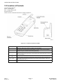


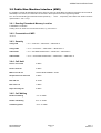


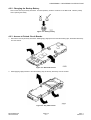


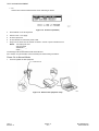
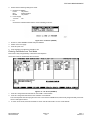
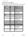

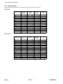
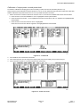

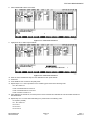

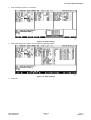


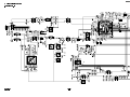


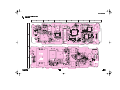


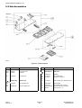


![IFW451_p01 [Konvertiert]](http://vs1.manualzilla.com/store/data/006663837_2-b9fc3b4fb1770fb647e0a7a561979307-150x150.png)