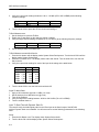
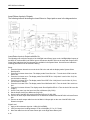
1
MPX G2
Guitar
Effects Processor
Service
Manual
MPX G2 Service Manual
Precautions
Save these instructions for later use.
Follow all instructions and warnings marked on the unit.
Always use with the correct line voltage. Refer to the manufacturers operating instructions for power requirements. Be advised that
different operating voltages may require the use of a different line cord and/or attachment plug.
Do not install the unit in an unventilated rack, or directly above heat producing equipment such as power amplifiers. Observe the
maximum ambient operating temperature listed in the product specification.
Slots and openings on the case are provided for ventilation; to ensure reliable operation and prevent it from overheating, these
openings must not be blocked or covered. Never push objects of any kind through any of the ventilation slots. Never spill a liquid of
any kind on the unit.
This product is equipped with a 3-wire grounding type plug. This is a safety feature and should not be defeated.
Never attach audio power amplifier outputs directly to any of the unit’s connectors.
To prevent shock or fire hazard, do not expose the unit to rain or moisture, or operate it where it will be exposed to water.
Do not attempt to operate the unit if it has been dropped, damaged, exposed to liquids, or if it exhibits a distinct change in performance
indicating the need for service.
This unit should only be opened by qualified service personnel. Removing covers will expose you to hazardous voltages.
This triangle, which appears on your component, alerts you to the presence of uninsulated, dangerous voltage inside the
enclosure… voltage that may be sufficient to constitute a risk of shock.
CAUTION
RISK OF ELECTRIC SHOCK
DO NOT OPEN
This triangle, which appears on your component, alerts you to important operating and maintenance Instructions in this
accompanying literature.
Notice
This equipment generates and uses radio frequency energy and if not installed and used properly, that is, in strict accordance with the
manufacturer's instructions, may cause interference to radio and television reception. It has been type tested and found to comply with
the limits for a Class B computing device in accordance with the specifications of Part 15 of FCC Rules, which are designated to
provide reasonable protection against such interference in a residential installation. However, there is no guarantee that interference
will not occur in a particular installation. If this equipment does cause interference to radio or television reception, which can be
determined by turning the equipment OFF and ON, the user is encouraged to try to correct the interference by one or more of the
following measures:
Reorient the receiving antenna
Relocate the computer with respect to the receiver
Move the computer away from the receiver
Plug the computer into a different outlet so that the computer and receiver are on different branch circuits.
If necessary, the user should consult the dealer or an experienced radio/television technician for additional suggestions. The user may
find the following booklet prepared by the Federal Communications Commission helpful:
“How to identify and Resolve Radio/TV Interference Problems.
This booklet is available from the U.S. Government Printing Office, Washington, DC 20402, Stock No. 004-000-00345-4.
Le présent appareil numérique n'émet pas de bruits radioélectriques dépassant les limites applicables aux appareils numériques de Ia
class B prescrites dans le Règlement sur le brouillage radioélectrique édicté par le ministère des Communications du Canada.
Copyright © 1999 - 2001 Lexicon, Inc.
All Rights Reserved
Lexicon Inc. ● 3 Oak Park ● Bedford, MA 01730-1441 ● Tel (781) 280-0300 ● Customer Service Fax (781) 280-0499
Lexicon Part # 070-14395 Rev 0
Printed in the United States of America
Lexicon
Safety Suggestions
basement, near a swimming pool, near an open
window, etc.
Read Instructions Read all safety and operating
instructions before operating the unit.
Object and liquid entry Do not allow objects to
fall or liquids to be spilled into the enclosure
through openings.
Retain Instructions Keep the safety and
operating instructions for future reference.
Heed Warnings Adhere to all warnings on the
unit and in the operating instructions.
Follow Instructions Follow operating and use
instructions.
Heat Keep the unit away from heat sources such
as radiators, heat registers, stoves, etc., including
amplifiers which produce heat.
Ventilation Make sure that the location or
position of the unit does not interfere with its
proper ventilation. For example, the unit should
not be situated on a bed, sofa, rug, or similar
surface that may block the ventilation openings;
or, placed in a cabinet which impedes the flow of
air through the ventilation openings.
Wall or Ceiling Mounting Do not mount the unit
to a wall or ceiling except as recommended by
the manufacturer.
Power Sources Connect the unit only to a power
supply of the type described in the operating
instructions, or as marked on the unit.
Grounding or Polarization* Take precautions
not to defeat the grounding or polarization of the
unit’s power cord.
*Not applicable in Canada.
Power Cord Protection Route power supply
cords so that they are not likely to be walked on
or pinched by items placed on or against them,
paying particular attention to cords at plugs,
convenience receptacles, and the point at which
they exit from the unit.
Nonuse Periods Unplug the power cord of the
unit from the outlet when the unit is to be left
unused for a long period of time.
Water and Moisture Do not use the unit near
water — for example, near a sink, in a wet
Cleaning The unit should be cleaned only as
recommended by the manufacturer.
Servicing Do not attempt any service beyond
that described in the operating instructions. Refer
all other service needs to qualified service
personnel.
Damage requiring service The unit should be
serviced by qualified service personnel when:
• the power supply cord or the plug
has been damaged
• objects have fallen, or liquid has
been spilled into the unit
• the unit has been exposed to rain
• the unit does not appear to operate
normally or exhibits a marked change
in performance
• the unit has been dropped, or the
enclosure damaged
MPX G2 Service Manual
SAFETY SUMMARY
The following general safety precautions must be observed during all phases of operation, service and repair of this instrument. Failure to comply with
these precautions or with specific warnings elsewhere in these instructions violates safety standards of design manufacture and intended use of the
instrument. Lexicon assumes no liability for the customer’s failure to comply with these requirements.
GROUND THE INSTRUMENT
To minimize shock hazard the instrument chassis and cabinet
must be connected to an electrical ground. The instrument is
equipped with a three-conductor AC power cable. The power
cable must either be plugged into an approved three-contact
electrical outlet or used with a three-contact to two-contact
adapter with the grounding wire (green) firmly connected to an
electrical ground (safety ground) at the power outlet. The power
jack and mating plug of the power cable meet International
Electrotechnical Commission (IEC) safety standards.
DO NOT OPERATE IN AN EXPLOSIVE
ATMOSPHERE
Do not operate the instrument in the presence of flammable gases
or fumes. Operation of any electrical instrument in such an
environment constitutes a definite safety hazard.
KEEP AWAY FROM LIVE CIRCUITS
Operating personnel must not remove instrument covers.
Component replacement and internal adjustments must be made
by qualified maintenance personnel. Do not replace components
with power cable connected. Under certain conditions, dangerous
voltages may exist even with the power cable removed. To avoid
injuries, always disconnect power and discharge circuits before
touching them.
SAFETY SYMBOLS
General definitions of safety symbols used on equipment or in
manuals.
Instruction manual symbol: the product will be marked
with this symbol when it is necessary for the user to refer to the
instruction manual in order to protect against damage to the
instrument.
Indicates dangerous voltage. (Terminals fed
from the interior by voltage exceeding 1000 volts must be so
marked.)
WARNING
The WARNING sign denotes a hazard. It calls attention to a
procedure, practice, condition or the like which, if not correctly
performed or adhered to, could result in injury or death to
personnel.
DO NOT SERVICE OR ADJUST ALONE
Do not attempt internal service or adjustment unless another
person, capable of rendering first aid and resuscitation, is present.
DO NOT SUBSTITUTE PARTS OR MODIFY
INSTRUMENT
Because of the danger of introducing additional hazards, do not
install substitute parts or perform any unauthorized modification to
the instrument.
DANGEROUS PROCEDURE WARNINGS
Warnings, such as the example below, precede potentially
dangerous procedures throughout this manual. Instructions
contained in the warnings must be followed.
WARNING
CAUTION
The CAUTION sign denotes a hazard. It calls attention to an
operating procedure, practice, condition or the like which, if not
correctly performed or adhered to, could result in damage to or
destruction of part or all of the product.
NOTE:
The NOTE sign denotes important information. It calls attention to
procedure, practice, condition or the like which is essential to
highlight.
CAUTION
Electrostatic Discharge (ESD) Precautions
Dangerous voltages, capable of causing death, are present in this
instrument. Use extreme caution when handling, testing and
adjusting.
The following practices minimize possible damage to ICs resulting from
electrostatic discharge or improper insertion.
•
Keep parts in original containers until ready for use.
•
Avoid having plastic, vinyl or Styrofoam in the work area.
•
Wear an anti—static wrist-strap.
•
Discharge personal static before handling devices.
•
Remove and insert boards with care.
•
When removing boards, handle only by non-conductive surfaces
and never touch open-edge connectors except at a static-free
workstation.*
•
Minimize handling of ICs.
•
Handle each IC by its body.
•
Do not slide ICs or boards over any surface.
•
Insert ICs with the proper orientation, and watch for bent pins on
ICs.
•
Use static shielding containers for handling and transport.
‘To make a plastic-laminated workbench anti-static, wash with a
solution of Lux liquid detergent, and allow drying without rinsing.
Lexicon
Table of Contents
Chapter 1 Reference Documents, Required Equipment............................. 1-1
Reference Documents............................................................................................................................. 1-1
Required Equipment................................................................................................................................ 1-1
Tools .................................................................................................................................................... 1-1
Test Equipment.................................................................................................................................... 1-1
Chapter 2 General Information ................................................................... 2-1
Periodic Maintenance .............................................................................................................................. 2-1
Ordering Parts ......................................................................................................................................... 2-1
Returning Units to Lexicon for Service .................................................................................................... 2-1
Chapter 3 Specifications............................................................................. 3-1
Chapter 4 Performance Verification............................................................ 4-1
Diagnostics .............................................................................................................................................. 4-1
Analog Audio Performance:..................................................................................................................... 4-1
Setup:................................................................................................................................................... 4-1
Input to Send........................................................................................................................................ 4-3
Insert Return Inputs to Outputs: ......................................................................................................... 4-16
Lexicon Audio Precision ATE Summary ............................................................................................ 4-33
Chapter 5 Troubleshooting ......................................................................... 5-1
http://www.lexicon.com/kbase/index.asp ................................................................................................. 5-1
Diagnostics .............................................................................................................................................. 5-1
Power On Diagnostics: ........................................................................................................................ 5-1
Error Indication:.................................................................................................................................... 5-1
Test Descriptions: ................................................................................................................................ 5-2
Functional Tests / Extended Diagnostics................................................................................................. 5-5
Functional Test Descriptions ................................................................................................................... 5-6
Switch Test: ......................................................................................................................................... 5-6
Front Panel Pots .................................................................................................................................. 5-8
LED Test .............................................................................................................................................. 5-9
Display Character Test ........................................................................................................................ 5-9
Display Block Test ............................................................................................................................. 5-10
Auto Test Execution........................................................................................................................... 5-11
Burn In Loop ...................................................................................................................................... 5-11
Footpedal Test ................................................................................................................................... 5-12
MIDI Test ........................................................................................................................................... 5-13
DRAM Test ........................................................................................................................................ 5-14
WCS Test........................................................................................................................................... 5-15
Lo SRAM Test.................................................................................................................................... 5-15
ROM Test........................................................................................................................................... 5-16
TOP LEVEL MENU UTILITIES & TOOLS ............................................................................................. 5-16
Exit Diags........................................................................................................................................... 5-17
Scope Loops ...................................................................................................................................... 5-17
Software Err Log ................................................................................................................................ 5-17
Clear Err Log...................................................................................................................................... 5-18
2186 Tools ......................................................................................................................................... 5-18
View Alg Nums................................................................................................................................... 5-19
UTILITY MENU (Options Button) .......................................................................................................... 5-19
Repeat Test ....................................................................................................................................... 5-19
Test Result Menu............................................................................................................................... 5-20
View DRAM........................................................................................................................................ 5-26
MIDI Scope ........................................................................................................................................ 5-26
EMERGENCY DIAGNOSTICS.............................................................................................................. 5-26
Removing the Top Cover:...................................................................................................................... 5-27
MPX G2 Service Manual
Power Supply: ........................................................................................................................................5-27
Battery Voltage:......................................................................................................................................5-28
Systems Clocks:.....................................................................................................................................5-29
APPENDIX A: Software Error Messages ...............................................................................................5-29
Chapter 6 Theory of Operation ................................................................... 6-1
Analog ......................................................................................................................................................6-1
Overview...............................................................................................................................................6-1
Input......................................................................................................................................................6-2
Tone Block............................................................................................................................................6-3
Dynamic Gain .......................................................................................................................................6-3
Send .....................................................................................................................................................6-4
Aux Inputs (including Speaker Simulator).............................................................................................6-5
Output ...................................................................................................................................................6-6
Supplies ................................................................................................................................................6-6
Digital .......................................................................................................................................................6-7
ARCHITECTURE..................................................................................................................................6-7
SCHEMATIC WALK-THROUGH ........................................................................................................6-14
DETAILS.............................................................................................................................................6-17
Chapter 7 - Parts List.................................................................................. 7-1
Main Board ...............................................................................................................................................7-1
Display Board ...........................................................................................................................................7-5
Front Panel Input Board ...........................................................................................................................7-6
Chassis/Mechanical .................................................................................................................................7-6
Packaging/Miscellaneous.........................................................................................................................7-7
Power Cords.............................................................................................................................................7-7
Chapter 8 Schematics and Drawings ......................................................... 8-1
Schematics:..............................................................................................................................................8-1
Drawings: .................................................................................................................................................8-1
Lexicon
Chapter 1 Refe r ence Documents, Required Equipment
Reference Documents
MPX G2 Owner's Manual - Lexicon P/N 070-11542 latest revision
Required Equipment
Tools
The following is a minimum suggested technician's tool kit required for performing disassembly, assembly
and repairs:
• Clean, antistatic, well lit work area.
• (1) #1 Phillips tips screwdriver
• (1) 14mm socket nut driver
• Solder: 63/37 - Tin/Lead Alloy composition, low residue, no-clean solder.
• Magnification glasses and lamps
• SMT Soldering / De-soldering bench-top repair station
Test Equipment
The following is a minimum suggested equipment list required to perform the proof of performance tests.
• Amplifier with speakers or headphones.
• Cables: (dependent on your signal source)
• 2 shielded audio cables with 1/4" plugs on one end (T/S for single ended, T/R/S for
balanced) and appropriate connections on the opposite ends for connection to Low
Distortion Oscillator.
• RCA male-to-male braided shield style cable
• 1 MIDI cable: male 5 pin DIN to male 5 pin DIN, 3ft minimum
• (1) Low Distortion Oscillator with a single-ended or balanced output < 600 (output impedance),
<0.005% THD+N with a Tone Burst function.
• (1) Analog distortion analyzer and level meter with single-ended or balanced input, switchable
30kHz low pass filter or audible band-pass (20-20kHz) filter.
• (1) DMM ( Digital Multimeter)
• (1) Frequency Counter
• (1) 100 MHz oscilloscope with 1x, 10x probes and storage features
• (1) Footpedal with a 10-100k range with cable
• (1) Stereo footswitch T/R/S momentary closed style and cable
• (1) Bench power supply providing a variac adjustment and transformer isolation
1-1
Lexicon
Chapter 2 Gene r al Information
Periodic Maintenance
Under normal conditions the MPX G2 system requires minimal maintenance. Use a soft, lint-free cloth
slightly dampened with warm water and mild detergent to clean the exterior surfaces of the connector box.
Do not use alcohol, benzene or acetone-based cleaners or any strong commercial cleaners. Avoid
using abrasive materials such as steel wool or metal polish. It the unit is exposed to a dusty environment, a
vacuum or low-pressure blower may be used to remove dust from the unit's exterior.
Ordering Parts
When ordering parts, identify each part by type, price and Lexicon Part Number. Replacement parts can be
ordered from:
LEXICON, INC.
3 Oak Park
Bedford, MA 01730-1441
Telephone: 781-280-0300; Fax: 781-280-0499; email: [email protected]
ATTN: Customer Service
Returning Units to Lexicon for Service
Before returning a unit for warranty or non-warranty service, consult with Lexicon Customer
Service to determine the extent of the problem and to obtain Return Authorization. No equipment
will be accepted without Return Authorization from Lexicon.
If Lexicon recommends that a MPX G2 be returned for repair and you choose to return the unit to Lexicon
for service, Lexicon assumes no responsibility for the unit in shipment from the customer to the factory,
whether the unit is in or out of warranty. All shipments must be well packed (using the original packing
materials if possible), properly insured and consigned, prepaid, to a reliable shipping agent.
When returning a unit for service, please include the following information:
•
•
•
•
•
•
•
•
•
Name
Company Name
Street Address
City, State, Zip Code, Country
Telephone number (including area code and country code where applicable)
Serial Number of the unit
Description of the problem
Preferred method of return shipment
Return Authorization #, on both the inside and outside of the package
Please enclose a brief note describing any conversations with Lexicon personnel (indicate the name of the
person at Lexicon) and give the name and telephone daytime number of the person directly responsible for
maintaining the unit.
Do no include accessories such as manuals, audio cables, footswitches, etc. with the unit, unless
specifically requested to do so by Lexicon Customer Service personnel.
2-1
Lexicon
Chapter 3 Spec i fications
I/O
Instrument input: mono 1/4 inch 1megΩ unbalanced, with analog soft clipping circuit and front panel input level control
Levels: minimum +2.2dBu for full scale, maximum +10dBu max
A/D: 24-bit
Return Inputs: stereo, 1/4 inch, 50κΩ unbalanced, with analog soft clipping circuit and ganged level control on rear panel
Levels: minimum –10dBu for full scale; maximum +18dBu max (for +4 nominal inputs); +18 dBu with rear level pot at
minimum
A/D: 24-bit
Main L and R Outputs: 1/4 inch TRS balanced (2), XLR 3-wire balanced (2)
Nominal Level: front panel adjustable to +4dBu
Maximum Output Level: balanced: +18dBu into 600Ω; unbalanced: +21dBu into 100κΩ
D/A: 24-bit
Send Output: mono, 1/4 inch unbalanced
Nominal Level: software adjustable to +4dBu
Maximum Output Level: +18dBu into 100κΩ
D/A: 24-bit
Audio performance
Frequency response: 20Hz to 20kHz;+1 to -1.5dB for input to send; +1 to -1.5dB for return to output
THD+N: <0.01%, at 1kHz nominal output level; <.01% at 1kHz insert returns to main output; .01% at 1kHz input to main
outputs
Dynamic Range: Instrument input to send:
-110dB (unweighted) minimum Input to Send with Relay Bypass on
-120dB (unweighted) Input to Send with Noise Gate on
-97dB (unweighted) typical instrument to main outputs in Bypass
Sample rate: 44.1kHz
Return Mix: When the Return Mix option is selected, MPX G2 will mix the analog Aux inputs with the post converter output
signal from the DSP.
Throughput delay without send/return loop: Input to Main Output <3ms, nominal
Internal Audio Data Paths
Conversion: 24-bit A/D, 24-bit D/A
DSP: 32 bits
Control Interface
MIDI: 7-pin DIN connector for MIDI IN/powered bi-directional remote 5-pin DIN connectors for MIDI THRU and OUT
Footswitch: 1/4 inch T/R/S phone jack for 3 independent footswitches
Foot pedal: 1/4 inch T/R/S phone jack (10κΩ min, 100κΩ max impedance)
Remote Power In: 2.5mm barrel for 9VAC remote power
General
Dimensions: 19.0"W x 1.75"H x 13"D (483 x 45 x 330mm); 19 inch rack mount standard, 1U high
Weight: Net: 7.2lbs (3.2kg); Shipping: 11lbs (4.98kg)
Power Requirements: 100-240VAC, 50-60Hz, 25W, 3-pin IEC power connector
Environment: Operating temperature: 32° to 104°F (0° to 40°C); Storage temperature: -20° to 170°F (-30° to 75°C); Humidity:
maximum 95% without condensation
Electrical Approvals
Safety Compliance: UL1419 and CSA 22.2 No. 1-94 (UL and C-UL marks); EN60065 (TUV-GS and CE marking per Directive
73/23/EEC)
EMC Compliance: FCC Class B; EN55022 Class B and EN50082-1; (CE marking per Directive 89/336/EEC)
Specifications subject to change without notice.
3-1
Lexicon
Chapter 4 Perfo r mance Verification
This section provides a procedure for verification of the normal operation of the MPX G2 internal processors
and the integrity of the analog and digital audio signal paths. This procedure does not require removal of
the MPX G2 covers.
Diagnostics
The MPX G2 contains three types of Diagnostics: Power On Diagnostics, Extended Diagnostics, and
Emergency Diagnostics. Each of these is described fully the chapter on Troubleshooting. When the MPX
G2 is powered on, Power On Diagnostics will run automatically to verify proper operation of its internal
system. The Power On Diagnostics consist of the following tests:
FPGA Test
Z80 CPU Test
ROM Checksum Test
Stack RAM Test
ADSP2186 Test
WCS Test
Lo SRAM Test
Lex-2186 Test
Sample Rate Test
Digipot Test
Analog Audio Performance:
NOTE: In order to properly test the MPX G2, every step in the Setup section must be set in order. This is to
insure proper troubleshooting of an MPX G2 if service is needed. Failure to set the unit up properly will
cause incorrect readings. Many of the tests in this procedure are provided to verify functional operation.
Test results given for tests intended to verify functionality do not necessarily represent any published
performance specification.
Setup:
1. Turn on the MPX G2 and wait for the Power On Diagnostics cycle to finish.
2. Turn the front panel knob to select program 250 Clean Slate.
3. Press the Edit button. The display should read: Edit select Mix. Turn the knob until the display reads:
Edit select Effects Order.
4. Press the Gain button. Once pressed its Led will flash off/on and the display will read Gain select: no
effect.
5. Turn the knob until the display reads: Gain select *Crunch. The Gain Led will start to flash more rapidly.
6. Press the Gain button. The '*' will disappear and the Gain Led will be flashing slower. This is an
indication that the Crunch effect is now loaded.
7. Press the Effect 1 button. The Effect 1 Led will flash off/on and the display will read FX 1 select: no
effect.
8. Turn the knob until the display reads: FX 1 select: 13 *Volume (S). The Effect 1 Led will start to flash
more rapidly.
9. Press the Effect 1 button. The '*' will disappear and the Effect 1 Led will be flashing slower. This is an
indication that the Volume (S) effect is now loaded.
10. Set the Gain pots (Low Mid Hi ) on the front panel so the levels are at 0 (the level will change on the
display as the pot each pot is turned).
11. Press the Edit button twice. The display reads: Edit Select: Mix.
12. Press the Yes button and the display reads: Send Level 0 (flashing). Turn the knob CCW to set the
Send Level to -18. Press the No button to get you back to the Edit select Mix.
13. Turn the knob until the display reads: Edit select Noise Gate. Press the Yes button 3 times. The display
reads: NoiseGate Thrsh. Turn the knob CW until the reading is -20dB.
14. Press the Yes button. The display reads: NoiseGate Atten. Turn the knob CCW for a -90dB setting.
15. Press the Yes button. The display reads: NoiseGate Offset the dB level should be at -3dB.
4-1
MPX G2 Service Manual
16. Press the Yes button. The display reads: NoiseGate ATime. Press Yes and turn the knob CW until
setting is at 20.
17. Press the Yes button. The display reads: NoiseGate HTime. Press Yes and turn the knob CCW until
setting is at 20.
18. The MPX G2 now has to be placed in a test program called Development. This will require several
steps before the remaining settings for the Performance Section are set properly.
18.1.
Press the System button. The display reads: System Select: Audio
18.2.
Turn the knob CW until the display reads: System Select: MIDI.
18.3.
Press the Yes button 4 times until the display reads: MIDI Ctl Send None = None
18.4.
Press the Options button the display reads: MIDI Reset Press YES
18.5.
Press and hold the Effect 1 button until the display reads: Debug Mode then release.
18.6.
Press the Options button. The display reads: MIDI Ctl Send None=None.
18.7.
Press the No button 4 times until the display reads: System Select: MIDI.
18.8.
Turn the knob CW until the display reads: System Select :Development
19. The Development Diagnostics Menu will now be available.
20. Press the Yes button Twice until the display reads: Devel DSP Bypass. Turn the knob to set this to Byp
0.
21. Press the Yes button Five times until the display reads: Devel Insrt Type. Turn the knob CCW to set this
to Stereo.
22. Press the Yes button Eight times until the display reads: Devel LoCut. Turn the knob to set this to 0.
23. Press the Yes button Three times until the display reads: Devel HiCut. Turn the knob to set this to 0.
24. Press the Yes button once. The display reads: Devel Bass. Turn the knob to set this to 0.
25. Press the Yes button once. The display reads: Devel Trebl. Turn the knob to set this to 0.
26. Press the Yes button three times until the display reads: Devel Gtone. Turn the knob CCW to Byp 0.
27. Press the Yes button once. The display reads: Devel Fgood. Turn the knob to set this to Out 0.
28. Press the Yes button twice. The display reads: Devel Gain. Turn the knob CCW to Byp 0.
29. Press the Yes button twice. The display reads: Devel Send. Turn the knob to set this to Gn 0.
30. Press the Yes button once. The display reads: Devel Mute. Turn the knob CCW to Byp 0.
31. Press the Program button. The display reads: Clean Slate.
The MPX G2 is now ready for the tests that follow.
For each test, you will be instructed to make different setting changes to the above procedure, mainly in the
form of input levels. All measurements fall within a range containing both Upper and Lower limit rather than
a set number. The range values will be listed as Upper limit values first and Lower limit values.
Note: In the tests to follow, Input refers to the Rear Guitar Input Jack on the back of the MPX G2.
32. Connect an audio input cable between the Low Distortion Oscillator and the MPX G2 Rear Guitar Input
jack.
33. Connect an audio output cable from the Insert Send output jack on the rear of the MPX G2 to the
Distortion Analyzer.
4-2
Lexicon
Input to Send
The following tests will be testing the Input to Send path as seen in the diagram below:
Input To Send Tests In Bypass:
This test will verify the Audio signal path from the Rear Input to the Send output of the MPX G2
In Bypass
Signal Levels:
1. Apply a 1kHz-sinewave signal at +0.5dBu (820 mVRMS) to the Rear Guitar Input jack of the MPX G2.
2. Press the Edit button. The display will read Edit select Mix. Press the Yes button once. The display will
read Send Level. Turn the knob for a setting of -10.
3. Verify an output level reading between -0.64 to -1.76 dBu (720 to 632 mVRMS).
4. Reset the Send Level in the Edit menu to +8.
5. Verify an output level reading between 17.36 to 16.24 dBu (5.72 to 5.03 Vrms).
6. Apply a 1kHz-sinewave signal at +1dBu (870 mVRMS).
7. Turn the Bypass on by pressing the Bypass button on the front panel.
8. Verify an output level reading between 1.56 to -0.44 dBu (927 to 736 mVRMS).
9. Reapply a 1kHz-sinewave signal at +0.5dBu (820 mVRMS).
10. Turn off the Bypass from the front panel.
11. Add a 600Ω load to the output signal feeding the analyzer.
12. Verify an output level reading between 11.36 to -9.24 dBu (2.87 to .267 Vrms).
Frequency Response Measurement:
1. Disable all Filters on the Distortion Analyzer.
2. Apply a 1kHz-sinewave signal at +1dBu (870 mVRMS).
3. Set the Analyzer for a 0dB reference.
4. Verify the output level reading is between 1.0 to -1.5 dBu (875 to 647 mVRMS) at the following
frequency settings.
20,000Hz
4,000Hz
60Hz
16,000Hz
2,000Hz
20Hz
12,000Hz
250Hz
10,000Hz
100Hz
4-3
MPX G2 Service Manual
THD+N Measurement:
1. Set the Analyzer to measure THD+N.
2. Enable the Lo pass filters on the analyzer (30kHz or 20kHz).
3. Verify an output THD+N reading is between (0.15 to 0.0007%) at the following frequency settings.
20,000Hz
3,000Hz
15,000Hz
997Hz
10,000Hz
100Hz
5,000Hz
20Hz
4. Set the Analyzer back to measure level.
Signal to Noise Ratio:
1. Apply a 1kHz-sinewave signal at +2.2dBu (1.0 Vrms).
2. Set the Analyzer for a 0dB reference (@ 1kHz).
3. Turn off the oscillator.
4. Verify an output level reading between -99.94 to-120.00 dBu (7.6 to 0.8 uVRMS).
5. Turn the oscillator back on.
Signal Level with NoiseGate On/Off:
1. Apply a 1kHz-sinewave signal at -24dBu (49 mVRMS).
2. Press the Edit button and turn the knob CW to the Noise Gate menu.
3. Press the Yes button once. The display reads: NoiseGate Enable Off. Turn the knob CW to select
Guitar Input.
4. Press the Yes button once. The display reads: NoiseGate Send Off. Turn the knob CW to set this to
On.
5. Verify an output level reading range between -39.94 to -100.00 dBu (7.8m to 7.6u Vrms).
6. In the Edit menu turn the NoiseGate Send and Enable back to the Off position.
7. Apply a 1kHz-sinewave signal at -16.5dBu (115.9 mVRMS).
8. Verify an output level reading range between 1.06 to -1.06 dBu (875 to 686 mVRMS).
Input To Send Test With Tone On:
This test will verify the Audio signal path from the Rear Input to the Send output of the MPX G2
With the Tone circuit enabled. There are 3 parameters that must be set for this test.
Signal Levels:
1. Press the System button until the display reads: System Select Development.
2. Press the Yes button 23 times until the display reads Devel GTone Byp 0. Turn the Knob CW to turn
the Tone circuit On 1.
3. Press the Edit button. The display will read Noise Select Mix. Turn the knob CW until the display reads
Edit select Noise Gate. Press the Yes button once. The display will read NoiseGate Enable. Set it to
Off.
4. Press the Yes button once. The display will read NoiseGate Send. Set this to the Off setting.
5. Press the Edit button a few times until the display reads: Edit Select: Mix.
6. Press the Yes button once. The display reads: Send Level. Turn the knob CW to set the level to +8.
7. Apply a 1kHz-sinewave signal at +1dBu (870 mVRMS) to the Rear Guitar Input jack of the MPX G2.
8. Verify an output level reading between 17.26 to 16.24dBu (5.7 to 5.0 Vrms).
THD+N Measurement:
1. Set the Analyzer to measure THD+N.
2. Enable the Lo pass filters on the analyzer (30kHz or 20kHz).
3. Verify an output THD+N reading is between (0.15 to 0.0007%) at the following frequency settings.
20,000Hz
3,000Hz
4-4
15,000Hz
997Hz
10,000Hz
100Hz
5,000Hz
20Hz
Lexicon
5. Set the Analyzer back to measure level.
Signal To Noise Ratio:
1. Apply a 1kHz-sinewave signal at +2.2dBu (1.0 Vrms).
2. Set the Analyzer for a 0dB reference (@ 1kHz).
3. Turn off the oscillator.
4. Verify an output level reading between -99.94 to-120.00 dBu (7.8 to 0.8 uVRMS).
5. Turn the oscillator back on.
Frequency Response Measurement:
1. Disable all Filters on the Distortion Analyzer.
2. Apply a 1kHz-sinewave signal at -15.5dBu (130 mVRMS).
3. Set the Analyzer for a 0dB reference.
4. Verify the output level reading is between 1.06 to -1.56 dBu (875 to 647 mVRMS) at the following
frequency settings.
20,000Hz
16,000Hz
12,000Hz
10,000Hz
4,000Hz
2,000Hz
250Hz
100Hz
60Hz
20Hz
5. Set the Low Gain to -25 using the front panel knob.
6. Verify the output level readings for each of the frequency settings in the table below.
Freq.
Upper
Hz (Vrms)
dBu
20,000 (1.1)
3.40
16,000 (1.1)
3.39
12,000 (1.1)
3.38
10,000 (1.1)
3.37
4,000 (1.1)
3.16
2,000 (1.0)
2.51
997 (.83)
0.62
250 (.34)
-7.07
100 (.22)
-10.79
60 (.20)
-11.59
20 (.20)
-12.05
Lower
(Vrms)
dBu
(.90)
1.28
(.90)
1.27
(.90)
1.26
(.90)
1.25
(.90)
1.04
(.81)
0.39
(.65)
-1.50
(.27)
-9.19
(.17)
-12.91
(.16)
-13.71
(.15)
-14.17
7. Set the Low Gain to +25 using the front panel knob.
8. Verify the output level readings for each of the frequency settings in the table below.
Freq.
Upper
Hz (Vrms)
dBu
20,000 (1.1)
3.41
16,000 (1.1)
3.42
12,000 (1.1)
3.43
10,000 (1.1)
3.45
4,000 (1.2)
3.64
2,000 (1.3)
4.27
997 (1.6)
6.10
250 (3.8)
13.79
100 (5.8)
17.51
60 (6.4)
18.37
20 (6.8)
18.87
Lower
(Vrms)
dBu
(.90)
1.29
(.90)
1.30
(.90)
1.31
(.90)
1.33
(.92)
1.52
(1.0)
2.15
(1.2)
3.98
(3.0)
11.67
(4.6)
15.39
(5.0)
16.25
(5.4)
16.75
4-5
MPX G2 Service Manual
9. Set the Low Gain to 0, then set the Mid Gain to -25 using the front panel knob.
10. Verify the output level readings for each of the frequency settings in the table below.
Freq.
Upper
Hz (Vrms)
dBu
20,000 (1.0)
2.24
16,000 (1.0)
1.68
12,000 (.84)
0.66
10,000 (.76)
-0.15
4,000 (.38)
-6.12
2,000 (.20)
-11.86
997 (.10)
-17.65
250 (.19)
-12.21
100 (.45)
-4.67
60 (.67)
-1.22
20 (1.1)
2.66
Lower
(Vrms)
dBu
(.80)
0.12
(.70)
-0.44
(.65)
-1.46
(.60)
-2.27
(.30)
-8.24
(.15)
-13.98
(.08)
-19.77
(.15)
-14.33
(.35)
-6.79
(.53)
-3.34
(.82)
0.54
11. Set the Mid Gain to +25 using the front panel knob.
12. Verify the output level readings for each of the frequency settings in the table below.
Freq.
Upper
Hz (Vrms)
dBu
20,000 (1.3)
4.53
16,000 (1.4)
5.08
12,000 (1.6)
6.07
10,000 (1.7)
6.88
4,000 (3.4)
12.82
2,000 (6.5)
18.54
997 (12.5)
24.18
250 (6.8)
18.93
100 (3.0)
11.48
60 (2.0)
8.16
20 (1.3)
4.37
Lower
(Vrms)
dBu
(1.0)
2.41
(1.1)
2.96
(1.2)
3.95
(1.3)
4.76
(2.7)
10.70
(5.1)
16.42
(9.8)
22.06
(5.4)
16.81
(2.3)
9.36
(1.6)
6.04
(1.0)
2.25
13. Apply a 1kHz-sinewave signal at -30.5dBu (23 mVRMS).
14. Set the Mid Gain to 0, then set the High Gain to +50 using the front panel knob.
4-6
Lexicon
15. Verify the output level readings for each of the frequency settings in the table below.
Freq.
Upper
Hz (Vrms)
dBu
20,000 (6.2)
18.07
16,000 (7.3)
19.45
12,000 (8.6)
20.92
10,000 (9.4)
21.67
4,000 (11)
23.37
2,000 (10)
22.41
997 (7.2)
19.37
250 (2.2)
8.96
100 (.90)
1.28
60 (.57)
-2.73
20 (.27)
-9.27
Lower
(Vrms)
dBu
(4.8)
15.95
(5.7)
17.33
(6.7)
18.80
(7.4)
19.55
(8.9)
21.25
(8.0)
20.29
(5.6)
17.25
(1.7)
6.84
(.70)
-0.84
(.44)
-4.85
(.21)
-11.39
16. Set High Gain setting back to 0.
Input To Send Test With DSP On:
This test will verify the Audio signal path from the Rear Input to the Send output of the MPX G2
With the DSP circuit enabled.
Signal Level:
1. Press the System button on the front panel. The display will read Devel GTone On 1. Turn the knob
CCW to place the Tone circuit into Byp 0.
2. Press the No button 21 times until the display reads: Devel DSP Bypass Byp 0. Turn the Knob CW to
turn the DSP circuit On 1.
3. Apply a 1kHz-sinewave signal at +1dBu (870 Vrms) to the Rear Guitar Input jack of the MPX G2.
4. Verify an output level reading between 12.76 to 11.64 dBu (3.4 to 3.0 Vrms).
Frequency Response Measurement:
1. Disable all Filters on the Distortion Analyzer.
2. Apply a 1kHz-sinewave signal at +1dBu (870 Vrms).
3. Set the Analyzer for a 0dB reference.
4. Verify the output level reading is between 1.06 to -1.56 dBu (875 to 647 mVRMS) at the following
frequency settings.
20,000Hz
4,000Hz
60Hz
16,000Hz
2,000Hz
20Hz
12,000Hz
250Hz
10,000Hz
100Hz
Frequency Response Measurement with Gain On:
1. Press the Yes button 21 times until the display reads Devel GTone Byp 0. Turn the knob CW to turn the
GTone circuit On 1.
2. Disable all Filters on the Distortion Analyzer.
3. Apply a 1kHz-sinewave signal at +1dBu (870 Vrms).
4. Set the Analyzer for a 0dB reference.
4-7
MPX G2 Service Manual
5. Verify the output level reading is between 1.06 to -1.56 dBu (875 to 647 mVRMS) at the following
frequency settings.
20,000Hz
4,000Hz
60Hz
16,000Hz
2,000Hz
20Hz
12,000Hz
250Hz
10,000Hz
100Hz
6. Turn the knob CCW to place the GTone circuit back into Byp 0.
THD+N Measurement:
1. Set the Analyzer to measure THD+N.
2. Enable the Lo pass filters on the analyzer (30kHz or 20kHz).
3. Verify an output THD+N reading is between (0.15 to 0.0007%) at the following frequency settings.
20,000Hz
3,000Hz
15,000Hz
997Hz
10,000Hz
100Hz
5,000Hz
20Hz
4. Set the Analyzer back to measure level.
THD+N Measurement with Soft Sat On:
1. Press the No button until the display reads: System Select Development. Turn the knob CCW until the
display reads: System Select Audio.
2. Press the Yes button once. The display reads: Audio Soft Sat Off. Turn the knob CW to turn the Soft
Sat circuit On.
3. Verify the output level readings for each of the input level settings in the table below.
Levels
(Vrms)
-3dBu (.55)
-2dBu (.60)
-1dBu (.70)
0dBu (.80)
+1dBu (.90)
Upper
%
1.10
3.06
5.38
7.54
9.38
Lower
%
0.14
0.73
1.66
2.60
3.42
5. Turn the knob CCW to turn the Soft Sat circuit back Off.
Signal To Noise Ratio:
1. Apply a 1kHz-sinewave signal at +2.2dBu (1.0 Vrms).
2. Set the Analyzer for a 0dB reference (@ 1kHz).
3. Turn off the oscillator.
4. Verify an output level reading between -99.94 to-120.00 dBu (7.8 to 0.8 uVRMS).
5. Turn the oscillator back on.
Input To Send Test with Dynamic Gain On:
This test will verify the Audio signal path from the Rear Input to the Send output of the MPX G2
with the Dynamic Gain circuit enabled. You will now need to set the following parameters for the following
tests
Setup:
1. Press the No Button once. The display reads: System Select Audio.
2. Turn the Knob CW until the display reads: System Select Development.
4-8
Lexicon
3. Press the Yes button twice. The display reads: Devel DSP Bypass On 1. Turn the knob CCW to turn
the DSP circuit to Byp 0.
4. Press the Yes button 21 times. The display reads: Devel Gtone. Turn the knob and set the level to Byp
0.
5. Press the No button 4 times. The display reads: Devel Bass. Turn the knob and set the level to 0.
6. Press the Yes button once. The display reads: Devel Trebl. Turn the knob and set the level to 0.
7. Press the Yes button 6 times the display reads: Devel Gain Byp 0. Turn the knob CW to turn the Gain
circuit On 1.
8. Press the Edit button 3 times. The display reads: Edit Select Mix.
Signal Level:
1. Apply a 1kHz-sinewave signal at -5.5dBu (411 mVRMS).
2. Set the Analyzer for a 0dB reference (@ 1kHz).
3. Verify an output level reading between 10.7 to 11.76dBu (2.7 to 3.0 Vrms).
4. Press the System button. The display reads: Devel Gain On 1.
5. Press the No button 9 times until the display reads: Devel Drive 0. Turn the knob CW to set the Drive
level to 60.
6. Apply a 1kHz-sinewave signal at -70.5dBu (231 mVRMS).
7. Set the Analyzer for a 0dB reference (@ 1kHz).
8. Verify an output level reading between 4.4 to 2.2dBu (1.3 to 1.0 Vrms).
9. Turn the knob CCW and set the Drive level to 0.
10. Press the Yes button 4 times. The display reads: Devel M-Vol 42 Turn the knob CCW to set the Volume
level to -60.
11. Apply a 1kHz-sinewave signal at -10.5dBu (231 mVRMS).
12. Set the Analyzer for a 0dB reference (@ 1kHz).
13. Verify an output level reading between -54.34 to -55.46 dBu (1.5 to 1.3 mVRMS).
14. Turn the knob CW and set the Drive M-Vol to -14.
15. Press the Yes button 3 times. The display reads: Devel FGood Out 0. Turn the knob CW so the setting
is In 1. This will engage the Feel Good circuit.
16. Press the No button 7 times. The display reads: Devel Drive 0. Turn the knob CW for a setting of 10.
17. Press the No button once. The display reads: Devel Feel 0. Turn the knob CW for a setting of 8.
Note: In the following part of this test an oscillator with a tone burst function must be set for the specs below
in step 18. The resulting output from the MPX G2 must be feed to a storage oscilloscope that is capable of
measuring and storing the information in time domain as indicated in the 2 graphs below.
18. Apply a 1kHz-sinewave signal Burst at -6dBu (388 mVRMS).
19. Set the Analyzer for a 0dB reference (@ 1kHz).
20. The tone burst is measured in a time domain. Measure the positive peak amplitude at various times
during the test from (0-28ms). The waveform measurement should look like the following signal in the
figure below. Notice that the amplitude of each peak in the burst decreases over time.
4-9
MPX G2 Service Manual
Feel Good Circuit On
21. Press the Yes button 8 times. The display reads: Devel FGood In 1. Turn the knob CCW so the setting
is Out 0 this will disengage the Feel Good circuit.
22. Again apply a 1kHz-sinewave signal Burst at -6dBu (388 mVRMS).
23. Set the Analyzer for a 0dB reference (@ 1kHz).
24. Verify the waveform measurement looks like the following signal in the figure below with the Feel Good
circuit off.
4-10
Lexicon
Feel Good Circuit Off
Frequency Response Measurements:
1. Press the No button 9 times. The display will read Devel LoCut 0. Turn the knob CW so the setting is
20.
2. Apply a 1kHz-sinewave signal at -20.5dBu (73 mVRMS).
3. Set the Analyzer for a 0dB reference (@ 1kHz). Verify the output level readings for each of the
frequency settings in the table below.
Freq.
Upper
Hz (Vrms)
dBu
20,000 (.37)
-6.32
16,000 (.41)
-5.41
12,000 (.46)
-4.58
10,000 (.48)
-4.22
4,000 (.50)
-3.86
2,000 (.43)
-5.13
997 (.30)
-8.33
250 (.09)
-18.85
100 (.036) -26.74
60 (.021) -31.28
20 (.006) -41.92
Lower
(Vrms)
dBu
(.30)
-8.44
(.33)
-7.53
(.36)
-6.70
(.37)
-6.34
(.39)
-5.98
(.34)
-7.25
(.23)
-10.45
(.07)
-20.97
(.028) -28.86
(.016) -33.40
(.005) -44.04
4-11
MPX G2 Service Manual
4. Turn the knob CCW to set LoCut back to 0.
5. Press the Yes button 3 times. The display will read Devel HiCut. Turn the knob CW so the setting is 35.
6. Verify the output level readings for each of the frequency settings in the table below.
Freq.
Upper
Hz (Vrms)
dBu
20,000 (.01)
-37.93
16,000 (.01)
-36.00
12,000 (.02)
-33.49
10,000 (.02)
-31.90
4,000 (.05)
-23.98
2,000 (.10)
-18.05
997 (.18)
-12.41
250 (.40)
-5.74
100 (.30)
-8.14
60 (.20)
-11.54
20 (.06)
-21.51
Lower
(Vrms)
dBu
(.007) -41.05
(.009) -39.12
(.01)
-36.61
(.01)
-35.02
(.03)
-27.10
(.07)
-21.17
(.13)
-15.53
(.28)
-8.86
(.20)
-11.26
(.18)
-14.66
(.05)
-24.63
7. Turn the knob CCW to set Hi Cut back to 0.
8. Press the Yes button 2 times. The display will read Devel Trebl 0. Turn the knob CW so the setting is
25.
9. Verify the output level readings for each of the frequency settings in the table below.
Freq.
Upper
Hz (Vrms)
dBu
20,000 (20)
28.25
16,000 (18)
27.44
12,000 (16)
26.06
10,000 (14)
24.99
4,000 (6)
18.31
2,000 (3)
12.78
997 (2)
7.75
250 (1.1)
2.74
100 (1.0)
2.27
60 (1.0)
2.11
20 (1.0)
2.10
Lower
(Vrms)
dBu
(12)
24.13
(11)
23.32
(10)
21.94
(9)
20.87
(4)
14.19
(2)
8.66
(1.2)
3.63
(.66)
-1.38
(.63)
-1.85
(.62)
-2.01
(.62)
-2.02
10. Turn the knob CCW to set Treble to -25.
4-12
Lexicon
11. Verify the output level readings for each of the frequency settings in the table below.
Freq.
Upper
Hz (Vrms)
dBu
20,000 (.05)
-24.44
16,000 (.05)
-23.55
12,000 (.06)
-22.09
10,000 (.07)
-20.98
4,000 (.15)
-14.11
2,000 (.30)
-8.55
997 (.50)
-3.55
250 (.90)
1.38
100 (1.0)
1.94
60 (1.0)
2.02
20 (1.0)
2.06
Lower
(Vrms)
dBu
(.03)
-28.56
(.03)
-27.67
(.04)
-26.21
(.04)
-25.10
(.10)
-18.23
(.20)
-12.67
(.30)
-7.67
(.60)
-2.74
(.60)
-2.18
(.60)
-2.10
(.60)
-2.06
12. Turn the knob CW to set Treble to 0.
13. Press the No button once. The display will read Devel Bass 0. Turn the knob CW to set it to 25.
14. Verify the output level readings for each of the frequency settings in the table below.
Freq.
Upper
Hz (Vrms)
dBu
20,000 (.90)
1.31
16,000 (.90)
1.31
12,000 (.90)
1.32
10,000 (.90)
1.32
4,000 (.90)
1.36
2,000 (.90)
1.48
997 (1.0)
1.93
250 (1.7)
6.44
100 (3.2)
12.24
60 (4.3)
14.84
20 (5.6)
17.15
Lower
(Vrms)
dBu
(.70)
-1.31
(.70)
-1.31
(.70)
-1.30
(.70)
-1.30
(.70)
-1.26
(.70)
-1.14
(.70)
-0.69
(1.2)
3.82
(2.3)
9.62
(3.2)
12.22
(4.1)
14.53
15. Turn the knob CCW to set Bass to -25.
16. Verify the output level readings for each of the frequency settings in the table below.
Freq.
Upper
Hz (Vrms)
dBu
20,000 (.90)
1.31
16,000 (.90)
1.31
12,000 (.90)
1.30
10,000 (.90)
1.30
4,000 (.90)
1.26
2,000 (.90)
1.14
997 (.80)
0.67
250 (.50)
-3.96
100 (.25)
-9.59
60 (.20)
-12.04
20 (.20)
-13.60
Lower
(Vrms)
dBu
(.70)
-1.31
(.70)
-1.31
(.70)
-1.32
(.70)
-1.32
(.65)
-1.36
(.65)
-1.48
(.60)
-1.95
(.36)
-6.58
(.20)
-12.21
(.20)
-14.66
(.10)
-16.22
4-13
MPX G2 Service Manual
THD+N Measurement:
1. Apply a 1kHz-sinewave signal at -10.0dBu (245 mVRMS).
2. Set the Analyzer for a 0dB reference (@ 1kHz).
3. Set the Analyzer to measure THD+N.
4. Enable the Lo pass filters on the analyzer (30kHz or 20kHz).
5. Verify an output THD+N reading is between (0.15 to 0.0007%) at the following frequency settings.
20,000Hz
3,000Hz
15,000Hz
997Hz
10,000Hz
100Hz
5,000Hz
20Hz
6. Set the Analyzer back to measure level.
Signal To Noise Ratio:
1. Apply a 1kHz-sinewave signal at +2.2dBu (1.0 Vrms).
2. Set the Analyzer for a 0dB reference (@ 1kHz).
3. Turn off the oscillator.
4. Verify an output level reading between -99.94 to-120.00 dBu (7.8 to 0.8 uVRMS).
5. Turn the oscillator back on.
Signal To Noise Ratio with Tone Enabled:
1. Press the No button 17 times. The display reads: Devel DSP Bypass Byp 0. Turn the knob CW so DSP
is On 1.
2. Press the Yes button 21 times. The display reads: Devel Gtone. Verify the circuit is set to On 1.
3. Press the Yes button 3 times. The display reads: Devel Gain. Verify the gain is set to On 1.
4. Apply a 1kHz-sinewave signal at +2.2dBu (1.0 Vrms).
5. Set the Analyzer for a 0dB reference (@ 1kHz).
6. Turn off the oscillator.
7. Verify an output level reading between -89.94 to-120.00 dBu (24.2 to 0.8 Vrms).
8. Turn the oscillator back on.
Signal To Noise Ratio Noise Gate On No Input:
1. Press the Edit button. The display reads: Edit Select Mix. Turn the knob CW until it reads: Edit Select
Noise Gate.
2. Press the Yes button once. The display reads: NoiseGate Enable Off. Turn the knob CW so the display
reads Guitar Input. This enables the NoiseGate circuit.
3. Press the Yes button once. The display reads: NoiseGate Send Off. Turn the knob CW to On to enable
the circuit.
4. Press the System button. The display reads: Devel Gain. Verify the gain is set to On 1.
5. Apply a 1kHz-sinewave signal at +2.2dBu (1.0 Vrms).
6. Set the Analyzer for a 0dB reference (@ 1kHz).
7. Turn off the oscillator.
8. Verify an output level reading between -119.94 to-140.00 dBu (0.8 to 0.08 uVRMS).
Input To Send Tests With Clean On:
These tests will verify the Audio signal path from the Rear Input to the Send output of the MPX G2 with the
Clean circuit enabled. The following tests parameters will be needed in order to perform these tests.
Setup
1. Press the Yes button 2 times. The display reads: Devel Send Gn 0. Turn the knob CW to select Cln 1.
The Clean circuit is now enabled.
2. Press the Edit button. The display reads: NoiseGate Send On. Turn the knob CCW to Off.
3. Press the No button once. The display reads: NoiseGate Enable Guitar Input. Turn the knob CCW to
Off.
4-14
Lexicon
Signal Level:
1. Apply a 1kHz-sinewave signal at +1.0dBu (870 mVRMS).
2. Set the Analyzer for a 0dB reference.
3. Verify an output level reading between 17.36 to 16.24 dBu (5.72 to 5.0 Vrms).
Frequency Response Measurements:
1. Disable all Filters on the Distortion Analyzer.
2. Apply a 1kHz-sinewave signal at +1dBu (870 Vrms).
3. Set the Analyzer for a 0dB reference.
4. Verify the output level reading is between 1.06 to -1.56 dBu (875 to 647 mVRMS) at the following
frequency settings.
20,000Hz
4,000Hz
60Hz
16,000Hz
2,000Hz
20Hz
12,000Hz
250Hz
10,000Hz
100Hz
THD+N Measurement:
1. Set the Analyzer to measure THD+N.
2. Enable the Lo pass filters on the analyzer (30kHz or 20kHz).
3. Verify an output THD+N reading is between (0.15 to 0.0007%) at the following frequency settings.
20,000Hz
3,000Hz
15,000Hz
997Hz
10,000Hz
100Hz
5,000Hz
20Hz
4. Set the Analyzer back to measure level.
Signal To Noise Ratio:
1. Set the Analyzer for a 0dB reference (@ 1kHz).
2. Turn off the oscillator.
3. Apply a 1kHz sinewave signal at 2.2dBu (1.0 Vrms).
4. Verify an output level reading between -104.94 to-120.00 dBu (3.8 to 1.2 uVRMS).
4-15
MPX G2 Service Manual
Insert Return Inputs to Outputs:
The following tests will be testing the Insert Return to Output path as seen in the diagram below:
Insert Return Inputs to Outputs with Mix On:
The following tests verify the integrity of the Left/Right Insert Return Inputs to the Left/Right Main Outputs of
the MPX G2. As described in the above Input to Sends tests the MPX G2 must be setup with Program 250
Clean Slate loaded and the Development Row available in the System Menu. Once these are loaded the
following parameters must be set before testing.
Setup:
1. Press the System button then turn the knob CW to the end until the display reads: System Select
Development.
2. Press the Yes button three times. The display reads: Devel Sum On 1. Turn the knob CCW to set the
Sum to Off.
3. Press the Yes button once. The display reads: Devel DSP R Sw. Verify that it is set for Nrm 10 (If not,
use the knob to change).
4. Press the Yes button once. The display reads: Devel DSP L Sw. Verify that it is set for Nrm 10 (If not,
use the knob to change).
5. Press the Yes button once. The display reads: Devel Mix Switch Off 0. Turn the knob CW to set this to
On 1.
6. Press the Yes button 8 times. The display reads: Devel SpkrSim BP On 1.Turn the knob CW to set this
to Byp 0.
7. On the Front panel, turn the Input Level Pot to Minimum (fully CCW).
8. Set the Output Level Pot to Maximum (fully CW).
9. On the back of the MPX G2 set the Insert Return Pot to 10 (fully CW).
10. Connect an audio input cable between the Low Distortion Oscillator and the MPX G2 Left Insert Return
jack.
11. Connect an audio output cable from the Left Main 1/4 Output jack on the rear of the MPX G2 to the
Distortion Analyzer.
Signal Level:
1. Apply a 1kHz-sinewave signal at -11dBu (218 mVRMS).
2. Verify an output level reading between 27.06 to 24.94 dBu (17.5 to 13.7 Vrms).
3. Move the cable from the Left Insert Return jack to the Right Insert Return jack.
4-16
Lexicon
4. Move the cable from the Left Main Output jack to the Right Main Output Jack.
5. Verify its output level reading is between 27.06 to 24.94 dBu (17.5 to 13.7 Vrms).
Signal Level with 600Ω Load:
1.
2.
3.
4.
5.
6.
Apply a 1kHz-sinewave signal with a 600Ω load at -11dBu (218 mVRMS).
Verify an output level reading between 17.86 to 15.74 dBu (6 to 4.7 Vrms).
Move the cable from the Right Insert Return jack to the Left Insert Return jack.
Move the cable from the Right Main Output Jack to the Left Main Output Jack.
Verify its output level reading is between 17.86 to 15.74 dBu (6 to 4.7 Vrms).
Remove the 600Ω load.
Frequency Response Measurement:
1. Disable all Filters on the Distortion Analyzer.
2. Apply a 1kHz-sinewave signal at -11dBu (218 mVRMS).
3. Set the Analyzer for a 0dB reference.
4. Verify the output level reading is between 1.06 to -1.56 dBu (875 to 647 mVRMS) at the following
frequency settings.
20,000Hz
4,000Hz
60Hz
16,000Hz
2,000Hz
20Hz
12,000Hz
250Hz
10,000Hz
100Hz
5. Move the cable from the Left Insert Return jack to the Right Insert Return jack.
6. Move the cable from the Left Main Output jack to the Right Main Output Jack.
7. Verify the output level reading is between 1.06 to -1.56 dBu (875 to 647 mVRMS) at the following
frequency settings.
20,000Hz
4,000Hz
60Hz
16,000Hz
2,000Hz
20Hz
12,000Hz
250Hz
10,000Hz
100Hz
8. Enable the Lo pass filters on the analyzer (30kHz or 20kHz).
Crosstalk Left/Right Measurements:
1. Move the cable from the Right Main Output Jack to the Left Main Output Jack.
2. Verify the crosstalk output level reading is between -62.94 to -120 dBu (552 to 1.2 uVRMS) at the
following frequency settings.
20,000Hz
3,000Hz
15,000Hz
997Hz
10,000Hz
100Hz
5,000Hz
20Hz
3. Move the cable from the Right Insert Return jack to the Left Insert Return jack.
4. Move the cable from the Left Main Output jack to the Right Main Output Jack.
5. Verify the crosstalk output level reading is between -62.94 to -120 dBu (552 to 1.2 uVRMS) at the
following frequency settings.
20,000Hz
997Hz
10,000Hz
100Hz
THD+N Measurement:
1. Connect an audio input cable between the Low Distortion Oscillator and the MPX G2 Left Insert Return
jack.
2. Connect an audio output cable from the Left Main ¼” Output jack on the rear of the MPX G2 to the
Distortion Analyzer.
4-17
MPX G2 Service Manual
3. Apply a 1kHz-sinewave signal at -11dBu (218 mVRMS).
4. Set the Analyzer to measure THD+N.
5. Verify an output THD+N reading is between 0.01 - 0.0001% at the following frequency settings.
20,000Hz
3,000Hz
15,000Hz
997Hz
10,000Hz
100Hz
5,000Hz
20Hz
6. Move the cable from the Left Insert Return jack to the Right Insert Return jack.
7. Move the cable from the Left Main Output jack to the Right Main Output Jack.
8. Verify an output THD+N reading is between (0.01 to 0.0001%) at the following frequency settings.
20,000Hz
3,000Hz
15,000Hz
997Hz
10,000Hz
100Hz
5,000Hz
20Hz
9. Set the Analyzer back to measure level.
Signal To Noise Ratio:
1. Apply a 1kHz-sinewave signal at -10dBu (245 mVRMS).
2. Set the Analyzer for a 0dB reference (@ 1kHz).
3. Turn off the oscillator.
4. Verify an output level reading between -82.94 to-120.00 dBu (55 to 0.8 uVRMS).
5. Move the cable from the Right Insert Return jack to the Left Insert Return jack.
6. Move the cable from the Right Main Output jack to the Left Main Output Jack.
7. Verify an output level reading between -82.94 to-120.00 dBu (55 to 0.8 uVRMS). Turn the oscillator
back on.
Insert Return Inputs to Outputs with Sum On:
The following test verifies the Inserts to Outputs with the Sum circuit engaged. The following parameters
must be set up before testing.
Setup/Test:
1. Press the System button then turn the knob CW to the end until the display reads: System Select
Development.
2. Press the Yes button 3 times. The display reads: Devel Sum Off 0. Turn the knob CW to On 1. This will
enable the Sum circuit.
3. Press the Yes button once. The display reads: Devel DSP R Sw Nrm10. Turn the knob CW to set the
left DSP to Loop 1.
4. Press the Yes button once. The display reads: Devel DSP L Sw Nrm10. Turn the knob CW to set the
left DSP to Loop 1.
5. Press the Yes button once. The display reads: Devel Mix Switch. Verify that Mix is set to Off 0.
6. Press the Yes button 4 times. The display reads: Devel SpkSp. Verify that Mix is set to Byp 0.
7. Press the Yes button 4 times. The display reads: Devel SpkrSim.BP. Verify that Mix is set to Byp 0.
8. Move the cable from the Left Insert Return jack to the Right Insert Return jack.
9. Apply a 1kHz-sinewave signal at -10dBu (245 mVRMS).
10. At the Left Main Output verify an output level reading between 27.06 to 24.94 dBu (17.5 to 14 Vrms).
Insert Return Inputs to Outputs with Split On:
The following test verifies the Inserts Return Inputs to Outputs with the Split circuit engaged. The following
parameters must be set up before testing.
Setup/Test:
1. Press the No button 11 times. The display reads: Devel Sum On 1. Turn the knob CCW to Off 0.
2. Press the No button 2 times. The display reads: Devel Split Off. Turn the knob CW to On this will
enable the Split switch. Note: The MPX G2 is already set for the proper input level from the last test.
4-18
Lexicon
3. At the Left Main Output verify an output level reading between 27.06 to 24.94 dBu (17.5 to 14 Vrms).
4. Switch the cable from the Left Main Output to the Right Main output.
5. Verify an output level reading between 27.06 to 24.94 dBu (17.5 to 14 Vrms).
Insert Return Inputs to Outputs with DSP On:
The following tests verify the Inserts to Outputs with the DSP circuit engaged. The following parameter must
be set up before testing.
Setup:
1. Press the System button until the display reads: System Select Development.
2. Press the Yes button once. The display reads: Devel Split. Off. Turn the knob CCW to Off 0.
3. Press the Yes button 2 times. The display reads: Devel Sum On 1. Turn the knob CCW to Off 0.
4. Press the Yes button once. The display reads: Devel DSP R Sw Nrm10. Verify that the Mix is set to
Loop 1.
5. Press the Yes button once. The display reads: Devel DSP L Sw Nrm10. Verify that the Mix is set to
Loop 1.
6. Press the Yes button once. The display reads: Devel Mix Switch. Verify that it is set to Off 0.
7. Press the Yes button 4 times. The display reads: Devel SpkSp. Verify that it is set to Byp 0.
8. Press the Yes button 4 times. The display reads: Devel SpkrSim.BP. Verify that Mix is set to Byp 0.
9. Connect an audio input cable between the Low Distortion Oscillator and the MPX G2 Left Insert Return
jack.
10. Connect an audio output cable from the Left Main 1/4 Output jack on the rear of the MPX G2 to the
Distortion Analyzer.
Signal Level:
1. Apply a 1kHz-sinewave signal at -11dBu (218 mVRMS).
2. Verify an output level reading between 27.26 to 25.14 dBu (17.5 to 14 Vrms).
3. Move the cable from the Left Insert Return jack to the Right Insert Return jack.
4. Move the cable from the Left Main Output jack to the Right Main Output Jack.
5. Verify an output level reading between 27.26 to 25.14 dBu (17.5 to 14 Vrms).
Signal Level with Bypass Engaged:
1. Press the Bypass button on the front panel of the MPX G2.
2. Verify an output level reading at the Right Main Output between -64.94 to -120 dBu (439 to 1.3
uVRMS).
3. Move the cable from the Right Insert Return jack to the Left Insert Return jack.
4. Move the cable from the Right Main Output jack to the Left Main Output Jack.
5. Verify an output level reading between -64.94 to -120 dBu (439 to 1.3 uVRMS).
6. Press the Bypass button on the front panel again to turn it back off.
Frequency Response Measurement:
1. Disable all Filters on the Distortion Analyzer.
2. Apply a 1kHz-sinewave signal at -11dBu (218 mVRMS).
3. Set the Analyzer for a 0dB reference.
4. Verify the output level reading is between 1.06 to -1.56 dBu (875 to 647 mVRMS) at the following
frequency settings.
20,000Hz
4,000Hz
60Hz
16,000Hz
2,000Hz
20Hz
12,000Hz
250Hz
10,000Hz
100Hz
5. Move the cable from the Left Insert Return jack to the Right Insert Return jack.
4-19
MPX G2 Service Manual
6. Move the cable from the Left Main Output jack to the Right Main Output Jack.
7. Verify the output level reading is between 1.06 to -1.56 dBu (875 to 647 mVRMS) at the following
frequency settings.
20,000Hz
4,000Hz
60Hz
16,000Hz
2,000Hz
20Hz
12,000Hz
250Hz
10,000Hz
100Hz
8. Enable the Lo pass filters on the analyzer (f30kHz or 20kHz).
Crosstalk Left/Right Measurements:
1. Move the cable from the Right Main Output Jack to the Left Main Output Jack.
2. Verify the crosstalk output level reading is between -62.94 to -120 dBu (552 to 1.2 uVRMS) at the
following frequency settings.
20,000Hz
10,000Hz
997Hz
100Hz
3. Move the cable from the Right Insert Return jack to the Left Insert Return jack.
4. Move the cable from the Left Main Output jack to the Right Main Output Jack.
5. Verify the crosstalk output level reading is between -62.94 to -120 dBu (552 to 1.2 uVRMS) at the
following frequency settings.
20,000Hz
997Hz
10,000Hz
100Hz
THD+N Measurement with Soft Sat On:
Because you have to leave the Development Row in this test to turn Soft Sat on, access to the
Development Row will have to be recalled and the settings for the DSP will have to be reset. Please
perform the following steps to insure proper set for this section of the test.
Setup:
1. Press the System button until the display reads: System select Development.
2. Turn the knob CCW until the display reads: System select Audio.
3. Press the Yes button once. The display reads: Audio Soft Sat Off. Turn the knob CW On.
4. Press the No button once to get back to the System Page. Select Audio.
5. The MPX G2 now has to be placed in a test program called Development. This will require several
steps before the remaining settings for the Performance Section are set properly.
5.1. Press the System button. The display reads: System select Audio.
5.2. Turn the knob CW until the display reads: System select MIDI.
5.3. Press the Yes button 4 times until the display reads: MIDI Ctl Send None = None.
5.4. Press the Options button. The display reads: MIDI Reset Press YES.
5.5. Press and hold the Effect 1 button until the display reads: Debug Mode then release.
5.6. Press the Options button. The display reads: MIDI Ctl Send None=None.
5.7. Press the No button 4 times until the display reads: System Select MIDI.
5.8. Turn the knob CW until the display reads: System select Development. The Development
Diagnostics Menu will now be available.
6. Connect an audio input cable between the Low Distortion Oscillator and the MPX G2 Left Insert Return
jack.
7. Connect an audio output cable from the Left Main 1/4 Output jack on the rear of the MPX G2 to the
Distortion Analyzer.
Check the following Parameters in the Development Row to insure settings are correct.
1. Press the System button until the display will reads: System Select Development.
2. Press the Yes button once. The display reads: Devel Split. Off. Turn the knob CCW to Off 0.
3. Press the Yes button 2 times. The display reads: Devel Sum On 1. Turn the knob CCW to Off 0.
4-20
Lexicon
4.
5.
6.
7.
8.
Press the Yes button once. The display reads: Devel DSP R Sw Nrm10. Verify that Mix is set to Loop 1.
Press the Yes button once. The display reads: Devel DSP L Sw Nrm10. Verify that Mix is set to Loop 1.
Press the Yes button once. The display reads: Devel Mix Switch. Verify that it is set to Off 0.
Press the Yes button 4 times. The display reads: Devel SpkSp. Verify that it is set to Byp 0.
Press the Yes button 4 times. The display reads: Devel SpkrSim.BP. Verify that Mix is set to Byp 0.
1. Set the Analyzer to measure THD+N.
2. Verify the output level readings for each of the input level settings in the table below.
Levels
(Vrms)
-15dBu (.14)
-14dBu (.15)
-13dBu (.17)
-12dBu (.19)
-11dBu (.21)
Upper
%
1.56
4.14
6.96
9.54
11.71
Lower
%
0.14
0.76
1.71
2.65
3.47
3. Move the cable from the Left Insert Return jack to the Right Insert Return jack.
4. Move the cable from the Left Main Output jack to the Right Main Output Jack.
5. Verify the output level readings for each of the input level settings in the table below.
Levels
(Vrms)
-15dBu (.14)
-14dBu (.15)
-13dBu (.17)
-12dBu (.19)
-11dBu (.21)
Upper
%
1.56
4.14
6.96
9.54
11.71
Lower
%
0.14
0.76
1.71
2.65
3.47
6. Set the Analyzer back to measure level.
7. At this time, in order to continue you will want to turn the Soft Sat back 0ff and reset the MPX G2 as
described at the top of this test.
THD+N Measurement – Soft Sat OFF:
1. Apply a 1kHz-sinewave signal at -14dBu (155 mVRMS).
2. Set the Analyzer to measure THD+N.
3. Verify an output THD+N reading is between (0.01 to 0.0007%) at the following frequency settings.
20,000Hz
3,000Hz
15,000Hz
997Hz
10,000Hz
100Hz
5,000Hz
20Hz
4. Move the cable from the Right Insert Return jack to the Left Insert Return jack.
5. Move the cable from the Right Main Output jack to the Left Main Output Jack.
6. Verify an output THD+N reading is between (0.01 to 0.0007%) at the following frequency settings.
20,000Hz
3,000Hz
15,000Hz
997Hz
10,000Hz
100Hz
5,000Hz
20Hz
7. Set the Analyzer back to measure level.
Signal To Noise Ratio:
1. Apply a 1kHz-sinewave signal at -10dBu (245 mVRMS).
2. Set the Analyzer for a 0dB reference (@ 1kHz).
4-21
MPX G2 Service Manual
3.
4.
5.
6.
7.
8.
Turn off the oscillator.
Verify an output level reading between -92.94 to-120.00 dBu (18 to 0.8 uVRMS).
Move the cable from the Left Insert Return jack to the Right Insert Return jack.
Move the cable from the Left Main Output jack to the Right Main Output Jack.
Verify an output level reading between -92.94 to-120.00 dBu (18 to 0.8 uVRMS).
Turn the oscillator back on.
Insert Return Inputs to Outputs with Speaker Sim On:
This will test verify the Inserts to Outputs with the Speaker Sim circuit engaged. The following parameters
must be set up before testing.
Setup:
1. Press the System button until the display reads: System Select Development.
2. Press the Yes button once. The display reads: Devel Split Off. Verify that it is set to Off.
3. Press the Yes button 2 times. The display reads: Devel Sum. Verify that it is set to Off.
4. Press the Yes button once. The display reads: Devel DSP R Sw Nrm10. Verify that it is set to Loop 1.
5. Press the Yes button once. The display reads: Devel DSP L Sw Nrm10. Verify that it is set to Loop 1.
6. Press the Yes button once. The display reads: Devel Mix Switch. Verify that it is set to Off 0.
7. Press the Yes button once. The display reads: Spkr Simulator. Turn the knob CW to On 1.
8. Press the Yes button 4 times. The display reads: Devel SpkSp. Turn the knob CW to On 1.
9. Connect an audio input cable between the Low Distortion Oscillator and the MPX G2 Left Insert Return
jack.
10. Connect an audio output cable from the Left Main 1/4 Output jack on the rear of the MPX G2 to the
Distortion Analyzer.
Signal Level:
1. Apply a 1kHz-sinewave signal at -11dBu (218 mVRMS).
2. Verify an output level reading between 27.26 to 25.14 dBu (17.5 to 14 Vrms).
3. Move the cable from the Left Insert Return jack to the Right Insert Return jack.
4. Move the cable from the Left Main Output jack to the Right Main Output Jack.
5. Verify an output level reading between 27.26 to 25.14 dBu (17.5 to 14 Vrms).
THD+N Measurement:
1. Apply a 1kHz-sinewave signal at -17dBu (109 mVRMS).
2. Set the Analyzer to measure THD+N.
3. Verify an output THD+N reading is between (0.01 to 0.0007%).
4. Move the cable from the Right Insert Return jack to the Left Insert Return jack.
5. Move the cable from the Right Main Output jack to the Left Main Output Jack.
6. Verify an output THD+N reading is between (0.01 to 0.0007%).
7. Set the Analyzer back to measure level.
Signal To Noise Ratio:
1. Apply a 1kHz-sinewave signal at -10dBu (245 mVRMS).
2. Set the Analyzer for a 0dB reference (@ 1kHz).
3. Turn off the oscillator.
4. Verify an output level reading between -89.94 to-120.00 dBu (24 to 0.8 uVRMS).
5. Move the cable from the Left Insert Return jack to the Right Insert Return jack.
6. Move the cable from the Left Main Output jack to the Right Main Output Jack.
7. Verify an output level reading between -89.94 to-120.00 dBu (24 to 0.8 uVRMS).
8. Turn the oscillator back on.
Frequency Response Measurement set at 3.0K:
1. Press the Yes button once. The display will read Devel SFreq. Turn the knob CCW to set this to 3.0k
2. Disable all Filters on the Distortion Analyzer.
4-22
Lexicon
3. Apply a 1kHz-sinewave signal at -17dBu (109 mVRMS).
4. Set the Analyzer for a 0dB reference.
5. Verify the output level reading is between at the following frequency settings.
Freq.
Upper
Hz (Vrms)
dBu
20,000 (.030) -28.47
16,000 (.080) -19.32
12,000 (.40)
-6.73
10,000 (1.0)
2.40
4,000 (1.2)
4.09
2,000 (1.0)
2.56
997 (1.0)
2.06
250 (1.1)
3.28
100 (1.4)
5.05
60 (.40)
-5.48
20 (.03)
-27.41
Lower
(Vrms)
dBu
(.020) -32.59
(.050) -23.44
(.20)
-10.85
(.60)
-1.72
(.80)
-0.03
(.65)
-1.56
(.60)
-2.06
(.70)
-0.85
(.20)
0.93
(.25)
-9.60
(.02)
-31.53
6. Move the cable from the Right Insert Return jack to the Left Insert Return jack.
7. Move the cable from the Right Main Output jack to the Left Main Output Jack.
8. Verify the output level reading is between at the following frequency settings.
Freq.
Upper
Hz (Vrms)
dBu
20,000 (.030) -28.47
16,000 (.080) -19.32
12,000 (.40)
-6.73
10,000 (1.0)
2.40
4,000 (1.2)
4.09
2,000 (1.0)
2.56
997 (1.0)
2.06
250 (1.1)
3.28
100 (1.4)
5.05
60 (.40)
-5.48
20 (.03)
-27.41
Lower
(Vrms)
dBu
(.020) -32.59
(.050) -23.44
(.20)
-10.85
(.60)
-1.72
(.80)
-0.03
(.65)
-1.56
(.60)
-2.06
(.70)
-0.85
(.20)
0.93
(.25)
-9.60
(.02)
-31.53
Note: For the remaining tests in the Speaker Sim section, we will only be measuring the Left Output.
Frequency Response Measurement set at 3.0K and HPeak On:
1. Press the Yes button 2 times. The display reads: Devel HPeak Off. Turn the knob CW to turn Peak On.
2. Disable all Filters on the Distortion Analyzer.
3. Apply a 1kHz-sinewave signal at -17dBu (109 mVRMS).
4. Set the Analyzer for a 0dB reference.
4-23
MPX G2 Service Manual
5. Verify the output level reading is between at the following frequency settings.
Freq.
Upper
Hz (Vrms)
dBu
20,000 (.50)
-63.86
16,000 (.001) -57.63
12,000 (.003) -47.49
10,000 (.007) -40.65
4,000 (.60)
-2.19
2,000 (1.5)
6.50
997 (1.0)
2.06
250 (1.0)
2.19
100 (2.0)
7.50
60 (.40)
-6.67
20 (.030) -28.49
Lower
(Vrms)
dBu
(.30)
-67.98
(.60)
-61.75
(.002) -51.61
(.004) -44.77
(.40)
-6.31
(1.0)
2.38
(.60)
-2.06
(.60)
-1.93
(1.1)
3.38
(.20)
-10.79
(.020) -32.61
Frequency Response Measurement set at 3.0K,and Shelf On:
1. Turn the knob CCW to turn the Devel HPeak Off.
2. Press the No button once. The display reads: Devel Shelf Off. Turn the knob CW to turn the Shelf
circuit On.
3. Disable all Filters on the Distortion Analyzer.
4. Apply a 1kHz-sinewave signal at -17dBu (109 mVRMS).
5. Set the Analyzer for a 0dB reference.
6. Verify the output level reading is between at the following frequency settings.
Freq.
Upper
Hz (Vrms)
dBu
20,000 (007)
-41.06
16,000 (020)
-32.61
12,000 (.070) -21.31
10,000 (.15)
-13.56
4,000 (2.0)
7.97
2,000 (1.1)
3.14
997 (1.0)
2.06
250 (1.1)
3.17
100 (2.0)
8.44
60 (.40)
-5.63
20 (.030) -27.44
Lower
(Vrms)
dBu
(004)
-45.18
(.010) -36.73
(.040) -25.43
(.10)
-17.68
(1.2)
3.85
(.70)
-0.98
(.60)
-2.06
(.70)
-0.95
(1.3)
4.32
(.25)
-9.75
(.020) -31.56
Frequency Response Measurement set at 3.0K,Shelf On and HPeak On :
1. Press the Yes button once. The display reads: Devel HPeak Off. Turn the knob CW to turn Peak On.
2. Disable all Filters on the Distortion Analyzer.
3. Apply a 1kHz-sinewave signal at -17dBu (109 mVRMS).
4. Set the Analyzer for a 0dB reference.
4-24
Lexicon
5. Verify the output level reading is between at the following frequency settings.
Freq.
Upper
Hz (Vrms)
dBu
20,000 (.002) -52.82
16,000 (.004) -45.07
12,000 (.015) -34.44
10,000 (.030) -27.34
4,000 (2.5)
10.08
2,000 (1.3)
4.27
997 (1.0)
2.06
250 (1.1)
2.83
100 (2.0)
8.09
60 (.40)
-5.98
20 (.030) -27.80
Lower
(Vrms)
dBu
(.001) -56.94
(.003) -49.19
(.009) -38.56
(.020) -31.46
(1.5)
5.96
(.80)
0.15
(.60)
-2.06
(.70)
-1.29
(1.2)
3.97
(.25)
-10.10
(.020) -31.92
Frequency Response Measurement set at 4.2 K:
1. Turn the knob CCW to turn the Devel HPeak Off.
2. Press the No button once. The display will read Devel Shelf On. Turn the knob CCW to set this to Off.
3. Press the No button once. The display reads: Devel SFreq 3.0k. Turn the knob CW to set the frequency
to 4.2k.
4. Disable all Filters on the Distortion Analyzer.
5. Apply a 1kHz-sinewave signal at -17dBu (109 mVRMS).
6. Set the Analyzer for a 0dB reference.
7. Verify the output level reading is between at the following frequency settings.
Freq.
Upper
Hz (Vrms)
dBu
20,000 (.020) -31.55
16,000 (.060) -22.39
12,000 (.25)
-9.78
10,000 (.70)
-0.68
4,000 (1.0)
2.17
2,000 (.85)
0.64
997 (1.0)
2.06
250 (1.7)
6.95
100 (3.4)
12.81
60 (.70)
-1.21
20 (.055) -23.03
Lower
(Vrms)
dBu
(.010) -35.67
(.040) -26.51
(.15)
-13.90
(.45)
-4.50
(.60)
-1.95
(.50)
-3.48
(.60)
-2.06
(1.1)
2.83
(2.0)
8.69
(.40)
-5.33
(.035) -27.15
Frequency Response Measurement set at 5.8 K:
1. Turn the knob CW to set the SFreq to 5.8k.
2. Disable all Filters on the Distortion Analyzer.
3. Apply a 1kHz-sinewave signal at -17dBu (109 mVRMS).
4. Set the Analyzer for a 0dB reference.
4-25
MPX G2 Service Manual
5. Verify the output level reading is between at the following frequency settings.
Freq.
Upper
Hz (Vrms)
dBu
20,000 (.020) -32.55
16,000 (.045) -24.76
12,000 (.15)
-14.98
10,000 (.25)
-9.41
4,000 (.75)
-0.31
2,000 (.80)
0.22
997 (1.0)
2.06
250 (1.8)
7.07
100 (3.4)
12.94
60 (.70)
-1.09
20 (.055) -22.92
Lower
(Vrms)
dBu
(.010) -35.67
(.030) -28.88
(.085) -19.10
(.015) -13.53
(.50)
-4.43
(.50)
-3.90
(.60)
-2.06
(1.1)
2.95
(2.1)
8.82
(.40)
-5.21
(.040) -27.04
Frequency Response Measurement set at 8.0 K:
1. Turn the knob CW to set the SFreq to 8.0k.
2. Disable all Filters on the Distortion Analyzer.
3. Apply a 1kHz-sinewave signal at -17dBu (109 mVRMS).
4. Set the Analyzer for a 0dB reference.
5. Verify the output level reading is between at the following frequency settings.
Freq.
Upper
Hz (Vrms)
dBu
20,000 (.025) -29.76
16,000 (.065) -21.68
12,000 (.20)
-11.91
10,000 (.40)
-6.38
4,000 (1.8)
2.45
2,000 (1.0)
2.14
997 (1.0)
2.06
250 (1.2)
3.46
100 (2.1)
8.75
60 (.40)
-5.31
20 (.035) -27.13
Lower
(Vrms)
dBu
(.015) -33.88
(.040) -25.80
(.10)
-16.03
(.20)
-10.50
(.65)
-1.67
(.60)
-1.98
(.60)
-2.06
(.70)
-0.66
(1.3)
4.63
(.25)
-9.43
(.020) -31.25
Inputs to Outputs Post DSP:
This test will verify the Input to Outputs with Post DSP. The following parameters must be set up before
testing.
Setup:
1. On the front panel of the MPX G2 set the Low, Mid, and High Gain pots to 0.
2. Press the System button until the display reads: System Select Development.
3. Press the Yes button once. The display reads: Devel Split. Verify that it is set to Off 0.
4. Press the Yes button once. The display reads: Devel DSP Bypass On 1. Turn the Knob CW to set it to
Byp 0.
5. Press the Yes button once. The display reads: Devel Sum. Verify that it is set to Off 0.
6. Press the Yes button once. The display reads: Devel DSP R Sw. Turn the Knob CCW to set it to
Nrm10.
4-26
Lexicon
7. Press the Yes button once. The display reads: Devel DSP L Sw. Turn the Knob CCW to set it to Nrm10.
8. Press the Yes button once. The display reads: Devel Mix Switch. Verify that it is set to Off 0.
9. Press the Yes button 4 times. The display reads: Devel SpkSp On 1. Turn the knob CCW to set it to
Byp 0.
10. Press the Yes button 4 times. The display reads: Devel SpkrSim BP. Turn the knob CCW to set it to
Byp 0.
11. Press the Yes button 5 times. The display reads: Devel Bass. Verify that it is set to 0.
12. Press the Yes button once. The display reads: Devel Trebl. Verify that it is set to 0.
13. Press the Yes button 3 times. The display reads: Devel GTone. Turn the knob CCW to set it to Byp 0.
14. Press the Yes button 3 times. The display reads: Devel Gain. Turn the knob CCW to set it to Byp 0.
15. Press the Yes button 2 times. The display reads: Devel Send. Verify that it is set to Gn 0.
16. Connect an audio input cable between the Low Distortion Oscillator and the MPX G2 Rear Guitar Input
jack.
17. Connect an audio output cable from the Left Main 1/4 Output jack on the rear of the MPX G2 to the
Distortion Analyzer.
Signal Level:
1. Apply a 1kHz-sinewave signal at +1dBu (870 Vrms).
2. Verify an output level reading between 27.29 to 25.14 dBu (18 TO 14 Vrms).
3. Switch the cable from the Left Main Output jack to the Right Main Output jack.
4. Verify an output level reading between 27.29 to 25.14 dBu (18 TO 14 Vrms).
Frequency Response Measurement:
1. Disable all Filters on the Distortion Analyzer.
2. Apply a 1kHz-sinewave signal at +1dBu (870 mVRMS).
3. Set the Analyzer for a 0dB reference.
4. Verify the output level reading is between 2.06 to -3.06 dBu (1to .545 Vrms) at the following frequency
settings.
20,000Hz
4,000Hz
60Hz
16,000Hz
2,000Hz
20Hz
12,000Hz
250Hz
10,000Hz
100Hz
5. Move the cable from the Right Main Output jack to the Left Main Output Jack.
6. Verify the output level reading is between 2.06 to -3.06 dBu (1to .545 Vrms) at the following frequency
settings.
20,000Hz
4,000Hz
60Hz
16,000Hz
2,000Hz
20Hz
12,000Hz
250Hz
10,000Hz
100Hz
THD+N Measurement:
1. Set the Analyzer to measure THD+N.
2. Enable the Lo pass filters on the analyzer (30kHz or 20kHz).
3. Verify an output THD+N reading is between (0.01 to 0.0007%) at the following frequency settings.
20,000Hz
3,000Hz
15,000Hz
997Hz
10,000Hz
100Hz
5,000Hz
20Hz
4. Switch the cable from the Left Main Output jack to the Right Main Output jack.
5. Verify an output THD+N reading is between (0.01 to 0.0007%) at the following frequency settings.
20,000Hz
3,000Hz
15,000Hz
997Hz
10,000Hz
100Hz
5,000Hz
20Hz
4-27
MPX G2 Service Manual
6. Set the Analyzer back to measure level.
Signal To Noise Ratio:
1. Apply a 1kHz-sinewave signal at +1.75dBu (.95Vrms).
2. Set the Analyzer for a 0dB reference (@ 1kHz).
3. Turn off the oscillator.
4. Verify an output level reading between -92.94 to-120.00 dBu (18.0 to 0.8 uVRMS).
5. Move the cable from the Right Main Output jack to the Left Main Output Jack.
6. Verify an output level reading between -92.94 to-120.00 dBu (18.0 to 0.8rms).
7. Turn the oscillator back on.
Signal Level with Insert Set to PreOut:
1. Press the No button 21 times. The display reads: Devel InsertType Left. Turn the knob CCW to set the
MPX G2 for PreOut.
2. Apply a 1kHz-sinewave signal at +1dBu (870 mVRMS).
3. Verify an output level reading between 27.56 to -24.94 dBu (18.5 to .57 Vrms).
4. Move the cable from the Left Main Output jack to the Right Main Output Jack.
5. Verify an output level reading between 27.56 to -24.94 dBu (18.5 to .57 Vrms).
THD+N Measurement with Insert Set to Pre Out:
1. Set the Analyzer to measure THD+N.
2. Apply a 1kHz-sinewave signal at -1dBu (690 mVRMS).
3. Verify an output THD+N reading is between (0.01 to 0.0007%) at the following frequency settings.
20,000Hz
3,000Hz
15,000Hz
997Hz
10,000Hz
100Hz
5,000Hz
20Hz
4. Move the cable from the Right Main Output jack to the Left Main Output Jack.
5. Verify an output THD+N reading is between (0.01 to 0.0007%) at the following frequency settings.
20,000Hz
3,000Hz
15,000Hz
997Hz
10,000Hz
100Hz
5,000Hz
20Hz
Signal To Noise Ratio with DSP and GTone Circuit On:
1. Press the No button 5 times. The display reads: Devel DSP Bypass Byp 0. Turn the knob CW to set it
to On 1.
2. Press the Yes button 21 times. The display reads: Devel GTone Byp 0. Turn the knob CW to set it to
On 1.
3. Apply a 1kHz-sinewave signal at +2.2dBu (1 Vrms).
4. Set the Analyzer for a 0dB reference (@ 1kHz).
5. Turn off the oscillator.
6. Verify an output level reading between -92.94 to-120.00 dBu (18.0 to 0.8 uVRMS).
7. Move the cable from the Left Main Output jack to the Right Main Output Jack.
8. Verify an output level reading between -92.94 to-120.00 dBu (18.0 to 0.8 uVRMS).
9. Turn the oscillator back on.
Input to Output Display Noise Test:
Setup:
1. Turn the Gain knobs Lo, Mid, and Hi on the front panel to the following levels: Lo (0) Mid (+4) Hi (25).
2. Press the Edit button once. Next press the Gain button. It will start to flash and the display reads: Gain
select Church.
4-28
Lexicon
3. Press the Yes button 5 times. The display will read Gain InLvl Level. The value under the Level will be
flashing. Set it for (36).
4. Press the System button until the display reads: System select Development.
5. Press the Yes button twice. The display reads: Devel DSP Bypass. Turn the knob CCW to set this to
Byp 0.
6. Press the Yes button 14 times. The display reads: Devel Feel. Verify that it is set to 0.
7. Press the Yes button once. The display reads: Devel Driver 0. Turn the knob CW to set its value to 30.
8. Press the Yes button twice. The display reads: Devel Bass 0. Turn the knob CW to set its value to +10.
9. Press the Yes button once. The display reads: Devel Trebl 0. Turn the knob CCW to set its value to -8.
10. Press the Yes button 3 times. The display reads: Devel GTone. Verify that it is set to On 1.
11. Press the Yes button once. The display reads: Devel FGood Out 0. Turn the knob CW to set the circuit
In 1.
12. Press the Yes button 2 times. The display reads: Devel Gain. Verify that it is set to On 1.
13. Turn off the oscillator.
14. Verify an output level reading between -49.94 to -120 dBu (2.5 to 0.8 mVRMS).
15. Move the cable from the Right Main Output jack to the Left Main Output Jack.
16. Verify an output level reading between -49.94 to -120 dBu (2.5 to 0.8 mVRMS).
17. Turn the oscillator back on.
Input to Output Volume at (0) Test:
1. Apply a 1kHz-sinewave signal at -77 dBu (109 uVRMS).
2. Verify an output level reading between -34.94 to -37.06 dBu (14 to 11 mVRMS).
3. Move the cable from the Left Main Output jack to the Right Main Output Jack.
4. Verify an output level reading between -34.94 to -37.06 dBu (14 to 11 mVRMS).
Input to Output Volume at (-64) Test:
1. Press the Edit button. The display reads: Edit Select Mix.
2. Press the Gain button. The display reads: Gain Select Crunch.
3. Press the Yes button 4 times. The display reads: Gain InLvl Level with the value under InLvl flashing.
Turn the knob CCW for a level setting of -64.
4. Verify an output level reading between -65 to -95 dBu (436 to 014 uVRMS).
5. Move the cable from the Right Main Output jack to the Left Main Output Jack.
6. Verify an output level reading between -65 to -95 dBu (436 to 014 uVRMS).
Midi Functionality
This test will quickly verify that the MPX G2 MIDI circuitry transmits and receives MIDI data. A more
thorough test of the Midi circuitry can be found in the Troubleshooting section of this manual.
1. Connect one end of a Midi cable to the MPX G2 Midi Out jack and the other end to the MPX G2
Remote/In jack.
2. Press and hold the Edit button while powering up the MPX G2.
3. Release the Edit button when the display reads the following.
Diags: Test
< Function Tests
4. Turn the front panel knob CW until the display reads.
Diags: Tests
<
MIDI
5. Press the Store button ( which should be flashing ).
6. If the test passes, the display will read
4-29
MPX G2 Service Manual
MIDI Test:
Passed
(done)
Footpedal Functionality
This test will quickly verify that the MPX G2 footpedal circuitry is functioning. A generic foot controller with a
potentiometer value from 10K-500K should be used. A more thorough test of the circuitry using a custom
built Foot Controller (Spec reference: Lexicon part # 770-08508) can be found in the Troubleshooting
section of this manual.
When using a generic foot controller, the operator must vary the pedal over its entire range from minimum
(pedal fully up) to maximum (pedal fully down) within 5 seconds after the test is executed. Otherwise, the
test will fail.
1. Connect the footpedal to the MPX G2 rear panel Foot Pedal jack and place the pedal in the up position.
2. Press and hold the Edit button while powering up the MPX G2.
3. Release the Edit button when the display reads the following:
Diags: Test
< Function Tests
4. At the Functions Tests menu turn the Encoder until the display reads the following:
Diags: Tests
<
Footpedal
5. Press the Store button (which should be flashing). The display will read the following:
Footpedal Test:
Testing...
6. Within 5 seconds, move the pedal over its entire range (min to max).
7. If the test passes, the display reads:
Footpedal Test:
Passed (done)
8. To Exit test press and hold the < button.
Footswitch Functionality
This test will quickly verify that the MPX G2 footswitch circuitry is functional. For this test a generic dual
momentary footswitch or Lexicon footswitch (Lexicon P/N 750-09277) must be used.
1. Connect the footswitch to the MPX G2 rear panel Footswitch jack.
2. Press and hold the Edit button while powering up the MPX G2.
3. Release the Edit button when the display reads the following:
Diags: Test
< Function Tests
4. At the Functions Tests menu turn the Encoder until the display reads the following:
Diags: Tests
<
Switch
5. Press the Store button (which should be flashing).The display will read the following:
4-30
Lexicon
Switch test
Hold < to Exit
6. At this point the same approach is used for the Footswitches except that 'Held' is not displayed. When
the left footswitch is pressed, the display reads:
Foot SW 2 Ring
Pressed
7. When the left footswitch is released the display reads:
Foot SW 2 Ring
Released
8. Press the right footswitch. The display will now read:
Foot SW 1 Tip
Pressed
9. When the right footswitch is released the display reads:
Foot SW 1 Tip
Released
10. To Exit test press and hold the < button.
Listening /QC
Required Equipment
Guitar
Guitar cable
Stereo headphones
Setup
1. Connect the Guitar to the front panel Guitar jack with the Guitar cable.
2. Connect the stereo headphones to the headphones jack on the back of the MPX G2.
3. Set the Output Level Pot fully CCW.
4. Set the Input Level Pot fully CW.
5. Power up the MPX G2. Turn the front panel knob to select and load Program # 219 Stand Alone Only
InfiniteEcho.
Verify Clean Audio
Program #219 involves all the effects available in the MPX G2; therefore it is the best program to listen to in
order to hear unwanted artifacts that may be present in the unit when troubleshooting an audio problem.
Without input, this program will generate audio due to the nature of its structure. To complete the audio path
for clean processing plugging in a guitar and playing a few notes will be required. In this test you will hear
the MPX G2's own generated audio and the audio from the guitar together.
1. Put on the stereo headphones.
2. Slowly increase the Output Level Pot until it is at a comfortable listening level.
3. Adjust the Input Level Pot over its entire range, and verify that no pops, clicks, or scratchiness is heard
when turning the pot.
4-31
MPX G2 Service Manual
4. Set the Input Level Pot to the 12:00 position.
5. Adjust the Output Level Pot over its entire range, and verify that no pops, clicks, or scratchiness is heard
when turning the pot.
6. Set the Output Level Pot back to a comfortable listening level.
7. With the Guitar play a few notes and listen to how they are processed through the unit
8. Listen for any pops, clicks, or distortion in the audio.
9. Set the Output Level Pot fully CCW.
Shock Test
1. Lift one corner of the MPX G2 four inches off the work surface and drop.
2. Verify that no audio or display intermittence is caused by this action.
3. Repeat for each of the remaining three corners of the unit.
Note: Keep one corner of the unit touching the work surface at all times to prevent damage to the unit.
4-32
Lexicon
Lexicon Audio Precision ATE Summary
This chart represents a summary of test Audio Precision test settings and parameters used by Lexicon
Manufacturing in production testing of all MPX G2 product. This is provided as a reference and supplement
to bench test settings found in the proof of performance in this manual.
Sweep
Left
Right
Freq.
Bal/Unbal Gnd/Flt Level
Measure Reading Upper
Lower
Fltr
Imp.
Input to Send Output at 0 out in
Bypass 0.5dBu In
Input to Send Output at 18 out
in Bypass 0.5dBu In
Input to Send Output Relay
+1dBu In
Input to Send Output at 18 out
in Bypass 600 Ohn 0.5dBu In
Input to Send Frequency
Response in Bypass +1dBu In
Input to Send THD+N in
Bypass +1dBu In
Input to Send SNR in Bypass
+2.2dBu In
Input to Noise Gate On
NONE
0.5dBu
OFF
997
UNBAL
FLOAT dBu
LEVEL
-1.2
-0.64
-1.76
OFF
100K 22-22K
NONE
0.5dBu
OFF
997
UNBAL
FLOAT dBu
LEVEL
16.8
17.36
16.24
OFF
100K 22-22K
NONE
+1dBu
OFF
997
UNBAL
FLOAT dBu
LEVEL
---------
1.56
-0.44
OFF
100K 22-22K
NONE
0.5dBu
OFF
997
UNBAL
FLOAT dBu
LEVEL
10.8
11.36
9.24
OFF
100K 22-22K
FREQ
+1dBu
OFF
20-20K UNBAL
FLOAT dBr
LEVEL
0
1.06
-1.56
OFF
THD+N
+1dBu
OFF
20-20K UNBAL
FLOAT %
THD+N ---------
0.4/4.0
0.0007
OFF
100K 10500K
100K 22-22K
NONE
+2.2dBu OFF
997
UNBAL
FLOAT dBr
LEVEL
---------
-99.94
-120
OFF
100K 22-22K
NONE
-24dBu
OFF
997
UNBAL
FLOAT dBu
LEVEL
---------
-39.94
-100
OFF
100K 22-22K
Input to Noise Gate Off
NONE
OFF
16.5dBu
997
UNBAL
FLOAT dBu
LEVEL
0
1.06
-1.06
OFF
100K 22-22K
NONE
+1dBu
OFF
997
UNBAL
FLOAT dBu
LEVEL
16.8
17.36
16.24
OFF
100K 22-22K
THD+N
+1dBu
OFF
20-20K UNBAL
FLOAT %
THD+N --------
0.65/2.5 0.0007
OFF
100K 22-22K
NONE
+2.2dBu OFF
997
UNBAL
FLOAT dBr
LEVEL
--------
-96.94
-120
OFF
100K 22-22K
FREQ
-15dBu
OFF
20-20K UNBAL
FLOAT dBr
LEVEL
0
1.06
-1.56
OFF
100K 10500K
FREQ
-15dBu
OFF
20-20K UNBAL
FLOAT dBr
LEVEL
--------
1.06
-1.06
OFF
100K 10500K
FREQ
-15dBu
OFF
20-20K UNBAL
FLOAT dBr
LEVEL
--------
1.06
-1.06
OFF
100K 10500K
FREQ
-15dBu
OFF
20-20K UNBAL
FLOAT dBr
LEVEL
--------
1.06
-1.06
OFF
100K 10500K
FREQ
-15dBu
OFF
20-20K UNBAL
FLOAT dBr
LEVEL
--------
1.06
-1.06
OFF
100K 10500K
FREQ
-30dBu
OFF
20-20K UNBAL
FLOAT dBr
LEVEL
--------
1.06
-1.06
OFF
100K 10500K
NONE
+1dBu
OFF
997
UNBAL
FLOAT dBu
LEVEL
12.2
12.76
11.64
OFF
100K 22-22K
FREQ
+1dBu
OFF
20-20K UNBAL
FLOAT dBr
LEVEL
0
1.06
-1.56
OFF
FREQ
+1dBu
OFF
20-20K UNBAL
FLOAT dBr
LEVEL
0
1.06
-1.56
OFF
THD+N
+1dBu
OFF
20-20K UNBAL
FLOAT %
THD+N --------
0.4/4.0
0.0007
OFF
100K 10500K
100K 10500K
100K 22-22K
-3 to
+1
997
UNBAL
FLOAT %
THD+N --------
.6 to 7.6 .1-6.6
OFF
100K 22-22K
UNBAL
FLOAT dBr
LEVEL
-94.94
OFF
100K 22-22K
Test Description
Band
Input To Send Files
BYPASS
TONE ON
Input to Send Output w/Tone
Enabled 0.5dBu In
Input to Send THD+N w/Tone
Enabled +1dBu In
Input to Send SNR w/Tone
Enabled +2.2dBu In
Input to Send Flat Freq
Response Tone Enabled 15.5dBu In
Input to Send Low Cut Freq
Resp Tone Enabled -15.5dBu
In
Input to Send Low Boost Freq
Resp Tone Enabled -15.5dBu
In
Input to Send Mid Cut Freq
Resp Tone Enabled -15.5dBu
In
Input to Send Mid Boost Freq
Resp Tone Enabled -15.5dBu
In
Input to Send Hi Boost Freq
Resp Tone Enabled -30.5dBu
In
DSP ON
Input to Send Output Pre DSP
Enabled 0.5dBu In
Input to Send Freq Resp Pre
DSP Enabled +1dBu In
Input to Send Freq Resp Pre
DSP & Tone Enabled +1dBu In
Input to Send THD+N Pre DSP
Enabled +1dBu In
Input to Send Soft Sat THD+N
Pre DSP Enabled
Input to Send SNR Pre DSP
Enabled +2.2dBu In
I-4dBu
OFF
SSATDS
NONE
+2.2dBu OFF
--------
-120
4-33
MPX G2 Service Manual
DYNAMIC GAIN ON
Input to Send Output Dynamic
Gain -5dBu In
Input to Send Output Dynamic
Gain Drive=60 -70dBu In/R
Input to Send Output Dynamic
Gain. GainVol= -60, -10dBu In
Input To Send +Feel Good
Test
Input To Send -Feel Good Test
Input to Send Flat Freq
Response Dynamic Gain 20.5dBu In
Input to Send Low Cut Max
Freq Resp Dyn Gain -20.5dBu
In
Input to Send Hi Cut Max Freq
Resp Dyn Gain -20.5dBu In
Input to Send Treble Boost
Freq Resp Dyn Gain -20.5dBu
In
Input to Send Treble Cut Freq
Resp Dyn Gain -20.5dBu In
Input to Send Bass Boost Freq
Resp Dyn Gain -20.5dBu In
Input to Send Bass Cut Freq
Resp Dyn Gain -20.5dBu In
Input to Send THD+N
w/Dynamic Gain Enabled 10dBu In
Input to Send SNR Dynamic
Gain Enabled +2.2dBu In
Input to Send SNR Dyn Gain,
Tone & DSP Enabled +2.2dBu
In
Input to Send SNR Noise Gate
On, No Input
NONE
-5dBu
OFF
997
UNBAL
FLOAT dBu
LEVEL
10.7
11.76
9.64
OFF
100K 22-22K
NONE
-70dBu
OFF
997
UNBAL
FLOAT dBu
LEVEL
3.34
4.4
2.2
OFF
100K 22-22K
NONE
-10dBu
OFF
997
UNBAL
FLOAT dBu
LEVEL
-54.4
-53.34
-55.46
OFF
100K 22-22K
NONE
-6dBu
OFF
997 brst UNBAL
FLOAT dBu
LEVEL
--------
100K 22.22K
NONE
-6dBu
OFF
997 brst UNBAL
FLOAT dBu
LEVEL
--------
FREQ
-20dBu
OFF
20-20K UNBAL
FLOAT dBu
LEVEL
--------
-30to6.5 OFF
999to4.5
-30to6.5 OFF
999to4.5
-------- -------OFF
FREQ
-20dBu
OFF
20-20K UNBAL
FLOAT dBu
LEVEL
--------
1.06
-1.06
OFF
100K 10500K
FREQ
-20dBu
OFF
20-20K UNBAL
FLOAT dBu
LEVEL
--------
1.56
-1.56
OFF
FREQ
-20dBu
OFF
20-20K UNBAL
FLOAT dBu
LEVEL
--------
2.06
-2.06
OFF
100K 10500K
100K 10500K
FREQ
-20dBu
OFF
20-20K UNBAL
FLOAT dBu
LEVEL
--------
1.06
-1.06
OFF
FREQ
-20dBu
OFF
20-20K UNBAL
FLOAT dBu
LEVEL
--------
1.31
-1.31
OFF
FREQ
-20dBu
OFF
20-20K UNBAL
FLOAT dBu
LEVEL
--------
1.31
-1.31
OFF
THD+N
-10dBu
OFF
20-20K UNBAL
FLOAT %
THD+N --------
0.4/4.0
0.0007
OFF
100K 10500K
100K 10500K
100K 10500K
100K 22-22K
NONE
-4dBu
OFF
997
UNBAL
FLOAT dBr
LEVEL
--------
-95.94
-120
OFF
100K 22-22K
NONE
+2.2dBu OFF
997
UNBAL
FLOAT dBr
LEVEL
--------
-89.94
-120
OFF
100K 22-22K
NONE
+2.2dBu OFF
997
UNBAL
FLOAT dBr
LEVEL
--------
-119.94 -140
OFF
100K 22-22K
NONE
+1dBu
OFF
997
UNBAL
FLOAT dBu
LEVEL
16.8
17.36
16.24
OFF
100K 22-22K
FREQ
+1dBu
OFF
20-20K UNBAL
FLOAT dBr
LEVEL
0
1.06
-1.56
OFF
THD+N
+1dBu
OFF
20-20K UNBAL
FLOAT %
THD+N --------
0.4/4.0
0.0007
OFF
100K 10500K
100K 22-22K
NONE
+2.2dBu OFF
997
UNBAL
FLOAT dBr
LEVEL
--------
-104.94 -120
OFF
100K 22-22K
NONE
-11dBu
-11dBu 997
UNBAL
FLOAT dBu
LEVEL
26
27.06
24.94
OFF
100K 22-22K
NONE
-11dBu
-11dBu 997
UNBAL
FLOAT dBu
LEVEL
16.8
17.86
15.74
OFF
100K 22-22K
FREQ
-11dBu
--------
20-20K UNBAL
FLOAT dBr
LEVEL
0
1.06
-1.56
OFF
FREQ
--------
-11dBu 20-20K UNBAL
FLOAT dBr
LEVEL
0
1.06
-1.56
OFF
XTALK
-11dBu
-11dBu 20-20K UNBAL
FLOAT dB
LEVEL
--------
-62.94
-120
OFF
100K 10500K
100K 10500K
100K 22-22K
THD+N
-11dBu
-11dBu 20-20K UNBAL
FLOAT %
THD+N --------
0.01
0.0001
OFF
100K 22-22K
THD+N
-11dBu
-11dBu 20-20K UNBAL
FLOAT %
THD+N --------
0.01
0.0001
OFF
100K 22-22K
NONE
-10dBu
--------
997
UNBAL
FLOAT dBr
LEVEL
--------
-82.94
-120
OFF
100K 22-22K
NONE
--------
-10dBu 997
UNBAL
FLOAT dBr
LEVEL
--------
-82.94
-120
OFF
100K 22-22K
Sweep
Left
Right
Bal/Unb Gnd/Flt Level Measur Readin Upper
al
e
g
Lower
Fltr
Imp.
100K 22-22K
100K 10500K
CLEAN + ON
Input to Send Output w/Clean+
Enabled 0.5dBu In
Input to Send Frequency
Response w/Clean+ Enabled
Input to Send THD+N
w/Clean+ Enabled
Input to Send SNR w/Clean+
Enabled +2.2dBu In
Insert Return Inputs To
Outputs
MIX ON
Insert Returns to Output Level 11dBu In Mix On
Insert Returns to Output Level
Into 600 Ohms -11dBu In Mix
On
L.Insert Return to L Output
Freq Resp -11dBu In Mix On
R.Insert Return to R Output
Freq Resp -11dBu In Mix On
Insert Returns to Output Xtalk 11dBu In Mix On
L.Insert Return to L. Out
THD+N -11dBu In Mix On
R.Insert Return to R. Out
THD+N -11dBu In Mix On
L.Insert Return to L Output
SNR Mix On -10dBu In
R.Insert Return to R Output
SNR Mix On -10dBu In
Test Description
4-34
Freq.
Band
Lexicon
SUM SW ON
R. Insert Return to Outputs 10dBu In Sum Switch On
NONE
-10dBu
-10dBu 997
UNBAL
FLOAT dBu
LEVEL
26
27.06
24.94
OFF
100K 22-22K
NONE
-10dBu
-10dBu 997
UNBAL
FLOAT dBu
LEVEL
26
27.06
24.94
OFF
100K 22-22K
NONE
-11dBu
-11dBu 997
UNBAL
FLOAT dBu
LEVEL
26.2
27.26
25.14
OFF
100K 22-22K
NONE
-11dBu
-11dBu 997
UNBAL
FLOAT dBu
LEVEL
--------
-64.94
-120
OFF
100K 22-22K
FREQ
-11dBu
--------
20-20K UNBAL
FLOAT dBr
LEVEL
0
1.06
-1.56
OFF
100K 10500K
FREQ
--------
-11dBu 20-20K UNBAL
FLOAT dBr
LEVEL
0
1.06
-1.56
OFF
100K 10500K
XTALK
-11dBu
-11dBu 20-20K UNBAL
FLOAT dB
LEVEL
--------
-62.94
-120
OFF
100K 22-22K
SOFT_S
AT
-15dBu
-15dBu -26
UNBAL
FLOAT %
THD+N --------
1.2 8.5 .16-6
OFF
100K 22-22K
THD+N
-11dBu
-11dBu 20-20K UNBAL
FLOAT %
THD+N --------
.01-.02 0.0007
OFF
100K 22-22K
THD+N
-11dBu
-11dBu 20-20K UNBAL
FLOAT %
THD+N --------
.01-.02 0.0007
OFF
100K 22-22K
NONE
-10dBu
-10dBu 997
UNBAL
FLOAT dBr
LEVEL
--------
-92.94
-120
OFF
100K 22-22K
NONE
-10dBu
-10dBu 997
UNBAL
FLOAT dBr
LEVEL
--------
-92.94
-120
OFF
100K 22-22K
NONE
-11dBu
-11dBu 997
UNBAL
FLOAT dBu
LEVEL
26.2
27.26
25.14
OFF
100K 22-22K
NONE
-17dBu
-17dBu 997
UNBAL
FLOAT %
THD+N ---------
0.01
0.0007
OFF
100K 22-22K
NONE
-11dBu
-11dBu 997
UNBAL
FLOAT dBr
LEVEL
---------
-89.94
-120
OFF
100K 22-22K
NONE
-11dBu
-11dBu 997
UNBAL
FLOAT dBr
LEVEL
--------
-89.94
-120
OFF
100K 22-22K
FREQ
-17dBu
-17dBu 20-20K UNBAL
FLOAT dBr
LEVEL
---------
1.06
-1.06
OFF
100K 10500K
FREQ
-17dBu
-17dBu 20-20K UNBAL
FLOAT dBr
LEVEL
---------
1.06
-1.06
OFF
100K 10500K
FREQ
-17dBu
-17dBu 20-20K UNBAL
FLOAT dBr
LEVEL
---------
1.06
-1.06
OFF
100K 10500K
FREQ
-17dBu
-17dBu 20-20K UNBAL
FLOAT dBr
LEVEL
---------
1.06
-1.06
OFF
100K 10500K
FREQ
-17dBu
-17dBu 20-20K UNBAL
FLOAT dBr
LEVEL
---------
1.06
-1.06
OFF
100K 10500K
FREQ
-17dBu
-17dBu 20-20K UNBAL
FLOAT dBr
LEVEL
---------
1.06
-1.06
OFF
100K 10500K
FREQ
-17dBu
-17dBu 20-20K UNBAL
FLOAT dBr
LEVEL
---------
1.06
-1.06
OFF
100K 10500K
FREQ
-17dBu
-17dBu 20-20K UNBAL
FLOAT dBr
LEVEL
---------
1.06
-1.06
OFF
100K 10500K
SPLIT SW ON
R. Insert Return to Outputs 10dBu In Split Switch On
POST DSP
Insert Returns to Output Level
Post DSP -11dBu In
Insert Returns to Output Mute
Post DSP -11dBu In
L.Insert Return to L Output
Frequency Response -11dBu
In Post DSP
R. Insert Return to R Output
Frequency Response -11dBu
In Post DSP
Insert Returns to Output
Crosstalk Post -11dBu In Post
DSP
Insert Returns to Output Soft
Sat THD+N -15 to -11 dBu In
Post DSP
L. Insert Return to L. Output
THD+N+N -14dBu In Post DSP
R. Insert Return to R. Output
THD+N+N -14dBu In Post DSP
L. Insert Return to L Output
SNR -10dBu In Post DSP
R. Insert Return to R Output
SNR -10dBu In Post DSP
SPEAKER SIM
Insert Return to Output Level
w/Post DSP Speaker Simulator
-11dBu In
L. Insert Return to Output
THD+N w/Post DSP Speaker
Simulator -17dBu In
L.Insert Return to Output L.
SNR Post DSP Speaker
Simulator -11dBu In
L.Insert Return to Output R.
SNR Post DSP Speaker
Simulator -11dBu In
L.Insert Return to L Out Freq
Resp Post DSP Spk Sim. 3.0K
-17dBu In
R..Insert Return to R Out Frq
Resp Post DSP Spk Sim. 3.0K
-17dBu In
L.Insrt Return to L Out Frq Rsp
Post DSP Spk Sim. 3.0K Pk 17dBu In
L. Insert Return to L Out Frq
Rsp Post DSP Spk Sim. 3.0K
Shelf -17dBu In
L. Insert Return to L Out Freq
Resp Post DSP Spk Sim. 3.0K
Shelf Peak -17dBu In
L.Insert Return to L Out Freq
Resp Post DSP Spk Sim. 4.2K
-17dBu In
L.Insert Return to L Out Freq
Resp Post DSP Spk Sim. 5.8K
-17dBu In
L.Insert Return to L Out Freq
Resp Post DSP Spk Sim. 8.0K
-17dBu In
4-35
MPX G2 Service Manual
Input To Outputs
POST DSP
Test Description
Sweep
Left
Right
Freq.
Input to Output Level Post DSP
+1dBu In
Input to L Output Frequency
Response Post DSP +1dBu In
Input to R Output Frequency
Response Post DSP +1dBu In
Input to L.Output THD+N Post
DSP +1dBu In
Input to R. Output THD+N Post
DSP +1dBu In
Input to L Output SNR Post
DSP +1.75dBu In
Input to R Output SNR Post
DSP +1.75dBu In
Input to Output Level Pre-Out
Enabled +1dBu In
Input to Output Level THD+N
Pre-Out Enabled +1dBu In
Input to L. Out SNR DSP, Gain
& Tone +2.2dBu In
Input to R. Out SNR DSP, Gain
& Tone +2.2dBu In
Input To Output Display Noise
Test
Input To Send Input Volume
Test (0) Test
Input To Send Input Volume
Test (-64) Test
NONE
+1dBu
OFF
997
FREQ
+1dBu
OFF
20-20K UNBAL
FREQ
+1dBu
OFF
THD+N
+1dBu
THD+N
+1dBu
NONE
4-36
Measur Reading Upper
e
LEVEL 26.2
27.26
Lower
Filter Imp.
25.14
OFF
100K 22-22K
FLOAT dBr
LEVEL
0
2.06
-3.06
OFF
20-20K UNBAL
FLOAT dBr
LEVEL
0
2.06
-3.06
OFF
OFF
20-20K UNBAL
FLOAT %
THD+N --------
.01-.02 0.0007
OFF
100K 10500K
100K 10500K
100K 22-22K
OFF
20-20K UNBAL
FLOAT %
THD+N --------
.01-.02 0.0007
OFF
100K 22-22K
997
UNBAL
FLOAT dBr
LEVEL
--------
-92.94
-120
OFF
100K 22-22K
997
UNBAL
FLOAT dBr
LEVEL
--------
-92.94
-120
OFF
100K 22-22K
NONE
+1.75dB OFF
u
+1.75dB OFF
u
+1dBu
OFF
997
UNBAL
FLOAT dBu
LEVEL
26.25
27.56
-24.94
OFF
100K 22-22K
THD+N
-1dBu
20-20K UNBAL
FLOAT %
THD+N --------
.01-.02 0.0007
OFF
100K 22-22K
NONE
+2.2dBu OFF
997
UNBAL
FLOAT dBr
LEVEL
--------
-92.94
-120
OFF
100K 22-22K
NONE
+2.2dBu OFF
997
UNBAL
FLOAT dBr
LEVEL
--------
-92.94
-120
OFF
100K 22-22K
NONE
OFF
OFF
997
UNBAL
FLOAT dBu
LEVEL
--------
-49.94
-120
OFF
100K 22-22K
NONE
-77dBu
OFF
997
UNBAL
FLOAT dBu
LEVEL
--------
-34.94
-37.06
OFF
100K 22-22k
NONE
-77dBu
OFF
997
UNBAL
FLOAT dBu
LEVEL
--------
-65
-95
OFF
100K 22-22k
NONE
OFF
Bal/Unba Gnd/Flt Level
l
UNBAL FLOAT dBu
Band
Lexicon
Chapter 5 Trou b leshooting
Check the Lexicon web site for the latest software and information:
http://www.lexicon.com
The Lexicon Support Knowledgebase:
http://www.lexicon.com/kbase/index.asp
Diagnostics
The MPX G2 contains three types of diagnostics: Power On Diagnostics, Extended Diagnostics, and
Emergency Diagnostics. Each of these will be described in this chapter.
Power On Diagnostics:
On normal power up, the MPX G2 will automatically execute a set of tests, which comprise the Power On
Diagnostics. As the test sequence begins, all LEDs will turn on for approximately two seconds. During the
execution of the Power On Diagnostics, the code numbers of the tests in the diagnostics will be displayed
momentarily on the rightmost 7-segment display on the front panel. The titles to each code number are
shown in the table below. On a successful completion of the tests, the display will cycle to the state it was in
when the MPX G2 was last powered off.
Error Indication:
If any of the Power On Diagnostics tests fail, an error message will be displayed on the front panel as
shown in the example below:
E
4
The Error E 4 in this example indicates the MPX G2 Lexichip WCS test has failed. Information about the
failure will be stored in an error log file in the SRAM for future analysis. More information on the error log file
will follow in this chapter. At this time, due to the failure, the MPX G2 will stop executing the Power On
Diagnostics. However you can continue the tests by pressing the Program button on the front panel. The
sequence of the tests and the corresponding codes are as follows:
Error #
Test
NA
NA
1
2
3
4
5
6
7
8
FPGA Test
Z80 CPU Test
ROM Checksum Test
Stack RAM Test
ADSP2186 Test
WCS Test
Lo SRAM Test
Lex-2186 Test
Sample Rate Test
Digipot Test
5-1
MPX G2 Service Manual
Test Descriptions:
FPGA Test:
This test verifies that the address and data lines are functional. If this test passes, the DONE signal line on
U85 pin 55 will go high causing RESET1/ signal to go high allowing the Z80 (U90) to boot.
In the event of a failure, the CPU will not be able to display any messages. The MPX G2 will not function
and service will be needed.
Z80 CPU Test:
This test checks for stuck CPU register bits. The Z80 (U90) passes a value through its internal registers,
then reads the value back to verify the data sent matches the data it received. In the event of a failure, the
CPU will not be able to display any messages. The MPX G2 will not function and service will be needed.
1
ROM Checksum Test:
The ROM Checksum, which is a byte size value, is located in the last location of Bank 0. The test adds the
entire ROM (U93) including the Checksum byte, expecting 0 as the result.
Before the test is executed, a 1 is displayed in the rightmost 7-segment display on the MPX G2.
If a failure occurs, a E is then displayed in the leftmost 7-segment display along with the 1 on the MPX G2
indicating an Error E 1 has occurred.
If an error occurs, there are two options:
Press the Program Button on the front panel to continue the Power On Diagnostics sequence.
or
Press the Store Button, which will start a walking 1’s pattern that is applied to the Address and Data
busses of the CPU to help in troubleshooting the problem.
2
Stack RAM Test:
This test checks a portion of the volatile area of the Z80 SRAM (U89) (address 6000-67FF). It verifies that
this portion of the SRAM is available as a temporary storage location for diagnostic tests.
Before the test is executed, a 2 is displayed in the rightmost 7-segment display on the MPX G2.
If a failure occurs, E is then displayed in the leftmost 7-segment display along with the 2, indicating an Error
E 2 has occurred.
At this time you will have the option to press the Program Button on the front panel to continue the Power
On Diagnostics sequence`
3
ADSP2186 Test:
This test verifies that the Lexichip Crystal Oscillator Y1 is working. It does this by reading the generated
frequencies and making sure they are within tolerance (22.1MHz - 23.1MHz).
Before the test is executed, a 3 is displayed in the rightmost 7-segment display on the MPX G2. If a failure
occurs, an E is then displayed in the leftmost 7-segment display along with the 3 on the MPX G2, indicating
an Error E 3 has occurred.
If an error occurs, there are two options:
Press the Program Button on the front panel to continue the Power On Diagnostics sequence.
or
5-2
Lexicon
Press the Store Button, which will start a walking 1’s pattern that is applied to the Address and Data
busses of the CPU to help in troubleshooting the problem.
4
WCS Test:
This test verifies the program memory space of the Lexichip-2 (U85) is working. The memory space is first
filled with the value 55 hex (1010 1010 binary), and then each memory location is read back to see if it
contains the 55hex value. If 55 hex is read back, the memory is then filled with AA hex (1010 1010 binary)
and the test is repeated. It is then filled with 0’s and repeated again. Upon completion, an address test
verifies all address lines are active and the memory is filled with 0’s.
Before the test is executed, a 4 is displayed in the rightmost 7-segment display on the MPX G2.
If a failure occurs, an E is then displayed in the leftmost 7-segment display along with the 4 on the MPX G2,
indicating an Error E 4 has occurred.
If an error occurs, there are two options:
Press the Program Button on the front panel to continue the Power On Diagnostics sequence.
or
Press the Store Button, which will start a walking 1’s pattern that is applied to the Address and Data
busses of the CPU to help in troubleshooting the problem.
5
2186 SRAM Test:
This test will verify the memory spaces of the ADSP2186 (U88) and SRAM (U89). The memory space is
first filled with the value 55 hex ( 1010 1010 binary ), then each memory location is read back to see if is
contains the 55hex. If 55 hex is read back, the memory is then filled with AA hex (1010 1010 binary) and
the test is repeated, it is then filled with 0’s and repeated again. On it completion an address test verifies all
address lines are active and the memory is filled with 0’s. The address range for this test is 2000-27FF.
Before the test is executed, a 5 is displayed in the rightmost 7-segment display on the MPX G2.
If a failure occurs, an E is then displayed in the leftmost 7-segment display along with the 5 on the MPX G2,
indicating an Error E 5 has occurred. The display will also read the following:
2186 SRAM Test Failed
If an error occurs, there are two options:
Press the Program Button on the front panel to continue the Power On Diagnostics sequence.
or
Press the Store Button, which will start a walking 1’s pattern that is applied to the Address and Data
busses of the CPU to help in troubleshooting the problem.
6
Lex-2186 Test:
This test will verify that the serial audio communication between the ADSP2186 U88 and the Lexichip U85
is working. The ADSP2186 sends a value to the Lexichip then reads the value back and then verifies the
data it sent is what it received back. The Lexichip is loaded with an I/O program that feeds the value it
receives back to the ADSP2186 unprocessed.
Before the test is executed, a 6 is displayed in the rightmost 7-segment display on the MPX G2.
If a failure occurs, an E is then displayed in the leftmost 7-segment display along with the 6 on the MPX G2,
indicating an Error E 6 has occurred. The display will also read the following:
Lex-2186 Test
Failed
If an error occurs, there are two options:
5-3
MPX G2 Service Manual
Press the Program Button on the front panel to continue the Power On Diagnostics sequence.
or
Press the Store Button, which will start a walking 1’s pattern that is applied to the Address and Data
busses of the CPU to help in troubleshooting the problem.
7
Sample Rate Test:
This test verifies the relative frequencies of the DSP’s (ADSP2186) master clock crystal Y2 and the sample
rate (44.1kHz). The range of the frequency is read and must be between 44.078k to 44.124kHz. When the
DSP counts the samples the range must be between (22663 and 22687ns)
Before the test is executed, a 7 is displayed in the rightmost 7-segment display on the MPX G2.
If a failure occurs, E is then displayed in the leftmost 7-segment display along with the 7, indicating an Error
E 7 has occurred. The display will also read the following:
SRATE Test
Failed
If an error occurs, there are two options:
Press the Program Button on the front panel to continue the Power On Diagnostics sequence.
or
Press the Store Button, which will start a walking 1’s pattern that is applied to the Address and Data
busses of the CPU to help in troubleshooting the problem.
8
Digipot Test:
This test will verify that one section of the 18 Digipots are working. The digipots are tested more thoroughly
during Audio Precision testing. In this test, the ASDP2186 sends data to the Digipots and verifies the data
received is the same as the data sent. There are 2 Digipots per package for a total of 9 components.
During the test, the ADSP2186 sends 3 signals to the Digipots. Digipot_Clk, Digipot_Data and Digipot_Rst.
The Digipot_Clk and Digipot_Rst signals are sent to the Digipots in parallel. The Digipot_Data signal is sent
to the Digipots serially. For example, the data input (pin 12) of Digipot U14 is connected to the Digipot_Data
signal. The data output signal of U14 (pin 2 COUT) is named DP_DATA1. This signal is connected to the
data input (pin 12) of Digipot U13. The data output signal of U13 (pin 2) is named DP_DATA2 and so on.
The following is a table that describes the order in which the Digipots are tested along with the Data Input
and Data Output signal names.
Digipot IC
U14
U13
U12
U31
U41
U42
U43
U44
U3
Data_Input Name
DIGIPOT_DATA
DP_DATA1
DP_DATA2
DP_DATA3
DP_DATA4
DP_DATA5
DP_DATA6
DP_DATA7
DP_DATA8
Data_Output Name
DP_DATA1
DP_DATA2
DP_DATA3
DP_DATA4
DP_DATA5
DP_DATA6
DP_DATA7
DP_DATA8
DIGIPOT_FB*
Schmatic Page Number
11 & 12
11
11
10
10
8
8
9
17
* This is the last data output in the chain. It has a -2.5VDC offset. The offset is removed by Q13 and it's
associated circuit. The signal name becomes DP_FBK and this signal reports back to the ADSP2186 to
verify the data is correct.
5-4
Lexicon
Due to the nature of the Digipots and the way they are tested, the diagnostics are unable to detect which
Digipot is bad because they are tested serially. If the test fails, verify all 3 signals are present at the
Digipots. Trace the DP_DATA path signals. If there’s a bad, shorted or missing DP_DATA signal, the
DP_FBK signal won’t report the correct data to the ADSP2186.
Functional Tests / Extended Diagnostics
These diagnostics are provided to verify specific MPX G2 functions.
To enter the Functional Tests / Extended Diagnostics, power on the unit while pressing down and holding
down the Edit button. When the display reads Lexicon release the edit button. After 5 seconds the display
reads:
Diags: Tests
< Function Tests
At this point you are placed at the top of the Functional Tests Menu. Turning the Encoder CW will allow you
to access and select all the test available in this Menu. Below is a list of those tests:
Switch*
Pot
LED*
Display Char*
Display Block*
Auto Execution
Burn-in Loop
Footpedal
MIDI
DRAM
WCS
SRAM
ROM Checksum
2186 SRAM
2186-Lex
Sample Rate
Digipot
Once the test is displayed, the STORE LED will flash about once every second. The STORE button must
be pressed to execute the test. When a test is executed, the STORE LED will go off. When the test is
finished, the STORE LED will start flashing again.
* When running the Switch, LED, Display Char & Display Block Tests, the NO< button must be pressed and
held for about ½ second to exit the tests.
Pressing the NO< button in Function Tests mode displays a message that will then take you to the
Extended Diagnostics Menu. The display reads:
Diags: Top Level
Tests
>
At this point you are placed at the top of the Top Level Menu which consists of 6 sub-menus. Turning the
Encoder CW will allow you to access these 6 sub-menus available in this menu. Below is a list of those
menus:
Exit Diags
Scope Diags
5-5
MPX G2 Service Manual
SoftwareErrLog
Clear Err Log
2186 Tools
View Alg Nums
When the desired menu is displayed, pressing the >YES button will enter the menu item. To exit the menu
item and return to the Top Level Menu, press the NO< button.
Functional Test Descriptions
To enter the Functional Tests / Extended Diagnostics, power on the unit while pressing down and holding
down the Edit button. When the display reads Lexicon release the edit button. After 5 seconds the display
reads:
Diags: Tests
< Function Tests
Switch Test:
The Switch Test will verify the operation of the ENCODER, Front Panel Buttons, Footswitches *, & Left and
Right Insert Returns Jacks on the back of the MPX G2.
*A Lexicon Dual Momentary Footswitch (Lexicon P/N 750-09277) is connected to the ¼" phone jack on the
rear panel of the MPX G2 labeled "Footswitch". The left footswitch is labeled "RING and right is labeled
"TIP". A ¼” Phone Plug is used for testing the Insert Return Jacks.
Turning the Encoder once CW will select the Switch test. When the test is selected, the display will read the
following:
Diags: Tests
<
Switch
When the STORE button is pressed to execute the test, the display will read the following:
Switch Test
Hold < to exit
No Front Panel LEDs are lit.
All Front Panel Buttons, Footswitches, Encoder and Insert Return Jacks are active for testing.
Front Panel Switches:
When any of the 19 front panel switches are pressed, the top half of the display will indicate the name of the
switch and the bottom half of the display will read "Pressed". See example below:
Gain Button
Pressed
When button is released, the bottom half of the display will read "Released". See example below:
Gain Button
Released
5-6
Lexicon
When a front panel switch is held down for more than 1/2 second, the bottom display will read "Held"
instead of "Pressed". See example below:
Gain Button
Held
Note: When the NO< button is held for more than 1/2 second the test will exit and display the following:
Diags: Tests
<
Switch
Footswitches:
For this test a Lexicon Dual Momentary Footswitch (Lexicon P/N 750-09277), or equivalent, must be
inserted into the Footswitch ¼ jack on the back of the MPX G2
The same approach is used for the Footswitches except that Held is not displayed when a footswitch is held
down for more than ½ second. When the left footswitch is pressed, the display reads:
Foot SW 1 Ring
Pressed
When the left footswitch is released the display reads:
Foot SW 1 Ring
Released
Press the right footswitch, the display will now read:
Foot SW 2 Tip
Pressed
When the right footswitch is released the display reads:
Foot SW 2 Tip
Released
Insert Return Jacks:
Insert a ¼” Phone Plug to the Left Insert Return Jack on the back of the MPX G2, the display reads:
Left Insert
Inserted
When the ¼” Phone Plug is removed from the Left Insert Return Jack, the display reads:
Left Insert
Removed
Next insert the ¼” Phone Plug to the Right Insert Return Jack on the back of the MPX G2, the display
reads:
Right Insert
Inserted
When the ¼” Phone Plug is removed from the Right Insert Return Jack, the display reads:
5-7
MPX G2 Service Manual
Right Insert
Removed
Encoder:
The Encoder Test verifies the operation of the Encoder including direction and its 36 positions. It's designed
so if there is a bad position on the Encoder, the display will never indicate a "Passed" message. This is
achieved by having the accumulator value reset to 0 if a switch position is bad or if the Encoder is turned in
the opposite direction during the test. Therefore, the accumulator will never see the expected value of 36 so
the program wouldn't be able to perform the next task.
When the Encoder is being tested, the top half of the display will indicate the Encoder direction. The test
requires the CW direction to be tested first.
When the ENCODER is being turned CW the display reads:
Encoder <> CW
Accumulator Value -------------5
CW Test
In this example, the Encoder was turned 5 positions CW.
After the ENCODER is turn 1 revolution CW (covering all 36 positions) the display reads:
Encoder <> CW
0
CCW Test
The bottom half of the display (CCW Test) indicates the CCW test is ready to be executed. When the
ENCODER is being turned CCW, the display will read
Encoder <> CCW
Accumulator Value -----------3
CCW Test
In this example, the Encoder was turned 3 positions CCW.
After the ENCODER is turn 1 revolution CCW (covering all 36 positions) the display will then read:
Encoder <> CCW
Encoder Passed
Pressing and holding the NO< button for about ½ second will exit the test.
Front Panel Pots
This test verifies the functionality of the Low, Mid, High and Output pots on the Front Panel of the MPX G2.
They are connected to Digipots (digitally read potentiometers) on the main board. Therefore, they are read
digitally. The Low pot is connected to U42, the Mid pot is connected to U44, the High pot is connected to
U43 and the Output pot is connected to U3.
Note: Prior to running this test, turn the pots fully CW.
At the Functions Tests menu turn the Encoder until the display reads the following:
Diags: Tests
<
Pot
Next press the STORE button and release, the display will read the following approximately 2 seconds after
the release of the STORE button.
Tone Pot test
Turn a pot
5-8
Lexicon
When the pot labeled Low gets initially turned CCW, the display reads:
Low Pot:
Turn CCW: 62*
* 62 indicates the position of the pot under test and this value can range from 0-63. Turn the pot fully-CCW
and the display will then read:
Low Pot:
Turn Fully CW
After this pot is turned fully CW, the display reads:
Low Pot:
Pot Complete
Testing the Mid, High and Output Pots will display the same message on the lower half of the display as
shown above. When the last pot is fully tested the bottom half of the display reads:
Output pot:
Test Complete
To exit the test, press and hold down the NO< button (for about 3 seconds) until the display reads:
Diags: Tests
<
Pot
LED Test
This test will verify that all of the 44 LEDs are working properly.
At the Functions Tests menu turn the Encoder until the display reads the following:
Diags: Tests
<
LED
Next press the STORE button and release, the display will read the following:
LED Test CW/CCW
Hold < to exit
All Front (44) Panel LEDs should be lit at this time. The Encoder is active for testing the LEDs. When the
Encoder is turned 1 position CW, the Gain LED will only be lit. By continuing to turn the ENCODER knob
CW, each LED will light individually in a sequential manner each time the Encoder is turned.
After the last LED is tested, turning the Encoder 1 more position CW will allow no LEDs to be lit.
To exit the test, press and hold down the NO< button (for about ½ second) until the display reads:
Diags: Tests
<
LED
Display Character Test
This test will verify that all the display segments are working properly.
5-9
MPX G2 Service Manual
At the Functions Tests menu turn the Encoder until the display reads the following:
Diag: Tests
< Display Char
Next press the STORE button and release, the display will read the following:
Disp Char CW/CCW
Hold < to exit
Turning the Encoder 1 position CW will display the following:
0000000000000000
0000000000000000
To fully test the display, continue to turn the Encoder. You will observe that a different character is
displayed each time the Encoder is turned. First the numbers 0-9 are shown, then the Alphabet containing
upper and lower case characters and other characters. When the display is filled with the following
character the test is complete:
ÄÄÄÄÄÄÄÄÄÄÄÄÄÄÄÄ
ÄÄÄÄÄÄÄÄÄÄÄÄÄÄÄÄ
To exit the test, press and hold down the NO< button (for about ½ second) until the display reads:
Diag: Tests
< Display Char
Display Block Test
This test will verify all of the 32 character blocks and their pixels are functioning properly. When used in
conjunction with the character test above, most display problems can be easily identified and debugged.
At the Functions Tests menu turn the Encoder until the display reads the following:
Diag: Tests
< Display Block
Next press the STORE button and release, the display will read the following:
Disp Blk CW/CCW
Hold < to exit
When the ENCODER is turned 1 position CW, one character block in the upper left hand corner will lit as
follows:
g
Each time the ENCODER is turned in the CW direction, a character block is lit. Continuing to turn the
Encoder will effectively walk you through all 32 of the character blocks.
After the last block bottom right hand corner is tested, all display blocks will light followed by all blocks off
each time the Encoder is turned 1 position CW.
To exit the test, press and hold down the NO< button (for about ½ second) until the display reads:
5-10
Lexicon
Diag: Tests
< Display Block
Auto Test Execution
Note: This test is for Lexicon Manufacturing use only. The test requires custom test fixtures, which
are not available for sale.
The following tests are included in the Auto Execution Test:
Footpedal Test (refer to this test later on in this chapter)
MIDI Test
(refer to this test later on in this chapter)
At the Functions Tests menu turn the Encoder until the display reads the following:
Diags: Tests
< Auto Execution
Next press the STORE button and release. If the tests pass, the display reads:
Auto Execution
Passed
If a failure occurs, the Auto Execution Test will halt on the test that failed, display the name of the test on
the top half of the display and display the message "Failed" on the bottom half of the display. See the
following example:
MIDI Test
Failed
Burn In Loop
The Burn In Loop will continuously run the following tests:
ROM Checksum Test
Hi SRAM Test (ADSP2186 RAM)
Low SRAM (size) test (Non erasable, not touching the
volatile area)
Lexichip WCS Test
ADSP2186 - Lexichip Serial Audio Interface Test
Lexichip DRAM Test
At the Functions Tests menu turn the Encoder until the display reads the following:
Diags: Tests
< Burn-in Loop
Next press the STORE button and release.
After the STORE button is pressed, the top half of the display will indicate what test is being executed and
the bottom half of the display will indicate the test is running. See example below:
DRAM Test
Running
5-11
MPX G2 Service Manual
During the execution of the DRAM Test, a chase pattern is first displayed on the leftmost 7 segment display
followed by moving to the middle and then to the rightmost 7 segment display. This feature was added to let
the operator know that the test is running and didn’t crash on burn in. This test will take about 2 ½ minutes.
If a test failed during burn in, the unit will jump out of the diagnostic loop and display what test failed. The
top half of the display will indicate the test and the bottom half will indicate Failed. For example, if the
DRAM Test failed, the display would read:
DRAM Test
Failed
To exit the loop, press and hold the NO< button until the display reads:
Diags: Tests
< Burn-in Loop
Footpedal Test
This test can be performed with the customer built Lexicon Foot Controller Test Fixture (Lexicon part
#770-08508 - not available for sale) or generic foot controller with a potentiometer value from 10K-500K
The test checks out part of LM393 (U8) and its associated circuit as well as the FPGA (U84).
The test will check the Foot Pedal Controller Input by using the Foot Controller Test Fixture which contains
an LFO to sweep the Controller input from it's minimum value (0VDC) to it's maximum voltage (+5VDC).
The test will analyze the data generated by U8 during the sweep and confirms that the circuit is accurately
reporting the voltage to the FPGA (U84). When the sweep from min to max to has been completed
successfully, the test will display "PASS".
When using a generic foot controller, the operator must vary the pedal over its entire range from min (pedal
fully up) to max (pedal fully down) within 5 seconds after the test is executed. Otherwise, the test will fail.
When selected, the display will read the following:
At the Functions Tests menu turn the Encoder until the display reads the following:
Diags: Tests
<
Footpedal
Next press the STORE button and release. The display will read the following:
Footpedal Test:
Testing...
After the STORE button is pressed, the test is executed and the display will read the following within 5
seconds if the test passed:
Footpedal Test:
Passed (done)
If the test failed the display reads:
Footpedal Test:
Failed (done)
To exit the test, press and hold down the NO< button until the display reads:
5-12
Lexicon
Diags: Top Level
Test
>
MIDI Test
Note: This test is for Lexicon manufacturing use only. The test requires custom test fixtures, which
are not available for sale. UUT = Unit Under Test
This test verifies that the MIDI input and MIDI outputs (2) circuits are working. The test transmits data out of
the MIDI OUT and Remote/In jacks and will attempt to read the data through the MIDI IN jack. The test also
verifies that pin 50 (MIDI IN) and pin 51 (MIDI OUT) of the FPGA chip (U84) is working.
To check the MIDI Output to Remote/In, a 5 Pin Male DIN to 5 Pin Male DIN Pin Cable (also known as a
MIDI Cable) must be connected between the Remote/In jack and the MIDI OUT jack.
To test the MIDI Output at the Remote/In jack (J14 pin 3), a 5-pin DIN Male plug must be installed at J14
and the plug must be wired as follows:
-
Jumper pin 3 to pin 5. This will connect the MIDI Output to the MIDI Input of J14.
-
Jumper pin 1 to pin 4. This will enable the OPTO Isolator 6N138 (U9) so it can pass the MIDI
Data through Pin 2 of U9. Pin 2 gets pulled high (+5V) when the DIN plug is connected to J14.
In Manufacturing, a MIDI Comparator fixture was designed to verify both MIDI outputs are working. It was
designed to reduce the test time when verifying the operation of the MIDI circuits. The following equipment
is required when using this fixture:
5 Pin Male DIN to 5 Pin Male DIN Pin Cable (3 feet Minimum). Also known as a MIDI Cable.
7 Pin Male DIN to 7 Pin Male DIN Pin Cable (3 feet Minimum). Also known as a MIDI Cable.
MIDI Comparator Fixture (TEG P/N 770-90096).
Remote Power In Power Supply Tester (TEG P/N 770-90097).
The following setup is required:
-
Using the 7 Pin DIN cable, connect one end to the jack on the rear panel of the UUT
labeled "Remote/In" and the other end to the jack on the MIDI Comparator Fixture labeled
"OUT".
Using the 5 Pin DIN cable, connect one end to the jack on the rear panel of the UUT
labeled MIDI Out and the other end to the jack on the MIDI Comparator labeled "In".
Using the Remote Power In Power Supply Tester, connected the single ended plug to the
jack on the rear panel of the UUT labeled "Remote Power In".
Power on the Remote Power In Power Supply Tester and verify the LED on the MIDI
Comparator Fixture is lit.
At the Functions Tests menu turn the Encoder until the display reads the following:
Diags:Tests
<
MIDI
Next press the STORE button and release.
If the test passed, the display reads:
MIDI Test
Passed (done)
5-13
MPX G2 Service Manual
If the test failed because the MIDI Input didn't received any data, the display reads:
MIDI Test Failed
Rec Tim (done)
If the test failed because the MIDI Output didn't transmit any data, the display reads:
MIDI Test Failed
Tran Tim (done)
If the test failed because the MIDI Input received bad or wrong data, the display reads:
MIDI Test Failed
Bad Data (done)
DRAM Test
This test will put the Lexichip 2 (U85) into a mode that will allow the Z80 processor (U90) to read and write
to the (5) 256K X 4 DRAM’s (U78-82) through the Lexichip. To actually test the DRAMs, the Z80 processor
performs two tests: a data test and an address test. During the data test the Z80 processor writes "AAAAA"
(hex) (10101010101010101010) into all of the memory locations then reads them back to check them. It
repeats the process with "55555" (10100101010101010101). For the address test, the Z80 processor
writes a count into the memory then reads it back (i.e. 00000000000000000001, 00000000000000000010,
00000000000000000011).
At the Functions Tests menu turn the Encoder until the display reads the following:
Diags: Tests
<
DRAM
Next press the STORE button and release. After the STORE button is pressed, the test is executed and
display will read the following during the test:
DRAM Test
Running
During the execution of the DRAM Test, a chase pattern is first displayed on the leftmost 7 segment display
followed by moving to the middle and then to the rightmost 7 segment display. This feature was added to let
the operator know that the test is running and has not crashed.
If the test passed (after 2 ½ minutes), the display reads:
DRAM Test
Passed (done)
If the test failed, the display reads:
DRAM Test
Failed (done)
When the test is finished, the STORE button LED is flashing. The OPTIONS button LED is lit.
5-14
Lexicon
The NO< button is active to exit the Test Menu into the Top Level Menu.
WCS Test
This test will verify the Writeable Control Store of the Lexichip 2 (U85) is working. The WCS is first filled
with the value 55 hex (0101 0101 binary), then each memory location is read to see if it contains 55. If 55 is
in the memory location, the location is filled with AA hex (1010 1010 binary), and the next location is
processed. Once the WCS has been checked for 55's and filled with AA's, the process is repeated checking
for AA's and storing 0's into memory. Following this test is an Address test, which will verify that all the
address lines are active and connected to the Lexichip 2. Finally the memory is checked for 0's.
At the Functions Tests menu turn the Encoder until the display reads the following:
Diags: Tests
<
WCS
Next press the STORE button and release. After the STORE button is pressed, the test is executed and
display will read the following if the test passed:
WCS Test:
Passed (done)
If the test failed, the display reads:
WCS Test:
Failed (done)
Press the NO< button to exit the Test Menu into the Top Level Menu.
Lo SRAM Test
This test will verify the memory spaces of the ADSP2186 (U88) and SRAM (U89). The memory space is
first filled with the value 55 hex (1010 1010 binary), then each memory location is read back to see if is
contains the 55hex. If 55 hex is read back, the memory is then filled with AA hex (1010 1010 binary) and
rd
the test is repeated. The test is repeated a 3 time, filling memory with 0s. When the test is completed, an
address test verifies that all address lines are active and the memory is filled with 0’s. The address range
for this test is 2000-27FF.
At the Functions Tests menu turn the Encoder until the display reads the following:
Diags: Tests
<
SRAM
Next press the STORE button and release. After the STORE button is pressed, the test is executed and
display will read the following if the test passed:
SRAM Test:
Passed (done)
If the test failed, the display reads:
SRAM Test:
Failed (done)
5-15
MPX G2 Service Manual
The NO< button is active to exit the Test Menu into the Top Level Menu.
ROM Test
This test will verify the ROM’s Checksum, which is a byte size value, is located in the last location of Bank
0. The test adds the entire ROM (U93) including the Checksum byte, expecting 0 as the result.
At the Functions Tests menu turn the Encoder until the display reads the following:
Diags: Tests
<
ROM Checksum
Next press the STORE button and release. After the STORE button is pressed, the test is executed and
display will read the following if the test passed:
ROM Test:
Passed (done)
If the test failed, the display reads:
ROM Test:
Failed (done)
The NO< button is active to exit the Test Menu into the Top Level Menu.
TOP LEVEL MENU UTILITIES & TOOLS
Entering the Top Level Menu allows the operator to access Utilities and Tools for troubleshooting purposes.
The Functional Tests/Extended Diagnostics are invoked by holding down the EDIT button while powering
on the unit. When the display reads:
Lexicon
Release the EDIT button. Approximately 5 seconds after the EDIT button is released, the display reads:
Diags:Tests
< Function Tests
To access the Top Level Menu upon diagnostics entry, press the NO< button, the display will then read as
follows:
Diags: Top Level
Tests
>
Turning the encoder CW allows the operator to select the following Utilities & Tools:
Tests
Exit Diags
Scope Loops
Software Error Log
Clear Err Log
2186 Tools
View Alg Nums
5-16
Lexicon
When you have made a selection, the >YES button must be pressed in order to enter the menu item. To
exit the selection, press the NO< button.
The following describes the Utilities and Tools.
Exit Diags
This utility will provide a way to exit the Diagnostics without powering off the unit.
At the Top Level Tests menu, turn the Encoder until the display reads the following:
Diags: Top Level
Exit Diags
>
Pressing the STORE button at this time will exit the diagnostic mode and put the MPX G2 into normal
operating mode.
Scope Loops
The Scope Loops are tools that will help the technician troubleshoot a problem.
At the Top Level Tests menu, turn the Encoder until the display reads the following:
Diags: Top Level
Scope Loops >
The Scope Loops Menu has a sub Menu of four loops for the purpose of troubleshooting the MPX G2
Below is the list of those Loops
Lexichip Scope
Z80-Lex Wr Tst
Display Read
Display Write
Pressing the >YES button at this time will take you to the top of the Scope Loop Selection. See example
below.
Diags:Scope Loop
< Lexichip Scope
Turning the Encoder CW at this time will allow you to select the one of the remaining Loop tests.
Turning the ENCODER CCW will display the previous scope loop. To execute a scope loop, press the
STORE button. The loop will run one cycle. To run a scope loop 1-254 times or infinite, press the OPTIONS
button to access the Repeat Test utility and select the desired number of repeats by using the encoder.
To exit the Scope Loop Menu and enter the Top Level Menu, press the NO< button and the display will
read the following:
Diags: Top Level
Scope Loops >
Software Err Log
This utility records software errors and is used specifically for the programmers. It records up to 10 errors.
5-17
MPX G2 Service Manual
At the Top Level Tests menu, turn the Encoder until the display reads the following:
Diags: Top Level
SoftwareErrLog >
To view the Error Log, press the >YES button for a display of:
Error Log #1
< E0
To view the other records (#2-10), turn the Encoder CW.
To exit, press the NO< button for a display of:
Diags: Top Level
SoftwareErrLog >
Refer to Appendix A for a list of software error messages.
Clear Err Log
This will erase all error message information that can be stored in the 10 record Error Log.
At the Top Level Tests menu turn the Encoder until the display reads the following:
When selected, the display will read the following:
Diags: Top Level
Clear Err Log >
To clear the Error Log, press the >YES for a display of:
Err log cleared
<
The Error Log is cleared. To exit, press the NO< button for a display of:
Diags: Top Level
Clear Err Log >
2186 Tools
This is a tool used only by the programmers for viewing certain information in each program (preset). It is
not intended to be used as a tool for troubleshooting.
When selected, the display will read the following:
Diags: Top Level
2186 Tools
>
To enter the 2186 Tool Menu, press the >YES button.
To view the items in the menu, use the Encoder.
To exit the 2186 Tool Menu and enter the Top Level Menu, press the NO< button.
5-18
Lexicon
View Alg Nums
This is a tool used only by the programmers for viewing certain information in each program (preset). It is
not intended to be used as a tool for troubleshooting.
When selected, the display will read the following:
Diags: Top Level
View Alg Nums >
To view the information in a program, press the >YES button for a display of:
Program #:201 00
<00 00 00 00 00
To view information in other programs, turn the Encoder CW to select the desired program.
To exit, press the NO< button for a display of:
Diags: Top Level
View Alg Nums >
UTILITY MENU (Options Button)
The Utility Menu will provide several tools for troubleshooting an MPX G2.
The following is a list of the tools available:
Repeat Test
Last Test Result
DRAM Adr (View DRAM at various addresses)
MIDI (MIDI Scope)
This utility is accessible when a test or scope loop is selected. They are available via the Options button.
When the OPTIONS button is pressed, the Utility Menu is accessed and the display reads:
Repeat Test
>
1 times
Pressing the >Yes button at this time will selected the other utilities available.
When viewing Repeat Test, DRAM Adr and MIDI Of, the encoder will be active to change a variable in the
utility.
This is explained in detail as follows.
Repeat Test
This utility allows a test or scope loop to be run 1-254 times or infinitely. It can be used to discover
intermittent failures and in some cases, help troubleshoot a consistent failure. For example, if the MIDI Test
failed, the technician can have the test run continuously to verify what part of the circuit is at fault.
This utility will work with the following tests:
Footpedal
WCS
5-19
MPX G2 Service Manual
MIDI
SRAM
DRAM
Auto Execution
Digipot
ROM
2186 SRAM
2186-Lex
Sample Rate
When the OPTIONS button is pressed, the display will read the following:
Repeat test
1 times
The OPTIONS LED will flash about once every second instead of being on continuously.
Turn the Encoder 1 position CCW to select Infinite or CW to select 2-254 times. Once the selection is
made, press the OPTIONS button. The display will read the previous test that was selected. Press the
STORE button to execute the selected test or scope loop.
The following scope loops apply to this option:
Lexichip Scope
Z80-Lex Wr Tst
DISPLAY Read
DISPLAY Write
To exit a test or scope loop that's being executed more than 1 time, press the >YES button until the test or
scope loop name is displayed on the bottom half of the display.
Test Result Menu
This utility will display a pass/fail status of the last test that was run and will apply only to the following tests:
*Test No.
9
10
11
12
13
14
15
16
17
18
Test Name
Footpedal
MIDI Wraparound
DRAM (U79-82)
WCS
SRAM
ROM Checksum
2186 SRAM
Lex-2186 Serial Test
Sample Rate
Digipot
* Note - The test numbers are different than the ones that are assigned for the power up
diagnostics.
When selected, the display will read the following if the last test passed:
Last Test:Passed
<>
If the last test failed, the following will be displayed:
Last Test: Failed
* <> X times
5-20
Lexicon
* Note: X = The amount of times the test failed.
If a test failed, pressing the >YES button again will display detailed information on the test. The information
displayed will represent specific details depending upon which test was run. The following are examples
that explain how to interpret the information.
Footpedal Failure (9)
When the Footpedal Test fails, the Address field will contain information that will indicate the last DC
voltage the ADC, Analog to Digital Converter (U8 and associated circuitry) read. The value in the Address
Field is in hexadecimal and must be converted to decimal notation.
After the value is converted to decimal, it must be divided by 2500 to indicate the last DC voltage that the
ADC read.
When Test Result is selected, the display will read the following:
Last Test: Failed
<> *1 times
* This assumes that the test was run 1 time.
Pressing the >YES button again will display the following if the Footpedal Test failed.
Following is an example where the last DC voltage read by the ADC was 2.01VDC:
Test #7
A:13B7 ────── Address Field
<S:0132
R:0000
└──┴─┬──┴──┘
These fields contain ───┘
no useful information
13B7(hex) = 5047 (decimal)
5047/2500=2.0188VDC
To exit, press the OPTIONS button.
MIDI Wraparound Failure (10)
When the MIDI Wraparound Test fails, the Address, Data Sent and Data Received fields are used. The
Data Sent and Data Received fields only use 1 byte (2 characters).
The Address field contains an error code from the following list:
1 - Transmit Timeout (UART (FPGA remains busy, never actually transmits)
2 - Receive Timeout (UART (FPGA) never got any data)
3 - Frame Error (stop bit, etc)
4 - Bad Data (UART (FPGA) got the wrong data back)
When Test Result is selected, the display will read the following:
Last Test: Failed
<> *1 times
* This assumes that the test was run 1 time.
Pressing the >YES button again will display the following if the MIDI Test failed:
5-21
MPX G2 Service Manual
(This is an example where the MIDI Input didn't receive any data.)
Test #10 A:0002
<S:00FF R:0000
To exit, press the OPTIONS button and the previous selection will be displayed.
DRAM Failure (11)
When the DRAM Test fails, Address, Data Sent and Data Received fields are used. All of these fields will
display the information in hex.
This information will point to which DRAM is at fault (U79-83 1MEGX4). Each DRAM has 4 bits of data for a
total of 20 bits.
When Test Result is selected, the display will read the following:
Last Test: Failed
<> *1 times
* This assumes that the test was run 1 time.
Pressing the >YES button again will display the following if the DRAM Test failed:
(This is an example of a DRAM failure where D2 (LD2) is bad on U83.)
Detailed ─────┬─ 55 Test A:40000
Information
└─ S:55555 R:55551
55 Test = Type of Test (55,AA, Address. Refer to section 2.11 for details)
A: = The Address (in Hex) at the time of the failure.
S: = The Data sent (in Hex)
R: = The Data received (in Hex)
Each Hex value contains 4 bits of binary. 4 bits of binary is called a nibble.
To determine which bit is at fault, the hex values must be converted to binary as follows:
Hex Binary
Data Sent
55555=0101 0101 0101 0101 0101
Data Received 55551=0101 0101 0101 0101 0001
MSB
The data sent and
data received values
in this nibble are
different.
LSB
Bit 2
Bit 2 was bad because the data sent for bit 2 was 1 but the data received for bit 2 was 0.
Therefore, if the Data Received of the right most hex value is different than the Data Sent of the right most
hex value, U83 or its associated circuitry is the suspect.
The following are examples of failures if the Address Test failed when testing the DRAMs:
LABUS0 shorted to ground5-22
Add Test A:00000
Lexicon
<S:0000F R:FFFF0
LABUS1 shorted to ground-
Add Test A:00000
<S:0000F R:0202F
LABUS2 shorted to ground- Add Test A:00000
<S:0000F R:0404F
LABUS3 shorted to ground- Add Test A:00000
<S:0000F R:0808F
LABUS4 shorted to ground- Add Test A:00000
<S:0000F R:1010E
LABUS5 shorted to ground- Add Test A:00000
<S:0000F R:2020D
LABUS6 shorted to ground-
Add Test A:00000
<S:0000F R:4040B
LABUS7 shorted to ground-
Add Test A:00000
<S:0000F R:80807
LABUS8 shorted to ground-
Hi Addr A:40000
<S:40404 R:10101
To exit, press the OPTIONS button and the previous selection will be displayed.
WCS Failure (12)
When the WCS Test fails, Address, Data Sent and Data Received fields are used. All of these fields will
display the information in hex. The Address field will display what the Lexichip Address (LA0-LA9) was at
the time of the failure. The Data Sent field will display what Data was sent to the Writeable Control Store
(program memory) of the Lexichip. The Data Received will display the Data received from the WCS.
When Test Result is selected, the display will read the following:
Last Test: Failed
<> *1 times
This assumes that the test was run 1 time.
Pressing the >YES button 2 times will display the following if the WCS Test failed:
(This is an example where LA3 is shorted to ground.)
Test #12 A:5000
<S:5000 R:5008
5-23
MPX G2 Service Manual
In order to determine which bit is bad, the Sent and Received information (which is in hex) must be
converted to binary notation as follows:
The data sent and data received values
in this nibble are different.
Hex
Binary
Data Sent
5000=0101 0000 0000 0000
Data Received 5008=0101 0000 0000 1000
Bit 3 ──────┘
Bad
MSB
LSB
Bit 15
Bit 0
To exit, press the OPTIONS button and the previous selection will be displayed.
SRAM Failure (13)
When the SRAM Test fails, Address, Data Sent and Data Received fields are used. All of these fields will
display the information in hex. The Address field will display what the Address (ADDR0-ADDR13 &A14)
was at the time of the failure.
The Data Sent field will display what Data was sent to the SRAM (U89). The Data Received will display the
Data received from the SRAM.
When Test Result is selected, the display will read the following:
Last Test: Failed
<> *1 times
* This assumes that the test was run 1 time.
Pressing the >YES button 2 times will display the following if the SRAM Test failed:
(This is an example where DATA 6 is bad.)
Test #13 A:6000
<S:0055 R:0015
In order to determine which bit is bad, the Sent and Received information (which is in hex) must be
converted to binary notation as follows:
The data sent and data received values
in this nibble are different.
Data Sent
Data Received
Hex
Binary
0055=0000 0000 0101 0101
0015=0000 0000 0001 0101
These Bytes
are not used
LSB
Bit 0
Bit 6 Bad
To exit, press the OPTIONS button and the previous selection will be displayed.
5-24
Lexicon
2186 SRAM Failure (14)
When the 2186 SRAM Test fails, Address, Data Sent and Data Received fields are used. All of these fields
will display the information in hex. The Address field will display what the Address (ADDR0-ADDR13 &A14)
was at the time of the failure. The Data Sent field will display what Data was sent to the SRAM (U89). The
Data Received will display the Data received from the SRAM.
When Test Result is selected, the display will read the following:
Last Test: Failed
<> *1 times
* This assumes that the test was run 1 time.
Pressing the >YES button 2 times will display the following if the SRAM Test failed:
(This is an example where DATA 6 is bad.)
Test #13 A:2000
<S:0055 R:0015
In order to determine which bit is bad, the Sent and Received information (which is in hex) must be
converted to binary notation as follows:
The data sent and data received values
in this nibble are different.
Data Sent
Data Received
Hex Binary
0055=0000 0000 0101 0101
0015=0000 0000 0001 0101
These Bytes
are not used Bit 0
LSB
Bit 6 Bad
To exit, press the OPTIONS button and the previous selection will be displayed.
ROM Checksum Failure (14)
When the ROM Checksum Test fails, the Sent and Received fields are used. The Sent Field contains the
checksum value in hex and the Received Field contains the calculated value.
When Test Result is selected, the display will read the following:
Diags: Top Level
Test result >
Pressing the >YES button 2 times will display the following if the ROM Checksum Test failed:
Test #14 A:5000
<S:5000 R:5001
Checksum Value ───┘
└─── Calculated Value
If the ROM Checksum Test fails, it is likely an indication of a defective ROM (U93).
To exit, press the OPTIONS button and the previous selection will be displayed.
5-25
MPX G2 Service Manual
View DRAM
This utility allows the operator to view the data stored in the DRAMs (U78-U82). The utility becomes useful
when the operator determines which bit is at fault when using the information stored in the Last Test Result
utility. By using the encoder, the data can be viewed at each of the 256 memory locations (addresses),
00000 - 000FF.
When selected, the display will read the following:
DRAM Adr: 00000
<>
Data: 00000
Pressing the >YES button will display the following:
(This is an example where LD2 is bad.)
┌─ This is the address 40000. Turning
│ the encoder will scroll through
│ 256 memory locations.
DRAM Adr: 00000
<> Data: 55551 ──── Data Received. To view Data Sent, use the Last Test utility.
Here are some helpful hints to determine the type of failure (Address or Data). If the values in the Data
Field remain the same when scrolling through the 256 memory locations, the failure is likely to be a data
failure (check data lines (LD0-LD19). If the values in the Data Field change when scrolling through the 256
memory locations, the failure is likely to be an address failure (check address lines LABUS0-LABUS8).
To exit, press the OPTIONS button and the previous selection will be displayed.
MIDI Scope
This tool monitors the incoming MIDI data. When selected, the display will read the following:
Scrolls through
data 0-256*
Displays the last address the MIDI Data came the
in at. Starts at 7800, ends at 78FF.
MIDI Of -0 7800
< 32 6F C3 F3 00 ────── MIDI Data received
└─ Last byte entered is displayed here and
moves to the left each time a byte is entered
* To scroll the data, turn the encoder CW/CCW respectively. The data will be shifted one byte each time the
encoder is turned.
EMERGENCY DIAGNOSTICS
This is another troubleshooting tool used for clearing the SRAM and enabling the Display Read and Write
scope loops.
To access the Emergency Diagnostics, the STORE button must be held down while powering on the unit.
When the right 7-segment display has a "d" displayed, the STORE button can be released. This will indicate
the system is in the Emergency Diagnostic mode.
The -24, -18, 0 and Clip Right Headroom LEDs are lit in case the 7-segment display isn't working.
5-26
Lexicon
To access the menu, the EDIT button must be pressed and the 7-segment display will now read 0 and no
headroom LEDs will be lit.
This selection (0) is the Display Read Scope Loop. When the STORE button is pressed, the scope loop
starts running infinitely.
There are 3 selections 0, 1 and 2. The ENCODER is used to make the selections.
When 1 (Display Write Scope Loop) is selected the right 7-segment display will read 1 and both -24
Headroom LEDs will be lit.
When the STORE button is pressed, the scope loop starts running infinitely.
When 2 (Initialize Operating System) is selected the right 7-segment display will read 2 and both -18
Headroom LEDs will be lit. When the STORE button is pressed, the Operating System reinitializes and
enters normal operating mode.
The following information aids the testing of a non-functioning unit (no display, pegged level and clip LEDs,
load noises, popping, crashes, and or no output). The following test procedures are provided for checking
power supplies, system clocks, and battery voltages.
WARNING
CAUTION
As the following procedures require removal of the MPX G2
cover, it is imperative that these tests be performed with regard
to all safety and ESD precautions.
Removing the Top Cover:
Remove the eight-(8) screws, which attach the MPX-G2 top cover to the chassis.
WARNING
THE POWER SUPPLY IN THIS UNIT HAS A LIVE HEAT SINK.
DO NOT TOUCH WHILE THE UNIT IS PLUGGED IN AND POWERED ON.
Power Supply:
1. Plug in the MPX-G2 and set the Variac for nominal line voltage.
2. Set the DMM to measure VDC and check the following regulated voltages for proper levels using the
chassis as ground.
Supplies
Location
Range
+15VA
Test point marked +15VA
just above C153 left of P/S
+14.25 to + 15.75
5-27
MPX G2 Service Manual
-15VA
Test point marked -15VA
just above C150 left of P/S
-14.25 to –15.75
+5VO
(Analog Output)
Test point marked +5VO
just left of C136
+4.75 to + 5.25
-5VO
(Analog Output)
Test point marked -5VO
just above U29 left of P/S
-4.75 to –5.25
+5VI
(Analog Input)
Test point marked +5VI
below U68 top left corner
of Main board.
+4.75 to + 5.25
-5VI
(Analog Input)
Test point marked -5VI
below U68 top left corner
of Main board.
-4.75 to –5.25
+2.5VDIN
(Input Dig-Pot)
Test point marked +2.5VDIN
above U68 top left corner
of Main board.
+2.38 to +2.63
-2.5VDIN
(Input Digi-Pot)
Test point marked -2.5VDIN
above U69 top left corner
of Main board.
-2.38 to -2.63
+2.5VDOUT
(Output Digi-Pot)
Test point marked +2.5VDOUT
left of U10 rear left corner
above Rear input jack J1.
+2.38 to +2.63
-2.5VDOUT
(Ouput Digi-Pot)
Test point marked to the
left of U11 rear left corner
above Rear input jack J1.
-2.38 to -2.63
+1.8VIN
(Input Latch-Up)
Rear of R292 just below Q28
top left corner of Main board.
+1.7 to +1.9
-1.8VIN
(Input Latch-Up)
Rear of R295 just left of C308
top left corner of Main board.
-1.7 to -1.9
+1.8VO
(Output Latch-Up)
Rear of R16 just below Q3
back of Main board above J4
+1.7 to +1.9
-1.8VO
(Output Latch-Up)
Rear of R19 just below Q4
back of Main board above J4
-1.7 to -1.9
Battery Voltage:
1.
2.
3.
4.
5.
Turn the MPX G2 off and detach the power cord.
Set the DMM for a DC voltage on the 20 volts DC scale.
Locate battery just to the Left of the power supply
Place the DMM probes on either side of the Battery (Black to negative Red to positive).
The reading should be 2.50V. If the voltage reading is below 2.5V replace the battery.
5-28
Lexicon
Systems Clocks:
These procedures verify the major crystals and other clocks that are important to the operation of the MPX
G2. A frequency counter and oscilloscope are required for the following tests. The oscilloscope’s ground
lead should be connected to the digital ground Pin 16 of U93.
1. Locate Y1 just above the Lexichip-2 (U85) to the Right of the power supply. Measure the Left side of Y1
and verify a frequency of 22,5792MHz.
2. Locate Y2 just to the Left of U93 near the front of the Main board. Measure the Left side of Y2 and
verify a frequency of 16,000MHz.
3. Locate Y3 just to the Left of U95 in the upper Right hand corner of the Main board. Measure the rear of
Y3 and verify a frequency of 10,000MHz.
APPENDIX A: Software Error Messages
The following are software error messages that were created by the programmers to help find software
bugs during software development.
If a software error occurs, the appropriate error message will be displayed on the upper left corner of the
display.
Please note that the software error messages E1- E7 have no relation to the error messages that are
displayed on the 7 segment or headroom LED displays for the power on diagnostics.
E0 - No error
E1 - midi in overflow
E2 - midi out overflow
E3 - midi in frame error
E4 - too many dump bytes
E5 - incorrect num dump bytes
E6 - dump buffer full
E7 - Display timeout
E8 - midi handshake timeout error
E9 - compact data error
E10 - compact midi data error
E11 - out of range program number
E12 - prog ptr error getting prog name
E13 - prog ptr error getting large prog
E14 - prog ptr error getting small prog
E15 - prog ptr error getting prog status
E16 - prog ptr error clearing reg
E17 - prog load error: reg unassigned
E18 - prog load error: cleanup
E19 - 2186 DM overflow error
E20 - 2186 PM overflow error
E21 - 2186 INT overflow error
E22 - 2186 INT and PM overflow error
E23 - 2186 BK overflow error
E24 - 2186 INT steps overflow error
E25 - 2186 Already a FIRST error
E26 - 2186 effect order error
E27 - 2186 effect already assigned error
E28 - 2186 command clear timeout after load
E29 - 2186 command clear timeout after "prepare for load"
E30 - audio param memory error in compact
E31 - audio param memory error in "will_fit"
5-29
MPX G2 Service Manual
E32 - extract param alg num error
E33 - extract param size error
E34 - compact param alg num error
E35 - compact param size error
E36 - "will fit" param size error
E37 - "get size" param size error
E38 - "get size" alg num error
E39 - "get size" effect number error
E40 - 2186 resync: waiting for RESYNC command clear
E41 - 2186 resync: waiting for RESYNC command clear 2nd try
E42 - 2186 load: error count inc in external mode
E43 - ran out of timers
5-30
Lexicon
Chapter 6 Theo r y of Operation
Analog
Overview
The MPX G2 is intended to be used in at least three ways: 1) guitar amp mode, 2) flat amp/direct-toconsole mode, and 3) mix mode. Its analog circuitry can be divided roughly into seven blocks: main input,
TONE, DYNAMIC GAIN, insert send, insert return (a.k.a. aux input), main output and the power supply. The
main input and insert returns (a.k.a. aux input) are inputs. The send and the main output are outputs. The
TONE block is the set of master tone controls for the unit. The DYNAMIC GAIN is a signal-processing block
consisting of analog EQ and distortion.
When the MPX G2 is used with a guitar amp, the guitar is plugged into the MPX G2 input and the MPX G2
send goes to the guitar amp input. This gives the user DSP before the guitar amp for wah-wah, phaser,
and other predistortion effects. It also allows the user to drive his amp with the TONE and/or DYNAMIC GAIN
blocks. The guitar amp's preamp gives the guitarist his "tone." The guitar amp's send then goes into one of
the aux inputs for post distortion effects. Finally, the output of the MPX G2 goes to the guitar amp's returns
for amplification.
Use with a flat amp is simpler. The main outputs of the MPX G2 go to a flat amp, which feeds a full-range
speaker. The main outputs can also go directly into a recording console or a PA mixer. In these cases, the
MPX G2's send and aux input act like a normalized effects loop. There is a speaker simulator, which gives
a band-limited response like a guitar cabinet. This removes the high-end sizzle that would make the
DYNAMIC GAIN sound cheesy and gives the low-end thump of the low-damping factor associated with tube
amps.
Use of mix mode is similar to use with a flat amp. The main difference is that the aux inputs can be used as
the mix inputs for an external sound source like a CD player, so that the guitarist can "Jam along with Jimi."
To accommodate these uses, the MPX G2 has plenty of signal-routing capability. If you look at the signalrouting diagram, you can see the following switches: DSP BYPASS, GTONE BYPASS, DYNAMIC GAIN BYPASS,
SEND SELECT, SUM, SPLIT, DSP LEFT/RIGHT, SPEAKER SIMULATOR BYPASS/SPEAKER SIMULATOR SPLIT, and MIX.
For the purist who wants a straight analog chain before his amp, the pre dynamic gain DSP can be
bypassed. The SEND SELECT switch bypasses the whole gain block including tone and IN VOL.
If a device with stereo outputs is plugged in to the aux inputs, the SUM allows the two channels to be mixed
together into a mono signal and sent to the left channel. Since the speaker simulator is mono and is part of
the left channel, the SUM allows both aux input signals to be sent to the speaker simulator. The SPLIT takes a
mono signal at the right aux input jack and splits it to feed both the right and left channels.
The MIX switches work in conjunction with the DSP LEFT/RIGHT switches. In mix mode, the DSP LEFT/RIGHT
switches are set to normal so that DYNAMIC GAIN and GAIN BLOCK BYPASS go straight through to the postdynamic gain DSP, and the MIX switches are set to on to accommodate the external sound source.
In insert mode, the DSP LEFT/RIGHT switches are normalized for empty jacks and are set to Loop for an
inserted plug. Insert mode acts like a normalized effects loop and breaks the normalized connection when
a plug is inserted. DYNAMIC GAIN gets normalized to the left channel when the left aux input is empty, and
GAIN BLOCK BYPASS is normalized to the right channel when the right aux input jack is empty. If the user
wants to bypass the outboard effect that is in the loop, he toggles the insert button and the DSP LEFT/RIGHT
switch goes to normal. DYNAMIC GAIN is sent to the speaker simulator for use with a flat amp; the speaker
simulator can be bypassed for use with a guitar amp.
6-1
MPX G2 Service Manual
In parallel mode, the DSP switches are set to loop and the mix switches are on. This treats the postdynamic gain DSP as if it were in a parallel effects loop.
Input
This section is found on page 7 of the main board schematic. There are two input jacks: one on the front
panel (front panel input board scheme) and one on the rear panel. They are wired so that plugging into the
front-panel jack overrides the rear-panel jack. The grounds of the input jacks are connected to the chassis
by small caps (C3 of main bd., C4 of front panel bd.) which are shorts at radio frequencies to permit any
EMI that may get radiated from the jack to be shunted to ground, while at the same time isolating the rearpanel input ground plane/front panel ground from the chassis at audio frequencies to prevent ground loops.
The input is high impedance so that it will not load down the passive pickups used in most electric guitars.
This 1-Megohm input impedance will pick up quite a bit of noise when a guitar is not plugged in. For this
reason a switching jack is used to short the input to ground when both jacks are empty. C2 (main bd.)/C5
(front bd.) and FB1 (main bd.)/FB1 (front bd.) prevent RFI radiation from the box and give ESD protection.
D1 (main bd.)/D1 (front bd.) provides protection from input overvoltage, including ESD. R1 (main bd.)/R3
(front bd.) is current limiting to protect these diodes. C1 (main bd.)/C1 (front bd.) is a dc blocking cap, which
is necessary, when a piezo pick-up is connected to the input, otherwise bias currents from U1 (main bd.)/U1
(front bd.) would charge up the crystal and it would cease to work.
R2 (main bd.)/R1 (front bd.) gives the bias currents a path to ground and keeps U1 (main bd.)/U1 (front bd.)
operational. R3 (main bd.)/R2 (front bd.) is further current limiting for the opamp input if the input exceeds
the rails. U1 (main bd.)/U1 (front bd.) is wired as a noninverting buffer to keep its input impedance high. The
signal is then sent to the input-level pot, R4 (front panel pot board schematic). C1 blocks any dc that could
cause a current to flow through the pot and produce wiper noise. When R4 is set for no clipping, it has a 2.2 dBu signal coming out of it. Because 0dBFS of the ADC is 2.2dBu single-ended, 2.2 dBu is the working
level throughout the circuit. The wiper of the pot is buffered by U1.
Next, the signal is split and routed to DSP bypass crossfade switch and to the soft-sat circuit (p. 7 of main
board scheme). U72 is a buffer that prevents soft-sat from loading down the input-level pot buffer. The softsat circuit comprises voltage sources (Q33 and Q34) which turn on when the signal exceeds .88-V in the
positive direction or -0.88-V in the negative direction. This builds in a 4-dB margin before the ADC starts to
clip. R310, R311, R312, and R313 set these turn-on points. R308 forms a voltage divider with R309 to
determine the slope of soft-sat.
The control signals for the soft-sat circuit are created by the signal conditioning transistors found on page
15 of the main board schematic: Q25- Q27 enable and disable the soft-sat. When the soft-sat line is low,
Q26 is off and Q27 is on. With Q26 off, the base of Q33 (p. 7) is at 5 volts, which disables it. With Q27 on,
Q25 is off and the base of Q34 (p.7) is at -5 volts, which disables it. So when the soft-sat line is low, soft-sat
is disabled.
When the soft-sat line is high, Q26 is on and Q27 is off. With Q26 on, the base of Q33 is at .18 volts.
Whenever Q33’s emitter goes over .88 volts, it will turn on. With Q27 off, Q25 is on and the base of Q34 is
at -.18 volts. Whenever Q34’s emitter goes below -88 volts, it will turn on.
U73a and U73b form a differential driver to drive the inputs of the ADC, U76. R306 and R307 form a unitygain inverter out of U73b. C326 is compensation. R334 and R335 form the anti-alias filter with C346, as
well as provide latchup protection for the ADC. Because the ADC runs from a unipolar 5-V supply, it selfbiases its inputs to 2.2-Vdc. C327 and C330 block this DC voltage to eliminate a huge current flow due to
this bias being connected to the output of a ground referenced opamp. R337, R338 and C347-350 provide
filtering for the ADC supplies to prevent noise from entering the ADC on its supply lines. The ADC feeds
the pre-dynamic gain DSP.
The pre-dynamic gain DSP goes into the CS4390 DAC, U75. C342-345 and R333 filter its power supply.
U74b and its associated components make up the 3rd-order, differential, anti-imaging filter. The filter's
6-2
Lexicon
corner frequency is 20 kHz. This filter takes a differential signal and sums it to make it single-ended.
Therefore its output is 8.2 dBu. R314 forms an attenuator with R315. This brings the signal level back
down to 2.2 dBu.
Q37 and Q36 are JFET switches that crossfade. One fades from off to on when the other fades from on to
off. Q39 is an inverting level-shifter which translates 0 Volts on the input to +5 Volts on its collector and +5
Volts on the input to -15 Volts on its collector. Q38 is also an inverting level-shifter. It translates +5 Volts on
Q39’s collector to -15 Volts on its collector and -15 Volts from Q39 to +15 Volts on its collector. These two
transistors together have translated 0 Volts on the net, DSP_SWITCH, to -15 Volts on Q38’s collector and
+5 Volts on this net to +15 Volts on Q38’s collector.
R319 and C335 set the fade time for Q37. Q35 is an inverter, which drives Q36 in the direction opposite of
Q37. R318 and C334 set the fade time for Q36. When one of the diodes (D58, D59) is reverse-biased it
turns on its JFET.
Tone Block
The tone block is found on pages 8 and 9 of the schematic. This is the first circuit to use digi-pots. A digi-pot
is a digitally controlled pot. The digital control signals for the digi-pot are level shifted from 0/+5V range to
the -2.5/2.5-voltage range by U28 (p. 1).
The first digi-pot encountered is the InVol, U43. It allows you to attenuate the signal before the tone controls
so that they can be set to large amounts of boost without distortion. However, when they are set for cut, the
InVol is set to unity to preserve dynamic range. Diode pair D49 limits the signal level to prevent digi-pot
latchup.
The next digipots encountered are the tone controls. These are controlled by the pots on the front panel
labeled Low, Mid and High. These front panel pots are control voltages that are processed by the digital
section. The data generated from the digital section is level shifted and sent to U42-U44. Diode pairs D44,
D45, D47-D51 limit the signal levels to prevent digi-pot latchup. Offset from prior stage that could also
cause a dc drop across the pot is eliminated by C196/C205.
The low control is shelving, has a + 15 dB range. The mid control has +25 dB of range. However, the high
control is 30 dB of boost only. This is to prevent the user from dialing up bad guitar tones. It is a high-pass
shelf.
Q19 and Q20 are JFET switches that crossfade. One fades from off to on, when the other fades from on to
off. Q30 is an inverting level-shifter which translates 0 Volts on the input (GTONE_SWITCH/) to +5 Volts on
its collector and +5 Volts on the input to -15 Volts on its collector. Q31 is also an inverting level-shifter. It
translates +5 Volts on Q30’s collector to -15 Volts on its collector and -15 Volts on Q30’s collector to +15
Volts out. These two transistors together have translated 0 Volts on the net, GTONE_SWITCH/ to -15 Volts
on Q31’s collector and +5 Volts on this net to +15 Volts on Q31’s collector.
R195 and C180 set the fade time for Q19. Q32 is an inverter, which drives Q20 in the direction opposite
from Q19. R196 and C181 set the fade time for Q20. When one of the diodes (D52, D53) is reverse-biased
it turns on it’s JFET.
Dynamic Gain
The input to the DYNAMIC GAIN (pp.10 &11) is buffered by U40. C185, R176 and U38 are the lo-cut (a.k.a.
Color) filter. This filter is a high-pass filter whose corner frequency is varied by the digi-pot, U41. Diode
pairs D42 and D46 prevent digi-pot latchup. U34b is the drive amp. Its gain is adjustable from 0 dB to 64
dB. R170 and C172 are compensation for U34b. D43 prevents digi-pot latch-up. D39 and D40 are the
clipping LEDs. R169 provides current limiting to protect the LEDs. The output impedance of this stage
changes depending on whether the LEDs are conducting or not. This would modulate the attenuator, which
follows. Therefore, U36a is required as a buffer.
6-3
MPX G2 Service Manual
monitors the signal at the clip LEDs with a peak detector, U35. This signal is amplified, inverted
and offset in a positive direction by U33b. The amount of gain and offset are varied by U31a. This signal is
sent to the cathode of clip LED D39 and inverted by U33a and sent to the anode of clip LED D40. The
switches in U37 are used to defeat FEEL GOOD by connecting the LEDs to ground rather the output of the
FEEL GOOD circuit.
FEEL GOOD
The hi-cut filter (p. 10) comprises R164, C165, U31 and U32. It is a low-pass filter whose corner frequency
can be varied. Diode pairs D27 and D38 prevent digi-pot latchup. U14a (p.11) is the master volume control
for DYNAMIC GAIN. It is protected from latchup by D38 of the prior stage. U12, U13, U15, U16 and U17 form
the post-dynamic gain tone-control circuit. The bass control is shelving and has a +/-15 dB range. The
Treble circuit has a +/- 28 dB at 20 kHz. Diode pairs D23-D25 and D28 prevent digi-pot latchup.
Q14 and Q15 are JFET switches that crossfade. One fades from off to on, when the other fades from on to
off. Q16 is an inverting level-shifter which translates 0 Volts on its input to +5 Volts on its output and +5
Volts on the input to -15 Volts out. Q17 is also an inverting level-shifter. It translates +5 Volts on its input to 15 Volts on its output and -15 Volts on the input to +15 Volts out. These two transistors together have
translated 0 Volts on the net, GAIN_SWITCH/ to -15 Volts on Q17’s collector and +5 Volts on this net to
+15 Volts on Q17’s collector. R114 and C108 set the fade time for Q14. Q18 is an inverter, which drives
Q15 in the direction opposite to that Q14 is going. R115 and C109 set the fade time for Q15. When one of
the diodes (D30, D31) is reverse-biased, it turns on its JFET.
Send
The send select switch (p.12) is a 74HC4053. It is an IC containing three digitally controlled SPDT analog
switches. The output from DYNAMIC GAIN is buffered by U20a. This signal is split and sent to the send select
switch and to insert left (p.13). The output from PRE-DISTORTION DSP is buffered by U20b. This signal serves
as the gain block bypass (a.k.a. clean). It is split and sent to the select switch (p.12) and to insert right
(p.13). C99 and C100 eliminate offset from the prior stages. The send select switch chooses whether
DYNAMIC GAIN or the gain block bypass (a.k.a. clean) is sent to the send output. Its output is buffered by
U19b and is fed to U14, the send-level digi-pot. This digi-pot is protected from latchup by D26. Offset from
the prior stage that could also cause a dc drop across the pot is eliminated by C95.
U19a boosts this signal by 15.8 dB. This allows us to get outputs as high as +18 dBu. C38 is dc blocking to
prevent offsets from reaching the bypass relay and causing a switching pop. It is 47uF to minimize lowfrequency loss when driving a low-input impedance. R52 provides a ground reference.
Q7 plays two roles: power-on/power-off muting and analog noise gate. R49 forms a voltage divider with Q7.
With Q7 on, this divider provides 36 dB of attenuation. R48, R50, and C36 maintain the cut-off state of the
FET during large negative excursions of the audio signal. D69 prevents this network from turning on the
FET during positive excursions of the audio signal. The gate/mute control signal from the Z80 is level
shifted and inverted by Q43. The Zout of R350, R51 and C417 sets the FET turn on ramp time constant
(ramp from audio out to audio muted). R451 and C417 set the FET turn off ramp time constant.
RY11 is the bypass relay that gives a buffered, low-noise path from the input of the box to send during
bypass. Q60 drives the relay’s coil. D66 protects Q60 from the coil’s flyback and R449/C415 filter the
supply to prevent relay noise from getting on the supply. C416 is dc blocking to prevent offsets from
reaching the bypass relay and causing a switching pop. It is 47uF to minimize low-frequency loss when
driving low-input impedance. R450 provides a ground reference.
C414 provides ac-coupling to the output. R447 provides a ground reference. R49 and 47 provide the 600ohm output impedance. D14 is ESD and overvoltage protection. R47 is current-limit protection for D14.
FB6 and C35 prevent RFI emission.
6-4
Lexicon
Aux Inputs (including Speaker Simulator)
AUX INPUTS
The aux-input circuit is found on page 13 of the main board schematic. The aux input jacks, J8 and J9,
each have a switch that senses when a plug has been inserted and sends out a logical high on the
corresponding insert status line. C39, C44, FB7, and FB8 prevent RFI radiation from the box and protect it
from ESD. D15 and D16 provide protection from input overvoltage, including ESD. R53 and R58 are
current limiting to protect these diodes. C40 and C45 are dc blocking caps, which protect the circuit from
any external dc.
R54 and R59 give the op amps’ bias currents a place to go and their value set the 50K Ohms input
impedance of the aux input jacks. R55 and R60 give additional protection to the input buffers by limiting
current if the input signal exceeds the supply rails. R61 is a ganged pot giving us a 28-dB attenuation
range. This accommodates input signals from -10 dBu to +18 dBu. R62 and R63 set the maximum
attenuation. U7a and b buffer the output of R61.
The SUM switch allows the two-aux inputs to be mixed together into a mono signal and sent to the left
channel. This circuit is comprised of switches U22a and U27a as well as the buffer U23 and the summer
U26. In addition the summer boosts the summed signals by 12.2 dB to bring it up to the +2.2 dBu level.
R155 sets the gain for the sum signal. C119 and C134 eliminate offset from the prior stages. R128/129 and
R152 are bias-current paths for the opamps. The right channel is boosted 12.2dB as well. U21b supplies
this boost.
U26a and U21b can clip, if the Aux Input Level pot is improperly set. To aid the user in proper setting of this
control, we have clip detectors. Each clip detector comprises an envelope follower and comparator. The
envelope follower is a rectifier, U25a/D32 or U25b/D33 combined with a low pass filter, R140/C125 or
R146/C127. This extracts the envelope of the waveform, which is sent to the comparator, U24. Whenever
one of the envelopes is greater than the reference set by R142/R143 and R133/R134, its comparator pulls
CLIP_RET/ low.
The SPLIT takes a mono signal at the right aux input jack and splits it to feed both the right and left channels.
It comprises switches U22c and U27b, the buffer U23 and the inverter U26. U21a and U26b feed the postDSP input switches, U22b and U27c, which switch between the send signals (insert_L and insert_R) and
the aux input signals from R61. C118, C112, C113 and C139 eliminate offset from the prior stages. R126,
R127, R158 and R159 are bias-current paths.
SPEAKER SIMULATOR
Because the left channel has the DYNAMIC GAIN signal, it has a speaker simulator (p. 14). The speaker
simulator is formed by three blocks: 1) a low-pass shelf (R221, R222, and C255). The shelf switch, U58b
enables and disables it. It is cascaded with 2) a low-pass, state- variable filter (U57, U54, U56, U51, U50,
and associated components). The peak switch, U52c switches this filter’s Q from no peaking to peaking.
U54 and U51 switch its corner frequency of the state-variable filter between four positions. It is cascaded
with 3)a high-pass filter (U49a and associated components).
The speaker simulator is bypassed using the speaker sim switch, U52b. C241 and C239 eliminate offset
from the prior stages. R211 and R212 are bias-current paths. Also the output can be routed to the right
channel by way of the speaker split switch, U52a and U60c. C238, C261 and C262 eliminate offset from the
prior stages. R209, R236 and R237 are bias-current paths.
POST DISTORTION ADC
Beyond this point the two channels are identical (p. 15). The soft-sat circuit comprises voltage sources
(Q21-Q24) which turn on when the signal exceeds .88V in the positive direction or -0.88V in the negative
direction. R245-R248 and R251-R254 set these turn-on points. R256 and R250 form voltage dividers with
R255 and R249 to determine the slope of soft-sat.
6-5
MPX G2 Service Manual
Q25- Q27 enable and disable the soft-sat. When the soft-sat line is low, Q26 is off and Q27 is on. With Q26
off, the bases of Q24 and Q21 are at 5 volts, which disables them. With Q27 on, Q25 is off and the bases of
Q23 and Q22 are at -5 volts, which disables them. So when the soft-sat line is low, soft-sat is disabled.
When the soft-sat line is high, Q26 is on and Q27 is off. With Q26 on, the bases of Q24 and Q21 are at .18
volts. Whenever the emitter of Q24 or Q21 goes over .88 volts, the transistor will turn on. With Q27 off, Q25
is on and the bases of Q23 and Q22 are at -.18 volts. Whenever the emitter of one goes below -.88 volts, it
will turn on.
U62 and U63 form differential input drivers for the ADC, U64. The anti-aliasing filters comprise R267, R268
and C280 for the left channel and R265, R266 and C279 for the right. R267, R268, R265 and R266 also
provide latchup protection by limiting current into the ADC. C270, C273, C275 and C278 are dc blockers
that prevent a dc current from flowing due to the difference in potential between the ADC's self-biased input
and the ground reference of the driving op amps. C281-C284, R269 and R270 filter the ADC's supply.
Output
The post-DYNAMIC GAIN DSP goes into the CS4390 DAC (p.16). C301- C304 and R289 filter its power
supply. The 0 dBFS output of the DAC is 8.2 dBu differential. U65a and U66a and their associated
components make up the anti-imaging filters. Their corner frequencies are set to 20 kHz.
U60a and U61a are the left and right MIX switches respectively. C260 and C265 eliminate offset from the
prior stages. U65b and U66b are the summing amps that sum the post-dynamic gain DSP signal with the
external sound source. The post-dynamic gain DSP signal is attenuated by 2 dB. For a mix ratio of 50/50,
the external sound source leg of the two channels has a 4 dB boost to bring it up to the 6.2dBu level of the
attenuated DSP signal. R241/R238 set this gain. R240/R235 are the bias-current paths.
This is followed by the output-level digi-pot, U3 (p. 17). C97 and C98 (p.16) block dc offset from the prior
stages. Diode pairs D8-D9 prevent digi-pot latchup. U2b and U4a form a balanced line driver with U2a and
U4b and have a gain of 15 dB to bring the signal up to 21 dBu single ended. When driving a balanced load,
the line driver puts out 27 dBu differentially. RC4556s were chosen for their ability to drive low impedances
(large loads). C16, C17, C22 and C23 are dc blocking caps. R8, R13, R24 and R29 provide a ground
reference for the outputs. R6 & R4, R11 & R9, R22 & R20, and R27 & R25 set the 600-ohm output
impedance. D2, D3, D6, and D7 protect the outputs from ESD and overvoltage originating from outside the
box. R4, R9, R20, and R25 are current limiting protection for these diodes. Q1, Q2, Q5, and Q6 are the
output mutes to eliminate turn-on and brownout pops. R5 & R7, R10 & R12, R21 & R23, and R26 & R28
linearize the FETs for lower distortion, and C6, C9, C12 and C15 provide the mute time constant. FB2FB5, C7, C8, C13 and C14 prevent RFI emission.
U5a and U5b are the stereo headphone amps. An RC4556 was chosen for its ability to drive low
impedances (large loads). C31 and C32 are dc blocking caps. R40 and R41 provide a ground reference for
the outputs. R39 and R42 set the 75-ohm output impedance. D10 and D11 are ESD and overvoltage
protection. R39 and R42 also provide current-limiting protection for these diodes.
Supplies
U71 and U70 provide the input +5 and -5-V supplies respectively. U30 and U29 provide the output +5 and 5-V supplies respectively. U10, U11, U68 and U69 form the digi-pot supplies. R89/90, R91/92, R296/297
and R298/299 set the output voltages of these regulators to +/-2.5 Volts.
There are also separate input and output supplies for the latch-up protection diodes. They comprise the
transistors Q3, Q4, Q28 and Q29. The diode resistor combination on the bases gives a 1.2-volt reference
for the positive supplies and a -1.2 volt reference for the negative supplies. The transistor itself adds an
additional .6 voltage drop, resulting in +/- 1.8-volt supplies. The positive supply sinks current and the
negative supply sources current.
6-6
Lexicon
Digital
ARCHITECTURE
The Z80 handles the system software. The 2186 deals with signal routing and non-reverb DSP. The
Lexichip does the reverb. The FPGA soaks up most of the discrete logic, and includes a MIDI UART. The
EPROM holds the program information for the z80 and the 2186 as well as configuration data for the FPGA.
The SRAM holds variables for the Z80 and 2186, and serves as a communication channel between the two
processors.
The Z80 and 2186 share the system address and data busses. This is possible because both processors
have bus request/acknowledge features. The Z80 owns the bus most of the time, but the 2186 takes over
for about 1/4 of each word clock.
Because of the faster timing of the 2186, it is no longer capable of accessing the Lexichip. It can, however,
still access the control and status registers. The 2186 handles many of the real-time system operations,
including refreshing the LED displays, reading and debouncing the switches and encoder, transmitting MIDI
clock, reading the footpedal and front panel pots, and updating the digipots in the analog section. All other
system functions are performed by the Z80.
The 2186 and Lexichip talk through their serial ports, running at 128 fs. This allows up to 8 16-bit channels
of data to pass between the chips in both directions.
Z80-2186 Bus Sharing:
The Z80 and the 2186 are on the system bus. The Z80 owns the bus for about 70% of the time,
surrendering it to the 2186 for a few microseconds every sample period (22 usec). The Z-80 stops
executing when the 2186 owns the bus, so its effective speed is really its clock speed multiplied by the time
on the bus, or around 7 MHz. The 2186, however, runs even when it doesn't own the bus, stopping only
when it has to make an external access.
The exact ratio of Z80 to 2186 time, as well as which chunk of the word clock belongs to which processor,
is programmable. The Lexichip's DEG0 line goes high to tell the Z80 to give the bus to the 2186. When the
2186 is finished, it gives the bus back to the Z80. This flexibility allowed the 2186's time on the bus to be
fine-tuned to a resolution of 128th of a word clock. In order not to interfere with the Z80's access of the
Lexichip, the 2186 is given access roughly halfway through the word clock (while the Lexichip executes
instruction 64), and always surrenders it before the end of the word clock.
This bus-sharing technique creates a problem when we have to sync the Z80 to the Lexichip's execution of
its first instruction. The solution is to send the Lexichip's _WAIT line into the Z80's _BUSREQ input.
6-7
MPX G2 Service Manual
Memory Map:
The EPROM is divided into 8 32K banks. The Z80 selects the bank by writing to the I register, whose
contents are placed on the high address bus during refresh. The three extended address lines (labeled
P15-P17 on the schematic) are mapped into the I register as follows:
D7
ADDRESS
D6
D5
D4
BANK 0
D3
D2
P17
D1
P16
BANK 1
D0
P15
BANK 2
BANK 3
0x0000
COMMON ROM
COMMON ROM
COMMON ROM
COMMON ROM
0x4000
see below
see below
see below
see below
0x8000
COMMON ROM
ROM BANK 1
ROM BANK 2
ROM BANK 3
0xC000
ROM BANK 0
ADDRESS
BANK 4
BANK 5
BANK 6
BANK 7
0x0000
COMMON ROM
COMMON ROM
COMMON ROM
COMMON ROM
0x4000
see below
see below
see below
see below
0x8000
ROM BANK 4
ROM BANK 5
ROM BANK 6
ROM BANK 7
0xC000
ROM BANK 4
When A15 is low, the Z80 addresses either the common ROM, or the memory-mapped peripherals defined
below. When A15 is high, the Z80 addresses the ROM bank selected by P15-P17.
The 2186 can't drive A14 or A15. When it takes over the bus, A15 is pulled low and A14 is pulled high,
allowing the 2186 to access memory-mapped peripherals in the "0x4000" block.
The 16K block between 0x4000 and 0x8000 contains the SRAM and memory-mapped peripherals. We
have to shoehorn a 32K SRAM into this area, so once again we use the same bank-switching technique as
with the EPROM. The Z80 sets bit 4 of the I register, called RAM_A14, to determine which bank it will
access. When the 2186 owns the bus, RAM_A14 is gated low.
6-8
Lexicon
Here is how this area is mapped:
ADDRESS
VIEW FROM Z80
RAM_A14 = 0
VIEW FROM Z80
RAM_A14 = 1
0x4000
SRAM
LOAD SRAM
0x4400
(used by 2186
(used during
0x4800
during boot and
boot and
0x4C00
program load)
UPPER HALF
0x5000
LEXICHIP
OF SRAM
0x5400
FPGA UART
(used for
0x5800
FPGA REG 1
preset
0x5C00
FPGA REG 2
storage)
0x6000
SRAM SHARED
SRAM SHARED
0x6400
WITH 2186
WITH Z80
0x6800
0x6C00
VIEW FROM 2186
program load)
FPGA REG 1
SRAM
FPGA REG 2
0x7000
LEXICHIP
0x7400
FPGA UART
0x7800
2186 INTERNAL
0x7C00
RAM/REGISTERS
The peripherals are mapped into different addresses for the Z80 and the 2186 so that each processor can
maximize its usage of the SRAM. The 2186 boots from the low 4K of the SRAM.
The 8K chunk of SRAM starting at 0x6000 is used by the Z80 for general storage. The lowest 2K of this
chunk is visible by both the Z80 and the 2186. The Z80 must keep variables which must be visible to the
2186 in this area.
When the RAM bank select line (RAM_A14) is high, the entire 16K block from 0x4000 to 0x7FFF is mapped
to the upper half of SRAM, which the Z80 will use to store user preset data. Because the Z80's stack is
invisible when RAM_A14 is high, the Z80 must be careful to disable interrupts when accessing upper RAM.
The FPGA has two internal 8-bit registers (reg1 and reg2).
REGISTER 1 (write only):
bit 0
SAVE_SRAM. When 1, it prevents the DSP from writing to the low byte of the SRAM. The Z80
asserts this bit when preparing to load a new program into the DSP. This prevents the DSP from
overwriting the program with audio data.
bit 2
ENABLE_NMI. When 1, enables the NMI output. The rate is set by the “SPEAKER” register. The
divisor divides the master clock (22.58 MHz / 256). "0" gives 3 mS and 255 will get 11 S, and so on.
6-9
MPX G2 Service Manual
bit 3
RESET_UART. When 1, resets the MIDI UART. This needs to be set for at least 1 usec after
power-up.
bit 4
ENABLE_BUSREQ. Gates DEG0. When 1, allows DSP_ON_BUS to go high after DEG0. When
0, keeps DSP_ON_BUS at 0.
bit 5
SELECT_FOOT. Determines whether the footpedal or the front panel pots will be converted by the
DSP's integrating ADC. When 1, the footpedal is selected. When 0, one of the pots is selected.
Bit 5 is new to MPX G2.
REGISTER 2 WRITE:
bit 0
undefined
bit 1
undefined
bit 2
undefined
bit 3
RESET_COUNTER. When 1, resets the word clock counter, turning off FC and its multiples. The
Z80 sets RESET_COUNTER to resync the 2186.
bit 4
undefined
bit 5
undefined
bit 6
undefined
bit 7
undefined
The DSP performs a write to register 2 in order to relinquish the bus.
REGISTER 2 READ
bit 0
UART TXRDY. UART transmit ready. 0 = busy. The processor must not write to the UART when
this line is low. A write to the UART will set TXRDY within 1 usec.
bi 1
RXRDY. UART receive ready. 1 = receive data is ready. Reading from the UART address clears
this bit.. On power-up, the Z80 should read the UART address to pre-clear RXRDY.
bit 2
FRAMING ERROR. When set, indicates a UART receive framing error. This bit is updated every
time a serial byte is received in the UART. It is not valid unless the RXRDY bit is also set.
6-10
Lexicon
I/O Map
To reduce the load on the system data bus, the I/O bus is isolated from the main bus with a transceiver
(see Sheet 4 description under Schematic Walk-through). The direction of the transceiver is controlled by
the A0 line. Thus, all odd I/O addresses must be writes and all even addresses must be reads.
A7 A6 A5 A4
READ
WRITE
-----------------------------------------------------------------------------------------------------------------0 0 0 0
STATUS 1
CONTROL_WR
0 0 0 1
STATUS 2
0 0 1 0
BLUE_WR1
0 0 1 1
0 1 0 0
DISPLAY_WR1
0 1 0 1
0 1 1 0
DISPLAY_WR2
0 1 1 1
1 0 0 0
LCD_CTL_WR
1 0 0 1
SPEAKER
1 0 1 0
BLUE_WR2
1 0 1 1
1 1 0 0
LCD
LCD
1 1 0 1
1 1 1 0
(BLUE_WR3)
1 1 1 1
STATUS 1 ( U71, U75, sheet 5):
BIT 0
BIT 1
BIT 2
BIT 3
BIT 4
SWITCH_ROW 0
SWITCH_ROW 1
SWITCH_ROW 2
SWITCH_ROW 3
DIGIPOT_FPK: serial output from the digipot chain, used for diagnostic feedback
STATUS 2 (U71, U75, sheet 5):
BIT 0
BIT 1
BIT 2
BIT 3
BIT 4
BIT 5
ENC1 (phase A of the rotary encoder)
ENC2 (phase B of the rotary encoder)
footswitch tip
footswitch ring
LEFT_INSERT_STAT: 0 = plug inserted into left return
RIGHT_INSERT_STAT: 0 = plug inserted into right return
CONTROL (U66, sheet 4):
This is an addressable latch. A1 determines whether a bit is set or reset, and A2-A4 determines the bit to
change.
ADDRESS
01, 03
04, 07
09, 0B
0D, 0F
11, 13
15, 17
; old11, 13
_RESET_DSP resets the 2186 when low.
_MUTE mutes the analog outputs when low.
_RESET_LEX resets the lexichip when low.
AUX_MONO_SUM sums the right Aux input to the left when high
SPEAKER_SIM_FREQ_A
SPEAKER_SIM_FREQ_B
SOFT_SAT enables soft saturation of the ADC when high.
6-11
MPX G2 Service Manual
; old15, 17
19, 1B
1D,1F
_RESET_ADC resets the ADC when low
_RESET_DAC resets the DAC when low
MIX_INSERT (new for MPX G2)
(new for MPX G2)
These signals are initialized to 0 by _RESET.
DISPLAY 1 (U74, sheet 3):
bit 0
bit 1
bit 2
bit 3
bit 4
bit 5
bit 6
column address 0
column address 1
column address 2
RIGHT_ROW0
RIGHT_ROW1
RIGHT_ROW2
RIGHT_ROW3
These signals are initialized to 0 by _RESET1. There are five columns of LED's, starting at address 1 and
ending at address 6. Address 0 is unused. The RIGHT_ROW bits are active high, unlike the left row bits.
DISPLAY 2 (U63, sheet 3):
bit 0
bit 1
bit 2
bit 3
bit 4
bit 5
bit 6
bit 7
left row 0
left row 1
left row 2
left row 3
left row 4
left row 5
left row 6
left row 7
These bits are active low.
LCD CONTROL (U72, sheet 3):
bit 0
bit 1
bit 2
bit 3
bit 4
bit 5
bit 6
bit 7
CONTRAST0
CONTRAST1
CONTRAST2
CONTRAST3
LCD_READ
LCD_ADDR1
SOFT_SAT
(unused)
These signals are described in sheet 3 of the schematic walkthrough.
SPEAKER
Note: The speaker simulator freq is not used in REV2 and up.
The FPGA contains a programmable 8-bit counter, whose output, SPEAKER_FREQ, drives the switchedcapacitor speaker simulator filter. SPEAKER_FREQ is a square wave whose frequency is 100 times the
cutoff frequency of the filter. The counter should be programmed to: 256 - (225792/Fc) where Fc is the
cutoff frequency in Hz. The lowest cutoff frequency is 882 Hz. In the 3KHz - 7KHz range, changing the
modulus by 1 changes the fc by less than two semitones.
6-12
Lexicon
BLUE_WR1 (U64, sheet 5)
bit 0
bit 1
bit 2
bit 3
bit 4
bit 5
bit 6
bit 7
SEND_SELECT
_DSP_BYP
FEEL_GOOD
SHELF
HIGH_PEAK
DSP_BYP
OVL LED (active high)
LVL LED (active high)
These signals are initialized to 0 by _RESET1.
BLUE_WR2 (U64, sheet 5)
bit 0
bit 1
bit 2
bit 3
bit 4
bit 5
bit 6
bit 7
SUM_MONO
RT_INSERT_CTL
_MOJO_TONE_BYP
_SX_TONE_BYP
MOJO_BYP
_SX_BYP
_SPKR_SIM_BYP
LEFT_INSERT_CTL
These signals are initialized to 0 by _RESET1.
In addition, the following control lines are driven directly by the 2186:
_DIGIPOT_RST
strobes digipot data into the digipots
DIGIPOT_DATA
serial digipot control data
DIGIPOT_CLK clocks the serial digipot data
RESET_PEDALwhen high, discharges the pedal ADC integrating cap.
SEL_ADCA and SEL_ADCB and SEL_ADCC select the front panel pot to be digitized:
B A
0 0
0 1
1 0
1 1
+5V cal voltage
Pot 1
Pot 2
Pot 3
6-13
MPX G2 Service Manual
SCHEMATIC WALK-THROUGH
SHEET 1:
This sheet shows the Z80 and 2186 wire-ORed onto the data and address busses. As the 2186 doesn't
drive A14 and A15, these lines are pulled high and low, respectively, when the 2186 owns the bus. The
values of R215 and R216 are a compromise to quickly bring the address lines to their correct values once
the Z80 relinquishes the bus and not to pull too hard. The Tau of 2.2K with the 60 pF max capacitance on
A15 is about 130 nsec. This is longer than the shortest time it could take the 2186 to regain the bus. The
solution is to omit A14 and A15 from the decoding equations (where possible) when the DSP owns the bus.
This works as long as the DSP doesn't make an SRAM access too soon after it has acquired the bus.
The relatively sluggish decoding of P15-P17 by the FPGA requires an 80 nsec EPROM.
The SRAM (U54) is made non-volatile by battery BAT1 and associated components (sheet 18).
The worst-case data bus loading is about 90 pF. The worst-case address bus loading is about 85 pF. The
Z80 timings are done with 100 pF loads, so these loads should be acceptable. However, the 2186 timings
are done with 50 pF loads, so I've added extra wait states to the 2186 bus access cycles, to be
conservative.
The two 1N914 diodes and a 2.2K resistor on the EPROM/FLASH are necessary for power on pattern
loading of the FPGA. The RD line is floating when power is first applied, so the diodes provide an active
LOW OE to the EPROM while the FPGA boots. The FPGA signal goes HIGH when it is finished.
The 74HC4053 provides level shifting for the DigiPot control signals to +/- 2.5V.
SHEET 2
Sheet 2 contains the Lexichip and 256K x 20 bits of audio DRAM. The DRAM layout allows for 1M x 4
chips.
SHEET 3:
This sheet contains the display drivers.
The LEDs on the front panel are physically divided into those on the left of the LCD and those on the right.
On the left are two discrete LED's for level meters and three 7-segment displays. On the right are 19
discrete LED's, that are organized as 5 columns of 4 rows. The row-column organization is based on MPX
1. The display and switch matrixes are the same, except that the level meters have been replaced by
discrete level and clipping LED's.
Octal D-flop U74 clocks the IO_DATA bus (a buffered version of the system data bus) on the rising edge of
_DISPLAY_WR1. U74's low three bits are decoded by U69, to create five active-low column select lines.
These are buffered and inverted by switching transistors Q33-Q37. When a selected COL line is driven
high and a ROW line is driven low, the LED at the crosspoint of the col and row will light. Also, if one of the
front panel switches in the selected column is pressed, the SWITCH_ROW signal corresponding it its row
will go high. Resistors R336, R338, R340, R342 and R344 pull non-selected columns to ground, which is
necessary for the proper detection of the switches.
We drive the right row lines directly with U74. We can get away with this because U74 is only driving four
lines, so the total current in the IC remains below 100 mA. However, because we need eight row drivers for
the left display, we use discrete transistors Q25-Q32. The 100-Ohm resistors (R298, etc) limit the row
current to about 28 mA.
6-14
Lexicon
Writing to octal D-flop U72 sets the LCD access mode. The Z80 sets LCD_READ if the next LCD access
will be a read, and clears it if the next access will be a write. The Z80 also sets LCD_ADDR1 if the next
access will be data transfer, and clears it if the next access will be command or status.
The four LSB's of U72, together with resistors R319-R322, form a crude DAC, which controls the LCD
contrast voltage. Most LCD's require a contrast voltage between 0 and 5V, in which case R317 is installed
and R318 is omitted. For those that require negative voltages, R318 is installed and R317 is omitted.
SHEET 4:
Octal transceiver U73 decouples the system data bus from the IO data bus in order to reduce loading on
the system bus. _IOREQ enables the transceiver, and ADDR0 controls the direction. Thus, all odd IO
addresses must be writes, and all even ones reads.
The heart of this sheet is the FPGA, U45. This section will only provide an overview of the FPGA
functionality.
U45 is a Xilinx Field-Programmable Gate Array (FPGA). It consists of a collection of 144 "Configurable
Logic Blocks" (CLB's), each of which resembles a small PAL. The configuration of these CLB's, as well as
the inter-CLB routing, is held in the FPGA's internal SRAM, which is loaded during power-up from the upper
4Kbytes of the EPROM. On power-up, U45 reads the EPROM by driving ADDR0-ADDR15 and _ROM_EN.
Once it is configured, it stops driving the address lines, then brings DONE high, which brings the Z80 out of
reset and gives it control of the bus. The power-up sequence is described later.
U45 performs the following tasks:
ADDRESS DECODING. U45 does some of the address decoding and chip select generation. It creates:
P15-P18, the upper bank addresses for the EPROM,
RAM_A14, the upper address for the SRAM,
_ROM_EN, the EPROM chip select,
_HI_RAM_EN, the chip select for the high byte of SRAM,
_LO_RAM_RD, the read strobe for the low byte of SRAM,
_LO_RAM_WR, the write strobe for the low byte of SRAM,
_LEX_WR, the lexichip write strobe,
_LEX_EN, the lexichip chip select,
LCD_EN, the LCD strobe,
_RD_STATUS, which gates the status registers (U528 and U532, sheet 5) onto the data bus,
_CONTROL_WR, which clocks the addressable latch U518.
Some of the I/O address decoding is at U67, an HC138.
CLOCK GENERATION. U45 divides _MC (512 FS) from the lexichip to make 256FS, 128FS, _128FS,
8FS, FS, and FS_QUAD, which are used by the A/D and D/A converters and the serial link between the
2186 and the lexichip. FS_QUAD is a version of FS, which leads FS by 90 degrees. It is used to mux data
to/from the A/D and D/A converters. RETURN_SCLK is a special narrow-duty-cycle version of 128FS,
which meets the bitclock requirements of the CS5335.
SYNCHRONIZED WORD CLOCK. U45 synchronizes its internally generated word clock (FS) to the
Lexichip's master clock (_MC), to create _LEX_WC.
MIDI UART. U45 contains a stripped-down UART capable of sending and receiving asynchronous data at
31.25 Kbaud. When it receives a byte, it asserts _INT, which interrupts the Z80.
WAIT STATE GENERATOR. U45 decodes Z80 accesses to the Lexichip and LCD, adding two wait states
for Lexichip accesses and four for LCD accesses.
6-15
MPX G2 Service Manual
LEXICHIP SYNCHRONIZATION. U45 uses LEXPHSAB from the Lexichip to make sure that write
accesses to the Lexichip remain stable during the Lexichip's "A" phase. It also generates LEXPHSDA,
which clocks the address bus into U55 and U56 to meet the Lexichip's address setup and hold
requirements.
BUS ARBITRATION. When U45 sees a high DEG0 from the Lexichip, which happens about half-way
through the Lexichip's word clock cycle, it asserts _ZBUSREQ. The Z80 gets off the bus and asserts
_ZBUSACK. When U45 sees this, it asserts DSP_ON_BUS, which gives the 2186 access to the system
bus. Once the 2186 has finished, it writes to an internal register in U45, which clears DSP_ON_BUS, giving
the bus back to the Z80. When the Z80 wants to sync up to the Lexichip's first instruction, it writes to a
special register in the Lexichip, which asserts _LEX_WAIT. U45 OR's this signal into the _ZBUSREQ
signal. This halts the Z80 until the Lexichip reaches the top of its instruction list.
An addressable latch was used for U66 instead of a D-flop because the control lines are likely to be set and
cleared independently. With an addressable latch, it is easier to set and clear individual bit.
SHEET 5:
Sheet 5 includes the inputs, the LCD interface, the MPX G2-specific control signals, and the pedal A/D
converter.
U75 reads the multiplexed switches from the right front panel, the encoder, and the footswitches. R646R649, C554 and C556 help to debounce the encoder. U71 reads other status signals.
D-flops U64 and U65 create the MPX G2-specific control signals.
MPX G2 has a five-channel footpedal A/D: the footpedal, three front-panel pots, and a 5V reference, used
to calibrate the front-panel pots. The A/D converter is the integrating type made from current source Q13,
comparator U10 and a 16-bit timer in the 2186.
To start the conversion, the 2186 brings RESET_PEDAL high, which turns on Q14, which discharges
capacitor C72 to less than 0.2V. Next, the 2186 selects whether to digitize the foot pedal or the pots. It
does this with a signal called SELECT_FOOT, which is bit 5 of register 1 inside the FPGA. When
SELECT_FOOT is high, the footpedal comparator output (FOOT_COMP) is routed to the 2186's interrupt
(PEDAL_ADC). When SELECT_FOOT is low, the pot comparator (POT_COMP) goes to PEDAL_ADC. If
a pot has been selected, the 2186 selects which pot with control lines SEL_ADCA and SEL_ADCB and
SEL_ADCC.
The 2186 then starts its timer and brings RESET_PEDAL low. C72 starts to charge from the current
source. Once the capacitor voltage exceeds the voltage to be digitized, PEDAL_ADC goes low. This
produces a high-level interrupt on the 2186, which disables the timer. At its convenience, the 2186 reads
the timer and derives the voltage on the pedal. This technique allows high resolution (14 bits) and low cost.
The input voltage range is 0-10 V. R101 puts the 5V-excitation voltage on the pedal ring, while preventing
excessive current draw from the 5V supply.
SHEET 6:
The MIDI in connector (J13) does double duty as the interface to the MIDI remote. In addition to the
standard MIDI input signals on pins 4 and 5, it sends a copy of MIDI out to pins 1 and 3, and also routes
power from the remote power jack (J14) to pins 6 and 7.
Opto_isolator U12 provides the necessary MIDI input isolation. U44 and Q16 create a copy of the MIDI
input signal, and send it to the MIDI thru jack (J12). Q15 and Q17 buffer the MIDI_OUT data from the
FPGA, and send it out J11 and J13. MIDI_OUT is pulled to ground with R105 because during initialization,
the FPGA IO pins are "weakly pulled up" as the Xilinx literature so accurately puts it.
6-16
Lexicon
SHEET 18:
This sheet includes the reset circuit and SRAM battery backup.
During power-up, U43 pin 1 pulls _RESET to ground until the voltage at pin 2 rises above approximately
4.3V. R195 and C208 form a power-on delay. R195 charges C208, which keeps Q20 turned on until its
base reaches Vcc-1.2V. At that point, Q20 turns off, and U43 pin 1 goes to Vcc. This causes _RESET to
go high.
D33 is there to allow a quick response to loss of Vcc. When Vcc slips below 4.3V, D33 is back-biased.
D32 provides a quick discharge path for C208 to allow long resets in the event of short losses of Vcc.
Jumper W3 provides a manual reset.
When Vcc is absent, Q21 is off, and the SRAM's supply voltage (VRAM) comes from the lithium battery. In
order for the SRAM to go into power-down mode, its chip enable pin (WRITE_PROTECT) must be high.
R200 ties WRITE_PROTECT to VRAM.
When Vcc is preset, but _RESET is active, Q21 will be off, which keeps Q22 off as well. This keeps
WRITE_PROTECT high, protecting the SRAM contents until the system is stable.
When Vcc is present and _RESET is off, Q21 is on, which brings WRITE_PROTECT low and turns on Q22,
which couples Vcc to VRAM. D34 keeps Vcc from charging the battery, and R203 adds extra protection to
the battery, as required by some regulating agencies.
Power resistors R113, R114, R116, and R117 are needed to meet the power supply's minimum current
specs.
DETAILS
Power-On Sequence
When +5V comes on from a cold start, it charges C206, and roughly 100 msec later (the timing is not
critical), _RESET goes high. Refer to sheet 18 of the schematic walk-through for a description of the reset
circuit.
The first thing to come out of reset is U45, the FPGA (sheet 4). It has an internal low-voltage detector, so it
starts its initialization phase when Vcc rises above about 2.8V AND _RESET goes high. When the FPGA
enters its initialization phase, it drives ADDR0-ADDR15 and _ROM_EN, and reads roughly 4 Kbytes of
configuration data from the ROM's upper memory. It then performs an error check on the data. If the check
fails, it keeps retrying to reload the data. If there are problems with the EPROM, data, or address busses,
the FPGA will load forever. This is a handy feature, because the FPGA will toggle the address lines,
making it possible to check for shorts and opens in the bus.
During the initialization phase, the FPGA pulls all IO pins to 5V through high-impedance resistors. During
the initialization phase, a roughly 1 MHz clock will appear on pin 74 of U45. If this clock never appears, and
U45 pin 55 (DONE) stays low, U45 is dead.
IMPORTANT NOTE: manually pulling _RESET low (e.g. by shorting W3 on sheet 18) does NOT put the
FPGA into initialization phase. It only resets the states of the flip-flops inside of it. The only way to put the
FPGA into initialization phase is to cycle power.
When the initialization phase finishes, DONE goes high, which brings _RESET1 high, which brings the Z80
out of reset. The Z80 performs power-on diagnostics of the system.
Once the Z80 passes its diagnostics, it gives the bus to the 2186 so that it can perform its own diagnostics.
The two processors pass the bus back and forth until all of the diagnostics are completed. Then the Z80
6-17
MPX G2 Service Manual
performs a synchronization. When this is completed, the 2186 will own the bus about 30% of time, starting
just after the rising edge of FS (located above U15). Power-up is complete.
FPGA Serial Communications
The serial data is clocked to/from the A/D and D/A converters at 128FS. A quadrature word clock
(FS_QUAD) allows muxing four channels of A/D and D/A into a single serial port. All A/D and D/A data is in
2
I S format, meaning MSB-first, starting one bit cell after the rising or falling edge of the converter's word
clock.
The serial link between the 2186 and the Lexichip is broken into 128 time slots organized as 8 bidirectional
channels of 16-bit data:
TIME SLOT
DSP_LEX_DATA
LEX_DSP_DATA
---------------------------------------------------------------------------------------------------------------------9-24
RIGHT REVERB
RIGHT REVERB
25-40
LEFT DELAY
LEFT DELAY 1
41-56
RIGHT DELAY
LEFT DELAY 2
57-72
LEFT DELAY 3
73-88
RIGHT DELAY 1
89-104
RIGHT DELAY 2
105-120
RIGHT DELAY 3
121-8
LEFT REVERB
LEFT REVERB
6-18
Lexicon
Chapter 7 - Pa r ts List
Main Board
PART NO.
DESCRIPTION
QTY
200-12358
202-00499
202-00525
202-09296
202-09794
POT,RTY,5K25AX2,7MMFL,14,20L
RES,CF,5%,1/2W,27 OHM
RES,CF,5%,1/4W,510 OHM
RES,CF,5%,1/8W,1K OHM
RESSM,RO,0 OHM,0805
1.00
2.00
1.00
1.00
7.00
202-09897
202-09899
RESSM,RO,5%,1/10W,470 0HM
RESSM,RO,5%,1/10W,47 OHM
2.00
26.00
202-10557
RESSM,RO,5%,1/10W,4.7K OHM
14.00
202-10558
RESSM,RO,5%,1/10W,47K OHM
17.00
202-10559
202-10569
RESSM,RO,5%,1/10W,100 OHM
RESSM,RO,5%,1/10W,10 OHM
3.00
11.00
202-10573
RESSM,RO,5%,1/10W,470K OHM
6.00
202-10574
202-10586
RESSM,RO,5%,1/10W,10M OHM
RESSM,RO,5%,1/4W,100 OHM
1.00
20.00
202-10597
RESSM,RO,5%,1/10W,180 OHM
6.00
202-10598
202-11040
202-11041
RESSM,RO,5%,1/10W,330 OHM
RESSM,RO,5%,1/10W,150 OHM
RESSM,RO,5%,1/10W,680 OHM
2.00
2.00
8.00
202-11043
202-11071
202-11072
RESSM,RO,5%,1/10W,24K OHM
RESSM,RO,5%,1/4W,75 OHM
RESSM,RO,5%,1/4W,220 0HM
1.00
3.00
7.00
202-11073
202-11074
RESSM,RO,5%,1/4W,270 OHM
RESSM,RO,5%,1/4W,510 OHM
1.00
7.00
202-11074
RESSM,RO,5%,1/4W,510 OHM
8.00
202-11683
RESSM,RO,5%,1/10W,5.1 OHM
10.00
202-12484
202-12893
202-12894
202-12929
202-12933
203-10424
203-10577
RESSM,RO,5%,1/10W,510K OHM
RESSM,RO,5%,1/10W,560K OHM
RESSM,RO,5%,1/10W,1.3M OHM
RESSM,RO,5%,1/4W,68 OHM
RESSM,RO,5%,1/4W,10 OHM
RESSM,RO,1%,1/10W,4.99K OHM
RESSM,RO,1%,1/10W,1.91K OHM
2.00
2.00
2.00
1.00
1.00
5.00
6.00
203-10578
RESSM,RO,1%,1/10W,2.21K OHM
10.00
203-10579
203-10580
203-10581
203-10583
RESSM,RO,1%,1/10W,2.49K OHM
RESSM,RO,1%,1/10W,3.01K OHM
RESSM,RO,1%,1/10W,3.32K OHM
RESSM,RO,1%,1/10W,10.0K OHM
1.00
2.00
2.00
51.00
EFFECTI■ INACTIVE
■10/06/98
■10/06/98
■10/06/98
10/06/98■
REFERENCE
R61
R348,349
ECO (RY1/C38)
ECO (R230/R232)
R62,63,243,244,336
R388,390
R392,418
R353-361,365-368
R370-381,386
R51,66,69,70,257,262
R264,344,351,420,430
R431,434,435
R8,13,24,29,40,41
R67,68,292,295,339
R383-385,451,453,454
R249,255,309
R38,93,95,96,140
R146,162,179-182
R114,115,195,196
R318,319
R391
R4,9,20,25,47,72
R394,396,398,400
R402,404,406,408
R424-428,433
R245,248,252,254
R311,313
R410,411
R250,256
R415-417,436,438
R440,442,444
R75
R39,42,449
R77,78,81,82,84
R85,87
R86
R1,6,11,22,27
R53,58
R1,6,11,22,27,49
R53,58
R14,17,269,270,289
R290,293,333,337,338
R132,137
R16,19
R138,144
R409
R423
R30,31,36,37,106
R273,275,282,284
R326,327
R76,79,83,88,343
R362-364,382,419
R73
R97,99
R184,185
R52,56,57,74,94,98
R103,104,116-120
R136,189,223-225
R231,233,263
R272,274,278
7-1
MPX G2 Service Manual
PART NO.
DESCRIPTION
QTY
203-10896
RESSM,RO,1%,1/10W,1.00K OHM
48.00
203-10896
RESSM,RO,1%,1/10W,1.00K OHM
49.00
203-10897
RESSM,RO,1%,1/10W,2.00K OHM
36.00
203-10898
RESSM,RO,1%,1/10W,4.87K OHM
6.00
203-10992
203-11080
203-11083
203-11110
203-11493
203-11519
203-11546
203-11547
203-11707
203-11723
203-11724
RESSM,RO,1%,1/10W,6.04K OHM
RESSM,RO,1%,1/10W,1.15K OHM
RESSM,RO,1%,1/10W,49.9K OHM
RESSM,RO,1%,1/10W,16.5K OHM
RESSM,RO,1%,1/10W,3.92K OHM
RESSM,THIN,1%,1.00M OHM,MELF
RESSM,RO,1%,1/10W,14.0K OHM
RESSM,RO,1%,1/10W,715K OHM
RESSM,RO,1%,1/10W,150K OHM
RESSM,RO,1%,1/10W,4.75K OHM
RESSM,RO,1%,1/10W,150 OHM
3.00
5.00
2.00
1.00
1.00
1.00
1.00
1.00
1.00
2.00
11.00
203-11731
203-11737
203-11739
203-11742
203-11743
RESSM,RO,1%,1/10W,1.62K OHM
RESSM,RO,1%,1/10W,5.76K OHM
RESSM,RO,1%,1/10W,8.66K OHM
RESSM,RO,1%,1/10W,75.0K OHM
RESSM,RO,1%,1/10W,100K OHM
1.00
4.00
2.00
1.00
12.00
203-11744
RESSM,RO,1%,1/10W,1.00M OHM
12.00
203-11889
203-11891
203-11897
203-11996
203-11997
203-11998
RESSM,RO,1%,1/10W,110 OHM
RESSM,RO,1%,1/10W,2.26K OHM
RESSM,RO,1%,1/10W,21.5K OHM
RESSM,RO,1%,1/10W,6.49K OHM
RESSM,RO,1%,1/10W,13.7K OHM
RESSM,RO,1%,1/10W,20.0K OHM
8.00
1.00
1.00
2.00
4.00
9.00
203-12249
203-12383
203-12476
203-12493
203-12495
203-12496
RESSM,RO,1%,1/10W,5.36K OHM
RESSM,RO,1%,1/10W,5.11K OHM
RESSM,RO,1%,1/10W,4.02K OHM
RESSM,RO,1%,1/10W,806 OHM
RESSM,RO,1%,1/10W,3.16K OHM
RESSM,RO,1%,1/10W,3.24K OHM
4.00
4.00
2.00
2.00
4.00
2.00
7-2
EFFECTI■ INACTIVE
■10/06/98
10/06/98■
REFERENCE
R279,281,283,285
R286,300-304,317
R320,322-325,328
R341,342,352
R421,429,432,446
R447,450,455
R3,43-46,55,60
R64,65,71,80,105
R110,135,141,164
R170,171,177,178
R229,258-261,306
R307,340,345-347
R350,393,395,397,399
R401,403,405,407
R412-414,437,439
R441,443,445
R3,43-46,55,60,64
R65,71,80,105,110
R135,141,164,170,171
R177,178,229,232
R258-261,306,307,340
R345-347,350,393,395
R397,399,401,403,405
R407,412-414,437,439
R441,443,445
R107-109,112,113
R122,123,125-131
R147,149-158,169
R174,175,190,191
R209-212,236,237
R246,247,251,253
R310,312
R111,134,143
R15,18,222,291,294
R54,59
R167
R448
R2
R198
R199
R172
R32,35
R159-161,197,265-268
R308,334,335
R221
R201,205,214,217
R239,242
R173
R48,121,165,166,168
R186,187,208,234
R305,321,452
R5,7,10,12,21,23
R26,28,50,139
R145,369
R89-92,296-299
R226
R227
R277,288
R203,206,216,218
R100,183,193,228
R329-332,422
R200,204,213,219
R235,240,276,287
R133,142
R192,194
R202,207,215,220
R238,241
Lexicon
PART NO.
DESCRIPTION
QTY
203-12497
203-12499
203-12523
203-12896
203-12897
203-12898
203-12934
203-12935
240-00608
240-00614
RESSM,RO,1%,1/10W,8.25K OHM
RESSM,RO,1%,1/10W,45.3K OHM
RESSM,RO,1%,1/10W,6.98K OHM
RESSM,RO,1%,1/10W,147 OHM
RESSM,RO,1%,1/10W,976 OHM
RESSM,RO,1%,1/10W,47.5K OHM
RESSM,RO,1%,1/10W,82.5 OHM
RESSM,RO,1%,1/10W,1.65K OHM
CAP,ELEC,2.2uF,50V,RAD
CAP,ELEC,47uF,16V,RAD
240-05764
240-06611
240-07335
CAP,ELEC,330uF,25V,RAD,LO-PRO
CAP,ELEC,1000uF,25V,RAD
CAP,ELEC,47uF,25V,RAD,NON-POL
240-09367
240-09786
240-10758
240-11827
CAPSM,ELEC,10uF,25V,NONPOL,20%
CAP,ELEC,100uF,25V,RAD,LOW ESR
CAPSM,ELEC,1uF,50V,20%,5.5mmH
CAPSM,ELEC,10uF,16V,20%
2.00
1.00
3.00
54.00
240-12483
244-00662
244-01488
244-02342
244-06883
244-10423
244-11588
244-12482
244-12490
245-09291
245-09876
245-09895
CAP,ELEC,100uF,10V,NONPOL,20%
CAP,MYL,.1uF,100V,RAD,5%
CAP,MYL,.22uF,100V,RAD,10%
CAP,MYL,.68uF,50V,RAD,10%
CAP,MYL,.01uF,100V,RAD,5%
CAP,MYL,.22UF,10%,RAD
CAP,MYL,.039uF,100V,RAD,10%
CAP,MYL,.15uF,50V,RAD,5%
CAP,MYL,.056uF,50V,10%,RAD
CAPSM,CER,470pF,50V,COG,5%
CAPSM,CER,.01uF,50V,Z5U,20%
CAPSM,CER,10pF,50V,COG,10%
3.00
3.00
5.00
1.00
2.00
1.00
1.00
2.00
1.00
1.00
1.00
13.00
245-10561
245-10562
CAPSM,CER,100pF,50V,COG,5%
CAPSM,CER,150pF,50V,COG,10%
6.00
15.00
245-10587
CAPSM,CER,18pF,50V,COG,10%
8.00
245-10976
245-10977
CAPSM,CER,47pF,50V,COG,5%
CAPSM,CER,330pF,50V,COG,5%
1.00
7.00
245-11594
245-11595
CAPSM,CER,2200pF,50V,COG,5%
CAPSM,CER,.01uF,50V,COG,5%
3.00
8.00
245-11598
245-11625
245-12485
CAPSM,CER,8200pF,50V,COG,5%
CAPSM,CER,33pF,50V,COG,5%
CAPSM,CER,.1uF,25V,Z5U,20%
1.00
1.00
219.00
2.00
1.00
1.00
1.00
2.00
2.00
2.00
3.00
1.00
29.00
3.00
2.00
7.00
EFFECTI■ INACTIVE
REFERENCE
R124,148
R163
R176
R188
R33,34
R101,102
R271,280
R314-316
C351
C38,43,46,99,100,106
C107,112,113,118
C119,122,134-136
C139,195,196,205
C218,220,238,239
C241,260-262,265,416
C150,153,415
C395,403
C16,17,22,23,31,32
C414
C40,45
C356
C177,268,417
C10,11,62,64,66,67
C69,70,74-76,93-98
C142,145,146,148
C193,201,221,237
C270,273,275,278
C283,284,302,303
C305,307-309,311
C312,314,315,317
C318,321,322,327
C330,344,345,349
C350,363,413,420
C182,332,333
C255,291,293
C152,155,157,159,354
C219
C54,331
C1
C215
C79,185
C210
C352
C36
C19,26,114,117,130
C133,167,168,227
C292,300,371,372
C55-59,61
C2,7,8,13,14,35,39
C44,49,50,151,154
C156,158,355
C103,269,274,326
C382,383,387,388
C172
C200,285,287,294
C296,338,340
C279,280,346
C225,226,231,234
C249,250,404,406
C165
C88
C3-6,9,12,15,18,20
C24,27-30,33,34,41
C42,47,48,51-53,60
C63,65,68,71-73,77
C78,80-82,84-87
C90-92,101,102,104
C105,108-111,115
7-3
MPX G2 Service Manual
PART NO.
DESCRIPTION
QTY
245-12486
CAPSM,CER,5600pF,50V,COG,20%
7.00
245-12487
245-12488
245-12522
245-12524
245-12962
CAPSM,CER,.018uF,50V,COG,10%
CAPSM,CER,.022uF,50V,COG,10%
CAPSM,CER,120pF,50V,COG,10%
CAPSM,CER,68pF,50V,COG,5%
CAPSM,CER,5600pF,50V,COG,5%
1.00
1.00
2.00
3.00
7.00
270-06671
270-11545
300-10509
FERRITE CHOKE,2.5 TURN
FERRITESM,CHIP,600 OHM,0805
DIODESM,1N914,SOT23
2.00
14.00
18.00
300-10563
DIODESM,DUAL,SERIES,GP,SOT23
40.00
300-11599
DIODESM,GP,1N4002,MELF
310-10422
310-10510
TRANSISTORSM,2N4403,SOT23
TRANSISTORSM,2N3904,SOT23
13.00
14.00
310-10565
TRANSISTORSM,2N3906,SOT23
10.00
310-10566
310-12196
TRANSISTORSM,2N4401,SOT23
TRANSISTORSM,J108,N-CH,SOT23
13.00
11.00
330-09350
330-09877
330-10417
330-10523
330-10527
330-10533
330-10534
330-10535
330-10536
330-11094
340-00742
340-01525
340-07726
340-08225
340-10567
340-10877
340-11045
340-11573
IC,DIGITAL,LEXICHIP 2
ICSM,DIGITAL,74HC174,SOIC
ICSM,DIGITAL,74HC00,SOIC
ICSM,DIGITAL,74HCU04,SOIC
ICSM,DIGITAL,74HC138,SOIC
ICSM,DIGITAL,74HC245,SOIC
ICSM,DIGITAL,74HC259,SOIC
ICSM,DIGITAL,74AC273,SOIC
ICSM,DIGITAL,74HC273,SOIC
ICSM,DIGITAL,74HC257,SOIC
IC,LINEAR,7805 (LM 340 T-5)
IC,LINEAR,7905,-5V REG
IC,LINEAR,LM337T,TO-220
IC,LINEAR,LM317T,TO-220
ICSM,LIN,MC34164,+5V MON,SOIC
ICSM,LIN,4556,DUAL OP AMP,SOIC
ICSM,LIN,LM393,DUAL COMP,SOIC
ICSM,LIN,NJM4580,DUALOPAMP,SOP
1.00
2.00
1.00
1.00
2.00
1.00
1.00
1.00
4.00
2.00
2.00
2.00
2.00
2.00
1.00
3.00
2.00
33.00
7-4
EFFECTI■ INACTIVE
■08/18/98
08/18/98■
7.00
■10/06/98
REFERENCE
C116,120,121,123-129
C131,132,137,138,140
C141,143,144,147,149
C160-164,166,169-171
C173-176,178-181,183
C184,186-192,194
C197-199,202-204
C206-209,211,214,216
C217,222,223,229,230
C232,233,235,236,240
C242-248,251-254
C256-259,263,264,266
C267,271,272,276,277
C281,282,289,290,298
C299,301,304,306,310
C313,316,319,320
C323-325,328,329
C334-337,342,343,347
C348,353,357-362
C364-370,373-381
C384-386,389-394
C396-402,405,407-412
C418,419
C89,286,288,295
C297,339,341
C224
C228
C83,212
C21,25,213
C89,286,288,295
C297,339,341
FB15,16
FB1-14
D20,29-31,41,52,53
D58-65,67-69
D1-11,14-19,23-28
D32,33,36-38,42-51
D54,55
D21,22,34,35,56,57
D66
Q3,21,24,28,33,52-59
Q9-13,17,18,26,31
Q32,35,38,41,60
Q8,16,25,27,30,39
Q40,42,43,61
Q4,22,23,29,34,44-51
Q1,2,5-7,14,15,19
Q20,36,37
U85
U86,87
U83
U95
U92,94
U102
U91
U103
U97-99,101
U100,104
U30,71
U29,70
U11,69
U10,68
U77
U2,4,5
U8,24
U1,6,7,15-17,20,21
U23,26,32,34-36
Lexicon
PART NO.
DESCRIPTION
QTY
340-11574
340-11597
340-12936
340-13540
346-10507
346-10508
ICSM,LIN,TLC2272,DUALOPAMP,SOP
ICSM,LIN,TL072,DUAL OPAMP,SOIC
ICSM,LIN,OPA2134,DU OP AMP,SO8
IC,LINEAR,LM2940C,5V REG,TO220
ISCM,SS SWITCH,74HC4051,SOIC
ICSM,SS SWITCH,74HC4053,SOIC
1.00
2.00
2.00
2.00
1.00
9.00
346-12489
350-11046
350-11084
350-11540
350-12384
355-11581
355-12333
355-13141
365-11092
365-11898
375-12982
390-12144
390-12385
390-12386
410-03584
430-10419
460-04285
510-06042
510-09790
510-10745
510-10881
510-10984
510-11049
510-11087
510-11390
510-11548
510-11549
510-11585
520-09736
680-11067
701-12859
704-06165
710-11520
710-11520
720-03571
740-11287
ICSM,SS SWITCH,74HC4052,SOIC
ICSM,SRAM,32KX8,85NS,SOIC,20UA
ICSM,FPGA,3042A,10X10,7NS,PLCC
IC,FLASH,4M,MPXG2,V1.00
ICSM,DRAM,1MX4,60NS,SOJ
ICSM,DIGI-POTX2,AUDIO,45K,SOP
ICSM,DAC,CS4390,24BIT,STR,SSOP
ICSM,ADC,CS5360,24BIT,STR,SSOP
ICSM,UPROC,Z80,CMOS,10MHz,PLCC
ICSM,uPROC,ADSP2186,TQFP
IC,OPTO-ISOL,HCPL2601
CRYSTALSM,16.000MHz,PAR,18pF
CRYSTALSM,10.000MHz,PAR,HC49
CRYSTALSM,22.5792MHz,PAR,HC49
RELAY,2P2T,LOW LEVEL,DIP,12V
LEDSM,INNER LENS,RED
BAT,LITH,3V@160mAh,VERT COIN
CONN,DC POWER,PC,DJ005,2.5MM
CONN,DIN,5FC@180DEG,PCRA,SHLD
CONN,POST,100X025,HDR,2MC,POL
CONN,XLR,3MC,PCRA,PLASTIC CMPT
CONN,JMP,.6X2.5MM,16FC,TRAP
CONN,DIN,7FC@270DEG,PCRA,SHLD
1/4"PH JACK,PCRA,3C,SW-TR,G,FT
CONN,POST,079,HDR,16MC,LC
1/4"PH JACK,PCRA,2C,SW-T,G,FT
1/4"PH JACK,PCRA,2C,SW-TS,FT
CONN,POST,079,HDR,12MC,LC
IC,SCKT,32 PIN,PC,TIN,LO-PRO
CABLE,.156,HSG/ST&T,6C,9.5"
SHIELD,1/4"PH JACK,.76X.9X.55
HEAT SINK,TO-220,AAVID 5968B
PC BD,MAIN,MPXG2
PC BD,MAIN,MPXG2
TAPE,KAPTON,1/2"
LABEL,S/N,PCB,PRINTED
2.00
1.00
1.00
1.00
5.00
9.00
2.00
2.00
1.00
1.00
1.00
1.00
1.00
1.00
1.00
2.00
1.00
1.00
2.00
4.00
2.00
1.00
1.00
5.00
1.00
2.00
2.00
2.00
1.00
1.00
1.00
2.00
1.00
1.00
0.00
1.00
EFFECTI■ INACTIVE
10/06/98■
■10/06/98
10/06/98■
■10/06/98
REFERENCE
U38-40,45,48-50,53
U55-57,59,62,63,65
U66,72-74
U33
U25,46
U19,47
U30,71
U96
U18,22,27,28,37,52
U58,60,61
U51,54
U89
U84
U93
U78-82
U3,12-14,31,41-44
U67,75
U64,76
U90
U88
U9
Y2
Y3
Y1
RY1
D39,40
BAT1
J15
J12,13
J21,22;W1,3
J2,5
J19
J14
J3,4,6,10,11
J20
J1,7
J8,9
J17,18
U93
J16
OVER J1
U30,71
REV 6 PC BOARD
REV 7 PC BOARD
RY1/C38 RESISTOR
Display Board
430-11088
680-11587
710-11530
LED,DSPLY,7-SEG,GRN,3DIG,.56
CABLE,079,SCKT/SCKTRA,12C,2.5"
PC BD,DSPLY,MPXG2
MPX G2 FRONT PANEL POT BOARD
200-11570
POT,RTY,CONC,10K25AX3,12,35L
200-12173
POT,RTY,PC,10KBX2,6MMFL,16,30L
240-11827
CAPSM,ELEC,10uF,16V,20%
245-12485
CAPSM,CER,.1uF,25V,Z5U,20%
340-11573
ICSM,LIN,NJM4580,DUALOPAMP,SOP
430-07325
LED,RED,T1,LITON
430-07326
LED,GRN,T1,LITON
510-10546
CONN,POST,079,HDR,4MC
510-11585
CONN,POST,079,HDR,12MC,LC
1.00
1.00
1.00
DISP1
J1
1.00
3.00
1.00
2.00
1.00
1.00
1.00
1.00
1.00
R4
R1-3
C1
C2,3
U1
D1
D2
J2
J1
7-5
MPX G2 Service Manual
EFFECTI■ INACTIVE
PART NO.
DESCRIPTION
QTY
REFERENCE
510-12874
710-11529
CONN,POST,100X025,HDR,2MC,PCRA
PC BD,FP POT,MPXG2
2.00
1.00
J3,4
1.00
1.00
1.00
1.00
1.00
1.00
2.00
1.00
1.00
1.00
1.00
1.00
2.00
1.00
R3
R2
R1
C1
C4
C5
C2,3
FB1
D1
U1
J1
J4
J2,3
TO MAIN BD (J20)
POWER SWITCH
ENCODER
LEVEL POTS
CONCENTRIC POT,
REAR LEVEL POT
CONCENTRIC POT
SWITCH ASSY
FP ASSY TO CHASSIS
& INSERT
MAIN BD TO CHAS (4);
PWR SUP TO CHAS (4);
CVR TO CHAS REAR(4);
BRACKET TO COVER/
CHASSIS/INSERT (4)
XLR CONN TO CHASSIS
DIN CONN TO CHAS(3);
DISPLAY TO INSERT(2)
CHASSIS GND
PWR SUP GND
CHASSIS GND
SW ASSY (3) & DSPLY
BD (2) TO INSERT
SW ASSY TO
MAIN BD (J20)
PWR SUP TO AC CONN
& PWR SW
DISPLAY TO MAIN BD
POT BD (J1) TO
MAIN BD (J17)
FP INPUT BD (J1) TO
POT BD (J2)
POT BD (J3) TO
MAIN BD (W3)
FP INPUT BD (J2) TO
MAIN BD (J22);
MAIN BD (J21) TO
POT BD (J4);
FP INPUT BD (J3) TO
MAIN BD (W1)
Front Panel Input Board
202-11074
203-10896
203-11744
244-10423
245-09895
245-10562
245-12485
270-11545
300-10563
340-11573
510-10546
510-11582
510-12874
710-11531
RESSM,RO,5%,1/4W,510 OHM
RESSM,RO,1%,1/10W,1.00K OHM
RESSM,RO,1%,1/10W,1.00M OHM
CAP,MYL,.22UF,10%,RAD
CAPSM,CER,10pF,50V,COG,10%
CAPSM,CER,150pF,50V,COG,10%
CAPSM,CER,.1uF,25V,Z5U,20%
FERRITESM,CHIP,600 OHM,0805
DIODESM,DUAL,SERIES,GP,SOT23
ICSM,LIN,NJM4580,DUALOPAMP,SOP
CONN,POST,079,HDR,4MC
1/4"PH JACK,PCRA,2C,SW-T,G,PT
CONN,POST,100X025,HDR,2MC,PCRA
PC BD,FP INPUT,MPXG2
Chassis/Mechanical
430-12512
454-11095
550-11063
550-11560
550-11561
DISP,VF,16X2CHAR,5X7DOT
SW,ROCKER,1P2T,6A@250,VERTSLIM
KNOB,.84,6MM/FL,BLK
KNOB,.43X.65,6MM/FL,BLK,LINE
KNOB,.43X.48,6MM/FL,BLK,LINE
1.00
1.00
1.00
3.00
2.00
550-11562
630-11484
640-10467
KNOB,.61,8MM,CONC,BLK,LINE
GASKET,KEYPAD,3X3,MPX 1
SCRW,M3X6MM,FH,PH,BZ
1.00
1.00
4.00
640-10498
SCRW,M3X6MM,PNH,PH,BZ
641-11466
641-11834
SCRW,TAP,#4X3/8,PNH,PH,BZ,TRI
SCRW,TAP,AB,#2X1/4,PNH,PH,ZN
4.00
5.00
643-10492
644-01747
644-10494
650-10427
NUT,M4X.7MM,KEP,ZN
WSHR,INT STAR,#4,ZN
WSHR,FL,M4CLX9ODX.8MM THK
RVT,SNAP-IN,.12DIA,NYL
1.00
1.00
1.00
5.00
680-11295
CABLE,079,SCKT/SCKT,16C,2.5"
1.00
680-12480
CABLE,AC PWR,2C,SHLD,12.75"
1.00
680-12516
680-12870
CABLE,RIB,24G,14CX.1,3.25"L
CABLE,079,SCKT/SCKT,12C,2.5"
1.00
1.00
680-12871
CABLE,079,SCKT/SCKT,4C,3"
1.00
680-12872
CABLE,COAX,.100,SCKTX2,2C,2.5"
1.00
680-12873
CABLE,COAX,.100,SCKTX2,2C,10"
3.00
700-11555
700-11556
700-12479
701-11061
702-11490
CHASSIS,INSERT,FP,MPXG2
CHASSIS,1UX12,MPXG2
COVER,TOP,1UX12
BRACKET,MTG,RACK,1U,MPX 1
COVER,PROT,PS,2.9X5.7
1.00
1.00
1.00
2.00
1.00
7-6
16.00
Lexicon
PART NO.
DESCRIPTION
QTY
702-11550
703-11553
740-08556
740-08558
740-09538
740-11482
750-11396
750-11565
PANEL,FRONT,MPXG2
LENS,5.4X1.25,MPXG2
LABEL,GROUND SYMBOL,0.5"DIA
LABEL,TUV CERTIFIED,BAYERN
LABEL,S/N,CHASSIS,PRINTED
LABEL,WARN/APP,FCC/C-UL/CE,PRO
PWR SUP,+5V@3A,+/-15V,40W
ASSY,PCB/SW/CAP,9SM/10LG,MPXG2
1.00
1.00
1.00
1.00
1.00
1.00
1.00
1.00
EFFECTI■ INACTIVE
REFERENCE
CHASSIS GND
TOP COVER
CHASSIS REAR
TOP COVER
Packaging/Miscellaneous
070-11542
730-11364
730-11444
730-11541
730-11543
740-07693
GUIDE,USER,MPXG2
BUMPER,FEET,.5SQX.23H,ADH,BLK
CARD,WARRANTY,LEXICON,8.5X11
CARD,REGISTRATION,GENERAL
BOX,21.5X5.38X20,BLANK
INSERT,FOAM,ENDCAP,1UX9&12
INSERT,CORR,ACC,21X4.5
CERTIFICATE,CE,MPXG2
BOX,21X5X19,MPXG2
LABEL,LEXICON DIG AUDIO,3"X5"
1.00
4.00
1.00
1.00
1.00
2.00
1.00
1.00
1.00
2.00
541-00781
730-04346
730-09509
730-11361
OUTER BOX
INNER BOX
Power Cords
680-09149
680-08830
680-10093
680-10094
680-10095
680-10096
680-10097
680-10098
CORD,POWER,NA/IEC,SVT,VW-1,10A
CORD,POWER,IEC,6A,2M,EURO
CORD,POWER,IEC,5A,2M,UK
CORD,POWER,IEC,6A,2M,ITALY
CORD,POWER,IEC,6A,2M,SWISS
CORD,POWER,IEC,6A,2M,AUSTRALIA
CORD,POWER,IEC,6A,2M,JAPAN
CORD,POWER,IEC,6A,2M,UNIVERSAL
1.00
1.00
1.00
1.00
1.00
1.00
1.00
1.00
7-7
Lexicon
Chapter 8 Sche m atics and Drawings
Schematics:
060-11528
060-11539
060-12883
060-12892
SCHEM,MAIN BD,MPXG2
SCHEM,DSPLY BD,MPXG2
SCHEM,FP POT BD,MPXG2
SCHEM,FP INPUT BD,MPXG2
Drawings:
080-11563
080-11564
080-11538
080-12882
080-12891
080-11527
ASSY DWG,CHASSIS,MPXG2
ASSY DWG,SHIPMENT,MPXG2
PC,ASSY DWG,DSPLY BD,MPXG2
PC,ASSY DWG,FP POT BD,MPXG2
PC,ASSY DWG,FP INPUT BD,MPXG2
PC,ASSY DWG,MAIN BD,MPXG2
8-1
8-3
Your Notes:
8-4
8-5
Your Notes:
8-6
8-7
Your Notes:
8-8
8-9
Your Notes:
8-10
8-11
Your Notes:
8-12
8-13
Your Notes:
8-14
8-15
Your Notes:
8-16
8-17
Your Notes:
8-18
8-19
Your Notes:
8-20
8-21
Your Notes:
8-22
8-23
Your Notes:
8-24
8-25
Your Notes:
8-26
8-27
Your Notes:
8-28
8-29
Your Notes:
8-30
8-31
Your Notes:
8-32
8-33
Your Notes:
8-34
8-35
Your Notes:
8-36
8-37
Your Notes:
8-38
8-39
Your Notes:
8-40
8-41
Your Notes:
8-42
8-43
Your Notes:
8-44
8-45
Your Notes:
8-46
8-47
Your Notes:
8-48
8-49
Your Notes:
8-50
8-51
Your Notes:
8-52
8-53
Your Notes:
8-54
8-55
Your Notes:
8-56
8-57
Your Notes:
8-58
8-59
Lexicon, Inc.
3 Oak Park
Bedford, MA 01730-1441
Tel: 781-280-0300
Customer Service Fax: 781-280-0499
Email: [email protected]
www.lexicon.com
Lexicon Part No. 070-14395 Rev 0
Printed in U.S.A.