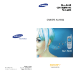
1
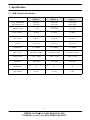
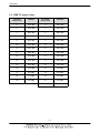
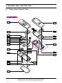
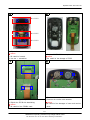
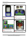
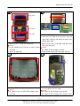
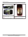
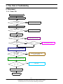
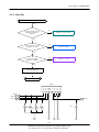
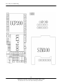
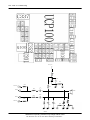
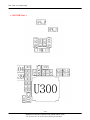
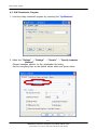
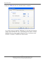
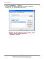
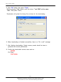
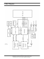
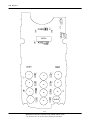
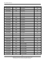
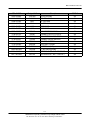
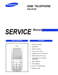
GSM TELEPHONE
SGH-C300
GSM TELEPHONE
CONTENTS
1.
Specification
2.
Exploded View and Parts list
3.
Chart of Troubleshooting
4.
Array course control
5.
Block Diagrams
6.
PCB Diagrams
7.
MAIN Electrical Parts List
8.
Reference data
9.
Safety Precautions
10. Product Function
Contents
1. Specification
1-1. GSM/CDMA General Specification ...........................................................................1-1
1-2. GSM TX power class ...............................................................................................1-2
2. Exploded View and Parts list
2-1. Cellular phone Exploded View ..................................................................................2-1
2-2. Cellular phone Parts list ............................................................................................2-2
2-3. Disassembly ...............................................................................................................2-4
2-4. Assembly ....................................................................................................................2-6
3. Flow Chart of Troubleshooting
3-1. Baseband ....................................................................................................................3-1
3-1-1. Power ON .............................................................................................................3-1
3-1-2. Initial ......................................................................................................................3-5
3-1-3. SIM Part ................................................................................................................3-8
3-1-4. Microphone Part ..................................................................................................3-10
3-1-5. Receiver Part ......................................................................................................3-12
3-1-6. Speaker Part .......................................................................................................3-12
3-2. RF .............................................................................................................................3-15
3-2-1. EGSM Rx ............................................................................................................3-15
3-2-2. DCS Rx ...............................................................................................................3-17
3-2-3. EGSM TX ............................................................................................................3-19
3-2-4. DCS TX ...............................................................................................................3-21
4. Array course control
4-1. Downloading Binary Files ......................................................................................4-2
4-2. Pre-requsite for Downloading ................................................................................4-2
4-3. S/W Downloader Program .....................................................................................4-3
5. Block Diagrams
6. PCB Diagrams
Contents
7. MAIN Electrical Parts List
8. Reference data
8-1. Reference Abbreviate ..............................................................................................8-1
9. Safety Precautions
9-1. Repair Precaution ......................................................................................................9-1
9-2. ESD(Electrostaically Sensitive Devices) Precaution ................................................9-2
10. Product Function
1. Specification
1-1. GSM General Specification
G S M 9 00
Ph ase 1
EGSM 900
Ph ase 2
DCS1 800
Phase 1
F r eq. Ban d[MHz]
Up lin k/D own lin k
89 0~9 15
93 5~9 60
88 0~9 15
92 5~9 60
171 0~ 178 5
180 5~ 188 0
ARF CN r a nge
1 ~12 4
0~ 124 &
975 ~1 023
51 2~ 885
T x/ Rx s p ac in g
45 M H z
45 M H z
95 M H z
Mod. Bit r ate/
Bit Period
270 .8 33 Kb ps
3.692 us
270 .8 33 Kb ps
3.692 us
270 .8 33 Kb ps
3.692 us
T ime Slot Peri od/F r ame
Period
576 .9 us
4.615 ms
576 .9 us
4.615 ms
576 .9 us
4.615 ms
Mod ula ti on
0 .3 GMSK
0 .3 GMSK
0 .3 GMSK
MS Power
33 dBm~ 1 3 dB m
33 dB m~ 5 dB m
30 dB m~ 0 dBm
Powe r Cla s s
5 pcl ~ 15 pcl
5 pcl ~ 19 pcl
0 pcl ~ 15 pcl
Sensi ti vity
- 10 2 dBm
-10 2 dBm
- 10 0 dBm
TDMA Mux
8
8
8
C ell Rad ius
35 Km
35 Km
2 Km
1-1
Specification
1-2. GSM TX power class
TX Power
control level
GSM900
TX Power
control level
DCS1800
5
33±2 dBm
0
30±3 dBm
6
31±2 dBm
1
28±3 dBm
7
29±2 dBm
2
26±3 dBm
8
27±2 dBm
3
24±3 dBm
9
25±2 dBm
4
22±3 dBm
10
23±2 dBm
5
20±3 dBm
11
21±2 dBm
6
18±3 dBm
12
19±2 dBm
7
16±3 dBm
13
17±2 dBm
8
14±3 dBm
14
15±2 dBm
9
12±4 dBm
15
13±2 dBm
10
10±4 dBm
16
11±3 dBm
11
8±4 dBm
17
9±3 dBm
12
6±4 dBm
18
7±3 dBm
13
4±4 dBm
19
5±3 dBm
14
2±5 dBm
15
0±5 dBm
1-2
2. Exploded View and Parts List
2-1. Cellular phone Exploded View
QHI01
QFR01
QFL01
QFR01
QFU01
QAR01
QMO01
QKP02
QKP01
QCR05
QME02
QSP01
QMP01
QMI01
QLC01
QPC01
QAN05
QME01
QRE02
QAN02
QFL01
QSC01
QRF03
QCR05
QRE01
QCR06
QCR05
QIF01
QRF01
QBA01
QBA00
2-1
SAMSUNG Proprietary-Contents may change without notice
This Document can not be used without Samsung's authorization
Exploded View and Parts List
2-2. Cellular phone Parts list
Design LOC
QAN02
INTENNA-SGHC300
GH42-01026A
QAN05
ASSY MEC-INTENNA CONTACT
GH75-08168A
QAR01
AUDIO-RECEIVER
3009-001248
QBA00
PMO-COVER BATT
GH72-35005A
QBA01
INNER BATTERY PACK-800MAH,MAIN
GH43-02589A
QCR05
SCREW-MACHINE
6001-001478
QCR05
SCREW-MACHINE
6001-001478
QCR05
SCREW-MACHINE
6001-001478
QCR06
SCREW-MACHINE
6001-001155
QFU01
ASSY COVER-SLIDE UPPER
GH98-02593A
QKP01
ASSY KEYPAD-MAIN(RUSS/BLK)
GH98-03231A
QKP02
ASSY KEYPAD-SUB(OPEN/SIL)
GH98-02701A
QLC01
ELA UNIT-SGHC300 LCD MODULE KI
GH96-02439A
QME01
UNIT-DOME SHEET (F/K)
GH59-03770A
QME02
UNIT-DOME SHEET (N/K)
GH59-03769A
QMI01
MICROPHONE-ASSY-SGHC300
GH30-00323A
QMO01
MOTOR-DC
3101-001324
QMP01
PBA MAIN-SGHC300 (PBA MAIN)
GH92-03086A
QPC01
MEA-SLIDE FPCB KIT
GH97-06882A
QRE02
ASSY BRACKET-REAR
GH98-02598A
QRF01
MPR-TAPE SHEET RF
GH74-28478A
QSC01
MPR-TAPE COVER SHEET SCREW
GH74-28472A
QSP01
SPEAKER
3001-002083
QHI01
ASSY HINGE-SLIDE
GH98-02594A
QFL01
ASSY COVER-SLIDE LOWER
GH98-02595A
QFR01
ASSY CASE-FRONT
GH98-02596A
ASSY CASE-REAR
GH98-02597A
QRF03
PMO-COVER EAR
GH72-35003A
QIF01
PMO-COVER IF
GH72-35004A
QRE01
Discription
2-2
SAMSUNG Proprietary-Contents may change without notice
This Document can not be used without Samsung's authorization
SEC CODE
Exploded View and Parts List
Discription
SEC CODE
BAG PE
6902-000297
ADAPTOR-EU 220V TYPE(BLK)
GH44-01334A
LABEL(P)-WATER SOAK
GH68-02026A
LABEL(P)-WATER SOAK
GH68-02026A
MANUAL-SFC
GH68-04336A
LABEL(P)-BARCODE RUSSIA
GH68-08494A
MANUAL USERS-EU RUSSIAN
GH68-12796A
LABEL(R)-MAIN(SER)
GH68-13315B
BOX(P)-UNIT MAIN(SER)
GH69-04832B
PMO-COVER SLIDE WINDOW
GH72-35006A
RMO-RUBBER CSP
GH73-08597A
RMO-RUBBER LCD PBA
GH73-08818A
MPR-GASK TAPE
GH74-24020A
MPR-TAPE IF COVER
GH74-24740A
MPR-GASK TAPE
GH74-24796A
MPR-SPONGE INTENNA
GH74-28468A
MPR-TAPE SLIDE WINDOW
GH74-28470A
MPR-VINYL BOHO WINDOW
GH74-28851A
MPR-SPONGE MAIN PCB
GH74-29058A
MPR-SPONGE LCD FPCB
GH74-29059A
MPR-TAPE ESD
GH74-29066A
MPR-TAPE FPCB BACK B
GH74-29067A
MPR-SPONGE KEYPAD
GH74-29255A
MPR-SPONGE KEYPAD
GH74-29255A
MPR-INSU TAPE
GH74-29334A
MPR-ELEC TAPE
GH74-29335A
MPR-INSU TAPE
GH74-29352A
MPR-INSU TAPE
GH74-29352A
MPR-SPONGE SPK
GH74-29444A
MPR-SPONGE
GH74-29579A
2-3
SAMSUNG Proprietary-Contents may change without notice
This Document can not be used without Samsung's authorization
Exploded View and Parts List
2-3. Disassembly
1
2
1) After get out the cover of earjack and IF connector
cover, disjoint REAR's lower locker and upper locker
1)Disjoint the REAR screw of 4 points.
as a picture below.
※ caution
※ caution
1) Be careful of scratch.
1) Be careful of scratch.
3
4
1) Remove the green tape on the FPCB with
tweezers.
1) Disjoint two lockers assembled with PBA.
2) Disjoint the FPCB by desoldering.
※ caution
※ caution
1) Be careful of the damage of devices.
1) Be careful of the FPCB's crack
2-4
SAMSUNG Proprietary-Contents may change without notice
This Document can not be used without Samsung's authorization
Exploded View and Parts List
5
6
M1.4*L3.0
M1.4*L3.5
M1.4*L3.0
1) Disjoint 6 screws.
※ caution
1) Disjoint HINGE ASS'Y as a picture below
1) Be careful of scratch.
※ caution
2) Use the '+' screwdriver.
1) Be careful of the damage of FPCB
7
8
1) Remove the green tape from the FPCB
1) Remove the motor with tweezers.
2) Remove the receiver with tweezers.
2) Disjoint the FPCB with desoldering.
※ caution
※ caution
1)Be careful of the damages of motor and receiver
wires.
1) Be careful of the FPCB's crack.
2-5
SAMSUNG Proprietary-Contents may change without notice
This Document can not be used without Samsung's authorization
Exploded View and Parts List
2-4. Assembly
1
2
< Bad >
< Good >
1) Put the SUB PBA on the UPPER with LCD's
guide holes.
1) Assemble the SUB KEYPAD on UPPER as 2) Insert the motor and receiver on each places.
※ caution
picture below.
※ caution
1) Be careful of overlap the wires.
1) Put the holes around 3*4 KEY on the UPPER.
2) Be careful of the damage of wires.
3
4
1) After inserting the LCD FPCB in the connector,
soldering it and attach the green tape.
※ caution
1) Be careful of the scratch on the plastic.
2) Be careful of the crack on LCD FPCB.
1) Insert the MAIN FPCB as picture below.
※ caution
1) Be careful of the crack on LCD FPCB.
2-6
SAMSUNG Proprietary-Contents may change without notice
This Document can not be used without Samsung's authorization
Exploded View and Parts List
5
6
M1.4*L3.0
M1.4*L3.5
M1.4*L3.0
1) Fold the FPCB as the picture below.
2) Insert the LCD FPCB to the connector along the
SILK LINE, soldering and attach the green tape,
double sticky tape.
1) Screw up the 6 points with SLIDE JIG.
3) Move out the cover of the tape. Fold the FPCB
※ caution
and push that place.
1) Fix the handset on the JIG not to move it down ※ caution
the Slide.
1) Be careful of the damage of FPCB.
2) Screw up right size.
2) Attach double sticky tape with white silk line.
7
8
1) Assemble the 3*4 Keypad as picture below.
※ caution
1) Be careful of the 3*4 KEY PAD escaping from
the holes.
1) After locking the PAB to the two hooks, insert
the microphone into the holder.
※ caution
1) Be careful of the damage of the devices.
2) Be careful of MIC escaping from the KEY PAD.
2-7
SAMSUNG Proprietary-Contents may change without notice
This Document can not be used without Samsung's authorization
Exploded View and Parts List
9
10
1) At first,assemble the REAR's upper and joint the
lower with pushing two lockers.
1) Screw up the 4 points with SCREW JIG.
※ caution
※ caution
1)Be careful of the scratch on the plastic.
1)Be careful of the scratch on the plastic.
2-8
SAMSUNG Proprietary-Contents may change without notice
This Document can not be used without Samsung's authorization
3. Flow Chart of Troubleshooting
3-1.Baseband
3-1-1. Power ON
'Power On' does not work
Check the current consumption
Yes
Current consumption
>= 100mA
No
Download again
Yes
Check the Vbat Voltage
Voltage >=3.3V
No
Charge the Battery
Yes
Check the pin of UCP100
No
Check UCP100 and C115
Pin#J12 >= 2.8V
Yes
Pin#A13 and pin#A14
=2.8V
No
pin#G11 = 1.8V
No
Check UCP100 and C116
Yes
Yes
Check the clock signal at pin#21 of U400
Freq = 26MHz
Vrms >=300mV
Vpp≒ 900mV
No
Check the clock generation circuit
(related to OSC400)
Yes
Check the clock signal at pin#5,#6 of U401
No
Check U401
Freq = 13Mz
Yes
Check the initial operation
END
3-1
SAMSUNG Proprietary-Contents may change without notice
This Document can not be used without Samsung's authorization
Flow Chart of Troubleshooting
3-2
SAMSUNG Proprietary-Contents may change without notice
This Document can not be used without Samsung's authorization
Flow Chart of Troubleshooting
VRF_2. 9V
OSC400
C415
C41 4
GND1
3 HOT
2
HOT
4 GND2
1
26M_OUT
RTXQN
R4 02
AFC
RTXQP
C420
C42 1
VCCD_2 .9 V
C42 2
24
23
RX1900B
25
REF_OP
VCC_BBQ
Q
22
21
QB
20
19
REFIN
REFINB
VAFC
RX1 900
26
16
VLDO2
VCC_REF
VBAT
18
17
39 pF
VL DO1
DCS_L NA_IN_P
27
15
C425
VBAT
RX1 800
14
C42 4
RX18 00B
DCS_L NA_IN_N
13
28
VDD
U4 00
12
GSM_LNA_IN_N
30
RX8 50B
31
C429
11
R407
RX9 00
TXOP_HI
TXOP_LO
RX8 50
10
C427
GSM_LNA_IN_P
29
VCC_TXVCO
R404
RX9 00B
33
NC
34
NC
1
35
VCC_FE
2
I
IB
3
5
4
SDATA
SCLK
SEN
6
C43 4
C4 35
7
8
NC
R411
GND
VCC_BBI
9
32
VLDO3
C437
C4 36
SERLE
SERCLK
SERDAT
RTXIN
RTXIP
VRF_2. 9V
L4 09
C4 23
8
VCC
1
7
_PR
C431
R408
C432
C426
CLK13M_TR
6
_CLR
D
3
R406
5
Q
C430
L410
R403
CK
2
GND
_Q
4
26 M_OUT
R405
R409
U401
R410
C433
3-3
SAMSUNG Proprietary-Contents may change without notice
This Document can not be used without Samsung's authorization
C428
CLK13M_MC
CLK13M_YMU
Flow Chart of Troubleshooting
DS P _DB ( 0 : 1 5 )
DS P _AB( 0 : 8 )
DS P_IO
DS P _RW N
FL AS H_RES ET
T X_EN
D SP _DB( 1 4 )
D SP _DB( 1 5 )
F3
E2
E3
D3
D2
DB 1 3
DB 1 4
DB 1 5
D SP _DB( 1 3)
DB 1 1
DB 1 2
D SP _DB( 1 1 )
D SP _DB( 1 2 )
F4
F1
F2
DB 7
DB 8
DB 1 0
DSP _DB( 1 0 )
G4
DB 9
D SP _DB( 8 )
D SP _DB( 9 )
D SP _DB( 7 )
DB 6
2
NC5
1
S E RCK
S E RDA
S ERL E2
S ERL E1
O CT L 7
O CT L 6
O CT L 5
O CT L 4
O CT L 3
O CT L 2
O CT L 1
O CT L 0
RES ETN_CS P
RW N
I| O
AB 0
AB 1
AB 2
AB 3
AB 4
AB 5
AB 6
AB 7
AB 8
DB 0
DB 1
DB 2
DB 3
DB 4
DB 5
H5
J6
G3
L3
K6
P1
L5
N1
N2
M2
M1
K7
K5
K1
K2
K3
J5
D SP _DB( 6 )
D SP _DB( 4 )
D SP _DB( 5 )
D SP _DB( 1 )
DSP _DB( 2 )
D SP _DB( 3 )
D SP _DB( 0 )
DS P_AB ( 7 )
DS P_AB ( 8 )
DS P_AB ( 4 )
DS P_AB ( 5 )
DS P_AB ( 6 )
DS P_AB ( 3 )
DS P_AB ( 1 )
DS P_AB ( 2 )
DS P_AB ( 0 )
L2
R3
E6
C5
F5
E5
A4
A3
B3
G6
B1
A2
C1
C2
H8
GNDS10
H7
VDDB
A6
DAIDI
GNDD
M10
DAIDO
VDDD
N11
VSS1
J4
DINTR
VDD_IO1
G5
N5
J3
C1 0 1
VDD1 2
VDD3 4
N9
J1 3
C1 1
R1 0
UP _CL K
VB AT
C1 1 0
SIM CL K
SIM _IO
UP _RS T
J1 1
SIM RS T
K1 1
P 10
K8
F1 2
C1 1 8
VCCB _2 . 9 V
KEY_RO W ( 0 )
KEY_CO L ( 2 )
RS T
P W R_KEEP
INTRQ
VIB _EN
RTCAL ARM
VR EF
VBAT
UP _S DI
UP _S DO
UP _S CL K
UP _CS
BAND_S EL 1
MO T
KEY_B L 1
KEY_B L 2
VS IM
SIM _CL K
SIM DATA
UP _IO
S IM _RS T
S IM _IO
Q 1 00
SIM _RS T
K1 4
K1 2
S IM _CL K
G1 2
H1 1
G1 3
VS IM
F1 3
VRTC
L ED1 _DRV
L ED2 _DRV
F1 5
RING_DRV
A1 4
C9
C1 2
B 10
D1 0
VL DO _7
VL 5 S _B
VL DO _6
VL 5 S _A
VIB _DRV
VL DO _5
B 12
B 11
A1 3
A1 2
J1 2
VL 4 S _B
VL DO _3
G1 1
VL 4 S _A
VL DO _2
VL DO _4
VL DO _1
L8
F1 4
CS N_P S C
M7
N7
VACC
S DI_P S C
S D O _P S C
E1 4
S CL K_PS C
VE XT
E1 3
E1 1
VB AT
D1 4
D1 5
CH_RES
CH_ISE N
CH _B DRV
E1 0
A1 0
ADC_AUX2
E9
ADC_AUX1
VREF
2
3
H1 0
CREF
R TC_ALM N
1
C1 1 1
VCCA_2 . 9 V
C1 1 2
VRF_2. 9 V
C1 1 3
R1 0 0
5. 1K
C1 1 5
VCCD_1 . 8 V
VCCD_2 . 9 V
C1 1 4
TP 1 . 8 V
C1 1 6
VRTC_3 V
C 11 7
1
2
BAT 10 0
R B 4 14 _IV0 2 N
This Document can not be used without Samsung's authorization
VCCD_2 . 9 V
VDD1
VCCA_2 . 9 V
DAIRN
F1 1
B15
3-4
SAMSUNG Proprietary-Contents may change without notice
VCCD _2 . 9V
F6
C1 0 2
GNDB
R1 1 3
F7
C1 0 3
UCP 1 0 0
C4
C1 2 0
C10
VDD5
VIB_RNG_EN
VM O D_EN
S ERL E
SERCL K
S ERDAT
GNDS11
C1 19
B13
VDD67
INTRQ
L9
GND_PSC1
K15
MODE
E8
GNDQ
PWR_KEEP
L1 0
GND_PSC2
M9
M3
PWR_SW1N
PWR_ON
RESET_O
N10
GND_HCUR
PSW1_BUF
K9
N6
VDD2
L7
PWR_SW2
C15
JIG_ON
K4
MC
CLK13 M_MC
VDD3
C14
VDD_IO2
DSP_INT
NC7
P3
R2
VSS2
P5
XOENAQ
R6
P6
VSS3
N4
RTC_CLK
D1
L11
DAICK
M6
VDDV
L6
VSS4
CLK3 2K
P13
GNDV
P4
VDD_OCTL
M1 3
VXVCM
R13
VREGN
R4
B4
AUXOUTN
AUXOUTN
L13
VREGP
R14
D13
GND_OCTL
K13
F8
GNDS1
AUXINP
AUXOUTP
AUX_ADC3
AUXOUTP
F9
GNDS2
L14
F1 0
MICOUTN
AUXINP
P15
GNDS3
M1 5
G7
GNDS4
MICOUTN
GNDS5
MICOUTP
N15
MICINN
N14
MICINP
M1 4
MICINN
G8
MICINP
GNDS6
MICOUTP
G10
AOUTBN
AOUTBN
AUXINN
AUXINN
H6
G9
P12
GNDS7
AOUTBP
GNDS8
AOUTBP
R12
AOUTAN
N12
GNDS9
AOUTAN
RXTXQN
P11
J7
H9
C6
GNDS12
RTXQN
RXTXQP
RTXQP
AOUTAP
AOUTAP
J8
J9
GNDS13
C7
GNDS14
RXTXIN
RTXIN
J10
RXTXIP
D6
GNDS15
RTXIP
K10
GNDS16
B6
RAREF1
B5
RAREF2
D7
NC6
AFC
D9
TXP
E7
AFC
GNDS17
VAPC
Flow Chart of Troubleshooting
3-1-2. Initial
Initial Failure
Yes
The pin #G11 of UCP100 =
No
1.8V and
the pin #J12 of UCP100 =
Check the UCP100
(if it has some problem, it is to be replaced.)
2.8V ?
Yes
Is the pin #K9 of UCP100
No
"Low → High" ?
Check the UCP100
(if it has some problem, it is to be replaced.)
Yes
There is 32.768kHz wave
No
Check the UCP200
forms at the C216 and C217
Yes
Is the pin #A4 of UCP100
No
Check the UCP200
is "High"
Yes
The voltage is "High" at the
No
Check the UCP100
C112,C114,C115
Yes
No
LCD display is O.K
Check the LCD part
Yes
No
Sound is O.K
Check the Audio part
Yes
END
3-5
SAMSUNG Proprietary-Contents may change without notice
This Document can not be used without Samsung's authorization
Flow Chart of Troubleshooting
3-6
SAMSUNG Proprietary-Contents may change without notice
This Document can not be used without Samsung's authorization
Flow Chart of Troubleshooting
VCCD_1 . 8 V
VCCD_1 . 8 V
VCCD_2 . 9 V
VCCD_1 . 8 V
VCCD_2 . 9 V
VRT C_3 V
C2 1 0
C2 1 2
C2 1 1
C2 1 3
R2 0 2
VREF
A( 2 2 )
CL K1 3 M _T R
A( 2 3 )
D( 6 )
E7
XCP _D6
XCP _D5
D( 7 )
D5
XCP _D7
D( 8 )
C4
XCP _D8
D( 9 )
B4
XCP _D9
D( 1 0 )
B3
XCP _D1 0
D( 1 1 )
C1
C2
XCP _D1 2
D2
XCP _D1 3
D( 1 4 )
D3
XCP _D1 4
D( 1 5 )
E3
XCP _D1 5
D8
C12
RSTB
E10
C11
F17
CKI
VSSA
VRTC
TD O
T RS T
TDI
F1 2
F1 5
TR_RS T
H1 2
TM S
G12
T CK
H1 3
G15
CKO / IACK/ ER AM H I
L12
IO B IT[ 2 ] / VEC[ 3 ] / ER O M HI
IO B IT[ 1 ] / VEC [ 4 ] / P L L TO A
INT# 0
XCP _D1 1
D( 1 2 )
D( 1 3 )
VDDA
E15
G16
F10
B1
M1
VDDE
VDDE
VDDE
U16
U15
P8
N16
E16
U2
VDDE
VDDE
VDDE
VDDE
VDDE
VDDE
E2
E17
R1
G1
T13
R4
R16
R17
A2
A5
B14
VDDE
VDD
VDD
VDD
VDD
VDD
VDD
VDD
VDD
A3
C16
VSS
VSS
VDD
VSS
H7
F6
G9
G10
VSS
VSS
VSS
VSS
H11
K6
J7
K7
VSS
VSS
VSS
VSS
L8
L10
M7
J11
L9
L6
VSS
VSS
VSS
VSS
VSS
L17
VDD
XPA36_A23 _CS5N
D( 5 )
D6
XVREF
XCP _D4
XCP _D1
VDD_DPLL
C5
VSS_DPLL
D( 4 )
XPA35_A22
XCP _D3
XPA3 2_CS0 N
XCP _D2
F7
H14
2
B5
F8
A( 0 )
IO 7
K1 1
CHG _O F F
N4
DSP _INT
R1 2
DSP _IO
RW N
U5
AB # 8
T1 7
DSP _AB ( 8 )
AB # 7
T1 4
DSP _AB ( 7 )
AB # 6
R1 4
DSP _AB ( 6 )
DSP _RW N
D S P_AB ( 8 : 0 )
B 13
XCP _A0 _BEO N
F 11
XCP _A1
P12
DSP _AB ( 5 )
A( 2 )
E1 4
XCP _A2
AB # 4
P11
DSP _AB ( 4 )
A( 3 )
D 15
XCP _A3
AB # 3
N1 1
DSP _AB ( 3 )
A( 4 )
B 15
XCP _A4
AB # 2
R1 3
DSP _AB ( 2 )
A( 5 )
C 14
XCP _A5
AB # 1
M 10
A( 6 )
A 16
XCP _A6
AB # 0
U1 3
A( 7 )
A 15
XCP _A7
A( 8 )
B 17
XCP _A8
DB # 1 5
P10
DS P _DB ( 1 5 )
A( 9 )
C 17
XCP _A9
DB # 1 4
R1 1
DS P _DB ( 1 4 )
A( 1 0 )
D 16
XCP _A1 0
DB # 1 3
T1 1
DS P _DB ( 1 3 )
A( 1 1 )
F 14
XCP _A1 1
DB # 1 2
U1 1
DS P _DB ( 1 2 )
A( 1 2 )
G 14
XCP _A1 2
DB # 1 1
M8
DS P _DB ( 1 1 )
A( 1 3 )
G 13
XCP _A1 3
DB # 1 0
N8
DS P _DB ( 1 0 )
A( 1 4 )
G 17
XCP _A1 4
DB # 9
N7
DS P _DB ( 9 )
A( 1 5 )
J1 2
XCP _A1 5
DB # 8
P7
DS P _DB ( 8 )
A( 1 6 )
K1 2
XCP _A1 6
DB # 7
M6
DS P _DB ( 7 )
A( 1 7 )
K1 3
XCP _A1 7
DB # 6
R7
DS P _DB ( 6 )
A( 1 8 )
K1 4
AB # 5
UCP 2 0 0
DSP _AB ( 1 )
DSP _AB ( 0 )
D S P_DB ( 1 5: 0 )
XCP _A1 8
DB # 5
T7
DS P _DB ( 5 )
A( 1 9 )
L 14
XCP _A1 9
DB # 4
U7
DS P _DB ( 4 )
A( 2 0 )
L 15
XCP _A2 0
DB # 3
P6
DS P _DB ( 3 )
DB # 2
R6
DS P _DB ( 2 )
DB # 1
U6
DS P _DB ( 1 )
DB # 0
P5
DS P _DB ( 0 )
A 12
CP _C S RO M EN1
CP_CS RAM EN
L CD_CS
DL C_DET ECT
YM U_EN
XCP _A2 1
XCP _CS R O M EN
A 13
XCP _CS R AM EN
M 15
XP A0 / C S 1 N
M 14
XP A1 / C S 2N
M 11
XP A2 / C S 3N
N1 4
XP A3 / C S 4N
XTIC_M O D E
XCP TS TS TO P _CKO
XAG 3
D1 1
XCP _W EN
XAG 2
E1 1
P 16
XP A4 / O EN
XAG 1
A1 1
XP A5 / W AITN
XAG 0
B11
U PP ER_BYTE
T 15
XP A6 / B E1 N
C 13
ICHRG
2
R2 1 8
PA34/ T_REQB
R 219
C2 1 4
E8
C6
F9
XCP_TDO
XCP_TRSTN
C2 1 6
C2 1 7
D1 3
XCP_TMS
XCP_TDI
XCP_TCK
D7
G8
PA33/ T_REQA
B7
A7
D1 0
XO S C3 2 O UT
C7
PA18/ T_ACK
N17
M17
PN17/ DRQ
PA26/ OM1
PA27/S M1 _CLK
E4
G4
XR TCAL ARM _N
P13
PA25/ OM0
G2
M3
XPA23 /P WM2
XPWM1
FLASH_RESET
XPA24 /P WM3
F4
H6
H5
PA22/S M1 _DATA
R5
PA20/ CP_MI
XPA21 / CP_SCK
K4
J6
PA19/ CP_MO
L1
L2
PA14/ RX1
X2 R TC
SIM_CLK/S M0_CLK
SIM_DATA/S M0_DATA
N10
U1 2
G3
PA13/ TX1
PA29/I OM1
G6
F1
G5
PA28/I OM0
XPA16 / RX0
PA31/I M1
XPA15 / TX0
L3
H4
XPA11 / IRDARX
PA30/I M0
F3
E1
N1
K5
XPA12 / IRDATX
X1 R TC
CP_KB[9] / TR_GNT_DMA
CP_KB[7] / TR_SIZE1
CP_KB[8] / TR_NEXEC
CP_KB[6] / TR_PROT0
T4
P3
N3
CP_KB[4] / TR_SIZE0
CP_KB[5] / TR_CLK
CP_KB[3] / TR_CS_IPCP
CP_KB[2] / TR_CS_PERF
T3
T1
U3
L4
C2 1 5
R2
XP A1 0 / IRQ 4
CP_KB[1] / TR_CS_IROM
YM U_IRQ
M4
XP A8 / IRQ 2
XP A9 / IRQ 3
CP_KB[0] / TR_CS_IRAM
XP A7 / IRQ 1
P2
N2
L5
FL IP _S NS
U2 0 1
O S C2 0 0
KEY_CO L ( 0 : 4 )
TR_RST
RT CAL ARM
KEY_CO L ( 0 )
KEY_CO L ( 1 )
KEY_R O W ( 0: 4 )
VO
VS
GND
3
XB S W N
M9
T5
INT RQ
VCC B _2 . 9 V
R2 1 7
M1 2
P 15
CP _O E N
R2 1 6
D1 2
DEB UG _DCD
CP _W EN
VB AT
4
A( 2 1 )
1
L 16
3
A( 1 )
R2 1 5
XCP _D0
D( 1 )
D( 2 )
D( 3 )
2
A( 0 : 2 0 )
L13
1
A6
D( 0 )
NC
NC
D( 0 : 1 5 )
N15
TR_RS T
CL K3 2 K
KEY_CO L ( 2 )
CP _T DO
KEY_CO L ( 3 )
TR_RST
KEY_CO L ( 4 )
CP _T DI
KEY_RO W ( 0 )
CP _T M S
KEY_RO W ( 1 )
CP _T CK
KEY_RO W ( 2 )
DEB UG _D S R
KEY_RO W ( 3 )
EAR_SW ITCH
VCCD_2 . 9 V
KEY_RO W ( 4 )
JAC K_IN
P W R_KEEP
S IM RST
DEBUG _DTR
DEB UG _RI
D EB UG _RT S
FL ASH_RESET
D EB UG _TXD
B ACKL IG HT_EN
DEBUG _RXD
R2 2 0
B P _CF
D EB UG _CT S
CHG _D ET
UP _CS
UP _S CLK
S DS _TXD
S D S_R XD
UP _S DO
SIM DAT A
UP _S DI
S IM CL K
3-7
SAMSUNG Proprietary-Contents may change without notice
This Document can not be used without Samsung's authorization
1
Flow Chart of Troubleshooting
3-1-3. Sim Part
"Insert SIM is displayed on the LCD
Yes
No
Check the SIM connector's
(SIM100) connection to
SIM card
Resolder or change SIM100
Yes
No
Check the voltage at pin#1
of SIM100 >= 2.8V ?
Check the UCP100
Yes
No
Is there any signals
pin#2,#3,#4 of SIM100 ?
Check the UCP100
Yes
Check the SIM Card
END
NC
NC
10
NC
9
8
I/ O
NC
7
6
GND
VPP
5
CLK
4
3
VCC
2
1
VCC
S IM 100
VS IM
S IM _RS T
S IM _CL K
S IM _IO
C1 0 9
C1 05
C1 0 6
C1 0 7
C1 0 8
3-8
SAMSUNG Proprietary-Contents may change without notice
This Document can not be used without Samsung's authorization
Flow Chart of Troubleshooting
3-9
SAMSUNG Proprietary-Contents may change without notice
This Document can not be used without Samsung's authorization
Flow Chart of Troubleshooting
3-1-4. Microphone Part
Microphone does not work
Yes
No
Is the assembled status of
microphone O.K?
Reassembled the microphone
Yes
Check the reference voltage on mic path
Yes
No
VR301 ≒ 2.0V ?
Resolder or change
R357,R355,C354,R359,R358,C356
R353,C352,C351,R356,C358,C357
①
Yes
No
Check UCP100
Is microphone ok?
Yes
END
3-10
SAMSUNG Proprietary-Contents may change without notice
This Document can not be used without Samsung's authorization
②
Flow Chart of Troubleshooting
VCCA_2 . 9 V
R3 5 3
C3 5 1
C3 5 2
R3 5 4
R3 5 5
M ICO UT P
R3 5 6
R3 5 7
C3 54
M ICINP
M IC3 0 0
R3 5 8
C3 56
M ICINN
R3 5 9
R3 6 2
C3 57
R3 60
VR3 01
C3 5 8
U403
M ICO UTN
3-11
SAMSUNG Proprietary-Contents may change without notice
This Document can not be used without Samsung's authorization
R3 6 1
Flow Chart of Troubleshooting
3-1-5. Receiver Part
There is no sound from the Receiver
Yes
Is the terminal of Receiver
O.K ?
No
Replace the Receiver
Yes
Is there any signals at the
pin#A11 and pin#N12 of
UCP100 ?
No
Check UCP100
Check R106,R107 (LCD PCB Part)
Yes
END
3-1-6. Speaker Part
There is no sound from the Buzzer
Yes
Is the terminal of Speaker
O.K ?
No
Replace the Speaker
Yes
Is there any signals at the
pin#A13 and pin#N12 of
UCP100 ?
No
Check U300,R338,R342
Yes
END
3-12
SAMSUNG Proprietary-Contents may change without notice
This Document can not be used without Samsung's authorization
Flow Chart of Troubleshooting
< LCD PCB Part >
3-13
SAMSUNG Proprietary-Contents may change without notice
This Document can not be used without Samsung's authorization
Flow Chart of Troubleshooting
SP K3 00
R33 8
L 3 00
SP K_N
L 3 01
R34 2
S P K_P
C3 50
C3 4 9
Z D3 0 5
Z D3 06
3-14
SAMSUNG Proprietary-Contents may change without notice
This Document can not be used without Samsung's authorization
Flow Chart of Troubleshooting
3-2.RF
CONTINUOUS RX ON
3-2-1. EGSM RX
RF INPUT : 62CH
AMP : -50dBm
NO
NORMAL CONDITION
catch the channel?
CHECK
ANT contact ?
YES
NO
PAM400 CHECK
pin12 ≥ -65dBm ?
PAM400,RFS400
resolder or change
YES
NO
PAM400 CHECK
pin16 ≥ -65dBm ?
PAM400
resolder or change
YES
NO
F401 CHECK
pin3,4 ≥ -65dBm ?
F401
resolder or change
YES
NO
U400 CHECK
pin29,30 ≥ -65dBm ?
C411,C413,L408
resolder or change
YES
NO
U400
pin 17 : 2.8V ?
UCP100 pinA13, C114
change or resolder
YES
U400 CHECK
pin 19,20
freq :26MHz ?
Vp-p : 380mV?
NO
OSC400
change or resolder
YES
U400
pin 2,3,22,23 Vp-p
: 120mV ?
NO
U400
resolder or change
YES
UCP100 CHECK!!
3-15
SAMSUNG Proprietary-Contents may change without notice
This Document can not be used without Samsung's authorization
Flow Chart of Troubleshooting
3-16
SAMSUNG Proprietary-Contents may change without notice
This Document can not be used without Samsung's authorization
Flow Chart of Troubleshooting
3-2-2. DCS RX
CONTINUOUS RX ON
RF INPUT : 698CH
AMP : -50dBm
NO
NORMAL CONDITION
catch the channel?
CHECK
ANT contact ?
YES
NO
PAM400 CHECK
pin12 ≥ -65dBm ?
PAM400,RFS400
resolder or change
YES
NO
PAM400 CHECK
pin20 ≥ -65dBm ?
PAM100
resolder or change
YES
NO
F400 CHECK
pin3,4 ≥ -65dBm ?
F400
resolder or change
YES
NO
U400 CHECK
pin27,28 ≥ -65dBm ?
C405,C407,L406
resolder or change
YES
NO
U400
pin 17 : 2.8V ?
UCP100 pinA13, C114
change or resolder
YES
U400 CHECK
pin 19,20 :
26MHz ?
Vp-p : 380mV?
OSC400
change or resolder
YES
U400 pin 2,3,22,23
Vp-p
: 120mV ?
NO
U400
resolder or change
YES
UCP100 CHECK!!
3-17
SAMSUNG Proprietary-Contents may change without notice
This Document can not be used without Samsung's authorization
Flow Chart of Troubleshooting
3-18
SAMSUNG Proprietary-Contents may change without notice
This Document can not be used without Samsung's authorization
Flow Chart of Troubleshooting
3-2-3. EGSM TX
NO
PAM400 pin12 :
about 2~3 dBm?
NO
PAM400
pin6 : 2.8 V?
UCP100
check & change
YES
CONTINOUS TX ON CONDITION
TX POWER DAC: 600 CODE APPLIED
CH : 62
RBW : 100KHz
VBW : 100KHz
SPAN : 10MHz
REF LEV. : 10dBm
ATT. : 20dB
YES
C400,RFS400
check&change
PAM400
pin7 : 3.7 V?
NO
BATTERY
check & change
YES
PAM400
pin 8 : 1.6V ?
NO
R401
Check
YES
NO
PAM400 pin11
about : -5dBm ?
YES
PAM400
pin 4 : 2.9V?
NO
YES
PAM400
change or resolder
NO
UCP100
check
U400
pin17 : 2.8V ?
YES
U400
pin19,20 : 26MHz
?
Vp-p : 380mV?
UCP100pinA13,C114
change or resolder
NO
OSC400
change or resolder
YES
NO
U400
pin2,3,22,23
:100mV?
YES
UCP100
change or resolder
U400
change or resolder
3-19
SAMSUNG Proprietary-Contents may change without notice
This Document can not be used without Samsung's authorization
Flow Chart of Troubleshooting
3-20
SAMSUNG Proprietary-Contents may change without notice
This Document can not be used without Samsung's authorization
Flow Chart of Troubleshooting
3-2-4. DCS TX
NO
PAM400 pin12 :
about 2~3 dBm?
NO
PAM400
pin6 : 2.8 V?
UCP100
check & change
CONTINUOUS TX ON CONDITION
CH : 698CH(DCS)
TX POWER CODE: 520 CODE Aplied
RBW : 100KHz
VBW : 100KHz
SPAN : 10MHz
REF LEV. : 10dBm
ATT. : 20dB
YES
YES
C400,RFS400
check&change
PAM400
pin7 : 3.7 V?
NO
BATTERY
check & change
YES
PAM400
pin 8 : 1.6V ?
NO
R401
Check
YES
NO
PAM400 pin1
about : -5dBm ?
YES
NO
PAM400
pin 4 : 0V?
YES
PAM400
change or resolder
NO
UCP100
check
U400
pin17 : 2.8V ?
YES
U400
pin19,20 : 26MHz
?
Vp-p : 380mV?
UCP100pinA13,C114
change or resolder
NO
OSC400
change or resolder
YES
NO
U400
pin2,3,22,23
:100mV?
YES
UCP100
change or resolder
U400
change or resolder
3-21
SAMSUNG Proprietary-Contents may change without notice
This Document can not be used without Samsung's authorization
Flow Chart of Troubleshooting
3-22
SAMSUNG Proprietary-Contents may change without notice
This Document can not be used without Samsung's authorization
Flow Chart of Troubleshooting
1
ANT40 0
2
1
4
3
ANT401
3
1
4
2
1
4
3
2
ANT
C401
C402
R400
C405
C40 7
C411
C413
A
2
RFS400
C
3
4
3
3
4
G
5
G
G
4
OUT
OUT
OUT
OUT
F4 00
2
G
G
F401
2
L405
IN
IN
1
1
L40 3
C4 06
C40 3
C41 0
L40 2
C419
1
11
16
20
4
6
DCSIN
19
GND
21
GND
C40 0
12
ANT
17
GND
PAM4 00
15
GND
VBATT
VCC1
VCC2
V1
NC
NC
VRAMP
VMOD_EN
13
GND
GSM90 0_IN
RX2
RX1
VBS
VT X
5
GND
7
10
2
3
8
9
14
18
C40 4
L407
C41 2
C408
C4 16
VBAT
C417
C409
R40 1
VMOD_EN
VAPC
SAMSUNG Proprietary-Contents may change without notice
G
1
L406
L408
5
C41 8
This Document can not be used without Samsung's authorization
2
4
3
L40 4
GSM_PAM_IN
DPCS_PAM_IN
DCS_LNA_IN_N
DCS_LNA_IN_P
GSM_LNA_IN_N
GSM_LNA_IN_P
TX_EN
BAND_SEL1
3-23
4. Array course control
4-1
SAMSUNG Proprietary-Contents may change without notice
This Document can not be used without Samsung's authorization
Array course control
Software Downloading
4-1. Downloading Binary Files
ㆍThree binary files for downloading C300
- C300XXYY.s3 : Main source code binary
4-2. Pre-requsite for Downloading
ㆍDownloader Program(OptiFlash.exe)
ㆍC300 Mobile Phone
ㆍData Cable
ㆍBinary files
4-2
SAMSUNG Proprietary-Contents may change without notice
This Document can not be used without Samsung's authorization
Array course control
4-3. S/W Downloader Program
1. Load the binary download program by executing the "Optiflash.exe"
2. Select the "Options" → "Settings" → "Generic" → "Specify hardware
platform".
Choose hardware platform for the downloader file setting.
Set the everything else as the default values which are shown below
4-3
SAMSUNG Proprietary-Contents may change without notice
This Document can not be used without Samsung's authorization
Array course control
3.Select the COM port when the download cable is connected
Up to twelve ports are supported. Additionally you can select the maximum
transfer speed OptiFlash will use to communicate with the phone. However,
OptiFlash will use a slower speed if either the PC's or the phone's serial
hardware is incapable of handling the selected speed
4-4
SAMSUNG Proprietary-Contents may change without notice
This Document can not be used without Samsung's authorization
Array course control
4. Select the "Flash&Verify" → "Browse"
Set the directory path and choose the lastet s/w binary, for example
"XC300XXYY.s3", for the downloader binary setting.
Make sure that not to change the reserved memory regions.
In case of C300 the reserved regions are :
- 0x00008000 - 0x0001ffff
4-5
SAMSUNG Proprietary-Contents may change without notice
This Document can not be used without Samsung's authorization
Array course control
5. Click "OK" button then press "Flash".
(Before pressing 'Flash' button, push the button '*'and 'END' at the same
time. Then press 'Flash'.)
Downloader will upload the binary file as below for the downloading.
6. When downloading is finished successfully, there is a "All is well" message.
7. After finishing downloading, Certain memory resets should be done to
guarantee the normal performance.
8. Confirm the downloaded version name and etc. :
*#1234#
Full Reset :
*2767*3855#
4-6
SAMSUNG Proprietary-Contents may change without notice
This Document can not be used without Samsung's authorization
5. Block Diagrams
5-1
SAMSUNG Proprietary-Contents may change without notice
This Document can not be used without Samsung's authorization
Block Diagrams
5-2
SAMSUNG Proprietary-Contents may change without notice
This Document can not be used without Samsung's authorization
6. PCB Diagrams
ANT
EAR300
SPK300
Z D3 0 6
ZD308
ZD309
Z D 305
ZD307
ANT401
ANT400
ZD310
ZD311
G6
RFS400
U404
PAM400
U300
G1
G2
F401 F400
GND1
UCP200
G8
CP
CP_TDO
G7
OSC400
U400
UME101
U401
OSC200
G5
D0
CP_OEN
A(3) CP_TMS
TP1.8V
RSTCP_TCK U402 CP_WEN
MEM_RST CP_TDI
UCP100
SIM100
Q100
U103
U201
VR301
U403
BAT100
ZD303 ZD302 ZD301
VR300
MIC300
G4
BTC300
IFC300
U102
ZD304
G3
SDS_TXD JIG_ON SDS_RXD
VBATGND
CN200
6-1
SAMSUNG Proprietary-Contents may change without notice
This Document can not be used without Samsung's authorization
U202
ZD313
ZD314
Q 30 0
PCB Diagrams
ZD312
CN300
3
6
9
LED200
LED201
LED202
LED203
2
LED204
LED205
5
8
0
*
VR208
7
VR207
LED206
4
VR204
VR203VR206
LED207
1
VR205 VR201VR200
VR202
SHAPE
6-2
SAMSUNG Proprietary-Contents may change without notice
This Document can not be used without Samsung's authorization
7. MAIN Electrical Parts List
SEC CODE
Design LOC
Discription
0403-001547
ZD304
DIODE-ZENER
SA
0406-001083
ZD301
DIODE-TVS
SA
0406-001083
ZD302
DIODE-TVS
SA
0406-001083
ZD303
DIODE-TVS
SA
0406-001210
ZD305
DIODE-TVS
SA
0406-001210
ZD306
DIODE-TVS
SA
0406-001254
ZD307
DIODE-TVS
SA
0406-001254
ZD308
DIODE-TVS
SA
0406-001254
ZD309
DIODE-TVS
SA
0406-001254
ZD310
DIODE-TVS
SA
0406-001254
ZD311
DIODE-TVS
SA
0406-001254
ZD312
DIODE-TVS
SA
0406-001254
ZD313
DIODE-TVS
SA
0406-001254
ZD314
DIODE-TVS
SA
0501-000225
Q300
TR-SMALL SIGNAL
SA
0504-000168
Q100
TR-DIGITAL
SA
0601-002053
LED200
LED
SA
0601-002053
LED201
LED
SA
0601-002053
LED202
LED
SA
0601-002053
LED203
LED
SA
0601-002053
LED204
LED
SA
0601-002053
LED205
LED
SA
0601-002053
LED206
LED
SA
0601-002053
LED207
LED
SA
0801-002529
U103
IC-CMOS LOGIC
SA
0801-003013
U401
IC-CMOS LOGIC
SA
1009-001024
U202
IC-HALL EFFECT S/W
SA
1108-000010
UME101
IC-MCP
SA
1201-002364
PAM400
IC-POWER AMP
SA
1203-003304
UCP100
IC-POWER SUPERVISOR
SA
1203-003663
U102
IC-BATTERY
SA
1204-001811
U300
IC-MELODY
SA
1205-003098
U400
IC-TRANSCEIVER
SA
1209-001219
U201
IC-SENSOR
SA
1405-001082
U403
VARISTOR
SA
1405-001082
VR200
VARISTOR
SA
1405-001082
VR201
VARISTOR
SA
7-1
SAMSUNG Proprietary-Contents may change without notice
This Document can not be used without Samsung's authorization
STATUS
Main Electrical Parts List
SEC CODE
Design LOC
Discription
1405-001082
VR203
VARISTOR
SA
1405-001082
VR206
VARISTOR
SA
1405-001082
VR300
VARISTOR
SA
1405-001082
VR301
VARISTOR
SA
1405-001183
VR202
VARISTOR
SA
1405-001183
VR204
VARISTOR
SA
1405-001183
VR205
VARISTOR
SA
1405-001183
VR207
VARISTOR
SA
1405-001183
VR208
VARISTOR
SA
2007-000140
R107
R-CHIP
SA
2007-000140
R327
R-CHIP
SA
2007-000142
R362
R-CHIP
SA
2007-000144
R100
R-CHIP
SA
2007-000157
R202
R-CHIP
SA
2007-000157
R215
R-CHIP
SA
2007-000157
R321
R-CHIP
SA
2007-000157
R332
R-CHIP
SA
2007-000160
R303
R-CHIP
SA
2007-000161
R320
R-CHIP
SA
2007-000161
R329
R-CHIP
SA
2007-000161
R355
R-CHIP
SA
2007-000161
R359
R-CHIP
SA
2007-000162
R104
R-CHIP
SA
2007-000162
R106
R-CHIP
SA
2007-000162
R110
R-CHIP
SA
2007-000162
R217
R-CHIP
SA
2007-000164
R221
R-CHIP
SA
2007-000164
R300
R-CHIP
SA
2007-000165
R334
R-CHIP
SA
2007-000170
R218
R-CHIP
SA
2007-000170
R408
R-CHIP
SA
2007-000170
R410
R-CHIP
SA
2007-000171
R113
R-CHIP
SA
2007-000171
R322
R-CHIP
SA
2007-000171
R338
R-CHIP
SA
2007-000171
R342
R-CHIP
SA
2007-000171
R354
R-CHIP
SA
7-2
SAMSUNG Proprietary-Contents may change without notice
This Document can not be used without Samsung's authorization
STATUS
Main Electrical Parts List
SEC CODE
Design LOC
Discription
2007-000171
R360
R-CHIP
SA
2007-000171
R361
R-CHIP
SA
2007-000171
R400
R-CHIP
SA
2007-000171
R406
R-CHIP
SA
2007-000172
R103
R-CHIP
SA
2007-000172
R200
R-CHIP
SA
2007-000172
R201
R-CHIP
SA
2007-000172
R203
R-CHIP
SA
2007-000172
R204
R-CHIP
SA
2007-000172
R205
R-CHIP
SA
2007-000172
R206
R-CHIP
SA
2007-000172
R207
R-CHIP
SA
2007-000172
R208
R-CHIP
SA
2007-000172
R209
R-CHIP
SA
2007-000172
R210
R-CHIP
SA
2007-000566
R333
R-CHIP
SA
2007-000566
R335
R-CHIP
SA
2007-000566
R336
R-CHIP
SA
2007-000566
R337
R-CHIP
SA
2007-000775
R301
R-CHIP
SA
2007-000775
R302
R-CHIP
SA
2007-000775
R315
R-CHIP
SA
2007-000831
R105
R-CHIP
SA
2007-000831
R331
R-CHIP
SA
2007-001119
R318
R-CHIP
SA
2007-001119
R353
R-CHIP
SA
2007-001307
R409
R-CHIP
SA
2007-001308
R405
R-CHIP
SA
2007-001320
R319
R-CHIP
SA
2007-001320
R356
R-CHIP
SA
2007-001323
R328
R-CHIP
SA
2007-001325
R316
R-CHIP
SA
2007-002797
R403
R-CHIP
SA
2007-002965
R324
R-CHIP
SA
2007-002965
R325
R-CHIP
SA
2007-002965
R407
R-CHIP
SA
2007-007014
R344
R-CHIP
SA
7-3
SAMSUNG Proprietary-Contents may change without notice
This Document can not be used without Samsung's authorization
STATUS
Main Electrical Parts List
SEC CODE
Design LOC
Discription
2007-007142
R323
R-CHIP
SA
2007-007142
R326
R-CHIP
SA
2007-007142
R357
R-CHIP
SA
2007-007142
R358
R-CHIP
SA
2007-007573
R216
R-CHIP
SA
2007-007573
R219
R-CHIP
SA
2007-007741
R402
R-CHIP
SA
2007-008045
R304
R-CHIP
SA
2007-008045
R305
R-CHIP
SA
2007-008045
R306
R-CHIP
SA
2007-008045
R307
R-CHIP
SA
2007-008045
R308
R-CHIP
SA
2007-008045
R309
R-CHIP
SA
2007-008045
R310
R-CHIP
SA
2007-008045
R311
R-CHIP
SA
2007-008045
R312
R-CHIP
SA
2007-008045
R313
R-CHIP
SA
2007-008045
R314
R-CHIP
SA
2007-008045
R317
R-CHIP
SA
2007-008137
R108
R-CHIP
SA
2007-008419
R339
R-CHIP
SA
2007-008419
R340
R-CHIP
SA
2007-008419
R341
R-CHIP
SA
2007-008419
R343
R-CHIP
SA
2007-008419
R345
R-CHIP
SA
2007-008419
R346
R-CHIP
SA
2007-008419
R347
R-CHIP
SA
2007-008419
R348
R-CHIP
SA
2007-008419
R349
R-CHIP
SA
2007-008419
R350
R-CHIP
SA
2007-008419
R351
R-CHIP
SA
2007-008419
R352
R-CHIP
SA
2007-008516
R401
R-CHIP
SA
2007-008806
R404
R-CHIP
SA
2007-009160
R109
R-CHIP
SA
2203-000233
C117
C-CER,CHIP
SA
2203-000233
C215
C-CER,CHIP
SA
7-4
SAMSUNG Proprietary-Contents may change without notice
This Document can not be used without Samsung's authorization
STATUS
Main Electrical Parts List
SEC CODE
Design LOC
Discription
2203-000254
C102
C-CER,CHIP
SA
2203-000254
C103
C-CER,CHIP
SA
2203-000254
C200
C-CER,CHIP
SA
2203-000254
C201
C-CER,CHIP
SA
2203-000254
C202
C-CER,CHIP
SA
2203-000254
C203
C-CER,CHIP
SA
2203-000254
C205
C-CER,CHIP
SA
2203-000254
C209
C-CER,CHIP
SA
2203-000254
C211
C-CER,CHIP
SA
2203-000254
C305
C-CER,CHIP
SA
2203-000330
C216
C-CER,CHIP
SA
2203-000330
C217
C-CER,CHIP
SA
2203-000359
C349
C-CER,CHIP
SA
2203-000359
C350
C-CER,CHIP
SA
2203-000359
C357
C-CER,CHIP
SA
2203-000359
C358
C-CER,CHIP
SA
2203-000386
C426
C-CER,CHIP
SA
2203-000438
C306
C-CER,CHIP
SA
2203-000438
C343
C-CER,CHIP
SA
2203-000438
C344
C-CER,CHIP
SA
2203-000438
C346
C-CER,CHIP
SA
2203-000438
C430
C-CER,CHIP
SA
2203-000627
C433
C-CER,CHIP
SNA
2203-000654
C303
C-CER,CHIP
SA
2203-000679
C210
C-CER,CHIP
SA
2203-000812
C107
C-CER,CHIP
SA
2203-000812
C108
C-CER,CHIP
SA
2203-000812
C427
C-CER,CHIP
SA
2203-000812
C431
C-CER,CHIP
SA
2203-000940
C105
C-CER,CHIP
SA
2203-000995
C109
C-CER,CHIP
SA
2203-000995
C345
C-CER,CHIP
SA
2203-001072
C348
C-CER,CHIP
SA
2203-001405
C302
C-CER,CHIP
SA
2203-001412
C428
C-CER,CHIP
SA
2203-005344
C118
C-CER,CHIP
SA
2203-005344
C213
C-CER,CHIP
SA
7-5
SAMSUNG Proprietary-Contents may change without notice
This Document can not be used without Samsung's authorization
STATUS
Main Electrical Parts List
SEC CODE
Design LOC
Discription
2203-005344
C347
C-CER,CHIP
SA
2203-005446
C401
C-CER,CHIP
SA
2203-005514
C354
C-CER,CHIP
SA
2203-005514
C356
C-CER,CHIP
SA
2203-005682
C312
C-CER,CHIP
SA
2203-005682
C313
C-CER,CHIP
SA
2203-005682
C314
C-CER,CHIP
SA
2203-005682
C315
C-CER,CHIP
SA
2203-005682
C316
C-CER,CHIP
SA
2203-005682
C317
C-CER,CHIP
SA
2203-005682
C318
C-CER,CHIP
SA
2203-005682
C319
C-CER,CHIP
SA
2203-005682
C320
C-CER,CHIP
SA
2203-005682
C321
C-CER,CHIP
SA
2203-005682
C322
C-CER,CHIP
SA
2203-005682
C323
C-CER,CHIP
SA
2203-005682
C324
C-CER,CHIP
SA
2203-005682
C325
C-CER,CHIP
SA
2203-005682
C326
C-CER,CHIP
SA
2203-005682
C327
C-CER,CHIP
SA
2203-005682
C328
C-CER,CHIP
SA
2203-005682
C329
C-CER,CHIP
SA
2203-005682
C330
C-CER,CHIP
SA
2203-005682
C331
C-CER,CHIP
SA
2203-005682
C332
C-CER,CHIP
SA
2203-005682
C333
C-CER,CHIP
SA
2203-005682
C334
C-CER,CHIP
SA
2203-005682
C335
C-CER,CHIP
SA
2203-005682
C336
C-CER,CHIP
SA
2203-005682
C416
C-CER,CHIP
SA
2203-005682
C418
C-CER,CHIP
SA
2203-005682
C419
C-CER,CHIP
SA
2203-005683
C405
C-CER,CHIP
SA
2203-005683
C407
C-CER,CHIP
SA
2203-005719
C411
C-CER,CHIP
SA
2203-005719
C413
C-CER,CHIP
SA
2203-005719
C414
C-CER,CHIP
SA
7-6
SAMSUNG Proprietary-Contents may change without notice
This Document can not be used without Samsung's authorization
STATUS
Main Electrical Parts List
SEC CODE
Design LOC
Discription
2203-005719
C420
C-CER,CHIP
SA
2203-005719
C422
C-CER,CHIP
SA
2203-005736
C406
C-CER,CHIP
SA
2203-005736
C410
C-CER,CHIP
SA
2203-005736
C417
C-CER,CHIP
SA
2203-005819
C111
C-CER,CHIP
SA
2203-005819
C112
C-CER,CHIP
SA
2203-005819
C114
C-CER,CHIP
SA
2203-005819
C115
C-CER,CHIP
SA
2203-005819
C116
C-CER,CHIP
SA
2203-006048
C101
C-CER,CHIP
SA
2203-006048
C106
C-CER,CHIP
SA
2203-006048
C119
C-CER,CHIP
SA
2203-006048
C204
C-CER,CHIP
SA
2203-006048
C207
C-CER,CHIP
SA
2203-006048
C212
C-CER,CHIP
SA
2203-006048
C214
C-CER,CHIP
SA
2203-006048
C218
C-CER,CHIP
SA
2203-006048
C219
C-CER,CHIP
SA
2203-006048
C300
C-CER,CHIP
SA
2203-006048
C304
C-CER,CHIP
SA
2203-006048
C307
C-CER,CHIP
SA
2203-006048
C309
C-CER,CHIP
SA
2203-006048
C311
C-CER,CHIP
SA
2203-006048
C353
C-CER,CHIP
SA
2203-006048
C423
C-CER,CHIP
SA
2203-006048
C432
C-CER,CHIP
SA
2203-006194
C404
C-CER,CHIP
SA
2203-006194
C421
C-CER,CHIP
SA
2203-006194
C424
C-CER,CHIP
SA
2203-006257
C338
C-CER,CHIP
SA
2203-006257
C351
C-CER,CHIP
SA
2203-006260
C100
C-CER,CHIP
SA
2203-006260
C104
C-CER,CHIP
SA
2203-006260
C206
C-CER,CHIP
SA
2203-006260
C208
C-CER,CHIP
SA
2203-006260
C434
C-CER,CHIP
SA
7-7
SAMSUNG Proprietary-Contents may change without notice
This Document can not be used without Samsung's authorization
STATUS
Main Electrical Parts List
SEC CODE
Design LOC
Discription
2203-006318
C403
C-CER,CHIP
SA
2203-006324
C110
C-CER,CHIP
SA
2203-006361
C124
C-CER,CHIP
SA
2203-006377
C126
C-CER,CHIP
SA
2203-006423
C310
C-CER,CHIP
SA
2203-006423
C408
C-CER,CHIP
SA
2203-006423
C412
C-CER,CHIP
SA
2203-006423
C415
C-CER,CHIP
SA
2203-006423
C435
C-CER,CHIP
SA
2203-006423
C436
C-CER,CHIP
SA
2203-006423
C437
C-CER,CHIP
SA
2203-006556
C400
C-CER,CHIP
SA
2203-006556
C429
C-CER,CHIP
SA
2203-006562
C113
C-CER,CHIP
SA
2203-006562
C120
C-CER,CHIP
SA
2203-006562
C121
C-CER,CHIP
SA
2203-006626
C339
C-CER,CHIP
SA
2203-006626
C342
C-CER,CHIP
SA
2203-006626
C425
C-CER,CHIP
SA
2203-006681
C125
C-CER,CHIP
SA
2404-001339
C301
C-TA,CHIP
SA
2404-001343
C308
C-TA,CHIP
SA
2404-001374
C409
C-TA,CHIP
SA
2404-001406
C355
C-TA,CHIP
SA
2404-001414
C337
C-TA,CHIP
SA
2404-001414
C352
C-TA,CHIP
SA
2404-001463
C439
C-TA,CHIP
SA
2404-001463
U404
C-TA,CHIP
SA
2703-001236
L410
INDUCTOR-SMD
SA
2703-002200
L408
INDUCTOR-SMD
SA
2703-002313
L405
INDUCTOR-SMD
SA
2703-002484
L406
INDUCTOR-SMD
SA
2703-002544
L300
INDUCTOR-SMD
SA
2703-002544
L301
INDUCTOR-SMD
SA
2703-002558
L407
INDUCTOR-SMD
SA
2703-002917
L402
INDUCTOR-SMD
SA
2703-002917
L403
INDUCTOR-SMD
SA
7-8
SAMSUNG Proprietary-Contents may change without notice
This Document can not be used without Samsung's authorization
STATUS
Main Electrical Parts List
SEC CODE
Design LOC
Discription
2801-003856
OSC200
CRYSTAL-SMD
SA
2801-004587
OSC400
CRYSTAL-SMD
SA
2904-001592
F401
FILTER-SAW
SA
2904-001599
F400
FILTER-SAW
SA
3301-001534
L409
BEAD-SMD
SA
3301-001729
L200
BEAD-SMD
SA
3705-001358
RFS400
CONNECTOR-COAXIAL
SA
3708-002112
CN300
CONNECTOR-FPC/FFC/PIC
SA
3709-001384
SIM100
CONNECTOR-CARD EDGE
SA
3710-001611
IFC300
CONNECTOR-INTERFACE
SA
3711-006228
BTC300
HEADER-BATTERY
SA
3722-002249
EAR300
JACK-EAR PHONE
SA
4302-001130
BAT100
BATTERY-LI(2ND)
SA
GH09-00036A
UCP200
IC MICOM-SGHX480
SA
GH71-06338A
ANT400
NPR-BRACKET ANT CONTACT
SA
GH71-06338A
ANT401
NPR-BRACKET ANT CONTACT
SA
7-9
SAMSUNG Proprietary-Contents may change without notice
This Document can not be used without Samsung's authorization
STATUS
8. Reference data
8-1. Reference Abbreviate
AAC: Advanced Audio Coding.
AVC : Advanced Video Coding.
BER : Bit Error Rate
BPSK: Binary Phase Shift Keying
CA : Conditional Access
CDM : Code Division Multiplexing
C/I : Carrier to Interference
DMB : Digital Multimedia Broadcasting
EN : European Standard
ES : Elementary Stream
ETSI: European Telecommunications Standards Institute
MPEG: Moving Picture Experts Group
PN : Pseudo-random Noise
PS : Pilot Symbol
QPSK: Quadrature Phase Shift Keying
RS : Reed-Solomon
SI : Service Information
TDM : Time Division Multiplexing
TS : Transport Stream
8-1
SAMSUNG Proprietary-Contents may change without notice
This Document can not be used without Samsung's authorization
9. Safety Precautions
9-1. Repair Precaution
● Repair in Shield Box, during detailed tuning.
Take specially care of tuning or test,
because specipicty of cellular phone is sensitive for surrounding interference(RF noise).
● Be careful to use a kind of magnetic object or tool,
because performance of parts is damaged by the influence of manetic force.
● Surely use a standard screwdriver when you disassemble this product,
otherwise screw will be worn away.
● Use a thicken twisted wire when you measure level.
A thicken twisted wire has low resistance, therefore error of measurement is few.
● Repair after separate Test Pack and Set because for short danger (for example an
overcurrent and furious flames of parts etc) when you repair board in condition of
connecting Test Pack and tuning on.
● Take specially care of soldering, because Land of PCB is small and weak in heat.
● Surely tune on/off while using AC power plug, because a repair of battery charger is
dangerous when tuning ON/OFF PBA and Connector after disassembing charger.
● Don't use as you pleases after change other material than replacement registered on SEC
System.
Otherwise engineer in charge isn't charged with problem that you don't keep this rules.
9-1
SAMSUNG Proprietary-Contents may change without notice
This Document can not be used without Samsung's authorization
Safety Precautions
9-2. ESD(Electrostatically Sensitive Devices) Precaution
Several semiconductor may be damaged easilly by static electricity. Such parts are called by
ESD(Electrostatically Sensitive Devices), for example IC,BGA chip etc. Read Precaution below.
You can prevent from ESD damage by static electricity.
● Remove static electricity remained your body before you touch semiconductor or parts with
semiconductor. There are ways that you touch an earthed place or wear static electricity
prevention string on wrist.
● Use earthed soldering steel when you connect or disconnect ESD.
● Use soldering removing tool to break static electricity. , otherwise ESD will be damaged by
static electricity.
● Don't unpack until you set up ESD on product. Because most of ESD are packed by box
and aluminum plate to have conductive power,they are prevented from static electricity.
● You must maintain electric contact between ESD and place due to be set up until ESD is
connected completely to the proper place or a circuit board.
9-2
SAMSUNG Proprietary-Contents may change without notice
This Document can not be used without Samsung's authorization
10. Product Function
Main Function
-
SMS or MMS messages
Voicemail
Broadcast message
SOS messages
Calendar, Alarm, Calculator, Voice memo, Speed dial, etc...
10-1
SAMSUNG Proprietary-Contents may change without notice
This Document can not be used without Samsung's authorization
This Service Manual is a property of Samsung Electronics Co.,Ltd.
Any unauthorized use of Manual can be punished under applicable
International and/or domestic law.
ⓒ
Samsung Electronics Co.,Ltd.
2006. 12. Rev.1.0