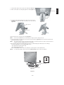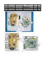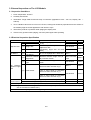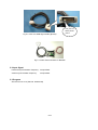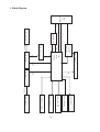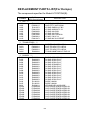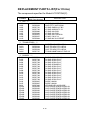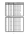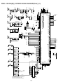
1
PART NO. 599910742 SERVICE MANUAL COLOR MONITOR MultiSync MODEL LCD1970NX LCD1970NX (B) / (C) LCD1970NX-BK (B) / (C) 1st Edition NEC-MITSUBISHI ELECTRIC VISUAL SYSTEMS CORPORATION NOVEMBER 2004 200412 08RJ1LBY 08RJ1LCY 08RJ2LBY 08RJ2LCY WARNING The SERVICE PERSONNEL should have the appropriate technical training, knowledge and experience necessary to: • Be familiar with specialized test equipment, and • Be careful to follow all safety procedures to minimize danger to themselves and their coworkers. To avoid electrical shocks, this equipment should be used with an appropriate power cord. This equipment utilized a micro-gap power switch. Turn off the set by first pushing power switch. Next, remove the power cord from the AC outlet. To prevent fire or shock hazards, do not expose this unit to rain or moisture. This symbol warns the personnel that un-insulated voltage within the unit may have sufficient magnitude to cause electric shock. This symbol alerts the personnel that important literature concerning the operation and maintenance of this unit has been included. Therefore, it should be read carefully in order to avoid any problems. PRODUCT SAFETY CAUTION 1. When parts replacement is required for servicing, always use the manufacturer's specified replacement. 2. When replacing the component, always be certain that all the components are put back in the place. 3. As for a connector, pick and extract housing with fingers properly since a disconnection and improper contacts may occur, when wires of the connector are led. 4. Use a proper screwdriver. If you use screwdriver that does not fit, you may damage the screws. CONTENTS Page No. USER'S MANUAL --------------------------------------------------------------------- 1-1 SERIAL NUMBER INFORMATION ----------------------------------------------- 2-1 DISASSEMBLY ------------------------------------------------------------------------- 3-1 ADJUSTMENT PROCEDURES ---------------------------------------------------- 4-1 INSPECTION ----------------------------------------------------------------------------- 5-1 TROUBLE SHOOTING --------------------------------------------------------------- 6-1 CIRCUIT DESCRIPTION ------------------------------------------------------------- 7-1 REPLACEMENT PARTS LIST ----------------------------------------------------- 8-1 BLOCK DIAGRAM -------------------------------------------------------------------- 9-1 SCHEMATIC DIAGRAMS ----------------------------------------------------------- 10-1 PACKING SPECIFICATION -------------------------------------------------------- 11-1 REVISION HISTORY ------------------------------------------------------------------ 12-1 User's Manual MultiSync LCD1970V MultiSync LCD1970NX User’s Manual 1-1 Index Warning, Caution ......................................................................................................................... English-1 Declaration ...................................................................................................................................English-1 Canadian Department of Communications Compliance Statement ............................................ English-2 Declaration of Conformity ............................................................................................................ English-2 Contents .......................................................................................................................................English-3 Quick Start ...................................................................................................................................English-4 Controls ........................................................................................................................................ English-8 Recommended use .................................................................................................................... English-10 Specifications for LCD1970V ..................................................................................................... English-12 Specifications for LCD1970NX .................................................................................................. English-13 Features ..................................................................................................................................... English-14 Troubleshooting .......................................................................................................................... English-15 TCO’03 ....................................................................................................................................... English-16 Manufacturer’s Recycling and Energy Information ..................................................................... English-17 1-2 TO PREVENT FIRE OR SHOCK HAZARDS, DO NOT EXPOSE THIS UNIT TO RAIN OR MOISTURE. ALSO, DO NOT USE THIS UNIT'S POLARIZED PLUG WITH AN EXTENSION CORD RECEPTACLE OR OTHER OUTLETS UNLESS THE PRONGS CAN BE FULLY INSERTED. REFRAIN FROM OPENING THE CABINET AS THERE ARE HIGH VOLTAGE COMPONENTS INSIDE. REFER SERVICING TO QUALIFIED SERVICE PERSONNEL. CAUTION CAUTION: TO REDUCE THE RISK OF ELECTRIC SHOCK, MAKE SURE POWER CORD IS UNPLUGGED FROM WALL SOCKET. TO FULLY DISENGAGE THE POWER TO THE UNIT, PLEASE DISCONNECT THE POWER CORD FROM THE AC OUTLET.DO NOT REMOVE COVER (OR BACK). NO USER SERVICEABLE PARTS INSIDE. REFER SERVICING TO QUALIFIED SERVICE PERSONNEL. This symbol warns user that uninsulated voltage within the unit may have sufficient magnitude to cause electric shock. Therefore, it is dangerous to make any kind of contact with any part inside this unit. This symbol alerts the user that important literature concerning the operation and maintenance of this unit has been included. Therefore, it should be read carefully in order to avoid any problems. Caution: When operating the MultiSync LCD1970V/MultiSync LCD1970NX with a 220-240V AC power source in Europe, use the power cord provided with the monitor. In the UK, a BS approved power cord with a moulded plug has a Black (five Amps) fuse installed for use with this equipment. If a power cord is not supplied with this equipment please contact your supplier. When operating the MultiSync LCD1970V/MultiSync LCD1970NX with a 220-240V AC power source in Australia, use the power cord provided with the monitor. If a power cord is not supplied with this equipment please contact your supplier. For all other cases, use a power cord that matches the AC voltage of the power outlet and has been approved by and complies with the safety standard of your particular country. Declaration Declaration of the Manufacturer We hereby certify that the colour monitor MultiSync LCD1970V (L194RK)/MultiSync LCD1970NX (L194RH) are in compliance with and marked with Council Directive 73/23/EEC: – EN 60950-1 Council Directive 89/336/EEC: – EN 55022 – EN 61000-3-2 – EN 61000-3-3 – EN 55024 NEC-Mitsubishi Electric Visual Systems Corporation 4-13-23, Shibaura, Minato-Ku Tokyo 108-0023, Japan Windows is a registered trademark of Microsoft Corporation. NEC is a registered trademark of NEC Corporation. ENERGY STAR is a U.S. registered trademark. OmniColor is a registered trademark of NEC-Mitsubishi Electronics Display Europe GmbH in the countries of EU and Switzerland. ErgoDesign is a registered trademark of NEC-Mitsubishi Electric Visual Systems Corporation in Austria, Benelux, Denmark, France, Germany, Italy, Norway, Spain, Sweden and U.K. NaViSet is a trademark of NEC-Mitsubishi Electronics Display Europe GmbH in the countries of EU and Switzerland. MultiSync is a registered trademark of NEC-Mitsubishi Electric Visual Systems Corporation in the countries of U.K., Italy, Austria, Netherlands, Switzerland, Sweden, Spain, Denmark, Germany, Norway and Finland. All other brands and product names are trademarks or registered trademarks of their respective owners. As an ENERGY STAR® Partner, NEC-Mitsubishi Electronics Display of America has determined that this product meets the ENERGY STAR guidelines for energy efficiency. The ENERGY STAR emblem does not represent EPA endorsement of any product or service. English-1 1-3 English WARNING Canadian Department of Communications Compliance Statement DOC: This Class B digital apparatus meets all requirements of the Canadian Interference-Causing Equipment Regulations. C-UL: Bears the C-UL Mark and is in compliance with Canadian Safety Regulations according to CAN/CSA C22.2 No. 60950-1. FCC Information 1. Use the attached specified cables with the MultiSync LCD1970V (L194RK)/MultiSync LCD1970NX (L194RH) colour monitor so as not to interfere with radio and television reception. (1) The power supply cord you use must have been approved by and comply with the safety standards of U.S.A., and meet the following condition. Power supply cord Length Plug shape Non shield type, 3-conductor 2.0 m U.S.A (2) 2. Please use the supplied shielded video signal cable. Use of other cables and adapters may cause interference with radio and television reception. This equipment has been tested and found to comply with the limits for a Class B digital device, pursuant to part 15 of the FCC Rules. These limits are designed to provide reasonable protection against harmful interference in a residential installation. This equipment generates, uses, and can radiate radio frequency energy, and, if not installed and used in accordance with the instructions, may cause harmful interference to radio communications. However, there is no guarantee that interference will not occur in a particular installation. If this equipment does cause harmful interference to radio or television reception, which can be determined by turning the equipment off and on, the user is encouraged to try to correct the interference by one or more of the following measures: • Reorient or relocate the receiving antenna. • Increase the separation between the equipment and receiver. • Connect the equipment into an outlet on a circuit different from that to which the receiver is connected. • Consult your dealer or an experienced radio/TV technician for help. If necessary, the user should contact the dealer or an experienced radio/television technician for additional suggestions. The user may find the following booklet, prepared by the Federal Communications Commission, helpful: “How to Identify and Resolve Radio-TV Interference Problems.” This booklet is available from the U.S. Government Printing Office, Washington, D.C., 20402, Stock No. 004-000-00345-4. Declaration of Conformity This device complies with Part 15 of FCC Rules. Operation is subject to the following two conditions. (1) This device may not cause harmful interference, and (2) this device must accept any interference received, including interference that may cause undesired operation. U.S. Responsible Party: Address: Tel. No.: NEC-Mitsubishi Electronics Display of America, Inc. 500 Park Blvd, Suite 1100 Itasca, Illinois 60143 (630) 467-3000 Type of Product: Display Monitor Equipment Classification: Class B Peripheral Model: MultiSync LCD1970V (L194RK)/MultiSync LCD1970NX (L194RH) We hereby declare that the equipment specified above conforms to the technical standards as specified in the FCC Rules. English-2 1-4 English Contents Your new NEC MultiSync LCD monitor box* should contain the following: • MultiSync LCD monitor with tilt/swivel/height adjust stand • Power Cord • Video Signal Cable (15-pin mini D-SUB male to 15-pin mini D-SUB male) • User’s Manual • CD ROM (includes complete User’s Manual in PDF format). To see the User’s Manual, Acrobat Reader 4.0 or higher must be installed on your PC. Power Cord User’s Manual * 15-pin mini D-SUB male to 15-pin mini D-SUB male CD-ROM Remember to save your original box and packing material to transport or ship the monitor. English-3 1-5 Quick Start To attach the MultiSync LCD monitor to your system, follow these instructions: 1. Turn off the power to your computer. 2. For the PC or MAC with DVI digital output (NX only): Connect the DVI signal cable (not included) to the connector of the display card in your system (Figure A.1). Tighten all screws. For the PC with Analog output: Connect the 15-pin mini D-SUB signal cable to the connector of the display card in your system (Figure A.2). Tighten all screws. For the MAC: Connect the Macintosh cable adapter to the computer, then attach the 15-pin mini D-SUB signal cable to the Macintosh cable adapter (Figure B.1). Tighten all screws. DVI signal cable (not included) NOTE: Figure A.1 Figure A.2 Macintosh Cable Adapter (not included) Figure B.1 Some Macintosh systems do not require a Macintosh cable adapter. 3. Place hands on each side of the monitor to tilt the LCD panel 30-degree angle and lift up to the highest position (Figure C.1). 4. Connect all cables to the appropriate connectors (Figure C.1). 5. Place power cord into the specific hooks indicated in Figure C.2. 6. Place the D-Sub into the specific hooks indicated in Figure C.2. 30˚ Tilt Power Cord D-SUB Cable Highest Stand Position DVI Cable (not included) Figure C.1 Figure C.2 English-4 1-6 DVI Cable (NX only) Flat 9. Hold the all cables firmly and place the cable cover onto the stand (Figure D.1). To remove the cable cover, lift the cover off as shown in Figure D.2. Figure C.3 Insert Top First Then Bottom Figure D.1 Figure D.2 10. Connect the power cord to the power outlet (Figure E.1). NOTE: Please refer to Caution section of this manual for proper selection of AC power cord. 11. The vacation switch on the back side of the monitor must be turned on (Figure E.1). Turn on the monitor with the front power button and the computer. NOTE: The vacation switch is a true on/off switch. If this switch is on the OFF position, the monitor cannot be turned on using the front button. DO NOT switch on/off repeatedly. 12. No-Touch Auto Adjust automatically adjusts the monitor to optimal settings upon initial setup for most timings. For further adjustments, use the following OSM controls: • Auto Adjust Contrast (Analog input only) • Auto Adjust (Analog input only) Refer to the Controls section of this User’s Manual for a full description of these OSM controls. NOTE: If you have any problems, please refer to the Troubleshooting section of this User’s Manual. OFF Position ON Position Vacation Switch Power Button Figure E.1 English-5 1-7 English 7. Place the DVI cable into the specific hooks indicated in Figure C.3. 8. Make sure all cables are resting flat against the stand (Figure C.3). Raise and Lower Monitor Screen The monitor may be raised or lowered. To raise or lower screen, place hands on each side of the monitor and lift or lower to the desired height (Figure RL.1). NOTE: Handle with care when raising or lowering the monitor screen. Figure RL.1 Tilt and Swivel Grasp both sides of the monitor screen with your hands and adjust the tilt and swivel as desired (Figure TS.1). NOTE: Handle with care when tilting and swivelling the monitor screen. Figure TS.1 Remove Monitor Stand for Mounting To prepare the monitor for alternate mounting purposes: 1. Place hands on each side of the monitor and lift up to the highest position. Remove the cable cover (Figure S.1). 2. Disconnect all cables. 3. Place monitor face down on a non-abrasive surface (Figure S.2). NOTE: Handle with care when monitor facing down, for avoiding the damage to the front buttons. 4. Remove the 2 screws connecting the stand to the monitor (Figure S.2). Figure S.1 Figure S.2 English-6 1-8 7. Connect the cables to the back of the monitor. 8. Reverse this process to re-attach stand. NOTE: Use only VESA-compatible alternative mounting method. Handle with care when removing stand. Figure S.3 Figure S.4 Flexible Arm Installation This LCD monitor is designed for use with a flexible arm. To mount the monitor to a flexible arm: 1. Follow the instructions on how Remove Monitor Stand for Mounting to remove the stand. 2. Using the 4 screws from the stand removal and attach the arm to the monitor (Figure F.1). NOTE: The LCD monitor should only be used with an approved arm (e.g. GS mark). To meet the safety requirements, the monitor must be mounted to an arm, which guaranties the necessary stability under consideration of the weight of the monitor. Thickness of Bracket (Arm) 2.0~3.2mm 4 Screws (4M) (Max Depth: 8.5mm) 100mm Weight of LCD assembly: 4.9kg MAX (LCD1970V) 5.4kg MAX (LCD1970NX) 100mm Figure F.1 English-7 1-9 English 5. Lift up the stand to unlatch the upper hooks and remove the stand (Figure S.3). 6. Remove the 2 screws on the top of the monitor (Figure S.4). The monitor is now ready for mounting in an alternate manner. Controls OSM (On-Screen Manager) control buttons on the front of the monitor function as follows: To access OSM menu, press any of the control buttons (MENU/EXIT, Left, Right, Down, Up). To change signal input, press the SELECT button (NX only). To change DV MODE, press the RESET button (NX only). NOTE: OSM must be closed in order to change signal input. LCD1970V LCD1970NX Button Menu MENU/EXIT Open OSM main menu. Exits the OSM controls. Exits to the OSM main menu. Left/Right Moves the highlighted area left/right to select control menus. Moves the bar left/right to increase or decrease the adjustment. Down/Up Moves the highlighted area down/up to select one of the controls. SELECT Active Auto Adjust function. Enter the OSM sub menu. RESET Resets the highlighted control menu to the factory setting. NOTE: When RESET is pressed in the main and sub-menu, a warning window will appear allowing you to cancel the RESET function by pressing the MENU/EXIT button. Brightness/Contrast Controls BRIGHTNESS Adjusts the overall image and background screen brightness. CONTRAST Adjusts the image brightness in relation to the background. DV MODE (NX only) Alows you to select the suitable setting for Movie, Picture and etc. AUTO CONTRAST (Analog input only) Adjusts the image displayed to optimal settings. Auto Adjust (Analog input only) Automatically adjusts the Image Position, H. Size and Fine settings. Image Controls (Analog input only) LEFT / RIGHT Controls Horizontal Image Position within the display area of the LCD. DOWN / UP Controls Vertical Image Position within the display area of the LCD. H.SIZE Adjusts the horizontal size by increasing or decreasing this setting. FINE Improves focus, clarity and image stability by increasing or decreasing this setting. English-8 1-10 Colour Control System: Six colour presets select the desired colour setting (sRGB and NATIVE colour presets are standard and cannot be changed). R,G,B: Increases or decreases Red, Green or Blue colour depending upon which is selected. The change in colour will appear on screen and the direction (increase or decrease) will be shown by the bars. NATIVE: Original colour presented by the LCD panel that is unadjustable. sRGB: sRGB mode dramatically improves the colour fidelity in the desktop environment by a single standard RGB colour space. With this colour supported environment, the operator could easily and confidently communicate colour without further colour management overhead in the most common situations. Tools OFF TIMER: Monitor will automatically power-down when the end user has selected a predetermined amount of time. HOT KEY: You can adjust the brightness and contrast directly. When this function is set to ON, you can adjust the brightness with left or right control and contrast with up or down control while the OSM menu is off. FACTORY PRESET: Selecting Factory Preset allows you to reset all OSM control settings back to the factory settings. The RESET button will need to be held down for several seconds to take effect. Individual settings can be reset by highlighting the control to be reset and pressing the RESET button. Menu Tools LANGUAGE: OSM control menus are available in eight languages. OSM LEFT/RIGHT: You can choose where you would like the OSM control image to appear horizontally on your screen. OSM DOWN/UP: You can choose where you would like the OSM control image to appear vertically on your screen. OSM Turn Off: The OSM control menu will stay on as long as it is in use. In the OSM Turn Off submenu, you can select how long the monitor waits after the last touch of a button to shut off the OSM control menu. OSM Lock Out: This control completely locks out access to all OSM control functions without Brightness and Contrast. When attempting to activate OSM controls while in the Lock Out mode, a screen will appear indicating the OSM controls are locked out. To activate the OSM Lock Out function, press SELECT, then right control button and hold down simultaneously. To deactivate the OSM Lock Out, press SELECT, then left control button and hold down simultaneously while in the OSM menu. RESOLUTION NOTIFIER: This optimal resolution is 1280 x 1024. If ON is selected, a message will appear on the screen after 30 seconds, notifying you that the resolution is not at 1280 x 1024. Information The Information menu indicates the current input, display resolution, horizontal and vertical frequency, and polarity settings of the monitor. The model and serial numbers of your monitor are also indicated. OSM Warning OSM Warning menus disappear with Exit button. NO SIGNAL: This function gives a warning when there is no Horizontal or Vertical Sync. After power is turned on or when there is a change of input signal, the No Signal window will appear. RESOLUTION NOTIFIER: This function gives a warning of use with optimized resolution. After power is turned on or when there is a change of input signal or the video signal doesn’t have proper resolution, the Resolution Notifier window will open. This function can be disabled in the Menu Tools. OUT OF RANGE: When input signal is non-supported timing or the video signal doesn’t have proper timing, the Out of Range menu will appear. English-9 1-11 English Colour Control System Recommended use Safety Precautions and Maintenance FOR OPTIMUM PERFORMANCE, PLEASE NOTE THE FOLLOWING WHEN SETTING UP AND USING THE MULTISYNC LCD COLOUR MONITOR: • DO NOT OPEN THE MONITOR. There are no user serviceable parts inside and opening or removing covers may expose you to dangerous shock hazards or other risks. Refer all servicing to qualified service personnel. • Do not spill any liquids into the cabinet or use your monitor near water. • Do not insert objects of any kind into the cabinet slots, as they may touch dangerous voltage points, which can be harmful or fatal or may cause electric shock, fire or equipment failure. • Do not place any heavy objects on the power cord. Damage to the cord may cause shock or fire. • Do not place this product on a sloping or unstable cart, stand or table, as the monitor may fall, causing serious damage to the monitor. • Do not place any objects onto the monitor and do not use the monitor outdoors. • The inside of the fluorescent tube located within the LCD monitor contains mercury. Please follow the bylaws or rules of your municipality to dispose of the tube properly. • Do not bend power cord. • Do not use monitor in high temperatured, humid, dusty, or oily areas. • Do not cover vent on monitor. Immediately unplug your monitor from the wall outlet and refer servicing to qualified service personnel under the following conditions: • When the power supply cord or plug is damaged. • If liquid has been spilled, or objects have fallen into the monitor. • If the monitor has been exposed to rain or water. • If the monitor has been dropped or the cabinet damaged. • If the monitor does not operate normally by following operating instructions. • If glass is broken, handle with care. • If monitor or glass is broken, do not come in contact with the liquid crystal and handle with care. CAUTION • • Allow adequate ventilation around the monitor so that heat can properly dissipate. Do not block ventilated openings or place the monitor near a radiator or other heat sources. Do not put anything on top of monitor. • The power cable connector is the primary means of detaching the system from the power supply. The monitor should be installed close to a power outlet which is easily accessible. • Handle with care when transporting. Save packaging for transporting. Image Persistence: Please be aware that LCD Technology may experience a phenomenon known as Image Persistence. Image Persistence occurs when a residual or “ghost” image of a previous image remains visible on the screen. Unlike CRT monitors, LCD monitors’ image persistence is not permanent, but constant images being displayed for a long period of time should be avoided. To alleviate image persistence, turn off the monitor for as long as the previous image was displayed. For example, if an image was on the monitor for one hour and a residual image remains, the monitor should be turned off for one hour to erase the image. NOTE: As with all personal display devices, NEC-Mitsubishi Electronics Display recommends displaying moving images and using a moving screen saver at regular intervals whenever the screen is idle or turning off the monitor when not in use. English-10 1-12 • For optimum performance, allow 20 minutes for warm-up. • Adjust the monitor height so that the top of the screen is at or slightly below eye level. Your eyes should look slightly downward when viewing the middle of the screen. • Position your monitor no closer than 40 cm and no further away than 70 cm from your eyes. The optimal distance is 50 cm. • Rest your eyes periodically by focusing on an object at least 20 feet away. Blink often. • Position the monitor at a 90° angle to windows and other light sources to minimize glare and reflections. Adjust the monitor tilt so that ceiling lights do not reflect on your screen. • If reflected light makes it hard for you to see your screen, use an anti-glare filter. • Adjust the monitor’s brightness and contrast controls to enhance readability. • Use a document holder placed close to the screen. • Position whatever you are looking at most of the time (the screen or reference material) directly in front of you to minimize turning your head while you are typing. • Avoid displaying fixed patterns on the monitor for long periods of time to avoid image persistence (after-image effects). • Get regular eye checkups. Ergonomics To realize the maximum ergonomics benefits, we recommend the following: • Adjust the Brightness until the background raster disappears. • Do not position the Contrast control to its maximum setting. • Use the preset Size and Position controls with standard signals. • Use the preset Colour Setting. • Use non-interlaced signals with a vertical refresh rate between 60-75 Hz. • Do not use primary colour blue on a dark background, as it is difficult to see and may produce eye fatigue to insufficient contrast. Cleaning the LCD Panel • When the liquid crystal panel is stained with dust or dirt, please wipe with soft cloth gently. • Please do not rub the LCD panel with hard material. • Please do not apply pressure to the LCD surface. • Please do not use OA cleaner it will cause deterioration or discolor on the LCD surface. Cleaning the Cabinet • Unplug the power supply • Gently wipe the cabinet with a soft cloth • To clean the cabinet, dampen the cloth with a neutral detergent and water, wipe the cabinet and follow with a dry cloth. NOTE: Many plastics are used on the surface of the cabinet. DO NOT clean with benzene, thinner, alkaline detergent, alcoholic system detergent, glass cleaner, wax, polish cleaner, soap powder, or insecticide. Do not touch rubber or vinyl to the cabinet for a long time. These types of fluids and fabrics can cause the paint to deteriorate, crack or peel. English-11 1-13 English CORRECT PLACEMENT AND ADJUSTMENT OF THE MONITOR CAN REDUCE EYE, SHOULDER AND NECK FATIGUE. CHECK THE FOLLOWING WHEN YOU POSITION THE MONITOR: Specifications for LCD1970V Monitor Specifications MultiSync LCD1970V Monitor LCD Module Diagonal: 48.2 cm/19.0 inches Viewable Image Size: 48.2 cm/19.0 inches Native Resolution (Pixel Count): 1280 x 1024 Input Signal Active matrix; thin film transistor (TFT) liquid crystal display (LCD); 0.294 mm dot pitch; 250 cd/m2 white luminance; 450:1 contrast ratio, typical. Video: ANALOG 0.7 Vp-p/75 Ohms Sync: Separate sync.TTL Level Horizontal sync. Positive/Negative Vertical sync. Positive/Negative Composite sync. Positive/Negative*2 Sync on Green (Video 0.7 Vp-p and Sync. 0.3 Vp-p)*2 Display Colours 16,777,216 Depends on display card used. Synchronization Range Horizontal: 31.5 kHz to 81.1 kHz Vertical: 56.0 Hz to 75.0 Hz Viewing Angle Left/Right: 80°/80° (CR > 5) Up/Down: 80°/80° (CR > 5) 720 x 400*1 : VGA-Text 640 x 480*1 at 60 Hz to 75 Hz 800 x 600*1 at 56 Hz to 75 Hz 832 x 624*1 at 75 Hz 1024 x 768*1 at 60 Hz to 75 Hz 1152 x 870*1 at 75 Hz 1280 x 1024 at 60 Hz to 75 Hz Resolutions Supported Active Display Area Notes Automatically Automatically Some systems may not support all modes listed. NEC-Mitsubishi Electronics Display cites recommended resolution at 60 Hz for optimal display performance. Horizontal: 376.3 mm/14.8 inches Vertical: 301.1 mm/11.9 inches Power Supply AC 100-240V ~ 50/60Hz Power Consumption (without optional Sound Bar) 36W (typ) Current Rating 0.65-0.35A Dimensions 412.5 mm (W) x 386.5-496.5 mm (H) x 220.0 mm (D) 16.2 inches (W) x 15.2-19.5 inches (H) x 8.7 inches (D) Weight 7.0 kg (15.4 lbs) Environmental Considerations Operating Temperature: Humidity: Feet: Storage Temperature: Humidity: Feet: 5°C to 35°C/41°F to 95°F 30% to 80% 0 to 10,000 Feet -10°C to 60°C/14°F to 140°F 10% to 85% 0 to 30,000 Feet *1 Interpolated Resolutions: When resolutions are shown that are lower than the pixel count of the LCD module, text may appear different. This is normal and necessary for all current flat panel technologies when displaying non-native resolutions full screen. In flat panel technologies, each dot on the screen is actually one pixel, so to expand resolutions to full screen, an interpolation of the resolution must be done. *2 If your display is not showing a picture of the SOG and Composite Sync. Signal, please contact our hotline for further assistance. NOTE: Technical specifications are subject to change without notice. English-12 1-14 Monitor Specifications MultiSync LCD1970NX Monitor LCD Module Diagonal: 48.2 cm/19.0 inches Viewable Image Size: 48.2 cm/19.0 inches Native Resolution (Pixel Count): 1280 x 1024 Input Signal Active matrix; thin film transistor (TFT) liquid crystal display (LCD); 0.294 mm dot pitch; 250 cd/m2 white luminance; 500:1 contrast ratio, typical. Video: ANALOG 0.7 Vp-p/75 Ohms Digital Input: DVI Sync: Separate sync.TTL Level Horizontal sync. Positive/Negative Vertical sync. Positive/Negative Composite sync. Positive/Negative*2 Sync on Green (Video 0.7 Vp-p and Sync. 0.3 Vp-p)*2 Display Colours 16,777,216 Depends on display card used. Synchronization Range Horizontal: 31.5 kHz to 81.1 kHz (Analog) 31.5 kHz to 81.1 kHz (Digital) Vertical: 56.0 Hz to 75.0 Hz Viewing Angle Left/Right: 88°/88° (CR > 10) Up/Down: 88°/88° (CR > 10) 720 x 400*1 : VGA-Text 640 x 480*1 at 60 Hz to 75 Hz 800 x 600*1 at 56 Hz to 75 Hz 832 x 624*1 at 75 Hz 1024 x 768*1 at 60 Hz to 75 Hz 1152 x 870*1 at 75 Hz 1280 x 1024 at 60 Hz to 75 Hz Resolutions Supported Active Display Area Notes Automatically Automatically Automatically Some systems may not support all modes listed. NEC-Mitsubishi Electronics Display cites recommended resolution at 60 Hz for optimal display performance. Horizontal: 376.3 mm/14.8 inches Vertical: 301.1 mm/11.9 inches Power Supply AC 100-240V ~ 50/60Hz Power Consumption (without optional Sound Bar) 38W (typ) Current Rating 1.2-0.6A Dimensions 412.5 mm (W) x 386.5-496.5 mm (H) x 220.0 mm (D) 16.2 inches (W) x 15.2-19.5 inches (H) x 8.7 inches (D) Weight 7.5 kg (16.5 lbs) Environmental Considerations Operating Temperature: Humidity: Feet: Storage Temperature: Humidity: Feet: 5°C to 35°C/41°F to 95°F 30% to 80% 0 to 10,000 Feet -10°C to 60°C/14°F to 140°F 10% to 85% 0 to 40,000 Feet *1 Interpolated Resolutions: When resolutions are shown that are lower than the pixel count of the LCD module, text may appear different. This is normal and necessary for all current flat panel technologies when displaying non-native resolutions full screen. In flat panel technologies, each dot on the screen is actually one pixel, so to expand resolutions to full screen, an interpolation of the resolution must be done. *2 If your display is not showing a picture of the SOG and Composite Sync. Signal, please contact our hotline for further assistance. NOTE: Technical specifications are subject to change without notice. English-13 1-15 English Specifications for LCD1970NX Features Thin-frame design creates more desktop space for you to work and play, while the flat screen’s crisp, bright images and crystalclear text deliver a comfortable viewing experience. No Touch Auto Adjust automatically adjusts your optimal image settings upon initial power-on. Colour Control System allows you to change between six colour settings on your display to match your personal preference. Redesigned OSM controls allow you to quickly and easily adjust all elements of your screen image. NaViSet software offers an expanded and intuitive graphical interface, allowing you to more easily adjust OSM display settings via mouse and keyboard. Height adjustable stand with tilt, swivel and cable management adds flexibility to your viewing preferences. The flat screen’s crisp, bright images and crystal-clear text deliver a comfortable viewing experience. ErgoDesign Features: Enhance human ergonomics to improve the working environment, protect the health of the user and save money. Examples include OSM controls for quick and easy image adjustments, tilt base for preferred angle of vision, small footprint and compliance with MPRII and TCO guidelines for lower emissions. Plug and Play: The Microsoft® solution with the Windows® 95/98/Me/2000/XP operating system facilitates setup and installation by allowing the monitor to send its capabilities (such as screen size and resolutions supported) directly to your computer, automatically optimizing display performance. IPM (Intelligent Power Manager) System: Provides innovative power-saving methods that allow the monitor to shift to a lower power consumption level when on but not in use, saving two-thirds of your monitor energy costs, reducing emissions and lowering the air conditioning costs of the workplace. Multiple Frequency Technology: Automatically adjusts monitor to the display card’s scanning frequency, thus displaying the resolution required. FullScan Capability: Allows you to use the entire screen area in most resolutions, significantly expanding image size. VESA Standard Mounting Interface: Allows users to connect their MultiSync monitor to any VESA standard third party mounting arm or bracket. Allows for the monitor to be mounted on a wall or an arm using any third party compliant device. English-14 1-16 No picture • The signal cable should be completely connected to the display card/computer. • The display card should be completely seated in its slot. • Check the Vacation Switch should be in the ON position. • Front Power Switch and computer power switch should be in the ON position. • Check to make sure that a supported mode has been selected on the display card or system being used. (Please consult display card or system manual to change graphics mode.) • Check the monitor and your display card with respect to compatibility and recommended settings. • Check the signal cable connector for bent or pushed-in pins. Power Button does not respond • Unplug the power cord of the monitor from the AC outlet to turn off and reset the monitor. • Check the Vacation Switch on the back side of the monitor. Image Persistence • Please be aware that LCD Technology may experience a phenomenon known as Image Persistence. Image Persistence occurs when a residual or “ghost” image of a previous image remains visible on the screen. Unlike CRT monitors, LCD monitors’ image persistence is not permanent, but constant images being displayed for a long period of time should be avoided. To alleviate image persistence, turn off the monitor for as long as the previous image was displayed. For example, if an image was on the monitor for one hour and a residual image remains, the monitor should be turned off for one hour to erase the image. NOTE: As with all personal display devices, NEC-Mitsubishi Electronics Display recommends displaying moving images and using a moving screen saver at regular intervals whenever the screen is idle or turning off the monitor when not in use. Image is unstable, unfocused or swimming is apparent • Signal cable should be completely attached to the computer. • Use the OSM Image Adjust controls to focus and adjust display by increasing or decreasing the fine total. When the display mode is changed, the OSM Image Adjust settings may need to be re-adjusted. • Check the monitor and your display card with respect to compatibility and recommended signal timings. • If your text is garbled, change the video mode to non-interlace and use 60Hz refresh rate. LED on monitor is not lit (no green or amber colour can be seen) • Power Switch should be in the ON position and power cord should be connected. • Check the Vacation Switch should be in the ON position. Display image is not sized properly • Use the OSM Image Adjust controls to increase or decrease the H. SIZE. • Check to make sure that a supported mode has been selected on the display card or system being used. (Please consult display card or system manual to change graphics mode.) No Video • If no video is present on the screen, turn the vacation switch off and on again. • Make certain the computer is not in a power-saving mode (touch the keyboard or mouse). English-15 1-17 English Troubleshooting TCO’03 Congratulations! The display you have just purchased carries the TCO’03 Displays label. This means that your display is designed, manufactured and tested according to some of the strictest quality and environmental requirements in the world. This makes for a high performance product, designed with the user in focus that also minimizes the impact on our natural environment. Some of the features of the TCO’03 Display requirements: Ergonomics • Good visual ergonomics and image quality in order to improve the working environment for the user and to reduce sight and strain problems. Important parameters are luminance, contrast, resolution, reflectance, colour rendition and image stability. Energy • Energy-saving mode after a certain time – beneficial both for the user and the environment • Electrical safety Emissions • Electromagnetic fields • Noise emissions Ecology • The product must be prepared for recycling and the manufacturer must have a certified environmental management system such as EMAS or ISO 14 001. • Restrictions on: - chlorinated and brominated flame retardants and polymers - heavy metals such as cadmium, mercury and lead. The requirements included in this label have been developed by TCO Development in cooperation with scientists, experts, users as well as manufacturers all over the world. Since the end of the 1980s TCO has been involved in influencing the development of IT equipment in a more user-friendly direction. Our labelling system started with displays in 1992 and is now requested by users and IT-manufacturers all over the world. For more information, please visit www.tcodevelopment.com English-16 1-18 NEC-Mitsubishi Electric Visual Systems Corp. is strongly committed to environmental protection and sees recycling as one of the company’s top priorities in trying to minimize the burden placed on the environment. We are engaged in developing environmentally-friendly products, and always strive to help define and comply with the latest independent standards from agencies such as ISO (International Organisation for Standardization) and TCO (Swedish Trades Union). For more information, and for help in recycling your old NEC or Mitsubishi monitors, please visit our website at http://www.nec-mitsubishi.com (in Europe) or http://www.nmv.co.jp/environment (in Japan) or http://www.necmitsubishi.com/markets-solutions/totaltrade (in USA). Country-specific recycling programmes can also be found at: Sweden - http://www.el-retur.se Germany - http://www.recyclingpartner.de/ Holland - http://www.mirec.nl/ Japan - http://www.diarcs.com/ Energy saving: This monitor features an advanced energy saving capability. When a VESA Display Power Management Signaling (DPMS) Standard signal is sent to the monitor, the Energy Saving mode is activated. The monitor enters a single Energy Saving mode. LCD1970V Mode Power consumption LED colour Normal Operation Approx. 36W Green Energy Saving Mode Less than 2W Amber Off Mode Less than 1W Unlit Mode Power consumption LED colour Normal Operation Approx. 38W Green Energy Saving Mode Less than 2W Amber Off Mode Less than 1W Unlit LCD1970NX English-17 1-19 English Manufacturer’s Recycling and Energy Information Serial Number Information Refer to the serial number information shown below. EX.) SERIAL NUMBER LABEL Model Name : LCD1970NX LCD1970NX-BK SERIAL NO. : g g g g g g g g g g Manufactured Year : ( Last digit ) Manufactured Month : January to September October November December 1 to 9 X Y Z Classification code : Discriminate by cabinet color White : 0 Black : 1 Running number : Note : This running number doesn’t reset at each month. (Example) Jan.: 00001, 00002, 00003, ….., 01234, Feb.: 01235, 01236, 01237, ….., 99999, 00001, Mar.: 00002, 00003, 00004, ….. Factory Code: NPG China factory : Y Control Code: For B ver. (Europe) : B For C ver. (China) : C 2-1 DISASSEMBLY g Before you disassemble the set, turn off power and pull out the power plug. g Use the proper screwdriver. If oversize or undersize screwdriver is used, screws may be damaged. g Assembly is the opposite process of disassembly. Symbol 1 2 2 For Europe (NPG Part Number) 14300471 14900211 14900221 For China (NMV Part Number) --79PQ7860 79PQ7861 Description SC,PL-CPIMS4*16*3K STAND UNIT L194R WH STAND UNIT L194R BK 1 2 3-1 Cabinet Color --White Black Version B/C B/C B/C Symbol 3 4 4 5 5 6 For Europe (NPG Part Number) 14300471 14300271 14300311 10107361 10107371 14300801 For China (NMV Part Number) ------79PQ7832 79PQ7833 --- 5 3 4 6 3-2 Description SC,PL-CPIMS4*16*3K P3X8 ML(IN) P3.0*8 MC(ZN) BACK L194RJ (N) WH BACK L194RJ (N) BK SC #3FSUSMS*3*6*15K Cabinet Color --White Black White Black --- Version B/C B/C B/C B/C B/C B/C Symbol 7 8 9 10 11 12 For Europe (NPG Part Number) 14000121 14300201 14000491 R3201481 JM100401 AM0RJ1ML For China (NMV Part Number) ------79PQ7825 79PQ7815 79PQ7808 Description SCREW (CUP)3x8x15BF SCREW 4#-40Tx4.8HLx4HLx5 SC,CBIPSx4x8x15B WIRE CC12P 1571#30L180 U INVERT-POWER 1970V AU MAIN INSERT ASSY Cabinet Color ------------- Version B/C B/C B/C B/C B/C B/C 7 10 7 9 8 CN56 S402 S401 11 CN55 S404 CN54 12 CN53 CN2 3-3 Symbol 13 14 14 14 15 16 16 17 17 18 For Europe For China (NPG Part Number) (NMV Part Number) 14300801 --10107611 79PQ7840 10107611 ----79PQ7842 12001211 79PQ7855 R3900251 79PQ7804 R3900241 79PQ7803 11700771 79PQ7849 11700781 79PQ7850 AS0RH1ML 79PQ7812 Description SC #3FSUSMS*3*6*15K BEZEL WH(N) BC L194RJ BEZEL WH(N) BC L194RJ BEZEL BK(N) C L194RJ CHASSIS BASE 1970NXH,(LPL WIRE SW 1015#18L60 GRAY WIRE SW 1015#18L60 BLK COVER UNIT WH L194RJ COVER UNIT BK L194RJ SW INSERT ASSY Cabinet Color --White Black Black --White Black White Black --- 13 15 16 14 13 17 18 J801 3-4 Version B/C B /C B C B/C B/C B/C B/C B/C B/C Symbol 19 20 For Europe (NPG Part Number) R3201471 3A684091 (NMV Part Number) For China (NMV Part Number) 79PQ7824 3A684091 Description WIRE CC30P 1589#30L220 TFT LM190E02-A4K5 19 20 3-5 Cabinet Color ----- Version B/C B/C ADJUSTMENT PROCEDURES TABLE OF CONTENTS Page 1. Application .............................................................................................................................. 4-2 2. Adjustment Conditions ............................................................................................................ 4-2 2.1 Time for Adjustment .......................................................................................................... 4-2 2.2 Measuring Instruments, Jigs, and Tools............................................................................ 4-2 2.3 Power Supply Voltage ....................................................................................................... 4-2 2.4 Aging ................................................................................................................................. 4-2 3. Default Setting ........................................................................................................................ 4-3 4. Basic Operation (Front Control Panel Layouts)...................................................................... 4-3 5. Set Adjustments ...................................................................................................................... 4-4 5.1 Power On .......................................................................................................................... 4-4 5.2 Factory Mode .................................................................................................................... 4-5 5.2.1 How to Enter Service Mode........................................................................................ 4-5 5.2.2 How to Use Service Mode .......................................................................................... 4-6 5.2.3 How to Exit Service Mode ........................................................................................ 4-10 5.2.4 Burn in Mode ............................................................................................................ 4-10 6. Auto Contrast Adjustment ......................................................................................................4-11 6.1 ADC Bias and Gain Control .............................................................................................4-11 6.2 Panel Brightness Check...................................................................................................4-11 6.3 Panel Color Check ...........................................................................................................4-11 6.4 Color Temperature Check ................................................................................................4-11 6.5 Reference Signal Timing ................................................................................................. 4-12 4-1 1. Application This adjustment specification should be applied to the adjustment of the LCD1970NX (L194RJ). 2. Adjustment Conditions 2.1 Time for Adjustment Adjustments should be made only when the unit is fully assembled. 2.2 Measuring Instruments, Jigs, and Tools When adjusting the unit, use measurement instruments, jigs, and tools specified below. a. Use a signal generator that can produce an all white, or all black screens. Signal timing should be VG-819. The amplitude of each signal (R, G, B) output should be maintained at 0.7Vp-p ± 0.05V when a load of 75 Ω is connected. 2.3 Power Supply Voltage INPUT: 100Vac ~ 240Vac ±10%, 47~63Hz 2.4 Aging Not required. 4-2 3. Default Setting Item Power Supply Input Freq. OSM Setting BRIGHTNESS CONTRAST Color Temp. OSM TRUN OFF OSM LOOK OUT Resolution notifier OFF TIMER OSD/OSM SETTING URL SETTING HOT KEY LANGUAGE Condition AC100V~240V 1280×1024@75Hz 100% 50% NATIVE 45 sec. NO ON OFF OSM WWW.NECMITSUBISHI.COM ON ENGLISH 4. Basic Operation (Front Control Panel Layouts) (1) (2) (3) BUTTON (1) MENU/EXIT Left/Right (2) 4 Direction Control Key Down/Up (3) SELECT/1 (4) RESET (5) Power LED (6) POWER 2 (4) (5) (6) MENU Open OSM main menu. Exits the OSM controls. Exits to the OSM main menu. Moves the highlighted area left/right to select control menus. Moves the bar left/right to increase or decrease the adjustment. Moves the highlighted area down/up to select one of the controls. Active Auto Adjust function. Enter the OSM sub menu. Resets the highlighted control menu to the factory setting. Power LED, is green when monitor is on; amber when in power saving mode. Switch on/off monitor power. 4-3 5. Set Adjustments 5.1 Power On 1) Plug the AC power cable into the wall outlet. Then press the POWER key. Confirm that the status LED is amber, and that the OSM [NO SIGNAL] is displayed. NOTE: If the status LED is not amber after the POWER key is pressed check that the power cable is properly connected. If the power cable is properly connected, the POWER key is pressed, and the status LED does not show amber, the unit will require further troubleshooting. 2) Input a signal of 1280 x 1024@75Hz. Confirm that the status LED changes from amber to green. NOTE: If the status LED did not change from amber to green, the unit will require further troubleshooting. 3) Press the “MENU/EXIT” key. Confirm that the OSM is shown on the LCD screen. Information Indicate the Input signal-timing mode. Resolution /Frequency 8: Moves the right group icon 3: Moves the left group icon 5: No function 6: No function SELECT: No function RESET: No function EXIT: OSM is close Press, “RESET” + “SELECT” at the same time under the condition of the above OSM to enter Factory mode. 4-4 5.2 Factory Mode The following pages comprise the Service Menu. The Warning Message 5.2.1 How to Enter Service Mode 1. Open Information menu (Signal information). 2. Press “SELECT”+”RESET”. 3. The Warning Message will be shown. 4. Then press “Select” to enter the Service Mode. 5. Press, “EXIT” to close OSM menu. Information Menu 4-5 5.2.2 How to Use Service Mode Page1: This page is used to check user’s HOURS RUNNING and system’s total HOURS RUNNING. 1. Press “SELECT” to move cursor on HOURS RUNNING. 2. Press “3(LEFT)” + ”RESET” at the same time to check HOURS RUNNING. 3. Press ”6(DOWN)” or ”5(UP)” to move cursor to FACTORY PRESET. 4. Press, “SELECT” to reset all function to initial status (include user’s HOURS RUNNING and AUTO INFORMATION). HOURS RUNNING This Indicates On time and Off mode (power save) time (hours, minutes). There are two timers. RESETTABLE: Display Reset-able timers. UNRESETTABLE: Display Un reset-able timers. The following key operation changes the timer indication. Select “HOURS RUNNING”. Press, “8(RIGHT)” + “RESET”: Display Un reset-able timers. Press, “3(LEFT)” + “RESET”: Display Reset-able timers. Press, “3(LEFT)” + “8(RIGHT)” + “RESET”: Timer is cleared The indicated number will change every 5minutes. On mode time: xxxH xxM Off Mode time: xxxH xxM F/W ID and F/W VER. Indicate Firmware ID and Firmware version. F/W ID (LCD1970NX): C59SLP10 FACTORY RESET When the proceed key is pushed during Factory reset, Hours Running and Auto Count is cleared. 4-6 Page2: This page is used to adjust RGB offset, and gain. AUTO CONTRAST A gain, offset1 and offset2 are auto adjusted. Input frequency: Analog signal, white frame and gray pattern. 1. Press “6(DOWN)” or “5(UP)” to move cursor to AUTO CONTRAST. 2. Press, “SELECT“ for auto balance. GAIN: The manual adjustment of the gain of analog input each color can be carried out. OFFSET1: The manual adjustment of the preceding stage offset of analog input each color can be carried out. OFFSET2: The manual adjustment of the latter stage offset of analog input each color can be carried out. OFST2CO: Only this value is lowered from OFFSET2 after performing AUTO CONTRAST. (Initial: 4) Page3: AUTO CONTRAST: No. of auto-contrast control trials conducted by the user. * This value can be reset by factory preset in the service menu. AUTO ADJUST: No. of auto-adjustment trials conducted by the user. * This value can be reset by factory preset in the service menu. BRIGHT MAX: Brightness control Max. (Initial: 255) BRIGHT MIN: Brightness control Min. (Initial: 52) PWM0 FRQ: Backlight brightness control frequency it decides by the multiple of this figure and a vertical synchronization signal. (Initial: 35 = 3.5 times) 4-7 Page4: OSD DESIGN: It does not operate. OSD SELECT: The OSD/OSM display is modified for the OSD user menu. 0: OSD: (Japanese destination) 1: OSM: Setting for shipment (overseas destination) (setting for shipment) URL: Display/non-display of the Internet address is modified for MONITOR INFO. 0: No displayed 1: Display: WWW.NECMITSUBISHI.COM 2: Display: WWW.NMV.CO.JP (Japanese destination) EDID WP: EDID write-protected function is changed. 0: Enable 1: Disable (Setting for shipment) 4-8 (overseas destination) (setting for shipment) Page5: CS SAMPLE COMP: The position that detects the synchronized signal of a composite signal is adjusted. 0: A synchronized signal is detected in a 2/8 level synchronous position. 1: A synchronized signal is detected in a 3/8 level synchronous position. 2: A synchronized signal is detected in a 4/8 level synchronous position. 3: A synchronized signal is detected in a 5/8 level synchronous position. (Setting for shipment) CS SAMPLE SOG: The position that detects the synchronized signal of sync on green signal is adjusted. 0: A synchronized signal is detected in a 2/8 level synchronous position. 1: A synchronized signal is detected in a 3/8 level synchronous position. 2: A synchronized signal is detected in a 4/8 level synchronous position. 3: A synchronized signal is detected in a 5/8 level synchronous position. (Setting for shipment) Page6: It does not operate. 4-9 5.2.3 How to Exit Service Mode Press the “EXIT” key to close OSM menu (Service mode). If you turn off (power off) the monitor in the Service mode, it will exit the Service mode. Likewise, if you unplug the power cord while in the Service mode, it will exit the Service mode. 5.2.4 Burn in Mode The monitor can display color image without signal for aging. Enter “Burn in mode” if Press “RESET” and “SELECT” key simultaneously when “No signal” OSM is shown. Display Color can be changed by “Burn in mode” menu. Exit “Burn in mode” by pressing “MENU/EXIT” or turning on video signal input or turning off “Monitor power” that is hardware off or software off. Default setting: White, Red, Green, Blue = 255 4-10 6. Auto Contrast Adjustment 6.1 ADC Bias and Gain Control a: Enter the input signal of VESA 640x480 (75Hz) in 8Grayscale+Window+Frame pattern. Input signal level: 0.7Vp-p b: OSM into factory mode c: OSM select to “auto contrast” then press “Left” or “Right” button, then push down key. d: Press “SELECT” key to auto BIAS and GAIN execute. 6.2 Panel Brightness Check a: Enter the input signal of VESA 1280x1024 (75Hz) in full white pattern. Input signal level: 0.7Vp-p b: OSM setting “brightness” to Max. and “contrast” to 50%. c: Color temperature setting to “NATIVE” mode. d: Check the center luminance: 200 cd/m2 6.3 Panel Color Check a: Enter the input signal of VESA 1280x1024 (75Hz) in full white pattern. Input signal level: 0.7Vp-p. b: Color temperature setting to “NATIVE” mode. c: Check the center color coordination. x=313 ±30 y=329 ±30 6.4 Color Temperature Check a: Enter the input signal of VESA 1280x1024 (75Hz) in full white pattern. Input signal level: 0.7Vp-p. b: OSM “brightness” setting to MAX (100) and “contrast” setting to 50%. c: OSM into factory mode, and adjust R, G, B GAIN to meet below color temperature table. d: Each color temperature SPEC. as below: Control the color temperature according to the correlation data as follows. Measurement of correlation data is available only for preset white color 9300K~5000K. Color Temp. 9300K 8200K 7500K 6500K (sRGB) 5000K Native True value x y 0.283 0.297 0.292 0.307 0.299 0.315 0.313 Product check Tolerance ± 0.011 ± 0.011 ± 0.011 0.329 0.346 0.359 Native color of LCD panel. ± 0.011 ± 0.011 4-11 Auto-alignment adjust Tolerance ± 0.005 ± 0.005 ± 0.005 (1) ± 0.005 (2) ∆ E94 < 15 ± 0.005 6.5 Reference Signal Timing Item Pixel frequency Horizontal frequency Line Time total Horizontal active display Horizontal sync pulse Horizontal back porch Horizontal front porch Horizontal sync polarity Vertical Frequency Frame time total Vertical active display Vertical sync pulse Vertical back porch Vertical front porch Vertical sync polarity Abbreviation fc fh Th Thd Thp Thb Thf fv Tv Tvd Tvp Tvb Tvf VESA 1280x1024 75Hz 135.00MHz 79.98kHz 12.50us 1688CLK 9.48us 1280CLK 1.07us 144CLK 1.84us 248CLK 0.12us 16CLK POS 75.03Hz 13.33ms 1066H 12.80ms 1024H 0.04ms 3H 0.48us 38H 0.01ms 1H POS 4-12 VESA 640x480 75Hz 31.500MHz 37.50kHz 26.67us 840CLK 20.32us 640CLK 2.03us 64CLK 3.81us 120CLK 0.51us 16CLK NEG 75.00Hz 13.33ms 500H 12.80ms 480H 0.08ms 3H 0.43ms 16H 0.03ms 1H NEG INSPECTION TABLE OF CONTENTS Page 1. General Description ------------------------------------------------------------------------------------------ 5-2 2. Electrical Characteristics ------------------------------------------------------------------------------------ 5-3 2.1 Power Supply --------------------------------------------------------------------------------------------- 5-3 2.2 LCD Panel ------------------------------------------------------------------------------------------------- 5-4 2.3 85Hz Refresh Rate Support --------------------------------------------------------------------------- 5-4 2.4 White Color Temperature ------------------------------------------------------------------------------- 5-4 2.5 Check Power Manage Function ---------------------------------------------------------------------- 5-5 3. External Inspection on the LCD Module ---------------------------------------------------------------- 5-6 3.1 Inspection Conditions ----------------------------------------------------------------------------------- 5-6 3.2 Electrical Inspection Specification -------------------------------------------------------------------- 5-6 3.3 Polarizer Defects ----------------------------------------------------------------------------------------- 5-9 3.4 Foreign Material ------------------------------------------------------------------------------------------ 5-9 3.5 Line Defect ------------------------------------------------------------------------------------------------- 5-9 3.6 Bezel Appearance --------------------------------------------------------------------------------------- 5-9 4. Safety Test ------------------------------------------------------------------------------------------------------ 5-10 4.1 Input Current Measurements -------------------------------------------------------------------------- 5-10 4.2 Power Source/Earth Connections -------------------------------------------------------------------- 5-10 4.3 Dielectric Strength Test --------------------------------------------------------------------------------- 5-11 4.4 Leakage Current Test ----------------------------------------------------------------------------------- 5-11 4.5 Insulation Resistance Test ----------------------------------------------------------------------------- 5-12 5. PLUG & PLAY Communication Inspection ------------------------------------------------------------- 5-13 5.1 System Connection -------------------------------------------------------------------------------------- 5-10 5.2 Input Signal ------------------------------------------------------------------------------------------------ 5-14 5.3 Programs --------------------------------------------------------------------------------------------------- 5-14 5.4 Operations ------------------------------------------------------------------------------------------------- 5-15 5.4.1 EDID Data Inspection and Writing to the D-SUB Connector (Analog) ----------------- 5-15 5.4.2 EDID Data Inspection and Writing to the DVI-D Connector (Digital) ------------------- 5-18 5.5 EDID Data File -------------------------------------------------------------------------------------------- 5-19 Appendix Reference Signal Timings ---------------------------------------------------------------------- 5-20 5-1 1. General Description Product Specifications LCD Module Frequency Pixel Pitch Resolution Color Brightness *1) Contrast Ratio Viewing Angle Horizontal Vertical Pixel Clock Viewable Size Multi Pixel Digital Control Color Control On Screen Display Power Management Plug and Play USB Hub Speaker Headphone Jack Microphone Jack Auto Adjustment Brightness control range Controllable Function OSM Video Sync Input Signal Input DDC Signal Cable LG.Philips LM190E02-A4K5 Analog Input Digital Input 0.294mm 1280x1024 dots (SXGA) 16.7 million colors (8 bit) 2 250cd/m (Typical) 500:1 (Typical) 88/88(L/R), 88/88(U/D) (CR>10: Typical) 31.5 – 81.1 kHz 31.5 – 81.1 kHz 56.0 – 76.0 Hz 56.0 – 76.0 Hz 25.1 – 135.0 MHz 25.1 – 135.0 MHz 376.32 x 301.056 mm Yes (with smoothing) Yes Yes Yes Yes (VESA DPMS, EPA, GEEA lavel) Yes (VESA DDC2B) Yes (USB Version 2.0 Self Powered Hub 1 up-stream / 4 down-stream) No No No Yes (Position / Size / Phase) 50% - 100% Brightness, Contrast, Auto contrast, DV mode, Auto adjust, H. Position, V. Position, Fine, Color control, Resolution notifier, Hot key, Factory preset, Language, OSM position, Off timer, OSM turn off, OSM lock out, Monitor inf. RGB 0.7Vp-p Input Impedance 75 ohm Separate sync: TTL Level Composite, Sync on Green TMDS Video Mini D-sub 15pin DVI-D DDC2B Mini D-sub 15pin to Mini D-sub 15pin (L=2.0m) DVI-D to DVI-D (L=2.0m) *1): You should satisfy this value for products of 60% and more. *2): Soft off mode 5-2 Power Supply Current Rating Universal AC100 – 240V 1.2A (AC100V) / 0.6A (AC240V) 5 – 35°C 30 – 80% (without condensation) 367.0(W) x 362.0 – 472.0(H) x 198(D) mm 426.0(W) x 446.0(H) x 252.0(D) mm 7.5kg 9.8kg Yes, 100mm x 100mm Up & Down 30° to -5° / Yes ±170° / NA Safety: UL / c-UL, TuV GS EMC: FCC-B VLF / ELF: MPR-II, TCO’03 Others: CE, Ctick, PSB, AS, TCO’03(AN), TCO’99(ANBK), GOST, PCBC, BSMI User’s manual, AC Power code (2.0m), Analog Cable (2.0m, mind-sub 15 pin), Digital Cable (2.0m, DVI-D), USB Cable (2.0m) Temp. Humid. Net Dimension Gross Net Weight Gross VESA compatible arm mounting interface Tilt / Swivel / Rotation Operational Environment Complied Regulatory and Guidelines Accessories 2. Electrical Characteristics 2.1 Power Supply AC Input Input Voltage (Rating) Input Voltage Range Frequency (Rating) Frequency Range Power Consumption AC Leakage Current Inrush Current (Cold Start) KK+Inlet connector type Pin 1 2 3 100 – 240VAC 90 – 264VAC 50 / 60Hz 47 – 63Hz 38W (Typ.) < 0.25 mA @AC 100V, < 3.5mA @AC230V < 30A 0-P@AC110V, < 50A 0-P@AC220V 3 polarity, 10A 250V 65°C VDE, UL CSA approved CEE input connector. EN60320 Class I standard compliant Name L N FG I/O I I I 5-3 Definition Live Neutral Frame GND 2.2 LCD Panel LCD Effective display size Pixel number Color filter arrangement Display method Drive method Pixel pitch Dot number Back-light Luminance Contrast ratio Display color Viewing angle Response time Active matrix thin-film-transistor (TFT) 376.32(H) x 301.056(V) mm 1280 x 1024 pixels RGB vertical stripes IPS, Normally black Active matrix thin-film-transistor (TFT) 0.294(H) x 0.294(V) mm 1280 x 1024 dots CCFL x 4pcs. 2 250 cd/m 500:1 (typical) 16.7 million colors (8 bit) 88/88(L/R), 88/88(U/D) (CR>10: Typical) Rising: 12msec (Typical) Falling: 13msec (Typical) Back-light Life Time 40,000 hours (Min.) Brightness adjustment range 50% to 100% 2.3 85Hz Refresh Rate Support Monitor should display 85Hz refresh rate mode as emergency mode. Monitor should display “Out of Range” warning menu at this mode. 2.4 White Color Temperature White color temperature is 6 presets as 9300, 8200, 7500, sRGB (6500), 5000 and Native. Default value of user color should be Native that is maximum setting for panel. Target of color setting Color Temp. 9300K 8200K 7500K 6500K (sRGB) 5000K Native True value x y 0.283 0.297 0.292 0.307 0.299 0.315 0.313 Product check Tolerance ± 0.011 ± 0.011 ± 0.011 0.329 0.346 0.359 Native color of LCD panel. ± 0.011 ± 0.011 5-4 Auto-alignment adjust Tolerance ± 0.005 ± 0.005 ± 0.005 (1) ± 0.005 (2) ∆ E94 < 15 ± 0.005 2.5 Check Power Manage Function This function conform DPMS of VESA, and International Energy Star Office Equipment program. Power Management condition and status for ANALOG Input mode. Mode On Stand-by Suspend Off Horizontal On Off On Off Vertical On On Off Off Power Supply 240Vac 240Vac 240Vac 240Vac Input Timing VESA 1280x1024 (75Hz) VESA 1280x1024 (75Hz) VESA 1280x1024 (75Hz) VESA 1280x1024 (75Hz) Power Consumption 38W +20% 2W 2W 2W Recovery Time from power saving mode: less than 3sec., Power Management condition and status for DIGITAL Input mode. Mode DE Horizontal Vertical Power Supply On Pulses On ON 240Vac Active off No Pulses N/A N/A 240Vac Recovery Time from power saving mode: less than 3sec., 5-5 Input Timing VESA 1280x1024 (75Hz) VESA 1280x1024 (75Hz) Power Consumption 38W +20% 2W 3. External Inspection on The LCD Module 3.1 Inspection Conditions 1. Room temperature: 20-25°C 2. Humidity: 65 ±5%RH 3. Illumination: Single 20W fluorescent lamp non-directive (Appearance 300 ~ 700 Lux, Display 180 ~ 200Lux) 4. To be a distance about 35 cm in front of LCD unit, viewing line should be perpendicular to the surface of the module judge the visual appearance with human’s eyes. 5. Take off the protector of polarizer while judging the display area. 6. If there is any question while judging, check the panel again while operating 3.2 Electrical Inspection Specification Item (1) Bright dots (2) Dark dots Adjacent Dots Dot Defect Criteria Horizontally adjacent 2 dots (R+G, Max. 3 G+B) Max. 3 Horizontally, vertically or combined Not Allowed adjacent 3 dots (Separately bright dots and dark Not Allowed dots) Remar Note 1 Note 2 (3) Bright dots (4) Dark dots (5) Dot defects except R or G or B (Bright Dot + Dark Dot) (1) and (2) (6) Distance between Distance between bright dots (R - Max. 2 for each bright dots R): less than 5.9mm color Note 5 (7) Distance between Distance between (6) s: less than (6)’s 9mm Not Allowed Note 6 Max. 3 Note 7 Not Allowed Note 8 Two or more pixels or sub-pixels with more than one fault of (5). Min. Distance between bright dots (8) Fault cluster Max. 7 Note 3 Note 4 Two or more pixels or sub-pixels with more than one fault of (1). Two or more pixels or sub-pixels with more than one fault of (2). Total amount of Bright Dot (R, G, B) and Dark Dot (R, G, B) Total amount of Bright Dot (G) Note 9. Every dot herein means sub-pixel (each Red, Green or Blue color) Total amount of Dot Defects Max. 13 Max. 4 - Note 10. Bright & Dark Dots are larger than one third of sub-pixel. (Dots smaller than one third of sub-pixel are not counted as a defect dots.) Note 11. Do not use the [ND] filter in counting a bright dot. 5-6 :Bright Dot :Dark Dot Note 1. Horizontally adjacent 2 dots (R+G, G+B) Count as horizontally adjacent 2 dots RG GB RG RG RG GB Do not count as adjacent 2 dots RG RG RG RG etc. Combination with Bright & Dark Dot Combination except horizontally adjacent 2 dots. Note 2. 1) + 2) : Max. 3 Note 3. Horizontally, vertically or combined adjacent 3 dots (separately bright dots and dark dots) Count as adjacent 3 dots Do not count as adjacent 3 dots Note 4. Do not count the horizontally adjacent 2 dots (R-G, G-B) 5-7 Note 5. Distance between bright dots Count as defect R R G ≤ 5.9mm Do not count as defect G B ≤ 5.9mm B R ≤ 5.9mm R ≤ 5.9mm G G B ≤ 5.9mm B ≤ 5.9mm Combination with Bright Dot & Dark Dot Distance between the same colors R G ≤ 5.9mm G B B ≤ 5.9mm ≤ 5.9mm Combination with the different color Note 6. Distance between the group of (6)'s. Count as defect R R ≤9m ≤ 5.9mm R R G ≤ 5.9mm G ≤9m ≤ 5.9mm G G ≤ 5.9mm B B ≤9m ≤ 5.9mm Note 7. Two or more pixels or sub-pixels with more than one fault of 5) within 5x5 pixels 5x5 pixels Dot Defect The number of cluster within all screen : Max. 3 1 Cluster Note 8. Two or more pixels or sub-pixels with more than one fault of 1) or 2) within 5x5 pixels Count as defect 5x5 pixels RG Do not count as defect 5x5 pixels 5x5 pixels RG RG RG RG RG 5-8 R B B ≤ 5.9mm 3.3 Polarizer Defects Items NOTE: Criteria Scratch Linear 0.01 ≤ W ≤ 0.05, 1.0 ≤ L ≤ 10.0, N ≤ 4 Dent Circular 0.2 ≤ D ≤ 0.8, N ≤ 4 D: Average Diameter D=(a+b)/2 W: Width, L: Length, Linear: a>2b, Circular: a≤2b N: Quantity b a. Extraneous substances, which can be wiped out, like Finger Print, Particles are not considered as a defect. b. Defects which are on the Black Matrix (outside of Active Area) are not considered as a defect. a 3.4 Foreign Material Items Criteria Foreign Material NOTE: D: Average Diameter Linear 0.03 ≤ W ≤ 0.10, 0.3 ≤ L ≤ 3.0, N ≤ 4 Circular 0.25 ≤ L ≤ 0.8, N ≤ 5 D=(a+b)/2 W: Width, L: Length, Linear: a>2b, Circular: a<2b N: Quantity b Length: The line of apsides (Long distance) a 3.5 Line Defect All kinds of line defects such as vertical, horizontal, or cross marks are not allowed. 3.6 Bezel Appearance Scratches, minor dents, stains, dust particles on the Bezel frame are not considered a defect. 5-9 4. Safety Test • Destination : All over the world • Applicable standards : UL60950/C-UL/EN60950 • Unit class : Class I units (the units protected against electric shocks by protective earthing, or those equipped with 3-core power cords) • Ratings : AC100 - 240V 50/60Hz 1.5A/0.8A 4.1 Input Current Measurements Under the measuring conditions specified below, an input current should be measured while the 50Hz input voltage is maintained at 220V AC (+0 to -5V). The input currents measured should all confirm so they satisfy the judgment standard. (The rear rating plates are the same as those for North America and Europe. Therefore, measurements should also be based on this setting.) (1) Measuring conditions • Condition of the set : ON mode • Measuring conditions : The inspection signal is set at “19” and “white” is displayed throughout the screen. At that time, the brightness and contrast should be kept under the brightest condition. (2) Judgment standard • The input current should be kept below 0.8A +10%. 4.2 Power Source/Earth Connections a. Checks on the power source/earth connections The earth side of the cord or the earth wire of the inlet filter for the cord set should be visually checked to see that it is connected to the chassis block of the unit as specified below. 1) The earth wire color should be spiral of green and yellow. [Units applicable to UL60950 or IEC60950 (EN60950)] 2) The earth wire should be firmly connected to the chassis block by the use of a screw (See Note) of 3.5mm∅ in diameter. Note: Spring washers or star washers should be used, without fail. b. Earth resistance testing This testing should be carried out prior to the dielectric strength test. The earth resistance should be 0.1Ω or less when a current of 25A AC is carried between the earth side of the cord (the plug block or the section closest to the plug where no plug is provided) and the metallic block (the D-SUB connector) that is used as a safety earth for the unit. Where the earth resistance exceeds 0.1Ω, the condition should be still acceptable if the earth resistance is 0.1Ω or less when the resistance of the power cord is excepted. 5-10 4.3 Dielectric Strength Test To confirm the freedom from insulation breakdown, testing should be carried out under the conditions specified below. 1) Measuring conditions • Measuring instrument: Dielectric strength tester (The specified voltage should be maintained in the state that a current of 10mA is carried.) • Testing point: Between the electrical circuit block and the exposed metallic block (D-SUB connector) Note: The electrical circuit block means the power input block (primary side). Testing should be carried out under the condition that both poles of the power plug are short-circuited. (Where a 3-core cord is used, the two poles other than the earth terminal should be short-circuited.) 2) Judgment standard The freedom from insulation breakdown should be confirmed under the condition that the applied voltage is maintained at 1500V AC (+0 to 50V) for one minute. Even though the result of this testing is OK, such a condition should be regarded as unacceptable if there is a leakage (flashing) around the section where the test voltage has been applied. If the result of insulation resistance test is found unacceptable, to be carried out after this testing, such a condition should be regarded as that an insulation breakdown has occurred. 4.4 Leakage Current Test A leakage current should be measured under the conditions specified below, in order to confirm that the requirements of the judgment standard are met. 1) Measuring conditions • Measuring instrument: Leakage current meter (A 1500Ω resistor should be incorporated, together with a bypass capacitor of 0.15µF.) • Testing point: Between the exposed metallic block (D-SUB connector) and Phases A and B of the power source. • Condition of the set: A power cable should be connected without connecting a signal generator. The toggle switch on the set side should be turned ON and OFF. 2) Judgment standard The leakage current measured should be 1.5mA or less with an input of 240V AC × 1.06 +5/-0V (60Hz). 5-11 4.5 Insulation Resistance Test An insulation resistance should be measured under the conditions specified below, in order to confirm that the requirements of the judgment standard are met. 1) Measuring conditions • Measuring instrument: 500V DC MEGOHM Meter • Testing point: Between the power circuit block and the exposed metallic block (D-SUB connector) • Measured value readout: A test voltage should be applied for one minute and the resistance value should be read out thereafter. 2) Judgment standard: 10MΩ or more 5-12 5. PLUG & PLAY Communication Inspection 5.1 System Connection This system should be connected as shown below. Fig.5.1.1 D-SUB connector connection Fig 5.1.2 DVI-D connector connection 5-13 Fig 5.1.3 DVI to D-SUB Signal Cable (Special) Fig 5.1.4 DDC Communication I/F BOARD 5.2 Input Signal Horizontal synchronization frequency: Not specified. Vertical synchronization frequency: Not specified. 5.3 Program Service tool Ver. 3.27 (Part No. 599910735) 5-14 The pins of there points cuts it. 5.4 Operation 5.4.1 EDID Data Inspection and Writing to the D-SUB Connector (Analog) 1) Connect the EDID data-writing unit with jigs, etc. 2) Copy all the files of the service tool Ver. 3.27 in a proper directory. 3) Start [Service2.EXE] of the service tool Ver. 3.27. 4) When the screen as shown below appears, check to [LCD] of [Monitor Type] and press the [START] button. 5) When the screen as shown below appears, adjust the cursor to [LCD1970NX D-SUB] and double click. 5-15 6) Enter Factory mode, a tag 4 is select by the ”6(DOWN)” or ”5(UP)” key move cursor to EDID WP (EDID write-protection). 7) A numerical value is set to "0" (OFF) and EDID write-protection is canceled. 8) When the screen as shown below appears, check to [EDID_READ] and press the [OK] button. 9) When the screen as shown below appears, confirm that the correct data are displayed in the columns of EDID DATA CONTENTS and Serial information. If all the displayed data are [FF] or the like, or if the serial number is different from that of the corresponding unit, then EDID data writing should be carried out. 10) When a screen of Item 6 is displayed by pressing the [BACK] button, check to [EDID_WRITE] and press the [OK] button. 5-16 11) When the screen as shown below appears, examine the serial number of the unit, enter an input in the column of [Input Serial No.] through the keyboard, and press the [Input OK] button. Enter an input in the column of [.Year=> ] in manufactured year(A.D. four digits) and [Month=>] in manufactured month through the keyboard, and press the [Input OK] button. LCD1970NX-ANALOG 12) When the [WRITE EDID] button is pressed, writing of the EDID data only is carried out. Upon the completion of correct writing, a display of [EDID Monitor Write OK] is presented in the column of [STATUS]. LCD1970NX-ANALOG 5-17 13) If the writing of EDID data is completed normally, EDID WP will be returned to "1 (ON)" and Factory mode will be closed. 14) Upon the normal completion of EDID data writing, press the [Exit] button to close the program. 5.4.2 EDID Data Inspection and Writing to the DVI Connector (Digital) 1) Connect the EDID data writing unit with jigs, etc. (Refer to a Fig.5.1.2 DVI-D connector connection figure) 2) The "BACK" button is pushed twice and the [MODEL SELECT] screen is displayed. Cursor is united and double-clicked to [LCD1970NX (DVI-D)]. 3) 6) to 14) is carried out in the procedure of the "5.4.1 EDID Data Inspection and Writing to the D-SUB Connector (Analog) ". 5-18 5.5 EDID Data File EDID date: LCD1970NX_A.edi (ANALOG) 0 1 2 3 4 5 6 7 8 9 A B C D E F 00 FF FF FF FF FF FF 00 38 A3 62 66 01 01 01 01 10 Note1 Note2 01 03 0E 26 1E 78 EA CB 05 A3 58 4C 9B 25 20 13 50 54 BF EF 80 71 4F 81 40 81 80 01 01 01 01 30 01 01 01 01 01 01 30 2A 00 98 51 00 2A 40 30 70 40 13 00 78 2D 11 00 00 1E 00 00 00 FD 00 38 4B 1F 50 51 0E 00 0A 20 20 20 20 20 20 00 00 00 FC 00 4C 60 43 44 31 39 37 30 4E 58 0A 20 20 20 00 00 00 FF 70 00 Note3 Note3 Note3 Note3 Note3 Note3 Note3 Note3 Note3 Note3 Note3 Note3 Note3 00 Note4 00 EDID date: LCD1970NX_D.edi (DIGITAL) 0 1 2 3 4 5 6 7 8 9 A B C D E F 00 FF FF FF FF FF FF 00 38 A3 62 66 01 01 01 01 10 Note1 Note2 01 03 80 26 1E 78 EA CB 05 A3 58 4C 9B 25 20 13 50 54 BF EF 80 71 4F 81 40 81 80 01 01 01 01 30 01 01 01 01 01 01 30 2A 00 98 51 00 2A 40 30 70 40 13 00 78 2D 11 00 00 1E 00 00 00 FD 00 38 4B 1F 50 51 0E 00 0A 20 20 20 20 20 20 00 00 00 FC 00 4C 60 43 44 31 39 37 30 4E 58 0A 20 20 20 00 00 00 FF 70 00 Note3 Note3 Note3 Note3 Note3 Note3 Note3 Note3 Note3 Note3 Note3 Note3 Note3 00 Note4 00 Note 1: address 10h Week of manufacture = Month of manufacture × 4 Note 2: address 11h Year of manufacture - 1990 Note 3: address 71h ~ 7Dh Serial Number (ASCII coded) If less than 13 char, terminate with 0Ah and fill the rests with 20h. Note 4: address 7Fh Checksum The sum of entire 128 byte should be equal to 00h. 5-19 Appendix Reference Signal Timings H-Video H active Horizontal H back H pulse H front H total V-Video V active Vertical V front V back V pulse V total 5-20 Item Pixel frequency Horizontal frequency Line Time total Horizontal active display Horizontal sync pulse Horizontal back porch Horizontal front porch Horizontal sync polarity Vertical Frequency Frame time total Vertical active display Vertical sync pulse Vertical back porch Vertical front porch Vertical sync polarity Item Pixel frequency Horizontal frequency Line Time total Horizontal active display Horizontal sync pulse Horizontal back porch Horizontal front porch Horizontal sync polarity Vertical Frequency Frame time total Vertical active display Vertical sync pulse Vertical back porch Vertical front porch Vertical sync polarity Item Pixel frequency Horizontal frequency Line Time total Horizontal active display Horizontal sync pulse Horizontal back porch Horizontal front porch Horizontal sync polarity Vertical Frequency Frame time total Vertical active display Vertical sync pulse Vertical back porch Vertical front porch Vertical sync polarity No. Abbreviation fc fh Th Thd Thp Thb Thf fv Tv Tvd Tvp Tvb Tvf No. Abbreviation fc fh Th Thd Thp Thb Thf fv Tv Tvd Tvp Tvb Tvf No. Abbreviation fc fh Th Thd Thp Thb Thf fv Tv Tvd Tvp Tvb Tvf 1 VGA 640x480 60Hz 25.175MHz 31.47kHz 31.78us 800CLK 25.42us 640CLK 3.81us 96CLK 1.91us 48CLK 0.64us 16CLK NEG 59.992Hz 16.68ms 525H 15.25ms 480H 0.06ms 2H 1.02ms 33H 0.35ms 10H NEG 2 MAC 640x480 30.24MHz 35.00kHz 28.57us 864CLK 21.16us 640CLK 2.12us 64CLK 3.17us 96CLK 2.12us 64CLK NEG 66.66Hz 15.00ms 525H 13.71ms 480H 0.09ms 3H 1.11ms 39H 0.09ms 3H NEG 3 VGA 640x480 72Hz 31.500MHz 37.86kHz 26.41us 832CLK 20.32us 640CLK 1.27us 40CLK 4.06us 128CLK 0.76us 24CLK NEG 72.81Hz 13.73ms 520H 12.68ms 480H 0.08ms 3H 0.74ms 28H 0.24ms 9H NEG 4 VESA 640x480 75Hz 31.500MHz 37.50kHz 26.67us 840CLK 20.32us 640CLK 2.03us 64CLK 3.81us 120CLK 0.51us 16CLK NEG 75.00Hz 13.33ms 500H 12.80ms 480H 0.08ms 3H 0.43ms 16H 0.03ms 1H NEG 5 VGA 720x350 70Hz 28.322MHz 31.47kHz 31.78us 900CLK 25.42us 720CLK 3.81us 108CLK 1.91us 54CLK 0.64us 18CLK POS 70.087Hz 14.27ms 449H 11.12ms 350H 0.06ms 2H 1.91ms 60H 1.18ms 37H NEG 6 VGA 720x400 70Hz 28.322MHz 31.47kHz 31.78us 900CLK 25.42us 720CLK 3.81us 108CLK 1.91us 54CLK 0.63us 18CLK NEG 70.087Hz 14.27ms 449H 12.71ms 400H 0.06ms 2H 1.11ms 35H 0.38ms 12H POS 5-21 Item Pixel frequency Horizontal frequency Line Time total Horizontal active display Horizontal sync pulse Horizontal back porch Horizontal front porch Horizontal sync polarity Vertical Frequency Frame time total Vertical active display Vertical sync pulse Vertical back porch Vertical front porch Vertical sync polarity Item Pixel frequency Horizontal frequency Line Time total Horizontal active display Horizontal sync pulse Horizontal back porch Horizontal front porch Horizontal sync polarity Vertical Frequency Frame time total Vertical active display Vertical sync pulse Vertical back porch Vertical front porch Vertical sync polarity Item Pixel frequency Horizontal frequency Line Time total Horizontal active display Horizontal sync pulse Horizontal back porch Horizontal front porch Horizontal sync polarity Vertical Frequency Frame time total Vertical active display Vertical sync pulse Vertical back porch Vertical front porch Vertical sync polarity No. Abbreviation fc fh Th Thd Thp Thb Thf fv Tv Tvd Tvp Tvb Tvf No. Abbreviation fc fh Th Thd Thp Thb Thf fv Tv Tvd Tvp Tvb Tvf No. Abbreviation fc fh Th Thd Thp Thb Thf fv Tv Tvd Tvp Tvb Tvf 7 VESA 800x600 56Hz 36.00MHz 35.16kHz 28.44us 1024CLK 22.22us 800CLK 2.00us 72CLK 3.56us 128CLK 0.67us 24CLK POS 56.25Hz 17.78ms 625H 17.07ms 600H 0.06ms 2H 0.63ms 22H 0.03ms 1H POS 8 VESA 800x600 60Hz 40.00MHz 37.88kHz 26.40us 1065CLK 20.00us 800CLK 3.20us 128CLK 2.20us 88CLK 1.00us 40CLK POS 60.32Hz 16.58ms 628H 15.84ms 600H 0.11ms 4H 0.61ms 23H 0.03ms 1H POS 9 VESA 800x600 72Hz 50.000MHz 48.08kHz 20.80us 1040CLK 16.00us 800CLK 2.40us 120CLK 1.28us 64CLK 1.12us 56CLK POS(/NEG) 72.19Hz 13.85ms 666H 12.48ms 600H 0.13ms 6H 0.48ms 23H 0.77ms 37H POS(/NEG) 10 VESA 800x600 75Hz 49.500MHz 46.88kHz 21.33us 1056CLK 16.16us 800CLK 1.62us 80CLK 3.23us 160CLK 0.32us 16CLK POS 75.00Hz 13.33ms 625H 12.80ms 600H 0.06ms 3H 0.45ms 21H 0.02ms 1H POS 11 MAC 832x624 57.28MHz 49.73kHz 20.11us 1152CLK 14.52us 832CLK 1.12us 64CLK 3.91us 224CLK 0.56us 32CLK NEG 74.55Hz 13.41ms 667H 12.55ms 624H 0.06ms 3H 0.78ms 39H 0.02ms 1H NEG 12 VESA 1024x768 60Hz 65.000MHz 48.35kHz 20.68us 1344CLK 15.75us 1024CLK 2.09us 136CLK 2.46us 160CLK 0.37us 24CLK NEG 60.00Hz 16.67ms 806H 15.88ms 768H 0.12ms 6H 0.60ms 29H 0.06ms 3H NEG 5-22 Item Pixel frequency Horizontal frequency Line Time total Horizontal active display Horizontal sync pulse Horizontal back porch Horizontal front porch Horizontal sync polarity Vertical Frequency Frame time total Vertical active display Vertical sync pulse Vertical back porch Vertical front porch Vertical sync polarity Item Pixel frequency Horizontal frequency Line Time total Horizontal active display Horizontal sync pulse Horizontal back porch Horizontal front porch Horizontal sync polarity Vertical Frequency Frame time total Vertical active display Vertical sync pulse Vertical back porch Vertical front porch Vertical sync polarity Item Pixel frequency Horizontal frequency Line Time total Horizontal active display Horizontal sync pulse Horizontal back porch Horizontal front porch Horizontal sync polarity Vertical Frequency Frame time total Vertical active display Vertical sync pulse Vertical back porch Vertical front porch Vertical sync polarity No. Abbreviation fc fh Th Thd Thp Thb Thf fv Tv Tvd Tvp Tvb Tvf No. Abbreviation fc fh Th Thd Thp Thb Thf fv Tv Tvd Tvp Tvb Tvf No. Abbreviation fc fh Th Thd Thp Thb Thf fv Tv Tvd Tvp Tvb Tvf 13 VESA 1024x768 70Hz 75.000MHz 56.48kHz 17.71us 1328CLK 13.65us 1024CLK 1.81us 136CLK 1.92us 144CLK 0.32us 24CLK NEG 70.07Hz 14.27ms 806H 13.60ms 768H 0.11ms 6H 0.51ms 29H 0.05ms 3H NEG 14 VESA 1024x768 75Hz 78.75MHz 60.02kHz 16.66us 1312CLK 13.00us 1024CLK 1.22us 96CLK 2.24us 176CLK 0.20us 16CLK POS 75.03Hz 13.33ms 800H 12.80ms 768H 0.05ms 3H 0.47ms 28H 0.02ms 1H POS 15 MAC 1152x870 75Hz 100.00MHz 68.82kHz 14.56us 1456CLK 11.52us 1152CLK 1.28us 128CK 1.44us 144CLK 0.32us 32CLk NEG 75.06Hz 13.32ms 915H 12.67ms 870H 0.04ms 3H 0.57ms 39H 0.04ms 3H NEG 16 VESA 1280x960 60Hz 108.00MHz 60.00kHz 16.67us 1800CLK 11.85us 1280CLK 1.04us 112CLK 2.89us 312CLK 0.89us 96CLK POS 60.00Hz 16.67ms 1000H 16.0ms 960H 0.05ms 3H 0.60ms 36H 0.017ms 1H POS 17 VESA 1280x960 75Hz 129.60MHz 75.000kHz 13.333us 1728CLK 9.877us 1280CLK 0.988us 128CLK 1.975us 256CLK 0.494us 64CLK POS 75.000Hz 13.333ms 1000H 12.800ms 960H 0.040ms 3H 0.480ms 36H 0.013ms 1H POS 18 VESA 1280x1024 60Hz 108.00MHz 63.981kHz 15.63us 1688CLK 11.85us 1280CLK 1.04us 112CLK 2.30us 248CLK 0.44us 48CLK POS 60.02Hz 16.67ms 1066H 16.00ms 1024H 0.05ms 3H 0.59ms 38H 0.02ms 1H POS 5-23 Item Pixel frequency Horizontal frequency Line Time total Horizontal active display Horizontal sync pulse Horizontal back porch Horizontal front porch Horizontal sync polarity Vertical Frequency Frame time total Vertical active display Vertical sync pulse Vertical back porch Vertical front porch Vertical sync polarity No. Abbreviation fc fh Th Thd Thp Thb Thf fv Tv Tvd Tvp Tvb Tvf MODE 19 VESA 1280x1024 75Hz 135.00MHz 79.98kHz 12.50us 1688CLK 9.48us 1280CLK 1.07us 144CLK 1.84us 248CLK 0.12us 16CLK POS 75.03Hz 13.33ms 1066H 12.80ms 1024H 0.04ms 3H 0.48us 38H 0.01ms 1H POS 5-24 CIRCUIT DESCRIPTION TABLE OF CONTENTS Page 1. Block Diagram ........................................................................................................................ 7-2 2. Power Circuit .......................................................................................................................... 7-3 2.1 Power Input ....................................................................................................................... 7-3 2.2 DC to DC Circuit................................................................................................................ 7-3 2.3 Panel Vcc Control ............................................................................................................. 7-3 3. Microprocessor Control Circuit ............................................................................................... 7-3 3.1 Clock Circuit ...................................................................................................................... 7-3 2 3.2 I C Buses .......................................................................................................................... 7-3 3.3 General-purpose Port........................................................................................................ 7-3 3.3.1 Key Scan Status ......................................................................................................... 7-3 3.3.2 Scalar Control............................................................................................................. 7-4 3.3.3 Led Control ................................................................................................................. 7-4 3.3.4 Data Memory .............................................................................................................. 7-4 4. Scalar...................................................................................................................................... 7-4 7-1 1. Block Diagram S402 to Powe B/D +5V +12V Inverter control Mute U401 MW1537 U406 24LC02 Scaler Gm5221 U403 S401 to Panel U402 SW HAT1053 3.3V 1.8V P402 DSUB HV U409 74LVC14 DDC Data R,G,B LVDS R,G,B P401 DVI DDC Data U408 24LC16 X401 14.3MHz S404 to Key B/D S403 to G-probe U405 ROM A29002 U407 24LC02 7-2 2. Power Circuit 2.1 Power Input 15V & 5V DC input from Power Board through S402 to interface. The 12V is provide Panel Vcc. The 5V is provide Flash Memory, and EEPROM. 2.2 DC to DC Circuit U401 is used generate the system power. It provides low-dropout voltage output 3.3V and 1.8V to provide Scalar. U601 is used USB the system power. It provides low-dropout voltage output 3.3V to provide USB. 2.3 Panel Vcc Control Panel power control used Q401 and U402 from U403 (pin 67) PPWR. While the PPWR stay at High level; the panel voltage is 3.3V. While the PPWR stay at Low level; the panel voltage is 0V. 3. Microprocessor Control Circuit 3.1 Clock Circuit The X401 is crystal; it generates a 14.318MHz output for Scalar IC. 3.2 I2C Buses 2 There are 3 set I C in the circuit: 2 The first I C is used for Analog EDID in U406 (Pin6: SCL, Pin5: SDA) And Analog DDC/CI in U403 (Pin77: SCL, Pin78: SDA) The second I2C is used for Digital EDID in U407 (Pin6: SCL, Pin5 SDA) The third I2C is used for OSD parameter stored in U403 (Pin92: SCL, Pin93: SDA). 3.3 General-purpose Port 3.3.1 Key Scan Status U403 pin 81 is for “POWER” U403 pin 69 is for OSD “MENU/EXIT” adjust U403 pin 85 is for OSD “SELECT/1 2” adjust U403 pin 88 is for OSD “RESET” adjust Pin 101 Pin 100 UP DOWN v RIGHT LEFT Pin 89 Pin 84 v v v v v v v 7-3 3.3.2 Scalar Control U403 Pin178 input scalar reset signal. 3.3.3 LED Control U403 pin 83 controls Q404 for Green LED. U403 pin 82 controls Q403 for Amber LED. 3.3.4 Data Memory Flash Memory IC (U405) store F/W parameters. 4. Scalar The scalar IC (U403) is analog and digital interface input. It embedded ADC, MCU, and LVDS circuit. X401 output 14.318M Hz fed to U403. U409 schmitt trigger for sync. Waveform processor. And fed to U403 for mode detect. 7-4 REPLACEMENT PARTS LIST TABLE OF CONTENTS Page Model LCD1970NX (B) (For Europe) ........................................................................................ 8-2 Model LCD1970NX-BK (B) (For Europe) .................................................................................. 8-9 Model LCD1970NX (C) (For China) ........................................................................................ 8-16 Model LCD1970NX-BK (C) (For China) ................................................................................... 8-23 8-1 REPLACEMENT PARTS LIST(For Europe) The components specified for Model LCD1970NX(B) SYMBOL For Europe (NPG Part Number) *** ICS *** U401 U402 U403 U405 U406 U407 U408 U409 U410 E1A12251 EQ500117 E1A12271 EHA12331 EHA50051 EHA50051 EHA10081 EHA50011 EHA10471 DESCRIPTION IC SMD MW1537BCM5 CHIP FET P HAT1053M IC SMD GM5221-LF-BC IC SMD A290021TL-70 IC SMD 24LC02B IC SMD 24LC02B IC SMD 24LC16B SO8 IC MOS 74LVC14 IC SMD MIC1815 RESET *** TRANSISTORS *** Q401 EN000211 Q402 EN000211 Q403 EN000211 Q404 EN000211 Q405 E2A00341 CHIP TR NPN DTC114EUA CHIP TR NPN DTC114EUA CHIP TR NPN DTC114EUA CHIP TR NPN DTC114EUA TR SMD MMBT3906-LF PNP SO *** DIODES *** D401 E4K00341 D402 E4K00351 D403 E4K00351 D404 E4K00351 D405 E4K00341 D406 E4K00351 D407 E4K00351 D408 E4K00351 D409 E4K00351 D410 E4K00351 D411 E4K00351 D412 E4K00351 D413 E4K00351 D414 EJ100231 D415 EJ100231 D801 EL500611 ZD401 EYD40562 ZD402 EYD40562 ZD403 EYD40562 ZD404 EYD40562 ZD405 EYD40562 ZD406 EYD40562 ZD407 EYD40562 DI SMD SCS495D-LF DI SMD SCS217K-LF DI SMD SCS217K-LF DI SMD SCS217K-LF DI SMD SCS495D-LF DI SMD SCS217K-LF DI SMD SCS217K-LF DI SMD SCS217K-LF DI SMD SCS217K-LF DI SMD SCS217K-LF DI SMD SCS217K-LF DI SMD SCS217K-LF DI SMD SCS217K-LF DIODE 1N4001 DIODE 1N4001 LED SMD JEC-3227UOGE CHIP DIODE ZENER UDZS5.6B CHIP DIODE ZENER UDZS5.6B CHIP DIODE ZENER UDZS5.6B CHIP DIODE ZENER UDZS5.6B CHIP DIODE ZENER UDZS5.6B CHIP DIODE ZENER UDZS5.6B CHIP DIODE ZENER UDZS5.6B 8-2 SYMBOL ZD408 For Europe (NPG Part Number) EYD40562 DESCRIPTION CHIP DIODE ZENER UDZS5.6B *** RELAYS & SWITCHES *** SW801 J3A00041 SW802 J3A00041 SW803 JCA00031 SW804 J3A00041 SW805 J3A00041 XD1012 R3900251 SW SMD TACT TSXH-2G SW SMD TACT TSXH-2G SW SMD TACT TMFV-1502 SW SMD TACT TSXH-2G SW SMD TACT TSXH-2G WIRE SW 1015#18L60 GRAY *** PWB ASSYS *** INVPWR JM100401 MAIN AM0RJ1ML SW AS0RH1ML U INVERT-POWER L194RJ LG MAIN INSERT ASSY SW INSERT ASSY *** COILS & FILTERS *** B402 HM017031 B403 HM017031 B404 HM017031 B405 HM017021 B406 HM017031 B407 HM017031 B408 HM017031 B409 HM017021 B410 HM017021 B411 HM017021 B412 HM017021 B413 HM017021 B414 HM017021 B415 HM017021 B416 HM017021 B417 HM017061 B418 HM017061 B419 HM017061 B420 HM011532 B421 HM011532 B422 HM017021 B423 HM017021 B424 HM017021 B425 HM017021 B426 HM017021 B427 HM017021 B428 HM017021 B429 HM017021 B430 HM017021 B431 HM017021 B432 HM017021 B433 80000991 L BEAD SMD MHC1608S121P L BEAD SMD MHC1608S121P L BEAD SMD MHC1608S121P L BEAD SMD MCB1608S121G L BEAD SMD MHC1608S121P L BEAD SMD MHC1608S121P L BEAD SMD MHC1608S121P L BEAD SMD MCB1608S121G L BEAD SMD MCB1608S121G L BEAD SMD MCB1608S121G L BEAD SMD MCB1608S121G L BEAD SMD MCB1608S121G L BEAD SMD MCB1608S121G L BEAD SMD MCB1608S121G L BEAD SMD MCB1608S121G L BEAD SMD MCB1608H750G L BEAD SMD MCB1608H750G L BEAD SMD MCB1608H750G CHIP FERRITE BK2125HS431 CHIP FERRITE BK2125HS431 L BEAD SMD MCB1608S121G L BEAD SMD MCB1608S121G L BEAD SMD MCB1608S121G L BEAD SMD MCB1608S121G L BEAD SMD MCB1608S121G L BEAD SMD MCB1608S121G L BEAD SMD MCB1608S121G L BEAD SMD MCB1608S121G L BEAD SMD MCB1608S121G L BEAD SMD MCB1608S121G L BEAD SMD MCB1608S121G BEAD WBR6H-3T-R7K-B5 8-3 SYMBOL B434 B435 B436 B437 B439 B442 For Europe (NPG Part Number) 80000991 80000991 HM017021 HM017021 HM017021 HM017021 DESCRIPTION BEAD WBR6H-3T-R7K-B5 BEAD WBR6H-3T-R7K-B5 L BEAD SMD MCB1608S121G L BEAD SMD MCB1608S121G L BEAD SMD MCB1608S121G L BEAD SMD MCB1608S121G *** ELECTRICAL PARTS & MISCELLANEOUS PARTS *** LCD P402 X401 XD1002 XD1007 XD1010 XD1011 3A684091 (NMV Part Number) RA805152 E8100131 RE010081 RG030031 R3201481 R3201471 *** APPEARANCE PARTS *** LABEL 15004101 M-CONN 17002721 XD1000 10107361 XD1001 10107611 XD1003 12001211 XD1004 11700771 XD1008 12302271 XD1009 14900211 TFT LM190E02-A4K5 CN MINI-D-SUB 15P SIDE OSC X'TAL 49US 14.318MHZ CABLE VIDEO GR DSUB-DSUB PW CORD EU 2M R-PLUG GR WIRE CC12P 1571#30L180 WIRE CC30P 1589#30L220 LABEL RATING LCD1970NXH W PAD,L194,LPL BACK L194RJ (N) WH BEZEL WH(N) BC L194RJ CHASSIS BASE 1970NXH,(LPL COVER UNIT WH L194RJ SHIELD 1970VH/NXH STAND UNIT L194R WH *** PRINTED & PACKING MATERIALS *** BAG-1 13700483 BAG LCD1960NX EPE CARTON 13204921 CARTON BOX LCD1970NX B MANUAL 15503533 MANUAL ASSY LCD1970NX B WRNTY1 15802261 SHEET CAUTION PISA19 B WRNTY2 15802161 SHEET SETUP LCD1970NX/V B XD1005 13401781 FILLER B L194R,(A,B,C,) XD1006 13401771 FILLER T L194R,(A,B,C,) *** RESISTORS *** F401 FM100000 F402 FM100000 R401 FM010103 R403 FM010103 R404 FM010103 R405 FM010103 R406 FM010000 R407 FM010103 R408 FM010103 R409 F8012490 R410 FM010103 R411 FM010103 CHIP 1/8W(T) 5% 0 H CHIP 1/8W(T) 5% 0 H CHIP RES 1/10W(T) 5% 10KO CHIP RES 1/10W(T) 5% 10KO CHIP RES 1/10W(T) 5% 10KO CHIP RES 1/10W(T) 5% 10KO CHIP RES 1/10W(T) 5% 0OHM CHIP RES 1/10W(T) 5% 10KO CHIP RES 1/10W(T) 5% 10KO R SMD METAL 1/10W 249 F 0 CHIP RES 1/10W(T) 5% 10KO CHIP RES 1/10W(T) 5% 10KO 8-4 SYMBOL R412 R416 R420 R421 R422 R428 R429 R431 R434 R437 R438 R439 R440 R441 R442 R443 R444 R445 R446 R447 R448 R449 R450 R451 R452 R453 R454 R455 R456 R459 R460 R461 R462 R463 R464 R465 R466 R467 R468 R469 R470 R471 R472 R473 R474 R475 R476 R477 For Europe (NPG Part Number) FM010103 FM010103 FM010103 FM010103 FM010103 FM010103 FM010103 FM010103 FM010103 F8014709 FN517509 F8018459 FM010103 FM010473 FM010101 F8014709 FM010101 FN517509 F8018459 F8014709 FM010101 FM010101 FN517509 F8018459 FM010101 FM010101 FM010222 FM010222 FM010103 FM010103 FM010473 FM010101 FM010101 FM010101 FM010101 FM010000 FM010000 FM010000 FM010000 FM010000 FM010000 FM010000 FM010000 FM010103 FM010472 FM010472 FM010101 FM010101 DESCRIPTION CHIP RES 1/10W(T) 5% 10KO CHIP RES 1/10W(T) 5% 10KO CHIP RES 1/10W(T) 5% 10KO CHIP RES 1/10W(T) 5% 10KO CHIP RES 1/10W(T) 5% 10KO CHIP RES 1/10W(T) 5% 10KO CHIP RES 1/10W(T) 5% 10KO CHIP RES 1/10W(T) 5% 10KO CHIP RES 1/10W(T) 5% 10KO R SMD METAL 1/10W 47 F 06 R SMD METAL 1/3W 75 F T 1 R SMD METAL 1/10W 84.5 F CHIP RES 1/10W(T) 5% 10KO CHIP 1/10W(T) 5% 47K CHIP RES 1/10W(T) 5% 100O R SMD METAL 1/10W 47 F 06 CHIP RES 1/10W(T) 5% 100O R SMD METAL 1/3W 75 F T 1 R SMD METAL 1/10W 84.5 F R SMD METAL 1/10W 47 F 06 CHIP RES 1/10W(T) 5% 100O CHIP RES 1/10W(T) 5% 100O R SMD METAL 1/3W 75 F T 1 R SMD METAL 1/10W 84.5 F CHIP RES 1/10W(T) 5% 100O CHIP RES 1/10W(T) 5% 100O CHIP RES 1/10W(T) 5% 2.2K CHIP RES 1/10W(T) 5% 2.2K CHIP RES 1/10W(T) 5% 10KO CHIP RES 1/10W(T) 5% 10KO CHIP 1/10W(T) 5% 47K CHIP RES 1/10W(T) 5% 100O CHIP RES 1/10W(T) 5% 100O CHIP RES 1/10W(T) 5% 100O CHIP RES 1/10W(T) 5% 100O CHIP RES 1/10W(T) 5% 0OHM CHIP RES 1/10W(T) 5% 0OHM CHIP RES 1/10W(T) 5% 0OHM CHIP RES 1/10W(T) 5% 0OHM CHIP RES 1/10W(T) 5% 0OHM CHIP RES 1/10W(T) 5% 0OHM CHIP RES 1/10W(T) 5% 0OHM CHIP RES 1/10W(T) 5% 0OHM CHIP RES 1/10W(T) 5% 10KO CHIP RES 1/10W(T) 5% 4.7K CHIP RES 1/10W(T) 5% 4.7K CHIP RES 1/10W(T) 5% 100O CHIP RES 1/10W(T) 5% 100O 8-5 SYMBOL R478 R479 R480 R481 R482 R483 R484 R485 R486 R487 R488 R489 R490 R492 R493 R494 R495 For Europe (NPG Part Number) DESCRIPTION FM100222 FM010103 FM010103 FM010103 FM010103 FM100332 FM010103 FM010103 FM010103 FM010103 FN012009 FN012009 FM010103 FM010103 FM010472 FM010103 FM010103 CHIP RES 1/8W(T) 5% 2.2KO CHIP RES 1/10W(T) 5% 10KO CHIP RES 1/10W(T) 5% 10KO CHIP RES 1/10W(T) 5% 10KO CHIP RES 1/10W(T) 5% 10KO R SMD METAL 1/8W 3.3K J T CHIP RES 1/10W(T) 5% 10KO CHIP RES 1/10W(T) 5% 10KO CHIP RES 1/10W(T) 5% 10KO CHIP RES 1/10W(T) 5% 10KO R SMD 1/10W 20H F 0603 R SMD 1/10W 20H F 0603 CHIP RES 1/10W(T) 5% 10KO CHIP RES 1/10W(T) 5% 10KO CHIP RES 1/10W(T) 5% 4.7K CHIP RES 1/10W(T) 5% 10KO CHIP RES 1/10W(T) 5% 10KO *** CAPACITORS *** C401 GGM10620 C402 GX433052 C403 GX433052 C404 GX410423 C409 GX410423 C410 GX410423 C411 GGR22714 C412 GX410423 C413 GGR22714 C414 GX410423 C415 GGR10714 C416 GX410423 C417 GX410423 C418 GGR22714 C419 GX410423 C420 GGR22714 C421 GGM22610 C422 GX410423 C423 GX410423 C424 GX410423 C425 GX410423 C426 GGM22610 C427 GX410423 C428 GX410423 C429 GX410423 C430 GX410423 C431 GX410423 C432 G2M10550 C433 GX410353 C ELE105 10U 16V M (T) LO C SMD C0G 33P 50V J 0603 C SMD C0G 33P 50V J 0603 C SMD X7R 0.1U 16V K 0603 C SMD X7R 0.1U 16V K 0603 C SMD X7R 0.1U 16V K 0603 VC ELE105 220U 10V M (T)L C SMD X7R 0.1U 16V K 0603 VC ELE105 220U 10V M (T)L C SMD X7R 0.1U 16V K 0603 C ELE105 100U 10V M (T) L C SMD X7R 0.1U 16V K 0603 C SMD X7R 0.1U 16V K 0603 VC ELE105 220U 10V M (T)L C SMD X7R 0.1U 16V K 0603 VC ELE105 220U 10V M (T)L C ELE105 22U 10V M(T) LOW C SMD X7R 0.1U 16V K 0603 C SMD X7R 0.1U 16V K 0603 C SMD X7R 0.1U 16V K 0603 C SMD X7R 0.1U 16V K 0603 C ELE105 22U 10V M(T) LOW C SMD X7R 0.1U 16V K 0603 C SMD X7R 0.1U 16V K 0603 C SMD X7R 0.1U 16V K 0603 C SMD X7R 0.1U 16V K 0603 C SMD X7R 0.1U 16V K 0603 C ELE105 1U 50V M T PW C SMD X7R 0.01U 50V K 060 8-6 SYMBOL C434 C435 C436 C437 C438 C439 C440 C441 C442 C443 C444 C445 C446 C447 C448 C449 C450 C451 C452 C453 C454 C455 C456 C457 C458 C459 C460 C461 C462 C463 C464 C465 C467 C468 C470 C471 C472 C473 C475 C476 C477 C478 C480 C481 C484 C485 C486 C487 For Europe (NPG Part Number) GX410423 GGM22610 GX410423 GGM22610 GX410423 GX410423 GX410423 GX410423 G2M10550 GX410353 GGM22610 GX410423 GX410423 GX410423 GX410423 GX410423 GX410423 GX410423 M745R65D M745R65D GGM22610 GX410423 GX410423 GX410423 GX410423 GX410423 GGM22610 GX410423 GX410423 GX410423 GX410423 GX410423 GX410423 GX410353 GX410353 GX410423 GX410423 GX410353 GX410423 GX410423 GX410353 GX410353 GX410423 GX410353 GX447052 GX447052 GX410423 GX410423 DESCRIPTION C SMD X7R 0.1U 16V K 0603 C ELE105 22U 10V M(T) LOW C SMD X7R 0.1U 16V K 0603 C ELE105 22U 10V M(T) LOW C SMD X7R 0.1U 16V K 0603 C SMD X7R 0.1U 16V K 0603 C SMD X7R 0.1U 16V K 0603 C SMD X7R 0.1U 16V K 0603 C ELE105 1U 50V M T PW C SMD X7R 0.01U 50V K 060 C ELE105 22U 10V M(T) LOW C SMD X7R 0.1U 16V K 0603 C SMD X7R 0.1U 16V K 0603 C SMD X7R 0.1U 16V K 0603 C SMD X7R 0.1U 16V K 0603 C SMD X7R 0.1U 16V K 0603 C SMD X7R 0.1U 16V K 0603 C SMD X7R 0.1U 16V K 0603 C SMD C0G 5.6P 50V D 0603 C SMD C0G 5.6P 50V D 0603 C ELE105 22U 10V M(T) LOW C SMD X7R 0.1U 16V K 0603 C SMD X7R 0.1U 16V K 0603 C SMD X7R 0.1U 16V K 0603 C SMD X7R 0.1U 16V K 0603 C SMD X7R 0.1U 16V K 0603 C ELE105 22U 10V M(T) LOW C SMD X7R 0.1U 16V K 0603 C SMD X7R 0.1U 16V K 0603 C SMD X7R 0.1U 16V K 0603 C SMD X7R 0.1U 16V K 0603 C SMD X7R 0.1U 16V K 0603 C SMD X7R 0.1U 16V K 0603 C SMD X7R 0.01U 50V K 060 C SMD X7R 0.01U 50V K 060 C SMD X7R 0.1U 16V K 0603 C SMD X7R 0.1U 16V K 0603 C SMD X7R 0.01U 50V K 060 C SMD X7R 0.1U 16V K 0603 C SMD X7R 0.1U 16V K 0603 C SMD X7R 0.01U 50V K 060 C SMD X7R 0.01U 50V K 060 C SMD X7R 0.1U 16V K 0603 C SMD X7R 0.01U 50V K 060 C SMD C0G 47P 50V J 0603 C SMD C0G 47P 50V J 0603 C SMD X7R 0.1U 16V K 0603 C SMD X7R 0.1U 16V K 0603 8-7 SYMBOL C488 C489 C490 C491 C492 C493 C494 C495 C496 C497 C498 C499 C500 C501 C502 C503 C504 C505 C506 C507 C510 C511 For Europe (NPG Part Number) GX410423 GX410423 GX410423 GX410423 GX410423 GX410423 GX410423 GX410423 GX410423 GX410423 GX410423 GX410423 GX410423 GX410423 GX410423 GX410423 GX410423 GX410423 GX410353 GX410423 GX410423 GX410423 DESCRIPTION C SMD X7R 0.1U 16V K 0603 C SMD X7R 0.1U 16V K 0603 C SMD X7R 0.1U 16V K 0603 C SMD X7R 0.1U 16V K 0603 C SMD X7R 0.1U 16V K 0603 C SMD X7R 0.1U 16V K 0603 C SMD X7R 0.1U 16V K 0603 C SMD X7R 0.1U 16V K 0603 C SMD X7R 0.1U 16V K 0603 C SMD X7R 0.1U 16V K 0603 C SMD X7R 0.1U 16V K 0603 C SMD X7R 0.1U 16V K 0603 C SMD X7R 0.1U 16V K 0603 C SMD X7R 0.1U 16V K 0603 C SMD X7R 0.1U 16V K 0603 C SMD X7R 0.1U 16V K 0603 C SMD X7R 0.1U 16V K 0603 C SMD X7R 0.1U 16V K 0603 C SMD X7R 0.01U 50V K 060 C SMD X7R 0.1U 16V K 0603 C SMD X7R 0.1U 16V K 0603 C SMD X7R 0.1U 16V K 0603 8-8 REPLACEMENT PARTS LIST(For Europe) The components specified for Model LCD1970NX-BK(B) SYMBOL For Europe (NPG Part Number) *** ICS *** U401 U402 U403 U405 U406 U407 U408 U409 U410 E1A12251 EQ500117 E1A12271 EHA12331 EHA50051 EHA50051 EHA10081 EHA50011 EHA10471 DESCRIPTION IC SMD MW1537BCM5 CHIP FET P HAT1053M IC SMD GM5221-LF-BC IC SMD A290021TL-70 IC SMD 24LC02B IC SMD 24LC02B IC SMD 24LC16B SO8 IC MOS 74LVC14 IC SMD MIC1815 RESET *** TRANSISTORS *** Q401 EN000211 Q402 EN000211 Q403 EN000211 Q404 EN000211 Q405 E2A00341 CHIP TR NPN DTC114EUA CHIP TR NPN DTC114EUA CHIP TR NPN DTC114EUA CHIP TR NPN DTC114EUA TR SMD MMBT3906-LF PNP SO *** DIODES *** D401 E4K00341 D402 E4K00351 D403 E4K00351 D404 E4K00351 D405 E4K00341 D406 E4K00351 D407 E4K00351 D408 E4K00351 D409 E4K00351 D410 E4K00351 D411 E4K00351 D412 E4K00351 D413 E4K00351 D414 EJ100231 D415 EJ100231 D801 EL500611 ZD401 EYD40562 ZD402 EYD40562 ZD403 EYD40562 ZD404 EYD40562 ZD405 EYD40562 ZD406 EYD40562 ZD407 EYD40562 DI SMD SCS495D-LF DI SMD SCS217K-LF DI SMD SCS217K-LF DI SMD SCS217K-LF DI SMD SCS495D-LF DI SMD SCS217K-LF DI SMD SCS217K-LF DI SMD SCS217K-LF DI SMD SCS217K-LF DI SMD SCS217K-LF DI SMD SCS217K-LF DI SMD SCS217K-LF DI SMD SCS217K-LF DIODE 1N4001 DIODE 1N4001 LED SMD JEC-3227UOGE CHIP DIODE ZENER UDZS5.6B CHIP DIODE ZENER UDZS5.6B CHIP DIODE ZENER UDZS5.6B CHIP DIODE ZENER UDZS5.6B CHIP DIODE ZENER UDZS5.6B CHIP DIODE ZENER UDZS5.6B CHIP DIODE ZENER UDZS5.6B 8-9 SYMBOL ZD408 For Europe (NPG Part Number) EYD40562 DESCRIPTION CHIP DIODE ZENER UDZS5.6B *** RELAYS & SWITCHES *** SW801 J3A00041 SW802 J3A00041 SW803 JCA00031 SW804 J3A00041 SW805 J3A00041 XD1012 R3900241 SW SMD TACT TSXH-2G SW SMD TACT TSXH-2G SW SMD TACT TMFV-1502 SW SMD TACT TSXH-2G SW SMD TACT TSXH-2G WIRE SW 1015#18L60 BLK *** PWB ASSYS *** INVPWR JM100401 MAIN AM0RJ1ML SW AS0RH1ML U INVERT-POWER L194RJ LG MAIN INSERT ASSY SW INSERT ASSY *** COILS & FILTERS *** B402 HM017031 B403 HM017031 B404 HM017031 B405 HM017021 B406 HM017031 B407 HM017031 B408 HM017031 B409 HM017021 B410 HM017021 B411 HM017021 B412 HM017021 B413 HM017021 B414 HM017021 B415 HM017021 B416 HM017021 B417 HM017061 B418 HM017061 B419 HM017061 B420 HM011532 B421 HM011532 B422 HM017021 B423 HM017021 B424 HM017021 B425 HM017021 B426 HM017021 B427 HM017021 B428 HM017021 B429 HM017021 B430 HM017021 B431 HM017021 B432 HM017021 B433 80000991 L BEAD SMD MHC1608S121P L BEAD SMD MHC1608S121P L BEAD SMD MHC1608S121P L BEAD SMD MCB1608S121G L BEAD SMD MHC1608S121P L BEAD SMD MHC1608S121P L BEAD SMD MHC1608S121P L BEAD SMD MCB1608S121G L BEAD SMD MCB1608S121G L BEAD SMD MCB1608S121G L BEAD SMD MCB1608S121G L BEAD SMD MCB1608S121G L BEAD SMD MCB1608S121G L BEAD SMD MCB1608S121G L BEAD SMD MCB1608S121G L BEAD SMD MCB1608H750G L BEAD SMD MCB1608H750G L BEAD SMD MCB1608H750G CHIP FERRITE BK2125HS431 CHIP FERRITE BK2125HS431 L BEAD SMD MCB1608S121G L BEAD SMD MCB1608S121G L BEAD SMD MCB1608S121G L BEAD SMD MCB1608S121G L BEAD SMD MCB1608S121G L BEAD SMD MCB1608S121G L BEAD SMD MCB1608S121G L BEAD SMD MCB1608S121G L BEAD SMD MCB1608S121G L BEAD SMD MCB1608S121G L BEAD SMD MCB1608S121G BEAD WBR6H-3T-R7K-B5 8-10 SYMBOL B434 B435 B436 B437 B439 B442 For Europe (NPG Part Number) 80000991 80000991 HM017021 HM017021 HM017021 HM017021 DESCRIPTION BEAD WBR6H-3T-R7K-B5 BEAD WBR6H-3T-R7K-B5 L BEAD SMD MCB1608S121G L BEAD SMD MCB1608S121G L BEAD SMD MCB1608S121G L BEAD SMD MCB1608S121G *** ELECTRICAL PARTS & MISCELLANEOUS PARTS *** LCD P402 X401 XD1002 XD1007 XD1010 XD1011 3A684091 (NMV Part Number) RA805152 E8100131 RE010091 RG030051 R3201481 R3201471 *** APPEARANCE PARTS *** LABEL 15004111 M-CONN 17002721 XD1000 10107371 XD1001 10107611 XD1003 12001211 XD1004 11700781 XD1008 12302271 XD1009 14900221 TFT LM190E02-A4K5 CN MINI-D-SUB 15P SIDE OSC X'TAL 49US 14.318MHZ CABLE VIDEO BLK DSUB-DSUB PW CORD EU 2M BLK WANSHIN WIRE CC12P 1571#30L180 WIRE CC30P 1589#30L220 LABEL RATING LCD1970NXH B PAD,L194,LPL BACK L194RJ (N) BK BEZEL WH(N) BC L194RJ CHASSIS BASE 1970NXH,(LPL COVER UNIT BK L194RJ SHIELD 1970VH/NXH STAND UNIT L194R BK *** PRINTED & PACKING MATERIALS *** BAG-1 13700483 BAG LCD1960NX EPE CARTON 13204921 CARTON BOX LCD1970NX B MANUAL 15503533 MANUAL ASSY LCD1970NX B WRNTY1 15802261 SHEET CAUTION PISA19 B WRNTY2 15802161 SHEET SETUP LCD1970NX/V B XD1005 13401781 FILLER B L194R,(A,B,C,) XD1006 13401771 FILLER T L194R,(A,B,C,) *** RESISTORS *** F401 FM100000 F402 FM100000 R401 FM010103 R403 FM010103 R404 FM010103 R405 FM010103 R406 FM010000 R407 FM010103 R408 FM010103 R409 F8012490 R410 FM010103 R411 FM010103 CHIP 1/8W(T) 5% 0 H CHIP 1/8W(T) 5% 0 H CHIP RES 1/10W(T) 5% 10KO CHIP RES 1/10W(T) 5% 10KO CHIP RES 1/10W(T) 5% 10KO CHIP RES 1/10W(T) 5% 10KO CHIP RES 1/10W(T) 5% 0OHM CHIP RES 1/10W(T) 5% 10KO CHIP RES 1/10W(T) 5% 10KO R SMD METAL 1/10W 249 F 0 CHIP RES 1/10W(T) 5% 10KO CHIP RES 1/10W(T) 5% 10KO 8-11 SYMBOL R412 R416 R420 R421 R422 R428 R429 R431 R434 R437 R438 R439 R440 R441 R442 R443 R444 R445 R446 R447 R448 R449 R450 R451 R452 R453 R454 R455 R456 R459 R460 R461 R462 R463 R464 R465 R466 R467 R468 R469 R470 R471 R472 R473 R474 R475 R476 R477 For Europe (NPG Part Number) FM010103 FM010103 FM010103 FM010103 FM010103 FM010103 FM010103 FM010103 FM010103 F8014709 FN517509 F8018459 FM010103 FM010473 FM010101 F8014709 FM010101 FN517509 F8018459 F8014709 FM010101 FM010101 FN517509 F8018459 FM010101 FM010101 FM010222 FM010222 FM010103 FM010103 FM010473 FM010101 FM010101 FM010101 FM010101 FM010000 FM010000 FM010000 FM010000 FM010000 FM010000 FM010000 FM010000 FM010103 FM010472 FM010472 FM010101 FM010101 DESCRIPTION CHIP RES 1/10W(T) 5% 10KO CHIP RES 1/10W(T) 5% 10KO CHIP RES 1/10W(T) 5% 10KO CHIP RES 1/10W(T) 5% 10KO CHIP RES 1/10W(T) 5% 10KO CHIP RES 1/10W(T) 5% 10KO CHIP RES 1/10W(T) 5% 10KO CHIP RES 1/10W(T) 5% 10KO CHIP RES 1/10W(T) 5% 10KO R SMD METAL 1/10W 47 F 06 R SMD METAL 1/3W 75 F T 1 R SMD METAL 1/10W 84.5 F CHIP RES 1/10W(T) 5% 10KO CHIP 1/10W(T) 5% 47K CHIP RES 1/10W(T) 5% 100O R SMD METAL 1/10W 47 F 06 CHIP RES 1/10W(T) 5% 100O R SMD METAL 1/3W 75 F T 1 R SMD METAL 1/10W 84.5 F R SMD METAL 1/10W 47 F 06 CHIP RES 1/10W(T) 5% 100O CHIP RES 1/10W(T) 5% 100O R SMD METAL 1/3W 75 F T 1 R SMD METAL 1/10W 84.5 F CHIP RES 1/10W(T) 5% 100O CHIP RES 1/10W(T) 5% 100O CHIP RES 1/10W(T) 5% 2.2K CHIP RES 1/10W(T) 5% 2.2K CHIP RES 1/10W(T) 5% 10KO CHIP RES 1/10W(T) 5% 10KO CHIP 1/10W(T) 5% 47K CHIP RES 1/10W(T) 5% 100O CHIP RES 1/10W(T) 5% 100O CHIP RES 1/10W(T) 5% 100O CHIP RES 1/10W(T) 5% 100O CHIP RES 1/10W(T) 5% 0OHM CHIP RES 1/10W(T) 5% 0OHM CHIP RES 1/10W(T) 5% 0OHM CHIP RES 1/10W(T) 5% 0OHM CHIP RES 1/10W(T) 5% 0OHM CHIP RES 1/10W(T) 5% 0OHM CHIP RES 1/10W(T) 5% 0OHM CHIP RES 1/10W(T) 5% 0OHM CHIP RES 1/10W(T) 5% 10KO CHIP RES 1/10W(T) 5% 4.7K CHIP RES 1/10W(T) 5% 4.7K CHIP RES 1/10W(T) 5% 100O CHIP RES 1/10W(T) 5% 100O 8-12 SYMBOL R478 R479 R480 R481 R482 R483 R484 R485 R486 R487 R488 R489 R490 R492 R493 R494 R495 For Europe (NPG Part Number) DESCRIPTION FM100222 FM010103 FM010103 FM010103 FM010103 FM100332 FM010103 FM010103 FM010103 FM010103 FN012009 FN012009 FM010103 FM010103 FM010472 FM010103 FM010103 CHIP RES 1/8W(T) 5% 2.2KO CHIP RES 1/10W(T) 5% 10KO CHIP RES 1/10W(T) 5% 10KO CHIP RES 1/10W(T) 5% 10KO CHIP RES 1/10W(T) 5% 10KO R SMD METAL 1/8W 3.3K J T CHIP RES 1/10W(T) 5% 10KO CHIP RES 1/10W(T) 5% 10KO CHIP RES 1/10W(T) 5% 10KO CHIP RES 1/10W(T) 5% 10KO R SMD 1/10W 20H F 0603 R SMD 1/10W 20H F 0603 CHIP RES 1/10W(T) 5% 10KO CHIP RES 1/10W(T) 5% 10KO CHIP RES 1/10W(T) 5% 4.7K CHIP RES 1/10W(T) 5% 10KO CHIP RES 1/10W(T) 5% 10KO *** CAPACITORS *** C401 GGM10620 C402 GX433052 C403 GX433052 C404 GX410423 C409 GX410423 C410 GX410423 C411 GGR22714 C412 GX410423 C413 GGR22714 C414 GX410423 C415 GGR10714 C416 GX410423 C417 GX410423 C418 GGR22714 C419 GX410423 C420 GGR22714 C421 GGM22610 C422 GX410423 C423 GX410423 C424 GX410423 C425 GX410423 C426 GGM22610 C427 GX410423 C428 GX410423 C429 GX410423 C430 GX410423 C431 GX410423 C432 G2M10550 C433 GX410353 C ELE105 10U 16V M (T) LO C SMD C0G 33P 50V J 0603 C SMD C0G 33P 50V J 0603 C SMD X7R 0.1U 16V K 0603 C SMD X7R 0.1U 16V K 0603 C SMD X7R 0.1U 16V K 0603 VC ELE105 220U 10V M (T)L C SMD X7R 0.1U 16V K 0603 VC ELE105 220U 10V M (T)L C SMD X7R 0.1U 16V K 0603 C ELE105 100U 10V M (T) L C SMD X7R 0.1U 16V K 0603 C SMD X7R 0.1U 16V K 0603 VC ELE105 220U 10V M (T)L C SMD X7R 0.1U 16V K 0603 VC ELE105 220U 10V M (T)L C ELE105 22U 10V M(T) LOW C SMD X7R 0.1U 16V K 0603 C SMD X7R 0.1U 16V K 0603 C SMD X7R 0.1U 16V K 0603 C SMD X7R 0.1U 16V K 0603 C ELE105 22U 10V M(T) LOW C SMD X7R 0.1U 16V K 0603 C SMD X7R 0.1U 16V K 0603 C SMD X7R 0.1U 16V K 0603 C SMD X7R 0.1U 16V K 0603 C SMD X7R 0.1U 16V K 0603 C ELE105 1U 50V M T PW C SMD X7R 0.01U 50V K 060 8-13 SYMBOL C434 C435 C436 C437 C438 C439 C440 C441 C442 C443 C444 C445 C446 C447 C448 C449 C450 C451 C452 C453 C454 C455 C456 C457 C458 C459 C460 C461 C462 C463 C464 C465 C467 C468 C470 C471 C472 C473 C475 C476 C477 C478 C480 C481 C484 C485 C486 C487 For Europe (NPG Part Number) GX410423 GGM22610 GX410423 GGM22610 GX410423 GX410423 GX410423 GX410423 G2M10550 GX410353 GGM22610 GX410423 GX410423 GX410423 GX410423 GX410423 GX410423 GX410423 M745R65D M745R65D GGM22610 GX410423 GX410423 GX410423 GX410423 GX410423 GGM22610 GX410423 GX410423 GX410423 GX410423 GX410423 GX410423 GX410353 GX410353 GX410423 GX410423 GX410353 GX410423 GX410423 GX410353 GX410353 GX410423 GX410353 GX447052 GX447052 GX410423 GX410423 DESCRIPTION C SMD X7R 0.1U 16V K 0603 C ELE105 22U 10V M(T) LOW C SMD X7R 0.1U 16V K 0603 C ELE105 22U 10V M(T) LOW C SMD X7R 0.1U 16V K 0603 C SMD X7R 0.1U 16V K 0603 C SMD X7R 0.1U 16V K 0603 C SMD X7R 0.1U 16V K 0603 C ELE105 1U 50V M T PW C SMD X7R 0.01U 50V K 060 C ELE105 22U 10V M(T) LOW C SMD X7R 0.1U 16V K 0603 C SMD X7R 0.1U 16V K 0603 C SMD X7R 0.1U 16V K 0603 C SMD X7R 0.1U 16V K 0603 C SMD X7R 0.1U 16V K 0603 C SMD X7R 0.1U 16V K 0603 C SMD X7R 0.1U 16V K 0603 C SMD C0G 5.6P 50V D 0603 C SMD C0G 5.6P 50V D 0603 C ELE105 22U 10V M(T) LOW C SMD X7R 0.1U 16V K 0603 C SMD X7R 0.1U 16V K 0603 C SMD X7R 0.1U 16V K 0603 C SMD X7R 0.1U 16V K 0603 C SMD X7R 0.1U 16V K 0603 C ELE105 22U 10V M(T) LOW C SMD X7R 0.1U 16V K 0603 C SMD X7R 0.1U 16V K 0603 C SMD X7R 0.1U 16V K 0603 C SMD X7R 0.1U 16V K 0603 C SMD X7R 0.1U 16V K 0603 C SMD X7R 0.1U 16V K 0603 C SMD X7R 0.01U 50V K 060 C SMD X7R 0.01U 50V K 060 C SMD X7R 0.1U 16V K 0603 C SMD X7R 0.1U 16V K 0603 C SMD X7R 0.01U 50V K 060 C SMD X7R 0.1U 16V K 0603 C SMD X7R 0.1U 16V K 0603 C SMD X7R 0.01U 50V K 060 C SMD X7R 0.01U 50V K 060 C SMD X7R 0.1U 16V K 0603 C SMD X7R 0.01U 50V K 060 C SMD C0G 47P 50V J 0603 C SMD C0G 47P 50V J 0603 C SMD X7R 0.1U 16V K 0603 C SMD X7R 0.1U 16V K 0603 8-14 SYMBOL C488 C489 C490 C491 C492 C493 C494 C495 C496 C497 C498 C499 C500 C501 C502 C503 C504 C505 C506 C507 C510 C511 For Europe (NPG Part Number) GX410423 GX410423 GX410423 GX410423 GX410423 GX410423 GX410423 GX410423 GX410423 GX410423 GX410423 GX410423 GX410423 GX410423 GX410423 GX410423 GX410423 GX410423 GX410353 GX410423 GX410423 GX410423 DESCRIPTION C SMD X7R 0.1U 16V K 0603 C SMD X7R 0.1U 16V K 0603 C SMD X7R 0.1U 16V K 0603 C SMD X7R 0.1U 16V K 0603 C SMD X7R 0.1U 16V K 0603 C SMD X7R 0.1U 16V K 0603 C SMD X7R 0.1U 16V K 0603 C SMD X7R 0.1U 16V K 0603 C SMD X7R 0.1U 16V K 0603 C SMD X7R 0.1U 16V K 0603 C SMD X7R 0.1U 16V K 0603 C SMD X7R 0.1U 16V K 0603 C SMD X7R 0.1U 16V K 0603 C SMD X7R 0.1U 16V K 0603 C SMD X7R 0.1U 16V K 0603 C SMD X7R 0.1U 16V K 0603 C SMD X7R 0.1U 16V K 0603 C SMD X7R 0.1U 16V K 0603 C SMD X7R 0.01U 50V K 060 C SMD X7R 0.1U 16V K 0603 C SMD X7R 0.1U 16V K 0603 C SMD X7R 0.1U 16V K 0603 8-15 REPLACEMENT PARTS LIST(For China) The components specified for Model LCD1970NX(C) SYMBOL For China (NMV Part Number) *** ICS *** U401 U402 U403 U405 U406 U407 U408 U409 U410 79PQ7789 79PQ5258 79PQ7791 79PQ7796 79PQ5880 79PQ5880 79PQ5015 79PQ5257 79PQ5884 DESCRIPTION IC SMD MW1537BCM5 CHIP FET P HAT1053M IC SMD GM5221-LF-BC IC SMD A290021TL-70 IC SMD 24LC02B IC SMD 24LC02B IC SMD 24LC16B SO8 IC MOS 74LVC14 IC SMD MIC1815 RESET *** TRANSISTORS *** Q401 79PQ5304 Q402 79PQ5304 Q403 79PQ5304 Q404 79PQ5304 Q405 79PQ7797 CHIP TR NPN DTC114EUA CHIP TR NPN DTC114EUA CHIP TR NPN DTC114EUA CHIP TR NPN DTC114EUA TR SMD MMBT3906-LF PNP SO *** DIODES *** D401 79PQ7798 D402 79PQ7799 D403 79PQ7799 D404 79PQ7799 D405 79PQ7798 D406 79PQ7799 D407 79PQ7799 D408 79PQ7799 D409 79PQ7799 D410 79PQ7799 D411 79PQ7799 D412 79PQ7799 D413 79PQ7799 D414 79PQ5847 D415 79PQ5847 D801 79PQ7800 ZD401 79PQ5250 ZD402 79PQ5250 ZD403 79PQ5250 ZD404 79PQ5250 ZD405 79PQ5250 ZD406 79PQ5250 ZD407 79PQ5250 DI SMD SCS495D-LF DI SMD SCS217K-LF DI SMD SCS217K-LF DI SMD SCS217K-LF DI SMD SCS495D-LF DI SMD SCS217K-LF DI SMD SCS217K-LF DI SMD SCS217K-LF DI SMD SCS217K-LF DI SMD SCS217K-LF DI SMD SCS217K-LF DI SMD SCS217K-LF DI SMD SCS217K-LF DIODE 1N4001 DIODE 1N4001 LED SMD JEC-3227UOGE CHIP DIODE ZENER UDZS5.6B CHIP DIODE ZENER UDZS5.6B CHIP DIODE ZENER UDZS5.6B CHIP DIODE ZENER UDZS5.6B CHIP DIODE ZENER UDZS5.6B CHIP DIODE ZENER UDZS5.6B CHIP DIODE ZENER UDZS5.6B 8-16 SYMBOL ZD408 For China (NMV Part Number) 79PQ5250 DESCRIPTION CHIP DIODE ZENER UDZS5.6B *** RELAYS & SWITCHES *** SW801 79PQ7801 SW802 79PQ7801 SW803 79PQ7802 SW804 79PQ7801 SW805 79PQ7801 XD1012 79PQ7804 SW SMD TACT TSXH-2G SW SMD TACT TSXH-2G SW SMD TACT TMFV-1502 SW SMD TACT TSXH-2G SW SMD TACT TSXH-2G WIRE SW 1015#18L60 GRAY *** PWB ASSYS *** INVPWR 79PQ7815 MAIN 79PQ7808 SW 79PQ7812 U INVERT-POWER L194RJ LG MAIN INSERT ASSY SW INSERT ASSY *** COILS & FILTERS *** B402 79PQ5848 B403 79PQ5848 B404 79PQ5848 B405 79PQ5850 B406 79PQ5848 B407 79PQ5848 B408 79PQ5848 B409 79PQ5850 B410 79PQ5850 B411 79PQ5850 B412 79PQ5850 B413 79PQ5850 B414 79PQ5850 B415 79PQ5850 B416 79PQ5850 B417 79PQ5865 B418 79PQ5865 B419 79PQ5865 B420 79PQ5265 B421 79PQ5265 B422 79PQ5850 B423 79PQ5850 B424 79PQ5850 B425 79PQ5850 B426 79PQ5850 B427 79PQ5850 B428 79PQ5850 B429 79PQ5850 B430 79PQ5850 B431 79PQ5850 B432 79PQ5850 B433 79PQ1233 L BEAD SMD MHC1608S121P L BEAD SMD MHC1608S121P L BEAD SMD MHC1608S121P L BEAD SMD MCB1608S121G L BEAD SMD MHC1608S121P L BEAD SMD MHC1608S121P L BEAD SMD MHC1608S121P L BEAD SMD MCB1608S121G L BEAD SMD MCB1608S121G L BEAD SMD MCB1608S121G L BEAD SMD MCB1608S121G L BEAD SMD MCB1608S121G L BEAD SMD MCB1608S121G L BEAD SMD MCB1608S121G L BEAD SMD MCB1608S121G L BEAD SMD MCB1608H750G L BEAD SMD MCB1608H750G L BEAD SMD MCB1608H750G CHIP FERRITE BK2125HS431 CHIP FERRITE BK2125HS431 L BEAD SMD MCB1608S121G L BEAD SMD MCB1608S121G L BEAD SMD MCB1608S121G L BEAD SMD MCB1608S121G L BEAD SMD MCB1608S121G L BEAD SMD MCB1608S121G L BEAD SMD MCB1608S121G L BEAD SMD MCB1608S121G L BEAD SMD MCB1608S121G L BEAD SMD MCB1608S121G L BEAD SMD MCB1608S121G BEAD WBR6H-3T-R7K-B5 8-17 SYMBOL B434 B435 B436 B437 B439 B442 For China (NMV Part Number) 79PQ1233 79PQ1233 79PQ5850 79PQ5850 79PQ5850 79PQ5850 DESCRIPTION BEAD WBR6H-3T-R7K-B5 BEAD WBR6H-3T-R7K-B5 L BEAD SMD MCB1608S121G L BEAD SMD MCB1608S121G L BEAD SMD MCB1608S121G L BEAD SMD MCB1608S121G *** ELECTRICAL PARTS & MISCELLANEOUS PARTS *** LCD 3A684091 TFT LM190E02-A4K5 P402 79PQ7176 CN MINI-D-SUB 15P SIDE X401 79PQ7820 OSC X'TAL 49US 14.318MHZ XD1002 79PQ5083 CABLE VIDEO GR DSUB-DSUB XD1007 79PQ7909 PW CORD CHN CCC 2M GRY WA XD1010 79PQ7825 WIRE CC12P 1571#30L180 XD1011 79PQ7824 WIRE CC30P 1589#30L220 *** APPEARANCE PARTS *** LABEL 79PQ7881 M-CONN 79PQ7904 XD1000 79PQ7832 XD1001 79PQ7840 XD1003 79PQ7855 XD1004 79PQ7849 XD1008 79PQ7857 XD1009 79PQ7860 LABEL RATING LCD1970NXH W PAD,L194,LPL BACK L194RJ (N) WH BEZEL WH(N) BC L194RJ CHASSIS BASE 1970NXH,(LPL COVER UNIT WH L194RJ SHIELD 1970VH/NXH STAND UNIT L194R WH *** PRINTED & PACKING MATERIALS *** BAG-1 79PQ7382 BAG LCD1960NX EPE BAG-3 79PQ5129 PE BAG (340*225) CRTON1 79PQ7865 CARTON BOX LCD1970NX C CRTON2 79PQ5613 CARTON SHEET FOR 15 IN LC MANU1 79PQ7894 MANUAL ASSY LCD1970NX C MANU2 79PQ7891 MANUAL LCD1970NX C WRNTY1 79PQ7900 SHEET SETUP LCD1970NX C WRNTY2 79PQ7226 NAVISET CARTON BOX FLYER WRNTY3 79PQ7112 SALES OFFICE LIST(B) XD1005 79PQ7875 FILLER B L194R,(A,B,C,) XD1006 79PQ7874 FILLER T L194R,(A,B,C,) *** RESISTORS *** F401 79PQ1890 F402 79PQ1890 R401 79PQ5675 R403 79PQ5675 R404 79PQ5675 R405 79PQ5675 R406 79PQ5320 R407 79PQ5675 CHIP 1/8W(T) 5% 0 H CHIP 1/8W(T) 5% 0 H CHIP RES 1/10W(T) 5% 10KO CHIP RES 1/10W(T) 5% 10KO CHIP RES 1/10W(T) 5% 10KO CHIP RES 1/10W(T) 5% 10KO CHIP RES 1/10W(T) 5% 0OHM CHIP RES 1/10W(T) 5% 10KO 8-18 SYMBOL R408 R409 R410 R411 R412 R416 R420 R421 R422 R428 R429 R431 R434 R437 R438 R439 R440 R441 R442 R443 R444 R445 R446 R447 R448 R449 R450 R451 R452 R453 R454 R455 R456 R459 R460 R461 R462 R463 R464 R465 R466 R467 R468 R469 R470 R471 R472 R473 For China (NMV Part Number) 79PQ5675 79PQ7910 79PQ5675 79PQ5675 79PQ5675 79PQ5675 79PQ5675 79PQ5675 79PQ5675 79PQ5675 79PQ5675 79PQ5675 79PQ5675 79PQ7911 79PQ6053 79PQ7912 79PQ5675 79PQ5039 79PQ5272 79PQ7911 79PQ5272 79PQ6053 79PQ7912 79PQ7911 79PQ5272 79PQ5272 79PQ6053 79PQ7912 79PQ5272 79PQ5272 79PQ5315 79PQ5315 79PQ5675 79PQ5675 79PQ5039 79PQ5272 79PQ5272 79PQ5272 79PQ5272 79PQ5320 79PQ5320 79PQ5320 79PQ5320 79PQ5320 79PQ5320 79PQ5320 79PQ5320 79PQ5675 DESCRIPTION CHIP RES 1/10W(T) 5% 10KO R SMD METAL 1/10W 249 F 0 CHIP RES 1/10W(T) 5% 10KO CHIP RES 1/10W(T) 5% 10KO CHIP RES 1/10W(T) 5% 10KO CHIP RES 1/10W(T) 5% 10KO CHIP RES 1/10W(T) 5% 10KO CHIP RES 1/10W(T) 5% 10KO CHIP RES 1/10W(T) 5% 10KO CHIP RES 1/10W(T) 5% 10KO CHIP RES 1/10W(T) 5% 10KO CHIP RES 1/10W(T) 5% 10KO CHIP RES 1/10W(T) 5% 10KO R SMD METAL 1/10W 47 F 06 R SMD METAL 1/3W 75 F T 1 R SMD METAL 1/10W 84.5 F CHIP RES 1/10W(T) 5% 10KO CHIP 1/10W(T) 5% 47K CHIP RES 1/10W(T) 5% 100O R SMD METAL 1/10W 47 F 06 CHIP RES 1/10W(T) 5% 100O R SMD METAL 1/3W 75 F T 1 R SMD METAL 1/10W 84.5 F R SMD METAL 1/10W 47 F 06 CHIP RES 1/10W(T) 5% 100O CHIP RES 1/10W(T) 5% 100O R SMD METAL 1/3W 75 F T 1 R SMD METAL 1/10W 84.5 F CHIP RES 1/10W(T) 5% 100O CHIP RES 1/10W(T) 5% 100O CHIP RES 1/10W(T) 5% 2.2K CHIP RES 1/10W(T) 5% 2.2K CHIP RES 1/10W(T) 5% 10KO CHIP RES 1/10W(T) 5% 10KO CHIP 1/10W(T) 5% 47K CHIP RES 1/10W(T) 5% 100O CHIP RES 1/10W(T) 5% 100O CHIP RES 1/10W(T) 5% 100O CHIP RES 1/10W(T) 5% 100O CHIP RES 1/10W(T) 5% 0OHM CHIP RES 1/10W(T) 5% 0OHM CHIP RES 1/10W(T) 5% 0OHM CHIP RES 1/10W(T) 5% 0OHM CHIP RES 1/10W(T) 5% 0OHM CHIP RES 1/10W(T) 5% 0OHM CHIP RES 1/10W(T) 5% 0OHM CHIP RES 1/10W(T) 5% 0OHM CHIP RES 1/10W(T) 5% 10KO 8-19 SYMBOL R474 R475 R476 R477 R478 R479 R480 R481 R482 R483 R484 R485 R486 R487 R488 R489 R490 R492 R493 R494 R495 For China (NMV Part Number) DESCRIPTION 79PQ5277 79PQ5277 79PQ5272 79PQ5272 79PQ5681 79PQ5675 79PQ5675 79PQ5675 79PQ5675 79PQ6604 79PQ5675 79PQ5675 79PQ5675 79PQ5675 79PQ5868 79PQ5868 79PQ5675 79PQ5675 79PQ5277 79PQ5675 79PQ5675 CHIP RES 1/10W(T) 5% 4.7K CHIP RES 1/10W(T) 5% 4.7K CHIP RES 1/10W(T) 5% 100O CHIP RES 1/10W(T) 5% 100O CHIP RES 1/8W(T) 5% 2.2KO CHIP RES 1/10W(T) 5% 10KO CHIP RES 1/10W(T) 5% 10KO CHIP RES 1/10W(T) 5% 10KO CHIP RES 1/10W(T) 5% 10KO R SMD METAL 1/8W 3.3K J T CHIP RES 1/10W(T) 5% 10KO CHIP RES 1/10W(T) 5% 10KO CHIP RES 1/10W(T) 5% 10KO CHIP RES 1/10W(T) 5% 10KO R SMD 1/10W 20H F 0603 R SMD 1/10W 20H F 0603 CHIP RES 1/10W(T) 5% 10KO CHIP RES 1/10W(T) 5% 10KO CHIP RES 1/10W(T) 5% 4.7K CHIP RES 1/10W(T) 5% 10KO CHIP RES 1/10W(T) 5% 10KO *** CAPACITORS *** C401 79PQ7916 C402 79PQ5489 C403 79PQ5489 C404 79PQ5240 C409 79PQ5240 C410 79PQ5240 C411 79PQ5838 C412 79PQ5240 C413 79PQ5838 C414 79PQ5240 C415 79PQ5889 C416 79PQ5240 C417 79PQ5240 C418 79PQ5838 C419 79PQ5240 C420 79PQ5838 C421 79PQ6038 C422 79PQ5240 C423 79PQ5240 C424 79PQ5240 C425 79PQ5240 C426 79PQ6038 C427 79PQ5240 C428 79PQ5240 C429 79PQ5240 C ELE105 10U 16V M (T) LO C SMD C0G 33P 50V J 0603 C SMD C0G 33P 50V J 0603 C SMD X7R 0.1U 16V K 0603 C SMD X7R 0.1U 16V K 0603 C SMD X7R 0.1U 16V K 0603 VC ELE105 220U 10V M (T)L C SMD X7R 0.1U 16V K 0603 VC ELE105 220U 10V M (T)L C SMD X7R 0.1U 16V K 0603 C ELE105 100U 10V M (T) L C SMD X7R 0.1U 16V K 0603 C SMD X7R 0.1U 16V K 0603 VC ELE105 220U 10V M (T)L C SMD X7R 0.1U 16V K 0603 VC ELE105 220U 10V M (T)L C ELE105 22U 10V M(T) LOW C SMD X7R 0.1U 16V K 0603 C SMD X7R 0.1U 16V K 0603 C SMD X7R 0.1U 16V K 0603 C SMD X7R 0.1U 16V K 0603 C ELE105 22U 10V M(T) LOW C SMD X7R 0.1U 16V K 0603 C SMD X7R 0.1U 16V K 0603 C SMD X7R 0.1U 16V K 0603 8-20 SYMBOL C430 C431 C432 C433 C434 C435 C436 C437 C438 C439 C440 C441 C442 C443 C444 C445 C446 C447 C448 C449 C450 C451 C452 C453 C454 C455 C456 C457 C458 C459 C460 C461 C462 C463 C464 C465 C467 C468 C470 C471 C472 C473 C475 C476 C477 C478 C480 C481 For China (NMV Part Number) 79PQ5240 79PQ5240 79PQ7913 79PQ5355 79PQ5240 79PQ6038 79PQ5240 79PQ6038 79PQ5240 79PQ5240 79PQ5240 79PQ5240 79PQ7913 79PQ5355 79PQ6038 79PQ5240 79PQ5240 79PQ5240 79PQ5240 79PQ5240 79PQ5240 79PQ5240 79PQ7918 79PQ7918 79PQ6038 79PQ5240 79PQ5240 79PQ5240 79PQ5240 79PQ5240 79PQ6038 79PQ5240 79PQ5240 79PQ5240 79PQ5240 79PQ5240 79PQ5240 79PQ5355 79PQ5355 79PQ5240 79PQ5240 79PQ5355 79PQ5240 79PQ5240 79PQ5355 79PQ5355 79PQ5240 79PQ5355 DESCRIPTION C SMD X7R 0.1U 16V K 0603 C SMD X7R 0.1U 16V K 0603 C ELE105 1U 50V M T PW C SMD X7R 0.01U 50V K 060 C SMD X7R 0.1U 16V K 0603 C ELE105 22U 10V M(T) LOW C SMD X7R 0.1U 16V K 0603 C ELE105 22U 10V M(T) LOW C SMD X7R 0.1U 16V K 0603 C SMD X7R 0.1U 16V K 0603 C SMD X7R 0.1U 16V K 0603 C SMD X7R 0.1U 16V K 0603 C ELE105 1U 50V M T PW C SMD X7R 0.01U 50V K 060 C ELE105 22U 10V M(T) LOW C SMD X7R 0.1U 16V K 0603 C SMD X7R 0.1U 16V K 0603 C SMD X7R 0.1U 16V K 0603 C SMD X7R 0.1U 16V K 0603 C SMD X7R 0.1U 16V K 0603 C SMD X7R 0.1U 16V K 0603 C SMD X7R 0.1U 16V K 0603 C SMD C0G 5.6P 50V D 0603 C SMD C0G 5.6P 50V D 0603 C ELE105 22U 10V M(T) LOW C SMD X7R 0.1U 16V K 0603 C SMD X7R 0.1U 16V K 0603 C SMD X7R 0.1U 16V K 0603 C SMD X7R 0.1U 16V K 0603 C SMD X7R 0.1U 16V K 0603 C ELE105 22U 10V M(T) LOW C SMD X7R 0.1U 16V K 0603 C SMD X7R 0.1U 16V K 0603 C SMD X7R 0.1U 16V K 0603 C SMD X7R 0.1U 16V K 0603 C SMD X7R 0.1U 16V K 0603 C SMD X7R 0.1U 16V K 0603 C SMD X7R 0.01U 50V K 060 C SMD X7R 0.01U 50V K 060 C SMD X7R 0.1U 16V K 0603 C SMD X7R 0.1U 16V K 0603 C SMD X7R 0.01U 50V K 060 C SMD X7R 0.1U 16V K 0603 C SMD X7R 0.1U 16V K 0603 C SMD X7R 0.01U 50V K 060 C SMD X7R 0.01U 50V K 060 C SMD X7R 0.1U 16V K 0603 C SMD X7R 0.01U 50V K 060 8-21 SYMBOL C484 C485 C486 C487 C488 C489 C490 C491 C492 C493 C494 C495 C496 C497 C498 C499 C500 C501 C502 C503 C504 C505 C506 C507 C510 C511 For China (NMV Part Number) 79PQ5244 79PQ5244 79PQ5240 79PQ5240 79PQ5240 79PQ5240 79PQ5240 79PQ5240 79PQ5240 79PQ5240 79PQ5240 79PQ5240 79PQ5240 79PQ5240 79PQ5240 79PQ5240 79PQ5240 79PQ5240 79PQ5240 79PQ5240 79PQ5240 79PQ5240 79PQ5355 79PQ5240 79PQ5240 79PQ5240 DESCRIPTION C SMD C0G 47P 50V J 0603 C SMD C0G 47P 50V J 0603 C SMD X7R 0.1U 16V K 0603 C SMD X7R 0.1U 16V K 0603 C SMD X7R 0.1U 16V K 0603 C SMD X7R 0.1U 16V K 0603 C SMD X7R 0.1U 16V K 0603 C SMD X7R 0.1U 16V K 0603 C SMD X7R 0.1U 16V K 0603 C SMD X7R 0.1U 16V K 0603 C SMD X7R 0.1U 16V K 0603 C SMD X7R 0.1U 16V K 0603 C SMD X7R 0.1U 16V K 0603 C SMD X7R 0.1U 16V K 0603 C SMD X7R 0.1U 16V K 0603 C SMD X7R 0.1U 16V K 0603 C SMD X7R 0.1U 16V K 0603 C SMD X7R 0.1U 16V K 0603 C SMD X7R 0.1U 16V K 0603 C SMD X7R 0.1U 16V K 0603 C SMD X7R 0.1U 16V K 0603 C SMD X7R 0.1U 16V K 0603 C SMD X7R 0.01U 50V K 060 C SMD X7R 0.1U 16V K 0603 C SMD X7R 0.1U 16V K 0603 C SMD X7R 0.1U 16V K 0603 8-22 REPLACEMENT PARTS LIST(For China) The components specified for Model LCD1970NX-BK(C) SYMBOL For China (NMV Part Number) *** ICS *** U401 U402 U403 U405 U406 U407 U408 U409 U410 79PQ7789 79PQ5258 79PQ7791 79PQ7796 79PQ5880 79PQ5880 79PQ5015 79PQ5257 79PQ5884 DESCRIPTION IC SMD MW1537BCM5 CHIP FET P HAT1053M IC SMD GM5221-LF-BC IC SMD A290021TL-70 IC SMD 24LC02B IC SMD 24LC02B IC SMD 24LC16B SO8 IC MOS 74LVC14 IC SMD MIC1815 RESET *** TRANSISTORS *** Q401 79PQ5304 Q402 79PQ5304 Q403 79PQ5304 Q404 79PQ5304 Q405 79PQ7797 CHIP TR NPN DTC114EUA CHIP TR NPN DTC114EUA CHIP TR NPN DTC114EUA CHIP TR NPN DTC114EUA TR SMD MMBT3906-LF PNP SO *** DIODES *** D401 79PQ7798 D402 79PQ7799 D403 79PQ7799 D404 79PQ7799 D405 79PQ7798 D406 79PQ7799 D407 79PQ7799 D408 79PQ7799 D409 79PQ7799 D410 79PQ7799 D411 79PQ7799 D412 79PQ7799 D413 79PQ7799 D414 79PQ5847 D415 79PQ5847 D801 79PQ7800 ZD401 79PQ5250 ZD402 79PQ5250 ZD403 79PQ5250 ZD404 79PQ5250 ZD405 79PQ5250 ZD406 79PQ5250 ZD407 79PQ5250 DI SMD SCS495D-LF DI SMD SCS217K-LF DI SMD SCS217K-LF DI SMD SCS217K-LF DI SMD SCS495D-LF DI SMD SCS217K-LF DI SMD SCS217K-LF DI SMD SCS217K-LF DI SMD SCS217K-LF DI SMD SCS217K-LF DI SMD SCS217K-LF DI SMD SCS217K-LF DI SMD SCS217K-LF DIODE 1N4001 DIODE 1N4001 LED SMD JEC-3227UOGE CHIP DIODE ZENER UDZS5.6B CHIP DIODE ZENER UDZS5.6B CHIP DIODE ZENER UDZS5.6B CHIP DIODE ZENER UDZS5.6B CHIP DIODE ZENER UDZS5.6B CHIP DIODE ZENER UDZS5.6B CHIP DIODE ZENER UDZS5.6B 8-23 SYMBOL ZD408 For China (NMV Part Number) 79PQ5250 DESCRIPTION CHIP DIODE ZENER UDZS5.6B *** RELAYS & SWITCHES *** SW801 79PQ7801 SW802 79PQ7801 SW803 79PQ7802 SW804 79PQ7801 SW805 79PQ7801 XD1012 79PQ7803 SW SMD TACT TSXH-2G SW SMD TACT TSXH-2G SW SMD TACT TMFV-1502 SW SMD TACT TSXH-2G SW SMD TACT TSXH-2G WIRE SW 1015#18L60 BLK *** PWB ASSYS *** INVPWR 79PQ7815 MAIN 79PQ7808 SW 79PQ7812 U INVERT-POWER L194RJ LG MAIN INSERT ASSY SW INSERT ASSY *** COILS & FILTERS *** B402 79PQ5848 B403 79PQ5848 B404 79PQ5848 B405 79PQ5850 B406 79PQ5848 B407 79PQ5848 B408 79PQ5848 B409 79PQ5850 B410 79PQ5850 B411 79PQ5850 B412 79PQ5850 B413 79PQ5850 B414 79PQ5850 B415 79PQ5850 B416 79PQ5850 B417 79PQ5865 B418 79PQ5865 B419 79PQ5865 B420 79PQ5265 B421 79PQ5265 B422 79PQ5850 B423 79PQ5850 B424 79PQ5850 B425 79PQ5850 B426 79PQ5850 B427 79PQ5850 B428 79PQ5850 B429 79PQ5850 B430 79PQ5850 B431 79PQ5850 B432 79PQ5850 B433 79PQ1233 L BEAD SMD MHC1608S121P L BEAD SMD MHC1608S121P L BEAD SMD MHC1608S121P L BEAD SMD MCB1608S121G L BEAD SMD MHC1608S121P L BEAD SMD MHC1608S121P L BEAD SMD MHC1608S121P L BEAD SMD MCB1608S121G L BEAD SMD MCB1608S121G L BEAD SMD MCB1608S121G L BEAD SMD MCB1608S121G L BEAD SMD MCB1608S121G L BEAD SMD MCB1608S121G L BEAD SMD MCB1608S121G L BEAD SMD MCB1608S121G L BEAD SMD MCB1608H750G L BEAD SMD MCB1608H750G L BEAD SMD MCB1608H750G CHIP FERRITE BK2125HS431 CHIP FERRITE BK2125HS431 L BEAD SMD MCB1608S121G L BEAD SMD MCB1608S121G L BEAD SMD MCB1608S121G L BEAD SMD MCB1608S121G L BEAD SMD MCB1608S121G L BEAD SMD MCB1608S121G L BEAD SMD MCB1608S121G L BEAD SMD MCB1608S121G L BEAD SMD MCB1608S121G L BEAD SMD MCB1608S121G L BEAD SMD MCB1608S121G BEAD WBR6H-3T-R7K-B5 8-24 SYMBOL B434 B435 B436 B437 B439 B442 For China (NMV Part Number) 79PQ1233 79PQ1233 79PQ5850 79PQ5850 79PQ5850 79PQ5850 DESCRIPTION BEAD WBR6H-3T-R7K-B5 BEAD WBR6H-3T-R7K-B5 L BEAD SMD MCB1608S121G L BEAD SMD MCB1608S121G L BEAD SMD MCB1608S121G L BEAD SMD MCB1608S121G *** ELECTRICAL PARTS & MISCELLANEOUS PARTS *** LCD 3A684091 TFT LM190E02-A4K5 P402 79PQ7176 CN MINI-D-SUB 15P SIDE X401 79PQ7820 OSC X'TAL 49US 14.318MHZ XD1002 79PQ5086 CABLE VIDEO BLK DSUB-DSUB XD1007 79PQ7908 PW CORD CHN CCC 2M BLK WA XD1010 79PQ7825 WIRE CC12P 1571#30L180 XD1011 79PQ7824 WIRE CC30P 1589#30L220 *** APPEARANCE PARTS *** LABEL 79PQ7882 M-CONN 79PQ7904 XD1000 79PQ7833 XD1001 79PQ7842 XD1003 79PQ7855 XD1004 79PQ7850 XD1008 79PQ7857 XD1009 79PQ7861 LABEL RATING LCD1970NXH B PAD,L194,LPL BACK L194RJ (N) BK BEZEL BK(N) C L194RJ CHASSIS BASE 1970NXH,(LPL COVER UNIT BK L194RJ SHIELD 1970VH/NXH STAND UNIT L194R BK *** PRINTED & PACKING MATERIALS *** BAG-1 79PQ7382 BAG LCD1960NX EPE BAG-3 79PQ5129 PE BAG (340*225) CRTON1 79PQ7865 CARTON BOX LCD1970NX C CRTON2 79PQ5613 CARTON SHEET FOR 15 IN LC MANU1 79PQ7894 MANUAL ASSY LCD1970NX C MANU2 79PQ7891 MANUAL LCD1970NX C WRNTY1 79PQ7900 SHEET SETUP LCD1970NX C WRNTY2 79PQ7226 NAVISET CARTON BOX FLYER WRNTY3 79PQ7112 SALES OFFICE LIST(B) XD1005 79PQ7875 FILLER B L194R,(A,B,C,) XD1006 79PQ7874 FILLER T L194R,(A,B,C,) *** RESISTORS *** F401 79PQ1890 F402 79PQ1890 R401 79PQ5675 R403 79PQ5675 R404 79PQ5675 R405 79PQ5675 R406 79PQ5320 R407 79PQ5675 CHIP 1/8W(T) 5% 0 H CHIP 1/8W(T) 5% 0 H CHIP RES 1/10W(T) 5% 10KO CHIP RES 1/10W(T) 5% 10KO CHIP RES 1/10W(T) 5% 10KO CHIP RES 1/10W(T) 5% 10KO CHIP RES 1/10W(T) 5% 0OHM CHIP RES 1/10W(T) 5% 10KO 8-25 SYMBOL R408 R409 R410 R411 R412 R416 R420 R421 R422 R428 R429 R431 R434 R437 R438 R439 R440 R441 R442 R443 R444 R445 R446 R447 R448 R449 R450 R451 R452 R453 R454 R455 R456 R459 R460 R461 R462 R463 R464 R465 R466 R467 R468 R469 R470 R471 R472 R473 For China (NMV Part Number) 79PQ5675 79PQ7910 79PQ5675 79PQ5675 79PQ5675 79PQ5675 79PQ5675 79PQ5675 79PQ5675 79PQ5675 79PQ5675 79PQ5675 79PQ5675 79PQ7911 79PQ6053 79PQ7912 79PQ5675 79PQ5039 79PQ5272 79PQ7911 79PQ5272 79PQ6053 79PQ7912 79PQ7911 79PQ5272 79PQ5272 79PQ6053 79PQ7912 79PQ5272 79PQ5272 79PQ5315 79PQ5315 79PQ5675 79PQ5675 79PQ5039 79PQ5272 79PQ5272 79PQ5272 79PQ5272 79PQ5320 79PQ5320 79PQ5320 79PQ5320 79PQ5320 79PQ5320 79PQ5320 79PQ5320 79PQ5675 DESCRIPTION CHIP RES 1/10W(T) 5% 10KO R SMD METAL 1/10W 249 F 0 CHIP RES 1/10W(T) 5% 10KO CHIP RES 1/10W(T) 5% 10KO CHIP RES 1/10W(T) 5% 10KO CHIP RES 1/10W(T) 5% 10KO CHIP RES 1/10W(T) 5% 10KO CHIP RES 1/10W(T) 5% 10KO CHIP RES 1/10W(T) 5% 10KO CHIP RES 1/10W(T) 5% 10KO CHIP RES 1/10W(T) 5% 10KO CHIP RES 1/10W(T) 5% 10KO CHIP RES 1/10W(T) 5% 10KO R SMD METAL 1/10W 47 F 06 R SMD METAL 1/3W 75 F T 1 R SMD METAL 1/10W 84.5 F CHIP RES 1/10W(T) 5% 10KO CHIP 1/10W(T) 5% 47K CHIP RES 1/10W(T) 5% 100O R SMD METAL 1/10W 47 F 06 CHIP RES 1/10W(T) 5% 100O R SMD METAL 1/3W 75 F T 1 R SMD METAL 1/10W 84.5 F R SMD METAL 1/10W 47 F 06 CHIP RES 1/10W(T) 5% 100O CHIP RES 1/10W(T) 5% 100O R SMD METAL 1/3W 75 F T 1 R SMD METAL 1/10W 84.5 F CHIP RES 1/10W(T) 5% 100O CHIP RES 1/10W(T) 5% 100O CHIP RES 1/10W(T) 5% 2.2K CHIP RES 1/10W(T) 5% 2.2K CHIP RES 1/10W(T) 5% 10KO CHIP RES 1/10W(T) 5% 10KO CHIP 1/10W(T) 5% 47K CHIP RES 1/10W(T) 5% 100O CHIP RES 1/10W(T) 5% 100O CHIP RES 1/10W(T) 5% 100O CHIP RES 1/10W(T) 5% 100O CHIP RES 1/10W(T) 5% 0OHM CHIP RES 1/10W(T) 5% 0OHM CHIP RES 1/10W(T) 5% 0OHM CHIP RES 1/10W(T) 5% 0OHM CHIP RES 1/10W(T) 5% 0OHM CHIP RES 1/10W(T) 5% 0OHM CHIP RES 1/10W(T) 5% 0OHM CHIP RES 1/10W(T) 5% 0OHM CHIP RES 1/10W(T) 5% 10KO 8-26 SYMBOL R474 R475 R476 R477 R478 R479 R480 R481 R482 R483 R484 R485 R486 R487 R488 R489 R490 R492 R493 R494 R495 For China (NMV Part Number) DESCRIPTION 79PQ5277 79PQ5277 79PQ5272 79PQ5272 79PQ5681 79PQ5675 79PQ5675 79PQ5675 79PQ5675 79PQ6604 79PQ5675 79PQ5675 79PQ5675 79PQ5675 79PQ5868 79PQ5868 79PQ5675 79PQ5675 79PQ5277 79PQ5675 79PQ5675 CHIP RES 1/10W(T) 5% 4.7K CHIP RES 1/10W(T) 5% 4.7K CHIP RES 1/10W(T) 5% 100O CHIP RES 1/10W(T) 5% 100O CHIP RES 1/8W(T) 5% 2.2KO CHIP RES 1/10W(T) 5% 10KO CHIP RES 1/10W(T) 5% 10KO CHIP RES 1/10W(T) 5% 10KO CHIP RES 1/10W(T) 5% 10KO R SMD METAL 1/8W 3.3K J T CHIP RES 1/10W(T) 5% 10KO CHIP RES 1/10W(T) 5% 10KO CHIP RES 1/10W(T) 5% 10KO CHIP RES 1/10W(T) 5% 10KO R SMD 1/10W 20H F 0603 R SMD 1/10W 20H F 0603 CHIP RES 1/10W(T) 5% 10KO CHIP RES 1/10W(T) 5% 10KO CHIP RES 1/10W(T) 5% 4.7K CHIP RES 1/10W(T) 5% 10KO CHIP RES 1/10W(T) 5% 10KO *** CAPACITORS *** C401 79PQ7916 C402 79PQ5489 C403 79PQ5489 C404 79PQ5240 C409 79PQ5240 C410 79PQ5240 C411 79PQ5838 C412 79PQ5240 C413 79PQ5838 C414 79PQ5240 C415 79PQ5889 C416 79PQ5240 C417 79PQ5240 C418 79PQ5838 C419 79PQ5240 C420 79PQ5838 C421 79PQ6038 C422 79PQ5240 C423 79PQ5240 C424 79PQ5240 C425 79PQ5240 C426 79PQ6038 C427 79PQ5240 C428 79PQ5240 C429 79PQ5240 C ELE105 10U 16V M (T) LO C SMD C0G 33P 50V J 0603 C SMD C0G 33P 50V J 0603 C SMD X7R 0.1U 16V K 0603 C SMD X7R 0.1U 16V K 0603 C SMD X7R 0.1U 16V K 0603 VC ELE105 220U 10V M (T)L C SMD X7R 0.1U 16V K 0603 VC ELE105 220U 10V M (T)L C SMD X7R 0.1U 16V K 0603 C ELE105 100U 10V M (T) L C SMD X7R 0.1U 16V K 0603 C SMD X7R 0.1U 16V K 0603 VC ELE105 220U 10V M (T)L C SMD X7R 0.1U 16V K 0603 VC ELE105 220U 10V M (T)L C ELE105 22U 10V M(T) LOW C SMD X7R 0.1U 16V K 0603 C SMD X7R 0.1U 16V K 0603 C SMD X7R 0.1U 16V K 0603 C SMD X7R 0.1U 16V K 0603 C ELE105 22U 10V M(T) LOW C SMD X7R 0.1U 16V K 0603 C SMD X7R 0.1U 16V K 0603 C SMD X7R 0.1U 16V K 0603 8-27 SYMBOL C430 C431 C432 C433 C434 C435 C436 C437 C438 C439 C440 C441 C442 C443 C444 C445 C446 C447 C448 C449 C450 C451 C452 C453 C454 C455 C456 C457 C458 C459 C460 C461 C462 C463 C464 C465 C467 C468 C470 C471 C472 C473 C475 C476 C477 C478 C480 C481 For China (NMV Part Number) 79PQ5240 79PQ5240 79PQ7913 79PQ5355 79PQ5240 79PQ6038 79PQ5240 79PQ6038 79PQ5240 79PQ5240 79PQ5240 79PQ5240 79PQ7913 79PQ5355 79PQ6038 79PQ5240 79PQ5240 79PQ5240 79PQ5240 79PQ5240 79PQ5240 79PQ5240 79PQ7918 79PQ7918 79PQ6038 79PQ5240 79PQ5240 79PQ5240 79PQ5240 79PQ5240 79PQ6038 79PQ5240 79PQ5240 79PQ5240 79PQ5240 79PQ5240 79PQ5240 79PQ5355 79PQ5355 79PQ5240 79PQ5240 79PQ5355 79PQ5240 79PQ5240 79PQ5355 79PQ5355 79PQ5240 79PQ5355 DESCRIPTION C SMD X7R 0.1U 16V K 0603 C SMD X7R 0.1U 16V K 0603 C ELE105 1U 50V M T PW C SMD X7R 0.01U 50V K 060 C SMD X7R 0.1U 16V K 0603 C ELE105 22U 10V M(T) LOW C SMD X7R 0.1U 16V K 0603 C ELE105 22U 10V M(T) LOW C SMD X7R 0.1U 16V K 0603 C SMD X7R 0.1U 16V K 0603 C SMD X7R 0.1U 16V K 0603 C SMD X7R 0.1U 16V K 0603 C ELE105 1U 50V M T PW C SMD X7R 0.01U 50V K 060 C ELE105 22U 10V M(T) LOW C SMD X7R 0.1U 16V K 0603 C SMD X7R 0.1U 16V K 0603 C SMD X7R 0.1U 16V K 0603 C SMD X7R 0.1U 16V K 0603 C SMD X7R 0.1U 16V K 0603 C SMD X7R 0.1U 16V K 0603 C SMD X7R 0.1U 16V K 0603 C SMD C0G 5.6P 50V D 0603 C SMD C0G 5.6P 50V D 0603 C ELE105 22U 10V M(T) LOW C SMD X7R 0.1U 16V K 0603 C SMD X7R 0.1U 16V K 0603 C SMD X7R 0.1U 16V K 0603 C SMD X7R 0.1U 16V K 0603 C SMD X7R 0.1U 16V K 0603 C ELE105 22U 10V M(T) LOW C SMD X7R 0.1U 16V K 0603 C SMD X7R 0.1U 16V K 0603 C SMD X7R 0.1U 16V K 0603 C SMD X7R 0.1U 16V K 0603 C SMD X7R 0.1U 16V K 0603 C SMD X7R 0.1U 16V K 0603 C SMD X7R 0.01U 50V K 060 C SMD X7R 0.01U 50V K 060 C SMD X7R 0.1U 16V K 0603 C SMD X7R 0.1U 16V K 0603 C SMD X7R 0.01U 50V K 060 C SMD X7R 0.1U 16V K 0603 C SMD X7R 0.1U 16V K 0603 C SMD X7R 0.01U 50V K 060 C SMD X7R 0.01U 50V K 060 C SMD X7R 0.1U 16V K 0603 C SMD X7R 0.01U 50V K 060 8-28 SYMBOL C484 C485 C486 C487 C488 C489 C490 C491 C492 C493 C494 C495 C496 C497 C498 C499 C500 C501 C502 C503 C504 C505 C506 C507 C510 C511 For China (NMV Part Number) 79PQ5244 79PQ5244 79PQ5240 79PQ5240 79PQ5240 79PQ5240 79PQ5240 79PQ5240 79PQ5240 79PQ5240 79PQ5240 79PQ5240 79PQ5240 79PQ5240 79PQ5240 79PQ5240 79PQ5240 79PQ5240 79PQ5240 79PQ5240 79PQ5240 79PQ5240 79PQ5355 79PQ5240 79PQ5240 79PQ5240 DESCRIPTION C SMD C0G 47P 50V J 0603 C SMD C0G 47P 50V J 0603 C SMD X7R 0.1U 16V K 0603 C SMD X7R 0.1U 16V K 0603 C SMD X7R 0.1U 16V K 0603 C SMD X7R 0.1U 16V K 0603 C SMD X7R 0.1U 16V K 0603 C SMD X7R 0.1U 16V K 0603 C SMD X7R 0.1U 16V K 0603 C SMD X7R 0.1U 16V K 0603 C SMD X7R 0.1U 16V K 0603 C SMD X7R 0.1U 16V K 0603 C SMD X7R 0.1U 16V K 0603 C SMD X7R 0.1U 16V K 0603 C SMD X7R 0.1U 16V K 0603 C SMD X7R 0.1U 16V K 0603 C SMD X7R 0.1U 16V K 0603 C SMD X7R 0.1U 16V K 0603 C SMD X7R 0.1U 16V K 0603 C SMD X7R 0.1U 16V K 0603 C SMD X7R 0.1U 16V K 0603 C SMD X7R 0.1U 16V K 0603 C SMD X7R 0.01U 50V K 060 C SMD X7R 0.1U 16V K 0603 C SMD X7R 0.1U 16V K 0603 C SMD X7R 0.1U 16V K 0603 8-29 BLOCK DIAGRAM S401 to Panel U408 24LC16 U402 SW HAT1053 +12V LVDS X401 14.3MHz S402 to Powe B/D Inverter control U403 Mute +5V 3.3V U401 MW1537 1.8V S404 to Key B/D Scaler Gm5221 S403 to G-probe U405 ROM A29002 U409 74LVC14 HV U406 24LC02 DDC Data R,G,B R,G,B P401 DVI P402 DSUB 9-1 DDC Data U407 24LC02 MODEL LCD1970NX(B)/(C) SCHEMATIC DIAGRAM MAIN BOARD (Display) (1/4) +5V B401 NC S401 RXO3RXO3+ LV_E2 LV_E3 RXE1RXE1+ LV_E4 LV_E5 LV_E6 LV_E7 LV_E8 LV_E9 RXECRXEC+ RXOCRXOC+ RXE0RXE0+ RXE2RXE2+ RXE3RXE3+ 32 C406 2 PANEL_EN PPWR Hi-On R404 10K +5V LVDS_GND 1 2 0.1uF C408 C409 NC 0.1uF +5V 0.1uF 5 GND B406 MHC1608S121P 1 2 2 MUTE R492 10K GND 1 R493 Q405 4.7K MMBT3906-LF 2SA1037AK 0.1uF GND 10-1 C511 0.1uF 16V +5V R490 10K C416 + C415 100u 10V S9B-PH-K GND GND C417 0.1uF B407 MHC1608S121P + C418 220u 16V GND 2 +12V 1 F401 C419 0.1uF 0 <Value-B> <Value-C> B408 MHC1608S121P 1 1 + C407 NC C410 Q402 9 8 7 6 5 4 3 2 1 0R GND +1.8V GND PWM0 C414 2 V18 PWM0 R406 2 Vin 2 S402 + C420 220u 16V 2 4 1 1 PBIAS +3.3V 2 1N4001 GND 1N4001 2 DTC114TKA B405 MCB1608S121G 1 2 3 D414 GND R405 1 V33 NC GND B439 MCB1608S121G 1 2 GND F402 0 <Value-B> <Value-C> 2 D415 33PF B432 MCB1608S121G 1 2 LVDS_GND GND + C413 220u 10V 2 0.1uF 33PF R402 GND GND GND C412 + C411 220u 10V C403 C512 0.47u CRS01 C404 0.1uF 3 MIC1815 Vin C402 1 2 PANEL_VCC D416 Q401 DTC114TKA 1 LVDS_GND U401 B404 MHC1608S121P B402 MHC1608S121P 6 5 2 1 10K GND +5V R496 33K GND JAE FI-X30S-HF NC Si3457DV 4 R403 510 2 + C405 470u 16V 10K 2 1 PANEL_VCC B403 MHC1608S121P U402 + C401 10u 16V 3 LV_O6 LV_O7 LV_O8 LV_O9 LV_E0 LV_E1 R401 +12V G LV_E[0..9] RXO2RXO2+ RXO1RXO1+ S2 30 29 28 27 26 25 24 23 22 21 20 19 18 17 16 15 14 13 12 11 10 9 8 7 6 5 4 3 2 1 S1 D 2 RXO0RXO0+ S LV_O0 LV_O1 LV_O2 LV_O3 LV_O4 LV_O5 31 1 LV_O[0..9] 2 2 MODEL LCD1970NX(B)/(C) SCHEMATIC DIAGRAM MAIN BOARD (Scaler) (2/4) C439 C440 C441 0.1uF 0.1uF 0.1uF 0.1uF GND B413 MCB1608S121G 1 2 1.8V_PLL TMDS_GND 3.3V_PLL 0.01uF +5V GND CVDD_1.8 B414 MCB1608S121G 1 2 3.3V_LBAD C443 + C442 1u 50V 2 2 C438 ADC_GND C447 C448 C449 C450 C451 0.1uF 0.1uF 0.1uF 0.1uF 0.1uF 0.1uF TMDS_GND R408 C446 0.1uF 3.3V_PLL 2 C445 R407 1 Close to respective power Pins + C444 22u 10V GND 1 Close to respective power Pins C455 C456 C457 C458 C459 0.1uF 0.1uF 0.1uF 0.1uF 0.1uF HOST_SDA/UART_DO HOST_SCL/UART_DI C452 C453 5.6pF X401 5.6pF S4BPH_J TCLK XTAL 14.318MHz GND U410 NC GND +3.3V 3.3V_LVDS B416 MCB1608S121G 1 2 3.3V_DVDD VCC 2 RSTN 1 GND 3 1 C510 0.1u 16V 1 SOT23_3P C461 C462 C463 C464 C465 0.1uF 0.1uF 0.1uF 0.1uF 0.1uF GND C506 0.01uF GND 2 + C460 22u 10V B442 MCB1608S121G 2 3 3 3 3 DDC_SCL_VGA DDC_SDA_VGA DDC_SCL_DVI DDC_SDA_DVI 3 3 3 3 3 3 3 3 3 BLUE+ BLUESOG_MCSS GREEN+ GREENRED+ REDHSYNC VSYNC 3 3 3 3 3 3 3 3 LVDS_GND R491 0 ADC_GND +5V TMDS_GND ADC_TEST GND TMDS_GND GND GND B435 WBR6H-3T-R7K-B5 1 2 GND RMADDR0 R411 10K RMADDR1 R412 10K RMADDR2 R416 10K RMADDR3 R420 10K RMADDR4 R421 10K RMADDR5 R422 10K RMADDR6 R423 NC RMADDR7 R424 NC RMADDR8 R425 NC RMADDR9 R426 NC RMADDR10 R427 NC RMADDR11 R428 10K RMADDR12 R430 NC RMADDR13 NC RMADDR14 R433 NC RMADDR15 R435 NC RMADDR16 R436 NC RMADDR17 DO NOT STUFF U404 ROM_CSn RMADDR15 GPIO7/IRQin R413 R414 R417 NC ROM_SCSn NC ROM_SDO NC ROM_WP# 1 2 3 4 CE# SO WP# VSS VCC HOLD# SCK SI 8 7 6 5 ROM_HOLD# R415 ROM_SCLK R418 ROM_SDI R419 NC/SST25VF010 NC GPIO8/IRQout NC RMADDR17 NC RMADDR16 C466 NC GND GND RMADDR[0..17] AVDD_IMB_3.3 AVDD_RX2_3.3 AVDD_RX1_3.3 AVDD_RX0_3.3 AVDD_RXC_3.3 AVDD_BLUE_3.3 AVDD_GREEN_3.3 AVDD_RED_3.3 AVDD_ADC_3.3 LBADC_VDD_3.3 AVDD_RPLL_3.3 115 117 122 127 131 136 144 149 153 156 163 165 168 177 AGND_IMB AGND_RX2 AGND_RX1 AGND_RX0 AGND_RXC GND_RXPLL AGND_BLUE AGND_GREEN AGND_RED AGND_ADC GND_ADC GND_RPLL AGND_RPLL LBADC_GND 170 169 TCLK XTAL 178 RESETn 142 143 146 147 148 151 152 181 182 155 BLUE+ BLUESOG_MCSS GREEN+ GREENRED+ REDHSYNC/CSYNC VSYNC RESERVED 118 119 123 124 128 129 132 133 RX2+ RX2RX1+ RX1RX0+ RX0RXC+ RXC- 138 CLKOUT 114 REXT RMADDR17 RMADDR16 RMADDR15 RMADDR14 RMADDR13 RMADDR12 RMADDR11 RMADDR10 RMADDR9 RMADDR8 RMADDR7 RMADDR6 RMADDR5 RMADDR4 RMADDR3 RMADDR2 RMADDR1 RMADDR0 183 184 185 186 187 188 189 192 193 194 195 196 197 198 199 200 201 202 ROM_ADDR17 ROM_ADDR16 ROM_ADDR15 ROM_ADDR14 ROM_ADDR13 ROM_ADDR12 ROM_ADDR11 ROM_ADDR10 ROM_ADDR9 ROM_ADDR8 ROM_ADDR7 ROM_ADDR6 ROM_ADDR5 ROM_ADDR4 ROM_ADDR3 ROM_ADDR2 ROM_ADDR1 ROM_ADDR0 RMDATA7 RMDATA6 RMDATA5 RMDATA4 RMDATA3 RMDATA2 RMDATA1 RMDATA0 203 204 207 208 1 2 3 4 ROM_DATA7 ROM_DATA6 ROM_DATA5 ROM_DATA4 ROM_DATA3 ROM_DATA2 ROM_DATA1 ROM_DATA0 ROM_OEn ROM_WEn ROM_CSn 5 6 7 ROM_OEn ROM_WEn ROM_CSn gm5221 U405 BOOTSTRAPS STUFF ONLY - R428, ROM_ADDR12, so "DDC2Bi defaults to DDC_VGA". RMADDR[0..17] RMADDR17 RMADDR16 RMADDR15 RMADDR14 RMADDR13 RMADDR12 RMADDR11 RMADDR10 RMADDR9 RMADDR8 RMADDR7 RMADDR6 RMADDR5 RMADDR4 RMADDR3 RMADDR2 RMADDR1 RMADDR0 30 2 3 29 28 4 25 23 26 27 5 6 7 8 9 10 11 12 TP3 R433 is the switch for using SPI ROM or external Flash ROM. If you want to use SPI ROM, Please install R433 If you want to use external flash ROM, please use default. 1 NC/A17 A16 A15 A14 A13 A12 A11 A10 A9 A8 A7 A6 A5 A4 A3 A2 A1 A0 NC 32 OE WE 24 31 CE 22 DQ7 DQ6 DQ5 DQ4 DQ3 DQ2 DQ1 DQ0 21 20 19 18 17 15 14 13 GND 16 0.1uF 10-2 R429 R431 GND R434 10K GND 24 11 26 27 40 10 13 14 15 16 17 18 19 20 21 22 LV_E9 LV_E8 LV_E7 LV_E6 LV_E5 LV_E4 LV_E3 LV_E2 LV_E1 LV_E0 CH3P_LV_O CH3N_LV_O CLKP_LV_O CLKN_LV_O CH2P_LV_O CH2N_LV_O CH1P_LV_O CH1N_LV_O CH0P_LV_O CH0N_LV_O 29 30 31 32 33 34 35 36 37 38 LV_O9 LV_O8 LV_O7 LV_O6 LV_O5 LV_O4 LV_O3 LV_O2 LV_O1 LV_O0 RESERVED RESERVED RESERVED RESERVED 43 44 45 46 JTAG_RESET RESERVED RESERVED RESERVED RESERVED RESERVED RESERVED RESERVED JTAG_TDO RESERVED JTAG_TDI 56 57 58 59 60 61 62 63 64 65 66 RESERVED RESERVED RESERVED RESERVED 47 48 49 55 PPWR PBIAS 67 68 PPWR PBIAS GPIO0 GPIO1 GPIO2 GPIO3 GPIO4 GPIO5 GPIO6 GPIO7 GPIO8 GPIO9/NVRAM_SCL GPIO10/NVRAM_SDA 81 82 83 84 85 88 89 90 91 92 93 GPIO0 GPIO1 GPIO2 GPIO3 GPIO4 GPIO5 GPIO6 GPIO7/IRQin GPIO8/IRQout GPIO9/SCL GPIO10/SDA GPIO15 LV_O[0..9] 1 PPWR PBIAS SCL SDA 4 4 98 99 100 101 PWM0 MUTE RIGHT LEFT 1 1 4 4 69 MENU 4 RESERVED RESERVED 167 135 RESERVED CRVSS CRVSS CRVSS CRVSS CRVSS CRVSS CRVSS CRVSS CRVSS CRVSS CRVSS CRVSS 70 206 191 180 140 97 94 76 74 51 42 8 87 LVDS_GND 10K 10K 3 LBADC_IN1 LBADC_IN2 LBADC_IN3 LBADC_RETURN 1 1 POWER_ON 4 LED_AMBER 4 LED_GREEN 4 PLUS 4 SELECT 4 RESET 4 MINUS 4 +3.3V 3.3V_LBAD B437 MCB1608S121G 1 2 C434 0.1uF GND WR RMDATA7 RMDATA6 RMDATA5 RMDATA4 RMDATA3 RMDATA2 RMDATA1 RMDATA0 LV_E[0..9] 1 RESERVED CH3P_LV_E CH3N_LV_E CLKP_LV_E CLKN_LV_E CH2P_LV_E CH2N_LV_E CH1P_LV_E CH1N_LV_E CH0P_LV_E CH0N_LV_E GPIO11/PWM0 GPIO12/PWM1 GPIO13/PWM2 GPIO14/PWM3 +5V GND AT49F010-45JC 32-Pin PLCC Socket AGND PQFP208P(0.5) C467 VCC 3.3V_A HOST_SCL/UART_DI HOST_SDA/UART_DO DDC_SCL_VGA DDC_SDA_VGA DDC_SCL_DVI DDC_SDA_DVI +5V RMDATA[0..7] R432 +3.3V RMADDR[0..17] B434 WBR6H-3T-R7K-B5 1 2 ADC_GND 250R 1% DO NOT STUFF 10K TP1 TP2 R409 113 120 125 130 134 141 145 150 154 172 171 71 72 77 78 79 80 RX2+ RX2RX1+ RX1RX0+ RX0RXC+ RXC- RX2+ RX2RX1+ RX1RX0+ RX0RXC+ RXC- 3.3V_TMDS R410 B438 MCB1608S121G 1 2 ADC_GND DDC_SCL_VGA DDC_SDA_VGA DDC_SCL_DVI DDC_SDA_DVI TMDS_GND B433 WBR6H-3T-R7K-B5 1 2 GND HOST_SCL/UART_DI HOST_SDA/UART_DO 2 + C454 22u 10V ADC_GND 10K 1 2 3 4 3.3V_DVDD B415 MCB1608S121G 1 2 10K S403 +3.3V U403 3.3V_AVDD 2 + C437 22u 10V 0.1uF TMDS_GND +1.8V 1.8V_TMDS B412 MCB1608S121G 1 2 C436 3.3V_TMDS 0.01uF AVDD_LV_E_3.3 AVDD_LV_E_3.3 AVDD_LV_3.3 AVDD_LV_O_3.3 AVDD_LV_O_3.3 + C432 1u 50V NC NC NC NC NC NC NC NC NC NC NC +1.8V 3.3V_LVDS 52 53 54 104 105 157 158 159 160 161 162 0.1uF 86 9 41 75 96 139 179 0.1uF CVDD_1.8 CVDD_1.8 CVDD_1.8 CVDD_1.8 CVDD_1.8 CVDD_1.8 CVDD_1.8 0.1uF CVDD_1.8 AVSS_LV_E AVSS_LV_E AVSS_LV AVSS_LV_O AVSS_LV_O 0.1uF 1 1.8V_AVDD + C435 22u 10V +1.8V 0.1uF 1.8V_PLL C433 12 23 25 28 39 + C426 22u 10V C431 116 121 126 137 164 166 0.1uF C430 VDD_RX2_1.8 VDD_RX1_1.8 VDD_RX0_1.8 VDD_RXPLL_1.8 VDD_ADC_1.8 VDD_RPLL_1.8 0.1uF C429 50 73 95 190 205 0.1uF C428 RVDD_3.3 RVDD_3.3 RVDD_3.3 RVDD_3.3 RVDD_3.3 0.1uF C427 1.8V_TMDS GPIO16 GPIO17 GPIO18 GPIO19 GPIO20 GPIO21 GPIO22 GPIO23 NC C425 1.8V_AVDD 3.3V_DVDD 1 C424 3.3V_PLL B410 MCB1608S121G 1 2 2 C423 1 ADC_GND B411 MCB1608S121G 1 2 1 +1.8V +3.3V 2 1 C422 2 + C421 22u 10V 3.3V_TMDS B436 MCB1608S121G 1 2 102 103 106 107 108 109 110 111 112 +3.3V 3.3V_AVDD B409 MCB1608S121G 1 2 1 +3.3V GND 173 174 175 176 GND MODEL LCD1970NX(B)/(C) SCHEMATIC DIAGRAM MAIN BOARD (DVI/VGA Input) (3/4) +5V D401 RBD495D D402 SCS217 3 2 B417 1 2 MCB1608H750G R437 C468 47R 1% 0.01uF BLUE+ BLUE+ 2 BLUE- 2 C469 C471 0.1uF ADC_GND 2 MCB1608H750G C476 0.1uF ADC_GND C483 NC NC GND GND GND D404 SCS217 B419 1 47R 1% 75R 1% C477 84.5R 2 MCB1608H750G R447 47R 1% 75R 1% C480 0.1uF ADC_GND 84.5R 2 BK2125HS431 R452 100R VGA_VSYNC B421 1 2 BK2125HS431 R453 100R R455 C484 U409A 1 2 C485 10K R461 R462 GND ZD407 MM5Z5V6 DVI CON 47K 2 WR 8 7 6 5 VCC WP SCL SDA A0 A1 A2 GND C488 0.1uF C489 0.1uF C490 0.1uF MM3Z5V6 C491 0.1uF HSYNC 2 VSYNC 2 C508 14 8 1 2 3 4 R489 20R 1% C509 74LVC14 NC GND R463 R464 100R 100R R465 R466 R467 R468 R469 R470 0R 0R 0R 0R 0R 0R R471 R472 0R 0R +3.3V DDC_SDA_DVI 2 DDC_SCL_DVI 2 C507 0.1uf D410 SCS217 D411 SCS217 C492 0.1uF 10-3 D412 SCS217 C493 0.1uF D413 SCS217 +5V 1 2 1 2 1 2 1 2 1 2 1 2 1 2 1 2 C487 0.1uF 20R 1% U409D 9 74LVC14 R473 TMDS_GND 6 GND 3 D409 SCS217 U409C 5 ZD408 3 D408 SCS217 R488 NC 14 0.1uf 3 D407 SCS217 2 +3.3V U407 AT24C02 GND D406 SCS217 RED- 0.01uF 47pF R495 C486 GND 100R 100R 2 7 NC RED+ GND 10K NC R459 R460 3 18 17 10 9 2 1 13 12 5 4 21 20 23 24 R458 3 DAT0+ DAT0DAT1+ DAT1DAT2+ DAT2DAT3+ DAT3DAT4+ DAT4DAT5+ DAT5clk+ clk- R457 3 11 3 19 22 10K 3 1/3shield 2/4shield 0/5shield clk shield MM3Z5V6 3 25 26 27 29 28 8 15 6 7 14 16 GND GND R G B RGB GND HSYNC VSYNC SYNC GND DDC SCL DDC SDA +5V HPD R456 2 GND GND 3 ZD406 0.01uF RED+ 74LVC14 1 From Host PC TMDS Signal. P401 2.2K 4 74LVC14 7 2 47pF 2.2K GREEN- 0.01uF U409B 3 7 +5V 2 ADC_GND VGA_HSYNC B420 1 D405 RBD495D C478 C481 1 R451 R454 GREEN+ C479 GND GND R443 NC R450 2 C482 GND 0.01uF GREEN+ ADC_GND +5V GND C473 C474 14 ZD405 MM3Z5V6 ADC_GND 0.1uF 7 ZD404 MM3Z5V6 2 ZD403 MM3Z5V6 B418 1 R446 ADC_GND C472 SOG_MCSS 2 NC R445 3 ZD402 100R MM3Z5V6 R449 ZD401 GND 100R MM3Z5V6 0.1uF 2 DDC_SCL_VGA R448 31 32 2 DDC_SDA_VGA D403 SCS217 ADC_GND +5V DZ11A1-P34 0.01uF 84.5R 14 11 C470 1 2 12 2 PC_+5V 3 100R 100R WR 75R 1% 1 17 R441 13 R442 R444 NC R438 R439 10 5 9 4 8 3 7 2 6 1 16 5 6 7 8 47K 10K 10K SDA SCL WP VCC +5V P402 15 C475 GND A2 A1 A0 ADC_GND 14 U406 AT24C02 4 3 2 1 R440 R494 3 1 C494 0.1uF TMDS_GND 10K RX0+ RX0RX1+ RX1RX2+ RX2- 2 2 2 2 2 2 RXC+ RXC- 2 2 GND GND MODEL LCD1970NX(B)/(C) SCHEMATIC DIAGRAM MAIN BOARD (Key Pad EEPROM) (4/4) R474 R475 4.7K U408 AT24C16 4.7K C495 +5V A0 VCC 8 2 A1 WP 7 3 A2 SCL 6 R476 100R SDA 5 R477 100R 4 VSS 0.1uF 1 GND B422 B423 B424 B425 B426 B427 B428 B429 B430 B431 1 13 2 3 4 5 6 7 8 9 10 1411 12 C496 C497 C498 C499 C500 C501 C502 C503 C504 C505 0.1uF 0.1uF 0.1uF 0.1uF 0.1uF 0.1uF 0.1uF 0.1uF 0.1uF 0.1uF 1 1 1 1 1 1 1 1 1 1 GND 10-4 2 MCB1608S121G 2 MCB1608S121G 2 MCB1608S121G 2 MCB1608S121G 2 MCB1608S121G 2 MCB1608S121G 2 MCB1608S121G 2 MCB1608S121G 2 MCB1608S121G 2 MCB1608S121G R485 R486 R487 10K R483 150R 10K R482 10K 10K R481 10K R484 R480 10K 10K R479 Q403 10K R478 150R S404 HEADER 12 SDA 2 +5V DTC114TKA 14 2 stuffing Option GND 13 SCL Q404 DTC114TKA LED_GREEN 2 LED_AMBER 2 RESET 2 SELECT 2 LEFT 2 RIGHT 2 MINUS 2 PLUS 2 EXIT 2 POWER_ON 2 Packing Specification (1) Caution Sheet (Bver. only) Put it on EPS top and attach by tape. (2) MANUAL ASSY (3) POWER CORD (5) FILLER T (4) SIGNAL CABLE (7) SHEET SETUP (8) BAG (6) FILLER B (9) 11-1 ITEM (1) (2) (2) (3) (3) (3) (3) (4) (4) (5) (6) (7) (7) (8) (9) (9) DESCRIPTION SHEET CAUTION PISA19 B MANUAL ASSY LCD1970NX B MANUAL ASSY LCD1970NX C PW CORD EU 2M R-PLUG GR PW CORD EU 2M BLK WANSHIN PW CORD CHN CCC 2M GRY WA PW CORD CHN CCC 2M BLK WA CABLE VIDEO GR DSUB-DSUB CABLE VIDEO BLK DSUB-DSUB FILLER T L194R,(A,B,C,) FILLER B L194R,(A,B,C,) SHEET SETUP LCD1970NX/V B SHEET SETUP LCD1970NX C BAG LCD1960NX EPE CARTON BOX LCD1970NX B CARTON BOX LCD1970NX C For Europe (NPG Part Number) 15802261 15503533 --RG030031 RG030051 ----RE010081 RE010091 13401771 13401781 15802161 --13700483 13204921 --- 11-2 For China (NMV Part Number) ----79PQ7894 ----79PQ7909 79PQ7908 79PQ5083 79PQ5086 79PQ7874 79PQ7875 --79PQ7900 79PQ7382 --79PQ7865 Cabinet color Version White/Black White/Black White/Black White Black White Black White Black White/Black White/Black White/Black White/Black White/Black White/Black White/Black B B C B B C C B/C B/C B/C B/C B C B/C B C