1
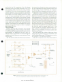
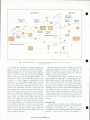
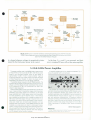
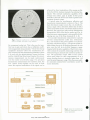
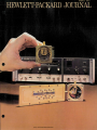
MAttUtt 19 /D HEWLETT-PACKARDJOURN © Copr. 1949-1998 Hewlett-Packard Co. A High-Performance 2-to-18-GHz Sweeper This precise, compact microwave sweep oscillator is a significant contribution to its field. The latest microelectronic and YIG technology makes it possible. by Paul R. Hernday and Carl J. Enlow THE NEED FOR VERY BROADBAND swept microwave sources is well established. Produc tion testing of multi-octave devices requires a broad band sweeper that is simple to operate. Automated test systems need a source that is programmable and can be phase locked. Broadband receiver testing often requires a compact unit for on-site swept tests. The broad area of microwave design calls for a generalpurpose sweeper that offers precision performance and is simple to interface with related equipment and convenient to operate. The truly broadband source, a single oscillator capable of sweeping a frequency range such as 2 to 18 GHz in one uninterrupted sweep, is not presently available, but there are alternatives. The most direct method is to sequence several narrower-band sweepers by means of an external controller so the resulting sweep covers the desired range. Another approach, using one sweeper and several plug-in RF heads installed in a "head-holder", reduces cir cuit redundancy and simplifies operation by giving frequency control to a single sweeper, but the equip ment is still physically large. A more compact scheme is to put the required oscil lators in a single sweeper and sequence them inter nally. More compact yet is a single oscillator followed by a harmonic multiplier to produce the higher frequencies. A New Sweeper This last scheme is used in the new Model 86290A 2-to-18-GHz RF Plug-In for the 8620A Sweep Oscilla tor mainframe, making the combination the most compact broadband sweeper currently available (see Fig. 1). Designed to meet the requirements of all ma jor sweeper applications, the 8620A/86290A pro vides more than +5 dBm of power, leveled to within ±0.9 dB, in fast, continuous sweeps over the 2-to-18GHz frequency range or any portion of this range (Fig. 2). Besides the 2-to-18-GHz band, the 86290A pro vides three narrower bands: 2-6.2, 6-12.4, and 12-18 GHz. All bands are selectable by means of a frontpanel dial drum switch on the 8620A mainframe. In CW mode in any of the narrower bands, the output frequency is accurate within ±20 MHz and resolution is 100 kHz, specifications approaching those of the traditionally more precise signal generator. Sweep ing over the widest band the frequency is accurate within ±80 MHz. Undesired harmonics are at least 25 dB and typically 30 dB below the desired output signal. The new sweeper weighs just 15 kg (33 Ib), so it can Cover: In the background is the new Model 86290A 2-to-18-GHz RF Plug-in installed in an 8620A Sweep Oscillator mainframe. In the foreground are the three components whose develop ment made the broadband RF plug-in possible: a Y/Gtuned oscillator (top), a power amplifier (left), and a YIG-tuned multiplier (right). In this Issue: A High-Performance 2-to-18-GHz Sweeper, by Paul R. Hernday and Carl J . E n l o w . p a g e 2 Broadband Swept Network Measure ments, by John J. Dupre and Cyril J. Yansouni ................. pa§e 15 The Dual Function Generator: A Source of a Wide Variety of Test Signals, by Ronald J. Riedel and Dan D. Danielson . . page 18 e Hewlett-Packard Company, 1975 Printed in USA © Copr. 1949-1998 Hewlett-Packard Co. Fig. 1 . Model 86290 A is a new R F plug-in for Model 8620A Sweep Oscillator. Four frequency bands are selectable by front-panel con trols: 2-6.2, 6-12.4, 72-78, and 2- 18 GHz. The combination is the most compact broadband sweeper currently available. easily be carried to field sites. Its versatility makes it useful in a wide array of applications, some of which are described in the article beginning on page 15. RF Design Fig. 3 is the RF block diagram of the 86290A. The basic elements are a single wide-band YIG-tuned os cillator (YTO), a power amplifier, and a 2-to-18-GHz YlU-tuned multiplier (YTM). Consisting of a steprecovery-diode and a YIG-tuned filter, the multiplier converts the amplified YTO signal to useful RF power levels at twice and three times the YTO frequency. The YTO's tuning range is 2-6.2 GHz. The YTM passes this signal directly to provide the first of the three narrower bands mentioned earlier. The other two bands, 6-12.4 and 12-18 GHz, are derived by tuning the YTM to twice and three times the YTO frequency as the YTO is tuned over 3-6.2 and 4-6 GHz respectively. Here the YTM is specially biased to provide maximum harmonic level. These three single bands will be referred to as bands 1, 2, and 3, cor responding to their respective harmonic numbers and 8620A dial drum positions. Band 4, 2-18 GHz, is obtained by automatically sweeping, in sequence, the required portions of these three bands. Power leveling in the 86290A is achieved by sens ing output power with a broadband directional detec- 5 dBm tor, comparing this signal to a level control voltage, and applying the error signal to a PIN modulator. The modulator precedes the amplifier so the modula tor's insertion loss is cancelled by the excess smallsignal gain of the amplifier (see box, page 11). The modulator also contains a directional coupler to sample the YTO signal and route it to the rear panel for counting or phase-lock applications. In general, the conversion efficiency of a harmonic multiplier drops as the harmonic number n in creases. Therefore, for a given drive power, the high est output power is achieved by keeping n as small as possible. In a sweeper, small n means fewer band switch points and correspondingly simpler drive cir cuitry and cleaner display. However, small n implies greater oscillator range, since the YTO must tune, in this case, from 2 GHz to an upper limit set by 18/n GHz. The choice of n = 3 as the maximum for the 86290A was determined by the state of the art in YIG oscillator technology. While the multiplier approach is compact and does not require the development of multi-octave os cillators, it does pose several tough design con straints. The YTM and YTO must have excellent tun ing characteristics to permit good tracking of the de sired harmonic by the narrow passband of the YIG filter. Multiplier conversion loss must be 11 dB or better and the power amplifier must supply at least 100 mWat 2-6. 2 GHz to guarantee the + 5 dBm power output specification. In addition, the YIG control circuitry must be very stable with temperature and time and must compensate for the tuning errors in herent in magnetically tuned devices. Tracking YIG Components 10 Frequency (GHz) Fig. 2. The 2-18 GHz plug-in provides more than +5 dBm of power output, internally leveled to within ±09 dB. External leveling is a/so possible. Tracking the YTO harmonic with the single-pole YIG-tuned filter proved to be a challenging design task. The YTM 1-dB bandwidth, as low as 20 MHz at some frequencies, dictates how closely the two must track to avoid unacceptable variations in output power. © Copr. 1949-1998 Hewlett-Packard Co. Fig. 3. RF block diagram of the 2-18 GHz plug-in. The YIG-tuned oscillator and YIG-tuned harmonic multiplier track each other in fre quency. The sources of tracking error include magnetic saturation, hysteresis, and delay, and thermal drift and aging in both the YIG devices and the control cir cuits. Some of the magnetic effects can be compen sated in the control circuits. Others must be con trolled by optimizing the design of the YIG magnets themselves. Each YIG-device/driver block has its own set of fre quency errors. One way to guarantee tracking would be to modify the errors of one block to make it track the other. Another way is to correct the errors of both blocks independently, so when they are put together only very minor adjustments are necessary. This is the approach taken for the 86290A. The benefits are many. It simplifies production and service, provides excellent frequency accuracy, and results in a typical frequency nonlinearity less than ±8 MHz in bands 1. 2. and 3 and ±30 MHz in the 2-18 GHz band. Magnet Design Hysteresis and saturation are familiar effects whose magnitudes depend upon the magnet core material. Saturation is also influenced strongly by the magnet geometry, particularly the shape of the pole. For the 86290A, the magnet gap and pole face diameter were chosen based on YIG sphere size, and the opti mum pole taper for these dimensions was derived.1 Hysteresis is also affected by geometry in that the overall magnetic hysteresis is a function of the length of core that is made from high-hysteresis material and of the flux density in this portion of the core. Magnet core materials must be chosen to mini mize both hysteresis and saturation. Of the soft magnetic materials generally used in these applica tions, the 50% and 80% nickel alloys are the most convenient. •Nonlmeanty is the difference between the actual output frequency and that indicated by the SWEEP OUTPUT voltage in the MANUAL mode The configuration of these materials in the magnet is complicated by their thermal expansion character istics. Unless applied correctly, these materials can contribute significantly, through gap change, to the overall temperature dependence of the YIG device. In the 86290A magnets, these materials are used where required by hysteresis and saturation consider ations and their lengths are chosen to satisfy a zerogap-drift constraint. Applying this technique to the design of the YTO and YTM magnet structures re sulted in the following magnetic properties, mea sured in bands 1, 2 and 3. YTO YTM Maximum Hysteresis Error (MHz) ±1 ±2 Maximum Saturation Error (MHz) ±3 ±18 The effect of hysteresis errors is further reduced by the fact that the two magnet structures are similar and have similar sweep histories. Thus there is con siderable cancellation. The remaining nonlinearity caused by saturation can be compensated by the YIG control circuits, to be described later. The third magnetic effect, sweep delay, is caused by the bucking effect of eddy currents induced in core and package materials by a change in applied magnetic field. The lagging field at the YIG causes a lag in the actual tuned frequency. A large portion of this delay comes from the magnetic core itself and cannot be eliminated without laminating the core, which decreases rigidity and makes hermetic sealing difficult. However, eddy currents in the circuit sup port structure can be reduced by avoiding closed loops and by using thin, high-resistance metals. The remaining influence is compensated very well by the control circuits, as explained later. Magnet gap change is not the only source of ther- © Copr. 1949-1998 Hewlett-Packard Co. mal drift in the YIG components. The YIG spheres themselves and the oscillator transistor in the YTO can contribute drifts more than an order of magni tude greater than even an uncompensated magnet. Careful alignment of the YIG sphere's anisotropic field and the use of heater/regulators greatly reduce these effects in the new sweeper (see boxes, pages 6 and 8). Aging, mentioned earlier as a source of tracking error, results mainly from gradual change of the gap itself. At 6 GHz, a 0.0025-mm variation in a 2.5-mm gap causes a frequency shift of 6 MHz. This sort of variation can be expected over a few weeks time unless great care is taken in the attachment of the magnets. YIG magnets for the 86290A are held in place by strong metal clamps so there is negligible gap change with time. YIG Driver Design Ideally, spherical YIG resonators tune linearly with applied magnetic field according to the relation f = yH, where H is the applied field in gauss and y is approximately 2.8 MHz/gauss (see box, page 13). Magnetic field is proportional to current through the magnets, so a linear frequency sweep requires a linear curreni lamp. The YIG driver circuits have three main sections: the circuits that change the tuning current ranges as the YIG components are swept across the bands, the driving current sources, and finally, the compensa tion for the effects of magnetic saturation and delay. A representative driver schematic is shown in Fig. 4. A frequency control signal of zero to ten volts is ap plied for each of bands 1, 2, and 3. Depending on the band, zero volts represents 2, 6, or 12 GHz, and ten volts represents 6.2, 12.4, or 18 GHz. Ul and the resis tive networks around it constitute an inverting ampli fier with three possible combinations of gain and dc offset. Each resistive network corresponds to one of the three bands and is switched into effect by the band control inputs. For an increasing input voltage, V falls and the feedback loop comprised of U2, Ql, Q2, Q3, and Rref assures that Vref=V. The current through Rref increases proportionally. Ql's base current is negligible and U2's input im pedance is high; therefore, the entire current is de livered to the magnet. Each YIG device has a driver of this type. Every range-switching network has two adjustments, and must be aligned for proper YTO frequency excursion and optimum YTM harmonic tracking. If the YIG components were i Heal, this would be Band 1 Control (T) Band 2 Control (?) Band 3 Control (T) • 20V Frequency Reference ( -20VFR) Râ„¢. Saturation Compensation Band Switching Fig. tune resonators. driver circuits provide the linear current ramps that tune the YIG resonators. The drivers also compensate for magnetic saturation and delay in the YIG magnets. © Copr. 1949-1998 Hewlett-Packard Co. A 2-18-GHz YIG-Tuned Multiplier The YIG-tuned multiplier (YTM) is the key to the 86290A's broad frequency range. While multipliers have an established place this microwave design, the important contributions of this device are its extremely wide input and output frequency ranges and its efficient generation of harmonic power. Given a high-level, 2-6.2-GHz drive signal, the YTM provides second and third harmonic power to 18 GHz with conversion loss under 11 dB. It can also pass the fundamental signal with ap proximately 6 dB loss, completing the frequency range without the need to bypass the YTM. These features, combined with tuning linearity better than ±18 MHz in any of the harmonic ranges, make the YTM a very powerful microwave component. The YTM is shown schematically in Fig. 1. An HP step-reco very-diode (3RD) is employed as the nonlinear, harmonicgenerating element. It is followed by a single-sphere YIG-tuned filter, which tracks the desired harmonic and rejects the others. To minimize conversion loss, the SRD's self-biased condi tion is modified with an external bias signal. This signal is shaped from the 86290A's frequency control voltage and is set in the factory for optimum YTM performance. The 3RD is for ward biased for 2.0-6.2 GHz output. Coupling to and from the YIG resonator is accomplished via conducting loops that pass over opposite sides of the sphere to ground. These loops are situated at right angles to the ap plied magnetic tuning field, H, and are at right angles to one another to avoid direct coupling from input to output. The output power is proportional to RF current (see box, page 13), so the 3RD must be driven from a low-impedance source. The input matching circuit provides this low impedance, trans forming the 50Ãà generator impedance to less than 10Ã1 over a broad frequency range. It also prevents the flow of harmonic energy back into the driving source. The input circuit, the 3RD, and the YIG filter's input coupling loop are on a sapphire substrate, and the output loop is located on a second substrate. Beneath each loop is a hole slightly larger than the YIG sphere. The substrates are placed back to back with the sphere between the loops. Temperature compensation of the YIG filter is accomplished enough. In reality, saturation and delay make addi tional circuitry necessary. Linearity is improved by shunting Rref with selected resistors as the YIG fre quency is increased. The circuit that does this is in dicated in Fig. 4. As Vref drops with increasing mag net current, it crosses the level set by the divider, R4 and R5, and the diode conducts. The ratio of R4 and R5 determines the switch point, and their magnitudes govern the amount of correction applied. Several such networks are used as needed to reduce nonlinearity of a given YIG device to a few megahertz across any band. Delay compensation can be implemented at the reference resistor or in the range switching circuitry. The delay mechanism itself can be represented quite well by a simple RC low-pass circuit (Fig. 5). The cir cuit's response to a linear ramp is given by eout(t) = at - aRC(l-e-tRC). where ein(t) = at. Thus a signal of the form 1 -e~l ic is RFIn 2-6.2 GHz Low-Pass Filter S t e p Y | G Recovery «. h Diode Fig. 1. using two established techniques. First, the sphere is mounted near a known crystalline axis to reduce temperature depen dence. Then, when the circuit is in operation, the entire sub strate assembly is heated to a constant 75°C. A tiny beadstyle thermistor monitors the temperature near the sphere. An external circuit, mounted on an attached printed circuit board, supplies a control signal to a resistive heater alongside the substrates. Roben Jo/y Alejandro Chu References 1 J Moll and S Hamilton. "Physical Modeling of the 3RD for Pulse & Harmonic Generator Circuits . Proceedings of the IEEE. Vol 57. No 7. July 1969 2 "Harmonic Generator Using 3RD & 3RD Modules HP Application Note 920 3 Matthaei. Young, and Jones. Handbook ol Microwave Filter Design", McGrawHill Book Company, 1964 required to compensate the magnet for delay. This is present in the current flowing through the low-pass circuit, given by i(t) = aC[l-e-^c]. Magnetic delay rm is approximately 150 micro seconds for unlaminated structures of good design. RC is analogous to rm, so compensation can be real ized with components of convenient size. The use of this circuit in an actual driver is illus trated in Fig. 4. Point A is a virtual ground when con nected to Ul by the FET switch. Current into this node causes an increase in frequency. Elements R¡ and C¡ (i = 1 ,2 ,3) are selected to duplicate the magnet time constant and to provide, in conjunction with the feedback resistor Rfi, a signal level consistent with the actual delay effect. A second RC leg may be paralleled with the first to tailor the compensation more closely for a particular device. The selection and loading of the proper R and C val- © Copr. 1949-1998 Hewlett-Packard Co. eln = at Fig. 5. Magnetic delay is repre sented well by an PC network. Thus a simple network can pro vide a compensating signal. Magnetic Magnet | Current Field ues for each range could be a tedious affair. In the 86290A, a fixed capacitor, an operational amplifier, and variable resistors provide a compensating wave form that is continuously variable in both time con stant and magnitude, eliminating the nefiH for selec ted components. Minimizing Drift Drift of the frequency control voltage causes a fre quency error, but since this signal is common to both drivers, no tracking error occurs. However, great care must be taken to minimize sources of drift within the drivers. All operational amplifier offsets are nulled and ±2 ppm/°C metal film resistors are used in gain and offset functions. The driver reference resistors are matched to ±1 ppm/°C and are derated greatly to re duce self-heating. In the band-switching circuits, the FETs are operated directly into the high-impedance operational amplifier to eliminate the effects of FET on-resistance drift. Another source of drift is found in the 8620A main frame's + 20V frequency reference ( + 20VFR), which is the reference voltage for both current sources. It is related to drive current by the equation, + 20VFR -Vref I= ref Variations in +20VFR may be as high as ±0.4 mV/°C. To avoid the corresponding frequency and tracking drifts, the supply is compared to a stable reference in the 86290A and a correction signal is applied to the drivers. This technique also makes the instrument immune to variations in + 20VFR among mainframes. Frequency Control Two types of signals control the 86290A output fre quency: logic signals that select the range of the cur rent source in the YIG driver, and the 0-10V fre quency control voltage that drives the current source across the selected range. The control scheme for generating these inputs is illustrated in Fig. 6. For the narrow ranges (2-6.2 GHz, 6-12.4 GHz, and 12-18 GHz), the 0-10V tuning voltage from the 8620A mainframe is essentially a direct input to the YIG drivers. In all three uf these ranges, Ql is switched on, routing the tuning voltage through U4, a voltage follower, to the drivers. Similarly, the range logic is determined by direct mainframe inputs: the band 1, 2, and 3 lines are routed through dual-input OR gates to an 1C that shifts the TTL level to 0-1 0V for driving the FET switches in the YIG drivers. When the 2-to-18-GHz range is selected, the 0-10V tuning voltage from the mainframe is no longer suit able as a direct input to the YIG drivers. To cover this range, the drivers must sweep across the narrow ranges sequentially. This requires that for each 0-10V excursion by the mainframe tuning voltage, the YIG driver frequency control voltage must make three 0-10V excursions. Waveforms 4 and 5 in Fig. 6 show this relationship. Selection of band 4, 2-18 GHz, causes Ql to turn off, Q2 to turn on, and Kl to close. The mainframe tuning voltage is then directed through Kl to the in puts of two comparators, Ul and U2, which are refer enced at +2.625 volts and +6.500 volts, respectively. The combined outputs of these comparators, wave forms 1,2, and 3 in Fig. 6, indicate the desired YIG driver range as a function of mainframe tuning vol tage: 0-2. 625V corresponds to 2-6.2 GHz, 2.6256.500V corresponds to 6-12.4 GHz, and 6.50010.000V corresponds to 12-18 GHz. In addition to controlling the YIG driver range, these signals switch offset and gain around U3 to convert the tuning vol tage into the required frequency control voltage, waveform 5 in Fig. 6. From this discussion, it might be concluded that © Copr. 1949-1998 Hewlett-Packard Co. A 2.0-6.2-GHz YIG-Tuned Oscillator The fundamental signal source in the 86290A is a 2.0-6.2-GHz, YIG-tuned transistor oscillator (see Fig. 1). It fea tures a 20-mW output level, ±3-MHz tuning accuracy, hystere sis under 2 MHz, and frequency drift of less than 150 kHz/°C. Fig. 1. The YTO circuit is built in microstrip on a sapphire substrate. All transistors are HP 35820. The circuit is shown schematically in Fig. 2. The oscillator stage consists of Q1, feedback inductance L1, and the YIG sphere with its coupling loop. Q1 presents a negative resistance to the resonator over the desired frequency range. Oscillation amplitude grows until the average negative resistance seen looking into the emit ter of Q1 equals the resistance of the YIG resonator.1 The re sonator detunes very slightly to present a reactance equal and opposite to that seen at the emitter of Q1 . Q2 and Q3. along with their matching structures, form a broadband buffer amplifier.2 The five bias resistors are located externally and allow the selec tion each a unique operating point for each transistor; hence each stage can be optimized for maximum output power or adjusted for desired harmonic level. The choice of YIG sphere parameters is crucial to oscillator performance. RF coupling increases with sphere size, given a constant coupling loop diameter. As sphere and loop dia meters become comparable, however, the uniformity of the RF coupling field degrades. This enhances spurious YIG reson ances which show up as sharp frequency discontinuities as the oscillator is swept. Sphere and loop diameters in the YTO are 0.063 mm and 0.127 mm respectively. The density of magnetic dipoles within the sphere is deter mined by its saturation magnetization. This parameter is bounded on the high side by the intrusion of spurious YIG reson ances in the lower portion of the band, and on the low side by a decrease in RF coupling. For the 2-6.2 GHz range, a 600-gauss sphere is the best compromise. The greater portion of the YTO's uncompensated frequency drift is caused by the temperature dependence of the sphere's anisotropic field. Such drift can be reduced greatly by orienting the YIG for zero anisotropy. With proper initial orientation, as many as eight temperature compensated (TC) points may be found in a single 360° rotation of the sphere about an axis per pendicular to the applied dc magnetic field. In this oscillator, the YIG sphere is mounted on a beryllium oxide rod in such an orientation. It is then rotated until a TC point is found. Finally, a 75°C of is attached to the rod to further reduce the effect of ambient temperature changes. The whole assembly is sup ported in a quartz tube to minimize heat losses (see Fig. 1). The design of the tuning magnet is discussed in the main text. Magnets are held in place with pairs of metal clamps, and are hermetically sealed with a stable, moisture-resistant epOxy. The oscillator is housed in a mu-metal shield can. Heat is trans ferred from the oscillator circuit via a copper bar that sup ports the circuit and passes through the wall of the center body and shielding can to make thermal contact with the 86290A's aluminum heat sink casting. Roger Stanc/iff Paul Hernday References 1 P. M Ollivier. "Microwave YIG-Tuned Transistor Oscillator-Amplifier Design Application to C-Band . IEEE Journal of Solid-State Circuits. Volume SC-7, pp 54-60. February 1972 2 J Dupre. "1 8 to 4 2 GHz YIG-Tuned Transistor Oscillator with a Wideband Buffer Amplifier1 , IEEE GMTT Symposium Digest. 1969. pp 432-438 v Fig. 2. © Copr. 1949-1998 Hewlett-Packard Co. Band 1 2-6.2 GHz Range 6-12.4 GHz Range 12-18 GHz Range 2-18 GHz Sequential Logic Generator Control Lines for YTO and YTM Magnet Drivers Frequency Control Voltage [5] Fig. band-select from control circuits take the tuning voltage and band-select signals from the 8620 A mainframe and provide 0-10V ramps that drive the YIG-driver current sources across the proper to In band 4, 2-18 GHz, the sweep stops momentarily at band-switch points to avoid frequency and power gaps. there is considerable overlap — 200 MHz and 400 MHz — at the range switch points. This would be the case if on each excursion of the frequency control vol tage the limits were exactly 0 and +10 volts. Actual ly, the limits are adjusted at U3 so the overlap is less than 20 MHz at each switch point. Mainframe/Plug-ln Interface (Band 4) The 86290A plug-in carries on a two-way com munication with the 8620A mainframe. To avoid fre quency and power gaps as it sweeps across three sepa rate ranges sequentially, the 86290A must have a means of stopping the sweep generator in the mainframe dur ing range switching intervals. (This is what causes the two flat levels in waveform 4 of Fig. 6.) Also, to achieve fast sweep tracking between YTO and YTM in sequential operation, the maximum rate of fre quency change must be no greater than in singlerange operation. Since the 2-to-18-GHz range is about three times wider than the other ranges, the plug-in needs a way to reduce the maximum sweep rate by a factor of three when operating sequentially. The mechanism for accomplishing both of these things is shown in Fig. 7. © Copr. 1949-1998 Hewlett-Packard Co. 8620A Mainframe Bipolar Current Source Retrace R e f e r e n c e 86290A Plug-in Sweep Ramp Integrator R ' _jrVi R Current Source Reference Reduces Forward Sweep Rate Fig. signals the interface circuits generate stop-sweep signals and limit the maximum sweep rate in band 4. To follow the sequence of events, assume that band 4, 2-18 GHz, has just been selected. The band 4 logic line causes Kl to close and the tuning voltage is directed through Kl-1 to the switch point compara tors, Ul and U2 (these are the same comparators shown in Fig. 6 as a part of the logic generator). The outputs of Ul and U2 are monitored by an EXCLUSIVE OR gate, U3, which triggers a monostable circuit whenever Ul or U2 changes output states. The out put of this monostable is a six-millisecond pulse, which is returned to the mainframe. This pulse is in verted in the mainframe and used to gate open the path between the current source and the ramp inte grator. This pulse also goes to the Z-axis output, where it is available for blanking an oscilloscope dis play during the stop-sweep interval, thus avoiding bright spots and spikes that might otherwise ap pear on the display at the two range switch points. Continuing around the circuit path, the output of the sweep ramp integrator is clamped at its two extremes and amplified to produce a zero-to-ten-volt sweep output voltage. This ramp voltage is then offset and attenuated as a function of front-panel control set tings to generate the desired tuning voltage and com plete the stop-sweep loop. The maximum sweep rate in band 4 is fixed by switching a single resistor in the 86290A, Rl, to ground. Rl loads the current source reference cir cuitry to reduce the forward sweep rate reference voltage, V2, by a factor of three. The mainframe stop-sweep inverter, U4, has one other important input path. It comes from the pro gramming connector on the rear panel. This input is used in test systems with the 8410B network ana lyzer (see article, page 15). It allows the 8410B to stop the sweep oscillator in the same manner that the 86290A does. In a system where both the 86290A and the 8410B are used, this input is a wired-OR line, which allows either instrument to stop the sweep. This is a particularly important feature. It allows the 8410B to make continuous phase and amplitude mea surements from 2 to 18 GHz when used with the 86290A. Leveling Loop As Fig. 8 shows, 86290A power leveling is accom plished by controlling the operating point of the PIN is modulator as a function of Vs and V,pt. V a voltage derived by detecting and amplifying a small portion, -16 dB, of the 2-18 GHz output signal. Vset 10 © Copr. 1949-1998 Hewlett-Packard Co. Auxiliary Output (2-6.2 GHz) Directional Coupler/ Detector RF Output (2-18 GHz) Coupler Detector Compensation Band Switching and Retrace Blanking W/GHz 8755 Modulator Drive UL 27.8 kHz Fig. operating PIN power :c internally leveled by controlling the operating point of the PIN modulator. The ALC the is designed to have a high enough slew rate to respond to the ¡>iyu are-wave modu lation from the 8755/4 Network Analyzer. is a shaped reference voltage; its magnitude is deter mined by the front-panel power level control. In the loop, Vsense and Vset are summed, and their sum is compared to zero volts at the main amplifier. A 2.0-6.2-GHz Power Amplifier The power amplifier used in the 86290A had to meet one ma jor requirement: it had to provide 20 dBm (100 mW) of power output to the YIG-tuned multiplier, given an input power of approximately 10 dBm. The term "power amplifier" might be surprising, because much higher powers have been achieved at these frequencies. However, to obtain the power and the bandwidth at the same time is a real design challenge. The amplifier design is based on the HP 35820 transistor. The amplifier has two stages of preamplification that account for 4.5 dB gain, and three stages of power amplification that account for an additional 5.5 dB. The preamplifier has been des cribed in detail elsewhere.1 Power amplifier design could have followed any of three ave nues. A large number of preamplifier stages could have been paralleled, using power dividers and combiners, or two-stage power amplifiers with 18 dBm power output could have been built and paralleled to get the desired output. A third method was to parallel two transistors within a stage and obtain the 20 dBm output with three stages. Although it required more circuit optimization, this option had the advantages of lower manufac turing cost, smaller size, and lower power dissipation, and was therefore used in the amplifier. The HP 35820 transistor pair was modeled as a single device to obtain its small-signal S-parameters. The large-signal parameters were obtained experimen tally using external tuners at high RF power levels. The input, in terstage and output matching networks were then designed and the designs verified using a computer. All amplifier stages are built on sapphire substrates. Fig. 1 shows the amplifier with its lid removed. Fig. 1. The amplifier has a rather large small-signal gain between 2 and 3 GHz. Since the amplifier follows the PIN modulator, ampli fier gain compression detracts from system on/off ratio, an important parameter when the 86290A is being modulated by the 8755A Network Analyzer (see text, page 13). To shape the gain and saturating characteristics, a frequency selective attenuator consisting of three PIN diodes imbedded in a microstrip is is used at the input of the amplifier. Its attenuation is set with an external bias voltage and ranges from 2 to 8 dB at 2 GHz. Loss drops to 1 dB above 4 GHz, where compression is slight. Ganesh Basawapatna References 1 P. Chen, "Design & Applications of 2-6.5 GHz Transistor Amplifiers", IEEE Journal of Solid-State Circuits. August 1974. Vol SC-9, No. 4 11 © Copr. 1949-1998 Hewlett-Packard Co. Product Design of the 86290A Along with the RF performance goals that defined the 86290A in the early development stage were some equally de manding mechanical objectives. The plug-in had to fit into what seemed like an impossibly small space for a 2-18-GHz source (13 x 15 x 28 cm). It had to be quick and easy to assemble and every section had to be readily accessible for easy servicing. It had to to approximately 50 watts; yet, it would have to run with no more than a 1 5-20°C temperature rise throughout to ensure good reliability. The 86290A is a fully modular design consisting of four main assemblies (Fig. 1): an RF section that houses the microcircuits, a control section, and front and rear panel assemblies. Com munication between the control and RF sections takes place via flexible shielded cables for YTO FM coil drive and ALC detector signals, and a single ribbon cable from which each microcircuit takes its supply voltages and control signals. venient replacement of a failed component. As a further service aid, a printed-circuit extender board is mounted on the under side of the control section. With the 8620A top cover removed, this extender can be used to elevate any of the six boards for convenient testing. The RF section (Fig. 2) is easily removed and opened. The ex tra-length interconnect cables allow servicing of the RF com ponents. A special RF test cable clipped to the side of the RF section casting aids in servicing. Product design of the RF section and rear panel focused on cooling the microcircuits and YIG-dnver components. Since microcircuit reliability was the most important objective, a special heat sink casting design was undertaken. The result was a structure that makes maximum use of the air flow from the fan in the 8620A. The air passes through this casting first, then over the circuit boards and through the rear panel, where a finned Fig. 2. Fig. 1. Printed-circuit boards are dedicated to separate electrical functions for optimum servicing and minimum repair cost. They are interconnected by a single, multilayer printed-circuit mother board. Edge connectors at the ends of this board form the sole interface with the front and rear panel assemblies. This design greatly streamlines production of the instrument. The RF section is preassembled, connected to a special test set, and fully RF tested before being installed in the instrument. Front and rear panel assemblies are processed similarly. Printed-circuit boards are dc pretested by computer and then functionally pretested in a simulated instrument before being plugged into the final instrument. These techniques allow troubleshooting at the lowest, simplest levels, and result in little if any troubleshooting at final turn-on. The same modular features result in excellent serviceability. The front and rear panels come off with the removal of four screws. They can be tilted outward and tested with the instru ment operating normally, and will then readily unplug for con casting provides heat sinking for the YIG-dnver reference resis tors and driver transistors. The main text describes the care taken to provide excellent frequency accuracy and ensure tracking between the YTM filter and the desired YTO harmonic. Absolute delay compensa tion is built into the YTO-driver pair. As a result, the YTO and its driver are treated as an assembly. If a YTO fails, a new YTO and dedicated driver board are installed. Adjustments can be done with basic test equipment. Mounted atop the RF section are three labels. One explains a simple service technique for aligning YTO and YTM for opti mum frequency accuracy and tracking. The others call out re sistor values selected at the factory for YTO and YTM linearity compensation— a reference, should a part be misplaced during servicing. Any deviation from zero is amplified and sent to a modulator driver stage which shifts the modulator operating point, changing Vsense so that its sum with Vset is returned to zero. In a swept, broadband leveling application such as this, unflat power sensing elements can degrade the maximum leveled power if their frequency responses are not properly compensated. For the 86290A, this compensation is provided by shaping the inter nally generated 1-volt/GHz sweep reference voltage and using that waveform as one input to the power reference amplifier shown in Fig. 8. Shaping is ad justed once in each instrument to compensate for variations in directional detector sensitivity. The corresponding frequency-related variations in Vset force the loop to make the desired correction. William Misson Billy Knorpp 12 © Copr. 1949-1998 Hewlett-Packard Co. How YIG Tuning Works The resonators in the 86290A's wide-band oscillator and tun able multiplier are tiny 0.5-0.6-mm spheres fabricated from single crystals of the ferrite Yttrium-Iron-Garnet (YIG). Placed in an RF coupling structure in a dc magnetic field, highly polished YIG spheres exhibit a high-Q resonance at a fre quency proportional to the dc field. When electromagnets are used to produce this field, the resonant frequency is proportion al to magnet current. While YIG of other shapes is useful in mi crowave design, spheres are used here because of their linear tuning characteristic. To understand the phenomenon of ferri magnetic resonance, consider diagrams (a) through (d). In the ferrite with no dc magnetic field applied, there is a high density of randomly oriented magnetic dipoles, each consisting of the minute cur rent loop formed by a spinning electron. When a dc magnetic field, H0, of sufficient magnitude is applied, the dipoles align parallel to the applied field, producing a strong net magne tization, M0, in the direction of H0. If an RF magnetic field is applied at right angles to H0, the net magnetization vector will ffitl Ã-tltÃ-tÃ-t!) (a) Randomly oriented magnetic dipoles in the unmagnetized ferrite. TMO (b) The effect of a dc magnetic field on mag netic dipoles in the ferrite. Magnet (c) Precession of net magnetization vector due to RF magnetic field. (d) YIG bandpass filter showing RF coupling loops, sphere, and magnetic poles. As with any high-performance ALC loop in a swept source, the 86290A loop had to have sufficient band width that power variations as a function of sweep rate would be negligible. Also, a primary design goal was to achieve loop slew rates great enough that the instrument could be modulated directly when used with the 8755A Network Analyzer (see article, page 15). This would eliminate the need for the external modulator normally required in this application, and as a consequence, deliver the full +5 dBm to the de vice under test. Satisfying this requirement meant that the loop would have to respond to the 27.8-kHz square wave precess, at the frequency of the RF field, about an axis coin cident with H0. The processing magnetization vector may be represented as the sum of M0 and two sinusoidally varying RF magnetization components mA and my. The angle of pre cession <)>, and therefore the magnitudes of mx and my, will be small except at the natural precession frequency. This fre quency, known as the ferrimagnetic resonant frequency, is a linear function of the dc field H0. Diagram (d) shows the basic elements of a YIG bandpass filter.1 The filter consists of a YIG sphere at the center of two loops, whose axes are perpendicular to each other and to the dc field H0. One loop carries the RF input current, and the other loop is connected to the load. When H0 is zero, the mutually perpendicular orientation of the loops results in large input-tooutput isolation. With H0 applied, there is a net magnetization vector in the direction of H0. The magnetic field hx produced by the RF driving current in the input loop causes the net magne tization vector to precess about the z-axis. The resulting RF magnetization component, my, induces a voltage in the output loop. fre frequencies away from the ferrimagnetic resonant fre quency, my and the voltage it induces are small, so input-tooutput isolation is high. When the input current is at the ferri magnetic resonant frequency, <S> and my are maximum. There is a large transfer of power from input to output, and insertion loss is low. Thus the filter center frequency is the ferrimagnetic resonant frequency and can be tuned by varying H0 with rr.agnet current In oscillator designs, a single loop couples the YiG spheie ic an active circuit having a negative resistance over the desired frequency range. The resonator can be modeled as a parallel RLC circuit. When the resonator resistance is greater than the negative resistance of the active circuit, and the imaginary parts of the two impedances are equal and opposite, osci llation will occur. Oscillation amplitude will grow until the average values of the resonant and negative resistances are equal. Frequency stability in both filter and oscillator designs is affected by the temperature dependence of the YIG sphere's inherent anistropic field. The contribution of anisotropy to re sonant frequency is dependent, in turn, on the orientation of the sphere's crystalline axes with respect to H0, the dc magnetic field. The sphere can be rotated such that this contribution is zero. Reference 'For 'Magnetically aetailed treatment see. for instance, PS Carter, Jr . 'Magnetically Tunable Microwave Filters Using Single-Crystal Yttrium-lron-Garnet Resonators IRE Transactions on Microwave Theory and Techniques. Vol MTT-9. No 3, May 1961 modulating signal produced by the 8755A. This sig nal would drive the loop into and out of saturation for a minimum on/off ratio of 20 dB. Also, the loop would have to come out of saturation fast enough to main tain no worse than 45/55 symmetry. To add a further complication, equally good performance was ex pected over the 10-dB range of the power level control. In general, as modulator attenuation approaches saturation in an ALC loop, the corresponding loss of sensitivity in control current constitutes a loss in loop gain, and hence a loss of bandwidth and slew rate. However, the slewing capability of the modula tor itself is not reduced. Consequently, a technique © Copr. 1949-1998 Hewlett-Packard Co. Knorpp designed the RF section heat sink casting. Dick Bingham designed the FM driver board. Jack Kuhlman provided the coupler/modulator design. Phil Chen did the early YTO design. Industrial de sign support came from Dave Eng and Roy Church. We also wish to thank Callum Logan, Jeff Gomer and Jim Yarnell for fabricated part process development. The lab team had important assistance in micro electronic technology from Weldon Jackson, Yeng Wong, Jim Smith and Pete Planting. Phil Froess and Harry Portwood of the transistor fabrication group helped ensure a good supply of high-performance devices. Production Engineering support for the 86290A is provided by John Turner at the instrument level and Alejandro Chu and Val Peterson for the components. Additional help has been given by Jeff Ho and Alan Kafton, and by Bud Edgar for the 8620A modification. The 86290A operation and service manual was written by Doug Andrus and Don Jackson. Jim Arnold set up the fine instrument support program. We aré indebted to Cyril Yansouni and Jack Dupre for their leadership and encouragement over the several years of developmental work. 2 for achieving a uniformly fast slew rate, even while approaching saturation, involves alternately switch ing between closed and open-loop control of the mo dulator drive current. Ideally, for a pulse input, the loop would remain closed until it began to lose gain as the modulator neared saturation. At this point the loop would be switched open, and the modulator would be driven on into saturation by bypassing the main amplifier and driving the modulator directly. In recovering from maximum attenuation, the re verse sequence would occur. The 86290A ALC loop uses this technique to satisfy the 8755A modulation requirement. Level sensing circuitry establishes the attenuation level at which the closed-to-open-loop transition occurs. Acknowledgments The authors gratefully acknowledge the contri butions of the many talented people who cooperated very effectively to make the 86290A a reality. The de tailed YTM concept was provided by Kit Keiter, and Robert Joly did the early design and optimization. Earl Heldt did much of the early magnet and circuit pack age designs for the YIG tuned devices. Alejandro Chu made several important improvements in YTM per formance, did the original ALC design, and gave valu able help in many other areas, including FET switch ing and delay compensation in the YIG drivers. Ganesh Basawapatna designed the 2-6.2 GHz power amplifier and contributed greatly to several other RF designs. Roger Stancliff made valuable improve ments in the ALC design and did final design of the YTO. Gary Holmlund did the exacting YTO and YTM driver designs and helped to coordinate the many changes that took place during the prototype phase. Bill Misson did the excellent product design and Bill References 1. Y. Ishikawa and S. Chikazumi, "Design of High Power Electromagnets", Japanese Journal of Applied Physics, Volume 1, No. 3, September 1962. 14 © Copr. 1949-1998 Hewlett-Packard Co. Broadband Swept Network Measurements Vector and scalar measurements can be made from 2 to 18 GHz in one sweep by pairing the new 2-18-GHz sweep oscillator with other microwave instruments. by John J. Dupre and Cyril J. Yansouni BROADBAND COVERAGE, precision frequen cy characteristics, and compactness make the new 8620A/86290A Sweep Oscillator (see article, page 2) suitable for a wide variety of network mea surement applications. Its internally leveled output power and low harmonic and spurious levels over the 2-to-18-GHz frequency range are important in the measurement of broadband microwave components. Its frequency accuracy and stability are important for testing narrow-band, higb-O devices. frequency by the frequency reference voltage. The VTO searches around that frequency until phaselock is achieved. The sweep oscillator then begins its sweep with the analyzer maintaining phase-lock. When the VTO reaches the end of its range, the ana lyzer commands the sweeper to stop sweeping and the search and lock procedure is repeated before the sweep is resumed. An example of this capability is shown in Fig. 2. The input reflection coefficient of a ferrite junction circulator from 2 to 18 GH/ is displayed in polar for mat. Although designed primarily for the 5-to-10-GHz range, its out-of-band performance including the phase of the reflection coefficient is often important. This display allows convenient adjustment of inband and out-of-band parameters. Transmission gain and phase may also be mea sured with the system of Fig. 1. Since the system is frequency selective and therefore unaffected by sweeper harmonic output, dynamic range is 60 dB. Vector Network Measurements Complete characterization of a network requires measurement of the magnitude and phase of its driv ing point and transfer characteristics. Phase informa tion is vital for component design and often neces sary for system, component, and antenna testing. At microwave frequencies, scattering parameters1 are widely used because they relate incident to reflected and transmitted waves at the network terminals. Measurement of network scattering parameters in one continuous 2-to-18-GHz sweep is now possible with a new Network Analyzer, the HP 8410B, and the 8620A/86290A Sweep Oscillator. The HP 8410B, like its predecessor, the 8410A,2 measures complex ra tios by translating the microwave signal to an IF by a sampling process. A phase-lock loop locks a harmon ic of the VTO that drives the sampler to the micro wave signal. The contribution of the 8410B is new cir cuitry that interfaces with the 8620A Sweep Oscilla tor and allows phase-locking over broad frequency sweeps instead of only over octave ranges. Three interface lines are necessary for reliable broadband phase-locking (Fig. 1). A frequency refer ence line from the oscillator provides an analog vol tage corresponding to the output frequency with an accuracy of ±35 MHz. A blanking line provides a pulse during retrace and at band-switch points. Final ly, a stop-sweep line from the analyzer can command the 86290A to stop sweeping momentarily. At the be ginning of each sweep and at band-switch points, the analyzer VTO is tuned approximately to the locking Scalar Network Measurements For a broad range of applications, amplitude-only or scalar measurements are sufficient to characterize FREQUENCY REFERENCE STOP-SWEEP 841 4A Polar Sweep Oscillator 8620A86290A Display 841 OB or Network Analyzer «41 2A Phase/ Magnitude Display 8743A Option 18 Reflection/Transmission Test Set Device Under Test Fig. 1. A 2-to-18-GHz scattering parameter measurement system. 15 © Copr. 1949-1998 Hewlett-Packard Co. achieved by direct modulation of the sweep oscilla tor by the 8755A Analyzer instead of an external mo dulator. This external modulation capability of the sweeper (see article, page 2) makes its full power available at the test device and leads to greater mea surement dynamic range. A typical setup for simultaneous reflection and transmission measurements is shown in Fig. 3. The dual directional coupler covers the 2-to-18-GHz fre quency range with a directivity better than 30 dB at 2 GHz and 26 dB at 18 GHz. The 8755A displays simul taneously the return loss (A/R) and the transmission characteristic (B/R) of the device under test (Fig. 4). Absolute power measurement is also possible by dis playing any one of the three channels (R, A, B). For accurate transmission measurement, typically low-loss measurements (cable loss, attenuation, etc.), one would use the power splitter in an alterna tive setup, also shown in Fig. 3 . The power splitter ex hibits better than 0.25 dB tracking between the two arms over the full dc-to-18-GHz frequency range. Coupled with the ratio capability of the 8755A, it pro vides a means of accurately measuring insertion loss without having to measure and correct for system er rors. The equivalent output SWR of this splitter when used either for ratio measurement or as a source leveling device is typically better than 1.25 over the same frequency range. Thus the power split ter minimizes measurement uncertainty caused by source mismatch. Fig. 2. Reflection coefficient of a ferrite junction circulator from 2 to 78 GHz. Full scale is unity reflection. the component under test. This is the case for inser tion loss or gain and return loss or reflection coeffi cient (magnitude) measurements.3 The 8755A Swept Amplitude Analyzer4 allows for simultaneous dis play of return loss and transmission parameters. When it is used with the 8620A/86290A Sweep Oscillator and the 11692D Dual Directional Coupler, this simul taneous measurement can be made continuously over the entire 2-to-18-GHz range. For precision transmission measurement (low insertion loss), the new 11667A Power Splitter can be used. In both cases, the required modulation of the signal can be MODULATOR DRIVE 8620A86290A Sweep Oscillator SWEEP OUT Reference Channel Reflection Channel 11692D Dual Directional Coupler Transmission Channel Device Under Test Det 11664A Detector 11 667 A Power Splitter Transmission Channel Device Under Test Fig. 3. System for simultaneously measuring transmission and re flection parameters. 16 © Copr. 1949-1998 Hewlett-Packard Co. Paul R. Hernday ! i"W^^ Paul Hernday, project manager - ->~:· for the 86290A RF Plug-in, re ceived his BSEE degree from the University of Wisconsin (Madison) in 1968 and joined HP in 1969. Besides the 86290A, he's worked on analyzers and Gunn oscil lators and. before joining HP. on Van de Graff accelerators. .JQ I He's a member of IEEE. A native jl^ | of southern California, Paul is ^ I married, has two small children, and lives in Santa Rosa, where he serves on the board of directors of the Family Service Agency of Sonoma County. A major interest, shared by his wife, is the evolution of life styles that emphasize human values and a res pect for the natural environment. Paul also enjoys hiking and camping with his family, woodworking, gardening, reading, and keeping up with developments in many areas of science. Fig. 4. Frequency response of a bandpass filter measured by the system of Fig. 3. Acknowledgments We would like to acknowledge the contributions of Doug Rytting, Bruce Donecker, Lewis Newton, and Richard Barg for the 8410B Network Analyzer. The 11667A Power Splitter was designed by Julius Botka and Brent Palmer. Jim Davis, Russ Johnson, and Jim Kaylor have contributed in the area of network analyzer applications. References 1. R.W. Anderson, "S-Parameter Techniques for Faster, More Accurate Network Design," Hewlett-Packard Journal, February 1967. 2. R.W. Anderson and O.T. Dennison, "An Advanced New Network Analyzer for Sweep-Measuring Amplitude and Phase from 0.1 to 12.4 GHz," Hewlett-Packard Journal, February 1967. 3. "High-Frequency Swept Measurements," HewlettPackard Application Note 183. 4. H. Vifian, F. David, and W. Frederick, "A 'Voltmeter' for the Microwave Engineer," Hewlett-Packard Journal, November 1972. John J. Dupre Jack Dupre is section manager for sweep oscillators at HP's Santa Rosa (California) Division. He's been designing YIG-tuned oscil lators and other components for sweepers and spectrum ana lyzers since he came to HP in 1964. just after receiving his BS degree in electronic engineering from California Polytechnic Uni versity (San Luis Obispo). Along the way he's earned his MSEE degree at Stanford University (1967) and been awarded a patent for a YIG-tuned Gunneffect oscillator design. He's a member of IEEE. Jack was born in Louisville, Kentucky. He and his wife and three children live in Santa Rosa and enjoy traveling and photography. Carl J. Enlow Carl Enlow has been with HP since 1967, designing various parts of the 8620 Sweep Oscillator family. He's now project manager for the 8620A.86290A interface ana is responsible tor introducing the 86290A to production. Born in Kilgore, Texas. Carl spent three years as a guided missile tech nician in the U.S. Navy before entering the University of Illinois (Champaign-Urbana) to work for his BSEE degree, which he re ceived in 1 967. Now living in Santa Rosa, California, Carl is married and has a son and a daughter. He's an active tennis player and golfer, likes to play the stock market, and enjoys seeing new places with the family and participating in Indian Guide ac tivities with his son. Cyril J. Yansouni Y a n s o u n i i s e n g i n e e r i n g manager for sweep oscillators and ^^^~ network analyzers at HP's Santa Rosa Division With HP since 1967, he's been a sweeper de signer, YTO and amplifier project leader, and sweeper section manager. Born in Alexandria, Egypt. Cyril graduated from the Catholic University of Louvain, Belgium in 1965 with a degree in electrical and mechanical en gineering, and in 1967 received his MSEE degree from Stanford University. Cyril is married and has two children. He enjoys traveling with his family, and usually encounters no language barriers; he's fluent in English, French, Italian, and Arabic. A tennis player and music lover, Cyril serves on the board of directors of the Santa Rosa Symphony Orchestra and on the electronic advisory committee of Santa Rosa Junior College. I 17 © Copr. 1949-1998 Hewlett-Packard Co. C y r i l The Dual Function Generator: A Source of a Wide Variety of Test Signals FM signals, AM signals, dc levels, tone bursts, pulses and ramps, in addition to sine, square, and triangular waves, are produced by this new dual-source function generator. by Ronald J. Riedel and Dan D. Danielson MANY LAB-BENCH APPLICATIONS in the audio, ultrasonic, video, and RF fields require the engineer to have more than one signal source available. Such would be the case when sweep-fre quency testing amplifiers and filters, testing modula tion and detections systems, evaluating discrimina tors, and simulating transducer outputs. With this in mind, we set out to design a truly general-purpose signal source that in many cases could replace combinations of sine-wave oscil lators, signal generators, sweep oscillators, and pulse generators now used. Such an instrument, be sides the obvious cost savings, would enhance user convenience by making the various test signals pushbutton selectable so the user wouldn't have to sort out and reconnect wires and cables. Neither would he have to worry about signal level incompati bility or logic threshold mismatch. The result of this design effort is the Model 3312A Function Generator (Fig. 1). This instrument has two independent waveform generators that can be used separately, or in combination with one modulating, gating, sweeping, or otherwise controlling the other. The main generator operates overa range of 0.1 Hz to 13 MHz and the other generator, called the modula tion generator, covers a range of 0.01 Hz to 10 kHz, Fig. 1 . Model 331 2A Function Generator combines two signal sources to produce a wide variety of test signals. Total fre quency coverage is from 0.01 Hz to 13 MHz. giving a total coverage of 9 decades for the two generators. Like other HP function generators, the new Model 3312A produces sine, square, and triangular wave forms of high quality (Fig. 2a). It also generates pulses and ramps with continuous control of the Fig. 2. Oscillogram (a), made by a sampling scope of the triangle waveform, demonstrates pre servation of good waveform shape at high frequencies, in this case 10 MHz (sweep time is 20 ns/div and vertical deflection factor is 1 V/div). Multiple exposure oscillogram (b) shows the main gen erator output at 100 kHz modu lated by various internallygenerated waveforms at 1 kHz. 18 © Copr. 1949-1998 Hewlett-Packard Co. Fig. 3. Multiple exposure oscillogram (a) shows pulse trains generated in the single-cycle and multiple-cycle modes: the bottom trace shows the internallygenerated gating waveform. Oscillogram (b) shows how the waveform is a/ways completed in the multiple-cycle mode (top) and single-cycle mode (center): the gating waveform is at bot tom. The start/stop phase is se lectable over a range of -80° to +90°. ratio between up and down slope of the ramps or the on and off times of the pulses (see box, page 20). Also generated are one-volt rectangular waves with a rise time of less than 10 ns, available from the main genera tor's SYNC output. These are useful not only as triggers for oscilloscopes and counters, but also as a source of fast rise pulses for testing logic circuits and for lowlevel testing of the transient response of wideband amplifiers. A 60-dB step attenuator and a 20-dB vernier give the main generator an amplitude range of 1 mV to 10 V into a 50Q toad (20V into an open circuit). A dc offset voltage can be added to the output. The output of the modulation generator is fixed at 1 volt into a high impedance. gle-cycle or multiple-cycle modes of operation. These modes greatly expand the variety of wave forms that the new Function Generator can produce. Narrow, low-duty-cycle pulse trains can be obtained by setting the main generator to a relatively high fre quency and using the trigger mode with a low-fre quency gating signal, as shown in Fig. 3a. Pulse bursts, useful for testing counting circuits, are ob tained by using the multiple-cycle mode. When operating in the single cycle or multiplecycle modes, the starting phase can be adjusted over a range of +90" to —60". The generator always com pletes the last cycle and stops on the same phase on which it started (Fig. 3b). These modes can be used at the same time as the AM and FM modes, making it possible to generate a wide variety of waveforms such as tone bursts or the "chirp" waveform shown in Fig. 4a. The modulation generator can also sweep the main generator up to two decades in frequency at sweep rates as slow as 1 sweep per 100 seconds, use ful for plotting frequency response on X-Y recorders, or at rates up to 100 sweeps per second for oscillo scope display (Fig. 4b). The gating mode can be used in combination with this mode to provide retrace blanking. Multiple Combinations The two generators can be used separately for tests of multiple input devices such as modulators. On the other hand, the main generator can be amplitude or fre quency modulated by the second generator (or an ex ternal source), giving the user a built-in choice of sine, square, or triangular waveform modulation (Fig. 2b). Square-wave modulation in the FM mode, for example, produces an FSK (frequency-shift-key ing) waveform. Triangular modulation provides a convenient waveform for testing detector linearity. The modulation generator (or an external source) can also gate or trigger the main generator to give sin- What's Inside A simplified block diagram of the new function Fig. 4. 'Chirp" or swept-burst waveform, upper trace in (a), is made by sweeping the main generator with the ramp from the modulation generator, shown in the lower trace, and gating it off during retrace. Sweep is from 7 to 70 kHz. Oscillogram (b) shows the output of a series R-L-C circuit driven from 3 kHz to 1 MHz by the main generator (vertical scale is 100 mV/div). The oscilloscope horizontal axis was driven by the ramp output of the modulation generator. 19 © Copr. 1949-1998 Hewlett-Packard Co. Variable Symmetry with Constant Frequency The versatility of a function generator can be increased by equipping it to generate pulses and ramps in addition to its other waveforms. Pulses and ramps are produced by varying the duty cycle of the square and triangular waveforms How ever, it would also be desirable to maintain a constant repeti tion rate as the duty cycle varies so that frequency may be read directly from the front-panel controls. This can be done using only a single control with the circuit in the diagram below. In the diagram, the period T, of the positive slope of the triangle is proportional to 1/1, while T2, the period of the nega tive slope, is proportional to 1/I2. \-¡ and I2are in turn linear func tions of e, and e2 thus: k/T, = e, and k/T2 = e2 e,= R Where a is the fractional rotation of the symmetry control, and ranges from 0 to 1 . Substituting (4) and (5) into (3), we have: R, (1) e0R2 where k is a constant determined by the frequency range controls. To maintain constant frequency f0, 1-a) R, +Ra e0R2 kf0 Combining terms yields: (2) TI + T2 = 1/f0 Therefore from (1) and (2), we have: 1 + 1 = 1 e i e o k f . Thus, the frequency f0 is completely independent of a, the symmetry control setting. (3) e, and e2 may vary over the range: To maintain a constant frequency while the symmetry is varied, e, and e2 must be varied in sucha way as to keep the left side of equation (3) constant. Since the relationship between e, and e2 is not linear, this requirement could represent some difficulty in realization The rather simple circuit shown in the diagram solves this problem nicely. It is easily seen that: ,(ore2) =ï e0 R, In the Model 331 2A, this range was selected to provide a duty cycle range of 20% to 80%. tor Cl through constant-current sources II and 12, a technique similar to that used in other HP function generators.1 2'3 The direction of current flow is deter mined by the diode current switch under control of the comparator. The comparator, in turn, is set or generator is shown in Fig. 5. The heart of the instru ment is the main triangle generator, shown in more detail in Fig. 6. As shown in Fig. 6. a triangular waveform is gener ated by alternately charging and discharging capaci 20 © Copr. 1949-1998 Hewlett-Packard Co. -17V MAIN Output Fig. 5. the diagram of the Model 3312 A Function Generator. The frequency of the main generaioi is controlled by a front-panel knob, by the modulation generator, by an external vol tage, or by any combination of the three. reset as the triangular waveform reaches a positive or negative limit. Positive feedback around the compar ator provides hysteresis that sets the limits and thus the peak-to-peak amplitude of the triangle. Frequency ranges are selected by switching capaci tor Cl and changing resistors in the current sources. Frequency control within each range is accom plished by varying the control voltage applied to the current sources. As shown in the block diagram of Fig. 5, this may be done with the front-panel fre quency dial, by applying a voltage from the modula Positive Feedback (Hysteresis) tion generator, or with an external voltage (applied through a rear-panel connector). An external voltage can control the frequency over a 1000:1 range, thus enabling the generator to serve as a highly linear vol tage-controlled oscillator in a phase-lock loop or in voltage-to-frequency converter applications. High-Quality Waveforms The triangular waveform is shaped into a sine wave with less than 0.5% distortion (below 50 kHz) by a 12-diode nonlinear shaping network.3 The per- To Function Select Switches <«< j I, To Sine Shaper and Function Select Switches v v Feedback to Comparator 21 © Copr. 1949-1998 Hewlett-Packard Co. Fig. 6. Main generator produces triangle waves and square waves as part of its normal operation. The square wave is divided down to 1 volt peak for the sync output. Asymmetrical control of currents n and 12 provides a means of varying the up-down ratio of the triangle (see box on opposite page). formance of most diode sine shapers tends to de grade seriously at frequencies of several megahertz and higher, particularly with respect to third harmon ic distortion. In the Model 3312A, the sine shaper is followed by a low-pass LC filter that has a sharp cut off at 14 MHz. This filter attenuates third harmonics substantially at generator frequencies above 5 MHz, enabling the instrument to produce sine waves with all harmonics more than 30 dB below the fundamen tal up to its maximum frequency. The output amplifier has separate parallel paths for the high and low frequencies. This gives it wide bandwidth and a high slew rate to maintain good square and triangle wave shape without compro mising dc stability and low offset. An integratedcircuit operational amplifier is used for the low fre quencies while the ac-coupled high-frequency path is optimized for wide bandwidth. The two paths are summed in the final gain stage and then buffered through cascaded emitter-followers to the output. The sine wave is derived by shaping the triangular wave as in the main generator. Currents for charging and discharging the integra tor are supplied through the diode-resistor networks at the integrator input. The range of current provided by the FREQUENCY control gives a 100:1 frequency span on any range. The symmetry control, however, affects only the run-down time so frequency is also af fected by this control. In the sweep mode, these networks supply un equal currents, giving a 90:10 ratio of up to down times. At the same time, the reference input to the comparator is changed so that the ramp operates be tween — 9 and 0 volts, rather than the symmetrical ±5-volt range of the triangle. This places the top end of a frequency sweep at the frequency indicated on the main generator's frequency dial. The bottom end is then determined by the setting of the modulation level control. In the FM mode, on the other hand, the modulating waveforms are centered on the zero axis and thus give frequency modulation (up to ±5%) centered on the frequency set on the main tuning dial. When operating in the sweep mode, the symmetry control affects the "retrace" time. This can be extend ed up to 10x its normal time. To facilitate setting up a frequency sweep, a "0 Hz" position is provided on the modulation fre quency range switch. In this position, the modula tion generator ramps down to its lowest level and then stops. Then, when the frequency range switch is moved to one of the other positions, the main genera tor starts at the lower limit and sweeps up. The "0 Hz" position is obtained by the circuit driv- Slow Ramps The design of the modulation generator differs from that of the main generator because it has to generate very slow ramps for the sweep function while it does not have to operate to frequencies as high as the main generator. Therefore, it was de signed around an integrator that effectively gives the large capacitance needed for the very slow ramps.4 A block diagram is shown in Fig. 7. The triangular wave is generated by integrating the square wave. The triangle level is compared to the square wave level and when the two are equal, the comparator switches the square wave generator to its other state. 0 Hz Control Squarewave Generator TTL Signal to Gating Logic Fig. frequency Reset generator uses an integrator lor very low frequency operation. Reset level and symmetry are altered for ramp waveforms. 22 © Copr. 1949-1998 Hewlett-Packard Co. External Gate/Trigger Input From Main Generator Comparator External Trigger Ui Sequential Gating Logic From Modulation > Generator Amplifier Enable To Integrating Capacitor C1 of Main Generator From Triangle Buffer Amplifier of Main Generator Gating Amplifier D1 Fig. operating signal control circuit prevents the main generator from operating when a gate signal is not present. (The switches are on the rear panel.) the waveforms may be applied to the modulator, it is possible to have sine, square, or triangle modulation of sine, square, or triangle carriers. If none of the modulation function buttons (sine, square, or triangle) is depressed, an external wave form may be applied to the front-panel connector for amplitude or frequency modulating the main genera tor, as selected by the modulation mode buttons (AM or FM). ing the FET switch Q2 on the integrator shown in Fig. 7. When the range switch is set to "0 Hz", one in put to gate 1 goes high. Assuming the other input is high, the output of gate 1 goes low, Ql is turned on which in turn turns on Q2, clamping the integrator at its lowest level. Gates 1 and 2 form a flip-flop that pre vents Q2 from being turned on until the modulation generator completes its current cycle. Versatile Modulation Gate and Trigger Functions The waveforms generated by the modulation generator are available at a front-panel connector. In AM or FM operation, the signal at this port is the sine, triangle, or square wave selected by the modula tion function buttons. In the sweep mode, the output is the sweep ramp which is then available for driving the horizontal axis of a scope or X-Y recorder during a frequency sweep. For AM modulation, the main and modulation sig nals are routed to an integrated circuit balanced mod ulator. The modulator output is amplified and then routed to the main output amplifier. Because any of S P E C I F I C A T I O N S The versatility of the Model 3312A is greatly en hanced by the gate and trigger functions. These al low the main generator to be gated on and off under control of either the modulation generator or an exter nal source. A block diagram of the trigger/gate circuit is shown in Fig. 8. The gating amplifier shown closes a negative feedback loop around the main triangle generator, preventing oscillation. Whenever the gat ing amplifier is disabled by the gating signal, the main generator is released to generate the output ± ION Rise or fall t.me (tos to W.j • 10 nsec Duty cycle vanes HP Model 3312A Function Generator DC OFFSET -10 volt: Main Generator OUTPUT WAVEFORMS S-ne square triangle - ramp pulse sweep trigger gate AM and FM FREQUENCY CHARACTERISTICS RANGE 0 t Hz to 13 MHz m B decade ranges DIAL ACCURACY zSSol tul scale SQUARE WAVE RISE OR FALL TIME (10*. to 90", j 18 rvec at ful rated output ABERRATIONS 10-. TRIANGLE LINEARITY ERROR 1 ft at 100 Hi VARIABLE SYMMETRY 80.20» to i MHZ Pustvng me CAL but»» results SPECTRAL PURITY SINE WAVE DISTORTION • 0 5'= THD from 10 Hz » 50 kHz 30 OB be*O* 'uncamemai from 50 kHz to 1 3 MHz OUTPUT CHARACTERISTICS IMPEDANCE 50(1 - IDS LEVEL 20 V p-p <nio open orcuil 10 V p-p mto SOU LEVEL FLATNESS (SINE WAVEl • 3*. from 10 Hz to 100 kHz at lull rated output M kHz reference) • 10". from 1 00 KHz to 1 0 MHz at Ml rated output ATTENUATOR 1 1 101 100 1 ana 1 000 1 Vemer gives 10 1 corWrtuOus control STEP ATTENUATOR ACCURACY Better than 5% SYNC OUTPUT 1 V p-p square wave into open cvcuM Impedance 5011 «tne DC ir setting Pusnmg me CAL button n offset Instantaneous ac vortag* • v dC offset kmfted to sifor EXTERNAL FREQUENCY CONTROL RANGE 10001 on any range INPUT REQUIREMENT Witnctal setal 10. Oto -2V ± 20*» linearly t* frequency iOOO 1 An ac voltage modulates the frequency about a o» setting within me kmts I 1 • t- 10) « range setting LINEARITY Ratio of ou«>ut frequency to mput voRage (At AV) is knear «rm.fi 0 5*c over a tOO 1 frequency range INPUT IMPEDANCE 2 B • MODULATING CHARACTERISTICS TYPES AM FM Sweep Trigger Gate or Burst internal or e AMPLITUDE MODULATION DEPTH 0 to 100°. MODULATION FREQUENCY DC to - 1 h EXTERNAL SENSITIVITY 1 0 V (K> f or 1 00% w CARRIER 3 dB BANDWIDTH tOOHzio 5MHz CARRIER ENVELOPE DISTORTION 2*. at 70*. sine wave modulation w*i 'kHz FREQUENCY MODULATION MODULATION FREQUENCY DC to 50 kHz euemai DtSTQRTION 35 dB al tc 10 MHz. '„, = 1 kHz 10*. n DEVIATION INTERNAL MODULATION) Oto • 5> INTERNAL MODULATION SOURCE FREQUENCY RANGE 0 01 HZ to 10 kHz 23 © Copr. 1949-1998 Hewlett-Packard Co. OUTPUT LEVEL • 1 0 V p-p mÃ-o 10 «1 SPECTRAL PURITY Sin» Wave Distortion • 2". THD Irom to Hz to 10 kHz SYMMETRY Variable SWEEP CHARACTERISTICS SWEEP WIDTH tOO 1 on any range SWEEP RATE OOTHzlolOOHz ,9010rarrp . 0 rtt provxM* manual Mtkng at Sweep Start with Modulation Generator operation suppressed SWEEP MODE Repetitive linear sweep between start and Mop frequency settings Retrace time can be increased wrth symmetry control RAMP LINEARITY ERROR 1°. at 100 Hz GATE CHARACTERISTICS FREQUENCY RANGE 0 1 Hz to 1 MHz ISKigte or mufapte cycles) START STOP PHASE RANGE - 90 10 - 80* GATING SIGNAL FREQUENCY RANGE Internal 0 01 Hz to 10 kHz Ertemal DC to t MHz <TTL compatible input level) General OPERATING TEMPERATURE: O C to - 55 C specrfccalions apply from 0*C to 40-C POWER '00120220240V • 51. 10". swncnao* 40 Hz to 440 Hz - 25 VA DIMENSIONS: 2t3 • 102 • 377 mm (8 375 . 4 • 14 825 in} WEIGHT UN "5bS( PRICE IN U SA.. 3312A $900 MANUFACTURING DtVIStON: I.OVELAND INSTRUMENT DIVISION P O Box 301 81 5 Founeenffi Street S W Lovetand Colorado 8053' waveform. When the gating amplifier is again en abled at the end of the gating signal, diode Dl is ini tially back-biased, so waveform generation contin ues until the waveform reaches a level set by the START/STOP PHASE control, at which time diode Dl be comes forward biased, closing the negative feedback loop and stopping the main generator. When in the trigger mode, the one-shot multi vibrator, fired by the positive transition of the gating signal, generates a short pulse that disables the gat ing amplifier only long enough to allow waveform generation to get under way. The modulation genera tor then produces one full cycle and stops. Acknowledgments Product design and mechanical layout were done by Bob Moomaw. Industrial design was by Jon Pennington. Thanks go to group leader Noel Pace for his guidance throughout the project, and to section man ager Bob Dudley and initial product manager Jerry rr Dan D. Danielson From the city of Grand Junction on Colorado's western slope. Dan Danielson crossed the continental divide to earn a BSEE degree at the University of Colorado( 1 972). Fromthere. he went straight to work for Hewlett-Packard in func tion generator development. Dan's spare time activities include the standard Colorado outdoors (skiing, fishing, hiking) Estes for help in defining the instrument. Also, spe cial thanks are due Doc Hadley, who moved on to 1C production before the project's completion, but whose early design efforts, particularly in the sym metry control circuits, exerted a positive influence on the project.,-' References 1. H. Heflin, "Compact Function Generator with En hanced Capability/Cost Ratio." Hewlett-Packard Journal, July 1973. 2. R.C. Hanson, "Compact Function Generator Covers 0.0005 Hz to 5 MHz," Hewlett-Packard Journal, June 1969. 3. R.L. Dudley, "A Voltage-Programmable Low-Fre quency Function Generator with Plug-in Versatility," Hewlett-Packard Journal, November 1965. 4. R.H. Brunner, "A New Generator of Frequencies Down to 0.01 GPS." Hewlett-Packard Journal, June 1 <):>!. Q| Hewlett-Packard Company. 1501 Page Mill Road. Palo Alto. California 94304 T PACKARD JOl HYVI. Ronald J. Riedel A Missouri native. Ron Riedel earned BSEE and MSEE degrees at the University of Missouri in Columbia. He then joined HewlettPackard (1972). going to work on function generators. Like other residents of Loveland, Colorado, he skis, fishes, and goes hiking but he's also learning classic guitar and spends time as a coun selor in church youth work. Bulk Rate U.S. Postage Paid Hewlett-Packard Company MARCH 1975 Volume 26 • Number 7 Technical Information from the Laboratories of Hewlett-Packard Company Hewlett-Packard S A.. CH-1217 Meyrin 2 Geneva. Switzerland Yokogawa-Hewlett-Packard Ltd . Shibuya-Ku Tokyo 151 Japan Editorial Director . Howard L. Roberts Managing Editor • Richard P Dolan Art Director. Photographer • Arvid A. Danielson Illustrator • Sue M. Perez Administrative Services. Typography • Anne S LoPresti European Production Manager . Michel Foglia /"^ I delete A our I please off) /^\ [3 A I I f") [Z O O . To change your address or delete your name from our mailing list please send us your old address lable (it peels off) O (l r\ I Page Palo 94304 \J I AA \—J LJ ll L O O . Send changes to Hewlett-Packard Journal 1501 Page Mill Road Palo Alto California 94304 USA Allow 60 days © Copr. 1949-1998 Hewlett-Packard Co.