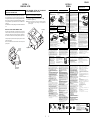
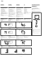
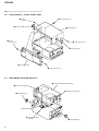
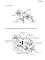
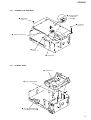
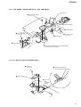
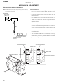
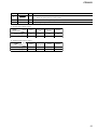
1
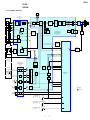
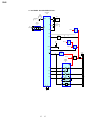
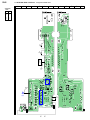
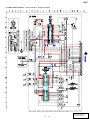
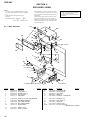
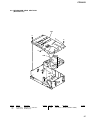
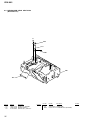
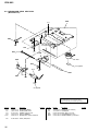
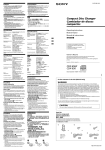
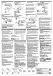
CDX-602
SERVICE MANUAL
US Model
Ver 1.0 2001.07
Model Name Using Similar Mechanism
CDX-646
CD Drive Mechanism Type
MG-251B-137
Optical Pick-up Name
KSS-720A
SPECIFICATIONS
System
Compact disc digital audio system
Laser diode properties Material: GaAlAs
Wavelength: 780 nm
Emission Duration: Continuous
Laser out-put Power: Less than
44.6 µW*
* This output is the value measured at a distance of 200 mm
from the objective lens surface on the Optical Pick-up Block.
Frequency response
Wow and flutter
Signal-to-noise ratio
Outputs
10 – 20,000 Hz
Below the measurable limit
94 dB
BUS control output (8 pins)
Analog audio output (RCA pin)
Current drain
800 mA (during CD playback)
800 mA (during loading or ejecting
a disc)
Operating temperature –10°C to +55°C (14°F to 131°F)
Dimensions
Approx. 262 × 90 × 185 mm
(10 3/8 × 3 5/8 × 7 3/8 in.)
(w/h/d) not incl. projecting parts
and controls
Mass
Approx. 2.1 kg (4 lb. 10 oz.)
Power requirement
12 V DC car battery
(negative ground)
Supplied accessories
Disc magazine (1)
Parts for installation and
connections (1 set)
Design and specifications are subject to change without
notice.
COMPACT DISC CHANGER
9-873-234-01
Sony Corporation
2001G0500-1
C 2001.7
e Vehicle Company
Shinagawa Tec Service Manual Production Group
CDX-602
TABLE OF CONTENTS
1.
SERVICING NOTES ................................................ 3
2.
GENERAL
Installation ....................................................................... 4
Connections ..................................................................... 4
3.
DISASSEMBLY
3-1.
3-2.
3-3.
3-4.
3-5.
Disassembly Flow ...........................................................
Case (Upper T), Front Panel Assy ..................................
Mechanism Deck (MG-251B-137) .................................
JACK Board ....................................................................
MAIN Board, Slide Variable Resister
(Elevator Height Sensor) (RV202) .................................
ELJ Motor Assy (Elevator) (M104) ................................
Escutcheon (T) ................................................................
Chassis (U.S) Sub Assy ..................................................
Chassis Assy ....................................................................
RF Board .........................................................................
Sled Motor Assy (251) (M101),
Optical Pick-up (KSS-720A) ..........................................
LSW Board, Spindle Motor (S) Sub Assy (M102) ........
ELJ Motor Assy (Chucking) (M103) .............................
3-6.
3-7.
3-8.
3-9.
3-10.
3-11.
3-12.
3-13.
5
6
6
7
7
8
8
9
9
10
ASSEMBLY
4-1.
4-2.
4-3.
4-4.
Assembly Flow ................................................................
Optical Pick-up Complete Assy ......................................
Gear (Lomini)/(Load Cam) Assy ....................................
Operation Check .............................................................
5.
MECHANICAL ADJUSTMENT .......................... 14
6.
ELECTRICAL CHECK .......................................... 15
7.
DIAGRAMS
8.
EXPLODED VIEWS
8-1.
8-2.
8-3.
8-4.
8-5.
Case Section ....................................................................
Mechanism Deck Section-1 (MG-251B-137) ................
Mechanism Deck Section-2 (MG-251B-137) ................
Mechanism Deck Section-3 (MG-251B-137) ................
Mechanism Deck Section-4 (MG-251B-137) ................
9.
2
Flexible Circuit Board Repairing
• Keep the temperature of the soldering iron around 270 ˚C during repairing.
• Do not touch the soldering iron on the same conductor of the
circuit board (within 3 times).
• Be careful not to apply force on the conductor when soldering
or unsoldering.
CAUTION
Use of controls or adjustments or performance of procedures
other than those specified herein may result in hazardous radiation exposure.
10
11
11
4.
7-1. Block Diagram – SERVO Section – ..............................
7-2. Block Diagram
– BUS CONTROL/POWER SUPPLY Section – ...........
7-3. Note for Printed Wiring Boards and
Schematic Diagrams .......................................................
7-4. Printed Wiring Boards – RF/LSW Boards – .................
7-5. Schematic Diagram – RF/LSW Boards – ......................
7-6. Printed Wiring Boards
– MAIN Board (Component Side) – ..............................
7-7. Printed Wiring Boards
– MAIN (Conductor Side)/SWITCH Boards – ..............
7-8. Schematic Diagram – MAIN Board (1/2) – ..................
7-9. Schematic Diagram
– MAIN (2/2)/SWITCH Boards – ..................................
7-10. Printed Wiring Boards – JACK Board – ........................
7-11. Schematic Diagram – JACK Board – .............................
7-12. IC Pin Function Description ...........................................
Notes on chip component replacement
• Never reuse a disconnected chip component.
• Notice that the minus side of a tantalum capacitor may be damaged by heat.
12
12
13
13
17
18
19
20
21
22
23
24
25
26
26
31
34
35
36
37
38
ELECTRICAL PARTS LIST ............................... 39
SAFETY-RELATED COMPONENT WARNING!!
COMPONENTS IDENTIFIED BY MARK 0 OR DOTTED
LINE WITH MARK 0 ON THE SCHEMATIC DIAGRAMS
AND IN THE PARTS LIST ARE CRITICAL TO SAFE
OPERATION. REPLACE THESE COMPONENTS WITH
SONY PARTS WHOSE PART NUMBERS APPEAR AS
SHOWN IN THIS MANUAL OR IN SUPPLEMENTS PUBLISHED BY SONY.
CDX-602
SECTION 1
SERVICING NOTES
NOTES ON HANDLING THE OPTICAL PICKUP BLOCK OR BASE UNIT
The laser diode in the optical pick-up block may suffer electrostatic breakdown because of the potential difference generated by
the charged electrostatic load, etc. on clothing and the human body.
During repair, pay attention to electrostatic breakdown and also
use the procedure in the printed matter which is included in the
repair parts.
The flexible board is easily damaged and should be handled with
care.
DISC MAGAZINE GETTING OUT PROCEDURE
ON THE POWER SUPPLY IS OFF
Inserting a disc
1
Remove the CASE (LOWER.T) beforehand
Insertion d’un disque
Lever (ML.S)
3
• Pour écouter un disque de 8 cm (3 po.), utilisez l’adaptateur Sony CSA-8, vendu
séparément, à l’exclusion de tout autre, pour éviter tout probléme de
fonctionnement. Si vous utilisez un autre adaptateur, l’appareil risque de ne
pas fonctionner correctement. Quand vous utilisez l’adaptateur CD Sony,
vérifiez que les trois griffes soient bien en prise sur le CD de 8 cm.
• Ne pas insérer d’adaptateur CD Sony CSA-8 dans le chargeur sans disque, car
cela pourrait provoquer un dysfonctionnement.
10 discs, one in each tray
10 disques, un par plateau
10 discos, uno en cada bandeja
有 10 張唱碟,每一托盤裝一張
Utilisez le magasin à disques fourni ou un magasin
à disques XA-250. Vous ne pouvez pas utiliser de
magasin à disques XA-10B avec cet appareil.
L'utilisation d'un autre type de magasin à disques
risque de provoquer un dysfonctionnement.
2
• To listen to an 8 cm (3 in.) CD, use the separately sold Sony CD adapter CSA-8.
Be sure to always use the specified adapter, as failing to do so may cause a
malfunction of the unit. If you use any other adapter, the unit may not operate
properly. When using the Sony CD adapter, make sure the three catches on the
adapter are firmly latched onto the 8 cm CD.
• Do not insert the Sony CD adapter CSA-8 in the magazine without a disc,
malfunction may result.
Push to unlock the door
Poussez pour déverrouiller la porte
Empuje para desbloquear la puerta
推開門鎖
Remarques
Tab
Onglet
Lengüeta
小翼
Use the supplied disc magazine or the disc
magazine XA-250.The disc magazine XA-10B can
not be used with this unit.If you use any other
magazine,it may cause a malfunction.
裝入一張唱碟
Notes
c
Note: Take out the magazine only when the tray is completely within the
magazine. If the disk or tray is sticking out, turn on the power and
eject the magazine.
This section is extracted from
instruction manual.
Inserción de discos
Labeled surface up
Etiquette vers le haut
Con la superficie de la etiqueta hacia arriba
貼標簽面朝上
With the arrow side facing up
Avec la partie fléchée tournée vers
le haut
Con el lado de la flecha hacia arriba
有箭頭標誌的一面朝上
1) Press the lever (ML.S) assy in the direction of arrow A.
2) Removal the magazine assy.
NOTES ON LASER DIODE EMISSION CHECK
The laser beam on this model is concentrated so as to be focused
on the disc reflective surface by the objective lens in the optical
pick-up block. Therefore, when checking the laser diode emission, observe from more than 30 cm away from the objective lens.
Notas
• Para escuchar un disco compacto de 8 cm, utilice el adaptador de discos
compactos Sony CSA-8, que podrá adquirir por separado. Asegúrese de utilizar
siempre el adaptador especificado, ya que si utiliza otro tipo de adaptador es
posible que la unidad no funcione correctamente. Al utilizar el adaptador de
discos compactos Sony, asegúrese de que los tres enganches del adaptador
están firmemente ajustados al disco compacto de 8 cm.
• No inserte el adaptador de discos compactos Sony CSA-8 en el cargador sin
discos, ya que pueden producirse fallos de funcionamiento.
Emplee el cargador de discos suministrado o el
XA-250. El cargador de discos XA-10B no puede
utilizarse con esta unidad. Si emplea otro tipo de
cargador, puede producir fallos de
funcionamiento.
註
• 要聽 8 cm CD 時,請用另售品的 Sony CD 轉接器 CSA-8。一定請使用指定的轉接器,
否則將可能使機器故障。如果使用任何其他轉接器,機器將可能不能作正常的操作。使
用 Sony 牌 CD 轉接器時,須確認轉接器上的 3 個簧舌是否穩固地固定好 8 cm CD。
• 不要把 Sony CD 轉接器 CSA-8 裝入沒有唱碟的唱碟匣中。
請使用附帶的唱碟匣或唱碟匣 XA-250。唱碟匣 XA-10B
是不能用於本機的。您如果隨便使用其他唱碟匣,將可
能引起故障的。
Disc magazine
Chargeur de disques
Cargador de discos
唱碟匣
x
Slide open
Coulissez pour ouvrir
Deslice para abrir
滑開
To remove
Retrait
Extracción
取出
Note
To prevent injury, do not insert your hand in the CD changer.
Remarque
Pour éviter toute blessure, ne pas introduire la main dans le
changeur de CD.
Nota
Para evitar lesiones, no inserte la mano en el cambiador de CD.
註
請勿將手伸進 CD 換碟機內,以防傷害。
Note
4
When a disc magazine is inserted into the CD changer or the
reset button of the connected car audio is pressed, the unit will
automatically be activated and read the information on the
CDs. When the information on all the CDs in the disc magazine
has been read, the unit will automatically stop operation.
Remarque
A
If the optical pick-up block is defective, please replace the whole
optical pick-up block.
Never turn the semi-fixed resistor located at the side of optical
pick-up block.
OPTICAL
PICK-UP
BLOCK
SECTION 2
GENERAL
If the disc magazine does not lock properly
Take out the magazine, and after pressing the Z (EJECT) button,
re-insert it.
Si vous ne pouvez pas fermer le chargeur de disques
Sortez le chargeur et, après avoir appuyé sur la touche Z (EJECT), réinsérez-le.
Si el cargador de discos no se cierra correctamente
Extraiga el cargador, pulse el botón Z (EJECT) y vuelva a insertarlo.
如果唱碟匣沒有鎖定妥當
請取出唱碟匣,按下 Z (EJECT) 按鈕後再將它裝進去。
Z (EJECT)
Use the unit with the door closed completely
Otherwise, foreign matter may enter the unit and
contaminate the lenses inside the changer.
Utilisez cet appareil avec la fenêtre complètement
fermée
Sinon, des corps étrangers pourraient pénétrer dans
l’appareil et encrasser les lentilles dans le lecteur.
Emplee la unidad con la puerta completamente cerrada
De lo contrario podrían introducirse objetos extraños y
contaminar las lentes del interior del cambiador.
請完全關上門使用机器
否則,會有塵垢進入機器弄髒換碟器內部的透鏡。
Quand un chargeur de disques est inséré dans le changeur de
CD ou si la touche de réinitialisation de l’autoradio raccordé est
enclenchée, l’appareil se met automatiquement en marche et
reproduit les CD. Lorsque tous les CD du chargeur ont été
reproduits, l’appareil s’arrête automatiqement.
Nota
Cuando inserta un cargador de discos en el cambiador de
discos compactos, o si está pulsado el botón de reposición del
equipo de audio para automóvil conectado, la unidad se
activará automáticamente y leerá la información de los discos
compactos. Una vez leída la información de todos los discos
compactos del cargador de discos, la unidad detendrá
automáticamente la operación.
註
當把唱碟匣裝入 CD 換碟器或按下了連接著的汽車音響的重調按鈕
時,機器即將自動被激活(打開)並讀取 CD 上的資料。
當讀完唱碟匣中所有 CD 上的資料時,機器即將自動停止操作。
Magazine assy
Notes on the disc magazine
Remarques sur le chargeur de disques
Notas sobre el cargador de discos
唱碟匣須知
• Do not leave the disc magazine in locations with high
temperatures and high humidity such as on a car
dashboard or in the rear window where the disc magazine
will be subjected to direct sunlight.
• Do not place more than one disc at a time onto one tray,
otherwise the changer and the discs may be damaged.
• Do not drop the disc magazine or subject it to a violent
shock.
• Ne pas laisser le chargeur de disques dans un endroit très
chaud ou très humide comme sur le tableau de bord ou
sur la plage arrière de la voiture où il serait en plein soleil.
• Ne pas insérer plus d’un disque à la fois sur le plateau,
sinon le changeur et les disques risquent d’être
endommagés.
• Ne pas laisser tomber le chargeur de disques ni le cogner.
• No lo deje en lugares muy húmedos o con temperaturas
altas, como en el salpicadero del automóvil o en la
ventanilla trasera, expuesto a la luz solar directa.
• No inserte más de un disco en una bandeja de una vez, ya
que en caso contrario el cambiador y los discos pueden
dañarse.
• No lo deje caer ni lo exponga a golpes violentos.
• 不要把唱碟匣放置在高溫,高濕的地方。例如放在汽車儀錶
板上或車後窗下等唱碟匣會直接照射到陽光的地方。
• 一個托盤上不要同時裝放一張以上的唱碟。否則,可能會損
壞換碟器和唱碟。
• 別讓唱碟匣掉落地上或受到強烈的衝擊。
When the tray comes out
Si la bandeja se sale
Normally, the trays will not come out of
the magazine. However, if they are
pulled out of the magazine, it is easy to
re-insert them.
Normalmente, las bandejas no se salen
del cargador. No obstante, si esto ocurre,
pueden volver a insertarse con facilidad.
Lorsque le plateau sort
脫出托盤時
En principe, les plateaux ne sortent pas
du chargeur. Toutefois, s’ils sortent du
chargeur, il est facile de les réinsérer.
SEMI-FIXED
RESISTOR
With the cut-away portion of the tray facing you, insert
the right corner of the tray in the slot, then push in the
left corner until it clicks.
Note
Do not insert the tray upside down or in the wrong direction.
通常,托盤是不會從唱碟匣中脫落的。但
是萬一被拉出脫離唱碟匣,您可以很簡單
地再把它裝插回去的。
Nota
No inserte la bandeja al revés o en la dirección incorrecta.
Avec la portion découpée du plateau vous faisant face,
insérer le coin droit du plateau dans la fente, puis
enfoncer le coin gauche jusqu’au déclic.
讓托盤有缺口的一邊朝著自己方向將托盤右角插入槽中,然後
壓入左角至聽到卡搭聲響。
Remarque
Ne pas insérer le plateau à l’envers ou dans le mauvais sens.
註
裝插托盤時,切勿插反了面或錯方向。
Notes on handling discs
Remarques sur la manipulation des disques
Notas sobre el manejo de discos
持拿光碟須知
A dirty or defective disc may cause sound drop-outs during
playback. To enjoy optimum sound, handle the disc as
follows.
• Handle the disc by its edge, and to keep the disc clean,
do not touch the unlabeled surface. (fig. A)
• Do not stick paper or tape on the disc. (fig. B)
• Keep your discs in their cases or disc magazines when
not in use.
Do not expose discs to direct sunlight or heat sources
such as hot air-ducts. Do not leave discs in a car parked
in direct sunlight where there can be a considerable
rise in the temperature inside the car. (fig. C)
• Before playing, clean the discs with an optional
cleaning cloth. Wipe each disc in the direction of the
arrows. (fig. D)
Do not use solvents such as benzine, thinner,
commercially available cleaners or antistatic spray
intended for analog discs.
• Discs with special shapes (heart-shaped discs,
octagonal discs etc.) cannot be played on this unit.
Attempting to do so may damage the unit. Do not use
such discs.
Un disque sale ou défectueux peut provoquer des pertes de son
à la lecture. Manipuler le disque comme suit pour obtenir un
son optimal.
• Manipuler le disque par son arête et le maintenir dans un
état propre, ne pas le toucher sur la surface non
imprimée. (fig. A)
• Ne pas coller de papier ou de bande adhésive sur le
disque. (fig. B)
• Conservez vos disques dans leurs boîtiers ou des
pochettes de rangement lorsqu’ils ne sont pas utilisés.
Ne pas laisser les disques en plein soleil ou près d’une
source de chaleur comme des conduits d’air chaud. Ne pas
laisser les disques dans une voiture garée en plein soleil
car la température de l’habitacle risque d’augmenter
considérablement. (fig. C)
• Avant la lecture, essuyer les disques avec un chiffon de
nettoyage en option. Essuyer chaque disque dans le sens
des flèches. (fig. D)
Ne pas utiliser de solvants tels que de la benzine, du diluant,
des produits de nettoyage vendus dans le commerce ou de
vaporisateurs anti-statiques destinés aux disques
analogiques.
• Il n’est pas possible d’utiliser les disques de formes
spéciales (en forme de cœur ou octogonaux, etc.) avec cet
appareil. Vous risquez d’endommager l’appareil.
N’essayez jamais de lire ces disques.
Es posible que se produzca ausencia de sonido durante la
reproducción, si el disco está sucio o es defectuoso. Para
disfrutar de una calidad de sonido óptima, utilice el disco de
la siguiente forma.
• Maneje el disco por los bordes. Para mantenerlo
limpio, no toque la superficie sin etiqueta (fig. A).
• No adhiera papeles ni cinta sobre el disco (fig. B).
• Guarde los discos en sus cajas o en los cargadores de
discos cuando no los utilice.
No exponga los discos a la luz solar directa ni a fuentes
térmicas, como conductos de aire caliente. No deje los
discos en un automóvil aparcado bajo la luz solar
directa donde pueda producirse un considerable
aumento de temperatura en el interior de dicho
automóvil (fig. C).
• Antes de la reproducción, limpie los discos con un paño
de limpieza opcional en la dirección de las flechas (fig.
D).
No utilice disolventes como bencina, diluyentes,
productos de limpieza disponibles en tiendas del ramo ni
aerosoles antiestáticos destinados a discos analógicos.
• Los discos con formas especiales (forma de corazón,
octagonales, etc.) no pueden reproducirse en esta
unidad. Si lo intenta, puede dañar la unidad. No utilice
tales discos.
唱碟髒了或變形,可能會在放音時發生聲音脫落現像。為保持
良好的音質條件,請按照如下所述正確地拿唱碟。
• 請拿唱碟邊緣以保持唱碟清潔,不要接觸沒貼標簽的唱碟面。
(圖 A)
• 不要在唱碟上貼紙條或黏膠帶。(圖 B)
• 在不使用光碟時,請將其放在光碟盒或光碟匣內。
不要讓唱碟暴露於直射陽光下或熱氣管等熱源旁邊,也不要把
唱碟放在停駐在炎陽下的汽車裡,因為那裡會升到很高的溫度。
(圖 C)
• 放音前,請用選購件的清潔用布擦拭乾淨唱碟,如圖所示應沿
箭頭所指方向擦拭。(圖 D)
不可利用油精,稀疏劑,市售的清潔劑或摸擬式唱碟用的抗靜
電噴射劑等溶劑清潔唱碟。
• 特殊形狀的光碟(心形光碟,八邊形光碟等)不能在本機上播
放。否則會損壞本機。切勿使用此類光碟。
Remarques sur les disques
Notas sobre los discos
Notes on discs
If you use the discs explained below, the sticky residue can
cause the disc to stop spinning and may cause malfunction
or ruin your discs.
Do not use second-hand or rental CDs that have a sticky
residue on the surface (for example from peeled-off stickers
or from ink, or glue leaking from under the stickers).
• There are paste residue. Ink is sticky. (fig. E)
Do not use rental CDs with old labels that are beginning to
peel off.
• Stickers that are beginning to peel away, leaving a
sticky residue. (fig. F)
Do not use your discs with labels or stickers attached.
• Labels are attached. (fig. G)
Notes on CD-R discs
• You can play CD-Rs (recordable CDs) designed for
audio use on this unit (fig. H).
• Some CD-Rs (depending on the equipment used for its
recording or the condition of the disc) may not play on
this unit.
• You cannot play a CD-R that is not finalized*.
* A process necessary for a recorded CD-R disc to be played
on the audio CD player.
Si vous utilisez les disques décrits ci-dessous, le résidu adhésif
risque de provoquer l’arrêt de la rotation du disque et
d’entraîner un dysfonctionnement ou d’endommager vos
disques.
N’utilisez pas de CD de seconde main ou de location qui
présentent des résidus adhésifs à la surface (par exemple
d’étiquettes décollées ou d’encre, de colle dépassant de
l’étiquette).
• Résidus de colle. L’encre colle. (fig. E)
N’utilisez pas de CD de location avec d’anciennes étiquettes
qui commencent à se décoller.
• Les étiquettes qui commencent à se décoller laissent des
résidus adhésifs. (fig. F)
N’utilisez pas vos disques avec des étiquettes ou des
autocollants apposés dessus.
• Les étiquettes sont fixées. (fig. G)
Remarques sur les disques CD-R
• Vous pouvez écouter avec cet appareil des CD-R (CD
enregistrables) conçus pour une utilisation audio. (fig. H)
• Certains CD-R (en fonction des conditions de l’équipement
d’enregistrement ou du disque) risquent de ne pas être
lus avec cet appareil.
• Vous ne pouvez pas lire de disques CD-R non finalisés*.
* Un processus nécessaire à la lecture des disques CD-R
enregistrés sur le lecteur de CD audio.
3
Con la parte de corte de la bandeja hacia afuera, inserte
la esquina derecha de dicha bandeja en la ranura y, a
continuación, ejerza presión en la esquina izquierda
hasta oír un chasquido.
A
B
C
D
This way
Oui
Así
正確
Not this way
Non
Así no
不正確
Not this way
Non
Así no
不正確
This way
Oui
Así
正確
3
E
Si emplea los discos descritos a continuación, el residuo
adherente puede causar que el disco deje de girar y producir
fallos de funcionamiento o dañar los discos.
No utilice discos compactos de segunda mano o de alquiler
que tengan residuos adherentes en la superficie (por
ejemplo, de adhesivos despegados o tinta, o de restos de
pegamento de los adhesivos).
• Residuos adherentes. Tinta adherente (fig. E).
No utilice discos compactos de alquiler con etiquetas
viejas que estén comenzando a despegarse.
• Adhesivos que empiezan a despegarse, dejando un
residuo adherente (fig. F).
No emplee discos con etiquetas o adhesivos fijados.
• Etiquetas adheridas (fig. G).
唱碟須知
若使用以下說明中的光碟,粘性殘留物會造成光碟停止旋轉,
並會導致機器故障或毀壞光碟。
注意別使用表面殘留有黏膠液的二手舊唱碟或出租的 CD 唱碟
(例如撕掉了標籤的位置,印墨,新貼標籤邊緣溢出的多餘黏膠
液)。
• 有未乾印墨或殘餘黏膠糊。(圖 E)
別用那老標籤被剝離的出阻 CD 唱碟。
• 標籤部分剝離,留下黏性膠糊。(圖 F)
請勿使用表面附有說明文字或標貼的光碟。
• 附貼標籤。(圖 G)
CD-R 唱碟須知
• 您可以在本唱機(圖 H)上播放為音頻使用而設計的 CD-R
(可錄音 CD)。
• 某些 CD-R (取決于錄音時所用的設備或唱碟本身的情況)
不能用本唱機播放。
• 未完成的 CD-R 是不能播放的 * 。
* 在音頻 CD 播放機上播放已錄音的 CD-R
唱碟所必需的程序。
Notas sobre discos CD-R
• Puede reproducir discos CD-R (discos compactos
grabables) diseñados para uso de audio en esta unidad
(fig. H).
• Determinados discos CD-R (dependiendo del equipo
utilizado para su grabación o la condición del disco)
pueden no reproducirse en esta unidad.
• No es posible reproducir discos CD-R no finalizados*.
* Proceso necesario para reproducir en el reproductor de CD
de audio los discos CD-R grabados.
F
G
H
Look for this mark to distinguish CD-Rs for audio use.
Ce symbole permet de distinguer les CD-R conçus pour
une utilisation audio.
Busque esta marca para distinguir los discos CD-R para
uso de audio.
尋找此符號來辨認音頻 CD-R 。
This mark denotes that a disc is not for audio use.
Ce symbole indique qu’un disque n’est pas conçu
pour une utilisation audio.
Esta marca indica que el disco no es para uso de audio.
此符號表示該唱碟為非音頻唱機。
CDX-602
安裝
Installation
Installation
Instalación
Connections/Connexions/
Conexiones/連接
Precautions
Précautions
Precauciones
使用前須注意
• Choose the mounting location carefully, observing the following:
— The unit is not subject to temperatures exceeding 55°C (131°F) (such as in a
car parked in direct sunlight).
— The unit is not subject to direct sunlight.
— The unit is not near heat sources (such as heaters).
— The unit is not exposed to rain or moisture.
— The unit is not exposed to excessive dust or dirt.
— The unit is not subject to excessive vibration.
— The fuel tank should not be damaged by the tapping screws.
— There should be no wire harnesses or pipes under the place where you are
going to install the unit.
— The spare tire, tools or other equipment in or under the trunk should not be
interfered with or damaged by the screws or the unit itself.
• Be sure to use only the supplied mounting hardware for a safe and secure
installation.
• Use only the supplied screws.
• Make holes of ø 3.5 mm (5/32 in.) only after making sure there is nothing on the
other side of the mounting surface.
• Choisir l’emplacement de montage en tenant compte des observations
suivantes:
— Appareil non soumis à des températures dépassant 55°C (131°F) (comme
dans une voiture parquée au soleil).
— Appareil non soumis au rayonnement solaire direct.
— Appareil à l’écart de sources de chaleur (comme des radiateurs).
— Appareil non exposé à la pluie ou à l’humidité.
— Appareil non exposé à des poussières ou à des souillures en excès.
— Appareil non exposé à des vibrations excessives.
— Vérifier que le réservoir d’essence ne risque pas d’être endommagé par les vis
taraudeuses.
— Il ne doit pas y avoir de faisceau de fils ou de tuyaux à l’emplacement du
montage.
— Vérifier que l’appareil ou les vis ne risquent pas d’endommager ou de gêner
la roue de secours, les outils, ou autre objet dans le coffre.
• Pour garantir la sécurité de l’installation, utiliser uniquement le matériel de
montage fourni.
• Utilisez uniquement les vis fournies.
• Ne percez les trous de 3,5 mm (5/32 po.)ø qu'après vous être assuré qu'il n'y avait
rien de l'autre côté de la surface de montage.
• Elija cuidadosamente el lugar de montaje y tenga en cuenta lo siguiente:
— La unidad no queda sometida a temperaturas superiores a los 55°C (como en
un automóvil aparcado a la luz solar directa).
— La unidad no queda sometida a la luz solar directa.
— La unidad no queda cercana a fuentes térmicas (como aparatos de
calefacción).
— La unidad no queda expuesta a la lluvia o a la humedad.
— La unidad no queda expuesta a polvo o suciedad excesivos.
— La unidad no queda sometida a vibraciones excesivas.
— El depósito de combustible no deberá dañarse con los tornillos
autorroscantes.
— No deberá haber mazos de conductores ni tubos debajo del lugar donde vaya
a instalar la unidad.
— La rueda de repuesto, las herramientas, u otros equipos situados dentro o
debajo del portaequipajes no deberán verse interferidos ni dañados por los
tornillos ni por la propia unidad.
• Para realizar una instalación segura, emplee solamente la ferretería de montaje
suministrada.
• Utilice sólo los tornillos suministrados.
• Antes de hacer los orificios de ø 3,5 mm, compruebe que no haya nada en el otro
lado de la superficie de montaje.
• 請參照下列各項仔細選擇安裝位置:
- 機器不能遭受超過 55℃ 的溫度 (例如停駐於炎陽下的汽車內)。
- 機器不可直接照射到陽光。
- 機器不可靠近熱源 (例如加熱器等)。
- 不要讓機器暴露雨中或潮濕處。
- 不要把機器放在多塵或污穢的地方。
- 別讓機器受到強烈的震動。
- 小心別讓攻絲螺釘鑽傷了燃油箱。
- 注意安裝機器位置下面不要有電線束或配管。
- 行李箱中或下面的備胎,工具或其他設備的取存不可受到機器的安裝螺釘或機器
本身的干擾或損傷。
• 為了安裝確實和安全,請限使用附帶的安裝五金件。
• 限使用附帶的螺絲釘。
• 務請在確認安裝面的另一側沒有任何其他物品之後開 ø 3.5 mm 的孔。
Instalación de la unidad
如何安裝機器
Los soportes 1 proporcionan dos posiciones de montaje, alta y baja. Utilice los
orificios para tornillo apropiados según sus preferencias.
支架1提供了兩種安裝位置,高和低。跟据您的考慮,請使用合適的螺孔。
Horizontal installation
Installation horizontale
Instalación horizontal
水平安裝
Align with the marked position.
BUS AUDIO IN
BUS CONTROL IN
4
3
2
5
3
Aligner sur le repère.
1
Alinee en la posición marcada.
Connection diagram/Schéma de connexion/Diagrama de conexión/
接線圖
Sony BUS 兼容汽車音響
Les supports 1 offrent deux positions de montage, haut et bas. Utilisez les trous
de vissage appropriés en fonction de vos préférences.
HORIZONTAL
連接說明。
Sistema de audio del automóvil
compatible con BUS Sony
Installation de l’appareil
Unit: mm (in.)
Unité: mm (po.)
Unidad: mm
單位:mm
Con respecto a los detalles, consulte el manual de instalación/conexiones del sistema de audio del
automóvil.
詳細請參考汽車音響的安裝
Autoradio compatible BUS Sony
How to install the unit
2
Pour plus de détails, consulter le manuel d’installation/connexions de l’autoradio.
Sony BUS compatible car audio
The brackets 1 provide two positions for mounting, high and low. Use the
appropriate screw holes according to your preference.
1
For details, refer to the Installation/Connections manual of the car audio.
2
對準標誌位置。
1
ø 3.5 (5/32)
CDX-602
Vertical installation
Installation verticale
1
2
VERTICAL
豎直安裝
Instalación vertical
Unit: mm (in.)
Unité: mm (po.)
Unidad: mm
單位:mm
Align with the marked position.
Note
For connecting two or more changers, the XA-C30 source selector (optional) is necessary.
3
Remarque
Pour raccorder deux ou plusieurs changeurs, le sélecteur de source XA-C30 (en option)
est nécessaire.
2
3
Aligner sur le repère.
1
Alinee en la posición marcada.
對準標誌位置。
Nota
Si desea conectar dos o más cambiadores, es preciso utilizar un selector de fuente XAC30 (opcional).
2
1
ø 3.5 (5/32)
Suspended installation
Installation suspendue
Instalación suspendida
懸掛安裝
When the unit is to be installed under the rear tray etc. in the trunk compartment,
make sure the following provisions are made.
• Choose the mounting location carefully so that the unit can be installed
horizontally.
• Make sure the unit does not hinder the movement of the torsion bar spring etc.
of the trunk lid.
Si l’appareil doit être installé sous la plage arrière dans le coffre, par exemple,
observer les précautions suivantes.
• Bien choisir l’emplacement pour pouvoir installer l’appareil à l’horizontale.
• Vérifier que l’appareil ne gêne pas les mouvements du ressort de fermeture du
coffre, entre autres.
Si va a instalar la unidad debajo de la bandeja trasera, etc., del maletero, tenga en
cuenta lo siguiente:
• Elija el lugar de montaje cuidadosamente de forma que sea posible instalar la
unidad horizontalmente.
• Asegúrese de que la unidad no dificulta el movimiento del muelle de la barra de
torsión, etc., de la tapa del maletero.
機器安裝在後行李箱托架下面等位置時,必須作好如下的準備。
• 小心地選擇能水平地安裝機器的位置。
• 確認機器是否不會阻撓後行李箱蓋的扭桿彈簧等。
1
2
ø 3.5 (5/32)
Unit: mm (in.)
Unité: mm (po.)
Unidad: mm
單位:mm
HORIZONTAL
Align with the marked position.
Aligner sur le repère.
1
Alinee en la posición marcada.
對準標誌位置。
2
2
3
1
3
Inclined installation
Installation inclinée
Instalación inclinada
傾斜安裝
After installing the unit, align the dials with one of the marks so that the arrows
are as vertical as possible.
Après avoir installé l’appareil, alignez les disques sur un repère de façon à ce que
les flèches soient dans la position la plus verticale possible.
Una vez instalada la unidad, alinee los diales de forma que una de las marcas de
las flechas se encuentre en la posición más vertical posible.
安裝好機器之後,請旋轉度盤對準標誌中的一個使箭頭盡可能呈垂直方向的位置。
TAL
L
HOR
IZON
TAL
IZON
L
TICA
VER
HOR
VER
TICA
Note
Be sure to align the left and right dials with the same mark.
Remarque
Veillez á aligner les disques gauche et droite sur le même repère.
Nota
Asegúrese de alinear los diales izquierdo y derecho con la misma marca.
4
4
L
TICA
VER
TAL
IZON
HOR
註
左、右度盤一定都要對準同一標誌。
註
要連接兩個以上的換碟器時,您便須利用 XA-C30 聲源選擇器 (選購件)。
CDX-602
SECTION 3
DISASSEMBLY
• This set can be disassembled in the order shown below.
3-1.
DISASSEMBLY FLOW
Note 1: The process described in
can be performed in any order.
Note 2: Without completing the process described in
, the next process can not be performed.
SET
3-2. CASE (UPPER T), FRONT PANEL ASSY
(Page 6)
3-3. MECHANISM DECK (MG-251B-137)
(Page 6)
3-4. JACK BOARD
(Page 7)
3-5. MAIN BOARD,
SLIDE VARIABLE RESISTOR
(ELEVATOR HEIGHT SENSOR) (RV202)
(Page 7)
3-7. ESCUTCHEON (T)
(Page 8)
3-6. ELJ MOTOR ASSY (ELEVATOR) (M104)
(Page 8)
3-8. CHASSIS (U.S) SUB ASSY
(Page 9)
3-9. CHASSIS ASSY
(Page 9)
3-10. RF BOARD
(Page 10)
3-11. SLED MOTOR ASSY (251) (M101),
OPTICAL PICK-UP (KSS-720A)
(Page 10)
3-12. LSW BOARD,
SPINDLE MOTOR (S) SUB ASSY (M102)
(Page 11)
3-13. ELJ MOTOR ASSY (CHUCKING) (M103)
(Page 11)
5
CDX-602
Note: Follow the disassembly procedure in the numerical order given.
3-2.
CASE (UPPER T), FRONT PANEL ASSY
3 screw
(PTT2.6 × 6)
3 screw (PTT2.6 × 6)
4 lever (FLT. 838)
5 case (upper T)
1 screw
(PTT2.6 × 6)
3 screw (PTT2.6 × 6)
4 lever (FLT. 838)
2 front panel assy
1 screw (PTT2.6 × 6)
3-3.
MECHANISM DECK (MG-251B-137)
4 mechanism deck (MG-251B-137)
2 tension coil spring (FL)
2 tension coil spring (FL)
1 two dampers (T)
filament tape
3 jack flexible board
(CNJ901)
1 two dampers (T)
6
CDX-602
3-4.
JACK BOARD
Remove the jack board of
the arrow.
1 ground point screw
(PTT2.6 × 6)
2 jack board
3-5.
MAIN BOARD, SLIDE VARIABLE RESISTOR (ELEVATOR HEIGHT SENSOR) (RV202)
1 main flexible board
(CNJ101)
5 two screws (FP)
5 screw (FP)
6 main board
2 Remove two solders of
the elevator motor leads (M104).
2 Remove three solders of
the slide variable resistor
(RV202).
2 Remove two solders of
the switch board leads.
7 screw
(PTT2 × 4)
8 slide variable resistor
(elevator height sensor)
(RV202)
3 screw (PTT2 × 4)
4 heat sink (T)
7
CDX-602
3-6.
ELJ MOTOR ASSY (ELEVATOR) (M104)
1 screw
(PTT2 × 4)
2 bracket (EVM.S)
4 ELJ motor assy (elevator)
(M104)
3 spacer (MO)
3-7.
ESCUTCHEON (T)
3 two claws
2 Remove the claw
in the direction of arrow A.
A
4 Remove the ditch
in the direction of arrow B.
B
5 Remove the escutcheon (T)
in the direction of arrow C.
3 claw
C
4 ditch
1 screw (T)
8
CDX-602
3-8.
CHASSIS (U.S) SUB ASSY
1 three screws
(PTT2 × 4)
A
2 Remove the edge
in the direction
of arrow A.
1 two screws
(PTT2 × 4)
3
5 chassis (U.S) sub assy
1 screw
(PTT2 × 4)
4 spring (SUT)
3-9.
CHASSIS ASSY
6 chassis assy
4
5 spring (stopper.lower)
3
2
A
3
1 Turn the gear (EVD.S) fully
in the direction of arrow A.
9
CDX-602
3-10. RF BOARD
3 two screws
(PS2 × 4)
4 RF board
3 two screws
(PS2 × 4)
2 Remove four solders
of the LSW board leads
and spindle motor leads (M102).
2 Remove two solders
of the sled motor leads
(M101).
1 OP flexible board (CN102)
3-11. SLED MOTOR ASSY (251) (M101), OPTICAL PICK-UP (KSS-720A)
1 two precision screws
(P2 × 3)
2 sled motor assy (251)
(M101)
OP flexible board
4 Turn shaft (feed) assy
in the direction
of the arrow,
then remove it.
adhesive
sheet
optical
pick-up
Note: After connecting OP flexible board,
fix it with adhesive sheet
to optical pick-up.
3 optical pick-up
(KSS-720A)
10
CDX-602
3-12. LSW BOARD, SPINDLE MOTOR (S) SUB ASSY (M102)
8 two precision screws
(P1.7 × 2.2)
7
3 spring (chucking)
6 retainer (disc)
1 precision screw
(P2 × 2.5)
5 bracket (CP)
4 precision screw
(P2 × 2.2)
2 LSW board
9 Remove the spindle motor (S) sub assy (M102)
in the direction of the arrow.
3-13. ELJ MOTOR ASSY (CHUCKING) (M103)
2 two screws
(PTT2 × 4)
1 Remove two solders of
the chucking motor leads (M103).
3 retainer (CHM)
4 ELJ motor
assy
(chucking)
(M103)
11
CDX-602
SECTION 4
ASSEMBLY
• This set can be assembled in the order shown below.
4-1.
ASSEMBLY FLOW
4-2. OPTICAL PICK-UP COMPLETE ASSY
(Page 12)
4-3. GEAR (LOMINI)/(LOAD CAM) ASSY
(Page 13)
4-4. OPERATION CHECK
(Page 13)
Note: Follow the assembly procedure in the numerical order given.
4-2.
OPTICAL PICK-UP COMPLETE ASSY
chuck plate
1 Move the lever (LOCK 3A) in the direction of arrow A,
and return it a little in the direction of arrow B
from the position where the chuck plate is moved
down to the lower limit.
B
A
3 stop ring 2.0 (E type)
4 tension spring (DH)
2 optical pick-up complete assy
Note: Insert the shaft (A) first.
shaft (A)
12
CDX-602
4-3.
GEAR (LOMINI)/(LOAD CAM) ASSY
gear (LOAD 2)
2 Attach the gear (LOMINI) at the position
shown in Fig. A.
gear (LOMINI)
shaft (rotary prevention C)
chuck plate
B
1 Move the lever (LOCK 3A)
fully in the direction of arrow B
to move the chuck plate up.
marking
Fig. A
slit
3 Attach the gear (LOAD CAM) assy
with its facing inside.
4 stop ring 1.5 (E type)
4-4.
OPERATION CHECK
1 Confirm that the slider moves in the direction of arrow C to move down
the chuck plate if the gear (LOAD CAM) is rotated in the direction of arrow
A or the chuck plate moves up and the slider moves in the direction of
arrow D if the gear is rotated in the direction of arrow B.
slider
chuck plate
D
C
A
B
gear (LOAD CAM) assy
13
CDX-602
SECTION 5
MECHANICAL ADJUSTMENT
• Elevator Height (Address) Adjustment
Note: This adjustments is necessary when the system controller (IC201),
variable resistor (RV201), slider (R), slider (L), or chassis (ELV)
was replaced for any repair.
Adjustment Method:
1. Connect this set to the master unit (e.g. MDX-C7970/C7970R),
load a disc magazine, and place the set vertically as shown
below.
Connection:
power supply
(DC 14.4 V)
2. Connect the regulated power supply to the master unit, and
turn the power on.
master unit
3. Press the DISC button on the master unit and select DISC 5.
+
GND
4. At this time, if the elevator shaft does not position between
comb teeth A and B at addresses 5 and 6 as shown below,
adjust the following.
5. Press repeatedly the DISC + and – buttons on the master unit
so that the elevator shafts moves from address 6 to address 5,
or from 5 to 6. At this time, adjust RV201 on the main board
so that the elevator shaft positions smoothly between comb
teeth A and B.
BUS cable
6. Further, place the set horizontally and make same adjustment
as mentioned above.
compact disc changer
CONTROL connector
(CN901)
7. After adjustment at addresses 5 to 6 is finished, check all operations from addresses 1 to 10 with the set placed vertically
and horizontally respectively to confirm that the elevator shaft
positions in a range between comb teeth A to B.
comb tooth at address 6
comb tooth at address 6
elevator shaft
A
A
B
B
elevator shaft
comb tooth at address 5
comb tooth at address 5
OK
RV201
14
NG
CDX-602
SECTION 6
ELECTRICAL CHECK
Note:
1. This check is performed with the set placed horizontally.
2. Power supply voltage: DC14.4 V (more than 3 A).
3. Be sure to use the disc “YEDS-18” parts code: 3-702-101-01, but only
when indicated.
Focus Bias Check
Connection:
– RF Board (Component Side) –
Connection:
power supply
(DC 14.4 V)
master unit
+
GND
oscilloscope
(AC range)
BUS cable
+
–
TP (VC)
IC101
TP (RFAC)
compact disc changer
CONTROL connector
(CN901)
Procedure:
1. Connect the oscilloscope to TP (RFAC) and TP (VC) on the
RF board.
2. Put the set into play mode by loading the disc (YEDS-18).
3. Confirm that oscilloscope waveform is clear and check RF signal level is correct or not.
Note:
Clear RF signal waveform means that the shape “◊” can be clearly distinguished at the center of the waveform.
RF signal waveform
VOLT/DIV: 200 mV
TIME/DIV: 500 ns
(10 : 1 probe in use)
level: 1.4 ± 0.3 Vp-p
When observing the eye pattern, set the oscilloscope to AC range
and raise the vertical sensitivity so that it may be easily seen.
15
CDX-602
Tracking Offset Check
Connection:
– RF Board (Component Side) –
oscilloscope
(DC range)
+
–
TP (VC)
IC101
TP (TE)
Procedure:
1. Connect the oscilloscope to TP (TE) and TP (VC) on the RF
board.
2. Put the set into play mode by loading the disc (YEDS-18).
3. Press the [. AMS >] button on the master unit, and check
the traverse waveform*.
4. Confirm that the oscilloscope waveform is symmetrical on the
top and bottom in relation to 0 V dc, and check this level.
* Traverse waveform: This is the tracking error wave form appears
when crossing the track.
Traverse waveform
VOLT/DIV: 500 mV
TIME/DIV: 2 ms
Center: 0 V
A
0V
B
A=B
traverse waveform
(100 track jump waveform)
16
CDX-602
SECTION 7
DIAGRAMS
7-1.
BLOCK DIAGRAM – SERVO Section –
FILTER
RF AMP,
FOCUS/TRACKING ERROR AMP
IC101
6
B
7
C
8
I-V AMP
D
9
RFAC
SUMMING
AMP
A
EQ
IN
4
3
FILO
RF EQ RFAC
15
AMP
RFAC
VCA
B
C
RFDC
SUMMING
AMP
D
RFDCO
F
11
E
FE
TRACKING
ERROR
AMP
F
28
ASYMMENTRY
CORRECTOR
DIGITAL
PLL
EFM
DEMODULATOR
TE
16
18
AOUT1
DIGITAL FILTER,
NOISE SHAPER
LD
1
LD
DIGITAL SIGNAL PROCESSOR,
DIGITAL SERVO PROCESSOR,
DIGITAL FILTER, D/A CONVERTER
IC101
FE
APC AMP
TIMING
LOGIC
XTAI
72
75
L
GROUNDISOLATION
IC401
R
67
X501
16.9344MHz
60
MUTING
Q410, 420
TE
EMPH
12
PD
AIN2
LOUT2
GFS
2
64
99 RW SEL
66 EMPH
MUTE 67
18
42 GFS
MUTING CONTROL
SWITCH
Q402
RFDC
FE
TE
PD
AUTOMATIC
POWER
CONTROL
Q101
76
BUFFER
XTAO
RW/ROM
SW
71
CLOCK
GENERATOR
ERROR
CORRECTOR
CD-ROM/RW
SELECT SWITCH
Q202
LASER DIODE
70
PWM
&
AOUT2
INTEGRATOR
77
LOUT1
AIN1
16k RAM
RF AMP OFFSET
CONTROL SWITCH
Q102
30
SERIAL
IN
INTERFACE
D/A
INTERFACE
RFDC
RW/ROM
FOCUS
ERROR
AMP
10
RFAC
ASYI
49
ASYO
48
DC OFST
E
51
CN901 (1/2)
INTERNAL BUS
A
AC
SUM
CLTV
PCO
FILI
DETECTOR
54 53 56 55
DATA
5
CLOK
7
XLAT
6
61 CDDAT
59 CDCLK
60 CDLAT
43 39 41 40
RFDC
FE
TE
SE
OPTICAL
PICK-UP BLOCK
(KSS-720A)
8
9
VO3+
VO3–
VIN3+
COIL
DRIVE
VIN3–
A/D CONVERTER
25
30
24
31
TFDR
7
M101
(SLED)
M
10
11
VO4–
COIL
DRIVE
VIN2+
VO2+
VO2–
VIN4–
MOTOR
DRIVE
VIN2–
32
32
31
33
22
28
21
29
FRDR
DIGITAL SERVO
SIGNAL PROCESS
6
FFDR
PWM GENERATOR
(FOCUS)
VIN4+
44 SENS
SUBCODE
PROCESS
CPU
INTERFACE
SQSO
1
SQCK
2
SCOR
20
56 SQSO
58 SQCK
52 SCOR
TRDR
(TRACKING)
VO4+
8
OP AMP
ANALOG SWITCH
TRACKING/FOCUS COIL DRIVE,
SLED/SPINDLE/CHUCKING
MOTOR DRIVE
IC201
2-AXIS DEVICE
SENS
MIRR
DFCT
FOK
SYSTEM CONTROLLER
IC201 (1/2)
SERVO AUTO
SEQUENCER
SERVO
INTERFACE
SFDR
SCLK
SRDR
FOK
M
12
13
VO1+
VO1–
MOTOR
DRIVE
VIN1–B
18
26
MDP
43 SCLK
24
41 FOK
XRST 3
DIGITAL
CLV
62 XRST
SSTP
M102
(SPINDLE)
9
• SIGNAL PATH
: CD PLAY
27
M103
(CHUCKING)
M
5
4
VL0+
VL0–
FWD
MOTOR
DRIVE
REV
5 LOADF
1
6 LOADR
2
ON : When the optical pick-up
is inner position
ON : When completion of the disc
chucking operation
ON : When completion of the disc
save operation
SW3
(LIMIT)
98 LIM SW
SW1
(CHUCKING END DETECT)
97 LOAD SW
SW2
(SAVE END DETECT)
96 SAVE SW
17
17
AUDIO
OUT
CDX-602
7-2.
BLOCK DIAGRAM – BUS CONTROL/POWER SUPPLY Section –
SYSTEM CONTROLLER
IC201 (2/2)
SW201
MAGAZINE
DETECT
ON : When magazine
is set
RV201
MCK 37
51 MAGLK SW
ELEVATOR
MOTOR DRIVE
IC301
OUT1
9
OUT2
7
MOTOR
DRIVE
IN1
3
IN2
4
RV202
ELEVATOR HEIGHT
SENSOR
4 ELVF
3 ELVR
DRIVER +8V
AVRH 34
+8V
REGULATOR
IC304
ELVON 24
D306
BATTERY
CHECK
Q302
BUCHK 46
SW801
D307
+3.3V
REGULATOR
IC306
SERVO +3.3V
Z
DAC/SERVO +5V
EJECT SW 50
+5V
REGULATOR
IC305
CDON 23
RESET 75
RESET SIGNAL
GENERATOR
IC303
CN901 (2/2)
CONTROL
+3.3V
REGULATOR
Q303, 305
B. UP +3.3V
PS901
7
B. UP
BUS INTERFACE
(FOR SONY BUS)
IC302
VCC 14
UNI SI 16
10
UNI SO 17
9
UNI CK 18
11
BUSON 45
1
13
X0
M
X1
M104
(ELEVATOR)
EHS 36
ELEVATOR HEIGHT
(ADDRESS)
81
80
X201
4MHz
18
18
8
SO
DATA
5
DATA
6
SI
SCK
CLK
BUSON OUT
LOF
BUSON OUT
BUSON IN
RESET
RESET
SWITCH
RST
4
CLK
4
12
6
BUSON
2
2
7
RST
CDX-602
7-3.
• Circuit Boards Location
NOTE FOR PRINTED WIRING BOARDS AND SCHEMATIC DIAGRAMS
Note on Printed Wiring Board:
• X : parts extracted from the component side.
• Y : parts extracted from the conductor side.
f
: internal component.
•
•
: Pattern from the side which enables seeing.
(The other layers' patterns are not indicated.)
Caution:
Pattern face side:
(Conductor Side)
Parts face side:
(Component Side)
Parts on the pattern face side seen from
the pattern face are indicated.
Parts on the parts face side seen from
the parts face are indicated.
Note on Schematic Diagram:
• All capacitors are in µF unless otherwise noted. pF: µµF
50 WV or less are not indicated except for electrolytics
and tantalums.
• All resistors are in Ω and 1/4 W or less unless otherwise
specified.
f
•
: internal component.
• C : panel designation.
JACK board
MAIN board
Note: The components identified by mark 0 or dotted line
with mark 0 are critical for safety.
Replace only with part number specified.
• A : B+ Line.
• H : adjustment for repair.
• Power voltage is dc 14.4V and fed with regulated dc power
supply from CD changer controller.
• Voltages and waveforms are dc with respect to ground
under no-signal conditions.
no mark : CD PLAY
• Voltages are taken with a VOM (Input impedance 10 MΩ).
Voltage variations may be noted due to normal production tolerances.
• Waveforms are taken with a oscilloscope.
Voltage variations may be noted due to normal production tolerances.
• Circled numbers refer to waveforms.
• Signal path.
J : CD PLAY
SWITCH board
RF board
LSW board
19
19
CDX-602
7-4.
PRINTED WIRING BOARDS – RF/LSW Boards –
1
2
3
• See page 19 for Circuit Boards Location.
4
5
6
7
8
9
10
11
12
13
• Semiconductor
Location
F-7
H-7
SW2
SAVE END
DETECT
B
SW1
CHUKING
END DETECT
C
TP106
TP105
TP103
TP104
BLK
Q101
Q102
A
RED
H-6
J-5
YEL
Location
IC101
IC201
WHT
Ref. No.
D
M101
(SLED)
M
M103
(CHUKING)
M
E
F
C103
OPTICAL
PICK-UP
BLOCK
(KSS-720A)
CN102
Q101
C101
OP FLEXIBLE
BOARD
G
C102
R102
R101
C111
R103
R105 Q102
IC101
H
R121
C107
R218
MAIN FLEXIBLE
BOARD
I
C202
R214
R211
MAIN BOARD
R210
(Page 22)
C106
R110
R112
R216
C201
C122
TP107
BLK
TP108
RED
C205
M
R207
R205
C204
TP102
R203
BLU
YEL
R201
BLU
C217
R202
M102
(SPINDLE)
YEL
C203
R204
LSW BOARD
C121
C104
R215
R209
R206
K
C105
R117
C206
R208
J
R119
R109
R108
C209
C207
R212
C109
R106
R213
CNJ101
A
R219
R113
TP
(TE) R107
R104
R220
C208
C108
R120
R122
TP
TP
(RFAC) (VC)
R223 R222
IC201
TP101
1-679-421-
SW3
(LIMIT)
12
(12)
12
12
1-679-422- (12)
1-679-421-
20
20
(12)
CDX-602
7-5.
SCHEMATIC DIAGRAM – RF/LSW Boards – • See page 27 for for Waveforms. • See page 28 for IC Block Diagrams.
(Page 24)
21
21
The components identified by mark 0 or dotted
line with mark 0 are critical for safety.
Replace only with part number specified.
CDX-602
7-6.
• Semiconductor
Location
2
3
4
5
6
7
8
9
10
11
12
Location
E-2
E-3
E-3
F-5
F-5
F-5
G-4
IC101
IC201
IC301
IC302
IC303
IC306
IC401
C-8
F-9
H-4
D-3
G-3
C-5
C-6
Q202
Q302
Q303
Q305
Q402
Q410
Q420
G-8
F-6
F-4
G-4
F-6
D-4
E-4
MAIN BOARD (COMPONENT SIDE)
A
C105
C108
B
C112
C109
C104
R102
R104
C110
C107
C122
R107
R106
C106 R105
R101
C103
R122
R123
C123
C408
R407
R408
R406
IC306
R404
C
R412
IC302 C304
IC401
R223
C504
C413
R410
R506
R505
C121
R125
IC101
R504 C502
R503 C501
C503
R502
R501
R418
D
C317
Q410
C418
D301
C318
R114
R409
C414
R417 R403
C101
C412
C306
R416
R414
Q420 R415
R413
R301
R411
R405
R421
D305
C411
R420
A
C431
RF BOARD
CNJ101
D304
E
R422
R207
Q402
C205
R304
F
R306
D310
R311
D307
R302
C203
C119
R309
R310 C312
IC303
C309
R222
Q302
IC201
C204
R221
C206
R202
Q202
R303
C308
G
D306
C307
Q303
MAIN FLEXIBLE BOARD
D301
D304
D305
D306
D307
D310
D312
1
• See page 19 for Circuit Boards Location.
R103
Ref. No.
PRINTED WIRING BOARDS – MAIN Board (Component Side) –
R305
Q305
R210
D312
C201
R201
C314
C303
H
C301
C302
R204
R211
IC301
SW201
MAGAZINE
DETECT
JACK FLEXIBLE BOARD
I
B
JACK BOARD
CNJ901
(Page 26)
J
K
11
1-681-576-
22
22
(11)
(Page 20)
CDX-602
7-7.
PRINTED WIRING BOARDS – MAIN (Conductor Side)/SWITCH Boards – • See page 19 for Circuit Boards Location.
1
2
3
5
6
7
8
9
10
11
• Semiconductor
Location
12
MAIN BOARD (CONDUCTOR SIDE)
A
TP121
B
4
TP122
TP125
TP120
X501
(CHASSIS)
TP117 TP119
TP123
C506
C407
BP121
TP116
TP118
TP126
C
BP122
C319
TP109
TP108
TP106
TP107
C410
TP105
D
C115
TP104
C505
C316
TP103
TP110
C409
C419
C116
TP111
TP113
E
TP112
TP309
TP114
TP115
X201
IC305
TP310
F
BP201
TP201
BP301
BP202
TP323
BP302
RV201
C310
C311
TP322 TP321
TP304 TP303
BLU
C315
YEL
RED
TP324
BLK
G
IC304
TP202
C313
H
11
1-681-576-
M
TP101
(CHASSIS)
I
M104
(ELEVATOR)
(CHASSIS)
TP102
SWITCH BOARD
YEL
J
SW801
Z
BLU
11
1-681-578-
K
RV202
ELEVATOR
HEIGHT
SENSOR
(11)
(CHASSIS)
23
23
(11)
Ref. No.
Location
IC304
IC305
H-12
F-12
CDX-602
SQSO
XRST
SQCK
XLAT
DATA
CLOK
SCLK
GFS
C101
0.1
SENS
• See page 27 for Waveforms. • See page 28 for IC Block Diagram.
SCOR
7-8. SCHEMATIC DIAGRAM – MAIN Board (1/2) –
A1
GND
XRST
SQSO
SQCK
SYSM
DATA
XLAT
CLOK
SENS
SCLK
VDD
ATSK
SPOB
SPOA
XLON
XUGF
XPCK
COUT
GFS
C2PO
SCOR
1 GND
WFCK
R114
1k
LMUT
TP101
MIRR
RMUT
DFCT
AVDD2
FOK
AOUT2
+8V
+8V
MDP
SRDR
SFDR
TRDR
MAIN
TFDR
FLEXIBLE
FFDR
BOARD
FRDR
TP103
TP104
TP105
TP106
TP107
TP108
CH.FWD
LIM.SW
TP109
TP110
TP111
TP112
SRDR
MDP
SFDR
LIMSW
TRDR
SFDR
TFDR
SRDR
FFDR
TFDR
AIN2
MDP
LOUT2
SSTP
AVSS2
SFDR
AVSS1
SRDR
LOUT1
DIGITAL SIGNAL PROCESSOR,
TRDR
BP121
FWD
R123
100k
FFDR
D/A CONVERTER
FRDR
IC101
CXD3017Q
FRDR
LIMSW
SW
R125
33k
TP116
XTAI
C121
220p
C122
220p
XTSL
EMPH
EMPH
C123
0.1
VC
BCK
FE
PCMD
DOUT
VDD
VSS
AVDD3
PCO
FILI
FILO
CLTV
AVSS3
RFAC
BIAS
ASYI
ASYO
IGEN
RFDC
TE
AA4
C506
47
4V
TP122
TP123
26
R102 10k
RF
RFAC
C106
0.0033
R105
1M
R107
10k
A3
A4
R103
3.3k
C105
0.047
R106
470k
C103
0.1
C115
1000
16V
R104 3.3k
GND
C109
0.01
C104
0.0015
C107
220p
C112
0.1
C108
0.1
A5
C110 1
A7
C205
0.1
R207
1k
(Page 25)
SCOR
SQSO
SQCK
CLOK
XLAT
DATA
XRST
EMPH
A8
SW201
(MAGAZINE DETECT)
ON:WHEN MAGAZINE
R204
470k
SW
MAGLK
SCOR
GRSCOR
NC
NC
HS
SQSO
SQCK
CDLAT
CDCLK
CDDAT
XRST
XQOK
EMPH
MUTE
RAMCS
RAMIO7
RAMIO6
RAMIO5
RAMA10
X201
4MHz
RAMIO4
RESET
RAMIO2
RAMIO3
IS SET
R311
100k
EJECT
SW
X1A
MD2
X0A
MD1
MD0
VSS
X0
BUCHK
X1
BUSON
A9
SENS
VCC
SENS
RAMIO1
SCLK
RAMIO0
GFS
RAMA0
FOK
RAMA1
VSS
R223
1k
SCLK
C119
0.1
GFS
TP201
C204
0.1
R221 10k
A11
KEY1
RAMA2
TP202
RAMA3
IC201
MB90473PFV-G
-111-BNDE1
SINGLE
6/10 SEL
R222 10k
KEY0
SYSTEM CONTROLLER
BP201
C203
0.1
A10
C206
0.1
FOK
RV202
10k
MCK
EHS
CFSEL
AVSS
TEXTSEL
AVRH
RV201
47k
RV202
AVCC
ESPSEL
BP202
ELEVATOR HEIGHT
EEDAT
TEST
NC
MAG SW
LOAD2
SAVE SW
NC
LOAD SW
FL BOOT
SENSOR
R211
100k
LOAD1
LIMSW
LIM SW
EECLK
RW SEL
NC
TX
RX
ELVON
CDON
LEDLAT
VCC
LEDDAT
LEDCLK
UNI CK
UNI SO
UNI SI
RAMA11
RAMA14
VSS
RAMA12
RAMA7
LOADR
ELVF
LOADF
RAMA6
ELVR
RAMA4
R210
1k
RAMA5
SW
RAMA8
R202
0
Q202
DTC124EKA
-T146
A12
SCK
SO
FWD
REV
FWD
REV
CD-ROM/RW
SELECT SWITCH
SI
GND
TP126
RFAC
AA3
LRCK
TP121
RAMA9
+3.3V
TP120
R101 33k
+5V
RF
AVDD0
BP122
C505
47
4V
X501
16.9344MHz
TP117
TP118
TP119
A2
XTAO
CE
RFAC
C504
0.001
XVSS
XVDD
SE
RF
R506
10k
AVDD1
TES1
AVSS0
TE
R504
10k
AIN1
TEST
XRDE
FE
R505
10k
LOAD1
RAMA13
VC
TP115
C502
100p
AA1
LOAD2
XWRE
SW
R503
10k
AOUT1
DIGITAL FILTER,
RAMWE
(Page 21)
TP113
TP114
R502
10k
DIGITAL SERVO PROCESSOR,
TRDR
FFDR
REV
ADIO
LOAD1
C501
100p
AA2
TFDR
R122
33k
FRDR
LOCK
VSS
LOAD2
C503
0.001
MDP
TP125
CH.REV
R501
10k
FOK
TP102
A13
A14
A15
A16
C201
0.1
24
24
R201
10k
CDX-602
7-9. SCHEMATIC DIAGRAM – MAIN (2/2)/SWITCH Boards – • See page 28 for IC Block Diagrams.
EJECT
TP301
TP802
A1
GND
TP302
TP801
SW801
D312
UDZS-TE17-6.8B
TP321
TP323
BP301
ELV-
TP303
ELV+
TP304
M104
BP302
TP322
RESET
SO
DATA
SO
VREF
SCK
SCK
LOF
REV
BUSON
OUT
FWD
VCC
R301
47k
RST
SI
SI
IC301
LB1930M-TLM
(CHASSIS)
TP324
IC302
BA8272AFV-E2
ELEVATOR MOTOR DRIVE
(ELEVATOR)
CLK
GND
BUSON
IN
BUSON
OUT
A2
TP305
BUS INTERFACE
(FOR SONY BUS)
TP306
TP307
TP308
TP309
C301
0.1
C302
0.1
C303
0.1
C304
0.1
D304
RB521S-30-TE61
D305
RB521S-30-TE61
D301
RB521S-30-TE61
CLK 1
RST
JACK
DATA
FLEXIBLE
BUSON
BOARD
GND
GND
C306
0.0047
GND
TP310
B.UP
Q303,305
B.UP
+3.3V REGULATOR
B.UP
TP311
IC303
XC61CN2502PR
R302
100k
R305
100k
O
A3
Q305
2SB1202FAT-TL
TP312
TP313
I
(Page 26)
LCH
AGND
RCH
G
13
A4
R306
47k
R304
150k
RESET SIGNAL
R309
47k
GENERATOR
BATTERY
CHECK
R303
120k
C307
0.33
C308
0.1
R420 0
D307
1SS355TE-17
R422 470
D306
UDZS-TE17-6.2B
Q302
2SC2712-YG-TE85L
R421 470
Q303
2SC2712-YG-TE85L
C310
1000
16V
C309
0.01
C311
100
16V
R310
100k
C312
0.1
D310
MA8056-H-TX
A5
A7
(Page 24)
+3.3V REGULATOR
IC306
RH5RL33AA-T1
G
C315
1000
16V
C314
0.1
C316
100
16V
VOUT
VIN
VIN
O
IC304
NJM2395AF08
GND
I
+8V REGULATOR
CONT
GND
CONT
C313
100
16V
VOUT
A8
+5V REGULATOR
IC305
NJM2395AF05
C317
0.1
C318
0.1
A9
C319
220
16V
A10
(CHASSIS)
(CHASSIS)
A11
C414
100p
R409
12k
Q402
DTA114EKA-T146
R405
6.8k
AA3
MUTING CONTROL SWITCH
AA1
R403
6.8k
C409
10
16V
IC401(2/2)
TLV2362IPWR
R413
220
C411
100p
GROUND-ISOLATION
R404
6.8k
AA2
R415
100k
IC401(1/2)
TLV2362IPWR
Q420
UN2226-TX
MUTING
C431
0.001
AA4
R406
6.8k
R411
12k
A12
R412
12k
C412
100p
A13
A14
R417
5.6k
R410
12k
R407
5.6k
C410
10
16V
A15
R414
220
A16
R418
33k
C419
47
4V
C418
0.1
R408
33k
C408
0.1
C407
47
4V
C413
100p
25
25
R416
100k
Q410
UN2226-TX
MUTING
CDX-602
7-10.
PRINTED WIRING BOARDS – JACK Board –
• See page 19 for Circuit Boards Location.
7-11.
SCHEMATIC DIAGRAM – JACK Board –
JACK BOARD (COMPONENT SIDE)
C906
D904
C902
D903
C901
1
CNJ901
13
C904 D901
D902
JACK FLEXIBLE BOARD
FB902
B
FB903
MAIN BOARD
CN301
(Page 22)
FB901
(Page 25)
11
1-681-577-
(11)
CN901
L
AUDIO OUT
R
4
CONTROL
JACK BOARD (CONDUCTOR SIDE)
5
(FOR SONY BUS)
7
6
5
1
7
8
3
4
2
PS901
2
1
3
8
6
11
1-681-577-
(11)
26
26
CDX-602
• Waveforms
– RF Board –
– MAIN Board –
1 IC101 qh (FE) (CD play mode)
1 IC101 wh (MDP) (CD play mode)
1.8 Vp-p
Approx.
100 mVp-p
7.5 µs
2 IC101 qk (TE) (CD play mode)
2 IC101 yj (XTAO) (CD play mode)
Approx.
250 mVp-p
4.2 Vp-p
59.1 ns
3 IC101 qg (RFAC) (CD play mode)
3 IC201 ia (X1) (CD play mode)
1.4 ± 0.3 Vp-p
3.8 Vp-p
250 ns
27
CDX-602
• IC Block Diagrams
– RF Board –
IC101
CXA2581N-T4
RW/ROM
A
30 DC OFST
29 RFDCI
–
+
B
–
+
28 RFDCO
C
D
DVC
DVC
VCC
VC
–
+
DVC
VC
RW/ROM
VOFST
27 VC
VC
LD
EQ
26 RFC
25 VFC
24 BST
RFAC
VCA
23 RFG
VCC
22 VCC
1
PD
2
EQ IN
3
APC AMP
EQ ON/OFF
RW/ROM
AC SUM
GND
RFAC
SUMMING
AMP
4
5
A
A
A
B
C
D
B
C
B
C D
21 CEI
–
+
20 CE
D
DVC
A
B
C
D
6
7
8
9
VOFST
–
+
VC
RW/ROM
19 TE BAL
RW/ROM
E 10
GM
F 11
GM
SW 12
APC-OFF
(Hi-Z)
RW/ROM
(H/L)
–
+
18 TE
VC
RW/ROM
RW/ROM
DVCC 13
B
DVC
DVC 14
D
A
17 FEI
VOFST
–
+
–
+
C
DVC
VC
RW/ROM
RFAC 15
28
16 FE
CDX-602
IC201
FWD
REV
1
2
VCC2
3
VLO–
4
LA6576L-TE-L
THERMAL SHUT DOWN
INPUT
36
S-GND
CH2-4
MUTE
35
MUTE2
CH1
MUTE
34
MUTE1
33
VIN4
32
VIN4–
31
VIN4+
30
VREF-IN
29
VIN1 (VREF)-SW
28
VREF-OUT (CH1)
27
REG-OUT
26
REG-IN
25
VIN3+
24
VIN3–
23
VIN3
22
VIN2+
21
VIN2–
20
VIN2
19
VIN1+B
OUTPUT
CONTROL
VO4+
6
+
–
5
LEVEL
SHIFT
VO3+
VO3–
+
–
VO4–
+
–
VLO+
7
VIN1/VREF
SWITCH
8
LEVEL
SHIFT
9
5VREG
+
–
–
+
LEVEL
SHIFT
+
–
VO2+ 10
+
–
VO2– 11
VO1+ 12
VO1– 13
VCC1 14
–
+
VIN1 15
+
–
LEVEL
SHIFT
+
–
VIN1–A 16
VIN1+A 17
VIN1–B 18
–
+
AMP-A
–
+
AMP-B
29
CDX-602
– MAIN Board –
VDD
VSS
AVDD3
PCO
FILI
FILO
CLTV
AVSS3
RFAC
BIAS
ASYI
ASYO
AVDD0
IGEN
AVSS0
ADIO
RFDC
CE
TE
CXD3017Q
DOUT
IC101
60
59 58 57
56 55 54 53
52
51 50 49 48
47
46 45
44
43 42 41
LRCK 61
PCMD 62
ERROR
CORRECTOR
INTERNAL BUS
DIGITAL
OUT
D/A
INTERFACE
ASYMMETRY
CORRECTOR
DIGITAL
PLL
16K
RAM
40 SE
39 FE
38 VC
OPERATIONAL
AMPLIFIER
ANALOG SWITCH
EFM
DEMODULATOR
A/D
CONVERTER
BCK 63
EMPH 64
XVDD 65
XTAI
XTAO
XVSS
AVDD1
AOUT1
AIN1
66
67
68
69
70
71
TIMING
LOGIC
CLOCK
GENERATOR
SERVO DSP
LOUT1 72
PWM
AVSS1 73
AVSS2 74
LOUT2 75
SUBCODE
PROCESSOR
PWM
RMUT 79
LMUT 80
TRACKING
SERVO
TRACKING
PWM GENERATOR
SLED
SERVO
SLED PWM
GENERATOR
SERVO
INTERFACE
OVER SAMPLING
DIGITAL FILTER
AIN2 76
FOCUS PWM
GENERATOR
SERVO AUTO
SEQUENCER
SERIAL IN
INTERFACE
26 MDP
25 LOCK
MIRR, DFCT,
FOK
DETECTOR
24 FOK
23 DFCT
22 MIRR
IN2 4
CLK OUT
DATA OUT
DATA IN
RESET
9 OUT1
8 NC
7 OUT2
LINK OFF
MOTOR
DRIVE
CIRCUIT
BUS ON
CONTROL
CIRCUIT
14
13
12
11
10
9
8
BUFFER
30
CONTROL
RESET
SWITCH
1
2
3
4
5
6
7
BUS ON IN
GND
BUS CLK
VREF
BUS DATA
BUS RESET
6 P-GND
BUS ON OUT
S-GND 5
NJM2395AF08
NJM2395AF05
1
2
3
4
CONT
DATA
XLAT
CLOK
SENS
IN1 3
IC304
IC305
GND
SYSM
10 NC
BUFFER
BA8272AFV-E2
VIN
XRST
IC302
VOUT
SQSO
SQCK
LB1930M-TLM
9 10 11 12 13 14 15 16 17 18 19 20
C2PO
SCOR
5 6 7 8
WFCK
XUGF
XPCK
GFS
4
SPOA
SPOB
XLON
3
SCLK
VDD
ATSK
1 2
21 COUT
VCC
VCC 1
NC 2
FRDR
FFDR
TRDR
TFDR
SRDR
SFDR
DIGITAL
CLV
CPU
INTERFACE
IC301
33
32
31
30
29
28
27 SSTP
3rd ORDER
NOISE SHAPER
AOUT2 77
AVDD2 78
PWM GENERATOR
FOCUS
SERVO
37 XTSL
36 TES1
35 TEST
34 VSS
CDX-602
7-12.
IC PIN FUNCTION DESCRIPTION
• MAIN BOARD IC201 MB90473PFV-G-111-BNDE1 (SYSTEM CONTROLLER)
Pin No.
Pin Name
I/O
Description
1, 2
RAMA5, RAMA6
O
Address signal output to the S-RAM Not used (open)
3
ELVR
O
Motor drive signal (elevator down direction) output to the elevator motor drive (IC301) *1
4
ELVF
O
Motor drive signal (elevator up direction) output to the elevator motor drive (IC301) *1
5
LOADF
O
Motor drive signal (load chucking direction) output to the chucking motor drive (IC201) *2
6
LOADR
O
Motor drive signal (save direction) output to the chucking motor drive (IC201) *2
7, 8
RAMA7, RAMA12
O
Address signal output to the S-RAM Not used (open)
9
VSS
—
Ground terminal
10
RAMA14
O
Address signal output to the S-RAM Not used (open)
11
RAMWE
O
Write enable output to the S-RAM Not used (open)
12 to15
RAMA13, RAMA8,
RAMA9, RAMA11
O
Address signal output to the S-RAM Not used (open)
16
UNI SI
I
Serial data input from the SONY bus interface (IC302)
17
UNI SO
O
Serial data output to the SONY bus interface (IC302)
18
UNI CK
I
Serial data transfer clock signal input from the SONY bus interface (IC302)
19
LEDDAT
O
Not used (open)
20
LEDCLK
O
Not used (open)
21
VCC
—
Power supply terminal (+3.3V)
22
LEDLAT
O
Not used (open)
23
CDON
O
D/A converter and servo section power supply on/off control signal output “H”: power on
24
ELVON
O
Mechanism deck section power supply on/off control signal output “H”: power on
25
RX
I
Input terminal at the flash memory data write mode Not used (open)
26
TX
O
Output terminal at the flash memory data write mode Not used (open)
27
NC
O
Not used (open)
28
EECLK
O
Serial data transfer clock signal output to the EEPROM Not used (open)
29
FL BOOT
I
Flash memory data write control signal input terminal “L” active Not used (fixed at “H”)
30, 31
NC
O
Not used (open)
32
EEDAT
I/O
Two-way data bus with the EEPROM Not used (open)
33
AVCC
—
Power supply terminal (+3.3V) (for A/D converter)
34
AVRH
I
35
AVSS
—
36
EHS
I
Elevator height position detection signal input from the RV202 (elevator height sensor)
(A/D input)
37
MCK
I
Input of detection signal for the fine adjustment (elevator height (address) adjustment; RV201) of
elevator height position (A/D input)
38, 39
KEY0, KEY1
I
Not used (fixed at “H”)
40
VSS
—
41
FOK
I
Focus OK signal input from the CXD3017Q (IC101) “L”: NG, “H”: OK
42
GFS
I
Guard frame sync signal input from the CXD3017Q (IC101) “L”: NG, “H”: OK
43
SCLK
O
Serial data reading clock signal output to the CXD3017Q (IC101)
44
SENS
I
Internal status signal (sense signal) input from the CXD3017Q (IC101)
45
BUSON
I
Bus on/off control signal input from the SONY bus interface (IC302) “H”: bus on
46
BUCHK
I
Battery detection signal input “L”: battery on
47, 48
MD0, MD1
I
Setting terminal for the CPU operational mode (fixed at “H” in this set)
49
MD2
I
Setting terminal for the CPU operational mode (fixed at “L” in this set)
50
EJECT SW
I
Eject switch (SW801) input terminal “L” active
51
MAGLK SW
I
Magazine detect switch (SW201) input terminal “L”: magazine is set
Reference voltage (+3.3V) input terminal (for A/D converter)
Ground terminal (for A/D converter)
Ground terminal
31
CDX-602
Pin No.
Pin Name
I/O
52
SCOR
I
Subcode sync (S0+S1) detection signal input from the CXD3017Q (IC101)
53
GRSCOR
I
Subcode sync (S0+S1) detection signal input terminal Not used (open)
54
NC
O
Not used (open)
55
HS
O
Normal/high speed playback control signal output terminal
“L”: high speed playback Not used (open)
56
SQSO
I
Subcode Q data input from the CXD3017Q (IC101)
57
NC
O
Not used (open)
58
SQCK
O
Subcode Q data reading clock signal output to the CXD3017Q (IC101)
59
CDCLK
O
Serial data transfer clock signal output to the CXD3017Q (IC101)
60
CDLAT
O
Serial data latch pulse signal output to the CXD3017Q (IC101)
61
CDDAT
O
Serial data output to the CXD3017Q (IC101)
62
XRST
O
System reset signal output to the CXD3017Q (IC101) “L”: reset
63
XQOK
O
Subcode Q OK pulse signal output terminal Not used (open)
64
XRDE
O
D-RAM read enable signal output terminal Not used (open)
65
XWRE
O
D-RAM write enable signal output terminal Not used (open)
66
EMPH
O
Emphasis control signal output to the CXD3017Q (IC101) “H”: emphasis on
67
MUTE
O
Audio line muting on/off control signal output “H”: muting on
68
RAMA10
O
Address signal output to the S-RAM Not used (open)
69
RAMCS
O
Chip select enable output to the S-RAM Not used (open)
70 to 74
RAMIO7 to
RAMIO3
I/O
Two-way data bus with the S-RAM Not used (open)
75
RESET
I
76
RAMIO2
I/O
Two-way data bus with the S-RAM Not used (open)
77
X1A
O
Sub system clock output terminal Not used (open)
78
X0A
I
79
VSS
—
80
X0
I
Main system clock input terminal (4 MHz)
81
X1
O
Main system clock output terminal (4 MHz)
82
VCC
—
Power supply terminal (+3.3V)
83, 84
RAMIO1, RAMIO0
I/O
Two-way data bus with the S-RAM Not used (open)
O
Address signal output to the S-RAM Not used (open)
85 to 88 RAMA0 to RAMA3
32
Description
System reset signal input from the SONY bus interface (IC302) and reset signal generator (IC303)
“L”: reset
For several hundreds msec. after the power supply rises, “L” is input, then it changes to “H”
Sub system clock input terminal Not used (fixed at “L”)
Ground terminal
89
SINGLE
I
Setting terminal for the single disc/multiple discs mode
“L”: single disc mode, “H”: multiple discs mode (fixed at “H”)
90
6/10 SEL
I
Setting terminal for the 6 discs changer/10 discs changer model
“L”: 10 discs changer model, “H”: 6 discs changer model Not used (open)
91
CFSEL
I
Custom file on/off setting terminal “L”: custom file on Not used (fixed at “H”)
92
TEXTSEL
I
CD text mode setting terminal
“L”: CD text on, “H”: does not display track name Not used (fixed at “H”)
93
ESPSEL
I
ESP mode setting terminal “L”: ESP on Not used (open)
94
TEST
I
Test on/off setting terminal “L”: test mode Not used (fixed at “H”)
95
MAG SW
I
Magazine in/out detect switch input terminal Not used (open)
96
SAVE SW
I
Save end detect switch (SW2) input terminal
“L”: When completion of the disc save operation
97
LOAD SW
I
Chucking end detect switch (SW1) input terminal
“L”: When completion of the disc chucking operation
CDX-602
Pin No.
Pin Name
I/O
Description
98
LIM SW
I
Sled limit in detect switch (SW3) input terminal
“L”: When the optical pick-up is inner position
99
RW SEL
O
CD-ROM/RW selection signal output “L”: CD-RW, “H”: CD-ROM
100
RAMA4
O
Address signal output to the S-RAM Not used (open)
*1 elevator motor (M104) control
Mode
Terminal
STOP
ELEVATOR ELEVATOR
UP
DOWN
BRAKE
ELVF (pin 4)
“L”
“L”
“H”
“H”
ELVR (pin 3)
“L”
“H”
“L”
“H”
STOP
LOAD
CHUCKING
SAVE
BRAKE
LOADF (pin 5)
“L”
“L”
“H”
“H”
LOADR (pin 6)
“L”
“H”
“L”
“H”
*2 chucking motor (M103) control
Mode
Terminal
33
CDX-602
SECTION 8
EXPLODED VIEWS
NOTE:
• -XX and -X mean standardized parts, so they
may have some difference from the original
one.
• Color Indication of Appearance Parts
Example:
KNOB, BALANCE (WHITE) . . . (RED)
↑
↑
Parts Color Cabinet's Color
8-1. CASE SECTION
• Items marked “*” are not stocked since they
are seldom required for routine service. Some
delay should be anticipated when ordering
these items.
• The mechanical parts with no reference number in the exploded views are not supplied.
• Hardware (# mark) list and accessories and
packing materials are given in the last of the
electrical parts list.
The components identified by
mark 0 or dotted line with mark
0 are critical for safety.
Replace only with part number
specified.
#2
19
#2
20
B
18
#3
13
A
#2
16
#2
19
14
15
MG-251B-137
#2
12
17
10
#3
RV202
18
#3
9
7
8
6
B
4
5
22
23
not supplied
1
A
3
1
not supplied
2
Ref. No.
Part No.
Description
1
2
* 3
4
5
3-047-852-01
3-045-543-81
3-024-065-01
X-3375-357-1
1-681-577-11
DAMPER (T)
CASE (LOWER. T)
CUSHION (EJECT-T)
ARM (FLT) ASSY
JACK BOARD
6
7
8
9
10
3-376-464-11
A-3283-194-A
1-676-340-12
1-676-339-12
1-681-578-11
SCREW (+PTT 2.6X6), GROUND POINT
MAIN BOARD, COMPLETE
JACK FLEXIBLE BOARD
MAIN FLEXIBLE BOARD
SWITCH BOARD
12
13
X-3379-707-1 DOOR (L) ASSY
3-224-392-21 PANEL (L), FRONT
34
Remark
not supplied
Ref. No.
Part No.
Description
14
15
* 16
17
18
3-022-007-02
3-041-218-21
3-022-012-01
3-042-244-11
3-038-166-01
BUTTON (EJT) (Z)
ESCUTCHEON (T)
HEAT SINK (T)
SCREW (T)
SPRING (FL), TENSION COIL
3-047-886-11
3-046-160-81
3-935-636-11
X-3375-360-2
1-227-137-11
LEVER (FLT. 838)
CASE (UPPER. T)
SCREW (FP)
ARM (FRT) ASSY
RES, VAR, SLIDE 10K
(ELEVATOR HEIGHT SENSOR)
19
20
22
23
RV202
Remark
CDX-602
8-2. MECHANISM DECK SECTION-1
(MG-251B-137)
101
#3
#3
#3
102
103
Ref. No.
101
102
Part No.
Description
X-3378-091-1 CHASSIS (U. S) SUB ASSY
3-024-161-01 SPRING (SUT)
Remark
Ref. No.
103
Part No.
Description
Remark
3-011-997-01 SPRING (STOPPER. LOWER)
35
CDX-602
8-3. MECHANISM DECK SECTION-2
(MG-251B-137)
#3
152
M104
154
153
151
Ref. No.
Part No.
151
* 152
153
3-024-170-01 SPRING (SB), TENSION
3-040-790-02 BRACKET (EVM. S)
X-3378-092-6 CHASSIS (D. S) SUB ASSY
36
Description
Remark
Ref. No.
Part No.
* 154
M104
3-014-685-01 SPACER (MO)
A-3301-123-A ELJ MOTOR ASSY (ELEVATOR)
Description
Remark
CDX-602
8-4. MECHANISM DECK SECTION-3
(MG-251B-137)
#8
213
212
#4
211
210
209
204
208
205
202
#8
207
214
206
#6
#3
#6
M103
201
#3
#6
Ref. No.
Part No.
Description
* 201
* 202
204
205
206
3-024-150-01
X-3378-080-1
3-321-813-01
3-017-139-01
3-022-839-02
RETAINER (CHM)
BRACKET (CHM. D) ASSY
WASHER, COTTER POLYETHYLENE
GEAR (WORM LOAD A)
ARM (NSW)
207
208
3-573-936-00 STOPPER, REEL
X-3373-552-1 GEAR (LOAD CAM) ASSY
Remark
Ref. No.
Part No.
Description
209
210
* 211
212
213
3-010-252-11
3-010-268-01
A-3290-194-L
3-010-254-11
3-010-253-01
ROLLER (CRE)
SPRING (DH), TENSION
MAIN ASSY, CHASSIS (EVY)
SHAFT (ROTARY PREVENTION C)
GEAR (LOMINI)
* 214
M103
A-3326-947-A RF BOARD, COMPLETE
A-3301-123-A ELJ MOTOR ASSY (CHUCKING)
Remark
37
CDX-602
8-5. MECHANISM DECK SECTION-4
(MG-251B-137)
259
#10
258
#7
not supplied
257
#11
256
255
M102
254
252
not supplied
#9
M101
#5
251
253
#11
not supplied
The components identified by mark 0 or dotted
line with mark 0 are critical for safety.
Replace only with part number specified.
Ref. No.
Part No.
Description
251
252
253
254
0 255
1-676-341-11
3-025-743-01
X-3378-101-1
3-931-832-01
8-820-103-11
OP FLEXIBLE BOARD
SPRING (FEED), LEAF
HOLDER (SLED. S) ASSY
GEAR (SL MIDWAY)
OPTICAL PICK-UP KSS-720A/C-RP
256
38
A-3291-669-A SHAFT (FEED) ASSY
Remark
Ref. No.
Part No.
Description
257
* 258
259
M101
M102
3-010-263-01
1-679-422-12
A-3301-954-B
A-3315-151-A
A-3301-998-A
DETENT (SHAFT THRUST)
LSW BOARD
BASE (OPT. S) (J) ASSY
SLED MOTOR ASSY (251)
SPINDLE MOTOR (S) SUB ASSY
Remark
CDX-602
SECTION 9
ELECTRICAL PARTS LIST
NOTE:
• Due to standardization, replacements in the
parts list may be different from the parts specified in the diagrams or the components used
on the set.
• -XX and -X mean standardized parts, so they
may have some difference from the original
one.
• RESISTORS
All resistors are in ohms.
METAL: Metal-film resistor.
METAL OXIDE: Metal oxide-film resistor.
F: nonflammable
Ref. No.
Part No.
• Items marked “*” are not stocked since they
are seldom required for routine service.
Some delay should be anticipated when ordering these items.
• SEMICONDUCTORS
In each case, u: µ, for example:
uA. . : µA. .
uPA. . : µPA. .
uPB. . : µPB. .
uPC. . : µPC. .
uPD. . : µPD. .
• CAPACITORS
uF: µF
• COILS
uH: µH
Description
Remark
1-681-577-11 JACK BOARD
***********
< CAPACITOR >
C901
C902
C904
C906
1-162-964-11
1-164-156-11
1-162-927-11
1-162-964-11
CERAMIC CHIP
CERAMIC CHIP
CERAMIC CHIP
CERAMIC CHIP
0.001uF
0.1uF
100PF
0.001uF
10%
5%
10%
50V
25V
50V
50V
< CONNECTOR >
CN901 1-779-077-51 PLUG, CONNECTOR (CONTROL, AUDIO OUT)
CNJ901 1-778-775-21 CONNECTOR, FPC 13P
< DIODE >
D901
D902
D903
D904
8-719-978-33
8-719-978-33
8-719-017-94
8-719-017-94
DIODE
DIODE
DIODE
DIODE
DTZ-TT11-6.8B
DTZ-TT11-6.8B
MA8180
MA8180
< FERRITE BEAD >
FB901
FB902
FB903
1-500-445-21 FERRITE
1-500-445-21 FERRITE
1-500-445-21 FERRITE
JACK
0uH
0uH
0uH
< IC LINK >
PS901 1-532-686-21 LINK, IC
**************************************************************
A-3283-194-A MAIN BOARD, COMPLETE
*********************
1-676-339-12 MAIN FLEXIBLE BOARD
1-676-340-12 JACK FLEXIBLE BOARD
< CAPACITOR >
C101
C103
C104
C105
C106
1-164-156-11
1-164-156-11
1-162-965-11
1-165-176-11
1-162-967-11
CERAMIC CHIP
CERAMIC CHIP
CERAMIC CHIP
CERAMIC CHIP
CERAMIC CHIP
0.1uF
0.1uF
0.0015uF 10%
0.047uF 10%
0.0033uF 10%
25V
25V
50V
16V
50V
C107
C108
C109
C110
C112
1-162-960-11
1-164-156-11
1-162-970-11
1-125-837-11
1-164-156-11
CERAMIC CHIP
CERAMIC CHIP
CERAMIC CHIP
CERAMIC CHIP
CERAMIC CHIP
220PF
0.1uF
0.01uF
1uF
0.1uF
50V
25V
25V
6.3V
25V
10%
10%
10%
Ref. No.
MAIN
The components identified by
mark 0 or dotted line with mark
0 are critical for safety.
Replace only with part number
specified.
When indicating parts by reference
number, please include the board.
Part No.
Description
Remark
C115
C119
C121
C122
C123
1-115-466-11
1-164-156-11
1-162-960-11
1-162-960-11
1-107-826-11
ELECT
CERAMIC CHIP
CERAMIC CHIP
CERAMIC CHIP
CERAMIC CHIP
1000uF
0.1uF
220PF
220PF
0.1uF
C201
C203
C204
C205
C206
1-164-156-11
1-164-156-11
1-164-156-11
1-107-826-11
1-164-156-11
CERAMIC CHIP
CERAMIC CHIP
CERAMIC CHIP
CERAMIC CHIP
CERAMIC CHIP
0.1uF
0.1uF
0.1uF
0.1uF
0.1uF
C301
C302
C303
C304
C306
1-164-156-11
1-164-156-11
1-164-156-11
1-164-156-11
1-162-968-11
CERAMIC CHIP
CERAMIC CHIP
CERAMIC CHIP
CERAMIC CHIP
CERAMIC CHIP
0.1uF
0.1uF
0.1uF
0.1uF
0.0047uF 10%
25V
25V
25V
25V
50V
C307
C308
C309
C310
C311
1-128-934-11
1-107-826-11
1-162-970-11
1-115-466-00
1-125-972-61
CERAMIC CHIP
CERAMIC CHIP
CERAMIC CHIP
ELECT
ELECT
0.33uF
0.1uF
0.01uF
1000uF
100uF
20%
10%
10%
20%
20%
10V
16V
25V
16V
16V
C312
C313
C314
C315
C316
1-107-826-11
1-125-972-61
1-164-156-11
1-115-466-00
1-125-972-61
CERAMIC CHIP
ELECT
CERAMIC CHIP
ELECT
ELECT
0.1uF
100uF
0.1uF
1000uF
100uF
10%
20%
16V
16V
25V
16V
16V
C317
C318
C319
C407
C408
1-164-156-11
1-164-156-11
1-128-499-11
1-124-589-11
1-164-156-11
CERAMIC CHIP
CERAMIC CHIP
ELECT
ELECT
CERAMIC CHIP
0.1uF
0.1uF
220uF
47uF
0.1uF
C409
C410
C411
C412
C413
1-126-157-11
1-126-157-11
1-162-927-11
1-162-927-11
1-162-927-11
ELECT
ELECT
CERAMIC CHIP
CERAMIC CHIP
CERAMIC CHIP
10uF
10uF
100PF
100PF
100PF
20%
20%
5%
5%
5%
16V
16V
50V
50V
50V
C414
C418
C419
C431
C501
C502
1-162-927-11
1-164-156-11
1-124-589-11
1-162-964-11
1-162-927-11
1-162-927-11
CERAMIC CHIP
CERAMIC CHIP
ELECT
CERAMIC CHIP
CERAMIC CHIP
CERAMIC CHIP
100PF
0.1uF
47uF
0.001uF
100PF
100PF
5%
20%
10%
5%
5%
50V
25V
16V
50V
50V
50V
C503
C504
1-162-964-11 CERAMIC CHIP
1-162-964-11 CERAMIC CHIP
0.001uF
0.001uF
10%
10%
50V
50V
20%
10%
10%
10%
10%
20%
20%
20%
20%
16V
25V
50V
50V
16V
25V
25V
25V
16V
25V
25V
25V
16V
16V
25V
39
CDX-602
MAIN
Ref. No.
C505
C506
LSW
Part No.
RF
Description
1-124-589-11 ELECT
1-124-589-11 ELECT
Remark
47uF
47uF
20%
20%
Ref. No.
16V
16V
< DIODE >
D301
D304
D305
D306
D307
8-719-071-34
8-719-071-34
8-719-071-34
8-719-069-56
8-719-988-61
DIODE
DIODE
DIODE
DIODE
DIODE
RB521S-30-TE61
RB521S-30-TE61
RB521S-30-TE61
UDZSTE-176.2B
1SS355TE-17
D310
D312
8-719-977-03 DIODE DTZ5.6B
8-719-978-33 DIODE DTZ-TT11-6.8B
< IC >
IC101
IC201
IC301
IC302
IC303
8-752-402-31
6-800-418-01
8-759-527-33
8-759-829-46
8-759-827-97
IC
IC
IC
IC
IC
CXD3017Q
MB90473PFV-G-111-BNDE1
LB1930M-TLM
BA8272AFV-E2
XC61CN2502PR
IC304
IC305
IC306
IC401
8-759-833-13
8-759-833-12
8-759-444-93
8-759-662-11
IC
IC
IC
IC
NJM2395AF08
NJM2395AF05
RH5RL33AA-T1
TLV2362IPWR
< TRANSISTOR >
Q202
Q302
Q303
Q305
Q402
8-729-901-00
8-729-230-49
8-729-230-49
8-729-822-84
8-729-027-23
TRANSISTOR
TRANSISTOR
TRANSISTOR
TRANSISTOR
TRANSISTOR
Q410
Q420
8-729-015-39 TRANSISTOR
8-729-015-39 TRANSISTOR
DTC124EK
2SC2712-YG
2SC2712-YG
2SB1202FAST
DTA114EKA-T146
Description
R306
R309
R310
R311
R403
1-216-841-11
1-216-841-11
1-216-845-11
1-216-845-11
1-218-867-11
METAL CHIP
METAL CHIP
METAL CHIP
METAL CHIP
RES-CHIP
47K
47K
100K
100K
6.8K
5%
5%
5%
5%
2%
1/16W
1/16W
1/16W
1/16W
1/16W
R404
R405
R406
R407
R408
1-218-867-11
1-218-867-11
1-218-867-11
1-216-830-11
1-216-839-11
RES-CHIP
RES-CHIP
RES-CHIP
METAL CHIP
METAL CHIP
6.8K
6.8K
6.8K
5.6K
33K
2%
2%
2%
5%
5%
1/16W
1/16W
1/16W
1/16W
1/16W
R409
R410
R411
R412
R413
1-219-316-11
1-219-316-11
1-219-316-11
1-219-316-11
1-219-274-11
RES-CHIP
RES-CHIP
RES-CHIP
RES-CHIP
RES-CHIP
12K
12K
12K
12K
220
2%
2%
2%
2%
2%
1/16W
1/16W
1/16W
1/16W
1/16W
R414
R415
R416
R417
R418
1-219-274-11
1-216-845-11
1-216-845-11
1-216-830-11
1-216-839-11
RES-CHIP
METAL CHIP
METAL CHIP
METAL CHIP
METAL CHIP
220
100K
100K
5.6K
33K
2%
5%
5%
5%
5%
1/16W
1/16W
1/16W
1/16W
1/16W
R420
R421
R422
R501
R502
1-216-864-11
1-219-282-21
1-219-282-21
1-218-871-11
1-218-871-11
METAL CHIP
RES-CHIP
RES-CHIP
RES-CHIP
RES-CHIP
0
470
470
10K
10K
5%
2%
2%
2%
2%
1/16W
1/16W
1/16W
1/16W
1/16W
R503
R504
R505
R506
1-218-871-11
1-218-871-11
1-218-871-11
1-218-871-11
RES-CHIP
RES-CHIP
RES-CHIP
RES-CHIP
10K
10K
10K
10K
2%
2%
2%
2%
1/16W
1/16W
1/16W
1/16W
DTC323TK
DTC323TK
Remark
< VARIABLE RESISTOR >
< RESISTOR >
RV201
R101
R102
R103
R104
R105
1-216-839-11
1-216-833-11
1-216-827-11
1-216-827-11
1-216-857-11
METAL CHIP
METAL CHIP
METAL CHIP
METAL CHIP
METAL CHIP
33K
10K
3.3K
3.3K
1M
5%
5%
5%
5%
5%
1/16W
1/16W
1/16W
1/16W
1/16W
R106
R107
R114
R122
R123
1-216-853-11
1-216-833-11
1-216-821-11
1-216-839-11
1-216-845-11
METAL CHIP
METAL CHIP
METAL CHIP
METAL CHIP
METAL CHIP
470K
10K
1K
33K
100K
5%
5%
5%
5%
5%
1/16W
1/16W
1/16W
1/16W
1/16W
R125
R201
R202
R204
R207
1-216-839-11
1-216-833-11
1-216-864-11
1-216-853-11
1-216-821-11
METAL CHIP
METAL CHIP
METAL CHIP
METAL CHIP
METAL CHIP
33K
10K
0
470K
1K
5%
5%
5%
5%
5%
1/16W
1/16W
1/16W
1/16W
1/16W
R210
R211
R221
R222
R223
1-216-821-11
1-216-845-11
1-216-833-11
1-216-833-11
1-216-821-11
METAL CHIP
METAL CHIP
METAL CHIP
METAL CHIP
METAL CHIP
1K
100K
10K
10K
1K
5%
5%
5%
5%
5%
1/16W
1/16W
1/16W
1/16W
1/16W
R301
R302
R303
R304
R305
1-216-841-11
1-216-845-11
1-216-846-11
1-216-847-11
1-216-845-11
METAL CHIP
METAL CHIP
METAL CHIP
METAL CHIP
METAL CHIP
47K
100K
120K
150K
100K
5%
5%
5%
5%
5%
1/16W
1/16W
1/16W
1/16W
1/16W
40
Part No.
1-223-834-11 RES, ADJ, CARBON 47K
< SWITCH >
SW201 1-529-565-41 SWITCH, PUSH (1KEY) (MAGAZINE DETECT)
< VIBRATOR >
X201
1-781-282-11 VIBRATOR, CERAMIC (4MHz)
X501
1-760-307-11 VIBRATOR, CERAMIC (16.9344MHz)
**************************************************************
1-679-422-12 LSW BOARD
**********
*
< SWITCH >
SW3
1-529-565-41 SWITCH, PUSH (1KEY) (LIMIT)
**************************************************************
A-3326-947-A RF BOARD, COMPLETE
*******************
*
< CAPACITOR >
C101
C102
C103
C104
C105
1-107-826-11
1-126-206-11
1-164-156-11
1-107-826-11
1-126-206-11
CERAMIC CHIP
ELECT CHIP
CERAMIC CHIP
CERAMIC CHIP
ELECT CHIP
0.1uF
100uF
0.1uF
0.1uF
100uF
10%
20%
10%
20%
16V
6.3V
25V
16V
6.3V
CDX-602
Ref. No.
Part No.
Description
C106
C107
C108
C109
C111
1-164-156-11
1-164-156-11
1-107-826-11
1-164-156-11
1-107-826-11
CERAMIC CHIP
CERAMIC CHIP
CERAMIC CHIP
CERAMIC CHIP
CERAMIC CHIP
0.1uF
0.1uF
0.1uF
0.1uF
0.1uF
Remark
C121
C122
C201
C202
C203
1-126-206-11
1-164-156-11
1-117-681-11
1-164-156-11
1-162-962-11
ELECT CHIP
CERAMIC CHIP
ELECT CHIP
CERAMIC CHIP
CERAMIC CHIP
100uF
0.1uF
100uF
0.1uF
470PF
20%
10%
6.3V
25V
16V
25V
50V
C204
C205
C206
C207
C208
1-162-962-11
1-162-962-11
1-162-962-11
1-164-227-11
1-164-227-11
CERAMIC CHIP
CERAMIC CHIP
CERAMIC CHIP
CERAMIC CHIP
CERAMIC CHIP
470PF
470PF
470PF
0.022uF
0.022uF
10%
10%
10%
10%
10%
50V
50V
50V
25V
25V
C209
C217
1-164-227-11 CERAMIC CHIP
1-164-156-11 CERAMIC CHIP
0.022uF
0.1uF
10%
25V
25V
10%
10%
20%
25V
25V
16V
25V
16V
Ref. No.
RF
SWITCH
Part No.
Description
R210
R211
R212
R213
1-216-839-11
1-216-833-11
1-216-839-11
1-216-833-11
METAL CHIP
METAL CHIP
METAL CHIP
METAL CHIP
33K
10K
33K
10K
5%
5%
5%
5%
Remark
1/16W
1/16W
1/16W
1/16W
R214
R215
R216
R218
R219
1-216-839-11
1-216-841-11
1-216-842-11
1-216-841-11
1-216-843-11
METAL CHIP
METAL CHIP
METAL CHIP
METAL CHIP
METAL CHIP
33K
47K
56K
47K
68K
5%
5%
5%
5%
5%
1/16W
1/16W
1/16W
1/16W
1/16W
R220
R222
R223
1-216-834-11 METAL CHIP
1-216-821-11 METAL CHIP
1-216-819-11 METAL CHIP
12K
1K
680
5%
5%
5%
1/16W
1/16W
1/16W
< SWITCH >
SW1
1-529-566-31 SWITCH, PUSH (1KEY)
(CHUKING END DETECT)
SW2
1-529-566-31 SWITCH, PUSH (1KEY) (SAVE END DETECT)
**************************************************************
< CONNECTOR >
1-681-578-11 SWITCH BOARD
*************
CN102 1-778-303-21 CONNECTOR, FPC (ZIF) 16P
CNJ101 1-778-777-21 CONNECTOR, FPC 26P
< SWITCH >
< IC >
IC101
IC201
SW801 1-692-431-21 SWITCH, TACTILE (Z)
**************************************************************
8-752-089-74 IC CXA2581N-T4
8-759-832-99 IC LA6576L-TE-L
MISCELLANEOUS
**************
< TRANSISTOR >
Q101
Q102
8-729-141-48 TRANSISTOR
8-729-901-00 TRANSISTOR
2SB624-BV345
DTC124EK
251
0 255
M101
M102
M103
< RESISTOR >
R101
R102
R103
R104
R105
1-216-801-11
1-216-837-11
1-216-837-11
1-216-845-11
1-216-801-11
METAL CHIP
METAL CHIP
METAL CHIP
METAL CHIP
METAL CHIP
22
22K
22K
100K
22
5%
5%
5%
5%
5%
1/16W
1/16W
1/16W
1/16W
1/16W
R106
R107
R108
R109
R110
1-216-864-11
1-216-845-11
1-216-833-11
1-216-836-11
1-216-836-11
METAL CHIP
METAL CHIP
METAL CHIP
METAL CHIP
METAL CHIP
0
100K
10K
18K
18K
5%
5%
5%
5%
5%
1/16W
1/16W
1/16W
1/16W
1/16W
R112
R113
R117
R119
R120
1-216-845-11
1-218-859-11
1-216-833-11
1-216-864-11
1-218-879-11
METAL CHIP
METAL CHIP
METAL CHIP
METAL CHIP
METAL CHIP
100K
3.3K
10K
0
22K
5%
0.5%
5%
5%
0.5%
1/16W
1/10W
1/16W
1/16W
1/10W
R121
R122
R201
R202
R203
1-218-847-11
1-218-847-11
1-216-826-11
1-216-833-11
1-216-833-11
METAL CHIP
METAL CHIP
METAL CHIP
METAL CHIP
METAL CHIP
1K
1K
2.7K
10K
10K
0.5%
0.5%
5%
5%
5%
1/10W
1/10W
1/16W
1/16W
1/16W
R204
R205
R206
R207
R208
1-216-839-11
1-216-833-11
1-216-839-11
1-216-833-11
1-216-839-11
METAL CHIP
METAL CHIP
METAL CHIP
METAL CHIP
METAL CHIP
33K
10K
33K
10K
33K
5%
5%
5%
5%
5%
1/16W
1/16W
1/16W
1/16W
1/16W
R209
1-216-833-11 METAL CHIP
10K
5%
1/16W
The components identified by mark 0 or dotted
line with mark 0 are critical for safety.
Replace only with part number specified.
1-676-341-11
8-820-103-11
A-3315-151-A
A-3301-998-A
A-3301-123-A
OP FLEXIBLE BOARD
OPTICAL PICK-UP KSS-720A/C-RP
SLED MOTOR ASSY (251)
SPINDLE MOTOR (S) SUB ASSY
ELJ MOTOR ASSY (CHUCKING)
M104
RV202
A-3301-123-A ELJ MOTOR ASSY (ELEVATOR)
1-227-137-11 RES, VAR, SLIDE 10K
(ELEVATOR HEIGHT SENSOR)
************************************************************
**************
HARDWARE LIST
**************
#2
#3
#4
#5
#6
7-685-792-09
7-685-781-09
7-624-104-04
7-627-554-07
7-628-253-00
SCREW +PTT 2.6X6 (S)
SCREW +PTT 2X4 (S)
STOP RING 2.0, TYPE-E
SCREW, PRECISION +P 2X2.2
SCREW +PS 2X4
#7
7-627-553-27 SCREW, PRECISION +P 2X2.5
#8
7-624-102-04 STOP RING 1.5, TYPE-E
#9
7-627-850-28 SCREW, PRECISION +P 1.4X3
#10
7-627-000-00 SCREW, PRECISION +P 1.7X2.2 TYPE 3
#11
7-627-553-37 PRECISION SCREW +P 2X3 TYPE 3
************************************************************
41
CDX-602
Ref. No.
Part No.
Description
Remark
ACCESSORIES & PACKING MATERIALS
*******************************
3-225-284-11 MANUAL, INSRTUCTION (ENGLISH, FRENCH,
SPANISH, TRADITIONAL CHINESE)
A-3301-944-A MAGAZINE (250T) ASSY
***********************************************************
PARTS FOR INSTALLATION AND CONNECTIONS
**************************************
501
* 502
503
504
3-040-583-21
X-3369-824-1
1-590-874-11
1-590-519-21
501
BRACKET (T)
SCREW ASSY
CORD, CONNECTION (RCA PIN CORD 5.5m)
CORD (WITH CONNECTOR) (BUS CABLE 5.5m)
502
BRACKET
×2
+PSW4 × 10
×4
TAPPING SCREW
(DIA.5 × 20) × 4
SCREW ASSY
503
RCA PIN CORD 5.5 m
×1
42
504
BUS CABLE 5.5 m
×1
Ref. No.
Part No.
Description
Remark
CDX-602
MEMO
43
CDX-602
REVISION HISTORY
Clicking the version allows you to jump to the revised page.
Also, clicking the version at the upper right on the revised page allows you to jump to the next revised
page.
Ver.
1.0
Date
2001.07
Description of Revision
New