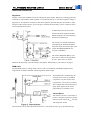
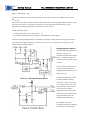
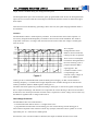
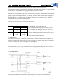
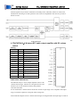
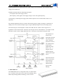
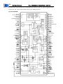
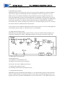
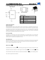
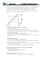
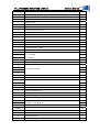
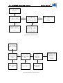
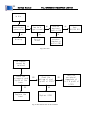
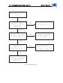
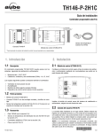
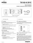
1
TCL OVERSEAS HOLDINGS LIMITED Service Manual 3 SERVICE MANUAL FOR M28 ONE-CHIP CHASSIS PART I. Servicing Precautions When working, the unit is with high voltage about 25KV inside. So, to avoid the risk of electric shock, be careful to adjust the chassis! 1. Only qualified personnel should perform service procedures. 2. All specification must be met over line voltage ranger of 110V AC to 240V AC 50Hz/60Hz. 3. Do not operate in WET/DAMP conditions. 4. Portions of the power supply board are hot ground. The remaining boards are cold ground. 5. Discharge of CRT anode should be done only to CRT ground strap. 6. When fuse blow, ensure to replace a fuse with the same type and specification. 7. Keep the wires away from the components with high temperature or high voltage. 8. When replacing the resister with high power, keep it over the PCB about 10mm. 9. The CRT anode high voltage has been adjusted and set in the factory. When repairing the chassis, do not make the high voltage exceed 27.5KV (The beam current is 0uA). Generally, the high voltage is set on 25.5KV±1.5KV (The beam current is 700uA). * The values of parameters above are for information only. 10. Before return the fixed unit, do check all the covering of wires to ensure that not fold or not short with any metal components. Check the entire protection units, such as control knobs, rear cabinet & front panel, insulation resister & capacitor, mechanical insulators and so on. 11. There are some mechanical and electrical parts associating with safety (EMC) features (Generally related to high voltage or high temperature or electric shock), these features cannot be found out from the outside. When replace these components, perhaps the voltage and power suit the requirements, but efficient X-ray protection may not be provided. All these components are marked with Ì in the schematic diagram. When replace these, you’d better look up the components listed in this manual. If the component you replaced not has the same safety (EMC) performance, harmful X-ray may be produced. 4 Service Manual TCL OVERSEAS HOLDINGS LIMITED PART II -Product Specification 1. 1.1 a. b. Ambient Conditions: Ambient Temperatures: Operating: -10ć ~ +40ć Storage: -15ć ~ +45ć 1.2 Humidity a. Operation: <80% b. Storage: <90% 1.3 Air Pressure: 86kpa ~ 106kpa 2. GENERAL SPECIFICATION 2.1 MPU & Chroma IC: TMPA8803CSN (One-Chip) 2.2 TV Broadcasting System PAL DK/BG SECAM DK/BG NTSC 3.579/4.43 AV MODE 2.3 Scanning Lines & Frequencies 525/625 lines 15.625KHz/15.75KHz 50/60Hz 2.4 Color Sub-Carrier: 4.433MHz/3.579MHz 2.5 IF: Picture 38.9MHz Sound 5.5/6.5MHz 2.6 Power Consumption: 80W 2.7 Power Supply: AC 220V 50Hz±10% 2.8 Audio Output Power (7%THD): 4W + 4W 2.9 Aerial Input Impedance: 75 Unbalanced Din Jack Ant.Input 2.10 Product Safety Requirement: VDE Approval 2.11 Product EMC/EMI Requirement: FTZ Approval 3. Basic Features of Controller 3.1 Channel Tuning Method: Voltage Synthesizer TCL OVERSEAS HOLDINGS LIMITED Service Manual 5 3.2 Presettable Program: 100 Programs 3.3 Tuning for VHF and UHF Bands: Auto/Manual/Fine Tuning 3.4 Picture and Sound Adjustment Bright, Contrast, Color and Volume Control TINT Control (NTSC) Sharpness Control 3.5 OSD General Features (Volume, Brightness, Contrast, Color, Program, Band, Auto Search, Manual, Tune, Muting, AV and Sleep Timer) NICAM and Dual Language German Stereo Indicator 3.6 Sleep Timer: 10-120 Minutes with 10Min.Increment 3.7 Auto Off When No Broadcasting Signal: 15 min 3.8 Full Function Infrared Remote Control 3.9 Remote Effective Distance: 8m 4. Construction of Front Panel Main Power Switch Remote Sensor Standby Indicator Menu Select TV/AV Select Program and Volume Up/Down 5. Construction of Real Panel 75 Aerial Terminal RCA Socket –Audio-R+L In/Out, Video- In/Out Y/U/V Input 6. Other Information 6.1 Colour Temperature: 9300K X=284 Y=299 6.2 Magnetic Field: Bv=0.2~0.5Gs 6 Service Manual PART III. TCL OVERSEAS HOLDINGS LIMITED Brief Introduction on Chassis AV INPUT/ OUTPUT RF IN TUNER SAW NICAM BD AUDIO AMP R/G/B XTAL OSC TMPA8803CPN(M28) CRT DRIVE I2C BUS E2PROM INFRARED REMOTE REMOTE CONTROL CONTROL RECEIVER V OUTPUT DPC H DRIVE H OUTPUT FBT SWITCH POWER MC44608 The TV signal is amplified by the frequency mixing circuit of the tuner. Then the tuner output PIF and SIF signals. The IF signals are amplified about 20dB by the pre IF amplifier (Q101). Having passed 42 , ƻ 41 . The IF signal pass the video the SAW, the IF signals go into the TMP8803CPN from pin ƻ detect circuit to generate CVBS signal. Then the processor deals the signal with luminance and chroma separation. The processor deals the luminance signal with Y-Delay, Y-Gamma correction, Y-hf compensation and black strength, all which ensure that there are enough bandwidth and gain with Y signal, so that the resolution of picture detail is improved and the Y signal is well timed with chroma signal. The processor also deals the chroma signal with chroma sub-carrier recovery, color system recognition and color signal decoding, then outputs B-Y and R-Y color difference signal. A matrix circuit converts the color difference signal (Y, B-Y and R-Y) into primary color signal (R/G/B). On the other hand, the processor separated the horizontal and vertical sync signal from the CVBS signal which was generated by video detect circuit. Having passed the horizontal (or vertical) frequency dividing circuit, the H (or V) OSC signal, which be generated by H-AFC (or V-AFC), is changed to H (or V) drive signal. The H/V drive signal make the horizontal/vertical circuits and scan output circuit to generate H/V saw tooth wave TCL OVERSEAS HOLDINGS LIMITED Service Manual 7 1.Channel Section The RF signal is converted into IF signal by the tuner. Then the IF signal cross the IF amplifier circuit (pre IF amplifier) to get a gain about 15dB. By the coupling capacitance (c110) and the match resistance (R114 56), the input resistance of the pre-IF amplifier match with the tuner. The signals pass a parallel connection circuit with voltage NFB, which combines the advantages of low output impedance, of wide dynamic range and of less components. R116 is a voltage NFB component, which is used to adjust the gain in the pass band. Having been amplified by the IF amplifier, the IF signal pass a SAW, and then come into TMPA8803CSN from pin41 and pin42 with balance. The processor deal the IF signal with IF detection, PLL demodulation, IF AGC, AFC, video peak detection, and color system recognition etc., then output a AGC signal from pin 43 to the tuner to adjust the input amplitude of IF signal. R217, C218 and C219 make up of picture IF PLL circuit, which is used to control IF detection. IC201 output a sound IF signal from pin 31 and a video signal, which will be amplified by Q209, from pin30. The processor output a sound system control signal to Q208. If the processor output a high level from pin59 (sound detection), Q208 is on, and a video signal is separated from the IF signal by a trap. With capacitance coupling, the video signal comes into IC201 from pin26, and then it is selected by inner switches and output from pin45. Having come out, the video signal will be amplified by Q210, and a sync signal will be separated by a sync separate circuit which is made up by C208, Q202 and Q203. Then the video come into inner 870X CPU module from IC201 pin62 to detect whether the signal is live signal. Tuning control and band switch control circuits The processor output a tuning control signal from pin60. The control signal will pass Q103 common emitter amplifying circuit, then an integrating circuit. Finally, it is added to the VT terminal to provide all channels’ tuning voltage for the tuner to stabilize the channels. 2.Vertical Output Section TMPA8803CSN outputs vertical saw-tooth wave from pin 16. It come to pin5 of LA7840 with DC coupling, and is amplified by inner difference amplifier. Pin4 of LA7840 is the same phase input terminal. R307 and R308 are DC offset resistances. C305 is a filter capacitor. In application to M28, pin4 of la7840 is fixed as the DC amplify ref terminal. The amplified saw tooth wave come out la7840 from pin2 and make the deflect coil to generate the deflect current. R314 and C301 filtrate the inductive interference from the horizontal deflect coil. R317 and C309 are used to eliminate spurious oscillation generated by the deflect coil and distributed capacitance resonance. C308, R313, C307 and accessory circuit are in charge of draw AC saw tooth wave out at the deflect coil terminal connected with R315 & R316, and feedback to the input terminal of la7840 (pin5) to correct the linearity of horizontal scan. C306 is a high frequency decoupling capacitor. D301 and C303 make up of a voltage pump up circuit. La7840 output a vertical kickback impulse from pin7 to locate the OSD characters. 3.Horizontal Output Section The processor outputs horizontal drive impulse from pin 13. The drive impulse is done with voltage division by R238 and R401, and then comes to the base of the drive triode (Q401). C401 is used to eliminate the noise in the H drive impulse. T401 is a horizontal drive transformer. Q402 is a horizontal output triode with a damper inside. L402 is connected with the emitter of the horizontal output diode to eliminate the radiation and to improve the distortions at the cross of vertical and horizontal white 8 Service Manual TCL OVERSEAS HOLDINGS LIMITED lines. C406 and C402 are retrace capacitors and C421 is an s-correct capacitor. L441 and L442 are horizontal linear inductors. R441 is used to eliminate the parasitic oscillation caused by horizontal linear inductors. C420, R413 and D411 are used to correct the M-distortion in horizontal direction. C422, R415 and R415A are coupling components for the horizontal retrace impulse, which are feed back to pin 12 of TMPA8803CSN. D404 is a negative peak-killer diode. Horizontal scanning distortion and the method to compensate it The deflect coil and the horizontal output triode have some resistance R while they are ducting. The resistance R will cause the non-linear distortion, which means that the right direction scanning speed of the electron beam becomes slower, and the right of the raster is compressed to generate distortion. We use a horizontal linear adjuster to compensate this kind of distortion. We use L412 and L411 as the H linear adjusters in H scanning section of M28 chassis. R411, which is parallel connected with L411 and L412, is a despiking resistance for preventing the oscillation by compensating inductor and the stray capacitance. The linear adjuster is a transductor coil with a magnetic core inside. If the current, which pass the linear adjuster coil, increase to a certain value, the magnetic core becomes saturated to decrease the inductance of the linear adjustment inductor. If the +B is steady, the increase speed of Iy is faster to compensate the reducing of deflecting current by the resistance R mention above. We can adjust the magnetic core to chang the inductance of the linear compensate inductor to adjust the H linearity. The EHT generation circuit The FBT supply the anode high voltage, focus voltage and screen voltage for M28 chassis. D401 and C408 are in charge of regulating the primary impulse of the transformer to output a voltage of 190V for the video amplifiers. The ( 10 ) ~ ( 8 ) coils of the FBT supply the heater with power. Having passed the divider and clipping circuits, which are maded up by R415, R415A, C422 and D404, the H retrace impulses getting out from ( 3 ) ~ ( 10 ) coils are inputed to pin12 of TMPA8803CSN to generate sand castle impulse. To limit the beam current in a safe range, we add a ABL circuit in M28 chassis. We add two sampling resistances (R414, R415) between +24V power supply and pin7 of the FBT. The voltage at the joint of the two resistances is feed back to pin27 of TMPA8803CSN to control bright and contrast to limit the beam current. It is also in charge of regulating EHT. C410 is a fliter capacitor for ABL voltage. The impulses, which are induced by secondary coil 5, are changed to 12V once passed the regulating and fliting circuit made up by D402 and C413. IC401 change 12V power supply to 9V for many circuits, such as R/G/B output circuit of TMPA8803CSN, IC4053, pre IF-amplifier circuit, bright dots killer circuit and S terminal circuit. IC402 outputs a 5V power supply for the keyboard circuit. C418, C417, C423 and C425 are fliter capacitors. D402 and C413 are incharge of regulating and flitering for the output of coil6 to supply the V scanning output section with 24V power. The 24V is added to the upper terminal of the V deflecting yoke as the DC bias for the movement of V center. Extension distortion and compensation This kind of distortion is mainly caused by the structure of CRT. Due to the srcreen of SF CRT is not a ture flat screen, the distances from the deflecting center to the screen are not the same. The scanning speed of the electron beam is uniform. If the electron beam scannning the screen equally with the TCL OVERSEAS HOLDINGS LIMITED Service Manual 9 effect of ture linear sawtooth current, the E-W sides of the picture are stretched. That is the extension distortion. Usually, we add a S-correct capacitor in series with the deflecting coil to compensate this kind of distortion. The integral character of S-correct capacitor make the current waveform S shape. So the scanning speed of electron beam at the center of screen is faster than the one at the side. So this action can correct the extension distortion. C421 is a S-correct capacitor. The capacitance is inverse ratio with the correcting effect. 10 Service Manual PART IV. TCL OVERSEAS HOLDINGS LIMITED IC Pin Description 1. MC44608-High Voltage PWM Controller Pin 1 2 3 Name Description Demag The Demag pin offers 3 different functions: Zero voltage crossing detection (50mV), 24ǂA current detection and 120ǂA current detection. The 24ǂA level is used to detect the secondary reconfiguration status and the 120ǂA level to detect an Over Voltage status called Quick OVP. Isense Control Input The Current Sense pin senses the voltage developed on the series resistor inserted in the source of the power MOSFET. When Isense reaches 1V, the Driver output (pin 5) is disabled. This is known as the Over Current Protection function. A 200ǂA current source is flowing out of the pin 3 during the start–up phase and during the switching phase in case of the Pulsed Mode of operation. A resistor can be inserted between the sense resistor and the pin 3, thus a programmable peak current detection can be performed during the SMPS stand–by mode. A feedback current from the secondary side of the SMPS via the opto–coupler is injected into this pin. A resistor can be connected between this pin and GND to allow the programming of the Burst duty cycle during the Stand–by mode. 4 Ground This pin is the ground of the primary side of the SMPS. 5 Driver The current and slew rate capability of this pin are suited to drive Power MOSFETs. 6 VCC This pin is the positive supply of the IC. The driver output gets disabled when the voltage becomes higher than 15V and the operating range is between 6.6V and 13V. An intermediate voltage level of 10V creates a disabling condition called Latched Off phase. 7 This pin is to provide isolation between the Vi pin 8 and the VCC pin 6. 8 This pin can be directly connected to a 500V voltage source for start–up function of the IC. During the Start–up phase a 9 mA current source is internally delivered to the VCC pin 6 allowing a rapid charge of the VCC capacitor. As soon as the IC starts–up, this current source is disabled. Vi TCL OVERSEAS HOLDINGS LIMITED Service Manual11 OPERATING DESCRIPTION Regulation The pin 3 senses the feedback current provided by the opto-coupler. During the switching phase the switch S2 is closed and the shunt regulator is accessible by the pin 3. The shunt regulator voltage is typically 5V. The dynamic resistance of the shunt regulator represented by the zener diode is 20:. The gain of the Control input is given on Figure 10 which shows the duty cycle as a function of the current injected into the pin 3. A 4KHz filter network is inserted between the shunt regulator and the PWM comparator to cancel the high frequency residual noise. The switch S3 is closed in Stand–by mode during the Latched Off Phase while the switch S2 remains open. (See section PULSED MODE DUTY CYCLE CONTROL). The resistor Rdpulsed (Rduty cycle burst) has no effect on the regulation process. This resistor is used to determine the burst duty cycle described in the chapter “Pulsed Duty Cycle Control” on page 8. PWM Latch The MC44608 works in voltage mode. The on–time is controlled by the PWM comparator that compares the oscillator sawtooth with the regulation block output. The PWM latch is initialized by the oscillator and is reset by the PWM comparator or by the current sense comparator in case of an over current. This configuration ensures that only a single pulse appears at the circuit output during an oscillator cycle. Current Sense The inductor current is converted to a positive voltage by inserting a ground reference sense resistor RSense in series with the power switch. The maximum current sense threshold is fixed at 1V. The peak current is given by the following 12 Service Manual TCL OVERSEAS HOLDINGS LIMITED equation: Ipkmax = 1/Rsense(:) (A) In stand–by mode, this current can be lowered as due to the activation of a 200PA current source: IpkMAX-STBY The current sense input consists of a filter (6k:, 4pF) and of a leading edge blanking. Thanks to that, this pin is not sensitive to the power switch turn on noise and spikes and practically in most applications, no filtering network is required to sense the current. Finally, this pin is used: – as a protection against over currents (Isense > I) – as a reduction of the peak current during a Pulsed Mode switching phase. The overcurrent propagation delay is reduced by producing a sharp output turn off (high slew rate). This results in an abrupt output turn off in the event of an over current and in the majority of the pulsed mode switching sequence. Demagnetization Section The MC44608 demagnetization detection consists of a comparator designed to compare the VCC winding voltage to a reference that is typically equal to 50mV. This reference is chosen low to increase effectiveness of the demagnetization detection even during start–up. A latch is incorporated to turn the demagnetization block output into a low level as soon as a voltage less than 50 mV is detected, and to keep it in this state until a new pulse is generated on the output. This avoids any ringing on the input signal which may alter the demagnetization detection. For a higher safety, the demagnetization block output is also directly connected to the TCL OVERSEAS HOLDINGS LIMITED Service Manual13 output, which is disabled during the demagnetization phase. The demagnetization pin is also used for the quick, programmable OVP. In fact, the demagnetization input current is sensed so that the circuit output is latched off when this current is detected as higher than 120PA. This function can be inhibited by grounding it but in this case, the quick and programmable OVP is also disabled. Oscillator The MC44608 contains a fixed frequency oscillator. It is built around a fixed value capacitor CT succesively charged and discharged by two distinct current sources ICH and IDCH. The window comparator senses the CT voltage value and activates the sources when the voltage is reaching the 2.4V/4V levels. The complete demagnetization status DMG is used to inhibit the recharge of the CT capacitor. Thus in case of incomplete transformer demagnetization the next switching cycle is postpone until the DMG signal appears. The oscillator remains at 2.4V corresponding to the sawtooth valley voltage. In this way the SMPS is working in the so called SOPS mode (Self Oscillating Power Supply). In that case the effective switching frequency is variable and no longer depends on the oscillator timing but on the external working conditions (Refer to DMG signal in the Figure 5). The OSC and Clock signals are provided according to the Figure 5. The Clock signals correspond to the CT capacitor discharge. The bottom curve represents the current flowing in the sense resistor Rcs. It starts from zero and stops when the sawtooth value is equal to the control voltage Vcont. In this way the SMPS is regulated with a voltage mode control. Overvoltage Protection The MC44608 offers two OVP functions: – a fixed function that detects when VCC is higher than 15.4V – a programmable function that uses the demag pin. The current flowing into the demag pin is mirrored and compared to the reference current Iovp (120PA). Thus this OVP is quicker as it is not impacted by the VCC inertia and is called QOVP. In both cases, once an OVP condition is detected, the output is latched off until a new circuit 14 Service Manual TCL OVERSEAS HOLDINGS LIMITED START–UP. Start–up Management The Vi pin 8 is directly connected to the HV DC rail Vin. This high voltage current source is internally connected to the VCC pin and thus is used to charge the VCC capacitor. The VCC capacitor charge period corresponds to the Start–up phase. When the VCC voltage reaches 13V, the high voltage 9mA current source is disabled and the device starts working. The device enters into the switching phase. It is to be noticed that the maximum rating of the Vi pin 8 is 700V. ESD protection circuitry is not currently added to this pin due to size limitations and technology constraints. Protection is limited by the drain–substrate junction in avalanche breakdown. To help increase the application safety against high voltage spike on that pin it is possible to insert a small wattage 1k: series resistor between the Vin rail and pin 8. The Figure 6 shows the VCC voltage evolution in case of no external current source providing current into the VCC pin during the switching phase. This case can be encountered in SMPS when the self supply through an auxiliary winding is not present (strong overload on the SMPS output for example). The Figure 16 also depicts this working configuration. In case of the hiccup mode, the duty cycle of the switching phase is in the range of 10%. Mode Transition The LW latch Figure 7 is the memory of the working status at the end of every switching sequence. Two different cases must be considered for the logic at the termination of the SWITCHING PHASE: 1. No Over Current was observed TCL OVERSEAS HOLDINGS LIMITED Service Manual15 2. An Over Current was observed These 2 cases are corresponding to the signal labeled NOC in case of “No Over Current” and “OC” in case of Over Current. So the effective working status at the end of the ON time memorized in LW corresponds to Q=1 for no over current and Q=0 for over current. This sequence is repeated during the Switching phase. Several events can occur: 1. SMPS switch OFF 2. SMPS output overload 3. Transition from Normal to Pulsed Mode 4. Transition from Pulsed Mode to Normal Mode 1. SMPS SWITCH OFF When the mains is switched OFF, so long as the bulk electrolithic bulk capacitor provides energy to the SMPS, the controller remains in the switching phase. Then the peak current reaches its maximum peak value, the switching frequency decreases and all the secondary voltages are reduced. The VCC voltage is also reduced. When VCC is equal to 10V, the SMPS stops working. 2. Overload In the hiccup mode the 3 distinct phases are described as follows (refer to Figure 6): The SWITCHING PHASE: The SMPS output is low and the regulation block reacts by increasing the ON time (dmax = 80%). The OC is reached at the end of every switching cycle. The LW latch (Figure 7) is reset before the VPWM signal appears. The SMPS output voltage is low. The VCC voltage cannot be maintained at a normal level as the auxiliary winding provides a voltage which is also reduced in a ratio similar to the one on the output (i.e. Vout nominal / Vout short–circuit). Consequently the VCC voltage is reduced at an operating rate given by the combination VCC capacitor value together with the ICC working consumption (3.2mA) according to the equation 2. When VCC crosses 10V the WORKING PHASE gets terminated. The LW latch remains in the reset status. The LATCHED–OFF PHASE: The VCC capacitor voltage continues to drop. When it reaches 6.5V this phase is terminated. Its duration is governed by equation 3. The START–UP PHASE is reinitiated. The high voltage start–up current source (–ICC1 = 9mA) is activated and the MODE latch is reset. The VCC voltage ramps up according to the equation 1. When it reaches 13V, the IC enters into the SWITCHING PHASE. The NEXT SWITCHING PHASE: The high voltage current source is inhibited, the MODE latch (Q=0) activates the NORMAL mode of operation. Figure 2 shows that no current is injected out pin 2. The over current sense level corresponds to 1V. As long as the overload is present, this sequence repeats. The SWITCHING PHASE duty cycle is in the range of 10%. 16 Service Manual TCL OVERSEAS HOLDINGS LIMITED 3. Transition from Normal to Pulsed Mode In this sequence the secondary side is reconfigured (refer to the typical application schematic on page 13). The high voltage output value becomes lower than the NORMAL mode regulated value. The TL431 shunt regulator is fully OFF. In the SMPS stand–by mode all the SMPS outputs are lowered except for the low voltage output that supply the wake–up circuit located at the isolated side of the power supply. In that mode the secondary regulation is performed by the zener diode connected in parallel to the TL431. The secondary reconfiguration status can be detected on the SMPS primary side by measuring the voltage level present on the auxiliary winding Laux. (Refer to the Demagnetization Section). In the reconfigured status, the Laux voltage is also reduced. The VCC self–powering is no longer possible thus the SMPS enters in a hiccup mode similar to the one described under the Overload condition. In the SMPS stand–by mode the 3 distinct phases are: The SWITCHING PHASE: Similar to the Overload mode. The current sense clamping level is reduced according to the equation of the current sense section, page 5. The C.S. clamping level depends on the power to be delivered to the load during the SMPS stand–by mode. Every switching sequence ON/OFF is terminated by an OC as long as the secondary Zener diode voltage has not been reached. When the Zener voltage is reached the ON cycle is terminated by a true PWM action. The proper SWITCHING PHASE termination must correspond to a NOC condition. The LW latch stores this NOC status. The LATCHED OFF PHASE: The MODE latch is set. The START–UP PHASE is similar to the Overload Mode. The MODE latch remains in its set status (Q=1). The SWITCHING PHASE: The Stand–by signal is validated and the 200PA is sourced out of the Current Sense pin 2. 4. Transition from Stand–by to Normal The secondary reconfiguration is removed. The regulation on the low voltage secondary rail can no longer be achieved, thus at the end of the SWITCHING PHASE, no PWM condition can be encountered. The LW latch is reset. At the next WORKING PHASE a NORMAL mode status takes place. In order to become independent of the recovery time SWITCHING PHASE constant on the secondary side of the SMPS an additional reset input R2 is provided on the MODE latch. The condition Idemag<24PA corresponds to the activation of the secondary reconfiguration status. The R2 reset insures a return into the NORMAL mode following the first corresponds to 1V. START–UP PHASE. Pulsed Mode Duty Cycle Control During the sleep mode of the SMPS the switch S3 is closed and the control input pin 3 is connected to TCL OVERSEAS HOLDINGS LIMITED Service Manual17 a 4.6V voltage source thru a 500: resistor. The discharge rate of the VCC capacitor is given by ICC–latch (device consumption during the LATCHED OFF phase) in addition to the current drawn out of the pin 3. Connecting a resistor between the Pin 3 and GND (RDPULSED) a programmable current is drawn from the VCC through pin 3. The duration of the LATCHED OFF phase is impacted by the presence of the resistor RDPULSED. The equation 3 shows the relation to the pin 3 current. Pulsed Mode Phases Equations 1 through 8 define and predict the effective behavior during the PULSED MODE operation. The equations 6, 7, and 8 contain K, Y, and D factors. These factors are combinations of measured parameters. They appear in the parameter section “K factors for pulsed mode operation” page 4. In equations 3 through 8 the pin 3 current is the current defined in the above section “Pulsed Mode Duty Cycle Control”. 2. TDA9801-Single standard VIF-PLL demodulator and FM-PLL detector FUNCTIONAL DESCRIPTION 18 Service Manual TCL OVERSEAS HOLDINGS LIMITED SYMBOL PIN DESCRIPTION VIF1 1 VIF differential input 1 VIF2 2 VIF differential input 2 TOP 3 tuner AGC TakeOver Point (TOP) connection ADJ 4 phase adjust connection MUTE 5 sound mute switch connection TPLL 6 PLL time constant connection CVBS 7 CVBS (positive) video output n.c. 8 not connected AF 9 AF output DAF 10 AF amplifier decoupling capacitor connection SI 11 sound intercarrier input TAGC 12 tuner AGC output VSO 13 video and sound intercarrier output VI 14 buffer amplifier video input AFC 15 AFC output VCO1 16 VCO1 reference circuit for 2fPC VCO2 17 VCO2 reference circuit for 2fPC GND 18 ground supply (0 V) AGC 19 AGC detector capacitor connection VP 20 supply voltage (+5 V) Stage IF amplifier The VIF amplifier consists of three AC-coupled differential amplifier stages. Each differential stage comprises a feedback network controlled by emitter degeneration. AGC detector, IF AGC and tuner AGC The automatic control voltage to maintain the video output signal at a constant level is generated in accordance with the transmission standard. Since the TDA9801 is suitable for negative modulation only the peak sync pulse level is detected. The AGC detector charges and discharges capacitor CAGC to set the IF amplifier and tuner gain. The voltage on capacitor CAGC is transferred to an internal IF control signal, and is fed to the tuner AGC to generate the tuner AGC output current on pin TAGC (open-collector output). The tuner AGC takeover point level is set at pin TOP. This allows the tuner to be matched to the SAW filter in order to achieve the optimum IF input level. Frequency detector and phase detector The VIF amplifier output signal is fed into a frequency detector and into a phase detector. During acquisition the frequency detector produces a DC current proportional to the frequency difference between the input and the VCO signal. After frequency lock-in the phase detector produces a DC current proportional to the phase difference between the VCO and the input signal. The DC current of TCL OVERSEAS HOLDINGS LIMITED Service Manual19 either frequency detector or phase detector is converted into a DC voltage via the loop filter which controls the VCO frequency. Video demodulator The true synchronous video demodulator is realized by a linear multiplier which is designed for low distortion and wide bandwidth. The vision IF input signal is multiplied with the ‘in phase’ component of the VCO output. The demodulator output signal is fed via an integrated low-pass filter (fg = 12 MHz) for suppression of the carrier harmonics to the video amplifier. VCO, AFC detector and travelling wave divider The VCO operates with a symmetrically connected reference LC circuit, operating at the double vision carrier frequency. Frequency control is performed by an internal variable capacitor diode. The voltage to set the VCO frequency to the actual double vision carrier frequency is also amplified and converted for the AFC output current. The VCO signal is divided-by-2 with a Travelling Wave Divider (TWD) which generates two differential output signals with a 90 degree phase difference independent of the frequency. Video amplifier The composite video amplifier is a wide bandwidth operational amplifier with internal feedback. A nominal positive video signal of 1 V (p-p) is present at pin VSO. Buffer amplifier and noise clipper The input impedance of the 7 dB wideband CVBS buffer amplifier (with internal feedback) is suitable for ceramic sound trap filters. Pin CVBS provides a positive video signal of 2 V (p-p). Noise clipping is provided internally. Sound demodulation LIMITER AMPLIFIER The FM sound intercarrier signal is fed to pin SI and through a limiter amplifier before it is demodulated. The result is high sensitivity and AM suppression. The limiter amplifier consists of 7 stages which areinternally AC-coupled in order to minimizing the DC offset. FM-PLL DETECTOR The FM-PLL demodulator consists of an RC oscillator, loop filter and phase detector. The oscillator frequency is locked on the FM intercarrier signal from the limiter amplifier. As a result of this locking, the RC oscillator is frequency modulated. The modulating voltage (AF signal) is used to control the oscillator frequency. By this, the FM-PLL operates as an FM demodulator. AF AMPLIFIER The audio frequency amplifier with internal feedback is designed for high gain and high common-mode rejection. The low-level AF signal output from the FM-PLL demodulator is amplified and buffered in a low-ohmic audio output stage. An external decoupling capacitor CDAF removes the 20 Service Manual TCL OVERSEAS HOLDINGS LIMITED DC voltage from the audio amplifier input. By using the sound mute switch (pin MUTE) the AF amplifier is set in the mute state. 3. TDA9874A Digital TV sound demodulator/decoder SYMBOL PIN DESCRIPTION EXTIR 1 external audio input right channel EXTIL 2 external audio input left channel Vref2 3 analog reference voltage for DAC and operational amplifiers P2 4 second general purpose I/O pin OUTM 5 analog output mono VSSA4 6 analog ground supply 4 for analog back-end circuitry OUTL 7 analog output left OUTR 8 analog output right VDDA1 9 analog supply voltage 1; back-end circuitry 5 V VSSA1 10 analog ground supply 1; back-end circuitry VSSD1 11 digital ground supply 1; core circuitry VDDD1 12 digital supply voltage 1; core voltage regulator circuitry VSSD2 13 digital ground supply 2; core circuitry TP2 14 additional test pin 2; connected to VSSD for normal operation NICAM 15 serial NICAM data output (at 728 kHz) TP1 16 additional test pin 1; connected to VSSD for normal operation PCLK 17 NICAM clock output (at 728 kHz) ADDR1 18 first I2C-bus slave address modifier input XTALO 19 crystal oscillator output XTALI 20 crystal oscillator input TEST2 21 test pin 2; connected to VSSD for normal operation Iref 22 resistor for reference current generation; front-end circuitry ADDR2 23 second I2C-bus slave address modifier input VSSA2 24 analog ground supply 2; analog front-end circuitry VDEC 25 analog front-end circuitry supply voltage decoupling TEST1 26 test pin 1; connected to VSSD for normal operation SIF2 27 sound IF input 2 Vref1 28 reference voltage; for analog front-end circuitry SIF1 29 sound IF input 1 CRESET 30 capacitor for Power-on reset VSSA3 31 digital ground supply 3; front-end circuitry VDDA3 32 analog front-end circuitry regulator supply voltage 3 (5 V) SCL 33 I2C-bus serial clock input SDA 34 I2C-bus serial data input/output SDO 35 I2S-bus serial data output WS 36 I2S-bus word select input/output SCK 37 I2S-bus clock input/output TCL OVERSEAS HOLDINGS LIMITED SYSCLK 38 system clock output VDDD3 39 digital supply voltage 3; digital I/O pads VSSD3 40 digital ground supply 3; digital I/O pads P1 41 first general purpose I/O pin MONOIN 42 analog mono input Service Manual21 FUNCTIONAL DESCRIPTION Description of the demodulator and decoder section 1. SIF INPUTS Two inputs are provided, pin SIF1 and pin SIF2. For higher SIF signal levels the SIF input can be attenuated with an internal switchable ҟ10 dB resistor divider. As no specific filters are integrated, both inputs have the same specification giving flexibility in application. The selected signal is passed through an AGC circuit and then digitized by an 8-bit ADC operating at 24.576 MHz. 2. AGC The gain of the AGC amplifier is controlled from the ADC output by means of a digital control loop employing hysteresis. The AGC has a fast attack behaviour to prevent ADC overloads, and a slow decay behaviour to prevent AGC oscillations. For AM demodulation the AGC must be switched off. When switched off, the control loop is reset and fixed gain settings can be chosen. The AGC can be controlled via the I2C-bus. 3. MIXER The digitized input signal is fed to the mixers, which mix one or both input sound carriers down to zero IF. A 24-bit control word for each carrier sets the required frequency. Access to the mixer 2 control word registers is via the I C-bus or via Easy Standard Programming (ESP). When receiving NICAM programs, a feedback signal is added to the control word of the second carrier mixer to establish a carrier-frequency loop. 4. FM AND AM DEMODULATION An FM or AM input signal is fed through a switchable band-limiting filter into a demodulator that can be used for either FM or AM demodulation. Apart from the standard (fixed) de-emphasis characteristic, an adaptive de-emphasis is available for Wegener-Panda 1 encoded satellite programs. 5. FM DECODING A 2-carrier stereo decoder recovers the left and right signal channels from the demodulated sound carriers. Both the European and Korean stereo systems are supported. Automatic FM dematrixing is also supported, which means that the FM sound mode identification 22 Service Manual TCL OVERSEAS HOLDINGS LIMITED (mono, stereo or dual) switches the FM dematrix directly. No loop via the microcontroller is needed. For highly overmodulated signals, a high deviation mode for monaural audio sound single carrier demodulation can be selected. NICAM decoding is still possible in high deviation mode. 6. FM IDENTIFICATION The identification of the FM sound mode is performed by AM synchronous demodulation of the pilot and narrow-band detection of the identification frequencies. The result is available via the I2C-bus interface. A selection can be made via the I2C-bus for B/G, D/K and M standards, and for three different time constants that represent different trade-offs between speed and reliability of identification. A pilot detector allows the control software to identify an analog 2-carrier (A2) transmission within approximately 0.1 s. TCL OVERSEAS HOLDINGS LIMITED Service Manual23 Automatic FM dematrixing, depending on the identification, is possible. 7. NICAM DEMODULATION The NICAM signal is transmitted in a DQPSK code at a bit rate of 728 kbits/s. The NICAM demodulator performs DQPSK demodulation and passes the resulting bitstream and clock signal to the NICAM decoder and, for evaluation purposes, to various pins. A timing loop controls the frequency of the crystal oscillator to lock the sampling instants to the symbol timing of the NICAM data. 8. NICAM DECODING The device performs all decoding functions in accordance with the “EBU NICAM 728 specification”. After locking to the frame alignment word, the data is descrambled by applying the defined pseudo-random binary sequence. The device then synchronizes to the periodic frame flag bit C0. The status of the NICAM decoder can be read out from the NICAM status register by the user. The OSB bit indicates that the decoder has locked to the NICAM data. The VDSP bit indicates that the decoder has locked to the NICAM data and that the data is valid sound data. The C4 bit indicates that the sound conveyed by the FM mono channel is identical to the sound conveyed by the NICAM channel. The error byte contains the number of sound sample errors (resulting from parity checking) that occurred in the past 128 ms period. The Bit Error Rate (BER) can be calculated using the following equation: BER = bit errors / total bits §error byte h 1.74 hҏ10-5 9. NICAM AUTO-MUTE This function is enabled by setting bit AMUTE to logic 0. Upper and lower error limits may be defined by writing appropriate values to two registers in the I2C-bus section. When the number of errors in a 128 ms period exceeds the upper error limit, the auto-mute function will switch the output sound from NICAM to whatever sound is on the first sound carrier (FM or AM) or to the analog mono input. When the error count is smaller than the lower error limit, the NICAM sound is restored. The auto-mute function can be disabled by setting bit AMUTE to logic 1. In this case clicks become audible when the error count increases. The user will hear a signal of degrading quality. If no NICAM sound is received, the outputs are switched from the NICAM channel to the 1st sound carrier. A decision to enable or disable the auto-mute is taken by the microprocessor based on an interpretation of the application control bits C1, C2, C3 and C4, and possibly any additional strategy implemented by the user in the microcontroller software. When the AM sound in NICAM L systems is demodulated in the 1st sound IF and the audio signal connected to the mono input of the TDA9874A, the controlling microprocessor has to ensure switching from NICAM reception to mono input, if auto-muting is desired. This can be achieved by 24 Service Manual TCL OVERSEAS HOLDINGS LIMITED setting bit AMSEL = 1 and bit AMUTE = 0. 10. CRYSTAL OSCILLATOR The digital controlled crystal oscillator (DCXO) is fully integrated. Only an external 24.576 MHz crystal is required. 11. TEST PINS All test pins are active HIGH. In normal operation of the device they can be left open-circuit, as they have internal pull-down resistors. Test functions are for manufacturing tests only and are not available to customers. 12. POWER FAIL DETECTOR The power fail detector monitors the internal power supply for the digital part of the device. If the supply has temporarily been lower than the specified lower limit, the power failure register bit PFR in subaddress 0, will be set to logic 1. Bit CLRPFR, slave register subaddress 1, resets the Power-on reset flip-flop to logic 0. If this is detected, an initialization of the TDA9874A has to be performed to ensure reliable operation. 13. POWER-ON RESET The reset is active LOW. In order to perform a reset at power-up, a simple RC circuit may be used which consists of an integrated passive pull-up resistor and an external capacitor connected to ground. The pull-up resistor has a nominal value of 50 kǂ, which can easily be measured between pins CRESET and VDDD3. Before the supply voltage has reached a certain minimum level, the state of the circuit is completely undefined and remains in this undefined state until a reset is applied. The reset is guaranteed to be active when: ǂҏThe power supply is within the specified limits (4.5 to 5.5 V) ǂҏThe crystal oscillator (DCXO) is functioning ǂҏThe voltage at pin CRESET is below 0.3VDDD (1.5 V if VDDD = 5.0 V, typically below 1.8 V). The required capacitor value depends on the gradient of the rising power supply voltage. The time constant of the RC circuit should be clearly larger than the rise time of the power supply (to make sure that the reset condition is always satisfied), even when considering tolerance spreading. To avoid problems with a too slow discharging of the capacitor at power-down, it may be helpful to add a diode from pin CRESET to VDDD. It should be noted that the internal ESD protection diode does not help here as it only conducts at higher voltages. Under difficult power supply conditions (e.g. very slow or non-monotonic ramp-up), it is recommended to drive the reset line from a microcontroller port or the like. TCL OVERSEAS HOLDINGS LIMITED Service Manual25 Description of the DSP 1. LEVEL SCALING All input channels to the digital crossbar switch are equipped with a level adjustment facility to change the signal level in a range of ǂ15 dB. Adjusting the signal level is intended to compensate for the different modulation parameters of the various TV standards. Under nominal conditions it is recommended to scale all input channels to be 15 dB below full-scale. This will create sufficient headroom to cope with overmodulation and avoids changes of the volume impression when switching from FM to NICAM or vice versa. 2. NICAM PATH The NICAM path has a switchable J17 de-emphasis. 3. NICAM AUTO-MUTE If NICAM is received, the auto-mute is enabled and the signal quality becomes poor. The digital crossbar switches automatically to FM, channel 1 or the analog mono input, as selected by bit AMSEL. This automatic switching depends on the NICAM bit error rate. The auto-mute function can be disabled via the I2C-bus. 4. FM (AM) PATH A high-pass filter suppresses DC offsets from the FM demodulator that may occur due to carrier frequency offsets, and supplies the FM monitor function with DC values, e.g. for the purpose of microprocessor controlled carrier search or fine tuning functions. An adaptive de-emphasis is available for Wegener-Panda 1 encoded satellite programs. The de-emphasis stage offers a choice of settings for the supported TV standards. The 2-channel decoder performs the dematrixing of ½(L + R), R to L and R signals of ½ (L + R) and ½(L ҟҏR) to L and R signals or of channel 1 and channel 2 to L and R signals, as demanded by the different TV standards or user preferences. Automatic FM dematrixing is also supported. 26 Service Manual TCL OVERSEAS HOLDINGS LIMITED Using the high deviation mode, only channel 1 (mono) can be demodulated. The scaling is ҟ6 dB compared to 2-channel decoding. 5. MONITOR This function provides data words from the FM demodulator outputs and FM and NICAM signals for external use, such as carrier search or fine tuning. The peak level of these signals can also be observed. Source selection and data read out are performed via the I2C-bus. 6. DIGITAL CROSSBAR SWITCH The input channels are derived from the FM and NICAM paths, while the output channels comprise I2S-bus and the audio DACs to the analog crossbar switch. It should be noted that there is no connection from the external analog audio inputs to the digital crossbar switch. 7. DIGITAL AUDIO OUTPUT The digital audio output interface comprises an I2S-bus output port and a system clock output. The I2S-bus port is equipped with a level adjustment facility that can change the signal level in a ǂ15 dB range in 1 dB steps. Muting is possible, too, and outputs can be disabled to improve EMC performance. The I2S-bus output matrix provides the functions for forced mono, stereo, channel swap, channel 1 or channel 2. Automatic selection for TV applications is possible. In this case the microcontroller program only has to provide a user controlled sound A or sound B selection. 8. STEREO CHANNEL TO THE ANALOG CROSSBAR PATH A level adjustment function is provided with control positions of 0 dB, +3 dB, +6 dB and +9 dB in combination with the audio DACs. The Automatic Volume Level (AVL) function provides a constant output level of ҟ20 dB (full-scale) for input levels between 0 dB (full-scale) and ҟ26 dB (full-scale). There are some fixed decay time constants to choose from, i.e. 2, 4 or 8 seconds. Automatic selection for TV applications is possible. In this case the microcontroller program only has to provide a user controlled sound A or sound B selection. 9. GENERAL The level adjustment functions can provide signal gain at multiple locations. Great care has to be taken when using gain with large input signals, e.g., due to overmodulation, in order not to exceed the maximum possible signal swing, which would cause severe signal distortion. The nominal signal level of the various signal sources to the digital crossbar switch should be 15 dB below digital full-scale (ҟ15 dB full-scale). Description of the analog audio section 1. ANALOG CROSSBAR SWITCH AND ANALOG MATRIX The TDA9874A has one external analog stereo input, one mono input, one 2-channel and one single-channel output port. Analog source selector switches are employed to provide the desired TCL OVERSEAS HOLDINGS LIMITED Service Manual27 analog signal routing capability, which is done by the analog crossbar switch section. The basic signal routing philosophy of the TDA9874A is that each switch handles two signal channels at the same time (e.g. left and right, language A and B) directly at the source. Each source selector switch is followed by an analog matrix to perform further selection tasks, such as putting a signal from one input channel, say language A, to both output channels or for swapping left and right channels. The analog matrix provides the functions given in the follow table. Automatic matrixing for TV applications is also supported. All switches and matrices are controlled via the I2C-bus. Analog matrix functions MODE MATRIX OUTPUT L OUTPUT R OUTPUT 1 L input R input 2 R input L input 3 L input L input 4 R input R input 2. EXTERNAL AND MONO INPUTS The external and mono inputs accept signal levels of up to 1.4 V (RMS). By adding external series resistors to provide suitable attenuation, the external input could be used as a SCART input. Whenever the external or mono input is selected, the output of the DAC is muted to improve the crosstalk performance. 3. AUDIO DACS The TDA9874A comprises a 2-channel audio DAC and an additional single-channel audio DAC for feeding signals from the DSP section to the analog crossbar switch. These DACs have a resolution of 15 bits and employ four-times oversampling and noise shaping. 4. AUDIO OUTPUT BUFFERS The output buffers provide a gain of 0 dB and offer a muting possibility. The post filter capacitors of the audio DACs are connected to the buffer outputs. 5. STANDBY MODE Switch diagram for the analog audio section The standby mode disables most functions and reduces power dissipation of the TDA9874A. It 28 Service Manual TCL OVERSEAS HOLDINGS LIMITED provides no other function. Internal registers may lose their information in standby mode. Therefore, the device needs to be initialized on returning to normal operation. This can be accomplished in the same way as after a Power-on reset. Audio signal flow. 4. TDA7057AQ 2u8 W stereo BTL audio output amplifier with DC volume control Pinning SYMBOL PIN DESCRIPTION VC1 1 DC volume control 1 n.c. 2 not connected Vl (1) 3 voltage input 1 VP 4 positive supply voltage Vl (2) 5 voltage input 2 SGND 6 signal ground VC2 7 DC volume control 2 OUT2+ 8 positive output 2 PGND2 9 power ground 2 OUT2ҟ 10 negative output 2 OUT1ҟ 11 negative output 1 PGND1 12 power ground 1 OUT1ҙ 13 positive output 1 FUNCTIONAL DESCRIPTION The TDA7057AQ is a stereo output amplifier with two DC volume control stages. The device is designed for TVs and monitors, but is also suitable for battery-fed portable recorders and radios. In conventional DC volume control circuits the control or input stage is AC-coupled to the output stage via external capacitors to keep the offset voltage low. In the TDA7057AQ the two DC volume control stages are integrated into the input stages so that no TCL OVERSEAS HOLDINGS LIMITED Service Manual29 coupling capacitors are required and a low offset voltage is still maintained. The minimum supply voltage also remains low. The BTL principle offers the following advantages: ǂҏLower peak value of the supply current ǂҏThe frequency of the ripple on the supply voltage is twice the signal frequency. Consequently, a reduced power supply with smaller capacitors can be used which results in cost reductions. For portable applications there is a trend to decrease the supply voltage, resulting in a reduction of output power at conventional output stages. Using the BTL principle increases the output power. The maximum gain of the amplifier is fixed at 40.5 dB. The DC volume control stages have a logarithmic control characteristic. Therefore, the total gain can be controlled from +40.5 dB to ҟ33 dB. If the DC volume control voltage falls below 0.4 V, the device will switch to the mute mode. The amplifier is a short-circuit protected to ground, VP and across the load. A thermal protection circuit is also implemented. If the crystal temperature rises above +150 ǂC the gain will be reduced, thereby reducing the output power. Special attention is given to switch-on and switch-off clicks, low HF radiation and a good overall stability. Block diagram. 5. TMPA8803CSN The TMPA8803CSN is an integrated circuit for a PAL/NTSC TV. It consists of two pieces of IC chip in one package, using Multi-Chip-Package (MCP) technology. One is a micro 30 Service Manual TCL OVERSEAS HOLDINGS LIMITED controller (MCU) and the other one is a signal processor (SP) for a color TV. The TV signal processor contains PIF, SIF, Video, multi-standard chroma, Sync, RGB processors. Service Manual31 TCL OVERSEAS HOLDINGS LIMITED PINNING SYMBOL PIN DESCRIPTION SYMBOL PIN BAND2 Band selector SIF in 33 1 DESCRIPTION Input terminal for H correction and 2nd SIF. Terminal to be connected capacitor TV/AV 2 TV/AV switch DC NF 34 for DC Negative Feedback from SIF Det output. Terminal to be connected with loop KEY 3 Panel key input PIF PLL 35 filter for PIF PLL. This terminal voltage is controlled PIF VCO frequency. GND 4 GND IF vcc(5V) 36 Vcc terminal for IF circuit. Supply 5V. Terminal to be RESET 5 System clock reset output S-reg 37 connected capacitor for stabilizing internal bias. X-TAL 6 38 IF AGC 39 IF GND 40 GND terminal for IF circuit. Input terminals for IF signals. Pin41 X’tal connecting pins X-TAL 7 TEST 8 5V 9 Vdd Supply 5V IF in 41 GND 10 GND for Slicer circuit IF in 42 GND 11 GND terminal for Analog block. RF AGC 43 12 Input terminal for FBP. Y/C 5V 44 AV out 45 FBP /SCP out H out in 13 Test pin for out-going test. Be tied to low. Output terminal for Horizontal driving pulse. Terminal to be connected capacitor for H-AFC 14 H AFC filter. This terminal voltage controls H VCO frequency. BLACK DET 46 15 generate V saw signal. V saw amplitude is kept constant by V AGC APC FIL 47 16 H vcc 17 N.C. 18 Cb 19 Output terminal for Vertical driving IK in 48 RGB 9V 49 N.C. R out 50 Input terminal for Cb signal. G out 51 pulse. Vcc terminal for DEF circuit. Supply 9V. Terminal to be connected with IF AGC filter. and Pin42 are both input poles of differential amplifier. Output terminal for RF AGC control level. Vcc terminal for Y/C circuit. Supply 5V. Output terminal for CVBS or Y signal selected by BUS (Video SW). Terminal to be connected with Black Det filter for black stretch. filter for Chroma demodulation. This terminal voltage controls frequency of VCXO function. V out for SIF Det De-Emphasis. Terminal to be connected with APC Terminal to be connected capacitor to V saw Terminal to be connected capacitor Deepmph Input terminal to sense ACB cathode current. Vcc terminal for RGB circuit. Supply 9V. Output terminals for R /G/B signal. 32 Service Manual TCL OVERSEAS HOLDINGS LIMITED Y in 20 Input terminal for Y signal. B out 52 Cr 21 Input terminal for Cr signal. GND 53 GND terminal for Analog block. TV-GND 22 GND terminal for Digital block. GND 54 GND for Oscillator circuit C in 23 Input terminal for Chroma signal. 5V 55 Vdd for Oscillator circuit Supply 5V EXT in 24 Input terminal for Video signal. 50/60 56 PAL/NTSC selector terminal voltage is clipped about 3.3V SDA 57 I2C bus serial data input /output Vcc terminal for Digital block. This DIG 5V 25 by regulator circuit. TV in 26 Input terminal for Video signal. SCL 58 I2C bus serial clock input /output ABCL in 27 Input terminal for ABL/ACL control. VOL 59 Volume control signal output Audio out 28 Output terminal for Audio signal. VT 60 Tune voltage controller 61 Band selector TV sync 62 Sync signal input RMT in 63 POWER 64 IF vcc(9V) 29 TV out 30 SIF out 31 EXT audio 32 Vcc terminal for IF circuit. Supply 9V. BAND1 Output terminal for detected PIF signal. Output terminal for detected SIF signal. Input terminal for External Audio signal. Remote control signal preprocessor input LED output SIGNAL PROCESSOR DESCRIPTIONS 1. Tank-coil-less PIF VCO TMPA8803 adopts a tank-coil-less PIF VCO circuit, which has advantages of cost, performance of weak IF input and easy to design PCB layout. The PIF PLL system has self-alignment circuit, so that the micro controller needs only to order the PIF PLL system to start self-alignment through the IIC bus. The self-alignment finishes within 50 msec. 2. Built-in Sound Band Pass Filter A sound band pass filter is integrated on the chip for multi frequency SIF systems. The 1st SIF demodulator multiplies PIF input signal and regenerated PIF carrier from VCO with 90-degree angle, and gets multi-frequency SIF signal as 6.5MHz, 6.0MHz, 5.5MHz and 4.5MHz according to the SIF system. A frequency converter converts one of those four SIF signals into 1 MHz-SIF signal by selecting the converting frequency through the IIC bus. The built-in sound BPF rejects undesired frequency components of 1MHz-SIF signal. A narrow-band 1 MHz PLL FM demodulator with no external tank-coil achieves to output sound signal with better S/N ratio. 3. AFT A recent IF system adopts a digital AFT circuit. But analog DC voltage is used as interface between an IF system and a micro controller in the AFT control loop. TMPA8803 adopts a digital interface through IIC bus shown as below. 4. Non-standard IF signals TMPA8803 prepares ways for non-standard IF inputs. The OVER MOD switch is available for over-modulated PIF signals in the condition of more than 87.5% modulation at 100 IRE, which is the maximum modulation Standard of PAL and NTSC. In addition, TMPA8803 has capability to TCL OVERSEAS HOLDINGS LIMITED Service Manual33 modulate more than 400% over-modulated SIF signal without undesired voltage turning over also. 5. AV switch The audio switch has one input for an external audio, and another for internal demodulated audio signal. The switched audio signal goes into the audio attenuator, which has controllability of audio gain from 0 dB to –80dB or less with near log curve characteristic. The video switch has one input for an external CVBS or S-VHS signal, the other for the demodulated TV video signal and the last for an external YCbCr signal, mainly coming form a DVD player. The Cin terminal for the external S-VHS signal has capability to detect DC level of the input signal, and the micro controller can read the result as ‘Cin DC’ through the IIC bus. This function may prepare a way for automatic switching, when inserting S-VHS connection, by means of software control. A monitor output is available with the selected video signal. In the case of selecting S-VHS input, Y and C signals are mixed for the monitor output. This output is useful for signal detecting by the TC3 counting of the micro controller through an external LPF circuit for strict signal detecting performance. 6. Asymmetric Sharpness External analog circuits are likely to generate ‘over-shoot’ signal. The asymmetric sharpness circuit is provided to compensate this undesired signal. It is possible to get more gain of pre-shoot than over-shoot by using the asymmetric sharpness, instead of that a conventional sharpness function generates both pre-shoot and over-shoot symmetrically. 7. Scan Velocity Modulation (SVM) The SVM output is available for a large screen size TV. The SVM or the monitor output is selectable at pin45 through the IIC bus. The SVM gain and timing is also selectable to match an external SVM drive circuit. 8. Chroma demodulator The multi-color chroma demodulator is integrated with the automatic color system detection. The 1H-delay line is integrated on the chip for PAL chroma demodulation. The 1H-delay line can acts as a 34 Service Manual TCL OVERSEAS HOLDINGS LIMITED chroma comb filter on NTSC chroma system. 9. Base Band Color System TMPA8803 features a base band color system for a YCbCr inputs capability for a DVD and a SDTV signals. Those signals are demodulated out side of TMPA8803, so that color signals (Cb, Cr) has different color level, different demodulation angle and different relative amplitude from the color signals demodulated by the internal chroma demodulator of TMPA8803. The base band color system is required to have control functions of color saturation, TINT and relative amplitude, and TMPA8803 has all of these functions in it. Because of base band TINT function, TMPA8803 has capability to control PAL TINT, which is basically hard to control on a conventional signal processor IC. Of course the control software can inhibit the PAL TINT function. YCbCr inputs are also available for PIP operation with Ys input at pin18. In case of no PIP application, connecting the pin18 to GND via a 10k-ohm resister is recommended. 10. AKB (Auto-Kine-Bias) system TMPA8803 provides AKB capability with the software control, for automatic dark and bright level control at the manufacture’s factory. TMPA8803 includes circuits below as hardware on the chip. (1) AKB reference pulse generator (2) IK feedback input (3) comparaters to check feedback level (4) read bus to know the result of comparison The software can achieve AKB functionality by (5) analyzing the comparison result (6) controlling cutoff and drive through the IIC bus. 11. Transparent OSD interface TMPA8803 provides a transparent OSD capability. A conventional OSD system provides a half-tone function for OSD interface, by reducing the gain of a main picture signal during high period of ‘Ym’ signal from the micro controller. TMPA8803 has one more control line as ‘I’ for OSD from the micro TCL OVERSEAS HOLDINGS LIMITED Service Manual35 controller, which enables to put a color on the same area of half-tone, so that software can achieve a see-through color menu by using the transparent OSD. 12. Noise Level Detection The Noise level detector is integrated. The result can be read through the IIC bus. According to the result, the micro controller can adjust level of some controls in the signal processor. For example, (1)When a noisy signal comes in, horizontal synchronization is influenced and the picture on the screen looks bad. Selecting less H-AFC gain makes the picture looks better. (2)When a noisy signal comes in, SECAM system causes very strong color noise. Reducing color saturation level makes noisy impression better. (3)When a very noisy signal comes in, the vertical frequency detector sometimes makes miss-detection, and causes vertical jittering. Selecting the auto-50Hz mode or auto-60Hz mode, according to the vertical frequency information just before, may solves the vertical jittering. 13. Signal Detection Flags There are some flags on the READ BUS registers. They indicate that a certain signal is detected at the moment. But reliability of a detection result is not so accurate if checking only one flag, so that confirming several flags, which means similar result by each other, at the same time is recommended. 14. Control the Signal Processor The signal processor is connected with the micro controller by means of internal wiring. All functions of the signal processor can be controlled through IIC bus, which is a part of the internal connections. 15. Color system: Automatic mode for Southern-America The Automatic color identification system for “SA AUTO” mode may not work well. In order to make sure automatic color system identification in South America are, design the control software with following algorithm. 36 Service Manual TCL OVERSEAS HOLDINGS LIMITED 6. HEF4066BP-Quadruple bilateral switches DESCRIPTION The HEF4066BP has four independent bilateral analogue switches (transmission gates). Each switch has two input/output terminals (Y/Z) and an active HIGH enable input (E). When E is connected to VDD a low impedance bidirectional path between Y and Z is established (ON condition). When E is connected to VSS the switch is disabled and a high impedance between Y and Z is established (OFF condition). Pinning diagram. The HEF4066BP is pin compatible with the HEF4016B but exhibits a much lower ON resistance. In addition the ON resistance is relatively constant over the full input signal range. 7. TC9028F-INFRARED REMOTE CONTROL TRANSMITTING CHIP TC9028F is CMOS LSI for Infrared Remote Control Transmitting suitable for Remote Controlling TV, VCR, Video Disk, CD-Player etc. Using a 4bit Microcontroller, various transmittings are structured by a programming. Functional diagram E0 to E3 enable inputs Y0 to Y3 input/output terminals Z0 to Z3 input/output terminals PIN CONNECTION (TOP VIEW) PIN NAME PIN DESCRIPTION Power 1 VDD=~.O-~.OV, 3V (Typ.) Supply 20 Output for 2 Resonator connecting pins. Connects ceramic resonator with capacitor. Built-in Osc. Input for Osc. 3 feedback resistance. Reset Input 4 RST for going reset. Be held to "L" ( ı 3 instruction cycles) Input Port PO 5~8 4bit input port. Built-in pulldown resistance. I/O Port P1 9~12 4bit I/0 ports with latch. I/O Port P2 13~16 resistance. Output Port 17 Pch open drain output port. 18 Hiah current output port. For drivina Built-in pulldown P51 Output Port P52 Output Port P53 indication LED. 19 High current output port. For driving infrared LED. Service Manual37 TCL OVERSEAS HOLDINGS LIMITED 8. M24C08-8Kbit Serial I²C Bus EEPROM Logic Diagram NC NC E2 Vss Pin Connections Signal Names E2 Chip Enable Inputs SDA Serial Data/Address Input/Output SCL Serial Clock WC Write Control Vcc Supply Voltage Vss Ground SIGNAL DESCRIPTION Serial Clock (SCL) The SCL input pin is used to strobe all data in and out of the memory. In applications where this line is used by slaves to synchronize the bus to a slower clock, the master must have an open drain output, and a pull-up resistor must be connected from the SCL line to VCC. In most applications, though, this method of synchronization is not employed, and so the pull-up resistor is not necessary, provided that the master has a push-pull (rather than open drain) output. Serial Data (SDA) The SDA pin is bi-directional, and is used to transfer data in or out of the memory. It is an open drain output that may be wire-OR’ed with other open drain or open collector signals on the bus. A pull up resistor must be connected from the SDA bus to VCC. Chip Enable (E2) These chip enable inputs are used to set the value that is to be looked for on the three least significant bits (b3, b2, b1) of the 7-bit device select code. These inputs may be driven dynamically or tied to VCC or VSS to establish the device select code. Write Control ( WC ) The hardware Write Control pin( WC ) is useful for protecting the entire contents of the memory from inadvertent erase/write. The Write Control signal is used to enable ( WC =VIL) or disable ( WC =VIH) write instructions to the entire memory area. When unconnected, the WC input is internally read as VIL, and write operations are allowed. 38 Service Manual TCL OVERSEAS HOLDINGS LIMITED When WC =1, Device Select and Address bytes are acknowledged, Data bytes are not acknowledged. 9. LA7840 -Vertical Deflection Output Circuit The LA7840 is a vertical deflection output IC for TVs and CRT displays with excellent image quality that use a BUS control system signal processing IC. This IC can drive the direct (even including a DC component) deflection yoke with the sawtooth wave output from the BUS control system signal processing IC. Because the maximum deflection current is 1.8 Ap-p, the LA7840 is suited for small and medium screen sets. Pin Name 1. GND 2. Ver OUTPUT 3. OUTPUT STAGE Vcc 4. NON INV.INPUT 5. INVERTING INPUT 6. Vcc 7. PUMP UP OUT Service Manual39 TCL OVERSEAS HOLDINGS LIMITED PART V. Adjusting Description Flowchart chart of alignment procedure for M28 chassis: B+ adjustment NICAM Adjustment Sub-brightnes s Adjustment White balance Adjustment Pincushion and screen width adjustment Electrical properties checking for chassis Aging Screen center & size adjustment (PAL) RF AGC adjustment Adjustment of screen voltage and focus Screen center & size adjustment (NTSC) Sub-color & Sub-tint adjustment QC Checking ALIGNMENT PROCEDURE FOR M28 CHASSIS: I) Adjustment of +B Voltage 1. Apply 110-240VAC(ǂ5V) to mains power input, and Philips standard testing pattern to RF input. 2. Adjust VR830 in STANDARD mode until voltage at (B+) is 112V ǂ0.25V. II) NICAM Adjustment (for NICAM model only) 1. Apply a 38.9MHz color bar with NICAM signal to the IF input. 2. Monitor the DC voltage at pin 15 of IC1101. 3. Adjust T1101 until the voltage at pin 15 of IC1101 becomes 2.5 +/- 0.1V. 4. Then check the waveform at pin 4 and 6 of P1103 and it must show correct audio signal. III) The alignment of RFAGC (choose A or B) A) 1. Connect the detector shown below to collector of Q101. 2. Receive a grey scale signal with 70dB V amplitude. 3. Adjust RFAGC item until the output of the detector becomes 0.8Vpp B) 1. Receive a grey scale signal with 60dB V amplitude. 2. Adjust RFAGC data until the noise of the picture just disappear. IV) Adjustment of Sub-contrast, Sub-tint and Sub-colour for NSTC and PAL signal. 1. Enter D-mode, and connect the probe of Oscilloscope to the conjunction between R201 and P201 (B-out). 40 Service Manual TCL OVERSEAS HOLDINGS LIMITED 2. Apply the Grey-scale/Colour-bar (NTSC signal) to the AV input, in STANDARD status. 3. Select CNTC to adjust the sub-contrast, until that the amplitude “A” is 2.2VP-P as shown below. 4. Select COLC to adjust the sub-colour by tuning the amplitude of “a” and “d” to the same. 5. Select TNTC to adjust the sub-tint by tuning the amplitude of “b” and “c” to the same. 6. Apply the Grey-scale/Colour-bar (PAL signal) to the AV input, in STANDARD status. 7. Select COLP to adjust the sub-colour by tuning the amplitude of “a”, “b”, “c” and “d” to the same. V) Adjustment of Focus, Screen Voltage and Sub-brightness 1. Receive a crosshatch pattern. 2. Adjust the “FOCUS” VR on the flyback to make the picture clear. 3. Enter D-mode and press “MUTE” key and the screen will become a horizontal line. Then adjust the “SCREEN” VR on the flyback transformer to set the intensity of the line to a minimum visible level (the line can just be seen). 4. Press “MUTE” key again and the TV will become full raster. 5. Select BRTC to adjust the sub-brightness, until that the 2nd dark bar of 8 level grey scales just can be seen. VI) Adjustment of White balance 1. Receive a black and white pattern at STANDARD status. 2. Use a color analyzer to measure the black side of the screen. By changing the value of GB and BB, set the reading of the color analyzer to x=284, y=299. 3. Then measure the white side of the screen. By changing the value of GD and BD, set the reading of the color analyzer to x=284, y=299. 4. Repeat step 2&3 until you can get the correct reading for both black and white sides. VII) Adjustment of Pincushion and Picture Width (for pure flat model only) 1. Receive a crosshatch pattern. 2. Adjust VR1024 until the vertical line become straight. 3. Adjust VR1023 for horizontal size. VIII) Adjustment of Picture Geometry (PAL) 1. Apply the crosshatch pattern (PAL signal) to the RF input, in STANDARD status. TCL OVERSEAS HOLDINGS LIMITED Service Manual41 2. Select HPOS to adjust the Horizontal center. 3. Select VP50 to adjust the Vertical center. 4. Select HIT to adjust the Vertical amplitude. 5. Select VLIN to adjust the vertical linearity. 6. Select VSC to adjust the vertical S-correction. IX) Adjustment of Picture Geometry (NTSC) 1. Apply the crosshatch pattern (NTSC signal) to the RF input, in STANDARD status. 2. Select HPS to adjust the Horizontal center. 3. Select VP60 to adjust the Vertical center. 4. Select HITS to adjust the Vertical amplitude. 5. Select VLIS to adjust the vertical linearity. 6. Select VSS to adjust the vertical S-correction. X) Adjustment of OSD position 1. Enter D-mode and press key “NOTE”. 2. Select OSD1 to adjust OSD horizontal position (volumebar picturebar half blue panel OSD ). 3. Select OSDF1 to adjust OSD PLL DATA (volumebar picturebar half blue panel OSD ). 4. Select OSD2 to adjust OSD horizontal position except OSD1 items. 5. Select OSDF2 to adjust OSD PLL DATA except OSDF1 items. XI) D-mode Enter D-mode by press D-mode key, then you can adjust the setting according CPU specification. System setting of M28 ITEM GROUP1 Description Initial KEY 0 RB R CUT OFF 80 GB G CUT OFF 80 BB B CUT OFF 80 GD G DRIVE 40 BD B DRIVE 40 GROUP2 KEY 1 HPOS/ Horizontal Position 50HZ 0D HPS Horizontal Position 60HZ 10 HIT/ Hight 50Hz 29 HTTS Hight 60Hz 26 VP50 Vertical Position 50Hz 05 VP60 Vertical Position 60Hz 01 VLIN V Linearity 50Hz 07 VLIS V Linearity 60Hz 07 VSC VS Correction 50Hz 03 VSS VS Correction 60Hz 00 42 Service Manual TCL OVERSEAS HOLDINGS LIMITED VBLK V BLK Start / Stop 00 VCEN V CENTERING 16 OSDH OSD vertical position 50HZ 25 OSDHS OSD vertical position 60HZ 1F GROUP 3 KEY 3 CNTX CONTRAST MAX. 59 CNTN CONTRAST MIN. 08 BRTX BRIGHT MAX.(difference from center) 20 BRTN BRIGHT MIN.(difference from center) 25 COLX COLOR MAX.(difference from center) 4F COLN COLOR MIN. 00 TNTX TINT MAX.(difference from center) 28 TNTN TINT MIN.(difference from center) 28 GROUP 4 KEY 4 BRTC BRIGHT CENTER 50 COLC COLOR CENTER NTSC 4F COLS COLOR CENTER SECAM 40 COLP COLOR CENTER PAL(shift data from COLC) 00 SCOL SUB COLOR ( Cr input (#21) gain up) 04 SCNT SUB CONTRAST 0F CNTC CONTRAST CENTER 40 TNTC TINT CENTER 40 GROUP 5 KEY 5 ST3 SHARP CENTER 3.58NTSC TV 20 SV3 SHARP CENTER 3.58NTSC VIDEO 20 ST4 SHARP CENTER OTHER TV 18 SV4 SHARP CENTER OTHER VIDEO 18 SVD SHARP CENTER DVD 19 ASSH ASYMMETRY-SHARPNESS 04 SHPX SHARP MAX.(difference from center) 1A SHPN SHARP MIN.(difference from center) 1A GROUP 6 OPT KEY 6 OPTION DATA C6 0 adjust mode 0: engineer 1:factory 0 1 0:normal 1: mute sound when no sync in TV 1 2 0:NORMAL 1: mute video during change channle 1 3 au gain 0:50khz 1: 25khz 0 4 when no sync 1: AFT 0: no AFT 0 5 AV change 1: mute 0: no mute sound 0 Service Manual43 TCL OVERSEAS HOLDINGS LIMITED 6 7 1 standby state 0: high standby 1: low standby FLG0 1 06 0 OVER MOD 0 1 N Buzz Cancel 1 2 1 3 SLO f0 shift 0 4 hotel mode TV mode enter 0 5 hotel mode AV mode enter 0 6 hotel mode 0 7 Vco readjust when position select 0:enable 1:disable 0 FLG1 34 0 0 1 Secam 0:disable 2 LOGO 0:disable 1:enable 1 3 TINT por 0 4 1 6 PIF SELECT 01:45.75 MHZ 011 :38.9MHZ 100 :38MHZ 7 APC 1:AUTO 0:PRESET 0 5 1:enable 0 1 0 STBY 1F 0 1 1 2 hd kill timer set *40us 3 1 1 1 4 when STBY.1 =1 ,after AC on 0: standby 1: power on 1 5 after AC power on, 1: ref STBY.1 0: last state 0 6 auto sleep function 0 7 0 MODE0 12 0 NICAM 0:DISABLE 1:ENABLE 0 1 English language select 1 2 Russia language select 0 3 vietnam language select 0 4 mute type 0: y mute 1: RGB mute 1 5 0 6 when mode0.7 = 1 ; preset sound system after ASM 00: BG 01 :I 10:DK 11: M 7 preset sound system after ASM 0:disable 1:enable 0 MODE1 0 D5 0 BG system enable 1 1 I system enable 0 2 DK system enable 0 3 M system enable 1 44 Service Manual TCL OVERSEAS HOLDINGS LIMITED 4 VIDEO2 enable 1 5 video3 enable 0 6 YUV enable 1 7 pos num select 0:238 1:100 1 MUTT standby -->wake time 00 STAT contrast up timer afer standy off 00 GROUP 7 KEY 7 RF AGC RF AGC 20 SBY SECAM B-Y BLACK ADJUST 08 SRY SECAM R-Y BLACK ADJUST 08 BRTS SUB BRIGHT shift data of BRTC 00 TXTS TEXT RGB CONTRAST MAX. 1F RGCN TEXT RGB CONTRAST MIN. 00 SECD SECAM MODE 08 GROUP 9 KEY 8 V25 VOLUME 25 32 V50 VOLUME 50 4B V100 VOLUME 100 64 GROUP 10 KEY 9 SVM SVM 00 PYNX Normal H.SYNC max 28 PYNN Normal H.SYNC min 18 PYXS Search H.SYNC max 22 PYNS Search H.SYNC min 1E GROUP 11 KEY CALENDAR CLTO TV mode & SOUND SYS != M 4B CLTM TV mode & SOUND SYS = M 4C CLVO VIDEO 4D CLVD YUV MODE 48 CLTO CLTM CLVO CLVD bit setting 7 KILLER OFF 6 P/N ID 5 C GAMMA 4 3 NTSC-MATRIX 2 1 YDL 0 ABL ABL SETUP 27 TCL OVERSEAS HOLDINGS LIMITED Service Manual45 5 TB1254N RGB ABL 1 4 TB1254N WPS 0 3 2 1 0 ABL point setup 0 DCBS 1 1 1 VIDEO DATA SETUP 33 0~3 Y GAMMA BLACK STRETCH 3 4~5 OSD LEVEL 3 DEF V AGC SELECT 01 0 GROUP 14 V AGC reference, 0:depends on YC Vcc 1: Depends on integrated regulator KEY NOTE-BOOK OSD 1 OSD Horizontal Position (volume bar, picture bar, half blue panel OSD) 0B OSDF 1 OSD PLL DATA (volume bar, picture bar, half blue panel OSD) 55 OSD 2 OSD Horizontal Position except OSD1 items 48 OSDF 2 OSD PLL DATA except OSD1 items 75 HAFC 0 1 2 3 NOIS 0 1 2 UCOM 09 When nois.2=1 ; TV hafc gain If nois.2=0 TV hafc gain depend on noise (0~1) In video mode hafc gain HAFC DATA 01 Noise det Fix the hafc gain MCU DATA 00 46 Service Manual PART VI. TCL OVERSEAS HOLDINGS LIMITED Troubleshooting Flow chart No PIC, No raster No Sound, Fuse Blown Is L804 (+B) shorted to earth? NO Is the drain of Q801 shorted to earth? NO Is DB801 OK? Yes Yes Check the load of +B, such as the collector of Q402 Check Q801 NO Replace DB801 Yes Check IC801 and its peripheral components Fig.1 No picture, no raster, no sound, Fuse Blown No PIC , No r ast er No sou nd, ab norma l +B voltage Is the +B resistance to earth ok? Yes Is the working voltage of Q831 ok? Yes Check IC802, Q832 and their peripheral components NO NO Check the load of +B Check VR830 and the bias circuit of Q831 Fig.2 No picture, no raster, no sound, abnormal +B voltage Service Manual47 TCL OVERSEAS HOLDINGS LIMITED No PIC, No raster No sound, +B OK Is the H-out waveform at Pin13 of IC201 OK? YES Check the waveform and static working point of Q401 NG NO Is the voltage of pin25 of IC201 5V? YES Replace IC201 Replace Q401 and R402 NO Is the resistance to earth of pin25 of IC201 OK? NO Replace IC201 YES Can IC401 output a voltage of 9V? YES Check R233, C231 and C233 NO Check IC401 and its peripheral circuits Fig.3 No picture, no raster, no sound, B+ OK OK Check Q402 and FBT 48 Service Manual TCL OVERSEAS HOLDINGS LIMITED Check the RGB waveform at the point of pin4, pin 5, pin6 of P201 Sound OK, Raster OK, No PIC OK Check Q501, Q502, Q503 and their peripheral components OK Check the H sync waveform at pin62 of IC201 NG Check the waveform at pin26 of IC201 OK Check the waveform at pin30 of IC201 Check the waveform at pin45 of IC201 OK NG Replace IC201 Check IC201 and its peripheral components NG NG Check Q208, Q209 and their peripheral components OK Check Q202, Q203, Q210 and their peripheral components Fig.4 No picture, raster OK, sound OK NG Service Manual49 TCL OVERSEAS HOLDINGS LIMITED No raster,No PIC,Sound OK Check the heater voltage. Is it 6.3V? No Check the voltage of pin10 of the FBT Yes Check the horizontal section circuit. No NG Is the horizontal circuit OK? NG Check R407 OK Check the R/G/B cathode voltage. Replace the CPT OK Check the screen voltage. Replace the FBT OK Yes Check the video amplying section NG NG Re-adjust the screen knob on the FBT OK Replace the CPT Fig.5 No raster, no picture, sound OK Replace R407 50 Service Manual TCL OVERSEAS HOLDINGS LIMITED Pic OK, No Sound Check the Vcc voltage at pin4 of IC601 NG Check the peripheral supply circuits of pin4 of IC601 OK Check the vol control voltage at pin1 of IC601 NG OK NG Replace IC201 OK OK Check the speakers and the leads connected with them Check the waveform at pin59 of IC201 Check the peripheral components of pin1 of IC601 Check the waveforms between pin8&10 and pin11&13 of IC601 NG Check the input signal waveforms at pin3&5 of IC601 NG Check IC603, Q606,Q607 OK Check the waveform od pin38 of IC201 OK OK Replace IC601 Fig.6 Picture OK, no sound Check Q609 and its peripheral components NG Replace IC201 Service Manual51 TCL OVERSEAS HOLDINGS LIMITED Tuning control not work Is the voltage of BM terminal of the tuner 5V? Can the VT voltage vary from 0 to 30V while tuning? Yes Yes Check the tuner, Q101, IC201 and IF section circuit. No No Check the circuit from pin60 of IC201 to VT terminal of the tuner Check the 9V power supply circuit for the tuner Fig.7 Tuning control not work The channels cannot be stored Check the H sync impulse waveform at pin62 of IC201 OK Check IC001 and IC201 NG Check waveform at pin45 of IC201 with video signal input NG Check IC201 OK Check Q202, Q203 and their peripheral components NG Replace the fail components Fig.8 The channel can not be stored OK Check the IF and AFT section of IC201 and its peripheral circuits 52 Service Manual TCL OVERSEAS HOLDINGS LIMITED No Color OK Check the color system setting Does the TV signal too weak? NG Yes Re-setting Check the antenna Check the waveform at pin6&7 of IC201 NO NG Check X001,C021,C022 OK Check the peripheral components of pin47 of IC201 Fig.9 No color The channel cannot be switched Check the voltages of pin4 & pin5 of the tuner OK Replace the tuner NG Check the voltage of pin1 & pin61 of IC201 NG Replace IC201 Fig.10 The channel can not be switched OK Check the peripheral components of pin 1 & pin61 of IC201 Service Manual53 TCL OVERSEAS HOLDINGS LIMITED One Horizontal Line Check the deflect yoke junction terminal NG Correct it OK NG Check the 24V voltage at pin2 of IC301 Check the 24V power supply circuit OK Check the V sawtooth waveform at pin1 of IC301 NG Check IC201 and the peripheral circuit of pin16 of IC201 OK Check IC301and its peripheral components Fig.11 One horizontal line 54 Service Manual TCL OVERSEAS HOLDINGS LIMITED No PIC, No Sound, Noise dots Check the AGC voltage of the tuner NG Check the AGC section circuit OK Check the VT voltage of the tuner NG Check the VT section circuit OK Check the voltages of band select terminals of the tuner OK NG NG Check band select section circuit Check Q101 and its peripheral components Check the 5V power supply terminal of the tuner Check 5V power supply circuit OK Check the tuner NG Replace the tuner Fig.12 No picture, no sound, snow dots TCL OVERSEAS HOLDINGS LIMITED Service Manual55 Examples 1. The indicator is always light. Cannot turn it on by remote handset or local key. Analysis: We can draw a conclusion that the MCU section is not working. So the remote / local key cannot wake up the machine. Perhaps the reset circuit of MCU or the crystal oscillator causes the failure. Having checked the circuit, we find that all components of the reset section of MCU are OK. So we have a suspicion that the crystal oscillator is failure. We replace it with a new crystal oscillator, so the machine can work normally. 2. No sound, no picture blue screen in TV status The blue screen indicates that the video output and scanning circuit and MPU are all ok. The failure may exit in the section from the tuner to pin26 of TMPA8803CSN. We use an oscilloscope to observe the waveform of pin30, and the waveform is ok, but no signal input from the pin26. We check the circuit carefully and we find the emitter of Q209 is cold joint. So the TV signal cannot pass the Q209. That is the failure. 3. Power is switched on, and makes noises. No sound, no picture. First, we disconnect the power supply circuit in the position of +B and switch the machine on. We use a multi meter to measure of +B terminal. The voltage of +B terminal is OK. While connect the +B power supply, we measure the +B again, and we found the voltage is 0V. There must be something wrong with the horizontal power supply circuit, which is supplied by the +B voltage. Having checked the horizontal output triode, we find that there is a short between the collector and the emitter of Q402. The defective horizontal output triode is replaced and the machine is OK. 4. The horizontal output triode is too hot. The low or heavy drive current can cause this phenomenon. The resolution of right area of the raster is low. So we make a suspicion that the low drive current for horizontal output triode make the current linearity worse. We check the horizontal drive section. The power supply for it is OK. Two 1.5W resisters in parallel compose R402. One of the twos is cold soldering, and the resistance of R402 is changed from 2.4K to 4.8K. The voltage that is added to T401 drop down, and therefore the driver current is weak. The work temperature of horizontal output triode is rising. Having re-soldering R402, the temperature of horizontal output triode is OK. 5. Sound Ok, no picture (Black Screen) The standby and working status can be changed freely. But the screen is black. Menu or picture is invisible. The heater is lighting, so the horizontal scanning circuit is ok. Retrace lines are visible if we adjust the screen voltage. All these above indicate that RGB level is cut off, and this is a kind of protection method of Toshiba chassis for the CRT. If there is something wrong, which make TMPA8803 not receive the FBP impulse through pin12, with the scanning section. TMPA8803 will change the RGB output to black level via the I2C bus automatically. At the same time, TMPA8803CSN will make the beam current smallest to prevent the screen of the CRT not be hurt by the electron beam. We check the circuit according to the clew above and find that D404 is breakdown, so the FBP 56 Service Manual TCL OVERSEAS HOLDINGS LIMITED impulses disappear and screen is “black”. 6. Screen is white with visible retrace lines Generally, this kind of failure may occur at the section of the end video amplifying. The cathode current cannot be cut off during the traceback time because the three cathodes current is too large and the three cathodes voltage is too low. Only the failure of bias circuit can make the three cathodes not be cut off at the same time because the fail probability of the three video amplifying circuits is very small. We find that there is a short at the collector of Q510. This matter makes the emitters of Q501/502/503 on the lower voltage. The retrace lines appear on the screen for the lower cathode voltage. We replace Q510 with good one and all is ok. 7. One vertical line on the screen The failure means that there is something wrong with the horizontal deflecting circuit and the horizontal scanning has stopped. For the traceback impulses from the primary coil of the FBT still exist, the heater voltage and EHT voltage affect the display of vertical line in the screen. We check the horizontal deflecting section, and we find that R411 has been breakdown, and the terminal pad of L412 has been damaged by high temperature. The L412 is heavier than the other small components, and it is supported by two legs. So the legs are easy to loose to cause the cold soldering. And the deflecting current all pass R411, and R411 is blew. 8. No AV signal input First, we we checked the AV input circuit but not find anything abnormal. So we exchange TV input channel and AV input channel. The AV signal can be displayed normally. So there is something wrong with the inner circuit of Pin24 of IC201. Having replaced TMPA8803CSN, all is OK. 9. Fuse blew once switch the set on If the failure happen, first we should check the rectifier circuit and the switch power circuit to find whether there are some short components. Second, we should check whether there are shorts at the horizontal output section. While we did with this failure, we found a short at the load section of +B power supply. We checked the horizontal output triode. In addition a short happened between the collector and the emitter, there was an open inside the retrace cap C406. We can draw a conclusion that the open make the retrace time less, so the amplitude of retrace impulse increased, and broke the horizontal output triode down. 10. Some channel cannot be searched out This is a defect of tuning function not the failure of MCU or the tuner. Perhaps, the input channel signal cannot reach the MCU. Besides the AFA/AFB circuits intergrated inside the TMPA8803, M117 includes a horizontal sync separation circuit, which is composed by Q202 and Q203. This circuit can separate the horizontal sync signal from the composite signal which is output from pin45 of TMPA8803. And the H sync signal input to MCU from pin62. This is a mark for MCU to judge whether the set has received a channel. 11. No PIC, no sound, no raster, remote and local key unavailable First we should check the power section. As this example, the switch power supply circuit can work TCL OVERSEAS HOLDINGS LIMITED Service Manual57 normally, and can output a main power of 112V. We checked the second voltage regulation section, and we found that the H-Vcc ( 9V ) was about 4.5V only. As the 18V power supply was OK, we suppose that there should be a short in the load section. We found a short at pin17 of IC201. Q207 and Q206 were not damaged. C030 was broken down. Once we havd replaced C030 and IC201, H-Vcc was OK. Because C030 as short, the base voltage of Q206 became higer. And the voltage of H-Vcc became higher also. So IC201 was damaged.