1
L
HEWLETT
PACKARD
OPERATING A N D SERVICE M A N U A L
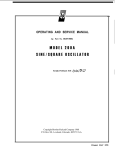
MODEL 333A/334A
DISTORTION A N A L Y Z E R
Serial Numbers:
333A: 1137A03146 and greater
334A: 1140A05641 and greater
Appendix C, Manual Backdating Changes, adapts this manual to
lower serial numbers.
WARNING
I
To help minimize the possibility of electrical fire
or shock hazards, do not expose this instrument
to rain or excessive moisture.
Manual Part NO.00333-90008
Microfiche Part No. 00333-90058
@Copyright Hewlett-Packard Company 1966
P.O.Box 301, Loveland, Colorado, 80537 U.S.A.
Reproduced with Permission, Courtesy of Agilent Technologies, Inc.
prlnttd: October 1975,1985
Pa
HEWLETT
PACKARD
CERTIFICATION
Hewlett-Packard Company certifies that this product met its published specifcations at the time of shipment from the
factory. Hewlett-Packard further certifies that its calibration measurements are traceable to the United States National Bureau of Standards, to the extent allowed by the Bureau’s calibration facility, and to the calibration facilities
of other International Standards Organization members.
WARRANTY
This Hewlett-Packard product is warranted against defects in material and workmanship for a period of one year
from date of shipment [,except that in the case of certain components listed in Section I of this manual, the warranty
shall be for the specified period] During the warranty period, Hewlett-Packard Company will, at its option, either
repair or replace products which prove to be defective.
.
For warranty service or repair, this product must be returned to a service facility designated by - h p . Buyer shall
prepay shipping charges to -hp- and -hp- shall pay shipping charges to return the product to Buyer. However, Buyer
shall pay all shipping charges, duties, and taxes for products returned to -hp- from another country.
Hewlett-Packard warrants that its software and firmware designated by -hp- for use with an instrument will execute its
programming instructions when properly installed on that instrument. Hewlett-Packard does not warrant that the
operation of the instrument, or software, or firmware will be uninterrupted or error free.
LIMITATION OF WARRANTY
The foregoing warranty shall not apply to defects resulting from improper or inadequate maintenance by Buyer,
Buyer-supplied software or interfacing, unauthorized modification or misuse, operation outside of the environmental
specifications for the product, or improper site preparation or maintenance.
NO OTHER WARRANTY IS EXPRESSED OR IMPLIED. HEWLETT-PACKARD SPECIFICALLY
DISCLAIMS THE IMPLIED WARRANTIES OF MERCHANTABILITY AND FITNESS FOR A PARTICULAR
PURPOSE.
EXCLUSIVE REMEDIES
THE REMEDIES PROVIDED HEREIN ARE BUYER’S SOLE AND EXCLUSIVE REMEDIES. HEWLETTPACKARD SHALL NOT BE LIABLE FOR ANY DIRECT, INDIRECT, SPECIAL, INCIDENTAL, OR CONSEQUENTIAL DAMAGES, WHETHER BASED ON CONTRACT, TORT, OR ANY OTHER LEGAL THEORY.
ASSISTANCE
Product maintenance agreements and other customer assistance agreements are available
for Hewlett-Packad products.
For any assistance, contact your nearest Hewlett-Packard Sales and Service Office.
Addnsscr are provided at the back
of this manual.
HEWLETT
PACKARD
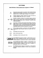
SAFETY SUMMARY
Tho following ganorol ufoty pneoutionr murt bo oburvod during all p h r m of oporotior, urviw, and nprir of thir
inrtrumont friluro to comply with thaw procautions or with rprcific warnings oluwhon in thir manual violotw
rrfoty rtandrrdr of dosign, mrnufrcturo, and intondod u u of tho inrtrumont Howlott-PieLordCompany assume8 no
liability for tho curtomar'r foiluro to comply with thou roquinmont8. This is I Srfoty Class 1 inrtrumont
GROUND THE INSTRUMENT
To minimize shock hazard, the instrument chassis and cabinet must be connected t o an electrical ground. The instrument is equipped with a three-conductor ac power cable. The power
cable must either be plugged into an approved three-contact electrical outlet or used with a
three-contact t o two-contact adapter with the grounding wire (green) firmly connected to an
electrical ground (safety ground) at the power outlet. The power jack and mating plug of the
power cable meet International Electrotechnical Commission (IEC) safety standards.
DO NOT OPERATE IN AN EXPLOSIVE ATMOSPHERE
Do not operate the instrument in the presence of flammable gases or fumes. Operation of any
electrical instrument in such an environment constitutes a definite safety hazard.
KEEP AWAY FROM LIVE CIRCUITS
Operating personnel must not remove instrument covers. Component replacement and internal
adjustments must be made by qualified maintenance personnel. Do not replace components
with power cable connected. Under certain conditions, dangerous voltages may exist even with
the power cable removed. To avoid injuries, always disconnect power and discharge circuits
before touching them.
DO NOT SERVICE OR ADJUST ALONE
Do not attempt internal service or adjustment unless another person, capable of rendering first
aid and resuscitation, is present.
DO NOT SUBSTITUTE PARTS OR MODIFY INSTRUMENT
Because of the danger of introducing additional hazards, do not install substitute parts or perform any unauthorized modification t o the instrument. Return the instrument t o a HewlettPackard Sales and Service Office for service and repair to ensure that safety features are maintained.
DANGEROUS PROCEDURE WARNINGS
Warnings, such as the example below, precede potentially dangerous procedures throughout
this manual. Instructions containe# in the warnings must be followed.
WARNING
I
Dongarour voltagu, wprbla of wuring drth, o n prwont in thir inrtrumont Uso ox.
tnmo wution whon handling, twting, and rdjurting.
A
SAFETY SYMBOLS
General Definitions of Safety Symbols Used On Equipment or In Manuals.
-
4
A
Instruction manual symbol: the product will be marked with this
symbol when it is necessary for the user to refer to the instruction
manual in order to protect against damage to the instrument.
/s
Indicates dangerous voltage (terminals fed from the interior by
voltage exceeding lo00 volts must be so marked).
OR@
Protective conductor terminal. For protection against electrical
shock in case of a fault. Used with field wiring terminals to indicate the terminal which must be connected to ground before
operating equipment.
Low-noise or noiseless, clean ground (earth) terminal. Used for a
signal common, as well as providing protection against electrical
shock in case of a fault. A terminal marked with this symbol must
.be connected to ground in the manner described in the installation
(operating) manual, and before operating the equipment.
,
D
/f;r
OR
Frame or chassis terminal. A connection to the frame (chassis) of
1, the equipment which normally includes all exposed metal structures.
---
Alternating current (power line).
Direct current (power line).
Alternating or direct current (power line).
The WARNING sign denotes a hazard. It calls attention to a procedure, practice, condition or the like, which, if not correctly performed or adhered to, could result in injury or death to personnel.
0
WARNING
CAUTION
E
'
The CAUTION sign denotes a hazard. It calls attention to an
operating procedure, practice, condition or the like, which,if not
correctly performed or adhered to, could result in damage to or
destruction of part or all of the product.
The NOTE sign denotes important information. It calls attention
to procedure, practice, condition or the like, which is essential to
highlight.
Table of Contents
Model 333A/334A
T A B L E OF CONTENTS
Section
I
GENERAL INFORMATION
1.1
Description
1.6
Accessory Features
1.8
Option
1.10 Instrument Identification
..
..
Page
.
.
.
.
.
.
.
.
1-3
. . . . .. .. .. .. .. .. .... 1-3
1-3
. . . . . . . . . . .. .. .. .... 1-3
1-3
Section
INSTALLATION
2 .1 Introduction
2.3
Inspection
2.5
Power Requirements
2.7
Three-Conductor Power Cable
2.10 Installation
2.12
Bench Installation
2.14
Rack Installation
2.16 Repackaging For Shipment
page
2-1
.
.
.
.
.
.
.
.
.
.
.
.
.
.
.
. . . . . . . . . . . . 2-1
2-1
. . . . . . .. .. .. .. .. .. .. 2-1
...
2-1
2-1
..
. . . . . .. .. .. .. .. ... ... 2-1
.
. . . . .. .. .. .. 2-1
2-1
.
Section
-ge
III OPERATINGINSTRUCTIONS . . . . . . 3-1
3- 1. Introduction . . . . . . . . . . . . 3.1
3.4 . Controls and Indicators . . . . . . 3-1
3.6 . General Operating Information . . 3-1
3.7 .
Input Connections . . . . . . . 3-1
3.9 .
Voltmeter Characteristic$ . . 3-1
Output Terminals . . . . . . . 3-2
3.12 .
3.14 . Operating Procedures. . . . . . . 3-2
3.15 .
Instrument Turn.On . . . . . . 3-2
Adjustment of Meter
3.16 .
Mechanical Zero . . . . . . . 3-2
3.18 .
DistortionMeasurement . . . 3-2
Distortion Measurement of AM
3.21 .
RF Carriers (334A only). . . 3-3
3.22 .
Voltage Measurement . . . . . 3-3
3.23 .
Meter Indication . . . . . . . 3-4
Use of Output Terminals . . . 3-4
3.27 .
11
.
..
333A1334A with Option 01
3-4
3.30
Manual Nulling
3-4
3.32
Section
Page
IV
THEORY OF OPERATION
4-1
Overall Description
4-1
4.1
4.3
Block Diagram Description
4-1
4.4
Distortion Measuring
Operation
4 1
Distortion Measurement in AM
4.8
Carriers.
4-1
4.10
Voltmeter Operation
4-1
4.12
Detailed Circuit Description
4-1
4.13
Impedance Converter Circuit
4-1
4.17
Rejection Amplifier Circuit
4-2
4.39
High Pass Filter
4-5
4.41
Meter Amplifier
4-5
4.49
Power Supply Circuit
4-7
4.54
RF Detector Circuit (334Aonly) 4-7
.
..
.
.
...
.
...
.
........
.. .. .. .. .. .. .. ..
....
.......... .
..........
. . .. .. ..
.
.
.. .. .. .. .. .. ...
.....
Section
V
MAINTENANCE
Introduction
5.1
5.3
Required Test Equipment
.
.
. .. .. .. .. .. .. .. .. .. .. .. .. Page
5-1
5-1
. . . . . 5-1
Section
Page
V
MAINTENANCE (Cont’d)
5-1
Performance Checks
5-1
5.5
5.9
Fundamental Rejection Check
5-1
5.10
Second Harmonic Accuracy
5-2
Instrument Induced
5.11
Distortion Check
5-2
5.12
Frequency Calibration Accuracy
Check
5-3
Automatic Nulling Mode Check 5-4
5.13
5.14
Input Impedance Check
5-4
5.17
Minimum Input Level Check
5-5
5.18
DC Isolation Check
5-5
5.19
Voltmeter Accuracy and
Frequency Response Check
5-6
5.20
High Pass Filter Check
5-7
5.21
Residual Noise Check
5-7
5.22
AM Detector Check (Model
5-7
334Aonly)
5.23 Adjustment and Calibration
Procedure
5-8
Power Supply and Bias
5.26
Adjustments
5-8
5.27
Voltmeter Gain Adjustments
5-8
Voltmeter Frequency Response
5.28
Adjustment
5-10
Bridge Balance Adjustment
5-10
5.29
Sensitivity SwitchCalibration 5-11
5.30
Adjustment of Factory Selected
5.31
Components
5-11
5.33 Troubleshooting Procedure
5-11
5.38
Troubleshooting Voltmeter
5 .12
Function
5.40
Troubleshooting Distortion
Function
5-14
5.45
Photoresistor Check and
Adjustment (A6V1thruA6V5) 5-15
Servicing Etched Circuit
5.49
5-16
Boards
Servicing Rotary Switches
5-16
5.52
Isolating the Impedance
5-54 *
Converter
5-16
Section
Page
6-1
VI
REPLACEABLE PARTS
Introduction
6-1
6.1
Ordering Information
6-1
6.4
Non-Listed Parts
6-1
6.6
.........
. . . . . . ..
..
.......
..
.
.
..
.
..
..
.
.
.
..
.
.
.............
....
..
......
....
.....
..........
............
. . . . . . . . ..
.........
..
.
.
.
.
.........
....
...........
...........
.
.
.
.
.
. . . . . . . . .. .. ..
.
........
...
.........
............
.......
.........
Section
CIRCUITDIAGRAMS
7- 1 Introduction
M
.
...........
............
Page
7-1
7-1
APpen&
A
CODE LIST OF MANUFACTURERS
B
SALES AND SERVICE OFFICES
C
MANUAL BACKDATING CHANGES
iii
Model 333A1334A
Table of Contents
L I S T OF T A B L E S
Number
Page
1 1
1- 1
Specifications
3.1
Effect of Harmonics on Voltage
Measurements
3-1
RequiredTestEquipment
5-0
5.1
Second Harmonic Accuracy Check
5-2
5.2
5.3
Frequency Calibration Accuracy Check 5-4
5.4
Voltmeter Frequency Response Check
5-6
..
..
..
..............
. . . . .. .. .. .. .. .. .. ..
...
.
.
Number
5.5
Power Supply and Bias Adjustments
5.6
Sensitivity Switch Calibration
Factory Selected Components
5.7
..
.
5.8 .
5.9 .
6.1 .
. . Page
5-8
.. .. .. .. .. 5-12
5-12
. . . . . . . . . . 5-13
.
. . .. .. .. .. .. .. .. .. .. 5-15
6-6
Troubleshooting Aid
Photoresistor Check
Replaceable Parts
L I S T OF I L L U S T R A T I O N S
Number
Model 333A Distortion Analyzer
1.1
Front and Rear Panel Description
3.1
Manual Nulling Test Setup
3.2
Impedance Correction Graph
3.3
4.1
Block Diagram
4.2
Bridge Waveforms
Wien Bridge Circuit and Rejection
4.3
Characteristics
.
...
.
..
..
4.6 .
4.4
4.5
4.7
4.8
5.1
5.2
5.3
lv
..
..
.
111
. .. .. .. Page
3 -0
3- 5
3-5
.
.
.
.
.
.
. . .. .. .. .. .. .. .. .. .. .. .. 4-0
4-2
. . . . . . . . . . . 4-3
Auto Control Loop Detector . . . . . . . 4-3
Reference and E r r o r Phase
Relationship . . . . . . . . . . . . . 4-4
Rejection Amplifier Block Diagram and
Typical Frequency Rejection
Characteristic . . . . . . . . . . . . 4-5
Bandwidth Versus Null Depth . . . . . . 4-6
Simplified Metering Circuit . . . . . . . 4-7
Fundamental Rejection Check . . . . . 5-1
Instrument Induced Distortion Check . . 5-2
Frequency Calibration Accuracy Check 5-3
Number
.
..
5.7 .
5.8 .
6.1 .
6.2 .
6.3 .
7.1 .
7.2 .
5.4
5 .5
5.6
.
7.4 .
7.5 .
7.3
7.6
.
...........
Page
Capacitance Check
5-5
DC Isolation Check
5-6
Voltmeter Accuracy and Frequency
Response Check
5-7
Shielded Load Assembly
5-8
Adjustment and Chassis Mounted
Component Location
5-9
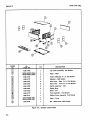
Mechanical Parts
6-2
Modular Cabinet Parts
6-4
Frequency Tuning Assembly
6-5
Internal Wiring Data
74/74
Impedance Converter (P/O A2) and RF
Detector (A4)
7-5/74
Rejection Amplifier (A3). Bridge Balance
(P/OA6) andH h Pass Filter (A7) 7-7/7-8
Meter AmplifiervP/O A2)
7-9/7-10
Control Circuit (A5) and Bridge
Balance (P/O A6)
7-11/7-12
7-13/7-14
Power Supply (Al)
...........
. . . .. .. .. .. .. .. .. ..
..........
. . .. .. .. .. .. .. .. .. ..
......
.........
...........
......
........
.........
Section I
Model 333A/334A
SECTION I
GENERAL I N F O R M A T I O N
1-1. DESCRIPTION.
1-6. ACCESSORY FEATURES.
1-2. The Hewlett-Packard Models 333A and 334A
Distortion Analyzers axe solid state instruments for
1-7. The accessory available with the 333Aand334A
Distortion Analyzers is a voltage divider probe, -hpModel No. 10001A. The features of the probe are:
measuring distortion on ac voltages. The Models
333A and 334A include two control loops that autom a t i c d y tune both legs of a bridge circuit which rejects the fundamental when the rejection circuit is
initially set within the range of the loops. The 334A
has a high impedance detector which operates from
550 M z to greater than 65 MHz and provides the capability of monitoring the distortion of the amplitude
modulation on an rf carrier.
1-3. Distortion levels of 0.1% to 100%full scale are
measured in seven ranges for any fundamental frequency of 5 Hz to 600 W z . Harmonics are indicated upto
3 MHz. The high sensitivity of these instruments requires only 0.3V r m s for the 100% set level reference.
The distortion characteristics can be monitored atthe
OUTPUT connectors with an oscilloscope, a true r m s
voltmeter, or a wave analyzer. The instruments are
capable of an isolation voltage of 400 volts above
chassis ground.
a. 10 megohms shunted by 10 pF, giving 1O:l
b.
attenuation.
DC to 30 MHz bandwidth.
c.
2% division accuracy.
d.
e.
600Vpeakinput.
5 ns rise-time.
1-8. OPTION.
1-9. Option 01 is a standard -hp- Model 333A or 334A
with a special meter and meter amplifier, compensated to permit response to W (volume units)
character istic 8.
1-10 INSTRUMENT IDENTICATION.
1-4. The voltmeter can be used separately for general
purpose voltage and gain measurements. It has a
frequency range of 5 Hz to 3 MHz (20 Hz to 500 M z
for 300 pV range) and a voltage range of 300pV to
300 V r m s full scale.
1-11. Hewlett-Packard uses a two-section serial
number. The first section (prefix) identifies a series
of instruments. The last section (suffjx) identifies a
particular instrument within the series. If a letter is
included with the serial number, it identifies the country in which the instrument was manufactured. If the
1-5. The AM detector included in the Model 334A is
serial prefix of your instrument differs from the one
on the title page of this manual, a change sheet w i l l
a broadband dc restoring peak detector consisting of
a semiconductor diode and filter circuit. AM distorbe supplied to make this manual cornpatable with newtion levels as low as 0.3% can be measured on a 3 V
e r instruments o r the backdating information in Appento 8 V rms carrier modulated 30% in the standard
dix C will adapt this manual to earlier instruments.
broadcast band. Distortion less than 1% can be
All correspondence with Hewlett -Packard should include the complete serial number.
measured at the 8ame level of the carrier up to 65 Mc.
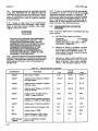
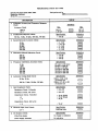
Table 1-1. Specifications
Fundamental Input Greater Than 30 V
MODEL 333A
DISTORTION MEASUREMENT RANGE
RANGE
*3%
*6%
*12%
Any fundamental frequency, 5 Hz to 600 kHz.
Distortion levels of 0. 1%-100%are measured
full scale in 7 ranges.
1
I
DISTORTION MEASUREMENT ACCURACY
Harmonic measurement accuracy (full scale)
Fundamental Input Less Than 30 V
*ts%
RANGE
*3%
100%-0.3%
10 HZ
1MHz
1 0 H ~
3MHz
0.1%
30 Hz
20 Hz
500 W z
300 kHz
*12%
10 Hz
1.2 MHz
I
50 Hz
Elimination Characteristics:
Fundamental Rejection > 80 dB
Second Harmonic Accuracy for a
fundamental of:
5 Hz to 20 Hz: better than +1dB
20 Hz to 20 W z : better than 4.6 dB
20 kHz to 100 kHz: better than -1 dB
100 W z to 300 kHz: better than -2 dB
300 kHz to 600 kHz: better than -3 dB
1-1
Model 333A/334A
Section I
Table 1-1. Specifications (Cont'd)
Distortion Introduced by Instrument:
> -70 dB from
5 He to 200 kHz
> -64 dB from 200 kHz to 600 kHz
Meter indication is proportional to the average value of a waveform.
NOISE MEASUREMENTS
Voltmeter residual noise on the 300 pV range:
< 25 p V r m s terminated in shielded 60OQ <30
p V rrns terminated in shielded 100 kS1.
FREQUENCY CALIBRATION ACCURACY
5 Hz to 300 kHz
Better than *5% from
Better than f 10% from 300 kHz to 600 kHz
*
INPUT IMPEDANCE
Distortion Mode: 1 MS1 *5% shunted by <70 pF.
Voltmeter Mode:
1 Mi2 15% shunted by 4 0 pF (333A only),
1 Mi2 *5% shunted by 4 5 F (334A only),
1 to 300 V ranges; 1 MS1 *5 shunted by<70 pF,
300 pV t o 0.3 V ranges.
4l
INPUT LEVEL FORDISl?ORTIONMEASOaEMENTS
0.3 V rrns for 100% set level (up to 300 V may
be attenuated to set level reference). The
minimum measurable distortion for floating
operation on the X1 frequency range L 50dB
below the fundamental.
DC ISOLATION
Signal ground may be rl00 Vdc from external
chassis.
VOLTMETER ACCURACY:
300 pv
1 mV-30 V
100 V-300 V
*2%
I
*5%
MODEL 334A
Same as Model 333A except as indicated below:
AM DETECTOR
High impedance dc restoring peak detector with
semi-conductor diode operates from 550kHz to
greater than 65 MHz. Broadband input.
Maximum input; 40 V p-p ac or 40 V peak
transient.
CARRIER FREQUENCY
550kHzto 1.6 MHz: Distortion introduced by
detector is c 0.3% for 3 to 8 volt carriers
modulated 30%.
1-2
I
20 H E - ~ O O ~ H Z
10 He-1 MHe
5 Hz-3 M H e
10 HE-300~ H Z 5 He-500kHz
30 HZ-300 IrHz
X10 through X10 K, manual null tuned to
less than 10%of set level; total frequency
hold-in 1 1% about true manuaX null.
100 Hz to 600 kHz: Meter reading within0 to
+l. 5 dB of manual null.
VOLTMETER FREQUENCY RANGE
5 Hz to 3 MHz (300 pV range: 20 Hz-500 Hie).
I
AUTOMATIC NULLWG MODE
Set Level: At least 0.2 V rms.
Frequency Ranges:
X1, manual null tuned to less than 3% of set
level; total frequency hold-in io. 5% about
true manual null.
AUTOMATIC NULL ACCURACY
5 Hz to 100 Iiz: Meter reading within 0 to +3
dB of manual null.
VOLTMETER RANGE
300 p V to 300 V rrns full scale (13 ranges),
10 dB per range.
RANGE
OUTPUT
For input frequencies from 20 Hz to 600 kRz,
0.1 V rma 0.01 V open circuit for full scale
meter deflection; 0.05 V rms f 0.005 V into
2 kS2 f o r full scale meter deflection.
HIGH-PASS FILTER
3 dB point at 400 Hz with 18 dB per octave roll
off. 60 Hz rejection > 40 dB. Normally used
only with fundamental frequencies greater than
1BHZ.
POWER SUPPLY
100 V/120 V/220 V/240 V + 5% 108, 48
66 Hz, approximately 4 watts. -
-
-
1.6 MHz to 65 MHz: Distortion introduced by
detector is c 1%for 3 to 8 volts r m s carriers
modulated 30%.
NOTE
Distortion measurement at carrier levels
as low as 1 volt may be made with reduced
accuracy.
OPTION 01
Indicating meter has W characteristics conforming to FCC Requirements for AM, FM,
and TV broadcasting.
Section XI
Model 333A/334A
S t C T I O N II
INSTALLATION
2-1. I NTR ODUCTIO N .
2-2. This section contains information and instructions necessaryfor the installation and shipping of the
Models 333A/334A Distortion Analyzers. Included
a r e initial inspectionprocedures, power and grounding
requirements, installation information, and instructions for repackaging for shipment.
Instructions for the conversion a r e included with the
kit. The rack mount for the Model 333A/334A ie an
EIA standard width of 19 inches. When mounted in a
rack using the rack mount kit, additional support at
the rear of the instrument should be provided if vibration or similar stress is likely.
2-15. REPACKAGING FOR SHIPMENT.
2 - 3 . INSPECTION.
This instrument w a s carefully inspected both
mechanically and electrically before shipment. It
shouldbe physically free of m m s or scratches and in
perfect electrical order upon receipt. To confirm
this, the instrument should be inspected for physical
damage in transit. Also checkfor supplied accessories,
and test the electrical performance of the instrument
using the procedure outlined in Paragraph 5-5. If
there isdamageordeficiency, see the warranty on the
inside front cover of this manual.
2-4.
2-16. The following paragraphs contain a general guide
f o r repackaging of the instrument for shipment. Refer
to Paragraph 2-17 if the original container is to be
used; 2-18 if it ia not. If you have any questions, contact your local hp Sales and Service Office. (See
Appendix B f o r &ice locations.)
- -
NOTE
If the instrument is to be shippedsto
Hewlett-Packardfor service or repair,
attach a tag to the instrument identifying the owner and indicate the service
or repair to be accomplished. Include
the model number and full serial number of the instrument. In any correspondence, identify the instrument by
model number, serial number, and
serial number prefix.
2 - 5 . POWER REQUIREMENTS.
-
2-6. The Model 333A/334A can be operated from any
ac source of 100 V/120 V/220 V/240 V + 5% 10%
48 66 Hz. With the instrument disconnected from
the ac power source, move the slide (located on the
rear panel) until the desired line voltage appears.
Power dissipation ie approximately 4 watts.
-
2 - 7 . THREE-CONDUCTOR POWER C A B L E .
2-8. To protect operating personnel, the National
ElectricalManufacturers'Association (NEMA) recommends that the instrument panel and cabinet be grounded.
All Hewlett-Packard instruments a r e equipped with a
three-conductor power cable, which, when plugged into anappropriate receptacle, grounds the instrument.
The offset pinon the power cable three-prong connector is the ground wire.
2-9 .INSTALLATION.
2-10. The Model 333A/334A is fully transistorized;
therefore, no special cooling is required. However,
the instrument should not be PerateBwhere the ambient temperature exceeds 55 C (131 F).
2-11. BENCH mSTALLATION,
2-12. The Model 333A/334A is shipped with plastic
feet and tilt stand in place, ready for use as a bench
instrument
.
2-13. RACK INSTALLATION,
2-14. The Model 333A/334A may be rack mounted by
using the 5"RackMount Kit (-hp- Part No. 5060-0775).
2-17. If original container is to be used, proceed as
follows:
a Place instrument in original container if available. If original container is not available, a suitable
one can be -purchased from your nearest -hp- Sales
and Service Office.
b. Ensure that container is well sealed with strong
tape or metal bands.
2-18.
If original container is not to be used, proceed
as follows:
a. Wrap instrument in heavy paper or plastic before placing in an inner container.
b. Place packing material around all sides of instrument and protect panel face with cardboard strips.
c. Place instrument and inner container in a heavy
carton or wooden box and seal with strong tape or
metal bands.
d. Mark shipping container with "DELICATE
INSTRUMENT, I' "FRAGILE, etc.
I'
2-1
Section TII
Model 333A/334A
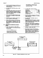
@LINE switch turns instrument ac power on.
Pilot lamp glows when instrument is turned ON.
@Meter indicates distortion or voltage level of
input.
@MODE switch selects MAIUUAL or AUTOMATIC
bridge tuning operation.
@FREQUENCY RANGE switch selects frequency
range which corresponds to fundamental of input
Signal.
@COARSE BALANCE control provides coarse adjustment for balancing the Wien bridge circuit.
6 FINE BALANCE control provides a vernier ad'justment
for balancing the Wien bridge circuit.
7 Frequency dial tunes the Wien bridge circuit to
of input signal.
'fundamental
@HJGH PASS FILTER switch inserts or bypasses
HIGH PASS FILTER i n SET LEVEL and DISTORTION function. When inserted, filter provides > 40 dB attenuation to 50 60 Hz hum
components but no attenuation to frequencies
over 1 kHz.
@OUTPUT connectors provide means of monitoring output of meter circuit.
@Frequency vernier provides fine adjustment of
frequency dial.
@METER RANGE switch selects full scale range
of meter in percent, dB and r m s volts.
-
-
O S E N S I T M T Y selector provides r) 50 dB atteauation of input signal in 10 dB steps in SET LEVEL
and DISTORTION functions.
@SENSITIVITY VERNIER control provides fine
adjustment of sensitivity setting.
@Mechanical zero adjust provides mechanical
zero adjustment of meter.
OFUNCTION switch selects type of operation of
instrument.
@Shorting bar connects circuit ground to chassis
ground.
@INPUT terminals provide connections for input
stgnal.
@RF INPUT connector (Model 334A only) provides
input connection for AM RF carrier input signal.
20 FUSE provides current overload protection for
instrument circuits.
21 Line voltage switch sets inrrtrument to
'operate
from 100 V/120 V/220 V/240 V.
@) Ac power connector provides input connectton
for ac power.
0
~~~
Figure 3-1.
3- 0
Front and Rear Panel Description
Model 333A/334A
Section III
S E C T I O N 111
OPERATING INSTRUCTIONS
3-1. INTRODUCTION.
3-2. The Models 333A and 334A DistortionAnalyzers
measure total harmonic distortion of fundamentalfrequencies from 5 Hz to 600 kHz; harmonics upto 3 MHc
a r e included. The sharp elimination characteristics
( >80 dB), the low level of instrument induced dtstortion, and the meter accuracy of these instrumentsresult in highly accurate measurement of low level harmonic distortion.
3-3. An rms calibrated voltmeter is inherent in the
333A and 334A. The voltmeter provides a full scale
sensitivity of 300 p volts r m s (residual noise <25p volts).
The voltmeter frequency range is from 5 HZ to 3 MHz
except on the 0.0003 volt range, which is from 20 Hz
to 500 kHz.
3-4. CONTROLS AND INDICATORS.
3-5. Figure 3-1 illustrates anddescribesthefunction
of all front and rear panel controls, connectors, and
indicators. The description of each component is
keyed to the drawing included within the figure,
Table 3-1
Effect of Harmonics on Voltage Measurements
Input Voltage
Characteristics
Fundamental = 100
Fundamental + 10%
2nd harmonic
Fundamental + 20%
2nd harmonic
Fundamental + 50%
2nd harmonic
Fundamental + 10%
3rd harmonic
Fundamental + 208
3rd harmonic
Fundamental + 50%
3rd harmonic
- 102
100 - 110
96 - 104
102
100
112
100.5
102
94
- 108
112
90
- 116
NOTE
This chart is universal in application
since these errors are inherent in all
average-responding voltage-measuring
instruments.
3-7. INPUT CONNECTIONS.
3-9. VOLTMETER CHARACTERISTICS.
3-10. The RMS VOLTS markmgs on the meter face
a r e based on the ratio between the average and effective
(rms) values of a pure sine wave, The ratio of average
to effective values in a true sine wave is approximately
0.9 to 1. When the meter is used to measure complex
waves, the voltage indicated may not be the rms value
of the signal applied. This deviation of meter indication exists because the ratios of average to effective
values a r e usually not the same in a complex wave as
in a sine wave. The amount of deviation depends on
the magnitude and phase relation betweenthe harmonics
and fundamental frequency of the signal applied.
Table 3-1 lists the deviation of the meter indication
of a sine wave partly distorted by harmonics. A s indicated in the table, harmonic content of less than 108
results in very small errors.
100
100
100
100.5
I
3-6.GENERAL OPERATING INFORMATION.
3-8. The input signal can be connected to the 333A
and 334A through twisted pair leads or a shieldedcable
with banana plug connectors. Keep all test leads as
short as possible to avoid extraneous pickup from
stray ac fields. When measuring Low-level signals,
ground loope may occur causing erroneous readings.
Ground loops may be avoided by connecting the 333A/
334A Distortion Analyzer t o an appropriate isolation
transformer to break the chassis ground from power
supply ground. Connect all other instruments to one
power strip with the three-prong connectors as close
as possible.
Meter
3 -11. When making distortion measurements where
tne fundamental frequency is suppressed and the r e
mainder of the signal is measured, the reading obtained on an average responding meter may deviate
from the true total rms value. When the residual
wave contains many inharmonically related sinusoids,
the maximum error in the distortion reading is about
11 % (11 % of the measured distortion) low for distortion levels below 10 %.
-
EXAMPLE :
Measured
Distortion
2.5%
Maximum Error
Total
In Meter Indication
Distortion
+O. llx0.025=
0.025+0.0027=
0.00027
0.0277 or 2.8%
This example represents the maximum possible error,
and in most cases the error is less. In distortion
measurements, the reading of an average-responding
meter is sufficiently close to the r m s value to be
satisfactory for most applications.
3-12.
OUTPUT TERMINALS.
3-13. The OUTPUT terminals provide a 0.1 V r m s
open circuit output for full scale meter deflection.
These terminals can be used to monitor the output
signal with an oscilloscope, a true r m s voltmeter, or
a wave analyzer. The combination of the distortion
meter and oscilloscope provides more significant in3-1
Model 333A/334A
Section I
I
f
formation about the device under test than the
expression of distortion magnitude alone. Information
obtained from the oscilloscope pattern is specific and
reveals the nature of distortion which sometimes
occurs at such low levels that it is difficult to detect
in the presence of hum and noise. The impedance at
the OUTPUT terminals is 2000 ohms, therefore, capacitive loads greater than 50 pF should be avoided
to maintain the accuracy of meter readings.
b.
Set NORM-R. F. DET. switch to NORM.
C.
Set FUNCTION switch to SET LEVEL.
d. Set MODE switch to MANUAL.
e.
set HIGH PASS FILTER switch to IN.
f.
3-14. OPERATING PROCEDURES.
3-15.
If fundamental frequency is 1kHz or greater,
Set SENSITIVITY selector to MIN. position,
and rotate VERNIER control maximum
counterclockwise.
INSTRUMEN" TURN-ON.
NOTE
a Set the 115-230 VAC switch to coincide with the
line voltage in we. Turn switch to ON position.
Pilot lamp w i l l glow, indicating application d
primary power.
The bandwidth of the SENSIT M T Y selector is reduced
in the two extreme CCW
positions (positions used with
an input signal greaterthan
30 V).
ADJUSTMENT OF METER MECHANICAL
ZERO.
3-16.
3-17. The meter ia properly zero-set when the
pointer rests over the zero calibration mark and the
instrument ie in its normal operating enivronment
and is turned off, Zero-set the meter as follows to
obtain maximum accuracy and mechanical stability:,
a. Turn instrument on and allow it to operate
for at least 20 minutes, to let meter movement reach normal operating temperature.
b. Turn instrument off and allow 30 seconde
for all capacitors to discharge.
c. Rotate zero adjustment screw clockwise until pointer is left of zero and moving upscale.
d. Continue rotating screw clockwise; stop when
pointer ia exactly at zero.
e. When pointer is exactly over zero, rotate
adjustment screw slightly counterclockwise
to relieve tension on pointer suspension. If
pointer moves aff zero, repeat steps c through
e, but make counterclockwise rotation lese.
g.
Set METER RANGE switch to SET LEVEL,
and set BALANCE COARSE and FINE controls to center position.
h.
Connect signal to be measuredto 333A/334A
INPUT terminals.
I
Set SENSITIVITY selector to obtain meter
indication greater than 1/3 full scale.
Adjust SENSITIVITY VERNIERfor full scale
meter indication if making distortion measurement in percent; if making distortion measurement in dB adjust SENSITMTY VERNIER
for 0 dB meter indication.
e
DO NOT EXCEED THE INPUT VOLTAGES LISTED BELOW ro PREVENT
DAMAGING COMPONENTS ON A2
NOTE
If unable to adjust for full scale
or OdB indication, (which indicates
input signal is below 0.3 volts),
set METER RANGE selector downscale. Use this new setting as the
100'KDor OdB SET LEVEL position,
thus making the next range 30%
or -10 dB, etc.
BOARD.
VOLTMETER FUNCTION - l V
RANGE AND BELOW, AND
DISTORTION ANALYZER
FUNCTION MAXIMUM
SENSITIVITY.
1. 300 VABOVE 100 HE
2. 50 VABOVE 1 kHz
-
3-19.
a.
k. Set FREQUENCY RANGE switch and frequency
dial to fundamental frequency of input signal.
MANUAL MODE.
Turn instrument on and mechanically zero
meter according to procedure in Paragraphs
3-15 and 3-16.
3-2
1
REMOVE SHORTING STRAP BETWEEN
FRAME GROUND ( A ) AND CHASSIS
GROUND ( ) TERMINALS ON FRONT
PANEL INPUT TERMINALS WHEN
MEASURING DISTORTION BETWEEN
TWOPOINTSWHICHAFEDCOFFSET
FROM GROUND POTENTIAL.
DISTORTION MEASUREMENT.
3-18.
WARNING
1.
Set FUNCTION switch to DISTORTION.
m. Adjust frequency dial vernier and BALANCE
COARSE and FINE controls for minimum
Section III
Model 333A/334A
meter indication. Set METERRANGE switch
down-scale as necessary to keep meter indication on scale.
n.
0.
3-21.
Repeat step m until no further reduction in
meter indication can be obtained.
DO NOT EXCEED MAXIMUM INPUT
VOLTAGES LISTED ON REAR PANEL.
Observe distortion either in percentage or
dB, as indicated by meter deflection and
METER RANGE switch setting. For example,
if meter indicates 0 . 4 and METER RANGE
setting is 1 8 , distortion measured is 0.4%
of fundamental. Similarly, if meter indicates -6 dB and METER RANGE setting ie
-40 dB, distortion measured is -46 dB from
fundamental.
NOTE
In MANUAL mode the accuracy
of distortion measurements is
affected by frequency stability
of the input signal. An inaccuracy
in distortion indications occurs
when the frequency drift of the
input signal exceeds the bandwidth
of the rejection curve.
p.
If desired, r m s voltage of input signalcan
be measured by setting FUNCTION switch to
VOLTMETER, and setting METER RANGE
switch to obtain an on-scale indication.
a.
Turn instrument on and mechanically zero
meter according to procedure in Paragraphs
3-15 and 3-16.
b.
Set NORM.-R F. DET. switch to R. F. DET.
c.
Connect input signal to R F. INPUT terminal
on rear panel.
d.
Refer to Paragraph 3-19 for manual distortion measurement; refer to Paragraph 3-20
for automatic distortion measurement.
NOTE
If no meter deflection can be
obtained with an R F input, diode
A4CR1 should be checked. A
spare diode is located on the
outside of the A4 shield.
3-22.
VOLTAGE MEASUREMENT.
a.
Turn instrument on and mechanically zero
meter according to procedure in Paragraphs
3-15 and 3-16.
b.
Set NORM.-R. F. DET. switch to NORM.
c.
Set FUNCTION switch to VOLTMETER.
6
Set METER RANGE switch to a range
exceeding amplitude of signal to be measured.
3-20. AUTOMATIC MODE.
a
Perform steps athroughlof Paragraph 3-19.
b.
Adjust frequency dial vernier and BALANCE
COARSE and FINE control8 for minimum
meter indication.
C.
DISTORTION MEASUREMENT OF AM RF
CARRIERS (334A only).
When meter indication is less than 10% of
SET LEVEL indication, set MODE switch to
AUTOMATIC. (If fundamental cannot be
manually nulled below 10% of SET LEVEL
indication, automatic mode cannot be used).
e. Connect signal to be measured to INPUT
terminals.
f.
Set METER RANGE switch to give a reading
as close to full scale as possible, and ob-
d. Set METER RANGE switch down-scale to
serve meter indication.
obtain on-scale meter indication.
e.
Observe distortion either in percentage or
dB, as indicated by meter deflection and
METER RANGE switch setting. For example,
if meter indicates 0 . 4 and METER RANGE
setting is 1 8 , distortion measured is 0.4%
of fundamental. Similarly, if meter indicates
-6 dB and METER RANGE setting is -40 dB,
distortion measured is -46 dB from fundamental.
f.
If desired, r m s voltage of input signal canbe
measured by setting FUNCTION switch to
VOLTMETER, and setting METER RANGE
switch to obtain an on-scale indication.
g. The dB scale of the 333A/334A is calibrated
in dBm, such that 0 dBm = 1 milliwatt dissipated by 600 ohms. Therefore, a dBm measurement must be made across 600 ohms.
However, dB measurements across other
impedances can be converted to dBm by use
of the Impedance Correction Graph of Figure 3-3. For example: to convert a -30 dB
reading across 200 ohms to dBm, locate the
200 ohm impedance line at the bottom of the
graph. Follow the impedance line to the
heavy black line, and read the meter correction at that point. The correction for 200
ohms is +5 dBm; thus the corrected reading
is -25 dBm.
3-3
Section III
3-23. METER INDICATION.
3-24. The 333A/334A meter is calibrated to indicate
in both dB and volts. It is interesting to notethat the
METER RANGE markings differ from most ac voltmeter range markings. On most ac voltmeters (600
ohms) 0 dB corresponds to the 1 volt range. This is
not true in the case of the 333A/334A. Since the instrument is primarily a distortion analyzer, measurements
are in dB (relative measurement) rather than in dBm
(absolute measurement). Zero dB on the 333A/334A
corresponds to 0.3 volt range rather than the 1 volt
range. This allows a10 dB greater dynamic range of
distortion measurements.
3-25. E measurements are to be made in dBm, 10 dB
must be subtracted from the METER RANGE setting.
Thus 0 dB becomes the -10 dBm range for absolute
power measurements. Zero dBm is equal to 1 milliwatt dissipatedby any impedance andinthis particular
case is 800 ohms. The +10 DECIBELS marking on the
meter face indicatesthat when voltmeter measurements
are being made, the indication (METER RANGE plus
meter indication) is 10 dB greater than when power
(dBm) measurements are being made.
3-26. In short, when distortion and voltage measurements are being made, utilize the instrument METER
RANGE and meter scale as they exist. For absolute
power measurements in dBm, simply subtract 10 dB
from the METER RANGE setting.
3-27. USE OF OUTPUT TERMINALS.
3-28. InVOLTMETERand SET LEVEL functions, the
333A/334A can be used as a low distortion, wide-band
amplifier. A portion of the meter input (0.1 V r m s
open circuit for full scale meter deflection is provided
at the OUTPUT terminals.
3-29. In DISTORTION function, the distortion (0.1 V
r m s open circuit forfull scale deflection) is provided
at the OUTPUT terminals for monitoring purposes.
NOTE
The INPUT
terminal and the
OUTPUT
terminal should not be
connected directly together when
making low level measurements.
These terminals are isolated from
each other by 1 ohm which reduces
the effects of common mode voltages.
3-4
Model 333AI334A
3-30. 333A/334A WT”H OPTION 01.
3-31. Operating procedures for the 333A/334A with
Option01 are the same a s for the standard instrument.
The onlydifference between the standard and optional
instrument is that the Option 01 has a special meter
and meter amplifier which is compensated to respond
to W (volume unit) characteristics.
3-32.
MANUAL NULLING.
3-33. Since the frequency and balance controls are
rather sensitive in the MANUAL mode, the following
i n f o r m a t i o n i s s u p p l i e d to simplify nulling the
333A/334A in the MANUAL mode. When nulling the
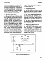
333A/334A in the MANUAL mode, connect the equipment as shown below and adjust the 333A/334A frequency and balance controls for the waveform shown
in step a below. Additional waveforms are provided
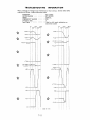
to simplify nulling.
No harmonic dietortion. Frequency
and balance adjustment correct.
Frequency and balance control improperly adjusted.
Frequency approximately correct;
balance incorrect.
Balance approximately correct; frequency incorrect.
Second harmonic predominant; frequency and balance adjusted.
Second harmonic predominant; frequency and balance adjusted; phase
changed.
Second harmonic predominant; frequency and balance adjusted; phase
changed.
Third harmonic predominant.
Balance incorrect; meter reading &
scale.
Frequency incorrect; meter readin(
off scale.
Model 333A/334A
Section IV
I
I
I
I
I
I
I
I
I
I
I
L
I
I
I
3
I f
I
I
I
I
PI
I
I
I
I
I
I
I
I
I
1
I
I
I
3
j P
I
I
I
I
I
I
I
I
I
I
I
I
I
I
I
I
I
I
I
I
I
I
I
Y
Ym
0
W
W
lb
I
I
I
I
I
I
I
I
-----
---A-
I
1
I
I
I
I
I
I
I
I
I
I
I
I
I
I
I
I
I
I
.-
I
I
I
I
I
I
I
I
I
I
I
I
I
I
I
1
Section IV
Model 333A/334A
SECTION IV
THEORY OF O P E R A T I O N
4-1. OVERALL DESCRIPTION.
4-2. Models 333A and 334A Distortion Analyzers include an impedance converter, a rejection amplifier,
a metering circuit, and a power supply. The Model
334A also contains an AM detector. The impedance
converter provides a low noise input circuit with a
high input impedance independent of source impedance
placed at the INPUT terminals. The rejection amplifier rejects the fundamental frequency of the input
signal and passes the remaining frequency components
on to the metering circuit for measuring distortion.
The metering circuit provides visual indications of
distortion and voltage levels on the front panel meter,
M1. The AM detector (Model 334A only) detects the
modulating signal from the R F carrier and filters all
RF components from the modulating signal before it
is applied to the impedance converter circuit,
4-3. BLOCK DIAGRAM DESCRIPTION.
(Refer to Figure 4-1)
4-4.
DISTORTION MEASURING OPERATION.
4-5. For distortion measurement, the input signalis
applied to the impedance converter (Assembly A2)
through the FUNCTION selector, S1, and the one
megohm attenuator. The one megohm attenuator is a
voltage divider network which provides 50 dB attenuation in 10 dB steps. The desired level of attenuation
is selected by the SENSITIVITY selector, S2. The
impedance converter provides impedance matching and
unity gain between the INPUT terminals and the input
of the rejection amplifier.
4-6. The rejection amplifier consists of a preamplifier,
a Wien bridge, andabridge amplifier. The SENSITIVITY
VERNER control, at the input of the preamplifier,
provides a set level signal to obtain a full scale reading on the meter for any voltage level at the input of
the instrument. With the FUNCTION switch inthe SET
LEVEL position, a ground is applied to the Wienbridge
circuit to allow a signal reference level to be set up
on the meter. With the FUNCTION switch in theDISTORTION position, the Wien bridge is used a s an interstage coupling network between the preamplifier
and bridge amplifier. The Wien bridge is then tuned
and balanced to reject the fundamental frequency of the
applied input signal. Two automatic control loops consisting of two phase detectors, lamp drivers, lamps,
and photocells provide fine tuning and balance in the
AUTOMATIC MODE. The remaining frequency components a r e applied to the bridge amplifier and are
measured as distortion by the metering circuit. Negative feedback from the bridge amplifier to the preamplifier narrows the rejectionresponse of the Wien bridge.
4-7. The output of the rejection amplifier is applied
to the metering circuit through the post-attenuator.
The post-attenuator is used to limit the input signal
level applied to the metering circuit to 1 mV for full
scale deflection. Sensitivity of the metering circuit
is increased to 300 p V for full scale deflection onthe
.0003Vrange. The metering circuit provides a visual
indication of the distortion level of the input signal.
In addition to the indication provided by t h e meter, the
OUTPUT terminals provide a means of monitoring
the distortion components.
4-8.
DISTORTION MEASUREMENT IN AM
CARRIERS.
4-9.
The Model 334A Distortion Analyzer contains an
AM detector circuit for measuring envelope distortion
in AM carriers. The input signal is applied to the in-
p t of the AM detector circuit where the modulating
signal is recovered from the RF carrier. The s i p a l
is then applied to the impedance converter circuit
through the one megohm attenuator and then through
the same circuits previously described in the distortion measuring mode operation.
4-10. VOLTMETER OPERATION.
4-11. In the voltmeter mode of operation, the input
signal is applied to the impedance converter circuit
through the 1:l and 1OOO:l attenuator. The 1:l attenuation ratio isusedonthe0.0003 too. 3 VOLTSrangcs,
and the 1OOO:l attenuationratiois used in the 1 to 300
VOLTS ranges. With the FUNCTION switch i n the
VOLTMETER position, the output of the impedance
converter bypasses the rejection amplifier and is
applied to the metering circuit through the postattenuator (METER RANGE switch). Metering circuit
sensitivity is increased from 1 mV for full scale
deflection to 300 pV on the ,0003V range, as it was in
the distortion measuring operation. The function of
the post-attenuator and metering circuit is the same for
voltmeter operation a s for the distortion measuring
operation.
4-12. DETAILED CIRCUIT DESCRIPTION.
4-13. IMPEDANCE CONVERTER CIRCUIT.
;
4-14. The input signal is applied to the impedance
converter circuit through the 1:1and 1000: 1attenuator
S3R12 in voltmeter operation, and through the one
megohm attenuator S2R1 through S2R6 in distortion
operation. Capacitive dividers S C 1 through S C 1 0
in the attenuator keep the frequency response flat.
The impedance converter is a low distortion, high
input impedance amplifier circuit with gain independent of the source impedance placed at the INPUT
t erm inals.
4-15. Instrument induced distortion of the signal
being measured is minimized hy keeping the input
impedance and the gain of the impedance converter
4-1
Section IV
linear. The input impedance is kept linear by use of
local positive feedback from the source of A2Ql to
the gate of A2Ql and to the protective diodes A2CR2
and A2CR3. Thus signals with a large source impedance can be measured accurately. Overall induced
distortion is further minimized by a high open loop
gain and 100% negative feedback. The high open loop
gain is achieved by local positive feedback from the
emitter of A2Q3 to the collector of A2Q2. Overall
negative feedback from the emitter circuit of A2Q4
t o the source of A2Ql results in unity gain from the
impedance converter.
4-16. The bias points of the transistors in the impedance converter are selected to minimize instrument
induced distortion. A2Q1, an extremely low noise,
high impedance field effect transistor, is the major
component that makes linearity of the impedance converter independent of the signal source impedance.
4-17.
REJECTION AMPLIFIER CIRCUIT.
(Refer to Figures 7-3 and 7-5)
4-18. The rejection amplifier circuit consists of the
preamplifier (A3Q1 thru A3Q3), the Wien bridge
resistive leg and auto control loop (A5Q1 thru A5Q9
with associated lamp and photocell), the reactive leg
and auto control loop (A5Q10 thru A5Q18 with associated lamp and photocell), and the bridge amplifier
(A3Q4 thru A3Q6).
4-19.
WIEN BRIDGE CIRCUIT.
In the distortion measuring operationthe Wien
bridge circuit is used a s a rejection filter for the
fundamental frequency of the input signal. With the
FUNCTION selector, S1, inthe DISTORTION position,
the Wien brldqe is connected as an interstage coupling
network between the preamplifier circuit and the
bridge amplifier circuit. The bridge is tuned to the
fundamental frequency of the input signal by setting
the FREQUENCY RANGE selector, S4, for the applicable frequency range, andtuning the capacitors C4A
through C4D. The bridge circuit is balanced by adjusting the COARSE balance control, R4, andthe FINE
balance control, R5. In the AUTOMATIC MODE fine
tuning and balancing are accomplished by photoelectric
cells which are in the resistive and reactive legs of
the Wien bridge. The e r r o r signals for driving the
photocells are derived by detecting the bridge output
using the input signal as a reference,
4-23. When the Wien bridge is not tuned exactly to
the frequency to be nulled, aportion of the fundamental
4 -2
4-22.
I N P U T TO BRIDGE
OUTPUT OF BRIDGE
I F RESISTIVE LEG
I S UNBALANCED
OUTPUT OF BRIDGE
IF REACTIVE L E G
IS DETUNEO
PREAMPLIFIER CIRCUIT.
4-20. The signal from the impedance converter is
applied to the preamplifier, which is used during SET
LEVEL and DISTORTION measuring operations.
Negative feedback from the junction of A3R10 and
A3Rll is applied to the junction of A3R2 and A3C2 to
establish the operating point for A3Q1. Negative
feedback from the emitter of A3Q3 is applied to the
emitter d A3Q1 to stabilize the preamplifier. The
preamplifier, like the impedance converter, is
designed for high open loop gain and low closed loop
gain to minimize instrument induced distortion.
4-21.
Model 333AI334,
Figure 4-2.
Bridge Waveforms
frequency will appear at the bridge output. The phase
of this signal depends on which leg of the bridge is nc
tuned, or on the relative e r r o r s in tuning if neither i f
set correctly. The magnitude of the signal is propor
tional to the magnitude of the tuning e r r o r of either 0.
both legs of the bridge.
4-24. Figure 4-2a shows a sinusoidinputtothe Wien
bridge. If the resistive leg of the bridge is slightly
unbalanced, the output of the bridge is very small,
but has the waveform shown in Figure 4-2b and is in
phase with the input. A s the resistive leg is tuned,
the signal approaches zero amplitude at null and then
becomes larger, but 180° out of phase, if the null
position is passed. When the resistive leg is correctly
tuned and the reactive leg is tuned through null, a
similar waveform is produced, Figure 4-2c. The
only difference is that the reactive signal is 90° out
of phase with the resistive signal.
4-25. When the bridge output is detected using the
input signal as the reference, the error signals in
phase or 1800 out of phase with the reference develop
a voltage that is used to vary the resistance in the
resistive leg of the bridge, to tune it to the correct
null position. Signals of the form in Figure 4-2c do not
develop any voltage, as the resistive detector is insensitive to inputs differingfrom the reference by 90°.
Section IV
Model 333A/334A
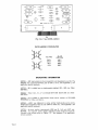
(5
E IN
0
~
TYPICAL WlEN BRIDGE
I
Figure 4-3.
Wien Bridge Circuit and Rejection Characteristics
4-26. In an independent, but similar, control loop,
the bridge input signal is shifted 900 and used as the
reference signal for the detector. This detector
develops control voltages to null the reactive leg of
the bridge, but is insensitive to signals of the form
in Figure 4-2b, which are caused by small tuning
e r r o r s of the resistive branch.
4-27. The result is that the two control loops derive
information from a common source and develop two
independent control signalsfor nulling the two legs of
the bridge. These control voltages are used to vary
the brilliance of lamps, which in turn cause resistance
changes in photocells that form part of the Wien bridge.
4-28. When the bridge circuit is tuned and balanced,
the voltage and phase of the fundamental, which
appears at junction of the series reactive leg (SQR1,
3, 5, 7, or 9 and C4A/B) and the shunt reactive leg
(SQRll, 13, 15, 17, or 19, and C4C/D), is the same
as at the midpoint of the resistive leg (A3R12 and
A3R14). When these two voltages are equal and in
phase, the fundamental frequency will not appear at
the drain of the field effect transistor A3Q4. For
frequencies other than the fundamental, the reactive
leg of the Wien bridge offers various degrees of
attenuation and phase shift which cause a voltage at
the output points of the bridge. This difference voltage between the reactive leg and resistive leg is amplified by A3Q4, A3Q5, and A3Q6. Figure 4-3 illustrates a typical Wien bridge circuit and the rejection
characteristics for it.
4-29. The Wien bridge circuit is designed to cover a
continuous frequency range of over a decade for each
position of the FREQUENCY RANGE selector S4. S4
provides coarse tuning of the reactive leg by changing
the bridge circuit constants in five steps at 1 decade
per step. For the automatic control loop, the reference voltage is taken from R6 at the input to the rejection amplifier and applied to the buffer amplifier
A5Q7. The reference voltage is amplified and clipped
by A5Q8 and A5Q9, and coupled to the detector A5Q4.
The output of the metering circuit, which contains the
fundamental frequency if either leg of the bridge is
untuned, is applied to the buffer amplifier A5Q1.
It is amplified by A5Q2 and A5Q3 and coupled to the
detector A5Q4.
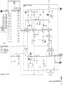
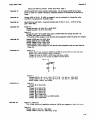
4-30. Refer to Figure 4-4, partial scheiiiatic for
detector operation. The discussion is applicable
to both resistive and reactive detector circuits.
4-31. The signals from the e r r o r amplifier, (A5Q2
andA5Q3) will be equal and of opposite phase, and
will cancel out each other when t h e detector, A5Q4, is
off. However, when the positive half of the referencc
square wave gates A5Q4 on, the signal from thc collector of A5Q3 will be shorted to ground. Thus the
signal from the collector of A5Q2 will be couplcd
through the filter network to the base of A5Q5. If thc
signal from A5Q2 is in phase with the referencc, thc
positive half of the signal will be passcd, and if it is
out of phase, the negative half will be passed.
4-32. The normal working voltage at A5TP3 is between0 and -1 volt. The dc output of the filter nctwork
causes the voltage at A5TP3 to go in a positive dircction (toward zero) for in phase e r r o r signals, and in
a negative direction (toward -1 V) for out of phase e r r o r
signals. The change in base voltage is then ampIificd
by A5Q5 and lamp driver A5Q6. This will change thc
brilliance of lamp A6DS1, which will v a r y the resistance of A6V1 in the direction necessary to balance the
resistive leg of the bridge.
I
I
I
I
I
1
I
Figure 4-4. Auto Control Loop Detector
4-3
Section IV
Model 333A/334
4-33. Refer to Figure 4-5 for the phase relationship
of the bridge error signal andreference voltage at the
base of A5Q4. The shaded portions of the e r r o r signals ( b a n d c) indicate that part of the e r r o r signal
which contributes to the dc lamp control voltage. As
indicatedind, any e r r o r signal that ie 90° outofphase
with the reference does not affect the dc lamp control
voltage, because equal amounts of the positive and
negative portions are passed.
4-34. The operation d the reactive branch control
loop ie similar to that of the resistive branch. The
45'
135'
225'
phase delay circuit, A5Q15, A5Q16, S4AF and
S4C1 through S4C5, shifts the
reference voltagc
90°, aa shown in Figure 4-5f. This makes the detector
A5Ql2 sensitive to components of the bridge e r r o r
signal that are 900 out of phase (g and h). The outpui
of the lamp driver, A5Q14, controls the brilliance of
A6DS2, which varies the resietance of A6V2 through
A6V5 to tune the branches of the reactive leg. Deck
AR of the FREQUENCY RANGE switch, 54, switches
A5R56 in parallel with A5R55 on the top three frequency ranges. A6DS2 w i l l become brighter, and lower
the resistance of A6V2 through A6V5, makingvariatio
45'
315'
f
a
Ref. signal for Reactive
Detector (A56 12 b
Ref. signalfor Resistive
Detector (A564)
b
Resistive Error signal
in phase with reference
at bridge
Reactive Error signal
in phase with reference
at bridge
h
Resptive Error signal
180 out of phase
Reactive Error signal
out of phase
d
i
Reactive Error signal
30 out of phase (Results
in no output from Resistive Detector)
R e p t i v e Error signal
90 out of phase(Results
in no output from Reactive Detector)
e
Error signal, reactive
leg detuned, resistive
.eg unbalanced
Error signal, Reactive
leg detuned, Resistive
leg unbalanced
Figure 4-5.
4-4
Reference and Error Phase Relationship
13s'
225'
316'
Model 333A/334A
E IN
Section IV
PREAMPLIFIER
A30IA303
1,
L
NEGATIVE FEEDBACK
FREOUENCY
3311/3141-10
Figure 4-6.
Rejection Amplifier Block Diagram and Typical Frequency Rejection Characteristic
in resistance less than on the two lower ranges, However, less variation in resistance is needed to tune
the leg, because the impedance in the reactive leg
becomes progressively less as the higher frequency
ranges are selected.
Refer to Figure 4-7, BandwidhVersus Null Depth for
further detail on the rejection characteristic.
4-35. Any e r r o r signal that is not an integralmultiple
of 900 is the result of the reactive leg of thebridge
being detuned, andthe resistive leg being unbalanced.
For example, an error signal that is 45O out of phase
(Figure4-5e and j) will result in outputs from both
resistive and reactive detectors to tune the bridge
and reject the fundamental.
4-40. The HIGH PASS FILTERis normally used when
the fundamental of the input signal is greater than 1
kHz. In the voltmeter mode of operation, the filter
is not used. In SET LEVEL and DISTORTION functions the filter presents >40 dB attenuation to 50 or
80 Hz hum components, but offers no attenuation to
frequencies over 1 kHz. The filter assembly, A7,
consists of A7C1, A7C2, and A7L1. The filter can
be inserted or bypassed by the HIGH PASS FILTER
switch, S9.
4-36. When the FUNCTION selector is set to the
VOLTMETER or SET LEVEL position, the junction
of the series and shunt reactive branches of the Wien
bridge is connected to circuit groundthroughA3R19
by SlBF which disables the frequency rejection
characteristic of the bridge circuit. With the bridge
circuit disabled, the rejection amplifier circuit provides one dB of gain for the fundamental frequency
and the harmonics. In the SET LEVEL operation, this
signal is used to establish the SET LEVEL reference.
4-37.
BRIDGE AMPLIFIER CIRCUIT.
4-38. The bridge amplifier circuit consists of three
stages of amplification, A3Q4 through A3Q6. The
f i r s t stage of amplification, A3Q4, is a field effect
transistor which amplifies the difference signal between
the gate and the source. The field effect transistoris
selected for minimum noise performance with the high
impedances of the Wien bridge circuit. The signal
from the drain is applied to the two stage feedback
amplifier A3Q5 and A3Q6. The output of A3Q6 is
coupled to the meter circuit by the post attenuator
S3Rl through S3R11. Negative feedback from the output of the bridge amplifier is applied to the preamplifier circuit to narrow the frequency rejection
characteristic. It can be noted from the rejection
characteristic (refer to Figure 4-3) for the bridge
that the rejection of harmonic voltages is not constant. Typically the second harmonic is attenuated
several dF3 more than the third harmonic andthethird
more than the fourth. The result of the negative feedback is illustrated by the rejection characteristic
shown in dashed lines on the attenuation and phase
characteristic of Figure 4-3. Figure 4-6 shows a
simplified block diagram of the rejection amplifier
with the typical frequency-rejection characteristic.
4-39. HIGH PASS FILTER.
(Refer to Figure 7-3).
4 -4 1. METER- AMPLIFIER
(Refer to Figure 7-4)
4-42. The meter amplifier consists of the post attenuator, the meter amplifier circuit, and the meter
rectifier circuit.
4-43.
POST ATTENUATOR.
4-44. The post attenuator, S3R1 through S3Rl1, is a
resistive network which attenuates the input signal in
10 dB steps. The attenuotor is usedin conjunction
with either the input sensitivity attenuator or the
1OOO:l attenuator to limit the signal level to the
meter amplifier to 1 mV for full scale deflection on
all ranges from 1 mV to 300 V full scale. The meter
circuit sensitivity is increased to 300 p V for full
scale deflection on the ,0003V range by switching
resistors A2R29 and A2R30 into the calibration network. Resistor A2R41 and capacitor A2C29 are also
switched into the calibration network on the .0003V
range to extend the passband of the amplifier.
4-45. METER AMPLIFIER CIRCUIT.
4-46. The meter amplifier circuit consists of a five
stage amp!ifier circuit, A2Q5 through A2Q9, which
develops the current for full scale meter deflection.
Negative dc feedback from the emitter circuit of
A2Q0 is applied to the base of A2Q5 to stabilize the
dc operating point of the meter amplifier circuit and
to minimize the tendency for dc drift due to ambient
temperature changes. A2R51 and A2CR8 are electrically in the circuit only when the meter amplifier ie overloaded. When the voltage on the emitter of A2Q9
4-5
Model 333A/334A
Section IV
0
-10
X IW
APPROXIMATE PERCENT 8ANDWIDTH=
-20
- 30
- 40
DEPTH OF NULL, DB
f0
333A/ S3.A-no
Figure 4-7.
4-6
Bandwidth Versus Null Depth
-50
- 60
- 70
Section IV
Model 333A/334A
becomes abnormally large during anoverload, A2CR8
breaks down and provides a lower resistance charging path for A2C15, which reduces the transient recovery time of the meter amplifier. Negative ac feedback is applied from the collector circuit of A2Q9 to
the emitter circuit of A2Q5. This feedback is used
to ensure f l a t frequency response, to improve linearity, and to reduce the effect of variationof transistor
parameters with environmental changes. In this
manner, the calibration of the instrument is made
dependent on high quality passive components.
4-47.
METER RECTIFIER CIRCUIT.
4-48. The meter rectifier is connected in a bridge
type configuration with a diode in each upper branch
and a dc milliammeter connectedacross the midpoints
of the bridge. The simplified meter rectifier is illustrated in Figure 4-8. The generator represented by
A2Q5 through A2Q9 with the internal impedance %
provides the meter, M l , with current for full scale
deflection and develops a voltage across the calibration network, which closes the ac feedback loop.
Capacitors A2C27 and A2C28 are used as coupling
capacitors for the ac feedback loop, outw signal to
the OUTPUT connector, and the bridge error signal
to the input of the automatic fine tuning loops. The
mechanical inertia of the meter and A2C26 prevents
the meter from responding to individual current
pulses, Therefore, the meter indication corresponds
to the average value of the current pulses rather than
the peak value. The meter is calibrated to indicate
the r m s value uf a sine wave. Resistor A2R45 impresses a fixed bias across diodes A2CR6 and A2CR7
(biasingthem close to the barrier voltage) to makethe
meter amplifier response linear to large variations
in signal amplitude. The linearity of this type uf circuit is also increased by including the meter circuit
in the overall feedback loop.
4-49.
POWER SUPPLY CIRCUIT.
(Refer to Figure 7-6)
4-50. The power supply circuit consists of a +25 volt
series regulated supply anda -25 volt series regulated
supply which is the reference supply for the +25 volt
SUPPlY
4-51. The -25 volt regulated supply is oftheconventional aeriesregulator type. The amplifier A1Q5 is
used to increase the loop gain of the circuit, thus improving voltage regulation. The positive feedback
applied to the junction of AlR11 and AlR12 is used to
further improve the line frequency suppression of the
circuit.
4-52. The +25 volt regulated supply is of the conventional series regulator type and operates the same as
the -25 volt regulated supply.
4-53. RF DETECTOR CIRCW". (334A only)
(Refer t o Figure 7-2)
4-54. The RF detector circuit consists of a rectifier,
A4CR1, and filter circuit. The RF signal is applied
to the circuit through the RF INPUT connector onthe
rear panel, The rectifier diode A4CR1 recovers the
modulating signal from the RF carrier and the filter
circuit removes any RF components before the signal
ia applied to the impedance converter circuit through
the NORM-RF DET switch. SI.
rI
I
I
I
I
I
I
I
L-
Figure 4-8. Simplified Metering Circuit
4-7
Section V
I
Model 333A/33U
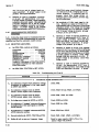
Table 5-1. Required Test Equipment
I
I
I
INSTRUMENT
TYPE
I
I
I
USE
SPECIFICATIONS
RECOMMENDED
MODEL
~
Voltage Range: 300 pV to
300 V r m s
Accuracy: f 0.2 % at 400 Hz
Performance Checks,
Adjustment and Calibration
Voltage Range: 300 W Vto 3V
Frequency Range: 10 Hz to 3 MH
-hp- Model 652A Test
Performance Checks,
Adjustment and Calibration Oscillator
Wave Analyzer
Bandwidth: 5 kHz to 600 kHz
Dynamic Range: >80 dB
Performance Checks
Electronic
Counter
Functions: period, 1 sec. gate
Accuracy: f2 counts
Performance Checks,
-hp- Model 5532A
Adjustment and Calibration I Electronic Counter
Voltmeter
Calibrator
I
Test Oscillator
'$
oscilloscope
I
~
~
-hp- Model 310A Wave
Analyzer
Adjustment and Calibration, -hp- Model 3465A
Multimeter
Troubleshooting
~~~
~~~~~
-hp- Model 140A/1402A/
1420A Oscffloscope
~~~~
AC Voltmeter
Voltage Range: 100 pV to 30V
Frequency Range: 20 Hz to 4 MHz
Troubleshooting
-hp- Model 400F
AC Voltmeter
Filter Box
Filtered Outputs: 500 Hz, 5kHz
250 kHz, 600 kHz
Output Distortion: <80 dB
Performance Checks
White Model 2640 Filter
Set
Power Supply
Output Voltage: &OO Vdc
Performance Checks
-hp- Model 6515A Power
I
-hp- Model 606A Signal
Generator
Signal Generator
5-0
~
I
Ran :lorn'to lwoMC
Accuracy:*l *(O. 03% readings +
0.02% Range) worst Case
Bandwidth: DC to 10 MHz
Vertical: Dual Channel
Multimeter
~~~~
I
-hp- Model 738BR Voltmeter Calibrator
Oscillator
Voltage Range: 1V
Frequency Range: 1 lcHz
Output: Floating, f 400 Vdc
Performance Checks
-hp- Model 204C
Oscillator
AC Probe
Input Impedance: 10 M52
shunted by 10 pF
Trouble shooting
-hp- Model 11074A
Voltage Divider Probe
Terminating
Re sistance s
Feedthru: 5052 f 1%
and
Feedthru: 60052 f 1%
-hp- Model 11048B
Performance Checks
and
Adjustment and Calibration
-hp- Model 11095A
Shielded Loads
Resistance: 60052
and
Resistance: 100 k52
Performance Checks
See Figure 5-7
Resistors
F x d 100 k52f 1%, 1/2 W
and
Fxd: 10 k52 f 1%1/2 W
Fxd: 500 kSZ f 18, 1W
Performance Checks
-hp- Part NO,0727-0208
-hp- Part NO. 0757-0215
- h p part NO. 07304156
Section V
Model 333A/334A
SECTION V
MAINTENANCE
5-1. I NTR ODUCTI 0 N.
5-2. This section contains maintenance and service
information for the 333A and 334A Distortion Analyzers. Included a r e Performance Checks, Adjustment
and Calibration Procedures, and Troubleshooting
Techniques.
5-8. A Performance Check Test Card is provided at
the end of this section for recording the performance
of the instrument during the performance checks. The
card may be removed from the manual and used as a
permanent record of the incoming inspection or of
a routine performance check. If the instrument fails
to meet any of its specifications, perform theAdjuatment and Calibration Procedures, Paragraph 5-23.
5 - 3 . REQUIRED T E S T EQUIPMENT.
VOLTMETER ACCURACY AND FREQUENCY
RESPONSE CHECK.
5-9.
5-4. The e uipment needed to properly maintain the
Model 333A7334A is listed in Table 5-1. If the recommended model is not available, any instrument
that has specifications equal t o or better than the required specifications may be used.
a. Conned voltmeter calibrator t o 333A/334A
as shown in Figure 5-1. Test oscillator
w i l l be used later in check.
Set 333A/334A FUNCTION Switch to VOLTMETER.
Set voltmeter calibrator for 400 Hz r m s
C.
output.
d. Check 333A/334A voltmeter f u l l scale reading on all ranges against appropriate rms
input from voltmeter calibrator. Voltmeter
accuracy should be within &2%.
b.
5-5. PERFORMANCE CHECKS.
5-6. The performance checks are in-cabinet procedures that can be used to verify instrument performance. These procedures can be used for periodic
maintenance, to check specifications after a repair,
or for incoming quality control inspection. Performance checks for both the 333A and 334A are provided.
The performance checks are applicable toboth instruments except where noted in paragraph heading.
5-7. The performance checks a r e made with the ac
power cord connected to nominal line voltage (lOOv/
120V/ 220V/ 240V, 48 to 66 Hz), MODE SWPTCH to
MANUAL, HIGH PASS FILTER to OUT, and NORM.
R F. DET. switch to NORM, unless otherwise
specified.
-
e.
Disconnect voltmeter calibrator.
f.
Connect 5052 output of test oscillator, terminated in 5052, to 333A/334A.
g.
Set 333A/334A METER RANGE switch to 3
VOLTS.
VOLTMETER CALIBRATOR
hp 738BR
DISTORTION ANALYZER
hp 333A/334A
c.
r~
(9
tt
''
0 0
006
0
I
I
I
I
-
I
I
TEST OSCILLATOR
I
hp 6521
9 - 8
Figure 5-1.
fiL
son FEED-THRU
I
TERMINATION
I
I
I
I
I
------------
SSA-B-1468
Voltmeter Accuracy and Frequency Response Check
5-1
Model 333A/334A
Section V
3V RANGE
METER INDICATION
MIN.
MAX.
FREQ.
FREQ.
0.0003V RANGE
METER INDICATION
MIN.
MAX.
20 Hz
30 Hz
1 kHz
10 ma
100 kFiz
300 k?Iz
285 pV
294 pV
294 pV
294 pV
294 pV
294 pV
285 pV
I
2.94
2.94
2.94
2.94
2.94
2.85
2.85
h.
V
V
V
V
V
V
V
3.06 V
3.06 V
3.06 V
3.06 V
3.06V
3.15V
3.15V
Set test oscillator to 400Hz, and adjust
amplitude until 333A/334A meter indication
is 3 V. Set reference on meter of test oscillator and use amplitude control to maintain
set reference whenever frequency of oscillator is varied.
500 kHz
5-10. FUNDAMENTAL REJECTION CHECK
a. Connect test equipment to 333A/334A 88
shown in F e e 5-2. Set filter pass frequency t o 500 Hz.
NOTE
The test oscillator output ie filtered
so that the input to the 333A1334A
is a pure ac signal.
t Set test oscillator to each frequency lMed in
Table 5-2. At each respective frequency,
333A/334A meter reading should be within
tolerances listed in table.
j.
k
Set 333A/334A METER RANGE switch to
b.
Set 333A/334A controls as follows:
FUNCTION
VOLTMETER
METER RANGE
1 VOLT
MODE
MANUAL
XI00
FREQUENCY RANGE
Frequency Dial.
5
c.
Set test oscillator frequency to 500 Hc, and
adjust amplitude for indication of 1.0 volt on
0.0003 VOLTS.
Set test oscillator to 400 Hz, and adjust amplitude until 333A/334A meter indication is
300 pV. Set a reference on meter of test
oscillator and use amplitude control to maintain set reference whenever frequency of
oscillator is varied.
315 p V
306pV
306 p V
306 pV
306 p V
306 p V
315 p V
. . . .. .. .. .. .. .. .. . .
. . . . . . . . .. .. .. .. .. .. . .
.............
meter of 333A/334A.
1.
Set test oscillator to each frequency listed
in Table 5-4. At each respective frequency,
333A/334A meter reading should be within
tolerances listed in table.
6
Set 333A/334A FUNCTION switchto SeT
LEVEL, and set METER RANGE to 0.3 V.
Adjust SENSITIVITY controls for OdB indication on 333A/334A meter.
WAVE ANALYZER
hp 310A
FILTER SET
WHITE 2640
3S3&-@-14e6
Figure 5-2.
5-2
Fundamental Rejection Check
Section V
Model 333A/334A
Adjust wave analyzer controls for maximum
reading (approximately 500 Hz), and use as
OdB reference.
d.
f.
Set 333A/334A FUNCTION Switch to DISTORTION.
e.
g.
Adjust 333A/334A frequency dial vernier and
BALANCE controls for minimum meter indication. When meter indication is less than
10% of SET LEVEL indication, set MODE
switch to AUTOMATIC.
Set test oscillator frequency to 15 Hz at an
amplitude of 1 volt.
Adjust 333A/334A SENSR'IVITY controls for
O d B indication on meter.
Set 333A/334A FUNCTION switch to DISTORTION. Stepdown METER RANGE swltch
while adjrusting frequency dial and vernier
balance controls for best null indication on
meter. Do naC change frequency or balance
settlngs after best null is obtained.
f.
Set 333A/334A FUNCTION switch to SET
LEVEL, and set METER RANGE switch to
e.
h.
i.
c.
Reduce 333A/334A METERRANGE Wpitch
setting as necessary to maintain on-scale
meter indication.
g.
Observe wave analyzer meter, and reduce
wave analyzer range setting as necessary to
maintain on-scale meter indication.
h.
OdB.
Set test oscillator frequency to 30 Hz, and
adjust amplitude for OdB indication on 333A/
334A meter.
Set 333A/334A FUNCTION switch to DISTORTION. Meter reading should not change
more than +1 dB from O d B reference.
NOTE
Repeat Steps b through h f o r each respective
frequency and second harmonic listed in
Table 5-3. 333A/334A meter readings should
remain within tolerances listed in table,
.i
mental rejection; therefore, the
total fundamental rejection is the
sum of the 333A/334A METER
RANGE setting and the wave
analyzer reading.
333A/334A
TEST OSCILLATOR 333A/334A
FREQUENCY
FREQUENCY
TOLJIFbdNCES
(Second Harmonic)
j.
The 333A/334A METER RANGE setting plus
the wave analyzer reading should tutal more
than -80 dB.
k.
Repeat steps b through j with 333A/334A
and test equipment frequencies set t o 5 kHz,
50 kHz, 250 kHz, and 800 UIz.
5-11.
a.
b.
SECOND HARMONIC ACCURACY CHECK
Connect test oscillator 50$20utput, terminated in 5051 load, to 333A/334A.
5-12.
400 kHz
1 MHZ
c-2.0 dB
C-3.0 dB
quency to 500 Hz.
b.
............
FEED-THRU
TERM INATION
c*O. 6 dB
e-1.0 dB
a. Connect test equipment to 333A/334A a8
shown in Figure 5-3. Set fflter pass fre-
.........
. . . . .. .. .. ... ... ... ... ... ... .. .. .
6oon
100 kHz
INSTRUMENT INDUCED DISTORTION CHECK.
Set 333A/334A controls as follows:
FUNCTION,
SET LEVEL
ODB
METER RANGE
MANUAL
MODE..
FREQUENCYRANGE
X1
Frequency Dial.
15
TEST OSCILLATOR
ho 652A
20 kHz
10 kHz
50 kHz
200 kHz
500 kHz
FILTER SET
WHITE 2 6 4 0
Set 333A/334A controls as follows:
SET LEVEL
FUNCTION
SENSITIVITY..
MAX.
SENSlTMTYVERNIER..
MIN.
METER RANGE.
ODB
MODE..
MANUAL
FREQUENCY RANGE.
XlOO
Frequency Dial
5
. . . .. .. .. .. .. .. .. . . . .
.....
............
. . . . . . . .. .. .. .. .. .. . .
..............
1
DISTORTION ANALYZER
hp 333Al334A
~
Figure 5-3.
InEtrument Induced Distortion Check
5-3
Section V
Model 333A/334A
C.
Set test oscillator frequency to 500 Hz, and
adjust amplitude for indication of +2 d~ on
333A/334A meter.
d.
Set 333A/334A FUNCTION switch to DISTORTION.
e.
Adjust 333A/334A frequency dial vernier and
BALANCE controls for minimum meter indication. When meter indication is lessthan
10%of SET LEVEL indication, set MODE
switch to AUTOMATIC.
Reduce 333A/334A METER RANGE setting
as necessary to maintain on-scale meter
indication.
f.
e. 333A/334A meter indication should be at
least 70 dB below +2 dB reference.
h. Repeat steps b through g with 333A/334A
and test equipment frequencies set to 250
kHz and 600 IrHz. 333A/334A meter indication should be at least 64 dB below +2 dB
reference.
5-13.
FREQUENCY CALIBRATION ACCURACY
CHECK.
a. Connect test equipment to 333A/334A as
shown in Figure 5 4 . Set electronic counter
to read period.
NOTE
In this check, the 333A/334A
frequency dial is held constant
and the input frequency is varied
and monitored. If the dial is low,
the input frequency will be high at
null and vice versa.
Set 333A/334A controls as follows:
b.
.. .. ..- .. .. .. .. .. SET
.. .. ..LEVEL
.MAX.
ODB
MODE.. . . . . . . . . . . . . . M.ANUAL
FREQUENCYRANGE . . . . . . . . . . X l
FUNCTION
SENSITIVITY..
METERRANGE
Frequency Dial.
. . . . . . . . . . . . . 10
Set test oscillator frequency to 10 Hz, and
adjust amplitude for indication of +2 dB on
333A/334A meter.
C.
Set 333A/334A FUNCTION switch to
DISTORTION.
e. Do not adjust 333A/334A frequency controls.
m j x test oscillator frequency and 333A/
334A BALANCE controls for minimum indication on 333A/334A meter.
f. Repeat stepe until best null is indicated on
333A/334A. Reduce METER RANGE setting
as necessary to maintainon-scale meter
indication.
g* Electronic counter should indicate period of
100 meec f 5 m8ec (10 Hz f 5%).
6
h.
Set electronic counter t o read frequency.
Repeat Steps b through f for each frequency
listed in Table 5-4. At each respective
frequency setting, electonic counter should
indicate that test oscillator frequency ie
within tolerances listed in table.
ELECTRONIC COUNTER
hp 5532A
TEST OSCILLATOR
hp 652A
0
d
U14-I-14S7
DISTORTION ANALYZER
hp 333A/334A
6oon
FEED-THRU
TERMINATION
hp 1 1 0 9 5 ~
Figure 5-4.
5 -4
clu
0 - 0 09
ADAPTER
BNC
hp Port
"Tu
NO.
1250-0072
Frequency Calibration Accuracy Check
0
Section V
Model 333A/334A
1.
r
333A/334A
TEST
FREQUENCY OSCILLATOR
FREQUENCY
1100 kHz
200 kHz
400 kHz
600 kHz
ELECTRONIC
COUNTER
INDICATION
m. Adjust SENSITIVITY controls for +2 dB indication 333A/334A meter.
n. Set 333A/334A FUNCTION switch to DISTORTION.
950 Hz to 1050 Hz
95kHz to 105 kHz
190 kHz to 210 ldIz
360 kHz to 440 kHz
540 kHz to 660 kHz
Adjust 333A/334A frequency dial vernier and
BALANCE controls for minimum meter indication. Reduce METER RANGE setting as
necessary to maintain on-scale meter reading. Note meter reading.
P. Set 333A/334A FUNCTION and METER
RANGE switch, respectively, to SET LEVEL.
Then set FUNCTION switchto DISTORTION.
q* Adjust 333A/334Afrequency dial vernier and
BALANCE controls for meter indication of
less than 10% of set level (*2 dB).
0.
AUTOMATIC N U L m G MODE CHECK.
5-14.
a. Connect 5051 output of test oscillator, terminated in 5052 load, t o 333A/334AINPUT
terminal.
b.
C.
Set 333A/334A controls as follows:
SET LEVEL
FUNCTION.
SET LEVEL
METER RANGE
MANUAL
MODE
X1
FREQUENCY RANGE
Frequency Dial
25
. . .. .. .. .. .. .. ..
. . . . . . . . .. .. .. .. .. .. . . .
............
Set test oscillator frequency to 25 Hz at an
amplitude of 1 V.
r.
Set 333A/334A MODE switch to AUTOMATIC.
Reduce METER RANGE setting as necessary
to maintain on-scale meter readmg. Meter
reading should be within +l.5 dB -0dB of
manually nulled reading obtained in step 0.
5.
Repeat steps k through r with 333A/334Aand
test oscillator frequency set to 5 kHz, 50 kHz,
d. Adjust SENSITIVITY controls for +2 dB
indication on 333A/334A meter.
e.
Set 333A/334A FUNCTION switch to DISTORTION.
Adjust 333A/334A frequency dial vernier
and BALANCE controls for minimum meter
indication. Reduce METER RANGE setting
as necessary to maintain on-scale meter
reading. Note meter reading.
g* Set 333A/334A FUNCTION and METER
RANGE switch, respectively, to SET LEVEL.
Then set FUNCTION switch t o DISTORTION.
h. Adjust 333A/334A frequency dial vernier
and BALANCE controls for meter indication
of less than 3% of set level (c2 dB).
f.
i.
1.
k.
Set 333A/334A MODE switch to AUTOMATIC.
Reduce METER RANGE setting as necessary
to maintain on-scale meter reading. Meter
reading should be within +3 dB -0dB of
manually nulled reading obtained in step f.
Repeat steps b through i with 333A/334A
frequency dial set t o 50, and test oscillator
frequency set to 50 Hz.
Set 333A/334A controls as follows:
FUNCTION.
SET LEVEL
METER RANGE
SET LEVEL
MODE..
MANUAL
FREQUENCY RANGE
X10
Frequency Dial.
50
. . .. .. .. .. .. .. ..
. . . . . . . .. .. .. .. .. . . .
...........
Set test oscillator frequency to 500 He, at an
amplitude of 1 V.
and 500 kHz.
5-15.
INPUT IMPEDANCE CHECK.
5-16.
RESISTANCE CHECK
a. Connect 5052 output of test oscillator, terminated in 5052 load, to 333A/334AMPUT
terminals.
b.
Set 333A/334A controls as follows:
FUNCTION.
VOLTMETER
SENSITIVITY
MAX.
SENSITIVITY VERNIER.
MAX.
METER RANGE
1 VOLT
C.
Set test oscillator frequency to 100 Hz, and
adjust amplitude for indication of 1 volt on
333A/334A meter.
d.
Connect a 100 k51 resistor in series with
333A/334A input.
e.
333A/334A meter indication should be between
0.85 V and 0.95 V.
This verifies an input
resistance of 1MS~&%involtmeter function.
.........
. . . . . . .. .. .. .. .. ..
..........
Remove 100 kS1 resistor, and reconnect
oscillator to 333A/334A.
g* Set 333A/334A FUNCTION switch to SET
LEVEL, and set METER RANGE switch to
0.1 VOLT.
h. Adjust 333A/334A SENSITIVITY controls
for meter indication of 0.1 V.
f.
5-5
Model 333A/334A
Section V
i.
Connect 100 k52 resistor in series with
333A/334A input.
h.
j,
333A/334A meter indication should be between 85 mV and 95 mV. This verifies an
input resistance of 1 MSZ*5% in set level
and distortion functions.
i.
CAPACITANCE CHECK
a, Connect 5052 output of test oscillator, terminated in 5051 load, and 10 k52 resistor to
333A/334A as shown in Figure 5-5. Connect
the resistor lead to the INPUT terminal of
the 333A/334A, and insert the other lead
directly into the 5052 load. Connect the ground
lead from the 333A/334A to the outer shield
of the 50 52 load; do not use an adapter, as it
would add capacitance.
b. Set 333A/334A controls as follows:
FUNCTION.
VOLTMETER
MAX.
SENSITIVITY..
SENSITIVITY VERNIER. ,
,
MAX.
1 VOLT
METER RANGE
5-17,
. . .. .. .. .. .. .. .. . . . .
. . . . . . .. .. . .. .
C.
d.
e.
f.
8.
Set test oscillator to 100 Hz and adjust amplitude for 333A/334A meter indicationof 1V.
Set a reference on meter of test oscillator
and use amplitude control to maintain set
reference whenever frequency of oscillator
is varied.
Increase frequency of test oscillator to 540
(455) kHz. 333A (334A) meter indication
should be 0.707 V or greater. verifying an
input capacitance of 30 (35) pF or less on
1 V range in voltmeter function.
Set 333A/334A METER RANGE switch to
0.1 V range.
Set test oscillator to 100 Hz and adjust amplitude for 333A/334A meter indication of 0.1V.
Set a reference on meter of test oscillator
and use amplitude control to maintain set
reference whenever frequency of oscillator
is varied.
Increase frequency of test oscillator to 230
kHz. 333A/334A meter indication should be
70.7 mV or greater, verifying an input
capacitance of 70 pF or less on 0.1 V range
in toltmeter function.
TEST OSCILLATOR
hp 652A
0
333A-1-1469
5 -6
j.
5-18.
a.
b.
c.
d.
e.
Set 333A/334A FUNCTION switch to SET
LEVEL.
Set test oscillator to 100 Hz and adjust amplitude for 333A/334A meter indication of
0 . 1 V. Set a reference on meter of test oscillator and use amplitude control to maintain
set reference whenever frequency of oscillator is varied.
Increasefrequencyof test oscillator to 230 kHz.
333A/334A meter indication should be 70.7
mV or greater, verifying an input capacitance
of 70 pF or less in set level and distortion
functions.
MINIMUM INPUT LEVEL CHECK
Connect 5051 output of test oscillator, terminated in 5052 load, to 333A/334A INPUT
terminals.
Set 333A/334A controls a s follows:
VOLTMETER
FUNCTION
SENSITIVITY..
MAX.
SENSITMTYVERNIER..
MAX.
0 . 3 VOLTS
METER RANGE
Set test oscillator to 400 He and adjust
amplitude for 333A/334A meter indication
of 0 . 3 v.
Set 333A/334A FUNCTION switch to SET
LEVEL.
333A/334A should indicate full scale or
greater.
. . . .. .. .. .. .. .. .. . . . .
. . . . . . .. .. . . .
DC ISOLATION CHECK
a. Set the 6515A to zero output, and connect
test equipment to 333A/334A as shown in
Figure 5-6.
5-19.
[wIInlnOI
REMOVE SHORTING BAR BETWEEN CHASSIS GROUND ( + )
AND FRAME GROUND ( A ) ON
333A/334A INPUT TERMINALS.
b.
Set 333A/334A controls a s follows:
. . .. .. .. .. .. .. .. VOLTMETER
. . . 1 VOLT
FUNCTION.
METER RANGE
5On FEED-THRU
TERM INATION
-
DISTORTION ANALYZER
hp 333A/334A
Model 333A/334A
Section V
TO GROUND
( f ) TERMINAL
(ON R E A R PANEL
O F T H E hp 2 0 4 C )
SUPPLY
ps:WER
p 6515A
DIGITAL MULTIMETER
hp 3 4 6 5 ~
L
Ffgure 5-6.
c.
DC Isolation Check
Set oscillator to 1 kHz, and adjust amplitude
for 333A/334A meter indication of 0.9 V.
d. Set power supply to A00 VDC. 333A/3344
meter indication should not change. There
should be approximately 0.27 mA indicated
on the Multimeter's 1 mA range.
5-20.
am
'I
1
h.
5-21.
a.
HIGH PASS FILTER CHECK.
Connect 500 output of test oscillator, terminated in 500 load, to INPUT terminals of
333A/334A.
Reading on 333A/334A meter should be at
least40 dB below 0 dB setting.
RESIDUAL NOISE CHECK.
Connect a shielded 60051 load across 333A/
334A INPUT terminals. (See Figure 5-7
for details on constructing shielded load).
Be sure that shorting bar is connected between chassis ground and circuit ground on
INPUT terminals.
Set 333A/334A controls as follows:
,
, VOLTMETER
FUNCTION ,
METER RANGE
,
0.0003 VOLTS
c. Meter should indicate less than 25 pV.
d. Remove 60052 load. Connect a shielded 100k52
load across INPUT terminals. (See Figure
5-7 for details on constructingshieldedload).
e. Meter should indicate less than 30 pV.
b.
b.
Set 333A/334A controls as follows:
FUNCTION.
SET LEVEL
METERRANGE
SET LEVEL
IN
HIGH PASS FILTER. ,
C.
Set test oscillator to 5 W e at an amplitude
of 0.3 V. Set a reference on meter of test
. . .. .. .. .. .. .. .. ..
..... ....
oscillator and use amplitude control to
maintain set reference whenever frequency
of oscillator is varied.
d. Adjust 333A/334A S E N S T M T Y controls for
meter indication of OdB.
5-22.
a.
b.
e.
Set test oscillator to 1 We.
f.
Reading on 333A/334A meter should be
within 0 . 5 dB of 0 dEJ setting.
g*
Set test oscillator to 60 Hz.
. . . .. .. . .. . .
AM DETECTOR CHECK (Model 334A OnlJr).
Connect high frequency signal generator 5052
RF output to 334A R. F. INPUT terminal.
Set 33449 controls as follows:
FUNCTION.
.SET LEVEL
NORM. R.F. DET.
,
R F. DET.
METER RANGE
.SET LEVEL
MODE,.
,
,, ,
MANUAL
FREQUENCYRANGE ,
, ,
XlOO
Frequency Dial
,,
, 10
-
. . . . . .. .. . .. .
. . . .. .. .. . .. ... . .. . . .
. . . .. . . . . .
5-7
Section V
-
No.
Description
1
2
3
4
Connector, male
Connector, male w/indator
Lug, terminal 900
Resistor, 100 kS1, 1/1 W, 58,
metal flm
OR
Resistor, 600 a, 1/4 W, 0.5%
metal film
Washer, int. lock
Spacer, 6-32 threaded
Shield
Screw, bind. head, 6-32 x 1/4 in.
-hp- Part NO.
1251-0174
1251-0175
0360-0042
0758-0053
-
4
5
6
7
STO-O-OOOB
Figure 5-7.
8
Shielded Load Assembly
0757-1037
2 190-0007
0 380-0058
1251-1073
2470-0001
switch to MANUAL, HIGH PASS FILTER TO OUT, and
NORM. -RF. DET. switch to NORM, unless otherwise specified.
c.
Set high frequency signal generator to 1 M H z
at an amplitude of 3V. Modulate high frequency signal generator output 30% at 1kHz,
using a test oscillator.
d,
Adjust 334A SENSITIVITY controls for OdB
meter indication.
a.
Remove top and bottom covers.
e.
Set 334A FUNCTION switch to DISTORTION.
b.
Secure shorting bar between chassis ground
and circuit ground INPUT terminals.
f.
Adjust 334A frequency dial vernier and balance controls for minimum meter indication.
c.
Connect common lead of a dc voltmeter to
either INPUT ground terminal.
Distortion should be more than 40 dB below
OdB reference.
d.
Perform the measurements and adjustments
listed in Table 5-5.
5-26.
g.
5-23. ADJUSTMENT A N D CALIBRATION
POWER SUPPLY AND BIAS ADJUSTMENTS.
PR 0 CED U RE.
5-24. The following is a complete adjustment and
calibration procedure for the 333A and 334A. Before
proceeding with these adjustments, the Performance
Checks should be performed to determine whether
adjustments are necessary. If your instrument does
not meet the test limits specified in the following steps,
refer to Troubleshooting Procedure, Paragraph 5-34.
Adjustment locations are shown in Figure 5-8.
5-25. The adjustment and Calibration Procedure ie
performed with the ac power cord connected to nominal line voltage (115 V/230 V) 48 to 66 He, MODE
MEASUREMENT
POINT
VOLTAGE
LIMITS
DO NOT ALLOW PROBE TO SHORT
A2TP1 TO GROUND. IF THIS
HAPPENS, A2Q4 MAY BE DESTROYED.
VOLTMETER GAIN ADJUSTMENTS.
5-27.
.a
Connect voltmeter calibrator t o 333A/334A
as shown in Figure 5-1.
b.
Set Distortion Analyzer controls as follows:
VOLTMETER
FUNCTION.
METER RANGE
0.001 VOLTS
ADJUSTMENT
. . .. .. .. .. .. .. ..
REGULATION
line voltage between
5 and 126.5 VAC)
-25 V f 0.25 V
+25 V f 1.0 V
-11.3 v &. 1 v
,+8.2 V f 0.5 V
+2.65 V f 0.2 V
-19.5 v f 0.5 v
'%.
AlR13
-25 V i 0.5 V
Any violet wire
None *
Any red wire
+25 V f 1.0 V
-11.3 v
A2 TP1
A2R3
+8.2 V i 0.5 V
MR20
Aa TP2
A3R4
A3 TP1
+2.65 V f 0.2 V
A3R16
-19.5 v f 0.5 v
A3 TP2
*Referencedto-25 volt supply; -25 volt supply must be adjusted f i r s t .
I
Section V
Model 333AJ334A
334A ONLY
V//A
S3C6
S3C 1
~~~~
~
Figure 5-8.Adjustment and Chassis Mounted Component Location.
5 -9
Section V
Model 333AI3344
k.
Adjust A2R34 (400 Hz CAL. ) for a meter indication of 1.0 mV.
Set test oscillator frequency to 2 MHe, a
attenuate output by 40 dB, maintainingrefm'
ence set in step j.
1.
Set 333A/334A METER RANGE Switch to
0.01 VOLTS.
Set Voltmeter Calibrator to 0.3 mV r m s
output. Set 333A/334A METER RANGE
switch to 0.0003 VOLTS.
m. AdjustA2R39 for 333A/334Ameter indication
of 9 mV.
c.
Set voltmeter calibrator to 1 mV r m s output
at 400 Hz.
d.
e.
f.
The meter should indicate 300 pV f 6 p V
(*2%). If n e c e s s q , change value of A~FUO*
to set reading within these limits. Typical
values for this resistor a r e from 15052 to
30052. Increasing resistance decreases the
meter reading, and vice versa.
n.
Set test oscillator frequency to 3 MHz.
0.
Adjust A2C21 for 333A/334A meter indication
of 9 mV.
NOTE
Adjustments of A2R39 and A2C21
interact. Therefore, it may be
necessary to repeat the two adjustments to bring both within
tolerance.
5-28. VOLTMETER FREQUENCY RESPONSE
STMENT.
a. Connect test oecillator to 333A/334A as Shawn
in Flgure 5-1.
b.
C.
NOTE
P.
Set 333A/334A METER RANGE switch to
. 3 VOLTS.
Cover plate (Item 33 in Figure
6-1) must be in place before
performing these adjustments.
9.
Disconnect test oscillator, and connect voltmeter calibrator to 333A/334A.
Set voltmeter calibrator to 0.3V r m s at 400
Hz. Note 333A/334A meter reading.
Disconnect voltmeter calibrator, and connect
test oscillator to 333A/334A.
Set test oscillator frequency to 400 Hz, and
adjust amplitude until 333A/334A meter indication is same as in step r. Set a reference on meter of test oscillator and use amplitude control to maintain set reference whenever frequency of oscillator is varied.
Set test oscillator frequency to 2.5 MHz.
Set 333A/334A controls as follows:
FUNCTION.
VOLTMETER
METER RANGE ,
0.0003 VOLTS
. . . .. .. .. .. .. .
Set test oscillator to 400 Hz, and adjust amplitude for 333A/334A meter indication of 300
pV. Set a reference on meter of test oscillator and use amplitude control to maintain
set reference whenever frequency of oscillator is varied.
r.
8.
t.
d. Set test oscillator frequency to 20 Hz.
U.
e.
V.
333A/334A meter should indicate 300 pV
f 15pV. If reading exceeds these limits,
change value of A2C30*. Typical values
for this capacitor are between 10 pF and
50 pF.
f.
Set 333A/334A METER RANGE switch to 1
VOLT.
g.
Disconnect test oscillator, and connect voltmeter calibrator to 333A/334A as shown in
Figure 5-6.
W.
X.
Y*
5-29. BRIDGE BALANCE ADJUSTMENT.
h. Set voltmeter calibrator to 0.9 V r m s at
400 Hz. Note 333A/334A meter reading.
5-10
i.
Disconnect voltmeter calibrator and connect
test oscillator to 333A/334A.
1.
Set test oscillator frequency to 400 Hz, and
adjust amplitude so that 333A/334A meter
reading is same as in step h. Set a reference on meter of test oscillator and u s e
amplitude control to maintain set reference
whenever frequency of oscillator is varied.
Adjust S3C6 for 333A/334A meter indication
of 0.3 v.
Set 333A/334A METER RANGE switch to 3
VOLTS.
Set test oscillator frequency to 200 kHz, and
increase amplitude by 20 dB, maintaining
reference set in step t.
Adjust S3C1 for 333A/334A meter indication
of 3 v.
MAINTAIN THE LEAD DRESS TO C3
AND THE TUNING CAPACITOR, C4.
ANY CHANGE IN LEAD DRESS WILL
CAUSE A CHANGE IN CAPACITANCE.
a Connect test equipment to 333A/334A as
shown in Figure 5-4.
b.
Set 333A/334A controls as follows:
FUNCTION,. , , , ,
SETLEVEL
.
. ..
Section V
Model 333A/334A
. .. . . . .. . . . .
. . . . . . . .. .. .. .. ..... .
............
SENSITIVITYVERNlER..
MIN.
SENSITIVITY.
.1 step counterclochise
METER RANGE
,
,
SET LEVEL
MODE..
MANUAL
FREQUENCY RANGE
X1K
Frequency Dial.
60
C.
Turn slot on trimmer capacitor C3 parallel
with side casting of instrument.
d. Set test oscillator frequency to 60 kHz, and
adjust amplitude for indication of +2 dB on
Set 333A/334A COARSE and FINE BALANCE
controls to center of range.
f.
Set 333A/334A FUNCTION switch to DISTORTION.
Observe electronic counter indication. If
test oscillator frequency is not between
57 kHz and 63 kHz, 333A/334A frequency
dial is out of tolerance. Follow steps below to bring frequency dial within tolerance:
Set 333A/334A controls as in step b.
Set test oscillator frequency for electronic counter indication of 60.00 HI,
and adjust amplitude for indication of
+2 dB on meter of 333A/334A.
C.
Set test oscillator frequency to 400 Hz, adjust amplitude for indication of 9 mV on
333A/334A meter.
. .. .. .. .. .. .. ..
. . . . . .......... . .
reference whenever frequency of oscillator
is varied.
g* Adjust test oscillator frequency vernier control and C3 for definite null indication on
meter of 333A/334A. Reduce METER
RANGE setting as necessary to maintain
on-scale reading.
h.
Set Distortion Analyzer controls as follows:
FUNCTION..
SETLEVEL
METER RANGE
0.01 VOLTS
SENSITIVITY
Position 5
SENSITIVITY VERNIER
MAX.
d. Set a reference on meter of test oscillator
and use amplitude control to maintain set
333A/334A meter.
e.
b.
5-31.
e.
Set test oscillator frequency to 100 kHz.
f.
Adjust S2C5 for 333A/334A meter indication
of 9 mV.
8.
Set 333A/334A SENSITIVITY switch to each
position listed in Table 5-6, and increase
test oscillator output by 10 dB f o r each respective decrease in SENSITIVlTY switch
position. Adjust appropriate capacitor for
333A/334A meter indication of 9 mV at each
setting.
NOTE
When switching the SENSITMTY
positions, be careful not to move
SENSITIVITY VERNIER control
from MAX. position.
ADJUSTMENT OF FACTORY SELECTED
COMPONENTS.
Set 333A/334A COARSE and FINE BALANCE controls to center of range.
5-32. Certain components in the Model 333A/334A
are individually selected to compensate for va.rying
Adjust 333A/334A frequency dial vernier
control for definite null.
Remove knob from frequency dial. Do
not change tuning capacitor, C4, setting
Loosen retaining screws in frequency
dial plate, and slip dial until 60 is directly under mark on indicator. Be
careful not to change C4 setting.
Tighten retaining screws and replace
knob.
5-30.
SENSITIVITY SWITCH CALIBRATION.
a. Connect test oscillator to 333A/334A ae
shown in Figure 5-1.
NOTE
Selector positions for the SENSIT M T Y selector will be referred to
as follows: MIN = Position 1, next
step = Position 2, etc., to MAX =
Position 6.
circuit parameters. These components are designated
lqr an asterisk (*) on the schematic and in the parts
list, and the typical value is shown Table 5-7
describes the function of the factory selected components and lists their value ranges.
5-33, T R O U BLES H 0 OTI N G PR 0 CEDU R E t .
5-34. This section contains procedures designed to
assist in the isolation of malfunctions, These procedures are based on a systematic analysis of the
instrument circuits in an effort to localize the probTable 5-6.
SENSITIVITY
Switch
Position
Position
Position
Position
4
3
2
1
Sensitivity Switch Calibration
TEST OSCILLATOR
OUTPUT (Increase)
FOR 9 mV
+lo dB
ac4
+20 dB
+30 dB
+40 dB
s2c3
s2c2
ADJUST
ac1
5-11
Model 333A/334
Section V
lem. Theseoperations should be undertakenonly after
it has been established that the difficulty cannot be
eliminated by the Adjustment and Calibration Procedures. An investigation should also be made to insure
that the trouble is not a result of conditions external
to the 333A/334A.
5-35. Conduct a visual check of the 333A/334Afor
possible burned or loose components, loose connections, or any other obvious condition which might
suggest a source of trouble.
5- 37. Trouble in the Model 333A/334A can g e n e r w
be isolated to circuits of one of the two principu
instrument functions-voltmeter or distortion.
order for the distortion function to Operate properly,
the voltmeter function must operate properly. Therefore, troubleshoot the voltmeter function first to
assure that it works normally before attempting ta
locate a trouble in the distortion function.
558. TROUBLESHOOTING VOLTMETER
FUNCTION.
5-39. Follow the steps below to troubleshoot the volt.
meter function:
THE 333A/334A CONTAINS VERY HIGH IMPEDANCE. HIGH FREQUENCY CIRCUITS. CONTAMINATIONOFTHE SWITCHES, CIRCUIT
BOARDSOR TUNXNGCAPACXTORWILLCAUSE
HIGH IMPEDANCE LEAKAGE PATHS AND
SUBSEQUENT DETERIORATION OF THE
PERFORMANCE OFTHE INSTRUMENT.
AVOIDTOUCHINGANYOFTHESE CIRCUITS
WITH THE BARE FINGERS, AS SKIN OILS ARE
EXTREMELY CONTAMINATING.
5-36. Table 5-8 contains a list of typical front panel and
internal trouble symptoms, as well as the probable cause
oftrouble. If the instrument malfunction cannot be locatedthrough use of the table, refer to Paragraphs 5-38
through 5-44.
Table 5-7.
I
COMPONENT
Set 333A/334A controls as follows:
.VOLTMETER
FUNCTION
METER RANGE.
1 VOLT
Connect a 1V rms, 1lrHz signal to 333A/
334A INPUT TERMINALS.
b.
Measure ac output of impedance converter
at A2-pin 4 for approximately 1 mV rms
(Use 10 M51/10 pF impedance probe), If
proper signal is present, proceed to step c;
if not proceed to step d.
C.
Measure ac input to meter amplifier at A2pin 6for approximately 1mVrms. If proper
signal is present, check meter amplifier
circuit. (See schematic diagram of Fig-
. . . . .. .. . .. ..
Factory Selected Components
FUNCTION
Low
VALUE
Normal
47 pF
High
47 pF
A2C22*
Sets range of A2C21
0 PF
A2C23*
Adjusts meter frequency response
in 2 MHz region
100 pF
240 pF
320 pF
A2C30*
Adjusts meter frequency response
in 20 Ha region
10 p F
22 p F
50 p F
A2C29*
Adjusts meter flatness on 0.0003 V
range at 300 lcHz
0 PF
390 pF
680 pF
A2R30*
Adjusts meter amplifier gain on
0.0003 V range at 400 Hz.
15051
30051
300 SZ
A3Cll*
Adjugts bridge amplifier frequency
response in 1 MHz to 3 MHe region
56 pF
127 pF
127 pF
A3R17*
Adjusts gain of rejection amplifier
1k51
2 k52
3 k51
c 9*
Adjusts tracking of frequency dial
0 PF
2.2 pF
6.8 pF
Ft3*
Adjusts range of S2R8
051
39052
39051
S3R14*
Adjusts flatness of 1OOO:l attenuator in 2 MHz to 3 M?iz region
7.551
100
1051
S4R6* through
Must be individually matched
to be f 1/48
--
--
S4Ft26*.
5-12
a.
Model 333A/334A
Section V
Table 5-8. Troubleshooting Aid
I
SYMPTOM
1.
PROBABLE CAUSE
FRONT PA EL SYMPTOMS
A. No meter deflection with signal at input; ON lamp
not illuminated. (ALL FUNCTIONS).
Check Fuse (Fl).
B. No meter deflection with signal at input; Output
Check M1.
normal. (All FUNCTIONS).
C. Will nat null manually; VOLTMETER and SET
LEVEL FUNCTIONS normal.
Check AIAF, CIA-D, C3, R4, R5, A6DS1, and
A6V1.
D. No SENSITIVITY VERNIER control in SET
LEVEL mode.
CheckR2, R3, andS2R8.
E. BALANCE controls erratic. (DISTORTION
FUNCTION only).
Check R4 and R5.
F.
No meter deflection with RF input. (R.F.
DET. only).
G. Low meter reading with input signal frequency
below 1 kHz. (Set Level Function only).
2.
1a3
Check diode A4CR1. Spare diode located on outside of A4 shield.
Check to see if high pass filter is in the OUT
position.
MTERNALAATl TMENT SYMPTOMS
A. Insufficient -25 volts adjustment with AlR13,
measured at any violet wire.
Check AlC1, AlC11, AlCR3, AlCR4, AlCR? and
A1Q4 through AlQ6.
B. +25 volts supply out of specs, measuredatany
red wire.
Check -25 volts (see Symptom 2-A above), AlC2,
AlC6, AlCR1, AlCR2 and AlQlthroughAlQ3.
C. Insufficient bias adjustment with A2R3, measured at A2TP1.
Check -25 volts (see Symptom 2-A above), A2C4,
A2C14 and A2Ql through A2Q4.
D. Insufficient bias adjustment with A2R20, measured at A2TP2.
Check -25 volts (see Symptom 2-A above), +25
volts (see Symptom 2-B above), A2C15, A2Q5
through A2Q9.
E. Insufficient 400 Hz adjustment with A2R34.
Check +8.2 volts bias (see Symptom 2-Dabove),
check for -4 Vdc at + meter terminal and Check M1.
F. Insufficient gain adjustment with A2R39.
Check A2Q5 through A2Q9, and A2C23.
G. Insufficient 3 MHz calibration adjustment with
Check A2C22. (Increasing value of capacitor
will decrease meter reading).
A2c21.
H. Insufficient bias adjustment with A3R4, measured at A3TP1.
Check -25 volts (see Symptom 2-A above), +25
volts (see Symptom 2-B above), A3C1, A3C6
and A3Q1 through A3Q3.
J. Insufficient bias adjustment with A3R16, measured at A3TP2.
Check -25 volts (see Symptom 2-A above),
A3C7, and A3Q4 through A3Q6. Change
A3R17. (Increasing value of resistor wilI
increase voltage at A3TP2.)
5-13
Model 333A/3m
Section V
333A/334A meter should indicate between
4 . 5 dB and 4 . 8 dB, verifying gain in rejection amplifier. If sufficient gain is
present, check Wien bridge circuit. 3
sufficient gain is not present, proceed with
the following steps.
ure 7-4 for ac and dc voltage levels on
meter amplifier). If proper signal is not
present, check poet attenuator.
d.
Measure ac input to impedance converter
at A2-pin 1 for approximately 1 mV rms.
If proper signal is present, checkimpedance
converter and power supply. (Seeappropriate
schematic diagrams for ac and dc voltage
levels in impedance converter and power
supply). If proper signal is not present,
check input attenuator and FUNCTION switch.
C.
5-40. TROUBLESHOOTING DISTORTION
FUNCTION.
d. Measure ac output of rejection amplitier at
AS-pin 2 for approximately 0.32 V rms. If
proper voltage is present, check high pass
filter and switch, and check function and
5-41. Followthe steps below to troubleshoot the distortion function by f i r s t troubleshooting the rejection
amplifier and then the automatic control circuit.
meter range ewitch connections. If proper
voltage is not present, go to step e.
5-42. REJECTION AMPLIFIER
a.
b.
Set amplitude of 1 mz input signal t o . 3 v
rms. Measure ac signal at AS-pin 7 f o r
approximately 185 mV r m s (use a 10 Mn/lO pF
impedance probe). This voltage will incream
to approximately 2.4 V in distortion mode at
null. If proper voltage is present, proceed
to step d; if not, go to step f.
Set 333A/334A controls 88 follows:
VOLTMETER
FUNCTION
,
MANUAL
MODE..
METER RANGE
. 3 VOLTS
MAX.
SENSITIVITY..
SENSITIVITYVERNIER..
MAX.
.XlK
FREQUENCY RANGE
FrequencyDial..
5
Connect a 1kHz signal to 333A/334A INPUT,
and adjust amplitude for O d B indication
333A/3 34A meter.
. . .. .. ... ... ... ... ... ... ... .. .
. . . . . . .. .. .. .. ..
. . .. .. .. .. .. .. .. .. . .
Set 333A/334A FUNCTION to SET LEVEL.
e.
Measure ac signal at AB-pin 8 for approximately 315 mV r m s (we a 10 Mbl/lO pFprobe,
and be sure that Wien bridge is detuned with
1 mz input and 333A/334Afrequency at 5 kH2).
If proper voltage is present, check A3Q1
through A396 and associated circuitry. If
proper voltage is not present, check Wien
bridge circuit.
f.
Measure ac input to rejection amplifier at
AS-pin 1 for approximately 0.29 V rms. If
proper voltage is present, checkA3Ql through
A3Q3 and associated circuitry. If proper
Table 5-8. Troubleshooting Aid (Cont'd)
SYMPTOM
PROBABLE CAUSE
3.
A.
AUTOMATIC
No indication of square wave reference voltage
(frequency of fundamental of the input signal)
at A5TP1 and A5TP4.
n
)DE INOPERATIVE
Check A5Q7.
B. No indication of square wave at A5TP4.
A5TP1 normal square wave indication.
Check A5Q15 through A5Q18, and A5Q12.
C. No indication of square wave at A5TP1.
A5TP4 normal square wave indication,
Check A5Q8, A5Q9, and A5Q4.
D. No bridge error signal at A5TP2 or A5TP5.
Check A2R50 and A5Q1.
E. No indication of "chopped" sine wave (frequency
of fundamental of the input signal) at A2TP2.
A5TP2 normal.
Check A5Q2 thru A5Q4.
F. No indication of "chopped" sine wave at A5TP5,
Check A5Q10 thru A5Q12.
A5TP2 indication normal.
G. Normal indicationat A5TP1, TP2, TP4 andTP5.
Check A5Q5, A5Q6, A5Q13, and A5Q14.
H. Drifts off null on any one frequency range.
Check for open capacitor (S4Cl-C5) on frequency range with problem.
5-14
Section V
Model 333A/334A
5-47.
PHOTORESISTOR CHECK
a. Turn 333A/334A off, and set MODE to
MANUAL and FREQUENCY RANGE to X1K.
b. Disconnect all wires to A6 board except to
pins 6, 7, and 8 (lamp drive voltage connections).
c. Turn 333A/334A on, and check value of
photoresistors at pins listed in Table 5-9.
Allow a tolerance of *20% on values.
voltage is not present, check sensitivity
vernier and check function switch connections.
5-43. AUTOMATIC CONTROL CIRCUIT.
5-44. The automatic control circuit is made up of
two control loops-resistive and reactive-that are
identical with the exception of the 900 phase lag circuit in the reactive loop. The following steps list a
procedure for checking the resistive loop only; however, the same general procedure can be used to
check the reactive loop. Refer to the schematic diagram of Figure 7-5 for circuit voltages and waveforms, as well as the 333A/334A control settings.
a.
b.
c.
6
e.
f.
5-45.
Check waveform at A5TP1. If proper waveform is present, proceed to step b; if not go
to step f.
Check waveform at A5TP2. If proper waveform is present, proceed to step c; it not go
to step e.
Measure dc voltage at AB-pin 17forapproximately +16V (manual mode). Set FUNCTION
to DISTORTION, and manually null the input
signal. Set MODE to AUTOMATIC, turn
BALANCE COARSE control fully counterclockwise and check for approximately e20
Vdc at AB-pin 17. Then turn BALANCE
COARSE control fully clockwise and check
for approximately +12 Vdc at A5-pin 17.
If proper voltages are present, check
photoresistors as outlined in Paragraph 5-46.
If proper voltages are not present, go to step d.
Measure dc voltage at A5TP3 for approximately -0.5 V (manual mode). Set MODE to
AUTOMATIC, turn BALANCE COARSE control fully counterclockwise and check for
approximately -1 Vdc at A5TP3, then turn
BALANCE COARSE control fully clockwise
and check for 0 Vdc at A5TP3. If proper
voltages are present, check A5Q6. If proper
voltages are not present, check A5Q5 and
check MODE switch connections.
Check waveform at A5-pin 16. If proper
waveform is present, check A5Q1 through
A5Q4 and associated circuitry. If proper
waveform is not present, check A2R50.
Check waveform at negative side of A5C10.
If proper waveform is present, check A5Q7
through A5Q9 and associated circuitry. If
proper waveform is not present, check R6.
PHOTORESISTOR CHECK AND ADJUSTMENT
(A6V1 thru A6V5).
5-46. The following steps give a procedure for
checking, and if necessary, adjusting the photoresistors in the Wienbridge balancing circuit. Paragraph 5-48
tells how to check the resistance of each individual
photoresistor. If a photoresistor is not within tolerance, adjust the resistance of it according to the step8
in Paragraph 5-48.
Table 5-9.
I
Photoresistor Check
I
I
11 1 1
PHOTORESISTOR
PINS(A6)
::io
1, 10
3, 4
5, 10
v5
d.
RESISTANCE
j
15 kS2
150 kS2
150 kS2
If any resistance value is out of tolerance,
refer to Paragraph 5-48. If all values are
within tolerance, reconnect wires to A6
board. (See Figure 7-1 for wire color code
diagram of A6 board).
5- 48. PHOTORESISTOR ADJUSTMENT
NOTE
If the photoresistors are adjusted,
perform the Bridge Balance Adjustment, Paragraph 5-30.
a. Turn 333A/334A off, and set MODE to MANUAL and FFtEQUENCY to XlK.
v
b.
Disconnect all wires to A6 board except to
pins 6, 7, and 8 (lamp drive voltage
connections).
C.
Remove A6 board mounting screw (access to
mounting screw is through hole in A3 board).
Remove screw which holds plastic cover to
A6 board, and remove plastic cover.
d.
Adjust resistance of photoresistors by repositioning individual photoresistor around
light source. If resistance is low, move
photoresistor away from light source; if
resistance is high, move photoresistor closer
to light source. After repositioning a photoresistor, replace plastic cover on A6 boards
so that photoresistor is not affected by out
side light. Then measure resistance of
photore sistor
.
e.
If an individual photoresistor cannot be adjusted within tolerance, replace the photoresistor.
f.
After adjusting photoresistors, replace screw
securing plastic cover to A6 board and replace
A6 mounting screw. Reconnect wires to A6
board (See Figure 7-1 for wire color code
diagram of A6 board).
5-15
Section V
Model 333A/334~
5-49. SERVICING ETCHED CIRCUIT BOARDS.
5- 50. The Model 333A has six-etched circuit boards
and the Model 334A has seven. Use caution when removing them to avoid damaging mounted components.
The -hp- part number for the assembly is marked on
the circuit board to identify it. Refer to Section VI
for parts replacement and -hp- part number information.
5-51. The etched circuit boards are of the platedthrough type. The electrical connection between the
two sides of the board is made by a layer of metal
plated through the component hole. When working on
these boards, observe the following rules:
a.
U s e a low-heat (25 to 30 watts) small-tip
soldering iron, and a small diameter rosin
core solder.
b.
Remove circuit components by placing the
soldering iron on the component lead on
either side of the board, and pulling up on
the lead. If a component is obviously damaged, clip leads off as close to the component as possible and then remove leads with
a soldering iron.
e.
5-52.
NENTS.
c.
d.
5-18
Clean component lead hole by heating the
hole with the iron and inserting a wooden
toothpick. Remove the toothpick after the
solder has cooled and insert the new
component lead.
To replace components, shape new leads and
insert them in lead holes. Reheat the soldering
SERVICING ROTARY SWITCHES.
5-53. The 333A/334A has five rotary type switches
FUNCTION, SENSITIVITY, FREQUENCY RANGE,
MODE, and METER RANGE. When working on these
switches, observe the following rules:
a.
Use a low-heat (25 to 50 watts) small-tip
soldering iron, and a small diameter rosin
core solder.
b.
When replacing components, attempt to dress
them as nearly to their original alignment
a s possible.
Cleanexcessive fluxfrom the connection and
adjoining area.
After cleaning the switch, apply a light coat
of lubriplate to the switch detent balls. DO
NOT apply lubricant to the switch contacts
or allow lubricant to contaminate components.
c.
d
5-54.
EXCESSIVE HEAT CAN CAUSE THE
CIRCUIT ANDBOARDTOSEPARATE
OR CAUSE DAMAGE TO THE COMPO-
iron and adda small amount of new solder as requiredto insure a goodelectrical connection.
Clean excessive flux from the connection and
adjoining area.
ISOLATING THE IMPEDANCE CONVERTER.
5-55. A problem can be isolated to the Impedance
Converter by making two distortion measurements
with the SENSITIWTY control in two adjacent positions and the VERNIER control adjusted to compensate for this. If the meter reading differs by more
than 3 dB between the two positions of the SENSITIVITY control, and t h e lower reading is in the more
counterclockwise position, then the Impedance Converter is attenuating higher level signals. A possible interference with this test may come from the
automatic mode circuitry. Disconnect power supply
pins 4 and 5 on A5 assembly to disable the automatic
mode circuitry for this test.
PERFORMANCE CHECK TEST CARD
Hewlett-Packard Model 333A/334A
Dietortion Analyzer
Test performed by
Date
Serial No.
CHECK
DE SCRIPTION
1. Voltmeter Accuracy and Frequency Response
Check
Accuracy Check
,0003
.001
Indication
Mi&
-
V
294 pV
0.98 mV
Specification
v
2. Fundamental Rejection Check
Specification
< +l.0 dB
3. Second Harmonic Accuracy Check
15 He
10 kHz
50 kHz
200 kHe
500 kHz
dB
< -1.0 dB
< -2.0 dB
c k0.6
< -3.0 dB
Specification
Instrument Induced Distortion Check
500 Hz
250 kHz
600 kHz
306 pV
102 mV
Indication
0
Indication
0
0
0
0
0
Indication
> -70 dB
> -64 dB
> -64 dB
~
5.
0
> -80 dB
500 Hz, 5 kHz, 50 k€Iz, 250 kHz, 600 kHz
4.
0
Max.
-
~~
Specification
95 msec to 105 msec
950 Hz to 1050 Hz
95 kHz to 105 kHz
190 kHz to 210 kHz
360 kHz to 440 kHe
540 kHe to 660 kHz
Frequency Calibration Accuracy Check
10 Hz
1 kHz
100 kHz
200 kHz
400 kHz
600 kHz
Specification
6. Automatic Nulling Mode Check
Within +3 dB -0 dB
of manual null
Within +l.5 dB -0 dB
of manual null
25Hz, 50Hz
500 Hz, 5 W z , 50kHz, 500kHz
Indication
0
0
0
0
n
0
Indication
0
0
~
Resistance Check, Voltmeter
Resistance Check, Set Level
Capacitance Check, Voltmeter
1v
.1 v
Specification
1 MS1 &5%
1 MS1 *5%
Indication
< 30 pF (333A)
< 35 pF (334A)
c 70 pF
0
0
0
0
0
c 70 pF
0
Capacitance Check, Set Level
.1 v
8. Minimum Input Level Check
0.3 V
9. DC Isolation Check:
333A/334A Meter
Power Supply Ammeter
Specification
100% set level
Specif k a t ion
No change in indication
No indication
Indication
0
Indication
0
0
PERFORMANCE CHECK TEST CARD (CONT'D)
Indication
9.
Accuracy Check (Cont'd)
,003 v
01 v
.03 V
.1 v
.3 v
1
3
10
30
100
300
Frequency Response Check, 3 V range
10 He
1 kHz
10 kfIe
100 kHz
1M H E
2MHz
3MH5
Frequency Response Check, .0003 V range
20 Hz
30 Hz
1 kHz
10 kRz
100 kHz
300 kHz
500 kHz
.
-
Max.
-
Min.
2.94 mV
9.8 mV
29.4 mV
98 mV
.294 V
.98 V
2.94 V
9.8 V
29.4 V
98.0 V
294.0 V
3.06 mV
10.2 mV
30.6 mV
102 mV
.306 V
1.02 v
3.06 V
10.2 v
30.6 V
102.0 v
306.0 V
Min.
-
Max.
-
2.94 V
2.94 V
2.94 V
2.94 V
2.94 V
2.85 V
2.85 V
Min.
285 pV
294 pV
294 pV
294 pV
294 p V
294 p V
285 pV
-
-
10. High Pass Filter Check:
60 HZ Rejection
Specif icat ion
11. Residual Noise Check:
6000 Load
100 kbE Load
Specification
c 25 pV
c 30 LLV
12. AM Detector Check (Model 334A only)
Dfgtortion
Specification
> 40 dB
3.06 V
3.06 V
3.06 V
3.06 V
3.06 V
3.15 V
3.15 V
Max.
315 pV
306 pV
306 pV
306 pV
306 pV
306 pV
315 pV
0
0
0
0
U
0
0
Indication
0
Indication
0
0
~~
> -40 dB
Indication
0
Section VI
Model 333A/334A
SECTION V I
REPLACEABLE PARTS
6-1. INTRODUCTION.
6-3. Figures 8-1 through 6-3 illustrate the replaceable mechanical parts used in the 333A/334A. Miscellaneous parts are listed at the end of Table 6-1.
6-2. This section contains information for ordering
replacement parts. Table 6-1 lists parts in alphameric order of their reference designators and indicates the description, -hp- part number of each part,
together with any applicable notes, and provides the
following:
a.
To obtain replacement parts, address order or
inquiry to your local Hewlett-Packard Field Office.
(See Appendix for list of office locations.) Identify
parts by their Hewlett-Packard part numbers. Include
inatrument model and serial numbers.
6-5.
Total quantity used in the instrument (TQ
column). The total quantity of a part is given
the first time the part number appears,
b.
Descriptions of the part. (&e list of abbreviations below. )
c.
Typical manufacturer of the part in a fivedigit code. (See Appendix for list of manufacturers.) Parts that are manufactured by
Hewlett-Packard a r e identitiedby the abbreviation -hp-.
d.
6-4. ORDERING INFORMATION.
6-6. NON-LISTED PARTS.
6-7.
Manufacturer's part number.
To obtain a part that is not listed, include:
a.
Instrument model number.
b.
Instrument serial number.
c.
Description of the part.
d
Function and location of the part.
AgRfWATIOW
. . . . .inJd.dinwa
n
. . . . . . . . . m a d film
DO(
......nulutmctunr
pp
. . . . . . .rniatw
.....................
mvy
,.. . . . . . . .
optimum vdua m k m d ar lrmly.
mr.q vdu* *om, lprt nuy ba omimdl
no Nndwd w p n u m b lrim
tlcW 01 spaid wpa
@
Ougntd.Nmwn
DEClMAL MULTIPLIERS
mg.
kilo
M
O
MorM.0
mkro
Kork
h
nmo
da
P
10
tamro
d
I
a
1 0.9
10-12
10-15
10.18
STD4.2734
DESIGNATOM
.............................
rol
b.n.ry
_ _ .. ,. w i t o r
. . . . . . . . . . . . . . . .di&
. , . ,. , .
............................... f i l ~ r a .........................
HR . . . . . . . . . . . . . . . . . . . . . . . . . . . .
.km OCR . . . . . . . . . . . . . . . . .W M S i n o r d IC . . . . . . . . . . . . . . . . . . . .inugratadcncuit R . . . . . . . . . . . . . . . . . . . . . . . . . . . . . . miRor
J
f U I
I&
................................
...........................
................................
..................... mck
P ...........................
RT
. . . . . . . . . . . . . . . . . . . . . . . . .I h u m M a
K
. . . . . . . . . ...
*.111).
. &LI
lwnp M
pan MP
...............................
...........................
TI
.......................
. . rwrnind nrip
U.
V.
W
. . . misrosirwit
Ibphotmll. *IC.
. . . . . . . . . . ..&
. . . . . . .. ~ s k @ t
. . ..Iwrpholdr
Iurkoidr
. . . . . . .ayw
.........................
......w m k
6-1
Section V I
Model 3334/334A
R
UNDER
KNOB
P/O Figure 6-1. Mechanical Parts
m
Section VI
Model 333A/334A
INDEX
-hpPART NO.
TQ
00331-00104
00331-04301
5040-0601
00331-01202
00331-01203
00333-04001
5040 5158
0370-0160
0370-0025
00331-01201
03'70-0046
0370-0113
0380-0200
0370-0112
1510-0091
00333-01202
00331-00103
1251-0135
00331-00601
1
1
4
1
1
1
1
1
1
1
1
1
2
3
4
1
1
1
2
00331-00602
0340-0099
1510-0534
00331-00101
00331-00603
03'70-011'7
0370-0114
5040-0669
61B-40D-4
5020-0630
1
5
5
1
1
1
2
1
1
1
Binding Post Assembly
Deck
Shield SW Range
Knob &Wed black
Knob Round Red vernier
Disc, Assembly Vernier drive
Plate Frequency Dial
Hub Dial
0340-0100
00331-01204
00332-00602
00331-04102
4
1
1
1
Insulator Binding Post
Bracket - Mounting
Shield - RF Det.
Cover - Plate
-
DESCRIPTION
-
Gusset Center
Plate Panel
Glide Plastic
Bracket PC Board Mount, Rear
Bracket PC Mount
Dial Plate
Indicator Dial
Knob Round black
Knob Round black vernier
Bracket Support
Knob Lever Switch black
Knob Skirted Bar black
Standof3 Hinged
Knob SkFrted Bar black
Binding Post Assembly red
Bracket PC Mounting
Gusset Side
Connector Printed Circuit 15 pin
Shield Divider
-
-
-
-
-
-
-
-
-
Shield - SW Function
Insulator - Binding P o d
-
-
-
-
-
-
-
P/O Figure 6-1. Mechanical Parts
6-3
Model 333A/334~
Section V I
INDEX
-
-hp-
8
DE SCRIPTION
TQ
PART NO.
5060- 8587
00334-00206 (334A)
00333-00206 (333A)
5060-073 1
50 60-8737
5000-8597
5000-8599
5060-0222
5000-0051
1490-00 30
5060-0767
5060-871 1
00334 -00205 (334)
00333-00205 (333)
5060-8740
1
1
1
2
2
2
2
2
2
1
5
1
1
1
1
Top Cover Assembly Full Module
Panel
- Rear
Frame Assembly 5 x 11 Full Moctule
Retainer Half Module
Side Cover Rear 5 x 11 Full Module
Side Cover Front 5 x 11 Full Module
Handle Assembly Side
Beauty Strip
Stand Tilt
Foot Assembly Full Module
Battom Cover Assembly Full Module
-
-
-
Panel
Kit
- Front
-
-
- Rock Mount HPlf Module
Figure 6-2. Modular Cabinet Ports
6-4
-
Model 333A/334A
Section VI
\
INDEX
1
2
3
4
5
-hp- PART NO.
0370-0160
3030-0001
2370-0016
61B-4OD-4
5040-0669
6
7
8
9
10
11
12
13
14
00333-04001
5020-0630
3030-0004
2390-0009
2190-0010
5040-5158
2530 0003
0510-0005
3050-0017
-
DESCRIPTION
Knob
Set screw
Screw
Plate: frequency dial
Disc assemb1y:vernier
drive
Dial: FREQUENCY
Dial: hub
Set screw
Screw
Lock washer
Indicator
Screw
Clip: retaining
Washer
INDEX I -b-PARTNO.
15
5020-0639
00333-63601
16
17
5020-0327
19
20
21
22
23
24
25
26
27
28
29
I
19
DESCRIPTION
Casting Cap drive
Gear Spur assembly
shaft
5040-0631
Bracket: cap mounting
3030-0022
Set screw
1500-0004
Coupler: insulator
Gear assembly
5060-0020
5060-0021
Gear assembly
5000-0637
Spring: thrust
3050-0180
Washer
00331-00102 Plate: cap mounting
2460-0004
Bolt
Lock washer
2190-0057
3 1014889
Switch: slide DPDT SE
Figure 6-3. Frequency Tuning Assembly
(-hp- Part NO. 00333-60701)
NOTE
Items 1 through 11 are not included in assembly, and must be
ordered separately.
6-5
Section VI
REFERENCE
DESIGNATOR
A1
Model 333A/3%
-hpPART NO.
00333-66501
-Table 6-1. Replaceable Parts (Cont'd)
DESCRIPTION
M FR
TQ
1 Assembly: etched circuit board power suppl -hpincludes
C1 thru C11
CR1 thru CR7
MFR. PARTNO.
Q1 t h n Q6
R1 thru R15
AlC1, A1C2
A1C3
0180-0308
0180-0061
2
4
C: fxd A1 elect 200 p F +loo% -10% 50 vdcw
C: fxd AI elect 100 pF ~ 7 5 %
-10% 15 vdcw
56289
56289
AlC4
0 150-0085
1
C: fxd c e r 2200 pF i 2 0 8 500 vdcw
56289
A1C5
0 180-00 58
7
C: fxd A1 elect 50 p F +75% -10% 25 vdcw
56289
A1C6
A1C7
0180-0050
0180-0039
2
3
C: fxd AI elect 40 p F +75% -10% 50 vdcw
C: fxd Al elect 100 p F +75% -10% 12 vdcw
56289
56289
A1C8
AlC9
0180-0061
Not assigned
C: fxd Al elect 100 pF +75% -10% 15 vdcw
56289
AlClO
0180-0059
C: fxd AI elect 10 p F +75% -10% 25 vdcw
56289
AlCll
0180-0050
C: fxd Al elect 40 p F +75% -10% 50 vdcw
56289
AlCRl thru
AlCR6
AlCR7
1901-0026
6
Diode: Si 200 piv 0.75A
04713
SR1358-8
1902-0045
1
Diode: breakdown 7.2V i2% 400 mW
04713
5210939-144
AlQl
AI@, AlQ3
AlQ4, A1Q5
A1Q$
1854-0062
1854-0039
1853-001 2
1854-0062
2
2
2
TSTR: Si NPN 2N1701
TSI'R: Si NPN 2N3053
TSTR S i P N P
TSI'R: Si NPN 2N1701
86684
04713
80131
86684
2N701
2N3053
2N2904A
2N1701
AlRl
AlR2
A1R3
A1R4
A1R5
0766-0029
0686-1025
0686-7525
0686-6825
2
3
4
4
Not assigned
R fxd met oxide 100 i2% 3 W
R fxd comp 1 k 0 i5% 1/2 W
R fxd comp 7.5 kS1 i5% 1/2 W
R: fxd comp 6.8 kS1 i5% 1/2 W
07115
01121
01121
01121
FP-3
EB1025
EB7525
EB6825
A1R6
AlR?
AlRB
AlRg
AlFUO, A l R l l
0698-4471
0757-0440
0686-1025
0766-0020
0686-6825
1
1
28480
28480
01121
07115
01121
0698-4471
0757-0440
EB1025
FP-3
EB6825
AIR12
AlR13
AIR14
AlR15
0686-7525
2100-2635
0686-2025
0686-5125
01121
EB7525
1
1
1
i%l
EB2025
EB5125
A2
00333- 66512
1
Assembly: etched circuit board meter
amplifier and impedance converter
includes
C1 thru C29
Q1 thru Q9
R1 thru R51
CRI thru CR8
-hp-
A2
00333-66508
1
Assembly: etched circuit board meter
amplifier and impedance converter
(Option 01 only) includes
C l thru C25
Q l thru Q9
R1 t h N R51
C27 thru C29
CR1 thru CR8
-hp-
0 140-0201
0140-0200
2
4
E: fxd mica 12 pF i5%
E: fxd mica 390 pF *5%
D4062
D4062
Aac1
A2C2, A2C3
2
fxd flm 7.15 k n i16 1/8 W
k d met flm 7.50 k 0 il% 1/8 W
k d comp 1k 0 i5% 1/2 W
fxd met oxide 100 4%3 W
R fxd comp 68000 i546 1/2 W
-
#See Appendix C for backdating information.
6-0
R:
R
R
R:
R k d comp 7.5 k 0 *5% 1/2 W
R var lin cermet flm 1 kn *IO% 1/2 W
R fxd comp 2 k 0 t5% l/2 W
R fxd comp 5.1 kS1 i5% 1/2 W
01121
-
34D39720DSB
30D107GO15DC2DSM
C067B501G222MLC
CDH
30D506GO25CC2DSM
30D406GO50D2-DSB
30D107GO12CC2DSM
30D107GO15DC2DSM
30D106GO25BB2DSM
30W06GO50DD2
DSM
-
O M
Obd
Model 333A/334A
REFERENCE
DESIGNATOR
Section VI
-hpPART NO.
-Table 6-1.
Replaceable Parts (Cont'd)
DESCRIPTION
TG
MFR
MFR. PARTNO.
56289
150D185X9035B2DYS
30D506GO06CB2
DSM
30D207F003CC2DSM
RDM15C220J5C
30D106G015BA2DSM
A2C4
0180-010 1
-1
A2C5
0180-0033
2
C: fxd AI elect 50 pF
+loo% -10% 6 vdcw
56289
A2C6
0180-0060
2
C: fxd AI elect 200 pF +75% -10% 3 vdcw
56289
A2C7
A2C8
0140-0145
0180 -0224
1
6
C: fxd mica 22 pF 15%
C: fxd A1 elect 10 pF +75% -10% 15 vdcw
04062
56289
A2C9
A2C10
0 140-0193
0180-0104
1
2
C: fxd mica 82 pF 15%
C: fxd AI elect 200 p F ~ 7 5 %
-10% 15 vdcw
04062
56289
A2Cll
A2C12
0140-0200
0160-01 70
3
C: fxd mica 390 p F *5%
C: fxd elect 0.22 p F + 80% 20 % 25 vdcw
04062
56289
A2C13
A2C14
0160-0161
0180 -0307
3
3
C: fxd my 0.01 p F *lo% 200 vdcw
C: fxd AI elect 500 p F +75% -10% 15 vdcw
56289
56289
A2C15
0 180- 1736
1
C fxd AI eIect 1300 pF +75% -10% 2.5 vdca
56289
A2C16
A2C17
0 160-0 195
0140-0218
1
2
C: fxd c e r 1000 pF *20% 250 vdcw
C: fxd mica 160 pF *20%
56289
04062
A2C18
0180-0061
C: fxd A1 elect 100 p F +75% -10% 15 vdcw
56289
A2c19
A2C20
0 140-0200
0 160-0174
1
C: fxd mica 390 pF ~ 5 %
C: fxd elect 0.47 p F + 80 .% 20 8 25 vdcw
04062
56289
30D107G015DC2DSM
RDMl5F 391J3C
5C 1137-CML
A2C2 1
A2C22*
A2C23*
0 130-0017
0140 -0 190
1
1
1
C: var c e r 8-50 pF
C: fxd mica 39 pF *5%
C: fxd mica 240 pF *5%
72982
04062
04062
557-610-343
RDMl5E390J3C
RDM15F241J3C
A2C24
A2C25
0150-0 121
0180 -1941
C: fxd c e r 0.1 p F +80% -20%50 vdcw
C: fxd AI elect 130 p F +75% -10% 15vdcw
56289
56289
A2C26
A2C26
A2C27. A2C28
0180-0033
56289
0180 -0058
C: fxd AI elect 50 p F +loo% -10% 6 vdcw
Delete on Option 01 instrument
C: fxd A1 elect 50 p F +75% -10% 25 vdcw
5C50Bl-CML
30D107GO15DC2DSM
30D506GO06CB2-
56289
A2C29*
0140-0198
1
C: fxd mica 200 pF ~ 5 %
-hP-
A2C30*
0180-0228
1
C: fxd T a elect 22 p F 4 0 % 15 vdcw
56289
150D226X9015B2DYS
A2CRl thru
A2CR4
42CR5
A2CR6, A2CR7
A2CR8
1901-0044
4
07910
obd
1901-0535
1902-0584
2
1
Diode: Si 20 mA/+lV 10 na at -1OV/50 wiv
2 pF 2 ns
Not assigned
Diode: hot carrier
Diode: breakdown 14. OV 15% 75 pF
-hpD7263
FZ 1403
42Ql
42Q2
42Q3
42Q4
4245
1855-00 82
1853-0203
1854- 0354
1853-0086
1854-0297
1
1
1
1
1
TSTR: Si P-channel FET
rSTR Si PNP 360 mW 700 m z
rmR: 0.36 w 350 MHZ 15 v
ISI'R: S i P N P
rmR: S ~ N P N * *
-hp-hp-hp37263
34713
2N4250
MPS6513-5
42Qs
4247
i2Q8, A2Q9
1853-0010
1854-00 19
1853-0010
3
1
rmR: S ~ P N P * *
rsm s i ~ m
SM4713
lTTR: S i P N P *
14713
*hp14713
42R1
42 R2
42R3
i2R4
i2R5
0683 30 15
0683-9135
2100-2031
0683-3635
0683-5145
R fxd comp 30052 i596 1/4 W
3: fxd comp 91 kS1 *5% 1/4 W
R: v u lin trim 50 kQ *lo% 1/2 W
R: fxd comp 36 kR *5% 1/4 W
fxd comp 510 kS1 i5% 1/4 W
I1121
11121
-hp11121
11121
ZB3015
2B 9135
0140-0199
-
#See Appendix C for backdating
infor mat ion.
2
1
1
3
1
-
C: fxd T a elect 1.8 /.IF 4 0 % 35 vdcw
-
-
> OpCion 01 only
-
RDM15E820J3C
30D207GO150F4DSM
RDM15F391J3C
5C9B-CML
-
192P10392 PTS
34D507G015FJ4
DSB
34D138G2R5FJ4DSB
19C251A
RDM15F161G3C
-
DSM
30D506GO25CC2DSM
3M4713
ZB3635
2B5145
6-7
Model 3 3 3 A / 3 m
REFERENCE
DESIGNATOR
- hp-
-Table 6-1.
PART NO.
TC
A2R6
A2R7
A2R8
A2RS
A2RlO
0683-1025
0683-3025
0683-1025
0683-7515
0683-1535
2
4
1
1
A2Rll
A2Rl2
MR13
A2R14
MRl5
0083-4335
0883-8215
0683-68 15
0683-1515
0683-4715
A2Rl6
A2Rl7
A2Rl8
A2Rl9
0683-4705
0683-6215
0683-2405
0883-2015
2100-1738
IA2R20
A2Ml
A2m2
urn3
A2R24
A2R25
-
1
2
1
1
1
R: fxd comp 43 k 0 *5% 1/4 W
R fxd comp 6200 *5% 1/4 W
R: fxd comp 6800 *5% 1/4 W
R fxd comp 1500 *5% 1/4 W
R fxd comp 4700 *5% 1/4 W
01121
01121
01121
01121
01121
cB4335
CB8215
CB6815
CB1515
CB4715
1
R
R:
R:
R:
R
fxd comp 470 t5% 1/4 W
fxd comp 6200 *5% 1/4 W
fxd comp 240 &5%1/4 W
fxd comp 2000 *5% l/4 W
var lin trim 10 k 0 4 0 % 112 W
01121
01121
01121
01121
-hp-
CB4705
CB6215
CB2405
CB2015
R
R:
R:
R:
R
fxd comp 30000 *5% 1/4 W
fxd comp 5100 *5% 1/4 W
fxd comp 510 *5% 1/4 W
fxd comp 68000 *5% 1/4 W
fxd comp 2000 *5% 1/4 W
01121
01121
01121
01121
01121
CB3025
CB5115
CB5105
CB6825
CB2015
01121
01121
01121
91637
01121
CB2025
CBl235
CB2405
DCS 1/2
CB 3015
2
4
1
0 683 3025
5
7
A2R30
A2R31
A2R32
MR32
A2R33
A2R34
0898-3147
0757-1 102
0757-0346
2100-0206
1
1
2
1
Am35
0757-0346
0683-3945
1
A2R39
A2R40
M R 41
0083-3025
0683-1015
2100- 1788
0757-0390
0683-1815
Am42
MR43
Am44
Am45
A2R46
0883-1005
0683-2425
0683-1015
0683-2405
0683-3025
A2R47, A2R48
A2R17, A2R48
0683-5115
0683-5105
A2Ii49, MR50
A2R37
A2R38
R: fxd comp 10000 t5% 1/4 W
-
MFR. PARTNO.
R fxd comp 7500 *5'% 1/4 W
R: fxd comp 15 k 0 *5% 1/4 W
0683-2025
0683- 1235
0683-2405
0698-3174
0683-3015
A2R38
M FR
CB1025
CB3025
CB1025
CB7515
CB1535
3
1
1
A2R29
DESCRIPTION
01121
01121
01121
01121
01121
0883-5115
0 683 5105
0683-6825
0683-2015
A2R26
A2R27
UR28
-
Replaceable Parts (Cont'd)
1
7
1
1
1
5
1
1
R: fxd comp 30000 *5% 1/4 W
R: fxd comp 10000 *5% 1/4 W
R: fxd
R: fxd
R: fxd
R fxd
R: fxd
comp 20000 &5%1/4 W
comp 12 k 0 *5% 1/4 W
comp 240 *5% 1/4 W
carbon flm 4.420 4%
1/2 W
comp 3000 *5% 1/4 W
Not assigned
R: fxd met flm 1910 *l%1/8 W
91637
R fxd met flm 1800 *1%1/8 W (Opt.01only) 75042
R fxd met flm 10.00 *1%1 8 W
75042
4
R var ww lin trim 500 *lo
1.5 W
1
R fxd met flm 10.00 4%
1/8 W
R fxd comp 390 k 0 *5% 1/4 W
R
R:
R:
R
R
fxd comp 30000 *5% 1/4 W
fxd comp 1000 *5% 1/4 W
var cermet flm lin trim 5 0 8 410%
~
1/2
fxd met flm 36.50 *l%1/8 W
fxd comp 1800 *5% 1/4 W
R
R
R:
R
R
fxd comp 100 *5% 1/4 W
fxd comp 24000 *5% 1/4 W
fxd comp 1000 *5% 1/4 W
fxd comp 240 15% 1/4 W
fxd comp 30000 *5% 1/4 W
w
71450
MFF 1/8 T-1
CEA T - 0
Obd
CEA T - 0
obd
Obd
110
75042
01121
CEA T - 0
CB 3945
01121
01121
CB3025
CB1015
;%2
01121
CEA T-0
CB1815
01121
01121
01121
01121
01121
CB1005
CB2425
CB1015
CB2405
CB3025
01121
01121
CB5115
CB5105
CB2025
CB1245
2
2
R fxd comp 5100 +5% 1/4 W
R fxd comp 510 15% 1/4 W
0683-2025
0683-1245
1
R: fxd comp 20000 *5% 1/4 W
R fxd comp 120 k 0 *5% 1/4 W
01121
01121
00333-66503
1
beembly: etched circuit board rejectipn
amplifier include8
ClthruC15
Q l thruQ6
CR1
R l thru R33
C: fxd A1 elect 100 pF+75% -10% 12 vdcw
C: fxd A1 elect 200 p F +75% -10% 3 vdcw
-hp-
Obd
Obd
(Option 01 only)
MI251
A3
A3C1
A3C2
0180-0039
0180-0060
A3C3
ASCI
0180-0022
0140 -0 190
2
1
C: fxd Ta elect 3.9 p F
C: fxd mica 39 pF *5%
A
3eo Appendix C for backdating
Idormation.
*8
> option 01 only
56289
56289
*lo% 35 vdcw
58289
14655
I
D107GOl2CC2-~
30D207cO03CC%
DSM
150D395X9035B2
obd
Model 333A/334A
section V I
-Table 6-1. Replaceable Parts (Cont'd)
TC
DESCRIPTION
1 C: fxd mica 240 pF *5%
~~~
REFERENCE
DESIGNA TOR
-hpPART NO.
A3C5
A3C6
A3C7
A3C8
0140-0199
0180-0022
0170*0040
0180-0039
A3C9
A3C10
A3Cll*
A3C12
0 140-0 110
MFR.
-hp-
MFR. PARTNO.
1
C: fxd Ta elect 3.9 fiF 4 0 % 35 vdcw
C: fxd my 0.047 @ F110% 200 vdcw
C: fxd A1 elect 100 p F +75% -10% l a vdcw
56289
56289
56289
150D395X9035B2
192P47392-PTS
30D107GOl2CC2-
0180-0062
1
C: fxd A1 elect 300 p F
+loo% -10% 6 vdcw
56289
30D307G006DF2DSM
0140-0196
1
1
0180-0104
C: fxd mica 150 pF 15%
C: fxd mica 127 pF 12%
C: fxd A1 elect 200 p F +75% -10% 15 vdcw
00853
00853
56289
A3C13
0180-0307
C: fxd A1 elect 500 p F +75% -10% 15 vdcw
56289
A3C14
A3C15
0140-0191
0180-0307
1
C: fxdmica 56 pF is% 300 vdcw
C: fxd Al elect 500 p F +75% -10% 15 vdcw
19701
56289
RDM15F151J3C
RDM15E(l27) G
30D207G015DF4DSM
34D507GO 15FJ4
DSB
RCM15E560J 300 1
34D507G015FJ4DSB
A3CRl
A3Q1
A3Q2
A3Q3
A3Q4
A3Q5
A3Q6
1901-0053
1854-0215
1854-0297
1854-09 54
18550209
1854-03 54
1853-0036
1
2
2
1
Diode: Si 30V working low leakage
Si N P H 2N3904
Si NlJN 310 mW
f
TSTR:
TSTR:
TSTR!
TSTR!
TSTR.
TSTR
07263
04713
04713
3 72 63
-hPD,7263
04713
534817
2N3906-5
A3R1
A3R2
A3R3
A3R4
A3R5
0683-2415
0683-1245
0683 1035
2100-2522
0686-20 15
1
1
2
1
2
R
R
R:
R:
R:
fxd comp 240 62 15% 1/4 W
fxd comp 120 k n +5% 1/4 W
fxd comp 10 k n 15% 1/2 W
varlin trim 10 k61 f 10 % 1/2 W
fxd comp 200Q &5%1/2 W
31121
31121
31121
73138
31121
CB2415
CB1245
EB1035
62-227-1
EB2015
A3R6
A3R7
A3R8
A3R9
A3R10
0686-3625
0683-1025
0683-6825
07 57-028 1
0683-1515
4
1
1
R:
R:
R
R
R:
fxd comp 3.6 khl*5% 1/2 W
fxd comp 10 k 0 15% 1/4 W
fxd comp 6800 0 15% 1/4 W
fxd met flm 2.74 k n 11%1/8 W
fxd comp 150 n 15% 1/4 W
11121
01121
01121
75042
01121
EB3625
CB1035
CB6825
CEA T - 0
CB1515
A3R11
A3Rl2
A3R13
A3R14
A3R15
0683-2035
07574435
0698-4471
07 57 -0281
0683-1265
1
1
1
1
1
R
R
R
R:
R:
fxd comp 20 k n 15% 1/4 W
fxd flm 3920 61 il%1/8 W
fxd flm 7.15 k n 11%1/8 W
fxd met flm 2.74 k n 11%1/8 W
fxd comp 12Mn 15% 1/4 W
31121
-hp-hp-hp11121
CB2035
A3Rl6
A3FU7*
A3R18
A3Rl9
A3R20
2100-2489
0683-302 5
0683-7525
0683-10 15
0683-3625
1
R
R
R
R
R
fxd
fxd
fxd
fxd
i 10 % 1/2 W
comp 3000 n 15% 1/4 W
comp 7500
*5% 1/4 W
comp 100 0 15% 1/4 W
comp 3800 0 15% 1/4 W
13138
)I121
31121
11121
11121
32 -226-1
33025
2B7525
2B1015
2-625
A3R2 1
A3R22
A3R23
A3R24, A3R25
A3R26
0683-5615
0683-3015
0683-3315
0683-2025
06834705
1
1
1
2
1
R
R
R:
R
R
fxd
fxd
fxd
fxd
fxd
comp 560 61 &5%1/4 W
comp 300 n 15% 1/4 W
comp 330 n 15% 1/4 W
comp 2000 0 15% 1/4 W
comp 47 n i5% 1/4 W
11121
I1121
I1121
11121
11121
2B5615
ZB3015
33315
32025
2B4705
A3R27
A3R28
A3R29
43R30
43R31
0683-2015
0683-1035
0683-7535
R fxd comp 200 5) 15% 1/4 W
R fxd comp 10 kn 15% 1/4 W
R: fxd comp 7500 n 15% 1/4 W
1121
1121
1121
:m015
0683-3335
2
1121
:B3335
43R32
43R33
A3R34
A3R35, A3R36
A3-7
0757-0445
0683-3335
0683-1035
0683-4705
OMS-33 15
1
-
1
1
1
-
SiNPN
Si
SiNPN
Si PNP 2N3906
var lin trim 5 k 0
rlot aeaigned
k fxd comp 33 kn *5% 1/4 W
i:fxd flm 13 k n 11% 1/8 W
e fxd comp 33 kn 15% 1/4 W
3: fxd 10 k n 1 5 % 1/4 W
3: fxd 47 i7 1 5 % 1/4 W
R: fxd 330 61 i 5% 1/4W
DgM
-
FD3444
Sw 3611
MPS 6513-5
S24817
OM
ZB1265
JB1035
:B7525
.hp1121
1121
CB 4705
CB 3315
6-9
Model 333A1334A
Section VI
I
lAl
REFERENCE
DESIGNATOR
-hpPART NO.
-Table 6-1.
00332-66502
-1
A4Cl. A4C2
A4C3
0140-0180
0140-0156
A4CR1
A4L1, A4L2
A5
TC
Replaceable Parts (Cont'd)
DESCRIPTION
M FR
MFR. PARTNO.
Assembly: etched circuit board R F detectoi
(334A only) includes
C1 thru C3
L1 and L2
CR1
-hp-
4
1
C: fxd mica 2000 pF *2%
C: fxd mica 1500 pF i2%
00853
00853
RDM19F202G3C
RDM19F152C3C
1910-0016
3
Diode: Ge 60 wiv 1 me
93332
D2361
9140-0052
2
Coil: RF 3.3 mH
82042
WC-611
00333-66505
1
Assembly: auto control board includes
-hp-
C1 thru C31
CR1 thru CR6
Q1 thru Q l 8
R1 thru R71
A5Cl
0180-0084
4
C: fxd Al elect 35 p F +75% -10% 6 vdcw
56289
A5C2
0180-0063
1
C: fxd A1 elect 500 p F +75% -10% 3 vdcw
56289
A5C3
A5C4
0150-0093
0180-0224
5
C: fxd c e r 0.01 p F +80% -20% 100 vdcw
C: fxd Al elect 10 pF ~ 7 5 %-10% 15 vdcw
91418
56289
A5C5, A5C6
0180-0058
C: fxd Al elect 50 pF +75% -10% 25 vdcw
56289
A5C7
A5C8
0150-0093
0180-1737
2
C: fxd c e r 0.01 p F +So% -20% 100 vdcw
C: fxd Al elect 2600 p F +75% -10% 2.5vdcw
91418
56289
A5C9
A5C10
0140-0195
0180-1735
1
2
C: fxd mica 130 pF i5%
C: fxd T a elect 0.22 p F i l O % 35 vdcw
00853
56289
A5Cll
0150-0093
C: fxd cer 0.01 p F +80% -20% 100 vdcw
91418
TA
A5Cl2. A5C13
0 180-00 64
C: fxd Al elect 35 p F +75% -10% 6 vdcw
56289
A5C14
A5C15
0160-0179
0180-0161
C: fxd mica 33 pF a 5 8
C: fxd Ta elect 3.3 p F 120% 35 vdcw
30853
56289
A5C16
0180-1735
C: fxd Ta elect 0.22 p F i l O % 35 vdcw
56289
30D356C006BB2DSM
RDM15E330J3S
150E335X0035B2DYS
150D224X9035AZDYS
A5C17, A5C18
0180-0224
C: fxd Al elect 10 p F i75% -10% 15 vdcw
56289
A5C19. ASC20
0 180-00 58
C: fxd Al elect 50 p F +75% -10% 25 vdcw
56289
A5C21
A5C22
0150-0093
0180-1737
C: fxd c e r 0.01 p F +80% -20% 100 vdcw
C: fxd AI elect 2800 pF +75% -10% 2. 5vdcw
31418
56289
A5C23
0180-0197
C: fxd T a elect 2.2 p F *IO% 20 vdcw
56289
A5C24
0180-0064
C: fxd AI elect 35 p F +75% -10% 6 vdcw
i6289
A5C25
0180-0224
C: fxd A1 elect 10 pF +75% -10% l5vdcw
i6289
A5C26
0180-0045
1
C: fxd A1 elect 20 p F +75% -10% 25 vdcw
i6289
A5C27
A5C28
0160-0157
0180-0224
1
C: fxd my 0.0047 p F i10% 200 vdcw
2: fxd A1 elect 10 ILF+75% -10% 15 vdcw
i6289
i6289
192P47292 PTS
IOD106COl5A2DSM
A5C29
A5C30
0 160-0 179
0150-0093
2: fxd mica 33 pF i5%
3: fxd c e r 0.01 p F +80% -20% 100 vdcw
to853
11418
WMI 5E330.13S
rA
ohd
30D356C006BB2DSM
30D507G003DF2-
DSM
2
2
TA
obd
30D106C015A2DSM
30D506G025CC2DSM
TA
obd
34D268G2R5 FP4
DSB
RDM15F131J3C
150D224X9035A2DYS
-
O M
-
30D108co15BA2
DSM
30D506C025C C2 DSM
I'A
ohd
34D268C2R5FP4DSB
150D225X9020AZDYS
%OD356COO6BB2
DSM
3OD106G015A2DSM
i0D208G025C B2 -
Dm
6-10
-
'
Model 333A/334A
REFERENCE
DESIGNATOR
Section VI
-hpPART NO.
-Table 6-1.
TC
-
Replaceable Parts (Cont'd)
DESCRIPTION
-
C: fxd my 0.01 p F *lo% 200 vdcw
MFR
56289
192P10392-PTS
Diode: Ge 60 wiv 1 ma
Diode: Si 100 wiv 12 pF 100 mA
Diode: Ge 60 wiv 1 me
Diode: Si 100 wiv 12 pF 100 mA
93332
93332
93332
93332
D2361
D3072
D2361
D3072
MFR. PARTNO.
A5C3 1
0 160-0 161
A5CRl
A5CR2, A5CW
A5CR4
A5CR5, A5CR@
1910-0016
1901-0025
1910-0016
1901-0025
5
A5Q1 thru
A5Q3
A W
A5Q5 thru
44567
AS@, A5Q9
A5Q10, A5Qll
1854-0033
12
TSTR Si NPN 2N3391
24446
2N3391
1851-0017
1854-0033
2
TSTR GeNPN2N1304
TSTR Si NPN 2N3391
01295
24446
2N1304
2N3391
1854-0005
1854-0033
4
TSI'R: Si NPN 2N708
TSTR: Si NPN 2N3391
07263
24446
O M
2N3391
A5Ql2
A5Q13 thru
A5Q16
A5Q17, A5Q18
1851-0017
1854-0033
TSTR: Ge NPN 2N1304
TSTR: Si NPN 2N3391
01295
24446
2N1304
2N3391
1854-000 5
TSTR Si NPN 2N708
07263
obd
A5Rl
A5R2
A5R3
A5R4
A5R5, A5R6
0683-2235
0683-1035
0683-2735
0683-1035
0683-1235
R fxd comp 22 k0*5% 1/4
R fxd comp 10 k 0 *5% 1/4
R: h d comp 27 k 0 *5% 1/4
R: fxd comp 10 k51 *5% 1/4
R fxd comp 12 k51 *5% 1/4
01121
01121
01121
01121
01121
CB 2235
CB 1035
CB 2735
CB 1035
CB 1235
A5R7, A5R8
A5R9
A5R10, A5Rll
A5R12
A5R13
0683- 1015
0683-1235
0683-1035
0683-754 5
0683 -0 515
R fxd comp 1000 +5% 1/4 W
R fxd comp 12 k 0 *5% 1/4 W
R: fxd comp 10 k51 i5% 1/4 W
R fxd comp 750 k 0 *5% 1/4 W
R fxd comp 5.10 *5% 1/4 W
01121
01121
01121
01121
01121
CB 1015
CB 1235
CB 1035
CB 7545
51G5
A5R14
A5R15
A5R16
A5R17
A5R18
0683 -20 15
0683-1035
0683-2235
0683-1035
0683-2025
R
R
R
R:
R:
01121
01121
01121
31121
01121
CB 2015
CB 1035
CB 2235
CB 1035
CB 2025
A5R19
A5R20
A5R2 1
A5R22 *
A5R23
0683-363 5
0683-1615
0683-3615
0757 -0437
0683-1045
R:
R:
R
R
fxd comp 36 k 0 *5% 1/4 W
fxd comp 1800 *5% 1/4 W
fxd comp 3600 *5% 1/4 W
fxd met flm 4.75 k51 f 1 % 1/8 W
k fxd comp 100 k51 *5% 1/4 W
31121
01121
01121
75042
11121
CB3635
CB 1615
CB 3615
ZEC T-0
ZB 1045
A5R24
A5R25
A5R26 thru
A5R30
A5R31
A5R32
0683-1035
0683-5125
0683-1035
R fxd comp 10 k 0 *5% 1/4 W
R fxd comp 51000 *5% 1/4 W
R fxd comp 10 k 0 *5% 1/4 W
31121
31121
11121
CB 1035
CB 5125
CB 1035
2
2
1
1
2
W
W
W
W
W
fxd comp 20051 *5% 1/4 W
fxd comp 10 k 0 *5% 1/4 W
fxd comp 22 k 0 *5% 1/4 W
fxd comp 10 k 0 4%1/4 W
fxd comp 200051 *5% 1/4 W
0683-1845
0683-30 35
1
P: fxd comp 180 k51 *5%4'11 W
3: fxd comp 30 k 0 *5% 1/4 W
11121
11121
ZB 1845
2B 3035
A5R33
A5R34, A5R35
A5R36, A5R37
A5R38, A5R39
A5R40 thru
A5R42
0683- 6835
0683-1005
0683-1035
0683- 1015
0683-1235
2
i: fxd
i: fxd
i: fxd
3: fxd
i: fxd
11121
11121
11121
11121
11121
ZB 6835
2B 1005
ZB 1035
ZB 1015
ZB 1235
A5R43, A5R44
A5R45
A5R46
A5R47
A5R48
0683-1035
0683-7 54 5
0683-1005
0683-2015
0683-1035
Q fxd comp 10 k51 *5% 1/4 W
k fxd comp 750 k51 *5% 1/4 W
2: fxd comp 1051 *5% 1/4 W
2: fxd comp 20052 *5% 1/4 W
i: fxd comp 10 k 0 *5% 1/4 W
11121
I1121
H121
n121
I1121
ZB 1035
:B 7545
:B 1005
:B 2015
:B 1035
A5R49
A5R50
A5R51
0683-2235
0683-1035
0683-2025
i: fxd comp 22 k n *5% 1/4 W
2: fxd comp 10 k51 *5% 1/4 W
k fxd comp 20000 *5% 1/4 W
I1121
I1121
,1121
:B 2235
:B 1035
:B 2025
comp
comp
comp
comp
comp
68 k52 *5% 1/4 W
100 *5% 1/4 W
10 k51 *5% 1/4 W
10052 *5% 1/4 W
12 k51 4%1/4 W
obd
6-11
Model 333A/334A
section VI
REFERENCE
DESIGNATOR
-hpPART NO.
-Table 6-1.
TQ
-
Replaceable Parts (Cont'd)
-
DESCRIPTION
M FR
01121
01121
01121
75042
7504:
01121
CB 3635
CB 1615
CB 3615
CEA T - 0
CEA T-O
CB 2225
€2: fxd comp 1205) *5% 1/4 W
R fxd comp 10 k5) *5% 1/4 W
R fxd comp 330053 *5% 1/4 W
01121
01121
01121
01121
CB 1035
CB 1215
CB 1035
CB 3335
0683-1035
R: fxd comp 10 k5) &5%1/4 W
01121
CB 1035
0683-3035
0683-6835
R: fxd comp 30 k5) *5% 1/4 W
R: fxd comp 68 k5) *5% 1/4 W
01121
01121
CB 3035
CB 6835
Assembly: bridge balance board includes
-hp-
A5R52
A5Ft53
A5R54
A5R55*
A5R56*
A5R57
0683-3635
0683-1615
0683-3615
R: fxd comp 36 kS2 *5% 1/4 W
R: fxd comp 1605) *5% 1/4 W
R. fxd comp 3600 *5% 1/4 W
0698-4470
R: f x d m e t f l m 6 . 9 8 k D * 1 % 1 / 8 W
R: f x d c o m p 1 5 k 5 ) ~ 1 % 1 / 8 W
R: fxd comp 22005) *5% 1/4 W
A5R58
A5R59
A5R60
A5R61 thru
0683-1035
0683-12 15
0683-1035
0683-3325
0757-0446
0683-2225
R: fxd comp 10 kS2 *5% 1/4 W
1
4
MFR. PARTNO.
obd
obd
A5R64
A5R65 thru
A5R69
A5R70
A5R71
A6
00333-66506
1
DSlandDB
A6DS1, A 6 D S
2 140-0053
A6Vl thru
A6V3
A6VZ. A6V5
A7
2
VlthruV5
Lamp: incd 10 V 14 mA
24446
1869 D
1990-0043
Cell: photoconductive CdS
03911
CLO5HL
1990-0044
Cell: photoconductive CdS
03911
CLO5HN
Assembly: filter board includes
-hp-
00333-66507
1
c1 and c2
L1
A7C1
A7C2
0 170-0064
1
1
C: fxd my 1.3 p F 4 0 % 50 vdcw
C: fxd my 0.47 p F &lo%100 vdcw
56289
56289
A7L1
9 100- 1317
1
[nductor: 180 mH &% 7 pin miniature socke
-hp-
0160-2115
obd
148P Yellow jacket
148P47491
base
c1
fxd my 0.33 p F &lo%400 vdcw
k d my 1 p F i 10% 400 vdcw
var cer 5-20 pF
var air 12.5 to 535.1 pF 4 sect
fxd cer ,005 p F 40% 250 vpc
fxd mica 39 pF i 10%
fxd cer .005 p F 20% 250 vac
Z: fxd mica 270 pF 5% 500 vdcw
2: fxd Ti- 2.2 pF 10% 500 vdcw
Node: Si 100 mA 100 wiv 12 pF
(option 01 only)
84411
84411
72982
-hp08988
72136
D8988
34062
78488
D7263
663UW
Obd
663F
Obd
503000BZP028R
C:
C:
2:
2:
3:
:
2:
c7
C8
c9*
CR1
DS1
1450-0049
1
Light: indicator
72765
S99-125 (clear)
F1
F2
2 1100320
21100311
2 1104 3 18
1
1
2
?use: 0.15 amp 250 V slow-blow(l15VOp.
?use: 0.062 amp 250 V slow-blow (230VoE
We: l/8 amp 250V elow-blow
71400
71400
71400
MDL-15/100
MDL -1/16
MDL-l-/8
11, 52
14
1251-2367
1
Le Figure 6-1
:onnedor: ac power cord receptacle
82389
EAC-301
L1, I3
9140 -0041
9 170-00 16
2
1
1
1
1
35265
12114
-hp-
4-2500-1
36-590-652A1/38
c3
c4
c5
C6
F1
:
1
2
0160-0953
0160-3327
0130-0006
0121-0004
0160-3333
0 140-002 1
0160-3333
0 140-0206
0 150-0015
1901-0025
c2
i
!IBq#
1120-0
H1
1120-0398
a1
1
1
2
1
1
1
1
-
*
*
*
ndudor: fxd 2.5 mH 4 0 % 305)
hod: shielding
:oil:
flxed configuration
ggrpf&p-
deter: W (option 01 only)
> Option 01 only
6-12
:&
-hp-
THD-8-502M 1.4KV
RCM15E3gOK
THD-8-502M 1.mv
ZDM15F271J5C
rype GA
obd
FD 2387
Obd
Model 333A/334A
REFERENCE
D ESI GNATOR
Section V I
-hpPART NO.
-Table 6-1.
TQ
-
Replaceable Parts (Cont'd)
DESCRIPTION
0686-3915
2100-1736
1
1
1
1
0686-1035
1
R fxd met oxide 4000 +5% 3 W
R fxd comp 470 +lo% 1/2 W
R: fxd comp 3900 *5% i/a w
R var conc r e a r sect. 3 k 0 panel sect.
1000 *lo% 2 w
R fxd comp 10 k 0 *5% 1/2 W
0813-0029
0683-5125
2
1
0683-1325
1
s1
0683-3335
0686-1055
3rO0-0878
1
1
1
S2
00331-61902
sac1 thru
s2c5
S2C6
52 c 7
S2C8
s2c9
s2C10
0767-0001
0687 -470 1
R4, R5
MFR
75042
01121
01121
01121
MFR. PARTNO.
PMF-3
E B 4701
E B 3915
obd
Obd
01121
E B 1035
R fxd 1.00 *3% 3 W
R fxd comp 51000 *5% 1/4 W
91637
01121
RSB-95
CB 5125
01121
CB 1325
-hp01121
78854
-hp-
F&h055
1
R: fxd comp 13000 4%114 W
Not a8Signed
R fxd comp 33 k 0 +5% 1/4 W
R fxd comp 1 M *5% 1/2 w
Switch: function
Switch Assembly: sensitivity
0132-0004
5
C: var trim 0.7 t o 3.0 p F
72982
535-009-4R
0160-0205
0140-0152
0160-0958
0 180-0990
0160-0205
2
1
1
1
C:
C:
C:
C:
C:
10 pF *5% 500 vdcw
1000 pF *5% 300 vdcw
390 p F *5% 300 vdcw
100 p F 4%300 vdcw
10 pF *5% 500 vdcw
04062
04062
04062
04062
04062
RDM15C100J5S
DMl6FlO2J
RDMl5F39lJ3S
RDM15FlOlG3S
RDM15C100J5S
0698-3118
0698-3 119
0757-0846
0698-3120
0757-0862
0698-3121
1
1
1
1
1
1
R
R
R
R
19701
19701
19701
19701
19701
19701
MF7CT-0.
MF7CT-0
MF7CT-0
MF7CT-0
MF'ICT-0
MF7CT-0
obd
Obd
obd
Obd
obd
obd
2100-1438
1
fxd met flm 32400 4%
1/2 W
fxd met flm 69800 4%
1/2 W
fxd met flm 22.1 B 0 4%
I'/2 W
fxd met flm 69.8 kSZ*l% 1/2 W
R fxd met flm 221 k 0 +l% 1/2 W
R fxd met flm 698 k 0 *l%l/2 W
Not assigned
R var pot lin 10000 *lo% 1/2 w
11237
Series 45
obd
00333-61903
1
Switch Assembly: meter range includes
R1 thru R l 4
C1 thru C6
-hp-
S3C1
S3C2, S3C3
s3 c 4
s3c5
s3C6
0132 -0004
0140-0180
0180 -0I82
0140-0004
012 1-0039
1
2
1
1
1
C:
C:
C:
C:
C:
72982
72136
535-009-4R
RDM19F202G3C
i%6
72982
RCM 15E 620 J
557-062-U2P034R
S3R1
0686-2215
0698-3138
0698-3139
0698-3138
0698-3139
1
4
5
R fxd comp 2200 *5% 1/2 W
R fxd met flm 277.50 *1/4 8 1/4 W
R: fxd met flm 410.2662 4 / 4 8 1/4W
R fxd met flm 277.50 *1/4% 1/4 W
R fxd met flm 410.2651 4 / 4 % 1/4 W
01121
19701
19701
19701
19701
CB 2215
MFBCT-0
MFBCT-0
MFBC T - 0
MFBC T - 0
19701
19701
19701
19701
19701
MFBCT-0
MFBCT-0
MFBCT-0
MFBCT-0
MFBCT-0
obd
MFBCT-0
MF6C T - 0
CB-75G5
obd
obd
R10
R11
R12
R14
S2R1
s2R2
s2R3
s2R4
s2R5
s2R6
S2R7
s2R8
s3
s3R2
s 3R3
S3R4
s3R5
fxd mica
fxd mica
fxd mica
fxd mica
fxd mica
var trim 0.7-3.0 pF
fxd mica 2000 p F *2%
fxd mica 47 pF-*2%
fxd mica 62 p F *5%
var cer trim 8-50 pF
S3Rll
0698-3138
0 698-3 139
0698-3138
0698-3139
0698-3137
1
R fxd met flm
R fxd met flm
R fxd met flrn
R: fxd met flm
R fxd met flm
S3R12
S3R13
S3R14
0698-3146
0698-3145
0683-0755
1
1
1
R fxd met flm 999 k 0 *1/4% 1/4 W
R fxd met flm 1 k 0 4 / 4 6 1/4 W
R: fxd comp 7.5SZ *5% 1/4 W
19701
19701
01121
00333-61901
1
Switch Assembly: frequency range. includes
c1 thru c 5
R1 thruR21
-hp-
0180-0197
1
*lo% 200 vdcw
C: fxd 2.2 LLF
56289
S3R6
s3R7
S3R8
s3R9, S3R10
s4
s4c1
-
277.50 +1/4% 1/4 W
410.260 *1/4% 1/4 W
277.50 *1/4% 1/4 W
410.260 *1/4% 1/4 W
189.751 *1/4 % 1/4 W
Obd
obd
obd
obd
obd
Obd
obd
obd
obd
150D225X9020A2-
DYS
6-13
section VI
REFERENCE
DESIGNA TOR
MoQl 333A/334A
-hpPART NO.
-Table 6-1. Replaceable P a r t s (Cont'd)
T6
DESCRIPTION
1 C: fxd Ta elect 0.22 U F 4 0 % 35 vdcw
SIC2
0180-1735
S4c3
54c4
54c5
S4C6
S4R1
SIR2
0160-0 162
0160-0154
0140-0083
0150-0015
0698-8686
0757-0872
0727-0853
0698-3544
2
2
2
4
S4R7
SIW*
0698-34 18
am
0698-3535
0690 -4424
SIR3
S4R4, S4R5
am*
S4RlO
SIRll
SIR12
SIRl3
0698-8686
0757-0872
0'727-0853
0 698 3544
S4R17
S4R18*
0698-3418
S4Rl9
0698-3535
0698-4424
S4R20
2
R fxd met flm 26.1 k n 4%
1/2 W
75042
CECT-0
obd
2
2
2
2
(not separately replaceable)
R fxd met flm 1.65 kn A% 1/2 W
R: fxdflm 1 . 4 0 k n 1 %1/8W
R fxd carbon flm 28.8 Mi2 *I%2 W
R: fxd met flm 1.3. Mn *1%1 2 W
R. fxd carbon flm 2.61 MQ *1 1/2 W
75042
75042
CECT-0
CECT-0
obd
obd
91637
I;%
cF7Cl/2-T+ 1304-I
Dcs 1/2
Obd
75042
CECT-0
obd
75042
CECT-0
obd
75042
75042
CEC T - 0
CEC T - 0
Obd
88140
82389
82389
76854
-hp-hp-
8928K61
11E 1036
Type
llA-10SA
187
obd
70903
KH-4147
obd
SB-437-5
C:
C:
C:
C:
Part of Frequency Range switch assembly
*
s
R: fxd met flm 255 kn *l%1/2 W
Part of Frequency Range switch assembly
(not separately replaceable)
R fxd met flm 26.1 kSZ 4%
1/2 W
Part of Frequency Range switch assembly
(not separately replaceable)
R: fxd met fIm 1.65 kbl& 1/2 W
R: fxd flm 1.40 kS1* 1 % 1/8 W
Part of Frequency Range switch assembly
(not separately replaceable)
1
1
2
1
T1
3101-0036
3101- 1609
3101-01 10
3100-1716
3101-0889
9100- 1316
1
Switch: toggle AC power spat
Switch: slide 2-DPDT 1.5A 250 VAC
Switch: slide DPDT (334A only)
Switch: position lever
Switch: alideDPDT
Transformer: power
w1
8120-1348
1
Assembly: cable power cord set
s8
s9
150D224X9035A2DYS
192P22392-PTS
192P22292-PTS
RCM15E22 1J
Type GA
MF7C 1/2-To-1304
DCS 1/2
obd
CECT-0
obd
S4R26*
56
57
MFR. PARTNO.
56289
56289
00853
7848a
-hP.
19701
91637
75042
SIR21 thru
s5
M
fxd my 0.022 p F *lo% 200 vdcw
fxd my 0.0022 pF *lo% 200 vdcw
fxd mica 220 p F *5%
fxd TI 2.2 MMF ~ 1 0 %500 vdcw
R: fxd carbon flm 28.8 MQ 4%
2W
R: fxd met flm 1.3 Mi2 *1%1/2 W
R: fxd carbon flm 2.61 MQ *I%l/2 W
R: fxd met flrn 255 k n A%1/2 W
Part of Frequency Range switch assembly
(not separately replaceable)
1
1
1
1
-
S4Rl4, S4R15
S4Rl6*
FR
56289
-
MISCE L LANEous
XFl
0400-0111
00331-61603
00331-61604
00331-61605
00333-61603
1
1
1
1
1
Bushing: nylon black plastic
Cable "A"
Cable "B"
Cable "C"
Cable: control
28520
-hp-hp-hp-hp-
00333-61602
00333-61601
1400-0043
1400-0084
00333-90006
1
1
1
1
1
Cable: filter
Cable: main
Clip: Fahnstock brass
Holder: Fuse F1 extractor post type
Manual: operating and service
-hp-hp79963
75915
-hp-
00332-00601
5040-0702
0340-0089
0403-0150
1
2
1
4
Shield: Power A
Washer: shoulder
Insulator: binding poet
Guides: P.C. board grey
-hp-hp-hP-hp-
[30332-61603
1250-1414
8l20-0789
1
1
1
:able Assembly ConsMing of:
Connector: RF TRAXL F'EM SGL HOLE RR
Coaxial-Cable: 50 n,3-h., Il-OD, 28 AWG
-hp14931
6-14
-hP-
-
#148
342014
3OJSll9-1
obd
Section M
Model 333AI334A
S E C T I O N VI1
CIRCUIT DIAGRAMS
diagrams as well as component location drawings of
each printed circuit board.
7-3. Genera schematic notes, which apply to dl the
listed on page 7-2.
schematic diagrams,
7-4. An explanation of terms and symbols used on
the schematic diagrams is given below.
7-1. INTRODUCTION.
7-2* This section cOntahlScircuit diagramsto aid in
the operation and maintenance of the Models 333A and
334A. Figure 7-1 is an internal wiring diagram that
shows the colors of the circuit board wires.
Figures 7-2 through 7-6 contain detailed schematic
---REFER ENCE DESIGNAT10 NS
ASSEMBLY
REFERENCE
DEUWATION
JACK XA2 IS HOUNTED ON
CHASSIS OR ANOTHER ASSEMBLY
ASSEMELY
ASSEMEL7
PART NUYEER
NAME W X J D E S A241 SWASSEMELYI
------
DENOTES SIGNAL
TEST VOLTAGE
COMPLETE DESIGNATOR IS A2R4
SUBASMBLY Of A2
(COMPLETE DESIGNATOR IS A2611
I
I
WIRE COLOR: COLOR COOE IS THE SAME
18
I
I
I-
OR STIIND1s THE RESISTOR COLOR CODE FIRST
WMEER INDICATES EASE COlbR SECOND I OFF TERMINAL MAY OR
UlJBER INDENTIFIES WIDER STdlP, AND
MAY NOT BE NbMEER€D
W E THIRD INDICATES THE NARROWER
STRIP. (&& DENOTES WtiT/RED/TZL WIRE)
FEMALE PIN
1
YPLETE
2ISSMNLITOR
AZAIRI
PARTIAL REFERENCE DESIGNATIONS ARE SHOWN: PREFIX WITH ASSEMBLY OR SUBASSEMBLY
DESIGNATION(S) OR BOTH FOR COMPLETE DESIGNATION
STO-8-2192
7-1
Model 333A/334A
Section M
GENERAL SCHEMATIC NOTES
PARI'IAL REFERENCE DESIGNATIONS ARE SHOWN. PREFIX WITH
ASSEMBLY OR SUBASSEMBLY DESIGNATION(@ OR ECYI'H FOR
COMPLETE DESIGNATION.
1.
COMPONENT VALUES ARE SHOWN AS FOLLOWS UNLESS OTHER-
2.
WISE NOTED
RESLSTANCE IN OHMS
CAPACITANCE IN MICROFARADS
3.
DENOTESFRAMEGROUND.
4. $
DENOTESEARTH GROUND.
6
5.
DENOTES CHASSIS GROUND. (FLOATABLE)
DENOTES CIRCUTC GROUND. (ON BOARD)
0.
---
7.
- - -DENOTESASSEMBLY.
8.
DENOTES MAIN SIGNAL PATH.
9.
DENOTES FEEDBACK PATH.
1-1
DENOTES FRONT PANEL MARKING.
10.
11*
r-----
L-----J
DENOTES REAR PANEL MARKING.
DENOTES SCREWDRIVER ADJUST.
12.
13. ~ ~ E N O T E
FRONT
S
PANEL CONTROL.
14.
*
AVERAGE VALUE SHOWN, OPTIMUM VALUE SELECTED AT
FACI'ORY.
DENOTES COMPONENTS NOT MOUNTED ON
ASSEMBLY.
15.
DENOTES TROUBLESIIOOTmG INFORMATION LOCATED ON
APRON PAGE OF RESPECTIVE SCHEMATIC.
16.
17.
18.
7-2
t
DENOTES DC VOLTAGE THAT MUST BE MEASURED WITH
io MCI/IO PF IMPEDANCE PROBE TO PREVENT OSCILLATIONS.
0
DENOTES SIGNAL CONNECTION.
Model SSSA/SSU
Section M
A5
TP3
0
TPi
0
*lPi
0
crm
40J
0
OI
7,
'0,b
8 A
d
13
0
1
It3
A2
0
%?
0 4
,iT/
WIRECOLORCODE
BLACK
0
BROWN
RED
ORANGE
1
1
YtLLOW
4
5
6
7
GRBLN
BLIR
VIOLET
\rr/
I
A6
3
Figure 7-1. Internal Wiring Dat.
7-3
BACKDATING INFORMATION
NOTE 1 - MR3/FUO/R39 are different in some earlier instruments and
are not directly interchangeable with the ones listed in Table 6-1. See
Appendix C, Change 11 for applicable numbers.
-
NOTE 2 The A2 Component locator for earlier instruments is shown
below. It applies to the following instruments and serial numbers:
-
333A 110lA02085 and below
334A 1106A03240 and below
(Also applies to Option 01)
SEE NOTE 1
SEE NOTE 1
SEE NOTE 1
BACKDATIN G IN FO R MAT10N
NOTE 1 - A2R3/R20/R39 are different in some earlier instruments and
are not directly interchangeable with the ones listed in Table 6-1.
See
Appendix C, Change 11 for applicable numbers.
-
NOTE 2 The A2 Component locator for earlier instruments is shown
below. It applies to the following instruments and serial numbers:
-
333A 1101A02085 and below
334A 1106A03240 and below
(Also applies to Option 01)
-
Note 3 The value of A3R37 is 47 K f2 in earlier instruments. The voltage at A3RP2 will also be increased t o -20..2 V dc. See change No. 14
in Appendix C.
7-6
TRO U BLESH 0 OTlN G INFORM AT10 N
When checking the voltages and waveforms for this circuit, set the 333A/334A
controls as follows, unless otherwise noted:
FUNCTION.
SET LEVEL
METER RANGE
0.3 VOLTS
MANUAL
MODE,
SENSITIVITY
MAX.
SENSITIVITY VERNIER.
MAX.
XlOO
FREQUENCYRANGE
Frequency Dial.
10
0 . 3 V r m s at 1 kHz
Input Signal.
...........
. . . . . .. .. .. .. .. .. .. .. ..
...........
....
......
.........
...........
0.29 V r m s at pin 1.
fi
0. 185 V r m s at pin 7. In DISTORTION function, with input nulled, signal
at pin 7 should change to 2.4 V rms. Use a 10 MS2/10 pF impedance
probe for this measurement.
fi
0 V r m s at pin 8. In DISTORTION function but not nulled (frequency dial
set t o 50), signal at pin 8 changes t o 0.315 V rms. Use a 10 MS2/10 pF
impedance probe for this measurement.
0.32 V r m s at pin 2.
3
-cII-R24-
-"lJ-
@
-m2-
-829-R2l-
-n22-R26-R25-
I O
.v3'
ee
-ye.
CIZ
-RI4+31-
J
-R20-823-
38
Yi
40
50
60
-CIS.?-
-DSI
(1
-
00333 B 3707
n
n
A6
A3
(hp PART NO. 00333-66503 R E V . D )
BACKDATING I N F O R M A T I O N
NOTE 1-A2R3/I?.20/R39 are different in some earlier instruments and
a r e not directly interchangeable with the ones listed in Table 6-1. See
Appendix C (Change No. 11) for applicable serial numbers.
NOTE 2 -A2C29 was 390 pF in some e a r l i e r instruments. Do not change
A2C29 to the value shown in Table 6-1 unless a frequency response problem is encountered on the 300 y V range. See Appendix C for applicable
serial numbers (Change No. 7 ) .
NOTE 3 - S3C4 was 22 pF and A2C19 was 680 pF on some earlier instruments. These capacitors should not be changed unless frequency response becomes a problem at 3 SMz and 1 4Mz respectively. Refer to
.\ppendiu C, Change No. 5 for applicable s e r i a l numbers.
7-9a
TRO U B LES H 0 OTlN G IN FO RMAT10 N
1 mV r m s between pins 6 and 15 for full scale deflection on the 0 to 1
scale on the 0.001 V to 300 V ranges. 300 p V r m s between pins 6 and 15
for 300 p V indication on 300 p V range.
+7.4v
f6r6V
Voltage between collector of A2Q7
and pin 15 for full scale deflection
on the 0 to 1 scale.
f ZlV--f
+6.9V
Voltage between collector of A2Q9
and pin 15 for full scale deflection
on the 0 to 1 scale on 0.OlVrange
and above. (Cannot be measured
on 0.01 V range and below because
the meter amplifier will oscillate.)
-5.5v
b
- 3 ./25V
0.3 V p-p from either pin 10 o r 11
t o ground for full scale deflection
on 0 to 1 scale.
~7pY~-c2OTPI
03
2 0
c4
-R5-
c-1
-R4-
4zk
-Rl4-
-R2-
-CR2-CR3-
@
-c7-R9-CS-
-r12-
-RIO-
=(GJ
C13IO
0
-R47-CR6-
-Rl3-
@
-R45-
hp
@
-c3-
-Rl5-
-R7-
--Rl8-
-R6-
CY)-
-RII-
1
0
-CR4-
-c12-Rl6-r17-
3
-c24-13
R 20
-R24-R25-
A2
Part NO. 00333-66512
7-9b
-RI-CI-CRI-
@
-Re-CII-
-
-R424337-
0
TROUBLESHOOTING
INFORMATION
.When checking the voltages and waveforms for this circuit, set the 333A/334A
controls as follows, unless otherwise noted:
. . . . . . . . . . . SET LEVEL
. . . . . . . . . SET LEVEL
. . . . . . . . . . . . . . MANUAL
. . . . . . XlOO
. . . . . . . . . 10
. . . . . . . . . . . 1 kHz for full scale indication on
FUNCTION.
METERRANGE
MODE
FREQUENCY RANGE
Frequency Dial.
Input Signal
333A/334A meter
IEO'
360'
0'
180'
360'
SOo I 270'
I
I
I
I
I
I
I
i
I
i
I
I
I
I
I
I
I
I
I
I
I
I
I
I
I
I
I
I
I
I
1
I
I
I
t
i
I
I
I
I
I
I
I
i
I
5
7-11
333A-8-1472
I
I
I
I
8
l
l
,
I
l
*Fk
+Tk
-c4-R7-R6-R5-
+y'@
@
-R4-
c3
-R3-
-CRI-CR2-
-CR5-
-Rl4-CR7-
-Rl5-RII-
@
-Rl2-CR4-cR3CR6
-
SEE NOTE 2-Rl-
-
fpz-)-
-@TI-
c3 sek3-RIO-RE-
!{-7--l g7-1
R
0
SWITCH ASSEhIBLY CONFIGUILL\TION
2
$-3]
I
V 0LT AG E
SLIDE
POSITION
240V
220 v
120 v
ABC
ABD
B ac
I oov
B8D
12
BACK OAT IN G IN F 0 R MAT10 N
NOTE 1 - R12 was located on the A1 Assembly and designated as A1R1. The
resistor was connected between pins 10 and 11 on Al. See Appendjx C, for
applicable s e r i a l numbers.
NOTE 2 - R9 is added here on instruments prefixed 820- (822- for 334A)
and be low.
NOTE 3 - Value was . 0 1 p F on serials 820-01245 (822-01565 for 334A)
and below.
NOTE 4 - C8 is added t o instruments whose s e r i a l number is 533-00200
(538-00200 for 334A) and below.
NOTE 5 - A1R13 was different in some earlier instruments and is not directly interchangeable with the one listed in Table 6-1. See Appendix C for
applicable s e r i a l numbers.
NOTE 6 - In some e a r l i e r instruments A1R6 was 12.1 kS1 and A1R7 was
12.7 kS2. T o improve power supply regulation these r e s i s t o r s should be
changed to the values shown in Figure 7 - 6 . See Appendix C for applicable
s e r i a l numbers.
7-12
Model 333A/334A
Appendix A
-
COO8 LIST 0 1 MANU1ACtURIRS
Tb.follOria( coda mmkrs u a han tb F d o M m l y Coda f
a y y u h e b l l a r s Camlodng
R4-1 (Name to Coda) a d H4-2 (Coda
to -a)
ad thaIr lata.1 .uppl.m.aU. TTm d.1. d r m s i o a ad tb d.1. d tb mpplemmt. wed appew at the bottom of a19-a.
1
Alphab a t i d codas h v e been ubftruily
to mwliers mt rpprriq In tb. E4 8.ldbootr.
Coda
No.
4oQQo
00136
ooIl3
00181
0055(
oQsI8
00575
oow
00719
00781
oowe
00815
00883
00836
0011
m s
0
1
m
Olea
01121
01255
om1
01295
01340
01538
01589
01610
Ol930
Olwo
01114
01116
01286
01660
miss
ani
01171
01815
w2w
05508
03705
03191
OS816
038-77
03888
WOE4
MOO0
04013
o(o61
04111
04211
04554
04404
04651
04613
04113
MI32
04171
04790
04811
048-70
04010
O
W
05211
Addrau
Y.pd.chpa
.....
Coda
V.S.AC-.
.Aq m
r d V.S.
McCoy S k t r m l c S . . M a t d w y @rlcgs, R.
sic. LL.cbaniU Corp.
Rocbwtrr, N.T.
05574
CIMO, Ioc.
I*ml.lms.caul.
HuddU
C m , W .
06503
05616
Mlctrm, Co., be..
V d a y Stream, N.T.
OulOeLlac.
ClVrrfIIill, N.J.
05614
Aaraox Corp.
.New B a d f d , y . . l .
Amp.Iac.
H u r l s h y , R. 06'728
A i r e d R.dl0 Corp..
Bocatm, N. J .
C r a . n , LM..
.whitby, OOMO,Qnh o s m
05185
N0rtb.mE-m
LrborrtarI~~,
Iac..
,.Bur-,
Wls.
05gO
o600(
m o c h f c co.,
. ....
............
................
....
...........
........
..............
..... .......
.....
...........
..-,
ac.
.....citydI&Wtry,c.l.
...
.LcahIIgelas, Q1.
...........L i r i q b m , N. J .
........
B?alb,N.Y.
.......
.Brocldon,Mau.
........ .Mlhukao,wia
Littom In&u&las, Iac. .... Bavarly EUh, C.L.
TRW 8.mf-s,Iac..
...La-,
c.l.
Toxu ln#hum.d., lac.,
TRo.iator Roductr Div.. . . . .W ,T o x u
Tba Alliuva Mf#. Co . . . . . . ..Allllmce. Ohio
snvllput.Inc. ........L o S ~ O l a S . C I 1 .
Pacific Relays, Lr. ........vm *ys, cal.
mctavmv.
Goo-Co
CUlS. Eolmrcarp..
MimoIab Iaf..
o.rurrl~blcco.,
Ca~~ItoraPr.
A16n Productm Co.
AUlrn BrwJlay co..
... .Naw Yark, N . E
. . . . . . . . . . . .Rockford, Ill.
(Atd.brod Bro8. SUk Co..
Amarocli Corp.
PalsaEnglnaeriryCo . . . . . & ~ t ~ C h r a , C a l .
Ferroleub. Corp. d
Amaria
.atulrtl.a, N. Y.
Wlmalock S&da,Inc..
.Low B m h , N. J.
Cola Ibrbbrr ud mutla Lr .&mydo, Cal.
Ampb.aol-Borg 6 l a c b o n i e S
Corp.
.Bradrisr,Ill.
-0
c o w . oi hriu,a m i COaQetar ud Materials
Mviaion
.&mer?iUa, N . J .
voc8uw co. d Amaria,
Inc.
old sybroot, cmn.
HopEnglnaaringCo.. SUI Fel.mad0, Cal.
H U ~ M O Tool 6 Dia
Nsrark,N. J
Nylon yoldiao Corp.
-ld,N.
J.
C. E. Lmlcodnctor Rod.
Dept.
m,
N.Y.
Apex Machina 6 .mOl Q.
hyta1.0hio
EldamaCorp.
Comptcm, C U I .
Rrkar SUI Co..
.Loa mho.Q1.
~ t r 0 s 0w m c cap.
.wuum,Yus.
Pyrolum R.ri.tor Co.,
Ine.
. . C d u K n o l l s , N.J.
.............
...
.
................
.............
..............
.
..........
.......
................
......
...........
.......
..
.............
m u mv.,
...
............
. . . . ......
....
w a r CO.,
.
Fln&raaPlsnt......
&mer?iUa,N.J.
A r m , R u t a d HW~IUI
Elect. Co..
Aulford, Cocm.
L.mbertvIlle, N. J .
T u u u s Corp.
Arc0 &bcponlc W..
but Nack, N.Y.
Essex W i r e .
.Los Ang.les, Cal.
H i 4 DivI~ion0i Aaraox. .Myrtle Beach, 9. C.
Precision F'aper Tube Co.
Whaalbg, IU
Rlo AltD DivbLon of WwlattRclmrd Co.
.F'alo Alto, cpl.
Sylvanla klactric Product.,
Micrwava Device Dh. . Younhh W a r , QL.
Rlroc.Eqr.Iac.
Culvar City. Cal.
Motorola Iac. SamicmPuelor
Rod. Mv.
Phomlr. A r h l u
Flltroa Co. ,&e. Waatem
DW.
Culvar City, Cal.
AutomaUcSlectricCo..
Northlab, DL
Sequoia Wire Co.
Radwood City, Cal.
El Manta, Cal.
Precialoa Coil
Co.
U
P.M. Motor Compay. . . . . .Westelmstar, l
CompoDInt bug. Sarrice
W. Bridgawatar, Mu.
Co.
Twentieth Century PluUcs,
Ine..
L O r M O b S , Cal.
Wastir/haJaa Slaetric Corp.
Samlmnluctor lhpt. . . . . . . Y o u ~ o o d ,R .
..........
.....
...........
........
...........
...............
.....
.......
....
............
..............
WOlS-40
h i d : my,1010
yyuhctwer
No.
............& W,Q1.
Dk. . . . . . . . . . . . . . . . .N. e w Y m k , N . T .
VIklag W.k...........
Rrk Q1.
Icora Elrho-nutluIac.. . . . .atnnyWa: Q1.
comn, p k m c (c/o m.etrtcJ
W C o . ) ............ CIwaM, Ohio
B u b u ColmU~Co. . . . . . . . . . .Rockford. lU.
o6090
00171
00402
00540
wws
06068
misi
WE12
06980
07088
01126
01151
01158
01149
On33
On56
OR61
OR8
07512
07581
07591
01700
01810
01910
07935
07980
08145
Om80
08558
08524
08684
08711
08118
08711
08791
08806
08984
00016
09091
09134
00145
OOlSO
093m
09569
09795
10114
10411
10046
............
......
...
...............
............
....
.....
11236 CTS d Barw, IDC.
B.rru, lad.
11231 chiTeLpbooa d
c.Ltiorni.,Lr
..ao.Puadelm,CJ.
11242 Bay 9ht. ~ c t r c n i c Corp.
s
w8ltb.m. I&.
11312 Taladyaa Ioc. ,Micrmnva
MI..
RloAlto, CJ.
11514 N a U o a l S U I
* . D O m w , CJ.
11463 Raeidon Conactor Corp.
JM.ia,N. Y
Tiilan O p t i d Co.
11534 D u n a n Qactroaics Iac.
Cort. Maa, W.
R d y n H a l g b , L a a ( I I M , N.Y. 11111 GaarrlIartrumrntCorp.,
Y.~~O-TOI cow..
w ~ . m u r ~Y.p .
semimI&lIcta Mvidm pmducts
S t n r U t ~ ~ C O . .Bd.crp., QL.
N&,N.J.
W . M L e l d EWnaarLq Inc..
. W M a l d , Y.U. 11111 Imperial Elntronic,Ioc.
R m m Rrk, C.L.
U C k C O . , M T . Of11870 M . t b . , Iac.
RLaAlt0.C.L.
W W r Corp.
-rt,
Cmn. 12136 m l p h i .
Co.
C h , N.J.
R.).ebemCorp.
RdrocdClW, Cal. 12361 OroraWg.Co., Lr.
SadyOrora,'R
h s c h ud Lomb O # l u l
12514 CMton Iad. he. ,Rtr-tarn
Co.
.Rocb.&r,N.Y.
Dk...
Alhquarqw,N.M.
S.T.A. PrCo: d
1 2 W I2hr-t
Mf#.Co.
War, N. H.
-.ria
-,
m. i z n a m fllt.r corp.
w. m v r , ~
ArmbaPecbmlcBudnn
12850 NI&&IC CO., LM.
T-,
J.p.lr
Co., Iac.
N n ~ k a l l e N.
, P 11881 Matax Ehctronics Corp.
CLrk, N.J .
~ . . d . m e c m ~ ~ m m ~ ~ d
12990 Dolt. SamIcoriductor he.
Newport Beuh. CJ.
Co., Ine.
Pamcook, N.H. 12954 Mckma Elactronics Corp.. ScoUahla, horn
Wltchit., knu
Gmmrrl Davicas Co. ,he.
Indtampllr, M. l3OlB Airco SUlrplT Co., Inc.
compoosnt. IDC. ,AN.DW.
he,m n 1 3 ~ 1wuco R C ~ U C ~ .
. ~ . m t ma.
.
Torriq~tonMf#.Co. ,Wea Dlv.
Vm Nuya, Cal. 15103 Tbermolloy.
Drllu, TOPI
varisn haec. EXIHC mv.
& cui-, cal. 15azi &litroo lhvicos h e .
~.ppn,
N.Y.
lblrin Elacbic Co.
Vm Nuya, Cal. 13506 Teleiunbn (Omba)
.8.mrar,Dlgihn CO.
-n.
Cal. 13635 M I d h d - W r i o b t Div. of
Ruulator Ehctronks
R c m c IndUatries,he.
KaMu City, knu
Corp..
.-Us,
yinn. 140099 Sem-Tech
.Newtury R r k , c.l.
W-e
Elactr'ie
14193 C U . R e d s t m Corp
h
t
.
M a t u , CJ.
Corp. ,Elactronic Tuba Mv.
Elmim, N. Y. 14298 American Compomnta, Inc.. Cauboboeken, Pa.
PiknOhmCorp..
N s r Y a r k , N.Y. 14433 ITTSemiColductor, r M v . d
Chch-Qrphilr CO.
City d -7,
QL.
Int. Telephom a d Telegraph
Silicon Tr8nsi.tor Coap.
C u l a p t c e , N.Y.
Corporation
.Weat R l m Beach, Fk.
Amat Corp..
Cuher Clty, Cal. 14493 HmIett-RckardCompny..
Lorelud, Colo.
14855
Cornall
hblier
Electric
Corp
, Newark, N.J.
Prircblld C a m e n 6 hat. Corp.,
Mauntlin Vier, Cal. 14814 C o r n i q QH Warka
Con&& N . E
S a m i c d c t m MI..
&u C*brial,Cal.
Wnwmoh Rubtar Co.
Mruap~lir,Minn. 14752 E b b o Cuba lac..
Bktclwr Corp, 'Iln
.Monterey R r k , Cal. 14960 WIlliuna Mfc. Co.
&J o u , C U
Llttla hllr, N.J.
sy1vml.Pact. Prod. Inc.,
15108 Tba Splura Co. ,Inc.
Ner York, N. 1.
Ut. vlsr Oparruoas
LIoMhin V i e r , Cal. 15105 Wsbstrr Elactrolrics Co.
Tachnlcd Wire Products
15181 Scionics Corp.
NartbrIdga,c.l.
N. Hollywood, W.
Inc.
Crralord, N.J. 15291 MjWQbb BushW Co.
Bodbe Elect. Co.
Chiago, Ill. 15558 Micron Elactronics. rU&nCity,LoqI.had,N. T,
Coatine~~WDnicaCorp..
&rthorw, Cal. 15568 Amprobebat. Corp.
L p b o O r , N.T.
R.ythwa M f g . Co., Lml15631 Cabletronics
.Costa Men, CJ.
c ~ l d u c t mDiv.
wxnfain Viaw, Cal. 15173 h e n t l e t h Century Coll
spr.gc&.,c:
clur cal
H W I ~ t t - R d o r dCO.,
Fhm4bm,ihU:
N w Jeraay Mvisloo.
Roclprry, N. J. 15601 r e m
Mounhin vi-,
W.
U.S. 5@naarwCo.
Lor Angelas, Cal. 15818 A m a h InC.
Blirm,DdkrtC~
pomOcr,Cal. 16031 * ~ c * ~ Y f c . C o . . . . . . . ~ * P l a , N . C .
m s s w a q co.
18179 O m n t - ~ t r a l l l c .
u,
-,c.md.
16352 Compute M& Corp.
D.ut.cb h.t.lwr Corp.
Lor Angelas, cpl. 16554 Elecboid Co.
Unioa, N. I.
ariltol CO., nu
watartury, conn 16185 Boot. Aircraft kt Cow..
w e n , QL.
Slaa Compvly
SUIV U y , ca. 16688 Id& R o c . m e r CO.
De Jur Meter MI. . . . . . . . .. .Brooklyn,
N.Y.
ITT c.Mon Electric Inc.,
.
Phoeni. Mv..
phoenix, kizom 16758 Delco Rpdlo Div. of G.M.Corp.
Iblemo. lad.
NWoW R.di0 h b . Inc.
Pnrpmw, N. J. 17109 Tbermonetics lnc. . . . . . . . . C u r s p Rrk,Cal.
c89 Kleetronicr Semfcorductor
,
Mounepln Vlsr, Cal.
openu,JN,Mv.& ca#Inc
Lorell, w..
Corp. . . . . Al;ron.Ohio
Ganaral Electric Co.,
11745 Angatrohm Rec.Inc. . . . . No. Hollywood, Cal.
ohia 11856 SlUconi. Inc. . . . . . . . . . . . . .z*nnyda,Cal.
Minbhua Lamp Dapt.
11870 McGraw-EdIaon Co. . . . . . .
N. E.
M11-R.ln
w
o
e
t mkys i
n
.
.
.CMB ~ nC ~,
I . 1 8 Power
~
*sign RclJlc JDC.
,a.
Electronic E n e l o w e s Inc.. ,Lor-olea,
cu
18085 Clevlt. Corp. S a m i C d U C b
,Cal.
T e a a Capacitor Co.
Houston, T e x u 18324 S W u C S COW.
,Cal.
HoUIat~n,Yur.
18478 Ty-Car Mf#.Co. ,Iac.
Tech.M.he.Atohm
.Div.
DaaPIUms, U.
Elact..
h m k , c a . 1841 T W
Eleebo
SI, Lr.
.aaco,
m. 18585 Choma
. . . Pktmilla,Y.u.
.&It. IUsco, N. '1.
c t K Component. M..
.~ewton,Y u s . 18585 Curtf'
18611 Visbay Inatrumen
W o q Battary Co. d
~
~
o
m
~
l
o
,
c
w
,
18875
E.I.
DuPont
and
cplud., Ltd..
P C N U Y I ~ ~ & n ~ ~ u b o n . c u r t wights,
on
POM. 18911 hr.nt Mfe.Co.
Nomalit, COM. 19315 Tha BandlxcO*.
Control Mv. . . . . . . . . . . Tebrboro, N.J.
Carnml Tramistor Wastam
Corp..
& ~ A a g ~ I e scai.
,
195W Th0-A
EdI.onInduStrf.*.
mv.
of McGraw-Edlaon
West O r y a , N. J.
Ti-Tal,Inc.. . . . . . . . . . . . . . . Barkaley, Cal.
Carborurdum~o.
Ni.guaFal&,N.y.
19589 Cone-..
...........~ ~ ~ P u
OS341 Ultrodx, Lr.
08301 Uabrl'QrbIIn Corp,P.cL
. . . . . . . . . . . . . . . . ,..
...........
....
..
..........
.........
..............
................
........
..............
....
.........
-
................
....
............
.......
......
...........
............
........
......
........
..
.
......
...........
..............
.........
.. ..
....
.........
..............
..............
......
...
............
......
.
....
..........
.....
...
............
....
.....
.....
.......
...
..
.........
.........
..........
. . .....
....
............
....
.......
...........
....
...................
............
....
........
......
......
............
............
..................
....
........
...........
...........
......
....
....
. . . . . .......... .. ..
........
.....
......
:: .. .. .. .. . . u
.........
......
...
...........
.....
.
..
.
.
..
..........
.......
.....
.......
.....
.........
..............
......
....
From: Hudbaok -1emeWm
HI-1 M d J
V 1970
k
Model 333A/334A
Appendix A
C O O I L I S T O f M A N W A C T U R I R S (Continued)
Code
No.
19044
19701
20183
21220
21355
21520
23020
23042
23783
24455
24055
24881
2630S
20402
20051
20992
28480
28520
30817
33173
35434
38196
36207
37912
39543
40920
40931
42190
43990
44655
46384
47904
48020
49856
52090
52983
54294
55020
55933
55938
50137
56289
58474
5M40
59730
00741
01775
02119
03743
04959
85092
68295
08340
70270
70309
70318
70417
70485
70583
70874
70903
70998
71wa
71034
71M1
71218
71219
71286
71313
71400
71434
71447
71450
71468
11471
Mdreu
Manufacturer
LRC Electronics
No.
...
.....
.....
...
General Atronlcs Corp.
Philadelphia, Pa.
Executon, Inc.
Long I.M CitY, N. Y.
New B r i U , Conn.
P d n i r B u l q Co. ,Tho
Fansteel Mehllurgical C a p . . . .N. CNCUO, Ill.
General Reed Co. . . . . . . . . . .Mehcboa, N.J.
TeCorp.
Indluopoli., Ind.
Brltlah Rad10 Electronics L a . . .WuhIwtOn,DC.
G. 1. L u n p Dlvision, N e b R r k , C l w e M , Ohio
General Radio Co.
.West Concor4Mus.
Memcor Inc. ,Comp. MI.
.HuntIngbnJnd.
Cries Reproducer Corp. . . . New Rochelle, N. Y .
Crobort File Co. of Amrrica, Inc. C u b h d t , N. J.
Compac/Hollirt.r Co. . . . . . . . Hollletor, Cal.
Hamilton Watch Co. . . . . . . . . . L a n c u t e r , Pa.
Hevlett-Packard Co.
Palo Alto, Cal.
Heyman Mfg. Co.
Kenllworth, N. J.
Instrument SpccWties CO.,
.Little Falls, N. J .
v i y T u b Dept. . . . . Ownsboro, Ky.
m e o h m I~C.
c h i a g o , ni.
Sanwyct Coil Products,
Ltd.
HawL..brry, Ontarlo, C a u d a
Cunningham, W.H. 0 HU,
Ltd.
.Toronto, Ontario, Canada
P.R. Mallory&Co.,Inc. ....Indiwpoli.,Ind.
M e c l m n i d Mumtries Rod.Co.
Alpon, Ohio
Mlnlature Preclsion Beuinlp,Inc. Keen, N. H.
Honeywell Inc.
. M l m r p o U * , m.
Muter Co. . . . . . . . . .
Chicago, Ill.
C. A. Norgmn Co.
Ohmite Mfg. Co.
. . . . . stokie, Ill.
Penn E q . & M f g . Corp.
.Doylestam, Pa.
Polaroid Corp.
Cambridge, -6.
Precision Thermometer &
Inn.Co. . . . . . . . . . . . . . Soutbmptm, Pa.
Microwave & Power Tube Div. . .Waltham, Mus.
Rowan Controller Co. . . . . . . .Westrnlnater, Md.
HPCo., Med. Elec. MI.
Waltham, blrss.
Shnllcross Mfg. Co.
Selma, N. C.
hicago, Ill.
Slmpson Electric Co.
Sonotone Corp.
ford, N. Y.
Raytheon Co. Commerci.1
So. No-,
COM.
0 System Div.
spUrldin( Flbre Co., Inc.
Tonawud., N. Y.
Sprague Electric Co.
North Adams, W a .
%perlor Elect. Co. . . . . . . . . . .Bristol, Conn.
.Tu-, O U .
TelaxCorp.
Thomu P Belts Co. . . . . . . . . . Ellzabeth, N. J.
Triplett Electrical IMt. Co. . . . . Bluffton, Ohio
Unlon Switch and Signal Div. of
Westinghouse Alr Brake Co. . . Pittsburgh, Pa.
Universal Electric CO. . . . . . . . 0aM.0, Mlch.
Ward-Leonard Electric Co. . . Mt. Vernon, N. Y.
New York, N. Y.
Western Electric Co. , Inc.
Weston Inat. Inc. Weston-Newark. Newark, N. J.
Wittek Mfg. Co.
ChicaKQ. Ill.
Minnesoh M l n l y 0 Mfg. CO.
91. Paul, WM.
Revere Mincom D k .
Allen Wg. Co.
Hutlord, Conn.
Allied Control
.New York, N. Y.
..........
......
.....
........
..........
.............
..............
........
..........
..
.
.........
....
.. .. .. ..
.....
..........
....
...........
......
......
........
....
....
...............
...
.............
.......
............
...........
. . . . . . . . . . . .O.rden City, N. Y.
Ampiex, Div. of Chrysler Corp. .Detroit, Mlch.
Inc. . . Chicago, Ill.
Atlantlc Indla Rubbor
Amperlte Co., Inc.
. . Unlon City, N. J.
ADC Products Inc.
Mlnneapolls, M ~ M .
Blrd Electric Corp. . . . . . . . . . C l e v e M , Ohio
Birnkch Radlo Co. . . . . . . . . New York, N. Y.
Bllley Electrlc Co. , Inc. . . . . . . . . . .Erie, Pa.
W b n Gear Work8 DW. d
Murray Co. ol T e n s . . . . . .Qu1nc.l. blus.
Buditadlo. Inc. . . . . . . . . . . Willcughby, Ohio
C a m b r i m Thormlmlcs Corp. Cambrldy, Mus.
Carnloe F u t r n r Corp. . . . . . . P a r a m u , N. J.
..........
. . Llnbmhurit,
€usrmanabUg. Mv. ol
L. 1.
, N. Y.
M c G r a v - W u m C o . . . . . . . . 91. LouIS. Wo.
C h l e y o Condonaor Corp. . . . . . . . Chicago, Ill.
Calif. g r i q Co. ,Inc.
Pico-Rlvera, Cal.
eluwt, Ind.
mcorp.
ITT CElectrlc Inc.
Loa Angeles. Cal.
C l n m a . Dlv. Aerovox Corp. . . . . Burknlr, Ca1.
oO015-49
Revised: May. 1970
.....
...
.................
cod.
Address
Manufacturer
Code
71402 c. P. Clare L CO. . . . . . . . . . . . .Chicago, ni.
71590 CentmlrbMv. d
Glob. Union Inc. . . . . . . . .Mllvaukm, Wis.
71016 CommercW PLurics Co. . . . . . . .CNcago, Ill.
71700 Cornlsh Wire Co. , The . . . . . New York, N. Y.
71707 Cor0 Coil Co. ,he.
Rwldence, R. 1.
71744 Chicago Mlnlature Lamp Work8 . . .Chicago, Ill.
71785 CLrh Mfg. Co.,
.Chicago, Ill.
Howard 8. Jones MI.
71984 Dow Corning Corp. . . . . . . . . . Mldland, Wich.
72130 Electro Motlve lug. Co., Inc.
...
WL-LntlC,
COM.
72619 DWig
....
Brooklyn, N.Y.
72056 1b M & COW.
Electronlcr Div. . . . . . . . . . . .KeMbJ, N. J.
72699 General Instrument Corp.,
cap mvision. . . .
e w u k , N.J.
72765 Drake M f g . Co. . .
Helghts, ni.
72825 HughH. E b y h .
Philadelphi., Pa.
72928 m e m a n CO. . . . . . . . . . . . . . . .cmcago, PI.
72902 E l y t i c Bop Nut Corp. . .
72904 Robert M. Hadley Co.
72982 Erle Technologlenl Product., Inc. . . .Erie, Pa.
73061 HurscnMfg. Co., Inc..
.Princeton, Ind.
Chicago, Ill.
73076 H . M . HuperCo.
m.,
I~C.
73158 HeUpor m v . of
.Fullerton, Cal.
.
of
73293 H U ~ I W ~ o d u c t mvision
Hughes Aircraft Co.
Neaport Beach. Cal.
75445 Amperex Elect. Co.
HlckavUIe, L. I. , N. Y.
73508 Bradley Semicaducbr Corp.
.New Haven, Conn.
Hutford, COM.
73559 CuUng Electric, Inc.
73586 Clrcle F M f g . Co.
.Trenton, N. J .
73082 George K. Garrett Co.,
Div. MSL Industrles, Inc.. Phlladelphla, Pa.
73734 Federal Screw Product., Inc. . . . .Chicago.Ill.
Clnclnnatl, Ohio
73743 Flscher Spccinl Mfg. Co.
73793 General Industries Co. , The . . . . . Elyrla, Ohio
73846 Goshen Stamping & Tool Co.
.Goshen, Ind.
73898 J F D Electronics Corp.
.Brooklyn, N. Y.
73905 Jennlngs Radio Mfg. Corp. . . . . Sm Jose, Cal.
Ridgefield, N. J.
73957 Groove-Pin Corp.
.Neptune, N. J.
74270 SignalIte Inc.
Winchester, Mass.
74455 J . H . Winns, and S ~ M
74881 m s e w Condenser Corp.
.Chicago, ni.
74808 R. F. Products Dlvirlon of
Ampbnol-Borg Electronic Carp.
..................... Danbury, Conn.
74970 E. F. Johnson CO.
WMeCa. MlM.
75042 Internatlonal Rellstance Co. Phlladelphla, Pa.
75263 Keystone Carbon Co., Inc.
.St. Marys, Pa.
75370 CTSKnightr, Inc.
.SPndwlch, Ill.
75382 K u l b Electrlc Corp.
Mt. Vernon, N. Y.
75818 L ~ M
Electric M f g . Co.
C h i c a p , Ill.
75915 Llttlefuse, Inc.
.Des Plalnel, Ill.
78005 Lord Wg. Co.
.Erie, Pa.
70210 C.W. Marwedel
.9n Franciaco, Cal.
70433 Cenral Instrument Corp.,
Micunold mvinon . . . . . . . . . Newark, N. J.
70487 James Millen Mfg. Co., Inc. . . Malden, Mus.
70493 J . W . Miller Co.
Loa mhs,CaI.
70530 Clnch-Monadnock, DW. of Unlted C u r
Futener Corp.
Sm Lcandro, Ca1.
70545 Mwller Electric Co.
CleveLud, Ohio
78703 National Union . . . . . . . . . . . . .Newark, N. J.
70854 Oak Murufacturing Co.
Crystal Lake, Ill.
77000 Ttm Bendix Corp. ,
Electrodynunics Mv.
N. Hollpood, Cal.
77075 Paclflc Metals Co. . . . . . .9n Franclaco. Cal.
77221 Phaostran Instrument and
Electronic Co.
So. Rudcna, Cal.
77252 PhUadelphi. -1
md
Wire Corp.
.Philadelphi., Pa.
77342 American Machin P Fcundry Co.
Potter P Brumfisld D k . . . . . . Princeton. Ind.
77030 TRW Electronic Components Div. Camden, N.J.
77038 G O M hstrumed
~
Corp.,
.Brooklyn. N. Y.
Rectlflrr Divlsion
77704 RrsishnCe Product. Co. . . . . Harrisburg, Pa.
77909 Rubtmrcmft Corp. d Callf.
Torrancr, Cal.
78189 Shakeproof Mvision of
nlinols Tool Work8 . . . . . . . . . . ..Elgin, Ill.
78177 Sigma.. . . . . . . . . . . . .So. Bralntree, War.
78183 Signal Indicator Corp.
New York. N. Y.
78190 Struth.rr-DunnInc. . . . . . . . . . Pltman. N . J .
.......
.......
.........
........
..
.....
............
.....................
...
...
...................
......
..........
.
....
....
......
.........
.............
....
.....
..........
.
...
..........
......
.......
.........
..............
.......
.........
........
........
....
...
........
...........
........
...
......
Address
Manuhchrrer
No.
Thompson-Bremer & Co. . . . . . . Chicago, Ill.
a n Franclsco, Cal.
TiUey Mfe. Co.
Stackpole Carbon Co. . . . . . . ..SI. Marys. Pa.
SLudPrd Thomson Corp. . . . . .Walttmm, Mus.
TlMernUn RoduCtS. InC. . . . . C l . V C L u d , Ohlo
78790 T r u u f o r m e r E n g b e r s . . . .San C.brlel, Cal.
78947 UclnIte Co.
.Nevtonvllle, Y.U.
79130 Waldes Kohfnoor Inc. . . Long IsLud City, N. Y.
79142 Veeder Root, Inc. . . . . . . . . .Hutford, C ~ M .
79251 Wenco Wg. Co.
Chicago, Ill.
i ~ n 7Contlnental-Wirt Electronlcs Corp.
. . . . . . . . . . . . . . . . . . . Philadelphi., Pa.
79863 Zierick Mfg. Corp. . . . . . New Rochelle, N. Y.
8003 I Mepco Division of Sessions Clock Co.
. . . . . . . . . . . . . . . . . . Morrlstown,
.
N.J.
80035 Prestole Corp. . . . . . . . . . . . . .Toledo, Ohio
80120 Schnlker Alloy Products Co. . . E l h b e t h , N. J.
80131 Electronlc Industries Aasoclatlon.
SIorrhrd tube or aemi-conductor device,
any manufacturer.
80207 Unlmpx &Itch, Dlv. Mamn Electronics
Corp. . . . . . . . . . . . . . .walliqlord, COM.
80223 United TraMformer Cow. . . .New York. N. Y.
80248 Oxford Electric Corp..
CNcGo, Ill.
80294 BWrM Inc..
Riverside, Cal.
80411 ~ r c mv.
o
of Robertrhaw Controk Co.
. . . . . . . . . . . . . . . . . . . . Columbus, Ohlo
80486 All Star Product. Inc. . . . . . . . Defiance, Ohio
80509 Avery Label Co. . . . . . . . . . . Monrovi.. Cal.
80583 H a m w l u n d Co. , Inc.
.Mus Hill, N. C.
80640 Steveno, Arnold, Co.,Inc.
.Boston, Maas.
80813 Dlmco Gray Co. . . . . . . . . . . . .Dayton, Ohlo
81030 International Inst. Inc. . . . . . . .Orange, COM.
70452
78471
70480
78493
78553
........
...........
............
.-. . . . . . .
.............
.
...
81312 Winchester Elec. Div. Litton Ind., Inc.
. . . . . . . . . . . . . . . . . . . . mfh,
COM.
Milltazuy Speclflcation . . . . . . . . . . . . . . . . .
Internatlonal Rectifier Corp. . El Segundo, Cal.
Airpax Electronics, Inc. . Cambridge, Maryland
Barry Controls, Mv. Barry Wrlght Corp.
Watertown, Maas.
82042 Carter Precision Electric Co. . . . . Srokie, Ill.
82047 Sperti Faraday Inc., Copper Hevitt
Electric Div.
Hobken, N. J.
82110 Electric Regulator Corp.
Norwalk, Conn.
82142
81349
81483
81541
81800
..................
............
....
82 170
82209 hfaprie Industries, Inc. . . . .Creenvlch, COM.
82219 Sylvanla Electric Prod., Inc.
Electronic Tube Divislon
82378 Astron Corp.. . . . E a t New
Chicago, Ill.
82389 Switchcraft, Inc.
82047 Metals I Controls Inc.,
-ricer Product..
M e t a r o , blur.
82700 Phillip.-Advance Control Co
JoUet, Ill.
82844 Research Product. Corp.
iron, Wls.
82877 Rolton'Mfg. Co., Inc.
Wwdstock, N.Y.
81893 Vector Electronic Co.. . . . . . . . Glendale, Cal.
83058 C u r h r b n e r Co.
83000 New Hampshire Brill
Bearing, Inc.
. P e t e r b o r w h N. R.
83125 General Lutrument Corp.,
Capacitor m v . , . . . . . . . . . murdton, S.C.
83148 ITT Wlre and Cable Div. . . . .Loa h g e l e e , Cal.
83186
9prlngfield, N.J.
v,
Red Bank, N.J.
83298
83315
. . . . .Nearport Beach, Cal.
83324 R o m Inc.
83330 Smlth, HermanH., Inc. . . . . . Brooklyn, N.Y.
83332 Tech Labe . . . . . . . . . . Palliades Park, N. J .
83385 Central Screw Co. . . . . . . . . . . . CNcago. Ill.
83501 a v l t t Wke and Cable Co. , Dlv. of
Amerace Corp.
Brooldleld, Mass.
............
.......
..
.....
....
........
..
..
83 5M
........
....
. . . . . . PWnficld, N. J.
Prod. Mv. . .
. . , . , .New York, N. Y.
Model Eng. and Ma.,h e . . . . Huntington. tad.
Loyd Scrugga Co. . . . . . . . . . . . .Featurn, Mo.
Aeronautical IMt. 0 W l O CO. . . . . L d , N. J.
Great Neck, N. Y.
Arm Electronlcr Inc
A. J . Glesener Co., Inc. . . 9u, Francisco, C.L.
Tub. DR.
83740
,
, ,
83777
83821
83942
84171
84394
84411 TRW Capacitor Dlv.
,
,
. . . . . . . . Ogalhla.
Neb.
From: Handbook Lpplemeou
H4-I &ted J-y
1970
Model 333A/334A
Appendix A
COD# LIST O f M A N U f A C t U R I R S (Continued)
Co6
No.
Cod.
No.
......
....
........
..
.........
..........
w b r Turntan, Inc.
.Bbomlgtm, Id.
Boolr(ooY~Company..
Boonton, N.J.
.9n hrrrci.Co, QI.
85411 A. 8. Boyd Co.
& Co.
.9a FrUUi.Co, c.l.
85414 R. Y.
Bunden, C a n .
85460 I(oilodyord., Inc..
C N c y o , Ill.
1 9 1 1 s e u n l o n Rubbar Co.
LO# Ai?#OlO8, mil.
86114 N n L r bull# e.
88191 C l U h Rwciboa R&t. Co., Inc.
C W n H e m , Pa.
86579
RWlBIOO Rubb.r Rodue(. COQ.
Dayton, Obi0
86884 Radio Corp. af A m d c a , Electronic Comp.
0 M c u Dlvlsioa
Harrison, N. J.
86928
9.utrom ws. co.
OLndal., Cal.
Amboim, Cal.
61034 Yuc0Inh.tri.r
a n i 6 phi100 Corpolrtion (Luudah mririoa)
.......................LaMdal.,Pa.
81413 Weetorn librow Q.u Product. Co.
.9m F r a a c k o , W.
81664 van WWrr P RoC.tr Inc. .9n h . r r i r c o , Cal.
81930 Tower Mfg. Corp.
Roridoncr, R.I.
Lincoln, Ill.
88140 Cutlor-ffammor, Inc.
88120 0oUld-N.tlonl Batbrier, lac.. a. Rul, yine
BufhI0,N.Y.
88698 G m o r a l U , I n c .
89231 O r r y t u m e c t r l c c o .
wud, Cal.
Scbrnoctady, N. Y.
89413 0.1. wtributlq Corp.
Security Co.
.Detroit, ytch.
89479
Chicyo, Ill.
89645 U n i M mndormor Co.
W030
United Bba Muhinary Corp. , Borerly, -8.
w179 u.a Rubbor Co., Cormmar lad. 0
m t l c r RC.~.
m.
R.PLC,
N.J.
Bollevllla @acIallty Tool Wg., Inc.
WS65
. B d l e V ~ Ill.
,
Chicago, Ill.
9 0 1 4 United Cam Fut.mr Corp.
909-70 Bearing rnglneo~
Co.
.9.a Rancirco, CU
91146 1" Cannon Elect. he., m o m DIV.
&lem,IYur.
9.a Francirco, Cal.
eiaw Connor mrtn(r X f g . Co.
91345 yillor Dial 0 N r m o p U Co. , El Yonte, Cal.
91418 ILdto Ibptdrialr Co.
chicyo, Ill.
Meboro, Man#.
9 l W Augat Inc.
W
e
Electroaicr,
Ync.
Columbur,
Neb.
91631
91541 Elco Corp.
Willow Grore, Pa.
91819 Epiphone Inc.
New York, N. Y.
.Wakefield,
Mane.
91131 Gremar Mfg. Co., Inc.
Redwood City, Cal.
91811 K F Development Co.
91888 Y J c o Uyr., Inc..
.Chicago, Ill.
91870
85454
......
...................
........
.........
..........
..................
.
........
.........
.
..........
. . ....
.......
..............
........
..
.........
...................... . . . . .
..
.......................
...
. .
..........
. . . . . . . .......
......
.............
. . . . . . .....
.....
.....
...........
Tha follow-
HOIIOFOU ~nc.,M
CSwitch
~
mvlsion
...................... Freeport, Ill.
N.hm-BW. 4 w C 0 . . . . . . . wud, Cal.
91961
Peabdy, Mu..
Tru-conaretor Corp.
92361 Slpot O p U d Co., Inc.
Rochaator, N.Y.
92601 Termlito lrvuLtd Wit.Co., hc.
Tarrytorn, N.Y.
92701 IYC Ma@etlcr Carp.
.Wrabuty, L.1. , N. Y.
92w Budmo Lamp Co.
I(urmy, N. J.
93s3a &lr.nl. Lloctrlc Rod. be., '
SImIcoadoctor Dlr.
.Wotum, Man*.
93360 Robbtar P Y p r r Inc.
PUUa&. Park, N. J.
93410 Sam- Coobola, Mr. d P.wx
WIre Corp..
U . n r f l O l d , Ohio
93691 Wators Ws. Co.
Culver Clty, Cal.
93929 G. V. Controb
Livlngston, N. J.
mi31 Gem4 Cab10 Corp.
Bayomn, N. J.
94144
Co. , Comp. MI.,
Ind. CODlp. OPOrotlOM..
@ h C J , Man#.
94148 ScientUIc Electronlcr
Raductr, Inc..
Loveland, Colo.
94154 Wagnor Eloct. Corp.,
Newark, N.J.
TUng-SOlDlV.
94191 Curtiu-WrI@t Corp.,
FlOCbOIdCB Dl?.
.Mpott.r.on, N. J.
o11aa 3outh Chartor Corp.
Cbeator, Pa.
94390 WIro cloth Produet., he..
.Bsllwood, Ill.
94315 Automatlc Netal rod act^ Co. Brooklyn, N. Y.
mea Worcerter R e r d NumlpM Corp.
Worcemter. M a a m .
94696 Magnecraft Elrctrlc Co.
Chi&,
Ill.
95013 George A. Phllbrick Reroarcbrr, Inc.
Boston, LIosr.
95146 Alco Elect. Wg. Co.
h w r e n c e , -8.
95236 AllieeFmductrCorp.
DIMI., R..
95238 Contlmntal Conmctor Corp.
WoodM., N.Y.
95263 Leecraft Wg. Co., lac.
.Lory Inland, N.Y.
95185 NaUoml Coil Co.
.Soridan, Wyo.
95115 Vltramon, Inc.
.Bridgeport, COM.
Bloomfleld, N. J.
95348 Gordca Corp.
95354 Methcde Wg. Co.
Rollis Meadows, Ill.
95566 Arnold Engimerlrq Co..
Marengo, Ill.
95111 Dags Electric Co., Inc.
Franklin, Ind.
95984 StemonWg. Co.
Wayne, Ill.
95981 Wecbeur Co.
Chicago, Ill.
9 0 6 1 Mtcrorave k m c . ,Went,Inc. hnnyvale, Cal.
eaiw
.......
....
....................
..
..........
.......
...
............
.........
..........
......
....
..........
............
.....
.........
....
.
...................
.......
......................
......
........
...
..
..........
.........
..........
.....
.......
......
.............
............
.
. . . . .o h , N.Y.
. . . rt. Cumel, Ill.
. . . . . . . . . .L a -lee, cal.
Ytm-BolrFell ..........Frwport, Ill.
Cultom Serow Co. .......... Chl-,
Ill,
W w m w Anmchtoe, Inc. . BurlW@n, Mu#.
Excel mndormor Co. .......Quud, Crl.
9 l W 5 HI^ mr. oi brwox corp.
96256 Thorduaon-Y.Irrrur Inc.
96ZW solar wg. co.
96396 W c r m l t c h , Dl?. af
963590
94341
96501
WW6
96733
99881
91434
97539
.........
. O r c l u d Park, N.Y.
Xcelito, lac.
4n F e d Elec. Uyr. Co. San Pornando.QI.
Thomaon I d Inc.
Lw# Inland, N. Y.
bauehlReuRLq&.
N.J.
Automatlc & Recisla We. , Englewood, N. J.
Yfmkorr, N. Y.
97979 $eon Rooirtor Corp.
mea
98141
98159
98220
98118
98191
98516
98410
98751
98134
98821
98918
99100
99313
99918
99515
99101
99800
99848
09918
99934
99942
99951
.....
tfttocl k & m
. .-,
.
........
Inc.. W.r-West?ex
. ....
...........
.........
........
.........
........
...........
..............
..................
.....................
.
Commb. Dlr. i .
.New Rochello, N. Y.
R - R d c O . Inc.
J u m I c a , N.Y.
Rubbar Tack, Inc.
.Oud.m, Crl.
H E W l O t t - R e l r P r d CO.,
~ l l d d l a El ~ O C . my.
~
mcal.
Illlwcdot. Inc.
a.R.pc*m, cal.
balochoCorp.
l&maromch, N.Y.
zero WS. CO.
.&tu&, cal.
Stc Inc.
. C l o ? e M , Ohio
Gemd N u l he., Eloceoonler Dl?.
Llimslpour, Lune
h a c 0 Mvtaon of HWM~-P.JU~ CO.
Falo Alto, Cal.
North H l u l Electronic., Inc. Qen Cove, N.Y.
Interaptlad Elactroaic Rooouch Corp.
.Burhank, Cal.
Columbia Toct~nldlalCorp.
New York, N. Y.
V u h Anmciatos.
pnlo Alto, Cal.
Winebeater,-8.
AtlooCorp.
Marshall Ind., Capacitor DIr: YonrovIa, Cal.
Control Swltch Dlvielon, Conkola Co.
ol America
El Sagundo, Cal.
Delann Elechonice Corp. . East Aurora, N. Y.
Wilco Corporatlon
Indlplmpoli., Ind.
BrwnCorp.
Whipply, N.J.
Rembmrdt, Inc.
Boaton, Mans.
Hoffman Electronics Corp.,
El Monte, Cal.
Semiconductor Division
Techmlcgy-Instrument Corp.
of California
Newbury Park, Cal.
.....................
...
.........
...........
.
............
.......
..........
...........
.....
.......
HP Vendors t w o m numbor asdgaed in tho latost ~ p p l e m o nto
t the F a d e d m l y Code for bfanuhchuers Hudbook.
......
..
........................
YJCO
Tool rrd Dls
Lo# Angelor, Callf.
W W Leather Rcducto Corp.
Nowuk, N.J.
OOOAB ETA
LWWd
OOOBB Reci.lon Inatnumat Comp. Co. Van Nugr, Crl.
OOOOF
oooOZ
eieae
YMlt.ehrra
oooC9
8owlett-P.cLprd CO., C o l o h
Colordo wings, Colorado
Sprlnss Dlv.
O
O
O
m Rubber E q . P h e h p m e n t
.Hap&, Cal.
O
O
O
m A 'X D yis. Co.
.SmJam, Cal.
...
..
.........
OOOQQ Cooltron..
. . . . . . . . . . . . . ..Oakland, Cal.
. . . . . B u r U t o n , CJ.
. . . . . . . .. L a Aryelas, Cal.
OWWW Cali?ornia Eartern Lnb
WOW 9. K. Smlth Co.
,
Model 333Ai334A
Appendix C
1MANUAL BACKDATING CHANGES
-
MODEL 333A1334A
DISTORTION ANALYZER
This manual backdating sheet makes this manual applicable to earlier instruments. Instrument-component values that differ from those in the manual,
yet are not listed in the backdating sheet, should be replaced using the part
number given in the manual.
333A
Instrument Serial Prefix
Make Manual Changes
I
1
r
334A
Make Manual Changes
Inetrument Serial Prefix
1
533-00200 and below
#1 thru #13
538-00200 and below
61 thru 613
624-00800 and below
#4 thru #13
#4 thru %13
820-01315 and below
#5 thru #13
727-00825 and below
908-01865 and below
NOTE 1
15 thru ~1~
I
910-01350 and below
#6 thru #13
I
#7 thru #13
910-01525 and below
910-01525 and below
NOTE 2
#8 thru #13
908-02415 and below
x9 thru #13
908-02445 and below
#lo
974-02691 and below
#12, #13
1140A03540 and below
#13
I
I
I
910-01420 and below
910-01665 and below
1
#lo
thru #13
1811, 612, #13
I
thru 613
I
I
I 1140A04740 and below I #14
1137A02625 and below
1137A02945 and below
1137A03145 and below
1137A03171 to
1137A03315
1137A03170 and below
I
#15
'
1140A05365 and below
#15
1140AO5640 and below
1140A05791 to
1140A06190
#le
#17
1140A05790 and below
#18
I
Model 333A/334A
Appendix C
Manual Backdating Changes Model 333A/334A
CHANGE 61
Page 2
Table 6-1:
Add AlC8, 0150-0085 C: fxd cer 0.0022 p F 500 vdcw.
Change A2R51 to 0683-7535 R k d comp 75 kn 1/4 W *5%.
Figure 7-4:
Change value of A2Ft51 to 75 k h
Figure 7-6:
Add Capacitor, AlC8, 0.0022 pF, between cathode of AlCEM and base of AlQ5.
CHANGE #2
Table 6-1:
Change A2C12 to 0150-0084 C: fxd cer 0.1 p F 40% -20% 50 vdcw.
change A2C2O to 0180-1735 C: hrd 0.47 pF *lo% 35 Vdcw.
Change A2Rl6 and A2R28 to 0683-1005 R: fxd comp 10 ohms *5% 1/4 W.
NOTE 1 Exclrrding: 822-0178?,
-01811,
-01834,
-01853,
NUTE 2 Excluding:
-01791,
-01813,
-01835,
-01855,
-01792,
-01817,
-01837,
-01858,
-01794,
-01823,
-01839,
-01861,
-01806 thru -01808,
41796, -01799 t b -01802,
~
-01824, -01825, -01827, -01829, -01830, -01832,
-01842, -01844, -01845, -01848, -01851, -01852,
and -01863.
910-01493, -01494, -01495, -01497, -01500, -01501, -01503, -01504, -01507, -01508,
-01509, -01510, 41512, -01514, -01515, -01516, -01518, -01520, -01521, and
-01524.
Figure 7-2:
Change value of A2Rl6 to 10 ohms.
Change value of A2C12 to 0.1 pF,
Figure 7-4:
Delete A2C30 from circuit.
Change value of A2R28 to 10 ohms.
Change value of A2C20 to 0.22 pF.
CHANGE 63
Figure 7-5:
Delete A5C31 from circuit.
Table 6-1:
Delete A5C31.
CHANGE #4
Figure 7-2:
Delete A2R18 from circuit. Replace with Diode A2CR5.
Figure 7-4:
Delete A2R19 from circuit.
Table 6-1:
Delete A2R18 and A2R19.
Add A2CR5, 1901-0025, Diode: Si 50 mA,
Change A2Q1 to 18554082.
&
1 V 100 PlV 12 PF.
CHANGE 65
Change A2C19 to 680 pF, Part # 0140-0208. This capacitor should not be replaced
with the value listed in Table 6-1 unless a frequency response problem ia encountered
at 1MHz. S3C4 was 22 pF and should not be replaced unless a frequency response
problem is encountered at 3 MHz on the 1 V and 1 mV ranges.
CHANGE #6
Change the location of It9 as indicated in the following illustration.
J'
c-2
- -
Model 333A/33rlA
Appendix C
CHANGE 67
Manual Backdating Changes Model 333A/334A Page 3
A2C29 was 390 pF in some earlier inetrumente. Do not change A2C29 to the value
shown in Table 6-1 unless a frequency response problem is encountered on the 300 pV
range.
CHANGE #8
Change A3R3 to 12 khl. It A w l is changed it may be necessary to change the value
of A3R3 to compensate f a r transistor gain.
CHANGE #9
Delete FU2 and add AlR1, connected between pine 10 and 11 on Al. A l R l L 33 k a
part # 0687-3331.
CHANGE # l o
Table 6-1:
Change the part # of Cable W1 to 8120-0078.
Change the part # of 54 to 1251-1009.
Page 6-4:
Change the part # of the 333A rear panel to 00333-00202 and change the part # d
the 3 3 4 rear panel to 00334-00202.
The parts in thie change are not directly interchangeable unless all parts are changed.
Change AlR13 part # to 2100-1434.
change A2R3 to part # 21006094.
Change A3R20 to part # 2100-1738.
Change A3R39 to part # 2100-0151.
The resistors in this change are not directly interchangeable with tbe ones listed in
Table 6-1.
CHANGE 111
CHANGE #12
Figure 7-3:
Delete the 47 ohm resistors A3R35 and A3R36 in series with the
Replace the resistors with a direct connection.
Change the value of A3R16 to 3300 ohms and delete A3R34.
Change the circuit in the vicinity of A3R37 as shown below:
f
25 volt lines.
Table 6-1:
Change A3R16 to R: var 3.3 k51 f 10 8 1/8 W, -hp- part no. 2100-1435.
Change A3R37 to R var 100 kS1 f 30 % 1/8 W, -hp- part no. 2100-0362.
Delete A3R34, A3R35, and A3R36.
CHANGE #13
Page 6-3:
Change @ to 5040-0642.
Page 6-4:
to 5060-0739.
Change
Change
to 5060-0766.
to 5000-0732.
Change
Change
to 5000-0733.
to 5060-0751.
to 00334-00201 and 00333-00201.
8
8
CHANGE #l4
Page 5-8, Table 5-5:
The voltage limits and regulation values for A3TP2 are changed to
- 20.2 V
f 0.3 V.
Page 6-9:
Change A3Q4 to part No. 1855-0006.
Change A3R37 to Part No. 06834735, 47 kS2.
c-3
Model 333A/334A
Appendjx C
CHANGE #lS
Page 6-12 :
Delete L59100-3447.
Page 6-13:
Add R9, Part No. 0813-0029, R. fxd 1.0 51 f 3% 3 W.
CHANGE # l e
Page 5-6:
Under DC XSOLATION check Pagagraph d, Change "appraximately .27 mA" to "No
Current", and "1 mA range" to "10mA range)',
Page 6-13:
Delete Rl4, Part No. 0688-1055, R: fxd comp. 1 Ma.
Figure 7-2, Page 7 - 5 / 7 4
Delete R14; 1 M51 in parallel with C2, C3 input circuit.
CHANGE #17
Page 6-14:
Change SIR2 and SIR12 to Part No. 0698-4074, 1.02 Mtl.
Change SIR1 and SIN1 to Part No. 0698-4075, 30.0 Mtl.
Figure 7-3, Page 7 - 7 / 7 4
Change SI=, SR12 to 1.02 Mfl and SIR1, SIR11 to 30.0 M f l .
CHANGE #18
Page 1-2, Table 1-1:
-
Delete 100 V/120 V/ 220 V/ 240 V + 5% 109, 48 to 66 HE, approximately 4 watte.
Add 115 V or 230 V i 10% 48% to 440 Hz, approximately 4 watts. Terminals are
provided f o r external battery supply. Positive and negative voltage8 between 28 V
and 50 V are required Current drain from each voltage is 40 mA.
- -
Page 2-1, Paragraph 2-6:
Delete 100 V/ 120 V/ 220 V/ 240 V + 5% lo%, 48 to 66 Hz.
Add 115
230 Volt8 (i lo%), at 48 440 Hz.
Add at the end d the paragraph: The instrument can be battery operated by connecting two 28 50 V batterlee (rated at 40 milllamperee) to the battery terminal on the
rear panel.
-
Figure 3-1, Page 3-0:
Change the rear panel illustration a8 shown below.
Change Index No. 21 to read: Line Voltage (115/230 V) ewftch eete instrument to operate from 115 V or 230 V ac.
Add Index No. 23; Battery voltage (+ 28 to + 50 V dc and 28 to 50 V dc) terminals
provide connection f a r external batterlee.
-
-
Page 3-2:
Delbte text uuder Bragraph 3-15.
Add s t e p a and b indicated below.
a, If line voltage L to be wed, set 115-230 V ac
ewftch to coincide with voltage. Turn LINE
d c h to ON poettion. Pilot lamp will glow,
indicating application of grimary power.
b.
-
--
Xf batterlee are to be used, connect bath a
+ 28 to + 50 Vand 28 to 50 Vbattery (or
ather dc eource) to + and battery terminah,
respectively. (The LINe switch and pilot
lamp are not in the circuit when batteries
are used, thereforer an external switch may
be used to provide a convenient meam f o r
dieconnecting the batterlea). When a dc
power source L used, check the 25 V power
supply output (any violet lead). If the output
L not 25 V i 0.5 V, a d j u t the power supply
according to the procedure in Poragrapb 5-26.
-
-
Page 4-7:
Add the following text to the dLcus8ion on the Power Supply Circuit.
C-4
Appendix C
Model 333A/334A
4-53. Diode6 AlCR5 and AlCR6 a r e coupling and protection diode6 for external battery supplier. The
diode6 protect the retie6 regulator circuit8 from
application d incorrect polarity at the battery input
terminrcle. The diode6 oleo protect external batterie6
from being charrged when the ac power ia being ueed
with batterier connected to the battery t e r m i n a h
Page 5-1, Paragraph 5-7:
Change the f i r s t sentence to read The performance check6 are made with the ac
power cord connected to nominal line voltage (115 V/ 220 V, 48 to 440 HE),
...
Page 5-8, Paragraph 5-25:
Change 440 HE to 66 HE.
Figure 6-1, Page 6-2:
Add battery terminal inputs, Index No.
view d the cabinet.
'8
34, 35, and 36 to the top and bottom
Figure6-1, Page6-3:
Add the Index No. 'e and aeeociated data aa indicated below.
INDEXNO.
PARTNO.
TQ
DESCRIPTION
34
034010087
1
Ineulator-Binding Poet, Triple
35
0340-0091
1
Ineulator-Binding Post, Triple
36
1510-0011
3
Binding Post Aeeembly, Black
Change Index No. 15 to Part No. 1510-0091 and Index No. 22 to Part No.
1510-0534.
Page 6-12, Table 6-1:
Delete J1, 52.
Add J1 thru J3.
Figure 7-6, Page 7-13/7-14:
Add 53 to the echematic 88 shown below.
c-5