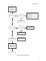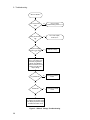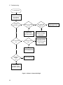
1
Service Manual
Agilent Model 66312A
Dynamic Measurement DC Source
and Agilent Model 6612B
System DC Power Supply
For instruments with Serial Numbers:
Agilent 66312A: US37442096 and up
Agilent 6612B: US37470826 and up
Agilent Part No. 5962-0874
Microfiche No 6962-0875
5
Printed in U.S.A.
September, 2000
Warranty Information
CERTIFICATION
Agilent Technologies certifies that this product met its published specifications at time of shipment from the factory.
Agilent Technologies further certifies that its calibration measurements are traceable to the United States National
Bureau of Standards, to the extent allowed by the Bureau's calibration facility, and to the calibration facilities of other
International Standards Organization members.
WARRANTY
This Agilent Technologies hardware product is warranted against defects in material and workmanship for a period of
three years from date of delivery. Agilent Technologies software and firmware products, which are designated by
Agilent Technologies for use with a hardware product and when properly installed on that hardware product, are
warranted not to fail to execute their programming instructions due to defects in material and workmanship for a
period of 90 days from date of delivery. During the warranty period Agilent Technologies will, at its option, either
repair or replace products which prove to be defective. Agilent Technologies does not warrant that the operation for
the software firmware, or hardware shall be uninterrupted or error free.
For warranty service, with the exception of warranty options, this product must be returned to a service facility
designated by Agilent Technologies. Customer shall prepay shipping charges by (and shall pay all duty and taxes) for
products returned to Agilent Technologies. for warranty service. Except for products returned to Customer from
another country, Agilent Technologies shall pay for return of products to Customer.
Warranty services outside the country of initial purchase are included in Agilent Technologies’ product price, only if
Customer pays Agilent Technologies international prices (defined as destination local currency price, or U.S. or
Geneva Export price).
If Agilent Technologies is unable, within a reasonable time to repair or replace any product to condition as warranted,
the Customer shall be entitled to a refund of the purchase price upon return of the product to Agilent Technologies.
LIMITATION OF WARRANTY
The foregoing warranty shall not apply to defects resulting from improper or inadequate maintenance by the
Customer, Customer-supplied software or interfacing, unauthorized modification or misuse, operation outside of the
environmental specifications for the product, or improper site preparation and maintenance. NO OTHER WARRANTY
IS EXPRESSED OR IMPLIED. AGILENT TECHNOLOGIES. SPECIFICALLY DISCLAIMS THE IMPLIED
WARRANTIES OF MERCHANTABILITY AND FITNESS FOR A PARTICULAR PURPOSE.
EXCLUSIVE REMEDIES
THE REMEDIES PROVIDED HEREIN ARE THE CUSTOMER'S SOLE AND EXCLUSIVE REMEDIES. AGILENT
TECHNOLOGIES SHALL NOT BE LIABLE FOR ANY DIRECT, INDIRECT, SPECIAL, INCIDENTAL, OR
CONSEQUENTIAL DAMAGES, WHETHER BASED ON CONTRACT, TORT, OR ANY OTHER LEGAL THEORY.
ASSISTANCE
The above statements apply only to the standard product warranty. Warranty options, extended support contacts,
product maintenance agreements and customer assistance agreements are also available. Contact your nearest
Agilent Technologies. Sales and Service office for further information on Agilent Technologies' full line of Support
Programs.
2
Safety Summary
The following general safety precautions must be observed during all phases of operation of this instrument. Failure to comply
with these precautions or with specific warnings elsewhere in this manual violates safety standards of design, manufacture, and
intended use of the instrument. Agilent Technologies, Inc. assumes no liability for the customer's failure to comply with these
requirements.
WARNING
Servicing instructions are for use by service-trained personnel. To avoid dangerous electrical shock, do not perform any servicing
unless you are qualified to do so. Some procedures described in this manual are performed with power supplied to the instrument
while its protective covers are removed. If contacted, the energy available at many points may result in personal injury.
BEFORE APPLYING POWER.
Verify that the product is set to match the available line voltage, the correct line fuse is installed, and all safety precautions (see
following warnings) are taken. In addition, note the instrument's external markings described under "Safety Symbols"
GROUND THE INSTRUMENT.
Before switching on the instrument, the protective earth terminal of the instrument must be connected to the protective conductor
of the (mains) power cord. The mains plug shall be inserted only in an outlet socket that is provided with a protective earth
contact. This protective action must not be negated by the use of an extension cord (power cable) that is without a protective
conductor (grounding). Any interruption of the protective (grounding) conductor or disconnection of the protective earth terminal
will cause a potential shock hazard that could result in personal injury.
FUSES
Only fuses with the required rated current, voltage, and specified type (normal blow, time delay, etc.) should be used. Do not use
repaired fuses or short-circuited fuseholders. To do so could cause a shock or fire hazard.
KEEP AWAY FROM LIVE CIRCUITS.
Operating personnel must not remove instrument covers. Component replacement and internal adjustments must be made by
qualified service personnel. Do not replace components with power cable connected. Under certain conditions, dangerous
voltages may exist even with the power cable removed. To avoid injuries, always disconnect power, discharge circuits and
remove external voltage sources before touching components.
DO NOT SERVICE OR ADJUST ALONE.
Do not attempt internal service or adjustment unless another person, capable of rendering first aid and resuscitation, is present.
Any adjustment, maintenance, and repair of this instrument while it is opened and under voltage should be avoided as much as
possible. When this is unavoidable, such adjustment, maintenance, and repair should be carried out only by a skilled person who
is aware of the hazard involved.
DO NOT SUBSTITUTE PARTS OR MODIFY INSTRUMENT.
Because of the danger of introducing additional hazards, do not install substitute parts or perform any unauthorized modification
to the instrument. Return the instrument to an Agilent Technologies, Inc. Sales and Service Office for service and repair to
ensure that safety features are maintained.
SAFETY SYMBOLS
Refer to the table on the following page
WARNING
The WARNING sign denotes a hazard. It calls attention to a procedure, practice, or the like, which, if not
correctly performed or adhered to, could result in personal injury. Do not proceed beyond a WARNING sign
until the indicated conditions are fully understood and met.
Caution
The CAUTION sign denotes a hazard. It calls attention to an operating procedure, or the like, which, if not
correctly performed or adhered to, could result in damage to or destruction of part or all of the product. Do not
proceed beyond a CAUTION sign until the indicated conditions are fully understood and met.
3
Safety Symbol Definitions
Symbol
Description
Direct current
Alternating current
Both direct and alternating current
Three-phase alternating current
Earth (ground) terminal
Protective earth (ground) terminal
Frame or chassis terminal
Terminal is at earth potential (Used for measurement and control circuits designed to be
operated with one terminal at earth potential.)
Terminal for Neutral conductor on permanently installed equipment
Terminal for Line conductor on permanently installed equipment
On (supply)
Off (supply)
Standby (supply)
Units with this symbol are not completely disconnected from ac mains when this switch
is off. To completely disconnect the unit from ac mains, either disconnect the power
cord or have a qualified electrician install an external switch.
In position of a bi-stable push control
Out position of a bi-stable push control
Caution, risk of electric shock
Caution, hot surface
Caution (refer to accompanying documents)
4
Notice
The information contained in this document is subject to change without notice. Agilent Technologies makes no
warranty of any kind with regard to this material, including but not limited to, the implied warranties of
merchantability, and fitness for a particular purpose.
Agilent Technologies shall not be liable for errors contained herein or for incidental or consequential
damages in connection with the furnishing, performance or use of this material.
This document contains proprietary information which is protected by copyright. All rights are reserved. No part of
this document may be photocopied, reproduced, or translated into another language without the prior written consent
of Agilent Technologies.
ã Copyright 1997, 2000 Agilent Technologies, Inc.
Printing History
The edition and current revision of this manual are indicated below. Reprints of this manual containing minor
corrections and updates may have the same printing date. Revised editions are identified by a new printing date. A
revised edition incorporates all new or corrected material since the previous printing date.
Changes to the manual occurring between revisions are covered by change sheets shipped with the manual. In some
cases, the manual change applies only to specific instruments. Instructions provided on the change sheet will
indicate if a particular change applies only to certain instruments.
First Edition ............February, 1997
Second Edition ...... September, 2000
Instrument Identification
The power supply is identified by a unique serial number such as, US36310101. The items in this serial number are
explained as follows:
US36310101
The first two letters indicate the country of manufacture. US = United States.
The next four digits are the year and week of manufacture or last significant design change.
Add 1960 to the first two digits to determine the year. For example, 36=1996. The third and
fourth digits specify the week of the year (31 = the thirty-first week).
The last four digits (0101) are a unique number assigned to each unit.
5
Table of Contents
Warranty Information
Safety Summary
Notice
Printing History
Instrument Identification
Table of Contents
INTRODUCTION
Organization
Safety Considerations
Related Documents
Revisions
Manual Revisions
Firmware Revisions
Electrostatic Discharge
VERIFICATION AND PERFORMANCE TESTS
Introduction
Test Equipment Required
Measurement Techniques
Setup for Most Tests
Electronic Load
Current-Monitoring Resistor
Operation Verification Tests
Performance Tests
Programming
Constant Voltage (CV) Tests
CV Setup
Voltage Programming and Readback Accuracy
CV Load Effect
CV Source Effect
CV Noise (PARD)
Transient Recovery Time
Constant Current (CC) Tests
CC Setup
Current Programming and Readback Accuracy
Current Sink (CC-) Operation
CC Load and Line Regulation
CC Load Effect
CC Source Effect
CC Noise (PARD)
Performance Test Equipment Form
Performance Test Record Form
6
2
3
4
5
5
6
9
9
9
9
10
10
10
10
11
11
11
12
12
13
13
13
13
13
14
14
14
14
15
15
16
16
16
16
17
17
18
18
19
19
20
TROUBLESHOOTING
Introduction
Test Equipment Required
Overall Troubleshooting
Flow Charts
Specific Troubleshooting Procedures
Power-on Self-test Failures
CV/CC Status Annunciators Troubleshooting
Bias and Reference Supplies
J307 Voltage Measurements
Manual Fan Speed Control
Disabling Protection Features
Post-repair Calibration
Inhibit Calibration Switch
Calibration Password
Initialization
ROM Upgrade
Identifying the Firmware
Upgrade Procedure
Disassembly Procedures
List of Required Tools
Cover, Removal and Replacement
A2 Interface Board, Removal and Replacement
Front Panel Assembly, Removal and Replacement
A3 Front Panel Board, Removal and Replacement
A1 Main Control Board
T1 Power Transformer, Removal and Replacement
Line Voltage Wiring
PRINCIPLES OF OPERATION
Introduction
I/O Interface Signals
A3 Front Panel Circuits
A2 Interface Circuits
Primary Interface
Secondary Interface
A1 Main Board Circuits
Power Circuits
Control Circuits
REPLACEABLE PARTS LIST
21
21
22
22
22
33
36
37
37
38
39
39
40
40
40
41
41
41
41
42
42
43
43
43
44
44
44
44
47
47
47
48
48
48
48
50
50
52
55
Introduction
55
DIAGRAMS
65
Introduction
General Schematic Notes
Backdating
INDEX
65
65
65
73
7
1
Introduction
Organization
This manual contains information for troubleshooting and repairing to the component level the Agilent Model
66312A Dynamic Measurement DC Source and the Agilent Model 6612B System DC Power Supply. Hereafter both
models will be referred to as the dc power supply.
This manual is organized as follows:
Chapter 1
Organization
Chapter 2
Performance tests
Chapter 3
Troubleshooting procedures
Chapter 4
Principles of operation on a block-diagram level
Chapter 5
Replaceable parts
Chapter 6
Diagrams
Safety Considerations
WARNING:
Hazardous voltages exist within the dc power supply chassis.
This dc power supply; is a Safety Class I instrument, which means it has a protective earth terminal. This terminal
must be connected to earth ground through a power source equipped with a 3-wire, ground receptacle. Refer to the
"Safety Summary" page at the beginning of this manual for general safety information. Before operation or repair,
check the dc power supply and review this manual for safety warnings and instructions. Safety warnings for specific
procedures are located at appropriate places in the manual.
Related Documents
The following documents are shipped with your dc power supply:
a a User’s Guide, containing installation, operating, and calibration information.
a a Programming Guide, containing detailed GPIB programming information.
9
1 - Introduction
Revisions
Manual Revisions
This manual was written for dc power supplies that have the same manufacturing dates (the first four digits) as those
listed on the title page and whose unique identification number (the last four digits) are equal to or higher than those
listed in the title page.
NOTE:
1) If the first four digits of the serial number of your unit are higher than those shown in the title
page, your unit was made after the publication of this manual and may have hardware or firmware
differences not covered in this manual. If they are significant to the operation and/or servicing of
the dc power supply, those differences are documented in one or more Manual Change sheets
included with this manual.
2) If the first four digits of the serial number of your unit are lower than those shown on the title
page, your unit was made before the publication of this manual and can be different from that
described here. Such differences are covered in the backdating section in Chapter 6.
Firmware Revisions
You can obtain the firmware revision number by either reading the integrated circuit label, or query the dc power
supply using the GPIB *IDN?' query command (see Chapter 3, ROM Upgrade).
Electrostatic Discharge
CAUTION:
The dc power supply has components that can be damaged by ESD (electrostatic discharge).
Failure to observe standard antistatic practices can result in serious degradation of performance,
even when an actual failure does not occur.
When working on the dc power supply, observe all standard, antistatic work practices. These include, but are not
limited to:
a
Working at a static-free station such as a table covered with static-dissipative laminate or with a conductive
table mat (Agilent P/N 9300-0797, or equivalent).
a
Using a conductive wrist strap, such as Agilent P/N 9300-0969 or 9300-0970.
a
Grounding all metal equipment at the station to a single common ground.
a
Connecting low-impedance test equipment to static-sensitive components only when those
components have power applied to them.
a
Removing power from the dc power supply before removing or installing printed circuit boards.
10
2
Verification and Performance Tests
Introduction
This document contains test procedures to verify that the dc power supply is operating normally and is within
published specifications. There are three types of tests as follows:
Built-in Self Tests
These tests, run automatically when the power supply is turned on, check most
of the digital circuits and the programming and readback DACs.
Operation Verification
These tests verify that the power supply is probably operating normally but do
not check all of the specified operating parameters.
Performance Tests
These tests check that the supply meets all of the operating specifications as
listed in the Operating Manual.
NOTE:
The dc power supply must pass the built-in self-tests before calibration or any of the verification
or performance tests can be performed. If the supply fails any of the tests or if abnormal test
results are obtained, refer to the troubleshooting procedures in Chapter 3. The troubleshooting
procedures will determine if repair and/or calibration is required.
Test Equipment Required
Table 2-1 lists the equipment required to perform the verification and performance tests. A test record sheet with
specification limits and measurement uncertainties (when test using the recommended test equipment) may be found
at the back of this section.
WARNING:
SHOCK HAZARD. These tests should only be performed by qualified personnel. During the
performance of these tests, hazardous voltages may be present at the output of the supply.
Table 2-1. Test Equipment Required for Verification and Performance Tests
Type
Specifications
Recommended Model
Current Monitor
Resistor
15 A (0.1 ohm) 0.04%,
for power supplies up to 15 A output
Guildline 9230/15
DC Power Supply
Minimum 2.5 A output current rating
Agilent 6632B
Digital Voltmeter
Resolution: 10 nV @ 1V
Readout: 8 1/2 digits
Accuracy: 20 ppm
Agilent 3458A or equivalent
Electronic Load
20 V, 5 A minimum, with transient capability
Agilent 6060B or equivalent
GPIB Controller
HP Series 300 or other controller with full
GPIB capabilities
11
2 - Verification and Performance Tests
Resistor
(substitute for electronic
load if load is too noisy
for CC PARD test)
1 ohm, 12 W (or 2 ohm adjustable)
1 k ohm, 5%, 3 W
9 ohm, 100 W
or
Rheostat, 10 ohm, 150 W
Ohmite D12K2R0 (2 ohm adjustable)
Agilent p/n 0813-0001
Ohmite RLS10R (10 ohm adjustable)
Ohmite 11F103
Oscilloscope
Sensitivity: 1 mV
Bandwidth Limit: 20 MHz
Probe: 1:1 with RF tip
Agilent 54504A or equivalent
RMS Voltmeter
True RMS
Bandwidth: 20 MHz
Sensitivity: 100 µV
Agilent 3400B or equivalent
Variable-Voltage
Transformer
Adjustable to highest rated input voltage range.
Power: 500 VA
Measurement Techniques
Test Setup
Most tests are performed at the rear terminals of the supply as shown in Figure 2-1a. Measure the dc voltage directly
at the +S and -S terminals. If the Power Supply is equipped with a Local/Remote switch, set the switch to Remote
and connect the output for remote sensing. Use adequate wire gauge for the load leads.
-S
-
+
-S
SENSE
+S
-
+
SENSE
+S
Local
Local
Remote
Remote
NOTE: Connector
is removable
+
-
DVM, Scope, or
+
-
50VDC MAX TO
DVM or
Set to
Remote
Remote
-
DC
RMS voltmeter
(for CV tests)
50VDC MAX TO
Set to
Load
resistor
Ammeter
+
1K
+
B.
Current
RMS voltmeter
monitor
-S
-
+
+S
SENSE
Local
(for CC tests)
+
Remote
+
-
-
50VDC MAX TO
Set to
+
Remote
Electronic
-
Load
DC
(see note)
Load
resistor
Ammeter
1K
+
Note: Use dc supply with same polarity
External
Replace load with 9 ohm resistor
for CC noise test.
DC supply
C.
A.
Figure 2-1. Test Setup
12
+
-
connectons for - CC tests.
Verification and Performance Tests - 2
Electronic Load
Many of the test procedures require the use of a variable load capable of dissipating the required power. If a variable
resistor is used, switches should be used to either; connect, disconnect, or short the load resistor. For most tests, an
electronic load can be used. The electronic load is considerably easier to use than load resistors, but it may not be
fast enough to test transient recovery time and may be too noisy for the noise (PARD) tests.
Fixed load resistors may be used in place of a variable load, with minor changes to the test procedures. Also, if
computer controlled test setups are used, the relatively slow (compared to computers and system voltmeters) settling
times and slew rates of the power supply may have to be taken into account. "Wait" statements can be used in the
test program if the test system is faster than the supply.
Current-Monitoring Resistor
To eliminate output-current measurement error caused by voltage drops in the leads and connections, connect the
current monitoring resistor between the -OUT and the load as a four-terminal device. Connect the currentmonitoring leads inside the load-lead connections directly at the monitoring points on the resistor element.
Operation Verification Tests
To assure that the supply is operating properly, without testing all specified parameters, perform the following test
procedures:
a. Perform the turn-on and checkout procedures given in the Operating Manual.
b. Perform the Voltage Programming and Readback Accuracy test, and the Current Programming and Readback
Accuracy tests from this procedure.
Performance Tests
NOTE:
A full Performance Test consists of only those items listed as “Specifications” in Table A-1 of the
Operating Manual, and that have a procedure in this document.
The following paragraphs provide test procedures for verifying the supply's compliance with the specifications listed
in Table A-1 of the Operating Manual. All of the performance test specifications and calculated measurement
uncertainties are entered in the appropriate Performance Test Record Card for your specific model. You can record
the actual measured values in the column provided in this card.
If you use equipment other than that recommended in Table 2-1, you must recalculate the measurement uncertainties
for the actual equipment used.
Programming
You can program the supply from the front panel keyboard or from a GPIB controller when performing the tests.
The test procedures are written assuming that you know how to program the supply either; remotely from a GPIB
controller or locally using the control keys and indicators on the supply's front panel. Complete instructions on
remote and local programming are given in the User’s Guide and in the Programming Guide.
13
2 - Verification and Performance Tests
Constant Voltage (CV) Tests
CV Setup
If more than one meter or if a meter and an oscilloscope are used, connect each to the terminals by a separate pair of
leads to avoid mutual coupling effects. For constant voltage dc tests, connect only to +S and -S, since the unit
regulates the output voltage that appears between +S and -S, and not between the (+) and (-) output terminals. Use
coaxial cable or shielded two-wire cable to avoid noise pickup on the test leads.
Voltage Programming and Readback Accuracy
This test verifies that the voltage programming, GPIB readback and front panel display functions are within
specifications. Note that the values read back over the GPIB should be identical to those displayed on the front
panel.
a.
Turn off the supply and connect a digital voltmeter between the +S and the -S terminals as shown in Figure 21a.
b.
Turn on the supply and program the supply to zero volts and the maximum programmable current with the load
off.
c.
Record the output voltage readings on the digital voltmeter (DVM) and the front panel display. The readings
should be within the limits specified in the performance test record chart for the appropriate model under CV
PROGRAMMING @ 0 VOLTS. Also, note that the CV annunciator is on. The output current reading should be
approximately zero.
d.
Program the output voltage to full-scale.
e.
Record the output voltage readings on the DVM and the front panel display. The readings should be within the
limits specified in the performance test record chart for the appropriate model under CV PROGRAMMING @
FULL SCALE.
CV Load Effect
This test measures the change in output voltage resulting from a change in output current from full load to no load.
a.
Turn off the supply and connect the output as shown in Figure 2-1a with the DVM connected between the +S
and -S terminals.
b.
Turn on the supply and program the current to the maximum programmable value and the voltage to the fullscale value.
c.
Adjust the load for the full-scale current as indicated on the front panel display. The CV annunciator on the
front panel must be on. If it is not, adjust the load so that the output current drops slightly.
d.
Record the output voltage reading on the DVM connected to +S and -S.
e.
Open the load and again record the DVM voltage reading. The difference between the DVM readings in steps
(d) and (e) is the load effect voltage, and should not exceed the value listed in the performance test record chart
for the appropriate model under CV LOAD EFFECT.
14
Verification and Performance Tests - 2
CV Source Effect
This test measures the change in output voltage that results from a change in ac line voltage from the minimum to
maximum value within the line voltage specifications.
a.
Turn off the supply and connect the ac power line through a variable voltage transformer.
b.
Connect the output as shown in Figure 2-1a with the DVM connected between the +S and the -S terminals. Set
the transformer to nominal line voltage.
c.
Turn on the supply and program the current to the maximum programmable value and the output voltage to the
full-scale value .
d.
Adjust the load for the full-scale current value as indicated on the front panel display. The CV annunciator on
the front panel must be on. If it is not, adjust the load so that the output current drops slightly.
e.
Adjust the transformer to the lowest rated line voltage (e.g., 104 Vac for a 115 Vac nominal line voltage input).
f.
Record the output voltage reading on the DVM.
g.
Adjust the transformer to the highest rated line voltage (e.g., 127 Vac for 115 Vac nominal line voltage input).
h.
Record the output voltage reading on the DVM. The difference between the DVM reading is steps (f) and (h) is
the source effect voltage and should not exceed the value listed in the performance test record chart for the
appropriate model under CV SOURCE EFFECT.
CV Noise (PARD)
Periodic and random deviations (PARD) in the output (ripple and noise) combine to produce a residual ac voltage
superimposed on the dc output voltage. CV PARD is specified as the rms or peak-to-peak output voltage in the
frequency range specified in the User’s Guide.
a.
Turn off the supply and connect the output as shown in Figure 2-1a to an oscilloscope (ac coupled) between the
(+) and the (-) terminals. Set the oscilloscope's bandwidth limit to 20 MHz and use an RF tip on the oscilloscope
probe.
b.
Turn on the supply and program the current to the maximum programmable value and the output voltage to the
full-scale value.
c.
Adjust the load for the full-scale current value as indicated on the front panel display.
d.
Note that the waveform on the oscilloscope should not exceed the peak-to-peak limits in the performance test
record chart for the appropriate model under CV NOISE (PARD).
e.
Disconnect the oscilloscope and connect an ac rms voltmeter in its place. The rms voltage reading should not
exceed the RMS limits in the performance test record chart for the appropriate model under CV NOISE
(PARD).
15
2 - Verification and Performance Tests
Transient Recovery Time
This test measures the time for the output voltage to recover to within the specified value following a 50% change in
the load current.
Loading
Transient
tttt
t
v
t
v
Unloading
Transient
Figure 2-2. Transient Waveform
a.
Turn off the supply and connect the output as in Figure 2-1a with the oscilloscope across the +S and the -S
terminals.
b.
Turn on the supply and program the output voltage to the full-scale value and the current to the maximum
programmable value.
c.
Set the load to the Constant Current mode and program the load current to 1/2 the power supply full-scale rated
current.
d.
Set the electronic load's transient generator frequency to 100 Hz and its duty cycle to 50%.
e.
Program the load's transient current level to the supply's full-scale current value and turn the transient generator
on.
f.
Adjust the oscilloscope for a waveform similar to that in Figure 2-2.
g.
The output voltage should return to within the specified voltage (v) in less than the specified time (t). Check
both loading and unloading transients by triggering on the positive and negative slope.
Constant Current (CC) Tests
CC Setup
Follow the general setup instructions in the Measurement Techniques paragraph and the specific instructions given
in the following paragraphs.
Current Programming and Readback Accuracy
This test verifies that the current programming and readback are within specification.
a.
Turn off the supply and connect the current monitoring resistor across the power supply output and the DVM
across the resistor. See "Current Monitoring Resistor" for connection information.
b.
Turn on the supply and program the output voltage to 5 V and the current to 20mA (±1mA).
c.
Divide the voltage drop (DVM reading) across the current monitoring resistor by its resistance to convert to
amps and record this value (Iout). Also, record the current reading on the front panel display. The readings
should be within the limits specified in the performance test record card for the appropriate model under CC
PROGRAMMING @ 0 AMPS.
d.
Program the output current to full-scale .
16
Verification and Performance Tests - 2
e.
Divide the voltage drop (DVM reading) across the current monitoring resistor by its resistance to convert to
amps and record this value (Iout). Also, record the current reading that appears on the front panel display. The
readings should be within the limits specified in the performance test record card for the appropriate model
under CC PROGRAMMING @ FULL-SCALE.
Current Sink (-CC) Operation
This test verifies current sink operation and readback.
a.
Turn off the supply and connect the output as shown in Figure 2-1a, except connect a dc power supply in place
of the electronic load as indicated. Connect the DMM across the current shunt.
b.
Set the external power supply to 5 V and a current value approximately 20% above the full scale current rating
of the supply under test.
c.
Turn on the supply under test and program the output voltage to zero and full scale output current. The current
on the UUT display should be approximately −1.4 A.
d.
Divide the voltage drop across the current monitoring resistor by its resistance to obtain the current sink value in
amps and subtract this from the current reading on the display. The difference between the readings should be
within the limits specified in the performance test record chart under CURRENT SINK READBACK.
Low Range Current Readback Accuracy
This test verifies the readback accuracy of the 20 milliampere current range.
a.
Turn off the supply and connect the output as shown in Figure 2-1b. Set the DMM to operate in current mode.
b.
Turn on the supply under test, set the current range to LOW, and program the output voltage to zero and full
scale output current. The current on the UUT display should be approximately 0 mA.
c.
Record the current reading on the DMM and the reading on the front panel display. The difference between the
two readings should be within the limits specified in the performance test record chart under 20mA RANGE
CURRENT READBACK ACCURACY @ 0A.
d.
Program the output voltage to 20V and record the current reading on the DMM and the reading on the front
panel display. The difference between the readings should be within the limits specified in the performance test
record chart for the appropriate model under 20mA RANGE CURRENT READBACK ACCURACY @ 20mA
e.
Turn off the supply and connect the output and an external supply as shown in Figure 2-1c. Set the DMM to
operate in current mode.
f.
Turn on the external supply and program it to 20 V and 1 amp. Then program the supply under test to zero
volts and 1 amp. The UUT display should read approximately −20 mA.
c.
Record the current reading on the DMM and the reading on the front panel display. The difference between the
two readings should be within the limits specified in the performance test record chart under 20mA RANGE
CURRENT READBACK ACCURACY @ −20 mA.
CC Load and Line Regulation
These tests (CC Load Effect and CC Source Effect given below) are tests of the dc regulation of the power supply's
output current. To insure that the values read are not the instantaneous measurement of the ac peaks of the output
current ripple, several dc measurements should be made and the average of these readings calculated. An example of
how to do this is given below using an Agilent 3458A System Voltmeter programmed from the front panel. Set up
the voltmeter and execute the "Average Reading" program follows:
a.
Program 10 power line cycles per sample by pressing NPLC 1 0 ENTER .
b.
Program 100 samples per trigger by pressing (N Rdgs/Trig) 1 0 0 ENTER .
17
2 - Verification and Performance Tests
c.
Set up voltmeter to take measurements in the statistical mode as follows:
Press Shift key, f0, Shift key, N.
Press ^ (up arrow) until MATH function is selected, then press >.
Press ^ (up arrow until STAT function is selected then press (ENTER).
d.
Set up voltmeter to read the average of the measurements as follows:
Press Shift key, f1, Shift key, N.
Press down arrow until RMATH function is selected, then press >.
Press ^ (up arrow) until MEAN function is selected, then press ENTER.
e.
Execute the program by pressing f0, ENTER, TRIG, ENTER.
f.
Wait for 100 readings and then read the average measurement by pressing f1, ENTER.
To repeat the measurement, perform steps (e) and (f).
CC Load Effect
This test measures the change in output current for a change in load from full scale output voltage to short circuit.
a.
Turn off the supply and connect the output as shown in Figure 2-1a with the DVM connected across the current
monitoring resistor.
b.
Turn on the supply and program the current to the full scale current value and the output voltage to the
maximum programmable voltage value.
c.
Adjust the load in the CV mode for full scale voltage as indicated on the front panel display. Check that the CC
annunciator of the UUT is on. If it is not, adjust the load so that the output voltage drops slightly.
d.
Record the output current reading (DVM reading/current monitor resistance value in ohms). You may want to
use the average reading program described under “CC Load and Line Regulation”.
e.
Short the load switch and record the output current reading. The difference in the current readings in steps (d)
and (e) is the load effect and should not exceed the limit specified in the performance test record chart for the
appropriate model under CC LOAD EFFECT.
CC Source Effect
This test measures the change in output current that results when the AC line voltage changes from the minimum to
the maximum value within the specifications.
a.
Turn off the supply and connect the ac power line through a variable voltage transformer.
b.
Connect the output terminals as shown in Figure 2-1a with the DVM connected across the current monitoring
resistor. Set the transformer to the nominal line voltage.
c.
Turn on the supply and program the current to the full scale value and the output voltage to the maximum
programmable value.
d.
Adjust the load in the CV mode for full scale voltage as indicated on the front panel display. Check that the CC
annunciator of the UUT is on. If it is not, adjust the load so that the output voltage drops slightly.
e.
Adjust the transformer to the lowest rated line voltage.
f.
Record the output current reading (DVM reading/current monitoring resistor in ohms). You may want to use
the average reading program described under “CC Load and Line Regulation”.
g.
Adjust the transformer to the highest rated line voltage.
h.
Record the output current reading again. The difference in the current readings in steps (f) and (h) is the CC
source effect and should not exceed the values listed in the performance test record card under CC SOURCE
EFFECT.
18
Verification and Performance Tests - 2
CC Noise (PARD)
Periodic and random deviations (PARD) in the output combine to produce a residual ac current, as well, as an ac
voltage superimposed on the dc output. Constant current (CC) PARD is specified as the rms output current in a
frequency range 20 Hz to 20 Mhz with the supply in CC operation.
a.
Turn off the supply and connect the load, monitoring resistor, and rms voltmeter as shown in Figure 2-1a. The
Current Monitoring resistor may have to be substituted by one with a higher resistance and power rating, such
as a 1 ohm 5 W current shunt in series with a 9 ohm resistor, to get the RMS voltage drop high enough to
measure with the RMS voltmeter. Leads should be as short as possible to reduce noise pick-up. An electronic
load may contribute ripple to the measurement so if the RMS noise is above the specification a resistive load
may have to be substituted for this test.
b.
Check the test setup for noise with the supply turned off. Other equipment (e.g. computers, DVMs, etc.) may
affect the reading.
c.
Turn on the supply and program the current to full scale and the output voltage to the maximum programmable
value.
d.
The output current should be at the full scale rating with the CC annunciator on.
e.
Divide the reading on the rms voltmeter by the monitor resistance to obtain rms current. It should not exceed the
values listed in the performance test record card under CC NOISE (RMS).
Performance Test Equipment Form
Test Facility:_________________________
Report Number ________________________
____________________________________
Date _________________________________
____________________________________
Customer _____________________________
____________________________________
Tested By ____________________________
Model ______________________________
Ambient Temperature (C) ________________
Serial No. ____________________________
Relative Humidity (%) ___________________
Options _____________________________
Nominal Line Frequency __________________
Firmware Revision ____________________
Special Notes:
Test Equipment Used:
Description
Model No.
Trace No.
Cal. Due Date
AC Source
_________________
_________________
_________________
DC Voltmeter
_________________
_________________
_________________
RMS Voltmeter
_________________
_________________
_________________
Oscilloscope
_________________
_________________
_________________
Electronic Load
_________________
_________________
_________________
Current Shunt
_________________
_________________
_________________
_________________
_________________
_________________
19
2 - Verification and Performance Tests
Performance Test Record Form
Model _________________
Report No _______________ Date __________________
Test Description
Minimum Specs.
Results*
Maximum
Specs.
Measurement
Uncertainty
− 10 mV
_________
+ 10 mV
1.6 µV
Vout − 3 mV
_________
Vout + 3 mV
1.6 µV
19.980 V
_________
20.020 V
335 µV
Vout − 9 mV
_________
Vout + 9 mV
335 µV
Load Effect
− 2.0 mV
_________
+ 2.0mV
20 µV
Source Effect
− 0.5 mV
_________
+ 0.5 mV
20 µV
Peak-to-Peak
0 mV
_________
+ 3 mV
872 µV
RMS
0 mV
_________
+ 0.5 mV
50 µV
0 mV
_________
+ 20 mV
3 mV
− 1.0 mA
_________
+ 1.0 mA
15.2 µA
Iout − 0.25 mA
_________
Iout + 0.25 mA
15.2 µA
1.998 A
_________
2.002 A
252 µA
Iout − 4.3 mA
_________
Iout + 4.3 mA
252 µA
Constant Voltage Tests
Voltage Programming and Readback
Low Voltage (0V) Programming
Front Panel Display Readback
High Voltage (Full Scale) Programming
Front Panel Display Readback
PARD (Ripple and Noise)
Transient Response
Voltage in 100 µs
Constant Current Tests
Current Programming and Readback
Low current (0A) Programming
Readback Accuracy @ Iout = 20 mA
High Current (Full Scale) Programming
Readback Accuracy @ Iout
Isink − 3.65 mA _________ Isink + 3.65 mA
200 µA
− 2.5 µA
_________
+ 2.5 µA
0.1 µA
Iout − 22.5 µA
_________
Iout + 22.5 µA
1.7 µA
Iout − 22.5 µA
_________
Iout + 22.5 µA
1.7 µA
0 mA
_________
+ 1.0 mA
200 µA
Load Effect
− 0.5 mA
_________
+ 0.5 mA
1.6 µA
Source Effect
− 0.5 mA
_________
+ 0.5 mA
1.6 µA
Current Sink (@ -1.4A) Readback
20 mA Range Current Readback
Readback Accuracy @ 0 A
Readback Accuracy @ + 20 mA
Readback Accuracy @ − 20 mA
PARD (Current Ripple and Noise)
RMS
* Enter your test results in this column
20
3
Troubleshooting
Introduction
WARNING:
SHOCK HAZARD. Most of the troubleshooting procedures given in this chapter are
performed with power applied and protective covers removed. Such maintenance should
be performed only by service trained personnel who are aware of the hazards (for
example, fire and electrical shock).
CAUTION:
This instrument uses components which can either be damaged or suffer serious
performance degradation as a result of ESD (electrostatic discharge). Observe the
standard antistatic precautions to avoid damage to the components. An ESD summary is
given in Chapter 1.
This chapter provides troubleshooting and repair information for the dc power supply. Before attempting to
troubleshoot the dc power supply, first check that the problem is with the supply itself and not with an
associated circuit. The verification tests in Chapter 2 enable you to isolate a problem to the dc power
supply. Troubleshooting procedures are provided to isolate a problem to one of the circuit boards or a
particular circuit. Figure 3-2 shows the location of the circuit boards and other major components of the
unit. If a problem has been isolated to the A1 Control circuit board, additional troubleshooting procedures
are available to isolate the problem to the defective component(s). Disassembly procedures are provided at
the end of this chapter and should be referred to, as required, in order to gain access to and/or replace
defective components.
If a component is defective, replace it and then conduct the verification test given in Chapter 2.
NOTE:
Note that when certain components are replaced, the supply must be calibrated (see "Post
Repair Calibration" later in this chapter). If the A2 Interface Board is replaced, the supply
must be initialized before it is calibrated. See "Initialization" later in this chapter.
Chapter 5 lists all of the replaceable parts for the power supplies. Chapter 6 contains schematics, test point
measurements, and component location diagrams to aid you in troubleshooting the supply.
21
3 - Troubleshooting
Test Equipment Required
Table 3-1 lists the test equipment required to troubleshoot the power supply. Recommended models are
listed.
Table 3-1. Test Equipment Required for Troubleshooting
Type
Purpose
Recommended Model
GPIB Controller
To communicate with the supply via the
GPIB interface
HP Series 300
Digital Voltmeter
To check various voltage levels
Agilent 3458A
Oscilloscope
To check waveforms and signal levels
Agilent 54504A/54111A
Electronic Load
To test operation of current circuit
Agilent 6060B
IC Test Clips
To access IC pins
AP Products No. LTC
Ammeter/Current
Shunt
To measure output current
Guildline 9230/15
Overall Troubleshooting
Overall troubleshooting procedures for the power supply are given in the Figure 3-1. The procedures first
check that neither an AC input, nor a bias supply failure is causing the problem and that the supply passes
the turn-on self test (error annunciator stays off). The normal turn-on, self-test indications are described in
the "Checkout Procedure" in Chapter 3 of the User's Guide.
If the supply passes the self test and there are no obvious faults, you should perform the verification
procedures in Chapter 2 from the front panel to determine if any functions are not calibrated or are not
operating properly. Then program and read back a voltage via the GPIB to see if the supply responds
properly to bus commands. If the supply fails any of the tests, you will be directed to the applicable flow
chart or troubleshooting procedure.
Flow Charts
Troubleshooting flow charts are given in Figure 3-1 sheets 1-13. Several flow charts make reference to the
test points listed in Chapter 6. The circuit locations of the test points are shown on the schematics and on
the component location diagrams in Chapter 6.
22
Troubleshooting - 3
Disconnect power, and
all loads then remove
cover. Set sense
switch to local,
reconnect power and
turn unit on.
Is Display on?
No
Is Fan on?
No
1. Check ac input and line cord.
2. Check line fuse.
3. Check line voltage selection,
see Fig. 3-3.
4. Check ac and bias voltages,
see Table 3-3.
Yes
Go To "No Display",
Sheet 5, "A"
Yes
Is Fan on?
No
24V @ Q305-2
?
No
Check +15V Unreg
bias circuit
Yes
Check fan and Fan
Driver circuit
Yes
Error Message
displayed?
Yes
See Self Test Error
Codes, Table 3-2
No
Program full scale
voltage and current
and enable output.
Check the output
voltage with a DMM.
Go to sheet 2
Figure 3-1 Sheet 1. Main Flowchart
23
3 - Troubleshooting
From Sheet 1
Protect
Annunciator on?
Yes
Press "Protect" Key
FS
displayed
?
Yes
R369 (FUSE)
2-4.5V?
No
Check F309, VR305,
R369, R414 and R454
Yes
Replace A2 Interface
board
No
Yes
OT
displayed
?
No
Yes
RT301
(HS_TERM), 2.5V
?
No
OC
displayed
?
Yes
Disable OCP, Reset
Protect and go to top of
page
Yes
Go to "OV @ Turn On",
Sheet 9, "E"
No
OV
displayed
?
No
RI (remote inhibit)
displayed, replace A2
Interface board
Output
voltage and
readback within
spec?
No
Go to "Voltage
Troubleshooting" Sheet 6, "B"
Yes
Go to Sheet 3
Figure 3-1 Sheet 2. Main Flowchart
24
No
Check RT301 and
R326
Troubleshooting - 3
Figure 3-1 Sheet 3. Main Flowchart
25
3 - Troubleshooting
From Sheet 3
Program the supply up and
down to check the down
programming speed.
Down
programming
OK?
No
Go to "Slow Downprogrammer"
Sheet 12, "H"
No
Replace A2 Interface
board
Yes
Check RI/DFI port (see
User's Guide)
RI/DFI OK?
Yes
No problems found
with basic operation.
Perform Verification
and Performance tests
to determine if a
problem exists.
Figure 3-1 Sheet 4. Main Flowchart
26
Troubleshooting - 3
"A" From Sheet 1
Measure 5Vp A2 J206,
(Red to Black) and 5Vp
Unreg (White to Black)
5V biases OK?
No
Check A1, +5V
Interface Bias Supply
No
Replace A2 Interface
board
Yes
Check 5V @ A2J211
Pin 1 to 8
5V OK?
Yes
Check for 5V pulses at
A2J211 Pins 4 (Tx)
and 5 (Rx) to primary
ground.
Tx Pulses OK?
No
Yes
Rx Pulses OK?
Yes
No
Replace Front Panel/
Display board
Figure 3-1 Sheet 5. No Display
27
3 - Troubleshooting
"B" From Sheet 2
CC Annunciator
ON?
Yes
Go to "Current
Troubleshooting" Sheet 7, "C"
Yes
Go to "No Output",
Sheet 8, "D"
No
Unreg Annunciator
ON
?
No
Output and display
close to prog value
?
Yes
Calibrate Voltage
No
CV_PROG @ R322 should
be 0 to -4.8 volts for 0 to
full scale programmed
voltage and VMON @
U322-7 should be 0 to 4.7
volts for 0 to full scale
output voltage
CV_PROG OK?
No
Replace A2 Interface
board
No
Troubleshoot U322B
circuit
Yes
VMON OK?
Yes
If output is OK and readback is
not, replace A2 Interface board.
If the display equals the output,
troubleshoot U322A circuit
Figure 3-1 Sheet 6. Voltage Troubleshooting
28
Troubleshooting - 3
"C" From Sheet 3 or 6
Unreg Annunciator
ON
?
Yes
Go to "Output Current
Unregulated" Sheet 13, "I"
No
Output and display
close to prog value
?
Yes
Calibrate Current
No
CC_PROG @ R336 is 0 to -4.8V
for 0 to full scale programmed
current, IMON_H @ U318A-7 is 0
to -4.8 volts for 0 to full scale output
current and IMON_L @ U319A-6 is
0 to -4.8 volts for 0 to 20mA output
current in the low current readback
range.
CC_PROG OK?
No
Replace A2 Interface
board
No
Troubleshoot R431
and U319A circuit
Yes
IMON_H OK?
Yes
IMON_L OK?
No
Yes
If output is OK and readback is
not, replace A2 Interface board.
If the display equals the output,
troubleshoot U324A/B circuit
circuits.
OK below about
12mA but not
above?
No
Check U319A circuit
Yes
Check Q302 circuit
Figure 3-1 Sheet 7. Current Troubleshooting
29
3 - Troubleshooting
"D" From Sheet 6
Gated (G)+/-15V
@ F302 & F304
OK?
No
PM_INHIBIT @
R390 high
?
No
Yes
Yes
U321-5 > +15mV
?
Replace A2 Interface
board
No
Check R360 and
U326B circuit
No
Check U321 circuit
Yes
Voltage @ U3217=U321-5
?
Yes
Check output series
regulator and
downprogrammer
stages U308, U309,
Q303, Q306 through
Q310 and F309
Figure 3-1 Sheet 8. No Output
30
Check U311/U312
circuits
Troubleshooting - 3
"E" From Sheet 2
Connect DC coupled
scope across the
output terminals and
turn on the supply while
observing the scope.
Output
momentarily goes
high
?
Yes
Go to "Output Held High",
Sheet 10,"F"
Yes
Replace A2 Interface
Board
No
Replace A2 Interface
board
No
Check that OV is
programmed to
maximum or replace
A2 Interface board
No
Disable the OV
protection by sending
the command
"DIAG:SCR 0"
Unit still OVs?
No
U327-7 Low
(OV_DETECT*)
?
Yes
OV_PROG = +4V?
Yes
Check U327 circuit
Figure 3-1 Sheet 9. Overvoltage at Turn-On
31
3 - Troubleshooting
"F" From Sheet 9
Disable the OV
protection by sending
the command
"DIAG:SCR 0"
Disabled
annunciator on?
Yes
No
CV annunciator
on?
No
Gated +/-15 Biases
at zero?
No
PM_INHIBIT @
R380 15V
?
Yes
No
Check Series
Regulator circuits,
U309, Q303, Q308 etc.
Replace A2 Interface
board and go back to
beginning. Probable
2nd problem.
Voltmeter reads
+OL?
No
Check Vmon amplifier,
U322B (Vmon = 0 to
4.7V for 0 to full scale
output voltage)
Yes
Check U316A (gain of
-1) and U322A circuits
Yes
"CONTROL"
U321B-7
< 0V ?
No
Check U321B circuit
Yes
Check Series
Regulator circuits,
U309, Q303, Q308 etc.
Figure 3-1 Sheet 10. Output Held High
32
Yes
Check U311/U312
Gated Bias circuits
Troubleshooting - 3
"G" From Sheet 3
Program the output
voltage and current to
the full scale value and
the OV to 1/2.
OV_Prog @
A1R321 =2V
?
No
A2 Interface Board or
cable W8 defective
No
Check A1R382, R401,
Imon_comp (0V) and
U327
No
Check A1R321, R387,
R391, R405, C349,
C317 and U327
Yes
A1 U327-3 0V
?
Reset the OV and
observe the OV_SCR*
signal. Each time OV is
reset (Shift, Prot Clr)
the unit will generate
another OV. The OV
pulse (OV_SCR*) is
5us long.
Yes
A1U327-2 Neg.
?
A1R378,
OV_SCR* pulse
low 5us?
Yes
A1U327-7,
OV_DETECT*,
Low?
Yes
No
Check A1U327
No
Check A1R301, C353,
U302A, R378 and A2
Interface Board
No
Check Q301, U302A
and all associated
resistors and
capacitors
Yes
A1Q301 emitter
pulses high 5us?
Yes
Check A1CR301
Figure 3-1 Sheet 11. Unit Did Not Overvoltage
33
3 - Troubleshooting
"H" From Sheet 4
Connect an external power
supply across the output (+ to
+, - to -). Program the UUT
voltage to 0V, Output ON and
the test supply to 5V and 2A
Meter indicates 5V,
-1.5A
?
Yes
Unit operating normally
No
Check U321A, D327,
R324 and R362
No
Check U308A, Q306,
D319 and associated
circuits
No
U321A-1 -0.4V
?
Yes
U308A-1 -1.5V
?
Yes
Check Q306, Q309,
R436 and -Rail
Figure 3-1 Sheet 12. Slow Downprogrammer
34
Troubleshooting - 3
"I" From Sheet 7
Output current less
than rating
?
Yes
U326B-6 = 0.6V
?
No
Control (F307) =
U326B-6
?
No
Check R360, U321B
Yes
Check output and
downprogrammer
stages Q307-Q309
Yes
No
U308A-3 > -0.5V
?
Yes
Check U321A circuit
No
Check for 1 of Q303 or
Q310 stages not
conducting
CC_Prog @ R336
>-4.8V
?
Yes
Replace A2 Interface
board
No
Check the following:
Imon_P, U325A-6=0V
Imon_H, U318A-6=>3.5V
Voltages OK
?
No
Check associated
circuit
Yes
Check U324A/B
Note, U324A has a
gain of -1
Figure 3-1 Sheet 13. Current at Maximum
35
3 - Troubleshooting
Specific Troubleshooting Procedures
Power-on Self-test Failures
The power-on self-test sequence tests most of the digital and DAC circuits. If the supply fails self-test, the
display "ERR" annunciator will come on. You can then query the unit to find out what the error(s) are.
When an error is detected, the output is not disabled so you can still attempt to program the supply to help
troubleshoot the unit. Table 3-2 lists the self test errors and gives the probable cause for each error.
NOTE:
A partial self test is performed when the *TST? query is executed. Those tests that
interfere with normal interface operation or cause the output to change are not performed
by *TST?. The return value of *TST? will be zero if all tests pass, or the error code of the
first test that failed. The power supply will continue normal operation if *TST? returns a
non-zero value.
Table 3-2. Self-Test Error Codes/Messages
Error Code
Description
Probable Cause
E1
Checksum in Read-only Non-volatile ROM
A2 Interface Bd
E2
Checksum in Config Non-volatile ROM
A2 Interface Bd
E3
Checksum in Cal Non-volatile ROM
A2 Interface Bd
E4
Checksum in State Non-volatile ROM
A2 Interface Bd
E5
Checksum in RST Non-volatile ROM
A2 Interface Bd
E10
RAM test failed
A2 Interface Bd
E11
12 bit DAC test failed, 0 is written to DAC U241A and
B, ADC U242 is checked for 133 +/- 7 counts
A2 Interface Bd
E12
12 bit DAC test failed, 4095 is written to DAC U241A
and 0 to B, ADC U242 is checked for 71 +/- 7 counts
A2 Interface Bd
E13
12 bit DAC test failed, 0 is written to DAC U241A and
4095 to B, ADC U242 is checked for 71 +/- 7 counts
A2 Interface Bd
E14
12 bit DAC test failed, 4095 is written to DAC U241A
and B, ADC U242 is checked for 10 +/- 7 counts
A2 Interface Bd
E15
8 bit DAC test failed, 10 and 240 are written to DAC
U244, ADC U242 is checked for 10 and 240 +/- 7 counts
A2 Interface Bd
E80
Dig I/O test failed, SEC_PCLR written low and high,
read back through Xilinx
A2 Interface Bd
E213
RS-232 input buffer overrun
A2 Interface Bd
E216
RS-232 framing error
A2 Interface Bd
E217
RS-232 parity error
A2 Interface Bd
E218
RS-232 UART input overrun
A2 Interface Bd
E220
Front Panel comm UART input overrun
A3 Front Panel/Display Bd
E221
Front Panel comm UART framing error
A3 Front Panel/Display Bd
E222
Front Panel comm UART parity error
A3 Front Panel/Display Bd
E223
Front Panel firmware input buffer overrun
A3 Front Panel/Display Bd
36
Troubleshooting - 3
CV/CC Status Annunciators Troubleshooting
The CV/CC annunciators are particularly helpful when troubleshooting a unit with no output. If the unit has
no output voltage or current and one of the annunciators is on then the problem is in the control circuit
associated with that annunciator. An example of how this might be useful would be in a case where the
voltage and current are programmed to some positive value, there is no output voltage and the CV
annunciator is on. This indicates that the problem is probably in the Voltage Amplifier circuit. If the CC
annunciator were on then the problem would likely be in the Current Amplifier. If UNR is indicated then
neither the voltage nor the current circuits are in control and the problem would be in circuits after the
gating diodes such as the driver or output regulator stages.
When troubleshooting the CV/CC status annunciators or the status readback circuits, first measure the
voltage drop across the gating diodes; A1 D317 (CV) and D321 (CC). A conducting diode indicates an
active (ON) control circuit. This forward drop is applied to the input of the associated status comparator
(U328C and D respectively) and drives the output (CV_DETECT* or CC_DETECT*) low. The low signal
indicates an active status which is sent to the A2 board microprocessor. The front panel CV annunciator
indicates when the CV mode is active (CV_DETECT* is low). The front panel CC annunciator indicates
when the CC mode is active (CC_DETECT* is low). The UNREGULATED (UNR) annunciator comes
on when neither the CV nor CC is active.
Bias and Reference Supplies
Before troubleshooting any circuit check the bias and/or reference voltages to make sure that they are not
the cause. Table 3-3 lists the bias and reference voltage test points for the A1 Main Control , A2 Interface,
and the A3 Front Panel/Display boards. Unless otherwise noted, all voltages are measured with respect to
secondary common (R431) with no load on the supply.
Table 3-3. Bias and Reference Voltages
Bias
Test Point
Common
Measurement
+5V primary
A1 J206-1(Red)
Chassis (J206-2 black)
+5V +/- 0.15V
+5V secondary
A1 R423
Secondary Common
+5V +/- 0.2V
+15V secondary
A1 R419
Secondary Common
+15V +/- 0.6V
-15V secondary
A1 R422
Secondary Common
-15V +/- 0.6V
+15V secondary gated
A1 F304
Secondary Common
+14.2V +/- 5%
-15V secondary gated
A1 F302
Secondary Common
-14.2V +/- 5%
A1 D311 cathode
- Output
+32V +/- 10% (100mV P/P)
A1 D307 Anode
Secondary Common
-6.5V +/- 10% (100mV P/P)
A1 J307-6
Secondary Common
+2.5V +/- 5%
1
+Rail
-Rail1
+2.5V reference
2
1
Measured with respect to - Output at nominal ac input line voltage
2
the 2.5V reference originates on the A2 Interface board
37
3 - Troubleshooting
J307 Voltage Measurements
J307 connects the A1 Main Board Assembly to the A2 Interface Assembly. Table 3-4 provides a quick
method of determining if the voltages between these assemblies are within the normal range. If any of these
voltages is outside the normal range, refer to the flowcharts to further troubleshoot the circuit associated
with the abnormal voltage.
Table 3-4. Voltage Measurements at J307 (A2 Interface to A1 Main board)
A1J307
Pin #
38
Signal Name
CV Mode
Full Scale Voltage
No Load
CC Mode
Full Scale Voltage
Full Load
1
PM_INHIBIT (Enabled)
0
0
2
OV_SCR*
+5
+5
3
OV_PROG
+3.9
+3.9
4
FAN_PROG
+2.8
+3.8
5
OV_DETECT*
+5
+5
6
SW_POS (Norm)
+5
+5
7
RANGE_SELECT (High)
0
0
8
OS_TRIM_NEG (COMP)
+1.7
+1.7
OS_TRIM_NEG (SCPI)
+4.0
+4.0
9
+5Vs
+5
+5
10
COMMON
0
0
11
COMMON
0
0
12
+15Vs
+15
+15
13
-15Vs
-15
-15
14
HS_THERM (@25C)
+2.5
+2.5
15
FUSE
+2.4
+2.6
16
IMON_H
0
+3.5
17
IMON_L
IMON_L (@20mA Out)
0
+4.8
+14.7
+4.8
18
IMON_P
0
0
19
VMON
+4.8
+4.8
20
COMMON
0
0
21
COMMON
0
0
22
COMMON
0
0
23
COMMON
0
0
24
CV_PROG
-4.8
-4.8
25
CC_PROG
-4.8
-4.8
26
CC_DETECT*
+5
0
27
CCN_DETECT*
+5
+5
28
CV_DETECT*
0
+5
Troubleshooting - 3
Manual Fan Speed Control
Under some circumstances such as testing acoustical devices where the fan noise would interfere with the
test, it would be advantageous to reduce the fan speed. If the test requires a very light load, the ambient
temperature is low and the duration of the test is short, the fan speed may be temporarily reduced. The turnon default is "Automatic" so this procedure must be performed, as needed, every time the line voltage is
turned on. To manually control the fan speed:
a.
Simultaneously depress the "0" and "1" keys. EEINIT <model> will be displayed.
b.
Using the Up/Down annunciator keys select FAN:MODE<AUTO>.
c.
Using the Up/Down arrows select FAN:MODE <MAN>.
d.
Press "Enter".
e.
Simultaneously depress the "0" and "1" keys. EEINIT <model> will be displayed.
f.
Using the Up/Down annunciator keys select FAN:SPEED <data>.
g.
Press "Enter Number".
h.
Enter the desired speed (numeric entry range is 0 to 100%).
i.
Press "Enter".
Disabling Protection Features
Except for overvoltage protection, the power supply's protection features may be disabled. This is not
recommended as a normal operating condition but is helpful under some circumstances such as
troubleshooting. The turn-on default is "NO-PROTECT OFF" (protection enabled) so this procedure must
be performed, as needed, every time the line voltage is turned on. To disable the protection:
a.
Simultaneously depress the "0" and "1" keys. EEINIT <model> will be displayed.
b.
Using the Up/Down annunciator keys select NO-PROTECT <OFF>.
c.
Using the Up/Down arrows select NO-PROTECT <ON>.
d.
Press "Enter".
39
3 - Troubleshooting
Post-repair Calibration
Calibration is required annually and whenever certain components are replaced. If components in any of
the circuits listed below are replaced, the supply must be re-calibrated as described in Appendix B of the
User's Guide.
a.
A1 Control Board: Voltage or Current Monitor Amplifier circuits, High Bandwidth Current Amplifier,
or Current Monitor resistors R425/R431.
b.
A2 Interface Board.
If the Interface board A2 is replaced, the supply must be initialized first (see "Initialization" later in this
chapter) and then be calibrated.
Inhibit Calibration Switch
If "CAL DENIED" appears on the display when calibration is attempted, or if error code 401 occurs when
calibrating over the GPIB, the internal INHIBIT CAL switch has been set. This switch setting prevents
unauthorized or inadvertent power supply calibration. You must reset this switch in order to calibrate the
supply.
This four-section switch, S201, is located on the A2 Interface board near the GPIB connector. The switch
has 2 functions related to calibration. One is Inhibit Calibration. With this switch set the supply will not
respond to calibration commands, thus providing security against unauthorized calibration. The other
switch allows you to bypass the password in case it is forgotten.
Switch 3
Switch 4
Normal
Off
Off
Clear
Password
Off
On
Inhibit
Calibration
On
Off
4 3 2 1
ON
S201
Calibration Password
In order to enter the calibration mode, you must use the correct password as described in Appendix B of
the Operating Manual. As shipped from the factory, the number 0 (zero) is the password. If you use an
incorrect password, "OUT OF RANGE" will appear on the display for front panel calibration (or error
code 402 occurs for GPIB calibration) and the calibration mode will not be enabled.
If you have changed the password and have forgotten it, you can set the configuration switch on A2
Interface board to bypass the password. See "Calibration Switch" paragraph above.
40
Troubleshooting - 3
Initialization
The dc power supply's GPIB address and model number as well as other constants which are required to
program and calibrate the supply are stored in a EEPROM on the A2 Interface board. The Interface board
also contains references and other components that will affect the alignment of the supply. If the Interface
board is replaced, the supply must be reinitialized and calibrated. To initialize the power supply:
a.
Enable the Calibration mode.
b.
Simultaneously depress the "0" and "1" keys.
c.
Using the Up/Down arrows select the appropriate model number.
d.
Press "Enter".
The dc power supply will go through the turn-on self test sequence. It is now re-initialized and must be
calibrated. See Appendix A of the User’s Guide for the calibration procedure.
ROM Upgrade
Identifying the Firmware
You can use the *IDN? query to identify the revision of the supply's firmware. The query will readback
the revisions of the Primary Interface ROM located on the A2 Interface board. The manufacturer and model
number of the supply are also returned. The following is a sample program:
10
ALLOCATE L$[42]
20
OUTPUT 705;"*IDN?"
30
ENTER 705;L$
40
DISP L$
50
END
The computer will display the manufacturer's name, the model number, a "0," and then the firmware
revision. Example: "Agilent,66312A,0,A.00.01". The revision level of the ROM can also be found on the
label affixed to the physical IC chip itself.
Upgrade Procedure
If the Interface board ROM is upgraded you can re-initialize the supply without affecting the calibration.
a.
Enable the Calibration mode.
b.
Simultaneously depress the "0" and "1" keys. EEINIT <model> will be displayed.
c.
Using the Up/Down annunciator keys select ROMUPD <model>.
d.
Using the Up/Down arrows select the appropriate model number.
e.
Press "Enter".
The supply will go through the turn-on self test sequence and return to the power supply metering mode.
41
3 - Troubleshooting
Disassembly Procedures
The following paragraphs provide instructions on how to disassemble various components of the dc power
supply. Once disassembled, the components can be reassembled by performing the disassembly
instructions in reverse order. Figure 3-2 shows the location of the major components of the unit.
Figure 3-2. Component Location
WARNING:
SHOCK HAZARD. To avoid the possibility of personal injury, turn off AC power and
disconnect the line cord before removing the top cover. Disconnect the GPIB cable and
any loads, and remote sense leads before attempting disassembly.
CAUTION:
Most of the attaching hardware is metric. Use of other types of fasteners will damage
threaded inserts. Refer to the list of required tools when performing disassembly and
replacement.
List of Required Tools
a.
2PT Pozidriv screwdrivers.
b.
T10 and T15 Torx screwdrivers.
c.
Hex drivers: 7 mm for GPIB connector,
3/16" for RS-232 connector,
1/4" for front panel binding posts
d.
Long nose pliers.
e.
Antistatic wrist discharge strap.
42
Troubleshooting - 3
Cover, Removal and Replacement
a.
Using a T15 Torx screwdriver, unscrew the two captive screws which hold the rear bezel to the dc
power supply, and then remove the two screws from the bottom of the case.
b.
Slide the cover backward until it clears the rear of the power supply.
A2 Interface Board, Removal and Replacement
To remove the Interface Board, proceed as follows:
a.
Remove the cover of the power supply as described under, "Cover Removal and Replacement."
b.
Remove the two 7 mm and 3/16 inch hex screws that hold the GPIB and RS-232 connectors in place.
c.
Slide the board forward until the notch on the right side of the Interface board aligns with the fan
spacer board. Rotate the right side up slightly to disengage the board from the slot in the left side of the
chassis.
d.
Unplug the cable from J206. Depress the release button located at the end of the connector where the
wires enter the housing.
e.
Unplug the flat cables. Note the position of the conductive side for reinstallation. Connectors release
the cable by pulling out end tabs as shown by the arrows in the following figure.
f.
To reinstall the Interface board, perform the above steps in reverse order.
Front Panel Assembly, Removal and Replacement
This procedure removes the front panel assembly from the dc power supply.
a.
Remove the Power Supply Cover as described earlier in, "Top Cover Removal and Replacement."
b.
Disconnect the cable between the Front Panel board and the Interface board at the Interface board. You
may have to remove the Interface board as described above to accomplish this.
c.
Using a Torx T10 driver remove the three screws from each side of the supply that hold the front panel
brackets to the chassis.
d
Slide the Front Panel assembly forward slightly to unplug the Binding Post connector and with a Torx
T15 driver remove the screw connecting the ground wire to the chassis.
e.
To remove the left bracket, locate and carefully peel off the left vinyl trim to gain access to the side
screw that secures the front panel bracket the chassis. Using a Torx T15 driver remove the screw
located behind the vinyl trim.
f.
To remove the right bracket, depress the plastic tab located behind the front panel in the upper right
corner.
g.
To reinstall the Front Panel Assembly, perform the above steps in reverse order.
43
3 - Troubleshooting
A3 Front Panel Board, Removal and Replacement
First remove the front panel assembly as described under, "Front Panel Assembly, Removal and
Replacement." Once you have access to the front panel board perform these steps:
a.
Remove the RPG knob by pulling it away from the front panel.
b.
Pull back the right side of the board near the RPG about 1/8th of an inch. Slide the board to the left to
disengage the holding clips.
c.
To reinstall the Front Panel board, perform the above steps in reverse order.
A1 Main Control Board
a.
Remove the top cover and the A2 Interface board as described above.
b.
Disconnect all cables going to connectors on the main control board.
NOTE:
Be sure to note the position and orientation of all cables prior to removal so that no
mistake is made later when reinstalling these cables.
c.
Disconnect the ground wire between the main board and the chassis. This wire is secured to the side of
the chassis near the AC input by a Torx T10 screw.
d.
Remove three Torx T15 screws which secure the main control board to the chassis.
e.
Slide the main board towards the front panel to release it from chassis mounted standoffs and then lift
the board out of the chassis.
T1 Power Transformer, Removal and Replacement
To remove the power transformer, the front panel assembly must first be removed to gain access to the
bracket screws that hold the transformer in place.
a.
Remove the front panel assembly as described above.
b.
Remove the two Torx T10 screws securing the rear of the transformer bracket to the bottom of the
chassis and the two screws securing the front of the bracket.
c.
Use long nose pliers to disconnect all wires going to the transformer terminals.
d.
Lift the transformer out of the chassis.
NOTE:
The AC power connections at the transformer primary are line voltage dependent. Refer
to Figure 3-3 subsequent reconnection.
Line Voltage Wiring
Figure 3-3 illustrates the primary wiring configuration of the power transformer for various ac line
voltages. Use long nose pliers to disconnect the wires going to the transformer terminals.
NOTE:
44
Install the correct fuse when changing the ac line voltage from a previous setting:
for 110/120 Vac: 2 A, Agilent p/n 2110-0002;
for 220/230 Vac: 1 AT, Agilent p/n 2110-0007
Troubleshooting - 3
grey
white/red/grey
orange
(spare)
orange
orange
white/yellow
white/violet
white/yellow
white/violet
orange
grey
white/red/grey
grey
grey
orange
(spare)
orange
orange
white/yellow
white/violet
orange
white/red/grey
white/yellow
white/violet
white/red/grey
white/red
white/black
white/brown
white/red
red
white/black
black
white/brown
Figure 3-3. Transformer Wiring
45
4
Principles of Operation
Introduction
This section describes the different functional circuits used in the dc power supply models covered in this
manual. First, the I/O external signals that connect to the Agilent power supply are described. Next, the
overall block diagrams for the dc power supply are described in detail.
The simplified block diagrams in this section show the major circuits on the dc power supply as well as
the signals between circuits. They also show the reference designations of some of the components in the
functional circuit. These same reference designators are shown in the schematic diagrams in Section 6.
I/O Interface Signals
Table 4-1 describes the interface signals between the power supply and the end user (or other external
circuits and devices).
Table 4-1. Power Supply Interface signals
Connector
Signal
Description
Front panel outputs
+OUT
-OUT
Positive DC output voltage
Negative DC voltage (or return)
Rear panel
output/sense screw
terminals
+OUT
-OUT
+ sense
- sense
common
Positive DC output voltage
Negative DC voltage (or return)
+OUT sensing terminal1
-OUT sensing terminal1
connected to ground conductor
1
Set SENSE switch to "Remote" when using the sensing
terminals.
INH/FLT
connector
pin 1
pin 2
pin 3
pin 4
FLT/INH mode2
FLT output
FLT Common
INH Input
INH Common
2
Digital I/O mode
OUT 0
OUT 1
IN 2/OUT 2
Common
as-shipped configuration
RS-232 connector
XON-XOFF
RTS-CTS
DTR-DSR
NONE
uses ASCII control codes DC# and DC1
uses Request-To-Send and Clear-To-Send lines
uses Data-Terminal-Ready and Data-Set-Ready lines
there is no flow control
GPIB connector
GPIB /IEEE 488
Provides the interface to an external GPIB controller
Ac input connector
ac mains
Can be 100 Vac, 120 Vac, 220 Vac or 240 Vac Input
47
4 - Principles of Operation
A3 Front Panel Circuits
As shown in Figure 4-1, the supply's front panel assembly contains a circuit board, a keypad, a liquid
crystal display (LCD), and a rotary control (RPG) for the output voltage and current. With the exception of
the RPG (A3G1), the A3 Front Panel board is an assembly-level replaceable part. A separate front panel
binding post board is also included on the unit. It is also available as an assembly-level replaceable part.
The A3 front panel board contains microprocessor circuits, which decode and execute all keypad and RPG
commands that are transferred to the power supply output via the serial I/O port to the primary interface
circuits on the A2 interface board. The front panel microprocessor circuits also process power supply
measurement and status data received on the serial I/O port. This data is displayed on the LCD.
A2 Interface Circuits
The circuits on the A2 interface board provide the interface between the GPIB interface, RS-232 interface,
and front panel interface and the dc power supply. Communication between the power supply and a GPIB
controller is processed by the GPIB interface and the primary microprocessor circuits on the A2 board. The
A2 Interface board is assembly-level replaceable; it contains no user-replaceable parts.
With the exception of the front panel microprocessor, all digital circuits, analog-to-digital converters
(ADC) and digital-to-analog converters (DAC) in the dc power supply are located on the A2 Interface
board. All control signals between the A2 interface board and the A1 main board are either analog or level
signals.
Primary Interface
The primary microprocessor circuits (DSP, ROM, and RAM chips) decode and execute all instructions
and control all data transfers between the controller and the secondary interface. The primary
microprocessor circuits also processes measurement and status data received from the secondary interface.
A Dual Asynchronous Control chip on the A2 board converts the RS-232, RI/DFI, and front panel data into
the primary microprocessor's 8-bit data format. The serial data is transferred between the primary interface
and the secondary interface via a serial bus and optical isolator chips. These chips isolate the primary
interface circuits (referenced to earth ground) from the secondary interface circuits.
Secondary Interface
The secondary interface circuits include a programmed logic array, EEPROM, boot-ROM, 8 and 12-bit
DAC circuits, and 8 and 16-bit ADC circuits. The programmed logic array translates the serial data
received from the primary interface into a corresponding digital signal for the appropriate DAC/ADC
circuits. The logic array is also connected directly to four DAC/ADC circuits. Under control of the logic
array, the selected DAC converts the data on the bus into an analog signal. Conversely, the selected ADC
converts the analog signals from the A1 board into a digital signal.
The logic array also directly receives status information from the A1 main board via three level-sensitive
signal lines, which inform the array of the following operating conditions: constant voltage mode
(CV_Detect*), constant current mode (CC_Detect*), and overvoltage (OV_Detect*). The PM_Inhibit
control signal is used to shut down the bias voltage to the output stages and keep the power supply output
off. The OV_SCR* control signal is used to fire the SCR and keep the power supply output off when an
overvoltage condition has occurred.
48
Principles of Operation - 4
Figure 4-1. A2/A3 Block Diagram
49
4 - Principles of Operation
The EEPROM (electrically erasable programmable read-only memory) chip on the A2 interface board
stores a variety of data and configuration information. This information includes calibration constants,
GPIB address, present programming language, and model-dependent data, such as the minimum and
maximum values of voltage and current. One of the EEPROM storage locations holds a checksum value
which is used to verify the integrity of the EEPROM data. Access to the calibration data in the EEPROM
is controlled by the combination of a password and switch settings on A2S201, located on A2 interface
board (see Chapter 3 "Inhibit Calibration Switch").
The Dual 12-bit DAC converts the programmed value of voltage and current on the bus into the CV_Prog
and CC_Prog signals, which are sent to the CV control circuits in order to control the magnitude of the
output voltage in the CV mode and output current in CC mode. The CV_Prog and CC_Prog signals are in
the 0 to -5 V range, which corresponds to the zero to full-scale output ratings of the dc power supply.
The Quad 8-bit DAC converts programmed information for the following circuits into analog format:
overvoltage setting (OV_Prog), and fan speed programming (Fan_Prog). The OV_Prog signal is applied to
the OV detect circuit, which compares the programmed overvoltage setting with the actual output voltage.
The Fan_Prog signal is applied to the fan speed control circuit in order to speed up the fan as temperature
increases, and to slow the fan speed down as temperature decreases.
The 16-bit ADC in conjunction with a 4x1 multiplexer returns data from the following measurement
signals to the logic array: monitored output voltage (VMon), monitored high-range current (Imon_H),
monitored low-range current (Imon_L), and monitored peak current (Imon_P). All measurement signals are
in the range of 0 to +5V, which corresponds to the zero to full-scale readback capability of the dc power
supply.
The 8-channel, 8-bit ADC returns the following signals to the logic array: high-range output current
(Imon_H), overvoltage (V_Mon), ambient temperature (Temp_Amb), heatsink temperature (HS_Therm),
and output fuse state (Fuse). Four of these signals are for fan control. The logic array varies the Fan_Prog
signal depending upon the ambient temperature, the heatsink temperature, and the present output voltage
and current. The Fuse signal informs the logic array if the output fuse (F309) is open.
A1 Main Board Circuits
Power Circuits
As shown in Figure 4-2, the power circuits consist of: input power rectifiers and filter, an output regulator,
a downprogrammer circuit, current-monitoring resistors, an overvoltage SCR, and an output filter.
The ac input rectifier and filter converts ac input to a dc level. The output regulator regulates this dc level at
the output of the power supply. The output regulator stage consists of two parallel NPN series regulators
mounted on a heatsink and connected between the +Rail and the +Ouput. The conduction of these series
regulators is increased or decreased by the Control signal from the CV/CC control circuits in order to
regulate the output voltage (in CV mode), or output current (in CC mode).
An NPN downprogramming transistor is connected between the +Output and the -Rail. The conduction of
the downprogramming transistor is controlled by the DP_Control signal from the CV/CC control circuits.
Whenever the output voltage is greater than the programmed voltage setting, the downprogramming
transistor conducts and shunts current away from the load until the output voltage equals the programmed
setting.
50
Principles of Operation - 4
Figure 4-2. A1 Block Diagram
51
4 - Principles of Operation
The SCR, connected across the output, will fire and short the output when an overvoltage condition is
detected. The SCR is controlled by the OV_SCR* signal from the crowbar control circuit (described in the
next section).
Two current shunt resistors (RmHi and RmLo) monitor the output current. RmHi monitors the high current
range; RmLo monitors the low current range. Shunt clamps are connected in parallel across RmLo to limit
the current to approximately 25 mA (the maximum rating of the low current range).
The output filter capacitor provides additional filtering of the dc output.
Control Circuits
As shown in Figure 4-2, the control circuits consist of the CV/CC control, output voltage/current monitor,
bias supplies, and SCR control.
The CV/CC control circuits provide a CV control loop and a CC control loop. For any value of load
resistance, the supply must act either as a constant voltage (CV) or as a constant current (CC) supply.
Transfer between these modes is accomplished automatically by the CV/CC control circuit at a value of
load resistance equal to the ratio of the programmed voltage value to the programmed current value. A low
level CV_Detect* or CC_Detect* signal is returned to the secondary interface to indicate that the
corresponding mode is in effect.
With the CV loop in control, the output voltage is regulated by comparing the programmed voltage signal
CV_Prog (0 to -5V) with the output voltage monitor signal VMon. The VMon signal is in the 0 to +5 V
range, which corresponds to the zero to full-scale output voltage range of the supply. If the output voltage
exceeds the programmed voltage, the Control signal goes low, causing the output regulator to conduct less
and decrease the output voltage. Conversely, if the output voltage is less than the programmed voltage, the
Control signal goes high, causing the regulator to conduct more and increase the output voltage. Depending
upon the position of the Sense switch, the output voltage is either monitored at the supply's output terminals
(local), or at the load (remote), using the +S and -S terminals with remote sense leads connected to the load.
If the output voltage goes higher than the programmed value, the downprogramming stage is turned on.
With the CC loop in control, the output current is regulated by comparing the programmed current signal
CC_Prog (0 to -5V), with the output current monitor signal Imon_H. The Imon_H signal is produced by
measuring the voltage drop across current monitoring resistor and is in the 0 to +3.5 V range, which
corresponds to the zero to full-scale output current range. If the output current exceeds the programmed
value, the Control signal goes low, causing the output regulator to conduct less and thus decrease the output
current. Conversely, if the output current is less than the programmed value, the Control signal goes high,
causing the output transistors to conduct more and increase the output current. A gross current limit circuit
protects the output if the output current exceeds the maximum current rating of the unit.
When the downprogramming stage is turned on (in either CV or CC mode), the CV/CC control circuit
causes the Control signal to go low, which in turn causes the downprogramming transistors to conduct
current away from the load and speed up downprogramming.
During operation, a PM_Inhibit signal will cause the output stage bias/shutdown circuit to turn off the gated
15 V bias voltages and shut down the output if any of the following occur:
The output is programmed off.
An overvoltage condition is detected (OV_Detect* signal is received).
The line voltage falls below 90 volts (approximately).
52
Principles of Operation - 4
Current readback is provided by three separate circuits. The previously discussed high range current signal
(Imon_H) returns the high range currrent measurement. When the unit is operating in the low current
readback mode, a separate low range current shunt and amplifier provides low-current readback via the
Imon_L signal . A shunt clamp (Q304 and Q305) clamps the voltage across RmLo to approximately 1.8 V.
The third current readback circuit consists of a high bandwidth current amplifier that returns dynamic
current measurements from the output filter capacitor via the Imon_P signal. Note that the Imon_H and the
Imon_P dignal are combined to return the actual output current measurement.
An overvoltage detect circuit compares the output voltage to the programmed overvoltage setting. When
the output exceeds the programmed setting, the OV_Detect* signal goes low, which informs the logic aray
that an OV condition has occurred. The crowbar control circuit is enabled when the OV_SCR* signal is
received. When an overvoltage condition occurs, the SCR control circuit generates the OV signal, which
causes the following actions to occur:
1. The SCR fires, shorting the supply's output.
2. The microprocessor circuits are notified of the OV condition (OV_Detect* is low) in order to
program the ouput off, turn off the 15V bias supply, and update the status of the unit.
3. The PM_Inhibit signal goes high, programming the output off and shutting down the +15V bias for
the output regulators.
4. When a output protection clear command is executed, the microprocessor circuits resets the OV
circuits, tutns on the +15V bias supply, and programs the output to its previous level.
The fan driver control circuit provides the DC voltage to operate the cooling fan. The Fan_Prog signal
from the secondary interface circuit varies this voltage according to the ambient and heaatsink temperature
as well as the output voltage and current of the supply.
53
5
Replaceable Parts List
Introduction
This section lists the replaceable parts for Agilent models 66312A and 6612B. Refer to Figure 5-1 for the
location of mechanical parts with the reference designators MP. Refer to the board location diagrams in
Chapter 6 for the location of electrical parts.
Designator
A1
A2
A2
A3
A4
B1
G1
T1
W-1
W-2
W-3
W-4
W-5
W-5
W-6
W-7
W-8
W9
Part_Number
5063-3428
5063-3429
5063-3439
5063-3430
06611-60022
06632-60002
0960-0892
9100-5399
06611-80003
06611-80006
06611-80004
06611-80005
06611-80007
06011-80003
5080-2457
5080-2452
5080-2448
06611-60056
8120-4383
8120-1351
8120-1369
8120-1689
8120-0698
8120-2104
8120-2956
8120-4211
8120-4753
Table 5-1. Chassis, Electrical
Qty
Description
1
Control PCA
1
Interface PCA for 6612B
1
Interface PCA for 66312A
1
Front Panel PCA
1
Binding Post PCA
1
Fan Assembly
1
Rotary pulse generator
1
Main Power Transformer
1
Primary Power Cable
1
Interface Power Cable
1
Secondary Power Cable
1
Secondary Bias Cable
1
Output Cable
1
Magnetic Core
1
Display Power/Comm Cable
1
Interface Power Cable
1
Interface Signal/Bias Cable
2
T1 Primary Jumper
1
Line Cord, (std U.S. 115Vac input)
1
Line Cord, Option 900,
1
Line Cord, Option 901,
1
Line Cord, Option 902,
1
Line Cord, Option 904,
1
Line Cord, Option 906,
1
Line Cord, Option 912,
1
Line Cord, Option 917,
1
Line Cord, Option 918,
55
5 - Replaceable Parts
Designator
MP1
MP2
MP3
MP4
MP5
MP6
MP7
MP8
MP9
MP9
MP10
MP11
MP12
MP13
MP14
MP15
MP16
MP17
MP18
MP19
MP20
MP21
MP22
MP23
MP24
MP25
MP26
MP27
MP28
MP29
MP30
MP31
MP32
MP33
MP34
MP35
MP36
56
Part_Number
06611-00001
5063-3413
06611-00003
06611-00005
06611-00004
1510-0091
0590-0305
33120-87401
06612-40002
66312-40001
06611-40001
06611-40002
06611-00002
03478-88304
5041-8801
0515-0430
5020-2860
1400-1826
0515-0433
06611-20003
06612-20002
0380-0644
2190-0586
3050-0849
06611-40006
0515-0374
06611-40005
06611-80002
1400-0493
1400-1281
5001-0438
0515-2535
1252-1488
0360-2604
0370-2862
1400-0977
1252-3056
5962-0872
5962-8108
5962-0874
Table 5-2. Chassis, Mechanical
Qty
Description
1
Chassis
1
Front Panel
1
Side Bracket, Left
1
Side Bracket, Right
1
Transformer Bracket
2
Binding Post
2
Hex Nut 6-32 w/Lockwasher
1
Knob
1
Window (6612B)
1
Window (66312A)
1
Pushrod (Ref Line Switch)
1
Keypad
1
Cover
1
Rear Bezel
4
Foot
13
Screw M4x0.7x8mm, Torx T15, Pan, Conical cup
1
Main Heat Sink
6
Spring Clip
6
Screw M3x0.5x6mm, Torx T10, Pan, Conical cup
1
Insulator Pad
1
Thermal Insulator
2
Stud Mounted Standoff (ref GPIB Connector)
2
Helical Lock Washer, M4
2
Flat Washer, #10
1
Fan Spacer
5
Screw M3x0.5x10mm, Torx T10, Pan, Conical cup
1
Support Plate
1
Rear Panel Label
1
Cable Tie
3
Cable Clip
4
Side Trim
2
Screw, M3x0.5x8mm, Torx T10, Pan Head
1
Terminal Block, 4 Position, RI/DFI
1
Terminal Block, 5 Position, Output/Sense
1
Pushbutton (Ref Sense Switch)
2
Battery Clip (Cover Ground)
2
Screw Lock Kit (ref RS232 Connector)
1
Operating Guide
1
Programming Guide
1
Service Guide
Replaceable Parts - 5
Figure 5-1. Mechanical Parts ldentification
57
5 - Replaceable Parts
Designator
A1
C301, 302
C303
C304
C305
C306
C307
C308, 309
C310
C313
C314
C315
C316
C317
C318
C319
C320
C321
C322, 323
C324
C325
C326, 327
C328
C329, 330, 331
C332
C333
C334
C335
C336
C337, 338
C339
C340
C341
C342, 344
C345
C346 - 350
C352, 353
C354
C355
C356 - 363
C364, 365
58
Table 5-3. A1 Control PC Board Assembly
Part_Number
Qty
Description
5063-3428
1
Control PC Assembly
0160-4801
2
Cap 100 pF 5%
0160-5422
1
Cap 0.047 uF 20%
0160-4834
1
Cap 0.047 uF 10%
0160-4846
1
Cap 1500 pF 100V
0180-4129
1
Cap 1 uF 35V
0160-4834
1
Cap 0.047 uF 10%
0160-8180
2
Cap 1000 pF
0180-4136
1
Cap 10 uF 20V
0160-0161
1
Cap 0.01 uF 10%
0160-5471
1
Cap 0.1 uF 5% 50V
0160-4801
1
Cap 100 pF 5%
0160-4833
1
Cap 0.022 uF 10%
0160-4812
1
Cap 220 pF 5%
0160-4801
1
Cap 100 pF 5%
0160-4812
1
Cap 220 pF 5%
0160-4801
1
Cap 100 pF 5%
0160-4833
1
Cap 0.022 uF 10%
0160-4801
2
Cap 100 pF 5%
0160-6827
1
Cap 0.022 uF 400V
0160-4801
1
Cap 100 pF 5%
0160-4791
2
Cap 10 pF 5% 100V
0160-7277
1
Cap 2.2 uF 50V
0160-4791
3
Cap 10 pF 5% 100V
0160-4831
1
Cap 4700 pF 10%
0160-4807
1
Cap 33 pF 5% 100V
0160-4801
1
Cap 100 pF 5%
0160-4807
1
Cap 33 pF 5% 100V
0160-4814
1
Cap 150 pF 5%
0160-5422
2
Cap 0.047 uF 20%
0160-4814
1
Cap 150 pF 5%
0160-5422
1
Cap 0.047 uF 20%
0160-4831
1
Cap 4700 pF 10%
0160-5422
2
Cap 0.047 uF 20%
0160-4807
1
Cap 33 pF 5% 100V
0160-5422
5
Cap 0.047 uF 20%
0160-5422
2
Cap 0.047 uF 20%
0180-4033
1
Cap 2200 uF 35 V
0180-2980
1
C-F 1000 uF 50V
0160-5422
8
Cap 0.047 uF 20%
0160-4835
2
Cap 0.1 uF 10% 50V
Replaceable Parts - 5
Designator
C366
C367, 368
C369
C370
C371, 372
C373
C374
C375
C376
C377
C378, 379
C380, 381
C383
C384
C385
C386
C387
CR301
D301 - 310
D311, 312
D312
D313
D315
D316
D317
D318
D319, 321, 322
D323, 325
D326 - 328
D329
D330
Part_Number
0160-4918
0160-4835
0160-5422
0160-5932
0180-4818
0160-8232
0180-4138
0180-0197
0180-4129
0160-5422
0180-4129
0150-0081
0180-4129
0160-4807
0160-4787
0160-4511
0160-5644
06611-60008
2200-0143
1884-0310
1901-0987
0590-0199
1205-0282
1901-0731
1901-1087
1901-0987
1901-1098
1901-0880
1901-0987
1901-1098
1901-0880
1901-1098
1901-0880
1901-1098
1901-0880
5063-3416
0535-0031
1205-0219
0515-0374
1906-0349
Qty
1
2
1
1
2
1
1
1
1
1
2
2
1
1
1
1
1
1
1
1
1
1
1
10
2
1
1
1
1
1
1
3
2
3
1
1
1
1
1
1
Description
Cap 0.022 uF 10%
Cap 0.1 uF 10% 50V
Cap 0.047 uF 20%
Cap 0.47 uF 250VAC
Cap 8200 uF 16V
Cap 50 uF 30V
Cap 8200 uF 50V
Cap 2.2 uF 20V TA
Cap 1 uF 35V
Cap 0.047 uF 20%
Cap 1 uF 35V
Cap 0.01 uF +80
Cap 1 uF 35V
Cap 33 pF 5% 100V
Cap 22 pF 5% 100V
Cap 220 pF 200V
Cap 0.033 uF 50V
Assembly-REG/HS
Ref CR301 Machine Screw 4-40
Ref CR301 Thyristor, SCR MCR69-3
Ref CR301 Diode, Power (see CR301)
Ref CR301 Hex Nut W/Lockwasher
Ref CR301 Heat Sink
Diode
Diode, Power
Diode, Power (see CR301)
Diode
Diode
Diode, Power (see Q304)
Diode
Diode
Diode
Diode
Diode
Diode
Bridge Recifier Assembly
Ref D330 Hex Nut M3x0.5 w/Lockwasher
Ref D330 Heat Sink
Ref D330 Screw M3x0.5x10mm, Torx T10, Pan
Ref D330 Rectifier
59
5 - Replaceable Parts
Designator
D334
D336 - 341
F301
F302
F303
F304
F305, 306
F307
F308
F309
F310
J303
J304
J305
J307
J308
J309
J314
CR301
Q301
Q302
Q303
Q304
Q305
Q306
Q307
Q308 - 310
60
Part_Number
1901-0880
1901-1098
2110-0303
2110-0007
2110-0927
2110-0671
2110-0699
2110-0671
2110-0699
2110-0671
2110-0699
2110-0967
2110-0699
1251-4245
1251-8512
1252-0063
1252-5977
1252-3771
1252-7041
1252-0063
06611-60008
1854-1330
06611-60007
1205-0282
1251-3411
1855-0831
1855-0725
06611-60006
0340-0950
0590-0199
2200-0143
3050-1021
1855-0726
1901-0987
1205-0282
5060-3245
1205-0282
1854-0828
1853-0497
1855-0725
1854-1174
Qty
1
6
1
1
1
1
1
1
2
1
1
1
1
1
1
1
1
1
1
1
1
1
1
1
2
1
1
1
1
1
1
1
1
1
1
1
1
1
1
1
3
Description
Diode
Diode
Fuse 2AT 250V (for 110/120 Vac)
Fuse 1AT 250V (for 220/230 Vac)
Ref F301 Fuseholder with cap
Fuse 0.125A 125V
Fuse, Submin 5AM
Fuse 0.125AM 125V
Fuse, Submin 5AM
Fuse 0.125AM 125V
Fuse, Submin 5AM
Fuse, Submin 4 AM
Fuse, Submin 5AM
Connector, 2 Pin Male
Connector
Connector
Connector
AC Input Connector
Connector
Connector
Connector
Transistor, NPN
Assembly-REG/HS
Ref Q302 Heat Sink
Ref Q302 Connector
Ref Q302 MOSFET N-Chan
MOSFET
Assembly-REG/HS Q304/D316
REF Q304 Insulator
REF Q304 Hex Nut W/Lockwasher
REF Q304 Machine Screw 4-40
REF Q304 Shoulder Washer
REF Q304 MOSFET P-Chan
REF Q304 Diode, power
REF Q304 Heat Sink
Assembly-HS,REG
Ref Q305 Heat Sink
Ref Q305 Transistor, NPN
Transistor, PNP
MOSFET
Transistor, NPN
Replaceable Parts - 5
Designator
R301
R302
R303
R304
R305
R306
R307
R308
R309
R310 - 312
R314
R315 - 319
R320
R321
R322, 323
R324
R325
R326, 327
R328, 329
R330
R331
R332
R333, 334
R335
R336
R337
R338
R339
R340
R341 - 343
R344
R345
R346
R347
R348
R349
R350
R351
R352
R353
R354
Part_Number
0698-3441
0698-3430
0698-3441
0683-4725
0698-3441
0683-2255
0683-0475
0698-3430
0698-0085
0757-0280
0757-0316
0757-0280
0698-0092
0698-3441
0757-0280
0757-0317
0698-6360
0757-0442
0698-6360
0698-3496
7175-0057
0698-6360
0757-0442
0757-0449
0698-6360
0757-0442
0698-8234
0698-8827
0698-6533
0683-0475
0757-0442
0698-6630
0698-3156
0757-0441
0698-6392
0757-0441
0698-3156
0757-0442
0698-3156
0811-1669
0757-0279
Qty
1
1
1
1
1
1
1
1
1
3
1
5
1
1
2
1
1
2
2
1
1
1
2
1
1
1
1
1
1
3
1
1
1
1
1
1
1
1
1
1
1
Description
Res 215 Ohm 1%
Res 21.5 Ohm 1%
Res 215 Ohm 1%
Res 4.7K 5% 0.25W
Res 215 Ohm 1%
Res 2.2M 5% 0.25W
Res 4.7 Ohm 5% 0.25W
Res 21.5 Ohm 1%
Res 2.61K 1%
Res 1K 1% 0.125W
Res 42.2 Ohm 1%
Res 1K 1% 0.125W
Res 2.61K 1%
Res 215 Ohm 1%
Res 1K 1% 0.125W
Res 1.33K 1% 0.125W
Res 10K 0.1%
Res 10K 1% 0.125W
Res 10K 0.1%
Res 3.57K 1% 0.125W
Jumper Wire #22
Res 10K 0.1%
Res 10K 1% 0.125W
Res 20K 1% 0.125W
Res 10K 0.1%
Res 10K 1% 0.125W
Res 12.1K 0.1%
Res 1M 1% 0.125W
Res 12.5K 0.1%
Res 4.7 Ohm 5% 0.25W
Res 10K 1% 0.125W
Res 20K 0.1%
Res 14.7K 1%
Res 8.25K 1%
Res 22K 0.1%.125W
Res 8.25K 1%
Res 14.7K 1%
Res 10K 1% 0.125W
Res 14.7K 1%
Res 1.8 Ohm 5% 2W
Res 3.16K 1%
61
5 - Replaceable Parts
Designator
R355
R356
R357
R358
R359
R360
R361
R362
R363
R364
R366
R367
R368
R369
R370
R371
R372
R373
R375
R376
R377
R378
R379
R380
R381
R382
R383, 385
R386
R387
R388
R389
R390
R391
R392
R393
R394
R395
R396
R397
R398
R401
62
Part_Number
0757-0442
0698-3156
0757-0442
7175-0057
0698-3156
0698-3160
0698-3162
0757-0459
0698-6631
0698-0084
0757-0449
0757-0459
0698-3162
0757-0455
0698-0084
0757-0449
0698-3160
0698-0082
0698-6631
0757-0340
0757-0394
0698-3445
0757-0199
0698-3155
0757-0419
0698-3157
0757-0199
0757-1093
0698-3157
0757-0419
0757-0459
0698-3155
0698-3153
0757-1093
0699-1972
0698-8816
0698-8827
7175-0057
0698-3359
0698-8816
0698-3558
Qty
1
1
1
1
1
1
1
1
1
1
1
1
1
1
1
1
1
1
1
1
1
1
1
1
1
1
2
1
1
1
1
1
1
1
1
1
1
1
1
1
1
Description
Res 10K 1% 0.125W
Res 14.7K 1%
Res 10K 1% 0.125W
Jumper Wire #22
Res 14.7K 1%
Res 31.6K 1%
Res 46.4K 1%
Res 56.2K 1%
Res 2.5K 0.1%
Res 2.15K 1%
Res 20K 1% 0.125W
Res 56.2K 1%
Res 46.4K 1%
Res 36.5K 1%
Res 2.15K 1%
Res 20K 1% 0.125W
Res 31.6K 1%
Res 464 Ohm 1% 0.125W
Res 2.5K 0.1%
Res 10K 1% 0.25W
Res 51.1 Ohm 1% 0.125W
Res 348 Ohm 1% 0.125W
Res 21.5K 1%
Res 4.64K 1%
Res 681 Ohm 1% 0.125W
Res 19.6K 1%
Res 21.5K 1%
Res 3K 1% 0.125W
Res 19.6K 1%
Res 681 Ohm 1% 0.125W
Res 56.2K 1%
Res 4.64K 1%
Res 3.83K 1%
Res 3K 1% 0.125W
Res 1.74M 1% 0.125W
Res 2.15 1%
Res 1M 1% 0.125W
Jumper Wire #22
Res 12.7K 1% 0.125W
Res 2.15 1%
Res 4.02K 1%
Replaceable Parts - 5
Designator
R402
R403
R404
R405
R406
R407
R408
R409
R410
R411
R412
R413
R414
R415
R416
R418, 419
R421 - 423
R425
R430
R431
R432, 433
R434, 435
R436 - 438
R439
R440
R441
R442
R443
R444, 445
R446
R447
R448, 449
R450, 451
R452, 453
R454
R455, 456
R457
R458
RT301
S301
S302
Part_Number
0699-2048
0757-0289
0757-0465
0698-8826
0757-0397
0757-0199
0698-7332
0698-4486
0757-0414
0699-1972
0757-0416
0698-3279
0757-0438
0811-3290
0698-4202
7175-0057
7175-0057
0699-4484
0686-2225
0811-3771
0699-0267
0699-1513
0699-4707
0699-1867
0699-2246
0699-1867
0699-2246
0698-8834
0699-1866
0698-8834
0698-3456
0757-0407
0757-0433
0698-8812
0757-0338
0757-0401
0757-0407
0698-3160
0837-0397
3101-2808
3101-2894
Qty
1
1
1
1
1
1
1
1
1
1
1
1
1
1
1
2
3
1
1
1
2
2
3
1
1
1
1
1
2
1
1
2
2
2
1
2
1
1
1
1
1
Description
Res 800K 0.1%
Res 13.3K 1%
Res 100K 1%
Res 825K 1%
Res 68.1 Ohm 1%
Res 21.5K 1%
Res 1M 1% 0.125W
Res 24.9K 1% 0.125W
Res 432 Ohm 1% 0.125W
Res 1.74M 1% 0.125W
Res 511 Ohm 1% 0.125W
Res 4.99K 1%
Res 5.11K 1%
Res 0.1 Ohm 5% 2W
Res 8.87K 1%
Jumper Wire #22
Jumper Wire #22
Res 72 Ohms
Res 2.2K 5% 0.5W
Res 0.25 Ohm 1%
Res 10K 0.05% 0.1W
Res 40K 0.05% 0.1W
Res 0.25 Ohm 5% 3W
Res 3.2K 0.1%
Res 25K 0.05%
Res 3.2K 0.1%
Res 25K 0.05%
Res 9K 0.1% 0.125W
Res 2.7K 0.1% 0.1W
Res 9K 0.1% 0.125W
Res 287K 1%
Res 200 Ohm 1% 0.125W
Res 3.32K 1%
Res 1 Ohm 1% 0.125W F
Res 1K 1% 0.25W F
Res 100 Ohm 1% 0.125W
Res 200 Ohm 1% 0.125W
Res 31.6K 1% 0.125W
Thermistor
Push Button Switch, DPST
Push Button Switch, DPDT
63
5 - Replaceable Parts
Designator
T301
U302
U304
U308, 309
U311
U312
U315, 316
U318, 319
U320, 321
U322
U324
U325
U326
U327
U328
VR301, 302
VR303
VR304
VR305
Part_Number
9100-4350
1990-0543
5060-3232
1826-0106
1205-0282
5063-2389
1826-1597
1205-0402
5060-3229
1826-0214
1205-0282
5060-2948
1826-0122
1205-0282
1826-1533
1858-0077
1858-0076
1826-1533
1826-3521
1826-1533
1826-1878
1826-2252
1826-3521
1826-0962
1826-0065
1826-1370
1902-0958
1902-0955
1902-0957
1902-3092
Designator
A4
C601, 602
C605
J615
R800
Table 5-4. A4 Binding Post PC Board Assembly
Part_Number
Qty
Description
06611-60022
1
Binding Post PCA
0150-0081
2
Capacitor, 0.01 uF
0160-0128
1
Capacitor, 2.2 uF
1252-0056
1
Connector, 4 pin
0698-8812
1
Resistor, 1 ohm
U305
U306
U307
64
Qty
1
1
1
1
1
1
1
1
1
1
1
1
1
1
2
1
1
2
2
2
1
1
1
1
1
1
2
1
1
1
Description
Current Transformer
Opto-Isolator
Assembly-HS
Ref U304 Integrated Circuit
Ref U304 Heat Sink
Assembly-REG/HS
Ref U305 Integrated Circuit
Ref U305 Heat Sink
Assembly-HS
Ref U306 Integrated Circuit
Ref U306 Heat Sink
Assembly-HS
Ref U307 Integrated Circuit
Ref U307 Heat Sink
Integrated Circuit
Transistor Array
Transistor Array
Integrated Circuit
Integrated Circuit
Integrated Circuit
Integrated Circuit
Integrated Circuit
Integrated Circuit
Integrated Circuit
Integrated Circuit
Integrated Circuit
Zener Diode 10V 5%
Zener Diode 7.5V 5%
Zener Diode 9.1 V 5%
Zener Diode 4.99V 2%
6
Diagrams
Introduction
This chapter contains drawings and diagrams for troubleshooting and maintaining the Agilent Model
66312A Dynamic Measurement DC Source and the Agilent Model 6612B System DC Power Supply.
Unless otherwise specified in the drawings, a drawing or diagram applies to both models and input voltage
options.
General Schematic Notes
a All resistors are in ohms 1%, 1/8 W, unless otherwise specified.
a All resistors are in ohms 1%, 1/8 W, unless otherwise specified.
a All capacitors are in microfarads unless otherwise specified.
a Unless otherwise noted, bias connections to integrated-circuit packages are as follows:
Common
5V
14-pin packages
pin 7
pin 14
16-pin packages
pin 8
pin 16
20-pin packages
pin 10
pin 20
Backdating
a REVISION “A” boards: The schematic sheets in this manual apply to Revision “B”
Control Boards. The revision number of the board is located under the Agilent logo (next to
U302). Revision A boards do not contain the following components that are shown in this
manual:
C387, D339, D340, D341,
R353, R331, R358, R396, R458
65
6 - Diagrams
Table 6-1. A1 Board Component Locations
Ref.
C301
C302
C303
C304
C305
C306
C307
C308
C309
C310
C313
C314
C315
C316
C317
C318
C319
C320
C321
C322
C323
C324
C325
C326
C327
C328
C329
C330
C331
C332
C333
C334
C335
C336
C337
C338
C339
C340
C341
C342
C344
C345
C346
C347
C348
C349
C350
C352
C353
C354
C355
C356
C357
C358
C359
C360
C361
C362
C363
C364
C365
C366
C367
C368
C369
66
X
5.125
1.725
10.55
0.75
1.8
8.05
1.55
1.35
0.95
6.275
2.25
2.5
3.725
6.825
6.75
6.825
4.3
2.025
6.325
6.725
4.5
2.725
4.7
2.025
6.325
4.775
2.0
2.5
5.1
5.65
5.725
4.6
6.325
1.9
1.55
1.65
2.05
10.67
8.15
9.42
10.57
6.175
6.4
4.75
0.4
6.925
4.85
6.85
5.1
9.8
10.05
5.575
7.35
7.025
4.45
7.85
7.125
5.0
4.13
1.425
1.825
3.725
2.95
1.925
10.8
Y
3.975
3.975
3.7
2.725
2.225
3.625
3.4
1.9
0.465
5.15
0.25
2.675
0.875
3.25
4.55
3.875
4.05
3.975
2.8
3.875
4.05
0.525
1.6
3.25
2.1
3.325
2.95
2.225
1.975
4.65
0.55
2.0
1.65
2.55
1.57
1.575
1.4
4.825
4.125
5.39
5.275
1.8
3.425
0.7
4.1
3.975
0.7
3.325
4.6
3.475
2.8
2.075
4.2
0.875
1.325
4.575
1.325
1.625
2.125
3.975
3.975
0.7
3.975
4.425
1.075
Ref.
C370
C371
C372
C373
C374
C375
C376
C377
C378
C379
C380
C381
C383
C384
C385
C386
C387
Cr301
D301
D302
D303
D304
D305
D306
D307
D308
D309
D310
D311
D312
D313
D314
D315
D316
D317
D318
D319
D321
D322
D323
D325
D326
D327
D328
D329
D330
D334
D335
D336
D337
D338
D339
D340
D341
F301
F302
F303
F304
F305
F306
F307
F308
F309
F310
X
1.125
8.925
9.725
1.475
9.1
6.275
8.3
3.5
8.025
7.65
0.475
1.01
4.9
4.025
4.85
0.68
5.8
3.5
9.0
10.52
9.2
10.35
8.85
8.7
8.7
8.5
10.85
10.67
8.45
3.3
4.55
6.425
2.25
5.05
2.85
1.9
4.6
2.775
4.45
2.525
2.175
3.925
5.375
3.625
2.0
8.05
6.225
6.925
7.625
7.075
7.55
4.7
2.025
4.6
0.964
6.05
10.35
5.225
10.42
10.45
7.475
10.02
4.1
9.925
Y
0.625
2.975
1.775
3.575
4.55
3.325
0.775
3.9
2.2
2.35
3.96
4.285
4.6
2.105
1.75
3.85
1.075
3.575
2.175
3.6
2.175
3.6
2.2
2.25
3.775
3.775
3.6
3.6
4.575
3.275
0.7
0.6
2.35
3.1
1.625
2.45
4.05
0.825
0.35
0.475
0.575
0.725
0.45
0.25
2.85
5.275
3.15
2.8
4.95
5.05
2.45
4.5
4.35
4.5
2.379
3.975
4.15
3.525
2.3
4.15
0.35
4.85
3.525
4.85
Ref.
J303
J304
J305
J307
J308
J309
J314
Q301
Q302
Q303
Q304
Q305
Q307
Q308
Q309
R301
R302
R303
R304
R305
R306
R307
R308
R309
R310
R311
R312
R314
R315
R316
R317
R318
R319
R320
R321
R322
R323
R324
R325
R326
R327
R328
R329
R330
R331
R332
R333
R334
R335
R336
R337
R338
R339
R340
R341
R342
R343
R344
R345
R346
R347
R348
R349
R350
R351
X
10.72
10.3
10.45
7.7
0.587
0.256
7.2
5.495
3.8
0.832
4.85
7.35
3.323
1.339
2.583
2.625
1.125
3.825
8.275
1.525
2.4
6.15
3.7
2.725
7.825
2.525
0.75
4.4
6.4
4.8
1.625
3.225
7.525
8.75
7.025
0.6
3.225
4.95
3.375
7.95
2.075
1.75
2.625
2.4
2.95
2.85
2.25
6.825
6.05
3.225
5.575
1.95
1.375
2.35
5.325
1.325
1.225
6.925
2.625
3.225
7.625
1.8
3.825
4.65
7.025
Y
2.15
5.35
4.325
1.7
1.368
4.49
5.3
4.2
2.8
4.571
2.8
4.925
4.571
4.571
4.571
3.975
3.975
4.35
3.975
3.975
2.325
3.525
4.4
3.975
4.85
4.425
3.0
3.7
3.525
4.15
3.975
1.225
2.975
1.25
3.525
3.55
0.925
0.25
2.1
1.35
0.5
0.95
0.775
1.825
2.8
2.425
2.0
2.725
4.65
0.725
2.9
1.4
0.225
2.75
3.975
4.425
4.425
2.725
0.975
1.125
2.975
2.1
0.7
0.7
2.725
Ref.
R352
R353
R354
R355
R356
R357
R358
R359
R360
R361
R362
R363
R364
R366
R367
R368
R369
R370
R371
R372
R373
R375
R376
R377
R378
R379
R380
R381
R382
R383
R385
R386
R387
R388
R389
R390
R391
R392
R393
R394
R395
R396
R397
R398
R401
R402
R403
R404
R405
R406
R407
R408
R409
R410
R411
R412
R413
R414
R415
R416
R418
R419
R421
R422
R423
X
2.4
1.8
2.775
5.15
2.775
1.85
6.5
2.85
4.25
7.825
5.05
1.45
5.75
3.525
6.325
4.025
8.475
3.225
3.625
5.55
4.35
0.75
10.12
3.5
6.15
7.525
7.825
5.0
6.25
7.625
7.725
5.85
6.55
4.125
5.375
7.725
6.65
5.95
2.625
3.475
3.425
0.75
6.225
6.525
6.35
2.85
6.025
5.425
6.45
3.525
6.625
2.625
3.175
3.075
2.35
3.275
8.05
8.575
2.75
7.95
3.95
7.95
3.95
7.475
7.925
Y
2.025
3.5
1.425
0.7
1.325
1.4
3.5
1.725
0.7
3.975
0.25
3.4
4.65
1.325
0.7
0.7
2.35
1.025
0.875
3.525
0.7
2.9
4.5
3.775
4.65
3.975
3.425
4.15
4.2
3.525
3.975
4.2
4.65
0.7
0.7
2.975
4.2
4.65
0.875
1.65
0.875
2.8
0.25
3.975
4.65
3.975
2.8
3.975
4.2
0.7
3.525
0.675
1.65
2.1
2.65
1.65
4.125
2.35
3.325
4.575
3.15
3.175
3.675
2.35
2.65
Ref.
R425
R430
R431
R432
R433
R434
R435
R436
R437
R438
R439
R440
R441
R442
R443
R444
R445
R446
R447
R448
R449
R450
R451
R452
R453
R454
R455
R456
R457
R458
Rt301
S301
S302
T301
U302
U304
U305
U306
U307
U308
U309
U311
U312
U315
U316
U318
U319
U320
U321
U322
U324
U325
U326
U327
U328
Vr301
Vr302
Vr303
Vr304
Vr305
X
4.1
6.275
6.625
2.0
2.0
1.35
1.35
1.55
0.475
4.125
5.725
6.175
6.175
6.175
4.7
4.25
4.25
4.7
5.25
6.025
6.025
7.025
6.125
4.525
4.525
7.325
5.125
4.775
6.525
5.95
1.002
9.757
1.119
3.225
5.225
8.3
8.45
7.35
8.15
4.725
2.125
5.65
7.125
7.45
3.825
6.425
5.2
6.425
5.825
2.2
2.475
3.9
6.625
6.95
5.15
2.5
2.85
7.725
7.525
8.1
Y
2.4
5.35
2.4
3.05
3.15
2.75
2.85
5.35
5.35
5.35
2.1
1.9
2.0
1.7
1.7
1.8
2.1
1.9
0.7
3.15
3.05
2.8
3.25
3.3
3.4
1.95
2.175
1.325
0.825
0.8
4.944
0.326
3.41
2.325
4.625
3.325
1.15
2.375
2.475
3.975
4.3
3.975
3.975
4.5
1.175
2.1
1.975
3.1
0.55
1.875
1.4
2.05
1.175
4.55
1.125
2.125
1.925
4.95
4.95
2.025
Figure 6-1. A1 Board Component Locations
Figure 6-2. A4 Board Component Locations
Figure 6-3. A1 Board schematic (sheet 1)
Figure 6-3. A1 Board schematic (sheet 2)
Figure 6-3. A1 Board schematic (sheet 3)
Index
—+—
+OUT, 47
+sense, 47
—A—
A1 board removal, 44
A1 Main board, 50
A2 board removal, 43
A2 Interface Board, 48
A2S201, 50
A3 board removal, 44
A3 Front Panel, 48
ADC, 48
—D—
DAC, 48
disable protection, 39
disassembly - tools, 42
disassembly procedure, 42
downprogramming, 50, 52
DP_Control, 50
—E—
EEPROM, 50
electronic load, 13
electrostatic discharge, 10
error codes, 36
—B—
bias voltages, 37, 38
—C—
cal denied, 40
calibration, 40
calibration - post repair, 40
CC, 37
CC line regulation, 17
CC load effect, 18
CC load regulation, 17
CC loop, 52
CC noise, 19
CC- operation, 17
CC source effect, 18
CC_Detect*, 48, 52
CC_Prog, 50, 52
clear password, 40
component locations
A1, 66
A4, 68
constant current tests, 16
constant voltage tests, 14
Control, 50, 52
copyrights, 5
cover removal, 43
current monitoring resistor, 13
current sink, 17
CV, 37
CV load effect, 14
CV loop, 52
CV Noise, 15
CV source effect, 15
CV/CC control, 50, 52
CV_Detect*, 48, 52
CV_Prog, 50, 52
—F—
F309, 50
fan speed, 39
Fan_Prog, 50, 52
firmware revisions, 10, 41
FLT, 47
front panel removal, 43
Fuse, 50
—G—
GPIB, 47
—H—
hazardous voltages, 9
history, 5
HS_Therm, 50
—I—
identification, 5
IDN? query, 41
Imon_H, 50
IMon_H, 52
Imon_L, 50
Imon_P, 50
INH, 47
inhibit calibration, 40
initialization, 41
interface signals, 47
—J—
J307 voltages, 38
—L—
line voltage wiring, 44
73
Index
—M—
safety summary, 3
schematic
manual revisions, 10
A1, 69, 70, 71
—N—
notice, 5
—O—
-OUT, 47
out of range, 40
OV_Detect*, 48, 52
OV_Prog, 50
OV_SCR*, 48, 52
A4, 68
schematic notes, 65
SCR, 52
secondary interface, 48
self-test, 36
-sense, 47
sense switch, 52
serial number, 5
series regulator, 50
shunt clamp, 52
status annunciators, 37
—P—
PARD, 15, 19
password, 40
performance test form, 19
performance tests, 13
PM_Inhibit, 52
power-on self-test, 36
primary interface, 48
printing, 5
programming, 13
protection, 39
—R—
readback accuracy, 14
reference voltages, 37, 38
replaceable parts - A1 board, 58
replaceable parts - binding posts, 64
replaceable parts - chassis, 55
revisions, 10
RmHi, 52
RmLo, 52
ROM upgrade, 41
RPG, 48
RS-232, 47
—S—
safety considerations, 9
74
—T—
Temp_Amb, 50
test equipment, 11
test setup, 12
trademarks, 5
transformer removal, 44
transient recovery, 16
troubleshooting - bias and reference supplies, 37, 38
troubleshooting - equipment, 22
troubleshooting - flowcharts, 22
troubleshooting - introduction, 21
troubleshooting - overall, 22
troubleshooting - status annunciators, 37
—U—
UNR, 37
—V—
verification tests, 13
VMon, 50, 52
voltage programming, 14
—W—
warranty, 2