1
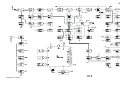
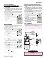
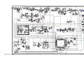
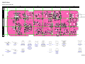
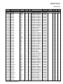
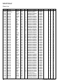
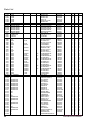
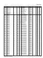
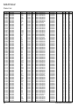
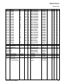
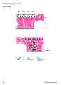
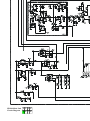
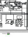
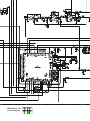
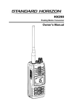
VHF FM Marine Transceiver HX290 SERVICE MANUAL HX290 Service Manual EM045N90A 1 Specifications General Frequency Ranges: Channel Spacing: Frequency Stability: Emission Type: Antenna Impedance: Supply Voltage: Current Consumption: Operating Temperature: Battery Type and Capacity: Waterproof Rating: Case Size (W x H x D): Weight (Approx.): TX: 156.025 MHz - 157.425 MHz RX: 156.050 MHz - 163.275 MHz 25 kHz ±10 ppm (–4 °F to +140 °F [–20 °C to +60 °C]) 16K0G3E 50 Ω 7.4V DC, Negative Ground (Battery Terminal) 320 mA (Receive, Typical at AF MAX.) 50 mA (Standby) 1.6 A / 0.7 A (TX: 5 W / 1W) –4 °F to +140 °F (–20 °C to +60 °C) Lithium-Ion, 1170 mAh JIS-8 / IPX8 1.5 m (about 5Ft) for 30 minutes 2.24” x 5.24” x 1.73” (57 x 133 x 44 mm) (w/o knob & antenna) 10.9 oz (310 g) (w/FNB-110LI, Belt Clip, & Antenna) Transmitter RF Power Output: Modulation Type: Maximum Deviation: Spurious Emission: Microphone Impedance: 5 W / 1 W (@7.4 V ) Variable Reactance ±5 kHz –75 dBc typical 2 kΩ Receiver Circuit Type: Intermediate Frequencies: Adjacent Channel Selectivity: Intermodulation: Hum & Noise Ratio: Sensitivity: Selectivity: AF Output (Internal SP): Double-Conversion Superheterodyne 1st: 21.7 MHz, 2nd: 450 kHz 70 dB typical 68 dB typical 40 dB typical 0.25 µV for 12 dB SINAD 25 kHz (–70 dB) 700 mW @16 Ω for 10 % THD (@7.4 V) Performance specifications are nominal, unless otherwise indicated, and are subject to change without notice. Measured in accordance with TIA/EIA-603. Important Note The HX290 was assembled using Pb (lead) free solder, based on the RoHS specification. Only lead-free solder (Alloy Composition: Sn-3.0Ag-0.5Cu) should be used for repairs performed on this apparatus. The solder stated above utilizes the alloy composition required for compliance with the lead-free specification, and any solder with the above alloy composition may be used. 2 HX290 Service Manual Exploded View & Miscellaneous Parts CP9877001 FRONT PANEL ASSY RA1096000 COIL SPRING (085RIGHT) RA046760A O RING (ANT) RA107910B LATCH NAIL RA1194200 RUBBER CAP (MIC) RA108700B KNOB SCREW (SP/MIC) RA119510A LATCH PLATE RA1193900 VOL KNOB RA119440A HOLDER (PTT) RA1194300 RUBBER KNOB (PTT) RA108700B KNOB SCREW (SP/MIC) RA1314600 PORON SHEET(WINDOW) RA1310000 RUBBER KNOB G6090212 LCD RA107890A LIGHT GUID (LCD) RA1081000 INTER CONNECTOR (LCD) RA1089600 REFLECTOR SHEET RA1312800 MIC HOLDER RUBBER Unsolder the three battery terminals to remove the MAIN Unit from the Rear Case MAIN UNIT RA1079400 RING NUT (VOL) RA1079500 RUBBER PACKING (VOL) CS2102101 TERMINAL ASSY RA1195000 RUBBER PACKING (CASE) RA119470A RUBBER PACKING (TERMINAL) RA1195000 SHEET (HEAT 6X5 t0.5) CP9876001 REAR PANEL ASSY RA0919700 O RING (6X2.2) VXSTD P/N Q3000176 AAH02X001 AAG85X002 AAG85X003 AAH68X001 AAH97X001 S6000418 DESCRIPTION CAT460 Antenna FNB-110LI Li-Ion Battery Pack PA-44B 120VAC Wall Charger (Type-A plug) PA-44C 230VAC Wall Charger (Type-C plug) CD-52 Charger Cradle CLIP-22 Belt Clip HAND STRAP HX290 Service Manual Non-designated parts are available only as part of a designated assembly. REF. VXSTD P/N U24108020 U44105001 U9900068 DESCRIPTION BIND HEAD TAPTITE-B M2X8SUS PAN HEAD TAPTITE-B M2X5 PAN HEAD TAPTITE-B M2X4NI#3 QTY. 2 10 3 3 Note 4 HX290 Service Manual Block Diagram HX290 Service Manual 5 Note 6 HX290 Service Manual Circuit Description 1. Receive Signal Path 3. Squelch Control Incoming RF from the antenna jack passes through a lowpass filter consisting of coils L1001, L1002, & L1004, capacitors C1005, C1009, C1015, C1025, & C1214, antenna switching diode D1004 (RLS135), and Surge Protector diode D1005 (1SS400). The squelch circuitry consists of a noise amplifier and band-pass filter and noise detector within Q1026 (NJM2591V). When no carrier received, noise at the output of the detector stage in Q1026 (NJM2591V) is amplified and band-pass filtered by the noise amplifier section of Q1026 (NJM2591V) and the network between pins 7 and 8, and then rectified by detection circuit in Q1026 (NJM2591V). Signals within the frequency range of the transceiver enter a high-pass filter consisting of coils L1012 and L1014, capacitors C1054, C1057, and C1065, then amplified by Q1015 (3SK294) and enter a Varactor-tuned band-pass filter consisting of coils L1021 & L1023, capacitors C1098, C1102, C1104, C1113, C1115, & C1211, and diode D1016 (DAN235E), before first mixing by Q1023 (3SK318). Buffered output from the VCO is amplified by Q1004 (2SC5006) to provide a pure first local signal between 134.35 and 141.575 MHz for injection to the first mixer Q1023 (3SK318). The 21.7 MHz first mixer product then passes through monolithic crystal filter XF1001/XF1002 to strip away all but the desired signal, which is then amplified by Q1025 (2SC4915). The amplified first IF signal is applied to FM IF subsystem IC Q1026 (NJM2591V), which contains the second mixer, second local oscillator, limited amplifier, noise amplifier, and RSSI amplifier. A second local signal is produced from the PLL reference/ second local oscillator of X1001 (21.25 MHz). The 21.25 MHz reference signal is delivered to mixer section of FM IF subsystem IC Q1026 (NJM2591V) which produce the 450 kHz second IF mixed with the first IF signal. The second IF then passes through the ceramic filter CF1001 to strip away unwanted mixer products, and is then applied to the limited amplifier in the FM IF subsystem IC Q1026 (BA4116FV), which removes amplitude variations in the 450kHz IF, before detection of the speech by the ceramic discriminator CD1001. 2. Audio Amplifier The demodulated audio signal from the Q1026 (NJM2591V) passes through the de-emphasis circuit, then applied to the audio filter Q1030 (LM2902PWR). Then passes through the audio mute switch Q1033 (TC7S66FU), the audio volume VR1006 and the audio power amplifier Q1035 (TDA2822L) pin 7, providing up to 700 mW of audio power to the 16-ohm loudspeaker. HX290 Service Manual The resulting DC squelch control voltage is passed to pin 64 of the microprocessor Q1028 (UPD78F0484GK). If no carrier is received, this signal causes pin 38 of Q1028 (UPD78F0484GK) to go low and pin 67 to go high. Pin 67 signals of Q1028 (UPD78F0484GK) to disable the supply voltage to the audio amplifier Q1035 (TDA2822). Thus, the microprocessor blocks output from the audio amplifier, and silences the receiver, while no signal is being received (and during transmission, as well). 4. Transmit Signal Path The speech input from the microphone MC1001 passes through the audio amplifier Q1027 (NJM12902V), which is adjusted the microphone gain. The speech signal passes through pre-emphasis circuit to Q1027 (NJM12902V), which contains the IDC, and low-pass filter. Then passes through VR1004 which allows manual adjustment of the transmitter deviation level. The filtered audio signal is applied to varactor diode D1006 (HVC306B), which frequency modulates the VCO Q1006 (2SC5006). The modulated signal from the VCO Q1006 (2SC5006) is buffered by Q1004 (2SC5006). The low-level transmit signal is then passes through the TX switching diode D1018 (DAN235E) to the buffer amplifier Q1018 (2SC5226), driver amplifier Q1013 (RQA0004PXDQS), then amplified transmit signal is applied to the final amplifier Q1012 (RQA0011DNS) up to 5.0 watts output power. The transmit signal then passes through the antenna switch D1003 (RLS135) and is low-pass filtered to suppress harmonic spurious radiation before delivery to the antenna. 7 Circuit Description 4-1 Automatic Transmit Power Control Current from the final amplifier is sampled by C1012 & C1020, and R1006 & R1010, and is rectified by D1002 (RB715F). The resulting DC is fed back through Q1014 (LM2904PWR) to the drive amplifier Q1013 (R Q A 0 0 0 4 P X D Q S ) and final amplifier Q1012 (RQA0011DNS), for control of the power output. When the microprocessor selects “High” or “Low” power levels, pin 66 of Q1028 (UPD78F0484GK) to go low at “High” power selected or pin 66 of Q1028 (UPD78F0484GK) to go high at “Low” power selected. 5. PLL Frequency Synthesizer The PLL circuitry on the Main Unit consists of VCO Q1006 (2SC5006), VCO buffer Q1004 (2SC5006), PLL subsystem IC Q1022 (LV2105V), which contains a reference divider, serial-to-parallel data latch, programmable divider, phase comparator and charge pump, and crystal X1001 which frequency stability is ±10 ppm @ –20 °C to +60 °C. While receiving, VCO Q1006 (2SC5006) oscillates between 134.35 and 141.575 MHz according to the transceiver version and the programmed receiving frequency. The VCO output is buffered by Q1004 (2SC5006), then applied to the prescaler section of Q1022 (LV2105V). There the VCO signal is divided by 64 or 65, according to a control signal from the data latch section of Q1022 (LV2105V), before being sent to the programmable divider section of Q1022 (LV2105V). The data latch section of Q1022 (LV2105V) also receives serial dividing data from the microprocessor Q1028 (UPD78F0484GK), which causes the pre-divided VCO signal to be further divided in the programmable divider section, depending upon the desired receive frequency, so as to produce a 25.0 kHz derivative of the current VCO frequency. Meanwhile, the reference divider sections of Q1022 (LV2105V) divides the 21.25 MHz crystal reference from the reference oscillator section of Q1022 (LV2105V), by 850 to produce the 25.0 kHz loops reference. 8 The 25.0 kHz signal from the programmable divider (derived from the VCO) and that derived from the reference oscillator are applied to the phase detector section of Q1022 (LV2105V), which produces a pulsed output with pulse duration depending on the phase difference between the input signals. This pulse train is filtered to DC and returned to the Varactor D1008 and D1009 (both HVC350B). Changes in the level of the DC voltage applied to the Varactor, affecting the reference in the tank circuit of the VCO according to the phase difference between the signals derived from the VCO and the crystal reference oscillator. The VCO is thus phase-locked to the crystal reference oscillator. The output of the VCO Q1006 (2SC5006) after buffering by Q1004 (2SC5006) is applied to the first mixer as described previously. For transmission, the VCO Q1006 (2SC5006) oscillates between 156.025 and 157.425 MHz according to the model version and programmed transmit frequency. The remainder of the PLL circuitry is shared with the receiver. However, the dividing data from the microprocessor is such that the VCO frequency is at the actual transmit frequency (rather than offset for IFs, as in the receiving case). Also, the VCO is modulated by the speech audio applied to D1006 (HVC306B), as described previously. 6. Miscellaneous Circuits Push-To-Talk Transmit Activation When the PTT switch on the Main Unit is closed, pin 72 of Q1028 (UPD78F0484GK) goes low. This signal disables the receiver by disabling the 5 V supply bus at Q1009 (UMD5N) to the front-end, FM IF subsystem IC Q1026 (NJM2591V). At the same time, Q1008 (UMD5N) activate the transmit 5 V supply line to enable the transmitter. HX290 Service Manual Alignment The HX290 has been carefully aligned at the factory for the specified performance across the marine band. Realignment should therefore not be necessary except in the event of a component failure. All component replacement and service should be performed only by an authorized STANDARD HORIZON representative, or the warranty policy may be voided. The following procedures cover the sometimes critical and tedious adjustments that are not normally required once the transceiver has left the factory. However, if damage occurs and some parts are replaced, realignment may be required. If a sudden problem occurs during normal operation, it is likely due to component failure; realignment should not be done until after the faulty component has been replaced. We recommend that servicing be performed only by authorized STANDARD HORIZON service technicians who are experienced with the circuitry and fully equipped for repair and alignment. Therefore, if a fault is suspected, contact the dealer from whom the transceiver was purchased for instructions regarding repair. Authorized STANDARD HORIZON service technicians realign all circuits and make complete performance checks to ensure compliance with factory specifications after replacing any faulty components. Those who do undertake any of the following alignments are cautioned to proceed at their own risk. Problems caused by unauthorized attempts at realignment are not covered by the warranty policy. Also, STANDARD HORIZON must reserve the right to change circuits and alignment procedures in the interest of improved performance, without notifying owners. Under no circumstances should any alignment be attempted unless the normal function and operation of the transceiver are clearly understood, the cause of the malfunction has been clearly pinpointed and any faulty components replaced, and the need for realignment determined to be absolutely necessary. The following test equipment (and thorough familiarity with its correct use) is necessary for complete realignment. Correction of problems caused by misalignment resulting from use of improper test equipment is not covered under the warranty policy. While most steps do not require all of the equipment listed, the interactions of some adjustments may require that more complex adjustments be performed afterwards. Do not attempt to perform only a single step unless it is clearly isolated electrically from all other steps. Have all test equipment ready before beginning, and follow all of the steps in a section in the order presented. HX290 Service Manual Required Test Equipment RF Signal Generator with calibrated output level at 200 MHz Frequency Counter: >0.1 ppm accuracy at 200 MHz AF Signal Generator Deviation Meter (linear detector) VHF Sampling Coupler Inline Wattmeter with 5% accuracy at 200 MHz 50-ohm Non-reactive Dummy Load: 10W at 200 MHz 7.4 VDC, 2A Regulated DC Power Supply IBM® PC/compatible computer with Microsoft® Windows® 2000, XP, or Vista Standard Horizon HX290 Service Flag Controller and CT-111 (or CT-29 + CT-97) Clone Cable. Alignment Preparation & Precautions A dummy load and inline wattmeter must be connected to the main antenna jack in all procedures that call for transmission, except where specified otherwise. Correct alignment is not possible with an antenna. After completing one step, read the following step to determine whether the same test equipment will be required. If not, remove the test equipment (except dummy load and wattmeter, if connected) before proceeding. Correct alignment requires that the ambient temperature be the same as that of the transceiver and test equipment, and that this temperature be held constant between 20 °C and 30 °C (68 °F ~ 86 °F). When the transceiver is brought into the shop from hot or cold air it should be allowed some time for thermal equalization with the environment before alignment. If possible, alignments should be made with oscillator shields and circuit boards firmly affixed in place. Also, the test equipment must be thoroughly warmed up before beginning. Note: Signal levels in dB referred to in this procedure are based on 0 dBµ = 0.5 µV(closed circuit). 9 Alignment Before Alignment Transmit Power Adjustment Remove the Front Panel from the transceiver according to the following procedures: Set up the test equipment as shown below, and set the DC Power Supply voltage to 7.4 V. Set the channel to CH16. Use the key to set the transceiver to “HI” power. With the PTT switch pressed, adjust VR1003 so that RF output power is 5.0 W ± 0.1 W. Release the PTT switch, then set the transceiver to “LOW” power by pressing the key. With the PTT switch pressed, adjust VR1001 so that RF output power is 0.9 W ± 0.1 W. Release the PTT switch. 1. Disconnect the antenna from the transceiver. 2. Remove the VOL knob, MIC/SP Screw (with Rubber Cap), and Battery Pack from the transceiver. 3. Remove the two screws which located at the bottom side on the battery compartment of the transceiver. 4. Carefully pull out the chassis from the Front Panel. Refer to the “Exploded View“ on the page 4. Reference Frequency Adjustment Set up the test equipment as shown below, and set the DC Power Supply voltage to 7.4 V. Turn the transceiver on. Set the channel to CH16. Use the key to set the transceiver to “LOW” power. With the PTT switch pressed, adjust VR1002 so the Frequency Counter reading is 156.800 MHz ± 100 Hz. Release the PTT switch. 50 Ω Dummy Load Inline Wattmeter TX Deviation Adjustment Set up the test equipment as shown below, and set the DC Power Supply voltage to 7.4 V. Set the AF Signal Generator output to 100 mVrms at 1 kHz. Set the channel to CH16 with “LOW” power. With the PTT switch pressed, adjust VR1004 so that the maximum deviation is 4.2 kHz ± 0.1 kHz. Release the PTT switch. Turn the transceiver off. RF Sampling Coupler AF Signal Generator GND Deviation Meter AF Signal Generator Frequency Counter VR1003 VR1001 Regulated Power Supply VR1004 VR1002 TX SECTION ALIGNMENT SETUP 10 HX290 Service Manual Alignment Software Alignment Set up the Software Alignment Mode Install the HX290 Service Flag Controller Program to your computer. Connect the CT-111 (or CT-29 + CT-97) Clone Cable between the MIC/SP jack of the HX290 and the Serial Port of your computer. Execute the HX290 Service Flag Controller Program. Select the COM port number which is connected to the Clone Cabl (HX290). key while Press and hold in the turning the transceiver on. Select “Alignment ON” Radio Button of the HX290 Service Flag Controller Program. Click the left mouse button on the [SET] button of the HX290 Service Flag Controller Program. Then turn the transceiver off. Terminates the Software Alignment Mode Execute the HX290 Service Flag Controller Program again. Connect the CT-111 (or CT-29 + CT-97) Clone Cable between the MIC/SP jack of the HX290 and the Serial Port of your computer. Execute the HX290 Service Flag Controller Program. Select the COM port number which is connected to the Clone Cabl (HX290). key while Press and hold in the turning the transceiver on. Select “Alignment OFF” Radio Button of HX290 Service Flag Controller Program. Click the left mouse button on the [SET] button of the HX290 Service Flag Controller Program. Turn off the transceiver. Then turn the transceiver off. After Alignment Squelch Adjustment Set up the test equipment as shown at the right, and set the DC Power Supply voltage to 7.4 V. Turn the transceiver on. Set the channel to CH16, then turn the transceiver off. Press and hold in the key while turning the transceiver on to enter the Alignment Mode. The display will be shown the “AL”. key repeatedly until Press the the Alignment Item “ti” is shown on the display. Set the RF Signal Generator output to 156.800 MHz, at a level of 0 dBµV, ±3.0 kHz deviation with a 1 kHz audio tone. Press the key to record a tight level. Adjust VR1005 so that the transceiver’s display becomes “031”. Press the key to save the new setting. Press the key repeatedly until the Alignment Item “tH” is shown on the display. Set the RF Signal Generator output to 156.800 MHz, at a level of –8 dBµV, ±3.0 kHz deviation with a 1 kHz audio tone. Press the key to record a threshold level. Press and hold the key for one second to save the new setting. Turn the transceiver off. Assemble the transceiver while being carefully so that Rubber Packing does not protrude from a Front Case. Important Note: To ensure the radio is water proof, make sure the gasket is installed on the chassis correctly and is not pinched when inserted into the front case. RF Signal Generator 16 Ω 1 W Resistor GND 16 Ω 1 W Resistor Regulated Power Supply VR1005 RX SECTION ALIGNMENT SETUP NOTICE Do not touch the Alignment Item “dC”. HX290 Service Manual 11 Note 12 HX290 Service Manual MAIN Unit Circuit Diagram RX: 3.51 V TX: 0 V RX: 4.17 V TX: 0 V RX: 2.34 V TX: 0 V RX: 2.87 V RX (WX CH): 0 V TX: 0 V RX: 1.11 V TX: 0 V RX: 4.69 V TX: 0 V RX: 2.54 V TX: 0 V RX: 2.10 V TX: 0 V RX: 4.85 V TX: 0 V 80 mVrms 80 mVrms RX: 2.47 V TX: 0 V RX: 1.00 V TX: 0 V RX: 0 V TX (Hi): 4.35 V TX (Low): 1.50 V 80 mVrms RX: 7.38 V TX: 7.34 V RX (SIGNAL: Non): 0 V RX (SIGNAL: 40 dBµ): 0.31 V TX: 0 V RX: 0 V TX: 2.68 V RX (SIGNAL: Non): 0 V RX (SIGNAL: 40 dBµ): 3.30 V TX: 0 V RX: 0 V TX: 2.82 V RX: 0 V RX (WX CH): 3.29 V TX: 0 V RX: 0 V TX: 1.69 V RX: 2.83 V TX: 0 V RX: 0 V TX (Hi): 0.83 V TX (Low): 0.35 V RX: 3.28 V TX: 0 V RX: 0 V TX (Hi): 0.42 V TX (Low): 0.18 V RX: 3.18 V TX: 3.18 V RX: 2.16 V TX: 2.16 V RX: 0 V TX (Hi): 1.31 V TX (Low): 0.56 V RX: 0 V TX (Hi): 0 V TX (Low): 3.28 V RX: 0 V TX (Hi): 2.19 V TX (Low): 0.76 V RX: 7.30 V TX: 0 V RX: 2.58 V RX: 3.51 V TX: 2.55 V TX: 3.47 V RX: 3.28 V TX: 3.28 V PLL UNLOCK: 0 V RX: 2.32 V TX: 2.32 V RX: 3.30 V TX: 0 V 45 mVrms 930 mVrms RX (SIGNAL: Non): 0 V RX (SIGNAL: 40 dBµ): 2.36 V TX: 0 V 460 mVrms RX: 2.47 V TX: 2.47 V RX: 3.17 V TX: 3.17 V RX: 1.87 V TX: 1.93 V RX: 1.60 V TX: 3.17 V RX: 5.00 V TX: 1.78 V 220 mVrms RX: 1.53 V TX: 1.53 V RX (SAVE "OFF"): 2.77 V RX (SAVE "ON"): 0 V TX: 2.77 V RX: 3.29 V TX: 3.29 V RX: 3.23 V TX: 3.23 V RX: 0 V TX: 4.86 V RX: 5.00 V TX: 5.00 V RX: 3.29 V TX: 0 V RX: 4.90 V TX: 0 V RX: 3.11 V TX: 3.11 V RX: 3.30 V TX: 3.30 V RX: 0 V TX: 3.29 V RX: 2.08 V TX: 2.08 V RX: 1.04 V TX: 1.04 V BACKLIGHT "ON": 3.29 V RX: 3.00 V TX: 3.00 V RX: 1.47 V TX: 1.47 V BACKLIGHT "ON": 1.21 V BACKLIGHT "ON": 1.09 V BACKLIGHT "ON": 2.97 V RX: 1.79 V TX: 1.79 V HX290 Service Manual 13 MAIN Unit Note 14 HX290 Service Manual MAIN Unit Parts Layout (Side A) A B C D E F G H 1 2 3 4 µPD78F0484GK (Q1028) HX290 Service Manual TDA2822L (Q1035) LM2904PWR (Q1014) 2SC4617 (BR) (Q1039) DTC144EE (26) (Q1005, 1020) TC7S66FU (E9) (Q1033) RB715F (3D) (D1024) 15 MAIN Unit Parts Layout (Side B) a b c d e f g h 1 2 3 4 16 NJM2591V (Q1026) LV2105V (Q1022) 2SA1774 (FR) (Q1016, 1032) R1EX24008ATAS0I (Q1019) LM2902PWR (Q1030) NJM12902V (Q1027) 2SB1132 (BA) (Q1036) 2SC4617 (BR) (Q1011, 1017) 2SC4915 (QY) (Q1025) 2SC5006 (24) (Q1004, 1006) 2SC5226 (R22) (Q1018) 3SK294 (UV) (Q1015) 3SK318 (YB) (Q1023) DTC144EE (26) (Q1003, 1007, 1021, 1024, 1029, 1034, 1038) RQA0004PXDQS (PX) (Q1013) SN74LVC1G66 (Q1034) RQA0011DNS (Q1012) TAR5S33U (Q1002) TAR5S50U (Q1001) UMD5N (Q1008, 1009, 1010, 1031, 1037) DA221 (K) (D1023) IMN10 (N10) (D1020) DAN235E (D1016, 1018) HX290 Service Manual MAIN Unit Parts List REF C 1001 C 1002 C 1003 C 1004 C 1005 C 1007 C 1008 C 1009 C 1010 C 1011 C 1012 C 1013 C 1014 C 1015 C 1016 C 1017 C 1018 C 1019 C 1020 C 1021 C 1022 C 1023 C 1024 C 1025 C 1027 C 1029 C 1030 C 1032 C 1033 C 1034 C 1035 C 1036 C 1037 C 1038 C 1039 C 1040 C 1041 C 1042 C 1043 C 1044 C 1045 C 1046 C 1047 C 1049 C 1050 C 1051 C 1052 C 1053 C 1054 C 1055 C 1056 C 1057 C 1058 C 1059 C 1060 C 1062 C 1063 C 1064 C 1065 C 1066 C 1067 C 1068 C 1069 C 1071 C 1072 C 1073 C 1074 C 1075 C 1076 C 1077 C 1079 DESCRIPTION PCB with Components Printed Circuit Board CHIP CAP. CHIP CAP. CHIP CAP. CHIP CAP. CHIP CAP. CHIP CAP. CHIP CAP. CHIP CAP. CHIP CAP. CHIP CAP. CHIP CAP. CHIP CAP. CHIP CAP. CHIP CAP. CHIP CAP. CHIP CAP. CHIP CAP. CHIP CAP. CHIP CAP. CHIP CAP. CHIP CAP. CHIP CAP. CHIP CAP. CHIP CAP. CHIP CAP. CHIP CAP. CHIP CAP. CHIP CAP. CHIP CAP. CHIP CAP. CHIP CAP. CHIP CAP. CHIP CAP. CHIP CAP. CHIP CAP. CHIP CAP. CHIP CAP. CHIP CAP. CHIP CAP. CHIP CAP. CHIP CAP. CHIP CAP. CHIP CAP. CHIP CAP. CHIP CAP. CHIP CAP. CHIP CAP. CHIP CAP. CHIP CAP. CHIP CAP. CHIP CAP. CHIP CAP. CHIP CAP. CHIP CAP. CHIP CAP. CHIP TA.CAP. CHIP CAP. CHIP CAP. CHIP CAP. CHIP CAP. CHIP CAP. CHIP CAP. CHIP CAP. CHIP CAP. CHIP TA.CAP. CHIP CAP. CHIP CAP. CHIP CAP. CHIP TA.CAP. CHIP CAP. CHIP CAP. HX290 Service Manual VALUE 0.001uF 0.01uF 0.001uF 0.001uF 18pF 0.01uF 0.1uF 27pF 0.01uF 0.1uF 0.5pF 0.01uF 0.001uF 6pF 0.001uF 0.01uF 0.01uF 10uF 0.5pF 0.1uF 10uF 0.01uF 0.001uF 10pF 5pF 0.001uF 0.001uF 0.001uF 27pF 27pF 56pF 0.001uF 33pF 18pF 18pF 10uF 0.1uF 33pF 22pF 0.01uF 10uF 10uF 1pF 0.01uF 15pF 0.001uF 10uF 0.001uF 18pF 0.001uF 0.01uF 15pF 1uF 0.001uF 0.001uF 10uF 0.001uF 0.001uF 33pF 0.01uF 0.001uF 0.001uF 82pF 1uF 0.1uF 0.001uF 15pF 0.22uF 10uF 10pF 0.001uF V/W 50V 25V 50V 50V 50V 25V 10V 50V 25V 10V 50V 25V 50V 50V 50V 25V 25V 6.3V 50V 10V 6.3V 25V 50V 50V 50V 50V 50V 50V 50V 50V 50V 50V 50V 50V 50V 6.3V 10V 50V 50V 25V 6.3V 6.3V 50V 25V 50V 50V 6.3V 50V 50V 50V 25V 50V 6.3V 50V 50V 16V 50V 50V 50V 25V 50V 50V 50V 6.3V 35V 50V 50V 10V 16V 50V 50V TOL. B B B B CH B B CH B B CK B B CH B B B B CK B B B B CH CH B B B CH CH CH B CH CH CH B B CH CH B B B CK B CH B B B CH B B CH B B B B B CH B B B CH B B CH B CH B MFR'S DESIG AM045N000 GRM155B11H102KA01D GRM155B11E103KA01D GRM155B11H102KA01D GRM155B11H102KA01D GRM1552C1H180JZ01D GRM155B11E103KA01D GRM155B11A104KA01D GRM1552C1H270JZ01D GRM155B11E103KA01D GRM155B11A104KA01D GRM1554C1HR50BZ01D GRM155B11E103KA01D GRM155B11H102KA01D GRM1552C1H6R0DZ01D GRM155B11H102KA01D GRM155B11E103KA01D GRM155B11E103KA01D JMK212BJ106KG-T GRM1554C1HR50BZ01D GRM155B11A104KA01D JMK212BJ106KG-T GRM155B11E103KA01D GRM155B11H102KA01D GRM1552C1H100BZ01D GRM1552C1H5R0CZ01D GRM155B11H102KA01D GRM155B11H102KA01D GRM155B11H102KA01D GRM1552C1H270JZ01D GRM1552C1H270JZ01D GRM1552C1H560JD01D GRM155B11H102KA01D GRM1552C1H330JZ01D GRM1552C1H180JZ01D GRM1552C1H180JZ01D JMK212BJ106KG-T GRM155B11A104KA01D GRM1552C1H330JZ01D GRM1552C1H220JZ01D GRM155B11E103KA01D JMK212BJ106KG-T JMK212BJ106KG-T GRM1554C1H1R0BZ01D GRM155B11E103KA01D GRM1552C1H150JZ01D GRM155B11H102KA01D JMK212BJ106KG-T GRM155B11H102KA01D GRM1552C1H180JZ01D GRM155B11H102KA01D GRM155B11E103KA01D GRM1552C1H150JZ01D GRM155B30J105KE18D GRM155B11H102KA01D GRM155B11H102KA01D TEESVA1C106M8R GRM155B11H102KA01D GRM155B11H102KA01D GRM1552C1H330JZ01D GRM155B11E103KA01D GRM155B11H102KA01D GRM155B11H102KA01D GRM1552C1H820JD01D GRM155B30J105KE18D TEESVA1V104M8R GRM155B11H102KA01D GRM1552C1H150JZ01D GRM155B31A224KE18D TEESVA1C106M8R GRM1552C1H100BZ01D GRM155B11H102KA01D VXSTD P/N CS2101701 FR0222200 K22178809 K22148834 K22178809 K22178809 K22178218 K22148834 K22108802 K22178222 K22148834 K22108802 K22178285 K22148834 K22178809 K22178208 K22178809 K22148834 K22148834 K22080802 K22178285 K22108802 K22080802 K22148834 K22178809 K22178297 K22178207 K22178809 K22178809 K22178809 K22178222 K22178222 K22178230 K22178809 K22178224 K22178218 K22178218 K22080802 K22108802 K22178224 K22178220 K22148834 K22080802 K22080802 K22178287 K22148834 K22178216 K22178809 K22080802 K22178809 K22178218 K22178809 K22148834 K22178216 K22088803 K22178809 K22178809 K78120077 K22178809 K22178809 K22178224 K22148834 K22178809 K22178809 K22178234 K22088803 K78160025 K22178809 K22178216 K22108808 K78120077 K22178297 K22178809 VERS. LOT SIDE LAY ADR 111111111111111111111111111111111111111111111111111111111111111111111111- B B B B B B A B B A B B B B A B B B B A B A B B B A A B B B B B B B B B B B B B B B B B B B B B B B B B B B B B B B B B B A B A B B B A B B B e1 e1 h3 h3 h3 e1 D1 h3 e1 D1 h3 e1 c3 g3 B4 e1 c3 e1 g3 B3 e1 C3 c2 g3 c3 C3 C3 c2 c3 c3 f3 c2 c3 f3 f3 e2 c3 f3 g3 e2 e2 c2 c3 e2 g2 f3 c2 b3 g2 e3 f3 g2 c3 b2 f3 f3 b3 e3 g2 c2 g2 B4 e3 B4 b3 g2 e3 B4 b3 g2 e3 17 MAIN Unit Parts List REF C 1080 C 1081 C 1082 C 1083 C 1084 C 1085 C 1086 C 1088 C 1089 C 1090 C 1091 C 1092 C 1094 C 1095 C 1096 C 1097 C 1098 C 1099 C 1100 C 1101 C 1102 C 1103 C 1104 C 1105 C 1107 C 1108 C 1109 C 1110 C 1111 C 1112 C 1113 C 1114 C 1115 C 1116 C 1117 C 1119 C 1120 C 1121 C 1122 C 1123 C 1124 C 1125 C 1126 C 1127 C 1128 C 1129 C 1130 C 1131 C 1132 C 1133 C 1135 C 1137 C 1138 C 1139 C 1140 C 1141 C 1142 C 1143 C 1144 C 1145 C 1146 C 1147 C 1148 C 1149 C 1150 C 1151 C 1152 C 1153 C 1154 C 1155 C 1156 C 1157 C 1158 18 DESCRIPTION CHIP CAP. CHIP CAP. CHIP TA.CAP. CHIP CAP. CHIP CAP. CHIP CAP. CHIP CAP. CHIP CAP. CHIP CAP. CHIP CAP. CHIP CAP. CHIP CAP. CHIP CAP. CHIP CAP. CHIP CAP. CHIP CAP. CHIP CAP. CHIP CAP. CHIP CAP. CHIP CAP. CHIP CAP. CHIP CAP. CHIP CAP. CHIP CAP. CHIP CAP. CHIP CAP. CHIP CAP. CHIP CAP. CHIP CAP. CHIP CAP. CHIP CAP. CHIP CAP. CHIP CAP. CHIP CAP. CHIP CAP. CHIP CAP. CHIP CAP. CHIP CAP. CHIP CAP. CHIP CAP. CHIP CAP. CHIP CAP. CHIP CAP. CHIP CAP. CHIP CAP. CHIP CAP. CHIP CAP. CHIP CAP. CHIP CAP. CHIP CAP. CHIP CAP. CHIP CAP. CHIP CAP. CHIP CAP. CHIP CAP. CHIP CAP. CHIP CAP. CHIP CAP. CHIP CAP. CHIP CAP. CHIP CAP. CHIP CAP. CHIP CAP. CHIP CAP. CHIP CAP. CHIP CAP. CHIP CAP. CHIP CAP. CHIP CAP. CHIP CAP. CHIP CAP. CHIP CAP. CHIP CAP. VALUE 0.001uF 0.1uF 0.47uF 0.001uF 0.01uF 10uF 0.001uF 0.001uF 15pF 1uF 8pF 0.001uF 8pF 5pF 10pF 0.001uF 15pF 68pF 1uF 1uF 3pF 15pF 1pF 1uF 0.01uF 0.01uF 12pF 100pF 1pF 27pF 3pF 0.001uF 18pF 5pF 0.001uF 4pF 0.01uF 18pF 0.001uF 22pF 0.01uF 18pF 0.001uF 22pF 0.001uF 10uF 33pF 0.001uF 0.001uF 0.1uF 8pF 0.01uF 33pF 0.01uF 0.1uF 0.001uF 330pF 0.0056uF 0.01uF 0.01uF 0.01uF 0.0068uF 82pF 0.1uF 270pF 270pF 15pF 10uF 0.001uF 0.47uF 0.01uF 0.01uF 1uF V/W 50V 10V 35V 50V 25V 6.3V 50V 50V 50V 6.3V 50V 50V 50V 50V 50V 50V 50V 50V 6.3V 6.3V 50V 50V 50V 6.3V 25V 25V 50V 50V 50V 50V 50V 50V 50V 50V 50V 50V 25V 50V 50V 50V 25V 50V 50V 50V 50V 6.3V 50V 50V 50V 10V 50V 25V 50V 25V 10V 50V 50V 25V 25V 25V 25V 25V 50V 10V 50V 50V 50V 6.3V 50V 6.3V 25V 25V 6.3V TOL. B B B B B B B CH B CH B CH CH CH B CH CH B B CJ CH CK B B B CH CH CK CH CJ B CH CH B CH B CH B CH B CH B CH B B CH B B B CH B CH B B B B B B B B B CH B CH CH CH B B B B B B MFR'S DESIG GRM155B11H102KA01D GRM155B11A104KA01D TEESVA1V474M8R GRM155B11H102KA01D GRM155B11E103KA01D JMK212BJ106KG-T GRM155B11H102KA01D GRM155B11H102KA01D GRM1552C1H150JZ01D GRM155B30J105KE18D GRM1552C1H8R0DZ01D GRM155B11H102KA01D GRM1552C1H8R0DZ01D GRM1552C1H5R0CZ01D GRM1552C1H100BZ01D GRM155B11H102KA01D GRM1552C1H150JZ01D GRM1552C1H680JZ01D GRM155B30J105KE18D GRM155B30J105KE18D GRP1553C1H3R0CZ01E GRM1552C1H150JZ01D GRM1554C1H1R0BZ01D GRM155B30J105KE18D GRM155B11E103KA01D GRM155B11E103KA01D GRM1552C1H120JZ01D GRM1552C1H101JD01D GRM1554C1H1R0BZ01D GRM1552C1H270JZ01D GRP1553C1H3R0CZ01E GRM155B11H102KA01D GRM1552C1H180JZ01D GRM1552C1H5R0CZ01D GRM155B11H102KA01D GRM1552C1H4R0CZ01D GRM155B11E103KA01D GRM1552C1H180JZ01D GRM155B11H102KA01D GRM1552C1H220JZ01D GRM155B11E103KA01D GRM1552C1H180JZ01D GRM155B11H102KA01D GRM1552C1H220JZ01D GRM155B11H102KA01D JMK212BJ106KG-T GRM1552C1H330JZ01D GRM155B11H102KA01D GRM155B11H102KA01D GRM155B11A104KA01D GRM1552C1H8R0DZ01D GRM155B11E103KA01D GRM1552C1H330JZ01D GRM155B11E103KA01D GRM155B11A104KA01D GRM155B11H102KA01D GRM155B11H331KA01D GRM155B11E562KA01D GRM155B11E103KA01D GRM155B11E103KA01D GRM155B11E103KA01D GRM155B11E682KA01D GRM1552C1H820JD01D GRM155B11A104KA01D GRM1552C1H271JA01D GRM1552C1H271JA01D GRM1552C1H150JZ01D JMK212BJ106KG-T GRM155B11H102KA01D GRM155B30J474KE18D GRM155B11E103KA01D GRM155B11E103KA01D GRM155B30J105KE18D VXSTD P/N K22178809 K22108802 K78160029 K22178809 K22148834 K22080802 K22178809 K22178809 K22178216 K22088803 K22178210 K22178809 K22178210 K22178207 K22178297 K22178809 K22178216 K22178232 K22088803 K22088803 K22178205 K22178216 K22178287 K22088803 K22148834 K22148834 K22178214 K22178236 K22178287 K22178222 K22178205 K22178809 K22178218 K22178207 K22178809 K22178206 K22148834 K22178218 K22178809 K22178220 K22148834 K22178218 K22178809 K22178220 K22178809 K22080802 K22178224 K22178809 K22178809 K22108802 K22178210 K22148834 K22178224 K22148834 K22108802 K22178809 K22178803 K22148802 K22148834 K22148834 K22148834 K22148803 K22178234 K22108802 K22179715 K22179715 K22178216 K22080802 K22178809 K22088802 K22148834 K22148834 K22088803 VERS. LOT SIDE LAY ADR 1- B e4 1- A B3 1- B b3 1- B e3 1- B e3 1- B b3 1- B g3 1- B b3 1- B e3 1- A B3 1- B g2 1- B d3 1- B f2 1- B c3 1- B d3 1- B d3 1- B f3 1- B c3 1- B a2 1- A B3 1- B f2 1- B c3 1- B f3 1- B d2 1- B f2 1- B d3 1- B b2 1- B b2 1- B b2 1- B a2 1- B f2 1- B a3 1- B f3 1- B d3 1- B a2 1- B f2 1- B f2 1- B d3 1- B e2 1- B d3 1- B d3 1- B d3 1- B a3 1- B e3 1- B e3 1- B b3 1- B e2 1- B e3 1- B b3 1- B b2 1- B d2 1- B d2 1- B d2 1- B b1 1- B b1 1- B c2 1- B f1 1- B f1 1- B c1 1- B c1 1- B c2 1- B g2 1- B c1 1- B c2 1- B c2 1- B c2 1- B f1 1- B c1 1- B c1 1- A D1 1- B b2 1- A E2 1- A D1 HX290 Service Manual MAIN Unit Parts List REF C 1159 C 1160 C 1161 C 1162 C 1163 C 1164 C 1165 C 1167 C 1168 C 1169 C 1170 C 1171 C 1172 C 1173 C 1174 C 1175 C 1176 C 1177 C 1178 C 1179 C 1180 C 1181 C 1182 C 1183 C 1184 C 1185 C 1186 C 1187 C 1188 C 1189 C 1190 C 1191 C 1192 C 1193 C 1194 C 1196 C 1197 C 1198 C 1199 C 1200 C 1203 C 1204 C 1205 C 1206 C 1207 C 1208 C 1209 C 1210 C 1211 C 1212 C 1214 C 1215 CD1001 CF1001 D 1001 D 1002 D 1003 D 1004 D 1005 D 1006 D 1007 D 1008 D 1009 D 1010 D 1011 D 1012 D 1013 D 1014 D 1015 D 1016 D 1017 D 1018 D 1019 DESCRIPTION CHIP CAP. CHIP CAP. CHIP CAP. CHIP CAP. CHIP CAP. CHIP CAP. CHIP CAP. CHIP CAP. CHIP CAP. CHIP CAP. CHIP CAP. CHIP CAP. CHIP CAP. CHIP CAP. CHIP CAP. CHIP CAP. CHIP CAP. CHIP CAP. CHIP CAP. CHIP CAP. CHIP CAP. CHIP CAP. CHIP CAP. CHIP CAP. CHIP CAP. CHIP CAP. CHIP CAP. CHIP CAP. CHIP CAP. CHIP CAP. CHIP CAP. CHIP TA.CAP. CHIP CAP. CHIP CAP. CHIP CAP. CHIP CAP. CHIP TA.CAP. CHIP CAP. CHIP CAP. CHIP CAP. CHIP CAP. AL.ELECTRO.CAP. CHIP CAP. CHIP CAP. CHIP CAP. CHIP CAP. CHIP CAP. CHIP CAP. CHIP CAP. CHIP CAP. CHIP CAP. CHIP CAP. CERAMIC DISC CERAMIC FILTER SURGE ABSORBER DIODE DIODE DIODE DIODE DIODE LED DIODE DIODE LED LED LED LED LED LED DIODE DIODE DIODE DIODE HX290 Service Manual VALUE 10uF 560pF 0.1uF 0.1uF 0.033uF 1uF 1uF 1uF 15pF 1uF 10pF 10uF 47pF 1uF 10pF 0.1uF 1uF 0.047uF 0.0033uF 0.047uF 0.1uF 0.047uF 270pF 0.01uF 0.0047uF 10uF 0.01uF 0.001uF 10uF 1uF 0.01uF 22uF 1uF 0.01uF 0.1uF 0.001uF 10uF 0.1uF 100pF 100pF 0.1uF 220uF 100pF 0.001uF 0.001uF 0.001uF 0.001uF 0.001uF 2pF 10uF 10pF 47pF V/W 6.3V 50V 10V 10V 10V 6.3V 6.3V 6.3V 50V 6.3V 50V 6.3V 50V 6.3V 50V 10V 6.3V 10V 50V 10V 10V 10V 50V 25V 50V 6.3V 25V 50V 6.3V 6.3V 25V 16V 6.3V 25V 10V 50V 16V 10V 50V 50V 10V 10V 50V 50V 50V 50V 50V 50V 50V 6.3V 50V 50V TOL. B B B B B B B B CH B CH B CH B CH B B B B B B B CH B B B B B B B B B B B B B CH CH B CH B B B B B CK B CH CH MFR'S DESIG JMK212BJ106KG-T GRM155B11H561KD01 GRM155B11A104KA01D GRM155B11A104KA01D GRM155B11A333KA01D GRM155B30J105KE18D GRM155B30J105KE18D GRM155B30J105KE18D GRM1552C1H150JZ01D GRM155B30J105KE18D GRM1552C1H100BZ01D JMK212BJ106KG-T GRM1552C1H470JZ01D GRM155B30J105KE18D GRM1552C1H100BZ01D GRM155B11A104KA01D GRM155B30J105KE18D GRM155B11A473KA01D GRM155B11H332KA01D GRM155B11A473KA01D GRM155B11A104KA01D GRM155B11A473KA01D GRM1552C1H271JA01D GRM155B11E103KA01D GRM155B11H472KA01D JMK212BJ106KG-T GRM155B11E103KA01D GRM155B11H102KA01D JMK212BJ106KG-T GRM155B30J105KE18D GRM155B11E103KA01D TEESVB21C226M8R GRM155B30J105KE18D GRM155B11E103KA01D GRM155B11A104KA01D GRM155B11H102KA01D TEESVA1C106M8R GRM155B11A104KA01D GRM1552C1H101JD01D GRM1552C1H101JD01D GRM155B11A104KA01D UUR1A221MCL6GS GRM1552C1H101JD01D GRM155B11H102KA01D GRM155B11H102KA01D GRM155B11H102KA01D GRM155B11H102KA01D GRM155B11H102KA01D GRM1554C1H2R0BZ01D JMK212BJ106KG-T GRM1552C1H100BZ01D GRM1552C1H470JZ01D CDA450C24 LTM450FW EZAEG3A50AV RB715F T106 RLS135 TE-11 RLS135 TE-11 1SS400 TE61 HVC306B TRU-E 19-213/S2C-AN1P2B/3T HVC350B-TRF-E HVC350B-TRF-E 19-213/S2C-AN1P2B/3T 19-213/S2C-AN1P2B/3T 19-213/S2C-AN1P2B/3T 19-213/S2C-AN1P2B/3T 19-213/S2C-AN1P2B/3T 19-213/S2C-AN1P2B/3T DAN235E TL HVC306B TRU-E DAN235E TL 1SS400 TE61 VXSTD P/N K22080802 K22178806 K22108802 K22108802 K22108803 K22088803 K22088803 K22088803 K22178216 K22088803 K22178297 K22080802 K22178228 K22088803 K22178297 K22108802 K22088803 K22108801 K22178815 K22108801 K22108802 K22108801 K22179715 K22148834 K22178838 K22080802 K22148834 K22178809 K22080802 K22088803 K22148834 K78120028 K22088803 K22148834 K22108802 K22178809 K78120077 K22108802 K22178236 K22178236 K22108802 K48100013 K22178236 K22178809 K22178809 K22178809 K22178809 K22178809 K22178289 K22080802 K22178297 K22178228 H7901430 H3900572 Q9000867 G2070752 G2070128 G2070128 G2070634 G2070918 G2071096 G2070596 G2070596 G2071096 G2071096 G2071096 G2071096 G2071096 G2071096 G2070612 G2070918 G2070612 G2070634 VERS. LOT SIDE LAY ADR 1- B e1 1- B f1 1- B b1 1- B b1 1- B f1 1- B g1 1- B f1 1- B b1 1- B f1 1- B b1 1- B d1 1- B f1 1- B b1 1- B e1 1- B e1 1- B f1 1- B f2 1- B b1 1- B f1 1- B b1 1- A B1 1- B b1 1- B a2 1- B b2 1- B b2 1- A A2 1- A A2 1- B h1 1- B f1 1- B h1 1- A A2 1- B h2 1- A B1 1- A A2 1- A A1 1- A A1 1- A A1 1- A A2 1- B h3 1- B h3 1- A A2 1- B h2 1- B g2 1- B g4 1- B g4 1- A B1 1- B f1 1- B f1 1- B f3 1- B f2 1- B g3 1- B f1 1- B c1 1- B c1 1- B h3 1- A B4 1- B g3 1- B g3 1- B g3 1- B c3 1- A E4 1- B c3 1- B c3 1- A D4 1- A D4 1- A G3 1- A G2 1- A H3 1- A H2 1- B f2 1- B a2 1- B d3 1- A D1 19 Parts List REF D 1020 D 1021 D 1022 D 1023 D 1024 D 1025 DS1001 F 1001 FB1001 FB1002 FB1003 FB1004 FB1005 J 1001 J 1002 J 1003 J 1004 L 1001 L 1002 L 1003 L 1004 L 1005 L 1006 L 1007 L 1008 L 1009 L 1010 L 1011 L 1012 L 1013 L 1014 L 1015 L 1016 L 1017 L 1018 L 1019 L 1020 L 1021 L 1022 L 1023 L 1024 L 1025 L 1026 L 1027 MC1001 Q 1001 Q 1002 Q 1003 Q 1004 Q 1005 Q 1006 Q 1007 Q 1008 Q 1009 Q 1010 Q 1011 Q 1012 Q 1013 Q 1014 Q 1015 Q 1016 Q 1017 Q 1018 Q 1019 Q 1020 Q 1021 Q 1022 Q 1023 Q 1024 Q 1025 Q 1026 Q 1027 Q 1028 20 DESCRIPTION DIODE DIODE DIODE DIODE DIODE DIODE LCD CHIP FUSE FERRITE BEADS FERRITE BEADS FERRITE BEADS FERRITE BEADS FERRITE BEADS SHIELD FINGER CONNECTOR CONTACT CONTACT COIL COIL M.RFC COIL M.RFC M.RFC COIL COIL COIL M.RFC COIL M.RFC M.RFC M.RFC M.RFC M.RFC M.RFC M.RFC M.RFC M.RFC M.RFC M.RFC M.RFC M.RFC M.RFC M.RFC M.RFC MIC. ELEMENT IC IC TRANSISTOR TRANSISTOR TRANSISTOR TRANSISTOR TRANSISTOR TRANSISTOR TRANSISTOR TRANSISTOR TRANSISTOR FET FET IC FET TRANSISTOR TRANSISTOR TRANSISTOR IC TRANSISTOR TRANSISTOR IC FET TRANSISTOR TRANSISTOR IC IC IC VALUE V/W TOL. 3.15A 0.1uH 4.7uH 0.82uH 0.033uH 0.039uH 0.082uH 4.7uH 0.056uH 0.022uH 0.18uH 0.068uH 0.1uH 0.047uH 0.068uH 0.039uH 0.082uH 0.039uH 0.056uH 0.056uH 1.5uH 1.5uH 2% 2% 2% 2% 2% 2% MFR'S DESIG 1SS400 TE61 1SS400 TE61 1SS400 TE61 DA221 TL UDZS TE-17 6.8B 1SS400 TE61 AM045N FHC16 322ADTP BLM18PG330SN1D BLM15BD102SN1D BLM18PG330SN1D BLM15BD102SN1D BLM18PG330SN1D 3525 3100103 MJC-046-C1-3.5-T OG-503040 OG-503040 E2 0.25-1.9-6.5T-L E2 0.25-1.9-6.5T-L HK1608 R10J-T E2 0.28-1.0-4.5T-R LK1608 4R7K-T LK1608 R82K-T E2 0.25-1.9-6.5T-L AS030621-33NK E2 0.45-1.5-4.5T-L HK1608 39NJ-T E2 0.25-1.9-6.5T-L C1608CB-82NG-RF LK1608 4R7K-T C1608CB-56NG-RF HK1608 22NJ-T C1608CB-R18G-RF C1608CB-68NG-RF HK1608 R10J-T HK1608 47NJ-T HK1608 68NJ-T C1608CB-39NG-RF HK1608 82NJ-T C1608CB-39NG-RF HK1608 56NJ-T HK1608 56NJ-T LK1608 1R5K-T LK1608 1R5K-T PF0-1055P TAR5S50U(TE85L.F) TAR5S33U(TE85L.F) DTC144EE TL 2SC5006-T1 DTC144EE TL 2SC5006-T1 DTC144EE TL UMD5N TR UMD5N TR UMD5N TR 2SC4617 TL R RQA0011DNS RQA0004PXDQS LM2904PWR 3SK294(TE85L) 2SA1774 TL R 2SC4617 TL R 2SC5226-5-TL R1EX24008ATAS0I DTC144EE TL DTC144EE TL LV2105V-TLM 3SK318 TL DTC144EE TL 2SC4915-O(TE85L.F) NJM2591V-TE1 NJM12902V-TE1 UPD78F0484GK(S)-GAK-AX VXSTD P/N G2070634 G2070634 G2070634 G2070178 G2070888 G2070634 G6090212 Q0000118 L9190141 L9190133 L9190141 L9190133 L9190141 S5000226 P1091309 S5000243 S5000243 L0022401 L0022401 L1690528 L0022395 L1690688 L1690417 L0022401 L0022586 L0022601 L1690523 L0022401 L1691044 L1690688 L1691041 L1690520 L1691102 L1691042 L1690528 L1690524 L1690526 L1691039 L1690527 L1691039 L1690525 L1690525 L1690846 L1690846 M3290045 G1094097 G1094549 G3070075 G3350068 G3070075 G3350068 G3070075 G3070343 G3070343 G3070343 G3346178R G3070392 G3070391 G1094010 G4802948 G3117748R G3346178R G3352268E G1094879 G3070075 G3070075 G1093191 G4803188 G3070075 G3349158O G1094024 G1093592 VERS. LOT SIDE LAY ADR 1- A D1 1- A D1 1- B b2 1- B d2 1- B d1 1- B f1 1- A D2 1- A A1 1- A A1 1- B h3 1- B g2 1- B h3 1- A A2 1- B h3 1- B h2 1- A B2 1- A B2 1- B h3 1- B g3 1- B c2 1- B g3 1- B c3 1- A C3 1- B g3 1- B c3 1- B f3 1- B g3 1- B f3 1- B g3 1- B c3 1- B g2 1- B e3 1- B g2 1- B e3 1- B g2 1- B f2 1- B d3 1- B f3 1- B c3 1- B f3 1- B d3 1- B e3 1- B e2 1- B d2 1- A C1 1- B e1 1- B e1 1- B c3 1- B c3 1- A B4 1- B c3 1- B c3 1- B e2 1- B e2 1- B d3 1- B c2 1- B f3 1- B e3 1- A B3 1- B g2 1- B b3 1- B b3 1- B d3 1- B d2 1- A B3 1- B f2 1- B b3 1- B e2 1- B b2 1- B d2 1- B c1 1- B f1 1- A E1 : Please contact Vertex Standard HX290 Service Manual Parts List REF Q 1029 Q 1030 Q 1031 Q 1032 Q 1033 Q 1034 Q 1035 Q 1036 Q 1037 Q 1038 Q 1039 R 1001 R 1002 R 1003 R 1004 R 1005 R 1006 R 1007 R 1008 R 1009 R 1010 R 1011 R 1012 R 1013 R 1014 R 1015 R 1016 R 1017 R 1018 R 1019 R 1020 R 1021 R 1022 R 1023 R 1024 R 1025 R 1026 R 1027 R 1028 R 1029 R 1030 R 1031 R 1032 R 1033 R 1034 R 1035 R 1036 R 1037 R 1038 R 1039 R 1040 R 1041 R 1042 R 1043 R 1044 R 1045 R 1046 R 1047 R 1048 R 1049 R 1050 R 1051 R 1052 R 1053 R 1054 R 1055 R 1056 R 1057 R 1058 R 1059 R 1060 R 1061 R 1062 DESCRIPTION TRANSISTOR IC TRANSISTOR TRANSISTOR IC TRANSISTOR IC TRANSISTOR TRANSISTOR TRANSISTOR TRANSISTOR CHIP RES. CHIP RES. CHIP RES. CHIP RES. CHIP RES. CHIP RES. CHIP RES. CHIP RES. CHIP RES. CHIP RES. CHIP RES. CHIP RES. CHIP RES. CHIP RES. CHIP RES. CHIP RES. CHIP RES. CHIP RES. CHIP RES. CHIP RES. CHIP RES. CHIP RES. CHIP RES. CHIP RES. CHIP RES. CHIP RES. CHIP RES. CHIP RES. CHIP RES. CHIP RES. CHIP RES. CHIP RES. CHIP RES. CHIP RES. CHIP RES. CHIP RES. CHIP RES. CHIP RES. CHIP RES. CHIP RES. CHIP RES. CHIP RES. CHIP RES. CHIP RES. CHIP RES. CHIP RES. CHIP RES. CHIP RES. CHIP RES. CHIP RES. CHIP RES. CHIP RES. CHIP RES. CHIP RES. CHIP RES. CHIP RES. CHIP RES. CHIP RES. CHIP RES. CHIP RES. CHIP RES. CHIP RES. HX290 Service Manual VALUE 47k 470k 150k 330k 82k 10k 22k 2.2k 220 10k 22k 220 680 4.7k 220 10k 56k 33k 220 330 100 15k 120 4.7k 4.7k 2.7k 560 560 2.2k 330 220k 330k 4.7k 47k 470 330 2.2k 22k 180 82k 470k 100 47k 100 39k 100 2.2k 150 220 22k 47k 330 47k 100 47k 47k 6.8k 10k 1.8k 33k 4.7k 220 V/W TOL. 1/16W 1/16W 1/16W 1/16W 1/16W 1/16W 1/16W 1/16W 1/16W 1/16W 1/16W 1/16W 1/16W 1/16W 1/16W 1/16W 1/16W 1/16W 1/16W 1/16W 1/16W 1/16W 1/16W 1/16W 1/16W 1/16W 1/16W 1/16W 1/16W 1/16W 1/16W 1/16W 1/16W 1/16W 1/16W 1/16W 1/16W 1/16W 1/16W 1/16W 1/16W 1/16W 1/16W 1/16W 1/16W 1/16W 1/16W 1/16W 1/16W 1/16W 1/16W 1/16W 1/16W 1/16W 1/16W 1/16W 1/16W 1/16W 1/16W 1/16W 1/16W 1/16W 1% 1% 1% 1% 1% 1% 1% 1% 1% 1% 1% 0.5% 0.5% 0.5% 1% 0.5% 1% 1% 1% 1% 1% 1% 1% 1% 1% 1% 1% 1% 1% 1% 1% 1% 1% 1% 1% 1% 1% 1% 1% 1% 1% 1% 1% 1% 1% 1% 1% 1% 1% 1% 1% 1% 1% 1% 1% 1% 1% 1% 1% 1% 1% 1% MFR'S DESIG DTC144EE TL LM2902PWR UMD5N TR 2SA1774 TL R TC7S66FU(TE85R.F) DTC144EE TL TDA2822L-S08-R 2SB1132 T100 R UMD5N TR DTC144EE TL 2SC4617 TL R RMC1/16SK473FTH RMC1/16SK474FTH RMC1/16SK154FTH RMC1/16SK334FTH RMC1/16SK823FTH RMC1/16SK103FTH RMC1/16SK223FTH RMC1/16SK222FTH RMC1/16SK221FTH RMC1/16SK103FTH RMC1/16SK223FTH RR0510P-221-D RR0510P-681-D RR0510P-472-D RMC1/16SK221FTH RR0510P-103-D RMC1/16SK563FTH RMC1/16SK333FTH RMC1/16SK221FTH RMC1/16SK331FTH RMC1/16SK101FTH RMC1/16SK153FTH RMC1/16SK121FTH RMC1/16SK472FTH RMC1/16SK472FTH RMC1/16SK272FTH RMC1/16SK561FTH RMC1/16SK561FTH RMC1/16SK222FTH RMC1/16SK331FTH RMC1/16SK224FTH RMC1/16SK334FTH RMC1/16SK472FTH RMC1/16SK473FTH RMC1/16SK471FTH RMC1/16SK331FTH RMC1/16SK222FTH RMC1/16SK223FTH RMC1/16SK181FTH RMC1/16SK823FTH RMC1/16SK474FTH RMC1/16SK101FTH RMC1/16SK473FTH RMC1/16SK101FTH RMC1/16SK393FTH RMC1/16SK101FTH RMC1/16SK222FTH RMC1/16SK151FTH RMC1/16SK221FTH RMC1/16SK223FTH RMC1/16SK473FTH RMC1/16SK331FTH RMC1/16SK473FTH RMC1/16SK101FTH RMC1/16SK473FTH RMC1/16SK473FTH RMC1/16SK682FTH RMC1/16SK103FTH RMC1/16SK182FTH RMC1/16SK333FTH RMC1/16SK472FTH RMC1/16SK221FTH VXSTD P/N G3070075 G1094009 G3070343 G3117748R G1092116 G3070075 G1094497 G3211327R G3070343 G3070075 G3346178R J24189525 J24189537 J24189531 J24189535 J24189528 J24189489 J24189492 J24189497 J24189508 J24189489 J24189492 J24189103 J24189115 J24189135 J24189508 J24189143 J24189526 J24189494 J24189508 J24189510 J24189504 J24189491 J24189505 J24189488 J24189488 J24189517 J24189513 J24189513 J24189497 J24189510 J24189533 J24189535 J24189488 J24189525 J24189512 J24189510 J24189497 J24189492 J24189507 J24189528 J24189537 J24189504 J24189525 J24189504 J24189524 J24189504 J24189497 J24189506 J24189508 J24189492 J24189525 J24189510 J24189525 J24189504 J24189525 J24189525 J24189521 J24189489 J24189516 J24189494 J24189488 J24189508 VERS. LOT SIDE LAY ADR 1- B a1 1- B b1 1- B e1 1- B h1 1- A B1 1- B h1 1- A A2 1- B h2 1- B f1 1- B f1 1- A A1 1- B h3 1- A D1 1- A D1 1- A D1 1- A D2 1- A B3 1- A D1 1- A C3 1- B c2 1- A B3 1- B c2 1- B c2 1- B c3 1- B c3 1- A C3 1- B c3 1- B c3 1- B c3 1- B f3 1- A E4 1- B e3 1- B c3 1- A D4 1- B c2 1- B e3 1- B e3 1- B b1 1- B a2 1- A B4 1- B b3 1- B g3 1- B g3 1- B e4 1- A B3 1- B b3 1- B e3 1- B e4 1- A B3 1- B b3 1- B g2 1- B g2 1- B e3 1- A B3 1- B g2 1- A B3 1- B b3 1- B g2 1- B g3 1- B b3 1- A B3 1- B b3 1- B d3 1- B b3 1- B d3 1- B b3 1- B b3 1- B d3 1- B d3 1- A B3 1- B a2 1- A B3 1- B d3 21 MAIN Unit Parts List REF R 1063 R 1064 R 1065 R 1066 R 1067 R 1068 R 1069 R 1070 R 1074 R 1075 R 1076 R 1077 R 1078 R 1079 R 1080 R 1081 R 1082 R 1083 R 1084 R 1085 R 1086 R 1087 R 1088 R 1089 R 1090 R 1091 R 1092 R 1093 R 1094 R 1095 R 1096 R 1097 R 1098 R 1099 R 1100 R 1101 R 1102 R 1103 R 1104 R 1105 R 1106 R 1108 R 1109 R 1110 R 1111 R 1112 R 1113 R 1114 R 1115 R 1116 R 1117 R 1118 R 1120 R 1121 R 1122 R 1123 R 1124 R 1125 R 1126 R 1127 R 1128 R 1129 R 1130 R 1131 R 1132 R 1133 R 1134 R 1135 R 1136 R 1137 R 1138 R 1139 R 1140 22 DESCRIPTION CHIP RES. CHIP RES. CHIP RES. CHIP RES. CHIP RES. CHIP RES. CHIP RES. CHIP RES. CHIP RES. CHIP RES. CHIP RES. CHIP RES. CHIP RES. CHIP RES. CHIP RES. CHIP RES. CHIP RES. CHIP RES. CHIP RES. CHIP RES. CHIP RES. CHIP RES. CHIP RES. CHIP RES. CHIP RES. CHIP RES. CHIP RES. CHIP RES. CHIP RES. CHIP RES. CHIP RES. CHIP RES. CHIP RES. CHIP RES. CHIP RES. CHIP RES. CHIP RES. CHIP RES. CHIP RES. CHIP RES. CHIP RES. CHIP RES. CHIP RES. CHIP RES. CHIP RES. CHIP RES. CHIP RES. CHIP RES. CHIP RES. CHIP RES. CHIP RES. CHIP RES. CHIP RES. CHIP RES. CHIP RES. CHIP RES. CHIP RES. CHIP RES. CHIP RES. CHIP RES. CHIP RES. CHIP RES. CHIP RES. CHIP RES. CHIP RES. CHIP RES. CHIP RES. CHIP RES. CHIP RES. CHIP RES. CHIP RES. CHIP RES. CHIP RES. VALUE 4.7k 4.7k 100k 10k 100k 4.7k 10k 2.2k 0 2.2k 2.2k 1k 1k 1k 100k 100k 100k 120k 47 220 22 1k 820 820 47k 47k 1.2k 2.2k 220k 10k 470k 47k 47k 47k 39k 39k 8.2k 2.2k 4.7k 150k 4.7k 330k 22k 2.2k 10k 220k 100k 47k 22k 10k 4.7k 22 470k 4.7k 120k 68k 470k 15k 15k 33k 1.8k 10k 10k 4.7k 33k 10k 10k 330k 0 1M 100 180k 470k V/W 1/16W 1/16W 1/16W 1/16W 1/16W 1/16W 1/16W 1/16W 1/16W 1/16W 1/16W 1/16W 1/16W 1/16W 1/16W 1/16W 1/16W 1/16W 1/16W 1/16W 1/16W 1/16W 1/16W 1/16W 1/16W 1/16W 1/16W 1/16W 1/16W 1/16W 1/16W 1/16W 1/16W 1/16W 1/16W 1/16W 1/16W 1/16W 1/16W 1/16W 1/16W 1/16W 1/16W 1/16W 1/16W 1/16W 1/16W 1/16W 1/16W 1/16W 1/16W 1/16W 1/16W 1/16W 1/16W 1/16W 1/16W 1/16W 1/16W 1/16W 1/16W 1/16W 1/16W 1/16W 1/16W 1/16W 1/16W 1/16W 1/16W 1/16W 1/16W 1/16W 1/16W TOL. 1% 1% 1% 1% 1% 1% 1% 1% 5% 1% 1% 1% 1% 1% 1% 1% 1% 1% 0.5% 1% 5% 1% 1% 1% 1% 1% 1% 1% 1% 1% 1% 1% 1% 1% 1% 1% 1% 1% 1% 1% 1% 1% 1% 1% 1% 1% 1% 1% 1% 1% 1% 5% 1% 1% 1% 1% 1% 1% 1% 1% 1% 1% 1% 1% 1% 1% 1% 1% 5% 1% 1% 1% 1% MFR'S DESIG RMC1/16SK472FTH RMC1/16SK472FTH RMC1/16SK104FTH RMC1/16SK103FTH RMC1/16SK104FTH RMC1/16SK472FTH RMC1/16SK103FTH RMC1/16SK222FTH RMC1/16S JPTH RMC1/16SK222FTH RMC1/16SK222FTH RMC1/16SK102FTH RMC1/16SK102FTH RMC1/16SK102FTH RMC1/16SK104FTH RMC1/16SK104FTH RMC1/16SK104FTH RMC1/16SK124FTH MCR01MZPD47R0 RMC1/16SK221FTH RMC1/16S 220JTH RMC1/16SK102FTH RMC1/16SK821FTH RMC1/16SK821FTH RMC1/16SK473FTH RMC1/16SK473FTH RMC1/16SK122FTH RMC1/16SK222FTH RMC1/16SK224FTH RMC1/16SK103FTH RMC1/16SK474FTH RMC1/16SK473FTH RMC1/16SK473FTH RMC1/16SK473FTH RMC1/16SK393FTH RMC1/16SK393FTH RMC1/16SK822FTH RMC1/16SK222FTH RMC1/16SK472FTH RMC1/16SK154FTH RMC1/16SK472FTH RMC1/16SK334FTH RMC1/16SK223FTH RMC1/16SK222FTH RMC1/16SK103FTH RMC1/16SK224FTH RMC1/16SK104FTH RMC1/16SK473FTH RMC1/16SK223FTH RMC1/16SK103FTH RMC1/16SK472FTH RMC1/16S 220JTH RMC1/16SK474FTH RMC1/16SK472FTH RMC1/16SK124FTH RMC1/16SK683FTH RMC1/16SK474FTH RMC1/16SK153FTH RMC1/16SK153FTH RMC1/16SK333FTH RMC1/16SK182FTH RMC1/16SK103FTH RMC1/16SK103FTH RMC1/16SK472FTH RMC1/16SK333FTH RMC1/16SK103FTH RMC1/16SK103FTH RMC1/16SK334FTH RMC1/16S JPTH RMC1/16SK105FTH RMC1/16SK101FTH RMC1/16SK184FTH RMC1/16SK474FTH VXSTD P/N J24189488 J24189488 J24189529 J24189489 J24189529 J24189488 J24189489 J24189497 J24189070 J24189497 J24189497 J24189487 J24189487 J24189487 J24189529 J24189529 J24189529 J24189530 J24189346 J24189508 J24189005 J24189487 J24189495 J24189495 J24189525 J24189525 J24189515 J24189497 J24189533 J24189489 J24189537 J24189525 J24189525 J24189525 J24189524 J24189524 J24189522 J24189497 J24189488 J24189531 J24189488 J24189535 J24189492 J24189497 J24189489 J24189533 J24189529 J24189525 J24189492 J24189489 J24189488 J24189005 J24189537 J24189488 J24189530 J24189527 J24189537 J24189491 J24189491 J24189494 J24189516 J24189489 J24189489 J24189488 J24189494 J24189489 J24189489 J24189535 J24189070 J24189541 J24189504 J24189532 J24189537 VERS. LOT SIDE LAY ADR 1- B d2 1- B d1 1- B a2 1- B f2 1- B a2 1- B f2 1- B f2 1- B d3 1- B b2 1- B d3 1- B d3 1- B a3 1- B a3 1- B a3 1- B f2 1- B f2 1- B f2 1- B f2 1- B e2 1- B e3 1- B b3 1- B e2 1- B e2 1- B d2 1- B d2 1- A E2 1- B d2 1- B d2 1- B b1 1- B b1 1- B f2 1- A E1 1- A E1 1- A E1 1- B g1 1- B f2 1- B f2 1- B c1 1- B f2 1- B c2 1- B f2 1- B f1 1- B c1 1- B c1 1- A D1 1- A E1 1- A E1 1- A E1 1- A E1 1- A E1 1- A E1 1- B c1 1- B f2 1- A E1 1- B f1 1- B g1 1- B f1 1- B b1 1- B f1 1- B g1 1- A E1 1- A E1 1- A E1 1- B d1 1- B b1 1- B f1 1- A E1 1- B f1 1- B b1 1- B e1 1- B e1 1- B b1 1- B f2 HX290 Service Manual MAIN Unit Parts List REF R 1141 R 1142 R 1143 R 1144 R 1145 R 1146 R 1147 R 1148 R 1149 R 1150 R 1152 R 1153 R 1154 R 1155 R 1157 R 1158 R 1159 R 1160 R 1161 R 1162 R 1163 R 1164 R 1165 R 1166 R 1167 R 1168 R 1169 R 1170 R 1172 R 1173 R 1174 R 1175 R 1176 R 1178 R 1179 R 1180 S 1009 TH1001 TH1002 TH1003 VR1001 VR1002 VR1003 VR1004 VR1005 VR1006 X 1001 X 1002 XF1001 XF1002 DESCRIPTION CHIP RES. CHIP RES. CHIP RES. CHIP RES. CHIP RES. CHIP RES. CHIP RES. CHIP RES. CHIP RES. CHIP RES. CHIP RES. CHIP RES. CHIP RES. CHIP RES. CHIP RES. CHIP RES. CHIP RES. CHIP RES. CHIP RES. CHIP RES. CHIP RES. CHIP RES. CHIP RES. CHIP RES. CHIP RES. CHIP RES. CHIP RES. CHIP RES. CHIP RES. CHIP RES. CHIP RES. CHIP RES. CHIP RES. CHIP RES. CHIP RES. CHIP RES. TACT SWITCH THERMISTOR THERMISTOR THERMISTOR POT. POT. POT. POT. POT. POT. XTAL NX6035SA XTAL SMD-49TA XTAL FILTER XTAL FILTER INTER CONNECTOR LIGHT GUIDE REFLECTOR SHEET MIC HOLDER RUBBER HX290 Service Manual VALUE 10k 22k 10k 10k 8.2k 10k 56k 1.5k 150k 180k 22k 4.7k 0 4.7k 27k 47k 2.2k 2.2k 10k 10k 2.2 0 1k 1k 4.7k 1k 4.7 4.7 3.9k 100k 0 0 0 4.7k 1.2k 0 10k 10k 10k 10k 10k 21.25MHz 9.8304MHz V/W 1/16W 1/16W 1/16W 1/16W 1/16W 1/16W 1/16W 1/16W 1/16W 1/16W 1/16W 1/16W 1/16W 1/16W 1/16W 1/16W 1/16W 1/16W 1/16W 1/16W 1/4W 1/16W 1/16W 1/16W 1/16W 1/16W 1/16W 1/16W 1/16W 1/16W 1/16W 1/16W 1/16W 1/16W 1/16W 1/16W TOL. 1% 1% 1% 1% 1% 1% 1% 1% 1% 1% 1% 1% 5% 1% 1% 1% 1% 1% 1% 1% 5% 5% 1% 1% 1% 1% 5% 5% 1% 1% 5% 5% 5% 1% 1% 5% MFR'S DESIG RMC1/16SK103FTH RMC1/16SK223FTH RMC1/16SK103FTH RMC1/16SK103FTH RMC1/16SK822FTH RMC1/16SK103FTH RMC1/16SK563FTH RMC1/16SK152FTH RMC1/16SK154FTH RMC1/16SK184FTH RMC1/16SK223FTH RMC1/16SK472FTH RMC1/16S JPTH RMC1/16SK472FTH RMC1/16SK273FTH RMC1/16SK473FTH RMC1/16SK222FTH RMC1/16SK222FTH RMC1/16SK103FTH RMC1/16SK103FTH RMC1/4 2R2JATP RMC1/16S JPTH RMC1/16SK102FTH RMC1/16SK102FTH RMC1/16SK472FTH RMC1/16SK102FTH RMC1/16S 4R7JTH RMC1/16S 4R7JTH RMC1/16SK392FTH RMC1/16SK104FTH RMC1/16S JPTH RMC1/16S JPTH RMC1/16S JPTH RMC1/16SK472FTH RMC1/16SK122FTH RMC1/16S JPTH EVQPUB02K NCP15WL473J03RC NCP15WL473J03RC NCP15WL473J03RC PVZ3A103A01R00 PVZ3A103A01R00 PVZ3A103A01R00 PVZ3A103A01R00 PVZ3A103A01R00 TP76N00N RY-8935 21.25MHZ 9.8304MHZ 21.700MHZ 21.700MHZ (LCD) (LCD) (HX290) VXSTD P/N J24189489 J24189492 J24189489 J24189489 J24189522 J24189489 J24189526 J24189496 J24189531 J24189532 J24189492 J24189488 J24189070 J24189488 J24189493 J24189525 J24189497 J24189497 J24189489 J24189489 J24245229 J24189070 J24189487 J24189487 J24189488 J24189487 J24189066 J24189066 J24189519 J24189529 J24189070 J24189070 J24189070 J24189488 J24189515 J24189070 N5090167 G9090175 G9090175 G9090175 J51820103 J51820103 J51820103 J51820103 J51820103 J60800307 H0103391 H0103393 H1102395 H1102395 RA1081000 RA107890A RA1089600 RA1312800 VERS. LOT SIDE LAY ADR 1- B b1 1- B f1 1- B f1 1- A B1 1- B a1 1- A B1 1- B a2 1- B a1 1- B b1 1- B a2 1- B a1 1- B b2 1- B b1 1- B b2 1- B h1 1- A B1 1- B f1 1- B f1 1- A A1 1- B b2 1- B h1 1- B b2 1- B h1 1- B h1 1- A A2 1- A A2 1- A A2 1- A A2 1- B f1 1- A A1 1- B d1 1- B d1 1- A F3 1- B b3 1- A C4 1- B f1 1- B f4 1- A C3 1- B a2 1- B b1 1- A B3 1- A F2 1- A B4 1- A F3 1- A F1 1- B h1 1- B b2 1- B d1 1- B e2 1- B d2 1111- 23 MAIN Unit Note 24 HX290 Service Manual CD-52 Charger Cradle Exploded View RA1294100 CASE (CD-52) RA1294300 LIGHT GUIDE (CD-52) CHARGER UNIT : When removing the Charger Unit from the Case, gently pull on the charger unit while pushing the four charging terminals from the outside of the case. RA1236500 (x 2 pcs) SHEET (HEAT6X6) RA1294200 BOTTOM PLATE (CD-52) Ref. VXSTD P/N Description Qty. U24208020 BIND HEAD TAPTITE-P 2.6X8SUS 4 Circuit Diagram HX290 Service Manual 25 CD-52 Charger Cradle Parts Layout (Side A) (Side B) NJW4100V (Q2003) 26 BA09CC0FP (Q2001) 2SB1201S (Q2002) HX290 Service Manual CD-52 Charger Cradle Parts List REF C 2001 C 2002 C 2003 C 2004 C 2005 C 2006 C 2007 C 2008 C 2009 C 2010 C 2011 D 2001 D 2002 D 2003 D 2004 F 2001 J 2001 Q 2001 Q 2002 Q 2003 R 2001 R 2003 R 2004 R 2005 R 2006 R 2007 R 2008 R 2009 R 2010 R 2011 R 2012 R 2013 R 2014 R 2015 R 2017 R 2018 R 2019 R 2020 R 2021 R 2022 DESCRIPTION Printed Circuit Board CHIP CAP. CHIP CAP. CHIP CAP. AL.ELECTRO.CAP. CHIP CAP. CHIP CAP. CHIP CAP. CHIP CAP. CHIP CAP. CHIP CAP. CHIP CAP. DIODE LED DIODE DIODE CHIP FUSE CONNECTOR IC TRANSISTOR IC CHIP RES. CHIP RES. CHIP RES. CHIP RES. CHIP RES. CHIP RES. CHIP RES. CHIP RES. CHIP RES. CHIP RES. CHIP RES. CHIP RES. CHIP RES. CHIP RES. CHIP RES. CHIP RES. CHIP RES. CHIP RES. CHIP RES. CHIP RES. TERMINAL HX290 Service Manual VALUE 0.1uF 0.1uF 0.1uF 47uF 0.01uF 0.047uF 0.001uF 0.1uF 0.1uF 0.1uF 0.1uF V/W TOL. 25V 25V 16V 16V 50V 25V 50V 16V 16V 16V 16V B B B B B B B B B B 1/4W 1/16W 1/16W 1/16W 1/16W 1/16W 1/8W 1/8W 1/16W 1/16W 1/16W 1/16W 1/16W 1/16W 1/16W 1/16W 1/16W 1/16W 1/16W 1/16W 5% 1% 1% 5% 1% 1% 5% 10% 1% 1% 1% 1% 1% 1% 0.5% 0.5% 5% 5% 5% 5% 2A 330 100k 27k 10k 100k 10k 1k 0.33 6.8k 10k 8.2k 100k 27k 10k 3.3k 3.3k 10k 10k 0 390 MFR'S DESIG AM045N000 GRM21BB11E104KA01L GRM21BB11E104KA01L GRM188B11C104KA01D UVR1C470MDD GRM188B11H103KA01D GRM188B11E473KA01D GRM188B11H102KA01D GRM188B11C104KA01D GRM188B11C104KA01D GRM188B11C104KA01D GRM188B11C104KA01D 1SR154-400 TE25 BRPY1211F-TR RSX101VA-30TR 1SS400 TE61 FCC16 202ADTP MJC-005-B-B-2 BA09CC0FP(TAPE) 2SB1201S-TL NJW4100V(TE1) RMC1/4 331JATP RMC1/16 104FTP RMC1/16 273FTP RMC1/16 103JATP RMC1/16 104FTP RMC1/16 103FTP RMC1/8T 102J RMC1/8 R33KTP RMC1/16 682FTP RMC1/16 103FTP RMC1/16 822FTP RMC1/16 104FTP RMC1/16 273FTP RMC1/16 103FTP RGC1/16C332DTP RGC1/16C332DTP RMC1/16 103JATP RMC1/16 103JATP RMC1/16 000JATP RMC1/16 391JATP (CHRG) VXSTD P/N FR0222400 K22140811 K22140811 K22124805 K40129107 K22174823 K22144811 K22174821 K22124805 K22124805 K22124805 K22124805 G2070684 G2070706 G2070984 G2070634 Q0000147 P1091377 G1094432 G3070195 G1094305 J24245331 J24183104 J24183273 J24185103 J24183104 J24183103 J24215102 J24219001 J24183682 J24183103 J24183822 J24183104 J24183273 J24183103 J24189415 J24189415 J24185103 J24185103 J24185000 J24185391 RA0769800 VERS. LOT SIDE LAY ADR 111111111111111111111111111111111111111111- 27 Note 28 HX290 Service Manual HX290 Main Unit Circuit Diagram 1 2 3 4 5 6 7 8 HX290 Main Unit Circuit Diagram 1 2 3 4 5 6 7 8 HX290 Main Unit Circuit Diagram 1 2 3 4 5 6 7 8 HX290 Main Unit Circuit Diagram 1 2 3 4 5 6 7 8 HX290 Main Unit Circuit Diagram 1 2 3 4 5 6 7 8 HX290 Main Unit Circuit Diagram 1 2 3 4 5 6 7 8 HX290 Main Unit Circuit Diagram 1 2 3 4 5 6 7 8 HX290 Main Unit Circuit Diagram 1 2 3 4 5 6 7 8 HX290 Main Unit (Side “A”) Parts Layout 1 2 HX290 Main Unit (Side “A”) Parts Layout 1 2 HX290 Main Unit (Side “B”) Parts Layout 1 2 HX290 Main Unit (Side “B”) Parts Layout 1 2 Note HX290 Service Manual 29 © 2011 VERTEX STANDARD CO., LTD. Marine Division of VERTEX STANDARD US Headquarters 10900 Walker Street, Cypress, CA 90630, U.S.A. 30 All rights reserved. No portion of this manual may be reproduced without the permission of VERTEX STANDARD CO., LTD. HX290 Service Manual