1
Model 671
Spectroscopy Amplifier
Operating and Service Manual
Printed in U.S.A.
ORTEC® Part No. 736840
Manual Revision G
1202
Advanced Measurement Technology, Inc.
a/k/a/ ORTEC®, a subsidiary of AMETEK®, Inc.
WARRANTY
ORTEC* warrants that the items will be delivered free from defects in material or workmanship. ORTEC makes
no other warranties, express or implied, and specifically NO WARRANTY OF MERCHANTABILITY OR
FITNESS FOR A PARTICULAR PURPOSE.
ORTEC’s exclusive liability is limited to repairing or replacing at ORTEC’s option, items found by ORTEC to
be defective in workmanship or materials within one year from the date of delivery. ORTEC’s liability on any
claim of any kind, including negligence, loss, or damages arising out of, connected with, or from the performance
or breach thereof, or from the manufacture, sale, delivery, resale, repair, or use of any item or services covered
by this agreement or purchase order, shall in no case exceed the price allocable to the item or service furnished
or any part thereof that gives rise to the claim. In the event ORTEC fails to manufacture or deliver items called
for in this agreement or purchase order, ORTEC’s exclusive liability and buyer’s exclusive remedy shall be release
of the buyer from the obligation to pay the purchase price. In no event shall ORTEC be liable for special or
consequential damages.
Quality Control
Before being approved for shipment, each ORTEC instrument must pass a stringent set of quality control tests
designed to expose any flaws in materials or workmanship. Permanent records of these tests are maintained for
use in warranty repair and as a source of statistical information for design improvements.
Repair Service
If it becomes necessary to return this instrument for repair, it is essential that Customer Services be contacted in
advance of its return so that a Return Authorization Number can be assigned to the unit. Also, ORTEC must be
informed, either in writing, by telephone [(865) 482-4411] or by facsimile transmission [(865) 483-2133], of the
nature of the fault of the instrument being returned and of the model, serial, and revision ("Rev" on rear panel)
numbers. Failure to do so may cause unnecessary delays in getting the unit repaired. The ORTEC standard
procedure requires that instruments returned for repair pass the same quality control tests that are used for
new-production instruments. Instruments that are returned should be packed so that they will withstand normal
transit handling and must be shipped PREPAID via Air Parcel Post or United Parcel Service to the designated
ORTEC repair center. The address label and the package should include the Return Authorization Number
assigned. Instruments being returned that are damaged in transit due to inadequate packing will be repaired at the
sender's expense, and it will be the sender's responsibility to make claim with the shipper. Instruments not in
warranty should follow the same procedure and ORTEC will provide a quotation.
Damage in Transit
Shipments should be examined immediately upon receipt for evidence of external or concealed damage. The carrier
making delivery should be notified immediately of any such damage, since the carrier is normally liable for damage
in shipment. Packing materials, waybills, and other such documentation should be preserved in order to establish
claims. After such notification to the carrier, please notify ORTEC of the circumstances so that assistance can be
provided in making damage claims and in providing replacement equipment, if necessary.
Copyright © 2002, Advanced Measurement Technology, Inc. All rights reserved.
*ORTEC® is a registered trademark of Advanced Measurement Technology, Inc. All other trademarks used
herein are the property of their respective owners.
iii
CONTENTS
WARRANTY . . . . . . . . . . . . . . . . . . . . . . . . . . . . . . . . . . . . . . . . . . . . . . . . . . . . . . . . . . . . . . . . . . . . . . . ii
SAFETY INSTRUCTIONS AND SYMBOLS . . . . . . . . . . . . . . . . . . . . . . . . . . . . . . . . . . . . . . . . . . . . . . . iv
SAFETY WARNINGS AND CLEANING INSTRUCTIONS . . . . . . . . . . . . . . . . . . . . . . . . . . . . . . . . . . . . . v
1. DESCRIPTION . . . . . . . . . . . . . . . . . . . . . . . . . . . . . . . . . . . . . . . . . . . . . . . . . . . . . . . . . . . . . . . . . . . 1
1.1. GENERAL . . . . . . . . . . . . . . . . . . . . . . . . . . . . . . . . . . . . . . . . . . . . . . . . . . . . . . . . . . . . . . . . 1
2. SPECIFICATIONS . . . . . . . . . . . . . . . . . . . . . . . . . . . . . . . . . . . . . . . . . . . . . . . . . . . . . . . . . . . . . . . .
2.1. PERFORMANCE . . . . . . . . . . . . . . . . . . . . . . . . . . . . . . . . . . . . . . . . . . . . . . . . . . . . . . . . . . .
2.2. CONTROLS AND INDICATORS . . . . . . . . . . . . . . . . . . . . . . . . . . . . . . . . . . . . . . . . . . . . . . .
2.3. INPUTS . . . . . . . . . . . . . . . . . . . . . . . . . . . . . . . . . . . . . . . . . . . . . . . . . . . . . . . . . . . . . . . . . .
2.4. OUTPUTS . . . . . . . . . . . . . . . . . . . . . . . . . . . . . . . . . . . . . . . . . . . . . . . . . . . . . . . . . . . . . . . .
2.5. ELECTRICAL AND MECHANICAL . . . . . . . . . . . . . . . . . . . . . . . . . . . . . . . . . . . . . . . . . . . . . .
3
3
4
4
5
5
3. INSTALLATION . . . . . . . . . . . . . . . . . . . . . . . . . . . . . . . . . . . . . . . . . . . . . . . . . . . . . . . . . . . . . . . . . .
3.1. POWER CONNECTION . . . . . . . . . . . . . . . . . . . . . . . . . . . . . . . . . . . . . . . . . . . . . . . . . . . . . .
3.2. PREAMPLIFIER CONNECTION . . . . . . . . . . . . . . . . . . . . . . . . . . . . . . . . . . . . . . . . . . . . . . . .
3.3. PULSED RESET PREAMPLIFIERS AND INHIBIT IN CONNECTION . . . . . . . . . . . . . . . . . . . .
3.4. CONNECTION OF TEST PULSE GENERATOR . . . . . . . . . . . . . . . . . . . . . . . . . . . . . . . . . . .
3.5. SHAPING CONSIDERATIONS . . . . . . . . . . . . . . . . . . . . . . . . . . . . . . . . . . . . . . . . . . . . . . . . .
3.6. LINEAR OUTPUT CONNECTIONS . . . . . . . . . . . . . . . . . . . . . . . . . . . . . . . . . . . . . . . . . . . . .
3.7. PILE-UP REJECTION USING PUR OUTPUT . . . . . . . . . . . . . . . . . . . . . . . . . . . . . . . . . . . . . .
3.8. LIVETIME CORRECTION USING BUSY OUTPUT . . . . . . . . . . . . . . . . . . . . . . . . . . . . . . . . .
3.9. INPUT COUNT RATE USING CRM OUTPUT . . . . . . . . . . . . . . . . . . . . . . . . . . . . . . . . . . . . .
6
6
6
6
6
7
7
8
8
8
4. OPERATING INSTRUCTIONS . . . . . . . . . . . . . . . . . . . . . . . . . . . . . . . . . . . . . . . . . . . . . . . . . . . . . . . 9
4.1. INITIAL TESTING AND OBSERVATION OF PULSE WAVEFORMS . . . . . . . . . . . . . . . . . . . . 9
4.2. STANDARD SETUP PROCEDURES . . . . . . . . . . . . . . . . . . . . . . . . . . . . . . . . . . . . . . . . . . . . . 9
4.3. POLE-ZERO ADJUSTMENTS FOR RESISTIVE-FEEDBACK PREAMPLIFIER . . . . . . . . . . . 10
4.4. BASELINE RESTORER (BLR) SETTING . . . . . . . . . . . . . . . . . . . . . . . . . . . . . . . . . . . . . . . . 11
4.5. INTERNAL CONTROLS . . . . . . . . . . . . . . . . . . . . . . . . . . . . . . . . . . . . . . . . . . . . . . . . . . . . . 12
4.6. DIFFERENTIAL INPUT MODE . . . . . . . . . . . . . . . . . . . . . . . . . . . . . . . . . . . . . . . . . . . . . . . . 13
4.7. SYSTEM THROUGHPUT . . . . . . . . . . . . . . . . . . . . . . . . . . . . . . . . . . . . . . . . . . . . . . . . . . . . 14
4.8. CHARGE COLLECTION OR BALLISTIC DEFICIT EFFECTS . . . . . . . . . . . . . . . . . . . . . . . . 15
4.9. PILE-UP REJECTOR (PUR) AND LIVETIME CORRECTOR . . . . . . . . . . . . . . . . . . . . . . . . . 16
4.10. OPERATION WITH SEMICONDUCTOR DETECTORS . . . . . . . . . . . . . . . . . . . . . . . . . . . . 17
4.11. OPERATION IN SPECTROSCOPY SYSTEMS . . . . . . . . . . . . . . . . . . . . . . . . . . . . . . . . . . 20
4.12. OTHER EXPERIMENTS . . . . . . . . . . . . . . . . . . . . . . . . . . . . . . . . . . . . . . . . . . . . . . . . . . . . 21
5. MAINTENANCE . . . . . . . . . . . . . . . . . . . . . . . . . . . . . . . . . . . . . . . . . . . . . . . . . . . . . . . . . . . . . . . . .
5.1. TEST EQUIPMENT REQUIRED . . . . . . . . . . . . . . . . . . . . . . . . . . . . . . . . . . . . . . . . . . . . . . .
5.2. PULSER TEST . . . . . . . . . . . . . . . . . . . . . . . . . . . . . . . . . . . . . . . . . . . . . . . . . . . . . . . . . . . .
5.3. SUGGESTIONS FOR TROUBLESHOOTING . . . . . . . . . . . . . . . . . . . . . . . . . . . . . . . . . . . .
5.4. FACTORY REPAIR . . . . . . . . . . . . . . . . . . . . . . . . . . . . . . . . . . . . . . . . . . . . . . . . . . . . . . . .
5.5. TABULATED TEST POINT VOLTAGES . . . . . . . . . . . . . . . . . . . . . . . . . . . . . . . . . . . . . . . . .
25
25
25
26
26
26
iv
SAFETY INSTRUCTIONS AND SYMBOLS
This manual contains up to three levels of safety instructions that must be observed in order to avoid
personal injury and/or damage to equipment or other property. These are:
DANGER Indicates a hazard that could result in death or serious bodily harm if the safety instruction is not
observed.
WARNING
Indicates a hazard that could result in bodily harm if the safety instruction is not observed.
CAUTION
Indicates a hazard that could result in property damage if the safety instruction is not
observed.
Please read all safety instructions carefully and make sure you understand them fully before attempting to
use this product.
In addition, the following symbol may appear on the product:
ATTENTION–Refer to Manual
DANGER–High Voltage
Please read all safety instructions carefully and make sure you understand them fully before attempting to
use this product.
v
SAFETY WARNINGS AND CLEANING INSTRUCTIONS
DANGER
Opening the cover of this instrument is likely to expose dangerous voltages. Disconnect the
instrument from all voltage sources while it is being opened.
WARNING Using this instrument in a manner not specified by the manufacturer may impair the
protection provided by the instrument.
Cleaning Instructions
To clean the instrument exterior:
! Unplug the instrument from the ac power supply.
! Remove loose dust on the outside of the instrument with a lint-free cloth.
! Remove remaining dirt with a lint-free cloth dampened in a general-purpose detergent and water
solution. Do not use abrasive cleaners.
CAUTION To prevent moisture inside of the instrument during external cleaning, use only enough liquid
to dampen the cloth or applicator.
!
Allow the instrument to dry completely before reconnecting it to the power source.
vi
1
ORTEC MODEL 671
SPECTROSCOPY AMPLIFIER
1. DESCRIPTION
1.1. GENERAL
The ORTEC Model 671 high-performance, energy
spectroscopy amplifier is ideally suited for use with
germanium, silicon surface-barrier, and Si(Li)
detectors. It can also be used with scintillation
detectors and proportional counters. The Model 671
input accepts either positive or negative polarity
signals from a detector preamplifier and provides a
positive 0 to 10-V output signal suitable for use with
single- or multichannel pulse height analyzers. Its
gain is continuously variable from 2.5 to 1500.
:
the range of 0.5 to 10 s, and the TRI/GAUSS
switch combine to offer 12 different shaping times.
A bipolar output is also provided for measurements
requiring zero cross-over timing.
To minimize spectrum distortion at medium and
high counting rates (Fig. 1.2), the unipolar output
incorporates a high-performance, gated, baseline
restorer with several levels of automation.
Automatic positive and negative noise
discriminators ensure that the baseline restorer
Automation of critical adjustments makes the 671
easy to set up with any detector, while minimizing
the required operator expertise.
A front-panel switch on the Model 671 provides the
choice of either a triangular or a Gaussian pulse
shape on the UNIPOLAR output connector.
(Fig. 1.1) The noise performance of the triangular
pulse shape is equivalent to a Gaussian pulse
shape having a 17% longer shaping time constant.
In applications where the series noise component is
dominant, and the pile-up rejector is utilized, the
triangular shape will generally offer the same
deadtime and slightly lower noise than the
Gaussian pulse shape. A front-panel switch permits
selection of the optimum shaping time constant for
each detector and application. Six time constants in
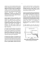
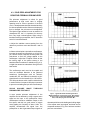
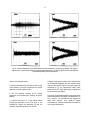
Fig. 1.1. Gaussian Triangular, and Bipolar Pulse Shapes
for a 2-:s Shaping Time. Vertical scale, 5 V per
division; horizontal scale, 2 :s per division.
Fig. 1.2. (a) Resolution and (b) Peak Position Stability as a Function of Counting Rate.
See specifications for spectrum broadening and spectrum shift.
2
operates only on the true baseline between pulses
in spite of changes in the noise level. No operator
adjustment of the baseline restorer is needed when
changes are made in the gain, the shaping time
constant, or the detector characteristics. Negative
overload recovery from the reset pulses generated
by transistor reset preamplifiers and pulsed optical
feedback preamplifiers is also handled
automatically. A monitor circuit gates off the
baseline restorer and provides a reject signal for a
multichannel analyzer until the baseline has safely
recovered from the overload.
Several operating modes are selectable for the
baseline restorer. For making either a manual or
automatic PZ adjustment, the PZ position is
selected. This position can also be used where the
slowest baseline restorer rate is desired. For
situations where low frequency noise interference is
a problem, the HIGH rate can be chosen. On
detectors where perfect PZ cancellation is
impossible, the AUTO baseline restorer rate
provides the optimum performance at both low and
high counting rates.
automatic noise discriminator. A multicolor pile-up
rejector LED on the front panel indicates the
throughput efficiency of the amplifier. At low
counting rates the LED flashes green. The LED
turns yellow at moderate counting rates and red
when pulse pile-up losses are >70%.
When long connecting cables are used between the
detector preamplifier output and the amplifier input,
noise induced in the cable by the environment can
be a problem. The Model 671 provides two
solutions. For low to moderate interference
frequencies the differential input mode can be used
with paired cables from the preamplifier to suppress
the induced noise. At high frequencies a common
mode rejection transformer built into the 671 input
reduces noise pick-up. The transformer is
particularly effective in eliminating interference
from the display raster generators in personal
computers.
All toggle switches on the front panel lock to
prevent accidental changes in the desired settings.
A front-panel limit (LIM) push button is included with
the unipolar output to facilitate monitoring the
accuracy of the PZ adjustment on an oscilloscope.
When pressed, this button inserts a diode limiter in
series with the unipolar output connector. This
prevents overload distortions in the oscilloscope
when using the more sensitive amplitude scales
required for observing the PZ adjustment.
An efficient pile-up rejector is incorporated in the
671 Spectroscopy Amplifier. It provides an output
logic pulse for the associated multichannel analyzer
to suppress the spectral distortion caused by pulses
piling up on each other at high counting rates
(Fig. 1.3). The fast amplifier in the pile-up rejector
includes a gated baseline restorer with its own
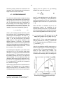
Fig. 1.3. Demonstration of the Effectiveness of the
Pile-Up Rejector in Suppressing the Pile-up Spectrum.
See Pulse Pile-Up Rejector specifications.
3
2. SPECIFICATIONS1
UnipolarOutput <±0.005%/°C for gain, and <±7.5
2.1. PERFORMANCE
Note: Unless otherwise stated, performance
specifications are measured on the unipolar output
with 2- s Gaussian shaping, the manual PZ mode,
and the AUTO BLR mode.
:
GAIN RANGE Continuously adjustable from 2.5 to
1500. Gain is the product of the COARSE and FINE
GAIN controls.
UNIPOLAR PULSE SHAPES Switch selection of
a nearly triangular pulse shape or a nearly
Gaussian pulse shape at the UNI output (Fig. 1.1,
Table 2.1).
BIPOLAR OUTPUT PULSE SHAPE Rise of the
bipolar output pulse from 0.1% to maximum
amplitude is 1.65 times selected SHAPING TIME.
Zero cross-over of the bipolar output pulse delayed
from the maximum amplitude of Gaussian
UNIPOLAR output by 0.33 times selected
SHAPING TIME.
INTEGRAL NONLINEARITY (UNIPOLAR Output)
<±0.025% from 0 to +10 V.
:
NOISE Equivalent input noise <5.0 V rms for
gains >100, and <4.5 V rms for gains >1000.
:
:V/°C for dc level.
Bipolar Output <±0.007%/°C for gain, and <±30
:V/°C for dc level.
WALK Bipolar zero cross-over walk is <±3 ns over
a 50:1 dynamic range.
OVERLOAD RECOVERY Unipolar and bipolar
outputs recover to within 2% of the rated output
from a X 1000 overload in 2.5 non-overloaded
pulse widths using maximum gain.
SPECTRUM BROADENING† (Fig. 1.2.) Typically
<8% broadening of the FWHM for counting rates up
to 100,000 counts per second (counts/s), and <15%
broadening for counting rates up to 200,000
counts/s. Measured on the 1.33-MeV gamma-ray
line from a 60Co radioactive source under the
following conditions: 10% efficiency ORTEC
GAMMA-X PLUS detector, 8.5-V amplitude for the
1.33-MeV gamma-ray on the unipolar output.
SPECTRUM SHIFT† (Fig. 1.2) Peak position
typically shifts <±0.018% for counting rates up to
100,000 counts/s, and <±0.05% for counting rates
up to 200,000 counts/s. Measured on the 1.33-MeV
line under conditions specified for SPECTRUM
BROADENING.
TEMPERATURE COEFFICIENT (0 to 50°C)
1
Specifications subject to change without notice.
† Results may not be reproducible if measured with a detector producing a large number
of slow-risetime pulses or having quality inferior to the specified detector.
4
DIFFERENTIAL INPUT Differential nonlinearity
<±0.012% from -9 V to +9 V. Maximum input ±10 V
(dc plus signal). Common mode rejection ratio
>1000.
PULSE PILE-UP REJECTOR
Threshold Automatically set just above noise level
on fast amplifier signal. Independent of slow
amplifier BLR threshold.
Minimum Detectable Signal Limited by detector
and preamplifier noise characteristics.
Pulse Pair Resolution Typically 500 ns. Measured
using the 60CO 1.33-MeV gamma-ray under the
following conditions: 10% efficiency germanium
detector, 4-V amplitude for the 1.33-MeV gammaray at the unipolar output, 50,000 counts/s.
panel INPUT and a cable having its center
conductor connected to the preamplifier ground
through an impedance matching resistor is
connected to the rear-panel INPUT. The impedance
matching resistor must match the output impedance
of the preamplifier.
BAL (Differential Input Gain Balance) A 20-turn
potentiometer mounted on the PC board inside the
module allows the gains of normal and differential
reference inputs to be matched for maximum
common mode noise rejection in DIFF mode.
PZ ADJUSTMENT 20-turn potentiometer on the
front panel permits screwdriver adjustment of the
PZ cancellation. The adjustment covers
preamplifier exponential decay time constants from
40 s to 4. For transistor reset preamplifiers or
pulsed optical feedback preamplifiers, set the PZ
adjustment fully counterclockwise.
:
2.2. CONTROLS AND INDICATORS
FINE GAIN Front-panel, 10-turn precision
potentiometer with locking, graduated dial provides
continuously variable, direct reading, gain factor
from 0.5 to 1.5.
COARSE GAIN Front-panel, eight-position switch
selects gain factors of 5, 10, 20, 100, 200, 500, and
1000.
SHAPING TIME Six-position switch on the front
panel selects shaping times of 0.5,1, 2, 3, 6, and 10
s for the pulse-shaping filter network.
:
MODE Two-position locking toggle switch on the
front panel selects either GAUSS (Gaussian) or TRI
(Triangular) pulse shaping for the UNI (unipolar)
output.
INPUT POS/NEG
Front-panel, two-position
locking toggle switch accommodates either positive
or negative input polarities.
NORM/DIFF Two-position slide switch mounted on
the printed circuit board selects the normal (NORM)
or differential (DIFF) input modes. In the NORM
position, both front- and rear-panel INPUT
connectors function as the same normal input for
the preamplifier signal cable. In the DIFF mode,
the rear-panel INPUT connector becomes a
differential ground reference input, and the frontpanel INPUT remains the normal input for the
preamplifier signal cable. In the DIFF mode, the
preamplifier signal cable is connected to the front-
LIMIT PUSHBUTTON Inserts a diode limiter in
series with the front-panel UNI output connector.
Prevents overload distortions in the oscilloscope
when observing accuracy of the PZ adjustment on
the more sensitive oscilloscope ranges.
BLR A front-panel, three-position, locking, toggle
switch selects the baseline restorer rate. PZ position
offers lowest fixed rate, for adjusting PZ
cancellation. AUTO position matches the rate of the
PZ position at low counting rates, but increases the
restoration rate as the counting rate rises. HIGH
rate position is provided for suppressing low
frequency interference.
PUR ACCEPT/REJECT LED Multicolor LED
indicates percentage of pulses rejected because of
pulse pile-up. LED appears green for 0-40%, yellow
for 40-70%, and red for >70% rejection.
2.3. INPUTS
INPUT (Front Panel) Front-panel, BNC connector
accepts preamplifier signals of either polarity with
risetimes less than the selected SHAPING TIME,
and exponential decay time constants from 40 s to
4. For the NEG INPUT switch setting, the input
on a coarse gain of 5, and
impedance is 1000
at coarse gain settings $10. For the POS
465
INPUT switch setting, the input impedance is
for a coarse gain of 5, and 1460
for
2000
coarse gains $10. Input is dc-coupled, and
protected to ±25 V.
:
S
S
S
S
5
INPUT (Rear Panel) BNC connector, identical to
f ront-panel INPUT when PW B-mounted
NORM/DIFF slide switch is in the NORM position.
When operating in the differential input mode with
the slide switch set to DIFF, the rear-panel INPUT
is used for the preamplifier ground reference
connection. For the DIFF and POS INPUT switch
setting, the input impedance is 1000 on a coarse
at coarse gain settings $10.
gain of 5, and 465
For the DIFF and NEG INPUT switch setting, the
input impedance is 2000 for a coarse gain of 5,
for coarse gains $10. Input is dcand 1460
coupled, and protected to ±25 V.
S
S
S
S
INH IN Rear-panel BNC input connector accepts
reset signals from transistor reset preamplifiers or
pulsed optical feedback preamplifiers. Positive NIM
standard logic pulses or TTL levels can be used.
Logic is selectable as active high or active low via
printed circuit board jumpers. Inhibit input initiates
the protection against distortions caused by the
preamplifier reset. This includes turning off the
baseline restorers, monitoring the negative
overload recovery at the unipolar output, and
generating PUR (reject) and BUSY signals for the
duration of the overload. The PUR and BUSY logic
pulses are used to prevent analysis and correct for
the reset deadtime in the associated ADC or
multichannel analyzer.
2.4. OUTPUTS
S
S
Bi Front- and rear-panel BNC connectors provide
bipolar shaped pulses with the positive lobe leading.
The linear output range is 0 to ±10 V. Front- panel
. Rear-panel output
output impedance <1
impedance selectable for either <1 or 93 using
a printed circuit board jumper. Baseline between
pulses has a dc level of 0 ± 10 mV. Short-circuit
protected.
S
S
S
CRM The Count Rate Meter output has a rear-panel
BNC connector and provides a 250-ns-wide, +5-V
logic signal for every linear input pulse that exceeds
the pile-up inspector threshold. Output impedance
is 50 .
S
S
PUR Pile-Up Reject output is a rear-panel, BNC
connector. Provides a +5-V NIM standard logic
pulse when pulse pile-up is detected. Output also
present for a pulsed reset preamplifier during reset,
and reset overload recovery. Output pulse is
selectable as active high or active low by means of
a printed circuit board jumper. Output impedance is
50
. Used with an associated ADC or
multichannel analyzer to prevent analysis of
distorted pulses.
S
PREAMP Rear-panel standard ORTEC connector
(Amphenol 17-10090) provides power for the
associated preamplifier. Mates with power cords on
all standard ORTEC preamplifiers.
2.5. ELECTRICAL AND MECHANICAL
UNI
Front- and rear-panel BNC connectors
provide positive, unipolar, shaped pulses with a
linear output range of 0 to +10 V. Front-panel
. Rear-panel output
output impedance <1
impedance selectable for either <1 or 93 using
a printed circuit board jumper. Outputs are dcrestored to 0 ± 5 mV and short-circuit protected.
S
BUSY Rear-panel BNC connector provides a +5-V
logic pulse for the duration that the linear signals
exceed the positive or negative baseline restorer
thresholds, or the pile-up inspector threshold, or for
the duration of the INH IN input signal. Useful for
deadtime corrections with an associated ADC or
multichannel analyzer. Positive NIM standard logic
pulse is selectable as active high or active low via
a printed circuit board jumper. Output impedance is
50 .
POWER REQUIRED The Model 671 derives its
power from a NIM Bin supplying ±24 V and ±12 V,
such as the ORTEC Model 4001A/4002A Bin/Power
Supply. The power required is +24 V at 100 mA, -24
V at 200 mA, +12 V at 325 mA, and -12 V at
180 mA.
WEIGHT
Net 1.5 kg (3.3 lb).
Shipping 3.1 kg (7.0 lb).
DIMENSIONS Standard single-width module, 3.45
X 22.13 cm (1.35 X 8.714 in.) Front panel per
DOE/ER- 0457T.
6
3. INSTALLATION
3.1. POWER CONNECTION
The 671 operates on power that must be provided
by a NIM-standard bin and power supply such as
the ORTEC 4001/4002 series. Convenient test
points on the power supply control panel should be
used to check that the dc voltage levels are not
overloaded. The bin and power supply is designed
for relay rack mounting. If the equipment is rack
mounted, be sure that there is adequate ventilation
to prevent any localized heating of the components
that are used in the 671. The temperature of the
equipment mounted in racks can easily exceed the
maximum limit of 50°C unless precautions are
taken.
3.2. PREAMPLIFIER CONNECTION
The Preamp connector of this amplifier is directly
compatible with ORTEC preamplifiers as well as
with standard Aptec, Canberra, PGT, and Tennelec
(serial numbers greater than 2000) preamplifiers.
Preamplifier power at +24 V, -24 V, +12 V, and -12
V is available through the Preamp connector on the
rear panel.
When a BNC cable longer than ten feet is used to
connect the preamplifier output to the amplifier
input, the characteristic impedance of the cable
should match the impedance of the preamplifier
output. All ORTEC preamplifiers contain series
terminations that are either 93
or variable;
coaxial cable type RG-62/U or RG-71/U is
recommended.
S
3.3. PULSED RESET PREAMPLIFIERS
AND INHIBIT IN CONNECTION
The 671 Amplifier is directly compatible with most
pulsed reset preamplifiers such as the ORTEC TRP
(Transistor Reset Preamplifier) Series. The
amplifier automatically senses preamplifier resets
and gates off the amplifier's baseline restorer.
Preamplifier inhibit signals are not required for
proper amplifier operation; however, since the
preamplifier resetting process is nonlinear by
nature, spurious phantom peaks may show up in
the spectra if the inhibit signal from the preamplifier
is not used.
INHIBIT IN CONNECTION Connection of the
PREAMPLIFIER INHIBIT OUT signal to the rearpanel INHIBIT IN connector will result in the system
being disabled during the reset period and thus
avoid spurious peaks in the spectra. Preamplifiers
with an Inhibit time switch such as ORTEC PLUS
Detector with series 132 Preamplifier can be set to
position "1", which is the shortest preamp inhibit
blocking time.
PZ SETTING The Amplifier's PZ control should be
set fully counterclockwise (CCW) when used with a
pulsed reset preamplifier.
3.4. CONNECTION OF TEST PULSE
GENERATOR
THROUGH A PREAMPLIFIER The satisfactory
connection of a test pulse generator such as the
ORTEC 419 or 448 Pulse Generator or equivalent
depends primarily on two considerations: the
preamplifier must be properly connected to the 671
as discussed in Sections 3.2 and 3.3, and the
proper signal simulation must be applied to the
preamplifier. To ensure proper input signal
simulation, refer to the instruction manual for the
particular preamplifier being used.
DIRECTLY INTO THE 671 The ORTEC test pulse
generators are designed for direct connection.
When any one of these units is used, it should be
terminated with a 100- terminator at amplifier
input or be used with at least one of the output
attenuators set at In.
S
SPECIAL CONSIDERATIONS FOR POLE-ZERO
CANCELLATION When a tail pulser is connected
directly to the amplifier input, the Pole-Zero should
be adjusted. See Section 4.3 for the pole-zero
7
adjustment. If a preamplifier is used and a tail
pulser is connected to the preamplifier test input, it
is not possible to adjust the pole-zero for both the
preamplifier pole and the pole from the pulser tail.
3.5. SHAPING CONSIDERATIONS
The Shaping Time switch on the front panel of the
671 can be set to select time constants in steps of
0.5, 1, 2, 3, 6, and 10 s. Choice of triangular and
Gaussian filters doubles the time constants
available for optimum resolution. Triangular
shaping will usually give better results. The choice
of the proper shaping time is generally a
compromise between operating at a shorter time
constant for accommodation of high counting rates
and operating with a longer time constant for a
better signal-to-noise ratio. Since the full amplitude
of the preamplifier output pulse must be preserved,
the peaking time (measurement time) must be large
compared to preamplifier output pulse risetime. The
amplifier shaping time should be greater than five
times the charge collection time of the detector.
Use the detector manufacturer's suggested shaping
times as a starting point and adjust the shaping as
your needs for resolution versus count rate vary.
:
GERMANIUM DETECTORS Shaping times for
high-purity germanium (HPGe) detectors will vary
from 1 to 6 s using the unipolar output, depending
on the size, configuration, and charge collection
time of the specific detector and preamplifier.
Coaxial detectors have significant variations in
charge collection times due to their large volumes.
Compromises must often be made since the
shaping time that will give the best resolution will
usually be longer than the optimum time needed for
the best throughput at high counting rates.
:
Planar detectors require shaping times in the range
of 3 to 10 s for optimum resolution. Lithium-drifted
silicon detectors, Si(Li), have similar shaping time
requirements.
:
SILICON CHARGED PARTICLE DETECTORS
These detectors have very fast risetimes on the
order of 10 ns or less. A unipolar output and a 0.5to 2- s shaping time will generally provide optimum
resolution.
:
SCINTILLATION DETECTORS The energy
resolution of scintillation counters depends largely
on the scintillator and photomultiplier, and therefore
a shaping time of five times the decay-time
constant of the scintillator is a reasonable choice.
For Nal detectors that have a decay time constant
of about 230 ns, the optimum shaping time is l s.
The bipolar output can be used to reduce overload
effects and microphonics without sacrificing
resolution.
:
GAS PROPORTIONAL COUNTERS Proportional
counters have both short and long components in
their charge collection times. The components
typically fall in the 0.5- to 5- s range, and lead to
variable amounts of preamplifier output signal being
lost as the amplifier shaping time constant is
changed. Selection of longer shaping times (>2 s)
helps to minimize the problem caused by long
risetimes. Due to the multiple components in the
charge collection time, the correct pole-zero
cancellation is not possible. This will often cause an
undershoot if the Unipolar output is used. Bipolar
shaping can be used to reduce this effect with little
change in the resolution.
:
:
3.6. LINEAR OUTPUT CONNECTIONS
Since the 671 unipolar output is normally used for
spectroscopy, the 671 is designed with a great
amount of flexibility for the pulse to be interfaced
with an analyzer. To minimize spectrum distortion
at medium and high counting rates, the unipolar
output incorporates a high-performance, gated
baseline restorer with automatic setup. Automatic
positive and negative noise discriminators ensure
that the baseline restorer operates only on the true
baseline between pulses in spite of changes in the
noise level. For pulse-height analysis, the unipolar
output must be directly connected to the input of a
multichannel analyzer.
The bipolar output, with its symmetry about the
baseline, can be used for cross-over timing or may
be preferred for spectroscopy when operating into
ac-coupled systems at high counting rates. Typical
system block diagrams for a variety of experiments
are described in Section 4.
8
3.7. PILE-UP REJECTION USING PUR
OUTPUT
The PUR (Pile-Up Reject) output on the rear panel
is used at the gate or pile-up reject input of a
multichannel analyzer to suppress pile-up in the
recorded spectrum. The fast amplifier in the pile-up
rejector includes a gated baseline restorer with an
automatic noise discriminator to eliminate the need
for any operator adjustments. When pileup occurs,
a logic true pulse is generated which lasts until the
unipolar output returns to the baseline, normally a
width of six times the shaping time. If used with a
pulsed reset preamplifier, this output also includes
a reject during the reset and recovery interval.
3.8. LIVETIME CORRECTION USING
BUSY OUTPUT
The signal from the rear-panel Busy output
connector provides a nominally +5 V logic pulse for
the duration that the Unipolar output pulse exceeds
the baseline restorer threshold or pile-up inspector
threshold or when the external INH IN is true. For
livetime correction, Busy should be connected to
the Busy In connector on the MCA. For optimal
livetime correction with ORTEC analyzers like the
ADCAM®, an internal jumper in the amplifier should
be set to match the unipolar, triangular, or Gaussian
mode. The output is internally jumper selectable as
active low or active high. It is shipped as active
high.
3.9. INPUT COUNT RATE USING CRM
OUTPUT
A positive logic pulse is generated for each 671
input pulse that exceeds the pile-up inspector
threshold level. The pulses are available through
the CRM (Count Rate Meter) output on the rear
panel and are intended for use in a count rate meter
or counter to monitor the true input count rate into
the amplifier.
9
4. OPERATING INSTRUCTIONS
4.1. INITIAL TESTING AND OBSERVATION
OF PULSE WAVEFORMS
Refer to Section 6 for information on testing
performance and observing waveforms using a
pulser. Figure 4.1 shows some typical unipolar
Gaussian, unipolar triangular, and bipolar output
waveforms.
4.2. STANDARD SETUP PROCEDURES
a. Connect the detector, preamplifier, high-voltage
power supply, and amplifier into a basic system and
connect the amplifier unipolar output to an
oscilloscope. Connect the preamplifier power cable
to the Preamp power connector on the rear panel of
the 671. Turn on power in the bin and power supply
and allow the electronics of the system to warm up
and stabilize.
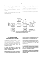
A block diagram of a typical ORTEC gamma-ray
spectroscopy system is shown in Figure 4.2.
b. Set the 671 controls initially as follows:
Shaping Time
Mode
Coarse Gain
Fine Gain
BLR
Polarity
:
3 or 6 s
Triangle
20
1.00
PZ
Match preamplifier output
polarity
c. Use a 60Co calibration source; set about 25 cm
from the active face of the detector. The unipolar
output pulse from the 671 should be about 8 V,
using a detector that has a preamp with a
conversion gain of 300 mV/MeV.
d. Readjust the Gain control so that the higher peak
from the 60Co source (1.33 MeV) provides an
amplifier output at about 9 V.
Fig. 4.1. Typical Effects of Shaping-Time Selection
on Gaussian, Triangular, and Bipolar Output
Waveforms.
Fig. 4.2. Typical Gamma-Ray Spectroscopy System.
10
4.3. POLE-ZERO ADJUSTMENTS FOR
RESISTIVE-FEEDBACK PREAMPLIFIER
The pole-zero adjustment is critical for good
performance at high count rates in unipolar
operation and for correct operation of the BLR
circuit. This adjustment should be checked carefully
for the best possible results. Whenever the shaping
time is changed. the pole-zero must be adjusted.
The bipolar output resolution is not as sensitive to
misadjusted PZ, but it is important for recovery
from very large overload pulses. When using a
transistor reset-type preamplifier, the PZ should be
set to full counterclockwise.
a. Adjust the radiation source spacing from the
detector to provide a count rate between 1 and 10
kHz.
b. Observe the unipolar output with an oscilloscope.
Increase the scope input sensitivity to 20-100 mV
per vertical division. Depress the front-panel LIM
push-button to limit the voltage applied to the
oscilloscope. Adjust the PZ adjust control so that
the trailing edge of the pulses returns to the
baseline without overshoot or undershoot (Fig. 4.3).
A slight bias toward an undershoot often gives the
best results.
The oscilloscope used must be dc-coupled and
must not contribute distortion in the observed
waveforms. Oscilloscopes such as Tektronix
models 465, 475, and 7904 will overload for a 10-V
signal when the vertical sensitivity is <100 mV/Div.
The LIM push-button switch inserts a diode limiter
in series with the front-panel UNI output connector
to prevent overloading the input of the oscilloscope.
USING SQ UARE WAVE
PREAMPLIFIER TEST INPUT
T HROUGH
A more precise pole-zero adjustment of the
amplifier can be obtained by using a square wave
signal as the input to the preamplifier. Many
oscilloscopes include a calibration output on the
front panel, and this is a good source of square
wave signals at a frequency of about 1 kHz. The
amplifier differentiates the signal from the
preamplifier so that it generates output signals of
Fig. 4.3. Typical Waveforms Illustrating Pole-Zero
Adjustment Effects; Oscilloscope Trigger, Busy Output;
60
Co Source with 1.33-MeV Peak Adjusted -9 V; Count
Rate, 3 kHz; Shaping Time Constant, 2 :s.
alternate polarities on the leading and trailing edges
of the square wave input signal, and these can be
compared as shown in Fig. 4.4 to achieve excellent
pole-zero cancellation.
11
Fig. 4.4. Pole-Zero Adjustment Using a Square Wave Input to the Preamplifier. (a) PZ properly adjusted; slow trigger to
separate pulses. (b) Overcompensated; fast trigger to superimpose pulses. (c) Properly adjusted; pulses superimposed.
(d) Undercompensated; pulses superimposed.
Use the following procedure:
a. Remove all radioactive sources from the vicinity
of the detector. Set up the system as for normal
operation, including detector bias.
b. Set the amplifier controls as for normal
operations; this includes gain, shaping, and input
polarity.
c. Connect the source of 1 kHz square waves
through an attenuator to the Test input of the
preamplifier. Adjust the attenuator so that the
amplifier output amplitude is 8 to 10 volts.
d. Observe the unipolar output of the amplifier with
an oscilloscope triggered from the amplifier Busy
output. Adjust the PZ control for proper response
according to Fig. 4.4. Depress the LIMIT pushbutton on the 671 while observing the adjustment
on the oscilloscope display.
Figure 4.4.(a) shows the amplifier output as a series
of alternate positive and negative shaped pulses. In
Fig. 4.4.(b)-(c), the oscilloscope was triggered to
show both positive and negative pulses
simultaneously. These pictures show more detail to
aid in proper adjustment.
12
4.4. BASELINE RESTORER (BLR)
SETTING
To minimize spectrum distortion at medium and
high counting rates, the unipolar output incorporates
a high-performance, gated, baseline restorer with
several levels of automation. Automatic positive
and negative noise discriminators ensure that the
baseline restorer operates only on the true baseline
between pulses in spite of changes in the noise
level. No operator adjustment of the baseline
restorer is needed when changes are made in the
gain, the shaping time constant, or the detector
characteristics. Negative overload recovery from
the reset pulses generated by transistor reset
preamplifiers and pulsed optical feedback
preamplifiers is also handled automatically to
eliminate the need for operator adjustments. A
monitor circuit gates off the baseline restorer and
provides a reject signal for a multichannel analyzer
until the baseline has safely recovered from the
overload.
BLR RATE For making pole-zero adjustments, the
PZ position is selected. This position can also be
used where the slowest baseline restorer rate is
desired.
With the BLR Rate set to AUTO, the BLR is
automatically set for optimum performance
throughout the usable input range for the shaping
selected.
The HIGH rate can be used for situations where low
or medium frequency noise interference is present
and is independent of the counting rate. The HIGH
rate setting is normally not used since there will be
a small loss of resolution due to increased noise
when used in high resolution systems.
4.5. INTERNAL CONTROLS
These controls are on the printed wiring board
(PWB) and can be accessed by removing the right
side cover. Figure 4.5 shows the location of these
controls.
Fig. 4.5. Position of Internal Controls.
13
NORM-DIFF Internal PWB mounted, two-position
slide switch. NORM position selects single ended
inputs from front-panel input or rear-panel input
connectors. In the DIFF position, the front-panel
input is connected to the preamplifier signal cable,
and a cable connected to the preamplifier ground
through an impedance matching resistor is
connected to the rear-panel input.
BAL (DIFFERENTIAL INPUT GAIN BALANCE)
Internal PWB 20-turn screwdriver potentiometer
allows maximization of noise rejection when using
differential input. See Section 4.6.
UNI-OUT (UNIPOLAR ZOUT) Jumper plug, W1,
provides ZOUT, #1
or -93
for the rear-panel
Unipolar output. Shipped in the 93- position.
S
S
S
BI-OUT (BIPOLAR ZOUT) Jumper plug, W2,
provides ZOUT, #1
or -93 ) for the rear-panel
Bipolar output. Shipped in the 93- position.
_____
BUSY/BUSY Jumper plug, W3, allows the Busy
output to be a positive true or negative true logic
signal. Shipped in BUSY (positive true) position.
___
PUR/PUR Jumper plug, W5, allows the Pile-Up
Reject (PUR) output to be a positive true or
negative true logic signal. Shipped in PUR (positive
true) position.
___
INH/INH Jumper plug, W6, allows the INH IN input
to accept either positive true or negative true logic
signals. Shipped in INH (positive true) position.
S
S
S
TRI/GAUSS Jumper plug, W7, allows optimal
livetime correction when used with ORTEC
analyzers like the ADCAM® by connecting the
BUSY output to the analyzer Busy In as described
in Section 3.8. The jumper should be set to match
the Unipolar Mode, TRI for Triangle and GAUSS for
Gaussian. Shipped in TRI position.
4.6. DIFFERENTIAL INPUT MODE
When long connecting cables are used between the
detector and preamplifier input, noise induced in the
cable by the environment can be a problem. The
differential input mode can be used with paired
cables from the preamplifier to suppress the
induced noise.
BAL (DIFFERENTTAL INPUT GAIN BALANCE)
The BAL potentiometer is used to adjust the gain
balance between the positive and negative inputs
and to adjust the balance between the front- and
rear-panel inputs when the differential (DIFF) input
mode is used. The initial adjustment of Gain
Balance is made by providing the same input to
both the front- and rear-panel inputs. This can be
accomplished by using a BNC "T" connector to feed
the input signal on the front-panel input to the rearpanel input. Set the amplifier gain to maximum.
Connect an oscilloscope to the unipolar output.
While observing the signal on the oscilloscope,
used a small screwdriver to adjust the Gain Balance
(internal adjustment has been factory set, Fig. 4.5)
potentiometer until the display on the oscilloscope
shows minimum signal. Remove the BNC "T"
connector when the adjustment is complete, and
the positive and negative gains will be matched for
use with NORM input.
If the differential input mode is being used, connect
the differential input cable to the BNC connector on
the rear panel. Adjust BAL potentiometer until there
is minimum noise around the baseline of the output
signal. If there is a problem in getting minimum
noise, repeat the initial procedure with the BNC "T"
and the adjustment.
DIFFERENTIAL INPUT SIGNAL The differential
input signal or phantom is used only in the
differential (DIFF) input mode. The normal preamp
output is connected to the front-panel input with the
amplifier input polarity set to match this signal. A
second output cable must be added to the
preamplifier with its center, signal pin connected to
the preamplifier ground with the same value as the
normal preamp output series resistor (usually 93.1
or 51 ).
S
Many ORTEC preamplifiers have two Energy
outputs, each with a 93.1- series resistor. For
differential operation, one output is connected to
the amplifier front-panel input. The second output is
modified by connecting the preamplifier end of the
series 93.1- resistor to ground within the preamp
(soldering may be necessary). This second output
S
S
14
should be properly marked and connected to the
rear-panel input. Both cables should be the same
length and be run next to each other.
digitizing time are ignored. For non-extending
deadtime the output rate is given by2
4.7. SYSTEM THROUGHPUT
To achieve the desired results in high-rate energy
spectroscopy, the experimenter must consider not
only the input rate, but also the unpiled-up output
rate. The unpiled-up output rate is determined by
the processing time of the shaping amplifier, the
pile-up inspection time, and the input rate. For
semi-Gaussian time-invariant filter amplifiers, the
unpiled-up output rate is theoretically given by2
ro = ri exp (-TDri)
(1)
where ro is the unpiled-up output count rate, ri is the
input count rate, and TD is the deadtime or effective
processing time of the amplifier. The value of TD is
equal to the sum of the effective amplifier pulse
width, Tw, and the time-to-peak of the amplifier
output pulse, Tp. The type of deadtime in the
shaping amplifier is referred to as extending
deadtime since a second event arriving before the
end of the initial deadtime extends the deadtime by
an additional amplifier output pulse width, Tw, from
the occurrence of the second pulse.
A normalized plot of Equation (1) is shown as the
solid line in Fig. 4.6. The maximum mean output
rate equals 1 /TD exp (1) and occurs when the mean
input rate equals 1 /TD. At this maximum output rate
the deadtime losses are 63.2%. For input count
rates exceeding 1 /TD the unpiled-up output rate
decreases. When using a pile-up inspection circuit,
the value of TD is given either by the sum of Tw and
Tp, or by the sum of Tp and the pile-up inspection
time, whichever is larger.
where TD is the digitizing time for the ADC and is
designated T M in Equation (3). This relationship is
shown as the dashed line in Fig. 4.6. The maximum
obtainable output count rate is 1/TD) and occurs at
ri = 4 .
When the ADC is considered as part of the
spectroscopy system, the deadtimes of the
amplifier and ADC are in series. The combination of
the extending deadtime of the amplifier followed by
the non-extending deadtime of the ADC is given by2
where U[TM-(TW -TP)] is a unit step function that
changes value from 0 to 1 when TM is greater than
(TW -TP). Equation (3) reduces to Equation (1) when
TM is less than (TW -TP).
A plot of the unpiled-up ampilifier output rate as a
function of input rate for six values of shaping time
is shown in Fig.4.7. The measured deadtime, TD, is
shown for each shaping time constant. The
maximum value of the unpiled-up output rate
increases with decreasing values of shaping time
Spectroscopy systems also have a deadtime that is
caused by the digitizing time of the Analog-toDigital Converter (ADC). This deadtime is a nonextending deadtime since events arriving during the
2
R. Jenkins, R.L. Gould, and D.A. Gedcke, Quantitative X-Ray
Spectroscopy, Marcel and Dekker, Inc., New York, (1980).
Fig. 4.6. Plot of Normalized Output Rate as a Function of
Normalized Input Rate for Spectrometers with Simple
Deadtime.
15
Fig. 4.7. Plot of the Unpiled-Up Amplifier Output Rate
as a Function of Input Rate for Six Values of Shaping
Time Constants.
constant. A set of throughput curves will remain
nearly unchanged for a given amplifier for various
energy ranges, detector types, and sizes.
The advantage of shorter shaping time constants to
achieve higher output count rates is clearly shown
in Fig. 4.7. However, shorter time constants also
result in increased noise and increased charge
collection time effects. Under worst case conditions,
the noise increases inversely as the square root of
the ratio of shaping time constants. The increase in
the total energy resolution is the noise contribution
combined in quadrature with the statistical
contribution of the detector at the energy of interest.
Consequently, the percentage of degradation in
energy resolution can be much less than the
percentage increase in noise.
4.8. CHARGE COLLECTION OR
BALLISTIC DEFICIT EFFECTS
Charge collection distances in large-volume HPGe
detectors are often 3 cm or more, resulting in
charge collection times exceeding 300 ns.3,4,5
These charge collection times are due to the transit
time of the holes and the electrons in germanium
3
E. Sakai, "Charge Collection in Coaxial Ge(Li) Detectors," IEEE
Trans. Nuct. Sci., NS-1 5, 310, (1968).
4
E. Sakai, T.A. McMath, and R.G. Franks, "Further Charge
Collection Studies in Coaxial Ge(Li) Detectors," IEEE Trans.
Nucl. Sci., NS-16, 68, (1968).
5
T.H. Becker, E.E. Gross, and R.C. Trammell, "Characteristics of
High-Rate Energy Spectroscopy Systems with Time-invariant
Filters," IEEE Tran& Nucl. Sci., NS-28, 1, (1981).
Fig. 4.8. Charge Collection Effect Waveforms. (a) Typical
current Pulse Waveforrns for a 28% Efficient HPGe
Detector, and (b) the Simple Differentiation Circuit Used
to Obtain the Current Waveforms.
and are not due to defects in the detector. Fig.
4.8(a) shows some typical current pulse waveforms
from a 140-cm3 28% efficient HPGe detector.
These current pulse waveforms were obtained
using the simple differentiation circuit shown in Fig.
4.8(b), which has a 15-ns time constant. The
current pulses range in duration from 100 ns to
greater than 350 ns. Pulses having equivalent total
charge but different durations produce different
output pulse heights when processed by a chargesensitive preamplifier and a semi-Gaussian filter
amplifier. This results in the distortion of the
spectrum in direct proportion to the pulse amplitude
or energy. This distortion is most pronounced at
short shaping time constants. Figure 4.9(a) shows
a portion of a spectrum obtained with a 10%
efficient HPGe detector at 2- s shaping time, using
the 1.33-MeV line of 60Co. An equivalent spectrum
using a 0.5- s shaping time is shown in Fig. 4.9(b)
and is significantly distorted.
:
:
16
Fig.4.10. Energy Resolution FWHM as a Function of
Amplifier Shaping Time Constant for a 10% HPGe
Detector and a 28% HPGe Detector for the 122-keV 57Co
Line and the 1.33-MeV 60Co Line.
Fig. 4.9. Charge Collection Effect Spectrum. Logarithmic
Display of Spectrum Taken with a 10% Efficient HPGe
Detector for the 1.33 MeV 60Co Line. (a) A 2-:s Shaping
Time Constant and (b) a 0.5-:s Shaping Time Constant.
Charge collection time effects are of significant
importance when using large-volume Ge detectors
at high energy. The performance of two HPGe
detectors is compared in Fig. 4.10 at two different
energies. When using the 122-keV line of 57CO,
the principal cause of resolution degradation with
decreased shaping time constant is the increase in
noise. However, when using the 1.33-MeV line of
60
Co, the significant degradation in resolution is due
to charge collection effects. The calculated
resolution for the 10% detector at 1.33 MeV is
shown as the dashed line in Fig. 4.10. and indicates
approximately 2.0 keV FWHM at a 0.5- s shaping
time constant. The measured resolution under
these test conditons was 7.2 keV, indicating that
charge collection effects dominate. In Fig. 4.10,
charge collection effects begin to appear at time
constants less than 3 s.
:
:
4.9. PILE-UP REJECTOR (PUR) AND
LIVETIME CORRECTOR
An efficient pile-up rejector is incorporated in the
amplifier to suppress the spectral distortion which is
caused by pulses piling up on each other at high
counting rates. High counting rate for pile-up is
dependent on the dead time per pulse, TD, and
hence the selected shaping time. TD is 9 times the
front-panel shaping time, Tc. High count rate for the
PUR is when the normalized count rate RiTD >0.5,
where Ri is the amplifier input rate (see Fig. 4.6).
For example, for 6- s shaping Ri is 9 kHz and for 2s shaping, Ri is 28 kHz. Amplifier throughput for
this condition using Equation (1) in Section 4.7 is
60% of the input rate. A multicolor pile-up rejector
LED is included on the front panel to indicate the
throughput efficiency of the amplifier. At low
counting rates (pulse pile-up losses <40%) the LED
flashes with a green color. At moderate counting
rates the color changes to yellow. The color
changes to red at high counting rates when the
pulse pile- up losses are >70%.
:
:
The fast amplifier in the pile-up rejector includes a
gated baseline restorer with its own automatic noise
discriminator to eliminate the need for any operator
adjustments. This function is also protected against
negative overloads from pulsed reset preamplifiers.
The PUR (pile-up reject) output logic pulse can be
used at the gate or reject input of a multichannel
analyzer to suppress pile-up in the recorded
spectrum.
17
The block diagram for a gamma-ray spectroscopy
system with pile-up rejection and live time
correction is shown in Fig. 4.11.
FOR A RESISTIVE
CONNECT:
FEEDBACK
PREAMP,
b. Livetime correction signal (Busy output) to the
ADC Busy In.
ADDITIONAL CONNECTION FOR TRP (Transistor
Reset Preamplifiers) Shown in dotted lines.
c. Inhibit Output from TRP to the amplifier inhibit In.
a. Inhibit pulse from PUR to ADC PUR or ADC
anticoincidence input.
Fig. 4.11. Block Diagram for a Gamma-Ray Spectroscopy System
with Pile-Up Rejection and Livetime Correction.
4.10. OPERATION WITH
SEMICONDUCTOR DETECTORS
CALIBRATION OF TEST PULSER An ORTEC
419 Precision Pulse Generator, or equivalent, is
easily calibrated so that the maximum pulse height
dial reading (1000 divisions) is equivalent to a 10MeV loss in a silicon radiation detector. The
procedure is as follows:
a. Connect. the detector to be used to the
spectrometer system, that is, preamplifier, main
amplifier, and biased amplifier.
b. Allow excitation from a source of known energy
(for example, alpha particles) to fall on the detector.
c. Adjust the amplifier gain and the bias level of the
biased amplifier to give a suitable output pulse.
d. Set the pulser Pulse Height control at the energy
of the alpha particles striking the detector (e.g., set
the dial at 547 divisions for a 5.47-MeV alpha
particle energy).
e. Turn on the pulser and use its Normalize control
and attenuators to set the output due to the pulser
for the same pulse height as the pulse obtained in
step c. Lock the Normalize control and do not move
it again until recalibration is required.
The pulser is now calibrated; the Pulse Height dial
reads directly in MeV if the number of dial divisions
is divided by 100.
18
Fig. 4.12. System for Measuring Amplifier and Detector
Noise Resolution.
Fig. 4.13. Noise as a Function of Bias Voltage.
AMPLIFIER NOISE AND RESOLUTION
MEASUREMENTS As shown in Fig. 4.12, a
preamplifier, amplifier, pulse generator,
oscilloscope, and wide-band rms voltmeter such as
the Hewlett-Packard 3400A are required for this
measurement. Connect a suitable capacitor to the
input to simulate the detector capacitance desired.
To obtain the resolution spread due to amplifier
noise:
a. Measure the rms noise voltage (Erms) at the
amplifier output.
b. Turn on the 419 precision pulse generator and
adjust the pulser output to any convenient readable
voltage, Eo, as determined by the oscilloscope.
The full-width-at-half-maximum (FWHM) resolution
spread due to amplifier noise is then
where Edial is the pulser dial reading in MeV and
2.35 is factor for rms to FWHM. For averageresponding voltmeters such as the Hewlett-Packard
400D, the measured noise must be multiplied by
1.13 to calculate the rms noise.
The resolution spread will depend on the total input
capacitance, since the capacitance degrades the
signal- to-noise ratio much faster than the noise.
DETECTOR
NOISE-RESOLUTION
MEASUREMENTS
The measurement just
described can be made with a biased detector
instead of the external capacitor that would be used
to simulate detector capacitance. The resolution
spread will be larger because the detector
contributes both noise and capacitance to the input.
The detector noise-resolution spread can be
isolated from the amplifier noise spread if the
detector capacity is known, since
(Ndet)2 +(Namp)2 = (Ntotal)2,
where Ntotal is the total resolution spread and Namp
is the amplifier resolution spread when the detector
is replaced by its equivalent capacitance.
The detector noise tends to increase with bias
voltage, but the detector capacitance decreases,
thus reducing the resolution spread. The overall
resolution spread will depend upon which effect is
dominant. Figure 4.13 shows curves of typical
noise-resolution spread versus bias voltage, using
data from several ORTEC silicon surface-barrier
semiconductor radiation detectors.
AMPLI F I E R
NOISE-RESOLUTION
MEASUREMENTS USING MCA Probably the
most convenient method of making resolution
measurements is with a pulse height analyzer as
shown by the setup illustrated in Fig. 4.14.
19
Fig. 4.14. System for Measuring Resolution with a Pulse
Height Analyzer.
The amplifier noise-resolution spread can be
measured directly with a pulse height analyzer and
the mercury pulser as follows:
a. Select the energy of interest with an ORTEC 419
Precision Pulse Generator. Set the amplifier and
biased amplifier gain and bias level controls so that
the energy is in a convenient channel of the
analyzer.
b. Calibrate the analyzer in keV per channel, using
the pulser; full scale on the pulser dial is 10 MeV
when calibrated as described above.
c. Obtain the amplifier noise-resolution spread by
measuring the FWHM of the pulser peak in the
spectrum.
The detector noise-resolution spread for a given
detector bias can be determined in the same
manner by connecting a detector to the preamplifier
input. The amplifier noise resolution spread must be
subtracted as described in Section 4.10, "Detector
Noise-Resolution Measurements." The detector
noise will vary with detector size and bias
conditions and possibly with ambient conditions.
CURRENT-VOLTAGE MEASUREMENTS FOR Si
AND Ge DETECTORS The amplifier system is not
directly involved in semiconductor detector currentvoltage measurements, but the amplifier serves to
permit noise monitoring during the setup. The
detector noise measurement is a more sensitive
method of determining the maximum detector
Fig. 4.15. System for Detector Current and Voltage
Measurements.
voltage than a current measurement and should be
used because the noise increases more rapidly than
the reverse current at the onset of detector
breakdown. Make this measurement in the absence
of a source.
Figure 4.15 shows the setup required for currentvoltage measurements. An ORTEC 428 Bias
Supply is used as the voltage source. Bias voltage
should be applied slowly and reduced when noise
increases rapidly as a function of applied bias.
Figure 4.16 shows several typical current-voltage
curves for ORTEC silicon surface-barrier detectors.
When it is possible to float the microammeter at the
detector bias voltage, the method of detector
current measurement shown by the dashed lines in
Fig. 4.15 is preferable. The detector is grounded as
in normal operation, and the microammeter is
connected to the current monitoring jack on the 428
detector bias supply.
Fig. 4.16. Silicon Detector Back Current vs Bias Voltage.
20
4.11. OPERATION IN SPECTROSCOPY
SYSTEMS
H I G H-RESO L UT I O N AL PHA-PART I CL E
SPECTROSCOPY SYSTEM The block diagram of
a high-resolution spectroscopy system for
measuring natural alpha particle radiation is shown
in Fig. 4.17. Since natural alpha radiation occurs
only above several MeV, an ORTEC 444 Biased
Amplifier is used to suppress the unused portion of
the spectrum; the same result can be obtained by
using digital suppression on the MCA in many
cases. Alpha-particle resolution is obtained in the
following manner:
b. Slowly increase the bias level and biased
amplifier gain until the alpha peak is spread over 5
to 10 channels and the minimum- to maximumenergy range desired corresponds to the first and
last channels of the MCA.
c. Calibrate the analyzer in keV per channel using
the pulser and the known energy of the alpha peak
(see Section 4.10, "Calibration of Test Pulser") or
two known energy alpha peaks.
d. Calculate the resolution by measuring the
number of channels at the FWHM level in the peak
and converting this to keV.
a. Use appropriate amplifier gain and minimum
biased amplifier gain and bias level. Accumulate
the alpha peak in the MCA.
Fig. 4.17. System for High-Resolution Alpha-Particle Spectroscopy.
21
HIGH-RESOLUTION
GAM M A- RAY
SPECTROSCOPY SYSTEM A high-resolution
gamma-ray spectroscopy system block diagram is
shown in Fig. 4.18. Although a biased amplifier is
not shown (an analyzer with more channels being
preferred), it can be used if the only analyzer
available has fewer channels and only higher
energies are of interest.
When germanium detectors nitrogen cryostat are
used, it is from about 1 keV FWHM up that are
cooled by a liquid possible to obtain resolutions to
4 keV (depending on the energy of the incident
radiation and the size and quality of the detector).
Reasonable care is required to obtain such results.
Some guidelines for obtaining optimum resolution
are:
a. Keep interconnection capacities between the
detector and preamplifier to an absolute minimum
(no long cables).
b. Keep humidity low near the detector-preamplifier
junction.
c. Operate the amplifier with the shaping time that
provides the best signal-to-noise ratio.
d. Operate at the highest allowable detector bias to
keep the input capacity low.
Fig. 4.19. Scintillation-Counter Gamma
Spectroscopy System.
S C I N T I L L AT I O N - C O U N T ER G AM M A
SPECTROSCOPY SYSTEMS The ORTEC 671
can be used in scintillation-counter spectroscopy
systems as shown in Fig. 4.19. The amplifier
shaping time constants should be selected in the
region of 0.5 to 1 s for Nal or plastic scintillators.
For scintillators having longer decay times, longer
time constants should be selected.
:
X-RAY
SPECT ROSCOPY
USING
PROPORTIONAL COUNTERS Space charge
effects in proportional counters, operated at high
gas amplification, tend to degrade the resolution
capabilities drastically at x-ray energies, even at
relatively low counting rates. By using a high-gain
low-noise amplifying system and lower gas
amplification, these effects can be reduced and a
considerable improvement in resolution can be
obtained. The block diagram in Fig. 4.20 shows a
system of this type. Analysis can be accomplished
by simultaneous acquisition of all data on a
multichannel analyzer or counting a region of
interest in a single-channel analyzer window with a
counter and timer or counting ratemeter.
4.12. OTHER EXPERIMENTS
Fig. 4.18. System for High-Resolution Gamma
Spectroscopy.
Block diagrams illustrating how the 671 and other
ORTEC modules can be used for experimental
setups for various other applications are shown in
Figs. 4.21 through 4.24.
22
Fig. 4.20. High-Resolution X-Ray Energy Analysis System
Using a Proportional Counter.
Fig. 4.21. General System Arrangement for Gating Control.
23
Fig. 4.22. Gamma-Ray Charged-Particle Coincidence Experiment.
Fig. 4.23. Gamma-Ray Pair Spectroscopy.
24
Fig. 4.24. Gamma-Gamma Coincidence Experiment.
25
5. MAINTENANCE
5.1. TEST EQUIPMENT REQUIRED
The following test equipment should be utilized to
adequately test the specifications of the 671
Spectroscopy Amplifier:
1. ORTEC 419 Precision Pulse Generator or 448
Research Pulser.
2. Tektronix 465, 475, or 485 Series Oscilloscope
or equivalent with bandwidth greater than 100 MHz.
3. Hewlett-Packard 3400A RMS Voltmeter.
e. Decrease the Fine Gain control from 1.5 to 0.5
and check to see that the output amplitude
decreases by a factor of 3. Return the Fine Gain
control to maximum at 1.5.
:
f. With the Shaping Time switch set for 1 s,
measure the time to the peak on the unipolar output
pulse; this should be 2.2 s for 2.2 .
:
J
g. Change the Shaping Time switch to 0.25 through
6 s. At each setting, check to see that the time to
the unipolar peak is 2.2 . Return the switch to 1 s.
:
J
:
OVERLOAD TESTS Start with maximum gain,
J=2 s, and a +10 V output amplitude. Increase the
pulser output amplitude by X1000 and observe that
the unipolar output returns to within 200 mV of the
baseline within 27 s after the application of a
single pulse from the pulser. It will probably be
necessary to vary the PZ Adj control on the front
panel in order to cancel the pulser pole and
minimize the time required for return to the
baseline.
:
5.2. PULSER TEST6
Coarse Gain
Fine Gain
Input Polarity
Shaping Time Constant
BLR Rate
UNI Shaping
1K
1.5
Positive
2 s
PZ
Gaussian
:
a. Connect a positive pulser output to the 671 input
and adjust the pulser to obtain +10 V at the 671
Unipolar output. This should require an input pulse
of 6.6 mV, using a 100- terminator at the input.
Switch Unipolar Mode to Triangle. This should also
be 10 V.
S
b. Measure the positive lobe of the Bipolar output.
This should also be +10 V.
c. Change the Input polarity switch to Neg and then
back to Pos while monitoring the outputs for a
polarity inversion. The negative output should
clamp at -1V.
d. Decrease the Coarse Gain switch stepwise from
1K to 5 and ensure that the output amplitude
changes by the appropriate amount for each step.
Return the Coarse Gain switch to 1 K.
6
See IEEE Standards, No. 301-1976.
:
LINEARITY The integral nonlinearity of the 671
can be measured by the technique shown in
Fig. 6.1. In effect, the negative pulser output is
subtracted from the positive amplifier output to
cause a null point that can be measured with
excellent sensitivity. The pulser output must be
varied between 0 and 10V, which usually requires
an external control source for the pulser. The
amplifier gain and the pulser attenuator must be
adjusted to measure 0 V at the null point when the
pulser output is 10 V. The variation in the null point
as the pulser is reduced gradually from 10 V to 0 V
is a measure of the nonlinearity. Since the
subtraction network also acts as a voltage divider,
this variation must be less than
(10 V full scale) x (±0.025% maximum nonlinearity)
x (1/2 for divider network) = ±1.25 mV
for the maximum null-point variation.
26
5.3. SUGGESTIONS FOR
TROUBLESHOOTING
In situations where the 671 is suspected of a
malfunction, it is essential to verify such
malfunction in terms of simple pulse generator
impulses at the input. The 671 must be
disconnected from its position in any system, and
routine diagnostic analysis performed with a test
pulse generator and an oscilloscope. It is
imperative that testing not be performed with a
source and detector until the amplifier performs
satisfactorily with the test pulse generator.
The testing instructions in Section 5.2 should
provide assistance in locating the region of
trouble and repairing the malfunction. The two
side plates can be completely removed from the
module to enable oscilloscope and voltmeter
observations.
5.4. FACTORY REPAIR
Fig. 5.1. Circuit Used to Measure Nonlinearity.
OUTPUT LOADING Use the test set up of
Fig. 5.1. Adjust the amplifier output to 10V
and observe the null point when the front panel
output is terminated in 100S. The change
should be <5 mV.
NOISE Measure the noise at the amplifier
Unipolar output with maximum amplifier gain and
2- s shaping time. Using a true rms voltmeter,
the noise should be less than 5 V x 1500 (gain),
or 7.5 mV.
:
:
For an average responding voltmeter, the noise
reading would have to be multiplied by 1.13 to
calculate the rms noise. The input must be
terminated in 100S during the noise
measurements.
This instrument can be returned to the ORTEC
factory for service and repair at a nominal cost.
Our standard procedure for repair ensures the
same quality control and checkout that are used
for a new instrument. Always contact Customer
Services at ORTEC, (865) 483-2231, before
sending in an instrument for repair to obtain
shipping instructions and so that the required
Return Authorization Number can be assigned to
the unit. This number should be marked on the
address label and on the package to ensure
prompt attention when the unit reaches the
factory.
5.5. TABULATED TEST POINT
VOLTAGES
The voltages given in Table 6.1 are intended to
indicate typical dc levels that can be measured on
the printed circuit board. In some cases the circuit
will perform satisfactorily even though, due to
component tolerances, there may be some
voltage measurements that differ slightly from the
27
listed values. Therefore the tabulated values
should not be interpreted as absolute voltages but
are intended to serve as an aid in
troubleshooting.
28
Bin/Module Connector Pin Assignments
For Standard Nuclear Instrument Modules
per DOE/ER-0457T.
Pin
1
2
3
4
5
6
7
8
9
*10
*11
12
13
14
15
*16
*17
18
19
20
21
22
Function
+3 V
-3V
Spare bus
Reserved bus
Coaxial
Coaxial
Coaxial
200 V dc
Spare
+6 V
-6V
Reserved bus
Spare
Spare
Reserved
+12 V
- 12 V
Spare bus
Reserved bus
Spare
Spare
Reserved
Pin
23
24
25
26
27
*28
*29
30
31
32
*33
*34
35
36
37
38
39
40
*41
*42
G
Function
Reserved
Reserved
Reserved
Spare
Spare
+24 V
- 24 V
Spare bus
Spare
Spare
117 V ac (hot)
Power return ground
Reset (Scaler)
Gate
Reset (Auxiliary)
Coaxial
Coaxial
Coaxial
117 V ac (neutral)
High-quality ground
Ground guide pin
Pins marked (*) are installed and wired in
ORTEC’s 4001A and 4001C Modular System
Bins.