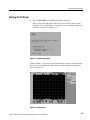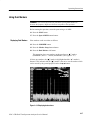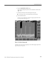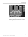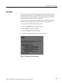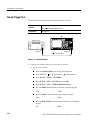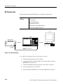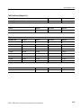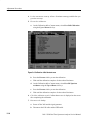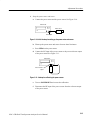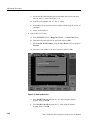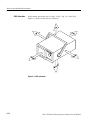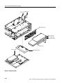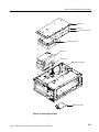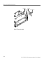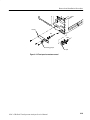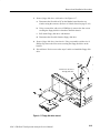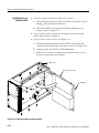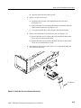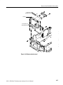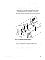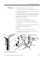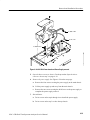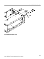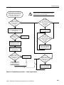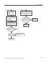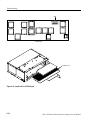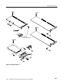
1
Service Manual
3026
3 GHz Real Time Spectrum Analyzer
071-0420-00
Warning
The servicing instructions are for use by qualified
personnel only. To avoid personal injury, do not
perform any servicing unless you are qualified to
do so. Refer to the Safety Summary prior to
performing service.
E Sony/Tektronix Corporation. All rights reserved.
Copyright E Tektronix, Inc. All rights reserved.
Copyright
Tektronix products are covered by U.S. and foreign patents, issued and pending. Information in this publication supercedes
that in all previously published material. Specifications and price change privileges reserved.
Printed in Japan.
Sony/Tektronix Corporation, P.O.Box 5209, Tokyo Int’l, Tokyo 100–31 Japan
Tektronix, Inc., P.O. Box 1000, Wilsonville, OR 97070–1000
TEKTRONIX and TEK are registered trademarks of Tektronix, Inc.
WARRANTY
Tektronix warrants that the products that it manufactures and sells will be free from defects in materials and workmanship
for a period of one (1) year from the date of shipment. If a product proves defective during this warranty period, Tektronix,
at its option, either will repair the defective product without charge for parts and labor, or will provide a replacement in
exchange for the defective product.
In order to obtain service under this warranty, Customer must notify Tektronix of the defect before the expiration of the
warranty period and make suitable arrangements for the performance of service. Customer shall be responsible for
packaging and shipping the defective product to the service center designated by Tektronix, with shipping charges prepaid.
Tektronix shall pay for the return of the product to Customer if the shipment is to a location within the country in which the
Tektronix service center is located. Customer shall be responsible for paying all shipping charges, duties, taxes, and any
other charges for products returned to any other locations.
This warranty shall not apply to any defect, failure or damage caused by improper use or improper or inadequate
maintenance and care. Tektronix shall not be obligated to furnish service under this warranty a) to repair damage resulting
from attempts by personnel other than Tektronix representatives to install, repair or service the product; b) to repair
damage resulting from improper use or connection to incompatible equipment; c) to repair any damage or malfunction
caused by the use of non-Tektronix supplies; or d) to service a product that has been modified or integrated with other
products when the effect of such modification or integration increases the time or difficulty of servicing the product.
THIS WARRANTY IS GIVEN BY TEKTRONIX IN LIEU OF ANY OTHER WARRANTIES, EXPRESS OR
IMPLIED. TEKTRONIX AND ITS VENDORS DISCLAIM ANY IMPLIED WARRANTIES OF
MERCHANTABILITY OR FITNESS FOR A PARTICULAR PURPOSE. TEKTRONIX’ RESPONSIBILITY TO
REPAIR OR REPLACE DEFECTIVE PRODUCTS IS THE SOLE AND EXCLUSIVE REMEDY PROVIDED TO
THE CUSTOMER FOR BREACH OF THIS WARRANTY. TEKTRONIX AND ITS VENDORS WILL NOT BE
LIABLE FOR ANY INDIRECT, SPECIAL, INCIDENTAL, OR CONSEQUENTIAL DAMAGES IRRESPECTIVE
OF WHETHER TEKTRONIX OR THE VENDOR HAS ADVANCE NOTICE OF THE POSSIBILITY OF SUCH
DAMAGES.
Table of Contents
General Safety Summary . . . . . . . . . . . . . . . . . . . . . . . . . . . . . . . . . . . .
Service Safety Summary . . . . . . . . . . . . . . . . . . . . . . . . . . . . . . . . . . . . .
Preface . . . . . . . . . . . . . . . . . . . . . . . . . . . . . . . . . . . . . . . . . . . . . . . . . . .
Introduction . . . . . . . . . . . . . . . . . . . . . . . . . . . . . . . . . . . . . . . . . . . . . . .
xi
xiii
xv
xix
Product Overview . . . . . . . . . . . . . . . . . . . . . . . . . . . . . . . . . . . . . . . . . .
Specifications . . . . . . . . . . . . . . . . . . . . . . . . . . . . . . . . . . . . . . . . . . . . . .
1–1
1–3
Warranted Characteristics . . . . . . . . . . . . . . . . . . . . . . . . . . . . . . . . . . . . . . . . . .
Typical Characteristics . . . . . . . . . . . . . . . . . . . . . . . . . . . . . . . . . . . . . . . . . . . . .
Nominal Traits . . . . . . . . . . . . . . . . . . . . . . . . . . . . . . . . . . . . . . . . . . . . . . . . . . .
Certification and Compliances . . . . . . . . . . . . . . . . . . . . . . . . . . . . . . . . . . . . . . .
1–3
1–7
1–9
1–13
Installation . . . . . . . . . . . . . . . . . . . . . . . . . . . . . . . . . . . . . . . . . . . . . . . .
2–1
Supplying Operating Power . . . . . . . . . . . . . . . . . . . . . . . . . . . . . . . . . . . . . . . . .
Operating Environment . . . . . . . . . . . . . . . . . . . . . . . . . . . . . . . . . . . . . . . . . . . .
Applying and Interrupting Power . . . . . . . . . . . . . . . . . . . . . . . . . . . . . . . . . . . .
Repackaging Instructions . . . . . . . . . . . . . . . . . . . . . . . . . . . . . . . . . . . . . . . . . . .
Installed Options . . . . . . . . . . . . . . . . . . . . . . . . . . . . . . . . . . . . . . . . . . . . . . . . .
2–1
2–3
2–4
2–5
2–5
Operating Instructions . . . . . . . . . . . . . . . . . . . . . . . . . . . . . . . . . . . . . .
2–7
Preparations . . . . . . . . . . . . . . . . . . . . . . . . . . . . . . . . . . . . . . . . . . . . . . . . . . . . .
Setup . . . . . . . . . . . . . . . . . . . . . . . . . . . . . . . . . . . . . . . . . . . . . . . . . . . . . . . . . . .
Turning On the Power . . . . . . . . . . . . . . . . . . . . . . . . . . . . . . . . . . . . . . . . . . . . .
Observing Spectrum . . . . . . . . . . . . . . . . . . . . . . . . . . . . . . . . . . . . . . . . . . . . . . .
Dividing the Display Area and Changing the Display Mode . . . . . . . . . . . . . . .
Using the Block Mode to Acquire Data . . . . . . . . . . . . . . . . . . . . . . . . . . . . . . . .
Using Dual Markers . . . . . . . . . . . . . . . . . . . . . . . . . . . . . . . . . . . . . . . . . . . . . . .
Trigger and Mask Pattern . . . . . . . . . . . . . . . . . . . . . . . . . . . . . . . . . . . . . . . . . . .
Changing the Display Frame . . . . . . . . . . . . . . . . . . . . . . . . . . . . . . . . . . . . . . . .
Shutting Power Off . . . . . . . . . . . . . . . . . . . . . . . . . . . . . . . . . . . . . . . . . . . . . . .
2–7
2–8
2–9
2–10
2–12
2–15
2–17
2–20
2–24
2–26
Theory of Operation . . . . . . . . . . . . . . . . . . . . . . . . . . . . . . . . . . . . . . . .
3–1
Module Overview . . . . . . . . . . . . . . . . . . . . . . . . . . . . . . . . . . . . . . . . . . . . . . . . .
3–1
Specifications
Operating Information
Theory of Operation
3026 3 GHz Real Time Spectrum Analyzer Service Manual
i
Table of Contents
Performance Verification
Performance Verification . . . . . . . . . . . . . . . . . . . . . . . . . . . . . . . . . . . .
4–1
Conventions . . . . . . . . . . . . . . . . . . . . . . . . . . . . . . . . . . . . . . . . . . . . . . . . . . . . .
Self Tests . . . . . . . . . . . . . . . . . . . . . . . . . . . . . . . . . . . . . . . . . . . . . . . . . . . . . . .
Calibration . . . . . . . . . . . . . . . . . . . . . . . . . . . . . . . . . . . . . . . . . . . . . . . . . . . . . .
Performance Tests . . . . . . . . . . . . . . . . . . . . . . . . . . . . . . . . . . . . . . . . . . . . . . . .
Prerequisites . . . . . . . . . . . . . . . . . . . . . . . . . . . . . . . . . . . . . . . . . . . . . . . . . . . . .
Equipment Required . . . . . . . . . . . . . . . . . . . . . . . . . . . . . . . . . . . . . . . . . . . . . . .
10 MHz Reference Output Test . . . . . . . . . . . . . . . . . . . . . . . . . . . . . . . . . . . . . .
10 MHz Reference Input Test . . . . . . . . . . . . . . . . . . . . . . . . . . . . . . . . . . . . . . .
Center Frequency Accuracy Test . . . . . . . . . . . . . . . . . . . . . . . . . . . . . . . . . . . . .
Flatness and Aliasing Test . . . . . . . . . . . . . . . . . . . . . . . . . . . . . . . . . . . . . . . . . .
Attenuator Test . . . . . . . . . . . . . . . . . . . . . . . . . . . . . . . . . . . . . . . . . . . . . . . . . . .
Span and Center Frequency Test . . . . . . . . . . . . . . . . . . . . . . . . . . . . . . . . . . . . .
Frame Update Interval Test . . . . . . . . . . . . . . . . . . . . . . . . . . . . . . . . . . . . . . . . .
Internal Trigger Test . . . . . . . . . . . . . . . . . . . . . . . . . . . . . . . . . . . . . . . . . . . . . . .
External Trigger Test . . . . . . . . . . . . . . . . . . . . . . . . . . . . . . . . . . . . . . . . . . . . . .
C/N Test . . . . . . . . . . . . . . . . . . . . . . . . . . . . . . . . . . . . . . . . . . . . . . . . . . . . . . . .
RF Reference Level Test . . . . . . . . . . . . . . . . . . . . . . . . . . . . . . . . . . . . . . . . . . .
RF Flatness Test . . . . . . . . . . . . . . . . . . . . . . . . . . . . . . . . . . . . . . . . . . . . . . . . . .
Test Record . . . . . . . . . . . . . . . . . . . . . . . . . . . . . . . . . . . . . . . . . . . . . . . . . . . . . .
4–2
4–3
4–5
4–7
4–8
4–9
4–10
4–11
4–14
4–16
4–18
4–20
4–23
4–26
4–30
4–32
4–34
4–38
4–41
Adjustment Procedures
Adjustment Procedures . . . . . . . . . . . . . . . . . . . . . . . . . . . . . . . . . . . . . .
5–1
Requirements for Adjustments . . . . . . . . . . . . . . . . . . . . . . . . . . . . . . . . . . . . . . .
Equipment Required . . . . . . . . . . . . . . . . . . . . . . . . . . . . . . . . . . . . . . . . . . . . . . .
Adjustments . . . . . . . . . . . . . . . . . . . . . . . . . . . . . . . . . . . . . . . . . . . . . . . . . . . . .
5–2
5–3
5–4
Maintenance . . . . . . . . . . . . . . . . . . . . . . . . . . . . . . . . . . . . . . . . . . . . . . .
6–1
Related Maintenance Procedures . . . . . . . . . . . . . . . . . . . . . . . . . . . . . . . . . . . . .
Preparation . . . . . . . . . . . . . . . . . . . . . . . . . . . . . . . . . . . . . . . . . . . . . . . . . . . . . .
Inspection and Cleaning . . . . . . . . . . . . . . . . . . . . . . . . . . . . . . . . . . . . . . . . . . . .
6–1
6–2
6–4
Removal and Installation Procedures . . . . . . . . . . . . . . . . . . . . . . . . . .
6–9
Preparation . . . . . . . . . . . . . . . . . . . . . . . . . . . . . . . . . . . . . . . . . . . . . . . . . . . . . .
Access Procedure . . . . . . . . . . . . . . . . . . . . . . . . . . . . . . . . . . . . . . . . . . . . . . . . .
Procedures for External Modules . . . . . . . . . . . . . . . . . . . . . . . . . . . . . . . . . . . . .
Procedures for Internal Modules . . . . . . . . . . . . . . . . . . . . . . . . . . . . . . . . . . . . .
Procedures for Board Modules . . . . . . . . . . . . . . . . . . . . . . . . . . . . . . . . . . . . . . .
Procedures for Power Supply Modules . . . . . . . . . . . . . . . . . . . . . . . . . . . . . . . .
Procedures for Rear Panel Modules . . . . . . . . . . . . . . . . . . . . . . . . . . . . . . . . . . .
6–9
6–13
6–19
6–30
6–38
6–48
6–55
Troubleshooting . . . . . . . . . . . . . . . . . . . . . . . . . . . . . . . . . . . . . . . . . . . .
6–59
Troubleshooting Procedure . . . . . . . . . . . . . . . . . . . . . . . . . . . . . . . . . . . . . . . . .
Diagnostics . . . . . . . . . . . . . . . . . . . . . . . . . . . . . . . . . . . . . . . . . . . . . . . . . . . . . .
Symptoms and Faulty Modules . . . . . . . . . . . . . . . . . . . . . . . . . . . . . . . . . . . . . .
6–59
6–60
6–78
Accessing the BIOS . . . . . . . . . . . . . . . . . . . . . . . . . . . . . . . . . . . . . . . . .
6–81
Preparation . . . . . . . . . . . . . . . . . . . . . . . . . . . . . . . . . . . . . . . . . . . . . . . . . . . . . .
Setting the BIOS Parameters . . . . . . . . . . . . . . . . . . . . . . . . . . . . . . . . . . . . . . . .
Backing Up the System Files . . . . . . . . . . . . . . . . . . . . . . . . . . . . . . . . . . . . . . . .
6–82
6–83
6–89
Maintenance
ii
3026 3 GHz Real Time Spectrum Analyzer Service Manual
Table of Contents
Options
Options and Accessories . . . . . . . . . . . . . . . . . . . . . . . . . . . . . . . . . . . . .
7–1
Options . . . . . . . . . . . . . . . . . . . . . . . . . . . . . . . . . . . . . . . . . . . . . . . . . . . . . . . . .
Standard Accessories . . . . . . . . . . . . . . . . . . . . . . . . . . . . . . . . . . . . . . . . . . . . . .
Optional Accessories . . . . . . . . . . . . . . . . . . . . . . . . . . . . . . . . . . . . . . . . . . . . . .
7–1
7–2
7–2
Electrical Parts List . . . . . . . . . . . . . . . . . . . . . . . . . . . . . . . . . . . . . . . . .
8–1
Diagrams . . . . . . . . . . . . . . . . . . . . . . . . . . . . . . . . . . . . . . . . . . . . . . . . .
9–1
Mechanical Parts List . . . . . . . . . . . . . . . . . . . . . . . . . . . . . . . . . . . . . . .
10–1
Parts Ordering Information . . . . . . . . . . . . . . . . . . . . . . . . . . . . . . . . . . . . . . . . .
Using the Replaceable Parts List . . . . . . . . . . . . . . . . . . . . . . . . . . . . . . . . . . . . .
10–1
10–2
Electrical Parts List
Diagrams
Mechanical Parts List
3026 3 GHz Real Time Spectrum Analyzer Service Manual
iii
Table of Contents
List of Figures
iv
Figure 2–1: Power switch . . . . . . . . . . . . . . . . . . . . . . . . . . . . . . . . . . . .
Figure 2–2: RF INPUT connector . . . . . . . . . . . . . . . . . . . . . . . . . . . . .
Figure 2–3: System information . . . . . . . . . . . . . . . . . . . . . . . . . . . . . . .
Figure 2–4: Initial screen . . . . . . . . . . . . . . . . . . . . . . . . . . . . . . . . . . . .
Figure 2–5: START/STOP button . . . . . . . . . . . . . . . . . . . . . . . . . . . . .
Figure 2–6: Typical spectrum display (16 MHz center frequency
and 10 MHz span) . . . . . . . . . . . . . . . . . . . . . . . . . . . . . . . . . . . . . . .
Figure 2–7: Buttons in DISPLAY area . . . . . . . . . . . . . . . . . . . . . . . . .
Figure 2–8: Spectrogram display (upper) and spectrum display
(lower) . . . . . . . . . . . . . . . . . . . . . . . . . . . . . . . . . . . . . . . . . . . . . . . .
Figure 2–9: SELECT button . . . . . . . . . . . . . . . . . . . . . . . . . . . . . . . . .
Figure 2–10: Waterfall display and spectrum display . . . . . . . . . . . . .
Figure 2–11: ROLL BLOCK button . . . . . . . . . . . . . . . . . . . . . . . . . . .
Figure 2–12: Data acquisition in the Block mode . . . . . . . . . . . . . . . . .
Figure 2–13: Displaying dual markers . . . . . . . . . . . . . . . . . . . . . . . . .
Figure 2–14: MARKER TOGGLE button . . . . . . . . . . . . . . . . . . . . . .
Figure 2–15: Measurement of frequency difference with dual
markers . . . . . . . . . . . . . . . . . . . . . . . . . . . . . . . . . . . . . . . . . . . . . . .
Figure 2–16: Creation of trigger region . . . . . . . . . . . . . . . . . . . . . . . .
Figure 2–17: Created trigger mask (blue region) . . . . . . . . . . . . . . . . .
Figure 2–18: Waveform display before triggering . . . . . . . . . . . . . . . .
Figure 2–19: Frame in which trigger occurred . . . . . . . . . . . . . . . . . .
2–4
2–8
2–9
2–9
2–10
2–19
2–21
2–22
2–23
2–25
Figure 4–1: Display of the self test results . . . . . . . . . . . . . . . . . . . . . . .
Figure 4–2: CAL NEED indication in status indication area . . . . . . .
Figure 4–3: Initial test hookup . . . . . . . . . . . . . . . . . . . . . . . . . . . . . . . .
Figure 4–4: Initial test hookup . . . . . . . . . . . . . . . . . . . . . . . . . . . . . . . .
Figure 4–5: Modified test hookup . . . . . . . . . . . . . . . . . . . . . . . . . . . . .
Figure 4–6: Initial test hookup . . . . . . . . . . . . . . . . . . . . . . . . . . . . . . . .
Figure 4–7: Initial test hookup . . . . . . . . . . . . . . . . . . . . . . . . . . . . . . . .
Figure 4–8: Initial test hookup . . . . . . . . . . . . . . . . . . . . . . . . . . . . . . . .
Figure 4–9: Initial test hookup . . . . . . . . . . . . . . . . . . . . . . . . . . . . . . . .
Figure 4–10: Initial test hookup . . . . . . . . . . . . . . . . . . . . . . . . . . . . . . .
Figure 4–11: Initial test hookup . . . . . . . . . . . . . . . . . . . . . . . . . . . . . . .
Figure 4–12: Creating a trigger mask . . . . . . . . . . . . . . . . . . . . . . . . . .
Figure 4–13: Initial test hookup . . . . . . . . . . . . . . . . . . . . . . . . . . . . . . .
4–3
4–5
4–10
4–11
4–12
4–14
4–16
4–18
4–20
4–23
4–26
4–27
4–30
2–11
2–12
2–12
2–13
2–14
2–15
2–16
2–17
2–18
3026 3 GHz Real Time Spectrum Analyzer Service Manual
Table of Contents
Figure 4–14: Initial test hookup . . . . . . . . . . . . . . . . . . . . . . . . . . . . . . .
Figure 4–15: Initial hookup for setting up the power meter and
sensor . . . . . . . . . . . . . . . . . . . . . . . . . . . . . . . . . . . . . . . . . . . . . . . . .
Figure 4–16: Hookup for calibrating the power sensor . . . . . . . . . . . .
Figure 4–17: Hookup for setting the signal generator . . . . . . . . . . . . .
Figure 4–18: Hookup for checking the reference level accuracy . . . .
Figure 4–19: Initial test hookup . . . . . . . . . . . . . . . . . . . . . . . . . . . . . . .
Figure 4–20: Running the RF flatness check program on PC . . . . . .
Figure 5–1: Accessing the A5 Baseband board . . . . . . . . . . . . . . . . . . .
Figure 5–2: Adjustment and connector location . . . . . . . . . . . . . . . . .
Figure 5–3: Test hookup . . . . . . . . . . . . . . . . . . . . . . . . . . . . . . . . . . . . .
Figure 5–4: Initial test hookup . . . . . . . . . . . . . . . . . . . . . . . . . . . . . . . .
Figure 5–5: Loading the adjustment file from the floppy disk . . . . . .
Figure 5–6: Calibration & Set Constant menu . . . . . . . . . . . . . . . . . . .
Figure 5–7: Initial hookup for setting up the power meter and
sensor . . . . . . . . . . . . . . . . . . . . . . . . . . . . . . . . . . . . . . . . . . . . . . . . .
Figure 5–8: Hookup for calibrating the power sensor . . . . . . . . . . . . .
Figure 5–9: Test hookup . . . . . . . . . . . . . . . . . . . . . . . . . . . . . . . . . . . . .
Figure 5–10: Initial hookup for setting up the power meter and
sensor . . . . . . . . . . . . . . . . . . . . . . . . . . . . . . . . . . . . . . . . . . . . . . . . .
Figure 5–11: Hookup for calibrating the power sensor . . . . . . . . . . . .
Figure 5–12: Test hookup . . . . . . . . . . . . . . . . . . . . . . . . . . . . . . . . . . . .
Figure 5–13: Running the SG flatness measurement program on
PC . . . . . . . . . . . . . . . . . . . . . . . . . . . . . . . . . . . . . . . . . . . . . . . . . . . .
Figure 5–14: Label location . . . . . . . . . . . . . . . . . . . . . . . . . . . . . . . . . .
Figure 5–15: Serial number entry . . . . . . . . . . . . . . . . . . . . . . . . . . . . .
Figure 5–16: Test hookup . . . . . . . . . . . . . . . . . . . . . . . . . . . . . . . . . . . .
Figure 6–1: 3026 orientation . . . . . . . . . . . . . . . . . . . . . . . . . . . . . . . . . .
Figure 6–2: Guide to removal procedures . . . . . . . . . . . . . . . . . . . . . . .
Figure 6–3: External modules . . . . . . . . . . . . . . . . . . . . . . . . . . . . . . . .
Figure 6–4: Internal modules . . . . . . . . . . . . . . . . . . . . . . . . . . . . . . . . .
Figure 6–5: Board modules . . . . . . . . . . . . . . . . . . . . . . . . . . . . . . . . . . .
Figure 6–6: Power supply modules . . . . . . . . . . . . . . . . . . . . . . . . . . . .
Figure 6–7: Rear panel modules . . . . . . . . . . . . . . . . . . . . . . . . . . . . . .
Figure 6–8: Front-panel knob removal . . . . . . . . . . . . . . . . . . . . . . . . .
Figure 6–9: Line cord removal . . . . . . . . . . . . . . . . . . . . . . . . . . . . . . . .
Figure 6–10: Rear cover and cabinet removal . . . . . . . . . . . . . . . . . . .
Figure 6–11: Trim ring and menu buttons removal . . . . . . . . . . . . . . .
3026 3 GHz Real Time Spectrum Analyzer Service Manual
4–32
4–34
4–35
4–36
4–36
4–38
4–39
5–5
5–6
5–7
5–8
5–9
5–10
5–12
5–12
5–13
5–15
5–15
5–16
5–17
5–19
5–20
5–21
6–12
6–13
6–14
6–15
6–16
6–17
6–18
6–20
6–21
6–23
6–25
v
Table of Contents
Figure 6–12: Front-panel assembly removal . . . . . . . . . . . . . . . . . . . .
Figure 6–13: Disassembly of front-panel assembly . . . . . . . . . . . . . . .
Figure 6–14: Front-panel connectors removal . . . . . . . . . . . . . . . . . . .
Figure 6–15: Opening the top chassis . . . . . . . . . . . . . . . . . . . . . . . . . .
Figure 6–16: Fan and fan frame removal . . . . . . . . . . . . . . . . . . . . . . .
Figure 6–17: Floppy disk drive removal . . . . . . . . . . . . . . . . . . . . . . . .
Figure 6–18: Opening the down-converter chassis . . . . . . . . . . . . . . .
Figure 6–19: Hard disk drive and solid state disk removal . . . . . . . . .
Figure 6–20: Display module removal . . . . . . . . . . . . . . . . . . . . . . . . . .
Figure 6–21: Board retainer and shield cover removal . . . . . . . . . . . .
Figure 6–22: Daughter boards removal . . . . . . . . . . . . . . . . . . . . . . . .
Figure 6–23: A1 Mother board removal – Top side . . . . . . . . . . . . . . .
Figure 6–24: A1 Mother board removal – Bottom side . . . . . . . . . . . .
Figure 6–25: Down-converter and A5 Baseband board removal . . . .
Figure 6–26: A13 Filter board removal . . . . . . . . . . . . . . . . . . . . . . . . .
Figure 6–27: A11 and A12 DC Power boards removal . . . . . . . . . . . .
Figure 6–28: A10 Sub Power board and Power Supply removal . . . .
Figure 6–29: Power supply removal . . . . . . . . . . . . . . . . . . . . . . . . . . .
Figure 6–30: Rear panel modules removal . . . . . . . . . . . . . . . . . . . . . .
Figure 6–31: Rear BNC cable assembly removal . . . . . . . . . . . . . . . . .
Figure 6–32: Troubleshooting procedure 1 — Power supply
modules . . . . . . . . . . . . . . . . . . . . . . . . . . . . . . . . . . . . . . . . . . . . . . .
Figure 6–33: Troubleshooting procedure 2 — Signal processing
modules . . . . . . . . . . . . . . . . . . . . . . . . . . . . . . . . . . . . . . . . . . . . . . .
Figure 6–34: Troubleshooting procedure 3 — Clock modules . . . . . .
Figure 6–35: Troubleshooting procedure 4 — LCD display modules
Figure 6–36: Troubleshooting procedure 5 — CPU modules . . . . . . .
Figure 6–37: Troubleshooting procedure 6 — Front panel modules .
Figure 6–38: Location of the A11 and A12 DC Power boards . . . . . .
Figure 6–39: Location of the A5 Baseband and A13 Filter board . . .
Figure 6–40: Location of the A6 FFT board . . . . . . . . . . . . . . . . . . . . .
Figure 6–41: Location of the A7 DDC board . . . . . . . . . . . . . . . . . . . .
Figure 6–42: Location of the A8 Memory board . . . . . . . . . . . . . . . . .
Figure 6–43: U100 down-converter location . . . . . . . . . . . . . . . . . . . . .
Figure 6–44: LCD wire location . . . . . . . . . . . . . . . . . . . . . . . . . . . . . . .
Figure 6–45: Connecting the keyboard . . . . . . . . . . . . . . . . . . . . . . . . .
Figure 6–46: BIOS SETUP screen . . . . . . . . . . . . . . . . . . . . . . . . . . . . .
Figure 6–47: STANDARD CMOS SETUP screen . . . . . . . . . . . . . . . .
Figure 6–48: BIOS FEATURES SETUP screen . . . . . . . . . . . . . . . . . .
vi
6–26
6–27
6–29
6–31
6–32
6–33
6–34
6–35
6–37
6–39
6–42
6–44
6–45
6–47
6–49
6–51
6–53
6–54
6–57
6–58
6–61
6–64
6–66
6–68
6–69
6–70
6–71
6–72
6–73
6–74
6–75
6–76
6–77
6–82
6–83
6–84
6–85
3026 3 GHz Real Time Spectrum Analyzer Service Manual
Table of Contents
Figure 9–1: Block diagram . . . . . . . . . . . . . . . . . . . . . . . . . . . . . . . . . . .
Figure 9–2: Interconnect diagram . . . . . . . . . . . . . . . . . . . . . . . . . . . . .
9–1
9–3
Figure 10–1: External modules . . . . . . . . . . . . . . . . . . . . . . . . . . . . . . .
Figure 10–2: Front panel modules . . . . . . . . . . . . . . . . . . . . . . . . . . . . .
Figure 10–3: Internal modules . . . . . . . . . . . . . . . . . . . . . . . . . . . . . . . .
Figure 10–4: Power supply modules . . . . . . . . . . . . . . . . . . . . . . . . . . .
Figure 10–5: Board modules – 1 . . . . . . . . . . . . . . . . . . . . . . . . . . . . . . .
Figure 10–6: Board modules – 2 . . . . . . . . . . . . . . . . . . . . . . . . . . . . . . .
Figure 10–7: Cables . . . . . . . . . . . . . . . . . . . . . . . . . . . . . . . . . . . . . . . . .
10–5
10–7
10–9
10–11
10–13
10–15
10–17
3026 3 GHz Real Time Spectrum Analyzer Service Manual
vii
Table of Contents
List of Tables
viii
Table 1–1: Warranted characteristics — Frequency . . . . . . . . . . . . .
Table 1–2: Warranted characteristics — Amplitude . . . . . . . . . . . . .
Table 1–3: Warranted characteristics — Realtime span . . . . . . . . . .
Table 1–4: Warranted characteristics — Trigger/Acquisition . . . . .
Table 1–5: Warranted characteristics — Installation requirements
Table 1–6: Warranted characteristics — Environmental . . . . . . . . .
Table 1–7: Typical characteristics — Amplitude . . . . . . . . . . . . . . . .
Table 1–8: Typical characteristics — Filter . . . . . . . . . . . . . . . . . . . .
Table 1–9: Typical characteristics — Trigger/Acquisition . . . . . . . .
Table 1–10: Typical characteristics — Installation requirements . .
Table 1–11: Nominal traits — Frequency . . . . . . . . . . . . . . . . . . . . . .
Table 1–12: Nominal traits — Amplitude . . . . . . . . . . . . . . . . . . . . . .
Table 1–13: Nominal traits — FFT . . . . . . . . . . . . . . . . . . . . . . . . . . .
Table 1–14: Nominal traits — Filter . . . . . . . . . . . . . . . . . . . . . . . . . .
Table 1–15: Nominal traits — Trigger/Acquisition . . . . . . . . . . . . . .
Table 1–16: Nominal traits — System control . . . . . . . . . . . . . . . . . .
Table 1–17: Nominal traits — AC line power . . . . . . . . . . . . . . . . . . .
Table 1–18: Nominal traits — Mechanical . . . . . . . . . . . . . . . . . . . . .
Table 1–19: Certifications and compliances . . . . . . . . . . . . . . . . . . . . .
1–4
1–4
1–5
1–5
1–6
1–6
1–7
1–7
1–7
1–7
1–9
1–9
1–10
1–11
1–11
1–12
1–12
1–12
1–13
Table 2–1: Power-cord conductor identification . . . . . . . . . . . . . . . . .
Table 2–2: Power cord identification . . . . . . . . . . . . . . . . . . . . . . . . . .
2–2
2–2
Table 4–1: Performance tests . . . . . . . . . . . . . . . . . . . . . . . . . . . . . . . . .
Table 4–2: Test equipment . . . . . . . . . . . . . . . . . . . . . . . . . . . . . . . . . . .
Table 4–3: Level accuracy . . . . . . . . . . . . . . . . . . . . . . . . . . . . . . . . . . .
Table 4–4: The instrument settings for the span and center
frequency test . . . . . . . . . . . . . . . . . . . . . . . . . . . . . . . . . . . . . . . . . .
Table 4–5: The instrument settings for the RF reference level test . .
4–7
4–9
4–19
4–21
4–37
Table 5–1: Adjustments . . . . . . . . . . . . . . . . . . . . . . . . . . . . . . . . . . . . .
Table 5–2: Test equipment . . . . . . . . . . . . . . . . . . . . . . . . . . . . . . . . . . .
5–1
5–3
Table 6–1: Relative susceptibility to static-discharge damage . . . . . .
Table 6–2: External inspection check list . . . . . . . . . . . . . . . . . . . . . . .
Table 6–3: Internal inspection check list . . . . . . . . . . . . . . . . . . . . . . .
6–3
6–5
6–6
3026 3 GHz Real Time Spectrum Analyzer Service Manual
Table of Contents
Table 6–4: Summary of procedures . . . . . . . . . . . . . . . . . . . . . . . . . . .
Table 6–5: Tools required for module removal . . . . . . . . . . . . . . . . . .
Table 6–6: Normal supply voltage . . . . . . . . . . . . . . . . . . . . . . . . . . . . .
Table 6–7: Symptoms and faulty modules . . . . . . . . . . . . . . . . . . . . . .
Table 6–8: 3026 system files . . . . . . . . . . . . . . . . . . . . . . . . . . . . . . . . . .
6–10
6–11
6–72
6–78
6–89
Table 7–1: Options . . . . . . . . . . . . . . . . . . . . . . . . . . . . . . . . . . . . . . . . .
Table 7–2: Standard accessories . . . . . . . . . . . . . . . . . . . . . . . . . . . . . .
Table 7–3: Optional accessories . . . . . . . . . . . . . . . . . . . . . . . . . . . . . . .
7–1
7–2
7–2
3026 3 GHz Real Time Spectrum Analyzer Service Manual
ix
Table of Contents
x
3026 3 GHz Real Time Spectrum Analyzer Service Manual
General Safety Summary
Review the following safety precautions to avoid injury and prevent damage to
this product or any products connected to it. To avoid potential hazards, use this
product only as specified.
Only qualified personnel should perform service procedures.
To Avoid Fire or
Personal Injury
Use Proper Power Cord. Use only the power cord specified for this product and
certified for the country of use.
Use Proper Voltage Setting. Before applying power, ensure that the line selector is
in the proper position for the power source being used.
Connect and Disconnect Properly. Do not connect or disconnect probes or test
leads while they are connected to a voltage source.
Ground the Product. This product is grounded through the grounding conductor
of the power cord. To avoid electric shock, the grounding conductor must be
connected to earth ground. Before making connections to the input or output
terminals of the product, ensure that the product is properly grounded.
Observe All Terminal Ratings. To avoid fire or shock hazard, observe all ratings
and markings on the product. Consult the product manual for further ratings
information before making connections to the product.
The common terminal is at ground potential. Do not connect the common
terminal to elevated voltages.
Do not apply a potential to any terminal, including the common terminal, that
exceeds the maximum rating of that terminal.
Do Not Operate Without Covers. Do not operate this product with covers or panels
removed.
Use Proper Fuse. Use only the fuse type and rating specified for this product.
Avoid Exposed Circuitry. Do not touch exposed connections and components
when power is present.
Do Not Operate With Suspected Failures. If you suspect there is damage to this
product, have it inspected by qualified service personnel.
Do Not Operate in Wet/Damp Conditions.
Do Not Operate in an Explosive Atmosphere.
Keep Product Surfaces Clean and Dry.
Provide Proper Ventilation. Refer to the manual’s installation instructions for
details on installing the product so it has proper ventilation.
3026 3 GHz Real Time Spectrum Analyzer Service Manual
xi
General Safety Summary
Symbols and Terms
Terms in this Manual. These terms may appear in this manual:
WARNING. Warning statements identify conditions or practices that could result
in injury or loss of life.
CAUTION. Caution statements identify conditions or practices that could result in
damage to this product or other property.
Terms on the Product. These terms may appear on the product:
DANGER indicates an injury hazard immediately accessible as you read the
marking.
WARNING indicates an injury hazard not immediately accessible as you read the
marking.
CAUTION indicates a hazard to property including the product.
Symbols on the Product. The following symbols may appear on the product:
WARNING
High Voltage
xii
Protective Ground
(Earth) Terminal
CAUTION
Refer to Manual
Double
Insulated
3026 3 GHz Real Time Spectrum Analyzer Service Manual
Service Safety Summary
Only qualified personnel should perform service procedures. Read this Service
Safety Summary and the General Safety Summary before performing any service
procedures.
Do Not Service Alone. Do not perform internal service or adjustments of this
product unless another person capable of rendering first aid and resuscitation is
present.
Disconnect Power. To avoid electric shock, disconnect the mains power by means
of the power cord or, if provided, the power switch.
Use Care When Servicing With Power On. Dangerous voltages or currents may
exist in this product. Disconnect power, remove battery (if applicable), and
disconnect test leads before removing protective panels, soldering, or replacing
components.
To avoid electric shock, do not touch exposed connections.
3026 3 GHz Real Time Spectrum Analyzer Service Manual
xiii
Service Safety Summary
xiv
3026 3 GHz Real Time Spectrum Analyzer Service Manual
Preface
This is the service manual for the 3026 Real Time Spectrum Analyzer. The
manual contains information needed to service the analyzer to the module level.
Manual Structure
This manual is divided into sections, such as Specifications and Theory of
Operation. Further, some sections are divided into subsections, such as Product
Description and Removal and Installation Procedures.
Sections containing procedures also contain introductions to those procedures.
Be sure to read these introductions because they provide information needed to
do the service correctly and efficiently. The following contains a brief description
of each manual section.
H Specifications contains a description of the analyzer and the characteristics
that apply to it.
H Operating Information includes general information and operating
instructions.
H Theory of Operation contains circuit descriptions that support service to the
module level.
H Performance Verification contains procedures for confirming that the
analyzer functions properly and meets warranted limits.
H Adjustment Procedures contains a collection of procedures for adjusting the
analyzer to meet warranted limits.
H Maintenance contains information and procedures for performing preventive
and corrective maintenance of the analyzer. These instructions include
cleaning, module removal and installation, and fault isolation to the module.
H Options contains information on servicing factory-installed options.
H Electrical Parts List contains a statement referring you to Mechanical Parts
List, where both electrical and mechanical modules are listed.
H Diagrams contains an block diagram and an interconnection diagram.
H Mechanical Parts List includes a table of all replaceable modules, their
descriptions, and their Tektronix part numbers.
3026 3 GHz Real Time Spectrum Analyzer Service Manual
xv
Preface
Manual Conventions
This manual uses certain conventions that you should become familiar with.
Some sections of the manual contain procedures for you to perform. To keep
those instructions clear and consistent, this manual uses the following conventions:
H Names of front panel controls and menus appear in the same case (initial
capitals, all uppercase, etc.) in the manual as is used on the analyzer front
panel and menus. Front panel names are all upper-case letters; for example,
DISPLAY, MEASURE, SETUP etc.
H Instruction steps are numbered unless there is only one step.
Modules
Safety
Throughout this manual, any replaceable component, assembly, or part of the
analyzer is referred to generically as a module. In general, a module is an
assembly (like a circuit board), rather than a component (like a resistor or an
integrated circuit). Sometimes a single component is a module; for example, the
chassis of the analyzer is a module.
Symbols and terms related to safety appear in the Safety Summary near the
beginning of this manual.
Finding Other Information
Other documentation for the 3026 includes:
H The 3026 Real Time Spectrum Analyzer User Manual contains a tutorial to
quickly describe how to operate the analyzer. It also includes an in-depth
discussion on how to more completely use the analyzer features.
H The 3026 Real Time Spectrum Analyzer Programmer Manual explains how
to use the GPIB and LAN interfaces to remotely control the analyzer.
xvi
3026 3 GHz Real Time Spectrum Analyzer Service Manual
Preface
Contacting Tektronix
Product
Support
For application-oriented questions about a Tektronix measurement product, call toll free in North America:
1-800-TEK-WIDE (1-800-835-9433 ext. 2400)
6:00 a.m. – 5:00 p.m. Pacific time
Or contact us by e-mail:
[email protected]
For product support outside of North America, contact your
local Tektronix distributor or sales office.
Service
Support
Tektronix offers extended warranty and calibration programs as
options on many products. Contact your local Tektronix
distributor or sales office.
For a listing of worldwide service locations, visit our web site.
For other
information
In North America:
1-800-TEK-WIDE (1-800-835-9433)
An operator will direct your call.
To write us
Tektronix, Inc.
P.O. Box 1000
Wilsonville, OR 97070-1000
USA
Website
Tektronix.com
3026 3 GHz Real Time Spectrum Analyzer Service Manual
xvii
Preface
xviii
3026 3 GHz Real Time Spectrum Analyzer Service Manual
Introduction
This manual contains information needed to properly service the 3026 Real Time
Spectrum Analyzer as well as general information critical to safe and effective
servicing.
To prevent personal injury or damage to the analyzer, consider the following
before attempting service:
H The procedures in this manual should be performed only by a qualified
service person .
H Read the General Safety Summary and the Service Safety Summary,
beginning on page xi.
H Read Preparation for Use in section 2, Operating Information.
When using this manual for servicing, be sure to follow all warnings, cautions,
and notes.
Performance Check Interval
Generally, the performance check described in section 4, Performance Verification, should be done every 12 months. In addition, performance check is
recommended after module replacement.
If the analyzer does not meet performance criteria, repair is necessary.
Strategy for Servicing
Throughout this manual, the term, module, refers to any field-replaceable
component, assembly, or part of the analyzer.
This manual contains all the information needed for periodic maintenance of the
analyzer (Examples of such information are procedures for checking performance).
Further, it contains all information for corrective maintenance down to the
module level. To isolate a failure to a module, use the fault isolation procedures
found in Troubleshooting, part of section 6, Maintenance. To remove and replace
any failed module, follow the instructions in Removal and Installation Procedures, also part of section 6. After isolating a faulty module, replace it with a
fully-tested module obtained from the factory. Section 10, Mechanical Parts
List, contains part number and ordering information for all replaceable modules.
3026 3 GHz Real Time Spectrum Analyzer Service Manual
xix
Preface
xx
3026 3 GHz Real Time Spectrum Analyzer Service Manual
Specifications
Product Overview
The 3026 is a portable real time 3 GHz spectrum analyzer with real-time
frequency analysis functions.
The incorporated 3 GHz down converter enables you to perform spectrum
analysis, time domain analysis, and analog modulation analysis of Radio
Frequency (RF) signals without connecting any external devices.
The 3026, with the adoption of new architecture, can acquire time and frequency
domain data simultaneously. It can also accurately capture various kinds of
signals with a wide variety of triggering functions.
Real-time trigger functions in frequency domain allow you to trigger on
instantaneous events such as the starting point of a burst signal.
Using the trigger functions in time domain, triggering is available on impulse
noises which are barely captured in frequency domain.
In addition, the 3026 provides measurement functions that can evaluate the
performance of radio devices with simple operation. Moreover, four types of data
display functions offered in the system can allow you to analyze the acquired
data more precisely.
Features
The 3026 has the following features:
H Measurement frequency range: 50 Hz to 3 GHz
H Measurement span: 100 Hz to 3 GHz
H Complete real time frequency analysis
H Concurrent processing of real time frequency analysis and analog modulation analysis
H Provides comprehensive measurement functions to evaluate radio devices
such as occupied bandwidth (OBW), adjacent channel leakage power (ACP)
and power consumption.
H Four types of data display:
H Spectrum display
H Spectrogram display
H Waterfall display
H Analog demodulation display (AM, PM, FM, and FSK)
3026 3 GHz Real Time Spectrum Analyzer Service Manual
1–1
Specifications
H A range of trigger functions:
H Mask pattern trigger
H Level trigger
H External trigger
H Simultaneous data acquisition in frequency domain and time domain
H 6.5 inch full-color TFT display
H Equipped with a hard disk drive and a 3.5 inch floppy disk drive
H A selection of interface ports:
H GPIB port
H 10 BASE-T port
H VGA output port
H Printer port
Targets
The 3026 can perform complete real time analysis for the following:
H Analog modulation analysis (AM, PM, FM, and FSK)
H Variation analysis in PLL frequency:
Jitter in reference oscillator of a mobile telephone, localization of a radio set,
HD read-out jitter, etc.
H Analysis of momentary noise: Mixed noise, EMI measurement, etc.
H Multi-path measurement: Measurement of electric wave environment
H Electric wave interference: Radar interference
H Electric wave analysis: Burst signals
1–2
3026 3 GHz Real Time Spectrum Analyzer Service Manual
Specifications
The specifications on the 3026 Real Time Spectrum Analyzer can be classified
into three sub-sections: Warranted Characteristics, Typical Characteristics and
Nominal Traits. Certifications and Compliances are also found at the last page in
this section.
Warranted Characteristics
This section lists the various warranted characteristics that describe the 3026
Real Time Spectrum Analyzer. Electrical and environmental characteristics are
also included.
Warranted characteristics are described in terms of quantifiable performance
limits which are warranted.
As stated above, this section lists only warranted characteristics. A list of typical
characteristics starts on page 1–7.
Performance Conditions
The performance limits in this specification are valid with these conditions:
H The analyzer must have been calibrated/adjusted at an ambient temperature
between +20_ C and +30_ C.
H The analyzer must be in an environment with temperature, altitude,
humidity, and vibration within the operating limits described in these
specifications.
H The analyzer must have had a warm-up period of at least 20 minutes.
H The analyzer must be operating at an ambient temperature between +10_ C
and +40_ C.
3026 3 GHz Real Time Spectrum Analyzer Service Manual
1–3
Specifications
Table 1–1: Warranted characteristics — Frequency
Characteristics
Description
PV reference page
Center frequency setting characteristic
0.1 Hz step
Spectrum purity
–100 dBc/Hz (10 kHz offset)
4–32
Table 1–2: Warranted characteristics — Amplitude
Characteristics
Description
PV reference page
Reference level range
RF mode
–50 dBm to +30 dBm
BASEBAND mode
–30 dBm to +30 dBm
Maximum nondestructive input voltage
Internal gain calibration accuracy
Flatness
2-nd harmonic distortion
3-rd order distortion
Residual response
Image suppress
1–4
+30 dBm
"1.0 dB (at 25 MHz)
"2.0 dB (>500 Hz), +2.0 dB and –5.0 dB (v500 Hz)
v–70 dBc (–10 dBfs input level)
v–60 dBc (t20 MHz and v–10 dBfs input level)
v–70 dBc (w20 MHz and v–10 dBfs input level)
v–40 dBfs (vDC +10 bins)
v–65 dBfs (center "2 bins)
v–70 dBfs (other than above)
v–70 dB
4–34
4–16, 4–38
3026 3 GHz Real Time Spectrum Analyzer Service Manual
Specifications
Table 1–3: Warranted characteristics — Realtime span
Characteristics
Description
Minimum spectral frame update interval
4–23
1024-point analysis
160 ms
400 ms
4 ms
40 ms
100 ms
200 ms
(500 kHz to 5 MHz span)
(50 kHz to 200 kHz span)
(5 kHz to 20 kHz span)
(500 Hz to 2 kHz span)
(200 Hz span)
(100 Hz span)
256-point analysis
40 ms
400 ms
4 ms
40 ms
100 ms
200 ms
(500 kHz to 2 MHz span)
(50 kHz to 200 MHz span)
(5 kHz to 20 kHz span)
(500 Hz to 2 kHz span)
(200 Hz span)
(100 Hz span)
Realtime span
PV reference page
v2 MHz
Table 1–4: Warranted characteristics — Trigger/Acquisition
Characteristics
Description
Internal trigger
PV reference page
4–26
Level
Maximum
0 dBfs
Minimum
–55 dBfs
v
v
Frequency resolution
Span/800 (5 MHz span, 1024 points)
Span/640 ( 2 MHz span, 1024 points)
Span/160 ( 2 MHz span, 256 points)
Time resolution
Same as the spectral frame update interval.
External trigger
Input voltage range
4–30
0 to 5 V
3026 3 GHz Real Time Spectrum Analyzer Service Manual
1–5
Specifications
Table 1–5: Warranted characteristics — Installation requirements
Characteristics
Description
Heat emission
Maximum power
300 W
Maximum line current
4.0 Arms (at 50 Hz)
AC line source
Primary circuit dielectric voltage
withstand
15 s for 1,500 Vrms at 50 Hz
Grounding impedance
Verify the continuity of grounding connection, by any suitable means, between a
representative part required to be grounding and attachment-plug cap grounding pin.
(0.1 W at 30 A)
Table 1–6: Warranted characteristics — Environmental
Characteristics
Description
Atmospherics
Temperature
Operating
+10 _C to +40 _C
Non-operating
–20 _C to +60 _C
Relative humidity
Operating
20 % to 80 % (no condensation), Maximum wet-bulb temperature 29.4 _C
Non-operating
5 % to 90 % (no condensation), Maximum wet-bulb temperature 40.0 _C
Altitude
Operating
Up to 4.5 km (15,000 ft).
Maximum working temperature decreases by 1 _C at 300 m increments when the altitude
exceeds 1.5 km.
Non-operating
Up to 15 km (50,000 ft)
Dynamics
Random vibration
Operating
0.27 g rms, from 5 Hz to 500 Hz, 10 minutes
Non-operating
2.28 g rms, from 5 Hz to 500 Hz, 10 minutes
Shock
Non-operating
1–6
294 m/s2 (3.0G), half-sine, 11 ms duration, three times in every axis direction.
3026 3 GHz Real Time Spectrum Analyzer Service Manual
Specifications
Typical Characteristics
This subsection contains tables that list the various typical characteristics which
describe the 3026 Real Time Spectrum Analyzer.
Typical characteristics are described in terms of typical or average performance.
Typical characteristics are not warranted.
Table 1–7: Typical characteristics — Amplitude
Characteristics
Description
Input equivalent noise
–140 dBm/Hz at 1 GHz
Spurious response
v–65 dBc
Table 1–8: Typical characteristics — Filter
Characteristics
Description
Stopband attenuation
90 dB
Bandpass ripple
0.2 dB
Table 1–9: Typical characteristics — Trigger/Acquisition
Characteristics
Description
Roll mode update rate
10 frames/s
Table 1–10: Typical characteristics — Installation requirements
Characteristics
Description
Surge current
30 A (at 100 VAC)
15 A (at 200 VAC)
3026 3 GHz Real Time Spectrum Analyzer Service Manual
1–7
Specifications
1–8
3026 3 GHz Real Time Spectrum Analyzer Service Manual
Specifications
Nominal Traits
This section contains a collection of tables that list the various nominal traits
that describe the 3026 Real Time Spectrum Analyzer. Electrical and mechanical
traits are included.
Nominal traits are described using simple statements of fact such as “Four, all
identical” for the trait “Output Channels, Number of,” rather than in terms of
limits that are performance requirements.
Table 1–11: Nominal traits — Frequency
Characteristics
Description
Range
RF mode
10 MHz to 3 GHz
BASEBAND mode
50 Hz to 10 MHz
Span
RF mode
100 Hz to 3 GHz
BASEBAND mode
100 Hz to 10 MHz
Stability of Frequency Standard
"5
Residual FM
Maximum 3 Hz
10–9/day
Table 1–12: Nominal traits — Amplitude
Characteristics
Description
Input impedance
50 W
Input VSWR
v1.5 (reference level w–20 dBm)
A/D converter
12 bits, 25.6 MS/s
Input anti-aliasing filter
"0.3 dB (v10 MHz), –60 dB (w15.5 MHz)
3026 3 GHz Real Time Spectrum Analyzer Service Manual
1–9
Specifications
Table 1–13: Nominal traits — FFT
Characteristics
Description
Number of FFT points
1024 or 256
FFT window
Blackman-Harris
Hamming
Rectangle
Operation Accuracy
16-bit
Block-floating point
Overlapping
1–10
1024 points
512 points (at 2 MHz span)
768 points (at 1 MHz span)
896 points (at 500 kHz span)
896 points (at 200/20/2 kHz span)
960 points (at 100/10/1 kHz span)
992 points (at 50/5 kHz span)
992 points (at 500/200/100 Hz span)
256 points
128 points (at 2 MHz span)
192 points (at 1 MHz span)
224 points (at 500 kHz span)
128 points (at 200/20/2 kHz span)
192 points (at 100/10/1 kHz span)
224 points (at 50/5 kHz span)
224 points (at 500/200/100 Hz span)
3026 3 GHz Real Time Spectrum Analyzer Service Manual
Specifications
Table 1–14: Nominal traits — Filter
Characteristics
Description
Filter type
5 MHz span
134-tap FIR filter
2 MHz span
201-tap FIR filter
1 MHz span
268-tap FIR filter
500 kHz span
317-tap FIR filter
200 kHz span
391-tap FIR filter
100 kHz span
503-tap FIR filter
50 kHz span
503-tap FIR filter with 4-stage comb filter
20 kHz span
503-tap FIR filter with 4-stage comb filter
10 kHz span
503-tap FIR filter with 4-stage comb filter
5 kHz span
459-tap FIR filter with 4-stage comb filter
2 kHz span
503-tap FIR filter with 4-stage comb filter
1 kHz span
459-tap FIR filter with 4-stage comb filter
500 Hz span
459-tap FIR filter with 4-stage comb filter
200 Hz span
459-tap FIR filter with 4-stage comb filter
100 Hz span
503-tap FIR filter with 4-stage comb filter
FIR filter coefficient length
20 bits
Table 1–15: Nominal traits — Trigger/Acquisition
Characteristics
Description
Trigger mode
Auto, Normal
Trigger source
Internal or External
Internal trigger
Resolution
19 bits
External trigger
Input level
Acquisition mode
1.6 V
"0.2 V
Block or Roll
Maximum block length
1,024 FFT points
1,000 frames
256 FFT points
4,000 frames
3026 3 GHz Real Time Spectrum Analyzer Service Manual
1–11
Specifications
Table 1–16: Nominal traits — System control
Characteristics
Description
Bus type
ISA
CPU type
486 DX4-100 MHz
Main memory
32 M bytes
Hard disk drive
2.5 inches, 3 M bytes, solid-state disk
2.5 inches, 2.1 G bytes, hard disk
Floppy disk drive
3.5 inches, 2HD (1.44 M bytes)
Table 1–17: Nominal traits — AC line power
Characteristics
Description
Line voltage
100 to 240 VAC
Line frequency
48 Hz to 63 Hz
Table 1–18: Nominal traits — Mechanical
Characteristics
Description
Dimensions
Height
165 mm
Width
376 mm (handle included)
length
495 mm
Net weight
1–12
13.0 kg
3026 3 GHz Real Time Spectrum Analyzer Service Manual
Specifications
Certification and Compliances
The certification and compliances for the 3026 Real Time Spectrum Analyzer are
listed in Table 1–19.
Table 1–19: Certifications and compliances
Characteristic
Description
EC Declaration of Conformity – EMC
Meets intent of Directive 89/336/EEC for Electromagnetic Compatibility. Compliance
was demonstrated to the following specifications as listed in the Official Journal of the
European Union:
Australia/New Zealand Declaration of
Conformity – EMC
EN 55011
Class A Radiated and Conducted Emissions
EN 50081-1 Emissions:
EN 61000–3–2
AC Power Line Harmonic Emissions
EN 50082-1 Immunity:
EN61000–4–2
EN61000–4–3
EN61000–4–4
EN61000–4–5
EN61000–4–6
EN61000–4–8
EN61000–4–11
Electrostatic Discharge Immunity
RF Electromagnetic Field Immunity
Electrical Fast Transient/Burst Immunity
Power Line Surge Immunity
Conducted Disturbances Induced by RF Fields
Power Frequency Electromagnetic Field
Power Line Interruption Immunity
Complies with EMC provision of Radiocommunications Act per the following
standard(s):
AS/NZS 2064.1/2
EC Declaration of Conformity – Low Voltage
Industrial, Scientific, and Medical Equipment: 1992
Compliance was demonstrated to the following specification as listed in the Official
Journal of the European Union:
Low Voltage Directive 73/23/EEC, amended by 93/69/EEC
EN 61010-1:1993
Safety requirements for electrical equipment for
measurement control and laboratory use.
U.S. Nationally Recognized Testing Laboratory
Listing
UL3111-1
Standard for electrical measuring and test equipment.
Canadian Certification
CAN/CSA C22.2 No. 231
CSA safety requirements for electrical and electronic
measuring and test equipment.
Additional Compliance
ANSI/ISA S82.01:1994
Safety standard for electrical and electronic test,
measuring, controlling, and related equipment.
IEC61010-1
Safety requirements for electrical equipment for
measurement, control, and laboratory use.
3026 3 GHz Real Time Spectrum Analyzer Service Manual
1–13
Specifications
Table 1–19: Certifications and compliances (Cont.)
Characteristic
Description
Installation (Overvoltage) Category
Terminals on this product may have different installation (overvoltage) category
designations. The installation categories are:
Pollution Degree
CAT III
Distribution-level mains (usually permanently connected). Equipment at this
level is typically in a fixed industrial location.
CAT II
Local-level mains (wall sockets). Equipment at this level includes
appliances, portable tools, and similar products. Equipment is usually
cord-connected.
CAT I
Secondary (signal level) or battery operated circuits of electronic equipment.
A measure of the contaminates that could occur in the environment around and within
a product. Typically the internal environment inside a product is considered to be the
same as the external. Products should be used only in the environment for which they
are rated.
Pollution Degree 1
No pollution or only dry, nonconductive pollution occurs.
Products in this category are generally encapsulated,
hermetically sealed, or located in clean rooms.
Pollution Degree 2
Normally only dry, nonconductive pollution occurs.
Occasionally a temporary conductivity that is caused by
condensation must be expected. This location is a
typical office/home environment. Temporary
condensation occurs only when the product is out of
service.
Pollution Degree 3
Conductive pollution, or dry, nonconductive pollution that
becomes conductive due to condensation. These are
sheltered locations where neither temperature nor
humidity is controlled. The area is protected from direct
sunshine, rain, or direct wind.
Pollution Degree 4
Pollution that generates persistent conductivity through
conductive dust, rain, or snow. Typical outdoor locations.
Safety Certification Compliance
1–14
Equipment Type
Test and measuring
Safety Class
Class 1 (as defined in IEC 1010-1, Annex H) – grounded product
Overvoltage Category
Overvoltage Category II (as defined in IEC 1010-1, Annex J)
Pollution Degree
Pollution Degree 2 (as defined in IEC 1010-1). Note: Rated for indoor use only.
3026 3 GHz Real Time Spectrum Analyzer Service Manual
Operating Information
Installation
Supplying Operating Power
NOTE. Read all information and heed all warnings in this subsection before
connecting the analyzer to a power source.
WARNING. AC POWER SOURCE AND CONNECTION. The analyzer operates
from a single-phase power source. It has a three-wire power cord and two-pole,
three-terminal grounding type plug. The voltage to ground (earth) from either
pole of the power source must not exceed the maximum rated operating voltage,
250 volts.
Before making connection to the power source, be sure the analyzer has a
suitable two-pole, three-terminal grounding-type plug.
GROUNDING. This instrument is safety Class 1 equipment (IEC designation).
All accessible conductive parts are directly connected through the grounding
conductor of the power cord to the grounded (earthing) contact of the power
plug.
WARNING. The power input plug must be inserted only in a mating receptacle
with a grounding contact where earth ground has been verified by a qualified
service person. Do not defeat the grounding connection. Any interruption of the
grounding connection can create an electric shock hazard.
For electric shock protection, the grounding connection must be made before
making connection to the instrument’s input or output terminals.
Power Cord Information
A power cord with the appropriate plug configuration is supplied with each
analyzer. Table 2–1 gives the color-coding of the conductors in the power cord. If
you require a power cord other than the one supplied, refer to Table 2–2, Power
cord identification.
3026 3 GHz Real Time Spectrum Analyzer Service Manual
2–1
Installation
Table 2–1: Power-cord conductor identification
Conductor
Color
Alternate color
Ungrounded (Line)
Brown
Black
Grounded (Neutral)
Light blue
White
Grounded (Earthing)
Green/Yellow
Green
Table 2–2: Power cord identification
Plug configuration
Operating Voltage
2–2
Normal usage
Option number
North America
125 V
Standard
Europe
230 V
A1
United Kingdom
230 V
A2
Australia
230 V
A3
North America
230 V
A4
Switzerland
230 V
A5
This analyzer operates with any line voltage from 85–264 VACRMS with any line
frequency from 47–66 Hz. Before plugging the cord in the outlet, be sure that the
power supply voltage is proper.
3026 3 GHz Real Time Spectrum Analyzer Service Manual
Installation
Operating Environment
The following environmental requirements are provided to ensure proper
operation and long instrument life.
Operating Temperature
Ventilation Requirements
Operate the analyzer where the ambient air temperature is from 10_ C to +40_ C
with no diskette in the floppy drive. Store the analyzer in ambient temperatures
from –20_ C to +60_ C with no diskette in the floppy drive. After storage at
temperatures outside the operating limits, allow the chassis to stabilize at a safe
operating temperature before applying power.
The analyzer has a exhaust fan on its left side panel. Air enters the cabinet
through the air intakes on the right side, and exhausts through the exhaust fan.
To allow air circulation, leave the following space around the analyzer.
When used on a bench top:
Top and bottom surfaces . . . . . 2.5 cm or more
Left and right surfaces . . . . . . . 15 cm or more
Rear surface . . . . . . . . . . . . . . . 7.5 cm or more
When mounted on 19 inch rack:
Top and bottom surfaces . . . . . 2.5 cm or more
Left and right surfaces . . . . . . . 5 cm or more
Rear surface . . . . . . . . . . . . . . . 7.5 cm or more
3026 3 GHz Real Time Spectrum Analyzer Service Manual
2–3
Installation
Applying and Interrupting Power
Consider the following information when you power on or power off the
instrument, or when power is interrupted due to an external power failure.
Power On
To turn on the power to the analyzer, turn on the ON/STBY button located at the
bottom left corner of the front panel. When you turn on the power, Windows 95
is booted and the system software is subsequently started.
Upon power on, the analyzer runs a power-on self check. See Section 6,
Maintenance, for information on diagnostics and fault isolation.
ON/STBY
button
Figure 2–1: Power switch
Power Off
When you place the ON/STBY button on the front panel in the STAND-BY
position, the internal software detects the condition of the power switch and
shuts down the system before powering off the analyzer. You need not terminate
the application software of the analyzer or Windows 95 before the shutdown.
CAUTION. When turning on or off the power, be sure to use the ON/STBY button
on the front panel. While the power cord remains unplugged from the AC outlet,
or no voltage is being supplied to the AC outlet, be sure to keep the ON/STBY
button in the STAND-BY position.
Placing the front panel power switch in the STAND-BY position does not cause
the master mains to be off completely. To turn it off, unplug the power cord from
the outlet.
2–4
3026 3 GHz Real Time Spectrum Analyzer Service Manual
Installation
Repackaging Instructions
If you ship the analyzer, pack it in the original shipping carton and packing
material. If the original packing material is not available, package the instrument
as follows:
1. Obtain a corrugated cardboard shipping carton with inside dimensions at
least 15 cm (6 inches) taller, wider, and deeper than the instrument. The
shipping carton must be constructed of cardboard with 170 kg (375 pound)
test strength.
2. If you are shipping the instrument to a Tektronix field office for repair, attach
a tag to the instrument showing the instrument owner and address, the name
of the person to contact about the instrument, the instrument type, and the
serial number.
3. Wrap the instrument with polyethylene sheeting or equivalent material to
protect the finish.
4. Cushion the instrument in the shipping carton by tightly packing dunnage or
urethane foam on all sides between the carton and the analyzer. Allow
7.5 cm (3 in) on all sides, top, and bottom.
5. Seal the shipping carton with shipping tape or an industrial stapler.
NOTE. Do not ship the instrument with a diskette inside the floppy disk drive.
When the diskette is inside the drive, the disk release button sticks out. This
makes the button more prone to damage than otherwise.
Installed Options
Your instrument may be equipped with one or more instrument options. Except
for the line-cord options described by Table 2–2 on page 2–2, all options and
optional accessories are listed and described in Section 7, Options. For further
information and prices of instrument options, see your Tektronix Products
catalog or contact your Tektronix Field Office.
3026 3 GHz Real Time Spectrum Analyzer Service Manual
2–5
Installation
2–6
3026 3 GHz Real Time Spectrum Analyzer Service Manual
Operating Instructions
Before doing service, read the following operating instructions. These instructions are at the level appropriate for servicing these analyzer. The User Manual
contains more complete operating instructions.
Additional instructions are integrated into the service procedures found in later
sections of this manual. For instance, the procedures found in the section
Performance Verification contain instructions for making the front-panel settings
required to check each instrument characteristic included there. Also, the general
instructions for operating the analyzer’s internal diagnostic routines are found in
Section 6, Maintenance. You may also find the Product Description in Section 1
useful for understanding how the analyzer functions.
Preparations
To start this tutorial, the following devices are required:
H Signal generator or function generator
Example:
Arbitrary Waveform & Function Generator
Sony Tektronix AFG320
H Two BNC cables
H One N–BNC conversion connector (standard accessory)
3026 3 GHz Real Time Spectrum Analyzer Service Manual
2–7
Operating Instructions
Setup
1. First, make preparations for outputting. AM modulation signals from the
signal generator.
a. Connect the CH2 output of the signal generator to AM IN on the rear
panel of the signal generator with a BNC cable.
b. Set up the signal generator as follows:
CH1 output:
Function . . . . .
Frequency . . . .
Amplitude . . .
Modulation . . .
SINE
16 MHz
0.1 V
AM
CH2 output:
Function . . . . . SINE
Frequency . . . . 1 MHz
Amplitude . . . 1.0 V
2. Use the other BNC cable and BNC–N conversion connector to connect the
CH1 output of the signal generator with the RF INPUT connector on the
3026 front panel. (See Figure 2–2).
RF INPUT connector
Figure 2–2: RF INPUT connector
2–8
3026 3 GHz Real Time Spectrum Analyzer Service Manual
Operating Instructions
Turning On the Power
1. Press the ON/STBY button on the front panel of the 3026.
When you press the ON/STBY button, the system comes up and performs
Power-on self test. When the test is complete, system information appears at
the center of display. (See Figure 2–3.)
Figure 2–3: System information
In this condition, if you press any front panel button, or turn the general purpose
knob, the system information will be removed and the initial screen appears as
shown in Figure 2–4.
Figure 2–4: Initial screen
3026 3 GHz Real Time Spectrum Analyzer Service Manual
2–9
Operating Instructions
Observing Spectrum
SUMMARY. This section describes how to change the basic settings to view the
spectrum after the system has been installed.
Acquiring Data
When power is turned on, the initial settings are 100 MHz center frequency and
2 MHz span. First, change these settings to view the spectrum.
1. Press the START/STOP button. (See Figure 2–5.)
The LED on the top left of the button lights up, and a trace appears on the
display.
START/STOP button
Figure 2–5: START/STOP button
2–10
3026 3 GHz Real Time Spectrum Analyzer Service Manual
Operating Instructions
2. Press the FREQ button.
H Use the general purpose knob or value entry keys to set the center
frequency to 16 MHz.
You should have obtained the spectrum display. The current span is set to 2
MHz. Next, change the span.
3. Press the SPAN button.
H Set the span to 10 MHz by using the general purpose knob or value entry
keys. Pressing the Span 10 MHz bottom button will produce the same
result.
Figure 2–6 shows a typical spectrum display with the center frequency set to
16 MHz and the span set to 10 MHz.
Figure 2–6: Typical spectrum display (16 MHz center frequency and 10 MHz span)
3026 3 GHz Real Time Spectrum Analyzer Service Manual
2–11
Operating Instructions
Dividing the Display Area and Changing the Display Mode
SUMMARY. This section describes how to divide the display area into two and
observe the data in different display modes.
Dividing the Display Area
To divide the display area and change the display mode, use the buttons located
in the DISPLAY area. (See Figure 2–7.)
Figure 2–7: Buttons in DISPLAY area
4. Press the
button located in the DISPLAY area.
The display area is divided into two. The upper section displays the
spectrogram and the lower section displays the spectrum, as shown in Figure
2–8.
Figure 2–8: Spectrogram display (upper) and spectrum display (lower)
2–12
3026 3 GHz Real Time Spectrum Analyzer Service Manual
Operating Instructions
Changing the Display
Mode
Next, change the upper section into the waterfall display.
5. Press the SELECT button located at the bottom right of the general
purpose knob. (See Figure 2–9.)
SELECT button
Figure 2–9: SELECT button
The color of upper scale of the spectrogram display changes from gray to
blue. This indicates that the active area (that for which setting changes and
operations are valid) has been switched to the upper section.
NOTE. If the display area has been split, check which area is active before you
change the settings.
3026 3 GHz Real Time Spectrum Analyzer Service Manual
2–13
Operating Instructions
button in the DISPLAY area. The upper half is changed from
6. Press the
spectrogram display to waterfall display.
Figure 2–10: Waterfall display and spectrum display
Next, return the display to the previous condition.
7. Press the SELECT button.
The color of the top part of the lower scale changes from gray to blue.
8. Press the
2–14
button in the DISPLAY area.
3026 3 GHz Real Time Spectrum Analyzer Service Manual
Operating Instructions
Using the Block Mode to Acquire Data
SUMMARY. This section describes how to acquire data by using the Block mode.
In the Block mode, all the data is acquired and then it is displayed, unlike the
Roll mode in which each frame it displayed directly after it is acquired.
Changing the Basic
Settings
The Block mode is valid for a span setting of 2 MHz or lower. Therefore, first
change the span setting. In addition, change the trigger mode to auto mode
because the trigger function is not used in this example.
9. Press the Span 2 MHz bottom button. Alternatively, the general purpose
knob or value entry keys may be used.
10. Press the TRIG button.
11. Press the Mode bottom button.
12. Press the Trig Mode side button to select Auto.
The above steps complete the preparation for data acquisition in the Block mode.
Acquiring Data
13. Press the ROLL BLOCK button.
ROLL BLOCK button
Figure 2–11: ROLL BLOCK button
3026 3 GHz Real Time Spectrum Analyzer Service Manual
2–15
Operating Instructions
During data acquisition, a dialog box titled “Processing Data... Please Wait” is
indicated on the display. After the completion of data acquisition, the waveform
is displayed. (See Figure 2–12.)
Unlike the Roll mode, there is noticeable delay before data is displayed in the
Block mode. This is because data is displayed after sufficient data is acquired to
match the length specified by the block size and block count. Once the all the
data is acquired, acquisition ends and the data is displayed.
Figure 2–12: Data acquisition in the Block mode
When data has been acquired in the Block mode, return the data acquisition
mode to the Roll mode.
14. Press the ROLL BLOCK button.
The LED at the top left of the button turns off, which indicates that the data
acquisition mode has changed to the Roll mode.
15. Press the START/STOP button.
The LED at the top left of the button turns on and data acquisition is
resumed.
2–16
3026 3 GHz Real Time Spectrum Analyzer Service Manual
Operating Instructions
Using Dual Markers
SUMMARY. This section describes the procedure of using dual markers to
measure the frequency difference between two peaks in the spectrum.
Before starting the operation, return the span setting to 10 MHz.
16. Press the SPAN button.
17. Press the Span 10 MHz bottom button.
Displaying Dual Markers
Place markers on the waveform as follows:
18. Press the MARKER button.
19. Press the Marker Setup bottom button.
20. Press the Dual Marker side button.
x
This operation places two markers on the waveform: a “[ ]” marker
(MARKER1) and a “+” marker (MARKER2). (See Figure 2–13.)
x
+
Of these two markers, the “[ ]” marker is highlighted and the “ ” marker is
dimmed. This indicates that the “[ ]” marker is the active one: the marker which
can be moved by the general purpose knob or the a / ' buttons.
x
Figure 2–13: Displaying dual markers
3026 3 GHz Real Time Spectrum Analyzer Service Manual
2–17
Operating Instructions
Moving Markers
Next, move the two markers to the peaks which are located on the right and left
of the center peak.
21. Using the general purpose knob or the a / ' button, move the “[x]” marker to
the peak located on the left of the center spectrum. The value entry keys may
be used to enter the value directly.
22. Press the MARKER TOGGLE button located at the top right of the general
purpose knob. (See Figure 2–14.)
MARKER TOGGLE button
Figure 2–14: MARKER TOGGLE button
This operation toggles the active marker to the “+” marker located on the
center spectrum. The “+” marker will be highlighted.
23. Using the general purpose knob or the a / ' button, move the “+” marker to
the peak located on the right of the center spectrum. The value entry keys
may be used to enter the value directly.
NOTE. A more sophisticated way of moving a marker to a peak in the spectrum is
to use the Peak Find feature.
The frequency and amplitude differences between the two markers are displayed
as the DELTA readout. Further, the frequency difference is indicated as a
negative value because the marker value is calculated based on the position of
active marker. When you toggle the position of active marker, the frequency will
change to a positive value.
2–18
3026 3 GHz Real Time Spectrum Analyzer Service Manual
Operating Instructions
24. Press the MARKER TOGGLE button again.
The active marker is toggled and the frequency difference is indicated as a
positive value. (See Figure 2–15.)
Figure 2–15: Measurement of frequency difference with dual markers
3026 3 GHz Real Time Spectrum Analyzer Service Manual
2–19
Operating Instructions
Trigger and Mask Pattern
SUMMARY. Using a trigger mask pattern, triggering is available in two
dimensions: frequency and level. How to create a trigger mask pattern and how
to receive a trigger are described below.
In this tutorial, a trigger is made to occur by turning from the CH2 output of the
signal generator.
Changing the Basic
Settings
Before creating a trigger mask pattern, change the basic settings.
25. Change the span to 2 MHz to make the Block mode data acquisition
possible.
H Press the Span 2 MHz bottom button.
26. The spectrum of the modulated wave will appear on the display.
H Change the CH2 output frequency of the generator to 500 kHz.
Creating a Trigger Mask
Pattern
Create a trigger region over the spectrum of the modulated wave so that a trigger
will occur when the wave is turned on. After the setup procedure shown below, a
trigger will occur if the spectrum enters this region. (i.e., when the spectrum
breaks out of the trigger mask.)
27. Create a trigger region on the spectrum of the modulated wave located on the
left side. (See Figure 2–16.)
a. Press the TRIG button.
b. Press the Edit Freq–Mask bottom button.
c. Press the Display side button to select On.
This operation changes the color inside the scale to blue, and makes the
other items in the side menu available for creating a trigger mask.
d. Place an edit marker (a red arrow marker) on the bottom left of the
region.
H Press the Dir side button and select Hori. Next, use the general
purpose knob to set the horizontal position.
H Press the Dir side button and select Vert. Next, use the general
purpose knob to set the vertical position.
2–20
3026 3 GHz Real Time Spectrum Analyzer Service Manual
Operating Instructions
e. Press the MARKER TOGGLE button.
This operation changes the position of the edit marker with that of the
“[x]” marker.
f.
Position the edit marker at the bottom right of the region.
H As with step d above, set horizontal and vertical positions.
g. Press the Set side button.
The above steps complete the creation of a trigger region to the left of
the peak spectrum. See Figure 2–16.
Figure 2–16: Creation of trigger region
Although just this region allows triggering, create another trigger region on the
right side spectrum for practice.
3026 3 GHz Real Time Spectrum Analyzer Service Manual
2–21
Operating Instructions
28. Create a trigger region on the spectrum located on the right side. (See Figure
2–17.)
a. As with substeps d to g in step 27, create a trigger region.
The above operation has created the intended trigger mask. The blue
region is the created trigger mask.
Figure 2–17: Created trigger mask (blue region)
Setting Trigger Conditions
Next, establish trigger conditions as follows so that triggering occurs if the
spectrum appears outside the created trigger mask.
29. Press the Mode bottom button.
30. Press the Trig Mode side button and select Normal.
31. Press the Trig–Mask Condition bottom button.
32. Press the Freq–Mask side button and select Break.
Break causes a trigger when any part of the spectrum rises above the trigger
mask. Inside causes a trigger when any part of the spectrum falls below the
trigger mask.
2–22
3026 3 GHz Real Time Spectrum Analyzer Service Manual
Operating Instructions
Now, turn off the output of the modulation wave of the generator to ensure the
spectrum remains within the trigger mask. (See Figure 2–18.)
33. Turn off the CH2 output of the generator.
The above steps have completed the arrangements for triggering with a trigger
mask.
Figure 2–18: Waveform display before triggering
Acquiring Data
Next, use the created trigger mask to detect a trigger condition.
34. Press the ROLL BLOCK button.
When you press the button, a small window appears at the center of the
display, indicating the system is waiting for a trigger. At this moment, the
message “Input waveform: data is not acquired” is indicated on the top left
of the scale in red.
35. Turn on the CH2 output of the signal generator.
Soon a trigger will occur and the waveform is displayed.
3026 3 GHz Real Time Spectrum Analyzer Service Manual
2–23
Operating Instructions
Changing the Display Frame
SUMMARY. This section describes how to change the display frame of the data
acquired in the Block mode, and to examine how the waveform changes with
time. In this tutorial, you can use those data acquired by the “Trigger and Mask
Pattern” on page 2–20.
In the section of “Trigger and Mask Pattern”, the mask pattern trigger function is
used to acquire data in the Block mode.
In the Block mode, acquired data fills the number of frames specified by the
block size and block count. The block size is set to 20 by the initial setting
(factory default), thus 20 frames of data will be acquired.
The following steps change the frame from the acquired data lies that is
displayed. This is done by changing the frame on which the marker. To do this,
first turn a marker on.
36. Press the MARKER button.
37. Press the Marker Setup bottom button.
38. Press the Single Marker side button.
The “[x]” marker (MARKER1) is displayed on the center spectrum.
39. Press the Frame bottom button.
The number of the displayed frame can now be set by the general purpose
knob. Observe that the frame number “0” is displayed just above the side
menu.
40. Turn the general purpose knob to change the display frame.
Turn the general purpose knob clockwise to increase the frame number, and
observe how the displayed waveform spectrum changes.
Continue turning the general purpose knob and you will notice the first
frame in which right and left peaks just rose above the trigger mask. The
trigger occurred in this frame. (See Figure 2–19.)
2–24
3026 3 GHz Real Time Spectrum Analyzer Service Manual
Operating Instructions
Figure 2–19: Frame in which trigger occurred
As shown above, data acquisition in the Block mode allows you to observe the
waveform change frame by frame.
3026 3 GHz Real Time Spectrum Analyzer Service Manual
2–25
Operating Instructions
Shutting Power Off
With the following procedure, shut off the power supply to the 3026 and to the
signal generator.
41. Press the ON/STBY button on the instrument front panel.
A dialog box of “Saving current setup data.” appears on the center of the
display, then power is turned off.
42. Turn off power to the signal generator.
The above steps conclude the tutorials.
2–26
3026 3 GHz Real Time Spectrum Analyzer Service Manual
Theory of Operation
Theory of Operation
This section describes the electrical operation of the 3026 Real Time Spectrum
Analyzer using the major circuit blocks or modules as shown in Figure 9–1.
Module Overview
3 GHz Down Converter
The 3 GHz Down Converter Unit consists of 6 blocks:
IF converter (1st/2nd/3rd)
Synthesizer
25 MHz CAL signal generator
10 MHz reference frequency generator
Selecting and distributing circuit
Bypass relay logic circuit
The down converter works in the RF (10 MHz to 3 GHz) or Baseband (50 Hz to
10 MHz) mode.
3 GHz Down Converter in RF Mode (10 MHz to 3 GHz). The down converter
converts the input RF signals with frequency ranging from 10 MHz to 3 GHz
into the 3rd IF frequency signal of 21.4 MHz. The down-conversion frequency is
in a 1 MHz step.
The input RF signal is mixed with LO (Local Oscillator) signals in a 1 MHz step
within the converter, and is finally converted into the IF frequency signals. The
center frequency is 21.4 MHz. Each of the LO signals is generated by its
synthesizer using the 10 MHz reference clock.
The RF mode needs to set and adjust reference level. Adjusting the conversion
sensitivity and setting reference levels are done using the programmable
attenuator and amplifier, which are in the 1st converter input stage and in the 3rd
converter output stage.
The CAL signal generating circuit generates highly stable CAL signals of 25
MHz for calibrating conversion gains.
The 10 MHz reference frequency selection and distribution circuit selects an
internal or external 10 MHz reference frequency, and outputs the reference signal
to the synthesizer, the clock generating circuit on the A5 Baseband board, and
the 10 MHz output connector on the rear panel.
3026 3 GHz Real Time Spectrum Analyzer Service Manual
3–1
Theory of Operation
3 GHz Down Converter in Baseband Mode (50Hz to 10MHz). In the Baseband mode,
the input RF signals are sent directly to the A5 Baseband board. The 3 GHz
down converter is bypassed by the mechanical relay unit. The down converter
circuit is only used in the RF mode (10 MHz to 3 GHz). In the Baseband mode,
the input frequency ranges from 50 Hz to 10 MHz.
Baseband Board (A5)
The A5 Baseband board consists of 6 blocks:
AC/DC/GND input switching circuit
Programmable ATT (Attenuator)
LPF (Low Pass Filter)
BPF (Band Pass Filter)
4th mixer
Buffer amplifier
It performs signal processing including level adjustment, band limiting, and
frequency conversion, as required for A/D conversion.
AC/DC/GND Input Switching Circuit. The AC/DC/GND input coupling switching is
only used in the Baseband mode. In the RF mode, the AC coupling is used.
Programmable ATT. The programmable ATT is also used in the Baseband mode
only.
Low Pass Filter. The LPF remove unwanted high frequency signals to prevent
aliasing in the A/D converter.
Band Pass Filter. The BPF prevents excessive input of out-of-band signals, while
stopping images generated in the 4th mixer.
4th Mixer. The 4th mixer is only used in the RF mode. It converts the 3rd IF
signals sent from the 3 GHz down converter into the 4th IF frequency signals
which can be A/D-converted.
DDC Board (A7)
The A7 Digital Down Converter (DDC) board consists of 5 blocks:
DC level shifter
Excessive input detection circuit
12 bit A/D converter
Digital mixer
Digital filter
3–2
3026 3 GHz Real Time Spectrum Analyzer Service Manual
Theory of Operation
This board has these functions:
Digital signal processing (including digitization of input signals)
I/Q separation
Frequency conversion (before outputting the signals to the FFT board)
12-bit A/D Converter. The analog signal is converted to digital data using a 12 bit
A/D Converter with 25.6 MHz sample/second. The process includes frequency
conversion and I/Q separation by the digital orthogonal mixer. Then unwanted
bands are removed and a sample rate change is performed by the subsequent
digital filter.
Analog Block. Analog signals are processed with canceling DC offsets, as well as
DC level shifting to be fitted within the input range of A/D converter by the
input buffer, then input to the A/D converter.
The output level of the signals from the input buffer is monitored by the
excessive input signal detection circuit, and “OVERLOAD” is displayed on the
LCD (Liquid Crystal Display) screen if the specified level is exceeded.
In the secondary digital mixer, frequency conversion depending on the center
frequency setting is performed. Band limiting suitable for the span settings and
sample rate changing are performed by the subsequent multiple-step digital filter.
FFT Board (A6)
The A6 FFT board sends out I/Q data converted into the frequency domain, time
domain data without conversion, and trigger signals to the A8 Memory board.
The FFT board consists of 5 blocks:
Input FIFO
FFT processor
Output FIFO
Clock generating circuit
Distributing circuit
Input FIFO. The input FIFO consists of multiple dual-port RAMs and a control
circuit. It accumulates a block of input data in units of 1024 points or 256 points
from the DDC board at data rate varying with setting of span, and sends the data
to the FFT processor at a fixed clock rate.
3026 3 GHz Real Time Spectrum Analyzer Service Manual
3–3
Theory of Operation
FFT Processor. The FFT processor converts time domain data in blocks of 1024
points or 256 points into frequency domain data at high speed. The output from
the FFT, which appears in bursts, is input to the output FIFO, from which the
data is sent to the A8 memory board at more regular rate.
Output FIFO. The FIFO system is divided into two parts. One handles frequency
domain data, and the other time domain data. This improves the operating rate,
and allows real time analysis up to 2 MHz span.
Time domain data from the A7 DDC board branches into the two parts. The time
part has a single FIFO, from which time domain data is sent unchanged to the
memory board. The frequency part has a two stage FIFO arrangement. The
frequency domain data is sent from the second (output) FIFO to the Memory
board.
Memory Board (A8)
The A8 Memory board stores the acquired I/Q data, and controls signal
processing hardware. It consists of 8 blocks:
Acquisition memory (made up with data banks 0, 1, 2, and 3)
Address counter (FPGA)
Trigger memory
Trigger generating logic circuit (FPGA)
External trigger input circuit
Local controller (FPGA)
Clock generating circuit
GPIB interface
Acquisition Memory. The acquisition memory consists of four data banks 0, 1, 2,
and 3, which have a capacity of 2 M-bytes each (total 8 M-bytes). This memory
stores the I/Q data for frequency and time domain, occupying 4 M-bytes each.
Address Counter (FPGA). The address counter generates addresses for one FFT
point (bin) or one time-domain point, and maps addresses on the memories.
Trigger Memory. The trigger memory is written under the firmware control from
the 486 CPU board. The trigger conditions are created by a user who edits the
trigger mask patterns using the input menu.
The trigger memory data (level data) are compared with the acquisition data (I
and Q imaginary data) by the magnitude comparator logic (FPGA) on the A8
Memory board.
3–4
3026 3 GHz Real Time Spectrum Analyzer Service Manual
Theory of Operation
Trigger Logic. The Trigger Logic consists of 3 blocks:
Multiplier
Adder
Magnitude comparator
The momentary power level calculated in real-time based on the I/Q data is
compared with the trigger conditions to generate trigger signals, then output to
the A8 Memory board.
Local Controller (FPGA). The local controller sets up and controls all the signal
processing hardware ranging from the down converter to the Memory board, and
sends the upper bits of addresses to the acquisition memory to control writing
frame data.
Clock Generation. The clock generation/distribution circuit generates and
distributes synchronous system clock used by the FFT and Memory boards.
The clock generation circuit consists of a digital control VCXO. It generates
sampling clocks for the A/D converter locked with the 10 MHz reference
frequency supplied from the 3 GHz Down Converter, as well as LO signals for
the 4th mixer.
External Trigger Circuit (FPGA). The external triggering circuit detects a rising
edge in external trigger input signals, and sends an interrupt to the 486 CPU
board.
486 CPU Board
The 486 CPU board is installed with an Intel 486 100 MHz processor and
real-time OS. It carries out various acquisition data processing and outputs the
data to and receives data from the local controller.
The 486 CPU board controls entire system including the user interface, monitor
display, and these external interfaces:
GPIB interface
LAN network interface
Parallel port interface
LCD interface
This board also has a 2.5 inch 2.1 G-byte hard disk drive and a 3.5 inch floppy
disk drive as peripheral devices. It is equipped with keyboard, mouse, and
Centronics parallel connectors.
3026 3 GHz Real Time Spectrum Analyzer Service Manual
3–5
Theory of Operation
Mother Board (A1)
The Mother board consists of the ISA bus and local bus connectors for connecting these boards:
CPU board (ISA bus)
A6 FFT board (ISA bus and local bus)
A7 DDC board (ISA bus and local bus)
A8 Memory board (ISA bus and local bus)
The Mother board also has Power On/Off Control Logic and some stabilized
power supply circuits.
Power On/Off Control Logic. The Mother board controls the interfaces between the
boards and supplies the power. The power supply circuit on the Mother board
use a +24 V input to generate +20 V and +15 V output power using to be
supplied to the A5 Baseband board.
Power Supply Unit
The Power Supply Unit supplies +24 V/6.5 A DC to these modules:
A1 Mother board
A10 Sub Power board
A11 DC Power-1 board
A12 DC Power-2 board
DC fan (+24 V DC)
3 GHz Down Converter unit
Sub Power Board (A10)
DC Power-1 Board (A11)
The Sub Power board always supplies a +5V standby DC output, converted from
100 to 250 V AC, for the power control circuitry on the A1 Mother board in only
a small amount to the control logic.
The DC Power-1 board has two DC/DC Converter units. It generates two
voltages from +24 V DC:
+12 V/4.2 A DC (max)
+5 V/20 A DC (max)
The power is supplied to these modules:
Hard disk drive
Silicon hard disk unit
Floppy disk unit
LCD display unit
A1 Mother board
A6 FFT board
A7 DDC Board
A8 Memory board
CPU board (with a fan)
3–6
3026 3 GHz Real Time Spectrum Analyzer Service Manual
Theory of Operation
DC Power-2 Board (A12)
The DC Power-2 board converts from +24 V DC power to these voltages:
Analog –12 V/ digital *12V
Analog –5 V
Analog +5 V
Analog +12 V
Analog +24 V
Then it supplies the power to the following modules:
3 GHz Down Converter unit
A5 Baseband board
A1 Mother board
+24 V DC fan
The DC Power-2 board also has a power switch and power supply remote control
circuit, which turn off the power upon detection of a signal from the CPU board,
thus preventing accidents caused by any unintentional shut down of the power.
10 MHz Reference
Oscillator
The internal 10 MHz Reference Oscillator is a highly-stable oven-controlled
crystal oscillator and provides the internal 10 MHz reference frequency to the 3
GHz Down Converter.
Instead of the internal 10 MHz reference signal, the external reference signal can
be used through the rear panel connector.
All the synthesizers (in the 3 GHz Down Converter unit) and oscillators output
signals locked to the 10 MHz reference frequency selected and distributed by the
3 GHz Down Converter.
LCD Display Unit
The LCD display unit is a color 640 480 pixel 6.4 inch VGA compatible
TFT/LCD panel. It displays user interface information created by the 486 CPU
board.
The LCD interface output signal of the 486 CPU board is buffered in the LCD
buffer logic on the A1 Mother board, and then output to the LCD display unit.
3026 3 GHz Real Time Spectrum Analyzer Service Manual
3–7
Theory of Operation
Front Panel Key Boards
(A2 and A3)
The Front Panel Key board-1 and -2 consist of the following blocks:
Single chip key controller (Micro Controller MC68HC705)
On-chip ROM/RAM
Push keys
Menu select push keys
Rotary encoder
LEDs
RS-232C to/from TTL Level Conversion Logic
Rotary encoder changes span, frequency, and reference level. LEDs show the
selected key, acquisition state and mode. Key data is sent to the CPU board,
coded in RS-232C serial data format.
The 486 CPU board communicates with MC68HC705 MPU using the RS-232C
COM1 serial port. RS-232C to/from TTL Level Conversion Logic controls the
communication between the 486 CPU and the MC68HC705 (Key Board-1 and
-2 Controller CPU) by the RS-232C serial data line.
Hard Disk Drive
The hard disk unit includes the 2.1 G-byte Hard Disk Drive and Solid State Disk.
2.1 G-byte Hard Disk Drive. The hard disk is used for storing these kinds of data:
Acquisition data (xxxxx.iqa)
Setup data (xxxxx.cfg)
Screen hardcopy image data (BMP or EPS format)
2.5 inch Solid State Disk. The solid state (silicon) disk contains files of the
following categories:
3026 operating system
3026 firmware
3026 calibration data
Floppy Disk Drive
The 3.5 inch floppy disk drive is used for storing these data:
Acquisition data
Screen hardcopy data (BMP or EPS format)
It is also used for updating the firmware and hardware controls.
3–8
3026 3 GHz Real Time Spectrum Analyzer Service Manual
Performance Verification
Performance Verification
Two types of Performance Verification procedures can be performed on this
product: Self Tests and Performance Tests. You may not need to perform all of
these procedures, depending on what you want to accomplish.
H To rapidly confirm that the 3026 functions and was adjusted properly, just do
the Self Tests, which begin on page 4–3.
Advantages: These procedures require minimal additional time to perform,
require no additional equipment, and more completely test the internal
hardware of the 3026. They can be used to quickly determine if the analyzer
is suitable for putting into service, such as when it is first received.
H If more extensive confirmation of performance is desired, do the Performance Tests, beginning on page 4–7, after doing the Self Tests just referenced.
Advantages: These procedures add direct checking of warranted specifications. They require more time to perform and suitable test equipment is
required. (Refer to Equipment Required on page 4–9).
3026 3 GHz Real Time Spectrum Analyzer Service Manual
4–1
Performance Verification
Conventions
Throughout these procedures the following conventions apply:
H Each test procedure uses the following general format:
Title of Test
Equipment Required
Prerequisites
Procedure
H Each procedure consists of as many steps, substeps, and subparts as required
to do the test. Steps, substeps, and subparts are sequenced as follows:
1. First Step
a. First Substep
H First Subpart
H Second Subpart
b. Second Substep
2. Second Step
H Instructions for menu selection follow this format:
FRONT PANEL BUTTON → Bezel Menu Button → Bezel Submenu
Button. For example, “Press SETUP → Range → 10M–3GHz”.
NOTE. For details of buttons, keys, knob and connectors refer to Section 2
Operating Basics.
H In steps and substeps, the lead-in statement in italics instructs you what to
do, while the instructions that follow tell you how to do it. In the example
step below, “Set the 3026 controls” by doing “Press SETUP → Range →
10M–3GHz”.
Set the 3026 controls: Press SETUP → Range → 10M–3GHz”
STOP. The symbol at the left is accompanied by information you must read to do
the procedure properly.
4–2
3026 3 GHz Real Time Spectrum Analyzer Service Manual
Performance Verification
Self Tests
After you turn on the power, the analyzer performs the power-on self test by
using the self test routine. Upon its completion, it displays the result on the
monitor display as shown in Figure 4–1. On the bottom line of this system
information, the result of the self test is displayed.
The self tests use internal routines to confirm basic functionality and proper
adjustment. No test equipment is required to do these test procedures.
To view the results, do the following procedures:
1. Press the UTILITY button on the front panel.
2. Press Status of bottom bezel button.
3. Press System Info of side bezel button.
4. Check the screen message “Power on selftest : PASS”.
Figure 4–1: Display of the self test results
3026 3 GHz Real Time Spectrum Analyzer Service Manual
4–3
Performance Verification
The information is displayed on the LCD screen as shown in Figure 4–1. In this
example, the following information is provided.
H Hardware version : 1.03
H Firmware version : 1.13
H Firmware build : 11–AUG–1998 10:10:00
H OS version : 2.0 – year 2000 compliant
H BIOS version : BIOS version 2.5.2
H Graphic hardware : CHIPS 65540/45 VGA 32KB
H 3026 serial number : J300112
H Last full-calibration date : JUN–08–1998 18:27:52
H Result of self test : PASS
This displays the result of the test performed for the two ROMs, the A8
Memory, A6 DDC, and A7 FFT boards. If the result is normal, “Pass” is
displayed. If the test ended abnormally, “Fail” is displayed. Note that this
analyzer cannot be checked sufficiently only by this self test.
4–4
3026 3 GHz Real Time Spectrum Analyzer Service Manual
Performance Verification
Calibration
The calibration routine calibrates the amplifier gain based on the signal generator
within the analyzer. This calibration should be run when the analyzer is started or
during operation.
NOTE. Refer to section 5, Adjustment Procedures for full calibration.
If you perform this calibration when the analyzer is started, carry out warm-up
for 20 minutes or more after the power is turned on. This causes the analyzer
electrical performance to be stable. Then, run the calibration.
"
When the ambient temperature varies by 3 °C or more relative to that at the
previous calibration when the analyzer is in operation, WARM UP or CAL
NEED is displayed in red in the hardware status display area (see Figure 4–2) on
the display screen. This means that the analyzer prompts you to run the
calibration.
When a CAL NEED message appears,
execute RF calibration.
Figure 4–2: CAL NEED indication in status indication area
3026 3 GHz Real Time Spectrum Analyzer Service Manual
4–5
Performance Verification
When UNCAL is displayed in red, run the calibration using the following
procedure:
NOTE. Stop data acquisition before starting the calibration.
If the calibration is run while signal acquisition is in progress, the acquisition
stops and the calibration is run next.
1. Press the START/STOP button to set for the STOP mode. (When in the
STOP mode, the LED over the left of the START/STOP button goes off.)
2. Press the UTILITY button on the front panel.
3. Press the Diag/Cal bottom bezel button.
4. Press the Execute RF Cal side bezel button.
The calibration runs. It takes several seconds to complete. After the RF
calibration, “CAL NEED” changes to “CAL VALID”.
4–6
3026 3 GHz Real Time Spectrum Analyzer Service Manual
Performance Tests
This section contains a collection of procedures for checking that the 3026
performs as warranted.
Table 4–1: Performance tests
Titles
Page
Refer to (specification)
10 MHz reference output test
4–10
10 MHz reference input test
4–11
Center frequency accuracy test
4–14
Flatness and aliasing test
4–16
Attenuator test
4–18
Span and center frequency test
4–20
Frame update interval test
4–23
1–5
Internal trigger test
4–26
1–5
External trigger test
4–30
1–5
C/N test
4–32
1–4
RF reference level test
4–34
1–4
RF flatness test
4–38
1–4
1–4
STOP. These procedures extend the confidence level provided by the basic
procedures described on page 4–3. The basic procedures should be done first,
then these procedures performed if desired.
3026 3 GHz Real Time Spectrum Analyzer Service Manual
4–7
Performance Verification
Prerequisites
The tests in this section comprise an extensive, valid confirmation of performance and functionality when the following requirements are met:
H The cabinet must be installed on the 3026.
H You must have performed and passed the procedures under Self Tests, found
on page 4–3.
H A signal-path compensation must have been done within the recommended
calibration interval and at a temperature within ±3_ C of the present
operating temperature. (If at the time you did the prerequisite Self Tests, the
temperature was within the limits just stated, consider this prerequisite met.)
H The 3026 must have been last adjusted at an ambient temperature between
+15_ C and +25_ C, must have been operating for a warm-up period of at
least 20 minutes, and must be operating at an ambient temperature between
+10_ C and +40_ C. (The warm-up requirement is usually met in the course
of meeting the Self Tests prerequisites listed above.)
H The frequency counter (refer to page 4–9) must have been operating for a
warm-up period of at least 24 hours.
4–8
3026 3 GHz Real Time Spectrum Analyzer Service Manual
Performance Verification
Equipment Required
These procedures use external, traceable signal sources and signal measurement
instrument to directly check warranted characteristics. The required equipment
list follows this introduction.
Table 4–2: Test equipment
Item number and
description
Minimum requirements
Example
Purpose
1.
Frequency counter
Range: 10 MHz;
Aging rate: <5 10–9/day
Anritsu MF1603A option 01
Checking frequency
2.
Signal generator
10 kHz to 3 GHz; Variable amplitude
from –70 dBm to +13 dBm into 50 W;
Accuracy: < 1 dB; Function: FM
HP8648C option 1E5
Checking RF flatness
"
3.
Signal generator
Output voltage: >–10 dBm at 25 MHz;
SSB phase noise: <–110 dBc/Hz at
10 kHz offset
Anritsu MG3641A
Checking C/N
4.
Function generator
Frequency range: 100 Hz to 1 MHz;
Amplitude range: 0 to 5 Vp-p into
50 W
Sony/Tektronix AFG310
Checking frame update
interval
5.
RF power meter
10 MHz to 3 GHz
HP437B
Checking reference level
6.
RF power sensor
10 MHz to 3 GHz; RF Flatness: <3 %
HP8481A
Checking reference level
7.
RF step attenuator
10 dB step; Accuracy: <3%;
Range: >1 GHz
HP8496B
Checking reference level
8.
PC 1
Windows 95 or 98; GPIB board;
LabVIEW version 5.0 or later
(recommended)
National Instruments
LabVIEW and GPIB board
Software-based test
9.
BNC cable
Tektronix part number
012-1341-00
Signal interconnection
50 W, 36 in, male to male BNC
connectors
10. N–N cable
(two required)
50 W, 36 in, male to male N
connectors
11. GPIB cable 1
(two required)
2m, double-shielded
12. Terminator
Impedance: 50 W; connectors: female
BNC input, male BNC output
13. RF flatness check
program 1
LabVIEW version 5.0 or later
(recommended)
14. SG flatness floppy disk 1
Created or updated with the procedures described on page 5–11
1
Signal interconnection
Tektronix part number
012-0991-00
Software-based test
Tektronix part number
011-0049-01
Signal termination for the
10 MHz reference output test
Checking RF flatness
3.5 inch, 720 K or 1.44 Mbyte, DOS-compatible floppy
disk
Storing flatness correction
data for the HP8648 signal
generator
Used for the RF flatness test only. The test is performed by running the RF flatness check program (3026FREQ.EXE in
LabVIEW) on PC. The file can be downloaded from the Tektronix webpage found at http://www.tektronix.com.
3026 3 GHz Real Time Spectrum Analyzer Service Manual
4–9
Performance Verification
10 MHz Reference Output Test
This procedure checks whether 10 MHz reference output frequency error is
within the specified range.
Equipment
Required
One frequency counter (Item 1)
One 50 W BNC coaxial cable (Item 9)
One 50 W terminator (Item 12)
Prerequisites
See page 4–8
3026 (rear)
Frequency counter
10 MHz REF
OUTPUT
50 W BNC coaxial cable
50 W terminator
Figure 4–3: Initial test hookup
1. Install the test hookup and preset the instrument controls:
a. Hook up the frequency counter: Connect 10 MHz REF OUTPUT of the
3026 through a 50 W precision coaxial cable and a 50 W precision
terminator to INPUT-A of the counter. See Figure 4–3.
b. Set the counter controls:
Function . . . . . . . . . . . . . . . . . . A-FREQ
Gate time . . . . . . . . . . . . . . . . . 2 s
"
2. Check the frequency: Check that the frequency of the counter shows
10 MHz 1 Hz.
3. Disconnect the hookup: Disconnect the cable at 10 MHz REF OUTPUT.
4–10
3026 3 GHz Real Time Spectrum Analyzer Service Manual
Performance Verification
10 MHz Reference Input Test
This procedure checks whether 10 MHz reference input works correctly.
Equipment
Required
One signal generator (Item 2)
One 50 W BNC coaxial cable (Item 9)
One 50 W N–N coaxial cable (Item 10)
Prerequisites
See page 4–8
3026
Signal generator
Output
50 W N–N coaxial cable
RF input
Figure 4–4: Initial test hookup
1. Install the test hookup and preset the instrument controls:
a. Set the 3026 controls:
H Press the START/STOP button to stop data acquisition.
H Press DISPLAY:
(Spectrum) button.
H Press SETUP → Range → 10M–3GHz.
H Press SETUP → FFT → Window Blackman-Harris.
H Press SETUP → FFT → FFT Pts and select 1024.
H Press the FREQ button and set the frequency using the keypad.
Freq . . . . . . . . . . . . . . . . . . . . . 1000 MHz
H Press the SPAN button and set the span using the keypad.
Span . . . . . . . . . . . . . . . . . . . . . 200 kHz
3026 3 GHz Real Time Spectrum Analyzer Service Manual
4–11
Performance Verification
H Press the REF LEVEL button and set the reference level using the
keypad.
Ref . . . . . . . . . . . . . . . . . . . . . . 0 dBm
b. Set the signal generator controls:
Frequency . . . . . . . . . . . . . . . . . 1000 MHz
Amplitude . . . . . . . . . . . . . . . . –10 dBm
RF Output . . . . . . . . . . . . . . . . On
c. Hook up the generator: Connect the generator output through a 50 W
N–N coaxial cable to the 3026 RF INPUT. See Figure 4–4.
2. Acquire data:
a. Press the ROLL/BLOCK button to select the Roll mode.
b. Press the START/STOP button to start data acquisition.
3. Check the waveform display: Check that the spectrum is displayed at the
center approximately.
4. Modify the 3026 controls: Press SETUP → External Gain/Osc → Ref. Osc
and select External.
5. Check the waveform display: Check that the spectrum shifts from the center.
6. Modify the test hookup: Connect the 10 MHz reference output of the
generator through a 50 W BNC coaxial cable to 10 MHz REF INPUT of the
3026. See Figure 4–5.
3026 (rear)
Signal generator (rear)
10 MHz ref. output
50 W BNC coaxial cable
10 MHz REF
INPUT
Figure 4–5: Modified test hookup
4–12
3026 3 GHz Real Time Spectrum Analyzer Service Manual
Performance Verification
7. Check the waveform display: Check that the spectrum returns to the original
center position approximately.
8. Disconnect the hookup:
a. Disconnect the cables at RF INPUT and 10 MHz REF INPUT.
b. Press SETUP → External Gain/Osc → Ref. Osc and select Internal.
3026 3 GHz Real Time Spectrum Analyzer Service Manual
4–13
Performance Verification
Center Frequency Accuracy Test
This procedure checks the center frequency error is within the specified range.
Equipment
Required
One frequency counter (Item 1)
One signal generator (Item 2)
One 50 W BNC coaxial cable (Item 9)
One 50 W N–N coaxial cable (Item 10)
Prerequisites
See page 4–8
3026
Signal generator
Frequency counter (rear)
10 MHz ref. output
To 10MHz ref. input (rear)
Output
50 W BNC coaxial cable
RF input
50 W N–N coaxial cable
Figure 4–6: Initial test hookup
1. Install the test hookup and preset the instrument controls:
a. Hook up the frequency counter and the signal generator: Connect the
10 MHz reference output of the counter through a 50 W BNC coaxial
cable to 10 MHz reference input of the signal generator. See Figure 4–6.
b. Set the signal generator controls:
Frequency . . . . . . . . . . . . . . . . . 5 MHz
Amplitude . . . . . . . . . . . . . . . . –10 dBm
RF Output . . . . . . . . . . . . . . . . On
c. Hook up the signal generator: Connect the output of the signal generator
through a 50 W N–N coaxial cable to RF INPUT of the 3026. See
Figure 4–6.
4–14
3026 3 GHz Real Time Spectrum Analyzer Service Manual
Performance Verification
d. Set the 3026 controls:
H Press the START/STOP button to stop data acquisition.
H Press DISPLAY:
(Spectrum) button.
H Press SETUP → Range → 50–10MHz.
H Press FREQ button and set the frequency using the keypad.
Freq . . . . . . . . . . . . . . . . . . . . . 5 MHz
H Press SPAN button and set the span using the keypad.
Span . . . . . . . . . . . . . . . . . . . . . 100 Hz
H Press REF LEVEL button and set the reference level using the
keypad.
Ref . . . . . . . . . . . . . . . . . . . . . . 0 dBm
2. Acquire data:
a. Press the ROLL/BLOCK button to select the Roll mode.
b. Press the START/STOP button to start data acquisition.
3. Check the frequency:
a. Press MARKER → Peak Find → Highest Peak to place the marker on
the peak signal.
b. Read the frequency on the screen.
c. Check that the frequency is within a range of 5 MHz
"2.7 Hz.
4. Disconnect the hookup:
a. Disconnect the N–N cable at the 3026 RF INPUT.
b. Disconnect the BNC cable at 10 MHz reference input of the generator.
3026 3 GHz Real Time Spectrum Analyzer Service Manual
4–15
Performance Verification
Flatness and Aliasing Test
This procedure checks the flatness and aliasing errors are within the specified
range.
Equipment
Required
One signal generator (Item 2)
Prerequisites
See page 4–8
One 50 W N–N coaxial cable (Item 10)
3026
Signal generator
Output
50 W N–N coaxial cable
RF input
Figure 4–7: Initial test hookup
1. Install the test hookup and preset the instrument controls:
a. Set the 3026 controls:
H Press the START/STOP button to stop data acquisition.
H Press DISPLAY:
(Spectrum) button.
H Press SETUP → Range → 50–10MHz.
H Press SETUP → FFT → FFT Pts and select 1024.
H Press SETUP → FFT → Window Blackman-Harris.
H Press the FREQ button and set the frequency using the keypad.
Freq . . . . . . . . . . . . . . . . . . . . . 5 MHz
H Press the SPAN button and set the span using the keypad.
Span . . . . . . . . . . . . . . . . . . . . . 10 MHz
4–16
3026 3 GHz Real Time Spectrum Analyzer Service Manual
Performance Verification
H Press the REF LEVEL button and set the reference level using the
keypad.
Ref . . . . . . . . . . . . . . . . . . . . . . 0 dBm
b. Set the signal generator controls:
Frequency . . . . . . . . . . . . . . . . . 1 MHz
Amplitude . . . . . . . . . . . . . . . . –10 dBm
RF output . . . . . . . . . . . . . . . . . On
c. Hook up the generator: Connect the output of the generator through
a 50 W N–N coaxial cable to RF INPUT of the 3026. See Figure 4–7.
2. Acquire data:
a. Press the ROLL/BLOCK button to select the Roll mode.
b. Press the START/STOP button to start data acquisition.
3. Measure peak: Change the frequency of the signal generator from 1 MHz to
9 MHz in 1 MHz step, and read the peak value with the marker.
a. Set the frequency of the signal generator (to 1 MHz initially).
b. Press MARKER → Peak Find → Highest Peak to place the marker on
the peak signal.
c. Read the peak level and note it.
d. Repeat a to c for the frequency 1 MHz to 9 MHz in 1 MHz step.
4. Check the flatness: Check that the difference between the maximum and
minimum levels of each frequency is 2.0 dB or smaller.
5. Modify the signal generator settings:
Frequency . . . . . . . . . . . . . . . . . 16 MHz
6. Check the aliasing: Check that the maximum value of the frequency
components between 9 MHz and 10 MHz is –60 dBm or lower.
7. Modify the signal generator settings:
Frequency . . . . . . . . . . . . . . . . . 24 MHz
8. Check the aliasing: Check that the maximum value of the frequency
components between 1 MHz and 2 MHz is –60 dBm or lower.
9. Disconnect the hookup: Disconnect the cable at RF INPUT.
3026 3 GHz Real Time Spectrum Analyzer Service Manual
4–17
Performance Verification
Attenuator Test
This procedure checks the attenuator error is within the specified range.
Equipment
Required
One signal generator (Item 2)
Prerequisites
See page 4–8
One 50 W N–N coaxial cable (Item 10)
3026
Signal generator
Output
50 W N–N coaxial cable
RF input
Figure 4–8: Initial test hookup
1. Install the test hookup and preset the instrument controls:
a. Set the 3026 controls:
H Press the START/STOP button to stop data acquisition.
H Press DISPLAY:
(Spectrum) button.
H Press SETUP → Range → 50–10MHz.
H Press SETUP → FFT → FFT Pts and select 1024.
H Press SETUP → FFT → Window Blackman-Harris.
H Press the FREQ button and set the frequency using the keypad.
Freq . . . . . . . . . . . . . . . . . . . . . 2.5 MHz
H Press the SPAN button and set the span using the keypad.
Span . . . . . . . . . . . . . . . . . . . . . 5 MHz
H Press the REF LEVEL button and set the reference level using the
keypad.
Ref . . . . . . . . . . . . . . . . . . . . . . 0 dBm
4–18
3026 3 GHz Real Time Spectrum Analyzer Service Manual
Performance Verification
b. Set the signal generator controls:
Frequency . . . . . . . . . . . . . . . . . 2.5 MHz
Amplitude . . . . . . . . . . . . . . . . –20 dBm
RF output . . . . . . . . . . . . . . . . . On
c. Hook up the generator: Connect the output of the generator through
a 50 W N–N coaxial cable to RF INPUT of the 3026. See Figure 4–8.
2. Acquire data:
a. Press the ROLL/BLOCK button to select the Roll mode.
b. Press the START/STOP button to start data acquisition.
3. Measure peak: Press MARKER → Peak Find → Highest Peak to place the
marker on the peak signal. Read the peak level and note it.
4. Modify the 3026 control and check the level:
a. Change the reference level to one of the settings listed in Table 4–3.
b. Press MARKER → Peak Find → Highest Peak to place the marker on
the peak signal, and read the peak level.
"
c. Check that the difference between this peak level and the one noted at
step 3 is within 0.5 dB.
d. Repeat substeps a through c until all reference level settings listed in
Table 4–3 are checked.
e. Make sure that the reference level is set to –9 dBm for the next steps.
Table 4–3: Level accuracy
Reference level setting
Level accuracy limits
–3 dBm
±0.5 dB
–5 dBm
±0.5 dB
–9 dBm
±0.5 dB
5. Modify the signal generator controls:
Amplitude . . . . . . . . . . . . . . . . –5 dBm
6. Check the A/D converter overload:
a. Check that the message “OVERLOAD” is displayed on the 3026 screen.
b. Turn off the generator output, and check the message disappears.
3026 3 GHz Real Time Spectrum Analyzer Service Manual
4–19
Performance Verification
Span and Center Frequency Test
This procedure checks the span and the center frequency errors are within the
specified range.
Equipment
Required
One signal generator (Item 2)
Prerequisites
See page 4–8
One 50 W N–N coaxial cable (Item 10)
3026
Signal generator
Output
50 W N–N coaxial cable
RF input
Figure 4–9: Initial test hookup
1. Install the test hookup and preset the instrument controls:
a. Set the 3026 controls:
H Press the START/STOP button to stop data acquisition.
H Press the ROLL/BLOCK button to select the Roll mode.
H Press DISPLAY:
(Spectrum) button.
H Press SETUP → Range → 50–10MHz.
H Press SETUP → FFT → FFT Pts and select 1024.
H Press SETUP → FFT → Window Blackman-Harris.
H Press the REF LEVEL button and set the reference level using the
keypad.
Ref . . . . . . . . . . . . . . . . . . . . . . 0 dBm
4–20
3026 3 GHz Real Time Spectrum Analyzer Service Manual
Performance Verification
b. Set the signal generator controls:
Amplitude . . . . . . . . . . . . . . . . –10 dBm
RF output . . . . . . . . . . . . . . . . . On
c. Hook up the generator: Connect the generator output connector through
a 50 W N–N coaxial cable to the 3026 RF INPUT connector. See Figure
4–9.
2. Check the span and the center frequency: Do these procedure for each
combination of the settings specified in Table 4–4.
a. Modify the 3026 and the signal generator controls: Set the span and
center frequency of the 3026 and the test frequency of the generator as
listed in Table 4–4.
Table 4–4: The instrument settings for the span and center frequency test
3026
Signal generator
Span
Center frequency
Test frequency
10 MHz
5 MHz
1 MHz, 5 MHz, 9 MHz
5 MHz
5 MHz
3 MHz, 5 MHz, 7 MHz
2 MHz
5 MHz
4.2 MHz, 5 MHz, 5.8 MHz
1 MHz
5 MHz
4.6 MHz, 5 MHz, 5.4 MHz
500 kHz
5 MHz
4.8 MHz, 5 MHz, 5.2 MHz
200 kHz
5 MHz
4.92 MHz, 5 MHz, 5.08 MHz
100 kHz
5 MHz
4.96 MHz, 5 MHz, 5.04 MHz
50 kHz
1 MHz
980 kHz, 1 MHz, 1.02 MHz
20 kHz
1 MHz
992 kHz, 1 MHz, 1.008 MHz
10 kHz
1 MHz
996 kHz, 1 MHz, 1.004 MHz
5 kHz
100 kHz
98 kHz, 100 kHz, 102 kHz
2 kHz
100 kHz
99.2 kHz, 100 kHz, 100.8 kHz
1 kHz
100 kHz
99.6 kHz, 100 kHz, 100.4 kHz
500 Hz
10 kHz
9.8 kHz, 10 kHz, 10.2 kHz
200 Hz
10 kHz
9.92 kHz, 10 kHz, 10.08 kHz
100 Hz
10 kHz
9.96 kHz, 10 kHz, 10.04 kHz
b. Acquire data: Press the START/STOP button to start data acquisition.
3026 3 GHz Real Time Spectrum Analyzer Service Manual
4–21
Performance Verification
c. Check the frequency:
H Press the START/STOP button to stop data acquisition.
H Press MARKER → Peak Find → Highest Peak.
H Check that the peak signal is within
knob around) of the test frequency.
"1 bin (1 click by turning the
3. Disconnect the hookup: Disconnect the cable at RF INPUT.
4–22
3026 3 GHz Real Time Spectrum Analyzer Service Manual
Performance Verification
Frame Update Interval Test
This procedure checks the frame update interval.
Equipment
Required
One signal generator (Item 2)
One function generator (Item 4)
One 50 W BNC coaxial cable (Item 9)
One 50 W N–N coaxial cable (Item 10)
Prerequisites
See page 4–8
3026
Function generator
Signal generator
External modulation input
Output
Output
50 W BNC coaxial cable
50 W N–N coaxial cable
RF input
Figure 4–10: Initial test hookup
1. Install the test hookup and preset the instrument controls:
a. Set the 3026 controls:
H Press the START/STOP button to stop data acquisition.
H Press DISPLAY:
→
(Spectrum) →
(Spectrogram).
H Press SETUP → Range → 50–10MHz.
H Press SETUP → FFT → FFT Pts and select 1024.
H Press SETUP → FFT → Window Blackman-Harris.
H Press the FREQ button and set the frequency using the keypad.
Freq . . . . . . . . . . . . . . . . . . . . . 5 MHz
H Press the SPAN button and set the span using the keypad.
Span . . . . . . . . . . . . . . . . . . . . . 500 kHz
3026 3 GHz Real Time Spectrum Analyzer Service Manual
4–23
Performance Verification
H Press the REF LEVEL button and set the reference level using the
keypad.
Ref . . . . . . . . . . . . . . . . . . . . . . 0 dBm
H Press SETUP → Frame Period → 1, 6, 0, MHz/ms (160 ms) and
ENTER.
H Press SETUP → Block Size → Set to 200.
b. Set the function generator controls:
Signal . . . . . . . . . . . . . . . . . . . .
Frequency . . . . . . . . . . . . . . . . .
Amplitude . . . . . . . . . . . . . . . .
Offset . . . . . . . . . . . . . . . . . . . .
CH1 output . . . . . . . . . . . . . . . .
Sine
125 Hz
1.1 V
0V
On
c. Hook up the function generator: Connect the output of the function
generator through a 50 W BNC coaxial cable to the external modulation
input of the signal generator. See Figure 4–10.
d. Set the signal generator controls:
Frequency . . . . . . . . . . . . . . . . .
Amplitude . . . . . . . . . . . . . . . .
Modulation type . . . . . . . . . . . .
FM . . . . . . . . . . . . . . . . . . . . . .
RF output . . . . . . . . . . . . . . . . .
Modulation . . . . . . . . . . . . . . . .
5 MHz
200 mV
FM, Ext DC
100 kHz
On
On
e. Hook up the signal generator: Connect the output of the signal generator
through a 50 W N–N coaxial cable to RF INPUT of the 3026. See
Figure 4–10.
2. Acquire data:
a. Press the ROLL/BLOCK button to select the Block mode.
b. Press the START/STOP button to start data acquisition.
3. Check the waveform: Check that a sine wave for approximately 3.5 cycles is
displayed on the screen.
4. Modify the 3026 controls:
a. Press SETUP → FFT → FFT Pts and select 256.
b. Press SETUP → Frame Period → 4, 0, MHz/ms (40 ms) and ENTER.
4–24
3026 3 GHz Real Time Spectrum Analyzer Service Manual
Performance Verification
5. Modify the function generator controls:
Frequency . . . . . . . . . . . . . . . . 500 Hz
6. Acquire data: Press the START/STOP button to start data acquisition.
7. Check the waveform: Check that a sine wave for approximately 3.5 cycles is
displayed on the screen.
8. Disconnect the hookup:
a. Turn off the modulation on the signal generator.
b. Press DISPLAY:
.
c. Disconnect the cable at RF INPUT.
3026 3 GHz Real Time Spectrum Analyzer Service Manual
4–25
Performance Verification
Internal Trigger Test
This procedure checks that the internal trigger functions correctly.
Equipment
Required
One signal generator (Item 2)
Prerequisites
See page 4–8
One 50 W N–N coaxial cable (Item 10)
3026
Signal generator
Output
50 W N–N coaxial cable
RF input
Figure 4–11: Initial test hookup
1. Install the test hookup and preset the instrument controls:
a. Set the 3026 controls:
H Press the START/STOP button to stop data acquisition.
H Press DISPLAY:
→
(Spectrum) →
(Spectrogram).
H Press SETUP → Range → 50–10MHz.
H Press SETUP → FFT → FFT Pts and select 1024.
H Press SETUP → FFT → Window Blackman-Harris.
H Press the FREQ button and set the frequency using the keypad.
Freq . . . . . . . . . . . . . . . . . . . . . 7 MHz
H Press the SPAN button and set the span using the keypad.
Span . . . . . . . . . . . . . . . . . . . . . 2 MHz
H Press the REF LEVEL button and set the reference level using the
keypad.
Ref . . . . . . . . . . . . . . . . . . . . . . 0 dBm
4–26
3026 3 GHz Real Time Spectrum Analyzer Service Manual
Performance Verification
H Press SETUP → Frame Period → 1, 6, 0, MHz/ms (160 ms) and
ENTER.
H Press SETUP → Block Size → Set to 200.
H Press TRIG → Mode → Trig Mode and select Normal.
b. Set the signal generator controls:
Frequency . . . . . . . . . . . . . . . . . 7 MHz
Amplitude . . . . . . . . . . . . . . . . –10 dBm
RF output . . . . . . . . . . . . . . . . . On
c. Hook up the signal generator: Connect the output of the signal generator
through a 50 W N–N coaxial cable to RF INPUT of the 3026. See
Figure 4–11.
2. Acquire data:
a. Press the ROLL/BLOCK button to select the Roll mode.
b. Press the START/STOP button to start data acquisition.
3. Create a trigger mask: Make a 4
2 division mask. See Figure 4–12.
A
B
Figure 4–12: Creating a trigger mask
a. Press TRIG → Edit Freq-Mask → Display and select On.
b. Press the Clear Mask side button.
c. Move the edit marker (the red arrow marker) to the position A using the
general purpose knob. Press the Dir side button and select Hori or Vert
for the direction of movement.
d. Press the MARKER TOGGLE button to select another edit marker.
3026 3 GHz Real Time Spectrum Analyzer Service Manual
4–27
Performance Verification
e. Press the Same Level side button so that the current marker has the same
level as the previous one.
f.
Move the edit marker to the position B horizontally using the general
purpose knob.
g. Press the Set side button to complete the mask.
4. Modify the 3026 controls: Press TRIG → Trig-Mask Condition →
Freq-Mask and select Inside.
5. Acquire data:
a. Press the START/STOP button to stop the Roll acquisition.
b. Press the ROLL/BLOCK button to select the Block mode.
c. Press the START/STOP button again to start the Block acquisition.
6. Check the trigger: Check that the 3026 is not triggered.
7. Modify the signal generator control: Turn off the RF output of the generator.
8. Check the trigger: Check that the 3026 is triggered. The spectrum waveform
displays on screen.
9. Modify the 3026 controls: Press TRIG → Trig-Mask Condition →
Freq-Mask and select Break.
10. Acquire data: Press the START/STOP button to start data acquisition.
11. Check the trigger: Check that the 3026 is not triggered.
12. Modify the signal generator control: Turn on the RF output of the generator.
13. Check the trigger: Check that the 3026 is triggered. The spectrum waveform
displays on screen.
14. Modify the 3026 controls:
a. Press SETUP → FFT → FFT Pts and select 256.
b. Press SETUP → Frame Period → 4, 0, MHz/ms (40 ms) and ENTER.
15. Acquire data:
a. Press the ROLL/BLOCK button to select the Roll mode.
b. Press the START/STOP button to start data acquisition.
16. Create a trigger mask: Do step 3 to make the trigger mask.
17. Modify the 3026 controls: Press TRIG → Trig-Mask Condition →
Freq-Mask and select Inside.
4–28
3026 3 GHz Real Time Spectrum Analyzer Service Manual
Performance Verification
18. Acquire data:
a. Press the START/STOP button to stop the Roll acquisition.
b. Press the ROLL/BLOCK button to select the Block mode.
c. Press the START/STOP button again to start the Block acquisition.
19. Check the trigger: Check that the 3026 is not triggered.
20. Modify the signal generator control: Turn off the RF output of the generator.
21. Check the trigger: Check that the 3026 is triggered. The spectrum waveform
displays on screen.
22. Modify the 3026 controls: Press TRIG → Trig-Mask Condition →
Freq-Mask and select Break.
23. Acquire data: Press the START/STOP button to start data acquisition.
24. Check the trigger: Check that the 3026 is not triggered.
25. Modify the signal generator control: Turn on the RF output of the generator.
26. Check the trigger: Check that the 3026 is triggered. The spectrum waveform
displays on screen.
27. Disconnect the hookup:
a. Press DISPLAY:
.
b. Disconnect the cable at RF INPUT.
3026 3 GHz Real Time Spectrum Analyzer Service Manual
4–29
Performance Verification
External Trigger Test
This procedure checks that the external trigger functions correctly.
Equipment
Required
One function generator (Item 4)
Prerequisites
See page 4–8
One 50 W BNC coaxial cable (Item 9)
3026
Function generator
CH 1 Output
50 W BNC coaxial cable
EXT TRIG
Figure 4–13: Initial test hookup
1. Install the test hookup and preset the instrument controls:
a. Set the 3026 controls:
H Press the START/STOP button to stop data acquisition.
H Press DISPLAY:
→
(Spectrum) →
(Spectrogram).
H Press SETUP → Range → 50–10MHz.
H Press SETUP → FFT → FFT Pts and select 1024.
H Press SETUP → FFT → Window Blackman-Harris.
H Press the FREQ button and set the frequency using the keypad.
Freq . . . . . . . . . . . . . . . . . . . . . 7 MHz
H Press the SPAN button and set the span using the keypad.
Span . . . . . . . . . . . . . . . . . . . . . 2 MHz
H Press the REF LEVEL button and set the reference level using the
keypad.
Ref . . . . . . . . . . . . . . . . . . . . . . 0 dBm
4–30
3026 3 GHz Real Time Spectrum Analyzer Service Manual
Performance Verification
H Press SETUP → Frame Period → Maximum Overlap.
The frame period is set to 160 ms.
H Press SETUP → Block Size → Set to 200.
H Press TRIG → Mode → Trig Mode and select Normal.
H Press TRIG → Source → External Trigger Input.
H Press TRIG → Position → Set 10 %.
b. Set the function generator controls:
Function . . . . . . . . . . . . . . . . . .
Amplitude . . . . . . . . . . . . . . . .
Offset . . . . . . . . . . . . . . . . . . . .
CH1 output . . . . . . . . . . . . . . . .
Mode . . . . . . . . . . . . . . . . . . . .
Pulse
2V
1V
On
Trig
c. Hook up the function generator: Connect the output of the generator
through a 50 W BNC coaxial cable to EXT TRIG of the 3026. See
Figure 4–13.
2. Acquire data:
a. Press the ROLL/BLOCK button to select the Block mode.
b. Press the START/STOP button to start data acquisition.
3. Check the trigger:
a. Confirm that the 3026 is not triggered. The message “Input waveform:
data is not acquired” is displayed on the screen.
b. Press Trig Manual button on the function generator.
c. Confirm that the 3026 is triggered. The spectrum waveform displays on
the screen.
4. Disconnect the hookup:
a. Press DISPLAY:
.
b. Disconnect the cable at RF INPUT.
3026 3 GHz Real Time Spectrum Analyzer Service Manual
4–31
Performance Verification
C/N Test
This procedure checks the Carrier-to-Noise (C/N).
Equipment
Required
One signal generator (Item 3)
Prerequisites
See page 4–8
One 50 W N–N coaxial cables (Item 10)
3026
Signal generator
Output
50 W N–N coaxial cable
RF input
Figure 4–14: Initial test hookup
1. Install the test hookup and preset the instrument controls:
a. Set the 3026 controls:
H Press the START/STOP button to stop data acquisition.
H Press DISPLAY:
(Spectrum) button.
H Press SETUP → Range → 10M–3GHz.
H Press SETUP → FFT → FFT Pts and select 1024.
H Press SETUP → FFT → Window Blackman-Harris.
H Press the FREQ button and set the frequency using the keypad.
Freq . . . . . . . . . . . . . . . . . . . . . 25 MHz
H Press the SPAN button and set the span using the keypad.
Span . . . . . . . . . . . . . . . . . . . . . 100 kHz
H Press the REF LEVEL button and set the reference level using the
keypad.
Ref . . . . . . . . . . . . . . . . . . . . . . –15 dBm
4–32
3026 3 GHz Real Time Spectrum Analyzer Service Manual
Performance Verification
H Press SETUP → Average/Peak Hold → Average RMS.
H Press 1, 0, 0, and ENTER to set the average times to 100.
H Press DISPLAY: MENU → Screen/Trace →
Active Average/Peak Hold.
H Press MEASURE: C/N.
b. Set the signal generator controls:
Frequency . . . . . . . . . . . . . . . . . 25 MHz
Amplitude . . . . . . . . . . . . . . . . –20 dBm
RF output . . . . . . . . . . . . . . . . . On
c. Hook up the signal generator: Connect the output of the signal generator
through a 50 W N–N coaxial cable to RF INPUT of the 3026. See
Figure 4–14.
2. Acquire data:
a. Press the ROLL/BLOCK button to select the Roll mode.
b. Press the START/STOP button to start data acquisition.
3. Wait: Wait until the message “averaging complete” is displayed on the upper
left corner of the screen.
4. Modify the 3026 controls:
a. Press MARKER → Marker Setup → Dual Marker.
b. Press the MARKER TOGGLE button to select the Carrier marker (✖).
c. Press MARKER → Peak Find → Highest Peak to place the marker on
the peak signal.
d. Press the MARKER TOGGLE button to select the Noise marker (✚).
e. Using the keypad, set the Noise marker frequency to 25.01 MHz.
5. Check C/N: Read the C/No value on the screen and confirm that the value is
100 dB/Hz or higher.
6. Disconnect the hookup:
a. Press MEASURE: MENU → Standard Measure Off.
b. Press DISPLAY: MENU → Screen/Trace → Active Raw.
c. Press MARKER → Marker Setup → Single Marker.
d. Disconnect the cable at RF INPUT.
3026 3 GHz Real Time Spectrum Analyzer Service Manual
4–33
Performance Verification
RF Reference Level Test
This procedure checks the reference level error is within the specified range.
It uses the power meter, power sensor, and step attenuator to set the signal
generator output (the analyzer input) accurately.
Equipment
Required
One signal generator (Item 2)
One power meter (Item 5)
One power sensor (Item 6)
One step attenuator (Item 7)
Two 50 W N–N coaxial cables (Item 10)
Prerequisites
See page 4–8
1. Setup the power meter and sensor:
a. Connect the power meter and the power sensor. See Figure 4–15.
Power meter
Power sensor
Sensor input
Figure 4–15: Initial hookup for setting up the power meter and sensor
b. Warm up the power meter and sensor for more than 20 minutes.
c. Press ZERO on the power meter.
d. Connect the RF input of the power sensor to the power reference output
of the power meter. See Figure 4–16 on the next page.
e. Turn on POWER REF and execute the calibration.
f.
4–34
Disconnect the RF input of the power sensor from the reference output
of the power meter.
3026 3 GHz Real Time Spectrum Analyzer Service Manual
Performance Verification
Power meter
Power reference
output
Figure 4–16: Hookup for calibrating the power sensor
2. Preset the instrument controls:
a. Set the 3026 controls:
H Press the START/STOP button to stop data acquisition.
H Press the ROLL/BLOCK button to select the Roll mode.
H Press DISPLAY:
(Spectrum) button.
H Press SETUP → Range → 10M–3GHz.
H Press SETUP → FFT → FFT Pts and select 1024.
H Press SETUP → FFT → Window Blackman-Harris.
H Press the FREQ button and set the frequency using the keypad.
Freq . . . . . . . . . . . . . . . . . . . . . 25 MHz
H Press the SPAN button and set the span using the keypad.
Span . . . . . . . . . . . . . . . . . . . . . 5 MHz
H Press SETUP → Average/Peak Hold → Average RMS.
H Press 1, 0, 0, and ENTER to set the average times to 100.
H Press DISPLAY: MENU → Screen/Trace →
Active Average/Peak Hold.
b. Perform self calibration: Press UTILITY → Diag/Cal →
Execute RF Cal.
c. Set the signal generator controls:
Frequency . . . . . . . . . . . . . . . . . 25 MHz
RF output . . . . . . . . . . . . . . . . . On
3026 3 GHz Real Time Spectrum Analyzer Service Manual
4–35
Performance Verification
3. Set the signal generator output:
a. Hook up the instruments: See Figure 4–17.
H Connect the signal generator output through a 50 W N–N coaxial
cable to the step attenuator input.
H Connect the step attenuator output through a 50 W N–N coaxial
cable to the power sensor input.
Signal generator
Power meter
Step attenuator
Output
In
Out
Power sensor
50 W N–N coaxial cable
Figure 4–17: Hookup for setting the signal generator
b. Set the step attenuator to –10 dBm.
c. Adjust the signal generator output so that the power meter reads 0 dBm.
d. Disconnect the cable from the power sensor input.
4. Hook up the signal source: Connect the step attenuator output through a
50 W N–N coaxial cable to the 3026 RF INPUT. See Figure 4–18.
3026
Signal generator
Step attenuator
RF input
Output
50 W N–N coaxial cable
Figure 4–18: Hookup for checking the reference level accuracy
4–36
3026 3 GHz Real Time Spectrum Analyzer Service Manual
Performance Verification
5. Check the 3026 reference level: Do the procedure for each combination of
the settings specified in Table 4–5.
Table 4–5: The instrument settings for the RF reference level test
3026 ref. level setting
Step attenuator setting
3026 input level
+30 dBm
0 dB
+10 dBm
+20 dBm
0 dB
+10 dBm
+10 dBm
–10 dB
0 dBm
0 dBm
–20 dB
–10 dBm
–10 dBm
–30 dB
–20 dBm
–20 dBm
–40 dB
–30 dBm
–30 dBm
–50 dB
–40 dBm
–40 dBm
–60 dB
–50 dBm
–50 dBm
–70 dB
–60 dBm
a. Set the reference level and step attenuator to one of the settings listed in
Table 4–5 not yet checked. (Start with the 0 dB setting.)
b. Press the START/STOP button to start data acquisition.
c. Wait until the message “averaging complete” is displayed on the upper
left corner of the screen.
d. Press the START/STOP button again to stop data acquisition.
e. Press MARKER → Peak Find → Highest Peak to place the marker on
the peak signal.
f.
Read the peak level and confirm that the value is within
input level.
"1 dBm of the
6. Repeat step 5 until all reference level settings listed in Table 4–5 are
checked.
7. Disconnect the hookup:
a. Press DISPLAY: MENU → Screen/Trace → Active Raw.
b. Disconnect the cable at RF INPUT.
3026 3 GHz Real Time Spectrum Analyzer Service Manual
4–37
Performance Verification
RF Flatness Test
This procedure checks that the RF flatness is within the specified range.
Equipment
Required
One signal generator (Item 2)
One PC (Item 8)
One N–N cable (Item 10)
Two GPIB cables (Item 11)
One RF flatness check program (Item 13)
One SG flatness floppy disk (Item 14)
PC
3026
Signal generator
GPIB cable
Output
GPIB cable
50 W N–N coaxial cable
Figure 4–19: Initial test hookup
1. Install the test hookup and preset the instrument controls:
a. Turn off the signal generator, 3026, and PC.
b. Connect the generator output through a N–N coaxial cable to the 3026
RF INPUT. See Figure 4–19.
c. Connect the GPIB cables at the generator, 3026, and PC rear panel.
d. Turn on the generator, 3026, and PC.
e. Set the generator GPIB address to 1 and the configuration to Listener.
4–38
3026 3 GHz Real Time Spectrum Analyzer Service Manual
Performance Verification
f.
Install the RF flatness check program on PC (if not yet installed).
H Copy the file 3026FREQ.EXE (Item 13) to anywhere on the PC (for
example, under the C:\TEMP\3026 directory).
2. Let the instruments warm up: Allow one hour warm-up period before you go
to the next step.
3. Perform the auto-measurement:
a. Insert the floppy disk (Item 14) that stores the flatness correction data
file sflatoff.txt.
b. On the PC screen, double-click the 3026FREQ.EXE icon to run the
auto-measurement program.
c. Click the arrow button (➪) on the upper left corner to start the measurement. See Figure 4–20.
Click this button to start the measurement.
Figure 4–20: Running the RF flatness check program on PC
3026 3 GHz Real Time Spectrum Analyzer Service Manual
4–39
Performance Verification
d. In the dialog box that appears, click the OK button.
e. Wait until the measurement completes. It takes almost one hour.
The program measures the flatness at frequency 10 MHz to 3 GHz
in 1 MHz step.
f.
"
The flatness measurement results are shown on the freq vs ampl graph
(see Figure 4–20). Check that the flatness is within 2.0 dB.
g. Terminate the RF flatness check program by selecting Close from the
menu.
4. Disconnect the hookup:
a. Eject the floppy disk.
b. Turn off the generator and 3026.
c. Disconnect the GPIB cables.
d. Disconnect the N–N cable.
4–40
3026 3 GHz Real Time Spectrum Analyzer Service Manual
Performance Tests
Test Record
Photocopy the following 4 pages and use them to record the performance test
results for your analyzer.
3026 3 GHz Real Time Spectrum Analyzer Service Manual
4–41
Performance Tests
3026 Test Record (Page 1 of 4)
Serial Number:
Certificate Number:
Calibration Date:
Technician:
10 MHz reference output test
Low limit
10 MHz frequency accuracy
9,999,999 Hz
10 MHz reference input test
Test result
High limit
10,000,001 Hz
Normal
Abnormal
Test result
High limit
10 MHz reference input
Center frequency test
Low limit
Center frequency accuracy at 5 MHz
4.9999973 MHz
Flatness and aliasing tests
Low limit
Flatness
Aliasing in these
f
frequency
ranges
4–42
Test result
High limit
1 MHz
2.0 dB
2 MHz
2.0 dB
3 MHz
2.0 dB
4 MHz
2.0 dB
5 MHz
2.0 dB
6 MHz
2.0 dB
7 MHz
2.0 dB
8 MHz
2.0 dB
9 MHz
2.0 dB
1 MHz – 2 MHz
–60 dBm
9 MHz – 10 MHz
–60 dBm
Attenuator test
Level accuracy at these
reference
f
levels
l l
5.0000027 MHz
Low limit
Test result
High limit
–3 dBm
–0.5 dB
+0.5 dB
–5 dBm
–0.5 dB
+0.5 dB
–9 dBm
–0.5 dB
+0.5 dB
3026 3 GHz Real Time Spectrum Analyzer Service Manual
Performance Tests
3026 Test Record (Page 2 of 4)
Attenuator test
Normal
Abnormal
Test result
High limit
Overload
Span and center frequency tests
Span/Center frequency
Test frequency
Low limit
Span
C t ffreq.
Center
1 MHz
0.9875 MHz
1.0125 MHz
5 MHz
4.9875 MHz
5.0125 MHz
9 MHz
8.9875 MHz
9.0125 MHz
3 MHz
2.99375 MHz
3.00625 MHz
5 MHz
4.99375 MHz
5.00625 MHz
7 MHz
6.99375 MHz
7.00625 MHz
4.2 MHz
4.196875 MHz
4.203125 MHz
5 MHz
4.996875 MHz
5.003125 MHz
5.8 MHz
5.796875 MHz
5.803125 MHz
4.6 MHz
4.5984375 MHz
4.6015625 MHz
5 MHz
4.9984375 MHz
5.0015625 MHz
5.4 MHz
5.3984375 MHz
5.4015625 MHz
4.8 MHz
4.79921875 MHz
4.80078125 MHz
5 MHz
4.99921875 MHz
5.00078125 MHz
5.2 MHz
5.19921875 MHz
5.20078125 MHz
4.92 MHz
4.9196875 MHz
4.9203125 MHz
5 MHz
4.9996875 MHz
5.0003125 MHz
5.08 MHz
5.0796875 MHz
5.0803125 MHz
4.96 MHz
4.95984375 MHz
4.96015625 MHz
5 MHz
4.99984375 MHz
5.00015625 MHz
5.04 MHz
5.03984375 MHz
5.04015625 MHz
980 kHz
979.921875 kHz
980.078125 kHz
1 MHz
0.999921875 MHz
1.000078125 MHz
1.02 MHz
1.019921875 MHz
1.020078125 MHz
992 kHz
991.96875 kHz
992.03125 kHz
1 MHz
0.99996875 MHz
1.00003125 MHz
1.008 MHz
1.00796875 MHz
1.00803125 MHz
Span
C t ffreq.
Center
Span
C t ffreq.
Center
Span
Center freq.
freq
Span
C t ffreq.
Center
Span
C t ffreq.
Center
Span
C t ffreq.
Center
Span
C t ffreq.
Center
Span
C t ffreq.
Center
10 MHz
5 MHz
MH
5 MHz
5 MHz
MH
2 MHz
5 MHz
MH
1 MHz
5 MHz
MH
500 kHz
5 MHz
MH
200 kHz
5 MHz
MH
100 kHz
5 MHz
MH
50 kHz
1 MHz
MH
20 kHz
1 MHz
MH
3026 3 GHz Real Time Spectrum Analyzer Service Manual
4–43
Performance Tests
3026 Test Record (Page 3 of 4)
Span and center frequency tests (Cont.)
Span/Center frequency
Test frequency
Low limit
Span
C t ffreq.
Center
996 kHz
995.984375 kHz
996.015625 kHz
1 MHz
0.999984375 MHz
1.000015625 MHz
1.004 MHz
1.003984375 MHz
1.004015625 MHz
98 kHz
97.9921875 kHz
98.0078125 kHz
100 kHz
99.9921875 kHz
100.0078125 kHz
102 kHz
101.9921875 kHz
102.0078125 kHz
99.2 kHz
99.196875 kHz
99.203125 kHz
100 kHz
99.996875 kHz
100.003125 kHz
100.8 kHz
100.796875 kHz
100.803125 kHz
99.6 kHz
99.5984375 kHz
99.6015625 kHz
100 kHz
99.9984375 kHz
100.0015625 kHz
100.4 kHz
100.3984375 kHz
100.4015625 kHz
9.8 kHz
9.79921875 kHz
9.80078125 kHz
10 kHz
9.99921875 kHz
10.00078125 kHz
10.2 kHz
10.19921875 kHz
10.20078125 kHz
9.92 kHz
9.9196875 kHz
9.9203125 kHz
10 kHz
9.9996875 kHz
10.0003125 kHz
10.08 kHz
10.0796875 kHz
10.0803125 kHz
9.96 kHz
9.95984375 kHz
9.96015625 kHz
10 kHz
9.99984375 kHz
10.00015625 kHz
10.04 kHz
10.03984375 kHz
10.04015625 kHz
Span
C t ffreq.
Center
Span
C t ffreq.
Center
Span
C t ffreq.
Center
Span
C t ffreq.
Center
Span
C t ffreq.
Center
Span
C t ffreq.
Center
10 kHz
1 MHz
MH
5 kHz
100 kHz
kH
2 kHz
100 kHz
kH
1 kHz
100 kHz
kH
500 Hz
10 kHz
kH
200 Hz
10 kHz
kH
100 Hz
10 kHz
kH
Frame update interval test
Test result
High limit
Normal
Abnormal
Normal
Abnormal
Frame update interval
Internal trigger test
Internal trigger
4–44
3026 3 GHz Real Time Spectrum Analyzer Service Manual
Performance Tests
3026 Test Record (Page 4 of 4)
External trigger test
Normal
Abnormal
Test result
High limit
Test result
High limit
External trigger
C/N test
Low limit
C/No
100 dB/Hz
RF reference level test
Reference level
Test level
Low limit
+30 dBm
+10 dBm
+9 dBm
+11 dBm
+20 dBm
+10 dBm
+9 dBm
+11 dBm
+10 dBm
0 dBm
–1 dBm
+1 dBm
0 dBm
–10 dBm
–11 dBm
–9 dBm
–10 dBm
–20 dBm
–21 dBm
–19 dBm
–20 dBm
–30 dBm
–31 dBm
–29 dBm
–30 dBm
–40 dBm
–41 dBm
–39 dBm
–40 dBm
–50 dBm
–51 dBm
–49 dBm
–50 dBm
–60 dBm
–61 dBm
–59 dBm
RF flatness test
Low limit
Flatness
–2 dB
3026 3 GHz Real Time Spectrum Analyzer Service Manual
Test result
High limit
+2 dB
4–45
Performance Tests
4–46
3026 3 GHz Real Time Spectrum Analyzer Service Manual
Adjustment Procedures
Adjustment Procedures
This section contains information needed to adjust the
3026 Real Time Spectrum Analyzer.
The section is divided into three subsections:
H General information about adjusting the analyzer.
H A list of equipment required to perform the adjustments.
H The written procedures for adjusting the analyzer.
Purpose
Adjustment Interval
Adjustment After Repair
Adjustments
This procedure is used to return the analyzer to conformance with its Warranted
Characteristics as listed in Section 1, Specification. It can also be used to
optimize the performance of the analyzer. For performance verification procedures, refer to Section 4, Performance Verification.
Generally, these adjustments should be done every 12 months.
After the removal and replacement of a module due to electrical failure, do the
adjustment procedures in this section.
There are three adjustment procedures, as listed in Table 5–1.
Table 5–1: Adjustments
Adjustments
Refer to
Clock frequency adjustment
Page 5–4
Execution of auto-calibration
Page 5–8
Reconfiguration of down-converter
Page 5–19
NOTE. Whenever replacing the down converter, do the procedure
Reconfiguration of Down-Converter on page 5–19.
3026 3 GHz Real Time Spectrum Analyzer Service Manual
5–1
Adjustment Procedures
Requirements for Adjustments
Before doing the adjustments, note the following requirements.
Personnel
Warm-Up Period
Test Equipment
5–2
This procedure is only to be performed by trained service technicians.
This analyzer requires a 20 minute warm-up time in a 20_ C to 30_ C environment before it is adjusted. Adjustments done before the operating temperature
has stabilized may cause errors in performance.
Table 5–2 lists all test equipment required to adjust the analyzer.
3026 3 GHz Real Time Spectrum Analyzer Service Manual
Adjustment Procedures
Equipment Required
Table 5–2 lists the test equipment required to adjust the analyzer.
Table 5–2: Test equipment
Item description
Minimum requirements
Example
Purpose
1.
Frequency counter
Frequency range: 10 MHz;
Reference output: 10 MHz;
Aging rate: <5 10–9/day
Anritsu MF1603A option 01
Clock frequency adjustment
2.
Signal generator
10 kHz to 3 GHz; Accuracy: <1 dB;
Output level: –70 dBm to +13 dBm;
Function: FM
HP8648C option 1E5 1
RF flatness compensation
3.
RF power meter 2
10 MHz to 3 GHz
HP437B 1
RF flatness compensation
4.
RF power sensor 2
10 MHz to 3 GHz; RF Flatness: <3 %
HP8481A
RF flatness compensation
5.
Spectrum analyzer 2
Frequency range: DC to 3 GHz
Sony/Tektronix
3066 or 3086
Creating flatness correction
data for the HP8648 signal
generator
6.
PC 2
Windows 95 or 98; GPIB board;
LabVIEW version 5.0 or later
(recommended)
National Instruments
LabVIEW and GPIB board
Software-based measurement
7.
BNC cable
Tektronix part number
012-1341-00
Signal interconnection
8.
N–N cable
9.
GPIB cable
(two required)
50 W, 36 in, male to male BNC
connectors
50 W, 36 in, male to male N
connectors
Signal interconnection
2m, double-shielded
Tektronix part number
012-0991-00
Software-based adjustments
10. Extension cable
30 cm
Signal interconnection
11. Terminator
Impedance: 50 W; connectors:
female BNC input, male BNC output
Tektronix part number
174-4264-XX
Tektronix part number
011-0049-01
Clock frequency adjustment
12. N adapter
Female to female N connectors
RF flatness compensation
13. Adjustment tool
Manual adjustments
14. SG flatness
measurement program 2
LabVIEW version 5.0 or later
(recommended)
15. SG flatness floppy disk
Created or updated with the procedures described on page 5–11
Creating flatness correction
data for the HP8648 signal
generator
3.5 inch, 720 K or 1.44 Mbyte, DOS-compatible floppy
disk
Storing flatness correction
data for the HP8648 signal
generator
1
Use this instrument only. Some adjustment procedures specify that the 3026 controls this instrument over the GPIB.
2
Required only when creating a flatness correction data file for the HP8648 signal generator. You can choose two
ways to create the file: using the spectrum analyzer 3066/3086 or running the SG flatness measurement program
(SGFLATFILE.EXE in LabVIEW) on PC. The program file can be downloaded from the Tektronix webpage found at
http://www.tektronix.com.
3026 3 GHz Real Time Spectrum Analyzer Service Manual
5–3
Adjustment Procedures
Adjustments
Clock Frequency
Adjustment
This procedure adjusts the 3026 internal clock frequency.
Equipment
Required
One frequency counter (Item 1)
One 50 W BNC coaxial cable (Item 7)
One 30 cm extension cable (Item 10)
One 50 W terminator (Item 11)
NOTE. Warm up the frequency counter for more than 24 hours.
1. Access the A5 Baseband board: Refer to Removal and Installation Procedures in Section 6 for the detail.
a. Turn off the 3026.
b. Remove the cabinet.
c. Disconnect the rigid cable from the RF INPUT connector.
d. Remove the cable that connects J700 on the A5 Baseband board to J100
on the A7 DDC board.
e. Open the down-converter chassis to access the A5 Baseband board.
f.
Re-connect the cable between J700 on the A5 Baseband board and J100
on the A7 DDC board with a 30 cm extension cable (Item 10). See
Figure 5–1 and 5–2.
g. Turn on the 3026.
h. Warm up the 3026 for more than 20 minutes.
5–4
3026 3 GHz Real Time Spectrum Analyzer Service Manual
Adjustment Procedures
A7 DDC board
A5 Baseband board
Y610
J100 on A7
Re-connect the cable between
J100 on A7 DDC board and J700
on A5 Baseband board with a 30
cm extension cable (Tektronix part
number 174–4264–XX).
J700 on A5
Figure 5–1: Accessing the A5 Baseband board
3026 3 GHz Real Time Spectrum Analyzer Service Manual
5–5
Adjustment Procedures
J100
A7 DDC board
A5 Baseband board
Adjustment pot.
(side)
J700
Y610
Figure 5–2: Adjustment and connector location
5–6
3026 3 GHz Real Time Spectrum Analyzer Service Manual
Adjustment Procedures
3026 (rear)
Frequency counter
50 W BNC coaxial cable
50 W terminator
Figure 5–3: Test hookup
2. Connect the test equipment and set test equipment controls:
a. Hook up the frequency counter: Connect 10 MHz REF OUTPUT of the
3026 through a 50 W BNC coaxial cable and a 50 W terminator to
INPUT-A of the counter (See Figure 5–3).
b. Set the frequency counter controls:
Function . . . . . . . . . . . . . . . . . . A-FREQ
Gate time . . . . . . . . . . . . . . . . . 2 s
"
3. Adjust the clock frequency: Adjust Y610 on the oscillator so that the counter
frequency is 10 MHz 0.1 Hz.
4. Restore the analyzer to normal operation:
a. Power off the analyzer.
b. Referring to Removal and Installation Procedures in Section 6 to
reinstall the cabinet and other modules removed in step 1.
3026 3 GHz Real Time Spectrum Analyzer Service Manual
5–7
Adjustment Procedures
Execution of Auto
Calibration
This procedure executes the internal auto-calibration routine.
NOTE. In this procedure, you need a floppy disk storing the flatness correction
file sflatoff.txt. Refer to Preparing the flatness correction file on page 5–11 for
creating or updating the file.
Equipment
Required
One signal generator (Item 2)
One N–N cable (Item 8)
One GPIB cable (Item 9)
One SG flatness floppy disk (Item 15)
3026
Signal generator
GPIB cable
Output
50 W N–N coaxial cable
RF input
Figure 5–4: Initial test hookup
1. Install the test hookup and preset the instrument controls:
NOTE. If you have removed the cabinet of 3026, reinstall the cabinet and other
modules removed. Refer to Removal and Installation Procedures in Section 6.
a. Power off the 3026 and the signal generator.
b. Connect the output of the generator through a N–N coaxial cable to
RF INPUT of the 3026. See Figure 5–4.
c. Connect the 3026 and the generator with a GPIB cable.
d. Power on the 3026 and the generator.
e. Set the generator GPIB address to 1 and the configuration to Listener.
5–8
3026 3 GHz Real Time Spectrum Analyzer Service Manual
Adjustment Procedures
2. Enable the calibration:
a. Press UTILITY (Front) → Diag/Cal (Bottom) → Cal & Const (Side).
b. Enter 9 1 4 5 for the password and press OK.
3. Load the adjustment file:
a. Insert the floppy disk containing the flatness correction data (sflatoff.txt)
for the HP8648 signal generator into the 3026 disk drive.
b. Press RESTORE (Front) → Signal Generator Offset (Bottom)
→ File (Side).
c. Press Restore From Floppy side key.
Figure 5–5: Loading the adjustment file from the floppy disk
d. Select the file sflatoff.txt using the general purpose knob.
e. Press Restore side key. The HDD and FDD LEDs on the front panel
blink for about 10 seconds.
f.
Eject the floppy disk.
3026 3 GHz Real Time Spectrum Analyzer Service Manual
5–9
Adjustment Procedures
4. Let the instruments warm up: Allow a 20 minute warm-up period before you
go to the next step.
5. Execute the calibration:
a. On the Calibration & Set Constant menu, select Exec Full Calibration
using the Up and Down side keys.
Figure 5–6: Calibration & Set Constant menu
b. Press the Execute side key to start the calibration.
c. Wait until the calibration completes. It takes about 20 minutes.
d. On the Calibration & Set Constant menu, select Exec RF Spurious
avoidance using the Up and Down side keys.
e. Press the Execute side key to start the calibration.
f.
Wait until the calibration completes. It takes about 20 minutes.
6. Check the calibration result: Confirm that no error is displayed on the screen
after completing the calibration.
7. Disconnect the hookup:
a. Power off the 3026 and the signal generator.
b. Disconnect the N-N cable and the GPIB cable.
5–10
3026 3 GHz Real Time Spectrum Analyzer Service Manual
Adjustment Procedures
Preparing the flatness correction file. This procedure measures the flatness
correction data for the HP8648 signal generator and save the data to a floppy
disk.
You must create or update the flatness correction file when one of these
conditions is met:
H When you calibrate the 3026 initially.
H When you calibrate the HP8648 signal generator.
H When you use another HP8648 signal generator.
H When one year has elapsed from the last update of the file for the generator.
There are two methods to prepare the flatness correction files:
H Method 1 – Using the 3066 or 3086 spectrum analyzer (Item 5)
See below.
H Method 2 – Running the LabVIEW program (Item 14) on PC (Item 6)
Refer to page 5–14.
Method 1 – Using the 3066 or 3086 spectrum analyzer
Equipment
Required
One signal generator (Item 2)
One power meter (Item 3)
One power sensor (Item 4)
One spectrum analyzer (Item 5)
One N–N cable (Item 8)
Two GPIB cables (Item 9)
One N adapter (Item 12)
One floppy disk (Item 15)
3026 3 GHz Real Time Spectrum Analyzer Service Manual
5–11
Adjustment Procedures
1. Setup the power meter and sensor:
a. Connect the power meter and the power sensor. See Figure 5–7.
Power meter
Power sensor
Sensor input
Figure 5–7: Initial hookup for setting up the power meter and sensor
b. Warm up the power meter and sensor for more than 30 minutes.
c. Press ZERO on the power meter.
d. Connect the RF input of the power sensor to the power reference output
of the power meter. See Figure 5–8.
Power meter
Power reference
output
Figure 5–8: Hookup for calibrating the power sensor
e. Turn on POWER REF and execute the calibration.
f.
5–12
Disconnect the RF input of the power sensor from the reference output
of the power meter.
3026 3 GHz Real Time Spectrum Analyzer Service Manual
Adjustment Procedures
2. Install the test hookup and preset the instrument controls:
a. Power off the power meter, signal generator, and spectrum analyzer.
b. Connect RF Output of the signal generator through the N adapter
followed by the N–N coaxial cable to RF Input of the power sensor.
See Figure 5–9.
Spectrum analyzer
Signal generator
Power meter
GPIB cable
Output
GPIB cable
N adapter
Power sensor
N–N coaxial cable
Figure 5–9: Test hookup
c. Connect the GPIB cables at the signal generator, power meter, and
spectrum analyzer rear panel.
d. Power on the the signal generator, power meter, and spectrum analyzer.
e. Set the GPIB address for the signal generator to 1, while that for the
power meter to 13.
3. Let the instruments warm up: Allow a 20 minute warm-up period before you
go to the next step.
4. Perform the measurement:
a. Press CONFIG:Mode → Load → Dir and select the directory Bin using
the general purpose knob.
b. Press Expand Dir → File and select the file cal.cfd using the general
purpose knob.
c. Press OK.
d. Press View:C → Debug... → SG Flatness.
3026 3 GHz Real Time Spectrum Analyzer Service Manual
5–13
Adjustment Procedures
5. Save the data on a floppy disk:
a. Insert the adjustment floppy disk into the analyzer disk drive.
b. Press Copy Flatness to Floppy side key.
This copies the file sflatoff.txt under the following directory to the
floppy disk:
c:\Program Files\SONY Tektronix \3066\sys (for the 3066)
c:\Program Files\SONY Tektronix \3086\sys (for the 3086)
6. Disconnect the hookup:
a. Remove the floppy disk by pressing the eject button.
b. Power off the power meter, signal generator, and spectrum analyzer.
c. Disconnect the GPIB cables.
d. Disconnect the power sensor and the N–N cable.
Method 2 – Running the LabVIEW program on PC
Equipment
Required
One signal generator (Item 2)
One power meter (Item 3)
One power sensor (Item 4)
One PC (Item 6)
One N-N cable (Item 8)
Two GPIB cables (Item 9)
One N adapter (Item 12)
One SG flatness measurement program (Item 14)
One floppy disk (Item 15)
5–14
3026 3 GHz Real Time Spectrum Analyzer Service Manual
Adjustment Procedures
1. Setup the power meter and sensor:
a. Connect the power meter and the power sensor. See Figure 5–10.
Power meter
Power sensor
Sensor input
Figure 5–10: Initial hookup for setting up the power meter and sensor
b. Warm up the power meter and sensor for more than 30 minutes.
c. Press ZERO on the power meter.
d. Connect the RF input of the power sensor to the power reference output
of the power meter. See Figure 5–11.
Power meter
Power reference
output
Figure 5–11: Hookup for calibrating the power sensor
e. Turn on POWER REF and execute the calibration.
f.
Disconnect the RF input of the power sensor from the reference output
of the power meter.
3026 3 GHz Real Time Spectrum Analyzer Service Manual
5–15
Adjustment Procedures
2. Install the test hookup and preset the instrument controls:
a. Turn off the power meter, signal generator, and PC.
b. Connect RF Output of the signal generator through the N adapter
followed by the N–N coaxial cable to RF Input of the power sensor.
See Figure 5–12.
PC
Signal generator
Power meter
GPIB cable
GPIB cable
N adapter
Power sensor
Output
N–N coaxial cable
Figure 5–12: Test hookup
c. Connect the GPIB cables at the signal generator, power meter, and PC
rear panel.
d. Turn on the the signal generator, power meter, and PC.
e. Set the GPIB address for the signal generator to 1, while that for the
power meter to 13.
f.
Install the SG flatness measurement program on PC (if not yet installed).
H Copy the file SGFLATFILE.EXE (Item 14) to the PC hard disk
anywhere (for example, under the C:\TEMP\3026 directory).
3. Let the instruments warm up: Allow one hour warm-up period before you go
to the next step.
5–16
3026 3 GHz Real Time Spectrum Analyzer Service Manual
Adjustment Procedures
4. Perform the auto-measurement:
a. On the PC screen, double-click the SGFLATFILE.EXE icon to run the
auto-measurement program.
b. Click the arrow button (➠) on the upper left corner to start the measurement (see Figure 5–13).
c. In the dialog box that appears, enter the file name SFLATOFF.TXT
(by default, this file will be placed in the same directory as the file
SGFLATFILE.EXE, in this example, C:\TEMP\3026).
Click this button to start the measurement.
Figure 5–13: Running the SG flatness measurement program on PC
3026 3 GHz Real Time Spectrum Analyzer Service Manual
5–17
Adjustment Procedures
d. Wait until the measurement completes. It takes almost one hour.
The program measures the flatness of signal generator at amplitude
–5.0 dBm and frequency 10 MHz to 3 GHz in 1 MHz step. Then it
writes the results into the file SFLATOFF.TXT.
e. Terminate the SG flatness measurement program by selecting Close
from the menu.
f.
Open the file SFLATOFF.TXT in a text editor such as Notepad and
check the content. It looks like this:
0=0
1=0
2=0
3=0
...
1231=–0.610000
1232=–0.610000
1233=–0.610000
1234=–0.610000
1235=–0.610000
...
2997=-1.340000
2998=-1.350000
2999=-1.340000
3000=-1.350000
The left side represents the frequency in MHz, and the right side
represents the flatness in dB.
"
NOTE. If any flatness values are out of 3 dB, possibly cables and their
connections are not correct. Reconnect the cables and perform the measurement
again.
g. Insert the floppy disk (Item 15) for storing the flatness correction data.
h. Save the file SFLATOFF.TXT to the floppy disk.
5. Disconnect the hookup:
a. Eject the floppy disk.
b. Turn off the signal generator and the power meter.
c. Disconnect the GPIB cables.
d. Disconnect the power sensor and the N-N cable.
5–18
3026 3 GHz Real Time Spectrum Analyzer Service Manual
Adjustment Procedures
Reconfiguration of
Down-Converter
This procedure updates the down-converter configuration file when replacing the
down converter.
Equipment
Required
One signal generator (Item 2)
One 50 W N–N coaxial cable (Item 8)
1. Note the “m” and “o” values: They are indicated on the labels on the down
converter.
a. Power off the analyzer.
b. Referring to Removal and Installation Procedures in Section 6, open the
down-converter chassis.
Two same labels
Figure 5–14: Label location
3026 3 GHz Real Time Spectrum Analyzer Service Manual
5–19
Adjustment Procedures
c. Locate the label that indicates the serial number of the down converter,
and “m” and “o” values. See Figure 5–14.
d. Note the serial number, and “m” and “o” values.
e. Reinstall the down-converter chassis and the cabinet using the reverse of
substep b.
f.
Power on the analyzer.
2. Edit the RF DAC setting:
a. Press UTILITY (Front) → Diag/Cal (Bottom) → Cal & Const (Side).
b. Enter 9 1 4 5 in this order for the password and press OK.
c. Select Set DC Serial Number using the Up or Down side key and press
Execute.
d. Enter the serial number of the down converter and press OK.
Figure 5–15: Serial number entry
e. Press Set DC Const A and enter the “m” value using the numeric
keypad. Then, press OK.
f.
5–20
Press Set DC Const B and enter the “o” value using the numeric
keypad. Then, press OK.
3026 3 GHz Real Time Spectrum Analyzer Service Manual
Adjustment Procedures
3026
Signal generator
Output
50 W N–N coaxial cable
RF input
Figure 5–16: Test hookup
3. Install the test hookup and preset the instrument controls:
a. Set the signal generator controls:
Frequency . . . . . . . . . . . . . . . . . 1500 MHz
Amplitude . . . . . . . . . . . . . . . . –10 dBm
RF Output . . . . . . . . . . . . . . . . On
b. Hook up the signal generator: Connect the output of the signal generator
through a 50 W N–N coaxial cable to RF INPUT of the 3026 (See
Figure 5–16).
c. Set the 3026 controls: Set the parameters as follows using the FREQ
and SPAN keys.
Frequency . . . . . . . . . . . . . . . . . 1500 MHz
Span . . . . . . . . . . . . . . . . . . . . . 3 GHz
4. Acquire data:
a. Select Roll mode with the BLOCK/ROLL button.
b. Press START/STOP to start the acquisition.
5. Check the display: Confirm that a spectrum displays at around 1500 MHz.
6. Disconnect the hookup: Disconnect the cable at RF INPUT.
3026 3 GHz Real Time Spectrum Analyzer Service Manual
5–21
Adjustment Procedures
5–22
3026 3 GHz Real Time Spectrum Analyzer Service Manual
Maintenance
Maintenance
This section contains the information needed to do periodic and corrective
maintenance on the 3026 Real Time Spectrum Analyzer. The following
subsections are included:
H Preparation — Introduction plus general information on preventing damage
to internal modules when doing maintenance.
H Inspection and Cleaning — Information and procedures for inspecting the
analyzer and cleaning its external and internal modules.
H Removal and Installation Procedures — Procedures for the removal of
defective modules and replacement of new or repaired modules.
H Troubleshooting — Information for isolating and troubleshooting failed
modules. Included are instructions for operating the analyzer’s internal
diagnostic routines and troubleshooting trees.
Related Maintenance Procedures
The following sections contain information and procedures related to maintenance.
H Section 2, Operating Information, covers instructions useful when operating
the analyzer in order to troubleshoot it. It also details the service strategy and
lists options for obtaining maintenance service and for replacing failed
modules.
H Section 3, Theory of Operation, contains a circuit description at the module
or block level.
H Section 4, Performance Verification, contains procedures that may be useful
in isolating problems to modules by testing analyzer performance.
H Section 5, Adjustment Procedures, addresses after repair adjustment and the
interval between periodic adjustments. It contains a procedure for adjusting
the internal circuits of the analyzer.
H Section 9, Diagrams, contains a block diagram using individual modules as
blocks and an interconnection diagram showing connections between the
modules.
H Section 10, Mechanical Parts List, lists all field replaceable modules by part
number.
3026 3 GHz Real Time Spectrum Analyzer Service Manual
6–1
Maintenance
Preparation
Before servicing this product, read the Safety Summary and Introduction at the
front of the manual and the ESD information below.
CAUTION. Static discharge can damage any semiconductor component in this
analyzer.
Preventing ESD
When performing any service which requires internal access to the analyzer,
adhere to the following precautions to avoid damaging internal modules and their
components due to electrostatic discharge (ESD).
1. Minimize handling of static-sensitive modules.
2. Transport and store static-sensitive modules in their static protected
containers or on a metal rail. Label any package that contains static-sensitive
modules.
3. Discharge the static voltage from your body by wearing a grounded antistatic
wrist strap while handling these modules. Do service of static-sensitive
modules only at a static-free work station.
4. Nothing capable of generating or holding a static charge should be allowed
on the work station surface.
5. Handle circuit boards by the edges when possible.
6. Do not slide the modules over any surface.
7. Avoid handling modules in areas that have a floor or work-surface covering
capable of generating a static charge.
6–2
3026 3 GHz Real Time Spectrum Analyzer Service Manual
Maintenance
Susceptibility to ESD
Table 6–1 lists the relative susceptibility of various classes of semiconductors.
Static voltages of 1 kV to 30 kV are common in unprotected environments.
Table 6–1: Relative susceptibility to static-discharge damage
Semiconductor classes
Relative susceptibility
levels 1
MOS or CMOS microcircuits or discrete circuits, or linear
microcircuits with MOS inputs (most sensitive)
1
ECL
2
Schottky signal diodes
3
Schottky TTL
4
High-frequency bipolar transistors
5
JFET
6
Linear microcircuits
7
Low-power Schottky TTL
8
TTL (least sensitive)
9
1
Voltage equivalent for levels (voltage discharged from a 100 pF capacitor through
resistance of 100 ohms):
1 = 100 to 500 V
6 = 600 to 800 V
2 = 200 to 500 V
7 = 400 to 1000 V (est.)
3 = 250 V
8 = 900 V
4 = 500 V
9 = 1200 V
5 = 400 to 600 V
3026 3 GHz Real Time Spectrum Analyzer Service Manual
6–3
Maintenance
Inspection and Cleaning
Inspection and Cleaning describes how to inspect for dirt and damage. It also
describes how to clean the exterior and interior of the analyzer. Inspection and
cleaning are done as preventive maintenance. Preventive maintenance, when
done regularly, may prevent analyzer malfunction and enhance its reliability.
Preventive maintenance consists of visually inspecting and cleaning the analyzer
and using general care when operating it.
How often to do maintenance depends on the severity of the environment in
which the analyzer is used. A proper time to perform preventive maintenance is
just before analyzer adjustment.
General Care
Inspection and Cleaning
Procedures
The cabinet helps keep dust out of the analyzer and should normally be in place
when operating the analyzer. The analyzer’s front cover protects the front panel
and display from dust and damage. Install it when storing or transporting the
analyzer.
Inspect and clean the analyzer as often as operating conditions require. The
collection of dirt on components inside can cause them to overheat and breakdown. (Dirt acts as an insulating blanket, preventing efficient heat dissipation.)
Dirt also provides an electrical conduction path that could cause an analyzer
failure, especially under high-humidity conditions.
CAUTION. Avoid the use of chemical cleaning agents which might damage the
plastics used in this analyzer. Use only deionized water when cleaning the menu
buttons or front-panel buttons. Use a 75% isopropyl alcohol solution as a
cleaner and rinse with deionized water. Before using any other type of cleaner,
consult your Tektronix Service Center or representative.
Inspection — Exterior. Inspect the outside of the analyzer for damage, wear, and
missing parts, using Table 6–2 as a guide. Analyzers that appear to have been
dropped or otherwise abused should be checked thoroughly to verify correct
operation and performance. Immediately repair defects that could cause personal
injury or lead to further damage to the analyzer.
6–4
3026 3 GHz Real Time Spectrum Analyzer Service Manual
Maintenance
Table 6–2: External inspection check list
Item
Inspect for
Repair action
Cabinet, front panel,
and cover
Cracks, scratches, deformations,
damaged hardware or gaskets.
Repair or replace defective
module.
Front-panel knobs
Missing, damaged, or loose
knobs.
Repair or replace missing or
defective knobs.
Connectors
Broken shells, cracked insulation, Repair or replace defective
and deformed contacts. Dirt in
modules. Clear or wash out dirt.
connectors.
Carrying handle, bail,
cabinet feet.
Correct operation.
Repair or replace defective
module.
Accessories
Missing items or parts of items,
bent pins, broken or frayed
cables, and damaged connectors.
Repair or replace damaged or
missing items, frayed cables, and
defective modules.
Cleaning Procedure — Exterior. To clean the analyzer exterior, do the following
steps:
1. Remove loose dust on the outside of the analyzer with a lint free cloth.
2. Remove remaining dirt with a lint free cloth dampened in a general purpose
detergent-and-water solution. Do not use abrasive cleaners.
3. Clean the light filter protecting the monitor screen with a lint-free cloth
dampened with either isopropyl alcohol or, preferably, a gentle, general
purpose detergent-and-water solution.
CAUTION. To prevent getting moisture inside the analyzer during external
cleaning, use only enough liquid to dampen the cloth or applicator.
3026 3 GHz Real Time Spectrum Analyzer Service Manual
6–5
Maintenance
Inspection — Interior. To access the inside of the analyzer for inspection and
cleaning, refer to the Removal and Installation Procedures in this section.
Inspect the internal portions of the analyzer for damage and wear, using Table
6–3 as a guide. Defects found should be repaired immediately.
CAUTION. To prevent damage from electrical arcing, ensure that circuit boards
and components are dry before applying power to the analyzer.
Table 6–3: Internal inspection check list
6–6
Item
Inspect for
Repair action
Circuit boards
Loose, broken, or corroded
solder connections. Burned
circuit boards. Burned, broken, or
cracked circuit-run plating.
Remove failed module and
replace with a fresh module.
Resistors
Burned, cracked, broken, blistered condition.
Remove failed module and
replace with a fresh module.
Solder connections
Cold solder or rosin joints.
Resolder joint and clean with
isopropyl alcohol.
Capacitors
Damaged or leaking cases.
Corroded solder on leads or
terminals.
Remove damaged module and
replace with a fresh module from
the factory.
Semiconductors
Loosely inserted in sockets.
Distorted pins.
Firmly seat loose semiconductors. Remove devices that have
distorted pins. Carefully straighten pins (as required to fit the
socket), using long-nose pliers,
and reinsert firmly. Ensure that
straightening action does not
crack pins, causing them to
break off.
Wiring and cables
Loose plugs or connectors.
Burned, broken, or frayed wiring.
Firmly seat connectors. Repair or
replace modules with defective
wires or cables.
Chassis
Dents, deformations, and damaged hardware.
Straighten, repair, or replace
defective hardware.
3026 3 GHz Real Time Spectrum Analyzer Service Manual
Maintenance
Cleaning Procedure — Interior. To clean the analyzer interior, do the following
steps:
1. Blow off dust with dry, low-pressure, deionized air (approximately 9 psi).
2. Remove any remaining dust with a lint-free cloth dampened in isopropyl
alcohol (75% solution) and rinse with warm deionized water. (A cottontipped applicator is useful for cleaning in narrow spaces and on circuit
boards.)
STOP. If, after doing steps 1 and 2, a module is clean upon inspection, skip the
remaining steps.
3. If steps 1 and 2 do not remove all the dust or dirt, the analyzer may be spray
washed using a solution of 75% isopropyl alcohol by doing steps 4
through 8.
4. Gain access to the parts to be cleaned by removing easily accessible shields
and panels (see Removal and Installation Procedures).
5. Spray wash dirty parts with the isopropyl alcohol and wait 60 seconds for the
majority of the alcohol to evaporate.
6. Use hot (120_ F to 140_ F) deionized water to thoroughly rinse them.
7. Dry all parts with low-pressure, deionized air.
8. Dry all components and assemblies in an oven or drying compartment using
low-temperature (125_ F to 150_ F) circulating air.
Lubrication. There is no periodic lubrication required for this analyzer.
3026 3 GHz Real Time Spectrum Analyzer Service Manual
6–7
Maintenance
6–8
3026 3 GHz Real Time Spectrum Analyzer Service Manual
Removal and Installation Procedures
This subsection contains procedures for removal and installation of all mechanical and electrical modules. Any electrical or mechanical module, assembly, or
part listed in Section 10 of this manual is a module.
Preparation
WARNING. Before doing this or any other procedure in this manual, read the
Safety Summary found at the beginning of this manual. Also, to prevent possible
injury to service personnel or damage to this analyzer’s components, read
Installation in Section 2, and Preventing ESD in this section.
This subsection contains the following items:
H This preparatory information that you need to properly do the procedures
that follow.
H List of tools required to remove and disassemble all modules.
H Five module locator diagrams for finding the External modules (see Figure
6–3), Internal modules (see Figure 6–4), Board modules (see Figure 6–5),
Power supply modules (see Figure 6–6), and Rear panel modules (see Figure
6–7) in this analyzer.
H Procedures for removal and reinstallation of the electrical and mechanical
modules.
H A disassembly procedure for removal of all the major modules from the
analyzer at one time and for reassembly of those modules into the analyzer.
Such a complete disassembly is normally only done when completely
cleaning the analyzer. (Instructions for doing the actual cleaning are found
under Inspection and Cleaning at the beginning of this section.)
H Module disassembly procedures.
WARNING. Before doing any procedure in this subsection, disconnect the power
cord from the line voltage source. Failure to do so could cause serious injury or
death.
List of Modules
Section 10 lists all modules.
3026 3 GHz Real Time Spectrum Analyzer Service Manual
6–9
Removal and Installation Procedures
General Instructions
STOP. Read these general instructions before removing a module.
First read over the Summary of Procedures that follows to understand how the
procedures are grouped. Then read Equipment Required for a list of the tools
needed to remove and install modules in this analyzer.
If you are removing a module for service, begin by doing the procedure Access
Procedure (page 6–13). By following the instructions in that procedure, you
remove the module to be serviced while removing the minimum number of
additional modules.
Summary of Procedures
The procedures are described in the order in which they appear in this section. In
addition, you can look up any procedure for removal and reinstallation of any
module in the Table of Contents of this manual.
H The Access Procedure on page 6–13 first directs you to the procedure(s) (if
any) that are required to access the module to be serviced, then it directs you
to the procedure to remove that module.
Table 6–4: Summary of procedures
Procedure
Module
Procedures for
External Modules
H Line cord
H Cabinet
H Fan
H Display module
H Floppy disk drive
H A1 Mother board
H A5 Baseband board
H CPU board
H Down converter
H A10 Sub Power board
H A11 DC Power-1 board
H A12 DC Power-2 board
H Rear panel
H AC line filter
Procedures for
Internal Modules
Procedures for
Board Modules
Procedures for
Power Supply Modules
Procedures for
Rear Panel Modules
6–10
Page
H Front panel assembly
H Rear cover
H Hard disk drive
H Solid state disk
6–19
H A6 FFT board
H A7 DDC board
H A8 Memory board
6–38
H Power supply unit
H A13 Filter board
6–48
H BNC cable assembly
6–55
6–30
3026 3 GHz Real Time Spectrum Analyzer Service Manual
Removal and Installation Procedures
Equipment Required. Most modules in this analyzer can be removed with a
screwdriver handle mounted with a size #2, Phillips tip. Use this tool whenever a
procedure step instructs you to remove or install a screw unless a different size
screwdriver is specified in that step. All equipment required to remove and
reinstall each module is listed in the first step of its procedure.
Table 6–5: Tools required for module removal
Item
No.
Name
Description
1
Screwdriver handle
Accepts Phillips-driver bits
2
#1 Phillips tip
Phillips-driver bit for #1 size
screw heads
3
#2 Phillips tip
Phillips-driver bit for #2 size
screw heads
4
Flat-bladed screwdriver
Screwdriver for removing
standard-headed screws
5
Hex wrench, 0.05 inch
Standard tool
6
Hex wrench, 1/16 inch
Standard tool
7
Open-end wrench, 1/2 inch
Standard tool
8
Open-end wrench, 5/16 inch
Standard tool
9
Nut driver, 1/2 inch
Standard tool
10
Nut driver, 1/4 inch
Standard tool
11
Nut driver, 5/16 inch
Standard tool
12
Nut driver, 5 mm
Standard tool
13
Angle-tip tweezers
Standard tool
14
Needle-nose pliers
Standard tool
15
Soldering iron
Standard tool
3026 3 GHz Real Time Spectrum Analyzer Service Manual
Tektronix part
number
6–11
Removal and Installation Procedures
3026 Orientation
In this manual, procedures refer to “front,” “back,” “top,” etc. of the 3026.
Figure 6–1 shows how the sides are referenced.
Figure 6–1: 3026 orientation
6–12
3026 3 GHz Real Time Spectrum Analyzer Service Manual
Removal and Installation Procedures
Access Procedure
When you have identified the module to be removed for service, read General
Instructions found on page 6–10. Then use the flowchart in Figure 6–2 to
determine which procedures to use for removing the module. The removal
procedures end with installation instructions.
Locate the module to
be removed in
Figure 6–3 to 6–7.
Is
the module
in Figure
6–3?
Is
the module
in Figure
6–5?
Yes
Procedures for External Modules
Line cord
p.6–21
Cabinet
p.6–22
Trim ring
p.6–24
Front panel assembly
p.6–25
Front panel connectors
p.6–28
No
Is
the module
in Figure
6–4?
Yes
No
Is
the module
in Figure
6–6?
Do the procedures, Line
Cord and on page 6–21
and Rear Cover and
Cabinet on page 6–22.
No
Procedures for Internal Modules
Fan
p.6–30
Floppy disk drive
p.6–32
Hard disk drive
p.6–34
Solid state disk
p.6–34
Display module
p.6–36
Yes
Yes
Procedures for Board Modules
A6 FFT board
p.6–40
A7 DDC board
p.6–40
A8 Memory board
p.6–41
CPU board
p.6–43
A1 Mother board
p.6–44
Down converter
p.6–46
A5 Baseband board
p.6–46
Procedures for Power Supply Modules
A13 Filter board
p.6–49
A11 DC Power-1 board
p.6–50
A12 DC Power-2 board
p.6–50
A10 Sub Power board
p.6–52
Power supply unit
p.6–52
Procedures for Rear Panel Modules
Rear panel
p.6–55
AC line filter
p.6–56
BNC connectors
p.6–58
No
Figure 6–2: Guide to removal procedures
3026 3 GHz Real Time Spectrum Analyzer Service Manual
6–13
Removal and Installation Procedures
Line cord
Rear cover
Cabinet
EMI gasket
Display filter
Menu buttons
Front-panel assembly
Trim ring
Front-panel connectors
Figure 6–3: External modules
6–14
3026 3 GHz Real Time Spectrum Analyzer Service Manual
Removal and Installation Procedures
Fan frame
Fan
LCD module
Bracket
EMI core
Bracket
Bracket
Hard disk drive
Floppy disk
Solid state disk
Figure 6–4: Internal modules
3026 3 GHz Real Time Spectrum Analyzer Service Manual
6–15
Removal and Installation Procedures
Shield cover
Board retainer
A1 Mother board
A6 FFT board
A7 DDC board
A8 Memory board
CPU board
Down converter
A5 Baseband board
Figure 6–5: Board modules
6–16
3026 3 GHz Real Time Spectrum Analyzer Service Manual
Removal and Installation Procedures
Top chassis
Insulator
A12 DC Power-2 board
A11 DC Power-1 board
Shield cover
Power supply
A10 Sub Power board
A13 Filter board
Figure 6–6: Power supply modules
3026 3 GHz Real Time Spectrum Analyzer Service Manual
6–17
Removal and Installation Procedures
AC line filter
Rear panel
BNC cable
assembly
Connector cover
Figure 6–7: Rear panel modules
6–18
3026 3 GHz Real Time Spectrum Analyzer Service Manual
Removal and Installation Procedures
Procedures for External Modules
Do the Access Procedure (page 6–13) before doing any procedure in this group.
This group contains the following procedures:
H Front-panel knob
H Line cord
H Rear cover and cabinet
H Trim ring and menu buttons
H EMI gaskets
H Front-panel assembly
H Front-panel connectors
3026 3 GHz Real Time Spectrum Analyzer Service Manual
6–19
Removal and Installation Procedures
Front-Panel Knob
1. Assemble equipment and locate modules to be removed:
a. Have handy a 1@16-inch hex wrench (Item 6).
b. Find the module to be removed in the locator diagram External modules,
Figure 6–3, page 6–14.
2. Orient instrument: Set the 3026 so its bottom is down on the work surface
and its front is facing you.
3. Remove knob: Loosen the setscrew securing the knob using the 1@16-inch hex
wrench. Pull the knob toward you to remove it. See Figure 6–8.
4. Reinstallation: Place the knob onto the shaft, and tighten the setscrew using
the 11@ 6-inch hex wrench.
Release
Hex wrench, 1@16 inch
Front-panel knob
Figure 6–8: Front-panel knob removal
6–20
3026 3 GHz Real Time Spectrum Analyzer Service Manual
Removal and Installation Procedures
Line Cord
1. Assemble equipment and locate modules to be removed: No tools are needed.
Locate the module to be removed in the locator diagram External modules,
Figure 6–3, page 6–14.
2. Orient instrument: Set the 3026 so its bottom is down on the work surface
and its back is facing you.
3. Remove line cord: Find the line cord on the rear cover. See Figure 6–9. Now,
remove the line-cord retaining clamp by first unplugging the line cord from
the line cord receptacle (1). Next, grasp both the line cord and the retaining
clamp and rotate it 90 degrees, counter-clockwise (2). Pull the line cord and
clamp away to complete the removal (3).
4. Reinstallation: Do in reverse order step 3 to reinstall the line cord.
(2) Rotate
(1) Unplug
(3) Pull
Figure 6–9: Line cord removal
3026 3 GHz Real Time Spectrum Analyzer Service Manual
6–21
Removal and Installation Procedures
Rear Cover and Cabinet
1. Assemble equipment and locate modules to be removed:
a. Have handy a screwdriver with a size #2 Phillips tips (Items 1 and 3).
b. Locate the modules to be removed in the locator diagram External
modules, Figure 6–3, page 6–14.
2. Orient instrument: Set the 3026 so its bottom is down on the work surface
and its rear is facing you.
3. Disconnect line cord: Unplug the line cord from its receptacle at the rear
cover.
4. Remove rear cover: Using a screwdriver with a size #2 Phillips tip, remove
the four screws securing the rear cover to the analyzer. Lift off the rear cover.
5. Orient instrument: Set the 3026 so its bottom is down on the work surface
and its front is facing you.
6. Remove cabinet:
a. Using a screwdriver with a size #2 Phillips tip, remove the screw
securing the left side of the cabinet to the analyzer.
b. Grasp the right and left edges of the cabinet toward the back.
c. Slide the cabinet off the analyzer. Take care not to bind or snag the
cabinet on internal cabling as you remove it.
7. Reinstall cabinet and rear cover:
a. Do step 6 in reverse order to reinstall the cabinet. Take care not to bind
or snag the cabinet on internal cabling; redress cables as necessary.
When sliding the cabinet, be sure that the front edge of the cabinet aligns
with the groove containing the four EMI shields on the trim ring.
b. Do step 4 in reverse order to reinstall the rear cover. When reinstalling
the four screws at the rear cover, tighten them to a torque of 10 kg-cm
(8.7 in-lbs).
c. Plug the line cord to its receptacle at the rear cover. This completes the
3026 reassembly.
6–22
3026 3 GHz Real Time Spectrum Analyzer Service Manual
Removal and Installation Procedures
Rear cover
Cabinet
Figure 6–10: Rear cover and cabinet removal
3026 3 GHz Real Time Spectrum Analyzer Service Manual
6–23
Removal and Installation Procedures
Trim Ring and Menu
Buttons
1. Assemble equipment and locate modules to be removed: No tools are needed.
Locate the modules to be removed in the locator diagram External modules,
Figure 6–3, page 6–14.
2. Orient instrument: Set the 3026 so its bottom is down on the work surface
and its front is facing you.
3. Remove front-panel knob: Do the procedure Front-Panel Knob on
page 6–20.
4. Remove trim ring: Grasp the trim ring by the top edge and pry it up and lift it
forward to snap it off of the trim ring. If servicing the menu buttons, lift
them out of the trim ring. (When reinstalling, reinsert the menu buttons,
align the trim ring to the chassis and press it back on.)
CAUTION. To prevent contaminating 3026 parts, do not touch the carbon contact
points on the menu buttons installed in the trim ring. Also, do not touch the
contacts on the flex circuit exposed when you remove the trim ring.
5. Reinstallation: Do in reverse order steps 3 and 4 to reinstall the menu
buttons and trim ring.
EMI Gaskets
1. Assemble equipment and locate modules to be removed:
a. Have handy a pair of needle-nose pliers (Item 14).
b. Locate the modules to be removed in the locator diagram External
modules, Figure 6–3, page 6–14.
c. Do the procedure Trim Ring and Menu Buttons that precedes this
procedure to remove the trim ring only.
CAUTION. To prevent exceeding the environmental characteristics for EMI,
carefully follow the instructions given, when reinstalling the EMI gaskets and/or
the cabinet.
2. Remove EMI gaskets: Use a pair of needle-nose pliers to remove the four
sections of EMI gaskets from the groove in the trim ring.
3. Reinstall EMI gaskets: Press the EMI gaskets back into the groove in the
trim ring.
6–24
3026 3 GHz Real Time Spectrum Analyzer Service Manual
Removal and Installation Procedures
Trim Ring: when removing the
trim ring, grasp its back edge and
vigorously flex it upward before
pulling it forward.
Trim ring
Menu buttons
Figure 6–11: Trim ring and menu buttons removal
Front-Panel Assembly
NOTE. This procedure includes removal and reinstallation instructions for the
front-panel module and front-panel buttons. Unless either of those modules are
being serviced, do not do step 4, “Further disassembly of front-panel assembly.”
1. Assemble equipment and locate modules to be removed:
a. Have handy a flat-bladed screwdriver (Item 4) and a 0.05-inch and
1@ -inch hex wrench (Items 5 and 6).
16
b. Locate the module to be removed in the locator diagram External
modules, Figure 6–3, page 6–14.
c. Do the procedure Trim Ring and Menu Buttons on page 6–24 to remove
the trim ring only.
3026 3 GHz Real Time Spectrum Analyzer Service Manual
6–25
Removal and Installation Procedures
2. Orient instrument: Set the 3026 so its bottom is down on the work surface
and its front is facing you.
3. Remove front-panel assembly: See Figure 6–12.
a. Pull forward the top edge of the front-panel assembly slightly and lift it
up away until you can reach the interconnect cables.
b. Disconnect the cable at J08 of the A1 Mother board. (Refer to the
procedure A1 Mother Board on page 6–44.) Then pull it out of the front
subpanel.
c. Disconnect the flex-board connector from the front-panel assembly.
Flex-board
To J08 on the A1
Mother board
Figure 6–12: Front-panel assembly removal
6–26
3026 3 GHz Real Time Spectrum Analyzer Service Manual
Removal and Installation Procedures
4. Further disassembly of front-panel assembly: If the front panel or the
front-panel buttons are to be serviced, do the following substeps:
a. Remove the front-panel knob from the front-panel module with the
procedure Front-Panel Knob on page 6–20.
b. Remove the setscrew completely from the extension using the 0.05-inch
hex wrench, and then remove the extension from the shaft of the rotary
encoder.
c. As shown in Figure 6–13, release the five screws, and then remove the
A2 Key board-1 from the A3 Key board-2.
d. Now hand disassemble the front-panel assembly components using
Figure 6–13 as a guide. Reverse the procedure to reassemble.
Rotary encoder
A2 Key board-1
A3 Key board-2
To J08 on the A1
Mother board
Figure 6–13: Disassembly of front-panel assembly
3026 3 GHz Real Time Spectrum Analyzer Service Manual
6–27
Removal and Installation Procedures
5. Reinstallation:
a. If the front-panel assembly was further disassembled in step 4, then
reverse substeps 4a–4d to reassemble, using Figure 6–13 as a guide.
b. Do in reverse order the substeps in step 3 to reinstall the front-panel
assembly.
c. Reinstall the trim ring referring to the procedure Trim Ring and Menu
Buttons on page 6–24.
Front-Panel Connectors
1. Assemble equipment and locate modules to be removed:
a. Have available a screwdriver with a size #2 Phillips tip (Items 1 and 3)
and a 5@16-inch open-end wrench (Item 8).
b. Locate the module to be removed in the locator diagram External
modules, Figure 6–3, page 6–14.
c. Do the procedure Trim Ring and Menu Buttons on page 6–24 to remove
the trim ring only.
2. Orient instrument: Set the analyzer so its bottom is down on the work
surface and its rear is facing you.
3. Remove the RF input connector: See Figure 6–14.
a. Remove the rigid cable (W36) to the RF INPUT on the front-panel using
a 5@16 inch wrench.
b. Remove the four screws attaching the RF input connector to the chassis
using a screwdriver with a size #2 Phillips tip.
4. Remove the trigger input connector: See Figure 6–14.
a. Disconnect the cable (W17) from the connector.
b. Remove the four screws attaching the trigger input connector to the
chassis using a screwdriver with a size #2 Phillips tip.
5. Remove the bracket: Remove the three screws attaching the bracket to the
chassis using a screwdriver with a size #2 Phillips tip.
6. Reinstallation:
a. Do in reverse order step 3 through 5 to reinstall the front panel connectors.
b. Reinstall the trim ring referring to the procedure Trim Ring and Menu
Buttons on page 6–24.
6–28
3026 3 GHz Real Time Spectrum Analyzer Service Manual
Removal and Installation Procedures
Bracket
W17
W36
External trigger input
RF input
Figure 6–14: Front-panel connectors removal
3026 3 GHz Real Time Spectrum Analyzer Service Manual
6–29
Removal and Installation Procedures
Procedures for Internal Modules
Do the Access Procedure (on page 6–13) before doing any procedure in this
group. The procedures are presented in the order listed:
H Fan
H Floppy disk drive
H Hard disk drive and solid state disk
H Display module
Fan
1. Assemble equipment and locate modules to be removed:
a. Have handy a screwdriver with a size #2 Phillips tip (Items 1 and 3).
b. Locate the fan in the locator diagram Internal modules, Figure 6–4, page
6–15.
2. Orient instrument: Set the analyzer so its bottom is down on the work
surface and its rear is facing you.
3. Open the top chassis: See Figure 6–15.
a. Remove the seven screws securing the top chassis to the main chassis.
b. Open the top chassis.
4. Remove the fan: See Figure 6–16.
a. Disconnect the ribbon interconnect cable from J360 on the A12 DC
Power-2 board.
b. As shown in Figure 6–16, slide (2) in the direction indicated by
arrow (1) while pushing it, and then remove the fan and fan frame.
c. Release the four hooks securing the fan, then separate the fan and fan
frame.
6–30
3026 3 GHz Real Time Spectrum Analyzer Service Manual
Removal and Installation Procedures
A12 DC Power-2 board
J360
Figure 6–15: Opening the top chassis
3026 3 GHz Real Time Spectrum Analyzer Service Manual
6–31
Removal and Installation Procedures
Fan
Fan frame
Slide
To J360 on A12
DC Power-2 board
Figure 6–16: Fan and fan frame removal
5. Reinstallation:
a. Secure the fan to the fan frame.
b. Connect the fan cable to J360 on the A12 DC Power-2 board.
c. Align the four protrusions of the fan frame with the holes of the chassis.
Slide the fan and fan frame to the lower left until the fan is in place.
Floppy Disk Drive
1. Assemble equipment and locate modules to be removed:
a. Have handy a screwdriver with a size #1 and a size #2 Phillips tips
(Items 1, 2, and 3) and an angle-tip tweezers (Item 13).
b. Locate the module to be removed in the locator diagram Internal
modules, Figure 6–4, page 6–15.
2. Orient instrument: Set the analyzer so its bottom is down on the work
surface and its front is facing you.
6–32
3026 3 GHz Real Time Spectrum Analyzer Service Manual
Removal and Installation Procedures
3. Remove floppy disk drive with bracket: See Figure 6–17.
a. Disconnect the flat cable at J07 on the Mother board from the top
window using the tweezers. (Refer to A1 Mother Board on page 6–44.)
b. Using a screwdriver with a size #2 Phillips tip, remove the four screws
securing the floppy disk drive bracket to the main chassis.
c. Pull out the floppy disk drive with bracket.
d. Disconnect the flat cable from the floppy disk drive.
4. Remove floppy disk drive from bracket: Using a screwdriver with a size #1
Phillips tip, remove the four screws securing the floppy disk drive to the
bracket.
5. Reinstallation: Do in reverse order steps 3 and 4 to reinstall the floppy disk
drive.
J07
Use this hole to disconnect
the floppy disk cable.
Figure 6–17: Floppy disk drive removal
3026 3 GHz Real Time Spectrum Analyzer Service Manual
6–33
Removal and Installation Procedures
Hard Disk Drive and
Solid State Disk
1. Assemble equipment and locate modules to be removed:
a. Have available a screwdriver with a size Phillips #2 tip (Items 1 and 3)
and a 5@16 inch open-end wrench (Item 8).
b. Locate the modules to be removed in the locator diagram Internal
modules, Figure 6–4, page 6–15.
2. Orient instrument: Set the analyzer so its left side is down on the work
surface and its bottom is facing you.
3. Open the down-converter chassis: See Figure 6–18.
a. Disconnect the SMA connector from RF INPUT using the 51@ 6 inch
wrench. Refer to the Procedure Front-Panel Connectors on page 6–28.
b. Unplug the cable at J100 on the A5 Baseband board.
c. Remove the six screws securing the down-converter chassis. It is not
necessary to remove the screw at hinge.
To J100 on A5
Down-converter chassis
To RF INPUT
Figure 6–18: Opening the down-converter chassis
6–34
3026 3 GHz Real Time Spectrum Analyzer Service Manual
Removal and Installation Procedures
d. Open the down-converter chassis gently.
4. Remove the disk drive bracket:
a. Disconnect the flat cable of the hard disk and solid state disk.
See Figure 6–19.
b. Remove the three screws securing the disk drive bracket to the main
chassis on the bottom side. See Figure 6–18.
c. Lift up the hard disk drive and solid state disk with the bracket.
5. Remove the hard disk drive and solid state disk: See Figure 6–19.
a. Remove the three screws securing the solid state disk to the bracket.
Then, move the solid state disk away.
b. Remove the three screws securing the hard disk drive to the bracket.
Then, move the hard disk drive away.
6. Reinstallation: Do in reverse order steps 3 to 5 to reinstall the hard disk
drive and solid state disk.
From J06 on A1
Figure 6–19: Hard disk drive and solid state disk removal
3026 3 GHz Real Time Spectrum Analyzer Service Manual
6–35
Removal and Installation Procedures
Display Module
1. Assemble equipment and locate modules to be removed:
a. Have handy a screwdriver with a size #2 Phillips tip (Items 1 and 3).
b. Locate the module to be removed in the locator diagram Internal
modules, Figure 6–4, page 6–15.
2. Orient instrument: Set the analyzer so its bottom is down on the work
surface and its front is facing you.
3. Remove the display module: See Figure 6–20.
a. Remove the three screws securing the LCD bracket to the front chassis.
b. While lifting up the display module with its bracket, disconnect the
cables at J19, J20, and J24.
c. After taking out the display module with the bracket, remove the four
screws securing the LCD to the bracket.
4. Reinstallation: Do in reverse order step 3 to reinstall the display module.
6–36
3026 3 GHz Real Time Spectrum Analyzer Service Manual
Removal and Installation Procedures
From J09 on
A1 Mother board
J24
Bracket
From J10 and J11
on A1 Mother board
J19, J20
LCD
Figure 6–20: Display module removal
3026 3 GHz Real Time Spectrum Analyzer Service Manual
6–37
Removal and Installation Procedures
Procedures for Board Modules
Do the Access Procedure (on page 6–13) before doing any procedure in this
group. The procedures are presented in the order listed:
H Board retainer and shield cover
H A6 FFT board
H A7 DDC board
H A8 Memory board
H CPU board
H A1 Mother board
H Down converter
H A5 Baseband board
6–38
3026 3 GHz Real Time Spectrum Analyzer Service Manual
Removal and Installation Procedures
Board Retainer and
Shield Cover
1. Assemble equipment and locate modules to be removed:
a. Have handy a screwdriver with a size #2 Phillips tip (Items 1 and 3).
b. Locate the modules to be removed in the locator diagram Board
modules, Figure 6–5, page 6–16.
2. Orient instrument: Set the analyzer so its bottom is down on the work
surface and its right side is facing you.
3. Remove the board retainer: See Figure 6–21. Remove the one screw
attaching the retainer to the chassis using a screwdriver with a size #2
Phillips tip. Pull up the retainer away.
4. Remove the shield cover: Pull up the cover away. No tools are needed.
5. Reinstallation: Do in reverse order steps 3 and 4 to reinstall the board
retainer and shield cover.
Figure 6–21: Board retainer and shield cover removal
3026 3 GHz Real Time Spectrum Analyzer Service Manual
6–39
Removal and Installation Procedures
A6 FFT Board
1. Assemble equipment and locate modules to be removed:
a. Have handy a screwdriver with a size #2 Phillips tip (Items 1 and 3).
b. Locate the module to be removed in the locator diagram Board modules,
Figure 6–5, page 6–16.
c. Do the procedure Board Retainer and Shield Cover on page 6–39 and
Rear Panel on page 6–56 to remove those modules.
2. Orient instrument: Set the analyzer so its left side is down on the work
surface and its right side is facing you.
3. Remove the A6 FFT board: See Figure 6–22.
a. Unplug the cables at these connectors:
H J1200 on the A8 Memory board
H PRINTER on the CPU board
b. Remove the one screw attaching the FFT board to the main chassis using
a screwdriver with a size #2 Phillips tip.
c. Lift the board up away from the Mother board to complete the removal.
4. Reinstallation:
a. Do in reverse order step 3 to reinstall the A6 FFT board.
b. Refer to Board Retainer and Shield Cover on page 6–39 and Rear Panel
on page 6–56 to reinstall those modules.
A7 DDC Board
1. Assemble equipment and locate modules to be removed:
a. Have handy a screwdriver with a size #2 Phillips tip (Items 1 and 3).
b. Locate the module to be removed in the locator diagram Board modules,
Figure 6–5, page 6–16.
c. Do the procedure Board Retainer and Shield Cover on page 6–39 and
Rear Panel on page 6–56 to remove those modules.
2. Orient instrument: Set the analyzer so its left side is down on the work
surface and its right side is facing you.
6–40
3026 3 GHz Real Time Spectrum Analyzer Service Manual
Removal and Installation Procedures
3. Remove the A7 DDC board: See Figure 6–22.
a. Unplug the cable at J100 on the A7 DDC board.
b. Remove the one screw attaching the DDC board to the main chassis
using a screwdriver with a size #2 Phillips tip.
c. Lift the board up away from the Mother board to complete the removal.
4. Reinstallation:
a. Do in reverse order step 3 to reinstall the A7 DDC board.
b. Refer to Board Retainer and Shield Cover on page 6–39 and Rear Panel
on page 6–56 to reinstall those modules.
A8 Memory Board
1. Assemble equipment and locate modules to be removed:
a. Have handy a screwdriver with a size #2 Phillips tip (Items 1 and 3).
b. Locate the module to be removed in the locator diagram Board modules,
Figure 6–5, page 6–16.
c. Do the procedure Board Retainer and Shield Cover on page 6–39 and
Rear Panel on page 6–56 to remove those modules.
2. Orient instrument: Set the analyzer so its left side is down on the work
surface and its right side is facing you.
3. Remove the A8 Memory board: See Figure 6–22.
a. Unplug the cable at J1200 on the Memory board.
b. Remove the one screw attaching the Memory board to the main chassis
using a screwdriver with a size #2 Phillips tip.
c. Lift the board up away from the Mother board to complete the removal.
4. Reinstallation:
a. Do in reverse order step 3 to reinstall the A8 Memory board.
b. Refer to Board Retainer and Shield Cover on page 6–39 and Rear Panel
on page 6–56 to reinstall those modules.
3026 3 GHz Real Time Spectrum Analyzer Service Manual
6–41
Removal and Installation Procedures
To PRINTER on
the CPU board
From J700 on A5
Baseband board
Printer port
J100
GPIB port
A6 FFT board
J1200
PRINTER
FLOPPY
IDE
From J03
on A1
A7 DDC board
COM2
From A6
A8 Memory board
From J04
on A1
LCD
CPU board
From J02
on A1
From J05
on A1
Figure 6–22: Daughter boards removal
6–42
3026 3 GHz Real Time Spectrum Analyzer Service Manual
Removal and Installation Procedures
CPU Board
1. Assemble equipment and locate modules to be removed:
a. Have handy a screwdriver with a size #2 Phillips tip (Items 1 and 3).
b. Locate the module to be removed in the locator diagram Board modules,
Figure 6–5, page 6–16.
c. Do the procedures A7 DDC Board and A8 Memory Board to remove
those modules, which makes accessing the CPU board easier.
2. Orient instrument: Set the analyzer so its left side is down on the work
surface and its right side is facing you.
3. Remove the CPU board: See Figure 6–22.
a. Unplug the cables at IDE, FLOPPY, PRINTER, COM2, and LCD on the
CPU board.
b. Remove the two screws attaching the CPU board to the main chassis
using a screwdriver with a size #2 Phillips tip.
c. Lift the board up away from the Mother board to complete the removal.
4. Reinstallation:
a. Do in reverse order step 3 to reinstall the CPU board.
b. Refer to A7 DDC Board and A8 Memory Board to reinstall those
modules.
3026 3 GHz Real Time Spectrum Analyzer Service Manual
6–43
Removal and Installation Procedures
A1 Mother Board
1. Assemble equipment and locate modules to be removed:
a. Have handy a screwdriver with a size #2 Phillips tip (Items 1 and 3).
b. Locate the modules to be removed in the locator diagram Board
modules, Figure 6–5, page 6–16.
c. Do the procedure A6 FFT Board, A7 DDC Board, A8 Memory Board,
and CPU Board that precedes this procedure to remove those modules.
d. Do the procedure Hard Disk Drive and Solid State Disk on page 6–34 to
remove those modules.
2. Orient instrument: Set the analyzer so its left side is down on the work
surface and its right side is facing you.
3. Remove the A1 Mother board:
a. Unplug the cables at these connectors on the top side of A1 Mother
board: J02, J03, J04, J05, J06, J07, J08, J17, and J18. See Figure 6–23.
Use this hole to disconnect
the floppy disk cable and
external trigger input cable.
From EXT TRIG
input to J17
From floppy disk
drive to J07
J17
J18
J07
Thermo sensor
to J18
J03
J04
J05
From COM2 on CPU
board to J05
J08
J02
J06
From LCD on CPU
board to J05
From hard disk
drive to J06
From keyboard
to J08
From IDE on CPU
board to J02
Figure 6–23: A1 Mother board removal – Top side
6–44
3026 3 GHz Real Time Spectrum Analyzer Service Manual
Removal and Installation Procedures
b. Unplug the cables at these connectors on the bottom side of A1 Mother
board: J09, J10, J11, J12, J13, and J14. See Figure 6–24.
c. Remove the seven screws attaching the Mother board to the chassis
using a screwdriver with a size #2 Phillips tip. See Figure 6–23.
d. Lift the board up and away from the chassis to complete the removal.
J09
J10
J11
W100 from power supply
to J14
W350 from
A12 to J13
W220 from
A11 to J12
Back side of A1
J13
J14
From the display unit
J12
Figure 6–24: A1 Mother board removal – Bottom side
4. Reinstallation:
a. Do in reverse order step 3 to reinstall the A1 Mother board.
b. Refer to Hard Disk Drive and Solid State Disk on page 6–34 to reinstall
those modules.
c. Refer to A6 FFT Board, A7 DDC Board, A8 Memory Board, and CPU
Board to reinstall those modules.
3026 3 GHz Real Time Spectrum Analyzer Service Manual
6–45
Removal and Installation Procedures
Down Converter and
A5 Baseband Board
1. Assemble equipment and locate modules to be removed:
a. Have handy a screwdriver with a size #2 Phillips tip (Items 1 and 3) and
a 5@16 inch open-end wrench (Items 8).
b. Locate the modules to be removed in the locator diagram Board
modules, Figure 6–5, page 6–16.
2. Orient instrument: Set the analyzer so its left side is down on the work
surface and its bottom is facing you.
3. Open the down-converter chassis: Do the procedure Open the downconverter chassis, step 3 on page 6–34.
4. Orient instrument: Set the analyzer so its rear is down on the work surface
and its bottom is facing you.
5. Remove the A5 Baseband board: See Figure 6–25.
a. Unplug the cable at J450 on the A13 Filter board. Refer to the procedure
A13 Filter board on page 6–49.
b. Unplug the cable at CN15 on the down-converter.
c. Unplug the SMB cables at J100, J610, J620, and J700 on the Baseband
board.
d. Remove the four screws securing the shield case to the Baseband board.
Lift the case up and away.
e. Remove the four screws securing the Baseband board to the downconverter chassis.
f.
Remove the four spacer posts securing the Baseband board to the
down-converter chassis.
g. Lift the Baseband board up and away from the down-converter chassis to
complete the removal.
6. Remove the down converter with its chassis: See Figure 6–25.
a. Unplug the cables from these connectors on the down converter:
J3, J5, J6 (IO), J6(RF), J7, CN9, CN13, and CN15.
b. Remove the one screw at hinge.
c. Lift the down converter with its chassis up and away from the main
chassis.
6–46
3026 3 GHz Real Time Spectrum Analyzer Service Manual
Removal and Installation Procedures
From J6 (RF) on
the down converter
From J7 on the
down converter
From J5 on the
down converter
To J450 on A13
J7
CN13
CN9
CN15
J6 (RF)
To CN15 on the
down converter
From J430
on A13
J5 J6 (IO)
J3
J610
J620
J700
From J410 on A13
From W31 on A5
Left side
From J100
W38 from
on A5
10 MHz REF
OUTPUT From J610 on A5
W37 from 10 MHz
REF INPUT
J100
W38
W31
From J620 on A5
Thermo sensor
From J100 on
A7 DDC board
RF INPUT
Figure 6–25: Down-converter and A5 Baseband board removal
7. Reinstallation:
a. Do in reverse order step 6 to reinstall the down-converter with its
chassis.
b. Do in reverse order step 5 to reinstall the A5 Baseband board.
c. Do in reverse order step 3 to close the down-converter chassis.
3026 3 GHz Real Time Spectrum Analyzer Service Manual
6–47
Removal and Installation Procedures
Procedures for Power Supply Modules
This part contains the following removal and installation procedures.
The procedures are presented in the order listed:
H A13 Filter board
H A11 DC Power-1 board
H A12 DC Power-2 board
H A10 Sub Power board
H Power supply
6–48
3026 3 GHz Real Time Spectrum Analyzer Service Manual
Removal and Installation Procedures
A13 Filter Board
1. Assemble equipment and locate modules to be removed:
a. Have handy a screwdriver with a size #2 Phillips tip (Items 1 and 3).
b. Locate the module to be removed in the locator diagram Power supply
modules, Figure 6–6, page 6–17.
c. Remove the down-converter chassis to access the Filter board. Refer to
the procedure Down Converter and A5 Baseband Board on page 6–46.
2. Orient instrument: Set the analyzer so its top side is down on the work
surface and its bottom is facing you.
3. Remove the A13 Filter board: See Figure 6–26.
a. Disconnect the cables at J400, J410, J430, J440, and J450.
b. Remove the two screws securing the regulators and insulators to the
main chassis.
c. Remove the three screws securing the Filter board to the main chassis.
d. Lift the board up and away from the chassis.
4. Reinstallation:
a. Do in reverse order step 3 to reinstall the A13 Filter board.
b. Refer to Down Converter and A5 Baseband Board on page 6–46 to
reinstall the down-converter chassis.
From CN13 on the down converter
From CN9 on the down converter
From W320, W330
on A12 to J400
From J330 on A12
to J440
J400
J410
J430
J450
J440
From W38 on A5
Figure 6–26: A13 Filter board removal
3026 3 GHz Real Time Spectrum Analyzer Service Manual
6–49
Removal and Installation Procedures
A11 and A12 DC Power
Boards
1. Assemble equipment and locate modules to be removed:
a. Have handy a screwdriver with a size #2 Phillips tip (Items 1 and 3).
b. Locate the modules to be removed in the locator diagram Power supply
modules, Figure 6–6, page 6–17.
c. Do the procedure A13 Filter Board that precedes this procedure to
disconnect the cables at J400 and J440 on A13.
2. Orient instrument: Set the analyzer so its bottom is down on the work
surface and its top side is facing you.
3. Open the top chassis: Do the procedure Open the top chassis step 3 on page
6–30.
4. Remove the A11 DC Power-1 board: See Figure 6–27.
a. Unplug the cables at J310 and J320 on the A12 DC Power-2 board.
b. Unplug the cable at J12 on the A1 Mother board. See also Figure 6–24
on page 6–45.
c. Remove the six screws securing the insulator to the DC Power-1 board.
d. Remove the six screws securing the DC Power-1 board to the top
chassis.
e. Lift the board up and away from the top chassis.
5. Remove the A12 DC Power-2 board: See Figure 6–27.
a. Unplug the cables at J300, J330, and J360.
b. Unplug the cable at J13 on the A1 Mother board. See also Figure 6–24
on page 6–45.
c. Remove the six screws securing the A12 DC Power-2 board and
insulator to the top chassis.
d. Lift the board up and away from the top chassis.
6. Reinstallation:
a. Do in reverse order step 5 to reinstall the A12 DC Power-2 board.
b. Do in reverse order step 4 to reinstall the A11 DC Power-1 board.
c. Do in reverse order step 3 to close the top cover.
d. Refer to A13 Filter Board to reconnect the cables at J400 and J440 on
A13.
6–50
3026 3 GHz Real Time Spectrum Analyzer Service Manual
Removal and Installation Procedures
To J12 on A1
To J400 and J440 on A13
(bottom side)
To J310 on A12
To J320 on A12
A11 DC Power-1
board
W360 to J130 on A10
From the power supply
From the fan
W350
to J13 on A1
A12 DC Power-2
board
J360
W320
W330
J300
J330
J310
J320
Figure 6–27: A11 and A12 DC Power boards removal
3026 3 GHz Real Time Spectrum Analyzer Service Manual
6–51
Removal and Installation Procedures
A10 Sub Power Board
1. Assemble equipment and locate modules to be removed:
a. Have handy a screwdriver with a size #2 Phillips tip (Items 1 and 3).
b. Locate the module to be removed in the locator diagram Power supply
modules, Figure 6–6, page 6–17.
2. Orient instrument: Set the analyzer so its bottom is down on the work
surface and its top side is facing you.
3. Open the top chassis: Do the procedure Open the top chassis step 3 on page
6–30.
4. Remove the A10 Sub Power board: See Figure 6–28.
a. Unplug the cables at J100, J110, and J130.
b. Remove the two screws securing the Sub Power board to the main
chassis.
c. Lift the board up and away from the chassis.
5. Reinstallation:
a. Do in reverse order step 4 to reinstall the A10 Sub Power board.
b. Do in reverse order step 3 to close the top chassis.
Power Supply
1. Assemble equipment and locate modules to be removed:
a. Have handy a screwdriver with a size #2 Phillips tip (Items 1 and 3).
b. Locate the module to be removed in the locator diagram Power supply
modules, Figure 6–6, page 6–17.
2. Orient instrument: Set the analyzer so its bottom is down on the work
surface and its top side is facing you.
3. Open the top chassis: Do the procedure Open the top chassis step 3 on page
6–30.
4. Unplug the interconnect cables: See Figure 6–28. Unplug the three cables at
these connectors:
H J110 on the A10 Sub Power board
H J14 on the A1 Mother board (see also Figure 6–24 on page 6–45)
H J300 on the A12 DC Power-2 board (see also Figure 6–27 on page 6–51)
6–52
3026 3 GHz Real Time Spectrum Analyzer Service Manual
Removal and Installation Procedures
To J300 on A12
To J14 on A1
To W360 on A12
J100
J110
J130
Figure 6–28: A10 Sub Power board and Power Supply removal
5. Open the down-converter chassis: Do the procedure Open the downconverter chassis step 3 on page 6–34.
6. Remove the power supply: See Figure 6–29 on the next page.
a. Remove the four screws securing the power supply to the main chassis.
b. Lift the power supply up and away from the main chassis.
c. Remove the one screw securing the shield cover to the power supply to
complete the power supply removal.
7. Reinstallation:
a. Do in reverse order step 4 through 6 to reinstall the power supply.
b. Do in reverse order step 3 to close the top chassis.
3026 3 GHz Real Time Spectrum Analyzer Service Manual
6–53
Removal and Installation Procedures
To J100 on A5
To RF INPUT
Figure 6–29: Power supply removal
6–54
3026 3 GHz Real Time Spectrum Analyzer Service Manual
Removal and Installation Procedures
Procedures for Rear Panel Modules
Do the Access Procedure (on page 6–13) before doing any procedure in this
group. The procedures are presented in the order listed:
H AC line filter
H Rear panel
H Rear BNC cable assembly
3026 3 GHz Real Time Spectrum Analyzer Service Manual
6–55
Removal and Installation Procedures
AC Line Filter
1. Assemble equipment and locate modules to be removed:
a. Have handy a screwdriver with a size #2 Phillips tip (Items 1 and 3).
b. Locate the module to be removed in the locator diagram, Rear panel
modules, Figure 6–7, page 6–18.
2. Orient instrument: Set the analyzer so its bottom is down on the work
surface and its rear is facing you.
3. Remove the AC line filter: See Figure 6–30.
a. Unplug the power cable.
b. Remove the one screw securing the ground lead to the rear chassis.
c. Remove two screws securing the AC line filter to the rear chassis.
4. Reinstallation: Do in reverse order step 3 to reinstall the AC line filter.
Rear Panel
1. Assemble equipment and locate modules to be removed:
a. Have handy a screwdriver with a size #2 Phillips tip (Items 1 and 3) and
a 5 mm nut driver (Item 12).
b. Locate the module to be removed in the locator diagram, Rear panel
modules, Figure 6–7, page 6–18.
2. Orient instrument: Set the analyzer so its bottom is down on the work
surface and its rear is facing you.
3. Remove the GPIB connector cover: Use a 5 mm nut driver to remove the two
nut attaching the GPIB connector cover to the rear cover. See Figure 6–30.
4. Remove the rear cover: Using a screwdriver with a size #2 Phillips tip,
remove the four screws securing the rear panel to the main chassis. See
Figure 6–30.
5. Reinstallation: Do in reverse order steps 3 and 4 to reinstall the rear panel.
6–56
3026 3 GHz Real Time Spectrum Analyzer Service Manual
Removal and Installation Procedures
Figure 6–30: Rear panel modules removal
3026 3 GHz Real Time Spectrum Analyzer Service Manual
6–57
Removal and Installation Procedures
Rear BNC Cable
Assembly
1. Assemble equipment and locate modules to be removed:
a. Have handy a 1@2-inch open-end wrench (Item 7).
b. Locate the modules to be removed in the locator diagram, Rear panel
modules, Figure 6–7, page 6–18.
2. Orient instrument: Set the analyzer so its top side is down on the work
surface and its rear is facing you.
3. Remove BNC cable assembly: See Figure 6–31.
a. Using the open-end wrench, unscrew the nut securing the BNC
connector to the main chassis.
b. Referring to the procedure Down Converter and A5 Baseband board on
page 6–46, disconnect the cable at J3 (W37, 10 MHz REF INPUT) and
J6-IO (W38, 10 MHz REF OUTPUT) on the down converter.
c. Pull out the BNC cables from the chassis to complete the removal.
4. Reinstallation: Do in reverse order step 3 to reinstall the BNC cable
assembly.
To the down converter
W37
W38
10 MHZ REF
INPUT
10 MHZ REF
OUTPUT
Figure 6–31: Rear BNC cable assembly removal
6–58
3026 3 GHz Real Time Spectrum Analyzer Service Manual
Troubleshooting
This subsection contains information and procedures designed to help you isolate
faulty modules in the analyzer. If a module needs to be replaced, follow the
Removal and Installation Procedures located in this section.
Troubleshooting Procedure
This subsection consists of the following flowchart.
H Figure 6–32: Troubleshooting Procedure 1 — Power supply modules
H Figure 6–33: Troubleshooting Procedure 2 — Signal processing modules
H Figure 6–34: Troubleshooting Procedure 3 — Clock modules
H Figure 6–35: Troubleshooting Procedure 4 — LCD display modules
H Figure 6–36: Troubleshooting Procedure 5 — CPU modules
H Figure 6–37: Troubleshooting Procedure 6 — Front–panel modules
If a fault is detected, first check the power unit according to “Troubleshooting
Procedure 1 — Power supply modules” to make sure that the power has no
trouble. Then, locate the faulty board according to the troubleshooting tree for
each fault or the symptom/cause table.
Note that, because of the analyzer’s operation principles, it is frequently difficult
to locate the faulty module only from the symptom or the result of the self test.
Fault isolation may mostly be disabled particularly for the FFT (A6), DDC (A7),
and Memory (A8) boards. When repairing the analyzer, you may need to replace
these boards sequentially while rechecking operation of the analyzer.
3026 3 GHz Real Time Spectrum Analyzer Service Manual
6–59
Troubleshooting
Diagnostics
The analyzer has internal diagnostics that verify circuit functionality. The
analyzer automatically executes the internal diagnostics at power-on. You can
also run the internal diagnostics by using the menu selections. For more
information on the diagnostics, refer to Self Tests on page 4–3.
Displaying the Power-On
Self-Test Results
To display the power-on self-test results on screen, do the following procedure:
Running the Diagnostics
You can run the internal diagnostic routines using the menu selections described
in this procedure:
H Press UTILITY (Front) → Status (Bottom).
1. Press UTILITY (Front) → Diag (Side).
2. Select the test item using the Up and Down side keys.
3. Press the Execute side key to run the diagnostic.
4. Press the CLEAR button twice to exit the diagnostic menu.
6–60
3026 3 GHz Real Time Spectrum Analyzer Service Manual
Troubleshooting
Use this procedure to determine if an
analyzer problem is caused by the Low
Voltage Power Supply. Connect the
analyzer to the correct power source.
Turn on the power switch.
Is
there +24 V on
J300 pin 1 of the A12
DC Power-2 board?
(See Figure
6–38)
CAUTION. Make sure that the analyzer is turned off before
making connections on the A11 and A12 DC power supply
boards. Then, turn on the analyzer again.
Are J330
pin 1 at +5 V,
pin 2 at –5 V, and
pin 5 at +12 V on the A12 DC
Power-2 board?
(See Figure
6–38)
Yes
No
No
Disconnect the cable at J310 and
J320 on the A11 DC Power-1 board.
(See Figure 6–38)
Is
there +24 V
between pin 1 and 6
at J300?
No
Remove the cable at J330.
Replace the U150
Power Supply Unit.
Yes
Reconnect the cable between
A5 DC Power-1 board and
A12 DC Power-2 board.
Are J330
pin 1 at +5 V,
pin 2 at –5 V, and
pin 5 at +12 V on the A12 DC
Power-2 board?
(See Figure
6–38)
Yes
No
Locate the short-circuited
position of the loading side.
Replace the faulty board.
Disconnect the cable at J330
on the A12 DC Power-2 board.
(See Figure 6–38)
Is
there +24 V on
J300 pin 1 and 6 of the
A11 DC Power-1 board?
(See Figure
6–38)
Yes
No
Replace the A11
DC Power-1 board.
Yes
Replace the A12
DC Power-2 board.
Is
there +24 V on
J300 pin 1 and 6 of the
A11 DC Power-1 board?
(See Figure
6–38)
Yes
No
Locate the short-circuited
position of the loading side.
Replace the faulty board.
Figure 6–32: Troubleshooting procedure 1 — Power supply modules
3026 3 GHz Real Time Spectrum Analyzer Service Manual
6–61
Troubleshooting
Are
J310 pin 2 at +5 V,
pin 4 at +24 V, and
pin 7 at +24 V on the A12
DC Power-2 board?
(See Figure
6–38)
Yes
Unplug the cable at CN13 on
the U100 Down Converter.
(See Figure 6–43)
Replace the A11 DC
Power-1 board.
No
Locate the short-circuited
position of the loading side.
Replace the faulty board.
Yes
No
No
Are
J310 pin 2 at +5 V,
pin 4 at +24 V, and
pin 7 at +24 V on the A12
DC Power-2 board?
(See Figure
6–38)
Are
the voltages on
J430 of the A13 Filter
board OK? (See Table
6–6 and Figure
6–39)
Yes
Are
the voltages on
J430 of the A13 Filter
board OK? (See Table
6–6 and Figure
6–39)
No
Yes
Replace the U100
Down Converter.
Are
the voltages on
J430 of the A13 Filter
board OK? (See Table
6–6 and Figure
6–39)
Replace the A1
Mother board.
No
Replace the A5
Baseband board.
Yes
6–62
3026 3 GHz Real Time Spectrum Analyzer Service Manual
Troubleshooting
Are
the voltages on
W38 on the A5 Baseband
board OK? (See Table
6–6 and Figure
6–39)
Are
the fans
working?
Yes
The power supply
is OK.
No
No
Reconnect the fan power cable at
J360 the A12 DC Power-2 board.
(See Figure 6–38)
Unplug the cable at CN13 on
the U100 Down Converter.
(See Figure 6–43)
Are
the voltages on
W38 on the A5 Baseband
board OK? (See Table
6–6 and Figure
6–39)
Yes
Are
the fans
working?
Yes
No
No
Replace the
faulty fan(s).
Yes
Replace the U100
Down Converter.
Are
the voltages on
W38 on the A5 Baseband
board OK? (See Table
6–6 and Figure
6–39)
Replace the A11
DC Power-1 board.
Yes
No
Locate the short-circuited
position of the loading side.
Replace the faulty board.
3026 3 GHz Real Time Spectrum Analyzer Service Manual
6–63
Troubleshooting
Use this procedure
when the displayed
signal is abnormal.
With the input mode in RF,
select the Roll mode and
press the START button.
Set the input mode
to Baseband.
Set the 3026 as follows:
Input mode: RF
Center frequency: 100 MHz
Reference level: 0 dBm
Vary the reference level from
–50 dBm to +30 dBm.
Vary the reference level from
–50 dBm to +30 dBm.
Can you
hear the relays
working?
Can you
hear the relays
working?
Yes
(RF mode is OK)
No
Replace the A5
Baseband board.
No
Set the input mode
to Baseband.
Vary the reference level from
–50 dBm to +30 dBm.
Can you
hear the relays
working?
Yes
Set the signal generator as follows
and connect it to the 3026 RF input
(Refer to Performance Verification):
Frequency: 100 MHz
Level: –10 dBm
Probing pin 8 of U514 on the A5
Baseband board (see Figure 6–39),
measure the frequency using another
spectrum analyzer and a FET probe.
Refer to Removal and Installation for
accessing the A5 Baseband board
Is the
following stable
spectrum being displayed?
Frequency: 4.20 MHz
No
Yes Replace the U100 Down Converter
or the A5 Baseband board.
No
Replace the A5 Baseband
board, the A7 DDC board, or
the A8 Memory board.
Yes
Unplug the coaxial cable at J6, the third IF
output connector of the U100 Down
Converter (see Figure 6–43). Using
another spectrum analyzer, measure the
connector output.
Is the
following stable
spectrum being displayed?
Frequency: 21.4 MHz
Level: Approx. –13 dBm
Yes
Replace the A5
Baseband board.
No
Replace the U100
Down Converter.
Figure 6–33: Troubleshooting procedure 2 — Signal processing modules
6–64
3026 3 GHz Real Time Spectrum Analyzer Service Manual
Troubleshooting
Set the 3026 as follows:
Input mode: Baseband
Center frequency: 5 MHz
Span: 2 MHz
Reference level: 0 dBm
Unplug the coaxial cable at J6, the third IF
output connector of the U100 Down
Converter (See Figure 6–43). Using
another spectrum analyzer, measure the
connector output.
Set the signal generator as follows
and connect it to the 3026 RF input
(Refer to Performance Verification):
Frequency: 5 MHz
Level: –10 dBm
Is the
following stable
spectrum being displayed?
Frequency: 5 MHz
Level: Approx. –10 dBm
Probing pin 8 of U514 on the A5
Baseband board (see Figure 6–39),
measure the frequency using another
spectrum analyzer and a FET probe.
Is the
following stable
spectrum being displayed?
Frequency: 4.20 MHz
No
Replace the U100
Down Converter.
Yes
Replace the A5
Baseband board.
No
Yes
Does
the display seem
to be OK?
No
Replace the A7 DDC board, or
the A6 FFT board, or the A8
Memory board.
Yes
The 3026 is OK.
3026 3 GHz Real Time Spectrum Analyzer Service Manual
6–65
Troubleshooting
This procedure helps you
determine whether the clock
system is bad.
Modify the 3026 setting:
Reference Osc: External
Set the 3026 as follows in the SETUP menu:
Input Mode: RF
Reference Osc: Internal
Freq and Span: The values at which the fault occurs.
Connect the external 10 MHz, 0 dBm
reference signal to the 10 MHz REF INPUT
on the 3026 rear panel.
Set the output frequency of the signal
generator to the same as the 3026 center
frequency, and connect it to the RF input.
Is
the spectrum
frequency on the
display correct?
Is
the spectrum
frequency on the
display correct?
No
Yes
Yes
Connect the external 10 MHz, 0 dBm
reference signal to the 10 MHz REF INPUT
on the 3026 rear panel.
Unplug the coaxial cable at J5, the
internal 10 MHz reference input of the
U100 Down Converter (See Figure
6–43). Using another spectrum analyzer,
measure the connector output.
Modify the 3026 setting:
Reference Osc: External
Is
the spectrum
frequency on the
display correct?
No
Is the
spectrum 10.0 MHz
and –6 dBm?
w
No
No
Replace the A5
Baseband board.
Yes
Replace the U100
Down Converter.
Replace the U100
Down Converter.
Yes
The 3026 is OK.
Figure 6–34: Troubleshooting procedure 3 — Clock modules
6–66
3026 3 GHz Real Time Spectrum Analyzer Service Manual
Troubleshooting
Set the 3026 as follows
in the SETUP menu:
Input Mode: RF
Freq: 100 MHz
Span: 2 MHz
Ref: 0 dBm
Reconnect the coaxial cable to
J6 on the U100 Down Converter.
Set the signal generator as follows
and connect it to the 3026 RF input
(Refer to Performance Verification):
Frequency: 100 MHz
Level: –10 dBm
Unplug the coaxial cable at J6, the third
IF output connector of the U100 Down
Converter (See Figure 6–43). Using
another spectrum analyzer, measure the
connector output.
Is the
spectrum frequency
21.4 MHz?
No
Replace the U100
Down Converter.
Probing pin 8 of U514 on the A5
Baseband board (see Figure 6–39),
measure the frequency using another
spectrum analyzer and a FET probe.
Refer to Removal and Installation for
accessing the A5 Baseband board
Is the
spectrum frequency
4.20 MHz?
No
Yes
Probing pin 6 of U300 on the A5
Baseband board (see Figure 6–39),
measure the frequency using another
spectrum analyzer and a FET probe.
Yes
Is
the following
stable clock being output?
Frequency: 25.60 MHz
Level: –6 dBm
w
No
Replace the A5
Baseband board.
Yes
Replace the A7 DDC board
or A6 FFT board.
3026 3 GHz Real Time Spectrum Analyzer Service Manual
6–67
Troubleshooting
Use this procedure when an analyzer
displays nothing on the screen. Connect
the analyzer to the correct power source.
Turn on the power switch.
Can you
hear audible beep
approx. 10 s after
power-on?
No
Yes
Connect the external VGA
monitor to the VGA output on
the 3026 rear panel.
Is the
monitor display
OK?
No
Yes
After the
beep, can you
hear the hard disk drive
accessing intermittently
for 1 min or
more?
No
Replace the CPU board,
or the hard disk drive, or
the solid state disk (SSD).
Yes
Is the
LCD backlight
on?
No
Check the connection of the
LCD inverter wire W21, W22,
and W23. (See Figure 6–44)
Is the
LCD backlight
on?
Replace the LCD module.
Yes
Yes
Do any
random patterns
or characters
display?
No
No
Replace the LCD module.
Yes
Check the connection of the
LCD interface wire W19 and
W20. (See Figure 6–44)
Figure 6–35: Troubleshooting procedure 4 — LCD display modules
6–68
3026 3 GHz Real Time Spectrum Analyzer Service Manual
Troubleshooting
Use this procedure when an analyzer
displays nothing on the screen. Connect
the 3026 to the correct power source.
Turn on the power switch.
At
power-on,
does the screen display
a color pattern initially,
and go to
black?
No
Turn off the 3026. Check all
the cables coming out of the
CPU board. Then, turn on the
analyzer again.
Yes
Turn the 3026 off, and
on again.
Does
the screen display
characters normally, and
the hard disk drive
access LED
blink?
No
Replace the solid state disk
(SSD) or hard disk drive.
Yes
Turn the 3026 off, and
on again.
Does the
3026 display the initial
screen normally?
No
Replace the CPU board.
Yes
The 3026 is OK.
Figure 6–36: Troubleshooting procedure 5 — CPU modules
3026 3 GHz Real Time Spectrum Analyzer Service Manual
6–69
Troubleshooting
Use this procedure when the front panel
keys do not respond normally. Connect
the analyzer to the correct power source.
Turn on the power switch.
Do the
rotary encoder, the
main keys, or the side
keys operate
normally?
No
Replace the A2 Key board-1
or A3 Key board-2.
Yes
Done.
Figure 6–37: Troubleshooting procedure 6 — Front panel modules
6–70
3026 3 GHz Real Time Spectrum Analyzer Service Manual
Troubleshooting
W320
W220
W330
J300
W350
J350
W350
J360
J310
W210
J330
W200
J320
A11 DC Power-1 board
A12 DC Power-2 board
J310
J320
A12 DC Power-2 board
A11 DC Power-1 board (back)
Figure 6–38: Location of the A11 and A12 DC Power boards
3026 3 GHz Real Time Spectrum Analyzer Service Manual
6–71
Troubleshooting
J620
J610
Table 6–6: Normal supply voltage
A5 Baseband board
Board
Connector
Pin number Voltage
A5
W38
Pin 1
+5 V
Pin 2
–5 V
Pin 4
GND
Pin 5
+12 V
Pin 6
–12 V
Pin 1
+20 V
Pin 2
+8 V
Pin 3
+12 V
Pin 7
–12 V
J100
(IF IN)
U300
A13
W38
J430
U514
W31
A13 Filter board
J700
J450
A13 Filter board
J430
A5 Baseband board
J410
J440
J400
J700
Figure 6–39: Location of the A5 Baseband and A13 Filter board
6–72
3026 3 GHz Real Time Spectrum Analyzer Service Manual
Troubleshooting
W700
A6 FFT board
A6 FFT board
Figure 6–40: Location of the A6 FFT board
3026 3 GHz Real Time Spectrum Analyzer Service Manual
6–73
Troubleshooting
J100
A7 DDC board
A7 DDC board
Figure 6–41: Location of the A7 DDC board
6–74
3026 3 GHz Real Time Spectrum Analyzer Service Manual
Troubleshooting
J1200
A8 Memory board
A8 Memory board
Figure 6–42: Location of the A8 Memory board
3026 3 GHz Real Time Spectrum Analyzer Service Manual
6–75
Troubleshooting
CN13 (Analog I/O)
CN9 (Digital I/O)
CN15 (I/O)
J6 (RF)
J7 (I/O)
J5 (I/O)
J3 (EXT REF IN)
Left side
J6 (EXT REF OUT)
J7 (RF INPUT)
Figure 6–43: U100 down-converter location
6–76
3026 3 GHz Real Time Spectrum Analyzer Service Manual
Troubleshooting
W22
W21
Front
W19 and W20
The back of the
LCD module
To J09 on the
A1 Mother board
To J10 and J11 on
the A1 Mother board
W23
Figure 6–44: LCD wire location
3026 3 GHz Real Time Spectrum Analyzer Service Manual
6–77
Troubleshooting
Symptoms and Faulty Modules
Table 6–7: Symptoms and faulty modules
6–78
Symptom
Possible faulty module
The power-on self-test displays “MEMORY ERROR” or indicate
that the memory size is smaller than 32,768 K-bytes.
CPU board
The power-on self-test displays “FLOPPY DISK FAIL”.
Floppy disk drive
CPU board
W25, W28
The power-on self-test displays “PRESS A KEY REBOOT” or
“Invalid system disk. Replace the disk and then press any key”.
Hard disk drive
Solid state disk
CPU board
W26, W29
The power-up sequence is followed by the initial screen of the
Windows 95 instead of that of the 3026.
CPU board
Solid state disk
A fault occurs only in the RF mode.
RF3001 down-converter
A5 Baseband board
W16
A fault occurs only in the Baseband mode.
A5 Baseband board
A7 DDC board
The same symptom is found in both the RF and Baseband
modes.
A5 Baseband board
A6 FFT board
A7 DDC board
A8 Memory board
In the RF mode, the displayed spectrum goes abnormal only
with 10 MHz or more of span.
RF3001 down-converter
W16
In both of the RF and Baseband modes, the displayed
spectrum goes abnormal with a certain span.
A7 DDC board
A fault occurs only at 256 or 1024 of FFT points.
A6 FFT board
The Zoom mode does not work.
(The Freq mode and Dual mode are OK)
A7 DDC board
A8 Memory board
In the RF mode, a fault occurs in a certain center frequency
setting.
RF3001 down-converter
W16
In both of the RF and Baseband modes, a fault occurs in a
certain center frequency setting.
A7 DDC board
In the Baseband mode, a fault occurs only with a certain center
frequency.
A7 DDC board
A fault occurs only for the time-domain data.
A6 FFT board
A8 Memory board
3026 3 GHz Real Time Spectrum Analyzer Service Manual
Troubleshooting
Table 6–7: Symptoms and faulty modules (Cont.)
Symptom
Possible faulty module
A fault occurs only for the frequency-domain data
(Freq–Ampl, Freq–I, and Freq–Q).
A6 FFT board
A8 Memory board
W18
A fault occurs only for the in–phase data (Time–I and Freq–I).
A6 FFT board
A7 DDC board
A fault occurs only for a certain frame period.
A6 FFT board
A fault occurs only for a certain block size.
A8 Memory board
The internal trigger is disabled.
A6 FFT board
A7 DDC board
A8 Memory board
W18
The external trigger is disabled.
A8 Memory board
W17
The 3026 does not power on with the ON/STBY switch.
A2/A3 Key board
ON/STBY switch
Bezel button
W30
The 3026 cannot be shut down with the ON/STBY switch.
A1 Mother board
A10 Sub Power board
ON/STBY switch
The “OVERLOAD” indicator does not go off even if the input
signal is fully lowered.
RF3001 down-converter
A5 Baseband board
W16
The LCD displays nothing (the screen is black).
LCD unit
CPU board
W21, W22, W23
The LCD display colors are abnormal.
LCD unit
W19, W20
3026 3 GHz Real Time Spectrum Analyzer Service Manual
6–79
Troubleshooting
6–80
3026 3 GHz Real Time Spectrum Analyzer Service Manual
Accessing the BIOS
You can access the BIOS with an AT keyboard. For example, if a firmware
upgrade is unsuccessful and the 3026 do not start up, change the boot disk from
the hard disk to the floppy disk using the following procedures. Then you can
restart the analyzer with a DOS boot disk to install the firmware in the DOS
environment.
This section explains these topics:
H Setting the BIOS parameters
H Backing up the system files
NOTE. If you change the BIOS parameters, reset them to the factory default
settings after servicing the analyzer.
3026 3 GHz Real Time Spectrum Analyzer Service Manual
6–81
Accessing the BIOS
Preparation
Connect an AT keyboard to the DIN connector attached to the CPU board.
1. Turn off the analyzer.
2. Remove the rear cover and cabinet to access the keyboard connector of the
CPU board. Refer to Removal and Installation Procedures, Rear Cover and
Cabinet on page 6–22.
You can see the keyboard connector on the rear side of the CPU board.
Pull out the connector.
3. Connect the AT keyboard to the DIN connector in the analyzer.
NOTE. If you use a PS/2 keyboard, connect it through a PS/2-AT adapter
(Tektronix part number 103-0419-XX) to the AT connector.
PS/2 mouse
(mini DIN) connector
(unused)
CPU board
AT keyboard
(DIN) connector
Figure 6–45: Connecting the keyboard
6–82
3026 3 GHz Real Time Spectrum Analyzer Service Manual
Accessing the BIOS
Setting the BIOS Parameters
1. Turn on the analyzer.
After a few seconds, the BIOS start message appears on screen.
2. Press the Delete key on the AT keyboard.
The analyzer displays the AWARD BIOS SETUP screen. You can select the
menu with the arrow keys, Enter key, and ESC key on the AT keyboard.
Figure 6–46: BIOS SETUP screen
3026 3 GHz Real Time Spectrum Analyzer Service Manual
6–83
Accessing the BIOS
3. Select STANDARD CMOS SETUP and press the Enter key.
The STANDARD CMOS SETUP menu appears.
You can set the hard disk drive capacity on this screen.
Figure 6–47: STANDARD CMOS SETUP screen
6–84
3026 3 GHz Real Time Spectrum Analyzer Service Manual
Accessing the BIOS
4. Select BIOS FEATURES SETUP and press the Enter key.
The BIOS FEATURES SETUP menu appears.
You can select the boot disk, C (hard disk drive) or A (floppy disk drive).
Figure 6–48: BIOS FEATURES SETUP screen
5. When you complete setting, press the ESC key (Quit) to return to the initial
SETUP screen.
6. Select SAVE & EXIT SETUP and press the Enter key.
7. At the prompt “SAVE to CMOS and EXIT (Y/N)”, press y (yes) or n (no).
3026 3 GHz Real Time Spectrum Analyzer Service Manual
6–85
Accessing the BIOS
Factory Default Settings
6–86
The following figures show the factory default settings of the BIOS. If you have
changed any BIOS settings, reset them to the initial settings below. Then select
SAVE & EXIT to exit the BIOS menu.
3026 3 GHz Real Time Spectrum Analyzer Service Manual
Accessing the BIOS
NOTE. Do not set a password. If you set a password, the 3026 does not start up
at power on.
3026 3 GHz Real Time Spectrum Analyzer Service Manual
6–87
Accessing the BIOS
6–88
3026 3 GHz Real Time Spectrum Analyzer Service Manual
Accessing the BIOS
Backing Up the System Files
The solid state disk (drive C:) in the analyzer contains its system files. You can
back up the calibration files which are specific to each 3026. Copy these text
files to floppy disks with the following procedures, if necessary.
Table 6–8: 3026 system files
Category
File
Contents
Calibration
C:\DC.TBL
Down-converter calibration constants
C:\RFGAIN.CAL
RF gain calibration constants
C:\BSGAIN.CAL
Baseband gain calibration constants
C:\RFSET.CAL
RF settings
C:\IFFLAT.CAL
IF flatness calibration constants
C:\SFLATOFF.TXT
SG flatness calibration constants
C:\A8.RBF
A8 board FPGA logic object
C:\MYNET.CFG
IP address
C:\KERNEL.SYS
3026 operating system (VxWorks)
C:\BOOTROM.SYS
3026 boot file
C:\3026.OBJ
3026 firmware
(One floppy disk is
needed to save all the
calibration files))
Firmware
(Two floppy disks are
needed to save all the
firmware files))
To copy those files, follow these steps:
1. Connect an AT keyboard: Refer to the procedure Preparation on page 6–82
to connect the AT keyboard to the analyzer.
2. Start up the analyzer from the DOS boot disk:
NOTE. Refer to the Windows or DOS manual on creating the DOS boot disk.
a. Turn on the analyzer.
After a few seconds, the BIOS start message appears on screen.
b. Insert the DOS boot disk to the disk drive.
c. Press the Delete key on the AT keyboard to display the AWARD BIOS
SETUP screen.
d. Select BIOS FEATURES SETUP and press the Enter key.
e. In the BIOS FEATURES SETUP menu, enter A,C in the Boot Sequence
field to select the floppy disk as the boot device.
3026 3 GHz Real Time Spectrum Analyzer Service Manual
6–89
Accessing the BIOS
f.
Press the ESC key (Quit) to return to the initial SETUP screen.
g. Select SAVE & EXIT SETUP and press the Enter key.
h. At the prompt “SAVE to CMOS and EXIT (Y/N)”, press y (yes).
The analyzer starts up in the DOS environment.
3. Copy files to floppy disk(s): Use the DOS COPY command to save files to
floppy disk(s).
4. Shut down the analyzer.: After copying files, do the following substeps to
shut down the analyzer.
a. Press Ctrl-Alt-Del keys to reboot the analyzer.
After a few seconds, the BIOS start message appears on screen.
b. Press the Delete key on the AT keyboard to display the AWARD BIOS
SETUP screen.
c. Select BIOS FEATURES SETUP and press the Enter key.
d. In the BIOS FEATURES SETUP menu, enter C,A in the Boot Sequence
field to select the solid state disk (3026 system disk) as the boot device.
e. When you complete setting, press the ESC key (Quit) to return to the
initial SETUP screen.
f.
Select SAVE & EXIT SETUP and press the Enter key.
g. At the prompt “SAVE to CMOS and EXIT (Y/N)”, press y (yes).
The analyzer starts the 3026 application.
h. Turn off the ON/STBY switch.
6–90
3026 3 GHz Real Time Spectrum Analyzer Service Manual
Options
Options and Accessories
This appendix describes the various options as well as the standard and optional
accessories that are available for the 3026 Real Time Spectrum Analyzer.
Options
Tektronix will ship the options shown in Table 7–1:
Table 7–1: Options
Option #
Label
Description
A1
Universal European
power cord
220 V, 50 Hz power cord
Cable retainer
A2
UK power cord
240 V, 50 Hz power cord
Cable retainer
A3
Australian power cord
240 V, 50 Hz power cord
Cable retainer
A4
North American power
cord
240 V, 60 Hz power cord
Cable retainer
A5
Switzerland power cord
220 V, 50 Hz power cord
Cable retainer
1R
Rackmount
Spectrum Analyzer comes configured for installation in a
19 inch wide instrument rack.
3026 3 GHz Real Time Spectrum Analyzer Service Manual
7–1
Options and Accessories
Standard Accessories
The analyzer comes standard with the accessories listed in Table 7–2.
Table 7–2: Standard accessories
Accessory
Part number
User manual
071-0418-XX
Programmer manual
071-0419-XX
Data Viewer application software: 3.5I floppy disk
VIEW3026
U.S. power cord
161-0230-01
Optional Accessories
You can also order the optional accessories listed in Table 7–3.
Table 7–3: Optional accessories
7–2
Accessory
Part number
Service manual
071-0420-XX
Extension cable for adjustment use (30 cm)
174-4264-XX
PS/2–AT keyboard adapter
103-0419-XX
3026 3 GHz Real Time Spectrum Analyzer Service Manual
Electrical Parts List
Electrical Parts List
The modules that make up this instrument are often a combination of mechanical
and electrical subparts. Therefore, all replaceable modules are listed in section 10, Mechanical Parts List. Refer to that section for part numbers when
using this manual.
3026 3 GHz Real Time Spectrum Analyzer Service Manual
8–1
Electrical Parts List
8–2
3026 3 GHz Real Time Spectrum Analyzer Service Manual
Diagrams
Diagrams
This section contains the following diagrams for the 3026.
H Block diagram: Shows the modules and functional blocks.
H Interconnect diagram: Shows how the modules connect together.
3026 3 GHz Real Time Spectrum Analyzer Service Manual
9–1
Diagrams
9–2
3026 3 GHz Real Time Spectrum Analyzer Service Manual
RF input
3 GHz Down-converter
EXT TRIG
IEEE 488
STD port
A5
A13 Filter
Baseband board
A7
A6
DDC board
FFT board
Internal 10 MHz
reference oscillator
10 MHz
REF OUTPUT
A2/A3
GPIB
A8
Keyboard 1/2
Memory board
10 MHz
REF INPUT
Local bus
A1
Mother board
A12 DC Power-2
ISA bus
LCD inverter unit
Printer port
COM2
A11 DC Power-1
VGA port
CPU Board
32 MB Memory
LCD
Controller
6.4” LCD module
10 BASE-T
A10 Sub Power
J1
Control
Low voltage power supply
2.5 ” HDD
2.5” SSD
3.5” FD
Filter
Figure 9–1: Block diagram
3026 Service Manual
9–3
9–4
3026 Service Manual
W36
RF–J1
RF INPUT
10 MHz REF
OUTPUT
W38
W10
W11
RF–J6
IO–CN15
A5
Baseband board
W12
W13
IO–J7
IO–J5
IO–J6
J100 IF IN
W31 Control
J610 REF IN
J620 10MHz REF
Power
W38
J700
W16
RF3001
10MHz REF
INPUT
W37
IO–J3
A7 DDC board
J500
J18
W17
100
J1200
A6 FFT board
J600
J31
15A
J17
W18
W700
W40
Thermo
sensor
Power
Analog
Digital
IO–CN13
IO–CN9
EXT TRIG
INPUT
J100
50
Down converter
J500
J32
A8 Memory board
J600
J41
15A
J1300
J43
J1310
J21
15A
J22
A1 Mother board
J13 Power
J12 Power
J07
J06
W28
J430
J410
J450
W29
J05
W24
J04
W25
44
J03
W27
J14
J08
J09
W26
W20
Floppy disk drive
W100
Solid state disk
J23
W23
2
2
Back
Light
2
Left area
W15
10BASE–T port
For Down
converter
W220
7
A11 DC Power-1 board
W30
W210
For Baseband
board
J310
J330
W320, W330
Fan
J360
Key board
W200
J320
W36
A12 DC Power-2 board
B100
J101
W200
W210
W350
Back
Light
LCD unit
W22
W900
Front area
LCD interface board
J500
W14
VGA port
Lower area
6
J19
Right area
Parallel port
J440
CPU board
W910
15
J20
J24
Inverter unit
J22
Hard disk drive
W19
14
2
IDE
COM2
FLOPPY
LCD
J11
J10
W21
A13 Filter board
J400
ISA
J01
J02
J300
A10 Sub Power board
Power supply
W31
DC 24V, 9A
AC line
filter
J100
J110
W920
W930
W33
J130
W360
W360
2
Figure 9–2: Interconnect diagram
3026 Service Manual
9–5
9–6
3026 Service Manual
Mechanical Parts List
Mechanical Parts List
This section contains a list of the replaceable modules for the 3026. Use this list
to identify and order replacement parts.
Parts Ordering Information
Replacement parts are available through your local Tektronix field office or
representative.
Changes to Tektronix instruments are sometimes made to accommodate
improved components as they become available and to give you the benefit of
the latest circuit improvements. Therefore, when ordering parts, it is important to
include the following information in your order.
H Part number
H Instrument type or model number
H Instrument serial number
H Instrument modification number, if applicable
If you order a part that has been replaced with a different or improved part, your
local Tektronix field office or representative will contact you concerning any
change in part number.
Change information, if any, is located at the rear of this manual.
Part Number Revision
Level
Tektronix part numbers contain two digits that show the revision level of the
part. For most parts in this manual, you will find the letters XX in place of the
revision level number.
Part number revision level
670-7918-03
Revision level may show as XX
670-7918-XX
When you order parts, Tektronix will provide you with the most current part for
your product type, serial number, and modification (if applicable). At the time of
your order, Tektronix will determine the part number revision level needed for
your product, based on the information you provide.
3026 3 GHz Real Time Spectrum Analyzer Service Manual
10–1
Mechanical Parts List
Module Servicing
Modules can be serviced by selecting one of the following three options. Contact
your local Tektronix service center or representative for repair assistance.
Module Exchange. In some cases you may exchange your module for a remanufactured module. These modules cost significantly less than new modules and
meet the same factory specifications. For more information about the module
exchange program, call 1-800-TEK-WIDE, extension 6630.
Module Repair and Return. You may ship your module to us for repair, after which
we will return it to you.
New Modules. You may purchase replacement modules in the same way as other
replacement parts.
Using the Replaceable Parts List
This section contains a list of the mechanical and/or electrical components that
are replaceable for the analyzer. Use this list to identify and order replacement
parts. The following table describes each column in the parts list.
Parts list column descriptions
Column
Column name
Description
1
Figure & Index number
Items in this section are referenced by component number.
2
Tektronix part number
Use this part number when ordering replacement parts from Tektronix.
3 and 4
Serial number
Column three indicates the serial number at which the part was first effective. Column four
indicates the serial number at which the part was discontinued. No entries indicates the part is
good for all serial numbers.
5
Qty
This indicates the quantity of parts used.
6
Name & Description
An item name is separated from the description by a colon (:). Because of space limitations, an
item name may sometimes appear as incomplete. Use the U.S. Federal Catalog handbook
H6-1 for further item name identification.
7
Mfr. code
This indicates the code of the actual manufacturer of the part. (Code to name and address cross
reference is located after this page.)
8
Mfr. part number
This indicates the actual manufacturer’s or vendor’s part number.
Abbreviations
Mfr. Code to Manufacturer
Cross Index
10–2
Abbreviations conform to American National Standard ANSI Y1.1–1972.
The following table cross indexes codes, names, and addresses of manufacturers
or vendors of components listed in the parts list.
3026 3 GHz Real Time Spectrum Analyzer Service Manual
Mechanical Parts List
Manufacturers Cross Index
Mfr.
Code
Manufacturer
Address
City, State, Zip Code
S3109
FELLER
72 VERONICA AVE
UNIT 4
SUMMERSET NJ 08873
TK0191
SONY/TEKTRONIX
PO BOX 5209
TOKYO INTERNATIONAL
TOKYO JAPAN 100–3199
TK0435
LEWIS SCREW CO
4300 S RACINE AVE
CHICAGO IL 60609–3320
TK1163
POLYCAST INC
9898 SW TIGARD ST
TIGARD OR 97223
TK1287
ENOCH MFG CO
14242 SE 82ND DR
PO BOX 98
CLACKAMAS OR 97015
TK1908
PLASTIC MOLDED PRODUCTS
4336 SO ADAMS
TACOMA WA 98409
TK1918
SHIN–ETSU POLYMER AMERICA INC
1181 NORTH 4TH ST
SAN JOSE CA 95112
TK2058
TDK CORPORATION OF AMERICA
1600 FEEHANVILLE DRIVE
MOUNT PROSPECT, IL 60056
TK2432
UNION ELECTRIC
15/F #1, FU–SHING N. ROAD
TAIPEI, TAIWAN ROC
TK2548
XEROX BUSINESS SERVICES
DIV OF XEROX CORPORATION
14181 SW MILLIKAN WAY
BEAVERTON OR 97077
0JR05
TRIQUEST CORP
3000 LEWIS AND CLARK HWY
VANCOUVER WA 98661–2999
0KB01
STAUFFER SUPPLY
810 SE SHERMAN
PORTLAND OR 97214
00779
AMP INC
2800 FULLING MILL
PO BOX 3608
HARRISBURG PA 17105
07416
NELSON NAME PLATE CO
3191 CASITAS
LOS ANGELES CA 90039–2410
2W733
BELDEN CORPORATION
2200 US HIGHWAY 27 SOUTH
PO BOX 1980
RICHMOND IN 47375–0010
24931
SPECIALTY CONNECTOR CO INC
2100 EARLYWOOD DR
PO BOX 547
FRANKLIN IN 46131
6D224
HARBOR TRI–TEC
A BERG ELECTRONICS COMPANY
14500 SOUTH BROADWAY
GARDENA, CA 90248
61058
MATSUSHITA ELECTRIC CORP OF AMERICA
PANASONIC INDUSTRIAL CO DIV
TWO PANASONIC WAY
SECAUCUS NJ 07094
61857
SAN–0 INDUSTRIAL CORP
91–3 COLIN DRIVE
HOLBROOK NY 11741
61935
SCHURTER INC
1016 CLEGG COURT
PETALUMA CA 94952–1152
64537
KDI/TRIANGLE ELECTRONICS
60 S JEFFERSON ROAD
WHIPPANY, NJ 07981
73743
FISCHER SPECIAL MFG CO
111 INDUSTRIAL RD
COLD SPRING KY 41076–9749
75915
LITTELFUSE TRACOR INC
SUB OF TRACOR INC
800 E NORTHWEST HWY
DES PLAINES IL 60016–3049
78189
ILLINOIS TOOL WORKS INC
SHAKEPROOF DIV
ST CHARLES ROAD
ELGIN IL 60120
80009
TEKTRONIX INC
14150 SW KARL BRAUN DR
PO BOX 500
BEAVERTON OR 97077–0001
86928
SEASTROM MFG CO INC
701 SONORA AVE
GLENDALE CA 91201–2431
98291
SEALECTRO CORP
BICC ELECTRONICS
40 LINDEMAN DR
TURNBULL CT 06611–4739
3026 3 GHz Real Time Spectrum Analyzer Service Manual
10–3
Mechanical Parts List
Replaceable Parts List
Fig. &
Index
Number
Tektronix Part
Number
1–1
–2
Qty
Name & Description
Mfr.
Code
390–1196–XX
1
CABINET,SCOPE:TEK BLUE
80009
211–1042–XX
1
SCREW,MACHINE:M4X10MM L,BDGH,STL,ZN PL
80009
–3
200–3991–XX
1
COVER,REAR:HARD,POLYCARBONATE,LEXAN
80009
–4
211–1042–XX
4
SCREW,MACHINE:M4X10MM L,BDGH,STL,ZN PL
80009
–5
334–9876–XX
1
MARKER,IDENT:MKD WARNING,FUSE DATA,
SAFETY CONTROLLED,POLYCARBONATE
80009
–6
334–9875–XX
1
MARKER,IDENT:MKD I/O SIGNAL,POLYCARBONATE
80009
–7
161–0230–01
1
CABLE ASSY,PWR,:3,18 AWG,92 L
(STANDARD ACCESSORY)
TK2432
–8
334–9930–XX
1
MARKER,IDENT:MKD CAUTION
80009
–9
348–1289–XX
92
CM
SHLD GASKET,ELEC:MESH TYPE,3.2MM X 4.7MM,
SI SPONGE CORE,100M ROLL
80009
–10
354–0709–XX
1
RING,TRIM:LEXAN 940 SAFETY CONTROLLED
80009
–11
334–9874–XX
1
MARKER,IDENT:MKD 3026
80009
10–4
Serial No.
Effective
Serial No.
Discont’d
Mfr. Part Number
ORDER BY DESC
3026 3 GHz Real Time Spectrum Analyzer Service Manual
Mechanical Parts List
5
4
3
2
7
6
1
8
9
10
11
Figure 10–1: External modules
3026 3 GHz Real Time Spectrum Analyzer Service Manual
10–5
Mechanical Parts List
Replaceable Parts List
Fig. &
Index
Number
Tektronix Part
Number
2–1
–2
Serial No.
Effective
Serial No.
Discont’d
Qty
Name & Description
Mfr.
Code
366–0753–XX
14
PUSH BUTTON:TEK TAN,ABS
80009
260–2539–XX
1
SWITCH,SET:ELASTOMERIC BEZEL
80009
–3
378–0459–XX
1
FILTER,LIGHT:LCD
80009
–4
366–0753–XX
24
PUSH BUTTON:TEK TAN,ABS
80009
–5
129–A551–XX
5
SPACER,POST:11MM L,M3 INT/EXT THD,5.5MM HEX,
BRS NI PL
80009
–6
129–1510–XX
5
SPACER,POST:7MM L,M3 INT THRU,BRS,5.5MM HEX,NI PL
80009
–7
211–0871–XX
5
SCREW,MACHINE:M3X6MM L,PNH STL,ZN PL,CROSS REC,
W/FLAT(7MM OD) & LOCK WASHER
80009
–8
260–2497–XX
1
SWITCH,ROTARY:ENCODER,5V DC,70MA INCREMENTAL
80009
–9
671–4704–XX
1
CIRCUIT BOARD ASSY:A2 KEY BOARD 1
80009
–10
384–1686–XX
1
EXTENSION SHAFT:0.790 L X 0.500 DIA,PLASTIC
80009
–11
671–4703–XX
1
CIRCUIT BOARD ASSY:A3 KEY BOARD 2
80009
–12
366–1591–XX
26
PUSH BUTTON:DOVE GRAY,ABS
80009
–13
348–1276–XX
49
CM
GASKET,SHIELD:CONDUCTIVE FORM STRIP,
3.3MM X 4.8MM,W/ADHESIVE TAPE,1M L
80009
–14
386–7119–XX
1
PLATE:FRONT PANEL,AL
80009
–15
333–4302–XX
1
PANEL,FRONT:3026,LEXAN
80009
–16
213–0153–XX
1
SETSCREW:5–40X0.125,STL BK OXD,HEX SKT,CUP PT
80009
–17
366–0768–XX
1
KNOB:TEK TAN,SCROLL,31.75MM ID X 35.6MM,
OD X 10.7MM H,ABS,AWG2000 SERIES
80009
10–6
Mfr. Part Number
3026 3 GHz Real Time Spectrum Analyzer Service Manual
Mechanical Parts List
7
6
3
4
8
5
2
10
9
1
11
12
13
16
14
17
15
Figure 10–2: Front panel modules
3026 3 GHz Real Time Spectrum Analyzer Service Manual
10–7
Mechanical Parts List
Replaceable Parts List
Fig. &
Index
Number
Tektronix Part
Number
3–1
–2
Serial No.
Effective
Serial No.
Discont’d
Qty
Name & Description
Mfr.
Code
407–4655–XX
1
BRACKET:LCD,MOUNT
80009
119–6018–XX
1
LCD MODULE:6.4 INCH,TFT,640X480,VGA
80009
–3
426–2426–XX
1
FRAME,FAN MTG:POLYCARBONATE
80009
–4
174–4136–XX
1
CA ASSY,SP,ELEC:2.22CM L,W/FAN(12CM SQUARE)
80009
–5
220–0209–XX
2
NUT,M4:W/LOCK WASHER
80009
–6
119–2683–XX
1
FILTER,RFI:6A,250VAC,50/60HZ
80009
–7
211–1040–XX
2
SCREW,MACHINE:M3X8MM L,FLH,STL,MFZN–C,
CROSS REC
80009
–8
210–0978–XX
8
WASHER,FLAT:0.375ID X 0.5OD X 0.024,STL CD PL
80009
–9
211–0905–XX
4
SCREW,MACHINE:M3X6MM L,PNH,STL,MFZN–C,
CROSS REC
80009
–10
129–1443–XX
2
SPACER,POST:6.4MM L,6–32EXT,M3.5INT THD,7MM HEX,
STL,JACK SCREW FOR GPIB CONNECTOR
80009
–11
210–0056–XX
2
WASHER,LOCK:#10 SPLIT,0.047 THK,SI BRZ NP
80009
–12
333–4303–XX
1
PANEL,REAR
80009
–13
337–4189–XX
1
SHIELD,MECHANICAL:CABLE
80009
–14
407–4658–XX
1
BRACKET:HARD DISK
80009
–15
119–6048–XX
1
HDD UNIT:2.5INCH,2.1GB,FORMATTED
80009
–16
119–6048–XX
1
HDD UNIT:SOLID STATE,3MB,2.5INCH,E–IDE I/F,
FORMATTED
80009
–17
211–0905–XX
3
SCREW,MACHINE:M3X6MM L,PNH,STL,MFZN–C,
CROSS REC
80009
–18
211–0871–XX
6
SCREW,MACHINE:M3X6MM L,PNH,STL,MFZN–C,CROSS
REC W/FLAT(7MM OD) & LOCK WASHER
80009
–19
174–4154–XX
1
CA ASSY,SP,ELEC:3,26AWG,50CM L,W/THERMAL SENSOR
(W40)
80009
–20
211–1039–XX
3
SCREW,MACHINE:M2.5X6MM,FLH,STL,CR PL,CROSS REC
80009
–21
220–0227–XX
1
NUT,PLAIN,HEX:PLATE NUT
80009
–22
131–6669–XX
1
CONN,RF,JACK:N TO SMA,50OHM,PANEL MOUNT,FLANGE
80009
–23
131–6668–XX
1
CA ASSY,SP,ELEC:2.22CM L,W/FAN(12CM SQUARE)
80009
–24
407–4656–XX
1
BRACKET,COMPONENT(BNC)
80009
–25
211–0965–XX
3
SCREW,MACHINE:M3X8MM L,PNH,STL,MFZN–C,
CROSS REC
80009
–26
346–0237–XX
2
STRAP,TIEDOWN:3.5MM X 203MM L,66–NYLON
80009
–27
276–0337–XX
2
CORE,EM HALF:FERRITE,EMI, SPRS,IMP 50OHM
10 TO 100MHZ,2–HALF
80009
–28
259–0086–XX
1
FLEX CIRCUIT:BEZEL BUTTON
80009
–29
407–4657–XX
1
BRACKET,FDD:3026
80009
–30
211–1080–XX
4
SCREW,MACHINE:M2.5X4MM L,FLH,SST,CROSS REC
80009
–31
119–4404–XX
1
FLOPPY DISK DRIVE:3.5INCH 3–MODE W/INTERFACE,
FD–05HG–061
80009
10–8
Mfr. Part Number
3026 3 GHz Real Time Spectrum Analyzer Service Manual
Mechanical Parts List
3
4
2
6
1
7
5
9
Refer to Cables
on page 10–16.
10
8
11
12
26
27
28
13
23
29
14
15
20
25
30
31
21
18
17
24
22
16
19
Figure 10–3: Internal modules
3026 3 GHz Real Time Spectrum Analyzer Service Manual
10–9
Mechanical Parts List
Replaceable Parts List
Fig. &
Index
Number
Tektronix Part
Number
4–1
211–0945–XX
Serial No.
Effective
Serial No.
Discont’d
Mfr.
Code
Qty
Name & Description
4
SCREW,MACHINE:M4X8MM L,PNH,STL,MFZN–C,
CROSS REC
80009
–2
119–6047–XX
1
POWER SUPPLY:INPUT 85–264VAC,47–63HZ,OUT +24V/6.5A
80009
–3
337–4188–XX
1
SHIELD,POWER SUPPLY
80009
–4
212–0223–XX
1
SCREW,TAPPING:NO.3 X 6MM L,BDGH,STL MFZN–C,
TYPE 2,CROSS REC
80009
–5
211–0871–XX
6
SCREW,MACHINE:M3X6MM L,PNH,STL,ZN PL,
CROSS REC,W/FLAT(7MM OD) & LOCK WASHER
80009
–6
342–1053–XX
1
INSULATOR,DC POWER 1
80009
–7
671–4712–XX
1
CIRCUIT BOARD ASSY:A11 DC POWER 1
80009
–8
441–2168–XX
1
CHASSIS,TOP
80009
–9
211–0941–XX
11
SCREW,MACHINE:M3X6MM L,FLH,STL,MFZN–C,
CROSS REC
80009
–10
211–0965–XX
2
SCREW,MACHINE:M3X8MM L,PNH,STL,MFZN–C,
CROSS REC
80009
–11
342–1051–XX
1
INSULATOR,DC POWER 2
80009
–12
671–4713–XX
1
CIRCUIT BOARD ASSY:A12 DC POWER 2
80009
–13
211–0871–XX
6
SCREW,MACHINE:M3X6MM L,PNH,STL,ZN PL,
CROSS REC,W/FLAT(7MM OD) & LOCK WASHER
80009
–14
211–0871–XX
2
SCREW,MACHINE:M3X6MM L,PNH,STL,ZN PL,
CROSS REC,W/FLAT(7MM OD) & LOCK WASHER
80009
–15
671–4710–XX
1
CIRCUIT BOARD ASSY:A10 SUBPOWER
80009
–16
671–4642–XX
1
CIRCUIT BOARD ASSY:A13 FILTER
80009
–17
211–0871–XX
3
SCREW,MACHINE:M3X6MM L,PNH,STL,ZN PL,
CROSS REC,W/FLAT(7MM OD) & LOCK WASHER
80009
–18
211–0965–XX
2
SCREW,MACHINE:M3X8MM L,PNH,STL,MFZN–C,
CROSS REC
80009
–19
342–0163–XX
2
INSULATOR,PLATE:TRANSISTOR(TO–220),SILICON RUBBER
80009
10–10
Mfr. Part Number
3026 3 GHz Real Time Spectrum Analyzer Service Manual
Mechanical Parts List
10
9
11
12 A12
8
13
A11
7
6
4
14
5
15 A10
3
2
1
19
16 A13
17
18
Figure 10–4: Power supply modules
3026 3 GHz Real Time Spectrum Analyzer Service Manual
10–11
Mechanical Parts List
Replaceable Parts List
Fig. &
Index
Number
Tektronix Part
Number
5–1
–2
Serial No.
Effective
Serial No.
Discont’d
Mfr.
Code
Qty
Name & Description
671–4711–XX
1
CIRCUIT BOARD ASSY:A1 MOTHER
80009
211–0871–XX
7
SCREW,MACHINE:M3X6MM L,PNH STL,ZN PL,CROSS REC,
W/FLAT(7MM OD) & LOCK WASHER
80009
–3
119–6049–XX
1
BASEBAND MODULE:A5 BASEBAND,289–A712–01 WIRED
WITH SHIELD
80009
–4
119–6021–XX
1
MODULE,RF:DOWN CONVERTER,IN 10MHZ–3GHZ,
OUT 21.4MHZ RF3001–MOD(W/CHASSIS)
80009
10–12
Mfr. Part Number
3026 3 GHz Real Time Spectrum Analyzer Service Manual
Mechanical Parts List
1
A1
2
See page 10–15
for the details
A6
A7
A8
CPU
3
4
Figure 10–5: Board modules – 1
3026 3 GHz Real Time Spectrum Analyzer Service Manual
10–13
Mechanical Parts List
Replaceable Parts List
Fig. &
Index
Number
Tektronix Part
Number
6–1
–2
Serial No.
Effective
Serial No.
Discont’d
Mfr.
Code
Qty
Name & Description
671–4714–XX
1
CIRCUIT BOARD ASSY:A6 FFT,389–A707–01 WIRED
80009
211–0871–XX
1
SCREW,MACHINE:M3X6MM L,PNH,STL,MFZN–C,
CROSS REC W/FLAT(7MM OD) & LOCK WASHER
80009
–3
671–4715–XX
1
CIRCUIT BOARD ASSY:ICS4100 INTERCONNECT SWITCH
80009
–4
211–0871–XX
1
SCREW,MACHINE:M3X6MM L,PNH,STL,MFZN–C,
CROSS REC W/FLAT(7MM OD) & LOCK WASHER
80009
–5
671–4716–XX
1
CIRCUIT BOARD ASSY:A8 MEMORY 389–A709–XX
80009
–6
211–0871–XX
1
SCREW,MACHINE:M3X6MM L,PNH,STL,MFZN–C,
CROSS REC W/FLAT(7MM OD) & LOCK WASHER
80009
–7
119–6022–XX
1
CONTROLLER:ISA HALF SIZE,486CPU,100MHZ,PCA6145B
80009
–8
343–0549–XX
2
STRAP,TIEDOWN:1.6–19MM DIA,66NYLON
80009
–9
407–4659–XX
1
BRACKET:CPU BOARD
80009
–10
129–1051–XX
2
SPACER,POST:4.8MM L,4–40INT/4–40EXT,STL 4.8MM HEX
W/WASHER
80009
–11
211–0871–XX
1
SCREW,MACHINE:M3X6MM L,PNH,STL,MFZN–C,
CROSS REC W/FLAT(7MM OD) & LOCK WASHER
80009
10–14
Mfr. Part Number
3026 3 GHz Real Time Spectrum Analyzer Service Manual
Mechanical Parts List
1
A6
3
A7
5
A8
2
4
Attached to the CPU board
7
CPU
8
6
9
10
11
Figure 10–6: Board modules – 2
3026 3 GHz Real Time Spectrum Analyzer Service Manual
10–15
Mechanical Parts List
Replaceable Parts List
Fig. &
Index
Number
Tektronix Part
Number
7–1
Serial No.
Effective
Serial No.
Discont’d
Mfr.
Code
Qty
Name & Description
174–4155–XX
1
CA ASSY,RF:50OHM COAX,40CM L,
SMB(STR) TO SMB(RTANG) (W10)
80009
–2
174–4153–XX
1
CA ASSY,RF:50OHM COAX,26CM L,5D–2V,
SMB(STR) TO SMB(RTANG) (W12)
80009
–3
174–4152–XX
1
CA ASSY,RF:50OHM COAX,12CM L,1.5D–2V,
SMB(STR) TO SMB(RTANG) (W13)
80009
–4
174–4159–XX
1
CA ASSY,SP,ELEC:15,26AWG,15CM L,W/VGA CONN (W14)
80009
–5
174–4158–XX
1
CA ASSY,SP,ELEC:8,26AWG,24CM L (W15)
80009
–6
174–4163–XX
1
CA ASSY,SP,ELEC:50,26AWG,10CM L,W/CONN (W16)
80009
–7
174–4162–XX
1
CA ASSY,SP,ELEC:44,28AWG,15CM L,RIBBON,1MM PITCH
(W24)
80009
–8
174–4161–XX
1
CA ASSY,SP,ELEC:34,28AWG,14CM L,FLAT (W25)
80009
–9
174–4142–XX
1
CA ASSY,SP,ELEC:40,28AWG,25CM L,FLAT (W26)
80009
–10
174–4160–XX
1
CA ASSY,SP,ELEC:10,28AWG,14CM L,FLAT (W27)
80009
–11
174–4144–XX
1
CA ASSY,SP,ELEC:26,160MM L,FLAT FLEX (W28)
80009
–12
174–4143–XX
1
CA ASSY,SP,ELEC:44,28AWG,20CM L,FLAT,1MM PITCH,
W/3 CONNECTORS (W29)
80009
–13
174–4147–XX
1
CA ASSY,SP,ELEC:44,28AWG,15CM L,RIBBON,1MM PITCH
(W33)
80009
–14
174–4151–XX
1
CA ASSY,SP,ELEC:7,22AWG,32CM L,RIBBON (W35)
80009
–15
174–4149–XX
1
CA ASSY,RF:50OHM COAX,35CM L,1.5D–2W,BNC TO SMB
(STR) (W37)
80009
–16
174–4150–XX
1
CA ASSY,RF:50OHM COAX,20CM L,1.5D–2W,BNC TO SMB
(STR) (W38)
80009
–18
174–4145–XX
1
CA ASSY,SP,ELEC:2,26AWG,16CM L,2–N 8–N (W100)
80009
–19
174–4157–XX
1
CA ASSY,SP,ELEC:6,22AWG,50CM L,RIBBON (W320)
80009
–20
174–4156–XX
1
CA ASSY,SP,ELEC:10,22AWG,55CM L,RIBBON (W330)
80009
–21
174–4146–XX
1
CA ASSY,SP,ELEC:7,22AWG,34CM L (W900)
80009
10–16
Mfr. Part Number
3026 3 GHz Real Time Spectrum Analyzer Service Manual
Mechanical Parts List
1
2
3
See Figure 9–2, Interconnect diagram
for each cable location.
4
5
W13
W12
W10
6
W14
7
W15
W16
8
10
W24
9
11
W25
12
W27
W26
13
W28
14
W29
15
W33
16
17
W35
18
W37
19
W38
W100
20
W320
W330
W900
Figure 10–7: Cables
3026 3 GHz Real Time Spectrum Analyzer Service Manual
10–17
Mechanical Parts List
Replaceable Parts List
Fig. &
Index
Number
Tektronix Part
Number
Serial No.
Effective
Serial No.
Discont’d
Mfr.
Code
Mfr. Part Number
CA ASSY,PWR:3,1.0MM SQ,250V/10A,2.5 M
(OPTION A3 – AUSTRALIAN)
S3109
198–010
1
CA ASSY,PWR:3,1.0MM SQ,250V/10A,2.5 M
(OPTION A1 – EUROPEAN)
S3109
198–010
161–0104–07
1
CA ASSY,PWR:3,1.0MM SQ,240V/10A,2.5 M
(OPTION A2 – UNITED KINGDOM)
S3109
209010
161–0104–08
1
CA ASSY,PWR:3,18 AWG,250/10A,98 INCH L
(OPTION A4 – NORTH AMERICAN)
2W733
ORDER BY DESC
161–0167–XX
1
CA ASSY,PWR:3,0.75MM SQ,250V/10A,2.5 M
(OPTION A5 – SWITZERLAND)
S3109
ORDER BY DESC
071–0418–XX
1
MANUAL,TECH:USER,ENGLISH VERSION
071–0419–XX
1
MANUAL,TECH:PROGRAMMER,ENGLISH VERSION
Qty
Name & Description
––––––––
1
CABLE ASSY,PWER,:3,18 AWG,92 L
(STANDARD CABLE – SEE FIG 10–1–7)
161–0104–05
1
161–0104–06
STANDARD ACCESSORIES
OPTIONAL ACCESSORIES
10–18
071–0420–XX
1
MANUAL,TECH:SERVICE,ENGLISH VERSION
174–4264–XX
1
CA ASSY,SP,ELEC:50,26AWG,30CM L,W/CONN,
EXTENTION CABLE
103–0419–XX
1
ADAPTER,CONN:KEYBOARD
3026 3 GHz Real Time Spectrum Analyzer Service Manual