1
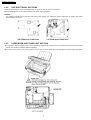
ORDER NO. KMF0501841C3
High Speed Laser Fax and Copier
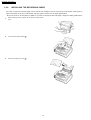
KX-FL612CX
KX-FL612CX-S
(for Asia, Middle Near East and Africa)
(for Saudi Arabia )
IMPORTANT INFORMATION ABOUT LEAD FREE, (PbF), SOLDERING
If lead free solder was used in the manufacture of this product the printed circuit boards will be marked PbF.
Standard leaded, (Pb), solder can be used as usual on boards without the PbF mark.
When this mark does appear please read and follow the special instructions described in this manual on the use of PbF and how
it might be permissible to use Pb solder during service and repair work.
© 2005 Panasonic Communications Co., Ltd. All
rights reserved. Unauthorized copying and
distribution is a violation of law.
KX-FL612CX / KX-FL612CX-S
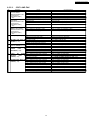
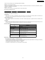
CONTENTS
Page
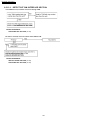
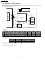
1 INTRODUCTION
1.1. ABOUT LEAD FREE SOLDER (PbF: Pb free)
Page
4
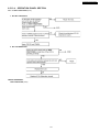
5.20. HOW TO REMOVE THE FUSER UNIT
55
4
5.21. HOW TO REMOVE THE CIS
56
5.22. NOTE FOR ASSEMBLING
57
5.23. INSTALLATION POSITION OF THE LEAD
58
1.2. HOW TO RECOGNISE THAT Pb FREE SOLDER IS
USED
5
1.3. SAFETY PRECAUTIONS
6
1.4. INSULATION RESISTANCE TEST
6
6.1. USER RECOVERABLE ERRORS
59
1.5. FOR SERVICE TECHNICIANS
6
6.2. PROGRAMMING AND LISTS
61
1.6. BATTERY CAUTION
6
6.3. TEST FUNCTIONS
64
1.7. AC CAUTION
7
6.4. REMOTE PROGRAMMING
68
1.8. PERSONAL SAFETY PRECAUTIONS
7
6.5. TROUBLESHOOTING DETAILS
76
1.9. SERVICE PRECAUTIONS
9
1.10. FOR BEST PERFORMANCE
9
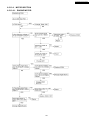
2 FEATURES AND SPECIFICATIONS
6 TROUBLESHOOTING GUIDE
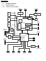
7 CIRCUIT OPERATIONS
59
147
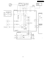
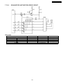
7.1. CONNECTION DIAGRAM
147
10
7.2. GENERAL BLOCK DIAGRAM
148
2.1. FEATURES
10
7.3. FACSIMILE SECTION
150
2.2. SPECIFICATIONS
11
7.4. NCU SECTION
161
2.3. OPTIONAL ACCESSORIES
11
7.5. ITS (Integrated telephone System) and MONITOR
3 INSTALLATION
SECTION
12
163
3.1. LOCATION OF CONTROLS
12
7.6. CIS CONTROL SECTION
165
3.2. CONNECTIONS
14
7.7. STEPPING MOTOR DRIVE SECTION
166
3.3. INSTALLATION
15
7.8. FAN MOTOR SECTION
170
7.9. SOLENOID DRIVE SECTION
172
4 MAINTENANCE
27
4.1. MAINTENANCE ITEMS AND COMPONENT LOCATIONS
7.10. LSU (Laser Scanning Unit) SECTION
173
27
7.11. SENSORS AND SWITCHES SECTION
175
4.2. PRINTING
29
7.12. OPERATION BOARD SECTION
184
4.3. PRINTING (PAPER PICK UP)
30
7.13. LCD SECTION
185
4.4. SCANNING (ADF)
31
7.14. HVPS (High Voltage Power Supply) SECTION
186
4.5. MAINTENANCE
32
7.15. HEAT LAMP CONTROL CIRCUIT
188
4.6. DOCUMENT JAMS
35
7.16. POWER SUPPLY BOARD SECTION
194
4.7. RECORDING PAPER JAMS
36
8 REFERENCE MATERIALS DATA
197
40
8.1. PRINTING OPERATION PRINCIPLE
5.1. UPPER MAIN CABINET SECTION
41
8.2. TERMINAL GUIDE OF THE ICs TRANSISTORS AND
5.2. LOWER MAIN CABINET SECTION
42
5.3. HOW TO REMOVE THE OPERATION PANEL ASS’Y
43
8.3. HOW TO REPLACE THE FLAT PACKAGE IC
206
5.4. HOW TO REMOVE THE PICK UP UNIT
44
8.4. DIGITAL BOARD SECTION
208
5.5. HOW TO REMOVE THE PICK UP ROLLER
45
8.5. MODEM SECTION
210
5.6. HOW TO REMOVE THE OPERATION BOARD
46
8.6. TEST CHART
216
5.7. HOW TO REMOVE THE LOWER FLAME
47
9 FIXTURES AND TOOLS
219
5.8. HOW TO REMOVE THE SEPARATION RUBBER
47
5.9. HOW TO REMOVE THE TRANSFER ROLLER
48
5.10. HOW TO REMOVE THE SEPARATION ROLLER
49
10.1. GENERAL SECTION
220
5.11. HOW TO REMOVE THE BOTTOM PLATE
50
10.2. OPERATION COVER SECTION (1)
221
5.12. HOW TO REMOVE THE ANALOG BOARD
50
10.3. OPERATION COVER SECTION (2)
222
5 DISASSEMBLY INSTRUCTIONS
DIODES
197
205
10 CABINET, MECHANICAL AND ELECTRICAL PARTS
LOCATION
5.13. HOW TO REMOVE THE HIGH VOLTAGE POWER
220
10.4. OPERATION COVER SECTION (3)
223
51
10.5. PICK UP SECTION
224
5.14. HOW TO REMOVE THE LASER UNIT
51
10.6. FUSER SECTION
225
5.15. HOW TO REMOVE THE FAN UNIT
52
10.7. UPPER MAIN CABINET SECTION
226
10.8. LOWER MAIN CABINET SECTION (1)
227
10.9. LOWER MAIN CABINET SECTION (2)
228
BOARD
5.16. HOW TO REMOVE THE LOW VOLTAGE POWER
BOARD
52
5.17. HOW TO REMOVE THE SOLENOID
53
5.18. HOW TO REMOVE THE HANDSET HOLDER
53
5.19. HOW TO REMOVE THE MAIN MOTOR
54
10.10. LOWER CABINET SECTION (3)
229
10.11. ACTUAL SIZE OF SCREWS AND WASHER
230
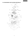
11 ACCESSORIES AND PACKING MATERIALS
2
231
KX-FL612CX / KX-FL612CX-S
232
15.1. ANALOG BOARD (PCB2)
248
12.1. CABINET AND ELECTRICAL PARTS
232
15.2. OPERATION BOARD (PCB3)
250
12.2. ACCESSORIES AND PACKING MATERIALS
234
15.3. HIGH VOLTAGE POWER SUPPLY BOARD (PCB4)
252
12.3. DIGITAL BOARD PARTS
234
15.4. LOW VOLTAGE POWER SUPPLY BOARD (PCB5)
253
12.4. ANALOG BOARD PARTS
237
15.5. EXIT SENSOR BOARD (PCB6)
254
12.5. OPERATION BOARD PARTS
239
15.6. DRUM AND TONER SENSOR BOARD (PCB7)
254
12.6. HIGH VOLTAGE POWER SUPPLY BOARD PARTS
240
15.7. VARISTOR BOARD (PCB8)
254
12.7. LOW VOLTAGE POWER SUPPLY BOARD PARTS
240
12.8. EXIT SENSOR BOARD PARTS
241
16.1. DIGITAL BOARD (PCB1)
255
12.9. DRUM AND TONER SENSOR BOARD PARTS
241
16.2. ANALOG BOARD (PCB2)
257
12.10. VARISTOR BOARD PARTS
241
16.3. OPERATION BOARD (PCB3)
259
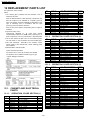
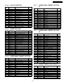
12 REPLACEMENT PARTS LIST
16 PRINTED CIRCUIT BOARD
255
12.11. FIXTURES AND TOOLS
241
16.4. HIGH VOLTAGE POWER SUPPLY BOARD (PCB4)
261
13 FOR THE SCHEMATIC DIAGRAMS
242
16.5. LOW VOLTAGE POWER SUPPLY BOARD (PCB5)
263
14 SCHEMATIC DIAGRAM
244
16.6. EXIT SENSOR BOARD PARTS (PCB6)
265
244
16.7. DRUM AND TONER SENSOR BOARD (PCB7)
265
248
16.8. VARISTOR BOARD (PCB8)
265
14.1. DIGITAL BOARD (PCB1)
15 SCHEMATIC DIAGRAM
3
KX-FL612CX / KX-FL612CX-S
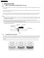
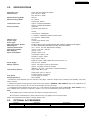
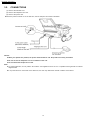
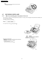
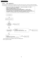
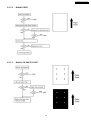
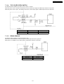
1 INTRODUCTION
1.1.
ABOUT LEAD FREE SOLDER (PbF: Pb free)
Note:
In the information below, Pb, the symbol for lead in the periodic table of elements, will refer to standard solder or solder that
contains lead.
We will use PbF solder when discussing the lead free solder used in our manufacturing process which is made from Tin, (Sn),
Silver, (Ag), and Copper, (Cu).
This model, and others like it, manufactured using lead free solder will have PbF stamped on the PCB. For service and repair
work we suggest using the same type of solder although, with some precautions, standard Pb solder can also be used.
Caution
• PbF solder has a melting point that is 50° ~ 70° F, (30° ~ 40°C) higher than Pb solder. Please use a soldering iron with
temperature control and adjust it to 700° ± 20° F, (370° ± 10°C). In case of using high temperature soldering iron, please
be careful not to heat too long.
• PbF solder will tend to splash if it is heated much higher than its melting point, approximately 1100°F, (600°C).
• If you must use Pb solder on a PCB manufactured using PbF solder, remove as much of the original PbF solder as possible
and be sure that any remaining is melted prior to applying the Pb solder.
• When applying PbF solder to double layered boards, please check the component side for excess which may flow onto the
opposite side (See figure, below).
1.1.1.
SUGGESTED PBF SOLDER
There are several types of PbF solder available commercially. While this product is manufactured using Tin, Silver, and Copper,
(Sn+Ag+Cu), you can also use Tin and Copper, (Sn+Cu), or Tin, Zinc, and Bismuth, (Sn+Zn+Bi). Please check the manufacturer’s specific instructions for the melting points of their products and any precautions for using their product with other
materials.
The following lead free (PbF) solder wire sizes are recommended for service of this product: 0.3mm, 0.6mm and 1.0mm.
4
KX-FL612CX / KX-FL612CX-S
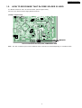
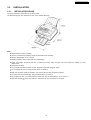
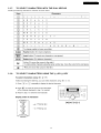
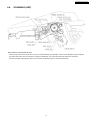
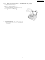
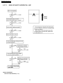
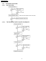
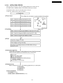
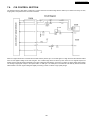
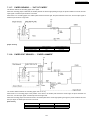
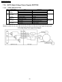
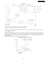
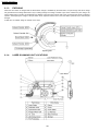
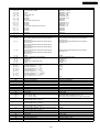
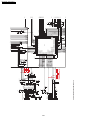
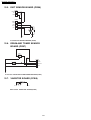
1.2.
HOW TO RECOGNISE THAT Pb FREE SOLDER IS USED
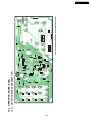
P.C.Boards marked as “PbF” use Pb Free solder. (See the figure below.)
Pb Free is not used the Power Supply Board of this unit.
BAT600
6
R724
CN614
1
R747
5
8
R610 R613
C608
R611
E E
C734
CN613
R737
E
Q620
L648
D608
C726
1
IC610
Q616 Q617
1
E
RA609 +3.3V/BAT
D602
L632
CN610
4
L630
16
J600
C648
8
PFUP1330YA
5
1
R722
L620 C731
C717
R723
1
Q613
R736
C666
E
Q622
1
C728
25 F605
RA602
26
L643
L605
L606
L604
8
25
C668
50
RA610
C721
CN612
8
Q623 Q615
E E
C736
C719
L621
L642
P_RTS
51
IC605
IC608
C720
R708
1
L654
75
Q614
E
+2.5V
C672
C738
L618
L619
100
L657 L655
L656
R768
R769
R767
REF-CH
E
L661
L660
L659
C694
L653
Q609
76
R704
R706
C706
C705
L623
L624
L625
L626
L658
E
C695
R707
X603
C697
C667
TP_AMON
TO-CH
R700
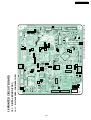
(Example :Digital board)
PbF
9
D607
+24V
MARKED
KX-FL512CX DIGITAL BOARD (PCB4) COMPONENT VIEW
Note : The “PbF” marked may be found on different areas of the same P.C.Board,depending on manufacture date.
5
KX-FL612CX / KX-FL612CX-S
1.3.
SAFETY PRECAUTIONS
1. Before servicing, unplug the AC power cord to prevent an electric shock.
2. When replacing parts, use only the manufacturer´s recommended components.
3. Check the condition of the power cord. Replace if wear or damage is evident.
4. After servicing, be sure to restore the lead dress, insulation barriers, insulation papers, shields, etc.
5. Before returning the serviced equipment to the customer, be sure to perform the following insulation resistance test to prevent
the customer from being exposed to shock hazards.
1.4.
INSULATION RESISTANCE TEST
1. Unplug the power cord and short the two prongs of the plug with a jumper wire.
2. Turn on the power switch.
3. Measure the resistance value with an ohmmeter between the jumpered AC plug and each exposed metal cabinet part
(screw heads, control shafts, bottom frame, etc.).
Note: Some exposed parts may be isolated from the chassis by design. These will read infinity.
4. If the measurement is outside the specified limits, there is a possibility of a shock hazard.
1.5.
FOR SERVICE TECHNICIANS
ICs and LSIs are vulnerable to static electricity.
When repairing, the following precautions will help prevent recurring malfunctions.
1. Cover the plastic part´s boxes with aluminum foil.
2. Ground the soldering irons.
3. Use a conductive mat on the worktable.
4. Do not touch the IC or LSI pins with bare fingers.
1.6.
BATTERY CAUTION
CAUTION
There is a danger of explosion if the battery is incorrectly replaced. Replace only with the same or equivalent type
recommended by the manufacturer. Dispose used batteries according to the manufacturerís instructions:
The lithium battery is a critical component (type No. CR-2032/V9A). Please observe for the proper polarity and exact location
when replacing and soldering the replacement battery.
6
KX-FL612CX / KX-FL612CX-S
1.7.
AC CAUTION
For safety, before closing the lower cabinet, please make sure of the following precautions.
1. The earth lead is fixed with the screw.
2. The AC connector is connected properly.
3. Wind the earth lead around the core 4 times.
4. Wind the earth AC around the core 4 times.
1.8.
1.8.1.
PERSONAL SAFETY PRECAUTIONS
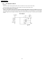
MOVING SECTIONS OF THE UNIT
Be careful not to let your hair, clothes, fingers, accessories, etc., become caught in any moving sections of the unit.
The moving sections of the unit are the rollers and a gear. There is a separation roller and a document feed roller which are rotated
by the document feed motor. A gear rotates the two rollers. Be careful not to touch them with your hands, especially when the unit
is operating.
7
KX-FL612CX / KX-FL612CX-S
1.8.2.
LIVE ELECTRICAL SECTIONS
All the electrical sections of the unit supplied with AC power by the AC power cord are live.
Never disassemble the unit for service with the AC power supply plugged in.
CAUTION:
AC voltage is supplied to the primary side of the power supply unit. Therefore, always unplug the AC power cord before
disassembling for service.
1.8.3.
LASER BEAM AND FUSER UNIT SECTION
• The printer of this unit utilizes a laser. Use of controls or adjustments or performance of procedures other than those specified
herein may result in hazardous radiation exposure.
• The fuser unit is inside of the unit and gets hot. Do not touch it when removing the jammed paper or cleaning the lower glass.
8
KX-FL612CX / KX-FL612CX-S
1.9.
1.9.1.
SERVICE PRECAUTIONS
PRECAUTIONS TO PREVENT DAMAGE FROM STATIC ELECTRICITY
Electrical charges accumulate on a person. For instance, clothes rubbing together can damage electric elements or change their
electrical characteristics. In order to prevent static electricity, touch a metallic part that is grounded to release the static electricity.
Never touch the electrical sections such as the power supply unit, etc.
1.10. FOR BEST PERFORMANCE
• To extend the life of the drum unit, the unit should never be turned OFF immediately after printing. Leave the power turned ON
for a minimum of 30 minutes after printing.
• In the printing process, heat is used to fuse toner onto the page. As a result, it is normal for the machine to produce an odor
during and shortly after printing. Be sure to use this unit in an area with proper ventilation.
• Do not cover slots or openings on the unit. Inspect the air circulation vents regularly and remove any dust build-up with a
vacuum cleaner.
• If the inside of the unit is dirty, clean it with a soft and dry cloth (especially the lower glass).
• When replacing the toner cartridge or drum unit, do not allow dust, water, or liquids to come in contact with the drum. This may
affect print quality.
• Store unused paper in the original packaging, in a cool and dry place. Not doing so may affect print quality.
• Do not place the unit in an area where the paper tray may be obstructed (i.e., by a wall,etc.).
• Keep the air circulation vents away from walls etc.more than 50 mm (1 31 / ") to let the unit cool down.
9
KX-FL612CX / KX-FL612CX-S
2 FEATURES AND SPECIFICATIONS
2.1.
FEATURES
General
• Help function
Display:
1. BASIC SETTINGS
2. FEATURE LIST
3. DIRECTORY
4. FAX SENDING/RECEIVING
5. COPIER
6. REPORTS
7. CALLER ID
• LCD (Liquid Crystal Display) readout
• TAM (Telephone answering machine) interface
Plain Paper Facsimile Machine
• Letter/A4/Legal, G3 compatible
• Automatic document feeder (20 sheets)
• Quick scan
• Resolution: Standard/Fine/Super fine/Photo/Photo with text.
(64 level)
− STANDARD: For printed or typewritten originals with
normal-sized characters.
− FINE: For originals with small printing.
− SUPER FINE: For originals with very small printing.
− PHOTO: For originals containing photographs, shaded
drawing,etc.
− PHOTO WITH TEXT:
photograph and text.
For
originals
containing
• Broad cast
• 250-sheet paper capacity (60 g/m2~ 75 g/m2)
• Distinctive ring detection.
Integrated Telephone System
• On-hook dialing
• Monitor speaker
• Voice muting
• Redialing function
• Station telephone directory
Enhanced Copier Function
• Multi-copy function (up to 99 copies)
• Enlargement and reduction
• Collate
• 64-Level halftone
10
KX-FL612CX / KX-FL612CX-S
2.2.
SPECIFICATIONS
Applicable Lines:
Document Size:
Public Switched Telephone Network
Max. 216 mm in width
Effective Scanning Width:
Effective Printing Width:
Max. 600 mm in length
208 mm
A4 : 202mm
Transmission Time*:
Letter/Legal : 208mm
Approx. 6 s/page (ECM-MMR)**
Scanning Density:
Approx. 8 s/page (ECM-MMR)***
Horizontal:
8 pels/mm (203 pels/inch)
Vertical:
3.85 lines/mm -STANDARD
7.7 lines/mm -FINE/PHOTO/PHOTO WITH TEXT
Halftone Level:
Scanner Type:
Printer Type:
Data Compression System:
Modem Speed:
Operating Environment:
Dimensions (H×W×D):
Mass (Weight):
Power Consumption:
15.4 lines/mm -SUPER FINE
64-level
Contact Image Sensor (CIS)
Laser printer
Modified Huffman (MH), Modified READ (MR), Modified, Modified READ (MMR)
14,400/12,000/9,600/7,200/4,800/2,400 bps; Automatic Fallback
10°C—32.5°C, 20—80% RH (Relative Humidity)
370 mm × 430 mm × 480 mm
Approx. 9.2 kg
Standby: Approx. 4 W
Transmission: Approx. 12W
Reception: Approx. 290 W
Copy: Approx. 290 W
Power Supply:
Memory Capacity:
Maximum: Approx. 950W (When the fuser lamp turns on)
220-240 V AC, 50/60Hz
Approx. 120 pages of memory transmission.
Approx. 170 pages of memory reception.
Laser diode properties:
(Based on ITU-T No. 1 Test Chart in standard resolution.)
Laser output: Max. 5 mW
Wave length: 760 nm—800 nm
Print Speed:
Printing Resolution:
Emission duration: Continuous
14 ppm (page per minute)
600 × 600 dpi
* Transmission speed depends upon the contents of the pages, resolution, telephone line conditions and capability of the other
party’s machine.
** Transmission speed is based upon the Original Test Chart. (Refer to ORIGINAL TEST CHART(P.216).) If the capability of the
other party´s machine is inferior to your unit, the transmission time may be longer.
*** Transmission speed is based upon the ITU-T No. 1 Test Chart and original mode. (Refer to ITU-T No.1 TEST CHART(P.217).)
If the capability of the other party´s machine is inferior to your unit, the transmission time may be longer.
Note:
• Any details given in these instructions are subject to change without notice.
• The pictures and illustrations in these instructions may vary slightly from the actual product.
Design and specifications are subject to change without notice.
2.3.
OPTIONAL ACCESSORIES
Model No.
KX-FA83E or KX-FA83A
KX-FA84E or KX-FA84A
Description
Specifications
Toner cartridge
Drum unit
1 toner cartridge
1 drum unit
11
KX-FL612CX / KX-FL612CX-S
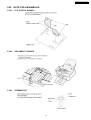
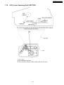
3 INSTALLATION
3.1.
3.1.1.
LOCATION OF CONTROLS
OVERVIEW
12
KX-FL612CX / KX-FL612CX-S
3.1.2.
CONTROL PANEL
13
KX-FL612CX / KX-FL612CX-S
3.2.
CONNECTIONS
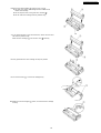
(1) Connect the handset cord.
(2) Connect the telephone line cord.
(3) Connect the power cord.
• When the power is turned on for the first time, the unit will print some basic information.
Caution:
• When you operate this product, the power outlet should be near the product and easily accessible.
• Be sure to use the telephone line cord included in this unit..
• Do not extend the telephone line cord.
Note:
• To avoid malfunction, do not position fax machine near appliances such as TVs or speakers which generate an intense
magnetic field.
• If any other device is connected on the same line, this unit may disturb the network condition of the device.
14
KX-FL612CX / KX-FL612CX-S
3.3.
3.3.1.
INSTALLATION
INSTALLATION SPACE
The space required to install the unit is shown below.
The dimensions given are necessary for the unit to operate efficiently.
Note:
• Avoid excessive heat or humidity.
• Use the unit within the following ranges of temperature and humidity.
• Ambient temperature: 10°C to 32.5°C
• Relative humidity: 20% to 80% (without condensation)
• Power cord length should be less than 5 meters (16.4 feet). Using a longer cord may reduce the voltage or cause
malfunctions.
• Avoid direct sunlight.
• Do not install near devices which contain magnets or generate magnetic fields.
• Do not subject the unit to strong physical shock or vibration.
• Keep the unit clean. Dust accumulation can prevent the unit from functioning properly.
• To protect the unit from damage, hold both sides when you move it.
• Do not place the unit in an area where the paper tray may be obstructed (i.e., by a wall, etc.)
• Keep this surface ( ) away from walls etc. more than 50 mm to let the unit cool down.
15
KX-FL612CX / KX-FL612CX-S
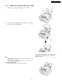
3.3.2.
PAPER STACKER
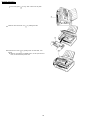
Line up the slots ( ) in the paper stacker with the pegs ( ) on the
bottom of the unit, then insert the two tabs of the paper stacker into the
slots on the unit ( ).
• Do not place the unit in an area where the paper stacker may be
easily bumped into.
• Document and recording paper will be ejected from the front of the
unit. Do not place anything in front of the unit.
• The paper stacker can hold up to approximately 100 sheets of
printed paper. Remove the printed paper before the paper stacker
becomes full.
3.3.3.
DOCUMENT STACKER
Pull the document stacker ( ) forward gently until it clicks into place,
then press the center part of the document stacker ( ) to open the
extender ( ).
16
KX-FL612CX / KX-FL612CX-S
3.3.4.
PAPER TRAY AND PAPER TRAY COVER
1.
Insert the paper tray ( ) into the slot ( ) on the back of the unit.
2.
Pull the tension plate forward ( ) and attach the paper tray cover ( ),
then push the tension plate back ( ).
Note:
• Do not place the unit in an area where the paper tray may be
obstructed (i.e., by a wall etc.).
) away from walls etc. more than 50 mm (1
• Keep this surface (
31/32") to let the unit cool down.
To remove the paper tray
Pull the paper tray forward in the direction of the arrow.
17
KX-FL612CX / KX-FL612CX-S
3.3.5.
INSTALLING THE RECORDING PAPER
A4, Letter or legal size recording paper can be used for fax messages. The unit can hold up to 250 sheets of 60/75 g/m2 to
paper, 230 sheets of 80 g/m2 or 200 sheets of 90 g/m2 paper. See the note for paper specifications.
• The unit is set for A4 size paper by default. If you want to use legal or letter size paper, change the setting (feature #16).
1.
Before inserting a stack of paper, fan the paper to prevent paper
jams.
2.
Pull the tension plate forward ( ).
3.
Remove the paper tray cover ( ).
18
KX-FL612CX / KX-FL612CX-S
4.
Insert the paper, print-side down ( ).
• The paper should not be over the tabs ( ).
• If the paper is not inserted correctly, readjust the paper, or the
paper may jam.
5.
Attach the paper tray cover ( ).
6.
Push the tension plate back ( ).
To use A4 size paper
Insert the tabs on the A4 paper guides ( ) into the slots.
• “L” is shown on the A4 paper guide for the left side. “R” is shown
on the A4 paper guide for the right side.
Note:
• When you use letter or legal paper, you do not need to install the
A4 paper guides.
• Change the recording paper size to “A4” (feature #16).
19
KX-FL612CX / KX-FL612CX-S
3.3.6.
3.3.6.1.
DOCUMENTS THE UNIT CAN SEND
USING THE ADF (AUTO DOCUMENT FEEDER)
Note:
• Remove chips, staples or other similar fasteners.
• Do not send the following types of documents. (Use copies for fax transmission.)
— Chemically treated paper such as carbon or carbonless duplicating paper
— Electrostatically charged paper
— Badly curled, creased or torn paper
— Paper with a coated surface
— Paper with a faint image
— Paper with printing on the opposite side that can be seen through the other side (i.e. newspaper)
Note for the auto document feeder and the scanner glass
• Check that ink, paste or correction fluid has dried completely.
• To transmit the document with a width of less than A4 size (210 mm), we recommend using a copy machine to copy the
original document onto letter-sized paper, then transmitting the copied document.
20
KX-FL612CX / KX-FL612CX-S
3.3.7.
TO SELECT CHARACTERS WITH THE DIAL KEYPAD
Pressing the dial keys will select a character as shown below.
3.3.8.
TO SELECT CHARACTERS USING THE (+) OR (-) KEY
21
KX-FL612CX / KX-FL612CX-S
3.3.9.
SETTING YOUR LOGO
The logo can be your company, division or name.
22
KX-FL612CX / KX-FL612CX-S
3.3.10. REPLACING THE TONER CARTRIDGE AND THE DRUM UNIT
When the display shows the following, replace the toner cartridge.
We recommend you replace the drum unit every fourth time you replace the toner cartridge. To check the drum life and quality,
please print the printer test list.
To ensure that the unit operates properly, we recommend the use of Panasonic toner cartridge (Model No. KX-FA83E/KXFA83A) and drum unit (Model No. KX-FA84E/KX-FA84A).
Caution:
• We cannot be responsible for any damage to the unit or degradation of print quality which may occur from the use
of non-Panasonic toner cartridge and drum unit.
• The drum unit contains a photosensitive drum. Exposing it to light may damage the drum. Once you have opened
the protection bag:
—Do not expose the drum unit to light for more than 5 minutes.
—Do not touch or scratch the green drum surface.
—Do not place the drum unit near dust or dirt, or in a high humidity area.
—Do not expose the drum unit to direct sunlight.
• Do not unplug the fax machine to prevent loss of fax documents in memory.
• Do not leave the toner cartridge out of the protection bag for a long time. It will decrease the toner life.
• Do not pour any toner into the toner cartridge.
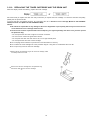
1. Before opening the protection bag of the new toner cartridge, shake
it vertically more than 5 times.
2. Remove the new toner cartridge from the protection bag.
Peel off the seal ( ) from the toner cartridge.
23
KX-FL612CX / KX-FL612CX-S
3. Lift open the front cover ( ), holding OPEN ( ).
4. Tap on the used toner cartridge several times to allow the remaining
toner to fall into the drum unit. Remove the drum and toner unit ( )
by holding the two tabs.
• Do not touch the transfer roller ( ).
• If you replace the toner cartridge and the drum unit at the same
time, skip to step 7.
5. Turn the two levers ( ) on the used toner cartridge firmly, until the
triangles ( ) match.
24
KX-FL612CX / KX-FL612CX-S
6. Remove the used cartridge ( ) from the drum unit ( ).
• The toner may stick to the cartridge and the drum unit. Be
careful when handling.
• Do not drop the toner on the green drum surface ( ).
• Put the used toner cartridge into the protection bag.
7. If you replace the drum unit at the same time, remove the new drum
unit from the protection bag.
Place the toner cartridge ( ) into the drum unit ( ) vertically.
8. Firmly press down the toner cartridge to snap into position.
9. Turn the two levers ( ) on the toner cartridge firmly.
10. Make sure that the triangles ( ) match, to install the toner cartridge
correctly.
25
KX-FL612CX / KX-FL612CX-S
• If the lower glass ( ) is dirty, clean it with a soft dry cloth.
11. Install the drum and toner unit ( ) by holding the tabs.
12. Close the front cover ( ) by pushing down on both sides, until
locked.
• While the unit displays “PLEASE WAIT”, do not open the front
cover, or disconnect the power cord.
26
KX-FL612CX / KX-FL612CX-S
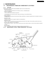
4 MAINTENANCE
4.1.
4.1.1.
MAINTENANCE ITEMS AND COMPONENT LOCATIONS
OUTLINE
MAINTENANCE AND REPAIRS ARE PERFORMED USING THE FOLLOWING STEPS.
1. Periodic maintenance
Inspect the equipment periodically and if necessary, clean any contaminated parts.
2. Check for breakdowns
Look for problems and consider how they arose.
If the equipment can be still used, perform copying, self testing or communication testing.
3. Check equipment
Perform copying, self testing and communication testing to determine if the problem originates from the transmitter, receiver or
the telephone line.
4. Determine causes
Determine the causes of the equipment problem by troubleshooting.
5. Equipment repairs
Repair or replace the defective parts and take appropriate measures at this stage to ensure that the problem will not recur.
6. Confirm normal operation of the equipment
After completing the repairs, conduct copying, self testing and communication testing to confirm that the equipment operates
normally.
7. Record keeping
Make a record of the measures taken to rectify the problem for future reference.
4.1.2.
MAINTENANCE CHECK ITEMS/COMPONENT LOCATIONS
27
KX-FL612CX / KX-FL612CX-S
4.1.2.1.
NO.
1
2
Maintenance List
OPERATION
Document Path
Rollers
CHECK
REMARKS
Remove any foreign matter such as paper.
—
If the roller is dirty, clean it with a damp cloth then dry Refer to MAINTENANCE CHECK
thoroughly.
ITEMS/COMPONENT LOCATIONS(
P.27).()
Sensors
Document sensor (PS500), Paper feed sensor (PS501), Printer See MAINTENANCE CHECK
cover open switch (SW101),ADF cover open sensor (SW501), ITEMS/COMPONENT LOCATIONS(P.27)
FB cover open sensor (SW500), ADF CIS position sensor and SENSORS AND SWITCHES
(PS502),FB CIS position sensor (PS503)Resist sensor (PC201) SECTION(P.175)TEST FUNCTIONS(P.64)
,Paper exit sensor (PS50). Paper sensor (PS1)Confirm the
operation of the sensors.
Glass
If the glass is dirty, clean them with a dry soft cloth.
Refer to MAINTENANCE(P.32).
Abnormal, wear and tear Replace the part. Check if the screws are tight on all parts.
—
or loose parts
3
4
5
4.1.2.2.
Maintenance Cycle
No.
Item
Cleaning Cycle
1
ADF Separation Roller (Ref.No.50)
3 months
2
Paper Feed Roller (Ref.No.154)
3 months
3
ADF Separation Rubber (Ref. No.35)
3 months
4
ADF Exit Roller (Ref.No.34)
3 months
5
Pick up Roller (Ref No.108)
3 months
6
Separation Rubber (Ref. No.99)
3 months
7
Document Feed Roller (Ref.No.154)
3 months
8
Transfer Roller (Ref.No.73)
3 months
9
Pressure Roller (Ref.No.120)
3 months
10
Heat Roller (Ref.No.127)
3 months
11
Exit Roller (Ref.No.142)
3 months
If each part has got dirty, clean it with a damp cloth then dry thoroughly.
* These values are standard and may vary depending on usage conditions.
28
Replacement
Cycle
Procedure
7 years* (100,000 documents) Refer to HOW TO REMOVE THE
SEPARATION ROLLER (P.49).
7 years (100,000 documents) Refer to HOW TO REMOVE THE
SEPARATION RUBBER (P.47).
7 years (100,000 documents) Refer to HOW TO REMOVE THE
SEPARATION RUBBER (P.47).
7 years (100,000 documents) Refer to HOW TO REMOVE THE
SEPARATION RUBBER (P.47).
7 years (100,000 documents) Refer to HOW TO REMOVE THE
PICK UP UNIT (P.45).
7 years (100,000 documents) Refer to HOW TO REMOVE THE
PICK UP ROLLER (P.44).
7 years (100,000 documents) Refer to
HOW TO REMOVE THE
SEPARATION RUBBER (P.47)
7 years (100,000 documents) Refer to HOW TO REMOVE THE
TRANSFER ROLLER (P.48).
7 years (100,000 documents) Refer to FUSER SECTION
(P.225).
7 years (100,000 documents) Refer to FUSER SECTION
(P.225).
7 years (100,000 documents) Refer to FUSER SECTION
(P.225).
KX-FL612CX / KX-FL612CX-S
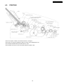
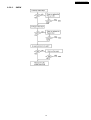
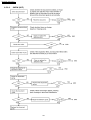
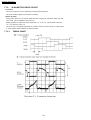
4.2.
PRINTING
• The motor pinion rotates in the direction shown in the figure.
• The gears of fixing and developing parts are driven by the GEAR IDLER 67.
• The GEAR PAPER FEED ROLLER drives the roller.
• The GEAR CLUTCH runs idle and GEAR PICKUP PAPER is still.
29
KX-FL612CX / KX-FL612CX-S
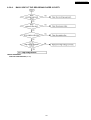
4.3.
PRINTING (PAPER PICK UP)
During printing
• When the SOLENOID is turned ON, the LEVER PICK UP CLUTCH is hooked on the RING of GEAR CLUTCH. It causes
the GEAR PICKUP PAPER to rotate.
• The recording paper is pressed by the PICKUP ROLLER and the top paper is separated and fed.
• Even the SOLENOID is turned OFF, it can not stop on the way of a turn because the tip of LEVER PICK UP CLUTCH is
on the CAM of GEAR PICKUP PAPER.
• When the tip of LEVER PICK UP CLUTCH returns to CAM´s home position, the GEAR CLUTCH RING is unhooked, then
the GEAR PICKUP PAPER is stopped.
30
KX-FL612CX / KX-FL612CX-S
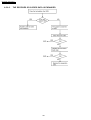
4.4.
SCANNING (ADF)
• DOCUMENT TRANSMISSION (ADF)
When the tip of the document is set to a point of contact between the separation roller and the separation pad through the
document feed roller, then the document is fed there separately. The document feed roller carries the document
and the CIS reads it through the glass. The document is exited through the document feed roller.
31
KX-FL612CX / KX-FL612CX-S
4.5.
MAINTENANCE
If a black line, a white line or a dirty pattern appears on your recording paper, on your original, or on the fax document received
by the other party, clean the white plate, scanner glass and lower glass.
4.5.1.
CLEANING THE INSIDE OF THE UNIT
If any of the following problems occurs, clean the inside of the unit:
— Document frequently misfeed.
— Black line, a white line or a dirty pattern appear on the original document when sending or copying.
Caution:
• Be careful when handling the drum and toner unit.
• Do not use paper products, such as paper towels or tissues, to clean inside of the unit.
1. Disconnect the power cord and the telephone line cord.
2. Lift open the front cover ( ) , holding OPEN ( ).
3. Clean the document separation roller ( ) with a cloth moistened with
isopropyl rubbing alcohol, and let all parts dry thoroughly.
4. Hold the center part of the front cover ( ), and pull open the inner
cover ( ).
• Do not touch the transfer roller ( ).
32
KX-FL612CX / KX-FL612CX-S
5. Clean the document feeder roller ( ) with a cloth moistened with
isopropyl rubbing alcohol, and let all parts dry thoroughly.
Clean the upper glass ( ) with a soft and dry cloth.
6. Push back the inner cover.
7. Remove the drum and toner unit ( ) by holding the two tabs.
8. Clean the lower glass ( ) with a soft and dry cloth.
9. Reinstall the drum and toner unit ( ) by holding the tabs.
33
KX-FL612CX / KX-FL612CX-S
10. Close the front cover ( ) by pushing down on both sides, until
locked.
11. Reconnect the power cord and the telephone line cord.
Note:
• Do not touch the transfer roller ( ).
34
KX-FL612CX / KX-FL612CX-S
4.6.
DOCUMENT JAMS
If the unit does not release the document during feeding, remove the jammed document as follows.
1. Lift open the front cover ( ), holding OPEN ( ).
2. Hold the center part of the front cover ( ), and pull open the
inner cover ( ).
• Do not touch the transfer roller ( ).
3. Remove the jammed document carefully ( ).
4. Push back the inner cover.
5. Close the front cover ( ) by pushing down on both sides,
until locked.
35
KX-FL612CX / KX-FL612CX-S
Note:
• Do not pull out the jammed document forcibly before
opening the front cover.
4.7.
4.7.1.
RECORDING PAPER JAMS
When the recording paper has jammed in the unit
If the unit does not eject any recording paper during reception or copying, the recording paper has jammed and the display will
show the following massage.
The display will show the following.
1. Lift open the front cover ( ), holding OPEN ( ).
2. Remove the jammed paper.
When the recording paper has jammed near the drum and
toner unit:
Remove the jammed paper ( ) carefully
by pulling it toward you.
• Do not touch the transfer roller ( ).
36
KX-FL612CX / KX-FL612CX-S
When the recording paper has jammed near the recording
paper exit:
2-1. Pull the tension plate forward ( ), then remove the paper tray
cover ( ).
2-2. Remove the recording paper ( ), then remove the drum and
toner unit ( ) to allow the jammed paper ( ) to pull free from the
rear cabinet.
2-3. Lift both green levers ( ) forward until they stop.
2-4. Remove the jammed paper ( ) from the fuser unit by pulling
it upwards carefully, then install the drum and toner unit.
37
KX-FL612CX / KX-FL612CX-S
2-5. Push back the levers ( ) to the original position.
3. Close the front cover ( ) by pushing down on both sides, until
locked.
4.
Re-insert the recording paper ( ).
• Before re-inserting, make sure to fan and straighten the
recording paper.
5.
Attach the paper tray cover ( ), then push back the tension plate
( ).
38
KX-FL612CX / KX-FL612CX-S
4.7.2.
When the recording paper is not fed into the unit properly
The display will show the following.
1. Pull the tension plate forward ( ), then remove the paper tray
cover ( ). Remove the recording paper ( ).
2.
Re-insert the recording paper. Attach the paper tray cover, then
push back the tension plate.
• Before re-inserting, make sure to fan and straighten the
recording paper.
39
KX-FL612CX / KX-FL612CX-S
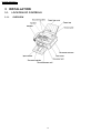
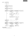
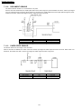
5 DISASSEMBLY INSTRUCTIONS
40
KX-FL612CX / KX-FL612CX-S
5.1.
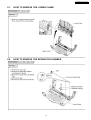
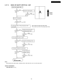
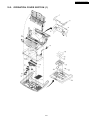
UPPER MAIN CABINET SECTION
CROSS REFERENCE:
A1: HOW TO REMOVE THE OPERATION PANEL ASS’Y (P.43)
A2: HOW TO REMOVE THE PICK UP UNIT (P.44)
A3: HOW TO REMOVE THE PICK UP ROLLER (P.45)
A4: HOW TO REMOVE THE OPERATION BOARD (P.46)
A5: HOW TO REMOVE THE LOWER FLAME (P.47)
A6: HOW TO REMOVE THE SEPARATION RUBBER (P.47)
A7: HOW TO REMOVE THE TRANSFER ROLLER (P.48)
A8: HOW TO REMOVE THE SEPARATION ROLLER (P.49)
41
KX-FL612CX / KX-FL612CX-S
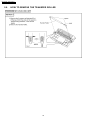
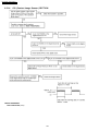
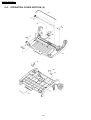
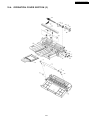
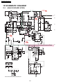
5.2.
LOWER MAIN CABINET SECTION
CROSS REFERENCE:
B1: HOW TO REMOVE THE BOTTOM PLATE (P.50)
B2: HOW TO REMOVE THE ANALOG BOARD (P.50)
B3: HOW TO REMOVE THE HIGH VOLTAGE POWER BOARD (P.51)
B4: HOW TO REMOVE THE LASER UNIT (P.51)
B5: HOW TO REMOVE THE FAN UNIT (P.52)
B6: HOW TO REMOVE THE LOW VOLTAGE POWER BOARD (P.52)
B7: HOW TO REMOVE THE SOLENOID (P.53)
B8: HOW TO REMOVE THE HANDSET HOLDER (P.53)
B9: HOW TO REMOVE THE MAIN MOTOR (P.54)
B10: HOW TO REMOVE THE FUSER UNIT (P.55)
C1: HOW TO REMOVE THE CIS (P.56)
42
KX-FL612CX / KX-FL612CX-S
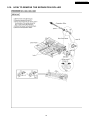
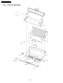
5.3.
HOW TO REMOVE THE OPERATION PANEL ASS’Y
43
KX-FL612CX / KX-FL612CX-S
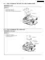
5.4.
HOW TO REMOVE THE PICK UP UNIT
44
KX-FL612CX / KX-FL612CX-S
5.5.
HOW TO REMOVE THE PICK UP ROLLER
45
KX-FL612CX / KX-FL612CX-S
5.6.
HOW TO REMOVE THE OPERATION BOARD
46
KX-FL612CX / KX-FL612CX-S
5.7.
HOW TO REMOVE THE LOWER FLAME
5.8.
HOW TO REMOVE THE SEPARATION RUBBER
47
KX-FL612CX / KX-FL612CX-S
5.9.
HOW TO REMOVE THE TRANSFER ROLLER
48
KX-FL612CX / KX-FL612CX-S
5.10. HOW TO REMOVE THE SEPARATION ROLLER
49
KX-FL612CX / KX-FL612CX-S
5.11. HOW TO REMOVE THE BOTTOM PLATE
5.12. HOW TO REMOVE THE ANALOG BOARD
50
KX-FL612CX / KX-FL612CX-S
5.13. HOW TO REMOVE THE HIGH VOLTAGE POWER BOARD
5.14. HOW TO REMOVE THE LASER UNIT
51
KX-FL612CX / KX-FL612CX-S
5.15. HOW TO REMOVE THE FAN UNIT
5.16. HOW TO REMOVE THE LOW VOLTAGE POWER BOARD
52
KX-FL612CX / KX-FL612CX-S
5.17. HOW TO REMOVE THE SOLENOID
5.18. HOW TO REMOVE THE HANDSET HOLDER
53
KX-FL612CX / KX-FL612CX-S
5.19. HOW TO REMOVE THE MAIN MOTOR
54
KX-FL612CX / KX-FL612CX-S
5.20. HOW TO REMOVE THE FUSER UNIT
55
KX-FL612CX / KX-FL612CX-S
5.21. HOW TO REMOVE THE CIS
56
KX-FL612CX / KX-FL612CX-S
5.22. NOTE FOR ASSEMBLING
5.22.1. FCC (DIGITAL BOARD)
5.22.2. DOCUMENT STACKER
5.22.3. THERMOSTAT
57
KX-FL612CX / KX-FL612CX-S
5.23. INSTALLATION POSITION OF THE LEAD
58
KX-FL612CX / KX-FL612CX-S
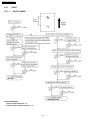
6 TROUBLESHOOTING GUIDE
6.1.
USER RECOVERABLE ERRORS
If the unit detects a problem, one or more of the following messages will appear on the display.
The explanations given in the [ ] are for servicemen only.
DISPLAY MESSAGE
CAUSE AND REMEDY
• Polygon motor error.
Refer to CALL SERVICE 1 (P.84).
• Laser beam error. Replace LSU unit.
Refer to CALL SERVICE 2 (P.85).
• Fuser unit cannot heat up. Replace fuser unit.
Refer to CALL SERVICE 3 (P.86).
• Fan motor error. Replace fan motor.
Refer to CALL SERVICE 4 (P.87).
• There is something wrong with the drum unit. Replace the drum unit and the toner cartridge.
• The document is not fed into the unit properly. Reinsert the document. If misfeeding occurs frequently,
clean the document feeder rollers and try again.
• The drum unit is not inserted properly. Reinsert it correctly.
• The installed drum is worn out. Replace the drum unit with a new one.
• The memory (telephone numbers, parameters, etc.) has been erased. Re-program.
• The front cover is open. Close it.
• There is no space to store new entries in navigator directory. Erase unnecessary entries.
• The drum life is complete. Replace the drum unit immediately.
• Recording paper was not fed into the unit properly. Reinsert the recording paper.
• The unit has a document in memory. See the other displayed message instructions to print out the
document.
• The memory is full of received documents due to lack of recording paper or a recording paper jam, etc.
Install paper or clear the jammed paper.
• When performing memory transmission, the document being stored exceeds the memory capacity of the
unit. Transmit the entire document manually.
• The inside of the unit is extremely cold and cannot be operated. Use the unit in a warmer area. While the
unit cannot be operated, the received documents are temporarily stored into the memory, and will be
printed out automatically when the unit warms up.
• When making a copy, the document being stored exceeds the memory capacity of the unit. Press STOP
to clear the message. Divide the document into sections.
• There is something wrong with the modem circuit.
• The other party´s fax machine is busy or has run out of recording paper. Try again.
• Recording paper is not installed or the unit has run out of paper. Install paper.
• Recording paper is not fed into the unit properly. Reinstall paper.
• A recording paper jam occurred. Clear the jammed paper.
[If the printout jams, please refer to RECORDING PAPER JAMS (P.36).]
• The unit is warming up. Wait for a while.
• The other party’s fax machine does not offer the polling function. Check with the other party.
• The other party´s fax machine is busy or has run out of recording paper. Try again.
59
KX-FL612CX / KX-FL612CX-S
DISPLAY MESSAGE
CAUSE AND REMEDY
• The document is jammed. Remove the jammed document.
• Attempted to transmit a document longer than 600 mm (23 5/8”). Press the STOP
document. Divide the document into two or more sheets and try again.
to remove the
• [Alternately, turn off service code #559 to enable sending of documents longer than 600 mm] (Refer to
DOCUMENT JAMS (P.35).)
• The drum life is near to the end. Replace the drum unit as soon as possible.
• The toner life is complete. Replace the toner cartridge immediately.
• The toner life is near to the end. Replace the toner cartridge as soon as possible.
• A transmission error occurred. Try again.
• The inside of the unit is too cold. Let the unit warm up. Wait for a while.
• The fax message was printed on paper which is shorter than letter size paper. Use the appropriate size
paper.
60
KX-FL612CX / KX-FL612CX-S
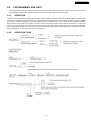
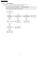
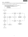
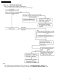
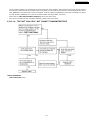
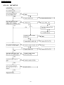
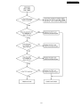
6.2.
PROGRAMMING AND LISTS
The programming functions are used to program the various features and functions of the machine, and to test the machine.
This facilitates communication between the user and the service man while programming the unit.
6.2.1.
OPERATION
There are 2 basic categories of programming functions, the User Mode and the Service Mode. The Service Mode is further broken
down into the normal and special programs. The normal programs are those listed in the Operating Instructions and are available
to the user. The special programs are only those listed here and not displayed to the user. In both the User and Service Modes,
there are Set Functions and Test Functions. The Set Functions are used to program various features and functions, and the Test
Functions are used to test the various functions. The Set Functions are accessed by entering their code, changing the appropriate
value, then pressing the SET key. The Test Functions are accessed by entering their code and pressing the key listed on the menu.
While programming, to cancel any entry, press the STOP key.
6.2.2.
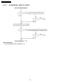
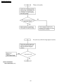
OPERATION FLOW
61
KX-FL612CX / KX-FL612CX-S
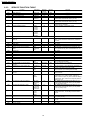
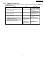
6.2.3.
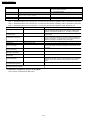
Code
SERVICE FUNCTION TABLE
Function
Set Value
Effective
Range
001~600
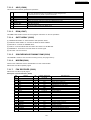
01~99
1~9
1, 2
Default
1, 2
1
501
502
514
520
Pause time set
Flash time
Bell signal detect time
CED frequency select
521
International mode select
X 100 msec
X 10 ms
X 100msec
1:2100 Hz
2:1100 Hz
1:ON 2:OFF
522
Auto standby select
1:ON 2:OFF
1, 2
1
523
Receive equalizer select
1~4
1
524
Transmission equalizer select
1:
2:
3:
4:
1:
2:
3:
4:
1~4
1
529
544
Call Service Clear
Document feed position adjustment
value set
X mm
0~4
2
550
551
552
553
Memory clear.
ROM check
DTMF single tone test
Monitor on FAX communication
select
1:ON 2:OFF
1:OFF
2:PHASE B
3:ALL
1, 2
1~3
2
1
554
555
556
557
558
561
571
Modem test
Scan check
Motor test
LED test
LCD test
KEY test
ITS auto redial time set
572
573
ITS auto redial line disconnection
time set
Remote turn-on ring number set
590
FAX auto redial time set
591
592
FAX auto redial time disconnection
time set
CNG transmit select
593
Time between CED and 300bps
594
Overseas DIS detection select
595
Receive error limit value set
596
0 km
1.8 km
3.6 km
7.2 km
0 km
1.8 km
3.6 km
7.2 km
030
70
3
1
0
X number of
times
X second
Remarks
---------------------------See Symptom/Countermeasure Table for long
distance and international calls in (P.118).
See Symptom/Countermeasure Table for long
distance and international calls in (P.118).
The resolution reverts to the default when
transmission is complete.
Set RX equalizer to automatic mode.
If it is difficult to feed documents, raise the set
value. If multi documents feed occurs, lower the
set value.
See (P.64).
See (P.64).
See (P.64).
Sets whether to monitor the line signal with the
unit´s speaker during FAX communication or not.
See (P.64).
See (P.64).
See (P.64).
See (P.64).
See (P.64).
See (P.64).
Selects the number of times that ITS is redialed
(not including the first dial).
Sets the interval of ITS redialing.
00~99
05
001~999
065
01~99
10
00~99
05
001~999
065
1:OFF
2:ALL
3:AUTO
1~3
2
1~3
1
1, 2
1
1~4
2
If the number of errors during transmission
exceeds this value, the sending side terminates
the call.
Transmit level set
1:75 msec
2:500 msec
3:1 sec
1:detects at
the 1st time
2:detects at
the 2st time
1: 5%
2: 10%
3: 15%
4: 20%
X dBm
- 15~00
11
598
Receiving sensitivity
43= -43 dBm
20~48
41
599
628
ECM frame size
H.V.P.S. check
1:256 2:64
1, 2
1
Selects the FAX transmission level. Refer to
(P.111)and (P.112).
Used when there is an error problem. Refer to
(P.118).
---------See (P.64).
X number of
rings
X number of
times
X second
62
Sets the number of rings before the unit starts to
receive a document in the TEL mode.
Selects the number of redial times during FAX
communication (not including the first dial).
Sets the FAX redial interval during FAX
communication.
Lets you select the CNG output during FAX
transmission. ALL: CNG is output at phase A.
AUTO: CNG id output only when automatic dialing
is performed. OFF: CNG id not output at phase A.
Refer to (P.111).
See Symptom/Countermeasure Table for long
distance and international calls in (P.118). Refer
to (P.112) and (P.118).
See Symptom/Countermeasure Table for long
distance and international calls in (P.118). Refer
to (P.111) and (P.118).
KX-FL612CX / KX-FL612CX-S
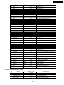
Code
Function
Set Value
630
Paper Jam Cause Distinction Code
639
651
LSU test
Write system program into the Flash Rom with a tool.
655
710
Cause Distinction Code of Call Service 3
Memory clear except History data
717
Transmit speed selection
718
Receive speed selection
721
722
763
Pause tone detect
Redial tone detect
CNG detect time for friendly
reception
771
T1 timer
774
T4 timer
815
852
853
854
874
875
880
881
882
Sensor & Vox check
Print test pattern
Top margin
Left margin
DTMF ON time
DTMF OFF time
History list
Journal 2 list
Journal 3 list
1:14400BPS
2:12000BPS
3:9600BPS
4:7200BPS
5:4800BPS
6:2400BPS
1:14400BPS
2:12000BPS
3:9600BPS
4:7200BPS
5:4800BPS
6:2400BPS
1:ON 2:OFF
1:ON 2:OFF
1:10 sec
2:20 sec
3:30 sec
1:35 sec
2:60 sec
X 100 sec
X msec
X msec
Effective
Range
Default
Remarks
0:No Paper Jam
1:The paper was pulled into the unit.
2:The paper was longer than the maximum length
of the register sensor.
3:The paper exit was not detected after the
registration.
4:The paper was longer than the maximum length
of the paper exit sensor.
5:The register sensor or paper exit sensor was
turned ON before the motor started to rotate.
6:The register sensor chattered.
7:The paper exit sensor chattered.
See (P.64).
See the parts number of the tool. (P.241). The
tool includes the operating manual for writing
program.
See (P.83).
To reset the value to the default one, except
History data. Please restart a power supply after
clearing a memory.
Adjusts the speed to start training during FAX
transmission. Refer to (P.111) and
1~6
1
1~6
1
Adjusts the speed to start training during FAX
reception. Refer to (P.112) and
1, 2
1, 2
1~3
2
1
3
Selects the tone detection for pause in dialing.
Sets the tone detection mode after redialing.
Selects the CNG detection tone of friendly
reception.
1, 2
1
00~99
00
1~5
1~7
060~200
060~200
3
4
90
90
Sets a higher value when the response from the
other party needs more time during FAX
transmission.
Use this function when delay occurs in the line
and communication.
(ex. Mobile comm) does not work well.
See (P.64).
See (P.64).
------------------------------------See (P.73).
See (P.116).
See (P.116).
63
KX-FL612CX / KX-FL612CX-S
6.3.
TEST FUNCTIONS
The codes listed below can be used to perform simple checks of some of the unit’s functions. When complaints are received
from customers, they provide an effective tool for identifying the locations and causes of malfunctions.
Test Mode
Type of Mode
Code
Function
Operation after code
input
“5” “5” “6”
0: Recording paper feed
1: Auto Document feed (STANDARD)
START
2: Auto Document feed (FINE)
3: Auto Document feed (SUPER FINE)
“5” “5” “4”
Telephone line circuit is connected automatically, output the following signals on
the circuit line.
START
1) OFF 2) 14400bps 3) 12000bps 4) 9600bps
5) 7200 bps 6) 4800bps 7) 2400bps 8) 300bps
9) 2100Hz 10) 1100Hz
“5” “5” “1”
Indicates the version and checks the sum of the ROM.
START
“5” “5” “8”
Checks the LCD indication.
Illuminates all the dots to check if they are normal.
START
Refer to OPERATION PANEL SECTION (P.131).
“5” “5” “2”
Outputs the DTMF as single tones. Used to check the frequencies of the
individual DTMF tones. Refer to DTMF SINGLE TONE TRANSMIT SELECTION
1....ON
(P.66).
2....OFF
MOTOR TEST
Service Mode
MODEM TEST
Service Mode
ROM CHECK
Service Mode
LCD CHECK
Service Mode
DTMF SINGLE TEST
Service Mode
LED CHECK
Service Mode
KEY CHECK
Service Mode
CIS TEST
Service Mode
“5” “5” “5”
LSU TEST
MEMORY CLEAR
Service Mode
Service Mode
“6” “3” “9”
“5” “5” “0”
START
High Voltage Power
Supply Board
CHECK
FAN TEST
Service Mode
“6” “2” “8”
START
Service Mode
“6” “7” “7”
START
“5” “5” “7”
START
“5” “6” “1”
START (any key)
All LEDs above the operation panel board flash on and off, or are illuminated.
Checks the button operation.
Indicates the button code on the LCD while the button is pressed. Refer to
BUTTON CODE TABLE (P.66), OPERATION PANEL SECTION (P.131).
LED lights up, CIS scanning. Refer to CIS (Contact Image Sensor) SECTION
(P.138).
Laser radiates, Polygon rotates Refer to LSU SECTION (P.137).
To reset the value to the default one, except the top margin (#853), left margin
(#854), time / day (#001), logo (#002), Fax no. (#003), History and Directory data.
Please restart a power supply after clearing a memory.
Refer to HIGH VOLTAGE VALUE CHECK POINT (P.139).
1:TEST OFF
2:High-speed rotation
3:Low-speed rotation
64
KX-FL612CX / KX-FL612CX-S
Test Mode
SENSOR CHECK
Type of Mode
Service Mode
Code
Function
Operation after code
input
“8” “1” “5”
First of all, press the copy button, and confirm the action of ON/OFF.
For each sensor’s operation, refer to SENSORS AND SWITCHES SECTION
(P.175).
D S C P R E D T * 3F * D 4 * V : LCD DISPLAY
D: Document sensor
D: Document set
-: No document
S: Paper Feed Sensor
S: Read position
-: No read position
C: Printer Cover Switch
C: Open
-: Close
P: Paper sensor
P: Recording paper set
-: No recording paper
R: Regist Sensor
R: Detect recording paper
-: Not defect recording paper
E: Exit Sensor
E: Detect recording paper
-: Not detect recording paper
D: Drum Sensor
D: DRUM set
-: No DRUM
T: Toner Sensor
T: Toner sensor ON
-: Toner sensor OFF
*: None
3F: Temperature of THERMISTOR
Hex (00-FF)
*: None
D4: Temperature of Atmosphere
Hex (00-FF)
*: None
V: VOX signal
V: Detect the tone on the line
PRINT TEST
PATTERN
Service Mode
“8” “5” “2”
START
-: Not detect
1. Press “852” then the SET key in the service mode.
2. As “PATNO =” is displayed on the LCD, enter the test pattern No. and press
the SET key.
3. When “No. = “is displayed on the LCD, enter the printing number and press the
SET key. (Press “00” for the infinite printing.)
4. “MODE” is displayed on the LCD. Press “0” to start printing or press “1” to go
to the next screen.
5. When “1” is pressed at MODE, “INTVL = “is displayed on the LCD. Enter the
printing interval (00~99 sec).
6. The printing repeats the designated number of times at the programmed
printing intervals.
Note:
The numbers in the boxes (XXX) indicate the keys to be input for the various test modes.
65
KX-FL612CX / KX-FL612CX-S
6.3.1.
DTMF SINGLE TONE TRANSMIT SELECTION
Note:
After performing this check, do not forget to turn the setting off.
otherwise, dialing in DTMF signal will not work.
6.3.2.
BUTTON CODE TABLE
66
KX-FL612CX / KX-FL612CX-S
6.3.3.
PRINT TEST PATTERN
1. NO. 01
3. NO.12
2. NO.08
• These print test patterns are just image printing, and
different from actual ones.
When it is required to judge the print quality, compare with
the printing of a nondefective machine.
67
KX-FL612CX / KX-FL612CX-S
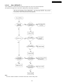
6.4.
REMOTE PROGRAMMING
If, after the call is connected, the customer describes the situation and it is determined that the problem can be corrected by
making parameter changes, this function makes it possible to change parameters such as the user code and service code from
another fax (using DTMF tones). Therefore, travel to the customer´s location is not required. However, it is not possible to
change all the parameters remotely (PROGRAM MODE TABLE(P.69)). The function used to accomplish this is remote
programming.
First, in order to check the current status of the service code parameter, print out the setup list (code: 991) and the service list
(code: 999) from the customer´s fax machine.
Based on this, the parameters for the desired codes can be changed.
The procedure for changing and listing parameters is described on ENTERING THE REMOTE PROGRAMMING MODE AND
CHANGING SERVICE CODES(P.68). Also, before exiting the remote programming mode, it is advisable to obtain a new list to
confirm that the changes were made correctly.
Hint:
Since the connected telephone is in use during the remote programming mode, it may be helpful to ask the customer to switch
to the speakerphone. This frees the customer from the need to remain right next to the fax while you are making parameter
settings. When finished, inform the customer. Also note that in very noisy locations where the DTMF tones are not audible, the
remote programming function will not work.
6.4.1.
ENTERING THE REMOTE PROGRAMMING MODE AND CHANGING SERVICE
CODES
CROSS REFERENCE:
PROGRAM MODE TABLE (P.69)
68
KX-FL612CX / KX-FL612CX-S
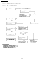
6.4.2.
PROGRAM MODE TABLE
Code
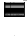
Function
001
002
003
004
006
012
013
016
017
022
023
025
026
031
032
037
039
041
044
046
058
068
076
079
080
501
502
514
520
521
522
523
524
529
544
Set date and time
Your logo
Your fax telephone number
Transmission report mode
FAX ring count
Remote TAM activation
Dialing mode
Paper size
Ringer pattern
Auto journal print
Overseas mode
Delayed transmission
Auto CALLER ID list
Distinctive ring
Fax ring pattern
Auto REDUCTION
LCD contrast
Remote FAX activation code
Receive alert
Friendly receive
Scan contrast
ECM Selection
FAX tone
Toner save
Set default
Pause time set
Flash time
Bell signal detect time
CED frequency select
International mode select
Auto standby select
Receive equalizer select
Transmission equalizer select
Memory clear for Call Service
Document feed position adjustment value
set
Memory clear
ROM check
DTMF signal tone test
Monitor on FAX communication
Modem test
Motor test
LED test
LCD test
Key test
ITS auto redial time set
ITS auto redial line disconnection time set
Remote turn-on ring number
FAX auto redial time set
FAX auto redial line disconnection time set
CNG transmit select
Time between CED and 300bps
Overseas DIS detection select
Receive error limit value set
Transmit level set
Receiving Sensitivity
ECM Frame size
H.V.P.S check
Paper jam cause distinction
LSU test
White system program into the Flash ROM
Cause distinction code of call service 3
Memory clear except History data
Transmit speed select
550
551
552
553
554
556
557
558
561
571
572
573
590
591
592
593
594
595
596
598
599
628
630
639
651
655
710
717
Set Value
mm/dd/yy hh:mm
----------------2:ON / 3:OFF / 1:ERROR
1 to 9 rings
ON/ID=11 / OFF
1:PULSE / 2:TONE
LETTER / A4 / LEGAL
A/B/C
1:ON / 2:OFF
1:NEXT FAX / 2:ERROR / 3:OFF
ON / OFF
1:ON / 2:OFF
1:ON / 2:OFF
1:B-D / 2:A / 3:B / 4:C / 5:D
1:ON / 2:OFF
NORMAL / DARKER
ON / OFF
1:ON / 2:OFF
1:ON / 2:OFF
1:NORMAL 2:LIGHT 3:DARKER
1:ON / 2:OFF
1:ON / 2:OFF
1:ON / 2:OFF
YES / NO
001~600 x 100msec
01~99 x 10ms
1~9 x 100msec
1:2100Hz / 2:1100Hz
1:ON / 2:OFF
1:ON / 2:OFF
1:0kms / 2:1.8km / 3:3.6km / 4:7.2km
1:0kms / 2:1.8km / 3:3.6km / 4:7.2km
--------0~4 xmm
----------------1:ON / 2:OFF
1:OFF / 2:Phase B / 3:ALL
----------------------------------------00~99
001~999sec
01~99
00~99
001~999sec
1:OFF / 2:ALL / 3:AUTO
1:75ms / 2:500ms / 3:1sec
1:1st / 2:2nd
1:5% / 2:10% / 3:15% / 4:20%
-15~00dBm
20~48
1:256 / 2:64
------------------------------------------------1:14400/ 2:12000/ 3:9600/ 4:7200/
5:4800/ 6:2400
69
Default
Jan/01/2005
None
None
ERROR
2
OFF
TONE
A4
A
ON
ERROR
OFF
ON
OFF
B-D
ON
NORMAL
ON CODE=*#9
ON
ON
NORMAL
ON
ON
OFF
NO
030
70
3
2100Hz
ON
ON
0 km
0 km
--------2mm
Remote
Setting
NG
NG
NG
OK
OK
NG
OK
NG
NG
OK
OK
NG
OK
OK
OK
OK
NG
NG
OK
OK
OK
OK
OK
OK
NG
OK
OK
OK
OK
OK
OK
OK
OK
NG
OK
----------------OFF
OFF
----------------------------------------05
065
10
05
065
ALL
75ms
1st
10%
11
41
256byte
------------------------------------------------14400bps
NG
NG
OK
OK
NG
NG
NG
NG
NG
OK
OK
OK
OK
OK
OK
OK
OK
OK
OK
OK
OK
NG
NG
NG
NG
NG
NG
OK
KX-FL612CX / KX-FL612CX-S
Code
Function
718
Receive speed select
721
722
763
771
774
815
852
853
854
874
875
880
881
882
991
994
995
996
998
999
Pause tone detect
Redial tone detect
CNG detect time for friendly reception
T1 timer
T4 timer
Sensor test
Print test pattern
Top margin
Left margin
DTMF ON time
DTMF OFF time
History list
Journal 2
Journal 3
Setup list
Journal list
Journal 2 list
Journal 3 list
History list
Service list
Set Value
1:14400/ 2:12000/ 3:9600/ 4:7200/
5:4800/ 6:2400
1:ON / 2:OFF
1:ON / 2:OFF
1:10s / 2:20s / 3:30s
1:35s / 2:60s
00~99 × 100msec
----------------1~5
1~7
060~200msec
060~200msec
1:Start
----------------1:Start
1:Start
1:Start
1:Start
1:Start
1:Start
Default
14400bps
Remote
Setting
OK
OFF
ON
30s
35s
00
----------------3
4
90
90
-------------------------------------------------------------------------
OK
OK
OK
OK
OK
NG
NG
OK
OK
OK
OK
NG
NG
NG
OK
OK
OK
OK
OK
OK
OK means “can set”.
NG means “can not set”.
Note:
Refer to SERVICE FUNCTION TABLE (P.62) for descriptions of the individual codes.
Example:
If you want to set value in the “004 Transmission report mode”, press the dial key number 1, 2 or 3 corresponding to the Set
Value you want to select. (1:ERROR/2:ON/3:OFF)
70
KX-FL612CX / KX-FL612CX-S
6.4.3.
USER MODE (The list below is an example of the SYSTEM SETUP LIST the unit
prints out.)
Note:
The above values are the default values.
71
KX-FL612CX / KX-FL612CX-S
6.4.4.
SERVICE MODE SETTINGS (Example of a printed out list)
Note:
The above values are the default values.
72
KX-FL612CX / KX-FL612CX-S
6.4.5.
HISTORY (Example of a printed out list)
Note:
See the following descriptions of this report. Item No. (1) ~ (54) are corresponding to the listed items in DESCRIPTIONS OF
THE HISTORY REPORT(P.74).
73
KX-FL612CX / KX-FL612CX-S
6.4.5.1.
DESCRIPTIONS OF THE HISTORY REPORT
(1) ROM VERSION
FLASH ROM version
(2) SUM
FLASH ROM internal data calculation.
(3) YOUR LOGO
The user logo recorded in the unit. If it is not recorded, NONE will be displayed.
(4) YOUR TELEPHONE NUMBER
The user telephone number recorded in the unit. If it is not recorded, NONE will be displayed.
(5) Not used
(6) FACTORY - CUSTOMER
This shows how many days from factory production until the user turns ON the unit.
(7) MONTH
The shows the very first month, date, year and time set by the user after they purchased the unit.
(8) DAY
The shows the very first month, date, year and time set by the user after they purchased the unit.
(9) YEAR
The shows the very first month, date, year and time set by the user after they purchased the unit.
(10) TIME
The shows the very first month, date, year and time set by the user after they purchased the unit.
(11) USAGE TIME
The amount of time the unit has been powered ON.
(12) FACTORY - NOW
This shows how many days from factory production until the user prints out this history list.
(13) TEL MODE
The amount of time the TEL mode setting was used.
(14) FAX MODE
The amount of time the FAX mode setting was used.
(15) Not used
(16) Not used
(17) FINAL RECEIVE MODE
The last set receiving mode by the user.
(18) TONE/PULSE SELECTION
The most recently used setting used, either TONE or PULSE.
(19) RECEIVE REDUCTION
The compression rate when receiving.
(20) SETTING NO. OF DIRECTORY
The recorded directory stations (one touch dial).
(21) NUMBER OF COPY
The number of pages copied.
(22) NUMBER OF RECEIVE
The number of pages received.
(23) NUMBER OF SENDING
The number of pages sent.
(24) NUMBER OF CALLER ID
The number of times Caller ID was received.
(25) Not used
(26) Not used
(27) Not used
74
KX-FL612CX / KX-FL612CX-S
(28) Not used
(29) Not used
(30) Not used
(31) NUMBER OF PRINTING HELP
The number of help lists printed until now.
(32) NUMBER OF DIVIDED PRINTING IN FAX RECEPTION
The number of faxes received that were divided into more than one sheet since the unit was purchased.
(33) Not used.
(34), (35) Not used.
(36) FAX MODE
Means the unit received a fax message in the FAX mode.
(37) MAN RCV
Means the unit received a fax message by manual operation.
(38) FRN RCV
Means the unit received a fax message by friendly signal detect.
(39) Not used
(40) RMT DTMF
Means the unit detected DTMF (Remote Fax activation code) entered remotely.
(41) PAL DTMF
Means the unit detected DTMF (Remote Fax activation code) entered by a parallel connected telephone.
(42) TURN-ON
Means the unit started to receive after 10 rings. (Remote Turn On: Service Code #573)
(43) Not used
(44) IDENT
Means the unit detected Ring Detection.
(45) Not used
(46) Not used
(47) Not used
(48) Not Used
(49) Not Used
(50) Printing number of the drum unit
(51) Paddle rotation number of the drum unit
(52) CALL SERVICE 3 failure cause record (the latest)
(53) CALL SERVICE 3 failure cause record (the last time)
(54) CALL SERVICE 3 failure cause record (the second last time)
75
KX-FL612CX / KX-FL612CX-S
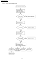
6.5.
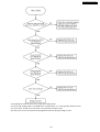
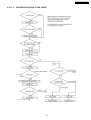
6.5.1.
TROUBLESHOOTING DETAILS
OUT LINE
Troubleshooting is for recovering quality and reliability by determining the broken component and replacing, adjusting or cleaning
it as required. First, determine the problem then decide the troubleshooting method. If you have difficulty finding the broken part,
determine which board is broken. (For example: the Digital PCB, Analog PCB, etc.) The claim tag from a customer or dealer may
use different expressions for the same problem, as they are not a technician or engineer. Using your experience, test the problem
area corresponding to the claim. Also, returns from a customer or dealer often have a claim tag. For these cases as well, you need
to determine the problem. Test the unit using the simple check list on SIMPLE CHECK LIST(P.78). Difficult problems may be hard
to determine, so repeated testing is necessary.
6.5.2.
STARTING TROUBLE SHOOTING
Determine the symptom and the troubleshooting method.
CROSS REFERENCE:
USER RECOVERABLE ERRORS(P.59)
SIMPLE CHECK LIST(P.78)
DIGITAL BOARD SECTION(P.208)
POWER SUPPLY BOARD SECTION(P.144)
76
KX-FL612CX / KX-FL612CX-S
6.5.3.
INITIALIZATION
There are two types of initialization, one is the short initialization (about 3 seconds) and the other is the long initialization (about
10 seconds). The short initialization makes the unit enter the standby mode. The long initialization makes the unit enter the
standby mode after cleaning or detecting the rest of toner.
77
KX-FL612CX / KX-FL612CX-S
6.5.4.
SIMPLE CHECK LIST
Note:
Check according to the service code referring to TEST FUNCTIONS (P.64)
78
KX-FL612CX / KX-FL612CX-S
6.5.5.
6.5.5.1.
SIMPLIFIED TROUBLESHOOTING GUIDE
PRINTING
No.
Symptom
1 GHOST IMAGE (P.88)
2 DARK
OR
WHITE
VERTICAL LINE (P.89)
3 DARK
OR
WHITE
HORIZONTAL LINE (P.90)
4 DIRTY
OR
HALF
DARKNESS
BACKGROUND (P.91)
5 BLACK PRINT (P.92)
6 LIGHT PRINT (P.93)
7 BLACK
DENSITY
IS
LIGHT OR UNEVEN(P.94)
8 BLANK PRINT (P.95)
9 BLACK OR WHITE POINT
(P.95)
Countermeasure
Replace drum unit
Check the transfer roller and spring
Check the high-voltage terminal
Go to HIGH VOLTAGE SECTION (P.140)
Check the heat roller and the pressurized roller and the spring
and the heat lamp and the thermistor
Failed the power supply board
Go to POWER SUPPLY BOARD SECTION (P.144)
Too thick or too thin recording paper
Use the recording paper from 16lb to 24lb
Dirty the lower glass or the reflecting mirror
Clean the lower glass and the reflecting mirror
Dust on the path of the laser beam
Clean the path of the laser beam
Dust on the developing roller
Replace drum unit
Failed the heat roller or the pressuizedr roller Check the heat roller and the pressurized roller
Failed LSU
Go to LSU SECTION (P.137)
Failed drum unit
Replace drum unit
Failed the gear
Check the gear
Failed the engine motor
Go to ENGINE MOTOR (P.135)
Failed the high-voltage terminal
Check the high-voltage terminal
Failed the high voltage power supply board
Go to HIGH VOLTAGE SECTION (P.140)
Scratch on the OPC drum
Replace drum unit
Static electricity on the documents (when Check the connection between the parts around CIS and earth
copying)
Failed drum unit
Replace drum unit
Life of drum unit is over
Replace drum unit
Dirty the pickup roller and the regist roller and Clean the pickup roller and the regist roller and the feed roller
the feed roller and the eject roller and the heat and the eject roller and the heat roller and the pressure roller
roller and the pressure roller
Failed the high-voltage terminal
Check the high-voltage terminal
Failed the high voltage power supply board
Go to HIGH VOLTAGE SECTION (P.140)
Dirty the recording paper path
Clean the recording paper path
Failed drum unit
Replace drum unit
Failed LSU
Go to LSU SECTION (P.137)
Failed the high-voltage terminal
Check the high-voltage terminal
Failed the high voltage power supply board
Go to HIGH VOLTAGE SECTION (P.140)
Failed the digital board
Check the digital board
Failed CIS (when copying)
Go to CIS (Contact Image Sensor) SECTION (P.138)
Short toner
Supply toner
Failed drum unit
Replace drum unit
Life of drum unit is over
Replace drum unit
Dirty the lower glass or the reflecting mirror
Clean the lower glass and the reflecting mirror
Failed the high-voltage terminal
Check the high-voltage terminal
Failed the high voltage power supply board
Go to HIGH VOLTAGE SECTION (P.140)
Failed drum unit
Replace drum unit
Failed LSU
Go to LSU SECTION (P.137)
Failed the high-voltage terminal
Check the high-voltage terminal
Failed the high voltage power supply board
Go to HIGH VOLTAGE SECTION (P.140)
Failed the digital board
Check the digital board
Failed CIS (when copying)
Go to CIS (Contact Image Sensor) SECTION (P.138)
Failed the developer roller (31.4mm pitch)
Replace drum unit
Failed the OPC drum (75.4mm pitch)
Replace drum unit
Failed the heat roller (62.8mm pitch)
Check the heat roller
Failed the charge blush (21mm pitch)
Replace drum unit
Failed the high voltage power supply board
Go to HIGH VOLTAGE SECTION (P.140)
Too thick or too thin recording paper
Use the recording paper from 16lb to 24lb
Failed
Failed
Failed
Failed
Failed
Cause
drum unit
transfer unit
the high-voltage terminal
the high voltage power supply board
fuser unit
79
KX-FL612CX / KX-FL612CX-S
6.5.5.2.
RECORDING PAPER FEED
No.
Symptom
1 MULTIPLE FEED (P.96)
2 THE RECORDING PAPER
IS WAVED OR WRINKLED
(P.96)
3 SKEW (P.97)
4 THE RECORDING PAPER
DOES NOT FEED (P.98)
5 THE RECORDING PAPER
JAM(P.99)”PAPER
JAMMED” ON THE LCD
6 BACK SIDE OF THE
RECORDING PAPER IS
DIRTY(P.101)
Cause
Dirty or failed the pickup roller
Dirty or failed the pickup rubber
Dirty the pressure roller or the heat roller
Failed the spring of pressure roller
Too thin recording paper
Dirty or failed the pickup roller
Dirty or failed the pickup rubber
Dirty or failed the paper feed roller
Dust on the recording paper path
Failed LSU
Over the max capacity of the recording paper
Too thick or too thin recording paper
Dirty or failed the pickup roller
Dirty or failed the pickup rubber
Failed the gear
Failed the engine motor
Failed the paper feed sensor lever
Failed the paper feed sensor
Dirty or failed the pressure roller
Dirty or failed the heat roller
Dust on the recording paper path
Failed the paper feed roller
Failed the gear
Failed the engine motor
Failed the paper feed sensor lever
Failed the paper feed sensor
Failed the exit sensor lever
Failed the exit sensor
Too thick or too thin recording paper
Not set the toner bottle
Dirty the recording paper path
Dirty the pressure roller
Dirty the regist roller
Failed the high-voltage terminal
Failed the high voltage power supply board
80
Countermeasure
Clean or replace the pickup roller
Clean or replace the separation rubber
Clean the pressure roller and the heat roller
Replace the spring of pressure roller
Use the recording paper from 16lb to 24lb
Clean or replace the pickup roller
Clean or replace the separation rubber
Clean or replace the regist roller
Clean the recording paper path
Replace LSU
Set up to MAX 150 sheets
Use the recording paper from 16lb to 24lb
Clean or replace the pickup roller
Clean or replace the separation rubber
Check the gear
Go to ENGINE MOTOR (P.135)
Check the regist sensor (paper top sensor) lever
----Clean or replace the pressure roller
Clean or replace the heat roller
Clean the recording paper path
Replace the regist roller
Check the gear
Go to ENGINE MOTOR (P.135)
Check the regist sensor (paper top sensor) lever
----Check the exit sensor lever
Go to PAPER EXIT SENSOR..... “PAPER JAMMED” (P.179)
Use the recording paper from 16lb to 24lb
Set toner bottle
Clean the recording paper path
Clean the pressure roller
Clean the regist roller
Check the high-voltage terminal
Go to HIGH VOLTAGE SECTION (P.140)
KX-FL612CX / KX-FL612CX-S
6.5.5.3.
COPY AND FAX
No.
Symptom
1 NO DOCUMENT FEED
(NO DOCUMENT
FEED,DOCUMENT JAM
and MULTIPLE
DOCUMENT FEED.)
(P.102)
DOCUMENT JAM (NO
DOCUMENT
FEED,DOCUMENT JAM
and MULTIPLE
DOCUMENT FEED.)
(P.102)
MULTIPLE DOCUMENT
FEED(NO DOCUMENT
FEED,DOCUMENT JAM
and MULTIPLE
DOCUMENT FEED.)
(P.102)
2 SKEW (ADF) (P.104)
3 THE SENT FAX DATA IS
SKEWED (P.105)
4 THE
RECEIVED
FAX
DATA IS SKEWED (P.105)
5 THE
RECEIVED
COPIED
DATA
EXPANDED (P.106)
OR
IS
6 BLACK
OR
WHITE
VERTICAL
LINE
IS
COPIED (P.107)
7 AN ABNORMAL IMAGE IS
COPIED (P.108)
Cause
Failed the document sensor lever
Failed the document sensor
Dirty or failed the separation roller
Dirty or failed the separation rubber
Failed the separation spring
Countermeasure
Replace the document sensor lever
Go to DOCUMENT SENSOR (P.161)
Clean or replace the separation roller
Clean or replace the separation rubber
Replace the separation spring
Dust or scratch on the document paper path
Failed the gear
Failed the ADF motor
Failed the ADF cover open switch lever
Clean the document paper path
Check the gear
Go to ADF MOTOR (P.136)
Replace the ADF cover open switch lever
Dirty or failed the separation roller
Dirty or failed the separation rubber
Failed the separation spring
Clean or replace the separation roller
Clean or replace the separation rubber
Replace the separation spring
Dust or scratch on the document paper path
Failed the document feed roller
Failed the document guide
The cause of ADF
The cause of scanner glass
Problem with the other FAX machine
The cause of printing
Problem with the other FAX machine
Dirty or failed the drive roller (at ADF)
Dirty or failed the document feed roller (at ADF)
Dirty or failed the separation roller (at ADF)
Failed CIS movement (at SG)
Dirty or failed the white plate (2 places)
Dirty or failed the glass board
The cause of printing
Failed CIS
Dirty or failed the white plate (2 places)
Dirty or failed the glass board
Dirty or failed the drive roller (at ADF)
Dirty or failed the document feed roller (at ADF)
Dirty or failed the separation roller (at ADF)
Failed CIS movement (at SG)
Failed CIS
The cause of printing
Clean the document paper path
Replace the document feed roller
Replace the document guide
Go to SKEW (ADF)(P.104)
----
81
Go to SKEW (ADF)(P.104)
Clean or replace the drive roller
Clean or replace the document feed roller
Clean or replace the separation roller
Replace the belt or the gear or the shaft or the ADF motor
Clean or replace the white plate
Clean or replace the glass board
Go to DARK OR WHITE VERTICAL LINE (P.89)
Go to CIS (Contact Image Sensor) SECTION (P.138)
Clean or replace the white plate
Clean or replace the glass board
Clean or replace the drive roller
Clean or replace the document feed roller
Clean or replace the separation roller
Replace the belt or the gear or the shaft or the ADF motor
Go to CIS (Contact Image Sensor) SECTION (P.138)
Go to DARK OR WHITE VERTICAL LINE (P.89)
KX-FL612CX / KX-FL612CX-S
6.5.5.4.
Others
No.
Symptom
Cause
1 Cannot print legal size
Not selected the legal mode
2 ´CHECK DRUM´ on the The drum unit can not be detected.
• Drum Sensor trouble
LCD
Countermeasure
Select the legal mode in the user programming mode
Go to DRUM SENSOR (P.177)
Go to LSU (Laser Scanning Unit) SECTION (P.173)
• Mechanical shutter trouble
3 ´CHANGE DRUM´ on the The toner sensor cannot detect the toner
LCD
sensor signal.
4 ´OUT OF PAPER´ on the Failed the paper sensor lever
LCD
Failed the paper sensor
5 ´COVER OPEN´ on the Failed the top cover open switch lever
LCD
Failed the top cover open switch
6 CALL SERVICE 1´ on the The polygon motor of LSU is unusually
LCD
7 CALL SERVICE 2´ on the The laser of LSU is unusually
LCD
8 CALL SERVICE 3´ on the The fuser temperature is unusually
LCD
9 CALL SERVICE 4´ on the The fan motor is unusually
LCD
82
Go to TONER SENSOR.... “TONER EMPTY”, “TONER
LOW”, “CHANGE DRUM” (P.182)
Replace the paper sensor lever
Go to PAPER SENSOR..... “OUT OF PAPER” (P.179)
Replace the top cover open switch lever
Go to TOP COVER OPEN SWITCH (P.177)
Check the connector and LSU and the digital board
Check the connector and LSU and the digital board
Check the connector and the fuser and the thermistor and the
digital board
Check the connector and the fan motor and the digital board
KX-FL612CX / KX-FL612CX-S
6.5.6.
CALL SERVICE TROUBLESHOOTING GUIDE
Call Service related error is most frequent.
Call Service 1 ----- Polygon doesn’t rotate......... Refer to LSU (Laser Scanning Unit) SECTION (P.173).
• First, listen to the sound. If rotation sound isn´t heard, check 24V line, POLON signal and POLCLK signal. If even a little of
sound is heard, check XREADY signal.
Call Service 2 ----- Laser isn´t output.......... Refer to LSU (Laser Scanning Unit) SECTION (P.173)
• This can be judged only by referring to signal. Check 5V line, XHSYNC, SPC, VIDEO, LDON.
Call Service 3 ----- Detection of fixing temperature.......... Refer to HEAT LAMP CONTROL CIRCUIT (P.188)
• *Service mode *655 tells the detection number and 3 latest temperatures of the thermistor. The cause distinction code of
the Call Service 3 and the thermistor temperature is displayed. Maximum 3 latest temperatures are displayed showing the
newest on the left. [AABB CCDD EEFF] AA, CC and EE show the cause distinction code and BB, DD and FF show their
temperature.
Cause distinction code
00: means that CALL SERVICE 3 has not been appeared.
01: means that it did not reach 56°C within 22 seconds since the heater was turned ON.
03: means that it did not reach the secondary stabilizing temperature (160°C) within 35 seconds from 56°C.
04: means that it became T2-40deg (120°C or below) after T2; the secondary stabilizing temperature (160°C). (The heater
has burnt out.)
05: means that it became over 220°C.
06: means that during printing the SHORT of the thermistor (AD: 01h or below) was detected.
07: means that the thermistor´s SHORT (AD:00h) and OPEN (AD: F9h or over) were detected.
Call Service 4 ----- Rotation of Fan.......... Refer to FAN MOTOR SECTION (P.170)
• Connector isn’t inserted firmly, dust is caught in and the fan is broken.
* As for Call Services 1, 2 and 4, turn the power OFF then ON to restart.
<Note>
Once “CALL SERVICE3” is displayed, the unit does not disappear until the Factory Setup or Service Function #529 is executed.
Therefore Service Function #529 should be executed before the confirmation, and #529 should be done after the countermeasure.
83
KX-FL612CX / KX-FL612CX-S
6.5.6.1.
CALL SERVICE 1
"CALL SERVICE 1" means that the polygon motor inside the LSU does not rotate.
The rotation of the polygon motor is detected by IC606-32pin (XREADY).
84
KX-FL612CX / KX-FL612CX-S
6.5.6.2.
CALL SERVICE 2
"CALL SERVICE 2" means that the synchronous signal out of the LSU cannot be detected.
The synchronous signal out of the LSU is detected by IC 606-33pin. (XHSYNC)
Note:
As for the "Pulse" waveform of the above flow chart, see the timing chart.
85
KX-FL612CX / KX-FL612CX-S
6.5.6.3.
CALL SERVICE 3
"CALL SERVICE 3" means that the temperature of the fuser does not rise up to or exceed a constant temperature.
The temperature is monitored with the thermistor inside the fuser and detected with the voltage input into IC 606-4pin.
*When Call Service 3 is occurred, the cause can be distinguished.
Refer to page 80 for details.
86
KX-FL612CX / KX-FL612CX-S
6.5.6.4.
CALL SERVICE 4
"CALL SERVICE 4" means that the FAN does not run or the running of the FAN cannot be detected normally.
The running of the FAN is detected by IC 605-91pin. "CALL SERVICE 4" is displayed when it detects NG five times continuously.
After repairing, copy five times.If “CALL SERVICE 4 “ is displayed,check again.
87
KX-FL612CX / KX-FL612CX-S
6.5.7.
6.5.7.1.
PRINT
GHOST IMAGE
CROSS REFERENCE:
HIGH VOLTAGE SECTION(P.140)
POWER SUPPLY BOARD SECTION(P.144)
88
KX-FL612CX / KX-FL612CX-S
6.5.7.2.
DARK OR WHITE VERTICAL LINE
Note:
When wiping the lower glass, reflecting mirror and LSU lens, use a dry and soft cloth.
CROSS REFERENCE:
LSU SECTION (P.137)
89
KX-FL612CX / KX-FL612CX-S
6.5.7.3.
DARK OR WHITE HORIZONTAL LINE
CROSS REFERENCE:
HIGH VOLTAGE SECTION (P.140)
90
KX-FL612CX / KX-FL612CX-S
6.5.7.4.
DIRTY OR HALF DARKNESS BACKGROUND
CROSS REFERENCE:
HIGH VOLTAGE SECTION (P.140)
91
KX-FL612CX / KX-FL612CX-S
6.5.7.5.
BLACK PRINT
CROSS REFERENCE:
HIGH VOLTAGE SECTION (P.140)
LSU SECTION (P.137)
92
KX-FL612CX / KX-FL612CX-S
6.5.7.6.
LIGHT PRINT
CROSS REFERENCE:
HIGH VOLTAGE SECTION (P.140)
93
KX-FL612CX / KX-FL612CX-S
6.5.7.7.
BLACK DENSITY IS LIGHT OR UNEVEN
CROSS REFERENCE:
HIGH VOLTAGE SECTION (P.140)
94
KX-FL612CX / KX-FL612CX-S
6.5.7.8.
BLANK PRINT
6.5.7.9.
BLACK OR WHITE POINT
95
KX-FL612CX / KX-FL612CX-S
6.5.8.
RECORDING PAPER FEED
6.5.8.1.
MULTIPLE FEED
6.5.8.2.
THE RECORDING PAPER IS WAVED OR WRINKLED
96
KX-FL612CX / KX-FL612CX-S
6.5.8.3.
SKEW
97
KX-FL612CX / KX-FL612CX-S
6.5.8.4.
THE RECORDING PAPER DOES NOT FEED
CROSS REFERENCE:
SENSOR SECTION (P.132)
MOTOR SECTION (P.135)
98
KX-FL612CX / KX-FL612CX-S
6.5.8.5.
THE RECORDING PAPER JAM
CROSS REFERENCE:
mode *630 distinguishes the cause.
PAPER EXIT SENSOR..... “PAPER JAMMED” (P.179)
0:No Paper Jam
FAN MOTOR SECTION (P.170)
1:Failed pick up
REGIST SENSOR (P.178)
2:The paper top sensor is not turned OFF although the fixed
time had passed since the sensor was turned ON.
When the recording paper jam is occurred, the service
99
KX-FL612CX / KX-FL612CX-S
3:The paper eject sensor is not turned ON although the
fixed time had passed since the paper top sensor was
turned ON.
4:The paper eject sensor is not turned OFF although the
fixed time had passed since it was turned ON.
5:The register sensor (paper top sensor) or paper exit
sensor was turned ON before the motor started to rotate.
6:The register sensor (paper top sensor) chattered.
7:The paper exit sensor chattered.
100
KX-FL612CX / KX-FL612CX-S
6.5.8.6.
BACK SIDE OF THE RECORDING PAPER IS DIRTY
CROSS REFERENCE:
HIGH VOLTAGE SECTION (P.140)
101
KX-FL612CX / KX-FL612CX-S
6.5.9.
6.5.9.1.
ADF (Auto document feed) SECTION
NO DOCUMENT FEED,DOCUMENT JAM and MULTIPLE DOCUMENT FEED.
CROSS REFERENCE:
SENSOR SECTION (P.132)
102
KX-FL612CX / KX-FL612CX-S
CROSS REFERENCE:
MOTOR SECTION (P.135)
103
KX-FL612CX / KX-FL612CX-S
6.5.9.2.
SKEW (ADF)
104
KX-FL612CX / KX-FL612CX-S
6.5.9.3.
THE SENT FAX DATA IS SKEWED
CROSS REFERENCE:
SKEW (ADF) (P.104)
6.5.9.4.
THE RECEIVED FAX DATA IS SKEWED
CROSS REFERENCE:
SKEW (P.97)
105
KX-FL612CX / KX-FL612CX-S
6.5.9.5.
THE RECEIVED OR COPIED DATA IS EXPANDED
106
KX-FL612CX / KX-FL612CX-S
6.5.9.6.
BLACK OR WHITE VERTICAL LINE IS COPIED
107
KX-FL612CX / KX-FL612CX-S
6.5.9.7.
AN ABNORMAL IMAGE IS COPIED
CROSS REFERENCE:
CIS (Contact Image Sensor) SECTION (P.138)
108
KX-FL612CX / KX-FL612CX-S
6.5.10. COMMUNICATION SECTION
Find the problem in the table shown below, and refer to the corresponding troubleshooting procedure in DEFECTIVE
FACSIMILE SECTION (P.110).
No.
Symptom
1 The paper dose not feed properly when faxing.
(Copying is also not possible.)
Content
Troubleshooting
2
The fax transmits successfully one time and fails another. Troubleshooting
(Copying is also possible.)
3
The fax receives successfully one time and fails another. Troubleshooting
(Copying is also possible.)
4
The fax completely fails to transmit or receive.
(Copying is also possible.)
Troubleshooting
5
The fax fails either to transmit or receive when making a
long distance or an international call.
(Copying is also possible.)
The fax image is poor when transmitting or receiving
during a long distance or international call.
No.1-No.5
Detailed description of the
possible causes (Similar to
troubleshooting items No.2
and No.3.)
6
7
The troubleshooting
procedure for each error
code will be printed on the
communication result
report.
109
Possible cause
Problem with the feeding
mechanism.
(Refer to TRANSMIT PROBLEM
(P.110)
Problem with the service line or with
the receiver´s fax.
(Refer to SOMETIME THERE IS A
TRANSMIT PROBLEM (P.111)
Problem with the service line or with
the transmitter´s fax.
(Refer to RECEIVE PROBLEM
(P.112)
Problem with the electric circuit.
(Refer to THE UNIT CAN COPY,
BUT CANNOT
TRANSMIT/RECEIVE (P.113)
Problem with the service line.
(Refer to HOW TO OUTPUT THE
JOURNAL REPORT (P.118)
KX-FL612CX / KX-FL612CX-S
6.5.10.1. DEFECTIVE FACSIMILE SECTION
6.5.10.1.1. TRANSMIT PROBLEM
CROSS REFERENCE:
CLEANING THE INSIDE OF THE UNIT (P.32)
ADF (Auto document feed) SECTION (P.102)
OPERATION PANEL SECTION (P.131)
110
KX-FL612CX / KX-FL612CX-S
6.5.10.1.2. SOMETIME THERE IS A TRANSMIT PROBLEM
Note:
“596: Transmit level set” represents a service code. Refer to the SERVICE FUNCTION TABLE (P.62).
“717: Transmit speed select” represents a service code. Refer to the SERVICE FUNCTION TABLE (P.62).
111
KX-FL612CX / KX-FL612CX-S
6.5.10.1.3. RECEIVE PROBLEM
Confirm the following before starting troubleshooting.
• Is the recording paper installed properly? Refer to the next page.
Note:
“596: Transmit level set” represents a service code. Refer to the SERVICE FUNCTION TABLE (P.62).
“718: Receive speed select” represents a service code. Refer to the SERVICE FUNCTION TABLE (P.62).
112
KX-FL612CX / KX-FL612CX-S
For the receiving problem, we have thought of causes other than in the software. Some causes may be when the fax changes
to the memory receiving mode (for example, when out of paper). and the memory becomes full of the unprinted fax data. In this
case, [MEMORY FULL] and its main cause (for example, “OUT OF PAPER”) are displayed on the LCD. Accordingly, by solving
the main problem, [MEMORY FULL] can be canceled and the receiving problem can solved.
Please refer to USER RECOVERABLE ERRORS (P.59) for the above items.
Also, when it actually becomes a hardware deformity, please check each sensor.
6.5.10.1.4. THE UNIT CAN COPY, BUT CANNOT TRANSMIT/RECEIVE
CROSS REFERENCE:
TEST FUNCTIONS (P.64)
113
KX-FL612CX / KX-FL612CX-S
6.5.11. SPECIAL SERVICE JOURNAL REPORTS
Journal 2 and Journal 3 shown below, which are special journals giving the additional detailed information about the latest 35
communications, can be printed by Service Code 881 or 882. Remote printing function for the journal reports (JOURNAL,
JOURNAL 2 and JOURNAL 3) is also available for service technicians. (Refer to PROGRAM MODE TABLE(P.69).) The
JOURNAL report only gives you basic information about a communication, but the other two journal reports provide different
information on the same item (communication).
HOW TO READ JOURNAL REPORTS:
Example:
1. Look at NO. 01 in the JOURNAL. If you want to know about the details about that item, see NO. 01 in the JOURNAL 2 and the
JOURNAL 3. You can get the following information.
* MODE: Fax transmission
* RCV. MODE: TEL
* TX SPEED: 9.6 kbps
* RESOLUTION: standard
* ENCODE: MH
* MAKER CODE: 79
2. Look at NO. 04 in the JOURNAL 2. CNG (0003) indicates that the CNG signal has been received three times since the
purchase date.
For further details, see JOURNAL 2 and JOURNAL 3.
114
KX-FL612CX / KX-FL612CX-S
6.5.11.1. JOURNAL 2
Refer to JOURNAL 2 in PRINTOUT EXAMPLE(P.116).
Journal 2 displays the additional detailed information about the last 35 communications.
Descriptions:
(1) RCV. MODE
Indicates which receive mode the unit was in when the unit received a fax message.
This information is also displayed when the unit transmitted a fax message.
(2) SPEED
Indicates the speed of the communication. If multiple pages are transmitted or received, it indicates the last page’s
communication speed. If there is a communication error, “?” is displayed.
(3) RESOLUTION
Indicates the resolution of the communication. If multiple pages are transmitted or received, it indicates the last page’s
resolution. If there is a communication error, “?” is displayed.
(4) RCV-TRIG. (CNT.)
Indicates the trigger that causes the unit to switch to the fax receive mode. The available options are listed in JOURNAL 2 in
PRINTOUT EXAMPLE(P.116). The values in parentheses indicate how many times the trigger has been used. (For example,
“0003” means three times.)
No.
1
2
3
4
5
Display
FAX MODE
MAN RCV
RMT DTMF
PAL DTMF
TURN-ON
Means the
Means the
Means the
Means the
telephone.
Means the
unit
unit
unit
unit
Function
received a fax message in the FAX mode.
received a fax message by manual operation.
detected DTMF (Remote Fax activation code) entered remotely.
detected DTMF (Remote Fax activation code) entered by a parallel connected
unit started to receive after 10 rings. (Remote Turn On: Service Code #573)
(5) ERROR→
→MEMORY
Indicates the reason why the unit received a fax message in memory.
If you look at No.11 in the JOURNAL 2 in PRINTOUT EXAMPLE(P.116), it shows the fax message was received in memory
due to “PAPER OUT” error.
NO RESPONSE DISAPPEARED ON JOURNAL
The “NO RESPONSE DISAPPEARED ON JOURNAL” displays the information about the last 10 communications terminated
by “No Response”. (Some of the communications terminated by “No Response” were not displayed in the JOURNAL.)
When a fax transmission cannot be performed because the other party’s unit is set to the TEL mode, “No response” will be
printed.
115
KX-FL612CX / KX-FL612CX-S
6.5.11.2. JOURNAL 3
Refer to JOURNAL 3 in PRINTOUT EXAMPLE(P.116).
Description
(9) ERROR LINE (RX)
(6) ENCODE
When an error occurs while receiving a fax, this shows
the number of error lines.
Compression Code: MH/MR/MMR
(7) MSLT
(10) MAKER CODE
MSLT means Minimum Scan Line Time. Used only at
the factory.
This shows a 2 digit code of the other party´s fax
machine brand.
(8) EQM
0E: “KX” model
EQM means Eye Quality Monitor. Used only at the
factory.
00: Unknown
79: “UF” model
19: “Xerox” model
6.5.11.3. PRINTOUT EXAMPLE
116
KX-FL612CX / KX-FL612CX-S
117
KX-FL612CX / KX-FL612CX-S
6.5.11.4. HOW TO OUTPUT THE JOURNAL REPORT
1. Press the MENU button.
2. Press “#”, then “8” and “3”.
3. Press the START/COPY/SET button.
4. The report prints out.
CROSS REFERENCE:
FEATURES(P.10)
Error code table:
(1) CODE
(2) RESULT
(3) MODE
SYMPTOM
Countermeasure*
28
40
41
42
43
44
46
48
49
50
51
52
54
58
59
65
65
68
70
72
75
79
PRESSED THE STOP KEY SND & RCV
DOCUMENT JAMMED
SND
NO DOCUMENT
SND
THE COVER WAS OPENED
SND
COMMUNICATION ERROR SND & RCV
COMMUNICATION ERROR
SND
COMMUNICATION ERROR
SND
COMMUNICATION ERROR
SND
COMMUNICATION ERROR
SND
COMMUNICATION ERROR
SND
COMMUNICATION ERROR
RCV
COMMUNICATION ERROR
RCV
COMMUNICATION ERROR
RCV
COMMUNICATION ERROR
RCV
COMMUNICATION ERROR
RCV
COMMUNICATION ERROR
RCV
ERROR-NOT YOUR UNIT
RCV
COMMUNICATION ERROR
RCV
ERROR-NOT YOUR UNIT
SND
COMMUNICATION ERROR
SND
COMMUNICATION ERROR
RCV
COMMUNICATION ERROR
RCV
ERROR-NOT YOUR UNIT
RCV
COMMUNICATION ERROR
RCV
MEMORY FULL
RCV
CANCELED
SND
FF
COMMUNICATION ERROR
Communication was interrupted by the STOP button.
The document paper is jammed.
No document paper.
The cover is open.
--------Transmission is finished when the T1 TIMER expires.
DCN is received after DCS transmission.
FTT is received after transmission of a 2400BSP training signal.
No response after post message is transmitted three times.
RTN and PIN are received.
No response after FTT is transmitted.
No post message.
RTN is transmitted.
PIN is transmitted (to PRI-Q).
PIN is transmitted.
Reception is finished when the T1 TIMER expires.
DCN is received after DIS transmission.
DCN is received after FTT transmission.
DCN responds to the post message.
DCN is received before DIS reception.
Reception is not EOP, EOM PIP, PIN, RTP or RTN.
No response at the other party after MCF or CFR is transmitted.
DCN is received after CFR transmission.
Carrier is cut when the image signal is received.
The document was not received due to memory full.
The multi-station transmission was rejected by the user.
SND & RCV Modem error. For the DCN, DCN, etc. abbreviations, refer to
MODEM SECTION (P.210).
SND=TRANSMISSION / RCV=RECEPTION
Most fax communication problems can be resolved by the following steps.
1. Change the transmit level. (Service code: 596, refer to SERVICE FUNCTION TABLE(P.62).)
2. Change the TX speed/RX speed. (Service code: 717/718, refer to SERVICE FUNCTION TABLE (P.62).)
118
1
2
3
4
5
6
7
8
8
8
9
11
13
14
2
2
13
13
16
12
KX-FL612CX / KX-FL612CX-S
Note*:
If the problem remains, see the following “Countermeasure” flow chart.
119
KX-FL612CX / KX-FL612CX-S
CROSS REFERENCE:
TEST FUNCTIONS (P.64)
120
KX-FL612CX / KX-FL612CX-S
CROSS REFERENCE:
TEST FUNCTIONS (P.64)
121
KX-FL612CX / KX-FL612CX-S
CROSS REFERENCE:
TEST FUNCTIONS (P.64)
122
KX-FL612CX / KX-FL612CX-S
CROSS REFERENCE:
TEST FUNCTIONS (P.64)
123
KX-FL612CX / KX-FL612CX-S
124
KX-FL612CX / KX-FL612CX-S
125
KX-FL612CX / KX-FL612CX-S
CROSS REFERENCE:
TEST FUNCTIONS (P.64)
126
KX-FL612CX / KX-FL612CX-S
6.5.12. INITIALIZING ERROR
After the power is turned on, the ASIC (IC606) initializes and checks each IC.
The ROM (IC607), SDRAM (IC604), and MODEM (IC600) are checked.
If initialization fails for the ICs, the system will not boot up.
In this case, please find the cause as follows.
CROSS REFERENCE:
NG EXAMPLE (P.209)
POWER SUPPLY BOARD SECTION (P.144)
127
KX-FL612CX / KX-FL612CX-S
6.5.13. ANALOG BOARD SECTION
This chapter provides the testing procedures required for the analog parts. A signal route to be tested is determined depending
upon purposes. For example, the handset TX route begins at the handset microphone and the signal is output to the telephone
line. The signal mainly flowing on this route is analog. You can trace the signal with an oscilloscope. The signal flow on each
route is shown in the Check Sheet here. If you find a specific problem in the unit, for example if you cannot communicate with
the H/S, trace that signal route locally with the following Check Sheet and locate the faulty point.
6.5.13.1. CHECK SHEET
Note: { }: Inside the digital board
128
KX-FL612CX / KX-FL612CX-S
6.5.13.2. DEFECTIVE ITS (Integrated Telephone System) SECTION
1. No handset and speakerphone transmission / reception
Perform a signal test in the ITS or the NCU section and locate a defective point (where the signal disappears) on each route
between the handset microphone and telephone line (sending), or between the telephone line and the handset speaker
(receiving), or between the microphone and the telephone line (sending), or between the telephone line and the speaker
(receiving). Check the components at that point. CHECK SHEET(P.128) is useful for this investigation.
2. No pulse dialing
3. No ring tone (or No bell)
4. No tone dialing
CROSS REFERENCE:
CHECK SHEET (P.128)
CROSS REFERENCE:
CHECK SHEET (P.128)
NCU SECTION (P.161)
129
KX-FL612CX / KX-FL612CX-S
6.5.13.3. DETECTIVE TAM INTERFACE SECTION
1. The FAX turns on, but does not arrive through TAM.
CROSS REFERENCE:
TAM INTERFACE SECTION (P.164)
2. A FAX is received, but won´t switch from TAM to FAX.
CROSS REFERENCE:
ANALOG BOARD SECTION (P.128)
TAM INTERFACE SECTION (P.164)
130
KX-FL612CX / KX-FL612CX-S
6.5.13.4. OPERATION PANEL SECTION
Refer to TEST FUNCTIONS (P.64).
1. NO KEY OPERATION
2. NO LCD INDICATION
CROSS REFERENCE:
TEST FUNCTIONS (P.64)
131
KX-FL612CX / KX-FL612CX-S
6.5.13.5. SENSOR SECTION
Refer to SENSORS AND SWITCHES for the circuit description.
Perform an SENSOR CHECK to determine if the sensor is operating correctly.
1. Check the document sensor .......... “CHECK DOCUMENT”
2. Check the paper feed sensor.......... “REMOVE DOCUMENT”
3. Check the hook switch
4. Check the cover open switch.......... “COVER OPEN”
132
KX-FL612CX / KX-FL612CX-S
5. Check the DRUM sensor.......... “CHECK DRUM”
6. Check the regist sensor.......... “FAILED PICKUP”
7. Check the paper sensor.......... “OUT OF PAPER”
8. Check the exit switch.......... “PAPER JAMMED”
133
KX-FL612CX / KX-FL612CX-S
9. Check the toner sensor.......... “TONER LOW”, “CHANGE DRUM”
As for the following check, remove the drum from the main body, set it again and close the cover, then perform that check
during initializing operation. Refer to SENSORS AND SWITCHES SECTION (P.175).
CROSS REFERENCE:
SENSORS AND SWITCHES SECTION (P.175)
134
KX-FL612CX / KX-FL612CX-S
6.5.13.6. MOTOR SECTION
6.5.13.6.1. ENGINE MOTOR
135
KX-FL612CX / KX-FL612CX-S
6.5.13.6.2. ADF MOTOR
136
KX-FL612CX / KX-FL612CX-S
6.5.13.7. LSU SECTION
CROSS REFERENCE:
LSU (Laser Scanning Unit) SECTION (P.173)
137
KX-FL612CX / KX-FL612CX-S
6.5.14. CIS (Contact Image Sensor) SECTION
CROSS REFERENCE:
TEST FUNCTIONS (P.64)
138
KX-FL612CX / KX-FL612CX-S
6.5.15. HIGH VOLTAGE VALUE CHECK POINT
Measurement Procedure
1. Open the TOP cover.
2. Remove the developing unit, if it is equipped.
3. Open the TOP cover, and turn ON the TOP cover SW.
(Push the TOP cover SW with a sharp-tipped insulator or insert folded paper, etc. to the slit.)
4. The unit enters the service mode when the TOP cover is open, then push *628.
(Don´t push the START button.)
5. Touch the output terminals under test with the high voltage probes.
6. Push the START button.
(This causes to output high voltage from each terminal, so be careful not to touch them. The sound “Pi Pi Pi” warns that the
high voltage is outputting.)
7. When the measurement is finished, push the STOP button.
(The high voltage output is stopped.)
8. Repeat the items No. 5~7 until the measurement is finished.
9. When the measurement is finished, turn OFF the TOP cover SW.
Output voltage of each terminal
No.
BIAS Name
CHG (Charge)
Specified output voltage
-1000V
The range of specified output voltage
-1000V± 30V
DEV (Developing)
-200V
-200V± 15V
TRA (Transfer)
-1000V
-1000V± 100V
* As for the High Voltage test equipment, FLUKE 85 (MULTI METER)+ HIOKI (HV PROBE 9014) or the equivalent should be
used.
139
KX-FL612CX / KX-FL612CX-S
6.5.16. HIGH VOLTAGE SECTION
140
KX-FL612CX / KX-FL612CX-S
141
KX-FL612CX / KX-FL612CX-S
142
KX-FL612CX / KX-FL612CX-S
* This Adjustment should be done with a single High Voltage Board.
* As for the High Voltage Probe, HV PROBE 9014 of HIOKI electric co. or the equivalent should be used.
* As for the tester, FLUKE 85 III multi meter or the equivalent should be used.
* Be careful not to touch the terminals during adjustment because the high voltage is used.
143
KX-FL612CX / KX-FL612CX-S
6.5.17. POWER SUPPLY BOARD SECTION
6.5.17.1. KEY COMPONENTS FOR TROUBLESHOOTING
Check the following parts first: F101, D101-D104, C106, Q101, PC101 and IC101.
This comes from our experience with experimental tests. For example: power supply and lightning surge voltage test, withstanding
voltage test, intentional short circuit test, etc.
Caution:
If you find a melted fuse in the unit, do not turn on the power until you locate and repair the faulty parts (except for the fuse);
otherwise the fuse will melt again and you cannot pinpoint the faulty point.
In most cases, the symptom is that nothing is output. It is more likely that the fault is in the primary side rather than the secondary
side. Check the primary side first.
144
KX-FL612CX / KX-FL612CX-S
6.5.17.2. TROUBLESHOOTING FLOW CHART
145
KX-FL612CX / KX-FL612CX-S
6.5.17.3. BROKEN PARTS REPAIR DETAILS
(D101~D104)
Check for a short-circuit in terminal 4. If D101~D104 is short-circuit, F101 will melt (open).
In this case, replace all of the parts (D101~D104, F101).
(Q101)
The worst case of Q101 is a short-circuit between the Drain and Gate because damage expands to the peripheral circuit of Q101.
This is due to a very high voltage through the Gate circuit which is composed of R109 and IC101.
You should change all of the parts listed as follows.
F101, Q101, R109, IC101
(D201)
If D201 is broken, the oscillation circuit in the power supply cannot operate. Check it with an electric tester.
146
KX-FL612CX / KX-FL612CX-S
7 CIRCUIT OPERATIONS
7.1.
CONNECTION DIAGRAM
147
KX-FL612CX / KX-FL612CX-S
7.2.
GENERAL BLOCK DIAGRAM
The following is an outline of each device IC on the digital board.
1. ASIC (IC606)
This custom IC is used for general FAX operations.
(1) CPU:
(2)
(3)
(4)
(5)
(6)
(7)
RTC:
DECODER:
ROM/RAM I/F:
LSU I/F:
I/O PORT:
ANALOG UNIT:
(8) MOTOR I/F:
This model uses a Z80 equivalent CPU operating at 16MHz.
Many of the peripheral functions are handled by custom designed LSIs.
As a result, the CPU only needs to process the results.
Real time clock.
Decords the address.
Controls the SELECT signal of ROM or RAM and bank switching.
Controls the polygon motor and outputs the VIDEO signal to LSU.
I/O Port Interface.
Sends beep tones,etc.
Convert the analog signal to the digital signal.
Controls the SCAN Motor.
2. G/A (IC605)
(1) OPERATION PANEL I/F: Serial interface with Operation Panel.
(2) ANALOG GATE ARRAY I/F: Controls the ANALOG GATE ARRAY.
(3) MOTOR I/F: Controls the ENGINE Motor.
(4) FAN I/F: Controls FAN MOTOR and detect the rotation of FAN MOTOR.
(5) SENSOR I/F: Controls the LED and detect the sensor signal.
(6) I/O PORT: I/O Port Interface.
3. ROM (IC607)
This 8MB FLASH ROM contains all of the program instructions on the unit operations.
4. Synchronous Dynamic RAM (IC604)
This SDRAM is used for CPU work and receiving memory and page memory.
5. MODEM (IC600)
Performs the modulation and the demodulation for FAX communication.
Detects the CALLER ID signal.
6. Read Section
CIS image sensor to read transmitted documents.
7. LSU (Laser Scanning Unit)
Forms the images on the OPC drum by rotating polygon motor and reflecting the laser beam against polygon.
8. Analog Board
Composed of ITS circuit and NCU circuit.
9. Sensor Section
Composed of 4 switches and 5 sensors.
10. Power Supply Board Switching Section
Supplies +5V and +24V to the unit and controls the HEATER.
11. High Voltage Power Supply Board Section
Supplies bias need for the printing operation: bias of the DRUM, Developing and Transcription.
12. Fixing Unit
Composed heat lamp, thermistor and thermal fuse.
148
KX-FL612CX / KX-FL612CX-S
149
KX-FL612CX / KX-FL612CX-S
7.3.
FACSIMILE SECTION
7.3.1.
DIGITAL SECTION
7.3.1.1.
DIGITAL BLOCK DIAGRAM
CN610
TO TXMOTOR
CN607
TO PC
CN613
TO SMPS
+24V
+5V
MOTOR DRIVER
IC610
ROM
IC607
RESET
RESET/REGULATOR
IC608
XROMCS
+3.3V
PC I/F
RESET
SDRAM
IC604
SDCLK etc
+5V
+3.3V
+2.5V
CPU
CN608
TO CIS
ASIC
IC606
A/D
MODEM
IC600
Image Processor
BUS
I/F
Print
Controller
LINEIN
CS
LINEOUT
CN611 TO
POLY
INT
CLK(16MHz)
FSK
IC
IC602
CN600
TO ANALOG
CN612
TO LASER
G/A
IC605
VOLIN/VOLOUT
EVOL
IC611
ANALOG ASIC Controll
E-VOL Controll
SENSOR Detect
FAN Controll
Motor Controll
I/O port
FSK IC Controll
CN606
TO OPE
PS601
PS600
MOTOR
DRIVER
IC609
CN609
TO RXMOTOR
CN603
TO PICK
CN604
TO EXIT
CN601
TO TNR
CN602
TO FAN
150
CN614
TO HVPS
KX-FL612CX / KX-FL612CX-S
7.3.1.2.
ASIC (IC606)
This custom IC is used for general FAX operations.
(1) CPU:
(2)
(3)
(4)
(5)
(6)
(7)
This model uses a Z80 equivalent CPU operating at 16MHz.
Many of the peripheral functions are handled by custom designed LSIs.
As a result,the CPU only needs to process the results.
Real time clock.
Decodes the address.
Controls the SELECT signal of ROM or RAM and bank switching.
Controls the polygon motor and outputs the VIDEO signal to LSU.
I/O Port Interface.
Sends beep tones,etc.
Convert the analog signal to the digital signal.
Controls the SCAN Motor.
RTC:
DECORDER:
ROM/RAM I/F:
LSU I/F:
I/O PORT:
ANALOG UNIT:
(8) MOTOR I/F:
7.3.1.3.
ROM (IC607)
This 8MB FLASH ROM contains all of the program instructions on the unit operations.
7.3.1.4.
GATE ARRAY (IC605)
(1) OPERATION PANEL I/F: Serial interface with Operation Panel.
(2) ANALOG GATE ARRAY I/F: Controls the ANALOG GATE ARRAY.
(3) MOTOR I/F: Controls the ENGINE Motor.
(4) FAN I/F: Controls FAN MOTOR and detect the rotation of FAN MOTOR.
(5) SENSOR I/F: Controls the LED and detect the sensor signal.
(6) I/O PORT: I/O Port Interface.
7.3.1.5.
SYNCHRONOUS DYNAMIC RAM (IC604)
This SDRAM is used for CPU work and receiving memory and page memory.
7.3.1.6.
MODEM(IC600)
Performs the modulation and the demodulation for FAX communication.
Detects the CALLER ID (DTMF) signal.
7.3.1.7.
FSK RECEIVER (IC602)
Detects the CALLER ID (FSK) signal.
Description of Pin Distribution (IC606)
PIN
No.
1
2
3
4
5
6
7
8
9
10
11
12
13
14
15
16
17
18
19
20
21
SIGNAL
VSS
VDD3.3A
AIN1
AIN2
AIN3
AMON
VSS
X32OUT
X32IN
3.3VBATIN
XBACKEN
RESCS2/CLKE/OP02
3.3VBATOUT
2.5VBATIN
XRESET
XORESET
VSS
VDD3.3V
XRESETI
XWDERR
TM0/IOP10
I/O
GND
PWR
AI
AI
AI
AO
GND
O
I
I
I
O
O
I
I
O
GND
PWR
I
O
O
POWER SUPPLIED
VOLTAGE
GND
3.3V
3.3V
3.3V
3.3V
3.3V
GND
3.3VBATT
3.3VBATT
3.3VBATT
3.3VBATT
3.3VBATT
3.3VBATT
2.5VBATT
3.3V
3.3V
GND
3.3V
3.3V
3.3V
3.3V
151
EXPLANATION
GND
POWER SOURCE
IMAGE DATA FROM CIS
THERMISTOR ON FUSE UNIT
THERMISTOR ON OPE UNIT
NOT USED
GND
RTC(32.768KHz)
RTC(32.768KHz)
POWER SOURCE(+3.3V/LITHIUM BATTERY)
BACKUP ENABLE(CONNECT TO RESET LINE)
NOT USED
POWER SOURCE(+3.3V/LITHIUM BATTERY)
POWER SOURCE(+2.5V/LITHIUM BATTERY)
RESET FOR INTERNAL CIRCUIT OF IC606
SYSTEM RESET OUTPUT
GND
POWER SOURCE
RESET INPUT
WATCH DOG ERROR OUTPUT
TX MOTOR CONTROL
KX-FL612CX / KX-FL612CX-S
PIN
No.
22
23
24
25
26
27
28
29
30
31
32
33
34
35
36
37
38
39
40
41
42
43
44
45
46
47
48
49
50
51
52
53
54
55
56
57
58
59
60
61
62
63
64
65
66
67
68
69
70
71
72
73
74
75
76
77
78
79
80
81
82
83
84
85
86
87
SIGNAL
TM1/IOP11
TM2/IOP12
TM3/IOP13
TXE/IOP14
VSS
VDD2.5V
TRS/OP06
HTRCTL
POLCLK
POLON
XREADY
XHSYNC
LDON
APC
VIDEO
XHSTRD/RBA[9]/IP00
XHSTWR/RBA[10]/IP01
RESINT
XRESCS1
RESCLK
VSS
VDD2.5V
XOUT
XIN
VSS
VDD3.3V
IOP07
XCHKCS/ÇnÇo03
XROMCS
XRD
XWR
DB0
DB1
DB2
DB3
DB4
DB5
DB6
DB7
DB8
DB9
DB10
VSS
VDD2.5V
DB11
DB12
DB13
DB14
DB15
VDD5V
VSS
VDD3.3V
SDCS
RAS
CAS
SDWE
SDDQMU
SDDQML
VSS
SDCLK
VSS
VDD3.3V
ADR0
ADR1
ADR2
ADR3
I/O
O
O
O
O
GND
PWR
O
O
O
O
I
I
O
O
O
I
I
I
O
O
GND
PWR
O
I
GND
PWR
O
O
O
O
O
I/O
I/O
I/O
I/O
I/O
I/O
I/O
I/O
I/O
I/O
I/O
GND
PWR
I/O
I/O
I/O
I/O
I/O
PWR
GND
PWR
O
O
O
O
O
O
GND
O
GND
PWR
O
O
O
O
POWER SUPPLIED
VOLTAGE
3.3V
3.3V
3.3V
3.3V
GND
2.5V
3.3V
3.3V
3.3V
3.3V
3.3V
3.3V
3.3V
3.3V
3.3V
3.3V
3.3V
3.3V
3.3V
3.3V
GND
2.5V
3.3V
3.3V
GND
3.3V
3.3V
3.3V
3.3V
3.3V
3.3V
3.3V
3.3V
3.3V
3.3V
3.3V
3.3V
3.3V
3.3V
3.3V
3.3V
3.3V
GND
2.5V
3.3V
3.3V
3.3V
3.3V
3.3V
5V
GND
3.3V
3.3V
3.3V
3.3V
3.3V
3.3V
3.3V
GND
3.3V
GND
3.3V
3.3V
3.3V
3.3V
3.3V
152
EXPLANATION
TX MOTOR CONTROL
TX MOTOR CONTROL
TX MOTOR CONTROL
TX MOTOR POWER CONTROL
GND
POWER SOURCE
TRANSFER BIAS CONTROL
HEATER CONTROL
LSU CONTROL(POLYGON MOTOR CLOCK)
LSU CONTROL(POLYGON MOTOR)
LSU CONTROL
LSU CONTROL
LSU CONTROL
LSU CONTROL
LSU CONTROL(VIDEO SIGNAL)
NOT USED
NOT USED
INTERRUPT FROM IC605
CHIP SELECT FOR IC605
CLOCK FOR IC605
GND
POWER SOURCE
SYSTEM CLOCK(24MHz)
SYSTEM CLOCK(24MHz)
GND
POWER SOURCE
OUTPUT PORT(FLASH WRITE PROTECT)
NOT USED
ROM(IC607) CHIP SELECT
CPU RD
CPU WR
DATA BUS 0
DATA BUS 1
DATA BUS 2
DATA BUS 3
DATA BUS 4
DATA BUS 5
DATA BUS 6
DATA BUS 7
DATA BUS 8
DATA BUS 9
DATA BUS 10
GND
POWER SOURCE
DATA BUS 11
DATA BUS 12
DATA BUS 13
DATA BUS 14
DATA BUS 15
POWER SOURCE
GND
POWER SOURCE
SDRAM(IC604) CHIP SELECT
SDRAM(IC604) ROW ADDRESS STROBE
SDRAM(IC604) COLUMN ADDRESS STROBE
SDRAM(IC604) WR SIGNAL
SDRAM(IC604) CONTROL
SDRAM(IC604) CONTROL
GND
SDRAM(IC604) CLOCK
GND
POWER SOURCE
ADDRESS BUS 0
ADDRESS BUS 1
ADDRESS BUS 2
ADDRESS BUS 3
KX-FL612CX / KX-FL612CX-S
PIN
No.
88
89
90
91
92
93
94
95
96
97
98
99
100
101
102
103
104
105
106
107
108
109
110
111
112
113
114
115
116
117
118
119
120
121
122
123
124
125
126
127
128
129
130
131
132
133
134
135
136
137
138
139
140
141
142
143
144
SIGNAL
ADR4
ADR5
ADR6
ADR7
ADR8
ADR9
ADR10
ADR11
ADR12
VSS
VDD2.5V
RBA0
RBA1
RBA2
RBA3
RBA4
RBA5
RBA6
RBA7/OP04
RBA8/OP05
VDD3.3V
VSS
EVOLIN
EVOLOUT
EVOLREF
TONE
XMDMCS
XMDMINT
CPC/IOP27
ADR13/IOP15
ADR14/IOP16
ADR15/IOP17
XNMI/XINT
TEST1
TEST2
TEST3
TEST4
VDD2.5V
VSS
F1
FTG
TXD/IOP20
RXD/IOP21
RTS/IOP22
CTS/IOP23
DSR/IOP24
DTR/IOP25
DCD/IOP26
ADSEL1
ADSEL2
VDD3.3V
VSS
VDD2.5A
VREFB
VCL
VREFT
VSSA
I/O
O
O
O
O
O
O
O
O
O
GND
PWR
O
O
O
O
O
O
O
O
O
PWR
GND
AI
AO
AI
AO
O
I
O
O
O
O
I
I
I
I
I
PWR
GND
O
O
O
I
O
I
I
O
O
O
O
PWR
GND
PWR
AO
AO
AO
GND
POWER SUPPLIED
VOLTAGE
3.3V
3.3V
3.3V
3.3V
3.3V
3.3V
3.3V
3.3V
3.3V
GND
2.5V
3.3V
3.3V
3.3V
3.3V
3.3V
3.3V
3.3V
3.3V
3.3V
3.3V
GND
3.3V
3.3V
3.3V
3.3V
3.3V
3.3V
3.3V
3.3V
3.3V
3.3V
3.3V
3.3V
3.3V
3.3V
3.3V
2.5V
GND
3.3V
3.3V
3.3V
3.3V
3.3V
3.3V
3.3V
3.3V
3.3V
3.3V
3.3V
3.3V
GND
2.5V
3.3V
3.3V
3.3V
GND
EXPLANATION
ADDRESS BUS 4
ADDRESS BUS 5
ADDRESS BUS 6
ADDRESS BUS 7
ADDRESS BUS 8
ADDRESS BUS 9
ADDRESS BUS 10
ADDRESS BUS 11
ADDRESS BUS 12
GND
POWER SOURCE
ROM/RAM BAKN ADDRESS BUS 0
ROM/RAM BAKN ADDRESS BUS 1
ROM/RAM BAKN ADDRESS BUS 2
ROM/RAM BAKN ADDRESS BUS 3
ROM/RAM BAKN ADDRESS BUS 4
ROM/RAM BAKN ADDRESS BUS 5
ROM/RAM BAKN ADDRESS BUS 6
NOT USED
NOT USED
POWER SOURCE
GND
NOT USED
NOT USED
NOT USED
TONE OUTPUT
MODEM(IC600) CHIP SELECT
MODEM(IC600) INTERRUPT
NOT USED
NOT USED
NOT USED
NOT USED
NOT USED
NOT USED
NOT USED
NOT USED
NOT USED
POWER SOURCE
GND
CLOCK FOR CIS
STROBE FOR CIS
RS232C CONTROL(FOR SERVICE FUNCTION)
RS232C CONTROL(FOR SERVICE FUNCTION)
RS232C CONTROL(FOR SERVICE FUNCTION)
RS232C CONTROL(FOR SERVICE FUNCTION)
RS232C CONTROL(FOR SERVICE FUNCTION)
RS232C CONTROL(FOR SERVICE FUNCTION)
RESET FOR MODEM
CHANNEL SELECT FOR AIN
CHANNEL SELECT FOR AIN
POWER SOURCE
GND
POWER SOURCE
STANDARD VOLTAGE FOR A/D
STANDARD VOLTAGE FOR A/D
STANDARD VOLTAGE FOR A/D
GND
Description of Pin Distribution (IC605)
PIN
No.
1
2
3
4
5
SIGNAL
I/O
VSS
SENCTL2/IOP06
SENCTL3/IOP07
SENIN0/IOP00
SENIN1/IOP01
0V
O
I
I
I
POWER SUPPLY
VOLTAGE
GND
5V
5V
5V
5V
153
EXPLANATION
GND
NOT USED
INPUT PORT(EX-HOOK)
INPUT FROM EXIT SENSOR
INPUT FROM REGIST SENSOR
KX-FL612CX / KX-FL612CX-S
PIN
No.
6
7
8
9
10
11
12
13
14
15
16
17
18
19
20
21
22
23
24
25
26
27
28
29
30
31
32
33
34
35
36
37
38
39
40
41
42
43
44
45
46
47
48
49
50
51
52
53
54
55
56
57
58
59
60
61
62
63
64
65
66
67
68
69
70
71
SIGNAL
I/O
SENIN2/IOP02
SENIN3/IOP03
IOP63/XCBUSY1
IOP64/XCBUSY2
IOP30(XHSYNC)
IOP31
IOP32
5V
VSS
IOP33
IOP34
IOP35
IOP36
IOP37
IOP40
IOP41
IOP42
IOP43
IOP44
5V
VSS
MILAT/IOP10
MIDAT/IOP11
MICLK/IOP12
IOP45
IOP46
IOP47
IOP50
IOP51
IOP52
IOP53
IOP54
IOP55
IOP56
3.3V
VSS
DB0
DB1
DB2
DB3
DB4
DB5
DB6
DB7
3.3V
VSS
ADR0
ADR1
ADR2
ADR3
ADR4
ADR5
ADR6
TEST0
TEST1
XWR
XRD
3.3V
VSS
CLK
VSS
XRESET
XCS
INT
KSTART
KLATCH/OP24/SENCTL3
I
I
O
O
I
O
O
5V
0V
O
I
O
O
O
O
O
O
O
O
5V
0V
O
O
O
O
O
O
I
O
I
O
I
O
O
3.3V
0V
I/O
I/O
I/O
I/O
I/O
I/O
I/O
I/O
3.3V
0V
I
I
I
I
I
I
I
I
I
I
I
3.3V
0V
I
0V
I
I
O
O
O
POWER SUPPLY
VOLTAGE
5V
5V
5V
5V
5V
5V
5V
5V
GND
5V
5V
5V
5V
5V
5V
5V
5V
5V
5V
5V
GND
5V
5V
5V
5V
5V
5V
5V
5V
5V
5V
5V
5V
5V
3.3V
GND
3.3V
3.3V
3.3V
3.3V
3.3V
3.3V
3.3V
3.3V
3.3V
GND
3.3V
3.3V
3.3V
3.3V
3.3V
3.3V
3.3V
5V
5V
3.3V
3.3V
3.3V
GND
3.3V
GND
3.3V
3.3V
3.3V
3.3V
3.3V
154
EXPLANATION
INPUT PORT(BELL)
INPUT PORT(TNREMP)
NOT USED
NOT USED
INPUT PORT(XHSYNC)
NOT USED
OUTPUT PORT(CISON)
POWER SOURCE
GND
OUTPUT PORT(CISLEDON)
INPUT PORT(DRUM)
OUTPUT PORT(PICKUP)
NOT USED
NOT USED
NOT USED
NOT USED
OUTPUT PORT(OPERST)
OUTPUT PORT(VOL0)
OUTPUT PORT(VOL1)
POWER SOURCE
GND
ANALOG ASIC CONTROL
ANALOG ASIC CONTROL
ANALOG ASIC CONTROL
OUTPUT PORT(VOL2)
OUTPUT PORT(SPMUTE)
NOT USED
INPUT PORT(HOOK)
OUTPUT PORT(LEDCTL)
INPUT PORT(PAPER)
OUTPUT PORT(PDWN)
INPUT PORT(TOPCVR)
OUTPUT PORT(DEV)
OUTPUT PORT(CHG)
POWER SOURCE
GND
DATA BUS 0
DATA BUS 1
DATA BUS 2
DATA BUS 3
DATA BUS 4
DATA BUS 5
DATA BUS 6
DATA BUS 7
POWER SOURCE
GND
ADDRESS BUS 0
ADDRESS BUS 1
ADDRESS BUS 2
ADDRESS BUS 3
ADDRESS BUS 4
ADDRESS BUS 5
ADDRESS BUS 6
NOT USED
NOT USED
WR SIGNAL
RD SIGNAL
POWER SOURCE
GND
CLOCK INPUT
GND
RESET INPUT
CHIP SELECT INPUT
INTERRUPT INPUT
OPERATION PANEL CONTROL
NOT USED
KX-FL612CX / KX-FL612CX-S
PIN
No.
72
73
74
75
76
77
78
79
80
81
82
83
84
85
86
87
88
89
90
91
92
93
94
95
96
97
98
99
100
SIGNAL
KSCLK
KTXD
KRXD/IP23/SENIN3
3.3V
VSS
VIN0/IP20(APC)
VIN1/IP21
VIN2/IP22
VOUT0/OP25
VOUT1/OP26
VOUT2/OP27
RM0
RM1
RM2
RM3
RXE
5V
VSS
IOP57
FANDET1/IOP14
FANON1/IOP15
FANDET2/IOP16
FANON2/IOP17
IOP60/CSI
IOP61/CCLK
IOP62/CSO
SENCTL0/IOP04
SENCTL1/IOP05
5V
I/O
O
I/O
I
3.3V
0V
I
I
I
O
O
O
O
O
O
O
O
5V
0V
O
I
O
O
O
O
O
I
O
O
5V
POWER SUPPLY
VOLTAGE
3.3V
3.3V
3.3V
3.3V
GND
3.3V
3.3V
3.3V
5V
5V
5V
5V
5V
5V
5V
5V
5V
GND
5V
5V
5V
5V
5V
5V
5V
5V
5V
5V
5V
155
EXPLANATION
OPERATION PANEL CONTROL
OPERATION PANEL CONTROL
INPUT FROM READ POSITION SENSOR
POWER SOURCE
GND
INPUT TO INVERTER
INPUT TO INVERTER
INPUT TO INVERTER
OUTPUT FROM INVERTER
OUTPUT FROM INVERTER
OUTPUT FROM INVERTER
RX MOTOR CONTROL
RX MOTOR CONTROL
RX MOTOR CONTROL
RX MOTOR CONTROL
NOT USED
POWER SOURCE
GND
NOT USED
DETECT FAN ROTATION
FAN CONTROL
OUTPUT PORT(BREAK)
FAN CONTROL
NOT USED
OUTPUT PORT(RLY)
INPUT PORT(VOX)
LED CONTROL FOR EXIT SENSOR
LED CONTROL FOR REGIST SENSOR
POWER SOURCE
KX-FL612CX / KX-FL612CX-S
7.3.2.
RTC BACKUP CIRCUIT
1. Function
This unit has a lithium battery (BAT600) which works for the Real Time Clock IC (RTC: inside IC606).
The RTC continues to work, backed up by a lithium battery even when the power switch is OFF.
2. RTC Inside (IC606) Backup Circuit Operation
When the power switch is turned ON, power is supplied to the RTC (inside IC606). At this time, the voltage at pin 10 of the
IC606 is +3.3V. When the power switch is turned OFF, the BAT600 supplies power to RTC through D602. The voltage at pin
10 of IC606 is about +2.5V. When the power switch is OFF and the voltage of +3.3V decreases, pin 10 of RTC (IC606)
becomes roughly the same voltage as the battery voltage. RTC goes into the backup mode, in which the power consumption
is lower.
156
KX-FL612CX / KX-FL612CX-S
7.3.3.
MODEM CIRCUIT OPERATION
The modem (IC600) has all the hardware satisfying the CCITT standards mentioned previously.
When the ASIC IC606 (114) is brought to a low level, the modem (IC600) is chip-selected and the resistors inside IC are selected
by the select signals from ASIC (IC606) ADR0-ADR4(pin 84~88). Commands are written through the data bus, and all processing
is controlled by the ASIC (IC606) according to CCITT procedures. Here, the INT signal dispatched from IRQ (pin 108 of IC600) to
the ASIC (IC606) implements post processing.
This modem (IC600) has an automatic application equalizer. With training signal 1 or 2 at the time of G3 reception, it can
automatically establish the optimum equalizer. The modem (IC600) operates using the 32.256MHz clock (X600).
1. Facsimile Transmission/DTMF Line Send
The digital image data on the data bus is modulated in the modem (IC600), and sent from pin 69 via modem IC600, Analog gate
array IC207(24→22), amplifier IC204(6→7) and the NCU section to the telephone line.
Refer to CHECK SHEET(P.128).
2. Facsimile Reception
The analog image data which is received from the telephone line passes through the NCU section and enters pin 60 of the
modem (IC600). The signals that enter pin 60 of the modem (IC600) are demodulated in the board to digital image signals, then
placed on the data bus.
In this case, the image signals from the telephone line are transmitted serially. Hence, they are placed on the bus in 8 bit units.
Here, the internal equalizer circuit reduces the image signals to a long-distance receiving level.
This is designed to correct the characteristics of the frequency band centered around 3 kHz and maintain a constant receiving
sensitivity.
It can be set in the service mode.
Refer to CHECK SHEET(P.128).
3. DTMF Transmission (Monitor tone)
The DTMF signal generated in the modem (IC600) is output from pin 69, and the NCU section to the telephone line the same
as facsimile transmission signals.
(DTMF Monitor Tone)
Refer to CHECK SHEET(P.128).
4. Busy/Dial Tone Detection
The path is the same as FAX receiving. When it is detected, the carrier detect bit of the resistor in the modem (IC600) becomes
1, and this status is monitored by ASIC (IC606).
5. Call Tone Transmission
This is the call signal which is generated the ASIC (IC606) and sent to the speaker.
157
KX-FL612CX / KX-FL612CX-S
7.3.4.
ANALOG SECTION
Composed of ITS circuit and NCU circuit.
7.3.4.1.
ANALOG GATE ARRAY (IC207)
The cross-point switch installed in this IC makes it possible to change the circuit configuration
for any analog signals such as the fax signals sent from the digital board. In addition,
this analog gate array integrates a handset circuit, input/output ports, etc.
This IC is controlled by ASIC(IC606) through GATE ARRAY (IC605) on the digital board.
Explanation of ANALOG GATE ARRAY (IC207 on the ANALOG Board)
No.
1
2
3
4
5
6
7
8
9
10
11
12
13
14
15
16
17
18
Name
STR
CLOCK
DATA
VDD
VOXOUT
VOXDET
VOXIN
VSS
NC
ROUT2
ROUT1
RIN
VCC
HSMICIN1
HSMICIN2
HSMICOUT
NC
NC
Function
Strobe input
Clock input
Data input
Logic power supply
VOX output
VOX detection adjustment
VOX input
Logic ground
Not used
HS receiver amp output 2
HS receiver amp output 1
HS receiver amp input
Analog ground
HS mic amp input 1
HS mic amp input 2
HS mic amp output
Not used
Not used
No.
19
20
21
22
23
24
25
26
27
28
29
30
31
32
33
34
35
36
158
Name
NC
EXTIN
EXTOUT
LINEOUT
LINEIN
MODEMTXIN
MODEMTXOUT
NC
TONEIN
NC
NC
GND
MODEMRXOUT
VLIN
VREF
VLOUT
SPOUT
SPIN
Function
Not used
Ext amp output
Ext amp input
Line amp output
Line amp input
MODEM TX amp input
MODEM TX amp output
Not used
Tone amp input
Not used
Not used
Analog ground
MODEM RX amp output
Volume amp input
Reference voltage output
Volume amp output
Speaker amp output
Speaker amp input
KX-FL612CX / KX-FL612CX-S
7.3.4.2.
DESCRIPTION OF BLOCK DIAGRAM IN ANALOG SECTION
1. Function
The analog section works as an interface between the telephone line.
The analog ASIC (IC207) on the analog board exchanges FAX TX and RX signals between the MODEM (IC600) and the analog
section.
The control signals transmitted to the analog section are output mainly from G/A IC605, and the analog status is stored as data
in G/A IC605.
2. Circuit Operation
[NCU]: Network Control Unit the NCU comprises of the following; DC loop forming circuit to connect with the telephone line;
Switching circuit for other interconnected telephones; Bell detection circuit; Side tone circuit; Remote fax activation circuit.
Refer to NCU SECTION (P.161) for the details.
159
SP(+)
SP(-)
CN200
1
2
IC611
VOL
DIGITAL
PIA
69
60
R246
C240
R247
CD 1
8
7 GND FC2 2
FC1
VCC
6
3
5
4
C324
TONE
ANALOG
SPKRM
SPKRP
LINEOUT_P
LINEIN
C611
R277
SPMUTE
C246 R251
R250
R343
C266
C325
C303
R231
R332
R230
C315
T203
R202 C200
DET
20
0/-6
MUTE2
0/-1/-2/-3dB
MUTE1
0/-1/-2/-3/-4/
-5/-6/-7/-8dB
0/-6/-12
1 2 3 4 5 6 7 8 9 10 11 12 13 14 15 16 17 18
A A A A A
D
5 4 3 2 1
0/-3
-20/-30
R288
C299
/BREAK
1
2
AGC
IC208
5 4 3
C307
R325
IC202-A
R206
C204
PC204
R318 C202
DC LOOP
36 35 34 33 32 31 30 29 28 27 26 25 24 23 22 21 20 19
12V IC204-B
R234 R242
C226
C229
C225 C233
MILAT
MICLK
MIDAT
R628 C613
IC207
R233 R241
C277
R344
C239 C238
R293
C227
C268
C223 R229
C224 R232
R244 R243
C237
R324
R297
C612
R319 C302
R282
R296
MICP C630 R658
62
MICM
C285
Q211
C313
IC600
R298
R287
C296
C253
R222
R315
R326
D213
RLY
PC205
C292
R335 C318
R334 C317
D212
Q212
SA201
R310 L242
D211
RY200
L239
L248
CN204
1
2
3
4
5
6
HSMIC(+)
HSMIC(-)
HSSP(+)
HSSP(-)
CN202
4
1
2
3
TO
HANDSET
BELL
POS200
L247
FG
SA200
CN203
1
2
3
4
5
6
KX-FL512CX : ANALOG BOARD : BLOCK DIAGRAM
IC202-B
C219
T202
~
D210
~
C281
C232 R236
R327 C309 R329
R289
R316
R330
LPF
C286
C308
R299
C294
IC204-A
R283
R295
R303
R218
C312
R331
C314
R312
R313
160
R314
7.3.4.3.
C320
C214
KX-FL612CX / KX-FL612CX-S
BLOCK DIAGRAM
KX-FL612CX / KX-FL612CX-S
7.4.
7.4.1.
NCU SECTION
GENERAL
This section is the interface between the telephone line and external telephone. It is composed of an EXT. TEL line relay (RLY200),
bell detection circuit, TAM interface circuit, line amplifier and side tone circuits and a multiplexer.
7.4.2.
EXT. TEL. LINE RELAY (RLY200)
1. Circuit Operation
Normally, this relay switches to the external telephone side (break) and switches to the open side (make) while OFF-HOOK.
{ IC605 (95) High Level→CN600 (27) High Level} →CN201 (2) High Level→Q212 ON→RLY200 (ON)→(make)
{ IC605 (93) LOW Level→CN600 (21) LOW Level} →CN201 (8) LOW Level→PC204 ON→Q211 (ON)→(make)
7.4.3.
BELL DETECTION CIRCUIT
1. Circuit Operation
The signal waveform for each point is indicated below. The signal (low level section) input to pin 6 of gate array IC605 on the
digital board is read by ASIC and judged as a bell.
TEL LINE→PC205 (1, 2 - 4)→IC605 (6)
7.4.4.
CALLING LINE IDENTIFICATION CIRCUIT
1. Function
This unit is compatible with the Caller ID service offered by your local telephone company. To use this feature, you must
subscribe to a Caller ID service. The data for the caller ID from the telephone exchange is sent during the interval between the
first and second rings of the bell signal. The data from the telephone exchange is a modem signal which is modulated in an FSK
(Frequency Shift Keying) format. Data “0” is a 1200 Hz sine wave, and data 1 a 2200 Hz sine wave.
There are two type of the message format which can be received: i.e.the single data message format and multiple data
message format.
The multiple data format allows to transmit the name and data code information in addition to the time and telephone number
data.
When there is multiple data in the unit, the name or telephone number are displayed.
2. Circuit Operation
FSK signal of the caller ID signal input from TEL LINE is processed with FSK receiver (IC602).
Refer to CHECK SHEET (P.128) for the route of caller ID signal.
161
KX-FL612CX / KX-FL612CX-S
7.4.5.
LINE AMPLIFIER AND SIDE TONE CIRCUIT
1. Circuit Operation
The reception signal output from the line transformer T201 is input to pin (2) of IC204 via C232, R236 and then the signal is
amplified at pin (1) of IC204 and sent to the reception system.
The transmission signal goes through C224, R232 and enters IC204-pin (6), where the signal is amplified. Then, it is output
from pin (7) of IC204 and transmitted to T201 via L230, C237, R244, R243. Without a side tone circuit, the transmission signal
will return to the reception amplifier via R236, C232. When the side tone circuit is active, the signal output from IC204 pin (7)
passes through L230, C237, R241, R233, C233, C225, C223, and R229 and goes into the amplifier IC204 pin (3). This circuit
is used to cancel the transmission return signal.
The TX signal is output to the circuit analog the route from the IC204 7 pin→L230→C237→R244→R243→T201→TEL LINE.
However, if balance is lost in the bridge, a voltage occurs between the IC207 6 pin and 5 pin and a side tone results, because
the balance cannot be maintained completely at all frequencies in the audio range some side tone always occur.
7.4.6.
LOW PASS FILTER AND NOTCH FILTER
1. Function
This low pass filter and notch filter attenuates the account signal from the commutator to eliminate influence on the conversation
and communication.
2. Circuit Operation
This low pass filter is an eight-order active filter, and the cutoff frequency is approximately 4 kHz.
NOTCH FILTER has filter pole of account signal frequency.
162
KX-FL612CX / KX-FL612CX-S
7.4.7.
REMOTE FAX ACTIVATION CIRCUIT
1. Function
Another telephone connected to same line activates the unit to the FAX mode by using a DTMF signal.
2. Signal Path
Refer to CHECK SHEET (P.128).
7.4.8.
TAM INTERFACE CIRCUIT
This circuit is to switch between FAX receiving and the external TAM’s message recording automatically. This circuit consists of the
monitor,transformer and amplifier.
For details, please refer to TAM INTERFACE SECTION (P.164).
7.5.
7.5.1.
ITS (Integrated telephone System) and MONITOR SECTION
GENERAL
The general ITS operation is performed by the special IC207 which has a handset circuit. The alarm tone, the key tone, and
the beep are output from the ASIC IC606 (digital board).
7.5.1.1.
TELEPHONE MONITOR
1. Function
This is the function when you are not holding the handset and can hear the caller’s voice from the line.
2. Circuit Operation
(Telephone Monitor Signal Path)
Signals received from the telephone line are output through at the speaker via the following path.
3. Signal Path
Refer to CHECK SHEET.
163
KX-FL612CX / KX-FL612CX-S
7.5.1.2.
HANDSET CIRCUIT
1. Function
This circuit controls the conversation over the handset, i.e. the transmitted and received voices to and from the handset.
2. Signal Path (Transmission signal)
Refer to CHECK SHEET.
3. Signal path (Reception signal)
Refer to CHECK SHEET.
7.5.1.3.
MONITOR CIRCUIT
1. Function
This circuit monitors various tones, such as (1) DTMF tone, (2) Alarm/Beep/Key tone/Bell.
2. Signal Path
a. DTMF MONITOR
(Speaker Operation)
Refer to CHECK SHEET.
(Handset Operation)
Refer to CHECK SHEET.
b. ALARM/BEEP/KEY TONE/BELL
Refer to CHECK SHEET.
7.5.1.4.
TAM INTERFACE SECTION
1. Function
When TAM is connected to this unit, the unit receives documents for FAX calls or the external TAM records a voice message
automatically.
2. Circuit Operation
The TAM INTERFACE circuit consists of the transformer (T202), amplifier (IC202), analog ASIC (IC207), MODEM (IC600) on
the digital board to detect the other party CNG signal, and RLY200 to separate EXT.TAM.
a. CNG signal detection circuit
The CNG signal from the other party’s FAX is detected in MODEM IC600 (digital board).
(Signal path)
Refer to CHECK SHEET(P.128).
b. Remote receiving
This is the parallel-connected DTMF signal for the TEL or EXT.TEL mode between T and R. When the other party is a FAX,
the unit switches to FAX receiving.
(Signal Path)
Refer to CHECK SHEET(P.128).
164
KX-FL612CX / KX-FL612CX-S
7.6.
CIS CONTROL SECTION
The scanning block of this device consists of a control circuit and a contact image sensor made up of a celfoc lens array, an LED,
a light guide, and photoelectric conversion elements.
When an original document is inserted and the start button pressed, pin 15 of IC605 goes to a high level and the transistor Q618
turns on.This applies voltage to the LED to light it. The contact image sensor is driven by each of the FTG-F1 signals output from
IC606, and the original image illuminated by the LED undergoes photoelectric conversion to output an analog image signal (SIG).
The analog image signal is input to the system ASIC on AIN1 (pin 3 of IC606) and converted into 8-bit data by the A/D converter
inside IC606. Then this signal undergoes digital processing in order to obtain a high-quality image.
165
KX-FL612CX / KX-FL612CX-S
7.7.
7.7.1.
STEPPING MOTOR DRIVE SECTION
ENGINE MOTOR DRIVE CIRCUIT
1. Functions
This motor functions for main operations FAX reception and copy printing.
This feed recording paper synchronized for printing.
2. Motor operation
Excitation pulses is output from G/A (IC605) pins 83, 84, 85 and 86. Then stepping pulses are output from driver IC (IC609) pin
No 2, 7, 8 and 13, and drives the motor coil.
During motor driving, pin 90 of G/A IC605 becomes a low level.
As a result, a current of about 1A are supplied to the motor coil.
7.7.1.1.
TIMING CHART
DRIVE MODE
FUNCTION
PRINT
MODE
-
PHASE PATTERN
2 phase
166
SPEED
951pps
CURRENT
1A
KX-FL612CX / KX-FL612CX-S
7.7.1.2.
ENGINE MOTOR DRIVE CIRCUIT
167
KX-FL612CX / KX-FL612CX-S
7.7.2.
SCAN MOTOR DRIVE CIRCUIT
1. Functions
This motor functions for main operations including FAX transmission.
This feed document paper synchronized for reading.
2. Motor operation
During motor driving, pin 25 of ASIC IC606 becomes a high level, and Q613, Q620 turns ON.
As a result, +24V is supplied to the motor coil.
Stepping pulses are output from ASIC IC606 pins, 21, 22, 23, 24, causing driver IC610 pins,
16 ~ 13 to drive the motor coil.
The motor coil is energized sequentially in 2 phase increments, which causes a 1-step rotation.
A 1-step rotation feeds 0.065mm of document paper.
7.7.2.1.
TIMING CHART
168
KX-FL612CX / KX-FL612CX-S
7.7.2.2.
SCAN MOTOR (ADF MOTOR) DRIVE CIRCUIT
DRIVE MODE
FUNCTION
SCAN
SCAN
SCAN
SCAN
SCAN
FAX
FAX/COPY
FAX/COPY
FAX/COPY
DOC.PREFEED/EJECT
STAND-BY
MODE
STANDARD
FINE/PHOTO
SUPER FINE
PHOTO WITH TEXT
-
169
PHASE PATTERN
2 phase
2 phase
1-2 phase
2 phase
2 phase
ALL PHASE OFF
SPEED
579pps
579pps
579pps
579pps
579pps
-
KX-FL612CX / KX-FL612CX-S
7.8.
FAN MOTOR SECTION
This FAN is used to radiate heat in the unit.
The signal level at pin 92/94 of IC605 becomes high, the FAN is activated. In this case, the pulse signal as shown below input
to pin 91 of IC605 and the rotation of the FAN is detected.
170
KX-FL612CX / KX-FL612CX-S
7.8.1.
FAN CONTROL
This unit is equipped with fan to prevent the developing device from rising in temperature while printing.
The air is inhaled from the right side of the unit.
The fan rotates at high speed (Approx. 3000 rpm) while printing (controlling the developing device). After printing is finished, it
rotates at low speed (Approx. 2200 rpm) when the temperature of the unit goes up over a fixed one or depending on the number
of printed papers (frequency).
While the fan is rotating at high speed, the voltage of Approx. 21 V is supplied to the fan, however, while rotating at low speed,
the supply voltage is decreased to Approx. 12V.
Each signal wave is as follows:
1. High-speed rotation (typ. 3000 rpm)
2. Low-speed rotation (typ. 2200 rpm)
171
KX-FL612CX / KX-FL612CX-S
7.9.
SOLENOID DRIVE SECTION
The solenoid drive circuit controls the pick-up clutch.
The solenoid is designed to be driven by +24V, driven by IC605-17 pin.
Diode D600 protects Q607 from backward voltage when the solenoid is driven.
Mode
SOLENOID ON
SOLENOID OFF
IC606-149 pin
high level
low level
172
KX-FL612CX / KX-FL612CX-S
7.10. LSU (Laser Scanning Unit) SECTION
173
KX-FL612CX / KX-FL612CX-S
174
KX-FL612CX / KX-FL612CX-S
7.11. SENSORS AND SWITCHES SECTION
All of the sensor and switches are shown below.
Sensor Circuit Location
Operation Panel
Operation Panel
High Voltage PCB
Toner Sensor PCB
Digital PCB
Digital PCB
Exit Sensor PCB
Toner Sensor PCB
Analog PCB
Sensor
PS101
SW146
SW101
SW60
PS601
PS600
PS51
SW60,IC60
SW200
Sensor or Switch Name
Document set
Paper Feed
Printer Open
OPC Set
Register
Paper
Exit
Dev & Toner Set
Hook
Message Error
[CHECK DOCUMENT]
[REMOVE DOCUMENT]
[COVER OPEN]
[CHECK DRUM]
[FAILED PICKUP]
[OUT OF PAPER]
[PAPER JAMMED]
[TONER EMPTY]
[TONER LOW]
[CHECK DRUM]
————
Note:
See TEST FUNCTIONS - SENSOR CHECK SECTION for the sensor test.
(#815 of Service Mode test. Refer to TEST FUNCTIONS (P.64).
7.11.1. HOOK SWITCH
When the handset is raised, the switch is turned OFF, and the signal at pin 33 of IC605 is high.
When the handset is returned, the switch is turned ON, and the signal at pin 33 of IC605 is low.
175
KX-FL612CX / KX-FL612CX-S
7.11.2. DOCUMENT SENSOR
The Sensor detects whether or not a document is in place.
When a document is detected, the shelter plate shuts off the sensor light, the photo-transistor turns OFF, and the input signal
of IC101-19pin becomes a high level. When there is no document, the shelter plate let the sensor light pass through, the phototransistor turns ON, and the input signal of IC101-19pin becomes a low level.
Document Set
No Document
Photo-transistor
OFF
ON
Signal (IC101-19pin)
High level
Low level
7.11.3. PAPER FEED SENSOR
The Sensor detects the front edge of the document.
When a document is detected, the switch turns ON, and the input signal of IC605-74pin becomes a low level. When there is no
document, the switch turns OFF, and the input signal of IC605-74pin becomes a high level.
Read Position
Non Read Position
Switch
ON
OFF
176
Signal (IC605-74pin)
Low level
High level
KX-FL612CX / KX-FL612CX-S
7.11.4. TOP COVER OPEN SWITCH
The Switches detect whether the printer cover is open or closed.
When the printer cover is closed, the switches turn ON, and the input signal of IC605-37pin becomes a high level.
When the printer cover is open, the switches turns OFF, and the input signal of IC605-37pin becomes a low level.
Switch
OFF
ON
Open
Close
Signal (IC605-37 pin)
Low level
High level
7.11.5. DRUM SENSOR
The Switch detects whether the OPC unit is set or not.
When there is the DRUM unit, the input signal of IC605-16pin becomes a high level.
When there is no DRUM unit, the input signal of IC605-16pin becomes a low level.
Signal (IC605-16 pin)
High level
Low level
DRUM Set
No DRUM
177
KX-FL612CX / KX-FL612CX-S
7.11.6. REGIST SENSOR
The Sensor detects whether or not the recording paper is present so that printing can start.
When the recording paper is detected, the shelter plate let the sensor light passing through, the photo-transistor turns ON, and the
input signal of IC605-5pin becomes a low level.
When there is no recording paper, the shelter plate closes the sensor light, the photo-transistor turns OFF, and the input signal of
IC605-5pin becomes a high level.
No Recording Paper
Recording Paper Regist
Photo-transistor
OFF
ON
178
Signal (IC605-5 pin)
High level
Low level
KX-FL612CX / KX-FL612CX-S
7.11.7. PAPER SENSOR..... “OUT OF PAPER”
The Sensor detects the recording paper are in place.
When the recording paper is detected, the shelter plate let the sensor light passing through, the photo-transistor turns ON, and the
input signal of IC605-35 pin becomes a low level.
When there is no recording paper, the shelter plate closes the sensor light, the photo-transistor turns OFF, and the input signal of
IC605-35 pin becomes a high level.
[Paper Sensor]
Recording Paper Set
No Recording Paper
Photo-transistor
OFF
ON
Signal (IC605-35 pin)
Low level
High level
7.11.8. PAPER EXIT SENSOR..... “PAPER JAMMED”
The sensor detects whether the recording paper exit out or noy.
When there is no recording paper at the position of the sensor, the shelter plate closes the sensor light, the photo-transistor fot
tarus OFF, and the input signal of IC605-4pin becomes high level.
When the recording paper reach the exit sensor, the shelter plate let the sensor light passing through, the photo-transistor ON, and
the input signal of IC605-4pin becomes a low level.
[Exit Sensor]
No Paper
Paper Exist
Photo-transistor
OFF
ON
179
Signal (IC605-4 pin)
High level
Low level
KX-FL612CX / KX-FL612CX-S
7.11.9. Detecting New Drum Units
Purpose
To investigate the actual number of printed papers with the drum units
(Investigating how the returned sets´ drum units were used)
Method
Whether the drum unit is new or old should be judged by detecting the turn delay of Mixing Paddle (Toner detection sensor).
• When shipping the drum unit, the mixing paddle gear is set to the position that has the space of more than one turn (max.
600).
• After the main motor starts, when the toner detection signal is not varied within the fixed time (max. 4.5 sec), the drum unit
is found new.
180
KX-FL612CX / KX-FL612CX-S
181
KX-FL612CX / KX-FL612CX-S
7.11.10. TONER SENSOR.... “TONER EMPTY”, “TONER LOW”, “CHANGE DRUM”
The Sensor detects whether or not the Drum unit and the toner are present.
When there is not Drum unit, Hall IC (IC60) turns off, and the input signal of IC605-7 pin (Digital P.C.B) becomes a High level
over 9s. When the Developer unit is set, Hall IC (IC60) turns ON/OFF. If the time of IC605-7 pin´s Low level is under 600ms,
there is enough toner in Developer unit, if not, toner is near empty.
Toner Sensor
The rest of toner is detected by the move speed of the magnet put on the pendulum of Mixing Paddle. The pendulum is pushed
up by the Mixing Paddle, then it falls down by its own weight. The rotation speed of paddle is set slower than the one of
pendulum which falls down by its own weight. When the toner is still left, the pendulum falls and stops on the toner, then pushed
by the paddle, it starts to rotate. When no toner is left, the pendulum falls to the bottom. Consequently the contact time between
the magnet and steel becomes short when toner is left and long with no toner.
State
Toner Set (full)
Near Empty Toner
Mixing Paddle does not rotate
Display
TONER LOW
CHANGE DRUM
182
Signal (IC605-7pin)
Low level = about 0.3s
Low level>0.6s
High level fix or Low level fix
KX-FL612CX / KX-FL612CX-S
7.11.10.1. TONER DETECTION FLOW
CAUTION:
1. Toner low can be judged by continuous 5-times TONER LOW signal at only printing.
(It is not executed at.)
2. Toner full can be judged by continuous 3-times TONER FULL signal at initialization.
(It is not executed at printing.)
3. In the ordinal operation, “CHECK DRUM” is displayed when TONER EMPTY sensor does not generate a signal for 2.7
seconds.
183
KX-FL612CX / KX-FL612CX-S
7.12. OPERATION BOARD SECTION
The unit consists of a LCD (Liquid crystal display), KEYs and LEDs (light-emitting diodes). They are controlled by the Gate Array
(IC101) and Gate Array (IC605: on the DIGITAL BOARD).
The key matrix table is shown below.
LCD MODULE
G/A
CN101
CN606
CN102
IC605
GATE ARRAY IC
IC101
8x5
KEYS
MATRIX
(Hard)
LED
3x3
KEYS
MATRIX
(Soft)
DIGITAL BOARD
OPERATION BOARD
1. Key Matrix
a. Hard Scan
KSL0
KSL1
KIN0
AUTO ANSWER
QUICK SCAN
KIN1
CALLER IQ
S6
KIN2
NEXT
VOL-
KIN3
STOP
CID-SEARCH
KSL2
KSL3
KSL4
COPY
RESOLUTION
FAX START
---------COLLATE
----------
PREV
---------VOL+
CID-PRINT
S12
S11
KIN4
MENU
DIRECTORY/
PROGRAM
---------MONITOR
HELP
KIN5
FLASH
#
KIN6
H/S MUTE
0
KIN7
REDIAL/PAUSE
*
9
3
6
8
2
5
7
1
4
*LED7 should be set to KSL4. "8 x 5" key matrix is executed by hardware scanning.
b. Soft Scan
SKS0 (LED6)
SKS1 (XLED9)
SKS2 (XLED10)
SKIN0 (XLED8)
S10
S4
S5
KIN1 (XLED12)
S7
S2
S1
2. LED
• AUTO ANSWER LED ON/OFF port---LED2
• CALLER IQ LED ON/OFF port---LED3
184
KIN2 (XLED11)
S9
S3
S8
KX-FL612CX / KX-FL612CX-S
7.13. LCD SECTION
The Gate Array (IC101) works only for writing the ASCII code from the data bus (D4~D7). V0 is supplied for the crystal drive.
R130 and R134 are density control resistors.
Consequently, in this unit, the timing (positive clock) is generated by the LCD interface circuitry in the gate array (IC101).
185
KX-FL612CX / KX-FL612CX-S
7.14. HVPS (High Voltage Power Supply) SECTION
7.14.1. HVPS SPECIFICATION
No
1
2
3
Output voltage
Electrostatic
Charge
CHG BIAS
Developing
DEV(-) BIAS
Developing
DEV(+) BIAS
Transfer
TRA(+) BIAS
Transfer
TRA(-) BIAS
Item
Rate output voltage
Impedance range
Output format
Rate output voltage
Impedance range
Output format
Rate output voltage
Output format
Variable output current
Output voltage
Output format
Rate output voltage
Output format
Specification
-1000±30V
50M~1000MΩ
Constant voltage
-200±15V
10M~2000MΩ
Constant voltage
+150+20V
Constant voltage
+4~25µA
+3500V Max.
Variable Constant current
-1000±100V
Constant voltage
Notes
Output current
varies with the
rate printed.
DEV BIAS is output from one of the output terminals after the DEV CHG signal selects DEV(+) BIAS and DEV(-) BIAS.
TRA BIAS is output from one of the output terminals after the TRA CLK signal selects TRA(+) BIAS and TRA(-) BIAS.
186
KX-FL612CX / KX-FL612CX-S
7.14.2. CHG-BIAS (Charge BIAS)/DEV(-) BIAS (Developing(-) BIAS)/DEV(+) BIAS
(Developing(+) BIAS) UNIT
When the CHG REM terminal becomes “L”, the transistor Q201 turns ON by IC101, Charge BIAS(-1000V) is output from CHG
OUTPUT, Developing(-) BIAS(-200V) is output from DEV(-) BIAS. After that, when DEV CHG terminal becomes “L”, Q202 turns
ON, and Developing(+) BIAS(+150V) is output from DEV(+) BIAS.
7.14.3. TRA(+) BIAS (Transfer(+) BIAS)/TRA(-) BIAS (Transfer(-) BIAS) UNIT
When the CHG REM terminal is “L” and the TRA CLK terminal is “Open”, Transfer(-) BIAS(-1000V) is output from TRA OUTPUT
the moment Charge BIAS(-1000V) is output from CHG OUTPUT. When 7.8KHz PWM (pulse-width modulation) signal is input to
the TRA CLK terminal, Q103 turns ON by IC101, and TRA(+) CURRENT BIAS according to the PWM signal is output from TRA
OUTPUT. The PWM signal will be turned to a constant voltage by the resistor and the condenser, and input to the IC101. The
IC101 compares this voltage with the feedback voltage from T101 and controls the Q103. As for the transfer current, +25µA is
output when DUTY of the TRA CLK input signal is 0%, or +4µA is output when that is 72%.
187
KX-FL612CX / KX-FL612CX-S
7.15. HEAT LAMP CONTROL CIRCUIT
The temperature of the fixing part of the Fixing Unit is converted to a voltage by THERMISTOR and input to IC606-4pin. The
heater turns ON/OFF the photo-coupler PC102 at the heater control port (IC606-29pin), and is turned ON/OFF at the triac
SCR101. And two thermostats are set on the AC line as the safety devices.
1. Control at Printing
a. After the printing signal is received, turn ON the heater.
b. After that, turn ON the motor at the Primary Stable Temperature (150°C).
c. After that, control at the Secondary Stable temperature (160°C), and feed papers.
188
KX-FL612CX / KX-FL612CX-S
2. Safety Protection
a. 2 thermostats are provided with the unit, and the heater circuit is shut down when their surface temperatures became over
189
KX-FL612CX / KX-FL612CX-S
135°C.
b. The heater control circuit of IC606 has the built-in function that the software turns off the heater control automatically if the
heater is not turned ON every a fixed time.
c. When the temperature became over 240°C, the heater control circuit of IC606 is turned off forcedly and system reset (IC606
pin 20 becomes Low) will be executed.
190
KX-FL612CX / KX-FL612CX-S
The correspondence readings between temperature measured by thermistor and HEX readings
Temperature(°C)
-10
-9
-8
-7
-6
-5
-4
-3
-2
-1
0
1
2
3
4
5
6
7
8
9
10
11
12
13
14
15
16
17
18
19
20
21
22
23
24
25
26
27
28
29
30
31
32
33
34
35
HEX reading
C2
BF
BC
B9
B5
B2
AF
AB
A8
A5
A2
9E
9B
98
95
91
8E
8B
88
85
82
7F
7C
79
76
73
70
6D
6A
68
65
63
60
5D
5B
59
56
54
52
4F
4D
4B
49
47
45
43
Temperature(°C)
36
37
38
39
40
41
42
43
44
45
46
47
48
49
50
51
52
53
54
55
56
57
58
59
60
61
62
63
64
65
66
67
68
69
70
71
72
73
74
75
76
77
78
79
80
81
HEX reading
41
40
3E
3C
3A
39
37
36
34
33
31
30
2F
2D
2C
2B
2A
29
27
26
25
24
23
22
21
20
20
1F
1E
1D
1C
1B
1B
1A
19
19
18
17
17
16
15
15
14
14
13
13
Note:
The value is displayed on LCD at TEST FUNCTIONS (P.64) [#815].
191
Temperature(°C)
82
83
84
85
86
87
88
89
90
91
92
93
94
95
96
97
98
99
100
101
102
103
104
105
106
107
108
109
110
111
112
113
114
115
116
117
118
119
120
121
122
123
124
125
HEX reading
12
12
11
11
10
10
10
0F
0F
0E
0E
0E
0D
0D
0D
0C
0C
0C
0C
0B
0B
0B
0A
0A
0A
0A
09
09
09
09
09
08
08
08
08
08
07
07
07
07
07
07
06
06
KX-FL612CX / KX-FL612CX-S
The correspondence readings between temperature measured by fixing thermistor and HEX readings
Temperature(°C)
0
1
2
3
4
5
6
7
8
9
10
11
12
13
14
15
16
17
18
19
20
21
22
23
24
25
26
27
28
29
30
31
32
33
34
35
36
37
38
39
40
41
42
HEX reading
E4
E4
E4
E4
E4
E4
E3
E3
E3
E3
E3
E2
E2
E2
E2
E1
E1
E1
E1
E0
E0
E0
E0
DF
DF
DF
DE
DE
DE
DD
DE
DD
DD
DD
DC
DC
DB
DB
DB
DA
DA
D9
D9
Temperature(°C)
84
85
86
87
88
89
90
91
92
93
94
95
96
97
98
99
100
101
102
103
104
105
106
107
108
109
110
111
112
113
114
115
116
117
118
119
120
121
122
123
124
125
126
HEX reading
B8
B7
B6
B5
B4
B3
B2
B1
B0
AE
AD
AC
AB
AA
A9
A8
A7
A6
A5
A3
A2
A1
A0
9E
9D
9C
9C
9A
99
98
96
95
94
93
91
90
8F
8D
8D
8B
8A
89
88
192
Temperature(°C)
168
169
170
171
172
173
174
175
176
177
178
179
180
181
182
183
184
185
186
187
188
189
190
191
192
193
194
195
196
197
198
199
200
201
202
203
204
205
206
207
208
209
210
HEX reading
58
57
56
56
55
54
53
52
51
50
4F
4E
4D
4C
4C
4B
4A
4A
49
48
47
46
45
44
44
43
42
41
40
40
3F
3E
3D
3C
3C
3B
3A
3A
39
38
37
37
36
KX-FL612CX / KX-FL612CX-S
Temperature(°C)
43
44
45
46
47
48
49
50
51
52
53
54
55
56
57
58
59
60
61
62
63
64
65
66
67
68
69
70
71
72
73
74
75
76
77
78
79
80
81
82
83
HEX reading
D8
D7
D7
D6
D6
D5
D5
D4
D3
D3
D2
D1
D1
D0
CF
CF
CE
CD
CD
CD
CC
CB
CA
CA
C9
C8
C7
C6
C5
C4
C3
C2
C2
C1
C0
BF
BE
BD
BC
BB
BA
Temperature(°C)
127
128
129
130
131
132
133
134
135
136
137
138
139
140
141
142
143
144
145
146
147
148
149
150
151
152
153
154
155
156
157
158
159
160
161
162
163
164
165
166
167
HEX reading
86
85
84
82
81
80
7F
7D
7C
7B
79
78
77
76
74
73
72
72
70
6F
6E
6D
6C
6A
69
69
68
67
66
64
63
62
61
60
5F
5E
5D
5C
5B
5A
59
Note:
Hex reading : 01h or below = Short of Thermistor
Hex reading : F9h or over = Open of Thermistor
193
Temperature(°C)
211
212
213
214
215
216
217
218
219
220
221
222
223
224
225
226
227
228
229
230
231
232
233
234
235
236
237
238
239
240
241
242
243
244
245
246
247
248
249
250
HEX reading
35
35
34
33
33
32
32
31
30
30
2F
2F
2E
2D
2D
2C
2C
2A
2B
2A
2A
29
2A
29
29
28
28
27
27
26
26
25
25
24
24
24
23
23
22
22
KX-FL612CX / KX-FL612CX-S
7.16. POWER SUPPLY BOARD SECTION
This power supply board uses the switching regulator method.
Block Diagram
AC
Input
CN101
T101
Input
Circuit
G
A
Rectifier
Circuit C106
B
+
-
Kick-on
Voltage
Circuit
A-B Voltage Wave Form
R106
R107
Converter
Circuit
Surge
absorber
circuit
24V
Output
Circuit
C
Q101
D
0
Surge
absorber
circuit
5V
Output
Circuit
C-D Voltage Wave Form
Control
Circuit
24V
PGND
5V
IC201
E
0
H
IC101
DGND
O.C.L
Over voltage
E-F
G-H Voltage Wave Form
F
Triac
SCR101
0
Error Detecting
Circuit PC101
CN102
Heat Lamp
Photo Trioc
Caupler PC102
HTRCTL
Freq. SW Circuit
PC103
PDWN
[Input Circuit]
The input current goes into the input rectifier circuit through the filter circuit. The filter circuit decreases the noise voltage and
the noise electric field strength.
[Rectifier Circuit]
The input current is rectified by D101~ D104 and charges C106 to make DC voltage. Then it supplies power to the converter
circuit.
[Kick-on voltage circuit]
Bias is applied to the Q101 gate via this circuit when the AC power is turned on and Q101 begins operating.
194
KX-FL612CX / KX-FL612CX-S
The following is an overview of how the power supply unit is controlled.
The control method of this power supply unit is pulse width modulation.
When Q1 is ON, the energy is charged in the transfer primary coil according to E1. When Q1 is OFF, the energy is output from
the secondary transfer as follows.
L → D1 → Load → L
Then the power is supplied to the Load. When Q1 is ON, power is not output from the secondary side. The output voltage is fed
back in the control IC according to the error amp rectifier. Then depending on how TON is controlled, stabilization occurs. Also,
when the current load becomes too large, in order to decrease the voltage output, the increase in is controlled and the output
voltage is stabilized.
Therefore, basically the timing: Ton/Toff of Q1 controls the output voltage.
195
KX-FL612CX / KX-FL612CX-S
[Surge Absorber Circuit]
This circuit is for absorbing surge voltage generated by the transformer.
[Control Circuit and Detecting Circuit]
The control circuit amplifies the output with increased voltage detected in the error detecting circuit. Then it drives the main
transistor.
In this power supply, the duty ratio is defined by changing the ON period of the main transistor.
This is shown as follows.
When the output voltage of the 24V circuit increases, the current of the photo coupler PC101 increases, the pulse width of the
output control IC becomes narrower and the ON period of Q101 becomes shorter.
[Over Current Limiter (O.C.L)]
The highest drain current (Q101) is limited by a limiter circuit (IC101) of 24V. The 24V output is limited by this circuit.
[Over Voltage Circuit]
If the 24V output increases because the error detecting circuit or control circuit is broken, IC101 will recognize this signal and
output becomes 0V.
Dummy load method (to quickly check the power supply output)
Refer to POWER SUPPLY BOARD SECTION (P.144).
196
KX-FL612CX / KX-FL612CX-S
8 REFERENCE MATERIALS DATA
8.1.
PRINTING OPERATION PRINCIPLE
8.1.1.
PROCESS CHART AND PROCESS BIAS
8.1.2.
CHARGING
Charging is the stage that keeps the surface of the sensitive drum a fixed electric potential. The sensitive drum is the Organic Photo
Conductor (OPC), which is a electric conductive cylinder whose surface is covered with the Charge Generation Layer (CGL) and
Charge Transfer Layer (CTL).
When the charging bias (DC -1.0 KV) is added and the minus charge is supplied to the charge brush while charging, the whole
surface potential of the drum is -600V.
Charging Part
197
KX-FL612CX / KX-FL612CX-S
8.1.3.
EXPOSING
When the drum which is charged with the fixed electric charge is irradiated by the laser beam, the plus charge and minus charge
are generated at the Charge Generation Layer. Passing through the Charge Transfer Layer which conducts the plus charge, the
minus-charged drum´s surface is neutralized to be skipped. Then the minus charge goes to the ground from the electric conductive
cylinder. Consequently the charge of the part which is not exposed remains as it is, and the electric potential of the scanned part
changes.
At that time an invisible image is created on the drum.
Exposing Part
8.1.4.
LASER SCANNING UNIT LOCATIONS
198
KX-FL612CX / KX-FL612CX-S
8.1.5.
DEVELOPING AND TRANSCRIPTION
The developing is the stage that the OPC drum with an invisible image is changed to visible by the toner. The developer consists
of mixing paddle, toner supply roller, developing roller, developing blade and OPC drum. The bias voltage is added to the
developing roller (DC -200V) and toner supply roller (DC -200V). Firstly the toner is mixed up in the mixing paddle and minuscharged by triboelectricity, then led to the toner supply roller. Secondly the potential difference causes to send the toner to the
developing roller from the toner supply roller. The supplied toner to the developing roller is kept to a certain layer thickness by the
developing blade and also it is charged by triboelectricity. Consequently the toner is transferred to the surface of the exposed OPC
drum by the potential difference between the developing roller and OPC drum´s surface.
The transfer is the stage that the created image on the OPC drum is transferred to the paper. When the transfer roller is pluscharged with the image, the minus-charged toner particles are gathered on the surface of the drum and transferred to the paper.
Developing and Transcription Part
The values of developing bias and supply bias are different from the ones described in the Service Manual for FL501.
The biases output from the unit of FL501,FLM551 and FLB751(FLB750) have the same voltage. However, the developing device
of FA78X(FA78A) converts the developing and supply biases inside the developing device to improve the image quality.
Developing bias
Supply bias
FA77X(FA77A) developing
device
-350V
-550V
FA78X(FA78A) developing device FA84X(FA84A/FA84E) developing
device
-180V
-200V
-350V
-200V
199
KX-FL612CX / KX-FL612CX-S
8.1.6.
CLEANING
The toner attached to the surface of the OPC drum is transferred to the paper at the transcription stage, but a part of the toner
remains. The cleaning is the stage that cleans the remain toner after the transcription stage. The remain toner on the drum and the
toner which was attached to the place where the laser beam didn´t scan are gathered to the developing roller to be used again.
When no paper is supplied, the transfer roller is minus-charged to eliminate the minus-charged toner.
Cleaning Part
200
KX-FL612CX / KX-FL612CX-S
8.1.7.
FIXING
On the process of the transfer, the transferred toner is weakly attached on the paper. Fixing means the process to fix the toner on
the paper permanently. The fixing part melts the toner at the high temperature using the halogen heater. The toner is fixed on the
paper by the heat and pressure through the fixing part with the image. The surface of the heat roller is rosined by Teflon and
lubricated to prevent from attaching the toners. The press roller is made of silicon, and its spring compresses the melted toner.
Fixing Part
The fixing part becomes high temperature, so the thermistor and the thermal fuse are provided.
1. Thermistor
The thermistor touches the heat roller and check the temperature to feed back to the control circuit. The surface temperature
should be kept 160 °C while printing.
2. Thermostat
The thermostat takes the same role with the thermal fuse. The thermostat is located near the heat roller, and it turns OFF the
power when the temperature around the thermostat becomes over 135°C.
201
KX-FL612CX / KX-FL612CX-S
8.1.8.
TIMING CHART (When Printing Two Sheets of Paper) BASIC
202
KX-FL612CX / KX-FL612CX-S
8.1.9.
Timing Chart [Initializing (Long)]
203
KX-FL612CX / KX-FL612CX-S
8.1.10. Timing Chart (when the registration sensor is turned OFF then ON during
initializing)
204
KX-FL612CX / KX-FL612CX-S
8.2.
TERMINAL GUIDE OF THE ICs TRANSISTORS AND DIODES
205
KX-FL612CX / KX-FL612CX-S
8.3.
HOW TO REPLACE THE FLAT PACKAGE IC
Even if you do not have the special tools (for example, a spot heater) to remove the Flat IC, with some solder (large amount),
a soldering iron and a cutter knife, you can easily remove the ICs that have more than 100 pins.
8.3.1.
PREPARATION
8.3.1.1.
For Power Supply Board
8.3.1.2.
• SOLDER
Sparkle Solder 115A-1, 115B-1 OR Almit Solder KR-19,
KR-19RMA
For P.C.Board with “PbF”
marking
• PbF (: Pb free) Solder
• Soldering Iron
• Soldering iron
Tip Temperature of 700°F ± 20°F (370°C ± 10°C)
Recommended power consumption is between 30 W to 40
W.
Note: We recommend a 30 to 40 Watt soldering iron. An
expert may be able to use a 60 to 80 Watt iron where
someone with less experience could overheat and damage
the PCB foil.
Temperature of Copper Rod 662 ± 50°F (350 ± 10°C)
(An expert may handle a 60~80 W iron, but a beginner
might damage the foil by overheating.)
• Flux
• Flux
Recommended Flux: Specific Gravity → 0.82.
HI115 Specific gravity 0.863
Type → RMA (lower residue, non-cleaning type)
(Original flux should be replaced daily.)
Note: See ABOUT LEAD FREE SOLDER (PbF: Pb free)
(P.4).
8.3.2.
FLAT PACKAGE IC REMOVAL PROCEDURE
1. Put plenty of solder on the IC pins so that the pins can be completely covered.
Note:
If the IC pins are not soldered enough, you may give pressure to the P.C. board when cutting the pins with a cutter.
2. Make a few cuts into the joint (between the IC and its pins) first and then cut off the pins thoroughly.
3. While the solder melts, remove it together with the IC pins.
When you attach a new IC to the board, remove all solder left on the land with some tools like a soldering wire. If some solder is
left at the joint on the board, the new IC will not be attached properly.
206
KX-FL612CX / KX-FL612CX-S
8.3.3.
FLAT PACKAGE IC INSTALLATION PROCEDURE
1. Temporarily fix the FLAT PACKAGE IC, soldering the two marked pins.
*Check the accuracy of the IC setting with the corresponding soldering
foil.
2. Apply flux to all pins of the FLAT PACKAGE IC.
3. Solder the pins, sliding the soldering iron in the direction of the arrow.
8.3.4.
BRIDGE MODIFICATION PROCEDURE
1. Lightly resolder the bridged portion.
2. Remove the remaining solder along the pins using a soldering iron as shown in the figure below.
207
KX-FL612CX / KX-FL612CX-S
8.4.
DIGITAL BOARD SECTION
When the unit fails to boot up the system, take the troubleshooting procedures very carefully. It may have a serious problem.
The symptom: No response when the power is turned on. (No LCD display, and keys are not accepted.)
The first step is to check the power source. If there is no problem with the power supply unit, the problem may lie in the digital
unit (main board).
As there are many potential causes in this case (ASIC, DRAM, etc.), it may be difficult to specify what you should check first.
If a mistake is made in the order of checks, a normal part may be determined faulty, wasting both time and money.
Although the tendency is to regard the problem as a serious one (IC malfunction, etc.), usually most cases are caused by solder
faults (poor contact due to a tunnel in the solder, signal short circuit due to solder waste).
Note:
1. Electrical continuity may have existed at the factory check, but a faulty contact occurred as a result of vibration, etc., during
transport.
2. Solder waste remaining on the board may get caught under the IC during transport, causing a short circuit.
Before we begin mass production, several hundred trial units are produced at the plant, various tests are applied and any
malfunctions are analyzed. (In past experiences, digital IC (especially, DRAM and ROM) malfunctions are extremely rare after
installation in the product.)
This may be repaired by replacing the IC, (DRAM etc.). However, the real cause may not have been an IC malfunction but a
soldering fault instead.
Soldering faults difficult to detect with the naked eye are common, particularly for ASIC and RA (Resistor Array). But if you have
an oscilloscope, you can easily determine the problem site or IC malfunction by checking the main signal lines.
Even if you don’t have such a measuring instrument, by checking each main signal line and resoldering it, in many cases the
problem will be resolved.
An explanation of the main signals (for booting up the unit) is presented below.
What are the main signals for booting up the unit?
Please refer to DIGITAL BLOCK DIAGRAM (P.150).
The ASIC (IC606) controls all the other digital ICs. When the power is turned on, the ASIC retrieves the operation code stored
in the ROM (IC607), then follows the instructions for controlling each IC. All ICs have some inner registers that are assigned to
a certain address.
It is the address bus by which the ASIC designates the location inside each IC. And the data bus reads or writes the data in
order to transmit the instructions from the ASIC to the ICs.
These signal lines are all controlled by voltages of 3.3V (H) or 0V (L).
208
KX-FL612CX / KX-FL612CX-S
8.4.1.
NG EXAMPLE
209
KX-FL612CX / KX-FL612CX-S
8.5.
MODEM SECTION
8.5.1.
FUNCTION
The unit uses MODEM (IC600) that serves as an interface between the control section for FAX transmission and reception and
the telephone line. During a transmitting operation, the digital image signals are modulated and sent to the telephone line.
During a receiving operation, the analog image signals which are received via the telephone line are demodulated and
converted into digital image signals. The communication format and procedures for FAX communication are standardized by
ITU-T. MODEM has hardware which sends and detects all of the necessary signals for FAX communication.
It can be controlled by writing commands from the ASIC (IC606: inside ASIC).
This MODEM also sends DTMF signals, generates a call tone (from the speaker), and detects a busy tone and dial tones.
Overview of Facsimile Communication Procedures (ITU-T Recommendation):
1. ON CCITT (International Telegraph and Telephone Consultative Committee)
The No. XIV Group of ITU-T, one of the four permanent organizations of the International Telecommunications Union (ITU),
investigates and make recommendations on international standards for facsimiles.
2. Definition of Each Group
• Group I (G1)
Official A-4 size documents without using formats which reduce the band width of a signal are sent over telephone lines.
Determined in 1968.
Transmission for about 6 minutes at a scanning line density of 3.85 lines/mm.
• Group II (G2)
Using reduction technology in the modulation/demodulation format, an A-4 size document is sent at an official scanning line
density of 3.85 lines/mm for about 3 minutes.
Methods to suppress redundancy are not used.
Determined in 1976.
• Group III (G3)
Method of suppressing redundancy in the image signal prior to modulation is used. An A-4 size document is sent within
about one minute.
Determined in 1980.
• Group IV (G4)
Transmission is via the data network. A method is provided for suppressing redundancy in signals prior to transmission, and
error-free reception of transmission is possible.
The scope of these facsimile applications is not limited simply to transmission of written statements. Through symbiotic
linkages with other communication methods, it can be expected to expand to include integrated services.
3. Facsimile Call Time Series
As shown in the following diagram, the facsimile call time series is divided into five phases.
Phase A : Call setting
Call setting can be manual/automatic.
Phase B : Pre-message procedure
Phase B is a pre-processing procedure and sequence for confirming the status of the terminal, transmission route, etc., and for
terminal control. It implements terminal preparation status, determines and displays terminal constants, confirms
synchronization status, etc. and prepares for transmission of facsimile messages.
Phase C : Message transmission
210
KX-FL612CX / KX-FL612CX-S
Phase C is the procedure for the transmitting facsimile messages.
Phase D : Post message procedure
Phase D is the procedure for confirming that the message is completed and received. For continuous transmission, phase B
or phase C is repeated for transmission.
Phase E : Call retrieval
Phase E is the procedure for call retrieval, that is for circuit disconnection.
4. Concerning Transmission Time
Transmission Time
= Control Time
+ Image Transmission Time
+ Hold Time
Transmission time consists of the following.
Control time:
This is time at the start of transmission when the functions at the sending and receiving sides are confirmed, the
transmission mode is established, and transmission and reception are synchronized.
Image transmission time:
This is the time required for the transmission of document contents (image data). In general, this time is recorded in the
catalog, etc.
Hold time:
This is the time required after the document contents have been sent to confirm that the document was actually sent, and
to check for telephone reservations and/or the existence of continuous transmission.
5. Facsimile Standards
Item
Connection Control Mode
Terminal Control Mode
Facsimile Signal Format
Modulation Mode
Transmission Speed
Redundancy Compression
Process
(Coding Mode)
Resolution
Line Synchronization Signal
1 Line Transmission Time
[ms/line]
Telephone Network Facsimile
G3 Machine
Telephone Network Signal Mode
T. 30 Binary
Digital
PSK (V. 27 ter) or QAM (V. 29)
300 bps (Control Signal)
2400, 4800, 7200, 9600, 12000, 14400 bps (FAX Signal)
1 dimension: MH Mode
2 dimension: MR Mode (K=2.4)
Main Scan: 8 pel/mm
Sub Scan: 3.85, 7.7l/mm
EOL Signal
Depends on the degree of data reduction.
Minimum Value: 10, 20
Can be recognized in 40ms.
6. Explanation of Communication and Compression Technology
a. G3 Communication Signals (T. 30 Binary Process)
For G3 Facsimile communication, this is the procedure for exchanging control signals between the sending and receiving
machines both before and after transmission of image signals.
Control signals at 300 bps FSK are: 1850 Hz...0, 1650Hz...1.
An example of a binary process in G3 communication is shown below.
211
KX-FL612CX / KX-FL612CX-S
Explanation of Signals
Control signals are comprised mainly of 8-bit identification signals and the data signals added to them. Data signals are
added to DIS and DCS signals.
Signal.....DIS (Digital Identification Signal)
Identification Signal Format.....00000001
Function:
Notifies the capacity of the receiving unit. The added data signals are as follows.
Signal.....DCS (Digital Command Signal)
Identification Signal Format.....X1000001
Example
(Some models do not support the following items.):
Bit No.
1
2
3
4
5
6
7
8
9
10
DIS/DTC
Transmitter --- T.2 operation
Receiver --- T.2 operation
T.2 IOC = 176
Transmitter --- T.3 operation
Receiver --- T.3 operation
Reserved for future T.3 operation features
Reserved for future T.3 operation features.
Reserved for future T.3 operation features.
Transmitter --- T.4 operation
Receiver --- T.4 operation
DCS
Receiver --- T.2 operation
T.2 IOC = 176
Receiver --- T.3 operation
Receiver --- T.4 operation
212
KX-FL612CX / KX-FL612CX-S
Bit No.
11, 12, 13, 14
0, 0, 0, 0
0, 1, 0, 0
1, 0, 0, 0
1, 1, 0, 0
0, 0, 1, 0
0, 1, 1, 0
1, 0, 1, 0
1, 1, 1, 0
0, 0, 0, 1
0, 1, 0, 1
1, 0, 0, 1
1, 1, 0, 1
0, 0, 1, 1
0, 1, 1, 1
1, 0, 1, 1
1, 1, 1, 1
15
16
17, 18
(0, 0)
(0, 1)
(1, 0)
(1, 1)
19, 20
(0, 0)
(0, 1)
(1, 0)
(1, 1)
21, 22, 23
(0, 0, 0)
(0, 0, 1)
(0, 1, 0)
(1, 0, 0)
(0, 1, 1)
(1, 1, 0)
(1, 0, 1)
(1, 1, 1)
24
25
26
27
28
29
30
31
32
33
(0)
(1)
34
35
36
37
38
39
40
41
42
43
DIS/DTC
Data signaling rate
V.27 ter fall back mode
V.27 ter
V.29
V.27 ter and V.29
Not used
Reserved
Not used
V.27 ter and V.29 and V.33
Not used
Reserved
Not used
V.27 ter and V.29 and V.33 and V.17
Not used
Reserved
Not used
Reserved
R8×7.7 lines/mm and/or 200×200 pels/25.4mm
Two-dimensional coding capability
Recording width capabilities
1728 picture elements along scan line length of
215 mm ± 1%
1728 picture elements along scan line length of
215 mm ± 1%
2048 picture elements along scan line length of
255 mm ± 1%
2432 picture elements along scan line length of
303 mm ± 1%
1728 picture elements along scan line length of
215 mm ± 1%
2048 picture elements along scan line length of
255 mm ± 1%
Invalid
Maximum recording length capability
A4 (297 mm)
Unlimited
A4 (297 mm) and B4 (364 mm)
Invalid
Minimum scan line time capability of the receiver
20 ms at 3.85 l/mm: T7.7 = T3.85
40 ms at 3.85 l/mm: T7.7 = T3.85
10 ms at 3.85 l/mm: T7.7 = T3.85
5 ms at 3.85 l/mm: T7.7 = T3.85
10 ms at 3.85 l/mm: T7.7 = 1/2 T3.85
20 ms at 3.85 l/mm: T7.7 = 1/2 T3.85
40 ms at 3.85 l/mm: T7.7 = 1/2 T3.85
0 ms at 3.85 l/mm: T7.7 = T3.85
Extend field
2400 bit/s handshaking
Uncompressed mode
Error correction mode
Set to “0”.
Error limiting mode
Reserved for G4 capability on PSTN
T.6 coding capability
Extend field
Validity of bits 17, 18
Bits 17, 18 are valid
Bits 17, 18 are invalid
Recording width capability 1216 picture elements along
scan line length of 151 ± mm 1%
Recording width capability 864 picture elements along
scan line length of 107 ± mm 1%
Recording width capability 1728 picture elements along
scan line length of 151 ± mm 1%
Recording width capability 1728 picture elements along
scan line length of 107 ± mm 1%
Reserved for future recording width capability.
Reserved for future recording width capability.
Extend field
R8×15.4 lines/mm
300×300 pels/25.4 mm
R16×15.4 lines/mm and/or 400×400 pels/25.4 mm
213
DCS
Data signaling rate
2400 bit/s, V.27 ter
4800 bit/s, V.27 ter
9600 bit/s, V.29
7200 bit/s, V.29
14400 bit/s, V.33
12000 bit/s, V.33
Reserved
Reserved
14400 bit/s, V.17
12000 bit/s, V.17
9600 bit/s, V.17
7200 bit/s, V.17
Reserved
Reserved
Reserved
Reserved
R8×7.7 lines/mm and/or 200×200 pels/25.4mm
Two-dimensional coding capability
Recording width
1728 picture elements along scan line length of
215 mm ± 1%
2432 picture elements along scan line length of
303 mm ± 1%
2048 picture elements along scan line length of
255 mm ± 1%
Invalid
Maximum recording length
A4 (297 mm)
Unlimited
B4 (364 mm)
Invalid
Minimum scan line time
20 ms
40 ms
10 ms
5 ms
0 ms
Extend field
2400 bit/s handshaking
Uncompressed mode
Error correction mode
Frame size 0 = 256 octets 1 = 64 octets
Error limiting mode
Reserved for G4 capability on PSTN
T.6 coding enabled
Extend field
Recording width
Recording width indicated by bits 17, 18
Recording width indicated by this field bit information
Middle 1216 elements of 1728 picture elements
Middle 864 elements of 1728 picture elements
Invalid
Invalid
Extend field
R8×15.4 lines/mm
300×300 pels/25.4 mm
R16×15.4 lines/mm and/or 400×400 pels/25.4 mm
KX-FL612CX / KX-FL612CX-S
Bit No.
44
45
46
DIS/DTC
Inch based resolution preferred
Metric based resolution preferred
Minimum scan line time capability for higher resolutions
“0”: T15.4 = T7.7 “1”: T15.4 = 1/2T7.7
Selective Polling capability
Extend field
47
48
DCS
Resolution type selection
“0”: neuritic based resolution
“1”: inch based resolution
Don’t care
Don’t care
Set to “0”.
Extend field
Note 1 - Standard facsimile units conforming to T.2 must have the following capability: Index of cooperation (IOC)=264.
Note 2 - Standard facsimile units conforming to T.3 must have the following capability: Index of cooperation (IOC)=264.
Note 3 - Standard facsimile units conforming to T.4 must have the following capability: Paper length=297 mm.
Signal
Training 2
Image Signal
RTC
(Return to Control)
———————
Refer to the next page.
———————
EOP
(End of Procedure)
MCF
(Message Confirmation)
DCN
(Disconnect)
MPS
(Multi-Page Signal)
X1110100
Function
A fixed pattern is transmitted to the receiving side at a speed
(2400 to 14400 bps) designated by DCS, and the receiving side
optimizes the automatic equalizer, etc., according to this signal.
Sends 0 continuously for 1.5 seconds at the same speed as the
training signal.
Notifies the sending side that TCF has been properly received. If
TCF is not properly received, FTT (Failure To Train) X0100010 is
relayed to the sender. The sender then reduces the transmission
speed by one stage and initiates training once again.
Used for reconfirming the receiving side like training 1.
———————
Sends 12 bits (0...01 × 6 times) to the receiver at the same speed
as the image signal and notifies completion of transmission of the
first sheet.
End of one communication
X0110001
End of 1 page reception
X1011111
Phase E starts.
X1110010
Completion of transmission of 1 page. If there are still more
documents to be sent, they are output instead of EOP. After MCF
reception, the sender transmits an image signal of the second
sheet.
If there is an operator call from the sender, it is output after RTC.
Training 1
TCF
(Training Check)
CFR
(Confirmation to Receive)
Identification Signal Format
———————
———————
X0100001
PRI-EOP
X1111100
(Procedural Interrupt-EOP)
PIP
X0110101
(Procedural Interrupt Positive)
This is output when an operator call is received.
b. Redundancy Compression Process Coding Mode
This unit uses one-dimensional MH format.
214
KX-FL612CX / KX-FL612CX-S
215
KX-FL612CX / KX-FL612CX-S
8.6.
8.6.1.
TEST CHART
ORIGINAL TEST CHART
216
KX-FL612CX / KX-FL612CX-S
8.6.2.
ITU-T No.1 TEST CHART
217
KX-FL612CX / KX-FL612CX-S
8.6.3.
ITU-T No.2 TEST CHART
218
KX-FL612CX / KX-FL612CX-S
9 FIXTURES AND TOOLS
219
KX-FL612CX / KX-FL612CX-S
10 CABINET, MECHANICAL AND ELECTRICAL PARTS
LOCATION
10.1. GENERAL SECTION
220
KX-FL612CX / KX-FL612CX-S
10.2. OPERATION COVER SECTION (1)
221
KX-FL612CX / KX-FL612CX-S
10.3. OPERATION COVER SECTION (2)
222
KX-FL612CX / KX-FL612CX-S
10.4. OPERATION COVER SECTION (3)
223
KX-FL612CX / KX-FL612CX-S
10.5. PICK UP SECTION
224
KX-FL612CX / KX-FL612CX-S
10.6. FUSER SECTION
225
KX-FL612CX / KX-FL612CX-S
10.7. UPPER MAIN CABINET SECTION
226
KX-FL612CX / KX-FL612CX-S
10.8. LOWER MAIN CABINET SECTION (1)
227
KX-FL612CX / KX-FL612CX-S
10.9. LOWER MAIN CABINET SECTION (2)
228
KX-FL612CX / KX-FL612CX-S
10.10. LOWER CABINET SECTION (3)
229
KX-FL612CX / KX-FL612CX-S
10.11. ACTUAL SIZE OF SCREWS AND WASHER
230
KX-FL612CX / KX-FL612CX-S
11 ACCESSORIES AND PACKING MATERIALS
231
KX-FL612CX / KX-FL612CX-S
12 REPLACEMENT PARTS LIST
RTL (Retention Time Limited)
Ref.
No.
10
11
12
13
14
15
16
17
18
19
20
21
22
23
24
Notes:
1. The marking (RTL) indicates that the Retention Time is
limited for this item.
After the discontinuation of this assembly in production, the
item will continue to be available for a specific period of
time. The retention period of availability is dependent on the
type of assembly, and in accordance with the laws
governing parts and product retention.
After the end of this period, the assembly will no longer be
available.
2. Important safety notice
mark have special
Components identified by
characteristics important for safety. When replacing any of
these components, use only manufacture´s specified parts.
Part No.
PFBX1192Z1
PFBX1191Z1
PFBC1100Z1
PFBC1098Z1
PFBX1193Z1
PFBC1101Z1
PFBC1099Z1
PFBX1190Z1
PFGP1285S1
PFGV1015Z
PFGD1050Z
PFGG1225Z1
PFGB1003Z3
PFGX1009Z
PFGG1224S1
Part Name & Description
PUSH BUTTON,DERC
PUSH BUTTON,NAVI
PUSH BUTTON,AUTO ANSWER
PUSH BUTTON,MENU
PUSH BUTTON,STP
PUSH BUTTON,COPY START
PUSH BUTTON,START
PUSH BUTTON,DIAL
PANEL,LCD
COVER,TEL CARD
CARD,TEL NO
GRILL,SUB
BADGE
RING,NAVI
GRILLE,OPERATION
Remarks
ABS-HB
ABS-HB
ABS-HB
ABS-HB
ABS-HB
ABS-HB
ABS-HB
ABS-HB
PS-HB
ABS-HB
PS-HB
12.1.2. OPERATION COVER SECTION (2)
3. The S mark means the part is one of some identical parts.
For that reason, it may be different from the installed part.
Ref.
No.
30
31
32
33
34
35
36
37
38
39
40
41
42
43
44
4. ISO code (Example : ABS-HB) of the remarks column
shows quality of the material and a flame resisting grade
about plastics.
5. RESISTORS & CAPACITORS
Unless otherwise specified;
All resistors are in ohms (Ω) k=1000Ω, M=1000kΩ
All capacitors are in MICRO FARADS (µF) P=µµF
*Type & Wattage of Resistor
Part No.
PFUS1444Z
PFDG1320Z
PFDJ1006Z
PFZRFL511M
PFUS1506Z
Not used
PFUS1437Y
PFUS1443Z
PFHX1679Z
PFJV1003Z
PFUV1065X
PFDE1209Z
PFUS1445Z
PFUS1447Z
PFUS1442Z
Part Name & Description
SPRING,ERATH DOC.A
GEAR,DOC.FEED ROLLER
SPACER,ROLLER
ROLLER ASS’Y
SPRING
LEAF SPRING
SPRING,EARTH OP B
COVER,SHEET
COVER,DISCHARGE BRUSH
COVER,OPERATION PANEL
LEVER,DOC,DETECTION
SPRING,EARTH DOCUMENT B
SPRING,EARTH DOC ROLLER
SPRING,EARTH OP A
Remarks
POM
POM
PS-HB
POM
12.1.3. OPERATION COVER SECTION (3)
Ref.
No.
50
51
52
53
54
55
56
57
58
59
60
61
62
63
64
65
66
67
68
69
70
71
72
73
74
75
76
77
12.1. CABINET AND ELECTRICAL
PARTS
12.1.1. OPERATION COVER SECTION (1)
Ref.
No.
1
2
3
4
5
6
7
8
9
Part No.
PFKR1029Z2
PFKR1030Z2
PFKE1030X1
PFUS1222Z
PFDG1015Y
PFQT2112Z
PFME1001Z
PFHG1094Z
PFJS08P33Z
Part Name & Description
GUIDE,DOCUMENT L
GUIDE,DOCUMENT R
GUIDE,DOCUMENT
COIL SPRING,SLIDER
GEAR,SLIDER
LABEL,FACE DOWN
SPACER ,DUMPER
RUBBER,DUMPER
CONNECTOR,8P
Remarks
ABS-HB
ABS-HB
PS-HB
232
Part No.
PFDS1010Z
PFDJ1063Y
PFDE1198Z
PFDG1189Z
PFDG1295Z
PFUS1422Z
PFDE1199Z
PFDE1200Y
PFDG1296Z
PFJS07P32Z
N2GZBE000006
PFUS1440Y
PFDF1098Z
PFDR1044Y
PFUS1441Y
PFUG1017Z
PFDG1297Z
PFDG1298Z
PFDE1201X
PFUS1019Z
PFDG1299Z
PFDJ1042Z
PFUS1269Y
PFDS1009Z
PFDG1294Z
PFMH1124Z
PFZX2FL511M
PFDJ1051X
Part Name & Description
ROLLER,SEPARATION
SPACER,SEPARATION ROLLER
ARM
GEAR
GEAR
COIL SPRING ,LOCK ARM
ARM,LOCK
SPACER,LOCK ARM
GEAR,SEPARATION
CONNECTOR,7P
CIS(CONTACT IMAGE SENSOR)
COIL SPRING,CIS
SHAFT,SUPPORT ROLLER
ROLLER ,DOC.SUPPORT
COIL SPRING,SUPPOR ROLLER
GUIDE,MIDDLE
GEAR
GEAR
ARM
TORSION SPRING
GEAR
SPACER,TRANSFER ROLLER
COIL SPRING
ROLLER,TRANSFER
GEAR
METAL PARTS
TRAY,DOCUMENT
SPACER
Remarks
POM
POM
POM
POM
POM
POM
POM
POM
PS-HB
POM
POM
POM
POM
KX-FL612CX / KX-FL612CX-S
12.1.4. PICK UP SECTION
Ref.
No.
90
91
92
93
94
95
96
97
98
99
100
101
102
103
104
105
106
107
108
Part No.
PFKV1101Y1
PFKE1029Y1
PFQT2354Z
PFKS1084Z1
PFHG1154Z
PFUS1424Z
PFHR1370Z
PFUS1425Z
PFHR1371Z
PFHG1155Z
PFKE1028X1
PFDG1300Z
PFUS1423Z
PFHR1368Z
PFHR1369Z
PFDJ1038Z
PFDR1018Z
PFDN1048Z
PFDR1041Z
Part Name & Description
COVER,TRAY
TRAY,PICK UP ROLLER
LABEL,PAPER SET
TRAY ,LIFT PAPER
RUBBER,LIFT PLATE
SPRING,PLATE LIFT
CASE,SEPARATION PAPER
SPRING,PAPER SEPARATION
SHEET,PAPER
RUBBER,SEPARATION PAPER
TRAY,BOTTOM
GEAR,PICK UP PAPER
SPRING,LIFT LOCK
LEVER,LOCK LIFT L
LEVER,LOCK LIFT R
SPACER,PICK UP PAPER
ROLLER,PICK UP GUIDE
ROLLER,PICK UP
ROLLE,PICK UP PAPER
12.1.7. LOWER MAIN CABINET SECTION
(1)
Remarks
Ref.
No.
180
181
182
183
184
185
186
187
188
189
190
191
192
193
194
195
196
197
198
PS-HB
PS-HB
PS-HB
ABS-HB
POM
PS-HB
POM
POM
POM
POM
POM
ABS-HB
12.1.5. FUSER SECTION
Ref.
No.
120
121
122
123
124
125
126
127
128
129
130
131
132
133
134
135
136
137
138
139
140
141
142
Part No.
PFDS1014Z
PFDJ1066Y
PFUS1426Z
PFUA1044Z
A4DP7K000001
PFDG1301Z
PFDJ1065Z
PFDS1011Y
PFDJ1064Z
PFJT1023Z
PFDE1207Z
PFTA1001Z
PFMH1085Z
PFJT1021Z
PFRT003
PFJT1022Z
PFHR1408Z
PFDG1302Z
PFUA1043X
PFUS1435Z
PFDR1043Y
PFHR1372Y
PFDR1042X
Part Name & Description
ROLLER,PRESSURE PFA
SPACER,PRESSURE ROLLER
COIL SPRING
CHASSIS,FUSER
HEATER
GEAR,HEAT ROLLER
SPACER,HEAT ROLLER A
ROLLER,HEAT
SPACER,HEAT ROLLER A
TERMINAL PLATE,WIRE B
LEVER,EXIT SENSOR
THERMOSTAT,FUSER
METAL PARTS,HEATER
TERMINAL PLATE,FUSER
SENSOR
TERMINAL PLATE,WIRE A
LEVER
GEAR,EJECT IDLER
CHASSIS,FUSER
SPRING,SUPPORT EJECT
ROLLER,SUPPORT EJECT
LEVER
ROLLER,EJECT
Part No.
XUC2FY
PFDG1201Z
PFUS1325Z
PFDJ1067Z
PFDN1065Z
PFDJ1044Z
PFDE1203Z
PFQT2076W
PFDE1204W
PFDF1097Z
PQDR9685Y
PFUS1275Z
PFGT2517Z-M
PFUE1022Z
PFUS1448Z
PF0G1006Z
PFQT2077Z
Part Name & Description
RETAINING RING
GEAR,FEED ROLLER
SPRING
SPACER,FEED ROLLER
ROLLER,FEED
SPACER
LEVER
INDICATION PLATE-LABEL
LEVER
SHAFT
ROLLER
COIL SPRING
NAME PLATE, AL
CASE,COVER
LEAF SPRING
MIRROR
LABEL
PFMD1065Z
PFHG1169Z
LPA1603K
PQLB1E1
PFJP03S04Z
PQMX10010Z
PQHR945Z
PFJS02P02Z
KR06TT251508
WLR18YK26CM4
PFJS02P34Z
PFJS08P31Z
PFJE1021Z
PFJS06P30Z
PFUS1431Z
PFJS04P28Z
PFJS05P29Z
PFUS1449Z
XWC4B
Part Name & Description
Remarks
COVER
RUBBER PARTS,FOOT
LASER UNIT
INSULATOR
AC SOCKET
CASE,COVER
BAND
CONNECTOR
INSULATOR
LEAD WIRE
CONNECTOR
CONNECTOR
LEAD WIRE
CONNECTOR,6P
COIL SPRING
CONNECTOR
CONNECTOR,5P
COIL SPRING
WASHER
S
12.1.8. LOWER MAIN CABINET SECTION
(2)
Remarks
Ref.
No.
210
211
212
213
214
215
216
217
218
219
220
221
222
223
224
225
226
227
228
229
230
231
232
233
234
235
236
237
PBT+ABS
S
POM
PBT+ABS
POM
ABS
POM
12.1.6. UPPER MAIN CABINET SECTION
Ref.
No.
150
151
152
153
154
155
156
157
158
159
160
161
162
163
164
165
166
Part No.
Remarks
POM
Part No.
PFUE1015Z
PFUS1450Z
WLL20YG24M3M
PFUS1028Z
PF0M1005Z
PFUS1429Z
PFUS1439Z
PFUS1502Z
PFJS02P12Z
PFAS50P006Z
PFUS1456Z
PFDG1310Z
PFDG1311Z
PFKF1058Z1
PFBH1024Z1
PFKM1115Z1
PFHX1657Z
PFUA1045Z
55SPM25D3NA
PFDG1304Y
XUC4FY
PFDG1306Y
PFDG1305Z
PFDG1303Z
XUC5FY
PFKM1114Z1
PFHX1674Z
PFHX1668Z
Part Name & Description
PLASTIC PARTS
TORSION SPRING
LEAD WIRE
LEAF SPRING
MIRROR
LEAF SPRING
COIL SPRING
TORSION SPRING
CONNECTOR
SPEAKER
TORSION SPRING
GEAR,IDLER
GEAR,IDLER
CABINET COVER,HANDSET
PUSH BUTTON,HOOK
CABINET BODY,HANDSET
SPACER
CHASSIS,GERA MAIN
DC MOTOR
GEAR,IDLER 67
E-RING
GEAR,FISER IDLER 2
GEAR,FUSER IDLER
GEAR,IDLER
RETAINING RING
CABINET BODY,MAIN
COVER,PROTECTION SHEET
COVER,CABINET SHEET
Remarks
ABS
POM
POM
PS
ABS-HB
PS
POM
POM
POM
POM
PS
POM
12.1.9. LOWER CABINET SECTION (3)
POM
ABS
Ref.
No.
240
241
242
243
244
245
250
251
252
253
254
POM
POM
233
Part No.
PFMH1125Z
PFJQ35S1S15D
PFDE1201X
PFUS1019Z
PFDG1299Z
PFDG1297Z
PFUA1046Z
PFDG1297Z
PFDG1307Z
PFDG1189Z
PFDG1308Z
Part Name & Description
PLATE,MOTOR
DC MOTOR
ARM
SPRING
GEAR,PLANET
GEAR,IDLER
CHASSIS
GEAR,IDLER
GEAR,PICK CLUTCH B
GEAR
GEAR
Remarks
S
POM
POM
POM
PBT+ABS
POM
POM
KX-FL612CX / KX-FL612CX-S
Ref.
No.
255
256
257
258
259
260
261
270
271
272
273
274
275
276
Part No.
PFDG1309Z
PFDG1176Z
PFHG1165Z
PFDE1202Z
PFUS1259Y
PFFP1003Z
PFUA1047Z
PFUS1430Z
PFUV1059Y
PFUS1451Z
PFUE1016Z
L6FALDGK0001
PFUS1428Z
PFUS1427Z
Part Name & Description
GEAR,PICK CLUTCH A
GEAR,IDLER B
RUBBER,SOLENOID
LEVER,PICK UP CLUTCH
SPRING,SOLENOID
PLUNGER,SOLENOID
CHASSIS,GERA CHASSIS
SPRING,TERMINAL TRS
CASE,FAN
SPRING,COVER OPEN
LEVER
MOTOR,FAN
LEAF SPRING,TERMINAL DEV
LEAF SPRING
Remarks
POM
POM
ABS
PS
ABS
12.2. ACCESSORIES AND PACKING
MATERIALS
Ref.
No.
A1
A2
A3
A4
Part No.
PFQW2204Z
PFZXFL511M
PFQX2155Z
PFQW2249Z
A4
A4
A4
PFQW2250Z
PFQW2248Z
PFQW2263Z
A5
A6
A7
A8
A8
A9
A10
A11
P1
P1
P2
P3
P4
P5
P6
P7
P8
P9
P10
PFKV1100Z1
PFKS1108Z1
PFKS1096Z1
PFJA03A010Z
PFJA03A008Z
PFJA02B002Z
PFJA1029Z
PFJXE1005Z
PFZE1304Z-M
PFZE1339Z-M
PFPN1307Z
PFPN1308Y
PFPN1360Z
PFPN1361Z
PFPD1165Y
PFPH1040Y
XZB20X35A04
XZB32X45A04
PFPH1046Z
Part Name & Description
Remarks
LEAFLET
GUIDE
INSTRUCTION BOOK
Q.R.G(PERSIAN) (KX-FL612CX
only)
Q.R.G(THAI) (KX-FL612CX only)
Q.R.G(ARABIC)
Q.R.G(SPANISH) (KX-FL612CX
only)
COVER,PAPER TRAY
PS-HB
PAPER TRAY
TRAY,PAPER STACKER
CORD,POWER(KX-FL612CX)
CORD,POWER (KX-FL612CX-S)
CORD,TEL
CORD,CURL
HANDSET
GIFT BOX (KX-FL612CX)
GIFT BOX (KX-FL612CX-S)
CUSHION
CUSHION
CUSHION
CUSHION
CUSHION
PROTECTION COVER
PROTECTION COVER
PROTECTION COVER
PROTECTION COVER
12.3. DIGITAL BOARD PARTS
Ref.
No.
PCB1
Part No.
PFWP1FL612CX
IC600
IC602
IC604
IC605
IC606
IC607
IC608
IC609
IC610
IC611
C1CB00001923
C1CB00001637
C3ABPG000102
C1CB00001566
C1CB00001551
PFWIFL612CX
C0DBFGD00012
C0GBH0000015
PFVIT2003APS
C0JBAR000386
Q602
Q603
Q604
Q605
Q606
Q607
PQVTDTC143E
2SB1197K
PQVTDTC143E
2SB1197K
PQVTDTC143E
2SB1197K
Part Name & Description
DIGITAL BOARD ASS´Y (RTL)
(ICs)
IC
IC
IC
IC
IC
IC (ROM)
IC
IC
IC
IC
(TRANSISITRS)
TRANSISTOR
TRANSISTOR
TRANSISTOR
TRANSISTOR
TRANSISTOR
TRANSISTOR
Remarks
S
S
S
S
S
S
S
234
Ref.
No.
Q609
Q612
Q613
Q614
Q615
Q616
Q617
Q618
Q619
Q620
Q621
Q622
Q623
Part No.
2SC4155S
PQVTD143Z106
PQVTD143Z106
2SC4155S
PQVTDTC143E
PQVTDTC143E
PQVTD143Z106
2SC4155S
2SB1197K
2SB1322
PQVTD143Z106
PQVTD143Z106
PQVTDTC143E
D600
D601
D602
D606
D607
D608
PQVDRLS73T
PQVDNNCD56DT
PFVDRMRLS245
B0JAME000005
MA7160
PFVDRMRLS245
BAT600
CR-2032/V9A
C600
C601
C602
C604
C605
C606
C607
C608
C609
C610
C611
C612
C613
C614
C615
C616
C617
C618
C619
C621
C622
C623
C624
C625
C626
C627
C628
C629
C630
C631
C632
C633
C634
C647
C648
C652
C654
C655
C656
C659
C661
C662
C663
C664
C665
C666
C667
C668
C669
C670
ECUV1C104ZFV
ECEA1VKA101
ECUV1C104ZFV
ECUV1H102KBV
ECUV1H102KBV
ECUV1H102KBV
ECUV1H102KBV
ECUV1H102KBV
ECUV1H102KBV
ECUV1H102KBV
ECUV1H103KBV
ECUV1H103KBV
ECUV1C104KBV
ECUV1A224KBV
ECUV1A224KBV
ECEA1CKS100
ECEA1CKS100
F2A0J1010036
ECUV1A224KBV
ECUV1A105ZFV
ECUV1C104ZFV
ECUV1H102KBV
ECUV1H102KBV
ECUV1H102KBV
ECUV1H102KBV
ECUV1H102KBV
ECUV1C104ZFV
ECUV1C104KBV
ECUV1H103KBV
ECUV1H100DCV
ECUV1H100DCV
ECUV1A224KBV
ECUV1H330JCV
ECUV1A224KBV
ECEA1VKA101
ECUV1H222KBV
ECUV1H222KBV
ECUV1H120JCV
ECUV1H150JCV
ECUV1H150JCV
ECUV1C104ZFV
ECUV1C104ZFV
ECUV1C104ZFV
ECUV1C104ZFV
ECUV1H270JCV
ECUV1C104ZFV
ECUV1C104ZFV
ECUV1C104ZFV
ECUV1C104ZFV
ECUV1C104ZFV
Part Name & Description
TRANSISTOR
TRANSISTOR
TRANSISTOR
TRANSISTOR
TRANSISTOR
TRANSISTOR
TRANSISTOR
TRANSISTOR
TRANSISTOR
TRANSISTOR
TRANSISTOR
TRANSISTOR
TRANSISTOR
(DIODES)
DIODE(SI)
DIODE(SI)
DIODE(SI)
DIODE(SI)
DIODE(SI)
DIODE(SI)
(BATTERY)
LITHIUM BATTERY
(CAPACITORS)
0.1
100
0.1
0.001
0.001
0.001
0.001
0.001
0.001
0.001
0.01
0.01
0.1
0.22
0.22
10
10
100
0.22
1
0.1
0.001
0.001
0.001
0.001
0.001
0.1
0.1
0.01
10p
10p
0.22
33p
0.22
100
0.0022
0.0022
12p
15p
15p
0.1
0.1
0.1
0.1
27p
0.1
0.1
0.1
0.1
0.1
Remarks
S
S
S
S
S
S
S
S
S
S
S
S
S
S
S
S
S
S
S
S
S
S
S
S
KX-FL612CX / KX-FL612CX-S
Ref.
No.
C671
C672
C673
C674
C675
C676
C677
C678
C679
C680
C681
C682
C683
C684
C685
C686
C687
C689
C690
C691
C692
C693
C694
C695
C696
C698
C699
C700
C701
C702
C703
C704
C705
C706
C708
C710
C711
C712
C713
C716
C717
C718
C719
C720
C721
C723
C724
C725
C726
C727
C729
C730
C731
C732
C733
C734
C735
C736
C737
C738
C739
C740
C741
C742
C743
C745
C746
C747
C748
C749
C751
C753
C754
Part No.
ECUV1C104ZFV
ECUV1C104ZFV
ECUV1C104ZFV
ECUV1H150JCV
ECUV1H150JCV
ECUV1H150JCV
ECUV1H270JCV
ECUV1C104ZFV
ECUV1C104ZFV
ECUV1H270JCV
ECUV1C104ZFV
ECUV1C104ZFV
ECUV1C104ZFV
ECUV1C104ZFV
ECUV1H120JCV
ECUV1H150JCV
ECUV1C104ZFV
ECUV1C104ZFV
ECUV1C104ZFV
ECUV1H270JCV
ECUV1C104ZFV
ECUV1C104ZFV
ECUV1C104ZFV
ECUV1C104ZFV
ECUV1C104ZFV
ECUV1C104KBV
ECUV1C104KBV
ECUV1C104KBV
ECUV1C104ZFV
ECUV1C104ZFV
ECUV1C104ZFV
ECUV1C104ZFV
ECUV1C104KBV
ECUV1C104KBV
ECUV1C104ZFV
ECUV1A105ZFV
ECUV1H332KBV
ECUV1A105ZFV
ECUV1A105ZFV
ECUV1H102KBV
ECUV1C104ZFV
ECUV1H102KBV
ECUV1C104ZFV
ECEA0JKA221
ECUV1C104ZFV
ECEA0JKA221
PFCA1HYK331M
ECUV1H104ZFV
ECUV1H104ZFV
ECEA1VKA101
ECUV1C104ZFV
ECUV1H104ZFV
ECUV1C104ZFV
ECUV1H104ZFV
ECEA1VKA101
F2A0J1010036
ECUV1C104ZFV
ECUV1C104ZFV
ECUV1C104ZFV
ECUV1H680JCV
ECUV1A224KBV
ECUV1H181JCV
ECUV1H181JCV
ECUV1A224KBV
ECUV1H222KBV
ECUV1H181JCV
ECUV1H181JCV
ECUV1H181JCV
ECUV1H181JCV
ECUV1H104ZFV
ECUV1A105ZFV
ECUV1A105ZFV
ECUV1C104KBV
Part Name & Description
0.1
0.1
0.1
15p
15p
15p
27p
0.1
0.1
27p
0.1
0.1
0.1
0.1
12p
15p
0.1
0.1
0.1
27p
0.1
0.1
0.1
0.1
0.1
0.1
0.1
0.1
0.1
0.1
0.1
0.1
0.1
0.1
0.1
1
0.0033
1
1
0.001
0.1
0.001
0.1
220
0.1
220
330p
0.1
0.1
100
0.1
0.1
0.1
0.1
100
100
0.1
0.1
0.1
68p
0.22
180p
180p
0.22
0.0022
180p
180p
180p
180p
0.1
1
1
0.1
Remarks
S
S
S
S
S
S
S
S
S
S
S
S
S
S
S
S
235
Ref.
No.
C755
C756
C757
C758
C761
Part No.
ECUV1H101JCV
ECUV1C104ZFV
ECUV1C104ZFV
ECEA1CKS100
ECUV1H181JCV
CN600
CN601
CN602
CN603
CN604
CN606
CN607
CN608
CN609
CN610
CN611
CN612
CN613
CN614
PQJS28X59Z
PQJP4G30Z
PQJP3G30Z
PQJP02G100Z
PQJP5G30Z
PQJP8G30Z
PQJS08X53Z
PQJP7G30Z
PQJP4G30Z
PQJP5G30Z
PQJP05G100Z
PQJP08G100Z
PQJP8G30Z
PQJP6G30Z
F600
F602
F603
F604
F605
F606
PFRB0031063
PFRB0031063
PFRB0031031T
PFRB0032315T
PFRB002122KZ
PFRB0031200
L601
L602
L603
L604
L605
L606
L633
L637
L638
L639
L627
L628
L642
L643
L644
L647
L641
L630
L649
L650
L653
L654
L655
L656
L657
L658
L659
L660
L661
PFVF1B102SP
PFVF1B102SP
PFVF1B102SP
PFVF1B102SP
PFVF1B102SP
PFVF1B102SP
PFVF1A102ST
PFVF1A102ST
PFVF1A102ST
PFVF1A102ST
PFVF1B252SDT
PFVF1B252SDT
PFVF1B252SDT
PFVF1B252SDT
PFVF1B252SDT
PFVF1B252SDT
PFVF1B601ST
PFVF2P221SG
PFVF2P221SG
PFVF2P221SG
PFVF1B102SP
PFVF1B102SP
PFVF1B102SP
PFVF1B102SP
PFVF1B102SP
PFVF1B102SP
PFVF1B102SP
PFVF1B102SP
PFVF1B102SP
L607
L614
L616
L610
L612
L613
L615
L631
L634
L635
L636
R663
R759
R760
PQLQR2BT
PQLQR1ET
PQLQR1ET
PQLQR2BT
PQLQR2BT
PQLQR2BT
PQLQR2BT
PQLQR2BT
PQLQR2KA20T
PQLQR2KA20T
PQLQR2KA20T
PQLQR2KA20T
PQLQR2KA20T
PQLQR2KA20T
Part Name & Description
100p
0.1
0.1
10
180p
(CONNECTORS)
CONNECTOR,28P
CONNECTOR,4P
CONNECTOR,3P
CONNECTOR,2P
CONNECTOR,5P
CONNECTOR,8P
CONNECTOR,8P
CONNECTOR,7P
CONNECTOR,4P
CONNECTOR,5P
CONNECTOR,5P
CONNECTOR,8P
CONNECTOR,8P
CONNECTOR,6P
(FUSES)
FUSE
FUSE
FUSE
FUSE
FUSE
FUSE
(CERAMIC FILTERS)
CERAMIC FILTER
CERAMIC FILTER
CERAMIC FILTER
CERAMIC FILTER
CERAMIC FILTER
CERAMIC FILTER
CERAMIC FILTER
CERAMIC FILTER
CERAMIC FILTER
CERAMIC FILTER
CERAMIC FILTER
CERAMIC FILTER
CERAMIC FILTER
CERAMIC FILTER
CERAMIC FILTER
CERAMIC FILTER
CERAMIC FILTER
CERAMIC FILTER
CERAMIC FILTER
CERAMIC FILTER
CERAMIC FILTER
CERAMIC FILTER
CERAMIC FILTER
CERAMIC FILTER
CERAMIC FILTER
CERAMIC FILTER
CERAMIC FILTER
CERAMIC FILTER
CERAMIC FILTER
(COILS)
COIL
COIL
COIL
COIL
COIL
COIL
COIL
COIL
COIL
COIL
COIL
COIL
COIL
COIL
(PHOTO ELECTRIC TRANSDUCERS)
Remarks
S
S
S
S
S
S
S
S
S
S
S
S
S
S
S
S
S
S
S
S
S
S
S
S
S
S
S
S
S
S
S
S
S
S
S
S
S
S
S
KX-FL612CX / KX-FL612CX-S
Ref.
No.
PS600
PS601
Part No.
PFVIRM574SL
PFVIRM574SL
L608
L609
L611
L617
L618
L619
L620
L621
L622
L623
L624
L625
L626
L640
L645
L646
L648
L651
L652
R601
R602
R603
R607
R608
R609
R610
R611
R612
R613
R614
R615
R616
R617
R618
R619
R620
R621
R622
R623
R624
R625
R626
R627
R628
R629
R630
R631
R632
R633
R634
R635
R636
R637
R638
R640
R641
R642
R643
R644
R645
R647
R649
R650
R652
R653
R654
R655
R656
R657
R658
ERJ3GEY0R00
ERJ6GEY0R00
ERJ6GEY0R00
ERJ6GEY0R00
ERJ3GEYJ271
ERJ3GEYJ271
ERJ3GEYJ271
ERJ3GEYJ271
ERJ6GEY0R00
ERJ3GEYJ271
ERJ3GEYJ271
ERJ3GEYJ271
ERJ3GEYJ271
ERJ6GEY0R00
ERJ3GEY0R00
ERJ3GEY0R00
ERJ6GEY0R00
ERJ6GEY0R00
ERJ6GEY0R00
ERG2SJ271
ERJ3GEYJ103
ERJ3GEYJ563
ERJ3GEYJ562
ERJ3GEYJ562
ERJ3GEYJ562
ERJ3GEYJ562
ERJ6GEYJ331
ERJ3GEYJ103
ERJ3GEYJ563
ERJ3GEYJ472
ERJ3GEYJ563
ERJ3GEYJ562
ERJ6GEYJ331
D0GG472JA002
ERJ3GEYJ101
ERJ3GEYJ563
ERJ12YJ390
D0GG472JA002
ERJ3GEYJ103
ERJ3GEYJ103
D0GG472JA002
ERJ3GEYJ103
ERJ3GEYJ102
ERJ3GEYJ103
ERJ3GEYJ101
ERJ6GEYJ331
ERJ3GEYJ563
ERJ3GEYJ562
ERJ3GEYF393
ERJ3GEYF393
ERJ3EKF2202
ERJ3EKF2202
ERJ3EKF1802
ERJ3EKF3302
ERJ3GEYJ101
ERJ3GEYJ101
ERJ3GEYJ101
ERJ3GEYJ181
ERJ3GEYJ102
ERJ3GEYJ103
ERJ3GEYJ473
ERJ3GEYJ473
ERJ3GEYJ473
ERJ3GEYJ101
ERJ3GEYJ101
ERJ3GEYJ103
ERJ3GEYJ272
ERJ3GEYJ222
ERJ3GEYJ102
ERJ3GEYJ102
Part Name & Description
PHOTO SENSOR
PHOTO SENSOR
(RESISTORS)
0
0
0
0
270
270
270
270
0
270
270
270
270
0
0
0
0
0
0
270
10k
56k
5.6k
5.6k
5.6k
5.6k
330
10k
56k
4.7k
56k
5.6k
330
4.7k
100
56k
39
4.7k
10k
10k
4.7k
10k
1k
10k
100
330
56k
5.6k
39k
39k
2.2k
2.2k
1.8k
3.3K
100
100
100
180
1k
10k
47k
47k
47k
100
100
10k
2.7k
2.2k
1k
1k
Remarks
Ref.
No.
R659
R660
R664
R668
R675
R678
R679
R680
R681
R682
R683
R687
R688
R690
R691
R695
R696
R697
R698
R701
R704
R705
R707
R708
R709
R710
R716
R719
R721
R722
R723
R724
R726
R727
R728
R729
R730
R731
R732
R733
R734
R735
R736
R737
R738
R739
R740
R741
R742
R743
R744
R745
R746
R747
R748
R749
R750
R751
R752
R753
R754
R755
R756
R757
R758
R764
R766
R767
R768
R769
R770
R771
R772
S
S
S
S
S
S
S
S
S
S
S
S
S
S
S
236
Part No.
ERJ3GEYJ391
ERJ3GEYJ472
ERJ3GEYJ203
ERJ3GEY0R00
ERJ3GEYJ473
ERJ3GEYJ470
ERJ3GEYJ105
ERJ3GEY0R00
ERJ3GEY0R00
ERJ3GEY0R00
ERJ3GEYJ220
ERJ3GEYJ473
ERJ3GEYJ473
ERJ3GEYJ101
ERJ3GEYJ101
ERJ3GEYJ220
ERJ3GEYJ220
ERJ3GEYJ220
ERJ3GEYJ220
ERJ3GEYJ473
ERJ3GEYJ475
ERJ3GEYJ4R7
ERJ3GEYJ334
ERJ3GEYJ222
ERJ3GEYJ472
ERJ3GEYJ4R7
ERJ3GEYJ100
ERJ3GEYJ183
ERJ3GEY0R00
ERJ3EKF1101
ERJ3EKF3602
ERJ8GEYJ2R2
ERJ3GEYJ103
ERJ3GEYJ101
ERJ3GEYJ101
PQ4R18XJ100
ERJ3GEYJ472
ERJ3GEYJ222
ERJ3GEYJ333
D0C1R47GA003
D0C1R47GA003
ERJ3GEYJ222
ERJ3GEYJ102
ERDS1VJ152
ERJ3GEYJ473
ERJ3GEYJ101
ERJ3GEYJ473
ERJ3GEYJ101
ERJ3GEYJ101
ERJ3GEYJ101
ERJ3GEYJ101
ERJ3GEYJ393
ERJ3GEYJ103
ERX1SJ2R2
ERJ3GEYJ472
ERJ3GEYJ102
ERJ3GEYJ102
ERJ3GEYJ303
ERJ3GEYJ683
ERJ3GEYJ104
ERJ3GEYJ473
ERJ3GEYJ103
ERJ3GEYJ562
ERJ3GEYJ222
ERJ3GEYJ183
ERJ3GEYJ220
ERJ3GEY0R00
ERJ3GEYJ181
ERJ3GEYJ181
ERJ3GEYJ181
ERJ3GEYJ103
ERJ3GEYJ273
ERJ3GEYJ100
Part Name & Description
390
4.7k
20k
0
47k
47
1M
0
0
0
22
47k
47k
100
100
22
22
22
22
47k
4.7M
4.7
330k
2.2k
4.7k
4.7
10
18k
0
1.1k
36k
2.2
10k
100
100
10
4.7k
2.2k
33k
0.47
0.47
2.2k
1k
1.5k
47k
100
47k
100
100
100
100
39k
10k
2.2
4.7k
1k
1k
30k
68k
100k
47k
10k
5.6k
2.2k
18k
22
0
180
180
180
10k
27k
10
Remarks
S
S
KX-FL612CX / KX-FL612CX-S
Ref.
No.
R773
R775
R778
R780
R781
Part No.
ERJ3GEYJ103
ERJ3GEYJ103
ERJ3GEYJ103
ERJ3GEYJ181
ERJ3GEYJ4R7
L632
RA600
RA601
RA602
RA603
RA604
RA605
RA606
RA607
RA608
RA609
RA610
RA611
RA612
RA613
RA614
RA615
RA616
RA617
RA618
RA619
RA620
RA621
EXCELDR35
PFXBV8V101JV
PFXBV8V101JV
PFXBV8V101JV
EXB38V220JV
EXB38V220JV
EXB38V220JV
EXB38V220JV
EXB38V220JV
EXB38V220JV
EXB38V220JV
EXB38V220JV
EXB38V220JV
EXB38V220JV
EXRV8V470JV
EXRV8V470JV
EXRV8V470JV
EXRV8V470JV
EXRV8V470JV
EXRV8V470JV
EXRV8V470JV
EXRV8V470JV
EXRV8V470JV
X600
X601
X602
X603
PFVC32256ZAT
PFVCK3.6N9Z
PFVCCSA24Z
H0A327200079
Part Name & Description
10k
10k
10k
180
4.7
(COMPONENTS PARTS)
RESISTOR ARRAY
RESISTOR ARRAY
RESISTOR ARRAY
RESISTOR ARRAY
RESISTOR ARRAY
RESISTOR ARRAY
RESISTOR ARRAY
RESISTOR ARRAY
RESISTOR ARRAY
RESISTOR ARRAY
RESISTOR ARRAY
RESISTOR ARRAY
RESISTOR ARRAY
RESISTOR ARRAY
RESISTOR ARRAY
RESISTOR ARRAY
RESISTOR ARRAY
RESISTOR ARRAY
RESISTOR ARRAY
RESISTOR ARRAY
RESISTOR ARRAY
RESISTOR ARRAY
RESISTOR ARRAY
(CRYSTAL OSCILLATORS)
CRYSTAL OSCILLATOR
CRYSTAL OSCILLATOR
CRYSTAL OSCILLATOR
CRYSTAL OSCILLATOR
Remarks
Ref.
No.
C206
C207
C208
C209
C212
C213
C214
C216
C218
C219
C221
C222
C223
C224
C227
C229
C230
C231
C232
C234
C236
C237
C240
C241
C242
C243
C244
C245
C246
C248
C250
C253
C256
C260
C265
C266
C267
C268
C269
C270
C271
C272
C273
C274
C275
C276
C277
C278
C279
C281
C282
C283
C284
C285
C286
C287
C292
C293
C294
C296
C297
C298
C299
C301
C302
C303
C307
C308
C309
C310
C311
C312
C313
S
S
S
S
S
S
S
S
S
S
S
S
S
S
S
S
S
S
S
S
S
S
S
S
S
12.4. ANALOG BOARD PARTS
Ref.
No.
PCB2
Part No.
PFLP1481CX-A
IC200
IC201
IC202
IC204
IC206
IC207
IC208
C0ABEB000038
C0ABEB000038
C0AABB000025
C0ABEB000038
PQVIMC34119D
AN6384SB
AN6123MS
Q202
Q207
Q210
Q211
Q212
Q213
B1AAKL000006
2SB1218ARL
PQVTDTC143E
2SA1627
PQVTDTC143E
2SB1218ARL
D200
D201
D202
D203
D208
D209
D210
D211
D212
D213
MA4056
MA4056
1SS133
1SS133
1SS133
1SS133
PQVDS1ZB60F1
MA4056
MA4056
1SS133
C200
C201
C202
C203
C204
C205
ECUV1C104KBV
ECUV1H621JCV
ECUV1C333KBV
ECUV1H562KBV
ECUV1H471JCV
ECUV1H621JCV
Part Name & Description
ANALOG BOARD ASS´Y (RTL)
(ICs)
IC
IC
IC
IC
IC
IC
IC
(TRANSISTORS)
TRANSISTOR(SI)
TRANSISTOR(SI)
TRANSISTOR(SI)
TRANSISTOR(SI)
TRANSISTOR(SI)
TRANSISTOR(SI)
(DIODES)
DIODE(SI)
DIODE(SI)
DIODE(SI)
DIODE(SI)
DIODE(SI)
DIODE(SI)
DIODE(SI)
DIODE(SI)
DIODE(SI)
DIODE(SI)
(CAPACITORS)
0.1
620k
0.033
0.0056
470k
620k
Remarks
S
S
S
S
S
S
S
S
S
S
S
S
S
S
S
237
Part No.
ECUV1H621JCV
ECUV1H272KBV
ECUV1H102KBV
ECUV1H153KBV
ECUV1H392KBV
ECUV1H392KBV
ECUV1H151JCV
ECUV1C104ZFV
ECEA1CKS100
ECUV1H271JCV
ECUV1C104ZFV
ECA1VM101
ECUV1C273KBV
ECUV1C104KBV
ECUV1A224KBV
ECUV1H680JCV
ECUV1C104KBV
ECUV1H681JCV
ECUV1C273KBV
ECEA1CK101
ECUV1H681JCV
ECEA1HKS4R7
ECUV1H222KBV
ECUV1H682KBV
ECUV1A105ZFV
ECUV1A105ZFV
ECUV1H100DCV
ECUV1H100DCV
ECUV1C473KBV
ECEA1CK470
ECUV1H101JCV
ECEA1HU2R2
ECEA1CKS100
ECUV1H103KBV
ECEA1HKS010
ECUV1C104KBV
ECUV1H820JCV
ECUV1H820JCV
ECUV1H680JCV
PFCA1HYK101M
ECUV1H332KBV
ECEA0JK221
ECEA1CKS100
ECUV1C104ZFV
ECUV1C104ZFV
ECUV1C104ZFV
ECUV1C104KBV
ECKD2H681KB
ECKD2H681KB
ECQE2E105KZ
ECUV1H820JCV
ECUV1H820JCV
ECUV1H820JCV
ECUV1H151JCV
ECUV1H681JCV
ECUV1H101JCV
ECEA1HKS2R2
ECUV1H103KBV
ECEA1CK470
ECUV1H103KBV
ECUV1C104ZFV
ECEA1CK101
ECUV1C123KBV
ECUV1H621JCV
ECUV1C273KBV
ECUV1H151JCV
ECUV1H680JCV
ECUV1H271JCV
ECUV1H822KBV
ECUV1C104ZFV
ECEA0JK331
ECUV1C104ZFV
ECEA1CKS100
Part Name & Description
620k
0.0027
0.001
0.015
0.0039
0.0039
150k
0.1
10
270k
0.1
100k
0.027
0.1
0.22
68k
0.1
680k
0.027
100
680k
4.7
0.0022
0.0068
1
1
10k
10k
0.047
47
100k
2.2
10
0.01
1
0.1
82k
82k
68k
100k
0.0033
220
10
0.1
0.1
0.1
0.1
680k
680k
1
82k
82k
82k
150k
680k
100k
2.2
0.01
47
0.01
0.1
100
0.012
620k
0.027
150k
68k
270k
0.0082
0.1
330
0.1
10
Remarks
S
S
S
S
S
S
S
S
S
S
S
S
S
S
S
S
S
S
S
S
S
S
S
S
S
S
S
S
S
S
S
KX-FL612CX / KX-FL612CX-S
Ref.
No.
C314
C315
C317
C318
C320
C321
C323
C324
C325
C326
C327
C328
C329
C52
C60
Part No.
ECUV1H472KBV
ECUV1H272KBV
ECUV1C104KBV
ECUV1C104KBV
ECUV1H103KBV
ECUV1H100DCV
ECEA1CK101
ECUV1A224KBV
ECUV1C683KBV
ECUV1H100DCV
ECUV1C104ZFV
ECUV1A105ZFV
ECUV1A105ZFV
ECUV1H271KBV
ECUV1C104ZFV
CN200
CN201
CN202
CN203
CN204
PQJP02G100Z
PQJS28X59Z
PQJJ1TB18Z
PQJJ1TC5Z
PQJJ1TC5Z
F200
K5G102A00041
L200
L201
L202
L205
L206
L207
L208
L209
L211
L212
L213
L214
L216
L217
L218
L220
L221
L222
L223
L224
L225
L230
L232
L234
L235
L236
L237
L249
L250
L253
L255
L256
L257
L258
L259
L260
L261
L265
L277
L285
L286
PFVF1B252SDT
PFVF1B252SDT
PFVF1B252SDT
PFVF1B252SDT
PFVF1B252SDT
PFVF1B252SDT
PFVF1B252SDT
PFVF1B252SDT
PFVF1B252SDT
PFVF1B252SDT
PFVF1B252SDT
PFVF1B252SDT
PFVF1B252SDT
PFVF1B252SDT
PFVF1B252SDT
PFVF1B252SDT
PFVF1B252SDT
PFVF1B252SDT
PFVF1B252SDT
PFVF1B252SDT
PFVF1B252SDT
PFVF1B252SDT
PFVF1B252SDT
PFVF1B252SDT
PFVF1B252SDT
PFVF1B252SDT
PFVF1B252SDT
PFVF1B252SDT
PFVF1B252SDT
PFVF1B252SDT
PFVF1B252SDT
PFVF1B252SDT
PFVF1B252SDT
PFVF1B252SDT
PFVF1B252SDT
PFVF1B252SDT
PFVF1B252SDT
PFVF1B252SDT
PFVF1B102SP
PFVF1B252SDT
PFVF1B252SDT
FLT200
FLT201
L239
L242
L247
L248
PFLE003
PFLE126
PQLQR1E32A07
PQLQR1E32A07
PQLQR1E32A07
PQLQR1E32A07
Part Name & Description
0.0047
0.0027
0.1
0.1
0.01
10k
100
0.22
0.068
10k
0.1
1
1
270k
0.1
(CONNECTORS & JACKS)
CONNECTOR,2P
CONNECTOR,28P
JACK
JACK
JACK
(FUSE)
FUSE
(CERAMIC FILTERS)
CERAMIC FILTER
CERAMIC FILTER
CERAMIC FILTER
CERAMIC FILTER
CERAMIC FILTER
CERAMIC FILTER
CERAMIC FILTER
CERAMIC FILTER
CERAMIC FILTER
CERAMIC FILTER
CERAMIC FILTER
CERAMIC FILTER
CERAMIC FILTER
CERAMIC FILTER
CERAMIC FILTER
CERAMIC FILTER
CERAMIC FILTER
CERAMIC FILTER
CERAMIC FILTER
CERAMIC FILTER
CERAMIC FILTER
CERAMIC FILTER
CERAMIC FILTER
CERAMIC FILTER
CERAMIC FILTER
CERAMIC FILTER
CERAMIC FILTER
CERAMIC FILTER
CERAMIC FILTER
CERAMIC FILTER
CERAMIC FILTER
CERAMIC FILTER
CERAMIC FILTER
CERAMIC FILTER
CERAMIC FILTER
CERAMIC FILTER
CERAMIC FILTER
CERAMIC FILTER
CERAMIC FILTER
CERAMIC FILTER
CERAMIC FILTER
(COILS)
COIL
COIL
COIL
COIL
COIL
COIL
(PHOTO ELECTRIC TRANSDUCERS)
Remarks
S
S
S
S
S
S
S
S
S
S
S
S
S
S
S
S
S
S
S
S
S
S
S
S
S
S
S
S
S
S
S
S
S
S
S
S
S
S
S
S
S
S
S
S
S
S
S
S
S
S
S
S
S
238
Ref.
No.
PC202
PC203
PC204
PC205
Part No.
0N3131SKU
0N3131SKU
PQVITLP627
B3PAA0000425
J200
J201
J202
J211
J212
J213
L226
L227
L228
L231
L240
L241
L262
L263
L264
L268
L276
L278
L279
L280
L283
L266
L267
L270
L271
L274
L275
L287
R234
R236
R237
R238
R240
R241
R242
R243
R244
R245
R246
R247
R248
R250
R251
R253
R266
R268
R270
R275
R276
R277
R278
R279
R280
R281
R282
R283
R284
R285
R287
R288
R289
R291
R293
R295
R296
R297
R298
R299
ERJ3GEY0R00
ERJ3GEY0R00
ERJ3GEY0R00
ERJ3GEY0R00
ERJ3GEY0R00
ERJ3GEY0R00
ERJ3GEY0R00
ERJ3GEY0R00
ERJ3GEY0R00
ERJ3GEY0R00
ERJ3GEY0R00
ERJ3GEY0R00
ERJ3GEY0R00
ERJ3GEY0R00
ERJ3GEY0R00
ERJ3GEY0R00
ERJ3GEY0R00
ERJ3GEY0R00
ERJ3GEY0R00
ERJ3GEY0R00
ERJ3GEY0R00
ERJ3GEYJ101
ERJ3GEYJ101
ERJ3GEYJ101
ERJ3GEYJ101
ERJ3GEYJ101
ERJ3GEYJ101
ERJ3GEYJ331
ERJ3GEY0R00
ERJ3GEYJ473
ERJ3GEYJ154
ERJ3GEYJ124
ERJ3GEYJ100
ERJ3GEYJ102
ERJ3GEYJ334
ERJ3GEYJ102
ERJ3GEY0R00
ERJ3GEYJ472
ERJ3GEYJ103
ERJ3GEYJ103
ERJ3GEYJ222
ERJ3GEYJ102
ERJ3GEYJ103
ERJ3GEYJ123
ERJ3GEYJ103
ERJ3GEYJ103
ERJ3GEYJ562
ERJ3GEYJ821
ERJ3GEYJ223
ERJ3GEYJ563
ERDS2TJ150
ERJ3GEYJ102
ERJ3GEYJ101
ERJ3GEYJ394
ERJ3GEYJ244
ERJ3GEYJ134
ERJ3GEYJ392
ERJ3GEYJ183
ERJ3GEYJ472
ERJ3GEYJ102
ERJ3GEYJ104
ERJ3GEYJ124
ERJ3GEYJ683
ERJ3GEYJ224
ERJ3GEYJ224
ERJ3GEYJ224
ERJ3GEYJ154
ERDS1TJ682
Part Name & Description
PHOTO COUPLER
PHOTO COUPLER
PHOTO COUPLER
PHOTO COUPLER
(RESISTORS)
0
0
0
0
0
0
0
0
0
0
0
0
0
0
0
0
0
0
0
0
0
100
100
100
100
100
100
330
0
47k
150k
120k
10
1k
330k
1k
0
4.7k
10k
10k
2.2k
1k
10k
12k
10k
10k
5.6k
820
22k
56k
15
1k
100
390k
240k
130k
3.9k
18k
4.7k
1k
100k
120k
68k
220k
220k
220k
150k
6.8k
Remarks
S
S
S
S
S
KX-FL612CX / KX-FL612CX-S
Ref.
No.
R300
R301
R302
R303
R304
R305
R308
R310
R312
R313
R314
R315
R316
R317
R318
R319
R320
R324
R325
R326
R327
R328
R329
R330
R331
R332
R334
R335
R340
R341
R342
R343
R344
Part No.
ERJ3GEYJ820
ERJ3GEYJ820
ERJ3GEYJ820
ERJ3GEYJ822
ERJ3GEYJ222
ERJ3GEYJ473
ERJ3GEY0R00
ERDS1TJ6R8
ERJ3GEYJ681
ERJ3GEYJ182
ERJ3GEYJ182
ERDS1VJ333
ERJ3GEYJ103
ERJ3GEYJ563
ERJ3GEYJ103
ERJ3GEYJ563
ERJ3GEYJ100
ERJ3GEYJ114
ERJ3GEYJ334
ERJ3GEYJ134
ERJ3GEYJ223
ERJ3GEYJ104
ERJ3GEYJ103
ERJ3GEYJ105
ERJ3GEYJ154
ERJ3GEYJ183
ERJ3GEYJ243
ERJ3GEYJ243
ERJ3GEYJ4R7
ERJ3GEYJ101
ERJ3GEYJ4R7
ERJ3GEYJ102
ERJ3GEYJ103
RLY200
PFSL003Z
SA200
SA201
ZNR200
ZNR71
PQVDDSS301L
PFRZ001Z
ERZVA7D151
PFRV271NS05K
SW200
PFSH1A011Z
T201
T202
PFLT8E003
PFLT8E004
Part Name & Description
82
82
82
8.2k
2.2k
47k
0
6.8
680
1.8k
1.8k
33k
10k
56k
10k
56k
10
110k
330k
130k
22k
100k
10k
1M
150k
18k
24k
24k
4.7
100
4.7
1k
10k
(RELAY)
RELAY
(VARISTORS)
VARISTOR (SURGE ABSORBER)
VARISTOR (SURGE ABSORBER)
VARISTOR
VARISTOR
(SWITCH)
SWITCH
(TRANSFORMERS)
TRANSFORMER
TRANSFORMER
Remarks
S
S
S
S
S
S
S
12.5. OPERATION BOARD PARTS
Ref.
No.
PCB3
PCB3-1
Part No.
PFWP2FL511M
K0L1AA000001
IC101
C1ZBZ0002089
LED101
LED102
D101
D102
D103
PQVDSLR325MC
PQVDR325CA47
1SS133
1SS133
1SS133
C103
C104
C105
C106
C110
C111
C112
C115
C117
C118
C119
C120
ECEA1CK101
ECUV1C104ZFV
ECUV1C104ZFV
ECUV1H103KBV
ECUV1C104ZFV
ECUV1C104ZFV
ECEA1CKS100
ECUV1H101JCV
ECUV1H101JCV
ECUV1H101JCV
ECUV1H103KBV
ECUV1C104ZFV
Part Name & Description
Remarks
OPERATION BOARD ASS´Y (RTL)
SWITCH,SET
(ICs)
(DIODES)
DIODE
DIODE
DIODE
DIODE
DIODE
(CAPACITOS)
100
0.1
0.1
0.01
0.1
0.1
10
100p
100p
100p
0.01
0.1
S
S
S
S
S
S
S
239
Ref.
No.
C122
C125
C128
C129
C130
C132
C133
C139
Part No.
ECUV1C104ZFV
ECUV1C104ZFV
ECUV1H101JCV
ECUV1H101JCV
ECUV1H101JCV
ECEA1CK101
ECUV1C104ZFV
ECUV1C104ZFV
CN101
L5DAAFB00001
CN102
PQJP8G43Y
PS101
CNA1006N
J164
J165
J166
J167
R102
R103
R104
R105
R106
R107
R110
R112
R113
R114
R115
R116
R117
R118
R119
R120
R121
R123
R127
R128
R129
R130
R131
R133
R134
R135
R138
R139
R146
R147
R148
R149
R152
ERJ3GEY0R00
ERJ3GEY0R00
ERJ3GEY0R00
ERJ3GEY0R00
ERJ3GEYJ123
ERJ3GEYJ181
ERJ3GEYJ123
ERJ3GEYJ181
ERJ3GEYJ123
ERJ3GEYJ181
ERJ3GEYJ181
ERJ3GEYJ181
ERJ3GEYJ181
ERJ3GEYJ181
ERJ3GEYJ181
ERJ3GEYJ181
ERJ3GEYJ181
ERJ3GEYJ181
ERJ3GEYJ563
ERJ3GEYJ331
ERJ3GEYJ472
ERJ3GEYJ123
ERJ3GEYJ103
ERJ3GEYJ223
ERJ3GEY0R00
ERJ3GEYJ101
ERJ3GEYJ101
ERJ3GEYJ122
ERJ3GEYJ101
ERJ3GEYJ101
ERJ3GEYJ331
ERJ3GEYJ331
ERJ3GEYJ101
ERJ3GEYJ123
ERJ3GEYJ4R7
ERJ3GEYJ123
ERJ3GEYJ181
SW101
SW102
SW103
SW104
SW105
SW106
SW107
SW108
SW109
SW110
SW111
SW112
SW113
SW114
SW115
SW116
SW117
SW118
SW119
SW120
EVQ11Y05B
EVQ11Y05B
EVQ11Y05B
EVQ11Y05B
EVQ11Y05B
EVQ11Y05B
EVQ11Y05B
EVQ11Y05B
EVQ11Y05B
EVQ11Y05B
EVQ11Y05B
EVQ11Y05B
EVQ11Y05B
EVQ11Y05B
EVQ11Y05B
EVQ11Y05B
EVQ11Y05B
EVQ11Y05B
EVQ11Y05B
EVQ11Y05B
Part Name & Description
0.1
0.1
100p
100p
100p
100
0.1
0.1
(LIQUID CRYSTAL DISPLAY)
LCD
(CONNECTOS)
CONNECTOR,8P
(PHOTO ELECTRIC TRANSDUCER)
PHOTO SENSOR
(RESISTORS)
0
0
0
0
12k
180
12k
180
12k
180
180
180
180
180
180
180
180
180
56k
330
4.7k
12k
10k
22k
0
100
100
1.2k
100
100
330
330
100
12k
4.7
12k
180
(SWITCHES)
SWITCH
SWITCH
SWITCH
SWITCH
SWITCH
SWITCH
SWITCH
SWITCH
SWITCH
SWITCH
SWITCH
SWITCH
SWITCH
SWITCH
SWITCH
SWITCH
SWITCH
SWITCH
SWITCH
SWITCH
Remarks
S
S
KX-FL612CX / KX-FL612CX-S
Ref.
No.
SW121
SW122
SW123
SW124
SW125
SW126
SW127
SW128
SW129
SW130
SW131
SW132
SW133
SW134
SW135
SW136
SW137
SW138
SW139
SW140
SW141
SW142
SW143
SW144
SW145
SW146
Part No.
EVQ11Y05B
EVQ11Y05B
EVQ11Y05B
EVQ11Y05B
EVQ11Y05B
EVQ11Y05B
EVQ11Y05B
EVQ11Y05B
EVQ11Y05B
EVQ11Y05B
EVQ11Y05B
EVQ11Y05B
EVQ11Y05B
EVQ11Y05B
EVQ11Y05B
EVQ11Y05B
EVQ11Y05B
EVQ11Y05B
EVQ11Y05B
EVQ11Y05B
EVQ11Y05B
EVQ11Y05B
EVQ11Y05B
EVQ11Y05B
EVQ11Y05B
K0L1AA000001
TH101
D4CC11030019
Part Name & Description
Remarks
SWITCH
SWITCH
SWITCH
SWITCH
SWITCH
SWITCH
SWITCH
SWITCH
SWITCH
SWITCH
SWITCH
SWITCH
SWITCH
SWITCH
SWITCH
SWITCH
SWITCH
SWITCH
SWITCH
SWITCH
SWITCH
SWITCH
SWITCH
SWITCH
SWITCH
SWITCH
(THERMISTOR)
THERMISTOR
12.6. HIGH VOLTAGE POWER
SUPPLY BOARD PARTS
Ref.
No.
PCB4
Part No.
EUKMBN889HA
IC101
AN6742S
Q101
Q102
Q103
Q201
Q202
2SB709A
2SB709A
2SD2137A
2SD2137A
2SA1699
D104
D105
D107
D109
D201
D203
D204
D205
ZD201
ZD202
PFVDDHM3FJ60
PFVDDHM3FJ60
PFVDERA1504
PFVDDHM3M20
PFVDERA1504
PFVDDHM3M20
PFVDERA1504
PFVDDHM3M20
PFVDRD62ESAB
PFVDRD150EB
CN2
PFJP06B01Z
C101
C102
C103
C104
C105
C108
C109
C110
C111
C112
C201
C202
C203
C204
PFEUKMG1V470
ECQV1H473JZ
PFEUKMG1H2R2
PFEUKMG1H010
ECJ2VB1H103K
ECJ2FB1H473K
ECJ2VB1H153K
ECKK3F471KBP
ECKK3D471KBB
ECKK3D471KBB
ECJ2FB1H473K
ECJ2VB1H102K
ECKK3D221KB
ECJ2VB1H103K
Part Name & Description
HIGH BOLTAGE POWER SUPPLY
BOARD ASS´Y (RTL)
(IC)
IC
(TRANSISTORS)
TRANSISTOR(SI)
TRANSISTOR(SI)
TRANSISTOR(SI)
TRANSISTOR(SI)
TRANSISTOR(SI)
(DIODE)
DIODE(SI)
DIODE(SI)
DIODE(SI)
DIODE(SI)
DIODE(SI)
DIODE(SI)
DIODE(SI)
DIODE(SI)
ZENER DIODE
ZENER DIODE
(CONNECTOR)
CONNECTOR,6P
(CAPACITORS)
47
0.047
2.2
1
0.01
0.047
0.015
470p
470p
470p
0.047
0.001
220p
0.01
Remarks
S
S
S
S
S
S
S
S
S
S
Ref.
No.
C205
C207
C209
Part No.
ECKR2H102KB
ECKK3D102KB
ECKR2H101KB5
IP101
PFBAICPN38
R101
R102
R104
R105
R106
R107
R108
R109
R110
R111
R112
R113
R114
R116
R117
R118
R119
R120
R121
R123
R124
R125
R126
R127
R202
R203
R204
R205
R206
R207
R208
R209
R210
R211
R212
R213
R214
PQ4R10XJ473
ERDS2TJ104
ERDS2TJ103
ERJ6ENF2003
PQ4R10XJ103
ERDS2TJ103
ERDS2TJ103
ERDS2TJ272
PQ4R10XJ103
PQ4R10XJ103
PQ4R10XJ103
ERJ6ENF1004
PQ4R10XJ103
PQ4R10XJ272
PQ4R10XJ000
PQ4R10XJ000
PFRGH16A306N
ERDS2TJ152
ERDS2TJ152
ER0S2TKF8451
ERJ6ENF1003
PQ4R10XJ000
PQ4R10XJ102
PFRGVR25J106
ERJ6ENF4872
PQ4R10XJ102
ERDS2TJ473
ERDS1TJ224
ER0S2TKF4532
PFRGR25F1504
PFRGVR25J105
PFRGVR25J105
ERDS2TJ333
PFRGR25F1005
PFRGVR25J105
PFRGVR25J105
PFRGVR25J106
SW101
PFSEDE2LCJ33
T101
T201
ETB20DKA1
ETB20DKD1
Part Name & Description
0.001
0.001
100p
(FUSE)
FUSE
(RESISTORS)
47k
100k
10k
200k
10k
10k
10k
2.7k
10k
10k
10k
1M
10k
2.7k
0
0
30M
1.5k
1.5k
8.45k
100k
0
1k
10M
48.7k
1k
47k
220k
45.3k
1.5M
1M
1M
33k
10M
1M
1M
10M
(SWITCH)
SWITCH
(COILS)
COIL
COIL
Remarks
S
S
S
S
S
S
S
S
S
S
S
S
S
S
S
S
S
S
S
S
S
S
12.7. LOW VOLTAGE POWER
SUPPLY BOARD PARTS
Ref.
No.
PCB5
ETXKM450E5B
S
IC101
IC201
PFVIFA5317P
PFVIPQ05RD11
S
S
Q101
Q201
2SK2717
2SC1740S
D101
D102
D103
D104
D105
D106
D108
D109
D110
PFVDLT1505
PFVDLT1505
PFVDLT1505
PFVDLT1505
PFVD05NU42
PFVDERA9102
PFVDERA9102
PSVD10ELS4
PFVDERA9102
240
Part No.
Part Name & Description
Remarks
LOW VOLTAGE POWER BORD ASS´Y
(RTL)
(ICs)
IC
S
IC
S
(TRANSISTORS)
TRANSISTOR(SI)
TRANSISTOR(SI)
S
(DIODES)
DIODE(SI)
S
DIODE(SI)
S
DIODE(SI)
S
DIODE(SI)
S
DIODE(SI)
S
DIODE(SI)
S
DIODE(SI)
S
DIODE(SI)
S
DIODE(SI)
S
KX-FL612CX / KX-FL612CX-S
Ref.
No.
D201
D202
ZD101
ZD102
ZD201
Part No.
PFVDYG901C2R
PFVD21DQ06
MA4300
MA4180
MA4062N
CN101
CN102
CN201
PQJP2D98Z
PQJP2D98Z
PFJP08B01Z
C101
C102
C103
C104
C105
C106
C107
C109
C110
C111
C112
C113
C115
C116
C201
C202
C204
C206
C208
C212
ECQU2A224ML
ECQU2A224ML
PFCKDCS222MY
PFCKDCS222MY
PFCKDCD222MY
PFCKLH2W560H
ECQE6103
ECKN3A221KRP
EEUFC1V390
ECQB1H102JF
ECQV1H224JZ
ECQB1H471JF
ECQB1H103JF
ECQU2A104ML
PFCKD2R102K
EEUFC1V102
EEUFC1C102
EEUFC1A151
ECQV1H474JZ
ECQV1H474JZ
L101
L102
L103
L105
L202
ELF15N010A
ELF15N010A
PQLQSTP03694
PQLE53
PQLE53
PC101
PC102
PC103
0N3171S
PFVIS21ME6NY
0N3171S
R101
R102
R103
R104
R105
R106
R107
R110
R111
R112
R113
R114
R115
R116
R117
R119
R120
R121
R122
R203
R204
R205
R206
R207
R208
R209
R212
R213
R214
R215
ERDS1TJ105
ERG2SJ104
ERG2SJ221
ERDS2TJ472
ERX2SJR33
ERDS2TJ823
ERDS2TJ823
ER0S2TKF2000
ERDS2TJ150
ERDS2TJ181
ERDS2TJ220
ERDS2TJ682
ER0S2TKF1502
ER0S2TKF1000
ERDS2TJ123
PFRDRF16J331
ERDS2TJ470
ERG1SJ121
ER0S2TKF1202
ERDS2TJ272
ERDS2TJ102
ERDS2TJ472
ERDS2TJ562
ERDS2TJ103
ER0S2TKF6801
ER0S2TKF1801
ER0S2TKF3301
ERDS2TJ221
ERDS2TJ102
ERDS2TJ562
F101
PFBA215315
Part Name & Description
DIODE(SI)
DIODE(SI)
ZENER DIODE
ZENER DIODE
ZENER DIODE
(CONNECTORS)
CONNECTOR,2P
CONNECTOR,2P
CONNECTOR,8P
(CAPACITORS)
0.22
0.22
0.0022
0.0022
0.0022
56P
0.01
220P
39
0.001
0.22
470p
0.01
0.1
1000p
1000
1000
150
0.47
0.47
(COILS)
COIL
COIL
COIL
COIL
COIL
(PHOTO ELECTRIC TRANSDUCERS)
PHOTO COUPLER
PHOTO COUPLER
PHOTO COUPLER
(RESISTORS)
1M
100k
220
4.7k
0.33
82k
82k
200
15
180
22
6.8k
15k
100
12k
330
47
120
12k
2.7k
1k
4.7k
5.6k
10k
6.8k
1.8k
3.3k
220
1k
5.6k
(FUSES)
FUSE
Remarks
S
S
S
S
S
Ref.
No.
F102
Part No.
PFBA215005
T101
ETB29AC1V8AD
TH101
PFRTD207D8R0
ZNR101
ERZVGAD751
SCR101
PFXFTM1661SE
Part Name & Description
FUSE
(TRANSFORMER)
TRANSFORMER
(THERMISTOR)
THERMISTOR
(VARISTOR)
VARISTOR
(COMPONENTS PART)
TRIAC
Remarks
S
S
S
12.8. EXIT SENSOR BOARD PARTS
S
S
S
S
Ref.
No.
PCB6
Part No.
PFLP1481MZ-B
PS51
PFVIRM574SL
CN51
CN52
PQJP03A21Z
PQJP5G43Y
C52
ECUV1H271KBV
Part Name & Description
Remarks
EXIT SENSOR BOARD ASS´Y (RTL)
(PHOTO ELECTRIC TRANSDUCER)
PHOTO SENSOR
S
(CONNECTORS)
CONNECTOR,3P
S
CONNECTOR,5P
S
(CAPACITOR)
270p
12.9. DRUM AND TONER SENSOR
BOARD PARTS
S
S
S
S
S
S
S
Ref.
No.
PCB7
Part No.
PFLP1481MZ-C
IC60
B4ABC0000001
CN60
PQJP4G30Z
SW60
PFSH1A005Z
C60
ECUV1C104ZFV
Part Name & Description
DRUM & TONER SENSOR BORD
ASS´Y (RTL)
(IC)
IC
(CONNECTOR)
CONNECTOR,4P
(SWITCH)
SWITCH
(CAPACITOR)
0.1
Remarks
S
S
12.10. VARISTOR BOARD PARTS
Ref.
No.
PCB8
Part No.
PFLP1481MZ-D
ZNR71
PFRV271NS05K
Part Name & Description
Remarks
VARISTOR BOARD ASS´Y (RTL)
(VARISTOR)
VARISTOR
12.11. FIXTURES AND TOOLS
Ref.
No.
EC1
EC2
EC3
EC4
EC5
EC6
EC7
EC8
EC9
EC10
S
Part No.
PQZZ6K7Z
PQZZ8K18Z
PFZZ5K13Z
PQZZ28F1Z
PQZZ4K5Z
PQZZ7K5Z
PQZZ2K12Z
PQZZ3K5Z
PFZZFL501M
PQZZ8K15Z
PFZZFL501M
KM79811245C0
Part Name & Description
Remarks
EXTENSION CORD, 6P
EXTENSION CORD, 8P
EXTENSION CORD, 5P
EXTENSION CORD, 28P
EXTENSION CORD, 4P
EXTENSION CORD, 7P
EXTENSION CORD, 2P
EXTENSION CORD, 3P
EXTENSION CORD, 5P
EXTENSION CORD, 8P
TOOL FOR WRITING PROGRAM
INTHE FLASH ROM.
BASIC FACSIMILE TECHNIQUE
(for training service
technicians)
Note:
Tools and Extension Cords are useful for servicing.
(They make servicing easy.)
S
241
KX-FL612CX / KX-FL612CX-S
13 FOR THE SCHEMATIC DIAGRAMS
Note:
1. DC voltage measurements are taken with an oscilloscope or a tester with a ground.
2. The schematic diagrams and circuit board may be modified at any time with the development of new technology.
3.
242
KX-FL612CX / KX-FL612CX-S
Memo
243
4
5
6
7
8
PG
DG
5V
HTRCTL
PDWN
2
5
6
TRS
TOPCVR
1
4
LDON
7
8
DG
XHSYNC
2
XREADY
5
4
3
2
1
B
XA
XB
COM
+24V
C729
F606
2.00A
Z0.1u
+24V
R737
1.5K 1/2W
PG
Q622
4
5
6
7
13
12
11
10
8
3
14
GND
2
15
9
1
16
IC610
+2.5V
39K
R745
Q623
Q621
R741 100
Z0.1u
Q615
)NC
)NC
Q614
PG
Q613
Q612
KX-FL612CX DIGITAL BOARD (PCB1) 1/4
Q620
+5VD
C730
+5VD
100
R739
2P221
+24V C727
35V100u
Z0.1u
NC
( )
C728
1A601
1A601
1A601
+5VD
L630
R744 100 L636
R743 100 L635
R742 100 L634
2.2 1W
TO SCAN MOTOR
5
A
CN610
L631
R747 L632
TO POLYGON
4
DG
+24V
POLON 3
1
POLCLK
CN611
TO LASER
6
+5V
DG 5
3
VIDEO
APC 2
DG
CN612
TO HVPS
4
DEV
CHG 3
GND
24V 1
CN614
3
PG
(
R763
(
R762
C731
+5VD
Z0.1u
2
R746
1
+3.3V
Q616
+3.3V
6.3V220u
24V
10K
C718
C717
K1000p
R722
Z0.1u
R723
XB
XA
B
A
+5VD
Q617
R724
NC
C732 Z0.1u
R738
0
L648
0
2.2(3216)
IC608
5
1 VIN
Cdelay
2 VSS
3 VROUT
4
VDOUT
C715
NC
C733 35V100u
47K
L652
1.25A
1K
D608
F605
R736
+3.3V
TOPCVR
TRS
DEV
CHG
PDWN
HTRCTL
TMXB
TMXA
TMB
TMA
TMPWR
POLON
POLCLK
XREADY
APC
VIDEO
LDON
XHSYNC
R726
(
C736
Z0.1u
F1.1K
Z0.1u
F36K
C719
)
(
10K
)NC
(a)
R713
)
NC
+3.3V
)
)NC
R711
NC
(
(
+2.5V
AIN1
AIN2
AIN3
R705
4.7
R765
)
L629
NC
(
TP_RST
A[1]
RBA[7]
RBA[6]
RBA[5]
A[8]
A[7]
A[6]
A[5]
A[4]
A[3]
A[2]
RBA[3]
RBA[2]
RBA[1]
RBA[0]
A[12]
A[11]
A[10]
A[9]
RBA[9]
RBA[8]
RBA[4]
1
2
3
4
5
6
7
8
9
10
11
12
13
14
15
16
17
18
19
20
21
22
23
24
IC607
A15
A16
A14
BYTE
VSS
A13
A12 DQ15/A-1
DQ7
A11
DQ14
A10
DQ6
A9
DQ13
A8
DQ5
NC9
NC10
DQ12
WE
DQ4
VDD
RESET
DQ11
NC13
DQ3
NC14
RDY/BSY DQ10
DQ2
A18
DQ9
A17
DQ1
A7
DQ8
A6
DQ0
A5
OE
A4
VSS
A3
CE
A2
A1
A0
109 VSS
110 EVOLIN
111 EVOLOUT
112 EVOLREF
TONE
113 TONE
MDMCS
114 XMDMCS
MDMINT
115 XMDMINT
CPC
116 CPC/IOP27
+3.3V TP_A13
117 ADR13/IOP15
TP_A14
118 ADR14/IOP16
TP_A15
119 ADR15/IOP17
120 XNMI/XINT
121 TEST1
122 TEST2
TP_NMI
123 TEST3
124 TEST4
125 VDD2.5V
C703
126 VSS
L627
1B252 Z0.1u
F1
127 F1
L628
1B252
FTG
128 FTG
TXD
129 TXD/IOP20
RXD
130 RXD/IOP21
RTS
131 RTS/IOP22
CTS
132 CTS/IOP23
DSR
133 DSR/IOP24
DTR
134 DTR/IOP25
MDMRESET
135 DCD/IOP26
ADSEL1
136 ADSEL1
ADSEL2
C704
137 ADSEL2
Z0.1u
138 VDD3.3V
139 VSS
R710
140 VDDA2.5A
C705
4.7
141 VREFB
C706 K0.1u
142 VCL
K0.1u
143 VREFT
+3.3V
144 VSSA
VOLOUTNC
( )
VOLIN
RESET
C707
Q610
( )
SDCLKE
WP
R714
NC
NC
(
)
(
R709
C735
47K
R766
0
C734
6.3V100u
R740
D607
C708
Z0.1u
24V
Z0.1u
C726
4.7K
R720 NC
R721
(
R761
( )
C721 C720
Z0.1u
( )
0
C714
NC
R712
(
R703
+24V
48
47
46
45
44
43
42
41
40
39
38
37
36
35
34
33
32
31
30
29
28
27
26
25
8
7
6
5
8
7
6
5
8
7
6
5
8
7
6
5
1
2
3
4
1
2
3
4
+3.3V
1
2
3
4
1
2
3
4
RA613
C698 K0.1u
C699 K0.1u
C700 K0.1u
TP_AMON
)
(
D[11]
D[3]
D[10]
D[2]
D[9]
D[1]
D[8]
D[0]
D[15]
D[7]
D[14]
D[6]
D[13]
D[5]
D[12]
D[4]
) RBA[8]
NC
) RBA[7]
RBA[6]
RBA[5]
RBA[4]
RBA[3]
RBA[2]
RBA[1]
RBA[0]
A[12]
32kHz
(b)
(c)
(d)
CN613
RA621
47
RA620
47
RA619
47
RA618
47
(e)
(f)
(g)
(h)
(i)
C709
( )
NC
R715
( )
NC
C702
C696 Z0.1u
RA614 47
+3.3V
0Ω
1
2
RA615 3
47 4
1
2
RA616 3
47 4
1
2
Z0.1u
8
7
6
5
8
7
6
5
1
2
3
47 4
1
2
3
4
C689
L622
J27p
Z0.1u
C691
C692
A[11]
A[10]
A[9]
A[8]
A[7]
A[6]
A[5]
A[4]
A[3]
A[2]
A[1]
A[0]
8
7
6
5
8
7
6
5
8
7
6
5
RA617 3
47 4
IC606
(j)
(k)
(l)
(m)
(n)
(o)
(p)
C701
Z0.1u
Z0.1u
C697 NC
C671
C690
Z0.1u
Z0.1u
VSS
VDD5V
DB15
DB14
DB13
DB12
DB11
VDD2.5V
VSS
DB10
DB9
DB8
DB7
DB6
DB5
DB4
DB3
DB2
DB1
DB0
XWR
XRD
XROMCS
XCHKCS/OP03
IOP07
VDD3.3V
VSS
XIN
XOUT
VDD2.5V
VSS
RESCLK
XRESCS1
RESINT
XHSTWR/RBA[10]/IP01
XHSTRD/RBA[9]/IP00
108
107
106
105
104
103
102
101
100
99
98
97
96
95
94
93
92
91
90
89
88
87
86
85
84
83
82
81
80
79
78
77
76
75
74
73
TO SMPS
72
71
70
69
68
67
66
65
64
63
62
61
60
59
58
57
56
55
54
53
52
51
50
49
48
47
46
45
44
43
42
41
40
39
38
37
(
)
J601
+2.5V
C670
Z0.1u
TP_ACS
C669 Z0.1u
TP_CHKCS
C672
Z0.1u
C673
Z0.1u
+5VD
+3.3V
TP_16M
14.1. DIGITAL BOARD (PCB1)
(z)
(A)
VDD3.3V
RBA8/OP05
RBA7/OP04
RBA6
RBA5
RBA4
RBA3
RBA2
RBA1
RBA0
VDD2.5V
VSS
ADR12
ADR11
ADR10
ADR9
ADR8
ADR7
ADR6
ADR5
ADR4
ADR3
ADR2
ADR1
ADR0
VDD3.3V
VSS
SDCLK
VSS
SDDQML
SDDQMU
SDWE
CAS
RAS
SDCS
VDD3.3V
VSS
VDD3.3A
AIN1
AIN2
AIN3
AMON
VSS
X32OUT
X32IN
3.3VBATIN
XBACKEN
XRESCS2/CLKE/OP02
3.3VBATOUT
2.5VBATIN
XRESET
XORESET
VSS
VDD3.3V
XRESETI
XWDERR
TMO/IOP10
TM1/IOP11
TM2/IOP12
TM3/IOP13
TXE/IOP14
VSS
VDD2.5V
TRS/OP06
HTRCTL
POLCLK
POLON
XREADY
XHSYNC
LDON
APC
VIDEO
1
2
3
4
5
6
7
8
9
10
11
12
13
14
15
16
17
18
19
20
21
22
23
24
25
26
27
28
29
30
31
32
33
34
35
36
(q)
(r)
(s)
(t)
(u)
(v)
(w)
(x)
(y)
1B601
L641
100
R690
(B)
(C)
(D)
(E)
244
0V
3.3V
R678
47
R691
100
TP_FCS
C738
J68p
14 SCHEMATIC DIAGRAM
X602 24MHz
62.5nS
J15p
C656
C655
J12p
3A700
L616
(19)
(20)
(21)
(22)
(23)
(24)
(25)
(26)
(27)
(28)
(29)
(30)
(31)
(14)
(15)
(16)
(17)
(18)
(11)
(12)
(13)
(10)
(7)
(8)
(9)
(2)
(3)
(4)
(5)
(6)
(1)
KX-FL612CX / KX-FL612CX-S
R679 1M
(19)
(20)
(21)
(22)
(23)
(24)
(25)
(26)
(27)
(28)
(29)
(30)
(31)
(14)
(15)
(16)
(17)
(18)
(11)
(12)
(13)
RA603
22
(10)
RA604
22
(7)
(8)
(9)
22
22
22
22
22
R680
R681
RA605
22
5
6
7
8
C679
5
6
7
8
RBA[5]
RBA[6]
RBA[3]
A[6]
A[7]
A[8]
A[9]
RA612 22
4
3
2
1
RA611 22
0
0
1
2
3
4
1
2
3
4
1
2
3
4
1
(2)
(3)
(4)
(5)
(6)
R764
R695
R696
R697
R698
D[4]
D[5]
D[6]
D[7]
J15p
J15p
J15p
C674
C675
C676
D[15]
D[14]
D[13]
D[12]
D[11]
D[10]
D[9]
D[8]
D[7]
D[6]
D[5]
D[4]
D[3]
D[2]
D[1]
D[0]
RA606 2
22
3
8
7
6
5
8
7
6
5
8
7
6
5
8
7
6
5
4
( )
VDD
DQ0
VDD
DQ1
DQ2
VSSQ
DQ3
DQ4
VDDQ
DQ5
DQ6
VSSQ
DQ7
VDD
DQML
WE
CAS
RAS
CS
BA0
BA1
A10
A0
A1
A2
A3
VDD
VSS
DQ15
VSSQ
DQ14
DQ13
VDDQ
DQ12
DQ11
VSSQ
DQ10
DQ9
VDDQ
DQ8
VSS
NC
DQMH
CLK
CKE
NC
A11
A9
A8
A7
A6
A5
A4
VSS
5
6
7
8
4
3
2
1
5
6
7
8
RA607 22
4
3
2
1
Z0.1u
C662
RA608 22
R668
0
R682
R683
54
53
52
51
50
49
48
47
46
45
44
43
42
41
40
39
38
37
36
35
34
33
32
31
30
29
28
0
22
R694 NC
4
3
2
1
C677 J27p
C661
)
(
D[11]
D[10]
D[9]
D[8]
D[15]
D[14]
D[13]
D[12]
C660
NC
( )
C659
J15p
RBA[4]
RBA[2]
RBA[1]
RBA[0]
A[12]
A[11]
A[10]
C663
D[0]
D[1]
D[2]
D[3]
Z0.1u
C678
Z0.1u
C664
Z0.1u
C665
KTXD
KSCLK
KSTART
2
3
TXD
RXD
8
GND
5
4
3
2
8
5V
100
&
+5VD
R644 L637 1A102
R643 L633 1A102
R642 L638 1A102
Z0.1u
2
3
GND
LED
CTL
5
POUT 4
1
THRM1
CN604
0
0
L646 0
L608
HAISHI
SENSOR L645
1K
R640
+5VD
5.6K
R632
TP_RTS
+5VD
R653 100
100
8
7
6
5
100
RA602
R652
1
2
3
4
R641 L639 1A102
100
C628
+5VD
100
C745
J180p 180
TO
THERMISTOR
TO OPE
7
GND
OPERST 6
KSCLK
KTXD
KSTART
THRM2
RPS 1
CN606
7
DTR
DSR 6
CTS 5
RTS 4
1
+5VD
CN607
TO FLASH
PROGRAMMER
47K
R647
Z0.1u
J27p
47K
47K
R649
R650
330
R630
SENCTL0
POUT
AIN2
ADSEL1
AIN3
ADSEL2
R749
1K
R750
1K
R638
F33K
OPERST
KSCLK
KTXD
KSTART
RPS
DTR
DSR
TXD
RXD
RTS
CTS
LEDCTL
PAPER
SENCTL1
REGIST
FANDET
FANON1
FANON2
PICKUP
R611
330
5.6K
330
R617
+5VD
E
C
C
E
K
PG
+24V
R621
Q603
Q605
+5VD
2 GND
GND
PAPER SENSOR
REGIST SENSOR
PG
FANDET
1
CN602
FANON
2
TO FAN
TO
PICK_UP
3
1 PICK
CN603
Q607
39 1/2W
+5VD
A
K
A
100
R619
4.7K 1/4W
R618
4.7K 1/4W
R622
+24V
KX-FL612CX DIGITAL BOARD (PCB1) 2/4
R610
5.6K
R616
Q602
Q604
Q606
4.7K 1/4W
R625
10K
10K
IC604
F39K
R633
F39K
R634
5.6V
D601
)
(
J27p
1
2
3
4
5
6
7
8
9
10
11
12
13
14
15
16
17
18
19
20
21
22
23
24
25
26
27
R646
R635
F22K
R636
F18K
R637
R623
0Ω
R631 56K
R645
NC
K1000p K1000p
C625
C624
F22K
C626
Z0.1u
C680
C657 NC
( )
C658 NC
(F)
(G)
(H)
C609
C608
10K
K1000p
K1000p
C627
C623 K1000p
C610
F600
(1)
(J)
K1000p
K1000p
K1000p
10K
R620
R613
0.63A
D600
L650
F602
2P221
R626
56K
270 2W
R602
0.63A
R601
C601
R624
PS601
PS600
245
56K
10K
0
35V100u
L651
+3.3V
L617
KX-FL612CX / KX-FL612CX-S
(I)
246
5
6
7
GLED
VLED
D609
PG
(
)
0.315A
F603
NC
( )
C722
C723
+24V
Q619
PG
6.3V220u
)
D604
D606 F604
Z0.1u
Q618
2.2K
8
9
10
11
12
13
14
4.7K
R748
IC609
Out3
C/R
NC9
VsB
NC10
NC19
RsB
l1
NC12
IN3
Out4
IN4
VmmB Vcc-15
VmmA Vcc-28
Out1
IN1
nc3
IN2
RsA
Io
nc5
NC24
nc6
VsA
Out2
Vr
GND
29 GND-29GND-30
C648
35V100u
1
2
3
4
5
6
7
R731
+5VD
PG
3.15A
PG
R733
0.47 1W
21
20
19
18
17
16
15
PG
30 GND
28
27
26
25
24
23
22
0.47 1W
C753
Z1u
PG
C713
PG
NC
( )
FTG
AIN1
100
R728
F1
100
R727
PG
Z1u
R719 18K
C711
PG
+5VD
C710
+5VD +5VD
C751
+24V
KX-FL612CX DIGITAL BOARD (PCB1) 3/4
4
3
5V
SI
2
CLK
1
SIG
GND
CN608
NC
TO CIS
1
SHEET
NC
- 1
-
4
HEAT
3
B
2
XB
1
A
)
XA
)
(
D605
CN609
33K
TO ENGINE MOTOR
D603
R732
C724 50V330u
C725
R730
2.2K
J180p
C740
(
(
R729
10(3216)
4.7K
R735
R734
J180p
C741
Z0.1u
K3300p
C752
NC
( )
Z1u
PG
C712
) (
10
)
)
Q611
NC
A
B
XA
XB
R718
NC
+5VD
R716
) NC
R717(
(
CISLEDON
F1
FTG
AIN1
CISON
RMPWR2
RMA
RMXA
RMB
RMXB
(a)
RMPWR2
FANDET
FANON1
BREAK
FANON2
CID
RLY
VOX
SENCTL0
SENCTL1
XAPC
XLASERON
XVIDEO
APC
LDON
VIDEO
RMA
RMB
RMXA
RMXB
C695
(
Z0.1u
1B252
1B102
1B102
1B102
L660
L659
L658
L647
1B102
270Ω
270Ω
270Ω
270Ω
L661
L623
L624
L625
L626
)
R706
NC
330K
4.7M
R707
R704
J600
(
R708
)
2.2K
BAT600
D602
C694
Z0.1u
C693
Z0.1u
+5VD
)
NC
C686
R699
(
76 VSS
77 VIN0/IP20(APC)
78 VIN1/IP21
79 VIN2/IP22
80 VOUT0/OP25
81 VOUT1/OP26
82 VOUT2/OP27
83 RM0
84 RM1
85 RM2
86 RM3
87 RXE
88 VDD5
89 VSS
90 IOP57
91 FANDET1/IOP14
92 FANON1/IOP15
93 FANDET2/IOP16
94 FANON2/IOP17
95 IOP60/CSI
96 IOP61/CCLK
97 IOP62/CSO
98 SENCTL0/IOP04
99 SENCTL1/IOP05
100 VDD5
C685
J12p
C683
Z0.1u
RPS
KTXD
KSCLK
KSTART
INT
CS
32.768KHz
C682
Z0.1u
VDD3.3 75
74
73
72
71
70
69
68
67
66
65
64
63
62
61
60
59
58
57
56
55
54
53
52
51
IC605
KRXD/IP23/SENIN3
KTXD
KSCLK
KLATCH/OP24/SENCTL3
KSTART
INT
XCS
XRESET
VSS
CLK
VSS
VDD3.3
XRD
XWR
TEST1
TEST0
ADR6
ADR5
ADR4
ADR3
ADR2
ADR1
ADR0
VSS
X603
1B102
L653
1B102
C681
Z0.1u
J15p
SDCLKE
R700
(b)
(c)
(d)
)NC
(
CLK
47K
C684
Z0.1u
C716
TMA
TMB
TMXA
TMXB
TMPWR
180
1
2
3
4
1
2
3
4
8
7
6
5
8
7
6
5
RA610 22
RA609 22
C667 Z0.1u
+3.3V
R780
50
49
48
47
46
45
44
43
42
41
40
39
38
37
36
35
34
33
32
31
30
29
28
27
26
C666
Z0.1u
VDD3.3
DB7
DB6
DB5
DB4
DB3
DB2
DB1
DB0
VSS
VDD3.3
IOP56
IOP55
IOP54
IOP53
IOP52
IOP51
IOP50
IOP47
IOP46
IOP45
MICLK/IOP12
MIDAT/IOP11
MILAT/IOP10
VSS
A[6]
A[5]
A[4]
A[3]
A[2]
A[1]
A[0]
R701
C687
Z0.1u
K1000p
270
270
270
270
L618
L619
L620
L621
TRS
HTRCTL
POLCLK
POLON
XREADY
XHSYNC
XLASERON
XAPC
XVIDEO
C668
Z0.1u
(
)
47K
R688
NC
47K
)
)
)
(B)
(C)
(D)
(E)
+5VD
(
(
(
(e)
(f)
(g)
(h)
(i)
(z)
(A)
TP_CHK
INT
CS
CLK
WP
MDMRESET
R779
R778 10K
R777 NC
R776 NC
R774 NC
C758
)
NC
(j)
(k)
(l)
(m)
(n)
(o)
(p)
(q)
(r)
(s)
(t)
(u)
(v)
(w)
(x)
(y)
R687
R686
RBA[9]
+3.3V
1B102
1B102
Q609
1B102
L654
L655
CISON
CISLEDON
DRUM
PICKUP
L656
L657
RESET
HSALC
EX-HOOK
POUT
REGIST
BELL
TNREMP
P-SHORT
XHSYNC
1 VSS
2 SENCTL2/IOP06
3 SENCTL3/IOP07
4 SENIN0/IOP00
5 SENIN1/IOP01
6 SENIN2/IOP02
7 SENIN3/IOP03
8 IOP63/XCBUSY1
9 IOP64/XCBUSY2
10 IOP30(XHSYNC)
11 IOP31
12 IOP32
13 VDD5
14 VSS
15 IOP33
16 IOP34
17 IOP35
18 IOP36
19 IOP37
20 IOP40
21 IOP41
22 IOP42
23 IOP43
24 IOP44
25 VDD5
OPERST
VOL0
VOL1
C761
J180p
MILAT
MIDAT
MICLK
VOL2
SPMUTE
FSKCTL
HOOK
LEDCTL
PAPER
PDWN
TOPCVR
DEV
CHG
(
R775
10K
16V10u
R772 10Ω
C757
Z0.1u
R773
10K
(51)
(50)
(49)
(48)
(47)
(46)
(45)
(44)
(36)
(37)
(38)
(39)
(40)
(41)
(42)
(43)
(35)
(33)
(34)
(32)
KX-FL612CX / KX-FL612CX-S
10
9
(48)
(49)
(50)
(51)
12
(46)
11
13
(47)
14
15
16
(45)
(44)
(36)
(37)
(38)
(39)
(40)
(41)
(42)
(43)
(35)
R675
VDD
DCLK
DATA
DR
CD
PWDN
IC1
IC2
C654
47K
C652
GS
IN-
IN+
VSS
OSC2
OSC1
CAP
J100p
C755
27K
R771
AG_M
TP_8M
8
3.579545MHz
X601
7
6
5
4
3
2
1
L615
VRef
IC602
K2200p
K2200p
D[7]
D[6]
D[5]
D[4]
D[3]
D[2]
D[1]
D[0]
A[4]
A[3]
A[2]
A[1]
A[0]
1A601
(33)
(34)
( )
R759
R760
C646
NC
1A601
(32)
20K
R664
NC
( )
C645
+3.3V
( )
C759
NC
Z0.1u
AG_M
AG_M
K0.22u
C647
1
2
3
4
5
6
7
8
9
10
11
12
13
14
15
16
17
18
19
20
21
22
23
24
25
26
27
28
29
30
31
32
33
34
35
36
37
38
SR4IN/RESERVED
SR3OUT/RESERVED
EYESYNC
EYECLK
RXD
SR1IO
NC7
EYEXY
SR4OUT
VDD1
RLSD#
DCLK
EN85#
GPIO
RTS#
DGND1
TXD
SA1CLK
RS4
RS3
RS2
RS1
RS0
YCLK
IACLK
IA1CLK
CTRLSIN_S/NC
RESERVED/NC-28
SOUT_S/NC
SIN_S/NC
FSYNC_S/NC
IARESET_S#/NC
AGND1
LINEIN_S/NC
MICP_S/NC
MICM_S/NC
MICBIAS_S/NC
NC38
RESERVED-128
2A601
L613
NC
NC
)
(
)
(
R665
R666
3A700
L614
C643 NC
C631
L609
J10p
TP_XCLK
K2200p
K0.22u
C743
R660
C634
L610
4.7K
J33p
2A601
0V
3V
FM214
IC600
31nS
GPO5
GPO6
VDD4
GPO7
GPI7
GPI6
GPI5
GPI4
GPI3
GPI2
READ#
CS#
WRITE#
CSBR#/RESERVED
D0
DGND3
D1
VDD3
DGND2
D2
D3
D4
D5
D6
D7
VDD2
MCLK_S/NC
ICLK_P
NC74
AVDD_P
SPKRM_P
SPKRP_P
AGND4
LINEOUT_P
VAA_P
VC_P
VREF_P
NC65
AG_M
K0.22u
2A601
L612
C742
+3.3V
0
C633
L611
C632
C739
K0.22u
K0.01u
1K
AG_M
K0.1u
C630 R658
AG_M
1
2
3
4
1
2
3
4
100
C613
1K K0.01u
8
7
6
5
RA601
8
7
6
5
R629
100
RA600
100
K0.1u
AG_M
R627 C612
R628
10K
NC
C620
( )
C622
Z0.1u
Z1u
C621
+5VD
D[4]
D[5]
D[6]
D[7]
D[0]
D[1]
D[2]
D[3]
AG_M
Telecom Company
C629
R656
R657
2.2K
1K
102
101
100
99
98
97
96
95
94
93
92
91
90
89
88
87
86
85
84
83
82
81
80
79
78
77
76
75
74
73
72
71
70
69
68
67
66
65
C635
32.256MHz
R659
390
R655
1A601
R663
R770
10K
C754
K0.1u
NC
0
10K
( )
(J)
LINEIN_P
LINEOUT_P
MDMCS
MDMINT
R753
R754
HOOK
FSKCTL
SPMUTE
VOL2
VOL1
VOL0
VOLIN
R751
R752
LINEOUT_P
P-SHORT
TONE
CPC
LINEIN_P
EX-HOOK
VOLOUT
HSALC
VOLIN
BREAK
VOX
BELL
MIDAT
CID
MICLK
RLY
MILAT
TNREMP
DRUM
K1000p
K1000p
C606
X6
X
10K
5.6K
2.2K
18K
R607
+24V
5.6K
2P221
L649
FAX TX
FAX RX
4 GND
NC
SPMUTE
FSKCTL
3
2
HOOK
DG
4
1
NC
5
AG
5VA
5VD
6
7
8
9
10 NC
11 24V
12 LINEOUT_P
13 P-SHORT
14 TONE
15 CPC
16 LINEIN_P
17 EX-HOOK
18 VOLOUT
19 HSALC
20 VOLIN
21 BREAK
22 VOX
23 BELL
24 MIDAT
25 CID
26 MICLK
27 RLY
28 MILAT
TO ANALOG
CN600
3 TNREMP
2 DRUM
1 +5V
CN601
+5VD
+5VA+5VD
L602 1B102
L603 1B102
R603
16
15 R755
14 R756
13 R757
12 R758
11
10
9
1B252
1B252
1B252
5.6K
J180p
J180p
J180p
L601 1B102
R608
C604
C748
C747
C602 56K
VDD
X2
X1
X0
X3
A
B
C
5.6K
C746
10K
R614 4.7K
KX-FL612CX DIGITAL BOARD (PCB1) 4/4
L642
L643
L644
X5
6
INH
7
VEE
8
VSS
100K4
X7
47K 5
3
30K1
68K2 X4
R769
R768
R767
K1000p
180
180
180
IC611
Z0.1u
L606 1B102
L605 1B102
L604 1B102
R609
R612
R615 56K
(I)
)
)
C636 NC
J10p
R654
(F)
(G)
(H)
( )
C760
NC
C756
LINEIN_P
C641
NC
(
C642
NC
(
( )
( )
C616
C617
X600
( )
C614
K0.22u
C615
K0.22u
+3.3V
C605
+5VD
2.7K
0Ω
C607
Z0.1u
C600
C737 Z0.1u
128
127
126
125
124
123
122
121
120
119
118
117
116
115
114
113
112
111
110
109
108
107
106
105
104
103
C744 NC
C749
AGND5
DVAA
DGND6
RESERVED-124
RESERVED-123
SR3IN
IRQ2#
GPI1
XCLK
RESERVED-118
XTALO
XTALI
RESET#
DGND5
VGG
VDD5
GPO0
GPO1
GPO2
IRQ1#
CTS#
DGND4
GPO3
GPO4
RESERVED-103
NC39
VREF_S/NC
VC_S/NC
VAA_S/NC
LINEOUT_S/NC
NC44
AGND2
SPKRP_S/NC
SPKRM_S/NC
AVDD_S/NC
RESERVED/NC-49
ICLK_S/NC
MCLK_P
CTRLSIN_P
RESERVED-53
SOUT_P
SIN_P
FSYNC_P
IARESET_P#
AGND3
NC59
LINEIN_P
MICP_P
MICM_P
MICBIAS_P
NC64
39
40
41
42
43
44
45
46
47
48
49
50
51
52
53
54
55
56
57
58
59
60
61
62
63
64
NC
C644
( )
C611
16V10u
16V10u
2A601
C619
L607
C618
6.3V100u
Z0.1u
C750
L640
K1000p
247
K0.01u
Z0.1u
+5VD +5VD
KX-FL612CX / KX-FL612CX-S
K0.22u
KX-FL612CX / KX-FL612CX-S
15 SCHEMATIC DIAGRAM
15.1. ANALOG BOARD (PCB2)
1K
C241
4
B
5
)
NC
L251
(
(
(
BEAD
L258
248
INPUT
3
BEAD
C313
16V10u
R330
2
DET
IC208
BEAD
4
5
C312
Z0.1u
1
GND
VCCOUTPUT
100
KX-FL612CX ANALOG BOARD (PCB2) 2/1
12K
NC
)
L233
K8200p
L256
6.3V330u
BEAD
L259
L260
Z0.1u
C218
100K
100K
+12VA BEAD
C216
R215
R216
+5VA
L223
C311
+5VD
L265
BEAD
)
BEAD
10K
BEAD
+5VA1
L208
C310 Z0.1u
+24VA
)
NC
16V10u
+24V
R328 100K
0
)
NC
NC
C304
R341
0
(
R225
L255
R327
C309
0
C305
)
(
J270p
)
NC
VREF
L252
J68p
J10p
R224
(
6
R331
C314
150K
K4700p
NC
( )
7
A
R329
J213
R249
8
2
+5VA
J212
(
1
130K
0
J202
) (
)
NC
IC205
22K
R326
130K
C308
)
NC
)
NC
R260
(
Q203
R256
C248
SPOUT
(
)
L257
J201
+5VA1
)
NC
L238
NC
BEAD
L214
R325
330K
C307
SPMUTE
6.3V100u
(
3
C321
BEAD
L207
)
NC
VREF
(NC)
NC
R322
(
FSKCTL
L229
(
)
NC
R239
R222
)
C306
()
)
BEAD
R321
NC
10K
(5)
6
5
R251
NC
3
C243
Z1u
4
( )
J270p
VIN
NC
C249
B
4
(
C219
7
A
Z1u
1K
C247
2
Q215
(
8
(
6.3V100u
33K
1
Z1u
Z1u
3
C240
K2200p
R235
)
NC
C235
10
R320
R206
IC202
C297
J470p
Z0.1u
C298
C204
FC1
VO1
LINEOUT_P
TXA2
TXA1
MICIN
L249
BEAD
L222
(
BEAD
MONITOR3
VCC
C242
2
BEAD
C228
BEAD
MIC(+)
FC2
L253
+5VA
BEAD
L209
CD
GND
R247
10K
-17dBm
(VS AG)
AGCIN
LINEOUT
HOOK
L237
C328
R250
1
VO2
TO SPEAKER
SW200
K0.012u
MIC(-)
5
C234
R238
18K
R232
K0.1u
3
6
C231 J680p
18K
R332
4
2
C224
1
0
MONITOR3
MONITORIN
L231
K2700p
C315
4.7K
10K
AGCIN
K0.033u
C202
R245
NC
( )
R204
15K
R318
C299
MONITOR4
CN200
+5VD
IC206
7
1
120K
SP+
C329
BEAD
2
L228 0
-14dBm
(VS AG)
D204
C236
J680p 8
L232
C303
SP-
D203
R246
10K
C246
K1000p
110K
10
J10p C326
J150p
R202
C244
R240
0
R324
J10p
C245
L226
(3)
(4)
+5VA
L227 0
C200
NC
D201
330K
+12VA
R209
C208
BEAD
R242
)
K0.015u
0
K0.047u
BEAD
( )
5
L225
4
L218
L254
NC
BEAD
R234
(
5
6
1M
4
B
NC
6
NC
7
A
3
R237
150K
3
2
10K
K0.1u
2.2K
(
C237
BEAD 50V4.7u
L230
K0.1u
K0.22u
C230
R248
( )
BEAD
B
110K
C322 ( )
NC
C209
BEAD
LINEIN
C250
J100p
D202
Q202
J68p
C226
8
BEAD
L200
J211
K6800p
47K
( )
R229
R230
-14.5dBm
(VS AG)
R253
NC
(2)
16V47u
NC
4
J10p
( )
510
( )
620
C227
R226
L221
C233
IC204
L224
7
R218
BEAD
2
L211
8
A
L201
1K
C225
(1)
50V2.2u
3
0
C253
T201 6
2
C229
1
)
IC200
1
C214
J150p
NC
(
L220
R214
10K
C301
J620p
C205
R210
J200
1
R241
7.5K
J620p
R201
6.2K
33K
BEAD
35V100u
J620p
R207
C221
J620p
R203
Z0.1u
C222
C206
BEAD
R221
L217
C212
L213
C201
BEAD
)
NC
NC
BEAD
L216
L210
) (
(
R233
10K
+12VA
C223
+24VA
R217
10K
R212
L205
K3900p
R231
5
10
6
4
K3900p
C207
K2700p
10K
10K
B
3
BEAD
A
R205
K0.027u
7
2
R200
BEAD
C213
C238
L212
8
1
NC
D200
IC201
C203 K5600p
-21dBm
(VS AG)
( )
K0.027u
R243
C232
47K
0
C239
R236
R244
L202
BEAD
KX-FL612CX / KX-FL612CX-S
Q207
3
5 S(W)/B2
J206
6
K680p
R310
( )
5
2
RLY203
1
R292
NC
C280
NC
( )
( )
E
( )
Q214
CN204
Q212
L248
33K 1/2W
BEAD
+5VD
R342
MONITORIN
+5VD
4.7
+5VA1
EXTIN
NC17
NC19
NC18
2.2K
R305 47K
MIC(-)
MIC(+)
CID
RLY
CID
AK
C
MILAT
MICLK
MIDAT
C277
K0.1u
VREF
L236
BEAD
R293
R298
150K
C286
J680p
BEAD
K0.1u
R334 24K
C317
L286
L240
C318
0
C294
16V47u
R335 24K
R219
680
HSMICOUT
J150p
R312
HSMICIN2
EXTOUT
220K
C285
R313
LINEOUT
R297
1.8K
RIN
VCC
HSMICIN1
FLT201
R308
BEAD
0
C293
LINEIN
-30dBm (VS TXA2
AG)
5VD 20
68K
R295
220K
R296
220K
C323
6.3V100u
NC 21
AG 22
MODEMTXIN
L263
0
L264
0
5
1
6
2
7
3
8
4
CN202
2 HSSP+
1 HSMIC3 HSSP4 HSMIC+
C320
K0.01u
MICIN
D217
C292
NC 23
DG 24
J214
0
( )
L287
330
50V2.2u
(
TXA2 19
+24V
0
ROUT1
MODEMTXOUT
)
TXA1
L283
24V 18
NC26
D209
100 P-SHORT
TXA1 17
ROUT2
NC L284
L274
NC9
TONEIN
+5VA1
TONE
P-SHORT 16
VSS
NC28
82
82
82
D208
-21dBm (VS AG)
TONE 15
VOXIN
NC29
C272
CPC 14
R282
L234
R283
C269
LINEIN_P
LINEIN_P 13
56K
R319
56K
VOXOUT
MODEMRXOUTVOXDET
GND
4 a/A1
1.8K
EX-HOOK 12
C302
K0.027u
LINEOUT_P
LINEIN
LINEOUT
VDD
VLIN
3 b/B1
R314
VOLOUT
VOLOUT 11
VREF
R300
R301
R302
L241
HSALC 10
HSALC
C266
C268
DATA
120K
K0.1u
100
0
R277
TONE
33
32
31
30
29
28
K0.1u
27
J82p
26
25
240K
24
BEAD 23
22
21
130K
20
J68p
19
BEAD
VLOUT
1
2
3
4
5
6
7
8
9
10
11
12
13
14
15
16
17
18
L285
L271
L250
L262
VOLIN
L261
BEAD
CLOCK
+5VA1
BEAD
9
BEAD
STR
SPOUT
J82p
8
VOLIN
L206
VOLIN
LINEIN_P
BREAK
SPIN
J82p
BREAK
100
IC207
36
35
K0.22u 34
C284
VOX
L270
390K
C324
J82p
7
R281
C283
VOX
SPOUT
VOLOUT
Z0.1u
6
BELL
C282
BELL
VREF
MIDAT
5
R291
Z0.1u
C276
0
J82p
C327
0
L268
C267
Z0.1u
L280
K0.068u
2 S(W)
J208 0
+5VD
1K
10K C325
R344
CID
16V10u
100
R343
BEAD
L267
RLY
MICLK
4.7
MIDAT
0
C274
4
L279
MILAT
6.3V220u
CID
100
C273
3
0
L266
18K
MICLK
L278
R340 L235
2
R285
1
RLY
VOX
(5)
CN201
)
Q213
R317
10K
MONITOR4
BELL
56K
KA
E
R316
3
HSALC
BREAK
C296
K0.01u
T202 5
4
P-SHORT
PC205
D212
2
(
5 E(W)
8.2K
R304
R299
Q210
R303 6.8K 1/2W
100
50V1u
R280
C265
R315
D211
J207
BEAD
250V1u
1
1 b1
L247
C281
MILAT
C295
J100p
NC
(4)
-21dBm
(VS CN203 3 - 4 )
NC
C
C287
6 b1
( )
2
0
4
K
D216
2
D213
3
( )
R311
RLY201
E
1
RLY201
5
)
0
+24V
8
(
NC
BEAD
6.8 1/2W
3
J209
POS200
L242
RLY203
A
4 b/B1
RLY203
7
RLY200
C
3 a/A1
SA200
2
FLT200
350V
4
SA201
ZNR200
ERZVA7D151
1
3000V
Z0.1u
R289
100K
C275
Q211
4.7K
K680p
C279
( )
K
2 E(G)/A2
3
4
K0.01u
PC202
A
CN203
1 a1
5
4
K
1A
0
16V10u
C256
E
F200
1
A
+5VD
L239
BEAD
)
RLY200
4
C278
1K
1K
C
1
(
R294
10K
22K
10K R268
R276
R266
J205
3
PC204
0
(3)
R284
( )
C270
NC
2
3.9K
( )
Q208
( )
NC
Q205
( )
R272
C258
R279
)
NC
+5VD
C257
R259
(
( )
C254
( )
NC
NC
C264
)
15 1/4W
NC
(
( )
Q209
R263
(2)
D210
R278
)
NC
50V100u C271
(
R288
R271
)
NC
PC203
(
-20dBm
(VS CN203 3 - 4 )
K3300p
R287
C260
R262
(1)
820
K0.01u
R270 5.6K
R275
NC 25
L275
100
SPMUTE
L276
0
FSKCTL
L277
BEAD
SPMUTE 26
FSKCTL 27
HOOK 28
HOOK
FAX TX
FAX RX
249
KX-FL612CX ANALOG BOARD (PCB2) 2/2
KX-FL612CX / KX-FL612CX-S
15.2. OPERATION BOARD (PCB3)
16V10u C112
Z0.1u
Z0.1u
)
(
C111
180.0
NC
180.0
R118
C110
180.0
R116
NC
180.0
R113
C108
180.0
R112
Z0.1u
180.0
R110
)
180.0
R107
(
180.0
R105
C107
R103
C105
+5VD
CALLER IQ
FLASH
NEXT
STOP
H/S MUTE
REDIAL/PAUSE
SW101
SW106
SW110
SW116
SW124
SW131
SW136
SW141
FOR
CHECKER
&
FOR SOFT
CHECK
12K
MENU
S6
#
-
CID SERACH
*
0
NC
DIRECTORY/PROG
(
QUICK SCAN
R124
)
AUTO ANSWER
R123
+5VD
SW111
SW117
COPY
SW125
9
SW103
SW132
PREV
SW118
SW137
8
CID PRINT
SW126
SW142
SW133
7
SW138
SW143
12K
SW107
R149
SW102
(1)
(2)
SW105
SW119
MONITOR
COLLATE
SW109
SW112
S11
SW127
5
SW134
3
SW139
S12
SW120
SW144
1
2
SW135
(3)
(4)
(5)
4
SW140
SW145
S7
S10
S3
TXD
RXD
SCLK
RESET
D7
D6
D5
D4
E
RWB
RS
33
32
31
30
29
28
27
26
25
24
23
(6)
(7)
(8)
(9)
(10)
(11)
(12)
(13)
(14)
(15)
(16)
SW128
S2
NC
SW121
KSL2
LED6
KIN1
LED7
XLED8
XLED9
KIN2
KIN3
XLED10
KSL3
KIN4
S4
)
SW113
1
2
3
4
5
6
7
8
9
10
11
12
13
14
15
16
17
18
19
20
21
22
S9
12K
R106
12K
R104
12K
R102
+5VD
44
43
42
41
40
39
38
37
36
35
34
SW108
+
IC101
RESOLUTION
6
KSL1
KSL0
KIN0
LED5
VDD-40
VSS-39
LED4
LED3
LED2
START
LATCH
SW104
HELP
KIN5
KIN6
KIN7
XLED12
XLED11
VDD-17
VSS-18
XLED13
XLED14
XLED15
LED1
FAX START
+5VD
(
SS5
D102
R152
180.0
+2.5V
+5VA
(17)
)
(
+5VD
R121
330.0
R120
+5VD
R151
1M 2/3W
180.0
180.0
56K
R115
180.0
R119
R114
NC
D103
D101
R117
R146
+5VD
100.0
J101
K
4
6.3V100u
E
C104
C103
)
NC
(
NC
C102
)
(
Z0.1u
)
NC
A
(
NC
)
C101
(
R108
R109
C
3
NC
NC
2
)
)
PS101
(
1M 2/3W
(
1
R111
R101
K0.01u
SW130
C106
SW123
SW146
S1
SW115
4.7K
S8
SW129
R122
SW122
C140
SW114
DOCUMENT
SET
SENSOR
KX-FL612CX OPERATION BOARD (PCB3) 1/2
250
P.F.
SENSOR
KX-FL612CX / KX-FL612CX-S
Z0.1u
C132
6.3V100u
C133
NC
TH101
C141
(
+5VD
)
+5VD
NC
R137
)
TO DIGITAL
CN102
(
1 RPS
2 THM
R134
R130
100.0
4 SDATA
R135
100.0
5 KSCK
100.0
J100p
7 GND
J100p
J100p C129
C130
R147
C128
12K
6 OPERST
K0.01u
C118 J100p
J100p C119
C117
J100p
R131
C115
3 KSTART
100.0
8 +5V
NC
+5VA
2
(
0
IC102-2
4
3
(
R141
NC
)
NC
CN103
C134 NC
)
(
)
(
)
1
1
2
2
C135
)
NC
NC
NC
)
(
(
)
R143
(
)
NC
(
(
C131
)
NC
NC
R140
(
)
C126
NC
C136
)
5
IC102-1
NC
C138
+2.5V
7
R129
)
NC
R150
(
8
1
6
)
(
NC
R142
(6)
(7)
(8)
(9)
(10)
(11)
(12)
(13)
(14)
(15)
(16)
NC
R144
)
(
NC
R145
NC
)
(
NC
C137
)
C127
(
C116
(
(
R136
(3)
(4)
(5)
)
+5VA
(1)
(2)
+5VD
CALLER IQ
R138
330.0
R139
330.0
LED101
AUTO ANSWER
LED102
TO COB
(17)
COB MODULE
10 DB7
9 DB6
8 DB5
7 DB4
)
NC
C124
5 R/W
4 RS
(
NC
(
R132
)
6 E
R127 10K
3 V0
+5VD
R148
1 VSS
CN101
Z0.1u
Z0.1u
C122
C139
(
NC
C123
C121
(
)
)
NC
Z0.1u
C120
2 VDD
4.7
C125
Z0.1u
1.2K
+5VD
R133
R128 22K
KX-FL612CX OPERATION BOARD (PCB3) 2/2
251
5
CN2
CN2
4
47k
R104
10k
R102
100k
R101
R107
10k
48.7k
R202
200k
R105
1 2 3 4 5 6 7 8
IC101
16 15 14 13 12 11 10 9
10k
R106
C101
47
2
R115
KX-FL612CX HIGH VOLTAGE POWER SUPPLY BOARD (PCB4)
CN2
DEV CHG 4
TRA CLK
CHG REM 3
TOP CVR 6
CN2
CN2
C102
10k
R110
R109
2
0.047
10k
10k
C103
C104 R116
1
2.7k
R117
R118
R108
10k
R111
2.7k
2.2
R112
R125 R113
C106
NC
10k
1M
0
0
C105
0
R114
R120
1.5k
1.5k
3
R123
Q101
R124 100k
8.45k
Q201
R121
Q102
D201
GND
SW101
R103
1k
R126
C201
0.047
47k
R204
NC
R201
!
!
C108
D104
D105
D109
T101
0.047
T201
1k
C109
R203
Q103
IP101
D107
!
0.015
D202
C110
CN2
C202
1
D101
1000p
D205
1
7
30
R119
220k 1000p
C205
R207 1.5M
R205
D203
470p
C112
C204 0.01
470p
C111
10M
220p
+24V
5
1M
1M
6
1M
ZD202
D204
R214 10M
1M
R212 R213
R211
10M
470p
C203
45.3k
C207
R127
R206
R209 R208
R210
ZD201
Q202
33k
1000p
100p
252
C209
0.01
15.3. HIGH VOLTAGE POWER SUPPLY BOARD (PCB4)
OPC
DEV-
DEV+
CHG
TRA-
TRA+
KX-FL612CX / KX-FL612CX-S
2
N
!
!
L103
!
!
F101
ZNR101
250V/ 5A
!
!
!
IC101_7
IC101_5
330
R119
25 s
25 s
!
3.5V
3V
1V
0V
0V
13V
-43V
17V
0V
!
TH101
!
D101
C105 L104
!
!
L102
2200p
!
1M
!
!
C1020.22
T101 B1-B2
L101
!
C106 56
R121
0.33
R105
320V
L105
!
D109
0V
-130V
320V
8
2
1
15
3
5
4
B1
B2
14.5V
6
IC101
7
P1
S1
T101 S3-S1
7V
R201 C203 C207
( ) ( )( )
D202
D201
1000p
L202 C201
!
T101 S3-S2
S3
S2
!
P2 T101
R111 D106
!
Q101
R103
220
C109
220p
R122
12k
D110
KX-FL612CX LOW VOLTAGE POWER SUPPLY BOARD (PCB5)
1
2
CN102
1
L
F102
C101
0.22
250V/ 3.15A
C116 120
0.1
SCR101
D102
D104
!
R110
R101
C115
0.01
200
1000p C111
C104
2200p
47
ZD101
R114
!
PC102
R104
D103
R106
D107
82k
82k
R107
4.7k
R112
PC103
R115
6.8k ZD102
15k
R116
C103
2200p
R120
C110 39
100
CN101
C112
0.22
0.01
C107
R113
C113 470p
180
R102
D105
D108
22
R117
C202
T101 P1-P2
PC101
1000
8V
0V
-20V
C204 1000
100
12k
R118 C114
( )
( )
R202
( )
PC101
10k
C208 0.47
R207
R205
R206
( )
Q201
IC201
D203
L204
L203
-70V
26V
0V
C206
R208
R209
4.7k
5.6k
ZD201
150
R212
0.47
R215 5.6k
C212
2.7k
PC103
6.8k
1.8k
3.3k
220
R214 1k
1k
253
PC102 R203
R213
R204
15.4. LOW VOLTAGE POWER SUPPLY BOARD (PCB5)
PGND
PGND
5V
3
4
6
PDWN
DGND
8
5
HTRCL
24V
2
7
24V
1
CN201
KX-FL612CX / KX-FL612CX-S
KX-FL612CX / KX-FL612CX-S
15.5. EXIT SENSOR BOARD (PCB6)
CN51
1
2
GND
3
( )
NC
C51 Z0.1u
THERM
CN52
1
2
LED
3
POUT
4
CTL
5
PS51
GND
A
C
K
E
DG2
C52 J270p
THRM1
DG2
FL612CX EXIT SENSOR BOARD (PCB6)
15.6. DRUM AND TONER SENSOR
BOARD (PCB7)
1
2
Z0.1u C60
IC60
1 OUTPUT 3
VCC
GND
2
CN60
1 +5VD
4
3
2 DRUM
3 TNREMP
SW60
4 GND
DG3
X-FL612CX DRUM AND TONER SENSOR BOARD(PCB7)
15.7. VARISTOR BOARD (PCB8)
J72
W6N10T
FG4
W6N10T
J71
ZNR71 271
FG5
KX-FL612CX VARISTOR BOARD(PCB8)
254
8
1
7
1
I
L650
1
C744
R655 64
R628
65
C629
R656
39
D
F603
PG
L602
2
CN600
R751
R752
R753
R754
D609
D603
D604
D605
E Q618
E
C723
R730
R731
R735
IC600
CN601
RA601
4
C737
1
R638
R733
102
IC602
103
C635
5
1
R630
CN604
R631
R615 R632 C627
D601
L608
C606 R609
C600
C623 R637
R625
E
R612
Q606
1
2
CN603
R626
E
D600
2 R729
1
R654
R657
C612
C613
C642
C616
R614
C607
F602
C733
CN608
CN606
CN609
R781
R750
1
28
7
R775
R778
R777
R776
L614
Q607
C617
L615
C628
1
4
C602
C641
C618
C750
L640
Q619
X601
R603
R633
C624
1
8 29 7
14
1
8
C724
C743
16
9
+3.3V
R766
R721
C714
TP_A13
TP_A14
TP_A15
X600
C673
PCB-CH
R635
L645
CN607
8
L653
1
1
L654
100
C706
C705
L623
L624
L625
L626
C697
RA602
REF-CH
TP_RTS
144
C696
TP_AMON
L658
AUTO-CH
DG
+5V
108
RA613
28
R694
27
RA614
X603
C689
R636
C626
R749
C758
1
8
R634
C625
IC611
C604
IC609
9
16
R755
R756
R757
R758
28
21 30 22
15
R774
L647
R727
R728
R734
L642
IC604
IC606
RA615
L613
C647
L610
L612
U
F604 D606
L659
C715
RA600
C701
R712
R703
C708
TP_NMI
C704
C694
75
Q609
25
3
RA606
D602
PbF
J600
RA609 +3.3V/BAT
C668
50
RA610
51
+2.5V
C672
E
Q614
1
8
8
+24V
IC610
C728
IC608
9
8 1013
12
9
11 15 14
E
E
Q613
D607
D608
RD
L648
E
E
R622
Q612
E
L632
Q623 Q615
E E
C727
C648
I
F600
C709
R715
E
Q604 E
Q621 E
R740
E
Q622
1
C726
Q620
0
R618
16
R763
C721
R737
C736
CN612
16
C719
C720
TP_CHKCS
J601
TP_FCS
3 5 7
WR
IC607
2 4 6 17
RA604
1
TP_ACS
RA608
RA603
C738
R688
6
73
RA612
RA611
RA607
54
1
R617
15
7
614
5 13
12
4
311
10
2
9
81
0
S
F606
E E
Q616 Q617
KX-FL612CX DIGITAL BOARD (PCB4) COMPONENT VIEW
PFUP1330XA
BAT600
C659
RA617
C666
26
IC605
76
R706
C695
C716
E
L643
L661
L660
L657 L655
L656
R768
R769
R767
L605
L606
L604
RA616
C660
R682
R700
R683
C690
R704
R707
X602
L618
L619
R696
R697
L641
1
24
R691
L620
C731
C717
R723
16.1.1. DIGITAL BOARD: COMPONENT VIEW
C667
RA605
R722
L621
L630
R708
5
4
RTS
1
R736
25 F605
48
25
R623
R601
R610
R613
C608
5
1 CN610
C734
R724
R611
R714
R713
R624
Q602
8
16.1. DIGITAL BOARD (PCB1)
1
R741
R621
3
Q610
E
Q605
RA621
RA619
RA620
RA618
Q603
C601
R747
CN602
CN611
CN614
1
1
5
6
1
255
CN613
16 PRINTED CIRCUIT BOARD
KX-FL612CX / KX-FL612CX-S
R620
R616
C609
L622
C692
C691
R726
PS601
1 2 3 4 5 6 7 8 9
A B C D E F G H I
TP_RST
R686
R687
C655
C661 C676
C663 C665
R668
C675
C634
+5V
R765
C707
L646
C633
L609
C755
R771
C756
C621
C622
R629
C636
TP_8M
R759
R748
R646
C643
C645
R665 R762
R666
R627
R658
C630
C722
+24V
L631
R607
L637
R641
R642
R643
R644
C745
R640
C741 C740
L649
C749
L607
C739
R663
C754
C620
R760
R664 C646
R770
R732
L603
C760 C759
L601
R608
Q611
R716
R717
C712
C752
C725
C710
C751
C753
C713
R719
L639
L633
C711
L611
C757
L638
R779
R773
R659
C631
C632
R772
C742
R660
C669
C677
C674
R764
C654
R675
C652
R720
R709
L629
R711
C678
+3.3V
C687
R710
C702
R650
R652
R653
L627
C700
L628
C699
C698
R699
C685
C683
R705
C693
R649
R647
C681
C761
C746
C747
C748
L644 R780
C682
R701
C686
C684
+3.3V/BAT
R698
R695
R690
C703
C664
C662
R680
C671
C680 C679
DG
L617
C657
C658
R681
TP_16M
C670
C656
L616
R679 R678
R739
R738
L636
L635
L634
R645
PFUP1330XA
256
C615
TP_XCLK
KX-FL612CX DIGITAL BOARD (PCB4) BOTTOM VIEW
PG
C718
R746
PS600
R742 R743 R744 C729
C735
+2.5V
C644
C614
C605
C610
R619
R602
L651
L652
C730
R745
R761
C732
PbF
TP_CHK
C611
C619
16.1.2. DIGITAL BOARD: BOTTOM VIEW
KX-FL612CX / KX-FL612CX-S
CN202
PCB-CH
AUTO-CH
PFUP1331YA-A
SW200
PbF
J347
J309
J308
J307
J310
1
4
J328
D217
J337
5
C294
8
27
J321
J327
J312 J303
J311
28
J306
FLT201
J333
J334
J301
J374
C323
J302
C272
D209
D208
C249
J373
1
2
J366
D202
PC203
E
J356
R271
R278
J320
R262
R263
J207
J209
CN204
D212
D211
J354
J350
J322
J286
R299
R315
C278
C279
SA201
T202
J361
POS200
J300
F200
J349 SA200
CN203
C281
J360
D216
D213
RLY200
J206
RLY201
R310
J364
R311
J208
KX-FL612CX ANALOG BOARD (PCB2) COMPONENT VIEW
D203
C248
T201
D204
Q202 E
J256
J344
J319
J367
C273
J318
J370
J358
J359
D201
C222
J317
J316
J371
J326
D200
CN201
C237
C298
CN200
C313
Q209
C270
1
C311
C253
C258
C265
C234
J346
J272
J271
J340
J345
J329
J325
J339
J273
J341
J369
J338
J214
J331
J304
E Q211
C256
PC202
J353
2
J314
J315
C218
J342
J335
C292
J343
257
J313
PC204
ZNR200
PC205
J205
J351
J332
FLT200
J352
16.2.1. ANALOG BOARD: COMPONENT VIEW
J324
RLY203
16.2. ANALOG BOARD (PCB2)
KX-FL612CX / KX-FL612CX-S
PFUP1331YA-A
PbF
J200
12 3 45 6 789
ABCDE FGH I
C231 C240
J K LMNOPQR
J202
R240
J201
R247 R251
S T UVWX YZ 0
L226
L232 C246
R250
L228
C242 C224
C236
R318 R321
L227 R238
C243 R232
L214
C315
R322
R215
C318 R335
R237 R200
R332
C306
C308
R246 C203
L264
C204
L225 C317
R216
R326 R206
L205 C207 R334
L275
C216
L209 L237
C212
C299 R327
L277
R325
C321
L202
L210
R205 C219
R317 C309
C307
R212
C230
R217
IC201 R222
L255
R231
C213
L223
IC202
L207
R214
C227
L216 R324
R331
L211 C200
R229 L217 R221
R210 C202 R320 L222 C314
C223 C226
L224
L263
R230 R234
L249
C303 L212 L218 R204
C225 R242
R202 C297 L256 R341 L259 R342
R218
C233 C229
L258 L283
C326
R201
C214
R233
L274
C201
L260
L220
L257
R241 L230 IC204
C206
R236
R329
R203 C312
R226 L221
C232
C209
C322
R244
L271
R328
R209
R207
C238 C239
L208 L270
C205
R243
C301
L268
C310
C221
L200
L213
L267
R330
C208 IC200
L266
L201
5
2
4
1
8
5
4
1
8
4
5
1
8
5
8
1
4
5
1 2
IC208
5 3
C241
L276
L229
R235
C228
L231
R245
L284
L286
L285
R225 L252
C304
R224
IC205
L238
C235 R239 L251
L254
C305 C247
R249
L253
C302
L233
C266 R319
R277
L206
R344
R343
C325
L250
R291
R302
L279
L280
L265
C254
R312
R313
L240
R308 R219
C293
R314 L241
L236
R296
C320 C277 R295
L287
C286
R293
R298
R283
L261
C269
L262
L235
R340
C274
L234
R297
C268
C285
R282
IC207
R285
C324
C327
C267
C282
R281
C276
C283
R301 L278 R300 C284
R279
R259
C264
R272
R280
Q205
C257
2
1
R284
C271
6
5
R275
R270
C260
Q207
E
C275
L248
R266
R287
R276
R288
R268
R289
2
1
R303
R304
D210
E
Q213
R305
6
5
R316
L247
L239
C296
R292
C280
R294
24V
L242
E
Q214
AG
C295
DG
J211
J213
J212
E
Q212
KX-FL612CX ANALOG BOARD (PCB2) BOTTOM VIEW
R253
C244
R248 C245
C250
R256
R260
Q208
E
E
E
Q203
E
Q210
2
1
16.2.2. ANALOG BOARD: BOTTOM VIEW
24VA
1
IC206
DG
E Q215
AG
28
27
4
5
8
8
2
19
4
4
1
36
18
1
3
2
5VD
3
4
1
1
1
5VA
258
C287
KX-FL612CX / KX-FL612CX-S
259
8
SW137
0
7
SW142
REDIAL/PAUSE H/S MUTE
FLASH
SW138
SW143
SW116
5
4
SW136
#
SW139
SW144
SW141
SW117
2
1
9
SW118
6
SW119
3
SW140
SW145
8
SW120
MONITOR
SW109
J148
1
J112
CN102
J123
2
C137
1
CN103
J149
J130
J154
J111
C132
C101
PS101
S1
SW123
C103
HELP
SW108
S7
SW121
J132
J158
J140
J131
J162
J161
J163
D101
D103
J115
J125
J134
J135
J136
J133
SW107
J155
D102
S8
SW115
S2
SW122
J128
J124
MENU
J138
SW106 J137
DIRECTRY
/RROGRAM
J150
J152
J147
J146
1
J127
J129
J142
S9
SW113
S3
SW114
CN101
J117
PREV
SW126
J145
J116
SW125
S10
S4
J156
SW128
SW124
SW132
S12
SW135
CID-SEARCH
123456789
A BC DE F GH I
CID-PRINT
SW133
S11
SW134
S6
S5
CALLER IQ
SW111
J122
SW130
C123
SW110
AUTO-CH
LED101
R101
PCB-CH
PbF
PFUP1332ZA
STOP
SW131
COLLATE
SW112
SW101
LED102
FAX START
SW104
COPY
SW103
QUICK SCAN
AUTO ANSWER
SW102
RESORUTION
SW105
J169
KX-FL612CX OPERATION BOARD (PCB3) COMPONENT VIEW
NEXT
J168
J120
J119
SW129
J126
10
SW127
J141
J113
J114
J143
J159
J144
J139
J118
J153
J157
J151
C112
16.3.1. OPERATION BOARD:COMPONENT VIEW
R151
16.3. OPERATION BOARD (PCB3)
KX-FL612CX / KX-FL612CX-S
260
16.3.2. OPERATION BOARD:BOTTOM VIEW
C133
J101
C102 R108 R109
C127
R111
R144
C126
R136
C136
R143
C138 C134 R142 C131
R145 C135 R141 R140
8
C104
C128
C129
C130
R137 C116
R119
5
IC102
4
1
C121
J167
J166 R116
C141 R104
R118 R105
R117
R113
R110 R112
R115
R114
J165
R102
SW146
R107
R152 J164
R146
R123
C106
R122
C140
R120 R121
R124
C111
R129
C139
R148
C124
C120 R150
R103
R132
C122
C105
R133
C125
R131
R135
C118
R134
C119
C107
C117
C115
R130
R128
R149
R127
23 22
12
11
IC101
44 1
33
34
C108
R147
C
B
R138
C110
PFUP1332ZA
KX-FL612CX OPERATION BOARD (PCB3) BOTTOM VIEW
R106
A
123456789
A BC DE F GH I
TH101
PbF
R139
KX-FL612CX / KX-FL612CX-S
1
CN2
R103
D101
R126
C101
D107
R108
R109
R110
Q102
R106
T101
IP101
R123
R204
R121
R102
R104
R101
R107
C103
IC101
Q101
SW101
C110
D104
D105
C111
R105
C106
R112
R113
R125
C109
C106
D201
T201
C201
PbF
ZD201
R206
R202
R118
R117
R114
C104
R111
C204
D204
Q202
R210
C205
D203
R127
C202
Q201
R116
C102
R201
D202
R120
R119
R115
D109
EUKMBN889H
R207
C112
C203
R211
KX-FL612CX HIGH VOLTAGE POWER SUPPLY BOARD (PCB4) COMPONENT VIEW
24V
GND
CHG
DEV
TRS
TOP
CVR
R124
Q103
R214
DEV
R203
R208
C209
16.4.1. HIGH VOLTAGE POWER SUPPLY BOARD:COMPONENT VIEW
C108
261
TRS
D205
R205
R209
ZD202
OPC
16.4. HIGH VOLTAGE POWER SUPPLY BOARD (PCB4)
CHG
R213
C207
R212
KX-FL612CX / KX-FL612CX-S
JC8
D109
EUKMBN889H
JA7
JA8
Q201 E
D201
R120
JC3
C104
NPKN889
R108
R102
JA6
CN2
JA2
D107
Q103 E
JA1
C101
R104
JA3
JA5
C103
R107
PbF
R121
R123
JA4
R204
T101
1
KX-FL612CX HIGH VOLTAGE POWER SUPPLY BOARD (PCB4) BOTTOM VIEW
C209
R211
ZD201
JC2
C111
R109
IP101
N38
262
D203
C205
R210
E
SW101
C110
D104
D105
C102
C203
R205
R207
TRS
JA10
JA9
R119
R208
D205
JC5
R212
R214
DEV
C207
R209
JC6
R213
C112
D204
JC1
R206
R127
Q202
JC10
CHG JC9
ZD202
JC7
OPC
T201
JC4
16.4.2. HIGH VOLTAGE POWER SUPPLY BOARD:BOTTOM VIEW
KX-FL612CX / KX-FL612CX-S
R207
L202
JB1
R205
JB2
L203 1
CN201
L204
R203
D203
C212
IC201
R204
C202
C206
R201
C204
JD1
R213
C203
C207
C103
C104
R118
IC101
T101
R113
JA1
C111
C112
C110
C102
D107
Q101
ZD101
R103
R104
D105
C107
D109
R102
L104
D108
R112
R111
R110
JC1
TH101
S
D110
ETXKM450E5B
NPX450E5-1A
C109
L102
R119
C106
D102
C115
R120
G
N
C101
PbF
SCR101
L103
CN101
F102
L 1
CN102
C116
HEATER
230V
R121
KX-FL612CX LOW VOLTAGE POWER SUPPLY BOARD (PCB5) COMPONENT VIEW
C105
E
PC101
E
PC103
R214
D202
PC102
R106
L105
16.5.1. LOW VOLTAGE POWER SUPPLY BOARD:COMPONENT VIEW
ZD201
Q201 E
C201
C208
D201
JD2
R202
R122
R114
ZD102
D106
R107
JE1
L101
D103
R105
D101
D104
ZNR101
"CAUTION-FOR CONTINUED PROTECTION
AGAINST RISK OF FIRE, REPLACE
ONLY WITH SAME TYPE AND RATING
OF FUSES."
F101
16.5. LOW VOLTAGE POWER SUPPLY BOARD (PCB5)
R208
R209
R212
R206
R215
C114
R115
R117
R116
C113
R101
263
T3.15AH 250V
T5AH 250V
KX-FL612CX / KX-FL612CX-S
F102
F101
1L
1
CN101
T10AH 250V
CN102
N
C101
SCR101
ZNR101
D104
G
L102
L103
D101
C106
L104
PC102
C105
PC103
D202
R214
E
R202
JD2
IC201
D201
JD1
L203
264
C204
C206
CN201
C208
C201
L202
JB1
JB2
PDWN
HTRCTL
5V
DG
PG
PG
24V
24V
C202
C207
D203
L204
R201
R204
R205
R208
R207
R209
R113
IC101
ZD201
R212
D108
R122
E
PC101
E
R112
R114
C212
Q201
ZD101
C107
R111
D106
T101
R117
R115
C114
R206
D105
ZD102
C113
R116
R118
C104
C112
Q101
C110
C111
JA1
R101
R103
R110
D110
D109
R102
R107
C102
C109
S
TH101
D107
JE1
R105
JC1
R106
R119
C115
D102
16.5.2. LOW VOLTAGE POWER SUPPLY BOARD:BOTTOM VIEW
R120
D103
L101
C103
R121
PbF
C116
T3.15AH 250V
R203
C203
R213
KX-FL612CX LOW VOLTAGE POWER SUPPLY BOARD (PCB5) BOTTOM VIEW
KX-FL612CX / KX-FL612CX-S
CN51
3
PFUP1331ZB-B (PFUP1331YA-B)
AUTO-CH
5
16.8. VARISTOR BOARD (PCB8)
CN60
4
12 345 6789
ABCDE FGH I
PFUP1331ZB-C (PFUP1331YA-C)
IC60
C60
PCB-CH
PFUP1331ZB-D
PbF
PFUP1331ZB-D (PFUP1331YA-D)
KX-FL612CX VARISTOR BOARD (PCB8)
ZNR71
J72
265
12 345 6789
ABCDE FGH I
PFUP1331ZB-B
PbF
12 345 6789
ABCDE FGH I
PFUP1331ZB-D
PbF
KX-FL612CX DRUM AND TONER SENSOR BOARD/PCB7
1
SW60
AUTO-CH
PFUP1331ZB-C
PbF
PCB-CH
PFUP1331ZB-C
PbF
KX-FL612CX EXIT SENSOR BOARD (PCB6)
PCB-CH
CN52
16.7. DRUM AND TONER SENSOR BOARD (PCB7)
PFUP1331ZB-B
PbF
1
PS51
C51
J71
C52
1
16.6. EXIT SENSOR BOARD PARTS (PCB6)
KX-FL612CX / KX-FL612CX-S
KX-FL612CX / KX-FL612CX-S
266
HI(Q)
KXFL612CX
KXFL612CXS