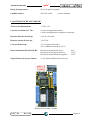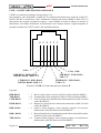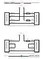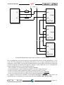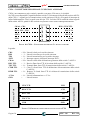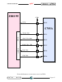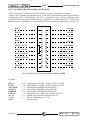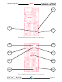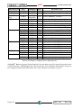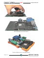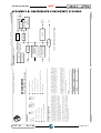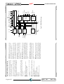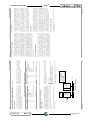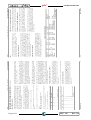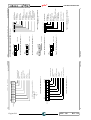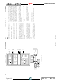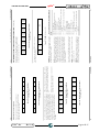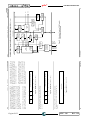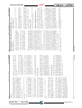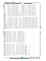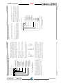
1
®
GPC 184
General Purpose Controller Z80195
MANUALE TECNICO
Via dell' Artigiano, 8/6
® 40016 San Giorgio di Piano
grifo
(Bologna) ITALY
E-mail: [email protected]
http://www.grifo.it
http://www.grifo.com
Tel. +39 051 892.052 (r.a.) FAX: +39 051 893.661
®
GPC 184
Edizione 3.20 Rel. 26 Febbraio 2001
®
, GPC , grifo®, sono marchi registrati della ditta grifo®
ITALIAN TECHNOLOGY
®
GPC 184
General Purpose Controller Z80195
MANUALE TECNICO
Modulo Intelligente Abaco® BLOCK, della Serie 4, nel formato 100x50
mm; contenitore, opzionale, per guide ad Ω tipo DIN 46277-1 e DIN
46277-3. CPU Z80195, con quarzo e clock da 22,1184 MHz (codice Z80,
Z180 compatibile). Jumper di configurazione usato per selezionare il
modo RUN/DEBUG e LED di attivita'. Fino a 512K di EPROM o
FLASH, fino a 512K di RAM, EEPROM seriale fino ad 8K. Tramite
FGDOS la memoria eccedente i 64K é gestita come RAM ROM disk. E'
possibile cancellare e riprogrammare autonomamente la FLASH di bordo
per inserire il proprio programma utente. Real Time Clock con possibilità
di generare INT. Circuiteria di Back Up per RAM ed RTC, tramite batteria
al LITIO interna ed esterna, con stato di carica acquisibile via software.
2 canali di Programmable Reload Timer da 16 bits e 4 canali di Timer
Counter da 8 bits, collegabili in cascata via software in modo da ottenere
un contatore fino a 32 bits. 2 linee seriali asincrone di cui una RS232ed una
settabile in RS232, RS422, RS485 o Current Loop, piu' una linea seriale
sincrona od asincrona in TTL. Le tre linee sono completamente settabili
via software con Baud Rate generator indipendenti, da 50 a 115200 Baud.
Doppia circuiteria di Watch Dog, gestibili via hardware e/o software.
Connettore di espansione per Abaco® I/O BUS da 26 vie. 18 linee di I/O
digitale su connettore standardizzato da 20 vie. Circuiteria di DMA per
trasferimento dati ad alta velocita' tra memorie e periferiche. Numerose
sorgenti d'interrupt, tra cui un'efficiente circuiteria di Power Failure.
Unica tensione di alimlentazione a 5Vdc con diverse modalita' di riduzione
consumi. Protezione della logica di bordo dai transienti tramite
TransZorb™. Vasta disponibilità di software di sviluppo quali Remote
Symbolic Debugger; Macro Assembler; GET 80; compilatori C (HI
TECH C 80, DDS MICRO C 85); compilatori PASCAL (PASCAL 80);
FGDOS 184; ecc.
Via dell' Artigiano, 8/6
® 40016 San Giorgio di Piano
grifo
(Bologna) ITALY
E-mail: [email protected]
http://www.grifo.it
http://www.grifo.com
Tel. +39 051 892.052 (r.a.) FAX: +39 051 893.661
®
GPC 184
Edizione 3.20 Rel. 26 Febbraio 2001
®
, GPC , grifo®, sono marchi registrati della ditta grifo®
ITALIAN TECHNOLOGY
Vincoli sulla documentazione
grifo® Tutti i Diritti Riservati
Nessuna parte del presente manuale può essere riprodotta, trasmessa, trascritta, memorizzata in un archivio o tradotta in altre lingue, con qualunque forma o mezzo, sia esso
elettronico, meccanico, magnetico ottico, chimico, manuale, senza il permesso scritto
della grifo®.
IMPORTANTE
Tutte le informazioni contenute sul presente manuale sono state accuratamente verificate, ciononostante grifo® non si assume nessuna responsabilità per danni, diretti o
indiretti, a cose e/o persone derivanti da errori, omissioni o dall'uso del presente manuale,
del software o dell' hardware ad esso associato.
grifo® altresi si riserva il diritto di modificare il contenuto e la veste di questo manuale
senza alcun preavviso, con l' intento di offrire un prodotto sempre migliore, senza che
questo rappresenti un obbligo per grifo®.
Per le informazioni specifiche dei componenti utilizzati sui nostri prodotti, l'utente deve
fare riferimento agli specifici Data Book delle case costruttrici o delle seconde sorgenti.
LEGENDA SIMBOLI
Nel presente manuale possono comparire i seguenti simboli:
Attenzione: Pericolo generico
Attenzione: Pericolo di alta tensione
Marchi Registrati
, GPC®, grifo® : sono marchi registrati della grifo®.
Altre marche o nomi di prodotti sono marchi registrati dei rispettivi proprietari.
ITALIAN TECHNOLOGY
grifo®
INDICE GENERALE
INTRODUZIONE ........................................................................................................................ 1
VERSIONE SCHEDA .................................................................................................................. 1
CARATTERISTICHE GENERALI ........................................................................................... 2
COMUNICAZIONE SERIALE ............................................................................................... 3
CLOCK ...................................................................................................................................... 3
PROCESSORE DI BORDO ..................................................................................................... 4
CONFIGURAZIONE SCHEDA .............................................................................................. 4
WATCH DOG ............................................................................................................................ 4
MEMORIE ................................................................................................................................. 6
ABACO® I/O BUS ...................................................................................................................... 6
LOGICA DI CONTROLLO ..................................................................................................... 6
COUNTATORI E TEMPORIZZATORI ................................................................................ 7
REAL TIME CLOCK ............................................................................................................... 7
LINEE DI I/O ............................................................................................................................ 7
SPECIFICHE TECNICHE ......................................................................................................... 8
CARATTERISTICHE GENERALI ........................................................................................ 8
CARATTERISTICHE FISICHE ............................................................................................. 8
CARATTERISTICHE ELETTRICHE ................................................................................... 9
INSTALLAZIONE ..................................................................................................................... 10
CONNESSIONI ....................................................................................................................... 10
CN2 - CONNETTORE PER BATTERIA ESTERNA DI BACK UP .............................. 10
CN1 - CONNETTORE PER ABACO® I/O BUS ............................................................... 11
CN3A - CONNETTORE PER LINEA SERIALE A ......................................................... 12
CN3B - CONNETTORE PER LINEA SERIALE B ......................................................... 14
CN5A - CONNETTORE PER SERIALE C E SEGNALI AUSILIARI .......................... 20
CN5 - CONNETTORE PER I/O DEL PIA ED IEEE ....................................................... 22
INTERFACCIAMENTO DEGLI I/O CON IL CAMPO..................................................... 24
INTERFACCE PER I/O DIGITALI ...................................................................................... 24
SEGNALAZIONI VISIVE ..................................................................................................... 25
ALIMENTAZIONE ................................................................................................................. 25
CONTATTO DI RESET ......................................................................................................... 25
JUMPERS ................................................................................................................................ 26
JUMPERS A 2 VIE ............................................................................................................... 28
JUMPERS A 5 VIE ............................................................................................................... 28
JUMPERS A 3 VIE ............................................................................................................... 29
BACK UP ................................................................................................................................. 29
JUMPER A STAGNO ............................................................................................................. 29
RESET E WATCH DOG ........................................................................................................ 30
INTERRUPTS ......................................................................................................................... 30
SELEZIONE MEMORIE ....................................................................................................... 31
SELEZIONE COMUNICAZIONE SERIALE ..................................................................... 32
POWER FAILURE ................................................................................................................. 35
GPC® 184
Rel. 3.20
Pagina I
grifo®
ITALIAN TECHNOLOGY
DESCRIZIONE SOFTWARE ................................................................................................... 36
MAPPAGGI ED INDIRIZZAMENTI ...................................................................................... 39
INTRODUZIONE ................................................................................................................... 39
MAPPAGGIO DELLE RISORSE DI BORDO .................................................................... 39
MAPPAGGIO ABACO® I/O BUS .......................................................................................... 39
MAPPAGGIO MEMORIE ..................................................................................................... 40
MAPPAGGIO I/O ................................................................................................................... 41
DESCRIZIONE SOFTWARE DELLE PERIFERICHE DI BORDO .................................. 45
REAL TIME CLOCK ............................................................................................................. 45
RETRIGGER WATCH DOG ESTERNO ............................................................................ 47
JUMPER DI CONFIGURAZIONE ...................................................................................... 47
EEPROM SERIALE ............................................................................................................... 47
STATO DELLA BATTERIA .................................................................................................. 48
LED DI ATTIVITA' ................................................................................................................ 48
PERIFERICHE DELLA CPU ................................................................................................ 48
SCHEDE ESTERNE .................................................................................................................. 49
BIBLIOGRAFIA ........................................................................................................................ 52
APPENDICE A: MONTAGGIO MECCANICO DELLA SCHEDA .................................. A-1
APPENDICE B: DESCRIZIONE COMPONENTI DI BORDO ......................................... B-1
APPENDICE A: SCHEMI ELETTRICI ............................................................................... C-1
APPENDICE D: INDICE ANALITICO ................................................................................ D-1
Pagina II
GPC® 184
Rel. 3.20
ITALIAN TECHNOLOGY
grifo®
INDICE DELLE FIGURE
FIGURA 1: SCHEMA A BLOCCHI ......................................................................................................... 5
FIGURA 2: FOTO DELLA SCHEDA ....................................................................................................... 9
FIGURA 3: CN2 - CONNETTORE PER BATTERIA ESTERNA DI BACK UP ............................................... 10
FIGURA 4: CN1 - CONNETTORE PER ABACO® I/O BUS .............................................................. 11
FIGURA 5: CN3A - CONNETTORE PER LINEA SERIALE A ................................................................. 12
FIGURA 6: SCHEMA DI COMUNICAZIONE SERIALE ............................................................................. 13
FIGURA 7: CN3B - CONNETTORE PER LINEA SERIALE B ................................................................. 14
FIGURA 8: DISPOSIZIONE LED, CONNETTORI, MEMORIE,ECC........................................................... 15
FIGURA 9: ESEMPIO COLLEGAMENTO PUNTO PUNTO IN RS 232 ....................................................... 16
FIGURA 10: ESEMIPO COLLEGAMENTO PUNTO PUNTO IN RS 422 ..................................................... 16
FIGURA 11: ESEMPIO COLLEGAMENTO PUNTO PUNTO IN RS 485 ..................................................... 16
FIGURA 12: ESEMPIO COLLEGAMENTO IN RETE IN RS 485 .............................................................. 17
FIGURA 13: ESEMPIO COLLEGAMENTO PUNTO PUNTO IN CURRENT LOOP A 4 FILI .............................. 18
FIGURA 14: ESEMPIO COLLEGAMENTO PUNTO PUNTO IN CURRENT LOOP A 2 FILI .............................. 18
FIGURA 15: ESEMPIO DI COLLEGAMENTO IN RETE IN CURRENT LOOP ............................................... 19
FIGURA 16: CN5A - CONNETTORE PER SERIALE C E SEGNALI AUSILIARI ......................................... 20
FIGURA 17: ESEMPIO DI COLLEGAMENTO PUNTO PUNTO IN TTL ..................................................... 20
FIGURA 18: SCHEMA DI COLLEGAMENTO SEGNALI DI CN5A ........................................................... 21
FIGURA 19: CN5 - CONNETTORE PER I/O DEL PIA ED IEEE ........................................................ 22
FIGURA 20: SCHEMA DI COLLEGAMENTO I/O DEL PIA ED IEEE ...................................................... 23
FIGURA 21: TABELLA DELLE SEGNALAZIONI VISIVE ......................................................................... 25
FIGURA 22: TABELLA RIASSUNTIVA JUMPERS ................................................................................... 26
FIGURA 23: DISPOSIZIONE JUMPERS LATO COMPONENTI ................................................................... 27
FIGURA 24: DISPOSIZIONE JUMPERS LATO STAGNATURE ................................................................... 27
FIGURA 25: TABELLA JUMPERS A 2 VIE ........................................................................................... 28
FIGURA 26: TABELLA JUMPERS A 5 VIE ........................................................................................... 28
FIGURA 27: TABELLA JUMPERS A 3 VIE ........................................................................................... 29
FIGURA 28: TABELLA DI SELEZIONE MEMORIE ................................................................................. 31
FIGURA 29: DISPOSIZIONE DRIVER PER COMUNICAZIONE SERIALE .................................................... 33
FIGURA 30: PIANTA COMPONENTI LATO COMPONENTI E STAGNATURA ............................................... 35
FIGURA 31: MAPPAGGIO DELLE MEMORIE ....................................................................................... 41
FIGURA 32: TABELLA INDIRIZZAMENTO I/O (PARTE 1) .................................................................... 42
FIGURA 33: TABELLA INDIRIZZAMENTO I/O (PARTE 2) .................................................................... 43
FIGURA 34: TABELLA INDIRIZZAMENTO I/O (PARTE 3) .................................................................... 44
FIGURA 35: SCHEMA DELLE POSSIBILI CONNESSIONI ........................................................................ 51
FIGURA A1: QUOTE PER MONTAGGIO IN PIGGY BACK .................................................................... A-1
FIGURA A2: MONTAGGIO IN PIGGY BACK ...................................................................................... A-2
FIGURA A3: MONTAGGIO SU GUIDA WEIDMULLER ........................................................................ A-2
FIGURA C1: SCHEMA ELETTRICO DI ESPANSIONE PPI .................................................................... C-1
FIGURA C2: SCHEMA ELETTRICO SPA 03 ..................................................................................... C-2
FIGURA C3: SCHEMA ELETTRICO QTP 16P ................................................................................. C-3
FIGURA C4: SCHEMA ELETTRICO QTP 24P (1 DI 2) ..................................................................... C-4
FIGURA C5: SCHEMA ELETTRICO QTP 24P (2 DI 2) ..................................................................... C-5
FIGURA C6: SCHEMA ELETTRICO DI INPUT OUTPUT SU ABACO® I/O BUS .................................. C-6
FIGURA C7: SCHEMA ELETTRICO INTERFACCIA BUS ..................................................................... C-7
FIGURA C8: SCHEMA ELETTRICO IAC 01..................................................................................... C-8
GPC® 184
Rel. 3.20
Pagina III
grifo®
Pagina IV
ITALIAN TECHNOLOGY
GPC® 184
Rel. 3.20
ITALIAN TECHNOLOGY
grifo®
INTRODUZIONE
L’uso di questi dispositivi é rivolto - IN VIA ESCLUSIVA - a personale specializzato.
Scopo di questo manuale é la trasmissione delle informazioni necessarie all’uso competente e sicuro
dei prodotti. Esse sono il frutto di un’elaborazione continua e sistematica di dati e prove tecniche
registrate e validate dal Costruttore, in attuazione alle procedure interne di sicurezza e qualità
dell'informazione.
I dati di seguito riportati sono destinati - IN VIA ESCLUSIVA - ad un utenza specializzata, in grado
di interagire con i prodotti in condizioni di sicurezza per le persone, per la macchina e per l’ambiente,
interpretando un’elementare diagnostica dei guasti e delle condizioni di funzionamento anomale e
compiendo semplici operazioni di verifica funzionale, nel pieno rispetto delle norme di sicurezza e
salute vigenti.
Le informazioni riguardanti installazione, montaggio, smontaggio, manutenzione, aggiustaggio,
riparazione ed installazione di eventuali accessori, dispositivi ed attrezzature, sono destinate - e
quindi eseguibili - sempre ed in via esclusiva da personale specializzato avvertito ed istruito, o
direttamente dall’ASSISTENZA TECNICA AUTORIZZATA, nel pieno rispetto delle
raccomandazioni trasmesse dal costruttore e delle norme di sicurezza e salute vigenti.
I dispositivi non possono essere utilizzati all'aperto. Si deve sempre provvedere ad inserire i moduli
all'interno di un contenitore a norme di sicurezza che rispetti le vigenti normative. La protezione di
questo contenitore non si deve limitare ai soli agenti atmosferici, bensì anche a quelli meccanici,
elettrici, magnetici, ecc.
Per un corretto rapporto coi prodotti, é necessario garantire leggibilità e conservazione del manuale,
anche per futuri riferimenti. In caso di deterioramento o più semplicemente per ragioni di
approfondimento tecnico ed operativo, consultare direttamente l’Assistenza Tecnica autorizzata.
Al fine di non incontrare problemi nell’uso di tali dispositivi, é conveniente che l’utente - PRIMA
DI COMINCIARE AD OPERARE - legga con attenzione tutte le informazioni contenute in questo
manuale. In una seconda fase, per rintracciare più facilmente le informazioni necessarie, si può fare
riferimento all’indice generale e all’indice analitico, posti rispettivamente all’inizio ed alla fine del
manuale.
VERSIONE SCHEDA
Il presente manuale è riferito alla scheda GPC® 184 versione 310700 e successive. La validità delle
informazioni riportate è quindi subordinata al numero di versione della scheda in uso e l’utente deve
quindi sempre verificare la giusta corrispondenza tra le due indicazioni. Sulla scheda il numero di
versione è riportato in più punti sia a livello di serigrafia che di stampato (ad esempio tra il
microprocessore e le memorie sul lato componenti).
GPC® 184
Rel. 3.20
Pagina 1
grifo®
ITALIAN TECHNOLOGY
CARATTERISTICHE GENERALI
La scheda GPC® 184, che fa parte della serie 4 delle CPU con ingombro di 100x50 mm, e' un potente
modulo di controllo, della fascia a basso prezzo, in grado di funzionare autonomamente come
periferica intelligente e/o remotata in una più vasta rete di telecontrollo e/o di acquisizione.
La GPC® 184 puo' essere fornita di un supporto in plastica provvisto degli attacchi per le guide ad
Omega tipo DIN 46277-1 e DIN 46277-3. In questo modo non e' necessario l’uso di un Rack, ma
la scheda puo' essere montata, in modo piu' economico, direttamente nel quadro elettrico. Viste le
ridotte dimensioni della scheda GPC® 184, questa puo' essere montata nella stessa guida in plastica
che contiene le periferiche di I/O, come ad esempio le ZBx xxx , formando in questo modo un unico
elemento BLOCK. Un'altra tipica applicazione della scheda GPC® 184, e' quella di essere adoperata
come un modulo di CPU da montare in Piggy Back sulle schede periferiche realizzate direttamente
dall'utente.
La programmazione e l'uso delle risorse della scheda diventa estremamente semplice grazie all'uso
del potente sistema operativo romato FGDOS. Esso supporta i linguaggi ad alto livello quali
compilatori C, PASCAL, ecc. e mette a disposizione le risorse di memoria come se fossero RAM/
ROM disk, consentendo un immediato utilizzo ad alto livello di questi dispositivi. L'FGDOS
consente la gestione anche di RAM cards PCMCIA , di display LCD o Fluorescenti, di una tastiera
a matrice e di una stampante parallela. Per un uso immediato di queste funzionalita', sono disponibili
delle apposite interfaccie o degli oggetti finiti come la MCI 64, KDx x24, QTP 24P e QTP 16P che
riducono notevolmente i costi. FGDOS, oltre alla nota facilita' di debug, consente di programmare
,direttamente a bordo scheda, una FLASH con il programma utente.
La caratteristica che distingue la GPC® 184 e' la presenza a bordo scheda di tre linee seriali asincrone
indipendenti, provviste di diverse interfacce elettriche, con cui si possono facilmente risolvere
applicazioni di conversione protocollo, raccolta dati da sistemi seriali, concentratore o smistatore di
linee seriali, ecc.
Per una rapida prototipizzazione si può ricorrere alle ottime schede SPA 03 ed SPA 04 su cui e'
possibile montare, anche in Piggy Back, la GPC® 184. La presenza del connettore Abaco® I/O BUS
consente inoltre di poter pilotare direttamente le schede di I/O tipo ZBR xxx, ZBT xxx e tramite
ABB 03, ABB 05, ecc. e' possibile gestire anche le numerose schede periferiche, disponibili sul BUS
Abaco®.
- Modulo Intelligente Abaco® BLOCK, della Serie 4, nel formato 100x50 mm.
- Contenitore, opzionale, per guide ad Ω tipo DIN 46277-1 e DIN 46277-3.
- CPU Z80195, con quarzo e clock da 22,1184 MHz (codice Z80, Z180 compatibile).
- Jumper di configurazione usato per selezionare il modo RUN/DEBUG e LED di
attivita'.
- Fino a 512K di EPROM o FLASH, fino a 512K di RAM, EEPROM seriale fino ad
8K. Tramite FGDOS la memoria eccedente i 64K é gestita come RAM ROM disk. E'
possibile cancellare e riprogrammare autonomamente la FLASH di bordo per inserire il
proprio programma utente.
- Real Time Clock con possibilità di generare INT.
- Circuiteria di Back Up per RAM ed RTC, tramite batteria al LITIO interna ed esterna,
con stato di carica acquisibile via software.
- 2 canali di Programmable Reload Timer da 16 bits e 4 canali di Timer Counter da 8
bits, collegabili in cascata via software in modo da ottenere un contatore fino a 32 bits..
- 2 linee seriali asincrone di cui una RS232ed una settabile in RS232, RS422, RS485 o
Current Loop, piu' una linea seriale sincrona od asincrona in TTL. Le tre linee sono
completamente settabili via software con Baud Rate generator indipendenti, da 50 a
Pagina 2
GPC® 184
Rel. 3.20
ITALIAN TECHNOLOGY
grifo®
115200 Baud.
- Doppia circuiteria di Watch Dog, gestibili via hardware e/o software.
- Connettore di espansione per Abaco® I/O BUS da 26 vie.
- 18 linee di I/O digitale su connettore standardizzato da 20 vie.
- Circuiteria di DMA per trasferimento dati ad alta velocita' tra memorie e periferiche.
- Numerose sorgenti d'interrupt, tra cui un'efficiente circuiteria di Power Failure.
- Unica tensione di alimlentazione a 5Vdc con diverse modalita' di riduzione consumi.
- Protezione della logica di bordo dai transienti tramite TransZorb™.
- Vasta disponibilità di software di sviluppo quali Remote Symbolic Debugger; Macro
Assembler; GET 80; compilatori C (HI TECH C 80, DDS MICRO C 85); compilatori
PASCAL (PASCAL 80); FGDOS 184; ecc.
Viene di seguito riportata una descrizione dei blocchi funzionali della scheda, con indicate le
operazioni effettuate da ciascuno di essi. Per una più facile individuazione di tali blocchi e per una
verifica delle loro connessioni, fare riferimento alla figura 1.
COMUNICAZIONE SERIALE
La comunicazione seriale é completamente settabilevia software, in modo completamente autonomo,
per quanto riguarda il protocollo fisico (baud rate, stop bit, bit per carattere, parità e gestione
handshake) su tutte le tre linee asincrone ed anche su quella sincrona (bit rate e sorgente di clock).
Tali settaggi avvengono tramite la programmazione dei registri interni del microprocessore relativi
alle sezioni ASCI, EMSCC e CSI/O come descritto nella documentazione tecnica della casa
costruttrice o nell’appendice B di questo manuale. Si prega di ricordare che la linea seriale sincrona
CSI/O condivide alcuni segnali con con la seriale asincrona ASCI 0, quindi le due sezioni non
possono essere usate contemporaneamente.
Dal punto di vista hardware, tramite una serie di comodi jumpers e driver da installare, é invece
possibile selezionare il protocollo elettrico di comunicazione. In particolare una linea (A) é sempre
bufferata in RS 232, una linea (C) non é bufferata ed é disponibile a livello TTL, mentre la rimanente
terza linea (B) può essere bufferata in RS 232, current loop,RS 485 ed RS 422; in quest’ultimo caso
é definibile anche l'attivazione e/o la direzionalità della linea di comunicazione.
Per ulteriori informazioni in merito alla comunicazione seriale fare riferimento ai paragrafi
"CONNETTORI" e "SELEZIONE COMUNICAZIONE SERIALE".
CLOCK
Sulla GPC® 184 é presente una circuiteria che provvede a generare la frequenza di clock per la CPU
(22,1184 MHz) da cui vengono ricavate anche le frequenze necessarie per le altre sezioni della
scheda (Timer, linee seriali, watch dog interno, ecc.). In caso di applicazioni particolarmente lente,
o per ridurre il consumo della scheda, la frequenza di clock può essere divisa via software, Si ricorda
che a seguito di un reset o power on la frequenza di clock della CPU é sempre dimezzata rispetto a
quella del quarzo. Comunque la scheda é completamente testata con una frequenza di clock da
22,1184 MHz e tutti i pacchetti di sviluppo software forniti dalla grifo® settano sempre questa
frequenza di lavoro.
GPC® 184
Rel. 3.20
Pagina 3
grifo®
ITALIAN TECHNOLOGY
PROCESSORE DI BORDO
La scheda GPC® 184 é predisposta per accettare il processore Z80195 prodotto dalla ZILOG. Tale
processore ad 8 bit é codice compatibile con lo Z80 e Z180 ed é quindi caratterizzato da un esteso
set di istruzioni (170), da un’alta velocità di esecuzione e di manipolazione dati e da un efficiente
gestione vettorizzata degli interrupts. Di fondamentale importanza é la presenza delle seguenti
periferiche interne al microprocessore:
- 2 Timer a 16 bit, con prescaler programmabile (PRT);
- 4 Timer Counter ad 8 bit (CTC);
- 2 linee seriali asincrone complete di segnali di handshake (ASCI);
- 1 linea seriale asincrona evoluta (EMSCC) in grado di gestire anche protocolli SDLC;
- 2 canali di DMA per trasferimenti dati ad alta velocità (DMAC);
- 1 interfaccia Centronics bidirezionale (IEEE) che condivide due port di I/O ad 8 bit (PIA);
- Gestore di memoria estesa (MMU);
- 1 linea seriale sincrona (CSI/O);
- Watch dog interno con tempo d'intervento programmabile;
- Controllore d'interrupt;
- 1 MByte di memoria indirizzabile;
- Generatore di cicli di wait per l'accesso a dispositivi esterni lenti;
- Possibilità di operare in idle e stop mode, per minimizzare i consumi.
Per maggiori informazioni sul componente si faccia riferimento all’apposita documentazione della
casa costruttrice, oppure all’appendice B di questo manuale. Si prega di ricordare che il precedente
elenco descrive le caratteristiche generali del microprocessore e che alcune di queste non sono
disponibili sulla scheda.
CONFIGURAZIONE SCHEDA
Allo scopo di rendere configurabile la scheda ed in particolare il programma applicativo sviluppato,
é stato previsto il jumper J4. La possibilità di acquisire via software lo stato di questo jumper, fornisce
all’utente la possibilità di gestire diverse condizioni tramite un unico programma, senza dover
rinunciare ad altre linee d’ingresso (le applicazioni caratteristiche sono: selezione della lingua di
rappresentazione, definizione parametri del programma, selezione della modalità operativa, ecc.).
Alcuni pacchettisoftware sviluppati per la GPC® 184 usano il jumper J4 per selezionare la modalità
operativa di RUN o DEBUG, come descritto negli appositi manuali d'uso degli stessi pacchetti.
In aggiunta la scheda ha un LED di attività, gestibile via software, che può essere usato per
visualizzare la configurazione attuale della scheda, come descritto negli appositi paragrafi.
WATCH DOG
La scheda GPC® 184 é provvista di una doppia circuiteria di watch dog che, se utilizzate, consentono
di uscire da stati di loop infinito o da condizioni anomale non previste dal programma applicativo.
Tali circuiterie sono composte da due sezioni astabili di cui una con un tempo d’intervento fisso a
circa 1,4 sec ed una con tempo d'intervento programmabile via software. Tutta la gestione avviene
via software (tramite l’accesso ad opportuni registri situati nello spazio d’indirizzamento della CPU)
e conferisce al sistema basato sulla scheda, una sicurezza estrema.
Pagina 4
GPC® 184
Rel. 3.20
grifo®
ITALIAN TECHNOLOGY
CN3A
CN3B
SERIAL LINE A
SERIAL LINE B
CN2
-
BACK UP
3V
LITHIUM
BATTERY
RS 232
RS 422
RS 485
CURRENT LOOP
RS 232
+
RTC
DRIVERS
IC5 SRAM
IC 2
EPROM,FLASH
IC 7
EEPROM
CPU
Z80195
RESET and
WATCH DOG
POWER
FAILURE
JUMPER
RUN/DEBUG
CONTROL
LOGIC
CN5A
CLK SERIAL I/O
SERIAL LINE C
CN5
DIGITAL I/O LINES
CN1
ABACO® I/O BUS
FIGURA 1: SCHEMA A BLOCCHI
GPC® 184
Rel. 3.20
Pagina 5
grifo®
ITALIAN TECHNOLOGY
MEMORIE
E’ possibile dotare la scheda di un massimo di 1032K di memoria variamente suddivisi con un
massimo di 512K Byte di EPROM o FLASH EPROM, 512K Byte di RAM statica ed 8K Byte di
EEPROM. La scelta della configurazione delle memorie presenti sulla scheda può avvenire in
relazione all’applicazione da risolvere e quindi alle esigenze dell’utente. Da questo punto di vista si
ricorda che la scheda viene normalmente fornita con 128K Byte di SRAM più 512 Byte di EEPROM
e che tutte le rimanenti configurazioni di memoria devono essere quindi opportunamente specificate
in fase di ordine della scheda.
Sfruttando la circuiteria di back up di bordo più l'eventuale batteria tampone esterna, si ha la
possibilità di mantenere i dati anche in assenza di alimentazione. Questa caratteristica fornisce alla
scheda la possibilità di ricordare in ogni condizione, una serie di parametri come ad esempio la
configurazione o lo stato del sistema, anche per lunghi periodi di inattività senza dover ricorrere a
costosi gruppi di continuità esterni.
Il mappaggio delle risorse di memoria avviene tramite una opportuna circuiteria di bordo, che
provvede ad allocare i dispositivi all’interno dello spazio d’indirizzamento del microprocessore.
Questa circuiteria é inoltre in grado di gestire automaticamente tutte le modalità d'indirizzamento
richieste dai pacchetti di sviluppo software per la GPC® 184.
Per maggiori informazioni fare riferimento al capitolo "MAPPAGGI ED INDIRIZZAMENTI" e
"DESCRIZIONE SOFTWARE DELLE PERIFERICHE DI BORDO". Per una descrizione più
approfondita sui dispositivi di memoria, sugli zoccoli da utilizzare e sullo strippaggio della scheda,
fare riferimento al paragrafo "SELEZIONE MEMORIE".
ABACO® I/O BUS
Una delle caratteristiche di fondamentale importanza della GPC® 184 è quella di disporre del
cosiddetto ABACO® I/O BUS: ovvero un connettore normalizzato con cui è possibile collegare la
scheda ad una serie di moduli esterni intelligenti e non. Tra questi si trovano moduli per acquisizione
di segnali analogici (A/D), per la generazione di segnali analogici (D/A), schede con contatori e
temporizzatori, schede per gestione di linee di I/O logico, ecc. e ne possono essere realizzati anche
su specifiche richieste dell’utente.
Utilizzando mother board come l’ABB 03 o l’ABB 05 é inoltre possibile gestire tutte le schede
periferiche in formato Europa con interfaccia per BUS ABACO®. Tale caratteristica rende la scheda
espandibile con un ottimo rapporto prezzo/prestazioni e quindi adatta a risolvere molti dei problemi
dell’automazione industriale.
Il capitolo "SCHEDE ESTERNE" mostra una breve descrizione di alcune di queste schede di
espansione.
LOGICA DI CONTROLLO
Il mappaggio di tutti i registri delle periferiche presenti sulla scheda e dei dispositivi di memoria, é
affidata ad un’opportuna logica di controllo che si occupa di allocare tali dispositivi nello spazio
d’indirizzamento della CPU. Per maggiori informazioni fare riferimento ai paragrafi “MAPPAGGIO
I/O” e "MAPPAGGIO MEMORIE".
Pagina 6
GPC® 184
Rel. 3.20
ITALIAN TECHNOLOGY
grifo®
COUNTATORI E TEMPORIZZATORI
La sezione di bordo CTC comprende 4 timer counter da 8 bit. Ogni canale può essere programmato
indipendentemente con un proprio prescaler, un proprio modo operativo (timer con trigger esterno,
contatore di fronti di salita o discesa, ecc.) ed una eventuale generazione d'interrupt. Il CTC é
completamente gestito via software programmando 5 registri allocati nello spazio di I/O del
microprocessore ed collegabile all'elettronica esterna tramite 7 segnali digitali che sono multiplexate
con linee di I/O. Sempre via software i canali del CTC possono essere collegati in cascata ottenendo
contatori e temporizzatori da 16, 24 e 32 bit.
In aggiunta la CPU dispone della sezione PRT che equivale a due temporizzatori a 16 bit che possono
essere usati per gestire dei tempi brevi. Questi timer sono programmabili via software tramite 7
registri indirizzati nello spazio di I/O della CPU.
REAL TIME CLOCK
La GPC® 184 dispone di un completo Real Time Clock in grado di gestire ore, minuti, secondi, giorno
del mese, mese, anno e giorno della settimana in modo completamente autonomo. L’alimentazione
del componente é fornita dalla circuiteria di back up in modo da garantire la validità dei dati in ogni
condizione operativa ed é completamente gestito via software, tramite la programmazione di 16
registri situati nello spazio di I/O della CPU dall'apposita logica di controllo. La sezione di RTC può
inoltre generare interrupt in corrispondenza di intervalli di tempo programmabili via software, in
modo da poter periodicamente distogliere la CPU dalle normali operazioni oppure periodicamente
risvegliarla dagli stati di basso assorbimento.
LINEE DI I/O
La CPU Z80195 include una sezione PIA ed un controllore bidirezionale IEEE per un totale di 24
linee di I/O digitale. Sei di queste linee sono usate per la gestione di alcune risorse di bordo (LED
di attività, stato batteria, EEPROM seriale, ecc.) mentre le rimanenti 18 sono collegate ad un
connettore standard di I/O ABACO®. La direzionalità di 15 delle 18 linee a disposizione utente é
settabile via software a livello di bit. Queste linee di I/O aggiungono la possibilità di collegare diversi
dispositivi (ad esempio interfaccie operatore) anche quando l'arbitraggio delle condizioni deve
essere completamente gestito via software. Un'apposita logica di controllo consente la programmazione
del PIA ed IEEE interni utilizzando 10 registri allocati nello spazio di I/O della CPU.
GPC® 184
Rel. 3.20
Pagina 7
grifo®
ITALIAN TECHNOLOGY
SPECIFICHE TECNICHE
CARATTERISTICHE GENERALI
Risorse della scheda:
2 timer a 16 bit (PRT)
4 timer counter a 8 bit (CTC)
2 canali DMA (DMAC)
1 linea seriale RS 232 (ASCI1=A)
1 linea seriale RS232,RS 422,RS 485,current loop(EMSCC =B)
1 linea seriale TTL (ASCI0=C)
1 linea seriale sincrona (CSI/O)
18 linee di I/O TTL programmabili (PIA, IEEE)
1 contatto locale di reset
2 watch dog astabili
1 real time clock
1 jumper di configurazione
1 interfaccia ABACO® I/O BUS
1 circuiteria di power failure
1 circuiteria di back up
Memoria:
IC 2:
IC 5:
IC 7:
EPROM da 128K x 8 a 512K x 8
FLASH EPROM da 128K x 8 a 512K x 8
SRAM da 128K x 8 a 512K x 8
EEPROM seriale da 256 ad 8K Byte
Tempo d'accesso memorie:
70 nsec
CPU:
ZILOG Z80195
Frequenza quarzo (clock):
22,1184 (22,1184) MHz
Intervento watch dog esterno:
da 940 msec a 2060 msec (tipico 1420 msec)
CARATTERISTICHE FISICHE
Dimensioni (L x A x P):
100 x 50 x 25 mm
110 x 60 x 60 mm
(senza contenitore)
(con contenitore per guide DIN)
Peso:
65 g
120 g
(senza contenitore)
(con contenitore per guide DIN)
Connettori:
CN1:
CN2:
CN3A:
CN3B:
CN5:
CN5A:
Pagina 8
26 vie scatolino verticale M
2 vie scatolino verticale M
Plug a 6 vie F
Plug a 6 vie F
20 vie scvatolino verticale M
4+4 strip verticale M
GPC® 184
Rel. 3.20
grifo®
ITALIAN TECHNOLOGY
Range di temperatura:
da 0 a 50 gradi Centigradi
Umidità relativa:
20% fino a 90%
(senza condensa)
CARATTERISTICHE ELETTRICHE
Tensione di alimentazione:
+5 Vdc ±5%
Corrente assorbita sui 5 Vdc:
120 mA (configurazione base)
140 mA (configurazione completa e massima)
Batteria di bordo di back up:
3,0 Vdc; 180 mAh
Batteria esterna di back up:
3,6÷5 Vdc
Corrente di back up:
2,5 µA (batteria di bordo)
4,5 µA (Batteria esterna da 3,6 V)
Rete terminazione RS 422, RS 485:
Resistenza terminazione linea=
Resistenza di pull up sul positivo=
Resistenza di pull down sul negativo=
Soglia d’intervento power failure:
52 mV prima dell'intervento del reset
120 Ω
3,3 KΩ
3,3 KΩ
FIGURA 2: FOTO DELLA SCHEDA
GPC® 184
Rel. 3.20
Pagina 9
grifo®
ITALIAN TECHNOLOGY
INSTALLAZIONE
In questo capitolo saranno illustrate tutte le operazioni da effettuare per il corretto utilizzo della
scheda. A questo scopo viene riportata l’ubicazione e la funzione degli strip, dei connettori e dei
LEDs, ecc. presenti sulla GPC® 184 ed alcuni schemi illustrativi.
CONNESSIONI
Il modulo GPC® 184 è provvisto di 6 connettori con cui vengono effettuati tutti i collegamenti con
il campo e con le altre schede del sistema di controllo da realizzare. Di seguito viene riportato il loro
pin out ed il significato dei segnali collegati; per una facile individuazione di tali connettori, si faccia
riferimento alla figura 9, mentre per ulteriori informazioni a riguardo del tipo di connessioni, fare
riferimento alle figure successive che illustrano il tipo di collegamento effettuato a bordo scheda.
CN2 - CONNETTORE PER BATTERIA ESTERNA DI BACK UP
CN2 é un connettore a scatolino, verticale, maschio, con passo 2,54 mm, a 2 vie.
Tramite CN2 può essere collegata una batteria esterna che provvede a mantenere i dati della SRAM
di bordo ed a garantire il funzionamento del real time clock, in assenza di tensione di alimentazione
(per maggiori informazioni fare riferimento al paragrafo “BACK UP”.
1
+Vbat
2
GND
FIGURA 3: CN2 - CONNETTORE PER BATTERIA ESTERNA DI BACK UP
Legenda:
+Vbat
GND
Pagina 10
=
=
I
-
Positivo della batteria esterna di back up
Negativo della batteria esterna di back up
GPC® 184
Rel. 3.20
ITALIAN TECHNOLOGY
grifo®
CN1 - CONNETTORE PER ABACO® I/O BUS
CN1 è un connettore a scatolino, verticale, maschio, con passo 2.54 mm, a 26 piedini.
Tramite CN1 si effettua la connessione tra la scheda e la serie di moduli esterni di espansione della
grifo®. Tale collegamento è effettuato tramite l’ABACO® I/O BUS di cui questo connettore riporta
tutti i segnali a livello TTL.
D0
1
2
D1
D2
3
4
D3
D4
5
6
D5
D6
7
8
D7
A0
9
10
A1
A2
11
12
A3
A4
13
14
A5
A6
15
16
A7
/WR
17
18
/RD
/IORQ
19
20
/RESET
N.C.
21
22
N.C.
/INT BUS
23
24
/NMI BUS
GND
25
26
+5 Vdc
FIGURA 4: CN1 - CONNETTORE PER ABACO® I/O BUS
Legenda:
A0÷A7
D0÷D7
/INT BUS
/NMI BUS
/IORQ
/RD
/WR
/RESET
+5 Vdc
GND
N.C.
GPC® 184
= O - Address BUS: BUS degli indirizzi.
= I/O - Data BUS: BUS dei dati.
= I - Interrupt request: richiesta d’interrupt (deve essere in open collector)
= I - Non Mascable Interrupt: richiesta d’interrupt non mascherabile (deve
essere in open collector).
= O - Input Output Request: richiesta operazione Input Output su I/O BUS.
= O - Read cycle status: richiesta di lettura.
= O - Write cycle status: richiesta di scrittura.
= O - Reset: azzeramento.
= I - Linea di alimentazione a +5 Vcc.
=
- Linea di massa.
=
- Non collegato.
Rel. 3.20
Pagina 11
grifo®
ITALIAN TECHNOLOGY
CN3A - CONNETTORE PER LINEA SERIALE A
CN3A é un connettore femmina, del tipo plug a 6 vie.
Sul connettore sono disponibili i segnali per la comunicazione della linea seriale A, in RS 232, che
é fisicamente collegata alla sezione ASCI 1 della CPU. La disposizione dei segnali, riportata di
seguito, é stata studiata in modo da ridurre al minimo le interferenze ed in modo da facilitare la
connessione con il campo, mentre i segnali rispettano le normative definite dal CCITT relative allo
standard RS 232.
6 5 4 3 2 1
GND
RXA RS232
CTSA RS232
+5 Vdc , GND
TXA RS232
RTSA RS232 (*1)
FIGURA 5: CN3A - CONNETTORE PER LINEA SERIALE A
Legenda:
RXA RS 232
TXA RS 232
CTSA RS 232
RTSA RS 232
+5 Vdc
GND
*1:
= I - Receive Data: linea di ricezione in RS 232 della seriale A=ASCI1.
= O - Transmit Data: linea di trasmissione in RS 232 della seriale A=ASCI1.
= I - Clear To Send: linea di abilitazione alla trasmissione in RS 232 della
seriale A=ASCI1.
= O - Request To Send: linea di richiesta di trasmissione in RS 232 della
seriale A=ASCI1 (*1).
= O - Linea di alimentazione a +5 Vcc.
=
- Linea di massa.
Il segnale di handshake di uscita RTSA non é gestibile via software ed é mantenuto sempre
attivo = +10 Vdc. Se questo stato é incompatibile con il sistema a cui si collega, provvedere
ad effettuare un collegamento senza questo segnale.
Pagina 12
GPC® 184
Rel. 3.20
grifo®
ITALIAN TECHNOLOGY
Z80
195
DRIVERS
CN3B
RS 422
RS 485
EMSCC
CURRENT
LOOP
RS 232
SERIAL LINE B
ASCI 0
CSI/O
CLOCKED SERIAL LINE
SERIAL LINE C
CN3A
RS 232
SERIAL LINE A
CN5A
ASCI 1
DRIVERS
FIGURA 6: SCHEMA DI COMUNICAZIONE SERIALE
GPC® 184
Rel. 3.20
Pagina 13
grifo®
ITALIAN TECHNOLOGY
CN3B - CONNETTORE PER LINEA SERIALE B
CN3B é un connettore femmina, del tipo plug a 6 vie.
Sul connettore sono disponibili i segnali per la comunicazione della linea seriale B, in RS 232,
RS 422, RS 485 o current loop che é fisicamente collegata alla sezione EMSCC della CPU. La
disposizione dei segnali, riportata di seguito, é stata studiata in modo da ridurre al minimo le
interferenze ed in modo da facilitare la connessione con il campo, mentre i segnali rispettano le
normative definite dal CCITT relative allo standard utilizzato.
6 5 4 3 2 1
GND
+5 Vdc , GND
RXB RS232 , RXB+ RS422 ,
RXTXB+ RS485 , RXB+ C.L.
CTSB RS232 , RXB- RS422 ,
RXTXB- RS485 , RXB- C.L.
TXB RS232 , TXB+ RS422 ,
TXB- C.L.
RTSB RS232 , TXB- RS422 ,
TXB+ C.L.
FIGURA 7: CN3B - CONNETTORE PER LINEA SERIALE B
Legenda:
RXB RS232
TXB RS232
CTSB RS232
RTSB RS232
RXB- RS422
RXB+ RS422
TXB- RS422
Pagina 14
= I - Receive Data: linea ricezione in RS 232 della seriale B=EMSCC.
= O - Transmit Data: linea trasmissione in RS 232 della seriale B=EMSCC.
= I - Clear To Send: linea di abilitazione alla trasmissione in RS 232 della
seriale B=EMSCC.
= O - Request To Send: linea di richiesta di trasmissione in RS 232 della
seriale B=EMSCC.
= I - Receive Data Negative: linea bipolare negativa di ricezione
differenziale in RS 422 della seriale B=EMSCC.
= I - Receive Data Positive: linea bipolare positiva di ricezione differenziale
in RS 422 della seriale B=EMSCC.
= O - Transmit Data Negative: linea bipolare negativa di trasmissione
differenziale in RS 422 della seriale B=EMSCC.
GPC® 184
Rel. 3.20
grifo®
ITALIAN TECHNOLOGY
TXB+ RS422
RXTXB- RS485
RXTXB+ RS485
RXB- C.L.
RXB+ C.L.
TXB- C.L.
TXB+ C.L.
+5 Vdc
GND
= O - Transmit Data Positive: linea bipolare positiva di trasmissione
differenziale in RS 422 della seriale B=EMSCC.
= I/O - Receive Transmit Data Negative: linea bipolare negativa di ricezione
e trasmissione differenziale in RS 485 della seriale B=EMSCC.
= I/O - Receive Transmit Data Positive: linea bipolare positiva di ricezione
e trasmissione differenziale in RS 485 della seriale B=EMSCC.
= I - Receive Data Negative: linea bipolare negativa di ricezione in
Current Loop della seriale B=EMSCC.
= I - Receive Data Positive: linea bipolare positiva di ricezione in Current
Loop della seriale B=EMSCC.
= O - Transmit Data Negative: linea bipolare negativa di trasmissione in
Current Loop della seriale B=EMSCC.
= O - Transmit Data Positive: linea bipolare positiva di trasmissione in
Current Loop della seriale B=EMSCC.
= O - Linea di alimentazione a +5 Vcc.
=
- Linea di massa.
CN3B
CN3A
CN5
BT1
CN5A
IC7
CN1
SERIAL
EEPROM
CN2
LD1
IC2
EPROM
FLASH
IC5
SRAM
P1
FIGURA 8: DISPOSIZIONE LED, CONNETTORI, MEMORIE,ECC.
GPC® 184
Rel. 3.20
Pagina 15
ITALIAN TECHNOLOGY
4
CTSA RS232, CTSB RS232
RTS
3
RTSA RS232, RTSB RS232
CTS
5
RXARS232, RXB RS232
TX
2
TXA RS232, TXB RS232
RX
6
GND
External System
CN3A,B GPC® 184
grifo®
GND
FIGURA 9: ESEMPIO COLLEGAMENTO PUNTO PUNTO IN RS 232
RXB- RS422
TX-
RXB+ RS422
TX+
TXB- RS422
RX-
TXB+ RS422
RX+
GND
GND
5
3
2
External System
CN3B GPC® 184
4
6
RXTXB- RS485
TX-,RX-
RXTXB+ RS485
TX+,RX+
4
5
GND
GND
External System
CN3B GPC® 184
FIGURA 10: ESEMIPO COLLEGAMENTO PUNTO PUNTO IN RS 422
6
FIGURA 11: ESEMPIO COLLEGAMENTO PUNTO PUNTO IN RS 485
Pagina 16
GPC® 184
Rel. 3.20
grifo®
ITALIAN TECHNOLOGY
Master
5
+
TXRX
-
120 Ω
4
Slave 1
+
TXRXB
CN3B
GND
GPC® 184
GND
6
Slave 2
6
CN3B
TXRXB
-
GND
+5V
5 +
4 6
GND
GPC® 184
4
+
Slave n
CN3B
TXRXB
GPC® 184
5
FIGURA 12: ESEMPIO COLLEGAMENTO IN RETE IN RS 485
Da notare che in una rete RS 485, devono essere presenti due resistenze di forzatura lungo la linea
e due resitenze di terminazione (120 Ω), alle estremità della stessa, rispettivamente vicino all'unità
Master ed all'ultima unità Slave.
A bordo della GPC® 184 è presente la circuiteria di terminazione e forzatura, che può essere inserita
o disinserita, tramite appositi jumpers, come illutrato in seguito.
In merito alla resistenza di terminazione dell'unità Master, provvedere a collegarla solo se questa non
é già presente al suo interno (ad esempio molti convertitori RS232-RS485 ne sono già provvisti).
Per maggiori informazioni consultare il Data-Book TEXAS INSTRUMENTS, "RS 422 and RS 485
Interface Cicuits", nella parte introduttiva riguardante le reti RS 422-485.
GPC® 184
Rel. 3.20
Pagina 17
grifo®
-
VCL
ITALIAN TECHNOLOGY
+
R
RXB- C.L.
TX+
RXB+ C.L.
TX-
5
R
TXB- C.L.
RX+
2
External System
CN3B GPC® 184
4
RX-
TXB+ C.L.
3
FIGURA 13: ESEMPIO COLLEGAMENTO PUNTO PUNTO IN CURRENT LOOP A 4 FILI
-
VCL
+
R
RXB- C.L.
TX+
RXB+ C.L.
TX-
TXB- C.L.
RX+
TXB+ C.L.
RX-
5
2
External System
CN3B GPC® 184
4
3
FIGURA 14: ESEMPIO COLLEGAMENTO PUNTO PUNTO IN CURRENT LOOP A 2 FILI
Pagina 18
GPC® 184
Rel. 3.20
grifo®
ITALIAN TECHNOLOGY
+
Master
R
+
TX
R
+
RX
-
VCL
Slave 1
5 +
RXB
4 CN3B
3 +
TXB
2
GPC® 184
Slave 2
5 +
RXB
4 CN3B
3 +
TXB
2 GPC® 184
Slave n
5
+
RXB
4
CN3B
+
2 TXB
GPC® 184
3
FIGURA 15: ESEMPIO DI COLLEGAMENTO IN RETE IN CURRENT LOOP
Per il collegamento in current loop passivo sono possibili due diversi tipi di collegamento: a 2 fili
ed a 4 fili. Tali connessioni sono riportate nelle figure 13÷15; in esse é indicata la tensione per
alimentare l’anello (VCL) e le resistenze di limitazione della corrente (R). I valori di tali componenti
variano in funzione del numero di dispositivi collegati e della caduta sul cavo di collegamento;
bisogna quindi effettuare la scelta considerando che:
- si deve garantire la circolazione di una corrente di 20 mA;
- su ogni trasmettitore cadono mediamente 2,35 V con una corrente di 20 mA;
- su ogni ricevitore cadono mediamente 2,52 V con una corrente di 20 mA;
- in caso di cortocircuito sulla rete ogni trasmettitore dissipi al massimo 125 mW;
- in caso di cortocircuito sulla rete ogni ricevitore dissipi al massimo 90 mW.
Per maggiori informazioni consultare il Data-Book HEWLETT-PACKARD, nella parte che
riguarda gli opto accoppiatori per current loop denominati HCPL 4100 e HCPL 4200.
GPC® 184
Rel. 3.20
Pagina 19
grifo®
ITALIAN TECHNOLOGY
CN5A - CONNETTORE PER SERIALE C E SEGNALI AUSILIARI
CN5A è un connettore a strip verticale, maschio, con passo 2.54 mm, a 4+4 piedini.
Su CN5A sono disponibili i segnali della linea seriale C (fisicamente collegata alla sezione ASCI 0
della CPU), i 3 segnali per la comunicazione seriale sincrona (CSI/O), un segnale di interrupt ed
infine l'alimentazione. Tutti i segnali sono del tipo TTL. La linea CSI/O condivide alcuni segnali
della seriale ASCI 0, quindi le due sezioni non possono essere usate contemporaneamente.
CKA0 , CKS
1
2
RXS , CTSC TTL
RTSC TTL , TXS
3
4
RXC TTL
/INT1
5
6
TXC TTL
GND
7
8
+5Vdc
FIGURA 16: CN5A - CONNETTORE PER SERIALE C E SEGNALI AUSILIARI
Legenda:
= I/O - Linea di clock per la seriale sincrona.
= I - Linea di ricezione per la seriale sincrona.
= O - Linea di trasmissione per la seriale sincrona.
= I - Interrupt request: richiesta d’interrupt /INT1.
= I/O - Linea di clock della del baud rate generator della seriale C=ASCI 0.
= I - Receive Data: linea TTL di ricezione della seriale C=ASCI 0.
= O - Transmit Data: linea TTL di trasmissione della seriale C=ASCI 0.
= I - Clear To Send: linea TTL di abilitazione alla trasmissione della seriale
C=ASCI 0.
= O - Request To Send: linea TTL di richiesta di trasmissione della seriale
C=ASCI 0.
= O - Linea di alimentazione a +5 Vcc
=
- Linea di massa.
RTSB TTL
CN5A GPC® 184
+5 Vdc
GND
2
CTSC TTL
RTS
3
RTSC TTL
CTS
4
RXC TTL
TX
6
TXC TTL
RX
7
GND
External System
CKS
RXS
TXS
/INT1
CKA0
RXC TTL
TXC TTL
CTSB TTL
GND
FIGURA 17: ESEMPIO DI COLLEGAMENTO PUNTO PUNTO IN TTL
Pagina 20
GPC® 184
Rel. 3.20
grifo®
ITALIAN TECHNOLOGY
Z80195
+5 Vdc
/INT1
PIN 5
CN5A
CSI/O
CKA0 , CKS
CTSC TTL , RXS
ASCI 0
RTSC TTL , TXS
RXC TTL
TXC TTL
PIN 1
PIN 2
PIN 3
PIN 4
PIN 6
FIGURA 18: SCHEMA DI COLLEGAMENTO SEGNALI DI CN5A
GPC® 184
Rel. 3.20
Pagina 21
grifo®
ITALIAN TECHNOLOGY
CN5 - CONNETTORE PER I/O DEL PIA ED IEEE
CN5 è un connettore a scatolino verticale, maschio, con passo 2.54 mm, a 20 piedini.
Tramite CN5 si effettua la connessione tra le 18 linee di I/O digitale delle interfaccie periferiche
programmabili PIA ed IEEE interne alla CPU e l’ambiente esterno. Alcuni piedini di questo
connettore hanno una duplice funzione infatti, via software, la sezione interna di CTC può essere
multiplexata con i segnali di I/O. Tutti i segnali di CN5 coincidono con segnali logici a livello TTL.
PIA 21
1
2
PIA 20
PIA 23
3
4
PIA 22
PIA 25
5
6
PIA 24
PIA 27
7
8
PIA 26
PIA 16 , ZC T2
9
10
NAUTOFD
PIA 14 , ZC T0
11
12
ZC T1 , PIA 15
PIA 12 , CLK T2
13
14
CLK T3 , PIA 13
PIA 10 , CLK T0
15
16
CLK T1 , PIA 11
GND
17
18
+5 Vdc
SELECT
19
20
PERROR
FIGURA 19: CN5 - CONNETTORE PER I/O DEL PIA ED IEEE
Legenda:
PIA1n
PIA2n
NAUTOFD
SELECT
PERROR
CLK Tn
ZC Tn
+5 Vdc
GND
Pagina 22
= I/O - Linea digitale n del port 1 del PIA interno alla CPU.
= I/O - Linea digitale n del port 2 del PIA interno alla CPU.
= I - Linea digitale dell'IEEE interno alla CPU.
= O - Linea digitale dell'IEEE interno alla CPU.
= O - Linea digitale dell'IEEE interno alla CPU.
= I - Segnale di clock o trigger del contatore n del CTC.
= O - Segnale zero count del contatore n del CTC.
= O - Linea di alimentazione a +5 Vcc.
=
- Linea di massa.
GPC® 184
Rel. 3.20
ITALIAN TECHNOLOGY
grifo®
Z80195
PIA 2
+5 Vdc
8 LINES
PIN 1÷8
CN5
PIA 1
NAUTOFD
SELECT
PERROR
7 LINES
1 LINE
2 LINES
PIN 9, 11÷16
PIN 10
PIN 19, 20
FIGURA 20: SCHEMA DI COLLEGAMENTO I/O DEL PIA ED IEEE
GPC® 184
Rel. 3.20
Pagina 23
grifo®
ITALIAN TECHNOLOGY
INTERFACCIAMENTO DEGLI I/O CON IL CAMPO
Al fine di evitare eventuali problemi di collegamento della scheda con tutta l’elettronica del campo
a cui la GPC® 184 si deve interfacciare, si devono seguire le informazioni riportate nei precedenti
paragrafi e le relative figure che illustrano le modalità interne di connessione.
- Per i segnali che riguardano la comunicazione seriale con i protocolli RS 232, RS 422, RS 485 o
current loop, fare riferimento alle specifiche standard di ognuno di questi protocolli.
- Tutti i segnali a livello TTL possono essere collegati a linee dello stesso tipo riferite alla massa
digitale della scheda. Il livello 0V corrisponde allo stato logico 0, mentre il livello 5V corrisponde
allo stato logico 1.
INTERFACCE PER I/O DIGITALI
Tramite CN5 (connettore compatibile con standard di I/O ABACO®) si può collegare la GPC® 184
ai numerosi moduli del carteggio grifo® che riportano lo stesso pin out. Dal punto di vista
dell'installazione, queste interfacce richiedono solo un flat cable da 20 vie (codice FLT.20+20) con
cui é possibile portare anche le alimentazioni, mentre dal punto di vista software la gestione é
semplice ed immediata. Di particolare interesse è la possibilità di collegare direttamente serie di
moduli come:
- QTP 16P, QTP 24P, KDL x24, KDF 224, DEB 01, ecc. con cui risolvere tutti i problemi di
interfacciamento operatore locale. Questi moduli sono già dotati delle risorse necessarie per gestire
un buon livello di colloquio uomo-macchina (includono infatti display alfanumerici, tastiera a
matrice e LEDs di visualizzazione) ad una breve distanza dalla GPC® 184. Dal punto di vista
software i driver disponibili rendono utilizzabili le risorse dell'interfaccia operatore direttamente
con le istruzioni ad alto livello per la gestione della console.
- MCI 64 con cui risolvere tutti i problemi di salvataggio di grosse quantità di dati. Questo modulo
é dotato di un connettore per memory card PCMCIA su cui possono essere inserite vari tipi di
memory card (RAM, FLASH, ROM, ecc) nei vari size disponibili. Dal punto di vista software i
driver disponibili coincidono con un completo file system e rendono utilizzabili le memory card
direttamente con le istruzioni ad alto livello per la gestione dei files, oppure con procedure che
consentono di leggere e scrivere dati ad indirizzi specifici della memory card.
- IAC 01, DEB 01 con cui gestire una stampante con interfaccia parallela CENTRONICS.
Quest'ultima può essere collegata direttamente all'interfaccia, con un cavo standard, e quindi gestita
con le istruzioni relative alla stampante del linguaggio di programmazione utilizzato.
- RBO xx, TBO xx, XBI xx, OBI xx con cui bufferare i segnali di I/O TTL nei confronti del campo.
Con questi moduli i segnali di input vengono convertiti in ingressi optoisolati di tipo NPN o PNP,
mentre i segnali di output vengono convertiti in uscite galvanicamente isolate a transistor o relé.
Alcune di queste interfacce possono essere collegate direttamente anche al CN5.
Per maggiori informazioni relative si veda il capitolo “SCHEDE ESTERNE” e la documentazione
del software utilizzato.
Pagina 24
GPC® 184
Rel. 3.20
grifo®
ITALIAN TECHNOLOGY
SEGNALAZIONI VISIVE
La scheda GPC® 184 é dotata delle segnalazioni visive descritte nella seguente tabella:
LED
COLORE
LD2
Verde
DESCRIZIONE
LED di attività, gestito via software.
FIGURA 21: TABELLA DELLE SEGNALAZIONI VISIVE
La funzione principale di questo LED é quella di fornire un’indicazione visiva dello stato della
scheda, facilitando quindi le operazioni di verifica di funzionamento di tutto il sistema. Per una più
facile individuazione di tale segnalazione visiva, si faccia riferimento alla figura 8, mentre per la
descrizione delle sue modalità di gestione consultare l'apposito paragrafo "LED DI ATTIVITA'".
ALIMENTAZIONE
L'unica tensione di alimentazione necessaria é:
+5 Vcc
che alimenta tutta la logica di bordo; deve essere compresa nel range 5 Vcc ±5% e deve
essere fornita tramite i pin 25 (GND) e 26 (+5 Vdc) di CN1.
La tensione di alimentazione é collegata a tutti i connettori della scheda ma per ottenere il miglior
percorso della corrente, si consiglia di fornire l'alimentazione tramite il CN1 e di prelevarla da tutti
gli altri connettori. Questo giustifica la direzionalità del segnale +5 Vdc riportata nella legenda di tutti
i connettori della scheda. Sulla scheda vengono generate tutte le tensioni necessarie e sono state
adottate tutte le scelte circuitali e componentistiche che tendono a ridurre la sensibilità ai disturbi ed
a ridurre i consumi. La GPC® 184 é il componente ideale in tutte le applicazioni in cui i consumi
ridotti sono un requisito importante infatti, con i soli 120 mA in funzionamento normale, é in grado
di essere tranquillamente alimentata da batterie, pannelli solari, piccoli alimentatori, ecc; per ridurre
ulteriormente il consumo, si possono facilmente usare le numerose modalità a basso assorbimento
del microprocessore. Una interessante circuiteria di power failure consente di riconoscere l'imminente
caduta dell'alimentazione e quindi di intervenire opportunamente via software, tramite una procedura
di risposta all'interrupt.
Si ricorda inoltre che è presente una circuiteria di protezione tramite TransZorb™ per evitare
danneggiamenti causati da tensioni di alimentazione errate.
CONTATTO DI RESET
Sulla GPC® 184 é presente un contatto di reset (P1) che una volta chiuso fà ripartire la scheda da una
condizione di azzeramento generale. La funzione principale di questo tasto é quella di uscire da
condizioni di loop infinito, soprattutto durante la fase di debug o di garantire uno stato certo di
partenza. Per una facile individuazione di tale contatto a bordo scheda, si faccia riferimento alla
figura 8.
GPC® 184
Rel. 3.20
Pagina 25
grifo®
ITALIAN TECHNOLOGY
JUMPERS
Esistono a bordo della GPC® 184 11 jumpers, di cui 3 a cavaliere ed 8 a stagno, con cui é possibile
effettuare alcune selezioni che riguardano il modo di funzionamento della stessa. Di seguito ne é
riportato l’elenco, l’ubicazione e la loro funzione nelle varie modalità di connessione.
JUMPER
N. VIE
FUNZIONE
J1
3
Seleziona il size per la SRAM su IC5
J4
2
Seleziona la connessione per l'ingresso di configurazione
RUN/DEBUG
J6
5
Seleziona il tipo e le dimensioni del dispositivo di memoria su IC2
JS1 , JS2
2
Collegano circuiteria di terminazione e forzatura alla linea seriale B
in RS 422, RS 485
JS3
3
Seleziona tipo di collegamento per il pin 1 di CN3A
JS4
3
Seleziona tipo di collegamento per il pin 1 di CN3B
JS10
2
Gestisce l'abilitazione hardware della circuiteria di watch dog esterna
JS14
2
Collega batteria di bordo BT1 alla circuiteria di back up.
JS15
3
Seleziona la direzione ed il modo operativo per la linea seriale B in
RS 422, RS 485
JS19
3
Collega circuiteria di power failure agli interrupt del microprocessore
FIGURA 22: TABELLA RIASSUNTIVA JUMPERS
Di seguito é riportata una descrizione tabellare delle possibili connessioni degli 11 jumpers con la
loro relativa funzione. Per riconoscere tali connessioni sulla scheda si faccia riferimento alla
serigrafia della stessa o alla figura 30 di questo manuale, dove viene riportata la numerazione dei pin
dei jumpers, che coincide con quella utilizzata nella seguente descrizione. Per l’individuazione dei
jumpers a bordo della scheda, si utilizzino invece le figure 23 e 24.
In tutte le seguenti tabelle l'* indica la connessione di default, ovvero quella impostata in fase di
collaudo, con cui la scheda viene fornita.
Pagina 26
GPC® 184
Rel. 3.20
grifo®
ITALIAN TECHNOLOGY
J4
J6
J1
FIGURA 23: DISPOSIZIONE JUMPERS LATO COMPONENTI
JS4
JS3
JS15
JS1
JS2
JS19
JS14
JS10
FIGURA 24: DISPOSIZIONE JUMPERS LATO STAGNATURE
GPC® 184
Rel. 3.20
Pagina 27
grifo®
ITALIAN TECHNOLOGY
JUMPERS A 2 VIE
JUMPER
CONNESSIONE
UTILIZZO
DEF.
J4
non connesso
Setta ingresso di configurazione al livello logico 1
(modalità RUN)
*
connesso
Setta ingresso di configurazione al livello logico 0
(modalità DEBUG)
non connessi
Non collegano la circuiteria di terminazione e
forzatura al ricevitore/trasmettitore RS 485 od al
ricevitore RS 422, della linea seriale B
Collegano la circuiteria di terminazione e forzatura
al ricevitore/trasmettitore RS 485 od al ricevitore
RS 422, della linea seriale B
*
non connesso
Non collega circuiteria di watch dog esterna a
circuiteria di reset
*
connesso
Collega circuiteria di watch dog esterna a circuiteria
di reset
non connesso
Non collega la batteria di bordo BT1 alla circuiteria
di back up
connesso
Collega la batteria di bordo BT1 alla circuiteria di
back up
JS1 , JS2
connessi
JS10
JS14
*
FIGURA 25: TABELLA JUMPERS A 2 VIE
JUMPERS A 5 VIE
JUMPER
J6
CONNESSIONE
UTILIZZO
DEF.
posizione 1-2 e 3-4 Predispone zoccolo IC2 per EPROM
posizione 2-3 e 4-5 Predispone zoccolo IC2 per FLASH EPROM
*
FIGURA 26: TABELLA JUMPERS A 5 VIE
Pagina 28
GPC® 184
Rel. 3.20
grifo®
ITALIAN TECHNOLOGY
JUMPERS A 3 VIE
JUMPER
CONNESSIONE
UTILIZZO
DEF.
J1
posizione 1-2
Predispone zoccolo IC5 per SRAM da 128K Bytes
*
posizione 2-3
Predispone zoccolo IC5 per SRAM da 512K Bytes
posizione 1-2
Collega pin 1 di CN3A a GND
posizione 2-3
Collega pin 1 di CN3A a +5 Vdc.
posizione 1-2
Collega pin 1 di CN3B a GND
posizione 2-3
Collega pin 1 di CN3B a +5 Vdc.
Non connesso
Configura la linea seriale B per lo standard elettrico
RS 232
JS3
JS4
JS15
JS19
*
*
posizione 1-2
Configura la linea seriale B per lo standard elettrico
RS 485 (half duplex a 2 fili)
posizione 2-3
Configura la linea seriale B per lo standard elettrico
RS 422 (full duplex a 4 fili)
Non connesso
Non collega la circuiteria di power failure
posizione 1-2
Collega la circuiteria di power failure al segnale di
interrupt /NMI della CPU
posizione 2-3
Collega la circuiteria di power failure al segnale di
interrupt /INT1 della CPU
*
*
FIGURA 27: TABELLA JUMPERS A 3 VIE
BACK UP
La GPC® 184 é provvista di una batteria al litio BT1 che provvede a tamponare la SRAM ed il RTC
di bordo anche in assenza della tensione di alimentazione. Il jumper JS14 provvede a collegare o
meno questa batteria in modo da salvaguardarne la durata prima dell’installazione o in tutti i casi in
cui il back up non é necessario. Una seconda batteria esterna può essere collegata alla circuiteria di
back up tramite il connettore CN2: quest’ultima non é interessata dalla configurazione del jumper
JS14 e sostituisce a tutti gli effetti la BT1.
Per la scelta della batteria esterna di back up seguire le indicazioni del paragrafo “CARATTERISTICHE
ELETTRICHE”, per l'individuazione della batteria di bordo si veda la figura 8 mentre per acquisire
lo stato di carica della/delle batterie di back up si veda l'apposito paragrafo "STATO DELLA
BATTERIA".
JUMPER A STAGNO
La connessione di default dei jumpers a stagno denominati JSxx, é effettuata con una sottile pista
sul lato stagnature. Quindi, se tale configurazione deve essere variata, si deve prima tagliare la pista
con un taglierino affilato e poi effettuare la connessione richiesta con uno stagnatore di bassa potenza
utilizzando dello stagno non corrosivo.
GPC® 184
Rel. 3.20
Pagina 29
grifo®
ITALIAN TECHNOLOGY
RESET E WATCH DOG
La scheda GPC® 184 è dotata di due circuiterie di watch dog molto efficiente e di facile gestione
software. In particolare le caratteristiche della circuiteria di watch dog esterna sono:
- funzionamento astabile;
- tempo d’intervento di circa 1420 msec;
- attivazione via hardware;
- retrigger via software.
Si ricorda che nel funzionamento astabile una volta scaduto il tempo d’intervento la circuiteria si
attiva, rimane attiva per il tempo di reset (circa 200 msec) e quindi si disattiva autonomamente. Con
il jumper JS10 si seleziona se collegare la circuiteria di watch dog esterna alla circuiteria di reset,
ovvero si attiva, via hardware, la sua gestione. Per quanto riguarda l’operazione di retrigger si faccia
riferimento all'ononimo paragrafo.
Le caratteristiche più importanti della circuiteria di watch dog interna alla CPU sono:
- funzionamento astabile;
- tempo d’intervento programmabile via software;
- attivazione via software;
- retrigger via software.
e la sua gestione é riportata nell'appendice B.
In corrispondenza dell'attivazione e sucessiva disattivazione del segnale di /RESET la scheda
riprende l’esecuzione del programma salvato su IC2 (EPROM o FLASH EPROM) all'indirizzo
0000H, partendo da una condizione di azzeramento generale.
Si ricorda inoltre che il segnale di /RESET generato dalla scheda é collegato al pin 20 del connettore
CN1 e che tra le sorgenti di reset della GPC® 184, oltre all'eventuale circuiteria di watch dog, sono
sempre presenti la circuiteria di power good ed il contatto P1.
Sui due pin del P1 si può collegare un contatto normalmente aperto (ad esempio un pulsante) ed una
volta chiuso questo contatto (cortocircuitando i due pin), la circuiteria di /RESET viene attivata.
INTERRUPTS
Una caratteristica peculiare della GPC® 184 è la notevole potenza nella gestione delle interruzioni.
Di seguito viene riportata una breve descrizione di quali sono i dispositivi che possono generare
interrupts e con quale modalità; per quanto riguarda la gestione di tali interrupts si faccia riferimento
ai data sheets del microprocessore oppure all’appendice B di questo manuale.
- ABACO® I/O BUS
->
- Real Time Clock
- Segnali ausiliari
- Power failure
->
->
->
- Periferiche della CPU->
Pagina 30
Genera un /NMI, tramite la linea /NMI BUS di CN1.
Genera un /INT0 non vettorizzato, tramite la linea /INT BUS di CN1.
Genera un /INT2 vettorizzato.
Genera un /INT1 vettorizzato, tramite l'ononimo segnale di CN5A.
Genera un /NMI od un /INT1 vettorizzato a seconda del collegamento
del jumper JS19.
Generano un interrupt vettorizzato. In particolare le possibili sorgenti
d'interrupt interno sono le sezioni: PRT 0, PRT 1, DMA 0, DMA 1,
CSI/O, ASCI 0, ASCI 1, CTC, EMSCC, ecc.
GPC® 184
Rel. 3.20
grifo®
ITALIAN TECHNOLOGY
Sulla scheda é presente una catena di priorità hardware che regolamenta l'attivazione contemporanea
di più interrupts. Per gli interrupts vettorizzati gli indirizzi delle procedure di risposta possono essere
programmati arbitrariamente via software, tramite i registri interni al microprocessore. In questo
modo l’utente ha sempre la possibilità di rispondere in maniera efficace e veloce a qualsiasi evento
esterno, stabilendo anche la priorità delle varie sorgenti. In aggiunta le periferiche interne hanno una
priorità programmabile che può essere variata via software.
SELEZIONE MEMORIE
La GPC® 184 può montare fino ad un massimo di 1032 Kbytes di memoria variamente suddivisa,
così come descritto nella seguente tabella:
IC
DISPOSITIVO
DIMENSIONE
CONFIGURAZIONE JUMPER
2
EPROM
128K Byte
J6 in posizione 1-2 e 3-4
EPROM
256K Byte
J6 in posizione 1-2 e 3-4
EPROM
512K Byte
J6 in posizione 1-2 e 3-4
FLASH EPROM
128K Byte
J6 in posizione 2-3 e 4-5
FLASH EPROM
512K Byte
J6 in posizione 2-3 e 4-5
SRAM
128K Byte
J1 in posizione 1-2
SRAM
512K Byte
J1 in posizione 2-3
EEPROM
256÷8K Byte
-
5
7
FIGURA 28: TABELLA DI SELEZIONE MEMORIE
Tutti i dispositivi sopra descritti devono essere con pin out di tipo JEDEC a parte l'EEPROM seriale
di IC7 che deve essere richiesta alla grifo® in fase di ordine della scheda. Per quanto riguarda le sigle
dei vari dispositivi che possono essere montati, fare riferimento alla documentazione delle case
costruttrici.
Normalmente la GPC® 184 é fornita nella sua configurazione di default con 128K SRAM su IC5 e
512 byte di EEPROM seriale su IC7; ogni configurazione diversa può essere autonomamente
montata dall'utente oppure richiesta nella fase di ordine. Sotto sono riportate i codici delle opzioni
di memoria disponibili:
.512K
.EE08
.EE16
.EE64
->
->
->
->
512K Byte di SRAM su IC5
1K Byte EEPROM seriale su IC7
2K Byte EEPROM seriale su IC7
8K Byte EEPROM seriale su IC7
Per ulteriori informazioni e costi delle opzioni, contattare direttamente la grifo®, mentre per una
facile individuazione dei dispositivi di memoria fare riferimento alla figura 8.
GPC® 184
Rel. 3.20
Pagina 31
grifo®
ITALIAN TECHNOLOGY
SELEZIONE COMUNICAZIONE SERIALE
La linea di comunicazione seriale A della scheda GPC® 184 può essere bufferata solo in RS 232, la
linea seriale B può essere bufferata in RS 232, RS 422, RS 485 o current loop e la linea seriale C non
é bufferata (livello TTL). Dal punto di vista software su tutte le tre linee seriali può essere definito
il protocollo fisico di comunicazione tramite la programmazione di alcuni registri interni della CPU.
In dettaglio possono essere programmate per lavorare con 7,8,9 bit per carattere; parità pari, dispari
o nessuna; 1 o 2 bit di stop; con baud rate standard o non standard.
La selezione del protocollo elettrico della seriale B avviene via hardware e viene effettuata tramite
un'opportuna configurazione dei jumpers di bordo, come descritto nelle precedenti tabelle, e
l'installazione di adeguati driver di comunicazione. Alcuni componenti necessari per le configurazioni
RS 422, RS 485 e current loop non sono montati e collaudati sulla scheda in configurazione di default;
per questo la prima configurazione della seriale B non in RS 232 deve essere sempre effettuata dai
tecnici grifo®. A questo punto l'utente può cambiare autonomamente la configurazione seguendo le
informazioni sotto riportate:
- LINEA SERIALE B=EMSCC SETTATA IN RS 232 (configurazione default)
IC9
= driver MAX 202
JS15
=
non connesso
IC10
= nessun componente
JS1, JS2 =
non connessi
IC11
= nessun componente
IC12
= nessun componente
IC13
= nessun componente
- LINEA SERIALE B=EMSCC SETTATA IN CURRENT LOOP (opzione .CLOOP)
IC9
= nessun componente
JS15
=
non connesso
IC10
= nessun componente
JS1, JS2 =
non connessi
IC11
= driver HP 4200
IC12
= nessun componente
IC13
= driver HP 4100
Da ricordare che l’interfaccia seriale in current loop é di tipo passivo e si deve quindi collegare
una linea current loop attiva, ovvero provvista di un proprio alimentatore come descritto nelle
figure 13÷15. L’interfaccia current loop può essere utilizzata per realizzare sia connessioni
punto punto che reti multipunto con un collegamento a 4 o 2 fili.
- LINEA SERIALE B=EMSCC SETTATA IN RS 422 (opzione .RS 422)
IC9
= nessun componente
JS15
=
posizione 2-3
IC10
= driver SN 75176
JS1, JS2 =
(*)
IC11
= nessun componente
IC12
= driver SN 75176
IC13
= nessun componente
Lo stato del segnale /RTSB=/RTS (gestito via software con i registri dell'EMSCC) consente
di abilitare o disabilitare il trasmettitore come segue:
/RTSB=/RTS = livello basso = stato logico 0 -> trasmettitore attivo
/RTSB=/RTS = livello alto = stato logico 1 -> trasmettitore disattivo
Per sistemi punto punto, la linea /RTSB=/RTS può essere mantenuta sempre bassa (trasmettitore
sempre attivo), mentre per reti multipunto si deve attivare il trasmettitore solo in corrispondenza
della trasmissione. La comunicazione RS 422 é di tipo full duplex.
Pagina 32
GPC® 184
Rel. 3.20
grifo®
ITALIAN TECHNOLOGY
HP
4200
HP
4100
MAX 202
MAX 202
MAX 202
Seriale B = EMSCC in RS 232
SN
75176
Seriale B = EMSCC in current loop
SN
75176
MAX 202
Seriale B = EMSCC in RS 422
SN
75176
MAX 202
Seriale B = EMSCC in RS 485
FIGURA 29: DISPOSIZIONE DRIVER PER COMUNICAZIONE SERIALE
GPC® 184
Rel. 3.20
Pagina 33
grifo®
ITALIAN TECHNOLOGY
- LINEA SERIALE B=EMSCC SETTATA IN RS 485 (opzione .RS 485)
IC9
= nessun componente
JS15
=
posizione 1-2
IC10
= nessun componente
JS1, JS2 =
(*)
IC11
= nessun componente
IC12
= driver SN 75176
IC13
= nessun componente
In questa modalità le linee da utilizzare sono i pin 4 e 5 di CN3B, che quindi diventano le linee
di trasmissione o ricezione a seconda dello stato del segnale /RTSB=/RTS (gestito via software
con i registri dell'EMSCC) come segue:
/RTSB=/RTS = livello basso = stato logico 0 -> linea in trasmissione
/RTSB=/RTS = livello alto = stato logico 1 -> linea in ricezione
Questa comunicazione la si utilizza sia per connessioni punto punto che multipunto con una
comunicazione half duplex. Sempre in questa modalità é possibile ricevere quanto trasmesso,
in modo da fornire al sistema la possibilità di verificare autonomamente la riuscita della
trasmissione; infatti in caso di conflitti sulla linea, quanto trasmesso non viene ricevuto
correttamente e viceversa.
(*)
Nel caso si utilizzi la linea seriale in RS 422 o RS 485, con i jumpers JS1 e JS2 é possibile
connettere la circuiteria di terminazione e forzatura sulla linea . Tale circuiteria deve essere
sempre presente nel caso di sistemi punto punto, mentre nel caso di sistemi multipunto, deve
essere collegata solo sulle schede che risultano essere alla maggior distanza, ovvero ai capi
della linea di comunicazione.
In fase di reset o power on, il segnale /RTSB=/RTS è mantenuto a livello logico alto di
conseguenza in seguito ad una di queste fasi il driver RS 485 è in ricezione o il driver di
trasmissione RS 422 è disattivo, in modo da eliminare eventuali conflittualità sulla linea di
comunicazione.
- LINEA SERIALE A=ASCI 1
Il segnale di handshake di uscita RTSA RS232 non é gestibile via software ed é mantenuto
sempre attivo = +10 V. Se questo stato é incompatibile con il sistema a cui si collega,
provvedere ad effettuare un collegamento senza questo segnale.
Il segnale di handshake in ingresso CTSA RS232 può essere acquisito leggendo lo stato del
segnale NINIT, collegato alla periferica interna IEEE della CPU, con la seguente corrispondenza:
CTSA RS232 attivo (+10 V)
-> NINIT = stato logico 0
CTSA RS232 disattivo (-10 V)
-> NINIT = stato logico 1
- LINEA SERIALE C=ASCI 0
La linea seriale C é disponibile sul connettore CN5A, a livello TTL, con i 5 appositi segnali:
TXC TTL, RXC TTL per la comunicazione; CTSC TTL, RTSC TTL per l'arbitraggio della
comunicazione e CKA0 per le temporizzazioni. Questa linea seriale può essere facilmente
bufferata con gli standard elettrici industriali, usando la scheda MSI 01.
I segnali di arbitraggio o handshake e quello di temporizzazione sono multiplexati rispettivamente
con i segnali RXS, TXS e CKS della sezione CSI/O; quindi la seriale asincrona C non può
essere usata contemporaneamente alla linea seriale sincrona. La scelta tra l'utilizzo della
sezione ASCI 0 o CSI/O per questi segnali é effettuata via software tramite il settaggio di un
apposito registro interno.
Per ulteriori informazioni relative alla comunicazione seriale fare riferimento agli esempi di
collegamento delle figure 9÷15 e17.
Pagina 34
GPC® 184
Rel. 3.20
ITALIAN TECHNOLOGY
grifo®
POWER FAILURE
In abbinamento alla circuiteria di controllo del consumo gestita dalla CPU, la GPC® 184 é inoltre
dotata di un'interessante circuiteria di power failure. Quest'ultima, con il jumper JS19, può essere
collegata a due diversi segnali di interrupt: /NMI o /INT1.
La circuiteria si preoccupa di controllare la tensione di alimentazione fornita alla scheda e quando
questa scende al valore di soglia (52 mV prima dell'intervento del reset), provvede ad attivare l'uscita
richiedendo l'attenzione della CPU, nel caso in cui JS19 sia collegato.
Da notare che il tempo che intercorre tra l'attivazione del power failure e quello del reset, varia in
funzione del tipo di alimentazione della scheda; questo normalmente é nell'ordine dei 100 µsec,
sufficienti solo per eseguire procedure di risposta veloci (ad esempio il salvataggio di un flag nella
memoria tamponata).
L'uso classico della circuiteria di power failure é quello di informare la scheda dell'imminente caduta
della tensione di alimentazione, in modo da salvare le necessarie condizioni di stato.
FIGURA 30: PIANTA COMPONENTI LATO COMPONENTI E STAGNATURA
GPC® 184
Rel. 3.20
Pagina 35
grifo®
ITALIAN TECHNOLOGY
DESCRIZIONE SOFTWARE
Questa scheda ha la possibilità di usufruire di una ricca serie di strutture software che consentono di
utilizzarne il modulo come sistema di sviluppo di sé stesso, sia in assembler che in linguaggi ad alto
livello. In questo modo l'utente può facilmente sviluppare le applicazioni necessarie in un tempo
veramente corto.
Si ricorda che tutti i pacchetti di sviluppo software forniti dalla grifo® settano sempre la frequenza
di clock più alta (22 MHz) in modo da ottenere le migliori prestazioni e che sono sempre
accompagnati da esempi che illustrano come utilizzare ogni sezione della GPC® 184.
In generale la scheda può utilizzare tutte le risorse software disponibili per il processore montato,
ovvero i numerosi pacchetti ideati per lo Z80 e Z180. Tra questi ricordiamo:
GET80
Completo programma di editor , comunicazione e gestione delle memorie di massa per le schede
della famiglia Z80. Questo programma, sviluppato dalla grifo®, consente di operare in condizioni
ottimali, tutte le volte che si deve usare il GDOS o la versione per FLASH EPROM FGDOS. Viene
fornito in abbinamento all’aquisto di uno dei pacchetti citati e può essere personalizzato con il nome
ed i dati dell’acquirente. Una serie di comodi menù a tendina facilitano l’uso del programma, il quale
può funzionare anche in abbinamento ad un mouse. Il programma, oltre che girare in ambiente
MS-DOS, gira tranquillamente anche sulle macchine MACINTOSH in abbinamento al programma
SOFT-PC. Viene fornito su dischetti MS-DOS da 3”1/2 con relativa documentazione sul manuale
GDOS 80.
GDOS 184
Tools di sviluppo completo per le schede della famiglia Z80. Viene fornito in abbinamento al
programma GET80, per consentire un immediato e pieno utilizzo di questo potente strumento di
sviluppo. Il GDOS può essere concettualmente diviso in due distinte strutture. Una struttura lavora
essenzialmente su PC, mantenendo il collegamento con la seconda tramite la linea seriale. La
seconda risiede in EPROM ed opera a bordo scheda. La parte a bordo scheda é essenzialmente un
potente sistema operativo che si preoccupa di eseguire tutte quelle funzioni a più basso livello e nello
stesso tempo consente di poter operare con linguaggi ad alto livello direttamente a bordo scheda.
L’abbinamento delle due strutture fa si che la scheda ed il PC si comportino come un’unica macchina.
Infatti la scheda usa, come se fossero le proprie, le risorse del PC come le memoria di massa quali
i floppy disk, l’hard disk; la stampante ecc. Il tutto avviene in modo completamente trasparente per
l’utente il quale usa questo tipo di macchina virtuale esattamente come é abituato ad adoperare il suo
PC. Molto interessante é la compatibilità del GDOS con tutti i linguaggi ed i programmi CP/M.
Questo significa che se l’utente ha dei programmi o dei linguaggi a cui sono legate delle applicazioni
o delle sue specifiche conoscenze o altro, può utilizzare tutto quanto ha, virtualmente senza
cambiamenti, in modo immediato sotto GDOS.
Il GDOS, oltre ai tipici drivers del PC, gestisce come RAM disk e ROM disk tutte le risorse di
memoria della scheda, eccedenti i 64KBytes, là dove queste siano presenti. Questo significa che i
dispositivi di RAM a bordo scheda, che spesso sono tamponati tramite batterie, possono essere
gestite in modo diretto dai linguaggi ad alto livello, trattando comodamente come files, le
informazioni da archiviare o ricercare.
Il tools viene fornito in EPROM, disco e CD con esempi di uso, utility e la relativa manualistica sul
sistema operativo.
Pagina 36
GPC® 184
Rel. 3.20
ITALIAN TECHNOLOGY
grifo®
FGDOS 184
Ha caratteristiche analoghe al GDOS, con la differenza che é in grado di programmare e cancellare
la FLASH EPROM a bordo scheda, con i programmi generati dall’utente. In questo modo non é
necessario un programmatore di EPROM esterno per congelare il programma. E’ inoltre possibile,
tramite un PC portatile, intervenire direttamente sulla macchina installata per cambiare il programma
di gestione.
Il tools viene fornito in FLASH EPROM, disco e CD con alcuni esempi di uso, utility e la relativa
manualistica sul sistema operativo.
xGDOS MCI 184
Versione del GDOS, o dell'FGDOS, in grado di gestire, ad alto livello, le schedine di memory card
tipo PCMCIA. In abbinamento alla scheda MCI 64, il sistema operativo di bordo gestisce come
RAM disk o ROM disk le memory card. Questo consente di risolvere rapidamente, e senza crearsi
problemi di gestione software, tutte quelle problematiche di raccolta dati che spesso si incontrano
nella realizzazione di strutture di data logging, gestendo questi dispositivi sempre con linguaggi ad
alto livello.
Il tools viene fornito in EPROM od in FLASH EPROM, a secondo le necessità dell’utente, disco e
CD con alcuni esempi di uso, utility e la relativa manualistica sul sistema operativo.
PASCAL 80
Completo e molto efficiente compilatore PASCAL per la famiglia Z80 di CPU. Ha delle caratteristiche
operative analoghe a quelle del Turbo PASCAL Ver.3 della Borland, a cui si fà riferimento per
quanto riguarda sia le caratteristiche che la manualistica. Il PASCAL 80 lavora in abbinamento ad
una delle varie versioni di sistema operativo GDOS. Le modalità di emulazione terminale offerta dal
programma GET80, supportano pienamente il tipico editor a pieno schermo del PASCAL, compresa
la gestione degli attributi. Sfruttando la possibilità di gestione di RAM disk e ROM disk, offerta dal
GDOS, si possono sfruttare appieno le possibilità di overlay del PASCAL per superare il limite dei
64KBytes di indirizzamento delle CPU della famiglia Z80.
Il programma viene fornito come file in ROM disk nella EPROM o FLASH EPROM del GDOS,e
su dischetto MS-DOS in abbinamento alle note tecniche ed una serie di esempi.
HI TECH C 80
Cross compilatore C professionale della Hi-Tech Software. Questo compilatore é estremamente
veloce e genera pochissimo codice. Questo risultato é ottenuto grazie a delle avanzate tecniche di
ottimizzazione del codice generato, basato su tecniche di Intelligenza artificiale che gli consentono
di ottenere un codice compatto ed estremamente veloce. Il pacchetto comprende IDE, compilatore,
ottimizzatore del codice, assemblatore, linker, debugger remoto, ecc. Questo tools é compatibile allo
standard ANSI/ISO C ed é provvisto di tutti i sorgenti delle librerie. Una volta fatto il porting del
modulo di debugger remoto, consente di debuggare il software direttamente nell’hardware in
sperimentazione. Questo tipo di specializzazione del debugger remoto é già disponibile, e viene
fornito, per tutte le schede di CPU della grifo®. Il pacchetto software viene fornito su dischetti da
3”1/2 nel formato MS-DOS, completo di un esauriente manuale.
Questa versione supporta le CPU Z80, Z180, 84C011, 84C11, 84C013, 80C13, 80C015, 84C15,
64180, NCS800, Z181, Z182 e tutti i derivati.
GPC® 184
Rel. 3.20
Pagina 37
grifo®
ITALIAN TECHNOLOGY
DDS MICRO C 85
E’ un comodo pacchetto software, a basso costo, che tramite un elementare I.D.E. permette di
utilizzare un editor, un compilatore C (integer), un assemblatore, un linker e un debugger remoto
abbinato ad un monitor. Sono inclusi i sorgenti delle librerie, una serie di utility ed una ricca
documentazione su dischetto da 3”1/2 nel formato MS-DOS.
MICRO IDE
E' un ambiente integrato per lo sviluppo di applicazioni basate su sistemi a microcontrollore.
Comprende tutti gli elementi necessari per lo sviluppo del firmware come: editor a più finestre;
possibilità di lanciare compilatori, assemblatori, linker a riga di comando; gestore di progetto; molte
utilità (emulazione terminale, calcolatrice, tabella ASCI, ecc.); possibilità di scaricare il codice alla
scheda remota. MICRO-IDE é il naturale complemento per il pacchetto DDS MICRO C 85.
NOICE
Potente struttura di debugger composta da un monitor debugger residente sulla scheda e da un
apposito programma MS-DOS che comunicano tramite una linea seriale in RS 232. Il NOICE
include: debug a livello sorgente, disassemblatore, visualizzatore di file, editor e visualizzazione
della memoria, numero di breakpoint illimitato, esecuzione di singole istruzioni indipendente
dall'hardware, definizione di simboli, possibilità di eseguire file di comandi, gestione del back trace,
help in linea, ecc.
RSD 184
Questo pacchetto é un debugger remoto simbolico che ha due modalità operative. La prima é una
modalità di debugger in simulazione su P.C., la seconda é una modalità di debugger in remoto. In
questo ultimo caso si riesce ad effettuare il debugger del codice direttamente sulla scheda target.
Tramite la linea seriale, si effettuato lo scaricamento del programma in HEX e della relativa tabella
dei simboli e sucessivamente é possibile debuggare il codice in modo simbolico, in modalità passo
passo, in esecuzione reale, mettere break point, ecc. con delle caratteristiche di comodità simili a
quelle di un In Circuit Emulator. Il programma RSD é in grado di supportare sia il codice Z80 che
i codici aggiuntivi dello Z180. Le possibilità di debuggare dell'RSD possono espletarsi sia in
abbinamento ad un Macro assemblatore come lo ZASM 80, che in abbinamento al compilatore C
CC 80. Molto importante é la possibilità di gestire dei break point software, legati ad una molteplicità
di eventi ed un break point hardware che fa capo al segnale di NMI.
Il tools viene fornito in EPROM e su un dischetto MS-DOS con il relativo manuale tecnico.
ZASM 80
Macro cross assemblatore in grado di lavorare su un qualsiasi PC in ambiente MS-DOS. E’ in grado
di supportare sia il mnemonico dello Z80 che i codici aggiuntivi presenti nello Z180. Il codice
generato può essere debuggato sia in simulazione sul PC che direttamente sul target, in modalità
remota, utilizzando il comodo RSD. Lo ZASM 80 é compatibile con il compilatorte CC 80, di cui
assembla il risultato della compilazione.
Il programma viene fornito su dischetto MS-DOS e con il relativo manuale tecnico.
CC 80
Compilatore C, compatibile con standard ANSI/ISO, completo di floating point, in grado di generare
codice per le CPU della famiglia Z80 e Z180. Si abbina al cross assemblatore ZASM 80 ed al
debugger remoto simbolico RSD.
Il programma viene fornito su dischetto MS-DOS e con il relativo manuale tecnico.
Pagina 38
GPC® 184
Rel. 3.20
ITALIAN TECHNOLOGY
grifo®
MAPPAGGI ED INDIRIZZAMENTI
INTRODUZIONE
In questo capitolo ci occuperemo di fornire tutte le informazioni relative alle caratteristiche hardware
e software della scheda. Tra queste si trovano le informazioni riguardanti il mappaggio delle
memorie, delle periferiche, dei registri, ecc.
MAPPAGGIO DELLE RISORSE DI BORDO
La gestione delle risorse della scheda è affidata ad una logica di controllo completamente realizzata
con logica combinatoria. Essa si occupa del mappaggio delle memorie e di tutte le periferiche di
bordo con una semplice gestione software e con un bassissimo assorbimento.
La logica di controllo è realizzata in modo da gestire separatamente il mappaggio delle memorie di
bordo ed il mappaggio delle periferiche viste in input/output. Complessivamente la CPU Z195
indirizza direttamente 64K Byte di memoria e 256 indirizzi di I/O, quindi alla logica di controllo è
assegnato il compito di allocare lo spazio logico d’indirizzamento delle memorie nello spazio fisico
disponibile. Questa gestione è effettuata via software tramite la programmazione della circuiteria di
MMU con cui si può definire quali memorie utilizzare con una suddivisione in segmenti di
dimensioni ed allocazioni programmabili. Per quanto riguarda il mappaggio dell’I/O si deve invece
ricordare che la logica di controllo provvede naturalmente a non utilizzare le locazioni riservate per
le periferiche interne della CPU, in modo da evitare ogni problema di conflittualità.
Riassumendo i dispositivi mappati sulla scheda sono essenzialmente:
- ABACO® I/O BUS
- Fino a 512K Byte di EPROM o FLASH EPROM su IC 2
- Fino a 512K Byte di SRAM su IC 5
- Fino a 8K Byte di EEPROM seriale su IC7
- Jumper di configurazione J4
- Real Time Clock
- Circuiteria di watch dog esterna
- LED di attività
- Tuttue le periferiche interne alla CPU (ASCI, EMSCC, PIA, IEEE, CTC, PRT, MMU,
DMAC, CSI/O, ecc.)
Questi occupano gli indirizzi riportati nei paragrafi seguenti e non possono essere riallocati in nessun
altro indirizzo. In caso di specifiche esigenze in termini di mappaggio, contattare direttamente la
grifo®.
MAPPAGGIO ABACO® I/O BUS
La logica di controllo della GPC® 184 provvede anche alla gestione dell’ABACO® I/O BUS,
definendo gli indirizzi in cui tale BUS viene allocato. In particolare, come si può notare dalle
sucessive tabelle indirizzamento I/O, tale BUS occupa gli indirizzi 80H÷D7H e F8H÷FFH. Un
accesso in I/O in un qualsiasi indirizzo compreso in questo range abilita il segnale /IORQ e tutti gli
altri segnali di controllo di CN1.
GPC® 184
Rel. 3.20
Pagina 39
grifo®
ITALIAN TECHNOLOGY
MAPPAGGIO MEMORIE
Sulla scheda i 1032K Byte di memoria che possono essere montati sono così allocati:
- Fino a 512K Byte di EPROM o FLASH EPROM allocati nello spazio di memoria
- Fino a 512K Byte di SRAM allocati nello spazio di memoria
- Fino a 8K Byte di EEPROM seriale allocati nello spazio di I/O
La GPC® 184 può indirizzare direttamente un massimo di 64K Byte di memoria che coincide con
lo spazio d’indirizzamento logico del microprocessore. Questa capacità di memoria, sulla scheda,
può essere suddivisa in tre segmenti distinti ognuno dei quali può avere indirizzi d'inizio e dimensioni
programmabili via software. La circuiteria di MMU, interna al microprocessore, si occupa appunto
di dividere lo spazio direttamente indirizzato dalla CPU in questi tre segmenti e di allocarli in
memoria nello spazio dei dispositivi fisici . Programmando la circuiteria di MMU tramite gli appositi
registri, è quindi possibile indirizzare indirettamente, un’area notevolmente superiore a quella
supportata direttamente dal microprocessore. Viene di seguito riportata una figura che illustra le
possibili configurazioni dei dispositivi allocati nello spazio di memoria: per maggiori informazioni
sulle modalità di gestione della MMU e sul significato esatto dei tre segmenti gestiti (Common Area
0, Common Area 1 e Bank Area) fare riferimento all'appendice B, mentre per una facile individuazione
e configurazione dei dispositivi di memoria fare riferimento alle figure 8 e 28.
All’atto del power on o del reset l'MMU é programmata in modo da allocare i 64K della CPU all'inizio
dello spazio fisico d'indirizzamento, quindi la scheda parte con l’esecuzione del codice posto
all’indirizzo logico 00000H della EPROM o FLASH EPROM di IC 2.
Per quanto riguarda la configurazione della scheda per la selezione del tipo e delle dimensioni dei
dispositivi di memoria installati sugli zoccoli IC2 ed IC5, utilizzare gli appositi jumpers come
descritto nel paragrafo "SELEZIONE MEMORIE".
Alcuni pacchetti software, come il GDOS ed FGDOS, si occupano autonomamente della gestione
della circuiteria di MMU per allocare tutta la memoria fisicamente presente a bordo scheda nello
spazio d’indirizzamento del microprocessore, senza interessare direttamente l’utente.
Pagina 40
GPC® 184
Rel. 3.20
grifo®
ITALIAN TECHNOLOGY
FFFFFH
COMMON Area 1
4÷64 KBytes
SRAM
IC 5
80000H
7FFFFH
BANK Area
4÷64 KBytes
EPROM / FLASH
IC 2
4÷64 KBytes
COMMON Area 0
00000H
FIGURA 31: MAPPAGGIO DELLE MEMORIE
MAPPAGGIO I/O
Il mappaggio delle periferiche di bordo è gestito dalla logica di controllo che provvede ad indirizzare
tali dispositivi all’interno dello spazio di I/O del microprocessore, che normalmente é di 256 byte.
Nella seguente tabella sono riportati i nomi, gli indirizzi, il tipo di accesso ed una breve descrizione
dei registri dei dispositivi, compreesi quelli interni alla CPU. Per quanto riguarda la descrizione del
loro significato ed utilizzo, si faccia riferimento al capitolo successivo "DESCRIZIONE SOFTWARE
DELLE PERIFERICHE DI BORDO".
GPC® 184
Rel. 3.20
Pagina 41
grifo®
ITALIAN TECHNOLOGY
DISPOSITIVO REG.
INDIRIZZO R/W
SIGNIFICATO
CNTLA0
00H
R/W Registro di controllo A per ASCI 0
ASCI
CSI/O
PRT
CPU
CNTLA1
CNTLB0
CNTLB1
STAT0
01H
02H
03H
04H
R/W
R/W
R/W
R/W
Registro di controllo A per ASCI 1
Registro di controllo B per ASCI 0
Registro di controllo B per ASCI 1
Registro di stato per ASCI 0
STAT1
TDR0
TDR1
RDR0
05H
06H
07H
08H
R/W
R/W
R/W
R/W
Registro di stato per ASCI 1
Registro di trasmissione dati per ASCI 0
Registro di trasmissione dati per ASCI 1
Registro di ricezione dati per ASCI 0
RDR1
ASEXT0
ASEXT1
ASTC0L
09H
12H
13H
1AH
R/W
R/W
R/W
R/W
Registro di ricezione dati per ASCI 1
Registro di controllo esteso per ASCI 0
Registro di controllo esteso per ASCI 1
Registro costante tempo bassa per ASCI 0
ASTC0H
ASTC1L
ASTC1H
CNTR
TRDR
TMDR0L
TMDR0H
RLDR0L
RLDR0H
TCR
TMDR1L
TMDR1H
RLDR1L
RLDR1H
FRC
CCR
RCR
OMCR
ICR
WSG
SCR
RAMUBR
RAMLBR
ROMBR
1BH
1CH
1DH
0AH
0BH
0CH
0DH
0EH
0FH
10H
14H
15H
16H
17H
18H
1FH
36H
3EH
3FH
D8H
EDH
EAH
EBH
ECH
R/W
R/W
R/W
R/W
R/W
R/W
R/W
R/W
R/W
R/W
R/W
R/W
R/W
R/W
R/W
R/W
R/W
R/W
R/W
R/W
R/W
R/W
R/W
R/W
Registro costante tempo alta per ASCI 0
Registro costante tempo bassa per ASCI 1
Registro costante tempo alta per ASCI 1
Registro di controllo CSI/O
Registro di trasmissione/ricezione CSI/O
Registro dati basso per Timer 0
Registro dati alto per Timer 0
Registro caricamento basso per Timer 0
Registro caricamento alto per Timer 0
Registro di controllo per Timer
Registro dati basso per Timer 1
Registro dati alto per Timer 1
Registro caricamento basso per Timer 1
Registro caricamento alto per Timer 1
Contatore conteggio libero
Registro di controllo CPU
Registro di controllo rinfresco
Registro di controllo modo operativo
Registro di controllo I/O
Registro per cicli di WAIT su chip select
Registro di configurazione sistema
Registro con limite superiore RAM
Registro con limite inferiore RAM
Registro con limite indirizzi ROM
FIGURA 32: TABELLA INDIRIZZAMENTO I/O (PARTE 1)
Pagina 42
GPC® 184
Rel. 3.20
grifo®
ITALIAN TECHNOLOGY
DISPOSITIVO REG. INDIRIZZO R/W
SIGNIFICATO
DMAC
SAR0L
20H
R/W Registro ind. sorgente basso DMA 0
SAR0H
21H
R/W Registro ind. sorgente medio DMA 0
SAR0B
22H
R/W Registro ind. sorgente alto DMA 0
DAR0L
23H
R/W Registro ind. destinazione basso DMA 0
DAR0H
24H
R/W Registro ind. destinazione medio DMA 0
DAR0B
25H
R/W Registro ind. destinazione alto DMA 0
BCR0L
26H
R/W Registro conteggio byte basso DMA 0
BCR0H
27H
R/W Registro conteggio byte alto DMA 0
MAR1L
28H
R/W Registro ind. memoria basso DMA 1
MAR1H
29H
R/W Registro ind. memoria medio DMA 1
MAR1B
2AH
R/W Registro ind. memoria alto DMA 1
IAR1L
2BH
R/W Registro ind. I/O basso DMA 1
IAR1H
2CH
R/W Registro ind. I/O medio DMA 1
IAR1B
2DH
R/W Registro ind. I/O alto DMA 1
BCR1L
2EH
R/W Registro conteggio byte basso DMA 1
BCR1H
2FH
R/W Registro conteggio byte alto DMA 1
DSTAT
30H
R/W Registro di stato DMA
DMODE
31H
R/W Registro di modo DMA
DCNTL
32H
R/W Registro di controllo DMA e WAIT
INTERRUPT
IL
33H
R/W Registro indirizzo basso tabella interrupt
ITC
34H
R/W Registro di controllo INT TRAP
IER
DFH
R/W Registro di controllo fronti degli interrupt
MMU
CBR
38H
R/W Registro con base COMMON Area 1
BBR
39H
R/W Registro con base BANK Area 1
CBAR
3AH
R/W Registro limiti BANK e COMMON area 1
REAL
SEC1
40H
R/W Registro dati per unità secondi
TIME
SEC10
41H
R/W Registro dati per decine secondi
CLOCK
MIN1
42H
R/W Registro dati per unità minuti
MIN10
43H
R/W Registro dati per decine minuti
HOU1
44H
R/W Registro dati per unità ore
HOU10
45H
R/W Registro dati per decine ore e AM/PM
DAY1
46H
R/W Registro dati per unità giorno
DAY10
47H
R/W Registro dati per decine giorno
MON1
48H
R/W Registro dati per unità mese
MON10
49H
R/W Registro dati per decine mese
YEA1
4AH
R/W Registro dati per unità anno
YEA10
4BH
R/W Registro dati per decine anno
WEE
4CH
R/W Registro dati per giorno della settimana
REGD
4DH
R/W Registro di controllo D
REGE
4EH
R/W Registro di controllo E
REGF
4FH
R/W Registro di controllo F
FIGURA 33: TABELLA INDIRIZZAMENTO I/O (PARTE 2)
GPC® 184
Rel. 3.20
Pagina 43
grifo®
ITALIAN TECHNOLOGY
DISPOSITIVO REG.
INDIRIZZO R/W
SIGNIFICATO
WDOG EST.
RWD
40H÷7FH
R/W Registro retrigger watch dog esterno
JUMPER J4
RUNDEB 40H÷7FH
R Registro acquisizione ingresoo config.
®
80H÷D7H
ABACO I/O
I/OBUS
R/W Indirizzi ABACO® I/O BUS
BUS
F8H÷FFH
IEEE
PARM
D9H
R/W Registro di modo interfaccia parallela
PARC
DAH
R/W Registro di controllo interf. parallela
PARC2
DBH
W Registro di controllo 2 interf. parallela
PART
DCH
R/W Registro costante di tempo interf. parallela
PARV
DDH
R/W Registro con vettore interf. parallela
PIA
PIA1CTC
DEH
R/W Registro selezione segnali PIA 1 o CTC
PIA1DIR
E0H
R/W Registro direzione dati PIA 1
PIA1D
E1H
R/W Registro dati PIA 1
PIA2DIR
E2H
R/W Registro direzione dati PIA 2
PIA2D
E3H
R/W Registro dati PIA 2
PIA2DA
EEH
R/W Registro dati alternativo PIA 2
CTC
CTC0
E4H
R/W Registro di controllo CTC 0
CTC1
E5H
R/W Registro di controllo CTC 1
CTC2
E6H
R/W Registro di controllo CTC 2
CTC3
E7H
R/W Registro di controllo CTC 3
EMSCC
EMSCCC
E8H
R/W Registro di controllo EMSCC
EMSCCD
E9H
R/W Registro dati EMSCC
WDOG INT.
WDTMR
F0H
R/W Registro principale watch dog interno
WDTCR
F1H
W Registro di comando watch dog interno
FIGURA 34: TABELLA INDIRIZZAMENTO I/O (PARTE 3)
Sulla GPC® 184 sono presenti alcuni dispositivi che non hanno specifici registri di gestione come
il LED di attività o l'EEPROM seriale. Tali periferiche sono comandate direttamente da linee di
I/O collegate all'interfaccia IEEE della CPU, come descritto nel capitolo sucessivo.
Pagina 44
GPC® 184
Rel. 3.20
ITALIAN TECHNOLOGY
grifo®
DESCRIZIONE SOFTWARE DELLE PERIFERICHE DI BORDO
Nel paragrafo precedente sono stati riportati gli indirizzi di allocazione di tutte le periferiche e di
seguito viene riportata una descrizione dettagliata della funzione e del significato dei relativi registri
(al fine di comprendere le successive informazioni, fare sempre riferimento alla tabella di
indirizzamento I/O). Qualora la documentazione riportata fosse insufficiente fare riferimento
direttamente alla documentazione tecnica della casa costruttrice del componente. In questo paragrafo
inoltre non vengono descritte le sezioni che fanno parte del microprocessore; per quanto riguarda la
programmazione di quest’ultime si faccia riferimento all’appendice B di questo manuale. Nei
paragrafi successivi si usano le indicazioni D0÷D7 e .0÷.7 per fare riferimento ai bits della
combinazione utilizzata nelle operazioni di I/O.
REAL TIME CLOCK
Questa periferica è vista in 16 locazioni di I/O consecutive di cui 3 di stato e le rimanenti 13 per i dati.
I registri dati sono utilizzati sia per operazioni di lettura (dell’orario attuale) che di scrittura (per
l’inizializzazione dell’orologio) così come i registri di stato i quali sono utilizzati in scrittura (per la
programmazione del modo di funzionamento dell’orologio) ed in lettura (per determinare lo stato
dell’orologio). Per quanto riguarda il significato dei registri dati vale la corrispondenza:
SEC1
SEC10
MIN1
MIN10
HOU1
HOU10
- Unita’ dei secondi
- Decine dei secondi
- Unita’ dei minuti
- Decine dei minuti
- Unita’ delle ore
- Decine delle ore
DAY1
DAY10
MON1
MON10
YEA1
YEA10
WEE
- Unita’ del giorno
- Decine del giorno
- Unita’ del mese
- Decine del mese
- Unita’ dell’ anno
- Decine dell’ anno
- Giorno della settimana
- 4 bit meno significativi:
SEC1.3÷SEC.0
- 3 bit meno significativi:
SEC10.2÷SEC10.0
- 4 bit meno significativi:
MIN1.3÷MIN1.0
- 3 bit meno significativi:
MIN10.2÷MIN10.0
- 4 bit meno significativi:
HOU1.3÷HOU1.0
- 2 bit meno significativi:
HOU10.1÷HOU10.0
Il terzo bit di tale registro, H10.2, indica l’AM/PM
- 4 bit meno significativi:
DAY1.3÷DAY1.0
- 2 bit meno significativi:
DAY10.1÷DAY10.0
- 4 bit meno significativi:
MON1.3÷MON1.0
- 1 bit meno significativo: MON10.0
- 4 bit meno significativi:
YEA1.3÷YEA1.0
- 4 bit meno significativi:
YEA10.3÷YEA10.0
- 3 bit meno significativi:
WEE.2÷WEE.0
Per quest’ultimo registro vale la corrispondenza:
WEE.2
WEE.1
WEE.0
Giorno della settimana
0
0
0
Domenica
0
0
1
Lunedi’
0
1
0
Martedi’
0
1
1
Mercoledi’
1
0
0
Giovedi’
1
0
1
Venerdi’
1
1
0
Sabato
I tre registri di controllo sono invece utilizzati come segue:
GPC® 184
Rel. 3.20
Pagina 45
grifo®
ITALIAN TECHNOLOGY
bit D7 D6 D5 D4 D3 D2 D1 D0
REGD = NU NU NU NU 30S IF B H
dove:
NU
= Non usato
30S
= Se attivo (1) permette di effettuare una correzione di 30 secondi dell’orario. Una volta
settato i secondi del RTC vengono azzerati ed i minuti incrementati se il precedente
valore dei secondi era superiore o uguale a 30.
IF
= Gestisce lo stato d’interrupt del RTC. In lettura riporta lo stato attuale d’interrupt
(1=attivo e viceversa), mentre se resettato con una scrittura determina la fine interrupt,
quando il RTC lavora in interrupt mode.
B
= Indica se possono essere effettuate operazioni di lettura/scrittura dei registri:
1 -> operazioni impossibili e viceversa.
H
= Se attivo (1) effettua la memorizzazione dell’orario fissato.
REG E = NU NU NU NU T1 T0 I M
dove:
NU
= Non usato.
T1 T0 = Determinano la durata del periodo di interrupt
0
0
->
1/64 secondo
0
1
->
1 secondo
1
0
->
1 minuto
1
1
->
1 ora
I
= Determina modalità di gestione interrupt:
1 -> seleziona l’interrupt mode in cui l’interrupt si attiva allo scadere del periodo
programmato e si disattiva con un reset del bit IF del registro D;
0 -> seleziona lo standard mode in cui l’interrupt si attiva allo scadere del periodo
programmato e si disattiva autonomamente dopo 7,8 msec.
M
= Maschera la generazione d'interrupt:
1 -> interrupt mascherato, il pin di interrupt é sempre disattivo.
0 -> interrupt non mascherato, il pin di interrupt riflette lo stato d'interrupt.
REG F = NU NU NU NU T 24/12 S R
dove:
NU
= Non usato.
T
= Stabilisce da quale contatore interno prelevare il segnale di conteggio:
1 -> contatore principale (conteggio veloce per test);
0 -> 15° contatore (conteggio normale).
24/12
= Stabilisce il modo di conteggio delle ore:
1 -> 0÷23;
0 -> 0÷11 con AM/PM.
S
= Se settato (1) provoca l’arresto dell’avanzamento dell’orologio fino alla sucessiva
abilitazione (0).
R
= Se settato (1) provoca il reset di tutti i contatori interni.
I registri del RTC utilizzano gli stessi indirizzi dei registri RUNDEB e RWD, quindi ogni accesso
ai registri del RTC implica un retrigger della circuiteria esterna di watch dog.
A seguito di un reset o power on nessuno dei registri del RTC é settato, mantenendo quindi i
precedenti valori; se la circuiteria di back up é collegata i registri dati del RTC sono aggiornati anche
quando la scheda non é alimentata.
Pagina 46
GPC® 184
Rel. 3.20
ITALIAN TECHNOLOGY
grifo®
RETRIGGER WATCH DOG ESTERNO
Il retrigger della circuiteria di watch dog presente sulla GPC® 184, avviene tramite una semplice
operazione di input al registro RWD. Affinché la circuiteria di watch dog non intervenga, é
indispensabile retriggerarla ad intervalli regolari di durata inferiore al tempo d’intervento. Se ciò non
avviene e tramite il jumper JS10 la circuiteria é connessa alla sezione di reset, una volta scaduto il
tempo d’intervento la scheda viene resettata. Il tempo d’intervento nella condizione di default è
mediamente di circa 1420 msec, ma può variare considerevolmente da 940 a 2060 msec.
Il registro RWD condivide l'indirizzo di altre periferiche di bordo ma questo non genera conflitti
infatti il retrigger é un'operazione di input ed il dato prelevato é privo di significato.
A seguito di un reset o power on, il tempo di intervento del watch dog esterno é azzerato.
JUMPER DI CONFIGURAZIONE
Lo stato del jumper di configurazione J4 può essere accquisito via software, effettuando una semplice
operazione di input all’indirizzo di allocazione del registro RUNDEB ed esaminando il bit D7.
L'acquisizione è in logica negata, ovvero:
J4 connesso
->
RUNDEB.7 = 0
J4 non connesso ->
RUNDEB.7 = 1
Tale jumper svolge la funzione di selettore delle modalità RUN (non connesso) o DEBUG
(connesso), caratteristica di alcuni pacchetti software della grifo®, mentre altre possibili applicazioni
possono essere quelle destinate al settaggio delle condizioni di lavoro, alla selezione di parametri
relativi al firmware di bordo, selezione della lingua, ecc.
Il registro RUNDEB condivide l'indirizzo di altre periferiche di bordo ma questo non genera conflitti
infatti l'acquisizione del jumper é un'operazione di input ed i dati D6÷D0 prelevati sono privi di
significato.
Per una facile individuazione della sua posizione sulla scheda si veda la figura 23.
EEPROM SERIALE
Per quanto riguarda la gestione del modulo di EEPROM seriale (IC7), si faccia riferimento alla
documentazione specifica del componente od ai programmi dimostrativi forniti con la scheda.
L'utente deve realizzare una comunicazione sincrona con il protocollo standard I2C BUS, tramite
alcune linee di I/O della sezione IEEE della CPU. Le uniche informazioni necessarie sono i
collegamenti elettrici:
NSTROBE
-> linea DATA input
(SDA)
NFAULT
-> linea DATA output
(SDA)
BUSY
-> linea CLOCK
(SCL)
Data l'implementazione hardware della circuiteria di gestione del modulo di EEPROM seriale, si
ricorda che su tale dispositivo i segnali A0,A1,A2 dello slave address sono tutti posti a 0 logico. Lo
stato logico 0 dei bit corrisponde allo stato logico basso (=0 V) del relativo segnale, mentre lo stato
logico 1 dei bit corrisponde allo stato logico alto (=5 V) del segnale. Si ricorda solo che i primi 32
bytes (0÷31) sono riservati e perciò si deve evitare la modifica dei medesimi.
Per ulteriori informazioni sulle modalità di gestione dei segnali della sezione IEEE fare riferimento
all'apposita documentazione tecnica dell'appendice B.
GPC® 184
Rel. 3.20
Pagina 47
grifo®
ITALIAN TECHNOLOGY
STATO DELLA BATTERIA
Lo stato della circuiteria di back up della GPC® 184 può essere acquisito via software, effettuando
una semplice acquisizione del segnale NSELECTIN della sezione IEEE, che ha la seguente
corrispondenza:
NSELECTIN = 0
->
batteria scarica (<2,265 V)
NSELECTIN = 1
->
batteria carica (> 2,265 V)
Come descritto nel paragrafo "BACK UP" sia la batteria di bordo che la batteria esterna sono
collegate alla circuiteria di back up, quindi lo stato descritto é relativo ad entrambe. Quando le
batterie sono entrambe scollegate (CN2 e JS14 non collegati) lo stato della batteria può variare in
modo randomico, ma questa é una condizione non significativa.
Per ulteriori informazioni sulla batteria di bordo e della relativa circuiteria di back up fare riferimento
ai precedenti appositi paragragfi.
LED DI ATTIVITA'
La logica di controllo consente la gestione software di un LED di attività, chiamato LD2, tramite
il segnale NACK della sezione IEEE, con le seguenti corrispondenze:
NACK = 0
-> LD2 attivo
NACK = 1
-> LD2 disattivo
Il segnale NACK è settato a livello logico 1 in fase di reset o power on, di conseguenza in seguito
ad una di queste fasi il LED è disattivo.
PERIFERICHE DELLA CPU
La descrizione dei registri e del relativo significato di tutte le periferiche interne della CPU (ASCI,
CSI/O,PRT,DMAC,INTERRUPT,MMU,CTC,EMSCC,PIA,IEEE) é disponibile nell'appendice B.
Per utilizzare correttamente la CPU 80195 sulla scheda GPC® 184, sono suggeriti i seguenti settaggi
dei registri interni:
OMCR
=
80H
SCR
=
28H
WDTMR =
73H
WDTCR =
B1H
DCNTL =
70H
WSG
=
00H
CCR
=
80H
ICR
=
00H
RCR
=
00H
DSTAT
=
00H
DMODE =
00H
TCR
=
00H
ITC
=
00H
IER
=
50H
CNTR
=
07H
Utilizzare le figure 32÷34 per gli indirizzi di tali registri e l'aapendice B per il significato dei valori
descritti. Qualora queste informazioni fossero ancora insufficienti, fare riferimento alla
documentazione tecnica della casa costruttrice.
Pagina 48
GPC® 184
Rel. 3.20
grifo®
ITALIAN TECHNOLOGY
SCHEDE ESTERNE
La scheda GPC® 184 si interfaccia a buona parte dei moduli della serie BLOCK e di interfaccia
operatore della grifo®, od a molti altri sistemi di altre ditte. Le risorse di bordo possono essere
facilmente aumentate collegandola alle numerose schede periferiche del carteggio grifo® tramite i
suoi connettori standard. Anche schede in formato Europa con BUS ABACO® possono essere
collegate, sfruttando gli appositi mother boards. A titolo di esempio ne riportiamo un elenco con una
breve descrizione delle carratteristiche di massima; per maggiori informazioni richiedere la
documentazione specifica:
QTP G28
Quick Terminal Panel 28 tasti con LCD grafico
Interfaccia operatore provvista di display LCD grafico da 240x128 pixel retroilluminato con
lampada a catodo freddo; tastiera a membrana da 28 tasti di cui 6 configurabili dall'utente; 16 LEDs
di stato con attributo di lampeggio; alimentatore a bordo scheda; interdaccia seriale in RS 232, RS
422-485 o current loop; linea seriale ausiliaria in RS 232; controllore per linea CAN. Tasti ed
etichette personalizzabili dall'utente tramite serigrafie da inserire in apposite tasche; contenitore
metallico e plastico; EEPROM di set up; 256K EPROM o FLASH; Real Time Clock; 128K RAM;
buzzer. Firmware di gestione che svolge funzione di terminale con primitive grafiche.
ADC 812
Analog to Digital Converter, 8 channels, 12 bits multi-range
Modulo periferico della serie 4 (100x50 mm); A/D converter DAS (Data Acquisition System) multirange a 8 canali da 12 bit; Track-Hold; tempo di conversione 6µs; range dei segnali d’ingresso ±10,
±5, +10, +5Vdc oppure 0÷20, 4÷20mA; interfaccia per ABACO® I/O BUS; possibilità di montaggio
diretto su guide Ω di tipo DIN 46277-1 e 3.
DAC 212
Digital to Analog Converter 12 bits, multi-range
Modulo periferico della serie 4 (100x50 mm); D/A converter multi-range a 2 canali da 12 bit; range
del segnali d’uscita ± 10 o 0/+10 Vdc; interfaccia per ABACO® I/O BUS; possibilità di montaggio
diretto su guide Ω di tipo DIN 46277-1 e 3.
CAN 14
Control Area Network, 1 channel, galvanically insulated
Modulo periferico della serie 4 (100x50 mm); UART CAN SJA1000; 1 canale seriale galvanicamente
isolato; interfaccia per ABACO® I/O BUS; possibilità di montaggio diretto su guide Ω di tipo DIN
46277-1 e 3.
IBC 01
Interface Block Comunication
Scheda di conversioni per comunicazioni seriali. 2 linee RS 232; 1 linea RS 422-485; 1 linea in fibra
ottica; interfaccia DTE/DCE selezionabile; attacco rapido per guide tipo DIN 46277-1 e 3.
ABB 03
Abaco Block BUS 3 slots
Mother board ABACO® da 3 slots; passo 4 TE; guidaschede; connettori normalizzati di alimentazione;
tasto di reset; LEDs per alimentazioni; interfaccia ABACO® I/O BUS. Attacco rapido per guide Ω.
®
GPC® 184
Rel. 3.20
Pagina 49
grifo®
ITALIAN TECHNOLOGY
ABB 05
Abaco Block BUS 5 slots
Mother board ABACO® da 5 slots; passo 4 TE; guidaschede; connettori normalizzati di alimentazione;
tasto di reset; LEDs per alimentazioni; interfaccia ABACO® I/O BUS; sezione alimentatrice per +5
Vdc; sezione alimentatrice per +V Opto; sezioni alimentatrici galvanicamente isolate; tre tipi di
alimentazione: da rete, bassa tensione o stabilizzata. Attacco rapido per guide Ω.
®
ZBR xxx
Zipped BLOCK Relays xx Input + xx Output
Periferica per xx Input optoisolati e visualizzati tipo NPN; xx relé da 3A con MOV; connettori a
morsettiera per ingressi optoisolati e uscite; connettore normalizzato ABACO® I/O BUS; LEDs di
visualizzazione; sezione alimentatrice a bordo; attacco rapide per guide Ω. Le possibili configurazioni
in termini di numero di I/O sono: xxx=324 con 32 In e 24 Out; xxx=246 con 24 In e 16 Out; xxx=168
con 16 In e 8 Out; xxx=84 con 8 In e 4 Out.
ZBT xxx
Zipped BLOCK Transistors xx Input + xx Output
Periferica per xy Input optoisolati e visualizzati tipo NPN; yz darlinghton da 3A con diodo di
ricircolo; connettori a morsettiera per ingressi optoisolati e uscite; connettore normalizzato ABACO®
I/O BUS; 61 LEDs di visualizzazione; sezione alimentatrice a bordo; attacco rapido per guide Ω. Le
possibili configurazioni in termini di numero di I/O sono: xxx=324 con 32 In e 24 Out; xxx=246 con
24 In e 16 Out; xxx=168 con 16 In e 8 Out; xxx=84 con 8 In e 4 Out.
FBC xxx
Flat Block Contact xxx vie
Interfaccia tra 1 connettore a perforazione di isolante (scatolino da xx vie maschio) e la filatura da
campo (morsettiere a rapida estrazione). Attacco rapido per guide tipo DIN 46277-1 e 3.
MCI 64
Memory Cards Interfaces 64 MBytes
Interfaccia per la gestione di Memory cards PCMCIA a 68 pins tramite un connettore normalizzato
I/O ABACO®; sono disponibili driver per linguaggi ad alto livello.
OBI N8 - OBI P8
Opto BLOCK Input NPN-PNP
Interfaccia per 8 input optoisolati e visualizzati tipo NPN, PNP, connettore a morsettiera, connettore
normalizzato I/O ABACO® a 20 vie; sezione alimentatrice; attacco rapido per guide DIN 462771 e 3.
TBO 01 - TBO 08
Transistor BLOCK Output
Interfaccia per 16 connettore normalizzato I/O ABACO® a 20 vie; 16 o 8 output a transistor in Open
Collector da 45 Vcc 3 A su connettore a morsettiera. Uscite optoisolate e visualizzate; attacco rapido
per guide DIN 6277-1 e 3.
MSI 01
Multi Serial Interface 1 linea
Interfaccia per linea seriale TTL e linea bufferata in RS 232, RS 422 o current loop. La seriale TTL
é su un connettore a morsettiera e quella bufferata su un connettore plug standard.
Pagina 50
GPC® 184
Rel. 3.20
GPC® 184
Rel. 3.20
ZBx series
PLC
EXTERNAL
LITIUM
BATTERY
3,6 V
IPC 52, UAR 24, etc.
ANY I/O TYPE
CI/O R16-T16, etc.
ABB 03 or ABB 05, etc.
QTP G28
-
+
ABACO ® I/O BUS
1 Hardware Serial Line RS 232
PC like or
Macintosh
ABACO ® BUS
MEMORIES, SHIFT
REGISTERs, PERIPHERALS,
or any syncronous serial interface
(CSI/O, SPI, Microwire) devices
1 Hardware Serial Line RS 232,
RS 422, RS 485, Current Loop
PC like or
Macintosh
QTP 22QTP G26
PRINTER MEMORY
CARD
TTL SERIAL LINE
GPC R/T94
MSI 01 GPC R/T63 QTP 03
direct to XBI 01, OBI 01, RBO 08, etc...
OPTO
RELAY TRANSISTOR COUPLED
18 DIGITAL TTL I/O LINES
QTP xxP
DIGITAL I/O INTERFACES:
PLC
ITALIAN TECHNOLOGY
grifo®
FIGURA 35: SCHEMA DELLE POSSIBILI CONNESSIONI
Pagina 51
grifo®
ITALIAN TECHNOLOGY
QTP 24P
Quick Terminal Panel 24 tasti con interfaccia Parallela
Interfaccia operatore provvista di display alfanumerico fluorescente 20x 2 o LCD 20x2, 20x4
retroilluminato a LEDs; tastiera a membrana da 24 tasti di cui 12 configurabili dall’utente; 16 LEDs
di stato; alimentatore a bordo scheda in grado di pilotare anche carichi esterni; interdaccia parallela
basata su 16 I/O TTL di un connettore normalizzato I/O ABACO® a 20 vie. Tasti ed etichette
personalizzabili tramite serigrafie da inserire in apposite tasche; opzione di contenitore metallico.
IPC 52
Intelligent Peripheral Controller
Scheda periferica intelligente in grado di acquisire 24 segnali analogici generati da trasduttori da
campo; 8 ingressi per PT 100, PT 1000; 8 ingressi per termocoppie J,K,S,T; 8 ingressi per segnali
in tensione ±2 V o corrente 0÷20 mA; interrogazione tramite BUS ABACO® o tramite linea seriale
in RS 232, RS 422-485 o current loop; 16 linee di I/O TTL; risoluzione di 16 bit più segno; 0,1 °C
di precisione; 5 acquisizioni al secondo; funzionamento come data logher.
JMS 34
Jumbo Multifunction Support per controllo assi
Scheda periferica per il controllo assi. 3 ingressi optoisolati per l'acquisizione di encoder incrementali
bidirezionali; gestione tacca di zero. 4 canali di D/A converter da 12 bits; range di uscita ±10 V. 8
ingressi optoisolati NPN. 8 uscite a transistor in Open Collector da 45 Vcc, 500 mA. Tutte le linee
di I/O visualizzate tramite LEDs; BUS a 8 bit; indirizzamento esteso.
BIBLIOGRAFIA
E’ riportato di seguito, un elenco di manuali e note tecniche, a cui l’utente può fare riferimento per
avere maggiori chiarimenti, sui vari componenti montati a bordo della scheda GPC® 184.
Manuale TEXAS INSTRUMENTS:
Manuale TEXAS INSTRUMENTS:
The TTL Data Book - SN54/74 Families
RS-422 and RS-485 Interface Circuits
Manuale NEC:
Memory Products
Manuale AMD
Flash Memory Products
Manuale XICOR:
Data Book
Manuale HEWLETT PACKARD:
Optoelectronics Designer’s Catalog
Manuale MAXIM:
Manuale MAXIM:
New Releases Data Book - Volume IV
New Releases Data Book - Volume V
Fogli tecnici SEIKO EPSON:
RTC 62421 Real Time Clock module
Fogli tecnici ZILOG:
Z80185/195 User's Manual
Per ulteriori informazioni ed aggiornamenti si possono visitare anche i siti internet delle case
costruttrici sopra riportate.
Pagina 52
GPC® 184
Rel. 3.20
grifo®
ITALIAN TECHNOLOGY
APPENDICE A: MONTAGGIO MECCANICO DELLA SCHEDA
La GPC® 184 può essere interfacciata al mondo esterno in due modalità; il primo é il cosidetto
montaggio in piggy back o a pila, con cui si monta la scheda al di sopra del proprio hardware,
sfruttando il prolungamento dei pin dei connettori CN1, CN5 e CN5A. Questi infatti si estendono
nel lato saldature per circa 7 mm, permettendo quindi un comodo inserimento su connettori femmina,
del tipo strip a passo 2.54 mm.
La seconda modalità di connessione, invece, consiste nell’inserire la scheda in un contenitore
plastico con attacchi diretti per le guide Ω DIN 46277-1 e 3 (opzione ordinabile con il codice
BLOCK.100.50); se la scheda é abbinata ad altre schede periferiche (ad esempio ZBR xxx o
ZBT xxx) può essere utilizzato un singolo contenitore più lungo, ottenendo un unico elemento.
Questo contenitore plastico é il tipo RS/100 della Weidmuller (codice 414487), e può essere ordinato
alla grifo® come opzione EXT-WMlll, dove lll indica la lunghezza desiderata, in mm. In questo caso
il collegamento elettrico tra la GPC® 184 e la scheda periferica avviene tramite un flat cable, che deve
essere più corto possibile, per i segnali ABACO® I/O BUS, come il FLT.26+26 I/O della grifo®.
Nelle figure seguenti sono riportate le quote meccaniche, relative alla posizioni dei connettori ed
alcune immagini riguardanti queste due modalità di connessione.
FIGURA A1: QUOTE PER MONTAGGIO IN PIGGY BACK
GPC® 184
Rel. 3.20
Pagina A-1
grifo®
ITALIAN TECHNOLOGY
FIGURA A2: MONTAGGIO IN PIGGY BACK
FIGURA A3: MONTAGGIO SU GUIDA WEIDMULLER
Pagina A-2
GPC® 184
Rel. 3.20
GPC® 184
Rel. 3.20
Low-Power Consumption
0°C to +70°C Temperature Range
■
■
Speed
(MHz)
20, 33
20, 33
DS971850301
The Z80185 and Z80195 feature an enhanced Z8S180
microprocessor linked with one enhanced channel of the
Z85230 ESCC™ serial communications controller, and 25
bits of parallel I/O, allowing software code compatibility
with existing software code.
Z80185/Z80195
S MART PERIPHERAL CONTROLLES
Low-EMI Option
Bidirectional Centronics Interface (IEEE 1284)
Circuit
VCC
GND
Connection
Power
Ground
VDD
VSS
Device
Power connections follow conventional descriptions below:
Notes:
All Signals with a preceding front slash, "/", are active Low.
1
These devices are well-suited for external modems using
a parallel interface, protocol translators, and cost-effective
WAN adapters. The Z80185/195 is ideal for handling all
laser printer I/O, as well as the main processor in costeffective printer applications.
Seventeen lines can be configured as bidirectional
Centronics (IEEE 1284) controllers. When configured as a
1284 controller, an I/O line can operate in either the host or
peripheral role in compatible, nibble, byte or ECP mode. In
addition, the Z80185 includes 32 Kbytes of on-chip ROM.
■
■
Two 8-Bit Parallel I/O Ports
One Channel ESCC™ Controller
■
■
Four Z80 CTC Channels
Enhanced Z8S180 MPU
■
■
SMART PERIPHERAL CONTROLLERS
Z80185/Z80195
PRELIMINARY PRODUCT SPECIFICATION
P R E L I M I N A R Y
The Z80185 and Z80195 are smart peripheral controller
devices designed for general data communications applications, and architected specifically to accommodate all
input and output (I/O) requirements for serial and parallel
connectivity. Combining a high-performance CPU core
with a variety of system and I/O resources, the Z80185/195
are useful in a broad range of applications. The Z80195 is
the ROMless version of the device.
GENERAL DESCRIPTION
5.0-Volt Operating Range
■
UART
Baud Rate
512 Kbps
512 Kbps
100-Pin QFP Package
ROM
(KB)
32 x 8
0
■
Part
Z80185
Z80195
FEATURES
Zilog
2
CLK/TRG
TOUT
TxD,
RxD
EMSCC
UARTs (2)
DMACs (2)
Figure 1. Z80185/195 Functional Block Diagram
16-Bit Programmable
Reload Timers (2)
CTCs (4)
8-Bit Data Bus
MMU
P R E L I M I N A R Y
16-Bit Address Bus
Parallel Ports (2)
Including IEEE
Bidirectional
Centronics Controller
Power Controller
Processor
TIMING DIAGRAMS (Continued)
Zilog
ZC/TO
TXA1-0,
RXA1-0
ROM
32K x 8
(Z80185 Only)
Decode
APPENDICE B: DESCRIZIONE COMPONENTI DI BORDO
Pagina B-1
DS971850301
/ROMCS
/RAMCS
A19-0
Z80185/Z80195
SMART PERIPHERAL CONTROLLERS
ITALIAN TECHNOLOGY
grifo®
Clock Generator
Bus State Controller (Dynamic Memory Refresh)
Memory Management Unit (MMU)
Central Processing Unit (CPU).
Direct Memory Access (DMA control—two channels)
Asynchronous Serial Communications Controller
(ASCI, two channels)
Programmable Reload Timers (PRT, two channels)
Clocked Serial I/O
Channel (CSIO)
Enhanced Z85C30 (EMSCC)
Counter/Timer Channels (CTC)
Parallel I/O
Bidirectional Centronics Controller.
DS971850301
■
■
■
■
■
■
■
■
■
The integrated I/O resources make up the remaining
functional blocks:
■
■
■
■
The Z80185 combines a high performance CPU core with
a variety of system and I/O resources useful in a broad
range of applications. The CPU core consists of four
functional blocks:
Architecture
Bus State Controller. This logic performs all of the status
and bus control activity associated with both the CPU and
some on-chip peripherals. This includes wait state timing,
reset cycles, DRAM refresh, and DMA bus exchanges.
The MPU portion of the Z80185 is the Z8S180 core with
added features and modifications. The single-channel
EMSCC of the Z80185 is compatible with the Z85233
EMSCC and features additional enhancements for
LocalTalk and the demultiplexing of the /DTR//REQ and
/WT//REQ lines.
27
DMA Controller. The DMA controller provides high-speed
transfers between memory and I/O devices. Transfer operations supported are memory-to-memory, memory to or
from I/O, and I/O-to-I/O. Transfer modes supported are
request, burst, and cycle steal. DMA transfers can access
the full 1 Mbyte addressing range with a block length up to
64 Kbytes, and can cross over the 64 Kbytes boundaries.
Central Processing Unit. The CPU is microcoded to
provide a core that is object-code compatible with the Z80
CPU. It also provides a superset of the Z80 instruction set,
including 8-bit multiply. This core has been modified to
allow many of the instructions to execute in fewer clock
cycles.
Memory Management Unit. The MMU allows the user to
“map” the memory used by the CPU (logically only 64
Kbytes) into the 1 Mbyte addressing range supported by
the Z80185. The organization of the MMU object code
maintains compatibility with the Z80 CPU while offering
access to an extended memory space. This is accomplished by using an effective “common area-banked area”
scheme.
Interrupt Controller. This logic monitors and prioritizes
the variety of internal and external interrupts and traps to
provide the correct responses from the CPU. To maintain
compatibility with the Z80 CPU, three different interrupt
modes are supported.
Clock Generator. This logic generates the system clock
from either an external crystal or clock input. The external
clock is divided by two, or one if programmed, and is
provided to both internal and external devices.
The Z80185 includes a Zilog Z8S180 MPU (Static Z80180
MPU). This allows software code compatibility with existing Z80/Z180 software code. The following is an overview
of the major functional units of the Z80185.
Z80185 MPU FUNCTIONAL DESCRIPTION
Z80185/Z80195
S MART PERIPHERAL CONTROLLES
28
Zilog
CKA0/CKS
/CTS0/RxS
/RTS0/TxS
TOUT/
/DREQ
Ø
EXTAL
XTAL
A19-A0
MMU
Clocked
Serial I/O
Port
16-Bit
Programmable
Reload Timers
(2)
Timing &
Clock
Generator
/WAIT
/IORQ
/HALT
/M1
/MREQ
Asynchronous
SCI
(Channel 1)
Asynchronous
SCI
(Channel 0)
/BUSACK
/RD
/WR
Figure 21. Z8S180 MPU Block Diagram
D7-D0
/BUSREQ
DMACs
(2)
CPU
Bus State Control
RxA1
DCD0/CKA1
TxA1
/DCD0
/CTS0
/RTS0
RxA0
CKA0/CKS
TxA0
TOUT//DREQ
Interrupt
DS971850301
Z80185/Z80195
SMART PERIPHERAL CONTROLLERS
/INT0
P R E L I M I N A R Y
/INT2
P R E L I M I N A R Y
/RESET
Address Bus (16-Bit)
Pagina B-2
Data Bus (8-Bit)
/INT1
Zilog
grifo®
ITALIAN TECHNOLOGY
GPC® 184
Rel. 3.20
/NMI
/RFSH
P R E L I M I N A R Y
GPC® 184
Rel. 3.20
000
001
010
011
10X
1X0
111
11
11
11
11
11
11
11
PIA27-20 in
ext (TOUT/DREQ)
ASCI0 Rx
ASCI1 Rx
EMSCC Rx
Reserved, do not program.
Source
DS971850301
Overrun
Error
Error
P F O B
E E R K
4x4 Bit
Error
FIFO
Error
Latches
000
001
010
011
10X
1X0
111
DAR18-16
PIA27-20 out
ext (TOUT/DREQ)
ASCI0 Tx
ASCI1 Tx
EMSCC Tx
Reserved, do not program.
Destination
FIFO Empty
All Error Bits Cleared (including those in the FIFO)
Receive Enable Cleared (cntla bit 6 = 0)
Transmit Enable Cleared (cntla bit 5 = 0).
RXA
Figure 22. ASCI Receiver
Shift Register
Notes:
PE = Parity Error
FE = Framing Error
OR = Overrun
BK = Break
MP = Multiprocessor Bit
29
If DCD is not auto-enabled, the /DCD pin has no effect on
the FIFOs or enable bits.
■
■
■
■
During Reset and in I/O Stop state, and for ASCI0 if /DCD0
is auto-enabled and is High, an ASCI is forced to the
following conditions:
11
11
11
11
11
11
11
DM1-0
MP
4-Byte
Bit Data FIFO
The receiver includes a 4-byte FIFO, plus a shift register as
shown in Figure 22.
The ASCI logic provides two individual full-duplex UARTs.
Each channel includes a programmable baud rate generator and modem control signals. The ASCI channels can
also support a multiprocessor communications format. For
ASCI0, up to three modem control signals and one clock
signal can be pinned out, while ASCI1 has a data-only
interface.
Z80185/Z80195
S MART PERIPHERAL CONTROLLES
DMA request signals between the various cells are handled
internally by the mechanisms described in this section,
and are not pinned-out, nor are the TEND termination
count outputs of the DMA channels.
Table 1. SAR18-16 and DAR18-16 I/O Device Encoding
Asynchronous Serial Communications
Interface (ASCI)
SAR18-16
SM1-0
The two DMA channels of the Z80185 can transfer data to
or from the EMSCC channel, the parallel interface, the
async ports, or an external device. The I/O device encoding in SAR18-16 and DAR18-16 of the existing Z80180 is
modified as shown in Table 1.
DMA Controller
Z80185 MPU FUNCTIONAL DESCRIPTION (Continued)
Zilog
30
When the receiver places a data character in the Receive
FIFO, it also places any associated error conditions in the
error FIFO. The outputs of the error FIFO go to the set inputs
of the software-accessible error latches. Writing a 0 to
CNTLA EFR is the only way to clear these latches. In other
words, when an error bit reaches the top of the FIFO, it sets
an error latch. If the FIFO has more data and the software
reads the next byte out of the FIFO, the error latch remains
set, until the software writes a 0 to the EFR bit. The error bits
are cumulative, so if additional errors are in the FIFO, they
will set any unset error latches as they reach the top.
Error Condition Handling
DS971850301
Parity and Framing Errors do not affect subsequent receiver operation.
Parity and Framing Errors
A Break is defined as a framing error with the data equal to
all zeros. When a break occurs, the all-zero byte with its
associated error bits are transferred to the FIFO, if it is not
full. If the FIFO is full, an overrun is generated, but the
break, framing error and data, are not transferred to the
FIFO. Any time a break is detected, the receiver will not
receive any more data until the RXA pin returns to a High
state. If the channel is set in multiprocessor mode and the
MPE bit of the CNTLA register is set to 1, then breaks,
errors and data will be ignored unless the MP bit in the
transmission is a 1. Note: The two conditions listed above
could cause a break condition to be missed if the FIFO is
full and the break occurs, or if the MP bit in the transmission
is not a 1 with the conditions specified above.
Break Detect
An overrun occurs if the receive FIFO is full when the
receiver has just assembled a byte in the shift register and
is ready to transfer it to the FIFO. If this occurs, the overrun
error bit associated with the previous byte in the FIFO is
set. The latest data byte is not transferred from the shift
register to the FIFO in this case, and is lost. Once an
overrun occurs, the receiver does not place any further
data in the FIFO, until the “last good byte received” has
come to the top of the FIFO so that the Overrun latch is set,
and software then clears the Overrun latch. Assembly of
bytes continues in the shift register, but this data is ignored
until the byte with the overrun error reaches the top of the
FIFO and is cleared with a write of 0 to the EFR bit.
The 4-byte Receive FIFO is used to buffer incoming data
to reduce the incidence of overrun errors. When the RE bit
is set in the CNTLA register, the RXA pin is monitored for
a Low transition. One-half bit time after the Low transition
of the RXA pin, the ASCI samples RXA again. If it has gone
back to High, the ASCI ignores the previous Low transition
and resumes looking for a new one, but if RXA is still Low,
it considers this a start bit and proceeds to clock in the data
based upon the internal baud rate generator or the external CKA pin. The number of data bits, parity, multiprocessor and stop bits are selected by the MOD2, MOD1, MOD0
and MP bits in the CNTLA and CNTLB registers. After the
data has been received the appropriate MP, parity and
one stop bit are checked. Data and any errors are clocked
into the FIFOs during the stop bit. Interrupts, Receive Data
Register Full Flag, and DMA requests will also go active
during this time.
Z80185/Z80195
SMART PERIPHERAL CONTROLLERS
Overrun Error
P R E L I M I N A R Y
FIFO and Receiver Operation
Zilog
ITALIAN TECHNOLOGY
grifo®
Pagina B-3
P R E L I M I N A R Y
Pagina B-4
0
1
0
1
0
0
1
1
=
=
=
=
16
64
1
Reserved, do not use.
Clock Mode
GPC® 184
Rel. 3.20
0
0
1
1
0
0
1
1
0
0
0
0
1
1
1
1
DS971850301
ss1
ss2
0
1
0
1
0
1
0
1
ss0
=
=
=
=
=
=
=
=
1
2
4
8
16
32
64
External Clock from CKA0
(see above).
2^ss
2^ss depends on the three LS bits of the CNTLB register:
DR
X1
31
The pins for this function are multiplexed with the RTS,
CTS, and clock pins for ASCI0. Note: It is possible to use
both ASCI0 and the CSIO at the same time. If bit 4 of the
System Configuration Register is set to 1, the CKS clock
signal will internally drive the clock for ASCI0 instead of the
system clock.
Clocked Serial I/O (CSIO)
The TOUT output of PRT1 is available on a multiplexed pin.
This logic consists of two separate channels, each containing a 16-bit counter (timer) and count reload register.
The time base for the counters is derived from the system
clock (divided by 20) before reaching the counter. PRT
channel 1 provides an optional output to allow for waveform generation.
Programmable Reload Timer (PRT)
Clock mode depends on bit 4 in ASEXT and bit 3 in CNTLB:
TC = (fPHI / (2 * baud rate * Clock mode)) - 2
TC is the 16-bit value in the ASCI Time Constant registers
The TC value for a given baud rate is:
Where:
BRG mode is bit 3 of the ASEXT register
PS is bit 5 of the CNTLB register
If Bit 7, RDRF Interrupt Inhibit, is set to 1 (see Figures 32
and 33), the ASCI does not request a Receive interrupt
when its RDRF flag is 1. Set this bit when programming a
DMA channel to handle the receive data from an ASCI. The
other causes for an ASCI Receive interrupt (PE, FE, OVRN,
and for ASCI0, DCD) continue to request Rx interrupt if the
RIE bit is 1. (The Rx DMA request is inhibited if PE or FE or
OVRN is set, so that software can tell where an error
occurred.) When this bit is 0, as it is after a Reset, RDRF will
cause an ASCI interrupt if RIE is 1.
The Rx DMA request is disabled when any of the error flags
PE or FE or OVRN are set, so that software can identify with
which character the problem is associated.
RDRF is set, and if enabled an Rx Interrupt or DMA
Request is generated, when the receiver transfers a character from the Rx Shift Register to the Rx FIFO. The FIFO
merely provides margin against overruns. When there’s
more than one character in the FIFO, and software or a
DMA channel reads a character, RDRF either remains set
or is cleared and then immediately set again. For example,
if a receive interrupt service routine doesn’t read all the
characters in the RxFIFO, RDRF and the interrupt request
remain asserted.
The ASCIs require a 50 percent duty cycle when CKA is
used as an input. Minimum High and Low times on CKA0
are typical of most CMOS devices.
Z80185/Z80195
S MART PERIPHERAL CONTROLLES
else baud rate = fPHI / ((10 + 20*PS) * 2^ss * Clock mode)
else if BRG mode baud rate = fPHI / (2 * (TC+2) * Clock
mode)
If ss2,1,0 = 111, baud rate = fCKA / Clock mode
The Receiver and Transmitter will subsequently divide the
output of the BRG (or the signal from the CKA pin) by 1, 16
or 64, under the control of the DR bit in the CNTLB register,
and the X1 bit in the ASCI Extension Control Register. To
compute baud rate, use the following formulas.
The Baud Rate Generator (BRG) has two modes. The first
is the same as in the Z80180. The second is a 16-bit down
counter that divides the processor clock by the value in a
16-bit time constant register, and is identical to the EMSCC
BRG. This allows a common baud rate of up to 512 Kbps
to be selected. The BRG can also be disabled in favor of
an external clock on the CKA pin.
Baud Rate Generator
Z80185 MPU FUNCTIONAL DESCRIPTION (Continued)
Zilog
32
SLEEP
I/O STOP
SYSTEM STOP
IDLE †
STANDBY†
Power-Down
Modes
Stop
Running
Stop
Stop
Stop
CPU
Core
Running
Stop
Stop
Stop
Stop
On-Chip
I/O
Running
Running
Running
Running
Stop
OSC.
Running
Running
Running
Stop
Stop
CLKOUT
RESET, Interrupts
By Programming
RESET, Interrupts
RESET, Interrupts, BUSREQ
RESET, Interrupts, BUSREQ
Recovery
Source
DS971850301
1.5 Clock
1.5 Clock
8 +1.5 Clock
217 +1.5 Clock (Normal Recovery)
26 +1.5 Clock (Quick Recovery)
Recovery Time
(Minimum)
If /WAIT is High at the rising edge of /RESET, accesses to
addresses below both the size of on-chip ROM and the
upper limit of /ROMCS, the user should select on-chip
ROM. Accesses that are above the size of the on-chip
ROM, but below the upper limit of /ROMCS, go off-chip with
/ROMCS asserted.
If /WAIT is Low at the rising edge of /RESET, the on-chip
program memory is disabled and all accesses to addresses below the upper limit of /ROMCS go off-chip. This
feature allows code development and emulation using
external devices before the user is ready to use on-chip
memory.
Z80185 On-Chip ROM Enable/Disable
The Z80185 processor features 32K x 8 of masked ROM.
This on-chip ROM allows zero-wait-state generation at the
maximum clock rate. The Z80195 processor is ROMless.
Table 2. Power Down Modes
This output is active when an external master has control
of the bus, as well as when the Z80185 processor has
control. The /IOCS output of the Z80185 operates correctly
if the "180 registers" are relocated to I/O address 40-7F or
80-BF, and takes into account the "Decode High I/O" bit in
the Z80185 System Configuration Register.
Z80185 I/O Chip Select
These facilities include two 16-bit Programmable Reload
Timers (PRTs) like those provided in the Z80180 and its
successors, plus four CTC channels like those in the
Z84C30. The TOUT output of PRT1 is output on a multiplexed pin, and the ZC/TO outputs and CLK/TRG inputs of
the CTC’s are multiplexed with PIA17-10 on an individual
basis, rather than simultaneously as on the Z80181. Internal cascading is provided between the CTCs, as described in CTC Control section.
Z80185 Counter/Timers
Z80185/Z80195
SMART PERIPHERAL CONTROLLERS
32K x 8 On-Chip Read-Only Memory (ROM)
P R E L I M I N A R Y
The /M1 generation logic of the Z80180 allows the use of
logic analyzer disassemblers that rely on /M1 identifying
the start of each instruction. If the MIE bit is set to 1, the
processor does not refetch an RETI instruction.
/M1
Zilog
grifo®
ITALIAN TECHNOLOGY
GPC® 184
Rel. 3.20
DS971850301
Since the clock oscillator has been stopped, a restart of
the oscillator requires a period of time for stabilization. An
18-bit counter has been added in the Z8S180 to allow for
When the device is in STANDBY mode, it behaves similar
to the SYSTEM STOP mode as it exists on the Z80180,
except that the STANDBY mode stops the external oscillator, internal clocks and reduces power consumption to
50 mA (typical).
3. Execute the SLEEP instruction.
2. Set the I/O STOP bit (D5 of ICR,
I/O Address = 3FH) to 1.
1. Set D6 and D3 to 1 and 0, respectively.
To enter STANDBY mode:
The Z8S180 is designed to save power. Two low-power
programmable power-down modes have been added:
STANDBY mode and IDLE mode. The STANDBY/IDLE
mode is selected by multiplexing D6 and D3 of the CPU
Control Register (CCR, I/O Address = 1FH).
STANDBY Mode
Notes:
†
IDLE and STANDBY modes are only offered in the Z8S180. Note that the
minimum recovery time can be achieved if INTERRUPT is used as the
Recovery Source.
There are five different power-down modes. SLEEP and
SYSTEM STOP are inherited from the Z80180. In SLEEP
Add-On Features
Z80185/Z80195
S MART PERIPHERAL CONTROLLES
33
The recovery source needs to remain asserted for the
duration of the 217 count, otherwise standby will be re-
oscillator stabilization. When the part receives an external
IRQ or BUSREQ during STANDBY mode, the oscillator is
restarted and the timer counts down 217 counts before
acknowledgment is sent to the interrupt source.
mode, the CPU is in a stopped state while the on-chip
I/Os are still operating. In I/O STOP mode, the on-chip I/Os
are in a stopped state while leaving the CPU running. In
SYSTEM STOP mode, both the CPU and the on-chip I/Os
are in the stopped state to reduce current consumption.
The Z8S180 has added two additional power-down modes,
STANDBY and IDLE, to reduce current consumption even
further. The differences in these power-down modes are
summarized in Table 2.
P R E L I M I N A R Y
The following is a detailed description of the enhancements to the Z8S180 from the standard Z80180 in the areas
of STANDBY, IDLE, and STANDBY-QUICK RECOVERY
modes.
Z8S180 POWER-DOWN MODES
Zilog
34
If exit conditions are met, the internal counter provides time
for the crystal oscillator to stabilize, before the internal
clocking and the system clock output within the Z8S180
are resumed.
/INT0 wake-up requires assertion throughout duration of
clock stabilization time (217 clocks).
STANDBY mode can be exited by asserting input /NMI.
The STANDBY mode may also exit by asserting /INT0,
/INT1 or /INT2, depending on the conditions specified in
the following paragraphs.
STANDBY Mode Exit with External Interrupts
If STANDBY mode is exited due to a reset or an external
interrupt, the Z8S180 remains relinquished from the system bus as long as /BUSREQ is active.
If the BREXT bit of the CPU Control Register (CCR) is
cleared, asserting the /BUSREQ will not cause the Z8S180
to exit STANDBY mode.
The Z8S180 regains the system bus when /BUSREQ is
deactivated. The address outputs and the bus control
outputs are then driven High; the STANDBY mode is
exited.
■ Asserting /BUSACK
/RD and /WR.
■ Tri-State the bus control outputs /MREQ, /IORQ,
■ Tri-State the address outputs A19 through A0.
The Z8S180 relinquishes the system bus after the clocking
is resumed by:
Optionally, if the BREXT bit (D5 of CPU Control Register) is
set to 1, the Z8S180 exits STANDBY mode when the
/BUSREQ input is asserted; the crystal oscillator is then
restarted. An internal counter automatically provides time
for the oscillator to stabilize, before the internal clocking
and the system clock output of the Z8S180 are resumed.
Z80185/Z80195
SMART PERIPHERAL CONTROLLERS
The interrupt source is active until the
acknowledge cycle is completed.
■
DS971850301
If the External Maskable Interrupt input is not active until
clocking resumes, the Z8S180 will not exit STANDBY
mode. If the Non-Maskable Interrupt (/NMI) is not active
until clocking resumes, the Z8S180 still exits the STANDBY
mode even if the interrupt sources go away before the
timer times out, because /NMI is edge-triggered. The
condition is latched internally once /NMI is asserted Low.
c. If the Global Interrupt Flag IEF1 is disabled, in other
words, reset to 0, and if an interrupt source is enabled
in the ITC, asserting the corresponding interrupt input
will still cause the Z8S180 to exit STANDBY mode. The
CPU will proceed to fetch and execute instructions
that follow the SLEEP instruction when clocking is
resumed.
The interrupt input follows the normal
interrupt daisy-chain protocol.
■
b. If the Global Interrupt Flag IEF1 is set to 1, and if an
interrupt source is enabled in the ITC, asserting the
corresponding interrupt input causes the Z8S180 to
exit STANDBY mode. The CPU performs an interrupt
acknowledge sequence appropriate to the input being asserted when clocking is resumed if:
a. If an interrupt source is disabled in the ITC, asserting
the corresponding interrupt input will not cause the
Z8S180 to exit STANDBY mode. This is true regardless
of the state of the Global Interrupt Enable Flag IEF1.
If an External Maskable Interrupt input is asserted, the CPU
responds according to the status of the Global Interrupt
Enable Flag IEF1 (determined by the ITE1 bit) and the
settings of the corresponding interrupt enable bit in the
Interrupt/Trap Control Register (ITC: I/O Address = 34H):
2. Exit with External Maskable Interrupts
If /NMI is asserted, the CPU begins a normal NMI interrupt
acknowledge sequence after clocking resumes.
1. Exit with Non-Maskable Interrupts
P R E L I M I N A R Y
STANDBY Mode Exit with BUS REQUEST
Zilog
ITALIAN TECHNOLOGY
grifo®
Pagina B-5
STANDBY-QUICK RECOVERY mode is an option offered
in STANDBY mode to reduce the clock recovery time in
STANDBY mode from 217 clock cycles (6.5 ms at 20 MHz)
to 26 clock cycles (3.2 ms at 20 MHz). This feature can only
be used when providing an oscillator as clock source.
Pagina B-6
2. Set the I/O STOP bit (D5 of ICR,
I/O Address = 3FH) to 1.
When the part is in IDLE mode, the clock oscillator is kept
oscillating, but the clock to the rest of the internal circuit,
including the CLKOUT, is stopped completely. IDLE mode
is exited in a similar way as STANDBY mode, in other
words, RESET, BUS REQUEST or EXTERNAL INTERRUPTS, except that the 217 bit wake-up timer is bypassed;
all control signals are asserted eight clock cycles after the
exit conditions are gathered.
DS971850301
1. Set D6 and D3 to 1 and 1, respectively.
3. Execute the SLEEP instruction.
35
Note: If STANDBY-QUICK RECOVERY is enabled, the
user must make sure stable oscillation is obtained within
64 clock cycles.
When the part is in STANDBY-QUICK RECOVERY mode,
the operation is identical to STANDBY mode except when
exit conditions are gathered, in other words, RESET, BUS
REQUEST or EXTERNAL INTERRUPTS. The clock and
other control signals are recovered sooner than the
STANDBY mode.
3. Execute the SLEEP instruction.
To enter STANDBY-QUICK RECOVERY mode:
2. Set the I/O STOP bit (D5 of ICR,
I/O Address = 3FH) to 1.
1. Set D6 and D3 to 0 and 1, respectively.
Standby-Quick Recovery Mode
Z80185/Z80195
S MART PERIPHERAL CONTROLLES
IDLE mode is another power-down mode offered by the
Z8S180. To enter IDLE mode:
P R E L I M I N A R Y
IDLE Mode
Zilog
DS971850301
R/W
Upon RESET
Bit
R/W
Upon RESET
Bit
R/W
0
MPE
CNTLA1
R/W
0
MPE
R/W
0
0
RE
R/W
RE
CNTLA0
R/W
1
/RTS0
R/W
x
0
0
0
0
1
1
1
1
R/W
0
0
0
1
1
0
0
1
1
R/W
0
0
1
0
1
0
1
0
1
R/W
0
GPC® 184
Multiprocessor Enable
Receive Enable
Transmit Enable
Request To Send
Read - Multiprocessor Bit Receive
Write - Error Flag Reset
Addr 01H
R/W
1
R/W
x
0
0
1
1
0
0
1
1
0
0
0
0
1
1
1
1
0
R/W
R/W
0
0
1
0
1
0
1
0
1
R/W
0
Multiprocessor Enable
Receive Enable
Transmit Enable
CKA1 Disable
Read - Multiprocessor Bit Receive
Write - Error Flag Reset
MODE Selection
Start + 7-Bit Data + 1 Stop
Start + 7-Bit Data + 2 Stop
Start + 7-Bit Data + Parity + 1 Stop
Start + 7-Bit Data + Parity + 2 Stop
Start + 8-Bit Data + 1 Stop
Start + 8-Bit Data + 2 Stop
Start + 8-Bit Data + Parity + 1 Stop
Start + 8-Bit Data + Parity + 2 Stop
CKA1D MPBR/ MOD2 MOD1 MOD0
EFR
Figure 23b. ASCI Control Register A (Ch. 1)
R/W
0
TE
37
Z80185/Z80195
S MART PERIPHERAL CONTROLLES
MODE Selection
Start + 7-Bit Data + 1 Stop
Start + 7-Bit Data + 2 Stop
Start + 7-Bit Data + Parity + 1 Stop
Start + 7-Bit Data + Parity + 2 Stop
Start + 8-Bit Data + 1 Stop
Start + 8-Bit Data + 2 Stop
Start + 8-Bit Data + Parity + 1 Stop
Start + 8-Bit Data + Parity + 2 Stop
MPBR/
MOD2 MOD1 MOD0
EFR
Figure 23a. ASCI Control Register A (Ch. 0)
R/W
0
TE
Addr 00H
P R E L I M I N A R Y
ASCI CHANNELS CONTROL REGISTERS
Z8S180 MPU REGISTERS
Zilog
grifo®
ITALIAN TECHNOLOGY
Rel. 3.20
GPC® 184
Rel. 3.20
R/W
0
MP
R/W
†
/CTS/
PS
R/W
0
PE0
DR = 0 (x16)
SS, 2, 1, 0
38
R/W
1
SS2
R/W
1
SS1
Z80185/Z80195
SMART PERIPHERAL CONTROLLERS
ظ
ظ
ظ
ظ
ظ
ظ
ظ
480
960
1920
3840
7680
15360
30720
DR = 0 (x16)
PS = 1
(Divide Ratio = 30)
1920
3840
7680
15360
30720
61440
122880
DS971850301
ظ
ظ
ظ
ظ
ظ
ظ
ظ
DR = 1 (x64)
Multiprocessor Bit Transmit
Multiprocessor
Clear To Send/Prescale
Parity Even or Odd
Divide Ratio
Clock Source and Speed Select
Figure 24. ASCI Control Register B (Ch. 0)
640
1280
2560
5120
10240
20480
40960
R/W
1
SS0
Addr 02H
DR = 1 (x64)
Ø ¸ 160
ظ
Ø ¸ 320
ظ
Ø ¸ 640
ظ
Ø ¸ 1280
ظ
Ø ¸ 2560
ظ
Ø ¸ 5120
ظ
Ø ¸ 10240
ظ
External Clock (Frequency < Ø)
PS = 0
(Divide Ratio = 10)
000
001
010
011
100
101
110
111
R/W
0
DR
P R E L I M I N A R Y
† /CTS - Depending on the condition of /CTS pin.
PS - Cleared to 0.
R/W
Invalid
Upon Reset
R/W
MPBT
CNTLB0
Bit
General
Divide Ratio
Zilog
P R E L I M I N A R Y
DS971850301
000
001
010
011
100
101
110
111
General
Divide Ratio
SS, 2, 1, 0
R/W
0
MP
R/W
0
/CTS/
PS
R/W
0
PE0
R/W
0
DR
R/W
1
SS1
ظ
ظ
ظ
ظ
ظ
ظ
ظ
480
960
1920
3840
7680
15360
30720
PS = 1
(Divide Ratio = 30)
DR = 0 (x16)
Multiprocessor Bit Transmit
Multiprocessor
Read - Status of /CTS pin
Write - Select PS
Parity Even or Odd
ظ
ظ
ظ
ظ
ظ
ظ
ظ
1920
3840
7680
15360
30720
61440
122880
DR = 1 (x64)
39
Z80185/Z80195
S MART PERIPHERAL CONTROLLES
Clock Source and Speed Select
Divide Ratio
Figure 25. ASCI Control Register B (Ch. 1)
640
1280
2560
5120
10240
20480
40960
R/W
1
SS0
Addr 03H
DR = 1 (x64)
R/W
1
SS2
Ø ¸ 160
ظ
Ø ¸ 320
ظ
Ø ¸ 640
ظ
Ø ¸ 1280
ظ
Ø ¸ 2560
ظ
Ø ¸ 5120
ظ
Ø ¸ 10240
ظ
External Clock (Frequency < Ø)
PS = 0
(Divide Ratio = 10)
DR = 0 (x16)
R/W
Invalid
Upon Reset
R/W
MPBT
Bit
CNTLB1
ASCI CHANNELS CONTROL REGISTERS (Continued)
Zilog
ITALIAN TECHNOLOGY
grifo®
Pagina B-7
Pagina B-8
40
Zilog
R
0
0
R
0
R
R/W
RDRF OVRN
STAT1
L
H
†† /CTS0 Pin
Upon Reset
Bit
R
R
PE
R
0
FE
R/W
0
RIE
†
R
R
††
R/W
0
TIE
Addr 04H
/DCD0 TDRE
Receive Data Register Full
Over Run Error
Parity Error
Framing Error
Receive Interrupt Enable
Data Carrier Detect
Transmit Data Register
Empty
R
0
FE
R/W
0
R/W
0
R
1
RIE CTS1E TDRE
R/W
0
TIE
Receive Data Register Full
Over Run Error
Parity Error
Framing Error
Receive Interrupt Enable
Reserved
Transmit Data Register
Empty
Transmit Interrupt Enable
Figure 27. ASCI Status Register (Ch. 1)
R
0
PE
Addr 05H
DS971850301
Z80185/Z80195
SMART PERIPHERAL CONTROLLERS
Transmit Interrupt Enable
Figure 26. ASCI Status Register (Ch. 0)
1
0
TDRE
† /DCD0 - Depending on the condition of /DCD0 Pin.
0
0
R/W
RDRF OVRN
STAT0
Upon Reset
Bit
P R E L I M I N A R Y
4
3
0
Transmit Data
6
5
4
3
Addr 07H
2 1 0
Transmit Data
x
x
x
x
Addr 08H
x x x
Received Data
x
x
x
x
x
x
Addr 09H
x
Received Data
DS971850301
Figure 31. ASCI Receive Data Register (Ch. 1)
x
TSR1
Read Only
Figure 30. ASCI Receive Data Register (Ch. 0)
x
TSR0
Read Only
Figure 29. ASCI Transmit Data Register (Ch. 1)
7
TDR1
Write Only
Figure 28. ASCI Transmit Data Register (Ch. 0)
1
2
5
7
6
Addr 06H
TDR0
Write Only
0
7
0
7
0
4
0
3
0
0
2
0
1
0
0
RDRF Interrupt Inhibit
DCD0 Disable
0 = DCD0 Auto-Enables Rx
1 = DCD0 Advisory to SW
CTS0 Disable
0 = CTS0 Auto-Enable Tx
1 = CTS0 Advisory to SW
X1 bit clk ASCI0
0 = CKA0 /16 or /64
1 = CKA0 is bit clock
BRG0 Mode
0 = As S180
1 = Enable 16-bit BRG counter
Break Feature Enable
Break Detect (RO)
Send Break
0 = Normal Xmit
1 = Drive TXA Low
New Z8S180 Register
Z80185/Z80195
S MART PERIPHERAL CONTROLLES
0
5
4
0
3
0
0
2
0
1
0
0
RDRF Interrupt Inhibit
Reserved (Program as 0)
X1 Bit CLK ASCI1
0 = CKA1 /16 or /64
1 = CKA1 is bit Clock
41
BRG1 Mode
0 = As S180
1 = Enable 16-bit BRG Counter
Break Feature Enable
Break Detect (RO)
Send Break
0 = Normal Xmit
1 = Drive TXA Low
New Z8S180 Register
Figure 33. ASCI1 Extension Control Register
(I/O Address 13)
0
6
Figure 32. ASCI0 Extension Control Register
(I/O Address 12)
0
6
5
P R E L I M I N A R Y
ASCI CHANNELS CONTROL REGISTERS (Continued)
Zilog
grifo®
ITALIAN TECHNOLOGY
GPC® 184
Rel. 3.20
GPC® 184
6
6
Rel. 3.20
4
3
2
42
1
0
4
3
2
1
0
SS2
1
R/W
SS1
1
R/W
SS0
1
R/W
4
Addr 0BH
2 1 0
2
1
3
2
1
0
0
Read - Received Data
Write - Transmit Data
End Flag
DS971850301
Ø ¸ 320
Ø ¸ 640
Ø ¸ 1280
External Clock
(Frequency < Ø ¸ 20)
Baud Rate
End Interrupt Enable
Receive Enable
Transmit Enable
Speed Select
Figure 35. CSI/O Transmit/Receive Data Register
3
Figure 34. CSI/O Control Register
TRDR
Read/Write
7 6 5 4
20
40
80
100
100
101
110
111
1
ظ
ظ
ظ
ظ
TE
0
R/W
000
001
010
011
RE
0
R/W
3
ASCI1 Time Constant High
1Dh
5
SS2, 1, 0
EIE
0
R/W
Addr 0AH
4
Z80185/Z80195
SMART PERIPHERAL CONTROLLERS
ASCI1 Time Constant Low
1Ch
5
Baud Rate
0
R
EF
6
Register:
Address:
7
Register:
Address:
6
SS2, 1, 0
R/W
Bit
Upon Reset
CNTR
ASCI0 Time Constant High
1Bh
5
ASCI0 Time Constant Low
1Ah
5
CSI/O REGISTERS
Register:
Address:
7
Register:
Address:
7
New Z8S180 Registers
7
P R E L I M I N A R Y
ACSI TIME CONSTANT REGISTERS
Zilog
Addr 0CH
2 1 0
4
3
Figure 37. Timer 1 Data Register L
5
Addr 14H
2 1 0
3
0
3
0
DS971850301
Figure 41. Timer 1 Reload Register L
1
2
5
7
6
Addr 16H
RLDR1L
Read/Write
4
Figure 40. Timer 0 Reload Register L
1
2
5
7
6
Addr 0EH
RLDR0L
Read/Write
4
TIMER RELOAD REGISTERS
6
TMDR1L
Read/Write
7
3
Figure 43. Timer 1 Reload Register H
Addr 17H
15 14 13 12 11 10 9 8
RLDR1H
Read/Write
Figure 42. Timer 0 Reload Register H
8
Addr 0FH
15 14 13 12 11 10 9
RLDR0H
Read/Write
Figure 39. Timer 1 Data Register H
When Read, read Data Register L
before reading Data Register H.
8
Addr 15H
15 14 13 12 11 10 9
TMDR1H
Read/Write
Figure 38. Timer 0 Data Register H
43
Z80185/Z80195
S MART PERIPHERAL CONTROLLES
When Read, read Data Register L
before reading Data Register H.
8
Addr 0DH
15 14 13 12 11 10 9
TMDR0H
Read/Write
P R E L I M I N A R Y
Figure 36. Timer 0 Data Register L
TMDR0L
Read/Write
7 6 5 4
TIMER DATA REGISTERS
Zilog
ITALIAN TECHNOLOGY
grifo®
Pagina B-9
Pagina B-10
R
R/W
R/W
R/W
R/W
R/W
R/W
0
0
0
0
0
0
0
0
Timer Interrupt Flag 1,0
Timer Interrupt Enable 1,0
Timer Output Control 1,0
DS971850301
Z80185/Z80195
SMART PERIPHERAL CONTROLLERS
Timer Down Count Enable 1,0
Figure 46. CPU Control Register
Note: See Figure 87 for full description.
0
D7 D6 D5 D4 D3 D2 D1 D0
CPU Control Register (CCR) Addr 1FH
Figure 45. Free Running Counter
1
Addr 18H
3
2
5
7
6
FRC
Read Only
4
Figure 44. Timer Control Register
TOC1,0 A15/TOUT
00
Inhibited
01
Toggle
10
0
11
1
R
CPU CONTROL REGISTER
44
Addr 10H
P R E L I M I N A R Y
TIF1 TIF0 TIE1 TIE0 TOC1 TOC0 TDE1 TDE0
0
0
0
0
0
0
0
0
TCR
FREE RUNNING COUNTER
R/W
Bit
Upon Reset
TIMER CONTROL REGISTER
Zilog
-
-
-
SA19
Addr 22H
SA16
Addr 21H
SA8
Addr 20H
SA0
000
001
010
011
111
SAR18-16
ext (TOUT/DREQ)
ASCI0 Rx
ASCI1 Rx
ESCC Rx
PIA27-20 IN
Source
DS971850301
-
-
-
Addr 25H
DA19
DA16
Addr 24H
DA8
Addr 23H
DA0
Z80185/Z80195
S MART PERIPHERAL CONTROLLES
000
001
010
011
111
DAR18-16
ext (TOUT/DREQ)
ASCI0 Tx
ASCI1 Tx
ESCC Tx
PIA27-20 OUT
Destination
45
Figure 48. DMA 0 Destination Address Registers
11
11
11
11
11
DM1-0
Bits 0-3 are used for DAR0B
-
DAR0B
Read/Write
DAR0H
Read/Write
DA15
DAR0L
Read/Write
DA7
P R E L I M I N A R Y
Figure 47. DMA 0 Source Address Registers
11
11
11
11
11
SM1-0
Bits 0-3 are used for SAR0B
-
SAR0B
Read/Write
SAR0H
Read/Write
SA15
SAR0L
Read/Write
SA7
DMA REGISTERS
Zilog
grifo®
ITALIAN TECHNOLOGY
GPC® 184
Rel. 3.20
46
Zilog
GPC® 184
Addr 27H
BC8
BCR0H
Read/Write
BC15
Rel. 3.20
D7
D6
IAR1B
D4
D3
D2
D1
D0
Addr 2D
-
-
-
Addr 2AH
MA19
MA16
Addr 29H
MA8
Addr 28H
MA0
Z80185/Z80195
SMART PERIPHERAL CONTROLLERS
=
=
=
=
=
DMA1 ext TOUT/DREQ
DMA1 ASCI0
DMA1 ASCI1
DMA1 ESCC
DMA1 PIA27-20 (P1284)
Alternating Channels
0 = DMA Channels
are independent
1 = Toggle between DMA
channels for same device
Currently selected DMA
Channel when Bit 7 = 1
Reserved, program as 0.
0 = TOUT//DREQ is DREQ In
1 = TOUT//DREQ is TOUT Out
000
001
010
011
111
New Z8S180 Register
DS971850301
Figure 50. DMA 1 Memory Address Registers
-
MAR1B
Read/Write
MAR1H
Read/Write
MA15
MAR1L
Read/Write
MA7
Figure 51. DMA I/O Address Register Ch. 1
D5
Figure 49. DMA 0 Byte Counter Registers
Addr 26H
BC0
BCR0L
Read/Write
BC7
P R E L I M I N A R Y
Addr 2CH
IA8
Addr 2BH
IA0
DS971850301
DE1
0
R/W
Bit
Upon Reset
R/W
DSTAT
DIE0
0
R/W
Addr 2FH
BC8
DMA Enable Ch 1, 0
DMA Enable Bit Write Enable 1, 0
DMA Interrupt Enable 1, 0
DMA Master Enable
Figure 53. DMA 1 Byte Count Registers
BCR1H
Read/Write
BC15
Addr 2EH
BC0
ext TOUT/DREQ
ASCI0 Rx
ASCI1 Rx or TOUT//DREQ pin
EMSCC in
Reserved, do not program.
Reserved, do not program.
PIA27-20 in
ext TOUT/DREQ
ASCI0 Tx
ASCI1 Tx
EMSCC out
Reserved, do not program.
Reserved, do not program.
PIA27-20 out
47
Request Routed to DMA Channel 1
BCR1L
Read/Write
BC7
000
001
010
011
10X
1X0
111
000
001
010
011
10X
1X0
111
Addr 30H
DIME
1
0
R
-
1
1
1
1
1
1
1
0
0
0
0
0
0
0
DIM1 IAR18-16
Figure 54. DMA Status Register
DE0 /DWE1 /DWE0 DIE1
0
1
1
0
R/W
W
W
R/W
Figure 52. DMA I/O Address Registers
IAR1H
Read/Write
IA15
IAR1L
Read/Write
IA7
Bits 3. This bit controls the direction and use of the TOUT/
DREQ pin. When it’s 0, TOUT/DREQ is the DREQ input;
when it’s 1, TOUT/DREQ is an output that can carry the
TOUT signal from PRT1, if PRT1 is so programmed.
Bits 5-4. Reserved and should be programmed as 0.
Bit 6. When both DMA channels are programmed to take
their requests from the same device, this bit (FF mentioned
in the previous paragraph) controls which channel the
device’s request is presented to: 0 = DMA 0, 1 = channel
1. When bit 7 is 1, this bit is automatically toggled by the
channel end output of the channels, as described above.
Z80185/Z80195
S MART PERIPHERAL CONTROLLES
Bits 2-0. With “DIM1”, bit 1 of DCNTL, these bits control
which request is presented to DMA channel 1, as follows:
P R E L I M I N A R Y
Bit 7. This bit should be set to 1 only when both DMA
channels are set to take their requests from the same
device. If this bit is 1 (it resets to 0), the channel end output
of DMA channel 0 sets a flip-flop, so that thereafter the
device’s request is visible to channel 1, but is not visible to
channel 0. The channel end output of channel 1 clears the
FF, so that thereafter, the device’s request is visible to
channel 0, but not visible to channel 1.
DMA REGISTER DESCRIPTION
Zilog
ITALIAN TECHNOLOGY
grifo®
Pagina B-11
Pagina B-12
48
Bit
Upon Reset
R/W
Cycle Steal Mode
Burst Mode
0
1
Source
M
M
M
I/O
1
Figure 55. DMA Mode Registers
Mode
MMOD
0
R/W
-
Addr 31H
MMOD
SM1, 0
00
01
10
11
0
R/W
0
SM0
R/W
SM1
Address
DAR0+1
DAR0-1
DAR0 Fixed
DAR0 Fixed
0
R/W
R/W
DM0
P R E L I M I N A R Y
0
DM1
Destination
M
M
M
I/O
1
1
DM1, 0
00
01
10
11
-
-
DMODE
DMA REGISTERS (Continued)
Zilog
Address
SAR0+1
SAR0-1
SAR0 Fixed
SAR0 Fixed
Ch 0 Destination Mode 1, 0
Ch 0 Source Mode 1, 0
Memory MODE Select
DS971850301
Z80185/Z80195
SMART PERIPHERAL CONTROLLERS
DS971850301
*
R/W
Upon Reset
Bit
Transfer Mode
M - I/O
M - I/O
I/O - M
I/O - M
1
0
DM1, 0
00
01
10
11
00
01
10
11
IWI1, 0
R/W
0
0
R/W
1
2
3
4
No. of Wait States
R/W
0
DIM0
Addr 32H
DIM1
MAR1+1
MAR1-1
IAR1 Fixed
IAR1 Fixed
Figure 56. DMA/WAIT Control Register
IAR1 Fixed
IAR1 Fixed
MAR1+1
MAR1-1
Address Increment/Decrement
R/W
0
DMS1 DMS0
Note:
* If using the Wait-State Generators provided in
register D8, the MWI1-0 bits should be set to 00.
Sense
Edge Sense
Level Sense
DMSi
0
1
2
3
R/W
1
No. of Wait States
R/W
1
IWI0
00
01
10
11
R/W
1
IWI1
P R E L I M I N A R Y
MWI1, 0
R/W
1
MWI1 MWI0
DCNTL
DMA REGISTERS (Continued)
Zilog
Memory Wait Insertion
I/0 Wait Insertion
/DREQi Select, i = 1, 0
DMA Ch 1 I/O Memory
Mode Select
49
Z80185/Z80195
S MART PERIPHERAL CONTROLLES
grifo®
ITALIAN TECHNOLOGY
GPC® 184
Rel. 3.20
GPC® 184
Rel. 3.20
50
Bit
Upon Reset
R/W
Bit
Upon Reset
R/W
Bit
Upon Reset
R/W
0
0
0
1
-
1
-
1
0
R/W
ITE2
0
R/W
1
R/W
ITE0
Addr 34H
ITE1
1
CYC1 CYC0
0
0
R/W R/W
Figure 59. Refresh Control Register
10 states
20 states
40 states
80 states
00
01
10
11
1
1
Interval of Refresh Cycle
-
-
CYC1, 0
1
Addr 36H
Figure 58. INT/TRAP Control Register
REFE REFW
1
1
R/W R/W
RCR
IL5
0
R/W
Addr 33H
0
0
P R E L I M I N A R Y
Figure 57. Interrupt Vector Low Register
IL6
0
R/W
ITC
TRAP UFO
0
0
R/W
R
IL7
0
R/W
IL
SYSTEM CONTROL REGISTERS
Zilog
DS971850301
Refresh Enable
Refresh Wait State
Cycle Select
TRAP
Undefined Fetch Object
/INT Enable 2, 1, 0
Interrupt Vector Low
Z80185/Z80195
SMART PERIPHERAL CONTROLLERS
R/W
R/W
DS971850301
R/W
Upon Reset
R/W
1
CA3
CBAR
0
Upon Reset
Bit
BB7
R/W
0
CB4
R/W
0
CB3
R/W
0
CB2
R/W
0
CB1
R/W
0
CB0
Addr 38H
R/W
0
BB4
R/W
0
BB3
R/W
0
BB2
R/W
0
BB1
R/W
0
BB0
Addr 39H
R/W
1
CA1
R/W
1
CA0
R/W
0
BA3
R/W
0
BA2
R/W
0
BA1
R/W
0
BA0
Addr 3AH
Figure 61. MMU Bank Base Register
R/W
0
BB5
Figure 60. MMU Common Base Register
R/W
0
CB5
P R E L I M I N A R Y
Figure 62. MMU Common/Bank Area Register
R/W
1
CA2
R/W
0
BB6
R/W
R/W
BBR
0
CB6
0
CB7
CBR
Bit
R/W
Upon Reset
Bit
MMU REGISTERS
Zilog
MMU Common Area Register
MMU Bank Area Register
MMU Bank Base Register
MMU Common Base
Register
51
Z80185/Z80195
S MART PERIPHERAL CONTROLLES
ITALIAN TECHNOLOGY
grifo®
Pagina B-13
Pagina B-14
52
R/W
Bit
Upon Reset
R/W
Bit
Upon Reset
1
1
1
Addr 3EH
-
I/O Compatibility
0
R/W
0
R/W
-
1
-
1
1
1
1
Addr 3FH
-
Figure 64. I/O Control Register
R/W
0
IOA6 IOSTP
/M1 Enable
I/O Address
Combination of 11
is reserved
I/O Stop
DS971850301
Z80185/Z80195
SMART PERIPHERAL CONTROLLERS
/M1 Temporary Enable
Figure 63. Operation Mode Control Register
Notes:
1. This register should be programmed to 0x0xxxxxb
(x = don't care) as a part of Initialization.
2. If the M1E bit is set to 1, the processor does not
fetch a RETI instruction.
IOA7
ICR
1
1
1
R/W
1
R/W
1
W
-
-
P R E L I M I N A R Y
M1E /M1TE /IOC
OMCR
SYSTEM CONTROL REGISTERS
Zilog
DS971850301
BREXT
0 = Ignore BUSREQ
In Standby/Idle
1 = Standby/Idle Exit
on BUSREQ
Standby/Idle Enable
00 = No Standby
01 = Idle After Sleep
10 = Standby After Sleep
11 = Standby After Sleep
64 Cycle Exit
(Quick Recovery)
Clock Divide
0 = XTAL/2
1 = XTAL/1
0
0
0
0
0
0
LNPHI
0 = Standard Drive
1 = 33% Drive On
EXT.PHI Clock
LNIO
0 = Standard Drive
1 = 33% Drive on Certain
External I/O
LNCPUCTL
0 = Standard Drive
1 = 33% Drive On CPU
Control Signals
LNAD/DATA
0 = Standard Drive
1 = 33% Drive On
A19-A0, D7-D0
New Z8S180 Register
Figure 65. CPU Control Register
0
D7 D6 D5 D4 D3 D2 D1 D0
CPU Control Register (CCR) Addr 1FH
0
Z80185/Z80195
S MART PERIPHERAL CONTROLLES
53
In addition, applications where EMI noise is a problem, the
Z8S180 can reduce the output drivers on selected groups
of pins to 33 percent of normal pad driver capability which
minimizes the EMI noise generated by the part (Figure 65).
P R E L I M I N A R Y
The CPU Control Register allows the programmer to select
options that directly affect the CPU performance as well as
controlling the STANDBY operating mode of the chip. The
CPU Control Register (CCR) allows the programmer to
change the divide-by-two internal clock to divide-by-one.
CPU CONTROL REGISTER
Zilog
grifo®
ITALIAN TECHNOLOGY
GPC® 184
Rel. 3.20
GPC® 184
Rel. 3.20
54
Setting D6, D3 to 1 and 1, respectively, enables the
STANDBY-QUICK RECOVERY mode. In this mode, its
operations are identical to STANDBY except that the clock
recovery is reduced to 64 clock cycles after the exit
conditions are gathered. Similarly, in STANDBY mode, the
Z8S180 enters STANDBY after fetching the second opcode
of a SLEEP instruction, if the I/O STOP bit is set.
Setting D6, D3 to 1 and 0, respectively, enables the
STANDBY mode. In the STANDBY mode, the clock oscillator is stopped completely. The Z8S180 enters STANDBY
after fetching the second opcode of a SLEEP instruction,
if the I/O STOP bit is set.
Setting D6, D3 to 0 and 1, respectively, enables the IDLE
mode. In the IDLE mode, the clock oscillator is kept
oscillating but the clock to the rest of the internal circuit,
including the CLKOUT, is stopped. The Z8S180 enters
IDLE mode after fetching the second opcode of a SLEEP
instruction, if the I/O STOP bit is set.
Bits 6 and 3. STANDBY/IDLE Enable. These two bits are
used for enabling/disabling the IDLE and STANDBY mode.
If an external oscillator is used in divide-by-one mode, the
minimum pulse width requirement must be satisfied.
Z80185/Z80195
SMART PERIPHERAL CONTROLLERS
TXA0
TXA1
TOUT
/IORQ
/RFSH
/HALT
ST
DS971850301
Bit 0. LNAD/DATA. This bit controls the drive capability of
the Address/Data bus output drivers. If this bit is set to 1,
the output drive capability of the Address and Data bus
output is reduced to 33 percent of its original drive capability.
/BUSACK
/RD
/WR
/M1
/MREQ
Bit 1. LNCPUCTL. This bit controls the drive capability of
the CPU Control pins. When this bit is set to 1, the output
drive capability of the following pins is reduced to 33
percent of the original drive capability:
/RTS0/TXS
CKA1
CKA0
Bit 2. LNIO. This bit controls the drive capability of certain
external I/O pins on the Z8S180. When this bit is set to 1,
the output drive capability of the following pins is reduced
to 33 percent of the original drive capability:
Bit 4. LNPHI. This bit controls the drive capability on the
PHI Clock output. If this bit is set to 1, the PHI Clock output
is reduced to 33 percent of its drive capability.
Bit 5. BREXT. This bit controls the ability of the Z8S180 to
honor a bus request during STANDBY mode. If this bit is
set to 1 and the part is in STANDBY mode, a BUSREQ is
honored after the clock stabilization timer is timed out.
P R E L I M I N A R Y
Bit 7. Clock Divide Select. Bit 7 of the CCR allows the
programmer to set the internal clock to divide the external
clock by two if the bit is 0 and divide-by-one if the bit is 1.
Upon reset, this bit is set to 0 and the part is in
divide-by-two mode. Since the on-board oscillator is not
guaranteed to operate above 20 MHz, an external source
must be used to achieve the maximum 33 MHz operation
of the device, such as an external clock at 66 MHz with 50
percent duty cycle.
Zilog
P R E L I M I N A R Y
Z80185/Z80195
S MART PERIPHERAL CONTROLLES
automatically transmit a flag before the data;
reset the Tx Underrun/EOM latch;
force the TxD pin High at the appropriate time when
using NRZI encoding;
deassert the /RTS pin after the closing flag;
and
better handle ABORTed frames when using the 10x19
status FIFO.
4-Byte Transmit FIFO
8-Byte Receive FIFO
Programmable FIFO Interrupt Levels Provide Flexible
Interrupt Response
Improved SDLC Frame Status FIFO
New Programmable Features Added with Write
Register 7'
■
■
■
■
■
DS971850301
Hardware and software compatible with Zilog's SCC/
ESCC
■
Significant features of the EMSCC include:
The CPU hardware interface has been simplified by relieving the databus setup time requirement and supporting
the software generation of the interrupt acknowledge signal (/INTACK). These changes allow an interface with less
external logic to many microprocessor families while maintaining compatibility with existing designs. I/O handling of
the EMSCC is improved over the SCC, with faster response
of the /DTR//REQ pin. The many enhancements added to
the EMSCC permits a system design that increases overall
system performance with better data handling and less
interface logic.
The combination of these features, along with the data
FIFOs, significantly simplifies SDLC driver software.
■
■
■
■
■
The Z80185 contains a single-channel EMSCC which
features a 4-byte transmit FIFO and an 8-byte receive
FIFO, this enhancement reduces the overhead required to
provide data to, and get data from, the transmitter and
receiver. The EMSCC also improves packet handling in
SDLC mode to:
A Full-Duplex Channel with a Baud Rate Generator
and Digital Phase-Locked Loop
Multi-Protocol Operation Under Program Control
■
■
EMSCC Programmable Clock
– Programmed to be Equal to System Clock
Divided by One or Two
– Programmed by System Configuration Register
Internal Connection of DMA Request and /WAIT Signals
Non-Multiplexed /DTR Pin
Programmable LocalTalk feature
55
Note: The EMSCC programmable clock must be programmed to divide-by-two mode when operating above
the following condition: PHI > 20 MHz at 5.0V
■
■
■
■
In addition, the following features have been added to the
EMSCC channel in the Z80185:
Asynchronous or Synchronous mode
DPLL Counter Output Available as Jitter-Free Clock
Source
■
■
Software Interrupt Acknowledge mode
Many Improvements to Support SDLC/HDLC Transfers:
– Deactivation of /RTS Pin after Closing Flag
– Automatic Transmission of the Opening Flag
– Automatic Reset of Tx Underrun/EOM Latch
– Complete CRC Reception
– TxD pin Automatically Forced High with NRZI
Encoding when Using Mark Idle.
– Receive FIFO Automatically Unlocked for
Special Receive Interrupts when Using the
SDLC Status FIFO.
– Back-to-Back Frame Transmission Simplified
■
■
Read Register 0 Latched During Access
Write registers: WR3, WR4, WR5, and WR10 are now
readable
■
■
ON-CHIP ENHANCED SERIAL COMMUNICATIONS CONTROLLER (EMSCC)
Zilog
ITALIAN TECHNOLOGY
grifo®
Pagina B-15
56
Zilog
Pagina B-16
Interrupt
Control
Control
Databus
Crystal
Oscillator
Amplifier
Channel A
Register
Figure 66. EMSCC Block Diagram
Interrupt
Control
Logic
Internal
Control
Logic
SDLC Frame Status FIFO
10 x 19
Receive MUX
CRC Checker,
Data Decode &
Sync Character
Detection
Receive Logic
Rec. Status Rec. Data
FIFO 8-Byte FIFO 8-Byte
CPU & DMA
Bus Interface
/INT
/INTACK
IEI
IEO
Baud Rate
Generator
Modem/Control Logic
Digital
Phase-Locked
Loop
Receive and Transmit Clock Multipexer
Data Encoding & CRC
Generation
Transmit Logic
Transmit FIFO
Transmit MUX
4 Bytes
P R E L I M I N A R Y
Tx-Rx
Channel A
RxD
/CTS
/DCD
/RTS
/DTR
/RTxC
/TRxC
TxD
DS971850301
Z80185/Z80195
SMART PERIPHERAL CONTROLLERS
I/O Address %E8
I/O Address %E9
DS971850301
Read Registers. The EMSCC contains ten read registers
(11 counting the receive buffer) in each channel. Four of
these may be read to obtain status information (RR0, RR1,
Write Registers. The EMSCC contains 16 write registers
(17 counting the transmit buffer) in each channel. These
write registers are programmed separately to configure
the functional "personality" of the channels. A new register,
WR7', was added to the EMSCC and may be written to if
WR15, D0 is set. Figure 50 shows the format of each write
register.
Initialization. The system program first issues a series of
commands to initialize the basic mode of operation. This is
followed by other commands to qualify conditions within
the selected mode. For example, in the Asynchronous
mode, character length, clock rate, number of stop bits,
and even or odd parity should be set first. Then the
interrupt mode is set, and finally, the receiver and transmitter are enabled.
Note: Upon power-up, or reset, the system clock is equal
to the EMSCC clock.
Divide-by-two should be programmed when operating the
Z80185 beyond 20 MHz, 5V.
EMSCC Channel A Control
Data
Z80185/Z80195
S MART PERIPHERAL CONTROLLES
5. WR1 bits 7-6 should not be programmed as 11.
4. WR14 bit 2 should be kept 0;
3. WR1 bit 5 has no effect;
57
2. if WR1 bits 7-6 are 10, and the processor reads the RDR
when the RxFIFO is empty, or writes the TDR when the
TxFIFO is full, the processor is "waited" until a character
arrives or has been sent out;
1. the DTR pin is not multiplexed and always follows WR5
bit 7;
In other words,
With the Z80185, the EMSCC channel's DTR, Tx and Rx
DMA Request and WAIT outputs are not subject to multiplexing and are routed separately to the CPU and pins.
RR10, and RR15). Two registers (RR12 and RR13) are
read to learn the baud rate generator time constant. RR2
contains either the unmodified interrupt vector (channel A)
or the vector modified by status information (channel B).
RR3 contains the Interrupt Pending (IP) bits (channel A
only). RR6 and RR7 contain the information in the SDLC
Frame Status FIFO, but is only read when WR15 D2 is set.
If WR7' D6 is set, Write Registers WR3, WR4, WR5, WR7,
and WR10 can be read as RR9, RR4, RR5, and RR14,
respectively. Figure 51 shows the format of each read
register.
P R E L I M I N A R Y
The Z80185 features a one-channel EMSCC that uses two
I/O addresses:
EMSCC
Zilog
grifo®
ITALIAN TECHNOLOGY
GPC® 184
Rel. 3.20
GPC® 184
= 00: sync modes
= 10: SDLC
= 0: no RTS
= 1: auto RTS deactivation
= 1: mark idle
= 1: Send Break
Rel. 3.20
58
TxD
RTS
Flag
Flag
Frame
Flag
DS971850301
16-Bit Idle
There is one other difference in EMSCC operation when
this new mode is enabled. The setting of the TxIP bit, that
normally occurs after the last bit of the CRC is sent, is
delayed until the 16-bit Idle is sent and RTS is negated.
Figure 67. EMSCC Transmitter Flag Commands
Flag
When the first five conditions above are set (as for LocalTalk
operation), the WR5.4 bit is used as a Select LocalTalk
Driver Enable control bit, rather than the Send Break
command bit used in async mode.
WR4.3-2
WR4.5-4
WR5.1
WR7'.2
WR10.3
WR5.4
If a certain set of register bits are set, RTS acts as a
LocalTalk Driver Enable output that operates as shown in
Figure 50. All of the following bits and fields must be
programmed exactly as shown to enable this mode:
Z80185/Z80195
SMART PERIPHERAL CONTROLLERS
Setting these register bits in this manner configures the
EMSCC Transmitter to send three Flags before a frame,
negating RTS during the first to create a coding violation,
when software writes the first character of a frame to the
TDR and TxFIFO. This mode also makes the Transmitter
ensure at least 16 bits of idle time between a closing Flag
and the end of frame interrupt. The RTS output is driven
active for one bit time at the start of the first of the three
Flags, then inactive for four bit times, then active again for
the duration of the opening Flags, the frame, and closing
Flag, plus 16 bit times thereafter.
P R E L I M I N A R Y
A LocalTalk feature has been added in one EMSCC of the
Z80185, operating as follows:
Zilog
0
1
0
1
0
1
0
1
0
1
0
1
0
1
0
1
0
1
0
1
0
1
0
1
0
1
0
1
DS971850301
0
0
1
1
0
1
0
1
0
1
0
1
Rx 5 Bits/Character
Rx 7 Bits/Character
Rx 6 Bits/Character
Rx 8 Bits/Character
0
0
1
1
0
1
0
1
0
0
1
1
0
1
0
1
X1 Clock Mode
X16 Clock Mode
X32 Clock Mode
X64 Clock Mode
8-Bit Sync Character
16-Bit Sync Character
SDLC Mode (01111110 Flag)
External Sync Mode
Figure 68. Write Register Bit Functions
WAIT Request Enable
Reserved,
Program as 00.
Sync Modes Enable
1 Stop Bit/Character
1 1/2 Stop Bits/Character
2 Stop Bits/Character
Parity EVEN//ODD
Auto Enables
Enter Hunt Mode
Rx CRC Enable
Address Search Mode (SDLC)
Parity Enable
0
1
0
1
Rx Enable
Sync Character Load Inhibit
Interrupt
Vector
Parity is Special Condition
0
0
1
1
D7 D6 D5 D4 D3 D2 D1 D0
Write Register 4
0
0
1
1
D7 D6 D5 D4 D3 D2 D1 D0
Write Register 3
V7
V6
V5
V4
V3
V2
V1
V0
59
Z80185/Z80195
S MART PERIPHERAL CONTROLLES
Tx Int Enable
Ext Int Enable
*
D7 D6 D5 D4 D3 D2 D1 D0
Write Register 2
P R E L I M I N A R Y
Rx Int Disable
Rx Int On First Character or Special Condition
Int On All Rx Characters or Special Condition
Rx Int On Special Condition Only
D7 D6 D5 D4 D3 D2 D1 D0
Write Register 1
Register 0
Register 1
Register 2
Register 3
Register 4
Register 5
Register 6
Register 7
Register 8
Register 9
Register 10
Register 11
Register 12
Register 13
Register 14
Register 15
Null Code
Point High
Reset Ext/Status Interrupts
Send Abort (SDLC)
Enable Int on Next Rx Character
Reset Tx Int Pending
Error Reset
Reset Highest IUS
0
0
1
1
0
0
1
1
0
0
1
1
0
0
1
1
Null Code
Reset Rx CRC Checker
Reset Tx CRC Generator
Reset Tx Underrun/EOM Latch
0
0
1
1
0
0
1
1
* With Point High Command
0
0
1
1
0
0
0
0
1
1
1
1
0
0
0
0
1
1
1
1
0
0
0
0
1
1
1
1
D7 D6 D5 D4 D3 D2 D1 D0
Write Register 0 (non-multiplexed bus mode)
EMSCC REGISTERS
Zilog
ITALIAN TECHNOLOGY
grifo®
Pagina B-17
60
Zilog
Pagina B-18
0
1
0
1
Sync6
Sync4
Sync14
Sync10
1
Sync7
Sync5
Sync15
Sync11
0
Sync4
Sync4
Sync4
Sync0
ADR4
ADR4
Sync3
Sync3
Sync3
1
ADR3
x
Sync2
Sync2
Sync2
1
ADR2
x
Sync1
Sync1
Sync1
1
ADR1
x
Sync4
Sync2
Sync12
Sync8
1
Sync3
Sync1
Sync11
Sync7
1
Sync2 Sync1 Sync0
Sync0
x
x
Sync10 Sync9 Sync8
Sync6 Sync5 Sync4
1
1
0
Sync0
Sync0
Sync0
1
ADR0
x
Monosync, 8 Bits
Monosync, 6 Bits
Bisync, 16 Bits
Bisync, 12 Bits
SDLC
DS971850301
Z80185/Z80195
SMART PERIPHERAL CONTROLLERS
Monosync, 8 Bits
Monosync, 6 Bits
Bisync, 16 Bits
Bisync, 12 Bits
SDLC
SDLC (Address Range)
Figure 69. Write Register Bit Functions (Continued)
Sync5
Sync3
Sync13
Sync9
1
D7 D6 D5 D4 D3 D2 D1 D0
Write Register 7
Sync5
Sync5
Sync5
Sync1
ADR5
ADR5
Sync6
Sync0
Sync6
Sync2
ADR6
ADR6
Sync7
Sync1
Sync7
Sync3
ADR7
ADR7
D7 D6 D5 D4 D3 D2 D1 D0
Write Register 6
0
0
1
1
Tx CRC Enable
RTS
/SDLC/CRC-16
Tx Enable
Send Break (Async Mode)
LocalTalk Driven Enable (HDLC Mode)
Tx 5 Bits(Or Less)/Character
Tx 7 Bits/Character
Tx 6 Bits/Character
Tx 8 Bits/Character
DTR
D7 D6 D5 D4 D3 D2 D1 D0
Write Register 5
P R E L I M I N A R Y
NRZ
NRZI
FM1 (Transition = 1)
FM0 (Transition = 0)
0
1
0
1
No Reset
Not used
Channel Reset
Force Hardware Reset
DS971850301
0
0
1
1
0
0
1
1
0
1
0
1
0
1
0
1
/TRxC O/I
/TRxC Out = Xtal Output
/TRxC Out = Transmit Clock
/TRxC Out = BR Generator Output
/TRxC Out = DPLL Output
Transmit Clock = /RTxC Pin
Transmit Clock = /TRxC Pin
Transmit Clock = BR Generator Output
Transmit Clock = DPLL Output
0
1
0
1
CRC Preset I//O
6-Bit//8-Bit Sync
Loop Mode
Abort//Flag On Underrun
Mark//Flag Idle
Go Active On Poll
61
Z80185/Z80195
S MART PERIPHERAL CONTROLLES
Receive Clock = /RTxC Pin
Receive Clock = /TRxC Pin
Receive Clock = BR Generator Output
Receive Clock = DPLL Output
Reserved
0
0
1
1
Figure 70. Write Register Bit Functions (Continued)
Software INTACK Enable
0
0
1
1
D7 D6 D5 D4 D3 D2 D1 D0
0
1
0
1
Write Register 11
0
0
1
1
D7 D6 D5 D4 D3 D2 D1 D0
VIS
NV
DLC
MIE
Status High//Status Low
Auto Tx Flag
Auto EOM Reset
Auto RTS Deactivation
Rx FIFO Int Level
Tx DMA Request Timing Mode
Tx FIFO Int Level
Extended Read Enable
32-Bit CRC Enable
D7 D6 D5 D4 D3 D2 D1 D0
Write Register 10
P R E L I M I N A R Y
Write Register 9
D7 D6 D5 D4 D3 D2 D1 D0
WR' Prime
EMSCC REGISTERS (Continued)
Zilog
grifo®
ITALIAN TECHNOLOGY
GPC® 184
Rel. 3.20
62
Zilog
GPC® 184
Rel. 3.20
D7 D6 D5 D4 D3 D2 D1 D0
Write Register 13
D7 D6 D5 D4 D3 D2 D1 D0
Write Register 12
Upper Byte of
Time Constant
Lower Byte of
Time Constant
0
0
1
1
0
0
1
1
0
1
0
1
0
1
0
1
Null Command
Enter Search Mode
Reset Missing Clock
Disable DPLL
Set Source = BR Generator
Set Source = /RTxC
Set FM Mode
Set NRZI Mode
D7 D6 D5 D4 D3 D2 D1 D0
Write Register 15
0
0
0
0
1
1
1
1
Figure 71. Write Register Bit Functions (Continued)
TC9
TC10
TC11
TC12
TC13
TC14
TC15
TC8
TC0
TC1
TC2
TC3
TC4
TC5
TC6
TC7
D7 D6 D5 D4 D3 D2 D1 D0
Write Register 14
P R E L I M I N A R Y
DS971850301
WR7' SDLC Feature Enable
Zero Count IE
SDLC FIFO Enable
DCD IE
Sync/Hunt IE
CTS IE
Tx Underrun/EOM IE
Break/Abort IE
BR Generator Enable
BR Generator Source
Reserved, Program as 0.
Auto Echo
Local Loopback
Z80185/Z80195
SMART PERIPHERAL CONTROLLERS
D6
D6
D6
DS971850301
D7
Read Register 2
D7
Read Register 1
D7
Read Register 0
D5
D5
D5
D4
D4
D4
D3
D3
D3
D2
D2
D2
D1
D1
D1
D0
D0
D0
V7
V6
V5
V4
V3
V2
V1
V0
Interrupt
Vector
End of Frame (SDLC)
CRC/Framing Error
Rx Overrun Error
Parity Error
Residue Code 0
Residue Code 1
Residue Code 2
D6
D5
D4
D3
D2
D1
SDLC FIFO Status and Byte Count (LSB)
*Can only be accessed if the SDLC FIFO enhancement
is enabled (WR15 bit D2 set to 1)
D7
Read Register 7*
SDLC FIFO Status and Byte Count (LSB)
D0
*Can only be accessed if the SDLC FIFO enhancement
is enabled (WR15 bit D2 set to 1)
FOS: FIFO Overflow Status
1 = FIFO Overflowed
0 = Normal
FDA: FIFO Data Available
1 = Status Reads from FIFO
0 = Status Reads from EMSCC
BC13
BC12
BC11
BC10
BC9
BC8
BC7
BC6
BC5
BC4
BC3
BC2
BC1
BC0
0
All Sent
0
Break/Abort
D6
Rx IP
Tx Underrun/EOM
D7
Tx IP
0
CTS
D0
D0
Ext/Status IP
D1
D1
Sync/Hunt
D2
D2
0
D3
D3
DCD
D4
D4
0
D5
D5
Tx Buffer Empty
Read Register 6*
D6
63
Z80185/Z80195
S MART PERIPHERAL CONTROLLES
Zero Count
Rx Character Available
D7
Read Register 3
P R E L I M I N A R Y
Figure 72. Read Register Bit Functions
EMSCC REGISTERS (Continued)
Zilog
ITALIAN TECHNOLOGY
grifo®
Pagina B-19
64
Zilog
D2
D1
D0
Pagina B-20
D7
D6
D5
Read Register 12
D4
D3
D2
D1
D0
Lower Byte
of Time Constant
D3
D2
D1
Figure 73. Read Register Bit Functions (Continued)
TC7
TC6
TC5
TC4
TC3
TC2
TC1
TC0
D4
D0
Upper Byte
of Time Constant
Break/Abort IE
DS971850301
Tx Underrun/EOM IE
CTS IE
Sync/Hunt IE
DCD IE
SDLC Status FIFO Enable
Zero Count IE
0
TC15
One Clock Missing
D5
TC14
Two Clocks Missing
D6
TC13
0
D7
TC12
Loop Sending
Read Register 15
TC11
0
D0
TC10
D1
TC9
D2
0
D3
On Loop
D4
TC8
D5
Z80185/Z80195
SMART PERIPHERAL CONTROLLERS
0
D6
D7
D3
Read Register 13
D5
D7
D6
Read Register 10
D4
P R E L I M I N A R Y
(asymmetric)
%D9 R/W
%DA R/W
%DB WO
%DC R/W
%DD R/W
I/O Addr/Access
P R E L I M I N A R Y
Busy (PtrBusy, PeriphAck)
nAck (PtrClk, PeriphClk)
PError (AckDataReq, nAckReverse)
nFault (nDataAvail, nPeriphRequest)
Select (Xflag)
DS971850301
■
■
■
■
■
The following signals are outputs in a Peripheral mode,
inputs in a Host mode:
Nine control signals have dedicated hardware pins, and
have ± 12 mA drive (P1284 Level 2) capability as does the
8-bit data port PIA27-20. Note: Signal names listed below
are those for the original Compatible mode. The names
shown in parentheses represent the same signal, but in a
more recent mode. The Z80185 does not include hardware
support for the P1284 EPP mode.
The Centronics P1284 Controller can operate in either the
Host or Peripheral role in Compatibility mode (host to
printer), Nibble or Byte mode (printer to host), and ECP
mode (bidirectional). It provides no hardware support for
the EPP mode, although it may be possible to implement
this mode by software.
Z80185/Z80195
S MART PERIPHERAL CONTROLLES
nStrobe (HostClk)
nAutoFd (HostBusy, HostAck)
nSelectIn (P1284Active)
nInit (nReverseRequest)
65
Note: The IEEE 1284 Interface should be used with the
/IOC bit (bit D5) in the OMCR set to 0. The setting of this bit
primarily affects RLE expansion in peripheral ECP forward
and host ECP reverse modes.
In general, the interface architecture automates operations that are seen as performance-critical, while leaving
less frequent operations to software control. To achieve
top performance, software should assign a DMA channel
to the current direction of data flow.
Note that, because the Host/Peripheral mode is fully controlled by software, a Z80185-based product can operate
as a Host in one system, or as a Peripheral in another,
without any change to the hardware. A Z80185-based
product could even act as a Host at one time and a
Peripheral at another time within the same system, if there
is a mechanism to control such alternate use.
■
■
■
■
The following signals are inputs in a Peripheral mode,
outputs in a Host mode:
Z80185 BIDIRECTIONAL CENTRONICS P1284 CONTROLLER
PARM Register
PARC Register
PARC2 Register
PART Register
PARV Register
Register Name
P1284 REGISTER MAP
Zilog
grifo®
ITALIAN TECHNOLOGY
GPC® 184
Rel. 3.20
GPC® 184
6
7
5
Select
4
nFault
Rel. 3.20
2
1
DREQ
6
7
5
nSlctIn
4
nInit
3
2
IllOp
1
DREQ
6
1=drive
PError
High
6
7
1=drive
Busy
High
7
5
1=drive
nSelctIn
High
4
1=drive
nInit
High
3
1=drive
nAutoFd
Low
2
1=drive
nStrobe
Low
1
1=drive
nSelctIn
Low
4
1=drive
nFault
High
3
1=drive
Busy
Low
2
1=drive
PError
Low
1
1=drive
Select
Low
Figure 75b. Writing to PARC in a Peripheral Mode
(I/O Address %DA)
5
1=drive
Select
High
0
1=drive
nFault
Low
0
1=drive
nInit
Low
DS971850301
Writing to PARC allows the software to set and clear the
output signals per the current mode:
Figure 75a. Writing to PARC in a Host Mode
(I/O Address %DA)
1=drive
nStrobe
High
1=drive
nAutoFd
High
0
Idle
0
Idle
Z80185/Z80195
SMART PERIPHERAL CONTROLLERS
DREQ is the Request presented to the DMA channels,
which may or may not be programmed to service this
request. If not, an interrupt can be enabled when DREQ is
set.
Figure 74b. Reading PARC in a Peripheral Mode
(I/O Address %DA)
nStrobe
nAutoFd
The controller sets IllOp (Illegal Operation) when it detects
an error in the protocol, for example, if it’s in Peripheral
mode and it detects that the host has driven P1284Active
(nSelectIn) Low at a time that mandates an immediate
Abort, that is, outside one of the “windows” in which this
event indicates an organized disengagement. If “status
interrupts” are enabled, such an interrupt is always requested when IllOp is set. Writing PARM with NewMode=1
clears IllOp.
66
3
IllOp
Figure 74a. Reading PARC in a Host Mode
(I/O Address %DA)
PError
Busy
nAck
P R E L I M I N A R Y
Reading the Parallel Controls (PARC) register allows software to sense the state of the input signals per the current
mode, plus two or three status flags:
Bidirectional Centronics Registers
Zilog
P R E L I M I N A R Y
6
7
5
1=drive
nAck
High
4
1=drive
nFault
High
Pagina B-21
6
7
2
1=drive
PError
Low
4
DREQIE
3
2
1
1=drive
nAck
Low
DREQIE = 1 enables interrupts when the controller sets
DREQ, except that in those modes that set DREQ when
they are entered, such setting doesn’t request an interrupt.
StatIE = 1 enables “status” interrupts that are described
separately for each mode.
Some modes set the Idle flag when they are entered.
However, such a setting of Idle never requests an interrupt.
IdleIE = 1 enables interrupts when the controller sets the
Idle flag. When software uses a DMA channel to provide
data to the P1284 controller, it can be expected that the
channel will do so in a timely manner, and thus, that an Idle
condition signifies that the channel has finished transferring the block. (Software can also enable an interrupt from
the DMA channel, but on the transmit side, such interrupts
are not well-synchronized to events on the P1284 controller.) Conversely, if software provides data, Idle may not be
grounds for an interrupt.
Mode
1
0
0
1=drive
nFault
Low
Z80185/Z80195
S MART PERIPHERAL CONTROLLES
1111
1000
1001
1010
1011
1100
1101
1110
0111
0000
0001
0010
0011
0100
0101
0110
MODE
67
Non-P1284 mode
Peripheral Compatible/Negotiation mode
Peripheral Nibble mode
Peripheral Byte mode
Peripheral ECP Reverse mode
Peripheral Inactive mode
Peripheral ECP Forward mode with software RLE
handling
Peripheral ECP Forward mode with hardware RLE
expansion
Host Negotiation mode
Host Compatible mode
Host Nibble mode
Host Byte mode
Host ECP Forward mode
Host Reserved mode
Host ECP Reverse mode with software RLE
handling
Host ECP Reverse mode with hardware RLE
expansion
Table 3. Bidirectional Centronics Mode Selection
Figure 77. PARM (I/O Address %D9)
5
StatIE
NewMode = 1 reinitializes the state machine to the initial
state for the mode called out by MODE. Never change
MODE without writing a 1 in this bit.
IdleIE
NewMode
The Parallel mode register (PARM) includes the basic
mode control of the controller:
DS971850301
3
1=drive
Busy
Low
Figure 76. Writing to PARC2 in a Peripheral Mode
(I/O Address %DB)
1=drive
PError
High
1=drive
Busy
High
Because there are five outputs in a Peripheral mode,
another register, called PARC2, allows software to change
the nAck line, rather than the Select line:
Z80185 BIDIRECTIONAL CENTRONICS P1284 CONTROLLER (Continued)
Zilog
ITALIAN TECHNOLOGY
grifo®
Pagina B-22
6
7
4
6
7
68
7
6
2
1
4
3
2
1
number of PHI clocks in critical time
4
3
Figure 80. PARV (I/O Address %DD)
5
Interrupt Vector
2
1
Figure 79. PART Read (I/O Address %DC)
5
0
The Vector Register PARV must be loaded by software with
the interrupt vector to be used for interrupts from this
controller.
IP
IUS
3
number of PHI clocks in critical time
0
0
0
DS971850301
A Time Constant Register PART must be loaded by software with the smallest number of PHI clocks that equals
or exceeds the “critical time” for the mode selected in
PARM. The critical time is 750 ns for Host Compatible
mode, 500 ns for most other modes, and the time necessary to indicate DMA completion in Host ECP Forward and
Peripheral ECP Reverse modes.
Figure 78. PART Write (I/O Address %DC)
5
clr IUS
Reading PART yields the status of the IP and IUS bits,
which are described in the Bidirectional Centronics Interface section:
clr IP
Set IUS
In non-P1284 mode, Host Negotiation mode, Reserved
Modes, and in Peripheral Compatible/Negotiation mode
when the host drives nSelectIn (P1284Active) High to
Z80185/Z80195
SMART PERIPHERAL CONTROLLERS
select negotiation, the direction of the PIA27-20 pins are
controlled by the PIA 2 Data Direction register, as on the
Z80181. Also in these modes the IOR is loaded on every
PHI clock, so that operation is virtually identical to the
Z80181. In other modes the controller controls the direction of PIA27-20 and when the IOR is loaded.
P R E L I M I N A R Y
A second output register has been added for PIA27-20.
Writing to either the Z80181-compatible PIA 2 Data Register (address E3) or the new Alternate PIA 2 Data Register
(address EE) writes to the Output Holding Register (OHR).
When the PIA27-20 pins are outputs, the outputs of the
OHR are the inputs to the second register, which is called
the I/O register (IOR), these outputs drive the PIA27-20
pins. When the pins are inputs, they are the inputs to the
IOR, which can be read from the PIA 2 Data Register
(address E3).
Zilog
P R E L I M I N A R Y
DS971850301
nAck
Busy
PError
Select
nFault
Host/Peripheral
Control Signal
Management
Data Path
Clocking
RLE
Counter
Time
Counter
PART
Register
PIA27-20
PIA2 Data
Register
Interrupt
Logic
PARV
Register
Output Holding
Register
Figure 81. Bidirectional Centronics P1284 Controller
Functional Block Description
nAutoFd
nStrobe
nSelectIn
nInit
PARC, PARC2
Registers
State
Counter
State
Machine
PARM
Register
Internal Data Bus
Data Path
Direction
IEO
IEI
69
Z80185/Z80195
S MART PERIPHERAL CONTROLLES
PIA2 Direction
Register
Z80185 BIDIRECTIONAL CENTRONICS P1284 CONTROLLER (Continued)
Zilog
grifo®
ITALIAN TECHNOLOGY
GPC® 184
Rel. 3.20
Z80185/Z80195
SMART PERIPHERAL CONTROLLERS
GPC® 184
Rel. 3.20
Pagina B-23
70
The controller drives its IEO output High, if its IEI input is
High, and its IP and IUS bits are both 0. A Z80 interrupt
acknowledge cycle is signalled by /M1 going Low, followed by /IORQ going Low. The controller, and all other
devices in the daisy-chain, freeze the contribution of their
IP bits to their IEO outputs while /M1 is Low, which prevents
new events from affecting the daisy-chain. By the time
/IORQ goes Low, one and only one device will have its IEI
pin High and its IEO pin Low — this device responds to the
interrupt by providing an interrupt vector, and setting its
IUS bit. This controller also clears its IP bit when it responds
to an interrupt acknowledge cycle.
The controller will begin requesting an interrupt of the
processor whenever IP is set, its IEI signal from the on-chip
daisy-chain is High/true, and its IUS bit is 0. Once it starts
requesting an interrupt, the controller will continue to do so
until /IORQ goes Low in an interrupt-acknowledge cycle,
or IP is 0, or IUS is 1.
Once IP is set, it remains set until software writes a 1 to
PART6.
3. PARM6 is 1, and the controller sets the Idle bit, except
when the controller forces the Idle bit to 1, when
software first places the controller in Peripheral Nibble,
Peripheral Byte, Peripheral ECP Reverse, Host Compatible, or Host ECP Forward mode. The following
sections describe when Idle is set in each mode.
2. PARM5 is 1, and a mode-dependent “status interrupt”
condition occurs. The following sections describe the
status interrupt conditions (if any) for each mode.
1. PARM4 is 1, and the controller sets the DREQ bit. This
does not include when the controller forces the DREQ
bit to 1, when software first places the controller in
Peripheral Nibble, Peripheral Byte, Peripheral ECP
Reverse, Host Compatible, or Host ECP Forward mode.
The controller sets its IP bit whenever any of three conditions occurs:
DS971850301
This mode operates identically to Non-P1284 mode as
described above, except that the Busy, nAck, PError,
nFault, and Select pins are outputs that can be controlled
via the PARC and PARC2 registers, and status interrupts
can occur in response to any edge on nAutoFd, nStrobe,
nSelectIn, or nInit. This mode differs from Peripheral Compatibility/Negotiation mode with nSelectIn (P1284 Active)
High, only in that the controller will not operate in Compatibility mode if nSelectIn goes Low.
Peripheral Inactive Mode
The Z80185 defaults to this mode after a Reset, and this
mode is compatible with the use of PIA27-20 on the
Z80181. The directions of PIA27-20 can be controlled
individually by writing to register E2, as on the Z80181. The
state of outputs among PIA27-20 can be set by writing to
register E3, and the state of all eight pins can be sensed by
reading register E3. The Busy, nAck, PError, nFault, and
Select pins are tri-stated in this mode, while nStrobe,
nAutoFd, nSelectIn, and nInit are inputs. There are no
status interrupts in this mode.
Non-P1284 Mode
The remainder of this section describes the operation of
the various PARM register modes that can be selected.
2. If the ISR allows nested interrupts, it can re-enable
processor interrupts, clear IP by writing hex 40 plus the
“critical time” value to the PART, and then read the
status from PARC and proceed based on that status. At
the end of the ISR it should clear IUS to allow further
interrupts from this controller and devices lower on the
daisy-chain, by writing hex 20 plus the “critical time”
value to the PART.
DS971850301
Status interrupts in this mode include rising and falling
edges on PError, nFault, and Select.
4. When a data byte has been valid on PIA27-20 for 750
ns (as controlled by the PART register), and the Busy
and PError lines are Low and the Select, nAck, and
nFault lines are High, the controller drives nStrobe Low.
After the controller has held nStrobe Low for 750 ns it
drives nStrobe back to High. Then it waits for 750 ns of
data hold time to elapse. If software or a DMA channel
has written another byte to the Output Holding Register
(thus clearing DREQ) by the time this wait is satisfied,
the controller transfers the byte from the Output Holding
Register to the Input/Output Register, sets DREQ again,
and returns to the event sequence at the start of this
paragraph. Otherwise, it sets Idle and returns to the
event sequence at the start of paragraph #2.
3. In this mode, the nAutoFd line is not under control of the
PARC register, but rather under control of which register the software uses to write data to the OHR. Each time
the controller transfers a byte from the OHR to the Input/
Output Register, it sets nAutoFd High if the byte was
written to address E3, and Low if the byte was written to
the “alternate” address EE. In a DMA application all of
the bytes transferred from one output buffer will have
the same state of nAutoFd, but this state can be
changed from one buffer to the next by changing the
I/O address used by the DMA channel. In non-DMA
applications software can set the state of nAutoFd for
each character, by writing data to the two different
register addresses.
2. If software, or a DMA channel, writes eight bits to the
Output Holding Register (OHR) when Idle is set, the
controller transfers the byte to the Input/Output Register and negates DREQ only momentarily, so as to
request another byte from software or the DMA channel.
71
Select, PError and nFault are under software control in this
mode, and nAutoFd can be sensed by software, but has no
other effect on operation.
If, in this mode, nStrobe goes (is) Low, P1284Active
(nSelectIn) is Low, and DREQ is 0, indicating that any
previous data has been taken by the processor or DMA
channel, the controller captures the data on PIA27-20 into
the Input/Output Register, sets DREQ to notify software or
the DMA channel to take the byte, drives the Busy line
High, and one PHI clock later drives nAck Low. When at
least 500 ns (as controlled by the PART register) have
elapsed, the controller drives nAck back to High. One PHI
clock later, if the CPU or DMA has taken the data and thus
cleared DREQ, the controller drives Busy back to Low,
otherwise it sets Idle.
In this mode, if P1284Active (nSelectIn) is Low, the controller sets PIA27-20 as inputs, regardless of the contents of
register E2; when P1284Active (nSelectIn) is High, PIA2720 are under the control of registers E2 and E3. On entry
to this mode, the controller sets the Idle bit, if DREQ is set
from a previous mode.
Peripheral Compatible/Negotiation Mode
This mode differs from Host Negotiation mode only in that
there are no status interrupts in this mode.
Host Reserved Mode
Status interrupts in this mode include rising and falling
edges on PtrClk (nAck), nAckReverse (PError), and
nPeriphRequest (nFault). nFault is not used during actual
P1284 negotiation, but is included because these events
are significant during Byte and ECP mode idle times.
Software has complete control of the controller, and can
either revert to Host Compatibility mode, or set one of the
following Host modes, depending on how the peripheral
responds to the Negotiation value(s).
Setting this mode puts PIA27-20 under control of registers
E2 and E3, as on the Z80181.
1. Setting this mode configures PIA27-20 as outputs regardless of the contents of register E2. When entering
this mode, the controller sets the Idle and DREQ bits,
but these settings do not request an interrupt.
1. If the ISR does not allow nested interrupts, it can clear
the IP and IUS bits by writing hex 60, plus the “critical
time” value to the PART, then read the status from PARC
and proceed based on that status. Near the end of the
ISR it should re-enable processor interrupts.
Host Negotiation Mode
Z80185/Z80195
S MART PERIPHERAL CONTROLLES
Host Compatible Mode
P R E L I M I N A R Y
As in other Zilog peripherals, the controller includes an
interrupt pending bit (IP), and an interrupt under service bit
(IUS). The controller is part of an on-chip interrupt acknowledge daisy-chain that extends from the IEI pin, through the
EMSCC, CTC, and this controller in a programmable
priority order, and from the lowest-priority of these devices
to the IEO pin. The interrupt request from the controller is
logically ORed with /INT0 and other on-chip interrupt
requests to the processor.
Zilog
Z80185 BIDIRECTIONAL CENTRONICS P1284 CONTROLLER (Continued)
The interrupt service routine, that is initiated when the
interrupt vector value identifies an interrupt from this controller, should save the processor context and then proceed as follows:
P R E L I M I N A R Y
Interrupts
Zilog
ITALIAN TECHNOLOGY
grifo®
Pagina B-24
72
First Data Bit
3
2
1
0
Signal
Busy
PError
Select
nFault
7
6
5
4
Second Data Bit
Table 4. Nibble Mode Bit Assignments
2. For each byte in this mode, the controller drives HostBusy
(nAutoFd) Low and waits until DREQ is cleared, indicating that the CPU or DMA has taken any previous data,
and the peripheral has driven PtrClk (nAck) Low. At this
point it samples the other four status lines from the
peripheral into the less-significant four bits of the Input/
Output Register as follows:
1. If, during Host Negotiation mode, software has placed
the value 00 or 04 on the data lines, and received a
positive response on Xflag (Select) and a Low on
nDataAvail (nFault) at a rising edge of PtrClk (nAck),
then after optionally programming a DMA channel to
store data, it should set this mode.
Host Nibble Mode
Status interrupts in this mode include rising and falling
edges on P1284Active (nSelectIn) and nInit, and rising
and falling edges on HostBusy (nAutoFd) and HostClk
(nStrobe) while P1284Active (nSelectIn) is High.
Z80185/Z80195
SMART PERIPHERAL CONTROLLERS
DS971850301
There are no status interrupts in Host Nibble mode.
If host software is programmed not to select all the data
that a peripheral has available, it should first disable the
DMA channel, if one is in use, then wait for DREQ to be 1
and PtrClk (nAck) to be High. If nDataAvail (nFault) is Low
at this point, the controller will have already driven HostBusy
(nAutoFd) Low to solicit the next byte. Software should
then program the controller back to Host Negotiation
mode, read the IOR to get the current byte, and take the
next byte from the peripheral under software control. After
the peripheral drives nAck High after the second nibble,
software can drive P1284Active (nSelectIn) Low to tell the
peripheral to leave Nibble mode.
3. If nDataAvail (nFault) is High at a rising edge of nAck in
this mode, indicating that the peripheral has no more
data, the controller sets Idle and waits for software to
program it back to Host Negotiation mode. Software
can then select the next mode (reference IEEE P1284
specification).
The controller then drives HostBusy (nAutoFd) back to
High, and waits for the peripheral to drive PtrClk (nAck)
back to High. Then it drives HostBusy (nAutoFd) back
to Low and waits for the peripheral to drive PtrClk (nAck)
Low. At this point it samples the four status lines from the
peripheral into the most-significant four bits of the Input/
Output Register, as shown above. Then it drives
HostBusy (nAutoFd) back to High, sets the DREQ bit,
and waits for the peripheral to drive PtrClk (nAck) back
to High. When this occurs, if the peripheral is driving
nDataAvail (nFault) Low, indicating more data is available, the controller then returns to the event sequence
at the start of paragraph #2.
P R E L I M I N A R Y
In this mode, software should monitor for the condition
P1284Active (nSelectIn) High, and nAutoFd Low simultaneously. If software detects this state, it should participate
in a Negotiation process. Software should read the value
on PIA27-20 and set PError, nFault, XFlag, and nAck as
appropriate for the data value. As long as P1284Active
(nSelectIn) remains High in this mode, software is in
complete control of the controller. After the host has driven
nStrobe Low and then High again for an acceptable value,
software should reprogram the MODE field to the appropriate one of the following Peripheral modes.
Zilog
P R E L I M I N A R Y
GPC® 184
Rel. 3.20
DS971850301
3. After data has been valid on the four control outputs for
500 ns (as controlled by the PART register), the controller drives the PtrClk (nAck) line Low. Then it waits for the
host to drive the HostBusy (nAutoFd) line back to High,
after which it drives PtrClk (nAck) back to High, switches
the four control lines to bits 7-4 of the IOR, and begins
waiting for the host to drive HostBusy (nAutoFd) back to
Low. When bits 7-4 have been valid for 500 ns and the
host has driven HostBusy (nAutoFd) Low, the controller
drives PtrClk (nAck) Low again and begins waiting for
the host to drive HostBusy (nAutoFd) High. When
HostBusy (nAutoFd) has been driven High, the controller returns the four control outputs to the state set by
software in PARC. At this point, if software or a DMA
channel has not yet written another byte to the Output
Holding Register (thus clearing DREQ), the controller
sets Idle and waits for software to do so. If/when
software or a DMA channel has written a new byte to the
OHR, the controller transfers the byte to the IOR, sets
DREQ, and clears Idle if it had been set. Then, when the
control outputs have been valid for 500 ns, the controller drives PtrClk (nAck) to High. It then waits for the host
to drive HostBusy (nAutoFd) back to Low, at which time
it switches the four control lines back to bits 3-0 of the
IOR and returns to the event sequence at the start of this
paragraph.
2. If software, or a DMA channel, writes a byte to the
Output Holding Register when Idle is set, the controller
immediately transfers the byte to the IOR and clears
Idle, and negates DREQ only momentarily to request
another byte from software or the DMA channel.
Setting this mode sets DREQ and Idle, but these settings
do not request an interrupt. The PIA27-20 pins remain
configured for data input but are not used. Instead, four of
the five control outputs are driven with the LS and MS four
bits of the Input/Output Register, as shown in Table 2, while
PtrClk (nAck) serves as a handshake/clock output. On
entering this mode the hardware begins routing bits 3-0 of
the IOR to these lines.
1. Software shouldn’t set this mode until there is reverse
data available to send. In other words, it should implement the P1284 “reverse idle mode” via software in
Peripheral Compatibility/Negotiation mode. After software has driven nDataAvail (nFault), AckDataReq
(PError), and Xflag (Select) all Low to signify that data
is available, then driven PtrClk (nAck) High after 500 ns,
and if requested programmed a DMA channel to provide data to send, when it sees HostBusy (nAutoFd)
Low to request data, software should set this mode.
Peripheral Nibble Mode
Z80185/Z80195
S MART PERIPHERAL CONTROLLES
73
2. For each byte, the controller drives HostBusy (nAutoFd)
Low to indicate readiness for a byte from the peripheral.
Then it waits for PtrClk (nAck) to go Low, at which time
it captures the state of PIA27-20 into the Input/Output
Register; sets the DREQ bit to request software, or the
DMA channel to take the byte, and drives HostBusy
(nAutoFd) High and HostClk (nStrobe) Low. When
software, or the DMA channel, has taken the byte (thus
clearing DREQ) and the peripheral has driven PtrClk
(nAck) back High, and at least 500 ns after driving
HostClk (nStrobe) Low, the controller drives HostClk
(nStrobe) back to High, and samples nDataAvail (nFault).
If it is still Low, the controller returns to the event
sequence at the start of this paragraph, otherwise it sets
the Idle flag.
1. When in Host Negotiation mode the software has presented the value hex 01 or 05 on PIA27-20, it has been
acknowledged by the peripheral, and the peripheral
has driven nDataAvail (nFault) and AckDataReq (PError)
to Low to indicate data availability and then driven
PtrClk (nAck) back to High, software should set this
mode. This sets PIA27-20 as inputs regardless of the
contents of register E2, and clears the Idle flag. The
controller then waits 500 ns (as controlled by the PART
register) before proceeding.
Host Byte Mode
Status interrupts in Peripheral Nibble mode include rising
and falling edges on P1284Active (nSelectIn) and nInit.
The controller sets the IllOp (Illegal Operation) bit if
P1284Active (nSelectIn) goes Low in this mode, before it
drives nAck High for the status states on the four control
lines, or after the host drives HostBusy Low thereafter, in
which case software should immediately enter Peripheral
Compatibility/Negotiation mode. If P1284Active goes Low,
but IllOp stays 0, indicating that the Host negated
P1284Active in a legitimate manner, software should enter
Peripheral Inactive mode for the duration of the “return to
Compatibility mode”, and then enter Peripheral Compatibility/Negotiation mode.
If there is no more data to send, when the controller sets
Idle, software should modify PARC to make nDataAvail
(nFault) and AckDataReq (PError) High, and then change
the mode to Peripheral Compatible/Negotiation. Then (after 500 ns) software should set PtrClk (nAck) back to High
in PARC and enter Reverse Idle state.
Z80185 BIDIRECTIONAL CENTRONICS P1284 CONTROLLER (Continued)
Zilog
grifo®
ITALIAN TECHNOLOGY
GPC® 184
Rel. 3.20
74
3. After each byte is transferred to the IOR, the controller
waits 500 ns data setup time (as controlled by the PART
register) before driving PtrClk (nAck) Low, and thereafter waits for the host to drive HostBusy (nAutoFd) High.
2. In this mode, as long as P1284Active (nSelectIn) remains High, the controller drives PIA27-20 as outputs,
regardless of the contents of register E2. When software, or a DMA channel, writes the first byte to the
Output Holding Register, the controller immediately
transfers the byte to the Input/Output Register, clears
Idle but negates DREQ only momentarily, to request
another byte from software, or the DMA channel.
1. Software should not set this mode until there is reverse
data available to send — that is, it should implement the
P1284 “reverse idle mode” via software in Peripheral
Compatibility/Negotiation mode. The exact sequencing among PtrClk (nAck), nDataAvail (nFault), and
AckDataReq (PError) differs according to whether this
mode is entered directly from Negotiation or from
reverse idle phase, and is controlled by software. But in
either case, before software sets this mode, it should
set nDataAvail (nFault) and AckDataReq (PError) to
Low, then after 500 ns, set PtrClk (nAck) to High. When
it detects that the host has driven HostBusy (nAutoFd)
Low to request data, software should set this mode,
which sets the DREQ and Idle flags.
Peripheral Byte Mode
There are no status interrupts in Host Byte mode.
If software is programmed not to accept all the data that a
peripheral has available in this mode, it should first disable
the DMA channel, if one is in use, and then wait for DREQ
to be 1 and nAck to be 1. Then it should reprogram the
controller back to Host Negotiation mode, read the last
byte from the IOR, drive HostClk (nStrobe) back to High,
and then drive P1284Active (nSelectIn) Low to instruct the
peripheral to leave Byte mode.
Z80185/Z80195
SMART PERIPHERAL CONTROLLERS
DS971850301
Status interrupts in Peripheral Byte Mode include rising
and falling edges on P1284Active (nSelectIn) and nInit.
In Case #2, if a falling edge on P1284Active happens any
time other than between a rising edge on HostClk (nStrobe),
and the next falling edge on HostBusy (nAutoFd), the
controller sets the IllOp bit to notify software that an
immediate Abort is in order, in which case software should
immediately enter Peripheral Compatibility/Negotiation
Mode. If P1284Active goes Low, but IllOp is not set,
meaning that the Host negated P1284Active in a “legal”
manner, software should enter Peripheral Inactive Mode
for the duration of the “return to Compatibility Mode”, and
then enter Peripheral Compatibility/Negotiation Mode.
In Case #1, the software should write zero to register E3 to
keep PIA27-20 outputs momentarily, and then set the
mode back to Peripheral Compatibility, so that the interface is fully under software control, set nDataAvail (nFault)
and AckDataReq (PError) High to signify no more data,
wait 500 ns, and set PtrClk (nAck) back to High. When
HostBusy goes back to Low, the software should set
PIA27-20 back to inputs.
Case 2: P1284Active (nSelectIn) Low.
Case 1: Idle set and no more data to send, or
While this mode is in effect, software should monitor the
interface for two conditions:
When this occurs, if software, or the DMA channel, has
not written more data to the Output Holding Register,
that is, if DREQ is still set, the controller sets the Idle flag
and waits for software or the DMA channel to do so. If
software, or the DMA channel, then writes data to the
Output Holding Register, the controller clears DREQ
and Idle. When there is data in the OHR and DREQ is 0,
this guarantees that it is appropriate to keep nDataAvail
(nFault), and AckDataReq (PError) Low to indicate that
more data is available, and the controller drives PtrClk
(nAck) back to High. The controller then waits for a
rising edge on HostClk (nStrobe), and then for the host
to drive HostBusy (nAutoFd) Low, at which time it
transfers the byte from the OHR to the Output Register,
sets DREQ, and then it returns to the event sequence at
the start of this paragraph.
P R E L I M I N A R Y
In response to Idle, software should enter Host Negotiation
mode. Thereafter, it can set HostBusy (nAutoFd) Low, to
enter Reverse Idle state, or enter Host Compatible mode
(reference IEEE P1284 specification), or conduct a new
negotiation.
Zilog
P R E L I M I N A R Y
DS971850301
4. In this mode, the alternate address for the Output
Holding Register allows software to send a “channel
address” or an RLE count value. Such bytes are typically written by software rather than a DMA channel.
Writing to the alternate address loads the OHR and
clears DREQ, like writing to the primary address, but
clears a ninth bit that is set when software, or a DMA
channel, writes to the primary address. A similar ninth
bit is associated with the Input/Output Register, from
which it drives the HostAck (nAutoFd) line.
3. If software, or a DMA channel, writes data to the Output
Holding Register while the Input/Output Register is
empty, the controller immediately transfers the byte to
the IOR, clears Idle, and negates DREQ only momentarily, to request another byte.
2. Setting this mode configures PIA27-20 as outputs regardless of the contents of register E2. On entry to this
mode, the controller sets Idle and DREQ to request a
byte from software or a DMA channel, but these settings
do not cause an interrupt request.
1. After a negotiation for ECP mode, “host” software
should remain in Negotiation mode so that it has complete control of the interface, until one of two situations
occurs. If software has data to send, it should optionally
program the DMA channel to provide the data, and then
set this mode. Alternatively, if software has no data to
send and it detects that nPeriphRequest (nFault) has
gone Low, indicating the peripheral is requesting reverse transfer, it should set PIA27-20 as inputs, wait 500
ns, drive nReverseRequest (nInit) to Low to indicate a
reverse transfer, and then set Host ECP Reverse mode.
In other words, software should handle all aspects of
ECP mode, other than active data transfer sequences.
Host ECP Forward Mode
Z80185/Z80195
S MART PERIPHERAL CONTROLLES
75
Status interrupts in Host ECP Forward mode include rising
and falling edges on nPeriphRequest (nFault).
6. While this mode is in effect, software should monitor for
the condition "Idle and no more data left to send", and/
or nPeriphRequest (nFault) Low. Host software has
complete freedom as to whether to honor the peripheral’s
reverse request on nFault while it has data to send.
When there is no more data, software can set Host
Negotiation mode to have full control of the interface,
and if requested can drive P1284Active (nSelectIn) to
Low in order to terminate ECP mode, or can set Host
ECP Reverse mode, wait 500 ns, and drive
nReverseRequest (nInit) to Low.
5. As each nine bits arrive in the IOR and thus out onto
PIA27-20 and HostAck (nAutoFd), the controller waits
one PHI clock and then drives HostClk (nStrobe) to
Low. It then waits for the peripheral to drive PeriphAck
(Busy) to High, after which it drives HostClk (nStrobe)
back to High. Then it waits for the peripheral to drive
PeriphAck (Busy) back to Low. When this has happened, if software or a DMA channel has written a new
byte to the Output Holding Register, and thus cleared
DREQ, the controller transfers the byte to the IOR, sets
DREQ again, and returns to the event sequence at the
start of this paragraph. Otherwise, it returns to the event
sequence at the start of paragraph #3. If software, or a
DMA channel, does not provide a new byte for the time
indicated in the PART register, the controller sets the
Idle flag.
Z80185 BIDIRECTIONAL CENTRONICS P1284 CONTROLLER (Continued)
Zilog
ITALIAN TECHNOLOGY
grifo®
Pagina B-25
Z80185/Z80195
SMART PERIPHERAL CONTROLLERS
Pagina B-26
GPC® 184
76
4. If HostAck (nAutoFd) is Low and the MS bit of the byte
is zero (PIA27 is Low), the byte is an RLE repeat count.
If the mode is “hardware RLE expansion," the controller
transfers (the seven LS bits of) it to the RLE counter,
leaves DREQ cleared, and drives PeriphAck (Busy)
High.
If HostAck (nAutoFd) is High, indicating that this byte is
neither an RLE value, nor a Channel Address, the controller captures the data from PIA27-20 into the Input/Output
Register, sets DREQ to request software, or the DMA
channel, to take this byte, and drives PeriphAck (Busy)
High. If the RLE counter is zero, the controller waits (if
necessary) for the host to drive HostClk (nStrobe) back to
High, after which it drives PeriphAck (Busy) back to Low
and returns to the event sequence at the start of paragraph
#3. If the RLE counter is non-zero, the controller waits for
software, or a DMA channel, to read the byte from the
Input/Output Register, negates DREQ only momentarily,
and decrements the RLE counter. It does this until the RLE
counter is zero, at which point it proceeds as described
above. Thus an RLE value of “n” results in the next byte
being provided to software, or a DMA channel “n+1” times.
3. For each byte, the controller waits for the host to drive
HostClk (nStrobe) to Low. When HostClk (nStrobe) is
Low and software, or the DMA channel, has taken any
previous byte and thus cleared DREQ, operation diverges into four cases depending on the state of
HostAck (nAutoFd), the mode, the MSbit of the data,
and the state of an internal 7-bit Run-Length Encoding
(RLE) counter.
2. In these modes, the controller configures PIA27-20 as
inputs regardless of the contents of register E2. On
entry to one of these modes, the controller clears the
Idle bit, if it had been set.
DS971850301
Status interrupts in Peripheral ECP Forward mode include
rising and falling edges on P1284Active (nSelectIn) and
nReverseRequest (nInit).
b. If P1284Active (nSelectIn) goes Low, the controller sets
the IllOp bit in PARC, if this occurs between the time the
host drives HostClk (nStrobe) Low, and when the controller subsequently drives PeriphAck (Busy) back to
Low, in which case software should immediately enter
Peripheral Compatibility/Negotiation mode. If P1284Active goes Low, but IllOp stays zero, indicating a “legal”
termination, software should enter Peripheral Inactive
mode and sequence the nAckReverse (PError),
PeriphAck (Busy), PeriphClk (nAck), nPeriphRequest
(nFault), and Xflag (Select) lines to leave ECP mode.
a. If the host drives nReverseRequest (nInit) Low in response to nPeriphRequest (nFault) Low, software should
drive nAckReverse (PError) Low, optionally program a
DMA channel to provide the data, and set Peripheral
ECP Reverse mode.
While this mode is set, if data to send becomes available,
software should drive nPeriphRequest (nFault) Low to alert
the host of this fact. Also software should monitor the
controller for either of two conditions:
6. If HostAck (nAutoFd) is Low, and PIA27 is High, the byte
is a “channel address." In this case, or when PIA27 is
Low and the mode is “software RLE handling," the
controller captures the data from PIA27-20 into the
Input/Output Register, leaves DREQ cleared to keep a
DMA channel from storing the byte, and sets the Idle bit,
which it does not otherwise set while in this mode.
Software should respond to this condition by reading
the byte from the PIA 2 data register E3. Software can
then do whatever else is needed to handle the situation,
and then set Busy High. Thereafter the controller clears
Idle, waits (if necessary) for the host to drive HostClk
(nStrobe) back to High, and then drives PeriphAck
(Busy) back to Low and returns to the event sequence
at the start of paragraph #3.
DS971850301
3. If PeriphAck (Busy) is Low, and the MSbit of the byte is
zero (PIA27 is Low), the byte is an RLE repeat count. If
the mode is “hardware RLE expansion,” the controller
transfers (the seven LSbits of) it to the RLE counter,
If PeriphAck (Busy) is High, indicating that this byte is
neither an RLE value nor a Channel Address, the
controller captures the data from PIA27-20 in the IOR,
sets DREQ to notify software, or the DMA channel to
take the byte, and drives HostAck (nAutoFd) High. If the
RLE counter is zero, the controller then waits (if necessary) for the peripheral to drive PeriphClk (nAck) back
to High, after which it drives HostAck (nAutoFd) back to
Low and returns to the event sequence at the start of
paragraph #2. If the RLE counter is non-zero, the
controller waits for software, or the DMA channel, to
read the byte from the IOR, negates DREQ only momentarily, and decrements the RLE counter. It does this
until the RLE counter is zero, at which point it proceeds
as described above. Thus an RLE value of “n” results in
the next byte being provided to software or a DMA
channel “n+1” times.
2. For each byte, the controller waits for the peripheral to
drive PeriphClk (nAck) Low. When this happens, and
software, or the DMA channel, has taken any previous
byte from the Input/Output Register and thus cleared
DREQ, operation diverges into four cases, depending
on the state of PeriphAck (Busy), the mode, the LS bit
of the data, and the state of an internal 7-bit RLE
counter.
1. In these modes the controller configures PIA27-20 as
inputs, regardless of the contents of register E2. On
entry to one of these modes, the controller clears the
Idle bit, if it had been set.
Z80185/Z80195
S MART PERIPHERAL CONTROLLES
77
6. Status interrupts in Host ECP Reverse mode include
rising and falling edges on nPeriphRequest (nFault).
nPeriphRequest carries a valid “reverse data available”
indication during Reverse ECP mode. If so, enable
status interrupts during this mode; if not, disable them.
5. If data has become available to be sent while this mode
is in effect and software elects to send it, it should drive
nReverseRequest (nInit) to High, set Host Negotiation
mode to take full control of the interface, wait for
nAckReverse (PError) to go High, and then set PIA2720 as outputs.
4. If PeriphAck (Busy) is Low, and the MSbit of the byte is
1 (PIA27 is High), the byte is a “channel address”. In this
case, or when the LSbit is zero, but the mode is
“software RLE handling," the controller captures the
data from PIA27-20 in the IOR, leaves DREQ cleared, to
keep a DMA channel from storing the byte, and sets
Idle, which it does not otherwise set in this mode.
Software should respond to this condition by reading
the byte from the PIA 2 data register E3, reprogramming
a DMA channel, if necessary, and doing whatever else
is needed to handle the channel address, and finally
setting HostAck (nAutoFd) High. Thereafter the controller clears Idle, waits for the peripheral to drive PeriphClk
(nAck) back to High, and then drives HostAck (nAutoFd)
back to Low, and returns to the start of the event
sequence in paragraph #2 above.
leaves DREQ cleared, and drives HostAck (nAutoFd)
High. Thereafter the controller waits for the peripheral to
drive PeriphClk (nAck) back to High, at which time it
drives HostAck (nAutoFd) back to Low and returns to
the event sequence at the start of paragraph #2.
Host ECP Reverse Modes
P R E L I M I N A R Y
1. After a negotiation for ECP mode, “peripheral” software
should remain in Compatibility/Negotiation mode with
P1284Active (nSelectIn) High, so that it has complete
control of the interface, though when it detects the host
drive HostAck (nAutoFd) Low for the second time, it
should then set nAckReverse (PError) High. If software
has data to send, it should drive nPeriphRequest (nFault)
Low at the same time, and optionally program a DMA
channel to provide the data. Whether or not it has data
to send, software should then set one of the two ECP
Forward modes.
Zilog
Z80185 BIDIRECTIONAL CENTRONICS P1284 CONTROLLER (Continued)
5. Thereafter, the controller waits for the host to drive
HostClk (nStrobe) back to High, at which time it drives
PeriphAck (Busy) back to Low, and returns to the event
sequence at the start of paragraph #3.
P R E L I M I N A R Y
Peripheral ECP Forward Modes
Zilog
grifo®
ITALIAN TECHNOLOGY
Rel. 3.20
GPC® 184
Rel. 3.20
78
4. As each nine bits arrive in the IOR, and thus out onto
PIA27-20 and PeriphAck (Busy), the controller waits
one PHI clock, and then drives PeriphClk (nAck) Low.
3. In this mode, an alternate address for the Output
Holding Register allows software to send a “channel
address” or an RLE count value. Such bytes are not
typically written by a DMA channel. Writing to this
alternate address loads the OHR and clears DREQ, the
same as writing to the primary address, but clears a
ninth bit set when software, or a DMA channel, writes to
the primary address. A similar ninth bit is associated
with the IOR, and drives the PeriphAck (Busy) line in this
mode.
2. If software, or a DMA channel, writes data to the Output
Holding Register while the Input/Output Register is
empty, the controller immediately transfers the byte to
the IOR, clears Idle, and negates DREQ only momentarily, to request another byte.
Z80185/Z80195
SMART PERIPHERAL CONTROLLERS
DS971850301
6. Status interrupts in Peripheral ECP Reverse mode include rising and falling edges on P1284Active
(nSelectIn) and nReverseRequest (nInit). Since there
are no “legal terminations” during the time this mode is
set, the controller sets IllOp for any falling edge on
P1284Active (nSelectIn) in this mode.
5. While this mode is in effect, software should monitor
whether the host drives nReverseRequest (nInit) High.
If it detects this, it should set the mode back to Peripheral ECP Forward, wait 500 ns and then drive
nAckReverse (PError) back to High, before proceeding
as described for Peripheral ECP Forward mode above.
It then waits for the host to drive HostAck (nAutoFd)
High, after which it drives PeriphClk (nAck) back to
High. The controller then waits for the host to drive
HostAck (nAutoFd) back to Low. When this has happened, if software, or the DMA channel, has written a
new byte to the Output Holding Register, and thus
cleared DREQ, the controller transfers the byte to the
IOR, sets DREQ again, and returns to the start of the
event sequence in this paragraph. Otherwise, it returns
to the event sequence at the start of paragraph #2. If
software, or the DMA channel, doesn’t provide new
data within the time indicated by the PART register, the
controller sets the Idle bit.
P R E L I M I N A R Y
1. In this mode, as long as nReverseRequest (nInit) is Low,
and P1284Active (nSelectIn) is High, the controller
drives the contents of the Input/Output Register onto
PIA27-20, regardless of the contents of the E2 register.
On entry to this mode, the controller sets Idle, and sets
DREQ to request data from software, or a DMA channel.
Peripheral ECP Reverse Mode
Zilog
80
D7
D5
D4
D3
D2
D1
D0
Decode High I/O
0 = A15-8 not decoded for
"non-180" registers.
1 = A15-8 must be 00 to
access "non-180" regs.
Daisy-Chain Configuration
Disable /ROMCS
0 = /ROMCS is Enabled
1 = /ROMCS is Disabled
0 = /RTS0, /CTS0, CKA0
1 = TxS, RxS, CKS
0 = ESCC CLK is PHI
1 = ESCC CLK is PHI/2
DS971850301
ROM Emulator Mode (REME)
0 = Data Bus in Normal Mode
1 = Data Bus in ROM Emulator Mode
Figure 82. System Configuration Register
(I/O Address %ED)
D6
Z80185/Z80195
SMART PERIPHERAL CONTROLLERS
Daisy-Chain Configuration
P R E L I M I N A R Y
This register controls a number of device-level features on
the Z80185 and includes the following control bits:
System Configuration Register
Zilog
ITALIAN TECHNOLOGY
grifo®
Pagina B-27
P R E L I M I N A R Y
Pagina B-28
0
0
1
0
0
1
0
0
0
1
1
1
DS971850301
b1
b6
0
1
X
0
1
X
b0
Z80185/Z80195
S MART PERIPHERAL CONTROLLES
Daisy Chain Configuration
IEI pin -> CTC -> EMSCC -> Bidirectional Centronics Controller -> IEO pin
IEI pin -> CTC -> Bidirectional Centronics Controller -> EMSCC -> IEO pin
IEI pin -> Bidirectional Centronics Controller -> CTC -> EMSCC -> IEO pin
IEI pin -> EMSCC -> CTC -> Bidirectional Centronics Controller -> IEO pin
IEI pin -> EMSCC -> Bidirectional Centronics Controller -> CTC -> IEO pin
IEI pin -> Bidirectional Centronics Controller -> EMSCC -> CTC -> IEO pin
81
Bits 1-0. These bits, plus bit 6, determine the routing of the
on-chip interrupt daisy-chain, and thus the relative interrupt priority of the on-chip interrupt sources on the daisychain as shown in Table 5.
Bit 2. ROM Emulator Mode Enable. When this bit is 1, read
data from on-chip sources is driven onto the D7-D0 pins,
as shown in Table 6. This bit resets to 0.
Bit 3. When this bit is 0, the PCLK clock of the EMSCC is
the same as the processor’s PHI clock. When this bit is 1,
this clock is PHI/2. Set this bit if the PHI clock is too fast for
the EMSCC.
tions, respectively. When this bit is 1, the pins have the
TXS, RXS, and CKS functions, and the CSIO facility can be
used. When this bit is 1, if ASCI0 is used, the “CTS autoenable” function must not be enabled. The multiplexing of
CKA0 is important only with respect to output — the same
external clock could be used for both ASCI0 and the CSIO.
Table 5. Interrupt Daisy-Chain Routing
Bit 4. When this bit is 0, the /RTS0/TXS, /CTS0/RXS, and
CKA0/CKS pins have the /RTS0, /CTS0 and CKA0 func-
Bit 5. Disable /ROMCS. When this bit is 1, /ROMCS is
forced to High, regardless of the status of the address
decode logic. This bit Resets to 0 so that /ROMCS is
enabled.
Bit 6. Daisy-Chain Configuration Bit 2. This bit is described
with bits 1-0 below.
Bit 7. Decode High I/O. If this bit is 0, as it is after a Reset,
A15-8 are not decoded for the registers for which A7-6 are
11, that is, the registers for the EMSCC, CTCs, I/O Ports,
Bidirectional Centronics Controller. If this bit is 1, A15-8
must all be zero to access these registers, as for the other
registers in the Z80185. When set to 0, this bit is compatible
with the Z80181 and Z80182, and allows shorter, and more
basic I/O instructions to be used to access these registers.
Alternately, when set to 1, this bit allows more extensive offchip I/O.
System Configuration Register (Continued)
Z80185 PIA AND MISCELLANEOUS REGISTERS (Continued)
Zilog
1
1
4
1
3
1
1
2
1
1
1
0
/RAMCS Wait Insertion
/ROMCS Wait Insertion
On-Chip ROM Wait Insertion
Other Memory Wait Insertion
Figure 86. WSG Chip Select Register
(I/O Address %D8)
1
5
84
Bits 5-4. This field controls how many wait states are
inserted for accesses to external memory in which /ROMCS
is asserted, and is encoded like bits 7-6.
Bits 7-6. This field controls how many wait states are
inserted for accesses to external memory in which /RAMCS
is asserted: 00 = none, 01 = 1, 10 = 2, 11 = 4 wait states.
6
7
WSG Chip Select Register (I/O Address %D8)
Z80185/Z80195
SMART PERIPHERAL CONTROLLERS
DS971850301
Note that this facility, and the one in the DCNTL register,
both logically OR into the WAIT signal, to allow this register
full control of wait states. Bits 7-6 of DCNTL should be
programmed to 00.
All fields in this register Reset to 11. The 4-wait-state
feature is included to allow the use of commodity DRAMs
with a clock rate at, or near, the maximum.
Bits 1-0. This field controls how many wait states are
inserted for accesses to external memory in which neither
/RAMCS nor /ROMCS is asserted, and is encoded the
same as bits 7-6.
Bits 3-2. This field controls how many wait states are
inserted for accesses to on-chip ROM, and is encoded like
bits 7-6. Note: On-chip ROM should be fast enough to
support no-wait-state operation at the maximum specified
clock rate, but this field is included as a “hedge” against
difficulties in this area, as well as to provide timing compatibility in unusual circumstances.
P R E L I M I N A R Y
The Memory Wait Insertion field of the DCNTL register
applies to all accesses to memory, and allows insertion of
0-3 wait states. In the Z80185, the WSG Chip Select
Register allows individual wait state control for the various
types and areas of memory.
Wait State Generation (WSG)
Zilog
grifo®
ITALIAN TECHNOLOGY
GPC® 184
Rel. 3.20
P R E L I M I N A R Y
GPC® 184
Rel. 3.20
1
0
0
5
0
3
0
2
0
1
0
0
/INT2 Mode Select
0X Normal Level Detect
10 Falling (Neg) Edge Det.
11 Rising (Pos) Edge Det.
/INT1 Mode Select
0X Normal Level Detect
10 Falling (Neg) Edge Det.
11 Rising (Pos) Edge Det.
/INT2 Sense/Unlatch
0 in: /INT2 is low
1 in: /INT2 is high
out: unlatch edge detection
/INT1 Sense/Unlatch
0 in: /INT1 is low
1 in: /INT1 is high
out: unlatch edge detection
Drive Select for pins listed below
0 Select normal drive
1 Select low noise (33%)
drive capabilities
0 = /DCD0/CKA0 is /DCD0
1 = /DCD0/CKA0 is CKA0
Figure 87. Interrupt Edge Register
(I/O Address %DF)
1
4
DS971850301
Bits 7-6. These bits control the interrupt capture logic for
the /INT2 pin. When these bits are 0X, the /INT2 pin is level
sensitive and Low active. When these bits are 10, negative
edge detection is enabled. Any falling edge will latch an
active Low on the internal /INT2 to the processor. This
interrupt must be cleared by writing a 1 to bit 3 of this
register. Programming these bits to 11 enables rising edge
interrupts to be latched. The latch must be cleared in the
same fashion as for a falling edge.
6
7
Interrupt Edge Register (I/O Address %DF)
Interrupt Edge Register
Z80185/Z80195
S MART PERIPHERAL CONTROLLES
/RTS
/DTR
TXD
/TRXC
BUSY
nAck
nAutoFd
nFault
nInit
nSelectIn
nStrobe
PError
Select
85
Bit 0. If this bit is 1, the /DCD0/CKA1 pin has the CKA1
function. The pin is always connected to the DCD input of
ASCI0, so if this pin is 1, and ASCI0 is used, it should not
be programmed to use DCD as a receive auto-enable.
A 1 in this bit selects the low noise option, which is a 33
percent reduction in drive capability. A 0 selects normal
drive, and is the default after power-up. Additionally, refer
to CPU Register (CCR) for a list of the pins that are
programmable for low drive, via the CCR register.
PIA 10-13
PIA 14-16/ZCT0 0-2
PIA 27-20
/ROMCS
/RAMCS
/IOCS
IEO
Bit 1. This bit selects low noise or normal drive for the
parallel ports, bidirectional Centronics controller pins,
Chip Select pins, and EMSCC pins as follows:
Bit 2. Software can read this register to sense the state of
the /INT1 pin. Writing a 1 to this bit clears the edge
detection logic for /INT1.
Bit 3. Software can read this register to sense the state of
the /INT2 pin. Writing a 1 to this bit clears the edge
detection logic for /INT2.
Bits 5-4. These bits control the interrupt capture logic for
the external /INT1 pin. When these bits are 0X, the /INT1 pin
is level sensitive and Low active. When these bits are 10,
negative edge detection is enabled. Any falling edge will
latch an active Low on the internal /INT1 to the processor.
This interrupt must be cleared by writing a 1 to bit 2 of this
register. Programming these bits to 11 enables rising edge
interrupts to be latched. The latch must be cleared in the
same fashion as for a falling edge.
Z80185 PIA AND MISCELLANEOUS REGISTERS (Continued)
Zilog
86
0
0
5
4
0
3
0
2
0
0
1
0
0
Reserved, program as 0.
PIA16/ZCTO3
0 = PIA16
1 = ZC/TO3
PIA15/ZCTO2
0 = PIA15
1 = ZC/TO2
PIA14/ZCTO1
0 = PIA14
1 = ZC/TO1
PIA13/CLKTRG3
0 = CLK/TRG3 = ZC/TO2
1 = CLK/TRG3 = pin
PIA12/CLKTRG2
0 = CLK/TRG2 = ZC/TO1
1 = CLK/TRG2 = pin
PIA11/CLKTRG1
1 = CLK/TRG1 = ZC/TO0
0 = CLK/TRG1 = pin
Reserved, program as 0.
Figure 88. PIA1/CTC Pin Select Register
(I/O Address %DE)
6
0
7
DS971850301
Bit 0. This bit is reserved and should be programmed as
0. CTC0's CLK/TRG0 input is always connected to the
PIA10 pin.
Bits 3-1. These bits control whether the CLK/TRG inputs of
CTCs 3-1 are taken from PIA3-1, respectively, or from the
ZC/TO outputs of CTC2-0, respectively. These bits do not
have any affect on the operating mode of the CTCs.
PIA1/CTC Pin Select Register (I/O Address %DE)
Bits 6-4. When the PIA1 data direction register has set the
corresponding pins as outputs, for each of these bits that
is 0, the pin is driven with the state of the corresponding bit
of the PIA 1 Data register, while for each of these bits that
Bit 7. Reserved, and should be programmed as 0.
The assignment of the choice between PIA1 and CTC I/Os
is controlled by the PIA1/CTC Pin Select Register (Figure
79).
Z80185/Z80195
SMART PERIPHERAL CONTROLLERS
is 1, the associated pin is driven with the indicated CTC
output. These bits Reset to 0.
P R E L I M I N A R Y
Individual Pin Selection Between PIA1 and
CTCs
Zilog
ITALIAN TECHNOLOGY
grifo®
Pagina B-29
P R E L I M I N A R Y
Pagina B-30
DS971850301
Bit D1. Software Reset. Writing a 1 to this bit indicates a
software reset operation, which stops counting activities
until another time constant word is written.
Bit D2. Time Constant. This bit indicates that the next byte
programmed is time constant data for the downcounter.
Bit D3. Mode Bit. This bit, along with bit 6, selects either
Timer mode or Counter mode (Table 8).
Bit D4. Clock/Trigger Edge Selector. This bit selects the
active edge of the CLK/TRG input pulses.
Bit D5. Prescaler Factor. This bit selects the prescaler
factor for use in the timer mode. Either divide-by-16 or
divide-by-256 is available.
Bit D6. Mode Bit. This bit, along with bit 3, is used to select
either Timer mode or Counter mode (Table 8).
Bit D7. Interrupt Enable. This bit enables the interrupt logic
so that an internal INT is generated at zero count. Interrupts
are programmed in either mode, and may be enabled or
disabled at any time.
The Channel Control Byte register has the following fields:
Channel Control Byte
This byte is used to set the operating modes and parameters. Bit D0 must be a 1 to indicate that this is a Control
Byte (Figure 82).
CTC Control Registers
0
0
1
1
1
0
1
CCW3
CCW6
0
Z80185/Z80195
S MART PERIPHERAL CONTROLLES
87
Long Counter mode. The prescaler
is clocked by the PIA pin, or for
CTC3-1 the ZC/TO output of
CTC-2, respectively, and the
counter is clocked by the prescaler.
Classic Counter mode. The counter
is clocked by the PIA pin, or for
CTC3-1 the ZC/TO output of
CTC-2 respectively.
Timer with CLK/TRG Trigger. The
prescaler is clocked by PHI, and the
counter is clocked by the prescaler.
Timing starts when the transition
specified by D4 is detected on the
PIA pin, or for CTC3-1, the ZC/T0
output of CTC2-0, respectively.
(Auto Start) Timer mode. The
prescaler is clocked by PHI, and the
counter is clocked by the prescaler.
Counting is enabled when the timer
constant is loaded.
Operation
Table 8. CTC Operation Modes
Z80185 PIA AND MISCELLANEOUS REGISTERS (Continued)
Zilog
88
Zilog
Figure 89. CTC Channel Control Word
Interrupt
1 Enables Interrupt
0 Disables Interrupt
Prescaler Value
1 Value of 256
0 Value of 16
CLK/TRG Edge Selection
0 Selects Falling Edge
1 Selects Rising Edge
DS971850301
Z80185/Z80195
SMART PERIPHERAL CONTROLLERS
Timer Mode (Auto Start)
Timer Mode CLK/TRG Pulse Starts
Classic Counter Mode
Long Counter Mode
Time Constant
0 No Time Constant Follows
1 Time Constant Follows
Reset
0 Continued Operation
1 Software Reset
Control or Vector
0 Vector
1 Control Word
CCW6 CCW3
0
0
0
1
1
0
1
1
Mode
D7 D6 D5 D4 D3 D2 D1 D0
Addr: E4h (Ch 0)
E5h (Ch 1)
E6h (Ch 2)
E7h (Ch 3)
P R E L I M I N A R Y
grifo®
ITALIAN TECHNOLOGY
GPC® 184
Rel. 3.20
P R E L I M I N A R Y
GPC® 184
Rel. 3.20
TC7
TC5
TC6
TC4
TC3
TC1
TC2
TC0
DS971850301
1. The HALT mode field of the WDT Master Register is not
used. Power control is handled as on the Z8S180.
The Z80185's Watch-Dog Timer (WDT) facility is identical
to Zilog's Z84C15 WDT with the following exceptions:
Watch-Dog Timer
Figure 90. CTC Time Constant
D7 D6 D5 D4 D3 D2 D1 D0
Time Constant
Before a channel can start counting, it must receive a time
constant. The time constant value may be anywhere between 1 and 256, with 0 indicating a count of 256 (Figure
90).
CTC Control Registers (Continued)
Z80185/Z80195
S MART PERIPHERAL CONTROLLES
Supplied By User
Channel Identifier
(Automatically Inserted by CTC)
0 0 Channel 0
0 1 Channel 1
1 0 Channel 2
1 1 Channel 3
0 Interrupt Vector Register
1 Control Register
89
2. Rather than having a separate /WDTOUT output pin,
the output of the WDT is logically Low-active-ORed with
the /RESET pin. A new register bit controls whether this
affects only the processor, by means of an internal logic
gate, or whether it also drives the /RESET pin Low in an
open-drain manner, so that external logic can be Reset
by the WDT as well. The latter is the default state after
power-up or Reset.
Figure 91. CTC Interrupt Vector
D7 D6 D5 D4 D3 D2 D1 D0
Interrupt Vector
If one or more of the CTC channels have interrupt enabled,
then the Interrupt Vector Word should be programmed.
Only the five most significant bits of this word are used, bit
D0 must be 0 . Bits D2-D1 are automatically modified by
the CTC channels after responding with an interrupt vector
(Figure 91).
Z80185 PIA AND MISCELLANEOUS REGISTERS (Continued)
Zilog
90
Bit D4. If this bit is 1 and the WDT times out, the Z80185
drives the /Reset pin Low to reset external logic. If this bit
is 0, a WDT timer only resets the Z80185 internally.
00 - Period is (TcC * 216)
01 - Period is (TcC * 218)
10 - Period is (TcC * 220)
11 - Period is (TcC * 222)
Bit D6-D5. WDT Periodic field (WDTP). This 2-bit field
determines the desired time period. Upon Power-on reset,
this field sets to "11".
Bit D7. Watch-Dog Timer Enable (WDTE). The WDT can be
enabled by setting this bit to 1. To disable WDT, write 0 to
this bit, followed by writing “B1h” to the WDT Command
Register. Upon Power-On Reset, this bit is set to 1 and the
WDT is enabled.
Watch-Dog Timer Master Register (WDTMR;I/O address F0h). This register controls the activities of the
Watch-Dog Timer.
Clearing the WDT. The WDT can be cleared by writing
“4Eh” into the WDTCR.
Disabling the WDT. The WDT is disabled by clearing WDT
Enable bit (WDTR7) to 0 followed by writing "B1h” to the
WDT Command Register (WDTCR; I/O Address F1h).
Enabling the WDT. The WDT is enabled by reset, and
setting the WDT Enable Bit (WDTMR7) to 1.
Z80185/Z80195
SMART PERIPHERAL CONTROLLERS
1
1
1
5
4
1
3
0
0
2
1
1
1
0
Watch-Dog Timer Enable
0 = Disable
1 = Enable
WDT Periodic Field
00 = Period is (TcC X 2*16)
01 = Period is (TcC X 2*18)
10 = Period is (TcC X 2*20)
11 = Period is (TcC X 2*22)
Drive /RESET
0 = WDT output only resets 185
1 = Output of WDT is driven
onto /RESET pin
Should be 0011
1
0
0
1
0
1
1
0
1
0
1
0
0
1
(4Eh) - Clear WDT to zero
(B1h) - Disable WDT
(After Clearing WDTE)
DS971850301
Figure 93. Watch-Dog Timer Command Register
0
1
D7 D6 D5 D4 D3 D2 D1 D0
WDTCR (Write Only)
Write B1h after clearing WDTE to “0” - Disable WDT
Write 4Eh - Clear WDT
Watch-Dog Timer Command Register (WDTCR; I/O
Address F1h). This register is Write Only (Figure 93).
Figure 92. Watch-Dog Timer Master Register
(I/O Address %F0)
6
7
Bit D3-D0. Reserved. These three bits are reserved and
should always be programmed as 0011. Reading these
bits returns 0011.
P R E L I M I N A R Y
Two registers control WDT operations. These are WDT
Master Register (WDTMR; I/O Address F0h) and the WDT
Command Register (WDTCR; I/O Address F1h). WDT
logic has a “double key” structure to prevent accidental
disabling of the WDT.
Watch-Dog Control Registers
Zilog
ITALIAN TECHNOLOGY
grifo®
Pagina B-31
P R E L I M I N A R Y
Pagina B-32
1
1
4
1
3
1
1
2
1
1
1
0
PIA 1 Data Direction Register
0 = Output
1 = Input
Figure 94. PIA 1 Data Direction Register
(I/O Address %E0)
1
5
0
0
0
5
0
4
0
3
0
2
0
1
0
0
PIA 1 Data Register
0
0
0
5
4
0
3
0
0
2
0
1
0
0
PIA 2 Data Register
GPC® 184
DS971850301
Figure 96. PIA 2 Data Direction Register
(I/O Address %E2)
6
7
When the processor reads the PIA 1 Data Register, the
data on the external pins is returned.
When the processor writes to the PIA 1 Data Register, the
data is stored in the internal buffer. Any bits that are output
are then driven on to the pins.
Figure 95. PIA 1 Data Register (I/O Address %E1)
6
7
The data direction register determines which of the PIA1610 pins are inputs and outputs. When a bit is set to 1, the
corresponding bit in the PIA 1 Data Register is an input. If
the bit is 0, then the corresponding pin is an output. These
bits must be set appropriately if these pins are used for
CTC inputs and outputs.
6
7
The Z80185 has two 8-bit bidirectional ports. Each bit is
individually programmable for input or output. Each port
includes two registers: the Port Direction Control Register
and the Port Data Register. The second port also includes
an Alternate Address that is used with the Bidirectional
Centronics feature.
Parallel Ports
Z80185/Z80195
S MART PERIPHERAL CONTROLLES
0
6
0
5
4
0
3
0
0
2
0
1
0
0
PIA 2 Data Register
0
0
0
5
4
0
3
0
0
2
0
1
0
0
PIA 2 Data Register
91
Reading and writing this register is exactly the same as
reading and writing address E3 as described above,
except that in certain modes of the Bidirectional Centronics
Controller, writing to this address sets a “ninth bit” in the
opposite sense from writing address E3, and this drives
one of the control outputs with the opposite polarity.
Figure 98. PIA 2 Data Alternate Address
(RW) (I/O Address %EE)
6
7
When the processor reads the PIA 2 Data Register, the
data on the external pins is returned. In certain modes of
the Bidirectional Centronics Controller, reading from this
address reads the data stored in the port register from
PIA27-20 under the control of the controller.
When the processor writes to the PIA 2 Data Register, the
data is stored in the internal buffer. Any bits that are output
are then driven on to the pins. In certain modes of the
Bidirectional Centronics Controller, an intermediate register called the Output Holding Register is activated, and the
transfer of data from the OHR to the pins is under the
control of the controller.
Figure 97. PIA 2 Data Register (I/O Address %E3)
0
7
The data direction register determines which of the PIA2720 pins are inputs and outputs. When a bit is set to a 1, the
corresponding pin is an input. If the bit is 0, then the
corresponding bit is an output. These settings can be
overridden by the Bidirectional Centronics Controller.
Z80185 PIA AND MISCELLANEOUS REGISTERS (Continued)
Zilog
grifo®
ITALIAN TECHNOLOGY
Rel. 3.20
grifo®
ITALIAN TECHNOLOGY
APPENDICE C: SCHEMI ELETTRICI
In questa appendice sono disponibili gli schemi elettrici delle interfaccie per la GPC® 184 più
frequentemente utilizzate. Tutte queste interfaccie possono essere prodotte autonomamente dall'utente
mentre solo alcune di esse sono schede grifo® standard e possono quindi essere ordinate.
100nF
100nF
100nF
Power supply
+5V
1
4
+5v
1N4148
25
b
5
22mF
+
Gnd
D
Gnd
6
/RES
3
RES
1
74HCT00
10K
+Vcc
26
+5V
C
10K
1
B
100nF
A
1
10K
/IRQ
+5V
1
P7
P6
P5
P4
P3
P2
P1
P0
Q7
Q6
Q5
Q4
Q3
Q2
Q1
Q0
/G
/P=Q
74HCT00
6
5
4
3
2
1
18
16
14
12
9
7
5
3
a
2
2
/RST
1
Standard I/O
20 pin connector
19
18
/CS
22mF +
+5V
100nF
/INT
/NMI
/CS1
/CS2
23
24
21
22
N.C.
N.C.
N.C.
N.C.
+5V
D7
D6
D5
D4
D3
D2
D1
D0
10K
9
8
7
6
5
4
3
2
BD7
BD6
BD5
BD4
BD3
BD2
BD1
BD0
8
7
6
5
4
3
2
1
1
19
/CS
4
+5V
A1
A0
/WR
/RD
/RST
BA1
BA0
/BWR
/BRD
/BRST
10
9
17
18
20
17
19
20
26 Vcc
3
B8
B7
B6
B5
B4
B3
B2
B1
9
8
7
6
5
4
3
2
19
1
A8
A7
A6
A5
A4
A3
A2
A1
/G2
/G1
Y8
Y7
Y6
Y5
Y4
Y3
Y2
Y1
10K
D7
D6
D5
D4
D3
D2
D1
D0
11
12
13
14
15
16
17
18
35
/CS
6
/WR
36
/RD
5
RESET
/CS
11
12
13
14
15
16
17
18
10K
A1
A0
/WR
/RD
/RST
PA7
PA6
PA5
PA4
PA3
PA2
PA1
PA0
82c55
/WR
/RD
+5V
74LS541
10K
ABACO® I/O BUS
26 pin connector
A8
A7
A6
A5
A4
A3
A2
A1
DIR
/G
RES
+5V
74LS245
2
+5V
+5V
10K
17
15
13
11
8
6
4
2
/BIRQ
19
Dip Switch
10K
BA7
BA6
BA5
BA4
BA3
BA2
16
15
14
13
12
11
10K
2
A7
A6
A5
A4
A3
A2
22mF +
+5V
74LS688
100nF
+5V
A1
A0
D7
D6
D5
D4
D3
D2
D1
D0
5
PC7
PC6
PC5
PC4
PC3
PC2
PC1
PC0
37
38
39
40
1
2
3
4
7
8
5
6
3
4
1
2
10
11
12
13
17
16
15
14
10
9
12
11
14
13
16
15
+5V
GND
N.C.
N.C.
PA.7
PA.6
PA.5
PA.4
PA.3
PA.2
PA.1
PA.0
PC.7
PC.6
PC.5
PC.4
PC.3
PC.2
PC.1
PC.0
3
4
8
A1
9
A0
27
28
29
30
31
32
33
34
D7
D6
D5
D4
D3
D2
D1
D0
7 Gnd
Standard I/O
20 pin connector
PB7
PB6
PB5
PB4
PB3
PB2
PB1
PB0
7
8
5
6
3
4
1
2
25
24
23
22
21
20
19
18
PB.7
PB.6
PB.5
PB.4
PB.3
PB.2
PB.1
PB.0
5
+5V
18
40 pin Dip
9
10
8
c
12
13
d
GND
100nF
17
+5V
6
+5V
22mF +
74HCT00
11 74HCT00
6
grifo®
Title: PPI example
A
B
C
Date: 16/11/1998
Rel. 1.1
Page :
1
1
of
D
FIGURA C1: SCHEMA ELETTRICO DI ESPANSIONE PPI
GPC® 184
Rel. 3.20
Pagina C-1
grifo®
A
B
ITALIAN TECHNOLOGY
C
D
1
1
CN1
CN4
+5V
RR2
D0
D1
D2
D3
D4
D5
D6
D7
100K
1
2
3
4
5
6
7
8
D0
D1
D2
D3
D4
D5
D6
D7
2
2
+5V
3
A0
A1
A2
A3
A4
A5
A6
A7
RR4
9
10
11
12
13
14
15
16
100K
A0
A1
A2
A3
A4
A5
A6
A7
1
2
3
4
5
6
+5V
74HCT688
J2
Dip Switch
RR1
17
15
13
11
8
6
4
2
P7
P6
P5
P4
P3
P2
P1
P0
100K
18
16
14
12
9
7
5
3
Q7
Q6
Q5
Q4
Q3
Q2
Q1
Q0
DSW1
1
2
3
4
5
6
7
8
3
IC1
1
/G
19
/P=Q
/CS
RR4
100K
+5V
4
/IRQ
/INT
/NMI
/CS1
/CS2
/WR
/RD
/RST
RR3
19
23
24
21
22
17
18
20
100K
4
/IRQ
/INT
/NMI
/CS1
/CS2
/WR
/RD
/RST
5
5
CN2
+5V
J1
26
1
R1
1K
100nF
C3
+Vdc
Gnd
Power supply
R2
1K
C4
+5v
C1
C2
+
LD2
LD1
Rosso
Rosso
25
100nF
22mF
100nF
2
Gnd
6
6
ABACO® I/O BUS
26 pin connector
grifo®
Title: SPA-03
Date: 16/11/98
Page :
A
B
C
1
Rel. 1.1
of
1
D
FIGURA C2: SCHEMA ELETTRICO SPA 03
Pagina C-2
GPC® 184
Rel. 3.20
grifo®
ITALIAN TECHNOLOGY
A
B
Standard I/O 20 pin connector
DISPLAY 2x20
+5V
CN1
CN4
1
7
8
5
6
3
4
1
2
PA.7
PA.6
PA.5
PA.4
PA.3
PA.2
PA.1
PA.0
C
DISPLAY 4x20
CN2
RR1
D7
D6
D5
D4
D3
D2
D1
D0
14
13
12
11
10
9
8
7
14
13
12
11
10
9
8
7
1
D3
D2
D1
D0
+5V
RR2
13
16
15
14
PC.2
PC.1
PC.0
PC.3
E
R/W
RS
E
R/W
RS
6
5
4
+5V
2
6
5
4
Contrast
3
3
RV1
J1
18
17
+5V
GND
C2
2
1
2
1
16
16
2
+5V
C1
R1
15
R3
15
R2
Keyboard connector
+5V
3
RR2
11
12
9
10
PC.4
PC.5
PC.6
PC.7
R7
4
R6
19
20
N.C.
N.C.
D
C
B
A
#
9
6
3
0
8
5
2
*
7
4
1
3
R5
3
R4
2
DC Power supply
1
Matrix
Keyboard
4x4
8
7
6
5
CN3
2
2
4
6
8
1
3
5
9
D0
D1
D2.
D3
2
5
8
0
3
6
9
#
A
B
C
D
1
2
3
4
5
3
6
7
8
1 2 3 4 5 6 7 8
A
+5V
1
4
7
*
10
12
11
13
14
B
C5
SN7407
7
CN5
4
4
3
PD1
+5V
~
A
-
+
~
C3
C4
+
4
SWITCHING
C9
C6
L1
C8
+
REGOLATOR
C7
+
TZ1
OPTIONAL
5
B
5
AC Power supply
Title:
QTP 16P
Date:
22-07-98
Page :
A
B
1
of
grifo®
Rel.
1.2
1
C
FIGURA C3: SCHEMA ELETTRICO QTP 16P
GPC® 184
Rel. 3.20
Pagina C-3
grifo®
A
B
I/O 20 pins
+5V
LCD 20x2
CN5
RR1
1
C
VFD FUTABA
CN2
PA.7
PA.6
PA.5
PA.4
PA.3
PA.2
PA.1
PA.0
ITALIAN TECHNOLOGY
7
8
5
6
3
4
1
2
D7
D6
D5
D4
D3
D2
D1
D0
LCD 20x4
CN4
CN6
1
3
5
7
9
11
13
15
14
13
12
11
10
9
8
7
14
13
12
11
10
9
8
7
SD
Col.1
Col.2
Col.3
Col.4
Col.5
Col.6
1
+5V
PC.2
PC.1
PC.0
PC.3
PC.4
2
RR2
13
16
15
14
11
18
17
/BUSY
20
TEST
16
E
R/W
RS
E
R/W
RS
6
5
4
6
5
4
CLK
Contrast
3
3
+5V
J1
+5V
GND
/SEL
/WR
18
17
+
8
2
1
2
1
14
10
12
16
16
15
N.C.
N.C.
3
PC.4
+
15
+VLED
C10
2
4
6
19
20
R7
R5
R6
11
3
CN3
+5V
PC.5
PC.6
PC.7
2
C12
C13
C9
RV1
R8
12
9
10
10
7
R9
Enter 6
L
H
D
9
R10
RR2
Esc
0
4
K
G
C
5
9
3
J
F
B
1
8
2
I
E
A
QTP 24 keyboard
4x6
8
R11
7
J2
6
5
4
3
2
1
8
6
10
4
12
2
Metal Panel
+5V
4
4
14
C3
IC3
7407
7
9
5
11
3
13
1
Col.6 Col.5 Col.4 Col3 Col.2 Col.1
LD1
LD2
LD3
5
5
LD4
QTP 24
LD5
LD6
LD7
LD8
A
B
C
D
LD9
LD10
LD11
LD12
E
F
G
H
LD13
LD14
LD15
LD16
I
J
K
L
A
1
2
3
4
5
6
7
8
ESC
9
0
ENTER
Title:
B
grifo®
QTP 24P
Date: 2 2 - 0 7 - 1 9 9 8
Rel. 1.2
Page :
2
of
1
C
FIGURA C4: SCHEMA ELETTRICO QTP 24P (1 DI 2)
Pagina C-4
GPC® 184
Rel. 3.20
grifo®
ITALIAN TECHNOLOGY
A
B
C
CN1
+5V
IC1
1
+
IC2
C5
+
C11
+ C7 +
3
C8
SWITCHING
PD1
1
REGOLATOR
M5480
17
18
19
20
21
22
23
24
8¸24Vac
4
LD16
LD15
25
2
2
+5V
14
R1
LD14
26
LD13
27
13
C4
C2
LD12
28
LD11
2
+5V
1
3
3
D4
LD10
D3
3
+5V
LD9
4
R4
R3
LD8
5
CLK
15
LD7
6
LD6
7
SD
16
LD5
8
4
4
LD4
9
LD3
10
LD2
11
LD1
12
5
5
Title:
Date: 2 2 - 0 7 - 1 9 9 8
Page :
A
B
grifo®
QTP 24P
2
of
Rel.
1.1
2
C
FIGURA C5: SCHEMA ELETTRICO QTP 24P (2 DI 2)
GPC® 184
Rel. 3.20
Pagina C-5
grifo®
A
B
ITALIAN TECHNOLOGY
C
D
1
22mF
+
1
25
Gnd
Gnd
+5V
/IRQ
/INT
/NMI
/CS1
/CS2
+5V
/BIRQ
19
23
24
21
22
1
1
2
3
4
5
74HCT32
19
9
8
7
6
5
4
3
2
3
a
+5V
A8
A7
A6
A5
A4
A3
A2
A1
19
1 /G2
/G1
ABACO® I/O BUS
26 pin connector
+5V
/CS
/RES
1
11
D0
D1
D2
D3
D4
D5
D6
D7
3
4
7
8
13
14
17
18
2
5
6
9
12
15
16
19
74LS541
10K
D7
D6
D5
D4
D3
D2
D1
D0
18
17
16
15
14
13
12
11
D0
D1
D2
D3
D4
D5
D6
D7
11
12
13
14
15
16
17
18
10K
Y1
Y2
Y3
Y4
Y5
Y6
Y7
Y8
1
19
/G1
/G2
A1
A2
A3
A4
A5
A6
A7
A8
6
3
a
A2
A1
A0
RES
2
1
9
10
9
c
+5V
GND
2
PA.7
PA.6
PA.5
PA.4
PA.3
PA.2
PA.1
PA.0
N.C.
N.C.
3
PC.7
PC.6
PC.5
PC.4
PC.3
PC.2
PC.1
PC.0
8
74HCT00
10
Standard I/O
20 pin connector
+5V
1
/CS2
2
/WR
/RES
1
11
D0
D1
D2
D3
D4
D5
D6
D7
3
4
7
8
13
14
17
18
D0
D1
D2
D3
D4
D5
D6
D7
74HCT00
6
19
20
+5V
18
22mF
+
74LS273
/RES
3
a
2
/CS1
/RD
10
9
12
11
14
13
16
15
/CLR
CLK
1Q
1D
2Q
2D
3Q
3D
4Q
4D
5Q
5D
6Q
6D
7Q
7D
8Q
8D
2
5
6
9
12
15
16
19
74LS541
22mF +
17
7
8
5
6
3
4
1
2
2
3
4
5
6
7
8
9
74HCT32
/WR
/RD
/RST
74HCT00
10K
10K
1N4148
/CLR
CLK
1Q
1D
2Q
2D
3Q
3D
4Q
4D
5Q
5D
6Q
6D
7Q
7D
8Q
8D
1
/RST
+
+5V
Y8
Y7
Y6
Y5
Y4
Y3
Y2
Y1
b
5
18
22mF
74LS273
4
5
/WR
10K
74LS541
10K
9
8
7
6
5
4
3
2
/BWR
/BRD
/BRST
BA2
BA1
BA0
17
18
20
11
10
9
B8
B7
B6
B5
B4
B3
B2
B1
1
Standard I/O
20 pin connector
/CS1
2
+5V
11
12
13
14
15
16
17
18
/CS1
/CS2
/CS3
/CS4
/CS5
/CS6
/CS7
/CS8
+5V
1
+5V
/P=Q
A8
A7
A6
A5
A4
A3
A2
A1
1
19 DIR
/G
/CS
/WR
/RD
/RST
A2
A1
A0
18
16
14
12
9
7
5
3
74LS245
10K
BD7
BD6
BD5
BD4
BD3
BD2
BD1
BD0
8
7
6
5
4
3
2
1
4
/G
Q7
Q6
Q5
Q4
Q3
Q2
Q1
Q0
N.C.
N.C.
N.C.
N.C.
+5V
D7
D6
D5
D4
D3
D2
D1
D0
P7
P6
P5
P4
P3
P2
P1
P0
10K
10K
2
17
15
13
11
8
6
4
2
Y0
Y1
Y2
Y3
Y4
6
G1
Y5
4
/G2A
Y6
5
/G2B Y7
/CS
10K
15
14
13
12
11
10
9
7
A
B
C
Dip Switch
10K
BA7
BA6
BA5
BA4
BA3
16
15
14
13
12
A7
A6
A5
A4
A3
1
2
3
/RES
+5V
74LS688
10K
3
A0
A1
A2
+5v
100nF
100nF
100nF
100nF
26
74LS138
100nF
+Vcc
100nF
+5V
+5V
Power supply
c
8
18
17
16
15
14
13
12
11
Y1
Y2
Y3
Y4
Y5
Y6
Y7
Y8
1
19
/G1
/G2
A1
A2
A3
A4
A5
A6
A7
A8
17
7
8
5
6
3
4
1
2
/CS2
/RD
+5V
2
3
4
5
6
7
8
9
4
+5V
GND
PA.7
PA.6
PA.5
PA.4
PA.3
PA.2
PA.1
PA.0
19
20
N.C.
N.C.
10
9
12
11
14
13
16
15
PC.7
PC.6
PC.5
PC.4
PC.3
PC.2
PC.1
PC.0
5
6
10K
74HCT32
+5V
+5V
13
A
d
11 74HCT00
B
13
grifo®
Title: I/O example
12
12
d
11
74HCT32
C
Date: 28/04/1999
Rel. 1.2
Page :
1
1
of
D
FIGURA C6: SCHEMA ELETTRICO DI INPUT OUTPUT SU ABACO® I/O BUS
Pagina C-6
GPC® 184
Rel. 3.20
grifo®
ITALIAN TECHNOLOGY
+Vcc
26
+5V
D
Power supply
100nF
1
100nF
C
100nF
B
100nF
A
1
1
+5v
22mF
+
Gnd
25
Gnd
+5V
/IRQ
/INT
/NMI
/CS1
/CS2
3
19
/BIRQ
17
15
13
11
8
6
4
2
1
23
24
21
22
/G
/P=Q
9
8
7
6
5
4
3
2
A8
A7
A6
A5
A4
A3
A2
A1
1
19 DIR
/G
/CS
+5V
/CS
/BWR
/BRD
/BRST
17
18
20
+5V
9
8
7
6
5
4
3
2
A8
A7
A6
A5
A4
A3
A2
A1
19
1 /G2
/G1
5
+5V
B8
B7
B6
B5
B4
B3
B2
B1
10K
11
12
13
14
15
16
17
18
D7
D6
D5
D4
D3
D2
D1
D0
4
+5V
74LS541
10K
ABACO® I/O BUS
26 pin connector
Y8
Y7
Y6
Y5
Y4
Y3
Y2
Y1
11
12
13
14
15
16
17
18
10K
/WR
/RD
/RST
5
4
5
6
/RES
c
10
8
74HCT00
74HCT00
10K
10K
9
b
+5V
1
22mF +
6
2
19
74LS245
10K
BD7
BD6
BD5
BD4
BD3
BD2
BD1
BD0
8
7
6
5
4
3
2
1
1N4148
Q7
Q6
Q5
Q4
Q3
Q2
Q1
Q0
3
4
/WR
/RD
/RST
P7
P6
P5
P4
P3
P2
P1
P0
1
2
3
4
5
6
7
8
N.C.
N.C.
N.C.
N.C.
+5V
D7
D6
D5
D4
D3
D2
D1
D0
Dip Switch
10K
18
16
14
12
9
7
5
3
10K
2
BA7
BA6
BA5
BA4
BA3
BA2
BA1
BA0
10K
A7
A6
A5
A4
A3
A2
A1
A0
16
15
14
13
12
11
10
9
+5V
74LS688
10K
2
12
a
3
RES
d
13
11 74HCT00
6
74HCT00
/RST
2
1
grifo®
Title: BUS interface
Date: 16/11/98
Page :
A
B
1
C
Rel. 1.1
of
1
D
FIGURA C7: SCHEMA ELETTRICO INTERFACCIA BUS
GPC® 184
Rel. 3.20
Pagina C-7
grifo®
A
ITALIAN TECHNOLOGY
B
C
D
1
1
CN2
20 pin Low-Profile Male
2
P1.0
P0.0
P0.1
P0.2
P0.3
P0.4
P0.5
P0.6
P0.7
P1.5
P1.7
P1.4
P1.6
P1.1
P1.2
P1.3
+5V
GND
CN1
25 pin D-Type Female
15
2
1
4
3
6
5
8
7
12
10
11
9
16
20
13
14
19
18
17
3
RR1
4,7 KW 9+1
+5V
C4 2,2 nF C6 2,2 nF C8 2,2 nF C10 2,2 nF
1
2
3
4
5
6
7
8
9
10
11
12
13
14
15
16
17
18
19
20
21
22
23
24
25
/STROBE
D1
D2
D3
D4
D5
D6
D7
D8
/ACK
BUSY
PE
SELECT
/AUTOLF
/FAULT
/RESET
MODE
2
3
22 mF 6,3V
C2
100 nF
+
C5
C3
C7
2,2 nF
2,2 nF
C11
C9
C1
2,2 nF
2,2 nF
2,2 nF
4
4
5
5
Title:
grifo®
IAC 01
Date: 13-11-98
Page :
A
B
1
Rel. 1.1
of
1
C
D
FIGURA C8: SCHEMA ELETTRICO IAC 01
Pagina C-8
GPC® 184
Rel. 3.20
ITALIAN TECHNOLOGY
grifo®
APPENDICE D: INDICE ANALITICO
A
ABACO® I/O BUS 6, 11, 30, 39, C-6
Alimentazione 9, 25, 35
ASCI 3, 8, 12, 20, 42
Assistenza 1
B
Back up 6, 9, 10, 28, 29, 48
Batteria 9, 10, 15, 28, 29, 48
Bibliografia 52
C
Caratteristiche
elettriche 9
fisiche 8
generali 2, 8
Clock 3, 8
Compilatori 37
Comunicazione seriale 3, 13, 32
Configurazione di default 26, 31, 32, 48
Connessioni 51
Connettori 8, 10, 15
CN1 11, 25, 39
CN2 10
CN3A 12, 29
CN3B 14, 29
CN5 22, 24
CN5A 20
Contatori 7, 22
Contatto di reset 25, 30
Contenitore 8, 53
Corrente assorbita 9
CPU 4, 8, 42, 48, B-1
CSI/O 3, 8, 20, 42
CTC 7, 8, 22, 44
Current loop 3, 14, 18, 32
D
Data 7, 45
Debug 28, 44
Debugger 38
Dimensioni 8
DMAC 8
Driver seriali 33
GPC® 184
Rel. 3.20
Pagina D-1
grifo®
ITALIAN TECHNOLOGY
E
EEPROM 6, 8, 31, 40, 47
EMSCC 3, 8, 14, 44
EPROM 6, 8, 31, 40
Espansione 6, 11, 49, C-1
F
FGDOS 40
FGDOS 184 37
FLASH EPROM 6, 8, 40
Foto 9
G
Garanzia 1
GDOS 40
GDOS 184 36
GET80 36
Guida A-1
H
Handshake 12, 34
I
I/O digitali 7, 22, 24, C-1, C-6
IEEE 7, 8, 22, 44, 47
Ingresso configurazione 4, 28, 44
Ingresso di configurazione 47
Installazione 10
Interfacciamento 24, 51
Interfaccie operatore 24, 49, C-3
Interrupt 11, 20, 30, 35, 43
Istruzioni 4
J
Jumper 26
2 vie 28
3 vie 29
5 vie 28
a stagno 29
L
LED 15, 25,
Linea seriale A
Linea seriale B
Linea seriale C
Pagina D-2
48
3, 12, 34
3, 14, 32
3, 20, 34
GPC® 184
Rel. 3.20
grifo®
ITALIAN TECHNOLOGY
Logica di controllo
6, 39
M
Manutenzione 1
Mappaggio 39
I/O 41
memorie 41
Memorie 6, 8, 15, 24, 28, 31, 40
MMU 40, 43
Montaggio 1, A-1
O
Opzione 32, 34, A-1
Opzioni 31
Ora 7, 45
P
Peso 8
PIA 7, 8, 22, 44
Pianta componenti 35
Piggy back A-1
Power failure 9, 29, 30, 35
Protocollo elettrico 32
Protocollo fisico 32
PRT 7, 8, 42
Q
Quarzo
3, 8
R
Real Time Clock 7, 30, 43, 45
Registri 41, 45, B-1
Reset 25, 30, 40
Rete current loop 19
Rete RS 485 17
Rete terminazione 9
RS 232 3, 12, 14, 16, 29, 32
RS 422 3, 9, 14, 16, 29, 32
RS 485 3, 9, 14, 16, 17, 29, 34
Run 28, 44
S
Schede esterne 49
Schema a blocchi 5
GPC® 184
Rel. 3.20
Pagina D-3
grifo®
ITALIAN TECHNOLOGY
Schemi elettrici C-1
Segnalazioni visive 25
Seriale sincrona 20, 34
Software 36
SRAM 6, 8, 31, 40
Stampante 24, C-8
T
Temperatura 9
Tempo d'accesso 8
Tempo d'intervento 8
Tempo d’intervento 30, 47
Temporizzatori 7, 22
Terminazione e forzatura 9, 17
TransZorb™ 25
TTL 24, 34
U
Umidità
9
V
Versione scheda 1
W
Watch dog
4, 8, 28, 30, 44, 47
Z
Z80195 4, B-1
Pagina D-4
GPC® 184
Rel. 3.20