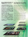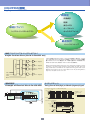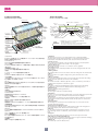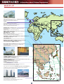
1
AN-B-1003F
ディスプレイ カタログ
Display catalog
VFD Module
CIG VFD
VFD
光と技術の
コミュニケーション
Futaba DISPLAY SOLUTIONS
新たな可能性を拓き続ける、 In the on-going pursuit of new possibilities,
,
Futaba s display devices continue to evolve.
双葉電子のディスプレイ。
100年を越す信頼の技術に支えられる、VFD。
発明王と呼ばれたエジソンが発見したエジソン効果をもと
に、1904年にフレミングが発明した真空管。双葉電子は、
真空管の開発・製造において、わが国有数のメーカーとし
ての歴史を歩んできました。その技術をディスプレイ分野に
活かしたVFD(Vacuum Fluorescent Display:蛍光表示
管)に応用・進化させ、数々の製品を提供してきました。現
在、
さまざまなディスプレイ技術が開発されているなかで、
VFD技術を活用したディスプレイは、自発光による広視野
角・高コントラスト、高い応答性、確かな色再現性、耐環境
性、高信頼性、長寿命性など、他にないメリットを持ち、暮ら
しのなかに溶け込んでいます。
迅速に市場投入できる競争力を提供。
双葉電子は、VFDの性能向上、機能向上に取り組み、実用
性の高いマンマシンインタフェースの開発を続けてきました。
システム設計の時間を大幅に短縮し、市場へスピーディー
に製品をリリースできるよう、
コントローラや電源を搭載した
VFDモジュールや、駆動用ICをデバイス内に組み込むこと
によりシステム構 成を簡 単にし、信 頼 性を高めるC I G
VFD(Chip In Glass VFD)などを開発。グローバルに拡大
したマーケットに対応した双葉電子ならではの開発システ
ムをご利用いただくことで、家庭電気製品やAV製品の表
示部、各種車載ディスプレイなど、多岐にわたる領域で、確
かな競争力をご提供します。
,
VFD s have been a reliable technology for over 100 years.
Based on the Edison effect discovered by T. Edison, John A.
,
Fleming invented the thermionic valve in 1904. Applying Fleming s
theory, Futaba started the development of vacuum tubes and has
been producing them as one of the leading companies in this
market. Technologies developed over the years were used to
produce Vacuum Fluorescent Displays (VFD) with development and
improvements still on-going today. Currently many types of VFD
displays have been developed and commonly used in our every day
life; featuring wide viewing angle, self-emissive light, high contrast,
high response time, accurate color reproduction, durable under
wide environmental conditions, high reliability, long life, etc.
Supply competitive products to the world-wide market quickly.
Futaba has been continuously improving the performance and
functionality of our VFD to enhance its abilities as a man-machine
interface. For the purpose of quickly releasing VFD products to
market, the time required for system design has been considerably
reduced. Furthermore, by developing VFD modules with built-in
controller/power supply, plus the IC driver installed in the VFD, the
system structure can be simplified to realize highly reliable Chip-in,
,
Glass (CIG) VFD s. Futaba s new product development system is
capable of satisfying the demand of the expanding world market
and a logical display technology choice to enhance the final product
competitiveness in various application areas such as displays for
home appliances, audio systems, and many automotive
applications.
目 次
CONTENTS
双葉電子のディスプレイ・・・・・・・・・・・・・・・・・・・・・・・・・・・・・・・・・・・・・・・・1
Futaba’s display devices・・・・・・・・・・・・・・・・・・・・・・・・・・・・・・・・・・・1
VFDモジュール・・・・・・・・・・・・・・・・・・・・・・・・・・・・・・・・・・・・・・・・・・・・・・・4
VFD module・・・・・・・・・・・・・・・・・・・・・・・・・・・・・・・・・・・・・・・・・・・・・・・・4
VFDモジュール・・・・・・・・・・・・・・・・・・・・・・・・・・・・・・・・・・・・・・・・・・・4
VFD module・・・・・・・・・・・・・・・・・・・・・・・・・・・・・・・・・・・・・・・・・・・・4
標準的なインタフェース・・・・・・・・・・・・・・・・・・・・・・・・・・・・・・・・・・・・5
Typical interfaces・・・・・・・・・・・・・・・・・・・・・・・・・・・・・・・・・・・・・・5
メッセージモジュールシリーズ・・・・・・・・・・・・・・・・・・・・・・・・・・・・・・・6
Message display module series ・・・・・・・・・・・・・・・・・・・・・・・・6
グラフィックモジュールシリーズ・・・・・・・・・・・・・・・・・・・・・・・・・・・・・・6
Graphic display module series・・・・・・・・・・・・・・・・・・・・・・・・・・6
キャラクタモジュールシリーズ・・・・・・・・・・・・・・・・・・・・・・・・・・・・・・・7
Character display module series・・・・・・・・・・・・・・・・・・・・・・・・7
カスタムモジュールシリーズ・・・・・・・・・・・・・・・・・・・・・・・・・・・・・・・・・7
Custom design module・・・・・・・・・・・・・・・・・・・・・・・・・・・・・・・・・7
CIGVFD・・・・・・・・・・・・・・・・・・・・・・・・・・・・・・・・・・・・・・・・・・・・・・・・・・・・8
CIG VFD・・・・・・・・・・・・・・・・・・・・・・・・・・・・・・・・・・・・・・・・・・・・・・・・・・・・8
CIGVFDの特徴・・・・・・・・・・・・・・・・・・・・・・・・・・・・・・・・・・・・・・・・・・・8
Features of CIG VFD ・・・・・・・・・・・・・・・・・・・・・・・・・・・・・・・・・・・8
CIGVFDの展開・・・・・・・・・・・・・・・・・・・・・・・・・・・・・・・・・・・・・・・・・・・9
Deployment of CIG VFD ・・・・・・・・・・・・・・・・・・・・・・・・・・・・・・・・9
CIGVFD製品紹介(表示コントローラ)
・・・・・・・・・・・・・・・・・・・・・・・10
CIG VFD products (Display controller)・・・・・・・・・・・・・・・・・10
CIGVFD製品紹介(AMVFD)
・・・・・・・・・・・・・・・・・・・・・・・・・・・・・・10
CIG VFD products (AMVFD)・・・・・・・・・・・・・・・・・・・・・・・・・・・10
CIGVFD製品紹介(5×7ドットコントローラ内蔵)・・・・・・・・・・・・・・11
CIG VFD products (5×7 dot matrix controller) ・・・・・・・・・11
CIGVFD製品紹介(階調表示)
・・・・・・・・・・・・・・・・・・・・・・・・・・・・・・11
・・・・・・・・・・・・・・・・11
CIG VFD products (Gray scale controller)・
・・・・・・・・・・・11
CIGVFD製品紹介(カーバッテリ対応表示コントローラ)
CIG VFD products (Display controller for automotive battery level)・・11
VFD ・・・・・・・・・・・・・・・・・・・・・・・・・・・・・・・・・・・・・・・・・・・・・・・・・・・・・・12
VFD ・・・・・・・・・・・・・・・・・・・・・・・・・・・・・・・・・・・・・・・・・・・・・・・・・・・・・・12
VFDの特徴/動作原理・・・・・・・・・・・・・・・・・・・・・・・・・・・・・・・・・・・12
Features of VFD/Principle of VFD operation・・・・・・・・・・・12
VFDの構造・・・・・・・・・・・・・・・・・・・・・・・・・・・・・・・・・・・・・・・・・・・・・13
Structure of VFD・・・・・・・・・・・・・・・・・・・・・・・・・・・・・・・・・・・・・・13
VFD製品紹介(ハイブリッドVFD)
・・・・・・・・・・・・・・・・・・・・・・・・・・・14
VFD products (Hybrid VFD) ・・・・・・・・・・・・・・・・・・・・・・・・・・・14
VFD製品紹介(FIVFD)
・・・・・・・・・・・・・・・・・・・・・・・・・・・・・・・・・・・14
VFD products (FIVFD)・・・・・・・・・・・・・・・・・・・・・・・・・・・・・・・・・14
VFD製品紹介(クリアバックグラウンドVFD)
・・・・・・・・・・・・・・・・・・15
VFD products (Clear background VFD)・・・・・・・・・・・・・・・・15
VFD製品紹介(バイプレーナVFD)
・・・・・・・・・・・・・・・・・・・・・・・・・・15
VFD products (Bi-Planar VFD)・・・・・・・・・・・・・・・・・・・・・・・・・15
VFD製品紹介(SLIM VFD)
・・・・・・・・・・・・・・・・・・・・・・・・・・・・・・・15
VFD products (Slim VFD) ・・・・・・・・・・・・・・・・・・・・・・・・・・・・・15
VFDの標準品・・・・・・・・・・・・・・・・・・・・・・・・・・・・・・・・・・・・・・・・・・・・・・・16
Standard-type VFD products・・・・・・・・・・・・・・・・・・・・・・・・・・・・・・16
セグメント、アルファニューメリック、5×7ドットマトリクス・・・・・・・・17
Segment, alpha numeric, 5×7 dot matrix type・・・・・・・・・17
DVD、STB用・・・・・・・・・・・・・・・・・・・・・・・・・・・・・・・・・・・・・・・・・・・18
DVD, STB ・・・・・・・・・・・・・・・・・・・・・・・・・・・・・・・・・・・・・・・・・・・・18
VFDの駆動方式・・・・・・・・・・・・・・・・・・・・・・・・・・・・・・・・・・・・・・・・・・・・・19
Driving system for VFD・・・・・・・・・・・・・・・・・・・・・・・・・・・・・・・・・・・19
周辺アプリケーション・・・・・・・・・・・・・・・・・・・・・・・・・・・・・・・・・・・・・・・・・22
Peripheral application・・・・・・・・・・・・・・・・・・・・・・・・・・・・・・・・・・・・・22
ドライバ・・・・・・・・・・・・・・・・・・・・・・・・・・・・・・・・・・・・・・・・・・・・・・・・22
Driver・・・・・・・・・・・・・・・・・・・・・・・・・・・・・・・・・・・・・・・・・・・・・・・・・22
フィルター・・・・・・・・・・・・・・・・・・・・・・・・・・・・・・・・・・・・・・・・・・・・・・23
Filter・・・・・・・・・・・・・・・・・・・・・・・・・・・・・・・・・・・・・・・・・・・・・・・・・・23
ホルダー・・・・・・・・・・・・・・・・・・・・・・・・・・・・・・・・・・・・・・・・・・・・・・・24
Holder・・・・・・・・・・・・・・・・・・・・・・・・・・・・・・・・・・・・・・・・・・・・・・・・24
VFDの信頼性試験項目・・・・・・・・・・・・・・・・・・・・・・・・・・・・・・・・・・・・・・・25
Reliability test item for VFD・・・・・・・・・・・・・・・・・・・・・・・・・・・・・・・25
使用上の注意事項・・・・・・・・・・・・・・・・・・・・・・・・・・・・・・・・・・・・・・・・・・・26
Proper operation cautions ・・・・・・・・・・・・・・・・・・・・・・・・・・・・・・・・26
双葉電子のご案内 ・・・・・・・・・・・・・・・・・・・・・・・・・・・・・・・・・・・・・・・・・・・28
Information about Futaba Corporation・・・・・・・・・・・・・・・・・・・・・28
ネットワーク ・・・・・・・・・・・・・・・・・・・・・・・・・・・・・・・・・・・・・・・・・・・・28
Network ・・・・・・・・・・・・・・・・・・・・・・・・・・・・・・・・・・・・・・・・・・・・・・28
会社概要・・・・・・・・・・・・・・・・・・・・・・・・・・・・・・・・・・・・・・・・・・・・・・・30
双葉電子の製品案内 ・・・・・・・・・・・・・・・・・・・・・・・・・・・・・・・・・・・・・31
Outline ・・・・・・・・・・・・・・・・・・・・・・・・・・・・・・・・・・・・・・・・・・・・・・・30
Product lines・・・・・・・・・・・・・・・・・・・・・・・・・・・・・・・・・・・・・・・・・・31
双葉電子の蛍光表示管
Futaba's VFD
双葉電子が提供する、高付加価値ディスプレイ・ソリューション。
Futaba offers a solution with high value-added displays
ディスプレイは、自動車にとってスピードや警告を知らせる重要な機能を持ち、
DVDやオーディオ機器、家電製品にとっては使いやすさを支える大切な機能
を持ちます。しかも、インタフェースとしての役割だけでなく、使用者の目が
最もふれる部分であることから、高いデザイン性や表現力が要求され、
製品の価値を決定する大きな要素ともなっています。双葉電子は、
VFD製品で世界トップシェアを占めています。それは、技術も、
ノウハウも、経験も、最高レベルにあるからです。「確かな性能
の表示部が欲しい」、「魅力的なディスプレイで競合をリード
したい」とお考えなら、パートナーとして双葉電子をお選
びください。国内はもとより世界各国のメーカーから
信頼をいただいているディスプレイ技術が、新製品
の価値を向上します。
In general, display devices can provide significant
functions to an end user. In a car for example, it
informs the driver of current speed or warnings. With
,
DVD s, audio systems and home appliances, it simplifies
the use of such appliances. Furthermore, not only does a
display act as an interface, but the display device also affects
,
the user s impression of the end product. This is due to the fact
,
that the display device is always exposed to end users eyes, which
in turn is one of the essential elements to determine product value.
Futaba has the largest market share of VFD products in the world,
allowing Futaba to lead the technology, know-how and experience in this
field. If you want “ a display which does not fail in its performance ”, or “ an
attractive display to beat your competition ”, you are recommended to choose
,
Futaba as your partner. Futaba s display technology will be sure to help you
,
enhance the quality of your new products with Futaba s highly esteemed performance in
the world as well as the domestic market.
2
Futaba's VFD
双葉電子の蛍光表示管
■ディスプレイなら双葉電子
●信頼に応えるパートナー
自動車や家電製品のディスプレイは、つねに
キーデザインとなり、
かつ、使いやすさを決定
する重要な要素です。双葉電子は、製品の開
発段階からパートナーとして参加し、豊富な経
験と高度な技術を提供。魅力的な製品づくり
を支援します。
●品質の高さを保証
品質体制、開発体制は、ISO9001ならびに
TS16949の認証を取得。確かな品質と信頼
性を実現しています。
●市場投入期間を短縮
双葉電子は、蛍光体材料開発、生産設備開
発部門を所有し、
自社により、材料、生産設備
からの一貫体制を実現。開発から量産まで迅
速に行えます。
●安定した供給
世界4拠点(日本、台湾、
フィリピン、中国)に
工場があり、
グローバルにスピーディーで安定
した製品の供給が行えます。
,
■Are you seeking a display? Here s
,
Futaba s display device.
●Reliable partner
The display device used in a car or home
appliance is a key factor in determining the
successful design of products and makes
the whole product more user-friendly.
Futaba will participate in your product
development as an integral partner starting
from early developmental through
production stages and help you develop a
successful product by offering our years of
VFD experience and technology.
●High quality guaranteed
,
Futaba s entire business system is certified
to ISO9001 and TS16949.
●Short lead-time
Futaba has a full range of manufacturing
processes, such as developing phosphor
material, developing internal production
facilities/tooling, etc. Therefore, our
integrated production system can shorten
the time required between the start of
development and the transfer of the
developed product to the mass production
line.
●Stable supply
Futaba has four production locations
worldwide; Japan, Taiwan, Philippines and
China. Products can be supplied quickly
and dependably to any place in the world.
3
VFDモジュール
VFD Module
VFDモジュール
VFD Module
VFDモジュールは蛍光表示管、コントローラ、アノード&グ
リッドドライバ、 電源回路などにより構成されたマンマシン
インタフェースユニットです。
小型、 軽量のため実装設計も簡単、 各種装置にスムーズ
に適合します。またユーザーフレンドリーなインタフェースで
ホストシステムとの接続も容易です。
双葉VFDモジュールは、 駆動回路設計はもちろんのこと、
輝度、 視認性、 寿命、 信頼性、 実装設計、メンテナンスなど
煩雑なマンマシンインタフェース設計を大幅に省力化します。
マーケットヘのタイムリーな製品リリース、より洗練された
マンマシンインタフェースの実現に双葉VFDモジュールを
お役立てください。
A VFD module is a highly sophisticated man-machine
interface which consists of a vacuum fluorescent display,
controller, anode/grid driver, power supply circuit, etc.
Compact and lightweight design,suitable for most
equipment, with simple connection to a host system.
FUTABA VFD modules allow easy interface design
(e.g.drive circuit design) and feature enhanced luminosity,
visibility, life-time, reliability and ease of maintenance.
FUTABA VFD modules allow timely product release to
market and improve the
man-machine interface.
ブロックダイヤグラム Block diagram
メッセージモジュールの一例 Example of message display module
アノードドライバ
Anode driver
NO.2
Drive IC
Ebb
CN1
RD
WR
CS
INT
BL
C/D
RESET
NO.1
Drive IC
アノードコントロール Anode control
コントロール
ゲートアレイ
Control gate array
グリッドコントロール Grid control
Ecc
A64
G128
NO.1
Driver IC
OSC
D0
∼
D7
A1
RAM
8K Bytes
256×16
グラフィック
ディスプレイ
Graphic display
NO.2
Driver IC
NO.3
Driver IC
+5V
DC/DC
コンバータ
converter
NO.4
Driver IC
Ebb
Ecc
Ef
キャラクタスクロールボード Character Scroll Board
グリッド
ドライバ
Grid driver
G1
Ef
ウェルカムスクロールボード Welcome Scroll Board
スクロール表示器がついたA4サイズ
のカタログスタンドです。携帯電話の赤
外線通信で文字入力が簡単に行えます。
視認性に優れた公共スペース向けの10
段のスクロール表示器です。コマンドに
より、日付/時刻、点滅、スクロールな
ど多彩な表示が可能で、SS無線送信で
リアルタイムな内容変更もできます。
A catalog stand in the size of A4,
equipped with a scroll display.
Characters can be readily input by means
of the infrared data communication of a
cell phone.
A 10-line scroll display for public spaces
which has excellent readability.
Date, time, blinking mode, scrolling and
other optional display modes can be set
by various commands. Content can be
changed by the SS radio communication
to display live news.
4
標準的なインタフェース
Typical interfaces
パラレル Parallel
■概要
複数の信号線を用いて通信する方式。デー
タ線の本数(4∼8ビット)でASCIIコードや
JISコードなどを通信する形式のもの。
■SUMMARY
A communication system using parallel signal
lines which transmits ASCII or JIS codes using
data lines (4 to 8 bits).
■概要
データを1ビットずつ順番に転送する通信方
式。データ通信の形式で同期式と非同期式が
ある。通信速度の設定(ボーレート)が可能。
■SUMMARY
A communication system to transmit data bit
by bit. There are two types; a synchronous
and an asynchronous type. Communication
speed (baud rate) can be set.
■概要
CPUのアドレスバス、データバス、R/W制御
線を用いてデータ転送する方式。メモリのア
クセスと同様に双方向通信が可能。
■SUMMARY
,
A system to transmit data using the CPU s
address-bus, data-bus and R/W control line.
Like the case of memory access, parallel
communication is available.
■概要
非同期式のシリアル通信で汎用の規格。
JISコードなどの転送で表示制御を行う。ノ
イズに強い。通信速度の設定(ボーレート)
が可能。
■SUMMARY
The industry standard for an asynchronous
serial communication for general use. Display
is controlled by transmitting JIS code, etc.
Good noise protection.
Communication speed (baud rate) can be set.
■概要
コンピュータの周辺機器を接続するための汎
用シリアル通信の規格。高速通信が可能。
■SUMMARY
The PC industry standard for high speed serial
communication. USB typically connects
peripheral devices of a computer.
■概要
赤外線通信(携帯電話の赤外線通信の出力を
利用したもの)対応機種など確認が必要。
■SUMMARY
Infrared data communication (a communication
system using the output of the infrared data
communication of a cell phone).
It is necessary to confirm the availability of this
feature on any particular cell phone.
シリアル Serial
CPUバス直結 CPU Bus
RS-232C RS-232C
USB Universal Serial Bus
IrDA(赤外線) IrDA
5
メッセージモジュールシリーズ
Message display module series
The message display module series features subtle display color with a
16-dot high quality font or a 24-dot large font, making the modules
suitable for indoor message display systems.
■Message display is achieved simply by saving display information to
the module's RAM. No complex display control is required from the
host system.
■Flicker-free scrolling is achieved by using the on board controller.
■Built-in power supply circuit (DC/DC converter) enables easy operation.
■An interface board is available for the message display.Serial
communication with RS-232C or RS-485A ensures simple operation
of a message display. (Refer to the following table.)
メッセージモジュールシリーズは、落ちつきのある表示色、24/16ドット高品位フォ
ント、大形フォントの採用により屋内メッセージ表示システムに最適なディスプレ
イモジュールです。
■モジュール上のRAMに表示情報を書き込むだけで表示が可能です。
■専用のコントローラにより、美しいスクロール表示が簡単な入力で実現でき
ます。
■電源回路(DC/DCコンバータ)を搭載していますので簡単に駆動できます。
■漢字フォント搭載の専用のインタフェースボードをオプションで用意しており
ます。RS-232CもしくはRS-485AのI/Fにて簡単に表示が可能です。
(対応
品種は仕様一覧参照)
メッセージモジュールシリーズ仕様一覧 Message display module series specifications
品 名
Part Number
文字高
ドット数
画面サイズ
外形寸法
Number of Dots
(W×H)
Display Area
(W×H) (mm)
Outer Dimensions
(W×H ×T) (mm)
文字数
Character height Number of
(mm)
Characters
インタフェース
電源
Interface
Power Supply
消費電力
インタフェースボード
Power Consumption Interface Board
Typ.(W)
(オプション/Option)
GP1041A01A
26.1
16
256×16
309.5×26.1
385.0×59.5×32.0
8bit Parallel
5V
10.0
−
GP1047A01A
35.7
16
256×16
460.5×35.7
525.0×59.5×40.0
8bit Parallel
5V
22.5
○
GP1048A01A
35.7
20
320×16
559.7×35.7
625.0×59.5×40.0
8bit Parallel
5V
27.5
○
GP1072A01A
51.6
16
256×16
639.6×51.6
720.0×85.0×41.9
8bit Parallel
5V,24V
31.7
○
GP1049B01A
51.7
14
224×16
559.7×51.7
625.0×79.5×43.0
8bit Parallel
5V,24V
29.3
○
GP1022A07C
35.7
11
264×24
316.5×35.7
385.0×62.0×35.1
8bit Parallel
5V,24V
14.9
○
GP1058A03A
51.3
14
336×24
557.5×51.3
625.0×80.0×43.0
8bit Parallel
5V,24V
29.3
○
グラフィックモジュールシリーズ
Graphic display module series
The graphic display module series uses a built-in custom designed
controller, and achieves very simple connection to the host system.
The compact lightweight and slim design makes it easy to build the
modules into various products, and achieving optimal man-machine
interfacing quality with excellent visibility.
■Graphic display is achieved simply by saving display information to the
module's RAM.
■Allows direct connection to system bus.
■Built-in power supply circuit (DC/DC converter) enables easy operation.
グラフィックモジュールシリーズは当社開発のコントローラ搭載によりホスト
システムとの接続は非常にシンプルです。また、各種応用製品への実装性を
考慮した小型、軽量、薄型のデザインで、VFDの視認性を生かした最適なマン
マシンインタフェースディスプレイが実現できます。
■モジュール上のRAMに表示情報を書き込むだけで表示が可能です。
■システムバスに直接接続できます。
■電源回路(DC/DCコンバータ)を搭載していますので簡単に駆動できます。
グラフィックモジュールシリーズ仕様一覧 Graphic display module series specifications
ドット数
画面サイズ
ドットピッチ
外形寸法
Part Number
Number of Dots
(W×H)
Display Area
(W×H) (mm)
Dot Pitch
(W×H) (mm)
Outer Dimensions
(W×H×T) (mm)
GP1183A01A
112×16
52.5×11.5
0.47×0.73
GP1184A01A
140×16
69.9×11.5
GP1039A02A
192×16
124.6×10.2
GP1046A03A
256×16
166.2×12.6
GP1112A01B
128×32
57.5×14.3
GP1120A01B
128×32
83.1×20.7
GP1127A01A
160×32
71.9×14.3
GP1111A01B
256×32
GP1152A01A
240×36
GP1135A01A
GP9002A01B
消費電力
インタフェース
電源
Interface
Power Supply
Power Consumption
Typ.(W)
80.0×36.0×13.7
8bit Parallel/RS-232C
5V
1.25
−
0.5×0.73
116.0×37.0×13.7
8bit Parallel/RS-232C
5V
1.4
−
0.65×0.65
180.0×40.0×26.1
8bit Parallel
5V
4.0
−
0.65×0.8
230.0×40.0×29.0
8bit Parallel
5V
3.8
−
0.45×0.45
88.0×44.0×20.7
8bit Parallel
5V
2.0
○
0.65×0.65
130.0×38.5×22.0
8bit Parallel
5V
3.5
○
0.45×0.45
130.2×43.0×26.2
8bit Parallel
5V
2.5
−
166.3×20.7
0.65×0.65
220.0×50.0×27.0
8bit Parallel
5V
3.8
○
149.8×28.6
0.61×0.8
205.2×62.0×30.0
8bit Parallel
5V
5.0
−
160×40
132.7×33.1
0.83×0.83
190.0×64.0×29.5
RS-232C
5V
7.1
○
128×64
57.5×28.7
0.45×0.45
103.0×53.5×22.5
8bit Parallel/Serial
5V
2.5
○
GP1118A01B
128×64
83.1×41.5
0.65×0.65
140.0×68.0×29.0
8bit Parallel
5V
5.0
○
GP1128A01A
160×64
71.9×28.7
0.45×0.45
125.0×56.3×29.6
8bit Parallel
5V
3.8
−
GP1129A01A
192×64
86.3×28.7
0.45×0.45
145.0×56.3×29.6
8bit Parallel
5V
4.3
−
GP1107A02B
256×64
115.1×28.7
0.45×0.45
180.0×55.0×26.0
8bit Parallel
5V
6.0
○
GP1157A01B
256×64
115.1×28.7
0.45×0.45
159.0×50.0×21.5
8bit Parallel/RS-232C
5V
4.5
○
GP1150A01A
256×64
163.7×40.2
0.64×0.63
230.0×88.5×29.3
RS-232C
24V
7.2
○
GP1063A01A
256×64
255.7×63.7
1.0×1.0
320.0×120.0×41.5
8bit Parallel
5V,12V
22.1
−
品 名
6
漢字フォント
Kanji Font
キャラクタモジュールシリーズ
Character display module series
キャラクタモジュールシリーズは5×7のドットマトリクス表示のVFDを使用し、
ソフト/ハードを一体化したモジュールで簡単に使用していただけます。
■モジュール上のワンチップマイコンにより表示制御が簡単、ホストシステ
ムの負荷が大幅に軽減できます。
■パラレル入力/シリアル入力を標準装備しています。
■アルファベット、数字、カタカナ、記号など200種類以上の豊富なフォント
で表示が可能です。
■電源回路(DC/DCコンバータ)
を搭載していますので簡単に駆動できます。
■小型、低消費電力でLCD同等の外形とインタフェースを採用した
LCD EMULATORSシリーズを取り揃えています。
The character display module series uses 5×7-dot matrix display
VFD and includes software and hardware.
■Easy display control is achieved using a one chip microcomputer
on the module.This reduces the work of the host system.
■Parallel input/Serial input as standard.
■Display using over 200 fonts with a range of alphabetic characters,
numbers, Katakana, symbols, etc.
■Built-in power supply circuit (DC/DC converter)enables operation
with the single power supply.
■The LCD EMULATORS are compact, low power VFD modules with
standard LCD interface.
キャラクタモジュールシリーズ仕様一覧 Character display module series specifications
品 名
桁数×行数
Part Number
Digits×Rows
キャラクタ
フォーマット
文字サイズ
外形寸法
Character format
Size of digit
(W×H)(mm)
Outer Dimensions
(W×H×T) (mm)
M16SD08FA M16SD08FJ
16×1
5×8(5×7+cursor)
2.1×4.7
ユーザ定義
文字数
インタフェース
電源
消費電力
Power Consumption
Power Supply
Typ.( W)
User's
Definable font
Interface
80.0×36.0×18.0
8
4/8bit Parallel/Serial
5V
0.4
M162SD07FA M162SD07FJ
16×2
5×8(5×7+cursor)
2.1×4.7
80.0×36.0×18.0
8
4/8bit Parallel/Serial
5V
0.7
M162SD12AA
16×2
5×7
3.5×5.5
137.0×27.5×11.7
8
Serial
5V
1.0
M162SD13AA
16×2
5×7
3.5×5.5
137.0×27.5×11.7
8
Serial
5V
1.0
M162MD05AA M162MD05AJ
16×2
5×8(5×7+cursor)
3.7×7.4
122.0×44.0×20.6
8
4/8bit Parallel/Serial
5V
1.7
M20SD03GR
20×1
5×7
3.5×5.0
150.0×31.0×18.6
−
8bit Parallel/Serial
5V
0.8
M202SD01LA
20×2
5×7
2.3×4.2
100.0×35.0×26.3
4
8bit Parallel/Serial
5V
1.6
M202SD16FA M202SD16FJ
20×2
5×8(5×7+cursor)
2.4×4.7
116.0×37.0×18.5
8
4/8bit Parallel/Serial
5V
0.7
M202SD08GR
20×2
5×7+cursor
3.5×5.0
155.0×43.0×20.6
−
8bit Parallel/Serial
5V
1.8
M202MD15FA M202MD15FJ
20×2
5×8(5×7+cursor)
3.9×7.7
146.0×43.0×20.6
8
4/8bit Parallel/Serial
5V
1.7
M202MD15DA
20×2
5×8(5×7+cursor)
3.9×7.7
146.0×43.0×25.1
−
RS-232C
24V
2.5
M202MD12BA M202MD12BJ
20×2
5×7+descriptor
5.5×10.5 190.0×64.0×27.0
−
RS-232C
5V
5.0
5×7+Dp,com,descriptor 7.2×11.3 273.0×76.2×31.5
−
8bit Parallel/Serial
5V
5.0
8
4/8bit Parallel/Serial
5V
1.5
M202LD06BA M202LD06BB
20×2
M204SD02FA M204SD02FJ
20×4
5×8(5×7+cursor)
2.4×4.2
100.0×60.0×20.6
135.0×70.0×31.0 3(AA)/4(AB)
M204SD01AA M204SD01AB
20×4
5×7
3.2×5.0
M204LD01AA
20×4
5×7
7.3×11.3 290.0×100.0×40.0
8bit Parallel/Serial
5V
3.8
−
8bit Parallel
5V
11.0
M242SD04FA M242SD04FJ
24×2
5×8(5×7+cursor)
2.2×4.7
118.0×36.0×17.0
8
4/8bit Parallel/Serial
5V
0.9
M40SD04GR
40×1
5×7+cursor
3.5×5.0
240.0×35.0×20.1
−
8bit Parallel/Serial
5V
1.5
M402SD10FA M402SD10FJ
40×2
5×8(5×7+cursor)
2.2×4.7
182.0×33.5×18.4
8
4/8bit Parallel/Serial
5V
1.1
M402SD07GR
40×2
5×7+cursor
3.5×5.0
240.0×43.0×20.6
−
8bit Parallel/Serial
5V
3.8
M404SD01BA M404SD01BB
40×4
5×7
3.0×5.0
230.0×60.0×32.0
3
8bit Parallel/Serial
5V
7.0
カスタムモジュール
Custom design module
お客様のご要望に合わせたカスタム仕様のモジュールの開発を承り
ます。
カスタムモジュールは各種機器、用途に応じた表示仕様の設計から、
表示制御およびホストとの通信ソフト等の開発、
さらにシステムの周
辺回路や部品の複合化で機器搭載での最適化を図ります。
これらのカスタム設計で、お客様の製品開発の省力化とシステムコス
トの削減をご支援します。
■カスタム仕様の対応一例
・カスタム表示パターンのVFD開発。
・最適な表示設計。(サイズ、輝度、
カラー等)
・表示制御および通信ソフトの開発。
・英数字から漢字、
その他言語のフォントの搭載。
・各種インタフェースの適用。(パラレル、RS232C、USBなど)
・供給電源に応じた専用電源回路(DC/DCコンバータ)の搭載。
・周辺部品(キースイッチ、
インジケータ等)や周辺回路の取り込み。
・ハウジング、
シールド等の筐体設計加工。
その他のご要望にもお応え致します。
詳細につきましては、お気軽にご相談ください。
Futaba develops highly customized modules corresponding with
customer's needs.
Custom design module realizes optimum design for individual system
applications by applying graphics design, controller, software for function &
communication with utilizing peripheral circuits for the system.
Our custom solution makes your system design easy & simple, and save
you time & cost.
■Customized design
・Applying original graphics design for VFD.
・Optimum VFD design with package size, luminance,color assignment, etc.
・Develop custom designed software for display function and
communication.
・Utilizing Alphabets, numerals and other character fonts for various
languages.
・Employing various interfacing circuit & protocol design.(parallel, RS232C,
USB etc.)
・Built-in power supply unit for required power source in the system.
・On board design with key switch, indicator and other peripheral
circuits & components.
・Design for housing case and shielding, etc.
We are ready for your various demands. Please contact us with your
details.
7
CIG VFD
CIG VFD
CIGVFDの特徴
Features of CIG VFD
CIGVFDの例。ドライバはフィラメント支持体の下側に配置されています。パタンエリア/パッケージサイズは従来タイプと同じ。
,
For CIGVFD, driver IC s and located under the filament support graphic area and display package size
are the same as conventional VFD.
■概要
CIGVFDは、VFD用ドライバを搭載したVFDです。多セグメントパタンでは、
多くのリードが必要とされ小型パッケージでは実現困難でした。
ドライ
バをVFDに実装することにより、VFDの駆動に必要な電極はVFD電源
と信号線だけになり、大幅に外部リードを減らすことができます。
■SUMMARY
CIGVFD is the VFD with a driver IC mounted on it. In many cases, a
conventional full dot matrix type or 5×7 dots type had difficulty to be
designed because of too many lead terminals. By mounting the driver IC
chip on VFD base plate, the leads needed to drive the VFD are only for
power supply and signal.
It is a drastic reduction of external leads.
■特徴
1.従来実現できなかった小型パッケージや、高密度、
大容量表示のVFD
が実現可能です。
2.基板上の配線が減少するため、基板設計が容易になり、開発期間の
短縮が可能です。
3.基板コストの低減が可能です。
4.リード本数を減らすことができ、実装性が向上します。
5.ドライバが内蔵されているため、ユーザはドライバを用意する必要が
ありません。
6.カスタムデザインのデバイスですが、周辺回路の標準化が可能です。
■FEATURE
,
1. The small package which couldn t be realized so far, the VFD of the
big capacity indication and high density can be realized.
2.Because wiring on the circuit board decrease, circuit board design
becomes easy, and a development period can be shortened.
3.This VFD can reduce the cost of PWB.
4.The number of the lead terminal were drastically reduced to several
connections to the PWB, which reduces the manufacturing complexity.
5. Since the VFD is constructed with driver IC,no external driver is
necessary.
6.The VFD is a custom design product.When employing the VFD
design,the peripheral devices can now be standardized.
■用途
グラフィック、ハイブリッドタイプ、
5×7ドットマトリクス
■APPLICATION
Graphic, Hybrid, 5×7 dots matrix type
■ CIGVFDの構造 Structure of Chip In Glass VFD
CIGVFD
グリッド
Grid
蛍光体
Phosphor
フィラメント
Filament
ベースプレート
Base Plate
ドライバチップ
Driver Chip
フィラメントリード
Filament Lead
ドライバチップ用リード
Lead of the Driver Chip
注意 Note
本製品は、半導体製品ですので静電気のお取扱いには十分ご注意願います。
,
CIG VFD is built using CMOS IC s. Precautions should be taken to minimize the risk of ESD.
8
CIGVFDの展開
Deployment of CIG VFD
高機能
自動表示
階調
表示メモリ
キースキャン
キャラクタフォント
単純ドライバ
シリアルインパラレルアウト
最適設計
ビットラインナップ
単純ドライバ(シリアルインパラレルアウト)
Simple function driver (Serial in Parallel out)
Shift Register
Output 1
Latch
Output 2
⋮
Data
Output 3
⋮
⋮
ドライバ内部にあるシフトレジスタへ、クロック入力の変化に合わせて、シリアル
でデータを入力します。ラッチ入力がハイの間は、パラレルデータがラッチ回路を
通してアウトプットバッファに転送され、ローの間は、直前のデータを保持します。
BKをハイにすることで、出力をすべてローにすることが出来ます。
While synchronizing with the input of the clock signal, data is input in a serially manner to the shift register inside the driver. While the latch input is at
high, parallel data is transmitted to the output buffer through the latch circuit.
While the latch input is low, the current data is held. By asserting BK to a
high level, all outputs can be set to low.
Output n
Clock
Latch
Blank
タイミングチャート Timing Chart of Grid (Digit) and Anode (Segment) Signals
駆動回路例 Example of Electrical Circuit for CIG VFD
グリッドスキャンのタイミングチャート: Grid Scan Timing Chart
Grid No.
tp
tblank
1G
2G
VH
VDD
下記は駆動デューティです。
The following is Duty
Factor
3G
4G
GND
Clock
Data
MICRO
CONTROLLER
Du=
Latch
ng
Blank
Timing No.
T1 T2 T3 T4 T5 T6 T7 T8 T9 T10 T11 T12 T13 T14 T15 T16 T17 T1
タイミングチャート:Timing Chart
Ef
Grid Scan Tn
Timing
Tx -
Timing Tn
T1
T2
T3
T4 ・・・ Tx ・・・ Tn- Tn- Tn- Tn
T1
Tx
Tx +
CLK
SI
LAT
ディミング:Dimming
BK
tp
tblank
tp
ブランキングタイム:Blanking
9
tblank
tp
tp
(tp+tblank) ×Tn
CIGVFD製品紹介
CIG VFD products
表示コントローラ display controller
コントローラ内蔵で簡単操作。
With a built-in controller, operation is simplified.
■概要
簡単なコマンドによりデータを表示RAMに書き込むことで表示が可能です。
表示RAMに書き込まれたデータは、自動表示機能によりデータに変更が
あるまで表示を維持します。
■特徴
◆グリッドスキャン制御が不要
◆一度の表示データ書き込みにより表示を維持
◆ソフト制御の負荷を軽減
◆16階調表示コントロールが可能
■SUMMARY
Message can be displayed by writing data into the display RAM using a
simple command. The data written into the display RAM maintains the
displayed message on the screen until there is a data change made by
the automatic display function.
■FEATURE
◆No grid scanning is needed.
◆Displayed message or image is maintained only by writing display
data.
◆Load required for the microcontroller is reduced.
◆Gray scale is available up to 16 levels.
AMVFD AMVFD
超高輝度のフルドットマトリクスディスプレイ誕生。
Newly developed, ultra-high luminance, full dot matrix display
表 示 例
■SUMMARY
By applying phosphor directly onto the IC, static drive of the pixels is
obtained.
Most suitable type VFD for a HUD (Head Up Display) which requires
high luminance.
■概要
ICチップの上に蛍光体を配置することで、点灯ドットのスタティック駆動
を実現。高輝度発光が可能なHUD
(ヘッドアップディスプレイ)に最適なV
FDです。
■特徴
◆ドライバ、コントローラ、メモリ機能を内蔵
◆フルドットマトリクス表示
◆視認性に優れたグリーン表示
■FEATURE
◆Driver, controller and memory functions are built-in.
◆Full dot matrix display
◆Green display with excellent readability.
10
5×7ドットコントローラ内蔵 5×7 dot matrix controller
キャラクタフォント内蔵により鮮明度をアップ。
Since character fonts are built-in, the interface is simplified.
■概要
キャラクタフォントを内蔵し、自動表示が可能なCIGVFDです。表示
RAMを内蔵していますので、データに変更があるまで表示を維持し
ます。キャラクタのカラーシフトも可能です。
■特徴
◆グリッド自動表示
◆キャラクタフォント内蔵
◆ユーザー定義用キャラクタRAM内蔵
◆部分輝度階調設定によりキャラクタのカラーシフトも可能
■SUMMARY
Automatic message display is easily implemented with CIG VFD
which has built-in character fonts. The built-in display RAM keeps
displaying messages until there is a change in data. Color shifting
of characters is also available.
■FEATURE
◆Grid auto scanning
◆Characters ROM(Custom order available)
◆User definition character RAM
◆Section gray scale control
階調表示 Gray scale controller
階調表示で多彩な表現を実現。
A variety of images can be displayed using gray scales.
■概要
16階調表示機能を内蔵したCIGVFDです。階調表示により、画像
表現が可能となり、表現力が向上しました。
■特徴
◆画像表示
◆高輝度、高精細で立体感を表現
◆動画と文字情報を重ねて表示
■SUMMARY
CIG VFD with a built-in function to display data in 16 gray scale levels.
Based on this gray scale capability, a variety of images can create an
attractive display.
■FEATURE
◆Picture expression.
◆3-D effect is represented with high luminance and high resolution.
◆Capability of superimposing text information on motion picture.
カーバッテリ対応表示コントローラ Display controller for automotive battery level
低電圧でも多セグメントを制御可能。
Multiple segments are controllable even at low voltages such as automotive battery level.
■概要
カーバッテリ電圧に対応したCIGVFDです。ダイナミック駆動タイプも
あり、
5×7ドットキャラクタなど多セグメント表示にも対応可能です。
■特徴
◆トリプレックス表示コントローラタイプあり
◆キースキャン機能内蔵タイプあり
◆動作温度−40∼85℃、保存温度 −55∼100℃
■SUMMARY
CIG VFD is usable at automotive battery voltage. A dynamic drive
type is also available. Multiple segment displays, such as 5x7 dot
character, can also be used.
■FEATURE
◆A triplex display controller type is available.
◆Some types have a built-in key scanning function.
◆Operating temperature: -40 to 85℃
Storage temperature: -55 to 100℃
11
VFD
VFD
VFDの特徴
Features of VFD
自発光で視認性に優れた、表示デバイス。
General VFD; Excellent Readability
構造
Structure
フィラメント
Filament
グリッド
Grid
観察方向
Viewing Direction
of the FLVFD
観察方向
Viewing Direction of the
VFD
リード Lead
VIVID GREEN
■概要
VFDとは、真空管の原理をもとに開発され改良・発展した表示デバイスです。真空
容器内のアノード電極上に蛍光体をパタンニングし、電子を衝突させ発光させます。
C.I.E Chromaticity Diagram(1931)
Presented by
FUTABA CORPORATION
0.900
530
535
535
545
■SUMMARY
VFD is a display device developed with vacuum triode tube technology.
The phosphor is patterned on the anode in vacuum package. Electrons come into
collision with the phosphor to emit light.
550
555
560
565
■FEATURE
1.Superior readability, with high self-luminance.
2.High reliability long life.
3. The FLVFD (Front Luminance VFD) is available, offering a wide viewing angle.
570
575
YELLOWISH
WISH ORANGE
585
590
.200
.300
.400
.500
.600
.700
605
.800
LIGHT BLUE
0
VFD用蛍光体はグリーンを基調に10色以上用意されています。
400
640
665
640
670
ピーク波長:λp
Peak Wavelengh
490
GE
AN
GE
DD
ISH
OR
AN
NG
RA
HO
EL
OR
LO
RE
sitiv
Sen
E
urve
460
W
ity C
460
NIS
50
LL
OW
460
450
440
360
430
420 400
565
HY
LU
HB
.100
PLE
E
0.000
0.000
PUR
LIS
470
REDDISH
PURPLE
BLU
PU
475
PURPLE
ISH
RP
.100
530
NIS
PURPLISH
RED
RED
PURPLE
BLUE
480
505
EE
485
465
GR
GREENISH
BLUE
.200
430
100%
YE
RED
PURPLISH
PINK
EN
490
EN
PINK
605
610
615
620
630
640
650
675
GRE
.300
SPECTRAL
DISTRIBUTIONS
600
ICI ILLUMINANT "C"
BLUE
GREEN
スペクトル分布
580
REDDISH
ORANGE
GRE
ORANGE
PINK
ISH
ORANGE
BLUSH
GREEN
495
比視
感度
曲線
.400
LOW
L
YE
YEL
580
N
W
LO
VIVID
.500
EE
GR
E
YE EN
LL ISH
OW
YELLOW
GREEN
GR
GREEN
500
UE
WISH
YELLOWISH
GEREEN
BL
.600
HT
505
LIG
.700
UE
515
BL
515
.800
■特徴
1.自発光・高輝度なので視認性に優れています。
2.環境に対する信頼性が高く、長寿命です。
3.
視野角を広く取れるFLVFD
(前面発光タイプ)もあります。
525
相対放射強度
Relative Intensity of Emission
520
520
550
580
610
700
730
760
Including standard green phosphor, over 10 additional colors
have been developed.
波長
Wavelength(nm)
動作原理
Principal of VFD Operation
フィラメントは、細いタングステンの芯線に、バリウム
蛍光表示管の基本動作原理
Principal of VFD Operation
(Ba)、
ストロンチウム(Sr)、
カルシウム(Ca)の酸化物
が被覆されています。フィラメントに規定の電圧を印加
フィラメント
Filament
することによって陰極温度が約600℃前後となり、熱電
子が放射されます。グリッドは、表示の妨げとならない金
グリッド Grid
属メッシュで、
これに正電圧を加えてフィラメントから放
射された電子を加速、拡散してアノードへ導いたり、逆
に負電圧を加えてアノードに向かう電子を遮断(カットオ
フ)
したりする役目を持っています。アノードは、ほぼ表
示すべきパターン状に形成された黒鉛などの導体の上
に表示パターンの形状に蛍光体を印刷したもので、
こ
電子
Electron
れに正電圧が印加されると前述のグリッドで加速、拡
散された電子が衝突して蛍光体を励起し、発光します。
点灯するセグメント
On-Segment
蛍光体として現在最も広く使用されているものは、発
+極
非点灯のセグメント
Off-Segment
−
極
アノード Anode
光色が緑(ピーク波長505nm)で動作電圧の低い
ZnO:Zn蛍光体です。また、蛍光体を変えることにより
赤橙色から青色まで各種のカラー発光が可能です。
12
The filament consists of a very thin tungsten wire coated with
barium, strontium and calcium oxides. Application of a
specified voltage raises the temperature of the filament
cathode to approximately 600℃, which causes thermionic
emission.
The grid is a thin stainless steel mesh.
When a positive voltage is applied to the grid, electrons
emitted by the filaments are accelerated and diffused towards
the anode. When a negative voltage is applied to the grid,
electron flow to the anode is cut off.
The anode consists of a conductor such as graphite, which is
coated with phosphor formed into the desired graphic pattern.
When a positive voltage is applied to the anode, electrons
accelerated and diffused by the grid collide with the anode,
exciting the phosphor and causing it to emit light. The most
widely used phosphor is ZnO: Zn, which operates at low
voltage and has a green peak wavelength of 505 nanometer.
Various colors, ranging from reddish orange to blue, can also
be obtained by using different types of phosphor.
構造
Structure
蛍光表示管の分解斜視図
Stranbismal Figure of VFD
蛍光表示管の断面図
Cross sectional view of VFD
⑪フロントガラス
Front Glass
⑪フロントガラス Front Glass
⑥グリッド
Grid
⑰サポート
Support
⑨ゲッター
Getter
①フィラメント
Filament
①フィラメント
Filament
⑫フリットガラス
Frit Glass
⑮透明導電膜
Transparent
Conductive Layer
⑧リード
Leads
⑱グリッド電極固定材 Erectrode
Bonding Material
⑦ガラス基板 Glass Substrate
⑤配線 Wiring Pattern
⑬蛍光体 Phosphor
⑯アンカー
Anchor
⑧リード
Leads
②コンタクトリード
Contact Lead
④絶縁被膜
Insulation Layer ※ 大型管、
クリアバックグラウンドVFD等の場合、下図の様に
④絶縁被膜
(クロスオーバ)
Insulation Layer
⑲金属蓋
Metal cap
③アノード電極 Anode Electrode
⑭スルーホール
Through Hole
ガラス管の排気管になることがあります。
排気管
shown below large size VFD or clear background VFD
Exhaust tip As
may need an exhaust tip instead of a metal cap.
③アノード
Anode Electrode
⑤配線
Wiring Pattern
⑩排気穴 Exhaust hole
⑲金属蓋
Metal cap
⑦ガラス基板
Glass Substrate
⑥グリッド
Grid
⑩排気穴
Exhaust hole
①Filament
The filament consists of a very thin tungsten wire coated with barium,
strontium and calcium oxides. Application of a specified voltage raises the
temperature of the filament cathode, and causes thermionic emission.
②Contact Lead
The contact lead electrically connects filament voltage to the transparent
conductive layer formed on the inside of the front glass.
③Anode Electrode
The anode electrode consists of a conductor such as graphite.
④Insulation Layer
The insulation layer electrically insulates the anode and grid electrode from
wiring pattern.
⑤Wiring Pattern
The wiring pattern connects the anode electrodes and grid to the metal leads.
⑥Grid
Applying positive or negative voltage to the grid controls the flow of the
electrons.
⑦Glass Substrate
Conventional soda-lime glass plate is used for the glass substrate. The wiring
pattern and other patterns are formed on the substrate.
⑧Leads
The leads are made of 426 alloy (Ni 42%, Cr 6%, Fe balance), which has a
similar thermal expansion coefficient as glass.
⑨Getter
The getter is important in maintaining a high vacuum level by absorbing
residual gasses left inside the display after the exhausting process.
⑩Exhaust hole
The air is exhausted through this hole.
⑪Front Glass
The front glass forms the vacuum package.
⑫Frit Glass
Frit glass is a low temperature melting glass used for bonding glass parts and
leads. It acts as a seal to maintain the vacuum inside the display.
⑬Phosphors
The phosphor is formed into the desired graphic pattern. When the electrons
emitted by the filament collide with the anode, the phosphor is excited and
emits light.
⑭Through Hole
The through hole is formed on the insulation layer. It connects the anode
electrode and wiring pattern.
⑮Transparent Conductive Layer
The transparent conductive layer is formed on the inside of the front glass. It
protects the display from external electrostatic charges.
⑯Anchor
It is the spring material by which absorb expansion by generation of heat
when passing current on a filament, and it is made for a filament not to be
bent.
⑰Support
The end of the filament by the side of an anchor and opposite is fixed.
⑱Grid Electorode Bonding Material
It is the adherence material for attaching a grid on a glass substrate and tying
electrically with wiring through a through hole.
⑲Metal cap
The metal cap seals the exhaust hole.
①フィラメント
タングステンの芯線にBa、Sr、Caの酸化物がコーティングされています。両端に電圧
を印加して熱電子を発生させます。
②コンタクトリード
フロントガラス内面の透明導電膜を電気的に接続します。
③アノード電極
フィラメントより飛び出した電子がアノード電極に到達し、電極上に形成された蛍光体
が発光します。
④絶縁被膜(クロスオーバ)
アノード/グリッド電極と配線を電気的に絶縁します。
⑤配線
リードとアノード/グリッド電極を電気的に接続します。
⑥グリッド
フィラメントより飛び出した電子をコントロールする電極です。
⑦ガラス基板
一般に窓ガラスなどに用いられているソーダライムガラスを使用しています。このガラ
ス上に電極やパタンを形成していきます。
⑧リード
ガラスと膨張率が同じである426合金(Ni42%、Cr6%、残りFe)です。電圧や信号を
供給するための引き出し電極です。
⑨ゲッター
バリウムの蒸着膜をフロントガラスの内面に形成します。この被膜が管内の残留ガス
を吸着します。
⑩排気穴
これより内部の空気を排気します。
⑪フロントガラス
真空容器を形成するためのカバーガラスです。
⑫フリットガラス
ガラスやリードを固着するシールです。真空を維持します。
⑬蛍光体
表示パタンの形をした蛍光体に電子が衝突し発光します。
⑭スルーホール
絶縁被膜にある穴のことです。配線とアノード/グリッド電極を電気的に接続します。
⑮透明導電膜
フロントガラスの内面に形成されています。外部からの静電気の影響による表示品位
の低下を防止しています。
⑯アンカー
フィラメント通電時の熱膨張を吸収し、
フィラメントがたわまないようにするバネ材です。
⑰サポート
アンカーと反対側のフィラメントの一端を固定します。
⑱グリッド電極固定材
グリッドをガラス基板上に取り付け、スルーホールを介して配線と電気的につなげる
ための固定材です。
⑲金属蓋
固着シールを塗られた金属蓋で封止します。
13
VFD製品紹介
VFD Products
ハイブリッドVFD Hybrid VFD
文字とアイコン、2つの表示で明確に伝達。
Clear information capability with characters and icons.
■概要
ハイブリッドVFDは、セグメント表示とフルドットマトリクス表示を一体化した蛍光管で
す。蛍光表示管はカスタム表示を容易に実現するため、製品のシステムに合った表
示が実現できます。
■特徴
1.自発光、高輝度、多色表示が可能です。
2.漢字などのテキスト表示やアイコン表示ができます。
3.小型の蛍光表示管においても視認性の良い表示を実現します。
4.三角形ピクセルのフルドットマトリクスで立体的な表示を実現します。
■SUMMARY
A hybrid VFD is the combination of fixed segments and a reconfigurable graphic VFD.
■FEATURE
1. Text such as a kanji and a character icons are possible within the same area.
2. For the miniature VFD, good readability is realized.
3. A 3-D display image is achieved by the reconfigurable matrix of triangular pixels.
■使用例 Sample
FIVFD Fully Integreted VFD
高輝度、高精細、マルチカラー…最新技術のすべてを統合。
High luminance, high resolution and multi-color, all the latest technologies are integrated.
■概要
新技術により高輝度・高精細カラーグラフィックVFDが誕生。いままでにない、
鮮明な画像で動画などが楽しめます。
■特徴
1.マルチカラーグラフィック表示
2.従来方式の2倍以上の高輝度
3.画素ピッチ0.4mm以下
4.固定表示とグラフィック表示の混在、カスタム表示が可能です。
5.CIG VFD
■SUMMARY
The high luminance and high resolution multi color re-configurable VFD has been
invented employing a new process technology.
A clear animation image is enjoyable that has never been realized by the conventional
device.
■FEATURE
1.Multicolor re-cofigurable display
2.High Luminance:Twice of that of conventional one.
3.Pixel Pitch:Less than 0.4mm
4.Combined with fixed segment graphic, Hybrid VFD is available.
The custom design capability is widely avalaible.
5.Chip In Glass(CIG) technology.
14
クリアバックグラウンドVFD Clear background VFD
表示エリアの背面を透視可能。バックライトと組み合わせファッショナブルな表示を実現。
Since the rear glass is transmissive, an attractive display expression is realized combined with the back lighting.
バックライトと組み合わせた表示例 Clear Background VFD with back lighting
■概要
従来黒色であった絶縁層をなくす事でVFDの後方を見通せるクリアバックグラウン
ドVFDを実現しました。VFD後方にお好みのアートなどを配置し、バックライトでライ
トアップさせる事で、ファッショナブルな表示が可能です。
■特徴
1.立体感のある表示
2.より多くの情報を表示
3.バックライトと組み合わせて
4.製品内部やメカの動きを外から確認
5.表示エリアをファッショナブルに、情報は自発光で見やすく
■SUMMARY
Eliminating the insulation layer of the VFD, the clear background VFD has been
realized. The rear side of VFD can be seen through the glass envelope. Locating
a desirable picture, artwork ,or backlighting, very unique display image to be
obtained.
■FEATURE
1. 3D image
2. Can be combined with back lighting giving a unique display effect and
appearance.
3. Combined with back lighting, unique display effect was reailzed.
4. The inside of the product and the structure of the movement are confirmed
from the outside.
5. A display area is being attractive.
バイプレーナ蛍光表示管(BPVFD) Bi-Planar VFD
2層表示により情報量が多く、立体感のある表示も可能。
Bi-Planar VFD; Double layer of information and 3-D image.
■概要
2組のアノード、グリッドと1組のフィラメントを一つの管内に併せ持つことで、
2
層表示を実現しました。
■特徴
1.立体感のある表示が可能です。
2.より多くの情報の表示が可能です。
■SUMMARY
With two sets of anodes and grids, and one set of filaments inside the package, a double layer of display graphics are realized.
■FEATURE
1. 3-D effect of display image.
2. Increasing information content.
SLIM VFD Slim VFD
パタンエリアレシオを改善して、大きな表示。小型製品に最適。
The pattern area is improved and most suitable for a compact type end product with a large display requirement.
SLIM VFD
■概要
パタン上下のデッドスペースが狭い小型のVFDです。
■特徴
◆有効パタンエリアが広い
◆小型の製品に搭載しやすい
従来のVFD
■SUMMARY
A compact type VFD with less dead space both at the top and bottom of the pattern
area.
■FEATURE
1.Pattern area of slim VFD is wider than conventional VFD.
2.It is easy to install in the small product.
15
VFDの標準品
Standard-type VFD products
製品紹介
Product Information
多彩な用途にご利用いただけるタイプを厳選した、VFDの標準品です。
Standard VFD Series; Selection of Standard VFD Series that allows a Wide Variety of Usage
7セグメントタイプ
Seven Segment VFD
■概要
数字を表示できる7セグメントタイプです。
■用途
時計、チューナ、カウンタ、電卓、キャシュレジ
スタ、電子秤
■SUMMARY
These are standard seven segment type VFDs,
which display numerical information.
■APPLICATION
Clock, Tuner, Counter, Calculator, Cash
Register, Electronic Balance, etc.
アルファニューメリックタイプ
Alpha Numeric Type VFD
■概要
数字とアルファベットを表示できます。
■用途
各種メッセージ表示部
■SUMMARY
These are standard Alpha Numeric type VFDs,
which display Alphabetical and numerical
information.
■APPLICATION
Message information equipment.
ドットマトリクスタイプ
Dot Matrix Type VFD
■概要
数字、アルファベットに加えて、カタカナや
簡単な記号を表示できます。
■用途
各種メッセージ表示部
■SUMMARY
These are standard Dot Matrix type VFDs,
which can display alpha numeric character
information including KATAKANA.
■APPLICATION
Message information equipment.
グラフィックタイプ
Graphic Type VFD
■概要
数字、アルファベット、カタカナ、漢字、記号、
図や表、絵などのすべての表示ができます。
■用途
各種メッセージ表示部
■SUMMARY
These are standard Graphic type VFDs, which
can display graphic information including
pictures and charts.
■APPLICATION
General message information equipment.
16
蛍光表示管標準品一覧
C.H.:文字の高さ寸法 Character Height C.W.:文字幅の寸法 Character Width C.P.:文字の中心から次の文字の中心までの距離 Distance between the centers of character P . L . :外形の横の長さ寸法 Horizontal Length of the Package P.H.:外形の縦の長さ寸法 Vertical Length of the Package P . T . :外形の厚さ寸法 Thickness of the Package
List of Standard VFD
セグメントタイプ(電卓、キャッシュレジスタ、電子秤用)
Segment Type (Calculator, Electronic Cash Register and Balance)
形 名
桁 数
Type Number
No. of Digits
外形寸法
文字寸法
表示パタン
Character Pattern
Character Dimension
Outer Dimensions
C.H.
C.W.
C.P.
P.H.
P.L.
P.T.
L.P.
L.L.
13-BT-80G
13
7.0
2.7
5.2
20.5
87.2
6.1
2.54
34.0
11-MT-62G
11
8.0
3.4
6.3
20.5
192.2
6.1
2.54
34.0
13-MT-11G
13
9.6
3.8
7.1
25.0
114.6
6.1
2.54
35.0
13-MT-64GK
13
9.0
3.6
7.0
20.0
115.7
6.1
2.54
3.5
15-MT-42G
15
8.0
3.5
6.4
20.5
118.2
6.1
2.54
22.0
13-LT-08G
13
111.0
5.0
8.2
25.0
129.0
6.1
2.54
34.0
9-BT-28G
9
7.4
4.0
8.5
20.5
100.0
6.1
2.54
16.5
10-MT-20GK
10
10.0
4.5
8.4
25.0
106.0
6.1
2.54
7.5
10-LT-07GK
10
12.4
6.3
13.0
33.5
160.2
8.0
4.0
7.0
5-BT-11G
5
17.6
3.6
16.5
25.0
55.6
6.1
2.54
7.5
7-LT-73GK
7
13.0
6.0
10.6
33.5
100.0
8.0
2.54
7.5
セグメントタイプ(クロック、タイマー用)
Segment Type (Clock and Timer)
外形寸法
文字寸法
形 名
桁 数
Type Number
No. of Digits
表示パタン
Character Pattern
C.H.
C.W.
P.H.
P.L.
P.T.
2-BT-428GN
3.5
7.6
4.0
6.9
18.5
48.2
6.1
2.0
4-BT-68Z
3.5
7.6
4.0
7.1
20.5
48.2
6.1
2.54
8.2
5-BT-83GK
5
7.6
3.6
6.5
25.0
55.6
6.1
2.54
15.0
4-LT-123GK
4
14.0
7.8
18.0
29.0
95.0
6.1
2.54
6.1
10-LT-34G
10
12.0
5.2
8.4
29.0
100.0
8.0
2.54
6.5
4-JT-84GK
Character Dimension
Outer Dimensions
C.P.
L.P.
L.L.
8.2
3.5
39.0
19.6
27.5
54.0
135.0
11.0
2.54
7.6
4-BT-52Z
4
7.6
4.3
7.6
25.0
61.4
6.1
2.54
8.2
5-LT-231NYK
4
12.5
6.8
11.3
20.5
75.0
6.5
2.0
6.9
アルファニューメリックタイプ
Alpha Numeric Type (Calculator, Electronic Cash Register and Balance)
形 名
桁 数
Type Number
No. of Digits
外形寸法
文字寸法
表示パタン
Character Pattern
Character Dimension
Outer Dimensions
C.H.
C.W.
C.P.
P.H.
P.L.
P.T.
L.P.
L.L.
5-LY-07G
5
12.5
7.0
13.5
29.0
90.0
6.1
2.0
10.0
16-LY-03G
16
12.5
7.0
11.0
29.0
205.2
8.0
2.0
10.0
20-LY-05GK
20
12.5
7.0
10.5
29.0
250.2
8.0
2.0
6.0
32-SY-01G
32
5.0
3.0
5.5
25.0
205.2
7.5
2.0
10.0
L.P.
L.L.
5×7ドットマトリクスタイプ
C I G はVFD用ドライバを内蔵しています。
C I G have VFD driver.
Dot Matrix Type
形 名
桁 数
Type Number
No. of Digits
外形寸法
文字寸法
キャラクタフォーマット
Character format
Character Dimension
Outer Dimensions
C.H.
C.W.
C.P.
P.H.
P.L.
P.T.
16-SD-03GK
16
5×7
5.0
3.5
4.8
20.5
100.0
6.1
1.5
6.5
16-SD-05GSK
16
5×7+cursor
5.0
3.3
4.7
16.2
100.0
6.1
1.5
4.0
16-MD-12NK
16
5×7
8.6
3.8
5.9
16.2
118.2
6.5
1.78
4.0
16-MD-05GK
16
5×7+Dp,com
8.8
5.2
8.4
25.0
160.2
8.0
2.0
6.5
162-MD-02G
16×2
5×7+Dp,com,descriptor
8.5
5.0
8.0
40.0
160.2
8.5
1.78
8.5
20-SD-06GK
20
5×7
4.3
2.4
13.7
16.2
100.0
5.5
1.5
6.0
202-SD-08GK
20×2
5×7+cursor
5.0
3.5
5.2
33.5
135.2
8.0
1.5
3.0
204-SD-01G
20×4
5×7
5.0
3.2
4.6
48.3
118.2
10.0
1.5
6.0
202-MD-07G
20×2
5×7+descriptor
10.5
5.5
7.4
48.3
175.2
10.0
2.0
10.0
202-LD-04GK
20×2
5×7+Dp,com,descriptor
11.3
6.5
9.9
48.3
230.0
10.0
2.0
6.0
204-LD-01GN
20×4
5×7
11.3
7.3
10.3
75.0
240.0
11.6
2.0
6.0
402-SD-07GK
40×2
5×7+cursor
5.0
3.5
4.7
33.5
220.2
8.0
1.5
6.5
404-SD-01G
40×4
5×7
5.0
3.0
4.3
48.3
205.2
10.0
1.5
6.1
20×4
5×7
5.0
3.2
4.55
48.3
118.2
10.0
2.0
6.0
204-SD-06GINK
CIG
17
VFDの標準品
Standard-type VFD products
製品紹介
Product Information
セグメントタイプ(DVD、STB用)
C I G はVFD用ドライバを内蔵しています。
Segment Type (DVD and STB)
形 名
外形寸法
パタンエリア
表示パタン
Character Pattern
Type Number
Outer Dimensions
Pattern Area
C.H.
C.W.
P.H.
P.L.
P.T.
L.P.
L.L.
FV823NK
6.0
56.2
14.2
81.2
6.5
1.78
16.5
8-BT-253NK
9.0
49.0
18.2
75.0
6.5
2.00
14.0
20U39117BAN
9.0
74.0
20.5
100.0
6.1
2.54
13.0
6-BT-337GNK
9.0
74.0
20.5
100.0
6.6
2.54
10.0
25U48109BAN
13.5
92.2
25.0
118.2
6.1
2.54
12.0
5-BT-191NK
9.0
49.0
16.2
75.0
5.9
2.00
11.5
6-BT-345NK
9.0
74.0
16.2
100.0
5.9
2.00
10.0
FV867ND
10.0
49.0
20.5
75.0
6.5
2.00
10.0
FV865ND
10.0
55.2
20.5
81.2
6.5
2.00
10.5
9-BT-184NK
8.8
74.0
16.2
100.0
5.9
2.00
10.5
11-BT-234NK
9.7
740
18.5
100.0
6.5
2.00
12.0
11-BT-235NK
9.7
74.0
18.5
100.0
6.5
2.00
12.0
11-MT-141NK
8.0
84.2
16.2
110.2
5.9
1.78
11.5
9-BT-185GNK
9.4
84.2
20.5
110.2
6.1
2.54
10.0
10-BT-262GNK
9.0
84.2
20.5
110.2
6.6
2.54
10.0
11-BT-236GNK
9.0
84.2
20.5
110.2
6.0
2.54
11.5
11-BT-247NK
9.0
84.2
20.5
110.2
6.0
2.54
11.5
12-BT-198GNK
9.0
92.2
20.5
118.2
6.1
2.54
10.0
12-BT-119GNK
13.5
109.2
25.0
135.2
6.1
2.54
11.5
13-ST-73GINK C I G
9.0
84.2
20.5
110.2
6.6
2.0
7.0
13-ST-74GINK C I G
9.0
84.2
20.5
110.2
6.6
2.0
7.0
R e c o r d e r / R e c e i v e r
P
l a y e r
C I G have VFD driver.
16-BT-131INK
CIG
12.0
86.7
20.5
118.2
5.9
2.0
10.0
FV825GIN
CIG
17.0
91.2
29.0
118.2
6.6
2.00
10.0
DM140GINK
CIG
13.5
103.0
25.0
129.0
6.1
2.00
10.0
18
VFDの駆動方式
Driving system for VFD
アノードグリッドの駆動方式 Driving method for Anode and Grid
スタティック駆動 Static Drive
G
スタティック駆動とは、
セグメントごとにアノード端子を引
き出す方式です。グリッドには、つねに正電圧を印加して
For static drive, generally there is one grid
that is individually pinned out. All anode
おき、必要なアノードに正電圧を印加することで表示を
行います。セグメントの数だけドライバポートが必要とな
segments must also individually be pinned
out. The grid is always supplied a positive
りますが、低電圧化、高輝度化が可能です。また、ダイナ
ミック駆動に必要なタイミング回路も不要です。
DC voltage, and each anode is supplied a
positive or negative voltage depending on it's
"selected" or "non-selected" status. Each
anode requires an individual driver port for
gn
dn
an gm
dm
this driving method, low voltage drive and
high luminance can be achieved with this
g1 f1 e1 d1 c1 b1a1
am
スタティック駆動用蛍光表示管のアノード電極接続
Anode connection for static driven VFD
driving method. The timing circuit which is
required for dynamic drive is not needed.
ダイナミック駆動
Dynamic Drive
nG
(n-1)G
1G
f g e
d
c b a
ダイナミック駆動用蛍光表示管のアノード電極接続
Anode connection for dynamic driven VFD
桁ごとにグリッド端子を引き出す方式です。各桁の対応
するセグメント電極がアノード端子として引き出されます。
グリッド端子には順番に正電圧が印加され、
そのタイミ
ングに合わせアノード端子にも正電圧を印加し、必要と
するセグメントを点灯します。スタティック駆動に比べ、
発光デューティが小さくなるため、高い電圧を印加する
必要がありますが、
ドライバポート数を圧倒的に減らす
ことができます。ダイナミック駆動の特殊な例としてデュ
ーティサイクルが1/2の場合をデュプレックス駆動とい
います。
For dynamic drive, there is one individually
pinned out grid for each digit. Corresponding
anode segments are internally connected and
pinned out. With dynamic drive a large
number of digits does not significantly
increase the number of leads. In order to be
luminate a desired segment, it's on time is
synchronized with its grid scanning. Relatively
higher voltage is required for dynamic drive
than static drive. When the duty cycle is 1/2,
it is called duplex drive.
フィラメントの駆動方式 Driving method for filament
フィラメントAC駆動 一般によく用いられる方法です。フィラメントAC駆動の
場合、
フィラメントの電位(カソード電位)は上下します。
フィラメント電位が下がっても必ず、アノード、
グリッド電
Filament AC Drive
圧がOFFになっている状態より高くなるようにカットオ
フバイアス電圧を印加してください(一般にツェナダイ
オードを用います)。通常カットオフバイアスは、
フィラメ
アノード、
グリッドON
Anode, Grid ON
交流駆動接続図
(センタータップ接地の場合)
Eb、Ec
Filament AC driving circuit
GND
(Center tap ground)
ント電圧用トランスのセンタタップに接続します。サイド
フィラメント
電位
Filament
potential
アノード、
グリッドOFF √2Ef
Anode, Grid OFF
タップにした場合、
フィラメント電位の振幅が大きくなり、
高いカットオフバイアス電圧が必要となります。また、ア
ノード、グリッド電圧がフィラメント電圧に対し充分高く
ない時、
タップの反対側がタップ側に比較して輝度が高
くなる場合があります。
フィラメントDC駆動 カーバッテリー駆動などに多く用いられます。フィラメン
Filament DC Drive
ト電圧のプラス側にかかるアノード、グリッドの実効電
圧はEf分低くなるため、AC駆動のVFDをDC駆動で使
用すると輝度傾斜が発生します。フィラメント直流電圧
を印加する場合の原理的接続図を左に示します。また、
を補正しています。ダイナミック駆動と組み合わせて使
用する場合、アノード、
グリッドドライバの出力に、波形
アノード、
グリッドON
Anode, Grid ON
直流駆動接続図
Filament DC
driving circuit
その電位関係を図に示します。フィラメントDC駆動用の
VFDは、輝度傾斜が発生しないように、内部電極構造
F
(+)
Ef
Eb、Ec
GND
電位
フィラメント
tential
Filament po
アノード、
グリッドOFF
Anode, Grid OFF
filament potential higher than the anode and grid off
voltage. Generally, a zener diode is used to set the
cut off bias voltage. It is recommended to ground
center tap of the filament. If one end of the filament is
connected to the ground, the amplitude of the
filament voltage will become larger, requiring a
higher cut off bias voltage. When anode and grid
voltage is not sufficiently higher than the filament
voltage, the luminance on the grounded side is lower
than the other side.
電位関係
Relation on each potential
F
(−)
AC filament drive is the most popular driving method
for the VFD. Since the filament potential (cathode
potential) has some amplitude, the proper cut off bias
voltage has to be applied to make the minimum
Eb−Ef
=Ec−Ef
Ef
のダレ、スパイクノイズが発生する可能性があるため、
数V程度のカットオフバイアス電圧を必要とすることが
あります。
電位関係
Relation on each potential
19
DC filament drive is commonly used for battery
driven VFD's. A basic connection diagram and
relation of electrode potentials are shown in figures
to the left. The directly heated filament has a voltage
gradient from the negative side to the positive side. If
a typical AC filament designed VFD is connected,
luminance gradient along with the voltage drop will
be observed. So, filament height of DC filament
designed VFD is offset to correct the luminance
gradient. When a DC driven filament is used together
with dynamic driven anodes and grids, unwanted
noise or spikes can occur on the anode or grid driver
output. A few volts of cut off bias voltage are required
to prevent cross talk.
VFDの駆動方式
Driving system for VFD
駆動電圧 Drive Voltage
■アノード、グリッド電圧
フィラメント電位に対して印加する電圧です。実際、
ドラ
イバに供給する電圧は、このアノード、グリッド電圧に
カットオフバイアス電圧を加えた電圧となります。マイコ
ンにより直接駆動する場合(高耐圧ポート付と呼ばれ
るVFDドライバ内蔵マイコンを使用したとき)、出力段
は負電源となっています。
■フィラメント電圧
フィラメントは、蛍光体を発光させるのに必要な熱電子
放出を行います。フィラメント電圧が高い場合、
フィラメ
ント表面にコーティングされた酸化物が蒸発し、輝度の
劣化を早め、寿命を短くします。またフィラメント電圧が
低い場合、安定した熱電子放出が得られなくなり、表示
品位の劣化を起こします。したがって、
フィラメント電圧は
必ず定格値(Typ)でご使用ください。
■カットオフバイアス電圧
アノード、
グリッドへの電圧出力がOFFであっても、
その
電位がフィラメント電位より高い場合は、熱電子がアノ
ードに到達して発光します。それを防ぐためにフィラメン
ト電位を持ち上げます。この電圧のことをカットオフバイ
アス電圧といいます。一般にカットオフバイアス電圧は
ツェナダイオードを用いてつくります。仕様書に書かれ
たカットオフバイアス電圧は、
フィラメント電圧Efが正弦
波、センタタップ接続の場合です。
Anode, Grid Voltage
Anode and grid voltages must be higher than
Filament Voltage
Application of a specified voltage raises the
temperature of the filament cathode, which
the filament voltage in order to illuminate the
display image. The voltage applied to the
causes thermionic emission. Excessive
voltage causes evaporation of the coating
driver is sum of anode or grid voltage and cut
off voltage. When the VFD is directly driven
by micro-controller (micro-controller with builtin VFD driver), the output becomes negative
voltage power supply.
and leads to degradation of display quality
and reduces the lifetime of the display.
Insufficient voltage causes unstable
thermionic emission and leads to degradation
of display quality. The rated filament voltage
should be carefully maintained.
Cut Off Bias Voltage
If the filament potential is lower than the
anode and grid cut off voltage, thermionic
electrons can reach the anode and cause
illumination of the phosphor. The filament
bias voltage should be increased to prevent
this problem. Generally, a zener diode is used
to obtain the bias voltage. The cut off bias
voltage specified in the specification is
calculated from the sine wave filament
voltage and filament center tap condition.
駆動波形 Relationship of Electrode Potential of Dynamic Drive VFD
ダイナミック駆動時の駆動波形を図に示します。アノード,グリッド供給電圧は
アノード,グリッド電圧にカットオフバイアス電圧を加えたものです。フィラメント
電位は漏れ発光防止のためカットオフバイアス電圧の分だけ高くなっています。
アノード、グリッドON電位
Anode,Grid On potential
フィラメント電位
Filament Potential
フィラメント電圧
Filament Voltage
(Ef)
GND
(アノード、
グリッドOFF電位)
(Anode,Grid OFF Potential)
アノード、
グリッド
供給電圧
Anode,Grid
Supply Voltage
ebb=eb+Ek
ecc=ec+Ek
カットオフ
Cut off bias
バイアス電圧 Voltage
(Ek)
アノード
グリッド電圧
Anode,Grid
Voltage
(eb、ec)
The figure shows relationship of electrode potential of dynamic driven
VFD. Anode and grid supply voltage is the sum of anode or grid voltage
and cut off bias voltage. Filament bias voltage(EK) is required to prevent
improper illumination.
ダイナミック駆動の基本回路と電位関係
Relation of Potential in Dynamic Driving
タイミングチャート Timing Chart of Grid (Digit) and Anode (Segment) Signals
タイミングチャートを図に示します。グリッドはオートスキャンニングさせておき、
グリッド波形に同期して必要な信号をアノードに出力することで望む表示が得
られます。下図に1,2,3,4グリッドに4,3,2,1を表示した例を示します。
T
tp
tb
1G
(最下位桁)
(LSD)
2G
グリッド
信号
Digit
Signal
This figure show the timing chart of the grid (digit) and anode (segment)
signals. The individually pinned out grids are repeatedly and sequentially
driven per the wave forms in figure. Anodes that are to be illuminated are
driven synchronously with their corresponding grid. The figure gives an
example of which segments to drive for the characters "4,3,2,1" to be
illuminated under grids 1,2,3 and 4 (1G, 2G, 3G and 4G).
3G
4G
nG
(最上位桁)
(MSD)
a
b
c
アノード
信号
d
Segment
Signal
e
T : くり返し周期
Recurrence Period
tp : パルス幅
Pulse Width
tb : ブランキング時間
Blanking Time
Du=tp/T
(デューティサイクル)
(Dutycycle)
a
f
f
g
表示内容
Display Font
b
g
e
c
d
1G
グリッド
(桁)、アノード
(セグメント)信号のタイミングチャート
Timing Chart of Grid(Digit)and Anode(Segment)Signals
2G
3G
4G
グリッド1GがONのタイミングでアノード信号b, c, f, gをONさせると、
1Gに4が表示されます。同時に2G、3G、4Gは、3 、2 、1 と表示されます。
The timing the grid 1G is on, and the anode b, c, f and g is on.
It shows 4 on 1G, 2G, 3G, and 4G also shows 3, 2, and 1 same as 1G is driven.
20
フルドットマトリクス部の駆動方法 Driving method for full dot matrix
構 造
Structure
Quadruple anode matrix
グリッド分割図
Grid assignment
4
重
ア
ノ
ー
ド
マ
ト
リ
ク
ス
1G
駆動原理
Principal of VFD operation
2G
3G
1-1
1-2
1-3
1-4
1-1
1-2
2-1
2-2
2-3
2-4
2-1
2-2
T1
1−2
1−3
1-2
1-3
1-4
1-1
T3
T4
T5
2G
3G
アノード
Anode
S-1
S-2
S-3
S-4
T2
1G
フィラメント
Filament
グリッド
Grid
配線例
Example of wiring
1-1
タイミングチャート
Timing chart
S-1
S-2
S-3
1-2
S-4
1−1
1−4
正面図
Front view 1G
Dual wire grid
デ
ュ
ア
ル
ワ
イ
ヤ
ー
グ
リ
ッ
ド
2G
3G
4G
T1
T2
T3
T4
1G
フィラメント
Filament
グリッド
Grid
2G
3G
アノード
Anode
S1
発光エリア
Lighting area
S2
側面図
Cross view
S3
ユニバーサル駆動 Driving method for universal driving
1G
T1
T2
T3
T4
2G
3G
アノード接続図 Anode connection table
T1
2G
3G
1G
2G
3G
P1
1a
2a
3a
P1
T1
T2
T3
P2
1b
2b
3b
P2
T1
T2
T3
P3
1f
2f
3f
P3
T1
T2
T3
P4
1g
2g
3g
P4
T1
T2
T3
P5
1c
2c
3c
P5
T1
T2
T3
P6
1e
2e
3e
P6
T1
T2
T3
複数のグリッドにまたがるパタン( )は、それら
のグリッドを同時にONする事で、点灯させる。
P7
1d
2d
3d
P7
T1
T2
T3
P8
P8
T1
T2
The pattern with more than one grid.
( ) is luminous to be powered on them
at a same time. P9
P9
T1
1G
1a
1f
1e
3a
2a
1b
2G
1d
1c
3G
グリッド分割図 Grid assignment
グリッドタイミングチャート
Grid timing chart
アノードタイミングチャート Anode timing chart
1G
T3
T4
駆動回路例(マイコン直接ドライブの場合)
Example of Electrical Circuit for Driving VFD (Micro Controller Direct Drive)
CPU
+5V
CPU
駆動
電源
VDD
GND
VFL
P1
1
P(n–2)
P(n–1)
Pn
PORT1 n-2
n-1
n
1
PORT2 n-1
n
nG
(n–1)
G
高耐圧ポート付マイコンによってVFDを直接
ドライブした場合の例を示します。
1G
An example of VFD direct driving using a
microcontroller with high voltage output ports is
shown in this diagram.
カットオフ
バイアス電圧Ek
Cut Off Bias Voltage
21
周辺アプリケーション
Peripheral Application
ドライバ
Driver
②コントローラドライバⅠ
①ドライバ(シリアルインパラレルアウト)
表示メモリを持ったドライバです。グリッドにタイミングを自分でつくりだしますので、表示データを1度書き込むことで
表示を行います。
シフトレジスタ、
ラッチ付のドライバです。スタティック駆
動のVFDや高電圧、多ポート数のVFD に使用されます。
②Controller Driver 1
①Driver (Serial In-Parallel Out)
Driver of this type has built-in shift register and latch. It is
commonly used for static drive VFD, high voltage drive
VFD or VFD with large number of ports of display.
Maker
NEC
OKI
PTC
Maker
Output
Voltage
Power
Supply
Number of Ports
μPD6700
18V
Positive
μPD16306
80V
Positive
μPD16310
80V
ML9261
Part Number
Driver of this type has display memory. It can generate grid timing by itself, Once data is send, display image can be
maintained.
Output
Voltage
Power
Supply
Number of Ports
Negative 8G×20S∼16G×12S
47
HOLTEK HT16512
35V
Negative 4G×16S∼11G×11S
PT6312
35V
Negative 6G×16S∼11G×11S
64
HT16515
35V
Negative 4G×24S∼12G×16S
PT6313-S
35V
Negative 4G×12S∼8G×8S
Positive
40
NJU3421A
45V
Negative 8G×16S∼15G×9S
PT6315
35V
Negative 4G×24S∼12G×16S
60V
Positive
60
NJU3422
45V
Negative 8G×8S
PT6315-S
35V
Negative 4G×12S∼8G×8S
PT6305
70V
Positive
48
NJU3423
45V
Negative 6G×16S∼11G×11S
PT6351
35V
Negative 12G×16S∼16G×12S
PT6306
70V
Positive
64
NJU3426
45V
Negative 14G×16S
PT6355
35V
Negative 7G×18S∼10G×16S
μPD16311
35V
Negative 8G×20S∼16G×12S
PT6324
35V
Negative 16G×24S
μPD16312
35V
Negative 4G×16S∼11G×11S
BU2872
30V
Negative 11G×11S∼4G×16S
μPD16313
35V
Negative 4G×16S∼11G×11S
BU2879
35V
Negative 8G×16S∼15G×11S
μPD16315
35V
Negative 4G×24S∼12G×16S
LC75725
45V
Negative (4∼11G)×43S
JRC
④カーバッテリ用デュプレックス駆動
Output
Part Number
Voltage
Power
Supply
カーバッテリ電圧での駆動を前提としたデューティサイ
クル1/2のドライバです。ディマー機能、キースキャン機
能の付いたタイプもあります。またデューティサイクル
1/3のシリーズもあります。
(トリプレックス駆動)
Number of Ports
50V
Positive
5×7dot・24digits 2rows
JRC
45V
Negative
5×7dot・16digits
RENESAS M66004
40V
Negative
5×7dot・16digits
ML9203
60V
Positive
5×7dot・16digits 2rows
ML9204
60V
Positive
5×7dot・24digits 2rows
ML9208
42V
Negative
5×7dot・16digits
ML9209
42V
Negative
Alpha Numeric・16digits
PT6302
45V
Negative
5×7dot・16digits
PT6314
70V
Positive
5×7dot・24digits 2rows
LC75710
50V
Negative
5×7dot・16digits
LC75711
50V
Negative
5×7dot・16digits
LC75712
50V
Negative
5×7dot・16digits
NJU3430
Maker
Part Number
Output
Voltage
Power
Supply
Number of Ports
MSM9210
18V
Positive
3G×32S
ML9212
18V
Positive
3G×32S
ML9213
18V
Positive
3G×56S
ML9226
18.5V
Positive
3G×32S
ML9227
18.5V
Positive
3G×27S
ML9228
18.5V
Positive
3G×82S
LC7573
18V
Positive
2G×19S
LC7574
18V
Positive
2G×37S
LC75741
18V
Positive
2G×53S
LC75742
18V
Positive
2G×41S
LC75750
18V
Positive
3G×88S
LC75754
18V
Positive
3G×24S
LC75756
18V
Positive
3G×52S
LC75757
18V
Positive
3G×41S
OKI
SANYO
VFD Driver
(Ports)
Output
Voltage
Power
Supply
100
60
43
Negative
HT49RV3/HT49CV3
52
22
30
Negative
HT49RV5/HT49CV5
56
22
30
Negative
HT49RV7/HT49CV7
100
22
30
Negative
HT49RV9/HT49CV9
100
28
30
Negative
μPD789871Sub Series
52
25
45
Negative
μPD780208 Sub Series
100
53
45
Negative
μPD780232 Sub Series
80
53
45
Negative
Parts Number
16bit
MB90M405 Series
HOLTEK
8bit
8bit
16bit
8bit
100
48
45
Negative
MN101C87 Series
64
26
40
Negative
MN101C88 Series
100
53
40
Negative
MN101CA3 Series
100
53
40
Negative
Negative
μPD784976A Sub Series
⑤そのほか
時計用など専用ドライバもあります。
⑤Others
Custom drivers for clock are also available.
Maker
HOLTEK
OKI
Part Number
Output
Voltage
Power
Supply
HT16561
18V
Positive
12H static
HT16562
18V
Positive
12H 1/2Duty
HT16565
18V
Positive
24H static
HT16566
18V
Positive
24H 1/2Duty
ML9298
18V
Positive
12H 1/2Duty
Number of Ports
次のようにトランジスタを外付します。
Package
(Pin)
Type
SANYO
ドライバの一部のポートが出力不足となった場合、
Micro Controller (built in VFD driver)
Maker
ROHM
ブースタ回路 Booster Circuit
マイコン(VFDドライバ内蔵)
FUJITSU
PTC
④Duplex Drive for Automotive Battery
This type of driver is specialized for duty=1/2 driving
conditions using automotive battery voltages. Some
driver also have dimming and key scan function.
HOLTEK H16514
PANASONIC
Part Number
35V
③Controller Driver 2 (with character fonts)
NEC
Maker
PT6311
This type of driver is commonly used for 5x7dots display
pattern. Character font is preregistered.
SANYO
Number of Ports
Negative 8G×20S∼16G×12S
主に5×7dot 表示を行うタイプで、
あらかじめ文字フォ
ントが登録されています。
PTC
Power
Supply
35V
③コントローラドライバⅡ(文字フォント内蔵)
OKI
Output
Voltage
HT16511
NEC
Maker
Part Number
MN101CA5 Series
112
57
40
32bit
MN103SD3 Series
100
−
−
−
RENESAS
16bit
M16C/39P Group
100
34
45
Negative
SANYO
8bit
LC876 Series
100
52/48
40
Negative
Notes
If some driver ports do not have enough output
capability, external transistor can be connected as
shown below.
VDD
ブースタ回路
Booster Circuit
OUT
CIGVFD display controller
22
VFL
フィルター
Filter
(1)コントラストの向上
VFDの表示セグメントである蛍光体の色は、白光に近く、外光があたる
と点灯セグメントと非点灯セグメントのコントラストが低下します。これを
防止するためにフィルターを使って外光反射光を抑え、
コントラストを向
上して、視認性を高めます。また、VFDの内部構造を見えにくくする効果
もあります。一般に透過率は民生用途では20∼40%、車載用途では5
∼20%くらいで使用されています。
(1) Improve Contrast
The phosphor that is display segment in VFD is almost white. If the light
from the outside shines the phosphor, the contrast between on and off
segment gets worse. The optical filter avoids the reflective light on the
phosphor to improve contrast and readability. And also, it has an effect
that the structure inside of VFD is difficult to be seen. The transmissivity
of the optical filter is generally used 20∼40% in commercial application,
5∼20% in car application.
外光 Light from the outside
VFD
外光反射光 Reflective light from the outside
蛍光体
フロントガラス
フィルター
Phosphor
Front Glass
Filter
(2)色の変調
フィルターを通すことで発色光を変化させることができます。
A)色の変更
グリーンは、輝度が高く、幅広いスペクトルを持っていますので、
さま
ざまなフィルターと組み合わせることで青∼赤までの発色を得ること
ができます。また、
ピンク系(ワインレッド系)のフィルターと組み合わ
せることで白色表示も可能です。現在、多色化が進んできており、主
体のグリーンの他に赤か青系が同時に使用された場合、赤系フィル
ターは青い光を透過しにくいので、フィルター特性により、見にくくな
ります。
B)色純度の向上
(2) Color Modulation
The color of light can be changed through the optical filter. Some
examples are shown below.
A) Changing the Color
The color green is high luminous and has a wide spectrum. It gets
appropriate color from blue to red combined with various optical filter.
Pink filter (color is almost wine red) can turn the color to white. The
various colors of phosphor have been developed. Used red or blue with
main color green, the optical filter of color close to red is difficult to
transmit the blue light. The blue light is hard to be seen because of the
characteristic of the filter.
B) Improvement of Color purity
By using same color filter as luminous light make the color more vivid.
発光色と同色のフィルターを用いることで、より鮮やかなカラーにす
ることができます。
(3)VFDの保護 VFDは、ガラスでできているため、強い圧力や衝撃に弱く、保護カバー
が必要です。一般にオーディオやビデオなどの機器は、セットの外観の
向上やコントラストの向上のためアクリル樹脂などの着色透明なプラス
チック材料を用いて兼用しています。実際にフィルターを使用する場合
には、フィルターメーカーとよくご相談のうえ、実物で充分にご確認くだ
さい。
23
(3) Guard the VFD
VFD is weak to a high pressure and a shock, since VFD is made of glass.
It needs a guard cover. The optical filter is used both as improvement of
set appearance and as improvement of contrast. So that the filter of
commercial equipment like audio and video set is made of
semitransparent plastics like acrylic resin. In case of using filter in
practice, please consult with filter manufacturer and confirm the real one
carefully.
周辺アプリケーション
Peripheral Application
ホルダー
Holder
■ホルダーの目的
・蛍光表示管の位置決めを行います。
・蛍光表示管リードの基板への挿入をガイドします。
・排気管の保護を行います。
・フィルターを保持します。
チップレス蓋逃げ穴
Hole for Metal Cap of VFD
■蛍光表示管用ホルダー設計の注意点
1.
基準面(Datum line)はガラス基板です。フロントガ
ラス基準でホルダーの設計をしないでください。
2.
リード切り残し部(1.5mmMAXの金属)がありますの
タブ Tab
で注意ください。
3.
洗浄工程の洗浄液は0.5mm高さのタブをホルダー
に設けることで残渣となることが抑えられます。
4.
このタブはVFDの外形公差を吸収するためにテンシ
ョンを持たせる設計をおすすめします。
リードガイド
Lead Guide
5.
排気管の保護を設ける場合、排気管寸法公差および
取付け時の取り扱いやすさを考慮してください。
また、チップレスタイプの金属蓋にストレスを与えない
ようホルダーに逃げ穴を設けてください。
リードガイド穴千鳥配置例
Guide for Stagger Lead Out
排気管用ガード
Guard for Exhaust Tip
6.
封着セメントのはみ出し
(外形寸法規格内)および排
気管固定用セメントのはみ出し
(寸法規格は図面に
入っている)に留意してください。
7.
ホルダーのリード穴出口を千鳥にすることにより、
狭リードピッチのVFDに対応できます。千鳥レイアウ
トにする場合はホルダーのリード穴出口とPCBスル
ーホール入口の間にスペースを設けますとリード挿
入に支障が発生する可能性がありますので、できるだ
けスペースを無くすよう考慮してください。またリード
を千鳥にガイドする場合はホルダーへの挿入性を高
めるためにガイド距離を十分に取って、ガイド角度を
極力小さく抑えるようにしてください。スルーホール
が千鳥の場合は最初にPCBにホルダーを付け、
その
後に蛍光表示管を取り付けるようにした方がリード
のPCBへの挿入性が向上します。
8.
一般的に蛍光表示管を使用する場合にはフィルター
を用います。このフィルターをホルダーと一体とする
ことで
・フィルターの標準化
・実装作業の効率化
・容易な色調変更 ホルダー挿入
Holder Insertion
を実現出来ます。
■Purpose of VFD holder
・Position of VFD can be fixed.
・It works as a guide to insert VFD lead to PCB
hole.
・Protect exhaust tip
・It can hold filter
■Please take the following points into
the consideration for the VFD holder
design.
1. Datum line is designed to the glass
substrate. The front glass plate must not be
used as datum plane.
2. The lead cut edge is remained at opposite
side of the lead out. Normally this
dimension is specified as 1.5mm Max.
3. 0.5mm stand off is recommendable to
prevent the washing liquid from remaining.
4. The design that tab has a tension for VFD
to absorb the tolerance is recommended.
5. To design the protection of the exhaust tip,
the tolerance of the tip location and
diameter, and handling should be taken into
consideration. Since tipless type VFD has
metal cap on the backside of the base plate,
please make a hole not give stress to the
metal cap for exhausting.
6. The excessive sealing paste (within the
tolerance of outer dimension specification)
should be considered.
7. Designing the holder to stagger lead out,
PCB design can be easier for the smaller
lead pitch (1.5, 1.25mm). Since every other
lead tilts bisymmetry direction, the following
points should be considered.
・Lead tilt angle should be minimized to
avoid difficulty for inserting the leads into
the holder.
・The gap between lead out portion of
holder and PCB should be minimized.
24
・It is recommended to attach the holder to
PCB first, and then insert the VFD.
8. Normally, filter is used for VFD to improve
display image. There are some advantages
combining the filter with the holder.
・Standardization of filters
・Assembly process improvement
・easier for switching filter color
VFDの信頼性試験項目
Reliability test item for VFD
双葉電子の蛍光表示管は、下表の信頼性試験を満足するよう設計・生産されております。MTTFは、108時間以上という市場実績があります。輝度の低
下に対する期待寿命は、アプリケーションの要求を十分満足させるように設計されています。民生用途では、輝度の半減期を3万時間以上と推定して
おります。
Futaba VFDs are designed and manufactured to satisfy the reliability tests shown in the below table. 108hour of MTTF was confirmed in accordance with
field experience. Luminance life expectancy is designed to satisfy the requirements of the application fully. For consumer application, the life expectancy
is estimated more than 30000 hours.
試 験 項 目
試 験 条 件
Test Item
Test Conditions
寿
命
Life
Function Durability
機 能 耐 久 性 試 験
振
動
耐
久
温
動
作
温
動
作
Low Temperature Operation
定格電圧印加により、室温にて1,000時間点灯
加速度4.4G、周波数 2,000cpm点灯状態にて X方向 4時間、Y、Z 各方向2時間加振
定格電圧印加により、85±2℃恒温槽中で96時間点灯
Lighted for the period of 96 hours at 85±2℃.
定格電圧印加により、−40±3℃恒温槽中で96時間点灯
Lighted for the period of 96 hours at −40 ±3℃.
+3
85 −0
℃
温 度 サ イ ク ル
+10
25 −5
℃
Temperature Cycling
+0
-30 −3
℃
30分
15分
30分
10秒
放
置
環 境 試 験
Environment Test
High Temperature Storage
低
温
放
置
Low Temperature Storage
熱
衝
度
非点灯状態で、85±2℃恒温槽中で72時間放置
Unlighted, subject at 85±2℃ for the period of 72 hours.
非点灯状態で、−40±3℃恒温槽中で72時間放置
Unlighted, subject at −40±3℃ for the period of 72 hours.
+3
85 −0
℃
撃
放
+10
25 −0
℃
+0
-55 −3
℃
Thermal Shock
湿
5秒
30分
置
Humidity(Steady State)
5分
30分
非点灯状態で 5サイクル放置
Unlighted, subject to the specified test condition as shown for 5 cycles.
非点灯状態で、40±2℃相対湿度90∼95%の恒温槽中で96時間放置
Unlighted, subject to a relative humidity of 90 to 95% and a temperature of 40±2℃ for the period 96 hours.
Unlighted, 1.5mm total excursion, 10∼55Hz frequency, sweep time cycle 1 minute vibration applied
for 2 hours in each X, Y, and Z directions.
物 理 特 性 試 験
Physical Characteristicst
加速度4G、周波数 55 ∼200Hz、掃引時間往復10分にて、X、Y、Z各方向2時間加振
振 動( 2 ) (非点灯状態)
Unlighted, 4G acceleration, 55∼200Hz frequency, sweep time cycle 10 minutes vibration applied for
2 hours in each X, Y, and Z directions.
Vibration(2)
衝
撃
最大加速度100G、作用時間6ms、半波正弦波、X 、X'、Y 、Y'、Z 、Z'各方向3回合計18回
(非点灯状態)
Unlighted, 100G maximum acceleration, 6ms duration time, half sine wave 3 times in each X, X', Y, Y',
and Z, Z'directions(18 times in total in unlightedstate).
Shock
は ん だ 付 け 性
230 ±5℃のはんだ槽中に5秒浸せき
Solderability
Immerse in a 230±5℃ solder pot for 5 seconds.
は ん だ 耐 熱 性
280 ±5℃のはんだ槽中に30 ±2秒浸せき
Resistance to Soldering Heat
Immerse in a 280 ±5℃ solder pot for 30 ±2 seconds.
端
子
強
Terminal Strength
度
一般の用途
自動車用
Application
Automotive Use
○
○
×
○
×
○
×
○
×
○
○
○
○
○
○
○
○
○
○
○
○
○
×
○
○
○
○
○
○
○
○
○
5分
全振幅1.5mm、周波数10∼55Hz、掃引時間往復1分にて、X、Y、Z各方向2時間加振
振 動( 1 ) (非点灯状態)
Vibration(1)
用 途
Application
15分
Filament voltage at 120% of the rated voltage and 20,000 cycles without
voltage applied to anode and grid.
Heater Cycling
温
定格電圧印加により、5サイクル点灯
Lighted, subject to the specified test conditoin as shown for 5 cycles.
フィラメント電圧を定格に対して 120%とし、2万サイクルくり返します。
(アノードグリッドには電圧を印加しない)
ヒーターサイクリング
高
×:Not Applicable
Lighted 4.4G acceleration, 2,000 cpm vibration applied for 4 hours in the X and each 2 hours in the Y and Z directions.
High Temperature Operation
低
×:該当しない
○:Applicable
Lighted for 1,000 hours at room temperature with applying the rated voltage.
Vibration Fatigue
高
○:該当する リード先端に250gの重鐘をつけ90°
折り曲げ、元の位置に戻すのを
1サイクルとし、3サイクル折り曲げる
A 250g weight, bend 90°
and then return to original position, 3 cycles.
25
使用上の注意事項
Proper operation cautions
この資料は、蛍光表示管をご使用いただくうえの注
This sheet shows some important points for
意事項の要点をまとめたものです。
handling and driving VFDs.
品質トラブル発生防止のため、機器の設計および組立工程
での取扱上、参考にしてください。
■発光のちらつき
■発光のちらつき
ダイナミック駆動の場合、次のような条件で発光のちらつき(フリッ
カ現象)が起こることがあります。なお、
この現象は駆動周波数を変
えることで解決できるもので、VFDの信頼性にかかわる問題ではあ
りません。設計時に以下の点をご留意ください。
■発光のちらつき
■Flickering
When a VFD is driven dynamically, flickering may occur as a result of
driving frequency. This phenomenon can be resolved by changing the
driving frequency. When designing, please note the following.
(1)The driving frequency is too low
When the display and the observer are not moving, flickering can occur
表示部、観察者が静止していて、駆動周波数が低いとき(およそ when the driving frequency is below 50 Hz. If the display and/or the
50Hz以下)に発生します。また、表示部や観察者が動いているときは、 observer is moving, flickering can occur even if the driving frequency is
フレーム周波数がそれ以上であってもちらつきを感じる場合がありま above 50 Hz.
す。
(2)Interference between filament frequency and
grid scanning frequency
(2)フィラメント電源周波数とフレーム周波数の干渉
VFDは、直熱型カソードであり、フィラメントに印加する交流電圧に The filament is used as a cathode. When the cathode potential is changed
よりカソード電位が上下し、発光に寄与する実効的なアノード、
グリ by the AC power supply voltage of the filaments, the effective voltage of the
ッド電圧が変化します。したがって、フィラメント電源周波数とフレー anodes and grids is changed. This can result in interference between the
ム周波数が、干渉することでちらつきを感じる場合があります。駆動 frequency of the AC power supply of the filaments and the grid scanning
frequency, which could cause flickering in the display. It is recommended
周波数は、220Hz 以上を推奨します。
that the filament driving frequency stay above 220 Hz.
(1)駆動周波数が低すぎる場合
(3)Interference between resonant frequency of
filaments and the frame frequency
フィラメントは弦と同様に固有振動を持っています。VFDに何らかの
Each filament wire has a natural resonant frequency. When a mechanical
衝撃が加わるとフィラメントは一定の周期で振動します。この振動数
shock is applied to the display, the filaments will vibrate. When a filament
を固有振動数といいます。フィラメントが振動を起こすと、フィラメン
vibrates, the distance between the filament and the grids change, causing
トとグリッド間の距離が変化し、
アノード電流が変化します。したがって、
the frequency as that of the filaments. Flickering occurs when the driving
駆動周波数が固有振動数とほぼ等しいか、
その整数分の1の場合、
frequency of the grids is almost the same as the resonant frequency of the
ちらつきが発生します。
filaments or a harmonic of it.
(3)フィラメント固有振動数とフレーム周波数の干渉
■漏れ発光
(1)カットオフバイアスが低い場合
フィラメントを交流で駆動する際、フィラメントのセンタータップをグ
ランドに接続した場合、フィラメント電位がグランドレベルより低下
するため、電子が流入し発光します。仕様書に規定されたカットオフ
バイアスは、
フィラメント電圧が正弦波、センタータップ時に駆動した
場合の電圧ですので、サイドタップで駆動した場合、漏れ発光する
ことがあります。
(2)ブランキングタイムが短い場合
グリッド駆動波形において、ONからOFFに変化するとき、ゆっくり下
がる場合があります。グリッド駆動波形が下がり切らないうちに次の
タイミングの信号がONすると漏れ発光が発生します。その場合には、
ブランキングタイムを広げてください。
(3)グリッド、アノード駆動波形にスパイクノイズがある場合
駆動波形にスパイクノイズが存在する場合、漏れ発光が発生するこ
とがあります。その場合、出力と負電源の間にコンデンサや抵抗を
入れ、スパイクノイズを小さくすることで対策します。
■Un-balanced Lighting
1) Cut off bias voltage is not sufficient
Segments luminesce when a positive voltage as referenced to the filament
is applied simultaneously to the anode and grid. When either the grid or
anode voltage are lower than the filament potential, segment luminescence
ceases. To turn a luminescing segment off the anode or grid must usually
have a negative potential to that of the filament. This negative potential is
called cut off bias voltage. Partial lighting may occur if the cut off bias
voltage is not sufficient for the AC filament drive . The cut off bias voltage
called out in the specification is calculated using sine wave filament voltage
and filament center tap condition. The side tap bias condition may cause a
greater amount of unwanted lighting if too low of a voltage is applied.
2) Blanking time is not sufficient
Blanking time is required between grid on times to prevent unwanted partial
luminance of a segment that is off. The bottom of the grid waveform tends to
be rounded, particularly when it transitions from on to off. A blanking time of
20 microseconds is typically used.
3) Grid or Anode drive pulse has spike noise
If the driving pulse has capacitive noise, partial lighting may occur. Adding a
capacitor or resistor between the negative power supply and the output can
solve this problem.
26
■フィラメント電圧
■Filament Voltage
(1)陰極温度は蛍光表示管の寿命を左右する最も重要な要因で
あり、均一で良好な発光を得るためにも、フィラメント電圧は特
に正しく定格内でご使用いただくようお願いします。フィラメン
ト電圧によって輝度を調整するような事は、絶対に行わないで
ください。
(2)フィラメント電圧は、直流印加用に設計されたものには直流電
圧を、交流印加用には交流電圧を印加してください。交流印加
の蛍光表示管に直流を印加しますと桁間(左右方向)に輝度
の傾斜がつきます。
(逆も同様です。)
(3)フィラメント電圧の波形は、正弦波と異なる場合でも実効値が
定格と合致するように設定してください。
(4)カットオフを容易にするため、
フィラメント回路に中点を出すか、
フィラメントトランスにセンタータップを設けて、
ここにカットオフ
バイアス(Ek)をかける事をお奨めします。
■輝度調整(ディミング)
1) The life of VFD’s depend considerably upon the cathode
temperature. The filament voltage is properly applied within
the rating to achieve uniform luminance. Brightness should
never be adjusted by changing the filament voltage.
2) When a VFD designed for AC filament voltage has DC
filament voltage applied, a brightness gradient will be
caused horizontally between the digits. Thus, only VFD’s
specially designed for DC filament voltage should be used in
such case.
3) The value of the filament voltage shall be set so that the
effective r.m.s. value may coincide with the rating;even when
the waveform is different from a sine wave.
4) The cut-off bias (Ek) should be applied to the center tap
provided in the filament transformer ; or a neutral point in the
filament circuit.
■Luminance Adjustment (Dimming)
周囲輝度に応じて輝度調整が必要になることがあります。たとえば
夜間であれば、高い輝度は不要であり、表示部の輝度自体が変化
しなくてもまぶしく見えます。そのような場合はグリッドスキャンの周
期(フレーム周期)を一定にしたまま、アノード、
グリッド出力のパル
ス幅を小さくして輝度を下げます。輝度はパルス幅に比例します。
スタティック駆動の場合も、同様に行います。見かけ上、ダイナミッ
ク駆動と同様になります。その駆動周期によって、ちらつきが発生
する場合があります。その場合は、
「発光のちらつき」の項をお読み
ください。アノード、グリッド電圧を下げて輝度を下げることも可能
ですが、表示ムラを発生する場合がありますので、推奨できません。
When VFDs are used for clocks or in automotive
applications, it is essential to be able to adjust luminance
according to ambient brightness. To decrease the
luminance, the grid scanning is maintained and the pulse
width of the anode and grid outputs is decreased.
Luminance is proportional to pulse width. Flickering may
occur if the frequency is improper. Please see "Notes for
Handling Futaba's VFD."
■Handling And Assembly
■装着および取扱い
(1)表示管を素手で扱うとリード線のはんだづけ性が劣化したり、
ガラス表示面を汚す場合がありますので、手袋または、指サック
を着用することをおすすめします。
(2)
リード線を折り曲げて使用する場合は、
リード根元のガラス封
着部に応力がかかり、クラック、欠けなどが生じないように注意
してください。通常根元から2mm以上離れた部分から折り曲げ
る必要があります。
(3)表示管の保持は、緩衝材を用いるなどして、ガラスにクラックや
欠けなどの生じないよう配慮するとともに、保証G以上の衝撃
や振動が加わらないようにしてください。
(4)排気管は、機械的に最も弱い部分であり、装着するときまたは
装着後、外力によって他の部品や筐体と接触しないよう、排気
管の周辺に充分なスペースを取ってください。
(5)工程で取り扱う場合、排気管の折損やガラス表面に傷が入る
ことがありますので、梱包内装箱または適切なトレーを用いるな
どの配慮をしてください。
(6)超音波洗浄により、フィラメントの断線や蛍光体の剥がれを生
じることがありますので、音波洗浄は絶対に行わないでください。
(7)パッケージの封着に用いられるガラス材料は、酸およびアルカ
リで劣化しやすいので、フラックスなどの薬剤の選択にご注意
ください。やむを得ずこのような薬剤を用いた場合は、水で十
分に洗浄を行ってください。
(8)はんだ付け工程で、保証以上の熱衝撃が加わらないように注
意してください。
(9)実装取り付けには、ホルダ−の使用をおすすめします。
■運搬
1) Be sure to handle VFDs with gloves or finger cots to keep
the lead soldering from deteriorating and to keep the surface
of the glass clean.
2) During lead bending, the leads should be bent a minimum of
2mm from the substrate edge so as to not chip or crack the
glass.
3) VFDs should be properly packaged in order to keep the glass
free from cracking and chipping, and to prevent the displays
from being subjected to excessive shock and vibration.
4) Since the exhaust tube is the most fragile part of a VFD,
sufficient area should be allowed for mounting of the display
in order to protect the exhaust tube from coming into contact
with other parts or any part of the equipment case.
5) In the manufacturing process, care must be taken to protect
the exhaust tube and glass package.
6) Exposure to strong ultrasonic waves for an extended period
can cause filament breakage and phosphor pealing.
Ultrasonic washing should be avoided.
7) Acids and alkalines easily affect the glass materials used for
package sealing. Care should be taken when selecting a solvent such as flux. When such solvent must be used,
sufficient washing is required.
8) VFDs should not be subjected to more thermal shock in a
soldering process than is applied during reliability testing.
9) It is recommended that a holder be used to attach VFDs to a PCB.
■Transportation
当社は、運搬中に破損したり、ガラス表面に傷などがつかないよう
充分留意した梱包を行っています。運搬移動の際には、当社より送
られた状態での梱包で取り扱ってください。
■保管
Futaba VFDs are carefully packaged to prevent mechanical
defects or surface scratches during transportation. Futaba factory
packaging should be used by customers for transportation.
■Storage
高温、高湿度また塩分や硫黄分の多い環境に長時間保管されると、
リード線のはんだ付け性やリード線間の絶縁が劣化したり、ガラス
表面に失透現象を生じることがありますので、適切な場所に保管し
てください。なお、長期保管の場合、再エージングを実施ください。
27
Avoid long term storage in a place having a salty or sulphurous
atmosphere, high temperature, or high humidity. These conditions
could lead to deterioration of lead soldering, degradation of the
insulation between leads, and lowering of glass surface clearness.
In the case of long term storage, displays need to be re-aged.
双葉電子のご案内
Information about Futaba Corporation
ネットワーク
Network
(FUTABA (Europe) GmbH)
フタバ(ヨーロッパ)ゲー・エム・ベー・ハー(FUTABA (Europe) GmbH)
Halskestrasse 9.D-47877 Willich, Germany
Phone:49-2154-9430 Facsimile:49-2154-943-200
U.K.Office
PO Box 535, The Barn, Banbury, Oxon OX15 6WZ, UK
Phone:44-1295-780012 Fax: 44-1295-780016
France Office
Allee de la gare, Bat. ISBA 95570 Bouffemont, France
Phone:33-139-35-2879 Fax:33-139-35-9347
世進電子株式会社(Se-jin Electron inc.)
4F, SJ TECHNOVILLE 60-19 KASAN-DONG, KEUMCHON-KU SEOUL,
KOREA 153-801
Phone:82-2-866-3333∼4 Facsimile:82-2-864-3375
雙葉電子科技開發(北京)有限公司(Futaba Electronics(Beijing)Co.,Ltd.)
中華人民共和国北京市海淀区北 路4号
澳中心嘉慧苑320室
Suite 320,〔Epoch center phase two〕
Granville court 4 Beiwa Road, Haidian District, Beijing P.R. China
Phone:86-10-68459790 Facsimile:86-10-68728633
富得巴国際貿易(上海)有限公司(FUTABA INTERNATIONAL TRADING(SHANGHAI)CO.,LTD. )
中華人民共和国上海市浦東大道1081∼1089号
中信五牛城啓泰閣18F-F室
Phone:86-21-5821-9250、86-21-5821-9260 Facsimile:86-21-5821-4376
雙葉電子部品(恵州)有限公司(FUTABA Corporation of Huizhou )
中華人民共和国広東省恵州市仲 高新技術産業開発区16号小区
Phone:86-752-2627111 Facsimile:86-752-2627118
富得巴(香港)有限公司(FUTABA(Hong Kong)Corporation,Ltd.)
Unit D 17th Floor, Somerset House, Taikoo Place, 979 King's Road,
Quarry Bay, Hong Kong
Phone:852-2563-6141 Facsimile:852-2811-0802
RUSSIA
Ulan Bator
MONGOLIA
a
Beijing
台湾双葉電子股 有限公司
FUTABA(Hong Kong)Corporation,Ltd.
NORTH
KOREA
P´yongyang
Seoul
SOUTH
KOREA
台湾雙葉電子股 有限公司(Taiwan FUTABA Electronics Corporation)
CHINA
中華民国高雄市楠梓加工出口区新開発路1號
Phone:886-7-3646516∼7 Facsimile:886-7-3642876
PAL
雙葉開發科技股 有限公司(Futaba Technology Development Corporation)
Shanghai
Thimphu
thmandu
中華民国高雄市苓雅區海邊路31號11F
11F, No.31. Hai-Pien Road Kaohsiung Taiwan 802 R.O.C.
Phone:886-7-3365777 Facsimile:886-7-3329881
台北営業所
11011 台北市信義路5段5號3G29室(台北世貿大樓)
Room 3G29, No. 5, Hsin-Yi Road, Sec. 5, Taipei 11011, Taiwan, R.O.C.
Phone:886-2-8789-5068 Facsimile:886-2-8789-5069
BHUTAN
BANGLADESH
Taipei
Dhaka
TAIWAN
alcutta
MYANMAR
Hong Kong
(BURMA)
Hanoi
LAOS
Viangchan
Rangoon
THAILAND
フタバ・コーポレーション・オブ・ザ・フィリピン(FUTABA Corporation of The Philippines)
Manila
Bangkok
120 North Science Avenue, Laguna Technopark-SEPZ, Binan,Laguna,Philippines
Phone:63-2-843-2866 Facsimile:63-2-843-2898
CAMBODIA
VIETNAM
PHILIPPINES
Phnum Pénh
Ho Chi Min City
BRUNEI
DARUSSALAM
Medan
MALAYSIA
Kuala Lumpur
SINGAPORE
FUTABA DENSHI Corp.(S)Pte.Ltd.
Ujungpandang
(FUTABA Corporation of The Philippines)
Jakarta
フタバデンシ・コーポレーション
(シンガポール)プライベート・リミテッド
FUTABA DENSHI Corp.(S)Pte.Ltd.
INDONESIA
150 Beach Road, #15-01, The Gateway West Singapore 189720
Phone:65-6291-9882 Facsimile:65-6291-7391
28
Tokyo
JAPAN
双葉電子 本社
Headquarters
双葉電子 販売拠点
Sales Offices
双葉電子 生産拠点
Plants
海外関係会社 販売拠点
Overseas Affiliates Sales Offices
海外関係会社 生産拠点
Overseas Affiliates Plants
(FUTABA Corporation of America)
フタバ・コーポレーション・オブ・アメリカ
(FUTABA Corporation of America)
Chicago office
711 E. State Parkway Schaumburg, IL 60173, U.S.A.
Phone:1-847-884-1444 Facsimile:1-847-884-1635
Detroit office
14492 Sheldon Road, Suite #370, Plymouth, MI 48170,U.S.A.
Phone:1-734-459-1177 Facsimile:1-734-459-1268
Huntsville factory
101 Electronics Blvd., Huntsville, Alabama 35824, U.S.A.
Phone:1-256-461-9399 Facsimile:1-256-461-1059
本 社
本
社 〒297-8588 千葉県茂原市大芝629
TEL.0475-24-1111(大代表)
研 究 開 発 本 部 〒299-4395 千葉県長生郡長生村藪塚1080
TEL.0475-32-6000(代)
幕張営業センター 〒261-8555 千葉市美浜区中瀬1-3 幕張テクノガーデンB6 TEL.043-296-5111(代)
電子部品営業グループ
工 場
電子部品事業部技術グループ
〒299-4395 千葉県長生郡長生村藪塚1080
長生電子管工場 〒299-4395 千葉県長生郡長生村藪塚1080
モジュール工 場 〒299-4395 千葉県長生郡長生村藪塚1080
幕張営業センター
TEL.043-296-5112
FAX.043-296-5122
TEL.0475-32-6111
FAX.0475-30-1066
TEL.0475-32-6051(代)
TEL.0475-32-6005(代)
蛍光表示管・蛍光表示管モジュール
名 古 屋 営 業 所 〒461-0027 名古屋市東区芳野1-16-32
TEL.052-933-6730(代)
FAX.052-931-8039
大 阪 営 業 所 〒533-0013 大阪市東淀川区豊里7-33-10
TEL.06-6325-8000(代)
FAX.06-6325-8023
長生工場群
29
双葉電子のご案内
Information about Futaba Corporation
双葉電子・会社概要
Outline
会社概要
COMPANY PROFILE
■ 代表取締役
■ 事業内容
Main Products:Vacuum Fluorescent Display (VFDs),
VFD modules, Components for press and punching
Directors
取締役会長(代表取締役) 細矢礼二
Chairman Reiji Hosoya
取締役社長(代表取締役) 桜田弘
President Hiroshi Sakurada
蛍光表示管、蛍光表示管モジュール、プレス金型用部
品及び省力機器、モールド金型用部品、プレシジョンプ
レート、ホビー用ラジコン機器の製造販売。
■ 設立
1948年(昭和23年)2月3日
■ 資本金
die sets, Precision plate, Labor-saving equipment,
Radio control equipment for hobby applications,
Radio control equipment for industrial applications,
Established:February 3,1948
Capital:22,558 million
取締役副社長(代表取締役) 金綱伸光
Vice President Nobumitsu Kanetsuna
225億5千8百万円(東証1部上場)
双葉電子のあゆみ
1948年(S23年)ラジオ受信用真空管の製造、販売を目的として、双葉電子工業株
式会社設立(長生郡茂原町)
電子管工場を設置(長生郡八積村)
東京支店を設置し、真空管の販売を開始(東京・神田花田町)
1949年(S24年) 電子管工場を長生郡茂原町(現茂原工場)に移転
1964年(S39年) 本社移転(茂原市高師)
1966年(S41年) 受信用真空管生産数 月産百万本突破
1968年(S43年) 表示放電管の製造、販売を開始
1969年(S44年) キーボード工場(千葉県茂原市)を設置し、キースイッチの製造、販
売を開始
1970年(S45年) 真空管製造を全面的に中止
丸型単管蛍光表示管の製造、販売を開始
1972年(S47年) 蛍光表示管の生産を目的として台湾双葉電子股 有限公司及び
秋田エレコンを設立
1973年(S48年) 本社を現在地の茂原市大芝629番地に移転
蛍光表示管の生産増強を目的として韓国双葉電子工業(株)
(S49年世進電子(株)
と社名変更)
を設立
米国に販売会社FUTABA industries U.S.A.(S53年FUTABA
Corp. of Americaと社名変更)
を設立
1975年(S50年)(株)朝日工業所を買収、(株)千葉エレコと社名変更し、蛍光表示
管の製造を開始
1978年(S53年) 東南アジアにおける販売拠点として富得巴(香港)有限公巴設立
1979年(S54年)ヨーロッパにおける販売拠点としてFUTABA(Europe)GmbH
(ドイツ)設立
(株)八幡原エレコを設立
1983年(S58年) 千葉県長生郡長生村に長生キーボード工場(S62年応用部品工場
に名称変更)
を設置、長生工場群の第一期工事完成
1985年(S60年) 東京証券取引所市場第二部に新規上場
1986年(S61年) 東京証券取引所市場第一部に指定
1987年(S62年) 長生工場群に長生電子管工場を設置
取締役社長衛藤五郎は取締役会長に、専務取締役細矢礼二は取
締役社長に就任
1990年(H2年) 創業者取締役会長衛藤五郎逝去
1991年(H3年) FUTABA DENSHI Corp.(S)Pte. Ltd.(シンガポール)
を設立(電
子部品の販売)
1992年(H4年) 東京支店(東京都千代田区)を廃止、営業本部(千葉市美浜区)に統合
1994年(H6年) 応用部品部門ISO9001の認証を取得
1995年(H7年) FUTABA Corp. of The Philippines
(フィリピン)
を設立
(蛍光表示管)
TRANS TRON Ltd.,Inc.(米国)
を設立
電子管部門ISO9001の認証を取得
1996年(H8年) 取締役社長 細矢礼二は取締役会長に、専務取締役 衛藤通彦は
取締役副会長に、専務取締役 西室厚は取締役社長に就任
1998年(H10年) 創立50周年を迎え、記念式典を挙行
1999年(H11年) ISO14001の認証を取得(マルチサイト認証)
を設立
2001年(H13年) 富得巴国際貿易(上海)有限公司(中国)
を設立(電子部品の製造・販売)
2002年(H14年) 双葉電子部品(恵州)有限公司(中国)
2003年(H15年) 国内連結子会社の株式会社千葉エレコおよび株式会社八幡原エ
レコを解散
電子管工場 ISO/TS16949:2002の認証を取得
2006年(H18年) 取締役 桜田弘は取締役社長に、取締役 金綱伸光は取締役副社
長に就任
30
History of FUTABA Corporation for industrial applications Digital read-out
1948 ・Futaba Corporation established in Mobara-cho,Chosei-gun, to manufacture
and sell radio receiver vacuum tubes.
Electron tube plant located in Yatsumi-mura, Chosei-gun, Chiba
Prefecture.
・Tokyo Branch established in Kanda-Hanada-cho, Tokyo, and
vacuum tube sales begun.
1949 ・Electron tube plant relocated to Mobara-cho, Chosei-gun
(now Mobara Plant)
1964 ・Headquarters moved to Takashi,Mobara, Chiba Prefecture.
1966 ・Manufacture of receiver vacuum tubes exceeds one million per month.
1968 ・Entered the display device industry with the manufacture and sale
of gas-discharge display tubes.
1969 ・Keyboard plant established in Mobara,Chiba Prefecture, and
manufacture and sale of key switches and related components begun.
1970 ・Manufacture of vacuum tubes completely shut down.
・Manufacture and sales of cylindrical multi-digit VFDs begun.
1972 ・Taiwan Futaba Electronics Corp. and Akita Elecom Co., Ltd.,
established to produce vacuum fluorescent displays.
1973 ・Headquarters relocated to current location at 629 Oshiba,Mobara,
Chiba Prefecture.
・Korean Futaba Corp.(name changed to Se-jin Electron Inc.in 1974)
established to strengthen production of VFDs.
・Futaba Industries U.S.A. (changed to Futaba Corp. of America in 1978)
established as U.S. sales company.
1975 ・Asahi Industry Co., Ltd., acquired; name changed to Chiba
Elecom Co., Ltd., and manufacture of VFDs begun there.
1978 ・Futaba (Hong Kong)Corp. established as Southeast Asian sales base.
1979 ・Futaba (Europe)GmbH.(Federal Republic of Germany)
established as European sales base.
・Yawatabara Elecom Co., Ltd., established(VFDs).
1983 ・Chosei Keyboard Plant (changed to Application Components Plant in 1987),
established in Chosei-mura, Chosei-gun,Chiba Prefecture, completing
phase one of Chosei plant complex.
1985 ・Company listed on the Second Section of the Tokyo Stock Exchange.
1986 ・Company shares listed on the First Section of the Tokyo Stock Exchange.
1987 ・Chosei Electronic Display Plant established within Chosei plant complex.
・President and Director Goro Etoh becomes chairman of the board,
and Senior Managing Director Reiji Hosoya becomes president.
1990 ・Chairman Goro Etoh passes away.
1991 ・Futaba Denshi Corp.(S) Pte.,Ltd.,(Singapore) established
(sale of electronic components).
1992 ・Tokyo Branch closed. Head sales office established in Makuhari
Techno-Garden, Mihama-ku,Chiba.
1994 ・VFD Module Group qualifies for ISO9001 certification.
1995 ・Futaba Corp. of the Philippines established(VFDs).
・TRANS TRON LTD., INC established(U.S.)
・VFD Division awarded ISO9001 certification.
1996 ・President Reiji Hosoya becomes chairman of the board; Senior Managing
Director Atsushi Nishimuro becomes president; and Senior Managing
Director Michihiko Etoh becomes vice-chairman.
1998 ・Ceremony held in commemoration of company's 50th anniversary.
1999 ・Awarded ISO14001 multi site certification.
2001 ・FUTABA International Trading(Shanghai) Co.,Ltd. established.
2002 ・FUTABA Corporation of Huizhou established.
(manufacture and sales of electronic components)
2003 ・The domestic consolidated subsidiaries, Chiba Eleco Co. Ltd. and
Yawatabara Eleco Co.Ltd., have been dissolved.
・The VFD factory acquired ISO/TS16949: 2002.
2006 ・Managing Director Hiroshi Sakurada becomes president; and Managing
Director Nobumitsu Kanetsuna becomes vice-president.
双葉電子の製品案内
Product lines
■プレス金型部品、省力機器
プレス金型の製作において、短納期・ローコ
スト化を実現するために、双葉電子は蓄積さ
れた技術を発揮して様々な製品とシステムを
生み出してきました。
プレス金型用ダイセットをはじめとする様々な
部品の規格・標準化、
そしてエアフィーダやオ
ートリールなどの省力機器、作業の効率化を
図れるダイ・マチックシステムの開発などを行
い、金型業界の生産性向上に貢献しています。
■モールド金型部品、プレシジョンプレート
プラスチック金型用モールドベースの規格化
は、安定した品質の製品を量産化することに
よって、お客様への即納体制を確立し、業界
に大幅な省力化をもたらしました。
プレシジョンプレートは、金型用材料や各種機
械装置の構造用材料として、幅広く使用され
ています。
モールドマーシャリングシステムは、センサー
内蔵型エジェクタピンを用いた簡単、低コスト
な計測システムです。金型内の樹脂圧力を
容易に測定する事ができ、射出成形の品質
向上とコストダウンに寄与しています。
■ホビー用ラジコン機器
Tools punching sets
Labor-saving press machinery
Futaba has created a wide variety of
components and systems that reduce delivery
time and the costs involved in fabricating
press tools. Moreover, we have standardized
various components, starting with those used
in press and die sets. The company has also
contributed to improved productivity in the
tooling industry by developing labor-saving
machinery-including air feeders, automatic
reels, and many others-along with the Diematic system, offering dramatically enhanced
production efficiency.
Mold-base components
Precision plating
To assist in the streamlining of fabrication for
plastic molding tools, Futaba has developed a
standardized system of mold bases for use in
plastic injection molding. These massproducible mold bases ensure consistency of
quality, pricing, and off-the-shelf delivery,
helping to streamline production and save
labor throughout the industry.
Precision plating is widely used for mold-base
materials and the structural material of various
machinery and equipment.
Hobby-oriented radio control
マニアをはじめ多くの人に夢のあるホビーと
して愛されているラジコン。
その生産能力と実績において、双葉電子は
世界NO.1を誇り、高度な技術力で完成度の
高い製品を次々と発表しています。
Radio control is the hobby of dreams for
millions of people throughout the world. Today
Futaba boasts a position as the world's leader
in production capability and sales,
continuously expanding its line of products for
the serious modeler.
■産業用ラジコン機器
Radio control equipment for industrial use
ホビー用ラジコンで培ってきた技術を応用し、
クレーン作業用、運搬作業用、農薬散布作業
用など、
ラジコンのメリットを最大限に生かし、
困難な条件下での作業で威力を発揮する各
種産業用ラジコンを開発しています。
The control technique we have fostered has
been applied to the development of industrial
radio-control systems. Utilizing their
technological advantages to the fullest extent,
these are formidable tools designed for work in
adverse conditions ranging from crane
operation and transport tasks to agricultural
chemical spraying and many others.
31
安全にお使いいただくために・
・
・
●ご使用の際は必ず「取扱説明書」
「納入仕様書」をよくお読みの上、正しくお使いください。
●火災・事故の原因になりますので表示された正しい仕様でお使いください。
●蛍光表示管はガラス切断面が露出していますので素手などでの取扱いはケガをするおそれがあります。
●表示された「警告!」
「注意!」事項を守らないと火災や感電、破裂などにより人身事故の原因となります。
●表示された「警告!」
「注意!」事項を守らないと周囲の設備、機器に損害を与えたりします。
Safety information
●Please read User's Manual and the Specifications before using the product.
●Improper use may cause burning or accident.
●The glass section is exposed on the vacuum fluorescent display. Handling the glass
section may cause injury.
●Serious injuries such as burns or electric shock and explosions may occur if the
warnings and cautions are not followed.
●Other facilities and equipment may be damaged if the warnings and cautions are not
followed.
仕様につきましては、性能・信頼性等の向上のため、予告なく変更する場合があります。
Specifications are subject to change without prior notice.
販売店/Retailers
本 社 〒297-8588 千葉県茂原市大芝629 TEL.0475-24-1111(大代表)
http://www.futaba.co.jp/
Printed in Japan/ 071010000MI