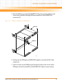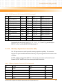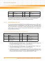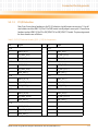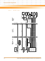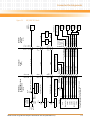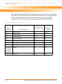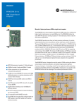
1
Embedded Computing for Business-Critical ContinuityTM MVME55006E Single Board Computer Installation and Use P/N: 6806800A37H September 2013 © 2013 Emerson All rights reserved. Trademarks Emerson, Business-Critical Continuity, Emerson Network Power and the Emerson Network Power logo are trademarks and service marks of Emerson Electric Co. © 2013 Emerson Electric Co. All other product or service names are the property of their respective owners. Intel® is a trademark or registered trademark of Intel Corporation or its subsidiaries in the United States and other countries. Java™ and all other Java-based marks are trademarks or registered trademarks of Sun Microsystems, Inc. in the U.S. and other countries. Microsoft®, Windows® and Windows Me® are registered trademarks of Microsoft Corporation; and Windows XP™ is a trademark of Microsoft Corporation. PICMG®, CompactPCI®, AdvancedTCA™ and the PICMG, CompactPCI and AdvancedTCA logos are registered trademarks of the PCI Industrial Computer Manufacturers Group. UNIX® is a registered trademark of The Open Group in the United States and other countries. Notice While reasonable efforts have been made to assure the accuracy of this document, Emerson assumes no liability resulting from any omissions in this document, or from the use of the information obtained therein. Emerson reserves the right to revise this document and to make changes from time to time in the content hereof without obligation of Emerson to notify any person of such revision or changes. Electronic versions of this material may be read online, downloaded for personal use, or referenced in another document as a URL to a Emerson website. The text itself may not be published commercially in print or electronic form, edited, translated, or otherwise altered without the permission of Emerson, It is possible that this publication may contain reference to or information about Emerson products (machines and programs), programming, or services that are not available in your country. Such references or information must not be construed to mean that Emerson intends to announce such Emerson products, programming, or services in your country. Limited and Restricted Rights Legend If the documentation contained herein is supplied, directly or indirectly, to the U.S. Government, the following notice shall apply unless otherwise agreed to in writing by Emerson. Use, duplication, or disclosure by the Government is subject to restrictions as set forth in subparagraph (b)(3) of the Rights in Technical Data clause at DFARS 252.227-7013 (Nov. 1995) and of the Rights in Noncommercial Computer Software and Documentation clause at DFARS 252.227-7014 (Jun. 1995). Contact Address Emerson Network Power - Embedded Computing 2900 South Diablo Way, Suite 190 Tempe, AZ 85282 USA Contents About this Manual . . . . . . . . . . . . . . . . . . . . . . . . . . . . . . . . . . . . . . . . . . . . . . . . . . . . . . . . . . . . . . . . . . . . . . . 13 1 Hardware Preparation and Installation . . . . . . . . . . . . . . . . . . . . . . . . . . . . . . . . . . . . . . . . . . . . . . . . . 19 1.1 1.2 1.3 1.4 1.5 1.6 1.7 Overview . . . . . . . . . . . . . . . . . . . . . . . . . . . . . . . . . . . . . . . . . . . . . . . . . . . . . . . . . . . . . . . . . . . . . . . . . . 19 Introduction . . . . . . . . . . . . . . . . . . . . . . . . . . . . . . . . . . . . . . . . . . . . . . . . . . . . . . . . . . . . . . . . . . . . . . . 19 Declaration of Conformity . . . . . . . . . . . . . . . . . . . . . . . . . . . . . . . . . . . . . . . . . . . . . . . . . . . . . . . . . . . 19 Getting Started . . . . . . . . . . . . . . . . . . . . . . . . . . . . . . . . . . . . . . . . . . . . . . . . . . . . . . . . . . . . . . . . . . . . 20 Overview of Startup Procedures . . . . . . . . . . . . . . . . . . . . . . . . . . . . . . . . . . . . . . . . . . . . . . . . . . . . . . 20 Unpacking Guidelines . . . . . . . . . . . . . . . . . . . . . . . . . . . . . . . . . . . . . . . . . . . . . . . . . . . . . . . . . . . . . . . 20 Configuring the Hardware . . . . . . . . . . . . . . . . . . . . . . . . . . . . . . . . . . . . . . . . . . . . . . . . . . . . . . . . . . . 21 1.7.1 Configuring the Board . . . . . . . . . . . . . . . . . . . . . . . . . . . . . . . . . . . . . . . . . . . . . . . . . . . . . . . . 22 1.7.2 Ethernet 2, PMC/SBC Mode, and P2 I/O Selection Headers (J6, J7, J28, J32, J34, J97 – J110) 25 1.7.2.1 Ethernet . . . . . . . . . . . . . . . . . . . . . . . . . . . . . . . . . . . . . . . . . . . . . . . . . . . . . . . . . . . 25 1.7.2.2 PMC/SBC Mode Selection . . . . . . . . . . . . . . . . . . . . . . . . . . . . . . . . . . . . . . . . . . . . 25 1.7.2.3 P2 I/O Selection . . . . . . . . . . . . . . . . . . . . . . . . . . . . . . . . . . . . . . . . . . . . . . . . . . . . . 26 1.7.3 Flash Boot Bank Select Header (J8) . . . . . . . . . . . . . . . . . . . . . . . . . . . . . . . . . . . . . . . . . . . . . 28 1.7.4 Flash 0 Programming Enable Switch (S3-1) . . . . . . . . . . . . . . . . . . . . . . . . . . . . . . . . . . . . . . 29 1.7.5 Safe Start ENV Switch (S5-1) . . . . . . . . . . . . . . . . . . . . . . . . . . . . . . . . . . . . . . . . . . . . . . . . . . . 29 1.7.6 Flash 0 Block Write Protect Switch (S3-2). . . . . . . . . . . . . . . . . . . . . . . . . . . . . . . . . . . . . . . . 30 1.7.7 SROM Initialization Enable Switch (S5-2) . . . . . . . . . . . . . . . . . . . . . . . . . . . . . . . . . . . . . . . . 30 1.7.8 PCI Bus 0.0 Speed Switch (S4-1). . . . . . . . . . . . . . . . . . . . . . . . . . . . . . . . . . . . . . . . . . . . . . . . 31 1.7.9 VME SCON Select Header (J27). . . . . . . . . . . . . . . . . . . . . . . . . . . . . . . . . . . . . . . . . . . . . . . . . 31 1.7.10 PCI Bus 1.0 Speed Switch (S4-2). . . . . . . . . . . . . . . . . . . . . . . . . . . . . . . . . . . . . . . . . . . . . . . . 32 1.7.11 EEPROM Write Protect Switch (S3-3) . . . . . . . . . . . . . . . . . . . . . . . . . . . . . . . . . . . . . . . . . . . 32 1.7.12 Setting the PMC Vio Keying Pin . . . . . . . . . . . . . . . . . . . . . . . . . . . . . . . . . . . . . . . . . . . . . . . . 33 1.8 Installing the RAM5500 Module . . . . . . . . . . . . . . . . . . . . . . . . . . . . . . . . . . . . . . . . . . . . . . . . . . . . . . 33 1.9 Installing PMCs . . . . . . . . . . . . . . . . . . . . . . . . . . . . . . . . . . . . . . . . . . . . . . . . . . . . . . . . . . . . . . . . . . . . . 35 1.9.1 Mounting the PMC Module . . . . . . . . . . . . . . . . . . . . . . . . . . . . . . . . . . . . . . . . . . . . . . . . . . . . 35 1.9.2 Primary PMCspan . . . . . . . . . . . . . . . . . . . . . . . . . . . . . . . . . . . . . . . . . . . . . . . . . . . . . . . . . . . . 37 1.9.3 Secondary PMCspan . . . . . . . . . . . . . . . . . . . . . . . . . . . . . . . . . . . . . . . . . . . . . . . . . . . . . . . . . . 40 1.10 Installing the Board . . . . . . . . . . . . . . . . . . . . . . . . . . . . . . . . . . . . . . . . . . . . . . . . . . . . . . . . . . . . . . . . . 41 1.10.1 Connection to Peripherals . . . . . . . . . . . . . . . . . . . . . . . . . . . . . . . . . . . . . . . . . . . . . . . . . . . . . 42 1.10.2 Completing the Installation . . . . . . . . . . . . . . . . . . . . . . . . . . . . . . . . . . . . . . . . . . . . . . . . . . . 43 1.11 Startup and Operation . . . . . . . . . . . . . . . . . . . . . . . . . . . . . . . . . . . . . . . . . . . . . . . . . . . . . . . . . . . . . . 43 MVME55006E Single Board Computer Installation and Use (6806800A37H) 3 Contents Contents 1.12 Applying Power . . . . . . . . . . . . . . . . . . . . . . . . . . . . . . . . . . . . . . . . . . . . . . . . . . . . . . . . . . . . . . . . . . . . 44 1.13 Switches and Indicators . . . . . . . . . . . . . . . . . . . . . . . . . . . . . . . . . . . . . . . . . . . . . . . . . . . . . . . . . . . . . 44 2 Functional Description . . . . . . . . . . . . . . . . . . . . . . . . . . . . . . . . . . . . . . . . . . . . . . . . . . . . . . . . . . . . . . . . 45 2.1 2.2 2.3 2.4 2.5 2.6 2.7 2.8 2.9 2.10 2.11 2.12 2.13 2.14 2.15 2.16 4 Overview . . . . . . . . . . . . . . . . . . . . . . . . . . . . . . . . . . . . . . . . . . . . . . . . . . . . . . . . . . . . . . . . . . . . . . . . . . 45 Block Diagram . . . . . . . . . . . . . . . . . . . . . . . . . . . . . . . . . . . . . . . . . . . . . . . . . . . . . . . . . . . . . . . . . . . . . 45 Features . . . . . . . . . . . . . . . . . . . . . . . . . . . . . . . . . . . . . . . . . . . . . . . . . . . . . . . . . . . . . . . . . . . . . . . . . . . 46 Processor . . . . . . . . . . . . . . . . . . . . . . . . . . . . . . . . . . . . . . . . . . . . . . . . . . . . . . . . . . . . . . . . . . . . . . . . . . 47 L3 Cache . . . . . . . . . . . . . . . . . . . . . . . . . . . . . . . . . . . . . . . . . . . . . . . . . . . . . . . . . . . . . . . . . . . . . . . . . . 47 System Controller . . . . . . . . . . . . . . . . . . . . . . . . . . . . . . . . . . . . . . . . . . . . . . . . . . . . . . . . . . . . . . . . . . 48 2.6.1 CPU Bus Interface . . . . . . . . . . . . . . . . . . . . . . . . . . . . . . . . . . . . . . . . . . . . . . . . . . . . . . . . . . . . 48 2.6.2 Memory Controller Interface . . . . . . . . . . . . . . . . . . . . . . . . . . . . . . . . . . . . . . . . . . . . . . . . . . 48 2.6.3 Interrupt Controller . . . . . . . . . . . . . . . . . . . . . . . . . . . . . . . . . . . . . . . . . . . . . . . . . . . . . . . . . . 49 2.6.4 I2C Serial Interface and Devices . . . . . . . . . . . . . . . . . . . . . . . . . . . . . . . . . . . . . . . . . . . . . . . . 49 2.6.5 Direct Memory Access (DMA). . . . . . . . . . . . . . . . . . . . . . . . . . . . . . . . . . . . . . . . . . . . . . . . . . 50 2.6.6 Timers . . . . . . . . . . . . . . . . . . . . . . . . . . . . . . . . . . . . . . . . . . . . . . . . . . . . . . . . . . . . . . . . . . . . . . 50 Flash Memory . . . . . . . . . . . . . . . . . . . . . . . . . . . . . . . . . . . . . . . . . . . . . . . . . . . . . . . . . . . . . . . . . . . . . . 51 System Memory . . . . . . . . . . . . . . . . . . . . . . . . . . . . . . . . . . . . . . . . . . . . . . . . . . . . . . . . . . . . . . . . . . . . 51 PCI Local Buses and Devices . . . . . . . . . . . . . . . . . . . . . . . . . . . . . . . . . . . . . . . . . . . . . . . . . . . . . . . . . . 51 2.9.1 Gigabit Ethernet Interface. . . . . . . . . . . . . . . . . . . . . . . . . . . . . . . . . . . . . . . . . . . . . . . . . . . . . 51 2.9.2 10/100Mb Ethernet Interface . . . . . . . . . . . . . . . . . . . . . . . . . . . . . . . . . . . . . . . . . . . . . . . . . . 52 2.9.3 PCI-to-PCI Bridges . . . . . . . . . . . . . . . . . . . . . . . . . . . . . . . . . . . . . . . . . . . . . . . . . . . . . . . . . . . . 52 2.9.4 PMC Sites . . . . . . . . . . . . . . . . . . . . . . . . . . . . . . . . . . . . . . . . . . . . . . . . . . . . . . . . . . . . . . . . . . . 52 2.9.5 PCI IDSEL Definition . . . . . . . . . . . . . . . . . . . . . . . . . . . . . . . . . . . . . . . . . . . . . . . . . . . . . . . . . . 52 2.9.6 PCI Bus Arbitration . . . . . . . . . . . . . . . . . . . . . . . . . . . . . . . . . . . . . . . . . . . . . . . . . . . . . . . . . . . 53 Asynchronous Serial Ports . . . . . . . . . . . . . . . . . . . . . . . . . . . . . . . . . . . . . . . . . . . . . . . . . . . . . . . . . . . 53 Real Time Clock and NVRAM . . . . . . . . . . . . . . . . . . . . . . . . . . . . . . . . . . . . . . . . . . . . . . . . . . . . . . . . . 54 System Control and Status Registers . . . . . . . . . . . . . . . . . . . . . . . . . . . . . . . . . . . . . . . . . . . . . . . . . . 54 Sources of Reset . . . . . . . . . . . . . . . . . . . . . . . . . . . . . . . . . . . . . . . . . . . . . . . . . . . . . . . . . . . . . . . . . . . . 54 VME Interface . . . . . . . . . . . . . . . . . . . . . . . . . . . . . . . . . . . . . . . . . . . . . . . . . . . . . . . . . . . . . . . . . . . . . . 55 PMC Expansion . . . . . . . . . . . . . . . . . . . . . . . . . . . . . . . . . . . . . . . . . . . . . . . . . . . . . . . . . . . . . . . . . . . . . 55 Debug Support . . . . . . . . . . . . . . . . . . . . . . . . . . . . . . . . . . . . . . . . . . . . . . . . . . . . . . . . . . . . . . . . . . . . . 55 MVME55006E Single Board Computer Installation and Use (6806800A37H) Contents 3 RAM55006E Memory Expansion Module . . . . . . . . . . . . . . . . . . . . . . . . . . . . . . . . . . . . . . . . . . . . . . . . 57 3.1 3.2 3.3 3.4 3.5 4 MOTLoad Firmware . . . . . . . . . . . . . . . . . . . . . . . . . . . . . . . . . . . . . . . . . . . . . . . . . . . . . . . . . . . . . . . . . . 63 4.1 4.2 4.3 4.4 4.5 4.6 5 Overview . . . . . . . . . . . . . . . . . . . . . . . . . . . . . . . . . . . . . . . . . . . . . . . . . . . . . . . . . . . . . . . . . . . . . . . . . . 57 Features . . . . . . . . . . . . . . . . . . . . . . . . . . . . . . . . . . . . . . . . . . . . . . . . . . . . . . . . . . . . . . . . . . . . . . . . . . . 57 Functional Description . . . . . . . . . . . . . . . . . . . . . . . . . . . . . . . . . . . . . . . . . . . . . . . . . . . . . . . . . . . . . . 57 3.3.1 RAM5500 Description . . . . . . . . . . . . . . . . . . . . . . . . . . . . . . . . . . . . . . . . . . . . . . . . . . . . . . . . 57 3.3.2 SROM. . . . . . . . . . . . . . . . . . . . . . . . . . . . . . . . . . . . . . . . . . . . . . . . . . . . . . . . . . . . . . . . . . . . . . . 58 3.3.3 Clocks . . . . . . . . . . . . . . . . . . . . . . . . . . . . . . . . . . . . . . . . . . . . . . . . . . . . . . . . . . . . . . . . . . . . . . 59 Memory Expansion Connector Pin Assignments . . . . . . . . . . . . . . . . . . . . . . . . . . . . . . . . . . . . . . . . 59 RAM5500 Programming Issues . . . . . . . . . . . . . . . . . . . . . . . . . . . . . . . . . . . . . . . . . . . . . . . . . . . . . . . 62 3.5.1 Serial Presence Detect (SPD) Data . . . . . . . . . . . . . . . . . . . . . . . . . . . . . . . . . . . . . . . . . . . . . . 62 Overview . . . . . . . . . . . . . . . . . . . . . . . . . . . . . . . . . . . . . . . . . . . . . . . . . . . . . . . . . . . . . . . . . . . . . . . . . . 63 Implementation and Memory Requirements . . . . . . . . . . . . . . . . . . . . . . . . . . . . . . . . . . . . . . . . . . . 63 MOTLoad Commands . . . . . . . . . . . . . . . . . . . . . . . . . . . . . . . . . . . . . . . . . . . . . . . . . . . . . . . . . . . . . . . 63 4.3.1 Utilities . . . . . . . . . . . . . . . . . . . . . . . . . . . . . . . . . . . . . . . . . . . . . . . . . . . . . . . . . . . . . . . . . . . . . 64 4.3.2 Tests . . . . . . . . . . . . . . . . . . . . . . . . . . . . . . . . . . . . . . . . . . . . . . . . . . . . . . . . . . . . . . . . . . . . . . . 64 4.3.3 Command List . . . . . . . . . . . . . . . . . . . . . . . . . . . . . . . . . . . . . . . . . . . . . . . . . . . . . . . . . . . . . . . 65 Using the Command Line Interface . . . . . . . . . . . . . . . . . . . . . . . . . . . . . . . . . . . . . . . . . . . . . . . . . . . 70 4.4.1 Rules . . . . . . . . . . . . . . . . . . . . . . . . . . . . . . . . . . . . . . . . . . . . . . . . . . . . . . . . . . . . . . . . . . . . . . . 72 4.4.2 Help . . . . . . . . . . . . . . . . . . . . . . . . . . . . . . . . . . . . . . . . . . . . . . . . . . . . . . . . . . . . . . . . . . . . . . . . 73 Firmware Settings . . . . . . . . . . . . . . . . . . . . . . . . . . . . . . . . . . . . . . . . . . . . . . . . . . . . . . . . . . . . . . . . . . 73 4.5.1 Default VME Settings . . . . . . . . . . . . . . . . . . . . . . . . . . . . . . . . . . . . . . . . . . . . . . . . . . . . . . . . . 74 4.5.1.1 CR/CSR Settings . . . . . . . . . . . . . . . . . . . . . . . . . . . . . . . . . . . . . . . . . . . . . . . . . . . . 77 4.5.1.2 Displaying VME Settings . . . . . . . . . . . . . . . . . . . . . . . . . . . . . . . . . . . . . . . . . . . . . 77 4.5.1.3 Editing VME Settings . . . . . . . . . . . . . . . . . . . . . . . . . . . . . . . . . . . . . . . . . . . . . . . . 78 4.5.1.4 Deleting VME Settings . . . . . . . . . . . . . . . . . . . . . . . . . . . . . . . . . . . . . . . . . . . . . . . 78 4.5.1.5 Restoring Default VME Settings . . . . . . . . . . . . . . . . . . . . . . . . . . . . . . . . . . . . . . . 79 Remote Start . . . . . . . . . . . . . . . . . . . . . . . . . . . . . . . . . . . . . . . . . . . . . . . . . . . . . . . . . . . . . . . . . . . . . . 79 Connector Pin Assignments . . . . . . . . . . . . . . . . . . . . . . . . . . . . . . . . . . . . . . . . . . . . . . . . . . . . . . . . . . . 81 5.1 5.2 Introduction . . . . . . . . . . . . . . . . . . . . . . . . . . . . . . . . . . . . . . . . . . . . . . . . . . . . . . . . . . . . . . . . . . . . . . . 81 Connectors . . . . . . . . . . . . . . . . . . . . . . . . . . . . . . . . . . . . . . . . . . . . . . . . . . . . . . . . . . . . . . . . . . . . . . . . 81 5.2.1 Asynchronous Serial Port Connector (J1) . . . . . . . . . . . . . . . . . . . . . . . . . . . . . . . . . . . . . . . . 82 MVME55006E Single Board Computer Installation and Use (6806800A37H) 5 Contents Contents 5.3 A Specifications . . . . . . . . . . . . . . . . . . . . . . . . . . . . . . . . . . . . . . . . . . . . . . . . . . . . . . . . . . . . . . . . . . . . . . . 117 A.1 A.2 B Power Requirements . . . . . . . . . . . . . . . . . . . . . . . . . . . . . . . . . . . . . . . . . . . . . . . . . . . . . . . . . . . . . . . 117 A.1.1 Supply Current Requirements . . . . . . . . . . . . . . . . . . . . . . . . . . . . . . . . . . . . . . . . . . . . . . . . 117 Environmental Specifications . . . . . . . . . . . . . . . . . . . . . . . . . . . . . . . . . . . . . . . . . . . . . . . . . . . . . . . 117 Thermal Validation . . . . . . . . . . . . . . . . . . . . . . . . . . . . . . . . . . . . . . . . . . . . . . . . . . . . . . . . . . . . . . . . . . 119 B.1 B.2 B.3 6 5.2.2 Ethernet Connectors (J2) . . . . . . . . . . . . . . . . . . . . . . . . . . . . . . . . . . . . . . . . . . . . . . . . . . . . . . 82 5.2.3 IPMC Connector (J3) . . . . . . . . . . . . . . . . . . . . . . . . . . . . . . . . . . . . . . . . . . . . . . . . . . . . . . . . . . 83 5.2.4 PCI/PMC Expansion Connector (J4) . . . . . . . . . . . . . . . . . . . . . . . . . . . . . . . . . . . . . . . . . . . . . 85 5.2.5 CPU COP Connector (J5) . . . . . . . . . . . . . . . . . . . . . . . . . . . . . . . . . . . . . . . . . . . . . . . . . . . . . . 87 5.2.6 PMC 1 Interface Connectors (J11, J12, J13, J14) . . . . . . . . . . . . . . . . . . . . . . . . . . . . . . . . . . 88 5.2.7 Boundary Scan Connector (J18) . . . . . . . . . . . . . . . . . . . . . . . . . . . . . . . . . . . . . . . . . . . . . . . . 93 5.2.8 PMC 2 Interface Connectors (J21, J22, J23, J24) . . . . . . . . . . . . . . . . . . . . . . . . . . . . . . . . . . 94 5.2.9 Asynchronous Serial Port (COM2) Planar Connector (J33) . . . . . . . . . . . . . . . . . . . . . . . . . 99 5.2.10 VMEbus Connectors (P1 & P2) (PMC Mode). . . . . . . . . . . . . . . . . . . . . . . . . . . . . . . . . . . . . 100 5.2.11 VMEbus Connectors (P1 & P2) (SBC Mode) . . . . . . . . . . . . . . . . . . . . . . . . . . . . . . . . . . . . . 102 5.2.12 Memory Expansion Connector (P4) . . . . . . . . . . . . . . . . . . . . . . . . . . . . . . . . . . . . . . . . . . . . 105 Headers . . . . . . . . . . . . . . . . . . . . . . . . . . . . . . . . . . . . . . . . . . . . . . . . . . . . . . . . . . . . . . . . . . . . . . . . . . 108 5.3.1 Ethernet 2, PMC/SBC Mode, and P2 I/O Selection Headers (J6, J7, J28, J32, J34, J97 – J110) 108 5.3.1.1 Ethernet . . . . . . . . . . . . . . . . . . . . . . . . . . . . . . . . . . . . . . . . . . . . . . . . . . . . . . . . . . 109 5.3.1.2 PMC/SBC Mode Selection . . . . . . . . . . . . . . . . . . . . . . . . . . . . . . . . . . . . . . . . . . . 110 5.3.1.3 P2 I/O Selection . . . . . . . . . . . . . . . . . . . . . . . . . . . . . . . . . . . . . . . . . . . . . . . . . . . . 111 5.3.2 Flash Boot Bank Select Header (J8) . . . . . . . . . . . . . . . . . . . . . . . . . . . . . . . . . . . . . . . . . . . . 115 5.3.3 VME SCON Select Header (J27). . . . . . . . . . . . . . . . . . . . . . . . . . . . . . . . . . . . . . . . . . . . . . . . 115 Overview . . . . . . . . . . . . . . . . . . . . . . . . . . . . . . . . . . . . . . . . . . . . . . . . . . . . . . . . . . . . . . . . . . . . . . . . . 119 Thermally Significant Components . . . . . . . . . . . . . . . . . . . . . . . . . . . . . . . . . . . . . . . . . . . . . . . . . . 119 Component Temperature Measurement . . . . . . . . . . . . . . . . . . . . . . . . . . . . . . . . . . . . . . . . . . . . . 122 B.3.1 Preparation . . . . . . . . . . . . . . . . . . . . . . . . . . . . . . . . . . . . . . . . . . . . . . . . . . . . . . . . . . . . . . . . 123 B.3.2 Measuring Junction Temperature . . . . . . . . . . . . . . . . . . . . . . . . . . . . . . . . . . . . . . . . . . . . . 123 B.3.3 Measuring Local Air Temperature . . . . . . . . . . . . . . . . . . . . . . . . . . . . . . . . . . . . . . . . . . . . . 123 B.3.4 Measuring Case Temperature. . . . . . . . . . . . . . . . . . . . . . . . . . . . . . . . . . . . . . . . . . . . . . . . . 124 MVME55006E Single Board Computer Installation and Use (6806800A37H) Contents C Related Documentation . . . . . . . . . . . . . . . . . . . . . . . . . . . . . . . . . . . . . . . . . . . . . . . . . . . . . . . . . . . . . . 127 C.1 C.2 C.3 Emerson Network Power - Embedded Computing Documents . . . . . . . . . . . . . . . . . . . . . . . . . . 127 Manufacturers’ Documents . . . . . . . . . . . . . . . . . . . . . . . . . . . . . . . . . . . . . . . . . . . . . . . . . . . . . . . . . 127 Related Specifications . . . . . . . . . . . . . . . . . . . . . . . . . . . . . . . . . . . . . . . . . . . . . . . . . . . . . . . . . . . . . . 129 Safety Notes . . . . . . . . . . . . . . . . . . . . . . . . . . . . . . . . . . . . . . . . . . . . . . . . . . . . . . . . . . . . . . . . . . . . . . . . . . . . 131 Sicherheitshinweise . . . . . . . . . . . . . . . . . . . . . . . . . . . . . . . . . . . . . . . . . . . . . . . . . . . . . . . . . . . . . . . . . . . . . 135 Index . . . . . . . . . . . . . . . . . . . . . . . . . . . . . . . . . . . . . . . . . . . . . . . . . . . . . . . . . . . . . . . . . . . . . . . . . . . . . . . . . . 141 MVME55006E Single Board Computer Installation and Use (6806800A37H) 7 Contents Contents 8 MVME55006E Single Board Computer Installation and Use (6806800A37H) List of Tables Table 1-1 Table 1-2 Table 1-3 Table 1-4 Table 2-1 Table 3-1 Table 3-2 Table 4-1 Table 5-1 Table 5-2 Table 5-3 Table 5-4 Table 5-5 Table 5-6 Table 5-7 Table 5-8 Table 5-9 Table 5-10 Table 5-11 Table 5-12 Table 5-13 Table 5-14 Table 5-15 Table 5-16 Table 5-17 Table 5-18 Table 5-19 Table 5-20 Table 5-21 Table 5-22 Table 5-23 Table 5-24 Table 5-25 Table A-1 Table A-2 Table B-1 Startup Overview . . . . . . . . . . . . . . . . . . . . . . . . . . . . . . . . . . . . . . . . . . . . . . . . . . . . . . . . . . . 20 MVME5500 Jumper Settings . . . . . . . . . . . . . . . . . . . . . . . . . . . . . . . . . . . . . . . . . . . . . . . . . . 22 MVME5500 Connectors . . . . . . . . . . . . . . . . . . . . . . . . . . . . . . . . . . . . . . . . . . . . . . . . . . . . . . 43 Front-Panel LED Status Indicators . . . . . . . . . . . . . . . . . . . . . . . . . . . . . . . . . . . . . . . . . . . . . 44 MVME5500 Features Summary . . . . . . . . . . . . . . . . . . . . . . . . . . . . . . . . . . . . . . . . . . . . . . . 46 RAM5500 Feature Summary . . . . . . . . . . . . . . . . . . . . . . . . . . . . . . . . . . . . . . . . . . . . . . . . . . 57 RAM5500 Connector (P1) Pin Assignments . . . . . . . . . . . . . . . . . . . . . . . . . . . . . . . . . . . . . 59 MOTLoad Commands . . . . . . . . . . . . . . . . . . . . . . . . . . . . . . . . . . . . . . . . . . . . . . . . . . . . . . . 65 COM1 Connector (J1) Pin Assignments . . . . . . . . . . . . . . . . . . . . . . . . . . . . . . . . . . . . . . . . 82 Ethernet Connector (J2) Pin Assignments . . . . . . . . . . . . . . . . . . . . . . . . . . . . . . . . . . . . . . 82 IPMC Connector (J3) Pin Assignments . . . . . . . . . . . . . . . . . . . . . . . . . . . . . . . . . . . . . . . . . 83 PCI/PMC Expansion Connector (J4) Pin Assignments . . . . . . . . . . . . . . . . . . . . . . . . . . . . . 85 CPU COP Connector (J5) Pin Assignments . . . . . . . . . . . . . . . . . . . . . . . . . . . . . . . . . . . . . . 87 PMC 1 Connector (J11) Pin Assignments . . . . . . . . . . . . . . . . . . . . . . . . . . . . . . . . . . . . . . . 88 PMC 1 Connector (J12) Pin Assignments . . . . . . . . . . . . . . . . . . . . . . . . . . . . . . . . . . . . . . . 89 PMC 1 Connector (J13) Pin Assignments . . . . . . . . . . . . . . . . . . . . . . . . . . . . . . . . . . . . . . . 91 PMC 1 Connector (J14) Pin Assignments . . . . . . . . . . . . . . . . . . . . . . . . . . . . . . . . . . . . . . . 92 Boundary Scan Connector (J18) Pin Assignments . . . . . . . . . . . . . . . . . . . . . . . . . . . . . . . . 93 PMC 2 Connector (J21) Pin Assignments . . . . . . . . . . . . . . . . . . . . . . . . . . . . . . . . . . . . . . . 94 PMC 2 Connector (J22) Pin Assignments . . . . . . . . . . . . . . . . . . . . . . . . . . . . . . . . . . . . . . . 95 PMC 2 Connector (J23) Pin Assignments . . . . . . . . . . . . . . . . . . . . . . . . . . . . . . . . . . . . . . . 97 PMC 2 Connector (J24) Pin Assignments . . . . . . . . . . . . . . . . . . . . . . . . . . . . . . . . . . . . . . . 98 COM2 Planar Connector (J33) Pin Assignments . . . . . . . . . . . . . . . . . . . . . . . . . . . . . . . . . 99 VME Connector (P2) Pin Assignments (PMC Mode) . . . . . . . . . . . . . . . . . . . . . . . . . . . . . 100 VME Connector (P2) Pinout with IPMC712 . . . . . . . . . . . . . . . . . . . . . . . . . . . . . . . . . . . . 102 VME Connector (P2) Pinouts with IPMC761 . . . . . . . . . . . . . . . . . . . . . . . . . . . . . . . . . . . 104 Memory Expansion Connector (P4) Pin Assignments . . . . . . . . . . . . . . . . . . . . . . . . . . . 105 Ethernet 2 Selection Headers (J6, J7, J100, J101) Pin Assignments . . . . . . . . . . . . . . . . 109 Ethernet 2 Selection Headers (J34, J97, J98, J99) Pin Assignments . . . . . . . . . . . . . . . . 109 PMC/SBC Mode Selection Headers (J28, J32) Pin Assignments . . . . . . . . . . . . . . . . . . . 110 P2 I/O Selection Headers (J102 – J110) Pin Assignments . . . . . . . . . . . . . . . . . . . . . . . . . 111 Flash Boot Bank Select Header (J8) Pin Assignments . . . . . . . . . . . . . . . . . . . . . . . . . . . . 115 VME SCON Select Header (J27) Pin Assignments . . . . . . . . . . . . . . . . . . . . . . . . . . . . . . . 115 Power Requirements . . . . . . . . . . . . . . . . . . . . . . . . . . . . . . . . . . . . . . . . . . . . . . . . . . . . . . . 117 MVME5500 Specifications . . . . . . . . . . . . . . . . . . . . . . . . . . . . . . . . . . . . . . . . . . . . . . . . . . . 117 Thermally Significant Components . . . . . . . . . . . . . . . . . . . . . . . . . . . . . . . . . . . . . . . . . . . 120 MVME55006E Single Board Computer Installation and Use (6806800A37H) 9 List of Tables Table C-1 Table C-2 Table C-3 10 Emerson Network Power - Embedded Computing Publications . . . . . . . . . . . . . . . . . .127 Manufacturers’ Documents . . . . . . . . . . . . . . . . . . . . . . . . . . . . . . . . . . . . . . . . . . . . . . . . . .127 Related Specifications . . . . . . . . . . . . . . . . . . . . . . . . . . . . . . . . . . . . . . . . . . . . . . . . . . . . . .129 MVME55006E Single Board Computer Installation and Use (6806800A37H) List of Figures Figure 1-1 Figure 1-2 Figure 1-3 Figure 1-4 Figure 1-5 Figure 1-6 Figure 1-7 Figure 1-8 Figure 1-9 Figure 1-10 Figure 1-11 Figure 1-12 Figure 1-13 Figure 1-14 Figure 1-15 Figure 1-16 Figure 1-17 Figure 2-1 Figure 2-2 Figure 3-1 Figure 5-1 Figure 5-2 Figure 5-3 Figure B-1 Figure B-2 Figure B-3 Figure B-4 MVME5500 Board Layout . . . . . . . . . . . . . . . . . . . . . . . . . . . . . . . . . . . . . . . . . . . . . . . . 24 Front Panel and Rear P2 Ethernet Settings . . . . . . . . . . . . . . . . . . . . . . . . . . . . . . . . . . 27 J28 and J32 Settings . . . . . . . . . . . . . . . . . . . . . . . . . . . . . . . . . . . . . . . . . . . . . . . . . . . . . 28 J102 - J110 Settings . . . . . . . . . . . . . . . . . . . . . . . . . . . . . . . . . . . . . . . . . . . . . . . . . . . . . . 28 J8 Settings . . . . . . . . . . . . . . . . . . . . . . . . . . . . . . . . . . . . . . . . . . . . . . . . . . . . . . . . . . . . . 28 S3-1 Settings . . . . . . . . . . . . . . . . . . . . . . . . . . . . . . . . . . . . . . . . . . . . . . . . . . . . . . . . . . . 29 S5-1 Settings . . . . . . . . . . . . . . . . . . . . . . . . . . . . . . . . . . . . . . . . . . . . . . . . . . . . . . . . . . . 29 S3-2 Settings . . . . . . . . . . . . . . . . . . . . . . . . . . . . . . . . . . . . . . . . . . . . . . . . . . . . . . . . . . . 30 S5-2 Settings . . . . . . . . . . . . . . . . . . . . . . . . . . . . . . . . . . . . . . . . . . . . . . . . . . . . . . . . . . . 30 S4-1 Settings . . . . . . . . . . . . . . . . . . . . . . . . . . . . . . . . . . . . . . . . . . . . . . . . . . . . . . . . . . . 31 J27 Settings . . . . . . . . . . . . . . . . . . . . . . . . . . . . . . . . . . . . . . . . . . . . . . . . . . . . . . . . . . . . 31 S4-2 Settings . . . . . . . . . . . . . . . . . . . . . . . . . . . . . . . . . . . . . . . . . . . . . . . . . . . . . . . . . . . 32 S3-3 Settings . . . . . . . . . . . . . . . . . . . . . . . . . . . . . . . . . . . . . . . . . . . . . . . . . . . . . . . . . . . 32 VIO Keying Pin Settings . . . . . . . . . . . . . . . . . . . . . . . . . . . . . . . . . . . . . . . . . . . . . . . . . . 33 Typical Placement of a PMC Module on a VME Module . . . . . . . . . . . . . . . . . . . . . . . 37 PMCspan Installation on a VME Module . . . . . . . . . . . . . . . . . . . . . . . . . . . . . . . . . . . . 39 Installation into a Typical VME Chassis . . . . . . . . . . . . . . . . . . . . . . . . . . . . . . . . . . . . . 42 Block Diagram . . . . . . . . . . . . . . . . . . . . . . . . . . . . . . . . . . . . . . . . . . . . . . . . . . . . . . . . . . 45 COM1 Asynchronous Serial Port Connections (RJ-45) . . . . . . . . . . . . . . . . . . . . . . . . 53 RAM500 Block Diagram . . . . . . . . . . . . . . . . . . . . . . . . . . . . . . . . . . . . . . . . . . . . . . . . . . 58 SBC/IPMC712 Mode . . . . . . . . . . . . . . . . . . . . . . . . . . . . . . . . . . . . . . . . . . . . . . . . . . . . 112 SBC/IPMC761 Mode . . . . . . . . . . . . . . . . . . . . . . . . . . . . . . . . . . . . . . . . . . . . . . . . . . . . 113 PMC Mode . . . . . . . . . . . . . . . . . . . . . . . . . . . . . . . . . . . . . . . . . . . . . . . . . . . . . . . . . . . . 114 Thermally Significant Components—Secondary Side . . . . . . . . . . . . . . . . . . . . . . . . 121 Thermally Significant Components—Primary Side . . . . . . . . . . . . . . . . . . . . . . . . . . 122 Thermalcouple Placement . . . . . . . . . . . . . . . . . . . . . . . . . . . . . . . . . . . . . . . . . . . . . . . 123 Machining a Heatsink . . . . . . . . . . . . . . . . . . . . . . . . . . . . . . . . . . . . . . . . . . . . . . . . . . . 125 MVME55006E Single Board Computer Installation and Use (6806800A37H) 11 List of Figures 12 MVME55006E Single Board Computer Installation and Use (6806800A37H) About this Manual Overview of Contents This manual is divided into the following chapters and appendices: Chapter 1, Hardware Preparation and Installation, provides MVME5500 board preparation and installation instructions for both the board and accessories. Also included are the power-up procedure. Chapter 2, Functional Description, describes the MVME5500 on a block diagram level. Chapter 3, RAM55006E Memory Expansion Module, provides a description of the RAM5500 memory expansion module, as well as installation instructions and connector pin assignments. Chapter 4, MOTLoad Firmware, describes the basic features of the MOTLoad firmware product. Chapter 5, Connector Pin Assignments, provides pin assignments for various headers and connectors on the MMVE5500 single-board computer. Appendix A, Specifications, provides power requirements and environmental specifications. Appendix B, Thermal Validation, provides information to conduct thermal evaluations and identifies thermally significant components along with their maximum allowable operating temperatures. Appendix C, Related Documentation, provides a listing of related Emerson manuals, vendor documentation, and industry specifications. Safety Notes summarizes the safety instructions in the manual. Sicherheitshinweise is a German translation of the Safety Notes chapter. The MVME55006E Single-Board Computer Installation and Use manual provides the information you will need to install and configure your MVME55006E single-board computer. It provides specific preparation and installation information, and data applicable to the board. The MVME55006E single-board computer will hereafter be referred to as the MVME5500. MVME55006E Single Board Computer Installation and Use (6806800A37H) 13 About this Manual About this Manual As of the printing date of this manual, the MVME5500 supports the models listed below. Model Number Description MVME55006E-0161R 1 GHz MPC7457 processor, 512MB SDRAM, Scanbe handles MVME55006E-0163R 1 GHz MPC7457 processor, 512MB SDRAM, IEEE handles RAM55006E-007 Memory expansion, 512MB SDRAM IPMC7126E-002 Multifunction rear I/O PMC module; 8-bit SCSI, Ultra Wide SCSI, one parallel port, three async and one sync/async serial ports. MVME712M6E Transition module with one DB-25 sync/async serial port, three DB-25 async serial port, one AUI connector, one D-36 parallel port and one 50-pin 8-bit SCSI; includes 3-row DIN P2 adapter board and cable. MVME7616E-001 Multifunction rear I/O PMC module; 8-bit SCSI, one parallel port, two async and two sync/async serial ports. Transition module with two DB-9 async serial port connectors, two HD-26 sync/async serial port connectors, one HD-36 parallel port connector, one RJ-45 10/100 Ethernet connector; includes 3row DIN P2 adapter board and cable (for 8-bit SCSI). MVME7616E-011 Transition module with two DB-9 async serial port connectors, two HD-26 sync/async serial port connectors, one HD-36 parallel port connector, one RJ45 10/100 Ethernet connector; includes 5-row DIN P2 adapter board and cable (for 16-bit SCSI); requires backplane with 5-row DIN connectors. PMCSPAN26E-002 Primary PMCSPAN with original VME IEEE ejector handles. PMCSPAN26E-010 Secondary PMCSPAN with original VME IEEE ejector handles. PMCSPAN16E-002 Primary PMCSPAN with Scanbe ejector handles. PMCSPAN16E-010 Secondary PMCSPAN with Scanbe ejector handles. 14 MVME55006E Single Board Computer Installation and Use (6806800A37H) About this Manual Conventions The following table describes the conventions used throughout this manual. Notation Description 0x00000000 Typical notation for hexadecimal numbers (digits are 0 through F), for example used for addresses and offsets 0b0000 Same for binary numbers (digits are 0 and 1) bold Used to emphasize a word Screen Used for on-screen output and code related elements or commands in body text Courier + Bold Used to characterize user input and to separate it from system output Reference Used for references and for table and figure descriptions File > Exit Notation for selecting a submenu <text> Notation for variables and keys [text] Notation for software buttons to click on the screen and parameter description ... Repeated item for example node 1, node 2, ..., node 12 . Omission of information from example/command that is not necessary at the time being . . .. Ranges, for example: 0..4 means one of the integers 0,1,2,3, and 4 (used in registers) | Logical OR MVME55006E Single Board Computer Installation and Use (6806800A37H) 15 About this Manual About this Manual Notation Description Indicates a hazardous situation which, if not avoided, could result in death or serious injury Indicates a hazardous situation which, if not avoided, may result in minor or moderate injury Indicates a property damage message No danger encountered. Pay attention to important information 16 MVME55006E Single Board Computer Installation and Use (6806800A37H) About this Manual Summary of Changes This manual has been revised and replaces all prior editions. Date Change Replaces January 2007 Default setting for J102 - J110 is [1-2] (see Figure 1-2 on page 27). 6806800A37A February 2007 Default setting for J32 is [1-2] 6806800A37B Default setting for J28 is [1-2} PMC Mode for J28 and J32 is factory default P2 PMC 2 I/O mode for J102-J110 is factory default P2 IPMC I/O is [2-3] See Figure 1-3 on page 28 and Figure 1-4 on page 28. March 2008 Updated to Emerson style standards. 6806800A37C October 2008 Updated Table 1-2 on page 22 to correctly identify the default setting for Jumpers J28, J32 as PMC mode by putting brackets around 1-2 on both in the Settings column. 6806800A37D August 2011 Added Safety Notes on page 131 and Sicherheitshinweise on page 135. 6806800A37E December 2012 Added Declaration of Conformity on page 19. 6806800A37G September 2013 Updated L3 Cache on page 47, Intel Ethernet Controller 82544EI replaced with 82545GM. 6806800A37H MVME55006E Single Board Computer Installation and Use (6806800A37H) 17 About this Manual About this Manual 18 MVME55006E Single Board Computer Installation and Use (6806800A37H) Chapter 1 Hardware Preparation and Installation 1.1 Overview This chapter contains the following information: 1.2 Board and accessory preparation and installation instructions ESD precautionary notes Introduction The MVME5500 is a single-board computer based on the PowerPC MPC7457 processor and the Marvell GT-64260B host bridge with a dual PCI interface and memory controller. On-board payload includes two PMC slots, two SDRAM banks, an expansion connector for two additional banks of SDRAM, 8MB boot Flash ROM, one 10/100/1000 Ethernet port, one 10/100 Ethernet port, 32MB expansion Flash ROM, two serial ports, NVRAM and a real-time clock. The MVME5500 interfaces to a VMEbus system via its P1 and P2 connectors and contains two IEEE 1386.1 PCI mezzanine card (PMC) slots. The PMC slots are 64-bit and support both front and rear I/O. Additionally, the MVME5500 is user-configurable by setting on-board jumpers. Two I/O modes are possible: PMC mode or SBC mode (also called 761 or IPMC mode). The SBC mode uses the IPMC712 I/O PMC and the MVME712M transition module, or the IPMC761 I/O PMC and the MVME761 transition module. The SBC mode is backwards compatible with the MVME761 transition module and the P2 adapter card (excluding PMC I/O routing) used on the MVME5100 product. This mode is accomplished by configuring the on-board jumpers and by attaching an IPMC761 PMC in PMC slot 1. Secondary Ethernet is configured to the rear. PMC mode is backwards compatible with the MVME5100 and is accomplished by configuring the on-board jumpers. 1.3 Declaration of Conformity For Declaration of conformity, refer MVME500 Series Declaration of Conformity. MVME55006E Single Board Computer Installation and Use (6806800A37H) 19 Hardware Preparation and Installation 1.4 Getting Started This section provides an overview of the steps necessary to install and power up the MVME5500 and a brief section on unpacking and ESD precautions. 1.5 Overview of Startup Procedures The following table lists the things you will need to do before you can use this board and tells where to find the information you need to perform each step. Be sure to read this entire chapter, including all Caution and Warning notes, before you begin. Table 1-1 Startup Overview What you need to do... Refer to... Unpack the hardware. Unpacking Guidelines on page 20 Configure the hardware by setting jumpers on the board. Configuring the Board on page 22 Install the MVME5500 board in a chassis. Procedure on page 41 Connect any other equipment you will be using Connection to Peripherals on page 42 Verify the hardware is installed. Completing the Installation on page 43 1.6 Unpacking Guidelines Unpack the equipment from the shipping carton. Refer to the packing list and verify that all items are present. Save the packing material for storing and reshipping of equipment. 20 MVME55006E Single Board Computer Installation and Use (6806800A37H) Hardware Preparation and Installation If the shipping carton is damaged upon receipt, request that the carrier’s agent be present during the unpacking and inspection of the equipment. Product Damage Avoid touching areas of integrated circuitry; static discharge can damage circuits. Inserting or removing modules with power applied may result in damage to module components. ESD Emerson strongly recommends that you use an antistatic wrist strap and a conductive foam pad when installing or upgrading a system. Electronic components, such as disk drives, computer boards, and memory modules can be extremely sensitive to electrostatic discharge (ESD). After removing the component from its protective wrapper or from the system, place the component flat on a grounded, static-free surface (and, in the case of a board, component side up). Do not slide the component over any surface. If an ESD station is not available, you can avoid damage resulting from ESD by wearing an antistatic wrist strap (available at electronics stores) that is attached to an active electrical ground. Note that a system chassis may not be grounded if it is unplugged. Personal Injury or Death Dangerous voltages, capable of causing death, are present in this equipment. Use extreme caution when handling, testing, and adjusting. 1.7 Configuring the Hardware This section discusses certain hardware and software tasks that may need to be performed prior to installing the board in a chassis. MVME55006E Single Board Computer Installation and Use (6806800A37H) 21 Hardware Preparation and Installation To produce the desired configuration and ensure proper operation of the MVME5500, you may need to carry out certain hardware modifications before installing the module. Most options on the MVME5500 are software configurable. Configuration changes are made by setting bits in control registers after the board is installed in a system. Jumpers and switches are used to control those options that are not software configurable. These settings are described further on in this section. If you are resetting the board jumpers or switches from their default settings, it is important to verify that all settings are reset properly. 1.7.1 Configuring the Board Figure 1-1 illustrates the placement of the jumpers, headers, switches, connectors, and various other components on the MVME5500. There are several manually configurable headers and switches on the MVME5500 and their settings are shown in Table 1-2. Each default setting is enclosed in brackets. For pin assignments on the MVME5500, refer to Chapter 5, Connector Pin Assignments. Table 1-2 MVME5500 Jumper Settings Jumpers / Switches J6, J100, J7, J101 Function Settings Ethernet 2 Selection Headers (see also J34, J97, J98, J99) 2-3 on all [1-2 on all] Rear P2 Ethernet (SBC mode) Front-panel Ethernet Refer to the hint on page 7 for a configuration limitation. J8 Flash Boot Bank Select Header No jumper installed [1-2] 2-3 Boots from Flash 0 Boots from Flash 0 Boots from Flash 1 S3-1 Flash 0 Programming Enable Header OFF [ON] Disables Flash 0 writes Enables Flash 0 writes S5-1 Safe Start ENV Header [OFF] Normal ENV settings used during boot Safe ENV settings used during boot ON 22 MVME55006E Single Board Computer Installation and Use (6806800A37H) Hardware Preparation and Installation Table 1-2 MVME5500 Jumper Settings (continued) Jumpers / Switches S3-2 Function Settings Flash 0 Block Write Protect Header OFF Disables Flash 0 J3 block writes Enables Flash 0 J3 block writes [ON] S3-4 Non-Standard Option Header [OFF] For factory use only S5-2 SROM Initialization Enable Switch OFF [ON] Enables SROM initialization Disables SROM initialization S4-1 PCI Bus 0.0 Speed Header [OFF] ON PMC board controls whether the bus runs at 33 MHz or 66 MHz Forces PCI bus 0.0 to remain at 33 MHz J27 VME SCON Select Header No jumper installed 1-2 [2-3] Always SCON No SCON Auto-SCON J28, J32 PMC/SBC Mode Selection Headers (set both jumpers) [1-2 on both] 2-3 on both PMC mode SBC/IPMC761 mode 1-2 on J28 2-3 on J32 SBC/IPMC712 mode [OFF] PMC board controls whether the bus runs at 33 MHz or 66 MHz. Refer to PMC/SBC Mode Selection on page 25 for a notice about configuring for IPMC mode. S4-2 PCI Bus 1.0 Speed Header ON S3-3 EEPROM Write Protect Header OFF Forces PCI bus 1.0 to remain at 33 MHz. Disables EEPROM programming Enables EEPROM programming [ON] J34, J97, J98, J99 Ethernet 2 Selection Headers (see also J6, J100, J7, J101) 1-2 on all Rear P2 Ethernet (set when in SBC/IPMC761 mode) Refer to a note on page 25 for a configuration limitation. [No jumpers installed] Front-panel Ethernet MVME55006E Single Board Computer Installation and Use (6806800A37H) 23 Hardware Preparation and Installation Table 1-2 MVME5500 Jumper Settings (continued) Jumpers / Switches Function Settings J102 –J110 P2 I/O Selection Headers 1-2 [2-3] PMC 2 I/O connected to P2 IPMC I/O connected to P2 Items in brackets are factory default settings. The MVME5500 is factory tested and shipped with the configuration described in the following section. Figure 1-1 MVME5500 Board Layout J5 J18 U28 U29 U30 U6 J21 U5 J8 J27 U19 U7 J22 U25 U16 J102 - J110 U4 PMC 2 XU2 1 XU1 J23 P1 J24 3 J102 - J110 S4 S3 U18 U15 U17 U27 U23 U12 PMC 1 J12 U11 U3 U22 J13 U10 U2 U26 U9 U20 U8 U125 3 J33 J14 J32 U126 ABT/RST GigE 10/100 ENET 1 ENET 2 S1 P2 U123 J28 U24 U31 BFL COM1 CPU J1 1 S5 S2 J2 J32 J6 / J100 J99 J98 J34 J97 J101 / J7 P4 U13 U1 J3 J11 U129 U14 1 U124 3 J4 J28 4436 0207 24 MVME55006E Single Board Computer Installation and Use (6806800A37H) Hardware Preparation and Installation 1.7.2 Ethernet 2, PMC/SBC Mode, and P2 I/O Selection Headers (J6, J7, J28, J32, J34, J97 – J110) All of the headers described below are used in conjunction with each other to select various modes of operation for 10/100BaseT Ethernet, PMC/SBC mode, and P2 I/O mode. 1.7.2.1 Ethernet Four 3-pin planar headers (J6, J7, J100, J101) and four 2-pin planar headers (J34, J97, J98, J99) are for 10/100/BaseT Ethernet 2 selection. Ethernet 1 is the Gigabit Ethernet port and is front panel only. For J6, J100, J7 and J101, install jumpers across pins 2-3 on all four headers for rear P2 Ethernet. For front-panel Ethernet, install jumpers across pins 1-2 on all four headers. If the rear P2 Ethernet is selected by jumpers J6, J7, J100, and J101, the Ethernet signals also connect to PMC 1 user I/O connector J14. If a PMC card is plugged into PMC slot 1, there may be a conflict between the I/O from the PMC card and the rear Ethernet signals. This conflict does not occur with the IPMC761 or IPMC712 modules. For J34, J97, J98 and J99, no jumpers are installed for front-panel Ethernet. For rear P2 Ethernet, install jumpers across pins 1-2 on all four headers when in SBC/IPMC761 mode. 1.7.2.2 PMC/SBC Mode Selection The MVME5500 is set at the factory for PMC mode. The SBC/IPMC761 mode should only be selected when using the IPMC761 module in conjunction with the MVME761 transition module. The PMC mode should be selected when using PMC modules with specific user I/O in conjunction with the corresponding transition module. PMC mode should also be selected when using PrPMC modules. MVME55006E Single Board Computer Installation and Use (6806800A37H) 25 Hardware Preparation and Installation Two 3-pin planar headers (J28, J32) control the supply of +/- 12 volts to the P2 connector; one or both of these voltages are required by the MVME712 or MVME761 module when operating in SBC mode. For PMC mode, jumpers are installed across pins 1-2 on both headers. For SBC/IPMC761 mode, install jumpers across pins 2-3 on both headers. For SBC/IPMC712 mode, install a jumper across pins 2-3 for J32 and install a jumper across pins 1-2 for J28. Product Damage When J28 is configured for SBC/IPMC mode, –12V is supplied to P2 pin A30. If there is an incompatible board plugged into this P2 slot, damage may occur. When J32 is configured for SBC/IPMC mode, +12V is supplied to P2 pin C7. If there is an incompatible board plugged into this P2 slot, damage may occur. 1.7.2.3 P2 I/O Selection Nine 3-pin planar headers (J102 –J110) are for P2 I/O selection. Jumpers are installed across pins 1-2 on all nine headers when in PMC mode. Install jumpers across pins 2-3 on all nine headers when in SBC/IPMC761 or SBC/IPMC712 mode to connect the extended SCSI signals to P2. 26 MVME55006E Single Board Computer Installation and Use (6806800A37H) Hardware Preparation and Installation Figure 1-2 Front Panel and Rear P2 Ethernet Settings Rear P2 Ethernet J6 (factory configuration) Front-Panel Ethernet J6 3 2 1 J7 3 2 1 J7 1 2 3 J100 1 2 3 J100 3 2 1 J101 3 2 1 J101 1 2 3 1 2 3 J34 J34 1 2 1 2 J97 1 2 1 2 1 2 1 2 J97 J98 J98 1 2 1 2 J99 J99 MVME55006E Single Board Computer Installation and Use (6806800A37H) 27 Hardware Preparation and Installation Figure 1-3 J28 and J32 Settings (factory configuration) PMC Mode SBC/IPMC761 Mode J28 J28 J28 3 2 1 3 2 1 3 2 1 J32 J32 J32 3 2 1 Figure 1-4 J102 - J110 Settings (extended SCSI) P2 IPMC I/O P2 PMC 2 I/O J102 – J110 3 2 1 3 2 1 (factory configuration) 1.7.3 SBC/IPMC712 Mode J102 – J110 3 2 1 3 2 1 Flash Boot Bank Select Header (J8) A 3-pin planar header selects the boot Flash bank. No jumper or a jumper installed across pins 1-2 selects Flash 0 as the boot bank. A jumper installed across pins 2-3 selects Flash 1 as the boot bank. Figure 1-5 J8 Settings J8 J8 1 1 1 2 2 2 3 3 3 Boots from Flash device 0 28 J8 Boots from Flash device 0 (factory configuration) Boots from Flash device 1 MVME55006E Single Board Computer Installation and Use (6806800A37H) Hardware Preparation and Installation 1.7.4 Flash 0 Programming Enable Switch (S3-1) This switch enables/disables programming of Flash 0 as a means of protecting the contents from being corrupted. The switch set to OFF disables all Flash 0 programming. The switch set to ON enables the programming, this is the factory setting. Figure 1-6 S3-1 Settings S3-1 1 1 ON Enables Flash 0 writes Disables Flash 0 writes 1.7.5 ON Safe Start ENV Switch (S5-1) This switch selects programmed or safe start ENV settings. When set to OFF, it indicates that the programmed ENV settings should be used during boot. Set to ON indicates that the safe ENV settings should be used. Figure 1-7 S5-1 Settings S5-1 1 ON 2 Normal ENV settings used during boot (factory configuration) 1 ON 2 Safe ENV settings used during boot MVME55006E Single Board Computer Installation and Use (6806800A37H) 29 Hardware Preparation and Installation 1.7.6 Flash 0 Block Write Protect Switch (S3-2) This switch supports the Intel J3 Flash family write protect feature. Set to OFF, it enables the lock-down mechanism. Blocks locked down cannot be unlocked with the unlock command. The switch must be set to ON in order to override the lock-down function and enable blocks to be erased or programmed through software. Refer to the Intel J3 Flash data sheet, listed in Appendix C, Related Documentation, for further details. Figure 1-8 S3-2 Settings S3-2 1 1 ON 2 2 3 3 4 4 Disable Flash 0 J3 block writes 1.7.7 ON Enable Flash 0 J3 block writes (factory configuration) SROM Initialization Enable Switch (S5-2) This switch enables/disables the GT-64260B SROM initialization. When set to 2, it enables the GT-64260B device initialization via I2C SROM. Set to ON disables this initialization sequence. Figure 1-9 S5-2 Settings S5-2 1 ON 2 Enable SROM initialization 30 1 ON 2 Disable SROM initialization (factory configuration) MVME55006E Single Board Computer Installation and Use (6806800A37H) Hardware Preparation and Installation 1.7.8 PCI Bus 0.0 Speed Switch (S4-1) This switch can force PCI bus 0.0 to run at 33 MHz rather than the standard method of allowing the PMC board to control whether the bus runs at 33 MHz or 66 MHz. Set to 1, it allows the PMC board to choose the PCI 0.0 bus speed. Set to ON forces PCI bus 0.0 to run at 33 MHz. Figure 1-10 S4-1 Settings S4-1 1 1 ON 2 2 PMC board controls PCI 0.0 bus speed (factory configuration) 1.7.9 ON Force PCI bus 0.0 to run at 33 MHz VME SCON Select Header (J27) A 3-pin planar header allows the choice for auto/enable/disable SCON VME configuration. A jumper installed across pins 1-2 configures for SCON disabled. A jumper installed across pins 23 configures for auto SCON. No jumper installed configures for SCON always enabled. Figure 1-11 J27 Settings J27 J27 J27 1 1 1 2 2 2 3 3 3 Always SCON No SCON Auto-SCON (factory configuration) MVME55006E Single Board Computer Installation and Use (6806800A37H) 31 Hardware Preparation and Installation 1.7.10 PCI Bus 1.0 Speed Switch (S4-2) This switch can force PCI bus 1.0 to run at 33 MHz rather than the standard method of allowing the PMC board to control whether the bus runs at 33 MHz or 66 MHz. Set to 1, it allows the PMC board to choose the PCI 1.0 bus speed. Set to ON forces PCI bus 1.0 to run at 33 MHz. Figure 1-12 S4-2 Settings S4-2 1 1 ON 2 ON 2 PMC board controls PCI 1.0 bus speed (factory configuration) Force PCI bus 1.0 to run at 33 MHz 1.7.11 EEPROM Write Protect Switch (S3-3) This switch enables/disables programming of the on-board EEPROMs as a means of protecting the contents from being corrupted. Set to 1, it disables EEPROM programming by driving the WP pin to a logic high. Set to ON to program any of the EEPROMs at addresses A0, A6, A8, and/or AA. Figure 1-13 S3-3 Settings S3-3 1 ON 2 2 3 3 4 4 Disables EEPROM programming 32 1 ON Enables EEPROM programming (factory configuration) MVME55006E Single Board Computer Installation and Use (6806800A37H) Hardware Preparation and Installation 1.7.12 Setting the PMC Vio Keying Pin Signalling voltage (Vio) is determined by the location of the PMC Vio keying pin. Each site can be independently configured for either +5V or +3.3V signalling. The option selected can be determined by observing the location of the Vio keying pin. Figure 1-14 VIO Keying Pin Settings +5V key option on a PMC board 1.8 +3.3V key option on a PMC board Installing the RAM5500 Module Procedure To upgrade or install a RAM5500 module, refer to and proceed as follows: 1. Attach an ESD strap to your wrist. Attach the other end of the ESD strap to the chassis as a ground. The ESD strap must be secured to your wrist and to ground throughout the procedure. 2. Perform an operating system shutdown. Turn the AC or DC power off and remove the AC cord or DC power lines from the system. Remove the chassis or system cover(s) as necessary for access to the VME boards. 3. Carefully remove the MVME5500 from its VME card slot and lay it flat, with connectors P1 and P2 facing you. 4. Inspect the RAM5500 module that is being installed on the MVME5500 host board to ensure that standoffs are installed in the four mounting holes on the module. MVME55006E Single Board Computer Installation and Use (6806800A37H) 33 Hardware Preparation and Installation 5. With standoffs installed in the four mounting holes on the RAM5500 module, align the standoffs and the P1 connector on the module with the four holes and the P4 connector on the MVME5500 host board and press the two connectors together until they are firmly seated in place. 4237 0903 6. Turn the entire assembly over and fasten the four short Phillips screws to the standoffs of the RAM5500. 7. Reinstall the MVME5500 assembly in its proper card slot following the procedure in the next section. Be sure the host board is well seated in the backplane connectors. Do not damage or bend connector pins. 8. Replace the chassis or system cover(s), reconnect the system to the AC or DC power source and turn the equipment power on. 34 MVME55006E Single Board Computer Installation and Use (6806800A37H) Hardware Preparation and Installation 1.9 Installing PMCs This section discusses the installation of a PMC module onto the MVME5500 and the installation of a primary and secondary PMCspan module onto the PMC/MVME5500 processor module. If you have ordered one or more of the optional RAM500 memory mezzanine boards for the MVME5500, ensure that they are installed on the board prior to proceeding. If they have not been installed by the factory, and you are installing them yourself, please refer to Installing the RAM5500 Module on page 33 for installation instructions. It is recommended that the memory mezzanine modules be installed prior to installing other board accessories, such as PMCs, IPMCs or transition modules. 1.9.1 Mounting the PMC Module PMC modules mount on top of the MVME5500. Perform the following steps to install a PMCmodule on your MVME5500. Personal Injury or Death Dangerous voltages, capable of causing death, are present in this equipment. Use extreme caution when handling, testing and adjusting. Product Damage Inserting or removing modules with power applied may result in damage to module components. Avoid touching areas of integrated circuitry, static discharge can damage these circuits. MVME55006E Single Board Computer Installation and Use (6806800A37H) 35 Hardware Preparation and Installation Procedure This procedure assumes that you have read the user’s manual that came with your PMCs. 1. Attach an ESD strap to your wrist. Attach the other end of the ESD strap to an electrical ground. Note that the system chassis may not be grounded if it is unplugged. The ESD strap must be secured to your wrist and to ground throughout the procedure. 2. Perform an operating system shutdown. Turn the AC or DC power off and remove the AC cord or DC power lines from the system. Remove chassis or system cover(s) as necessary for access to the VME modules. 3. If the MVME5500 has already been installed in a VMEbus card slot, carefully remove it as shown in Figure 1-17 and place it with connectors P1 and P2 facing you. Remove the filler plate(s) from the front panel of the MVME5500. 4. Insert the appropriate number of Phillips screws (typically 4) from the bottom of the MVME5500 into the standoffs on the PMC module and tighten the screws (refer to Figure 1-15). 36 MVME55006E Single Board Computer Installation and Use (6806800A37H) Hardware Preparation and Installation 5. Align the PMC module’s mating connectors to the MVME5500’s mating connectors and press firmly into place. Figure 1-15 1.9.2 Typical Placement of a PMC Module on a VME Module Primary PMCspan To install a PMCspan26E-002 PCI expansion module on your MVME5500, perform the following steps while referring to the figure on the next page: MVME55006E Single Board Computer Installation and Use (6806800A37H) 37 Hardware Preparation and Installation Procedure This procedure assumes that you have read the user’s manual that was furnished with your PMCspan. 1. Attach an ESD strap to your wrist. Attach the other end of the ESD strap to an electrical ground. Note that the system chassis may not be grounded if it is unplugged. The ESD strap must be secured to your wrist and to ground throughout the procedure. 2. Perform an operating system shutdown. Turn the AC or DC power off and remove the AC cord or DC power lines from the system. Remove chassis or system cover(s) as necessary for access to the VME modules. 3. If the MVME5500 has already been installed in a VMEbus card slot, carefully remove it as shown in Figure 1-17 and place it with connectors P1 and P2 facing you. 4. Attach the four standoffs to the MVME5500. For each standoff: Insert the threaded end into the standoff hole at each corner of the MVME5500 and thread the locking nuts into the standoff tips and tighten. 38 MVME55006E Single Board Computer Installation and Use (6806800A37H) Hardware Preparation and Installation 5. Place the PMCspan on top of the MVME5500. Align the mounting holes in each corner to the standoffs and align PMCspan connector P4 with MVME5100 connector J25. Figure 1-16 PMCspan Installation on a VME Module PMCspan MVME5500 2081 9708 6. Gently press the PMCspan and MVME5500 together and verify that P4 is fully seated in J4. 7. Insert four short screws (Phillips type) through the holes at the corners of the PMCspan and into the standoffs on the MVME5500. Tighten screws securely. MVME55006E Single Board Computer Installation and Use (6806800A37H) 39 Hardware Preparation and Installation 1.9.3 Secondary PMCspan The PMCspanx6E-010 PCI expansion module mounts on top of a PMCspanx6E-002. To install a PMCspanx6E-010, perform the following steps while referring to the figure on the next page: Personal Injury or Death Dangerous voltages, capable of causing death, are present in this equipment. Use extreme caution when handling, testing and adjusting. Product Damage Inserting or removing modules with power applied may result in damage to module components. Avoid touching areas of integrated circuitry, static discharge can damage these circuits. Procedure This procedure assumes that you have read the user’s manual that was furnished with the PMCspan, and that you have installed the selected PMC modules on your PMCspan according to the instructions provided in the PMCspan and PMC manuals. 1. Attach an ESD strap to your wrist. Attach the other end of the ESD strap to an electrical ground. Note that the system chassis may not be grounded if it is unplugged. The ESD strap must be secured to your wrist and to ground throughout the procedure. 2. Perform an operating system shutdown. Turn the AC or DC power off and remove the AC cord or DC power lines from the system. Remove chassis or system cover(s) as necessary for access to the VME module 3. If the Primary PMC Carrier Module and MVME5500 assembly is already installed in the VME chassis, carefully remove it as shown in Figure 1-17 and place it with connectors P1 and P2 facing you. 40 MVME55006E Single Board Computer Installation and Use (6806800A37H) Hardware Preparation and Installation 4. Remove four screws (Phillips type) from the standoffs in each corner of the primary PCI expansion module. 5. Attach the four standoffs from the PMCspanx6E-010 mounting kit to the PMCspanx6E-002 by screwing the threaded male portion of the standoffs in the locations where the screws were removed in the previous step. 6. Place the PMCspanx6E-010 on top of the PMCspanx6E-002. Align the mounting holes in each corner to the standoffs and align PMCspanx6E-010 connector P3 with PMCspanx6E-002 connector J3. 7. Gently press the two PMCspan modules together and verify that P3 is fully seated in J3. 8. Insert the four screws (Phillips type) through the holes at the corners of PMCspanx6E-010 and into the standoffs on the primary PMCspanx6E-002. Tighten screws securely. The screws have two different head diameters. Use the screws with the smaller heads on the standoffs next to VMEbus connectors P1 and P2. You are now ready to install the module into the VME chassis. Follow the procedure, Installing the Board on page 41. 1.10 Installing the Board Procedure Use the following steps to install the MVME5500 into your computer chassis. 1. Attach an ESD strap to your wrist. Attach the other end of the ESD strap to an electrical ground (refer to Unpacking Guidelines). The ESD strap must be secured to your wrist and to ground throughout the procedure. 2. Remove any filler panel that might fill that slot. 3. Install the top and bottom edge of the MVME5500 into the guides of the chassis. Only use injector handles for board insertion to avoid damage/deformation to the front panel and/or PCB. MVME55006E Single Board Computer Installation and Use (6806800A37H) 41 Hardware Preparation and Installation 4. Ensure that the levers of the two injector/ejectors are in the outward position. 5. Slide the MVME5500 into the chassis until resistance is felt. Figure 1-17 Installation into a Typical VME Chassis 6. Simultaneously move the injector/ejector levers in an inward direction. 7. Verify that the MVME5500 is properly seated and secure it to the chassis using the two screws located adjacent to the injector/ejector levers. 8. Connect the appropriate cables to the MVME5500. 1.10.1 Connection to Peripherals When the MVME5500 is installed in a chassis, you are ready to connect peripherals and apply power to the board. Figure 1-1 on page 24 shows the locations of the various connectors while Table 1-3 lists them for you. Refer to Chapter 5, Connector Pin Assignments for the pin assignments of the connectors listed below. 42 MVME55006E Single Board Computer Installation and Use (6806800A37H) Hardware Preparation and Installation If a PMC module is plugged into PMC slot 1, the memory mezzanine card cannot be used because the PMC module covers the memory mezzanine connector. Table 1-3 MVME5500 Connectors Connector Function J1 COM1 front-panel connector J2 Dual 1000/100/10BaseT front-panel connectors J3 IPMC connector J4 PCI/PMC expansion connector J5 CPU COP connector J11, J12, J13, J14 PMC 1 connectors J18 Boundary scan connector J21, J22, J23, J24 PMC 2 connectors J33 COM2 planar connector P1, P2 VME rear panel connectors P4 Memory expansion connector 1.10.2 Completing the Installation Verify that hardware is installed and the power/peripheral cables connected are appropriate for your system configuration. Replace the chassis or system cover, reconnect the system to the AC or DC power source, and turn the equipment power on. 1.11 Startup and Operation This section gives you information about: The power-up procedure Switches and indicators MVME55006E Single Board Computer Installation and Use (6806800A37H) 43 Hardware Preparation and Installation 1.12 Applying Power After you verify that all necessary hardware preparation is complete and all connections are made correctly, you can apply power to the system. When you are ready to apply power to the MVME5500: 1.13 Verify that the chassis power supply voltage setting matches the voltage present in the country of use (if the power supply in your system is not auto-sensing) On powering up, the MVME5500 brings up the MotLoad prompt, MVME5500> Switches and Indicators The MVME5500 board provides a single push button switch that provides both Abort and Reset (ABT/RST) functions. When the switch is depressed for less than three seconds, an abort interrupt is generated to the processor. If the switch is held for more than three seconds, a board hard reset is generated. The MVME5500 has two front-panel indicators: BFL, software controlled. Asserted by firmware (or other software) to indicate a configuration problem (or other failure). CPU, connected to a CPU bus control signal to indicate bus activity. The following table describes these indicators: Table 1-4 Front-Panel LED Status Indicators 44 Function Label Color Description CPU Bus Activity CPU Green CPU bus is busy. Board Fail BFL Yellow Board has a failure. MVME55006E Single Board Computer Installation and Use (6806800A37H) Chapter 2 Functional Description 2.1 Overview This chapter describes the MVME5500 on a block diagram level. 2.2 Block Diagram Table 2-1 shows a block diagram of the overall board architecture. Figure 2-1 Block Diagram MVME55006E Single Board Computer Installation and Use (6806800A37H) 45 Functional Description 2.3 Features The following table lists the features of the MVME5500. Table 2-1 MVME5500 Features Summary Feature Description Processor – Single 1 GHz MPC7457 processor – Bus clock frequency at 133 MHz L3 Cache – 2MB using SDR SRAM – Bus clock frequency at 200 MHz Flash – 8MB Flash soldered on board – 32MB expansion Flash soldered on board System Memory – Two banks on board for 512MB using 256MB devices – Expansion connector for a mezzanine board with two banks for 512MB using 256Mb devices – Double-bit-error detect, single-bit-error correct across 72 bits – Bus clock frequency at 133 MHz Memory Controller – Provided by GT-64260B – Supports one to four banks of SDRAM for up to 1GB per bank Processor Host Bridge – Provided by GT-64260B – Supports MPX mode or 60x mode PCI Interfaces – Provided by GT-64260B – Two independent 64-bit interfaces, one compliant to PCI spec rev 2.1 (Bus 0.0) and the other compliant to PCI spec rev 2.2 (Bus 1.0) – Bus clock frequency at 66 MHz – Provided by the HiNT PCI 6154 secondary interface – One 64-bit interface, compliant to PCI spec rev 2.1 (Bus 0.1) – Bus clock frequency at 33 MHz 46 Interrupt Controller – Provided by GT-64260B – Interrupt sources internal to GT-64260B – Up to 32 external interrupt inputs – Up to seven interrupt outputs Counters/Timers – Eight 32-bit counters/timers in GT-64260B I2C – Provided by GT-64260B – Master or slave capable – On-board serial EEPROMs for VPD, SPD, GT-64260B init, and user data storage MVME55006E Single Board Computer Installation and Use (6806800A37H) Functional Description Table 2-1 MVME5500 Features Summary (continued) 2.4 Feature Description NVRAM – 32KB provided by MK48T37 Real Time Clock – Provided by MK48T37 Watchdog Timers – One in GT-64260B – One in MK48T37 – Each watchdog timer can generate interrupt or reset, software selectable On-board Peripheral Support – One 10/100/1000BaseT Ethernet interface, one 10/100BaseT Ethernet interface – Dual 16C550 compatible UARTs PCI Mezzanine Cards – Two PMC sites (one shared with the expansion memory and has IPMC capability) PCI Expansion – One expansion connector for interface to PMCspan Miscellaneous – Reset/Abort switch – Front-panel status indicators, Run and Board Fail Form Factor – Standard VME Processor The MVME5500 supports the MPC7457 processor in the 483-pin CBGA package. The processor consists of a processor core, an internal 256KB L2 and an internal L3 tag and controller, which supports a backside L3 cache. 2.5 L3 Cache The MVME5500 uses two 8Mb SDR synchronous SRAM devices for the processor’s L3 cache data SRAM. This gives the processor a total of 2MB of L3 cache. These SRAM devices require a 3.3V core voltage. The MVME5500 provides 2.5V as the SRAM I/O voltage. The L3 bus operates at 200 MHz. MVME55006E Single Board Computer Installation and Use (6806800A37H) 47 Functional Description 2.6 System Controller The GT-64260B system controller for PowerPC architecture processors is a single chip solution that provides the following features: A 64-bit interface to the CPU bus A 64-bit SDRAM interface A 32-bit generic device interface for Flash, etc. Two 64-bit, 66 MHz PCI bus interfaces Three 10/100Mb Ethernet MAC ports (two ports not used) A DMA engine for moving data between the buses An interrupt controller An I2C device controller PowerPC bus arbiter Counter/timers Watchdog timer Each of the device buses are de-coupled from each other, enabling concurrent operation of the CPU bus, PCI buses and access to SDRAM. Refer to the GT-64260B System Controller for PowerPC Processors Data Sheet, listed in Appendix C, Related Documentation, for more details. 2.6.1 CPU Bus Interface The GT-64260B supports MPX or 60x bus mode operation. The MVME5500 board has jumper/build option resistors to select either operating mode at power-up. 2.6.2 Memory Controller Interface The GT-64260B can access up to four banks of SDRAM for a total of 1GB of SDRAM memory. The memory bus is capable of operating up to 133 MHz. The MVME5500 board has two banks on board and a connector for an expansion mezzanine board with two additional banks. 48 MVME55006E Single Board Computer Installation and Use (6806800A37H) Functional Description 2.6.3 Interrupt Controller The MVME5500 uses the interrupt controller integrated into GT-64260B to manage the GT64260B internal interrupts, as well as the external interrupt requests. The external interrupt sources include the following: On-board PMC interrupts LAN interrupts VME interrupts RTC interrupt Watchdog timer interrupts Abort switch interrupt External UART interrupts The interrupt controller provides up to seven interrupt output pins for various interrupt functions. For additional details regarding the external interrupt assignments, refer to the MVME5500 Single-Board Computer Programmer’s Reference Guide. 2.6.4 I2C Serial Interface and Devices A two-wire serial interface for the MVME5500 board is provided by a master/slave capable I2C serial controller integrated into the GT-64260B device. The I2C serial controller provides two basic functions. The first function is to optionally provide GT-64260B register initialization following a reset. The GT-64260B can be configured (by setting jumper J17) to automatically read data out of a serial EEPROM following a reset and initialize any number of internal registers. In the second function, the controller is used by the system software to read the contents of the VPD EEPROM contained on the MVME5500 board, along with the SPD EEPROM(s), to further initialize the memory controller and other interfaces. The MVME5500 board contains the following I2C serial devices: 256 byte EEPROM for fixed GT-64260B initialization 8KB EEPROM for VPD 8KB EEPROM for user-defined VPD MVME55006E Single Board Computer Installation and Use (6806800A37H) 49 Functional Description 256 byte EEPROM for SPD DS1621 temperature sensor The 8KB EEPROM devices are implemented using Atmel AT24C64 devices. These devices use two byte addressing to address the 8KB of the device. 2.6.5 Direct Memory Access (DMA) The GT-64260B has an 8-channel DMA controller integrated in the device. Each DMA channel is capable of moving data between any source and any destination. This controller can be programmed to move up to 16MB of data per transaction. The GT-64260B DMA channels also support chained mode of operation. For additional details regarding the GT-64260B DMA capability, refer to the GT-64260B System Controller for PowerPC Processors Data Sheet, listed in Appendix C, Related Documentation. 2.6.6 Timers The GT-64260B supplies eight 32-bit counters/timers, each of which can be programmed to operate as a counter or a timer. The timing reference is based on the GT-64260B Tclk input, which is set at 133 MHz. Each counter/timer is capable of generating an interrupt. The GT-64260B also has an internal 32-bit watchdog timer that can be configured to generate an NMI or a board reset. After the watchdog timer is enabled, it becomes a free running counter that must be serviced periodically to keep it from expiring. Following reset, the watchdog timer is disabled. The watchdog timer has two output pins, WDNMI and WDE. The WDNMI is asserted after the timer is enabled and the 24-bit NMI_VAL count is reached. The WDNMI pin is connected to one of the GT-64260B interrupt input pins so that an interrupt is generated when the NMI_VAL count is reached. The WDE pin is asserted after the watchdog timer is enabled and the 32-bit watchdog count expires. The WDE pin is connected to the board reset logic so that a board reset is generated when WDE is asserted. For additional details, refer to the GT-64260B System Controller for PowerPC Processors Data Sheet, listed in Appendix C, Related Documentation. 50 MVME55006E Single Board Computer Installation and Use (6806800A37H) Functional Description 2.7 Flash Memory The MVME5500 contains two banks of Flash memory accessed via the device controller contained within the GT-64260B. The standard MVME5500 product is built with the 128Mb devices. 2.8 System Memory System memory for the MVME5500 is provided by one to four banks of ECC synchronous DRAM in two banks. During system initialization, the firmware determines the presence and configuration of each memory bank installed by reading the contents of the serial presence detection (SPD) EEPROM on the board, and another one on the expansion memory module. The system firmware then initializes the GT-64260B memory controller for proper operation based on the contents of the serial presence detection EEPROM. If a PMC module is plugged into PMC slot 1, the memory mezzanine card cannot be used because the PMC module covers the memory mezzanine connector. 2.9 PCI Local Buses and Devices The GT-64260B on the MVME5500 provides two independent 64-bit, 33/66 MHz PCI buses. The GT-64260B documentation refers to these buses as PCI Bus 0 and PCI Bus 1. The devices on Bus 1 are the GT-64260B PCI bridge 1, one 32/64-bit PMC slot, and an 82545GM LAN device. The devices on Bus 0 are the GT-64260B PCI bridge 0, one 32/64-bit PMC slot and a HiNT PCI 6154 PCI-to-PCI bridge. For the purpose of this document, Bus 1 is also identified as PCI Bus 1.0, and Bus 0 is also identified as PCI Bus 0.0. 2.9.1 Gigabit Ethernet Interface The MVME5500 provides a Gigabit Ethernet transceiver interface (1000BaseT) using an Intel 82545GM integrated Ethernet device (Ethernet 1). It also supports 100BaseTX and 10BaseT modes of operation. The Ethernet interface is accessed via an industry-standard, front-panel mounted RJ-45 connector. MVME55006E Single Board Computer Installation and Use (6806800A37H) 51 Functional Description 2.9.2 10/100Mb Ethernet Interface The 10/100Mb Ethernet interface (Ethernet 2) comes from the GT-64260B, and connects to an external PHY. This port can be routed to a front-panel RJ-45 connector or to the P2 connector with user-configurable jumpers. Each Ethernet interface is assigned an Ethernet Station Address. The address is unique for each device. The Ethernet Station Address is displayed on a label affixed to the board. The assembly policy is to assign MAC addresses in such a manner that the higher value MAC address is assigned to Ethernet port 1 and the lower to Ethernet port 2. In addition, the Gigabit Ethernet address is stored in a configuration ROM interfaced to the 82545GM device, while the 10/100Mb Ethernet address is stored in the on-board VPD serial EEPROM. 2.9.3 PCI-to-PCI Bridges The MVME5500 uses a PCI 2.1 compliant, 66 MHz capable, HiNT PCI 6154 PCI-to-PCI bridge. The primary side connects to PCI Bus 0.0 of the GT-64260B and PMC/IPMC slot 1. The secondary side connects to PCI Bus 0.1 on which a PMC expansion connector and the VME controller resides. 2.9.4 PMC Sites The MVME5500 board supports two PMC sites. Both sites support processor PMC boards with two IDSELs and two arbitration request/grant pairs. Slot 1 is connected to PCI Bus 0.0 of the GT64260B and is 66 MHz capable. Slot 2 is connected to PCI Bus 1.0 of the GT-64260B and is also 66 MHz capable. If a PMC module is plugged into PMC slot 1, the memory mezzanine card cannot be used because the PMC module covers the memory mezzanine connector. 2.9.5 PCI IDSEL Definition PCI device configuration registers are accessed by using the IDSEL signal of each PCI agent to an A/D signal as defined in the Peripheral Component Interconnect (PCI) Local Bus Specification, Revision 2.2. IDSEL definitions for the MVME5500 are shown in the MVME5500 Single-Board Computer Programmer’s Reference Guide. 52 MVME55006E Single Board Computer Installation and Use (6806800A37H) Functional Description 2.9.6 PCI Bus Arbitration PCI arbitration for the MVME5500 PCI Buses 0.0 and 1.0 is provided by an external arbiter PLD. The arbiter PLD implements a round-robin priority algorithm. PCI arbitration for PCI Bus 0.1 is provided by the HiNT PCI 6154 secondary internal arbiter. 2.10 Asynchronous Serial Ports The MVME5500 board uses two TL16C550C universal asynchronous receiver/transmitters (UARTs) interfaced to the GT-64260B device bus to provide the asynchronous serial interfaces. EIA232 drivers and receivers reside on board. COM1 signals are wired to an RS-232 transceiver that interfaces to the front-panel RJ-45 connector. COM2 signals are also wired to a transceiver that interfaces to an on-board 9-pin header (refer to Chapter 5, Connector Pin Assignments, for more details). An on-board 1.8432 MHz oscillator provides the baud rate clock for the UARTs. COM1 Asynchronous Serial Port Connections (RJ-45) DCD# DCD 1 SIN RXD 5 SOUT TXD 4 DTR# DTR 8 GND 3 DSR# 6 NC RTS# RTS 2 CTS# CTS 7 RI# RJ45 Connector TL16C550C Figure 2-2 NC MVME55006E Single Board Computer Installation and Use (6806800A37H) 53 Functional Description 2.11 Real Time Clock and NVRAM The SGS-Thomson M48T37V is used by the MVME5500 board to provide 32KB of non-volatile static RAM, real-time clock and watchdog timer. The watchdog timer, if enabled, can be programmed to generate either an interrupt or system reset if it expires. Refer to the MK48T37V Data Sheet for programming information. The M48T37V consists of two parts: A 44-pin 330mil SOIC device that contains the RTC, the oscillator, 32KB of SRAM and goldplated sockets for the SNAPHAT battery. A SNAPHAT battery that houses the crystal and the battery. The SNAPHAT battery package is mounted on top of the SOIC MT48T37V device after the completion of the surface mount process. The battery housing is keyed to prevent reverse insertion. 2.12 System Control and Status Registers The MVME5500 CPU board contains System Control and Status Registers mapped into Bank 1 of the GT-64260B device bus interface. Refer for the MMVE5500 Single-Board Computer Programmer’s Reference Guide for details. 2.13 Sources of Reset The sources of reset on the MVME5500 are the following: 54 Power-up Abort/Reset Switch NVRAM Watchdog Timer GT-64260B Watchdog Timer System Control register bit VME Bus Reset MVME55006E Single Board Computer Installation and Use (6806800A37H) Functional Description 2.14 VME Interface The MVME5500 provides a Universe II controller for the VMEbus interface. 2.15 PMC Expansion The MVME5500 provides a PMC expansion connector to add more PMC interfaces than the two on the MVME5500 board. The connector is a Mictor AMP 767096-3 connector. 2.16 Debug Support The MVME5500 provides a boundary scan header (J18) and a COP (Riscwatch) header for debug capability. MVME55006E Single Board Computer Installation and Use (6806800A37H) 55 Functional Description 56 MVME55006E Single Board Computer Installation and Use (6806800A37H) Chapter 3 RAM55006E Memory Expansion Module 3.1 Overview The RAM55006E memory expansion module can be used on the MVME5500 as an option for additional memory capability. The expansion module has two banks of SDRAM with up to 512MB of available ECC memory. The RAM55006E incorporates a serial ROM (SROM) for system memory serial presence detect (SPD) data. The RAM55006E will hereafter be called the RAM5500. 3.2 Features The following table lists the features of the RAM5500 memory expansion module: Table 3-1 RAM5500 Feature Summary Form Factor Dual-Sided Mezzanine SROM Single 256 x 8 I2C SROM for SPD data SDRAM Double-bit error detect, single-bit error correct across 72 bits; 512MB mezzanine memory (two banks of 256MB memory in each) at 133 MHz 3.3 Functional Description The following sections describe the physical and electrical structure of the RAM5500 memory expansion module. 3.3.1 RAM5500 Description The RAM5500 is a memory expansion module that is used on the MVME5500 single board computer. It is based on a single memory mezzanine board design with two banks of memory. Each bank is 256MB of ECC memory using 256Mb devices in 32MB x 8 device organization. The RAM5500 provides a total added capacity of 512MB to the MVME5500. The SDRAM memory is controlled by the GT-64260B, which provides single-bit error correction and double-bit error detection. ECC is calculated over 72-bits. The on-board I2C SROM contains SPD data for the two banks, which is used by the memory controller for configuration. Refer to the MVME5500 Single Board Computer Programmer’s Reference Guide (V5500A/PG) for more information. MVME55006E Single Board Computer Installation and Use (6806800A37H) 57 RAM55006E Memory Expansion Module The RAM5500 memory expansion module is connected to the host board with a 140-pin AMP 4mm Free Height plug connector. This memory expansion module draws +3.3V through this connector. The RAM5500 SPD uses the SPD JEDEC standard definition and is accessed at address $A2. Refer to the following section on SROM for more details. Figure 3-1 RAM500 Block Diagram CLK (0:8) Bank of 9 (x8) SDRAM Registers AVC16722 Registers AVC16374 A, BA, WE_L, RAS_L, CAS_L, CS_C_L, CS_D_L DQM SROM SPD SCL SDA PLL Clock Driver A1_SPD A0_SPD CLK1 MVME5500 Mezzanine Connector 3.3.2 SROM The RAM5500 memory expansion module contains a single +3.3V, 256 x 8, serial EEPROM device (AT24C02). The serial EEPROM provides SPD storage of the module memory subsystem configuration. The RAM5500 SPD is software addressable by a unique address. 58 MVME55006E Single Board Computer Installation and Use (6806800A37H) RAM55006E Memory Expansion Module 3.3.3 Clocks The host board provides one SDRAM clock to the memory expansion connector. The frequency of the RAM5500 CLKS is the same as the host board. This clock is used to generate the on-board SDRAM clocks using a phase lock loop zero delay clock driver. 3.4 Memory Expansion Connector Pin Assignments The P1 connector on the RAM5500 is a 140-pin AMP 4mm Free Height mating plug. This plug includes common ground contacts that mate with standard AMP receptacle assemblies or AMP GIGA assemblies with ground plates. Refer to Memory Expansion Connector (P4) on page 105 for the P4 pin assignments. *Common GND pins mate to a GIGA assembly with a ground plate. The GIGA assembly is an enhanced electrical performance receptacle and plug from AMP that includes receptacles loaded with contacts for grounding circuits at 9 or 10 signal circuits. These ground contacts mate with grounding plates on both sides of the plug assemblies. Table 3-2 RAM5500 Connector (P1) Pin Assignments Pin Signal Signal Pin 1 GND* GND* 2 3 DQ00 DQ01 4 5 DQ02 DQ03 6 7 DQ04 DQ05 8 9 DQ06 DQ07 10 11 +3.3V +3.3V 12 13 DQ08 DQ09 14 15 DQ10 DQ11 16 17 DQ12 DQ13 18 19 DQ14 DQ15 20 21 GND* GND* 22 23 DQ16 DQ17 24 25 DQ18 DQ19 26 MVME55006E Single Board Computer Installation and Use (6806800A37H) 59 RAM55006E Memory Expansion Module Table 3-2 RAM5500 Connector (P1) Pin Assignments (continued) Pin Signal Signal Pin 27 DQ20 DQ21 28 29 DQ22 DQ23 30 31 +3.3V +3.3V 32 33 DQ24 DQ25 34 35 DQ26 DQ27 36 37 DQ28 DQ29 38 39 DQ30 DQ31 40 41 GND* GND* 42 43 DQ32 DQ33 44 45 DQ34 DQ35 46 47 DQ36 DQ37 48 49 DQ38 DQ39 50 51 +3.3V +3.3V 52 53 DQ40 DQ41 54 55 DQ42 DQ43 56 57 DQ44 DQ45 58 59 DQ46 DQ47 60 61 GND* GND* 62 63 DQ48 DQ49 64 65 DQ50 DQ51 66 67 DQ52 DQ53 68 69 +3.3V +3.3V 70 71 DQ54 DQ55 72 73 DQ56 DQ57 74 75 DQ58 DQ59 76 77 DQ60 DQ61 78 79 GND* GND* 80 60 MVME55006E Single Board Computer Installation and Use (6806800A37H) RAM55006E Memory Expansion Module Table 3-2 RAM5500 Connector (P1) Pin Assignments (continued) Pin Signal Signal Pin 81 DQ62 DQ63 82 83 CKD00 CKD01 84 85 CKD02 CKD03 86 87 CKD04 CKD05 88 89 +3.3V +3.3V 90 91 CKD06 CKD07 92 93 BA1 BA0 94 95 A12 A11 96 97 A10 A09 98 99 GND* GND* 100 101 A08 A07 102 103 A06 A05 104 105 A04 A03 106 107 A02 A01 108 109 +3.3V +3.3V 110 111 A00 CS_C_L 112 113 CS_D_L GND* 114 115 DQM8 DQM7 116 117 WE_L RAS_L 118 119 GND* GND* 120 121 CAS_L +3.3V 122 123 +3.3V DQM6 124 125 DQM5 SCL 126 127 SDA A1_SPD 128 129 A0_SPD DQM4 130 131 DQM3 DQM2 132 133 GND SDRAMCLK1 134 MVME55006E Single Board Computer Installation and Use (6806800A37H) 61 RAM55006E Memory Expansion Module Table 3-2 RAM5500 Connector (P1) Pin Assignments (continued) Pin Signal Signal Pin 135 GND +3.3V 136 137 DQM1 DQM0 138 139 GND* GND* 140 3.5 RAM5500 Programming Issues The RAM5500 contains no user programmable register, other than the SPD data. 3.5.1 Serial Presence Detect (SPD) Data This register is partially described for the RAM5500 within the MVME5500 Single Board Computer Programmer’s Reference Guide. The register is accessed through the I2C interface of the GT-64260B on the host board (MVME5500). The RAM5500 SPD is software addressable by a unique address. 62 MVME55006E Single Board Computer Installation and Use (6806800A37H) Chapter 4 MOTLoad Firmware 4.1 Overview This chapter describes the basic features of the MOTLoad firmware product, designed as the next generation initialization, debugger and diagnostic tool for high-performance embedded board products using state-of-the-art system memory controllers and bridge chips, such as the GT-64260B. In addition to an overview of the product, this chapter includes a list of standard MOTLoad commands and the default VME settings that are changeable by the user, as allowed by the firmware. The MOTLoad firmware package serves as a board power-up and initialization package, as well as a vehicle from which user applications can be booted. A secondary function of the MOTLoad firmware is to serve in some respects as a test suite providing individual tests for certain devices. MOTLoad is controlled through an easy-to-use, UNIX-like, command line interface. The MOTLoad software package is similar to many end-user applications designed for the embedded market, such as the real time operating systems currently available. Refer to the MOTLoad Firmware Package User’s Manual, listed in Appendix C, Related Documentation, for more details. 4.2 Implementation and Memory Requirements The implementation of MOTLoad and its memory requirements are product specific. The MVME5500 single-board computer (SBC) is offered with a wide range of memory (for example, DRAM, external cache, Flash). Typically, the smallest amount of on-board DRAM that a Emerson SBC has is 32MB. Each supported Emerson product line has its own unique MOTLoad binary image(s). Currently the largest MOTLoad compressed image is less than 1MB in size. 4.3 MOTLoad Commands MOTLoad supports two types of commands (applications): utilities and tests. Both types of commands are invoked from the MOTLoad command line in a similar fashion. Beyond that, MOTLoad utilities and MOTLoad tests are distinctly different. MVME55006E Single Board Computer Installation and Use (6806800A37H) 63 MOTLoad Firmware 4.3.1 Utilities The definition of a MOTLoad utility application is very broad. Simply stated, it is considered a MOTLoad command if it is not a MOTLoad test. Typically, MOTLoad utility applications are applications that aid the user in some way (that is, they do something useful). From the perspective of MOTLoad, examples of utility applications are: configuration, data/status displays, data manipulation, help routines, data/status monitors, etc. Operationally, MOTLoad utility applications differ from MOTLoad test applications in several ways: 4.3.2 Only one utility application operates at any given time (that is, multiple utility applications cannot be executing concurrently). Utility applications may interact with the user. Most test applications do not. Tests A MOTLoad test application determines whether or not the hardware meets a given standard. Test applications are validation tests. Validation is conformance to a specification. Most MOTLoad tests are designed to directly validate the functionality of a specific SBC subsystem or component. These tests validate the operation of such SBC modules as: dynamic memory, external cache, NVRAM, real time clock, etc. All MOTLoad tests are designed to validate functionality with minimum user interaction. Once launched, most MOTLoad tests operate automatically without any user interaction. There are a few tests where the functionality being validated requires user interaction (that is, switch tests, interactive plug-in hardware modules, etc.). Most MOTLoad test results (errordata/status-data) are logged, not printed. All MOTLoad tests/commands have complete and separate descriptions (refer to the MOTLoad Firmware Package User’s Manual for this information). All devices that are available to MOTLoad for validation/verification testing are represented by a unique device path string. Most MOTLoad tests require the operator to specify a test device at the MOTLoad command line when invoking the test. 64 MVME55006E Single Board Computer Installation and Use (6806800A37H) MOTLoad Firmware A listing of all device path strings can be displayed through the devShow command. If an SBC device does not have a device path string, it is not supported by MOTLoad and can not be directly tested. There are a few exceptions to the device path string requirement, like testing RAM, which is not considered a true device and can be directly tested without a device path string. Refer to the devShow command description page in the MOTLoad Firmware Package User’s Manual. Most MOTLoad tests can be organized to execute as a group of related tests (a testSuite) through the use of the testSuite command. The expert operator can customize their testing by defining and creating a custom testSuite(s). The list of built-in and user-defined MOTLoad testSuites, and their test contents, can be obtained by entering testSuite -d at the MOTLoad prompt. All testSuites that are included as part of a product specific MOTLoad firmware package are product specific. For more information, refer to the testSuite command description page in the MOTLoad Firmware Package User’s Manual. Test results and test status are obtained through the testStatus, errorDisplay, and taskActive commands. Refer to the appropriate command description page in the MOTLoad Firmware Package User’s Manual for more information. 4.3.3 Command List The following table provides a list of all current MOTLoad commands. Products supported by MOTLoad may or may not employ the full command set. Typing help at the MOTLoad command prompt will display all commands supported by MOTLoad for a given product. Table 4-1 MOTLoad Commands Command Description as One-Line Instruction Assembler bcb Block Compare Byte/Halfword/Word bch bcw bdTempShow Display Current Board Temperature bfb Block Fill Byte/Halfword/Word bfh bfw blkCp Block Copy MVME55006E Single Board Computer Installation and Use (6806800A37H) 65 MOTLoad Firmware Table 4-1 MOTLoad Commands (continued) Command Description blkFmt Block Format blkRd Block Read blkShow Block Show Device Configuration Data blkVe Block Verify blkWr Block Write bmb Block Move Byte/Halfword/Word bmh bmw br Assign/Delete/Display User-Program Break-Points bsb Block Search Byte/Halfword/Word bsh bsw bvb Block Verify Byte/Halfword/Word bvh bvw cdDir ISO9660 File System Directory Listing cdGet ISO9660 File System File Load clear Clear the Specified Status/History Table(s) cm Turns on Concurrent Mode csb Calculates a Checksum Specified by Command-line Options csh csw devShow Display (Show) Device/Node Table diskBoot Disk Boot (Direct-Access Mass-Storage Device) downLoad Down Load S-Record from Host ds One-Line Instruction Disassembler echo Echo a Line of Text elfLoader ELF Object File Loader 66 MVME55006E Single Board Computer Installation and Use (6806800A37H) MOTLoad Firmware Table 4-1 MOTLoad Commands (continued) Command Description errorDisplay Display the Contents of the Test Error Status Table eval Evaluate Expression execProgram Execute Program fatDir FAT File System Directory Listing fatGet FAT File System File Load fdShow Display (Show) File Discriptor flashLock Flash Memory Sector Lock flashProgram Flash Memory Program flashShow Display Flash Memory Device Configuration Data flashUnlock Flash Memory Sector Unlock gd Go Execute User-Program Direct (Ignore Break-Points) gevDelete Global Environment Variable Delete gevDump Global Environment Variable(s) Dump (NVRAM Header + Data) gevEdit Global Environment Variable Edit gevInit Global Environment Variable Area Initialize (NVRAM Header) gevList Global Environment Variable Labels (Names) Listing gevShow Global Environment Variable Show gn Go Execute User-Program to Next Instruction go Go Execute User-Program gt Go Execute User-Program to Temporary Break-Point hbd Display History Buffer hbx Execute History Buffer Entry help Display Command/Test Help Strings l2CacheShow Display state of L2 Cache and L2CR register contents l3CacheShow Display state of L3 Cache and L3CR register contents MVME55006E Single Board Computer Installation and Use (6806800A37H) 67 MOTLoad Firmware Table 4-1 MOTLoad Commands (continued) Command Description mdb Memory Display Bytes/Halfwords/Words mdh mdw memShow Display Memory Allocation mmb Memory Modify Bytes/Halfwords/Words mmh mmw mpuFork Execute program from idle processor mpuShow Display multi-processor control structure mpuStart Start the other MPU netBoot Network Boot (BOOT/TFTP) netShow Display Network Interface Configuration Data netShut Disable (Shutdown) Network Interface netStats Display Network Interface Statistics Data noCm Turns off Concurrent Mode pciDataRd Read PCI Device Configuration Header Register pciDataWr Write PCI Device Configuration Header Register pciDump Dump PCI Device Configuration Header Register pciShow Display PCI Device Configuration Header Register pciSpace Display PCI Device Address Space Allocation ping Ping Network Host portSet Port Set portShow Display Port Device Configuration Data rd User Program Register Display reset Reset System rs User Program Register Set set Set Date and Time sromRead SROM Read 68 MVME55006E Single Board Computer Installation and Use (6806800A37H) MOTLoad Firmware Table 4-1 MOTLoad Commands (continued) Command Description sromWrite SROM Write sta Symbol Table Attach stl Symbol Table Lookup stop Stop Date and Time (Power-Save Mode) taskActive Display the Contents of the Active Task Table tc Trace (Single-Step) User Program td Trace (Single-Step) User Program to Address testDisk Test Disk testEnetPtP Ethernet Point-to-Point testNvramRd NVRAM Read testNvramRdWr NVRAM Read/Write (Destructive) testRam RAM Test (Directory) testRamAddr RAM Addressing testRamAlt RAM Alternating testRamBitToggle RAM Bit Toggle testRamBounce RAM Bounce testRamCodeCopy RAM Code Copy and Execute testRamEccMonitor Monitor for ECC Errors testRamMarch RAM March testRamPatterns RAM Patterns testRamPerm RAM Permutations testRamQuick RAM Quick testRamRandom RAM Random Data Patterns testRtcAlarm RTC Alarm testRtcReset RTC Reset testRtcRollOver RTC Rollover testRtcTick RTC Tick MVME55006E Single Board Computer Installation and Use (6806800A37H) 69 MOTLoad Firmware Table 4-1 MOTLoad Commands (continued) Command Description testSerialExtLoop Serial External Loopback testSeriallntLoop Serial Internal Loopback testStatus Display the Contents of the Test Status Table testSuite Execute Test Suite testSuiteMake Make (Create) Test Suite testWatchdogTimer Tests the Accuracy of the Watchdog Timer Device tftpGet TFTP Get tftpPut TFTP Put time Display Date and Time transparentMode Transparent Mode (Connect to Host) tsShow Display Task Status upLoad Up Load Binary Data from Target version Display Version String(s) vmeCfg Manages user specified VME configuration parameters vpdDisplay VPD Display vpdEdit VPD Edit wait Wait for Test Completion waitProbe Wait for I/O Probe to Complete 4.4 Using the Command Line Interface Interaction with MOTLoad is performed via a command line interface through a serial port on the single board computer, which is connected to a terminal or terminal emulator (for example, Window’s Hypercomm). The default MOTLoad serial port settings are: 9600 baud, 8 bits, no parity. 70 MVME55006E Single Board Computer Installation and Use (6806800A37H) MOTLoad Firmware The MOTLoad command line interface is similar to a UNIX command line shell interface. Commands are initiated by entering a valid MOTLoad command (a text string) at the MOTLoad command line prompt and pressing the carriage-return key to signify the end of input. MOTLoad then performs the specified action. An example of a MOTLoad command line prompt is shown below. The MOTLoad prompt changes according to what product it is used on (for example, MVME6100, MVME3100, MVME5500). Example: MVME5500> If an invalid MOTLoad command is entered at the MOTLoad command line prompt, MOTLoad displays a message that the command was not found. Example: MVME5500> mytest "mytest" not found MVME5500> If the user enters a partial MOTLoad command string that can be resolved to a unique valid MOTLoad command and presses the carriage-return key, the command is executed as if the entire command string had been entered. This feature is a user-input shortcut that minimizes the required amount of command line input. MOTLoad is an ever changing firmware package, so user-input shortcuts may change as command additions are made. Example: MVME5500>[ver]sion Copyright: Motorola Inc.1999-2005, All Rights Reserved MOTLoad RTOS Version 2.0, PAL Version 1.0 RM01 Mon Aug 29 15:24:13 MST 2005 MVME5500> Example: MVME5500> ver MVME55006E Single Board Computer Installation and Use (6806800A37H) 71 MOTLoad Firmware Copyright: Motorola Inc.1999-2005, All Rights Reserved MOTLoad RTOS Version 2.0, PAL Version 1.0 RM01 Mon Aug 29 15:24:13 MST 2005 MVME5500> If the partial command string cannot be resolved to a single unique command, MOTLoad informs the user that the command was ambiguous. Example: MVME5500> te "te" ambiguous MVME5500> 4.4.1 Rules There are a few things to remember when entering a MOTLoad command: Multiple commands are permitted on a single command line, provided they are separated by a single semicolon (;). Spaces separate the various fields on the command line (command/arguments/options). The argument/option identifier character is always preceded by a hyphen (-) character. Options are identified by a single character. Option arguments immediately follow (no spaces) the option. All commands, command options, and device tree strings are case sensitive. Example: MVME5500> flashProgram –d/dev/flash0 –n00100000 For more information on MOTLoad operation and function, refer to the MOTLoad Firmware Package User’s Manual. 72 MVME55006E Single Board Computer Installation and Use (6806800A37H) MOTLoad Firmware 4.4.2 Help Each MOTLoad firmware package has an extensive, product-specific help facility that can be accessed through the help command. The user can enter help at the MOTLoad command line to display a complete listing of all available tests and utilities. Example MVME5500> help For help with a specific test or utility the user can enter the following at the MOTLoad prompt: help <command_name> The help command also supports a limited form of pattern matching. Refer to the help command page. Example MVME5500> help testRam Usage: testRam [-aPh] [-bPh] [-iPd] [-nPh] [-tPd] [-v] Description: RAM Test [Directory] Argument/Option Description -a Ph: Address to Start (Default = Dynamic Allocation) -b Ph: Block Size (Default = 16KB) -i Pd: Iterations (Default = 1) -n Ph: Number of Bytes (Default = 1MB) -t Ph: Time Delay Between Blocks in OS Ticks (Default = 1) -v O : Verbose Output MVME5500> 4.5 Firmware Settings The following sections provide additional information pertaining pertaining to the MVME5500 VME bus interface settings as configured by MOTLoad. A few VME settings are controlled by hardware jumpers while the majority of the VME settings are managed by the firmware command utility vmeCfg. MVME55006E Single Board Computer Installation and Use (6806800A37H) 73 MOTLoad Firmware 4.5.1 Default VME Settings As shipped from the factory, the firmware on the MVME5500 will program default values into the Universe II VME Interface chip. The firmware allows certain VME settings to be changed in order for the user to customize his/her environment. The following is a description of the default VME settings that are changeable by the user. For more information, refer to the MOTLoad User’s Manual and Tundra’s Universe II User Manual, listed in Appendix C, Related Documentation. 74 VME3PCI Master Enable = Y N = Do not set up or enable the VMEbus Interface. Y= Set up and enable the VMEbus Interface. PCI Slave Image 0 This image is set to zeroes and thus disabled. PCI Slave Image 1 Control = C0820000 Sets LSI1_CTL to indicate that this image is enabled, write posting is enabled, VMEbus data width is 32 bits, VMEbus address space is A32, data and non-supervisory AM encoding, no BLT transfers to the VMEbus, and to accept addresses in PCI memory space. PCI Slave Image 1 Base Address Register = 91000000 Sets LSI1_BS to indicate that the lower bound of PCI memory addresses to be transferred to the VMEbus by this image is 0x91000000. PCI Slave Image 1 Bound Address Register = B0000000 Sets LSI1_BD to indicate that the upper bound of PCI memory addresses to be transferred by this image is 0xB0000000. PCI Slave Image 1 Translation Offset = 70000000 Sets LSI1_TO to indicate that the PCI memory address is to be translated by 0x70000000 before presentation on the VMEbus; the result of the translation is: 0x91000000 + 0x70000000 = 0x101000000, thus 0x01000000 on the VMEbus. PCI Slave Image 2 Control = C0410000 Sets LSI2_CTL to indicate that this image is enabled, write posting is enabled, VMEbus data width is 16 bits, VMEbus address space is A24, data and non-supervisory AM encoding, no BLT transfers to the VMEbus, and to accept addresses in PCI memory space. PCI Slave Image 2 Base Address Register = B0000000 Sets LSI2_BS to indicate that the lower bound of PCI memory addresses to be transferred to the VMEbus by this image is 0xB0000000. MVME55006E Single Board Computer Installation and Use (6806800A37H) MOTLoad Firmware PCI Slave Image 2 Bound Address Register = B1000000 Sets LSI2_BD to indicate that the upper bound of PCI memory addresses to be transferred by this image is 0xB1000000. PCI Slave Image 2 Translation Offset = 400000000 Sets LSI2_TO to indicate that the PCI memory address is to be translated by 0x40000000 before presentation on the VMEbus; the result of the translation is: 0xB0000000 + 0x40000000 = 0xF0000000, thus 0xF0000000 on the VMEbus. PCI Slave Image 3 Control = C0400000 Sets LSI3_CTL to indicate that this image is enabled, write posting is enabled, VMEbus data width is 16 bits, VMEbus address space is A16, data and non-supervisory AM encoding, no BLT transfers to the VMEbus, and to accept addresses in PCI memory space. PCI Slave Image 3 Base Address Register = B3FF0000 Sets LSI3_BS to indicate that the lower bound of PCI memory addresses to be transferred to the VMEbus by this image is 0xB3FF0000. PCI Slave Image 3 Bound Address Register = B4000000 Sets LSI3_BD to indicate that the upper bound of PCI memory addresses to be transferred by this image is 0xB4000000. PCI Slave Image 3 Translation Offset = 4C000000 Sets LSI3_TO to indicate that the PCI memory address is to be translated by 0x4C000000 before presentation on the VMEbus; the result of the translation is: 0xB3FF0000 + 0x4C000000 = 0xFFFF0000, thus 0xFFFF0000 on the VMEbus. PCI Slave Image 4 -7 These images are set to zeroes and thus disabled. VMEbus Slave Image 0 Control = E0F20000 Sets VSI0_CTL to indicate that this image is enabled, write and read posting is enabled, program/data and supervisory AM coding, data width is 32 bits, VMEbus A32 address space, 64-bit PCI transfers are disabled, PCI Lock on RMW cycles are disabled, and to transfer into PCI memory space. VMEbus Slave Image 0 Base Address Register = 00000000 Sets VSI0_BS to define the lower bound of VME addresses to be transferred to the local PCI bus is 0x00000000. VMEbus Slave Image 0 Bound Address Register = (Local DRAM Size) Sets VSI0_BD to define that the upper bound of VME addresses to be equal to the size of local DRAM. MVME55006E Single Board Computer Installation and Use (6806800A37H) 75 MOTLoad Firmware VMEbus Slave Image 0 Translation Offset = 00000000 Sets VSI0_TO to define that no translation of the VMEbus address is to occur when transferred to the local PCI bus. According to the CHRP map in use by MOTLoad, this will result in transfers to local DRAM; that is, 0x00000000 on the VMEbus is 0x00000000 in local DRAM. VMEbus Slave Image 1 - 7 These images are set to zeroes and thus disabled. VMEbus Register Access Image Control Register = 00000000 The VRAI_CTL register is disabled. VMEbus Register Access Image Base Address Register = 00000000 The contents of the VRAI_BS register are not applicable since the image is disabled. PCI Miscellaneous Register = 10000000 The LMISC register is set for Universe I compatibility and the coupled window timer is disabled. Special PCI Slave Image Register = 00000000 The SLSI register is disabled. Master Control Register = 00C00000 The MAST_CTL register is set to retry forever before the PCI master signals error, transfer 128 bytes on posted writes before release, use VMEbus request level 3, request mode = Demand, Release When Done, align PCI transfers on 32 bytes and use PCI bus 0. Miscellaneous Control Register = 52040000 Sets MISC_CTL register to utilize 256 second VMEbus timeout, round robin arbitration, 256 second arbitration timeout, do not use BI-mode and assertion of VIRQ1 is to be ignored. User AM Codes = 40400000 Sets USER_AM to indicate a user AM code of 0. The resulting map is therefore: PCI addresses 0x91000000 - 0xB0000000: VMEbus A32/D32 space, addresses 0x01000000 - 0x2000000. PCI addresses 0xB0000000 - 0xB1000000: VMEbus A24/D16 space, addresses 0xF0000000 - 0xF1000000. PCI addresses 0xB3FF0000 - 0xB4000000: VMEbus A16/D16 space, addresses 0xFFFF0000 - 0xFFFFFFFF. 76 MVME55006E Single Board Computer Installation and Use (6806800A37H) MOTLoad Firmware VMEbus A32/D32 addresses from 0x00000000 to (local DRAM size) address the local memory of the MVME5500. The following sections provide additional information pertaining to the VME firmware settings of the MVME5500. A few VME settings are controlled by hardware jumpers while the majority of the VME settings are managed by the firmware command utility vmeCfg. 4.5.1.1 CR/CSR Settings The firmware supports both Auto Slot ID and Geographical Addressing for assigning the CR/CSR base address dependent on a hardware jumper setting. See the VME64 Specification and the VME64 Extensions for details. As a result, a 512K byte CR/CSR area can be accessed from the VMEbus using the CR/CSR AM code. 4.5.1.2 Displaying VME Settings To display the changeable VME setting, type the following at the firmware prompt: vmeCfg -s -m Displays Master Enable state vmeCfg -s -i(0 - 7) Displays selected Inbound Window state vmeCfg -s -o(0 - 7) Displays selected Outbound Window state vmeCfg -s -r184 Displays PCI Miscellaneous Register state vmeCfg -s -r188 Displays Special PCI Target Image Register state vmeCfg -s -r400 Displays Master Control Register state vmeCfg -s -r404 Displays Miscellaneous Control Register state vmeCfg -s -r40C Displays User AM Codes Register state vmeCfg -s -rF70 Displays VMEbus Register Access Image Control Register state MVME55006E Single Board Computer Installation and Use (6806800A37H) 77 MOTLoad Firmware 4.5.1.3 Editing VME Settings To edit the changeable VME setting, type the following at the firmware prompt: 4.5.1.4 vmeCfg -e -m Edits Master Enable state vmeCfg -e -i(0 - 7) Edits selected Inbound Window state vmeCfg -e -o(0 - 7) Edits selected Outbound Window state vmeCfg -e -r184 Edits PCI Miscellaneous Register state vmeCfg -e -r188 Edits Special PCI Target Image Register state vmeCfg -e -r400 Edits Master Control Register state vmeCfg -e -r404 Edits Miscellaneous Control Register state vmeCfg -e -r40C Edits User AM Codes Register state vmeCfg -e -rF70 Edits VMEbus Register Access Image Control Register state Deleting VME Settings To delete the changeable VME setting (restore default value), type the following at the firmware prompt: 78 vmeCfg -d -m Deletes Master Enable state vmeCfg -d -i(0 - 7) Deletes selected Inbound Window state vmeCfg -d -o(0 - 7) Deletes selected Outbound Window state vmeCfg -d -r184 MVME55006E Single Board Computer Installation and Use (6806800A37H) MOTLoad Firmware Deletes PCI Miscellaneous Register state 4.5.1.5 vmeCfg -d -r188 Deletes Special PCI Target Image Register state vmeCfg -d -r400 Deletes Master Control Register state vmeCfg -d -r404 Deletes Miscellaneous Control Register state vmeCfg -d -r40C Deletes User AM Codes Register state vmeCfg -d -rF70 Deletes VMEbus Register Access Image Control Register state Restoring Default VME Settings To restore all of the changeable VME setting back to their default settings, type the following at the firmware prompt: vmeCfg -z 4.6 Remote Start As described in the MOTLoad Firmware Package User's Manual, listed in Appendix C, Related Documentation, remote start allows the user to obtain information about the target board, download code and/or data, modify memory on the target, and execute a downloaded program. These transactions occur across the VMEbus in the case of the MVME5500. MOTLoad uses one of four mailboxes in the Universe II as the inter-board communication address (IBCA) between the host and the target. CR/CSR slave addresses configured by MOTLoad are assigned according to the installation slot in the backplane, as indicated by the VME64 Specification. For reference, the following values are provided: CR/CSR space for a board in the 1st slot will start at 0x0008.0000 CR/CSR space for a board in the 2nd slot will start at 0x0010.0000 CR/CSR space for a board in the 3rd slot will start at 0x0018.0000 CR/CSR space for a board in the 4th slot will start at 0x0020.0000 MVME55006E Single Board Computer Installation and Use (6806800A37H) 79 MOTLoad Firmware CR/CSR space for a board in the 5th slot will start at 0x0028.0000 CR/CSR space for a board in the 6th slot will start at 0x0030.0000 CR/CSR space for a board in the 7th slot will start at 0x0038.0000 CR/CSR space for a board in the 8th slot will start at 0x0040.0000 CR/CSR space for a board in the 9th slot will start at 0x0048.0000 CR/CSR space for a board in the ath slot will start at 0x0050.0000 CR/CSR space for a board in the bth slot will start at 0x0058.0000 CR/CSR space for a board in the cth slot will start at 0x0060.0000 For further details on CR/CSR space, please refer to the VME64 Specification, listed in Appendix C, Related Documentation. The MVME5500 uses a Tundra Universe II for its VME bridge. The offsets of the mailboxes in the Universe II are defined in the Universe II User Manual, listed in Appendix C, Related Documentation, but are noted here for reference: Mailbox 0 is at offset 7f348 in the CR/CSR space Mailbox 1 is at offset 7f34C in the CR/CSR space Mailbox 2 is at offset 7f350 in the CR/CSR space Mailbox 3 is at offset 7f354 in the CR/CSR space The selection of the mailbox used by remote start on an individual MVME5500 is determined by the setting of a global environment variable (GEV). The default mailbox is zero. Another GEV controls whether remote start is enabled (default) or disabled. Refer to the Remote Start chapter in the MOTLoad Firmware Package User's Manual for remote start GEV definitions. The MVME5500’s IBCA needs to be mapped appropriately through the master’s VMEbus bridge. For example, to use remote start using mailbox 0 on an MVME5500 installed in slot 5, the master would need a mapping to support reads and writes of address 0x002ff348 in VME CR/CSR space (0x280000 + 0x7f348). 80 MVME55006E Single Board Computer Installation and Use (6806800A37H) Chapter 5 Connector Pin Assignments 5.1 Introduction This chapter provides pin assignments for various headers and connectors on the MMVE5500 single-board computer. Asynchronous Serial Port Connector (J1) on page 82 Ethernet Connectors (J2) on page 82 IPMC Connector (J3) on page 83 PCI/PMC Expansion Connector (J4) on page 85 CPU COP Connector (J5) on page 87 PMC 1 Interface Connectors (J11, J12, J13, J14) on page 88 Boundary Scan Connector (J18) on page 93 PMC 2 Interface Connectors (J21, J22, J23, J24) on page 94 Asynchronous Serial Port (COM2) Planar Connector (J33) on page 99 VMEbus Connectors (P1 & P2) (PMC Mode) on page 100 VMEbus Connectors (P1 & P2) (SBC Mode) on page 102 Memory Expansion Connector (P4) on page 105 The following headers are described in this chapter: 5.2 Ethernet 2, PMC/SBC Mode, and P2 I/O Selection Headers (J6, J7, J28, J32, J34, J97 – J110) on page 108 Flash Boot Bank Select Header (J8) on page 115 VME SCON Select Header (J27) on page 115 Connectors This section discusses the various connectors on the MVME5500. MVME55006E Single Board Computer Installation and Use (6806800A37H) 81 Connector Pin Assignments 5.2.1 Asynchronous Serial Port Connector (J1) An RJ-45 receptacle is located on the front panel of the MVME5500 board to provide the interface to the COM1 serial port. The pin assignments for this connector are as follows: Table 5-1 COM1 Connector (J1) Pin Assignments Pin Signal 1 DCD 2 RTS 3 GNDC 4 TXD 5 RXD 6 GNDC 7 CTS 8 DTR 5.2.2 Ethernet Connectors (J2) Dual RJ-45 connectors are located on the front panel of the MVME5500 to provide the interface to the 10/100/1000BaseTX Ethernet ports. The pin assignments for these connectors are as follows: Table 5-2 Ethernet Connector (J2) Pin Assignments Pin 1000BaseTX 10/100BaseT 1 MDIO0_P TD+ 2 MDIO0_N TD– 3 MDIO1_P RD+ 4 MDIO2_P AC Terminated 5 MDIO2_N AC Terminated 6 MDIO1_N RD– 7 MDIO3_P AC Terminated 82 MVME55006E Single Board Computer Installation and Use (6806800A37H) Connector Pin Assignments Table 5-2 Ethernet Connector (J2) Pin Assignments (continued) Pin 1000BaseTX 10/100BaseT 8 MDIO3_N AC Terminated 5.2.3 IPMC Connector (J3) One 40-pin Molex .635 mm (.025") pitch board-to-board receptacle (52885) is used to provide a planar interface to IPMC module signals. This receptacle mates with the Molex 53627 plug thus providing the 10.0 mm stacking height of the PMC card. The pin assignments for this connector are as follows: Table 5-3 IPMC Connector (J3) Pin Assignments Pin Signal Signal Pin 1 I2CSCL I2CSDA 2 3 GND GND 4 5 DB8# GND 6 7 GND DB9# 8 9 DB10# +3.3V 10 11 +3.3V DB11# 12 13 DB12# GND 14 15 GND DB13# 16 17 DB14# +3.3V 18 19 +3.3V DB15# 20 21 DBP1# GND 22 23 GND No Connect 24 25 IPMC_INT +3.3V 26 27 +3.3V REQ# 28 29 GNT# GND 30 31 GND +3.3V 32 33 +5.0V +5.0V 34 MVME55006E Single Board Computer Installation and Use (6806800A37H) 83 Connector Pin Assignments Table 5-3 IPMC Connector (J3) Pin Assignments (continued) Pin Signal Signal Pin 35 GND GND 36 37 +5.0V +5.0V 38 39 GND GND 40 84 MVME55006E Single Board Computer Installation and Use (6806800A37H) Connector Pin Assignments 5.2.4 PCI/PMC Expansion Connector (J4) One 114-pin Mictor connector with a center row of power and ground pins is used to provide PCI/PMC expansion capability. The pin assignments for this connector are as follows: Table 5-4 PCI/PMC Expansion Connector (J4) Pin Assignments Pin Signal Signal Pin 1 +3.3V +3.3V 2 3 PCICLK PMCINTA# 4 5 GND PMCINTB# 6 7 PURST# PMCINTC# 8 9 HRESET# PMCINTD# 10 11 TDO TDI 12 13 TMS TCK 14 15 TRST# PCIXP# 16 17 PCIXGNT# PCIXREQ# 18 19 +12V –12V 20 21 PERR# SERR# 22 23 LOCK# SDONE 24 25 DEVSEL# SBO# 26 27 GND GND 28 29 TRDY# IRDY# 30 31 STOP# FRAME# 32 33 GND GND 34 35 ACK64# Reserved 36 37 REQ64# Reserved 38 GND MVME55006E Single Board Computer Installation and Use (6806800A37H) 85 Connector Pin Assignments Table 5-4 PCI/PMC Expansion Connector (J4) Pin Assignments (continued) Pin Signal Signal Pin 39 PAR PCIRST# 40 41 C/BE1# C/BE0# 42 43 C/BE3# C/BE2# 44 45 AD1 AD0 46 47 AD3 AD2 48 49 AD5 AD4 50 51 AD7 AD6 52 53 AD9 AD8 54 55 AD11 AD10 56 57 AD13 AD12 58 59 AD15 AD14 60 61 AD17 AD16 62 63 AD19 AD18 64 65 AD21 AD20 66 67 AD23 AD22 68 69 AD25 AD24 70 71 AD27 AD26 72 73 AD29 AD28 74 75 AD31 AD30 76 86 +5V MVME55006E Single Board Computer Installation and Use (6806800A37H) Connector Pin Assignments Table 5-4 PCI/PMC Expansion Connector (J4) Pin Assignments (continued) Pin Signal Signal Pin 77 PAR64 Reserved 78 79 C/BE5# C/BE4# 80 81 C/BE7# C/BE6# 82 83 AD33 AD32 84 85 AD35 AD34 86 87 AD37 AD36 88 89 AD39 AD38 90 91 AD41 AD40 92 93 AD43 AD42 94 95 AD45 AD44 96 97 AD47 AD46 98 99 AD49 AD48 100 101 AD51 AD50 102 103 AD53 AD52 104 105 AD55 AD54 106 107 AD57 AD56 108 109 AD59 AD58 110 111 AD61 AD60 112 113 AD63 AD62 114 5.2.5 GND CPU COP Connector (J5) The processor has a 0.100" COP header for use with the MPC7457 COP controllers. Table 5-5 CPU COP Connector (J5) Pin Assignments Pin Signal Signal Pin 1 CPUTDO QACK_L 2 3 CPUTDI CPUTRST_L 4 MVME55006E Single Board Computer Installation and Use (6806800A37H) 87 Connector Pin Assignments Table 5-5 CPU COP Connector (J5) Pin Assignments (continued) Pin Signal Signal Pin 5 QREQ_L 2.5V_VIO 6 7 CPUTCK OPTPU_2.5v 8 9 CPUTMS NC 10 11 SRESET_L NC 12 13 CPURST_L KEY (no pin) 14 15 CHECKSTPO_L GND 16 5.2.6 PMC 1 Interface Connectors (J11, J12, J13, J14) There are four 64-pin SMT connectors for the PMC 1 slot on the MVME5500 to provide a 32/64bit PCI interface and optional I/O interface. If a PMC module is plugged into PMC slot 1, the memory mezzanine card cannot be used because the PMC module covers the memory mezzanine connector. Table 5-6 PMC 1 Connector (J11) Pin Assignments Pin Signal Signal Pin 1 TCK –12V 2 3 GND INTA# 4 5 INTB# INTC# 6 7 PRESENT# +5V 8 9 INTD# PCI_RSVD 10 11 GND +3.3Vaux 12 13 CLK GND 14 15 GND GNT#/XREQ0# 16 17 REQ#/XGNT0# +5V 18 19 VIO AD31 20 21 AD28 AD27 22 23 AD25 GND 24 88 MVME55006E Single Board Computer Installation and Use (6806800A37H) Connector Pin Assignments Table 5-6 PMC 1 Connector (J11) Pin Assignments (continued) Pin Signal Signal Pin 25 GND C/BE3# 26 27 AD22 AD21 28 29 AD19 +5V 30 31 VIO AD17 32 33 FRAME# GND 34 35 GND IRDY# 36 37 DEVSEL# +5V 38 39 GND LOCK# 40 41 PCI_RSVD PCI_RSVD 42 43 PAR GND 44 45 VIO AD15 46 47 AD12 AD11 48 49 AD09 +5V 50 51 GND C/BE0# 52 53 AD06 AD05 54 55 AD04 GND 56 57 VIO AD03 58 59 AD02 AD01 60 61 AD00 +5V 62 63 GND REQ64# 64 Table 5-7 PMC 1 Connector (J12) Pin Assignments Pin Signal Signal Pin 1 +12V TRST# 2 3 TMS TDO 4 5 TDI GND 6 7 GND PCI_RSVD 8 MVME55006E Single Board Computer Installation and Use (6806800A37H) 89 Connector Pin Assignments Table 5-7 PMC 1 Connector (J12) Pin Assignments (continued) Pin Signal Signal Pin 9 PCI_RSVD PCI_RSVD 10 11 MOT_RSVD +3.3V 12 13 RST# MOT_RSVD 14 15 +3.3V MOT_RSVD 16 17 PME# GND 18 19 AD30 AD29 20 21 GND AD26 22 23 AD24 +3.3V 24 25 IDSEL AD23 26 27 +3.3V AD20 28 29 AD18 GND 30 31 AD16 C/BE2# 32 33 GND IDSELB 34 35 TRDY# +3.3V 36 37 GND STOP# 38 39 PERR# GND 40 41 +3.3V SERR# 42 43 C/BE1# GND 44 45 AD14 AD13 46 47 M66EN AD10 48 49 AD08 +3.3V 50 51 AD07 REQB_L 52 53 +3.3V GNTB_L 54 55 MOT_RSVD GND 56 57 MOT_RSVD EREADY 58 59 GND NC (RESETOUT_L) 60 61 ACK64# +3.3V 62 90 MVME55006E Single Board Computer Installation and Use (6806800A37H) Connector Pin Assignments Table 5-7 PMC 1 Connector (J12) Pin Assignments (continued) Pin Signal Signal Pin 63 GND NC (MONARCH#) 64 Table 5-8 PMC 1 Connector (J13) Pin Assignments Pin Signal Signal Pin 1 PCI_RSVD GND 2 3 GND C/BE7# 4 5 C/BE6# C/BE5# 6 7 C/BE4# GND 8 9 VIO PAR64 10 11 AD63 AD62 12 13 AD61 GND 14 15 GND AD60 16 17 AD59 AD58 18 19 AD57 GND 20 21 VIO AD56 22 23 AD55 AD54 24 25 AD53 GND 26 27 GND AD52 28 29 AD51 AD50 30 31 AD49 GND 32 33 GND AD48 34 35 AD47 AD46 36 37 AD45 GND 38 39 VIO AD44 40 41 AD43 AD42 42 43 AD41 GND 44 45 GND AD40 46 MVME55006E Single Board Computer Installation and Use (6806800A37H) 91 Connector Pin Assignments Table 5-8 PMC 1 Connector (J13) Pin Assignments (continued) Pin Signal Signal Pin 47 AD39 AD38 48 49 AD37 GND 50 51 GND AD36 52 53 AD35 AD34 54 55 AD33 GND 56 57 VIO AD32 58 59 PCI_RSVD PCI_RSVD 60 61 PCI_RSVD GND 62 63 GND PCI_RSVD 64 Table 5-9 PMC 1 Connector (J14) Pin Assignments Pin Signal Signal Pin 1 PMC1_1 (P2-C1) PMC1_2 (P2-A1) 2 3 PMC1_3 (P2-C2) PMC1_4 (P2-A2) 4 5 PMC1_5 (P2-C3) PMC1_6 (P2-A3) 6 7 PMC1_7 (P2-C4) PMC1_8 (P2-A4) 8 9 PMC1 _9 (P2-C5) PMC1_10 (P2-A5) 10 11 PMC1_11 (P2-C6) PMC1_12 (P2-A6) 12 13 PMC1_13 (P2-C7) PMC1_14 (P2-A7) 14 15 PMC1_15 (P2-C8) PMC1_16 (P2-A8) 16 17 PMC1_17 (P2-C9) PMC1_18 (P2-A9) 18 19 PMC1_19 (P2-C10) PMC1_20 (P2-A10) 20 21 PMC1_21 (P2-C11) PMC1_22 (P2-A11) 22 23 PMC1_23 (P2-C12) PMC1_24 (P2-A12) 24 25 PMC1_25 (P2-C13) PMC1_26 (P2-A13) 26 27 PMC1_27 (P2-C14) PMC1_28 (P2-A14) 28 29 PMC1_29 (P2-C15) PMC1_30 (P2-A15) 30 92 MVME55006E Single Board Computer Installation and Use (6806800A37H) Connector Pin Assignments Table 5-9 PMC 1 Connector (J14) Pin Assignments (continued) Pin Signal Signal Pin 31 PMC1_31 (P2-C16) PMC1_32 (P2-A16) 32 33 PMC1_33 (P2-C17) PMC1_34 (P2-A17) 34 35 PMC1_35 (P2-C18) PMC1_36 (P2-A18) 36 37 PMC1_37 (P2-C19) PMC1_38 (P2-A19) 38 39 PMC1_39 (P2-C20) PMC1_40 (P2-A20) 40 41 PMC1_41 (P2-C21) PMC1_42 (P2-A21) 42 43 PMC1_43 (P2-C22) PMC1_44 (P2-A22) 44 45 PMC1_45 (P2-C23) PMC1_46 (P2-A23) 46 47 PMC1_47 (P2-C24) PMC1_48 (P2-A24) 48 49 PMC1_49 (P2-C25) PMC1_50 (P2-A25) 50 51 PMC1_51 (P2-C26) PMC1_52 (P2-A26) 52 53 PMC1_53 (P2-C27) PMC1_54 (P2-A27) 54 55 PMC1_55 (P2-C28) PMC1_56 (P2-A28) 56 57 PMC1_57 (P2-C29) PMC1_58 (P2-A29) 58 59 PMC1_59 (P2-C30) PMC1_60 (P2-A30) 60 61 PMC1_61 (P2-C31) PMC1_62 (P2-A31) 62 63 PMC1_63 (P2-C32) PMC1_64 (P2-A32) 64 5.2.7 Boundary Scan Connector (J18) The boundary scan connector is used to provide boundary scan testing of all on-board JTAG devices in a single scan chain. Table 5-10 Boundary Scan Connector (J18) Pin Assignments Pin Signal Signal Pin 1 TRST_L GND 2 3 TDO GND 4 5 TDI GND 6 MVME55006E Single Board Computer Installation and Use (6806800A37H) 93 Connector Pin Assignments Table 5-10 Boundary Scan Connector (J18) Pin Assignments (continued) Pin Signal Signal Pin 7 TMS GND 8 9 TCK GND 10 11 NC GND 12 13 AW GND 14 15 NC GND 16 17 NC GND 18 19 NC NC 20 5.2.8 PMC 2 Interface Connectors (J21, J22, J23, J24) There are four 64-pin SMT connectors for the PMC 2 slot on the MVME5500 to provide a 32/64bit PCI interface and optional I/O interface. Table 5-11 PMC 2 Connector (J21) Pin Assignments Pin Signal Signal Pin 1 TCK –12V 2 3 GND INTA# 4 5 INTB# INTC# 6 7 PRESENT# +5V 8 9 INTD# PCI_RSVD 10 11 GND +3.3Vaux 12 13 CLK GND 14 15 GND GNT#/XREQ0# 16 17 REQ#/XGNT0# +5V 18 19 VIO AD31 20 21 AD28 AD27 22 23 AD25 GND 24 25 GND C/BE3# 26 94 MVME55006E Single Board Computer Installation and Use (6806800A37H) Connector Pin Assignments Table 5-11 PMC 2 Connector (J21) Pin Assignments (continued) Pin Signal Signal Pin 27 AD22 AD21 28 29 AD19 +5V 30 31 VIO AD17 32 33 FRAME# GND 34 35 GND IRDY# 36 37 DEVSEL# +5V 38 39 GND LOCK# 40 41 PCI_RSVD PCI_RSVD 42 43 PAR GND 44 45 VIO AD15 46 47 AD12 AD11 48 49 AD09 +5V 50 51 GND C/BE0# 52 53 AD06 AD05 54 55 AD04 GND 56 57 VIO AD03 58 59 AD02 AD01 60 61 AD00 +5V 62 63 GND REQ64# 64 Table 5-12 PMC 2 Connector (J22) Pin Assignments Pin Signal Signal Pin 1 +12V TRST# 2 3 TMS TDO 4 5 TDI GND 6 7 GND PCI_RSVD 8 9 PCI_RSVD PCI_RSVD 10 MVME55006E Single Board Computer Installation and Use (6806800A37H) 95 Connector Pin Assignments Table 5-12 PMC 2 Connector (J22) Pin Assignments (continued) Pin Signal Signal Pin 11 MOT_RSVD +3.3V 12 13 RST# MOT_RSVD 14 15 +3.3V MOT_RSVD 16 17 PME# GND 18 19 AD30 AD29 20 21 GND AD26 22 23 AD24 +3.3V 24 25 IDSEL AD23 26 27 +3.3V AD20 28 29 AD18 GND 30 31 AD16 C/BE2# 32 33 GND IDSELB 34 35 TRDY# +3.3V 36 37 GND STOP# 38 39 PERR# GND 40 41 +3.3V SERR# 42 43 C/BE1# GND 44 45 AD14 AD13 46 47 M66EN AD10 48 49 AD08 +3.3V 50 51 AD07 REQB_L 52 53 +3.3V GNTB_L 54 55 MOT_RSVD GND 56 57 MOT_RSVD EREADY 58 59 GND NC (RESETOUT_L) 60 61 ACK64# +3.3V 62 63 GND NC (MONARCH#) 64 96 MVME55006E Single Board Computer Installation and Use (6806800A37H) Connector Pin Assignments Table 5-13 PMC 2 Connector (J23) Pin Assignments Pin Signal Signal Pin 1 PCI_RSVD GND 2 3 GND C/BE7# 4 5 C/BE6# C/BE5# 6 7 C/BE4# GND 8 9 VIO PAR64 10 11 AD63 AD62 12 13 AD61 GND 14 15 GND AD60 16 17 AD59 AD58 18 19 AD57 GND 20 21 VIO AD56 22 23 AD55 AD54 24 25 AD53 GND 26 27 GND AD52 28 29 AD51 AD50 30 31 AD49 GND 32 33 GND AD48 34 35 AD47 AD46 36 37 AD45 GND 38 39 VIO AD44 40 41 AD43 AD42 42 43 AD41 GND 44 45 GND AD40 46 47 AD39 AD38 48 49 AD37 GND 50 51 GND AD36 52 53 AD35 AD34 54 MVME55006E Single Board Computer Installation and Use (6806800A37H) 97 Connector Pin Assignments Table 5-13 PMC 2 Connector (J23) Pin Assignments (continued) Pin Signal Signal Pin 55 AD33 GND 56 57 VIO AD32 58 59 PCI_RSVD PCI_RSVD 60 61 PCI_RSVD GND 62 63 GND PCI_RSVD 64 Table 5-14 PMC 2 Connector (J24) Pin Assignments Pin Signal Signal Pin 1 PMC2_1 (P2-D1) PMC2_2 (P2-Z1) 2 3 PMC2_3 (P2-D2) PMC2_4 (P2-D3) 4 5 PMC2_5 (P2-Z3) PMC2_6 (P2-D4) 6 7 PMC2_7 (P2-D5) PMC2_8 (P2-Z5) 8 9 PMC2_9 (P2-D6) PMC2_10 (P2-D7) 10 11 PMC2_11 (P2-Z7) PMC2_12 (P2-D8) 12 13 PMC2_13 (P2-D9) PMC2_14 (P2-Z9) 14 15 PMC2_15 (P2-D10) PMC2_16 (P2-D11) 16 17 PMC2_17 (P2-Z11) PMC2_18 (P2-D12) 18 19 PMC2_19 (P2-D13) PMC2_20 (P2-Z13) 20 21 PMC2_21 (P2-D14) PMC2_22 (P2-D15) 22 23 PMC2_23 (P2-Z15) PMC2_24 (P2-D16) 24 25 PMC2_25 (P2-D17) PMC2_26 (P2-Z17) 26 27 PMC2_27 (P2-D18) PMC2_28 (P2-D19) 28 29 PMC2_29 (P2-Z19) PMC2_30 (P2-D20) 30 31 PMC2_31 (P2-D21) PMC2_32 (P2-Z21) 32 33 PMC2_33 (P2-D22) PMC2_34 (P2-D23) 34 35 PMC2_35 (P2-Z23) PMC2_36 (P2-D24) 36 37 PMC2_37 (P2-D25) PMC2_38 (P2-Z25) 38 98 MVME55006E Single Board Computer Installation and Use (6806800A37H) Connector Pin Assignments Table 5-14 PMC 2 Connector (J24) Pin Assignments (continued) Pin Signal Signal Pin 39 PMC2_39 (P2-D26) PMC2_40 (P2-D27) 40 41 PMC2_41 (P2-Z27) PMC2_42 (P2-D28) 42 43 PMC2_43 (P2-D29) PMC2_44 (P2-Z29) 44 45 PMC2_45 (P2-D30) PMC2_46 (P2-Z31) 46 47 Not Used Not Used 48 49 Not Used Not Used 50 51 Not Used Not Used 52 53 Not Used Not Used 54 55 Not Used Not Used 56 57 Not Used Not Used 58 59 Not Used Not Used 60 61 Not Used Not Used 62 63 Not Used Not Used 64 5.2.9 Asynchronous Serial Port (COM2) Planar Connector (J33) A 10-pin 0.100" planar connector provides the interface to a second asynchronous serial debug port. The pin assignments for this connector are as follows: Table 5-15 COM2 Planar Connector (J33) Pin Assignments Pin Signal Signal Pin 1 COM2_DCD COM2_DSR 2 3 COM2_RX COM2_RTS 4 5 COM2_TX COM2_CTS 6 7 COM2_DTR COM2_RI 8 9 GND KEY (no pin) 10 MVME55006E Single Board Computer Installation and Use (6806800A37H) 99 Connector Pin Assignments 5.2.10 VMEbus Connectors (P1 & P2) (PMC Mode) The VME P1 and P2 connectors are 160-pin DINs. The P1 connector provides power and VME signals for 24-bit address and 16-bit data. The pin assignments for the P1 connector are specified by the VME64 Extension Standard (refer to Appendix C, Related Documentation, for the link to this specification). Row B of the P2 connector provides power to the MVME5500 and to the upper eight VMEbus address lines, and additional 16 VMEbus data lines. Please read the notes below as they pertain to the P2 connector. 1. When J28 is configured for IPMC mode, –12V is supplied to P2 pin A30. If there is an incompatible board plugged into this P2 slot, damage may occur. 2. When J32 is configured for IPMC mode, +12V is supplied to P2 pin C7. If there is an incompatible board plugged into this P2 slot, damage may occur. 3. J102 – J110 should be configured for PMC 2 I/O to connect PMC slot 2 user I/O from J24 to the P2 connector. The pin assignments for the P2 connector are as follows: Table 5-16 VME Connector (P2) Pin Assignments (PMC Mode) Pin ROW Z ROW A ROW B ROW C ROW D 1 PMC2_2 (J24-2) PMC1_2 (J14-2) +5V PMC1_1 (J14-1) /P2_RX- PMC2_1 (J24-1) 2 GND PMC1_4 (J14-4) GND PMC1_3 (J14-3) /P2_RX+ PMC2_3 (J24-3) 3 PMC2_5 (J24-5) PMC1_6 (J14-6) RETRY# (No connect) PMC1_5 (J14-5) /P2_TX- PMC2_4 (J24-4) 4 GND PMC1_8 (J14-8) VA24 PMC1_7 (J14-7) /P2_TX+ PMC2_6 (J24-6) 5 PMC2_8 (J24-8) PMC1_10 (J14-10) VA25 PMC1_9 (J14-9) PMC2_7 (J24-7) 6 GND PMC1_12 (J14-12) VA26 PMC1_11 (J14-11) PMC2_9 (J24-9) 7 PMC2_11 (J24-11) PMC1_14 (J14-14) VA27 PMC1_13 (J14-13) PMC2_10 (J24-10) 8 GND PMC1_16 (J14-16) VA28 PMC1_15 (J14-15) PMC2_12 (J24-12) 100 MVME55006E Single Board Computer Installation and Use (6806800A37H) Connector Pin Assignments Table 5-16 VME Connector (P2) Pin Assignments (PMC Mode) (continued) Pin ROW Z ROW A ROW B ROW C ROW D 9 PMC2_14 (J24-14) PMC1_18 (J14-18) VA29 PMC1_17 (J14-17) PMC2_13 (J24-13) 10 GND PMC1_20 (J14-20) VA30 PMC1_19 (J14-19) PMC2_15 (J24-15) 11 PMC2_17 J24-17) PMC1_22 (J14-22) VA31 PMC1_21 (J14-21) PMC2_16 (J24-16) 12 GND PMC1_24 (J14-24) GND PMC1_23 (J14-23) PMC2_18 (J24-18) 13 PMC2_20 (J24-20) PMC1_26 (J14-26) +5V PMC1_25 (J14-25) PMC2_19 (J24-19) 14 GND PMC1_28 (J14-28) VD16 PMC1_27 (J14-27) PMC2_21 (J24-21) 15 PMC2_23 (J24-23) PMC1_30 (J14-30) VD17 PMC1_29 (J14-29) PMC2_22 (J24-22) 16 GND PMC1_32 (J14-32) VD18 PMC1_31 (J14-31) PMC2_24 (J24-24) 17 PMC2_26 (J24-26) PMC1_34 (J14-34) VD19 PMC1_33 (J14-33) PMC2_25 (J24-25) 18 GND PMC1_36 (J14-36) VD20 PMC1_35 (J14-35) PMC2_27 (J24-27) 19 PMC2_29 (J24-29) PMC1_38 (J14-38) VD21 PMC1_37 (J14-37) PMC2_28 (J24-28) 20 GND PMC1_40 (J14-40) VD22 PMC1_39 (J14-39) PMC2_30 (J24-30) 21 PMC2_32 (J24-32) PMC1_42 (J14-42) VD23 PMC1_41 (J14-41) PMC2_31 (J24-31) 22 GND PMC1_44 (J14-44) GND PMC1_43 (J14-43) PMC2_33 (J24-33) 23 PMC2_35 (J24-35) PMC1_46 (J14-46) VD24 PMC1_45 (J14-45) PMC2_34 (J24-34) 24 GND PMC1_48 (J14-48) VD25 PMC1_47 (J14-47) PMC2_36 (J24-36) 25 PMC2_38 (J24-38) PMC1_50 (J14-50) VD26 PMC1_49 (J14-49) PMC2_37 (J24-37) 26 GND PMC1_52 (J14-52) VD27 PMC1_51 (J14-51) PMC2_39 (J24-39) 27 PMC2_41 (J24-41) PMC1_54 (J14-54) VD28 PMC1_53 (J14-53) PMC2_40 (J24-40) 28 GND PMC1_56 (J14-56) VD29 PMC1_55 (J14-55) PMC2_42 (J24-42) MVME55006E Single Board Computer Installation and Use (6806800A37H) 101 Connector Pin Assignments Table 5-16 VME Connector (P2) Pin Assignments (PMC Mode) (continued) Pin ROW Z ROW A ROW B ROW C ROW D 29 PMC2_44 (J24-44) PMC1_58 (J14-58) VD30 PMC1_57 (J14-57) PMC2_43 (J24-43) 30 GND PMC1_60 (J14-60) VD31 PMC1_59 (J14-59) PMC2_45 (J24-45) 31 PMC2_46 (J24-46) PMC1_62 (J14-62) GND PMC1_61 (J14-61) GND 32 GND PMC1_64 (J14-64) +5V PMC1_63 (J14-63) +5V 5.2.11 VMEbus Connectors (P1 & P2) (SBC Mode) The VME P1 and P2 connectors are 160-pin DINs. The P1 connector provides power and VME signals for 24-bit address and 16-bit data. The pin assignments for the P1 connector are specified by the VME64 Extension Standard (refer to Appendix C, Related Documentation, for the link to this specification). Row B of the P2 connector provides power to the MVME5500 and to the upper eight VMEbus address lines, and additional 16 VMEbus data lines. Please read the configuration notes below as they apply to the P2 connector. 1. When J28 is configured for IPMC mode, –12V is supplied to P2 pin A30. If there is an incompatible board plugged into this P2 slot, damage may occur. 2. When J32 is configured for IPMC mode, +12V is supplied to P2 pin C7. If there is an incompatible board plugged into this P2 slot, damage may occur. 3. J102 – J110 should be configured for IPMC I/O to connect the IPMC extended SCSI signals from J3 to the P2 connector. The pin assignments for the P2 connector are as follows: Table 5-17 VME Connector (P2) Pinout with IPMC712 Pin Row Z Row A Row B Row C Row D 1 PMC2_2 DB0# +5V RD- (10/100) PMC2_1 (J24-1) 2 GND DB1# GND RD+ (10/100) PMC2_3 (J24-3) 3 PMC2_5 DB2# N/C TD- (10/100) PMC2_4 (J24-4) 102 MVME55006E Single Board Computer Installation and Use (6806800A37H) Connector Pin Assignments Table 5-17 VME Connector (P2) Pinout with IPMC712 (continued) Pin Row Z Row A Row B Row C Row D 4 GND DB3# VA24 TD+ (10/100) PMC2_6 (J24-6) 5 PMC2_8 DB4# VA25 Not Used PMC2_7 (J24-7) 6 GND DB5# VA26 Not Used PMC2_9 (J24-9) 7 PMC2_11 DB6# VA27 +12V (LAN) PMC2_10 (J24-10) 8 GND DB7# VA28 PRSTB# PMC2_12 (J24-12) 9 PMC2-14 DBP# VA29 P DB0 PMC2_13 (J24-13) 10 GND ATN# VA30 P DB1 PMC2_15 (J24-15) 11 PMC2_17 BSY# VA31 P DB2 PMC2_16 (J24-16) 12 GND ACK# GND P DB3 PMC2_18 (J24-18) 13 PMC2_20 RST# +5V P DB4 PMC2_19 (J24-19) 14 GND MSG# VD16 P DB5 PMC2_21 (J24-21) 15 PMC2_23 SEL# VD17 P DB6 PMC2_22 (J24-22) 16 GND D/C# VD18 P DB7 PMC2_24 (J24-24) 17 PMC2_26 REQ# VD19 P ACK# PMC2_25 (J24-25) 18 GND I/O# VD20 P BSY PMC2_27 (J24-27) 19 PMC2_29 (J24-29) TXD3 VD21 P PE PMC2_28 (J24-28) 20 GND RXD3 VD22 P SEL PMC2_30 (J24-30) 21 PMC2_32 (J24-32) RTS3 VD23 P IME PMC2_31 (J24-31) 22 GND CTS3 GND P FAULT# PMC2_33 (J24-33) 23 PMC2_35 (J24-35) DTR3 VD24 TXD1_232 PMC2_34 (J24-34) 24 GND DCD3 VD25 RXD1 PMC2_36 (J24-36) 25 PMC2_38 (J24-38) TXD4 VD26 RTS1 PMC2_37 (J24-37) 26 GND RXD4 VD27 CTS1 PMC2_39 (J24-39) 27 PMC2_41 (J24-41) RTS4 VD28 TXD2 PMC2_40 (J24-40) 28 GND TRXC4 VD29 RXD2 PMC2_42 (J24-42) 29 PMC2_44 (J24-44) CTS4 VD30 RTS2 PMC2_43 (J24-43) 30 GND DTR4 VD31 CTS2 PMC2_45 (J24-45) MVME55006E Single Board Computer Installation and Use (6806800A37H) 103 Connector Pin Assignments Table 5-17 VME Connector (P2) Pinout with IPMC712 (continued) Pin Row Z Row A Row B Row C Row D 31 PMC2_46 (J24-46) DCD4 GND DTR2 GND 32 GND RTXC4 +5V DCD2 VPC Table 5-18 VME Connector (P2) Pinouts with IPMC761 Pin Row Z Row A Row B Row C Row D 1 DB8# DB0# +5V RD- (10/100) PMC2_1 (J24-1) 2 GND DB1# GND RD+ (10/100) PMC2_3 (J24-3) 3 DB9# DB2# RETRY# TD- (10/100) PMC2_4 (J24-4) 4 GND DB3# VA24 TD+ (10/100) PMC2_6 (J24-6) 5 DB10# DB4# VA25 Not Used PMC2_7 (J24-7) 6 GND DB5# VA26 Not Used PMC2_9 (J24-9) 7 DB11# DB6# VA27 +12VF PMC2_10 (J24-10) 8 GND DB7# VA28 PRSTB# PMC2_12 (J24-12) 9 DB12# DBP# VA29 PRD0 PMC2_13 (J24-13) 10 GND ATN# VA30 PRD1 PMC2_15 (J24-15) 11 DB13# BSY# VA31 PRD2 PMC2_16 (J24-16) 12 GND ACK# GND PRD3 PMC2_18 (J24-18) 13 DB14# RST# +5V PRD4 PMC2_19 (J24-19) 14 GND MSG# VD16 PRD5 PMC2_21 (J24-21) 15 DB15# SEL# VD17 PRD6 PMC2_22 (J24-22) 16 GND D/C# VD18 PRD7 PMC2_24 (J24-24) 17 DBP1# REQ# VD19 PRACK# PMC2_25 (J24-25) 18 GND O/I# VD20 PRBSY PMC2_27 (J24-27) 19 PMC2_29 (J24-29) AFD# VD21 PRPE PMC2_28 (J24-28) 20 GND SLIN# VD22 PRSEL PMC2_30 (J24-30) 21 PMC2_32 (J24-32) TXD3 VD23 INIT# PMC2_31 (J24-31) 22 GND RXD3 GND PRFLT# PMC2_33 (J24-33) 104 MVME55006E Single Board Computer Installation and Use (6806800A37H) Connector Pin Assignments Table 5-18 VME Connector (P2) Pinouts with IPMC761 (continued) Pin Row Z Row A Row B Row C Row D 23 PMC2_35 (J24-35) RTXC3 VD24 TXD1_232 PMC2_34 (J24-34) 24 GND TRXC3 VD25 RXD1_232 PMC2_36 (J24-36) 25 PMC2_38 (J24-38) TXD4 VD26 RTS1_232 PMC2_37 (J24-37) 26 GND RXD4 VD27 CTS1_232 PMC2_39 (J24-39) 27 PMC2_41 (J24-41) RTXC4 VD28 TXD2_232 PMC2_40 (J24-40) 28 GND TRXC4 VD29 RXD2_232 PMC2_42 (J24-42) 29 PMC2_44 (J24-44) VD30 RTS2_232 PMC2_43 (J24-43) 30 GND -12VF VD31 CTS2_232 PMC2_45 (J24-45) 31 PMC2_46 (J24-46) MSYNC# GND MDO GND 32 GND MCLK +5V MDI VPC Functionality for rows A and C and Z (Z1, 3, 5, 7, 9, 11, 13, 15, and 17) is provided by the IPMC761 in slot 1 and the MVME5500 Ethernet port 2. 5.2.12 Memory Expansion Connector (P4) One 140-pin connector is used to provide memory expansion capability. This connector interfaces to up to two additional banks of memory. The pin assignments for this connector are as follows: If a PMC module is plugged into PMC slot 1, the memory mezzanine card cannot be used because the PMC module covers the memory mezzanine connector. Table 5-19 Memory Expansion Connector (P4) Pin Assignments Pin Signal Signal Pin 1 GND GND 2 3 MD0 MD1 4 5 MD2 MD3 6 7 MD4 MD5 8 9 MD6 MD7 10 MVME55006E Single Board Computer Installation and Use (6806800A37H) 105 Connector Pin Assignments Table 5-19 Memory Expansion Connector (P4) Pin Assignments (continued) Pin Signal Signal Pin 11 +3.3V +3.3V 12 13 MD8 MD9 14 15 MD10 MD11 16 17 MD12 MD13 18 19 MD14 MD15 20 21 GND GND 22 23 MD16 MD17 24 25 MD18 MD19 26 27 MD20 MD21 28 29 MD22 MD23 30 31 +3.3V +3.3V 32 33 MD24 MD25 34 35 MD26 MD27 36 37 MD28 MD29 38 39 MD30 MD31 40 41 GND GND 42 43 MD32 MD33 44 45 MD34 MD35 46 47 MD36 MD37 48 49 MD38 MD39 50 51 +3.3V +3.3V 52 53 MD40 MD41 54 55 MD42 MD43 56 57 MD44 MD45 58 59 MD46 MD47 60 61 GND GND 62 63 MD48 MD49 64 106 MVME55006E Single Board Computer Installation and Use (6806800A37H) Connector Pin Assignments Table 5-19 Memory Expansion Connector (P4) Pin Assignments (continued) Pin Signal Signal Pin 65 MD50 MD51 66 67 MD52 MD53 68 69 +3.3V +3.3V 70 71 MD54 MD55 72 73 MD56 MD57 74 75 MD58 MD59 76 77 MD60 MD61 78 79 GND GND 80 81 MD62 MD63 82 83 MPAR0 MPAR1 84 85 MPAR2 MPAR3 86 87 MPAR4 MPAR5 88 89 +3.3V +3.3V 90 91 MPAR6 MPAR7 92 93 BA0# BA1# 94 95 MA12 MA11 96 97 MA10 MA9 98 99 GND GND 100 101 MA8 MA7 102 103 MA6 MA5 104 105 MA4 MA3 106 107 MA2 MA1 108 109 +3.3V +3.3V 110 111 MA0 B2_CS# 112 113 B3_CS# GND 114 115 DQM5 DQM7 116 117 SDWE# SDRAS# 118 MVME55006E Single Board Computer Installation and Use (6806800A37H) 107 Connector Pin Assignments Table 5-19 Memory Expansion Connector (P4) Pin Assignments (continued) Pin Signal Signal Pin 119 GND GND 120 121 SDCAS# +3.3V 122 123 +3.3V DQM6 124 125 DQM5 I2CSCL 126 127 I2CSDA A1_SPD (GND) 128 129 A0_SPD (NC) DQM4 130 131 DQM3 DQM2 132 133 GND CLK_MEZZ 134 135 GND +3.3V 136 137 DQM1 DQM0 138 139 GND GND 140 5.3 Headers This section discusses the various headers associated with the MVME5500. 5.3.1 Ethernet 2, PMC/SBC Mode, and P2 I/O Selection Headers (J6, J7, J28, J32, J34, J97 – J110) All of the headers described below are used in conjunction with each other to select various modes of operation for 10/100BaseT Ethernet, PMC/SBC mode and P2 I/O mode. 108 MVME55006E Single Board Computer Installation and Use (6806800A37H) Connector Pin Assignments 5.3.1.1 Ethernet Four 3-pin 2 mm planar headers and four 2-pin 2 mm planar headers are for 10/100/BaseT Ethernet 2 selection. Ethernet 1 is the Gigabit Ethernet port and is front panel only. The pin assignments for these headers are as follows: Table 5-20 Ethernet 2 Selection Headers (J6, J7, J100, J101) Pin Assignments 10/100 Ethernet Receive Pairs 10/100 Ethernet Transmit Pairs J6 J7 Pin Signal Signal Pin 1 FP_RX– FP_TX+ 1 2 RX– TX+ 2 3 P2_RX– P2_TX+ 3 J100 J101 1 FP_RX+ FP_TX– 4 2 RX+ TX– 5 3 P2_RX+ P2_TX– 6 For rear P2 Ethernet, install jumpers across pins 2-3 on all four headers (J6, J7, J100 and J101). For front-panel Ethernet, install jumpers across pins 1-2 on all four headers. If the rear P2 Ethernet is selected by jumpers J6, J7, J100 and J101, the Ethernet signals also connect to PMC 1 user I/O connector J14. If a PMC card is plugged into PMC 1, there may be a conflict between the I/O from the PMC card and the rear Ethernet signals. This conflict does not occur with the IPMC761 or IPMC712 modules. Table 5-21 Ethernet 2 Selection Headers (J34, J97, J98, J99) Pin Assignments Pin Signal J34 Pin Signal J97 1 PMC1_IO(7) 1 PMC1_IO (5) 2 P2_TX+ 2 P2_TX- J98 J99 MVME55006E Single Board Computer Installation and Use (6806800A37H) 109 Connector Pin Assignments Table 5-21 Ethernet 2 Selection Headers (J34, J97, J98, J99) Pin Assignments (continued) Pin Signal Pin Signal 1 PMC1_IO(3) 1 PMC1_IO (1) 2 P2_RX+ 2 P2_RX- For rear P2 Ethernet, install jumpers on all four headers (J34, J97, J98 and J99) when in SBC/IPMC761 mode. No jumpers are installed for front-panel Ethernet. 5.3.1.2 PMC/SBC Mode Selection Two 3-pin planar headers on the MVME5500 are for PMC/SBC mode selection. For PMC mode, install jumpers across pins 1-2 on both headers. For SBC/IPMC761 mode, install jumpers across pins 2-3 on both headers. For SBC/IPMC712 mode, install a jumper across pins 2-3 for J32 and install a jumper across pins 1-2 for J28. Selection notes follow the table. The pin assignments for these headers are as follows: Table 5-22 PMC/SBC Mode Selection Headers (J28, J32) Pin Assignments J28 J32 Pin Signal Pin Signal 1 Fused –12.0V 1 Fused +12.0V 2 P2_PMC1_IO (60) 2 P2_PMC1_IO (13) 3 PMC1_IO(60) 3 PMC1_IO(13) 1. When J28 is configured for SBC/IPMC mode, –12V is supplied to P2 pin A30. If there is an incompatible board plugged into this P2 slot, damage may occur. 2. When J32 is configured for SBC/IPMC mode, +12V is supplied to P2 pin C7. If there is an incompatible board plugged into this P2 slot, damage may occur. 3. Install jumpers across pins 1-2 on both headers to select PMC mode. Install jumpers across pins 2-3 on both headers to select SBC/IPMC761 mode. Install a jumper across pins 2-3 on J32 and install a jumper across pins 1-2 on J28 to select SBC/IPMC712 mode. 110 MVME55006E Single Board Computer Installation and Use (6806800A37H) Connector Pin Assignments 5.3.1.3 P2 I/O Selection Nine 3-pin 2 mm planar headers are for P2 I/O selection. Install jumpers across pins 1-2 on all nine headers to select PMC 2 I/O for P2 in PMC mode. Install jumpers across pins 2-3 on all nine headers to select IPMC I/O for P2 in SBC/IPMC761 or SBC/IPMC712 mode. The pin assignments for these headers are as follows: Table 5-23 P2 I/O Selection Headers (J102 – J110) Pin Assignments Pin Signal J102 Pin Signal J103 1 PMC2_IO (2) 1 PMC2_IO (5) 2 P2_PMC2_IO (2) 2 P2_PMC2_IO (5) 3 IPMC_DB8_L 3 IPMC_DB9_L J104 J105 1 PMC2_IO (8) 1 PMC2_IO (11) 2 P2_PMC2_IO (8) 2 P2_PMC2_IO (11) 3 IPMC_DB10_L 3 IPMC_DB11_L J106 J107 1 PMC2_IO (14) 1 PMC2_IO (17) 2 P2_PMC2_IO (14) 2 P2_PMC2_IO (17) 3 IPMC_DB12_L 3 IPMC_DB13_L J108 J109 1 PMC2_IO (20) 1 PMC2_IO (23) 2 P2_PMC2_IO (20) 2 P2_PMC2_IO (23) 3 IPMC_DB14_L 3 IPMC_DB15_L J110 1 PMC2_IO (26) 2 P2_PMC2_IO (26) 3 IPMC_DBP1_L MVME55006E Single Board Computer Installation and Use (6806800A37H) 111 112 P15 J3 J14 SCSI P14 Parallel P14 J14 Port J14 COM 1 P14 J14 COM 2 P14 J14 COM 3 P14 J14 COM 4 P14 IPMC712 J14-60 J28 -12v J14-13 J32 +12v Twisted J6, J7, Pair J100, Ethernet J101 J14-1,3,5,7 J102J110 P2 C1 to C4 P2 - P2 A30 A30 P2 - P2 C7 C7 J2-A29 to A31,C31,A32,C32 J2-A14 to A16,C16,A17,C17 J2-A14 to A16,C16,A17,C17 J2-A22 to A26,C26,A27,A28 P2-A19 to A24 P2-A25 to A32 P2-A19 to A24 P2-A25 to A32 COM 3 J9 - 2, 3, 4, 5, 20, 8 COM 2 J8 - 2, 3, 4, 5, 20, 8 COM 1 J7 - 2, 3, 4, 5 COM 4 J10-2, 3, 4, 17, 5, 20, 8, 15 J2-A22 to A26,C26,A27,A28 J2-C18 to C20, A21 P2-C27 to C32 P2-C27 to C32 J2-C18 to C20, A21 J2-A29 to A31,C31,A32,C32 P2-C23 to C26 P2-C23 to C26 Front Panel SCSI conn Printer Port J5 - 1 to 13,31,32 J20 P2-C8 to C22 J2 - C4, C5, A6, C6, A7, C7, A8, C8, A9 to A11, C11, A12, C12, A13 J3 J3-51 J4 50-pin SCSI interconnect P2-A1 to A18 J2 - C4, C5, A6, C6, A7, C7, A8, C8, A9 to A11, C11, A12, C12, A13 J3 J3-51 J2 - J2 A4 A4 J2A1, C1, A2, C2 P2-A1 to A18 +12VF J2A1, C1, A2, C2 MVME712M Transition Module (3839) P2-C8 to C22 P2-Z1 to Z17 (odd pins) J24-2,5,8,11,14,17,20,23,26 P2_PMC1_IO(60) P2_PMC1_IO(13) NC on IPMC712 Note: All PMC I/O nets are 0.010" wide for current carrying capability on the MVME5500. RJ-45 J97 to J99, J34 PMC1_IO (1,3,5,7) P2 C1 to C4 P2 Adapter (3 row) (3496 or 3216) Figure 5-1 Panel Front GT-64260B 10/100 Ethernet MVME5500 in SBC/IPMC712 Mode (3829) Connector Pin Assignments SBC/IPMC712 Mode MVME55006E Single Board Computer Installation and Use (6806800A37H) MVME55006E Single Board Computer Installation and Use (6806800A37H) P1 C1 to C4 P2-A1 to A18 P2-Z1 to Z17 (odd pins) -12VF +12VF C-, C+, T-, T+ J1-35 -45 P2-A25 to A28 J4-44,46,48,50 J4-64,63,54,56 P1-C31,C32,A31,A32 P1-A25 to A28 J4-32,31,34,33 P1-A21 to A24 P2-A21 to A24 P2-C31,C32,A31,A32 P2-A29 to A31,C31 J4-58,60,62,61 P1-C27 to C30 P2-A22 to A25 P2-C32,A32,A27,A28 P2-A16,C16,A17,C17 P2-C18 to C20,A21 J4-35,37,39,42 P1-C23 to C26 J9 - 6, 3, 2, 1 10/100 Ethernet COM 4 J7 - 2 to 5 COM 3 J7 - 2 to 5 COM 2 J5 - 3, 2, 7, 8 COM 1 J5 - 3, 2, 7, 8 Printer Port J4-15, 6 to 13, 3, 1, 5, 2, 14, 4, 17, 16 J12-35 -45 -12VF P2-C27 to C30 P2 - C4, C5, A6, C6, A7, C7, A8, C8, A9 to A11, C11, A12, C12, A13 to A15 J4 - P2 51 C26 +12V MVME761 Transition Module (3197) P2-C23 to C26 P1-C8 to C22,A19,A20 P1-A1 to A18 P2 A1, C1, A2, C2 J4 - P2 A4 8 J4 - 2, 1, 4, 3 J4-7,9,11 to 16,18,20 to 24,26,27,30 68 pin wide SCSI connector J1 P1-Z1 to Z17 (odd pins) P2 - P1 A30 A30 P2 - P1 C7 C7 P2-C8 to C22, A19, A20 J102J110 J24-2,5,8,11,14,17,20,23,26 P2_PMC1_IO(60) P2_PMC1_IO(13) NC on IPMC761 J14-1,3,5,7 Note: All PMC I/O nets are 0.010" wide for current carrying capability on the MVME5500. COM 4 Serial MUX COM 3 COM 2 COM 1 Parallel Port SCSI P15 J3 J14 P14 J14 P14 J14 P14 J14 P14 J14 P14 J14 P14 J14 P14 IPMC761 J14-60 J28 -12v J14-13 J32 +12v J6, J7, Twisted Pair J100, Ethernet J101 J97 to J99, J34 PMC1_IO (1,3,5,7) P2 C1 to C4 P2 Adapter (5 row) (3199) Figure 5-2 Panel RJ-45 Front GT-64260B 10/100 Ethernet MVME5500 in SBC/IPMC761 Mode (Rear Ethernet) (3829) Connector Pin Assignments SBC/IPMC761 Mode 113 114 P2_PMC1_IO(60) P2_PMC1_IO(13) J14-1,3,5,7 P2 A30 P2 C7 P2 C1 to C4 PMC2_IO (46:1) PMC1_IO (64:1) P2 P2 P2-Z1 to Z17 (odd pins) Note: All PMC I/O nets are 0.010" wide for current carrying capability on the MVME5500. J24 J14 J3 P2_PMC2_IO(2,5,8,11,14,17,20,23,26) PMC2_IO(2,5,8,11,14,17,20,23,26) J102J24-2,5,8,11,14,17,20,23,26 J110 J14-60 J28 -12v J14-13 J32 +12v Twisted J6, J7, Pair J100, Ethernet J101 J97 to J99, J34 PMC1_IO (1,3,5,7) PMC1_IO(60) PMC1_IO(13) PMC1_IO (1,3,5,7) P1 - D1 to D30, Z29, Z31 PMC2_IO PMC1_IO P1 - A19 to A32, C5, C6, C8 to C32 P1-Z1 to Z17 (odd pins) P1 A30 P1 C7 P1 C1 to C4 PMC2_IO (1, 3, 4, 6, 7, 9, 10, 12, 13, 15, 16, 18, 19, 21, 22, 24, 25, 27, 28, 30, 31, 33, 34, 36, 37, 39, 40, 42, 43, 45, 44, 46) PMC1_IO (3, 1, 7, 5, 11, 9, 15, 13, 17, 21, 19, 25, 24, 29, 27, 31, 33, 37, 35, 41, 39, 43, 38, 40, 44, 42, 48, 46, 45, 47, 49, 51, 50, 52, 54, 56, 60, 58, 62, 64, 53, 55, 59, 57, 63, 61) P2 Adapter (5 row) (3199) J3 - 2 to 64 (even pins) J4 - 1 to 9, 11 to 16, 18, 20 to 24, 26, 28, 30 to 35, 37, 39, 42, 44, 46, 48, 50 to 52, 54, 56, 58, 60 to 64 Figure 5-3 Panel RJ-45 Front GT-64260B 10/100 Ethernet MVME5500 in PMC Mode (3829) Connector Pin Assignments PMC Mode MVME55006E Single Board Computer Installation and Use (6806800A37H) Connector Pin Assignments 5.3.2 Flash Boot Bank Select Header (J8) A 3-pin 2 mm planar header selects the boot Flash bank. No jumper or a jumper installed across pins 1-2 selects Flash 0 as the boot bank. A jumper installed across pins 2-3 selects Flash 1 as the boot bank. The pin assignments for this header are as follows: Table 5-24 Flash Boot Bank Select Header (J8) Pin Assignments Pin Signal 1 GND 2 BANK_SEL 3 +3.3V 5.3.3 VME SCON Select Header (J27) A 3-pin 2 mm planar header allows the choice for auto/enable/disable SCON VME configuration. A jumper installed across pins 1-2 configures for SCON disabled. A jumper installed across pins 2-3 configures for auto SCON. No jumper installed configures for SCON always enabled. The pin assignments for this header are as follows: Table 5-25 VME SCON Select Header (J27) Pin Assignments Pin Signal 1 No SCON 2 SCON 3 Auto-SCON MVME55006E Single Board Computer Installation and Use (6806800A37H) 115 Connector Pin Assignments 116 MVME55006E Single Board Computer Installation and Use (6806800A37H) Appendix A A Specifications A.1 Power Requirements In its standard configuration, the MVME5500 requires +5V, +12V, and –12V for operation. On-board converters supply the processor core voltage, +3.3V, +1.5V, +1.8V, and +2.5V. A.1.1 Supply Current Requirements Table A-1 provides an estimate of the typical and maximum current required from each of the input supply voltages. Table A-1 Power Requirements Model Power +5V ± 5% MVME5500-0163 Typical: 6.7 A Maximum: 8.0 A MVME5500-0163 with memory mezzanine Typical: 7.5A Maximum: 9.0 A MVME5500-0163 with IPMC712/761 Typical: 7.60 A Maximum: 9.2 A In a 3-row chassis, PMC current should be limited to 19.8 watts (total of both PMC slots). In a 5row chassis, PMC current should be limited to 46.2 watts (total of both PMC slots). A.2 Environmental Specifications Table A-2 lists the environmental specifications, along with the board dimensions. Table A-2 MVME5500 Specifications Characteristics Specifications Operating Temperature 0° to +55° C (forced air cooling required) 400 LFM (linear feet per minute) of forced air cooling is recommended for operation in the upper temperature range. Storage Temperature –40° to 70° C MVME55006E Single Board Computer Installation and Use (6806800A37H) 117 Specifications Table A-2 MVME5500 Specifications (continued) Characteristics Specifications Relative Humidity Operating: 5% to 90% non-condensing Non-operating: 5% to 95% non-condensing Vibration Non-operating: 1 G sine sweep, 5–100 Hz, horizontal and vertical (NEBS1) Physical Dimensions 6U, 4HP wide (233 mm x 160 mm x 20 mm) MTBF 207,058 hours 118 MVME55006E Single Board Computer Installation and Use (6806800A37H) Appendix B B Thermal Validation B.1 Overview Board component temperatures are affected by ambient temperature, air flow, board electrical operation and software operation. In order to evaluate the thermal performance of a circuit board assembly, it is necessary to test the board under actual operating conditions. These operating conditions vary depending on system design. While Emerson performs thermal analysis in a representative system to verify operation within specified ranges, refer to Appendix A, Specifications, you should evaluate the thermal performance of the board in your application. This appendix provides systems integrators with information which can be used to conduct thermal evaluations of the board in their specific system configuration. It identifies thermally significant components and lists the corresponding maximum allowable component operating temperatures. It also provides example procedures for component-level temperature measurements. B.2 Thermally Significant Components The following table summarizes components that exhibit significant temperature rises. These are the components that should be monitored in order to assess thermal performance. The table also supplies the component reference designator and the maximum allowable operating temperature. You can find components on the board by their reference designators as shown in Figure B-2 and Figure B-1. Versions of the board that are not fully populated may not contain some of these components. MVME55006E Single Board Computer Installation and Use (6806800A37H) 119 Thermal Validation The preferred measurement location for a component may be junction, case, or air as specified in the table. Junction temperature refers to the temperature measured by an on-chip thermal device. Case temperature refers to the temperature at the top, center surface of the component. Air temperature refers to the ambient temperature near the component. Table B-1 Thermally Significant Components Reference Designator Generic Description Max. Allowable Component Temperature (deg. C) Measurement Location U2, U3 Flash, soldered 85 Ambient U16 Gigabit Ethernet 119 Case U22 System controller 110 Case U24 MPC7457 processor 103 Case U25 VME-to-PCI bridge 70 Ambient U27 Clock buffer 95 Case U31 PCI bridge 70 Ambient U41-43, U4547, U54-56, U60-62, U6466, U67-69 SDRAM 85 Case U123-124 L3 Cache 115 Case 120 MVME55006E Single Board Computer Installation and Use (6806800A37H) Thermal Validation Figure B-1 Thermally Significant Components—Secondary Side U76 U85 U77 U86 U78 U87 U79 U88 U80 U70 U32 U33 U71 U38 U39 U52 U72 U59 U58 U40 U81 U89 U44 U73 U90 U34 U35 U36 U53 U82 U37 U67 U64 U60 U54 U45 U41 U68 U65 U61 U55 U46 U42 U69 U66 U62 U56 U47 U43 U74 U92 U83 U96 U57 U48 U97 U98 U75 U49 U50 U99 U100 U51 U63 4203 0203 MVME55006E Single Board Computer Installation and Use (6806800A37H) 121 Thermal Validation Figure B-2 Thermally Significant Components—Primary Side J5 J18 U28 U29 U30 U7 U6 J21 U5 J8 J27 U19 J22 U25 U16 J102 - J110 U4 PMC 2 XU2 1 XU1 J23 P1 J24 3 J102 - J110 S4 S3 U18 U15 U17 U27 U23 U12 PMC 1 J12 U11 U3 U22 J13 U10 U2 U26 U9 U20 U8 U125 3 J33 J14 J32 U126 ABT/RST GigE ENET 1 S1 P2 U123 ENET 2 10/100 J28 U24 U31 BFL COM1 CPU J1 1 S5 S2 J2 J32 J6 / J100 J99 J98 J34 J97 J101 / J7 P4 U13 U1 J3 J11 U129 U14 1 U124 3 J4 J28 4436 0207 B.3 Component Temperature Measurement The following sections outline general temperature measurement methods. For the specific types of measurements required for thermal evaluation of this board, see Table B-1. 122 MVME55006E Single Board Computer Installation and Use (6806800A37H) Thermal Validation B.3.1 Preparation We recommend 40 AWG (American wire gauge) thermocouples for all thermal measurements. Larger gauge thermocouples can wick heat away from the components and disturb air flowing past the board. Allow the board to reach thermal equilibrium before taking measurements. Most circuit boards will reach thermal equilibrium within 30 minutes. After the warm up period, monitor a small number of components over time to assure that equilibrium has been reached. B.3.2 Measuring Junction Temperature Some components have an on-chip thermal measuring device such as a thermal diode. For instructions on measuring temperatures using the on-board device, refer to the component manufacturer’s documentation listed in Appendix C, Related Documentation. B.3.3 Measuring Local Air Temperature Measure local component ambient temperature by placing the thermocouple downstream of the component. This method is conservative since it includes heating of the air by the component. The following figure illustrates one method of mounting the thermocouple. Figure B-3 Thermalcouple Placement Tape thermocouple wire to top of component Thermocouple junction Air flow PWB MVME55006E Single Board Computer Installation and Use (6806800A37H) 123 Thermal Validation B.3.4 Measuring Case Temperature Measure the case temperature at the center of the top of the component. Make sure there is good thermal contact between the thermocouple junction and the component. We recommend you use a thermally conductive adhesive such as Loctite 384. If components are covered by mechanical parts such as heatsinks, you will need to machine these parts to route the thermocouple wire. Make sure that the thermocouple junction contacts only the electrical component. Also make sure that heatsinks lay flat on electrical components. The following figure shows one method of machining a heatsink base to provide a thermocouple routing path. 124 MVME55006E Single Board Computer Installation and Use (6806800A37H) Thermal Validation Machining a heatsink base reduces the contact area between the heatsink and the electrical component. You can partially compensate for this effect by filling the machined areas with thermal grease. The grease should not contact the thermocouple junction. Figure B-4 Machining a Heatsink Machined groove for thermocouple wire routing Thermocouple junction bonded to component ISOMETRIC VIEW Machined groove for thermocouple wire routing Through hole for thermocouple junction clearance (may require removal of fin material) Also use for alignment guidance during heatsink installation Thermal pad Heatsink base HEATSINK BOTTOM VIEW MVME55006E Single Board Computer Installation and Use (6806800A37H) 125 Thermal Validation 126 MVME55006E Single Board Computer Installation and Use (6806800A37H) Appendix C Related Documentation C C.1 Emerson Network Power - Embedded Computing Documents The Emerson Network Power - Embedded Computing publications listed below are referenced in this manual. You can obtain electronic copies of Emerson Network Power - Embedded Computing publications by contacting your local Emerson sales office. For documentation of final released (GA) products, you can also visit the following website: http://www.emersonnetworkpowerembeddedcomputing.com > Solution Services> Technical Documentation Search. This site provides the most up-to-date copies of Emerson Network Power - Embedded Computing product documentation. Table C-1 Emerson Network Power - Embedded Computing Publications Document Title Publication Number MVME55006E Single Board Computer Programmer’s Reference Guide 6806800H16 MVME7616E Transition Module Installation and Use 6806800A43 MVME712M6E Transition Module Installation and Use 6806800A44 MOTLoad Firmware Package User’s Manual 6806800C24 IPMC7126E/7616E I/O Module Installation and Use 6806800A45 PMCSPAN PMC Adapter Carrier Board Installation and Use 6806800A59 C.2 Manufacturers’ Documents For additional information, refer to the following table for manufacturers’ data sheets or user’s manuals. As an additional help, a source for the listed document is provided. Please note that, while these sources have been verified, the information is subject to change without notice. Table C-2 Manufacturers’ Documents Document Title and Source Publication Number or Search Term MPC7450 RISC Microprocessor User’s Manual MPC7450UM/D Rev 2 Freescale Product Information: http://www.freescale.com MVME55006E Single Board Computer Installation and Use (6806800A37H) 127 Related Documentation Table C-2 Manufacturers’ Documents (continued) Document Title and Source Publication Number or Search Term MPC7450 RISC Microprocessor Hardware Specification MPC7450EC/D Rev 3 Freescale Product Information: http://www.freescale.com GT-64260B System Controller for PowerPC Processors Data Sheet MV-S100414-00B Marvell Technologies, Ltd., http://www.marvell.com Intel Corportation, http://www.intel.com Intel 82545GM Gigabit Ethernet Controller with Integrated PHY Data Sheet 82545GM.pdf LXT971A 10/100Mbit PHY 3 Volt Synchronous Intel StrataFlash Memory 28F640K3, 28F640K18, 28F128K3, 28F128K18, 28F256K3, 28F256K18 (x16) 3 Volt Intel StrataFlash Memory 28F128J3A, 28F640J3A, 28F320J3A 290667 30855103.pdf PCI 6154 (HB2) PCI-to-PCI Bridge Data Book 6154_DataBook_v2.0.pdf PLX Technology, Inc. 870 Maude Avenue Sunnyvale, California 94085 http://www.plxtech.com/ TL16C550C Universal Asynchronous Receiver/Transmitter SLLS177E Texas Instruments P. O. Box 655303 Dallas, Texas 75265 http;//www.ti.com 3.3V-5V 256Kbit (32Kx8) Timekeeper SRAM M48T37V ST Microelectronics 1000 East Bell Road Phoenix, AZ 85022 http://www.st.com/stonline/ 2-Wire Serial CMOS EEPROM Atmel Corporation San Jose, CA http://www.atmel.com 128 AT24C02 AT24C04 AT24C64 AT24C256 AT24C512 MVME55006E Single Board Computer Installation and Use (6806800A37H) Related Documentation Table C-2 Manufacturers’ Documents (continued) Document Title and Source Publication Number or Search Term Universe II User Manual 8091142_MD300_01.pdf Tundra Semiconductor Corporation http;//www.tundra.com (CA91C042) C.3 Related Specifications For additional information, refer to the following table for related specifications. As an additional help, a source for the listed document is provided. Please note that, while these sources have been verified, the information is subject to change without notice. Table C-3 Related Specifications Document Title and Source Publication Number or Search Term VITA http://www.vita.com/ VME64 Specification ANSI/VITA 1-1994 VME64 Extensions ANSI/VITA 1.1-1997 2eSST Source Synchronous Transfer VITA 1.5-199x PCI Special Interest Group (PCI SIG) http://www.pcisig.com/ Peripheral Component Interconnect (PCI) Local Bus Specification, Revision 2.0, 2.1, 2.2 PCI Local Bus Specification IEEE http://standards.ieee.org IEEE - Common Mezzanine Card Specification (CMC) Institute of Electrical and Electronics Engineers, Inc. P1386 Draft 2.0 IEEE - PCI Mezzanine Card Specification (PMC) P1386.1 Draft 2.0 Institute of Electrical and Electronics Engineers, Inc. MVME55006E Single Board Computer Installation and Use (6806800A37H) 129 Related Documentation 130 MVME55006E Single Board Computer Installation and Use (6806800A37H) Safety Notes This section provides warnings that precede potentially dangerous procedures throughout this manual. Instructions contained in the warnings must be followed during all phases of operation, service, and repair of this equipment. You should also employ all other safety precautions necessary for the operation of the equipment in your operating environment. Failure to comply with these precautions or with specific warnings elsewhere in this manual could result in personal injury or damage to the equipment. Emerson intends to provide all necessary information to install and handle the product in this manual. Because of the complexity of this product and its various uses, we do not guarantee that the given information is complete. If you need additional information, ask your Emerson representative. This product is a Safety Extra Low Voltage (SELV) device designed to meet the EN60950-1 requirements for Information Technology Equipment. The use of the product in any other application may require safety evaluation specific to that application. Only personnel trained by Emerson or persons qualified in electronics or electrical engineering are authorized to install, remove or maintain the product. The information given in this manual is meant to complete the knowledge of a specialist and must not be used as replacement for qualified personnel. Keep away from live circuits inside the equipment. Operating personnel must not remove equipment covers. Only Factory Authorized Service Personnel or other qualified service personnel may remove equipment covers for internal subassembly or component replacement or any internal adjustment. Do not install substitute parts or perform any unauthorized modification of the equipment or the warranty may be voided. Contact your local Emerson representative for service and repair to make sure that all safety features are maintained. EMC (Results pending testing) This equipment has been tested and found to comply with the limits for a Class A digital device, pursuant to Part 15 of the FCC Rules. These limits are designed to provide reasonable protection against harmful interference when the equipment is operated in a commercial environment. This equipment generates, uses, and can radiate radio frequency energy and, if not installed and used in accordance with the instruction manual, may cause harmful interference to radio communications. MVME55006E Single Board Computer Installation and Use (6806800A37H) 131 Safety Notes Operation of this equipment in a residential area is likely to cause harmful interference in which case the user will be required to correct the interference at his own expense. Changes or modifications not expressly approved by Emerson Network Power could void the user's authority to operate the equipment. Board products are tested in a representative system to show compliance with the above mentioned requirements. A proper installation in a compliant system will maintain the required performance. Use only shielded cables when connecting peripherals to assure that appropriate radio frequency emissions compliance is maintained. Operation Product Damage High humidity and condensation on the board surface causes short circuits. Do not operate the board outside the specified environmental limits. Make sure the board is completely dry and there is no moisture on any surface before applying power. Damage of Circuits Electrostatic discharge and incorrect installation and removal can damage circuits or shorten its life. Before touching the board or electronic components, make sure that you are working in an ESD-safe environment. Board Malfunction Switches marked as “reserved” might carry production-related functions and can cause the board to malfunction if their setting is changed. Do not change settings of switches marked as “reserved”. The setting of switches which are not marked as “reserved” has to be checked and changed before board installation. Installation Data Loss Powering down or removing a board before the operating system or other software running on the board has been properly shut down may cause corruption of data or file systems. 132 MVME55006E Single Board Computer Installation and Use (6806800A37H) Safety Notes Make sure all software is completely shut down before removing power from the board or removing the board from the chassis. Product Damage Only use injector handles for board insertion to avoid damage to the front panel and/or PCB. Deformation of the front panel can cause an electrical short or other board malfunction. Product Damage Inserting or removing modules with power applied may result in damage to module components. Before installing or removing additional devices or modules, read the documentation that came with the product. Cabling and Connectors Product Damage RJ-45 connectors on modules are either twisted-pair Ethernet (TPE) or E1/T1/J1 network interfaces. Connecting an E1/T1/J1 line to an Ethernet connector may damage your system. Make sure that TPE connectors near your working area are clearly marked as network connectors. Verify that the length of an electric cable connected to a TPE bushing does not exceed 100 meters. Make sure the TPE bushing of the system is connected only to safety extra low voltage circuits (SELV circuits). If in doubt, ask your system administrator. MVME55006E Single Board Computer Installation and Use (6806800A37H) 133 Safety Notes Battery Board/System Damage Incorrect exchange of lithium batteries can result in a hazardous explosion. When exchanging the on-board lithium battery, make sure that the new and the old battery are exactly the same battery models. If the respective battery model is not available, contact your local Emerson sales representative for the availability of alternative, officially approved battery models. Data Loss Exchanging the battery can result in loss of time settings. Backup power prevents the loss of data during exchange. Quickly replacing the battery may save time settings. Data Loss If the battery has low or insufficient power the RTC is initialized. Exchange the battery before seven years of actual battery use have elapsed. PCB and Battery Holder Damage Removing the battery with a screw driver may damage the PCB or the battery holder. To prevent damage, do not use a screw driver to remove the battery from its holder. 134 MVME55006E Single Board Computer Installation and Use (6806800A37H) Sicherheitshinweise Dieses Kapitel enthält Hinweise, die potentiell gefährlichen Prozeduren innerhalb dieses Handbuchs vorrangestellt sind. Beachten Sie unbedingt in allen Phasen des Betriebs, der Wartung und der Reparatur des Systems die Anweisungen, die diesen Hinweisen enthalten sind. Sie sollten außerdem alle anderen Vorsichtsmaßnahmen treffen, die für den Betrieb des Produktes innerhalb Ihrer Betriebsumgebung notwendig sind. Wenn Sie diese Vorsichtsmaßnahmen oder Sicherheitshinweise, die an anderer Stelle diese Handbuchs enthalten sind, nicht beachten, kann das Verletzungen oder Schäden am Produkt zur Folge haben. Emerson ist darauf bedacht, alle notwendigen Informationen zum Einbau und zum Umgang mit dem Produkt in diesem Handbuch bereit zu stellen. Da es sich jedoch um ein komplexes Produkt mit vielfältigen Einsatzmöglichkeiten handelt, können wir die Vollständigkeit der im Handbuch enthaltenen Informationen nicht garantieren. Falls Sie weitere Informationen benötigen sollten, wenden Sie sich bitte an die für Sie zuständige Geschäftsstelle von Emerson. Das Produkt wurde entwickelt, um die Sicherheitsanforderungen für SELV Geräte nach der Norm EN 60950-1 für informationstechnische Einrichtungen zu erfüllen. Die Verwendung des Produkts in einer anderen Anwendung erfordert eine Sicherheitsüberprüfung für diese spezifische Anwendung. Einbau, Wartung und Betrieb dürfen nur von durch Emerson ausgebildetem oder im Bereich Elektronik oder Elektrotechnik qualifiziertem Personal durchgeführt werden. Die in diesem Handbuch enthaltenen Informationen dienen ausschließlich dazu, das Wissen von Fachpersonal zu ergänzen, können dieses jedoch nicht ersetzen. Halten Sie sich von stromführenden Leitungen innerhalb des Produktes fern. Entfernen Sie auf keinen Fall Abdeckungen am Produkt. Nur werksseitig zugelassenes Wartungspersonal oder anderweitig qualifiziertes Wartungspersonal darf Abdeckungen entfernen, um Komponenten zu ersetzen oder andere Anpassungen vorzunehmen. Installieren Sie keine Ersatzteile oder führen Sie keine unerlaubten Veränderungen am Produkt durch, sonst verfällt die Garantie. Wenden Sie sich für Wartung oder Reparatur bitte an die für Sie zuständige Geschäftsstelle von Emerson. So stellen Sie sicher, dass alle sicherheitsrelevanten Aspekte beachtet werden. MVME55006E Single Board Computer Installation and Use (6806800A37H) 135 Sicherheitshinweise EMV Das Produkt wurde in einem Emerson Standardsystem getestet. Es erfüllt die für digitale Geräte der Klasse A gültigen Grenzwerte in einem solchen System gemäß den FCC-Richtlinien Abschnitt 15 bzw. EN 55022 Klasse A. Diese Grenzwerte sollen einen angemessenen Schutz vor Störstrahlung beim Betrieb des Produktes in Gewerbe- sowie Industriegebieten gewährleisten. Das Produkt arbeitet im Hochfrequenzbereich und erzeugt Störstrahlung. Bei unsachgemäßem Einbau und anderem als in diesem Handbuch beschriebenen Betrieb können Störungen im Hochfrequenzbereich auftreten. Wird das Produkt in einem Wohngebiet betrieben, so kann dies mit grosser Wahrscheinlichkeit zu starken Störungen führen, welche dann auf Kosten des Produktanwenders beseitigt werden müssen. Änderungen oder Modifikationen am Produkt, welche ohne ausdrückliche Genehmigung von Emerson Network Power durchgeführt werden, können dazu führen, dass der Anwender die Genehmigung zum Betrieb des Produktes verliert. Boardprodukte werden in einem repräsentativen System getestet, um zu zeigen, dass das Board den oben aufgeführten EMV-Richtlinien entspricht. Eine ordnungsgemässe Installation in einem System, welches die EMV-Richtlinien erfüllt, stellt sicher, dass das Produkt gemäss den EMV-Richtlinien betrieben wird. Verwenden Sie nur abgeschirmte Kabel zum Anschluss von Zusatzmodulen. So ist sichergestellt, dass sich die Aussendung von Hochfrequenzstrahlung im Rahmen der erlaubten Grenzwerte bewegt. Warnung! Dies ist eine Einrichtung der Klasse A. Diese Einrichtung kann im Wohnbereich Funkstörungen verursachen. In diesem Fall kann vom Betreiber verlangt werden, angemessene Maßnahmen durchzuführen. Betrieb 1 Beschädigung des Produktes Hohe Luftfeuchtigkeit und Kondensat auf der Oberfläche des Produktes können zu Kurzschlüssen führen. Betreiben Sie das Produkt nur innerhalb der angegebenen Grenzwerte für die relative Luftfeuchtigkeit und Temperatur. Stellen Sie vor dem Einschalten des Stroms sicher, dass sich auf dem Produkt kein Kondensat befindet. 136 MVME55006E Single Board Computer Installation and Use (6806800A37H) Sicherheitshinweise Beschädigung von Schaltkreisen Elektrostatische Entladung und unsachgemäßer Ein- und Ausbau des Produktes kann Schaltkreise beschädigen oder ihre Lebensdauer verkürzen. Bevor Sie das Produkt oder elektronische Komponenten berühren, vergewissern Sie sich, daß Sie in einem ESD-geschützten Bereich arbeiten. Fehlfunktion des Produktes Schalter, die mit 'Reserved' gekennzeichnet sind, können mit produktionsrelevanten Funktionen belegt sein. Das Ändern dieser Schalter kann im normalen Betrieb Störungen auslösen. Verstellen Sie nur solche Schalter, die nicht mit 'Reserved' gekennzeichnet sind. Prüfen und ggf. ändern Sie die Einstellungen der nicht mit 'Reserved' gekennzeichneten Schalter, bevor Sie das Produkt installieren. Installation Datenverlust Das Herunterfahren oder die Deinstallation eines Boards bevor das Betriebssystem oder andere auf dem Board laufende Software ordnungsmemäss beendet wurde, kann zu partiellem Datenverlust sowie zu Schäden am Filesystem führen. Stellen Sie sicher, dass sämtliche Software auf dem Board ordnungsgemäss beendet wurde, bevor Sie das Board herunterfahren oder das Board aus dem Chassis entfernen. Beschädigung des Produktes Fehlerhafte Installation des Produktes kann zu einer Beschädigung des Produktes führen. Verwenden Sie die Handles, um das Produkt zu installieren/deinstallieren. Auf diese Weise vermeiden Sie, dass das Face Plate oder die Platine deformiert oder zerstört wird. Beschädigung des Produktes und von Zusatzmodulen Fehlerhafte Installation von Zusatzmodulen, kann zur Beschädigung des Produktes und der Zusatzmodule führen. Lesen Sie daher vor der Installation von Zusatzmodulen die zugehörige Dokumentation. MVME55006E Single Board Computer Installation and Use (6806800A37H) 137 Sicherheitshinweise Kabel und Stecker Beschädigung des Produktes Bei den RJ-45-Steckern, die sich an dem Produkt befinden, handelt es sich entweder um Twisted-Pair-Ethernet (TPE) oder um E1/T1/J1-Stecker. Beachten Sie, dass ein versehentliches Anschließen einer E1/T1/J1-Leitung an einen TPE-Stecker das Produkt zerstören kann. Kennzeichnen Sie deshalb TPE-Anschlüsse in der Nähe Ihres Arbeitsplatzes deutlich als Netzwerkanschlüsse. Stellen Sie sicher, dass die Länge eines mit Ihrem Produkt verbundenen TPE-Kabels 100 m nicht überschreitet. Das Produkt darf über die TPE-Stecker nur mit einem Sicherheits-KleinspannungsStromkreis (SELV) verbunden werden. Bei Fragen wenden Sie sich an Ihren Systemverwalter. Batterie Beschädigung des Blades Ein unsachgemäßer Einbau der Batterie kann gefährliche Explosionen und Beschädigungen des Blades zur Folge haben. Verwenden Sie deshalb nur den Batterietyp, der auch bereits eingesetzt wurde und befolgen Sie die Installationsanleitung. Datenverlust Wenn Sie die Batterie austauschen, können die Zeiteinstellungen verloren gehen. Eine Backupversorgung verhindert den Datenverlust während des Austauschs. Wenn Sie die Batterie schnell austauschen, bleiben die Zeiteinstellungen möglicherweise erhalten. 138 MVME55006E Single Board Computer Installation and Use (6806800A37H) Sicherheitshinweise Datenverlust Wenn die Batterie wenig oder unzureichend mit Spannung versorgt wird, wird der RTC initialisiert. Tauschen Sie die Batterie aus, bevor sieben Jahre tatsächlicher Nutzung vergangen sind. Schäden an der Platine oder dem Batteriehalter Wenn Sie die Batterie mit einem Schraubendreher entfernen, können die Platine oder der Batteriehalter beschädigt werden. Um Schäden zu vermeiden, sollten Sie keinen Schraubendreher zum Ausbau der Batterie verwenden. Umweltschutz Entsorgen Sie alte Batterien und/oder Blades/Systemkomponenten/RTMs stets gemäß der in Ihrem Land gültigen Gesetzgebung, wenn möglich immer umweltfreundlich. MVME55006E Single Board Computer Installation and Use (6806800A37H) 139 Sicherheitshinweise 140 MVME55006E Single Board Computer Installation and Use (6806800A37H) Index Numerics E 10/100Mb Ethernet 52 edit VME settings 78 environmental specifications 117 ESD precautions 21 Ethernet interface 10/100Mb 52 Gigabit 51 evaluating thermal performance 119 expansion memory 57 A abort/reset switch 44 air temperature range 117 ambient temperature, measuring 123 ambient temperatures 120 applying power 44 asynchronous serial ports 53 B block diagram 45 board component temperatures 119 connectors 42 description 19 dimensions 117 board fail LED 44 boundary scan header (J18) 55 C clocks RAM5500 59 command line rules MOTLoad 72 command line rules and help 70 completing the installation 43 connectors, list of 42 conventions 15 CPU bus activity LED 44 CR/CSR settings 77 D debug 55 default VME settings 74 delete 78 display 77 edit 78 restore 79 delete VME settings 78 dimensions 117 display VME settings 77 F features, hardware 46 firmware package help 70 firmware tests 64 firmware utilities 64 Flash memory 51 G Gigabit Ethernet 51 GT-64260B 48 CPU bus interface 48 DMA controller 50 I2C serial interface/devices 49 interrupt controller 49 memory controller interface 48, 57 timers 50 H hardware features 46 hardware preparations 22 headers, setting 22 heatsink, machining 124 help command MOTLoad 73 humidity 117 I indicators 44 install RAM5500 33 installation, completing 43 installing PCI mezzanine cards 35 PMCspan 37 primary PMCspan 37 MVME55006E Single Board Computer Installation and Use (6806800A37H) 141 Index J jumper settings 22, 25–32 L L3 cache 47 LEDs board fail 44 CPU bus activity 44 LFM 117 list of commands MOTLoad 65 M memory Flash 51 system 51 memory expansion module 57 features 57 installation 33 programming issues 62 MOTLoad command characteristics 71 command line help 73 command line interface 70 command line rules 72 command types 63 command versus test 64 commands 65 described 63 how employed 63 interface 70 memory requirements 63 prompt explained 71 test applications 64 test suites 65 tests described 64 utilities 64 MPC7455 processor 47 N NVRAM 54 O operating temperatures, maximum 119 142 P P1 connector 59 PCI bus arbitration 53 PCI IDSEL signal 52 PCI local bus/devices 51 PCI-to-PCI bridge 52 physical dimensions 117 PMC expansion connector 55 PMC sites 33, 52 power requirements 117 power, apply 44 primary PMCspan installing 37 R RAM5500 57 features 57 installation 33 P1connector 59 programming issues 62 real-time clock (RTC) 54 relative humidity 117 reset, sources of 54 restore VME settings 79 S serial ports 53 serial presence detect 62 settings, VME 74 signalling voltage (Vio) 33 sources of reset 54 specifications 117 SROM RAM5500 58 startup overview 20 switch, abort/reset 44 system controller 48 CPU bus interface 48 DMA controller 50 I2C serial interface/devices 49 interrupt controller 49 memory controller interface 48, 57 timers 50 system memory 51 MVME55006E Single Board Computer Installation and Use (6806800A37H) Index T V U vibration 117 Vio keying pin 33 VME settings 74 delete 78 display 77 edit 78 restore 79 Universe II controller 55 unpacking guidelines 20 W temperature measurement 120, 122, 123 temperature range 117 temperatures, component 119 thermal performance 119 timer, watchdog 54 watchdog timer 54 143 MVME55006E Single Board Computer Installation and Use (6806800A37H) Index 144 MVME55006E Single Board Computer Installation and Use (6806800A37H) HOW TO REACH LITERATURE AND TECHNICAL SUPPORT: Tempe, Arizona, USA 1 800 759 1107 1 602 438 5720 Munich, Germany +49 89 9608 0 For literature, training, and technical assistance and support programs, visit www.emersonnetworkpowerembeddedcomputing.com Emerson Network Power. The global leader in enabling Business-Critical Continuity™ AC Power Systems Connectivity DC Power Systems Embedded Computing Embedded Power Integrated Cabinet Solutions www.emersonnetworkpowerembeddedcomputing.com Outside Plant Power Switching & Control Precision Cooling Services Site Monitoring Surge & Signal Protection Emerson, Business-Critical Continuity, Emerson Network Power and the Emerson Network Power logo are trademarks and service marks of Emerson Electric Co. All other product or service names are the property of their respective owners. © 2013 Emerson Electric Co.